Development of low cost set up for anodic bonding and its characterization
6
Indian Journal of Pure & Applied Physics Vol. 46, October 2008, pp. 738-743 Development of low cost set up for anodic bonding and its characterization C C Tripathi + , Shruti Jain + , Pawan Joshi + , S C Sood + & Dinesh Kumar* + Ambala College of Engineering. & Applied Research, Devasthli, Ambala + E-mail: [email protected] *Electronic Science Department, Kurukshetra University, Kurukshetra Received 3 September 2007; revised 3 January 2008; accepted 3 April 2008 A low cost experimental set- up for anodic bonding has been developed indigenously in the college laboratory and glass silicon bonding parameters characterized. Anodic bonding between silicon and glass substrates has been characterized in detail. The effects of magnitude of the applied voltage on the time required for complete bonding have also been investigated. The effect of voltage, point contact, bond strength and electrostatic force in anodic wafer bonding process has also been analyzed. The glass to silicon bonding at 1150V, 450ºC has been successfully performed. This enables simple, but highly accurate, alignment of pre-patterned glass and silicon wafers. Fabricated devices have wide benefits like glass transparency at optical wavelengths Keywords: Low cost set-up, Silicon glass bonding 1 Introduction Wafer bonding is one of the key process steps for the construction and packaging of micro electro mechanical systems (MEMS). It is also a cost effective method for zero level MEMS packaging, and it has increasingly become a key technology for material integration in various areas of MEMS, microelectronics and opto-electronics. The manufacturers of MEMS, require wafer level bonding of one silicon wafer to another silicon substrate or a glass wafer. This provides the first level packaging solution that makes these processes economically viable. Different wafer bonding approaches are currently used in MEMS industry: Fusion, adhesive, eutectic, anodic, solder bonding etc 1,2 . Fusion bonding process requires a high temperature annealing, which is not always suitable for the devices with aluminium or copper integrated circuits. Also adhesive bonding been non-hermetic, more emphasis is being laid on low temperature bonding, which being not only reduces process cost and time, but also minimize bonding induced stress and warp age after cooling. Anodic bonding is one of the most used wafer level packaging procedures and the most robust process. This process is being widely used for bonding glass substrate to other conductive materials due to its good bond quality. It can serve as a hermetic and mechanical connection between glass and metal substrates or a connection between glass and semiconductor substrate 3,4 . Anodic bonding, which is also called field assisted thermal bonding or electrostatic bonding, is commonly used for adhesive free bonding of glass to silicon. This technique is used to join glass with metals and semiconductors at temperature well below the softening point of the glass 5 . In view of the large efforts for the development of MEMS devices to take advantage of micro fabrication technique, a new thrust has been generated to initiate work in the field of MEMS devices. This has led to the development of low cost set-up for fabrication of MEMS devices, which are dimensionally not very critical. In this paper, we present the development strategy of a low cost anodic bonding set-up using locally available equipments and facilities. The anodic bonding process for silicon substrates and glass materials has been investigated in detail. Firstly, the time needed for a complete bonding (thereafter as bonding performance) at different applied voltages has been evaluated. Effect of point contact, bond strength and electrostatic force have also been analyzed. The electrostatic force depends not only on the applied voltage, but also on other factors such as the bonding temperature and the sodium content in the glass wafer. The gap between the two wafers has a significant effect on the magnitude of electrostatic
-
Upload
independent -
Category
Documents
-
view
0 -
download
0
Transcript of Development of low cost set up for anodic bonding and its characterization
Indian Journal of Pure & Applied Physics
Vol. 46, October 2008, pp. 738-743
Development of low cost set up for anodic bonding and its characterization
C C Tripathi+, Shruti Jain
+, Pawan Joshi
+, S C Sood
+ & Dinesh Kumar*
+Ambala College of Engineering. & Applied Research, Devasthli, Ambala +E-mail: [email protected]
*Electronic Science Department, Kurukshetra University, Kurukshetra
Received 3 September 2007; revised 3 January 2008; accepted 3 April 2008
A low cost experimental set- up for anodic bonding has been developed indigenously in the college laboratory and glass
silicon bonding parameters characterized. Anodic bonding between silicon and glass substrates has been characterized in
detail. The effects of magnitude of the applied voltage on the time required for complete bonding have also been
investigated. The effect of voltage, point contact, bond strength and electrostatic force in anodic wafer bonding process has
also been analyzed. The glass to silicon bonding at 1150V, 450ºC has been successfully performed. This enables simple, but
highly accurate, alignment of pre-patterned glass and silicon wafers. Fabricated devices have wide benefits like glass
transparency at optical wavelengths
Keywords: Low cost set-up, Silicon glass bonding
1 Introduction
Wafer bonding is one of the key process steps for
the construction and packaging of micro electro
mechanical systems (MEMS). It is also a cost
effective method for zero level MEMS packaging,
and it has increasingly become a key technology for
material integration in various areas of MEMS,
microelectronics and opto-electronics. The
manufacturers of MEMS, require wafer level bonding
of one silicon wafer to another silicon substrate or a
glass wafer. This provides the first level packaging
solution that makes these processes economically
viable. Different wafer bonding approaches are
currently used in MEMS industry: Fusion, adhesive,
eutectic, anodic, solder bonding etc1,2
. Fusion bonding
process requires a high temperature annealing, which
is not always suitable for the devices with aluminium
or copper integrated circuits. Also adhesive bonding
been non-hermetic, more emphasis is being laid on
low temperature bonding, which being not only
reduces process cost and time, but also minimize
bonding induced stress and warp age after cooling.
Anodic bonding is one of the most used wafer level
packaging procedures and the most robust process.
This process is being widely used for bonding glass
substrate to other conductive materials due to its good
bond quality. It can serve as a hermetic and
mechanical connection between glass and metal
substrates or a connection between glass and
semiconductor substrate3,4
. Anodic bonding, which is
also called field assisted thermal bonding or
electrostatic bonding, is commonly used for adhesive
free bonding of glass to silicon. This technique is used
to join glass with metals and semiconductors at
temperature well below the softening point of the
glass5.
In view of the large efforts for the development of
MEMS devices to take advantage of micro fabrication
technique, a new thrust has been generated to initiate
work in the field of MEMS devices. This has led to
the development of low cost set-up for fabrication of
MEMS devices, which are dimensionally not very
critical. In this paper, we present the development
strategy of a low cost anodic bonding set-up using
locally available equipments and facilities. The anodic
bonding process for silicon substrates and glass
materials has been investigated in detail. Firstly, the
time needed for a complete bonding (thereafter as
bonding performance) at different applied voltages
has been evaluated. Effect of point contact, bond
strength and electrostatic force have also been
analyzed. The electrostatic force depends not only on
the applied voltage, but also on other factors such as
the bonding temperature and the sodium content in
the glass wafer. The gap between the two wafers has a
significant effect on the magnitude of electrostatic
TRIPATHI et al.: LOW COST SET UP FOR ANODIC BONDING
739
force, which implies that the bond quality through the
anodic bonding technique heavily relies on the surface
smoothness. This conclusion has been confirmed
experimentally.
2 Experimental Details
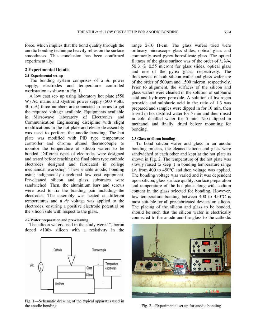
2.1 Experimental set-up
The bonding system comprises of a dc power
supply, electrodes and temperature controlled
workstation as shown in Fig. 1.
A low cost set- up using laboratory hot plate (550
W) AC mains and klystron power supply (500 Volts,
40 mA) three numbers are connected in series to get
the required voltage available. Equipments available
in Microwave laboratory of Electronics and
Communication Engineering discipline with slight
modifications in the hot plate and electrode assembly
was used to perform the anodic bonding. The hot
plate was modified with PID type temperature
controller and chrome alumel thermocouple to
monitor the temperature of silicon wafers to be
bonded. Different types of electrodes were designed
and tested before reaching the final plum type cathode
electrodes designed and fabricated in college
mechanical workshop. These enable anodic bonding
using indigenously developed low cost equipment.
Pre-cleaned silicon and glass substrates were
sandwiched. Then, the aluminium bars and screws
were used to fix the bonding pair including the
electrodes. The assembly was heated at different
temperatures and a dc voltage was applied to the
electrodes, ensuring a positive electrode potential on
the silicon side with respect to the glass.
2.2 Wafer preparation and pre-cleaning
The silicon wafers used in the study were 1”, boron
doped <100> silicon with a resistivity in the
range 2-10 Ω-cm. The glass wafers tried were
ordinary microscope glass slides, optical glass and
commonly used pyrex borosilicate glass. The optical
flatness of the glass surface was of the order of λ, λ/4,
50 λ (λ=0.55 micron) for glass slides, optical glass
and one of the pyrex glass, respectively. The
thicknesses of both silicon wafer and glass wafer are
of the order of 500µm and 1500 micron, respectively.
Prior to alignment, the surfaces of the silicon and
glass wafers were cleaned in the solution of sulphuric
acid and hydrogen peroxide. A solution of hydrogen
peroxide and sulphuric acid in the ratio of 1:3 was
prepared and samples were dipped in for 10 min, then
rinsed in hot distilled water for 5 min and then rinsed
in cold distilled water for 5 min. Next dipped in
methanol and finally, dried before mounting for
bonding. 2.3 Glass to silicon bonding
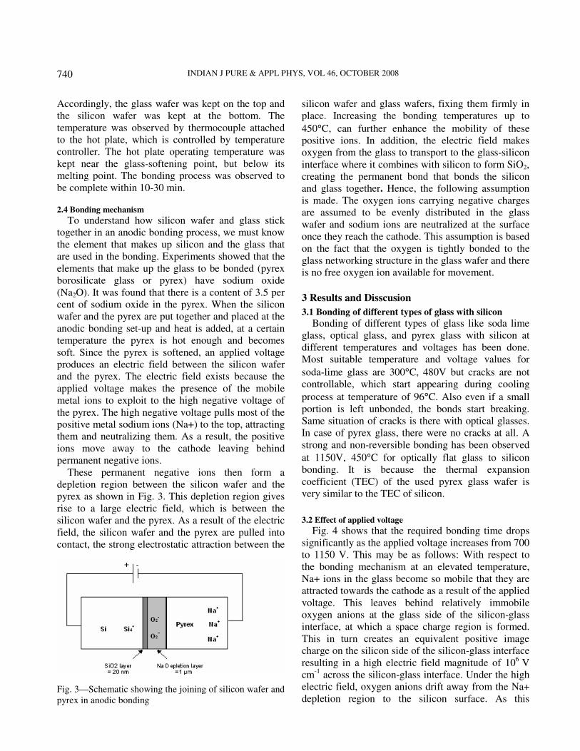
To bond silicon wafer and glass in an anodic
bonding process, the cleaned silicon and glass were
sandwiched to each other and kept at the hot plate as
shown in Fig. 2. The temperature of the hot plate was
slowly raised to keep it in bonding temperature range
i.e. from 400 to 450°C and then voltage was applied.
The bonding voltage was varied and it was dependent
upon silicon, glass surface quality, surface preparation
and temperature of the hot plate along with sodium
content in the glass selected for bonding. However,
low temperature bonding between 400 to 450°C is
most suitable for all pre-fabricated devices on silicon.
The placing of the silicon and glass to be bonded,
should be such that the silicon wafer is electrically
connected to the anode and the glass to the cathode.
Fig. 1—Schematic drawing of the typical apparatus used in
the anodic bonding
Fig. 2—Experimental set up for anodic bonding
INDIAN J PURE & APPL PHYS, VOL 46, OCTOBER 2008
740
Accordingly, the glass wafer was kept on the top and
the silicon wafer was kept at the bottom. The
temperature was observed by thermocouple attached
to the hot plate, which is controlled by temperature
controller. The hot plate operating temperature was
kept near the glass-softening point, but below its
melting point. The bonding process was observed to
be complete within 10-30 min. 2.4 Bonding mechanism
To understand how silicon wafer and glass stick
together in an anodic bonding process, we must know
the element that makes up silicon and the glass that
are used in the bonding. Experiments showed that the
elements that make up the glass to be bonded (pyrex
borosilicate glass or pyrex) have sodium oxide
(Na2O). It was found that there is a content of 3.5 per
cent of sodium oxide in the pyrex. When the silicon
wafer and the pyrex are put together and placed at the
anodic bonding set-up and heat is added, at a certain
temperature the pyrex is hot enough and becomes
soft. Since the pyrex is softened, an applied voltage
produces an electric field between the silicon wafer
and the pyrex. The electric field exists because the
applied voltage makes the presence of the mobile
metal ions to exploit to the high negative voltage of
the pyrex. The high negative voltage pulls most of the
positive metal sodium ions (Na+) to the top, attracting
them and neutralizing them. As a result, the positive
ions move away to the cathode leaving behind
permanent negative ions.
These permanent negative ions then form a
depletion region between the silicon wafer and the
pyrex as shown in Fig. 3. This depletion region gives
rise to a large electric field, which is between the
silicon wafer and the pyrex. As a result of the electric
field, the silicon wafer and the pyrex are pulled into
contact, the strong electrostatic attraction between the
silicon wafer and glass wafers, fixing them firmly in
place. Increasing the bonding temperatures up to
450°C, can further enhance the mobility of these
positive ions. In addition, the electric field makes
oxygen from the glass to transport to the glass-silicon
interface where it combines with silicon to form SiO2,
creating the permanent bond that bonds the silicon
and glass together. Hence, the following assumption
is made. The oxygen ions carrying negative charges
are assumed to be evenly distributed in the glass
wafer and sodium ions are neutralized at the surface
once they reach the cathode. This assumption is based
on the fact that the oxygen is tightly bonded to the
glass networking structure in the glass wafer and there
is no free oxygen ion available for movement.
3 Results and Disscusion
3.1 Bonding of different types of glass with silicon
Bonding of different types of glass like soda lime
glass, optical glass, and pyrex glass with silicon at
different temperatures and voltages has been done.
Most suitable temperature and voltage values for
soda-lime glass are 300°C, 480V but cracks are not
controllable, which start appearing during cooling
process at temperature of 96°C. Also even if a small
portion is left unbonded, the bonds start breaking.
Same situation of cracks is there with optical glasses.
In case of pyrex glass, there were no cracks at all. A
strong and non-reversible bonding has been observed
at 1150V, 450°C for optically flat glass to silicon
bonding. It is because the thermal expansion
coefficient (TEC) of the used pyrex glass wafer is
very similar to the TEC of silicon.
3.2 Effect of applied voltage
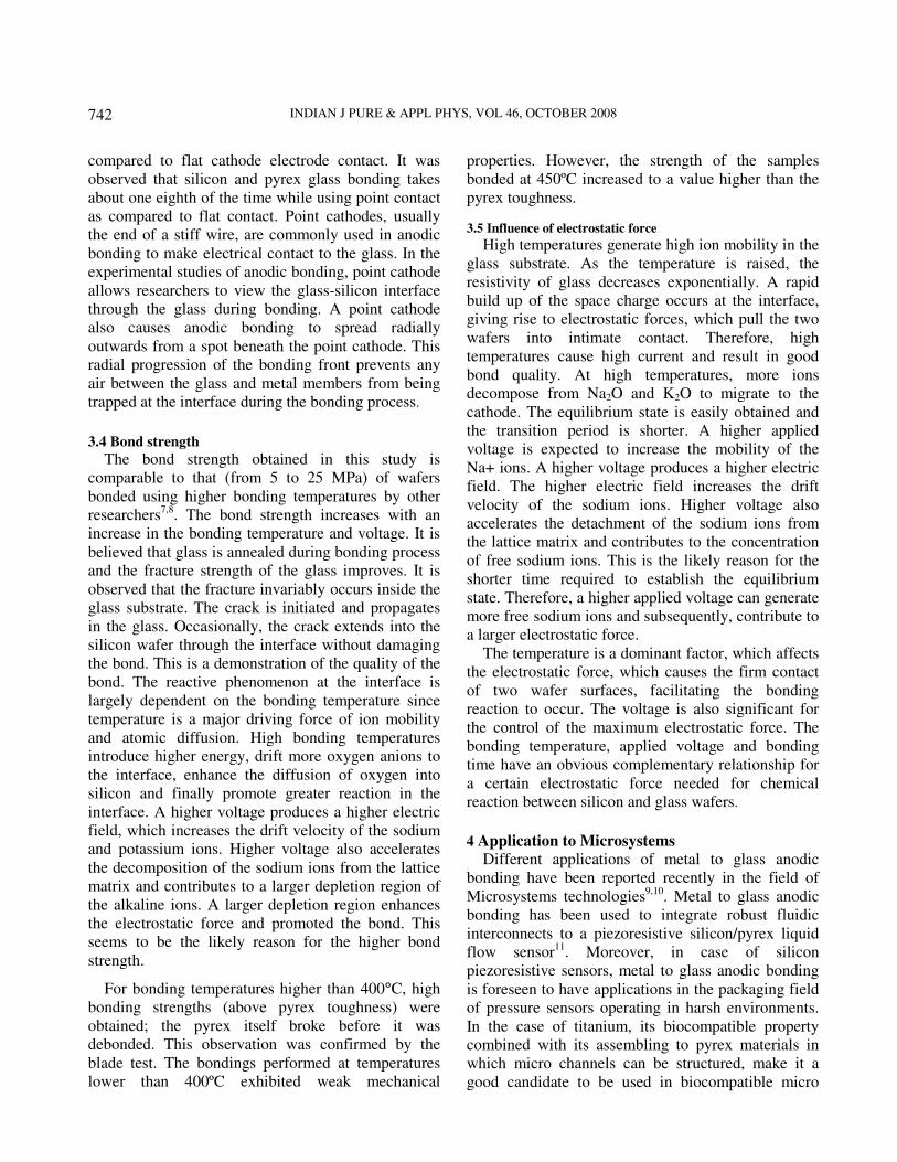
Fig. 4 shows that the required bonding time drops
significantly as the applied voltage increases from 700
to 1150 V. This may be as follows: With respect to
the bonding mechanism at an elevated temperature,
Na+ ions in the glass become so mobile that they are
attracted towards the cathode as a result of the applied
voltage. This leaves behind relatively immobile
oxygen anions at the glass side of the silicon-glass
interface, at which a space charge region is formed.
This in turn creates an equivalent positive image
charge on the silicon side of the silicon-glass interface
resulting in a high electric field magnitude of 106
V
cm-1
across the silicon-glass interface. Under the high
electric field, oxygen anions drift away from the Na+
depletion region to the silicon surface. As this
Fig. 3—Schematic showing the joining of silicon wafer and
pyrex in anodic bonding
TRIPATHI et al.: LOW COST SET UP FOR ANODIC BONDING
741
happens, oxidation of silicon by the oxygen anions is
presumed to occur and a thin oxide layer is formed at
the interface, which contributes to the migration of the
bonding front. However, at a small applied voltage,
i.e. a reduced electric field, the drift velocity and the
kinetic energy possessed by the oxygen anions cannot
sustain a high oxidation rate at the bonding front of
the silicon-glass interface, thus, a longer bonding time
is required. As the electric field becomes negligible,
reaction is extinguished at the interface and no
bonding can be achieved. We have observed that in
the absence of an electric field, there is no indication
of bonding. A large electric field is applied across the
joint, which causes an extremely strong bond to form
between the two materials.Fig. 5 shows a glass plate
bonded over a cavity etched into a silicon wafer using
anisotropic etching and Fig. 4 shows the plot of
bonding time versus applied voltage for p-type silicon
and pyrex glass.
The bonding current as a function of time is shown
in Fig. 6. The results show that the current rises
rapidly at the beginning of the bonding. It indicates
that the surge of Na+ ions drift to the cathode to
generate a current in the circuit. As the migration of
Na+ continues, the accumulation of positive charge
repels the incoming ions and the current density
decreases to an almost steady value. Bonding was
done at 1150V for 10-15 min. If the bonding voltage
is decreased the bonding time increases. It has been
observed that bonding depends not only upon the
voltage, temperature and time but it also depends
upon surface uniformity. Bonding voltage and time
are considerably reduced in case of optically flat surf
3.3 Effect of point cathode contact
The results indicate that point contact electrode
configuration provides excellent bonding uniformity
as compared to flat contact configuration. Table 1
shows the experimental parameters under which
various material combinations were successfully
bonded. It was found that bonding time depends upon
the applied voltage, temperature and cathode
electrode contact configuration (flat/point). Tabulated
values also show that bonding time strongly depends
on the contact configuration. Bonding, using point
cathode electrode contact6, is much faster as
Fig. 4—Plot of bonding time versus applied voltage for
p-type silicon and pyrex glass
Fig. 5—Silicon and glass bonding
Fig. 6—Plot of current as a function of time
Table 1—Bonding voltage and time
Bonding voltage (V) Bonding time (min)
770 40
1000 35
1050 30
1140 20
1150 10
INDIAN J PURE & APPL PHYS, VOL 46, OCTOBER 2008
742
compared to flat cathode electrode contact. It was
observed that silicon and pyrex glass bonding takes
about one eighth of the time while using point contact
as compared to flat contact. Point cathodes, usually
the end of a stiff wire, are commonly used in anodic
bonding to make electrical contact to the glass. In the
experimental studies of anodic bonding, point cathode
allows researchers to view the glass-silicon interface
through the glass during bonding. A point cathode
also causes anodic bonding to spread radially
outwards from a spot beneath the point cathode. This
radial progression of the bonding front prevents any
air between the glass and metal members from being
trapped at the interface during the bonding process.
3.4 Bond strength
The bond strength obtained in this study is
comparable to that (from 5 to 25 MPa) of wafers
bonded using higher bonding temperatures by other
researchers7,8
. The bond strength increases with an
increase in the bonding temperature and voltage. It is
believed that glass is annealed during bonding process
and the fracture strength of the glass improves. It is
observed that the fracture invariably occurs inside the
glass substrate. The crack is initiated and propagates
in the glass. Occasionally, the crack extends into the
silicon wafer through the interface without damaging
the bond. This is a demonstration of the quality of the
bond. The reactive phenomenon at the interface is
largely dependent on the bonding temperature since
temperature is a major driving force of ion mobility
and atomic diffusion. High bonding temperatures
introduce higher energy, drift more oxygen anions to
the interface, enhance the diffusion of oxygen into
silicon and finally promote greater reaction in the
interface. A higher voltage produces a higher electric
field, which increases the drift velocity of the sodium
and potassium ions. Higher voltage also accelerates
the decomposition of the sodium ions from the lattice
matrix and contributes to a larger depletion region of
the alkaline ions. A larger depletion region enhances
the electrostatic force and promoted the bond. This
seems to be the likely reason for the higher bond
strength.
For bonding temperatures higher than 400°C, high
bonding strengths (above pyrex toughness) were
obtained; the pyrex itself broke before it was
debonded. This observation was confirmed by the
blade test. The bondings performed at temperatures
lower than 400ºC exhibited weak mechanical
properties. However, the strength of the samples
bonded at 450ºC increased to a value higher than the
pyrex toughness.
3.5 Influence of electrostatic force
High temperatures generate high ion mobility in the
glass substrate. As the temperature is raised, the
resistivity of glass decreases exponentially. A rapid
build up of the space charge occurs at the interface,
giving rise to electrostatic forces, which pull the two
wafers into intimate contact. Therefore, high
temperatures cause high current and result in good
bond quality. At high temperatures, more ions
decompose from Na2O and K2O to migrate to the
cathode. The equilibrium state is easily obtained and
the transition period is shorter. A higher applied
voltage is expected to increase the mobility of the
Na+ ions. A higher voltage produces a higher electric
field. The higher electric field increases the drift
velocity of the sodium ions. Higher voltage also
accelerates the detachment of the sodium ions from
the lattice matrix and contributes to the concentration
of free sodium ions. This is the likely reason for the
shorter time required to establish the equilibrium
state. Therefore, a higher applied voltage can generate
more free sodium ions and subsequently, contribute to
a larger electrostatic force.
The temperature is a dominant factor, which affects
the electrostatic force, which causes the firm contact
of two wafer surfaces, facilitating the bonding
reaction to occur. The voltage is also significant for
the control of the maximum electrostatic force. The
bonding temperature, applied voltage and bonding
time have an obvious complementary relationship for
a certain electrostatic force needed for chemical
reaction between silicon and glass wafers.
4 Application to Microsystems
Different applications of metal to glass anodic
bonding have been reported recently in the field of
Microsystems technologies9,10
. Metal to glass anodic
bonding has been used to integrate robust fluidic
interconnects to a piezoresistive silicon/pyrex liquid
flow sensor11
. Moreover, in case of silicon
piezoresistive sensors, metal to glass anodic bonding
is foreseen to have applications in the packaging field
of pressure sensors operating in harsh environments.
In the case of titanium, its biocompatible property
combined with its assembling to pyrex materials in
which micro channels can be structured, make it a
good candidate to be used in biocompatible micro
TRIPATHI et al.: LOW COST SET UP FOR ANODIC BONDING
743
fluidic systems. Anodic bonding of pyrex can also be
successfully performed on thin metallic films. An
application of this technology is the encapsulation
under vacuum of quartz resonators. Pyrex caps are
bonded on thin metallic films forming the electrodes
of the resonators. Anodic bonding is gaining
significance in Micro-Total-Analysis Systems (µTAS)
and in miniaturized biological reactors because of its
promising use in sealing silicon and glass based micro
fluidic devices. The bonding technique can be broadly
applied in the fabrication of sensors, actuators,
microstructures, 3D integrated circuits and opto-
electronics devices. The recent developments in the
bonding technique have made the micro mechanical
design more flexible.
5 Conclusion We have successfully bonded silicon with glass at
1150V, 450°C in 10-15 min. It was found that
bonding time depends upon the applied voltage,
temperature and design of the cathode electrode and
the flatness of the surfaces to be bonded. Temperature
plays the major role as the mobility of the ions
increases and bonding takes less time.
Acknowledgement The authors would like to thank Director, Dr. Anil
Joshi, ACE & AR, Devasthali, for his constant
encouragement during the course of this work. The
authors also wish to acknowledge and extend thanks
to Sh Nalini Kant mentor of the college without
whose support and encouragement the work would
not have been possible. We also extend our sincere
thanks to our worthy Chairman, Dr Jaidev for his kind
support and motivation. The authors are also thankful
to Director, CEERI, Pilani, for providing pyrex
wafers used in the experiment.
References 1 Schmidt M A, Proceedings of the IEEE, 86 (1998)1575.
2 Chen M, Yuan L & Liu S, Sensors and Actuators, (2006).
3 Rogers T & Kowal J, Sensors and Actuators A, 46-47 (1995)
113-120.
4 Cheng Y T, Lin L & Najafi K, J Micro- electro Mechanical
Systems, 10 (2001) 392.
5 Madou M J, Fundamentals of Micro fabrication, the science
of Miniaturization, second edition, (CRC Press, New York),
2002.
6 Waris M & Ahmed M, Appl Surface Sci, 252 (2006) 7327.
7 Cozma A & Puers B, J Micromech Microeng, 5 (1995) 98.
8 Lee T M H, Hsing I M & Liaw C Y N, J Micro Electro Mech
System , 9 (2000) 469.
9 Blom M T, Chmela E, Gardeniers J G E, Berenschot J W,
Elwenspoek M, Tijssen R & Van den Berg A, J Micromech
Microeng, 11 (2001) 382.
10 Sim D Y, Kurabayashi T & Esashi M, J Micromech
Microeng, 6 (1996) 266.
11 Weber P, Briand D & De Rooij N F, Proceedings of Euro
sensors XVI, Prague, The Czech Republic, 15-18 (2002) 282.