Design & Simulation of Combinational Circuits by Cyclic Combinational Method
11
Page | 1 Design & Simulation of Combinational Circuits by Cyclic Combinational Method Abstract Digital circuits are called combinational if they are without memory: i.e. they have outputs that depend only on the present values of the inputs. Combinational circuits are generally consideration of as acyclic (i.e., feed- forward) structures. However, cyclic circuits can be combinational [1]. Conventional recognized techniques in logic analysis and timing analysis of combinational circuits have limited themselves to acyclic combinational circuits since cyclic circuits cannot be analyzed in conventional method. The temporal behavior of a circuit depends on the delay values of the circuit elements, but its functional or logical behavior should not be dependent on the delay values. Cyclic combinational circuits have structural feedback; however there is no logical feedback. In cyclic combinational circuit the primary outputs is combinational even when some intermediate signals in the circuit are sequential [2]. A general attitude for the synthesis of multilevel combinational circuits with cyclic topologies gives major improvements in area and delay with respect to the conventional acyclic combinational circuit. The analysis strategy for specific Boolean input values might be termed simulation. That is applying inputs and follows the evolution of the circuit. The goal of functional analysis is to determine what values appear; the goal of timing analysis is to determine when these values appear and the area, as a measure of the number of transistors in the final silicon implementation [3]. The objective of the study is to design & simulation of different combinational circuits in cyclic combinational method and analyzes the designs optimizing area, power and delay. To design, simulate and analyze different combinational circuit in cyclic combinational method the following activities are to be carried out: Detailed study of circuit model, its functional and temporal behavior, Synthesis of circuit using cyclic combinational method, Simulation of circuit using standard simulator , Analysis framework including area, power, timing consideration. 1.Introduction 1.1 History Switching relay circuit, introduced in the subject of seminal papers by Claude Shannon in 1938 [4]. This was the introduction of logic circuit. Then different algorithms are taken to synthesis the logic circuits. Within that one is BDD. Binary decision diagrams have come to the front as possibly the most successful data formation for representing Boolean functions [5]. In 1963, McCaw gave a new idea in his degree engineering thesis “Loops in Directed Combinational Switching Networks" [6]. He began with an example, the cyclic circuit shown in Figure 1. Figure 1: An example of cyclic combinational circuit presented by McCaw.
-
Upload
independent -
Category
Documents
-
view
0 -
download
0
Transcript of Design & Simulation of Combinational Circuits by Cyclic Combinational Method

Page | 1
Design & Simulation of Combinational Circuits by Cyclic Combinational Method
Abstract
Digital circuits are called combinational if they are without memory: i.e. they have outputs that depend only on the present values of the inputs. Combinational circuits are generally consideration of as acyclic (i.e., feed-forward) structures. However, cyclic circuits can be combinational [1]. Conventional recognized techniques in logic analysis and timing analysis of combinational circuits have limited themselves to acyclic combinational circuits since cyclic circuits cannot be analyzed in conventional method. The temporal behavior of a circuit depends on the delay values of the circuit elements, but its functional or logical behavior should not be dependent on the delay values. Cyclic combinational circuits have structural feedback; however there is no logical feedback. In cyclic combinational circuit the primary outputs is combinational even when some intermediate signals in the circuit are sequential [2]. A general attitude for the synthesis of multilevel combinational circuits with cyclic topologies gives major improvements in area and delay with respect to the conventional acyclic combinational circuit. The analysis strategy for specific Boolean input values might be termed simulation. That is applying inputs and follows the evolution of the circuit. The goal of functional analysis is to determine what values appear; the goal of timing analysis is to determine when these values appear and the area, as a measure of the number of transistors in the final silicon implementation [3]. The objective of the study is to design & simulation of different combinational circuits in cyclic combinational method and analyzes the designs optimizing area, power and delay. To design, simulate and analyze different combinational circuit in cyclic combinational method the following activities are to be carried out: Detailed study of circuit model, its functional and temporal behavior, Synthesis of circuit using cyclic combinational method, Simulation of circuit using standard simulator , Analysis framework including area, power, timing consideration. 1.Introduction 1.1 History Switching relay circuit, introduced in the subject of seminal papers by Claude Shannon in 1938 [4]. This was the introduction of logic circuit. Then different algorithms are taken to synthesis the logic circuits. Within that one is BDD. Binary decision diagrams have come to the front as possibly the most successful data formation for representing Boolean functions [5]. In 1963, McCaw gave a new idea in his degree engineering thesis “Loops in Directed Combinational Switching Networks" [6]. He began with an example, the cyclic circuit shown in Figure 1.
Figure 1: An example of cyclic combinational circuit presented by
McCaw.
Page | 2
In1995, Anand Raghunathan. Pranav Ashar, and Sharad Malik introduces test generation for cyclic combinational circuit. In practice, test generation for these circuits is handled in an awkward manner, typically with poor fault coverage [7]. In 2004 Marc D. Riedel re-writes the definition: combinational might well mean cyclic in his PhD thesis. 1.2 Overview Digital circuits can be classified into two types: A combinational circuit, which has output values dependant only on the present values of inputs applied to it. A sequential circuit, which has output values dependant on present as well as past values of inputs applied to it. Thus, a sequential circuit has memory, whereas a combinational circuit cannot store any information. From these behavioral definitions, popular textbooks explain a structural insight of these types: A combinational circuit consists of an acyclic structure, i.e., it contains only feed-forward paths. A sequential circuit consists of a cyclic structure, i.e., it contains loops or feedback paths. Now consider the circuit in Figure 2 is combinational since z is equal to the present value of x and does not depend on the past account of inputs. This can be easily verified by checking the circuit output for both x = 0 and x = 1.
Figure 2: A simple example of cyclic combinational circuit.
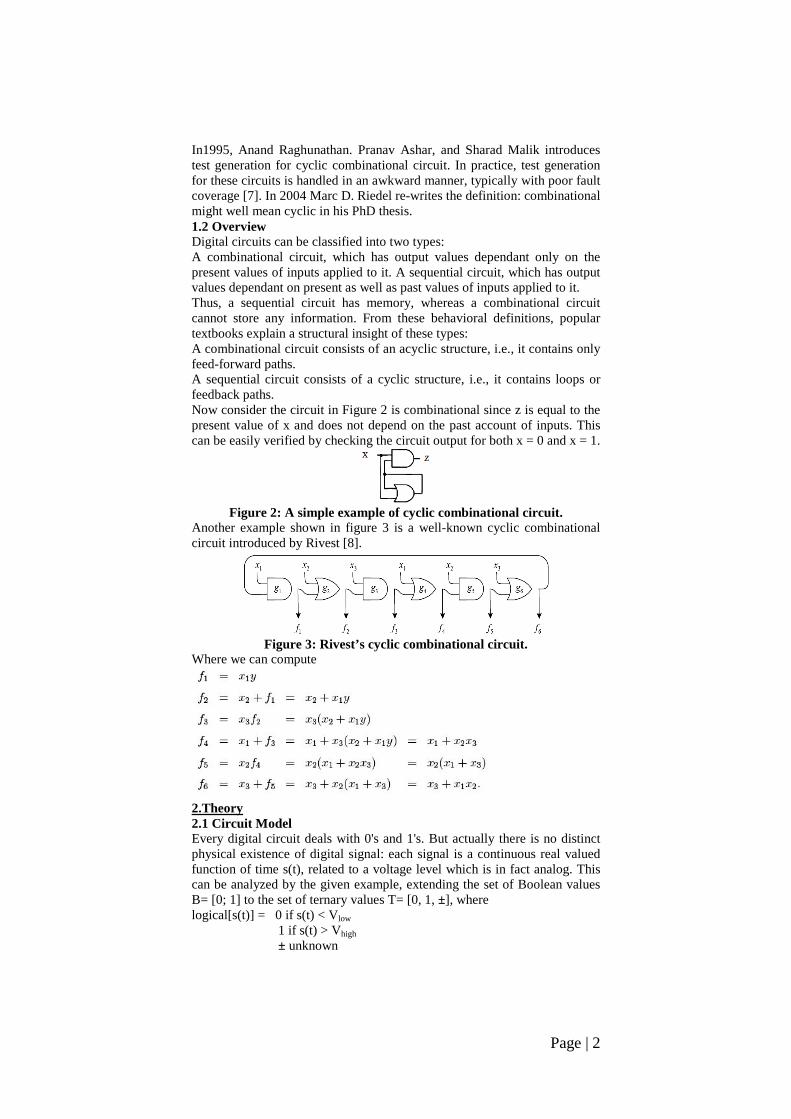
Another example shown in figure 3 is a well-known cyclic combinational circuit introduced by Rivest [8].
Figure 3: Rivest’s cyclic combinational circuit.
Where we can compute
2.Theory 2.1 Circuit Model Every digital circuit deals with 0's and 1's. But actually there is no distinct physical existence of digital signal: each signal is a continuous real valued function of time s(t), related to a voltage level which is in fact analog. This can be analyzed by the given example, extending the set of Boolean values B= [0; 1] to the set of ternary values T= [0, 1, ±], where logical[s(t)] = 0 if s(t) < Vlow 1 if s(t) > Vhigh
± unknown

Page | 3
The third value ‘±’ indicates that the signal is uncertain. It denotes a signal value that is unknown. 2.2 Analysis framework We can easily determine the value of circuit output when the input values are either ‘0’ or ‘1’ for any combinational circuit but cannot determine the output when value of the one of the inputs is ‘±’. The truth-tables for the common logic gates (AND, OR, NOT and XOR gates) including the ‘±’ values are shown in Figure 4.
Table 1: Truth table representation for common gates For representation of any combinational circuit in cyclic combinational method we have to analyze the circuit. Cyclic combinational circuits have structural feedback. So design should be such that the primary outputs should be able to give the output as ‘0’ or ‘1’ not ‘±’. So there is no logical feedback that is transmitted to produce the primary outputs. Let us take an example shown bellow in figure 5:
Figure 4: cyclic circuit with structural feedback
The output Y in the above figure is always equal to the input value X. Though there is structural feedback but the feedback path doesn’t have any significance in producing the logical output. For detailed analysis we can use two types of analysis any circuit model – (A) The functional analysis and (B) the timing analysis. The goal of functional analysis is to determine what values appear; the goal of timing analysis is to determine when these values appear. The case for the optimality of the cyclic circuit rests on two properties: Property 1: Each of the output functions depends on all its variables. Property 2: The output functions are distinct. 2.3 Comparative study with Examples 2.3.1 General Cyclic representation For representing the combinational functions in cyclic method Karnaugh map methodology is taken. Karnaugh map is a popular graphical technique which provides a simple method for simplifying Boolean expression. In this methodology first the truth table is drawn. Conventionally the input combinations are drawn in the left side of the truth table and output in the right side. For generation of cyclic expression secondly the dependency graph is drawn. Then from dependency graph the individual dependent output truth tables are redrawn using that current controlling output in the
X Y AND (X,Y)
OR (X,Y)
XOR (X,Y)
0 0 0 1 0 ± 1 0 1 1 1 ± ± 0 ± 1 ± ±
0 0 0 0 1 ± 0 ± ±
0 1 ± 1 1 1 ± 1 ±
0 1 ± 1 0 ± ± ± ±
X NOT(X)
0 1 ±
1 0 ±

Page | 4
left hand side of the truth table. After finding out the dependent truth table the minimized Boolean expressions are obtained from karnaugh map. The above procedure is repeated for each and every dependent output. After getting the required cyclic expressions for the combinational functions the functional and timing analysis is done using standard simulator. For comparative study between cyclic circuit and conventional acyclic combinational circuit let us take some examples. Example 1: suppose there are three Boolean functions;
The circuit can be implemented by basic logic gates as follows in figure 5
Figure 5: basic gate implementation of three functions f1, f2 & f3
The truth table of the above functions is shown below: inputs outputs
x1 x2 x3 f1 f2 f3
0 0 0 0 0 1 0 1 0 0 1 1 1 0 0 1 0 1 1 1 0 1 1 1
0 1 1 1 0 1 1 0 1 0 0 0 1 0 1 1 1 0 0 1 0 0 1 0
Table 2: truth table of function f1, f2 & f3 The dependency graph can be drawn as:
f2
f1 f3
Figure 6: dependency graph
So function f1 will be dependent on f2, function f2 will be dependent on f3 & function f3 will be dependent on f1 to produce a complete cycle. Now truth tables can be redrawn as follows:
Basic inputs controlling value output
x1 x2 x3 f2 f1
0 0 0 1 0 0 1 0 0 1 0 0 0 1 1 0 1 0 0 0 1 0 1 1 1 1 0 1 1 1 1 1
0 1 1 0 1 1 0 0

Page | 5
Basic inputs controlling value output
x1 x2 x3 f3 f2
0 0 0 1 0 0 1 1 0 1 0 1 0 1 1 0 1 0 0 1 1 0 1 0 1 1 0 0 1 1 1 0
1 0 0 0 0 1 1 1
Basic inputs controlling value output
x1 x2 x3 f1 f3
0 0 0 0 0 0 1 1 0 1 0 1 0 1 1 0 1 0 0 1 1 0 1 1 1 1 0 0 1 1 1 0
1 1 1 0 1 0 0 0
Table 3: Truth table for dependant f1, f2 & f3 Now k-map representation of cyclic function f1, f2 & f3 are shown below
k-map for f1 k-map for f2
k-map for f3
Figure 6: k-map representation for f1, f2 & f3
So the cyclic solution for the functions f1, f2 & f3 are :
x 1 0 x
x 0 x 0
1 x x 1
x 0 x 1
x 0 x 1
1 x x 0
x 0 0 x
1 x 1 x
1 x 1 x
x 1 x 0
0 x x 0
x 1 0 x
x1 x2 00
x3 f2
11
10
01
00 01 11 10
x1 x2 00
11
10
01
00 01 11 10 x3 f3
x3 f1
x1 x2 00
11
10
01
00 01 11 10

Page | 6
Figure 7: cyclic solution of functions f1, f2 & f3
Example 2: A seven segment display, as its name indicates, is composed of seven elements. Individually on or off, they can be combined to produce simplified representations of the integer. The segments of a 7-segment display are referred to by the letters a to g, as shown below;
Figure 8: seven segment display
A BCD to seven segment decoder has four inputs x0, x1, x2, x3 and seven outputs a to g. The four inputs bits, x0, x1, x2, x3 specifying a number from 0 to 9. The outputs are 7 bits, a, b, c, d, e, f, g, specifying which segments to light up in a display. The truth table for seven segment display decoder can be represented as follows;
Table 4: Truth table for 7 segment decoder
Accordingly the expression for the outputs can be represented by;
Page | 7
By branch and bound algorithm [3] and Karnaugh map technique the above expressions can be reduced to the cyclic expressions as follows:
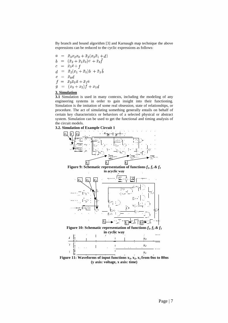
3. Simulation 3.1 Simulation is used in many contexts, including the modeling of any engineering systems in order to gain insight into their functioning. Simulation is the imitation of some real obsession, state of relationships, or procedure. The act of simulating something generally entails on behalf of certain key characteristics or behaviors of a selected physical or abstract system. Simulation can be used to get the functional and timing analysis of the circuit models. 3.2. Simulation of Example Circuit 1
Figure 9: Schematic representation of functions f1, f2 & f3 in acyclic way
Figure 10: Schematic representation of functions f1, f2 & f3
in cyclic way
Figure 11: Waveforms of input functions x3, x2, x1 from 0ns to 80ns
(y axis: voltage, x axis: time)
x1 x
x3
f1 f2 f3
x1 x2 x3
f1 f2 f3
x1
x2
x3

Page | 8
Figure 12: Waveforms of output functions f1, f2 & f3from 0ns to 80ns in
acyclic circuit shown in fig 9 (y axis: voltage, x axis: time)
Figure 13: Waveforms of output functions f1, f2 & f3from 0ns to 80ns in
cyclic circuit shown in fig10(y axis: voltage, x axis: time) 3.3. Simulation of Example2 seven segment display decoder
Figure 14: Schematic representation of seven segment display decoder
in acyclic way
Figure 15: Schematic representation of seven segment display decoder
in cyclic way
A
x0
x1
x3
x2
B
C
D
E
F
G
f3
f2
f1
f3
f2
f1
x3
x2
x0
x1
F
E
A
G
D
B
C

Page | 9
Figure 16: Waveforms of BCD input functions x3, x2, x1, x0 of seven
segment decoder from 0ns to 100ns(y axis: voltage, x axis: time)
Figure 17: Waveforms of output functions A to G of 7 segment decoder
from 0ns to 100ns in acyclic circuit shown in fig14(y axis: voltage, x axis: time)
Figure 18: Waveforms of output functions A to G of a seven segment
decoder from 0ns to 100ns in cyclic circuit shown in fig15(y axis: voltage, x axis: time)
4. Results Example 1
Acyclic circuit Cyclic circuit Area Power Delay Area Power Delay
MOSFETs - 186 MOSFET geometries - 20 * BJTs - 0 JFETs - 0 * MESFETs - 0
Average power consumed -> 1.354564e-003 watts Max power 9.266683e-002
PAD_R2_F1=1.0634e-008
MOSFETs - 164 MOSFET geometries - 20 * BJTs - 0 JFETs - 0 * MESFETs - 0
Average power consumed -> 1.824212e-003 watts Max power 8.003270e-002 at time 1e-009
PAD_R2_F1=1.0170e-008
PAD_R3_F2=2.7763e-008
PAD_R3_F2=3.0000e-008
PAD_R4_F3=4.0558e-008
PAD_R4_F3=5.7384e-008
x3
x2
x1
x0
A
B
C
D
E
F
G
A
B
C
D
E
F
G

Page | 10
Diodes - 0 * Capacitors - 8 Resistors - 6
at time 1e-009 Min power 9.366837e-005 at time 1e-008
Diodes - 0 * Capacitors - 8 Resistors - 6
Min power 8.728649e-006 at time 1e-008
Table 5: Comparative results between acyclic & cyclic circuit of example 1 Example 2(seven segment decoder)
Table 6: Comparative results between acyclic & cyclic circuit of example 2(seven segment decoder)
(a) (b)
Figure 19: (a) cyclic layout, (b) acyclic layout of example 1
Acyclic circuit Cyclic circuit Area Power Delay Area Power Delay
MOSFETs - 498 MOSFET geometries - 20 * BJTs - 0 JFETs - 0 * MESFETs - 0 Diodes - 0 * Capacitors - 13 Resistors - 11
Average power consumed -> 3.230626e-002 watts Max power 1.983398e-001 at time 1.58367e-009 Min power 2.123796e-002 at time 3.63475e-009
PAD_R2_A= 1.0756e-008
MOSFETs - 354 MOSFET geometries - 20 * BJTs - 0 JFETs - 0 * MESFETs - 0 Diodes - 0 * Capacitors - 13 Resistors - 11
Average power consumed -> 3.565808e-002 watts Max power 3.642983e-001 at time 1e-009 Min power 2.123948e-002 at time 2.67226e-009
PAD_R4_A=1.0091e-008
PAD_R3_B= 2.0211e-008
PAD_R7_B=1.0365e-008
PAD_R4_C= 2.0005e-008
PAD_R8_C=1.0875e-008
PAD_R5_D= 1.0662e-008
PAD_R6_D=1.0414e-008
PAD_R6_E= 1.0402e-008
PAD_R3_E=1.0409e-008
PAD_R7_F= 1.0928e-008
PAD_R2_F=1.0409e-008
PAD_R8_G= 4.0221e-008
PAD_R5_G=1.1113e-008

Page | 11
Figure 19: (a) cyclic layout, (b) acyclic layout of example 2
Discussion From the above results it can be concluded that cyclic circuits can produce same result as acyclic combinational circuits with lesser no. of gates. That means cyclic circuits are better in area, power consumption and delay consideration. A practical implementation with small runtimes for different practical circuits demonstrates the efficacy of this algorithm. This is a proposal for general methodology for the synthesis of multilevel combinational circuits with cyclic topologies. References [1] Marc D. Riedel & Jehoshua Bruck , “The Synthesis of Cyclic Combinational Circuits” Supported in part by the “Alpha Project” at the Center for Genomic Experimentation and Computation, a National Institutes of Health Center of excellence in Genomic Sciences, DAC 2003, June 2–6, 2003, Anaheim, California, USA. Page 163 [2] Sharad Malik (Dept. of Electrical Eng., Princeton Univ.), “Analysis of Cyclic Combinational Circuits”, page: 619 ,IEEE transaction on computer, 1063-6757/93,1993 [3] Marc D. Riedel, “Cyclic Combinational Circuits”, PhD. Thesis California Institute of Technology, Pasadena, California, 2004, page -75-81 [4] C. E. Shannon, “A Symbolic Analysis of Relay and Switching Circuits," Trans. AIEE, Vol. 57 , pp. 713-723, 1938. [5] R. E. Bryant, “Graph-Based Algorithms for Boolean Function Manipulation", IEEE Trans. Computers, Vol. C-35, No. 6, pp. 677-691, 1986. [6] C. R. McCaw, “Loops in Directed Combinational Switching Networks", Engineer's Thesis, Stanford University, 1963. [7] Anand Raghunathan, Pranav Ashar, Sharad Malik, “Test Generation for Cyclic Combinational Circuits”, 8th Intemational Conjerence on VLSI Design, pp. 104- January 1995 [8] R. L. Rivest, “The Necessity of Feedback in Minimal Monotone Combinational Circuits", IEEE Trans. Computers, Vol. C-26, No. 6, pp. 606-607, 1977.