Lecture 6 - Combinational Logic - Systems I: Computer ...
42
Systems I: Computer Organization and Architecture Lecture 6 - Combinational Logic Introduction • A combinational circuit consists of input variables, logic gates, and output variables. – The logic gates accept n input signals and generate the m signals that become output. • For n input variables, there are 2 n possible combinations of binary input values. – For each input combination, there will be one and only possible output combination. • Each input will have one or two wires. – If there is one wire, it will be either in the normal (unprimed) form or the complemented (primed) form. – If there are two wires, it will supply both forms.
-
Upload
khangminh22 -
Category
Documents
-
view
0 -
download
0
Transcript of Lecture 6 - Combinational Logic - Systems I: Computer ...

Systems I: Computer Organization and Architecture
Lecture 6 - Combinational Logic
Introduction
• A combinational circuit consists of input variables, logic gates, and output variables.– The logic gates accept n input signals and generate the
m signals that become output.• For n input variables, there are 2n possible
combinations of binary input values.– For each input combination, there will be one and only
possible output combination.• Each input will have one or two wires.
– If there is one wire, it will be either in the normal (unprimed) form or the complemented (primed) form.
– If there are two wires, it will supply both forms.

Block Diagram for a Combinational Circuit
CombinationalLogic Circuitn input
variablesm outputvariables
Combinational Circuit Analysis
• Analysis of a combinational circuit requires that we find the function(s) that the circuit implements.
• First we must ensure that the circuit is combinational and not sequential. (The lack of feedback paths or memory elements ensures that).
• After this, we try to find the logic function or truth table.

Analysis Procedure
1. Label all gate outputs that are a function of input variables with arbitrary symbols. Determine the Boolean functions for each gate output.
2. Label the gates that are a function of input variables and previously labeled gates with other arbitrary symbols. Find the Boolean functions for these gates.
3. Repeat the process outlined in step 2 until the outputs of the circuits are obtained.
4. By repeated substitution of previously defined functions, obtain the output Boolean functions in terms of input variables.
Analysis Example
B
A
C
F1
F2
F’2
T2
T1
T3

Analysis Example – The Outputs
• We initially get:F2 = AB + AC + BCT1 = A + B + CT2 = ABC
• Next, we consider the outputs of gates that are a function of symbol that are already defined:T3 = F’2T1
F1 = T3 + T2
Analysis Example – Solving For F1
F1 = T3 + T2 = F’2T1 + ABC= (AB + AC + BC)’(A + B + C) + ABC= (A’+B’)(A’+C’)(B’+C’)(A + B + C) + ABC= (A’ + B’C’)(AB’+AC’+ BC’+ B’C) + ABC= A’BC’ + A’B’C + AB’C’ + ABC

The Truth Table for F1
101101111000101011000101101
110110001000101110110110010
110110100000010000
F1T3T2T1F’2F2CBA
Design Procedure
• The design procedure starts with the verbal outline of the problem and ends with a logic circuit diagram or a set of Boolean functions from which the circuit diagram can be created.

The Steps in the Design Procedure
The procedure involves these steps:1. The problem is stated.2. The number of available input variables and
required output variables is determined.3. The input and output variables are assigned letter
symbols.4. The truth tables that defines the required
relationships between inputs and outputs are derived.
5. The simplified Boolean function for each output is obtained.
6. The logic diagram is drawn.
The Truth Table
• The truth table consists of input and output columns.
• The 1s and 0s for the input are obtained from the 2n combinations of n input variables.
• An output could be either 1 or 0 for every valid input combination.
• Some input combinations will not occur; these become don’t-care conditions.

Simplifying the Boolean Functions• The output functions are simplified by Boolean
algebra, Karnaugh maps or tabulation.• There will usually more than one simplified
expression to choose from.• Which expression we choose may depend on
circuit design constraints such as :– Minimum number of gates– Number of input to a gate– Minimum propagation time of the signal through the
circuit.– Minimum number of interconnections– Limitation of the driving capabilities of each gates.
Code Conversion From BCD to Excess-3
• BCD (Binary-Coded Decimal) and Excess-3 provide two different ways of representing a decimal value in a binary format.
• There will be a one-to-one correspondence between BCD inputs and the corresponding Excess-3 values.
• Not all the BCD minterms are valid values. These will lead to don’t-care conditions.

Truth Table for BCD to Excess-3
00111001
11010001
01011110
10010110
00011010
11100010
01101100
10100100
00101000
11000000
zyxwDCBA
BCD Inputs Excess-3 Outputs
Karnaugh Map for w
CDAB00 01 11 10
00
01
11
10
1 1 1
11
XX X X
X X
C
A
D
B
w = A + BC + BD

Karnaugh Map for x
CDAB00 01 11 10
00
01
11
10
1 1 1
1
1
XX X X
X X
C
A
D
B
x = B’C + B’D + BC’D’
Karnaugh Map for y
CDAB00 01 11 10
00
01
11
10
1 1
1
1
XX X X
X X
C
A
D
B
y = CD + C’D’
1
Karnaugh Map for z
CDAB00 01 11 10
00
01
11
10
1 1
1
1
XX X X
X X
C
A
D
B
z = D’
1
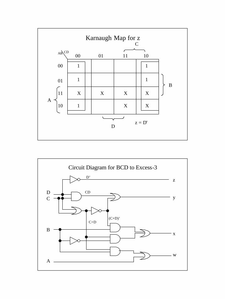
Circuit Diagram for BCD to Excess-3
y
z
DC
Bx
w
D’
CD
C+D(C+D)’
A

Half Adder
• The most basic arithmetic operation is the addition of two binary digits.
• We know that:– 0 + 0 = 0– 0 + 1 = 1 + 0 = 1– 1 + 1 = 10
• If both addends are 1, we need a carry bit which will be added to the addend in the next more significant bit.
Half Adder (continued)
• We can summarize this in the form of a truth table:
x y C S0 0 0 00 1 0 11 0 0 11 1 1 0
• From this we learn that:S = x’y + xy’ = x ⊕ yC = xy

Implementation of Half Adder
C
S
x
y
S = x’y + xy’C = xy
Implementing a Half Adder Using XOR
C
S
x
y
S = x ⊕ yC = xy

Implementing a Half Adder As a Product of Sums
C
S
x
y
S = (x+y)(x’+y’)C = xy
Implementing a Half Adder As a Product of Sums
C
S
x
y
S = (x+y)(x’+y’)C = (x’+y’)

Implementing a Half Adder
C
S
x
y
C = xyS = (C + x’y’)’
The Full Adder
• A full adder is a combinational circuit that forms the arithmetic sum of three inputs.– It consists of 3 inputs and two outputs.– Two of the inputs (x and y) are the same as in
the half adder.– The third input (z) is the carry from the addition
of the previous (lesser significance) bits.

Truth table for a full adder
1111101011011011000101110100101010000000SCzyx
Karnaugh Maps for Full Adder
yz
x0100 11 10
0
1
yz
x0100 11 10
0
1
1
1
1
1
S = x’y’z + x’ y z’ + x y’z’ + xyz
C = xy + xz + yz
1 1 1
1

Full Adder Circuit Diagram For the Sum
S
x
y
z
Full Adder Circuit Diagram For the Carry
C
x
y
z

Full Adder Circuit Diagram Using Half Adders
C
xy
z
S
S = z ⊕ ( x ⊕ y)
C = z •( x ⊕ y) + x•y
Block Diagram For Adders
HAA
B
C
S
FAAi
Bi
Ci+1
S
Ci
Full Adder
Half Adder

Binary Adder
• A binary adder is a digital circuit that produces the arithmetic sum of two binary numbers.
• It can be constructed by connecting a series of full adders in cascade.
4 –Bit Adder
FA
S3
B3 A3
FA
S2
B2 A2
FA
S1
B1 A1
FA
S0
B0 A0
C0
C1C2C3
C4

4-Bit Adder – An Example
Subscript i 3 2 1 0 Ci
Input Carry 0 1 1 0 Ai
Augend 1 0 1 1 Bi
Augend 0 0 1 1 Ci
Sum 1 1 1 0 Si
Output Carry 0 0 1 1 Ci+1
Carry Propagation
• Adding two binary numbers in parallel implies that we have all the bits that we need available at the same time. The cascading of carries seems to belie this assumption.
• If we can generate the necessary bits to determine carries in parallel, then we can actually do the summation without waiting for a carry to cascade through.

Carry Propagation
• We can add two additional terms:Gi – Carry GeneratePi Carry Propagate
• We can define them as:Pi = Ai ⊕Bi
Gi = Ai Bi
• The output sum and carry are now:Si = Pi ⊕ Gi
Ci+1 = Gi + Pi Ci
Carries in a Carry Lookahead Generator
C0 = input carryC1 = G0 + P0C0
C2 = G1 + P1C1 = G1 + P1(G0 + P0C0)= G1 + P1G0 + P1P0C0
C3 = G2 + P2C2
= G2 + P2G1 + P2P1G0 + P2P1P0C0

Carry Lookahead Generator
C3
C3
C3
C0
G0
P0
G1
P1
G2
P2
3-Bit Adder with Carry Generator
S2
S1
S0
C3
Carry
Lookahead
Generator
C3
C2
C1
C0
P2
P1
P0
P2
G2
B2
A2
B2
A2
B0
A0
P1
P0
G1
G0

Half Subtractor
• A half subtractor subtracts two bits and produces their difference and whether a 1 was borrowed.
• We must remember that:0 – 0 = 0; 1 – 0 = 1; and 1 – 1 = 0If we have 0 – 1, we must borrow from the next
place, so our difference is 1 with a borrow of 1.
Truth Table for the Half Subtractor
0011
1001
1110
0000
DByx
D = x’y + xy’ = x ⊕ yB = x’y

Full Subtractor
• A full subtractor performs subtraction between two bits takinginto account the potential borrow from a lower significance bit.
• A full subtractor’s inputs are– x, the minuend– y, the subtrahend– z, the borrow
Truth Table for the Half Subtractor
1111100011001011000101110110101110000000DBzyx

Karnaugh Maps for Full Subtractor
yz
x0100 11 10
0
1
yz
x0100 11 10
0
1
1
1
1
1
D = x’y’z + x’ y z’ + x y’z’ + xyz
B = x’y + x’z + yz
1
1
11
Adder-Subtracter
• Subtracting A – B is most easily done by adding B’ to A and then adding 1.
• This makes it convenient to combine both addition and subtraction into one circuit, called an adder-subtracter.
• M is the mode indicator– M = 0 indicates addition (B is left alone and C0 is 0)– M = 1 indicates subtraction (B is complement and C0 is
1).

4-Bit Adder-Subtractor
FA FA FA FA C0
C1C2C3
C4
S0S1S2S3
B0 A0B1 A1B2 A2B3 A3
M
Overflow
• If addition of 2 n-bit augends produces an n+1-bit sum, we say that overflow occurs.
• Overflow is a problem for computers if undetected because the answer that is produced is erroneous.

Examples Of No Overflow
Carries: 0 0 0 0+70 0 1000110 +70 0 1000110-80 1 0110000 +20 0 0010100-10 1 1110110 +90 0 1011010If there is no overflow, the carry into the sign bit matches the
carry out of the sign bit.
Carry out of sign bit Carry into sign bit
Examples Of Overflow
Carries: 0 1 1 0+70 0 1000110 -70 1 0111010+80 0 1010000 -80 1 0110000
+150 1 0010110 -150 0 1101010If there is overflow, the carry into the sign bit does not match
the carry out of the sign bit.
Carry out of sign bit Carry into sign bit

4-Bit Adder-Subtractor With Overflow Output
FA FA FA FA C0
C1C2C3
C4S0S1S2S3
B0 A0B1 A1B2 A2B3 A3
M
V
If V = 1, there is overflowIf V = 0, there is no overflow
Decimal Adder
• Some systems perform arithmetic on decimal values, which are stored in BCD form.
• A decimal adder requires 9 inputs: 4 bits for each decimal digit of the augend and a carry bit.
• The easiest way to construct a decimal adder is by using a binary adder and then convert the sum to decimal form.
• The five inputs are K (the binary carry), Z8, Z4, Z2and Z1.
• The five outputs are C (the decimal carry), S8, S4, S2 and S1.

The Truth Table for the BCD Adder
Binary Sum BCD Sum DecimalK Z8 Z4 Z2 Z1 C S8 S4 S2 S1
0 0 0 0 0 0 0 0 0 0 00 0 0 0 1 0 0 0 0 1 10 0 0 1 0 0 0 0 1 0 20 0 0 1 1 0 0 0 1 1 30 0 1 0 0 0 0 1 0 0 40 0 1 0 1 0 0 1 0 1 50 0 1 1 0 0 0 1 1 0 60 0 1 1 1 0 0 1 1 1 70 1 0 0 0 0 1 0 0 0 80 1 0 0 1 0 1 0 0 1 9
The Truth Table for the BCD Adder
Binary Sum BCD Sum DecimalK Z8 Z4 Z2 Z1 C S8 S4 S2 S1
0 1 0 1 0 1 0 0 0 0 100 1 0 1 1 1 0 0 0 1 110 1 1 0 0 1 0 0 1 0 120 1 1 0 1 1 0 0 1 1 130 1 1 1 0 1 0 1 0 0 140 1 1 1 1 1 0 1 0 1 151 0 0 0 0 1 0 1 1 0 161 0 0 0 1 1 0 1 1 1 171 0 0 1 0 1 1 0 0 0 181 0 0 1 1 1 1 0 0 1 19

BCD Adder
4-bit Binary Adder
Addend Augend
K
Z8 Z4 Z2 Z1
4-bit Binary Adder
S8 S4 S2 S1
Carry in Carry in
OutputCarry
0
Binary Multiplier
• Binary multiplication is performed the same way as decimal multiplication, except each line is either the multiplicand shifted or all zeros, depending on whether the multiplier bit is 1 or 0.
• Example:B1 B0
A1 A0
A0B1 A0B0
A1B1 A1B0
C3 C2 C1 C0

2-Bit MultiplierB0B1
A0
C0
A1
C1
HAHA
C2C3
4-Bit by 3-bit Multiplier
B0B1B2B3
A0
B0B1B2B3
A1
4–bit Adder
0
4–bit Adder
C Sum
B1B2B3
A2
B0
C6 C5 C4 C3 C2 C1 C0

Magnitude Comparator
• A magnitude comparator is a combinational circuit that compares two numbers, A and B and determines their relative magnitudes.
• The output is three variables that indicate whether A = B, A > B or A < B.
Magnitude Comparator – The Algorithm
• If A = A3A2A1A0 and B = B3B2B1B0 then if we define xi = AiBi + A’iB’i where i = 0, 1, 2, 3
• A = B when x3x2x1x0 = 1• (A > B)
= A3B’3 + x3A2B’2 + x3x2A1B’1 + x3x2x1A0B’0
• (A < B)= A’3B3 + x3A’2B2 + x3x2A’1B1 + x3x2x1A’0B0

Magnitude Comparator – The Circuit
x3
x2
x1
A3
B3
A2
B2
A1
B1
A0
B0
A = B
A > B
A < B
Decoders
• A decoder is a combinational circuits that converts binary information from the n coded inputs to a maximum of 2n unique outputs.
• The decoders in which that we are interested are n-to-m-line decoders, where 2n ≥ m.
• Commercial decoders usually include an enable input, without which there is no response from the decoder.

Truth Table For For a 3-to-8-Line Decoder
000000011111
000000100111
000001001011
000010000011
000100001101
001000000101
010000001001
100000000001
00000000XXX0
D0D1D2D3D4D5D6D7A0A1A2E
Enable Inputs Outputs
3-to-8 DecoderD0
000
D1001
D2010
D3011
D4100
D5101
D6110
D7111
E
A2
A1
A0

NAND Gate Decoder
• Some decoders are constructed with NAND gates instead of AND gates.
• Since NAND gates invert the outputs, it is more economical to invert the signals, i.e., E has a value 0 to enable the circuit and 1 to disable, and there is only one output Di with a value of 0.
2-to-4-Line NAND Gate Decoder Truth Table
1111XX1
0111110
1011010
1101100
1110000
D3D2D1D0A0A1E

2-to-4 Decoder With NAND GatesD0
00
D101
D210
D311
E
A0
A1
Expanding Decoders
• Sometimes a decoder may be needed but only smaller decoders are available.
• Take the example of using 2-to-4 decoders to build a 3-to-8 decoder:– The less significant inputs are attached to both
decoders.– A2 is used as E for the lower decoder and E’ in
the higher decoder.

3-to-8 Decoder Constructed With Two 2-to-4 Decoders
2 x 4decoder
2 x 4decoder
D0
D1
D2
D3
D4
D5
D6
D7
20
21
E
20
21
E
A0
A1
A2
Implementing A Full Adder With a Decoder
21
20
22x
y
z6
7
0
1
2
3
4
5
S
C

Encoders
• An encoder does the opposite of a decoder• An encoder has 2n (or less) inputs and n
outputs.• An encoder can be implemented using OR
gates whose inputs are determined from the truth table.:A0 = D1 + D3 + D5 + D7
A1 = D2 + D3 + D6 + D7
A2 = D4 + D5 + D6 + D7
EncodersD0
D1
D2
D3
D4
D5
D6
D7
000
001
010
011
100
101
110
111
A0
A1
A2

Priority Encoder
• A priority encode is an encoder with a priority function.
• If two or more inputs are both set, the input with the highest priority takes precedence.
• The outputs x and y indicate the encoded bit; the output V is a valid bit indicator, which is set when one or more bits are set to 1.
Truth Table For A Priority Encoder
Inputs OutputsD0 D1 D2 D3 x y V
0 0 0 0 X X 01 0 0 0 0 0 1X 1 0 0 0 1 1X X 1 0 1 0 1X X X 1 1 1 1

Karnaugh Map for X
01 11 1000
00
01
11
10
D0D1
D2D3
1X 1 1
1 1 1
1 1 1
1 1 1
D2
D3
Karnaugh Map for Y
01 11 1000
00
01
11
10
D0D1
D2D3
1X 1
1 1 1
1 1 1
1 1
D1D’2
D3

4-input Priority Encoder
D1
D2
D3
D0
V
x
y
Multiplexers• A multiplexer allows 2n input lines to share a single output
line.– The line currently using the common output line is
indicated by the select line inputs.– The select lines are decoded to determine which input
has use of the line.• A 4-to-1-line multiplexer has six inputs (four data inputs
and two select inputs and one output). – The truth table would require 64 lines.– It is more efficient and just as informative to use a
function table, where we indicate by function what the output will be.

4-to-1-Line Multiplexer
Y
I0
I1
I2
I3
S0
S1
4-to-1-Line Multiplexer Function Table
I311
I201
I110
I000
YS0S1
Select Output

Quadruple 2-to-1 Line Multiplexer
Quadruple2 x 1
multiplexer
Enable
Select
A0
A1
A2
A3
B0
B1
B2
B3
Y0
Y1
Y2
Y3