DESIGN OF APERTURE COUPLED DUAL BAND MICROSTRIP RECTANGULAR PATCH ANTENNA FOR WLAN AND PCS...
78
DESIGN OF APERTURE COUPLED DUAL BAND MICROSTRIP RECTANGULAR PATCH ANTENNA FOR WLAN AND PCS APPLICATIONS A Thesis submitted in partial fulfillment of the Requirements for the award of the Degree of MASTER OF ENGINEERING IN ELECTRONICS AND COMMUNICATION ENGINEERING Submitted By:- Ved Prakash Roll No. 800961020 Under the guidance of:- Dr. Rajesh Khanna Professor, ECED Thapar University, Patiala DEPARTMENT OF ELECTRONICS AND COMMUNICATION ENGINEERING, THAPAR UNIVERSITY PATIALA-147001, PUNJAB, INDIA JUNE, 2011
-
Upload
independent -
Category
Documents
-
view
0 -
download
0
Transcript of DESIGN OF APERTURE COUPLED DUAL BAND MICROSTRIP RECTANGULAR PATCH ANTENNA FOR WLAN AND PCS...

DESIGN OF APERTURE COUPLED DUAL BAND MICROSTRIP RECTANGULAR PATCH ANTENNA FOR WLAN AND PCS
APPLICATIONS
A Thesis submitted in partial fulfillment of the
Requirements for the award of the Degree of
MASTER OF ENGINEERING
IN
ELECTRONICS AND COMMUNICATION ENGINEERING
Submitted By:-
Ved Prakash
Roll No. 800961020
Under the guidance of:-
Dr. Rajesh Khanna
Professor, ECED
Thapar University, Patiala
DEPARTMENT OF ELECTRONICS AND COMMUNICATION ENGINEERING,
THAPAR UNIVERSITY
PATIALA-147001, PUNJAB, INDIA
JUNE, 2011


i
Abstract Microstrip patch antennas (MPA) are well suited for integration into many applications
owing to their conformal nature. There are many feeding techniques used for the
Microstrip patch antennas. Feeding technique such as coaxial feed (probe feed) has
disadvantages like drilling a hole in substrate and protruding connector due to which the
antenna structure is not completely planar. Also, this feeding arrangement makes the
configuration asymmetrical. To keep the structure planar, a microstrip line in the plane of
the patch can be etched to feed the antenna. But again, it suffers from the drawbacks that
the feed network interferes with the radiating properties of the antenna leading to
undesired radiations. Also, for thick substrates, which are generally employed to achieve
broad Bandwidth, both the feeding methods discussed above of direct feeding the
Microstrip patch antennas have some problems. In the case of a coaxial feed, increased
probe length makes the input impedance more inductive, leading to the matching
problem. For the microstrip feed, an increase in the substrate thickness increases its
width, which in turn increases the undesired feed radiations.
So the coupling techniques with the feed lines in the plane other then the antenna
are more suitable. Aperture coupled feed and proximity feed are two such feed
techniques. Of these, aperture coupled feed increases the bandwidth of the antenna and is
the most convenient feeding technique. Apart from this, aperture coupling provides a
greater radiation pattern symmetry and greater ease of design for higher impedance
bandwidth owing to a large number of design parameters. In this type of feed, by using
multiple patches bandwidth up to 70% are reported (however only single patch design is
attempted in this thesis). Also, the multilayered substrates need to be properly aligned.
So in this thesis, an aperture coupled antenna resonating at 2.43GHz, providing
144 MHz bandwidth for WLAN application is designed in CST MICROWAVE STUDIO
9. Loading slots at the non-resonating sides of the patch of single band aperture coupled
antenna make it dual band for WLAN (2.40-2.48 GHz) and personal communication
system (2.18-2.20 GHz).
The parametric study of the designed antenna and its fabrication has been
attempted in this thesis. The physical parameters examined in this study include the

ii
dimensions and locations of the substrates and their dielectric constants, feed line, ground
plane coupling slot, and patch. The antenna parameters like operating frequency, input
impedance, VSWR, Bandwidth, Return loss, directivity and gain are determined for each
antenna configuration.
The operating frequency, input impedance, VSWR, Bandwidth, Return loss, directivity
and gain of the single band antenna designed are 2.43GHz, 75ohm, 1.0325, 142MHz, -
29.923dB, 5.372 dBi and 6.167 dB respectively. The percentage bandwidth of the
antenna is 5.84.The dual band antenna having two slots on the non-resonating sides of
patch resonates at 2.20 GHz and 2.45 GHz and provides a percentage bandwidth of 2.27
and 3.67 respectively. The directivity of the antenna at 2.20GHz and 2.45 GHz are
5.033dBi and 5.402dBi, and gain is 5.849 dB and 6.0229dB respectively.

iii
ACKNOWLEDGEMENT
This thesis is completed with prayer of many and love of my family and friends.
However, there are few people that I would like to specially acknowledge and extend my
heartfelt gratitude who have made the completion of this thesis possible. With the biggest
contribution to this thesis; I would like to thank Dr. Rajesh Khanna had given me his
full support in guiding me with stimulating suggestions and encouragement to go ahead
in all the time of the thesis.
I am also thankful to Dr. A. K. Chatterjee, Head, Electronics and Communication
Engineering Department, for providing us with the adequate infrastructure in carrying the
work.
I am also thankful to Dr. Alpana Agarwal, P.G. Coordinator, Electronics and
Communication Engineering department, for the motivation and inspiration that triggered
me for the thesis.
At last but not the least my gratitude towards my parents and relatives, I would also like
to thank God for not letting me down at a time of crisis and showing me the silver lining
in the dark clouds.
Ved Prakash
(800961020)

iv
Table of Contents Certificate i
Abstract ii
Acknowledgements iv
Contents v
List of figures viii
List of Tables xi
Abbreviations xii
Chapter1………………………………………………………………………………1-17
1.1 Introduction……………………………………………………………………………1
1.2 Advantages and Disadvantages………………………………………………………..2
1.3 Feeding techniques………………………………………………………………….....3
1.4 Methods of Analysis..…………..…………………………………………………......7
1.5 General Comments on Designing Microstrip Patch Antennas………….……...........13
1.6 Utilization of the Electromagnetic Spectrum for Wireless Communication
Applications………………………………………………………………………….15
1.7 Objective of the thesis………………………………………………………………..17
1.8 Thesis Organization………………………………………………………...………..17
Chapter2……………………………………………………………………………...18-20
2.1History of the Aperture Coupled Microstrip Antennas……………...………………18
2.2Progress of the Aperture Coupled Microstrip Antenna…………………………...…18
2.2.1Bandwidth enhancement in Aperture coupled microstrip antennas……….18
2.2.2Dual frequency aperture coupled microstrip antennas……………………..19
2.2.3Antennas for WLAN and other wireless applications……………………...19
2.2.4Modeling of aperture coupled microstrip antennas…….………………......19
2.2.5Antenna with defected ground structure (DGS)…………….……………...20
Chapter 3……………………………………………………………………………..22-46
3.1Basics of Aperture coupled antenna……………….…………………………………22
3.2Equivalent circuit of Aperture Coupled antenna…………………….……………….23

v
3.3Single band antenna design…………………………….…………………………….25
3.4Physical Parametric Study of the antenna ……………..……………………………..27
3.4.1Effect of Patch length ………………..……………………………………..27
3.4.2 Effect of patch position along resonating (x-axis) direction……………….27
3.4. 3 Effect of patch width………………………………………………………29
3.4.4 Effect of patch position along non-resonating (y-axis) direction………….30
3.4.5 Effect of Aperture length…………………………………………………..30
3.4.6 Effect of Aperture (slot) width……………………………………………..33
3.4.7 Effect of feed line length or length of stub………………………………...34
3.4.8 .Effect of feed line width………………………………………………….36
3.4.9 Effect of height of antenna substrate ……………………………………...37
3.4.10 Effect of changing the Antenna and Feed substrates……………………..37
3.4.11 Effect of changing the feed substrate keeping duroid as antenna substrate38
3.4.12 Effect of aperture shape (Defected ground structure)…………………….39
3.4.13 Summarized dimensional parameters ……………………………………42
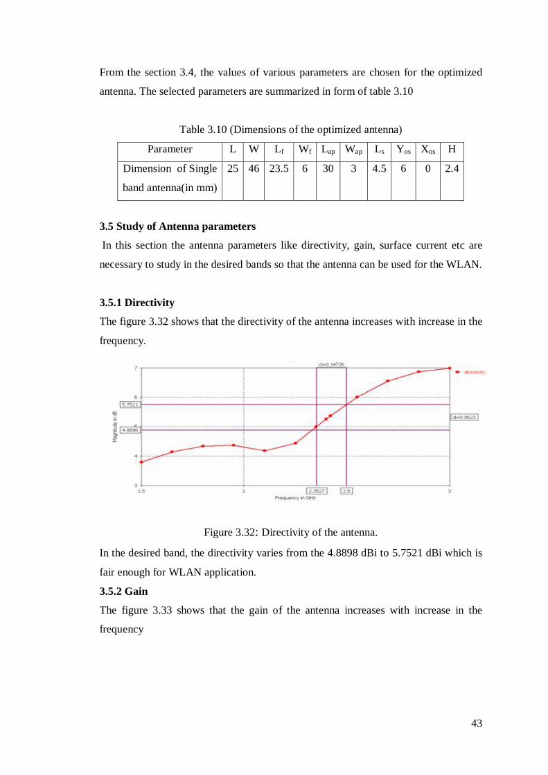
3.5 Study of Antenna parameters………………………………………………………...42
3.5.1 Directivity………………………………………………………………….42
3.5.2 Gain………………………………………………………………………...43
3.5.3 Surface current………………………………………………………….….44
3.5.4 Broadband far-fields ………………………………………………………44
Chapter 4……………………………………………………………………………...46-55
4.1 Dual band antenna design……………………………………………………………46
4.2 Parametric study of the antenna……………………………………………………...48
4.2.1 Effect of the change in the Offset (doff)……………………………………48
4.2.2 Effect of change in the length (L2) of slot 2 keeping the length (L1) of slot 1
constant………………………………………………………………………..…49
4.2.3 Effect of change in the length (L1) of slot 1 keeping the length (L2) of slot2
constant…………………………………………………………………………..51
4.2.4 Effect of change in the Slot widths……………………….………………..53
4.3 Comparison of Single and Dual band antenna……………………………………….53
4.4 Fabrication of the antenna……………………………………………………………55

vi
Chapter 5…………………………………………………………………………………59
5.1 Conclusion…………………………………………………………………………...59
5.2 Future Work………………………………………………………………………….59
List of Publications………………………………………………………………………60
References………………………………………………………………………………..61

vii
List of Figures Figure 1.1 Structure of a Microstrip Patch Antenna………………………...…….….1
Figure 1.2 Geometry of microstrip line feed (a) Directly feed and (b) Inset feed…....4
Figure 1.3 Geometry of coaxial probe feed microstrip patch antenna (a) top view and
(b) side view……………………………………………………………….4
Figure1.4 Geometry of an aperture coupled feed microstrip patch antenna (top
view)………………………………………………………………………5
Figure 1.5 Geometry of a proximity coupled microstrip feed microstrip patch antenna
(top view)………………………………..………………………………...6
Figure 1.6 Differention of the curve APB…………………………………………….8
Figure 1.7 A uniform grid…………………………………………………………….9
Figure 1.8 Staggering and leapfrogging of the grid…………………………………10
Figure 1.9 Staggering of grid by h/2 step……………………………………………10
Figure 1.10 Calculation of E and H fields [18]……………………………………….11
Figure 1.11 Genarilised method of computing the E and H fields……………………12
Figure 1.12 Grid structure of the fields (Yee lattice) [17]…………………………….13
Figure 1.13 Flowchart of the antenna design…………………………………………15
Figure 3.1 Pictorial view of the aperture feed……………………………………….22
Figure 3.2 Aperture coupled antenna block diagram [61]…………………………...23
Figure 3.3 Transmission equivalent circuit of the antenna [61]……………………..23
Figure 3.4 a) Front view of antenna b) Dimensional diagram of antenna…………..26
Figure 3.5 The Simulations time signals…………………………………………….26
Figure 3.6 S-parameter of the test antenna…………………………………………..26
Figure 3.7 Variation of S-parameter w.r.t patch length……………………………...27
Figure 3.8 Variation of S-parameter w.r.t patch position along resonating direction.28
Figure 3.9 Selected patch position for maximum coupling………………………….28
Figure 3.10 Variation of real (Z) w.r.t patch width…………………………………...29
Figure 3.11 Selected patch width with its input impedance…………………………..30

viii
Figure 3.12 Variation of S-parameter w.r.t patch position along non-resonating
direction………………………………………………………………….30
Figure 3.13 Variation of S-parameter with change in Slot length…………………….31
Figure 3.14 Variation of real (Z11) with change in slot length……………………….31
Figure 3.15 Smith chart variation with change in aperture length……………………32
Figure 3.16 Effect of position of aperture on S-parameter……………………………33
Figure 3.17 Variation of S-parameter with change in width of slot…………………..33
Figure 3.18 Variation of S-parameter with change in aperture position along
resonating side …………………………………………………………..34
Figure 3.19 Variation of S-parameter with change in length of feed line…………….35
Figure 3.20 Smith chart variations with change in feed line length…………………..35
Figure 3.21 Smith chart variations with change in feed line width…………………...36
Figure 3.22 Variation of S-parameter with change in width of feed line……………..36
Figure 3.23 Variation of S-parameter with change in height of antenna substrate…...37
Figure 3.24 Variation of resonating frequency with change in the dielectric constant of
both substrates……………………………………………………………37
Figure 3.25 Variation in resonating frequency with change in the feed substrate……38
Figure 3.26 Smith chart variations with change in feed substrate…………………….39
Figure 3.27 a) Rectangular aperture b) Dumbbell shape etched on the ground plane..40
Figure 3.28 S-parameter of the antenna………………………………………………40
Figure 3.29 VSWR of the antenna……………………………………………………41
Figure 3.30 Surface current distribution of the antenna………………………………41
Figure 3.31 Current distribution at arms of dumbbell of the antenna………………...42
Figure 3.32 Directivity of the antenna………………………………………………...43
Figure 3.33 Gain of the antenna………………………………………………………43
Figure 3.34 Polar plot of gain ………………………………………………………...44
Figure 3.35 Surface current of the antenna…………………………………………...44
Figure 3.36 Broadband far-field radiation of the antenna…………………………….45
Figure 4.1 View of the a) Single band antenna b) Dual band antenna with slots…...47
Figure 4.2 S-parameter of dual band antenna………………………………………..47
Figure 4.3 Smith chart of dual band antenna………………………………………...48

ix
Figure 4.4 Variation of S-parameter with change in the Slot Offset (doff)…………..48
Figure 4.5 Variation of S-parameter with change in length of slot2………………...50
Figure 4.6 Surface current of the antenna at 2.2 GHz……………………………….51
Figure 4.7 Variation of S-parameter with change in length of slot1………………...51
Figure 4.8 Surface current of the antenna at 2.45 GHz……………………………...52
Figure 4.9 Variation of S-parameter with change in width of the two slots
symmetrically.............................................................................................53
Figure 4.10 S-parameter of the two antennas……………………….………………...53
Figure 4.11 Smith chart of two antennas……………………………………………...54
Figure 4.12 Layer drafted on transparent sheet a) Feedline b) Aperture in ground c)
Patch of single band antenna………………..……………………………56
Figure 4.13 Negatives of a) Feedline b) Aperture in ground slot…………………...56
Figure 4.14 Negatives of Patches of a) Single band antenna b) Double band antenna57
Figure 4.15 Patches of a) Single b) Double band antenna……………………………57
Figure 4.16 Design flow of the PCB design…………………………………………..58

x
List of Tables Table1.1 The comparisons between the feeding methods for microstrip patch
antenna…………………………………………………………………….6
Table 1.2 Software and their theoretical models……………………………………14
Table 1.3 Approximate Band Designations……………….……………………......16
Table 1.4 Application and allocated frequency……………………………….……16
Table 3.1 Antenna transmission line model parameters……………………………24
Table 3.2 Dimensions of the unoptmized antenna……………………………….…25
Table 3.3 Resonating frequency for various patch lengths…………………………27
Table 3.4 Variation of S11 with position of patch………………………………….28
Table 3.5 Variation of input impedance with change in the patch width…………..29
Table 3.6 Variation in the resonating frequency, magnitude of S-parameter and real
Z11with change in the aperture length………………..………………….32
Table 3.7 Variation of the S-parameter with change in the width of slot…………..34
Table 3.8 Dielectric constant v/s resonating frequency…………………………….38
Table 3.9 Dielectric constant of feed substrate v/s Line impedance………………..38
Table 3.10 Dimensions of the optimized antenna……………………………………42
Table 3.11 Antenna parameters for optimized antenna……………………………...45
Table 4.1 Antenna parameters with varying Offset………………………………...49
Table 4.2 Antenna parameters with varying L2…………………………………….50
Table 4.3 Antenna parameters with varying L1…………………………………….52
Table 4.4 Comparison of antenna parameters for designed the antennas…………..55

xi
Abbreviations
MPA Microstrip Patch Antenna
ACRPMA Aperture coupled rectangular patch microstrip antenna
FDTD Finite-difference time-domain
WLAN Wireless local area network
PCS Personal communication system
Q Quality factor
CST Computer Simulation Technology
NUFFT Non-uniform fast Fourier transform
VSWR Voltage standing wave ratio

1
CHAPTER 1
An Overview of Microstrip Patch Antenna
In this chapter, an introduction to the Microstrip Patch Antenna (MPA) is given,
followed by its advantages and disadvantages. Some feed modeling techniques are
also discussed. The overview of FDTD analysis technique and designing an antenna is
also given. It covers the electromagnetic spectrum used for the various applications.
1.1 Introduction In its most basic form, a Microstrip patch antenna consists of a radiating patch on one
side of a dielectric substrate which has a ground plane on the other side as shown in
Figure 1.1. The patch is generally made of conducting material such as copper or gold
and can take any possible shape. The radiating patch and the feed lines are usually
photo etched on the dielectric substrate.
Figure 1.1 Structure of a Microstrip Patch Antenna
For a rectangular patch, the length L of the patch is usually 0.3333 L 0.5 ,
where is the free-space wavelength. The patch is selected to be very thin such that
(where t is the patch thickness). The height h of the dielectric substrate is
usually 0.003 ≤ h ≤ 0.05 . The dielectric constant of the substrate (εr) is
typically in the range 2.2 ≤ εr ≤ 12.
Microstrip patch antennas radiate primarily because of the fringing fields between the
patch edge and the ground plane. For good antenna performance, a thick dielectric
substrate having a low dielectric constant is desirable since this provides better
efficiency, larger bandwidth and better radiation[2], [5]. However, such a
configuration leads to a larger antenna size. In order to design a compact Microstrip
patch antenna, higher dielectric constants must be used which are less efficient and

2
result in narrower bandwidth. Hence a compromise must be reached between antenna
dimensions and antenna performance.
1.2 Advantages and Disadvantages Microstrip patch antennas are increasing in popularity for use in wireless applications
due to their low-profile structure. Therefore they are extremely compatible for
embedded antennas in handheld wireless devices such as cellular phones, pagers etc.
The telemetry and communication antennas on missiles need to be thin and conformal
and are often Microstrip patch antennas. Another area where they have been used
successfully is in Satellite communication. Some of their principal advantages are
given below [5]:
Light weight and low volume.
Low profile planar configuration which can be easily made conformal to host
surface.
Low fabrication cost, hence can be manufactured in large quantities.
Supports both, linear as well as circular polarization.
Can be easily integrated with microwave integrated circuits (MICs).
Capable of dual and triple frequency operations.
Mechanically robust when mounted on rigid surfaces
Microstrip patch antennas suffer from a number of disadvantages as compared to
conventional antennas. Their major disadvantages are [5]
Narrow bandwidth.
Low efficiency.
Low Gain.
Extraneous radiation from feeds and junctions.
Poor end fire radiator except tapered slot antennas.
Low power handling capacity.
Surface wave excitation.
Microstrip patch antennas have a very high antenna quality factor (Q). Q represents
the losses associated with the antenna and a large Q leads to narrow bandwidth and
low efficiency. Q can be reduced by increasing the thickness of the dielectric
substrate. But as the thickness increases, an increasing fraction of the total power
delivered by the source goes into a surface wave. This surface wave contribution can
be counted as an unwanted power loss since it is ultimately scattered at the dielectric

3
bends and causes degradation of the antenna characteristics. However, surface waves
can be minimized by use of photonic band gap structures [2]. Other problems such as
lower gain and lower power handling capacity can be overcome by using an array
configuration for the elements. 1.3 Feeding techniques
Microstrip patch antennas can be fed by a variety of methods. These methods can be
classified into two categories- contacting and non-contacting. In the contacting
method, the RF power is fed directly to the radiating patch using a connecting element
such as a microstrip line. In the non-contacting scheme, electromagnetic field
coupling is done to transfer power between the microstrip line and the radiating patch.
The four most popular feed techniques used are the microstrip line, coaxial probe
(both contacting schemes), aperture coupling and proximity coupling (both non-
contacting schemes)[2]-[7].
A microstrip feed uses a transmission line to connect the radiating patch to receive or
transmit circuitry. Electromagnetic field lines are focused between the microstrip line
and ground plane to excite only guided waves as opposed to radiated or surface
waves. Guided waves dominate in electrically thin dielectrics with relatively large
permittivities [2]. For the patch antenna, radiated waves at the patch edges are
maximized using electrically thick dielectric substrates with relatively low
permittivities. Hence, it is difficult to meet substrate height and permittivity
requirements for both the microstrip transmission line and patch antenna. Dielectric
substrates selected to satisfy the two conflicting criteria increase surface waves,
reduce radiation efficiency due to increased guided waves below the patch, and
increase side-lobes and cross-polarization levels from spurious feed line radiation [2].
A microstrip line feed is generally used in two configurations namely Directly fed and
Inset feed as shown in the figure 1.2.

4
Figure 1.2: Geometry of microstrip line feed (a) directly feed and (b) Inset feed
A probe fed antenna consists of a microstrip patch fed by the center conductor of a
coaxial line (see Figure 1.3). The outer coax conductor is electrically connected to the
ground plane. Due to the absence of a microstrip feed line, the substrate thickness and
permittivity can be designed to maximize antenna radiation. However, the probe
center conductor underneath the patch causes undesired distortion in the electric field
between the patch and ground plane and produces undesired reactive loading effects
at the antenna input port [2], [3]. The undesired reactance can be compensated by
adjusting the probe location on the patch.
Figure 1.3: Geometry of coaxial probe feed microstrip patch antenna (a) top view and
(b) side view.
In Aperture Coupled feeding technique, the radiating patch and the microstrip
feedline are separated by the ground plane thereby eliminating the direct electrical
connection between the conducting feed and radiating patch (see figure 1.4). Coupling
between the patch and the feed line is made through a slot or an aperture in the ground
plane.

5
Figure1.4: Geometry of an aperture coupled feed microstrip patch antenna (top view).
The coupling aperture is usually centered under the patch, leading to lower cross-
polarization due to symmetry of the configuration. The amount of coupling from the
feed line to the patch is determined by the shape, size and location of the aperture.
Since the ground plane separates the patch and the feed line, spurious radiation is
minimized. Generally, a high dielectric material is used for the bottom substrate and a
thick, low dielectric constant material is used for the top substrate to optimize
radiation from the patch [5]. Aperture coupled antennas are advantageous in arrays
because they electrically isolate the feed and phase shifting circuitry from the patch
antennas. The disadvantage is the required multilayer structure which increases
fabrication complexity and cost [2]. The major disadvantage of this feed technique is
that it is difficult to fabricate due to multiple layers, which also increases the antenna
thickness. This feeding scheme also provides narrow bandwidth.
The Proximity Coupled Feed technique is also called as the electromagnetic
coupling scheme. As shown in Figure 1.5, two dielectric substrates are used such that
the feed line is between the two substrates and the radiating patch is on top of the
upper substrate. The main advantage of this feed technique is that it eliminates
spurious feed radiation and provides very high bandwidth (as high as 13%) [5], due to
overall increase in the thickness of the microstrip patch antenna. This scheme also
provides choices between two different dielectric media, one for the patch and one for
the feed line to optimize the individual performances. Matching can be achieved by
controlling the length of the feed line and the width-to-line ratio of the patch. The
major disadvantage of this feed scheme is that it is difficult to fabricate because of the
two dielectric layers which need proper alignment. Also, there is an increase in the
overall thickness of the antenna.

6
Figure 1.5: Geometry of a proximity coupled microstrip feed microstrip patch antenna
(top view)
The comparison of the feeding techniques in tabulated form is given by table 1.1
Table1.1: (The comparisons between the feeding methods for microstrip patch
antenna) Feeding technique Advantages Disadvantages
Proximity Coupled No direct contact
between feed and patch.
Can have large effective
thickness for patch
substrate and much
thinner feed substrate.
Multilayer fabrication
required.
Microstrip Line Monolithic
Easy to fabricate.
Easy to match by
controlling Insert
position.
Spurious radiation from
feed line, especially for
thick substrate when
line width is significant.
Coaxial Feed Easy to match.
Low spurious radiation.
Large inductance for
thick substrate.
Soldering required.

7
Aperture Coupled Use of two substrates
avoids deleterious effect
of a high-dielectric
constant substrate on the
bandwidth and
efficiency.
No direct contact
between feed and patch
avoiding large probe
reactance or width
microstrip line.
No radiation from the
feed and active devices
since a ground plane
separates them from the
radiating patch
Multilayer fabrication
required.
Higher back-lobe
radiation.
1.4 Methods of Analysis The various models for the analysis of Microstrip patch antennas are the transmission
line model [3] [8]-[10], cavity model [11]-[13], FDTD [14]-[16] and full wave model
[5].The transmission line model is the simplest of all and it gives good physical
insight but it is less accurate. The cavity model is more accurate but is complex in
nature. The full wave models are extremely accurate, versatile and can treat single
elements and arrays. The FDTD method is easy to understand and implement in
software. CST Microwave studio uses the FDTD scheme.
Finite-difference time-domain (FDTD) is a popular computational electrodynamics
modeling technique. It is a time-domain method and solutions can cover a wide
frequency range with a single simulation run. The basic FDTD space grid and time-
stepping algorithm trace back to a seminal 1966 paper by Kane Yee [14].The
descriptor "Finite-difference time-domain" and its corresponding "FDTD" acronym
were originated by Allen Taflove [15]. The FDTD method belongs in the general
class of grid-based differential time-domain numerical modeling methods. This
method includes the following steps:
8
1) Discretization of fields using central-difference approximations to the space
and time partial derivatives.
Figure 1.6: Differention of the curve APB [17].
Consider the figure 1.6 where a simple differentiation of a curve is shown in 2D.
Using the central difference scheme, we have
……………………………………………………(1.1)
Now, consider the Maxwell’s equations as written below
…………………………………………………………………..(1.2
)
…………………………………………………………………..(1.
3) ………………………………………………………………………
(1.4)
…………………………………………………………………………(1.5
)
and
……………………………………………………….
(1.6)

9
Consider 1D system where a wave is travelling in x-direction and E-field is along y
axis and H-field is along z-axis.
Equations (1.2) and (1.3) can be written as
…………………………………………………………….
(1.7)
……………………………………………………………...(1.8)
2) Solving the finite-difference equations
The resulting finite-difference equations are solved in either software or hardware in a
leapfrog manner. Firstly, a general problem is discussed and then Maxwell’s
equations are solved. Consider a uniform grid xi as shown in the figure 1.7
Uniform grid: {xi }, xi = i h, i = 0,1,2,3,………and ui = u(xi)
Figure 1.7: A uniform grid [18].
According to the Finite difference scheme, the partial differentiation of the ui can be
written as
……………………………………………(1.9
)

10
…………………………………………..(1.10)
……………………..(1.11)
where = any initial value of ui and h is the increment in the consecutive grid
values.
are the change in the value of the grid from jumping one step ahead,
back and two steps ahead respectively.
Now the grid is traced in staggering and leapfrogging manner as shown in the figure
1.8
Figure 1.8: Staggering and leapfrogging of the grid [18].
Figure 1.9 shows the E and H-fields when the grid is staggering by h/2 step in space
at time t = 0.
Figure 1.9: Staggering of grid by h/2 step[18].
3) Solving the electric and magnetic field vector components in a volume of space are
solved subsequently at a given instant in time.
By replacing to and to , the equations 1.7 and 1.8 are written as
…………………………………………………………………….(1.1
2)
11
……………………………………………………………..……..(1.
13)
When Maxwell's differential equations are examined, it can be seen that the change in
the E-field in time (the time derivative) is dependent on the change in the H-field
across space (the curl). This results in the basic FDTD time-stepping relation that, at
any point in space, the updated value of the E-field in time is dependent on the stored
value of the E-field and the numerical curl of the local distribution of the H-field in
space [14].
Thus , for a particular grid at a given time,the equations 1.12 and 1.13 are written as
……………………………………………
……(1.14)
……………………………………………
…(1.15)
Figure 1.10 shows the view of the grids to calculate the E and H fields at cetain time
periods.
Figure 1.10: Calculation of E and H fields [18].
The normalized value of the E-field is given as

12
………………………………………………………………(1.16)
The H-field is time-stepped in a similar manner as E-field. At any point in space, the
updated value of the H-field in time is dependent on the stored value of the H-field
and the numerical curl of the local distribution of the E-field in space. Iterating the E-
field and H-field updates results in a marching-in-time process where in sampled-data
analogs of the continuous electromagnetic waves under consideration propagate in a
numerical grid stored in the computer memory.
Using the equations 1.16, 1.14 and 1.15 can be written as
……………………………………….(1.17
)
…………………………………...(1.18)
where
Equation 1.18 in another form can be written as
……………………………………...(1.19)
The figure 1.11 shows the genarilised method of computing the E and H fields.
Figure 1.11: Genarilised method of computing the E and H fields[18].

13
………………………………………… (1.20)
…………………………………………………(1.21)
………………………………………………(1.22)
……………………………………………...............(1.2
3)
……………………………………….........................(1.
24)
Thus, the equations 1.20 to 1.24 are solved for every interval. The process is repeated
over and over again until the desired transient or steady-state electromagnetic field
behavior is fully evolved.
Kane Yee's seminal 1966 paper proposed spatially staggering the vector components
of the E-field and H-field about rectangular unit cells of a Cartesian computational
grid so that each E-field vector component is located midway between a pair of H-
field vector components, and conversely [14]. This scheme, now known as a Yee
lattice, has proven to be very robust, and remains at the core of many current FDTD
software constructs. Figure 1.12 shows the simple cubic unit cells of a grid.
Figure 1.12: Grid structure of the fields (Yee lattice) [17]

14
In order to use FDTD a computational domain must be established. The
computational domain is simply the physical region over which the simulation will be
performed. The E and H fields are determined at every point in space within that
computational domain. The material of each cell within the computational domain
must be specified. Typically, the material is either free-space (air), metal, or
dielectric. Any material can be used as long as the permeability, permittivity, and
conductivity are specified.
Once the computational domain and the grid materials are established, a source is
specified. The source can be an impinging plane wave, a current on a wire, or an
applied electric field, depending on the application. Since the E and H fields are
determined directly, the output of the simulation is usually the E or H field at a point
or a series of points within the computational domain. The simulation evolves the E
and H fields forward in time. Processing may be done on the E and H fields returned
by the simulation. While the FDTD technique computes electromagnetic fields within
a compact spatial region, scattered and/or radiated far fields can be obtained via near-
to-far-field transformations.
1.5 General Comments on Designing Microstrip Patch Antennas To design microstrip patch antennas meeting certain specifications, the antenna
engineer should possess a combination of certain knowledge and skills. First, he/she
should have an understanding of the principles of operation of the basic MPA
structure. This can be obtained by studying the various modeling techniques like
transmission line model, cavity model or FDTD etc.
According to the understanding and availability of the software, one can select and
design the basic antenna structure in the software. Software can be selected from the
Table 1.2.
Table 1.2(Software and their theoretical models)
Software Name Theoretical model Company Name
Ensemble Moment method Ansoft
IE3D Moment method Zeland
PCAAD Cavity model Antenna Design
Associates
Fidelity FDTD Zeland

15
HFSS Finite element Ansoft
Microwave studio FDTD CST
The simulated results can be verified by mathematical modeling of antenna. But the
mathematical analysis of the antenna becomes very complex for the structures having
slots, shorted pins. The same antenna can also be designed in any other software for
verification. But the best method to verify the results is to fabricate the antenna and
get it tested to avail the measurement results. Here, in this thesis the CST Microwave
Studio is used as the simulation tool which is based on the FDTD model of analysis.
Figure 1.13 illustrates the design process of the antenna in form of a flowchart.
.
Antenna
Specifications
Fabricate
Draw design CST Microwave
studio using Aperture coupling.
Simulation results
Do results meet the desired
specifications?
Design
Yes
No Feedback
Feedback

16
Figure 1.13: Flowchart for the antenna design.
1.6 Utilization of the Electromagnetic Spectrum for Wireless
Communication Applications For reference purposes, we include table 1.3 which gives an overview of the
electromagnetic spectrum and its utilization for various wireless communication
applications.
Table 1.3(Approximate Band Designations) Approximate Band Designations
L-band 1-2GHz
S-band 2-4GHz
C-band 4-8GHz
X-band 8-12GHz
Ku-band 12-18GHz
K-band 18-26GHz
Ka-band 26-40GHz
U-band 40-60GHz

17
Defense and space markets which emphasize on maximum performance gave an
impetus to the development microstrip antennas and arrays in 1980s. However,
applications of microstrip antennas in commercial sector are galloping most rapidly in
21st century. The microstrip antennas for commercial systems require low-cost
materials, and simple and inexpensive fabrication techniques. Some of the
commercial systems that presently use microstrip antennas are listed in the table1.4
[22] below
Table 1.4 (Application and allocated frequency) Application Frequency
Global positioning Satellite 1575MHz and 1227MHz
Paging 931-932 MHz
Cellular Phone 824-849 MHz and 869-895 MHz
Personal Communication System 1.85-1.99 GHz and 2.18-2.20 GHz
GSM 890-915 MHz and 935-960 MHz
Wireless Local Area Networks 2.40-2.48 GHz and 5.4 GHz
Cellular Video 28 GHz
Direct Broadcast Satellite 11.7-12.5GHz
Automatic Toll Collection 905 MHz and 5-6 GHz
Collision Avoidance Radar 60 GHz, 77 GHz, and 90 GHz
Wide Area Computer Networks 2.40-2.48 GHz and 5.4 GHz
1.7 Objective of the thesis The objectives of the thesis are To study the basic principles of the Aperture coupled single band microstrip
rectangular patch antenna.
Design and simulation of wideband aperture coupled MPA.
Parametric study of the proposed antenna.
Design and simulation of dual band aperture coupled MPA.
Parametric study of the proposed antenna.
Fabrication of the designed antennas.
1.8 Thesis organization

18
The thesis is divided into five chapters.
Chapter 1 is dedicated to the Overview of Microstrip antenna.
Chapter 2 includes the literature survey on the aperture coupled antenna. The brief
idea about the researches done for bandwidth enhancement, dual frequency, modeling
of the aperture coupled antenna is given.
In Chapter 3, a single band antenna is designed and the effect of various physical
parameters on the resonating frequency is studied.
In Chapter 4, the single band antenna is loaded with slots such that a dual frequency
antenna is obtained.
Chapter 5 is dedicated to the conclusion and the future work.

19
Chapter 2
Literature survey on Aperture Coupled Microstrip
Antennas
This chapter is devoted to the evolution of the aperture coupled antenna and its
development in the recent past.
2.1 History of the Aperture Coupled Microstrip Antennas The first aperture coupled microstrip antenna was fabricated and tested by a graduate
student, Allen Buck, on August 1, 1984, in the University of Massachusetts Antenna
Lab. This antenna used Duroid substrates with a circular coupling aperture, and
operated at 2 GHz [19]. It was found that this antenna worked perfectly – it was
impedance matched, and the radiation patterns were good. Most importantly, the
required coupling aperture was small enough so that the back radiation from the
coupling aperture was much smaller than the forward radiation level [22].
2.2 Progress of the Aperture Coupled Microstrip Antenna Here we discuss in detail with references, some of the significant developments in the
field of aperture coupled microstrip antennas.
2.2.1 Bandwidth enhancement in Aperture coupled microstrip antennas
One of the useful features of the aperture coupled microstrip antenna is that it can
provide substantially improved impedance bandwidths due to the additional degrees
of freedom offered by the stub length and coupling aperture size. While single layer
probe or microstrip line-fed elements are typically limited to bandwidths of 2%-5%,
aperture coupled elements have been demonstrated with bandwidths up to 10 - 15%
with a single layer [25]-[27], and up to 30-50% with a stacked patch configuration
[28]-[31]. Bandwidth can be enhanced by using H-shaped [32], L-shaped aperture in
ground and by placing stubs in the patch [33], U-shaped slots in the patch [34]. A new
technique to increase the bandwidth of slot antenna without increasing the volume of
the antenna is obtained by using Z-slot and splitting the two side of the Z- slot into
two or three fingers is proposed by C.-J. Wang and S.-W. Chang [35].

20
2.2.2 Dual frequency aperture coupled microstrip antennas
An overview about the dual-frequency techniques for patch antennas, Orthogonal-
mode dual-frequency patch antennas, Multi-patch dual-frequency antennas,
Reactively-loaded patch antennas, geometries for single and dual linear polarization,
slotted rectangular-patch antenna, slotted cross-patch antenna, Cross-subarray dual-
frequency patch antenna is discussed by S. Maci and G. BifJi Gentili [36]. A compact
stack antenna consisting of square loop resonators, aperture couples, feed line and the
perturbation for dual- band and circular polarization (CP) applications is proposed by
J. C. Liu and B. H. Zeng, C. Y. Liu, H. C. Wu and C. C. Chang. This perturbation
applies both dual-mode and orthogonal mode effects existing in the square loop
resonator to present wide-band and circular polarization (CP) characteristics
simultaneously [37].
An annular ring has also been used for dual frequency where the frequency for the
propagating modes can be adjusted by choosing the inner and the outer radii.
However, the ratio of the two frequencies is somewhat limited [38]. It is also possible
to achieve dual frequency operation of a patch antenna by loading slots at both the
resonating side and at the non-resonating side of the patch and by using shorting pins
[39]-[40].
2.2.3 Antennas for WLAN and other wireless applications
A single fed aperture coupled antenna for WLAN application is designed and
discussed by Rashid A. Saeed, S. Khatun, Borhanuddin, M. A. Khazani, Rania A.
Mokhtar and Mahmoud Alshamary [41]. A dual-band antenna covering both the
bands (2.45 and 5.2 GHz) for WLAN application is designed by combining a
rectangular and two “L” shaped radiating elements embedding them on a single layer
structure and achieved bandwidth of 30%and 20% while maintaining the structural
compact size [42]. Multifrequency antenna for various wireless applications is
designed by using manifold slot structures like the printed slot, the slotted form and
inverted-L slot[43], fractal shapes [44][45][46], polygon patch [47].
2.2.4 Modeling of aperture coupled microstrip antennas
Analysis of the aperture coupled microstrip element is complicated by the presence of
two dielectric layers, and the microstrip line-to-slot transition. The initially the
aperture coupled element [19] presented a simplified cavity-type model, Sullivan and

21
Schaubert [48] analyzed it using a full-wave moment method solution. D M Pozar
used the reciprocity theorem to analyze the aperture coupled antenna [49]. Moment
method analysis techniques are versatile and highly accurate but take relatively long
simulation times. Cavity models, are more approximate requiring negligible computer
resources. Some examples of cavity models for aperture coupled microstrip antennas
include [50]-[51]. The numerical techniques like Green’s Functions, Mixed Potential
Integral Equations and Method of Moments used for the analysis of coupled antenna
are discussed by D. Yau and N. V. Shuley [52].
The basic Finite-difference time-domain FDTD space grid and time-stepping
algorithm trace back to a seminal 1966 paper by Kane Yee [14]. An improved Finite-
difference time-domain (FDTD) based on novel integral transform and the matrix
theory method has been extended to analyze the antennas with complicated
lumped/active networks [53]. A polarimetric scattering from two-dimensional (2-D)
rough surface is presented by the Finite-difference time-domain (FDTD) algorithm
[54]. Also, a new FDTD time-to-frequency domain conversion algorithm based on the
optimization of non-uniform fast Fourier transform (NUFFT) is presented by Y.-H.
Liu and Q. H. Liu and Z.-P. Nie [55].
2.2.5 Antenna with defected ground structure (DGS)
Multibanding of the antenna is also possible by using defected ground structure
(DGS) which disturbs the shield current distribution in the ground plane which
further influences the input impedance and current flow of the antenna providing a
bandpass or bandstop like filter and other microwave circuits [56] [57]. Method of
calculating the characteristics impedance of transmission line with DGS is given by J.
Lim, J. Lee, J. Lee, S.-M. Han, and D. Ahn. and Y. Jeong [58].
Thus, in many applications, operation at two or more discrete bands with an arbitrary
separation of bands is desired. In such cases, a patch capable of operating in multiple
bands is desirable. For most applications, all bands may be required to have the same
polarization, radiation pattern, and bandwidth characteristics. Multi-banding of an
antenna can be done by using fractal shapes [44][45][46], polygon patch [47], E-
shape, V-shape and U-shape patches [2],[6],[60]. One method is to use separate
patches abreast each other for different applications. Arraying of the antenna can also
be done but it increases the size of the antenna. Stacking of the patches can also be
used but it increases the volume of the antenna. It is also desirable to have one port

22
and an arbitrary separation of the frequency bands. All of these requirements impose
severe constraints on the use of natural modes [39]. An annular ring has also been
used for dual frequency where the frequency for the propagating modes can be
adjusted by choosing the inner and the outer radii. However, the ratio of the two
frequencies is somewhat limited [38]. It is also possible to achieve dual frequency
operation of a patch antenna by loading slots at both the resonating side and at the
non-resonating side of the patch and by using shorting pins [39]-[40].
In the proposed design, two slots are loaded at the patch to make it to dual frequency
antenna without increasing the volume unlike stacking of patches. Also, the
fabrication process of the slot is compatible with antenna fabrication technology.

23
Chapter 3
Single band Aperture Coupled antenna Design and its
parametric study
This chapter covers the basics of aperture coupling and the transmission line model
parameters of the proposed antenna are calculated. Firstly a single band antenna is
designed for WLAN applications at a frequency of 2.40GHz. The effect of various
parameters like patch width, patch length, dimensions and position of aperture etc…
on the designed antenna is described. An antenna with dumbbell shaped aperture in
the ground is also designed.
3.1 Basics of Aperture coupled antenna In 1985, a new feed technique involving a microstrip line electromagnetically coupled
to a patch conductor through an electrically small ground plane aperture was
proposed. The figure 3.1 shows the pictorial view of the aperture coupled antenna
Figure 3.1: Pictorial view of the aperture feed
As stated in chapter 1 that an aperture coupled antenna eliminates direct electrical
connections between the feed conductor and radiating patch, and the ground plane
electrically isolates the two structures. The two dielectric substrates can be selected
independently to optimize both microstrip guided waves and patch radiating waves.
Generally, the antenna substrate is thicker and has a lower dielectric constant than the
feed substrate. Aperture coupled antennas are advantageous in arrays because they
electrically isolate the feed and phase shifting circuitry from the patch antennas. The
disadvantage is the required multilayer structure which increases fabrication
complexity and cost. Figure 3.2 shows the aperture coupled microstrip antenna in

24
block diagram form. The feed line creates an electric field in the aperture (ground
plane slot), which induces surface currents on the patch. The patch edges
perpendicular to the feed line create fringing fields that radiate into free space.
Figure 3.2 Aperture coupled antenna block diagram [61]
3.2 Equivalent circuit of Aperture Coupled antenna The equivalent circuit of the aperture coupled antenna is shown in the figure 3.3.The
ground plane slot acts as an impedance transformer and parallel LC circuit (Lap and
Cap in Figure 3.3) in series with the microstrip feed line [61]. The LC circuit
represents the ground plane slot resonant behavior. The N:1 impedance transformer
represents the patch antenna's impedance effects being coupled through the ground
plane slot. The patch is modeled as two transmission lines terminated by parallel RC
components (Rrad and Cfring) due to patch edge fringing fields.
Figure 3.3 Transmission equivalent circuit of the antenna [61]
The antenna circuit model parameters are determined from equations (3.1) through
(3.8)

25
(3.1)
(3.2)
(3.3)
(3.4)
(3.5)
(3.6)
(3.7)
(3.8)
The antenna circuit model parameters for the antenna designed in section 3.3 are
tabulated in the table 3.1
Table 3.1(Antenna transmission line model parameters)
S.No. Variable Value
1 fr (Operating frequency) 2.43GHz
2 λr (Free space wavelength) 0.1234 m
3 ηo (Free space impedance) 377ohm
4 εr (Substrate dielectric constant) 2.20
5 εp,eff, (Patch effective relative dielectric
constant)
2.08

26
6 εf ,eff, (Feed effective relative dielectric
constant)
2.46
7 Wp (Width of Patch) 46 mm
8 Hp ( Height of Patch substrate) 2.402 mm
9 Wf (Width of feed) 6 mm
10 Hp ( Height of Patch substrate) 2.402 mm
11 ∆ (Field extension due to fringing) 1.2 mm
12 G (Parallel plate radiator conductance) 0.0030 S
13 B (Fringing field capacitive susceptance) 0.0064 S
14 Zo,p (Line impedance of patch) 11.59
15 Zo,f (Line impedance of feed) 50.07
16 Rrad (Fringing field resistance) 323.62 ohm
17 Cap (Aperture capacitance) 22.45 pF
18 Lap (Aperture inductance) 191.1 pF
19 Cfringe (Fringing field capacitance) 0.419 pF
20 N (Impedance transformer turns ratio) 1.53
3.3 Single band antenna design Firstly, a single band antenna consisting of a rectangular patch, rectangular aperture
and feed line was designed for WLAN application. The dimensions of the antenna
were calculated as per the equations given in CA Balanis [6].
Table 3.2(Dimensions of the unoptmized antenna)
S. No Parameters Value
1 fr (Resonating frequency) 2.42GHz
2 Lp (Length of patch) 40 mm
3 Wp (Width of patch) 48 mm
4 Lg (Length of Ground) 40 mm
5 Wg (Width of ground) 48 mm
6 Ha(Height of Antenna Substrate) 2.4 mm
7 Hf (Height of Substrate) 2.4 mm
8 Wf (Width of feed) 7.39 mm

27
9 Lf (Length of feed ) 22.65 mm
The aperture dimensions are taken such that the ratio of width to length of the
aperture is 1/10.
Figure 3.4: a) Front view of antenna b) Dimensional diagram of antenna.
The figure 3.4 shows us the front view of the unoptmized antenna which is excited by
a Gaussian pulse at the waveguide port as shown in figure 3.5.
Figure 3.5: The Simulations time signals
The figure 3.6 shows the S-parameters as a function of frequency

28
Figure 3.6: S-parameter of the test antenna
From the figure 3.6, it is observed that the antenna resonates at 1.76 GHz which is not
the desired frequency. Hence, we have to vary our parameters so that an optimized
antenna with desired bandwidth and frequency can be designed.
3.4 Physical Parametric Study of the antenna
In this section, the effect of the various physical parameters like patch length, patch
width, aperture dimensions, antenna and feed substrates, feed line dimensions
etc…are studied, by varying one parameter at a time and keeping all other parameters
constant so that one can get an optimized antenna for the desired applications.
3.4.1 Effect of Patch length
The patch length affects the resonating frequency of the antenna.
Figure 3.7: Variation of S-parameter w.r.t patch length
As the patch length is changed from 40 mm to 24mm, it is observed from the figure
3.7 and table 3.3 that the resonating frequency changes from 1.87 GHz to 2.38 GHz.
So, a patch length of 25 mm is chosen. Now, the position of the patch is varied such
the antenna resonates at the 2.42 GHz.
Table 3.3 (Resonating frequency for various patch lengths)
Length of patch (in mm) 40 38 36 34 32 30 28 24
Resonating freq. (in GHz) 1.87 1.92 1.97 2.02 2.08 2.14 2.22 2.38
3.4.2 Effect of patch position along resonating (x-axis) direction
Moving the patch relative to the aperture in the E-plane decreases the coupling level.
It can be seen from the figure 3.8 that, when the value of patch length offset (PLoff=
25 + LoP) is increased from 15 mm to 14 mm the magnitude of S11 parameter
approaches from -20.95 dB to -38.97 dB.

29
Figure 3.8: Variation of S-parameter w.r.t patch position along resonating direction.
From the figure 3.8 and table 3.4, the patch position is selected such that the
maximum coupling takes place at the desired frequency. Table 3.4 shows the variation
of coupling level and resonating frequency with change in the patch length offset.
Table 3.4 (Variation of S11 with position of patch)
Patch length offset (PLoff) in mm 15 14 13 12 11 10
S11(in dB) -20.95 -21.62 -29.55 -29.92 -33.49 -38.97
Resonating freq. (in GHz) 2.56 2.53 2.46 2.42 2.36 2.34
The position of the patch with PLoff equals to 12 mm is depicted in the figure 3.9.
Figure 3.9: Selected patch position for maximum coupling.

30
3.4. 3 Effect of patch width
The width of the patch affects the resonant resistance of the antenna, with a wider
patch giving a lower resistance. Square patches may result in the generation of high
cross polarization levels, and thus should be avoided unless dual or circular
polarization is required. The variation in the input impedance of the antenna is shown
in the figure 3.10
Figure 3.10: Variation of real (Z) w.r.t patch width.
It is observed from the figure 3.10 and table 3.5 that as the patch width increases from
38 mm to 46 mm the input impedance decreases 85 to 75.88 ohm.
Table 3.5(Variation of input impedance with change in the patch width)
Patch width (in mm) 38 40 42 44 46
Real (Z11)(in ohm) 85 84 82 83 79
Resonating freq.(in GHz) 2.36 2.38 2.40 2.41 2.295
The patch width of 46 mm is selected having the input impedance of 78.17 ohm is
shown in the figure 3.11:

31
Figure 3.11: Selected patch width with its input impedance.
3.4.4 Effect of patch position along non-resonating (y-axis) direction
Moving the patch relative to the slot in the H-plane direction has little effect on the
resonating frequency and the coupling level. The figure 3.12 depicts the change in the
S-parameter when patch is varied along the y-axis keeping the patch width fixed to 46
mm.
Figure 3.12: Variation of S-parameter w.r.t patch position along non-resonating
direction.
3.4.5 Effect of Aperture length
The coupling level is primarily determined by the length of the coupling aperture, as
well as the back radiation level. The aperture should therefore be made no larger than
is required for impedance matching.
32
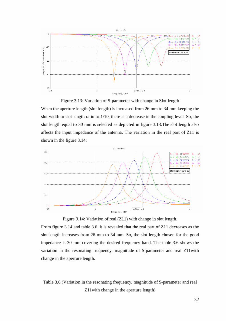
Figure 3.13: Variation of S-parameter with change in Slot length
When the aperture length (slot length) is increased from 26 mm to 34 mm keeping the
slot width to slot length ratio to 1/10, there is a decrease in the coupling level. So, the
slot length equal to 30 mm is selected as depicted in figure 3.13.The slot length also
affects the input impedance of the antenna. The variation in the real part of Z11 is
shown in the figure 3.14:
Figure 3.14: Variation of real (Z11) with change in slot length.
From figure 3.14 and table 3.6, it is revealed that the real part of Z11 decreases as the
slot length increases from 26 mm to 34 mm. So, the slot length chosen for the good
impedance is 30 mm covering the desired frequency band. The table 3.6 shows the
variation in the resonating frequency, magnitude of S-parameter and real Z11with
change in the aperture length.
Table 3.6 (Variation in the resonating frequency, magnitude of S-parameter and real
Z11with change in the aperture length)

33
Patch width (in mm) 26 28 30 32 34
Mag. of S11(in dB) -23.75 -23.52 -26.50 -30.56 -36.30
Resonating freq.(in GHz) 2.69 2.55 2.43 2.30 2.18
Real of Z11(ohm) 97 89 84 80 76
Figure 3.15: Smith chart variation with change in aperture length
From figure 3.15, it is concluded that the size of the locus of the smith chart is
controlled by the slot length. As the slot length increases, the size of the locus
increases. For proper matching the locus must be large enough that it passes through
the centre of the smith chart. Hence, slot length has to be chosen properly. Here, for
the desired frequency band the slot length chosen is 30mm. Now once the slot length
equal to 30mm is selected, figure 3.16 shows the effect of position of the slot length.
Figure 3.16: Effect of position of aperture on S-parameter.
34
When the aperture is moved along the non-resonating side, there is hardly any effect
on the S-parameter. From the figure 3.16, the position of the aperture is selected along
non-resonating side.
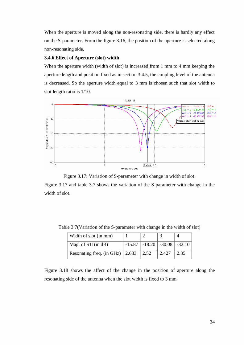
3.4.6 Effect of Aperture (slot) width
When the aperture width (width of slot) is increased from 1 mm to 4 mm keeping the
aperture length and position fixed as in section 3.4.5, the coupling level of the antenna
is decreased. So the aperture width equal to 3 mm is chosen such that slot width to
slot length ratio is 1/10.
Figure 3.17: Variation of S-parameter with change in width of slot.
Figure 3.17 and table 3.7 shows the variation of the S-parameter with change in the
width of slot.
Table 3.7(Variation of the S-parameter with change in the width of slot)
Width of slot (in mm) 1 2 3 4
Mag. of S11(in dB) -15.87 -18.20 -30.08 -32.10
Resonating freq. (in GHz) 2.683 2.52 2.427 2.35
Figure 3.18 shows the affect of the change in the position of aperture along the
resonating side of the antenna when the slot width is fixed to 3 mm.

35
Figure 3.18: Variation of S-parameter with change in aperture position along
resonating side.
From the figure 3.18, the position of the aperture along the resonating side of the
patch is selected such that maximum coupling takes place.
3.4.7 Effect of feed line length or length of stub
The length of feed line also affects the coupling level. When the feed line length is
increased from 22 mm to 26.5 mm as shown in figure 3.19, there is a decrease in the
coupling level from -8.42 dB to -30.08 dB at 2.4287 GHz. So, for proper matching
length of the feed line chosen is 23.5 mm which corresponds to a stub length of 4.5
mm.
Figure 3.19: Variation of S-parameter with change in length of feed line.
Also, the stub length is used to rotate the entire locus up (inductive) or down
(capacitive) on the Smith chart. When the feed line length is increased from 22 mm to
25 mm (i.e. the stub length is increased from 3 mm to 7.5 mm), the locus of the Smith
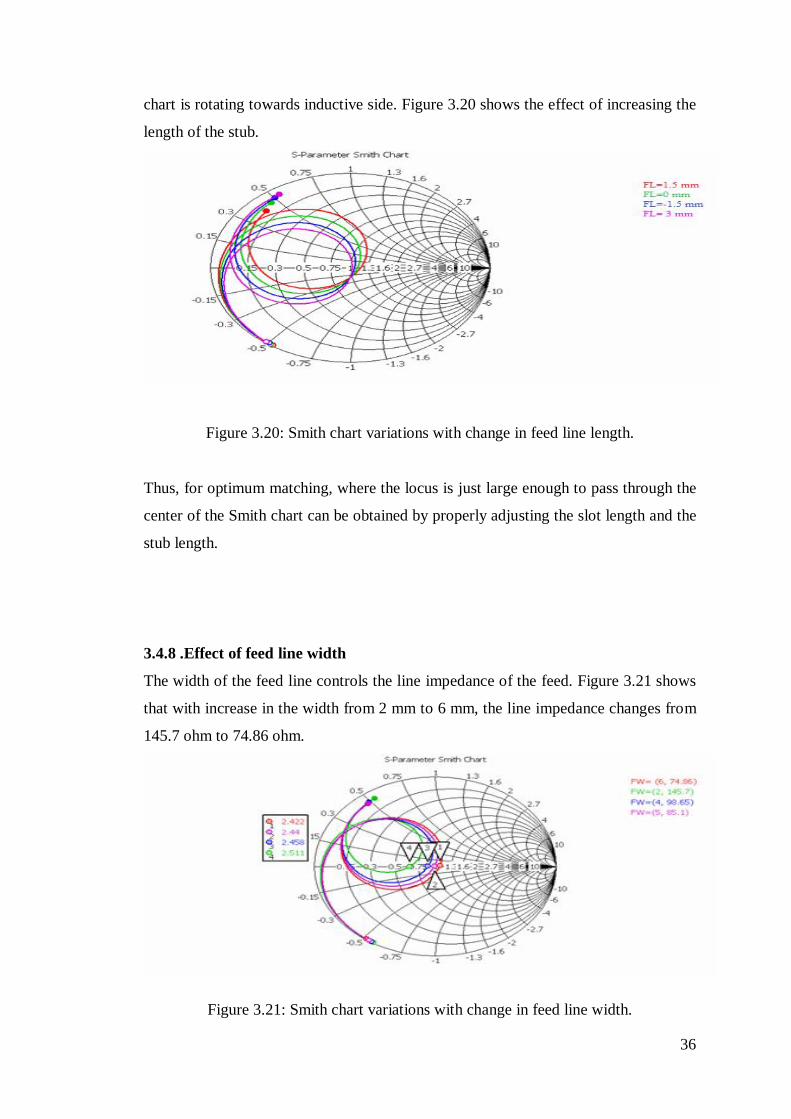
36
chart is rotating towards inductive side. Figure 3.20 shows the effect of increasing the
length of the stub.
Figure 3.20: Smith chart variations with change in feed line length.
Thus, for optimum matching, where the locus is just large enough to pass through the
center of the Smith chart can be obtained by properly adjusting the slot length and the
stub length.
3.4.8 .Effect of feed line width
The width of the feed line controls the line impedance of the feed. Figure 3.21 shows
that with increase in the width from 2 mm to 6 mm, the line impedance changes from
145.7 ohm to 74.86 ohm.
Figure 3.21: Smith chart variations with change in feed line width.

37
Also, the coupling level is affected by varying the feed line width. Figure 3.22 shows
that with increase in the width of feed line from 2 mm to 6 mm, the coupling
increases.
Figure 3.22: Variation of S-parameter with change in width of feed line.
Thus, for the desired frequency band the width of feed line selected is 6 mm.
3.4.9 Effect of height of antenna substrate
Now the height of antenna substrate is increased from 1.6 mm to 3.2 mm keeping the
other parameters same as selected in above sections. Figure 3.23 shows that with
increase in the height of the antenna substrate the bandwidth of the antenna increases.
Figure 3.23: Variation of S-parameter with change in height of antenna substrate.

38
3.4.10 Effect of changing the Antenna and Feed substrates
The resonating frequency of the antenna is dependent on the dielectric constant of the
substrates. The figure 3.24 shows that as the dielectric constant increases the
resonating frequency of the antenna decreases.
Figure 3.24: Variation of resonating frequency with change in the dielectric constant
of both substrates.
The table 3.8 shows that as the dielectric constant of the two substrates increases there
is a decrease in the resonating frequency.
Table 3.8(Dielectric constant v/s resonating frequency)
Dielectric constant 2.08 2.2 3.38 3.78 4.4 4.8 6
Resonating freq. (in GHz) 2.49 2.43 1.97 1.87 1.74 1.67 1.51
3.4.11 Effect of changing the feed substrate keeping duroid as antenna substrate
Generally, a high dielectric constant is used for the feed substrate so that the
radiations can be optimized. Hence, in this section the feed substrate is assigned
various materials like FR4, PTFE, Quartz etc keeping the antenna substrate as duroid
and the change in the resonating frequency are shown in the figure 3.25.

39
Figure 3.25: Variation in resonating frequency with change in the feed substrate.
As the feed line is etched on the feed substrate, the line impedance of the feed is also
changed. Table 3.9 shows the change in the resonating frequency and the line
impedance of the antenna with change in the feed substrate.
Table 3.9(Dielectric constant of feed substrate v/s Line impedance)
Dielectric constant of feed substrate 2.08 2.2 3.38 3.78 4.4
Resonating frequency(in GHz) 2.41 2.406 2.27 2.229 2.14
Line impedance(in ohm) 76.7 74.7 60.13 57.71 53.2
Figure 3.26 shows that as the dielectric constant of the feed substrate is increased
from 2.2 (duroid) to 4.4 (FR4), the line impedance decreases from 74.86 ohm to 53.2
ohm and the locus size increases making the impedance inductive.
Figure 3.26: Smith chart variations with change in feed substrate.
40
3.4.12 Effect of aperture shape (Defected ground structure)
Usually, a designer of microstrip circuits focuses on the analysis, synthesis, and
calculation of the microstrip circuit (conductor trace), including configuration,
dimensions, and structure of the microstrip conductor, while the ground side remains
a complete metallization structure. However, the ground plane structure can be
modified to improve electrical performance and reduce size of a microstrip circuit. In
recent years, there have been several new designs of microstrip circuits with defected
ground structure (DGS) [55- 62]. Microstrip lines with DGS have much higher
impedance and an increased slow-wave factor as compared to conventional
transmission lines. The DGS is attractive as it enables unwanted frequency rejection
and circuit size reduction. The DGS is a new type of microstrip design that exhibits
well-defined stop bands and pass bands in the transmission characteristics, and as
such it finds many applications in microwave printed circuits: filters, dividers,
amplifiers, oscillators, switches, directional couplers, antennas, etc.
The DGS applied to a microstrip line creates a resonance in the circuit, with the
resonant frequency controllable by changing the shape and the size of the slot .The
equivalent circuit of the DGS can be represented by a parallel LC resonant circuit in
series with the microstrip line. The transverse slot in the DGS increases the effective
capacitance, while the U-shaped slots attached to the transverse slot increase the
effective inductance of the microstrip line. This combination of DGS elements and
microstrip lines yields sharp resonances at microwave frequencies which can be
controlled by changing shape and size of the DGS circuitry. The shape and size of the
DGS slot controls both the fundamental resonant frequency and higher order
resonances. The size of the PCB area is also considered. To fulfill the different
requirements, a variety of DGS shapes have evolved over time, including dumbbell,
circular, bow-tie, hourglass and H-shaped structures. Figure 3.27 shows the
commonly used rectangular and dumbbell shape of the aperture.

41
Figure 3.27: a) Rectangular aperture b) Dumbbell shape etched on the ground plane.
In the antenna designed in section 3.4, a dumbbell shape is etched keeping all other
parameters fixed. The figure 3.28 shows the S-parameter of the antenna.
Figure 3.28: S-parameter of the antenna.
Figure 3.28 shows that the minimum value of S11 at 2.4343 GHz is -17.28 dB. It has
a 10 dB down bandwidth of 120 MHz covering WLAN band 2.40 GHz-2.48 GHz.
Figure 3.29 the VSWR of the antenna is shown. The VSWR of the antenna at 2.4343
GHz is 1.31.

42
Figure 3.29: VSWR of the antenna.
The DGS is realized by etching a “defective” pattern in the ground plane, which
disturbs the shield current distribution. This disturbance can change the characteristics
of a transmission line, such as equivalent capacitance or inductance, to obtain and the
band stop (“notch”) property. Figure 3.30 shows the current distribution of antenna.
Figure 3.30: Surface current distribution of the antenna.
It is inferred from the figure 3.30 that the current lines have a much greater density at
the arms of the dumbbell. A clearer view of the distribution is shown in figure 3.31.
Figure 3.31: Current distribution at arms of dumbbell of the antenna
Thus, the antenna can be used for WLAN applications.
3.4.13 Summarized dimensional parameters
43
From the section 3.4, the values of various parameters are chosen for the optimized
antenna. The selected parameters are summarized in form of table 3.10
Table 3.10 (Dimensions of the optimized antenna)
Parameter L W Lf Wf Lap Wap Ls Yos Xos H
Dimension of Single
band antenna(in mm)
25 46 23.5 6 30 3 4.5 6 0 2.4
3.5 Study of Antenna parameters
In this section the antenna parameters like directivity, gain, surface current etc are
necessary to study in the desired bands so that the antenna can be used for the WLAN.
3.5.1 Directivity
The figure 3.32 shows that the directivity of the antenna increases with increase in the
frequency.
Figure 3.32: Directivity of the antenna.
In the desired band, the directivity varies from the 4.8898 dBi to 5.7521 dBi which is
fair enough for WLAN application.
3.5.2 Gain
The figure 3.33 shows that the gain of the antenna increases with increase in the
frequency

44
Figure 3.33: Gain of the antenna.
In the desired band, the gain varies from the 5.8 dB to 6.5341 dB which is fair enough
for WLAN application. The figure 3.34 shows the absolute value of gain. The side
lobe level is -2.8 dB with respect to the main lobe at a frequency of 2.42.
Figure 3.34: Polar plot of gain.
3.5.3 Surface current
The peak surface current at the frequency of 2.45 GHz is shown in the figure 3.35.
The maximum surface current is obtained at the edges of the rectangular aperture in
the ground is 31.1 A/m.

45
Figure 3.35: Surface current of the antenna
3.5.4 Broadband far-fields
The broadband directivity, gain, E-field, H-field and power field are important
antenna parameters which a designer has to know about the antenna. Figure 3.36
shows the comparison of the far-fields calculated at a distance of 1 m from the
antenna.
Figure 3.36: Broadband far-field radiation of the antenna.
The values of the antenna parameters at 2.42 GHz are summarized in the table 3.11.
Table 3.11(Antenna parameters for optimized antenna)
Parameter Single Band
Frequency 2.42GHz

46
Directivity(dBi) 5.372
Gain(dB) 6.167
E-field(dBV/m) 20.93
H-field(dBA/m) -30.59
Power(dBW/m2) -4.834
The antenna gives a percentage bandwidth 6.125 covering the band of 2.35 GHz-2.50
GHz. The antenna has a fair directivity and gain of 5.372 dBi and 6.167 dB
respectively at frequency of 2.42 GHz. Thus, the antenna can be used for the WLAN
applications.
Chapter 4
Dual band antenna design and its parametric study
With introduction of new wireless applications, operation at two or more discrete
bands with an arbitrary separation of bands is desired. In such cases, a patch capable
of operating in multiple bands is desirable. For most applications, all bands may be
required to have the same polarization, radiation pattern, and bandwidth
characteristics. Several methods of obtaining multi-bands or wide bands have been
developed. Multi-banding of an antenna can be done by using E-shape, V-shape and
U-shape patches patches [2],[6],[60]. One method is to use separate patches abreast
each other for different applications. Stacking of the patches can also be used but it
increases the volume of the antenna. An annular ring has also been used for dual
frequency where the frequency for the propagating modes can be adjusted by
choosing the inner and the outer radii. However, the ratio of the two frequencies is
somewhat limited [39]. It is also possible to achieve dual frequency operation of a

47
patch antenna by loading slots at both the resonating side and at the non-resonating
side of the patch and by using shorting pins [38-39]. It is also desirable to have one
port and an arbitrary separation of the frequency bands. All of these requirements
impose severe constraints on the use of natural modes [38-40].
4.1 Dual band antenna design In chapter 3, an aperture coupled single band antenna for WLAN application was
designed. Now, antenna is now loaded with two slots at the non-resonating side of the
patch to make it to resonates at two frequency bands namely 2.18 GHz-2.20 GHz and
2.40 GHz-2.48 GHz for personal communication system (PCS) like smart homes and
WLAN applications respectively. Figure 4.1 shows the two antennas for the desired
applications.
Figure 4.1: View of the a) Single band antenna b) Dual band antenna with slots
When the dual band antenna was excited by a Gaussian pulse at the waveguide port
keeping all the parameters same as in case of the single band antenna, the S-parameter
of the antenna is shown in the figure 4.2

48
Figure 4.2: S-parameter of dual band antenna
From figure 4.2, it is revealed that the antenna covers a lower band of 2.1715GHz-
2.2216GHz which is apt enough to be used for PCS and a higher band of 2.4265 GHz-
2.5133GHz can be used for WLAN applications.
In figure 4.3, the Smith chart shows that the line impedance of the antenna is 74.86
ohm which can be easily matched with a 75 ohm SMA connector while testing the
antenna.
Figure 4.3: Smith chart of the dual band antenna.
It also depicts that the antenna resonates at 2.2 GHz and 2.466GHz for the dual band
operation. It is consists of two circles apart from a very small circle where antenna
seems to resonate at 1.76GHz but at this frequency the VSWR of the antenna is
greater than 2,so it cannot be considered as the resonating frequency
4.2 Parametric study of the antenna

49
The parametric study of the proposed antenna is done using CST microwave studio.
The effect of variation of different offsets and length is given below:
4.2.1 Effect of the change in the Offset (doff)
The variations in the resonating frequency with offset (doff) is shown in figure 4.4.
When the value of the offset is increased from 1mm to 4mm, there is a decrease in the
resonant frequency and impedance matching of the antenna.
Figure 4.4: Variation of S-parameter with change in the Slot Offset (doff).
The slots loaded have an optimum offset (doff) equals to 2mm is chosen. The antenna
parameters for the various offset values are tabulated in table 4.1.
Table 4.1 (Antenna parameters with varying Offset)
Offset=1 mm Offset=2 mm Offset=3 mm Offset=4 mm Parameters
Fr=2.2
GHz
Fr=2.45
GHz
Fr=2.2
GHz
Fr=2.45
GHz
Fr=2.2
GHz
Fr=2.45
GHz
Fr=2.2
GHz
Fr=2.45
GHz
Directivity
(in dBi)
4.616 5.321 5.029 5.388 5.612 5.454 5.063 5.420
Gain(in dB) 5.458 6.148 5.845 6.215 6.357 6.272 4.935 6.227
E-Field (in
dBV/m)
19.01 20.62 20.53 20.92 18.04 21.04 8.011 20.99
H-Fiel d(in
dBA/m)
-32.51 -30.90 -30.99 -30.60 -33.48 -30.48 -43.51 -30.53
P-field (in
dBW/m2)
-6.753 -5.142 -5.233 -4.842 -7.717 -4.723 -17.75 -4.767
4.2.2 Effect of change in the length (L2) of slot 2 keeping the length (L1) of slot 1
constant

50
The slot length also affects the resonating frequency and bandwidth of the antenna.
Figure 4.5 show the variation of resonant frequency and bandwidth of antenna when
length (L2) of slot 2 is varied from 7 mm to11mm keeping the length (L1) of the slot1
is fixed at 11 mm. With increase in the length L2, there is decrease in matching
characteristics but increase in the bandwidth of the antenna. The resonating frequency
of the both the bands decrease with the increase in the length of slot 2. Also, there is a
significant shift in the resonant frequency of the lower band as compared to the higher
band, showing that the slot 2 is responsible for resonating at low frequencies.
Figure 4.5: Variation of S-parameter with change in length of slot2.
From the figure 4.5, the length L2 equals to 7 mm is chosen as it gives us the
desirable bands at 2.2005 GHz and 2.4658 GHz. The antenna parameters for variable
length L2 are tabulated in table 4.2
Table 4.2 (Antenna parameters with varying L2)
L2=7mm
L2=8mm L2=9mm L2=10mm L2=11mm Parameter
s
Fr=2.
2GHz
Fr=2.
45GH
z
Fr=2.2
GHz
Fr=2.4
5GHz
Fr=2.2
GHz
Fr=2.4
5GHz
Fr=2.2
GHz
Fr=2.4
5GHz
Fr=2.2
GHz
Fr=2.4
5GHz
Directivity
(in dBi)
5.029 5.388 5.763 5.461 3.989 5.23 4.021 5.551 4.054 5.580
Gain(in
dB)
5.845 6.215 6.488 6.270 4.804 6.331 4.735 6.349 4.877 6.366
E-Field(in
dBV/m)
20.53 20.92 17.04 21.02 11.45 20.97 14.95 20.88 16.11 20.79

51
H-Field(in
dBA/m)
-
30.99
-
30.60
-34.49 -30.50 -40.07 -30.55 -36.57 -30.64 -35.41 -30.73
P field(in
dBW/ m2)
-
5.233
-
4.842
-8.725 -4.737 -14.31 -4.793 -10.81 -4.882 -9.653 -4.971
Figure 4.6 reveals that surface current at 2.2 GHz is highest near the slot 2 proving
that slot 2 is responsible for the resonating at the lower frequency band. The
maximum value of the surface current is 69.2 A/m.
Figure 4.6: Surface current of the antenna at 2.2 GHz.
4.2.3 Effect of change in the length (L1) of slot 1 keeping the length (L2) of slot2
constant
The variation of resonant frequency and impedance characteristics with length (L1) is
shown in figure 4.7. The length (L1) of slot 1 is varied from 7mm to 11mm keeping
the length L2 of slot 2 at 7mm. With increase in slot length L1 the resonant frequency
decreases. It is observed from the figure 4.7 that the higher band frequency subjects to
a much greater change due to increase in length of slot 1 as compared to lower
frequency band.

52
Figure 4.7:- Variation of S-parameter with change in length of slot1.
The length L1 equals to 11 mm is chosen as it gives the optimum results for the
desired application. The antenna parameters variable length L1 studied are tabulated
in table 4.3
Table 4.3 (Antenna parameters with varying L1)
L1=7mm
L1=8mm L1=9mm L1=10mm L1=11mm Parameters
Fr=2.2
GHz
Fr=2.45
GHz
Fr=2.2
GHz
Fr=2.45
GHz
Fr=2.2
GHz
Fr=2.45
GHz
Fr=2.2
GHz
Fr=2.45
GHz
Fr=2.2
GHz
Fr=2.45
GHz
Directivity(i
n dBi)
4.730 2.993 4.789 3.940 4.842 4.874 4.922 5.213 5.029 5.388
Gain(in dB) 5.556 3.535 5.619 4.833 5.661 5.733 5.737 6.054 5.845 6.215
E-Field (in
dBV/m)
19.94 3.720 20.13 13.07 20.23 18.45 20.38 20.27 20.53 20.92
H-Field (in
dBA/m)
-31.58 -47.80 -31.39 -38.45 -31.29 -33.07 -31.14 -31.25 -30.99 -30.60
P-Field (in
dBW/m2)
-5.824 -22.04 -5.632 -12.69 -5.526 -7.306 -5.380 -5.488 -5.233 -4.842
Figure 4.8 shows the surface current of the antenna at 2.45 GHz. The slot 1 is
responsible for radiations at the higher frequency band as the current due to slot 2
seems to be cancelled by oppositely flowing current. The maximum surface current at
2.45 GHz is 47.284 A/m.

53
Figure 4.8: Surface current of the antenna at 2.45 GHz.
4.2.4 Effect of change in the Slot Widths
The variation of resonant frequency with the slot width (W1) from 1mm to 4mm
symmetrically for both the slots is shown in figure 4.9. By increasing slot width from
1mm to 4 mm, decreases the resonating frequency and the coupling level.
Figure 4.9: Variation of S-parameter with change in width of the two slots
symmetrically.
The value of slot width equals to 2 mm is chosen corresponding to which the antenna
covers the frequency bands of 2.2 GHz and 2.46 GHz.
4.3 Comparison of Single and Dual band antenna
In chapter 3, single band antenna is designed for WLAN application. In this chapter,
the dual band antenna is designed. Figure 4.10 shows comparison of the two antennas
in terms of S-parameter.

54
Figure 4.10: S-parameter of the two antennas.
For the single band antenna, it can be inferred that, it resonates in the range 2.3603
GHz-2.4973 GHz, giving us a 10 dB bandwidth of 137 MHz which covers the WLAN
standard 2.40-2.48 GHz. The minimum return loss is obtained at the resonating
frequency 2.4284 GHz is -30.063 dB. For the dual band antenna, there are two bands
covering the ranges 2.18 GHz-2.20 GHz and the 2.40 GHz- 2.48 GHz. The bandwidth
of the antenna at the lower and the higher bands is 46MHz and 85 MHz respectively.
Also, the minimum return loss of the antenna at lower and higher bands is -16.907 dB
and -41 dB respectively. Figure 4.11 shows the Smith chart of the two antennas.
Figure 4.11: Smith chart of two antennas.
The figure 4.11 shows the Smith chart of the two antennas. The line impedance of the
antenna is 74.86 ohm which can be easily matched with a 75 ohm SMA connector
while testing the antenna. The Smith chart of the antenna shows the antenna
resonates at 2.423GHz for single and 2.2 GHz and 2.466 GHz for the double band

55
operation. It can also be inferred that the single band antenna have only one resistance
circle and the double band has two apart from a very small circle where antenna
seems to resonate at 1.76GHz but at this frequency the VSWR of the antenna is
greater than 2,so it cannot be considered as the resonating frequency. The comparison
of antenna parameters for both the antennas is listed in the Table 4.4.
Table 4.4 (Comparison of antenna parameters for designed the antennas)
Parameters Single
Band
Double Band
Frequency 2.42
GHz
2.20
GHz
2.45
GHz
Directivity(dBi) 5.372 5.033 5.402
Gain(dB) 6.167 5.849 6.229
E-field(dBV/m) 20.93 20.53 20.93
H-field(dBA/m) -30.59 -30.99 -30.59
Power(dBW/m2) -4.834 -4.828 -4.828
The directivity of the antennas is above 5dBi in each case, makes it suitable for the
wireless applications. They have an appreciable gain of around 6 dB. The E-field, H-
field and the Power measured at a distance of 1metre are also listed. The table 4.4
shows that the directivity of the antenna at 2.20GHz and 2.46GHz as 5.033dBi and
5.402dBi, and gain as 5.849dB and 6.0229dB respectively. These values are fair
enough to be used for the PCS and WLAN applications.
4.4 Fabrication of the antenna The hardware design of the antenna includes two processes namely PCB (Printed
circuit board) design and testing of the antenna. The various steps for the PCB design
are explained as:
1) Drafting of the layers on transparent sheet: - Firstly all layers of the antenna to
be designed are drafted on a transparent sheet whose photo is taken by the
camera on a film containing silver bromide coating in a dark room. If the
dimensions are very small, then the scaled diagram of the layers can be drawn
and the camera settings are changed accordingly. Figure 4.12 shows the layers
drafted on a transparent sheet.

56
2) Negative developing: - The film with silver coating is washed in A+B solution
for not more than 2-3 minutes otherwise the whole film will become black.
Then, the film is washed in the negative developer and dried at a temperature
up to 50-60 Now, the negative of the layers is obtained and can be taken to
sunlight. Figure 4.13 and 4.14 shows the negatives of the different layers.
Figure 4.12: Layer drafted on transparent sheet a) Feedline b) Aperture in ground
c) Patch of single band antenna.
Figure 4.13: Negatives of a) Feedline b) Aperture in ground slot.
3) Operations on PCB: - The PCB is cleaned with a brush and cut in the desired
size. Now the PCB is dipped once in the photo resist developer placed in
yellow light. It dried in an oven for 3-5 minutes. Now the negatives are put on
the PCB with proper alignment and exposed to ultraviolet radiations for 3

57
minutes. The PCB is washed carefully with photo resist developer in a well
cleaned container and etching is done with FeCl3. The designed PCB is shown
in the figure 4.15.
Figure 4.14: Negatives of Patches of a) Single band antenna b) Double band antenna.
Figure 4.15: Patches of a) Single b) Double band antenna.
Draft the layers of antenna on a transparent sheet.
Take photo of the layers on the negative by using a
camera.
Brush the
PCB
Cut PCB into required size.

58
Figure 4.16: Fabricate flow of the PCB design.
The steps for antenna fabrication are shown via a flowchart drawn in the figure 4.16.
The two fabricated PCBs are joined with adhesive and a SMA connector is soldered at
the feed point and the antenna is ready for the testing.
Chapter 5

59
Conclusion and Future Work
5.1 Conclusion
In this report, firstly an aperture coupled, rectangular patch single band antenna was
designed which resonates at 2.43 GHz and provides a bandwidth of 142 MHz, hence,
this antenna can be used for the WLAN applications. The designed antenna provides a
percentage bandwidth 5.84. The physical parameters examined in this study include
the dimensions and locations of the substrates and their dielectric constants, feed line,
ground plane coupling slot, and patch. The antenna parameters like operating
frequency, input impedance, VSWR, Bandwidth, Return loss, directivity and gain are
determined for each antenna configuration. Also, the effect of the physical parameters
is studied on the antenna parameters.
The designed antenna is loaded with two appropriately positioned and dimensioned
slots at the non-resonating sides of the patch making it to dual band resonating at 2.20
GHz and 2.45 GHz. The percentage bandwidth of the dual band antenna at 2.20 GHz
and 2.45 GHz is 2.27and 3.67 respectively. The directivity and gain of the antenna are
fair enough to be used for the personal communication system and WLAN
applications.
5.2 Future Work
The research work could be extended to
Multibanding of the antenna for various wireless applications.
Array designing to enhance the gain and other antenna properties.
Optimization of the antenna using Genetic algorithm, Neural network, PSO
(Particle Swarm optimization).
The antenna could be easily fabricated and tested for the desired results.

60
List of publication
Ved Prakash, Dr. Rajesh Khanna, “Aperture Coupled Microstrip Antenna For
WLAN Applications” , SPIN conference, Feb 23-24, 2011,
Communicated:
Ved Prakash, Dr. Rajesh Khanna, “Dual Band Aperture Coupled Rectangular Patch Antenna For PCS and WLAN Applications”, to International of Communication Engineering Applications, to be published in July 2011.
61
References [1] G. A. Deschamps, “Microstrip microwave antennas”, 3rd USAF Symposium on
Antennas, 1953.
[2] I. J. Bahl and P. Bhartia, Microstrip Antennas, Artech House, 1980.
[3] James, J. R., and P. S. Hall, Handbook of Microstrip Antennas, Vol. 1, London:
Peter Peregrinus Ltd., 1989.
[4] Lee, H. F., and W. Chen, Advances in Microstrip and Printed Antennas, New
York: John Wiley & Sons, 1997.
[5] G. Kumar and K. P. Ray, Broadband Microstrip Antennas, Artech House, 2003.
[6] C. A. Balanis, Antenna Theory, 3rd ed. John Wiley & Sons, Hoboken, NJ, 2005.
[7] Waterhouse, Microstrip Patch Antennas, World scientific publication house
co.pte.ltd, 2003.
[8] Bhatacharya, A. K., and R. Garg, ‘‘Generalized Transmission Line Model for
Microstrip Patches,” IEE Proc. Microwaves, Antennas Propagation, Pt. H, Vol. 132,
No. 2, pp. 93–98, 1985.
[9] Dubost, G., and G. Beauquet, ‘‘Linear Transmission Line Model Analysis of a
Circular Patch Antenna,” Electronics Letters, Vol. 22, pp. 1174–1176, October 1986.
[10] Babu, S., I. Singh, and G. Kumar, ‘‘Improved Linear Transmission Line Model
for Rectangular, Circular and Triangular Microstrip Antennas,’’ IEEE AP-S Int.
Symp. Digest, pp. 614–617, July 1997.
[11] Lo, Y. T., D. Solomon, and W. F. Richards, ‘‘Theory and Experiment on
Microstrip Antennas,” IEEE Trans. Antennas Propagation, Vol. AP-27, pp. 137–145,
March 1979.
[12] Richards, W. F., Y. T. Lo, and D. D. Harrison, ‘‘An Improved Theory for
Microstrip
Antennas and Applications,” IEEE Trans. Antennas Propagation, Vol. AP-29, pp. 38–
46 January 1981.
[13] Lo, T., and S. W. Lee, Antenna Handbook, New York: Van Nostrand Reinhold,
1988
[14] Kane Yee, "Numerical solution of initial boundary value problems involving
Maxwell's equations in isotropic media". IEEE Transactions on Antennas and
Propagation”, 302–307, 1966.

62
[15] A. Taflove ,"Application of the finite-difference time-domain method to
sinusoidal steady state electromagnetic penetration problems”. IEEE Transactions on
Electromagnetic Compatibility, 191–202, 1980.
[16] Lee, H. F., and W. Chen, Advances in Microstrip and Printed Antennas, New
York: John Wiley & Sons, 1997.
[17]http://en.wikipedia.org/wiki/Finite-difference_time-domain_method last accessed
on June 15,2011.
[18]http://photonics.tfp.unikarlsruhe.de/fileadmin/conferences/heraeus386/Heraeus38
6_Lavrinenko. pdf last accessed on June 15, 2011.
[19] D. M. Pozar, “A Microstrip Antenna Aperture Coupled to a Microstrip Line”,
Electronics Letters, Vol. 21, pp.49-50, January 17, 1985.
[20] D. M. Pozar, “Microstrip antennas”, IEEE Proc., vol. 80, pp. 79-91, January
1992.
[21] D. H. Schaubert, “Microstrip antennas”, Electromagnetics, vol. 12, pp. 381-401,
1992.
[22] D. M. Pozar, “A Review of Aperture Coupled Microstrip Antennas: History,
Operation, Development, and Applications”, 1996
[23] D. M. Pozar and D. H. Schaubert, Microstrip Antennas: The analysis and design
of microstrip antennas and arrays, IEEE Press, New York, 1995.
[24] Y. Yoshimura, “A microstripline slot antenna”, IEEE Trans. Microwave Theory
and Techniques, vol. MTT-20, pp. 760-762, November 1972.
[25] J.-F. Zurcher, “The SSFIP: A global concept for high performance broadband
planar antennas”, Electronics Letters, vol. 24, pp. 1433-1435, November 1988.
[26] S. Targonski and D. M. Pozar, “Design of wideband circularly polarized aperture
coupled microstrip antennas”, IEEE Trans. Antennas and Propagation, vol. 41, pp.
214-220, February 1993.
[27] F. Croq and A. Papiernik, “Large bandwidth aperture coupled microstrip
antenna”, Electronics Letters, vol. 26, pp. 1293-1294, August 1990.
[28] F. Croq and A. Papiernik, “Stacked slot-coupled printed antenna”, IEEE
Microwave and Guided Wave Letters, vol. 1, pp. 288-290, October 1991.
[29] F. Croq and D. M. Pozar, “Millimeter wave design of wide-band aperture
coupled stacked microstrip antennas”, IEEE Trans. Antennas and Propagation, vol.
39, pp. 1770-1776, December 1991.

63
[30] M. Edimo, P. Rigoland, and C. Terret, “Wideband dual polarized aperture
coupled stacked patch antenna array operating in C-band”, Electronics Letters, vol.
30, pp. 1196-1197, July 1994.
[31] S. D. Targonski and R. B. Waterhouse, “An aperture coupled stacked patch
antenna with 50% bandwidth”, IEEE International Symposium on Antennas and
Propagation, Baltimore, MD. 1996.
[32] H.S. Shin and N. Kim “Wideband and high-gain one-patch microstrip antenna
coupled with H-shaped aperture” Electronics Letters, Vol. 38 No.19, 12th September
2002.
[33] R. Joseph and T. Fukusako, “Bandwidth enhancement of circularly polarized
square slot antenna” Progress In Electromagnetics Research B, Vol. 29, 233-250,
2011.
[34] B. Vedaprabhu and K. J. Vinoy, “ An Integrated wideband multifunctional
antenna using a microstrip patch with two U-slots” Progress In Electromagnetics
Research B, Vol. 22, 221-235, 2010
[35] C.-J. Wang and S.-W. Chang, “Studies on dual-band Multi-slot antennas”
Progress In Electromagnetics Research, PIER 83, 293–306, 2008
[36] S. Maci and G. BifJi Gentili, “ Dual-Frequency Patch Antennas” IEEE
Antennas and Propagation Magazine, Vol. 39, No. 6, December 1997.
[37] J. C. Liu,B. H. Zeng, C. Y. Liu, H. C. Wu and C. C. Chang, “ A dual-mode
Aperture-coupled Stack antenna for WLAN dual-band and circular polarization
applications, Progress In Electromagnetics Research C, Vol. 17, 193-202, 2010.
[38] Wang,B.F., and Y.T.Lo, “Microstrip Antennas for Dual Frequency
Operation”,IEEE trans. Antennas and Propagation,Vol. AP-32., pp 938-943, 1984.
[39] Yazidi, M.El, M.Himdi, and J.P. Daniel,” Aperture Coupled Microstrip Antennas
for Dual Frequency operation,” Electron. Lett. , Vol-29,pp. 1506-1508, 1993
[40] Lu, J.-H, “Single feed Dual frequency rectangular microstrip Antenna with pair
of step-slots,” Electron.Lett. , vol.35,, pp. 354-355. 1999.
[41] Rashid A. Saeed, S. Khatun, Borhanuddin, M. A. Khazani, Rania A. Mokhtar
and Mahmoud Alshamary, “ Design of Single Fed Aperture Coupled Microstrip
Antennas for WLAN” IEEE, 2005
[42] O. Tze-Meng and T. K. Geok, “ A dual-band Omni-directional microstrip
antenna” Progress In Electromagnetics Research, Vol. 106, 363–376, 2010.

64
[43] Y.-C. Lee and J.-S. Sun, “ Compact Printed slot antennas for Wireless Dual and
Multi-band operations” Progress In Electromagnetics Research, PIER 88, 289–305,
2008
[44] C. Mahatthanajatuphat, S. Saleekaw, and P. Akkaraekthalin and M. Krairiksh, “
A Rhombic patch Monopole antenna with modified Minkowski fractal geometry for
UMTS, WLAN, and MOBILE WIMAX application” Progress In Electromagnetics
Research, PIER 89, 57–74, 2009
[45] C. Mahatthanajatuphat and P. Akkaraekthalin and S. Saleekaw, “A Bidirectional
Multiband antenna with modified Fractal slot fed by CPW” Progress In
Electromagnetics Research, PIER 95, 59-72, 2009.
[46] R. S. Aziz, M. A. S. Alkanhal, and A. F. A. Sheta, “Multiband fractal-like
antennas” Progress In Electromagnetics Research B, Vol. 29, 339-354, 2011.
[47] F. Bilotti and C. Vegni, “ Design of Polygonal patch antennas for portable
devices” Progress In Electromagnetics Research B, Vol. 24, 33-47, 2010.
[48] P. L. Sullivan and D. H. Schaubert, “Analysis of an aperture coupled microstrip
antenna”, IEEE Trans. Antennas and Propagation, vol. AP-34, pp. 977-984, August
1986.
[49] D. M. Pozar, “A reciprocity method of analysis for printed slot and slot coupled
microstrip antennas”, IEEE Trans. Antennas and Propagation, vol. AP-34, pp. 1439-
1446, December 1986
[50] M. Himdi, J. P. Daniel, and C. Terret, “Analysis of aperture coupled microstrip
antenna using cavity method”, Electronics Letters, vol. 25, pp. 391-392, March 1989.
[51] M. El Yazidi, M. Himdi, and J. P. Daniel, “Transmission line analysis of non-
linear analysis of slot coupled microstrip antenna”, Electronics Letters, vol. 28, pp.
1406-1407, July 1992
[52] D. Yau and N. V. Shuley, “Numerical analysis of an Aperture Coupled
Microstrip Patch antenna using Mixed Potential Integral equations and complex
images” Progress In Electromagnetics Research, PIER 18, 229–244, 1998.
[53] S.-Q. Xiao, Z. H. Shao, and B.-Z. Wang, “ Application of the improved Matrix
type FDTD method for active antenna analysis” Progress In Electromagnetics
Research, PIER 100, 245-263, 2010.
[54] J. Li, L.-X. Guo, and H. Zeng, “FDTD method investigation on the polarimetric
scattering from 2-d rough surface” Progress In Electromagnetics Research, PIER 101,
173-188, 2010.

65
[55] Y.-H. Liu and Q. H. Liu and Z.-P. Nie, “ A new efficient FDTD time-to-
frequency domain conversion algorithm” Progress In Electromagnetics Research,
PIER 92, 33–46, 2009.
[56] J. P. Geng, J. J. Li, R. H. Jin, S. Ye, X. L. Liang and M. Z. Li, “ The
development of curved microstrip antenna with defected ground structure” Progress
In Electromagnetics Research, PIER 98, 53-73, 2009.
[57] J.-Y. Sze T.-H. Hu and T.-J. Chen, “ Compact Dual-band Annular-ring slot
antenna with meandered grounded strip” Progress In Electromagnetics Research,
PIER 95, 299-308, 2009
[58] J. Lim, J. Lee, J. Lee, S.-M. Han, and D. Ahn and Y. Jeong, “ A new calculation
method for the characteristic impedance of transmission lines with modified ground
structures or perturbation” Progress In Electromagnetics Research, Vol. 106, 147-
162, 2010.
[59] C. Wu, J. Wang, R. Fralich, and J. Litva, “Analysis of a series-fed aperture
coupled patch array antenna”, Microwave and Optical Technology Letters, vol. 4, pp.
110-113, February 1991.
[60] P.K. Singhal, Piyush Moghe.”Design of single layer E-shape Microstrip Patch
Antenna”,IEEE,APMC proceeding,2005
[61] Kuchar, Alexander. "Aperture-Coupled Microstrip Patch Antenna Array."
Thesis. Technische Universität Wien, 1996.
[62] Manandhar, D. GPS reflected signal analysis using software receiver. Journal of
GlobalPositioning Systems, 5(1–2), 29–34, 2006.