Design Example Report
71
Power Integrations 5245 Hellyer Avenue, San Jose, CA 95138 USA. Tel: +1 408 414 9200 Fax: +1 408 414 9201 www.power.com Design Example Report Title 275 W PFC Front-End Using HiperPFS TM -4 PFS7627H Specification 100 VAC – 300 VAC Input; 440 VDC Output Application PFC Front-End Author Applications Engineering Department Document Number DER-547 Date August 23, 2017 Revision 1.1 Summary and Features Wide operating range 100 VAC – 300 VAC Highly integrated, low component count, low-cost PFC Ultra-low reverse recovery loss diode (Qspeed TM ) Power Integrations eSIP-16 low-profile controller package “Cool-Pad” package reduces IC mounting hardware Eliminates insulating pad/heat-spreader EN61000-3-2 Class-D compliant High PFC efficiency enables up to 80+ Platinum PC Main design Enhanced light load power factor (PF) PF >0.95 at 20% load and 230 VAC, 50 Hz input PF >0.95 at 50% load Frequency sliding maintains high efficiency across load range >95% from 20% to 100% load (115 VAC and 230 VAC input) Feed forward line sense gain – maintains relatively constant loop gain over entire operating voltage range Excellent transient load response Frequency adjusted over input line voltage and load Spread-spectrum across >60 kHz window simplifies EMI filtering requirements PATENT INFORMATION The products and applications illustrated herein (including transformer construction and circuits external to the products) may be covered by one or more U.S. and foreign patents, or potentially by pending U.S. and foreign patent applications assigned to Power Integrations. A complete list of Power Integrations' patents may be found at www.powerint.com. Power Integrations grants its customers a license under certain patent rights as set forth at <http://www.powerint.com/ip.htm>.
-
Upload
khangminh22 -
Category
Documents
-
view
0 -
download
0
Transcript of Design Example Report

Power Integrations 5245 Hellyer Avenue, San Jose, CA 95138 USA. Tel: +1 408 414 9200 Fax: +1 408 414 9201
www.power.com
Design Example Report
Title 275 W PFC Front-End Using HiperPFSTM-4 PFS7627H
Specification 100 VAC – 300 VAC Input; 440 VDC Output
Application PFC Front-End
Author Applications Engineering Department
Document Number DER-547
Date August 23, 2017
Revision 1.1
Summary and Features Wide operating range 100 VAC – 300 VAC Highly integrated, low component count, low-cost PFC Ultra-low reverse recovery loss diode (QspeedTM) Power Integrations eSIP-16 low-profile controller package “Cool-Pad” package reduces IC mounting hardware
Eliminates insulating pad/heat-spreader EN61000-3-2 Class-D compliant High PFC efficiency enables up to 80+ Platinum PC Main design Enhanced light load power factor (PF)
PF >0.95 at 20% load and 230 VAC, 50 Hz input PF >0.95 at 50% load
Frequency sliding maintains high efficiency across load range >95% from 20% to 100% load (115 VAC and 230 VAC input)
Feed forward line sense gain – maintains relatively constant loop gain over entire operating voltage range Excellent transient load response Frequency adjusted over input line voltage and load
Spread-spectrum across >60 kHz window simplifies EMI filtering requirements
PATENT INFORMATION The products and applications illustrated herein (including transformer construction and circuits external to the products) may be covered by one or more U.S. and foreign patents, or potentially by pending U.S. and foreign patent applications assigned to Power Integrations. A complete list of Power Integrations' patents may be found at www.powerint.com. Power Integrations grants its customers a license under certain patent rights as set forth at <http://www.powerint.com/ip.htm>.

DER-547 275 W PFC Front-End 23-Aug-17
Page 2 of 71
Power Integrations, Inc. Tel: +1 408 414 9200 Fax: +1 408 414 9201 www.power.com
Table of Contents Introduction ...................................................................................................... 5 11.1 Basic Specifications ...................................................................................... 5 1.2 Design for High Bus Voltage ......................................................................... 8
Power Supply Specification ................................................................................. 9 2 Schematic ....................................................................................................... 10 3 Circuit Description ............................................................................................ 11 44.1 Input EMI Filter and Rectifier ...................................................................... 11 4.2 PFS7627H Boost Converter ......................................................................... 11 4.3 Input Feed Forward Sense Circuit ............................................................... 12 4.4 Output Feedback ....................................................................................... 12 4.5 Bias Supply Series Regulator ...................................................................... 12
PCB Layout ...................................................................................................... 13 5 Bill of Materials ................................................................................................ 15 6 Inductor Design Spreadsheet ............................................................................ 17 7 Switching Inductor Specification ........................................................................ 22 88.1 Electrical Diagram ...................................................................................... 22 8.2 Electrical Specifications .............................................................................. 22 8.3 Material List .............................................................................................. 22 8.4 Inductor Build Diagram .............................................................................. 23 8.5 Inductor Construction ................................................................................ 23 8.6 Winding Illustrations .................................................................................. 24
eSIP U1 Heat Sink ............................................................................................ 27 99.1 eSIP U1 Heat Sink Machining Drawing ......................................................... 27 9.2 eSIP U1 Heat Sink Fabrication Drawing ....................................................... 28 9.3 eSIP U1 Assembly to Heat Sink Drawing ...................................................... 29 Performance Data ......................................................................................... 30 1010.1 No-Load / Light Load Input Power .............................................................. 30 10.2 PFC Efficiency ........................................................................................... 32 10.3 Input Power Factor .................................................................................... 33 10.4 Regulation ................................................................................................ 34
Load Regulation .................................................................................. 34 10.4.1 Line Regulation ................................................................................... 35 10.4.2
10.5 THD ......................................................................................................... 36 10.6 Input Current Harmonic Distortion (IEC 61000-3-2 Class-D) .......................... 37
50% Load at Output ........................................................................... 37 10.6.1 100% Load at Output .......................................................................... 38 10.6.2
Thermal Performance .................................................................................... 39 1111.1 115 VAC Thermal Measurements ................................................................ 40 11.2 230 VAC Thermal Measurements ................................................................ 40 Input Waveforms .......................................................................................... 41 1212.1 Input Current at 115 VAC and 60 Hz ........................................................... 41 12.2 Input Current at 230 VAC and 50 Hz ........................................................... 41

23-Aug-17 DER-547 275 W PFC Front-End
Page 3 of 71
Power Integrations Tel: +1 408 414 9200 Fax: +1 408 414 9201
www.power.com
12.3 Input Current at 277 VAC and 50 Hz ........................................................... 42 12.4 Start-up Waveforms ................................................................................... 42
100 VAC and 60 Hz ............................................................................. 42 12.4.1 115 VAC and 60 Hz ............................................................................. 43 12.4.2 230 VAC and 50 Hz ............................................................................. 43 12.4.3 264 VAC and 50 Hz ............................................................................. 44 12.4.4 277 VAC and 50 Hz ............................................................................. 44 12.4.5 300 VAC and 50 Hz ............................................................................. 45 12.4.6
12.5 Load Transient Response ........................................................................... 46 100 VAC, 60 Hz ................................................................................... 46 12.5.1 115 VAC, 60 Hz ................................................................................... 46 12.5.2 230 VAC, 50 Hz ................................................................................... 47 12.5.3 264 VAC , 50 Hz .................................................................................. 47 12.5.4 277 VAC, 50 Hz ................................................................................... 48 12.5.5 300 VAC, 50 Hz ................................................................................... 48 12.5.6
12.6 Line Dropout ............................................................................................. 49 1000 ms Line Dropout (115 VAC / 60 Hz and 230 VAC / 50 Hz) .............. 49 12.6.1 One Cycle Line Dropout (115 VAC / 60 Hz and 230 VAC / 50 Hz) ............ 50 12.6.2
12.7 Input Line Step .......................................................................................... 50 Line Sag (115 VAC ~ 85 VAC ~ 115 VAC, 60 Hz) ................................... 50 12.7.1 Line Swell (132 VAC ~ 147 VAC ~ 132 VAC, 60 Hz) ............................... 51 12.7.2 Line Sag (230 VAC ~ 170 VAC ~ 230 VAC, 50 Hz) ................................. 51 12.7.3 Line Swell (264 VAC ~ 300 VAC ~ 264 VAC, 50 Hz) ............................... 52 12.7.4 Line Swell (300 VAC ~ 410 VAC ~ 300 VAC, 50 Hz) ............................... 52 12.7.5
12.8 Power Good (PG) ....................................................................................... 53 115 VAC and 60 Hz ............................................................................. 53 12.8.1 230 VAC and 50 Hz ............................................................................. 53 12.8.2
12.9 Brown-In and Brown-Out at 6 V / Minute Rate ............................................. 54 Thresholds ......................................................................................... 54 12.9.1 Waveforms ......................................................................................... 54 12.9.2 Drain Voltage and Inductor Current ...................................................... 56 12.9.3
12.10 Output Ripple Measurements ................................................................... 57 Ripple Measurement Technique......................................................... 57 12.10.1 Measurement Results ....................................................................... 58 12.10.2
12.11 Gain-Phase Measurement Procedure and Results ...................................... 61 Measured Bode Plots ........................................................................ 62 12.11.1
Line Surge Test............................................................................................. 63 1313.1 Differential Mode Surge .............................................................................. 64 13.2 Common Mode Surge ................................................................................. 64 EMI Scans .................................................................................................... 65 1414.1 EMI Test Set-up ........................................................................................ 65 14.2 EMI Scans ................................................................................................. 67 Appendix A ................................................................................................... 69 15

DER-547 275 W PFC Front-End 23-Aug-17
Page 4 of 71
Power Integrations, Inc. Tel: +1 408 414 9200 Fax: +1 408 414 9201 www.power.com
15.1 Test Set-up for Efficiency Measurement ....................................................... 69 Revision History ............................................................................................ 70 16
Important Note: All testing should be performed using an isolation transformer to provide the AC input to the prototype board.

23-Aug-17 DER-547 275 W PFC Front-End
Page 5 of 71
Power Integrations Tel: +1 408 414 9200 Fax: +1 408 414 9201
www.power.com
1 Introduction
1.1 Basic Specifications This engineering report describes a PFC power supply utilizing a HiperPFS-4 PFS7627H PFC controller with integrated power MOSFET and external boost diode. This power supply is intended as a general purpose platform that operates from 100 VAC to 300 VAC input voltage and provides a regulated 440 V DC output voltage and continuous output power of 275 W. The DER-547 power supply is designed to operate with forced air cooling greater than 200 LFM for all input and load conditions up to the rated maximum ambient temperature of 50 ºC. This document contains the power supply specification, schematic, bill of materials, inductor documentation, printed circuit layout, and performance data.
Figure 1 – Populated Circuit Board Photograph (Angle View).

DER-547 275 W PFC Front-End 23-Aug-17
Page 6 of 71
Power Integrations, Inc. Tel: +1 408 414 9200 Fax: +1 408 414 9201 www.power.com
Figure 2 – Populated Circuit Board Photograph (Top View).

23-Aug-17 DER-547 275 W PFC Front-End
Page 7 of 71
Power Integrations Tel: +1 408 414 9200 Fax: +1 408 414 9201
www.power.com
Figure 3 – Populated Circuit Board Photograph (Back View).

DER-547 275 W PFC Front-End 23-Aug-17
Page 8 of 71
Power Integrations, Inc. Tel: +1 408 414 9200 Fax: +1 408 414 9201 www.power.com
1.2 Design for High Bus Voltage The DER-547 is a 275 W PFC design using the HiperPFS-4, PFS7627H from Power Integrations. Its input voltage range deviates slightly from the nominal universal operating range of 90 VAC to 265 VAC to an extended range of 100 VAC to 300 VAC. The output voltage is set to 440 VDC to accommodate input voltages greater than 265 VAC. To set the output voltage R19, see Figure 4, the lower resistor in the resistor divider chain on the FB pin, was changed from 162 k to 143 k. Decoupling capacitor C16 forms a time constant with R19 and should be kept constant for all possible impedances of the resistor divider. In this case the change is slight therefore C16 at 470 pF is still a reasonable value. To continue with optimum operation, the resistor divider ratio on the V pin should keep the same as that on the FB pin therefore R13 was also changed to 143 k. Decoupling capacitor C11 at 470 pF on the V pin is still acceptable with this slight impedance change. With the change in the V pin resistor R13 the brown-in and brown-out thresholds move up, hence necessitating the lower specified operating voltage to be moved up to 100 VAC from 90 VAC. The second side effect of changing the resistor divider ratio is increased Plim as the output voltage is set higher. As the difference between the designed maximum output power and Plim increases, the input current distortion may increase. This may result in a lower power factor, especially at light loads, and increased harmonic distortion depending on the system design. Again bench testing will verify design performance versus specifications requirements.

23-Aug-17 DER-547 275 W PFC Front-End
Page 9 of 71
Power Integrations Tel: +1 408 414 9200 Fax: +1 408 414 9201
www.power.com
2 Power Supply Specification Description Symbol Min Typ Max Units Comment
Input Voltage VIN 100 300 VAC 3 Wire.
Frequency fLINE 47 50/60 64 Hz
Output
Output Voltage VOUT 430 440 450 V
Output Ripple Voltage p-p VRIPPLE 30 V 20 MHz Bandwidth.
Output Current IOUT 0.63 A
Total Output Power
Continuous Output Power POUT 275 W
Efficiency
Full Load 97 % Measured at 230 VAC, 25 oC.
Minimum Efficiency at 20, 50 and 100 % of POUT
80+ 95 % Measured at 115 VAC Input.
Environmental Line Surge Differential Mode (L1-L2) Common Mode (L1/L2-PE)
2 3
kV kV
1.2/50 s Surge, IEC1000-4-5, Series Impedance:
Differential Mode: 2 Common Mode: 12
Ambient Temperature TAMB 0 50 oC Forced Convection Required. 200 LFM Min.
Auxiliary Supply Input Auxiliary Supply VAUX 12 15 20 V DC Supply.

DER-547 275 W PFC Front-End 23-Aug-17
Page 10 of 71
Power Integrations, Inc. Tel: +1 408 414 9200 Fax: +1 408 414 9201 www.power.com
3 Schematic
Figure 4 – Schematic.

23-Aug-17 DER-547 275 W PFC Front-End
Page 11 of 71
Power Integrations Tel: +1 408 414 9200 Fax: +1 408 414 9201
www.power.com
4 Circuit Description This PFC is designed around the Power Integrations PFS7627H integrated PFC controller. This design is rated for a continuous output power of 275 W and provides a regulated output voltage of 440 VDC nominal, maintaining a high input power factor and overall efficiency over line and load, while remaining low in cost.
4.1 Input EMI Filter and Rectifier Fuse F1 provides overcurrent protection to the circuit and isolates it from the AC supply in the event of a fault. Diode bridge BR1 rectifies the AC input. Capacitors C1, C2, C3, C4, C5 and C6 in conjunction with inductors L2 and L3, constitute the EMI filter for attenuating both common mode and differential mode conducted noise. Film capacitor C7 provides input decoupling charge storage to reduce input ripple current at the switching frequencies and harmonics. Resistors R1, R2 and CAPZero™-2 IC U2 are provided to discharge the EMI filter capacitors after line voltage has been removed from the circuit, while dissipating zero power during operation. Metal oxide varistor (MOV) RV1 protects the circuit during line surge events by effectively clamping the input voltage seen by the power supply.
4.2 PFS7627H Boost Converter The boost converter stage consists of the boost inductor L1 and the PFS7627H IC U1. This converter stage operates as a PFC boost converter, thereby maintaining a sinusoidal input current to the power supply while regulating the output DC voltage. Boost diode D4 is a Qspeed X-Series LXA06T600 for cost effective solution with balanced EMI and switching speed performance. During start-up, diode D2 provides an inrush current path to the output capacitor C17, bypassing the switching inductor L1 and switch U1 in order to prevent a resonant interaction between the switching inductor and output capacitor. NTC thermistor RT1 limits inrush current of the supply when line voltage is first applied. Thermistor RT1 is bypassed by the electro-mechanical relay RL1 after the output voltage is in regulation and a power good signal from U1 is asserted low. Resistor R3, R4, and Q1 drive relay RL1 and optocoupler U3. Diode D1 clamps the relay coil reverse voltage during de-assertion transitions Resistor R5 limits the current to the diode in the optocoupler. IC U3 provides optocoupler isolation through connector J2 for a POWER GOOD (PG) pin output signal if required.

DER-547 275 W PFC Front-End 23-Aug-17
Page 12 of 71
Power Integrations, Inc. Tel: +1 408 414 9200 Fax: +1 408 414 9201 www.power.com
Capacitor C15 provide a short, high-frequency return path to RTN for improved EMI results and to reduce U1 MOSFET Drain voltage overshoot during turn-off. Capacitor C9 decouples and bypasses the U1 VCC pin. Resistor R15 programs the output voltage level [via the POWER GOOD THRESHOLD (PGT) pin] below which the POWER GOOD pin will go into a high-impedance state. Capacitor C10 on the REF pin of U1 is a noise decoupler for the internal reference and also programs the output power for either full mode, 100% of rated power [C10 = 1 F] or efficiency mode, 80% [C10 = 0.1 F] of rated power.
4.3 Input Feed Forward Sense Circuit The input voltage of the power supply is sensed by the IC U1 using resistors R10, R11, R12 and R13. The capacitor C11 bypasses the V pin on IC U1.
4.4 Output Feedback An output voltage resistive divider network consisting of resistors R16, R17, R18, and R20 provide a scaled voltage proportional to the output voltage as feedback to the controller IC U11 setting the PFC output at 440 V. Capacitor C16 decouples the U1 FB pin. Resistor R14 and capacitor C13 provide the control loop dominant pole. C12 attenuates high-frequency noise.
4.5 Bias Supply Series Regulator The PFS7627H IC requires a regulated VCC supply of 12 V nominal for operation, with an absolute maximum voltage rating of 15 V. VCC levels in excess of this maximum could result in failure of the IC. Resistor R8, Zener diode VR1, and transistor Q2 form a series regulator that regulates the supply voltage to IC U1 to 12.4 V nominal. Capacitor C9 decouples the input auxiliary supply voltage to ensure reliable operation of IC U1. Resistors R6, R7 and capacitor C8 provide filtering of the external VCC voltage source. Reverse polarity protection of this source is achieved with diode D3. The +15 V auxiliary supply is applied on connector J4.

23-Aug-17 DER-547 275 W PFC Front-End
Page 13 of 71
Power Integrations Tel: +1 408 414 9200 Fax: +1 408 414 9201
www.power.com
5 PCB Layout
Figure 5 – Printed Circuit Layout, Top.

DER-547 275 W PFC Front-End 23-Aug-17
Page 14 of 71
Power Integrations, Inc. Tel: +1 408 414 9200 Fax: +1 408 414 9201 www.power.com
Figure 6 – Printed Circuit Layout, Bottom.

23-Aug-17 DER-547 275 W PFC Front-End
Page 15 of 71
Power Integrations Tel: +1 408 414 9200 Fax: +1 408 414 9201
www.power.com
6 Bill of Materials Item Qty Ref Des Description Mfg Part Number Mfg
1 1 BR1 800 V, 8 A, Bridge Rectifier, GBU Case GBU8K-BP Micro Commercial 2 4 C1 C2 C5 C6 680 pF, Ceramic, Y1 440LT68-R Vishay
3 2 C3 C4 CAP, FILM, 0.33 F, 20%, 760 VDC (330 VAC), RAD B32912B3334M Epcos
4 1 C7 CAP, FILM, 0.68 F, 5%, 630 VDC, RAD ECW-FA2J684J Panasonic 5 1 C8 47 F, 50 V, Electrolytic, Gen. Purpose, (6.3 x 11) EKMG500ELL470MF11D Nippon Chemi-Con 6 1 C9 1 f 35 V, Ceramic, X7R, 0603 C1608X7R1V105M TDK 7 2 C10 C13 1 F,50 V, Ceramic, X7R, 0805 C2012X7R1H105M TDK 8 2 C11 C16 470 pF, 50 V, Ceramic, X7R, 0805 CC0805KRX7R9BB471 Yageo 9 1 C12 100 nF, 25 V, Ceramic, X7R, 0805 08053C104KAT2A AVX 10 1 C14 1 nF, 50 V, Ceramic, X7R, 0805 08055C102KAT2A AVX 11 1 C15 10 nF, 1 kV, Disc Ceramic, X7R SV01AC103KAR AVX
12 1 C18 CAP, ALUM, 180 F, 550 VDC,20%, SNAP-IN (35 mm x 35 mm) ALC10A181DC550 Kemet
13 2 D1 D3 50 V, 1 A, Standard Recovery, GPP, SMB S1AB-13-F Diodes, Inc. 14 1 D2 800 V, 3 A, Recitifier, DO-201AD 1N5407-E3/54 Vishay 15 1 D4 600 V, 6 A, TO-220AC LXA06T600 Power Integrations
16 1 ESIPCLIP M4 METAL1
Heat Sink Hardware, Edge Clip, 20.76 mm L x 8 mm W x 0.015 mm Thk NP975864 Aavid Thermalloy
17 1 F1 5 A, 250V, Slow, TR5 37215000411 Wickman 18 1 HS1 FAB, Heat Sink, PFS, DER-547 61-00211-01 Custom 19 1 J1 5 Position (1 x 5) header, 0.156 pitch, Vertical 0026604050 Molex 20 2 J2 J4 2 Position (1 x 2) header, 0.1 pitch, Vertical 22-23-2021 Molex 21 1 J3 CONN HEADER 3POS (1x3) .156 VERT TIN 0026604030 Molex 22 1 JP1 Wire Jumper, Non-insulated, #22 AWG, 0.2 in 298 Alpha 23 1 JP3 Wire Jumper, Insulated, #24 AWG, 0.2 in C2003A-12-02 Gen Cable 24 1 JP4 Wire Jumper, Insulated, TFE, #22 AWG, 0.8 in C2004-12-02 Alpha 25 1 JP5 Wire Jumper, Insulated, TFE, #22 AWG, 0.7 in C2004-12-02 Alpha
26 1 L1 Custom, PFC Inductor, 400 H, PQ32/20, Vertical BQ32/30-1112CPFR TSD-3992
TDK Premier Magnetics
27 1 L2 9 mH, 5A, Common Mode Choke T22148-902S P.I. Custom Fontaine Tech
28 1 L3 330 H, 3.3 A, Vertical Toroidal 2218-V-RC VTK-00037
Bourns Premier Magnetics
29 1 NUT1 Nut, Hex 4-40, SS
30 13 PIN_RECPT1-PIN_RECPT13 CONN RECEPT PIN .037-.043" .150" 0331-0-15-15-18-27-10-0 Mill-Max
31 4
POST-CRKT_BRD_6-32_HEX1-POST-CRKT_BRD_6-
32_HEX4
Post, Circuit Board, Female, Hex, 6-32, snap, 0.375L, Nylon 561-0375A Eagle Hardware
32 1 Q1 PNP, Small Signal BJT, 40 V, 0.6 A, SOT-23 MMBT4403-7-F Diodes, Inc.
33 1 Q2 NPN, Small Signal BJT, GP SS, 40 V, 0.6 A, SOT-23 MMBT4401LT1G Diodes, Inc.
34 2 R1 R2 RES, 510 k, 5%, 1/4 W, Thick Film, 1206 ERJ-8GEYJ514V Panasonic 35 1 R3 RES, 10.0 k, 1%, 1/4 W, Thick Film, 1206 ERJ-8ENF1002V Panasonic 36 1 R4 RES, 16.2 k, 1%, 1/4 W, Thick Film, 1206 ERJ-8ENF1622V Panasonic 37 1 R5 RES, 3.01 k, 1%, 1/4 W, Thick Film, 1206 ERJ-8ENF3011V Panasonic 38 2 R6 R7 RES, 1 , 1%, 1/4 W, Thick Film, 1206 ERJ-8RQF1R0V Panasonic 39 1 R8 RES, 2.21 k, 1%, 1/8 W, Thick Film, 0805 ERJ-6ENF2211V Panasonic 40 4 R10 R11 R17 R18 RES, 6.2 M, 1%, 1/4 W, Thick Film, 1206 KTR18EZPF6204 Rohm 41 2 R12 R16 RES, 3.74 M, 1%, 1/4 W, Metal Film MFR-25FBF52-3M74 Yageo 42 2 R13 R19 RES, 143 k, 1%, 1/8 W, Thick Film, 0805 ERJ-6ENF1433V Panasonic 43 1 R14 RES, 30.1 k, 1%, 1/8 W, Thick Film, 0805 ERJ-6ENF3012V Panasonic 44 1 R15 RES, 332 k, 1%, 1/8 W, Thick Film, 0805 ERJ-6ENF3323V Panasonic

DER-547 275 W PFC Front-End 23-Aug-17
Page 16 of 71
Power Integrations, Inc. Tel: +1 408 414 9200 Fax: +1 408 414 9201 www.power.com
45 1 RL1 RELAY GEN PURPOSE SPST 8A 12V G6RL-1A-ASI-DC12 OMRON 46 1 RT1 NTC Thermistor, 2.5 , 5 A SL10 2R505 Ametherm 47 1 RTV1 Thermally conductive Silicone Grease 120-SA Wakefield 48 1 RV1 420 VAC, 67 J, 10 mm, RADIAL ERZ-V10D681 Panasonic 49 1 SCREW1 SCREW MACHINE PHIL 6-32 X 3/8 SS PMSSS 632 0038 PH Building Fasteners 50 1 SCREW2 SCREW MACHINE PHIL 4-40 X 3/8 SS PMSSS 440 0038 PH Building Fasteners 51 1 TO-220 PAD1 THERMAL PAD TO-220 .009" SP1000 1009-58 Bergquist 52 3 TP1 TP5 TP7 Test Point, BLK, THRU-HOLE MOUNT 5011 Keystone 53 1 TP2 Test Point, WHT, THRU-HOLE MOUNT 5012 Keystone 54 2 TP4 TP6 Test Point, RED, THRU-HOLE MOUNT 5010 Keystone 55 1 U1 HiperPFS-4 IC PFS7627H Power Integrations 56 1 U2 CAPZero-2 IC CAP200DG Power Integrations 57 1 U3 Optocoupler, 35 V, CTR 80-160%, 4-DIP LTV-817A Liteon 58 1 VR1 13 V, 2%, 300 mW, SOD-323 BZX384-B13,115 NXP 59 1 WASHER1 Washer, Lk, #6 SS 6NSLWS Olander 60 1 WASHER2 Washer Flat #6, SS FWSS 006 Building Fasteners 61 1 WASHER3 WASHER FLAT #4 SS FWSS 004 Building Fasteners
62 1 WASHER4 Washer, Shoulder, #4, 0.125 Shoulder x 0.140 Dia, Polyphenylene Sulfide PPS 7721-3PPSG Aavid Thermalloy
63 1 WASHER5 Washer, Lk, #4 SS 4NSLWS Olander

23-Aug-17 DER-547 275 W PFC Front-End
Page 17 of 71
Power Integrations Tel: +1 408 414 9200 Fax: +1 408 414 9201
www.power.com
7 Inductor Design Spreadsheet Note: If current density is higher than 6 A / mm2 on forced air cooling case, a “warning” will be generated. Need for a higher cross section of the wire should be made based on the thermal test result. With sufficient cooling, higher current densities can be used safely. Hiper_PFS-4_Boost_120116; Rev.1.0; Copyright Power Integrations 2016
INPUT INFO OUTPUT UNITS Continuous Mode Boost Converter Design Spreadsheet
Enter Application Variables Input Voltage Range Universal Universal Input voltage range
VACMIN 100
100 VAC
Minimum AC input voltage. Spreadsheet simulation is performed at this voltage. To examine operation at other votlages, enter here, but enter fixed value for LPFC_ACTUAL.
VACMAX 300 300 VAC Maximum AC input voltage
VBROWNIN
Info 91 VAC Brown-IN voltage has been modified since the V-pin ratio is no longer 100:1
VBROWNOUT
Info 78 VAC Brown-OUT voltage has been modified since the V-pin ratio is no longer 100:1
VO 440 Info 440 VDC
Brown IN/OUT voltage has changed due to modifications in the V-pin ratio from 100:1. Recommend Vpin ratio= FB pin ratio for optimized operation. Check the PF, input current distortion, brown in/out and power delivery
PO 275 W Nominal Output power fL 50 Hz Line frequency TA Max 40 °C Maximum ambient temperature
n
0.93
Efficiency should be between 0.85 and 0.99. Also, refer to the Loss Budget section and ensure that the estimated efficiency is close to the simulated efficiency
VO_MIN 418 VDC Minimum Output voltage VO_RIPPLE_MAX 20 VDC Maximum Output voltage ripple tHOLDUP 20 ms Holdup time VHOLDUP_MIN 310 VDC Minimum Voltage Output can drop to during holdup I_INRUSH 40 A Maximum allowable inrush current
Forced Air Cooling Yes
Yes
Enter "Yes" for Forced air cooling. Otherwise enter "No". Forced air reduces acceptable choke current density and core autopick core size
KP and INDUCTANCE
KP_TARGET 0.52
0.52
Target ripple to peak inductor current ratio at the peak of VACMIN. Affects inductance value
LPFC_TARGET (0 bias)
395 uH PFC inductance required to hit KP_TARGET at peak of VACMIN and full load
LPFC_DESIRED (0 bias)
395 uH
LPFC value used for calculations. Leave blank to use LPFC_TARGET. Enter value to hold constant (also enter core selection) while changing VACMIN to examine brownout operation. Calculated inductance with rounded (integral) turns for powder core.
KP_ACTUAL 0.497 Actual KP calculated from LPFC_ACTUAL
LPFC_PEAK
395 uH Inductance at VACMIN, 90°. For Ferrite, same as LPFC_DESIRED (0 bias)
Basic current parameters
IAC_RMS
2.96 A AC input RMS current at VACMIN and Full Power load
IO_DC 0.63 A Output average current/Average diode current PFS Parameters
PFS Part Number Auto
PFS7627H
If examining brownout operation, over-ride autopick with desired device size
Operating Mode Full Power Full Power Mode of operation of PFS. For Full Power mode

DER-547 275 W PFC Front-End 23-Aug-17
Page 18 of 71
Power Integrations, Inc. Tel: +1 408 414 9200 Fax: +1 408 414 9201 www.power.com
enter "Full Power" otherwise enter "EFFICIENCY" to indicate efficiency mode
IOCP min 8.0 A Minimum Current limit IOCP typ 8.4 A Typical current limit IOCP max 8.8 A Maximum current limit IP 5.31 A MOSFET peak current IRMS 2.46 A PFS MOSFET RMS current RDSON 0.41 Ohms Typical RDSon at 100 'C
FS_PK
83 kHz Estimated frequency of operation at crest of input voltage (at VACMIN)
FS_AVG
60 kHz Estimated average frequency of operation over line cycle (at VACMIN)
PCOND_LOSS_PFS 2.5 W Estimated PFS conduction losses PSW_LOSS_PFS 2.4 W Estimated PFS switching losses PFS_TOTAL 4.9 W Total Estimated PFS losses TJ Max 100 deg C Maximum steady-state junction temperature Rth-JS 2.80 °C/W Maximum thermal resistance (Junction to heatsink) HEATSINK Theta-CA 9.45 °C/W Maximum thermal resistance of heatsink INDUCTOR DESIGN Basic Inductor Parameters
LPFC (0 Bias)
395 uH Value of PFC inductor at zero current. This is the value measured with LCR meter. For powder, it will be different than LPFC.
LP_TOL 10.0 % Tolerance of PFC Inductor Value (ferrite only)
IL_RMS
2.87 A Inductor RMS current (calculated at VACMIN and Full Power Load)
Material and Dimensions Core Type Ferrite Ferrite Enter "Sendust", "Pow Iron" or "Ferrite"
Core Material PC44/PC95
PC44/PC95
Select from 60u, 75u, 90u or 125 u for Sendust cores. Fixed at PC44/PC95 for Ferrite cores. Fixed at -52 material for Pow Iron cores.
Core Geometry PQ
PQ
Toroid only for Sendust and Powdered Iron; EE or PQ for Ferrite cores.
Core PQ32/20 PQ32/20 Core part number Ae 170.00 mm^2 Core cross sectional area Le 55.50 mm Core mean path length AL 6530.00 nH/t^2 Core AL value Ve 9.44 cm^3 Core volume HT (EE/PQ) / ID (toroid) 5.12 mm Core height/Height of window; ID if toroid MLT 67.1 mm Mean length per turn BW 8.98 mm Bobbin width LG 1.38 mm Gap length (Ferrite cores only) Flux and MMF calculations BP_TARGET (ferrite only)
4050 Info 4050 Gauss Info: Peak flux density is too high. Check for Inductor saturation during line transient operation
B_OCP (or BP)
4021 Gauss Target flux density at worst case: IOCP and maximum tolerance inductance (ferrite only) - drives turns and gap
B_MAX
2347 Gauss peak flux density at AC peak, VACMIN and Full Power Load, nominal inductance
µ_TARGET (powder only)
N/A % %µ at peak current vs. zero current, at VACMIN, Full Power Load, divided by permeability at 0 current (powder only)
µ_MAX (powder only)
N/A % %µ vs. zero current, at VACMIN Full Power LOAD (powder only)
µ_OCP (powder only) N/A % %µ vs. zero current, at IOCP_typ (powder only)
I_TEST
8.4 A Current at which B_TEST and H_TEST are calculated, for checking flux at a current other than IOCP or IP; if blank IOCP_typ is used.
B_TEST
3838 Gauss Flux density at I_TEST and maximum tolerance inductance
µ_TEST (powder only)
N/A % relative permeability at I_TEST and typical inductance (powder only)

23-Aug-17 DER-547 275 W PFC Front-End
Page 19 of 71
Power Integrations Tel: +1 408 414 9200 Fax: +1 408 414 9201
www.power.com
Wire
TURNS
56
Inductor turns. To adjust turns, change BP_TARGET (ferrite) or µ_TARGET (powder)
ILRMS 2.87 A Inductor RMS current
Wire type Litz
Litz
Select between "Litz" or "Magnet" for double coated magnet wire
AWG 38 Info 38 AWG
!!! Info. Selected wire gauge is too thick and may caused increased losses due to skin effect. Consider using multiple strands of thinner wires or Litz wire
Filar 40
40
Inductor wire number of parallel strands. Leave blank to auto-calc for Litz
OD (per strand) 0.102 mm Outer diameter of single strand of wire OD bundle (Litz only) 0.90 mm Will be different than OD if Litz DCR 0.27 ohm Choke DC Resistance
P AC Resistance Ratio
1.35
Ratio of total Cu loss including HF ACR loss vs. assuming only DCR (uses Dowell equations)
J
Warning 8.85 A/mm^2 Current density is high, if copper loss is high use thicker wire, more strands, or larger core
FIT
99% % Percentage fill of winding window for EE/PQ core. Full window approx. 90%
Layers 5.1 Estimated layers in winding Loss calculations
BAC-p-p
1221 Gauss Core AC peak-peak flux excursion at VACMIN, peak of sine wave
LPFC_CORE_LOSS 0.33 W Estimated Inductor core Loss LPFC_COPPER_LOSS 2.95 W Estimated Inductor copper losses LPFC_TOTAL_LOSS 3.29 W Total estimated Inductor Losses External PFC Diode DPFC_PFC Diode Part Number
Auto
LXA06T600
PFC Diode Part Number
Type Qspeed PFC Diode Type Manufacturer PI Diode Manufacturer VRRM 600.00 V Diode rated reverse voltage IF 6.00 A Diode rated forward current Qrr 71.00 nC High Temperature VF 2.00 V Diode rated forward voltage drop PCOND_DIODE 1.25 W Estimated Diode conduction losses PSW_DIODE 0.30 W Estimated Diode switching losses P_DIODE 1.55 W Total estimated Diode losses TJ Max 100 deg C Maximum steady-state operating temperature Rth-JS Warning 2.20 degC/W Warning, Rth too low HEATSINK Theta-CA 35.94 degC/W Maximum thermal resistance of heatsink
IFSM
50.00 A Non-repetitive peak surge current rating. Consider larger size diode if inrush or thermal limited.
Output Capacitor COUT 180 180 uF Minimum value of Output capacitance
VO_RIPPLE_EXPECTED
11.9 V Expected ripple voltage on Output with selected Output capacitor
T_HOLDUP_EXPECTED
31.9 ms Expected holdup time with selected Output capacitor
ESR_LF 1.38 ohms Low Frequency Capacitor ESR ESR_HF 0.55 ohms High Frequency Capacitor ESR IC_RMS_LF 0.42 A Low Frequency Capacitor RMS current IC_RMS_HF 1.09 A High Frequency Capacitor RMS current
CO_LF_LOSS
0.24 W Estimated Low Frequency ESR loss in Output capacitor
CO_HF_LOSS
0.66 W Estimated High frequency ESR loss in Output capacitor
Total CO LOSS 0.90 W Total estimated losses in Output Capacitor Input Bridge (BR1) and Fuse (F1) F1_I^2t Rating 16.20 A^2*s Minimum I^2t rating for fuse Fuse Current rating 4.49 A Minimum Current rating of fuse VF 0.90 V Input bridge Diode forward Diode drop

DER-547 275 W PFC Front-End 23-Aug-17
Page 20 of 71
Power Integrations, Inc. Tel: +1 408 414 9200 Fax: +1 408 414 9201 www.power.com
IAVG 2.79 A Input average current at 70 VAC. PIV_INPUT BRIDGE 424 V Peak inverse voltage of input bridge PCOND_LOSS_BRIDGE 4.79 W Estimated Bridge Diode conduction loss
CIN
0.8 uF Input capacitor. Use metallized polypropylene or film foil type with high ripple current rating
RT1 10.61 ohms Input Thermistor value D_Precharge 1N5407 Recommended precharge Diode PFS4 small signal components C_REF 1.0 uF REF pin capacitor value RV1 4.0 MOhms Line sense resistor 1 RV2 6.0 MOhms Line sense resistor 2
RV3
6.0 MOhms Typical value of the lower resistor connected to the V-PIN. Use 1% resistor only!
RV4
141.2 kOhms Description pending, could be modified based on feedback chain R1-R4
C_V
0.566 nF V pin decoupling capacitor (RV4 and C_V should have a time constant of 80us) Pick the closest available capacitance.
C_VCC 1.0 uF Supply decoupling capacitor C_C 100 nF Feedback C pin decoupling capacitor Power good Vo lower threshold VPG(L)
380
380 V Vo lower threshold voltage at which power good signal will trigger
PGT set resistor 332.5 kohm Power good threshold setting resistor Feedback Components R1 4.0 Mohms Feedback network, first high voltage divider resistor
R2
6.0 Mohms Feedback network, second high voltage divider resistor
R3 6.0 Mohms Feedback network, third high voltage divider resistor R4 141.2 kohms Feedback network, lower divider resistor
C1
0.566 nF Feedback network, loop speedup capacitor. (R4 and C1 should have a time constant of 80us) Pick the closest available capacitance.
R5 33.2 kohms Feedback network: zero setting resistor C2 1000 nF Feedback component- noise suppression capacitor Loss Budget (Estimated at VACMIN) PFS Losses 4.90 W Total estimated losses in PFS Boost diode Losses 1.55 W Total estimated losses in Output Diode Input Bridge losses 4.79 W Total estimated losses in input bridge module Inductor losses 3.29 W Total estimated losses in PFC choke Output Capacitor Loss 0.90 W Total estimated losses in Output capacitor EMI choke copper loss 0.50 W Total estimated losses in EMI choke copper Total losses 15.43 W Overall loss estimate Efficiency 0.95 Estimated efficiency at VACMIN, full load. CAPZero component selection recommendation
CAPZero Device
CAP200DG
(Optional) Recommended CAPZero device to discharge X-Capacitor with time constant of 1 second
Total Series Resistance (Rcapzero1+Rcapzero2)
0.36 k-ohms Maximum Total Series resistor value to discharge X-Capacitors
EMI filter components recommendation
CIN_RECOMMENDED
680 nF Metallized polyester film capacitor after bridge, ratio with Po
CX2
680 nF X capacitor after differencial mode choke and before bridge, ratio with Po
LDM_calc
186 uH estimated minimum differencial inductance to avoid <10kHz resonance in input current
CX1
470 nF X capacitor before common mode choke, ratio with Po
LCM 10 mH typical common mode choke value
LCM_leakage
30 uH estimated leakage inductance of CM choke, typical from 30~60uH
CY1 (and CY2)
220 pF typical Y capacitance for common mode noise suppression

23-Aug-17 DER-547 275 W PFC Front-End
Page 21 of 71
Power Integrations Tel: +1 408 414 9200 Fax: +1 408 414 9201
www.power.com
LDM_Actual
156 uH cal_LDM minus LCM_leakage, utilizing CM leakage inductance as DM choke.
DCR_LCM 0.10 0.10 Ohms total DCR of CM choke for estimating copper loss
DCR_LDM 0.10
0.10 Ohms total DCR of DM choke(or CM #2) for estimating copper loss
Notes: 1) This design is intended for forced air cooling only. By using less strands in the Litz wire (ie. overall
smaller O.D.) and running at a higher current density a smaller core size can be used. 2) CX2 can be placed between CM chock and DM choke depending on EMI design requirement. 3) Infos/Warnings are verified to be within the safe operating conditions.

DER-547 275 W PFC Front-End 23-Aug-17
Page 22 of 71
Power Integrations, Inc. Tel: +1 408 414 9200 Fax: +1 408 414 9201 www.power.com
8 Switching Inductor Specification
8.1 Electrical Diagram
Figure 7 – Inductor Electrical Diagram.
8.2 Electrical Specifications Inductance Pins 1-6, measured at 100 kHz, 0.4 VRMS. 400 H ±5%
Resonant Frequency Pins 1-6. 1300 kHz (Min.)
8.3 Material List Item Description [1] Core: TDK Core: PC44PQ32/20Z-12, and gapped ALG 137 nH/T2. [2] Bobbin: BPQ32/20-112CPFR - TDK. [3] Magnet Wire: 40 x #38_Served Litz. [4] Bus Wire: #24 AWG, connects to pin 8. [5] Tape: 3M 1298 Polyester Film, 17.5 mm wide, 2.0 mils thick, or equivalent. [6] Varnish: Dolph BC-359, or equivalent.

23-Aug-17 DER-547 275 W PFC Front-End
Page 23 of 71
Power Integrations Tel: +1 408 414 9200 Fax: +1 408 414 9201
www.power.com
8.4 Inductor Build Diagram
Figure 8 – Inductor Build Diagram.
8.5 Inductor Construction Winding
Preparation Place the bobbin on the mandrel with the pin side is on the left side. Winding direction is clockwise direction.
Winding Start at pin 1, wind 56 turns of wire item [3] in 7 layers (8T/layer). At the last turn, terminate at pin 6. Apply tape item [5] to secure the winding.
Final Assembly
Grind both core center legs equally to get 400 H. Remove pins 2, 3, 4, 5, 7, 9, 10 and 11. Attach a bare-wire item [4] to the bottom core’s surface and wrap tape to secure the wire and core halves. Terminate the bare-wire at pin 8. Varnish with item [6].
56T – 40/#38 Served Litz
1
6
8
core

DER-547 275 W PFC Front-End 23-Aug-17
Page 24 of 71
Power Integrations, Inc. Tel: +1 408 414 9200 Fax: +1 408 414 9201 www.power.com
8.6 Winding Illustrations
Winding Preparation
Place the bobbin on the mandrel with the pin side is on the left side. Winding direction is clockwise direction.
Winding
Start at pin 1,
Wind 56 turns of wire item [3] in 7 layers (8T/layer). At the last turn, terminate at pin 6.

23-Aug-17 DER-547 275 W PFC Front-End
Page 25 of 71
Power Integrations Tel: +1 408 414 9200 Fax: +1 408 414 9201
www.power.com
Apply tape item [5] to secure the winding.

DER-547 275 W PFC Front-End 23-Aug-17
Page 26 of 71
Power Integrations, Inc. Tel: +1 408 414 9200 Fax: +1 408 414 9201 www.power.com
Final Assembly
Grind both core center legs equally to get 400 H. Attach a bare-wire item [4] to the bottom core’s surface and wrap tape to secure the wire and core halves. Terminate the bare-wire at pin 8. Remove pins 2, 3, 4, 5, 7, 9, 10 and 11. Varnish with item [6].

23-Aug-17 DER-547 275 W PFC Front-End
Page 27 of 71
Power Integrations Tel: +1 408 414 9200 Fax: +1 408 414 9201
www.power.com
9 eSIP U1 Heat Sink Note: The heat sink was designed for operation with forced air cooling for all operating conditions.
9.1 eSIP U1 Heat Sink Machining Drawing

DER-547 275 W PFC Front-End 23-Aug-17
Page 28 of 71
Power Integrations, Inc. Tel: +1 408 414 9200 Fax: +1 408 414 9201 www.power.com
9.2 eSIP U1 Heat Sink Fabrication Drawing
23-Aug-17 DER-547 275 W PFC Front-End
Page 29 of 71
Power Integrations Tel: +1 408 414 9200 Fax: +1 408 414 9201
www.power.com
9.3 eSIP U1 Assembly to Heat Sink Drawing

DER-547 275 W PFC Front-End 23-Aug-17
Page 30 of 71
Power Integrations, Inc. Tel: +1 408 414 9200 Fax: +1 408 414 9201 www.power.com
10 Performance Data All measurements performed at room temperature, 60 Hz input frequency for voltages below 150 VAC and input frequency of 50 Hz for 150 VAC and higher. During operation, an 80 mm fan was placed next to the board. Picture of measurement set up can be found in Figures in appendix.
10.1 No-Load / Light Load Input Power To measure no-load/light load input power, the UUT was operated with the relay and power good disabled by removing Q1 and R4. The contacts of relay RL1 were shorted with a wire jumper to bypass inrush thermistor RT1. Input power was measured using a Yokogawa WT310 set for integration mode, with an integration time of 20 minutes. The UUT was operated with an external auxiliary (bias supply) VCC of 12 V. The bias VCC voltage and current were measured as 12 V and 0.4 mA, resulting in a VCC bias power consumption of 4.8 mW.
Figure 9 – No-Load/Light Load Input Power (VCC Consumption from External DC Supply).
0
250
500
750
1,000
1,250
0 200 400 600 800 1000 1200
Inpu
t P
ower
(m
W)
Output Power (mW)
100 VAC115 VAC230 VAC264 VAC277 VAC300 VAC

23-Aug-17 DER-547 275 W PFC Front-End
Page 31 of 71
Power Integrations Tel: +1 408 414 9200 Fax: +1 408 414 9201
www.power.com
100 VAC 115 VAC 230 VAC 264 VAC 277 VAC 300 VAC
POUT (mW)
PIN (mW)
POUT
(mW) PIN
(mW) POUT
(mW) PIN
(mW) POUT
(mW) PIN
(mW) POUT
(mW) PIN
(mW) POUT
(mW) PIN
(mW) 0 32 0 34 0 36 0 38 0 41 0 46
150 184 150 194 149 201 150 203 150 204 150 207 295 336 295 338 296 364 296 368 296 370 296 365 517 564 518 565 518 602 519 588 519 591 520 585 1086 1158 1087 1163 1087 1232 1088 1213 1087 1208 1089 1185

DER-547 275 W PFC Front-End 23-Aug-17
Page 32 of 71
Power Integrations, Inc. Tel: +1 408 414 9200 Fax: +1 408 414 9201 www.power.com
10.2 PFC Efficiency
Figure 10 – Efficiency vs. Output Power.
91
92
93
94
95
96
97
98
99
100
0 25 50 75 100 125 150 175 200 225 250 275 300
Effi
cien
cy (
%)
Output Power (W)
100 VAC 115 VAC 230 VAC265 VAC 277 VAC 300 VAC

23-Aug-17 DER-547 275 W PFC Front-End
Page 33 of 71
Power Integrations Tel: +1 408 414 9200 Fax: +1 408 414 9201
www.power.com
10.3 Input Power Factor
Figure 11 – Input Power Factor vs. Output Power.
0.65
0.70
0.75
0.80
0.85
0.90
0.95
1.00
0 25 50 75 100 125 150 175 200 225 250 275 300
Pow
er F
acto
r
Output Power (W)
100 VAC115 VAC230 VAC265 VAC277 VAC300 VAC
DER-547 275 W PFC Front-End 23-Aug-17
Page 34 of 71
Power Integrations, Inc. Tel: +1 408 414 9200 Fax: +1 408 414 9201 www.power.com
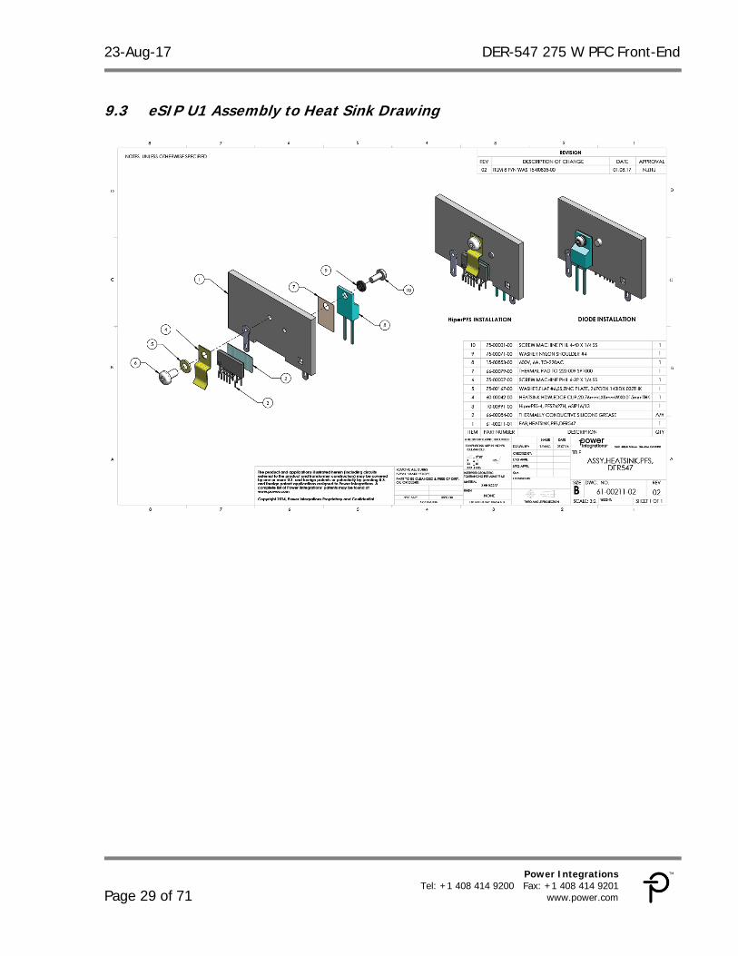
10.4 Regulation
Load Regulation 10.4.1
Figure 12 – Load Regulation.
430
432
434
436
438
440
442
444
446
448
450
0 25 50 75 100 125 150 175 200 225 250 275 300
Reg
ulat
ion
(VD
C)
Output Power (W)
100 VAC115 VAC230 VAC265 VAC277 VAC300 VAC

23-Aug-17 DER-547 275 W PFC Front-End
Page 35 of 71
Power Integrations Tel: +1 408 414 9200 Fax: +1 408 414 9201
www.power.com
Line Regulation 10.4.2
Figure 13 – Line Regulation.
430
432
434
436
438
440
442
444
446
448
450
75 100 125 150 175 200 225 250 275 300 325
Reg
ula
tion
(V
DC
)
Input Voltage (VAC)
10% LOAD20% LOAD50% LOAD100% LOAD

DER-547 275 W PFC Front-End 23-Aug-17
Page 36 of 71
Power Integrations, Inc. Tel: +1 408 414 9200 Fax: +1 408 414 9201 www.power.com
10.5 THD
Figure 14 – Input Current THD vs. Load.
Note: When on highline (230 VAC and 264 VAC) and 10% load the unit is bursting making the THD reading very high. To get an accurate reading the light load THD value should be integrated over several minutes.
0
5
10
15
20
25
30
35
0 25 50 75 100 125 150 175 200 225 250 275 300
%A
THD
Output Power (W)
100 VAC115 VAC230 VAC264 VAC277 VAC300 VAC

23-Aug-17 DER-547 275 W PFC Front-End
Page 37 of 71
Power Integrations Tel: +1 408 414 9200 Fax: +1 408 414 9201
www.power.com
10.6 Input Current Harmonic Distortion (IEC 61000-3-2 Class-D) Measured at 230 VAC Input 50 Hz.
50% Load at Output 10.6.1
Figure 15 – Amplitude of Input Current Harmonics for 50% Load at 230 VAC Input.
0
50
100
150
200
250
300
350
400
450
500
3 5 7 9 11 13 15 17 19 21 23 25 27 29 31 33 35 37 39
Har
mon
ic C
onte
nt
(mA
)
Harmonic Order
Class D LimitHarmonics Content

DER-547 275 W PFC Front-End 23-Aug-17
Page 38 of 71
Power Integrations, Inc. Tel: +1 408 414 9200 Fax: +1 408 414 9201 www.power.com
100% Load at Output 10.6.2
Figure 16 – Amplitude of Input Current Harmonics for 100% Load at 230 VAC Input.
0
100
200
300
400
500
600
700
800
900
1000
3 5 7 9 11 13 15 17 19 21 23 25 27 29 31 33 35 37 39
Har
mon
ic C
onte
nt (
mA
)
Harmonic Order
Class D LimitHarmonics Content

23-Aug-17 DER-547 275 W PFC Front-End
Page 39 of 71
Power Integrations Tel: +1 408 414 9200 Fax: +1 408 414 9201
www.power.com
11 Thermal Performance A 80 mm 12 VDC fan powered by 10 VDC supply to create a 200 LFM air flow was placed as shown in Appendix 1 with the UUT running at full load. The unit was allowed to reach thermal equilibrium [~2 hrs.] prior to thermal measurement with a FLIR camera. Table 1 shows full load temperature of key components measured at equilibrium, room temperature and with forced air cooling. See Appendix 1 for set-up.
Temperature (ºC) 275 W Load
Component 115 VAC 230 VAC Ambient (measured by FLIR) 22.0 22.0
CM Inductor L2 33.4 29.0 DM Inductor L3 34.0 29.2
Main Inductor L1 Wire 48.2 35.3 L1 Core 40.0 32.8
X1 Capacitor C3 28.9 27.2 X2 Capacitor C4 29.1 27.6
Bridge Capacitor C7 30.8 29.0 Bride Rectifier BR1 67.3 47.5
Output Capacitor C13 32.0 30.6 Boost Diode D4 59.2 45.8
Heat Sink Top (Close to PFS7627H) 37.2 32.2 PFS7627H U1 MOSFET 61.0 42.1
Table 1 – Steady-State Thermal Performance.

DER-547 275 W PFC Front-End 23-Aug-17
Page 40 of 71
Power Integrations, Inc. Tel: +1 408 414 9200 Fax: +1 408 414 9201 www.power.com
11.1 115 VAC Thermal Measurements
Figure 17 – Infra-Red Images of HiperPFS-4 MOSFET
at Thermal Equilibrium, 115 VAC, Full Load, with Forced-Air Flow.
Figure 18 – Infra-Red Images of Boost Diode at Thermal Equilibrium, 115 VAC, Full Load, with Forced-Air Flow.
11.2 230 VAC Thermal Measurements
Figure 19 – Infra-Red Images of HiperPFS-4 MOSFET
at Thermal Equilibrium, 230 VAC, Full Load, with Forced-Air Flow.
Figure 20 – Infra-Red Images of Boost Diode at Thermal Equilibrium, 230 VAC, Full Load, with Forced-Air Flow.

23-Aug-17 DER-547 275 W PFC Front-End
Page 41 of 71
Power Integrations Tel: +1 408 414 9200 Fax: +1 408 414 9201
www.power.com
12 Input Waveforms
12.1 Input Current at 115 VAC and 60 Hz
Figure 21 – 115 VAC, 50% Load. Upper: VIN, 50 V / div. Lower: IIN, 1 A / div., 5 ms / div.
Figure 22 – 115 VAC, 100% Load. Upper: VIN, 50 V / div. Lower: IIN, 1 A / div., 5 ms / div.
12.2 Input Current at 230 VAC and 50 Hz
Figure 23 – 230 VAC, 50% Load. Upper: VIN, 100 V / div. Lower: IIN, 500 mA / div., 5 ms / div.
Figure 24 – 230 VAC, 100% Load. Upper: VIN, 100 V / div. Lower: IIN, 500 mA / div., 5 ms / div.

DER-547 275 W PFC Front-End 23-Aug-17
Page 42 of 71
Power Integrations, Inc. Tel: +1 408 414 9200 Fax: +1 408 414 9201 www.power.com
12.3 Input Current at 277 VAC and 50 Hz
Figure 25 – 277 VAC, 50% Load. Upper: VIN, 100 V / div. Lower: IIN, 400 mA / div., 5 ms / div.
Figure 26 – 277 VAC, 100% Load. Upper: VIN, 100 V / div. Lower: IIN, 400 mA / div., 5 ms / div.
12.4 Start-up Waveforms
100 VAC and 60 Hz 12.4.1
Figure 27 – 100 VAC, No-Load. Upper: VIN, 100 V / div. Second: IIN, 5 A / div. Third: VOUT, 100 V / div. Lower: VAUX, 5 V / div, 50 ms / div.
Figure 28 – 100 VAC, Full Load. Upper: VIN, 100 V / div. Second: IIN, 5 A / div. Third: VOUT, 100 V / div. Lower: VAUX, 5 V / div, 50 ms / div.

23-Aug-17 DER-547 275 W PFC Front-End
Page 43 of 71
Power Integrations Tel: +1 408 414 9200 Fax: +1 408 414 9201
www.power.com
115 VAC and 60 Hz 12.4.2
Figure 29 – 115 VAC, No-Load. Upper: VIN, 100 V / div. Second: IIN, 5 A / div. Third: VOUT, 100 V / div. Lower: VAUX, 5 V / div, 50 ms / div.
Figure 30 – 115 VAC, Full Load. Upper: VIN, 100 V / div. Second: IIN, 5 A / div. Third: VOUT, 100 V / div. Lower: VAUX, 5 V / div, 50 ms / div.
230 VAC and 50 Hz 12.4.3
Figure 31 – 230 VAC, No-Load. Upper: VIN, 200 V / div. Second: IIN, 5 A / div. Third: VOUT, 100 V / div. Lower: VAUX, 5 V / div, 50 ms / div.
Figure 32 – 230 VAC, Full Load. Upper: VIN, 200 V / div. Second: IIN, 5 A / div. Third: VOUT, 100 V / div. Lower: VAUX, 5 V / div, 50 ms / div.

DER-547 275 W PFC Front-End 23-Aug-17
Page 44 of 71
Power Integrations, Inc. Tel: +1 408 414 9200 Fax: +1 408 414 9201 www.power.com
264 VAC and 50 Hz 12.4.4
Figure 33 – 264 VAC, No-Load. Upper: VIN, 200 V / div. Second: IIN, 5 A / div. Third: VOUT, 100 V / div. Lower: VAUX, 5 V / div, 50 ms / div.
Figure 34 – 264 VAC, Full Load. Upper: VIN, 200 V / div. Second: IIN, 5 A / div. Third: VOUT, 100 V / div. Lower: VAUX, 5 V / div, 50 ms / div.
277 VAC and 50 Hz 12.4.5
Figure 35 – 277 VAC, No-Load. Upper: VIN, 200 V / div. Second: IIN, 5 A / div. Third: VOUT, 100 V / div. Lower: VAUX, 5 V / div, 50 ms / div.
Figure 36 – 277 VAC, Full Load. Upper: VIN, 200 V / div. Second: IIN, 5 A / div. Third: VOUT, 100 V / div. Lower: VAUX, 5 V / div, 50 ms / div.

23-Aug-17 DER-547 275 W PFC Front-End
Page 45 of 71
Power Integrations Tel: +1 408 414 9200 Fax: +1 408 414 9201
www.power.com
300 VAC and 50 Hz 12.4.6
Figure 37 – 300 VAC, No-Load. Upper: VIN, 200 V / div. Second: IIN, 5 A / div. Third: VOUT, 100 V / div. Lower: VAUX, 5 V / div, 50 ms / div.
Figure 38 – 300 VAC, Full Load. Upper: VIN, 200 V / div. Second: IIN, 5 A / div. Third: VOUT, 100 V / div. Lower: VAUX, 5 V / div, 50 ms / div.

DER-547 275 W PFC Front-End 23-Aug-17
Page 46 of 71
Power Integrations, Inc. Tel: +1 408 414 9200 Fax: +1 408 414 9201 www.power.com
12.5 Load Transient Response
100 VAC, 60 Hz 12.5.1
Figure 39 – Transient Response, 100 VAC, 10-100-10% Load Step. Upper: VIN, 200 V / div. Second: IIN, 10 A / div. Third: VOUT (AC Coupled), 20 V / div. Lower: IOUT, 0.5 A / div., 100 ms / div.
Figure 40 – Transient Response, 100 VAC, 50-100-50% Load Step. Upper: VIN, 500 V / div. Second: IIN, 10 A / div. Third: VOUT (AC Coupled), 20 V / div. Lower: IOUT, 0.5 A / div., 100 ms / div.
115 VAC, 60 Hz 12.5.2
Figure 41 – Transient Response, 115 VAC,
10-100-10% Load Step. Upper: VIN, 200 V / div. Second: IIN, 10 A / div. Third: VOUT (AC Coupled), 20 V / div. Lower: IOUT, 0.5 A / div., 100 ms / div.
Figure 42 – Transient Response, 115VAC, 50-100-50% Load Step. Upper: VIN, 500 V / div. Second: IIN, 10 A / div. Third: VOUT (AC Coupled), 20 V / div. Lower: IOUT, 0.5 A / div., 100 ms / div.

23-Aug-17 DER-547 275 W PFC Front-End
Page 47 of 71
Power Integrations Tel: +1 408 414 9200 Fax: +1 408 414 9201
www.power.com
230 VAC, 50 Hz 12.5.3
Figure 43 – Transient Response, 230 VAC,
10-100-10% Load Step. Upper: VIN, 500 V / div. Second: IIN, 10 A / div. Third: VOUT (AC Coupled), 20 V / div. Lower: IOUT, 0.5 A / div., 100 ms / div.
Figure 44 – Transient Response, 230 VAC, 50-100-50% Load Step. Upper: VIN, 500 V / div. Second: IIN, 10 A / div. Third: VOUT (AC Coupled), 20 V / div. Lower: IOUT, 0.5 A / div., 100 ms / div.
264 VAC , 50 Hz 12.5.4
Figure 45 – Transient Response, 264 VAC,
10-100-10% Load Step. Upper: VIN, 500 V / div. Second: IIN, 10 A / div. Third: VOUT (AC Coupled), 20 V / div. Lower: IOUT, 0.5 A / div., 100 ms / div.
Figure 46 – Transient Response, 264 VAC, 50-100-50% Load Step. Upper: VIN, 500 V / div. Second: IIN, 10 A / div. Third: VOUT (AC Coupled), 20 V / div. Lower: IOUT, 0.5 A / div., 100 ms / div.

DER-547 275 W PFC Front-End 23-Aug-17
Page 48 of 71
Power Integrations, Inc. Tel: +1 408 414 9200 Fax: +1 408 414 9201 www.power.com
277 VAC, 50 Hz 12.5.5
Figure 47 – Transient Response, 277 VAC,
10-100-10% Load Step. Upper: VIN, 500 V / div. Second: IIN, 10 A / div. Third: VOUT (AC Coupled), 20 V / div. Lower: IOUT, 0.5 A / div., 100 ms / div.
Figure 48 – Transient Response, 277 VAC, 50-100-50% Load Step. Upper: VIN, 500 V / div. Second: IIN, 10 A / div. Third: VOUT (AC Coupled), 20 V / div. Lower: IOUT, 0.5 A / div., 100 ms / div.
300 VAC, 50 Hz 12.5.6
Figure 49 – Transient Response, 300 VAC,
10-100-10% Load Step. Upper: VIN, 500 V / div. Second: IIN, 10 A / div. Third: VOUT (AC Coupled), 20 V / div. Lower: IOUT, 0.5 A / div., 100 ms / div.
Figure 50– Transient Response, 300 VAC, 50-100-50% Load Step. Upper: VIN, 500 V / div. Second: IIN, 10 A / div. Third: VOUT (AC Coupled), 20 V / div. Lower: IOUT, 0.5 A / div., 100 ms / div.
23-Aug-17 DER-547 275 W PFC Front-End
Page 49 of 71
Power Integrations Tel: +1 408 414 9200 Fax: +1 408 414 9201
www.power.com
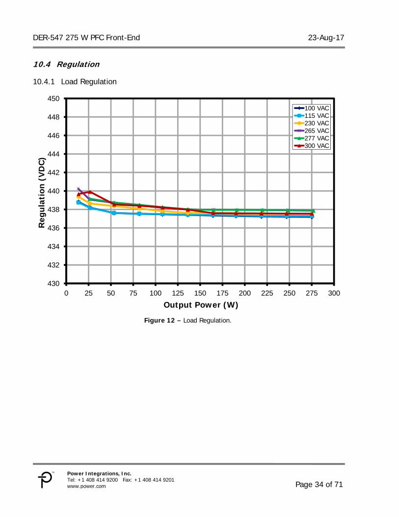
12.6 Line Dropout
1000 ms Line Dropout (115 VAC / 60 Hz and 230 VAC / 50 Hz) 12.6.1
12.6.1.1 50% Load at Output
Figure 51 – Line Dropout 115 VAC, 1000 ms. Upper: VIN, 100 V / div. Middle: IIN, 4 A / div. Lower: VOUT, 200 V / div., 200 ms / div.
Figure 52 – Line Dropout 230 VAC, 1000 ms. Upper: VIN, 400 V / div. Middle: IIN, 4 A / div. Lower: VOUT, 200 V / div., 200 ms / div.
12.6.1.2 Full Load at Output
Figure 53 – Line Dropout 115 VAC, 1000 ms. Upper: VIN, 100 V / div. Middle: IIN, 4 A / div. Lower: VOUT, 200 V / div., 200 ms / div.
Figure 54 – Line Dropout 230 VAC, 1000 ms. Upper: VIN, 400 V / div. Middle: IIN, 4 A / div. Lower: VOUT, 200 V / div., 200 ms / div.

DER-547 275 W PFC Front-End 23-Aug-17
Page 50 of 71
Power Integrations, Inc. Tel: +1 408 414 9200 Fax: +1 408 414 9201 www.power.com
One Cycle Line Dropout (115 VAC / 60 Hz and 230 VAC / 50 Hz) 12.6.2
12.6.2.1 Full Load at Output
Figure 55 – Line Dropout 115 VAC, 60 Hz. Upper: VIN, 200 V / div. Middle: IIN, 5 A / div. Lower: VOUT, 200 V / div., 50 ms / div.
Figure 56 – Line Dropout 230 VAC, 50 Hz. Upper: VIN, 400 V / div. Middle: IIN, 4 A / div. Lower: VOUT, 200 V / div., 50 ms / div.
12.7 Input Line Step
Line Sag (115 VAC ~ 85 VAC ~ 115 VAC, 60 Hz) 12.7.1
Figure 57 – Line Sag 115 VAC, 50% Load. Upper: VIN, 200 V / div. Middle: IIN, 5 A / div. Lower: VOUT (DC Offset), 20 V / div., 50 ms / div.
Figure 58 – Line Sag 115 VAC, 100% Load. Upper: VIN, 200 V / div. Middle: IIN, 5 A / div. Lower: VOUT (DC Offset), 20 V / div., 50 ms / div.
440 VDC 440 VDC

23-Aug-17 DER-547 275 W PFC Front-End
Page 51 of 71
Power Integrations Tel: +1 408 414 9200 Fax: +1 408 414 9201
www.power.com
Line Swell (132 VAC ~ 147 VAC ~ 132 VAC, 60 Hz) 12.7.2
Figure 59 – Line Sag 132 VAC, 50% Load. Upper: VIN, 200 V / div. Middle: IIN, 2 A / div. Lower: VOUT (DC Offset), 20 V / div., 50 ms / div.
Figure 60 – Line Sag 132 VAC, 100% Load. Upper: VIN, 200 V / div. Middle: IIN, 4 A / div. Lower: VOUT (DC Offset), 20 V / div., 50 ms / div.
Line Sag (230 VAC ~ 170 VAC ~ 230 VAC, 50 Hz) 12.7.3
Figure 61 – Line Sag 230 VAC, 50% Load. Upper: VIN, 400 V / div. Middle: IIN, 2 A / div. Lower: VOUT (DC Offset), 20 V / div., 50 ms / div.
Figure 62 – Line Sag 230 VAC, 100% Load. Upper: VIN, 400 V / div. Middle: IIN, 2 A / div. Lower: VOUT (DC Offset), 20 V / div., 50 ms / div.
440 VDC 440 VDC
440 VDC 440 VDC

DER-547 275 W PFC Front-End 23-Aug-17
Page 52 of 71
Power Integrations, Inc. Tel: +1 408 414 9200 Fax: +1 408 414 9201 www.power.com
Line Swell (264 VAC ~ 300 VAC ~ 264 VAC, 50 Hz) 12.7.4
Figure 63 – Line Sag 264 VAC, 50% Load. Upper: VIN, 400 V / div. Middle: IIN, 1 A / div. Lower: VOUT (DC Offset), 20 V / div., 50 ms / div.
Figure 64 – Line Sag 264 VAC, 100% Load. Upper: VIN, 400 V / div. Middle: IIN, 2 A / div. Lower: VOUT (DC Offset), 20 V / div., 50 ms / div.
Line Swell (300 VAC ~ 410 VAC ~ 300 VAC, 50 Hz) 12.7.5
Figure 65 – Line Sag 300 VAC, 50% Load. Upper: VIN, 400 V / div. Middle: IIN, 2 A / div. Lower: VOUT (DC Offset), 50 V / div., 50 ms / div.
Figure 66 – Line Sag 300 VAC, 100% Load. Upper: VIN, 400 V / div. Middle: IIN, 4 A / div. Lower: VOUT (DC Offset), 50 V / div., 50 ms / div.
440 VDC 440 VDC
440 VDC 440 VDC

23-Aug-17 DER-547 275 W PFC Front-End
Page 53 of 71
Power Integrations Tel: +1 408 414 9200 Fax: +1 408 414 9201
www.power.com
12.8 Power Good (PG) POWER GOOD (PG) pin waveforms were measured at start-up and shutdown with the PG output optocoupler collector (J2-2) tied to the VCC (J4-1) via a 10 k resistor. The PG optocoupler emitter was tied to the VCC return (J4-2).
115 VAC and 60 Hz 12.8.1
Figure 67 – 115 VAC, Full-load, VOUT Rising Edge. 1st: VAUX, 10 V / div. 2nd: VOUT, 200 V / div. 3rd: IIN, 10 A / div. 4th: PG, 10 V / div, 20 ms / div.
Figure 68 – 115 VAC, Full-load, VOUT Falling Edge. 1st: VAUX, 10 V / div. 2nd: VOUT, 200 V / div. 3rd: IIN, 10 A / div. 4th: PG, 10 V / div, 20 ms / div.
230 VAC and 50 Hz 12.8.2
Figure 69 – 230 VAC, Full-load, VOUT Rising Edge.
1st: VAUX, 10 V / div. 2nd: VOUT, 200 V / div. 3rd: IIN, 5 A / div. 4th: PG, 10 V / div, 20 ms / div.
Figure 70 – 230 VAC, Full-load, VOUT Falling Edge. 1st: VAUX, 10 V / div. 2nd: VOUT, 200 V / div. 3rd: IIN, 5 A / div. 4th: PG, 10 V / div, 20 ms / div.
Note: Cursor measurement shows the Power Good transition threshold, turn-on delay time and turn-off hold-up time.

DER-547 275 W PFC Front-End 23-Aug-17
Page 54 of 71
Power Integrations, Inc. Tel: +1 408 414 9200 Fax: +1 408 414 9201 www.power.com
12.9 Brown-In and Brown-Out at 6 V / Minute Rate Test conducted by first reducing, followed by increasing input AC voltage source at a rate of 6 V / min. The PFC converter DC output was loaded to 100% of rated load (electronic load), which was programmed to release the load when the DC output of the PFC dropped below 400 V [at brown-out]. After the load switches off it continues to draw about 1.5 mA and discharges the output capacitor of the PFC after the dynamic load is released at brown-out.
Thresholds 12.9.1Measured PFC Brown-Out Threshold 92.0 VAC Measured PFC Brown-In Threshold 82.0 VAC
Waveforms 12.9.2
Figure 71 – Brown-Out Followed by Brown-In at 100% Load.
Top: VIN, 100 V / div. Second: IIN, 4 A / div.
Third: VOUT, 200 V / div Lower: VDS, 200 V / div.
250 s / div.

23-Aug-17 DER-547 275 W PFC Front-End
Page 55 of 71
Power Integrations Tel: +1 408 414 9200 Fax: +1 408 414 9201
www.power.com
Figure 72 – Brown-out with 100% Load, Zoom-in
Upper (Red): VIN, 100 V / div. Second (Green): IIN, 4 A / div. Third (Blue): VOUT, 200 V / div. Lower (Yellow): VDS, 200 V / div. Zoom in 40 ms / div.
Figure 73 – Brown-in with 100% Load, Zoom-in Upper (Red): VIN, 100 V / div. Second (Green): IIN, 4 A / div. Third (Blue): VOUT, 200 V / div. Lower (Yellow): VDS, 200 V / div. Zoom in 40 ms / div.

DER-547 275 W PFC Front-End 23-Aug-17
Page 56 of 71
Power Integrations, Inc. Tel: +1 408 414 9200 Fax: +1 408 414 9201 www.power.com
Drain Voltage and Inductor Current 12.9.3Since PFC output diode is integrated into the package, there is no direct access of the power MOSFET Drain current. Therefore inductor current was measured at jumper JP1 location by replacing JP1 with a short wire loop in order to insert the current probe. The Drain voltage was measured at the DRAIN and SOURCE pins of IC U1.
Figure 74 – Input Voltage 115 VAC, 100% Load.
Upper: IINDUCTOR, 2 A / div. Lower: VDRAIN, 100 V / div., 2 ms / div. Zoom Upper: IINDUCTOR, 2 A / div. Zoom Lower: VDRAIN, 100 V / div., 5 s / div.
Figure 75 – Input Voltage 230 VAC, 100% Load. Upper: IINDUCTOR, 1 A / div. Lower: VDRAIN, 100 V / div., 2 ms / div. Zoom Upper: IINDUCTOR, 1 A / div. Zoom Lower: VDRAIN, 100 V / div., 5 s / div.
23-Aug-17 DER-547 275 W PFC Front-End
Page 57 of 71
Power Integrations Tel: +1 408 414 9200 Fax: +1 408 414 9201
www.power.com
12.10 Output Ripple Measurements
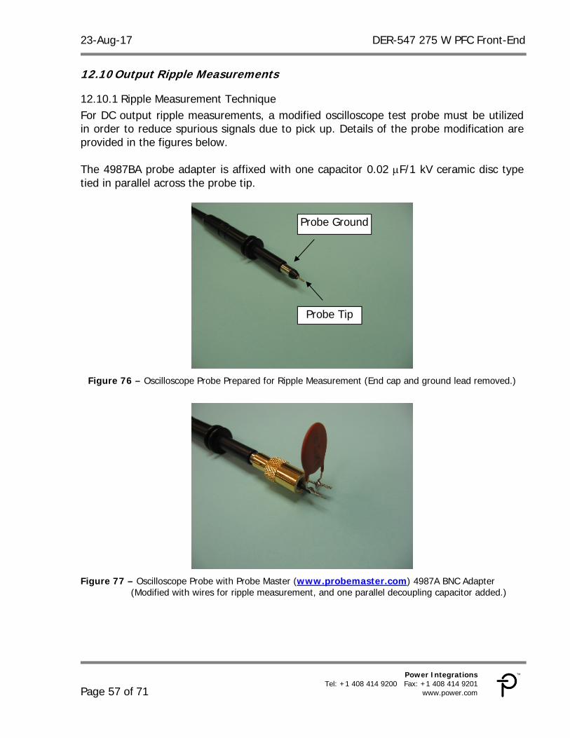
Ripple Measurement Technique 12.10.1For DC output ripple measurements, a modified oscilloscope test probe must be utilized in order to reduce spurious signals due to pick up. Details of the probe modification are provided in the figures below. The 4987BA probe adapter is affixed with one capacitor 0.02 F/1 kV ceramic disc type tied in parallel across the probe tip.
Figure 76 – Oscilloscope Probe Prepared for Ripple Measurement (End cap and ground lead removed.)
Figure 77 – Oscilloscope Probe with Probe Master (www.probemaster.com) 4987A BNC Adapter
(Modified with wires for ripple measurement, and one parallel decoupling capacitor added.)
Probe Ground
Probe Tip

DER-547 275 W PFC Front-End 23-Aug-17
Page 58 of 71
Power Integrations, Inc. Tel: +1 408 414 9200 Fax: +1 408 414 9201 www.power.com
Measurement Results 12.10.2
Figure 78 – Ripple, 100 VAC, 50% Load.
5 V / div., 2 ms / div. Figure 79 – Ripple, 100 VAC, 100% Load.
5 V / div., 2 ms / div.
Figure 80 – Ripple, 115 VAC, 50% Load.
5 V / div., 2 ms / div. Figure 81 – Ripple, 115 VAC, 100% Load.
5 V / div., 2 ms / div.

23-Aug-17 DER-547 275 W PFC Front-End
Page 59 of 71
Power Integrations Tel: +1 408 414 9200 Fax: +1 408 414 9201
www.power.com
Figure 82 – Ripple, 230 VAC, 50% Load.
5 V / div., 2 ms / div. Figure 83 – Ripple, 230 VAC, 100% Load.
5 V / div., 2 ms / div.
Figure 84 – Ripple, 264 VAC, 50% Load.
5 V / div., 2 ms / div. Figure 85 – Ripple, 264 VAC, 100% Load.
5 V / div., 2 ms / div.

DER-547 275 W PFC Front-End 23-Aug-17
Page 60 of 71
Power Integrations, Inc. Tel: +1 408 414 9200 Fax: +1 408 414 9201 www.power.com
Figure 86 – Ripple, 277 VAC, 50% Load.
5 V / div., 2 ms / div. Figure 87 – Ripple, 277 VAC, 100% Load.
5 V / div., 2 ms / div.
Figure 88 – Ripple, 300 VAC, 50% Load.
5 V / div., 2 ms / div. Figure 89 – Ripple, 300 VAC, 100% Load.
5 V / div., 2 ms / div.

23-Aug-17 DER-547 275 W PFC Front-End
Page 61 of 71
Power Integrations Tel: +1 408 414 9200 Fax: +1 408 414 9201
www.power.com
12.11 Gain-Phase Measurement Procedure and Results The PFC stage is supplied from an adjustable DC source for this test. Connect the
circuit as shown in figure below. Open the top end of the feedback divider network and insert a 100 –2 W resistor in series as shown. The signal injected in the loop for gain–phase measurement will be injected across this resistor.
Nodes A and B (two ends of the injection resistor) are connected to Channel 1 and Channel 2 of the frequency response analyzer using high voltage x100 attenuator probes. GND leads of both probes are connected to output return as shown.
The signal to be injected is isolated using the Bode–Box injection transformer model – 200–000 from Venable Industries. Test Procedure:
Adjust the input voltage to 150 VDC and confirm that the PFC output voltage is within regulation limits.
Inject a signal from the frequency response analyzer. The injected signal can be seen in the output voltage ripple of the PFC. Plot the gain phase by sweeping the injected signal frequency from 1 Hz to 1000 Hz.
Figure 90 – System Test Set-up for Loop Gain-Phase Measurement.

DER-547 275 W PFC Front-End 23-Aug-17
Page 62 of 71
Power Integrations, Inc. Tel: +1 408 414 9200 Fax: +1 408 414 9201 www.power.com
Measured Bode Plots 12.11.1
Figure 91 – Bode Plot with VIN = 150 VDC at 100%, 50% and 20% Load. 20% Load – Slide Bar #1 Gain Crossover, 5.944 Hz, Phase Margin 45.97°. 50% Load – Slide Bar #2, Gain Crossover 6.433 Hz, Phase Margin 49.41°. 100% Load – Slide Bar #3, Gain Crossover 7.723 Hz, Phase Margin 59.59°.
Figure 92 – Bode Plot with VIN = 300 VDC at 100%, 50% and 20% Load. 20% Load – Slide Bar #1, Gain Crossover 12.70 Hz, Phase Margin 64.46°. 50% Load – Slide Bar #2, Gain Crossover 9.379 Hz, Phase Margin 60.71°. 100% Load – Slide Bar #3, Gain Crossover 7.818 Hz, Phase Margin 63.44°.

23-Aug-17 DER-547 275 W PFC Front-End
Page 63 of 71
Power Integrations Tel: +1 408 414 9200 Fax: +1 408 414 9201
www.power.com
13 Line Surge Test Differential input line surge testing was completed on a single test unit to IEC61000-4-5. Input voltage was set at 230 VAC / 50 Hz. The UUT output was resistively loaded at full load and operation was verified following each surge event. The UUT was powered with a 13.5 V (9 V, 1.5 V x 3 in series) battery. A single-sided 0.062” thick copper-clad FR4 material was placed under the UUT, insulation side up, and with the copper side of the board connected to earth ground at the AC input connector.
Figure 93 – Line Surge UUT Set-up.

DER-547 275 W PFC Front-End 23-Aug-17
Page 64 of 71
Power Integrations, Inc. Tel: +1 408 414 9200 Fax: +1 408 414 9201 www.power.com
13.1 Differential Mode Surge AC Input Voltage (VAC)
Surge Voltage
(kV)
Phase Angle
(º)
Generator Impedance
()
Number of Strikes Test Result
230 +2 0 2 10 PASS 230 -2 0 2 10 PASS 230 +2 90 2 10 PASS 230 -2 90 2 10 PASS 230 +2 180 2 10 PASS 230 -2 180 2 10 PASS 230 +2 270 2 10 PASS 230 -2 270 2 10 PASS
13.2 Common Mode Surge AC Input Voltage (VAC)
Surge Voltage
(kV)
Phase Angle
(º)
Generator Impedance
()
Number of Strikes Test Result
230 +3 0 12 10 PASS 230 -3 0 12 10 PASS 230 +3 90 12 10 PASS 230 -3 90 12 10 PASS 230 +3 180 12 10 PASS 230 -3 180 12 10 PASS 230 +3 270 12 10 PASS 230 -3 270 12 10 PASS
23-Aug-17 DER-547 275 W PFC Front-End
Page 65 of 71
Power Integrations Tel: +1 408 414 9200 Fax: +1 408 414 9201
www.power.com
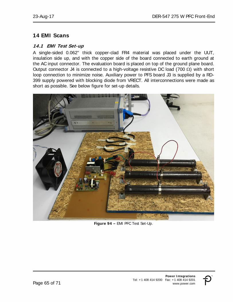
14 EMI Scans
14.1 EMI Test Set-up A single-sided 0.062” thick copper-clad FR4 material was placed under the UUT, insulation side up, and with the copper side of the board connected to earth ground at the AC input connector. The evaluation board is placed on top of the ground plane board. Output connector J4 is connected to a high-voltage resistive DC load (700 ) with short loop connection to minimize noise. Auxiliary power to PFS board J3 is supplied by a RD-399 supply powered with blocking diode from VRECT. All interconnections were made as short as possible. See below figure for set-up details.
Figure 94 – EMI PFC Test Set-Up.

DER-547 275 W PFC Front-End 23-Aug-17
Page 66 of 71
Power Integrations, Inc. Tel: +1 408 414 9200 Fax: +1 408 414 9201 www.power.com
Figure 95 – Zoom in Picture of EMI PFC Test Set-Up.

23-Aug-17 DER-547 275 W PFC Front-End
Page 67 of 71
Power Integrations Tel: +1 408 414 9200 Fax: +1 408 414 9201
www.power.com
14.2 EMI Scans
Figure 96 – 115 VAC, 100% Load.

DER-547 275 W PFC Front-End 23-Aug-17
Page 68 of 71
Power Integrations, Inc. Tel: +1 408 414 9200 Fax: +1 408 414 9201 www.power.com
Figure 97 – 230 VAC, 100% Load.

23-Aug-17 DER-547 275 W PFC Front-End
Page 69 of 71
Power Integrations Tel: +1 408 414 9200 Fax: +1 408 414 9201
www.power.com
15 Appendix A
15.1 Test Set-up for Efficiency Measurement The following setup is recommended for system efficiency, PF and THD measurements. Use of high resolution meters is recommended for output current and output voltage measurements. An 80 mm, 12 V DC fan (Adda A08112MS-A70GL) powered by 10 VDC is spaced 70 mm from the board edge for forced air cooling. See figures below for a typical equipment set-up, showing fan spacing and relative placement.
Figure 98 –Test Set-Up for Efficiency, Regulation, PF, THD and Thermal Performance.

DER-547 275 W PFC Front-End 23-Aug-17
Page 70 of 71
Power Integrations, Inc. Tel: +1 408 414 9200 Fax: +1 408 414 9201 www.power.com
16 Revision History Date Author Revision Description & changes Reviewed
27-Mar-17 SK 1.0 Initial Release Apps & Mktg 23-Aug-17 KM 1.1 Added Supplier for L1 and L3.

23-Aug-17 DER-547 275 W PFC Front-End
Page 71 of 71
Power Integrations Tel: +1 408 414 9200 Fax: +1 408 414 9201
www.power.com
For the latest updates, visit our website: www.power.com
Power Integrations reserves the right to make changes to its products at any time to improve reliability or manufacturability. Power Integrations does not assume any liability arising from the use of any device or circuit described herein. POWER INTEGRATIONS MAKES NO WARRANTY HEREIN AND SPECIFICALLY DISCLAIMS ALL WARRANTIES INCLUDING, WITHOUT LIMITATION, THE IMPLIED WARRANTIES OF MERCHANTABILITY, FITNESS FOR A PARTICULAR PURPOSE, AND NON-INFRINGEMENT OF THIRD PARTY RIGHTS. Patent Information The products and applications illustrated herein (including transformer construction and circuits’ external to the products) may be covered by one or more U.S. and foreign patents, or potentially by pending U.S. and foreign patent applications assigned to Power Integrations. A complete list of Power Integrations’ patents may be found at www.power.com. Power Integrations grants its customers a license under certain patent rights as set forth at http://www.power.com/ip.htm.
The PI Logo, TOPSwitch, TinySwitch, LinkSwitch, LYTSwitch, InnoSwtich, DPA-Switch, PeakSwitch, CAPZero, SENZero, LinkZero, HiperPFS, HiperTFS, HiperLCS, Qspeed, EcoSmart, Clampless, E-Shield, Filterfuse, FluxLink, StackFET, PI Expert and PI FACTS are trademarks of Power Integrations, Inc. Other trademarks are property of their respective companies. ©Copyright 2015 Power Integrations, Inc.
Power Integrations Worldwide Sales Support Locations WORLD HEADQUARTERS 5245 Hellyer Avenue San Jose, CA 95138, USA. Main: +1-408-414-9200 Customer Service: Phone: +1-408-414-9665 Fax: +1-408-414-9765 e-mail: [email protected]
GERMANY Lindwurmstrasse 114 80337, Munich Germany Phone: +49-895-527-39110 Fax: +49-895-527-39200 e-mail: [email protected]
JAPAN Kosei Dai-3 Building 2-12-11, Shin-Yokohama, Kohoku-ku, Yokohama-shi, Kanagawa 222-0033 Japan Phone: +81-45-471-1021 Fax: +81-45-471-3717 e-mail: [email protected]
TAIWAN 5F, No. 318, Nei Hu Rd., Sec. 1 Nei Hu District Taipei 11493, Taiwan R.O.C. Phone: +886-2-2659-4570 Fax: +886-2-2659-4550 e-mail: [email protected]
CHINA (SHANGHAI) Rm 2410, Charity Plaza, No. 88, North Caoxi Road, Shanghai, PRC 200030 Phone: +86-21-6354-6323 Fax: +86-21-6354-6325 e-mail: [email protected]
INDIA #1, 14th Main Road Vasanthanagar Bangalore-560052 India Phone: +91-80-4113-8020 Fax: +91-80-4113-8023 e-mail: [email protected]
KOREA RM 602, 6FL Korea City Air Terminal B/D, 159-6 Samsung-Dong, Kangnam-Gu, Seoul, 135-728 Korea Phone: +82-2-2016-6610 Fax: +82-2-2016-6630 e-mail: [email protected]
UK Cambridge Semiconductor, a Power Integrations company Westbrook Centre, Block 5, 2nd Floor Milton Road Cambridge CB4 1YG Phone: +44 (0) 1223-446483 e-mail: [email protected]
CHINA (SHENZHEN) 17/F, Hivac Building, No. 2, Keji Nan 8th Road, Nanshan District, Shenzhen, China, 518057 Phone: +86-755-8672-8689 Fax: +86-755-8672-8690 e-mail: [email protected]
ITALY Via Milanese 20, 3rd. Fl. 20099 Sesto San Giovanni (MI) Italy Phone: +39-024-550-8701 Fax: +39-028-928-6009 e-mail: [email protected]
SINGAPORE 51 Newton Road, #19-01/05 Goldhill Plaza Singapore, 308900 Phone: +65-6358-2160 Fax: +65-6358-2015 e-mail: [email protected]