Design and Fabrication of a Multipurpose Compliant ... - CORE
Upload
khangminh22Category
view
1download
0
Retrospective Theses and Dissertations Iowa State University Capstones, Theses and Dissertations
1-1-2003
Design, development and fabrication of circuits using the Design, development and fabrication of circuits using the
CMOS-70 process CMOS-70 process
Jonathan Vincent Williams Iowa State University
Follow this and additional works at: https://lib.dr.iastate.edu/rtd
Recommended Citation Recommended Citation Williams, Jonathan Vincent, "Design, development and fabrication of circuits using the CMOS-70 process" (2003). Retrospective Theses and Dissertations. 20088. https://lib.dr.iastate.edu/rtd/20088
This Thesis is brought to you for free and open access by the Iowa State University Capstones, Theses and Dissertations at Iowa State University Digital Repository. It has been accepted for inclusion in Retrospective Theses and Dissertations by an authorized administrator of Iowa State University Digital Repository. For more information, please contact [email protected].
Design, development and fabrication of circuits using the CMOS-70 process
by
Jonathan Vincent Williams
A thesis submitted to the graduate faculty
in partial fulfillment of the requirements for the degree of
MASTER OF SCIENCE
Major: Electrical Engineering
Program of Study Committee: Gary Tuttle (Major Professor)
Vikram Dalal Alan Constant
Iowa State University
Ames, Iowa
2003
Copyright© Jonathan Williams, 2003. All right reserved.

11
Graduate College Iowa State University
This is to certify that the master's thesis of
Jonathan Vincent Williams
has met the thesis requirements oflowa State University
Signatures have been redacted for privacy
111
TABLE OF CONTENTS
CHAPTER 1. INTRODUCTION ...................................................................... 1 Fabrication at Iowa State University Microelectronics Research Center ......................... 1 CMOS Process Development at the MRC ........................................................................ 1
CHAPTER 2. DESIGN ...................................................................................... 9 Derivation of Transistor Characteristics ........................................................................... 9 Design of the GMR Latch ............................................................................................... 12
CHAPTER 3. FABRICATION ........................................................................ 30 Overview and Design of the CMOS Process .................................................................. 30
CHAPTER 4. TESTING .................................................................................. 37 Testing Methods Used During Fabrication ..................................................................... 37 Testing of the Finished Wafers ........................................................................................ 40
CHAPTER 5. RESULTS AND DISCUSSION ............................................... 44 I
Pre-Fabrication Characterization .................................................................................... 44 Test Transistors ............................................................................................................... 44 Sheet Resistance Measurements ..................................................................................... 50 Gate Oxide Thicknesses .................................................................................................. 52 MOS Capacitor Measurements ....................................................................................... 52 Fractal Capacitors ........................................................................................................... 55 Digital-to-Analog Converter ........................................................................................... 55 Operational Transconductance Amplifiers ...................................................................... 58 Preliminary GMR Latch ................................................................................................. 62 Die Photornicrographs .................................................................................................... 64
CHAPTER 6. CONCLUSIONS ...................................................................... 67 Summary ......................................................................................................................... 67 Recommendations for Future Work ................................................................................ 67
APPENDIX A. CMOS PROCESS FLOW ..................................................... 69
APPENDIX B. EARLY WORK: THE GMR LATCH .................................. 74 Giant Magneto-Resistance Process Development at the MRC ....................................... 74 Overview and Design of the CMOS/GMR Process ........................................................ 76 GMR Latch Conclusions ................................................................................................. 79
RE FE REN CES CITED .................................................................................... 80

iv
ACKNOWLEDGEMENTS ••••••••••••••••••••••••••.•.•.••..•..•.•••••.•••.••.•••••••••.•••••.••.••••• 82

1
CHAPTER 1. INTRODUCTION
Fabrication at Iowa State University Microelectronics Research Center
The Microelectronics Research Center (MRC) at Iowa State University includes basic
semiconductor fabrication facilities. These facilities, funded in part by the National Science
Foundation, are used to teach fabrication principles to students through hands-on lab work, as
well as to provide the means to develop and produce working prototypes of devices for
research purposes.
The facilities include a four-tube Thermco diffusion furnace with phosphorus/boron
diffusion and oxide growth capability, a Karl-Suss MJB3 UV300 mask aligner (with
resolution down to .5 µm), a GCNMann 3600F Pattern Generator for lithographic mask
creation, wet process benches (for wafer cleaning/wet etching), a photoresist spinner, and a
Temescal BJD-1800 electron-beam evaporation system for metal deposition.
Characterization tools include a Nanometrics 210 Nanospec/AFT film/oxide thickness
measuring system, a four-point probe system for resistivity measurements and probe stations
used with HP4145B and HP4156A parameter analyzers and HP4280A Capacitance v.
voltage meters.
Recently, work has been done to develop a CMOS process using the facilities at the . MRC for class and research applications. The work presented here was intended to serve the
purposes of proof-of-concept, provision of additional fabrication capabilities and options to
the MRC and further characterization and refinement of the prior work.
CMOS Process Development at the MRC
A new addition to the MRC fabrication capabilities, the CMOS process has been

2
developed and preliminary testing and characterization has indicated the process is fully
functional. This process has been used for a fabrication laboratory taught in the Spring of
2003.
The CMOS process uses diffused single p-type wells for the creation of NMOS
transistors in an n-type substrate, along with fabrication of PMOS transistors in the substrate
(Figure 1). It uses a single metal layer (aluminum) for interconnects, and the metal is also
used for MOSFET gates. Fabrication is completed in sixteen steps, and involves six-mask
lithography.
NMOS PMOS
Figure 1. Cross-section of fabricated CMOS transistors.
Work on the CMOS process commenced in 2001, and drew upon older PMOS/bipolar
processes. The initial outline of the process, created by Nee-Fong Siah, underwent several
revisions and modifications as testing and characterization proceeded to further define proper
procedure and process capabilities. Several problems were identified, and fixes were devised.
CMOS development promises to create new opportunities. In addition to updating the
material taught in the fabrication laboratory, many modem circuits (analog, digital and
mixed-signal) make use of CMOS designs, and still others require both NMOS and PMOS

3
transistors (not necessarily used in a CMOS configuration). The process thus enables local
prototyping of designs and further research.
Advantages of the CMOS-70 Process
The CMOS-70 process is notable for its simplicity, robustness and low cost. It is
designed to take advantage of the fact that higher background doping for NMOS transistors
than PMOS transistors (as is the case with diffused p-wells inn-type background doping) can
lead to rough equality (in absolute value terms) between the threshold voltage characteristics
of NMOS and PMOS transistors. CMOS-70 also leverages basic proven and robust
processmg methods: wet and dry oxidation, wet etching, self-aligning manual
photolithography, phosphorus and boron doping using planar diffusion sources and high-
temperature drive stages and metallization. The process can be run completely in-house,
using a mask aligner, two process benches, three furnace tubes (fed with nitrogen, hydrogen
and oxygen), a metal deposition machine, common processing chemicals (primarily acetone,
methanol, hydrochloric acid, ammonium hydroxide, hydrofluoric acid and hydrogen
peroxide), and some test equipment.
Finally, the low number of steps required to fabricate simple circuits means fewer
expensive masks need to be created, less room for error, and increased tum-around time. The
entire fabrication process can be completed in less than 1 week, without the use of expensive
external processing such as ion implantation.
Utilizing the CMOS process
The CMOS process described here is designed to provide additional capabilities for the
MRC fabrication process. The work includes fabrication of standard test structures such as
4
NMOS and PMOS test transistors, n- and p-type diffusion resistors, diodes, n- and p-type
MOS capacitors, and fractal capacitors.
Three additional structures fabricated during this process deserve special mention: a
simple operational transconductance amplifier (OTA), a current-steering digital-to-analog
converter, and a GMR Latch.
Operational Transconductance Amplifier
The Operational Transconductance Amplifier (OTA) is very similar to the op-amp,
except the output is a current, rather than a voltage, based upon the differential input voltage.
The OT A used for this project is a simple, standard design (Figure 2), incorporating large
drive transistors (Q1 and Q4) for higher output current.. This design has a wide output
compliance voltage, meaning it is capable of a wide swing in output voltage to produce the
required output current (Wassenaar, Ismail and Lin, 2003).
Two figures-of-merit are of particular interest for the OT As fabricated here: gain
(transconductance, measured in amps/volt or Siemens) and offset (output current divergence
from ideal output current with zero input voltage difference).
OTAs are frequently used in on-chip high-frequency filters due to their simplicity and
lack of compensation capacitors.
5
V(5V)
01 02 03 04
05 06 > I < INN INP
Out )
LI I I ref
I 07 QB
09 010
Figure 2. Operational Transconductance Amplifier
Current-Steering DAC
The digital-to-analog converter topology used was a simple scaled-MOSFET current-
steering design (Figure 3).
In this circuit, current from a reference supply is directed to one of two outputs by n-
type MOSFETs. The MOSFETs' W/L ratio is sized such that each progressively higher bit
steers twice as much current as the next lower bit, thus ensuring that the output current is
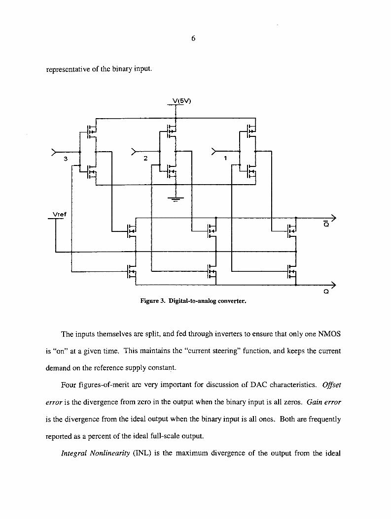
6
representative of the binary input.
3 2 1
Vref
9..___ ___ 9.___-----<19~--+) a
Figure 3. Digital-to-analog converter.
The inputs themselves are split, and fed through inverters to ensure that only one NMOS
is "on" at a given time. This maintains the "current steering" function, and keeps the current
demand on the reference supply constant.
Four figures-of-merit are very important for discussion of DAC characteristics. Offset
error is the divergence from zero in the output when the binary input is all zeros. Gain e"or
is the divergence from the ideal output when the binary input is all ones. Both are frequently
reported as a percent of the ideal full-scale output.
Integral Nonlinearity (INL) is the maximum divergence of the output from the ideal

7
output for any input value. Differential Nonlinearity (DNL) is the maximum divergence
from an ideal least-significant-bit (LSB) change of any single-step change in the output.
Both INL and DNL are frequently reported in terms of LSBs (Song, 2003).
GMR Latch
The initial direction of this research involved both the new CMOS process described
here and a fusion of that process with work on Giant Magneto-Resistance (GMR). Initial
work was towards the design, fabrication and testing of a CMOSIGMR latch. This latch was
first proposed by Kae Ann Wong in his Thesis, "A monolithic CMOS latch structure with
integrated GMR devices as non-volatile data storage and a multiple-state sensing technique
for pseudo spin-valve GMR devices" (1999). Das, Wong and Black pursued this structure
further in their paper, "Nonvolatile CMOS Latch Employing GMR Resistors" (2000). The
authors designed and had fabricated simple CMOS latches with differentially-programmed
GMR resistors in the NMOS source-to-ground connection (Figure 4). By using a shorting
(RESET) transistor, the latch could be made to consistently assume a specific logic state
depending upon which GMR resistor presented the greater resistance.
The prior work done on this circuit involved having fabrication done at outside sources,
and circuit functionality was demonstrated despite poor quality GMR layers.
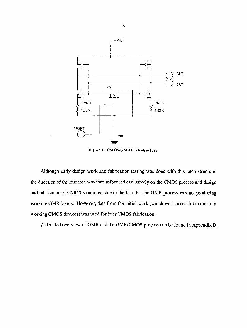
RESET
8
M9
Vss
GMR2
1.00 K
Figure 4. CMOS/GMR latch structure.
OUT
OUT
Although early design work and fabrication testing was done with this latch structure,
the direction of the research was then refocused exclusively on the CMOS process and design
and fabrication of CMOS structures, due to the fact that the GMR process was not producing
working GMR layers. However, data from the initial work (which was successful in creating
working CMOS devices) was used for later CMOS fabrication.
A detailed overview of GMR and the GMR/CMOS process can be found in Appendix B.

9
CHAPTER 2. DESIGN
The design process for this project proceeded from identification of ways to expand
upon and demonstrate current MRC capabilities, beginning with the initial concept (basic
circuit ideas and design, circuit topology and/or structure concept) to device physics and
requirements definitions, to circuit modeling with PSPICE, to die and wafer layout using
Tanner L-Edit and ending with actual fabrication. Additionally, testing from initial
fabrication runs obtained results that were used to modify assumptions regarding process and
device parameters, processing procedure and circuit functionality.
The mask set designed was specific to the CMOS process and included CMOS circuits
and test structures, as well as an updated GMR Latch structure.
Derivation of Transistor Characteristics
Since the goal of fabrication is making devices with certain predictable characteristics, it
was necessary for all aspects of this project to be able to derive device parameters from
process parameters. To do this, device physics came into play. Equation 1 (below) was used
to obtain the predicted threshold voltage-the point at which the MOSFET may be said to be
"on" (Taur and Ning, 1998; Streetman, 1992).

10
(1)
where
</J,n is the metal work.function (the difference between vacuum and Fermi level
energies): 4.28 eV for aluminum.
k is Boltzmann's constant: 8.625xl0-5 eV/K
Tis the temperature in Kelvin
NA is the doping concentration in cm-3
n; is the intrinsic carrier concentration: lxl010 cm-3
x is the electron affinity (difference between vacuum and conduction band
energy levels): 4.05 eV
Eg is the silicon bandgap: 1.12 eV
Q0 x is the equivalent oxide charge density in C/cm2
Cox is the oxide capacitance in F/cm2
EsiEo is the permittivity of silicon -- l.04E-12 Flem
A similar equation was used to find the PMOS threshold voltage.
Also important is a general idea of the channel carrier mobility to estimate the current of
the devices for a given gate voltage. Then-type MOSFET channel mobility may be derived
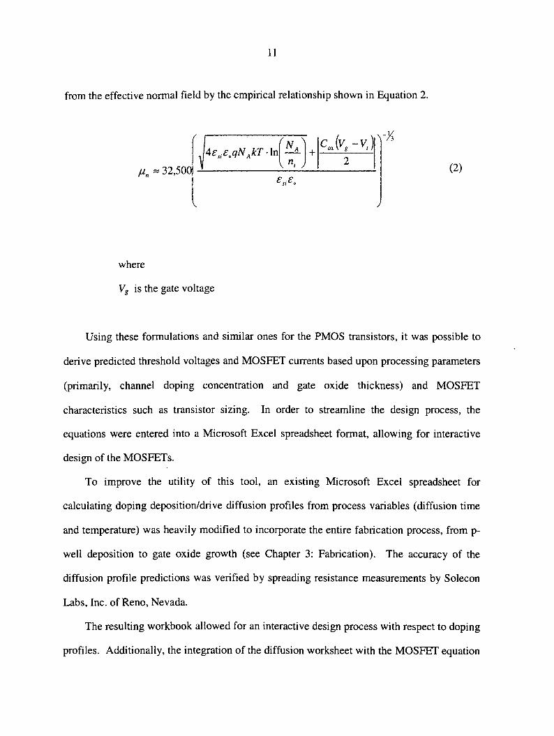
11
from the effective normal field by the empirical relationship shown in Equation 2.
. ( J c (v v) -K 4e e qN kT ·In NA + ox g - 1
'
n • A 2 µn = 32,500 ni
e,;e. (2)
where
Vg is the gate voltage
Using these formulations and similar ones for the PMOS transistors, it was possible to
derive predicted threshold voltages and MOSFET currents based upon processing parameters
(primarily, channel doping concentration and gate oxide thickness) and MOSFET
characteristics such as transistor sizing. In order to streamline the design process, the
equations were entered into a Microsoft Excel spreadsheet format, allowing for interactive
design of the MOSFETs.
To improve the utility of this tool, an existing Microsoft Excel spreadsheet for
calculating doping deposition/drive diffusion profiles from process variables (diffusion time
and temperature) was heavily modified to incorporate the entire fabrication process, from p-
well deposition to gate oxide growth (see Chapter 3: Fabrication). The accuracy of the
diffusion profile predictions was verified by spreading resistance measurements by Solecon
Labs, Inc. of Reno, Nevada.
The resulting workbook allowed for an interactive design process with respect to doping
profiles. Additionally, the integration of the diffusion worksheet with the MOSFET equation

12
worksheet allowed the direct relation of process parameters with the finished product.
Design of the GMR Latch
Although a working GMR process was unavailable, the component MOSFET devices
and latch functionality were tested. Further calculations and characterization of the resulting
structures spurred substantial modifications, and a new latch was included on the final test
layout (along with the other structures). Results from the initial fabrications were also used
to modify process parameters for other structures.
Qualitative overview of latch circuit
The latch circuit functions in similar fashion to a Clamped Bit-Line Current-mode Sense
Amplifier (CBLCSA-see Blalock and Jaeger, 1991). The latch is also able to function as a
normal CMOS latch for SRAM purposes.
The key to the nonvolatile memory aspect of the GMR latch is the RESET phase,
initiated by turning the RESET transistor on (bringing the RESET nmos gate high). Upon
transistor tum-on, both output nodes will be brought to approximately equal voltage. When
the RESET transistor is again turned off, the latch will settle into a pre-defined value based
on the differential programming of the GMR memory elements located between the latch
NMOS transistor Source nodes and ground.
During the RESET phase, the NMOS RESET transistor can be approximated as a short
between the output nodes. This approximation means the latch's PMOS transistors see equal
Va and Vos voltages; given equal processing parameters, equal current must flow through
these transistors. However, it is not possible for equal current to flow through the latch's
NMOS transistors, as the GMR elements present different resistive values. This means the

13
NMOS Vos voltages will be different, implying different values of current flow. The
qualitative view of the circuit thus leads to the conclusion that a small current must flow
across the RESET transistor when it is turned on. This current compensates for the different
Vos voltages seen by the latch's NMOS transistors.
Upon bringing the RESET transistor gate low (turning the RESET NMOS off), the
differential current flow across the RESET transistor is quickly converted to a voltage
difference, which is amplified by the latch, causing it to settle into one state or the other.
Of course, it is also reasonable to conclude that there is a small voltage difference across
the RESET transistor in the RESET phase (since the transistor does not present a true short);
this voltage difference will also be amplified once the transistor is turned off, aiding the
regeneration process.
Latch functionality is thus influenced by several factors. The first is GMR base
resistance and magnetoresistive change: it is necessary to have a sufficient current flow
across the RESET transistor that a significant voltage difference is generated, ensuring
consistent latch regeneration in the correct state. Qualitatively, this would mean the voltage
difference and RESET transistor current flow would need to be considerably higher than
background noise levels (perhaps several orders of magnitude). If the GMR base and
differential resistances are too small, the resultant current flow in the RESET state would be
lost in the noise, and latch performance would be unpredictable.
Second, RESET transistor sizing might be critical: if the reset transistor were too small,
turning it on would be insufficient to bring the output nodes together from their prior state. If
it were too large, leakage current flow with the RESET transistor off would be sufficient to
keep the latch from regenerating the proper new state. Restated, the RESET transistor must
be able to produce a loop gain of less than unity when on, and a loop gain greater than unity

14
when turned off. Correct sizing might be difficult to determine analytically.
Third, processing uniformity would be very important-variation in characteristics within
a latch could result in current imbalance during the RESET phase, causing the latch to
regenerate in an unpredictable or incorrect state.
Finally, asymmetry in the latch design (including differences in capacitance between the
legs of the latch or slight differences in resistance between the latch interconnections) could
influence latch functioning, as well.
Determination of Process Parameters for the GMR Latch
Numerical design process
The determination of process parameters required specification and input from several
sources. Work by Everitt, Pohm, and Daughton (1997) indicated that pseudo-spinvalves
have a size-dependent switching field threshold that can is also dependent both upon an
applied word-line field and the field generated by the sense current flowing through the bit.
The combined switching field is higher as bit sizes decrease (smaller bits act increasingly like
single magnetic domains, and so enjoy higher thresholds). In order to determine the
switching field, then, it was necessary to have some idea of the GMR bit sizing, and decide
on a sense current.
Further, in the name of fabrication feasibility, a minimum feature size had to be set. An
initial plan for 2µm x 8µm bit sizes was later changed to 4µm x 16 µm to accommodate
fabrication capabilities at the MRC and decrease lithography alignment errors.
Determination of the magnetic field incident on the GMR layers due to word line
current was a straightforward matter through application of Ampere's law (Equation 3)

H=-I-2m
where
15
H is the magnetic field in amps/meter
I is the current flowing in the word line in amps
(3)
r is the distance between the layer and the center of the word line in meters.
For the initial design, the field due to the sense current flowing down the GMR bit was
modeled through an approximation in which all of the current was assumed to flow through
the center copper spacer layer. Further, it was assumed this current flow could be
approximated as taking place through a wire. The field experienced by the outer magnetic
layers was then calculated using Ampere's law, as above.
Based on the data from Everitt et al. (199), a sense field of approximately 10-20 Oersted
would safely keep the devices from switching, with room to spare. Initial calculations
determined that a RESET phase current of about 25 µA (all transistors in saturation) would
be required to meet this specification.
Several other design criteria were incorporated at this point. A MOSFET threshold
value (VT) of about ±1 V was desired. Power supply voltage was assumed to be 5V. And
based upon measurements, background doping of then-type wafers was around l.7x1015/cm3•
In order to obtain rough equality (absolute value) between the PMOS and NMOS VT,
the gate oxide thickness was reduced to approximately 300A (typical for older processes in
the lab were gate thicknesses of 500-IOOOA). Oxide interface charges were initially assumed
to be a little worse than typical for silicon processing (5x10·9 C/cm2). From these
specifications, W IL ratios were calculated for the latch MOSFETs, and these values were

16
incorporated into the layout. For the NMOS, the W/L ratio was .446; for the PMOS, it was
1.14.
In addition to the above parameters, ambient temperature of 290K was specified. A p-
well doping with a surface concentration approximately one order of magnitude higher than
the background n-type doping was desired, along with a junction depth between the p-well
and substrate of between 4 and 5µm (plenty of room for subsequent processing). PMOS and
NMOS source and drain doping were specified as at least one order of magnitude higher than
background or p-well doping.
The numerical process parameter calculations were also used to determine appropriate
diffusion deposition and drive times and temperatures for the MOSFET source and drain
areas. An initial junction depth of .5µm was specified for compatibility with a CMOS
process test mask (which included MOSFETs with channel lengths of 2µm). The initial
NMOS boron SID deposition was to be conducted for 5 minutes at 800° C, and the drive-in
would be for 40 minutes at 950° C. The planned phosphorus SID deposition was to be done
for 10 minutes at 800° C, and the drive-in was expected to be for 22 minutes at 1050° C.
The drive-in times, above, were also designed such that wet oxidation conducted for the
entire time would result in approximately 3000A of new oxide.
Modeling design process
Prior work on the design of this latch pointed to some general guidelines for RESET
transistor sizing. In addition, PSPICE simulation was used to expand upon these guidelines.
In his thesis, Wong conducted an analysis of the GMR latch circuit, and proposed a
structure with a reset NMOS transistor W/L ratio 60 times as large as that of the latch's
transistors. This choice of W/L ratio was not explained in terms of Wong's analysis.
17
To gam further insight into the functioning of the circuit, SPICE simulation was
employed. The PSPICE simulation circuit was configured to run a three-second transient
simulation, divided into three parts: an initial settled state, a reset state, and a final re-settled
state. 10 pF capacitors were added to the outputs to simulate measurement equipment loads
on the circuit. The MOSFETS used a level 2 (process parameter) model in order to take
advantage of the calculated process parameters derived earlier in the design process.
Because the circuit would not initially settle into a real-world state, a short .I-volt pulse
produced by a voltage source .25 seconds into the simulation served to force the latch into a
predictable state. The RESET transistor's gate was initially set to OV, then taken to 5V after
one second, then taken back to OV one second later using a piecewise-linear (PWL) voltage
source. The expected result, if all were working correctly, would be a RESET phase in
which the output nodes were within a millivolt or less of each other, and a post-RESET phase
in which the output nodes would assume one state or the other, depending upon the
differential programming of the GMR elements.
From the beginning, this simulated circuit was not very well behaved. Very slight
modifications to process or circuit parameters resulted in very different behavior. This was
the case regardless of whether the modifications were to GMR element resistances or
transistor parameters. Additionally, the margin of error within which the PSPICE simulation
would behave as expected was very small-the resultant range of RESET transistor Width
values for a given Length over which the circuit would behave was 1-2 µm.
This odd simulation behavior was maintained despite several attempts to clean it up.
Increasing the current flow during RESET did not ameliorate the difficulty; neither did
adding or removing output capacitance, changing MOSFET models, using parts from the
PSPICE evaluation library rather than FETs modeled based on processing parameters or even

18
replacing the RESET transistor with a switch circuit device.
Layout
Attention was paid in the layout to several factors. First, minimum feature sizes of 4µm
were maintained, both in polygon dimensions and in spacing between adjacent polygons.
This was done both due to consideration of the capabilities of the lithographic equipment
(mask creation with the GCA/Mann pattern generator, photoresist exposure with the Karl-
Suss mask aligner) and the limitations of manual visual alignment. Likewise, layer overlap
(e.g. gate electrode over gate oxide, or metal over vias) was kept to a minimum of 2µm, and
in most cases 5 µm for the same reasons (Figure 5).
Figure S. Initial latch layout.
Additionally, it was necessary to ensure adequate spacing between p-well areas, as
diffusion drive-in steps result in lateral diffusion that might cause the p-well areas to short

19
together. This effect could also result in the shorting together of MOSFET source/drain areas,
so MOSFET length had to be at least several microns greater than the combined source/drain
junction depths.
Lateral diffusion during drive-in could have another undesired consequence: the
alteration of MOSFET width/length ratios. To compensate for this effect, all MOSFET
source and drain dimensions were decreased by an amount equal to the designed junction
depth (initially, .5µm).
Because of the extreme sensitivity of the PSPICE results to small changes in processing
or circuit parameters, and because the very narrow range of functioning solutions indicated
by PSPICE for a given set of parameters called for a process more tightly controlled that was
feasible given the processing equipment at hand, the decision was reached to design a test
wafer with a wide range of RESET transistor sizing. This range was centered, as best as
could be determined, around the solution PSPICE pointed to as functional. Additionally, the
range was made large enough to encompass the Width/Length ratio Wong used for his design,
relative to the sizing of the latch NMOS transistors.
Initially, the wafer layout included 2500 die (50 x 50); this number proved impractical
for fabricating lithographic masks within a reasonable amount of time, so was reduced to 100
(10 x 10).
Based upon a desired RESET (triode) current of 25 µA and a supply voltage of 5V, the
latch NMOS transistors were designed to be 20 µm long by 11 µm wide and the PMOS
transistors were designed to be 20 µm long by 28 µm wide. The RESET NMOS transistor
was designed to be 24 µm long and a variable number of microns wide; a two-fingered gate
design allowed a range from 23 µm to 617 µm for the channel width without excessive die
size.
20
The wafer layout used 8 masks.
The updated GMR Latch
Results from testing the initially-fabricated design caused the RESET-phase current
calculations to be revisited. The first latches could not be reset reliably into a state
depending upon differential resistance, and one possible culprit was insufficient differential
current to overcome processing variations, asymmetric capacitance, etc.
More accurate modeling of the field in a given layer produced by the current flowing
through the other layers indicated that the initial calculations had over-estimated the field
produced by a factor of almost 300, due to the proximity of the layers.
A more accurate value was derived by calculating the percentage of total current flow
through each layer (based upon layer conductivity and cross-sectional area) and using
superposition to sum the field present in the magnetic layers due to the total field
contributions of all other layers.
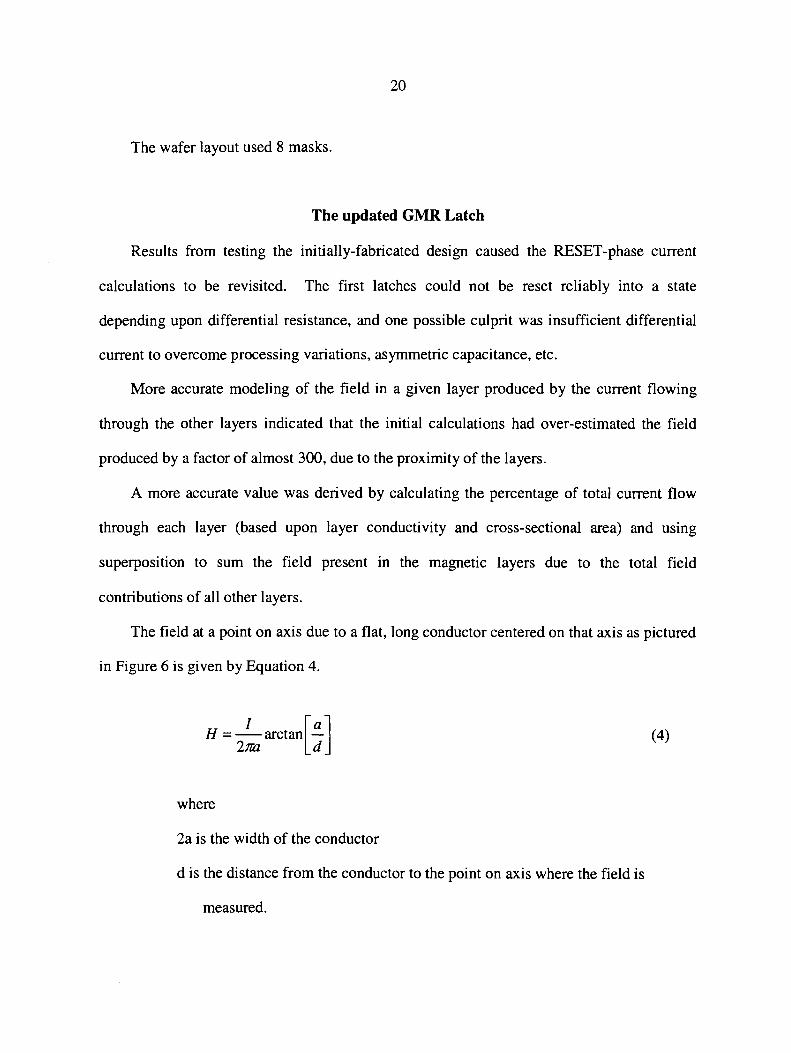
The field at a point on axis due to a flat, long conductor centered on that axis as pictured
in Figure 6 is given by Equation 4.
H = - 1- arctan[!!..] 2n:a d
(4)
where
2a is the width of the conductor
d is the distance from the conductor to the point on axis where the field is
measured.

21
Figure 6. Magnetic field lines and flux density due to a flat conductor (generated in Vizimag). Current flow is perpendicular to the plane of the page.
It should be noted that this equation primarily applies when the distance to the
measuring point from the conductor is significantly greater than the thickness of the
conductor. In our case, the two dimensions were comparable, at least for adjacent layers.
However, a comparison between this solution and the rigorous one (solved with the aid of
Mathematica) indicates agreement to three significant digits.
Using the above equation to sum fields from all layers, it was determined that a current
of about 7 .5 mA would be required to produce a field of 10 Oersted. The latch was thus
redesigned for a 1 mA RESET-state current (to provide room for error) and included in the
final test wafer (Figure 7).
The NMOS transistors in the new latch were 5 µm long and 160 µm wide, and the
PMOS transistors were 5 µm long and 400 µm wide. Both types of MOSFET used a
multiple-finger design.

22
Figure 7. New, high-current test latch.
As in the first latch, a range of sizes for the RESET transistor was used across the wafer.
Design of the Operational Transconductance Amplifier
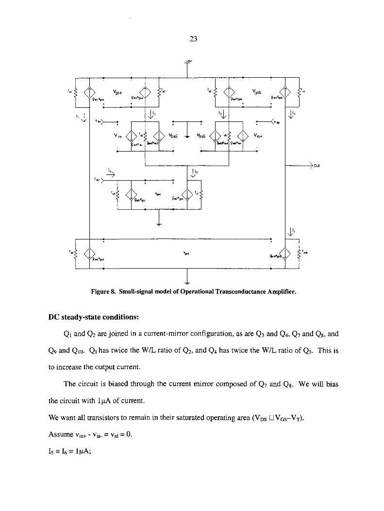
Design of the OTA began with a small-signal model of the circuit (Figure 8). The
circuit was designed to operate at 5 volts, with a bias current of lµA. Various MOSFET
parameters for the analysis are listed in Table 1.
Table 1. MOSFET Parameters for OTA
On=lµA) NMOS1
µ0 Cox: 57.2µA/V2
W/L: 4.1 2\j/8 : .844 V Yn: 2.06 V 112
VT: 1.38 v Vas: 1.48 V
PMOS1 µpCox: 22.9µA/V2
W/L: 10.3 2\j/B: .624 V
. 23 vl/2 'Yp·. 1 VT: -1.38 v Vas: -1.48 V
(ln=.SµA) NMOS1
µnCox: 57 .2µA/V2
W/L: 4.1 2\j/B: .844 V Yo: 2.06 V 112
VT: 1.38 v Vas: 1.45 V
PMOS1 µpCox: 22.9µA/V2
W/L: 10.3 2\jls: .624 V
V l/2 yp: .231 VT: -1.38 v Vas: -1.45 V
23
r., 1 Vgsb g.,v"m 1 g.,v,.. ~
'··
v in-
t----~Out
~ I., :>-----,----.--+------<>
r .. . ...
. ...
Figure 8. Small-signal model of Operational Transconductance Amplifier.
DC steady-state conditions:
Q1 and Q1 are joined in a current-mirror configuration, as are Q3 and Q4 , Q7 and Q8, and
Q9 and Q10. Q1 has twice the W/L ratio of Q2, and Q4 has twice the W/L ratio of Q3. This is
to increase the output current.
The circuit is biased through the current mirror composed of Q7 and Q8. We will bias
the circuit with lµA of current.
We want all transistors to remain in their saturated operating area (V ns [j V 05-V T ).
Assume Vin+ - Vin·= Vict = 0.
Is= 16 = lµA;

24
11 = 21z = 2h = 4 =I?= Is= 1 µA
Therefore, the small-signal parameters become:
v =v =v =15V gsa gsb gsd •
gm2=gm3=15.29µS gm5 =gm6 =15.26µS
gml = gm4 = gm1 = gm8 = 21.56µS gm9=gmlO=15.26µS
gmbs = gmb6 = /(gm5 = 2 12 Yn V =7.57µS(maxinput)tol6.2µS(mininput) '\J lf/ B + SB
Common-mode input range:
Vidc(max) = 5-1.45-(1.45-1.38)+ 1.45=4.93V
Vidc(min) = O+(l.48-1.38)+ l.45=1.57V
(where 1.47 volts is Vas-VT for Io= .5µA)
Output voltage swing:
Vout(max) = 5-.(1.5-1.4) = 4.9V
Vout(min) = O+(l.5-1.4) = .1 V
Because of the current mirror configuration, the output of the amplifier is essentially
produced by the differential pair, meaning the output can be written as in Equation 5.
(5)
Additionally, PSPICE simulation confirmed that the OTA would function normally over
a wide range of transistor parameters (Figure 9).
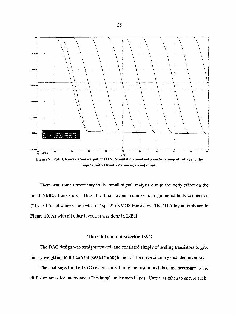
·:
-•1u•1
-111uA 1
l----1SluA1
-211uA-!
-251uA1
-311uAi
25
A1 11.96181?061, 1111.18•189811lm A2 5.0S31135115, -161.8641226311 d1f 91 60HlS:J44n, 21l.6798Z360u
: i ' -3SluA+---------------,.----------------.---·------------r---------------.,----------------.----------------T---------------.,----------------,.---------------.. ---------------_. 1U 1U 2U 3U ~ SU 6U 7U IU 9U 11U (9)-1•1(11)
U_U3
Figure 9. PSPICE simulation output of OT A. Simulation involved a nested sweep of voltage to the inputs, with 1 OOµA reference current input.
There was some uncertainty in the small signal analysis due to the body effect on the
input NMOS transistors. Thus, the final layout includes both grounded-body-connection
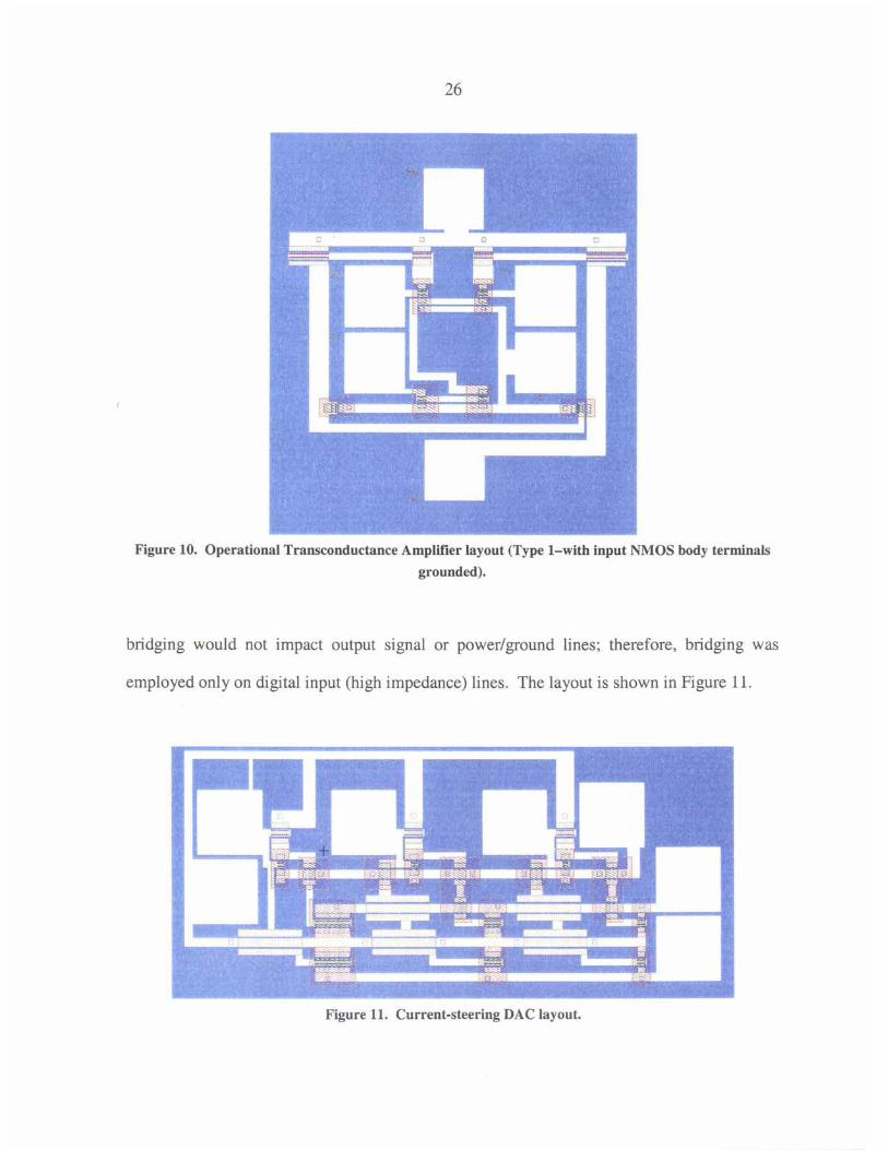
("Type l ") and source-connected ("Type 2") NMOS transistors. The OT A layout is shown in
Figure 10. As with all other layout, it was done in L-Edit.
Three bit current-steering DAC
The DAC design was straightforward, and consisted simply of scaling transistors to give
binary weighting to the current passed through them. The drive circuitry included inverters.
The challenge for the DAC design came during the layout, as it became necessary to use
diffusion areas for interconnect "bridging" under metal lines. Care was taken to ensure such
26
Figure 10. Operational Transconductance Amplifier layout (Type 1-with input NMOS body terminals grounded).
bridging would not impact output signal or power/ground lines; therefore, bridging was
employed only on digital input (high impedance) lines. The layout is shown in Figure 11.
Figure 11. Current-steering DAC layout.
27
Test structures
Several other test structures were added as well. Two MOS capacitors (200 µm x 200
µm) were included for C-V measurements. Two types of diodes (one that made use of a p-
well and n + type doping, and one that made use of adjacent p + and n + type doping in a p-well)
were included as well. Basic test n-MOSFETs (L: 5 µm, W: 24 µm) and p-MOSFETs (L: 5
µm, W: 48 µm) were also added. Finally, test resistors formed from p+ and n+ type diffusion
areas were included.
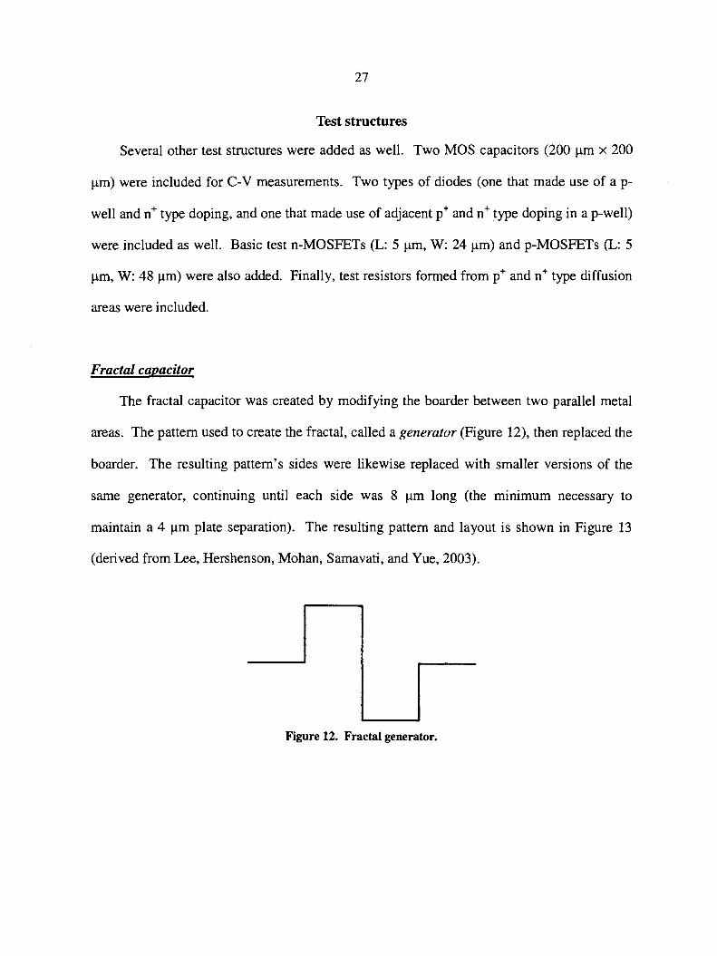
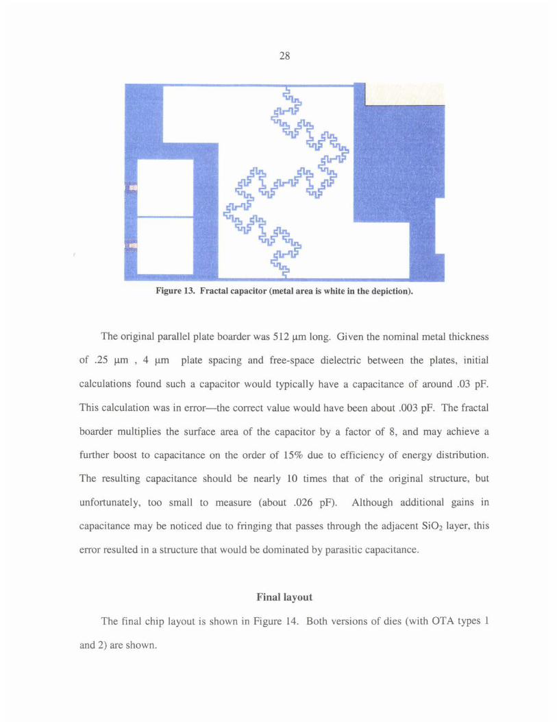
Fractal capacitor
The fractal capacitor was created by modifying the boarder between two parallel metal
areas. The pattern used to create the fractal, called a generator (Figure 12), then replaced the
boarder. The resulting pattern's sides were likewise replaced with smaller versions of the
same generator, continuing until each side was 8 µm long (the minimum necessary to
maintain a 4 µm plate separation). The resulting pattern and layout is shown in Figure 13
(derived from Lee, Hershenson, Mohan, Samavati, and Yue, 2003).
Figure 12. Fractal generator.
28
Figure 13. Fractal capacitor (metal area is white in the depiction).
The original parallel plate boarder was 512 µm long. Given the nominal metal thickness
of .25 µm , 4 µm plate spacing and free-space dielectric between the plates, initial
calculations found such a capacitor would typically have a capacitance of around .03 pF.
This calculation was in error-the correct value would have been about .003 pF. The fractal
boarder multiplies the surface area of the capacitor by a factor of 8, and may achieve a
further boost to capacitance on the order of 15% due to efficiency of energy distribution.
The resulting capacitance should be nearly 10 times that of the original structure, but
unfortunately, too small to measure (about .026 pF). Although additional gains in
capacitance may be noticed due to fringing that passes through the adjacent Si02 layer, this
error resulted in a structure that would be dominated by parasitic capacitance.
Final layout
The final chip layout is shown in Figure 14. Both versions of dies (with OTA types 1
and 2) are shown.

29
(a)
(b)
Figure 14. Final chip layout, with a) OTA type 1 and b) OTA type 2.

30
CHAPTER 3. FABRICATION
Overview and Design of the CMOS Process
The CMOS fabrication procedure designed at the MRC is a six-mask process. It is a
single p-well, metal gate design with one metal interconnect layer. This process was
designed primarily for use in a fabrication class taught at the MRC. The process created was
based heavily on an existing PMOS/BJT process used in the class, consisting of wet oxide
and dry oxide growth, boron nitride/cerium pentaphosphate planar diffusion deposition/drive
steps for p- and n-type doping, patterning with ultraviolet lithography and aluminum
deposition using electron-beam evaporation. The wafers thus fabricated included both
MOSFET (either PMOS or NMOS, depending upon the substrate) and BJT devices, as well
as other test structures (van der Pauw patterns for resistivity measurements, resistors and
MOS capacitors for Capacitance-voltage measurements). This older process was a four-
mask design with extensive robustness built in to compensate for the non-cleanroom
fabrication environment and manual fabrication process steps. The devices fabricated with
the older process were huge by modem standards (up to SOµm feature sizes with 10-20µm
layer overlap) and replicated across the wafers for redundancy.
Additionally, modifications to the CMOS-70 process were made to allow for
CMOS/GMR fabrication. Detail of these modifications can be found in Appendix B.
The fabrication process is also conducted in a non-cleanroom environment (HEP A
filtering, cleaning procedures and gloving helps to minimize contamination). The process
steps are detailed in Appendix A. Specific lab procedures followed those detailed in the
Microelectronics Research Center NSF Lab Manual (2002).

31
Processing challenges
Several processing runs were done in preliminary work before a successful product was
created, and a number of problems were encountered that called for modification of the
specified processing plan. Insufficient etching time during some lithography stages was
corrected. A 15-second HF dip prior to metallization, specified for earlier processes, was
dropped when it was discovered that the dip was sufficient to destroy the very thin gate
oxides used in this project. And planar diffusion sources which had been in use for years
were re-treated according to Carborundum's technical recommendations for pre-deposition
treatment (900°C 100% 0 2 for 30 minutes for the Boron Nitride discs, 8 hours at 900°C for
the cerium pentaphosphate discs) to ensure good performance.
After fabrication, several test wafers were sent to Solecon Laboratories, Inc. (Reno, NV)
for spreading resistance measurements. This measurement technique involves the physical
beveling of a wafer by grinding with a diamond slurry at angles between about 8° and 34°.
After the grinding process, twin measurement probes are stepped down the beveled edge to
make resistance measurements; these measurements are compared with known values to
determine doping profiles. These physical doping measurements agreed quite well with the
calculated expected values, although they verified that one constant used for doping
concentration calculation (the solid solubility limit of phosphorus in silicon at deposition
temperatures) had been too high. The measured doping profile agreed with more up-to-date
value for the phosphorus solid solubility in silicon.
A potentially serious problem was discovered after several fabrication runs resulted in
measured short-circuits between MOSFET source and drain areas: the use of pure aluminum
for contact with silicon. After metallization and metal trace patterning, the wafers are
subjected to a sintering anneal for 15 minutes at 425°C. This is done to ensure the

32
elimination of surface oxide between the deposited aluminum and the silicon substrate, as
well as good physical contact. Unfortunately, the solubility of silicon in aluminum is
significant, meaning that at sintering temperatures silicon diffuses easily into the aluminum
above it. This diffusion process does not occur evenly; diffusion occurs much more readily
along aluminum grain boundaries, leaving voids in the silicon into which the alumimum
flows down. This "spiking" effect can be quite significant, resulting in the shorting of
contacts through diffused regions to the substrate beneath. As a practical matter, this tends to
limit the viability of pure aluminum contacts to designs employing junction depths in excess
of 2-3µm (Plummer, Deal and Griffin, 2000). While the temperature of the sintering anneal
used in this process is lower than that used in industry (typically, 450-500°C), the short
junction depth (.5 µm) meant that excessive aluminum spiking could be a problem.
Although aluminum spiking was only one possible culprit, this possibility was dealt
with by a test-wafer layout redesign, using MOSFETS with much longer channel lengths.
This enabled the use of greater junction depths (1.5-2.0 µm). Adapting the deeper junction
depth to the GMR/CMOS project required undersizing all dimensions of source-drain
diffusion areas by 1.5 µm to compensate.
Processing parameters, initial design
Based upon calculations, preliminary successful processing runs of CMOS test wafers
used the following parameters, and with the results listed in Table 2.

33
Table 2. Initial processing parameters and results.
1. Four-point probe resistivity characterization Doping concentrations approximately 1. 7xl015
atoms/cm3, all wafers 2. Field Oxide was grown for 20 minutes at TWl: 2830A
3.
4.
5.
6.
7.
8.
9.
10.
11.
12.
13.
14.
15. 16. 17.
1050°C. TW2: 2702A
First lithography (p-well), BOE dip: 9 minutes.
Boron deposition for p-well, 30 minutes at 800°C soak time (all other processes done at 800°C, as well). Boron drive for p-well, 720 minutes at 1125°C (13.14 minutes steam ambient).
Second lithography (PMOS source/drain), BOE dip: 11 minutes. Boron deposition for PMOS Source/Drain, 20 minutes at 900°C. Boron drive for PMOS Source/Drain, 65 minutes at 950°C (51.48 minutes steam ambient). Third lithography (NMOS source/drain), BOE dip: 10 minutes. Phosphorus deposition for NMOS Source/Drain, 60 minutes at 900°C. Phosphorus drive for NMOS Source/Drain, 60 minutes at 1125°C (13.14 minutes steam ambient). Fourth lithography (gate oxide), BOE dip: 13 minutes. Gate oxide growth, 14 minutes at 1050°C in 0 2 ambient, followed by 20 minutes at 1050°C in N2 ambient to reduce interface charges. Fifth lithography (contact vias), BOE dip 11 minutes. Metal deposition (aluminum). Metal Patterning with PAN etch Post-metallization sintering anneal, 15 minutes at 425°C.
TW3: 2687A (Measured with Nanospec) < 1 ooA oxide remaining (Measured with Nanospec) NIA
TWl: 3104A TW2: 4229A TW3: 4196A < 1 ooA oxide remaining (Measured with Nanospec) NIA
TWl: 3650A TW2: 3161A TW3: 4525A < 1 ooA oxide remaining (Measured with Nanospec) NIA
TWl: 3374A TW2: 3908A TW3: 4865A lOOA oxide remaining (Measured with Nanospec) TWl: 3407A TW2: 3924A TW3: 302A < 1 ooA oxide remaining (Measured with Nanospec -2500A deposited Unwanted metal etched away Good ohmic contacts

34
Modification of processing parameters for final test wafer
Based upon measurements from preliminary work, diffusion parameters (deposition and
drive times and temperatures) were modified for the final test wafer. Specifically, measured
threshold voltages indicated that assumptions regarding interface charges were likely too
small (by a factor of 10). Adjusting for this resulted in agreement between predicted and
actual values.
After taking the change into account, it was found that p-well doping concentrations
were too small (about 5.3xl016/cm3) and needed to be adjusted upwards (to about
l.2x1016/cm\ This would result in threshold voltages for both NMOS and PMOS of about
±1.4 volts.
The adjusted processing variables used for the first fabrication run (N-1) of the final
wafer are listed below (Table 3).
Table 3. Modified processing parameters, Fab N-1. Ste 1. 2. 3. 4. 5. 6. 7.
Action Field Oxide Boron Deposition-p-well Boron Drive-p-well Boron Deposition-PMOS Boron Drive-PMOS Phosphorus Deposition-NMOS Phos horus Dri ve-NMOS
New Value 23.41 min @ 1075°C 30 min @ 850°C 600 min@ 1125°C 30 min @ 850°C 40 min@ 975°C 120 min @ 900°C 60 min @ 1125°C
For the second fabrication run on the final test wafer (N-2), the parameters were again
modified (Table 4).
35
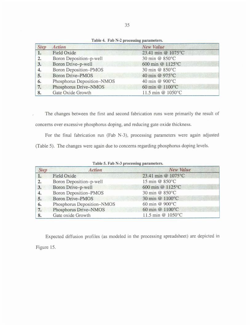
Table 4. Fab N-2 processing parameters. Step Action New Value 1. Field Oxide 23.41 min@ 1075°C 2. Boron Deposition-p-well 30 min @ 850°C 3. Boron Drive-p-well 600 min@ 1125°C 4. Boron Deposition-PMOS 30 min @ 850°C 5. Boron Drive-PMOS 40 min @ 975°C 6. Phosphorus Deposition-NMOS 40 min @ 900°C 7. Phosphorus Dri ve-NMOS 60 min @ 1100°C 8. Gate Oxide Growth 11.5 min@ 1050°C
The changes between the first and second fabrication runs were primarily the result of
concerns over excessive phosphorus doping, and reducing gate oxide thickness.
For the final fabrication run (Fab N-3), processing parameters were again adjusted
(Table 5). The changes were again due to concerns regarding phosphorus doping levels.
Ste 1. 2. 3. 4. 5. 6. 7. 8.
Table 5. Fab N-3 processing parameters. Action
Field Oxide Boron Deposition-p-well Boron Drive-p-well Boron Deposition-PMOS Boron Drive-PMOS Phosphorus Deposition-NMOS Phosphorus Drive-NMOS Gate oxide Growth
New Value 23.41 min @ 1075°C 15 min @ 850°C 600 min@ 1125°C 30 min @ 850°C 30 min@ 1100°c 60 min @ 900°C 60 min @ 1100°C 11.5 min @ 1050°C
Expected diffusion profiles (as modeled in the processing spreadsheet) are depicted in
Figure 15.

1.00E+20
1.00E+19
?E 1.00E+18 ---u c 0 :;:::
36
NMOS
g 1.00E+17 t====j==:=:.:-::-=t-=---·~-----1-----1------1 c G) (J c 8 1.00E+16
-1
1.00E+ 14 -t----+----t-----t-----l-__j.--+----+---+-----i
?E (J
0.00
1.00E+19
1.00E+18
c 1.00E+17 0
~ 'E G) g 1.00E+16 0 u
0.50 1.00 1.50 2.00 2.50 3.00 3.50 4.00
Depth (microns)
(a)
PMOS
1.00E+15 +----+---+----+--~___;f-----+----l----+-------1
1.00E+ 14 +----+----+-----+---___.~---+----+---+---~ 0.00 0.50 1.00 1.50 2.00 2.50 3.00 3.50 4.00
Depth (microns)
(b)
- background - p-well - NMOSS/D
- background - PMOS S/D
Figure 15. Expected diffusion profiles for a) NMOS and b) PMOS transistors.
37
CHAPTER 4. TESTING
Four methods were used to characterize wafers both during the fabrication process and
afterwards.
Testing Methods Used During Fabrication
Four-point probing
The determination of sheet resistance was done during fabrication using the four-point-
probe method. In this procedure, four in-line, evenly-spaced probes were placed on the
wafer surface. A known current was passed between the outer two probes, and a voltage
measurement was made between the inner two probes. When the probe spacing is much
greater than the thickness of the conducting layer being measured (or the thickness of a
wafer), the sheet resistance is given by Equation 6 (Brennan and Dickey, 2002):
R = (_!!__)v I s ln2 II
(6)
where
Rs is the sheet resistance
Vis the measured voltage
I is the known current
When the doping concentration is constant and the thickness of the material is known,
doping concentration can be determined (Equations 7 and 8) from the four-point-probe
measurement (Pierret, 1987).
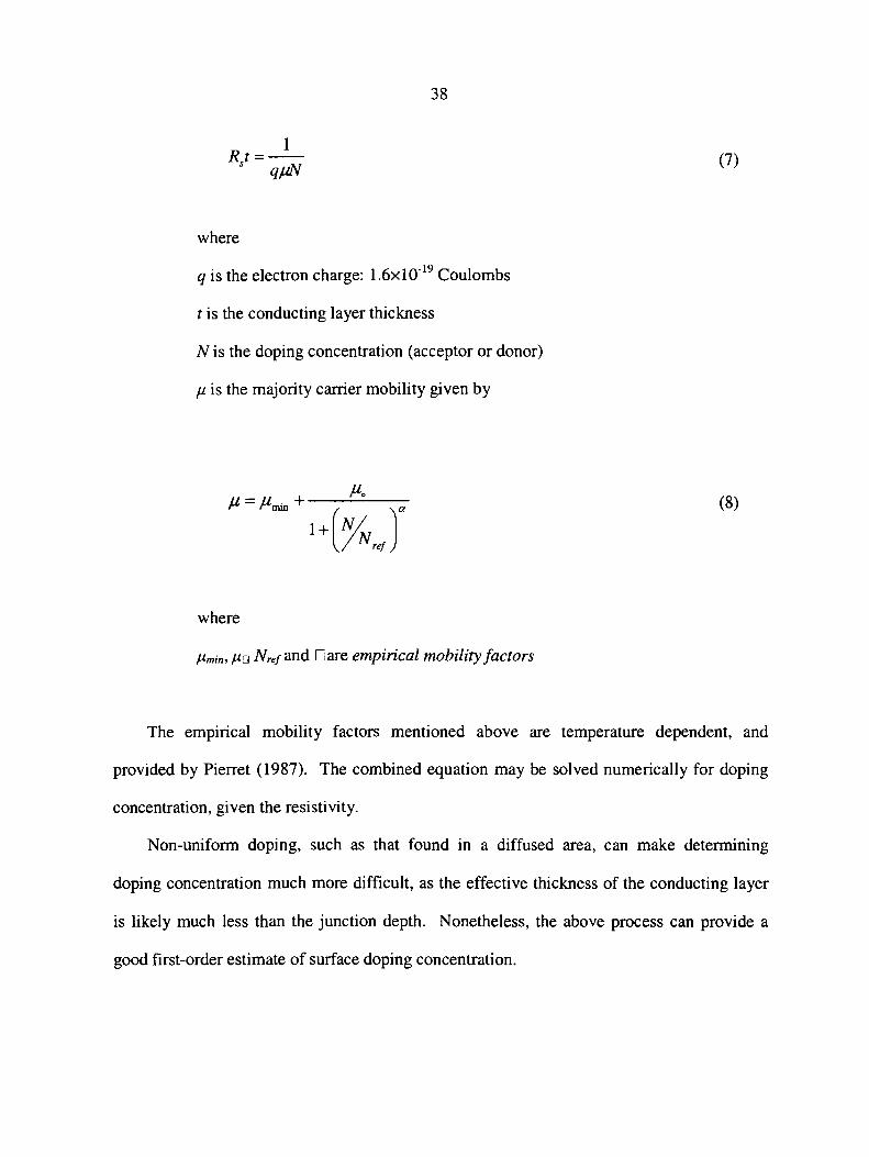
1 Rt=--s qµN
where
38
q is the electron charge: l.6x10·19 Coulombs
t is the conducting layer thickness
N is the doping concentration (acceptor or donor)
µ is the majority carrier mobility given by
µo µ=µmm+ a
1+(~,J
where
µmin, µG Nref and Dare empirical mobility factors
(7)
(8)
The empirical mobility factors mentioned above are temperature dependent, and
provided by Pierret (1987). The combined equation may be solved numerically for doping
concentration, given the resistivity.
Non-uniform doping, such as that found in a diffused area, can make determining
doping concentration much more difficult, as the effective thickness of the conducting layer
is likely much less than the junction depth. Nonetheless, the above process can provide a
good first-order estimate of surface doping concentration.

39
Hot probing
This two-probe measurement is capable of determining the doping type for most
semiconductor layers (Plummer, Deal and Griffin, 2000). At its most basic, one probe is
heated relative to the other, the probe tips are placed on the silicon wafer's surface, and a
voltage measurement is made between the probes using a multimeter.
Because of the "thermal emf' or "Seebeck" effect, majority earners in the
semiconductor around the heated probe acquire more energy and diffuse away from the
probe, leading to a voltage gradient. For a multimeter with a heated positive probe,
measurements on p-type material will yield a negative voltage, and those on n-type material
will yield a positive voltage.
Although a known temperature gradient can be used to determine doping concentration,
this measurement was used in this research only to determine doping type. The positive
voltage probe from a multimeter was heated for ten seconds with a heated soldering iron.
The probe tips were momentarily shorted to equalize the voltage (but too briefly to equalize
temperature). A voltage measurement was subsequently made and doping type inferred from
the polarity of the reading.
Nanospec film thickness measurements
The Nanometrics 210 Nanospec/AFT was used to determine oxide thicknesses on
silicon substrates. The measurement process consisted of initial calibration of the light
source intensity, followed by calibration of the oxide measurement against a known reference
with zero oxide thickness, and finally a measurement of the target material in question.
Oxide measurement recalibration was done every five measurements or more frequently.
During fabrication, the Nanospec machine was used to determine whether etching steps

40
were complete. This was facilitated by the inclusion of test areas on each die sufficiently
large to fill the entire field of the Nanospec microscope.
Testing of the Finished Wafers
Basic test structures
Initial post-fabrication testing consisted of verifying full functionality of test NMOS and
PMOS transistors. This was done by making measurements of the MOSFETs' Io v. Vos
characteristics for gate voltages in the range from 0 volts to 5 volts. A Hewlett-Packard
HP4145A parameter analyzer was used for this purpose. At a probe station, four probes were
used to make contact with source, drain, gate and body terminals.
For the initial GMR Latch design, it was necessary to isolate individual transistors using
probe tips to scrape gaps in metal traces. On the final test wafer, test transistors were
specifically included that needed no isolation prior to testing.
After determining functionality of the MOSFET transistors, several other basic
measurements were made. Capacitance measurements were made on the fractal capacitors
using an HP4280A 1 MHz Capacitance v. voltage meter at zero volts (as well as on a
sampling of the fractal capacitors using a voltage sweep from -10 volts to 10 volts).
Capacitance v. voltage measurements were also made using the HP4280A on MOS capacitor
structures using voltage sweeps from -10 volts to 10 volts. A Visual Basic applet automated
the measurement process using Hewlett-Packard's HP-lB control interface.
Additionally, sheet resistance measurements were made with an HP 4156A parameter
analyzer on the various van der Pauw test structures included in the chip layout using a
technique detailed by the National Institutes of Standards and Technology (NIST) on their
web site (NIST, 2002). In this technique, voltage measurements were made between two of

41
the four terminals on the van der Pauw structure while a known current was passed between
the other two terminals. The terminals used were then switched, and the current was passed
between the first two terminals and voltage was measured between the second pair of
terminals. The two resistance values thus obtained (RA and R8 ) could be used to find the
sheet resistance of the doped area in question by solving the following formula numerically
(Equation 9):
-(JlRA~ ) -(1r:RB~ ) e /Rs + e /Rs = 1 (9)
Thus, the sheet resistance for all doped areas (p-well, NMOS SID and PMOS SID) could
be determined and compared with expected sheet resistance values for a desired level of
doping concentration.
Testing of multi-transistor structures
Various external circuitry was required for testing of the DI A converters and operational
transconductance amplifiers.
Digital to Analog Converter
The DIA converter was characterized usmg seven probes, providing the following
signals/measurements: V cc (5 volts power), ground, Q and Q outputs, and three signals
representing a 3-bit input to the DAC. The three-bit digital input was generated from a Texas
Instruments 74HC191 four-bit binary up/down counter on an external breadboard, configured
to count "up". The bottom three bits were used for the DAC input. The 74HC191 was
clocked using the HP8116A mentioned above, using 5 volt clock pulses from 1 Hz to 50 kHz.

42
The 5 volt power and ground signals were produced by a Hewlett-Packard E3611A power
supply (which also powered the 74HC191), and the outputs were monitored on the HP4156A
parameter analyzer with the inputs set to "sampling". Full output measurements for an entire
000 to 111 binary input sequence were taken for all dies on both wafers.
Operational Transconductance Amplifier
The OT A devices were measured using six probes, providing the following signals and
measurements: V cc (10 volts power), ground, output, reference current input, and inverting
and noninverting inputs. The E3611A power supply was again used to provide power.
Inverting, noninverting, and reference current inputs were generated by the HP4156A
parameter analyzer, and the same machine was used to record the output. A nested sweep of
the two inputs was generated (stepping the noninverting input from 0 to 10 volts in 50m V
increments for voltage levels from 0 to 10 volts (in one-volt increments) on the inverting
input.
GMRLatch
For the initial GMR latch, seven probes made contact with the latch structures, used for
the following signals and measurements: V cc (5 volts power), ground, Q and Q outputs,
RESET, and NMOS source connections for the two legs of the latch. Two 10 kD
potentiometers were placed externally in the source-to-ground legs (one in each leg) of the
latch to simulate the effects of differentially-programmed GMR elements. The RESET
signal was created by the HP4150 parameter analyzer by sweeping that signal from zero volts
to 5 volts and back again using the "repeating" and "double" measurement settings, at a rate
of five volts per second. The latch itself was also powered at 5 volts using the HP4156A.
43
Changes in the Q and Q outputs were measured for various settings of the variable resistors.
For the final GMR latch, the RESET signal was generated by an HP8116A
pulse/function generator set to produce pulses at a rate of 1 per second. This was done to
provide a signal to RESET with much faster transition. Otherwise, the connections to the
latch were identical.

44
CHAPTER 5. RESULTS AND DISCUSSION
Pre-Fabrication Characterization
Prior to fabrication, four-point-probe measurements of the wafers selected for the
CMOS fabricationindicated background doping concentrations on the order of 9.8x1014 cm-3
(120 Q/O).
Test Transistors
The first fabrication of the final chip design (N-1) produced functional PMOS devices,
but the NMOS devices appeared as resistors (substantial current flow), regardless of the
voltage on the gate. Transistor action was not in evidence. It was hypothesized that the
problem had either been inadequate etching before deposition of the NMOS SID phosphorus,
or a problem with the phosphorus pentoxide diffusion source disks.
Measurements of Test Wafer 1 (NMOS SID phosporus above p-well boron) taken with
the hot probe and four-point-probe measurement apparatus indicated that, while the surface
was indeed n-type, it was likely barely so. The calculated sheet resistance of the phosphorus
doping layer was approximately 740 Q/O, with a surface concentration likely less than an
order of magnitude greater than the p-well doping concentration. The expected value for
normal doping after fabrication would be 20-30 Q/O.
The second fabrication (N-2) incorporated extra verification at every etching step to
eliminate this as a source of error: measurements with the Nanometrics Nanospec 210
confirmed less than lOOA of oxide left after primary etching, which was followed by one
minute of extra etching. Nonetheless, results for the second fabrication were similar to those
of the first: functional PMOS devices, barely functional NMOS devices (with a large "diode"

45
offset from the origin in Vos vs. Io measurements), and very high sheet resistances (nearly
750 Q/D) on Test Wafer 1.
Between the second and third fabrications, test fabrications were performed with the
phosphorus planar diffusion sources using very lightly doped p-type wafers (starting sheet
resistances were approximately 7000 Q/D). After a 30-minute deposition at 900°C, measured
sheet resistances on the test wafers ranged from about 930 to 1300 Q/D. Since Carborundum
(the manufacturer) specifies sheet resistances after a 30-minute deposition at 900°C from 10-
15 Q/D, it was clear that the doping was significantly out-of-specification and likely
inadequate for our purposes. Surface concentration of phosphorus doping was likely less
than lx1018 cm·3, prior to any drive-in step.
Subsequently, a similar 8-wafer test was run using 8 spare phosphorus pentoxide disks;
this test identified several disks which produced post-deposition resistances on the order of
80-120 Q/D. The two best disks were selected and a third fabrication run was undertaken.
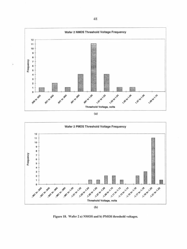
The results of the third fabrication (N-3) were excellent. Vos vs. Io measurements
(Figure 16) indicated no defects, with mean transistor parameters A=-.0011 for NMOS,
A=.015 for PMOS. Additionally, Vas vs . .JI: measurements indicated the NMOS and
PMOS transistors were very well matched. Mean threshold voltages for Wafer 1 were
1.0255 volts for NMOS and -1.059 volts for PMOS. For Wafer 2, mean threshold voltages
were 0.988375 volts and -0.94884 volts for NMOS and PMOS, respectively. The spread for
the threshold voltages on Wafers 1 and 2 is shown in Figures 17 and 18.

en 0.
1.20E-03
1.00E-03
8.00E-04
~ 6.00E-04
.E
2.00E-04
46
Typical NMOS 10 Vs. V0s, Fab N-3
- -- - ---------j
- ---------------------------------l
O.OOE+OO -f-"----,---.------,----,.-----,-----.------,.----.----..----l
O.OOE+OO
·2.00E-04
-4.00E-04
en 0. E -6.00E-04 ca .E
-8.00E-04
-1.00E-03
-1.20E-03
0 0.5
-5 -4.5
1.5 2 2.5
Vo5 , volts
(a)
PMOS 10 Vs. V0s, Fab N-3
-------- -----
-4 -3.5 -3 -2.5
Vos, volts
(b)
3 3.5 4
----------
-2 -1.5 -1
Figure 16. Typical a) NMOS and b) PMOS 10 v. Vos curves, Fabrication N-3.
4.5 5
-0.5 0

47
Wafer 1 NMOS Threshold Voltage Frequency
12
11
10
9
8 >a u 7 c Cl) ::::s 6 i ... 5 u.
4
3
2
0
Threshold Voltage, volts
(a)
Wafer 1 PMOS Threshold Voltage Frequency
12
11
10
9
8 > u 7 c Q) ::::s 6 i
5 ... 1L
4
3 '$~¢.
2
0
Threshold Voltage, volts
(b)
Figure 17. Wafer 1 a) NMOS and b) PMOS threshold voltages.
48
Wafer 2 NMOS Threshold Voltage Frequency
12
11
10
9
8 >-CJ 7 c Cl) :::J 6 er Cl) ... 5 u.
4
3
2
Threshold Voltage, volts
(a)
Wafer 2 PMOS Threshold Voltage Frequency
12
11
10
9
8 >-CJ 7 c Cl) :::J 6 i 5 ... u.
4
3
2
0
Threshold Voltage, volts
(b)
Figure 18. Wafer 2 a) NMOS and b) PMOS threshold voltages.
49
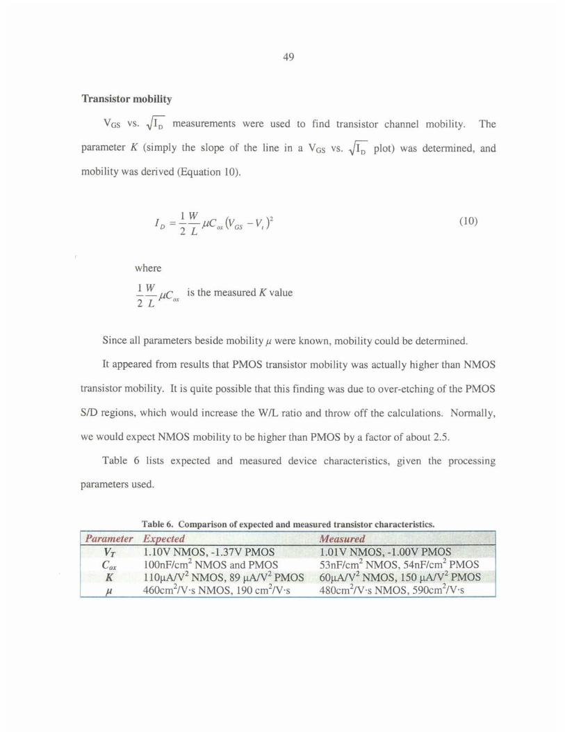
Transistor mobility
V Gs vs. JI: measurements were used to find transistor channel mobility. The
parameter K (simply the slope of the line in a V GS vs. JI: plot) was determined, and
mobility was derived (Equation 10).
(10)
where
1 W c is the measured K value 2z;µ ox
Since all parameters beside mobilityµ were known, mobility could be determined.
It appeared from results that PMOS transistor mobility was actually higher than NMOS
transistor mobility. It is quite possible that this finding was due to over-etching of the PMOS
SID regions, which would increase the W IL ratio and throw off the calculations. Normally,
we would expect NMOS mobility to be higher than PMOS by a factor of about 2.5.
Table 6 lists expected and measured device characteristics, given the processing
parameters used.
Table 6. Comparison of expected and measured transistor characteristics. Parameter Expected Measured
l.lOV NMOS, -l.37V PMOS l.OlV NMOS, -1.00V PMOS 100nF/cm2 NMOS and PMOS 53nF/cm2 NMOS, 54nF/cm2 PMOS 110µA/V2 NMOS, 89 µAIV2 PMOS 60µA/V2 NMOS, 150 µA/V2 PMOS 460cm2N·s NMOS, 190 cm2N·s 480cm2/V·s NMOS, 590cm2N·s
50
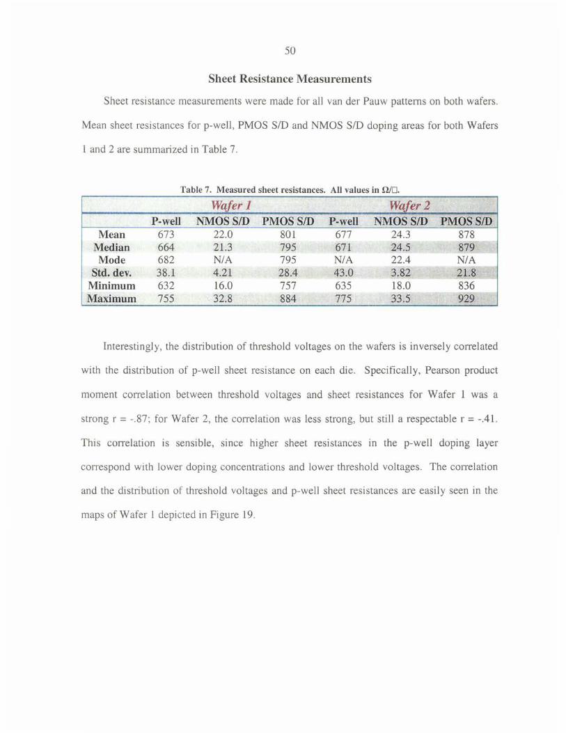
Sheet Resistance Measurements
Sheet resistance measurements were made for all van der Pauw patterns on both wafers.
Mean sheet resistances for p-well, PMOS SID and NMOS SID doping areas for both Wafers
1 and 2 are summarized in Table 7.
Table 7. Measured sheet resistances. All values in WO.
Wafer 1 Wqfer2 P-well NMOSS/D PMOSS/D P-well NMOSS/D PMOSS/D
Mean 673 22.0 801 677 24.3 878 ·-Median 664 21.3 795 671 24.5 879 --Mode 682 NIA 795 NIA 22.4 NIA
~
Std. dev. 38.1 4.21 28.4 43.0 3.82 21.8 ~-
Minimum 632 16.0 757 635 18.0 836 ~
Maximum 755 32.8 884 775 33.5 929
Interestingly, the distribution of threshold voltages on the wafers is inversely correlated
with the distribution of p-well sheet resistance on each die. Specifically, Pearson product
moment correlation between threshold voltages and sheet resistances for Wafer 1 was a
strong r = -.87; for Wafer 2, the correlation was less strong, but still a respectable r = -.41.
This correlation is sensible, since higher sheet resistances in the p-well doping layer
correspond with lower doping concentrations and lower threshold voltages. The correlation
and the distribution of threshold voltages and p-well sheet resistances are easily seen in the
maps of Wafer 1 depicted in Figure 19.

51
1 5
4.5
(a)
1.5
2.5
3.5
45
25 3.5
(b)
Figure 19. Interpolated wafer maps of a) NMOS threshold voltage and b) p-well sheet resistance. Higher values are represented by red shading; lowest values by blue shading.
52
In addition to measurements of the p-well doping, measured sheet resistances for the
PMOS SID van der Pauw areas indicated that boron doping overall was approximately what
was expected. The measured values correspond with surface doping concentrations on the
order of lxl017 cm-3 for p-well, lxl019 cm·3 for NMOS SID and 5xl017 cm·3 for PMOS SID
doping areas.
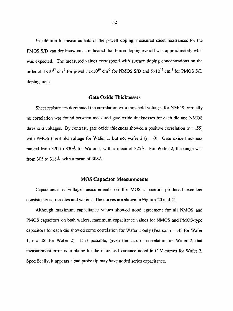
Gate Oxide Thicknesses
Sheet resistances dominated the correlation with threshold voltages for NMOS; virtually
no correlation was found between measured gate oxide thicknesses for each die and NMOS
threshold voltages. By contrast, gate oxide thickness showed a positive correlation (r = .55)
with PMOS threshold voltage for Wafer 1, but not wafer 2 (r = 0). Gate oxide thickness
ranged from 320 to 330A for Wafer 1, with a mean of 325A. For Wafer 2, the range was
from 305 to 318A, with a mean of 308A.
MOS Capacitor Measurements
Capacitance v. voltage measurements on the MOS capacitors produced excellent
consistency across dies and wafers. The curves are shown in Figures 20 and 21.
Although maximum capacitance values showed good agreement for all NMOS and
PMOS capacitors on both wafers, maximum capacitance values for NMOS and PMOS-type
capacitors for each die showed some correlation for Wafer 1 only (Pearson r = .43 for Wafer
1, r = .06 for Wafer 2). It is possible, given the lack of correlation on Wafer 2, that
measurement error is to blame for the increased variance noted in C-V curves for Wafer 2.
Specifically, it appears a bad probe tip may have added series capacitance.

53
Wafer 1 Capacitance v. Voltage, NMOS
6.00E-11
5.00E-11 ------ - - -------- ·- ------ ----- -----
Cl) "O 4.00E-11 --- -------- -- ---------- ----t--------------------f! J! a) g 3.00E-11 ---s ·c; ca Q. (l 2.00E-11 -------------------+-~~11oc:-----------------l
1.00E-11
O.OOE+OO r-------,,--------,.------+-----~--------,-----------1 -15
6.00E-11
5.00E-11 -------
Cl) "O 4.00E-11 ---f! ~ a) g 3.00E-11 s ·c; ca Q.
-10 -5 0
Voltage, volts
(a)
Wafer 1 Capacitance v. Voltage, PMOS
5
(l 2.00E-11 - - - -- --·- --- ---- ------ --- -- -----
1.00E-11 - --- -- - --- ·------------- ------ - ---
O.OOE+OO -15 -10 -5 0
Voltage, volts
(b)
5
10
10
Figure 20. Wafer 1 a) NMOS and b) PMOS MOS capacitor C-V curves.
15
-------1
15

5.00E-11
4.00E-11
111 3.50E-11 "C e J! 3.00E-11 oi g 2.50E-11 s '(j ftS c. ftS 0
2.00E-11
1.50E-11
54
Wafer 2 Capacitance v. Voltage, NMOS
1.00E-11 ---------------------!
5.00E-12 ---·------'-------------- ---- ----
0.00E+OO r----------,r--------,-------+-------,--------,--------l -15 -10 -5 0
Voltage, volts
(a)
Wafer 2 Capacitance v. Voltage, PMOS
6.00E-11
5.00E-11
Cll "C 4.00E-11 e ftS -oi g 3.00E-11 '--------------- -s c; ftS
5 10
c. ca 0 2.00E-11 - - - - ----------------<I-I-----------·------- -- - ---
1.00E-11 ~ - -
15
O.OOE+OO ..-------.---------,-------+-------,---------.------i -15 -1 0 -5 0
Voltage, volts
(b)
5 10
Figure 21. Wafer 2 a) NMOS and b) PMOS MOS capacitor C-V curves.
15
55
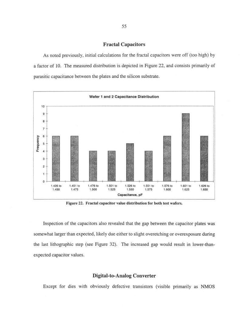
Fractal Capacitors
As noted previously, initial calculations for the fractal capacitors were off (too high) by
a factor of 10. The measured distribution is depicted in Figure 22, and consists primarily of
parasitic capacitance between the plates and the silicon substrate.
9
8
7
~ 6 c Cl> ::s 5 i u: 4
3
2
0 1.426 to
1.450 1.451 to
1.475
Wafer 1 and 2 Capacitance Distribution
1.476 to 1.500
1.501 to 1.525
1.526 to 1.550
Capacitance, pF
1.551 to 1.575
1.576 to 1.600
1.601 to 1.625
Figure 22. Fractal capacitor value distribution for both test wafers.
1.626 to 1.650
Inspection of the capacitors also revealed that the gap between the capacitor plates was
somewhat larger than expected, likely due either to slight overetching or overexposure during
the last lithographic step (see Figure 32). The increased gap would result in lower-than-
expected capacitor values.
Digital-to-Analog Converter
Except for dies with obviously defective transistors (visible primarily as NMOS
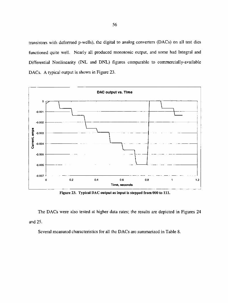
56
transistors with deformed p-wells), the digital to analog converters (DACs) on all test dies
functioned quite well. Nearly all produced monotonic output, and some had Integral and
Differential Nonlinearity (INL and DNL) figures comparable to commercially-available
DACs. A typical output is shown in Figure 23.
Ill Q.
0
-0.001
-0.002
i -0.003 ~ c l!! :; -0.004 0
-0.005
-0.006
-0.007
/
0
DAC output vs. Time
\ \ \ \
\ ~
\ \
1
\
0.2 0.4 0.6 0.8
Time, seconds
Figure 23. Typical DAC output as input is stepped from 000 to 111.
\
-c=
I I
I
1.2
The DACs were also tested at higher data rates; the results are depicted in Figures 24
and 25.
Several measured characteristics for all the DACs are summarized in Table 8.

57
DAC Output, 100 SPS
~ -0.002+-~~~~+-~~~~~~~~-+~~--~~~~~~~~~~~~t-~~~---~~~ Ill .;
~ :I u ... :I t 0
UI Q. E Ill
'E I!! ... :I 0 :; Q. ... :I 0
-0.003
-0.004
-0.006-"-~~~~~~~~~~~~~~~~~~~~~~~~~~~~~~~~~~~~~
0
0.002
0.001
0
-0.001
-0.002
-0.003
-0.004
-0.005
-0.006
-0.007 0
0.02 0.04 0.06
Time, seconds 0.08
Figure 24. DAC output at 100 samples per second.
DAC Output, 10 kSPS
0.001 0.002 0.003 0.004
Time, seconds
0.1 0.12
0.005 0.006
Figure 25. DAC output at 10,000 samples per second. Note that this is at the limit of the HP4156A measurement speed; the spikes of positive current are likely measurement artifacts.
58
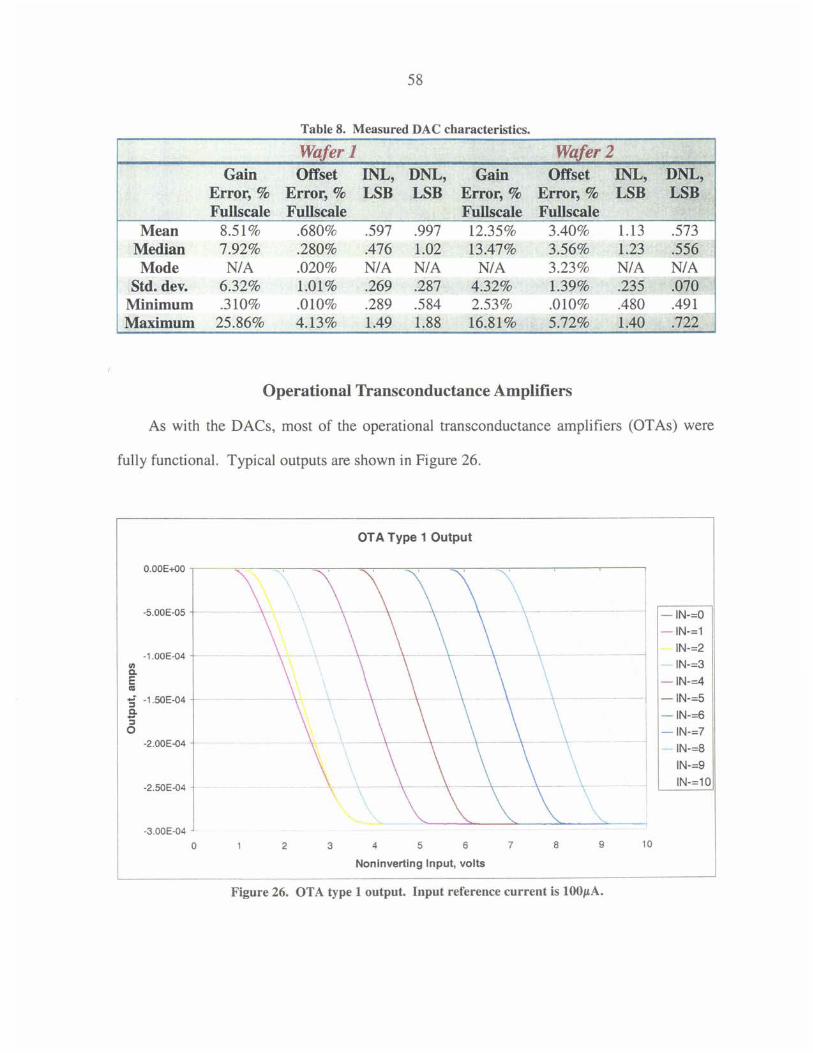
Table 8. Measured DAC characteristics.
Wqfer 1 Wqfer2 Gain Off set INL, DNL, Gain Off set INL, DNL,
Error,% Error,% LSB LSB Error,% Error,% LSB LSB Fullscale Fullscale Fullscale Full scale
Mean 8.51% .680% .597 .997 12.35% 3.40% 1.13 .573 Median 7.92% .280% .476 1.02 13.47% 3.56% 1.23 .556 Mode NIA .020% NIA NIA NIA 3.23% NIA NIA
Std. dev. 6.32% 1.01% .269 .287 4.32% 1.39% .235 .070 Minimum .310% .010% .289 .584 2.53% .010% .480 .491 Maximum 25.86% 4.13% 1.49 1.88 16.81% 5.72% 1.40 .722
Operational Transconductance Amplifiers
As with the DACs, most of the operational transconductance amplifiers (OTAs) were
fully functional. Typical outputs are shown in Figure 26.
"' c. E ~
-5.00E-05 - -- ---
-1.00E-04
'5 -1.50E-04 -c. :; 0
-2.00E-04
-2.50E-04
-3.00E-04 0
OT A Type 1 Output
2 3 4 5 6
Noninverting Input, volts
1 ------- -i
I
I ------- - --~
I I
--1 I
7 8 9 10
Figure 26. OT A type 1 output. Input reference current is lOOµA.
- IN-=0 - IN-=1
IN-=2 - IN-=3 - IN-=4 - IN-=5 - IN-=6 - IN-=7 - IN-=8
IN-=9 IN-=10

59
Sweeps of voltages on the inverting and noninverting inputs produced output that
closely tracked PSPICE model output (Figure 9, Chapter 2). The two types of OT As show
definite differences; however, the only statistically significant variance between the two
types appears to be in Wafer 1 OTA offset (p<.002, two-tailed T-Test for unequal-variance
samples), and Wafer 2 maximum current output (p = .014).
Distributions of OTA transconductance (gain) and current offset are shown in Figures
27 and 28 for Wafers 1 and 2.
It is notable that the output transconductance for the OT As was somewhat lower than
PSPICE predicted. This is likely due to the fact that the PSPICE model was not able to
account completely for such variables as resistive losses in the interconnects, parasitic
capacitances and variations in transistor W!L ratios due to small processing errors.

60
Wafer 1 Distribution of OT A Transconductance
5
4
2
~~~~~~~~~~~~~,~~~ ~ ~ ~ ~ ~ ~ ~ ~ ~ ~ ~ ~ ~ ~ ~ ~ ~ ~ ~ ~ ~ , , ~ , # , , ~ , ~ , ~ ~
Gain, µS
(a)
Wafer 1 Distribution of OTA Output Offset
4
Offset, µA
(b)
Figure 27. Wafer 1 distribution of OT A characteristics.

61
Wafer 2 Distribution of OTA Transconductance
(a)
Wafer 2 Distribution of OT A Output Offset
4
~ 3 i :::s
l 2
Q+-"'--+--""'-+---"-+------+-'---+-"'--t-----+~--t-~--+-'~-t---t---+~"-+-~-+-~+-----i~-+-~-+-~-+-'--+-----i~-1
~~~~~~~~~~~~~~~~~~~~~~ ~~~~~~~~~~~~~~~~~~~~~~ ~~~~~~~~$~$$$$~~~~~~~~
Offset, µA
(b)
Figure 28. Wafer 2 distribution of OT A characteristics.

62
Preliminary GMR Latch
Pre-fabrication characterization
Prior to fabrication, four-point-probe measurements of the wafers selected for the
preliminary GMR Latch indicated background doping concentrations on the order of
1.8xl015 cm·3 (65-67 C/ ).
Measurements taken during fabrication
In-fabrication measurements yielded expected values: all oxidations were calculated to
produce approximately 3000A except for the gate oxide, which produced approximately
350A.
Post-fabrication testing
The initial fabrication attempt of the preliminary GMR Latch wafer produced non-
working circuits. It was determined that the main problem was likely a mistake in calculated
deposition/drive parameters, which likely produced phosphorus doping that was inadequate
for NMOS SID areas. PMOS devices were working, but NMOS devices were not.
The second fabrication of the preliminary GMR Latch wafer (using deposition and drive
for the boron p-well areas, rather than ion implantation) produced fully functional devices.
After separating NMOS and PMOS transistors with a probe tip, functionality was confirmed
by making Vos vs. Io measurements. From these measurements, transistor lambda was
derived: A.=-.003 for NMOS, A.=.01 for PMOS for a sample pair of transistors.
Subsequently, Vas vs. JI; measurements on a sample set of transistors found a range
of threshold voltages of -1.2 to -1.39 volts for PMOS and .506 to .643 volts for NMOS. The
means were -1.34 volts and .570 volts, respectively. These finding were used to modify

63
assumptions regarding gate oxide interface charges, as it was found assuming a tenfold
increase in oxide interface charges fully accounted for the differences between the expected
threshold voltages (approximately ±1 volt) and the measured values.
Measures of functionality for the entire latch structure produced mixed results. Each leg
of the latch (an inverter) functioned as expected (Figure 29), and the latch assumed a stable
output state.
Measurements of the latch's RESET function were less successful. All measured
latches consistently assumed the same stable output state, regardless of the relative
resistances placed in the NMOS source-to-ground connections.
Inverter Transfer Curve, Fab GMR-3
i
l 2+-~~-t-~~-r-~~-+~~---t~+-~r--~~+-~~-+-~~-t-~~-1-~~---l:
I ~ r--_
0 0.5 1.5 2 2.5 3 3.5 4 4.5 5
V1n. volts
Figure 29. Transfer curve, single leg of GMR latch from preliminary GMR Latch design
Updated GMR Latch
Testing on the updated GMR Latch design was more successful, if only briefly. Initial
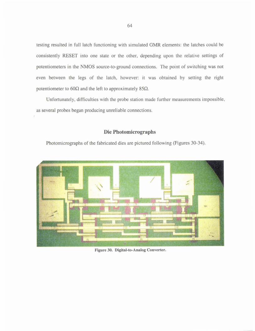
64
testing resulted in full latch functioning with simulated GMR elements: the latches could be
consistently RESET into one state or the other, depending upon the relative settings of
potentiometers in the NMOS source-to-ground connections. The point of switching was not
even between the legs of the latch, however: it was obtained by setting the right
potentiometer to 600 and the left to approximately 850.
Unfortunately, difficulties with the probe station made further measurements impossible,
as several probes began producing unreliable connections.
Die Photomicrographs
Photomicrographs of the fabricated dies are pictured following (Figures 30-34 ).
Figure 30. Digital-to-Analog Converter.
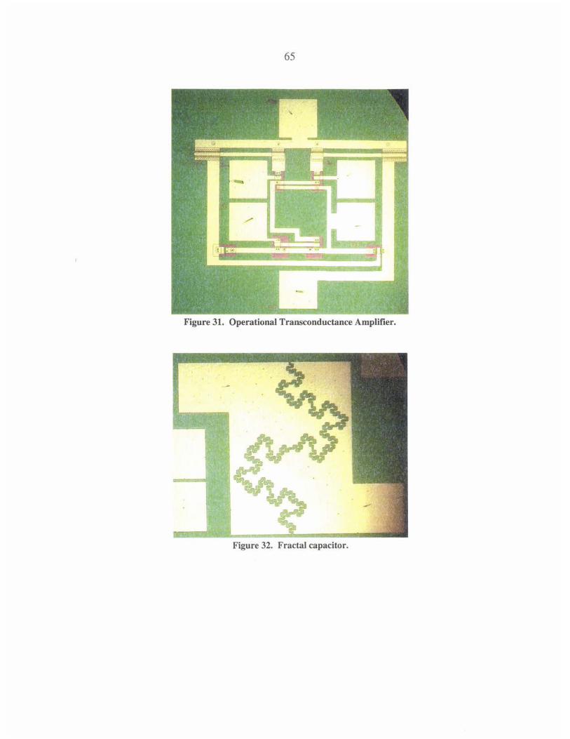
65
Figure 31. Operational Transconductance Amplifier.
Figure 32. Fractal capacitor.
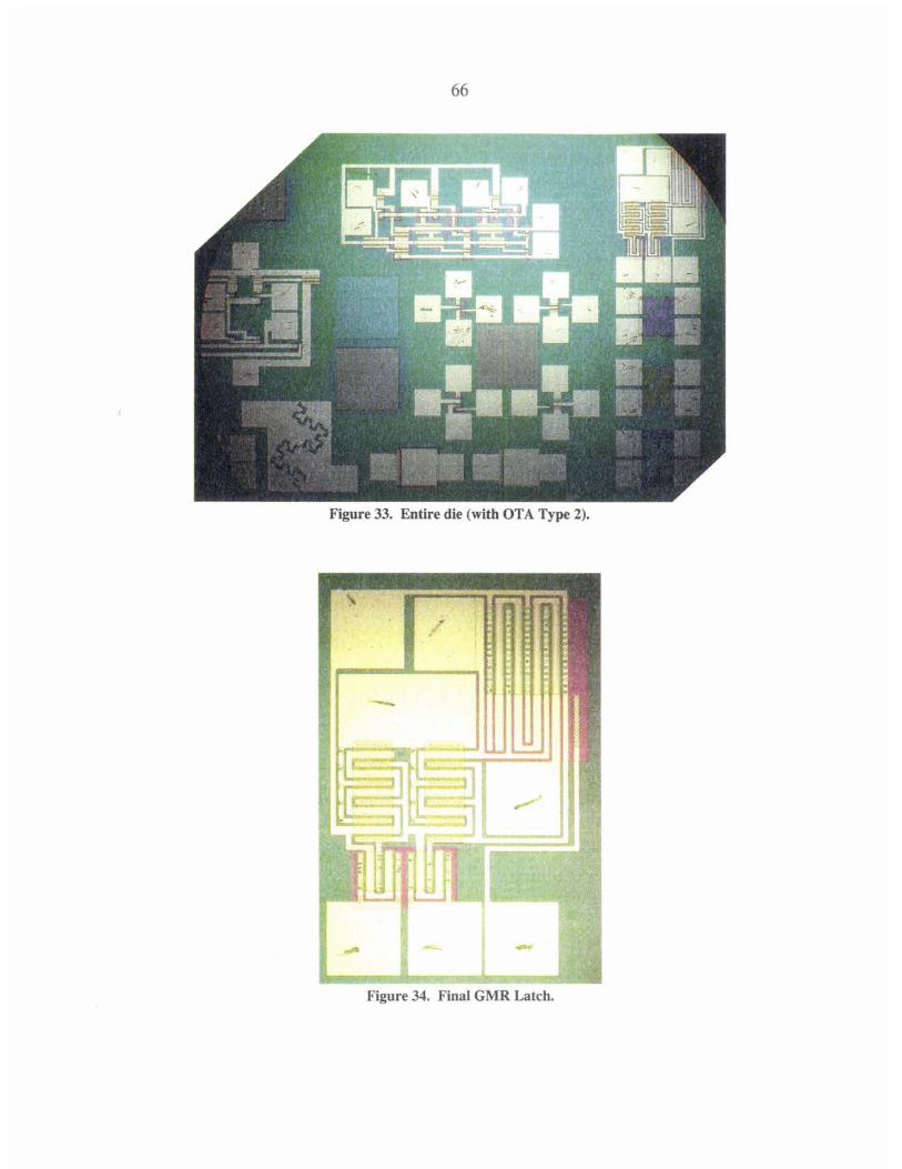
66
Figure 33. Entire die (with OTA Type 2).
Figure 34. Final GMR Latch.
67
CHAPTER 6. CONCLUSIONS
Summary
In this research, a CMOS process using manual processing technology has been refined,
explored and tested. Several potential trouble spots in the fabrication process have been
identified and eliminated, and a working process has been used to fabricate quality devices
and fully-functional rudimentary circuits. These circuits could easily serve as building
blocks for more complicated designs
Additionally, tools have been created and tested for transistor-level design. The tools in
question (in Excel spreadsheet format) would provide the prospective designer with the
means to interactively tailor processing parameters to produce devices with desired
characteristics.
Finally, research has been done on expanding fabrication capabilities using fractal
capacitors, a relatively new idea in on-chip capacitor design that lends itself well to simple
fabrication techniques.
All of these research successes are net gains in terms of ISU' s Microelectronics
Research Center capabilities. They will be of use both for academic lab work and in future
research into CMOS structures.
Recommendations for Future Work
At this point, CMOS-70 is a fully-working CMOS process, capable of producing both
digital and analog CMOS circuits. Future work could involve greater integration of circuitry
on-chip, exploration of twin-well and guarding structures, additional metal layers for multi-
level interconnects and polysilicon gate materials. The control of oxide charges could also

68
be explored more fully.
Much remains to be done in the way of testing of doping results for a new set of planar
diffusion sources. Further, refinement of transistor W/L control (through etching control and
lateral diffusion characterization) will result in greater ability to predict transistor
performance.
Finally, extensive work could be done at the MRC on fractal capacitor structures.
69
APPENDIX A. CMOS PROCESS FLOW
Characterization of the unprocessed wafers. This consists of measuring the sheet
resistance of the native n-type wafers using a four-point-probe measuring setup. Three test
wafers and the desired number of device wafers are selected for fabrication.
Growth of field oxide. In this step, as in all high-temperature processing steps, an RCA
standard clean is first performed on all test and device wafers. The cleaning procedure
involves a 15 minute bath in a 400ml ammonium hydroxide/500ml hydrogen
peroxide/2500ml deionized (DI) water solution at 80° C, followed by a DI water rinse, a 15-
second hydrofluoric acid dip, another DI water rinse, 15 minutes in a 500 ml hydrochloric
acid/500ml hydrogen peroxide/3000 ml DI water solution at 80° C, and a final rinse and dry.
The field oxide is grown in a wet (steam) ambient in a Thermco diffusion furnace;
approximately 4000-5000A is desired.
Patterning for p-well deposition/drive. All lithography steps consist of the following
procedures. First, an adhesion promoter (Hydro, or HMDS) is spun onto the surface of the
wafer to enhance adhesion of photoresist to the wafer. This is followed by spinning Clariant
AZ5209 photoresist on the wafer at 4000 rpm for 40 seconds (designed to produce a .9µm
film of photoresist evenly coating the wafer). Next, the wafer is baked at 100° C for one
minute to reduce the water content of the applied photoresist.
At this point, the wafer is exposed to ultraviolet light through a mask using a Karl-Suss
model MJB 3 UV 300 Mask Aligner. This mask aligner is capable of feature resolution
down to .4um "under optimum conditions".
After exposure, the wafer is developed using Clariant AZ312 MIF developer for one
minute, rinsed in DI water and examined for defects under a microscope. If no defects are

70
discovered, a post bake step (heating the wafer at 120° C for 25 minutes) follows.
The wafers are then submersed in a buffered oxide etch solution (15 parts Ammonium
Flouride/1 part Hydroflouric acid/4 parts DI water) using Test Wafer #1 as a guide for
determining when holes are etched through the oxide to the wafer surface (typically 10
minutes for 3000A. After the BOE step, Photoresist is removed using submersion in two
tubs of acetone (three minutes each), a I-minute rinse in methanol, and a DI water rinse and
dry.
p-Well deposition. In early test runs of the CMOS process, this step consisted of
sending the wafers to an outside source () to have the p-well dopant (boron) deposited using
an ion implantation procedure. This step was later changed to a deposition step using boron
nitride planar diffusion sources for decreased fabrication time and cost.
Boron deposition is accomplished by putting the device wafers and Test Wafer #1 in
proximity to (immediately facing) Carborundum BN-975 boron nitride wafers within a
diffusion furnace. Deposition involves two preparation steps (20 minutes in an
oxygen/nitrogen atmosphere to create a glass on the boron nitride wafers, and two minutes in
an oxygen/nitrogen/hydrogen atmosphere to transfer the boron glass to the device wafers),
followed by the actual boron deposition stage (a nitrogen ambient) which allows an amount
of boron to diffuse into the wafer from the boron glass on the surf ace. This procedure
produces a dose of boron doping near the surface of the wafer.
After furnace processing, the device wafers are briefly (2 minutes) deglazed by dipping
them in BOE to remove the boron glass grown during deposition.
p-Well drive-in. At this stage, the device wafers and all test wafers are subjected to an
RCA cleaning step, then put into the diffusion furnace once more. A low-temperature
(800°C) oxidation is conducted to grow a thin oxide on the surface of the wafers; this is done
71
primarily to oxidize the thin Si-B "boron skin" (silicon-boron phase) left on the surface of the
wafers after deglazing (left alone, this boron skin would serve both as a source of defects and
additional boron doping). Once this is completed, the furnace temperature is raised to the
desired drive-in temperature.
Upon reaching the desired temperature, a wet oxididation process grows approximately
3000A of silicon dioxide on the wafers. For the remainder of the drive-in time, the wafers
are subjected to a nitrogen ambient. The total drive-in time is designed to produce a
junction/substrate depth of about 4-5µm.
Patterning for PMOS source and drain. This lithographic step, employing mask #2,
patterns for and etches oxide openings for PMOS source and drain p-type (boron) doping in
the device wafers. Test Wafer #2 is used for etch rate calibration.
PMOS source and drain boron deposition. This step is identical to the p-Well
deposition step, except that the deposition time and temperature are designed to produce a
higher diffused dose of boron doping in the device wafers and Test Wafer #2.
PMOS source and drain boron drive-in. Largely identical to the p-Well drive-in step,
in this stage we use a lower drive-in temperature to grow 3000A of oxide on all device and
test wafers without substantially driving the deposited boron into the device wafers. This
will be accomplished in later drive-in steps.
Patterning for NMOS source and drain. Similar to the step Patterning for PMOS
source and drain, in this step we use mask #3 to pattern for and etch oxide openings for
NMOS source and drain n-type (phosphorus) doping in the device wafers. Test wafer #1 is
used for etch rate calibration.
NMOS source and drain phosphorus deposition. This step is similar to the PMOS
source and drain boron deposition stage. All device wafers and Test Wafer #1 are cleaned
72
and loaded into the phosphorus diffusion tube with the wafers facing Carborundum PH-900
cerium pentaphosphate discs. For phosphorus deposition, however, the wafers are only
exposed to a nitrogen ambient for a length of time and at a temperature required to obtain the
desired dosage of phosphorus doping.
Similar to the deposition of boron doping, this operation forms a phosphorus glass on
the surface of the target wafers. Cerium Pentaphosphate decomposes into CeP309 and P20 5.
The P20 5 is a dopant vapor that grows a phosphorus-silicon oxide on the surf ace of the
silicon wafers; in this step, the oxide decomposes into silicon dioxide and phosphorus doping
that diffuses into the wafer. After deposition, all exposed device and test wafers are deglazed
in BOE for two minutes.
NMOS source and drain phosphorus drive-in. This high-temperature step actually
serves the dual purpose of phosphorus and boron source/drain drive-in. In this way, more
uniform junction depths between NMOS and PMOS are possible. Additionally, part of the
drive-in step is used to grow 3000A wet oxide. All device and test wafers are processed.
Patterning for MOSFET gate oxide. Using mask #4, holes are patterned and etched
for the MOSFET gates. Test Wafer #3 is used for etch rate calibration.
Growth of gate oxide. After an RCA standard clean, all device and test wafers are
loaded into the oxidation tube of the furnace. 300-400A. of dry oxide (using 0 2) is grown on
all wafers.
Patterning and etching contact vias. Mask #5 was used to pattern and etch holes
(vias) in the oxide on the device wafers for metal contact to the substrate. Test Wafer #2 was
used for etch rate calibration.
Metallization. A Temescal model electron-beam evaporator was used to deposit
2500A. of aluminum on the device wafers. In this process, a beam of electrons from an

73
electron gun was used to strike a graphite crucible containing source aluminum. The
electrons heated the aluminum, causing some to boil off and deposit on the test wafers.
Initially, it was suggested that a 15-second HF dip prior to metallization could be used
to ensure all vias were clear of oxide. It was subsequently discovered that this step was
sufficient to destroy the gate oxide, and was abandoned.
Patterning for and etching metal contact pattern. This step was similar to the other
lithography/etch steps except no HMDS was used, and an etchant composed of 40 ml
phosphoric acid, 40 ml acetic acid, 10 ml nitric acid and 10 ml DI water was used to etch the
deposited aluminum. Etching times were between 4 and 7 minutes, depending upon the
number of wafers etched, room temperature, etc.
· Post-metallization sintering anneal. After etching, the device wafers were subjected
to a low-temperature (400° C) furnace step for about 10 minutes. This step was designed to
overcome any oxide barrier in the contact vias between silicon and aluminum (without it,
such contacts would tend to form a diode). Care had to be taken in this step not to anneal for
too long or at too high a temperature; this process produces aluminum "spiking" into the
silicon that can short out very shallow regions (less than 2µm deep or so).

74
APPENDIX B. EARLY WORK: THE GMR LATCH
Giant Magneto-Resistance Process Development at the MRC
Thus far, development of a Giant Magneto-Resistance process has consisted of
fabrication using electron-beam evaporation. The system used has been fitted with large
Helmholtz coils for magnetic field generation during film growth, and fabrication of GMR
thin film multilayers has been carried out. Work is ongoing. At this point, the primary issue
for further development is obtaining pure films, as excessive oxygen impurity content
appears to be swamping GMR effects in grown films .
The work at the MRC has consisted of growth of structures called "spin valves" and
"pseudo-spin valves". A "Spin valve" (Another term for stacks of thin-film magnetic
materials which exhibits GMR) usually refers to a device with two magnetic layers separated
by a nonmagnetic metal spacer, which has a "pinning" or "exchange" layer next to one of the
magnetic layers (a layer of harder magnetic material that keeps an adjacent softer layer
"pinned" in a certain magnetic orientation-see Figure 35). These devices are frequently used
in hard drive read heads. In operation, only the unpinned layer switches orientation in
response to an external magnetic field; the pinned layer keeps its orientation. This switching
operation changes the relative orientation of the two layers' magnetization, resulting in a
change in resistance.
Figure 35. Basic spin valve structure.

75
"Pseudo-spin valves" are relatively new devices that consist of two magnetic layers of
different thicknesses. The difference in thicknesses results in a difference in switching field
thresholds: the thinner layer switches at a lower threshold.
A simple fabrication of pseudo-spin valves consists of five layers of material: two outer
layers of nickel-iron-cobalt, two inner layers of cobalt-iron, and a center copper spacer. The
two outer layers are 70 A and 60 A thick. The two inner cobalt-iron layers are 15 A thick,
and the copper spacer is 27 .5 A thick. The two cobalt-iron layers are present to improve
lattice matching between the nickel-iron-cobalt and the copper, which otherwise might suffer
from lattice mismatching and degraded electron scattering "noise". Everitt, Pohm and
Daughton ( 1997). reported observed GMR of over 6% in fabricated and etched devices.
Pseudo-spin valves present interesting possibilities for digital memory applications
(Johnson, 2000; Black and Das, 2000). The thicker magnetic layer may be used to "store" a
bit state, which may then be read by the application of a low-level field sufficient to place the
thinner layer in a known configuration. A current sent down the length of the bit will
experience high or low resistance, depending upon the programming of the device (Figure
36).
Sense Line
<
Word Line
>
Sense Line
Figure 36. GMR pseudo-spin valve memory bit (z-axis dimension greatly exaggerated for clarity). Sense current travels through the bit; word-line current travels through the word-line metal overlaying the bit

76
Overview and Design of the CMOS/GMR Process
The CMOS Process was modified to allow the fabrication of GMR structures which
could interface with CMOS devices. The modification entailed the addition of two additional
lithography steps near the end of a CMOS fabrication.
In order to integrate GMR with the existing CMOS procedure, processing order was
critical. Two possibilities were considered. In the first, the CMOS process would be
completed without interruption, an insulating oxide would be deposited with Plasma-
Enhanced Chemical-Vapor Deposition (PECVD) or electron-beam evaporation and patterned,
and finally GMR would be deposited and patterned. In the second option, the CMOS process
would be interrupted before metal patterning, GMR would be deposited along with insulating
oxide, and aluminum would be deposited and patterned last.
Although the first option above offered the appeal of using the CMOS process unaltered,
it presented a severe difficulty. Due to the fact that the GMR elements, at the most 300A
thick, would be deposited on top of patterned metal 2500A thick and patterned insulating
oxide at least several hundred angstroms thick, it was clear that the GMR layers could not be
magnetized uniformly (e.g. parallel or antiparallel), and might even suffer from disconnects
if GMR deposition did not adequately coat the etched sidewalls of the oxide. Therefore, the
second option seemed a better choice.
However, the second option presented an obstacle of its own: how to pattern the
deposited word-line oxide. Because the GMR processing would be added to the CMOS
process before metallization, gate oxides were in danger of destruction if the word-line oxide
was etched (it would be deposited on top of the gate oxide). A further obstacle concerned the
patterning of the GMR multilayers; due to the different metal alloys which compose the

77
GMR deposition (detailed below), etching would most likely involve reactive ion etching
(RIE). An easier solution to both of these problems is negative-photoresist liftoff.
Unlike a standard patterning stage wherein areas not covered by photoresist are removed
by etching, in liftoff the photoresist is deposited, exposed and developed, then the desired
film is deposited on top. Subsequent exposure to acetone removes the remaining photoresist
and film above, leaving only the film where photoresist had not been.
To accomplish this type of patterning, the AZ5209 photoresist used in all lithography
steps is subjected to negative-tone processing (the processing described earlier is positive-
tone processing). The photoresist is spun on to the wafers and pre-baked as before. During
UV exposure through a mask pattern, the exposure time is reduced (1 minute vs. the standard
1 minute 24 seconds). After exposure, the wafers are given an additional post-exposure bake
(120° C for 45 seconds on a hot plate). They then undergo a flood exposure (a five-minute
exposure of the entire wafer to a Splice UV lamp model #5200-117V, serial #A651) while
spinning to ensure uniformity. The remaining lithography processing proceeds as before,
beginning with development.
The procedure noted here produces a photoresist wall profile suitable for a liftoff process.
This profile slopes inward, assuring discontinuity of subsequently deposited layers and ease
of liftoff. The regular wall profile slopes outward, which can cause problems with lifted
material clinging to the wafer.
This project added four steps in the standard CMOS process, inserting them between the
growth of gate oxide and Patterning and etching contact vias stages. The new steps are:
Pattern for GMR elements. Mask #5 in the modified procedure is used to pattern
photoresist for GMR memory elements using the liftoff process noted above.
78
Deposition of GMR and liftoff. A GMR thin film pseudo spin valve multilayer is
grown on the device wafers using electron-beam evaporation. The GMR stack consists
(bottom up) of a 50A Tantalum seed layer, a 40A. Ni6sFe20Co1s alloy layer, a 15A
Co9of'e10 alloy matching layer, a 27 A copper spacer layer, another 15A Co9of'e10 alloy
matching layer, a 60A Ni65Fe20Co1s alloy layer, and a top tantalum "cap" lOOA. thick to
prevent oxidation of the magnetic layers.
After GMR deposition, an acetone soak completes the liftoff process, leaving only
the desired patterns of GMR. Using the liftoff process with the GMR multilayer greatly
simplifies a patterning process that would otherwise require complex etching procedures.
Pattern for word-line oxide. Using Mask #6, we pattern for the insulating oxide
between the GMR elements and word lines crossing over them. This process also uses
liftoff; in order to protect the already-grown gate oxide from the soon-to-be-deposited
insulating oxide.
Deposition of word-line oxide and liftoff. An electron-beam evaporation process is
used to deposit Si02 on the device wafers. A subsequent acetone soak completes the
liftoff process, leaving only desired patterns of oxide.
The remaining steps resume processing with the patterning and etching for contact vias
(Mask #7), deposition of metal and patterning and etching for metal contact pattern (Mask
#8).
This modified process is thus intended to make as heavy use as possible of the existing
CMOS process, while allowing easy addition of GMR.

79
GMR Latch Conclusions
This is an area of exciting work, and the research detailed in this section indicates a
working design has been obtained. This design should provide functioning GMR Latches if
paired with GMR elements sized to compensate for the different resistances required to cause
the latch to switch.

80
REFERENCES CITED
Black Jr., W. C., & Das, B. (2000). Programmable logic using giant-magnetoresistance and spin-dependent tunneling devices. Journal of Applied Physics, 87(9), 6674-6679.
Blalock, T. N., & Jaeger, R. C. (1991). A high-speed clamped bit-line current-mode sense amplifier. IEEE Journal of Solid State Circuits, 26(4), 542-548
Brennan, R., & Dickey, D. (2002). Determination of Diffusion Characteristics Using Two-and Four-Point Probe Measurements. Retrieved March 19, 2003, from Solecon Laboratories Incorporated web site: http://www.solecon.com/pdf/determination_of_diffusion_characteristics_using_2_an d_4pp.pdf
Das, B., Wong, K. A., & Black Jr., W. C. (2000, September). Nonvolatile CMOS latch employing GMR resistors. Presented at the 26th European Solid-State Circuits Conference (ESSCIRC 2000).
Everitt, B. A., Pohm, A. V., & Daughton, J. M. (1997). Size dependence of switching thresholds for pseudo spin valve MRAM cells. Journal of Applied Physics, 81(8), 4020-4022.
Hall-Effect Measurements (2000). Retrieved April 25, 2002, from National Institute of Standards and Technologies Semiconductor Electronics Division's web site: http://www.eeel.nist.gov/812/hall.html
Johnson, M. (2000, February). Magnetoelectronic memories last and last... IEEE Spectrum, TI.,.33-38.
Lee, T. H., Harshenson, M. d. M., Mohan, S. S., Samavati, H., & Yue, C. P. (2003). RF Passive IC Components. In W. K. Chen (Ed.), Analog circuits and devices (pp. 2-1-2-12). Boca Raton, FL: CRC Press.
NSF Lah Manual.(n.d.). Retrieved February 3, 2002, from Iowa State University Microelectronics Research Center NSF Lab web site: http://tuttle.merc.iastate.edu/nsflab/labmanual/manual.htm
Pierret, Robert F. (1987). Advanced semiconductor fundamentals: volume VI. Reading, MA: Addison-Wesley.

81
Plummer, J. D., & Deal, M. D. (2000) Silicon VLSI technology: fundamentals, practice and modeling. Englewood Cliffs, NJ: Prentice-Hall.
Sedra, AS., & Smith, K. C. (1998). Microelectronics circuits (4th ed.). New York: Oxford University Press.
Song, B. S. (2003). Nyquist-Rate ADC and DAC. In W. K. Chen (Ed.), Analog circuits and devices (pp. 7-1-7-30). Boca Raton, FL: CRC Press.
Streetman, B. G. (1995) Solid-state electronic devices. Englewood Cliffs, NJ: Prentice-Hall.
Taur, Y., & Ning, T. H. (1998) Fundamentals of modem VLSI devices, Cambridge: Cambridge University Press.
Wassenaar, R.F., Ismail, M., & Lin, C. H. (2003). Operational Transconductance Amplifiers. In W. K. Chen (Ed.), Analog Circuits and Devices (pp. 6-1-6-18). Boca Raton, FL: CRC Press.
Wong, K.A. (1999). A monolithic CMOS latch structure with integrated GMR devices as non-volatile data storage and a multiple-state sensing technique for pseudo spin-valve GMR devices. Unpublished master's thesis, Iowa State University, Ames.

82
ACKNOWLEDGEMENTS
Several people made this work possible. I would like to thank my major professor, Dr.
Gary Tuttle, whose guidance and feedback kept my research on track. Likewise, I would like
to acknowledge Dr. Vikram Dalal, who has been a constant source for encouragement for me
throughout my graduate career, as well as a helpful sounding board for my work. Last but
not least, Dr. Alan Constant helped me with feedback regarding the GMR Latch.
Two fellow graduate students helped with my research. Nee-Fong Siah did most of the
legwork in the initial CMOS-70 process development, and collaborated with me on ironing
out multiple difficulties with the process and fabrication. Micah Decker assisted me with lab
work and equipment fixes, as well as preventing several disasters.
Last but certainly not least, I would like to thank my wife, Cindy, without whose
encouragement, experienced eye and infinite patience this work would not have been
completed.
Copyright © 2022 FDOKUMEN