
Design of multipurpose batch plants with uncertain production requirements
Upload
khangminh22Category
view
0download
0
Design and Fabrication of a Multipurpose Compliant Nanopositioning Architecture
by
Robert M. Panas
S.M. Mechanical Engineering Massachusetts Institute of Technology, 2009
Sc.B. Mechanical Engineering
Sc.B. Physics Massachusetts Institute of Technology, 2007
Submitted to the Department of Mechanical Engineering
in Partial Fulfillment of the Requirements for the Degree of
Doctor of Philosophy in Mechanical Engineering
at the
Massachusetts Institute of Technology
June 2013
2013 Massachusetts Institute of Technology All rights reserved.
Signature of Author………………………………………………………………………………… Department of Mechanical Engineering
May 20, 2013
Certified by………………………………………………………………………………………… Martin L. Culpepper IV
Associate Professor of Mechanical Engineering Thesis Supervisor
Accepted by……...………………………………………………………………………………… David E. Hardt
Professor of Mechanical Engineering Graduate Officer

2

3
Design and Fabrication of a Multipurpose Compliant Nanopositioning Architecture
by
Robert M. Panas
Submitted to the Department of Mechanical Engineering on May 20, 2013 in Partial Fulfillment of the
Requirements for the Degree of Doctor of Philosophy in Mechanical Engineering
ABSTRACT This research focused on generating the knowledge required to design and fabricate a high-speed application flexible, low average cost multipurpose compliant nanopositioner architecture with high performance integrated sensing. Customized nanopositioner designs can be created in ≈1 week, for <$1k average device cost even in batch sizes of 1-10, with sensing operating at a demonstrated 59dB full noise dynamic range over a 10khz sensor bandwidth, and performance limits of 135dB. This is a ≈25x reduction in time, ≈20x reduction in cost and potentially >30x increase in sensing dynamic range over comparable state-of-the-art compliant nanopositioners. These improvements will remove one of the main hurdles to practical non-IC nanomanufacturing, which could enable advances in a range of fields including personalized medication, computing and data storage, and energy generation/storage through the manufacture of metamaterials. Advances were made in two avenues: flexibility and affordability. The fundamental advance in flexibility is the use of a new approach to modeling the nanopositioner and sensors as combined mechanical/electronic systems. This enabled the discovery of the operational regimes and design rules needed to maximize performance, making it possible to rapidly redesign nanopositioner architecture for varying functional requirements such as range, resolution and force. The fundamental advance to increase affordability is the invention of Non-Lithographically-Based Microfabrication (NLBM), a hybrid macro-/micro-fabrication process chain that can produce MEMS with integrated sensing in a flexible manner, at small volumes and with low per-device costs. This will allow for low-cost customizable nanopositioning architectures with integrated position sensing to be created for a range of micro-/nano- manufacturing and metrology applications. A Hexflex 6DOF nanopositioner with titanium flexures and integrated silicon piezoresistive sensing was fabricated using NLBM. This device was designed with a metal mechanical structure in order to improve its robustness for general handling and operation. Single crystalline silicon piezoresistors were patterned from bulk silicon wafers and transferred to the mechanical structure via thin-film patterning and transfer. This work demonstrates that it is now feasible to design and create a customized positioner for each nanomanufacturing/metrology application. The Hexflex architecture can be significantly varied to adjust range, resolution, force scale, stiffness, and DOF all as needed. The NLBM process was shown to enable alignment of device components on the scale of 10’s of microns. 150µm piezoresistor arm widths were demonstrated, with suggestions made for how to reach the expected lower bound of 25µm. Flexures of 150µm and 600µm were demonstrated on

4
the mechanical structure, with a lower bound of ≈50µm expected for the process. Electrical traces of 800µm width were used to ensure low resistance, with a lower bound of ≈100µm expected for the process. The integrated piezoresistive sensing was designed to have a gage factor of about 125, but was reduced to about 70 due to lower substrate temperatures during soldering, as predicted by design theory. The sensors were measured to have a full noise dynamic range of about 59dB over a 10kHz sensor bandwidth, limited by the Schottky barrier noise. Several simple methods are suggested for boosting the performance to ≈135dB over a 10kHz sensor bandwidth, about a <1Å resolution over the 200µm range of the case study device. This sensor performance is generally in excess of presently available kHz-bandwidth analog-to-digital converters.
Thesis Supervisor: Martin L. Culpepper IV Title: Associate Professor of Mechanical Engineering

5
ACKNOWLEDGEMENTS
I owe a lot of people a great deal of thanks. I will start with the one who has possibly
ground out enough levels of thesis to have earned a Degree in Patience- my wife, Cynthia Panas.
I know that she has certainly felt like she was somehow a graduate student again, despite having
escaped with a degree back in 2011. Thank you for your assistance in all matters great and
small. I did not have time for life and work, so you took care of life. You also listened to the
soul-numbingly boring updates on the project each evening, each of which was capped with a
declaration that I was either just about done or that I would never finish. There really was no
middle ground. Just when it couldn’t get any worse, you stepped up and started building parts of
the thesis too- I don’t think there will ever be enough time to thank you fully.
Then there are my UROPs, Lucy, Prosper, Elizabeth, Veronica, somewhere between a
group of eager young minds and an unstoppable army of science. We advance, oxidizing,
depositing, and milling out Hexflexes like there is no tomorrow. For many of those machines,
on many of the days, there was no tomorrow- as they were breaking as fast as we could get them
working again. Thank you for your long hours and enthusiasm. You are now all experts in
Making Tiny Things®.
Next there are my coworkers-you compatriots in voluntary suffering. You crazy goofs,
why did we all think getting a doctoral degree was a good idea? Thank you for your support.
Last but in no way least, there is my mentor and advisor, Prof. Martin Culpepper. I
almost didn’t get a position in the lab, when I applied as a UROP sophomore year of undergrad.
Thank you for giving me a chance back then; thank you for your support time and time again
over these years as I tackled each seemingly impossible (from my view) task. You seemed much
more confident in my eventual success than I was most of the time, and that was surprisingly
heartening in those stressful times. Thank you for showing all of us what to do (Purpose!,
Importance!, Impact!) and what to not do (procrastinate, start sentences with prepositional
phrases) in order to become an academic.

6

7
CONTENTS
Abstract .....................................................................................................................................3
Acknowledgements ....................................................................................................................5
Contents .....................................................................................................................................7
Figures ..................................................................................................................................... 15
Tables....................................................................................................................................... 25
1 Introduction ....................................................................................................................... 27
1.1 Synopsis .................................................................................................................... 27
1.2 Argument .................................................................................................................. 28
1.2.1 Nanomanufacturing ................................................................................................ 28
1.2.2 Dependence............................................................................................................ 29
1.2.3 Present Nanopositioners ......................................................................................... 30
1.2.3.1 Speed .............................................................................................................. 31
1.2.3.2 Flexibility ........................................................................................................ 32
1.2.3.3 Cost ................................................................................................................. 33
1.2.3.4 Impact due to Limitations ................................................................................ 34
1.2.4 Nanopositioner Performance .................................................................................. 36
1.2.5 Fundamental Advances .......................................................................................... 36
1.2.5.1 Speed .............................................................................................................. 36
1.2.5.2 Flexibility ........................................................................................................ 38
1.2.5.3 Cost ................................................................................................................. 39
1.3 Thesis Scope .............................................................................................................. 40
1.4 Case Study ................................................................................................................. 41
1.5 Actuation Concept ..................................................................................................... 44
1.6 Background ............................................................................................................... 45
1.6.1 Nanopositioners ..................................................................................................... 45
1.6.2 Reluctance Actuation ............................................................................................. 46

8
1.6.3 Design Rules .......................................................................................................... 47
1.6.4 Non-Lithographically-Based Microfabrication ....................................................... 47
1.7 Thesis Structure ......................................................................................................... 48
2 Design of Piezoresistive Sensor Systems ........................................................................... 51
2.1 Synopsis .................................................................................................................... 51
2.2 Parameters ................................................................................................................. 52
2.3 Introduction ............................................................................................................... 53
2.4 Background ............................................................................................................... 53
2.5 DC Piezoresistive Sensor System Model .................................................................... 54
2.5.1 System Layout and Model ...................................................................................... 54
2.5.2 Flexure Model ........................................................................................................ 57
2.5.3 Wheatstone Bridge Model ...................................................................................... 58
2.5.4 Instrumentation Amplifier Model ........................................................................... 60
2.5.5 Source Voltage Model ............................................................................................ 61
2.5.6 Bias Voltage Model................................................................................................ 61
2.5.7 Power Supply Model .............................................................................................. 62
2.5.8 Digital Model ......................................................................................................... 63
2.5.9 Dominant Noise Sources and System Characteristics ............................................. 63
2.5.10 Performance Metrics ............................................................................................ 65
2.6 Insights from the model ............................................................................................. 65
2.6.1 Electronic Sources .................................................................................................. 65
2.6.2 Mechanical Sources ............................................................................................... 66
2.6.3 Thermal Sources .................................................................................................... 66
2.6.4 Johnson and Flicker Noise ...................................................................................... 66
2.7 Experimental Measurements and Model Verification ................................................. 67
2.8 Piezoresistive Sensor Design and Optimization .......................................................... 69
2.8.1 Reduced Piezoresistive Sensor System Model ........................................................ 69
2.8.2 Optimization Process.............................................................................................. 71
2.8.3 Analytical Optimization ......................................................................................... 74
2.8.4 Computational Optimization .................................................................................. 76
2.9 Conclusion................................................................................................................. 79

9
3 Engineering Schottky Diode Contacts .............................................................................. 81
3.1 Synopsis .................................................................................................................... 81
3.2 Introduction ............................................................................................................... 81
3.3 Background ............................................................................................................... 83
3.3.1 Metal-Semiconductor Contacts ............................................................................... 83
3.3.2 Soldering to Silicon ................................................................................................ 83
3.4 Theory ....................................................................................................................... 84
3.4.1 Reverse Bias Resistance ......................................................................................... 85
3.4.2 Electrical Model ..................................................................................................... 87
3.5 Experimental Setup .................................................................................................... 88
3.6 Contact Resistivity ..................................................................................................... 90
3.7 Bonding Parameter .................................................................................................... 91
3.8 Schottky Barrier Parameters....................................................................................... 91
3.9 Barrier Resistivity ...................................................................................................... 93
3.10 Barrier Voltage .......................................................................................................... 94
3.11 Discussion ................................................................................................................. 95
3.11.1 Proposed Mechanism ........................................................................................... 95
3.11.2 Oxide Effect ......................................................................................................... 96
3.12 Conclusion................................................................................................................. 96
4 Optimization of Piezoresistors with Schottky Diode Contacts ........................................ 99
4.1 Synopsis .................................................................................................................... 99
4.2 Introduction ............................................................................................................. 100
4.2.1 Non-Lithographically-Based Microfabrication ..................................................... 100
4.2.2 Optimization ........................................................................................................ 102
4.2.3 Device .................................................................................................................. 102
4.3 Existing Piezoresistors ............................................................................................. 103
4.4 Semiconductor Piezoresistor Model ......................................................................... 104
4.4.1 Model Overview .................................................................................................. 104
4.4.2 Silicon Resistance ................................................................................................ 106
4.4.3 Contact Resistance ............................................................................................... 108
4.4.4 Barrier Resistance ................................................................................................ 109

10
4.4.5 Delta Resistance ................................................................................................... 110
4.4.6 End Resistance ..................................................................................................... 111
4.4.7 Trace Resistance .................................................................................................. 111
4.4.8 Overall Equation .................................................................................................. 111
4.5 Electrical Performance ............................................................................................. 112
4.6 Gage Factor ............................................................................................................. 112
4.7 Schottky Barrier Noise ............................................................................................. 115
4.8 Constraint-Based Optimization ................................................................................ 117
4.8.1 Objective Function ............................................................................................... 117
4.8.2 Constraints ........................................................................................................... 118
4.8.3 Resistance Variation ............................................................................................. 119
4.9 Secondary Geometry................................................................................................ 120
4.9.1 Stress Concentrations ........................................................................................... 120
4.9.2 Epoxy Creep ........................................................................................................ 122
4.10 Model Validation ..................................................................................................... 123
4.10.1 Device ................................................................................................................ 123
4.10.2 I-V Performance ................................................................................................. 123
4.10.3 Gage Factor ........................................................................................................ 124
4.10.4 Maximum Strain ................................................................................................ 125
4.10.5 Noise .................................................................................................................. 126
4.10.6 Resistance Variation ........................................................................................... 127
4.11 Discussion ............................................................................................................... 128
4.11.1 Trends in Optimization ....................................................................................... 129
4.11.2 Advantage of NLBM-Fabricated Semiconductor Piezoresistors .......................... 131
4.11.3 Generalization .................................................................................................... 132
4.12 Conclusion............................................................................................................... 132
5 Non-Lithographically-Based Microfabrication .............................................................. 135
5.1 Section..................................................................................................................... 135
5.2 Introduction ............................................................................................................. 136
5.2.1 Motivation ........................................................................................................... 136
5.2.2 Hexflex Nanopositioner ....................................................................................... 138

11
5.3 Fabrication Process Overview .................................................................................. 140
5.3.1 Flow ..................................................................................................................... 140
5.3.2 Decoupling ........................................................................................................... 141
5.3.3 Generalization ...................................................................................................... 142
5.4 Bulk Micromachining .............................................................................................. 143
5.4.1 Overview ............................................................................................................. 143
5.4.2 Mechanical Milling .............................................................................................. 144
5.4.3 Attachment Kinematic Coupling\ ......................................................................... 148
5.4.4 Scaling ................................................................................................................. 150
5.5 Surface Micromachining .......................................................................................... 151
5.5.1 Overview ............................................................................................................. 151
5.5.2 Insulation ............................................................................................................. 152
5.5.3 Deposition ............................................................................................................ 153
5.5.4 Oxide Process Tuning .......................................................................................... 154
5.5.5 Scaling ................................................................................................................. 161
5.6 Sensor Integration .................................................................................................... 162
5.6.1 Overview ............................................................................................................. 162
5.6.2 Lamination ........................................................................................................... 162
5.6.3 Patterning ............................................................................................................. 165
5.6.4 Etching ................................................................................................................. 168
5.6.5 Transfer................................................................................................................ 171
5.6.6 Delamination ........................................................................................................ 175
5.6.7 Built-Up Edge ...................................................................................................... 175
5.6.8 Laser Cutting Parameters ..................................................................................... 176
5.6.9 Wax Etching Parameters ...................................................................................... 181
5.6.10 Silicon Etching Parameters ................................................................................. 183
5.6.11 Scaling ............................................................................................................... 186
5.7 Circuit Bonding ....................................................................................................... 187
5.7.1 Overview ............................................................................................................. 187
5.7.2 Metal-Semiconductor Contact .............................................................................. 187
5.7.3 Circuit Completion ............................................................................................... 188

12
5.7.4 Protective Coat ..................................................................................................... 188
5.7.5 Scaling ................................................................................................................. 189
5.8 Demonstration ......................................................................................................... 189
5.8.1 Device Overview.................................................................................................. 189
5.8.2 Setup .................................................................................................................... 192
5.8.3 Fabrication Results ............................................................................................... 193
5.8.4 I-V Characteristics ............................................................................................... 197
5.8.5 Noise Characteristics ............................................................................................ 199
5.8.6 Gage Factor Characteristics .................................................................................. 200
5.8.7 Motion Characteristics ......................................................................................... 206
5.9 Discussion ............................................................................................................... 208
5.9.1 Insulation ............................................................................................................. 208
5.9.2 Post-Etching Surface Roughness .......................................................................... 210
5.9.3 Maximum Strain .................................................................................................. 211
5.9.4 Minimum Sensor Size .......................................................................................... 213
5.9.5 Sensor Alignment ................................................................................................. 215
5.9.6 Pre-Fabricated Sensors ......................................................................................... 216
5.9.7 Sensor Performance ............................................................................................. 216
5.9.8 Actuation ............................................................................................................. 217
5.9.9 Device Operation ................................................................................................. 217
5.10 Conclusion............................................................................................................... 218
6 Conclusion ....................................................................................................................... 221
6.1 Synopsis .................................................................................................................. 221
6.2 Future Work ............................................................................................................ 223
6.2.1 Optimization Theory ............................................................................................ 223
6.2.2 Metal-Semiconductor Contacts ............................................................................. 223
6.2.3 Semiconductor Piezoresistor Design..................................................................... 223
6.2.4 Non-Lithographically-Based Microfabrication ..................................................... 224
6.2.5 Device .................................................................................................................. 225
6.2.6 Actuators .............................................................................................................. 226
6.2.7 Control ................................................................................................................. 226

13
References.............................................................................................................................. 227
A NLBM Process Instructions ........................................................................................... 243
A.1 Order ....................................................................................................................... 243
A.2 Process Scale ........................................................................................................... 244
A.3 Fabrication Order ..................................................................................................... 244
B Micromilling ................................................................................................................... 245
C 0 Pattern Generation ...................................................................................................... 251
D 1-1 Bulk Micromachining............................................................................................... 255
E 2-1 Surface Micromachining- Insulation ....................................................................... 265
F 2-2 Surface Micromachining- Deposition....................................................................... 271
G 3-1 Sensor Integration- Stock Forming ......................................................................... 281
H 3-2 Sensor Integration- Lamination .............................................................................. 283
I 3-3 Sensor Integration- Pre-Patterning Stamp Preparation ......................................... 285
J 3-4 Sensor Integration- Patterning ................................................................................ 287
K 3-5 Sensor Integration- Pre-Etching Stamp Preparation ............................................. 297
L 3-6 Sensor Integration- Etching ..................................................................................... 301
M 3-7 Sensor Integration- Pre-Transfer Stamp Preparation ............................................ 305
N 3-8 Sensor Integration- Transfer ................................................................................... 309
O 3-9 Sensor Integration- Delamination ........................................................................... 313
P 4-1 Circuit Bonding- Metal-Semiconductor Contact ..................................................... 315
Q 4-2 Circuit Bonding- Circuit Completion ...................................................................... 317
R 4-3 Circuit Bonding- Protective Coating ....................................................................... 319
S Low Noise Wheatstone Bridge ........................................................................................ 321
S.1 Intention .................................................................................................................. 321
S.2 Schematic ................................................................................................................ 321
S.3 PCB ......................................................................................................................... 322

14
Parts .................................................................................................................................... 323
15
FIGURES
Figure 1.1: Proposed Multipurpose Compliant Nanopositioner Architecture (MCNA)............... 28
Figure 1.2: Schematic of examples covering the main categories of nanomanufacturing,
including a) Serial operations (STM induced thermal decomposition) [6], b) Parallel operations
(NIL) [8], c) Hybrid operations (IBM Millipede tip array)[6]. ................................................... 29
Figure 1.3: Scale of nanopositioners and payload. The lower bound for ease of handling is
around the mm-scale, while increased size translates into generally lower bandwidths. The
positioners shown here are drawn from[13–15], while the payloads are from [16–18]. .............. 31
Figure 1.4: Schematic of the application of flexibility on the device level and on the architecture
level, examples drawn from [13], and [22]. ............................................................................... 33
Figure 1.5: Resource study demonstrating the need for rate, flexibility and cost improvements in
present positioners. Note that operator cost (time) dominates at high volume, while capital cost
(positioned) dominates at low volume. ...................................................................................... 34
Figure 1.6: Comparison of MEMS actuators with regards to their range, footprint, force scale and
ease of integration into the Hexflex parallel kinematics. The electrostatics [15] and Lorentz [7]
lack sufficient force, piezoelectrics [36] are difficult to implement with 6DOF motion, and
reluctance actuators are generally too large [37]. ....................................................................... 37
Figure 1.7: Design interactions between the components of the nanopositioner. ........................ 39
Figure 1.8: Layout of the multipurpose compliant nanopositioning architecture in this research.
................................................................................................................................................. 42
Figure 1.9: Fabricated metal flexural nanopositioner with single crystalline silicon piezoresistor
integrated sensing. The final fabricated device is shown, with 150µm dimension piezoresistors
attached to titanium flexures. ..................................................................................................... 43
Figure 1.10: Conceptual layout for a bi-polar dual-axis reluctance actuator. The electromagnetic
stress generated on each side of the plunger can be modulated either to generate normal or
tranverse stresses, resulting in the dual axis force generation. Coils are used to modulate a static
magnetic field, resulting in bi-polar force generation. ................................................................ 44

16
Figure 1.11: Positioners developed over a range of size scales. The devices are: A) Macroscale
6DOF maglev [13], b) Mesoscale 3DOF flexural [14], c) Microscale 6DOF flexural [15]Error!
Reference source not found.. ..................................................................................................... 46
Figure 1.12: Different methods of reluctance actuation in present use, separated into three
categories [42]........................................................................................................................... 46
Figure 1.13: Iterative topological optimization of a force sensing cantilever (black) with
piezoresistive sensor (red). The force is applied at the top right of the cantilever [38]. .............. 47
Figure 1.14: Pinwheel accelerometer fabricated through non-photolithographic surface
micromachining. A digital printing technique was used to form the structure [44]. ................... 48
Figure 2.1: Schematic layout of DC piezoresistive sensor system. ............................................ 55
Figure 2.2: Block diagram layout of full system model. ............................................................ 56
Figure 2.3: Block diagram representation of signal domain with main signal propagation path
highlighted in bold. The signal is generated in this domain. ...................................................... 56
Figure 2.4: Block diagram representation of flexure domain with main signal propagation path
highlighted in bold. The signal is transformed from force/displacement to strain in this domain.
................................................................................................................................................. 57
Figure 2.5: Block diagram representation of flexure domain with main signal propagation path
highlighted in bold. The strain signal is transformed into a voltage signal in this domain. ......... 58
Figure 2.6: Block diagram representation of the amplifier domain with main signal propagation
path highlighted in bold. The voltage signal is amplified in this domain. .................................. 60
Figure 2.7: Block diagram representation of the source voltage domain with main signal
propagation path highlighted in bold. The steady voltage that energizes the Wheatstone bridge is
generated in this domain. ........................................................................................................... 61
Figure 2.8: Block diagram representation of the bias voltage domain with main signal
propagation path highlighted in bold. The steady voltage used to offset the amplified signal is
generated in this domain. ........................................................................................................... 61
Figure 2.9: Block diagram representation of the power supply domain with main signal
propagation path highlighted in bold. The steady voltage powering the various electronic
components is generated in this domain..................................................................................... 62
Figure 2.10: Block diagram representation of the digital domain with main signal propagation
path highlighted in bold. The voltage signal is transformed into a digital signal in this domain. 63

17
Figure 2.11: Spectral distribution of signal and relevant noise. The bounding frequencies of the
sensor are shown including the measurement frequency, Nyquist frequency and sampling
frequency. The noise spectrum covers the full measured frequency range, of which only part is
occupied by the signal of interest. The remainder is attenuated by a digital filter placed above
the signal bandwidth. ................................................................................................................ 64
Figure 2.12: Polysilicon piezoresistive sensor noise spectrum compared to predictions. The
baseline noise spectrum in red is shown against two variations: (i) a reduction in bridge source
voltage shown in blue, and (ii) a reduction in the thermal shielding of the bridge shown in black.
................................................................................................................................................. 68
Figure 2.13: Measurement of noise spectral densities with and without thermal shielding. The
baseline thermally shielded measured spectral density (red) is shown against the unshielded
measured spectral density (grey). The predicted values are overlaid on the data, including the
full unshielded predicted full spectral density (black), and unshielded electrical spectral density
(blue). The significant variation between these cases lies in the predicted thermal component of
the full system spectral density with shielding (light green) and without (dark green). The model
is able to accurately capture the effect of thermal noise on the full system spectral density. ....... 69
Figure 2.14: Optimization process for maximizing sensor system performance. The general steps
are: (i) defining system bounds, (ii) choosing a solving method, (iii) optimizing, (iv) confirming
the design performance using the full model. ............................................................................. 72
Figure 2.15: Comparison of PR sensor materials given conditions described in the example case.
The sloped sections of the curves are either Johnson or amplifier limited, which can be scaled by
raising Vmax or Pmax, respectively. The flat sections indicate the system is flicker noise limited
which can be scaled by increasing Ω. Note the high predicted performance of bulk CNTs due to
their high gauge factors. ............................................................................................................ 73
Figure 2.16: Dynamic range vs. resistance plot for amplifier and Johnson noise co-dominated
system where metal film piezoresistors are used. The crossover resistance at which the power
and voltage limits transition is 1 kΩ. The maximum system dynamic range is found at this
resistance of 1 kΩ...................................................................................................................... 75
Figure 2.17: Operating surface of constraint based optimization. Constraints are mapped to this
surface. The optimizer operates mainly in the flicker limited domain where the piezoresistor

18
volume limits performance. Increases in resistor volume are associated with reductions in the
resistance, leading to a trend of maximum performance at the amplifier/flicker boundary. ........ 77
Figure 2.18: Dynamic range vs. resistance plot for flicker noise dominated system where
polysilicon piezoresistors are used. The crossover resistance at which the power and voltage
limits transition is 1 kΩ. The maximum sensor system dynamic range is found over a band of
resistances from roughly 0.1 to 10 kΩ, with subordinate noise sources causing minor reductions
at the edges of the range. ........................................................................................................... 78
Figure 3.1: Schematic of sample structure with overlaid electrical model. ................................. 85
Figure 3.2: Band diagram for silicon sample with opposed diodes in unbiased condition (top) and
under +V bias (bottom). The current limiting factor is the reverse biased diode at the + contact,
shown on left............................................................................................................................. 85
Figure 3.3: Anneal carried out on reverse bias diode sample, with pre-anneal rising I-V curve, a
1min anneal at 20V, then the post-anneal falling I-V curve which shows greater linearity and
lower voltage drop. ................................................................................................................... 89
Figure 3.4: Differential resistance measured from silicon sample, showing both the non-linear
barrier resistivity and the ohmic contact/silicon resistance. Note the flattening of the exponential
curve at low voltage (<1V) due to the voltage drop across the forward bias diode. .................... 89
Figure 3.5: Ohmic contact resistivity, ρc, for different solders and substrate temperatures.......... 90
Figure 3.6: Bonding parameter variation with a) substrate heating temperature, and b) doping.
The variability and value of β are reduced by increasing substrate temperature as in a), and
increasing carrier concentration as in b)..................................................................................... 91
Figure 3.7: Schottky barrier parameters shown over a range of doping levels. The effective
oxide drops with increasing doping, while the intrinsic barrier potential remains constant. ........ 92
Figure 3.8: Barrier resistivity plotted on log axes with best fit curve to data. ............................. 94
Figure 3.9: Barrier voltage decay constant plotted on log axes with best fit curve to data........... 94
Figure 4.1: Demonstration p-type silicon piezoresistor fabricated using NLBM and cured to a
TiAl4V flexure. Electrical connection to the silicon is created with indium solder. ................. 103
Figure 4.2: Schematic for Nr=2 piezoresistor with labeled geometry and component resistances.
The positive bond pad is on top, and is the one generating the barrier resistance, Rb, via a reverse
bias Schottky diode in this p-type silicon device. These pads are doped to CCsb, while the bulk

19
Silicon has carrier concentration CCpr. The two stress concentrations ke and kd are labeled, and
are discussed in section 4.9.1. .................................................................................................. 105
Figure 4.3: Nondimensionalized scaling of current crowding effect with bond pad length. The
effective pad length (after considering the current crowding effect) is divided by the
characteristic pad length. Two asymptotes are noted and are shown with the dotted lines. A
suggested design limit is shown: rL<1.5, as minimal gains are to be had values above this cutoff.
............................................................................................................................................... 109
Figure 4.4: Nondimensionalized scaling of bridge balance effect. The impedance ratio of the
bridge balace resistor / piezoresistor is shown on the x-axis. The maximum sensitivity occurs in
the region around unity............................................................................................................ 114
Figure 4.5: Equivalent circuit model for Schottky barrier noise as a current source. The voltage
over the barrier resistance is attenuated by ohmic losses in the piezoresistor. ........................... 116
Figure 4.6: Scaling of the kd stress concentration with ratio rρ, showing a reducing trend with
larger rρ. The fit is most accurate in the region of kd = 1.1-2, which is the expected operating
region. Piezoresistors with several different beam widths (100, 200, 470µm) were simulated and
found to all lie on roughly the same line. ................................................................................. 121
Figure 4.7: I-V performance of fabricated semiconductor piezoresistor. ................................. 124
Figure 4.8: Measured gage factor for piezoresistor test device. ............................................... 125
Figure 4.9: Measured gage factor for piezoresistor test device, with the Schottky barrier noise fit
line shown. .............................................................................................................................. 126
Figure 4.10: Resistance variation chart for fabricated gage, showing the four main noise sources,
piezoresistor johnson (PR J), flicker (PR F) noise, instrumentation amplifier noise (IA), and
Schottky barrier (SB F) noise. The actual gage resistance is shown at 756Ω. .......................... 128
Figure 4.11: Scaling of sensor performance when bulk silicon carrier concentration is allowed to
vary. The ideal case of highly doped (1021cm-3) Schottky barrier contacts forms the upper bound
solid line. Piezoresistors with undoped Schottky barriers are shown in two conditions, 10V and
20V bridge voltage. The transition from voltage to power limit is labeled for both lines by the Rx
transition. Below this, the gages are Vmax limited, above this they are Pmax limited. ................. 129
Figure 4.12: Scaling of sensor performance when the bulk silicon carrier concentration CCpr is
held to the optimal level for sensing, and the Schottky barrier contact carrier concentration CCsb
is allowed to vary. The increase in CCsb is associated with a reduction in both the scale of the

20
noise and the barrier resistance. The Schottky barrier noise ceases to be the dominant noise
source at ≈1020cm-3. ................................................................................................................ 131
Figure 5.1: Fabricated metal flexural nanopositioner with single crystalline silicon piezoresistor
integrated sensing. The final fabricated device is shown, with 150µm arm dimension
piezoresistors attached to titanium flexures.............................................................................. 139
Figure 5.2: Cartoon of NLBM process steps, showing 1. bulk micromachining of the
metal/polymer mechanical structure, 2. surface micromachining of the electrical traces for the
sensors, 3. Sensor integration to attach the piezoresistors, and 4. circuit bonding to link the
piezoresistors into the surface electrical structures. .................................................................. 140
Figure 5.3: Cartoon of TFPT process steps, showing 1. lamination of a thin silicon wafer to a
glass substrate with adhesive wax, 2. laser patterning of the silicon, 3. etching of the laser-
induced damage, 4. Transfer of the patterned silicon to the device, and 5. delamination of the
stamp. ..................................................................................................................................... 141
Figure 5.4: Bulk micromachined metal mechanical structure, produced with micromilling. This
is the titanium body of the Hexflex flexural nanopositioner. .................................................... 143
Figure 5.5: Tool calibration grooves, cut in similar material, form and depth as the cuts used to
form the bulk mechanical structure. ......................................................................................... 145
Figure 5.6: Micromilling of the metal structure. The metal stock is attached to a surfaced
kinematic coupling with removal wax adhesive. The under-structure of the device has been
milled, but it has not been freed from the stock........................................................................ 146
Figure 5.7: Micromilled titanium geometric negative. The machined piece is shown in a), while
the features on the geometric negative are identified in b). ...................................................... 147
Figure 5.8: Kinematic coupling attached to micromilling pallet in order to accelerate thermal
adhesion to the stock. .............................................................................................................. 148
Figure 5.9: Device with surface micromachined electrical structures, which are traces for circuit
routing. ................................................................................................................................... 152
Figure 5.10: Mechanical shadowmask, used to pattern trace deposition onto the mechanical
structure. The shadowmask was fabricated via micromilling, while the plastic kinematic contact
cover was fabricated with laser cutting. A magnetic preload is used to ensure that the
shadowmask is pressed against the surface of the Hexflex during deposition. .......................... 153

21
Figure 5.11: I-V measurements of the titanium oxide film produced on the surface of the
titanium bulk structures via combined electrochemical anodization and thermal oxidation. ..... 155
Figure 5.12: I-V measurements of the aluminum traces on titanium oxide film. ...................... 156
Figure 5.13: Oxide growth kinetics for isothermal oxidation of titanium in air, taken from [158].
The preferred temperature of 650°C is highlighted, and the axes have been scaled with units of
hours and thickness in microns to aid in design. ...................................................................... 159
Figure 5.14: Oxide film adherence to the titanium substrate as a function of film thickness, taken
from [157]. The asymptotic trends for adherence stress at low and high film thickness have been
identified to show the transition point for film strength. This transition occurs around 7µm, at
around 100 hrs in air at 650°C [157]. ....................................................................................... 160
Figure 5.15: Device with single crystalline silicon piezoresistors attached to the titanium
flexures via the thin film patterning and transfer process. ........................................................ 162
Figure 5.16: Stamp with laminated stock. ............................................................................... 164
Figure 5.17: Schematic of stamp at completion of lamination step. Silicon stock has been
attached to a glass stamp with wax, and a layer of hairspray has been coated over the surface of
the stamp. ................................................................................................................................ 165
Figure 5.18: Glass stamp in laser scribe fixture, which is used to align the gage patterning to the
coordinate frame defined by the edges of the stamp. ................................................................ 165
Figure 5.19: Silicon cutting pattern, composed of three layers: i) the piezoresistor shape, cut
first, then ii) the radial detiling lines cut to reduce thermal stresses, and finally iii) the theta
detiling lines cut to break the unwanted silicon into removable pieces. .................................... 166
Figure 5.20: Stamp with patterned silicon stock, prior to the cleaning process. ....................... 167
Figure 5.21: Stamp with cleaned piezoresistors, showing the removal of BUE. ...................... 168
Figure 5.22: Schematic of stamp at completion of patterning step. The silicon stock has laser
cut into the shape of the piezoresistor. This generates both primary and secondary BUE. The
secondary BUE is removed upon washing off the hairspray layer, as shown in the bottom figure.
............................................................................................................................................... 168
Figure 5.23: Cleaned and detiled stamp prepared for etching. ................................................. 169
Figure 5.24: Etched and cleaned stamp prepared for the transfer step. .................................... 170

22
Figure 5.25: Schematic of stamp at completion of etching step. The patterned silicon is
underetched with hexane, which aids the removal of the unwanted silicon. This underetched
silicon is then chemically etched to remove the laser damage and fillet the corners. ................ 171
Figure 5.26: Stamp prepared for transfer to the device. ........................................................... 172
Figure 5.27: Exploded view of transfer fixture setup, showing main components in the stack.
The alignment pins are within the perimeter of the Hexflex so that the stamps can be pressed
towards the center to preload. .................................................................................................. 173
Figure 5.28: Fabricated transfer fixture setup. The preload mechanisms surround the fixture
stack. This fixture is also used for aligning the Hexflex and shadowmask in deposition. The top
axial preload is removed for the deposition operation. ............................................................. 174
Figure 5.29: Schematic of transfer step, showing the filleted silicon piezoresistors with repaired
wax adhesion layer being transferred to the device surface. The stamp surface is covered with
MDS to prevent epoxy adhesion to the stamp. ......................................................................... 175
Figure 5.30: Schematic of delamination step, showing the piezoresistor cured to the device
surface after the stamp is removed and the adhesive wax is cleaned off from the surface. ........ 175
Figure 5.31: Closeup image of the laser induced built-up edge. The primary BUE is composed
of the silicon which redeposits at raised temperature, ablating the hairspray and welding itself to
the silicon surface. The secondary BUE is generally composed of the cooler dust which settles
onto the surface of the hairspray coating.................................................................................. 176
Figure 5.32: Schematic of the laser cutting process, showing the laser pulse energy pattern in a)
and the physical cutting pattern on the silicon surface in b). The four main parameters for laser
cutting are indicated in the charts; repeat factor, laser frequency, pulse energy, and pulse time.
............................................................................................................................................... 177
Figure 5.33: Cutting efficiency as a function of pulse energy and time. Three regions are
identified in the chart, the no-cutting, cutting and power limited regime. The optimal cutting
efficiency is found at 170ns and 500µJ. ................................................................................... 179
Figure 5.34: Cutting depth compared between the common maximum energy setting and the
optimal cutting efficiency setting. The maximum energy setting removes a larger amount of
material in the initial cut, and then proceeds to choke up the hole and reduce the removal rate.
............................................................................................................................................... 180

23
Figure 5.35: Cut geometry compared between the common maximum energy setting and the
optimal cutting efficiency setting. The maximum energy setting produces a much wider cut,
while the optimal setting produces a finer cut that reduces down to only about 20µm width after
many passes. ........................................................................................................................... 181
Figure 5.36: Silicon stamp detiling for pieces of various sizes as defined by the separation
between parallel lines cut in the silicon surface. Two methods are observed to occur; at widths
<140µm the laser cutting forces are observed to physically remove the small pieces, while at
larger widths the hexane dip underetches the wax anchoring the pieces to the stamp, causing
them to fall off during cleaning. The standard deviation in the average is plotted to give safe
bounds for choosing removal times. ........................................................................................ 182
Figure 5.37: Silicon etching effect on maximum tensile strain. The strain is greatly increased
from an as-cut strain of about 0.2mε, up to about 2.5mε after 20µm etching. The maximum
strain values largely plateau after the characteristic thickness of the primary BUE, as indicated in
the chart. After this point, the BUE and HAZ have been removed and the etchant is attacking
and rounding the bulk silicon. ................................................................................................. 184
Figure 5.38: Effect of etching on the laser cut edges of the thin silicon wafer. The wafer edge is
shown before the etching in a), with the BUE and HAZ indicated for clarity. The wafer is etched
by about 25µm, resulting in the profile shown in b), showing significant filleting of the top
corner, and less of the bottom corner. ...................................................................................... 185
Figure 5.39: Etching rates and resulting geometry as a function of etchant composition- HF
(49.25%), HNO3 (69.51%) and H2O, as described in [166]. The etching rate is a strong function
of the composition as shown in a), while b) shows that a range of concentrations that will
generate rounded corners. ........................................................................................................ 186
Figure 5.40: Device with piezoresistors integrated into the surface electrical structures via the
circuit bonding process. ........................................................................................................... 187
Figure 5.41: Diagram of the Hexflex nanopositioner structure from the underside. The main
components are identified including the flexure bearings, actuator paddles and center stage,
rigidified with ribbing. Semi-kinematic contacts are located in four of the twelve holes piercing
the structure. ........................................................................................................................... 190
Figure 5.42: Hexflex device in testing fixture, with electrical connections to the surface
deposited traces. ...................................................................................................................... 193

24
Figure 5.43: I-V characteristics of the six piezoresistive sensors on the Hexflex. .................... 197
Figure 5.44: Noise characteristics of the six piezoresistive sensors on the Hexflex. ................ 200
Figure 5.45: Out-of-plane gage factor measurement setup, with main components identified. A
linear bearing is attached to the Hexflex fixture and used to drive the center stage purely in the z-
axis. ........................................................................................................................................ 201
Figure 5.46: In-plane gage factor measurement setup, with main components identified. A
rotary bearing is attached to the Hexflex fixture and used to drive the center stage purely around
the z-axis. ................................................................................................................................ 201
Figure 5.47: Out-of-plane gage factor characteristics of the piezoresistive sensors on the
Hexflex. .................................................................................................................................. 203
Figure 5.48: In-plane gage factor characteristics of the piezoresistive sensors on the Hexflex. 203
Figure 5.49: Motion tracking capability of the integrated sensing demonstrated for the out-of-
plane linear displacement trajectory. The 1:1 mapping is shown with the blue solid line, which
corresponds to the correct sensor reading. ............................................................................... 207
Figure 5.50: Motion tracking capability of the integrated sensing demonstrated for the in-plane
rotary displacement trajectory. The 1:1 mapping is shown with the blue solid line, which
corresponds to the correct sensor reading. ............................................................................... 207
Figure 5.51: Surface variation and features observed after silicon etch, including both cratering
and large scale thickness variation over the surface of the piezoresistor. .................................. 210
Figure 5.52: High strain sample, observed to reach >7mε at which point the sample partially
delaminated from the titanium substrate. ................................................................................. 213
Figure 5.53: Minimum piezoresistor arm width formed using the laser cutter. The silicon has
not been cleaned off as the cleaning process was found to break devices with <150µm arm width.
............................................................................................................................................... 214
Figure C.1: Pattern highlighted in blue, showing the alignment mark at bottom center. ........... 252
Figure J.1: Rubber band alignment on fixture to ensure non-friction locked preload. ............... 290
Figure S.1: Schematic of low noise Wheatstone bridge circuit. ................................................ 322
Figure S.2: Schematic of low noise Wheatstone bridge circuit. ................................................ 323

25
TABLES
Table 1.1: Scale of nanomanufacturing positioning requirements .............................................. 30
Table 1.2: Comparison of fabrication methods .......................................................................... 40
Table 2.1: Common forms of flexure gain, εF ............................................................................ 57
Table 4.1: Silicon common orientations .................................................................................. 107
Table 4.2: I-V parameters ........................................................................................................ 124
Table 5.1: Comparison of fabrication methods ........................................................................ 137
Table 5.2: Comparison of fabrication methods ........................................................................ 149
Table 5.3: Sensor integration error budget ............................................................................... 193
Table 5.4: NLBM process error ............................................................................................... 196
Table 5.5: I-V parameters ........................................................................................................ 199
Table 5.6: Measured gage factors ............................................................................................ 204
Table A.1: Process Times and Costs. ....................................................................................... 244
Table S.1: Wheatstone bridge components. ............................................................................. 324

26

27
CHAPTER
1 INTRODUCTION
1.1 Synopsis
Nanomanufacturing offers many potential benefits, however most of its possible
applications have not reached the same level of developmental maturity as integrated circuit (IC)
production. This lack of development is due in part to rate, flexibility, and cost limitations
imposed by present nanopositioning equipment. This research focuses on generating the
knowledge required to design and fabricate a high bandwidth (≈1kHz), application flexible, low
cost (<$1k/device) multipurpose compliant nanopositioner architecture (MCNA) with high
performance integrated sensing as shown in Figure 1. This work enables the fabrication of
customized nanopositioner designs in ≈1 week, for <$1k average cost even in batch sizes of 1-
10, with sensing operating at a demonstrated 59dB full noise dynamic range over a 10khz sensor
bandwidth, and performance limits of 135dB. This is a ≈25x reduction in time, ≈20x reduction
in cost and potentially >30x increase in sensing dynamic range over comparable state-of-the-art
compliant nanopositioners [1]. These improvements will remove one of the main hurdles to
practical non-IC nanomanufacturing, which could enable advances in a range of fields including
personalized medication, computing and data storage, and energy generation/storage through the
manufacture of metamaterials.
This research produced advances in two avenues: flexibility and affordability. The
fundamental advance in flexibility is the use of a new approach to modeling the nanopositioner
and sensors as a combined mechanical/electronic system. This enabled the discovery of the
operational regimes and design rules needed to maximize performance, making it possible to
rapidly redesign nanopositioner architecture for varying functional requirements such as range,
resolution and force. The fundamental advance to increase affordability is the invention of a

28
hybrid fabrication process chain that can produce MEMS with integrated sensing in a flexible
manner, at small volumes and with low per-device costs. This will allow for low-cost
customizable nanopositioning architectures with integrated position sensing to be created for a
range of micro-/nano- manufacturing and metrology applications.
Figure 1.1: Proposed Multipurpose Compliant Nanopositioner Architecture (MCNA).
1.2 Argument
1.2.1 Nanomanufacturing
Nanomanufacturing is generally defined as the controlled manipulation of matter on the
nanoscale to manufacture devices and structures with features from atomic scale (0.1nm) up to
100nm [2–4]. Such a definition covers a range of processes including those used to produce
modern integrated circuits. This work will focus on non-IC nanomanufacturing methods because
of the significant practical differences in IC methods due to the specialization in an established
product and level of research maturity. Other types of nanomanufacturing lack this focused base
on which to spur development, and thus have not fulfilled their promised potential.
Practical non-IC nanomanufacturing promises a host of benefits over a range of fields
due to the possibility of the controlled patterning of matter on the nanoscale. This control will
advance the fields of personalized medicine [3], energy capture and transfer [2], [4], electronics
[3], [4] and machine design through surface films with high hardness, hydrophobicity, and low
friction [2].

29
Nanomanufacturing processes can be separated into three main categories, serial, parallel
and hybrid [5]. Serial processes such as nanoEDM, nanoindentation, DPN and probe-based EBL
[6], [7], act on a point of the surface which must be scanned over a surface for area patterning.
Parallel processes such as photolithography and NIL [8], [9] use a template to simultaneously
pattern a surface in a single step. Hybrid processes such as the IBM Millipede [6] and DPN
cantilever arrays [1], [5], [7] use an array of serial tools- probes- to simultaneously pattern
multiple points. This array is then scanned to ensure that all points on the surface are reached.
a)
b) c) Figure 1.2: Schematic of examples covering the main categories of nanomanufacturing,
including a) Serial operations (STM induced thermal decomposition) [6], b) Parallel
operations (NIL) [8], c) Hybrid operations (IBM Millipede tip array)[6].
1.2.2 Dependence
Nanopositioning is a requirement of nanomanufacturing processes [1], [7], [8]. The tools
used in nanomanufacturing must be aligned to the part with a positioning resolution on the scale
of the feature size, especially for several step operations. The tool must additionally be scanned
during serial and hybrid processes. Similar requirements hold for nanometrology as the sample
is usually scanned to produce a surface image [10], [11].
A scale of requirements for each type of nanomanufacturing operation is drawn from the
process descriptions [1], [5–8] and compared in Table 1.1. The maximum value for each
requirement is shown to indicate the general capabilities required for nanomanufacturing: a 6-
DOF positioner with nm-scale resolution, up to mm-scale range, single N-scale actuation effort
and kHz-scale bandwidth.
30
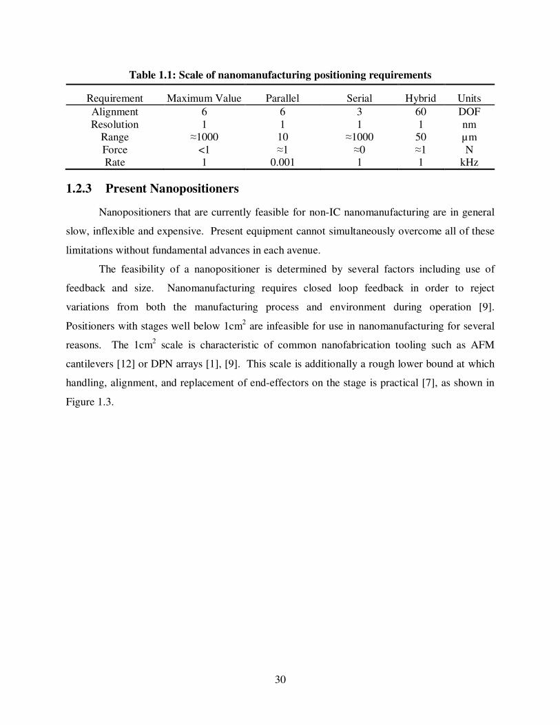
Table 1.1: Scale of nanomanufacturing positioning requirements
Requirement Maximum Value Parallel Serial Hybrid Units Alignment 6 6 3 60 DOF Resolution 1 1 1 1 nm
Range ≈1000 10 ≈1000 50 µm Force <1 ≈1 ≈0 ≈1 N Rate 1 0.001 1 1 kHz
1.2.3 Present Nanopositioners
Nanopositioners that are currently feasible for non-IC nanomanufacturing are in general
slow, inflexible and expensive. Present equipment cannot simultaneously overcome all of these
limitations without fundamental advances in each avenue.
The feasibility of a nanopositioner is determined by several factors including use of
feedback and size. Nanomanufacturing requires closed loop feedback in order to reject
variations from both the manufacturing process and environment during operation [9].
Positioners with stages well below 1cm2 are infeasible for use in nanomanufacturing for several
reasons. The 1cm2 scale is characteristic of common nanofabrication tooling such as AFM
cantilevers [12] or DPN arrays [1], [9]. This scale is additionally a rough lower bound at which
handling, alignment, and replacement of end-effectors on the stage is practical [7], as shown in
Figure 1.3.

31
Figure 1.3: Scale of nanopositioners and payload. The lower bound for ease of handling
is around the mm-scale, while increased size translates into generally lower bandwidths. The positioners shown here are drawn from[13–15], while the payloads are from [16–18].
Micropositioners with integrated tooling offers a possible solution to these issues but
generate new problems. The fab process for each integrated tool/positioner combination would
be unique. The custom fabrication process would require significant investments to implement
correctly for each new tool, a problem which is typical for MEMS fabrication processes [19].
This would significantly impair the application flexibility of the nanopositioner. In general,
meso- to macro- scale stages with closed loop control are the most feasible for
nanomanufacturing.
1.2.3.1 Speed
6 DOF Meso- and macro- scale nanopositioners that are feasible for nanomanufacturing
generally have operating bandwidths of less than 100 Hz [1], [7], [13], [20], [21]. This
bandwidth limitation in macroscale positioners is a function of the mass of the positioner stage,
(≈1kg) which is due to the need to carry sizable payloads such as wafers [9], [21], sensors and
actuators [13]. The large mass of the center stage translates to large force and power draw at
high bandwidth, placing a practical upper limit to their speed [7]. The large size and mass of the
stages also results in performance limiting structural resonances [9], [21]. Mesoscale positioners
generally utilize low force actuators that make it difficult to achieve high bandwidth [1] or are

32
limited by structural resonances [14] or utilize actuators whose force output is insufficient to
achieve kHz-scale bandwidth [1].
1.2.3.2 Flexibility
The flexibility of a nanopositioner is defined here by its capability to be used over a large
range of nanomanufacturing operations, including series, parallel and hybrid. Application
flexibility ensures that the positioner architecture does not need to be fundamentally redesigned
for each process, and simplifies the process of setting up/adjusting a nanomanufacturing line.
Nanopositioners must have several specific properties to be application flexible for
nanomanufacturing as defined above. The positioner must be capable of the six degrees of
freedom operation required for alignment in parallel and hybrid processes [1], [7]. Additionally,
the positioner must be capable of being easily adapted to the functional requirements of a
number of processes which vary in range, resolution, bandwidth, and force scale. This flexibility
can either be on the device level, where a single device is capable of carrying out a wide range of
processes, or the architecture level, where a general device design is customized for the
requirements of each particular process, as shown in Figure 1.4.

33
Figure 1.4: Schematic of the application of flexibility on the device level and on the
architecture level, examples drawn from [13], and [22].
Existing nanopositioners do not have the combination of features required for non-IC
nanomanufacturing process flexibility. A large number of existing nanopositioners such as AFM
stages [10], [11] lack the required six degrees of freedom. Positioners that do have the required
degrees of freedom [21] lack the performance and/or design rules needed to be easily adapted to
non-IC nanomanufacturing processes with different functional requirements, such as high (1kHz)
bandwidth requirements. This lack of flexibility is due to the high cost of the equipment at
present. Existing positioners are specialized to the particular requirements of the process that
can justify the high cost, such as surface scanning [11] or wafer photolithography [21] used in IC
nanomanufacturing.
1.2.3.3 Cost
The system cost for meso- and macro- scale nanopositioners is generally on the scale of
$100k [1], [10], [23–25], ranging from $30k [1], [24] to $100k+ [5], [25]. The high cost is
largely due to the actuators and sensors used. Large (kN) force actuators commonly used in
macroscale positioners [7] such as piezoelectrics [14] can cost about $10k/axis [26]. External
sensors such as capacitive probes [9], [13], [14] and laser interferometers [5], [9], [13], [21], [27]
are commonly used in nanopositioners, and also bring a price tag on the scale of $10k/axis [28].

34
1.2.3.4 Impact due to Limitations
The metrics of cost, rate, quality and flexibility are typically used to evaluate the
feasibility of a manufacturing process [25], [29] and it is important to maximize these metrics in
order to make nanomanufacturing practical [2]. At present, the limitations of low speed [30],
inflexibility and high cost of present nanopositioners are a major roadblock towards practical
non-IC nanomanufacturing operations as well as research and development.
Figure 1.5: Resource study demonstrating the need for rate, flexibility and cost
improvements in present positioners. Note that operator cost (time) dominates at high
volume, while capital cost (positioned) dominates at low volume.
An initial cost study was carried out to determine the impact of rate, flexibility and cost
improvements on non-IC nanomanufacturing. The results are shown in Figure 1.5. A single step
hybrid operation was chosen, such as an array of nano-ebeam tips for photoresist exposure, and it
was assumed that the operation would be carried out on a 100x100 grid over the sample. The
manufacturing equipment was assumed to be a nanopositioner with a mass-manufactured end-
effector, purchased for about $20/tool. Each device was assumed to be fabricated on a 12.5mm
diameter silicon wafer. Reasonable values were used for loading/unloading times (10 seconds)
and for the cost of labor monitoring the equipment at $100/hr. This enabled cost estimates for i)

35
the operator, ii) material, iii) power, and iv) equipment. When these costs were compared over
large and small volume production, it was found that the three metrics of interest, positioned rate,
flexibility and cost played a driving role in the average device production cost. The cost of the
operator dominates in present systems at high volumes (100M units) due to the low (50-100hz)
bandwidth of present nanomanufacturing positioners. The capital cost of the equipment
dominates in present systems at low volumes (1k units) due to the significant expense of
positioner development and fabrication (500k + 100k).
The low (<100 Hz) bandwidths of present nanopositioners make it infeasible to use them
for certain nanomanufacturing processes including nanometrology [30] or hybrid fabrication
processes when carried out at high volume. High bandwidths are needed for tip based
nanometrology as the surface must be repeatedly scanned during the imaging process [31].
Positioner bandwidths in AFMs commonly range up to several kHz [10], [11], suggesting a
desirable upper bandwidth on the scale of 1kHz for a nanopositioning architecture [31].
The inflexibility of present nanopositioners makes it difficult to adapt the equipment to
new processes. Non-IC Nanomanufacturing is a young field whose processes are not well
established, so specialty use equipment designs may have to go through much costly iteration. If
positioners must be completely rebuilt for each new process, the development cost of the
positioner can heavily influence the average device cost in a manufacturing setup.
The high ($100k) costs of present nanopositioners make it infeasible to carry out non-IC
nanomanufacturing research and development. It is expected that most nanoscale products will
need to be produced in high volume at a high rate [1], [2], [7], [25]. This may be reached by
either utilizing high rate equipment or parallelizing the process with many machines running on
the process simultaneously. A non-IC nanomanufacturing setup will likely require interwoven
fabrication and metrology [25] steps, each likely utilizing a nanopositioner. This
nanomanufacturing line could be on the scale from several up to hundreds of steps. At present
costs of around >$100k per nanopositioner, the positioning equipment could easily drive the
expense of the nanomanufacturing line, making it prohibitively costly to carry out research and
development on nanomanufacturing, or small to medium volume production. Only large scale
production is feasible at this scale, but such scaled production generally first requires research,
development and initially small production runs.

36
1.2.4 Nanopositioner Performance
There is a need for fast, affordable and application flexible nanopositioning equipment.
These improvements will remove one of the main roadblocks to practical nanomanufacturing.
The reduction of equipment cost is a present focus of nanomanufacturing research and
development [1], [2], [5], [8–10], [23], [32]. This is part of a push to develop ‘desktop
manufacturing’ equipment which capitalizes on the small scale of micro-/nano- processes
(forces, displacements) in order to reduce the cost and size of the equipment [1], [2], [5], [9],
[10], [32]. Specialty use equipment designs may have to go through much iteration whereas
multi-purpose equipment can be adapted to new uses without without costly and time-consuming
fundamental redesign.
Increases in nanopositioner bandwidth will aid in the feasibility of nanometrology as well
as a large set of nanomanufacturing processes. Electrical, optical and some thermal
nanomanufacturing serial tip-based processes become more feasible at high bandwidths, as they
can be positioner limited. The physics of process such as probe based EBL [6] is inherently
much faster than the bandwidth of the positioner. Inherently slower mass flow
nanomanufacturing processes like DPN [5], [33] and NIL [8] are process limited and will not
show rate increases with higher positioner bandwidth. An increase in nanopositioner bandwidth
enables the full range of nanomanufacturing processes which may be found in a manufacturing
setup, as compared to enabling only a fraction of the possible nanomanufacturing processes with
lower bandwidth architecture.
1.2.5 Fundamental Advances
1.2.5.1 Speed
Present nanopositioning equipment cannot be driven at kHz bandwidth due to the
macroscale of the devices. Force scales with ω2 [7] and the power with ω4 in an EM based
nanopositioner, leading to 102x and 104x increases in force and power respectively over the 100
Hz requirements. For a typical 6DOF magnetic levitation (maglev) nanopositioner [34], this
translates to 10.5N and 13W at 100Hz, but 1 kN and 130 kW requirements at 1kHz, well beyond
achievable levels. Reduced scale is required to reach the desired speeds, since mass and
therefore both force and power scale favorably with size. The lower limit on the scaling is
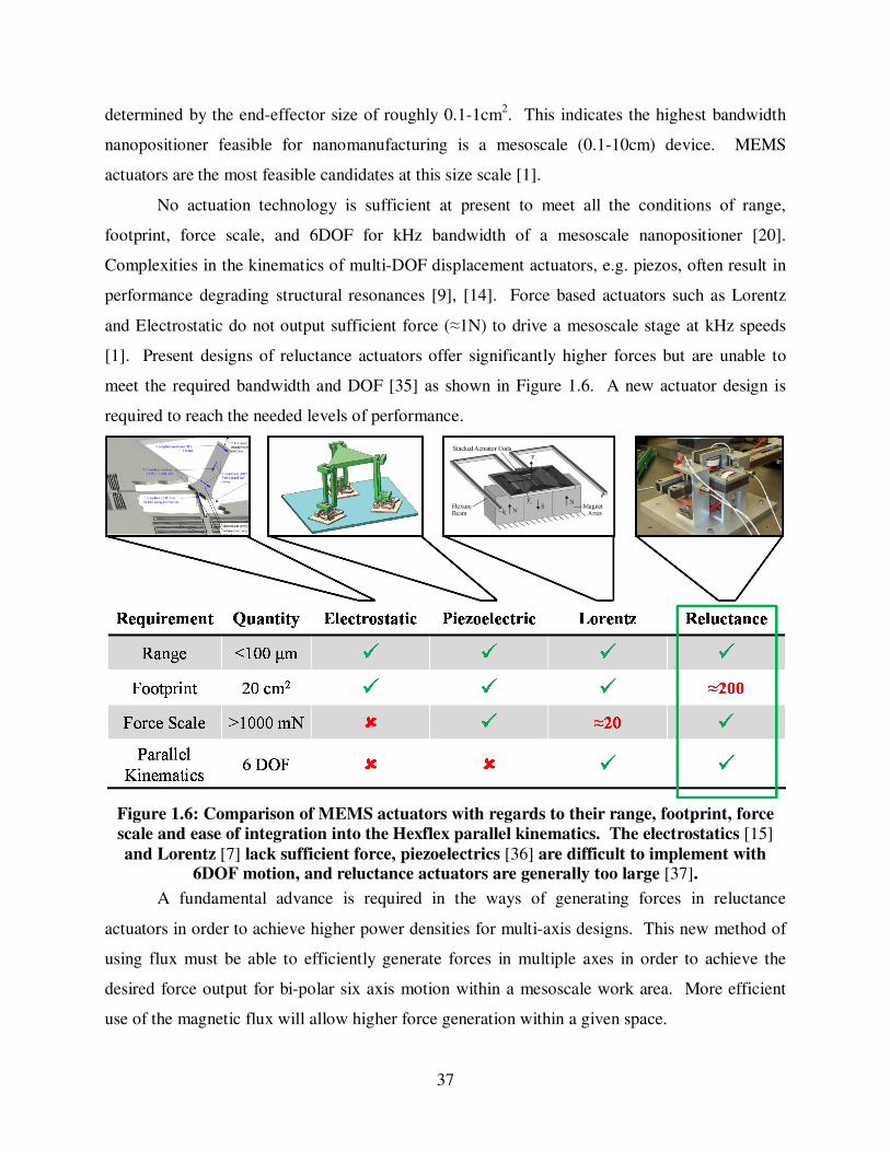
37
determined by the end-effector size of roughly 0.1-1cm2. This indicates the highest bandwidth
nanopositioner feasible for nanomanufacturing is a mesoscale (0.1-10cm) device. MEMS
actuators are the most feasible candidates at this size scale [1].
No actuation technology is sufficient at present to meet all the conditions of range,
footprint, force scale, and 6DOF for kHz bandwidth of a mesoscale nanopositioner [20].
Complexities in the kinematics of multi-DOF displacement actuators, e.g. piezos, often result in
performance degrading structural resonances [9], [14]. Force based actuators such as Lorentz
and Electrostatic do not output sufficient force (≈1N) to drive a mesoscale stage at kHz speeds
[1]. Present designs of reluctance actuators offer significantly higher forces but are unable to
meet the required bandwidth and DOF [35] as shown in Figure 1.6. A new actuator design is
required to reach the needed levels of performance.
Figure 1.6: Comparison of MEMS actuators with regards to their range, footprint, force
scale and ease of integration into the Hexflex parallel kinematics. The electrostatics [15] and Lorentz [7] lack sufficient force, piezoelectrics [36] are difficult to implement with
6DOF motion, and reluctance actuators are generally too large [37].
A fundamental advance is required in the ways of generating forces in reluctance
actuators in order to achieve higher power densities for multi-axis designs. This new method of
using flux must be able to efficiently generate forces in multiple axes in order to achieve the
desired force output for bi-polar six axis motion within a mesoscale work area. More efficient
use of the magnetic flux will allow higher force generation within a given space.
38
A design is presented schematically in this thesis, however development and
demonstration of the design lay outside the scope of the thesis work. It is included in this
discussion as the speed requirements are a crucial component of the new architecture and must
be built into it from the ground up. The speed requirement drove the meso-scale design, and can
only be fully met by a continuation of this work into developing a high force (≈1N at 1kHz), bi-
polar dual-axis actuator. This actuation improvement will enable higher force density in
mesoscale six-axis actuation, so as to drive the nanopositioner to higher bandwidths than
currently achievable.
1.2.5.2 Flexibility
Nanopositioners cannot presently be given the performance required for non-IC
nanomanufacturing process flexibility. An adaptable device architecture is the most cost- and
performance-effective method for meeting functional requirements that, like non-IC
nanomanufacturing processes range and resolution, can vary over orders of magnitude. This
cannot be done at present due to the lack of the required design rules for mesoscale 6DOF
nanopositioner actuators, bearings and sensors.
Existing design theories applicable for such devices are not sufficient for adjusting the
sensor, actuator, and bearing design for various applications without fundamental redesign.
Topology synthesis [38], [39] does not allow for minor variations without fundamental redesign,
since the relations between requirements and parameters is unknown. The building block
approach focuses on the component level, so does not explore the system level interactions [1].
Existing piezoresistive sensor optimization work [39–41] has focuses on limiting cases, and does
not approach the problem on the system level as shown in Figure 1.7, which is needed to
simultaneously optimize all variables in the sensor. Design studies for reluctance actuators have
focused on single DOF systems [42], which lack the design interactions of multi-DOF systems.
The single aspect focus of these design theories limits the utility of the derived rules.

39
Figure 1.7: Design interactions between the components of the nanopositioner.
A fundamental advance is required in the modeling approach used on the components of
the mesoscale nanopositioner. A new systems design approach to device modeling was
developed in this work to make the required advance. The approach takes into account the full
system controlling the component performance, including electronics as well as cross-component
interactions. This system-level model provides the insight to discover the operational regimes
and design rules needed to maximize performance. These discoveries make it possible to rapidly
redesign nanopositioner architecture for varying functional requirements like range, resolution,
bandwidth and force scale.
1.2.5.3 Cost
Present nanopositioning equipment cannot be made low cost (<$1k) mainly due to the
inherent expense of sensing. Integrated capacitive, piezoelectric or piezoresistive sensing offer
the possibility of significantly reduced sensing costs, to roughly $10-50/axis, which could reduce
the total device cost by several orders of magnitude- down to about $100-1000/device.
Integrated sensing requires µm/nm-scale electrical structures to be surface micromachined on a
mesoscale nanopositioner. A fabrication method is required that is capable of: i) bulk
micromachining of cm-scale mechanical structures out of robust materials, ii) surface
micromachining of integrated um/nm-scale electrical features, and iii) all at low average cost
(<$1k) per device even in small batches (<10).
No established fabrication process chain is able to simultaneously meet all three
requirements, as shown in Table 1.2. Traditional macroscale machining can produce cm-scale
parts from robust materials at low cost, but cannot produce µm/nm-scale electrical features. IC
photolithographic fabrication has been used to produce mesoscale nanopositioners, [1], [7]
however it results in high costs (≈$20k just for equipment costs), long fabrication times (≈6
months) and brittle structures. A range of non-lithographically based fabrication processes show
Sensor Actuator
Bearing
ElectronicsFull System
Model

40
the potential to meet all of the conditions above [8], [32], [43–45], but cannot do so at present
due to fabrication incompatibilities.
Table 1.2: Comparison of fabrication methods
Requirement Capability Macro-scale Fabrication
MEMS Lithographic Fabrication NLBM
Mechanical structures
Bulk micromachining
Electrical structures
Surface micromachining
Robust material Metals, polymers Low avg. cost
(for small batches) <$1k/device
Work has been carried out on bulk micromachining of metal mesoscale mechanical
structures [8], [32], [46–49] as well as electrical structures [43], [44], however these efforts have
not successfully been integrated on a single device with sensors due to fabrication difficulties at
the interface of the two types of fabrication. Problems occur at the interfaces: the interface of the
conductive electrical features with the integrated silicon sensing, the contact and alignment
between the sensors and the mechanical structure, and the edge features produced in the
patterned silicon.
A fundamental advance is required in the development of a hybrid process chain that can
merge macroscale bulk and microscale surface micromachining processes on robust materials. A
new process chain, Non-Lithographically-Based Microfabrication (NLBM) has been invented to
merge these two fabrication regimes and handle the challenges of the multi-scale interfaces.
This process is demonstrated to merge conventional machining with microfabrication techniques
to flexibly produce metal MEMS structures with integrated sensing, and do so in small batches,
with low per-device cost.
1.3 Thesis Scope
Three avenues of research are required to fully enable a high speed, application flexible
and low cost multi-purpose compliant nanopositioning architecture. These are: a high force
density actuator, a system level design theory, and a new fabrication process chain. The
development of a design theory and a fabrication process was given primary importance as these
enable a device to be produced. The thesis scope was bounded by these two avenues of

41
development, as these proved to be of sufficient complexity. The actuator development, while
necessary for high volume cost savings, is of secondary importance. A low speed nanopositioner
(100hz) will still enable a range of nanomanufacturing processes and reduce costs for small batch
nanomanufacturing research and development. The speed requirement is elucidated in this thesis
but must be solved by future work.
1.4 Case Study
A mesoscale nanopositioner architecture was developed in this work to demonstrate the
fundamental advances in the architecture flexibility, affordability, the capability of the integrated
sensing. The metal MEMS nanopositioner design was based around the Hexflex architecture
[50]. The Hexflex architecture is a 6DOF planar flexural nanopositioning platform which is
linked to ground via 6 flexural bearings in series, each of which provides a location of integrated
strain sensing [1]. This monolithic structure generates a stage, ground and flexure bearing in one
step. Strain sensing can be integrated into the design on a single surface, simplifying the
fabrication process. Actuation may be integrated into the design via three paddles on the central
stage, each bearing magnetic Halbach arrays that can be driven bi-directionally via Lorentz force
generation, and in 2-DOF, either vertically or in-plane [51], [52]. Three sets of 2-DOF actuators
provide the full 6-DOF motion required for the nanopositioner.

42
Figure 1.8: Layout of the multipurpose compliant nanopositioning architecture in this
research.
The Hexflex nanopositioner as shown in Figure 1.8 is designed as a meso-scale (5cm
diameter) positioner with a 1cm diameter center stage, sized to carry a range of common
nanomanufacturing/metrology probe tips. This size scale remains large enough to enable simple
loading and unloading of the payload, while its small scale keeps the positioner stage mass to
only a few grams, allowing for ≈0.5-1khz natural frequency. The structural ribbing on the center
stage is designed to push the unwanted resonances up to well above the kHz bandwidth. The
unwanted resonances are defined as those generated through the failure of the assumption of
rigid body motion. The main 6DOF each have a resonance frequency, and these can be modeled
with standard rigid body assumptions of the center stage. Higher order resonances are associated
with the flexing of this center stage as well as higher order modes of the flexures themselves.
The MCNA structure can thus be driven in closed loop operation at a bandwidth slightly above
that of the primary resonance around 0.5-1kHz, and below the frequency of the unwanted
resonances. The closed loop bandwidth is estimated to be about 1kHz, with an upper bound of a
few kHz, set by the unwanted resonances.
The flexures are designed to enable device motion of approximately 200µm range in any
direction. The standard bent wire flexural bearing [1] has been modified to be a wire and blade

43
flexure in series. This concentrates the stresses in the wire flexure, producing improved
sensitivity to in- and out-of-plane motion at the expense of range. The piezoresistive strain
sensors are fabricated in a U shape with electrical contacts at either end of the U. Each arm of
the sensor is approximately 150µm in width. This was found to be the safe lower bound of the
Thin Film Patterning and Transfer (TFPT) process at present as described below.
Previous work on the Hexflex architecture has produced this topology on the microscale
[7], [53] the mesoscale [1], and the macroscale [50]. Unfortunately, none of these designs have
produced a platform that can be feasibly used for nanomanufacturing/metrology research and
development. This requires i) low per-device cost, even in small batches, ii) robustness during
operation, and iii) both integrated sensing and actuation. A new fabrication process- NLBM- is
required to create the Hexflex architecture that can meet all three of these requirements, doing so
via low-cost convention milling of titanium structures combined with chemical and laser
patterning of single crystalline silicon piezoresistors. The Hexflex architecture fabricated
through this process is shown in Figure 5.1.
Figure 1.9: Fabricated metal flexural nanopositioner with single crystalline silicon
piezoresistor integrated sensing. The final fabricated device is shown, with 150µm
dimension piezoresistors attached to titanium flexures.
Results show that the nanopositioner structure with integrated sensing can capture 6DOF
motions with approximately 59dB full noise dynamic range at 10kHz. The focus of this research

44
is on providing low-cost, high performance integrated sensing. Improvements in the process are
suggested to raise the sensing performance to approximately 135dB over a 10khz sensor
bandwidth, sufficient to see angstrom-scale motion over the 200µm range. This sensor
performance is generally in excess of presently available kHz-bandwidth analog-to-digital
converters [54]. Methods for actuation are suggested, based off of previous work.
1.5 Actuation Concept
A schematic for a possible bi-polar dual axis reluctance actuator is shown in Figure 1.10.
This actuator concept utilizes both the normal and the shear components of the Maxwell stress
tensor at the surface of the plunger to generate two axis of force. These will both rise and drop
as the flux over the surface is changed. The dual axis control comes from the use of both sides
of the plunger. Not only does this cancel the magnetic preload on the plunger, but it also allows
for the controlled generation of a single axis force. If the fluxes on both sides are increased, then
the plunger will be pulled upwards, resulting in out-of-plane actuation. If the flux on one side is
increased, but the other side is decreased, then this will result in a net sideways force for in-plane
actuation. Coils are used to modulate a static magnetic field. This enables bi-polar control, as
the field may be either be electrically boosted or attenuated.
Figure 1.10: Conceptual layout for a bi-polar dual-axis reluctance actuator. The
electromagnetic stress generated on each side of the plunger can be modulated either to
generate normal or tranverse stresses, resulting in the dual axis force generation. Coils are used to modulate a static magnetic field, resulting in bi-polar force generation.
Several assumptions are made by this conceptual design. First, the plunger thickness is
assumed to be minimal so that the opposing forces largely cancel instead of generating
significant moments. Second, an out-of-plane counter-preload is required to cancel the force felt
on the plunger by the static magnetic field. A symmetric setup with a non-actuated magnet and
plunger below this one could create such a cancellation preload. Third, it is assumed that the
Magnetic Flux
Coils
S N S N
In-Plane Actuation
Plunger
Out-of-Plane ActuationCoil generated forces
Z
X

45
flux return path for each coil is separate and the reluctance of the return path is unchanging. This
should be possible with proper design of the actuator. Hall effect sensors may be used in the gap
to provide flux-based analog feedback, minimizing hysteresis and eddy current effects.
1.6 Background
1.6.1 Nanopositioners
Existing nanopositioners cover a wide range of designs over a large range of sizes and
different actuation/sensing technologies. Designs may be grouped into several common
categories such as size, function, performance or structure. Wafer steppers [9], [55], [56] are
intended to move large wafer payloads at a several Hz over large areas with nanometer
resolution. Mesoscale nanopositioners [1], [14] have been developed for chip alignment in
nanomanufacturing, and show bandwidths of around 100Hz. MEMS microscale nanopositioners
[7], [15], [57–59] are intended for applications including imaging scanning stages [15], [59],
micromirrors [58] and data access [7], [57]. Positioners of a range of sizes are shown in Figure
1.11. Nanopositioners with parallel kinematics are found in two main categories: planar
structures [1], [7], [59], which require out-of-plane actuation but have simple geometries, and
Stewart platforms [14], [15], [60], [61], which only require in-plane actuation but have complex
geometries. Nanopositioners with series kinematics [20], [62] offer simpler actuation, but
generally lower bandwidth.

46
a) b) c)
Figure 1.11: Positioners developed over a range of size scales. The devices are: A)
Macroscale 6DOF maglev [13], b) Mesoscale 3DOF flexural [14], c) Microscale 6DOF flexural [15]Error! Reference source not found..
1.6.2 Reluctance Actuation
Reluctance actuators can be divided into three main categories based off the use of
magnetic fields [42], as shown in Figure 1.12. Type I actuators [26], [63], [64] generate force by
varying reluctance through the gap width, which results in ‘pull-in’ problems at large
displacements. Type II actuators [65] generate force by varying reluctance through the overlap
area of the gap, which is more linear than Type I. Type III actuators [42] use a combination of
type I and II designs to produce force. Most reluctance actuator designs are single DOF,
however several multi-DOF designs have been developed [35], [56], [66], [67]. 6DOF designs
[35], [56] have significant range constraints over several of the DOF. Small scale reluctance
actuators found in MEMS [42] generally utilize simple C-shape magnetic circuits.
Figure 1.12: Different methods of reluctance actuation in present use, separated into three
categories [42].
Design work has been carried out to model high frequency effects like eddy currents and
hysteresis in magnetic actuators [68]. A wide range of designs have been developed for

47
magnetic actuators, with some focused on high speed actuation. 6-DOF designs have also been
demonstrated, but the 6-DOF and high-speed groups do not overlap.
1.6.3 Design Rules
A range of design theories and processes have been developed to aid in the design of
mesoscale mechanisms. Topology synthesis utilizes an iterative computer algorithm to optimize
a gridlike structure for the desired performance and is heavily dependent on the adjustment of
iteration parameters. An example of a force sensor is shown in Figure 1.13. Topology synthesis
has been used to design 2D flexures and sensors for mechanisms [38]. The building block
approach has been used to develop flexural bearings with integrated sensing for mesoscale
nanopositioners [1], but does not form a complete set of rules for designing the full sensor
system. Simple well-understood components are assembled to produce the desired structure in
this approach.
Figure 1.13: Iterative topological optimization of a force sensing cantilever (black) with
piezoresistive sensor (red). The force is applied at the top right of the cantilever [38].
A significant effort has been made to develop theories for improving piezoresistive
sensors. These theories have laid out analytical [39], [40], [69], [70] and computational [39]
optimization techniques to maximize the performance of sensors over a range of conditions.
These models have studied optimization through modeling flicker noise [40], doping conditions
[39] and thermal sensitivities [69]. Actuator design rules have been developed for variable
reluctance actuators that describe design tradeoffs for variables such as stroke [42].
1.6.4 Non-Lithographically-Based Microfabrication
Non-lithographic microfabrication processes are characterized by their use of alternate
methods of patterning and machining beyond the paired photolithographic patterning and

48
chemical machining that characterizes IC fabrication. Non-lithographic processes cover
categories a wide range of process types including parallel/serial operation and
additive/subtractive operation [45], [71], [72].
Figure 1.14: Pinwheel accelerometer fabricated through non-photolithographic surface
micromachining. A digital printing technique was used to form the structure [44].
Non-lithographic microfabrication is generally focused on structures with features
resolutions above 5µm [45], [49]. Present work has focused largely on structures such as
micromolds intended for micromanufacturing [32], [46]. Surface micromachining of
micromechanical structures [43], [44] shown in Figure 1.14 and microelectrical structures [73],
[74] has also been demonstrated. Interest has been expressed in developing process chains for
the general fabrication of MEMS using NPL microfab techniques [32], [43], [44], [75], however
this remains unrealized. These process chains offer the potential to significantly reduce both cost
and time associated with prototyping and small batch production for structures with >5µm
features [45].
1.7 Thesis Structure
The thesis is composed of several largely stand-alone sections. These sections are tied
together by the common focus on the development of the MCNA. The writing is laid out to
reflect this separation and avoid confusion; the research for each segment is combined with the
associated background and results.
The design and modeling of the device as a full system is presented in chapter 2. A
piezoresistor optimization theory was developed and used to direct the architecture design
towards the best possible sensing performance. The sensor design was part of the initial focus as
these were the dominant problem for fabrication.
The fabrication limitations imposed on the sensor are investigated in chapter 3. The
fabrication of custom gages using NLBM introduced complexities at the metal-semiconductor

49
interface. This chapter looks at the basic physics driving the observed Schottky barriers, and
produces models which enable the designer to accurately engineer these interfaces. This work
acts as a bridge between the flexibility research (optimization theory) and the affordability
research (process chain).
The adjustments to the optimization theory due to the unique sensor physics are shown in
chapter 4. The system design models are adjusted to account for the non-linear effects of the
Schottky barriers produced in NLBM fabricated sensors. The design rules and regimes for these
sensors are explored, and the theory is confirmed with a fabricated test device.
The sensors are parallelized and integrated into a multi-axis device in chapter 5. The
interface fabrication challenges encountered at the boundary between macro- and micro-
fabrication are solved through process chain engineering. The NLBM process is demonstrated
by the fabrication of a Hexflex with integrated sensing.

50

51
CHAPTER
2 DESIGN OF PIEZORESISTIVE SENSOR
SYSTEMS
2.1 Synopsis
This chapter will explore how to design the best possible sensing for a compliant device.
This theory is used to inform the design of the MCNA through the performance limits expected
from different sensing materials, as well as the geometries required for high performance
sensing.
Piezoresistive sensing systems have characteristics that enable them to act as fine-
resolution, high-speed force and displacement sensors within MEMS and other small-scale
systems. High-performance piezoresistive sensing systems are often difficult to design due to
tradeoffs between performance requirements, e.g. range, resolution, power, bandwidth, and
footprint. Given the complexity of the tradeoffs, traditional approaches to system design have
primarily focused upon optimizing a few, rather than all, elements of the sensing system. This
approach leads to designs that underperform the sensors optimized range and resolution by as
much as two orders of magnitude. In this work we present a general systems approach that
enables rapid optimization of all elements via a model that incorporates the behavior, noise and
sensitivity associated with each element of the sensing system. The model is presented in a
manner that makes the underlying principles and application accessible to a broad community of
designers. The utility of the model is demonstrated via an example wherein design parameters
are altered to maximize dynamic range.

52
2.2 Parameters
Nomenclature (in order of appearance)
Symbol Units Definition Symbol Units Definition δ m Displacement of compliant structure υ -- Active fraction of ADC voltage range F N Force on compliant structure Vrange V Full voltage range of ADC VS V Source voltage σy Pa Flexural material yield stress ΨM m, N Signal output of sensor system η -- Flexural material safety factor to yield Ψ m, N Signal input to sensor system VB Bias voltage σMv M Ambient vibrational displacement noise σTb C Bias voltage chip temperature noise σMt M Thermomechanical displacement noise σVb V Bias voltage noise
SMt(f) m2/Hz PSD of thermomechanical noise PSRRB(s) --
Bias voltage power supply rejection ratio kB m2kg/Ks2 Boltzmann’s constant Laplace transform T K Ambient temperature αVb 1/C Bias voltage thermal sensitivity k N/m Compliant structure stiffness FB(s) -- Bias voltage filter Laplace transform ζ -- Compliant structure damping ratio σVai V Amplifier input voltage noise ωn Rad/s Compliant structure natural frequency σVao V Amplifier output voltage noise f Hz Frequency ∆Vai V Amplifier input voltage offset Λ --, N/m Mechanical noise scaling factor ∆Vao V Amplifier output voltage offset
FF(s) -- Flexure mechanical filter Laplace αVai V Amplifier input offset thermal sensitivity
transform αVao V
Amplifier output offset thermal εF m-1, N-1 Flexure gain sensitivity Lf m Flexure length
CMRR(s) -- Amplifier common mode rejection ratio
bf m Flexure width Laplace transform hf m Flexure thickness
PSRRA(s) -- Amplifier power supply rejection ratio
E Pa Flexural material Young’s Modulus Laplace transform Nb -- Number of flexures in parallel VP V Power supply voltage αεF 1/C Flexure gain thermal sensitivity αVp 1/C Power supply voltage thermal sensitivity σTw C Bridge temperature noise σTp C Power supply thermal noise GSG -- Strain geometry gain σVp V Power supply voltage noise ε(x,y) -- Strain field over flexure σVr V Power supply ripple voltage noise
x m Distance along length of flexure RRR -- Power supply ripple rejection ratio y m Distance off neutral axis of flexure FP(s) -- Power supply filter Laplace transform Lr m Piezoresistor length σVc V ADC voltage noise hr m Piezoresistor thickness αVc 1/C ADC voltage thermal sensitivity γ -- Strain field constant σTc C ADC temperature noise L0 m Piezoresistor offset from flexure boundary ∆Vc V ADC voltage offset Nε -- Bridge strain type FD(s) -- Digital noise filter Laplace transform GF -- Piezoresistive gauge factor C (m, N)/V Calibration coefficient αGF 1/C Gauge factor thermal sensitivity A -- Coordinate transform matrix NTw -- Bridge thermal type M -- Axis noise summation vector αTw 1/C Bridge resistors thermal sensitivity
SΨM(f) m2/Hz, N2/Hz
PSD of signal output from sensory NTr -- Off-bridge thermal type system αTr 1/C Off-bridge resistors thermal sensitivity fm Hz Measurement frequency ∆Rw -- Bridge imbalance fs Hz Sampling frequency σVw V Bridge piezoresistor voltage noise fn Hz Nyquist frequency
SVw(f) V2/Hz PSD of piezoresistor noise ffilter Hz Digital filter bandwidth frequency R Ω Piezoresistor resistance fsig Hz Signal bandwidth frequency α -- Hooge constant for piezoresistor σAcc m, N Sensor system accuracy st. dev.
CC 1/m3 Carrier concentration for piezoresistor σRes m, N Sensor system resolution st. dev. Ω m3 Piezoresistor volume DR -- Dynamic range of sensor system
GSTC -- Span temperature compensation (STC) ρ Ωm Resistivity of piezoresistive material
gain B Hz Bandwidth of sensor system αSTC 1/C STC gain thermal sensitivity SVai V2/Hz PSD of amplifier input voltage noise αRstc 1/C STC resistance thermal sensitivity rf -- Filter to signal frequency ratio FT(s) -- Bridge thermal filter r -- Noise frequency band ratio αVs 1/C Source voltage thermal sensitivity Pmax W Maximum power dissipated at sensor σTs C Source voltage chip temperature noise Vmax V Maximum sensor source voltage σVs V Source voltage noise
Rcross Ω Voltage/power regime boundary
PSRRS(s) -- Source voltage power supply rejection resistance
FS(s)
-- ratio Laplace transform Ωmin m3 Minimum piezoresistor volume
Source voltage filter Laplace transform Ωmax m3 Maximum piezoresistor volume G -- Instrumentation amplifier gain Nr -- Piezoresistor serpentine factor αG 1/C Amplifier gain thermal sensitivity br M Width of resistor σTa C Amplifier chip temperature noise Rmin Ω Minimum piezoresistor resistance
Rmax Ω Maximum piezoresistor resistance

53
2.3 Introduction
Piezoresistors are widely used in microsystem sensing due to their low cost, small size,
low phase lag, and large dynamic range. They have been used to create MEMs
nanomanipulators [76], biocharacterization instruments [77], pressure sensors [78], inertial
sensors [79], mass sensors [80], and elements of high-speed atomic force microscopes (AFMs)
[40], [80], [81]. Many designers often only consider the performance of the transducing element
in the full sensing system, leading to the perception that these sensors are ‘too noisy’ for
precision applications. However, excellent performance may be obtained if the design properly
manages the tradeoffs between size, bandwidth, resolution, power, and dynamic range. This
requires the ability to accurately predict the effect of all relevant noise sources on the
performance of the full sensing system.
Herein, we present a systems approach that makes piezoresistive sensor system
optimization possible. The emphasis here is on the conceptual layout of a system model, the
technical details of modeling the noise sources associated with its components, and the insights
and results that come from integrating the individual components to form a view of the system’s
performance. The utility of this work is two-fold. The systems approach is a reinforcement of
best practices that are familiar to precision engineers, but less common for microsystem/MEMS
designers. The systems aspect is therefore targeted at this community. The modeling of the
many sub-system components will yield new information for the precision engineer and
microsystem/MEMS designer.
2.4 Background
Most high-resolution micro–sensor systems are typically based upon piezoresistive,
capacitive, or optical sensing methods. Optical methods are capable of high dynamic ranges
(>200 dB [28]) but tend to be too large and expensive (>$10,000 [28]) for low-cost
microsystems. Capacitive sensors are orders of magnitude less expensive than laser
interferometers, but require large sensor areas to achieve a high dynamic range. For example,
the force sensor developed by Beyeler et al. has a footprint of approximately 100 mm2 [82] and
exhibits a dynamic range of 57 dB at 30 Hz. A comparable piezoresistive sensor with the same
dynamic range could be three orders of magnitude smaller. This type of comparison is made

54
evident if one has the ability to ‘squeeze’ every ounce of performance from piezoresistive
systems. This is only possible when one models all aspects of the systems and is, thereby, able
to make good decisions regarding how to tune all components relative to each other. System
models also provide more certainty in the design process, thereby reducing guess work as well as
the time required to converge on a best design.
In those applications where piezoresistive sensors can replace capacitive and optical
methods, one needs to determine which type of piezoresistive material to use. The most
common materials that are used in microsystems are single crystal silicon, polysilicon and metal
film piezoresistors. Single crystal silicon piezoresistors typically have the highest dynamic range
due to their high gauge factors (20 to 100 depending on doping concentration [83], [84]) and low
flicker noise. The gauge factor of single crystal silicon depends upon crystallographic
orientation [85], therefore this material is typically only used in single axis, cantilever-type force
sensors [81], [83], [84]. For multi-axis devices, polysilicon and metal piezoresistors are typically
used given the gauge factor is largely isotropic. [86]. Polysilicon piezoresistors tend to have a
lower gauge factor (10-40 depending on doping [85]) and higher flicker noise than single crystal
silicon due to the effect of grain boundaries [87], [88]. Metal film piezoresistors have a
significantly lower gauge factor (~2) than single crystal and polysilicon piezoresistors but also
have nearly non-existent flicker noise due to their higher carrier concentration [80]. The optimal
material choice is dependent on the measurement frequency, type of device and device footprint.
In the following sections, we provide the means to make good material and geometry/design
decisions that yield the best device performance.
2.5 DC Piezoresistive Sensor System Model
2.5.1 System Layout and Model
We use the layout in Figure 2.1 to model the limits that noise imposes upon the sensing
system. A typical piezoresistive sensor system contains a voltage source that energizes a span
temperature compensated (STC) Wheatstone bridge and a piezoresistive element within the
bridge. An instrumentation amplifier is used to boost the bridge signal, which is nulled with a
bias voltage and read by an Analog-to-Digital Converter (ADC). This layout may be used to
model sensors that measure a force or displacement that is applied to a compliant element. The

55
model is generalized so that it may be used with a wide range of applications. Through this
model, we may gain insight on best design of general and specific sensor systems. The model
assumes the use of high-performance electrical components – instrumentation amplifier (Analog
Devices AD624), voltage source and bias (Texas Instruments REF50xx series), and ADC
(National Instruments 9215 ADC). This is essentially a best practice that ensures that these
electronics are not a significant source of noise. Their relevant noise values are provided in the
component datasheets.
Figure 2.1: Schematic layout of DC piezoresistive sensor system.
The system model includes the relevant thermal, electrical and mechanical noise sources.
These noise sources are included in the model for each subsection, as shown in Figs. 3-10. The
subsections are arranged as shown in Figure 2.2 to create the full system model. These figures
are a visual representation the characteristic equation of each part of the sensor system. The
Laplace transform of all filters, F(s), in the model are assumed to be non-dimensional and have
unity, steady-state gain. All n noise sources, σn, are considered to be unbiased, uncorrelated, and
normally distributed with spectral densities, Sn(f).
ADC
Vs
RSTC
RSTC
R3
R1 R4
R2
+
_G
VB

56
Figure 2.2: Block diagram layout of full system model.
We apply the following inputs to the compliant element, (i) a force or displacement
signal, Ψ, (ii) mechanical noise, σMv, e.g. vibrations, and (iii) thermomechanical noise, σMt, with
the spectral density [89]:
2( ) 4 .Mt B
n
S f k Tk
ζ
ω
=
(2.1)
A mechanical noise scaling factor, Λ, is used to convert between displacements and
forces. This factor has a unity value for displacement signals or value of k for force signals.
Figure 2.3: Block diagram representation of signal domain with main signal propagation
path highlighted in bold. The signal is generated in this domain.
Signal Input
Signal
Flexure
WheatstoneBridge
InstrumentationAmplifier
ADC
Software
Signal Output
SourceVoltage
BiasVoltage
PowerSupply
Signal Input Ψ(s)σMt
+
Signal
σMv Λ+
Flexure

57
2.5.2 Flexure Model
Figure 2.4: Block diagram representation of flexure domain with main signal
propagation path highlighted in bold. The signal is transformed from force/displacement to strain in this domain.
The flexure acts as a (a) mechanical filter and (b) transducer that converts a force or
displacement into a strain. The flexure behavior is therefore integrated as a gain, εF, within the
model. The appropriate gain depends upon the intended use of the sensor (force vs.
displacement sensing) and the grounding of the flexure (fixed-guided or fixed-free boundary).
Table 2.1 lists the gains that are found for commonly used flexures in both force and
displacement sensing.
Table 2.1: Common forms of flexure gain, εF
Type of sensing Fixed-guided Fixed-free Displacement 23
f fh L ( )23 2
f fh L
Force ( )23f b f f
L N b h E ( )26f b f f
L N b h E The strain geometry gain factor is obtained via Eq. 2.
0
21( , ) 1 1
r o r
o
h L Lr o r
SGL
r r f f
L L hG x y x y
L h L hε
γ
+ += ∂ ∂ = − −
∫ ∫ (2.2)
This value is based upon an average of the strain field that is directly sensed by the
piezoresistor. The strain field constant, γ, captures the effect of different flexural end conditions
and has value of 1 for fixed-guided, or 2 for fixed-free boundary conditions.
FF(s)
αεf
σTw
GSG
+
εF
x
Flexure
Signal
Wheatstone Bridge
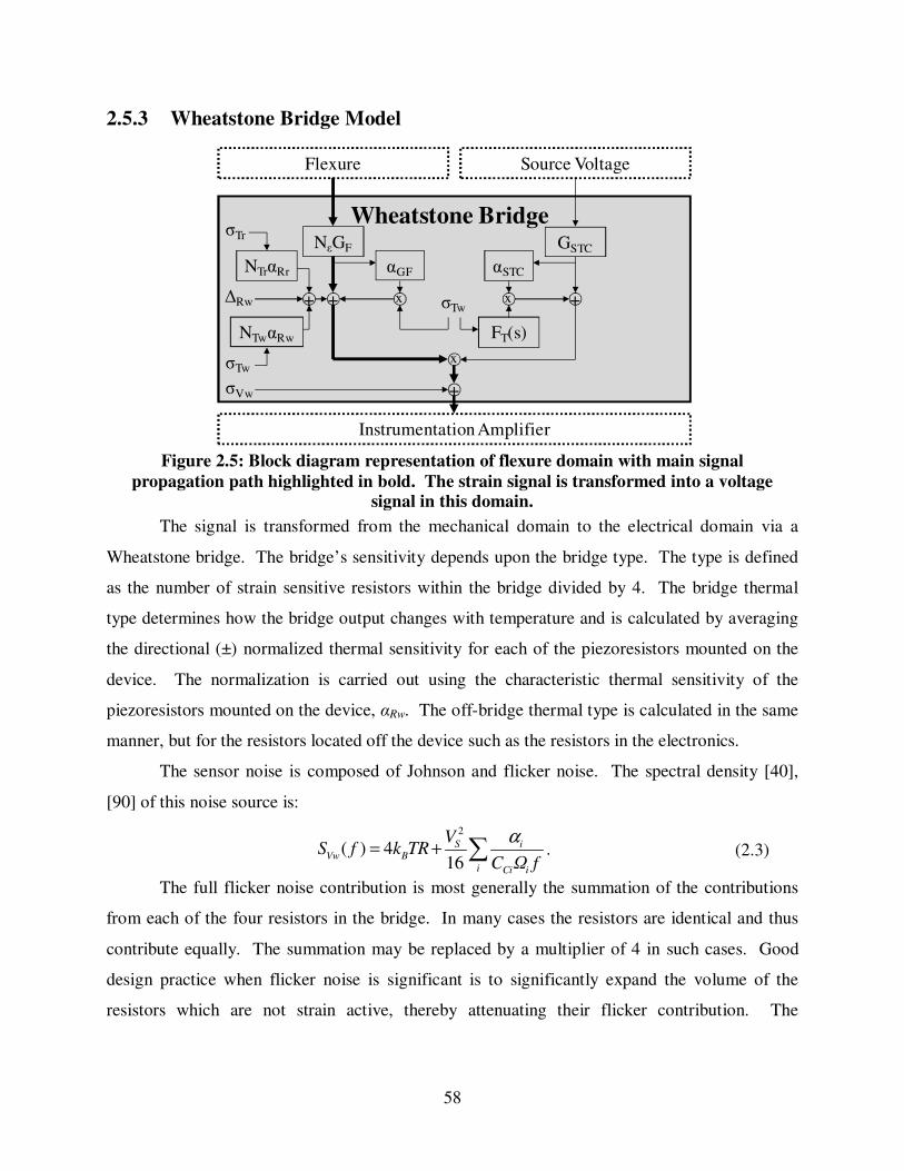
58
2.5.3 Wheatstone Bridge Model
Figure 2.5: Block diagram representation of flexure domain with main signal
propagation path highlighted in bold. The strain signal is transformed into a voltage signal in this domain.
The signal is transformed from the mechanical domain to the electrical domain via a
Wheatstone bridge. The bridge’s sensitivity depends upon the bridge type. The type is defined
as the number of strain sensitive resistors within the bridge divided by 4. The bridge thermal
type determines how the bridge output changes with temperature and is calculated by averaging
the directional (±) normalized thermal sensitivity for each of the piezoresistors mounted on the
device. The normalization is carried out using the characteristic thermal sensitivity of the
piezoresistors mounted on the device, αRw. The off-bridge thermal type is calculated in the same
manner, but for the resistors located off the device such as the resistors in the electronics.
The sensor noise is composed of Johnson and flicker noise. The spectral density [40],
[90] of this noise source is:
2
( ) 416
S iVw B
i Ci i
VS f k TR
C Ω f
α= + ∑ . (2.3)
The full flicker noise contribution is most generally the summation of the contributions
from each of the four resistors in the bridge. In many cases the resistors are identical and thus
contribute equally. The summation may be replaced by a multiplier of 4 in such cases. Good
design practice when flicker noise is significant is to significantly expand the volume of the
resistors which are not strain active, thereby attenuating their flicker contribution. The
NεGF
σTw
σVw
Wheatstone BridgeGSTC
αSTC
+
+
FT(s)x
σTr
αGF
+ x
NTwαRw
NTrαRr
Source VoltageFlexure
Instrumentation Amplifier
x∆Rw +
σTw

59
summation may be replaced by a multiplier of 4*Nε in such cases, as this only considers the
minimal volume, strain active resistors.
The bridge voltage is attenuated by the gain of the STC, which describes the loss in
bridge voltage caused by the STC resistors in series with the bridge. This gain is specifically set
to have a thermal sensitivity that cancels out the thermal sensitivity of both the piezoresistors and
flexure.
( )( ) 1
STC STCG
W STCSTC Rw Rstc
W STC STC W
R RG dT dT
R R R R
α
α α
= + − + +
(2.4)
The STC gain has a thermal sensitivity intended to passively cancel the gauge factor and
flexure gain thermal sensitivities [91].
( )W GF Ff
STC
Rstc Rw GF Ff
RR
α α
α α α α
+=
− − − (2.5)
The STC and bridge resistors may be separated by some distance; therefore they may
experience different temperatures. The bridge thermal filter can be used to characterize this
frequency dependent effect. Thermal variations occur at relatively low frequencies, therefore the
bandwidth of FT(s) is normally large enough to approximate as unity over the frequencies of
interest.

60
2.5.4 Instrumentation Amplifier Model
Figure 2.6: Block diagram representation of the amplifier domain with main signal
propagation path highlighted in bold. The voltage signal is amplified in this domain.
The Wheatstone bridge output signal is boosted via the instrumentation amplifier in order
to scale it to the full usable range of the ADC. The required amplifier gain is calculated by
constraining the maximum input to the ADC to υ, which is generally 0.9, or 90% of the ADC’s
full voltage range. The maximum signal is found by inputting the maximum strain safely
achievable in the flexure after the flexure gain.
.2
range
Y SG F STC S
V EG
G N G G Vε
υ η
σ= (2.6)
Wheatstone Bridge
ADC
GαG
σVao
-1 CMRR(s)
PSRRA(s) 1/2
αVao
σTa
∆Vao +
x
BiasVoltage
PowerSupply
SourceVoltage
+
Instrumentation
Amplifier
σVai
αVai
∆Vai +
+
+
σTa
σTa
+

61
2.5.5 Source Voltage Model
Figure 2.7: Block diagram representation of the source voltage domain with main signal
propagation path highlighted in bold. The steady voltage that energizes the Wheatstone bridge is generated in this domain.
The source voltage chip provides a steady energizing voltage to the Wheatstone bridge.
It is subject to electronic and thermal noise, but a filter is generally used to attenuate this noise
on the DC signal. Any variation in the source voltage will erroneously appear as a force or
displacement signal. Further detail on this domain can be found in the component datasheets.
2.5.6 Bias Voltage Model
Figure 2.8: Block diagram representation of the bias voltage domain with main signal
propagation path highlighted in bold. The steady voltage used to offset the amplified
signal is generated in this domain.
The signal can be adjusted to the center of the operating range through the use of the bias
voltage. This voltage simply provides a steady state offset for the output of the instrumentation
WheatstoneBridge
Power Supply
InstrumentationAmplifier
PSRRS(s)Source Voltage
FS(s)σVs
αG
σTs x +
VS
+
Power Supply
Instrumentation Amplifier
PSRRB(s)Bias Voltage
FB(s)σVb
αG
σTb x +
VB
+

62
amplifier. A filter may likewise be used to attenuate electrical or thermal noise. Further detail
on this domain can be found in the component datasheets.
2.5.7 Power Supply Model
Figure 2.9: Block diagram representation of the power supply domain with main signal
propagation path highlighted in bold. The steady voltage powering the various electronic
components is generated in this domain.
The power supply can produce variations in the force or displacement signal by varying
the voltage supply to the main chips in the piezoresistive sensor circuit: the source voltage, the
bias voltage and the instrumentation amplifier. These effects are in general highly attenuated
through power supply rejection ratios in each of the chips. A low pass filter may be used to
further attenuate the electronic and thermal noise in the power supply. The power supply will
generate thermal and voltage noise. The voltage noise can be separated into a diode bridge based
ripple which is attenuated by passing through the power supply electronics and a broad spectrum
noise generated by these electronics.

63
2.5.8 Digital Model
Figure 2.10: Block diagram representation of the digital domain with main signal
propagation path highlighted in bold. The voltage signal is transformed into a digital signal in this domain.
The ADC reads the signal into the digital domain, where it is passed through a digital
filter which can be adjusted to attenuate noise outside of the signal spectrum. The signal is
scaled by a calibration coefficient which is found by enforcing equality between ΨM and Ψ,
1.
F SG F STC S
CG N G G V Gεε
= (2.7)
When multiple sensors are used to obtain multi-axis measurements, uncorrelated noise
from each sensor is attenuated by the averaging effect of combining the multiple sensor readings,
which may be written as a vector to calculate the performance of the j axes of interest. The
coordinate transform matrix acts on the vector of sensor readings to produce the coordinates of
the device in the desired axes.
2,j j k
k
= ∑AM (2.8)
2.5.9 Dominant Noise Sources and System Characteristics
Partial derivatives of the model yield the sensitivity of system to noise sources. The
noise spectrum is obtained by considering the effect of all noise sources. Partial derivatives for
the dominant noise sources, σVw, σVai, σTw, are listed below.
ADC
Instrumentation Amplifier
+
∆Vc
σTc
σVc
αVc +
Signal Output ΨM(s)
MC
FD(s)Software

64
[
( )
( )( )
( ) ( )( ) ( )
( )( ) (0) ( )
(0) ( )
MD
Vw
M MD D
Vai Vao
MD STC S S Rw T STC
Tw
T Rw F SG F GF f T STC
Ψ sCF s G
Ψ s Ψ sCF s G CF s
Ψ sCF s GG F V F s
N ΨF G N G F sε ε
σ
σ σ
ασ
α α α α
∂=
∂
∂ ∂= =
∂ ∂
∂= ∆
∂
+ + + +
…
M
M M
M
(2.9)
The spectral densities from each of the n noise sources are scaled by their respective
frequency dependent sensitivities and geometrically summed to obtain the full system noise
spectral density: 2
(2 )( ) ( )M
Ψm n
n n
Ψ ifS f S f
π
σ
∂=
∂∑ (2.10)
The act of zeroing the sensor at the start of operation will cause attenuation of the low
frequency noise. This effect may be modeled as a high-pass filter with pole frequency at √12 fm.
The noise spectrum lies between fm and fn as seen in Figure 2.11. Analog anti-aliasing filters in
the ADC heavily attenuate the noise at frequencies greater than fn [92].
Figure 2.11: Spectral distribution of signal and relevant noise. The bounding frequencies
of the sensor are shown including the measurement frequency, Nyquist frequency and
sampling frequency. The noise spectrum covers the full measured frequency range, of
which only part is occupied by the signal of interest. The remainder is attenuated by a
digital filter placed above the signal bandwidth.
The signal spectrum defines the bandwidth over which a useful signal may occur. In
real-time operation, oversampling by roughly 20x - 100x higher than the signal bandwidth results
in minimal phase delay. The noise between fsig and fn is attenuated by the placement of a digital
filter, generally located roughly at rf = 10x higher than the signal bandwidth to minimize phase
delay in the signal [92].
fm fsfn
2x
ffilter
≈20-100x
fsig
rfSignal Spectrum
Noise Spectrum
Accuracy Resolution
log(f)

65
2.5.10 Performance Metrics
The system spectral noise density is integrated over the frequency range to produce an
estimate of the noise variance. An accuracy-like measurement of the signal of interest is found
by considering the pseudo-steady state measurement error (ΨM-Ψ), namely error which remains
relatively constant over changes in the signal. A resolution-like measurement of the signal is
found by considering the high frequency measurement error which changes faster than the signal.
From the spectral analysis viewpoint, the noise below fsig provides a measure of the accuracy-
like error and noise above fsig provides a measure of the resolution-like error. The spectral range
of the sensor accuracy-like measurement is set 100x below fm to ensure the estimate is within 5%
of the actual value, up to fsig.
100
( )sig
m
f
fAcc ΨmS f fσ = ∂∫ (2.11)
The spectral range of the sensor resolution-like measurement is set from fsig up to fn.
( )n
sig
f
Res Ψmf
S f fσ = ∂∫ (2.12)
The full noise of the system extends over the frequency bands of both components to
generate a single total noise measurement. This total band is indicated in as the full noise
spectrum in Figure 2.11. The full noise provides a more conservative measure of the noise
observed in the sensor, especially when the signal frequency varies over a wide range, up to fsig.
2.6 Insights from the model
2.6.1 Electronic Sources
We will shortly show that sensor noise is the dominant noise source in well-designed
sensing systems; therefore AC bridges are only rarely required to reduce amplifier noise.
Amplifier noise is typically only dominant in metal film sensor systems that have strict
limitations on power dissipation at the sensor. Metal film sensors require high amplification and
show low flicker noise, allowing the amplifier noise to be dominant in these cases. An AC
bridge will attenuate this noise, but adds new noise sources to the system and the secondary
sources are often not far below the amplifier noise, meaning little gain is found in dynamic
range.
66
2.6.2 Mechanical Sources
External mechanical noise sources do not significantly contribute to the overall noise in
most well designed sensor systems because this is attenuated by physical filters (e.g. via optical
tables) before they reach the sensor. Internally generated mechanical noise cannot be
equivalently attenuated and may play a role in determining the bottom limit sensitivity of the
sensor depending on whether the sensor motion is the measurand or the response to the
measurand. Thermomechanical noise may become a major noise source once propagated
through the electronics, but this is not generally the case unless the flexure stiffness is low. Such
mechanical vibration (either thermomechanical or internally generated) is a legitimate signal to
be tracked and countered rather than a noise source in closed loop positioning systems.
2.6.3 Thermal Sources
Errors caused by thermal fluctuations can generally be avoided by proper system design.
The Wheatstone bridge may be thermally balanced by placing the bridge resistors close together
so that they are subject to the same temperature. Similarly, STC resistors may be used to make
the gauge factor and flexure gain effectively thermally insensitive.
Bridge offsets generated by manufacturing inaccuracies are compensated with the bias
voltage. The thermal sensitivity of the bridge offset, however, is unaffected by the bias voltage
as may be discerned from Eq. (9). STC compensation is therefore only beneficial when the
signal offset is less than the signal range, beyond this range it can amplify thermal sensitivity.
Thermal fluctuations can be minimized through the use of insulation or active temperature
controls in cases where the manufacturing inaccuracies are large. This type of thermal control is
not necessary in most cases, since relative manufacturing inaccuracies are typically small in
MEMS. The noise in the piezoresistor itself generally limits the resolution of the sensor system.
2.6.4 Johnson and Flicker Noise
The noise in the sensor may be separated into two dominant sources: (1) Johnson noise
caused by the thermal agitation of electrons in a conductor and (2) flicker noise caused by
conductance fluctuations that manifest during the capture and release of charge carriers in the
piezoresistor [90]. Doping concentration affects resistivity, gauge factor and carrier
concentration of silicon piezoresistors, therefore silicon piezoresistors may be Johnson or flicker

67
noise dominated. There is a tradeoff between noise and sensitivity as dopant concentration is
varied. Optimization for CC as an extra variable may be performed if the link between dopant
concentration, gauge factor, resistivity, and carrier concentration are known. This is shown in
chapter 4.
In the case where the performance of the sensor is limited by flicker noise, an optimal
sensor length and thickness will exist. As the length and thickness of the sensor increases, the
sensor volume and therefore number of carriers increases. This acts to decrease flicker noise.
The average amount of strain in the sensor also decreases as the length and thickness of the
sensor increase. In balancing these two effects, optimal length and thickness may be found. The
optimal sensor to flexure length ratio is γ/3. The fixed-guided condition and other boundary
conditions are often found in multi-axis flexures. The optimal sensor to flexure thickness ratio
for sensors embedded in the flexure is 1/3, which is consistent with prior force sensor work [40].
2.7 Experimental Measurements and Model Verification
The noise characteristics of a simple quarter bridge (Ne = 1/4) polysilicon piezoresistive
sensor was compared to model predictions as shown in Figure 2.12. The sensor and electronics
are shielded from external noise sources. The sensor is located on a large aluminum thermal
reservoir within a Faraday cage. The flicker noise characteristics of the polysilicon
piezoresistive sensor were experimentally determined. The spectral density of the noise was
measured from 0.01 Hz to 5 kHz, corresponding roughly to the common range of operation for
such sensors.

68
Figure 2.12: Polysilicon piezoresistive sensor noise spectrum compared to predictions.
The baseline noise spectrum in red is shown against two variations: (i) a reduction in
bridge source voltage shown in blue, and (ii) a reduction in the thermal shielding of the
bridge shown in black.
The model indicates that the sensor flicker noise should be the dominant source over the
full range of measurement when the bridge is energized at 10 V. This prediction is verified by
the measured spectral density. The predicted and measured noises are 77 mV and 78 mV,
respectively. The model also correctly predicts the change in noise spectral density resulting
from a reduction in the bridge energizing voltage from 10 V to 3 V. In the reduced voltage
scenario, the predicted and measured noises are 23 mV and 21 mV, respectively.
In the third scenario studied in the experiment, the electrical and thermal shielding
surrounding the polysilicon piezoresistor was removed to expose the sensor to random
temperature variations (‘Exp. Data’). The spectral density of these temperature variations was
measured and propagated through the system model to predict the effect of exposing the sensor
on the noise spectral density. The electrical noise prediction was unaffected by this change,
however the thermal noise component of the prediction rose significantly to become a dominant
source over the low frequencies (0.01 to 1 Hz) as shown in Fig. 13. This effect was observed in
the measurements of the spectral densities with and without thermal shielding. This indicates
that thermal effects on system noise can effectively be integrated into a cohesive model as
described in the previous sections.
10-2 10-1 100 101 102 103 10410-16
10-14
10-12
10-10
10-8
10-6
10-4
10-2
100
Frequency (Hz)
Spec
tral
Den
sity
(V
2 /Hz)
10-2 10-1 100 101 102 103 10410-16
10-14
10-12
10-10
10-8
10-6
10-4
10-2
100
Frequency (Hz)
Spec
tral
Den
sity
(V
2 /Hz)
10 V Data10 V Model3 V Data3 V Model10 V Exp. Data10 V Exp. Model

69
Figure 2.13: Measurement of noise spectral densities with and without thermal shielding.
The baseline thermally shielded measured spectral density (red) is shown against the
unshielded measured spectral density (grey). The predicted values are overlaid on the
data, including the full unshielded predicted full spectral density (black), and unshielded
electrical spectral density (blue). The significant variation between these cases lies in the
predicted thermal component of the full system spectral density with shielding (light
green) and without (dark green). The model is able to accurately capture the effect of
thermal noise on the full system spectral density.
2.8 Piezoresistive Sensor Design and Optimization
2.8.1 Reduced Piezoresistive Sensor System Model
One of the most important system parameters is the dynamic range, i.e. the ratio of range
to resolution of the system. The range and resolution are functions of the flexure geometry but
the dynamic range is typically dependent only on the piezoresistor itself. Therefore, it is
generally good practice to optimize the sensor system to achieve the highest practical dynamic
range.
From the model it was determined that the three largest noise sources were the Johnson
noise, flicker noise and instrumentation amplifier noise. In the reduced model, only these three
noise sources are passed through the system to create a simplified expression for the resolution
of the sensor. The dynamic range of the sensor is given in Eq. (2.13),
10-2 10-1 100 101
10-5
10-4
10-3
10-2
10-1
100
Frequency (Hz)
Spec
tral
Den
sity
(V
2 /Hz)
10-2 10-1 100 101
10-5
10-4
10-3
10-2
10-1
100
Frequency (Hz)
Spec
tral
Den
sity
(V
2 /Hz)
10 V Exp. Data10 V DataExp. ModelElectricalExp. ThermalThermal
Removing Shielding

70
( )2
2
.
4 ln16
y F STC S SG
S ib Vai
i Ci i
r rr r r
r r
N G G V GDR
VE k TRB r S B
C Ω
N LR Ω L b h
b h
εσ
αη
ρ
=
+ +
= =
∑M (2.13)
The serpentine factor, Nr, describes the number of segments in the resistor. For example,
Nr = 1 corresponds to a resistor with current flow from end to end, while Nr = 2 corresponds to a
resistor with current flowing in a U shape through the same volume. This U-shaped flow is
formed by cutting a line through nearly the full length of the piezoresistors, such that the current
enters and leaves the piezoresistors on the same side. The resistor volume is the same in both
cases, but the resistance has been roughly quadrupled.
The bandwidth of the noise may be written as a function of the signal frequency where
the pole of the software first order, low pass filter is located at a multiple of the signal frequency.
The approximation of this bandwidth is given by Eq. (2.14) [90]. The full noise bandwidth is
used in this calculation, spanning from the lowest measurable frequency fm up to the low pass
filter at rffsig. This will produce a conservative estimate of the noise-based system resolution.
1 where2
f sig
m
m
r fB r f r
f
π = − =
(2.14)
This simplified model makes it possible to optimize the dynamic range of the sensing
system for most cases. However, when very small forces or displacements are being measured,
the thermomechanical noise may become greater than the noise from the instrumentation
amplifier and must be added as a fourth term to the dynamic range expression. This term is
dependent only on the flexure geometry, so will require a computational optimization, as
described below.
Optimization of the sensor system may be carried out using a constraint based
maximization procedure. In the general case, the objective function is the maximization of the
dynamic range as given by Eq. (2.13). However, alternate objective functions such as
minimization of the force resolution may also be used. The objective function is subject to
several sets of constraints. The maximization of the objective function is performed by adjusting
the values of the seven system variables: Lf, hf, bf, Lr, hr, br, and Vs. The doping concentration is
another variable that may be set for some types of materials such as doped silicon.

71
The constraints on these variables fall into four major categories: (i) fabrication
constraints, (ii) geometry constraints, (iii) voltage constraints, and (iv) performance constraints.
Fabrication constraints set limits on the minimum dimensions of the flexure beams and
piezoresistors. Some common geometry constraints are the device footprint which sets the
maximum size of the flexures and flexure geometry which sets limits on the size of the resistors.
Voltage constraints are composed of power and voltage limits. Power limits are based on how
much heat may be dissipated by the resistors on the flexure. This limit is used to help set the
supply voltage and the resistance of the resistors in the Wheatstone bridge. Voltage limits are
based on the limitations of the voltage source. Performance constraints are based on the desired
operation of the device. Several common performance constraints are minimum stiffness,
minimum natural frequency, maximum displacement, and maximum force.
The constraint based solver uses a search procedure to find the maximum dynamic range
for the given constraints. This is done by adjusting the values of the geometry and voltage
variables. As may be seen from Eq. (2.13) and the constraints, there are clear tradeoffs between
variables. For example, by increasing the resistor length, the flicker noise and GSG term decrease
but the Johnson noise increases. The dynamic range may either increase or decrease depending
on the supply voltage, Hooge constant, carrier concentration and temperature. Similar tradeoffs
occur when the dimensions of the flexure are varied since many of the resistor constraints are
directly linked to the flexure dimensions. A computer based solver is used to optimize the sensor
design due to the coupling of the resistor and flexure geometries. However, in the analytical
case, a simple procedure may be used to optimize the sensor design.
2.8.2 Optimization Process
The flexure geometry may be coupled or decoupled with the sensor performance
depending on the sensor system. A flow chart is shown in Figure 2.14 to illustrate the overall
optimization process. The first step in the optimization is to define the basic parameters of the
sensor system, fsig, Pmax, and Vmax. The signal frequency is set by defining the signal of interest,
while Pmax and Vmax are set by design limits. The initial values chosen for these limits should lie
safely within the present constraints of the full design. For example, Pmax is initially set such that
the power generated at the sensor can be safely dissipated in the MEMS structure.

72
Figure 2.14: Optimization process for maximizing sensor system performance. The
general steps are: (i) defining system bounds, (ii) choosing a solving method, (iii) optimizing, (iv) confirming the design performance using the full model.
The three system parameters can then be used to generate a comparison between the
performances of different piezoresistor materials using Figure 2.15. The material comparison
was calculated using the assumptions that Pmax = 100 mW, Vmax = 10 V and that the volume limit
defined by the layout of a three-axis sensor with a footprint of 100 mm2 [86]. Variations in these
assumptions will result in slight changes in the materials relative performance. The proper
piezoresistive material for use in a particular application may be identified from Figure 2.15.
The optimal dynamic range for each material and signal frequency was calculated using the
optimizing process defined in this work. The Johnson noise limited regime of the chart is
represented by the sloped sections of the lines and scales with √Pmax. The amplifier limited
regime of the chart, which creates a limit parallel to the Johnson noise limit, scales with Vmax.
The flicker noise limited regime is represented by the flat regions of the lines and scales with
√Ω. The majority of the other parameters in Eq. (2.13) including the yield strain and bridge
strain type scale the material curves equally over all frequencies.
Define fsig, Pmax, Vmax
Select Piezoresistive Material
Analytical
Set R using DR v. R ChartAmp Limited
Johnson LimitedRaise
Pmax
N
Raise Vmax
Flicker Limited
Confirm Design with Full Model
Are Resistance & Geometry Constraints Met? Y
N
Define Constraints
Maximize DR
Is NR a Variable?
N YIncrease NR
Until R=Rcross
Choose Optimization MethodComputational
Can Vmax be Increased?
Y
N
Can Pmax be Increased?
Y
System Bounds
Solving Method
Optimization
Confirmation

73
Figure 2.15: Comparison of PR sensor materials given conditions described in the
example case. The sloped sections of the curves are either Johnson or amplifier limited,
which can be scaled by raising Vmax or Pmax, respectively. The flat sections indicate the
system is flicker noise limited which can be scaled by increasing Ω. Note the high predicted performance of bulk CNTs due to their high gauge factors.
Several other factors may be included when choosing a piezoresistive material. Doped
silicon piezoresistors will generate the highest performance but provide the least design freedom
due to the need to align the piezoresistors along specific crystal planes for maximum gauge
factor. Metal foil and polysilicon piezoresistors have lower performance but offer significantly
greater design freedom through a wider range of substrate materials and possible orientations.
Carbon Nanotubes (CNTs) have the lowest performance but offer the greatest design freedom
due to their scale and post-fabrication assembly. Also, if multiple CNTs may be combined into a
single piezoresistor with the same properties demonstrated of individual CNTs, they have the
potential to outperform the dynamic range of doped silicon by up to an order of magnitude, due
to their high gauge factors [93].
Two different regimes of optimization exist, analytical and computational. In the
computational case, the sensor is flicker noise limited. The piezoresistor size is increased up to
the bounds defined by the flexural geometry to reduce flicker noise, but this creates a coupling
between the flexure geometry and dynamic range of the sensor. In the analytic case the flexure
geometry does not affect the dynamic range of the sensor as the piezoresistor size is significantly
below the bounds defined by the flexure geometry. If the system is not flicker noise limited,
then a range of resistor volumes are possible, all which generate roughly the same performance.
40
60
80
100
120
140
160
0.01 1 100 10000
Dyn
amic
Ran
ge (
dB)
Signal Frequency (Hz)
CNT (bulk)SiliconPolysiliconMetal FoilCNT (single)
10410010-2 102

74
The range is bounded on the lower end by the resistor volume becoming small enough that the
sensor is again flicker noise limited. The range of volumes means that the flexural geometry is
decoupled from performance in this resistor volume range. A near optimal solution can thus be
worked out using a significantly simpler graphical process in the analytic case. The general
optimization process will still provide a design with maximum performance, but may result in a
more complex design process than necessary.
2.8.3 Analytical Optimization
An estimate of the resistor volume must be made to provide a rough calculation of flicker
noise so that the dominant noise source can be identified. The volume estimate is found through
assuming that the resistor is γ/3 times the length of the flexure, as wide as possible to fit the
number of active resistors on the flexure and roughly 1/10 the thickness of the flexure for thin
film resistors or 1/3 if the piezoresistor is fabricated in the flexural material. As with power and
voltage limits, this produces a volume upper limit which satisfies the constraints of the present
design. The upper limit on the piezoresistor length was found through maximizing for the
tradeoff of volume based performance gains versus the reduction in the strain geometry gain.
Length ratios above γ/3 will show overall reduced dynamic range due to GSG attenuation.
The volume, power and voltage limits provide sufficient information to generate a plot of
the dynamic range versus the resistance for each of the three dominant terms. The voltage term
in the Johnson and amplifier noise expressions is maximized until either the power or voltage
limit is reached. Both of these expressions show a transition from power limited to voltage
limited operation at the regime crossover resistance.
2max
cross
max
VR
P= (2.15)
The chart generated by Eq. (2.13) is shown in Figure 2.16 for the example case described
above. The bandwidth is set around a 1kHz signal frequency, so from 0.1Hz up to the low pass
filter at 10x signal frequency, 10kHz. The dynamic ranges limits of each noise source are
independently graphed. The dynamic range of the full piezoresistive sensor system traces out the
limiting factor at each resistance, and at the crossover from one limiting source to another will
fall about 3 dB below the asymptotic approximations.
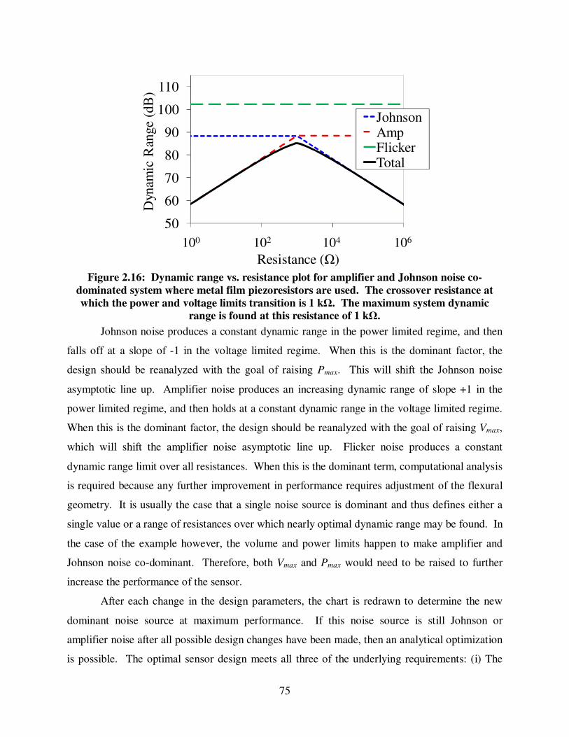
75
Figure 2.16: Dynamic range vs. resistance plot for amplifier and Johnson noise co-
dominated system where metal film piezoresistors are used. The crossover resistance at
which the power and voltage limits transition is 1 kΩ. The maximum system dynamic
range is found at this resistance of 1 kΩ.
Johnson noise produces a constant dynamic range in the power limited regime, and then
falls off at a slope of -1 in the voltage limited regime. When this is the dominant factor, the
design should be reanalyzed with the goal of raising Pmax. This will shift the Johnson noise
asymptotic line up. Amplifier noise produces an increasing dynamic range of slope +1 in the
power limited regime, and then holds at a constant dynamic range in the voltage limited regime.
When this is the dominant factor, the design should be reanalyzed with the goal of raising Vmax,
which will shift the amplifier noise asymptotic line up. Flicker noise produces a constant
dynamic range limit over all resistances. When this is the dominant term, computational analysis
is required because any further improvement in performance requires adjustment of the flexural
geometry. It is usually the case that a single noise source is dominant and thus defines either a
single value or a range of resistances over which nearly optimal dynamic range may be found. In
the case of the example however, the volume and power limits happen to make amplifier and
Johnson noise co-dominant. Therefore, both Vmax and Pmax would need to be raised to further
increase the performance of the sensor.
After each change in the design parameters, the chart is redrawn to determine the new
dominant noise source at maximum performance. If this noise source is still Johnson or
amplifier noise after all possible design changes have been made, then an analytical optimization
is possible. The optimal sensor design meets all three of the underlying requirements: (i) The
50
60
70
80
90
100
110
1 100 10000 1000000
Dyn
amic
Ran
ge (
dB)
Resistance (Ω)
JohnsonAmpFlickerTotal
106104102100
76
resistance should lie on the peak or plateau of maximum dynamic range in Figure 2.16, (ii) The
piezoresistor dimensions must lie within the limits described by the flexural dimensions, (iii) The
piezoresistor volume must be lie between Ωmin and Ωmax. The minimum piezoresistor volume is
defined by the resistor volume at which the flicker noise rises to become equal to that of the
present dominant noise source- amplifier or Johnson.
( )
if amplifier limitedln( )
1 if Johnson limited2 4
max
Vai
min
maxC sig
B
V
SrΩ
PC r fk T
απ
= ⋅
− (2.16)
The variables Lr, br, hr, CC and Nr are used in this optimization. There may be a range of
solutions for near optimal performance since this is no longer an optimization process: any
solution which fits within the resistance, volume and geometric bounds is adequate. One method
to check for possible solutions is to map the volume range, using Eq. (2.17), to an effective
resistance range, Rmin to Rmax, and compare these with the range of resistances for the optimal
dynamic range described in condition (ii) above. The intersection of these two sets contains the
resistance values which meet all criteria for a valid solution. If there is no intersection between
these two sets or if the solution is otherwise infeasible, then the computational optimization
method is required. The serpentine factor in Eq. (2.17) should be set to the minimum and
maximum values available to the designer to find the resistance bounds.
2 2 2
2
2 2 2
9r f min
min
max
r f
max
min
N LR
N LR
ρ γ
ρ β
Ω=
Ω
=Ω
(2.17)
2.8.4 Computational Optimization
The solution to the sensor optimization is dependent on the imposed constraints when
flicker noise is dominant. The type and number of constraints are unique to each design. A
constraint based solver is used to maximize the dynamic range of the sensor system.
In the flicker noise limited regime, the dynamic range of the sensor system may be
rewritten as a function of R and Lr. The term GSG reduces to a constant because optimal resistor-
to-beam length and thickness ratios exist for the flicker regime. This simplification removes the
dependence of Eq. (2.13) on Lf and hf. The resistor volume may be written as a function of both

77
the R and Lr variables as shown in Eq. (2.18). The supply voltage is also a function of R and is
set by either the voltage limit of the voltage source or the power limit of the resistor.
2 2r r
N LΩ
R
ρ= (2.18)
The removal of the two flexural variables in the flicker noise regime simplifies the dynamic
range expression sufficiently to allow the operating surface of the optimizer to be visualized for
the example design as shown Figure 2.17. The noise bandwidth is the same as in the resistance
variation chart above- 0.1Hz to 10kHz- capped at the upper end with a low-pass filter.
Figure 2.17: Operating surface of constraint based optimization. Constraints are
mapped to this surface. The optimizer operates mainly in the flicker limited domain
where the piezoresistor volume limits performance. Increases in resistor volume are
associated with reductions in the resistance, leading to a trend of maximum performance
at the amplifier/flicker boundary.
A constant Lr slice of Figure 2.17 differs from Figure 2.16 in that the resistance is now
directly linked to the volume. In Figure 2.16 it was assumed that Lr << Lf so that Lr could be
freely varied to effectively decouple R and Ω. In the coupled flicker noise regime, Lr is not
necessarily able to change, as it is optimized to a maximum. This results in an apparent inverse
relationship between R and Ω.

78
Figure 2.18: Dynamic range vs. resistance plot for flicker noise dominated system where
polysilicon piezoresistors are used. The crossover resistance at which the power and
voltage limits transition is 1 kΩ. The maximum sensor system dynamic range is found
over a band of resistances from roughly 0.1 to 10 kΩ, with subordinate noise sources causing minor reductions at the edges of the range.
The optimal value on this surface is found by mapping all of the constraints onto this
surface. Unfortunately, far more than two variables are needed to define the constraints, so these
boundaries cannot be plotted on a three dimensional surface plot. It is possible to see from the
surface plot that the maximum dynamic range in the flicker noise dominated regime trends
towards the low resistance corner at the intersection of flicker and amplifier noise asymptotes.
The constraint based solver will tend towards the lower resistance end of the plateau defined by
the flicker noise line in Figure 2.18 to increase the volume of the resistor and thus boost the
sensor dynamic range. The noise bandwidth is again the same as in the resistance variation chart
above- 0.1Hz to 10kHz- capped at the upper end with a low-pass filter.
A measure of decoupling may be gained in the design through Nr. This is because Nr
may be used in Eq. (2.18) to increase the resistance without further reducing the piezoresistor
volume. The benefit of this increase is that raising R up to Rcross increases the dynamic range of
the sensor by reducing the subordinate noise sources. However, care needs to be taken when
adjusting Nr in the optimization process since highly folded resistor geometries can significantly
increase the complexity of the MEMS fabrication process, while only resulting in small
performance gains.
50
60
70
80
90
100
110
1 100 10000 1000000
Dyn
amic
Ran
ge (
dB)
Resistance (Ω)
JohnsonAmpFlickerTotal
106104102100

79
A successful computational optimization will always result in a higher performance
device than the analytical optimization. The analytical optimization is focused only on
maximizing the dominant noise source when used for Johnson and amplifier limited systems. In
fact, the subordinate flicker noise still marginally contributes to the dynamic range. The
computational optimization takes this into account and maximizes the dynamic range of both the
dominant and subordinate noise sources. The tradeoff between the two optimizations is between
the level of coupling/complexity in the design and the performance. In the flicker noise limited
regime there is a strong link between these two, so large gains in performance may be found
through increasing the complexity of the design process. In the other two regimes the link may
be very weak such that very little performance is gained for the same increase in the design
process complexity.
2.9 Conclusion
As shown in this chapter, the piezoresistor itself is generally the limiting element in the
piezoresistive sensor system when proper modeling and optimization procedures are used to
design the systems. In order to improve the performance of piezoresistive sensor systems, better
piezoresistors should be developed. Novel materials, such as carbon nanotubes, offer the
potential to increase sensor performance by more than an order of magnitude due to their high
gauge factors [93]. However, more research needs to make these types of sensors feasible for
MEMS piezoresistive sensor systems.

80
81
CHAPTER
3 ENGINEERING SCHOTTKY DIODE
CONTACTS
3.1 Synopsis
This chapter will explore the physics of metal-semiconductor interfaces formed at the
contacts of silicon piezoresistors fabricated via NLBM. Models will be presented which enable
the designer to accurately engineer these interfaces.
The purpose of this work was to demonstrate a non-conventional approach for creating
electrical connections to silicon using near ambient temperature soldering. This removes a
significant hurdle to the fabrication of high performance, custom silicon piezoresistors. The
approach focuses on reducing the resistance of diodes that are undergoing reverse bias behavior,
commonly considered to be unacceptable for electrical connections. Reverse bias Schottky
barrier analytic models based on of quantum mechanical first principles are developed to explain
how the behavior is affected by doping, soldering temperature and geometry. This
understanding is encapsulated within parametric models that enable rapid design and
optimization of the electrical contacts to silicon. Using this model, one may design contacts for
practical applications that do not require high temperature processing. Indium solder is found to
be the best solder for this process.
3.2 Introduction
The intent of this work was to demonstrate and model solder-based electrical interfaces to
silicon created in near ambient conditions. This quantum mechanically driven understanding
will enable the reliable applied engineering of rapidly and simply fabricated electrical contacts to

82
silicon-based devices without high-temperature process conditions. The prime motivator for this
work was the development of high-performance, silicon-based piezoresistors where the sensor
performance is dependent on the quality of the electrical connections. A fabrication process has
been demonstrated [94] that is capable of creating metal microstructures with integrated silicon
piezoresistive sensing. Piezoresistors of customizable geometry down to approximately 150µm
width are desired for these devices [1]; however commercial bare silicon gages such as those
provided by Kulite, Micron Instruments and BCM Sensor Technologies are non-customizable
and are not commonly available in such sizes. A parallel sensor fabrication process to produce
these sensors has been developed [94] that requires low-temperature processing conditions for
the silicon electrical contacts. Here we show that such low temperature conditions can be
achieved with indium soldering, where the deliberate focus is on a non-intuitive, yet correct
approach to building ‘poor’ diodes operating in reverse bias behavior. These sensors could
provide large dynamic range sensing to metal MEMS devices including pressure sensors [78],
AFM [81], and precision flexural positioners [1] that can be used as a customizable positioning
platform for a wide range of applications including nanomanufacturing research and
development [5].
Single crystal silicon piezoresistors offer high strain sensitivity with gage factor ranging
from 120 [81], to 150 as provided commercially depending on orientation [95]; values which
exceeds the sensitivity of metal gages by several orders of magnitude. P-type wafers offer the
highest gage factor [96], and will be the focus of this work. This sensitivity is especially useful
in precision positioners for which large dynamic range sensing is desired [97]. A salient
difficulty with these sensors lies in making quality electrical contacts. Metal-semiconductor
interfaces are a regular focus of research due to their importance in electrical structures [98],
[99]. Doping and annealing are generally used to bridge this interface, however these
approaches can be impractical when the silicon is attached to a substrate that has significant
constraints on temperature and pressure, or is required in batch sizes below the scale that is
conducive for standard microfabrication methods [19]. It is desirable to find a means of making
an electrical connection to silicon that is design flexible, is cost effective in small batches (<100),
and may be carried out in ambient pressure and low <200°C temperature. Small batch
piezoresistor customization offers significant performance increases through multiple routes, i)
the piezoresistor serpentine factor [97], ii) piezoresistor size adjustment to alter power limits

83
[97], iii) geometric flexibility to fit on small flexures [1], iv) utilization of transverse gage
factors, and v) compact multi-piezoresistor designs for thermal stability.
A practical alternative to standard microfabrication processes would enable the creation
of custom piezoresistors. One option is laser scribing of the piezoresistor geometry into a thin
single crystal silicon wafer followed by stamping of the geometry onto the desired device, and
the creation of contacts once the piezoresistor is attached to the substrate [94]. This presently
requires fabrication of electrical contacts in near-ambient (less than 200°C) conditions, thereby
precluding the use of common techniques (chemical processes or high temperature annealing).
Soldering is a viable alternative to doping/annealing due to the localization of the heating. Low
resistance, (<1Ωcm) near-ohmic connections have been reported in literature for such methods
[100]. This work demonstrates the feasibility of generating electrical contact to single crystal
silicon using bench-top soldering methods. Herein it is shown that the best soldered connections
to semiconductors are the worst possible conventional diodes, with a low breakdown voltage and
a low resistance in reverse bias. Ohmic contact resistances of ≈1Ω-cm in series with
exponentially decaying non-ohmic barrier resistances of ≈15Ω-cm with voltage decay constant
≈2V are observed for <110> p-type wafers at 1017cm-3 doping.
3.3 Background
3.3.1 Metal-Semiconductor Contacts
Metal-semiconductor connections are commonly created through heavily doping the
silicon surface below the contact, then depositing metal onto the silicon surface. This contact is
annealed to create chemical intermediaries which reduce the barrier potential. The high doping
level drives the silicon properties closer to those of a conductor, when combined with the
annealing this helps to make the contact more nearly ohmic [101]. These processes
unfortunately generally require high (>500°C) temperatures that are not compatible with many
metal substrates.
3.3.2 Soldering to Silicon
Soldering provides a bench top alternative to the higher performance doping and
deposition process. This can be conducted at lower temperatures, with no required masking,

84
making it well-suited for a low-volume, high-variability fabrication process. The electrical
properties of such soldering operations have received less attention than those of the standard
bonding processes because of their generally lower performance than doped, annealed contacts.
Previous work on soldering to silicon has focused mainly on thermal and mechanical contacts.
Indium solder has mainly been used to make high thermal conductivity and/or mechanical
contacts to silicon [102]. In-Sn alloys have been used to carry out low-temperature wafer
bonding [103]. Rare-Earth alloys have more recently been used to create mechanical contacts
between ceramics and glass [104]. Research on electrical connectivity has been carried out using
these rare-earth solders [100] as well as aluminum [105]. Some measurements have been done
on low-temperature indium contacts to silicon to demonstrate feasibility [106]; however the
results were not generalized sufficiently for applied engineering. The preceding works provide a
base knowledge/experience that needed to be augmented in order to clearly describe (a) the
physics that dominate/limit at low temperature interfaces and (b) the performance to expect for
indium soldered contacts over varying wafer doping levels. This work fills this gap by defining
the performance bounds of indium solder contacts and providing an understanding of the
dominant physics driving such performance.
3.4 Theory
The utility of this theory lies in understanding how to define the properties of the non-
linear barrier in terms of standard electrical resistance, so that this may be integrated into existing
sensor design and optimization work [97]. The barrier analysis is commonly done in the
opposite fashion, where the ohmic resistance is integrated into the non-linear term [107]. This
common approach avoids the difficulty of linearizing the barrier effect, but also does not result in
familiar, electrical components that are well-suited for mechanical design and optimization.
Generating these effective electrical components is a key element to porting this theory to
applied engineering.
The samples were created with two metal-semiconductor contacts, labeled as + and – in
Figure 3.1. P-type silicon is used owing to its higher gage factors. This creates outward facing
diodes, which are expected to have a series ohmic contact resistance, Rc, and also on the positive
side, a non-linear barrier resistance, Rb, [107], [108]. The bulk silicon has a geometrically
determined resistance, RSi.

85
Figure 3.1: Schematic of sample structure with overlaid electrical model.
The band diagram for this model is shown in Figure 3.2, with the top diagram in the
unbiased equilibrium condition and the bottom diagram under positive voltage bias. The Fermi
level, EF, is shown with a dotted line in the diagram, as are the conduction band energy, EC, and
the valence band energy, EV. Electron holes are the majority carrier in p-type silicon and are
shown in the bottom diagram. Potential barriers exist at both contacts in the unbiased case. The
application of a voltage drives the negative contact barrier in forward bias, lowering its barrier
potential. The positive contact is in reverse bias and its barrier potential is largely unchanged,
leaving it as the dominant potential barrier. The electrical model will focus on this reverse bias
diode.
Figure 3.2: Band diagram for silicon sample with opposed diodes in unbiased condition
(top) and under +V bias (bottom). The current limiting factor is the reverse biased diode at the + contact, shown on left.
3.4.1 Reverse Bias Resistance
The main current transport mechanism for reverse bias flow is thermionic emission, TE,
over the potential barrier at low to moderate doping, as shown in Eq. (3.1) [109], where J(V) is
the current density, V is the applied reverse bias voltage over the barrier, A** is the modified
Richardson constant with value 32 Acm-2K-2 [110] for moderately doped p-type silicon at room
temperature, T is the temperature in K, q is the electron charge, φBp(V) is the barrier potential
defined in Eq. (3.2), and kB is Boltzmann’s constant. The forward current density is neglected in
RSiRc Rc
V+ V-+ _Solder
Silicon
Rb
Solder Si
E(h+)
EV
ECEF
V+
V-
h+
Solder
φBp0 φBi

86
Eq. (3.1), as it declines exponentially with increased reverse bias and becomes negligible relative
to the reverse current density once qV>φBp0-φBi, where φBp0 is intrinsic barrier potential, and φBi
is the built-in potential as defined in the supplement.
( )** 2( ) exp ( )Bp BJ V A T q V k Tϕ = − (3.1)
The ohmic and forward bias diode potential drops are assumed to be significantly less
than the drop over the reverse bias diode in the voltage range of interest (0-20V), so the voltage
over the reverse bias diode is approximated as equal to the voltage over the whole sample. This
approximation fails at same point that the barrier parameters stop being important, once ohmic
losses dominate.
Previous work has shown the barrier to be a function of voltage due to both an image
potential acting on charge carriers and an electric field correction factor [110]. The electric field
factor corresponds to the field action on the charge carriers across an intervening oxide layer
layer of thickness dox and permittivity εox [110]. Both terms are included in Eq. (3.2) where Em
is the electric field at the interface, εsi is the permittivity of silicon, γ is the fraction of the barrier
potential attributable to the Schottky-Mott relationship (≈0.25 [110]), and CCsb is the silicon
carrier concentration at the Schottky barrier. This semi-empirical linear electric field correction
factor is observed to well characterize the data observed in a range of studies of soft reverse bias
characteristics of Schottky barriers and has several competing proposed mechanisms [99]. We
include the form intended for a Schottky barrier with an intervening oxide layer [110], as the
oxide has not been cleared off the silicon prior to indium soldering.
( )21( )
2Csb Bim si
Bp Bp0 ox m m
si ox si
qC VqEV d E E
ϕεϕ ϕ γ
πε ε ε
+= − − = (3.2)
The built-in potential is commonly approximated using a Maxwell-Boltzmann
distribution at doping levels well below the critical threshold, Nv, the effective density of states
of the valence band. The potential is approximated with a 3/2 power scaling at doping levels
above the threshold [111]. This analysis is intended to extend into the degenerate regime, so will
use both terms in order to estimate the built in potential. These are combined in Eq. (3.3), where
h is Planck’s constant, and m*dh is the effective hole mass. The terms are scaled with functions
of the ratio CCsb/Nv to determine which approximation is dominant.

87
2 3 1
3 2
2
3ln 1
4
22
Csb Csb Csb CsbBBi Bp0
v v v v
dh Bv
C C C Ck T
q N N N N
m k TN
h
πϕ ϕ
π
−
∗
= + + +
=
(3.3)
A Taylor series of Eq. (3.2) – with respect to voltage – enables an examination of the
barrier potential voltage sensitivity. The first order term captures the linear voltage dependency
in the regime where the barrier resistance dominates. Higher order terms were found to generate
increasing error at larger voltages. The low voltage, small potential variations are of main
interest, as this generates the diode-like voltage drop and at high voltages the ohmic resistances
dominate.
0
3
40 2 3
3
42 3 3
( ) '
28
'2048 2
Bp V
Csb Bi oxBp0 Csb Bi si
si ox
Csb ox Csb siV
si Bi ox Bi
V V
q C dqC
q C d C q
ϕ ϕ ϕ
ϕ γϕ ϕ ϕ ε
π ε ε
γ εϕ
π ε ϕ ε ϕ
≈ − +
= − −
= +
…
(3.4)
The first term of φ0 and the second term of φ’V dominate in the non-degenerate regime.
The differential resistivity ρ(V) of the barrier can be found using the Eq’s (3.1) and (3.3) [112] to
find voltage dependence as shown in Eq. (3.5).
1
0**
( )( ) exp exp /
' '( )
b V
B B
V B V
qk k TJ VV V
V qA T k T q
τ
ρ
ϕρ
ϕ ϕ
− ∂
= = − ∂
(3.5)
This expression may be simplified into two general terms, a resistivity, ρb, and a voltage
decay constant Vτ.
3.4.2 Electrical Model
The barrier resistance is combined with the ohmic resistivities to produce the net
resistance R(V) expression for the sample in Eq. (3.6), where Ac is the areas of the contact, Gl is
the current crowding scaling factor [98], [113], ρc is the ohmic contact resistivity for Rc, the
ohmic contact resistance, lc is the length of the contact in parallel with current flow, tSi is the
thickness of the silicon sample perpendicular to the contact surface and the subscripts p/n stand
for the positive and negative contact pads, respectively.

88
( )
( ) ( )
1 1 1 1 1 1
1
( )
tan
V V
b cp lp c cp lp cn ln Si
li i i i ci Si Si c
R V A G e A G A G R
G where l t
τρ ρ
α α α ρ ρ
−− − − − − −
−
= + + +
= =
(3.6)
Integrating the inverse resistance over the voltage gives an expression in Eq. (3.7) that
may be fit to a measured I-V curve.
[ ]1 1
0( ) ( ) ( ) ln (0) ( )
V
I V R v dv R V V R R Vτ− − = = ∞ − ∫ (3.7)
The three parameters which adjust this curve are ρc, ρb, are Vτ, which determine the
barrier and contact resistances. These are used to determine more fundamental parameters such
as the Schottky barrier height through Eq. (3.5).
3.5 Experimental Setup
Measurements on silicon solder contacts were taken to determine the scale of the barrier
and contact resistances. The sample fabrication process was carried out as follows. The silicon
wafer thickness and resistivity was measured using a 1µm resolution micrometer and 4-point
probe. The wafer, ranging in thickness from 50µm to 500µm, was either cleaved or diced with a
laser scribe to approximately 5x15mm. This shaped sample was adhered to a glass substrate and
soldered at ≈290°C, in pads of 5x2mm at each end, with the silicon/glass heated to a range of
temperatures from ambient up to 200°C.

89
Figure 3.3: Anneal carried out on reverse bias diode sample, with pre-anneal rising I-V
curve, a 1min anneal at 20V, then the post-anneal falling I-V curve which shows greater linearity and lower voltage drop.
The soldered sample was attached to a 4-point probe measurement stand and annealed at
20V for 1min before the return I-V curve was measured, as shown in Figure 3.3. Eq. (3.7) was
fit to the I-V data, which determines the three model parameters. One such data run is shown
below in Figure 3.4 in the differential resistivity form to clearly indicate the barrier and contact
parameters (in bold).
Figure 3.4: Differential resistance measured from silicon sample, showing both the non-
linear barrier resistivity and the ohmic contact/silicon resistance. Note the flattening of
the exponential curve at low voltage (<1V) due to the voltage drop across the forward bias diode.
Several different solder types were considered, with a focus on low-temperature solders
and those mentioned in literature for making mechanical contact with silicon. These included: i)
Cerroloy 117, ii) Cerrobond 203, iii) rare-earth solder- Adheralloy AS-3EC, and iv) pure indium.
The first two are low temperature alloys which showed promise in mechanical adhesion to
0 5 10 15 200
50
100
150
200
250
300
350
Cur
rent
(m
A)
Voltage (V)
Pre-AnnealPost-Anneal
20V Anneal
Res
ista
nce
(Ω)
Voltage (V)
00 5 10 15
0.5
1Rb(ρb)
Rc(ρc) + RSi
Vτ

90
silicon. The Adheralloy solder is a relatively new alloy which is mentioned in literature as
producing a strong mechanical connection to silicon [104] as well as an ohmic contact with low
resistivity (0.01-0.02Ω-cm for n-doped 1018cm-3 [100]). Indium produces a strong mechanical
contact with silicon and has a high diffusivity, suggesting good electrical properties [102], [114].
3.6 Contact Resistivity
The contact resistivity term describes the ohmic component of the metal-semiconductor
resistance. The Cerroloy and Cerrobond solders demonstrated high resistivity (>102ohm-cm)
even in highly doped samples, so were replaced with the rare-earth and indium solders, whose
performance is shown in Figure 3.5. The samples with heated substrates to 160°C are labeled as
‘Heated’, and these demonstrated overall lower resistivities than the ambient temperature
samples. The resistivity is observed to level off at high doping levels (CCSat=1019.05cm-3). This
is approximately the transition point to degeneracy, as indicated by Nv≈1019.5cm-3. All of the
wafers are <100> orientation except the 1017.5cm-3 wafers, which are <110>, which shows a
resistivity above the trend. This is believed to be due to the orientation, as explained in the
discussion section.
Figure 3.5: Ohmic contact resistivity, ρc, for different solders and substrate
temperatures.
Indium consistently out-performed the rare-earth solder, and therefore this is used in all
subsequent analysis. A best case value of resistivity was observed for each wafer, associated
with soldering on a heated substrate at ≈160°C. These baseline values were found to follow a
1 1014
× 1 1015
× 1 1016
× 1 1017
× 1 1018
× 1 1019
× 1 1020
× 1 1021
×
1 103−
×
0.01
0.1
1
10
100
1 103
×
Indium HeatedIndiumRare EarthFit to Indium Heated
ρc
(Ω*c
m2 )
CCsb (cm-3)

91
trend, which is shown in Eq. (3.8), where CCρc=1012.09±0.88cm-3 for <100> wafers or 1012.94±0.88cm-
3 for <110> wafers, and cρc=-0.8962±0.0474.
( )
( )2( m )
c
c
c
Csb C c Csb CSat
c c
CSat C c
C C if C C
C C otherwise
ρ
ρ
ρ
ρ
ρ β<
= Ω ⋅ (3.8)
A bonding parameter, β, was introduced to describe the ratio between the measured
contact resistivity and the baseline resistivity for that doping level. Ideal processing would result
in β=1, however lower temperatures and surface contamination were found to raise β>1.
3.7 Bonding Parameter
The bonding parameter was observed to be strongly coupled to processing parameters, as
shown in Figure 3.6, with increasing value and variability in β at lower temperatures, as well as a
knee in the curve at the indium melting temperature, Tmelt. The variability in β is strongly
affected by CCsb as shown in Figure 3.6b which may be due at low CCsb to increased density
variation, increased temperature sensitivity or both. Reasonable performance limits of β<3 are
indicated in both charts and set bounds on the useable wafer doping (>1016) as well as processing
temperatures (>125°C).
Figure 3.6: Bonding parameter variation with a) substrate heating temperature, and b)
doping. The variability and value of β are reduced by increasing substrate temperature as in a), and increasing carrier concentration as in b).
3.8 Schottky Barrier Parameters
The information in the barrier parameters ρb and Vτ, may be mapped directly to the
effective oxide thickness, dox, and intrinsic Schottky barrier potential, φBp0, through Eq. (3.5).
The baseline resistivity (β=1) samples are used for the fit to minimize the effect of processing
variation. These are plotted as the filled in points in Figure 3.5, while the β>1 samples are
100 125 150 175 2001
2
3
4
1 1014
× 1 1017
× 1 1020
×
10
100
β β
Tsub (°C) CCsb (cm-3)a) b)
Tmelt
1

92
shown with hollow points. The intrinsic barrier potential holds at 466.5±21.6mV over five
orders of magnitude CCsb variation, suggesting the model is accurately capturing the interface
physics. This barrier value lies 0.16eV below reported In-pSi Schottky barrier height values
(0.63eV) [115], which may be due to several reasons, including non-homogeneities in the
interfacial oxide layer, the applied indium solder or the native oxide film. The soldering process
is intrinsically less uniform than a deposition process. The fabrication process additionally
generates greater difficulty in removing contamination and oxides in the process due to non-
cleanroom conditions and chemical limitations, all of which is known to affect the barrier height
[98]. Finally, Schottky barriers are altered by heating the contact above the silicide eutectic
temperature, and this commonly results in an increased barrier height [98]. This research was
largely carried out at low temperatures, around or below the eutectic temperature for indium
silicide (157°C) [116]. This may account for part of the difference between measured and
literature values.
Figure 3.7: Schottky barrier parameters shown over a range of doping levels. The
effective oxide drops with increasing doping, while the intrinsic barrier potential remains constant.
Thermionic emission dominates over tunneling when kBT>>E00 [98], where E00 is defined
by Eq. (3.9), ħ is the reduced Planck constant, and m* is the effective electron mass. The
samples studied in this research lie mainly within the TE dominated regime, as the transition to a
combination mechanism- thermionic-field emission, TFE- occurs at ≈1018cm-3. The TE-based
model was developed for this lower doping, higher barrier effect region, however it is observed
to accurately capture trends that extend into the TFE region, as shown in Figure 3.7. The barrier
parameters in the high doping regime are also of reduced importance, as the ohmic contact
1 1013
× 1 1014
× 1 1015
× 1 1016
× 1 1017
× 1 1018
× 1 1019
×
0
0.2
0.4
1
10
100
BarrierBarrier FitBarrier B=1OxideOxide FitOxide B=1
φB
p0(V
)
|do
x|(Ǻ
)CCsb(cm-3)

93
resistivity dominates. Thus there is little need to improve predictive accuracy of barrier
parameters in this regime.
00 2Csb
si
CqE
m ε∗=ℏ
(3.9)
The oxide film thickness parameter describes the fit of the electric field correction factor
to the data. This term is found to be generally an order of magnitude lower than the image force
potential reduction term, so is of secondary importance for predicting barrier parameters. The
electric field correction factor was found to show a negative dependence on oxide thickness,
resulting in negative oxide thicknesses when fitting to Eq. (3.2). The negative dependence is
conjectured to be due to the extension of the barrier electric field into the oxide, resisting the
passage of the majority carrier (holes) into the silicon and generating a negative sign in the
electric field value in the last term of Eq. (3.2). This linear electric field correction factor
provides predictive capability to the theory, as the oxide thickness shows consistent trends across
the range of doping levels. This semi-empirical fit is sufficient for the needs of this work, as the
focus is on the reliable design of electrical interfaces.
The measurements of oxide thickness show a low doping thickness of 20-80Å, which is
above that of native oxides. The highest value appears to be an outliner, which suggests the trend
may be closer to 20-40Å. This variation may also be due to the effect of contamination on the
surfaces. The important region of analysis is at mid-range doping, around 1017cm-3. The
thickness then drops with increasing CCsb as shown in Eq. (3.10), with CCd=10-12.492±3.597cm-3 and
cd=-0.3001±0.0474, with an average error of 1nm. This drop is possibly due to indium
penetration of the oxide.
dc
Csbox
Cd
Cd
C
=
(3.10)
3.9 Barrier Resistivity
The barrier resistivity term describes the scale of the exponentially-decaying barrier
resistance and is a function of CCsb and β as is shown in the logarithmic plot in Figure 3.8.

94
Figure 3.8: Barrier resistivity plotted on log axes with best fit curve to data.
The barrier resistivity shows a strong sensitivity to β, a much reduced inverse sensitivity
to CCsb, and appears insensitive to wafer orientation. The fit expression to this data is shown in
Eq. (3.11). This expression integrates Eq.’s (3.4), (3.5), and (3.10). A scaling term for β is
included, with exponent bρb=2.487±0.335, and an average error of 0.50 in log(ρb).
0
** 'bB
q
bk TBb
V
ke
qA T
ρ
ϕ
ρ βϕ
= (3.11)
3.10 Barrier Voltage
The barrier voltage decay constant describes the rate of relaxation of the potential barrier
as bias voltage is applied, and is a function of CCsb and β as is shown in the logarithmic plot in
Figure 3.9.
Figure 3.9: Barrier voltage decay constant plotted on log axes with best fit curve to data.
The barrier voltage constant falls within a tight band of values from 1-10V, shows little
sensitivity to β, a low inverse sensitivity to CCsb and is also insensitive to wafer orientation. The

95
fit expression to this data is shown in Eq. (3.12). This expression integrates Eq.’s (3.4), (3.5),
and (3.10). A scaling term for β is included, with exponent bvτ=-0.3553±0.0890 and average
error of 0.14 in log(Vτ).
'vbB
V
k TV
qτ
τ βϕ
= (3.12)
3.11 Discussion
The following contains a discussion of the mechanism believed to explain the observed
results in the context of supporting experimental evidence.
3.11.1 Proposed Mechanism
An amorphous native oxide forms on the surface of silicon exposed to ambient
conditions, on the range of 10-20Å [117]. Given the data we have obtained, it is consistent that
liquefied indium solder penetrates this oxide layer and the silicon below during soldering. This
penetration effect scales with doping levels, as shown in Figure 3.7, which is expected, given
that indium diffusion/penetration is enhanced by dopant interstitials in both the oxide and silicon
below [118]. The indium only sparsely penetrates the silicon crystal structure and this
penetration is on the scale of a few atoms over the ≈100s soldering time. Indium diffusion in
silicon occurs via the same mechanisms as boron [119], which is orientation dependent and
increases from <111> to <110> to <100> orientation [120]. The indium penetration into the
amorphous oxide reduces the effective oxide thickness but lacks such orientation dependency.
The Schottky barrier effects are believed to be dominated by this orientation independent
reduction in effective oxide thickness. The ohmic resistivity is influenced by both this oxide
thickness, and the crystalline silicon below, suggesting a mechanism for orientation dependence.
The indium ohmic contact resistivity drops sufficiently at high doping that secondary resistances
like the surface oxide become dominant, resulting in the observed leveling off of the contact
resistivity.
Heating at the junction during soldering increases the quantity of chemical intermediaries
created while the indium is in a liquid state. This would act to reduce both the intrinsic Schottky
barrier potential and the effective oxide thickness, explaining the β dependency. High bias
voltages (≈20V) over the barrier are believed to have a similar effect of generating intermediaries

96
through localized heating and large electric fields (106V/cm) at the interface, which would
explain the improvement seen by annealing at 20V.
3.11.2 Oxide Effect
The measurements suggest that the oxide drives the performance of the reverse bias
contact away from ohmic behavior through the negative dependence of the barrier height on the
electric field. A high breakdown voltage is desired in normal diode components, but the
opposite is desired here, where a good connection to the silicon requires a low breakdown
voltage diode at the positive contact. The oxide appears to be playing a detrimental role in
increasing the effective barrier height, but only as a second order effect to the image force
correction factor.
The proposed theory suggests that the best soldered connections to semiconductors are
the worst possible conventional diodes, with a low breakdown voltage and a low resistance in
reverse bias. A high voltage anneal ‘damages’ the diode, lowering the breakdown voltage. The
thick oxide layer appears to slightly raise barrier potential. The oxide also appears to contribute
to the minimum ohmic contact resistivity, so a consistent means of removing the oxide layer
without allowing native oxide formation in the following fabrication steps should improve device
performance.
3.12 Conclusion
This work demonstrates the feasibility of solder-based electrical interfaces to silicon
created in near ambient conditions, as well as providing models to predict the connection
performance. This knowledge enables the reliable design of simple electrical contacts to silicon
without high-temperature process conditions. These solder connections fill in a crucial need in
the development of high performance customizable silicon piezoresistors.
Electrical contacts are demonstrated using soldering methods in near ambient conditions
and a model based off of Schottky diode physics in reverse bias conditions is presented in order
to understand/predict the performance of these connections. The model has been demonstrated
to predict performance over a wide range of doping levels including 1014-19cm-3, which covers
the range typical for silicon piezoresistors. The barrier performance is predicted from three
parameters: i) intrinsic Schottky barrier potential, 2) oxide thickness, and iii) the process

97
depending bonding parameter. We present a modified I-V curve model composed of standard
electrical resistances, intended for use in engineering design. This model is flexible to the
addition of extra resistances and higher order voltage series expansion terms.
This work has revealed the dominant and limiting physics that govern contact
performance for purely soldered connections. The barrier resistivity, barrier voltage decay
constant and ohmic contact resistivity all decrease with increased doping. Constraints on the
doping level via gage factor doping sensitivity [40] may limit the ability of the designer to lower
the contact resistance. The theory presented here provides the designer with means to determine
the tradeoff between doping and contact electrical performance. The use of low temperature
doping methods such as electrical sparking [106] could raise the local doping level, which should
improve contact performance as per the models described above.

98

99
CHAPTER
4 OPTIMIZATION OF PIEZORESISTORS
WITH SCHOTTKY DIODE CONTACTS
4.1 Synopsis
This chapter will explore the physics of metal-semiconductor interfaces formed at the
contacts of silicon piezoresistors fabricated via NLBM. Models will be presented which enable
the designer to accurately engineer these interfaces.
A modeling theory is presented to predict the performance of piezoresistors which
incorporate Schottky diode electrical contacts. This new theory allows the design of high
performance gages which can be fabricated using Non-Lithographically-Based Microfabrication
(NLBM) techniques. These semiconductor piezoresistors can be designed in customizable sizes
and fabricated in parallel in order to integrate position sensing into MEMS flexural positioners.
Customizable nanopositioning platforms will enable advances in a range of nano-scale
fabrication and metrology applications. A semiconductor piezoresistor with Schottky diode
contacts was fabricated and attached to a titanium flexure. This device is shown to match
predicted electrical performance within about 8% and to show a gage factor of 116, within 2% of
the predicted value. Performance limits for Schottky diode semiconductor piezoresistors are
identified to be about 127dB full noise dynamic range for a quarter bridge over a 10kHz sensor
bandwidth on a 600µm width titanium flexure, making them ideal for sensing on meso-/micro-
scale flexural positioners. Methods of reaching these performance bound are suggested and their
impact on the sensor dynamic range are studied.
100
4.2 Introduction
The purpose of this work is to generate the design theory and modeling required to
optimize piezoresistors with Schottky diode contacts. These models and theories will enable the
design of piezoresistors utilizing low temperature solder contacts that show potential
performance exceeding that of commercial gages. Schottky diode piezoresistors are produced
with a new flexible fabrication process- Non-Lithographically Based Microfabrication (NLBM)
[94]. This process promises to produce customizable multi-gage structures fabricated in parallel,
with smaller geometry and higher potential performance than commercial gages. This provides a
means for integrating sensing into low cost customizable flexural nanopositioning architectures,
which will open opportunities for advancements in several fields including nanomanufacturing
R&D [3], multi-axis AFM [121], and advanced memory storage/computing structure fabrication
[3], [4].
4.2.1 Non-Lithographically-Based Microfabrication
NLBM is a new fabrication process that has been developed to produce multi-material
meso-/micro- structures with integrated multi-axis high performance silicon piezoresistive
sensing [94]. This was developed to fabricate metal MEMS nanopositioner architectures at low
average cost (<$1k/device) even in small (<10) batches, high flexibility (≈1 week to prototype),
out of robust materials like titanium and with high performance integrated sensing (up to 135dB
full noise dynamic range over a 10kHz sensor bandwidth). The fabrication uses indium solder
for electrical contact to the silicon piezoresistors, which produces sensors with Schottky diode
contacts. This work shows how to properly design piezoresistors with such Schottky barriers so
that their performance can be maximized.
Previous fabrication efforts have focused on producing all-silicon nanopositioners,
fabricated with conventional microfabrication methods [1], however the large size of the
nanopositioner produces a device that is too fragile and requires too much investment (≈$20k
tooling + labor, ≈6 months) to be redesigned for each new nanomanufacturing application [19]
with varying requirements of range, resolution, bandwidth, and stiffness. Metal structures
provide a means to bypass these restrictions, as they are more robust to typical nanopositioning
operation (including stage loading/unloading) and they can be fabricated with more
conventional, scalable machining methods. These fabrication methods produce a superior

101
substrate but do not allow for integrating sensing into the metal positioner as is possible in
standard microfabrication. Conventional commercial silicon gages are too wide for the ≈200µm
scale flexures desired for this architecture [1], [122], and are not feasible for sequential precision
assembly of ≈12 gages to a 6DOF metal nanopositioner. NLBM draws upon the strengths of
both conventional machining and microfabrication, resulting in customizable gages, multi-gage
parallel fabrication and precision placement onto robust metal microstructures.
NLBM occurs into several phases. The flexural substrate is micromilled, then insulation
and electrical traces are deposited onto the metal substrate. Piezoresistors are generated via laser
shaping of thin silicon wafers which have been attached to a rigid stamp. The gages are then
stamped in parallel onto the metal substrate and cured in place. Traces are linked to the gages,
resulting in multi-axis integrated piezoresistive sensing on a metal MEMS device [94]. The
traces are linked to the piezoresistors via a low temperature soldering process which occurs once
the gages are cured to the substrate. The process temperature is limited to avoid generating
destructive thermal strain in the silicon sensors. Indium was developed as a solder to meet these
requirements, and was shown to provide excellent contact performance. Indium solder is easily
applied, and does not require complex masking or doping processes to produce a consistent
electrical connection to silicon, so simplifies the fabrication process. This is important to enable
highly flexible, small-batch (<10) fabrication. The indium-silicon contacts create Schottky
diodes, one of which is driven in forward, and one in reverse bias. The net effect of these
contacts is the generation of both an ohmic contact resistance and an exponentially decaying
barrier resistance which appears as a voltage-drop.
NLBM provides the ability to fabricate customized single-crystalline piezoresistors,
which is one of the highest performance piezoresistive materials at the mesoscale [97], [123].
These sensors can be attached to a large range of substrate materials due to the flexibility of the
fabrication process, including robust materials like titanium. All steps in the fabrication process
are capable of low-volume, low per-device cost so it is easy to build customized microdevices in
small batches. All of this comes with a price- the sensors can have significant excess non-strain
sensitive resistance and a voltage drop. It is important to know how to design gages considering
these effects, so the best possible NLBM sensors can be created. We present the theory
necessary for such design in this chapter.

102
4.2.2 Optimization
We have previously demonstrated how to best design standard piezoresistors, where
effectively all resistance on the gage is piezoresistance [97]. Semiconductor gages have received
specific attention for sequential variable optimization, but these models do not include non-linear
I-V effects [41], [70], [124], [125]. We demonstrate here how to include these non-linear effects
as excess resistance and a voltage drop into the optimization framework developed for standard
piezoresistors [97]. We will show that when these terms are properly considered, with the
correct fabrication methods the effect of the Schottky diodes can often be reduced to only ≈10%
reduction in gage factor. The constraint-based optimization method minimizes the loss of sensor
performance that might otherwise accompany NLBM fabricated piezoresistors.
4.2.3 Device
A test device, shown in Figure 4.1, was fabricated to confirm the theory. This device is
composed of a 30µm thick p-type silicon sensor (2.8x1017 cm-3) cured to a titanium flexure. The
piezoresistor has indium soldered bond pads attached to wires linking the sensor to a DC
Wheatstone bridge. This device was fabricated using the NLBM process. The theory in this
page was able to predict the effective gage factor within 2%. The Schottky barrier noise on the
positive pad (right hand side) was found to be the dominant noise for this sensor.

103
Figure 4.1: Demonstration p-type silicon piezoresistor fabricated using NLBM and
cured to a TiAl4V flexure. Electrical connection to the silicon is created with indium solder.
4.3 Existing Piezoresistors
A range of materials are commonly used as piezoresistors. This includes metal gages,
bulk semiconductors and exotic nanomaterials. Several different metals are often used for metal
gages, including Karma and Constantan alloys [91]. These gages are available in a wide variety
of shapes and sizes due to the flexibility of the fabrication process. Bulk semiconductors
piezoresistors come in two main forms, single crystalline silicon [40], [41], [70] and
polycrystalline silicon [1], [85]. A range of nanostructures have been studied for their
piezoresistive properties including carbon nanotubes [93], silicon nanowires [126] and ZnO
nanowires [127]. Bulk semiconductor gages show the highest potential performance in the
micro-/meso- size scale (µm to mm dimension) due to a combination of low flicker noise and
high gage factor [123]. Nanostructures are generally heavily affected by flicker noise due to
their low carrier concentration [93], while metal gages have gage factors of about 2 [91], which
is about 20-100x lower than the gage factors predicted for bulk semiconductor gages [85], [95].
Single crystalline p-type silicon shows a gage factor of approximately 121 in the <110> direction
and 174 in the <111> direction [95]. Polycrystalline p-type silicon shows a gage factor of up to
40 [85]. Bulk semiconductors are fabricated in two main forms; either implanted into a silicon

104
substrate, or cured onto the substrate. Implanted devices must be built into a silicon substrate,
placing design restrictions on the overall device [40], [41], [70]. These gages do not require
assembly, so can simplify the overall fabrication process and allow for significantly smaller
geometries than assembled gages. Piezoresistors fabricated through curing to a substrate [91],
[128] allows for greater substrate variability than implanted devices, however this is method is
associated with larger gage sizes, more complex assembly and lower customizability in the gage
size/shape. Assembled bulk semiconductor gages are typically mass produced in several
common shapes and sizes. It is generally infeasible to produce custom gages in small batch sizes
due to the nature of the microfabrication process [19]. These gages are then assembled via a
delicate serial pick-and-place operation. NLBM fixes many of these limitations to assembled
gages by providing a means to produce custom gages and do so in parallel so they are not
directly handled.
Semiconductor gages are typically modeled as having only strain active resistance, with
no excess resistance in the sensor. This is a reasonable assumption since these gages are
typically heavily doped at the contact pads and current reversal segments [128]. This is not
presently done in NLBM due to restrictions on the fabrication process including pressure and
temperature. The low doping at the electrical contacts results in observable Schottky diode
effects, which are modeled in this paper. The theory presented here allows for separate doping
levels in the bulk silicon and at the electrical contact pads, however they are presently left the
same value. These models give designers the ability to weigh the performance gains from
additional doping against the increase in fabrication complexity. We also present suggestions for
incorporating a low-cost flexible doping process into NLBM including spray on dopant carried
out previous to laser patterning [129] and electrical discharge doping [106] carried out on the
assembled gage.
4.4 Semiconductor Piezoresistor Model
4.4.1 Model Overview
A model is presented for a single p-type semiconductor piezoresistor with Schottky diode
contacts. The piezoresistive structure is broken into discrete segments as shown in Figure 4.2
and these segments are analytically modeled. The current enters the sensor at the positive pad
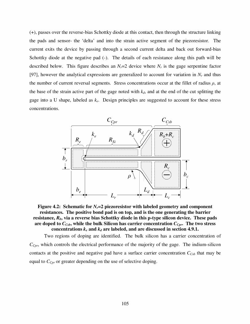
105
(+), passes over the reverse-bias Schottky diode at this contact, then through the structure linking
the pads and sensor- the ‘delta’ and into the strain active segment of the piezoresistor. The
current exits the device by passing through a second current delta and back out forward-bias
Schottky diode at the negative pad (-). The details of each resistance along this path will be
described below. This figure describes an Nr=2 device where Nr is the gage serpentine factor
[97], however the analytical expressions are generalized to account for variation in Nr and thus
the number of current reversal segments. Stress concentrations occur at the fillet of radius ρ, at
the base of the strain active part of the gage noted with kd, and at the end of the cut splitting the
gage into a U shape, labeled as ke. Design principles are suggested to account for these stress
concentrations.
Figure 4.2: Schematic for Nr=2 piezoresistor with labeled geometry and component
resistances. The positive bond pad is on top, and is the one generating the barrier
resistance, Rb, via a reverse bias Schottky diode in this p-type silicon device. These pads
are doped to CCsb, while the bulk Silicon has carrier concentration CCpr. The two stress concentrations ke and kd are labeled, and are discussed in section 4.9.1.
Two regions of doping are identified. The bulk silicon has a carrier concentration of
CCpr, which controls the electrical performance of the majority of the gage. The indium-silicon
contacts at the positive and negative pad have a surface carrier concentration CCsb that may be
equal to CCpr or greater depending on the use of selective doping.
br
Lc
LdLr
be
bc
Re RSi
Rd Rb+Rc
ρ
kekd
Rc
CCpr CCsb

106
4.4.2 Silicon Resistance
The strain active resistance in the sensor, Rsi, is calculated as shown in Eq. (4.1) [97],
where ρsi is the silicon resistivity, Lr is the length of the strain active segment of the piezoresistor,
br is the total width of the Nr number of arms all combined and hr is the thickness of the silicon.
2r r
si Si
r r
N LR
b hρ= (4.1)
The silicon resistivity is a function of several conditions including the bulk silicon carrier
concentration CCpr and the stress on the piezoresistor due to thermal expansion coefficient
mismatch with the substrate. Thermal stress appears to the piezoresistor as a two axis strain field
after the raised temperature cure. The resistance of silicon, represented by R, is altered by stress
in the silicon as shown in Eq. (4.2) [96]. The changes in resistance δR are due to two main
effects- longitudinal stress, shown with an ‘l’ subscript, and transverse stress, shown with a ‘t’
subscript. Longitudinal stress, σl, is parallel to the flow of current, while transverse stress, σt, is
perpendicular to the flow of current. The piezoresistive coefficients, πl and πt, describe the
material sensitivity to stress. This equation is used to calculate the effect of thermal stress on the
bulk silicon resistivity after curing to a substrate.
l l t t
R
Rπ σ π σ
∂= + (4.2)
The silicon resistivity (read out in Ω-m) is directly a function of CCpr, as shown in Eq.
(4.3), where αρ = -0.8026 and CCρ = 6.229x1013 cm-3. These values are calculated from
Thurber’s equation and the data presented by French et. al. [85]. A linear fit in log-log space is
used to capture the main trends. The piezoresistor with thermal expansion coefficient αsi is cured
to a substrate with thermal expansion coefficient αsub at elevated temperature ∆T above operating
conditions. The effect of the thermally generated strain field acting through Eq. (4.2) is captured
in the first part of the resistivity thermal coefficient αρT in Eq. (4.3), where υsi is the Poisson ratio
of silicon, El is the silicon Young’s modulus parallel to the current flow and Et is the silicon
Young’s modulus perpendicular to both the current flow and the wafer surface normal. The
piezoresistive thermal stress effect is attenuated by doping above ≈1017 cm-3, where αgf = 0.2014
and CCgf = 1.53x1022 cm-3 [40]. This is captured in the second part of αρT in Eq. (4.3).

107
( ) ( )
( ) ( )2
1 m
min 1, log1
Cpr
si T
C
Cgfsub si
T l t si l t l si t gf
si Cpr
CT
C
CE E E E
C
ρα
ρ
ρ
ρ
ρ α
α αα ν π ν π α
ν
= − ∆ Ω⋅
−= + + + ⋅ −
(4.3)
The piezoresistive coefficients are anisotropic with respect to crystal direction, and these
terms can be calculated as shown in Eq. (4.4), where π11 = 6.6x10⁻¹¹Pa-1, π12 = -1.1x10⁻¹¹Pa-1 and
π44 = 138.1x10⁻¹¹Pa-1 are fundamental material constants [95], <lc,mc,nc> is the normalized
direction of the current and <ls,ms,ns> is the normalized direction of the stress with respect to the
silicon crystal lattice. These terms allow for the longitudinal and transverse piezoresistive
coefficients to be calculated for any orientation.
( ) ( )( ) ( )
2 2 2 2 2 211 11 12 44
2 2 2 2 2 212 11 12 44
2l c s c s c s
t c s c s c s
l m m n n l
l l m m n n
π π π π π
π π π π π
= − − − + +
= + − − + + (4.4)
Parameters for common wafer orientations (100) and (110) are shown in Table 4.1, where
the current flow is normal to the flat in each case. Two stress vectors are listed for each wafer
type, the longitudinal stress (‘normal to flat’) and transverse stress (‘parallel to flat’), where both
stresses are in the plane of the wafer. The Young’s modulus in the direction of the stress is listed
[130] as is the gage factor for the current and stress combination in each row. The Young’s
modulus in the <112> direction is the same as that of the <110> direction [131]. The directions
are listed in specific vectors ‘[ ]’ instead of equivalent vectors ‘< >’ in order to show that the
wafer normal and the two stress vectors for each wafer form an orthogonal set. Either the
specific direction or the equivalent vectors may be used in Eq. (4.4) as long as the usage is
consistent.
Table 4.1: Silicon common orientations
Wafer Stress Vector Orientation vs Flat E (GPa) GF
(110) [-111] Normal 186.5 174.4
[1-12] Parallel 168.0 -74.87
(100) [011] Normal 168.0 120.6
[0-11] Parallel 168.0 -111.4
The gage factor is calculated for uniaxial stress as the product of the appropriate
piezoresistive coefficient and the Young’s modulus in the direction of the applied stress. A large

108
positive gage factor is observed when the current and stress are parallel, while a large negative
gage factor is observed when the current and stress are perpendicular. The (110) wafer
orientation was used for device design and fabrication in this research as it shows a larger
positive gage factor than the (100) wafer.
4.4.3 Contact Resistance
The contact resistance, Rc, encompasses the ohmic component of the indium-silicon
contact resistance. The contact resistance is calculated for both contact pads as shown in Figure
4.2, each assumed to be completely covered in indium solder, and combined into Eq. (4.5),
where ρc is the contact resistivity, bc is the width of the contact pad perpendicular to current flow,
Lc is the length of the contact pad parallel to current flow and Gl is the current crowding scaling
factor [98], [113]. The subscripts p/n stand for the positive and negative contact pads,
respectively. The contact resistivity is calculated from quantum mechanical first principles and
has been previously confirmed so for the sake of brevity it will not be rederived here. The
contact resistivity calculation requires a carrier concentration at the indium-silicon interface, for
which CCsb is used.
( ) ( )1 1
( )c c Csb
cn cn lncp cp lp
R Cb L Gb L G
ρ
= +
(4.5)
The current crowding scaling factor is generated by the finite resistance of the silicon
reducing the effect of bond pad area far from the initial current entrance side and is derived from
transmission line models. This expression includes both carrier concentrations. The silicon
contact pad has a resistivity determined by CCpr, while the ohmic contact resistivity is determined
by CCsb. A nondimensional pad length, rL, is used to calculate the current crowding scaling
factor in Eq. (4.6) and is calculated as the ratio of the real contact pad length over the
characteristic contact pad length, Lcc.
( )1 ( )tanh /
ccL
r c Csbl L L L c
si
h CG r r r L
ρ
ρ−= =
(4.6)
The effect of the current crowding scaling factor is shown in Figure 4.3 where the input is
the nondimensional pad length as calculated in Eq. (4.6) and the output is the nondimensional
ratio of the effective pad length Lce = LcGl normalized by the characteristic contact pad length.
The pad is too short for the current crowding effect to play a significant role in setting the contact

109
resistance when rL < 1, so Gl ≈ 1. The effective contact pad length then increases linearly with
actual pad length. The pad grows long enough for significant current reduction to be observed at
the end opposite the current entrance when rL > 1, so Gl < 1. This effect causes the effective
contact pad length to asymptote out to the characteristic contact pad length at rL >> 1. The net
effect of the current crowding effect is to reduce the utility of long contact pads. Minimal gain is
found past rL ≈ 1.5, so this is suggested as a design rule of thumb for setting the maximum
contact pad length.
Figure 4.3: Nondimensionalized scaling of current crowding effect with bond pad length.
The effective pad length (after considering the current crowding effect) is divided by the
characteristic pad length. Two asymptotes are noted and are shown with the dotted
lines. A suggested design limit is shown: rL<1.5, as minimal gains are to be had values above this cutoff.
4.4.4 Barrier Resistance
The barrier resistance, Rb, describes the non-ohmic reverse-bias Schottky barrier
component of the indium-silicon contact resistance, this occurs only at the positive pad for p-
type silicon devices as shown in Figure 4.2, and is calculated in Eq. (4.7). The barrier resistance
is composed of the barrier resistivity ρb, acting over the positive pad with its associated geometry
and current crowding scaling factor. This resistance exponentially decays with the ratio of the
voltage over the Schottky barrier, V, vs. the barrier voltage decay constant, Vτ. The barrier
0 0.5 1 1.5 20
0.5
1
1.5
2
Actual Pad Length rL
Eff
ectiv
e Pa
d L
engt
h L
ce /
Lcc
Eff. Lengthr
L << 1
rL >> 1
Design Limit
Lce = Lc
Lce = Lcc
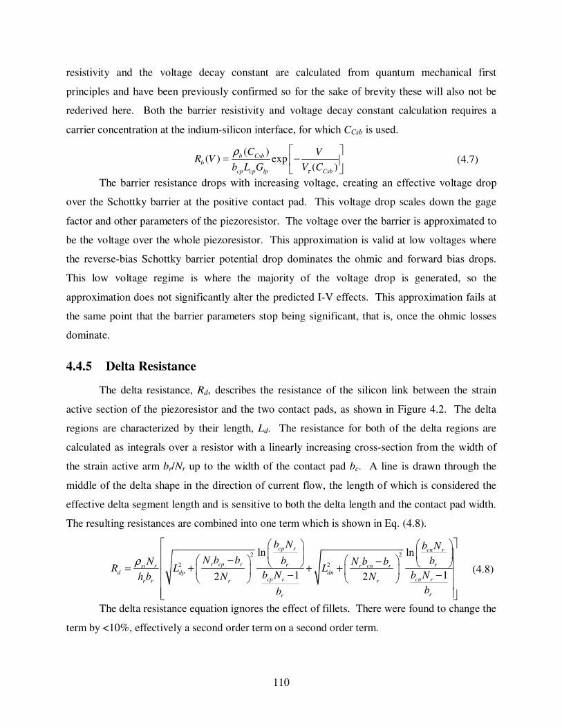
110
resistivity and the voltage decay constant are calculated from quantum mechanical first
principles and have been previously confirmed so for the sake of brevity these will also not be
rederived here. Both the barrier resistivity and voltage decay constant calculation requires a
carrier concentration at the indium-silicon interface, for which CCsb is used.
( )( ) exp
( )b Csb
b
cp cp lp Csb
C VR V
b L G V Cτ
ρ = −
(4.7)
The barrier resistance drops with increasing voltage, creating an effective voltage drop
over the Schottky barrier at the positive contact pad. This voltage drop scales down the gage
factor and other parameters of the piezoresistor. The voltage over the barrier is approximated to
be the voltage over the whole piezoresistor. This approximation is valid at low voltages where
the reverse-bias Schottky barrier potential drop dominates the ohmic and forward bias drops.
This low voltage regime is where the majority of the voltage drop is generated, so the
approximation does not significantly alter the predicted I-V effects. This approximation fails at
the same point that the barrier parameters stop being significant, that is, once the ohmic losses
dominate.
4.4.5 Delta Resistance
The delta resistance, Rd, describes the resistance of the silicon link between the strain
active section of the piezoresistor and the two contact pads, as shown in Figure 4.2. The delta
regions are characterized by their length, Ld. The resistance for both of the delta regions are
calculated as integrals over a resistor with a linearly increasing cross-section from the width of
the strain active arm br/Nr up to the width of the contact pad bc. A line is drawn through the
middle of the delta shape in the direction of current flow, the length of which is considered the
effective delta segment length and is sensitive to both the delta length and the contact pad width.
The resulting resistances are combined into one term which is shown in Eq. (4.8).
2 2
2 2
ln ln
1 12 2
cp r cn r
r cp r r rsi r r cn rd dp dn
cp r cn rr r r r
rr
b N b N
N b b b bN N b bR L L
b N b Nh b N N
bb
ρ
− − = + + + − −
(4.8)
The delta resistance equation ignores the effect of fillets. There were found to change the
term by <10%, effectively a second order term on a second order term.

111
4.4.6 End Resistance
The end resistance, Re, describes the resistive effect of the end segment of the
piezoresistor where the current reverses direction. The resistance is modeled as a block with
length equal to the circumference of a half circle trajectory exiting the center of one arm and
entering the center of the next, and with even current distribution as shown in Eq. (4.9). The end
width, be, is shown in Figure 4.2. This simple first order model is used because the end
resistance is a second order addition to the overall resistance so it is not necessary to precisely
capture the end effects. This provides a conservative estimate as the average current traversal
length will be below the πbr/(2Nr) term calculated below due to current crowding. The end
resistance occurs once for each current reversal, so scales with (Nr–1).
( )12
si r
e r
r e r
bR N
h b N
πρ= − (4.9)
4.4.7 Trace Resistance
The traces and other ohmic terms including wiring between the piezoresistor and the
bridge are included in the auxiliary resistance, Ra. These are assumed to be on the scale of <1Ω,
especially if thin aluminum traces (1µm thick, 800µm wide, 1cm long) are used to route current
around the surface of a titanium device. A safe upper bound on this resistance and that of the
conductive epoxy used to link the traces to the indium solder is ≈10Ω. This is the expected
method for creating electrical circuits on the surface of the metal MEMS using NLBM [94].
4.4.8 Overall Equation
The overall resistance of the piezoresistor, Rpr, is calculated as the sum of the component
resistances as shown in Eq. (4.10).
( ) ( )pr si c b d e a
R V R R R V R R R= + + + + + (4.10) The barrier resistance is the only voltage dependent term, where V is the voltage over the
whole piezoresistor. The rest of the terms are purely ohmic. The barrier and contact resistances
are functions of both CCpr and CCsb. The delta and end resistances are functions of only CCpr.

112
4.5 Electrical Performance
The current-voltage characteristics of the piezoresistor can be calculated from integrating
the net conductance over the voltage, as shown in Eq. (4.11).
1
0
(0)1( ) ( ) ( ) ln
( ) ( )
V pr
pr pr Csb
pr pr
RI V R v dv V V C
R R Vτ
−
= = − ∞ ∫ (4.11)
This expression is linearized around the operating voltage over the piezoresistor to
generate conventional electrical components- an effective voltage drop and an effective
resistance. The voltage dependent resistance is calculated from Eq. (4.10) and corresponds to the
line tangent to the I-V curve at the operating voltage. The barrier voltage drop, Vb, is calculated
by extrapolating this tangent line back to V=0, and is shown in Eq. (4.12). The voltage drop
asymptotically approaches a maximum value Vb0 as the barrier resistance decays to 0 at V > 5Vτ.
0
( ) ( ) ( )
(0)( ) ( ) ln
( )
b pr pr
pr
b b Csb
pr
V V V I V R V
RV V V C
Rτ
= −
= ∞ =
∞
(4.12)
4.6 Gage Factor
The equation for the piezoresistor effective gage factor is modified as shown in Eq. (4.13)
when the excess resistance and voltage drop are fed into a Wheatstone bridge model. The
voltage and resistance based adjustments to the gage factor are captured in two non-dimensional
adjustment factors, GV and GR. The resistance based adjustment has been implemented in
previous optimization efforts [41], [70].
( 2)min 1, log
( 2)
nV R
G G
n
CgfS b S siF l l gf
S pr S Cpr
CV V V RG E
V R V Cπ α
−= ⋅ ⋅ ⋅
(4.13)
The voltage adjustment factor describes the ratio of the usable voltage across the bridge
arm over the bridge source voltage. This captures the reduction in voltage due to the barrier
voltage drop. The resistance adjustment factor describes the ratio of the silicon sensitivity to
strain over the whole gage resistance sensitivity to strain. The resistance adjustment factor is
generalized in Eq. (4.14), where Rtot is the total resistance from contact pad to contact pad for the
gage. This includes any extra resistances in series and/or parallel with the piezoresistance.

113
tot sitot siR
tot si si tot
R RR RG
R R R R
∂∂ ∂= =
∂ (4.14)
The gage factor is the product of the appropriate piezoresistive coefficient and the
Young’s modulus in the stress direction. The longitudinal term, πl, is used for this design
process as this generate the highest gage factor of value 174.4 for (110) p-type wafers with the
current aligned <111>, normal to the flat. The current and stress are parallel in the longitudinal
term, and El is the silicon Young’s modulus in the stress direction. The gage factor is also a
function of doping [40], as described earlier in the silicon resistivity calculation. This effect is
captured by the last term in Eq. (4.13).
The resistive adjustment factor accounts for the excess non-strain active resistance in the
piezoresistor. It is calculated as the ratio of the strain active resistance over the total
piezoresistor resistance. The voltage adjustment factor accounts for the effective voltage drop
due to the reverse bias Schottky diode. It is calculated as the ratio of the effectively reduced
voltage over the Wheatstone bridge arm vs. the unaltered source voltage, VS. The exponent of n
accounts for the possibility of having either one (n = 1) or two (n = 2) semiconductor gages on
the same arm of the Wheatstone bridge. The operational voltage for both the resistance and
voltage drop is assumed to be VS/2.
The bridge balance resistance for a Schottky diode semiconductor gage provides the
designer with an extra degree of freedom, as the piezoresistor has a variable resistance. This is
only an issue when using an ohmic resistor for bridge balance. Good design practice is to
balance out a strain active piezoresistor with a non-strain-active duplicate in the same arm of the
bridge in order to cancel out thermal effects. The voltage across each piezoresistor is VS/2 if this
is done with semiconductor gages. The best bridge sensitivity when this is not possible is found
by matching the piezoresistor impedance at the operating voltage. The effect of varying the
bridge completion resistor is shown in Eq. (4.15) where Vo is the output voltage from the
Wheatstone bridge arm, Nε is the bridge strain type [97], and rRRpr(VS/2) is the bridge completion
resistance. This is only applicable when the semiconductor piezoresistor is matched with an
ohmic resistor. This means the bridges will not have semiconductor thermal balance
piezoresistors and cannot form certain types of half/full bridge configurations.

114
( )( )
2
4
1
BG
R
o S b F
R
rV V V G N
rε= −
+
(4.15)
The net effect of changing the impedance ratio rR is captured in the nondimensional
bridge impedance balance gain, GB, that attenuates the bridge sensitivity. The bridge impedance
balance effect can be brought to unity by holding rR ≈ 1, matching the piezoresistor impedance,
as is shown in Figure 4.4. The bridge will show the highest sensitivity to resistance changes in
the piezoresistor in this region, leading to the design rule of thumb of matching impedance.
Figure 4.4: Nondimensionalized scaling of bridge balance effect. The impedance ratio of
the bridge balace resistor / piezoresistor is shown on the x-axis. The maximum sensitivity
occurs in the region around unity.
A more complex tradeoff can be determined by reducing rR in order to raise the
piezoresistor operating voltage, Vpr, but this is not recommended as it introduces significant
complexity to optimization since there is not an analytical expression for the operating voltage.
The actual piezoresistor operating voltage can be found through Eq. (4.16), which generally must
be solved numerically except in the limiting case of rR = 1, where Vpr = (VS+Vb)/2.
( ) ( )S pr pr pr R pr pr
V V I V r R V= + (4.16) The optimization will generally use Vpr = VS/2, as this occurs with the good design
practice of bridge completion through piezoresistor duplication. This assumption also avoids un-
0 0.5 1 1.5 20
0.5
1
Impedance Ratio rR
Bri
dge
Sens
itivi
ty G
ain
GB
ScalingIdeal

115
necessary model complexity that provides little improvement to the optimization process
(typically ≈1dB).
4.7 Schottky Barrier Noise
The reverse-bias Schottky barrier produces flicker-like noise due to local mobility and
diffusivity fluctuations in the depletion zone of the diode [132], [133]. The forward bias
Schottky diode is ignored because the noise scales with R2 and the forward-bias diode resistance
is significantly larger than the reverse-bias diode resistance. The noise from the p-type indium-
silicon reverse-bias Schottky diode is shown in Eq. (4.17), which is derived from noise theory for
forward-bias, n-type wafers [132]. The theory is modified to work for holes as the dominant
carrier and under reverse bias. SVsb is the scaling factor to the frequency dependent term of the
noise, mdh* is the effective mass of holes, ≈1.15me, where me is the rest mass of an electron
[111], kB is the Boltzmann constant, T is the absolute temperature of the contact (K), εsi is the
permittivity of silicon, q is the charge of an electron, µh is the hole mobility in p-type silicon, and
φBi is the built-in Schottky barrier potential. The noise acts as a current source, Isb, across the
diode [132], and is transformed into voltage noise with the barrier resistance term. This term is
used as it describes the impedance of depletion zone area. The voltage across the barrier, Vbar,
exponentially determines the barrier resistance. The simple approximation of Vbar = Vpr works at
low voltages, when the dominant resistance is the barrier. This barrier resistance decays off to
insignificance relative to the ohmic resistances at higher voltages. The voltage equality
approximation is sufficiently accurate from an I-V perspective, as the error in barrier resistance
prediction only occurs when the barrier resistance is insignificant. The model does not work
from a noise perspective, as the barrier resistance continues to determine Schottky barrier noise
at all voltages. The voltage equality approximation (Vbar = Vpr) is instead replaced with Vbar =
Vpr-IprRpr(∞), which calculates the barrier voltage as the piezoresistor contact voltage less the
drop across the ohmic resistances. The equivalent circuit is shown in Figure 4.5.

116
Figure 4.5: Equivalent circuit model for Schottky barrier noise as a current source. The
voltage over the barrier resistance is attenuated by ohmic losses in the piezoresistor.
The flicker noise is scaled by the Hooge constant, αsb, which is experimentally
determined to be 0.257±0.001 for indium-silicon soldered contacts, with measurements shown in
the model validation section.
( )
2 3
2 3 3
( ) ( ( ) ( ))( )
12 ( )sb pr b pr pr B si
Vsb
h Csb dh Bi Csb
I V R V I V R k T qS V
C m C V
α ε
µ π ϕ∗
− ∞=
+ (4.17)
The hole mobility is calculated in Eq. (4.18), where µmin = 54.3 cm2V-1s-1 µ0 = 406.9
cm2V-1s-1, CCµ = 2.35x1017 cm-3 and αµ = 0.88 for p-type silicon at 300K [134].
( )10
h min
Csb CC C
µα
µ
µµ µ= +
+ (4.18)
The built-in potential describes the bending of the valence band (for p-type) from the
pinned end at a metal-semiconductor interface back to the unbent levels in the bulk
semiconductor. This potential is calculated as shown in Eq. (3.3).
The total reverse-bias Schottky barrier noise variance can be written in closed form as
shown in Eq. (4.19). The noise is integrated over the bandwidth of fmin to rfmin, where r is the
frequency band ratio of the software low pass filter cutoff frequency over the minimum
frequency fmin [97]. The δ term describes the variation of the Schottky barrier noise frequency
scaling from the typical flicker noise frequency scaling of 1/f, and is found to be 0.179±0.001 for
indium-silicon contacts with measurements shown in the model validation section. This
expression reduces to ln(r) as δ → 0.
21
( ) 1( )
min
min
rf
Vsb
Vsb Vsb
minf
S V rdf S V
f f
δ
δ δσ
δ
−
+
−= =∫ (4.19)
Rpr(∞)Vpr
Rb(Vbar)
Ipr(V)
Isb Vbar

117
4.8 Constraint-Based Optimization
4.8.1 Objective Function
The piezoresistor objective function as laid out for general ohmic, entirely strain-active
piezoresistance sensors (GV = GR = 1) [97] is altered in several places by the semiconductor-
based resistance and voltage adjustment factors. The gage factor term, Johnson noise, and
flicker noise are all adjusted, and the Schottky barrier noise is added to the dominant sources.
This modified objective function is shown in Eq. (4.20) where σysub is the yield stress of the
substrate, GSG is the strain geometry scaling factor, GSTC is the span temperature compensation
scaling factor, η is the substrate safety factor, Esub is the Young’s modulus of the substrate, M is
the multi-sensor noise attenuation factor, B is the resolution bandwidth accounting for first order
low pass filter rolloff at frequency rffsig, fsig is the signal upper frequency limit (device
bandwidth), rf is the frequency ratio of the filter frequency vs fsig, fmin is the lower bound
frequency (0.1Hz), and SVai is the noise power spectral density in of the instrumentation
amplifier. These terms are defined in the standard optimization framework [97]. The noise
bandwidth is based on the conservative definition of total noise, scaling from the lower bound
frequency fmin up to the low pass filter.
( )
2
1 22
4 2
4 1 14
1ln ( 2)
4 4 4
4
1 where2
ysub F SG S STC pr VB si
sub R
pr prS siV R Vai Vsb S
Cpr r r r min
pr ext
f sig
min
min
N G G V G N GSNR k TBR
E G
N NV rr G G S B S V
C L b h f
N N N
r fB r f r
f
ε
δ
δ
ε
σ
η
α
δ
π
−−
= + −
−+ + +
= +
= − =
M…
(4.20)
The noise terms are scaled by the number of semiconductor piezoresistors in the bridge,
Npr, which is the sum of the number of strain active piezoresistors and the number of extra
identical piezoresistors added for thermal balance, Next. The non-semiconductor piezoresistors
are assumed to be low excess noise standard ohmic resistors.
The Johnson noise is scaled to account for the non-linear resistance of the piezoresistor,
with the ohmic R in the noise variance replaced with R2I/V [135]. This can be rewritten in terms

118
of the resistance and voltage adjustment factors, returning it to the standard form of R but with
the adjustment factors included. This modified term applies only to the semiconductor
piezoresistors, the normal ohmic resistors produce unmodified Johnson noise.
The flicker noise is scaled by both the number of semiconductor piezoresistors and to
account for the reduced voltage over Rsi, the strain active section of the piezoresistor. Both the
voltage drop and the excess resistance in the piezoresistor act to reduce this voltage, and these
effects are captured in the adjustment factors. The flicker noise in Rsi dominates over the flicker
noise in the other silicon resistances as this is the section with the highest resistance, it has the
largest voltage drop combined with the smallest volume. Both of these effects boost the flicker
contribution from Rsi to dominate the noise calculation.
The Schottky barrier is included as introduced in Eq. (4.19), with the operating voltage
assumed to be VS/2 as described in the bridge balance section. This noise scales with the number
of semiconductor piezoresistors.
The most important use for the resistance and voltage adjustment factors is in the gage
factor calculation, as the optimizer with the adjusted gage factor will be able to account for the
Schottky barrier effects and optimize correctly. The addition of the noise adjustment factors help
to improve the optimizer accuracy, on the scale of ≈2-3dB.
4.8.2 Constraints
The power dissipation calculation is altered by the use of semiconductor piezoresistors
with excess resistance and voltage drops. These effects both attenuate the current flowing
through the device, lowering the power dissipation. The effect can be captured via the voltage
and resistance adjustment factors, as shown in Eq. (4.21), where Ppr is the power dissipated at a
semiconductor piezoresistor, Pmax is the maximum permissible full bridge power dissipation and
VPmax is the voltage upper limit introduced by power constraints, in the same form as in the
standard piezoresistor optimization [97].
22
2
4S
pr V R
si
max siPmax
V R
VP G G
R
P RV
G G
=
=
(4.21)

119
The voltage limit is calculated by assuming the bridge is entirely composed of
semiconductor piezoresistors and calculating the voltage at which Pmax is reached. This is done
because the typical use of the power constraint is to set a limit on the power generated at the
piezoresistor itself or on the flexure. The piezoresistor limit case is calculated by scaling the
piezoresistor power limit Pprmax up to the full bridge scale, so Pmax = 4Pprmax. The flexure limit
case is calculated by scaling the flexure power limit Pfmax by the number of strain active
piezoresistors, all of which are on the flexure, so Pmax = Pfmax/Nε. This scaling is to standardize
the definition of Pmax so that it can be used in general constraint expressions like Eq. (4.21).
Doping constraints can be introduced to the design space based on the practical limits of
1012cm-3 on the low end and 1021cm-3 on the high end [136]. The Schottky barrier carrier
concentration can further be constrained; if no contact pad doping is included, CCpr = CCsb, or if
contact pad doping is allowed, CCsb ≥ CCpr.
Fabrication limits for small gages may be used including gage aspect ratios, setting an
upper limit on the strain active segment length, Lr, divided by width, br/Nr. This avoids
producing excessively fragile structures during fabrication.
4.8.3 Resistance Variation
The standard resistance variation chart shows how the performance of the system is
affected by variations in the gage resistance [97]. The generation of this chart is altered in
several ways by the introduction of semiconductor gages, including the use of a more general
noise sensitivity calculation and the addition of an extra term for the Schottky barrier flicker
noise. The individual noise source limits must be calculated by rewriting the expressions in
terms of VS and Rsi. This change is implemented in Eq. (4.10) where the full expression for the
strain active piezoresistance is replaced simply by Rsi. The functional dependence on Rsi can be
propagated through the calculations, changing Ipr, V0, GV, GR, and SVsb to be functions of VS and
Rsi. The functions of flexure and piezoresistor geometry variables, like GSG, are not altered. The
bridge voltage may be made a function of Rsi by imposing the voltage and power constraints as
shown in Eq. (4.22), which finds the lower limit on voltage for each gage resistance.
20 0
( ) min ,( , ) ( , )
max siS si max
V S si R S si
P RV R V
G V R G V R
=
(4.22)

120
The dynamic range limitation for each of the dominant error sources can now be
calculated as a function of the variable Rsi only, by using the process described above and Eq.
(4.22). This enables the resistance variation chart to be plotted for each of the main noise
sources. The voltage and resistance adjustment factors in Eq. (4.22) are calculated using the
optimized bridge source voltage value, VS0, to avoid generating a self-referential calculation.
The accuracy of this calculation is thus greatest when Rsi approaches the optimized value, which
is also the area of greatest interest in the resistance variation plot.
4.9 Secondary Geometry
Several factors of the piezoresistor are not subject to calculation through the optimization
process laid out previously; these include the stress concentrations on the piezoresistor and the
creep in the epoxy.
4.9.1 Stress Concentrations
The main stress concentrations occur at two locations, at the current reversal end on the
piezoresistor (labeled as ke in Figure 4.2), and at the joint where the strain active segment begins
to expand into the delta segment (labeled as kd in Figure 4.2). The gage end stress concentration
is set by the kerf width of the laser forming the gage geometry [94], this is approximately 50µm
after etching to remove laser damage, for which FEA simulations predict ke = 1.5. The delta
stress concentration shows sensitivity to the beam width, br/Nr, and the delta fillet radius, ρ.
Devices of multiple beam widths (100µm, 200µm, and 470µm) were simulated and found to
produce an overlapping trend, as shown in Figure 4.6, if a geometric radius ratio, rρ, is defined as
shown in Eq. (4.23), where ckd = 0.4, and both the radius and the piezoresistor width are in
microns. The stress concentration factor follows a power law reduction in magnitude with
relation to the radius ratio as shown in Eq. (4.23), where akd = 2.63 and bkd = -0.570.
( )( )
1 kd
kd
b
d kd kd kd c
r r
k a r rb N
ρ= + = (4.23)
The error in the linear fit is <8% for 1<rρ<300, which covers the common range of
acceptable stress concentration factors. The radius ratio is defined in order to show how to scale
the relative dimensions while maintaining a constant stress concentration factor.

121
Figure 4.6: Scaling of the kd stress concentration with ratio rρ, showing a reducing trend
with larger rρ. The fit is most accurate in the region of kd = 1.1-2, which is the expected
operating region. Piezoresistors with several different beam widths (100, 200, 470µm) were simulated and found to all lie on roughly the same line.
The piezoresistor lies on a linearly decreasing strain field, meaning that the tip is
subjected to less strain than the base. This effect is captured by the nondimensional strain gain
terms ge, and gd for the end and delta stress concentrations, respectively. These terms define the
reduction in strain from the maximum value at the base of the flexure to the location of the stress
concentration. The end strain gain is typically about 2/3-1 since the piezoresistor is often
optimized to extend over about 1/3 of the flexure volume when flicker noise dominates [40],
[97]. The delta strain gain is typically about unity as it is located directly over the base of the
flexure.
Good design practice for the stress concentration suggests designing to match the
maximum stress at the two locations, so geke = gdkd. This can be used to calculate the required
delta stress concentration factor (typically 1.25), as the end stress concentration factor is fixed.
The radius ratio may be calculated with Eq. (4.23), to be ≈60. This gives a simple means to
determine how to scale the fillet radius ρ with the piezoresistor arm width.
100
101
102
103
10-1
100
Radius Ratio rρ
Stre
ss C
once
ntra
tion
Fact
or k
d-1
100µm200µm470µmFit

122
4.9.2 Epoxy Creep
Creep is known to occur in cured gages due to the viscoelastic properties of epoxy [137–
140]. This was a major issue for early strain sensing devices [140], leading to the focus on
implanted gage design for silicon devices. While epoxy technology has improved, creep is still a
consideration for gage design. Creep is known to be sensitive to several parameters, including
gage temperature, gage length, glue line thickness and epoxy cure temperature [137–139]. Gage
thermal stability was found to be a good indicator of creep resistance, as the gage is heated above
its maximum power, the creep effects become more significant [137]. The mechanism for this
variation is believed to be heating of the epoxy. Gage length is observed to be related to creep
resistance, longer gages appear to show reduced creep effects [104]. This is consistent with the
creep being dependent on the stress within the epoxy. Thicker glue lines are associated with
higher creep effects [137], which is why transducer quality gage cures are typically done with
high pressure. The epoxy cure temperature is known to play a role in determining creep effects,
as higher temperatures cure epoxies typically displace increased creep resistance [137], [138]. A
The characteristic time scale of creep effects for well cured epoxy has been measured at around
≈106min [138]. The strain scale for creep in well cured gages has been observed to be in the
scale of a few 100µε [139].
Best practices can be suggested from these characteristics. The gage should not be
operated above its power limit, and if creep is of particular concern, it should not be operated
close to the power limit. The gage length should be designed to provide as much length as
possible to distribute the stress through the epoxy. This can be accomplished by extending the
length of the end resistance segment of the gage, shown on the far left in Figure 4.2. The contact
pads should provide sufficient area on the base side, while an increased end area should anchor
on the flexure side. The glue line should be minimized by curing at the recommended pressure
of ≈250kPa. Finally, the epoxy should be cured at the recommended cure temperature if at all
possible. All of these effects should reduce creep down to minimal levels that can be accounted
for with a device rezeroing on monthly intervals. The monthly time scale is chosen as it is about
a decade faster than the characteristic creep time. Creep effects were found to occur in the
absence of gage power [139], so the total gage age is expected to be the conservative indicator
for rezeroing.

123
4.10 Model Validation
4.10.1 Device
A single piezoresistor was fabricated using the NLBM method of laser patterned silicon
stamped onto a titanium 6Al4V substrate [94], in order to confirm the piezoresistor model
described above. The piezoresistor was cured to the titanium with Vishay Micro-Measurements
M-Bond 600 epoxy under 240kPa pressure and at 150°C. This produced an approximately 9µm
thick glue line. The piezoresistor was connected to the Wheatstone bridge circuit with indium
soldering at the contact pads, then it was covered in a <50µm layer of Vishay Micro-
Measurements GageKote 8, an air dry acrylic coat intended to protect the gage.
A p-type (110) silicon wafer with a carrier concentration of 2.8x1017cm-3 was used for the
piezoresistor. This doping level was suggested by the constraint based optimization described
above. The geometry and parameters are as described: br = 1mm, hr = 31µm after etching, Lr =
5.47mm, be = 1mm, Ld = 1mm, bc = 2mm, Lc = 3mm. A large resistor width was chosen in order
to facilitate the fabrication process. The substrate flexure was fabricated to length Lf = 16.19mm,
width bf = 6.23mm and thickness hf = 0.75mm. The completed gage and substrate are shown in
Figure 4.1.
4.10.2 I-V Performance
A four-point probe setup was used to measure the I-V curve of the piezoresistor. The
device was loaded up to 20V potential to anneal the reverse-bias Schottky barrier in order to
improves its performance, then the descending I-V chart was recorded and is shown in Figure
4.7.

124
Figure 4.7: I-V performance of fabricated semiconductor piezoresistor.
The data shows a slight offset from ohmic behavior due to the exponential barrier
resistance. This effect appears as a constant voltage drop by about 5V. The best fit line for the
model was found to occur with a bonding parameter, β = 1.28, which describes the fabrication
variability in the process. Self-heating was observed to occur starting at around 9V, which is on
the scale of 80mW. The self-heating effect becomes significant by about 200mW, at which point
the bridge resistances started to show low pass filter-like dynamics. The predicted electrical
parameters were generated via the measured bonding parameter and are in close agreement
(≈10%) with the measured parameters as shown in Table 4.2.
Table 4.2: I-V parameters
Parameter Predicted with β Measured Error (%)
Rb(0) 825 819±41 0.73
Rohmic 993 969±48 2.5
Vτ 1.70 1.94±0.09 -12
Vb0 1.02 1.19±0.02 -14
4.10.3 Gage Factor
The test device was placed in an Instron 5869 Test Frame and the gage factor was
measured. The frame used a 1kN load cell with 2.5mN resolution to drive the flexure, while the
0 5 100
5
10
15
Voltage (V)
Cur
rent
(m
A)
MeasuredFit
Self Heating

125
resistance change in the piezoresistor was measured with a low noise Wheatstone bridge using an
AD624 instrumentation amplifier set at G = 100 [97]. The flexure was driven to 100µε, about
1.3% of yield, in order to observe the small scale gage factor. The gage factor is expected to be
nonlinear in this doping range. The theory assumes small deflections [40], [95], so the small
scale motion is of main interest. The results of this test are shown in Figure 4.8.
Figure 4.8: Measured gage factor for piezoresistor test device.
The resistance change and strain are derived from components of the general gain
equation as shown in Eq. (4.24) [97]. The measured force, F, is translated into effective strain,
εeff, via the flexure force to strain gain, εF, while the measured voltage output from the bridge V is
translated into fractional resistance change ∆R/R.
( )
eff
R R
F SG F
S STC
VF G G
N V G G
ε
ε
ε
∆
=
(4.24)
The gage factor of the device was measured to be 116±2, with a 3rd order term of
9.68±2.73x10⁸ which accounted for about 8% variation from linearity at 100µε. The model
predicts a gage factor of 117, which lies within the error bars of the measurement.
4.10.4 Maximum Strain
The maximum strain was determined through tension tests of the wafer material attached
to a titanium substrate via the NLBM process. The (110) wafer samples were found to fail at
2.2±0.2mε, while (100) wafer samples were found to fail at 2.5±0.1mε. These failure strains
0 20 40 60 80 1000
5
10
15
Strain (µε)
Piez
ores
istiv
e ef
fect
( ∆R
/Rx1
03 )
MeasuredNonlinear FitPredicted

126
were calculated by subtracting out the 0.75mε of thermal strain induced by the 150°C cure to
titanium. The net limit when considering the thermal strain is ≈ 3mε. This is about 40% of the
titanium yield strain, which is higher than standard engineering practice would suggest operating
a flexure system. Good design practice for flexures is typically to operate with a safety factor of
≈3-4, which would mean the gage should not be limiting the maximum flexure strain.
4.10.5 Noise
The test device was placed in a Faraday cage and linked to the Wheatstone bridge with
shielded wiring. The same bridge circuit was used as in the gage factor tests, and it was allowed
to thermally equilibrate for 30min before measuring the sensor noise. The bridge output was
recorded for 10sec at 50kHz. The power spectral density was calculated of the detrended
measurements, and is shown in Figure 4.9, with the fit line corresponding to αsb = 0.257±0.001
and δ = 0.179±0.001 in Eq. (4.19). The Schottky barrier Hooge constant is in the same range of
values, 100-10-3, as observed for hole flicker noise in n-type Chromium diodes in reverse bias
[133].
Figure 4.9: Measured gage factor for piezoresistor test device, with the Schottky barrier
noise fit line shown.
The noise spectral density was smoothed for the ith value with an expanding filter that
averages all values in the range i-w(i) to i+w(i), where the half-width, w(i), is calculated as
shown in Eq. (4.25). The filter is designed around the fact that the frequency variation of noise
10-1
100
101
102
103
10410
-9
10-8
10-7
10-6
10-5
10-4
10-3
10-2
Frequency (Hz)
Spec
tral
Den
sity
(V2 /H
z)
MeasuredFit

127
power spectral density is fairly constant, so nearby frequencies should share similar spectral
densities. A symmetric filter cancels out any net linear trends, and captures the value
characteristic of the frequency region. This works well for identifying large trends, but may
disguise sharp spikes. A weighted average would help the filter capture such features. The half-
width starts at 0 at low frequency, then expands with power p = 0.2 in order to capture the
increase in logarithmic variation found in sequential values. The scaling factor K = 6 is then
used to evenly change the width of the noise over all frequencies. The frequency is normalized
by the measurement characteristic frequency, fm, which is the inverse of the measurement time.
( )( ) = floor 1
p
m
f iw i K
f
−
(4.25)
4.10.6 Resistance Variation
The measurement of the noise and gage factor provides sufficient information to draw up
a resistance variation chart for the fabricated piezoresistors, assuming fmin=0.1Hz, fsig=1kHz,
rf=10. This is shown in Figure 4.10, where the main noise components are the piezoresistor
Johnson noise (PR J), the instrumentation amplifier noise (IA), the piezoresistor flicker noise
(PR F), and the Schottky barrier flicker noise (SBF). The Schottky barrier noise dominates over
the whole plotted range of resistances. Significant gains up to about 125dB over a 10khz sensor
bandwidth could be found by reducing the Schottky barrier noise. Two methods of doing so are
described below, increased contact pad doping and increased bridge voltage. The noise trend
also indicates that an increased resistance would produce a slightly higher overall performance.

128
Figure 4.10: Resistance variation chart for fabricated gage, showing the four main noise
sources, piezoresistor johnson (PR J), flicker (PR F) noise, instrumentation amplifier
noise (IA), and Schottky barrier (SB F) noise. The actual gage resistance is shown at
756Ω.
4.11 Discussion
The semiconductor piezoresistor model described in this paper is shown to predict the
performance and to capture the dominant physics of the piezoresistor. The performance bounds
of these NLBM-fabricated semiconductor piezoresistors can be studied by varying some of the
important parameters underlying the gage performance. The present fabrication process is
captured with the following parameters: minimum br/Nr = 150µm, cure temperature of 150°C, β
= 1.28, and otherwise the same dimensional limitations as the fabricated test piezoresistor. The
optimization process designs the best possible gages for a mesoscale titanium fixed-free flexure
with Lf = 10mm, bf = 600µm, and hf = 600µm. The sensor system is modeled with the following
parameters: Vmax = 10V, Pprmax = 80mW, fsig = 1kHz, rf = 10, fmin = 0.1Hz, Nε = 0.25, and a
matched strain-inactive semiconductor piezoresistor on the Wheatstone bridge arm, so Next = 1.
The doping limits are set at CCpr > 1016cm-3 in order to ensure stability in the bonding parameter,
with an upper limit of 1021cm-3 due to doping limitations [136]. The Schottky barrier carrier
concentration is varied relative to the bulk silicon carrier concentration.
101
102
103
104
105
40
60
80
100
120
140
160
180
Piezoresistor Resistance Rsi
(Ω)
Dyn
amic
Ran
ge (
dB)
TotalPR JIAPR FSB F
Actual Resistance

129
4.11.1 Trends in Optimization
The bulk silicon carrier concentration was varied over the full range in order to determine
the effect on sensor performance, as shown in Figure 4.11. The Schottky barrier carrier
concentration was held at two levels, either high doping where CCsb = 1021cm-3, or undoped,
where CCsb = CCpr. The optimal gage performance occurs between 1017 and 1018cm-3 when the
contact pads are highly doped. This is similar to the performance of commercial piezoresistors.
For undoped pads, the Schottky noise drives performance and the piezoresistor performance rises
rapidly with carrier concentration once past about 1019cm-3. This starts around the point where
the power limit is reached, shown by Rx, the crossover resistance transition, at which point the
bridge voltage starts to fall. The noise voltage sensitivity was studied by considering two bridge
limits, 10V and 20V. The 20V case shows about 5dB higher performance at low doping. This is
due to the exponential voltage sensitivity of the Schottky barrier resistance, but the effect is
reduced by the ohmic potential losses in the gage absorbing most of the voltage increase. This
case approaches the ideal piezoresistor performance around 1020cm-3.
Figure 4.11: Scaling of sensor performance when bulk silicon carrier concentration is
allowed to vary. The ideal case of highly doped (1021
cm-3
) Schottky barrier contacts
forms the upper bound solid line. Piezoresistors with undoped Schottky barriers are
shown in two conditions, 10V and 20V bridge voltage. The transition from voltage to
power limit is labeled for both lines by the Rx transition. Below this, the gages are Vmax limited, above this they are Pmax limited.
The Schottky barrier noise can be clearly seen to dominate in the undoped contact pad
case. The optimal bulk silicon carrier concentration is approximately 6x1017cm-3 if contact
1016
1017
1018
1019
1020
1021
60
80
100
120
140
Silicon Carrier Concentration CCpr
(cm-3)
Dyn
amic
Ran
ge (d
B)
10V, CCsb
=1021
20V, CCsb
=CCpr
10V, CCsb
=CCpr
Vmax limited
Pmax
limited
+ Vmax
Rx
transition
Optimal CCpr
130
doping is possible. Two methods are suggested for doing so. Doping could be integrated into
the fabrication process via spray on dopants before the wafer is diced into stock [129]. Spray on
dopants could be could be applied in small batches and adjusted for different designs, retaining
the general goals of the NLBM process. The alignment for this would have large tolerances, as
the bond pads are separated from the piezoresistive region by ≈1mm. A second option for
contact pad doping would be to use electrical discharges to locally inject boron dopant into the
wafer surface, as has been previously demonstrated [106]. Electrical discharge doping could be
carried out at low temperatures once the gage is cured to the substrate, a step which would be
easily integrated into the NLBM process. The performance gains from such contact pad doping
is shown in Figure 4.12, where CCpr = 6x1017cm-3. The Schottky barrier carrier concentration is
studied from the bulk silicon levels up to degenerate levels, at which point a performance plateau
is observed. Significant gains of ≈60dB over a 10kHz sensor bandwidth can be found from
selectively doping the contact pads, as the dominant noise source transitions from the Schottky
barrier to the Johnson and instrumentation amplifier noise at CCsb ≈ 1020cm-3. The bridge source
voltage reduces noise by about 5dB, consistent over the full doping range of the device.

131
Figure 4.12: Scaling of sensor performance when the bulk silicon carrier concentration
CCpr is held to the optimal level for sensing, and the Schottky barrier contact carrier
concentration CCsb is allowed to vary. The increase in CCsb is associated with a reduction
in both the scale of the noise and the barrier resistance. The Schottky barrier noise ceases to be the dominant noise source at ≈10
20cm
-3.
4.11.2 Advantage of NLBM-Fabricated Semiconductor Piezoresistors
The power constraint on NLBM fabricated piezoresistors can exceed that of other
semiconductor piezoresistors (20-50mW) [128] due to the larger contact area of the sensor.
These large contact pads to enable a greater heat transfer out of the device, providing thermal
stability despite higher heating loads. The increased power limit provides a crucial performance
boost, as performance scales with √Pmax [97]. With proper piezoresistor geometry and contact
pad doping, the NLBM fabricated gages show the potential to outperform similarly sized
commercial gages by anywhere from 4-12dB. Custom NLBM fabricated gages can be fabricated
down to smaller gage widths and thus onto smaller flexures than commonly available with
commercial gages because of the need to directly handle commercial gages vs. the stamp-based
handling in NLBM. Custom fabrication also allows for geometric optimization to each device
with such specializations as: linked multi-gage bridges, extreme aspect ratios, negative gage
factor piezoresistors, and tunable resistance to achieve the performance suggested by the
constraint-based optimization process [97].
1017
1018
1019
1020
1021
60
80
100
120
Schottky Carrier Concentration CCsb
(cm-3)
Dyn
amic
Ran
ge (
dB)
20V10V
Bulk Silicon CCpr

132
4.11.3 Generalization
The model presented in this paper is extensible to piezoresistors with non-Schottky
barrier-based voltage drops and excess resistance. The voltage and resistance adjustment factors
capture these effects whether they are due to diode behavior or other causes. The adjustment
factors have been comprehensively mapped to the dominant noise sources and objective function
used for constraint-based optimization. This mapping will help designers determine the
performance tradeoffs for even purely ohmic metal gages with excess resistance.
Indium was used in this research to create a low temperature interface to silicon; however
this process could be adapted to a new interface metal with the change of only a few parameters.
The intrinsic Schottky barrier height and oxide thickness variation with carrier concentration
would be required to calculate the barrier resistance. The ohmic contact resistivity variation with
carrier concentration would be required to calculate the contact resistance. Finally, the Hooge
noise constant for the Schottky barrier would need to be measured for the material and
processing conditions. The remainder of the parameters and calculations are generalizable.
4.12 Conclusion
In this work we formulate the modeling theory required to design and optimize
piezoresistors with Schottky diode contacts. We show how this theory enables the design of
piezoresistors which utilize low-temperature solder contacts. The performance of these sensors
are explored using optimization algorithms, and are shown to have potential dynamic ranges ≈
125dB over a 10kHz sensor bandwidth, exceeding that of commercial gages by upwards of 12dB
due to higher power limits. This modeling and optimization will allow for the creation of low-
cost customizable nanopositioning architectures with integrated position sensing, fabricated with
NLBM. The nanopositioning architectures will open opportunities for advancements in several
fields including nanomanufacturing R&D, multi-axis AFM, and advanced memory
storage/computing structure fabrication.
A demonstration semiconductor piezoresistor was fabricated and shown to have a gage
factor of 116±2, within 1% of the gage factor predicted by the modeling theory. The Schottky
barrier noise was measured and found to be flicker-like noise with exponent 1.179±0.001, and a
Hooge constant of 0.257±0.001, in the range of previously reported values. Optimization
parameters are presented for the generalized design of semiconductor piezoresistors with indium

133
soldered contacts. Contact pad doping performance thresholds are described for a range of
conditions, and the sensor full noise dynamic range limits are found to be around 126dB for a
quarter bridge 10kHz bandwidth sensor on a 600µm wide titanium MEMS flexure. The small
size and high potential dynamic range of the NLBM-fabricated piezoresistors makes them ideal
for meso-/micro-scale flexural positioners.
This work indicates that the inclusion of a small-batch design-flexible doping process to
NLBM could significantly (≈60dB over a 10kHz sensor bandwidth) improve the performance of
NLBM fabricated semiconductor piezoresistors. Two main methods are suggested for doing so;
utilizing spray-on dopants before the wafers are separated into piezoresistor stock or utilizing
electrical discharge doping after the piezoresistors are cured to the substrate. These methods
merit further study to determine whether they can be cost-effectively integrated into the NLBM
process flow.

134

135
CHAPTER
5 NON-LITHOGRAPHICALLY-BASED
MICROFABRICATION
5.1 Section
This chapter will describe the fabrication process used to create both the sensors and the
nanopositioner. Fabrication issues encountered at the boundary between macro- and micro-
fabrication are discussed, and the solutions are presented. The capabilities of the NLBM process
are demonstrated with the fabrication of a Hexflex with integrated sensing.
A process flow is described for the low cost, flexible fabrication of metal MEMS with
high performance integrated sensing. The process is capable of producing new designs in
≈1week at an average unit cost of <$1k/device even at batch sizes of ≈1-10, with expected
sensing performance limits of about 135dB over a 10khz sensor bandwidth. This is a ≈20x
reduction in cost, ≈25x reduction in time, and potentially >30x increase in sensing dynamic
range over comparable state-of-the-art compliant nanopositioners. The non-lithographically
based microfabriction (NLBM) process is uniquely suited to create high performance
nanopositioning architectures which are customizable to the positioning requirements of a range
of nanoscale applications. Customized positioning platforms can significantly reduce the cost of
nanomanufacturing research and development, as well as accelerate the development of new
processes and the testing of fabrication process chains without excess capital investment.
A 6-DOF flexural nanopositioner was fabricated using the newly developed process
chain. The integrated strain sensing was demonstrated to be capable of capturing 6-DOF
motions of the positioner stage. The fabrication process was measured to have ≈10µm
alignment. Sensor arm widths down to 150µm, flexure widths down to 150µm and trace widths
down to ≈100µm were shown to be feasible with this process. 59dB dynamic range sensing was

136
demonstrated for the nanopositioner over a 10kHz sensor bandwidth. Improvements are
proposed to reach performance in excess of 135dB over a 10kHz sensor bandwidth. This sensor
performance is generally in excess of presently available kHz-bandwidth analog-to-digital
converters [54].
5.2 Introduction
This work demonstrates a process flow of non-lithographically based microfabrication
processes (NLBM) which can be used to fabricate metal MEMS with integrated sensing, and do
so in small batches (<10 devices) with low average device cost (<$1k/device). This will allow
for low-cost customizable nanopositioning architectures with integrated position sensing to be
created [94] for a range of micro-/nano- manufacturing and metrology applications. Customized
positioning platforms can surmount one of the main hurdles to nanomanufacturing research and
development [5], as well as enable further developments in personalized medicine [3], parallel
AFM metrology [141], and advanced memory storage [6] by significantly reducing setup cost.
This will accelerate the testing and development of new processes like parallel DNP tip arrays
[5]. It will also aid in the testing of fabrication process chains without excess capital investment,
an active area of micromanufacturing research [32].
5.2.1 Motivation
MEMS positioning require integrated sensing to take full advantage of miniaturization.
Without sensing of commensurate scale and fabrication, the required metrology frame can
dominate the device in both size and cost. Laser interferometry can run to ≈10k/axis [28] and
can occupy a meter scale footprint [142]. Integrated sensing bypasses these size and cost issues
by operating within the device footprint and utilizing similar fabrication processes, with typically
similar costs to the device fabrication. Such integrated sensing generally requires nm to µm
scale electrical structures to be created on the MEMS device. A range of transducers are used in
MEMS, including piezoresistive [1], [15], capacitive [15], electrothermal [143], and
piezoelectric [144].
A fabrication process for feasible, customizable, meso-scale MEMS nanopositioners
must be able to meet several requirements in order to produce a device with integrated sensing: i)
bulk micromachine µm to mm scale mechanical structures out of robust materials like metals, ii)

137
surface micromachine nm to mm scale electrical structures on the surface of the mechanical
structure, and iii) do all of this at low device and production cost per device. The cost constraint
is imposed due to the low volume of devices typically required for the applications described
above. Batch sizes of <100 are typical of research and development. Standard MEMS
fabrication processes cannot feasibly access this region [19] due to the high capital costs and low
process flexibility. No established fabrication process chain can simultaneously meet all of the
requirements laid out above, so NLBM was developed to access this regime. Traditional
fabrication can produce mm and larger scale parts, and do so out of many different materials.
The wide range of material choice gives designers the freedom to find the material that is best
suited for the application- in this case a robust material that can sustain handling, attachment of
payloads, scratches and prolonged use. These processes are however unwieldy for putting down
multi-layer surface features. Integrated circuit-based MEMS microfabrication can produce
structures over the correct size scales, however it has significant limitations in the material
selection as bulk microfabricated mechanical structures are typically made from crystalline
materials [96]. IC microfabrication has been used to create micro- and meso- scale
nanopositioners, however it results in high costs (≈$20k just for equipment costs), long
fabrication times (≈6 months) and brittle structures that are unsuited for general operation [1].
Some early work has been done on titanium IC microfabrication [145], however this remains
infeasible from a time/cost investment perspective. The relative merits of conventional macro-
scale fabrication and IC based MEMS lithographic fabrication methods are shown in Table 1.2
but repeated in Table 5.1 for convenience.
Table 5.1: Comparison of fabrication methods
Requirement Capability Macro-scale Fabrication
MEMS Lithographic Fabrication NLBM
Mechanical Structures
Bulk micromachining
Electrical Structures Surface
micromachining
Robust Material Metals, polymers Low Avg. Cost in
small batches <$1k/device
Neither fabrication process alone meets all of the requirements for the creation of a
customizable low-cost per device MEMS nanopositioner with integrated sensing. A hybrid

138
process is needed to draw from the strengths of each of these in order to make a feasible
fabrication process chain.
A range of non-lithographically based fabrication processes have shown the potential to
meet all of the conditions described above [8], [43]. But these cannot be presently integrated
together due to fabrication incompatibilities. Previous work has been done on bulk
micromachining of metal mesoscale structures [8], [32], [46–49] and this work has shown
micromilling to be an accurate and effective method of creating µm to cm scale structures.
Surface micromachined electrical structures have also been demonstrated [43], [44], however
these two types of structures have not been integrated due to the incompatibilities at interfaces.
Here we will demonstrate a fabrication process chain that is capable of meeting both bulk and
surface micromachining requirements as well as cost limitations, all while handling the
challenges of the multi-scale interfaces.
5.2.2 Hexflex Nanopositioner
The non-lithographically based microfabrication process was driven by a case study
fabrication of a metal MEMS nanopositioner based around the Hexflex architecture [50]. The
Hexflex architecture is a 6DOF planar flexural nanopositioning platform which is linked to
ground via 6 flexural bearings in series, each of which provides a location of integrated strain
sensing [1]. Actuation may be integrated into the design via three paddles on the central stage,
each bearing magnetic Halbach arrays that can be driven bi-directionally via Lorentz force
generation, and in 2-DOF, either vertically or in-plane [51], [52]. Three sets of 2-DOF actuators
provide the full 6-DOF motion required for the nanopositioner.
The Hexflex nanopositioner as shown in Figure 5.1 is designed as a meso-scale (5cm
diameter) positioner with a 1cm diameter center stage, sized to carry a range of common
nanomanufacturing/metrology probe tips. This size scale remains large enough to enable simple
loading and unloading of the payload, while its small scale keeps the positioner stage mass to
only a few grams, allowing for 0.1-1khz natural frequency. The flexures are designed to enable
device motion of approximately 200µm range in any direction. The standard bent wire flexural
bearing [1] has been modified to be a wire and blade flexure in series. This concentrates the
stresses in the wire flexure, producing improved sensitivity to in- and out-of-plane motion at the
expense of range. The piezoresistive strain sensors are fabricated in a U shape with electrical

139
contacts at either end of the U. Each arm of the sensor is approximately 150µm in width. This
was found to be the safe lower bound of the Thin Film Patterning and Transfer (TFPT) process at
present as described below.
Previous work on the Hexflex architecture has produced this topology on the microscale
[7], [53], the mesoscale [1], and the macroscale [50]. Unfortunately, none of these designs have
produced a platform that can be feasibly used for nanomanufacturing/metrology research and
development. This requires i) low per-device cost, even in small batches, ii) robustness during
operation, and iii) both integrated sensing and actuation. A new fabrication process- NLBM- is
required to create the Hexflex architecture that can meet all three of these requirements, doing so
via low-cost convention milling of titanium structures combined with chemical and laser
patterning of single crystalline silicon piezoresistors. The Hexflex architecture fabricated
through this process is shown in Figure 5.1. Actuation has been omitted since the focus of this
development was on integrating the sensing. The addition of the actuation components is
described in the discussion section below, and involves a simple final cure operation.
Figure 5.1: Fabricated metal flexural nanopositioner with single crystalline silicon
piezoresistor integrated sensing. The final fabricated device is shown, with 150µm arm dimension piezoresistors attached to titanium flexures.
The process chain to produce this device is described in this chapter. Results show that
the nanopositioner structure with integrated sensing can capture 6DOF motions with
approximately 59dB dynamic range over a 10kHz sensor bandwidth. The focus of this research
is on providing low-cost, high performance integrated sensing. Improvements in the process are
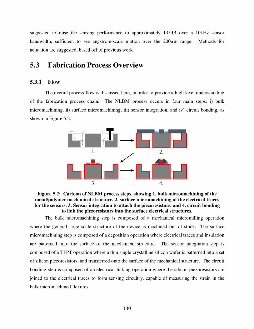
140
suggested to raise the sensing performance to approximately 135dB over a 10kHz sensor
bandwidth, sufficient to see angstrom-scale motion over the 200µm range. Methods for
actuation are suggested, based off of previous work.
5.3 Fabrication Process Overview
5.3.1 Flow
The overall process flow is discussed here, in order to provide a high level understanding
of the fabrication process chain. The NLBM process occurs in four main steps: i) bulk
micromachining, ii) surface micromachining, iii) sensor integration, and iv) circuit bonding, as
shown in Figure 5.2.
Figure 5.2: Cartoon of NLBM process steps, showing 1. bulk micromachining of the
metal/polymer mechanical structure, 2. surface micromachining of the electrical traces
for the sensors, 3. Sensor integration to attach the piezoresistors, and 4. circuit bonding to link the piezoresistors into the surface electrical structures.
The bulk micromachining step is composed of a mechanical micromilling operation
where the general large scale structure of the device is machined out of stock. The surface
micromachining step is composed of a deposition operation where electrical traces and insulation
are patterned onto the surface of the mechanical structure. The sensor integration step is
composed of a TFPT operation where a thin single crystalline silicon wafer is patterned into a set
of silicon piezoresistors, and transferred onto the surface of the mechanical structure. The circuit
bonding step is composed of an electrical linking operation where the silicon piezoresistors are
joined to the electrical traces to form sensing circuitry, capable of measuring the strain in the
bulk micromachined flexures.
1.
4.
2.
3.

141
Thin film patterning and transfer occurs in five main steps, i) lamination, ii) patterning,
iii) etching, iv) transfer, and iv) delamination, as shown in Figure 5.3. The lamination step dices
the large wafer into cm-scale thin silicon stock, which is adhered to a handling stamp. The
patterning step is composed of a laser cutting operation where the silicon stock is formed into the
desired piezoresistor shape. The etching step is composed of a chemical etching operation where
the laser induced edge damage is removed. The transfer step is composed of an epoxy cure
operation where the patterned piezoresistors are attached to the surface of the device. The
delamination step removes the stamp that held the piezoresistors, allowing the sensors to be
cleaned and later bonded to the surface electrical structures.
Figure 5.3: Cartoon of TFPT process steps, showing 1. lamination of a thin silicon wafer
to a glass substrate with adhesive wax, 2. laser patterning of the silicon, 3. etching of the
laser-induced damage, 4. Transfer of the patterned silicon to the device, and 5. delamination of the stamp.
5.3.2 Decoupling
The order of the operations has been chosen to maximally decouple the fabrication
process, in order to maximize the process chain flexibility. The substrate is fully produced
before the sensors are integrated into the device. This allows for a wide variety of methods to be
used to shape the bulk mechanical structure and the surface electrical structures. These methods
are not constrained by force, temperature or chemical compatibility with the sensors. The
sensors are nearly fully produced on a separate handling stamp, before being cured to the bulk
1.
LaserSi
Wax
Device Epoxy Hot Plate
Glass
2.
4. 5.
3.
Etchant

142
mechanical structure. This likewise decouples the sensor fabrication from the substrate, and
allows for a range of processes to be used on the sensors, including laser patterning and nitric/HF
silicon etching, without concern for damage or chemical compatibility with the mechanical
substrate.
The primary coupling occurs at the transfer step of sensor integration, when the sensors
are cured to the surface of the device. All components are subjected to increased temperature.
This was controlled for using a transfer fixture to maintain alignment throughout the temperature
variation. The substrate material decision was also influenced by the need to reduce thermal
expansion mismatch between substrate and sensor. The secondary coupling occurs during circuit
bonding, when electrical contact is made to the silicon sensor using indium solder. This again
requires raised temperature. This issue was simplified by matching the temperature of the cure
and soldering process, so the requirements were identical for both process coupling issues. The
indium is carried out at 15°0C substrate temperature to generate the most reliable contacts, so the
transfer cure is likewise carried out at 150°C. This ensures that the system can handle the
soldering temperature, as this is the zero strain temperature after curing the gages to the
substrate. The coupling between the structural and sensing elements generated constraints on the
fabrication process. The implications of this constraint and possible fixes for this will be
discussed.
5.3.3 Generalization
The NLBM process is envisioned as having greater applicability than the application to
which it is developed here- namely the Hexflex nanopositioner. The process has been laid out in
order to be generalizable to other structures, size scales, substrate materials, and other sensors
including carbon nanotubes [93], commercial piezoresistors [128], and printed strain gages
[146]. All parts of the NLBM process chain can be shifted in and out depending on material and
rate requirements. This process is fundamentally a decoupled fabrication of structure and sensor
to ensure maximum flexibility. The process chain draws from both conventional machining and
microfabrication to produce a hybrid assembly of methods that do not rely exclusively on costly
and inflexible photolithography to transfer geometry to the device structure.

143
5.4 Bulk Micromachining
5.4.1 Overview
The bulk micromachining step covers the fabrication of the generally mechanically active
substrate structure. The flexible elements, as well as stage and ground for the nanopositioner are
formed in this step. The surfaces on which the electronics will be deposited and transferred are
also formed. The focus of this research is on producing a process chain tuned to high flexibility,
small batch size and low per-device cost, all to enable nanomanufacturing/metrology research
and development. Mechanical micromilling was found to satisfy these conditions due to its
relatively rapid (≈4hr) fabrication rate, single device batch size and low cost ($200). The
structure produced by micromilling in the bulk micromachining step is shown Figure 5.4.
Figure 5.4: Bulk micromachined metal mechanical structure, produced with
micromilling. This is the titanium body of the Hexflex flexural nanopositioner.
A Hexagonal structure is created by micromilling titanium 6Al-4V stock on both
surfaces. This produces a relatively smooth (≈100nm RMS) flat surface for electrical structure,
shown face up in Figure 5.4, while the flexure width and stage ribbing are formed via milling
from the other side. Micromilling allows for 3D structures to be added to the normally planar
Hexflex structure [1]. The wire and blade flexures are produced during the underside milling
operation, so the whole device is released only in the final cutting operation. Semi-kinematic
contacts are machined into the device structure to aid in alignment with the sensors during the
later sensor integration transfer operation.

144
5.4.2 Mechanical Milling
The titanium stock is attached to a custom fabricated kinematic coupling using
Crystalbond 509, a thermally activated wax adhesive. This holds the small structures through the
cutting process with high stiffness, but can be removed without inducing damaging forces via
heating (>100°C) or soaking in a solvent (acetone). Crystalbond 509 was found to lose the
majority of its strength by 80°C, and flow by 100°C. At 120°C, Crystalbond can be wicked
between surfaces to form reliable 70µm films. The custom fabricated ‘attachment’ kinematic
coupling has much lower thermal mass than the standard micromilling pallet, and thus allows for
rapid heating and cooling in order to accelerate the wax adhesion process.
The micromilling process follows several steps. The attachment coupling is seated on the
micromill pallet, and faced flat to produce a reference plane parallel to the machine coordinate
frame. The attachment coupling is removed and stock is attached to this coupling via wax
adhesive. The stock bearing coupling is reattached to the pallet in the micromill, and the
sensors/electronics face of the device is machined by surfacing the whole stock. The stock
bearing coupling is removed, and the stock is unbounded then rebonded to the coupling upside
down- with the machined surface face against the attachment coupling. This retains the known
reference frame at the attachment coupling surface and ensures the planarity of the device top.
The device is next milled out to produce the full mechanical structure, relying on the known
coupling surface height for reference, as shown in Figure 5.6. Both sides of the mechanical
structure can thus be machined out of bulk stock and made largely parallel to the repeatability of
the wax film.
The Microlution 363-S 3-axis CNC micromill is capable of running end mills down to
5µm diameter, however the Hexflex mechanical structure did not require such fine features. The
minimum used tool diameter was 533µm which corresponded to 1.6mm tool length due to the
3:1 length:diameter aspect ratio typical of micro end mills. This was the smallest tool capable of
safely reaching through the full 1.5mm thickness of the Hexflex structure.
Accuracy in the cutting process was crucial for alignment, as the same milling operation
that produces the mechanical structure also produces the semi-kinematic contacts. Error in the
tool diameter thus translates directly into a shift in the location of the mechanical structure
relative to the piezoresistors during the semi-kinematically sligned transfer step. The tools were
calibrated by cutting parallel pockets as shown in Figure 5.5, where the reference height is set at

145
the stock surface. The cuts are made in the same material as the device (titanium) using the same
machining mode (climb milling) as used to form the mechanical structure, as well as to the same
depth as the finishing step used in the full milling operation. This subjected the tools to similar
loading conditions and deflections as seen during the final geometry determining step of the
actual milling operation.
Figure 5.5: Tool calibration grooves, cut in similar material, form and depth as the cuts
used to form the bulk mechanical structure.
The close and far wall separation of the pockets are measured using an optical
microscope to determine diMeas and doMeas, respectively. These are compared to the designed
dimensions of the close and far wall separation, diDes and doDes, in order to determine the scaling
between the microscope measurement frame and the micromill measurement frame. The two
dimensions are summed to cancel the opposing effects of the tool radius error, allowing for an
accurate measurement of the frame scaling coefficient, cf, as shown in Eq. (5.1).
iMeas oMeas
f
iDes oDes
d dMeasuredc
Designed d d
+= =
+ (5.1)
The tool diameter error, δd can now be accurately measured by averaging the difference
between the scaled measurement and the designed value for both inner and outer wall separation,
as shown in Eq. (5.2).
( )( )1
2oMeas iMeas
d iDes oDes
f
act nom d
d dd d
c
d d
δ
δ
−= − +
= +
(5.2)
The actual tool diameter is then determined as the sum of the nominal tool diameter and
the tool diameter error. This method allows for calibration of the tool diameter down to the
optical microscope resolution, approximately 2µm. Tool height errors can be measured during
the same process using the depth of the pocket compared to the nominal pocket depth. This error
was typically found to be <10µm, largely due to repeatable inaccuracy in the micromilling tool

146
length laser break-beam measurement system. The out-of-plane error was of less importance
than the in-plane error, as it did not directly affect the placement of the sensors.
The micromilling operation is shown in Figure 5.6, with the major components identified,
including the attachment kinematic coupling. The micromilling operation is able to reliably
machine out 600x600µm wire flexures 1cm long, which are attached to 150µm width blades that
are 1.5mm thick and about 1 cm long. These features are reproduced with approximately 5µm
accuracy due to both machine stability and tool deflection.
Figure 5.6: Micromilling of the metal structure. The metal stock is attached to a
surfaced kinematic coupling with removal wax adhesive. The under-structure of the device has been milled, but it has not been freed from the stock.
The reference plane was assumed to be below the bottom of the stock by the wax film
thickness in order to account for the Crystalbond. The wax film thickness was ensured using
Cospheric SLGMS-2.52 75-90um soda-lime glass microspheres. The Crystalbond film was
found to naturally form a film of about 70µm when both stock and pallet are coated before
contact. This film was found to vary by about 40µm due to variation in preload and heating.
Microspheres were chosen of a diameter slightly larger than the Crystalbond film in order to
ensure the microspheres were loaded by the stock/pallet contact. These spheres stabilize the film
thickness to 85±3µm over the surface of the device. The thickness was below the maximum
quote microsphere diameter. The reason for this discrepancy is believed to be due to the
compressive load during cooling, both from the Crystalbond film and from a 1kg weight placed
on the stock. These compress the spheres, which have two Hertzian contact joints in series. The
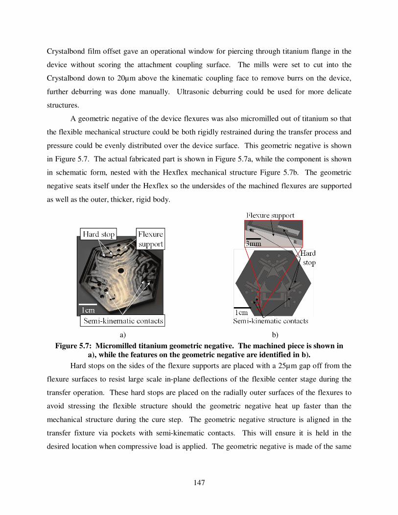
147
Crystalbond film offset gave an operational window for piercing through titanium flange in the
device without scoring the attachment coupling surface. The mills were set to cut into the
Crystalbond down to 20µm above the kinematic coupling face to remove burrs on the device,
further deburring was done manually. Ultrasonic deburring could be used for more delicate
structures.
A geometric negative of the device flexures was also micromilled out of titanium so that
the flexible mechanical structure could be both rigidly restrained during the transfer process and
pressure could be evenly distributed over the device surface. This geometric negative is shown
in Figure 5.7. The actual fabricated part is shown in Figure 5.7a, while the component is shown
in schematic form, nested with the Hexflex mechanical structure Figure 5.7b. The geometric
negative seats itself under the Hexflex so the undersides of the machined flexures are supported
as well as the outer, thicker, rigid body.
a)
b)
Figure 5.7: Micromilled titanium geometric negative. The machined piece is shown in
a), while the features on the geometric negative are identified in b).
Hard stops on the sides of the flexure supports are placed with a 25µm gap off from the
flexure surfaces to resist large scale in-plane deflections of the flexible center stage during the
transfer operation. These hard stops are placed on the radially outer surfaces of the flexures to
avoid stressing the flexible structure should the geometric negative heat up faster than the
mechanical structure during the cure step. The geometric negative structure is aligned in the
transfer fixture via pockets with semi-kinematic contacts. This will ensure it is held in the
desired location when compressive load is applied. The geometric negative is made of the same

148
material as the device mechanical structure in order to minimize thermal expansion errors during
the high temperature cure.
5.4.3 Attachment Kinematic Coupling\
The attachment kinematic coupling was designed to operate on the surface of the
micromill pallet, as shown in Figure 5.8. This pallet is held in the machine via a pneumatically
driven kinematic coupling. The second kinematic coupling in series enables the quick
attachment and removal of stock via the wax adhesive. The wax adhesion process requires both
surfaces to be at >90°C. The thermal time constant for the main micromill pallet is prohibitively
long for using the wax adhesive- about 30-60 minutes is required to for both heating and cooling
of the pallet. The increased temperature was also noted to be causing corrosion on parts of the
pallet.
Figure 5.8: Kinematic coupling attached to micromilling pallet in order to accelerate
thermal adhesion to the stock.
A thin kinematic coupling was designed in order to minimize the thermal mass of the
attachment surface. This coupling was found to heat and cool on the scale of about 5-10
minutes, and the coupling can be easily submerged in water to facilitate rapid cooling, without
causing corrosion. The attachment coupling can also be submerged in solvent in order to remove
wax, without concern for the pallet structure.

149
The attachment kinematic coupling is composed of three 1.5875mm diameter hardened
stainless steel balls each contacting two 1.5875mm diameter stainless steel cylinders. These
contact surfaces were used to avoid using up a significant fraction of the available micromilling
workspace. 3.175mm contact surfaces could be used with little difficulty, and would be more
resistant to unseating from machining forces. The preload is provided by a 2.54cm diameter,
3.175mm thick axially magnetized rare earth magnet seated between two 3.81cm diameter,
1.5875mm thick magnetic steel plates. The plates and the kinematic contact surfaces have all
been attached with a high temperature epoxy. A pocket was milled in the base in order to offset
the magnet from the coupling steel plate by approximately 1mm, thus generating approximately
30N preload. Notches were milled in the side of the base so that the surfaces could be separated
with a screwdriver. The whole structure is machined from aluminum due to the high thermal
conductivity and ease of machining.
Hertzian contact stress calculations for ball-on-cylinder conditions show that the 794µm
contact radius can handle 100N preload force with a safety factor of 3 [147]. The coupling has a
predicted stiffness of approximately 108 N/m at the contact surfaces, which will result in sub-
micron displacements for the typical range of micromilling cutting forces (<10N). The
positional variation of the attachment coupling was determined through the use of the micromill
reference height measurement operation, and is shown in Table 5.2. The micromill pallet was
measured in the same manner to provide comparison.
Table 5.2: Comparison of fabrication methods
Kinematic Coupling Z error (nm) θX error (µrad) θY error (µrad)
Maximum error (nm)
Stock 400 20 23 860 Pallet 240 1.70 2.3 250
The maximum error is calculated at the edge of the micromilling workspace; 25mm out
from the center, and combines the errors by assuming they are uncorrelated Gaussian variables.
The micromill pallet is able to maintain superior planarity and 40% better Z height repeatability,
likely due to the use of much higher preload forces. Overall, the maximum error for both
structures is sub-micron, which meets the micron-scale error allowances for the NLBM process
chain. This error is also only introduced into the thickness of the part as all in-plane features are
formed in one seating after the stock has been surfaced and flipped. This thickness variation

150
does not significantly impact the performance of the device or the alignment of the mechanical
structure with the sensors.
Several other stock attachment methods were attempted prior to the adoption of wax
thermal adhesive. Double sided tape was found to easily hold the sample, but to do so with low
stiffness and to make it difficult to remove the completed structure. The low in-plane stiffness
resulted in poor accuracy on fine feature machining. Screws were used to hold the stock in
place, however that was found to bow thin stock pieces and did not restrain the flexible elements
once they were machined. Wax was found to be the most reliable process as it provides adhesion
over the whole surface of the stock, does so at high stiffness, and can be removed with minimal
forces after cutting is complete.
5.4.4 Scaling
Mechanical micromilling was adopted for the bulk micromachining step in this research
in order to meet the demands of high flexibility, small batch size (down to a single device) and
short lead time. This is by no means the only way of generating a micromechanical structure.
Several others methods are suggested which shift the process chain towards higher volume,
lower flexibility, including titanium DRIE, chemical machining, electrochemical machining and
LIGA.
Titanium DRIE has been demonstrated [145] to produce complex, 3D structures from
bulk pure titanium. This could be used in multi-step processes to generate the desired ribbed
Hexflex structure, however it would need to be adapted to Titanium 6Al-4V to provide
equivalent performance. Titanium DRIE would allow for a high rate of parallelization of the
bulk micromachining, enabling a significant increase in production rate and batch sizes. This
rate gain is accompanied by a decrease in design flexibility due to the use of photolithographic
masks.
Chemical machining is commonly used to isotropically etch metals that have been
masked prior to etching [148]. This process is able to rapidly produce thin structures, and do so
in an easily parallelizable manner. Isotropic etching makes it difficult, however, to produce
sharp corners and complex 3D stepped shapes. This process has similar drawbacks to the
titanium DRIE operation, in that the use of masking results in generally decreased flexibility.

151
Electrochemical machining can be used to create fine metal structures in hard-to-machine
alloys [149]. It works by driving current from the tool (cathode) to the workpiece (anode) across
a ≈100µm gap while the pieces are submerged in a chemical bath. The workpiece is eroded
without any damage to the tool, allowing for fine feature generation and smooth surfaces. This
process is capable of high material removal rates, but is relatively inflexible due to the need for
the shaped tool. Numerical control electrochemical machining offers a more flexible means of
producing structures by moving a mill-like tool over a predetermined path to machine the
workpiece. This is an alternative to mechanical milling if finer surface finishes are required.
LIGA is a MEMS fabrication method which utilizes electroplating over patterned and
etched photoresist in order to produce metal 3D structures [96]. This can produce very fine
features due to the high fidelity of both photomasks and photoresist. The process is restricted to
materials that are capable of additive deposition, which is presently difficult for titanium and its
alloys [150]. LIGA offers a high degree of parallelization but is relatively inflexible due to the
need for masks. While technically a surface micromachining operation, this can be used to
generate the bulk mechanical structure.
These bulk micromachining operations are suggested as means of shifting the process
along the spectrum from high flexibility to high rate, all while maintaining the decoupled
structure of NLBM. Increased rates are generally associated with limited materials choices, as
plastics and some ceramics are infeasible for some of the methods outlined above.
5.5 Surface Micromachining
5.5.1 Overview
The surface micromachining step covers the fabrication of the generally electrically
active surface structures. The traces and contact pads for linking the device into off-structure
circuitry are formed in this step. This step is also associated with significantly low material
addition/removal rates than the bulk micromachining step, similar to a finishing operation after a
rough cut. Because the focus of this research is on producing a process chain tuned to high
flexibility, small batch size and low per-device cost, processes were chosen that enabled rapid
design changes with little cost/time investment. Insulation of the bulk structure by anodization
and thermal oxide growth followed by deposition through a mechanical shadowmask was found

152
to satisfy these conditions due to the relatively rapid (≈3 days) fabrication rate, single device
batch size and low cost ($200). This time is dominated by a 48hr thermal oxide growth step.
The structure produced by insulation and deposition in the surface micromachining step is shown
in Figure 5.9.
Figure 5.9: Device with surface micromachined electrical structures, which are traces
for circuit routing.
A titania film is deposited over the whole surface of the device, dulling the surface finish.
The mechanical shadowmask is used to impart a pattern to the deposition, resulting in conductive
surface electrical traces for linking the integrated sensing to off-device electronics. These traces
are shown in detail in Figure 5.9, where the sharp edges and high fidelity pattern transfer can be
observed.
5.5.2 Insulation
The part is cleaned with acetone and soap/water in order to remove organics, and then
submerged in 1M sulfuric acid for 5 minutes. This dip further reduced any variation in the
titania film growth, likely due to the sulfuric acid removing any remaining organics as well as
the native oxide on the titanium. The part is then electrochemically anodized at 60V for 5
minutes in the sulfuric acid bath, producing a blue-green oxide film. The part is rinsed in water
and placed in a Thermolyne 1500 programmable furnace for 40hrs at 650°C. The furnace is
ramped up to temperature at 5°C/min. A furnace stand is used to lift the part above the floor of

153
the furnace so that oxide growth will be uniform between the top and bottom of the structure,
thus minimizing structural stress and warping.
5.5.3 Deposition
The deposition process is carried out through a mechanically milled shadowmask, as
shown in Figure 5.10. This shadowmask was chosen to maximize flexibility in the process, as it
can be produced using the same methods as the mechanical structure- micromilling.
Figure 5.10: Mechanical shadowmask, used to pattern trace deposition onto the
mechanical structure. The shadowmask was fabricated via micromilling, while the
plastic kinematic contact cover was fabricated with laser cutting. A magnetic preload is
used to ensure that the shadowmask is pressed against the surface of the Hexflex during deposition.
The shadowmask is a 1.5mm thick titanium 6Al-4V plate that is machined on both
surfaces and intended to seat on the face of the mechanical structure to pattern the deposited
metal. The shadowmask material was matched to the mechanical structure in order to minimize
thermal expansion error during the deposition process. The cuts through the shadowmask are
carried out in a stepped fashion to ensure that the traces can be viewed from a 20° cone off the
surface normal without obstruction. This minimizes deposition thickness variation near the
edges of the pattern due to partial masking. Traces of large width (800µm) are used to minimize

154
unwanted resistance. The micromilled mechanical shadowmasking process was found to be
effective down to about 100µm trace width.
Electron-beam deposition was used in conjunction with the mechanical shadowmask to
form coatings of uniform thickness. This physical vapor deposition process was chosen due to
its highly directional nature and uniform films with good surface adhesion [96]. An aluminum
surface film of approximately 1µm is formed through the mechanical shadowmask to produce
traces with ≈1Ω resistance. These thin traces can also be plated over the flexible elements
without altering the device elastomechanics or causing the trace to delaminate during operation.
Such traces would enable electrical connections to the payload during operation. Aluminum is
used for the deposition material due to its good surface adhesion, minimal film stress and low
resistance.
5.5.4 Oxide Process Tuning
It was desired to create a thick (≈6µm) titania film over the titanium mechanical structure
which had a strong (>20MPa) adhesion strength to the bulk titanium. This stress threshold is set
by the epoxy failure strength of about 20MPa, so as to ensure that the epoxy delaminates before
the oxide film does. The thickness requirement is to ensure a high (>20V) dielectric breakdown
voltage across the oxide, so that the surface electronics do not short through the bulk mechanical
structure. The titania film was created via a combination of electrochemical anodization and
thermal oxide growth, which has been shown to produce high thickness films [151], [152]. The
combination process generates thicker films [151], and was found to improve the film
uniformity.
The electrochemical anodization voltage sets the initial film thickness [153]. This scales
from about 30nm at 5V up to about 190nm at 100V. Unfortunately this range is significantly too
low to produce the desired 6µm film thickness in a single step. A thick film is preferable,
however the film quality must be high; the film must have high surface adhesion and low
porosity. A 75V threshold is observed in literature where the film transitions from low voltage
high quality surface reproduction to high voltage porous film structure [154]. Sparking is
observed at the titanium surface in conjunction with the film breakdown into a porous structure.
The film quality threshold is also observed in the samples produced in this research, with
inconsistent film I-V performance observed at 83V anodization, but not at 60V. Titanium

155
samples of 2x3x0.05cm were run through the oxide growth process to generate 6µm films.
Chemworks CW2400 two part conductive epoxy was placed in over an approximately 1x1cm
section of the surface, and cured at 65C for 10 minutes. A section of the oxide was scraped away
about 2 cm from the epoxy and the titanium substrate was electrically grounded. A voltage was
applied to the epoxy and the current was measured to determine the resistive characteristics of
the film, as shown in Figure 5.11, where positive voltage indicates that the epoxy contact was at
higher voltage than the titanium substrate. 60V was found to be a safe upper limit for
electrochemical anodization, corresponding to an anodized film of approximately 110nm
thickness [153].
Figure 5.11: I-V measurements of the titanium oxide film produced on the surface of the
titanium bulk structures via combined electrochemical anodization and thermal
oxidation.
The 60V anodization sample was observed to follow a consistent trend of an
exponentially decreasing resistance in series with an ohmic resistance. Lower voltages resulted
in less resistance. Higher voltages resulted in inconsistent performance due to the film porosity.
The combination of exponential and ohmic resistance is characteristic of a Schottky barrier,
particularly one operating in reverse bias. Forward bias I-V curves typically have voltage decay
constants on the order of 26mV [99], which is significantly smaller than the 4.6V voltage decay
constant observed in the I-V curve. Aluminum traces in the shape of the final structure were
deposited onto oxide coated samples in order to mimic the materials used in the device. A
section of the device was cleared of oxide, and the titanium was grounded. The metal traces
0 5 10 15 200
20
40
60
80
100
120
Voltage (V)
Cur
rent
(uA
)
60V83V60V Fit

156
were subjected to voltages ranging from -5V to +5V, a range characteristic of that used in this
device. The positive and negative voltage data were fit using a series exponential and ohmic
resistance model, shown in Eq. (5.3), and in Figure 5.12. This data represents the leakage
current from the traces used on the device down to the bulk titanium.
Figure 5.12: I-V measurements of the aluminum traces on titanium oxide film.
The fit is based on the expressions derived for a reverse bias Schottky barrier, where Rox
is the voltage dependent impedance of the film, V is the voltage across the film from epoxy to
titanium substrate, ρb is the exponential barrier resistivity, Vτ is the exponential resistance voltage
decay constant, ρc is the ohmic contact resistivity, and A is the contact area.
( )V
Vb cox
R V eA A
τρ ρ−
= + (5.3)
The conductance was integrated over the operating voltage to produce an expression for
the I-V curve that could be fit directly to the data, as shown in Eq. (5.4), where Iox is the current
flowing through the film.
1
0
(0)1( ) ( ) ( ) ln
( ) ( )
Vox
ox ox Csb
ox ox
RI V R v dv V V C
R R Vτ
−
= = − ∞
∫ (5.4)
The 6µm film was found to have positive voltage bias parameters: ρb = 0.6MΩ-cm2, ρc =
70kΩ-cm2, and Vτ = 0.6V and negative voltage bias parameters: ρb = 1MΩ-cm2, ρc = 30kΩ-cm2,
and Vτ = 0.5V. The bulk titanium resistance was several orders of magnitude below the observed
film resistance, so was not included in the model. The thermal oxide films are reported to have
an ohmic resistivity of about 2x10⁹Ω-cm [155], which would appear as a contact resistivity of
-4 -2 0 2 4-4
-2
0
2
4
Voltage (V)
Cur
rent
(uA
)
MeasuredPositive FitNegative Fit
Oxide-Ti barrier in reverse bias
Trace-Ti barrier in reverse bias

157
about 1.2MΩ-cm2 for a 5µm film, significantly higher than the measured values. It is expected
that the method of fabrication and the deposited surface material play a role in determining this
value. Titania resistivity is known to be highly sensitive to oxygen [155] during growth, with up
to four orders of magnitude variation possible.
The piezoresistive device, titania film and titanium substrate form a metal-
semiconductor-metal interface, which generates a complex Schottky barrier [155], [156]. The
piezoresistive device is p-type silicon which acts like a forward diode for current flow off of the
device. The current passes from the piezoresistor, through the epoxy (in trace amounts) and in
parallel also exits the metallic traces deposited on the titania surface. The traces appear to
generate most of the leakage current so this is qualitatively modeled as a metal contact on the
surface of the titania film for simplicity. The titanium oxide acts like a lightly doped n-type
semiconductor [155]. Two Schottky barriers are formed in this layering. The first is from the
surface electrical structures to oxide, and is in forward bias when the sensors and traces are at
positive voltage above the grounded titanium substrate. The second in series is from the oxide to
the titanium below, and is in reverse bias. The reverse bias effects will drive the electrical
performance of the film which means the observed I-V characteristics at positive sensor voltage
are those of the oxide-titanium Schottky barrier in reverse bias. The conditions are reversed
when the surface is at negative voltage relative to the grounded substrate. The surface to oxide
barrier is in reverse bias, while the oxide to titanium barrier is in forward bias. The surface to
oxide barrier in reverse bias will dominate the film I-V characteristics at negative sensor voltage.
This explains the different I-V characteristics observed in the positive and negative voltage
regimes. These curves were also found to be strongly dependent on the maximum voltage
applied, past about 3V. High voltages had the effect of annealing the diode, reducing resistivity
significantly, which has been seen elsewhere [155]. The range of measurement was held to 3-4V
in order to minimize this error, while still capturing the important range.
The net resistivity between two traces on the surface is the resistivity from the higher
voltage trace to the bulk titanium, and from the bulk back to the lower voltage trace. Thus, it is
two barrier resistances in series, generally with one operating at positive voltage and one at
negative voltage. The rough symmetry of the positive and negative I-V curves indicates that the
bulk titanium will settle at a voltage approximately midway between that of the two traces. For a
gage at 5V on one end and 0V at the other, the bulk titanium will be at about 2.5V, and each

158
diode will see about 2.5V, allowing about 2µA leakage current. After a 20V anneal on each of
the gages, the leakage current stabilizes out at around 8µA, indicating that the high voltage
annealing causes a roughly 4x reduction is resistivity.
The thermal oxide growth temperature was set by two requirements, i) high film adhesion
strength, and ii) rapid film growth. Thermal oxide films are reported to have adhesion strengths
of about 70MPa when grown at <650°C, and less than approximately 7µm thick [157]. The
oxide films are observed to rapidly lose adhesion strength when formed at temperatures >650°C,
dropping down to about 10MPa by about 700°C [157]. This dropoff occurs at the same
temperature as the transition from anatase to rutile structure [158]. Temperatures well above
650°C are observed to result in cracked, peeling and porous surfaces [151], [152], [157]. The
growth rate, however, increases exponentially with temperature [152], [157–159]. A thermal
oxide growth temperature of 600-650°C was determined to satisfy the two requirements on the
process.
The thermal oxide growth time was set by two similar requirements, i) thick film for
large insulative effect while ii) retaining high film adhesion strength. The thickest possible film
is desired from the perspective of generating an insulating layer, however films >7µm are known
to have reduced adhesion to the titanium substrate [152], [157]. A good balance between these
two is found around 5-6µm, as high as possible while still safely below the adhesion strength
transition point. Previous work [157], [158] suggests that this thickness should be reached in
about 40hrs, as shown in Figure 5.13.

159
Figure 5.13: Oxide growth kinetics for isothermal oxidation of titanium in air, taken
from [158]. The preferred temperature of 650°C is highlighted, and the axes have been
scaled with units of hours and thickness in microns to aid in design.
The growth kinematics shown in Figure 5.13 were measured for pure titanium samples
heated in air. The conversion from film weight to film thickness is approximately
2.36µm/(mg/cm2) assuming pure titanium dioxide, and this conversion has been used to scale
the vertical axis for design convenience. The 650°C growth curve has been highlighted for
convenience.
The 650°C growth pattern is characterized by a small crystalline, high adhesion film that
initially dominates growth, but slows following a parabolic growth law by about 100-200hrs. An
external film made of larger crystals with a linear growth rate dominates the film composition
[157] at larger times, and are associated with reduced adhesion strength as found in previous
work on pure titanium samples [157] and shown in Figure 5.14. The 650°C conditions can still
result in poor film adhesion if the film is grown too thick.

160
Figure 5.14: Oxide film adherence to the titanium substrate as a function of film
thickness, taken from [157]. The asymptotic trends for adherence stress at low and high
film thickness have been identified to show the transition point for film strength. This transition occurs around 7µm, at around 100 hrs in air at 650°C [157].
The overall ideal growth time for 650°C conditions is thus about 40hrs, corresponding to
a ≈6µm film. Practical time and film adhesion strength limitations suggest the film should not be
made much thicker due to the rapid reduction in adhesion and increase in required time above
7µm and 100hrs.
The oxide adds a finite thickness to the structure due to the capture of oxygen in the
titania film. The thickness increase, ∆t, can be calculated stoichiometrically as shown in Eq.
(5.5), where M and ρ are the molar mass and density for the oxide (ox) and titanium (ti)
respectively. This effect scales with the thickness of the oxide film, tox, by a factor of about
44%. This results in approximately 2.2-2.6µm increase in dimension for a 5-6µm film.
ox ti
ox
ti ox
Mt t
M
ρ
ρ∆ = (5.5)
The oxide formation generates stress in the structure. This stress is most pronounced in
the thin blade flexures, where surface area dominates over volume. The stress is relieved by
tensioning the titanium core of the structure, resulting in an expansion that can be approximated
for simple structures by assuming two springs in parallel, one of which is the compressed film,
the other is the titanium substrate. This is shown in Eq. (5.6), where ∆x is the equilibrium
extension of the extruded structure (flexure) with a cross sectional area that is separated into

161
oxide, Aox, and substrate Asub. The Young’s Modulus for the oxide and substrate are Eox and Esub,
respectively, and the generated strain in the oxide film is εox.
ox ox ox
sub sub ox ox
E A Lx
E A E A
ε∆ =
+ (5.6)
The Hexflex structure is observed to gain approximately 75µm length on the blade
flexure after oxidization. This corresponds to approximately 4.7% strain generated in the surface
oxide during formation. The extension of the blade flexure length can generate issues with the
geometric negative structure. This is resolved by milling 75µm off of the contact surface on the
Hexflex structure side. This surface is on the virtual mass between the wire and blade flexure.
5.5.5 Scaling
Electrochemical/thermal oxide formation and e-beam deposition through a mechanical
shadowmask were adopted for the surface micromachining step in this research in order to meet
the demands of high flexibility, small batch size (down to a single device) and short lead time.
The insulation process and e-beam deposition are both fundamentally parallel processes, so the
rate may be easily increased by processing multiple devices in parallel. This makes the surface
micromachining step significantly more amenable to shifting along the rate scale than the bulk
micromachining step. Several others methods are suggested which operate at other
rate/flexibility scales, including other physical vapor deposition methods (PVD) and aerosol jet
printing.
Other PVD methods may be substituted in for e-beam deposition without fundamentally
altering the fabrication process. The mechanical shadowmask can be used for all of these
methods, however it produces the sharpest pattern edges when combined with a highly
directional deposition process like e-beam vs. a more diffuse process like sputtering [96]. The
range of PVD methods enable a wide variety of materials to be used should the designer wish to
selectively deposit ceramics, polymers or metals.
Aerosol jet printing is a highly flexible serial process where the material of interest is
aerosolized, sprayed through a fine nozzle onto the substrate surface, and finally sintered [160].
This can be done for a wide range of materials in rapid succession, so the insulation could be
deposited, then the electrical traces directly onto a metal substrate. This would bypass the
lengthy thermal oxide growth step.

162
5.6 Sensor Integration
5.6.1 Overview
The sensor integration step covers the fabrication and placement of the device sensing
onto the mechanical structure. This research focused on single crystalline silicon piezoresistors,
and the Thin Film Patterning and Transfer (TFPT) process was developed to integrate these into
the titanium device. The focus on high flexibility, small batch size and low per-device cost led
to the use of laser patterning of the silicon and manual preparation of the stamp. These steps can
be used to rapidly produce new designs (≈2 days) in small batches, and at low cost ($150).
Figure 5.15: Device with single crystalline silicon piezoresistors attached to the titanium
flexures via the thin film patterning and transfer process.
A laser scribe is used to pattern thin silicon stock, which is transferred to the surface of
the device via a handling stamp. The silicon piezoresistors are aligned to the device using semi-
kinematic contacts, and cured onto the base of the flexures, as shown in Figure 5.15. These
sensors are not yet linked to the surrounding electrical structures- the deposited traces.
5.6.2 Lamination
The first step of TFPT is the lamination of thin silicon wafer stock to a handling substrate
which was a glass stamp for this research. The silicon wafer thickness is chosen to reach the
desired piezoresistor thickness after etching. The piezoresistor thickness is typically <10% of the
thickness of the flexure, in order to ensure that the device elastomechanics are unchanged [97].

163
A 50µm wafer was used to produce the silicon stock for this research. The wafer is diced into
stock rectangles about 1mm larger than a box bounding the desired PR pattern, approximately
6x9mm for this work. This excess material facilitates alignment to the stamp and handling. The
stock is cut aligned to the desired crystallographic axis. The stress and current were run parallel
to the <111> direction on a (110) wafer for this research, which produces a high gage factor of
≈174.
The silicon stock is placed on a cleaned glass stamp, which is created by dicing standard
borosilicate microscopy glass slides into 12.5x26.4mm rectangles. Two sides of the stamp are
the original edges of the glass slide, so these surfaces are perpendicular to one another and flat.
These edges will be brought into contact with semi-kinematic contacts throughout the process to
act as references from which to determine alignment. The surfaces of the reference edges are
not, however, perpendicular to the slide face, as errors of ≈±3° were observed in standard slides.
The corner opposite to the reference corner is filed round, so as to help with applying preload for
alignment. Borosilicate glass has several useful properties for TFPT. It is a close match in
thermal expansion coefficient (9ppm/°C) to titanium (8.6ppm/°C). It is also transparent to the
1064nm laser used to pattern the silicon, so stamp material is not ejected during the cutting
operation. The borosilicate glass is slightly etched by the silicon etchant, however the stamp can
be masked with MWM100 etch resistant wax, and the etched glass residue is easily washed off.
The glass slides are also mass produced in an easily handled size with consistent geometry and
clean, sharp edges that facilitate reliable semi-kinematic alignment.
The stock is visually placed on the stamp within approximately 1mm of the location of
the final, patterned gage. This ensures that the patterning will remain within the bounds of the
stock. In practice, alignment of <500µm was easily done via markings placed below the glass
slide. The stock should be oriented within a few degrees of the desired alignment; otherwise the
gage factor will be reduced by cosine error in conjunction with sine error for the
current/transverse stress negative gage factor.
The stock is adhered to the stamp with wax. This is done by placing the stock/stamp on a
hotplate at 130°C surface temperature, with a small bead of MWM100 Black Mounting Wax
placed next to the stock. The wax will form a ≈25-30µm layer, thus requiring 2.5-3mm3 of wax
per cm2 of stock surface. This bead will rapidly melt, and wick under the stock. The wicking
action will filter out large contaminants (fibers, grit) from the wax that would otherwise keep the

164
stock from settling flat against the stamp surface. A single bead is used to avoid generating air
bubbles at the intersection of advancing fluid films. 10-20 minutes is typically sufficient for the
wax to fully wick under the stock. Extra beads may need to be placed around the perimeter of
the stock to accelerate the wicking process in some cases. If air bubbles are formed under the
stock, the stamp may be left on the hotplate for 30-90min to give the wax’s surface tension time
to eject the bubble. The stamp may be lifted to check the wicking/air bubble status after the first
minute of the process. The desired film is of even color and thickness. If not, then the stamp
should be left on the heat. Stock alignment may be maintained by adjusting the stock location
with plastic tweezers.
Figure 5.16: Stamp with laminated stock.
The stamp is prepared for patterning by coating the stock and stamp surface with a thin
organic film. Hairspray was used for its simply generated uniform coating. This organic film
will protect the silicon surface against laser damage. The lamination step results in the silicon
stock attached to the glass stamp and shielded as shown in Figure 5.16 and Figure 5.17.
Alignments of <250µm and <2° are typical, which is well within the 1mm tolerance for the
stock.

165
Figure 5.17: Schematic of stamp at completion of lamination step. Silicon stock has been
attached to a glass stamp with wax, and a layer of hairspray has been coated over the surface of the stamp.
5.6.3 Patterning
The second step of TFPT is the patterning of the silicon stock to create the desired
piezoresistor shape in the desired location. The stamp is placed in semi-kinematic alignment
fixture in the laser cutter as shown in Figure 5.18. An Electrox E-Box Workstation with a 20W
Scorpion Rapide II Yb: fiber laser is used for the patterning process. The laser cuts through the
silicon and wax, passes through the glass and cuts into the fixture below the stamp. This
generates refuse on the bottom of the stamp which can weld the stamp to the fixture unless a
shim is placed between the stamp and the metal surface, for which paper is used in this research.
Figure 5.18: Glass stamp in laser scribe fixture, which is used to align the gage
patterning to the coordinate frame defined by the edges of the stamp.
The laser fixture is aligned to the center of the laser cutter operating volume in order to
minimize frame warping due to the beam angle. The fixture is preloaded to the laser stage with
an elastic band, and the stamp is preloaded to the fixture with a compression spring pressed
Si
GlassWax
Hairspray

166
against the rounded edge of the stamp. The fixture is calibrated by cutting grids into a stamp
covered in magic marker ink. The alignment of this grid to the edge of the stamp is iteratively
adjusted to reach the desired value. The combined variability of the laser cutter and fixture
occurs in three parts: calibration, fixture and drift. The alignment calibration is carried out with a
single sample 15 minutes before each stamp set is cut. This introduces a 3µm standard deviation
in location, largely due to the fixture error. The fixture further introduces a 3µm standard
deviation in both axes for each stamp. The fixture is subject to thermal positional drift, which is
≈0.2µm/cut in X and ≈5µm/cut in Y.
The laser cutting parameters have been optimized to maximize the thermal cutting
efficiency in mm2 surface cut per Joule heat generated. A three step shape is cut into the silicon
stock: the pattern, radial detiling and theta detiling, all as shown in Figure 5.19.
Figure 5.19: Silicon cutting pattern, composed of three layers: i) the piezoresistor shape,
cut first, then ii) the radial detiling lines cut to reduce thermal stresses, and finally iii) the
theta detiling lines cut to break the unwanted silicon into removable pieces.
The first shape cut into the silicon is the final piezoresistor outline. This is offset from
the desired final dimensions by 26.2µm, the sum of the laser cutting radius (15.6µm) and the side
etch depth (≈10µm). This value is reduced from the full etch depth of 20µm likely because of
diffusion limitations. This pattern is created first to separate the fine piezoresistor features from
the bulk structure before thermal stresses build up in the stock. The piezoresistor outline is cut in
one continuous process starting from a point on the bottom of the shape and ending at the top of
the cut that splits the piezoresistor into two halves. The exit point of the laser was found to
exhibit less damage than the entrance point, so this exit point is placed at the location of common
stress buildup.

167
The second shape cut into the silicon is the radial detiling outline. These cuts separate
the stock into radially aligned pieces in order to further limit stress buildup, as the heating will
cause each piece to expand. The third and final shape cut into the silicon is the theta detiling
outline. These cuts dice the large area of unwanted silicon into thin strips with constant width.
The width of these strips is set so as to facilitate the easy removal via a hexane wax etch that will
be described below. An example of the patterned stamp is shown in Figure 5.20.
Figure 5.20: Stamp with patterned silicon stock, prior to the cleaning process.
The patterned silicon is now cleaned to remove part of the laser generated debris on the
surface of the piezoresistor. A 60s soak in water is sufficient to remove the hairspray, and part of
the secondary built-up edge (BUE) deposited onto the silicon surface during the cutting. The
remainder of the secondary BUE is removed via an acetone soak and slight mechanical abrasion
with a 5mm bristle camel hair paintbrush. The acetone is able to loosen the hairspray surface
coating that has been heat damaged by the laser cutter. The non-damaged hairspray dissolves in
soap and water. This is visible around the edges of the contact pads in Figure 5.21. One cut
does not heat the surface sufficiently to damage the coating. Several closely spaced cuts like that
in the detiling area heats the hairspray coating to the point that the chemical degrades, forming a
resistant coating that can only easily be removed with acetone. This effect of this cleaning
process and the location of the BUE is shown in Figure 5.21, which is the stamp after cleaning.
The BUE removal is visible in the difference between Figure 5.21 and Figure 5.20.

168
Figure 5.21: Stamp with cleaned piezoresistors, showing the removal of BUE.
The patterning step actions are shown schematically in Figure 5.22. This includes the
laser cut into the silicon and the surface cleaning to remove debris.
Figure 5.22: Schematic of stamp at completion of patterning step. The silicon stock has
laser cut into the shape of the piezoresistor. This generates both primary and secondary
BUE. The secondary BUE is removed upon washing off the hairspray layer, as shown in
the bottom figure.
5.6.4 Etching
The primary BUE and laser induced crack damage is removed from the silicon surface in
the etching step. Two etches are used; a hexane etch of the wax and a nitric/hydrofluoric etch of
the silicon. The wax etch removes any wax that was melted and ejected from the cut during the
patterning step. This wax is acid resistant, so would act as an etch mask to protect the laser
Primary BUE
LaserSecondary BUE
Si
Hairspray
Stamp
Wax

169
damaged sides of the cut. A 150s soak in hexane (the solvent for MWM100) is sufficient to
dissolve any surface wax and undercut the wax anchoring the tiled silicon around the
piezoresistor. The stamp is cleaned with a soft brush and soap and water, which typically pulls
off all remaining visible wax and completes the detiling process so as to leave only the patterned
gages on the surface of the stamp. The kinematic contact surfaces on the side of the stamp are
covered in MWM100 to protect them from the silicon etchant. The cleaned and detiled stamp is
shown in Figure 5.23.
Figure 5.23: Cleaned and detiled stamp prepared for etching.
The stamp is now ready for silicon etching as the patterned piezoresistor structure is
anchored to the surface, the pattern is exposed to etchant on all outer edges, and all excess wax
has been cleared away. The stamp is submerged in a 100mL silicon etching solution composed
of 9 parts nitric acid (69%) to 1 part hydrofluoric acid (49%) ratio by volume. The etching is
carried out for 8.33 minutes in order to remove 20µm of silicon at an average rate of 2.4µm/min
without agitation. The surface of the stamp and piezoresistors is cleaned with soap and water to
remove all contaminants left over from the etching step. This results in a stamp as shown in
Figure 5.24.

170
Figure 5.24: Etched and cleaned stamp prepared for the transfer step.
These two etches produce the following geometry on the stamp and silicon stock shown
in Figure 5.25. The wax is under etched by the hexane etch, which exposes both the upper and
lower corners of the laser cut edges to the silicon etchant. These corners are filleted by the HF
diffusion limited etching process which tends to round the upper corners more than the lower
corners of the laser cut sides. The primary BUE and all visible laser induced damage are
removed during this process. This raises the uniaxial fracture strain of the piezoresistors from
180µε to about 2500µε. The borosilicate glass stamp is etched at about half the rate of the
silicon. The thin arms of the piezoresistor are typically released during the hexane etch. The
under surfaces of these arms are generally still covered by a thin layer of wax and are further
protected by limited HF diffusion under the gage surface. This weak anchoring of the under
etched wax is addressed in the transfer step.

171
Figure 5.25: Schematic of stamp at completion of etching step. The patterned silicon is
underetched with hexane, which aids the removal of the unwanted silicon. This
underetched silicon is then chemically etched to remove the laser damage and fillet the corners.
5.6.5 Transfer
The piezoresistive sensors are prepared and attached to the mechanical substrate in the
transfer step. The stamp is first repaired to ensure that the thin silicon films will be able to
withstand the high pressures of the epoxy cure (240kPa). The stamp is placed back on a hotplate
at 130°C for 20min in order to wick the wax back under the piezoresistor. A small bead of wax
is deposited on the center of the piezoresistor to supply sufficient wax to refill under the sensors.
The symmetric placement is to avoid uneven surface tension effects pulling the piezoresistor
around on the stamp. Unbalanced surface tension effects could increase the alignment error.
The wax is cleaned off with hexane then soap and water to produce a clean surface held in place
with a strong wax anchor.
The stamp surface is shielded from adhesion to the epoxy by a thin layer of molybdenum
disulfide (MDS). MDS is a dry lubricant which can be obtained in spray form. The MDS is
sprayed into a small vial to produce an opaque liquid that will rapidly evaporate, leaving a fine
layer of MDS behind. The vial is used with a fine brush to paint an event coat of MDS onto the
surface of the stamp and up to the edge of the sensors. MDS is soluble in soap and water, so can
be washed off and reapplied if accidentally painted onto the face of the piezoresistors. The
stamps and piezoresistors are now ready for transfer to the mechanical structure. A completed
stamp is shown in Figure 5.26.
Filleted corners Under etched wax
Si
Stamp

172
Figure 5.26: Stamp prepared for transfer to the device.
The transfer process is carried out with a fixture to ensure proper alignment. Epoxy is
placed on the piezoresistor surface as well as their eventual contact location on the mechanical
structure. M-Bond 600 epoxy is used for its low cure temperature (>75°C), which provides
greater flexibility in material and process parameter selection. The epoxy is air dried for about
10 minutes, and then the surfaces are pressed together in the transfer fixture, shown in Figure
5.27, at 240kPa to ensure an even glueline of about 9±2µm. The cure is carried out at 150°C for
45min, with a 5°C/min ramp. This cure temperature is chosen to match the indium soldering
temperature so as to minimize thermal strain on the sensor during the circuit bonding operation.
The high thermally-based compressive preload on the piezoresistors also increases the tensile
strain range of the sensors. Silicon is typically lower in tensile stress than compressive stress, so
this helps increase the usable sensor range. The alignment is ensured with a semi-kinematic
fixture that holds the stamps and Hexflex mechanical structure in the desired location during the
transfer operation. The fixture was measured to have approximately 1.5µm standard deviation in
alignment for both axes.

173
Figure 5.27: Exploded view of transfer fixture setup, showing main components in the
stack. The alignment pins are within the perimeter of the Hexflex so that the stamps can
be pressed towards the center to preload.
Three stamps are used, each with two piezoresistors on them. Each stamp is aligned with
three pins to match the three constrained degrees of freedom. One set of three pins is also used
by the Hexflex mechanical structure for alignment. The geometric negative is also pressed
against this set of three pins, shown in the bottom left in Figure 5.27. All the structures-
geometric negative, alignment plate and Hexflex mechanical structure are fabricated on the same
micromill to ensure they retain the same coordinate frame. The in-plane preload is generated by
torsion springs, as shown in Figure 5.28. These press the stamps, mechanical structure and
geometric negative against their respective semi-kinematic contacts.
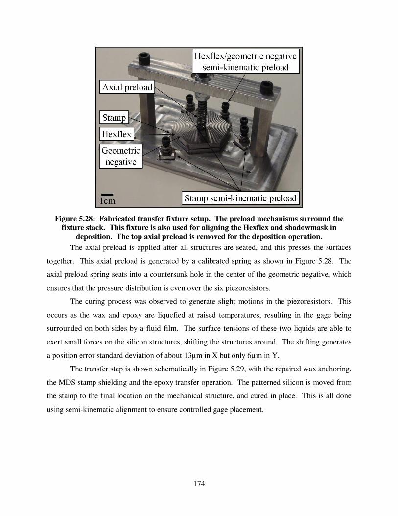
174
Figure 5.28: Fabricated transfer fixture setup. The preload mechanisms surround the
fixture stack. This fixture is also used for aligning the Hexflex and shadowmask in
deposition. The top axial preload is removed for the deposition operation.
The axial preload is applied after all structures are seated, and this presses the surfaces
together. This axial preload is generated by a calibrated spring as shown in Figure 5.28. The
axial preload spring seats into a countersunk hole in the center of the geometric negative, which
ensures that the pressure distribution is even over the six piezoresistors.
The curing process was observed to generate slight motions in the piezoresistors. This
occurs as the wax and epoxy are liquefied at raised temperatures, resulting in the gage being
surrounded on both sides by a fluid film. The surface tensions of these two liquids are able to
exert small forces on the silicon structures, shifting the structures around. The shifting generates
a position error standard deviation of about 13µm in X but only 6µm in Y.
The transfer step is shown schematically in Figure 5.29, with the repaired wax anchoring,
the MDS stamp shielding and the epoxy transfer operation. The patterned silicon is moved from
the stamp to the final location on the mechanical structure, and cured in place. This is all done
using semi-kinematic alignment to ensure controlled gage placement.
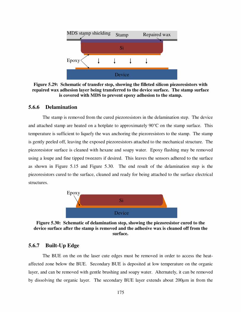
175
Figure 5.29: Schematic of transfer step, showing the filleted silicon piezoresistors with
repaired wax adhesion layer being transferred to the device surface. The stamp surface is covered with MDS to prevent epoxy adhesion to the stamp.
5.6.6 Delamination
The stamp is removed from the cured piezoresistors in the delamination step. The device
and attached stamp are heated on a hotplate to approximately 90°C on the stamp surface. This
temperature is sufficient to liquefy the wax anchoring the piezoresistors to the stamp. The stamp
is gently peeled off, leaving the exposed piezoresistors attached to the mechanical structure. The
piezoresistor surface is cleaned with hexane and soapy water. Epoxy flashing may be removed
using a loupe and fine tipped tweezers if desired. This leaves the sensors adhered to the surface
as shown in Figure 5.15 and Figure 5.30. The end result of the delamination step is the
piezoresistors cured to the surface, cleaned and ready for being attached to the surface electrical
structures.
Figure 5.30: Schematic of delamination step, showing the piezoresistor cured to the
device surface after the stamp is removed and the adhesive wax is cleaned off from the surface.
5.6.7 Built-Up Edge
The BUE on the on the laser cute edges must be removed in order to access the heat-
affected zone below the BUE. Secondary BUE is deposited at low temperature on the organic
layer, and can be removed with gentle brushing and soapy water. Alternately, it can be removed
by dissolving the organic layer. The secondary BUE layer extends about 200µm in from the
MDS stamp shielding Repaired wax
Device
Epoxy
Si
Stamp
Device
Epoxy
Si

176
laser cut edge, as shown in Figure 5.31. A more tenacious secondary BUE is observed between
closely spaced cuts, as seen in Figure 5.20 and Figure 5.21. This dissolves in acetone rather than
water. It is believed that this secondary BUE is composed of thermally damaged hairspray as it
has the qualities of a thin film rather than discrete debris. The primary BUE is deposited as
liquefied silicon at high temperature and burns through the organic layer to adhere to the bulk
silicon below. This forms a semi-solid ridge of about 10-15µm width and equivalent height.
The primary BUE masks the laser induced damage, and must be etched away to return the silicon
structure to full strength.
Figure 5.31: Closeup image of the laser induced built-up edge. The primary BUE is
composed of the silicon which redeposits at raised temperature, ablating the hairspray
and welding itself to the silicon surface. The secondary BUE is generally composed of the cooler dust which settles onto the surface of the hairspray coating.
5.6.8 Laser Cutting Parameters
Four parameters are required to determine how to cut the silicon stock. These are: i) the
repeat factor, nr, ii) laser pulse frequency, fl, iii) laser pulse energy, Ep, and iv) laser pulse width,
tp. All four of these factors are shown graphically in Figure 5.32. A simple schematic of the
cutting geometry is shown in Figure 5.32b, where each cut is modeled as a hemispherical
material removal operation.

177
a)
b)
Figure 5.32: Schematic of the laser cutting process, showing the laser pulse energy
pattern in a) and the physical cutting pattern on the silicon surface in b). The four main
parameters for laser cutting are indicated in the charts; repeat factor, laser frequency,
pulse energy, and pulse time.
The repeat factor describes the aspect ratio of cutting width vs. distance traveled between
pulses. A high repeat factor is associated with closely spaced cuts on the surface of the silicon.
This non-dimensional ratio determines whether the smoothness of the cut edges. A value of nr =
5, with 5 pulses per cut diameter translation, was found to produce smooth sided cuts through the
silicon. This is similar to values found in previous work [161], [162]. The repeat factor is
defined in Eq. (5.7), where w is the width of the cut and vl is the linear velocity of the laser cut.
l
r
l
wfn
v= (5.7)
The laser pulse frequency describes how quickly pulses are sent out by the laser. This is
typically run up to the limit of the laser power, Plmax, which is 20W for Electrox Scorpion Rapide
II system. Operating at the power limit as shown in Eq. (5.8) maximizes the speed of the cutting
process.
lmaxl
p
Pf
E≤ (5.8)
An upper limit on the laser pulse frequency can be defined by the generation of plasma
above the laser cut surface, which dissipates on the 1µs time scale [163], [164]. The cuts used in
this research were on the 50-100µs time scale, so the plasma time-scale was never reached.
The laser pulse parameters cannot be easily determined ab-initio as they are complex
functions of many processes including the laser ablation physics and thermodynamics. These
parameters are instead subjected to empirical optimization. An objective function can be
0
Laser Energy
Time
tp
Ep1
s lt f −=
w
Si
vl
l l rv f w n=
Cut area
Laser

178
generated from the ratio of cutting surface to the amount of heat generated, where the surface is
specifically not a function of cut width as shown in Figure 5.32b. We seek to maximize this
specific area of cutting. The heat generated in a cut is the pulse energy less the amount of energy
absorbed in the ablated silicon. This ablated silicon is ejected from the cut, carrying that energy
with it. An ideal cutting operation would use all of the laser energy for ablation, thus causing no
heating. The remaining heat energy, Eh, is calculated as shown in Eq. (5.9).
( )
2
( )
4
(1)
Volume
h l Si V
p p r
l
v
E Lwd
E E n
V w d
µ µ γ
µγ π
= − ∞
= =
(5.9)
The volume of material removed is calculated as a box of cut length L, depth d and width
w, all multiplied by a nondimensional volume ratio γV(n) to account for the hemispherical nature
of the cut. The volume ratio is a function of the number of cuts, n. This fraction is ≈0.5 when
n=1, and asymptotically approaches 1 as n grows large. The specific energy of silicon for laser
machining, µ l = 50J/mm3 [161], describes the theoretical energy required to ablate a volume of
silicon. The specific energy of cutting for the laser, µ l, describes the energy actually required to
ablate a volume of silicon as measured from cuts into silicon, as shown in Eq. (5.9). The average
cut width, depth and volume ratio for single pass cuts are used to estimate the volume ablated, V.
The pulse energy and repeat ratio are used to determine the energy used by the laser cutter to
remove the material. The specific area of heating for the cutting operation, saH, can now be
defined as shown in Eq. (5.10). This is a function of the laser pulse width and energy, as these
determine the specific energy of cutting for the laser.
1(1)
4 (1) ( )h l v
aH
p l Si l v v
E v ds
Ld E f w v d
π γ
µ π γ γ
−
= = − ∞
(5.10)
The cut is assumed to be many passes thick, so nr → ∞. This assumption affects all of
the pulse energy and time cuts equally, so does not affect the parameters for optimal cutting.
The objective function can now be used to study the full pulse energy and time parameter space
for the laser cutter, as shown in Figure 5.33. Each pulse time/energy setting was cut 4 times as
separate single cut parallel lines on a 1x1cm piece of silicon wafer. The cuts for multiple
settings were placed together on a single sample, and the sample was cleaved perpendicular to
the cuts so that the cross-section of each of the cuts could be easily measured with an optical
microscope.

179
Figure 5.33: Cutting efficiency as a function of pulse energy and time. Three regions are
identified in the chart, the no-cutting, cutting and power limited regime. The optimal cutting efficiency is found at 170ns and 500µJ.
Three regions are apparent in the specific area of cutting values. The low energy limit
cutoff for cutting scales with the pulse time. This is likely due to lower bounds on the optical
power required for ablation. The cutting region extends from this lower limit up to the
maximum pulse energy associated with each pulse time, which is determined by the cutting laser
power limits. Within the cutting region, a consistent trend in specific area of cutting is visible.
This trend is highlighted with contours on the X-Y plane of Figure 5.33. The optimal value
appears to be 170ns and 500µJ (70% power) for this equipment, with a dropoff in all directions.
The optimal cut width is about 31.2µm, with an average pulse fluence of 0.65J/mm2. This
optimum is expected to be machine dependent. The optimal cutting parameters are not the
maximum energy settings as might have been expected. These maximum power settings were
actually found to be on a fairly steep drop-off from the optimal values, with about 30-50% more
heating per area cut.

180
The cutting ability of the optimal setting was found to be significantly improved over that
of the maximum power setting, as shown in Figure 5.34. The cutting depth was studied to about
100µm, which was far more than needed for the 50µm thick wafers used in this research. The
maximum power cut generates a larger initial depth, then appears to clog the hole with remelted
black silicon. This silicon lowers cutting efficiency by interfering with further silicon ablation.
An immediate drop in cutting depth is observed, with further slow reductions as the number of
cuts increases. This is consistent with previous work where cuts were done with excess energy
deposition [162], [165]. The optimal settings show no such choking off as the silicon appears to
be ejected from the hole without significant remelting/redeposition. The optimal setting cutting
chart also does not show any sign of reduced cutting effectiveness after multiple cuts.
Figure 5.34: Cutting depth compared between the common maximum energy setting and
the optimal cutting efficiency setting. The maximum energy setting removes a larger
amount of material in the initial cut, and then proceeds to choke up the hole and reduce
the removal rate.
The geometry of the cut shows significant differences between the optimal settings and
the maximum power settings, as seen in Figure 5.35. The maximum power settings show a an
average surface cut width of about 55µm, while the optimal settings produce a surface cut width
of about 40µm. The optimal settings were found to produce a much tighter cut with increased
depth. The mid-depth width of the cut is shown in blue and pinches down to about 20µm,
resulting in a much finer cut.
0 2 4 6 80
50
100
Number of Cuts
Dep
th o
f C
ut (µ
m)
Max EOptimal

181
Figure 5.35: Cut geometry compared between the common maximum energy setting and
the optimal cutting efficiency setting. The maximum energy setting produces a much
wider cut, while the optimal setting produces a finer cut that reduces down to only about 20µm width after many passes.
The optimal settings process a generally improved cut for multiple reasons. The optimal
settings generate nearly half the heating while producing more rapid, reliable and finer cuts than
the maximum power settings. This is consistent with a relatively set amount of energy being
used to ablate the silicon, and then further energy is simply dissipated in heating the plasma
formed over the silicon surface. This thermal energy is passed to the silicon surface, causing
black silicon and remelt in the hole. The optimal settings cut off the laser pulse around the same
time scale that the laser energy transfer shifts to heating the plasma.
5.6.9 Wax Etching Parameters
The stamp is submerged in hexane to clean the wax off from the laser damaged edges of
the silicon stock. This process clears off any unwanted wax and also under-etches the film of
wax holding the piezoresistor to the stamp. This under-etching is unwanted under the
piezoresistor as it leaves the lower surface partially exposed to silicon etchant and the structure
vulnerable to mechanical loads. The under-etching is, however, useful for removing the
unwanted silicon on the stamp surface. A balance must be struck between etching the wax for
sufficient time to clean off the laser damaged area and halting the wax etch between the
piezoresistor is released from the stamp. A wax etch of >90s was found to be sufficient to clean
the laser damaged surfaces. Stock silicon exposed to longer etch times returned to full ≈2.5mε
0 2 4 6 80
20
40
60
Number of Cuts
Wid
th o
f C
ut (µ
m)
Max E SurfaceOptimal SurfaceOptimal Middle

182
strength. The second lower bound on wax etch time is the time required to detile the unwanted
silicon on the stamp. Large widths are desired for the tiled unwanted silicon, as this reduces the
amount of secondary BUE deposited onto the piezoresistor surface. The tradeoff between the
tile width and the wax etch time required to release the tile was studied. This was carried out by
laser cutting patterns of gradually increasing tile width on silicon stock that had been laminated
to the stamp surface with a 30µm film of MWM100 wax at 130°C. The patterned structures
were submerged in hexane for times ranging from 0s to 300s. The stamp was cleaned with a 3s
spray of hexane, and then brushed with soapy water. The combination of chemical and
mechanical agitation caused certain tiles to delaminate. The resulting hexane release curve is
shown in Figure 5.36, where the data points are shown in grey, the average release time for each
cut width is shown in red, the power trend is shown in blue and the standard deviation on each
time is bounded with the red lines.
Figure 5.36: Silicon stamp detiling for pieces of various sizes as defined by the
separation between parallel lines cut in the silicon surface. Two methods are observed to
occur; at widths <140µm the laser cutting forces are observed to physically remove the
small pieces, while at larger widths the hexane dip underetches the wax anchoring the
pieces to the stamp, causing them to fall off during cleaning. The standard deviation in
the average is plotted to give safe bounds for choosing removal times.
The fit line was generated with Eq. (5.11), where the release time, tr, is a function of the
tile cut separation wt. The fit values were found to be αr = 2.01±0.18, and the characteristic
separation wr = 33.7±7.3µm.
50 100 150 200 250 300 350 400 450 5000
50
100
150
200
250
300
Cut Separation (µm)
Tim
e (s
)
AverageStandard DeviationFit
Cutting Etching
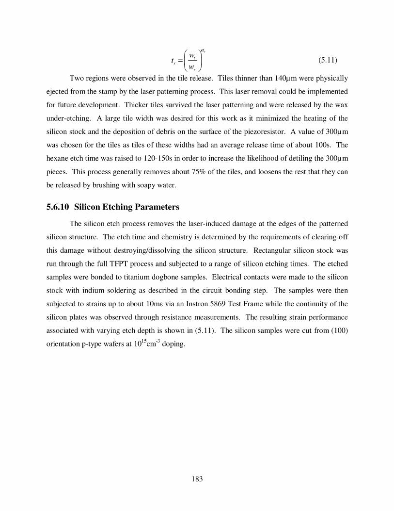
183
r
tr
r
wt
w
α
=
(5.11)
Two regions were observed in the tile release. Tiles thinner than 140µm were physically
ejected from the stamp by the laser patterning process. This laser removal could be implemented
for future development. Thicker tiles survived the laser patterning and were released by the wax
under-etching. A large tile width was desired for this work as it minimized the heating of the
silicon stock and the deposition of debris on the surface of the piezoresistor. A value of 300µm
was chosen for the tiles as tiles of these widths had an average release time of about 100s. The
hexane etch time was raised to 120-150s in order to increase the likelihood of detiling the 300µm
pieces. This process generally removes about 75% of the tiles, and loosens the rest that they can
be released by brushing with soapy water.
5.6.10 Silicon Etching Parameters
The silicon etch process removes the laser-induced damage at the edges of the patterned
silicon structure. The etch time and chemistry is determined by the requirements of clearing off
this damage without destroying/dissolving the silicon structure. Rectangular silicon stock was
run through the full TFPT process and subjected to a range of silicon etching times. The etched
samples were bonded to titanium dogbone samples. Electrical contacts were made to the silicon
stock with indium soldering as described in the circuit bonding step. The samples were then
subjected to strains up to about 10mε via an Instron 5869 Test Frame while the continuity of the
silicon plates was observed through resistance measurements. The resulting strain performance
associated with varying etch depth is shown in (5.11). The silicon samples were cut from (100)
orientation p-type wafers at 1015cm-3 doping.

184
Figure 5.37: Silicon etching effect on maximum tensile strain. The strain is greatly
increased from an as-cut strain of about 0.2mε, up to about 2.5mε after 20µm etching.
The maximum strain values largely plateau after the characteristic thickness of the
primary BUE, as indicated in the chart. After this point, the BUE and HAZ have been removed and the etchant is attacking and rounding the bulk silicon.
A plateau is observed in the strain performance of the silicon. Gains are seen up to
≈12µm etch depth, at which point the performance sensitivity to etching drops significantly.
This transition depth is characteristic of the primary BUE thickness. The performance plateau is
consistent with the silicon etchant removing the primary BUE that was shielding the stress
concentrations at around 10-15µm depth, with further etching simply attacking the bulk silicon.
The etch chemistry was chosen to selectively attack rounded corners, thus removing
potential stress concentrations. This is observed in Figure 5.38, which shows the as-cut silicon in
a). Both the primary BUE and the heat affected zone can be seen at the edges of the laser cut.
The wafer is etched by about 25µm in b) with a larger fillet on the upper corner (left hand side)
than the lower corner (right hand side).
0 5 10 15 200
0.5
1
1.5
2
2.5
3
Etch Dept (µm)
Max
Str
ain
(mε )
Bulk Si removal
Primary BUE removal
BUE thickness
range

185
a)
b)
Figure 5.38: Effect of etching on the laser cut edges of the thin silicon wafer. The wafer
edge is shown before the etching in a), with the BUE and HAZ indicated for clarity. The
wafer is etched by about 25µm, resulting in the profile shown in b), showing significant filleting of the top corner, and less of the bottom corner.
The etching solution was designed to round corners, produce a smooth surface finish, and
do so with a reliable, low etching rate for accurate control of the etching depth. The etching
properties of nitric and hydrofluoric acid mixtures are described in literature [166] as shown in
Figure 5.39. This was used to determine the correct solution composition, which is marked with
a red dot and corresponds to 9 nitric acid (69%) : 0 water : 1 hydrofluoric acid (49%) by volume.
Figure 5.39a shows how the etch rate varies with composition. The chosen composition lies far
down the curve towards lower rates that are less sensitive to variations in chemistry. The
measured etch rate was 2.36µm/min. Figure 5.39b shows how the etch geometry varies with
composition. The chosen composition lies within the region associated with mirrored surfaces
and rounded corners. The etching region from 8:0:2 to 9:0:1 satisfies all requirements. Initial
tests showed a slightly smoother surface associated with 9:0:1. This range of etching chemistries
lies well in the hydrofluoric acid diffusion limited regime. The nitric acid rapidly oxidizes the
exposed silicon surface, and the limited hydrofluoric acid dissolves this oxide. Hydrofluoric acid
is able to diffuse more rapidly to sharp corners, which acts to increase the etch rate on these
features [166]. The solution chemistry thus rounds out stress concentrations and smooths out
surfaces.

186
a)
b)
Figure 5.39: Etching rates and resulting geometry as a function of etchant composition-
HF (49.25%), HNO3 (69.51%) and H2O, as described in [166]. The etching rate is a
strong function of the composition as shown in a), while b) shows that a range of
concentrations that will generate rounded corners.
5.6.11 Scaling
The steps composing thin film patterning and transfer are largely serial operations with
the exception of the etching step. Handling operations are required for these serial processes.
Stock placement, detiling, stamp cleaning, stamp shielding and transfer all require fine control of
delicate structures. This process could be made more robust with automated handling. The
setup for TFPT is largely independent of PR geometry so design changes could be rapidly
implemented. Alternate methodologies could be implemented to simplify the process. The
detiling process in particular could be replaced with laser tile removal by thinning the tile width
down <140µm pitch. The effect of this aggressive cutting would need to be studied on the
silicon strain limit, as it may thermally crack the stock, increase BUE, damage the fragile device
with large silicon ejecta, or increase wax under etching. A more extensive acetone soak to clean
the patterned gage in conjunction with correctly tuned laser detiling would remove nearly all of
the manual steps required for this process.

187
5.7 Circuit Bonding
5.7.1 Overview
The circuit bonding step covers the attachment of the sensors to the deposited electrical
structures. This research focused on the use of tabletop indium soldering. The requirements of
high flexibility, small batch size and low per-device cost led to the development of a combined
indium soldering and conductive epoxy operation for generating contacts to the silicon. These
soldered contacts require little preparation time (≈1hr) and are produced at low cost ($10). The
completed device with sensor circuitry bonded to surface electrical features is shown in Figure
5.40.
Figure 5.40: Device with piezoresistors integrated into the surface electrical structures
via the circuit bonding process.
5.7.2 Metal-Semiconductor Contact
Electrical contacts are formed to the silicon piezoresistors in the metal-semiconductor
contact step. The device is seated in the geometric negative in order to ensure no unwanted
deflections occur during the step. The immobilized structure is placed on a hotplate so as to raise
the surface temperature of the mechanical structure to ≈150°C. This temperature was found to
improve contact performance by lowering the bonding parameter to nearly unity. Chemical
intermediaries are generated by the liquefied indium solder. The device is heated over about 1

188
min to avoid generating thermal variation at the surface. The geometric negative also helps even
out the temperature distribution by maintaining contact to all parts of the device.
A soldering iron set to 290°C is wetted in pure indium. This tip is rastered over the
contact pads on the piezoresistor with the motion aligned with the main axis of the piezoresistor.
This pattern avoids bridging the gap between the contact pads. It also limits the surface
scratching to be aligned with the axis of stress, which minimizes the chances of creating a
significant stress concentration on the surface. Indium will stick to the surface of the silicon with
a low contact angle if correctly applied. Failure is generally a result of surface contamination, an
unwetted soldering tip or a cool substrate.
5.7.3 Circuit Completion
Conductive epoxy is used to link the soldered contact pads to the electrical traces
deposited onto the surface of the mechanical structure. A low temperature method is desired in
order to avoid generating un-necessary and potentially damaging thermal stress on both the
electrical traces and piezoresistors. Chemtronic Circuitworks CW2400 two part epoxy was used
to make linkage. This epoxy has low resistance (<0.001Ω-cm) and can be cured at room
temperature if required. The room temperature cure requires 4 hrs, but can be reduced to 10min
if the device is cured at 65°C. The epoxy is also placed on the trace contact pads to protect the
thin deposited film from direct contact with spring pins.
5.7.4 Protective Coat
A protective coat is applied to the surface electrical structures, including the
piezoresistors. This coating aids in strain transfer to the piezoresistor, prevents damage to the
structures, reduces noise at the sensor and resists delamination. The conductive epoxy must be
cured before the protective coat is applied otherwise it will contaminate the protective coating
with silver particles. A low-temperature method is desired, as with the circuit completion step.
Gagekote #8 from Vishay Micromeasurements is used for the protective coating. This generates
a thin (<50µm) transparent film when painted onto a surface. The protective coating can be
deposited at room temperature and is ready after 4 hours. An elevated cure can be carried out at
65°C for 30 min.

189
5.7.5 Scaling
The soldering and conductive epoxy was used in the circuit bonding step to achieve the
goals of high flexibility, small batch size and low per-device cost desired for this research. The
metal-semiconductor contact process could be adjusted to increase the fabrication scale. These
pads could be defined and formed earlier in the process of TFPT if the contact pad location is
known. Metal film deposition onto the silicon stock would enable contact to be made without
direct soldering. Errors in alignment would result in either incomplete pad coverage or coverage
of part of the delta section of the piezoresistor. Both situations are acceptable for maintaining
high performance sensing. The metal film deposition would generally require typical
photolithographic processes which are associated with decreased flexibility but increased scale.
Precision dispersion and handling systems could be used to automate the epoxy and
acrylic handling. Further metal deposition or aerosol jet printing could also be used in place of
conductive epoxy for a more parallelizable process. The protective coat needs only be placed
over the sensors and electrical structure. A spray-painting operation could be used through a
mask to coat the surface of the device without covering the electrical contact pads.
5.8 Demonstration
5.8.1 Device Overview
A multi-axis nanopositioner was fabricated to demonstrate the capability of the full
NLBM process. This device is shown in detail in Figure 5.41 below. The underside of the
device is shown for added detail, as this side shows the ribbing and other structures. The top side
(+Z) is planar in order to facilitate the deposition of traces and sensors. Wire flexures of equal
width and thickness (600µm) are used to allow both in- and out-of-plane motion of the stage.
The blade flexures are of reduced thickness (150µm) but larger width (1.5mm) in order to offer
little stiffness to motion of the stage along the wire flexure axis while not deflecting during out-
of-plane motion. Nearly all out-of-plane motion then occurs in the wire flexures which have the
integrated strain sensors, labeled V1-6. Each piezoresistor is placed to one side of the in-plane
bending neutral axis of the wire flexure. This ensures the sensor will read in-plane deflection of
the wire flexure. The sets of gages (1-2, 3-4, and 5-6) are placed on opposite sides of the neutral
plane. Out-of-plane motion generates equal signals from both sensors in the set, while in-plane

190
motion then generates opposing signals. This allows for the motions to be mathematically
distinguished from one another at the voltage end.
The wire-blade design allows for full 6-DOF motion of the stage while amplifying out-
of-plane sensitivity at the expense of range. A wire-wire design would shift the dynamic range
of the device towards larger range but reduced sensitivity. Twelve holes are pierced through the
structure to account for the nine semi-kinematic contact pins used in the transfer fixture. The
Hexflex is used both face up and down in this fixture- face up for surface deposition through a
mechanical shadowmask, face down for the transfer of the sensors to the device surface. Three
of the nine semi-kinematic pins are located asymmetrically when viewed with regards to the 6-
fold axial symmetry of the device. Thus three extra holes must be placed for them. The holes
provide 250µm radial clearance for the pins, except for the semi-kinematic contacts shown at the
bottom of Figure 5.41. These four holes are D shaped, which provides a contact surface for
locating the Hexflex structure during the transfer and deposition steps.
Figure 5.41: Diagram of the Hexflex nanopositioner structure from the underside. The
main components are identified including the flexure bearings, actuator paddles and
center stage, rigidified with ribbing. Semi-kinematic contacts are located in four of the twelve holes piercing the structure.
Actuator paddles are located with triangular symmetry for the placement of actuator
magnets. Three force-based dual-axis Lorentz coil actuators will be used to drive the stage
motion [1], [7], [51]. Ribbing is used to link these paddles to the center stage in order to resist

191
the drumhead vibration of the stage and high mass paddles typical of fully planar Hexflex
designs [1]. The center stage is ≈1cm diameter, and is intended to carry a
nanometrology/manufacturing payload. Traces can be run out to the center stage if electrical
contact is desired. These traces would be deposited along the flexures during the surface
micromachining step. The outer Hexagonal structure is mechanically grounded. It also contains
the electrical bond pads needed to drive the sensors and payload.
A relation can be written between the stage motion and sensor readings, assuming ideal
flexure elastomechanics for the wire and blade. The finite ratio of the constraint vs. freedom
stiffness will scale the effective strain and thus the position-voltage coefficients down by a
fractional amount. This equally affects the range and resolution, so the sensing dynamic range is
unchanged. The transform matrix between the sensor voltage outputs, [V1,V2,…], and the motion
inputs [∆x,∆y,…] may be written as shown in Eq. (5.12), where r1 and r2 are device dimensions
shown in Figure 5.41, Gir is the in-plane position-voltage coefficient for the ith sensor, and Giz is
the out-of-plane position-voltage coefficient.
( ) ( )( ) ( )( ) ( )( ) ( )
0
0
sin 6 cos 6
sin 6 cos 6
sin 6 cos 6
sin 6 cos 6
1r 1 1r1
2r 1 2r2
3r 3r 1 3r3
4r 4r 1 4r4
z
5r 5r 1 5r5
6r 6r 1 6r6
1 1z 2 1z 1z
1
G r GV
G rGVx
G G rGVy
G G r GV
G G rGV
G G r GV
r G r G G
r
π π
π πθ
π π
π π
− − ∆ − = ⋅ ∆ + − − ∆ − −
−
− −
…
( ) ( ) ( ) ( )
( ) ( ) ( ) ( )
( ) ( ) ( ) ( )
( ) ( ) ( ) ( )
2
sin 6 cos 6 cos 6 sin 6
sin 6 cos 6 cos 6 sin 6
sin 6 cos 6 cos 6 sin 6
sin 6 cos 6 cos 6 sin 6
2z 2z 2z
1 2 3z 1 2 3z 3z
1 2 4z 1 2 4z 4z
1 2 5z 1 2 5z 5z
1 2 6z 1 2
G r G G
r r G r r G G
r r G r r G G
r r G r r G G
r r G r r
π π π π
π π π π
π π π π
π π π π
−
− + + −
− − − −
− − − + −
− + − −
x
y
6z 6z
z
G G
θ
θ
∆ ⋅ ∆ ∆
−
(5.12)
The position-voltage transform matrix is invertible due to the sign separation of in- and
out-of-plane motion for each sensor set. The matrix may be inverted to back out position from
the six voltage readings of the integrated sensing once the calibration values Gr and Gz are
known. A simple means of calibration is to enforce pure Z translation on the stage in order to
determine all Gz values simultaneously. A pure θz motion is next enforced in order to determine

192
all Gr values simultaneously. The third and sixth columns of the transform matrix show how
these two pure motions translate into voltages at each sensor. The in- and out-of-plane motions
for each of the three sensor sets are thus studied in parallel. All stage displacements are
superpositions of these six basic motions.
5.8.2 Setup
The Hexflex device is fabricated as shown in the previous figures through this paper.
The bulk mechanical structure is generated through micromilling. The surface electrical
structure is generated through anodization, thermal oxide growth and deposition with a
mechanical shadowmask. The sensor integration is carried out with TFPT using a 50µm (110) p-
type silicon wafer at 2.9x1016cm-3 doping. The circuit bonding is carried out with indium solder
and conductive epoxy. The gages were further annealed at 20V to stabilize performance and
reduce barrier noise/resistance. Six low noise Wheatstone bridge circuits [97] were linked to the
six integrated piezoresistors in the device. The gain on each bridge was set to 12 as determined
by the maximal utilization of the ADC voltage range [97]. Low noise metal film resistors were
used to complete and balance the quarter bridges [167], [168]. The Hexflex was seated in a
holder for mechanical anchoring as well as alignment of the electrical spring-pin contacts and
potential actuation coils. The finished device seated in the holder is shown in Figure 5.42.

193
Figure 5.42: Hexflex device in testing fixture, with electrical connections to the surface
deposited traces.
5.8.3 Fabrication Results
The fabrication process was found to produce all structures within the desired limits. The
sensor location is the most crucial parameter, as it is 50µm from the edge of the flexure and must
not significantly overshoot this edge. The scale of the errors occurring in this alignment is
tabulated in Table 5.3. The ≈2 standard deviation 95% error is listed for each source and this is
geometrically summed to find the net error of about ±27µm for the NLBM process.
Table 5.3: Sensor integration error budget
Source Error (±µm) 95% Micromilling 3
Micromill tooling 4 Pattern calibration 6 Laser and fixture 6
Repair 4 Transfer fixture 3
Cure 25 Sum 27
Bulk micromachining with the micro mill is only accurate to the 3µm accuracy of the
machine. The micro mill tooling is calibrated to remove large diameter errors in the micro end
mills. This calibration relies on two edge measurements, each limited by the resolution of the

194
optical microscope to about 1.5µm standard deviation. The net result is a confirmed 2µm
standard deviation in calibration. The patterning process is aligned with a single calibration
stamp before each run. This calibration again relies on the optical microscope and the stability
of the combined laser cutter/fixture to align the coordinate frame with about 3µm standard
deviation error in both axes. This error is consistent with the observed laser and fixture induced
variation of approximately 3µm standard deviation error in both axes. It is suspected that this is
evenly due to both the fixture alignment (1.5-2µm standard deviation) and the laser cutter
galvanometer error (2µm standard deviation). Thermal drift was observed to occur mainly in the
Y axis, along the long axis of the sensors. The piezoresistor placement is relatively insensitive to
errors along this axis as it only causes minor gage factor variation. The thermal drift was
measured to be around 5µm/cut in the Y axis, but around 0.2µm/cut in the X axis. The Y-axis
drift was removed with a readjustment of the pattern location after each cut. The significant
disparity between axes is likely due to the laser stage structural symmetry that balances out X
axis expansion. The Y axis is not equivalently balanced and thus shows thermal drift. Wax
repair under the piezoresistor requires the wax anchor be liquefied while holding the
piezoresistor in location. This process is found to produce about 2µm standard deviation error in
both axes, on the limit of the visible variation due to the roughened uneven edges of the gage.
The transfer fixture alignment was measured to be about 1.5µm standard deviation error in both
axes. The final error is that of the curing process, where the liquid wax and epoxy generate
fluidic forces on the piezoresistors, moving them around during the heated, pressurized cure.
The characteristic error for this cure process is 26µm. These sources are summed geometrically
based off of the assumption of uncorrelated error.
The dominant error source is from the curing process, where the heated epoxy and wax
films pull the sensors off of alignment. The main error was observed to occur in asymmetric
coating of the thin piezoresistor arms with epoxy. The epoxy is compressed during the transfer
and ends up largely on one side of the piezoresistor arms. This generates a slight sideways (X)
force on the gage, with reduced effect along the axis of the gage (Y). The error standard
deviation was observed to be ≈5µm for evenly coated sensors. Several large shifts (≈30µm)
were observed when the epoxy was coated onto the gage unevenly. This was apparent by the
highly asymmetrical epoxy flashing observed after delamination, consistently in the opposite
direction of the large shift. The asymmetrical epoxy placement is an artifact of the manual

195
application, and is thus not fundamental to the system. Improved epoxy placement via
automated systems or masking operations would minimize this effect and is expected to reduce
the curing error to ≈5µm.
The secondary error source is from the laser and fixture, which produces relatively high
error in the fixture alignment as well as in the repeat calibration and the Y axis thermal drift. A
more thermally stable fixture could be calibrated with many averaged samples, reducing the
patterning error to ≈1-2µm. This would also remove thermal drift from the list of sources. The
fixture alignment error is likely fundamental as a fixture error of 1.5-2µm standard deviation is
consistent between the laser and transfer semi-kinematic couplings. It is unlikely this can be
improved significantly with semi-kinematic couplings. The laser error of ≈2µm is likewise a
characteristic of the laser cutter machine.
The total scale of acceptable error is 50µm, which is about four standard deviations
observed for the NLBM process. Improvements in the epoxy deposition and laser fixture should
be able to significantly decrease the alignment error, down to ≈10µm. This upper bound on
acceptable misalignment is defined by the gap between the edge of the piezoresistor and the edge
of the flexure. The difference between the gap and the variation suggests that the process should
be well capable to locating the gages in the absence of unmodeled or unmeasured process
variation.
The net fabrication parameters for the main component are listed in Table 5.4. This
shows the capability of the NLBM process in terms of feature fabrication control and alignment.
The characteristic error is broken into two terms, the average error and the 95% variation in this
error. The values were measured over multiple locations on the device as all the structures occur
in 6-fold symmetry. These two parameters give an insight into the scale of the process errors
both repeatable and non-repeatable.

196
Table 5.4: NLBM process error
Component Desired (µm) Characteristic Error
(±µm) 95% Sensor X location 50 15±27
PR arm width 150 3±5 Wire flexure width 600 0±4 Blade flexure width 150 6±4
Trace width 800 -55±80 Trace location 1000 30±30
The sensor location is described in detail previously. It was desired to keep the sensor
50µm from the edge of the flexure. An average value of 65µm was observed for this, well within
acceptable values. This alignment is a function of many steps as described above. The
piezoresistor arm width is designed to be about 150µm wide. This is easily set during the
patterning step by the laser cutter. The width is reduced by 10µm on either side by silicon
etching. This process was measured to be accurate to within 3±5µm. The wire/blade flexures
and shadowmask traces are all generated during the bulk micromachining step. These are
produced by the micromill which has 3µm cutting accuracy. The tooling used for this process
generates further bias through diameter calibration error, which is typically on the scale of 4µm.
This was observed in error of the mechanical features. The trace location is a function of the
micromilling error, the transfer fixture error, and the deposition process error. This was
measured to be 30µm, significantly larger than the expected error from micromilling and
fixturing. Both the trace width and location errors are believed to be due to the variation in the
deposition process due to sample not being placed normal to the aluminum source. The
shadowmask then acts to block the full deposition of the trace, resulting in certain traces
appearing thinner. This can be resolved with thinner shadowmask structures or more normal
alignment to the source.
The parameters listed above capture the alignment of the electrical structure with the
mechanical structure. They also capture the scale of error associated with feature geometry. The
sensor errors are all on the scale of about 25µm, which is well within functional bounds for the
Hexflex nanopositioner. This shows that NLBM holds the potential to be used for fabricating a
range meso-/microscale devices with micron-scale accuracies.

197
5.8.4 I-V Characteristics
The current-voltage performance of the integrated piezoresistive sensors were measured
using a four-point probe setup and are shown for comparison in Figure 5.43. The I-V curves
show the expected diode behavior of an exponentially decaying resistance in series with an
ohmic resistor.
Figure 5.43: I-V characteristics of the six piezoresistive sensors on the Hexflex.
Gage 6 is not included in the analysis as it was fractured during the delamination step.
This was caused by the high degree of compliance of the multi-axis case study device- the
Hexflex structure. The delamination process induces small forces on the structure as the stamp
must be pulled off despite a viscous wax holding it in place. These forces were sufficient for the
last stamp to flex the structure (now released from the anchoring of the other stamps) far enough
to yield the final gage. It is expected that improved fixturing of the device during delamination,
or the inclusion of a chemical separation step such as hexane dissolution of the wax will increase
the robustness of this step. The remaining measured gages provide a sufficient demonstration of
i) the ability of the newly developed NLBM to fabricate integrated sensing on metal MEMS, and
ii) the ability of the non-linear piezoresistive design theory to model these fabricated sensors.
The gages were indium soldered at a reduced temperature (120-130°C) in order to
minimize any further crack propagation. Gage 6 showed too high resistance (100kΩ) for use as a
sensor despite this reduced temperature. Gage 1 is an outlier in this set, as it shows a bonding
parameter that is near unity (1.2), far below the bonding parameters observed for the other gages
0 5 10 150
2
4
6
8
Voltage (V)
Cur
rent
(mA
)
Gage 1Gage 2Gage 3Gage 4Gage 5

198
(6-12). The bonding parameter variation may have been due to acquired contamination in the
indium solder, despite cleaning, as wax was observed on the iron after the first gage soldering
operation.
The combined I-V, noise and gage factor characteristics of gage 1 can be understood as a
gage of performance equal to the other measured gages, but with a more linear I-V curve. This is
consistent with a shunt resistance in parallel to the gage, passing through the oxide insulation.
This was tested via a model that had the total gage resistance expression as shown in Eq. (4.10)
modified to be the regular Rpr placed in parallel with an oxide resistance, Rox. This modified
resistance expression was propagated through the current expression and gage factor calculation
to see the effect of an oxide shunt. A 10kΩ oxide shunt resistance was found to match the I-V
curve shape and produce an expected gage factor of about 70, as observed below. This disjunct
between the high performance I-V curve and low performance gage factor is due to the fact that
the shunt resistance affects the IV curve by limiting the effect of the barrier resistance, but has
only limited effect on the gage factor. The net effect of the inclusion of the oxide resistance on
the gage factor is an inclusion of a Rox/(Rox+Rpr)≈0.8 term to GR, on top of the standard values of
GR and GV given the β value. A Schottky barrier shunt was considered as a possible mechanism,
however this would have the effect of erasing the total effect of the barrier resistance on both the
I-V curve (consistent with data) and on gage factor (inconsistent with data). The barrier shunt
model predicts a gage factor of around 110, significantly higher than observed.
The average I-V parameters for the gages are listed in Table 5.5. The predicted values
are drawn from previous work on semiconductor piezoresistor design. The bonding parameter,
β, describes the variation of the ohmic resistivity from a baseline term associated with ideal
operating conditions. Variation is observed in this term as a function of soldering/substrate
temperature, and wafer doping level. The significant increase in this value over the design
predictions is due to the reduced indium soldering temperature and potential surface
contamination. The ohmic resistance matched the expected value as the resistance drop of the
higher thickness of the silicon wafer (35-45µm after 20µm etching) cancelled the increased
ohmic contact resistance due to the increased bonding parameter. The piezoresistance is part of
the ohmic term. The barrier resistance creates an apparent voltage drop which asymptotically
approaches the value Vb0 at high voltages. The barrier voltage drop is above the expected value
due to the higher bonding parameter. Overall, the performance of the gages is accurately

199
captured by the piezoresistor model, which has only one degree of freedom- the bonding
parameter. The bonding parameter provides insight into the fabrication process and suggests that
better performance could be obtained with higher indium soldering substrate temperatures.
Table 5.5: I-V parameters
Parameter Design Measured
(±σ) Model Error
(±σ) β 1.4 8.0±4.6 N/A
ohmic R 1.6kΩ 1.6±0.2kΩ 0.004±0.042kΩ Vb0 0.83V 2.7±1.3V -0.009±0.18V
5.8.5 Noise Characteristics
The noise characteristics of the piezoresistors were measured with a 50kHz National
Instruments NI9239 ADC and are shown for comparison in Figure 5.44. The noise shows the
expected 1/f-like performance, dominated by the Schottky barrier flicker noise. The observed
average Hooge constant, αsb, for the noise is 10-0.51±0.40, with standard deviation. This is given
logarithmically to indicate how the standard deviation scales the magnitude. This is a close
match to the expected value of 0.26 or 10-0.59. The average frequency scaling term, δ, is
0.16±0.11, which overlaps with the expected value of 0.18 as observed earlier.

200
Figure 5.44: Noise characteristics of the six piezoresistive sensors on the Hexflex.
5.8.6 Gage Factor Characteristics
The gage factors of the piezoresistors were measured by enforcing stage displacements
with an Instron 5869 Test Frame. The frame used a Solartron ACR15 LVDT with 100nm
resolution to drive the stage while simultaneously measuring the sensor outputs. The stage was
driven along its Z axis, normal to the plane of the device, to measure the out-of-plane sensitivity
of the piezoresistors. The setup for doing so is shown in Figure 5.45.
10-1
100
101
102
103
10410
-12
10-11
10-10
10-9
10-8
10-7
10-6
10-5
10-4
Frequency (Hz)
Spec
tral
Den
sity
(V2 /H
z)
Gage 1Gage 2Gage 3Gage 4Gage 5

201
Figure 5.45: Out-of-plane gage factor measurement setup, with main components
identified. A linear bearing is attached to the Hexflex fixture and used to drive the center
stage purely in the z-axis.
The stage was next rotated around the Z axis to measure the in-plane sensitivity of the
piezoresistors, as shown in Figure 5.46. These two tests capture the in- and out-of-plane
position-voltage coefficient, respectively, for each sensor.
Figure 5.46: In-plane gage factor measurement setup, with main components identified.
A rotary bearing is attached to the Hexflex fixture and used to drive the center stage purely around the z-axis.
The performance was measured over a few hundred microstrain to capture the small
signal gage factor behavior. This small signal behavior is the focus of the piezoresistor design
work.

202
The effective strain and resistance change is calculated using Eq. (5.13) [97]. The
measured displacement, δ, is translated into effective strain, εeff, via the flexure force to strain
gain, εF, and strain geometry gain GSG, while the measured voltage output from the bridge V is
translated into fractional resistance change ∆R/R via the bridge strain type, Nε, source voltage VS,
span temperature compensation gain GSTC, and amplifier gain G [97].
( )
eff
R R
F SG F
S STC
VG G
N V G G
ε
ε
δε
∆
=
(5.13)
Both the in- and out-of-plane gage factor can be accounted for in Eq. (5.13) through the
adjustment of the strain geometry gain. This term defines how the effective strain seen by the
piezoresistor is scaled down from the maximum at the base of the flexure by the location and
finite size of the gage [97], and is shown in both cases in Eq. (5.14). The out-of-plane strain
geometry gain, GSGz, is determined using the standard calculation [97] as the sensor is placed on
the surface of the flexure and is parallel to the neutral plane, where Lr is the length of the gage, Lf
is the length of the flexure and γ is the strain field constant. The in-plane strain geometry gain,
GSGr, includes an extra term to account for the fact that it is not placed at the edge of the flexure.
The additional term is determined through integrating the gage width, br, over the strain field
observed on the surface of the flexure during in-plane motion [97]. This calculation accounts for
the gage offset from the edge of the flexure, bo, where bf is the width of the flexure.
1
21 1
rSGz
f
r orSGr
f f
LG
L
b bLG
L b
γ
γ
= −
+= − −
(5.14)
The out-of-plane strain geometry term is approximately 0.84, while the in-plane term is
approximately 0.28. This provides a simple means for comparison of the dynamic range
between the two axes of motion sensing for each gage. The dynamic range of the in-plane
sensing should then be about 33% (-10dB) of the out-of-plane sensing. The strain vs. resistance
relations for the piezoresistors are shown in Figure 5.47 for out-of-plane sensing and Figure 5.48
for in-of-plane sensing. Eq. (5.13) and (5.14) enable the different axes to be normalized to
observe gage factor directly.

203
Figure 5.47: Out-of-plane gage factor characteristics of the piezoresistive sensors on the
Hexflex.
The in- and out- of plane gage factors show similar trends, which is expected given that
both motions are driving the piezoresistor in the same fashion. From the view of the sensor, it is
being tensioned and compressed in largely the same fashion from both types of displacement.
Secondary effects like shear stresses on the piezoresistor during in-plane motion may be
generating variations between the two methods.
Figure 5.48: In-plane gage factor characteristics of the piezoresistive sensors on the
Hexflex.
The gage factor for each device was determined by fitting a linear position-voltage
coefficient and a third order term to the data. This third order term is intended to capture any
0 50 100 150 200 2500
5
10
15
20
Strain (µε)
Piez
ores
istiv
e ef
fect
( ∆R
/Rx1
03 )
Gage 1Gage 2Gage 3Gage 4Gage 5
0 50 100 1500
5
10
15
Strain (µε)
Piez
ores
istiv
e ef
fect
( ∆R
/Rx1
03 )
Gage 1Gage 2Gage 3Gage 4Gage 5

204
non-linearity in the gage factor. The piezoresistors are designed to have a gage factor of 127.
The average linear gage factor is predicted through I-V measurements to be 88±26. The drop in
gage factor is due to the high bonding parameter. The average measured linear gage factor for
out-of-plane motion is 69±10. The average measured gage factor for in-of-plane motion is 71±3.
The measured gage factors are normalized to the intrinsic gage factor of the silicon, GF0=167, at
the device doping level via the ratio rGF=GF/GF0. This is done to illustrate the attenuation of the
gage factor due to the fabrication and I-V characteristics, which is the figure of merit predicted
by the model. Both the gage factors and their associated ratios are shown in Table 5.6 for
comparison between the gages.
Table 5.6: Measured gage factors
Gage Predicted GF (rGF)
Out-of-Plane In-Plane
Measured GF (rGF)
Model Error (∆rGF in %)
Measured GF (rGF)
Model Error (∆rGF in %)
1 134 (80%) 72 (43%) 37 67 (40%) 41 2 77 (46%) 59 (35%) 11 74 (44%) 1 3 72 (43%) 62 (37%) 5 70 (42%) 1 4 71 (43%) 74 (45%) -2 72 (43%) -1 5 87 (52%) 80 (48%) 4 69 (42%) 11
Both the in- and out-of-plane model are found to over predict the gage factor ratio by an
average of 11%, The single axis case study does not show significant error in the gage factor
prediction, while the multi-axis case study does. The error in the gage factor model prediction
may be due to a range of sources. Primarily, the error is occurring for gage 1, as this is predicted
to have a gage factor of about 134, but is showing values around 70. This is consistent with an
insulation short in parallel with the gage lowering the apparent resistance so the model over
predicts the performance of the gage. Absent gage 1, the average out-of-plane model error is 5%
and the average in-plane model error is only 3%. Several other error sources are noted below.
First, several error sources are noted that are unlikely to be the cause given the multiple
gages. Stock misalignment during the lamination step of TFPT would result in a reduction in the
gage factor. Doping variation in the wafer would affect the gage factor of the piezoresistor arms.
Both the angle and the doping variation would typically be unbiased error sources, so it is
expected that over all gages, the effect would average to 0. Thus, these two are unlikely to be the
cause of a 5% increase in the gage factor attenuation.

205
Second, several error sources are noted that would occur over all the gages and could
occur specifically for the multi-axis case study. These are: i) wafer flat misalignment, ii) gage
misalignment, iii) flatness/warping, iv) flexure geometry, v) oxide shorting vi) Schottky barrier
piezoresistance, vii) test setup, and viii) gage factor nonlinearity. The wafer that the gages are
cut from may have been misaligned to the crystal planes. This would cause a net reduction in
gage factor for all devices cut from this wafer, which would explain the consistent effect. The
wafer used for the six DOF structure was different from that used in the 1 DOF structure, so the
wafer-to-wafer variation may explain the reduced gage factor. Misalignments of the
piezoresistors in both X and Y would reduce the strain geometry gain below predicted values.
Warping or angled placement of the piezoresistor during the transfer process might reduce the
ability of the piezoresistor to react to small deflections of the flexure. This effect would uniquely
occur in the six DOF structure as the six gages will not all go down exactly evenly. The single
DOF device would not have an equivalent problem, as the gage would self-align to the surface.
Gage misalignment is unlikely to be the culprit as the alignments are known to be accurate
within about 30µm, and this is insufficient to attenuate the gage factor sufficiently. The flexure
geometry may be attenuating the strain observed at the flexure due to filleting. This geometry is
different between the single and multi-axis case study, so may play a role in the effective strain
observed by the gage. The limited insulation capability of the oxide film means that each gage
sees a resistor in parallel with it. This effect is predicted to reduce the gage factor by
approximately 2% on average, but this may be underestimating the effect. The Schottky barrier
at the positive sensor contact pad is known to have piezoresistive properties [169], which may be
activated by partial strain on the contact pads, and may be activated in a different manner than
the single axis device due to the different gage geometries. The test setup may have an
unanticipated compliance in the structure that reduces the displacement observed by the device.
This would explain the general trend over all gages, however the measured structure compliance
suggests this is not occurring. The measured z-stiffness of the structure during the test was
30kN/m, which is actually above the 27kN/m estimated for the structure. An extra displacement
in the structure would cause a decrease in stiffness, below that anticipated for the device and
bearing. This is not observed. The gage factor nonlinearity is observed in both case study
devices, and this would appear as a change in the apparent small-displacement gage factor if the
gages are not operate around 0 absolute strain. The gages are not operating around 0 strain, first
206
due to thermal compression and second due to the need to apply a net compression to them given
the slight flatness errors of the clamping plates on the test setups. The bias ensures the gages
remain safely within their operating range, near 0 or negatively biased, at the start of each
displacement test. The bias will apply a nonlinear change to the gage factor, which is estimated
to be on the scale of 1-5% based off of the measured nonlinearities in both case studies and the
literature [95]. This could account for the majority of the variation.
5.8.7 Motion Characteristics
The positioning capability of the device can be studied by comparing the known stage
location to the sensor indicated stage location after calibration. This is done using the
measurements of the gage factor. A known displacement was enforced on the device, and the
gage responses measured. The gage factors were measured to determine the sensor performance.
The first order gage factor term is now used to calculate a net voltage-to-motion coefficient via
Eq. (5.13), which translates the sensor voltage changes into sensed displacements. The sensed
displacement for each sensor is then combined as determined by the inverse of the calibration
matrix, shown in Eq. (5.12). This operation is simply an average of the sensed displacements
due to the symmetry of the structure and of the test trajectories. Both tests subject all of the
gages to equal displacements. The sensed and known positions are compared for the out-of-
plane case in Figure 5.49. The errors due to measurement (LVDT and ADC) are captured in the
scale of the data points.

207
Figure 5.49: Motion tracking capability of the integrated sensing demonstrated for the
out-of-plane linear displacement trajectory. The 1:1 mapping is shown with the blue solid line, which corresponds to the correct sensor reading.
The sensors are shown to provide accurate sensing over the range of motion studied in
this test, with RMS error of 0.32µm. The flicker noise on the sensors is attenuated by about 2.5x
by the 6 sensor averaging, as captured in M. The sensed and known positions are compared for
the in-plane case in Figure 5.50, which shows the same trends as the out-of-plane case.
Figure 5.50: Motion tracking capability of the integrated sensing demonstrated for the
in-plane rotary displacement trajectory. The 1:1 mapping is shown with the blue solid
line, which corresponds to the correct sensor reading.
The errors due to measurement (LVDT and ADC) are again captured in the scale of the
data points. The noise is slightly higher for the in-plane measurements due to the reduced in-
0 5 10 15 20 25 30 350
5
10
15
20
25
30
35
Actual δ (µm)
Sens
ed δ
( µ
m)
Measured1:1
0 5 10 15 200
5
10
15
20
Actual θ (mrad)
Sens
ed θ
(m
rad)
Measured1:1

208
plane motion sensitivity. Both trajectories were of similar linear scale when seen at the ends of
the wire flexures. The trend away from the 1:1 line around 5 and 12mrad are largely due to the
flicker noise variation in gage 2, as can be seen in Figure 5.48.
The gage factor and dominant noise characteristics of the sensors allow for a
measurement of the sensing dynamic range. The gage factor describes how the strain is
transformed into voltage, which allows for the maximum strain to be scaled into a maximum
voltage. The voltage noise and maximum voltage signal can be compared to find the dynamic
range of the sensors. These numbers are quoted for resolution dynamic range for a system with
1kHz operating BW and 10kHz sensing BW. The integrated sensing is designed to have a
resolution of 69dB dynamic range out-of-plane, and 59dB in-plane over a 10kHz sensor
bandwidth. The measured dynamic range is 59dB out-of-plane and 49dB in-plane. The
difference between these is due to the low substrate temperature during indium soldering which
raised the bonding parameter from 1.2 to about 8. This could be fixed by an improved
delamination process, more consistent heating, and reduced surface contamination.
The range and resolution of the device are directly calculated from the dynamic range.
The range of the device is set by the safety factor of 3, which allows for an estimated range and
resolution to be calculated. The out-of-plane range and resolution are expected to be
approximately 297µm and 94nm, respectively. The in-plane range and resolution are expected to
be approximately 261µm and 260nm, respectively. These numbers would be significantly
improved by increased substrate heating during the indium soldering step, as well as contact pad
doping. The effect of such improvements is expected to push the resolution below 1nm in both
axes.
5.9 Discussion
5.9.1 Insulation
A titania film insulation was used for this research due to its high mechanical adhesion to
the surface, as well as the high expected resistance (20x higher than measured). The oxide as
patterned is thus not an ideal solution for surface electrical isolation. Several solutions may be
possible. The titania film has excellent mechanical properties and can be produced in a simple,
low-cost manner, so it is desirable to continue to use it if feasible. Two methods are proposed to

209
improve the electrical properties of the titania film. First, the trace metal can be changed to
generate a large Schottky barrier with the titania. Second the bulk titanium can be biased to the
maximum voltage observed on the surface, which is typically 5V.
First, the trace material could be engineered to produce higher resistance. A positive
surface voltage relative to the titanium substrate puts the aluminum-to-oxide barrier in forward
bias, and the oxide-to-titanium barrier in reverse bias. The Schottky-Mott relationship suggests
that the barrier height should be a rough function of the difference between the work function of
the metal and the oxide. The work function for titania is roughly 4.3eV, which is a close match
with titanium 4.33eV [170], and aluminum ≈4.15eV. Measurements show that the reverse bias
resistance of the oxide-to-titanium barrier is slightly higher than that of the aluminum-to-oxide,
but not significantly. Silver (4.6eV [170]) filled epoxy was observed to show significantly larger
barrier resistivity and voltage decay constant than aluminum or titanium, which matches the
work function trend, but may be mainly due to the composite nature of the material. It also
showed similar ohmic contact resistivity (55kΩ-cm2) to the aluminum traces, indicating that the
ohmic term is less dependent on the trace material. The metal used for the trace deposition could
be chosen to have a large work function difference from that of titania. Gold (5.3eV [170]), or
platinum (5.5eV [170]) would be strong candidates. This should significantly improve the
barrier performance when the surface is at negative voltage relative to the bulk titanium.
Second, the bulk titanium could be held at the highest voltage found over the gage. For
the present design, the gage is held between 5V and ground. The signal end is at 5V, and is the
side that varies to generate the signal. It is therefore important to minimize the leakage current
from this end of the gage, as it will reduce the effective gage factor. By holding the bulk
titanium voltage to be approximately that of the signal end, the voltage difference will be
minimized and the oxide will show the highest possible resistance. Effectively, the signal end is
decoupled from the bulk titanium. The bulk titanium will have some leakage current to the
grounded end of the gage, but this does not affect the signal, as it is current dumped straight to
ground and will not change the voltage of the negative terminal to first order. An additional
benefit of this is that the main voltage drop will be in the form of the traces at negative voltages
relative to the bulk titanium, where the metal-oxide barrier is in reverse bias, so the use of large
work function material traces would be effective at controlling this leakage current.
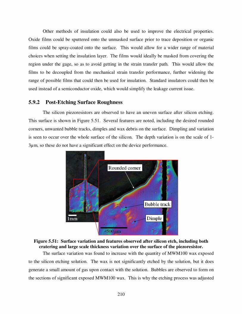
210
Other methods of insulation could also be used to improve the electrical properties.
Oxide films could be sputtered onto the unmasked surface prior to trace deposition or organic
films could be spray-coated onto the surface. This would allow for a wider range of material
choices when setting the insulation layer. The films would ideally be masked from covering the
region under the gage, so as to avoid getting in the strain transfer path. This would allow the
films to be decoupled from the mechanical strain transfer performance, further widening the
range of possible films that could then be used for insulation. Standard insulators could then be
used instead of a semiconductor oxide, which would simplify the leakage current issue.
5.9.2 Post-Etching Surface Roughness
The silicon piezoresistors are observed to have an uneven surface after silicon etching.
This surface is shown in Figure 5.51. Several features are noted, including the desired rounded
corners, unwanted bubble tracks, dimples and wax debris on the surface. Dimpling and variation
is seen to occur over the whole surface of the silicon. The depth variation is on the scale of 1-
3µm, so these do not have a significant effect on the device performance.
Figure 5.51: Surface variation and features observed after silicon etch, including both
cratering and large scale thickness variation over the surface of the piezoresistor.
The surface variation was found to increase with the quantity of MWM100 wax exposed
to the silicon etching solution. The wax is not significantly etched by the solution, but it does
generate a small amount of gas upon contact with the solution. Bubbles are observed to form on
the sections of significant exposed MWM100 wax. This is why the etching process was adjusted

211
to remove all visible wax. The dimples on the silicon corresponded to bubble nucleation spots
and tracks were apparent on the silicon surface following bubble sliding over the silicon.
Bubbles are known to act as local etch masks [171]. The larger scale variation in etch depth may
be due to self-heating at the silicon surface. The reaction is exothermic and sensitive to
temperature, meaning that it is possible for the etch rate to drive itself up in small areas if the
heat is not dissipated. This is unlikely given the low etching rate and hydrofluoric acid
concentration [171]. These minor surface variations may actually be beneficial as they may
provide improved adhesion for the epoxy cure. Thickness variations on the thin piezoresistor
arms are more likely to impact performance, and could cause stress concentrations or retain
debris during cleaning steps.
Several steps may be taken to reduce the etching variation. Alcohol may be added to the
etching solution to lower surface energy [166]. This will also lower the etching rate, so the
hydrofluoric acid concentration would likely need to be adjusted upwards. The solution may be
placed in an ice bath to control temperature more accurately. The solution may be stirred to
promote even diffusion of both reactants and heat throughout the mixture [171]. This was tested
briefly, and the stirred solution was found to remove bubbles. It also generated large and highly
varied etch rates at the edges of the device. The process was highly sensitive to stirring rate,
device orientation, and device location within the stirring container. It was found to be difficult
to make the process sufficiently repeatable. Ultrasonic agitation has been used to remove
bubbles in etching operations [172]. This is believed to be a significantly better solution than
stirring as does not have a high degree of anisotropy. The ultrasonic agitation will both mix the
solution and knock bubbles off of the silicon surface. These effects will occur throughout the
solution, rather than simply on the leading edge of the device as in the mixing situation. The
changes in etching rate are also expected to be more repeatable than with stirring. Early tests of
vibrational agitation (tapping the side of the etching container) were found to be partially
successful in dislodging bubbles. The silicon showed correspondingly reduced surface variation.
5.9.3 Maximum Strain
The strain limit of the processed silicon wafer is believed to be a function of the laser
damaged edges. Several steps may be taken to improve the strain limit. Longer wax etching
should further clear away any small amount of wax masking the damaged area, however this was

212
found to largely plateau in benefit after about 90s etching. A longer silicon etching time should
further attack the bulk silicon and reduce stress concentrations at the edges. A trend for this bulk
silicon sensitivity can be extrapolated from Figure 5.37, and this suggests that little gain is to be
had from further silicon etching. The primary BUE can be removed with mechanical force via
still bristled brushes. This exposes more of the HAZ and was found to result in more rounded
edges. This method is significantly more likely to break the delicate silicon structure, so was not
pursued after initial observation. The width of the cut made in the silicon was found to
determine the amount of rounding that occurred during the silicon etch. Wider gaps appear to be
rounded more aggressively, with exposed edges bring the most rounded as shown in Figure 5.51.
This is a difficult tradeoff when designing the inner cut of the piezoresistor that forms it into a U
shape, as it is desired that this gap be as small as possible to minimize the sensor width. None of
these possible methods were eventually integrated into the final process due to their drawbacks.
A study of the silicon strain limit did observe anomalously high strain limits for silicon
wafers diced from a p-type (100) wafer at 1015cm-3 doping. The samples were cut in alignment
with the wax flat, so along the <100> axes. The samples were observed to commonly survive up
to 4-5mε, with values up to 8mε. These levels are of interest since they would ensure the sensors
do not come close to yielding during full range operation. The highest strain limit sample is
shown in Figure 5.52 and is 30µm thick after etching. It delaminated from the titanium substrate
at around 7.5mε when the titanium began to neck in to failure. The silicon sample was later bent
around by 180° without failure, yielding lower bounds estimates on the strain limit at about 8mε.

213
Figure 5.52: High strain sample, observed to reach >7mε at which point the sample
partially delaminated from the titanium substrate.
The high strain limit samples generally occurred when the silicon blocks were fully
exposed on the stamp, and the solution was gently agitated by lifting the sample almost out of
solution slowly, once every 30s. The sample in Figure 5.52 was surrounded by silicon tiling
however. The significant increase in edge rounding is believed to be due to fluid flow, which
would accelerate the rounding of corners. This solution would be difficult to implement for the
inner edges of the piezoresistor. Ultrasonic agitation may provide a means to evenly agitate all
parts of the solution. The agitation method was found to work for (100) wafers, but showed little
success with (110) wafers. It is believed that the crystalline orientation may have been well
aligned to the cuts in the (100) wafer samples, which may have helped in reducing stress
concentrations. The common planes of cleaving for the (110) wafer do not line up with the
rectangular edges of the silicon samples, which may have resulted in higher stress
concentrations.
The higher strain limits on the (100) wafers suggests a means of increasing the robustness
of the fabrication process, as these would be able to tolerate much larger strains before fracture.
This is suggested as a means of resolving the tendency to gage damage during the delamination
step.
5.9.4 Minimum Sensor Size
Three steps in NLBM were found to place limits on the piezoresistor arm width; the laser
patterning step, the silicon etching step, and the cleaning steps. The laser patterning step
generates the piezoresistor pattern from silicon stock. A lower bound was observed to be below

214
25µm for patterning. The laser cut width is about 30µm, and it shows about 5µm position
variability during the cutting process. A 25µm gage was successfully cut into silicon stock as
shown in Figure 5.53. The arms are cut wider than the final desired dimension of 25µm in
expectation of the 10µm etching that occurs on both sides of each arm. Further reductions in the
laser cut width could allow for more tightly packed piezoresistor structures.
Figure 5.53: Minimum piezoresistor arm width formed using the laser cutter. The
silicon has not been cleaned off as the cleaning process was found to break devices with <150µm arm width.
The silicon etching step places a lower bound of about 30µm as the arm width should
likely be greater than the wax film thickness in order to limit the diffusion of hydrofluoric acid to
the under surface of the piezoresistor. The wax will generally be thoroughly under etched by the
hexane, so the under surface will likely be exposed to silicon etchant. The under surface should
not be significantly etched during the process as it could completely dissolve the fine features of
the piezoresistor arms. Sensor thickness variation could also cause warping in the transfer
process, resulting in either fracture or a poor gage factor.
The cleaning steps presently place the dominant limit on the gage width at about 100-
150µm. This is set by the mechanical agitation of the silicon surface cleaning operations. The
mechanical agitation serves to accelerate the removal of wax and debris from the top surface
without significantly removing the underside wax anchoring the piezoresistor to the stamp.
Manual brushing along the axis of the gage is used at present. A gentler process like a soft
bristle rotary brush may be able to better control the mechanical forces, and thus prevent
destruction of the fine features. A purely chemical solution could avoid generating significant

215
forces. The proper choice of a silicon protective coating chemical should make the use of a
chemical solvent more feasible. This would have the benefit of removing the manual step and
allowing for smaller gages.
The reduction in the minimum piezoresistor arm width would have immediate design
benefits. A small 25µm arm width gage would be highly desirable for integrating sensing into
meso/microscale flexural devices. The piezoresistor would be about 100µm wide total,
assuming the laser kerf width is not also reduced. A sensor on this scale could provide out-of-
plane sensing for flexures down to about 150µm. The 50µm extra width is required to ensure
alignment, given the measured alignment error of the NLBM process. Two-axis sensing (both
in- and out-of-plane) could be carried out on beams of about 225µm width if one arm was
centered over the beam midline as in the present design. Metal flexures of this scale can be
easily machined using NLBM, so the sensors are presently the limit to achieving such
miniaturization. This drop in size would provide a significant increase in design freedom.
5.9.5 Sensor Alignment
The cure process and laser fixture are the major sources of the alignment error in TFPT.
The cure process generates misalignment through fluid forces on the sensor during the cure step.
This is a function of epoxy deposition control. The curing alignment error should be
significantly reduced by symmetrically depositing epoxy onto the gage, via either automated
processes or masking operations. The laser fixture generates calibration error, laser positioning
error, fixture error and thermal drift. Fixture improvements should be able to reduce the thermal
sensitivity of the process to the point where a single time calibration would be possible. This
would remove two of the main components of the laser cutting process alignment error- the
calibrations and the thermal drift. The fixture could be anchored to the back plate of the laser
cutter, which does not expand or contract significantly in the X or Y directions as it is directly
anchored to the two vertical bearings. The fixture could also be machined out from a reduced
thermal sensitivity material like invar. The combination of these two steps should lower the
thermal effects on alignment by more than an order of magnitude. These fixes would reduce the
alignment error down to ≈10µm.

216
5.9.6 Pre-Fabricated Sensors
The TFPT process could be adjusted to place commercially produced pre-made strain
gages if desired. The commercial gages would be placed onto the stamp in the desired location,
anchored in place with wax adhesive then transferred to the mechanical structure. The alignment
of the initial placement would be a significant limitation for the process. This might be solved
with some kind of pick-and-place equipment or with alignment structures. Each gage could be
placed close to the desired location, and aligned while in liquid wax. The wax would be cooled
once the correct orientation is reached. The wax would be cleaned off, leaving the sensors ready
for transfer. These sensors would need to have thin or no lead wires as the gages would be
placed face down on a stamp and they must remain flat. The TFPT process would allow for
parallel placement of sensors with alignment determined previous to the transfer. This is not
presently possible to do, meaning that multi-sensor devices are often difficult to fabricate at
present, and typically require iterative curing operations. The separation of alignment and
transfer in TFPT decouples the process, making it easier to ensure both are done correctly.
5.9.7 Sensor Performance
The gage factors and noise scale of the sensors were found to lie within the range of
values expected from previous research. The sensors are Schottky barrier noise limited, meaning
that any reduction in this noise source will result in a significant performance boost. Two main
methods of improvement may be attempted. An increase in the bridge voltage will reduce the
Schottky barrier resistivity and also the noise. An increase of bridge voltage from 10V to 20V
should add ≈5dB to the dynamic range. An increase in the local doping concentration at the
contact pads would also drop the Schottky barrier noise. This may be accomplished with either
spray-on dopant or electrical discharge doping as discussed in previous work. A boost in both
voltage and the doping level at the barrier could raise the dynamic range of the sensors to about
135dB over a 10kHz sensor bandwidth, which would allow for sub-nm resolution over 100µm
range. Spray-on dopant could be used with masked silicon stock before the patterning process is
carried out. This would locally dope the region of silicon from which the pads will be formed
[129]. The alignment would not need to be exact as long as a large enough gap is left between
the piezoresistor segment and the contact pads. Electrical discharge doping could be carried out
during the circuit bonding step, with a borax solution and capacitor [106]. This would be easily

217
integrated into TFPT after gage formation and transfer to the mechanical substrate. The focus of
this research was to demonstrate the feasibility of the overall process flow, so these
improvements were not included in the present work.
5.9.8 Actuation
The Hexflex structure can be driven in the same form as previous meso-scale flexible
positioners [1], using multi-axis Lorentz coil actuators. The actuators are typically fabricated in
two steps, attaching magnets to the moving stage and fabricating coils to apply loads to the
magnets. The magnets are generally epoxied to the actuator paddles on the finished structure.
The integration of sensing into the device was the main focus of this research, so the actuation
fabrication was not included in the process. It is expected that an extra step could be easily
added to NLBM in order to integrate the actuation.
5.9.9 Device Operation
Silicon is known to have a non-linear gage factor [95]. This was observed in previous
analysis of the semiconductor piezoresistors produced by NLBM, and confirmed in this work.
This non-linearity could result in accuracy issues at large displacements. A non-linear
calibration is desired to capture and account for the sensor non-linearities. The non-linear
calibration requires a 1:1 mapping from the linear measured position recorded by the integrated
sensing to the non-linear actual position of the gage. The linear measured position is generated
by the inversion of the transform matrix shown in Eq. (5.12). The positioner uses each set of
sensors (1-2, 3-4 and 5-6) to read multiple axes. This mapping does not allow for non-linear
calibration on the scale of the sensor sets. Instead, it must be carried out on the full six-axis
position vector level. Only at the stage of the full position vector can the device motion and
sensor readings be linked with the 1:1 mapping required for non-linear calibration. The
mapping, once completed, would adjust the transform matrix linear output to the actual, non-
linear output. The mapping would require approximately 5-7 points per axis in order to capture
third order effects typical of gage factor non-linearity. About 100,000 points would be needed to
do this over the 6 axes, so the process would need to be automated, perhaps with a laser
interferometer measuring the device true position. A reduced set of equations could be fit to this

218
data to provide an expression for the adjustment of each axis based off the full 6 axis position
vector value.
5.10 Conclusion
The purpose of this work is to generate a process flow which can be used to fabricate
metal MEMS with integrated sensing, and do so flexible, in small batches, with low per-device
cost. The process is capable of producing new designs in ≈1week at an average unit cost of
<$1k/device even at batch sizes of ≈1-10, with expected sensing performance limits of about
135dB over a 10khz sensor bandwidth. This is a ≈20x reduction in cost, ≈25x reduction in time,
and potentially >30x increase in sensing dynamic range over comparable state-of-the-art
compliant nanopositioners. The process flow was used to create a low-cost customizable
nanopositioning architecture that is intended for use in a range of micro-/nano- manufacturing
and metrology operations. The customizable architecture will help surmount one of the
significant hurdles of nanomanufacturing research and development.
A Hexflex 6DOF nanopositioner with titanium flexures and integrated silicon
piezoresistive sensing was fabricated using NLBM. This device was designed around a metal
mechanical structure in order to improve its robustness for general handling and operation.
Single crystalline silicon piezoresistors were patterned from bulk silicon wafers and transferred
to the mechanical structure via TFPT. These gages provide high sensitivity strain sensing for all
six device axes. Both the device and sensors were created with a high-flexibility, low per-device
cost process which could be rapidly adjusted to make new designs. This work demonstrates that
it now feasible to design and create a customized positioner for each
nanomanufacturing/metrology application. The Hexflex architecture can be significantly varied
to adjust range, resolution, force scale, stiffness, and DOF all as needed.
The NLBM process was shown to enable alignment of device components on the scale of
10’s of microns. 150µm piezoresistor arm widths were demonstrated, with suggestions made for
how to reach the expected lower bound of 25µm. Flexures of 150µm and 600µm were
demonstrated on the mechanical structure, with a lower bound of ≈50µm expected for the
process. Electrical traces of 800µm width were used to ensure low resistance, with a lower
bound of ≈100µm expected for the process.

219
The integrated piezoresistive sensing was designed to have a gage factor of about 125,
but was reduced to about 70 due to lower substrate temperatures during soldering, all as
predicted by design theory. The sensors were measured to have a dynamic range of 59dB over a
10kHz sensor bandwidth, limited by the Schottky barrier noise. Several suggestions were
proposed for boosting the performance to ≈135dB over a 10khz sensor bandwidth, including
raising the bridge voltage to 20V and doping the contact pads. This sensor performance is
generally in excess of presently available kHz-bandwidth analog-to-digital converters [54].
Spray on dopants during the lamination step or electrical discharge doping during the circuit
bonding step were described as possible means for increasing the contact pad doping level.
This research has demonstrated a framework for a fabrication process that can be quickly
and easily adjusted to design modifications. This is ideal for research and development in order
to produce new positioning equipment at need and in short order. Suggestions were proposed for
scaling the process up to higher volumes, generally at the expense of flexibility. Further work in
required on pushing the limits of the process to smaller sensor sizes, lower sensor noise, finer
flexure geometry and better alignment. These improvements will all increase the benefits of
NLBM, enabling a wider range of MEMS devices to be produced quickly, in small batches and
at low cost.

220

221
CHAPTER
6 CONCLUSION
6.1 Synopsis
A process flow is described for the low cost, flexible fabrication of metal MEMS with
high performance integrated sensing. The process is capable of producing new designs in
≈1week at an average unit cost of <$1k/device even at batch sizes of ≈1-10, with expected
sensing performance limits of about 135dB over a 10kHz sensor bandwidth. This is a ≈20x
reduction in cost, ≈25x reduction in time, and potentially >30x increase in sensing dynamic
range over comparable state-of-the-art compliant nanopositioners. These improvements will
remove one of the main hurdles to practical non-IC nanomanufacturing, which could enable
advances in a range of fields including personalized medication, computing and data storage, and
energy generation/storage through the manufacture of metamaterials.
Advances were made in two avenues: flexibility and affordability. The fundamental
advance in flexibility is the use of a new approach to modeling the nanopositioner and sensors as
combined mechanical/electronic systems. This enabled the discovery of the operational regimes
and design rules needed to maximize performance, making it possible to rapidly redesign
nanopositioner architecture for varying functional requirements such as range, resolution and
force. The contributions to design science are listed below.
• Created integrated system models, included all components of sensing- flexure,
sensor, electronics, extending past previous efforts.
• Developed optimization framework, set down methods for proper use and
determined limits.
• Generated structure for constraint mapping and did so over all components and in
multiple domains- fabrication, electrical, thermal, extending past previous efforts.

222
• Extended noise and gage factor models to capture within-sensor non-linear I-V
behaviors, voltage drops and excess resistances, so can now design silicon gages
as well as other complex sensors.
• Created model for Schottky barrier noise from known physics that can be
integrated into optimization framework.
• Validated models via case study with measurements of IV characteristics, noise
and gage factor.
The fundamental advance to increase affordability is the invention of a hybrid fabrication
process chain that can produce MEMS with integrated sensing in a flexible manner, at small
volumes and with low per-device costs. This will allow for low-cost customizable
nanopositioning architectures with integrated position sensing to be created for a range of micro-
/nano- manufacturing and metrology applications. The contributions to fabrication science are
listed below.
• Invented new hybrid fabrication process chain- NLBM- that can produce non-
silicon structures with integrated sensing quickly, flexibly and at low cost.
• Characterized and modeled the physics of the fabrication process (machining,
oxide, lamination, patterning, etching, delamination, circuit bonding), linked the
physics to design models.
• Developed best practices for the fabrication steps.
• Identified performance limitations of the process, (alignment, feature scale,
mechanical).
• Validated process chain function and limits with case study.
This work demonstrates a means to design the best possible piezoresistive sensor for the
given constraints on a system. Quantum mechanics was used to model the non-linearities of the
sensors produced by NLBM, so as to integrate the results of the new fabrication process into the
models used for the new design process. A device with a metal mechanical structure, surface
electrical features and integrated piezoresistive sensing was fabricated to demonstrate the
capabilities of NLBM. This fabrication process is shown to rapidly produce high performance
devices in small batches that perform as predicted by the design theory laid out in this work. The
design theory can thus be used to rapidly alter the MCNA performance to meet the requirements

223
of a wide range of nano-manufacturing and metrology operations, and a metal MEMS device can
quickly be fabricated at low cost to meet this performance.
6.2 Future Work
A range of development remains to be done on the main avenues of research pursued in
this work. Several items of interest are discussed below.
6.2.1 Optimization Theory
The optimization theory was developed for DC Wheatstone bridge sensors. This can be
extended to other variants of piezoresistive sensing, including AC bridges or resonant mode
sensors. The noise expressions would be the main variation to the theory. Such additions to the
optimization framework would enable optimization of devices like piezoresistive AFMs and
other micro-/nano-metrology applications.
6.2.2 Metal-Semiconductor Contacts
Further study of the bonding parameter observed in the Schottky barrier studies could
reveal the mechanism by which the performance of the contacts is degraded. A better
understanding of this would allow the fabrication process to be adjusted to reliably achieve high
quality contacts. This work could also be adjusted to other contact metals and other deposition
methods. Film deposition is a likely candidate for solder replacement, but the performance of
such deposited films is unknown. It is expected that the contacts would display similar physics,
but with altered parameters.
The native oxide on the silicon could also be engineered to improve performance- an
increased thickness plays a secondary role in determining the sensitivity of the barrier to voltage
bias and contributes to the ohmic contact resistivity. A decreased oxide layer should increase the
barrier voltage sensitivity, causing the barrier to disappear exponentially quicker. It should also
reduce ohmic resistivity, which dominates at higher contact pad doping levels.
6.2.3 Semiconductor Piezoresistor Design
Further work remains on the modeling of Schottky barrier devices with regards to the
barrier gage factor, the silicon non-linear gage factor, and the device thermal sensitivity. The

224
Schottky barrier is known to have a gage factor [169], however this effect was not included in
the analysis as the contact pads were assumed to have no applied stress. This may not hold,
depending on the strength of the epoxy cure. The silicon is known to have a non-linear gage
factor [95], but this was not included in the analysis. It may be desirable to design for linearity,
at which point this must be included in the theory. The device thermal sensitivity is important
for mitigating thermal errors through span temperature compensation. Knowledge of the silicon
and contact temperature coefficients of resistance would allow for the cancellation of these
effects through the inclusion of counter varying resistances in the sensor system. Such span
temperature compensation resistances could be fabricated by depositing thin metal films between
gaps in the traces. Tight film thickness control is possible with deposition.
The limits on the semiconductor sensors were explored in this work, and several methods
of improvement were suggested. Gains can be had from including localized doping into the
fabrication process, either as spray-on or electrical discharge doping. Further gains could be had
from increasing the bridge source voltage, as this lowers the barrier resistivity and thus the noise.
6.2.4 Non-Lithographically-Based Microfabrication
The scaling of the NLBM process chain up to higher production rates and volumes was
discussed for each step of the process. These alternate methods would likely generate unique
surface or structural features on the device that would require additional research to balance the
process chain. One example is to use an acetone dip on the stamp to loosen the secondary BUE,
possibly to the point where the coating delaminates without need for mechanical abrasion.
Ultrasonication could be used. The improved cleaning would allow closer detiling spacing
(which generates more BUE), meaning laser detiling could be used. This would remove most of
the fine manual work required in the process, making TFPT significantly more scalable.
Improvements in the surface electrical isolation could likely be obtained from
engineering the trace material to have a larger work function difference from titania.
Additionally, the bulk titanium could be held at the bridge output voltage (presently ≈5V) in
order to minimize leakage current from bridge outputs to the bulk titanium. This could
significantly reduce any cross-talk between sensors and leakage currents through the device.
Silicon etching variations were observed and found to be likely due to bubble generation
on the silicon surface. These variations can cause stress concentrations in the device. Several

225
means for removing bubbles were suggested, with ultrasonic agitation being the recommended
method. This would need to be tested with thin silicon films on glass stamps to confirm the
small features are not shattered. The etch rate for such agitated processes would need to be
measured to hold the etch depth to ≈20µm. This ultrasonication should improve uniformity, and
edge roundness.
The strain limits on the patterned silicon were observed to reach unexpectedly high
values of about 3x the standard values. Several means for raising the standard strain limit of the
silicon were suggested, including using wafers of a different orientation and increased solution
agitation.
The minimum gage width sets a lower bound on the device flexure width, which in turn
bounds the footprint of the device. A reduced sensor width thus improves a wide range of design
limits, including size, speed and device stiffness. The limits on the gage width were determined
to be the surface cleaning operation. Two means of improving this are using a more regular
brushing operation or including a more vigorous chemical cleaning operation. This could reduce
the sensor size by about 6x, down to around 25µm arm widths. 100-200µm flexures could then
be instrumented, which would be a significant increase in the design space for metal MEMS.
The sensor alignment is limited in NLBM at present by the cure process and the laser
cutting thermal variation. The cure misalignment could be rectified by controlled deposition of
the epoxy. The laser cutting thermal variation could be rectified with a thermally insensitive
fixture. The reduction of these errors would tighten the alignment accuracy of the whole process
down to ≈10µm, allowing for the fabrication of finer structures.
The sensor integration step could be modified with further research to incorporate pre-
made piezoresistive sensors. This would simplify the process by using premade components.
The alignment of these sensors to the stamp would need to be solved, but once done would
provide a rapid means to get good performance sensing into metal microstructures.
6.2.5 Device
A nonlinear calibration could be used to improve accuracy. Several points would be
needed for each axis. These points could be assembled to generate a full position vector
mapping from measured to actual.

226
The device geometry could be adjusted for lower stiffness by replacing the blade flexure
with a wire flexure. This would increase range, given contact actuation force, but reduce
resolution. The bearing layout could also be modified to nest larger flexures in a given footprint.
The sensors could be improved by adding thermal balance piezoresistors to each of the
six strain active resistors. The thermal balance resistors would improve the accuracy of the
sensing without requiring larger flexures. Reduced size piezoresistors could be fit two-to-a-
flexure, so as to get half bridge strain sensing. This would require careful delta section design to
avoid stress concentrations. Strain sensing could be placed on both sides of the flexures if the
device was made fully planar. This dual sided setup would be significant more complex to
fabricate, with relatively little benefit, so is not recommended.
An electrically active payload could be driven by the nanopositioner if traces are
deposited along the flexures up to the stage. Research would be needed to confirm that the traces
do not delaminate under high surface strains. It is expected that this strain limit would be a
function of the trace thickness. Films of thickness ≤1µm should be sufficient.
6.2.6 Actuators
The MCNA requires high force density actuation. This was not included within the
scope of this thesis due to time constraints. ≈1N scale actuation would be ideal for achieving the
desired nanopositioner bandwidths. Reluctance actuators are suggested as the most likely means
for achieving this force range in a meso-scale device. A conceptual sketch of such an actuator is
shown in Figure 1.10. This will require significant electromagnetic design and modeling.
6.2.7 Control
The MCNA must have closed loop control for the best possible accuracy during micro-
/nano-manipulation. The controller for this will need to drive the device at kHz-scale bandwidth,
and do so over all six axes. A state space controller is the likely candidate. The largely linear
stiffness and sensing of the device should assist in generating a straightforward control
algorithm.

227
REFERENCES
[1] C. D. DiBiasio, “Concept Synthesis and Design Optimization of Meso-scale, Multi-Degree-of-Freedom Precision Flexure Motion Systems with Integrated Strain-based Sensors,” Massachusetts Institute of Technology, 2010.
[2] US Department of Energy, “Nanomanufacturing for Energy Efficiency,” Industrial
Technologies Program. [Online]. Available: www.bcsmain.com/mlists/files/NanoWorkshop_report.pdf. [Accessed: 13-Jul-2010].
[3] The Chemical Science and Technology Laboratory, “Cross-Industry Issues in Nanomanufacturing,” National Institute of Standards and Technology. [Online]. Available: www.nist.gov/cstl/upload/nano_small_web-3.pdf. [Accessed: 13-Jul-2010].
[4] US Department of Energy, “Nanomanufacturing,” Industrial Technologies Program. [Online]. Available: http://www1.eere.energy.gov/industry/nanomanufacturing/pdfs/nano_4pager_10-08.pdf. [Accessed: 13-Jul-2010].
[5] J. Haaheim and O. A. Nafday, “Dip Pen Nanolithography: A ‘ Desktop Nanofab’ Approach Using High-Throughput Flexible Nanopatterning,” Scanning, vol. 30, no. 2, pp. 137–150, 2008.
[6] A. A. Tseng, A. Notargiacomo, and T. P. Chen, “Nanofabrication by scanning probe microscope lithography: A review,” Journal of Vacuum Science and Technology B:
Microelectronics and Nanometer Structures, vol. 23, no. 3, pp. 877–894, 2005.
[7] D. Golda, “Design of a high-speed, meso-scale nanopositioners driven by electromagnetic actuators,” Massachusetts Institute of Technology, 2008.
[8] X. Fan, H. Zhang, S. Liu, X. Hu, and K. Jia, “NIL—a low-cost and high-throughput MEMS fabrication method compatible with IC manufacturing technology,” Microelectronics Journal, vol. 37, no. 2, pp. 121–126, Feb. 2006.
[9] H. Lan, Y. Ding, H. Liu, and B. Lu, “Review of the wafer stage for nanoimprint lithography,” Microelectronic Engineering, vol. 84, no. 4, pp. 684–688, Apr. 2007.
[10] D. R. Sahoo, P. Agarwal, and M. V. Salapaka, “Transient Force Atomic Force Microscopy: A New Nano-Interrogation Method,” in 2007 American Control Conference, 2007, pp. 2135–2140.
[11] S. Salapaka and M. Salapaka, “Scanning Probe Microscopy,” IEEE Control Systems
Magazine, vol. 28, no. 2, pp. 65–83, Apr. 2008.

228
[12] NanoScience Instruments, “AFM Cantilevers and Chips: Dimensions and Specifications.” [Online]. Available: http://www.teachnano.com/products/AFM_cantilevers.html. [Accessed: 15-Jul-2010].
[13] W. Kim, S. Verma, and H. Shakir, “Design and precision construction of novel magnetic-levitation-based multi-axis nanoscale positioning systems,” Precision Engineering, vol. 31, no. 4, pp. 337–350, Oct. 2007.
[14] J. Dong, S. M. Salapaka, and P. M. Ferreira, “Robust Control of a Parallel- Kinematic Nanopositioner,” Journal of Dynamic Systems, Measurement, and Control, vol. 130, no. 4, p. 041007, 2008.
[15] D. M. Brouwer, B. R. de Jong, and H. M. J. R. Soemers, “Design and modeling of a six DOFs MEMS-based precision manipulator,” Precision Engineering, vol. 34, no. 2, pp. 307–319, Apr. 2010.
[16] Xintek, “Carbon Nanotube AFM Tip.” [Online]. Available: http://www.xintek.com/products/afm/index.htm. [Accessed: 19-Apr-2013].
[17] NanoInk Inc, “NanoInk Consumables.” [Online]. Available: http://www.nanoink.net/consumables.html. [Accessed: 19-Apr-2013].
[18] Pentax, “Pentax Forums.” [Online]. Available: http://www.pentaxforums.com/forums/general-talk/118358-why-camera-sensors-still-rectangular.htm.
[19] S. A. Tadigadapa and N. Najafi, “Developments in Microelectromechanical Systems (MEMS): A Manufacturing Perspective,” Journal of Manufacturing Science and
Engineering, vol. 125, no. 4, pp. 816–823, 2003.
[20] K. M. Lee, H. Son, K. Bai, and J. K. Park, “Design Concept and Analysis of a Magnetically Levitated Multi- DOF Tiltable Stage for Micro Machining,” in Proceedings
of the 2nd International Conference on Micromanufacturing, ICOMM 2007, 2007.
[21] J. B. Wronosky, T. G. Smith, J. R. Darnold, and J. D. Jordan, “Maglev Six Degree-of-Freedom Fine Positioning Stage Control System,” Department of Energy Information
Bridge. [Online]. Available: http://www.osti.gov/bridge/servlets/purl/215316-U7oLlj/webviewable/215316 .pdf. [Accessed: 07-Jul-2010].
[22] Klocke Nanotechnik, “XYZ Manipulator.” [Online]. Available: http://www.nanomotor.de/n_xyz_manipulator.htm. [Accessed: 19-Apr-2013].
[23] N. Sarkar, C. Baur, E. Stach, Z. Jandric, R. Stallcup, M. Ellis, G. Skidmore, J. Liu, and G. K. Fedder, “Modular MEMS Experimental Platform for Transmission Electron Microscopy,” in 19th IEEE International Conference on Micro Electro Mechanical
Systems, 2006, pp. 146–149.

229
[24] D. Baldwin, “E-mail Discussion With Dale Baldwin of Mad City Labs.” .
[25] J. Luttkus, “Development of a Nanomanufacturing Line to Support Dip-Pen Nanolithography on a Massive Scale,” Massachusetts Institute of Technology, 2008.
[26] D. P. Cuff, “Electromagnetic Nanopositioner by in partial fulfillment of the requirements for the degree of at the,” Massachusetts Institute of Technology, 2006.
[27] S.-Y. Hsieh, C.-H. Jou, M.-Y. Chen, S.-C. Huang, C.-H. Lin, and L.-C. Fu, “Implementation of a 6-DOF Precision Positioning Platform for a Injection Molded Part,” in 33rd Annual Conference of the IEEE Industrial Electronics Society, IECON 2007, 2007, pp. 2922–2927.
[28] A. Slocum, Precision Machine Design. Eaglewood Cliffs, NJ: Prentice-Hall, Inc., 1992.
[29] S. Kalpakjian and S. Schmid, Manufacturing Engineering and Technology, 6th ed. New York, NY: Prentice-Hall, Inc., 2010.
[30] S. Devasia, E. Eleftheriou, and S. O. R. Moheimani, “A Survey of Control Issues in Nanopositioning,” IEEE Transactions on Control Systems Technology, vol. 15, no. 5, pp. 802–823, 2007.
[31] S. Salapaka, A. Sebastian, J. P. Cleveland, and M. V. Salapaka, “High bandwidth nano-positioner: A robust control approach,” Review of Scientific Instruments, vol. 73, no. 9, p. 3232, 2002.
[32] K. F. Ehmann, D. Bourell, M. L. Culpepper, T. J. Hodgson, T. R. Kurfess, M. Madou, K. Rajurkar, and R. E. Devor, “WTEC Panel Report on International Assessment of Research and Development in Micromanufacturing,” World Technology Evaluation Center
(WTEC), Inc. [Online]. Available: http://www.wtec.org/micromfg/report/Micro-report.pdf. [Accessed: 06-Jun-2010].
[33] J. M. Curran, R. Stokes, E. Irvine, D. Graham, N. a Amro, R. G. Sanedrin, H. Jamil, and J. a Hunt, “Introducing dip pen nanolithography as a tool for controlling stem cell behaviour: unlocking the potential of the next generation of smart materials in regenerative medicine.,” Lab on a chip, vol. 10, no. 13, pp. 1662–70, Jul. 2010.
[34] W.-J. Kim and S. Verma, “Nanoscale Path Planning and Motion Control with Maglev Positioners,” Journal of Dynamic Systems, Measurement and Control, vol. 129, no. 6, pp. 777–785, Oct. 2007.
[35] Z. Zhou and K. Lee, “Real-time Motion Control of a Multi-degree-of-freedom Variable Reluctance Spherical Motor,” in Proceedings of the 1996 13th IEEE International
Conference on Robotics and Automation, 1996, no. April 1996, pp. 2859–64.

230
[36] Q. Liang, D. Zhang, Q. Song, and Y. Ge, “Micromanipulator with integrated force sensor based on compliant parallel mechanism,” in 2010 IEEE International Conference on
Robotics and Biomimetics, 2010, pp. 709–714.
[37] H. Gutierrez and L. Fevre, “Design and Construction of a 6-DOF Positioning System with Long Range in XY and Nanometer Resolution using Magnetic Servo-Levitation.”
[38] W. M. Rubio, E. C. N. Silva, and S. Nishiwaki, “Piezoresistive sensor design using topology optimization,” Structural and Multidisciplinary Optimization, vol. 36, no. 6, pp. 571–583, Nov. 2008.
[39] J. C. Doll, S.-J. Park, and B. L. Pruitt, “Design optimization of piezoresistive cantilevers for force sensing in air and water,” Journal of applied physics, vol. 106, no. 6, p. 64310, Sep. 2009.
[40] J. A. Harley and T. W. Kenny, “1/F Noise Considerations for the Design and Process Optimization of Piezoresistive Cantilevers,” Journal of Microelectromechanical Systems, vol. 9, no. 2, pp. 226–235, 2000.
[41] S.-J. Park, J. C. Doll, A. J. Rastegar, and B. L. Pruitt, “Piezoresistive Cantilever Performance-Part II: Optimization.,” Journal of Microelectromechanical Systems, vol. 19, no. 1, pp. 149–161, Jan. 2010.
[42] S. Schonhardt, J. G. Korvink, J. Mohr, U. Hollenbach, and U. Wallrabe, “Combdrive Configuration for an Electromagnetic Reluctance Actuator,” Journal of
Microelectromechanical Systems, vol. 17, no. 5, pp. 1164–1171, Oct. 2008.
[43] C. E. Packard, A. Murarka, E. W. Lam, M. a Schmidt, and V. Bulović, “Contact-printed microelectromechanical systems.,” Advanced materials, vol. 22, no. 16, pp. 1840–4, Apr. 2010.
[44] E. W. Lam, H. Li, and M. A. Schmidt, “Silver Nanoparticle Structures Realized By Digital Surface Micromachining,” in Proceedings of the 15th International Conference on
Solid-State Sensors, Actuators and Microsystems, Transducers 2009, 2009, pp. 1698–1701.
[45] B. Bhushan, Tribology Issues and Opportunities in MEMS. Dordrecht, The Netherlands: Kluwer Academic Publishers, 1997.
[46] D. Huo, K. Cheng, and F. Wardle, “Design of a five-axis ultra-precision micro-milling machine—UltraMill. Part 1: holistic design approach, design considerations and specifications,” The International Journal of Advanced Manufacturing Technology, vol. 47, no. 9–12, pp. 867–877, Jun. 2010.

231
[47] P. T. Tang, J. Fugl, L. Uriarte, G. Bissacco, and H. N. Hansen, “Indirect tooling based on micromilling, electroforming and selective etching,” in Proceedings of the 2nd
International Conference on Multi-Material Micro Manufacture, 4M2006, 2006, no. c.
[48] S. Azcarate, L. Uriarte, S. Bigot, P. Bolt, L. Staemmler, G. Tosello, S. Roth, and A. Schoth, “Hybrid tooling : a review of process chains for tooling microfabrication within 4M,” in Proceedings of the 2nd International Conference on Multi-Material Micro
Manufacture, 4M2006, 2006, no. c, pp. 1–4.
[49] J. Nestler, K. Hiller, T. Gessner, L. Buergi, J. Soechtig, R. Stanley, G. Voirin, and S. Bigot, “A new technology platform for fully integrated polymer based micro optical fluidic systems,” in Proceedings of the 2nd International Conference on Multi-Material
Micro Manufacture, 4M2006, 2006.
[50] M. L. Culpepper and G. Anderson, “Design of a low-cost nano-manipulator which utilizes a monolithic, spatial compliant mechanism,” Precision Engineering, vol. 28, no. 4, pp. 469–482, Oct. 2004.
[51] D. Golda and M. L. Culpepper, “Modeling 3D magnetic fields for precision magnetic actuators that use non-periodic magnet arrays,” Precision Engineering, vol. 32, no. 2, pp. 134–142, Apr. 2008.
[52] D. Golda, J. H. Lang, and M. L. Culpepper, “Two-Layer Electroplated Microcoils With a PECVD Silicon Dioxide Interlayer Dielectric,” Journal of Microelectromechanical
Systems, vol. 17, no. 6, pp. 1537–1545, Dec. 2008.
[53] S.-C. Chen and M. L. Culpepper, “Design of a six-axis micro-scale nanopositioner—µHexFlex,” Precision Engineering, vol. 30, no. 3, pp. 314–324, Jul. 2006.
[54] “NI 9239 - National Instruments,” 2012. [Online]. Available: http://sine.ni.com/nips/cds/view/p/lang/en/nid/208797. [Accessed: 21-May-2013].
[55] T. Hu and W. J. Kim, “Modeling and Multivariable Control of a Novel Multi-Dimensional Levitated Stage with High Precision,” International Journal of Control, Automation and
Systems, vol. 4, no. 1, pp. 1–9, 2006.
[56] I. Philips, “Maglev Technology Backgrounder.” [Online]. Available: http://www.apptech.philips.com/ images/press_center/planarmaglev/maglev_technology_backgrounder.pdf. [Accessed: 21-Jun-2010].
[57] P. Cheung, R. Horowitz, and R. T. Rowe, “Design, fabrication, position sensing, and control of an electrostatically-driven polysilicon microactuator,” IEEE Transactions on
Magnetics, vol. 32, no. 1, pp. 122–128, 1996.

232
[58] J. R. Bronson and G. J. Wiens, “Feedback Control Of MEMS Micromirrors Subject To Parametric Uncertainty,” in Proceedings of the ASME International Design Engineering
Technical Conferences and Computers and Information in Engineering Conference,
IDETC/CIE 2007, 2007, no. 352.
[59] B. R. De Jong, D. M. Brouwer, H. V. Jansen, T. G. Lammertink, S. Stramigioli, and G. J. M. Krijnen, “A Planar 3 DOF Sample Manipulator for Nano-Scale Characterization,” in 19th IEEE International Conference on Micro Electro Mechanical Systems, 2006, pp. 750–753.
[60] Y. Chifu, H. Jingfeng, J. Hongzhou, and H. Junwei, “Modeling and Simulation of 6-DOF Parallel Manipulator Based on PID Control with Gravity Compensation in Simulink/ADAMS,” in 2008 International Workshop on Modelling, Simulation and
Optimization, 2008, pp. 391–395.
[61] J. Ma, D. Cong, Q. Huang, and J. Han, “Accurate Tracking Control Strategy of Harmonic Motion of 6-DOF Motion Simulator,” in 2007 IEEE International Conference on
Integration Technology, 2007, pp. 534–537.
[62] K.-H. Kim, Y.-M. Choi, D.-G. Gweon, D.-P. Hong, K.-S. Kim, S.-W. Lee, and M.-G. Lee, “Design of decoupled dual servo stage with voice coil motor and linear motor for XY long stroke uItra-precision scanning system,” in Proceedings of the International Society for
Optical Engineering (SPIE): International Conference on Mechatronics and Information
Technology: Mechatronics, MEMS and Smart Materials Conference, ICMIT 2005, 2005.
[63] N. C. Cheung, “A new type of direct-drive variable-reluctance actuators for industrial automation,” in 2002 IEEE International Conference on Industrial Technology, 2002.
IEEE ICIT ’02., 2002, vol. 1, pp. 30–34.
[64] R. Hamelinck, N. Rosielle, M. Steinbuch, and N. Doelman, “Large adaptive deformable mirror: Design and first prototypes,” in Proceedings of the International Society for
Optical Engineering (SPIE): Advanced Wavefront Control: Methods, Devices, and
Applications III, 2005, vol. 5894, no. 0, pp. 1–11.
[65] R. E. Clark, G. W. Jewell, P. Stewart, and D. Howe, “Tailoring force-displacement characteristics in medium-stroke linear variable reluctance actuators,” IEEE Transactions
on Magnetics, vol. 38, no. 5, pp. 3267–3269, Sep. 2002.
[66] N. C. Cheung, P. Jianfei, and Y. Jinming, “A Novel 2D Variable Reluctance Planar Actuator for Industrial Automation,” in Proceedings of the 10th European Conference on
Power Electronics and Applications, EPE 2003, 2003, no. ii.
[67] A. V. Lebedev, E. a. Lomonova, P. G. van Leuven, J. Steinberg, and D. a. H. Laro, “Analysis and initial synthesis of a novel linear actuator with active magnetic suspension,” in Conference Record of the 2004 IEEE Industry Applications Conference, 2004. 39th IAS
Annual Meeting., 2004, vol. 3, pp. 2111–2118.

233
[68] X. Lu, “Electromagnetically-driven ultra-fast tool servos for diamond turning,” Massachusetts Institute of Technology, 2005.
[69] C. Pramanik, H. Saha, and U. Gangopadhyay, “Design optimization of a high performance silicon MEMS piezoresistive pressure sensor for biomedical applications,” Journal of
Micromechanics and Microengineering, vol. 16, no. 10, pp. 2060–2066, Oct. 2006.
[70] S.-J. Park, J. C. Doll, and B. L. Pruitt, “Piezoresistive Cantilever Performance-Part I: Analytical Model for Sensitivity,” Journal of microelectromechanical systems, vol. 19, no. 1, pp. 137–148, Feb. 2010.
[71] N. Maluf and K. Williams, Introduction to microelectromechanical systems engineering, 2nd ed. Norwood, MA: Artech House, 2004.
[72] D. Bibber, “Design For Manufacturability For Micro Molded Devices,” in Proceedings of
the 2nd International Conference on Micromanufacturing, ICOMM 2007, 2007.
[73] H. Alemohammad, O. Aminfar, and E. Toyserkani, “Morphology and microstructure analysis of nano-silver thin films deposited by laser-assisted maskless microdeposition,” Journal of Micromechanics and Microengineering, vol. 18, no. 11, p. 115015, Nov. 2008.
[74] V. Leblanc, J. Chen, S. H. Kang, V. Bulovic, and M. a. Schmidt, “Micromachined Printheads for the Evaporative Patterning of Organic Materials and Metals,” Journal of
Microelectromechanical Systems, vol. 16, no. 2, pp. 394–400, Apr. 2007.
[75] A. J. Birnbaum, K. J. Wahl, R. C. Y. Auyeung, and A. Piqué, “Nanoporosity-induced effects on Ag-based metallic nano-inks for non-lithographic fabrication,” Journal of
Micromechanics and Microengineering, vol. 20, no. 7, p. 077002, Jul. 2010.
[76] Y. Yang, Z. Dong, Y. Qu, M. Li, and W. J. Li, “A programmable AFM-based nanomanipulation method using vibration-mode operation,” in 2008 3rd IEEE
International Conference on Nano/Micro Engineered and Molecular Systems, 2008, pp. 681–685.
[77] J. Otero and M. Puig-Vidal, “Low-noise Instrumentation for the Measurement of Piezoresistive AFM Cantilever Deflection in Robotic Nanobiocharacterization Applications,” in 2008 IEEE Instrumentation and Measurement Technology Conference, 2008, pp. 1392–1396.
[78] Y. Kanda and A. Yasukawa, “Optimum design considerations for silicon piezoresistive pressure sensors,” Sensors and Actuators A: Physical, vol. 62, no. 1–3, pp. 539–542, Jul. 1997.
[79] N. Yazdi, F. Ayazi, and K. Najafi, “Micromachined inertial sensors,” Proceedings of the
IEEE, vol. 86, no. 8, pp. 1640–1659, 1998.

234
[80] M. Li, H. X. Tang, and M. L. Roukes, “Ultra-sensitive NEMS-based cantilevers for sensing, scanned probe and very high-frequency applications.,” Nature nanotechnology, vol. 2, no. 2, pp. 114–20, Feb. 2007.
[81] J. Thaysen, A. Boisen, O. Hansen, and S. Bouwstra, “Atomic force microscopy probe with piezoresistive read-out and a highly symmetrical Wheatstone bridge arrangement,” Sensors and Actuators A: Physical, vol. 83, no. 1–3, pp. 47–53, May 2000.
[82] F. Beyeler, S. Muntwyler, and B. J. Nelson, “A Six-Axis MEMS Force–Torque Sensor With Micro-Newton and Nano-Newtonmeter Resolution,” Journal of
Microelectromechanical Systems, vol. 18, no. 2, pp. 433–441, Apr. 2009.
[83] X. Yu, J. Thaysen, O. Hansen, and A. Boisen, “Optimization of sensitivity and noise in piezoresistive cantilevers,” Journal of Applied Physics, vol. 92, no. 10, pp. 6296–6301, 2002.
[84] B. L. Pruitt and T. W. Kenny, “Piezoresistive cantilevers and measurement system for characterizing low force electrical contacts,” Sensors and Actuators A: Physical, vol. 104, no. 1, pp. 68–77, Mar. 2003.
[85] P. J. French, “Polysilicon: a versatile material for microsystems,” Sensors and Actuators
A: Physical, vol. 99, no. 1–2, pp. 3–12, Apr. 2002.
[86] M. A. Cullinan, R. M. Panas, and M. L. Culpepper, “Design of micro-scale multi-axis force sensors for precision applications,” in In Proceedings of the 2009 Annual Meeting of
the American Society for Precision Engineering, 2009, pp. 4–9.
[87] N. K. Upreti and S. Singh, “Grain boundary effect on the electrical properties of boron-doped polysilicon films,” Bulletin of Materials Science, vol. 14, no. 6, pp. 1331–1341, Dec. 1991.
[88] R. Brederlow, W. Weber, C. Dahl, D. Schmitt-Landsiedel, and R. Thewes, “Low-frequency noise of integrated polysilicon resistors,” IEEE Transactions on Electron
Devices, vol. 48, no. 6, pp. 1180–1187, Jun. 2001.
[89] D. Ramos, J. Tamayo, J. Mertens, M. Calleja, L. G. Villanueva, and A. Zaballos, “Detection of bacteria based on the thermomechanical noise of a nanomechanical resonator: origin of the response and detection limits.,” Nanotechnology, vol. 19, no. 3, p. 035503, Jan. 2008.
[90] S. D. Senturia, Microsystem Design. Springer, 2002, p. 720.
[91] Omega Engineering Inc., The Pressure Strain and Force Handbook Vol 29 (Volume 29), 8th ed. Stamford, CT: Omega, 2006.

235
[92] G. F. Franklin, J. D. Powell, and A. E. Naeini, Feedback Control Of Dynamic Systems -
5th edition, 5th ed. Upper Saddle River, NJ: Prentice Hall,2005, 2006.
[93] M. A. Cullinan and M. L. Culpepper, “Carbon nanotubes as piezoresistive microelectromechanical sensors: Theory and experiment,” Physical Review B, vol. 82, no. 11, p. 115428, Sep. 2010.
[94] R. M. Panas, M. A. Cullinan, and M. L. Culpepper, “Non-Lithographically-Based Microfabrication of Precision MEMS Nanopositioning Systems,” in Proceedings of the
2011 Annual Meeting of the American Society for Precision Engineering 26th Annual
Meeting, 2011.
[95] Y. Kanda, “Piezoresistive effect of silicon,” Sensors and Actuators A, vol. 28, pp. 83–91, 1991.
[96] M. J. Madou, Fundamentals of Microfabrication: The Science of Miniaturization, Second
Edition. CRC Press, 2002, p. 752.
[97] R. M. Panas, M. A. Cullinan, and M. L. Culpepper, “Design of piezoresistive-based MEMS sensor systems for precision microsystems,” Precision Engineering, vol. 36, no. 1, pp. 44–54, Jan. 2012.
[98] S. M. Sze and K. K. Ng, Physics of Semiconductor Devices, 3rd ed. Wiley-Interscience, 2006, p. 832.
[99] R. T. Tung, “Recent advances in Schottky barrier concepts,” Materials Science and
Engineering: R: Reports, vol. 35, no. July, pp. 1–138, 2001.
[100] H. Mavoori, A. G. Ramirez, and S. Jin, “Universal solders for direct and powerful bonding on semiconductors, diamond, and optical materials,” Applied Physics Letters, vol. 78, no. 19, p. 2976, 2001.
[101] B. V. Van Zeghbroeck, Principles of Semiconductor Devices and Heterojunctions. Prentice Hall, 2010, p. 450.
[102] J. S. Subramanian, P. Rodgers, J. Newson, T. Rude, Z. He, E. Besnoin, T. P. Weihs, V. Eveloy, and M. Pecht, “Room Temperature Soldering of Microelectronic Components for Enhanced Thermal Performance,” in Proceedings of the 6th International Conference on
Thermal, Mechanical and Multiphysics Simulation and Experiments in Micro-Electronics
and Micro-Systems, EuroSimE 2005, 2005, pp. 681–686.
[103] C. Lee, W.-F. Huang, and J.-S. Shie, “Wafer bonding by low-temperature soldering,” Sensors and Actuators A: Physical, vol. 85, no. 1–3, pp. 330–334, Aug. 2000.

236
[104] C. M. L. Wu, D. Q. Yu, C. M. T. Law, and L. Wang, “Properties of lead-free solder alloys with rare earth element additions,” Materials Science and Engineering: R: Reports, vol. 44, no. 1, pp. 1–44, Apr. 2004.
[105] B. S. Lim, E. Ma, M.-A. Nicolet, and M. Nathan (Natan), “Silicon resistor to measure temperature during rapid thermal annealing,” Review of Scientific Instruments, vol. 59, no. 1, p. 182, Jan. 1988.
[106] B. C. Dobbs, P. M. Hemenger, and S. R. Smith, “Ohmic Contacts on High Purity P-Type Silicon,” Journal of Electronic Materials, vol. 6, no. 6, pp. 705–716, 1977.
[107] V. Aubry and F. Meyer, “Schottky diodes with high series resistance:,” Journal of Applied
Physics, vol. 76, no. 12, pp. 7973–7984, 1994.
[108] M. Jang and J. Lee, “Analysis of Schottky Barrier Height in Small Contacts Using a Thermionic-Field Emission Model,” ETRI Journal, vol. 24, no. 6, pp. 455–461, 2002.
[109] S. L. Tu and B. J. Baliga, “On the Reverse Blocking Characteristics of Schottky Power Diodes,” IEEE Transactions on Electron Devices, vol. 39, no. 12, pp. 2813–2814, 1992.
[110] J. M. Andrews and M. P. Lepselter, “Reverse Current-Voltage Characteristics of Metal-Silicide Schottky Diodes,” Solid-State Electronics, vol. 13, pp. 1011–1023, 1970.
[111] J. A. del Alamo, Integrated Microelectronic Devices: Physics and Modeling. Prentice Hall, 2013, p. 850.
[112] C. Y. Chang, Y. K. Fang, and S. M. Sze, “Specific Contact Resistance of Metal-Semiconductor Barriers,” Solid-State Electronics, vol. 14, no. 7, pp. 541–550, Jul. 1971.
[113] D. Sawdai, D. Pavlidis, and D. Cui, “Enhanced transmission line model structures for accurate resistance evaluation of small-size contacts and for more reliable fabrication,” IEEE Transactions on Electron Devices, vol. 46, no. 7, pp. 1302–1311, Jul. 1999.
[114] A. MacDowell, S. Fakra, and G. Morrison, “Thermal and mechanical joints to cryo-cooled silicon monochromator crystals,” in Proceedings of SPIE Vol 6317: Advances in X-
Ray/EUV Optics, Components, and Applications, 2006, vol. 6317, p. 63171F.
[115] N. Tugluoglu, S. Karadeniz, S. Acar, and M. Kasap, “Temperature-Dependent Barrier Characteristics of Inhomogeneous In/p-Si (100) Schottky Barrier Diodes,” Chinese
Physics Letters, vol. 21, no. 9, pp. 1795–1798, Sep. 2004.
[116] F. Iacopi, P. M. Vereecken, M. Schaekers, M. Caymax, N. Moelans, B. Blanpain, O. Richard, C. Detavernier, and H. Griffiths, “Plasma-enhanced chemical vapour deposition growth of Si nanowires with low melting point metal catalysts: an effective alternative to Au-mediated growth,” Nanotechnology, vol. 18, no. 50, p. 505307, Dec. 2007.

237
[117] A. H. Al-Bayati, K. G. Orrman-Rossiter, J. a. van den Berg, and D. G. Armour, “Composition and structure of the native Si oxide by high depth resolution medium energy ion scattering,” Surface Science Letters, vol. 241, no. 1–2, pp. 91–102, Jan. 1991.
[118] P. B. Griffin, M. Cao, P. Vande Voorde, Y.-L. Chang, and W. M. Greene, “Indium transient enhanced diffusion,” Applied Physics Letters, vol. 73, no. 20, p. 2986, 1998.
[119] S. Solmi, A. Parisini, M. Bersani, D. Giubertoni, V. Soncini, G. Carnevale, A. Benvenuti, and A. Marmiroli, “Investigation on indium diffusion in silicon,” Journal of Applied
Physics, vol. 92, no. 3, p. 1361, 2002.
[120] R. B. Fair, “Boron Diffusion in Silicon-Concentration and Orientation Dependence, Background Effects, and Profile Estimation,” Journal of The Electrochemical Society:
Solid-State Science and Technology, vol. 122, no. 6, pp. 800–805, 1975.
[121] Y. Sun, B. J. Nelson, D. P. Potasek, and E. Enikov, “A bulk microfabricated multi-axis capacitive cellular force sensor using transverse comb drives,” Journal of Micromechanics
and Microengineering, vol. 12, no. 6, pp. 832–840, Nov. 2002.
[122] J. B. Gafford, R. M. Panas, M. A. Cullinan, and M. L. Culpepper, “Design Principles and Best Practices for Rapid Prototyping of Meso- and Micro-Scale Flexures via Micromilling,” in Proceedings of the 2010 Annual Meeting of the American Society for
Precision Engineering 25th Annual Meeting, 2010.
[123] M. A. Cullinan, R. M. Panas, C. M. DiBiasio, and M. L. Culpepper, “Scaling electromechanical sensors down to the nanoscale,” Sensors and Actuators A: Physical, vol. 187, pp. 162–173, Nov. 2012.
[124] A. A. S. Mohammed, W. A. Moussa, and E. Lou, “High Sensitivity MEMS Strain Sensor: Design and Simulation,” Sensors, vol. 8, pp. 2642–2661, 2008.
[125] B. Bae, B. R. Flachsbart, K. Park, and M. a Shannon, “Design optimization of a piezoresistive pressure sensor considering the output signal-to-noise ratio,” Journal of
Micromechanics and Microengineering, vol. 14, no. 12, pp. 1597–1607, Dec. 2004.
[126] S. Zhang, L. Lou, and C. Lee, “Piezoresistive silicon nanowire based nanoelectromechanical system cantilever air flow sensor,” Applied Physics Letters, vol. 100, no. 2, p. 023111, 2012.
[127] X. Xiao, L. Yuan, J. Zhong, T. Ding, Y. Liu, Z. Cai, Y. Rong, H. Han, J. Zhou, and Z. L. Wang, “High-strain sensors based on ZnO nanowire/polystyrene hybridized flexible films.,” Advanced materials, vol. 23, no. 45, pp. 5440–4, Dec. 2011.
[128] “Kulite Strain Gage Manual.” Leonia, New Jersey, p. 85, 2011.

238
[129] J. A. Silva, D. Pêra, M. C. Brito, J. M. Alves, J. Serra, and A. M. Vallêra, “Understanding the sprayed boric acid method for bulk doping of silicon ribbons,” Journal of Crystal
Growth, vol. 327, no. 1, pp. 221–226, Jul. 2011.
[130] J. C. Greenwood, “Silicon in mechanical sensors,” Journal of Physics E: Scientific
Instruments, vol. 21, no. 12, pp. 1114–1128, 1988.
[131] B. P. O’Connor, “The Effect of Crystallographic Orientation on Ductile Material Removal in Silicon,” Pennsylvania State University, 2002.
[132] M.-Y. Luo, G. Bosman, A. Van Der Ziel, and L. L. Hench, “Theory and Experiments of 1/f Noise in Schottky- Barrier Diodes Operating in the Thermionic-Emission Mode,” IEEE Transactions on Electron Devices, vol. 35, no. 8, pp. 1351–1356, 1988.
[133] J. Kim, Y. S. Kim, H. S. Min, and Y. J. Park, “Theory of 1/f Noise Currents in Semiconductor Devices With One-Dimensional Geometry and its Application to Si Schottky Barrier Diodes,” IEEE Transactions on Electron Devices, vol. 48, no. 12, pp. 2875–2883, 2001.
[134] N. D. Arora, J. R. Hauser, and D. J. Roulston, “Electron and Hole Mobilities in Silicon as a Function of Concentration and Temperature,” IEEE Transactions on Electron Devices, vol. 29, no. 2, pp. 292–295, 1982.
[135] J. L. Wyatt Jr. and G. J. Coram, “Nonlinear Device Noise Models : Satisfying the Thermodynamic Requirements,” IEEE Transactions on Electron Devices, vol. 46, no. 1, pp. 184–193, 1999.
[136] S. Franssila, Introduction to Microfabrication (Google eBook), 2nd ed. John Wiley & Sons, 2010, p. 534.
[137] M. E. Tuttle and H. F. Brinson, “Resistance-foil strain-gage technology as applied to composite materials,” Experimental Mechanics, vol. 24, no. 1, pp. 54–65, Mar. 1984.
[138] D. J. O’Brien, N. R. Sottos, and S. R. White, “Cure-dependent Viscoelastic Poisson’s Ratio of Epoxy,” Experimental Mechanics, vol. 47, no. 2, pp. 237–249, Jan. 2007.
[139] W. M. Shay, “Strain-gage stability measurements for three years at 150°C in air,” Experimental Mechanics, vol. 30, no. 2, pp. 158–163, Jun. 1990.
[140] A. A. Barlian, W. Park, J. R. M. Jr, A. J. Rastegar, and B. L. Pruitt, “Review: Semiconductor Piezoresistance for Microsystems,” Proceedsings of the IEEE, vol. 97, no. 3, pp. 513–552, 2009.
[141] M. Favre, J. Polesel-Maris, T. Overstolz, P. Niedermann, S. Dasen, G. Gruener, R. Ischer, P. Vettiger, M. Liley, H. Heinzelmann, and A. Meister, “Parallel AFM imaging and force

239
spectroscopy using two-dimensional probe arrays for applications in cell biology.,” Journal of molecular recognition : JMR, vol. 24, no. 3, pp. 446–52, 2011.
[142] Z. Zhang and C.-H. Menq, “Laser interferometric system for six-axis motion measurement.,” Review of Scientific Instruments, vol. 78, no. 8, p. 083107, Aug. 2007.
[143] M. Rakotondrabe, A. G. Fowler, and S. O. R. Moheimani, “Characterization of a 2-DoF MEMS nanopositioner with integrated electrothermal actuation and sensing,” in 2012
IEEE Sensors, 2012, pp. 1–4.
[144] D. J. Bell, T. J. Lu, N. A. Fleck, and S. M. Spearing, “MEMS actuators and sensors: observations on their performance and selection for purpose,” Journal of Micromechanics
and Microengineering, vol. 15, no. 7, pp. S153–S164, Jul. 2005.
[145] M. F. Aimi, M. P. Rao, N. C. MacDonald, A. S. Zuruzi, and D. P. Bothman, “High-aspect-ratio bulk micromachining of titanium,” Nature materials, vol. 3, no. 2, pp. 103–5, Feb. 2004.
[146] M. Maiwald, C. Werner, V. Zoellmer, and M. Busse, “INKtelligent printed strain gauges,” Sensors and Actuators A: Physical, vol. 162, no. 2, pp. 198–201, Aug. 2010.
[147] L. C. Hale, “Principles and Techniques for Designing Precision Machines,” Massachusetts Institute of Technology, 1999.
[148] O. Çakir, A. Yardimeden, and T. Özben, “Chemical machining,” Archives of Materials
Science and Engineering, vol. 28, no. 8, pp. 499–502, 2007.
[149] K. P. Rajurkar, D. Zhu, J. A. McGeough, J. Kozak, and A. De Silva, “New Developments in Electro-Chemical Machining,” CIRP Annals-Manufacturing Technology, vol. 48, no. 2, pp. 567–579, 1999.
[150] T. Uda, T. H. Okabe, Y. Waseda, and Y. Awakura, “Electroplating of titanium on iron by galvanic contact deposition in NaCl–TiCl2 molten salt,” Science and Technology of
Advanced Materials, vol. 7, no. 6, pp. 490–495, Sep. 2006.
[151] F. Jin, P. K. Chu, K. Wang, J. Zhao, A. Huang, and H. Tong, “Thermal stability of titania films prepared on titanium by micro-arc oxidation,” Materials Science and Engineering:
A, vol. 476, no. 1–2, pp. 78–82, Mar. 2008.
[152] Z. Abdolldhi, A. A. M. Ziaee, and A. Afshar, “Investigation of Titanium Oxide Layer in Thermal-Electrochemical Anodizing of Ti6Al4V Alloy,” International Journal of
Chemical and Biological Engineering, vol. 2, no. 1, pp. 44–47, 2009.
[153] E. Gaul, “Coloring Titanium and Related Metals by Electrochemical Oxidation,” Journal
of Chemical Education, vol. 70, no. 3, pp. 176–178, 1993.

240
[154] J.-L. Delplancke and R. Winand, “Galvanostatic Anodization of Titanium-I. Structures and Compositions of the Anodic Films,” Electrochimicia Acta, vol. 33, no. 11, pp. 1539–1549, 1988.
[155] E. T. Fitzgibbons and W. H. Hartwig, “Vapor Deposited Titanium Dioxide Thin Films: Some Properties As A Function Of Crystalline Phase,” Texas University at Austin Electronics Research Center, Austin, Texas, TR-86, 1970.
[156] R. G. Breckenridge and W. R. Hosier, “Titanium Dioxide Rectifiers,” Journal of Research
of the National Bureau of Standards, vol. 49, no. 2, pp. 65–72, 1952.
[157] C. Coddet, A. M. Chaze, and G. Beranger, “Measurements of the adhesion of thermal oxide films: application to the oxidation of titanium,” Journal of Materials Science, vol. 22, no. 2, pp. 2969–2974, 1987.
[158] E. Gemelli and N. H. A. Camargo, “Oxidation kinetics of commercially pure titanium,” Revista Materia, vol. 12, no. 3, pp. 525–531, 2007.
[159] R. Padma, K. Ramkumar, and M. Satyam, “Growth of titanium oxide overlayers by thermal oxidation of titanium,” Journal of Materials Science, vol. 23, no. 5, pp. 1591–1597, 1988.
[160] C. Goth, S. Putzo, and J. Franke, “Aerosol Jet Printing on Rapid Prototyping Materials for Fine Pitch Electronic Applications,” in 2011 IEEE 61st Electronic Components and
Technology Conference (ECTC), 2011, pp. 1211–1216.
[161] S. Hopman, A. Fell, K. Mayer, M. Mesec, A. Rodofili, and D. Kray, “Comparison of Laser Chemical Processing and LaserMicroJet for structuring and cutting silicon substrates,” Applied Physics A, vol. 95, no. 3, pp. 857–866, Jan. 2009.
[162] T. Corboline, E. C. Rea, and C. Dunsky, “High Power UV Laser Machining of Silicon Wafers,” in Proceedings of SPIE Vol. 5063 Fourth International Symposium on Laser
Precision Microfabrication, 2003, vol. 5063, pp. 495–500.
[163] H. W. Kang, H. Lee, S. Chen, and A. J. Welch, “Enhancement of Bovine Bone Ablation Assisted by a Transparent Liquid Layer on a Target Surface,” IEEE Journal of Quantum
Electronics, vol. 42, no. 7, pp. 633–642, 2006.
[164] P. Lorazo, L. J. Lewis, and M. Meunier, “Thermodynamic pathways to melting, ablation, and solidification in absorbing solids under pulsed laser irradiation,” Physical Review B, vol. 73, no. 13, p. 134108, Apr. 2006.
[165] A. Conneely, G. O’Connor, and T. Glynn, “Characteristics of High-Aspect Ratio Nanosecond Laser Ablation of Silicon at 355nm Wavelength,” in International Congress
on Applications of Lasers and Electro-Optics (ICALEO) 2007, 2007, p. M1303.

241
[166] B. Schwartz and H. Robbins, “Chemical Etching of Silicon,” Journal of The
Electrochemical Society, vol. 123, no. 12, pp. 1903–1909, 1976.
[167] F. Seifert, “Resistor Current Noise Measurements,” 2009.
[168] M. Belman and Y. Hernik, “Selecting Resistors for Pre-Amp, Amplifier, and Other High-End Audio Applications,” 2010.
[169] P. P. Fastykovsky, “Schottky Contact-Based Strain-Gauge Elements,” in Proceedings of
the 1992 International Conference on Industrial Electronics, Control, Instrumentation,
and Automation. Power Electronics and Motion Control, 1992, pp. 1568–1570.
[170] D. R. Lide, Ed., CRC Handbook of Chemistry and Physics, 89th ed. CRC Press, 2008, p. 2736.
[171] M. S. Kulkarni and H. F. Erk, “Acid-Based Etching of Silicon Wafers: Mass-Transfer and Kinetic Effects,” Journal of The Electrochemical Society, vol. 147, no. 1, pp. 176–188, 2000.
[172] J. Chen, L. Liu, Z. Li, Z. Tan, Q. Jiang, H. Fang, Y. Xu, and Y. Liu, “Study of anisotropic etching of (1 0 0) Si with ultrasonic agitation,” Sensors and Actuators A: Physical, vol. 96, no. 2–3, pp. 152–156, Feb. 2002.

242

243
APPENDIX
A NLBM PROCESS INSTRUCTIONS
A.1 Order
Non-lithographically-based microfabrication is broken up into multiple steps, each of
which is given a set of instructions and a unique appendix. This is for ease of locating the
instructions.
• Micromilling- separated due to the complexity of operating the micromill alone
• 0 Pattern generation
• 1-1 Bulk Micromachining
• 2-1 Surface Micromachining- Insulation
• 2-2 Surface Micromachining- Deposition
• 3-1 Sensor Integration- Stock Forming
• 3-2 Sensor Integration- Lamination
• 3-3 Sensor Integration- Pre-Patterning Stamp Preparation
• 3-4 Sensor Integration- Patterning
• 3-5 Sensor Integration- Pre-Etching Stamp Preparation
• 3-6 Sensor Integration- Etching
• 3-7 Sensor Integration- Pre-Transfer Stamp Preparation
• 3-8 Sensor Integration- Transfer
• 3-9 Sensor Integration- Delamination
• 4-1 Circuit Bonding- Metal-Semiconductor Contact
• 4-2 Circuit Bonding- Circuit Completion
• 4-3 Circuit Bonding- Protective Coating

244
A.2 Process Scale
The process times are shown in Table A.1, which gives an estimate for the work time,
total time and material/equipment costs involved to fabricate an MCNA using NLBM.
Table A.1: Process Times and Costs.
Main Step Substep Man-hours (hr)
Total Time (hr)
Marginal Equipment and Material Cost ($)
Bulk Micromachining Micromilling 3 5 200 Surface Micromachining Insulation 1 50 <10 Surface Micromachining Deposition 4 4 200
Sensor Integration Stock Forming 0.5 0.5 <10 Sensor Integration Lamination 1.5 2.5 <10 Sensor Integration Pre-Patterning Stamp Prep 0.5 0.5 <10 Sensor Integration Patterning 1.25 1.25 50 Sensor Integration Pre-Etching Stamp Prep 1.5 1.5 <10 Sensor Integration Etching 1 1 <10 Sensor Integration Pre-Transfer Stamp Prep 2.5 3 <10 Sensor Integration Transfer 1.5 7.5 <10 Sensor Integration Delamination 1 1 <10 Circuit Bonding Metal-Semiconductor Contact 1 1 <10 Circuit Bonding Circuit Completion 1 1 <10 Circuit Bonding Protective Coating 0.5 1 <10
A.3 Fabrication Order
The mechanical structures requires approximately 59hrs to fabricate, of which most of
this is the thermal oxidization step. This is best managed by fabricating the mechanical structure
first, then sending it off to the furnace and fabricating the stamps while the mechanical structure
is in the furnace. The sensors require approximately 10hrs to fabricate up to the transfer step,
which is approximately 2 days of work. This is 48 hours in the furnace, meaning both the
sensors and the mechanical structure should be completed by about day 3 of the process. The
sensors are transferred to the device on day 3 and sent back to the furnace. On day 4, the device
can be removed from the furnace and completed via circuit bonding.

245
APPENDIX
B MICROMILLING
1. Prepare air filters a. 1st Above HSM computer b. 2nd Behind optical table
i. Turn all the way off ii. Pop off connector to micromill
iii. Turn pressure back up to 20ish psi iv. Reconnect v. Turn pressure back up to full, should hit >90psi, want to go as high as possible
c. 3rd Behind micromill i. Plug hose into micromill membrane filter, this will bring pressure
ii. Turn knob at bottom of air filter behind right side of micromill, let it vent air/moisture out 1. Turn clockwise
d. Check that air pressure is about 80-100psi i. If not, repeat venting all 3 filters
2. Log in a. Name, lab, project
3. Turn on machine a. One of the switches is for the computer- this one should always stay on in general b. One for machine, labeled ‘main’ c. Boot up microlution software
i. Hit ok to accept PMAC 00, first option
4. Insert Pallet a. Jog, unclamp pallet b. If this fails, pressure is too low in the system
i. Air running for red mill drops pressure by 15psi ii. Method 1: Internal
1. Turn down the CInt pressure and TS Purge pressure in the machine to zero a. These are located on the gages in the machine front panel b. Pop knob out to make it adjustable

246
c. Turn CCW to turn reduce pressure 2. Now machine should have enough pressure to remove block and insert pallet 3. Must turn these back up once pallet installed,
a. Turn CInt and TS Purge back up to the green marks on the gage b. Turn CW to increase pressure c. Lock knob by pushing back in
iii. Method 2: External 1. Use air tank behind micromill 2. Turn top handle CW to open to about 1000-2000psi
a. may make popping noises, if it does so, don’t worry 3. close off regular air
a. turn yellow valve just after membrane air dryer to be perpendicular to pipe 4. regulator (gage further down line) should stabilize at 100-110psi
c. Insert pallet with the label Top on the top
5. Y Balance a. Tune counterbalance pressure until:
i. pallet can shift up and down without moving once left in location and force required to move it is approximately the same in both directions
ii. Should be about 0.25MPa iii. If it is working fine, then you are done with this step
b. Use counterbalance knob in the machine front panel c. Increased pressure will raise preload, force pallet to top, and vice versa d. If pallet moved too fast, will generate motion error, hit ok e. If cannot get counterbalance working, can’t get pressure high enough, then two fixes:
i. Method 1: vent 1. Turn pressure down to 0 2. Pull out tube on left hand side 3. Turn pressure back up to vent for 10 seconds 4. Turn pressure back down to 0 5. Reinsert tube 6. Bring pressure back up to balance pallet, should no longer have blockage
ii. Method 2: Disassembly 1. Take out counterbalance adjustment 2. Disassemble 3. Clean out tiny air vent hole, will be clogged with mineralization 4. WATCH OUT FOR TINY O RING- be very cautious about this falling out 5. Do not try to do without machine owner around
6. Phase a. Setup (top left of program), begin phasing b. Should shift through axes, running them over the range c. If can’t reach the limits or clunks try:
i. Method 1: rebalance y 1. Do if it is a Y axis problem
ii. Method 2: reboot 1. Turn off microlution program, try again 2. If that doesn’t work, reboot machine 3. If that doesn’t work, you’re screwed
d. Close the phasing window to return to the main program

247
7. Check Spindle a. Make sure spindle pressure (CLnt) is set back up to the required value) b. Test spindle by hitting Spindle Control\Start c. Should spin just fine d. If cannot spin, probably a clogged vent in the pneumatics going to the spindle e. Solution
i. Raise CInt and try disable/enable, start spindle several times, may pop out obstruction ii. Check that controller not showing an error like E-7, if it is, hit reset button on controller and try
spindle again
8. Load program a. Go to Combine\Browse, change from .txt file to .nc to find file, load it b. Add program to queue c. Load to put program into machine memory
9. Insert Z Measurement Tool a. If measuring workpiece offset
i. Release tool 1. If not a dud tool 2. Jog\Release tool 3. Make sure holding the tool while hitting the button as tool may fall out
ii. Put in dud tool 1. Usually a broken in tool in backwards, so large flat part is facing out 2. Want extending out by about 0.25” to 0.5”
iii. Clamp tool 1. Jog/Clamp Tool
iv. Clean 1. Tip
a. with kimwipe / paper towel b. want to make sure no refuse breaking laser beam
2. Z measurement area on stock a. With kimwipe / paper towel b. Want to make sure no refuse in between tool and surface
v. Enable Spindle b. If loading offset from stored file
i. This needed to ensure offset is kept from KC surface measurement earlier ii. Click on Wkp Offset button
iii. Click on retrieve 1. Located in Users\Bob\Offsets.txt
10. Run Code a. Hit cycle start for the program b. It should start cycling through the program lines
i. If it goes in one or two lines and stops, then hit stop, rewind Gcode, and cycle start again, should work fine
ii. If it retracts and hits z limit, have to turn off program and controller, restart, will not happen again c. It should measure length of dud tool first
i. Only doing if lines G120 and G123 left at beginning

248
ii. If there is a tool measurement error, and tool length measurement is aborted, iii. Solution
1. Check TS Purge pressure is in green zone, if it is too low, the laser will not be on 2. Clean laser surfaces with compressed air or a kimwipe 3. Increase then decrease TS Purge air pressure, this should clear out debris
a. Pop out TS purge knob on front machine panel b. Turn CCW to raise, CW to lower c. Pop back in once tuned to green region
4. Turn off machine (not computer) 5. Restart, get back to this point, rephrasing motors and such, error should be gone
d. Will then touch off against stock to set Z height e. Will then retract tool to change in cutting tool f. Check actual tool for damage
i. Use loupe to examine cutting edges, make sure undamaged g. Change cutting tool
i. Hold tool, and click release tool 1. If do not hold tool, sometimes it is kicked out and will fall in the oil bin
ii. Gently put in actual tool, click clamp tool iii. Hit enable spindle, wait 5 sec iv. Hit cycle start
h. Will go in and measure tool length, then retract and pause i. Align coolant flow with tool tip
i. If coolant flow will not start, whack side of oil filter structure behind machine once or twice ii. Flow can vary in pressure at times
iii. Try to line up coolant flow largely parallel with tool axis and close to tool to minimize sensitivity to flow rate
j. hit cycle start, and machine should start cutting
11. Shut down a. Retract Spindle
i. Can Jog ii. Click on z axis
iii. Click on open loop iv. Pull spindle back slowly v. Or use jog
b. Remove Tool i. Use same technique as described in ‘Insert Z Measurement Tool’
ii. Store tool c. Replace pallet with stopper
i. using same overpressurizing technique as mentioned for loading the pallet ii. Put in pallet plug
iii. Clean oil off of part d. Turn off machine
i. Close microlution program ii. Main = off
e. Unplug hose from membrane air filter on right hand side of micromill
12. Miscellaneous a. Membrane air Dryer
i. Mcmaster Part #: 7794T4 b. Protected with particulate filter

249
i. Mcmaster Part # 60115K73 ii. Replacement Particulate Filters: Mcmaster part #: 60115K2
c. Programing i. Add the following code to your header (if not using Bob modified microlution post-processor):
( T1 | Blunt surface offset tool)
N1 T1 M06 (Tool Change)
N2 G120 B1 H1 (Measure tool length)
N3 G92 X0 Y0 (Offsets in X and Y, if necessary; machine and pallet differ by
approx..X-.25 Y-2.5)
N4 G102 W1
N5 G123 H1 W1
N6 M05 (Spindle stop)
N7 G0 Z40 (Return to Z40 relative)
( T1 | 1/8" DIA 2FL END MILL ) This should be your tool name, use T1 for all tools
N8 T1 M6 (Tool Change)
N9 G120 B1 H1 (Measure tool length)
N10 G54
N11 G43 H1
N12 S20000 M03 M08 (Spindle speed, spindle on, coolant on)
N13 G0 X0 Y0 Z10 (Move close to part to check center and offset distance)
N14 M0

250

251
APPENDIX
C 0 PATTERN GENERATION
1. Design Gage a. Generate desired geometry
i. Use PR optimization theory b. Design fillets
i. P6.131 c. Choose detiling width
i. Presently 300um d. Create solidworks model
i. Leave cut through middle of PR with width of laser cut (31.2um)
2. Sketch preparation Sketch a. Purpose
i. First sketch, contains all of the limits and useful geometry ii. Put all measurements and framework in sketch preparation
b. Laser Pattern path - Outline edge of PR to set laser patterning path i. Offset = laser radius + 10um etching
c. Detiling Distance - Extended outline to choose detiling stop distance i. Offset = 5xlaser radius past laser patterning outline
ii. Round corners with circles so distance always same from patterned silicon iii. Put lines in instead of arcs (in the PR filleted region)
1. Want two lines joining at sharp corner, lines tangent to fillet 2. This will be used for detiling offset, so that detiling has no arcs in it—the arcs get cut in a
different order than lines, so mess up thermal distribution over part d. Stock
i. Place an outline of the expected stock size ii. This will serve to identify when to stop with theta detiling
3. Theta Detiling Sketch a. Purpose
i. this should follow the outline of the PR pattern ii. Cut this first of the two detiling lines
iii. this will avoid generating uneven thermal stresses on PR pattern b. Draw theta lines
i. Use integer multiples of characteristic detiling width for repeat offsets ii. starting in and working out away from the gage.
iii. Offset is from laser pattern path- placed down in sketch preparation

252
iv. Highlight laser pattern path in CCW order starting from bottom center of gage, then choose outline and set offset.
v. Can repeat this to generate as many offsets as needed to slice through unwanted silicon vi. Have the offsets extend about 500um past expected edge of silicon stock, so it is ensured that all is
cut even with stock misalignment vii. Show sketch preparation lines to tell when overlapping with stock edge
4. Radial Detiling Sketch a. Purpose
i. Cut this second of the two detiling lines ii. This breaks up the detiling pieces to be rectangular blocks, and limits thermal stresses in the cut
pieces b. Draw Radial Lines
i. Start from far away and draw line towards center of PR, want laser to finish close to PR surface ii. Start with lines at bottom, then fill in lines in CCW around PR
iii. Lines should start at points that are coincident with furthest out theta detiling lines iv. Lines should end on points that are coincident with the Detiling offset drawn in the sketch prep, so
as to ensure a controlled distance from the PR v. Place radial detiling lines at corners
1. want all detiled silicon pieces to be roughly rectangular, no L shapes 2. want ≤10:1 L:W ratio if possible
vi. Use integer multiples of characteristic detiling width for repeat offsets vii. starting in and working out away from the gage.
viii. Make sure drawing is symmetric, and that the radial lines go down in –y exactly as far as the theta lines
Figure C.1: Pattern highlighted in blue, showing the alignment mark at bottom center.
5. Pattern Sketch a. Purpose
i. Cut this before the detiling process begins, this will protect the delicate PR arms from thermal stresses
ii. This will cut out the actual PR shape from the silicon stock b. Draw Patterning lines

253
i. Start at bottom center of PR, draw lines in CCW direction, so that lines start/end on points that are coincident with the sketch prep Laser pattern path
1. Trying to redraw this laser pattern path 2. One exception- fillets
ii. Polygonalize the fillet 1. Draw the fillet using ≈20 small lines, each with start/end points still conincident on the
fillet arc, and do these in order, drawn CCW and sequentially. 2. Once all polygon lines drawn, highlight all and set them equal length to one another, will
even out the line distribution 3. This replaces the arc with straight lines- laser cuts straight lines in order drawn, and
direction drawn, then comes back and does arcs later. Want pattern drawn in one smooth shot
iii. Finish laser path at top of cut that separates the PR arms, at the kα location iv. Include mark at bottom of pattern
1. so that dxf has same bottom as the other two drawings a. will be reading in dxfs and setting reference point to bottom center of dxf, want
this to be the same point for all 3 sketches 2. draw as small line over the outer part of the vertical detiling line
a. see bottom center in figure
6. Make DXFs a. Correct View
i. Align screen normal to plane of these three sketches ii. Hide all but the sketch of interest, including the PR 3d solid
b. Save i. Save as, dxf
ii. Set names as: 1. Pattern 2. RDetiling 3. TDetiling
iii. Options: 1. ACAD v14 2. Fonts- AutoCAD standard 3. Linestyles- AutoCAD standard styles 4. Endpoint merging:
a. Enable merging b. High quality dwg export
5. Export all splines as splines 6. Export all sheets to one file
iv. Use annotation view: current v. Set zero location to bottom center
c. Fix i. Right click on just created dxf, open with notepad
ii. Search (ctrl-f) for MTEXT iii. Highlight this line and down for next 80ish lines until see ENDSEC, stop highlighting just above
ENDSEC iv. Delete this highlighted section, then delete again to remove to empty line v. Should still have ENDSEC and all remaining lines in file, as well as everything above the initial
MTEXT vi. Save- ctrl-s, close notepad window
d. Check i. Open dxf- default is with dxf editor
ii. Confirm no text in file

254

255
APPENDIX
D 1-1 BULK MICROMACHINING
1. Prepare NC code a. Tooling
i. Feeds/Speeds on p5.98 ii. For cutting titanium
1. 1/8” carbide – 180ft/sec, 20um/tooth, 4um/rev, a. 2 flute = 250um DoC
i. At 500-600um DoC, will kick kinematic coupling out of preload during cutting
b. 4 flute = 150um DoC i. This is because force from 4 flute is a bit higher
ii. This is causing tons of problems- too much cutting force, stick with 2 flute
2. 1/16” carbide – 180ft/sec, 10um/tooth, 2.5um/rev, 200um DoC a. Perhaps can do 250-300um DoC, would need to test this
3. 1/32” carbide – 180ft/sec, 10um/tooth, 2um/rev, 20% DoC 4. 1/64” carbide – 180ft/sec, 5um/tooth, 2um/rev, 20% DoC 5. 0.021” carbide – 180ft/sec, 5um/tooth, 2um/rev, 20% DoC
iii. For cutting aluminum 1. 1/8” carbide – 300ft/sec, 20um/tooth, 4um/rev, 20% DoC 2. 1/16” carbide – 300ft/sec, 10um/tooth, 2um/rev, 20% DoC 3. 1/32” carbide – 300ft/sec, 10um/tooth, 2um/rev, 20% DoC 4. 1/64” carbide – 300ft/sec, 5um/tooth, 2um/rev, 20% DoC 5. 0.021” carbide – 300ft/sec, 5um/tooth, 2um/rev, 20% DoC
iv. Finishing passes generally 1/5 of roughing DoC 1. Do one for each surface
v. Flutes 1. Check what tools are available 2. Some tools in 2 and 4 flutes 3. Make sure code matches actual tool availability
vi. True Diameter 1. P7.107 2. Errors in tool diameter will cause Hexflex to shift location relative to pins in both x and y
in plane 3. Cut two pockets so tool in climb milling surfaces with tool of interest
a. Ideal tool diameter = dTideal b. Pockets so as to match loading conditions in Hexflex c. Do in same material to be cut- titanium in this case d. Perhaps 1 rough cut + 1 fine cut depth into surface

256
i. 240um for 1/16” e. Perhaps 600um of material left between the cuts = dIideal
i. Match flexure width f. This stored as CalibrationBlock
i. two sets of parallel lines and pockets ii. 100um deep cuts
iii. Right at center (origin) so right below zero location- means surface height known pretty well so can do depth measurement too
iv. Tuned for each expected diameter tool, so gap between cuts always 600um
4. Measure gap between outer walls with microscope a. dOmeas
5. Measure gap between inner walls with microscope a. dImeas
6. Microscope scaling factor c = meas/ideal = (dOmeas + dImeas)/(dOideal + dIideal) 7. Diameter error δd = (dIideal - dImeas/c) 8. Actual tool diameter dTact = dTideal + δd
a. Hexflex cuts seems to reduce effective diameter error by about 4um from calibration, so measure Hexflex after fab to check if tool dia still too large. This is
9. Use the actual tool diameter for very precise cuts, like the ones locating the pseudokinematic contact faces (with 1/16” endmill)
10. Can do this with already cut Hexflex – measure flexure and pocket it is cut from a. dTideal = 1/16” b. dIideal = 600µm c. dOideal = 600µm + 2*1600µm = 3800µm
11. Can also look at tool depth error if cut into fresh surface a. Will not work with Hexflex, both surfaces cut with same operation, so no error b. This height error not nearly as important as diameter error
12. Change tool diameters in tools for specific pieces, not in general tool library 13. If tool measured, write down calibration and tape next to tool
b. General i. Offsets above stock
1. Have cuts start 100um over stock top, if the cut is breaking into fresh stock surface a. This will account for possible extra thick stock, don’t want tool to dig in too
deep 2. Once surface has been cut into, now know its height, so only put 10um extra height over
known surfaces ii. Offsets below stock
1. When cutting through, cut 20um above surface of kinematic coupling (this is the origin height), 20um ensures that no tools will pierce this (worst offset error is 15um for 1/16” tool
2. Will ensure no flange remaining iii. Wax Offset
1. Place coordinate frame 70um below stock lower surface, accounts for crystalbond thickness
2. When using microspheres, use their diameter. Using Cospheric.com (SLGMS-2.52 75-90um - 10g) 75-90um microspheres, correct thickness is 85um.
iv. Do plunge cuts for 1/8” tool and sometimes 1/16” tool 1. Generates less disruptive force on the kinematic coupling, so avoids unseating the
coupling and seizing the tool in the hole, which stops the cut 2. Try not to plunge cut next to a pocket wall 3. Plunge cuts go straight in vs helix which makes squealing noise and generates sideways
forces.

257
4. Plunge cut within the triangle marked by the three kinematic coupling balls if possible, this will provide restorative torques on the KC during the plunge. So the release cut should start and plunge right at the top of the Hexflex, not on the side
a. When this is not possible, be very gentle with the plunges v. Face bottom of Hexflex (opposite side to gage location) with 1/16”
1. Do so before using same tool to make the flexures and stage- this ensures same tool sets all critical heights and avoids tool offset error being introduced to the crucial gap between flexure surface and Hexflex surface that the geometric negative is machined for.
vi. Use an in-plane lead in for the hole cutting 1. This is where the cutting usually failsm makes very loud squealing each time it goes into
the pocket too 2. I think this is due to the tool rubbing against the side as it goes in and contacts the uncut
material below. Want the tool to go down the center of the hole, dig into the fresh material, then shift out to the edges
3. Presently doing 100µm DOC for the holes only 4. Presently doing peck drilling for the holes- retracts after each pass
vii. Post the hole cutting operation as a separate cut, as this is typically where it fails and must be redone
viii. Post the remainder of the cut after the holes as a separate cut, so the device can be easily finished should the holes fail
c. Post Process Adjustment i. Remove workpiece offset code lines
1. Remove 1st line: N10 G120 this sets dud tool length 2. Remove 2nd line: N20 G123 line at beginning of code- am going to use height as defined
by workpiece offset of bare kinematic coupling. 3. Remove lines 3-5: …N30 G00 Z60- causes the machine to go back y 60 from where it is,
will often make it hit limit, then need to reset controller 4. Keep lines starting with 6th and all rest:
a. Rest of code carries out cutting, so that is all fine
2. Cut Rough Stock a. Find stock size
i. Under stock sketch, needs to be at least as big as the final Hexflex (50mmx43mm) 1. probably 1/8” larger than Hexflex, so 53x46mm
b. 60mmx60mm fine c. Mark stock size on plates
i. preferably with scratching via calipers ii. then marker over scratch
d. Machine Out i. Bandsaw
1. Cut for titanium 2. 100-200feet/min 3. Press very hard 4. Do not want to allow material to work harden
ii. WaterJet 1. So much faster for 1/8” and thicker 2. High accuracy on piece thickness, so can go to 50x56mm
e. Chamfer edges on bottom face- want flat contact
3. Prepare Kinematic coupling

258
a. Separate coupling from pallet i. Use 2 screwdrivers to place into notches on side, rotate to peel from surface
ii. Do gently to try and avoid shock damage on the ball contacts b. Remove any stock on it
i. Follow step ‘Detach stock from kinematic coupling’
c. Prepare surface i. Face – possibly
1. Thoroughly clean surface of kinematic coupling at least at center with acetone and kimwipes/paper towels
a. So that micromill can get accurate height measurement 2. Reattach kinematic coupling
a. Gently bring sides together b. Lay on side on table with TOP up c. Line the KC up, rotate so two balls on bottom slowly come into contact first d. Use screwdriver in top notch, slowly rotate this to seat the KC top e. Adjust pieces so fall directly into alignment as screwdriver rotated
3. Only take off a few thousandths, perhaps 25um at a time 4. Follow micromill instructions
a. Insert pallet with kinematic coupling into micromill i. Nothing on kinematic coupling
b. Set X and Y in workpiece offsets G54 to 0, otherwise will cut a little to the side and mess it up
i. Hit update to store c. Have program PalletFacing25um stored on HSM computer and Micromill
computer i. This cuts off 25um from height as measured at the center of the KC
ii. Use 1/8” endmill ii. Sand- possibly
1. Do so if see or feel any burrs from machine tools having cut surface 2. Use fine grit sandpaper (600 grit) to attack surface for a few seconds 3. Wash with soap and water to clean off detritus 4. Use compressed air to dry
4. Set Workpiece Offset a. Clean KC surface at center
i. This is where height measurement will occur ii. Use acetone / goves / kimwipe / paper towel to remove crystalbond and other refuse
iii. Can use soap/water if still signs of contamination b. Reassamble KC
i. Use cotton swabs to clean contact surfaces on KC ii. Gently bring sides together
1. Lay on side on table with TOP up 2. Line the KC up, rotate so two balls on bottom slowly come into contact first 3. Use screwdriver in top notch, slowly rotate this to seat the KC top 4. Adjust pieces so fall directly into alignment as screwdriver rotated
c. Follow micromilling instructions i. Insert pallet with KC into micromill
1. Nothing on KC ii. Run WorkpieceOffset program
1. Stored in users/Bob 2. This will load the KC height offset into G54

259
3. Offset only maintained while controller still on, when turned off, resets all offsets to weird values
4. Can change the offset to other locations G54-59 if desired to be stored long term without being altered by other peoples programs (while controller still on)
a. Change the G123 code: W1 = G54 … W6=G59, W0 just applies offset without permanently storing it
b. Defaults to storing at W1, which is generally fine since will be checking height before cutting each time, and will likely not have anyone else using the machine between setting height and cutting
5. Should get around 3.21 ± 0.01 mm for pallet offset (assuming pallet not refaced) 6. Can do 2-3x if want to check if value is stable
d. Zero X, Y in offsets i. Click on Wkp Offset button
ii. Double click on X and Y, set each to 0 iii. Do for G54, or whichever offset was just stored iv. Click update
e. Save workpiece offset i. Save to file
1. Save to user folder, presently stored in users\Bob ii. This will maintain the offset even if the controller is turned off
f. Remove KC stock attachment i. Separate KC face from pallet – while pallet still in micromill
1. Use screwdriver in top notch, rotate to peel away top plate
5. Attach Stock to Kinematic Coupling a. Clean faces
i. Use acetone and wipe to attack surface- will come off in two layers. First is main layer of visible wax/grit. Second layer is when surface turns much lighter in color. Keep cleaning until see this second layer, may take 5-10 tries with clean wipe. To get off the second layer, use a fresh cleaning wipe each time and only wipe in one direction
ii. Can use soap/water if trouble cleaning surface b. Heat both KC and stock
i. On hotplate at 130°C (240 on indicator) ii. Kinematic coupling should be placed on aluminum plate so heat travels through steel plate, not
through steel balls iii. Surface of both should be >90C, check with multimeter iv. Stock with deburred edges face up v. KC with machining face up
c. Deposit wax i. wipe some on both surfaces
ii. want just a thin film, do this by rubbing wax stick over the surface just enough to leave a soap-film-like coating behind, doesn’t matter if this film congeals back together
iii. let it liquefy and spread (set in <1min) d. Sprinkle on spacer spheres
i. Using Cospheric.com (SLGMS-2.52 75-90um - 10g) 75-90um microspheres ii. Sprinkle so density around 1 per mm2, treat like salt
iii. Ensure placed at four corners and center e. Press surfaces together
i. Use pliers to lift and apply preload ii. Pick up stock, flip over onto KC
iii. If blobs of crystalbond are dripping down the side, then using too much

260
iv. Shift stock around a little to even out crystalbond, if scratching/grating then there is contamination, separate and clean.
v. Want to see a little bit of wax all around edges
f. Let cool i. Remove from heat
ii. Use pliers to remove iii. Ensure pallet aligned with stock so stock flush with top surface of pallet- do not want laser blocked
1. Want centered in X 2. Want 60mmx60mm piece offset over bottom of Y of pallet by 1-1.5mm (the non-filed
side, the side with a notch in it) iv. Can use blocks of material around to maintain preload and hold alignment v. 5 min in air- until about 65C
vi. 5 min in water vii. Blow dry with compressed air
g. Mark top i. Use marker to label top of stock, same side as top of kinematic coupling
6. Machine Bottom of Stock a. Reassamble KC
i. Use cotton swabs to clean contact surfaces on KC ii. Gently bring sides together
1. Lay on side on table with TOP up 2. Line the KC up, rotate so two balls on bottom slowly come into contact first 3. Use screwdriver in top notch, slowly rotate this to seat the KC top 4. Adjust pieces so fall directly into alignment as screwdriver rotated
b. Follow micromilling process instructions i. Program: MCNABottom
1. Ensure first 5 lines are removed ii. Load workpiece offsets after checking spindle
1. This needed to ensure offset is kept from KC surface measurement earlier 2. May have been lost if controller restarted 3. Located in Users\Bob\Offsets
iii. Tools (in order) 1. Face up tool is active (for double sided tools) 2. Put tool back in same spot retrieved from 3. 1/8” 2 flute flat endmill
7. Flip Stock On Kinematic Coupling a. Separate coupling from pallet
i. No need to remove pallet from micromill ii. Use 2 screwdrivers to place into notches on side, rotate to peel from surface
iii. Do gently to try and avoid shock damage on the ball contacts
b. Clean i. Deburr front surface of stock
ii. Use acetone and wipe to attack surface- will come off in two layers. First is main layer of visible wax/grit. Second layer is when surface turns much lighter in color. Keep cleaning until see this second layer, may take 5-10 tries with clean wipe. To get off the second layer, use a fresh cleaning wipe each time and only wipe in one direction
iii. Can use soap/water if trouble cleaning surface

261
c. Heat both KC and stock i. On hotplate at 130°C (230 on indicator)
ii. Kinematic coupling should be placed on aluminum plate so heat travels through steel plate, not through steel balls
iii. Surface of both should be >90C, check with multimeter iv. Stock on top, KC on bottom
d. Deposit Wax i. Cover top of stock with wax
ii. want just a thin film, do this by rubbing wax stick over the surface just enough to leave a soap-film-like coating behind, doesn’t matter if this film congeals back together
e. Sprinkle on spacer spheres i. Using Cospheric.com (SLGMS-2.52 75-90um - 10g) 75-90um microspheres
ii. Sprinkle so density around 1 per mm2, treat like salt iii. Ensure placed at four corners and center
f. Separate Pieces i. Wait until top surface temp >90C
ii. Slide stock off of coupling surface iii. Immediately move to reattach stock step once separated, just flip piece over, around y axis iv. mark on stock is still visible from top of pallet (when pallet is installed in micromill, the mark
should be on the top) v. press pieces together and shift around for 5-10 sec to ensure crystalbond distributed and film
thinned out
g. Cool i. Cool
1. Remove pallet and stock from hotplate 2. Let both air cool with crystalbond face up for about 5min 3. Place pieces in water to cool faster, for 5 min
ii. Clean 1. Remove crystalbond from stock surface with acetone and kimwipe
8. Mill Out Hexflex a. Reattach KC
i. Use cotton swabs to clean contact surfaces on KC ii. Pallet and base of KC should be in micromill
iii. Reattach gently, use screwdriver in top notch to brace 1. Line the KC up, rotate so two balls on bottom slowly come into contact first 2. Use screwdriver in top notch, slowly rotate this to seat the KC top 3. Adjust pieces so fall directly into alignment as screwdriver rotated
b. Follow micromilling process instructions i. Program: MCNATop
1. Ensure first 5 lines are removed 2. Check whether cutting with 2 or 4 flute endmills, confirm using these
a. Main issue for 0.021” endmills- have both ii. Load workpiece offsets after checking spindle
1. This needed to ensure offset is kept from KC surface measurement earlier 2. May have been lost if controller restarted 3. Located in Users\Bob\Offsets
iii. When drilling holes 1. Machine will stop after 2-3 holes because it gets a cap of titanium on the tip of the
endmill after piercing the first few holes. This cap keeps the mill from being able to cut into the next hole, so the machine gets a z axis error (can’t pierce in z) and halts

262
2. Solution a. Hit feed hold (yellow button) after the machine retracts from each hole b. Turn off spindle and coolant c. Gently touch kimwipe against side of tool, spin too CCW (backwards) to get all
debris and oil to wick off of tool onto kimwipe. Usually takes 10-20s of spinning
d. Turn on spindle and coolant e. Hit cycle start (green button) and the machine will continue on
iv. Tools (in order) 1. Face up tool is active (for double sided tools) 2. Put tool back in same spot retrieved from 3. 1/8” 2 flute flat endmill 4. 1/16” 4 flute flat endmill
a. CALIBRATED – from box 1, back left, has calibration number next to it 5. 0.021” 4 flute flat endmill
a. CALIBRATED – from precision endmills box, has calibration number next to it
6. 1/8” 2 flute flat endmill
c. Check that all holes and flanges cut at end i. Can use multimeter to check holes- look for resistance from bottom of hole to aluminum KC
1. Must make sure no oil shorting ti to aluminum anywhere 2. Check to see if Ti to Al resistance is low- if so, can’t do this. If high, can do this
ii. If not, may have mismeasured tool length- just rerun incorrect segment to cut correctly iii. Want to do so before removing piece from kinematic coupling- can’t be fixed after removal
d. Can shut down micromill at end
9. Detach Hexflex from Kinematic Coupling a. Separate coupling from pallet
i. Use 2 screwdrivers to place into notches on side, rotate to peel from surface ii. Do gently to try and avoid shock damage on the ball contacts
b. Heat both KC and stock i. On hotplate at 130°C (230 on indicator)
ii. Kinematic coupling should be placed on aluminum plate so heat travels through steel plate, not through steel balls
iii. Stock on top, KC on bottom
c. Separate Pieces i. Wait until top surface temp >90C, check with multimeter
ii. Use pliers, remove pieces from hotplate iii. Use screwdrivers/pliers/tweezers to gently push cut structure off of surface
1. Do not want to bend flexures d. Cool
i. Let both air cool with crystalbond face up for about 5min ii. Can place pieces in water to cool faster, for 5 min
e. Notch i. Put notches into the sides of the Hexflex where the preload springs will hit it- use fine file, only
about 0.002” deep
f. Clean i. Dunk Hexflex in acetone bath, then agitate slightly (30s) to remove CB
ii. Spray on acetone to fully remove wax iii. Deburr both outer edges of Hexflex very gently
1. Use file on outer edges 2. Use centerdrill in tool box 1 to chamfer all holes, put this in drill, much easier

263
a. Shift piece around when center drilling D shaped holes, want to get all edges of the hole
iv. Deburr flexure edges with a fingernail or piece of plastic- e.g. a credit card slid over the surface of the flexure, this will pull off the burrs
1. Can use fine grit sandpaper on NOT gage face (the one just milled) to remove burrs, but prefer the plastic deburring method
2. Do this for all edges on PR face and opposite face v. Clean Hexflex with soap and water to remove all grime
1. Use brush to get in all pockets and holes 2. Can use hand soap or simple green 3. Rinse in tap water 4. Clean off with DI water 5. Air dry with compressed air-
a. hose about 3-6” above device b. hold normal to surface c. clean about 5-30s d. air dry fingers holding device to avoid rewetting device e. use tweezers to remove from hand and place on kimwipe under petri dish
vi. Clean off kinematic coupling surface 1. Will need to zero off of this later, so must be clean 2. with acetone and kimwipes/paper towels
g. Celebrate!

264

265
APPENDIX
E 2-1 SURFACE MICROMACHINING-
INSULATION
1. Prepare furnace a. Check that it is not in use
i. Keys are in PV lab entrance b. Confirm furnace parameters
i. Want to raise temp by 5°C/min until reaching and stabilizing at 650°C for 40hr, then drop back to room temp at similar rate
ii. Not using first stage, leaving it at 146°C for 0min, then moving on to 650°C iii. SP idle set point at present iv. Tune off autotuning, sets control parameters v. LC 1 loop count
vi. R1 5.00 ramp rate 1 (°C/min) vii. L1 146 level 1 temp (°C)
viii. D1 0 dwell time at level 1 temp (min) ix. R2 5.00 ramp rate 2 (°C/min) x. L2 650 level 2 temp (°C)
xi. D2 2400 dwell time at level 2 temp (min) xii. Hb 35 temp error bounds (°C)
xiii. HiAl 670 high temp alarm value (°C), anything above 650 is fine xiv. PropP 11 proportional control gain xv. Int.t 57 integral control gain
xvi. Der.t OFF derivative control gain xvii. HiPl 25to75 max average power
xviii. C/F C temp units
2. Prepare Electrochemical anodization a. Sign in to hood
i. Fill in name, date, process in hood notebook b. Turn on hood light c. Clean fixture
i. solution container ii. stir bar
iii. stainless steel cathode iv. rinsing container- either petri dish half or other container to hold Hexflex after anodization

266
v. use soap/water, rinse all soap out, try to remove most moisture with papertowels or kimwipes vi. reassemble in anodizing fixture
d. Make wire basket i. Use fresh titanium wire
ii. Wire from Reactive Metal Studios, Round Grade #1 Titanium wire, 24 AWG iii. Wrap around unimportant surface- like one of the non-kinematic pin clearance holes iv. Place the notched surface down, so at bottom of solution container v. Wrap through hole 2x, pull wire taught to ensure good contact
vi. Tension wire so it presses against surface to maintain electrical contact
e. Clean device i. Soap and water on all surfaces
ii. Rinse with DI water iii. Compressed air dry or wick off with kimwipe iv. Use a kimwipe and acetone to do a final clean on the PR surface
f. Attach piece to stand i. Clip wire/device into anodizing fixture so that it can be dipped into the solution when ready
3. Put on safety equipment a. Safety glasses b. Lab coat
i. Buttoned up
c. Black acid-resistant apron d. White latex gloves e. Black acid resistant gloves
i. Pull these up over sleeves of lab coat ii. Should be overlap
4. Prepare solution a. Check for existing solution under hood
i. Labeled at 1M Sulfuric Acid in a semi-transparent plastic jug, 4” dia, 9” high ii. Check that it is clear, clean
b. Make new solution if none available i. Want 1 molar solution
ii. 500mL typically sufficient to submerge the Hexflex iii. 27mL sulfuric acid : 473 mL DI water iv. Put water into main container first, turn on stirbar to lowest setting
c. Add Solution i. Add acid to water in main container while stirbar going- do over about 5-10s
d. Prepare rinsing solution i. Fill rinsing container (should have been cleaned) with sufficient DI water to dunk the sample
5. Electronics a. Set up power supply
i. Use 120V power supply ii. From Reactive Metal Studios, SMT Micro anodizer
iii. Plug in to wall and place next to hood, only about 2-3ft from the anodizing fixture b. Test power supply

267
i. Make sure leads not connected ii. Turn on and get knobs set correctly
iii. Set voltage up to 60, then down to 0, should show no current flow iv. Want in control voltage setting, so CC/CV button pushed in and LED off v. Turn power supply off with V=0
c. Attach electrical contacts i. Connect V- to the stainless steel (cathode)
ii. Connect V+ to the device (anode) via the fixture, do not directly clip to device or titanium wire iii. Do not need anything in ground plug
6. Etch sample a. Turn on stir-bar
i. lowest on setting (60-120rpm)
b. Submerge sample i. Slide sample down via fixture to dunk it into the etching solution
ii. Want sample in center of the etching solution, about 5mm under surface of solution
c. Leave in for 5min i. Power supply should be off for this
7. Anodize sample a. Turn on power supply
i. 60V at Hexflex, 1. Set at 65V, possibly up to 70V if seeing lower voltage coloring after 1min 2. Yellow = 55V 3. Gold = 60V 4. Pink = 65V 5. Voltage drop normally about 5V at Hexflex/wire contact
ii. Raise over 2-3s
b. Leave anodizing for 5min i. Slide sample down via fixture to dunk it into the etching solution
ii. Want sample in center of the etching solution, about 5mm under surface of solution
c. Turn power supply off d. Lift sample out of solution with fixture e. Check results
i. Should be yellow (60) to pink (70) ii. If no coloring, then process got messed up, check solution, cathode material, voltage, surface
cleaning f. Loosen wire basket from fixture
i. Should be held in place with a screw, loosen this
g. Place sample and wire holding it into the rinsing container i. Should be filled with DI water
ii. Agitate device in solution to ensure surface washed in DI water
8. Shut down anodizing setup a. Store electronics
i. Turn power supply voltage knob to 0 by rotating CCW ii. Will hit hard stop when at 0

268
iii. Turn off iv. Unclip wires, wrap about power supply
b. Store solution i. Confirm solution not contaminated
ii. Pour back into 1M sulfuric acid jar iii. Put jar in right hand side of hood- acids side
c. Clean i. All dishes used except rinsing container
ii. Stirbar iii. Tweezers if used
d. Put away safety equipment i. Leave on gloves
e. Remove wire from device i. Use tweezers and gloves
ii. Only touch sides of Hexflex at all, never face, ideally don’t touch at all iii. Can clip or unwind ti wire iv. Leave Hexflex submerged in rinsing container once set
9. Clean Device a. Flush and refill rinsing container
i. Dump rinsing container water, holding device in container ii. Refill gently with more DI water
iii. Dump 3x times iv. Want to titrate any remaining contaminants
b. Clip Wire i. Remove wire attached to device- clip then unthread it from the hole
c. Rinse i. Hold device over water container with cleaned plastic tweezers- making sure to touch only edges or
areas where no gages will be ii. Run DI water over the gage surface for 3-5s
d. Dry i. Compressed air dry the front
ii. Seat device gage face up on a plate with a kimwipe/fabwipe on it, this will dry the back iii. Place glass petri dish over device- this will keep the gage face protected
10. Run furnace a. Bring to furnace
i. plastic tweezers ii. Device on plate
iii. Sample stand- titanium with three posts that will support device about iv. Key to furnace room- in PV lab entrance
b. Put device on sample stand in furnace i. Only handle device with cleaned plastic tweezers- making sure to touch only edges or areas where
no gages will be ii. Gage face up
iii. Put IN CENTER of furnace- if near front will heat unevenly, produce uneven oxide
iv. Close door once set
c. Turn on furnace program – from idle to run i. Double check program- 650C for 2400min

269
11. After- Check fit a. Put Hexflex into geometric negative b. Test to see if it sticks or comes out easily
i. Want to fall out if turn upside down, or with <0.1N force to pull out c. If sticks
i. Use small file to take in edges of flexure tip where contacts geometric negative ii. Do this iteratively, as want to take off as little as possible
iii. Likely due to bending or increase in dimension of thin blade that makes it jam iv. Cannot have this for transfer step, will break gages
d. If comes out easily i. All set

270

271
APPENDIX
F 2-2 SURFACE MICROMACHINING-
DEPOSITION
10. Reserve Time a. Fills up 2-3 days in advance, reserve >3 days to get good times b. Will require 3.5-4hrs c. Will require 30-45min prep time before engaging machine
11. Clean a. Clean off surface of device
i. Soap and water if any sign of grime ii. Acetone and kimwipe as final pass to remove dust
b. Clean off alignment fixture contacts i. Use cotton swab to clean semi-kinematic contacts, ensure no grime on these
c. Clean off shadowmask i. Paintbrush with soap and water, run bristles through gaps in shadowmask
ii. Rinse off with water iii. Check gaps with loupe to see if any debris left, if so, can use tweezers or repeat clean
12. Pack a. Plastic tweezers b. Fixture
i. Baseplate ii. Large disk magnet
iii. Shadowmask iv. Do not need axial preload structure or stands for it, or geometric negative, leave those out
c. Superglue d. Device
i. Bring this in a sample box, safely seated in a kimwipe to ensure cannot be damaged
e. Put everything but the device in the fixture box f. Print out a copy of these instructions

272
13. Deposition
Revised: Feb 2013, by Kurt Broderick
Machine Name: EML ebeam
CORAL Name: ebeam EML
What it does: Physical Vapor Deposition by evaporation of metals and ceramics
A) Emergency Shut-Off Procedure:
In case of an emergency, such as arcing in the vacuum chamber, do the following:
1. Shut of the MAIN and CONTROL circuit breakers on the PAK-8 power supply. 2. Close the HiVac valve. 3. Find MTL Staff.
(B) Warnings about this system
You can easily cause this piece of equipment significant damage costing thousands of dollars and
months of downtime. There are few interlocks and it lacks many of the “idiot-proof” safety
features that one would take for granted in a machine like this. The three potentially most
damaging operations are completely unprotected.
1) Vacuum System: Only one valve on the front panel should be open at a time. Opening the “HI-VAC” valve
while the “ROUGHING” valve is open will cause the Cryo pump to evaporate the oil from the
mechanical pump, contaminating the entire chamber, as oil boils at 10-4 Torr. This will destroy
the cryo pump by permanently fouling the activated carbon surfaces inside the cryo with
oil. Opening the “VENT” before the “HIGH VAC” valve has completely closed will also cause
the cryo to fail.
2) Opening the Chamber: Always check that the chamber is not under vacuum before raising the Chamber top plate
using the mechanical hoist. You MUST either FEEL or HEAR excess N2 vent air escaping

273
from the chamber BEFORE using the mechanical hoist. Raising the mechanical hoist while the
system is under vacuum will cause the bell jar to break-implode.
Also, the bell-jar gasket sticks to the chamber top plate, so lifting the hoist will often lift the bell
jar up into the air. Only lift the top-plate about a centimeter with the hoist, let the bell-jar drop
and then continue to lift the top-plate.
3) The Electron Beam
The third and most dangerous component of the system is the electron beam itself. The electron
beam is Powered, Focused and Aligned entirely by the user. You must make sure the Power dial
is not bumped when making positioning adjustments. Make sure the e-beam is hitting the
correctly filled (~2/3 full) crucible and correctly hits the source material, not the crucible
wall or hearth, and is not too narrowly focused. DO NOT OPERATE the e-beam with an
empty crucible or hearth: the beam would melt a hole through the machine, causing irreparable
damage to the system.
(C) Operating Procedure
1) Chamber Preparation & Substrate Loading
Vent the system:
1. From the standby position: (HIVAC and ROUGHING switches on the front panel are closed and the VENT switch is down, or off, on the right side of the chamber, water and circuit breakers OFF), open the VENT valve. Wait approximately 2 minutes.
2. Once you can feel N2 Vent gas escaping, or can hear it casing the butyl rubber chamber gasket to resonate, use the toggle switch “mechanical hoist” up to raise the top plate up 1 cm over the bell jar. The gasket sticks and sometimes the bell jar is lifted high into the air, where it could drop. If the mechanical hoist is used while the system is still under vacuum, the bell jar will implode/explode. BE CAREFUL. A new bell jar costs $2000 and takes months to be delivered.
3. Raise the top chamber plate up the rest of the way, and close the VENT valve. 4. Carefully guide the top of the chamber to rest at the side of the bell jar. Be very careful
not to hit the crystal or change its position while opening the chamber.
Chamber maintenance: cleaning, replace foil, adjust shutter
1. Delaminating films in the chamber can ruin your high-purity deposition material. To clean, use a particle mask, the vacuum, a razor, and fabwipes to clean the chamber wall, top plate, and related fixtures as needed. Replace the aluminum foil top plate shielding if it is in poor condition. All surfaces on the top plate must be covered line-of-sight from

274
the crucible by either disposable foil or the substrate plate. Vacuum up all loose debris, so when the chamber is vented or pumped and the air inside swirls, the material doesn’t get deposited in your crucible. Clean the hearth: any particles in here will cause the crucible to not sit snugly, and prevent the proper cooling of the crucible, making it superheat and either alloy into the evaporation material or break. Again, as fine particles are much more toxic than bulk materials, wear a mask to protect your lungs.
2. The shutter should be checked to make sure it is securely fastened to its bolt. The shutter can be placed either at the top of the chamber (by far the most common placement) or at the bottom of the chamber. Top placement has the advantage of shielding your samples from the deposition while the crystal helps you achieve a stable dep rate. Bottom placement is useful for materials that tend to spit while heating. A spit can ruin the crystal, requiring a time-consuming restart of the run. To determine which placement is best, ask the staff.
Check/replace crystal:
1. On the Inficon SQM-160 Rate/Thickness Monitor, press the “Xtal Life” button. If the
number displayed is </=90%, then replace the crystal. 2. On the crystal probe at the top of the chamber, gently grab the head of the small screw
between your fingers. 3. Pull the head of the screw out, removing the crystal holder like you are opening a very
tiny drawer. 4. Note that the cross pattern on the crystal faces up, the concentric circles face down. 5. Discard the old crystal and insert a new one. 6. Put the crystal holder back. It only goes in one way.
Load your sample:
1. Clean, new gloves should be worn when handling parts that go into the vacuum system, or when touching inside the chamber area.
2. Switch out shutter to bent version that will not hit fixture when it swings around. 1. Double check it will not cover device when shifted to the side- remember, shutter
will hit chamber walls 3. Locate Fixture
1. Find place on anchoring plate where fixture can sit that will be covered by shutter but will be uncoverable
4. Assemble Sample 1. Relax the three stamp springs so they will not interfere with the Hexflex 2. Put Hexflex into fixture with flat side facing up (should see no ribbing on center
stage), and with notch lined up with equivalent notch on the fixture base

275
3. EXTREME CAUTION: Release the Hexflex preload spring GENTLY with the tweezers, do not let this snap in, seat it against the side of the Hexflex in the notch
4. Ensure the Hexflex is preloaded against the three pins 5. Put the shadowmask onto the device gently 6. Release the shadowmask preload spring gently with the tweezers, do not let this
snap in, seat it against the side of the shadowmask in the notch 7. Ensure the shadowmask is preloaded against the three pins 8. Lift the whole fixture up and slowly bring the large magnet to the bottom of the
fixture, straight from below. Green tape facing away from the fixture, and magnet in the circle drawn on the bottom. Do not flip the fixture over, want to keep pieces where they are.
9. Put the whole fixture and magnet onto the sample plate, use 2-4 screws to gently anchor it to the plate
5. Mount your sample(s) onto a wafer plate with screws and tabs provided. 6. Load the wafer plate by sliding it into the two parallel rails on the underside of the top
plate. Make sure the shutter blocks the sample from deposition when the arm is pushed to the “closed” position and does not block it when fully opened.
7. Check that a reflective glass slide is in the holder at the bottom of the chamber, and that the arm is in the middle of its range of travel. It serves as a mirror, allowing you to aligning and focus the electron beam, and if you forget this mirror, or if you cannot see your beam, you must abort the run.
1. Should extend off of end of holder by about 0.5in
Load your crucible(s)
1. Make sure the correct source crucibles are loaded into the hearth. Check that there is enough material in the crucibles so that the electron beam will not burn through the bottom of the crucible. The crucibles should be ~ 2/3 full. If the crucible is not reasonably full, you will get poor evaporation results as a larger amount of heat gets directed back into the crucible. If it is more than ¾ full, it will splash out, causing the crucible to break prematurely. Add some source material to the center area of the crucible, if needed, to keep the target at an optimal height. Increase the melt time slightly, perhaps by 5 minutes, if you have added source material.
2. If loading multiple materials, load the last material first, and rotate to the first material, so you are on the first material, which will contact your substrate directly, when the run starts. When evaporating several layers, take accurate notes of the hearth position for each source on the Logsheet.
3. To Restate, for a two material series:
Load Material 2, rotate hearth CCW, Load Material 1, and pump down the chamber
Deposit Material 1, rotate CW, then Deposit Material 2
Prepare to start run:

276
1. Lightly wipe off the top rubber gasket and the mating metal chamber surface with a clean wipe wetted with a small amount of 2-propanol.
a. Alcohol is on the wall to the left of the hood 2. Run your finger under the gasket around the perimeter of the bell jar, lifting the
gasket 2-3 mm. This aids in getting a good vacuum seal. 3. Make sure the bottom of the bell jar is well centered within the marked area. 4. Lower the chamber top plate by pushing the hoist switch to the right. Guide the
chamber plate as it comes down so that it sits on the bell jar properly, taking care
to not bang the crystal monitor or trap foil in the seal. Do not lower the hoist more than 2 cm past when the top plate hits the bell jar, as it will push hard enough to break the jar.
Engage Coral – sign in to computer on the left
1. Make sure to change material to aluminum, off of gold
(2) System Evacuation
1. From the standby position: (HIVAC and ROUGHING closed on the front panel, with the vent toggle switch off, circuit breakers and water valves OFF) open the ROUGHING valve. Press the “Zero” button on the SQM-160 Controller and use that as a timer as the chamber pumps down.
2. If there is a good seal, the mechanical pump you should notice a change in the tone (the sound) that the pump makes after 30-45 seconds.
3. Make sure the roughing pump quiets down within TWO minutes. If it doesn’t, you have a bad seal and are going to “blow” the roughing pump oil up the building exhaust pipe – bad for the duct work, bad for the pump.
a. If you suspect a bad seal, close the ROUGHING VALVE and open the Vent valve to vent the chamber.
b. Raise the chamber plate and carefully swing it off to the side. Wipe the gasket again with IPA and run your finger between the gasket and the bell jar again. Look again for foil in the gasket, or poorly centered
c. Close the chamber plate and pump the chamber down again. If there is a good seal, the mechanical pump should become quieter within 1 minute as air is compressing less. If the pump doesn’t quiet down within 2 minutes, contact a staff member.
4. After roughing for about 3-5min, open the vent valve (actually dry N2) for 5 seconds, then close it again. Repeat this N2 purge every 30 seconds, for at least 5 cycles. This will help sweep out moisture from the chamber, improving base pressure and pump down time.
a. Will be ready to purge again each time when the pressure hits 1-2mtorr 5. Pump down to approximately 0.05-0.10 Torr, which should take about 3-5min, then close
the ROUGHING valve. Note the leak up rate (Rate Of Rise). The ROR should not be more than one log-scale increment/min. If the ROR is bad, vent the chamber and check or clean the seal and backfill with N2 and pump out the chamber again.
a. ROR of 20mTorr/min is fine, 100mTorr/min is bad

277
6. Check that the cryo is reading 15-20K (bottom of gage), if anything above this, contact Kurt. Also if cryo pump shows moisture on it, then something is wrong.
7. With ROUGHING valve still CLOSED, OPEN the HIGH VAC valve. Never have both vacuum valves open simultaneously
8. Pump a minimum of 20min, generally go 30min, can take 45min 9. Turn on ion gauge
a. On electronics stand to right of chamber, labeled with Ion Guage #1, toggle Gauge switch to the left (#1 Gauge is the active one)
b. the ion gage will not stay lit if the pressure in the chamber is >1E-4 Torr, which, due to the distance from the pump and chamber, will take at least 5 minutes more
10. Pump until 3x10⁻⁵ mTorr or lower, as measured by the ion gauge on the right side of the e-beam controller, set to Tube #1. You may wish to toggle the “degas” switch on for a minute to heat and dry the ion gauge bulb. The degas is only active if the pressure is <5E-5Torr.
(3) Programming the Inficon SQM-160 Rate/Thickness Monitor
1. Press the “Program” button. The display will read “Film “?” Rotate the large knob to
select the correct film type for your first deposition, then press “Enter/Next”. The film
numbers are on the guide found at the e-beam controller. Eleven films are pre-
programmed into the controller (films 2-11). To program the parameters for a film that is
not pre-programmed, see #3 below.
1. Will want to use program 4 for aluminum
2. Press “Next” sequentially to display your film’s Density, Tooling Factor, a fixed value
which varies between 70-90%, and Z-Factor. These values are also found on the guide
and should be programmed into the SQM-160. Press “Program” when done to return to
the main Rate & Thickness display.
Tooling factor is the ratio of deposition on the crystal to deposition on the sample. Z-
factor is the ratio of acoustic impedance in quartz to the acoustic impedance of your
material.
3. If your material is not pre-programmed into the controller, follow the steps below:
1. Press the “Program” button, and turn the knob so the display reads “Film 1” 2. Press “Next”. The upper display will read “Density”. Use the wheel to change
the displayed value to match the density of your film. A table of Film Parameters is found at the e-beam. Once adjusted, press “Next”. If you make a mistake at any time, press “Prev” to go back.

278
3. The large display will now read “Tooling Factor”. This value should always be the current posted value. Press “Next”.
4. The display will now read “Z-Factor”. Find the Z-factor for your film on the guide and use the wheel to select it. Press “Next” to enter that value. Press “Program” so that the large display reads “Film 1”. Always check that your entries are input correctly by pressing “Program” and “Next” through these three steps. Ignore any steps after Z-factor, as they aren’t used in this machine.
(4) Deposition
1. Before running a deposition, check that all of the following conditions have been satisfied.
o The vacuum pressure is under 3x10⁻⁵ mTorr. o The crystal life is more than 85%. o Clean glass slides are in position above the crucible for viewing o The SQM-160 has been programmed properly for your first material. o Check through the logbook to see the dep rate and current last used for your
deposition material. Use this as a guide. 2. Open 2 brass water valves, with a red handle behind the e-beam one foot off the floor. All
water valves must be opened immediately before your run starts, and must be closed immediately before you open the chamber at the end of a run, after allowing 10 to 15 minutes of active cooling. Check that the vacuum pressure ion gauge does not rise much when the water is turned on, as that signifies a water leak. If there is a leak, shut down the system per instruction “A” on the front page.
3. Turn on the MAIN and CONTROL circuit breakers. 4. Set Emission Dial on the PAK remote Gun Control to zero amps. Center the x-y position
at 0 and set the sweep controls at .5, in the middle of their ranges. 5. Verify the shutter is closed (check the top of the chamber) 6. All interlocks indicated by yellow lights on the front panel of the Gun Control Module
must be lit. 7. Turn the High Voltage Key to ON, then wait 30 seconds before proceeding. Press the
green Gun Control ON button. You will hear a relay click and see 8-10KV on the dial; the ON button will flash.
8. Turn up the power dial on the PAK remote until current is established, and slowly turn up the power, watching the “Amps-Current” gauge very closely, with a rate of 2mm arc length deflection, or .02 A a good starting point. Heat up at approximately 0.02-0.03 Amps per minute.
o Should see something once 0.1A reached for 5min o For fresh crucible can take 20min at 0.1A
9. As the source heats and becomes visible, use the x-y position controls on the PAK Remote Gun Control, the two left slide locators, to center the e-beam impact on the source material. Do this at low power so mistakes in beam aim don’t destroy the hearth! Turn off the room lights to allow easier viewing of the slightly heated crucible. As you move the beam, check to see that the current has not changed.
10. Note the “X” slide is reversed: move it right and the beam moves left. Once the beam is centered, use the sweep controls, the slides on the top right of the controller, to increase

279
the area heated in the crucible from half way to over 3/4 when doing Si, Al, or any material which sublimes like Cr, SiO2 or other oxides. These materials are susceptible to having the beam punch holes through to the center of the crucible if the sweep is narrow.
11. Watch the deposition rate: use about 1-3 A/s for a thin adhesion layer, or a liftoff film, and ~5 A/s for most others. Adjust power with the PAK remote as needed. When the A/sec is stable at targeted rate, check the ion gauge pressure. If the pressure is very high, material dependent, it may signal a vacuum pump or contamination problem. If ok, you can begin deposition. Open the SHUTTER open and press ZERO on the SQM-160 to reset the total thickness, and the clock.
o Will want to use 3A/s for aluminum, about 0.11A for good crucible 12. Visually monitor the vacuum chamber and the interlock lamps for anything unusual, such
as: o if the ammeter needle deflects past 0.4 Amps for more than one second, typical of
a short circuit typically between the filament and ground, and usually accompanied by a vigorous humming sound, then immediately turn the key off. Often these shorts are caused by thin delaminating films which are evaporated completely, and you can key back on and re-start your run, but if it again shorts, turn the key back off immediately, and start the 15 min cool down sequence, and notify staff for repairs.
o in other emergency situations, execute the Emergency Shut-off Procedure and notify staff.
13. Record the run parameters (baseline and run pressure, current, sweep settings, etc.) on the run log sheet while evaporation is occurring.
14. When thickness target is reached, close the SHUTTER. The thickness will continue to climb on the controller-but ignore it, as the display has memory effects, such as an averaging to reduce flutter, and the crystal is temperature sensitive, and will show increased deposition rate as it cools. Reduce the filament current at a rate of approximately 0.02 Amps every 10 seconds. Turn to zero current before turning the filament key OFF.
o Will want to stop at 10kA (1um) for aluminum 15. If you have a second layer to deposit, wait one minute after your first deposition then
proceed as follows: o Rotate the turret Clockwise to expose your second material. o Begin the second deposition following these instructions from step 5. Be sure that
the SQM-160 is properly programmed for your second material. 16. After your last deposition, with current ramped down and keyed OFF; leave the circuit
breakers, cooling fans, water ON and start a 10 min cooling clock.
(5) Shutdown
After having active cooled (circuit breakers, high Vacuum, and water on, but Key OFF) per above, shut down system and retrieve your sample:
1. Turn off ion gauge 2. CLOSE HiVac valve 3. Turn the MAIN and CONTROL circuit breakers OFF

280
4. Turn OFF all cooling water valves 5. Open the VENT toggle. Proceed to open the chamber per “SUBSTRATE LOADING \
VENT” instructions (1.1 above). 6. Unload your sample. 7. Remove the crucible(s) with tweezers if still is too hot to touch. 8. Reset shutter to the one originally in the chamber 9. Close chamber, and Pump down until rough pump is quiet, and then turn OFF the
ROUGHING valve
The system should now be in the STANDBY status: the system is under vacuum, all water valves are off, and the two rocker switches on the front panel and the side vent are closed/off.
1. Log out of coral
2. Disassemble Fixture o Unscrew from backplate o Put backplate away, store screws o Use razorblade/knife to pry magnet off of bottom- try to keep fixture level during this o Remove both preloads with tweezers / hexwrench o Gently lift off shadowmask o Gently lift off Hexflex, store this away immediately, only touch sides o Pack fixture back up

281
APPENDIX
G 3-1 SENSOR INTEGRATION-
STOCK FORMING
1. Items to bring a. Get key to 35-020 and laser scribe key.
i. 35-020 key is long and thin with rounded head, has 020 scratched into it ii. Laser scribe key is small, on a lanyard
b. Wafer c. Plastic tweezers d. Glass slides e. Petri dish cover
2. Boot up laser scribe a. Plug in key, turn b. Wake up computer c. once ‘CONTROL OFF’ shows on laser scribe, press laser start until ‘PSP tuning’ shows on the
LCD d. press ‘laser 1’ e. press ‘SHTR’ f. let it boot up to ‘CONTROL ON’, this means it is ready to cut g. leave machine door closed to keep temperature constant
3. Get code ready a. Open scriba3
i. Choose yes or ok for both popup windows that show up in first 5 sec ii. If it says there is disagreement between marker and profile, choose marker
b. Size out stock i. 1mm larger roughly on all sides than final piece
ii. Presently 5.5mm x 9mm
c. Open Stock file i. STKn???
ii. Set correct size iii. Ensure small tab in corner still holding stock in place- this will prevent pieces flying around
d. Save file

282
e. Send to laser cutter i. Hit lightning bolt button at top of screen
4. Prepare plate a. Place glass stamps
i. May need several 2-3 for under the wafer ii. Align these with horizontal lines on plate
b. Place wafer i. Slide wafer out from holder with plastic tweezers, place onto slides
ii. Align flat with horizontal lines on plate
c. Anchor wafer i. Use soft weights- like tape rolls in two places to weight down wafer
ii. Otherwise will move during cutting d. Raise laser cutter
i. Hit page on cutter bottons until see <MOTION> ii. Hit up arrow until reaches -2.93mm
e. Put plate in laser cutter i. Rotate clockwise by 0.109deg, so about 0.5mm over the 9” plate
ii. Zero location is to the right of the red dot center by about 1mm iii. Zero y is above the red dot by about 0.5mm
5. Cut a. Cut piece
i. Hit blue button on laser cutter gently
b. Repeat as needed i. Shift around location of laser and x,y offsets to change cutting location
ii. Scale up # of pieces cut once everything looking good
6. Shut down a. Once finished b. Gently separate stock from water
i. Use plastic tweezers c. Store all stock on glass slide d. Put wafer back in container e. Turn off laser scribe
i. Press ‘laser 0’ to turn off laser ii. Wait 3 seconds, turn key
f. Close program files i. Don’t want the scribe programs open for others to tamper with, but don’t have to close scriba

283
APPENDIX
H 3-2 SENSOR INTEGRATION-
LAMINATION
1. Prepare hotplate a. Set to 130°C surface
i. 215-225 on dial b. Turn off air in room
2. Make stamp a. Slice stamp
i. First- perpendicular to the long axis of the stamp, 26.4mm in from either edge ii. Second- parallel to the long axis, split the slide in half 12.5mm in from sides
iii. Use straight edge for this, do only medium pressure 1-5N, but scratch several times to get a deep line
iv. Break stamp by placing it between two flat surface- two other slides, with sliced edge right at edge of surfaces, compress these surfaces, then press down on cantilevered section
1. Wipe all surfaces (of flats and slide) clean before compressing- the glass grit and debris is what causes the crack to miss the line
b. Mark stamp i. Put reference corner in TOP LEFT
ii. Use diamond scribe to put numbers on stamp- make sure ref corner in TOP LEFT iii. Can put roman numerals on back too
c. File down corner opposite to reference corner i. If at all concerned, try the stamp on the fixture- confirm that it will naturally reseat despite
disturbances away from each of the three posts
d. Clean stamp i. Wash in soap/water
ii. Dry surface with compressed air iii. Can leave on kimwipe to dry back
e. Final Clean i. Right before placing stock on it, wipe with acetone and kimwipe to remove any remaining dust or
grime
3. Place silicon a. Put stamp down on guide image

284
i. Should be reference edges drawn on paper ii. Stamp location outline
1. LH- 1.3mm in from both reference edges 2. RH- 1.3mm down (Y) and 19.6mm over (X)
b. Place silicon stock i. Use plastic tweezers
ii. Check underside for large dust particles- wipe off iii. Place BUE face up over stamp outlines
c. Place wax i. Get 1mm3 chunks of wax, place on the inner edges of both stock pieces
d. Move to hotplate i. Pick up stamp at middle by tweezers
ii. Very gently move over to edge of hotplate iii. Very gently settle onto hotplate iv. If any pieces moved visibly, take off and rearrange v. Wait 2min for wax to liquefy and start wicking under stock
e. Move stamp to center of hotplate i. Leave in place for 40min until all wax same color under stock
ii. If bubbles appear, leave on (1-2hr) until they are gone iii. Can move stock if it shifts
f. Even out stamp i. Place smaller dot of wax on opposite side of main dot at 20min mark, or once the wax is fully
under the whole surface- trying to even out layer g. Remove from hotplate once even coloring and no bubbles h. Let cool 5 minutes
4. Clean silicon a. Remove wax blob
i. Use hexane painting to remove visible wax ii. Angle piece hexane drips down into hexane container, not over silicon
iii. Get down to shiny, clean surface- wipe brush on kimwipe after each brushing, to keep from recontaminating surface. Should be able to get clean, shiny face back, this may help hairspray adhesion
b. Clean reference edges i. Use kimwipe soaked in hexane to wipe edges clean

285
APPENDIX
I 3-3 SENSOR INTEGRATION-
PRE-PATTERNING STAMP
PREPARATION
1. Clean off remaining organics a. Hexane for any large deposits of wax b. Soap/water if significant debris that could block laser c. Does not need to be perfectly clean, just no thick obstructions
2. Coating a. Arrange stamps
i. face up in a line on a paper towel
b. Prepare hairspray i. Using John Frieda Frizz Ease Moisture Barrier Firm Hold Hairspray
ii. Amazon ID: B0015KPYAA iii. Shake up iv. Spray into trash to ensure still material in canister, and to confirm orientation of spray v. Practice aiming in short bursts
c. Spray on stamps i. Hold about 9” off from table surface, pointing straight down
ii. Start off of stamps iii. About 1 second to slew over all stamps while spraying- go fast, want THIN layer iv. Finish off of stamps
d. Dry film i. Let stamps dry for about 20-30min before being exposed to the laser
ii. Hairspray coating should thin out to leave interference rings on silicon surface
3. Clean Reference Edges a. Wipe edges with wet kimwipe
i. Repeat until no sign of hairspray on them ii. Wipe edge 3-5 times with wet section
iii. Dry with dry segment of kimwipe iv. Check reflection to see if any debris on surface
b. Want these clean so no problem with alignment

286

287
APPENDIX
J 3-4 SENSOR INTEGRATION-
PATTERNING
1. Prepare DXFs a. Get pattern set as per Pattern Generation
i. Alternately, p6.136 – Pattern, RDetiling, TDetiling b. Load onto usb if the correct DXFs are not already on the laser scribe computer
2. Gage location a. Open CAD file – LSFixture assembly b. Double Click/Open sketch, Gage Location c. Record the (x,y) coordinates for each of the two gages (x1,y1), (x2,y2), these are the desired locations for the
gages calibrated relative to the laser coordinate frame i. Remember to record these in + and -, where +x is to the right of the laser scribe zero and +y is
above the laser scribe zero, when looking ‘normal’ to surface ii. Presently LH = (-6.526mm,-7.926mm), RH = (11.723mm,-7.931mm)
d. Record the x distance from the stamp 0,0 to the middle of the LH gage and the middle of the RH gage i. LH = 4056 um
ii. RH = 22304 um iii. Separation = 18248.8um
3. Items to bring a. Get key to 35-020 and laser scribe key.
i. 35-020 key is long and thin with rounded head, has 020 scratched into it ii. Laser scribe key is small, on a lanyard
b. Usb with dxfs – if needed c. Stamps
i. Grab actual stamps to be patterned ii. If making, bring:
iii. Glass slides iv. File v. Marker
vi. Glass cutter
d. Fixture equipment i. Winter gloves, thermally insulating

288
ii. Latex gloves iii. Cotton swabs iv. Kimwipes v. Plastic tweezers
vi. Laptop- for offset calculation
4. Boot up laser scribe a. Plug in key, turn b. Wake up computer c. Set up laptop- Solidworks with LSFixture open d. once ‘CONTROL OFF’ shows on laser scribe, press laser start until ‘PSP tuning’ shows on the
LCD e. press ‘laser 1’ f. press ‘SHTR’ g. let it boot up to ‘CONTROL ON’, this means it is ready to cut h. leave machine door closed to keep temperature constant
5. Get code ready a. Open scriba3
i. Choose yes or ok for both popup windows that show up in first 5 sec ii. If it says there is disagreement between marker and profile, choose marker
b. If file unchanged i. Open files 0-3
ii. Save all as NEW test name, but keep open
c. If file changed i. Load previous file, use this structure
ii. Pull in DXFs 1. Change names to be __Pattern.dxf, __RDetiling.dxf, __TDetiling.dxf where __ is the part
name (DGn1,etc) 2. Store these in Laser Cutter users\Bob
iii. Fix Code 1. Starting from first line of code: 2. Set Z height = 0.490mm for fixture - 1.05mm for slide - 0.102mm for paper = -
0.662mm 3. One gage at a time
a. Delete existing logo b. Insert logo, choose replacement dxf c. Correct order: Pattern, Rdetiling, Tdetiling
4. Do LH gage first, then copy all 3 logo blocks and just change (x,y) locations and offsets 5. Position
a. Set it at (x,y) location from the stored coordinates i. LH (x,y) = (-6.526,-7.926)mm
ii. RH (x,y) = (11.723,-7.931)mm iii. Can use this for calibration (0) stamp, but will later change all the
other stamps (1-3), so doesn’t matter what is written for them b. Rotation is 0.016° c. x_offset and y_offset

289
1. are fix factors to add to account for frame misalignment. Use these variables to fine tune the position of the dxfs if doing full fixture alignment to the Hexflex. The angular mismatch is very small, so to first order they work just fine.
2. The thermal effect is accounted for by a 4um/cut shift upwards. If the order of piece cutting is changed, then this must be correspondingly updated. For instance- if recutting only 1 stamp
6. Laser a. Use optimized values b. 70% power c. 25kHz pulse frequency d. 200mm/s speed e. 170ns pulse time f. 0 wobble width
7. Special a. Repeat = 2 or 3
i. This should be set to cut through Si, does about 20um/cut, so 3x total (2 repeat) if 50um wafer, but want 4x total (3 repeat) if 60-65um wafer
b. Justification set to center bottom c. X angle (θx) is -0.604° (written on LS Fixture and p7.98)
8. Rename logo block to match dxf original name - Pattern, Rdetiling, Tdetiling and add gage # to end (1-6), the calibration stamp does not need the gage #
iv. Double check 1. By scrolling through gage dxf logo block sets and confirming values are the same
d. Save files
6. Make stamps a. If not done already b. Put on latex gloves c. Scribe
i. Place on notebook ¼” grid, scribe cuts 1”+1mm in from either side of slide 1. 26.4mm length formed at either end of slide
ii. Use same grid to dice these end blocks in half 1. 12.5mm width formed from this
d. Split i. Place over sharp edge, cantilevering the non-stamp section, with scratches face up
ii. Get hand over as much of stamp surface to distribute clamping force iii. Push down to snap iv. If any miss the cuts by ≥1mm, then discard, use new piece
e. Color
Stamp Gage Side X (mm) Y (mm)+thermal
1 2 LH 0.008 -0.011+0.004= -0.007
1 1 RH -0.008 -0.022+0.004= -0.018
2 4 LH 0.004 -0.018+0.008= -0.010
2 3 RH -0.014 -0.026+0.008= -0.018
3 6 LH 0.022 -0.023+0.012= -0.011
3 5 RH 0.002 -0.032+0.012= -0.020

290
i. Align stamp so fresh, reference edges are to top and left ii. Color surface with fresh magic marker
f. Label i. Flip stamp, label number 0-3
7. Install LS fixture a. Placement
i. Put on winter gloves ii. Open machine door
iii. Remove any plates that are on stage iv. Wipe off stage, front and right side with kimwipe to ensure no debris v. Pick up LS Fixture with one gloved hand
vi. Remove rubber band vii. Wipe bottom of fixture with kimwipes- ensure no grime will alter alignment
viii. Place LS Fixture onto front right of stage, seat into place b. Preload
i. Put string around back of stage, so there is an anchor point, loop this past screw heads on either side of understage, so it is anchored in the back
ii. Loop 2 rubber bands around string, then stretch them to pass around head of preload set screw iii. Adjust angle so the force line passes between posts
iv. Need this to ensure most reliable contact force transmission to the posts
Figure J.1: Rubber band alignment on fixture to ensure non-friction locked preload.
8. Cut Calibration Stamp a. Use latex gloves b. Shim
i. If one not already there: ii. Cut piece of flat paper (should be 0.102mm thick) to sit safely under stamp
iii. Cut rather than tear to ensure sharp, flat edges 1. Make the piece about 5-10mm larger than the stamp 2. Round/chamfer corner that will be under preload mechanism
iv. Place this at stamp location in fixture 1. Push piece up against pins, then pull back from all 3 pins by about 100um 2. Tape in place at edges that are not under stamp or preload mechanism
c. Clean i. Wipe contact faces of stamp posts with cotton swab
ii. Wipe contact edges of the stamp with a kimwipe
d. Place

291
i. Pull back preload – only touch plastic contact head, not aluminum ii. Place stamp with tweezers on top of the paper shim, try to get shim entirely covered by stamp
iii. This should be a calibration stamp 1. 12.5x26.4mm glass slide, rounded corner opposite reference corner 2. Black magic marker over whole face
iv. Gently release preload to push stamp into location 1. Adjust preload with screw if it is out of range, want about 3mm spring deflection
e. Flatten i. Pull back preload
ii. push down on stamp to ensure paper flattened iii. release stamp again iv. can push down while preloaded, want to see very little if any deflection
f. Seat Fixture i. Use plastic tweezers, push against side of LS fixture to gently ensure it is seated against stage
ii. Push generally so force is parallel to rubber band direction
g. Shield i. Place dud material (paper or silicon) over top of stamp, lean on preload pressure pad so not
touching stamp, should be off from stamp h. Load Program
i. Choose correct cutting program – stamp 0, calibration ii. Press lightning bolt button at top to send code to laser scribe
i. Warm up i. Warm up cut, wait 1 min
1. Repeat 4x, so 5 total warm up cuts and 5 minutes ii. Remove shield
j. Cut i. Very gently push cut button, and equally gently release it, trying not to rock machine at all. Do
slow press over 3-4 sec in and 3-4 sec out
k. Removal i. Pull back preload, only touching plastic preload pressure pad
ii. Use tweezers to gently slide stamp out
9. Calibration a. Move Fast
i. Don’t want to let thermal drift grow too bad ii. 10min to collect measurements
iii. 5min to update files b. Measure
i. Bring stamp in to PV lab, use high performance optical microscope in differential interferometry setting, 5x scope
ii. Align stamp so top horizontal laser cut is perfectly horizontal in image – this is the reference axis iii. Measure from top of theta detiling pattern to top of slide
1. This is the y gap, from the top horizontal line in theta detiling to the top edge of the slide 2. Do this for LH gage 3. Edges are chamfered, so top or bottom was touching posts, not certain which one was
doing so, need to check a. Scan up and down manually in Z to locate the edge, then check which is further
out iv. Measure right hand gage y gap
1. Same as right hand gap for measurement 2. If wrong,

292
a. Should be same value, they have been set in the sketch to be the same, assuming the angle is correct, tolerable error is 5-10um
b. Halt with rest of calibration c. Find angle difference
i. CCW is positive (RH gage closer to edge, smaller gap, than LH gage) ii. X separation is 21.053mm
d. Recalculate Gage Locations i. Set the RHy coordinate to be driven
ii. Set the top horizontal lines (parts measured) to be collinear in laser frame sketch, sketch should be fully constrained again
iii. New angle = old angle + error (remember, CCW is positive) iv. Turn off collinear relation, set RHy gage location dimension to be
driving e. Update calibration stamp
i. Put in new angle and new y value for calibration stamp ii. Update all stamps (1-3) with new angle)
f. Recut calibration stamp v. Measure from left edge of pattern (left edge of PR) to left of slide
1. This is the x gap, from the left hand edge of the left bond pad on the PR to the slide edge, should be about 2mm
2. Do this for LH gage 3. Edges are chamfered, so top or bottom was touching posts, not certain which one was
doing so, need to check a. Scan up and down manually in Z to locate the edge, then check which is further
out
c. Store i. Go to Laser Frame sketch in LSFixture, record the offsets used for the PR pattern and the x,y gaps
measured- put those into the sketch. This will now shift around the laser frame to match the measurements
ii. Remember to check the angle- CCW is positive, CW is negative iii. Also include the angular change in the update iv. Use CAD because laser frame is angled and skewed
d. Update i. Take new gage locations from the CAD sketch, use those to adjust the cutting files
10. Cut Stamps a. Use latex gloves b. Clean
i. Wipe contact faces of stamp posts with a cotton swab ii. Wipe contact edges of the stamp with a cotton swab
c. Place i. Pull back preload – only touch plastic contact head, not aluminum
ii. Place stamp with tweezers on top of the paper shim, try to get shim entirely covered by stamp iii. Gently release preload to push stamp into location
d. Flatten i. Pull back preload
ii. push down on stamp to ensure paper flattened iii. release stamp again
e. Seat Fixture i. Use plastic tweezers, push against side of LS fixture to gently ensure it is seated against stage
ii. Push generally so force is parallel to rubber band direction

293
f. Load Program i. Choose correct cutting program – stamp 1,2,3
ii. Check offsets iii. Press lightning bolt button at top to send code to laser scribe iv. Check that there is the right stamp number on the LCD screen on the laser scribe
g. Cut i. Very gently push cut button, and equally gently release it, trying not to rock machine at all. Do
slow press over 3-4 sec in and 3-4 sec out
h. Removal i. Pull back preload, only touching plastic preload pressure pad
ii. Use tweezers to gently slide stamp out
11. Clean up a. Replace placeholder stamp b. Store LS Fixture
i. Put on winter gloves ii. Remove rubber band and string
iii. Pick up fixture, drape rubber band and string over it iv. Store fixture in back left of laser scribe, so side with writing on it can be seen v. Cover fixture with folded paper to prevent dust deposition on fixture
vi. Need to do this to maintain thermal equilibrium vii. Replace other cutting surface on stage
c. Turn off laser scribe i. Press ‘laser 0’ to turn off laser
ii. Wait 3 seconds, turn key
d. Close program files i. Don’t want the scribe programs open for others to tamper with, but don’t have to close scriba
12. Recalibration a. Method 1
b. Test Stamp i. Cut out glass piece of similar size to stamps
ii. Color surface with black magic marker, make sure cutting area fully colored in
c. Code i. Code Shape should be 1x1mm grid of laser cuts that is intended to sit in from edges of stamp
by a gap g, 1. draw this starting at 0,0 and going in negative y, positive x. then use x,y position to
shift it around and angle to adjust it ii. Use expected x,y, offset, of (-10.685mm+g,2.577mm-g) so edge is close to right location
iii. use angle adjustment, (prob about 0.109°) iv. use X angle adjustment, (prob about -0.604°) v. Stored as CAL pieces
d. Run cut e. Measure
i. Bring stamp in to PV lab, use high performance optical microscope in differential interferometry setting, 10x scope

294
ii. Align stamp so top horizontal laser cut is perfectly horizontal in image – this is the reference axis
iii. Measure from center of cut to furthest out extension of slide 1. Edges are chamfered, so top or bottom was touching posts, not certain which one
was doing so, need to check a. Scan up and down manually in Z to locate the edge, then check with
further out b. Do this for both x and y
2. For x, trying to measure from top left of grid (at center of cut) parallel to horizontal cut out to furthest left extreme edge of slide (scan over z to find) at slide top left corner. Trying to go from grid 0,0 to fixture 0,0, using laser cutting frame of reference.
3. For y, trying to measure from top left of grid (center of cut) perpendicular to horizontal cut out to furthest top extreme edge of slide. Again looking to go from grid 0,0 to fixture 0,0 using laser cutting frame of reference. Keep in mind here that the horizontal laser cut is the reference, the vertical cut is skewed slightly.
4. Make sure to find furthest extend of slide edge in each case 5. X and y are both positive if cut is on slide surface, so positive x is to left, positive y
is up. 6. Check for horizontal cut angle relative to top edge of slide, positive theta is CCW,
record as θ. 7. Check for x skew by measuring angle of vertical cut relative to the vertical left edge
of the slide. Assume slide edges are perpendicular, and CW skew is positive. Record as θx
8. Record as (∆x, ∆y, ∆θ, ∆θx) for each grid
f. New Offset i. New offset are (x1,y1,θ1,θx1), old offsets were (x0,y0,θ0,θx0), intended gap is g (set as 500µm
typically), calculated as:
( ) ( )1 1 1 1 0 0 0 0, , , , , ,x x x
x y x g x y g xθ θ θ θ θ θ θ≈ + −∆ − +∆ −∆ +∆ −∆ (15)
ii. Remember that this is for the 0,0 top left corner of the alignment grid, which is supposed to be g in from both edges of the slide, so this is not the zero of the fixture
iii. The fixture is aligned to zero with ≈(x1-g,y1+g,θ1,θx1), but never really using this, also only approx. since gap is not along laser scribe axes. Better to use CAD to set this all up
g. Retest i. Confirm alignment with more test slides
1. Use multiple slides as laser will have misalignment, so will fixture 2. Use each slide 1x as may build up damage using same slide multiple times
ii. Iterate as angle misalignment generates slight errors in x,y for large changes (>50µm), once errors below this scale, can do several slides in one shot to find average error
iii. Looking to double check all math done right, should converge on gap = g and angles stabilize to no change
h. Adjust CAD i. Take (x1,y1,θ1,θx1) and feed these values into the CAD model
ii. Laser fixture sketch will read these in 1. x,y as offsets of the grid top left corner from the laser coordinate frame 0 (this in the
coordinate frame of the laser which is skewed, and tilted) 2. grid offset by g from the fixture edges, but parallel to these edges 3. the laser frame is horizontal (x) axis is angled relative to the horizontal part of the
grid by the θ term, where positive θ means a CW rotation of the laser frame relative to the grid

295
4. the laser frame vertical (y) axis is angled relative to the vertical part of the grid in the CW direction by (θ–θx). This will force laser coordinate frame to account for its skew.
5. This produces laser scribe axes from which to locate the PRs

296

297
APPENDIX
K 3-5 SENSOR INTEGRATION-
PRE-ETCHING STAMP PREPARATION
1. Clean debris 2. Clean off organic layer
a. Submerge samples in DI water for minimum 60s b. Rinse with DI water for 5s
3. Remove Secondary BUE a. Paint with acetone
i. Soak acetone brush in acetone ii. Wipe over surface for about 20-25s
iii. Rewet every 5-10s, ensure thick film of acetone on stamp b. Rinse with acetone
i. angle samples with PR tips down towards acetone jar, rinse surface with acetone ii. 3s rinse should be fine
iii. Want to clear off any residue c. Wash
i. Paint on soap with rough soap brush ii. Scrub surface for 30s
d. Rinse with water i. angle samples with PR tips down towards water jar, rinse surface with DI water
ii. 3s rinse should be fine iii. Want to clear off any residue
e. If BUE will not come off i. Use loupe and toothpick to attack stuck sections
ii. Sharpen toothpick until it has a very compliant tip, use that to rub at BUE iii. This will likely leave small scratches, so use sparingly iv. These scratches will be etch smoothed, so not destructive, just unwanted
f. Dry i. Make sure to dry
ii. Passive- air dry iii. Active- edge of hot plate, on alum plate. Want to hit 40C, leave under petri dish so can see when
moisture evaporation done iv. Leave samples under glass cover at all times, do not want dust buildup.

298
4. Wax Etch a. Place samples in hexane bath
i. Two minutes ii. No need to agitate
iii. Grab samples from top down on sides with plastic tweezers so they can be lowered into hexane
b. Hexane rinse i. From bottled hexane
ii. 2-3 sec iii. angle samples with PR tips down towards hexane jar iv. some stock will detile
c. Clean off tiling manually i. Anchor stamp to table surface so will not move
1. Double sided tape piece (small 1/4x1/4” piece) 2. Or use tiny droplet of water between stamp and flat surface below, will wick out and pull
surfaces together, hold in place. If too much water, will act as lubrication, then wick out some with edge of kimwipe until stamp becomes hard to move
3. Or use plastic tweezers to grab sides ii. Use soap brush (longer bristles, less force)
iii. Dip the brush in simple green iv. Gently paint along the axis of the PR, ensuring only to put tension on the now released PR arms
1. Be exceedingly gentle- the PR arms are cantilevered, do not apply any sideways or compressive forces on them
2. Only very tiny forces will be necessary to remove the silicon tiles v. After the tiling falls off, stick the silicon pieces to the brush tip and dip the brush in water, the
pieces will fall off. Rewet the brush with a small amount of soap and repeat until all pieces gone vi. Clean off the exposed wax on the stamp surface, being very cautious around the PR arms- do not
actually need to remove the wax right next to the arms.
d. Check i. Wash off surface of gage with DI water, hold sample nearly vertical to encourage the water
droplets to roll off ii. Wick off water by dipping lower surface of stamp into water, so droplets contact and can be
absorbed by larger volume iii. Can also use corner of kimwipe to wick off water, place edge or corner over the silicon tiles,
preferable at the end opposite to the pads iv. Note location of remaining wax
e. If tiling will not come off i. Use loupe and toothpick to attack stuck sections
ii. This will easily destroy the PR arms, so use sparingly
5. Stamp shielding a. Prepare Wax
i. Place about 5-10mm3 of fresh wax on a 1x1” glass stamp, want to make a 1/8” dot ii. Heat this to 130°C on the hotplate, so about 210-220 on the indicator
b. Mark semi-kinematic contact points on top of stamp with marker/pen i. 2mm and 24.4mm in from reference corner in X
ii. 2mm down from reference corner in Y c. Deposit Wax
i. Grab sample by middle with plastic tweezers- so tweezers on top and bottom of stamp ii. Hold so X surface (has 2 contacts) contacts are pointed down

299
iii. Dip the contact spots into the wax so the wax sticks to the stamp edges and coats it- use flatness of stamp surface to hinge stamp edge into wax if needed
iv. After each point is coated, remove the sample from the hotplate for 5s to ensure it stays cool v. Can tell when coated as the edge goes dark when seen from through the glass
vi. Do not linger over the heat, do in a few seconds for each, then remove from over heat- do not want to melt the wax holding the gages in place

300

301
APPENDIX
L 3-6 SENSOR INTEGRATION-
ETCHING
1. Record process in lab notebook a. Sample number
b. Agitation
c. Etch time (≈2.5um/min)
2. Prepare hood a. Safety Equipment
i. Nitrile (purple) gloves
ii. Safety glasses
b. Equipment to hood
i. Sample
ii. Stirring bar
iii. Stirring Plate
iv. Timer
v. Plastic tweezers/basket
c. Lights and blowers on
d. Carboy open (if working)
i. Check if working by opening then closing them, if hear a hissing noise when closed, means there is air
pressure and they are working
ii. If not working, open the air valve above the hood and too the right- next to the ceiling
e. Hood logbook (chemicals, quantities)
3. Prepare beakers
a. Beakers - Remove old labels with ethanol + a lab wipe or paper towel
i. ‘DI’ – 2x 250mL plastic,
ii. ‘HF’ - graduated cylinder, mark at 10mL
iii. ‘Nitric’ – 100mL plastic, mark at 90mL
iv. ‘9:0:1 Nitric:0:HF’ - 100 to 250mL plastic,
v. ‘9:0:1 Nitric:0:HF’ – 100mL plastic
b. Put these in the hood
i. Never stack beakers
ii. Never put (gloved or ungloved) fingers into beakers whether they are empty or full
c. Put stirring bar into Etching Solution container
4. Gown up

302
a. Blue apron over head, not arms
b. Face shield
c. Yellow gloves- check for discoloration, if so throw out
d. Arms into blue apron
5. Chemicals a. Preparation (for 100mL, 2 stamps)
i. Nitric 69%, 90mL into ‘Nitric’
ii. Pour Nitric into Etching Solution over tray
iii. HF 49%, 10mL into ‘HF’
iv. Pour HF into Etching Solution over tray
v. Mix at 240 rpm for 1 min – keep solution in hood when moving around
b. Notes
i. Hold with both hands
ii. Chemical containers should never be open outside of the hood
iii. All acid containers must be in secondary containment at all times including during filling. The tray is
acceptable secondary containment.
iv. Extra chemicals above the desired amount are poured into the ‘extra’ etch container
v. Wipe off any drips off of containers with a lab wipe and put away
6. Etching a. Set timer for etch time
i. 8:20 on timer
b. Put sample in solution with tweezers/basket
i. Do VERY gently, slowly, take about 3-5 seconds to let acid surround and wick over stamps, otherwise
they will get lifted in the basket by surface tension and can fall on one another
ii. Tap on side of container every 10s or so, want to knock bubbles off of device
c. Move to 1st
water after timer
i. Replace this water after each use if several baskets being used
d. Move to 2nd
water container
i. Replace this water after each use if several baskets being used
7. Cleanup a. Dispose of chemicals
i. Carboy - Check that all chemicals poured into carboy are on its label ii. Acid container in SAA
1. If carboy is unavailable, check satellite accumulation area for existing waste stream for
chemicals being used
2. If waste stream exists, make sure there’s enough space for waste to be generated.
3. If waste stream does not exist or existing container will be filled, find an empty compatible
container for waste
4. Check that labels are correct – full chemical names are used, approximate percentages are
indicated if they are consistent for the waste stream, hazards are listed, producer and PI
names are listed, tag is only dated if the container is full and DBN has been notified.
5. Use waste funnel for waste containers
6. Notify safety mgr of full containers
7. To start new SAA, use red tag label with chemical composition, store with other acids, use
polypropylene container for 9:0:1
8. Wash out any acid containers that have been emptied, rinsing at least three times in DI in the
sink in the hood, leaving the water running.
9. Completely deface or remove the label and label as empty with sharpie
10. Place in front of acid cabinet
b. Clean beakers i. Water running, 3x in DI

303
ii. Put on drying rack
c. Wash stir bar in beaker
d. Solid waste
i. Empty
ii. Refill with new waste (don’t pack)
e. Wash, dry gloves
8. Degown a. Arms out of blue apron
b. Yellow gloves
c. Face shield
d. Blue apron
9. Shut down hood a. Remove equipment
b. Lights, blowers off
c. Carboy closed
d. Log Book - Update log book entry indicating anything out of the ordinary in the etching or hoods
e. Clean SOP

304

305
APPENDIX
M 3-7 SENSOR INTEGRATION-
PRE-TRANSFER STAMP PREPARATION
1. Clean debris a. Submerge samples in DI water for >1min
i. Pull stamps out one at a time to complete cleaning- leave the rest in to continue soaking b. Rinse 3-5s in hexane
i. Hold sample at steep angle, with PR arms down ii. Spray onto pads and above, not much or at all on PR arms
c. Wipe off hexane from side of stamp i. with kimwipe soaked in hexane
ii. try to remove all visible wax with kimwipe
d. Anchor Stamp i. Double sided tape piece (small 1/4x1/4” piece)
ii. Or use tiny droplet of water between stamp and flat surface below, will wick out and pull surfaces together, hold in place. If too much water, will act as lubrication, then wick out some with edge of kimwipe until stamp becomes hard to move
iii. Or use plastic tweezers to grab sides
e. Paint soap onto surface i. On silicon first, painting axially to tension the PR arms
ii. Then on stamp around Si to remove the etching debris f. Rinse 3-5s in DI water
i. Hold sample at steep angle, with PR arms down ii. Spray onto pads and above, not much or at all on PR arms
g. Repeat i. Just until major debris removed from surface- doesn’t need to be perfect, will be recleaning
2. Stamp Repair a. Prepare hotplate
i. Turn off room air to stabilize temp ii. Set hotplate around 210 in indicator
b. Clean all stamps before moving to this step c. Cut wax cube
i. Want about 0.5-1mm3 of wax
d. Place wax i. Put between the delta sections on the middle of the PR

306
e. Put stamp on hotplate i. Gently place stamp at edge of hotplate, wait until wax slightly melted to move in
ii. Leave on 20min or longer if air bubbles observed under, generally 1hr iii. Can feed the wax if the blobs seem to be getting depleted (showing groove through middle), do this
by letting tiny piece of wax cling to one side of metal tweezers, then rest other side on hotplate next to sample, and rotate tweezers to bring the wax piece down towards blob. As it gets close and touches, it will melt, feeding the blob. Can stop by pulling the piece away from the blob.
iv. If one area not wicking, then can use feeding process to put a dot on it, then remove the piece from heat a few seconds later- the wicking in will happen in 10s, but will take longer to shift the piece around. Do this most often for ensuring wax wicked under tip of PR.
v. Do not want as hot as this will damage wax, making it difficult to clean off f. Cool for 1-2min
3. Clean surface a. Remove wax bump
i. Hexane paint wax blob until that is removed ii. Angle stamp so PR arms up, so hexane washes away from the small features
b. Clear out brush i. Wash out brush with clean hexane, wick into kimwipe to remove wax
c. Anchor Stamp i. Double sided tape piece (small 1/4x1/4” piece)
ii. Or use tiny droplet of water between stamp and flat surface below, will wick out and pull surfaces together, hold in place. If too much water, will act as lubrication, then wick out some with edge of kimwipe until stamp becomes hard to move
iii. Or use plastic tweezers to grab sides
d. Trim wax i. Wipe surface with clean hexane until visible wax around gages is gone
ii. Ensure bristles mainly pointed down- do not want these getting under side iii. Paint axially, ensuring to only put tension on PR arms iv. Do not want to underetch the wax- stop if this occurring v. Clear out brush every second or third pass to ensure no recontamination
e. Paint soap i. Paint soap/water onto surface with soft soap brush to clean wax off surface
f. Rinse in DI water g. Repeat
i. As needed, repeat the wax trim, soap and water rinse ii. Stop before wax underetched, can focus on soap/water if this happening
iii. If underetched, can repeat stamp repair and cleaning
4. Reclean Reference Surfaces a. Use kimwipe and hexane to completely remove any film on contact surfaces
5. Fill MDS vial a. If not >1/4” full b. Use gloves c. Shake up MDS spraypaint can
i. Molylube spraypaint ii. Mcmaster ID: 1409K66

307
d. Open vial and seat it on a kimwipe or papertowel- this is always a mess e. Place plastic tube into mouth of vial
i. Use the 1/8” dia tubing that is used to hold the paintbrush bristles intact ii. About 1” long, clear tube
iii. Or can use a different funnel
f. Align nozzle of MDS spraypaint into plastic tube and spray in short 1-2s bursts to fill up vial about ½ way
g. Throw out gloves, kimwipe and tube afterwards
6. Stamp Shielding a. Shake up MDS vial
i. 10 sec b. Stick vial to table with double sided tape
i. It loves to tip over, and man what a mess that is ii. Put in easy reach of where process is occuring
c. Prepare brush i. Use MDS brush
ii. Flatten brush in kimwipe to break gunk holding bristles together- fold kimwipe over brush and press down to break any stuck together bristles
d. Wet Brush i. Wet last 1/16” tip of brush
ii. Do not tip bottle iii. Paint on test slide and retry until leaving wetted lines iv. Recap vial shortly after each use or solvent will dissipate
e. Fine Paint i. Paint around edge holding brush with axis about 30deg off of being in the stamp plane, and with
axis about 30-45deg off of being normal to the side walls of the gage. The bristles should be trailing, not leading, so that they are dragged along the edge
ii. Paint along the edges going all the way around the device iii. Press down slightly with the brush so the bristles deflect against the stamp surface and slide along
the base of the edge of the PR without going over onto the top iv. Use Loupe and rest hand on table to make sure painting steadily v. Rotate sample instead of moving hand
vi. Get an outline all around the device vii. Each time need to refill the brush, redo brush preparation too
f. Rough Paint i. just rough cover the rest of the surface so the whole stamp is coated
ii. do not paint over stamp name, hard to see if this is done
7. Reclean Reference Surfaces a. Use kimwipe to brush off any MDS on contact surfaces

308

309
APPENDIX
N 3-8 SENSOR INTEGRATION-
TRANSFER
1. Set furnace a. Grab key
i. Take it off of the keychain in the PV Lab entrance ii. Says 017 scratched into it
iii. Need to have access to this room for rest of process
b. Check that furnace is not in use i. 35-017
c. Confirm furnace parameters i. Want to raise temp by 5°C/min until reaching and stabilizing at 150°C for 45min, then drop back to
room temp at similar rate ii. Using a two stage step to hold at just 150°C, first goes to 146°C, then pauses 1min and moves up to
150°C iii. SP idle set point at present iv. Tune off autotuning, sets control parameters v. LC 1 loop count
vi. R1 5.00 ramp rate 1 (°C/min) vii. L1 146 level 1 temp (°C)
viii. D1 1 dwell time at level 1 temp (min) ix. R2 5.00 ramp rate 2 (°C/min) x. L2 150 level 2 temp (°C)
xi. D2 45 dwell time at level 2 temp (min) xii. Hb 35 temp error bounds (°C)
xiii. HiAl >600 high temp alarm value (°C) xiv. PropP 11 proportional control gain xv. Int.t 57 integral control gain
xvi. Der.t OFF derivative control gain xvii. HiPl 25to75 max average power
xviii. C/F C temp units
2. Prepare Epoxy a. Mix new epoxy if existing vial is >1week old b. Label Vial
i. MBond 600 and date mixed

310
ii. Mark on side at 0.375” up from bottom and 0.7” iii. Vials are from VWR- part # 66011-020
c. Use gloves d. Put kimwipe under vial- will be messy e. Use funnel to fill vial to 0.375” with curing agent
i. Make sure label on bottle is face up, as curing agent dissolves writing on the sides it drips over
f. Use funnel to fill vial to 0.7” with adhesive i. Make sure label on bottle is face up, as curing agent dissolves writing on the sides it drips over
g. Screw on cap tightly and shake for 10s h. Let sit for 1 hr i. Throw out gloves
3. Brush Preparation a. Remove gloves
i. Don’t want bristles on gloves b. Trip tip on brush
i. Amazon ID: B0044S7GJW, Camelhair brush bristles cut to 1/8” ii. About 45deg , remove 1/16” to 1/8” of material
iii. Dispose of bristles c. Put back on gloves d. Wash tip in acetone, wipe on clean kimwipe e. Use compressed air for 10s while spinning brush to get out cut bristles f. Wet in acetone, let dry with bristles stuck together g. Check for stray fibers h. Do not use for 5 min
4. Cleaning a. Put on gloves b. Check that Hexflex slides into and out of geometric negative easily
i. If it does, then keep separate and attach one at a time ii. If it does not, then put the two together and put them onto the gages as a single unit later
iii. Can make this work by filing contact edges on flexures slightly
c. Clean 4x petri dishes i. Use acetone and a kimwipe
ii. Gages, Hexflex, Fixture, Geometric negative
d. Clean Hexflex surface i. Isopropyl/Acetone wash
ii. Only if grease apparent on surface iii. Paint on soap iv. Rinse in DI water v. Compressed air dry
vi. Put on kimwipe on metal plate, with cleaned petri dish over top
e. Set up fixture i. Put posts back on
ii. Check all springs working
f. Clean fixture i. Clean contacts and areas under stamps with q-tip
ii. Put under petri dish

311
g. Clean geometric negative i. Q-tip
ii. Compressed air iii. Put under petri dish
5. Paint on Epoxy a. Paint
i. Dip tip in ≈2/16-3/16”, hold for 2s, then let dry for 30-45s, can test tackiness of glue on glass slide ii. Practice a whole 5min set on glass slide before doing actual gages
iii. Time 1. Wait 45s- too wet 2. At 40s, dab onto glass slide 3. 45s to 2:15- good, use this for painting, can do 6 gages in this time 4. 2:15-5min fix up gages, smooth epoxy, do 2 or 3 times right up to end 5. 5min, finished at this point, rewet brush and do next section
a. Gages first b. Then device
6. 6min- epoxy hard, cannot be worked iv. Paint perpendicular to bristles , try to angle so just tips of bristles in contact v. Dabs on the PR arms
vi. Long strokes for the substrate vii. From PR tip to pads on PR
viii. Ensure PR is well covered and evenly covered along PR arms, otherwise will be pulled to side b. Aerate
i. 10 min- but go onto alignment step during this time ii. Under glass slide
6. Alignment a. Put stamps into fixture
i. Ensure each seated correctly, in correct spot (stamp 1,2,3 in spot 1,2,3) ii. Do this while waiting for 10-20min to pass
iii. Preload with the tension springs b. Make sure 10-15 minutes has passed since last epoxy down c. Put Hexflex face down onto gages
i. Make sure notch lines up with fixture ii. Gently lower into location
d. Release preload spring for Hexflex i. Probably use 2 tweezers
ii. Gently relax preload against Hexflex
e. Put geometric negative onto Hexflex i. Make sure notch lines up with fixture
ii. Gently lower into position, may need to jiggle around a little f. Release preload spring for geometric negative
i. With plastic tweezers ii. Gently relax preload against geometric negative
g. Assemble vertical preload i. Do not tighten yet
h. Confirm Preloads i. Light push on each part to confirm it is pressed against pins

312
i. Tighten vertical preload
7. Cure a. Put in CENTER of furnace b. Start program c. Return key to the PV lab

313
APPENDIX
O 3-9 SENSOR INTEGRATION-
DELAMINATION
1. Remove Fixture from furnace a. Make sure temp is <50C before doing so, preferably around 30°C
2. Disassemble a. Remove axial preload
i. Gently ii. Manually unscrew both screws simultaneously
iii. Remove entire top and spring
b. Remove all preload springs i. Use metal tweezers, gently relax all
ii. First remove the geometric negative spring – place it behind the anchor screw iii. Next the Hexflex spring – place it behind the anchor screw iv. Relax the stamp springs under the stamps
c. Remove geometric negative i. Gently pull off geometric negative- this is best time as gages are stabilized by stamps
ii. Only really needs to be removed if tough to get off d. Remove device
i. Grab from top down, gently slide up with ≈1N force max ii. No rush on this, can slowly wiggle device out by prying up each side with plastic tweezers- each
will lift by ≈100µm at a time, just keep going around shifting each side up iii. Hold with geometric negative- if this comes off then hold Hexflex
3. Delaminate a. Set hotplate to about 120-130 surface temp (230 on dial)
i. Wait until at temperature
b. Put device on edge of hotplate, wait 30s i. Should be seated on thermal spreader- alum plate 1/8” or in geometric negative, if this easily goes
on and off
c. Move device into middle of hotplate d. Put temperature sensor on top of stamp e. Remove stamps when temp on stamp ≈100°C

314
i. Use two tweezers ii. READ THIS:
iii. Use high temp plastic tweezers to push down on device ON EDGE, next to where prying stamp
up, for minimal ground path between the two tweezers, and hold it in place iv. Sharp tipped metal tweezers to leverage under edge of stamp with one side and resting on the
device surface with other side, then VERY gently and slowly twist tweezers, will pop stamp up v. Should be fairly easy, light rotation of the wrist to get off
vi. Will know, as wax will show signs of melting- will show bubbles and move when pressure applied to stamp
vii. Do all three in rapid succession once temp reached
f. Move device to edge of hotplate, wait 30s g. Take device + geometric negative off of heat h. Remove device from geometric negative i. Let device air cool for 5 min
4. Clean a. Rough clean
i. Hexane paint wax blob until that is removed from each gage
b. Clear out brush i. Wash out brush with clean hexane, wick into kimwipe to remove wax
c. Fine clean i. Clear out brush every pass to ensure no recontamination
ii. Only need a few wipes on each gage to remove residual wax iii. Can use toothpick tip to clean out any wax around edges, be gentle
d. Paint soap i. Paint soap/water onto surface with soft soap brush to clean wax off surface
e. Rinse in DI water f. Repeat
i. As needed, repeat the wax trim, soap and water rinse ii. One round typically fine

315
APPENDIX
P 4-1 CIRCUIT BONDING-
METAL-SEMICONDUCTOR CONTACT
1. Setup a. Put supports on either side of hotplate so can rest hands
i. Taller support on side that will be holding the soldering iron b. Heat hotplate to 130-150°C (230-250°C on dial) c. Turn off room air d. Assemble soldering iron
i. Use tip with ‘IS’ on it, for Indium Solder ii. Turn on to 550F
2. Solder a. Set device on plate
i. Thermal spreader plate (1/8” aluminum) ii. or in geometric negative if this goes on and off easily
b. Put device on hotplate on edge for 1min i. Rotate 120°every 10s, trying to evenly heat
c. Move device to middle of hotplate slowly i. Align PR axis to be perpendicular to soldering iron when in use
ii. Contact pads should be close to person
d. Rest thermocouple against device surface to measure temperature, wait until reaches 130-150C e. FULLY cover Indium soldering tip – this is main cause of problems
i. Spin tip in indium to ensure all surfaces coated f. Anchor device
i. Use one hand with high temp plastic tweezers to hold device in place
g. Spread solder onto contact pads i. Rest hand on support- need stability
ii. Raster the indium onto the surface iii. Scrape back and forth along axis of device, want scratches along axis not perpendicular to it iv. Start from edge of bond pad far from midline, raster back and forth moving slowly towards midline v. If any problems- confirm that tip is fully wetted
vi. Stop about 1/2mm from centerline h. Spin device to align next pad to soldering iron
i. Axis perpendicular to axis of soldering iron ii. Contact pads closer, PR arms further from person

316
iii. Do left hand side pads for each gage first, spinning device 120deg after each gage set. Do this on close side of device
iv. Then do all right hand pads for each gage, by working on the far side of the device, spinning device 120deg after each gage set
i. Slowly (10s) move device back to edge of hotplate, let sit for 1min i. Rotate 120°every 10s, trying to evenly cool
j. Remove device from heat k. Remove Hexflex from geometric negative
3. Fix a. Only rarely needed b. Can use toothpick and loupe to break any indium links between pads

317
APPENDIX
Q 4-2 CIRCUIT BONDING-
CIRCUIT COMPLETION
1. Clean contacts a. Ensure no significant grime or films on contact surfaces b. Can clean with hexane and soap/water
i. Can use acetone as needed
2. Setup a. Hotplate
i. Raise hotplate temperature to 50-65°C on the surface (90-100 on dial) ii. Turn off room air to stabilize temp
b. Epoxy i. Squeeze equal parts of CW2400 from each syringe, about 10 mm^3
ii. Chemtronic Circuitworks CW2400 iii. Ted Pella Inc. product #16043 iv. Stir together with a toothpick for 1-2 min
3. Place a. Make applicator
i. Either toothpick or cotton swab stem ii. Slice at 30° angle to axis of wooden stick, want to leave blade
iii. Trim width of blade to be smaller than smallest feature epoxy feature desired. 1. Probably 1mm width is fine
b. Wet applicator i. Dip in tip of stick to epoxy, only want tip covered, so <0.5mm3 of material
ii. Do not want significant amount hanging off tip, this can drip onto surface
c. Apply i. Apply by drawing away from area, towards hand holding applicator
ii. This will leave even film of width of applicator iii. Repeat this, always applying by same motion iv. Turn device if needed to create square shaped epoxy spots v. Make sure not to bridge contact pad gap with epoxy, stay away from this area
vi. Have 5 minutes to do this before epoxy ‘dead’ and need to mix more

318
d. Repeat i. As needed, generally need to mix 2 batches
4. Cure a. Choose temperature
i. Typically do elevated temperature, but room temperature cure allowed b. Room temperature
i. Leave for 4 hrs c. Elevated Temperature
i. Put device on thermal spreader 1. Plate for samples 2. Geometric negative for Hexflex
ii. Place device on edge of hotplate for 30s iii. Move to center iv. Leave on at 65±10°C for 10min v. Shift device to edge of hot plate, leave for 30s,
vi. Remove from surface

319
APPENDIX
R 4-3 CIRCUIT BONDING-
PROTECTIVE COATING
1. Setup a. Hotplate
i. Raise hotplate temperature to 50-65°C on the surface (90-100 on dial) ii. Turn off room air to stabilize temp
b. Epoxy i. Fill small vial with Gagekote if not full already
ii. Can put acetone in to lower viscosity
2. Prepare Brush a. Trim tip on brush
i. Amazon ID: B0044S7GJW, Camelhair brush bristles cut to 1/8” ii. About 45deg , remove 1/16” to 1/8” of material
b. Wash tip in acetone, wipe on clean kimwipe c. Use compressed air for 10s while spinning brush to get out cut bristles d. Wet in acetone, let dry with bristles stuck together e. Check for stray fibers f. Do not use for 5 min
3. Apply a. Paint Gagekote
i. Over gages, starting at tip of PR, pull back down ii. Go around contact pads
iii. Cover traces
4. Cure a. Choose temperature
i. Typically do elevated temperature, but room temperature cure allowed b. Room temperature
i. Leave for 4 hrs
c. Elevated Temperature

320
i. Put device on thermal spreader 1. Plate for samples 2. Geometric negative for Hexflex
ii. Place device on edge of hotplate (at 65°C) for 30s iii. Move to center iv. Leave on at 65±10°C for 30min v. Shift device to edge of hot plate, leave for 30s,
vi. Remove from surface

321
APPENDIX
S LOW NOISE WHEATSTONE BRIDGE
S.1 Intention
A low noise Wheatstone bridge circuit was designed to assist in the analysis of the
piezoresistor performance. This circuit uses a low noise DC voltage source combined with a low
noise operational amplifier to isolate and amplify strain signals sent to an analog-to-digital
converter.
S.2 Schematic
The circuit schematic follows the design laid out in Chapter 2. This is shown in detail in
Figure S.1. The circuit is organized into a Wheatstone bridge, on the left, an instrumentation
amp, center, and a voltage bias offset, right hand side. Each element in the Wheatstone bridge
connects in to the bridge via a terminal block. This is an inefficient method for large scale
connections, but allows for the grounding of shielded wire pairs, used in the highest performance
sensing. A low noise voltage source chip (REF50XX) is used to provide consistent bridge
voltage. This could be replaced with a tunable voltage source if the tuning resistance is chosen
properly for low noise (metal foil resistors, wirebound potentiometers) [NoiseInResistors].
Alternately, the precision voltage regulator could be stacked to be the sum of two chips. This
would provide more variability in output voltages, from 1V up to 20V. This is recommended for
future versions, as the bridge performance is enhanced by higher operating voltages. The
instrumentation amp has low input noise (4nV/√Hz), but more modern instrumentation
amplifiers (TI INA163, INA103, INA217) may provide improved performance. A space could
also be left at the output to include an anti-aliasing filter; however this has been largely
supplanted by analog-to-digital converters with built-in anti-aliasing filters. A switch is used to

322
determine whether the negative reference for the instrumentation amplifier output is at ground or
some offset voltage. The output voltage bias is probably un-necessary as this can be handled
digitally. The gain setting pins for the instrumentation amplifier are located below it. This
covers pins 3, 11, 12, 13, 16, as described in the AD624 user manual
Figure S.1: Schematic of low noise Wheatstone bridge circuit.
S.3 PCB
The circuit layout on the board follows is as shown in Figure S.2.

323
Figure S.2: Schematic of low noise Wheatstone bridge circuit.
This has been designed so as to route the shield grounds and circuitry grounds to the
power supply ground with minimum overlap. Any current flow through the ground causes a
voltage drop over the wire, which will affect the 0V assumption. Thus the paths are maintained
along separate lines until the last possible location- the power supply ground. Ground is
generated with a large width wire. The Wheatstone bridge terminal blocks are aligned along the
top, with the span-temperature compensation blocks. The output is on the other side of the
bridge. The gain pins for the AD624 are located below it, with pin labels for convenience. The
output voltage offset switch is on the left side. When it is up, towards the Wheatstone bridge
arrangement, the instrumentation amplifier output is measured against ground. When it is down,
then the output is measured against the voltage bias, run through a voltage divider.
Parts
The components required for the circuit are shown in table Table S.1.

324
Table S.1: Wheatstone bridge components.
Name Use Value Mfg’rr Mfg Part # Digikey Part #
Qty/ brd
Mate-N-Lok Power Connector Socket Power supply N/A Tyco 350766-1 A14280-ND 2
Mate-N-Lok Power Connector Header Power supply N/A Tyco 350429-1 A1468-ND 2
Mate-N-Lok Pin Connector Power supply N/A Tyco 350690-1 A14298-ND 6
Mate-N-Lok Socket Connector Power supply N/A Tyco 350689-1 A1437-ND 6
AD624 Instrumentation Amplifier N/A Analog
Devices AD624CDZ AD624CDZ 1
Switch Vref switch between ground and value SPDT Tyco STS121PC04 450-1609-
ND 1
Terminal Block Bridge wiring 3 connections On Shore Tech. ED555/3DS ED1515-ND 7
Double Row Socket Strip
Removable Components 2x36 pins Mill-Max Mfg
Corp. 803-43-072-10-
002000 ED90263-
ND 0.22
DIP Socket Strip VRef chips (Vs, Vb) (REF50xx) DIP8
8 pins, .300 gold
Mill-Max Mfg Corp.
110-43-308-41-001000
ED90032-ND 2
DIP Socket Strip IA chip (AD624) DIP16
16 pins, .300 gold
Mill-Max Mfg Corp.
110-43-316-41-001000
ED90034-ND 1
Tantalum UltraDip II Capacitors PS Filter 1.0uF, 10Ω,
25V Kemet T350A105K025AT 399-3528-ND 4
Tantalum UltraDip II Capacitors
Vref Vout (C.L in documentation)
47uF, 1.3Ω, 16V Kemet T350J476K016AT 399-3592-
ND 2
Aluminum Capacitors Vref Filter (Cfb, Cfs)
100uF, 2Ω, 25V Panasonic ECA-1EM101 P5152-ND 2
Multi-Turn Cermet Potentiometer Zero Balance 1k Vishay T93YA102KT20 T93YA-
1.0K-ND 1
DIP to SOIC socket Mount for Vref chips 8 pin Aries Electronics 08-350000-10 A724-ND 2
REF5010 Voltage reference
Voltage source and bias
10 V, up to 10mA
Texas Instruments REF5010AIDR 296-31715-
1-ND 1
REF5050 Voltage reference
Voltage source and bias
5 V, up to 10mA
Texas Instruments REF5050AID 296-22211-
5-ND 1
Power Supply Wire Power supply 18AWG, 16
strands @30AWG
General Cable C2535A.41.10 C2535-100-ND N/A
24-pin Connector Linking all sensing wires together
18-24AWG, 24 connectors Molex 76650-0071 WM8386-
ND N/A
Copyright © 2022 FDOKUMEN