Design and Verification of Hardware Building Blocks for High-Speed and Fault-Tolerant In-Vehicle...
10
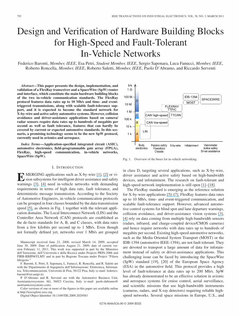
792 IEEE TRANSACTIONS ON INDUSTRIAL ELECTRONICS, VOL. 58, NO. 3, MARCH 2011 Design and Verification of Hardware Building Blocks for High-Speed and Fault-Tolerant In-Vehicle Networks Federico Baronti, Member, IEEE, Esa Petri, Student Member, IEEE, Sergio Saponara, Luca Fanucci, Member, IEEE, Roberto Roncella, Member, IEEE, Roberto Saletti, Member, IEEE, Paolo D’Abramo, and Riccardo Serventi Abstract—This paper presents the design, implementation, and validation of a FlexRay transceiver and a SpaceWire (SpW) router and interface, which constitute the main hardware building blocks of the two in-vehicle communication standards. The FlexRay protocol features data rates up to 10 Mb/s and time- and event- triggered transmissions, along with scalable fault-tolerance sup- port, and it is expected to become the standard network for X-by-wire and active safety automotive systems. However, collision avoidance and driver-assistance applications based on camera/ radar sensors require data rates up to hundreds of megabits per second as well as fault tolerance, features that can hardly be covered by current or expected automotive standards. In this sce- nario, a promising technology seems to be the new SpW protocol, currently used in avionics and aerospace. Index Terms—Application-specified integrated circuit (ASIC), automotive electronics, field-programmable gate array (FPGA), FlexRay, high-speed communication, in-vehicle networks, SpaceWire (SpW). I. I NTRODUCTION E MERGING applications such as X-by-wire [1], [2] or vi- sion subsystems for intelligent driver assistance and safety warnings [3], [4] need in-vehicle networks with demanding requirements in terms of high data rate, fault tolerance, and deterministic message transmission. According to the Society of Automotive Engineers, in-vehicle communication protocols can be grouped in four classes bounded by the data transmission speed [5], as shown in Fig. 1 together with the relevant appli- cation domains. The Local Interconnect Network (LIN) and the Controller Area Network (CAN) protocols are established as the de-facto standards for A, B, and C classes, with data rates from a few kilobits per second up to 1 Mb/s. Even though not formally defined yet, networks over 1 Mb/s are grouped Manuscript received June 23, 2008; revised March 14, 2009; accepted June 30, 2009. Date of publication August 21, 2009; date of current ver- sion February 11, 2011. This work was supported in part by the Ministero dell’Istruzione, dell’Università e della Ricerca under Projects PRIN-2006 and FIRB-RBIP06YLMY and in part by Regione Toscana under Project “Filiera Idrogeno.” F. Baronti, E. Petri, S. Saponara, L. Fanucci, R. Roncella, and R. Saletti are with the Dipartimento di Ingegneria dell’Informazione: Elettronica, Informat- ica, Telecomunicazioni, Università di Pisa, 56122 Pisa, Italy (e-mail: federico. [email protected]). P. D’Abramo and R. Serventi are with the Automotive Business Unit, Austriamicrosystems AG, 56023 Cascina, Italy (e-mail: paolo.dabramo@ austriamicrosystems.com). Color versions of one or more of the figures in this paper are available online at http://ieeexplore.ieee.org. Digital Object Identifier 10.1109/TIE.2009.2029583 Fig. 1. Overview of the buses for in-vehicle networking. in class D, targeting several applications, such as X-by-wire, driver assistance and active safety based on high-bandwidth devices, and infotainment. The research on fault-tolerant and high-speed network implementation is still open [1]–[18]. The FlexRay standard is emerging as the reference solution for X-by-wire applications [5]–[7]. FlexRay features data rates up to 10 Mb/s, time- and event-triggered communication, and scalable fault-tolerance support. However, advanced automo- tive control systems for blind spot and lane departure warnings, collision avoidance, and driver-assistance vision systems [3], [4] rely on data coming from multiple high-bandwidth sensors (radars, infrared, and charge-coupled device/CMOS cameras) and hence require networks with data rates up to hundreds of megabits per second. Existing high-speed automotive networks, such as the Media Oriented System Transport (MOST) or the IDB-1394 (automotive IEEE-1394), are not fault tolerant. They are devoted to transport a large amount of data for infotain- ment instead of safety or driver-assistance applications. This challenging issue can be faced by introducing the SpaceWire (SpW) standard [19], [20] of the European Space Agency (ESA) in the automotive field. This protocol provides a high level of fault-tolerance at data rates up to 200 Mb/s. SpW has already demonstrated to be an effective solution in avionic and aerospace systems for cruise control, aerial surveillance, and scientific missions that use high-bandwidth instruments (cameras, radars, and X-ray detectors) requiring reliable high- speed networks. Several space missions in Europe, U.S., and 0278-0046/$26.00 © 2009 IEEE
-
Upload
independent -
Category
Documents
-
view
1 -
download
0
Transcript of Design and Verification of Hardware Building Blocks for High-Speed and Fault-Tolerant In-Vehicle...
792 IEEE TRANSACTIONS ON INDUSTRIAL ELECTRONICS, VOL. 58, NO. 3, MARCH 2011
Design and Verification of Hardware Building Blocksfor High-Speed and Fault-Tolerant
In-Vehicle NetworksFederico Baronti, Member, IEEE, Esa Petri, Student Member, IEEE, Sergio Saponara, Luca Fanucci, Member, IEEE,
Roberto Roncella, Member, IEEE, Roberto Saletti, Member, IEEE, Paolo D’Abramo, and Riccardo Serventi
Abstract—This paper presents the design, implementation, andvalidation of a FlexRay transceiver and a SpaceWire (SpW) routerand interface, which constitute the main hardware building blocksof the two in-vehicle communication standards. The FlexRayprotocol features data rates up to 10 Mb/s and time- and event-triggered transmissions, along with scalable fault-tolerance sup-port, and it is expected to become the standard network forX-by-wire and active safety automotive systems. However, collisionavoidance and driver-assistance applications based on camera/radar sensors require data rates up to hundreds of megabits persecond as well as fault tolerance, features that can hardly becovered by current or expected automotive standards. In this sce-nario, a promising technology seems to be the new SpW protocol,currently used in avionics and aerospace.
Index Terms—Application-specified integrated circuit (ASIC),automotive electronics, field-programmable gate array (FPGA),FlexRay, high-speed communication, in-vehicle networks,SpaceWire (SpW).
I. INTRODUCTION
EMERGING applications such as X-by-wire [1], [2] or vi-sion subsystems for intelligent driver assistance and safety
warnings [3], [4] need in-vehicle networks with demandingrequirements in terms of high data rate, fault tolerance, anddeterministic message transmission. According to the Societyof Automotive Engineers, in-vehicle communication protocolscan be grouped in four classes bounded by the data transmissionspeed [5], as shown in Fig. 1 together with the relevant appli-cation domains. The Local Interconnect Network (LIN) and theController Area Network (CAN) protocols are established asthe de-facto standards for A, B, and C classes, with data ratesfrom a few kilobits per second up to 1 Mb/s. Even thoughnot formally defined yet, networks over 1 Mb/s are grouped
Manuscript received June 23, 2008; revised March 14, 2009; acceptedJune 30, 2009. Date of publication August 21, 2009; date of current ver-sion February 11, 2011. This work was supported in part by the Ministerodell’Istruzione, dell’Università e della Ricerca under Projects PRIN-2006 andFIRB-RBIP06YLMY and in part by Regione Toscana under Project “FilieraIdrogeno.”
F. Baronti, E. Petri, S. Saponara, L. Fanucci, R. Roncella, and R. Saletti arewith the Dipartimento di Ingegneria dell’Informazione: Elettronica, Informat-ica, Telecomunicazioni, Università di Pisa, 56122 Pisa, Italy (e-mail: [email protected]).
P. D’Abramo and R. Serventi are with the Automotive Business Unit,Austriamicrosystems AG, 56023 Cascina, Italy (e-mail: [email protected]).
Color versions of one or more of the figures in this paper are available onlineat http://ieeexplore.ieee.org.
Digital Object Identifier 10.1109/TIE.2009.2029583
Fig. 1. Overview of the buses for in-vehicle networking.
in class D, targeting several applications, such as X-by-wire,driver assistance and active safety based on high-bandwidthdevices, and infotainment. The research on fault-tolerant andhigh-speed network implementation is still open [1]–[18].
The FlexRay standard is emerging as the reference solutionfor X-by-wire applications [5]–[7]. FlexRay features data ratesup to 10 Mb/s, time- and event-triggered communication, andscalable fault-tolerance support. However, advanced automo-tive control systems for blind spot and lane departure warnings,collision avoidance, and driver-assistance vision systems [3],[4] rely on data coming from multiple high-bandwidth sensors(radars, infrared, and charge-coupled device/CMOS cameras)and hence require networks with data rates up to hundreds ofmegabits per second. Existing high-speed automotive networks,such as the Media Oriented System Transport (MOST) or theIDB-1394 (automotive IEEE-1394), are not fault tolerant. Theyare devoted to transport a large amount of data for infotain-ment instead of safety or driver-assistance applications. Thischallenging issue can be faced by introducing the SpaceWire(SpW) standard [19], [20] of the European Space Agency(ESA) in the automotive field. This protocol provides a highlevel of fault-tolerance at data rates up to 200 Mb/s. SpWhas already demonstrated to be an effective solution in avionicand aerospace systems for cruise control, aerial surveillance,and scientific missions that use high-bandwidth instruments(cameras, radars, and X-ray detectors) requiring reliable high-speed networks. Several space missions in Europe, U.S., and
0278-0046/$26.00 © 2009 IEEE

BARONTI et al.: DESIGN AND VERIFICATION OF HARDWARE BUILDING BLOCKS FOR IN-VEHICLE NETWORKS 793
Japan planned the use of SpW [21], which is also used inavionics [18] and recently for modular industrial robots [9].
The key point for the success of FlexRay and SpW standardslies in the hardware implementation of their relevant buildingblocks through high-performance designs, meeting stringentrequirements in terms of high speed, low electromagnetic inter-ference and high Electromagnetic Compatibility (EMC), wideoperating temperature range, and limited size and costs. Thispaper, after reviewing both standards, presents the hardwaredesign, the technology selection, and the verification/testingphase of their critical building blocks: the FlexRay Transceiverand the SpW router and interface. With respect to conferencepapers [22]–[24], where we proposed preliminary designs ofthe aforementioned blocks, this paper presents: 1) a deep insighton the design choices; 2) new implementation results relatedto technologies suitable for automotive systems, being [22],[24] limited to rad-tolerant or high-cost technologies mainlyfor aerospace systems; and 3) a detailed verification phaseat simulation and emulation levels, not present in [22]–[24],with experimental results ensuring exhaustive testing of thehardware blocks.
The next section introduces the FlexRay standard, andSections III and IV describe the FlexRay transceiver designand verification. The following sections present the SpW pro-tocol (Section V), the design and implementation of its mainhardware building blocks (Sections VI and VII), and theirexperimental validation (Section VIII).
II. FLEXRAY NETWORKING
FlexRay is a high-bandwidth fault-tolerant deterministiccommunication protocol with some advantages compared withboth the very popular CAN protocol and other emerging ones,such as Time-Triggered CAN (TTCAN) and Time-TriggeredProtocol version C (TTP/C). In fact, the FlexRay networkaccomplishes time-triggered as well as event-triggered trans-missions with a bit rate up to 10 Mb/s, making high-speed deter-ministic communications possible. Thus, the implementation ofadvanced distributed control systems is dramatically simplifiedwith respect to CAN networking, as the latter provides onlyasynchronous data exchange below 1 Mb/s, an order of mag-nitude slower than FlexRay. Moreover, the TTCAN protocol,which simply consists of a time-triggered session layer at thetop of the CAN protocol stack, does not provide the samelevel of fault-tolerance as FlexRay and TTP/C, since it doesnot directly implement important dependability services suchas bus guardian, membership service, and reliable acknowl-edgment. TTP/C has similar characteristics in terms of band-width and fault-tolerance capabilities, but with higher costsand reduced flexibility compared with FlexRay. Indeed, TTP/Cdoes not support event-triggered transmission, which is a majordrawback in the in-vehicle application scenario where severalsignals, including user commands and alarms, are inherentlyasynchronous [5].
FlexRay networking is very flexible and scalable in termsof network topology and fault-tolerance support. In fact, thesystem can support single-channel configuration, as well as thedual-channel one with some nodes connected to both channels
Fig. 2. Architecture of a FlexRay communication node. Optional blocks forscalable fault tolerance are represented in dashed lines. The main functionalblocks of the transceiver are also shown on the left-hand side of the figure.
and others connected to just one channel. Moreover, severalnetwork topologies are possible, such as linear passive buses,passive or active stars, and hybrid configurations, which canadvantageously be utilized to limit the propagation of a fault.
As far as a communication node is concerned, its basicbuilding blocks are shown in Fig. 2. The transceiver im-plements the physical layer of the protocol and operates asinterface between the medium, consisting of two differentiallines, named Bus Plus (BP) and Bus Minus (BM), and thecommunication controller. When there is no differential voltageon the bus lines (i.e., its absolute value is lower than theamount specified in [7]), the bus is in the idle state. Otherwise,a positive polarity of the differential voltage implies that ahigh logical level (Data_1) is being transmitted on the bus,while a negative one a low logical level (Data_0). On the otherhand, the communication controller is responsible for messagecoding and decoding and time synchronization, allowing theapplication running on the microcontroller to exchange dataover the FlexRay network. Fig. 2 also shows that the FlexRayarchitecture provides a scalable fault tolerance in terms of dual-channel redundancy as well as bus guardian adoption. Thebus guardian operates independently from the communicationcontroller, and if a failure occurs in the latter (e.g., an attemptto transmit data in a time slot reserved to another node), itdenies the bus access by disabling the bus driver. This way,the communication channel is protected against faulty nodes onthe bus [7], [25]. The application hosted by the microcontrollercan select the transceiver operating mode (normal operation,receive only, or low-power sleep operation modes) and readdiagnostic information related to the transceiver.
The FlexRay protocol specification is mature [7], and theresearch focus is now on the silicon implementation of itsbasic hardware components: the communication controller andthe transceiver [26], [27]. In particular, the design of thecommunication controller is fully digital and straightforwardsince it can rely on the popular E-Ray Intellectual Property(IP) macrocell from Bosch [26]. On the contrary, the designof the transceiver is quite challenging, as the reliability ofthe entire node mainly depends on that of this component.EMC performances, in terms of very low EM emissions and
794 IEEE TRANSACTIONS ON INDUSTRIAL ELECTRONICS, VOL. 58, NO. 3, MARCH 2011
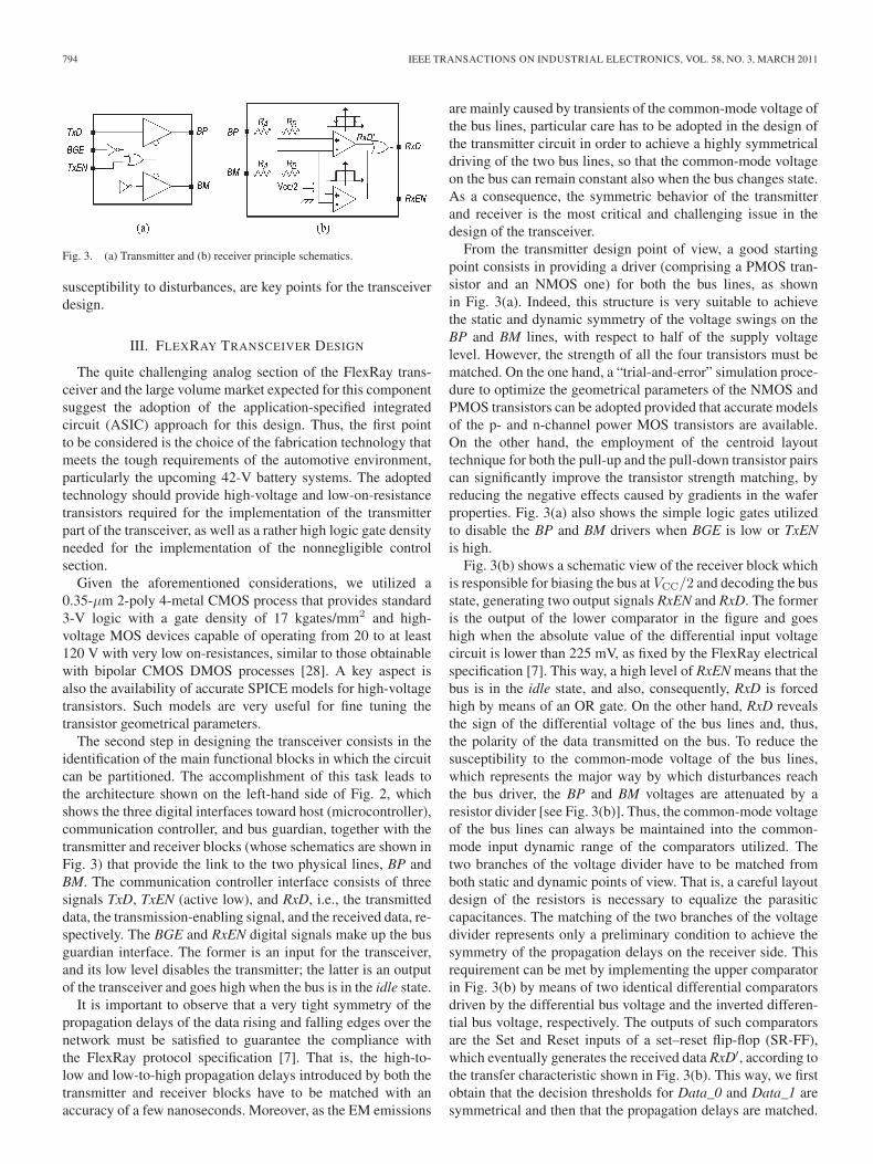
Fig. 3. (a) Transmitter and (b) receiver principle schematics.
susceptibility to disturbances, are key points for the transceiverdesign.
III. FLEXRAY TRANSCEIVER DESIGN
The quite challenging analog section of the FlexRay trans-ceiver and the large volume market expected for this componentsuggest the adoption of the application-specified integratedcircuit (ASIC) approach for this design. Thus, the first pointto be considered is the choice of the fabrication technology thatmeets the tough requirements of the automotive environment,particularly the upcoming 42-V battery systems. The adoptedtechnology should provide high-voltage and low-on-resistancetransistors required for the implementation of the transmitterpart of the transceiver, as well as a rather high logic gate densityneeded for the implementation of the nonnegligible controlsection.
Given the aforementioned considerations, we utilized a0.35-µm 2-poly 4-metal CMOS process that provides standard3-V logic with a gate density of 17 kgates/mm2 and high-voltage MOS devices capable of operating from 20 to at least120 V with very low on-resistances, similar to those obtainablewith bipolar CMOS DMOS processes [28]. A key aspect isalso the availability of accurate SPICE models for high-voltagetransistors. Such models are very useful for fine tuning thetransistor geometrical parameters.
The second step in designing the transceiver consists in theidentification of the main functional blocks in which the circuitcan be partitioned. The accomplishment of this task leads tothe architecture shown on the left-hand side of Fig. 2, whichshows the three digital interfaces toward host (microcontroller),communication controller, and bus guardian, together with thetransmitter and receiver blocks (whose schematics are shown inFig. 3) that provide the link to the two physical lines, BP andBM. The communication controller interface consists of threesignals TxD, TxEN (active low), and RxD, i.e., the transmitteddata, the transmission-enabling signal, and the received data, re-spectively. The BGE and RxEN digital signals make up the busguardian interface. The former is an input for the transceiver,and its low level disables the transmitter; the latter is an outputof the transceiver and goes high when the bus is in the idle state.
It is important to observe that a very tight symmetry of thepropagation delays of the data rising and falling edges over thenetwork must be satisfied to guarantee the compliance withthe FlexRay protocol specification [7]. That is, the high-to-low and low-to-high propagation delays introduced by both thetransmitter and receiver blocks have to be matched with anaccuracy of a few nanoseconds. Moreover, as the EM emissions
are mainly caused by transients of the common-mode voltage ofthe bus lines, particular care has to be adopted in the design ofthe transmitter circuit in order to achieve a highly symmetricaldriving of the two bus lines, so that the common-mode voltageon the bus can remain constant also when the bus changes state.As a consequence, the symmetric behavior of the transmitterand receiver is the most critical and challenging issue in thedesign of the transceiver.
From the transmitter design point of view, a good startingpoint consists in providing a driver (comprising a PMOS tran-sistor and an NMOS one) for both the bus lines, as shownin Fig. 3(a). Indeed, this structure is very suitable to achievethe static and dynamic symmetry of the voltage swings on theBP and BM lines, with respect to half of the supply voltagelevel. However, the strength of all the four transistors must bematched. On the one hand, a “trial-and-error” simulation proce-dure to optimize the geometrical parameters of the NMOS andPMOS transistors can be adopted provided that accurate modelsof the p- and n-channel power MOS transistors are available.On the other hand, the employment of the centroid layouttechnique for both the pull-up and the pull-down transistor pairscan significantly improve the transistor strength matching, byreducing the negative effects caused by gradients in the waferproperties. Fig. 3(a) also shows the simple logic gates utilizedto disable the BP and BM drivers when BGE is low or TxENis high.
Fig. 3(b) shows a schematic view of the receiver block whichis responsible for biasing the bus at VCC/2 and decoding the busstate, generating two output signals RxEN and RxD. The formeris the output of the lower comparator in the figure and goeshigh when the absolute value of the differential input voltagecircuit is lower than 225 mV, as fixed by the FlexRay electricalspecification [7]. This way, a high level of RxEN means that thebus is in the idle state, and also, consequently, RxD is forcedhigh by means of an OR gate. On the other hand, RxD revealsthe sign of the differential voltage of the bus lines and, thus,the polarity of the data transmitted on the bus. To reduce thesusceptibility to the common-mode voltage of the bus lines,which represents the major way by which disturbances reachthe bus driver, the BP and BM voltages are attenuated by aresistor divider [see Fig. 3(b)]. Thus, the common-mode voltageof the bus lines can always be maintained into the common-mode input dynamic range of the comparators utilized. Thetwo branches of the voltage divider have to be matched fromboth static and dynamic points of view. That is, a careful layoutdesign of the resistors is necessary to equalize the parasiticcapacitances. The matching of the two branches of the voltagedivider represents only a preliminary condition to achieve thesymmetry of the propagation delays on the receiver side. Thisrequirement can be met by implementing the upper comparatorin Fig. 3(b) by means of two identical differential comparatorsdriven by the differential bus voltage and the inverted differen-tial bus voltage, respectively. The outputs of such comparatorsare the Set and Reset inputs of a set–reset flip-flop (SR-FF),which eventually generates the received data RxD′, according tothe transfer characteristic shown in Fig. 3(b). This way, we firstobtain that the decision thresholds for Data_0 and Data_1 aresymmetrical and then that the propagation delays are matched.

BARONTI et al.: DESIGN AND VERIFICATION OF HARDWARE BUILDING BLOCKS FOR IN-VEHICLE NETWORKS 795
Fig. 4. Microphotograph and maximum ratings of the FlexRay transceiver.
RxD, generated by OR-ing RxD′ and RxEN, is a digital signal,so that all the conventional techniques can be employed to avoidpulse-shrinking phenomena from the output of the SR-FF to thecorresponding pin. In particular, a high-speed pad can be usedto reduce the negative effects of possible different propagationdelays of the output circuitry.
IV. FLEXRAY TRANSCEIVER VERIFICATION AND
IMPLEMENTATION RESULTS
Following the aforementioned design considerations, a fullycompliant FlexRay transceiver has been implemented. Fig. 4shows the microphotograph of the die, in which most of the areais occupied by the transmitter transistors. The verification phaseconsisted in measuring more than 500 fabricated devices todemonstrate the effectiveness of our design approach to achieveexcellent EMC performance and to meet the very demandingoperating requirements of the automotive environment (see theabsolute maximum ratings in Fig. 4), regarding temperature,bus voltage, latch-up immunity, and electrostatic dischargetolerance.
First of all, the digital part of the transceiver, comprising theinternal logic and the interfaces toward the communication con-troller, the bus guardian, and the host controller, was validated.During this phase, the current consumption in the differentoperating modes of the transceiver was also measured. Themaximum current in sleep mode is 50 µA, a very reasonablevalue for automotive applications; the typical value in receivemode is 1.5 mA due to the internal circuitry while extra 22 mAis needed in normal mode when transmitting (for the two 88-Ωbus terminations required by the standard [7]).
Then, both static and dynamic experimental tests were per-formed, connecting two transceivers to form a basic point-to-point FlexRay network. The static ones consisted in measuringthe steady-state values of the BP and BM voltages when trans-mitting Data_0 and Data_1 over the bus and in evaluating theirstatistical distribution over more than 500 different samples. Asan example, Fig. 5 shows the histogram of the measured valuesof bus differential voltage in the case of Data_1 transmission.Similar results were obtained for Data_0 transmission. The ex-
Fig. 5. Measured distribution of the differential bus voltage when transmittingData_1 over more than 500 parts.
Fig. 6. Bus transition from Data_0 to Data_1 and vice versa.
perimental results show that the mean values of the differentialvoltage over the bus, as well as the common-mode one, areexactly matched for the two bus states. Aside from this, theirstandard deviation was found to be a few tens of millivolts,showing a very good matching performance of the transmittertransistors and, thus, an excellent driving symmetry.
Dynamic tests consisted in transmitting sequences of Data_0and Data_1 to characterize the timing response of both thetransmitter and receiver circuits. The experimental results showa very good symmetry behavior of the bus line voltage anda good repeatability from sample to sample. As an example,Fig. 6 shows enlarged views of the bus differential voltageresponses induced by rising and falling transitions of the TxDsignal. These measurements allowed us to evaluate the risingand falling delays introduced by the transmitter (dBDTx01 anddBDTx10) and particularly, their asymmetry, which is a veryimportant parameter for the performance of a FlexRay network.The value obtained is 0.8 ns, an outstanding result that fullymeets the FlexRay specification, which requires the transmit-ting delay mismatch to be less than 4 ns. According to theFlexRay specification, the delays are defined as the time intervalbetween the transition of the relevant digital signal and the timeat which the differential voltage on the bus reaches 300 mVin the case of Data_1 and −300 mV in the case of Data_0.
Concerning the receiver, Fig. 7 shows the behavior of RxDfollowing a bus transition from idle to active (Data_0) and fromData_0 to Data_1, as represented by the voltages on the buslines BP and BM. It should be noticed that RxD reveals thepolarity of the differential bus voltage and that the measureddelays are fully compliant with the FlexRay specification.
Finally, the transceiver has been extensively tested under realautomotive conditions. To this aim, a FlexRay communicationnode was built up using the implemented transceiver and wasconnected to three other nodes with a linear bus network topol-ogy. Several bus transitions were generated by the transceiverunder test, and the bus line voltages were measured at both

796 IEEE TRANSACTIONS ON INDUSTRIAL ELECTRONICS, VOL. 58, NO. 3, MARCH 2011
Fig. 7. Measured behavior of the receiver circuit after a bus transition fromidle to active (Data_0) and from Data_0 to Data_1.
Fig. 8. Eye diagram of the differential bus voltage at the receiver side.
the transmitter side and the receiver side of the furthest node,which was 24 m away from the transmitter. The eye diagrammeasured in the latter point, which takes into account also thebus attenuation, is shown in Fig. 8. It should be noticed that theminimum aperture of the measured differential voltage fulfillsthe relevant FlexRay specification [7, Ch. 7], which is shown asthe gray area in Fig. 8.
V. SpW NETWORKING
The SpW standard features bidirectional full-duplex serialdata links up to 200 Mb/s over distances of about 10 m.SpW covers six protocol layers: physical, signal, character,exchange, packet, and network [19]. The physical layer is basedon low-voltage differential signaling (LVDS), like the high-speed IEEE-1394, while connectors and cables are specificallytailored for harsh environments. LVDS enables low-power andhigh-speed links with excellent EMC performance. Data–strobesignal encoding is adopted. Packet-switched data transfersamong different equipment are managed by routers. This topol-ogy reduces the weight and volume of the wire harness versuspoint-to-point direct connections. Wormhole routing in combi-nation with a credit-based flow control is supported to minimizememory buffer size and communication latency. Both path andlogical addressing schemes are available. Two extensions of thestandard, which are the Protocol Identifier (PID) and the Re-mote Memory Access Protocol (RMAP) [20], have been added
by stacking the transport layer on top of the six basic protocollayers. The PID allows the concurrent operation of differenttransport protocols over an SpW network without interference.A PID = 1 has been assigned to the RMAP protocol, whichspecifies procedures and message formats that allow an SpWnetwork to be configured, SpW nodes to be remotely controlled,and data/status information from nodes to be gathered. Cyclicredundancy checks (CRCs) are performed on the commandand data fields of the RMAP message. To increase networksecurity, an authorization key characterizes each node. TheSpW protocol overhead, for transferring data through RMAPwrite commands or answers to read commands, ranges from 13to 17 B. Using payload sizes of hundreds of bytes, the resultingoverhead is less than 10% of the available link bandwidth.This value is comparable to high speed but not fault-tolerantlinks such as IEEE-1394, MOST, and Ethernet, and hence,SpW can be used whenever a high bandwidth stream has to betransferred, e.g., infotainment or driver assistance/active safetybased on cameras and radars. SpW is event driven, like CAN,but owing to the exchange of special time-code characters,mixed event-/time-triggered schemes, like FlexRay, are alsosupported. To guarantee path redundancy and link failure toler-ance, thus increasing SpW robustness versus known protocolsas IEEE-1394, Group Adaptive Routing is supported. This is amethod of routing packets to a destination over different paths.Several ports can be grouped together so that, if a link is busyor unavailable due to failure, a packet is sent through the nextavailable link in the group.
VI. SpW ROUTER AND INTERFACE DESIGN
A. Review of the State of the Art and Technology Selection
This section describes the design of a complete SpW rout-ing and interfacing solution, compliant with RMAP and PID,achieved through novel hardware macrocells targeting severalfield-programmable gate array (FPGA) technologies. This isfundamental for the development of SpW in the automotivefield since no SpW router IP cores supporting the transport layerextensions, PID and RMAP, are currently available.
Unlike the FlexRay transceiver, the FPGA approach waspreferred to the ASIC one for the following reasons. CurrentFPGAs provide enough logic, memory and I/O resources (in-cluding LVDS drivers), and performance (timing, power, andoperating conditions) to meet the challenging requirementsof aerospace, avionic, and automotive systems. The FPGAnonrecurrent costs and time to market, much lower than theASIC ones, are more suitable for a scenario where the standardsare not frozen yet. Finally, a large market is not foreseen forspace and avionics, and automotive control systems for activesafety based on camera/radar are still in an evolving phase.
Susceptibility to failure due to radiation effects [29], a tra-ditional issue of space and military electronics, is becoming aconcern also for commercial avionics and safety-critical auto-motive systems. By choosing an inherently radiation-toleranttechnology, it is possible to mitigate radiation effects. To thisaim, antifuse FPGAs outperform SRAM-based FPGAs andoften offer built-in mitigation techniques (e.g., RTAX, which

BARONTI et al.: DESIGN AND VERIFICATION OF HARDWARE BUILDING BLOCKS FOR IN-VEHICLE NETWORKS 797
Fig. 9. Architecture of the SpW interface.
is a space-qualified version of the AX FPGAs [30], [31]).Radiation-tolerant SRAM-based FPGAs exist, e.g., the QPROversion of the Virtex family [32], but without built-in mitigationtechniques. From the thermal reliability point of view, antifusedevices can reach a junction temperature (Tj) of 150 ◦C; theautomotive AEC-Q100 qualified version of SRAM FPGAshas been recently released, e.g., for the Spartan family [33],reaching a maximum Tj value of 125 ◦C, which is lower thanthat of an antifuse. On the other hand, SRAM FPGAs are repro-grammable on field and offer reduced development time/cost,and many device architectures are available with differenttradeoffs between complexity and processing capability. BasicSRAM FPGA architectures are available for low-cost high-volume production (but extra programmable read-only memoryis needed for nonvolatile storage configuration). As an example,the Spartan XC3S1200E FPGA provides more than one-millionlogic gates with a device cost below ten dollars for high volume(hundreds of thousands of devices). Such values are much lowerthan antifuse devices, i.e., hundreds of dollars for AX familyor thousands for the RTAX one. A tradeoff between SRAMand antifuse are Flash FPGAs. For example, the ProASIC [34]family is available in automotive AEC-Q100 qualified grade upto Tj = 135 ◦C, is reprogrammable and nonvolatile, and haslow static power. The cost of a one-million-gate Flash FPGA,e.g., A3P1000, is below 20 dollars for high-volume production.Summarizing, antifuse is the first choice for military/spaceapplications while the reprogrammability of SRAM and FlashFPGAs is needed for automotive. The choice between SRAMand Flash depends on the requirements in terms of cost, perfor-mance, and reliability of the onboard subsystem.
B. SpW Interface Macrocell
The architecture of an SpW interface is shown in Fig. 9.In this paper, differently from [22] and [24], the very highspeed integrated circuit hardware description language (VHDL)code is partitioned in three blocks: LVDS drivers for data(Din/Dout) and strobe (Sin/Sout) signals, SpW Codec, andSpW I/O wrapper. The synthesized IP cell configuration mayinclude the driver module or not, depending if LVDS driversare available in the target technology as hardware macros orhave to be implemented off-chip through discrete drivers. TheSpW Codec consists of a transmitter, coding and serializingdata, plus a receiver, decoding and deserializing data, and afinite-state machine (FSM). The SpW I/O wrapper connects
the SpW Codec to the router core or to a remote host viathe advanced high-performance bus (AHB) wrapper, throughtransmitting (TX) and receiving (RX) bisynchronous First-InFirst-Out (FIFO) buffers. Since SpW adopts the wormholetechnique, small FIFO sizes (64 locations) can be used. Toavoid the RX FIFO overflow and the consequent loss of data,credit-based flow control tokens (FCTs) are used. The SpWinterface is also responsible for error detection and recovery.The link detects Parity, Char Sequence, Escape Sequence,Disconnect, and Credit errors. After error detection, the errorrecovery protocol follows these steps: disconnect the link inTX/RX directions, spill the current transmit packet, terminatethe current receive packet with the Error End of Packet flag,reset the FSMs to the initial state, and attempt to restart thelink.
C. SpW Router Macrocell
The proposed SpW router, in Fig. 10, is a VHDL macrocellwhose core is a switching matrix connected to the externalworld via a parameterizable number of SpW interfaces, a time-code interface, a control/status interface, and a host data transferinterface. The control/status interface provides the host withread (status check) and write (configuration) access to internalregisters of the SpW router and interfaces. The time-code inter-face distributes system time over an SpW network. The SpWrouter can be configured to be the time master of the network(the time code can be generated internally or acquired by anexternal host) or a time slave. The switching matrix connectseach input port to any output port. A round-robin arbiter selectsamong multiple requests to the same port. The routing tabletranslates logical addresses into physical ones (i.e., output portnumber) and provides group information for Group AdaptiveRouting. The router is configured by the internal programminginterface accessible by a local host through the AHB bus orremotely via the SpW links.
Each SpW interface in Fig. 10 derives its RX clock by XOR-ing incoming data and strobe signals. The TX clock is pro-grammable, obtained from the external system clock divided bylocal prescalers with a factor of 1, 2, 10, or 20. The router coreruns at a fixed clock obtained by dividing the external systemclock by a prescaler (using a factor of 3 for the architecture inFig. 10). The AHB host interface can be synchronous with therouter core or can optionally use an external AHB clock. Theaforementioned multiple clock domain architecture optimizesdynamic power consumption since each clock is tailored forthe specific subcircuit requirements.
The RMAP hardware decoder allows a remote control ofthe AHB bus from the SpW side. All the accessible registers,FIFOs, and memories in the AHB domain are mapped to amemory space, where an address is reserved to program therouter by means of RMAP commands. When a non-RMAPpacket, with PID �= 1, is received by the RMAP decoder, itis passed on to the host system and handled software-wise.From an architectural point of view, the RMAP decoder andSpW/AHB wrapper unit consists of an FSM, implementingthe RMAP protocol rules, local memory resources, a dedicatedunit for CRC calculation, and an AHB wrapper, which is a

798 IEEE TRANSACTIONS ON INDUSTRIAL ELECTRONICS, VOL. 58, NO. 3, MARCH 2011
Fig. 10. Architecture of a four-link SpW router with AHB/CAN wrapper.
bridge between the SpW router and the AHB bus, a de factostandard in embedded systems. This module acts as a masteror slave on the AHB bus; it can control the bus to execute adirect memory access transfer into memory devices or to initiatean SpW remote control session to a host system connectedat AHB.
In Fig. 10, a CAN module is connected to the AHB routerinterface to link the SpW router, and, hence, all the devices inthe SpW network domain, to preexisting automotive networks.Thus, the router acts as a gateway between CAN and SpWnetworks. To this aim, the HurriCANe IP, from ESA, canbe embedded with a complexity overhead of roughly 12 000equivalent ASIC gates. Moreover, a programmable core, e.g.,the well-known LEON or ARM IPs, can be connected to therouter AHB bus and integrated in the same device. This scenarioallows for a local processing of the data collected from the high-speed units on the SpW network.
VII. SpW ROUTER AND INTERFACE
IMPLEMENTATION RESULTS
To assess the reusability of the IP macrocells, the SpW IPshave been synthesized in different configurations on severalFPGA families: SRAM Altera Stratix II, Xilinx Virtex 2 andSpartan 3, antifuse Actel AX and RTAX, and Flash Actel Pro-ASIC. Table I summarizes the implementation results of theSpW router with eight or four links plus the AHB host inter-face on different FPGAs. The resulting complexity is roughly180 000 equivalent ASIC gates for the logic plus 2.8 kB ofRAM in case of eight SpW links and 120 000 equivalent ASICgates for the logic plus 2.2 kB of RAM in case of four SpWlinks. The free FPGA resources in Table I can be used tointegrate other IPs, such as the AHB–CAN wrapper.
The target data rate for the syntheses in Table I is 100 Mb/sper SpW link, which entails a maximum interface TX clock of100 MHz and an internal router core clock of roughly 33 MHz.The AHB host interface uses the same clock of the routercore. Both router configurations fit on AX2000, providing twomillion gates equivalent to 250 000 ASIC gates; the occupationis 81% of the available logic for the eight-link router and 55%for the four-link router. Such an FPGA platform is optimized forspace applications due to the availability of a rad-tolerant RTAX
TABLE ISpW IP ROUTER CHARACTERIZATION RESULTS
version with on-chip mitigation techniques. For high-capabilitySRAM FPGAs, such as the EP2S60 and the XC2V8000, theoccupation of the eight-link router is below 30% while the four-link router requires less than 20% of the available resources.For such SRAM FPGAs, more suitable for prototyping, theachievable maximum data rate increases up to 200 Mb/s. TheSpW router IP can also be fitted in smaller devices, suchas the SRAM Spartan XC3S1200E and the Flash AP31000,supporting the four-link router up to 100 Mb/s per link. TheseFPGAs are suitable for automotive systems, since they areAEC-Q100 qualified and available at low cost for high-volumemarket.
Compared to the state of the art, the proposed SpW routingsolution is the first IP macrocell mapped in antifuse, Flash, andSRAM FPGAs, which is compliant with the complete standardincluding PID and RMAP extensions. An ASIC SpW eight-link router in 0.35-µm 3.3-V ATMEL CMOS has been recentlyreleased [35], featuring a radiation tolerance to total ionizationdose up to 300 krad and a power consumption of 2 W with linksat 100 Mb/s. Our router IP core, fitted on the antifuse (RT)AXFPGA, offers the same 300-krad tolerance to total ionizationdose, and its measured power consumption is 1.3 W using a1.5-V supply for the core and 2.5-V supply for the LVDS I/O(400 mW of static power plus roughly 1.1 mW per Mb/s foreach of the eight links, at 100 Mb/s).
VIII. SpW ROUTER AND INTERFACE VALIDATION
The SpW IP cells have been tested at multiple levels. Func-tional, postsynthesis, and postlayout simulations have been
BARONTI et al.: DESIGN AND VERIFICATION OF HARDWARE BUILDING BLOCKS FOR IN-VEHICLE NETWORKS 799
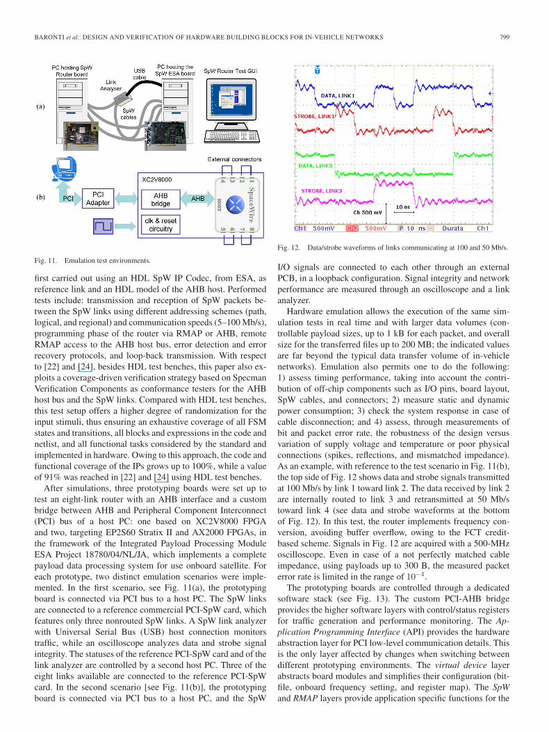
Fig. 11. Emulation test environments.
first carried out using an HDL SpW IP Codec, from ESA, asreference link and an HDL model of the AHB host. Performedtests include: transmission and reception of SpW packets be-tween the SpW links using different addressing schemes (path,logical, and regional) and communication speeds (5–100 Mb/s),programming phase of the router via RMAP or AHB, remoteRMAP access to the AHB host bus, error detection and errorrecovery protocols, and loop-back transmission. With respectto [22] and [24], besides HDL test benches, this paper also ex-ploits a coverage-driven verification strategy based on SpecmanVerification Components as conformance testers for the AHBhost bus and the SpW links. Compared with HDL test benches,this test setup offers a higher degree of randomization for theinput stimuli, thus ensuring an exhaustive coverage of all FSMstates and transitions, all blocks and expressions in the code andnetlist, and all functional tasks considered by the standard andimplemented in hardware. Owing to this approach, the code andfunctional coverage of the IPs grows up to 100%, while a valueof 91% was reached in [22] and [24] using HDL test benches.
After simulations, three prototyping boards were set up totest an eight-link router with an AHB interface and a custombridge between AHB and Peripheral Component Interconnect(PCI) bus of a host PC: one based on XC2V8000 FPGAand two, targeting EP2S60 Stratix II and AX2000 FPGAs, inthe framework of the Integrated Payload Processing ModuleESA Project 18780/04/NL/JA, which implements a completepayload data processing system for use onboard satellite. Foreach prototype, two distinct emulation scenarios were imple-mented. In the first scenario, see Fig. 11(a), the prototypingboard is connected via PCI bus to a host PC. The SpW linksare connected to a reference commercial PCI-SpW card, whichfeatures only three nonrouted SpW links. A SpW link analyzerwith Universal Serial Bus (USB) host connection monitorstraffic, while an oscilloscope analyzes data and strobe signalintegrity. The statuses of the reference PCI-SpW card and of thelink analyzer are controlled by a second host PC. Three of theeight links available are connected to the reference PCI-SpWcard. In the second scenario [see Fig. 11(b)], the prototypingboard is connected via PCI bus to a host PC, and the SpW
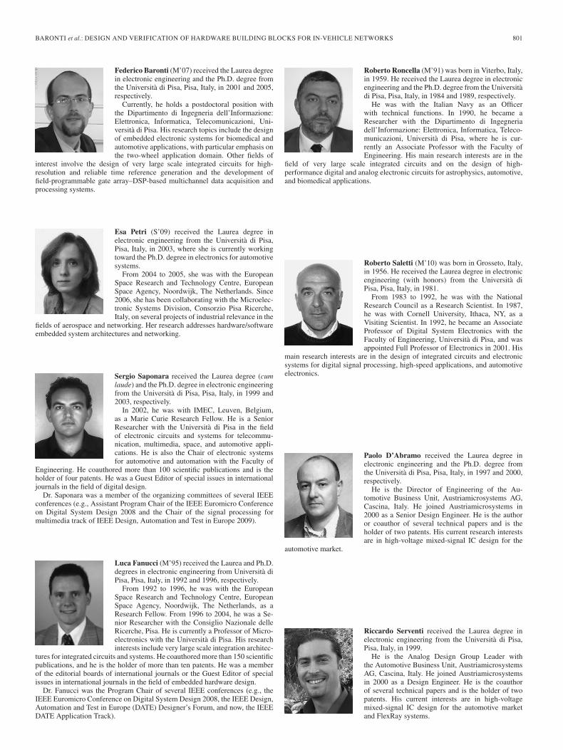
Fig. 12. Data/strobe waveforms of links communicating at 100 and 50 Mb/s.
I/O signals are connected to each other through an externalPCB, in a loopback configuration. Signal integrity and networkperformance are measured through an oscilloscope and a linkanalyzer.
Hardware emulation allows the execution of the same sim-ulation tests in real time and with larger data volumes (con-trollable payload sizes, up to 1 kB for each packet, and overallsize for the transferred files up to 200 MB; the indicated valuesare far beyond the typical data transfer volume of in-vehiclenetworks). Emulation also permits one to do the following:1) assess timing performance, taking into account the contri-bution of off-chip components such as I/O pins, board layout,SpW cables, and connectors; 2) measure static and dynamicpower consumption; 3) check the system response in case ofcable disconnection; and 4) assess, through measurements ofbit and packet error rate, the robustness of the design versusvariation of supply voltage and temperature or poor physicalconnections (spikes, reflections, and mismatched impedance).As an example, with reference to the test scenario in Fig. 11(b),the top side of Fig. 12 shows data and strobe signals transmittedat 100 Mb/s by link 1 toward link 2. The data received by link 2are internally routed to link 3 and retransmitted at 50 Mb/stoward link 4 (see data and strobe waveforms at the bottomof Fig. 12). In this test, the router implements frequency con-version, avoiding buffer overflow, owing to the FCT credit-based scheme. Signals in Fig. 12 are acquired with a 500-MHzoscilloscope. Even in case of a not perfectly matched cableimpedance, using payloads up to 300 B, the measured packeterror rate is limited in the range of 10−4.
The prototyping boards are controlled through a dedicatedsoftware stack (see Fig. 13). The custom PCI-AHB bridgeprovides the higher software layers with control/status registersfor traffic generation and performance monitoring. The Ap-plication Programming Interface (API) provides the hardwareabstraction layer for PCI low-level communication details. Thisis the only layer affected by changes when switching betweendifferent prototyping environments. The virtual device layerabstracts board modules and simplifies their configuration (bit-file, onboard frequency setting, and register map). The SpWand RMAP layers provide application specific functions for the

800 IEEE TRANSACTIONS ON INDUSTRIAL ELECTRONICS, VOL. 58, NO. 3, MARCH 2011
Fig. 13. Stacked prototyping environment.
protocol management via software. A Graphical User Interface(GUI) simplifies the prototype control enabling the following:router and link configuration, hardware reset, traffic generation(single and multiple data transfers, with selection of data pathsand payload data, also from external files), real-time statusmonitoring of AHB and SpW interfaces, and link control.
IX. CONCLUSION
This paper has presented the design, implementation, andverification of the FlexRay and SpW basic components. Theseprotocols are expected to become the future standards forhigh-speed and fault tolerant in-vehicle networks. The FlexRaytransceiver design represents one of the first fully functionaltransceivers ever presented, enabling X-by-wire applicationsup to 10 Mb/s. The circuit is able to operate in the harshautomotive environment (suitable for the upcoming 42-V bat-tery systems), has excellent symmetry between transmitter andreceiver blocks, and features reduced EM emissions. The SpWrouter and interface IP hardware macrocells are the first solu-tions compliant with the newest standard extensions, PID andRMAP. The macrocells have been implemented and tested onseveral SRAM, Flash, and antifuse FPGAs considering avionic,aerospace, and automotive target scenarios.
REFERENCES
[1] M. Bertoluzzo, G. Buja, and A. Zuccollo, “Design of drive-by-wirecommunication network for an industrial vehicle,” in Proc. IEEE IDIN,Jun. 2004, pp. 155–160.
[2] M. Bertoluzzo, P. Bolognesi, O. Bruno, G. Buja, A. Landi, andA. Zuccollo, “Drive-by-wire systems for ground vehicles,” in Proc. IEEEInt. Symp. Ind. Electron., May 2004, vol. 1, pp. 711–716.
[3] H. Takahashi, D. Ukishima, K. Kawamoto, and K. Hirota, “A study onpredicting hazard factors for safe driving,” IEEE Trans. Ind. Electron.,vol. 54, no. 2, pp. 781–789, Apr. 2007.
[4] J. McCall, “Video-based lane estimation and tracking for driver assis-tance: Survey, system, evaluation,” IEEE Trans. Intell. Transp. Syst.,vol. 7, no. 1, pp. 20–37, Mar. 2006.
[5] N. Navet, Y. Song, F. Simonot-Lion, and C. Wilwert, “Trends in automo-tive communication systems,” Proc. IEEE, vol. 93, no. 6, pp. 1204–1223,Jun. 2005.
[6] G. Leen and D. Heffernan, “Expanding automotive electronic systems,”Computer, vol. 35, no. 1, pp. 88–93, Jan. 2002.
[7] FlexRay Communications System Protocol Specification, v.2.1, 2005.[8] K. C. Lee, M. H. Kim, S. Lee, and H. H. Lee, “IEEE-1451-based smart
module for in-vehicle networking systems of intelligent vehicles,” IEEETrans. Ind. Electron., vol. 51, no. 6, pp. 1150–1158, Dec. 2004.
[9] T. Lamarche, “A virtual decomposition control based communication net-work for modular robots applications,” in Proc. IEEE Int. Conf. Comput.Commun. Networks, 2007, pp. 1321–1326.
[10] J. Broy and K. Muller-Glaser, “The impact of time-triggered communica-tion in automotive embedded systems,” in Proc. IEEE Symp. Ind. Embed.Syst., 2007, pp. 353–356.
[11] R. M. Daoud, H. H. Amer, H. M. Elsayed, and Y. Sallez, “Fault-tolerantethernet-based vehicle on-board networks,” in Proc. IEEE Ind. Electron.Conf., 2006, pp. 4662–4665.
[12] L. L. Lo Bello, O. Mirabella, and A. Raucea, “Design and implementationof an educational testbed for experiencing with industrial communicationnetworks,” IEEE Trans. Ind. Electron., vol. 54, no. 6, pp. 3122–3133,Dec. 2007.
[13] W. Hu, L. Guoping, and D. Rees, “Event-driven networked predictivecontrol,” IEEE Trans. Ind. Electron., vol. 54, no. 3, pp. 1603–1613,Jun. 2007.
[14] M. Short and M. Pont, “Fault-tolerant time-triggered communicationusing CAN,” IEEE Trans. Ind. Informat., vol. 3, no. 2, pp. 131–142,May 2007.
[15] G. Cena and A. Valenzano, “On the properties of the flexible time divisionmultiple access technique,” IEEE Trans. Ind. Informat., vol. 2, no. 2,pp. 86–94, May 2006.
[16] F. Gil-Castineira, F. J. Gonzalez-Castano, and L. Franck, “Extending ve-hicular CAN fieldbuses with delay-tolerant networks,” IEEE Trans. Ind.Electron., vol. 55, no. 9, pp. 3307–3314, Sep. 2008.
[17] P. Marino, F. Poza, M. A. Dominguez, and S. Otero, “Electronics inautomotive engineering: A top–down approach for implementing indus-trial fieldbus technologies in city buses and coaches,” IEEE Trans. Ind.Electron., vol. 56, no. 2, pp. 589–600, Feb. 2009.
[18] D. Gwaltney and J. M. Briscoe, Comparison of Communication Ar-chitectures for Modular Avionic Systems. Washington, DC: NASA,2006.
[19] Space engineering, SpaceWire–Links, nodes, routers and networks,Jan. 24, 2003, ECSS-E-50-12A.
[20] Remote Memory Access Protocol, Dec. 2006, ECSS-E-50-11 Draft F.[21] [Online]. Available: http://spacewire.esa.int[22] F. Baronti, S. Saponara, E. Petri, R. Roncella, R. Saletti, L. Fanucci, and
P. D’Abramo, “Hardware building blocks for high data-rate fault-tolerant in-vehicle networking,” in Proc. IEEE Int. Symp. Ind. Electron.,Jun. 2007, pp. 89–94.
[23] F. Baronti, P. D’Abramo, M. Knaipp, R. Minixhofer, R. Roncella,R. Saletti, M. Schrems, R. Serventi, and V. Vescoli, “FlexRay transceiverin a 0.35 µm CMOS high-voltage technology,” in Proc. IEEE DesignAutomat. Test Europe, 2006, pp. 201–205.
[24] S. Saponara, E. Petri, M. Tonarelli, I. DelCorona, and L. Fanucci, “FPGA-based networking systems for high data-rate and reliable in-vehiclecommunications,” in Proc. IEEE Design Automat. Test Europe, 2007,pp. 978–983.
[25] G. Buja, J. R. Pimentel, and A. Zuccollo, “Overcoming babbling-idiotfailures in CAN networks: A simple and effective bus guardian solutionfor the FlexCAN architecture,” IEEE Trans. Ind. Informat., vol. 3, no. 3,pp. 225–233, Aug. 2007.
[26] A. Techmer and P. Leteinturier, “Implementing FlexRay on silicon,” inProc. IEEE Int. Conf. Network., Int. Conf. Syst., Int. Conf. Mobile Com-mun. Learning Technol., Apr. 2006, pp. 34–40.
[27] TJA1080 FlexRay transceiver, Jul. 2006. [Online]. Available: http://www.nxp.com
[28] M. Knaipp and J. M. Park, “Cost effective integration of 70 V LDMOSdevices in a 0.35 µm standard low voltage CMOS process,” in Proc. ISPS,2004, pp. 251–254.
[29] NASA, Radiation Effects & Analysis. [Online]. Available: http://radhome.gsfc.nasa.gov
[30] AXcelerator Family FPGAs v.2.6, Actel, Mountain View, CA, Dec. 2005.[31] S. Saponara, L. Fanucci, M. Tonarelli, and E. Petri, “Radiation toler-
ant SpaceWire router for satellite on-board networking,” IEEE Aerosp.Electron. Syst. Mag., vol. 22, no. 5, pp. 3–12, May 2007.
[32] VirtexII Complete Data Sheet, Xilinx, San Jose, CA, May 2007.[33] XA Spartan 3 Automotive Family Complete Data Sheet, Xilinx, San Jose,
CA, Aug. 2007.[34] Automotive ProASIC 3 Handbook v1.0, Actel, Mountain View, CA,
Jan. 2008.[35] AT7910E, SpW-10X SpaceWire Router User Manual, Atmel, San Jose,
CA, Aug. 2008.
BARONTI et al.: DESIGN AND VERIFICATION OF HARDWARE BUILDING BLOCKS FOR IN-VEHICLE NETWORKS 801
Federico Baronti (M’07) received the Laurea degreein electronic engineering and the Ph.D. degree fromthe Università di Pisa, Pisa, Italy, in 2001 and 2005,respectively.
Currently, he holds a postdoctoral position withthe Dipartimento di Ingegneria dell’Informazione:Elettronica, Informatica, Telecomunicazioni, Uni-versità di Pisa. His research topics include the designof embedded electronic systems for biomedical andautomotive applications, with particular emphasis onthe two-wheel application domain. Other fields of
interest involve the design of very large scale integrated circuits for high-resolution and reliable time reference generation and the development offield-programmable gate array–DSP-based multichannel data acquisition andprocessing systems.
Esa Petri (S’09) received the Laurea degree inelectronic engineering from the Università di Pisa,Pisa, Italy, in 2003, where she is currently workingtoward the Ph.D. degree in electronics for automotivesystems.
From 2004 to 2005, she was with the EuropeanSpace Research and Technology Centre, EuropeanSpace Agency, Noordwijk, The Netherlands. Since2006, she has been collaborating with the Microelec-tronic Systems Division, Consorzio Pisa Ricerche,Italy, on several projects of industrial relevance in the
fields of aerospace and networking. Her research addresses hardware/softwareembedded system architectures and networking.
Sergio Saponara received the Laurea degree (cumlaude) and the Ph.D. degree in electronic engineeringfrom the Università di Pisa, Pisa, Italy, in 1999 and2003, respectively.
In 2002, he was with IMEC, Leuven, Belgium,as a Marie Curie Research Fellow. He is a SeniorResearcher with the Università di Pisa in the fieldof electronic circuits and systems for telecommu-nication, multimedia, space, and automotive appli-cations. He is also the Chair of electronic systemsfor automotive and automation with the Faculty of
Engineering. He coauthored more than 100 scientific publications and is theholder of four patents. He was a Guest Editor of special issues in internationaljournals in the field of digital design.
Dr. Saponara was a member of the organizing committees of several IEEEconferences (e.g., Assistant Program Chair of the IEEE Euromicro Conferenceon Digital System Design 2008 and the Chair of the signal processing formultimedia track of IEEE Design, Automation and Test in Europe 2009).
Luca Fanucci (M’95) received the Laurea and Ph.D.degrees in electronic engineering from Università diPisa, Pisa, Italy, in 1992 and 1996, respectively.
From 1992 to 1996, he was with the EuropeanSpace Research and Technology Centre, EuropeanSpace Agency, Noordwijk, The Netherlands, as aResearch Fellow. From 1996 to 2004, he was a Se-nior Researcher with the Consiglio Nazionale delleRicerche, Pisa. He is currently a Professor of Micro-electronics with the Università di Pisa. His researchinterests include very large scale integration architec-
tures for integrated circuits and systems. He coauthored more than 150 scientificpublications, and he is the holder of more than ten patents. He was a memberof the editorial boards of international journals or the Guest Editor of specialissues in international journals in the field of embedded hardware design.
Dr. Fanucci was the Program Chair of several IEEE conferences (e.g., theIEEE Euromicro Conference on Digital System Design 2008, the IEEE Design,Automation and Test in Europe (DATE) Designer’s Forum, and now, the IEEEDATE Application Track).
Roberto Roncella (M’91) was born in Viterbo, Italy,in 1959. He received the Laurea degree in electronicengineering and the Ph.D. degree from the Universitàdi Pisa, Pisa, Italy, in 1984 and 1989, respectively.
He was with the Italian Navy as an Officerwith technical functions. In 1990, he became aResearcher with the Dipartimento di Ingegneriadell’Informazione: Elettronica, Informatica, Teleco-municazioni, Università di Pisa, where he is cur-rently an Associate Professor with the Faculty ofEngineering. His main research interests are in the
field of very large scale integrated circuits and on the design of high-performance digital and analog electronic circuits for astrophysics, automotive,and biomedical applications.
Roberto Saletti (M’10) was born in Grosseto, Italy,in 1956. He received the Laurea degree in electronicengineering (with honors) from the Università diPisa, Pisa, Italy, in 1981.
From 1983 to 1992, he was with the NationalResearch Council as a Research Scientist. In 1987,he was with Cornell University, Ithaca, NY, as aVisiting Scientist. In 1992, he became an AssociateProfessor of Digital System Electronics with theFaculty of Engineering, Università di Pisa, and wasappointed Full Professor of Electronics in 2001. His
main research interests are in the design of integrated circuits and electronicsystems for digital signal processing, high-speed applications, and automotiveelectronics.
Paolo D’Abramo received the Laurea degree inelectronic engineering and the Ph.D. degree fromthe Università di Pisa, Pisa, Italy, in 1997 and 2000,respectively.
He is the Director of Engineering of the Au-tomotive Business Unit, Austriamicrosystems AG,Cascina, Italy. He joined Austriamicrosystems in2000 as a Senior Design Engineer. He is the authoror coauthor of several technical papers and is theholder of two patents. His current research interestsare in high-voltage mixed-signal IC design for the
automotive market.
Riccardo Serventi received the Laurea degree inelectronic engineering from the Università di Pisa,Pisa, Italy, in 1999.
He is the Analog Design Group Leader withthe Automotive Business Unit, AustriamicrosystemsAG, Cascina, Italy. He joined Austriamicrosystemsin 2000 as a Design Engineer. He is the coauthorof several technical papers and is the holder of twopatents. His current interests are in high-voltagemixed-signal IC design for the automotive marketand FlexRay systems.