Design and Implementation of GPIO Sensing for Minimally ...
58
Bachelor thesis Design and Implementation of GPIO Sensing for Minimally Intrusive Tracing of Wireless Sensor Networks Christian Richter Department of Computer Science Distributed Systems Group Kiel University Kiel, Germany 2020
-
Upload
khangminh22 -
Category
Documents
-
view
0 -
download
0
Transcript of Design and Implementation of GPIO Sensing for Minimally ...

Bachelor thesis
Design and Implementation of GPIO Sensing forMinimally Intrusive Tracing of Wireless Sensor
Networks
Christian Richter
Department of Computer ScienceDistributed Systems Group
Kiel UniversityKiel, Germany 2020

Design and Implementation of GPIO Sensing for MinimallyIntrusive Tracing of Wireless Sensor NetworksChristian Richter
© Christian Richter, 2020.
Supervisor 1: M.Sc. Oliver HarmsSupervisor 2: Prof. Dr. Olaf Landsiedel
Bachelor ThesisDepartment of Computer ScienceDistributed Systems GroupKiel University24118 Kiel, GermanyTelephone +49 431 880-00
Eidesstattliche Erklärung
Hiermit erkläre ich an Eides statt, dass ich die vorliegende Arbeit selbstständigverfasst und keine anderen als die angegebenen Quellen und Hilfsmittel verwendethabe.
Kiel, 12. November 2020
ii

Design and Implementation of GPIO Sensingfor Minimally Intrusive Tracing of Wireless Sensor NetworksCHRISTIAN RICHTERDepartment of Computer ScienceKiel University
AbstractA necessary tool for researchers and developers working on wireless algorithms forWireless Sensor Networks is the usage of testbeds composed of physical hardware.The verification and the debugging of algorithms running on such testbeds is notori-ously hard. Commonly used debugging utilities, like breakpoints and stack memoryexamination, are usually not available. Most of the time, a researcher will thus relysolely on printf debugging. When working on low-powered hardware, this comesnot without problems, since an algorithm’s execution will stall until the message istransmitted to a separate host through a serial connection. This intrusiveness candramatically influence algorithms depending on real-time constraints. Furthermore,because of a testbed’s inherently distributed nature, the correct temporal orderingof traces into a unified global time scale serves another challenge. In this paper, wepresent a design and implementation for sensing the General Purpose Input/Outputpins of microcontrollers in a distributed setting. Our system is less intrusive thanprintf debugging and offers low microsecond precision ordering of traces into a globaltimescale.
Keywords: IoT, sensor networks, distributed systems, time synchronization, dis-tributed debugging
iii


Contents
List of Figures vii
List of Tables ix
1 Introduction 1
2 Motivation 3
3 Background 53.1 Logic Analyzer . . . . . . . . . . . . . . . . . . . . . . . . . . . . . . 53.2 IoT Testbed at Kiel University . . . . . . . . . . . . . . . . . . . . . . 63.3 Clock Synchronization . . . . . . . . . . . . . . . . . . . . . . . . . . 7
3.3.1 Network Time Protocol . . . . . . . . . . . . . . . . . . . . . . 11
4 Related Work 134.1 Time Synchronization Systems . . . . . . . . . . . . . . . . . . . . . . 13
4.1.1 Glossy . . . . . . . . . . . . . . . . . . . . . . . . . . . . . . . 134.1.2 Reference Broadcasting . . . . . . . . . . . . . . . . . . . . . . 13
4.2 Distributed Tracing Systems . . . . . . . . . . . . . . . . . . . . . . . 144.2.1 Flocklab . . . . . . . . . . . . . . . . . . . . . . . . . . . . . . 144.2.2 Tracelab . . . . . . . . . . . . . . . . . . . . . . . . . . . . . . 144.2.3 Minerva . . . . . . . . . . . . . . . . . . . . . . . . . . . . . . 144.2.4 Flocklab 2 . . . . . . . . . . . . . . . . . . . . . . . . . . . . . 15
5 Design 175.1 Wireless Clock Synchronization System . . . . . . . . . . . . . . . . . 17
5.1.1 System Architecture . . . . . . . . . . . . . . . . . . . . . . . 175.1.2 Synchronization Beacons . . . . . . . . . . . . . . . . . . . . . 185.1.3 Clock Correction . . . . . . . . . . . . . . . . . . . . . . . . . 19
6 Implementation 236.1 Hardware . . . . . . . . . . . . . . . . . . . . . . . . . . . . . . . . . 23
6.1.1 Logic Analyzer . . . . . . . . . . . . . . . . . . . . . . . . . . 236.1.2 Wireless Transmitter/Receiver . . . . . . . . . . . . . . . . . . 246.1.3 GPS receiver . . . . . . . . . . . . . . . . . . . . . . . . . . . 25
6.2 Integration into Testbed . . . . . . . . . . . . . . . . . . . . . . . . . 256.3 Synchronization Beacon . . . . . . . . . . . . . . . . . . . . . . . . . 27
v

Contents
6.4 Observer Clock . . . . . . . . . . . . . . . . . . . . . . . . . . . . . . 286.5 Synchronization Node Clock . . . . . . . . . . . . . . . . . . . . . . . 286.6 Limitations . . . . . . . . . . . . . . . . . . . . . . . . . . . . . . . . 29
7 Evaluation 317.1 Logic Analyzer Frequency Stability . . . . . . . . . . . . . . . . . . . 317.2 Synchronization Node Frequency Stability . . . . . . . . . . . . . . . 32
7.2.1 Stability under System Load . . . . . . . . . . . . . . . . . . . 357.3 Receiver Jitter . . . . . . . . . . . . . . . . . . . . . . . . . . . . . . . 357.4 Clock Correction . . . . . . . . . . . . . . . . . . . . . . . . . . . . . 38
7.4.1 Simple Interpolation . . . . . . . . . . . . . . . . . . . . . . . 387.4.2 Moving Window Linear Regression . . . . . . . . . . . . . . . 38
8 Conclusion and Future Work 43
Bibliography 45
vi

List of Figures
3.1 Logic Analyzer example . . . . . . . . . . . . . . . . . . . . . . . . . 53.2 Trace visualization in pulseview . . . . . . . . . . . . . . . . . . . . . 63.3 Testbed node schematic . . . . . . . . . . . . . . . . . . . . . . . . . 73.4 Testbed Kiel floor plan . . . . . . . . . . . . . . . . . . . . . . . . . . 83.5 Clock skew in a distributed system . . . . . . . . . . . . . . . . . . . 93.6 Noise sources with different frequencies . . . . . . . . . . . . . . . . . 103.7 NTP on-wire protocol illustration . . . . . . . . . . . . . . . . . . . . 113.8 NTP critical-path . . . . . . . . . . . . . . . . . . . . . . . . . . . . . 12
5.1 Illustration of our designs architecture . . . . . . . . . . . . . . . . . 185.2 Beacon distribution mechanism . . . . . . . . . . . . . . . . . . . . . 185.3 Critical-path of our design . . . . . . . . . . . . . . . . . . . . . . . . 195.4 Synchronization node error . . . . . . . . . . . . . . . . . . . . . . . . 205.5 Reception jitter . . . . . . . . . . . . . . . . . . . . . . . . . . . . . . 215.6 Simple linear regression in a moving window . . . . . . . . . . . . . . 21
6.1 Logic Analyzer circuit board . . . . . . . . . . . . . . . . . . . . . . . 246.2 Picture transmitter/receiver hardware . . . . . . . . . . . . . . . . . . 256.3 Picture GPS receiver . . . . . . . . . . . . . . . . . . . . . . . . . . . 256.4 Hardware integration schematic . . . . . . . . . . . . . . . . . . . . . 266.5 Input signal schematic . . . . . . . . . . . . . . . . . . . . . . . . . . 27
7.1 Logic Analyzer frequency deviation . . . . . . . . . . . . . . . . . . . 327.2 Logic Analyzer allan deviation . . . . . . . . . . . . . . . . . . . . . . 337.3 NTP frequency deviation with GPS reception loss . . . . . . . . . . . 337.4 NTP clock skew with GPS reception loss . . . . . . . . . . . . . . . . 347.5 Clock skew distribution with GPS reception . . . . . . . . . . . . . . 347.6 Synchronization node frequency stability under CPU load . . . . . . . 357.7 Synchronization node clock skew under CPU load . . . . . . . . . . . 367.8 Schematic demodulation jitter . . . . . . . . . . . . . . . . . . . . . . 367.9 Receiver jitter distribution . . . . . . . . . . . . . . . . . . . . . . . . 377.10 Receiver systematic error . . . . . . . . . . . . . . . . . . . . . . . . . 377.11 Schematic simple interpolation mapping . . . . . . . . . . . . . . . . 387.12 Time error benchmark interpolation method . . . . . . . . . . . . . . 397.13 Moving window linear regression window size . . . . . . . . . . . . . . 397.14 Moving window linear regression clock skew . . . . . . . . . . . . . . 407.15 Synchronization error skewing and compressing time scale . . . . . . 41
vii

List of Figures
viii

List of Tables
2.1 Serial transfer delay on Tmote Sky . . . . . . . . . . . . . . . . . . . 3
3.1 Development board key values . . . . . . . . . . . . . . . . . . . . . . 7
7.1 Synchronization performance key values . . . . . . . . . . . . . . . . 40
ix

List of Tables
x

1Introduction
A significant portion of research in the realm of the Internet of Things (IoT) is in thefield of Wireless Sensor Networks and consequently concerns itself with the develop-ment of novel wireless algorithms. A fundamental part of developing such algorithmslies in their evaluation in aspects ranging from their performance to power consump-tion to even more elaborate tests, like the rigidity of an algorithm in the presence ofhigh rates of radio interference[1]. While software simulation solutions can provide arough approximation for some of these aspects, many factors of the physical world,like non-deterministic interference patterns or signal propagation in different spacialsettings are hard to capture in a software model. Therefore a vital verification andevaluation tool is the usage of testbeds composed of physical hardware. The devel-opment platforms used for such testbeds usually provide low-power microcontrollers,a radio, and an easy way to extend the board with custom hardware. While testingalgorithms on such testbeds significantly increases the legitimacy of the gathereddata for scientific publications, it becomes difficult to gather insights into an algo-rithm’s execution. In contrast to a software simulation environment, which can offera whole range of classic debugging utilities like breakpoints or stack memory obser-vation, on hardware testbeds, one usually relies on debugging by sending traces overa serial interface to a host (e.g., printf debugging), or toggling onboard LEDs whichmost development boards include. Especially with older development hardware, thecombination of low power CPU and single-threaded execution can cause problemswith using the serial interface for debugging purposes. Poorly placed and lengthyprintf statements could, for example, interfere with the execution of an algorithm.Besides the intrusiveness into the execution of a node, hardware nodes are inherentlysusceptible to clock drift. Therefore, locally timestamped traces are not linked toa universal timeline, as is the case with a software simulation environment. Evenwith additional time synchronization methods like the Network Time Protocol, non-deterministic network delays cause clock offsets that are too high to tolerate for ourapplications. Hence generating a global chronologic view of events using traditionaltechniques proves hard. We are thus tackling two problems with this work:
1. Offer a way to collect traces, while being as unintrusive as possible2. Order all collected traces into a unified timescale as precisely as possible
Contribution In this work, we provide a design and implementation for distributedtracing utilizing General Purpose Input/Output (GPIO) pins. Most microcontrollersprovide multiple pins with no fixed purpose that can be freely assigned for different
1

1. Introduction
input/output purposes. A pin configured as an output pin can be activated in a fewCPU Cycles and therefore provides an unintrusive way to channel information fromthe chip to the outside world. We utilize simple of-the-shelf logic analyzers to col-lect samples from the GPIOs. We timestamp samples by making use of the constantsampling rate of the logic analyzers. We present a system that maps traces collectedfrom individual nodes into a global timescale. To accomplish this, we add a newkind of node to our existing testbed infrastructure, called the synchronization node.These act as a reference time source by utilizing an external GPS receivers’ timeaccuracy to keep close proximity to UTC. We employ 433MHz ISM-Band transmit-ters and receivers to emit synchronization beacons from the synchronization nodesto a set of nodes that should have their clocks synchronized. These transmitters donot interfere with the frequency we conduct our regular tests in, therefore they arenot influencing the testbed results. The insertion of these synchronization beaconsallows for the proper alignment of collected samples from any trace collecting nodeinto a global timeline.
2

2Motivation
Differing to software emulation, what happens in a physical processor is entirelyopaque to the outside world. In order for a developer to still be able to get a viewinto the flow of execution on the processor, a standard tool is to leave traces atspecific code slices. A common form of tracing on PC or server-grade hardwareis outputting text directly into one of the standard streams, e.g., most commonlyprinting debug messages directly into a virtual terminal window. Another frequentlyused method is writing traces into secondary memory for later evaluation [2]. Whendeveloping for embedded hardware, such tools carry some serious weight with them.For example, if one would like to utilise a serial connection to transfer text traces toa separate host, it is easily possible to run into problems where the execution stallstoo long because of the transfer. Especially with real-time applications – that isapplications that rely upon a specific task executing within tight time bounds [3] – aserial transfer can easily break the available time quota. In Table 2.1 we display datafrom a prestudy we conducted. As we see on a low-performance development boardlike the Tmote Sky transfering a single character can stall an execution upwards to88µs. Besides the execution intrusiveness, most traditional tracing methods do notconcern themselves with the precise ordering of traces into one unified timescale. Abig portion of research for the IoT is concerned with algorithms that rely on tighttime synchronization between participating nodes in order to function. For instancesynchronized communication systems like Time Slotted Channel Hopping [4] won’tbe able to function if they do not continously account for the clocks of participatingnodes drifting apart over time. Debugging such algorithms in a distributed contextproves extremly difficult, as the clocks will have to be synchronized far more preciselythan the precision in which traces are ordered in traditional distributed tracingsolutions.
no. characters time (µs) difference (µs)0 191 -1 211 202 294 833 382 884 471 885 559 88
Table 2.1: Delay induced on a Tmote Sky by transfering strings of different lengthsthrough a serial connection to a host. We measured the duration of a transfer witha Logic Analyzer by toggling a GPIO pin before and after the printf statement.
3

2. Motivation
Both the intrusiveness and the coarse temporal event ordering thus severally limitsa researcher in the IoT in the ability to verify and debug novel wireless algorithms.Thus in this work we aim to to design and implement a tracing method that offersboth tight temporal ordering of traces, while being as unintrusive as possible.
4

3Background
We will start by giving a short introduction into Logic Analyzers, which we willuse to give us a chronologic view of a GPIO pins state. We also will give a shortinsight into the structure of our existing testbed. A significant portion will be spenttalking about clock synchronization since this is the central challenge, we will haveto overcome in our design.
3.1 Logic AnalyzerIn order to collect a chronologic sequence of GPIO events, we need to add someexternal capture device to the GPIO pins of our development boards. A candidatefor such a device are Logic Analyzers. They are usually used to capture digitalsignals – in contrast to a oscilloscope which task is capturing analogue waveforms –in embedded electronics for debugging and verification purporses. Logic Analyzerscome both in standalone form with integrated display, or as a simple capture device,requiring support from an additional computer to process the sampled data. InFigure 3.1 two Logic Analyzers are shown, which have to be used in conjunctionwith a computer by connecting over USB. As these capture devices are running
(a) Saleae Logic 8a
ahttps://www.saleae.com/
(b) Saleae Logic Clone
Figure 3.1: Illustrated are two commonly available Logic Analyzers that can beconnected to a computer over USB. Each is able to capture 8 digital input signalssimultanously.
completly headless, additional software support for processing of the incoming datais required.
5

3. Background
In Figure 3.2 we show the open-source utility pulseview[5], which is able to processdata from various external Logic Analyzers. As can be seen besides simply displaying
Figure 3.2: Captured and decoded I2C data from a DS1307 real-time clock.(Source: sigrok[5]). We can see two captured digital signals at the bottom, one forthe clock signal (SCL) and one for the data signal (SDA). The traces are capturedsimultaneously, i.e., they are temporally coherent. Above the digital waveforms,pulseview displays the automatically decoded I2C protocol.
the captured digital waves, advanced features like the automatic decoding for aselection of known digital protocols is possible as well.
3.2 IoT Testbed at Kiel UniversityWe will now give a short overview of the existing testbed at the distributed systemsgroup at Kiel University. The testbed currently spans an area with a maximumdiagonal of roughly 30 meters. Research is conducted on the Tmote Sky[6], ZolertiaZoul[7] and on nRF52[8] based development boards. We group each of these boardstogether with a Raspberry Pi 3B+, whereby each such composition is regardedas one testbed node (see Figure 3.3). We call each Raspberry Pi observer. Alldevelopment boards are connected over USB with the Raspberry Pi. The observeris both responsible for programming the various development boards when a new testrun should be bootstrapped, as well as collecting serial messages during a runningtest. The collection of serial messages is currently the only form of tracing offeredby our testbed. As can be seen in the floor plan displayed in Figure 3.4, the testbedcurrently consists of 20 nodes. A server is used as an entry point for orchestrationof new test runs. After a test run has concluded, the server also has the task ofcollecting all captured log data from every observer. In Table 3.1, we show some keystatistics of our development boards that are relevant for the GPIO tracing that weimplement. In a small prestudy, we measured the peak frequency with which eachdevelopment board is able to generate a signal by rapidly toggling a single GPIOand capturing and analyzing the output signal over a Logic Analyzer. Even on theolder Tmote Sky, cycling a single GPIO pin still takes considerable less time thantransfering a single character over a serial line. The new ARM based developmentboards are even nearly able to actuate a pin in less than two clock cycles.
6

3. Background
Raspberry Pi 3B+
USB Hub
Ethernet
Local Area Network
NRF-52
Sky Mote
Zolertia Zoul
Figure 3.3: Overview of the architecture of a testbed node. All development boardsare connected to the Raspberry Pi over the single available USB Hub. Furthermore,each observer is connected to a Local Area Network over Ethernet. Note that for thisrevision of the Raspberry Pi, the Ethernet und USB Hub Controller are combinedinto one package. The maximum throughput possible with each interface, therefore,depends on the amount of traffic on the other interface.
Board max. CPU clock rate max. GPIO frequency average change time cycles per changeTmote Sky 8MHz 320.87 KHz 1408ns 11.264nRF52 DK 64MHz 17.24 MHz 27.25ns 1.744Zolertia Zoul 32MHz 4 MHz 125ns 4
Table 3.1: Overview of some key values of the three development boards currentlyin use in our testbed. We show the maximum frequency at which each developmentboard can generate a periodic signal by toggling a GPIO pin. Furthermore, we showthe average time it takes to toggle a GPIO’s state, together with the number ofclock cycles spent. Note that because the amount of time it takes to toggle froma low state to a high state and vice versa can be slightly unsymmetric with somedevelopment boards, the amount of cycles is not always whole number.
3.3 Clock Synchronization
Before we can talk about how to synchronize clocks in a distributed system, we firsthave to take a look at how an electronic device is able to derive time. Most consumerelectronic devices, will derive their internal clock from a crystal oscillator[9]. A lowerfrequency internal oscillator is derived from this reference oscillator, by incrementinga CPU internal register with every tick of the reference oscillator. If this counter
7

3. Background
Figure 3.4: Floor plan of the testbed at Kiel University. Gray shows regular nodesthat are left untouched by this work. Red shows one node that implements oursynchronization node. Yellow and Blue are nodes that we updated with our newdesign. Both blue nodes are connected to a single GPS receivers and are used forthe evaluation of our work.
matches the mask value defined in a seperate register, the processor will signal ahardware interrupt, which can than be handled by the operating system. Using thisit is possible to obtain an internal Variable Frequency Oscillator (VFO).If that internal oscillator would hold it frequency at all times, we would be ableto derive a perfect clock. Unfortunately, in the real world there are no perfectoscillators. Since we are deriving the frequency of the internal oscillator directlyfrom the reference crystal oscillator, any frequency variations in the latter, directlytransfer into the former. As is illustrated in Figure 3.5 this will cause clocks to driftapart in a distributed system.Hereby T is some reference timescale and Cp a perfect clock tracking this referencetimescale. With respect to Cp we denote the time error function for a clock C as:
θ(t) = C(t)− Cp(t) (3.1)
C(t) hereby refers to the time of the clock C at some time t ∈ T in the referencetimescale. The time error between two clocks is often times also referred to as clockskew. Furthermore we want to differentiate between jitter and wander. We definejitter as the short-term variation (variations occur in a frequency higher than 10Hz)of a timing signal to its ideal position, whereas wander characterizes long-termvariations (occurances smaller than 10Hz) [10]. Lets denote with Fvnom the ideal
8

3. Background
T
T ′ Cp
C1
C2
θ1
θ1
θ2
θ3
Figure 3.5: Cp and C2 start with no skew between them. Because C2 has a higherfrequency than Cp, both clocks gradually drift apart with ever increasing time error(θ2 < θ3). C1 has the same frequency as Cp, but never loses the initial offset towardsCp. We call C1 and Cp out of phase.
nominal frequency of our internal VFO. Furthermore let Fv(t) be the true frequencythe oscillator has for any point in time t. We can than derive the actual time of thesystem clock C(t0) for some point in time t0:
C(t0) = 1Fvnom
∫ t0
0Fv(t)dt. (3.2)
In the following, when talking about the frequency deviation of a clock from itsnominal frequency, we will use the fractional frequency deviations:
Fv(t)− Fvnom
Fvnom
. (3.3)
A perfect clock will therefore have a frequency deviation of 0. Commonly alsothe unit parts-per-million (ppm) is used, which is defined as [10−6 s
s]. This unit
is useful, because most crystal oscillators will have frequency deviations near thiserror region. In order to measure such a frequency deviation, one needs to utilizea more precise oscillator as a reference point. Commonly used low-cost crystaloscillators in consumer electronics will have frequency deviations within 100 ppm.In the worst-case, this means that an internal clock derived from such an oscillatorwill increase its clock skew by 100µs in the span of one second. The degree towhich an oscillator produces the same frequency value – be its specified nominal
9

3. Background
ofrequency
deviation
time
Figure 3.6: Illustrated is the change in the deviation of the frequency from itsnominal value over time. As can be seen, there is a systematic, non-random offsetO of the frequency deviation. This is highlighted in the graph by the offset of theaverage frequency deviation marked with the dotted line. Furthermore, multiplerandom noise sources can be seen. A low amplitude white-noise jitter mixes withlarge scale random-walk wander.
frequency or some offset to it – throughout some specified period of time is calledfrequency stability [11]. Seldom will there be a perfectly stable crystal oscillatorwith a constant frequency deviation. We would otherwise be able to compensate forit once and have perfect clocks. Rather the frequency deviation itself will changeas well over time. Such change is called frequency drift [10] and is schematicallyillustrated in 3.6.Frequency fluctuations can further be categorized into two groups [11], non-randomand random fluctuations. Hereby non-random fluctuations could be any constantoffset of an oscillator from its nominal frequency caused, for example, by imprecisionsin the manufacturing process. These kind of errors can usually be easily compensatedfor. After determining the non-random fluctuations, one is able to determine therandom fluctuations of a clock by subtracting the non-random errors from a setof sampled frequencies. Random frequency fluctuations are categorized in differentgroups based upon the frequency of their occurrence. The slowest form of frequencydrift, usually accounting for the most time-error, is called random walk drift.Such long term variations in frequency are usually caused by external environmentalfactors like variations in the ambient temperature or changes in the air pressure[11].There are two metrics that are of interest to describe clocks in a distributed system[9]. The first is the notion of precision, which is a bound for the maximum time-errorbetween any two clocks. The second is accuracy, which is the proximity a clock willstay to some reference timescale T . Formally we can define both terms as follows.We denote with S the set of systems in a distributed system. Furthermore we definewith t ∈ T some point-of-time from the reference time scale. We can than definethe precision β as the smallest number satisfying:
∀p, q ∈ S : |Cp(t)− Cq(t)| ≤ β, (3.4)
10
3. Background
and the accuracy α as the smallest number satisfying:
∀p ∈ S : |Cp(t)− t| ≤ α. (3.5)
We outlined in our motivation the need for tightly ordered events in a unified globaltimescale. Therefore, we will be most interested in our design having as fine preci-sions as possible, with accuracy to a reference timescale like UTC being a secondaryconcern.We will now give a short introduction to the Network Time Protocol (NTP). Un-derstanding the principles and also the limitations of NTP will help to constitutethe decisions we took in our design.
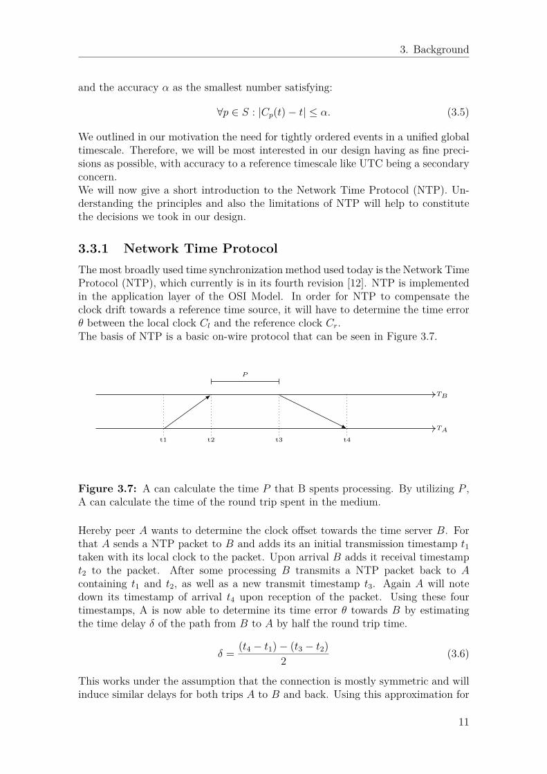
3.3.1 Network Time ProtocolThe most broadly used time synchronization method used today is the Network TimeProtocol (NTP), which currently is in its fourth revision [12]. NTP is implementedin the application layer of the OSI Model. In order for NTP to compensate theclock drift towards a reference time source, it will have to determine the time errorθ between the local clock Cl and the reference clock Cr.The basis of NTP is a basic on-wire protocol that can be seen in Figure 3.7.
P
t1 t2 t3 t4
TA
TB
Figure 3.7: A can calculate the time P that B spents processing. By utilizing P ,A can calculate the time of the round trip spent in the medium.
Hereby peer A wants to determine the clock offset towards the time server B. Forthat A sends a NTP packet to B and adds its an initial transmission timestamp t1taken with its local clock to the packet. Upon arrival B adds it receival timestampt2 to the packet. After some processing B transmits a NTP packet back to Acontaining t1 and t2, as well as a new transmit timestamp t3. Again A will notedown its timestamp of arrival t4 upon reception of the packet. Using these fourtimestamps, A is now able to determine its time error θ towards B by estimatingthe time delay δ of the path from B to A by half the round trip time.
δ = (t4 − t1)− (t3 − t2)2 (3.6)
This works under the assumption that the connection is mostly symmetric and willinduce similar delays for both trips A to B and back. Using this approximation for
11

3. Background
the time spent in the medium, we can deduce the time error:
θ = t3 + δ − t4 (3.7)
Since NTP is implemented at the highest level of the OSI layer stack and a NTPpacket might travel through a multitude of intermediate routers until reaching thereference time server, the critical path – as illustrated in Figure 3.8 – is quite sub-stantial. Taking a series of clock skew estimations will, therefore, usually incur highamounts of jitter. NTP is further organized in a hierarchical structure of reference
A
Network
B
Router1, ..., Routern
App → Physical
Physical → App
12
3
4567
8
9
1011 12
12
3
4567
8
9
1011 12
Figure 3.8: Marked in the gray boxes are the sections of the on-wire protocol thatcritically influence the synchronization effectivity. A packet will not only have totravel through a series of intermediate routers, but will have to traverse through thewhole OSI layer stack twice.
time servers. Children nodes hereby always synchronize their clocks with their par-ent nodes. At the top of the hierarchy lie time servers that directly track UTCby synchronizing to some atomic clock, for example, by utilizing a GPS receiver.Such a server is called a primary time server. Any other reference time server ona lower level is called a secondary time server. The different time servers are alsocommonly referred to by their Stratum level. The primary servers at the top of thehierarchy will hereby have Stratum level 1. The Stratum level increases with eachlevel in the hierarchy. Each new level will add to the maximum possible error inthe time estimation. All design decisions for NTP are influenced by this tendencyto non-deterministic delay in the time error estimation. To improve the precision ofNTP, the specification intends the usage of multiple reference time servers. Throughstatistical methods, NTP will try to derive an improved time error estimation byprocessing the data gathered through the on-wire protocol from each individual ref-erence server. Last, we want to touch shortly on how NTP corrects the frequencyand phase error determined by the on-wire protocol. A clock synchronized withNTP will, in normal operation conditions, never do sudden time jumps. NTP keepsan internal VFO that it tries to discipline to the frequency and phase of the referencetime server. For this, NTP employs a closed-loop feedback system. In per-secondintervals, NTP makes small adjustments to the frequency of the VFO in order tominimize both the frequency error as well as the phase error.
12

4Related Work
We will give here a short overview of alternative concrete implementations of GPIOtracing in a distributed setting. Furthermore, we will also look at wireless clock syn-chronization methods used in Wireless Sensor Networks. As observers are groupedwith the development boards in our testbed, the principles from such algorithmsshould hold merit for our purpose as well.
4.1 Time Synchronization Systems
4.1.1 GlossyGlossy is a flooding algorithm that is based on constructive interference[13]. Inorder to create such interference, transmitting nodes have to adhere to tight timebounds. Glossy only works if all nodes nearly retransmit a packet at the sametime. This is achieved by implementing the algorithm as close to the hardwareas possible. The probability of interruption resulting in delayed transmissions istherefore held to a minimum. Furthermore, to avoid that different clock frequencieslead to varying processing times, the processing path is kept as short as possible bydesign. Naturally, it follows that glossy is also extremely capable as a method forsynchronizing clocks. If one keeps track of the number of retransmissions a packethas undergone, one can deduce from the constant transmission and processing timethe trip time from the initiator of the flood to the receiving node.
4.1.2 Reference BroadcastingBy transmitting physical-layer broadcast messages from an initiator to a set of nodesthat should synchronize their clocks with each other, the reference broadcast system(RBS)[14] can offer fine-grained clock synchronization to a network of wireless sensornodes. Upon arrival, each node will generate a timestamp with its locally managedclock. The singular task of the broadcasts is thus only the creation of simultaneousevents at each node. Any delays at the sender are therefore not essential for theperformance of the synchronization system. Thus, the critical-path is reduced to onestep, which is the reception of the broadcast packet at each receiver. To reduce anyjitter introduced upon reception, multiple broadcast rounds are conducted. After afixed amount of broadcasts, nodes exchange the series of timestamps they collectedwith each other. Using this information, nodes can estimate their clock skew witheach other and adjust their clock frequencies adequately.
13

4. Related Work
4.2 Distributed Tracing Systems
4.2.1 Flocklab
Flocklab[15] offers tracing of power profiling and GPIO data. Furthermore, theexternal actuation of GPIO pins allows the generation of events at specific pointsduring a test run. Using only NTP synchronization for observer nodes, Flocklabreaches a precision of 40µs.Data is collected and timestamped directly on the observer nodes. Observers arebased on Gumstix XL6P COM embedded computers, which are relatively low-speccompared to the Raspberry Pi’s we deploy in our testbed at the time of writing thiswork. Because of the observer nodes’ low performance, the maximum sample ratefor GPIO events is 10KHz.
4.2.2 Tracelab
Building upon the existing Flocklab infrastructure, Tracelab[16] adds a new dataacquisition system based on a FPGA. The updated design allows for higher peakGPIO and power profiling event sampling rates. The old synchronization methodbased upon NTP is replaced with a wireless time synchronization mechanism. Aphase-Locked clock is realized on every observer by distributing PPS signal producedby a GPS receiver from one root observer to every other observer via Glossy. Thisdesign keeps the standard deviation of the clock synchronization error below 385ns.Furthermore, a jitter reduction heuristic is employed, which can reduce this error toa standard deviation of 155ns.
4.2.3 Minerva
Minerva[17] offers tracing as well as advanced in-hardware debugging options byutilizing the JTAG interface that is offered by many microcontrollers. Tracing isimplemented by direct access to the primary memory over the JTAG interface.Reading memory this way does not require the process to be stopped for the durationwhere memory is read. Thus this kind of tracing does not incur any overhead onnormal execution and is therefore non-intrusive while still offering a high degreeof expressiveness comparable to printf tracing. Since reading memory over JTAGhas latencies in the high microsecond range, this kind of tracing is less suitable forobserving variables that are updated in a high frequency. Debugging capabilitiesoffered by Minerva include the option to hold execution either arbitrarily or uponhitting a breakpoint. This works both on single nodes, as well as in a network-wide pseudo-synchronous fashion. Since Minerva only offers time synchronizationvia NTP and synchronous halting/resuming of the whole Wireless Sensor Networkis only precise in a millisecond range, the system is less suited for tracing tasks thatrequire temporally fine-grained tracing.
14

4. Related Work
4.2.4 Flocklab 2We should also mention the latest revision of the Flocklab testbed Architecture calledFlocklab 2[18]. The most notable changes are the replacement of the wireless timedistribution algorithm with time synchronization over the on-side local area net-work using Precision Time Protocol (PTP) [19], and the replacement of the FPGAbased data acquisition platform with direct GPIO capture using the ProgrammableRealtime Unit (PRU) of the utilized Beaglebone Green. Using PTP synchroniza-tion, clock precisions under one microsecond can be reached. For observers that areplaced out of reach of the local area network, therefore not allowing for PTP syn-chronization, the PPS from a Global Navigation Satellite System (GNSS) receiveris used to derive a precise clock.
15

4. Related Work
16

5Design
A common theme we find in all presented work which deals with high-precision fine-grained time synchronization above is the reduction of the critical-path – that is thenumber of steps in the design that in a concrete real-world implementation couldlead to delays, are kept to a bare minimum. This exact principle of keeping the paththat is essential to the performance of the clock synchronization system as small aspossible, is also the framework of our design.
5.1 Wireless Clock Synchronization SystemAlthough this paper is about GPIO tracing, our design will mainly be concernedabout the architecture of a clock synchronization network, as the precise orderingof GPIO events is the major challenge we have to overcome in this work. We takeadvantage of the close spatial proximity of our nodes, by basing our design aroundwireless based communication.
5.1.1 System ArchitectureWe extend the existing testbed architecture with a new component called synchro-nization node. The task of a synchronization node is to send beacon messages to agroup of observer nodes, as well as act as an accurate reference clock tracking UTCthrough some Global Navigation Satellite System receiver. Multiple synchronizationnodes are allowed to exist, with each serving a disjunct set of observers. In orderto send beacon messages each synchronization node is equipped with at minimum awireless transmitter, while each observer node needs to have at least a wireless re-ceiver. The system thus presents a simple star topology, with synchronization nodesat the center communicating with a set of surrounding observers. An overview ofthis architecture can be seen in Figure 5.1. Furthermore, each observer has to beequipped with a data acquisition system, that is able to capture GPIO traces. Everyobserver will have to implement an internal clock C, synchronized by our wirelesstime synchronization system, that is able to timestamp beacon and GPIO events.In the following we will use the notation
C(E) = t (5.1)
to denote the timestamp t taken with the internal clock C that is associated withsome beacon or GPIO event E.
17

5. Design
S0
GNSS
O1
B
Oi
BO0
BS1
GNSS
Oi+2
B
Oi+1
B
Oj
B
Sn
GNSS
Ol+1
B
Ol
BOk
BCoordinated Universal Time
Figure 5.1: Each synchronization node Si with i ∈ [n] is responsible for a subsetof observers Om with m ∈ [k]. Synchronization nodes distribute beacons to theobservers. All synchronization nodes track UTC by receiving time data thoughsome Global Navigation Satellite System receiver.
5.1.2 Synchronization BeaconsThe task of the synchronization nodes is to broadcast beacons to their respectivegroups of observers. Our goal is to generate events simultanously at each observer.A synchronization node S will note down its local time CS(B) = tS when emitting
S
O0
O1
O2
B
T0
B
t0O0
B
t0O1
B
t0O2
B
T1
B
t1O0
B
t1O2
B
T2
B
t2O0
B
t2O1
B
t2O2
Figure 5.2: Example of our synchronization system at work. Illustrated are threebeacon rounds. The second round is discarded, because one Observer didn’t receivea beacon.
a beacon B. Every observer O in turn will store the timestamp CO(B) = tO uponreception of this beacon. If a observer does not receive a beacon, the beacon round isdiscarded. An overview of this procdure can be seen in Figure 5.2. For each beaconround we acquire a pair of timestamps (tS, tO) between the synchronization nodeand each observer. The timestamp of the synchronization node hereby identifiesindividual beacon rounds. In theory, without jitter adding delay to the beaconreception, this pair provides us with the correlation between the synchronization
18

5. Design
nodes and each observers clocks. Using these pairs of timestamps we can furthermoredetermine the time error between each observer. Let O1, ..., On be a set of observersthat are synchronized to a synchronization node S and let B0, ..., Bm be a series ofbeacon events. We define the pairwise beacon time error between observers Oi, Oj
with respective local clocks Ci, Cj and a beacon Bk for every i, j ∈ [n] and k ∈ [m]as:
θi,j(Bk) = Ci(Bk)− Cj(Bk). (5.2)
5.1.3 Clock CorrectionAfter a test run we will have for every observer an equally long series of beacontimestamp pairs. As noted previously the synchronization node’s timestamp alsoacts as an identifier, allowing us to match events between observer nodes. Usingthis series of mappings between timestamps from the observers and synchronizationnode, we could now construct a mapping from each observers’s timescale into thesynchronization node’s reference timescale. Unfortunately, there will be variousfactors adding non-deterministic delays into our system in the physical world. Inour design, we can identify two critical sections that will add error we will have tohandle, as is illustrated in Figure 5.3. Foremost, it is to be expected that there
A
Medium
B
Signal propagation
Emit beacon D
Receive beacon
12
3
4567
8
9
1011 12
12
3
4567
8
9
1011 12
Figure 5.3: Marked in dark gray are the sections of our synchronization systemthat are part of the critical-path. If complete accuracy to the timescale is required,the signal propagation time has to be determined as well.
will be variations in the time it takes for a beacon to be received at each node.Moreover, we will also have to think about any delays that are introduced betweenemitting a beacon and generating a local timestamp on the synchronization node.Especially on systems without real-time guarantees, like our Raspberry Pi’s runningan unmodified Linux kernel, this can be an important error factor. Note that anysuch error will map evenly onto each observer, as seen in Figure 5.4.We can therefore easily look at the receiver error in isolation, by just examining thepairwise beacon time error between two observers, as is also illustrated in Figure5.5. For now, we assume that such noise, as seen in the illustration, will mainly beintroduced by our wireless receivers. Therefore, we expect that the oscillator that ourobservers will derive their clock from will hold a higher short term frequency stabilitythan the reference timing signal received by our receivers. In our evaluation, we willgive data supporting this assumption for our implementation. Let n be the numberof observers and m be the number of beacons collected. In order to compensate for
19

5. Design
Figure 5.4: Exempt from one of the test runs, which we will later conduct inour evaluation using the implementation of this design. Shown is the frequencydeviation of two observers, which are marked in blue and orange, over time. As wecan see, the error introduced by the synchronization node maps evenly onto everyslave node.
the receiver induced jitter, we use the assumed short-term stability of our observersto do a simple linear regression using the least squares method in a sliding windowof W ∈ N>1 samples on the beacon time error function θr,j, between one referenceobserver Or with r ∈ [n] and all remaining observers Oj with j ∈ [n] \ {r}. InFigure 5.6 we schematically illustrate this method. For each pair of observers Oj, Or
and beacon Bp with p ∈ [m −W ] we obtain a series of slopes αpj,r and intercepts
βpj,r. Using these we can now define the time transformation Γj,r that maps every
timestamp from Oj into the timescale of Or:
Γj,r(t) = t+ (βpj,r + t · αp
j,r) (5.3)
Hereby the slope and intercept come from the beacon Bp which is closest to thetimestamp t. The mapping into the timescale of the synchronization node is optionalbut needed if the long-term stability and accuracy towards UTC is desired, or adeployment with multiple synchronization nodes exists. Defining a mapping intothe synchronization nodes timescale works analogously to the way we created themapping between the observers. We can create a mapping between a synchronizationnode S and any observer Oi by first constructing a mapping ζ between the referenceobserver Or and S, again by performing a simple linear regression in a movingwindow, but this time on the timestamp pairs of the beacon messages collected byOr. We can then transform any observer Oi into the synchronization nodes timelineby composition of Γi,r and ζ:
ζ(Γj,r). (5.4)
We want to note that the transformation between observer and synchronization nodeis not done directly because there is a quadratic factor in the least-squares methodused to perform the linear regression. Thus because of the combination of the syn-chronization node error and receiver noise, one observer might be disproportionallystronger effected by the error added by the synchronization node.
20

5. Design
Figure 5.5: Exempt from the same testrun as figure 5.4. Shown is the relative fre-quency deviation between two slave nodes, calculated from the pairwise beacon timeerror. As can be seen the resulting frequency deviation seems to mostly representwhite noise.
Bea
con
time
erro
rwith
Or
Time domain of Oi
Figure 5.6: Illustration of the simple linear regression we perform. The dashedline shows the linear fit we calculated for the beacon time error associated withthe data points marked in blue. We here only show two linear approximations forillustration purposes. In our method, we generate such an approximation for everydata point. The green points mark the samples that lie in the moving window of Wsamples starting from the blue data points. As can be seen, the method assumes thatthere will be only a small amount of frequency drift in a short time frame, thereforeallowing us to approximate the clock drift by a linear function. Long term, we expectthe frequency deviation to wander in a random walk fashion, therefore setting thebound for the maximum size of the moving window.
21

5. Design
22

6Implementation
6.1 HardwareWe will start by introducing the hardware we add to our testbed in order to imple-ment the presented wireless clock synchronization system. We restrict ourselves tocommonly available and inexpensive off-the-shelf hardware. We start off by present-ing the Logic Analyzers we chose, which constitute the observer data acquisitiondevice.
6.1.1 Logic AnalyzerWe choose cheap off-the-shelf Logic Analyzers based on the EZ-USB® FX2LP™microcontroller by Cypress [20]. These can be found from various manufactureswith slight variations in their circuit design. They can capture 8 separate exter-nal digital signals simultaneously allowing us to sense at least two GPIO pins fromeach development board. In Figure 6.1, we show the circuit board of one of ourLogic Analyzers. We want to shortly touch on three key components, which of-fer functionalities which will be implemented in every board design, regardless ofmanufacturer. Central to the working of the Logic Analyzer itself is the FX2LPmicrocontroller, which is designed for easy development of USB 2.0 compatible pe-ripheral devices. The microcontroller disciplines an internal 48 MHz oscillator withan external 24 MHz crystal oscillator. A small EEPROM is included that is usedto store USB device descriptor data permanently. We want to especially emphasizethat these Logic Analyzers are not equipped with any addition flash memory, thatcould act as an intermediate buffer for samples. The only buffer available is a smallFIFO buffer in one of the USB endpoints [20]. Therefore, although these LogicAnalyzers are advertised with reaching sampling rates of up to 24 Msps (Million-samples-per-second), we found that in practice depending on the amount of otherdevices occupying the serial bus and the time spent processing incoming data, onlydiminished sample rates can be reached. For the Raspberry Pi 3B+ used in ourtestbeds, we found that a sample rate of 8MHz could be held consistently. We usethe open-source project sigrok 1 – and the associated open source driver fx2lafw 2 –to interface with the Logic Analyzers. Sigrok handles device enumeration and setup,that is it will identify any connected and supported Logic Analyzer and upload theappropriate firmware depending on the reported device descriptor. Sample data is
1https://sigrok.org/2https://sigrok.org/wiki/Fx2lafw
23

6. Implementation
(a) Top view (b) Bottom view
Figure 6.1: View of one of the Logic Analyzer circuit boards. We can see in Figure6.1a marked in red a small EEPROM and in green a 24MHz crystal oscillator. InFigure 6.1b we can see marked in red the FX2 microcontroller itself.
not streamed synchronously, rather USB bulk transfers are utilized to maximizethroughput. Sigrok offers an abstraction from the underlying hardware. Thereforeour implementation only has to focus itself on how to process the incoming blocksof sample data from the Logic Analyzer.
6.1.2 Wireless Transmitter/ReceiverA key principle of our design was the reduction of the critical path, i.e., the sectionsof the path that are able to introduce non-deterministic error should be kept to aminimum. We outlined that the crucial element in our design that can cause sucherror is the reception of a beacon message. Any indeterministic delay introduced inthis section will degrade the performance of our clock synchronization method. Forour implementation we therefore chose simple off-the-shelf superheterodyne based433 MHz transmitters and receivers, which can be seen in Figure 6.2. Our assump-tion is, that if less high-level processing happens in the transmitter and receiverhardware, the less potential there is for non-deterministic error. These transmittersand receivers do on-off keying (OOK) amplitude-shift keying (ASK) modulation,meaning that a high bit is encoded by the presence of a carrier signal, whereas theabsence of the carrier encodes a low bit. Interfacing to the transmitter and fromthe receiver works through a single data line. While these modules are extremelycheap and easy to come by, there is nearly no technical information available. Frompractical work we found that the integrated circuit on the receivers has to containat least an Automatic Gain Control (AGC) circuit that automatically adjusts theincoming signal from the antenna to some nominal level [21]. Moreover, we foundthat transmission ranges in the multiples of ten meters are possible. Because of
24

6. Implementation
(a) superheterodyne receiver(b) superhetero-dyne transmitter
Figure 6.2: Transmitters (b) and receivers (a) used in our implementation. Theinput data pin directly controls the modulation of the transmitter.
Figure 6.3: Ublox NEO-6M based GPS receiver. The pin header exposes twoGPIOs for a UART serial connection and a single pin that emits an accurate PPSsignal.
this, we can cover the whole floor where our testbed is deployed with just a singletransmitter.
6.1.3 GPS receiverThe final new hardware component that we add to our architecture are GPS receiversbased on the ublox NEO-6 GPS Modules [22]. In figure 6.3 one of such GPS receiversis shown. The module works completely standalone. Through the serial UARTinterface a host is able to acquire both positional and time information from theGPS receiver. Furthermore a Pulse-Per-Second (PPS) signal with accuracy within60ns is emitted by the module as well. We can therefore use this receiver as a highlyaccurate time reference that directly tracks UTC.
6.2 Integration into TestbedWe will now outline how the presented hardware is integrated into the existingtestbed architecture. As we mentioned in the background section, our testbed lies
25

6. Implementation
Raspberry Pi 3B+
GPIOS
433 MHz Transmitter
data
Ethernet
Local Area Network
GPS
tx
rx
PPS
(a) synchronization node
Raspberry Pi 3B+
USB Hub
Ethernet
Local Area Network
433 MHz Receiver
data
NRF-52
Sky Mote
Zolertia Zoul
Logic Analyzer
(b) observer
Figure 6.4: Integration of the hardware into the existing testbed architecture.
on a single floor, with two testbed nodes spaced at most 30 meters apart from eachother. Since we are easily able to reach any observer with a single transmitter, wewill only add a single synchronization node to our testbed. In Figure 3.4 we showwhich nodes in our testbed where updated with our new design. In Figure 6.4a weshow schematically the architecture of a synchronization node. We implement thesynchronization node upon one of our existing Raspberry Pi 3B+. We connect theGPS receiver and the 433 MHz transmitter with the raspberry pi over the GPIOinterface. Hereby the PPS pin of the GPS receiver is connected to one digital inputpin, while the UART pins (tx and rx) are connected with the respective UARTGPIOs of the Pi. The single data pin of the 433MHz transmitter is connectedto a digital output GPIO. The synchronization node is also added to the existinglocal area network and therefore able to communicate with the observers and theorchestration server.
In Figure 6.4b we illustrate the updated observers. We add both a Logic Analyzerand a 433 MHz receiver. The Logic Analyzer is connected to the same USB Hubas the various development boards. Unorthodoxically this time we don’t connectthe wireless receiver to one of the pi’s GPIO pins, but rather directly to the LogicAnalyzer.
26

6. Implementation
t
s
. . .
Figure 6.5: Digital input signal that the 433MHz transmitter receives from thesynchronization node.
6.3 Synchronization Beacon
We use a simple method to implement synchronization beacons. Because in ourtestbed, all observers are connected over a local area network with one central or-chestration server, it is sufficient for us to generate two events simultaneously at bothsynchronization node and observer node. A beacon in our system will therefore onlyhave to be distinguishable from random background noise, but will not have to holdany further information. This differs from systems like GPS, where a GPS receiverwill have to work completely self-sufficient, therefore requiring that the navigationmessage send out by the GPS satellite includes the timestamp of the GPS satelliteat the time of message transmission. Both observer node and synchronization nodecollect the timestamps – created with their respective internal clock – of the beaconevents. We will be able to use the timestamp of the synchronization node to identifybeacon messages that belong to a specific beacon round. After a testrun has con-cluded both synchronization node and observer send their set of timestamped eventsto the orchestration server. Because our synchronization beacons do not carry anyinformation, a node will have to acknowledge the arrival of a beacon, so we knowwhether a beacon round has to be discarded. For that, we inform observer nodesbeforehand whether they should expect an incoming synchronization beacon by uti-lizing the existing fixed network infrastructure. After the synchronization node hasfinished transmission of the beacon message, it will query all observer nodes whetherthe transmission was successful. In Figure 6.5 we illustrate the digital input signalthat we feed into the data line of the 433MHz transmitter of a synchronizationnode. Observers will listen for a total of five high pulses, which have a duration ofth = 800µs. By requiring the arrival of multiple high pulses, we prevent randomconstructive interference from creating false-positives when matching the incomingsignal for a beacon message. Furthermore we preamble the five high pulses witha 750ms phase, where we emit a square signal with a period of th
2 . This phase isneeded, so the AGC in our receivers can properly calibrate itself to our signal level.Without it, we would risk that the relevant portion of the beacon that the observersmatch on arrives only partially. The synchronization node will note down its localtimestamp after creating the last falling edge of the 5 pulses. Respectively eachobserver will generate a timestamp after reception of the falling edge of the fifthpulse.
27

6. Implementation
6.4 Observer ClockIn our implementation, timestamping is not done directly on the observers. Since ourLogic Analyzers transfer signal samples in blocks of multiple samples asynchronouslyto the observers, we cannot directly timestamp each incoming sample with the localclock each observer already has. Instead, each observer only passively constructsa clock with data we gather from the Logic Analyzer. We give away one of ourchannels from sensing GPIO pins, so it is connected directly to the data pin ofthe 433MHz receiver. Thereby we are ensuring the chronologic coherence betweenincoming beacon and GPIO tracing signals. All processing of the incoming data isdone on the observer nodes. Because we assume that the Logic Analyzer sampleswith a constant sampling rate, we know how much time passes between samples. IfFc is the nominal sampling frequency, there will be a time offset of δc = 1
Fcbetween
each incoming sample. For a number of N samples, time will therefore proceedN ·δc seconds. As we showed before the sampling frequency of the Logic Analyzer isobtained from a 24 MHz crystal oscillator. Since we are deriving the clock frequencyof our internal clock directly from the sampling frequency, every frequency deviationof the Logic Analyzer’s crystal oscillator will in turn transfer over as frequency errorto our internal clock. The clock we derive performs in a free-running mode, i.e.,we will not compensate for wander and jitter. Our final clock implementation istherefore fairly straightforward. Each observer O will count incoming samples fromthe Logic Analyzer. Concrete time values are derived, as is shown in the followingequation:
CO(E) = N(E) · δc. (6.1)
Hereby E is any event generated by the Logic Analyzer – that is either a simpleGPIO pin change or the matching of a beacon event on the receiver pin – and N(E)denotes the index of the series of samples that E occurred at.
6.5 Synchronization Node ClockWe use NTP to provide time synchronization for our synchronization nodes. TheNTP implementation that we deploy3 offers the ability to communicate with a ref-erence clock through a shared memory segment (SHM). The open-source projectgpsd4, which is able to interface with our GPS receiver using the previously men-tioned serial connection, provides such a SHM. Furthermore, using the GPS PPSsignal, NTP is able to reduce the jitter of the time estimations gathered from thereference SHM clock. We can thus utilize the GPS receiver module to receive ahighly accurate local reference clock. Because NTP now derives its time directlyfrom GPS, our node is a Stratum 1 time source. This reduces the critical-path ofNTP significantly and should result in much higher clock accuracy.
3http://www.ntp.org/4https://gpsd.gitlab.io/gpsd/index.html
28

6. Implementation
6.6 LimitationsA significant limitation with our design is that the derived internal clock CO for everyobserver O as well as our clock correction algorithm only works on events generatedfrom the Logic Analyzers. In the motivation chapter of this work, we expressed thatour tracing method adds to the existing set of tools. A researcher will therefore stillwant to use serial-tracing together with GPIO tracing. Our method is not able toimprove the precision of the internal clock that the Linux operating system runningon our observers manages. The order of serial line events is thus still only providedby regular NTP. Furthermore, since we directly capture and process the data of the433 MHz receivers over the Logic Analyzer, the maximum theoretical precision ofour system is bounded by our sample resolution, which with a sample rate of 8MHzis 125ns.
29

6. Implementation
30

7Evaluation
We will start our evaluation by first verifiying the assumptions that we made in ourimplementation about the short term frequency-stability of the logic analyzer andthe long-term stability of the receiver timing signal.
7.1 Logic Analyzer Frequency StabilityIn order to determine the characteristic frequency drift of the crystal oscillator inour Logic Analyzers, we connect the PPS output of a GPS receiver with the LogicAnalyzer of one of our observers that are synchronized with our method. See Figure3.4 for the placement of the observers we conducted all of our following experimentswith. The PPS signal is assumed as a ground truth 1Hz reference source. Any noisefrom the PPS signal will therefore add to the noise in the sample data of the logicanalyzers oscillator. In Figure 7.1 we can see the frequency deviation of one of ourLogic Analyzers over time.We can gather two interesting characteristics of the frequency stability of our LogicAnalyzer. First there seems to be a huge non-random deviation from the nominalfrequency of about 147ppm. Secondly, we observe that there seems to be large scalefrequency wander taking place. To get a real benchmark for the stability though,we will calculate the Allan variance[11][23]. As we illustrated in our backgroundsection, frequency deviations in oscillators are usually produced by the combinationof a multitude of different noise sources acting with different frequencies. Thus ifwe use classical methods to calculate the variance for the frequency deviations everysecond, the estimator will not converge. The allan variance allows to calculate thevariance for any time-domain spectral density without diverging. It is defined asfollows:
σ(τ)2 = 12τ 2 〈(xn+2 − 2xn+1 + xn)2〉. (7.1)
Hereby 〈〉 denotes an infinite time average and x is a series of GPIO traces, spacedwith an interval of τ . As noted in [11] a good estimation for such an infinite timeaverage can usually be gathered by calculating the average of an finite data set
σ(τ)2 ≈ 12(N − 2)τ 2
N−2∑i=1
(xi+2 − 2xi+1 + xi)2. (7.2)
In Figure 7.2 we show the Allan deviation – which per usual is defined as√σ(τ)2 –
for τ ∈ [1, 5 · 103] seconds.
31

7. Evaluation
Figure 7.1: Series of frequency deviation measurements taken over a period of 15hours. Each deviation is calculated by substracting the timestamps of two consec-utive PPS events. In dark blue we plot the raw timestamps. We can clearly see thediscrete 125ns second jumps manifesting themself in the frequency deviation. Bycalculating the moving average (light blue) over 10 frequency deviations, we get anapproximation of the course of the frequency deviation even below our maximumresolution.
As we can see, the lowest deviations occur in a range of 10s up until about 100s.Remember that we can only take samples every 125ns. This manifests itself as jitterin the lower time intervals. We can see that at a timescale of minutes the Allandeviation begins to increase, which is in accordance with the large scale wander weobserve in Figure 7.1.
7.2 Synchronization Node Frequency StabilityIn this section, we will look into the frequency stability of the synchronization node.This stability is not only significant because of the possibility of it adding up ontothe overall synchronization error, but furthermore, the results from this section,define whether a deployment with multiple synchronization nodes – and associatedsubset of obervers – is feasible.
We gather all data in this section from statistics produced by NTP1 on our only syn-chronization node. Because of the symmetry in the connection to the GPS receiver,this data should be reasonably accurate. In Figure 7.3, we show the deviation ofthe frequency over the period of a day.
1http://doc.ntp.org/4.2.4/monopt.html
32

7. Evaluation
Figure 7.2: Allan deviations for our Logic Analyzer. Values for τ are shown in alogarithmic scale.
Figure 7.3: Frequency deviations gathered from NTP statistics over a period of 20hours. Marked in red are periods of time when the GPS receiver lost reception tothe GPS satellites and therefore couldn’t provide a PPS signal.
As we can see, the frequent phases of GPS signal loss and the subsequent discon-tinuation of the reference PPS signal lead to substantial variations in the frequencydeviations determined by NTP. Because NTP only applies corrections gradually ata per-second interval, it takes over an hour until the induced offset in the frequency
33

7. Evaluation
deviation is corrected again. In Figure 7.4, we show the time error towards thereference GPS clock over the same timescale.
Figure 7.4: Clock skew over a period of 20 hours, gathered from the same data setas in figure 7.3. The magnified portion of the graph shows NTP’s long recalibrationperiod until the clock skew is gradually removed.
We can observe how the deviation in frequency results temporarily in time errors ashigh as 22ms. Again we also see how the clock skew is only gradually corrected untilnearly an hour after the initial signal loss. Therefore, a loss of GPS signal resultsin an unacceptable time error. Finally in Figure 7.5 we examine the performance ofPPS disciplined NTP under normal operating conditions.
Figure 7.5: Distribution of clock skew when filtering out the phases where theGPS receiver had no reception and the subsequent slow recalibration period.
34

7. Evaluation
We can observe that on average, the clock will stay accurate 7.87µs towards thereference GPS clock with a standard deviation of 16.33µs.
7.2.1 Stability under System LoadSince we implement our synchronization node on a regular Raspberry Pi, we furtherwant to look into the CPU temperature’s influence on our system clock. For this, weperiodically, for the duration of 128 seconds, set the CPU under high load using thestress2 utility. In Figure 7.6, we show the variations in CPU temperature inducedby the load against the frequency deviations reported by NTP.
Figure 7.6: Frequency stability of the synchronization node in the face of heatfluctuations produced by periodic phases of high CPU load. We show the CPUtemperature in red, while dark blue presents the frequency deviation reported byNTP. At the light blue marker, we begin setting the CPU under load by performinga stress test.
We can see how the rising CPU temperature results in alterations of the oscillatorfrequency that the Pi derives its clock from, by the delayed recorded changes inthe frequency deviation of the VFO that is kept by NTP. Again in Figure 7.7, weshow how the frequency changes result in increased time error towards the referenceGPS clock. We observe that even with continuous discipline from the external PPSsignal, fluctuations in heat are able to produce time errors as high as 250µs.
7.3 Receiver JitterThe second section in our design’s critical path is the reception of a beacon at anobserver. A receiver will seldom demodulate the modulated signal from a transmit-ter in the physical world without introducing error. This undesirable variation in
2https://linux.die.net/man/1/stress
35

7. Evaluation
Figure 7.7: Clock skew of the synchronization node in the face of heat fluctua-tions produced by periodic phases of high CPU load. Again red marks the CPUtemperature. This time dark blue presents the clock skew reported by NTP.
phase of the demodulated signal is also commonly referred to as jitter [24] and isschematically illustrated in Figure 7.8.
t
s
Figure 7.8: On top the input signal to the transmitter is shown. Right below isthe demodulated signal on the receiver side. There will be some expected constantpropagation and processing time, but also some variations at the falling and risingedges.
In order to approximate the overall jitter of one receiver, we connect our 433 MHztransmitter to a microcontroller that constantly generates a square wave signal witha period of 900µs and 50% duty cycle. Using our Logic Analyzers, we measure thelengths of the high pulses for two identical receivers. We show the distribution ofmeasured lengths in Figure 7.9. Our experiment shows two important characteristicsof our receivers. Foremost there are huge variations in the length of the demodulatedsignal, with the most significant discrepancy being about 100µs. Moreover, we seethat between identical receivers, the mean measured length will show variations. Forinstance, in the conducted experiment, we found a difference of about 2µs between
36

7. Evaluation
Figure 7.9: Distribution of high pulse durations. Marked in orange and blue arethe respective measurements from our two receivers. The dashed vertical line showsthe mean associated with each distribution.
the mean values. One further observation about the distribution is that it doesnot follow the typical curve of a normal distribution. This most likely indicatesthat besides quasi-random effects, there are also systematic errors from the receiverinvolved. This is further supported by looking at an excerpt of a series of consecutivelength measurements (see Figure 7.10). We can observe sudden jumps in the pulses’
Figure 7.10: Subset of 500 consecutive samples from the dataset we generated thedistribution histogram above.
duration, which seem to appear in a regular interval. Since our clock correctionmethod is based on statistical assumptions, this could result in degraded effectivityof our method.
37

7. Evaluation
7.4 Clock CorrectionAt last, we will look into the overall performance of our clock synchronization system.The results here are the outcome of the cumulative error introduced by the previousexamined error factors.
7.4.1 Simple InterpolationWe will first give a basic benchmark to compare our method against. For this, we dosimple interpolation between pairs of consecutive beacons, as shown in Figure 7.11,to produce a mapping that can transfer any timestamped event from the observerinto the synchronization nodes timescale.
Sync
hron
izat
ion
node
times
cale
Observer timescale
Figure 7.11: Illustrated in gray are the timestamp pairs associated with our bea-cons. Blue marks an event, which timestamp in the synchronization node’s timescalewas derived through linear interpolation between the two surrounding data points.
Again we used the PPS output of a GPS receiver to generate simultaneous eventsat two observer nodes. We measure the offset between the flanks of simultaneousPPS events at both observers, after transformation into the reference timescale. Theresults can be seen in Figure 7.12.We can observe that directly processing the beacon data as is will result in timeerrors closely resembling the receiver jitter we observed in the previous section.The absence of extreme errors, like we saw in the receiver length measurementdistribution, can be explained by the low probability of them occurring and that weonly emit beacons rougly in a second interval.
7.4.2 Moving Window Linear RegressionBefore we can determine the performance of our clock correction method, we willfirst look at how the window size, over which we approximate a linear fit, influencesour method’s performances. Again we use the same experimental setup as before,i.e., we generate simultaneous events at two observers using the PPS from a GPS
38

7. Evaluation
Figure 7.12: Time error distribution from one of our test runs where we directlymapped timestamps from the two observers into the synchronization nodes timescaleby using simple interpolation.
receiver. The standard deviation of the time error distribution of this data will beour control data that we will try to minimize. In Figure 7.13 we show the resultsfrom one of our experiments. We performed this experiment for multiple test runs.
Figure 7.13: Standard deviation per window size from one of our test runs. Inthis particular experiment, the minimal standard deviation was found at a windowsize of 118 samples.
We found that the ideal window size lies between 118 and 131 samples, with theaverage best window size over all experiments being 124 samples. We conducted allof the following clock corrections using this window size.In Figure 7.14, we show the time error distribution for one of our test runs afterevery node was mapped into the synchronization nodes timescale using our movingwindow linear regression method.
39

7. Evaluation
Figure 7.14: Distribution of the time error between simultaneous GPS PPS flanksfrom one of the test runs we conducted. The mean was shifted by 2400ns.
Note that we already corrected this data for the different mean values we determinedin the pulse length distribution, which was shown in the receiver jitter section.In a complex deployment of our system with multiple observer nodes, a one-timecalibration step between one reference observer and every other observer would berequired to reach results as above consistently. We can clearly see that our methodprovides a considerable improvement in comparison with the benchmark method,with the worst time error with our method being about a fourth of the worst timeerror that occurred in the benchmark.In Table 7.1 we show concrete results for multiple testruns for both methods.
Method avg. standard deviation max Tmote Sky CC nRF52 CC Zoul CCMoving Window Linear Regression 964ns 4960ns 40 317 158Benchmark - Interpolation 5251ns 27831ns 223 1781 891
Table 7.1: Results for both the benchmark method and our moving window linearregression method from multiple experiments. The average standard deviation iscalculated over all of our test runs. Furthermore, we show the maximum time errorwe measured in our series of experiments. Corresponding to this error, we outlinedthe number of clock cycles (CC) that would be missed for each development board.
Finally, in Figure 7.15, we show how error introduced from the synchronization nodecauses the reference timescale to stretch and compress. For this we measure in an-other experiment the time between consecutive PPS events from one of the observernodes. We see that in this particular experiment, the compression introduced by thesynchronization node resulted in the time between two consecutive PPS flanks tobe reduced by 400µs. Of course, this stretching and compression will apply to everyobserver, i.e., the errors’ ratios will stay the same. If one wants to use the GPIOtracing to measure time accurately, this timescale skew represents a big problem.
40

7. Evaluation
Figure 7.15: Error from the synchronization node locally skews the length betweenconsecutive PPS pulses. In orange, we show the frequency deviation of the observerdetermined through the receiver timing signal. Blue shows the length between con-secutive PPS events. Note that the plot seems to be solidly colored because theerror greatly amplifies the discrete 125ns jumps caused by our maximum samplingresolution.
41

7. Evaluation
42

8Conclusion and Future Work
In our motivation, we outline two targeted characteristics that our tracing methodshould possess. One is the unintrusiveness into the execution of an algorithm, whilethe other is the precise ordering of the events into a unified timescale. Our prestudiesshow, that GPIO tracing is a whole magnitude less intrusive than printf tracing overa serial connection, therefore fulfilling our first requirement. To provide fine-grainedtime synchronization, we implement a wireless clock synchronization system basedon beacons distributed by synchronization nodes to a subset of observers. We usebasic 433 MHz transmitters and receivers under the assumption that less high-level processing results in more predictable delays. This assumption turns out to bewrong, with the receivers being a significant source of jitter. Still, using simple linearregression on our dataset, we are able to seriously reduce the effect of this added jitteron our synchronization systems performance. In experiments we conducted we foundan average standard deviation of 964ns and a worst measured error of 4960ns. Whilea sizeable improvement over NTP, such precisions still mean that even on an olderboard like our Tmote Sky, simultaneous traces could still be off by 40 clock cycles.Furthermore, we find that implementing the synchronization node on a RaspberryPi 3B+ comes with some severe drawbacks. Even with the synchronization nodebeing connected directly to a GPS receiver, we do not reach precisions that are goodenough to accommodate for deployment with multiple synchronization nodes, evenwith perfect GPS reception. The main culprit hereby being the instability of the Pi’sclock under the influence of heat. Moreover, we found that the non-existing real-time guarantees of the Pi could lead to distortions in the mapping onto the referencetimescale, reducing our system’s usefulness for accurate time measurements.Future Work The most direct improvement that could be done to the currentimplementation is replacing the 433MHz transmitters and receivers with new hard-ware that is less prone to jitter. Furthermore, it should be easy to implement oursynchronization nodes upon microcontrollers that offer more real-time guaranteesand, therefore, better time synchronization precision. Our method currently needsto collect a large amount of data to perform the post-processing clock correction. Inthe future, this should be replaced with a closed-loop feedback design that performsactive corrections to frequency and phase, therefore transforming our observer clockfrom a free-running clock into an actively compensated one.
43

8. Conclusion and Future Work
44

Bibliography
[1] M. Schuß, C. A. Boano, M. Weber, and K. Römer, “A competition to pushthe dependability of low-power wireless protocols to the edge”, in Proceedingsof the 14th International Conference on Embedded Wireless Systems and Net-works (EWSN), Uppsala, Sweden: Junction Publishing, Feb. 2017, pp. 54–65,isbn: 978-0-9949886-1-4.
[2] V. Sundaram, P. Eugster, and X. Zhang, “Efficient diagnostic tracing for wire-less sensor networks”, in Proceedings of the 8th ACM Conference on Embed-ded Networked Sensor Systems, ser. SenSys ’10, Zürich, Switzerland: Associa-tion for Computing Machinery, 2010, pp. 169–182, isbn: 9781450303446. doi:10.1145/1869983.1870001.
[3] M. Ben-Ari, “Principles of concurrent and distributed programming”, in PHISeries in computer science, 1990.
[4] S. Duquennoy, A. Elsts, B. Al Nahas, and G. Oikonomo, “Tsch and 6tischfor contiki: Challenges, design and evaluation”, in 2017 13th InternationalConference on Distributed Computing in Sensor Systems (DCOSS), IEEE,2017, pp. 11–18.
[5] (n.d.). Pulseview, [Online]. Available: https://sigrok.org/wiki/PulseView(visited on 09/17/2020).
[6] J. Polastre, R. Szewczyk, and D. Culler, “Telos: Enabling ultra-low power wire-less research”, in IPSN 2005. Fourth International Symposium on InformationProcessing in Sensor Networks, 2005., IEEE, 2005, pp. 364–369.
[7] Zolertia Zoul Revision A Internet of Things hardware wireless module, for 2.4-GHz and 863-950MHz IEEE 802.15.4, 6LoWPAN and ZigBee® Applications,v.1.0.1, Zolertia, 2017.
[8] (n.d.). Bluetooth low energy and bluetooth mesh development kit for thenrf52810 and nrf52832 socs, [Online]. Available: https://www.nordicsemi.com / Software - and - Tools / Development - Kits / nRF52 - DK (visited on09/17/2020).
[9] A. S. Tanenbaum and M. Van Steen, Distributed systems: principles andparadigms. Prentice-Hall, 2007.
[10] “Definitions and terminology for synchronization networks”, International Telecom-munication Union, G.810, 1996, p. 27.
45

Bibliography
[11] D. Howe, D. Allan, and J. Barnes, “Properties of signal sources and measure-ment methods”, in Thirty Fifth Annual Frequency Control Symposium, May1981, pp. 669–716. doi: 10.1109/FREQ.1981.200541.
[12] D. Mills, J. Martin, J. Burbank, andW. Kasch, “Network time protocol version4: Protocol and algorithms specification”, RFC Editor, RFC5905, Jun. 2010,RFC5905. doi: 10.17487/rfc5905. [Online]. Available: https://www.rfc-editor.org/info/rfc5905.
[13] F. Ferrari, M. Zimmerling, L. Thiele, and O. Saukh, “Efficient network floodingand time synchronization with glossy”, in Proceedings of the 10th ACM/IEEEInternational Conference on Information Processing in Sensor Networks, IEEE,2011, pp. 73–84.
[14] J. Elson, L. Girod, and D. Estrin, “Fine-grained network time synchronizationusing reference broadcasts”, p. 17,
[15] R. Lim, F. Ferrari, M. Zimmerling, C. Walser, P. Sommer, and J. Beutel,“FlockLab: A testbed for distributed, synchronized tracing and profiling ofwireless embedded systems”, in Proceedings of the 12th international confer-ence on Information processing in sensor networks - IPSN ’13, Philadelphia,Pennsylvania, USA: ACM Press, 2013, p. 153, isbn: 978-1-4503-1959-1. doi:10.1145/2461381.2461402.
[16] R. Lim, B. Maag, B. Dissler, J. Beutel, and L. Thiele, “A testbed for fine-grained tracing of time sensitive behavior in wireless sensor networks”, in 2015IEEE 40th Local Computer Networks Conference Workshops (LCN Work-shops), Oct. 2015, pp. 619–626. doi: 10.1109/LCNW.2015.7365906.
[17] P. Sommer and B. Kusy, “Minerva: Distributed tracing and debugging in wire-less sensor networks”, in Proceedings of the 11th ACM Conference on Embed-ded Networked Sensor Systems - SenSys ’13, Roma, Italy: ACM Press, 2013,pp. 1–14, isbn: 978-1-4503-2027-6. doi: 10.1145/2517351.2517355.
[18] R. Trüb, R. D. Forno, L. Sigrist, L. Mühlebach, A. Biri, J. Beutel, and L.Thiele, “FlockLab 2: Multi-modal testing and validation for wireless IoT”,p. 7, 2020.
[19] “Ieee standard for a precision clock synchronization protocol for networkedmeasurement and control systems”, IEEE Std 1588-2008 (Revision of IEEEStd 1588-2002), pp. 1–300, 2008.
[20] EZ-USB® FX2LP™ USB Microcontroller High-Speed USB Peripheral Con-troller, 38-08032, Rev. AC, Cypress, Jul. 2019.
[21] (n.d.). Superhet radio AGC - automatic gain control electronics notes, [On-line]. Available: https://www.electronics-notes.com/articles/radio/superheterodyne-receiver/agc-automatic-gain-control.php (visitedon 09/17/2020).
[22] NEO-6 u-blox 6 GPS Modules, GPS.G6-HW-09005-E, ublox, 2011.[23] D. W. Allan, D. A. Howe, F. L. Walls, and D. B. Sullivan, “Characterization
of clocks and oscillators”, National Bureau of Standards, Gaithersburg, MD,NBS TN 1337, 1990, Edition: 0, NBS TN 1337. doi: 10.6028/NIST.TN.1337.
46

Bibliography
[24] Effect of RF System Parameters on Receiver (ATA5745/ATA5746) Sensitivity,9174B-AUTO-05/15, Atmel, 2015.
47

Bibliography
48