Software Defined Radio Platform for Cognitive Radio: Design and Hierarchical Management

Design and Implementation of a
Reconfigurable Radio Platform
by
Livia Ruiz Soriano
A Thesis presented to
the National University of Ireland
in fulfillment of the requirements for the degree of
M.Eng.Sc
Department of Electronic Engineering
NUI,Maynooth
Ireland
May 2007
Supervisor of Research: Dr.Ronan Farrell
Head of Department: Frank Devitt

All this work is dedicated to mum, dad, Ignacio and Barbara.

Table of Contents
1 INTRODUCTION 1
1.1 Motivation . . . . . . . . . . . . . . . . . . . . . . . . . . . . . . . 1
1.2 Contributions of this work . . . . . . . . . . . . . . . . . . . . . . 2
1.3 Organization of Thesis . . . . . . . . . . . . . . . . . . . . . . . . 2
2 RADIO SYSTEMS 3
2.1 Introduction . . . . . . . . . . . . . . . . . . . . . . . . . . . . . . 3
2.2 Evolution of Radio System . . . . . . . . . . . . . . . . . . . . . . 3
2.2.1 Early Beginnings . . . . . . . . . . . . . . . . . . . . . . . 4
2.2.2 Superheterodyne Architecture . . . . . . . . . . . . . . . . 4
2.2.3 IF Sampling Architecture . . . . . . . . . . . . . . . . . . . 5
2.2.4 Direct Conversion Architecture . . . . . . . . . . . . . . . 6
2.2.5 Near-Zero-IF or Low IF Architecture . . . . . . . . . . . . 7
2.2.6 Software Defined Radio . . . . . . . . . . . . . . . . . . . . 7
SDR Evolution . . . . . . . . . . . . . . . . . . . . . . . . 8
Advantages and Drawbacks of Software Defined Radio . . . 10
Applications of Software Defined Radio . . . . . . . . . . . 11
Technology Structure . . . . . . . . . . . . . . . . . . . . . 12
2.3 Wireless Standard Evolution . . . . . . . . . . . . . . . . . . . . . 15
2.4 Conclusion . . . . . . . . . . . . . . . . . . . . . . . . . . . . . . . 19
3 REQUIREMENTS AND SPECIFICATIONS 20
3.1 Introduction . . . . . . . . . . . . . . . . . . . . . . . . . . . . . . 20
3.2 Standard Specifications . . . . . . . . . . . . . . . . . . . . . . . . 20
3.3 System Specifications . . . . . . . . . . . . . . . . . . . . . . . . . 22
3.3.1 Radio Frequency Specifications . . . . . . . . . . . . . . . . 23
Receiver Specifications . . . . . . . . . . . . . . . . . . . . 23
Transmitter Specifications . . . . . . . . . . . . . . . . . . 30
3.3.2 Analog-to-Digital Conversion Specifications . . . . . . . . . 32
3.4 Implemented Architecture . . . . . . . . . . . . . . . . . . . . . . 38
3.4.1 SDR Specifications and Block Diagram . . . . . . . . . . . 40
3.5 Conclusion . . . . . . . . . . . . . . . . . . . . . . . . . . . . . . . 40
i

4 PLATFORM DESIGN 42
4.1 Introduction . . . . . . . . . . . . . . . . . . . . . . . . . . . . . . 42
4.2 Platform Overview . . . . . . . . . . . . . . . . . . . . . . . . . . 43
4.3 USB Interface and Digital Control Plane . . . . . . . . . . . . . . 44
4.3.1 Synchronization and Control . . . . . . . . . . . . . . . . . 44
4.4 Analog to Digital and Digital to Analog Conversion Stages . . . . 44
4.4.1 Implementation . . . . . . . . . . . . . . . . . . . . . . . . 46
ADCs . . . . . . . . . . . . . . . . . . . . . . . . . . . . . 46
DACs . . . . . . . . . . . . . . . . . . . . . . . . . . . . . 48
4.5 Baseband Signal Processing . . . . . . . . . . . . . . . . . . . . . 48
4.5.1 Filtering . . . . . . . . . . . . . . . . . . . . . . . . . . . . 49
4.5.2 Amplification . . . . . . . . . . . . . . . . . . . . . . . . . 50
4.6 Down-Conversion and Up-Conversion Stage . . . . . . . . . . . . 51
4.6.1 Specifications . . . . . . . . . . . . . . . . . . . . . . . . . 52
4.6.2 Frequency Synthesizer . . . . . . . . . . . . . . . . . . . . 53
Modulator and Demodulator . . . . . . . . . . . . . . . . . 56
4.7 Conclusions . . . . . . . . . . . . . . . . . . . . . . . . . . . . . . 57
5 RF FILTERING 59
5.1 Introduction . . . . . . . . . . . . . . . . . . . . . . . . . . . . . . 59
5.2 Overview of Filter Design . . . . . . . . . . . . . . . . . . . . . . 60
5.3 Specifications . . . . . . . . . . . . . . . . . . . . . . . . . . . . . 60
5.4 Filter Prototype . . . . . . . . . . . . . . . . . . . . . . . . . . . . 61
5.5 Filter Implementation . . . . . . . . . . . . . . . . . . . . . . . . 65
5.5.1 Overview to Microstrip Filters . . . . . . . . . . . . . . . . 65
5.5.2 Conclusion . . . . . . . . . . . . . . . . . . . . . . . . . . 72
6 RF AMPLIFICATION 73
6.1 Introduction . . . . . . . . . . . . . . . . . . . . . . . . . . . . . . 73
6.2 Overview . . . . . . . . . . . . . . . . . . . . . . . . . . . . . . . . 73
6.3 Low Noise Amplifier . . . . . . . . . . . . . . . . . . . . . . . . . 76
6.3.1 Specifications . . . . . . . . . . . . . . . . . . . . . . . . . 76
Design and Implementation . . . . . . . . . . . . . . . . . 77
6.4 Power Amplification Stage . . . . . . . . . . . . . . . . . . . . . . 79
Design and Implementation . . . . . . . . . . . . . . . . . 80
6.5 Conclusion . . . . . . . . . . . . . . . . . . . . . . . . . . . . . . . 82
7 CONSTRUCTION AND TESTING OF THE RECONFIG-
URABLE RADIO TESTBED 83
7.1 Introduction . . . . . . . . . . . . . . . . . . . . . . . . . . . . . . 83
7.2 Devices and Equipment . . . . . . . . . . . . . . . . . . . . . . . . 84
ii

7.3 Materials . . . . . . . . . . . . . . . . . . . . . . . . . . . . . . . 85
7.3.1 Implementation Problems . . . . . . . . . . . . . . . . . . 86
7.4 Platform Schematics and Layouts . . . . . . . . . . . . . . . . . . 87
7.4.1 Baseband board . . . . . . . . . . . . . . . . . . . . . . . . 87
7.4.2 Transmitter board . . . . . . . . . . . . . . . . . . . . . . 87
7.4.3 Receiver . . . . . . . . . . . . . . . . . . . . . . . . . . . . 90
7.5 Software . . . . . . . . . . . . . . . . . . . . . . . . . . . . . . . . 90
7.6 Results . . . . . . . . . . . . . . . . . . . . . . . . . . . . . . . . . 97
7.7 Future Work . . . . . . . . . . . . . . . . . . . . . . . . . . . . . . 98
7.8 Conclusion . . . . . . . . . . . . . . . . . . . . . . . . . . . . . . . 100
8 CONCLUSIONS AND FUTURE WORK 102
8.1 Conclusions . . . . . . . . . . . . . . . . . . . . . . . . . . . . . . 102
8.2 Comparasion with the Universal Radio Peripheral system . . . . . 104
8.3 Future Work . . . . . . . . . . . . . . . . . . . . . . . . . . . . . . 106
A ADC Simulations 107
A.1 Function ”variance1” . . . . . . . . . . . . . . . . . . . . . . . . . 107
A.2 Function ”simple ofdm1” . . . . . . . . . . . . . . . . . . . . . . . 111
A.3 Function ”my quantizer” . . . . . . . . . . . . . . . . . . . . . . . 113
A.4 Function”ber” . . . . . . . . . . . . . . . . . . . . . . . . . . . . . 116
B Transmitter and Receiver Drivers 117
B.1 Transmitter Inicialization . . . . . . . . . . . . . . . . . . . . . . . 117
B.2 Receiver Inicialization . . . . . . . . . . . . . . . . . . . . . . . . 118
B.3 Common Functions . . . . . . . . . . . . . . . . . . . . . . . . . . 118
B.3.1 Main Function . . . . . . . . . . . . . . . . . . . . . . . . 118
B.3.2 Function ”config clk()” . . . . . . . . . . . . . . . . . . . . 119
B.3.3 Function ”data write” . . . . . . . . . . . . . . . . . . . . 120
B.3.4 Function ”enable CE” . . . . . . . . . . . . . . . . . . . . 122
B.3.5 Function ”toggle LE” . . . . . . . . . . . . . . . . . . . . . 123
B.3.6 Function ”Toggle sclk” . . . . . . . . . . . . . . . . . . . . 124
C Microstrip Lines Theory 125
D Filters 129
D.1 Lumped Components Filters Response . . . . . . . . . . . . . . . 129
E Papers 132
Bibliography 136
iii

List of Figures
2.1 Superheterodyne Architecture. . . . . . . . . . . . . . . . . . . . . 5
2.2 IF Sampling Architecture. . . . . . . . . . . . . . . . . . . . . . . 6
2.3 Direct Conversion Architecture. . . . . . . . . . . . . . . . . . . . 6
2.4 Low IF Architecture. . . . . . . . . . . . . . . . . . . . . . . . . . 7
2.5 System Requirements Block. . . . . . . . . . . . . . . . . . . . . . 13
2.6 Layered Structure. . . . . . . . . . . . . . . . . . . . . . . . . . . 15
2.7 SDR and Wirelees Evolution. . . . . . . . . . . . . . . . . . . . . 18
3.1 Block Diagram of the Proposed Platform. . . . . . . . . . . . . . 23
3.2 PCS1900 Blocker Specifications [15]. . . . . . . . . . . . . . . . . 24
3.3 802.11 Blocker Specifications [15]. . . . . . . . . . . . . . . . . . . 24
3.4 UMTS blocker specifications. . . . . . . . . . . . . . . . . . . . . 25
3.5 DCS1800 Blocker Specifications [15]. . . . . . . . . . . . . . . . . 25
3.6 Noise networks in the receiver. . . . . . . . . . . . . . . . . . . . . 29
3.7 Flow chart of BB simulation. . . . . . . . . . . . . . . . . . . . . . 33
3.8 Converging Variance. . . . . . . . . . . . . . . . . . . . . . . . . . 36
3.9 BER . . . . . . . . . . . . . . . . . . . . . . . . . . . . . . . . . . 37
3.10 Direct converter receiver requirements. . . . . . . . . . . . . . . . 39
3.11 Block diagram of the system. . . . . . . . . . . . . . . . . . . . . 41
4.1 Block diagram of the system. . . . . . . . . . . . . . . . . . . . . 43
4.2 Time Diagram. . . . . . . . . . . . . . . . . . . . . . . . . . . . . 45
4.3 Comparation of ADC techniques [21]. . . . . . . . . . . . . . . . . 47
4.4 ADC Functional Block Diagram [22]. . . . . . . . . . . . . . . . . 47
4.5 DAC Functional Block Diagram [23]. . . . . . . . . . . . . . . . . 49
4.6 Low Pass Filter Frequency Response. . . . . . . . . . . . . . . . . 50
4.7 Base Band Amplifier and Low Pass Filter. . . . . . . . . . . . . . 51
4.8 ADF4360 Block Diagram [27]. . . . . . . . . . . . . . . . . . . . . 54
4.9 PLL Configuration: Flow Chart . . . . . . . . . . . . . . . . . . . 55
4.10 Demodulator: Block Diagram [28] . . . . . . . . . . . . . . . . . . 56
4.11 Modulator: Block Diagram [29] . . . . . . . . . . . . . . . . . . . 57
5.1 Filter Mask. . . . . . . . . . . . . . . . . . . . . . . . . . . . . . . 61
iv

5.2 Π Network Prototype. . . . . . . . . . . . . . . . . . . . . . . . . 64
5.3 T Network Prototype . . . . . . . . . . . . . . . . . . . . . . . . . 64
5.4 Bandpass Filter Prototype. . . . . . . . . . . . . . . . . . . . . . . 65
5.5 Field Distribution of a Microstrip Line Section. . . . . . . . . . . 66
5.6 Substrate Parameters. . . . . . . . . . . . . . . . . . . . . . . . . 67
5.7 Coupled Lines Layout. . . . . . . . . . . . . . . . . . . . . . . . . 67
5.8 Hairpin Layout. . . . . . . . . . . . . . . . . . . . . . . . . . . . . 68
5.9 Coupled Line Equivalent Prototype. . . . . . . . . . . . . . . . . . 69
5.10 6th Order Parallel Coupled Line Filter. . . . . . . . . . . . . . . . 70
5.11 6th Order Parallel Coupled Line Filter. . . . . . . . . . . . . . . . 71
5.12 6th Order Hairpin Filter with Passive Network Substituying First
and Last Sections . . . . . . . . . . . . . . . . . . . . . . . . . . . 71
5.13 6th Order Hairpin Filter: Simulations and Measurements. . . . . . 72
5.14 Implemented Microstrip Filter. . . . . . . . . . . . . . . . . . . . 72
6.1 Matching Networks. . . . . . . . . . . . . . . . . . . . . . . . . . . 75
6.2 LNA. . . . . . . . . . . . . . . . . . . . . . . . . . . . . . . . . . . 79
6.3 LNA Respond. . . . . . . . . . . . . . . . . . . . . . . . . . . . . 79
6.4 Power amplifier. . . . . . . . . . . . . . . . . . . . . . . . . . . . . 81
6.5 Power amplifier. . . . . . . . . . . . . . . . . . . . . . . . . . . . . 81
7.1 Distortion Sources. . . . . . . . . . . . . . . . . . . . . . . . . . . 86
7.2 Baseband schematic. . . . . . . . . . . . . . . . . . . . . . . . . . 88
7.3 Baseband schematic. . . . . . . . . . . . . . . . . . . . . . . . . . 89
7.4 Baseband Board. . . . . . . . . . . . . . . . . . . . . . . . . . . . 90
7.5 Tx schematic. . . . . . . . . . . . . . . . . . . . . . . . . . . . . . 91
7.6 Tx schematic. . . . . . . . . . . . . . . . . . . . . . . . . . . . . . 92
7.7 Top Tx Board. . . . . . . . . . . . . . . . . . . . . . . . . . . . . 92
7.8 Rx schematic . . . . . . . . . . . . . . . . . . . . . . . . . . . . . 93
7.9 Rx schematic . . . . . . . . . . . . . . . . . . . . . . . . . . . . . 94
7.10 Rx schematic . . . . . . . . . . . . . . . . . . . . . . . . . . . . . 95
7.11 Top Rx Board. . . . . . . . . . . . . . . . . . . . . . . . . . . . . 95
7.12 Software Stacks. . . . . . . . . . . . . . . . . . . . . . . . . . . . . 97
7.13 Matlab implementation. . . . . . . . . . . . . . . . . . . . . . . . 98
7.14 Constellation for a BPSK received signal. . . . . . . . . . . . . . . 98
7.15 Constellation for a QPSK received signal. . . . . . . . . . . . . . . 99
7.16 Eye diagram for a BPSK received signal. . . . . . . . . . . . . . . 99
7.17 Received Signal in the Oscilloscope. . . . . . . . . . . . . . . . . . 100
7.18 SDR Platform. . . . . . . . . . . . . . . . . . . . . . . . . . . . . 100
D.1 Bessel schematic. . . . . . . . . . . . . . . . . . . . . . . . . . . . 129
v

D.2 Bessel Filter Response. . . . . . . . . . . . . . . . . . . . . . . . . 130
D.3 Max Flat schematic. . . . . . . . . . . . . . . . . . . . . . . . . . 130
D.4 Max Flat Response. . . . . . . . . . . . . . . . . . . . . . . . . . . 130
D.5 Gaussian LC Filter. . . . . . . . . . . . . . . . . . . . . . . . . . . 131
D.6 Gaussian Response. . . . . . . . . . . . . . . . . . . . . . . . . . . 131
vi
List of Tables
2.1 Wireless evolution [11]. . . . . . . . . . . . . . . . . . . . . . . . . 16
3.1 Digital Cellular Telephones Specifications [5]. . . . . . . . . . . . . 21
3.2 Wireless Specifications [5]. . . . . . . . . . . . . . . . . . . . . . . 22
3.3 Radio Performance Specifictions . . . . . . . . . . . . . . . . . . . 23
3.4 Simulation Parameters. . . . . . . . . . . . . . . . . . . . . . . . . 34
3.5 Specifications . . . . . . . . . . . . . . . . . . . . . . . . . . . . . 40
4.1 Mixers Characteristics [26] . . . . . . . . . . . . . . . . . . . . . . 52
7.1 Commercial devices used . . . . . . . . . . . . . . . . . . . . . . . 84
7.2 Specifications . . . . . . . . . . . . . . . . . . . . . . . . . . . . . 97
8.1 USRP and SDR Platform Comparasion. . . . . . . . . . . . . . . 105
vii

Abstract
Wireless communications is a technology in continuous evolution, introducing
new services and applications techniques which permit dynamic spectrum alloca-
tion. Communication devices will need to support several protocols at different
frequencies. The hardware required for this ability will need to move seamlessly
between these protocols and frequencies without interruption to the communi-
cation session. One such technology capable of meeting these requirements is
software defined radio. This thesis describes the features and capabilities of the
reconfigurable radio platform which was developed in the Institute of Microelec-
tronic and Wireless Systems (IMWS), Maynooth as part of the CTVR effort in
cognitive radio systems.
The platform is designed to operate in a frequency band from 1.6GHz to 2.5GHz
and support the DCS1800, PCS 1900, UMTS-FDD, UMTS-TDD and 802.11b
standards. However, since two test licenses of 25 MHz have been provided by
COMREG (the Irish telecommunications regulator) to the CTVR (Centre for
Telecommunications Value-Chain Research) for use by its member institutions at
the center frequencies of 2.085GHz and 2.35GHz, these have been used as testing
frequencies during the development of the platform.
Of the supported standards GSM is the most difficult to meet. For this rea-
son the specifications for the receiver and transmitter are taken from the 2nd
generation of standards. These are a phase-noise of -152dBc/Hz and sensitiv-
viii

ity of -107dBm, with an out-of-band blocker of 0dBm. 30dBm is the maximum
peak-power output. Both transmitter and receiver have a maximum bandwidth
of 22MHz.
Both transmitter and receiver are implemented using a direct conversion archi-
tecture, chosen due to its low power dissipation, simpler design and easier tuning
across large frequency bands. As many off-the-shelf parts as possible have been
used for the implementation of the software defined radio. This permits the de-
velopment of the platform in a short space of time. However the specifications
of the commercially available parts do not meet the full requirements for the
platform. To address this some of the parts will be replaced by custom silicon
designs developed in the IMWS to improve performance. The platform consists
of a USB interface to standard PC, ADC and DAC, direct conversion transmitter
and receiver. The analog to digital conversion and digital to analog conversion
have a large influence on the performance of the platform. Consequently simula-
tions using Matlab have been carried out to calculate number of bits needed to
meet the SNR (Signal to noise ratio) requirements. A USB driver is implemented
to control sampling rate, chip enables, frequency selection and timing functions
across the entire platform. A USB interface chip is used operating up to 480Mbps.
It features the 8051 micro-controller which is programmed in C to provide control
signals for the rest of devices in the system such as: demodulator, PLL, ADCs,
DACs, modulator, gain control amplifiers and channel selected filters.
ix

Acknowledgements
First I would like to thank to my direct Master supervisor Gerard Baldwin, who
has been actively involved in many aspect of this thesis, and he helped me with
the developement of this project. Second, I would like to thank to Doctor Ro-
nan Farrell who supported this project and to many others who have aided this
research.
I am particulary grateful to Barbara Walsh because without her support I
wouldn’t have reached the end of this thesis. I especially appreciate her help
from the first day that I arrived to Ireland. Finally, I want to thank to all my
collegues from the Institute of Microelectronic and Wireless Systems for their
support and for their contributions to this work.
x

Chapter 1
INTRODUCTION
1.1 Motivation
Analog radio systems are gradually becoming obsolete. Wireless communica-
tions technologies are constantly evolving, characterized by things like: multiple
and evolving standards, different types of equipment for subscribers, different
transmission environments. The wireless industry is changing as the result of
the continuous convergence of the mobile and internet market. This market de-
mands inexpensive hardware, flexibility and easly implemented systems. These
requirements necessitate the development and implementation of a new and flex-
ible technology which meets the existing requirements of 2nd and 3rd generation
of mobile telecommunications and future standards that may emerge. Reconfig-
urable radio or SDR (Software Defined Radio) is one proposed solution to fulfil
these demands. Subscribers, network operators, service providers and equipment
manufacturers have different motivations and expectations from new technologies.
SDR is of interest as it has the potential to meet their different requirements.
This thesis presents a software defined radio platform that will allow SDR tech-
niques ti be demonstrated. It is the first generation of a reconfigurable radio
technology implementation. As a first step, the hardware platform uses only
components that are currently available on the market.
1

1.2 Contributions of this work
This work aims to construct the communications standards compliant for SDR,
from commercially available components. In doing so, it explores the capabilities
of commercial components and systems to meet the demands of SDR. Addition-
ally, this works highlights the areas on which not suitable parts are available. It
also provides a platform for experimental software development and applications
of SDR such as dynamic spectrum allocation and cognitive radio.
1.3 Organization of Thesis
Following this introductory chapter, Chapter 2 contains a background in recon-
figurable radio; development, available system architectures for this technology,
advantages and features. Chapter 3 introduces the chosen platform giving spe-
cific details about covered standards and requirements. Chapter 4 presents the
characteristics and qualities of the platform, paying particular attention to the
baseband part. Chapter 5 and 6 detail the radio frequency, RF, sections (filtering
and amplification), presenting the design steps. Finally chapter 7 introduces the
physical platform implementation, with the results and conclusions of the work.
The appendix contains details of the simulations functions, some of the code to
drive the software part of the platform, and theory details about microstrip lines.
2

Chapter 2
RADIO SYSTEMS
2.1 Introduction
In this chapter the evolution of digital communications radio systems is presented
from its inception at the beginning of the last to modern day implementations
using such technology as software defined radio, SDR. Various architectures are
presented along with their advantages and disadvantages, culminating in the out-
lining of the SDR system. Finally, some of the modern day standards are pre-
sented in order to explain the necessary specifications and requirements for an
SDR implementation.
2.2 Evolution of Radio System
Radio is derived from the term electromagnetic radiation which is the basis of
radio waves. Radio waves are electromagnetic signals which are propagated in
straight lines. The need to send signals over water without any wires led to the
discovery of radio telecommunications. In this thesis radio signal are referred
as microwave signals with frequencies between 300MHz and 300GHz. It is a
concept which involves transmission and reception environments where waves are
air-interface propagated in different frequency bands. The propagation character-
istics of these environments depend on several factors such as: location (latitude
3

and altitude), zone (mountain, urban, water etc), weather, movement, frequency
of communication and so forth. For this reason many different radio hardware
architectures have been developed according to the particular radio environment
and data transmission requirements. Consequently the choice of a particular RF,
Radio Frequency, and architecture will impact the performance of this system.
2.2.1 Early Beginnings
The first experiments in radio transmission are commonly held to have been car-
ried out by Marconi in an attempt to communicate across the Atlantic Ocean
without the use of wires. He developed a crude spark gap transmitter with which
he carried out the first transatlantic transmissions in 1901. This demonstrated
the future potential of radio communications and the area quickly developed.
One of the first truly electronic radio receiver architectures was the Tuned Radio
Frequency (TRF) architecture patented by Ernst Alexanderson in 1916 [1]. This
architecture was composed of various tuned radio frequency amplifiers. Each
stage is tuned to the transmitted frequency [1]. The final demodulation was done
by an envelope detector. This was basically an AM, amplitude modulation, sys-
tem with the same principles as modern day homodyne architectures. However
such receivers had problems associated with oscillations due to the interelectrode
capacitance of the electronic valves used to implement them.
2.2.2 Superheterodyne Architecture
In order to solve the issues caused by the previous architecture, Edwin Armstrong
invented the superheterodyne architecture in 1918 [1]. This was a new departure
from existing architectures. Instead of carrying out all the amplification and
filtering at the carrier frequency, Amstrong used multiple stages at different fre-
quencies. In doing so, he avoided issues with oscillations generated by coupling
from individual stages.
4

To this day this architecture is still in common use, and can be found in many
modern mobile phone base stations both in transmission and reception.
Even though widely used it is difficult to change system parameters such as
bandwidth due to the requirements for multiple filters at radio and intermediate
frequencies, due to the need to reject image signals and local oscillator signals.
In modern digital communications implementations of this, the analog to digi-
tal conversion is performed at baseband after the double down conversion stage,
which transforms the signal from RF frequencies to baseband. In this architec-
ture the final IF stage is carried out at a fixed frequency allowing the construction
of a high performance filter and local oscillator, thus significantly improving the
performance of the overall system. This gives high selectivity at the expense of
narrowband operation and high complexity [3]. Figure 2.1 illustrates a simple
configuration of this receiver.
Figure 2.1: Superheterodyne Architecture.
2.2.3 IF Sampling Architecture
A modern day development of the super heterodyne architecture is IF sampling.
In this architecture the final down conversion of the signal from IF to baseband
is done digitally. An ADC is placed at the IF stage. Subampling is necessary
to sample bandpass IF signals. This architecture is becoming more popular in
modern receiver designs. IF sampling is an appropriate architecture to deal with
wide bandwidth signal and multicarrier systems. The problem with this particular
5

architecture is that high frequency components in the signal can be aliased into
the band of interest. To solve this issue anti-aliasing filters are required increasing
the complexity of the system. Moreover this architecture requires high speed and
high resolution ADCs which consume more power. Figure 2.2 illustrates the radio
receiver for this architecture.
Figure 2.2: IF Sampling Architecture.
2.2.4 Direct Conversion Architecture
Direct Conversion Architecture is the modern day successor to the tuned radio
frequency architecture and has similarities to the earliest tuned receivers. The
RF signal is directly converted to baseband using a local oscillator at the same
frequency as the carrier signal, without any intermediate stage, and the resultant
problems with images [3]. This reduces filter requirements for this architecture.
However a DC offset can be generated due to any frequency error in the local
oscillator. This architecture can have a complex baseband signal for particu-
lar modulation schemes, special attention must be paid to the generation of the
quadrature local oscillation signal. Any error in the quadrature phase differ-
ence results in inband mirrored images corrupting the wanted signal. Figure 2.3
illustrates the configuration of the radio receiver for this architecture.
Figure 2.3: Direct Conversion Architecture.
6

2.2.5 Near-Zero-IF or Low IF Architecture
This is a practical attempt to combine the advantages of the superheterodyne
architecture with the advantages of the direct conversion architecture. Here the
signal is downconverted to near-zero IF using a standard heterodyne architecture.
This is subsequently sampled digitally at the Nyquist sampling rate. Generally
the sampling frequency is not more than twice the bandwidth of the baseband
signal plus some guard band for non-ideal sampling . This architecture does not
need to deal with DC offset problems as the signal is not at zero frequency so any
DC component from the RF circuit is not mixed with the direct converted de-
modulated signal. However it has the drawback that better image rejection filters
are required. Also the low IF frequency selected may fall within the flicker noise
region of the semiconductor process used to implement it. Figure 2.4 illustrates
the radio receiver configuration for this architecture.
Figure 2.4: Low IF Architecture.
2.2.6 Software Defined Radio
SDR has many meanings within the industry, but for the purposes of this thesis
the Federal Communication Commissions, FCC, definition is as follows [4].
FCC definition :”An SDR is a radio that includes a transmitter in which the
operating parameters of the transmitter including frequency range, modulation
type or maximum output power (either radiated or conduced) can be altered by
making a change in software without making any change to hardware components
that affect the radio frequency emissions”.
7
However aspirations and reality are different concepts. This can be implemented
in many ways. For example, one implementation could consist of an antenna
followed by the ADC/DAC. All signal processing is carried out in the digital
domain using software. The antenna remains the only analog stage in the sys-
tem. This is considering the SDR definition given by Joseph Mitola in 1991,
where the 8% of the functionality of the system is provided in software. However
suitable ADCs/DACs with the required resolution, speed, sensitivity and power
efficiency do not yet exist to implement such a system. On the other hand, the
pragmatic SDR is defined as a system where reconfigurability is added where it is
economically appropriate. In general this approach can utilize one or more of the
hardware architectures already outlined. This implementation is the more realis-
tic approach and is the one taken here. This approach uses hardware which can be
reconfigured by software. Depending on the down and up-converting stages, SDR
can be implemented by a superheterodyne, a direct conversion, an IF sampling or
a near zero architecture approach. The choice of a particular architecture for the
signal conversion is related to the utility and the reconfigurability requirements
of the system. To provide an overview of SDR, a discussion in the historical
evolution of SDR is presented next.
SDR Evolution
Historically, implementations of SDR have existed since the ’70’s, though at very
low frequencies in defence applications and with analog base stations. For mo-
bile telephony in the early ’80’s base stations started to be built around digital
hardware. Later, in the ’90’s SDR continued in development, in particular in
military interoperability endeavours. However commercial applications of SDR
were neither practical nor cost effective until the late 90’s. In the past few years,
important advances in A/D converters, DACs, RF technology and processing
hardware have allowed SDR to be considered from the commercial perspective [5].
8

The development of wireless networks in recent years (interoperability, better
signal propagation, better noise figure, etc) has helped the evolution of improved
SDR technology. The explosive growth of communications standards has ne-
cessitated the development of technology which can be quickly adapted to new
standards. SDR is one such technology. In the future SDR will be used to cover
the capabilities and services of all generations of wireless communications stan-
dards. The evolution of SDR is described as follows.
1. The First generation—Modal SDR: The first generation of SDR sys-
tems were not fully reconfigurable. Instead they generally consisted of sev-
eral separate radio implementations tied together at baseband [6]. An ex-
ample of this kind of SDR system is a dual-mode cell phone which consists
of two hardware radios , each one supporting a different telecommunica-
tion standard. However the user is limited to only two modes because the
phone allows switching just between the two modes built into the radio,
without the ability to upgrade the system with new waveforms or use new
frequencies [5]. All subsequent processing of the signals is done in software.
2. Second generation of SDR—Reconfigurable SDR: Reconfigurable
SDR is a radio which can be upgraded by software. It involves technologies
such as Digital Signal Processing (DSP), Application-Specific Integrated
circuit (ASICs) and Field Programmable gate arrays (FPGAs). This gen-
eration included more flexibility but a limited adaptability since reconfig-
uration is not realized in the totality of the system. This was achieved at
the expense of high hardware costs. As a result this was used for military
applications. The main problem is that the investment for these systems is
high and they become obsolete very quickly [5].
3. The final target—Pure Software Radio: This generation will have a
totally digital hardware part up to the antenna [6]. This is still an un-
9

reached target in need of further study. Suitable ADCs/DACs are not
available. In this generation the system hardware is completely flexible and
reconfigurable. It maximizes software reuse across platforms and software
generations. It runs on top of a standard operating system (OS) whether
on general purpose (GP), central processing units (CPUs), digital signal
processing (DSPs), or other processing engines [5].
Advantages and Drawbacks of Software Defined Radio
The principal advantage of SDR is the ability to adapt to new standards and
applications, without the need for hardware modifications. This has the knock-om
affect of enabling technologies like dynamic spectrum allocation, which produces
an improvement in spectral efficiency. A good SDR implementation can operate
over a large range of frequencies with channels of varying bandwidth and varying
modulation schemes. SDR brings advantages to many different users of wireless
communication systems. The advantages of SDR for some of these users are listed
as follows:
1. For mobile network operators: The introduction of a higher level of
flexibility reduces the cost of network roll-out.
2. For subscribers: The ability to change between standards permits an
easier international roaming and increased personalization. SDR features
flexibility to add new functionality such as new 4G standards to existing
phones.
3. For handset and base station manufacturers: Since one unit can
be used across multiple standards, capital cost decreases and production
flexibility increases. This produces new economies of scale. Because SDR
replaces multiple hardware radios in a single hardware platform a greater
economy is achieved.
10

4. For regulators: SDR enables dynamic spectrum allocation, which in-
creases the ability of the regulator to utilize the spectrum efficiently.
SDR has some drawbacks such as: higher power consumption, higher processing
power requirement and higher initial cost. Since the SDR approach involves high
speed and high resolution ADCs, from a power and cost point of view the design
may not be the best solution in some situations [7].
Applications of Software Defined Radio
SDR is used to provide wireless communication capabilities for many different
applications, both within the field of telecommunications and other such diverse
fields as medical devices [8]. Some of them are described below:
1. Emergency Services Communications: SDR is finding important use
in the filed of first response emergency service communications. The flexi-
bility of SDR allows the implementation of radio systems that can commu-
nicate between the many disparate radio systems in use by the emergency
services such as the police, ambulance service, and fire brigade.
2. Surveillance of Radio Systems: The capability of SDR to operate across
a wide range of frequencies and bandwidths, together with the ability to im-
plement new modulations schemes makes it an ideal tool for the surveillance
of new and existing standards.
3. Broadcasting: Due to the proliferation of new standards in broadcasting
(radio and television), new developed product using a particular architec-
ture must be upgraded. SDR has the adaptability and flexibility to achieve
this [8].
4. Medical equipment: SDR enables new functions and updates to be added
quickly and easily. It provides huge scope for product differentiation.
5. Dynamic Spectrum Allocation, DSA: The allocation of frequency spec-
trum internationally is regulated by the International Telecommunication
11

Union (ITU). For this purpose the world is divided in three regions ac-
cording to their geographical features [9]. Region 1 takes Europe, Africa,
part of Asia. Region 2 covers America, Greenland, part of the Atlantic
Ocean and the North Pacific Ocean. Region 3 covers The Pacific Islands,
Australia, India, China, the Indian Ocean and the South Pacific Ocean.
However the allocation band plan is independently regulated by govern-
ments in most countries, often with different frequency band allocations for
different applications. This method of frequency allocation is inefficient. A
more efficient mechanism is dynamic spectrum allocation (DSA). The main
principle of DSA is the use of unused spectrum, increasing the utilization
of the spectrum [9].
Depending on the purpose, the definition of the parameters according to
the spectrum may vary. Designers and regulators have two different points
of view regarding the use of spectrum. The constraints imposed by the
regulators for the use of the spectrum limit the possibilities for designers
to improve access to the spectrum. In order to adapt to the limitations
of both purposes an adaptable system is necessary. Thus SDR is a pro-
posed technology to adapt to these limitations. SDR can ensure that other
users are not affected by the adaptative system. Adaptability in Spectrum
allocation or dynamic spectrum allocation has been developed in systems
that use unlicensed bands such as cordless phones or Enhanced Data Rates
Evolution (EDGE) for global systems for mobile communications (GSM).
Technology Structure
The implementation of a SDR system gets more complicated since the main
requirement is adaptability. FigureFigure 2.5 illustrate the features needed for a
SDR system, these are described below:
1. Digital Signal Processing
12
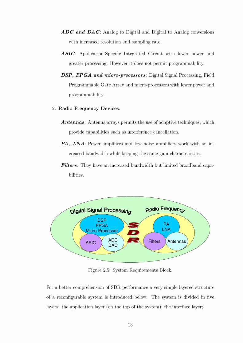
ADC and DAC : Analog to Digital and Digital to Analog conversions
with increased resolution and sampling rate.
ASIC : Application-Specific Integrated Circuit with lower power and
greater processing. However it does not permit programmability.
DSP, FPGA and micro-processors : Digital Signal Processing, Field
Programmable Gate Array and micro-processors with lower power and
programmability.
2. Radio Frequency Devices:
Antennas : Antenna arrays permits the use of adaptive techniques, which
provide capabilities such as interference cancellation.
PA, LNA: Power amplifiers and low noise amplifiers work with an in-
creased bandwidth while keeping the same gain characteristics.
Filters : They have an increased bandwidth but limited broadband capa-
bilities.
Figure 2.5: System Requirements Block.
For a better comprehension of SDR performance a very simple layered structure
of a reconfigurable system is introduced below. The system is divided in five
layers: the application layer (on the top of the system); the interface layer;
13

the configuration layer; the digital signal processing (DSP); and the radio fre-
quency (RF) layer at the bottom of the system.
Application layer : This level of the system corresponds to the user level,
which is responsible for the transmission and reception of data.
Interface layer : This level is responsible for interfacing the top layer or appli-
cation level and the radio hardware. It controls the information coming in and
going out of the radio, and packaging the incoming information before sending it
to the application layer. This layer containts the code for the algorithms that are
going to be used and their possible sequences of interconnection.
Some of the most important and significant parameters for the system like signal
and sampling rates have to be taking into consideration at this particular level.
As an example, the connection between USB 2.0 and the DSP layer, different
signal rates between both levels can generate problematic consequences on the
whole system performance.
Configuration layer : This layer controls the reconfiguration of the hardware.
It set up the various hardware elements according to the programming packets
sent by the interface layer.
Digital Signal Processing layer : This layer performs the actual operation
on the data to implement the functionality of the radio. At this level analog-to-
digital and digital-to-analog conversion take place. This level is highly dependent
on the previous level, because of the relationship between the sampling rate, num-
ber of quantization bits and the signal to noise ratio (SNR).
RF layer : At this level the signal is received or transmitted, up or down-
14

Figure 2.6: Layered Structure.
converted, amplified and filtered. Noise figure, power consumption and frequency
adaptability of the devices are the most important things to take in consideration
at this layer.
2.3 Wireless Standard Evolution
SDR, must meet a wide range of requirements for wireless communications stan-
dards. This section details the evolution of wireless standards for cellular mobile
telephony and their principal characteristics.
First Generation, 1G
This generation was mostly developed in the 1980s. It uses frequency division
multiple access (FDMA) techniques and analog voice coding [12]. Several exam-
ples of 1G systems are:
15

Table 2.1: Wireless evolution [11].
1. Advance Mobile Phone Services, AMPS: It uses 20 MHz band centred
around 800 MHz. It was deployed in Japan (1979) and United States
(1983) [12].
2. Nordic Mobile Telephone, NMT: Launched in 1981, cover Sweden, Norway,
Demark and Finland. It uses a band centred et 900 MHz, but it is not
longer used [12].
3. Total Access Communication System, TACS: It was initially deployed in
1985. Similar design to AMPS and is still in use in some parts of Europe [12].
Second Generation, 2G
This generation supports digitally encoded voice, limited data communication and
different levels of encryption. It uses time division multiple access (TDMA) tech-
niques, and in some cases code division multiple access (CDMA). It uses digital
data transmission. The capacity is increased using dynamic speech compression
techniques [11]. Second generation systems that were developed include:
1. IS-54, IS-136: American digital cellular standards. Based on TDMA tech-
niques.
16

2. Integral Digital Enhaced Network, iDEN: Motorola proprietary system cen-
tred at 800 MHz (private mobile radio spectrum). It uses TDMA tech-
niques.
3. Digital European Cordless Telephony, DECT: Based on TDMA techniques.
It has the highest data rate (1,728kps) of all TDMA digital cellular systems.
It is used for cordless phone at home.
4. Global System for Mobile, GSM: It was launched in 1991. It is based on
TDMA techniques with a band at 900 MHz, which has been extended with
a second band at 1800 MHz. It is the dominant world standard today.
Second Generation Towards Third Generation, 2.5G
This generation extends 2G systems, adding packet-switched connection and en-
hanced data rates. This generation set of standard, that led to, is composed
by:
1. IS95, CDMAone: Based on CDMA techniques, all user share the same
frequency. It is the first step for the 3G [12].
2. General Packet Radio Services, GPRS: It provides moderate speed data
(38-40kbps). GPRS is a method to enhanced 2G phones. It used circuit
switched data (CSD) to transfer data. This is a big steps towards 3G [12].
3. Enhanced Data Rate for GSM Evolution, EDGE: This technology is an
evolution of GPRS towards 3G standards. It is compatible with other
TDMA systems and can be used for any packet switch applications.
Third Generation, 3G
This generation provides universal roaming and an increased capacity [11]. All
3G standards are based on the CDMA technique. It provides hight data rates,
thus adding the capability to transmit data and video as well as voice. Some of
the 3G standards are specified below [1].
17

1. Universal Mobile Telecommunications System, UMTS: It is based on wide-
band code division multiple access, WCDMA. It is standardized by the
3rd generation partnership project, 3GPP. The specifications are based on
evolved global standard mobile specifications.
2. High Speed Downlink Packet Access, HSDPA: It is an evolved UMTS, pro-
viding 1.8 Mbps or 3.6 Mbps. in down-link.
3. High Speed Uplink Packet Access, HSUPA: Equally with HSDPA it is an
evolved UMTS, providing 5.76 Mbps in up-link.
4. Time Division-Synchronous Code Division Multiple Access, TD-SCDMA: It
dynamically adjusts the number of time slots used for uplink and downlink.
The spectrum allocation flexibility increases since it does not required paired
spectrum for downlink and uplink. It is used mostly in China.
5. CDMA2000: It constitutes UMTS’s principal competitor. It uses multi-
carrier synchronous CDMA techniques and provides 3.75Mhz bandwidth.
Figure 2.7: SDR and Wirelees Evolution.
Four Generation, 4G
This generation, according to the wireless world research forum (WWRF) is a
18

network that operates in internet technology and runs at speeds from 100Mbps
to 1Gbps. 4G terminals will have all the standards from 2G to 3G implemented.
According to the European Commission, 4G will ensure service across a variety
of wireless systems and networks. It will provide an optimum delivery via the
most appropiate network available [2]. Some of the additional standards for 4G
are described below [1].
1. Worwilde Interoperability for Microwave Access,WiMax IEEE802.16: It
provides high speed mobile data and telecommunications services. It works
on the spectrum band from 10 GHz to 66 GHz. It uses orthogonal frequency
division multiplexing, OFDM.
2. Wireless Broadband, WiBro: Wireless broadband internet technology, it is
merged into WiMax and uses OFDM and 8.75 MHz of channel bandwidth.
It is intended for portable internet usage.
3. LTE: Long Term Evolution. It is a new envolved release of the UMTS
standard. It is an upgraded UMTS with a simplified architecture to an
all-IP system [1].
2.4 Conclusion
This chapter has presented the evolution of radio systems towards software de-
fined radio, SDR. It has particularly described the advantages and applications
of SDR in the modern days. Flexibility and adaptability are two important qual-
ities of SDR derived from this chapter. A background of standard evolutions
toward SDR has been described. Concluding with SDR as a technology capable
of covering a wide range of wireless telecommunications standard due to its high
level of flexibility. This chapter has been a basic introduction to SDR to continue
more in detail in next chapter, which will introduce some of the qualities and
requirements demanded in a SDR platform.
19
Chapter 3
REQUIREMENTS AND
SPECIFICATIONS
3.1 Introduction
In this chapter transmitter and receiver requirements for various communication
standards are presented. These will be used to develop the requirements for the
SDR platform. The ADCs are simulated in order to specify their performance
for the platform.
3.2 Standard Specifications
The necessary requirements for each standard are presented in this section.
With the development of a reconfigurable radio platform as a target, a range of
standards have been taken into consideration in order to create the necessary
specification for this system.
The ideal approach would be the implementation of all the wireless standards
together: GSM, CDMA2000, UMTS, IEEE802.11x, IEEE802.16x, IEEE802.15x,
and IEEE 802.20x, Bluetooth and UWB. However the incompatibility between
air interfaces used by each standard is an issue. For this reason the standards are
20

Table 3.1: Digital Cellular Telephones Specifications [5].
be divided into different groups with similar characteristics [13] such as: symbol
rate; power; and range, according to Tables 3.1 and 3.2. These groups are
described below:
IEEE802.15.4a and Bluetooth: low rate (<1Mbit/s), short range (around
10m), and transmitted power less than 1mW.
IEEE802.15x and UWB: high rate (up to 500Mbits/s), short range (around
10m), low transmitted powers.
IEEE802.11x, IEEE802.16x, IEEE802.20x and 2G/3G mobile: lower
rates, higher powers, several bit rates. The common feature of this group of
standards is that at a fixed frequency with a range of bit rates they deliver ser-
vices to the end user over longer distances.
21

Table 3.2: Wireless Specifications [5].
Since the last group of standards is the most demanding, this platform is fo-
cused to meet as many requirements as possible for these standards. As DCS
and PCS share a band with the European 3G standards, these along with the
two bands within GSM as well as the 802.11 and 802.16 bands are of interest for
the platform. with the functionality of a local area Network (LAN) is difficult
to achieve. The physical layer radio performance specifications of this group are
described in Table 3.3.
3.3 System Specifications
The proposed platform is designed to operate in a frequency band from 1.6GHz
to 2.5GHz and support the DCS1800, PCS 1900, UMTS-FDD, UMTS-TDD and
802.11b standards. Of the supported standards DCS1800 is the most difficult to
22

Table 3.3: Radio Performance Specifictions
meet. For this reason the signal specifications for the receiver and transmitter
are taken from DCS1800. Both transmitter and receiver are implemented using
direct conversion architecture, chosen due to its low power dissipation, simpler
design and easier tuning across large frequency bands. As many off-the-shelf parts
as possible are used for the implementation of the software defined radio. The
platform is separated in three main blocks: receiver, transmitter and baseband
board. The proposed blocks for the design are shown in Figure 3.1.
Figure 3.1: Block Diagram of the Proposed Platform.
3.3.1 Radio Frequency Specifications
Receiver Specifications
The purpose of a RF receiver is to filter the received radio frequency signal and
convert it to baseband by mixing the signal with local oscillator. Some of the
23

most important parameters of interest at the receiver are: sensitivity, selectivity,
Noise Figure and third order intermodulation products [14]. These parameters
are decided by the BER and blocker performances of the system.
1. Selectivity and Blocker Specifications
Selectivity is the ability of the receiver to reject nearby signals outside of
the desired band and respond only to the required transmission. Some of
the causes of selectivity degradation in the receiver are the spurious signals
generated by adjacent channels [15]. The blocking performance specifies
the overall selectivity. Thus, the blocker specifications for the group of
standards covered by this platform are illustrated in Figure 3.2 to Figure 3.5.
Of these, the most difficult to achieve is DCS1800.
Figure 3.2: PCS1900 Blocker Specifications [15].
f0
f0 f0f0 f0
−11M
Hz
+11M
Hz
−73dBm −73dBm
−33M
Hz
+33M
Hz
−43dBm −43dBm
Inband IEEE 802.11b
Figure 3.3: 802.11 Blocker Specifications [15].
24

f0
f0−
10MH
z
f0+
10MH
z
f0−
15MH
z
f0+
15MH
z
−44dBm
−56dBmf0
f0−
10MH
z
f0+
10MH
z
f0−
15MH
z
f0+
15MH
z
−15dBm
−30dBm
−44dBm
1MH
z
1,815MH
z
1840MH
z
1885MH
z
1920MH
z
2000MH
Z
2055MH
z
2095MH
z
12750MH
z
2120MH
z
In−band In−bandIn−band
−15dBm
−30dBm
−44dBm
1MH
z
2025MH
z
2050MH
z
2095MH
z
2185MH
z
2230MH
z
2255MH
z
12750MH
z
−44dBm
−56dBm
UTMS−TDDUTMS−FDD
Pow
er
Pow
erP
ower
Pow
er
FrequencyFrequency
Figure 3.4: UMTS blocker specifications.
Figure 3.5: DCS1800 Blocker Specifications [15].
2. Receiver Sensitivity
This is the minimum signal power delivered to the input terminal of the
receiver for which the required BER is met for the particular radio system.
The BER value for acceptable performance in voice systems is generally
defined to be 10−3, however this depends on the used standard [14]. The
25

sensitivity can be calculated from the total noise figure and the noise floor
at the input of the receiver using equation(3.1)
Sensitivity(dBm) = NFtotal(dB) + CNRoutput(dB) + NFloor (3.1)
The reference sensitivity levels for the covered standards are given below:
(a) Sensitivity(DCS−1800) = -102dBm @SNR=9dB
(b) Sensitivity(PCS−1900) = -102dBm @SNR=9dB
(c) Sensitivity(UMTS−FDD) = -107dBm @SNR=18.9dB
(d) Sensitivity(UMTS−TDD) = -105dBm @SNR=6dB
(e) Sensitivity(802.11) = -76.5dBm @SNR=10dB
Of these the sensitivity requirements for UMTS-FDD is the lowest at -
107dBm, thus this is required sensitivity for this system.
3. Intermodulation Nonlinearities
This is the tendency for modulation products generated by devices with non
ideal characteristics, to lie in the band of interest. In a zero-IF architecture
this parameter is carefully considered since these unwanted signals lie in the
down-converted signal band and corrupt the wanted signal. The standard
model for it includes a third order term to model the nonlinearities. The
products contributed by this third order term appear at 2w1 − w2 and
2w2 − w1, where w1 and w2 are the frequency of the wanted signal and
an adjacent channel signal respectively [16]. As the input power increases
the third order intermodulation products increase producing distortion in
the desired signal. IIP3 (input third order intercept point) is a measure
the linearity of the system. The overall required system IIP3 is calculated
using the following approximation:
IIP3 = Pin +∆P
2(3.2)
26

where Pin is the power of the interference and ∆P is the increment between
the desired power and the interference power.
For m-stages the IIP3 can be obtained as follows:
1
A2IIP3
=1
A2IIP3,1
+α2
1
A2IIP3,2
+α2
1β21
A2IIP3,1
+ · · · (3.3)
where α1 and α3 are the first and third order gain of the first stage and
β1 is the first order gain of the second stage and so for. A2IIP3 is the third
order intercept point and is given by:
AIIP3 =
√4
3|α1
α3
| (3.4)
The IIP3 requirement for the covered standards are:
(a) IIP3(DCS−1800) = -18dBm
(b) IIP3(PCS−1900) = -18dBm
(c) IIP3(UMTS−FDD) = -21.3dBm
(d) IIP3(UMTS−TDD) = -20.9dBm
(e) IIP3(802.11) = -22.5dBm
In conclusion, the IIP3 requirement for this platform is limited by the high-
est, which is DCS1800 and it is : -18dBm.
4. Noise Figure
The NF, noise figure, is a parameter used to measure how much the SNR
is degraded as the received signal progress through the receiver [16]. It can
also be defined as the available SNR as the ratio between the available SNR
at the input and the output of a network. NF is the figure in dB of the
noise factor, F. Using this definition the following equation calculates the
noise factor for a single network:
F = (Sg
ktb)(
N
S) (3.5)
27

where Sg is the available signal power at the input, ktb is the available
noise power at the input, N is the available noise power at the output of
the network and S is the available signal power at the output of the network.
KTB is the thermal noise, at 290oK this is -174dBm/Hz. Hence including
the bandwidth of interest, the noise power at the receiver input in dBm is:
NoiseF loor = [−174 + 10 log(BW )](dBm) (3.6)
The noise figure NF for a single network is given below:
NFov(dB) = Pmin + 174dBm/Hz − SNRreq − 10 log(BW ) (3.7)
The NF specifications for the covered standards are studied in order to
generate the NF requirements of the system:
(a) NF(DCS−1800) = 11.8dB
(b) NF(PCS−1900) = 9.8dB
(c) NF(UMTS−FDD) = 9.6dB
(d) NF(UMTS−TDD) = 9.2dB
(e) NF(802.11) = 11dB
The noise figure for the system is calculated using the Friis [17] method
given in equation (3.8). The input and output impedance of all networks
components in the system are assumed to be 50 Ω. In order to obtain the
NF for the different stage in the system the gain of each independent stage
can be used. The equation below gives the total NF for an m-stages system.
Ftotal = F1 +m∑
i=2
Fi − 1∏m−1k=1 Gaink
(3.8)
NFtotal(dB) = 10 log Ftotal (3.9)
where Fi and Gk are the noise factor for each stage and gain of each element
28

respectively. NFtotal is referred to the total noise figure for the system.
In order to calculate the NF of this platform the schematic of Figure 3.6 is
used.
RLRSF1,G1 F2,G2 F3,G3 F4,G4 F5,G5
LNA DEMOD. ADCBPF LPF
Figure 3.6: Noise networks in the receiver.
Fi = 10NFi10 (3.10)
Gi = 10Gi10 (3.11)
Ftotal = F1 +F2 − 1
G1
+F3 − 1
G1G2
+F4 − 1
G1G2G3
+F5 − 1
G1G2G3G4
(3.12)
NFtotal(dB) = 10 log Ftotal (3.13)
A particular case in the calculation of the single NF in the m-stages system,
showed in the previous figure, is the NF of the ADC. This is due to the
high influence that the dynamic range of the ADC has over the noise factor
of the device. The NF of the ADC is calculated as follows [18]. From
the SNR given in the data sheet and the full scale voltage, V fs(RMS), the
effective input noise voltage is calculated, Vnoise(RMS), using equations (3.14)
and (3.15). The noise factor, F, is then given by the effective input noise
divided by the thermal noise as shown in equation (3.17). Using this result
the noise factor is then given by equation (3.18) and the NF is then F in
29

dB given in equation (3.20).
SNR = 20logV fs(RMS)
Vnoise(RMS)
(3.14)
Vnoise(RMS)= V fs(RMS)
10−SNR
20 (3.15)
PFS =V f 2
s(RMS)
R(3.16)
FADC =V 2
noise(RMS)
KTRB(3.17)
FADC = PFS × 1
KT× 10
−SNR10 × 1
B(3.18)
NFADC(dB) = 10× log Ftotal (3.19)
NFADC(dB) = PFSdBm+ 174dBm− SNR− 10 log
fs
2(3.20)
PFSdBmis the full scale input power. This is the power of a sinewave
which has an amplitude peak-to-peak that fills the ADC input range. In
equation(3.20), fs is given in Hz and it is the sample frequency of the ADC.
Consequently the NFtotal is calculated to meet the required specifications
of 11.8dB that arise from the DCS1800 standard.
Receiver specifications have been described in this section. Thus, the input signal
going to our SDR receiver is required to have: low power (down to -107dBm),
considerable high dynamic range, channel bandwidth up to 22MHz, and a center
frequency which is varying between 1.6GHz to 2.4GHz. In order to design the
requirements for the output signal from the SDR front-end, transmitter specifi-
cations are described in the next section.
Transmitter Specifications
The purpose of the transmitter is to modulate the desired signal, shift it to RF,
and amplify an RF carrier. The specification design for the transmitter is more
relax than for the receiver. This is because some of the parameters can be consid-
ered from the receiver for the design of the transmitter, such as the noise figure.
The most important design parameters to create the transmitter specifications
30

are: phase noise, output power level, power control range and frequency of op-
eration. The frequency of operation for this SDR platform has been described
previously since the band of covered standards was given. The rest of design
parameter values are described as follows:
1. Output Power Level
This is the power level of the transmitted signal from the antenna. The
maximum output power levels for the covered standards are described be-
low:
(a) P(DCS−1800) = 36dBm
(b) P(PCS−1900) = 36dBm
(c) P(UMTS−FDD) = 33dBm
(d) P(UMTS−TDD) = 24dBm
(e) P(802.11) = 11dBm
2. Power Control
This is the controlled variations in the output power level of the transmitted
signal from the antenna. Thus the transmitter in this platform has output
power control to comparative fine tolerances. The power control range is
given by the DCS1800 specifications, 36dBm of power control range with
steps of 2dB.
3. Transmitter Phase Noise
This noise is expressed in terms of single sideband phase noise (PN) mea-
sured in a 1 Hz bandwidth at an offset from the carrier relative to the carrier
amplitude. This phase noise in the transmitter is mainly caused by noise
coming from the PLL on the up-conversion stage.
The PN specifications for the covered standards are given below:
(a) PN(DCS−1800) = -154dBc/Hz
(b) PN(PCS−1900) = -154dBc/Hz
31

(c) PN(UMTS−FDD) = -148dBc/Hz
(d) PN(UMTS−TDD) = -154dBc/Hz
(e) PN(802.11) = ?
The phase noise for the standard 802.11 is not specified since this depends
on the used modulation scheme. However, the PN requirement in 802.11 is
more relaxed than the other standards. Hence, the hardest PN constrain
to meet is -154dBc/Hz which arises from the DCS1800 standard and forms
the requirement for this platform.
From the specifications described above, the output signal from the transmitter
is required to have: differential mode (I and Q channels), output power up to
30Bm, center frequency between 1.6GHz and 2.4GHz, enough signal power to
ensure a high SNR, a controlled dynamic range to meet the requirements for the
ADCs. The requirements for the ADC are explained in the next section.
3.3.2 Analog-to-Digital Conversion Specifications
The baseband processing stage provides optimum digitization, fast sample rate
conversion and configuration control for the system. In addition, the baseband
block of this platform must meet the requirements for 2G/3G, 802.11 and 802.16
standards. Hence, the specifications of this block are directly derived from the
signal characteristics incoming and out going to and from the system. Spurious
emissions by the transmitter are controlled by careful selection of the DAC. In
order to specify the ADC the blocker characteristics of the receiver for the covered
standards need to be considered. These parameters decide the dynamic range of
the signal and, as a consequence, of the baseband block.
To achieve the signal to noise ratio in the covered standards a minimum ADC res-
olution is required. This resolution depends on the number of bits per symbol, the
blocking performance and the required receiver sensitivity. As the bits/symbol
32

increases the SNR requirements of the receiver increase. This is reflected in the
number of bits in the ADC. Thus, a constellation such as Orthogonal Frequency-
Division Multiplexing, OFDM, will require more bits than simple Binary Phase
Shift Keying, BPSK. For this reason OFDM is used as the worst case example in
the simulations described here.
OFDM is a technique which combines digital modulation schemes with the prin-
Figure 3.7: Flow chart of BB simulation.
ciple of frequency division multiplexing, FDM. This technique is used to preserve
orthogonally in multi-path environments when large amounts of digital data are
33

transmitted. In OFDM the frequency spectrum is divided into sub-channels, then
each sub-channel transmits a bit stream by modulating a sub-carrier. The sub-
channels are combined together using the inverse fast Fourier transform, IFFT,
thus the receiver separates the channels by using the fast Fourier transform, FFT.
In order to eliminate the cross talk between sub-channels the sub-carrier frequency
is chosen so that the modulated data sub-channels are orthogonal to each other.
For the sub-carrier modulation several modulation schemes were used such as :
M-QAM, QPSK and BPSK. In the simulations the parameters of the signal are
modified in order to represent different transmission scenarios. Table 3.4 lists the
signal parameters that were modified. Therefore, simulations are done for several
Table 3.4: Simulation Parameters.
modulation schemes, number of carriers, channel noise and number of bits. The
transmission channel is represented by the addition of White Gaussian noise into
the signal. In the receiver the cyclic prefix of the OFDM signal is removed before
reaching the uniform quantizer, which adds quantization noise to the signal. This
is possible due to the assumption of perfect synchronisation between the trans-
mitter and the receiver. The BER (bit error ratio) is calculated at the output
of the system. Since the OFDM signal introduced into the system is a random
process, the SNR calculation requires the variance of both information and noise
signals. In order to achieve the specified BER from the standards, the required
minimum number of bits in the ADC is sought. This process is shown in the
Figure 3.7.
34

In the following equations the calculations of this process are presented. The
Matlab code used for the is included in appendix A. Equations (3.21) and (3.22)
give the expected value or mean (µ) of both noise and information signal, where
n is the system noise and ofdm is the information signal.
µn =Plnoise
i=1 ni
lnoiselnoise : noise length (3.21)
µofdm =Plofdm
i=1 ofdmi
lofdmlofdm : ofdm length (3.22)
λ2n =
k∑i=1
(ni − µn)2 (3.23)
λ2ofdm =
k∑i=1
(ofdmi − µofdm)2 (3.24)
ξ2n =
λ2n
k − 1(3.25)
ξ2ofdm =
λ2ofdm
k − 1(3.26)
σ2n =
1
samples 2·
k∑i=1
ξ2ni
(3.27)
σ2ofdm =
1
samples 2·
k∑i=1
ξ2ofdmi
(3.28)
In the above equations k is a variable which counts from 2 up to the number of
samples used for the simulation, λ2 is the temporary variance of both signals, ξ2
is the sample variance, which is an estimated variance and is based on a finite
sample, and σ2 is the total variance for both signals. The variance of both noise
and information signals converge as shown in Figure 3.8. These are simulated
using equations (3.23) to (3.27). It can be seen in Figure 3.8 that a significant
number of samples are required in order to accurately represent the variance of
the OFDM signal. The number of points in the OFDM signal constellation is ef-
fectively the number of points in the underlying sub-channel modulation scheme
times the number of sub-channels. This gives a large peak to average ratio re-
35
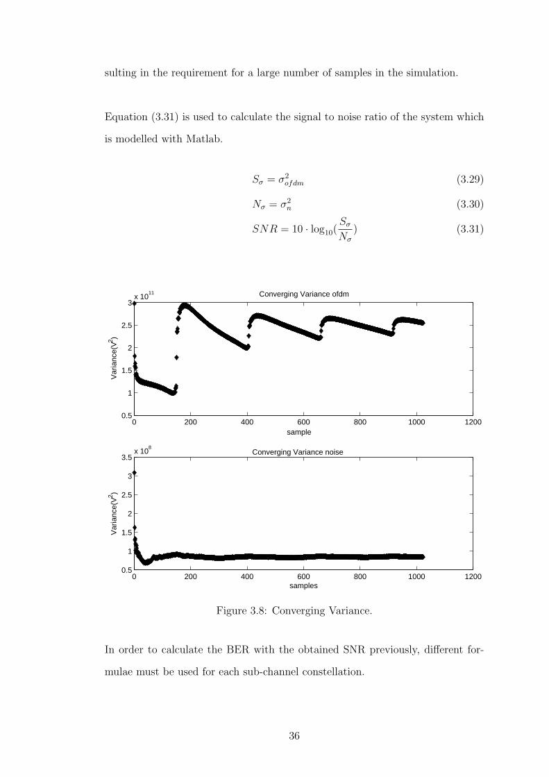
sulting in the requirement for a large number of samples in the simulation.
Equation (3.31) is used to calculate the signal to noise ratio of the system which
is modelled with Matlab.
Sσ = σ2ofdm (3.29)
Nσ = σ2n (3.30)
SNR = 10 · log10(Sσ
Nσ
) (3.31)
0 200 400 600 800 1000 12000.5
1
1.5
2
2.5
3x 10
11 Converging Variance ofdm
sample
Var
ianc
e(V2 )
0 200 400 600 800 1000 12000.5
1
1.5
2
2.5
3
3.5x 10
8Converging Variance noise
samples
Var
ianc
e(V
2 )
Figure 3.8: Converging Variance.
In order to calculate the BER with the obtained SNR previously, different for-
mulae must be used for each sub-channel constellation.
36

Pe = 0.5 · erfc(√
SNR) (3.32)
Pe = 2 · (1− 1√M
) · erfc√
32·(M−1)
· SNR (3.33)
Pe = 2 · (1− 1√2·M ) · erfc
√3
2·(M−1)· SNR (3.34)
erfc(x) = 2√π
∫∞x
e−u2du (3.35)
Equation (3.33) calculates the probability of error for BPSK, equation (3.34) cal-
culates the probability of error for QAM(16,64,256) and equation (3.35) calculates
the probability of error for QAM (8,32). Equation (3.35) is the complementary
error function. Figures 3.9(a) and 3.9(b) show the BER versus SNR for two dif-
ferent types of modulation scheme: 256 QAM, 32 QAM. These results are given
as a function of the number of quantization bits.
20 30 40 50 60 70 80 90 10010
−35
10−30
10−25
10−20
10−15
10−10
10−5
100
105 32 QAM
SNR
BE
R
45678
resolution
(a) BER vs SNR with 32QAM modulation.
20 30 40 50 60 70 80 90 10010
−5
10−4
10−3
10−2
10−1
100
101 256 QAM
SNR
BE
R
45678
resolution
4bits
(b) BER vs SNR with 256QAM modulation.
Figure 3.9: BER
It can be seen from this that at least 8 bits are required to achieve the necessary
BER. Additional bits are added to allow for signal amplitude variation at the
input of the ADC. Thus, 16-bit ADCs can be used which gives 8 bits of dynamic
37

range to allow for amplitude variation in the incoming signal. This corresponds
to 48dB of dynamic range available at the input to the ADC. This allows the
relaxation of the requirements for the automatic gain control in the receiver. The
previous plots have been created with the code in appendix A.
3.4 Implemented Architecture
The obtained specifications require a platform to transmit and receive across
the band from 1.5GHz to 2.5GHz with a receiver sensitivity of -117dBm. This
requires a NF of 9dBm and the phase noise of -154dBc/Hz. To achieve the specifi-
cations an architecture that can tune across this band and meet the tight receiver
specifications is required. In reference with the architecture described in chapter
2 a suitable architecture is now selected. The superheterodyne model is the most
common architecture for wireless communication. However requirement for an
intermediate frequency, and the associated filters, make this architecture difficult
to tune across a wide frequency band and thus unsuitable for SDR purposes [14].
Low-IF architecture is a possible solution for SDR, however the necessity of an
accurate image rejection filter renders this a difficult architecture to implement.
The remaining option is the direct conversion architecture. This technique trans-
forms the RF signal to zero frequencies at down-conversion and from zero frequen-
cies to RF at up-conversion using just one conversion stage. On the transmitter
side this architecture has the disadvantage of injection pulling. This issue is due
to leakage from the local oscillator to the PA. This arises as the signal at the
output of the power amplifier is a modulated high power signal with spectrum
centred around the LO frequencies. Without careful design some of the output
power may leak into the LO affecting the performance of the system. To solve
this problem the mixer in the modulator must be highly isolated. Similarly the
receiver may experience DC offset problems associated with the LO leakage and
38

power coupling to the input of the LNA. This is illustrated in Figure 3.10 as
an example of some of the drawbacks and requirements of the direct converter
receiver. Although it has the disadvantage of DC offset, a complex image re-
Figure 3.10: Direct converter receiver requirements.
jection filter is not needed in the direct conversion architecture. In addition the
problems caused by the DC offset are easier to solve. Double balanced mixers
and accuracy in phase quadrature and amplitude balanced in the LO with good
isolation between the LNA and the LO, are reliable solutions in the direct con-
version architecture.
Direct conversion is power efficient, has easy tuning across large frequency bands,
and low cost because of a reduced number of components. This guarantees a
higher level of integration than with other architectures [14]. Good image sup-
pression properties result from this approach. This SDR system must support
non-linear modulation schemes such as GMSK, linear modulation schemes such as
QPSK and quadrature modulation schemes such as QAM. In order to avoid signal
distortion due to saturation in the low noise amplifier (LNA) and power amplifier
(PA), there is a requirement for variable gain in the system [19]. Consequently
39

the PA is preceded by a variable gain amplifier which avoids the saturation of the
PA. Considering the receiver, the signal gain is controlled by an automatic gain
control, AGC, in the demodulator.
3.4.1 SDR Specifications and Block Diagram
The baseband and RF specifications have been created from the requirements
explained in this chapter. Table 7.2 is presenting the resulted specifications for
the design of this system.
Table 3.5: Specifications
Receiver Transmitter Baseband
IIP3: -0.87dBm Pout: 30dBm ADC/DAC resolution: 16bits
Sensitivity: -107dBm PN: -152dBc/Hz Sample rate up to 100Msps
BW: 22MHz BW: 22MHz 480Msps USB link
Frequency range : 1.6GHz to 2.5GHz
Standards: DCS1800, PCS1900, UMTS-FDD, UMTS-TDD and 802.11b
Given these requirements, a suitable platform in the direct conversion archi-
tecture has been selected. The proposed block diagram for the design of this
platform is illustrated in Figure 3.11. The system is separated into three blocks
according to their frequency characteristics.
3.5 Conclusion
Some limitations and requirements have been presented in this chapter. The cho-
sen architecture has also been presented in this chapter. The proposed platform
is only able to meet some of the wireless telecommunications standards due to the
difficulty in creating a pure SDR system capable of adapting to any environment.
A family of standards with similar characteristics has been selected compatible
with SDR implementation to be covered by this model. In the following chapter,
40

90o
90o
ADC
ADC
DAC
To
DAC
VGAPA
USBComputer
BB
RX
TX
LNA
LPF
LPF
Figure 3.11: Block diagram of the system.
the designed SDR testbed is presented taking in consideration all the studied
requirements given in this chapter.
41

Chapter 4
PLATFORM DESIGN
4.1 Introduction
In this chapter the design of the implemented platform is presented. Character-
istics for the different stages of the platform are given. Analog-to-digital conver-
sion, modulation and demodulation, and baseband signal processing stages are
described, and manufactures part numbers are detailed. RF amplification and
filtering stages are explained in detail in the following chapters.
At the receiver front-end, the antenna collects the signal. This is then filtered
and demodulated to baseband frequencies. The fact that most of the components
at the receiver are broadband devices enables the sweep of frequencies over a very
wide range. The signal characteristics are analyzed using digital signal processing
on the PC.
In the same way as the receiver, the transmitter performs the up conversion. The
RF synthesizer outputs a signal with the desired centre frequency to the mixer
which up converts the modulating signal to the desired transmit frequency. This
is then further amplified and filtered before reaching the antenna. During this
process of transmitting and receiving the signal, the hardware may be adapted
under software control to match the specifications of the particular standard.
42

4.2 Platform Overview
Following the block diagram of Figure 3.11 given in the previous chapter, the
platform with the corresponding device part numbers is illustrated in Figure 4.1.
This design is divided into three functional blocks: radio frequency receiver, radio
frequency transmitter and base band interface [20]. The implementation reflexes
this layout. Since one of the most difficult challenges to satisfy in reconfigurability
is the analog-to-digital conversion and digital-to-analog conversion stage, it was
the starting point. The results of the simulation for the ADC requirements were
presented in the previous chapter. These simulations were carried out to with
the target of finding the minimum resolution needed to fit the SNR limitations
for the worst case standard to be implemented here. The platform consists of a
USB interface to a standard PC, an ADC and a DAC and a direct conversion
architecture for transmitter and receiver.
90o
ADC
ADC
90o
DAC
VGAPA
ADL5330
MGA83563
USBCY7C68013
LNA
ToComputer
RX
MAX5875
LTC2205
TX
BB
AD8349
AD8132
AD8132
LNAAD8347
ADF4360
ADF4360
DAC
AD8132
AD8132
MBC13720
Figure 4.1: Block diagram of the system.
43

4.3 USB Interface and Digital Control Plane
In order to exchange data and information between the PC and the hardware plat-
form the USB2.0 standard is used. The interface between the USB host and the
platform is implemented by a high speed peripheral controller from Cypress Semi-
conductor. This chip contains both an 8051 microcontroller and a programmable
peripheral interface. The microcontroller is programmed using the C language.
Interrupts are used to control the exchange of data between the platform and the
PC. The code used to control the system is given in appendix B. Parameters such
as clock frequency in the 8051, center frequency of the transmitter and receiver
front-ends and output power are programmed in the PC and downloaded to the
microcontroller which controls the rest of the platform. In this way the platform
may be reconfigured.
4.3.1 Synchronization and Control
The clock waveforms required for the ADC and DAC are generated here. All
the control signals are processed by the baseband board. Timing functions are
implemented from this part by digital signal processing. The ADC has a parallel
pipeline architecture with a latency of seven clock cycles. The DAC has a switched
current architecture with a propagation delay of 1.5ns and a latency is 5.5 clock
cycles. The data is data is latched into and out of the USB chip. From this
information the required time diagram is shown in Figure 4.2.
4.4 Analog to Digital and Digital to Analog
Conversion Stages
Analog to digital conversion, ADC, is critical for the operation of the system.
This is one of the most important steps in a communications system since the
signal can be distorted due to non linear affects and information can be lost due
44

Q convert clkL and OE driven from Valid Q Latch output< 5ns
Valid I ADC data< 5ns
I convert clkL and OE driven from Valid I Latch output< 5ns
< 5ns Valid Q ADC data
Q convert clk
>6.25ns >6.25ns
Master clk
Inverted Master clk
I convert clk
Figure 4.2: Time Diagram.
to lack of resolution in the conversion process. With the advents of more com-
plex constellations such as OFDM the demand for higher resolution has increased
in the last few years. Consequently 16 bits ADCs with the required bandwidth
are becoming available in the market. These are replacing the previous available
state-of-the-art ADCs for wireless applications which were 14 bit resolution de-
vices operating with 100MHz sample rate. Converters with 16 bit resolution can
process higher dynamic ranges and achieve the requirements for most of the stan-
dards needed here. In a wide band system SFDR (Spurious Free Dynamic Range)
is the most important limitation for the choice of a particular ADC [21]. This is
because aliased spurious tones on the carrier can fold back on the carrier causing
distortion. This affect is further exasperated in multicarrier systems. From this
point of view Matlab simulations were carried out to calculate the minimum res-
olution required for the converter. This is documented in chapter 3.
For the digital to analog conversion (DAC) stage high performance DACs are
used in the transmitter. Thus the complete signal is reconstructed from the
digital data. The DAC performance is very important since the SDR platform
45

performs most of the signal processing digitally. Working in the digital domain
results in improved reconfigurability and programmability which is the purpose
of implementing SDR systems.
4.4.1 Implementation
ADCs
The choice of the ADC architecture depends on what kind of capability is im-
portant for this platform. Jitter in the ADC stage degradates the SNR in the
system. For this reason an ultra low jitter ADC is chosen. The SNR degradation
due to the jitter is given by the following equation [21]:
SNR = −20 log10(2πfin × tjitter) (4.1)
In addition, conversion speed is another requirement for SDR. Different ADC
architecture required different numbers of clock cycles per sample. Figure 4.3
shows a qualitative comparison of ADC techniques relating the resolution and
number of clock cycles used per sample. From this figure the fastest architec-
ture is flash or pipeline. Hence a 16 bit ADC which uses the pipelined multistep
technique is used. The devices chosen are the LTC2202/LTC2205/LTC2207 fam-
ily from Linear Technologies. This family are pin compatible with each other.
Currently the sample rate needed is not greater than 80Msps, consequently in
order to avoid excessive power consumption the LTC2205 is used. Nevertheless
the target is to achieve the maximum sample rate possible, thus the LTC2207
capable of sampling at 130MSps may also be used in this platform. This ADC
(LTC2205) is composed of five pipelined ADC stages with a differential analog
input to reduce even harmonics, increase the input range and improve common
mode noise immunity [22]. Some of the advantages of the pipeline architecture
are: digital correction with no increase in hardware size. However it requires
fast interstate processing since the architecture is implemented in several stages.
46

Figure 4.3: Comparation of ADC techniques [21].
Figure 4.4 illustrates the block diagram of the chosen ADC.
Figure 4.4: ADC Functional Block Diagram [22].
The timing jitter on the conversion for this ADC is 90fs, which does not con-
tribute to a significant degradation in the SNR. The noise figure, NF, for the
ADCs is calculated using equations (3.16) to (3.20) and it is 10.2dB. As shown
47

in Figure 4.1, two ADC devices are used, one for the in-phase and one for the
quadrature channel. They are situated just after the baseband filter and amplifier
which scale the signal to a suitable level for analog to digital conversion.
DACs
The reconstructed analog signal from the DAC must represent the digital signal
accurately. The major source of errors in the DAC is due to static nonlinearity.
These occur when the level spacing in the DAC is non-uniform. These errors
result in distortion which may cause spurious tones and degradation in SNR.
SFDR gives a measure of this effect. As for the ADCs, SNR, SFDR and sample
rate are the most significant parameters.
The maximum SNR is derived from the resolution of the DAC and is described
as following:
SNR = 6.02dB ×N + 1.76dB (4.2)
However, as in the ADC, jitter and thermal noise affect this ideal SNR. The
chosen DAC device is the MAX5875 from MAXIM [23]. The device features a
SFDR of approximately 80dBc, a sample rate up to 200Msps and a noise density
of -162dBFS/Hz which meets the required specifications for the transmitter. The
device is dual channel with 16 bit resolution implemented using a current steering
architecture as illustrated in Figure 4.5. As shown in Figure 4.1 one DAC is used
for the I channel and one DAC is used for the Q channel.
4.5 Baseband Signal Processing
This section describes the two stages of baseband processing: filtering and am-
plification. The receiver gain is the sum of the LNA, mixer and baseband am-
plification stage gains. The mixer gain control is used to provide variable gain
in the receiver. Therefore the gain of the baseband stage can be controlled. A
low pass antialiasing filter is included between the demodulator and the ADC to
48

Figure 4.5: DAC Functional Block Diagram [23].
prevent spurious high frequency signals from corrupting the wanted signal. The
amplification and filtering at the receiver are implemented using multiple feed-
back architecture. Similarly in the transmitter a baseband gain stage is used to
fit the output of the DAC to the input of the modulator. In the transmitter a low
pass reconstruction filter follows the DAC. Again the amplification and filtering
stages are implemented using multiple feedback architecture. This filter must
have a cut-off frequency similar to the bandwidth of the signal that is going to
be transmitted.
4.5.1 Filtering
The baseband filtering is composed of two low pass channel selection filters. They
are situated close to the DAC in the transmitter side, and to the ADC in the re-
ceiver side. The filters are acting as antialiasing filters and are implemented for
this platform to ensure suppression of out of channel interference. The receive
filter eliminates interfering signals that may be within the bandwidth of the de-
modulator but outside the bandwidth of the ADC. This filter in effect acts as the
49
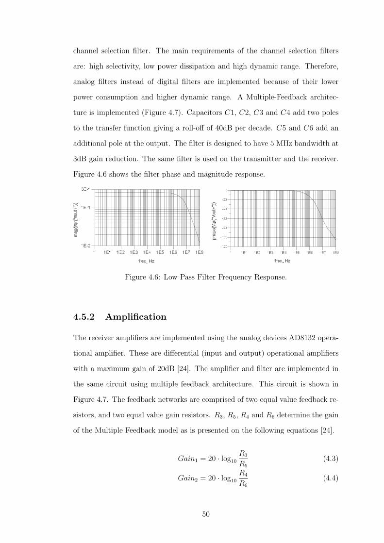
channel selection filter. The main requirements of the channel selection filters
are: high selectivity, low power dissipation and high dynamic range. Therefore,
analog filters instead of digital filters are implemented because of their lower
power consumption and higher dynamic range. A Multiple-Feedback architec-
ture is implemented (Figure 4.7). Capacitors C1, C2, C3 and C4 add two poles
to the transfer function giving a roll-off of 40dB per decade. C5 and C6 add an
additional pole at the output. The filter is designed to have 5 MHz bandwidth at
3dB gain reduction. The same filter is used on the transmitter and the receiver.
Figure 4.6 shows the filter phase and magnitude response.
Figure 4.6: Low Pass Filter Frequency Response.
4.5.2 Amplification
The receiver amplifiers are implemented using the analog devices AD8132 opera-
tional amplifier. These are differential (input and output) operational amplifiers
with a maximum gain of 20dB [24]. The amplifier and filter are implemented in
the same circuit using multiple feedback architecture. This circuit is shown in
Figure 4.7. The feedback networks are comprised of two equal value feedback re-
sistors, and two equal value gain resistors. R3, R5, R4 and R6 determine the gain
of the Multiple Feedback model as is presented on the following equations [24].
Gain1 = 20 · log10
R3
R5
(4.3)
Gain2 = 20 · log10
R4
R6
(4.4)
50

For the calculation of the correct gain for the operational amplifier the input char-
acteristics of the ADC device are taken into consideration so as to get the best
noise performance. The gain control of the down-converter is used to provide a
fixed amplitude of 500 mVp-p at the output of the demodulator. This allows the
largest region of linearity at the demodulator output for any given input. There-
fore the amplifier is able to work in the linear region for the selected frequency
range. Considering the output amplitude of 500 mVp-p, 250 mVp or 23dBm, the
basband amplifier requires a gain of approximately 13.1 dB to provide a full scale
input to the ADC. The AGC (Automatic Gain Control) on the demodulator has
a steady-state voltage of 1V with an expected input of 24 mVp-p. Resistors are
used as a voltage divider to provide the 24 mVp-p from the 500mVp-p signal.
With these values it is possible to calculate the control resistors for the AGC.
Thus, the obtained resistors values are 20kΩ and 1kΩ.
Figure 4.7: Base Band Amplifier and Low Pass Filter.
4.6 Down-Conversion and Up-Conversion Stage
Both down-conversion and up-conversion stages are implemented as direct con-
version architectures. A synthesizer consisting of voltage controlled oscillator,
PLL and reference signal is used to provide the center
51

4.6.1 Specifications
The mixer in the modulator and demodulator used in the transmitter and receiver
is required to meet certain specifications such as noise, linearity and isolation. The
noise generated by the mixer, which is represented by its noise figure, directly
contributes to the SNR of the received signal. High linearity, measured by the IP3,
is required to avoid intermodulation products [25]. Finally good isolation between
the ports of a mixer is required to avoid signal leakage. Signal leakages may occur
between the LO and RF inputs. Therefore in the receiver an LO to RF feeding-
through may produce a leakage to the LNA and hence the antenna. Feeding-
through from the RF port to the LO port in the transmitter may also result
in injection pulling in the LO. Also LO/baseband feed through is particularly
important. If large LO signals appear at the baseband output the following stage
may be desensitized. A further figure of merit for the mixer is the conversion
loss. This is the ratio between the RF input power and baseband output power
and is described as follows [26]:
Lc = 10 logRF input power
Baseband output powerdB (4.5)
Thus the mixer is specified by isolation, conversion loss, 3rd order intermodu-
lation product and the standing wave ratio (SWR). Table 4.6.1 presents these
performance parameters for different mixer architectures.
Table 4.1: Mixers Characteristics [26]
Mixer Type RF SWR RF/LO Isolation Lc 3oOrder IPSingle ended Poor Fair Good 13 dBm
Balanced(90o) Good Poor Good 13 dBm
Balanced(180o) Fair Excellent Good 13 dBmDoubled Balanced Poor Excellent Excellent 18 dBmImage rejection Good Good Good 15 dBm
The architecture is considered single-ended, balanced (90o), balanced (180o),
double-balanced and image rejection. Depending on which configuration is used,
52

single or double, the behaviour in the presence of noise varies. The single balanced
configuration (single RF and differential LO) has less input noise but the double
balanced configuration generates less even-mode distortion. In addition, a differ-
ential RF output provides more immunity to feed through of the RF signal to
the baseband IF [25]. A balanced mixer usually produces an optimum RF SWR
(Standing Wave Ratio). This a measure of signal mismatch with a value of 1 in-
dicating a perfect match. Finally the mixer output may contain spurious signals
due to the non linearity of the mixer. These are generated by intermodulation
and cross products of the RF and IF signals and the corresponding harmonics.
It is necessary that these components do not fall within the signal band of interest.
Since the architecture used in this SDR platform is the direct conversion architec-
ture, the signal is down-converted to zero frequencies and not to IF frequencies.
A balanced mixer is used, which avoids the requirement for an image rejection
filter. However to reduce leakage from the LO in the synthesizer to RF and base-
band an accurate frequency synthesizer with amplitude balanced in phase and
amplitude outputs is required.
4.6.2 Frequency Synthesizer
The synthesizer utilized is the Analog Devices ADF4360 [27]. This device is
composed of a divided by N-PLL and a VCO integrated in the same chip. The
device is has a 3-wire serial interface for control. Signals can be sent through
this interface to control the frequency sweep and the RF power output of the
chip. The desired frequency is programmed through software in the C language
over the serial interface. The flow chart from Figure 4.9 describes the sequence
followed to configure each register in the PLL. In this flow chart the programming
from power-up for the ADF4360 starts with the R counter latch, followed by the
control latch, finishing with the N counter latch. The device includes a 24 bit
input shift register, a 14 bit R counter and an 18 bit N counters. The data is
53

Figure 4.8: ADF4360 Block Diagram [27].
clocked into the 24 bit register on each rising edge of the CLK signal [27], and it
is transferred from this register to one of the latches on the rising edge of the LE
signal. The parameters of the synthesizer are calculated as follows [27].
fV CO = [(P ×B) + A]× fref/R (4.6)
Where fV CO is the desired centre frequency at the output(2.08 GHz or 2.35 GHz),
P is the prescaler value, A and B are the counter values, fref is the reference
frequency and R is the R counter value. The two phase frequency detector inputs
are: PDF1 and PDF2 given as follows:
PFD1 =1
N × fV CO
(4.7)
PFD2 =fref
R(4.8)
54

Figure 4.9: PLL Configuration: Flow Chart
N is expressed as follows:
N = (P ×B) + A (4.9)
The minimum N possible is:
Nmin = P 2 − P (4.10)
The counters only work if the prescaler output is less than 300 MHz. Thus:
fV CO
P/P + 1≤ 300MHz (4.11)
55
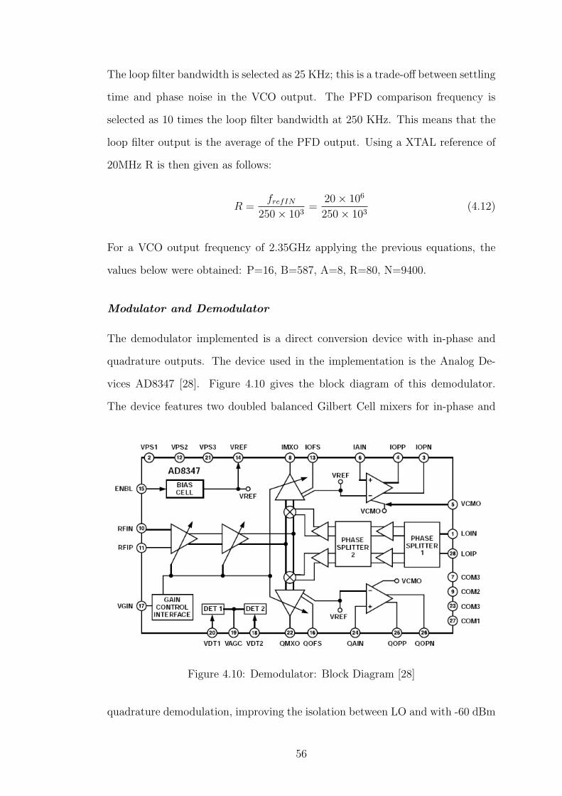
The loop filter bandwidth is selected as 25 KHz; this is a trade-off between settling
time and phase noise in the VCO output. The PFD comparison frequency is
selected as 10 times the loop filter bandwidth at 250 KHz. This means that the
loop filter output is the average of the PFD output. Using a XTAL reference of
20MHz R is then given as follows:
R =frefIN
250× 103=
20× 106
250× 103(4.12)
For a VCO output frequency of 2.35GHz applying the previous equations, the
values below were obtained: P=16, B=587, A=8, R=80, N=9400.
Modulator and Demodulator
The demodulator implemented is a direct conversion device with in-phase and
quadrature outputs. The device used in the implementation is the Analog De-
vices AD8347 [28]. Figure 4.10 gives the block diagram of this demodulator.
The device features two doubled balanced Gilbert Cell mixers for in-phase and
Figure 4.10: Demodulator: Block Diagram [28]
quadrature demodulation, improving the isolation between LO and with -60 dBm
56

leakage into the RF path for and LO input of -8 dBm. The mixers are driven by
a pair of LO signals with 90 degrees in phase difference. This devices operates
across a frequency band from 800 to 2700 MHz. The device has a high third order
intercept point at 11.5 dBm. This also has two baseband amplifiers which may
be used to amplify the signal after filtering. However, in this case, in order to
reduce noise and the baseband output offset voltage the signal is amplified using
differential amplifiers off-chip. The off-chip amplifiers are implemented as active
filters with gain as detail in previously in section 4.5.
A high quality quadrature modulator is used, the Analog Device AD8349. It
generates an output frequency range from 700MHz to 2700 MHz. The device
is composed of: a LO interface, a baseband voltage-current converter, two mix-
ers, differential to single ended amplifiers and bias circuit. The device uses two
Gilbert cells as up-converted. It has an IQ amplitude balance of 0.1 dB and a
quadrature error of 1.9o. The block diagram of the chip is presented in Figure
4.11.
Figure 4.11: Modulator: Block Diagram [29]
4.7 Conclusions
This chapter has documented the ADC, DAC, modulation and demodulation and
baseband filtering and amplification sections of the platform design. Commercial
57

off-the-shelf components have been used to implement this section of the platform.
Most of the specifications are met with these devices, however the reconfigura-
bility of the system needs to be improved. For example while the demodulator
and modulator can operate across a frequency range from 800 MHz to 2.5 GHz,
the synthesizer can only operate across a range from 2.05 GHz to 2.45 GHz.
Currently no commercial part is available to operate across the full band. The
design presented in this chapter is an implementation of an SDR system which
meets the required specifications within the limitations of commercially available
components.
58

Chapter 5
RF FILTERING
5.1 Introduction
This chapter describes design and implementation for the filters needed in the
front-end of the platform. An RF filter is required at both the input to the
receiver and at the output from the transmitter. These act as band select filters.
The filter at the reciver input is responsible for attenuating unwanted out of band
signals. The filter at the output from the transmitter is responsible for suppressing
spurious transmissions. Ideally these filters would be reconfigurable in both center
frequency and bandwidth. However no such filters exist commercially, thus for
this platform a compromise has been reached. As reconfigurable RF filters are
not possible with current technologies the filter implemented here is a broad band
static filter. This places extra filtering requirements on the baseband section,
limits the blocker performance of the receiver, and requires high linearity from
the transmitter power amplifier. In both cases the filter is implemented using
microstrip coupled lines. The design steps and implementation for these filters
are presented in this chapter.
59

5.2 Overview of Filter Design
The filter design is carried out as follows. Firstly a specification for the required
filter is developed. Once this is known a suitable low pass filter prototype is
selected such as Chebyshev, Butterworth or Bessel for example. Once the proto-
type filter is selected the filter order required is determinate. The prototype filter
transfer function coefficients are then calculated. Finally these are transformed
to the equivalent band pass filter and suitably impedance scaled. Once the the-
oretical filter is designed a suitable implementation is chosen. In order to meet
the implementation requirements of this platform these filters must be small in
size and low cost.
5.3 Specifications
The specifications for this filter are driven by the blocker specifications of the re-
ceiver. This project has available two frequency bands licensed for test purposes.
It is for this reason that the filters have been centered in these bands rather
than more typical commercial communication bands. However they have been
designed to meet the blocker specifications of the standards previously mentioned
in chapter 3. The two test frequencies are: 2.08GHz and 2.35GHz with 25MHz
of bandwidth each. The filter specifications are described as follows:
1. Lower cutoff frequency: fL−3dB = 2.008GHz
2. Upper cutoff frequency: fU−3dB = 2.422GHz
3. Center frequency: f0 = 2.105GHz
4. fL−20dB = 1.95GHz
5. fU−20dB = 2.48GHz
60

f L−20dB f L−3dB f U−20dBf U−3dB
0dB
−3dB
−20dB
−40dBfo frequency
Gai
n
Figure 5.1: Filter Mask.
5.4 Filter Prototype
There are several possible filter prototypes are: Chebyshev, Butterworth, Bessel
and Gaussian filters. The Chebyshev filter has very good stop band attenuation
however it has ripple in the pass band. The Butterworth filter is maximally flat
in the pass band but it does not have as good stop band attenuation as the
Chebyshev filter. However both of these filters do not have flat group delay. The
Gaussian filter has flat group delay but at the expense of poor stop band attenua-
tion. The Bessel filter aims to improve on this by allowing some group delay ripple
resulting in improved stop band attenuation. The important parameters for the
filter for our application are gain flatness in the pass band and a good group
delay characteristic. The Butterworth filter offers the best compromise, and was
chosen to be implemented here. The Butterworth characteristic function is given
as follows [30]:
A(w)2 =1
1 + K(w)2(5.1)
The approximation for the characteristic function can be defined as :
K(w) = wn (5.2)
61

The magnitude of the transfer function is given as:
| H(jw) |2 =G2
0
1 + ( ωωc
)2n(5.3)
where n is the order of the filter, wc is the cutoff frequency or -3dB frequency for
the low pass prototype and G0 is the DC gain of the filter. The required order of
the filter is determined from the equation:
As ≥ 1√1 + w2n
s
(5.4)
In doing so the following assumptions for the Butterworth filter are made: the
pass band edge is mapped to ωc = 1. The remaining parameter to be calculated
is the low pass equivalent stop band edge frequency. This is given as follows:
ωs =ω2
U−20dB − ω20
B × ωU−20dB
(5.5)
where ωs is the frequency for which the stop band attenuation is given, ω0 is the
center frequency given by ω0 =√
ωL × ωU , B is the band pass bandwidth. Thus
this results in 20dB attenuation at ωs = 5.9903rad/s. With this value the order
of the filter, n, is calculated using the following equations:
n ≥ log[1/(A2s)]− 1
2log(ws)(5.6)
Using the last equation and specifications for the filter the obtained value for n
is 6. In order to calculate the transfer function H(s) the previous expression can
be transformed as:
H(s)H(−s) =G2
0
1 + (−s2
ω2c
)n(5.7)
The resulting filter must be unconditionally stable, to achieve the filter polynomial
must be Horwitz. This equates to all the poles of the transfer function being in
62

the left half ’s’ plane. The kth pole is given by:
sk = ωcej(2k+n−1)π)
2n (5.8)
Thus with the previous equation the Butterworth polynomials can be obtained as
the denominator of the following transfer function written in terms of its poles:
H(s) =G0∏n
k=1(s−sk)
ωc
(5.9)
Assuming that wc = 1 it is possible to calculate the poles of the analog Butter-
worth filter prototype, these are given below:
s1 = −0.2588 + j0.9659 (5.10)
s2 = −0.7071 + j0.7071 (5.11)
s3 = −0.9659 + j0.2588 (5.12)
s4 = 0.9659− j0.2588 (5.13)
s5 = −0.7071− j0.7071 (5.14)
s6 = −0.2588− j0.9659 (5.15)
Multiplying these poles together the transfer function can be written as [30]:
Hs =1
s6 + 3.8637s5 + s4 + 7.4641s3 + 9.1416s2 + 7.4641s + 3.8637(5.16)
This is the transfer function of the low pass filter prototype. Regardless of how
the filter is to be finally implemented in hardware we require a prototype filter
implementation at this stage. The next step in this process is to synthesize a
circuit that implements this transfer function. A suitable filter topology is a
resistively terminated LC ladder structure. Component values for this may be
generated by continued fraction expansion of the driving impedance. This is de-
63

fined as the impedance looking into the input terminal when the output terminal
is terminated with a load resistor. For given filter orders there exist published
tables listing the element values [30] for normalized low pass filters. Figure 5.2
illustrates the general Π ladder network of a low pass filter prototype with the
following parameters: g0, g1, g2...gn+1.
Figure 5.2: Π Network Prototype.
Figure 5.3 gives the equivalent T filter implementation, where g0 to gn+1 are the
corresponding inductor and capacitor admittances in the low pass filter model.
Using published tables [30] the following 6th order filter element values are ob-
tained [26]: g1 = 0.52; g2 = 1.42; g3 = 1.93; g4 = 1.93; g5 = 1.42 and g6 = 0.52.
These coefficients are scaled to the desired center frequency and transformed to
a bandpass transfer function.
Figure 5.3: T Network Prototype
To transform from low pass configuration to bandpass, the equations below are
used:
∆ =ω2 − ω1
ω0
; ω0 =√
ω1ω2 (5.17)
For parallel elements:
Cp =Cn
ω0∆Z0
; Lp =Z0∆
ω0Cn
(5.18)
For series elements:
Cs =∆
ω0LnZ0
; Ls =Z0Ln
ω0∆(5.19)
64

The resulting values are: C1=3.97pF, L1=1.30nH, C2=0.19pF, L2=27.18nH,
C3=14.87pF, L3=0.35nH, C4=0.14pF, L4=37.18nH, C5=10.87pF, L5=0.48nH,
C6=0.52pF, L6=9.94nH
Figure 5.4: Bandpass Filter Prototype.
5.5 Filter Implementation
The filter may be implemented in several possible technologies. Among these
are lumped components implementation, microstrip coupled line implementa-
tion, strip line filters, SAW filters, metallic and dielectric cavities and distributed
resonator structure sections. The implementation of RF filters using lumped
component LC structures is difficult in this frequency range as the component
values are at the bottom end of the range of the available values and the wave
lengths involved are comparable to the dimensions of the required circuits. This
means that a distributed circuit treatment is required.
5.5.1 Overview to Microstrip Filters
Microstrip is a planar transmission line technology. It is the most popular ap-
proach for the realization of circuits in the 1 to 10 GHz range using printed
circuit board techniques. This is due to its characteristic of the low dispersion
at high frequencies, and its ease of integration with other passive and active mi-
crowave devices. A microstrip line is characterized by the following geometrical
parameters: W (conductor line width), T (conductor thickness) and H (substrate
thickness). The microstrip line is implemented as a conductor bonded to a di-
electric substrate [32]. This substrate is characterized by its relative permittivity,
65

εr, thickness, H and loss angle, tanδ. Since some of the fields generated by the
microstrip conductor exist in the air, the conductivity is also characterized by the
effective permittivity or effective dielectric constant, εe, which is directly related
to W/H and εr. The modes supported by microstrip lines are quasi-TEM due
the non simetrical structure of both the ground plane and the dielectric. It does
not support pure TEM waves since some of the field lines are in the air region
but most of them are in the dielectric region [26]. Figure 5.5 shows the field
distribution on a typical microstrip line.
Figure 5.5: Field Distribution of a Microstrip Line Section.
The substrate values used to simulate the filter prototypes is detailed below.
1. H = 0.4mm. Substrate thickness.
2. εr = 3.84. Relative dielectric constant.
3. Mur = 1. Relative permeatibility.
4. Cond = 1.0e50. Conductor conductivity.
5. Hu = 1.0e33. Cover height.
6. T = 0.035mm. Conductor thickness.
7. Tanδ = 0.017. Dielectric loss tangent.
8. Rough = 0mm. Conductor surface roughness.
9. Substrate = FR4
.
66

Figure 5.6: Substrate Parameters.
Some of the most common bandpass microstrip filters configurations are described
below:
1. Direct Coupled Resonator : This filter configuration uses λ/4 resonators
which are direct coupled using λ/4 transmission lines between adjacent
resonators. The impedance inverters are part of the resonators themselves
[31].
2. Direct Parallel Coupled : Parallel coupled lines are the most common con-
figuration used in microstrip filter design. However the lateral coupling
between the lines generates small spacing and small width which cannot
be accurately implemented. This is due to the nature of microstrip lines
which are not homogeneous and causes inequality between odd and even
mode phases [33]. This filter configuration uses λ/2 resonators with elec-
tromagnetic coupling between λ/4 sections [26].Figure 5.7 illustrates this
configuration.
Figure 5.7: Coupled Lines Layout.
3. Hairpin:Hairpin filters are coupled line filters. The orientation of hairpin
resonators alternates. This is because the electric and magnetic couplings
tend to add, resulting in the maximum coupling for a given spacing between
resonators. These have very similar characteristics to the parallel coupled
line filter configuration.
67

The length of the micrstrip lines which join each parallel couple line section
must at least λ/2 to avoid coupling between resonators. The filter configu-
ration is shown in Figure 5.8.
Figure 5.8: Hairpin Layout.
4. Combline Interdigital : This filter configuration uses λ/4 resonators which
are grounded at opposite ends for adjacent resonator. There is electromag-
netic coupling between resonators [26].
A small size filter is required for this platform. The area occupied by standard
couple line filters at these frequencies is too large. Normal hairpin structures
while occuping less space are still too large. For this platform a modified hairpin
structure is implemented. Simulation results have demonstrated that hairpin and
coupled line filters have very similar frequency response. Thus, the calculations
to generate parallel coupled line configurations are used to simulate the coupled
line filter and are implemented in a hairpin filter prototype. The next section
presents the design and simulations for the preselection filter using the equations
for microstrip lines and coupled line prototype filters.
Coupled Line Filter Theory
An N+1 coupled line bandpass filter is composed of N+1 admittance inverters,
J . Each coupled line corresponds to a transmission line network of -90o. The
equivalent model for each coupled line is shown in Figure 5.9. Impedance and
admittance inverters have the ability to transform series inductances to shunt ca-
pacitances and shunt capacitances to series capacitances. Thus, in this case the
68

Figure 5.9: Coupled Line Equivalent Prototype.
admittance inverters are separating parallel circuits. The admittance produced
from the J inverter can be defined as follows:
Y ′ =J2
Y0
(5.20)
In order to calculate the parameter J for each network the equations below are
used [26]:
J1
Y0
=J7
Y0
=
√πBw
2g1
=
√πBw
2g1
;J3
Y0
=J5
Y0
=πBw
2√
g3g5
(5.21)
J2
Y0
=J6
Y0
=J4
Y0
=πBw
2√
g2g1
=πBw
2√
g4g3
(5.22)
Assuming a Z0 of 50Ω the corresponding even and odd impedances are obtained
[26]:
Zoe = [1 + JZ0 + (JZ20)] (5.23)
Zoo = [1− JZ0 + (JZ20)] (5.24)
Zoe1 = Zoe7 = 1532; Zoe2 = Zoe6 = 345 (5.25)
Zoe3 = Zoe5 = 97.68 Zoe4 = 72.93 (5.26)
Zoo1 = Zoo7 = 1454.5; Zoe2 = Zoe6 = 308.9 (5.27)
Zoe3 = Zoe5 = 78.99 Zoe4 = 56.94 (5.28)
69

Using the impedances for each pair of coupled lines and knowing the charac-
teristic impedance of the line, the width, spacing and length can be calculated.
However due to the broadband characteristics of this filter and its expected low
insertion loss the obtained values for odd and even mode impedances in the two
outside coupled lines are particularly large of the orther of kohms. This results in
microstrip lines that are too narrow to manufacture. To solve this issue the filter
was redesigned without the requirement of 50Ω characteristic impedance in the
coupled line sections. However there are still some sections of the filter that are
not manufacturable. This filter is shown in Figure 5.11 and the corresponding
parallel coupled line model is shown in Figure 5.10. It can be seen for this figure
Figure 5.10: 6th Order Parallel Coupled Line Filter.
that the two outer most sections have a spacing of less than 0.15 mm, which is the
minimum spacing that we can manufacture. The design was done for a 6th order
direct coupled line filter which results in 7 couple lines sections, N+1. The two
outer most coupled line sections were replaced with discrete component sections.
The spacing for the second outer most coupled line section was adjusted to 0.16
mm and the width of that coupled line reoptimized.
70

Figure 5.11: 6th Order Parallel Coupled Line Filter.
This filter was then layed out in a modified hairpin configuration. Fig-
ure 5.12 shows the filter layout. This layout was then simulated in ADS using
Figure 5.12: 6th Order Hairpin Filter with Passive Network Substituying Firstand Last Sections .
co-simulation techniques for the coupled lines within ADS. The filter is built on
the FR4 0.4mm material. The filter response was then measured using a vector
network analyzer. Simulating and measured results are shown in Figure 5.13. It
is reflected in the input and output reflexion coefficients. The transfer character-
istic of the filter, S21, matches within 1.5dB. Similarly the reflection coefficient,
S11, matches also. Due to the losses in the used substrate the insertion loss of
the filter is approximately 5dB, while the lower edge of S11 is marginaly worse
than exopected. This can be improved with a lower loss substrate other than
FR4, such as RO4003 from the Rogers corporation.
71
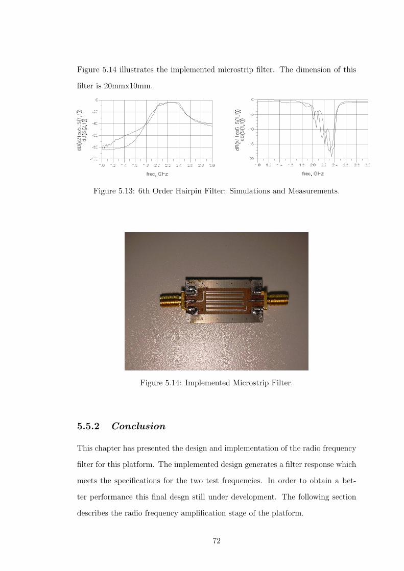
Figure 5.14 illustrates the implemented microstrip filter. The dimension of this
filter is 20mmx10mm.
Figure 5.13: 6th Order Hairpin Filter: Simulations and Measurements.
Figure 5.14: Implemented Microstrip Filter.
5.5.2 Conclusion
This chapter has presented the design and implementation of the radio frequency
filter for this platform. The implemented design generates a filter response which
meets the specifications for the two test frequencies. In order to obtain a bet-
ter performance this final desgn still under development. The following section
describes the radio frequency amplification stage of the platform.
72

Chapter 6
RF AMPLIFICATION
6.1 Introduction
In this chapter the transmitter and receiver RF amplification circuits are de-
scribed. In order to maximize the received and transmitted powers it is necessary
to match LNA and PA impedances to the antenna. This is achieved with a
matching network. In the case of the receiver the amplification circuit consists of
an LNA (low noise amplifier) device and external matching networks Similarly in
the case of the transmitter, this consists of a power amplifier(PA) chip and the
external matching networks along with a VGA (variable gain amplifier) to allow
transmitted power control.
6.2 Overview
The LNA was chosen for its linearity and low noise figure in the band of interest
while the PA was chosen for its efficiency and linearity. Both these ICs required
design of a suitable matching network. This is designed by representing the
reflected power at the input and output ports of the device using S (Scattering)
parameters and then selecting networks which minimize this reflected power. Any
N port network may be described by its N2 S parameters. The S parameters relate
the incident voltage waves on the ports to those reflected from the ports of the
73

network [26]. Thus, an example of an S parameter matrix is described below.
V1−
V2−
...
Vm−
=
S11 S12 . . . S1n
S21 S12 . . . S2n
......
......
Sm1 . . . . . . Smn
V1+
V2+
...
Vn+
Then, each element of the S matrix can be described as:
Smn =Vm
−
Vn+ (6.1)
Where Vm− is the reflected voltage at the input port m and Vn
+ is the transmitted
voltage at the output port n. Hence, Smm is the reflection coefficient of each port
and Smnis the transmission coefficient from port m to port n. Therefore the
transmitted and reflected power can be calculated employing these coefficients
[26]. If the circuit is considered as a 2 port network,S11, S22, S12, S21 are the
parameters to be measured, where:
1. S11: Input Return Loss
2. S22: Output Return Loss
3. S12: Isolation Coefficient
4. S21: Transmission Coefficient
S11 is a measure of the reflected power at the input. In order to achieve a good
match it is necessary to minimize S11, and in doing so maximize the amount
of power entering the network. Similarly S22 measures the reflected power at
the output port. Minimizing this parameter maximizes the transmitted power
available at the antenna in the transmitter. S21 is representing the forward gain
in the network. In the case of an amplifier this is its gain. S12 represents the
transmitted power from the output to the input of the network. If the network
is reciprocal S12 = S21.
74

The design of the matching network for the LNA is particularly complicated.
This is due to the fact that the LNA also requires optimum input impedances
for maximum signal power transform and minimum self noise generation. Due
to this, a no conjugated matching network in the input and output port may
provide the best trade-off between gain and noise figure.
On the other hand, for the transmitter maximum power is required. Thus con-
jugated impedance matching at the input and output of the PA is needed. The
maximum available gain, MAG, which can be attained under conjugated condi-
tions. MAG is described below [26].
MAG = 10 log| S21 || S12 | + 10 log K −
√K2 − 1 (6.2)
Where K is stability factor of the amplifier given by:
a = S22S11 (6.3)
b = S12S21 (6.4)
∆ = a− b (6.5)
K =1− |S11|2 − |S22|2 + |∆|2
2S11S22
(6.6)
The amplifier is unconditionally stable for K > 1. Figure 6.1 illustrates the
matching network configuration for a 2-port network. In order to obtain a con-
jugate match, ρ1 has to be the complex conjugated of Γin. Equally ρ2 has to
be the complex conjugated of Γout, where Γin and Γout are the input and output
Figure 6.1: Matching Networks.
75

reflexion coefficients respectively, and are given by equations 6.7 and 6.8:
Γin = S11 +S12S21ρ2
1− S22ρ2
(6.7)
Γout = S22 +S12S21ρ1
1− S11ρ1
(6.8)
where the reflexion coefficients are defined as the amplitude of the reflected volt-
age wave normalized to the amplitude of the incident voltage wave [26].
6.3 Low Noise Amplifier
6.3.1 Specifications
The LNA as its name suggests is an amplifier with a very low noise figure. From
the point of view of the Friis equation the LNA has the greatest effect on the
total noise figure of the system since it is the first amplification stage of the
signal. Consequently the noise figure of the LNA must be kept to the minimum
possible. The noise figure of the LNA and the thermal noise at the antenna
define the sensitivity of the system. The LNA must provide enough gain to allow
the mixer to demodulate the required reference sensitivity signal. The output of
the LNA must be within the dynamic range of the input of the mixer to avoid
amplitude mismatch. In this way the signal, after the downconversion stage, will
have large enough amplitude for the required dynamic range of the ADC’s. The
LNA is specified by the following parameters:
1. Gain: It is the ratio between the output power and the input power in the
LNA.
2. Noise figure: It is the ratio between the output SNR and the input SNR.
It is a measure of the noise contributed by the LNA.
3. Linearity: The ability of the amplifier to linearly increase the output signal
in line with the input signal. The gain of the amplifier drops off for larger
76

input signal causing distortion. This effect is characterized by the IIP3 and
3dB gain compression point.
4. Input impedance: This is the impedance seen looking into the input port
of the amplifier with a loaded output.
5. Dissipated power: This is the difference between the DC power inputted
and the RF power outputted. This depend of the architecture and technol-
ogy used in its implementation.
The required values for these parameters have been given in chapter 3. This
influences in the performance of the rest of the system. The bandwidth of the
LNA amplifier must also meet the bandwidth requirements of the receiver. As
previously stated the maximum gain with minimum noise is required from the
LNA. Generally the maximum gain and minimum noise do not occur at the same
operating point. For this reason a compromise is reached where an operating
point is chosen to give the best SNR and linearity at the output of the LNA.
Device manufacturers publish noise and gain circles to facilitate this.
Design and Implementation
The chosen LNA was the Freescale Semiconductor MBA13720. This device fea-
tures a gain of approximately 12dB with an optimum noise figure of 1.55dB. It
works in a frequency range from 400 MHz to 2.4 GHz. The LNA can work in three
modes: bypass, low IP3 and high IP3 modes [34]. Generally, the best noise figure
is achieved working in the low IP3 mode although the high IP3 mode achieves a
better gain but only by 1 dB. The LNA has a bypass switch which may be used to
minimize the loss between bypass and amplifier modes. The LNA S parameters
77

at 2.35 GHz are as follows [34].
S11 = 0.4479∠−470 (6.9)
S12 = 0.1494∠810 (6.10)
S21 = 3.322∠66.20 (6.11)
S22 = 0.6082∠−38.40 (6.12)
In order to ensure unconditional stability | Γin |< 1 and | Γout |< 1. Therefore
the stability of the LNA also depends on the external matching networks. Since
the stability conditions of a network are frequency dependent [26], the amplifier
may be perfectly stable at the working frequencies and unstable at surrounding
frequencies. Stability circles may be used to plot the regions of stable operation
on the Smith chart. Alternatively the stability factor K can be defined as it is
given in 6.13below [35].
K =1− |S11|2 − |S22|2 + |∆|2
2S11S22
(6.13)
a = S22S11 (6.14)
b = S12S21 (6.15)
∆ = a− b (6.16)
LNAK = 1 (6.17)
(6.18)
where LNAK is called the Linvill stability factor with the matching networks
shown Figures 6.2. For unconditionally stable operation the parameters must
achieve: K ≥ 1 [26]. However in this case the amplifier is working in its condi-
tionally stable zone because K = 1.
Figure 6.2 gives the diagram of the implemented LNA circuit including the match-
78

ing elements. Figure 6.3 gives the simulated response of this circuit. It can be
seen from Figure 6.3 that the gain at 2.08GHz is approximately 12dB while the
return loss is approximately -13dB. The gain drops to 10dB at 2.35GHz while the
return loss is approximately -12dB.
Figure 6.2: LNA.
Figure 6.3: LNA Respond.
6.4 Power Amplification Stage
Due to the requirements to support a variety of protocols high linearity together
with a large output power range are needed. For this reason the power ampli-
fication stage consists of a VGA, variable gain amplifier, under software control
followed by a fixed gain PA. This configuration offers the best flexibility and
efficiency compromise.
79

Design and Implementation
The implemented PA in the platform is a broadband GaAs power amplifier, which
works in the frequency band from 500 MHz to 6 GHz. This is the Agilent part
MGA-83563. This device generates an efficiency figure for maximum output
power of 37%, which meets the specifications. In addition the isolation produced
by the PA is approximately -38 dB. Figure 6.4 illustrates the PA design. The
input to this PA is power controlled by a VGA, which features a gain from -40dB
to 16 dB in a voltage range from 0V to 1.4V at its input.
The VGA device is the Analog Devices ADL5300. It is a high linearity am-
plifier which performs a linear-in-dB amplification with a gain control slope of
20mV/dB. The maximum input voltage is 1.4 V which generates a maximum
gain of approximately 20dB. The minimum input voltage is 0.2 which results in a
gain of -40dB. The device is able to operate up to 3GHz. The output impedance
of the VGA is 50 ohm in order to match the input impedance of the PA.
In order to calculate the external matching networks for the PA, the internal
S parameters described below are used.
S11 = 0.40∠−360 (6.19)
S12 = 0.024∠680 (6.20)
S21 = 11.07∠−820 (6.21)
S22 = 0.49∠−1750 (6.22)
The resulting external matching networks are presented in Figure 6.4. This is
achieved with a combination of microstrip lines and discrete components. This
model has been simulated in the ADS simulation environment to obtain the gain
response and linearity of the amplifier shown in Figure 6.5. The gain on the
PA is flat across the band of frequencies of interest at approximately 24dB. The
80
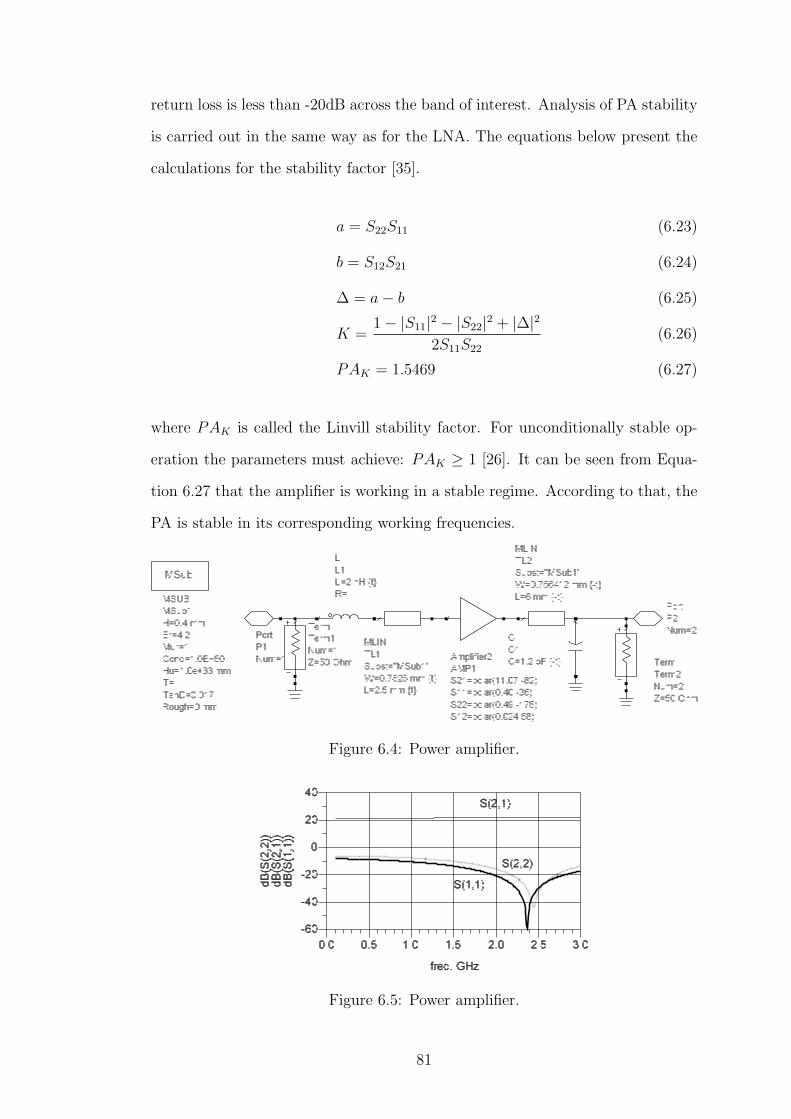
return loss is less than -20dB across the band of interest. Analysis of PA stability
is carried out in the same way as for the LNA. The equations below present the
calculations for the stability factor [35].
a = S22S11 (6.23)
b = S12S21 (6.24)
∆ = a− b (6.25)
K =1− |S11|2 − |S22|2 + |∆|2
2S11S22
(6.26)
PAK = 1.5469 (6.27)
where PAK is called the Linvill stability factor. For unconditionally stable op-
eration the parameters must achieve: PAK ≥ 1 [26]. It can be seen from Equa-
tion 6.27 that the amplifier is working in a stable regime. According to that, the
PA is stable in its corresponding working frequencies.
Figure 6.4: Power amplifier.
Figure 6.5: Power amplifier.
81

6.5 Conclusion
The implemented designs of the LNA and PA are described in detail in this chap-
ter. The circuit’s topologies and components values for the matching networks
of the amplifiers are presented. The simulated performance of both implementa-
tions is given including stability calculations and the resulting complete circuit
diagrams are given.
82

Chapter 7
CONSTRUCTION AND
TESTING OF THE
RECONFIGURABLE RADIO
TESTBED
7.1 Introduction
This chapter presents some of the details of the physical implementation for this
platform followed by some operational examples. An overview of the materials
and technology used in the construction of the board is given. Some of the
implementation problems overcome during fabrication are detailed. It gives an
overview about the available technology used for the realization of the software
defined radio system. It presents as well, some of the implementation issues during
the fabrication. Schematics and layouts for receiver, transmitter and baseband
board are shown. Some test results detailing the performance of the system are
given. Finally some plots resulting from the Matlab implemented software are
given at the end of this chapter.
83

7.2 Devices and Equipment
A variety of equipment and technologies are used in this platform. The integrated
circuits are implemented using CMOS, BICMOS and GaAs semiconductor tech-
nologies. Standard PCB (printed circuit board) techniques are used to construct
the prototypes with additional microstrip technique for certain elements of the
design. Table 7.1 presents a list of the integrated circuits used in the signal and
control paths. In the table part number, manufacturer, package, and frequency
range are given. Details of the system level layout of these components are given
in Figure 4.1 in chapter 4.
Table 7.1: Commercial devices used
Surface mount technology, SMT, is used exclusively in the construction of the
platform. The principal advantages of SMT over through hole techniques are [1]:
smaller components, placement of components over the two sides of the board
and better mechanical performance. The main disadvantage of SMT technol-
ogy is component handling. While SMT facilitates the construction of smaller
systems, this is achieved using smaller device packages. As the package size is
84

reduced these devices become more difficult to accurately mount and test.
7.3 Materials
The implementation of the whole system is realized using PCB technology. This
consists of metal layers separated by a dielectric. The dielectric used for the base-
band PCBs is FR4 (flame-retardardant formulation number 4). FR4 consists of
glass fibre woven material impregnated with epoxy resin. It is specified by its me-
chanical strength, dielectric breakdown voltage, dielectric constant and dielectric
loss angle. Standard FR4 material has a dielectric constant of 4.2, however this
changes with frequency. Also the dielectric loss displays a linear increase with
frequency in this material. Typically FR4 exhibits a loss of 0.03dB/cm/GHz for
microstrip lines implemented with 1.6mm thick material. This implies a constant
loss per wavelength at any frequency of 0.5dB/wavelength [32]. While this has
little or no bearing on sub GHz operation, it has significant affect at the frequen-
cies of our design. Where RF signals are concerned the PCB traces are designed
as controlled impedance lines. The principle type of controlled impedance line
implemented in this design is a microstrip line. The performance of the microstrip
line is affected by the physical and electrical characteristics of both the dielectric
and conductor materials. Poor design of the transmission lines for the desired fre-
quency will result in impedance mismatches which will generate reflected power,
reducing the overall SNR of the system.
Due to the loss nature of FR4, in order to reduce the losses at RF frequen-
cies a smaller thickness material is used. In this case 0.4mm thick FR4 is used.
This is possible as the RF boards are implemented separately from the basband
board.
85

7.3.1 Implementation Problems
The RF connections are implemented using microstrip lines. Some of the main
qualities of microstrip lines are: small dimension, low cost production, wide range
of characteristic impedance and working frequencies up to 110 GHz. However
this technology has the disadvantage of high loss due to the skin effect, radiation
losses, conductor losses and dielectric losses. The skin effect is the tendency
of the current to flow on the surface of the conductor as the signal frequency
increments [26]. Also, due to the structure of microstrip lines they do not exhibit
a true TEM transmission mode so the design equations are empirical. For these
reasons electromagnetic modelling of these structures is necessary. This was done
using the electromagnetic 2.5D solver, Momentum from Agilent. This allows us
to identify and avoid such a problems as: EMI(electromagnetic interference),
capacitive coupling (cross talk), collapsed feed lines (Rail collapse), substrate
coupling and reflexions due to bad matching. Figure 7.1 shows some of these
principal issues generated in the implementation of RF systems.
Figure 7.1: Distortion Sources.
These problems are solved with the addition of suitable filters and careful circuit
layout. For instance to decrease the noise at the output of the DC converter a
π section noise filter is used. In addition, in the RF receiver and transmitter a
metal can is place around various sections such as the LNA and VCO to provide
screening which increases the isolation between parts. This also improves the
86
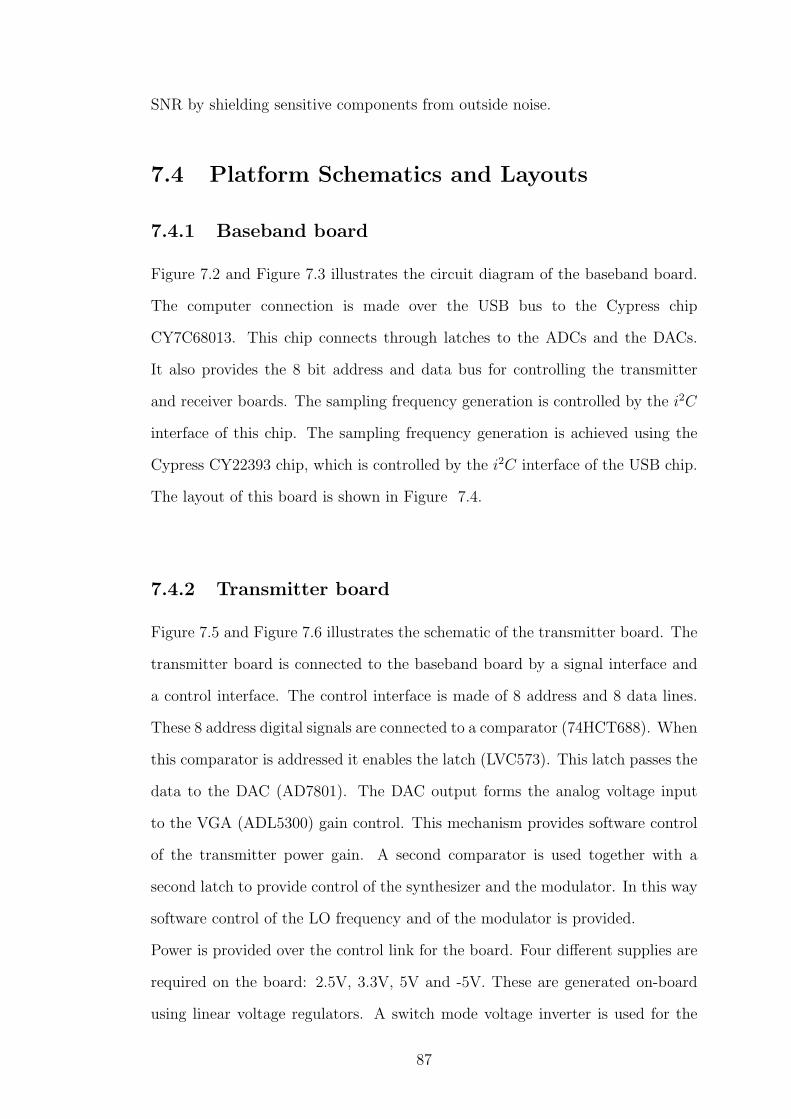
SNR by shielding sensitive components from outside noise.
7.4 Platform Schematics and Layouts
7.4.1 Baseband board
Figure 7.2 and Figure 7.3 illustrates the circuit diagram of the baseband board.
The computer connection is made over the USB bus to the Cypress chip
CY7C68013. This chip connects through latches to the ADCs and the DACs.
It also provides the 8 bit address and data bus for controlling the transmitter
and receiver boards. The sampling frequency generation is controlled by the i2C
interface of this chip. The sampling frequency generation is achieved using the
Cypress CY22393 chip, which is controlled by the i2C interface of the USB chip.
The layout of this board is shown in Figure 7.4.
7.4.2 Transmitter board
Figure 7.5 and Figure 7.6 illustrates the schematic of the transmitter board. The
transmitter board is connected to the baseband board by a signal interface and
a control interface. The control interface is made of 8 address and 8 data lines.
These 8 address digital signals are connected to a comparator (74HCT688). When
this comparator is addressed it enables the latch (LVC573). This latch passes the
data to the DAC (AD7801). The DAC output forms the analog voltage input
to the VGA (ADL5300) gain control. This mechanism provides software control
of the transmitter power gain. A second comparator is used together with a
second latch to provide control of the synthesizer and the modulator. In this way
software control of the LO frequency and of the modulator is provided.
Power is provided over the control link for the board. Four different supplies are
required on the board: 2.5V, 3.3V, 5V and -5V. These are generated on-board
using linear voltage regulators. A switch mode voltage inverter is used for the
87

output+
output-
output+
output-ADC
ADC
74LV
CH16
373A
74LV
CH16
373A
OE
P$9
2
1Q1
P$5
8
1Q2
P$5
9
GND
P$8
4
1Q3
P$6
0
1Q4
P$6
1
VCC
P$9
3
1Q5
P$6
2
1Q6
P$6
3
GND2
P$8
5
1Q7
P$6
4
1Q8
P$6
5
2Q1
P$7
6
2Q2
P$7
7
GND3
P$8
6
2Q3
P$7
8
2Q4
P$7
9
VCC1
P$9
4
2Q5
P$8
0
2Q6
P$8
1
GND4
P$8
7
2Q7
P$8
2
2Q8
P$8
3
2OE
P$7
52L
EP$7
4
2D8
P$7
3
2D7
P$7
2
GND5
P$8
8
2D6
P$7
1
2D5
P$7
0
VCC2
P$9
5
2D4
P$6
9
2D3
P$6
8
GND6
P$8
9
2D2
P$6
7
2D1
P$6
6
1D8
P$5
6
1D7
P$5
5
GND7
P$9
0
1D6
P$5
4
1D5
P$5
3
VCC6
P$9
6
1D4
P$5
2
1D3
P$5
1
GND11
P$9
1
1D2
P$5
0
1D1
P$4
9
1LE
P$5
7
VDD
P$9
VDD1
P$8
VDD2
P$5
VDD3
P$4
VDD4
P$3
OVDD
P$1
4OVDD1
P$1
3OVDD2
P$1
2OVDD3
P$1
1
GND
P$4
8GND1
P$3
8GND2
P$3
7GND3
P$3
6GND4
P$3
1OGND
P$2
5OGND1
P$2
4OGND2
P$2
3OGND3
P$1
5
1 P$1
2 P$2
6 P$6
7 P$7
10 P$10
16 P$16
17 P$1727P$27
28P$28
29P$29
30P$30
32P$32
33P$33
34P$34
26P$26
22P$22
18 P$18
19 P$19
20 P$2021P$21
35P$3
5
39P$3
9
46P$4
6
47P$4
7
45P$4
5
44P$4
4
43P$4
3
42P$4
2
41P$4
1
40P$4
0
R20A R20A1
C49
A
R19A C55A
C56A
I9C51A
VDD
P$9
VDD1
P$8
VDD2
P$5
VDD3
P$4
VDD4
P$3
OVDD
P$1
4OVDD1
P$1
3OVDD2
P$1
2OVDD3
P$1
1
GND
P$4
8GND1
P$3
8GND2
P$3
7GND3
P$3
6GND4
P$3
1OGND
P$2
5OGND1
P$2
4OGND2
P$2
3OGND3
P$1
5
1 P$1
2 P$2
6 P$6
7 P$7
10 P$10
16 P$16
17 P$1727P$27
28P$28
29P$29
30P$30
32P$32
33P$33
34P$34
26P$26
22P$22
18 P$18
19 P$19
20 P$2021P$21
35P$3
5
39P$3
9
46P$4
6
47P$4
7
45P$4
5
44P$4
4
43P$4
3
42P$4
2
41P$4
1
40P$4
0
R20A2 R20A3
C49
A1
R19A1 C55A1
C56A1
I1C51A1
GND
GND
GND
10k 10k
GND
0.1u
F
+3V310k
VcM100pF
100pF
GND
GND
10k100pF
VcMGND
10k 10k
GND
0.1u
F
+3V310k
VcM100pF
100pF
GND
GND
10k100pF
VcM
+3V3
Figure 7.2: Baseband schematic.
88

d0d1d2d3d4
d5d6d7
a0a1a2a3a4a5a6a7
DAC
24lc64
74HC1G
04
USB
Array
EEPROM
++
1 2
ON
C44
C46
21
Q2
69CTL0/*FLA
GA
6970CTL1/*FLA
GB
7071CTL2/*FLA
GC
7166CTL3
6667CTL4
6798CTL5
98
4RDY0/*SLR
D4
5RDY1/*SLW
D5
6RDY2
67R
DY3
78R
DY4
89R
DY5
91CLKOUT
111XTALOUT
1112XTALIN
12
14NC
1415NC
1516NC
16
101*WAKEUP
101
18DPLU
S18
19DMINUS
19
99RESET#
99
106INT5#
106
28INT4
2829T0
2930T1
3031T2
3132IFCLK
32RESERVED
33BKPT
34
39PSEN#
3940RD#
4041WR#
4142CS#
4236DE#
3835EA
35
2VCC 217VCC 1726VCC 2643VCC 4348VCC 4864VCC 6468VCC 6881VCC 81100VCC 100107VCC 10710AVCC 10
13AGND 133GND 320GND 2027GND 2749GND 4958GND 5865GND 6580GND 8093GND 93116GND 116125GND 125
82PA0/INT0#
8283PA1/INT1#
8384PA2/*SLO
E84
89PA3/*W
U2
8589PA4FIFOADR0
8990PA5/FIFOADR1
9091PA6/*PKTEND
9192PA7/*FLA
GD/SLC
S#
92
44PB0/FD0
4445PB1/FD1
4546PB2/FD2
4647PB3/FD3
4754PB4/FD4
5455PB5/FD5
5556PB6/FD6
5657PB7/FD7
57
72PC0/GPIFADR0
7273PC1/GPIFADR1
7374PC2/GPIFADR2
7475PC3/GPIFADR3
7576PC4/GPIFADR4
7677PC5/GPIFADR5
7778PC6/GPIFADR6
7879PC7/GPIFADR7
79
102P
D0/FD8
102
103P
D1/FD9
103
104P
D2/FD10
104
105P
D3/FD11
105
121P
D4/FD12
121
122P
D5/FD13
122
123P
D6/FD14
123
124P
D7/FD15
124
115P
E7/GPIFADR8
115
114P
E6/T2E
X114
113P
E5/INT6
113
112P
E4/RXD1O
UT
112
111P
E3/RXD0O
UT
111
110P
E2/T2O
UT
110
109P
E1/T1O
UT
109
108P
E0/T0O
UT
108
37SDA37
36SCL36
53RXD153
52TXD152
51RXD051
50TXD050
88D788
67D687
86D586
63D463
62D362
61D261
60D160
59D059
25A1525
24A1424
23A1323
22A1222
21A1121
1128A10128
127A9127
126A8126
120AA7120
119A6119
118A5118
117A4117
97A397
96A296
95A195
94A094
CY7C68013A
1 2 3 4
X1
R28A
R3A
R4A
84
SCL 6
SDA5
A0 1A1 2A2 3
VCC
GND
IC2
B11
49
B15
45
GND10
23
SELIQ
44GND
43
AVDD3.3-4
31
XOR
42
B12
48B13
47
A8
1
A7
2
A6
3
A5
4
A4
5
A3
6
OUTIP
29
/DORI
41
B9
51
B8
52
B7
53
B6
54
B5
55
B4
56
B3
57
B2
58
B0
60B1
59
MAX-1
B10
50
DVDD
61
A15
62
A14
63
A13
64
A12
65
A11
66
A10
67
A9
68
B14
46
GND13
13
AVDD3..3-6
21
GND11
20
OUTIN
28
GND5
36
GND6
33
DUTQP
25
DUTQN
24
GND7
30
AVDD3.3-3
32
PD
40
TORB
39
CLKP
38
CLKN
37
AVCLK
35
AVDD3.3-7
14
AVDD1.8
34
GND8
27
AVDD1.8-2
19
DACREF
18
FSADJ
17
REFIO
16
GND9
26
AVDD3.3-5
22
GND12
15
DVDD3.3
11A2
7
A1
8
A0
9
GND14
12
GND15
10
C11
C12
C14
C15
R21
R22
R23 R50
R55
R56
R66
R67
R68
TR6 C
17
C19
C22
C23
C62C63
C64
C65
C66
C67
C69
C70
C71C72
L1
TR8
1234 5 6
TR9
TR11123
4 5 6 TR12
OUTPUI OUTPUTQ
CLK_GND
C8
P$1
P$1
P$2
P$2
P$3
P$3
P$4
P$4
P$5
P$5
P$6
P$6
P$7
P$7
P$8
P$8
P$9
P$9
P$10
P$10
P$11
P$11
P$12
P$12
P$13
P$13
P$14
P$14
P$15
P$15
P$16
P$16
R5A
R6A
C20A
R2A
341 2
SW1
R1A
C19A
R27A
12IC1A
12p
12p
24Mhz
GND
GND
GND
GND
10k
2k2
2k2
24-LC65SM
+3V3
+3V3
MAX5875-2
1uF0.1uF
49.9 49.9
100ohm
49.9
100ohm
49.9
1uF
AGND
AGND
AGND
AGND
AGND
AGND
AGND
AGND
AGND
AGND
AGND
AGND AGND
DGND
DGND
DGND
DGND
CLKGND CLKGND CLKGND
CLKGND
+3V3
+3V3
+3V3
DVDD3.3
AVDD1.8
DVDD1.8 DGNDDGND
DGND
AVDD1.8
AGND
AGND
DVDD1.8
GND
10kGND
10kGND
1uF
100k
GND
100k
10uF
GND
+3V3
10k
4069D
+3V3
+3V3
GND
GND
Figure 7.3: Baseband schematic.
89

Figure 7.4: Baseband Board.
generation of -5V which supplies the differential amplifiers(AD8132). The layout
of the transmitter board is shown on figure 7.7
7.4.3 Receiver
Figure 7.8, Figure 7.9 and Figure 7.10 illustrate the schematics for the receiver
platform. As on the transmitter side, on the receiver the comparator is connected
to the 8 bit address bus. When the received address is equal to the assigned
address the comparator enables the latch (74HCT688). The latch connects the
digital control signals, each corresponding enable inputs on the different chips
on the board. Four different supply sources are utilized for this board: 2.5V,
3.3V, 5V and -5V. Again the power is supplied over the control interface. Linear
voltage regulators are again used for the generation of these supplies. A switch
mode voltage regulator is used for the generation of -5V used on the differential
amplifiers (AD8132). The layout of the receiver board is shown on Figure 7.11.
7.5 Software
As this platform is built for SDR there are significant software elements through
the system. These elements perform several functions, some of them perform
hardware control functions such as changing the desired center frequency or out-
put power levels, while others implement the interface between the PC and the
90

Data Bu
s
Addre
ss Bus
AD8132
AD8132
SMA
SMA
SMA
SMA
AD8349
PhaseSplitter
BiasMultiplexer
Multiplexer
VCOStage
1/2Counter
Output
14-Bit
ChargePump
Lock Detect
PreScaler
Control
ADF4360-1
74AH
C1G0
4
74HCT688
74ABT843
R3R5R6 R7
VIN-
1
VIN+
8
VOCM
2
VOUT
-5
VOUT
+4
V+3 V- 6
VIN-
1
VIN+
8
VOCM
2
VOUT
-5
VOUT
+4
V+3 V- 6
PIN
2
GND 1
PIN
2
GND 1
PIN
2
GND 1
PIN
2
GND 1
GND
GND
GND
GND
R1 R2
GND
R4R8 R9 R10R12
R13
C1 C2C5C6 GN
D
GND
C7 GND
C8
GND
R15
R16
C3 C4
IBBP1
IBBN2
COM13
LOIN5
LOIP6
VPS17
ENOP8 COM2 9
COM3 10
VOUT 11
VPS2 12
COM3A 13
COM3B 14
QBBN 15
QBBP 16
COM1A4
GND
GND
GND
GND
GND
GND
CPGND 1
AVDD 2
AGND 3
RFOUTA 4
RFOUTB 5
VVCO 6
VTUN
E7
AGND
18
AGND
29
AGND
310
AGND
411
CC12
RSET13
CN14
DGND15
REF16
CLK17
DATA18
LE19
MUXO
UT20
DVDD
21
AGND
522
CE23
CP24
C9C1
0
L1
L2
L3L4
GND GND GND GND
GND
GND
GND
C11
C12
C13
R11
R14
GND
C14
GND
C15
R17
NC11
GND3
NC22
OUT 4
NC3 5
VCC 6
GND
C16
C17
R18
GND
GND
A2
Y4
VDD5
GND 3
GND
E1
P02
Q03
P14
Q15
P26
Q27
P38
Q39
GND
10P4
11Q4
12P5
13Q5
14P6
15Q6
16P7
17Q7
18NO
T_P=
Q19
VCC
20
GNDGND GND
GNDGND
GNDGND
R21
C25
OE1
D02
D13
D24
D35
D46
D57
D68
D79
D810
MR11
GND
12LE
13
PRE
14
Q815
Q716
Q617
Q518
Q419
Q320
Q221
Q122
Q023
VCC
24
R22
R23
R24
R25
GND
GND
GND
GND
R26
R27
R28
R29
C41
R30
R31
R32
R33
C42
GND
C43
GND
C44
GND
C45
GND
8K8k8k 8K
280ohm 25ohm
+5V_
ang
+5V_
ang
+5V_
ang
-5V_a
ng
-5V_a
ng
1010 10 108K8K
3.3pF
3.3pF
10pF
10pF 10pF
10pF
8K8K
3.3pF
3.3pF
+5V_
ang
+5V_
ang
1.5pF
1.5pF
3.9nH
3.9nH
47nH
47nH
680pF
10nF
330pF3.9
K
2k
+3.3V
_ang
+3.3V
_ang
+3.3V_dig
10nF10uF
4.7k
+3.3V_dig
1nF
1nF
51OH
M
+5V_
dig
+5V_dig
+5V_dig
10k
2.2nF
+5V_dig
300ohm
300ohm
300ohm
300ohm
270ohm
270ohm
270ohm
270ohm
0.1uF
50 50 50 50
10pF
10pF
10pF
10pF
Figure 7.5: Tx schematic.
91

Power IN
Addre
ss bu
s
Data bus
Gain
Control
Input
GM Stage
Bias
And
Vref
Continuously
Variable
Atten
uator
Output
TZ
Stage
ADL5330
AD7801
74LVC573
74AHC1G04
74HCT688
MGA-83563
SMA
LP8345-5
LP8345-3.3
LP8345-2.5
MAX764
VPS11
COM12
INHI3
INLO4
COM1A5
VPS1A6
VREF
7
IPBS
8
OPBS
9
COM1
C10
COM2
11
COM2
A12
VPS2 13
COM2B 14
OPLO 15
OPHI 16
COM2C 17
VPS2A 18VPS2
B19
VPS2C
20
VPS2D
21
VPS2E
22
ENBL
23
GAIN
24
C18
C19
GND
GND
GND GND GND
GND
GND
C20
GND
C22
GND
C21
GND
C23
L5L6
DB7
1DB
62
DB5
3DB
44
DB3
5DB
26
DB1
7DB
08
CS9
WR10
DGND
11
PD12
LDAC
13
CLR
14
VDD
15
REFIN
16
AGND
17
NC18
VOUT
19
DGND
120
R19
R20
GND
GNDGNDGND GND
GND
OE1
1D2
2D3
3D4
4D5
5D6
6D7
7D8
8D9
GND
10LE
11
8Q12
7Q13
6Q14
5Q15
4Q16
3Q17
2Q18
1Q19
VCC
20
GND GND
A2 Y 4
VDD
5
GND
3
GND
E1
P02
Q03
P14
Q15
P26
Q27
P38
Q39
GND
10P4
11
Q412
P513
Q514
P615
Q616
P717
Q718
NOT_P=
Q19
VCC
20
GND GNDGNDGND
GND GND GND
1
23
4
5
GND
VD11GND2
IN3 GND1 4
GND2 5
OUT 6
GND
GND
GND
L7 L8
C26
GND
C27
GND
C28
PIN
2
GND 1
GND
IN2
GND 3
OUT
1
IN2
GND 3
OUT
1
IN2
GND 3
OUT
1
GND
GND
GND
C29
C32
C37
L9
C33
C34
L10
C35
C36
L11
C30
C31
OUT
1
FB2
SHDN
3
REF
4GN
D5
V+6
V+.
7LX
8
L12
C38
C39
GND
C40
C24
12
L13
CC1
CC2
CC3
CC4
CC5
CC6
CC7
CC8
CC9
CC10
CC11
CC12
GND
GND
GND
GND
GND
L14
C46
100pF
100pF
+5V_ang
+5V_ang
+5V_ang +5V_ang +5V_ang
+5V_ang
+5V_ang
+5V_ang
1nF 1nF1nF
100pF
120nH
120nH
1.4K
1k
+3.3V_dig
+5V_dig+5V_dig
2.2nH
18nH
+2.5V_ang
20pF
1pF
50pF
10uF
22uF
22uF
47uH
22uF
22uF
47uH
22uF
22uF
47uH
10uF
10uF
+5V_ang
+5V_dig
+3.3V
_dig
+3.3V
_ang
+2.5V
_ang
47uH
68uF
120uF
0.1uF
-5V_ang
100pF
1.2nH
0.1nF
0.1nF
0.1nF
0.1nF
0.1nF
0.1nF
0.1nF
0.1nF
0.1nF
0.1nF
0.1nF
+3.3V_dig
0.1nF
+5V_dig
+3.3V
_ang
+2.5V
_ang
+5V_ang
+3.3V
_dig
47uH
22uF
Figure 7.6: Tx schematic.
Figure 7.7: Top Tx Board.
92

AGC_
in
synth
_data
synth
_clk
synth
_le
mod_
en
lna_e
nIMXO
QMXO
Vref
MBC1
3720
XC6204
+
+
Phasesplitter
+
-
-
+
DET
Bias
Gain
Contr
olenable
AD8347
XC6204
+
+
ADF4360-1
Cargepump
14-bit_counter
control
VCO
prescaler
XC6204
+
+
EN2
1
BIAS2
RFOU
T3
RFIN
4
GND 5
EN1
6
U$4
C43
C44
U$6
C45
C46
R29
C47
11
22
3 3
4 4
VIN
1
VSS 2
CE3
NC4
VOUT
5
C48
C49
C50 1
2
JP13
45
61
12
2
3 3
4 4
LOIN
1
VPS1
2
IOPN
3
IOPP
4
VCMO
5
IAIN
6
COM3
7
IMXO
8
COM2
9
RFIN
10
RFIP
11
VPS2
12
IOFS
13
VREF
14EN
BL15
QOFS
16
VGIN
17
VDT2
18
VAGC
19
VDT1
20
VPS3
21
QMXO
22
COM3
-123
QAIN
24
QOPP
25
QOPN
26
COM1
27
LOIP
28
R30
C51 C52
12
JP23
45
6
U$12 C5
3C5
4
12
JP33
45
6
R31
R34
C55
C56
C57
C58
11
22
3 3
4 4
C59
R35
R36
R37
R38
11
22
3 3
4 4
VIN
1
VSS 2
CE3
NC4
VOUT
5
C60
C61
C62
C63
C64
C65
C66
C67
C68
U$16
U$17
U$18
U$19
C69
C70
CPGND 1
AVDD 2
AGND 3
RFOUTA 4
RFOUTB 5
VVCO 6
VTUN
E7
AGND
18
AGND
29
AGND
310
AGND
411
CC12
RSET13
CN14
DGND15
REF16
CLK17
DATA18
LE19
MUXO
UT20
DVDD
21
AGND
522
CE23
CP24
R39
C71
11
22
33
44
11
22
3 3
4 4
VIN
1
VSS 2
CE3
NC4
VOUT
5
C72
C73
C74
11
22
3 3
4 411
22
3 3
4 4
C75
C76
C77 R40
R41
C78
NC11
NC22
GND3 OUT 4
NC3 5
VCC 6
11
22
3 3
4 4 11
22
3 3
4 4 11
22
3 3
4 4
C79
INDUCTOR_0402
GND5
GND5
GND5
INDUCTOR_0402
GND5
GND5
GND5
GND5
GND5
GND5
GND5
GND5
GND5
GND5
GND5
GND5
GND5
GND5
GND5
GND5
INDU
CTOR
_0402
GND5
GND5
GND5
GND5GN
D5
GND5
GND5
GND5
GND5
GND5
GND5
GND5
GND5
GND5
GND5
GND5
GND5
GND5
INDUCTOR_0402
INDUCTOR_0402
INDU
CTOR
_0402
INDU
CTOR
_0402
GND5
GND5
GND5
GND5
GND5
GND5
GND5
GND5
GND5
GND5
GND5
GND5
GND5
GND5
GND5
GND5
GND5
GND5
GND5
GND5
Figure 7.8: Rx schematic
93

IMXO QM
XO
Vref Vr
ef
MAX764
AD8132
AD8132
XC6204
+
+
C95
C96
C97
C98
OUT
1
FB2
SHDN
3
REF
4GN
D5
V+6
V+_
7
LX8
VIN-
1
VOCM
2
V+ 3
VOUT+
4
VOUT-
5
V-6 VIN+
8C99
C100
C101
C102
C103
C104
R45
R46
R47
R48
R49
R50
R51
R52
VIN-
1
VOCM
2
V+ 3
VOUT+
4
VOUT-
5
V-6 VIN+
8C105
C106
C107
C108
C109
C110
R53
R54
R55
R56
R57
R58
R59
R60
C111C112
11
22
3 3
4 4
11
22
3 3
4 4
VIN
1
VSS 2
CE3
NC4
VOUT
5
C113
C114
C115
GND5
GND5
GND5
GND5
GND5
GND5
GND5
GND5
GND5
GND5
GND5
GND5
GND5
Figure 7.9: Rx schematic
94

a7 a6 a5 a4 a3 a2 a1 a0vcc
gnd
synth_data
synth_le
synth_clk
mod_en
lna_en
d0d1d2d3d4d5d6d7
d0 d1 d2 d3 d4 d5 d6 d7
AGC_in
74HC
T688
74HC
T688
74ABT843
74LVC573
AD7801
XC6204
+
+
E1
P02
Q03
P14
Q15
P26
Q27
P38
Q39
GND10 P4 11
Q4 12
P5 13
Q5 14
P6 15
Q6 16
P7 17
Q7 18
NOT_P=Q 19
VCC 20
E1
P02
Q03
P14
Q15
P26
Q27
P38
Q39
GND10 P4 11
Q4 12
P5 13
Q5 14
P6 15
Q6 16
P7 17
Q7 18
NOT_P=Q 19
VCC 20
IN2 OUT 4
IN2 OUT 4
C86
C87
OE1
D02
D13
D24
D35
D46
D57
D68
D79
D810
MR11
GND
12LE
13
PRE
14
Q815
Q716
Q617
Q518
Q419
Q320
Q221
Q122
Q023
VCC
24
C88
DIGITAL
GND
DIGITAL
GND
DIGITAL
GND
DIGITAL
GND
C89
R42
OE1
1D2
2D3
3D4
4D5
5D6
6D7
7D8
8D9
GND
10LE
11
8Q12
7Q13
6Q14
5Q15
4Q16
3Q17
2Q18
1Q19
VCC
20
DIGITAL
GND
DIGITAL
GND
C90
DB7
1
DB6
2
DB5
3
DB4
4
DB3
5
DB2
6
DB1
7
DB0
8
CS9
WR
10DG
ND11
PD12
LDAC
13
CLR
14
VDD
15
REF_IN
16
AGND
17
NC18
VOUT
19
DGND
120
DIGITAL
GND
DIGITAL
GND
C91
DIGITAL
GND
R43
R44
DIGITAL
GND
VIN
1
VSS 2
CE3
NC4
VOUT
5
C92
C93
C94
DIGITAL
GND
DIGITAL
GND
DIGITAL
GND
DIGITAL
GND
Figure 7.10: Rx schematic
Figure 7.11: Top Rx Board.
95

baseband board and still further elements implement modulation and demodu-
lation by software. Thus the hardware is changed and reconfigured by software
through these elements. There are three different software stacks implemented in
this platform as shown in Figure 7.12 .
Microcontroller stack:
This code is run on an 8051 microcontroller embedded in the USB inter-
face chip on the baseband board. It is written in C and implements the
embedded control functions such as the frequency synthesizer centre fre-
quency selection, VGA power control and device enabling and disabling. It
also manages the baseband board side of the USB interface. The compiler
used is the SDCC (small device C compiler). The compiled binary file is
transferred to the microcontroller over the USB interface at USB connection
time. This allows the updating of the embedded firmware to be updated
each time the USB connection is made.
PC driver:
This code is again written in C and implements a be-spoke USB driver
as a Linux kernel module. This driver provides separate USB end points
for configuration control, data input and data output. The configuration
information is transferred in 64 byte packets to the microcontroller memory
locations stated earlier, enabling direct control of hardware components
from the PC. The data is transferred in 512 byte packets, to and from
FIFOs on the microcontroller side, to and from buffers on the PC side. The
control and data interfaces are accessed on the PC side through a pseudo-
file.
System software:
This consists of an interface between Matlab and the pseudo-file written in
C. It is implemented as Matlab mex function. This interface permits the
implementation of communication schemes directly in Matlab.
96

FIFO
CONTROL
FIFO
FIFO
BUFFER
IN
OUT
IN
OUTBUFFER
BUFFER
CONTROL
PSEUDO
FILE INTERFACE
MATLAB
MATLAB
USB
MICROCONTROLLER
Figure 7.12: Software Stacks.
7.6 Results
Table 7.2 is presenting the resulted specifications for the design of this system.
Results are presented for simple BPSK and QPSK communication schemes using
Table 7.2: Specifications
Receiver Transmitter Baseband
IIP3: -0.87dBm Pout: 30dBm ADC/DAC resolution: 16bits
Sensitivity: -107dBm PN: -152dBc/Hz Sample rate up to 100Msps
BW: 22MHz BW: 22MHz 480Msps USB link
Frequency range : 1.6GHz to 2.5GHz
Standards: DCS1800, PCS1900, UMTS-FDD, UMTS-TDD and 802.11b
the SDR platform. These communication schemes are written in the Simulink
Matlab environment. Figure 7.13 shows the receiver implemented in Simulink.
The transmitted signal consists of raised cosine pulse with 50% rolloff at 20kbps
modulated on to a carrier at 2.21GHz using BPSK in the first case and QPSK
in the second case. The receiver implements non data added carrier and timing
recovery. Figure 7.14 shows the constellation for a received BPSK signal after
timing and carrier recovery. Figure 7.15 shows the constellation for a received
QPSK signal again after timing and carrier recovery. Figure 7.16 gives the eye
diagram for the received BPSK signal. Finally Figure 7.17 shows an oscilloscope
capture of the received signal in the BPSK case before digitization. A photo-
graph of the hardware elements of the platform is shown in Figure 7.18
97
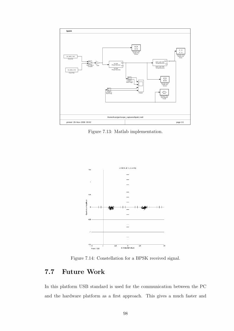
Scope1
Re
Im
Real−Imag toComplex
M−PSKPhase Recovery
Sig
Ph
M−PSKPhase Recovery
5
Gain
our_bpsk_i.mat
From File1
our_bpsk_r.mat
From File
Early−Late GateTiming Recovery
Sym
Ph
Early−Late GateTiming Recovery
Discrete−TimeScatter Plot
Scope2
Discrete−TimeScatter Plot
Scope1Discrete−Time
Scatter PlotScope
Discrete−TimeEye Diagram
Scope
Re(u)
Im(u)
Complex toReal−Imag2
Re(u)
Im(u)
Complex toReal−Imag
printed 28−Nov−2006 00:02 page 1/1
bpsk1
/home/lruiz/ger/scope_captures/bpsk1.mdl
Figure 7.13: Matlab implementation.
Point: 530
Figure 7.14: Constellation for a BPSK received signal.
7.7 Future Work
In this platform USB standard is used for the communication between the PC
and the hardware platform as a first approach. This gives a much faster and
98

Point: 70
Figure 7.15: Constellation for a QPSK received signal.
Figure 7.16: Eye diagram for a BPSK received signal.
99

Figure 7.17: Received Signal in the Oscilloscope.
Figure 7.18: SDR Platform.
cheaper design and implementation of the platform. However, the USB interface
does not have the required bandwidth to support enough data over the USB
bus. Thus a second generation of this SDR platform has already started under
development. This is implemented with FPGA, which gives much faster data
rate in the communication process and the capacity of the bus is increased.
7.8 Conclusion
This thesis has presented a basic hardware test bed for experimentation with SDR
technology. It has been focused on the direct conversion architecture. The adapt-
100

ability of the filter in channel bandwidth, bit rates, IP3 and sensitivity, permits
it to work within the desired group of standards. It is concerned within achiev-
ing many of the air interface specifications which have compatible requirements
providing the capability to operate across a width range of applications.
101

Chapter 8
CONCLUSIONS AND FUTURE
WORK
8.1 Conclusions
This thesis has presented a Software Defined Radio platform to work in a range of
frequencies from 1.6GHz to 2.4GHz. This meets the requirements of 2nd and 3rd
generation mobile telecommunications standards such as: DCS1800, PCS1900,
UMTS-FDD, UMTS-TDD and 802.11b. The implemented platform was built to
allow SDR techniques to be demonstrated.
The SDR communications standards required by this platform were constructed
based on a study of the requirements of the group of standards covered by the
platform Receiver and transmitter specifications were based on the strictest stan-
dard requirements, in this case DCS1800. These are phase noise of -152dBc/Hz,
out-of-band blocker of 0dBm, 30dBm maximum peak output power and 20MHz
of channel bandwidth. However sensitivity levels are limited by the UMTS re-
quirements of -107dBm.
Simulations were carried out in Matlab in order to decide the ADC specifications
102

needed to meet the SFDR requirements of the system. Thus, 16 bits converters,
which can process high dynamic range signals and achieve the requirements of the
standards needed here, were chosen. These ADCs give 8 bits of dynamic range, to
allow for amplitude variation in the incoming signal, according to the simulations.
This SDR platform uses a direct conversion architecture due to its easy tun-
ing across large frequency bands, low power dissipation and low cost. The design
of the platform was divided into three groups: baseband signal processing (ADC,
DAC, USB, LPF), receiver front-end (antenna, RF BPF, demodulator, LNA) and
transmitter (antenna, RF BPF, modulator and PA). This design was constructed
to meet the specifications within the limitations of commercially available com-
ponents.
Filter theory, synthesis and implementation were presented. Low pass filters
were used to ensure suppression of out of channel interference. These were im-
plemented using operational amplifiers in a multiple feedback configuration. RF
bandpass filters were used as band selected filters. These were implemented using
microstrip coupled line configurations. Simulations for both low pass and band-
pass filters were carried out using ADS and Mentor.
Matching networks and simulation results of the amplification stages were de-
tailed. Baseband amplification was used to ensure appropriate signal levels going
into the ADCs. The baseband amplifiers were implemented using operational
amplifiers. RF amplification is used in order to meet the output power require-
ments of the transmitter and the appropriate signal levels into the demodulator.
A power amplifier and a variable gain amplifier were required in the transmitter
in order to keep the SNR of the system within the required specifications. A low
noise amplifier was required by the receiver, which provides enough gain to allow
the mixer to demodulate the required reference signal.
103
Details of the physical implementation of the platform were given. Some of the
problems, such as SNR, found in the implementation process were described. To
improve SNR in the system, sensitive components were shielded from outside
noise.
The software used for this SDR platform was divided in three stacks: micro-
controller, PC driver, system software. An 8051 microcontroller was used, which
is embedded in the USB interface chip. A Linux kernel module was used as the
be-spoke USB driver. Matlab was used as the system software. This interface
permits the implementation of several communication schemes directly in Mat-
lab. The main advantage of this software is the easy communication between PC
and hardware without necessity of a complex application.
Simulation results provided an optimum SNR in the constellations schemes.
Again, Matlab was used to process the data files obtained from the measure-
ments. Receiver and transmitter signal characteristics were measured over the
development of this platform for two particular center frequencies, 2.08GHz and
2.35GHz. These test frequencies were provided by COMREG (the Irish commu-
nication regulator) to the CTVR.
8.2 Comparasion with the Universal Radio Pe-
ripheral system
Since SDR is a technology highly demanded in the market, several SDR plat-
forms were developed in parallel to this work. One of the most relevant projects
is the Universal Software Radio Peripheral (USRP). This prototype of SDR is
a low cost, high-speed USB based with the high sample-rate processing taking
place in the FPGA. This consists of four high-speed analog-to-digital converters,
104

four high-speed digital-to-analog converters, an FPGA and electronic circuitry
to achieve compatible interface between the different off-the-shelf components.
Two digital upconverters and downconverters are used for the interpolation and
frequency translation of the baseband and RF signals respectively. It is an open
design with freely available driver and schematics. This supports the free GNU
software package to experiment with the SDR daughterboard. The available
daughterboard’s at the moment of this peripheral support different range of fre-
quencies. Transceivers have been done for 1.5GHz to 2.1GHz, and for 2.3GHz to
2.9GHz. However there is no USRP transceiver that is covering 2G,3G and 802.11
communication standards (1.5GHz to 2.4GHz). Table 8.1 gives a comparasion
between the USRP project and the work that has been developed in this master.
As we can see, both project are supporting USB2.0 standard for the data trans-
Table 8.1: USRP and SDR Platform Comparasion.
mission to the PC. Some of the most important differences of this work with the
USRP project are the number of conversion stages, the architecture used for the
implementation, the sample rate, dynamic range, noise figure and the channel
bandwidth supported for each platform. These parameters and the election of
the direct conversion architecture have been explained in previous chapters.
105
8.3 Future Work
The approach taken in this platform for communication between the PC and the
hardware platform is to use an USB interface. This gives a much cheaper and
faster design and implementation of the platform. However, the USB interface
does not have the required bandwidth to support enough data over the USB bus.
The development of a second generation of this SDR platform is beginning. This
is implemented with FPGA, which gives much faster data rate and an increased
capacity of the bus.
The work presented here may be expanded with the design and implementation
of silicon reconfigurable devices. These must operate in a wide range of frequen-
cies. Future work may also be included in the study of standards to implement
a SDR system with a wider tuning range, which must meet requirements for all
the air-interface standards.
106

Appendix A
ADC Simulations
The simulations of the ADC’s has been carried out using Matlab. Thus in this
appendix the fuction utilized are presented.
A.1 Function ”variance1”
This function is created to generate the plots presented in chapter 4 for the
BER and the converging variance of the signal. The function take as argumen:
the number of samples used for the matlab simulation (samples), the type of
modulation scheme(M) and the number of carriers in the signal(number carriers).
function S N R = variance1(samples,M,number carriers)
%modulation=[2 4 8 16 32 64 256];
N=samples/256;
array ruido=[];
array real=[];
nBits=log2(M);
%SNR array=[20 30 45 60 75 80 100];
for i=1:N
figure(1)
real ofdm=simple ofdm1(M,number carriers);
107

real=real ofdm(1:256);
array real=[array real;real];
end
for bits=4:8
%for j=1:7
SNR=1;
YY noise=awgn(array real,SNR,’measured’,’db’);
y = my quantizer(YY noise,bits);
array ruido=(y-array real);
figure(2)
plot(array real)
figure(3)
plot(y)
figure(4)
plot(array ruido);
M ruido=sum(array ruido)/length(array ruido);
M real=sum(array real)/length(array real);
%e=enerBit(array real,length(array real));
for k=2:(samples)
temp ruido=sum((array ruido(1:k)-M ruido).^2);
%sum(array ruido(1:k).^2)-(sum(array ruido(1:k))).^2;
v ruido(k-1)=temp ruido/(k-1);
%temp ruido/(k-1);
temp real=sum((array real(1:k)-M real).^2);
%sum(array real(1:k).^2)-(sum(array real(1:k))).^2;
v real(k-1)=temp real/(k-1);
%temp real/(k-1);
%v(k)=(1/k^2)*sum(V(k:i));
n=1:length(v real);
108

figure(5)
plot(n,v real,’bd’,’MarkerEdgeColor’,’k’,
’MarkerFaceColor’,’g’,’MarkerSize’,5)
title(’Converging Variance ofdm’);
hold
figure(6)
plot(n,v ruido,’bd’,’MarkerEdgeColor’,’k’,
’MarkerFaceColor’,’g’,’MarkerSize’,5)
title(’Converging Variance ruido’);
end
Vtruido=(1/(samples)^2)*sum(v ruido);
%Vtotal ruido(bits-3)=Vtruido;
%(1/samples-1)*(sum(array ruido.^2)-(sum(array ruido)).^2);
Vtreal=(1/(samples)^2)*sum(v real);
%Vtotal real(bits-3)=Vtreal;
%(1/samples-1)*(sum(array real.^2)-(sum(array real)).^2);
%10*log10(v real(k)/v ruido(k));
snr=10*log10(Vtreal/Vtruido);
BER T(bits-3)=ber(SNR,snr,M);
S N R(bits-3)=snr;
N bits(bits-3)=bits;
% end
end
figure(7)
semilogy(N bits,BER T(1,:),’+’,N bits,BER T(2,:),’+’,
N bits,BER T(3,:),’-’,N bits,BER T(4,:),’o’,N bits,
BER T(5,:),’*’,N bits,BER T(6,:),’:’,N bits,BER T(7,:),’--’);
grid
109

legend(’BPSK’,’QPSK’,’8QAM’,’16QAM’,’32QAM’,’64QAM’,’256QAM’,7);
title(’ADC resolution’);
xlabel(’n bits’);
ylabel(’BERT’);
figure(8)
semilogy(S N R,BER T(1,:),S N R,BER T(2,:),S N R,BER T(3,:),S N R,
BER T(4,:),S N R,BER T(5,:),S N R,BER T(6,:),S N R,BER T(7,:));
grid
title(’ADC resolution’);
xlabel(’snr’);
ylabel(’BER’);
figure(9);
semilogy(N bits,BER T);
grid
legend(’4’,’5’,’6’,’7’,’8’,5);
title(’Ber’);
xlabel(’Nbits’);
ylabel(’BER’);
figure(10);
semilogy(SNR,BER T);
legend(’4’,’5’,’6’,’7’,’8’,5);
xlabel(’SNR’);
ylabel(’BER’);
grid
title(’Ber’);
110

A.2 Function ”simple ofdm1”
Function used to generate an OFDM signal. In the function the cycle prefix of
the signal is removed. The function takes as arguments: modulation scheme (M)
and number of carriers.
function [Pyy,real ofdm sig]= simple ofdm1(M,num sym)
%%%%%%%%%%%%
%OFDM generation script for Ger
%defines the sub-carrier modulation scheme - choose whichever one you
%want!
%method=’modulation type’
switch M
case 2
fid = fopen(’OFDMsignal BPSK’,’wb’);
case 4
fid = fopen(’OFDMsignal QPSK.pcm’,’wb’);
case 8
fid = fopen(’OFDMsignal 8QAM.pcm’,’wb’);
case 16
fid = fopen(’OFDMsignal 16QAM.pcm’,’wb’);
case 32
fid = fopen(’OFDMsignal 32QAM.pcm’,’wb’);
case 64
fid = fopen(’OFDMsignal 64QAM.pcm’,’wb’);
case 256
fid = fopen(’OFDMsignal 256QAM.pcm’,’wb’);
otherwise
disp(’wrong modulation’);
end
% QPSK: M= 4
111

% 8-QAM: M=8
% 16-QAM: M= 16
% 32-QAM : M=32
% 64-QAM: M=64
% 256-QAM: M=256
ofdm tx = [];
dyn sig prefix = [];
g prefix = [];
dyn ofdm = [];
%change this if you like but keep num sym <= fftSize/2 -1
%num sym = 1;
fftSize = 256;
numCarr = num sym;
carrSpacing = 1;
fft array = zeros(fftSize,1);
null signal length1 = int16(fftSize/6);
% Converting null signal lengh1 to double elements because It’s not
% possible to use zero() with an element type int16
null signal length=double(null signal length1);
null signal = zeros(abs(null signal length),1);
MidFreq = fftSize/4;%find the middle of the spectrum
CarrSpacing = 1;
StartCarr = MidFreq - round(((numCarr-1)*CarrSpacing/2));
FinCarr = MidFreq + floor(((numCarr-1)*CarrSpacing/2));
carriers = [StartCarr:CarrSpacing:FinCarr]+1;
negCarriers = fftSize-carriers+2;
%find the bins for the negative frequency carriers
for k=1:500
qam= randint(num sym,M,1);
112

f=1000*(0:511)/1024;
msg=qaskenco(qam,M);
fft array(carriers(1,1:numCarr),1) = msg(1:numCarr,1);
fft array(negCarriers(1,1:numCarr),1) =
conj(fft array(carriers(1,1:numCarr),1));
ofdm sig = ifft(fft array,fftSize);
%just to make sure the signal is real-valued
real ofdm sig = real(ofdm sig)*32767.0;
real ofdm sig = [real ofdm sig; null signal];
s=size(null signal);
Y = fft(real ofdm sig,1024);
Pyy = Y.* conj(Y)/1024; %Power spectrum
k=size(Pyy);
plot(f,(Pyy(1:512)));
l=size(f);
xlabel(’f’);
title(’OFDM Power Spectrum’);
count = fwrite(fid,real ofdm sig,’int16’);
end
status = fclose(fid);
display(’OFDM creation done...’);
A.3 Function ”my quantizer”
This function simulates an uniform quantizer to generate the digital signal. The
input arguments that the function have are: the information signal(x), the reso-
lution(N bits).
function y = my quantizer(x,n bits)
% --------------- [y,digital]=my quantizer(x,N bits) --------------
113

%
% Conversor A/D with uniform quantization of N bits
% Full scale, FE:+-1 voltio
% delta=2*FE/(2^N bits)
%
% Input:
% x: sampled Analog Signal to codec (volt),
% N bits: number of bits of the quantizer
% ------------------------------------------------------------
FE=max(abs(x));
delta=2*FE/(2^n bits);% step size
l=length(x)
% UNIFORM QUANTIZER
% The absolut value of all input arguments of the signal must be < 1
x1=x+delta/2;
dec=round(x1/delta);% number of step.It is between 1 and 2exp(n bits)
y=(dec*delta)-delta/2;%value of the quantized signal:
xq=(1/2)*(2*dec - 1)*delta
noise quant= x-y;
% ENCODING
for row=1:l
% 1) first bit, sign: - => 0 / + => 1
if sign(y(row))==1
digital(row,1)=1;
else
digital(row,1)=0;
end
% 2) Siguientes n-1 bits, magnitud cuantificada
aux=0;
114

for col=2:n bits
% Al escal?n m?s alto le asignaremos el c?digo 1000...0
if (abs(dec(row))/2^((n bits-1)-aux-1))==2
% the value of x is lying in the middle of the scale,
%it’s meaning that
% the quantized value is zero, thus the digital
%numaber will be both 00000..0 or 100..0
for col=2:n bits
digital(row,col)=0;
end
else
% If the cocient is less than 1 this position will be 0
% if not the value will be 1
if (abs(dec(row))/2^((n bits-1)-aux-1))<1
digital(row,col)=0;
else
digital(row,col)=1;
% En caso de ser pos. restamos
%la potencia si es neg. la % sumamos
if sign(y(row))==-1
dec(row)=dec(row)+2^((n bits-1)-aux-1);
else
dec(row)=dec(row)-2^((n bits-1)-aux-1);
end
end
aux=aux+1;
end
end
end
115

SNR dB=(6.02*n bits)-7.26; %paper equation of Review of quantization
A.4 Function”ber”
This function generates the BER corresponding to each particular mudulation
scheme. The input arguments are: SNR and modulation scheme.
function[BER] = ber(SNR1,SNR2,M)
% SNR1 is the signal to noise ratio inside throgh the channel
% The relationship between Q and erfc is given by:
% Q(x) = 0.5*erfc(x/sqrt(2));
snr1=10.^(SNR2/10);%Convert Eb/No from dB to a linear ratio
switch M
case 2,4%BPSKBER= .5*erfc(sqrt(snr1));
case 16,64,256%8QAM,16QAM,32QAM,64QAM,256QAMBER=2*(1-(1/sqrt(M)))*erfc(sqrt((3/(2*(M-1)))*(snr1)));
case8,32BER=2*(1-(1/sqrt(2*M)))*erfc(sqrt((3/(2*(M-1)))*(snr1)));
end
% Note: Q(x) = 0.5*erfc(x/sqrt(2))
116

Appendix B
Transmitter and Receiver Drivers
B.1 Transmitter Inicialization
A mask is assigned to each variable. The memory address in the microprocessor
for this instruccions is assigned as well.
xdata at 0x40C3 unsigned char OURRX PLL = 0x10;
sfr at 0x8E ckcon;
volatile xdata at 0xe600 unsigned char cpucs;
volatile xdata at 0xe601 unsigned char ifconfig;
data unsigned char sclk mask = 0x40;
data unsigned char sdat mask = 0x01;
data unsigned char sclk mask inv=0xBF ;
data unsigned char LE mask = 0x02 ;
data unsigned char LE mask inv = 0xFD ;
data unsigned char ourclock buf = 0x10;
data unsigned char Demod mask = 0x08;
data unsigned char Demod mask inv = 0xF7;
data unsigned char CE mask = 0x04;
data unsigned char CE mask inv = 0xFD;
117

B.2 Receiver Inicialization
A mask is assigned to each variable. The memory address in the microprocessor
for this instruccions is assigned as well.
xdata at 0x400F unsigned char OURRX PLL = 0x10;
sfr at 0x8E ckcon;
volatile xdata at 0xe600 unsigned char cpucs;
volatile xdata at 0xe601 unsigned char ifconfig;
data unsigned char sclk mask = 0x40;
data unsigned char sdat mask = 0x01;
data unsigned char sclk mask inv=0xBF ;
data unsigned char LE mask = 0x02 ;
data unsigned char LE mask inv = 0xFD ;
data unsigned char ourclock buf = 0x10;
data unsigned char Demod mask = 0x08;
data unsigned char Demod mask inv = 0xF7;
data unsigned char CE mask = 0x04;
data unsigned char CE mask inv = 0xFD;
B.3 Common Functions
B.3.1 Main Function
In the main function all the variables are configured with the corresponding val-
ues. Thus ’conf clk’ is the function which realize this process.
void main (void)
unsigned char i = 0;
cpucs = 0x12; // 0x02 = 12MHz , 0x0a = 24MHz , 0x12 = 48MHz
118

ifconfig &= 0x7f; // set the ifclk pin for input
ckcon &= 0xF8; // set the strech values to the most agressive
enable CE();
config clk();
while(1)
for (i=0; i<=1; i++)
waiting();// waste some clock cycles
//config clk();
B.3.2 Function ”config clk()”
This function has the task to configurate the PLL.
void config clk (void)
unsigned char ourdata1 = 0x00;
unsigned char ourdata2 = 0x00;
unsigned char ourdata3 = 0x00;
unsigned char i = 0;
unsigned char j = 0;
//Write in the R counter R=80
rdata1 = 0x00;
ourdata2 = 0x01;
ourdata3 = 0x41;
data write(ourdata1,ourdata2,ourdata3);
toggle LE();
119

for (i=0; i<=128; i++)
// waste some clock cycles
//For 2.35GHz with 250KHz compare frequency. The loop band width is 25KHz.
//writing on the Control latch
ourdata1 = 0x40;
ourdata2 = 0x01;
ourdata3 = 0x00;
data write(ourdata1,ourdata2,ourdata3);
toggle LE();
waiting();
for (i=0; i<=128; i++)
// waste some clock cycles
//Writing on the N counter with B=587 and A=8
ourdata1 = 0x02;
ourdata2 = 0x4B;
ourdata3 = 0x22;
data write(ourdata1,ourdata2,ourdata3);
toggle LE();
for (i=0; i<=128; i++)
B.3.3 Function ”data write”
With the following function is possible to write any kind of data in the variables.
120

unsigned char data write(unsigned char ourdata1, unsigned char ourdata2,
unsigned char ourdata3)
unsigned char i = 0;
unsigned char sdat = 0x0;
for (i=0; i<=7; i++)
sdat = ((ourdata1 >> 7-i) & 0x1);
f (sdat==0x0)
ourclock buf &= 0xFE;
if (sdat==0x1)
ourclock buf |= 0x01;
toggle sclk();
for (i=0; i<=7; i++)
sdat = ((ourdata2 >> 7-i) & 0x1);
if (sdat==0x0)
ourclock buf &= 0xFE;
if (sdat==0x1)
ourclock buf |= 0x01;
121

toggle sclk();
for (i=0; i<=7; i++)
sdat = ((ourdata3 >> 7-i) & 0x1);
if (sdat==0x0)
ourclock buf &= 0xFE;
if (sdat==0x1)
ourclock buf |= 0x01;
toggle sclk();
ourclock buf &= 0xFE;
OURRX PLL = ourclock buf;
//ourclock buf &= sclk mask inv; //set sclk=0
//OURRX PLL = ourclock buf;
return 0;
B.3.4 Function ”enable CE”
Function which enables the modulator and demodulator.
unsigned char enable CE(void)
unsigned char i = 0;
ourclock buf |= CE mask; //sets CE=1
122

ourclock buf |= Demod mask; //sets CE=1
OURRX PLL = ourclock buf;
return 0;
B.3.5 Function ”toggle LE”
Function which generate a square signal for the LE input on the LE interface
digital line in the PLL.
unsigned char toggle LE(void)
unsigned char i = 0;
ourclock buf &= LE mask inv; //set sclk=0
OURRX PLL = ourclock buf;
for (i=0; i<=1; i++)
// waste some clock cycles
ourclock buf |= LE mask; //sets sclk=1
OURRX PLL = ourclock buf;
for (i=0; i<=2; i++)
// waste some clock cycles
ourclock buf &= LE mask inv; //set sclk=0
OURRX PLL = ourclock buf;
for (i=0; i<=1; i++)
// waste some clock cycles
123

return 0;
B.3.6 Function ”Toggle sclk”
Function which generate the clock output from the USB interface chip.
unsigned char toggle sclk(void)
unsigned char i = 0;
ourclock buf &= sclk mask inv; //set sclk=0
OURRX PLL = ourclock buf;
for (i=0; i<=1; i++)
// waste some clock cyclesourclock buf |= sclk mask; //sets sclk=1
OURRX PLL = ourclock buf;
for (i=0; i<=2; i++)
// waste some clock cycles
ourclock buf &= sclk mask inv; //set sclk=0
OURRX PLL = ourclock buf;
for (i=0; i<=1; i++)
// waste some clock cycles
return 0;
124

Appendix C
Microstrip Lines Theory
Transmission lines can support three different kind of wave modes:
TEM: This mode does not have longitudinal field components. They have a
defined voltage, characteristic impedance and current.
TM: Transmission mode characterized by transverse magnetic waves and longi-
tudinal electric fields.
TE: Transmission mode characterized by transverse electric waves and longitu-
dinal magnetic fields.
In the case of TM and TE modes, a unique characteristic impedance is not
possible to define. However some approximations can be done so characteristic
impedance can be used. Thus, here a general introduction to Maxwell’s equations
for each case in a electromagnetic wave is presented. The electric and magnetic
fields of a a wave propagated along the z-axis are:
E(x, y, z) = [e(x, y) + z ez(x, y)]e−jβz (C.1)
H(x, y, z) = [h(x, y) + z hz(x, y)]e−jβz (C.2)
Where e(x, y) and h(x, y) represent the transverse (x,y)electric and magnetic
filed. Therefore assuming the transmission in a free region these equations can
125

be written as:
∇× E = −jωµH (C.3)
∇×H = −jωεE (C.4)
From the above vector equations each transversal component for magentic and
electric field can be obtained [26]. Since the equations for the transversal com-
ponents in a wave have been obtained is possible to obtain the characteristic
impedance and transversal fields for each propagated mode. Presented below are
the equations for these calculations:
1. TEM
ZTEM =Ex
Hy
=ωµ
β(C.5)
h(x, y) =1
ZTEM
z × e(x, y) (C.6)
2. TE
ZTE =Ex
Hy
=−Ey
Hx
=ωµ
β=
kn
β(C.7)
k = ω√
µε =2π
λ(C.8)
3. TE
ZTM =Ex
Hy
=−Ey
Hx
=β
ωε=
βη
k(C.9)
k = ω√
µε =2π
λ(C.10)
Where k is the wave number of the material filling the transmission line or waveg-
uide region [26]. Therefore both TE are TM waves are frequency dependent.
Considering the previous equations and knowing that microstrip lines are are
composed by a hybrid TM-TE wave it is possible to analyses microstrip lines.
Thus quasi-TEM modes are considered when the dielectric substrate is electri-
126

cally very thin (d < λ). In this case the fields are the same as those of static case.
Thus Microstrip line will have an unique characteristic impedance for a partic-
ular frequency. However the impedance in microstrip line is highly depending
on the substrate and the conductor charateristics. In consequence the following
equations are used for the calculation of the microstrip line parameters [26].
εe =εr + 1
2+
εr − 1
2
1√1 + 12H
W
(C.11)
Where 1 < εe < εr and is the effective dielectric constant. It is considered as
having a medium to replace the air and dielectric regions.
The characteristic impedance of the line can be calculated as:
Z0 =60
εr
ln(8H
W+
W
4H) for
W
H≤ 1 (C.12)
Z0 =120π
εrWH
+ 1.393 + 0.667 ln(WH
+ 1.444)for
W
H≥ 1 (C.13)
Knowing Z0 and εr the WH
can be calculated as follows:
W
H=
8eA
e2A − 2for
W
H< 2 (C.14)
W
H=
2
π(B − 1− ln(2B − 1) +
εr − 1
2εr
ln(B − 1) + 0.39− 0.61
εr
) forW
H> 2
(C.15)
where
A =Z0
60
√εr + 1
2+
εr − 1
εr + 1(0.23 +
0.11
εr
) (C.16)
B =377π
2Z0√
εr
(C.17)
The propagation constant and pahse velocity can be expresed as:
νp =c√εe
(C.18)
β = K0
√εe (C.19)
127

Figure C.1is a synthesis graph to obtain the corresponding width and height of
the microstrip line.
Figure C.1
Figure C.2
128

Appendix D
Filters
D.1 Lumped Components Filters Response
Maximum flat filters, Bessel filters, and Gaussian filters response with lumped
components habe been analyzed for this platform.
1. Bessel Response
Bessel filters are characterized for having a flat group delay and no over-
shoot. Figure D.1 and Figure D.2 show the implementation and response
of this bandpass filter. The simulated filter is a 4th order pi filter with
Figure D.1: Bessel schematic.
bandwidth from 1.8GHz to 2.6GHz. Observing the figures this filter has
a very small attenuation across the stop band which results a not reliable
model for this platform, as it said previously. In addition, the values for
the serial capacitors are very difficult to achieve with lumped components.
2. Maximum Flat Response
This kind of filter has very good in band amplitude flattened. The simu-
129

Figure D.2: Bessel Filter Response.
lated filter is a 5th order pi filter with bandwidth from 1.8GHz to 2.6GHz.
Figure D.3 and Figure D.4 shown the implementation and response of this
bandpass filter. Thus, according to the components values, the series ca-
pacitors are not able to be built since their values are in the order of fF.
Figure D.3: Max Flat schematic.
According to the frequency response, the maximum flat presents better at-
tenuation characteristics in the stop band than the Bessel filter. However
in relation to the requirements of this platform the filter does not meet the
specifications since the 20dB attenuation occurs at 3GHz, which is over the
required stop frequency for the expected filter.
Figure D.4: Max Flat Response.
130

3. Gaussian
The simulated LC bandpass Chebyshev filter is a 3rd order filter with a band
width from 1.8GHz to 2.6GHz. The filter presents a not flat response which
can generate attenuation problems on the required signal at the desired
frequencies. However according to the attenuation at the stop band the
filter presents very good attenuation characteristics and small number of
components. Figure ?? and Figure ?? illustrate the implementation and
response of this LC bandpass filter. Thus, according to the values on the
filter, series capacitors and parallel inductors are difficult to find in the
market.
Figure D.5: Gaussian LC Filter.
Figure D.6: Gaussian Response.
131

Appendix E
Papers
1. ”A Platform for the Development of Software Defined Radio” IEEE PIMRC
2007 Greece.
2. ”Demonstration of a Software Defined Radio Platform for dynamic spec-
trum allocation” IEEE DYSPAN 2007 Dublin.
3. ”Reconfigurable Transceiver Architectures: Front-end Hardware Require-
ments” RIA Colloquium on Physical Layer Wireless Communications,
Dublin 2006.
4. ”Reconfigurable Radio Testbed” ISSC 2006, Dublin.
132

ACRONYMS
ADC, Analog to Digital Conversion
AGC, Automatic Gain Control
AMPS, Advanced Mobile Phone Service
ASIC, Application Specific Integrated Circuit
BER, Bit Error Rate
BPSK, Binary Phase Shift Key
CDMA, Code Division Multiple Access
CMOS, Complementary Metal-Oxide Semiconductor
CPU, Central Processing Units
CSD, Circuit Switch Data
DAC, Digital to Analog Conversion
DCS, Digital Cellular System
DECT, Digital Enhanced Cordless Communications
DSA, Dynamic Spectrum Allocation
DSRC, Dedicated Short Range Communications
EMI, Electromagnetic Interferences
ETC, Enhanced Throughput Cellular
FCC, Federal Communication Commission
FPGA, Field Programmable Gate-Array
GMSK, Gaussian Minimum Shift Keying
GSM, Global System for Mobile Communications
HSDPA, High-Speed Downlink Packet Access
HSUPA, High-Speed Uplink Packet Acess
iDEN, Integrated Digital Enhaced Network
IF, Intermediate Frequency
IFFT, Inverse Fast Fourier Transform
ISI, Intersymbol Interferences
133
ITS, Intelligent Transportation System
ITU, International Telecommunication Union
LAN, Local Area Network
LNA, Low Noise Amplifier
LO, Local Oscillator
NMT, Nordic Mobile Telephone
NF, Noise Figure
OFDM, Orthogonal Frequency Division Multiplexing
OS, Operating System
PA, Power Amplifier
PAN, Personal Area Network
PC, Personal Computer
PCS, Personal Communication System
PN, Phase Noise
PLL, Pahse Locked Loop
PSK, Phase Shift Key
QAM, Quadrature Amplitude Modulation
RF, Radio Frequency
SDR, Software Defined Radio
SFDR, Spurious Free Dynamic Range
SMA, Surface Mount Assembly
SMD, Surface Mount Device
SMT, Surface Mount Technology
SNR, Signal to Noise Ratio
TACS, Total Access Communication System
UMTS, Universal Mobile Telecommunication System
USB, Universal Serial Bus
WiMax, Worldwide Interoperability for Microwave Access
WiBro, Wireless Broadband
134

W-CDMA, Wideband Code Division Multiple Access
WWRF, Wireless World Research Forum
135

Bibliography
[1] ”The free encyclopedia”wwww.wikipedia.org
[2] J.M.Pereira ”Fourth Generation: Now, it is Personal”Pereira
[3] J.Ryynanen ”Low-Noise Amplifier for Intagrated Multi-Mode Direct Conver-
sion Receivers”Helsinki University of Technology, Electronic Circuit Design,
Espoo 2004
[4] W.Tuttlebee ”Software Defined Radio: Origins, Drivers and International
Perspectives”,Tuttlebee,Wiley,ISBN 0-47-084464-7,2002 ,May 2000.
[5] J. Steinheider ”Software Defined Radio Come of Age”,wwww.rfdesign.com
,Mar 2003.
[6] J. Mitola ”Cognitive Radio”,Disertation, Royal Institute of Technology,May
2000.
[7] D.Buss,L.Evans ”SO CMOS Technology for Personal Internet Prod-
ucts”,IEEE Transactions on Electronics Devices, Vol 50, No.3, March 2003.
[8] R.Kohno ”Status on Studies in the IEICE Doftware Radio Technical
Group”,SDR Forum,Tokyo, April 2001 ,Mar 2003.
[9] S.Winder, J.Carr ”Radio and RF Enginnering”. Newnes, ISBN 0-7506-5608-5,
2002
[10] W.D. Horne, ”Adaptative Spectrum Access: Using the Full Spectrum
Space”,The MITRE Corporation, McLean, VA.
136

[11] B.Turner ”3G Tutorial”,NMS Communications,Fall VON 2002.
[12] L.Dıaz ”Wireless Communication Education: A Guide of Important Top-
ics”,Microwave Review,November 2005.
[13] G.Baldwin, L.Ruiz ”Reconfigurable Transceiver Architecture: Front end
Hardware Requirements”,Coloquium on Physical Layers Wireless Communi-
cationsMay 2006
[14] W.Tuttlebee ”Software defined radio:enabling technolo-
gies”,Tuttlebee,Wiley,ISBN 0-47-084464-7, 2002.
[15] J.Rudell, J.Wendoll,J.J.Ou, L.Lin, P.Gray ”An Integrated GSM/DECT Re-
ceiver: Design Specifications”,UCB Electronic Research Laboratory Memoran-
dum,UCB/ERL M97/82.
[16] H.Fischer, F.Henkel ”UMTS Multimode receiver design”. ICAS2004 IEEE.
[17] F.Friis ”Noise Figure of Radio Receivers”. Proc. IRE, Vol 32,pp. 419-422,
July 1994.
[18] W.Kester ”MT-006: ADC Noise Figure”. Analog Devices, Rev. A., 4-03-
2006.
[19] H.Tsurumi ”Broadband RF Stage Architecture for Software-Defined Radio
in Handheld Terminal Applications”,IEEE Communications Magazine, Febr-
yary 1999.
[20] L.Ruiz, G.Baldwin. ”Reconfigurable Radio Testbed”. ISSC 2006.
[21] K.Chung ”Data Conversion in Software Defined Radios”. HY-SDR Research
Center.
[22] Linear Technologies ”LTC2205/LTC2204 datasheet”. Data Sheet.
[23] MAXIM ”16-Bit, 200Msps, High Dynamic-Performance, Dual DAC with
CMOS Inputs”. Data Sheet.
137
[24] Analog Devices ”Low Cost, High Speed, Differential Amplifier AD8132”.
Data Sheet.
[25] B.Razavi ”RF Microelectronic”. Prentice Hall, ISBN 7-302-07522, 2005
[26] David M. Pozar ”Microwave Engineering”,John Wiley and Sons, Inc.,ISBN
0-471-17096-8, 1998.
[27] Analog Devices ”Integrated Synthesizer and VCO, ADF4360-1”. Data Sheet
[28] Analog Devices ”0.8 GHz to 2.7 GHz Direct Conversion Quadrature Demod-
ulator, AD8347”. Data Sheet
[29] Analog Devices ”0.7 GHz to 2.7 GHz Direct Conversion Quadrature Modu-
lator, AD8349”. Data Sheet
[30] R.Schaumann,M.E.Van Vankenburg ”Design of Analog Filters ”. Oxford
University Press , ISBN 0-19-511877-4, 2001
[31] A.Melloni ”Shyntesis of Direct Coupler Resonators Bandpass Filter for
WDM Systems ”. Journal of Lightwave Technology, Vol.20, No.2 , February
2002
[32] Thomas H. Lee ”Planar Micrwave Engineering”. Cambridge University
Press, ISBN 0-521-83526-7, 2004
[33] K.Shingh ”Coupled Microstrip filters: Simple Methodologies for Improve
Characteristics”. Communication System Group, ISRO Satellite Center
[34] Freescale Semiconductor ”MBC13720: SiGe, C Low Noise Amplifier with
Bypass Switch”. Data Sheet
[35] Peter Vizmuller ”RF Design Guide: Systems, Circuits and Equations”.
Artech House Publishers, 1995.
138
Copyright © 2022 FDOKUMEN