Design and Analysis of Reconfigurable Analo System
152
Design and Analysis of Reconfigurable Analo MASSACHUSETTS INSTITUTE OF TECHw ,OLo-y System by MARIO 2C11 Payam Lajevardi L BRARIES B.A.Sc. Electrical Engineering, University of British Columbia,'2003 and S.M. Electrical Engineering, Massachusetts Institute of Technology, 2005 Submitted to the Department of Electrical Engineering and Computer Science in partial fulfillment of the requirements for the degrees of Doctor of Philosophy at the MASSACHUSETTS INSTITUTE OF TECHNOLOGY February 2011 @ Massachusetts Institute of Technology 2011. All rights reserved. A uthor ............... -.. ----....----.. Department of Electri<al Engineering and Computer Science - - OctAvber 18, 2010 Certified by............---.......... - -. Anantha P. Chandrakasan Joseph F. and Nancy P. Keithley Professor of Electrical Engineering Thesis jupervisor Certified by ............................ ..... Hae-Seung Lee Professor of Electrical Engineering Thesis Supervisor Accepted by...........................- Terry P. Orlando Chairman, Departmental Committee on Graduate Students
-
Upload
khangminh22 -
Category
Documents
-
view
0 -
download
0
Transcript of Design and Analysis of Reconfigurable Analo System
Design and Analysis of Reconfigurable AnaloMASSACHUSETTS INSTITUTE
OF TECHw ,OLo-ySystem
by MARIO 2C11
Payam Lajevardi L BRARIESB.A.Sc. Electrical Engineering, University of British Columbia,'2003
and
S.M. Electrical Engineering, Massachusetts Institute of Technology,2005
Submitted to the Department of Electrical Engineering and ComputerScience
in partial fulfillment of the requirements for the degrees of
Doctor of Philosophy
at the
MASSACHUSETTS INSTITUTE OF TECHNOLOGY
February 2011
@ Massachusetts Institute of Technology 2011. All rights reserved.
A uthor ............... -.. ----....----..
Department of Electri<al Engineering and Computer Science- - OctAvber 18, 2010
Certified by............---.......... - -.Anantha P. Chandrakasan
Joseph F. and Nancy P. Keithley Professor of Electrical EngineeringThesis jupervisor
Certified by ............................ .....Hae-Seung Lee
Professor of Electrical EngineeringThesis Supervisor
Accepted by...........................-Terry P. Orlando
Chairman, Departmental Committee on Graduate Students

Design and Analysis of Reconfigurable Analog System
by
Payam Lajevardi
Submitted to the Department of Electrical Engineering and Computer Science
on August 29, 2010, in partial fulfillment of therequirements for the degrees of
Doctor of Philosophy
Abstract
A highly-configurable analog system is presented. A prototype chip is fabricated
and an ADC and filter functionalities are demonstrated. The chip consists of eight
identical programmable stages.In an ADC configuration, the first five stages are programmed to implement a 10-
bit ADC. The ADC has ENOB of 8 bits at 50 MSPS. The ENOB improves to 8.5 bits if
the sampling rate is lowered to 30MSPS. The ADC has an FOM of 150fJ/conversion-
step, which is very competitive with the state of the art ADCs. The first stage is
responsible for 75% of the input-referred noise power. The sampling noise is respon-
sible for 40% of the total noise power and the zero-crossing detector is responsible for
60%.The chip is tested in two different filter configurations. In one test, the first two
stages of the chip are configured as a second order Butterworth filter and the third
stage is configured as an amplifier. In another test, the first three stages of the chip are
programmed as a third-order Butterworth filter. The desired filter functionalities are
demonstrated in both configurations. It is shown that in a third order Butterworth
filter, more than 90% of the noise is due to the zero-crossing detector of the last stage.
This is mainly due to the fact that the noise of earlier stages is filtered with the filtertransfer function, but the noise of the last stage is not filtered.
The ZCBC architecture has been used to avoid the stability problems and scale
power consumption with sampling frequency. A new technique is introduced to im-
plement the terminating resistors in a ladder filter. This technique does not have
any area or power overhead. An asymmetric differential signaling is also introduced.
This method improves the dynamic range of the output signals, which is particularly
important in new technology nodes with low supply voltage.
Thesis Supervisor: Anantha P. ChandrakasanTitle: Joseph F. and Nancy P. Keithley Professor of Electrical Engineering
Thesis Supervisor: Hae-Seung LeeTitle: Professor of Electrical Engineering

4

Acknowledgments
I would like to thank Professor Anantha Chandrakasan and Professor Harry Lee for
their support. I enjoyed the learning opportunity in their research group and under
their supervision and guidance. I would also like to thank other members of Anantha
group and Harry Lee group whose valuable input have enhanced my insight in my
research. In addition, I would like to thank IBM and TSMC, which provided us with
fabrication facilities.
I would like to thank my parents, Soraya Mohammadi and Hosein Lajevardi, and
my brother, Pedram Lajevardi, for their support and love. Most important, I would
like to thank my wife, Laila Jaber Ansari for her ultimate love and support.
The funding was provided by DARPA and the Center of Integrated Circuits and
Systems (CICS) at MIT. We acknowledge chip fabrication through DARPA and the
TSMC University Shuttle Program.

6
Contents
1 Introduction
1.1 ADC Review .........
1.1.1 Pipeline ADC . . . . .
1.1.2 Over-Range Protection
1.2 Filter Review . . . . . . . . .
1.2.1 Passive Ladder Filter
1.2.2 Active Ladder Filter
1.2.3 Thesis Contribution.
2 Zero-Crossing-Based Circuits
2.1 Advantages of ZCBCs . . .
2.2 Sources of Nonlinearity . . .
2.3 Solution to some Challenges
. . . . . . . . . .
. . . . . . . . . .
in Pipeline ADC
. . . . . . . . . .
. . . . . . . . . .
. . . . . . . . . .
. . . . . . . . . .
(ZCBC)
3 System Architecture and Implementation
3.1 System Description . . . . . . . . . . . . . . . . .
3.1.1 The Need for ZCBC Implementation . . .
3.1.2 Implementation of a Reconfigurable Stage
3.1.3 ADC Configuration . . . . . . . . . . . . .
3.1.4 Filter Configuration . . . . . . . . . . . . .
3.2 System Components . . . . . . . . . . . . . . . .
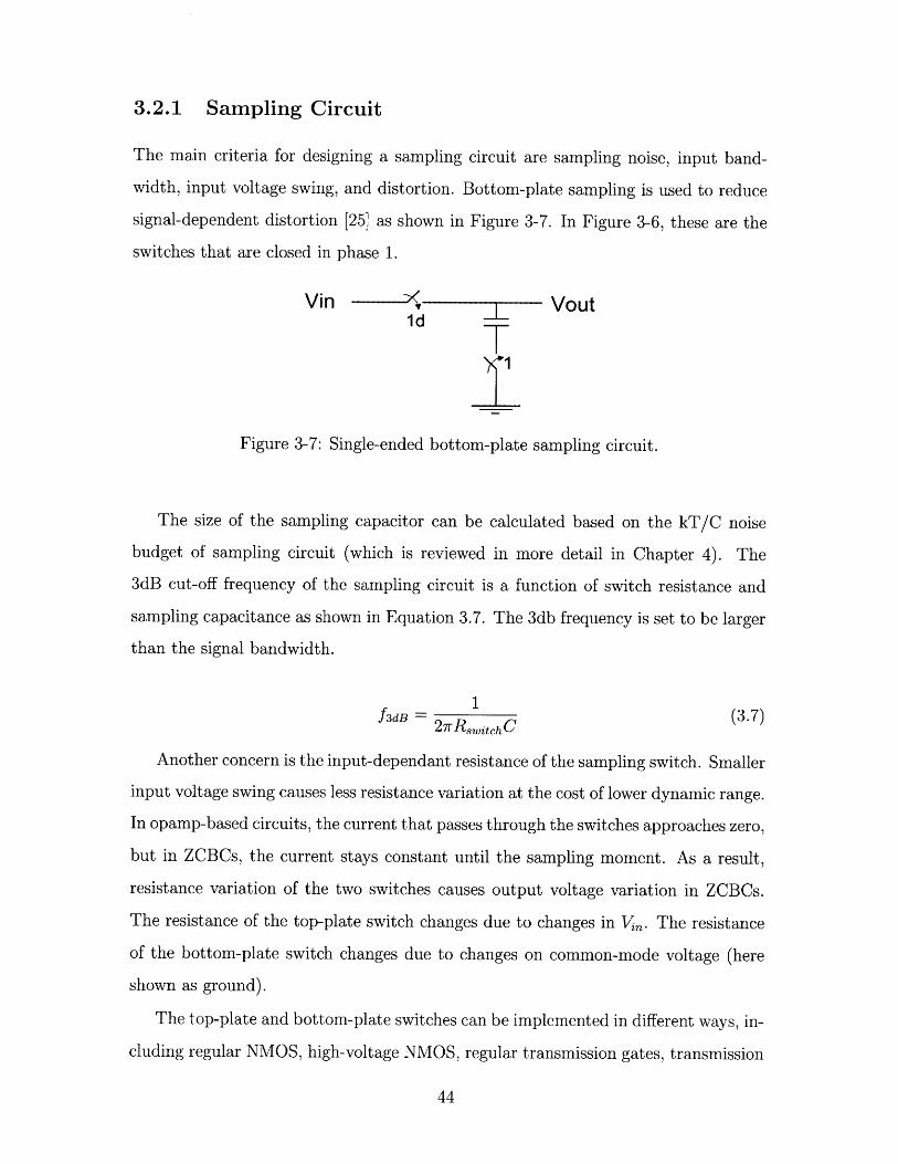
3.2.1 Sampling Circuit . . . . . . . . . . . . . .
3.2.2 Bootstrapping . . . . . . . . . . . . . . . .
19
20
21
22
23
24
25
27
37
37
39
41
42
43
43
44
47
. . . . . . . . . . . . .
. . . . . . . . . . . . . . . .
. . . . . . . . . . . . . . . .-
3.2.3 Zero-Crossing Detector . . . . . . . . . . . 48
3.2.4 Current Sources . . . . . . . . . . . . . . . . . . . . . . . . . . 49
3.2.5 The first Stage . . . . . . . . . . . . . . . . . . . . . . . . . . 51
3.2.6 Bit-Decision-Comparators (BDC) . . . . . . . . . . . . . . . . 51
3.2.7 Residue Plot . . . . . . . . . . . . . . . . . . . . . . . . . . . . 52
3.2.8 The Analog Buffer . . . . . . . . . . . . . . . . . . . . . . . . 53
3.2.9 Terminating Resistors . . . . . . . . . . . . . . . . . . . . .. 54
3.3 Asymmetric Differential Signaling . . . . . . . . . . . . . . . . . . . . 57
3.4 Programmability . . . . . . . . . . . . . . . . . . . . . . . . . . . . . 58
3.4.1 Programmability for functionality . . . . . . . . . . . . . . . . 58
3.4.2 Programmability for Calibration . . . . . . . . . . . . . . . . . 59
3.4.3 Programmability for Power Optimization . . . . . . . . . . . . 60
3.5 System Simulation . . . . . . . . . . . . . . . . . . . . . . . . . . . . 60
4 Noise Analysis 65
4.1 Noise Review . . . . . . . . . . . . . . . . . . . . . . . . . . . . . . . 65
4.1.1 Sampling Noise (kT/C Noise) . . . . . . . . . . . . . . . . . . 66
4.1.2 Effective Number of Bits (ENOB) and Figure of Merit (FOM) 68
4.1.3 Noise Gain . . . . . . . . . . . . . . . . . . . . . . . . . . . . . 69
4.1.4 Noise Bandwidth (NBW ) . . . . . . . . . . . . . . . . . . . . . 70
4.1.5 Noise of an amplifier . . . . . . . . . . . . . . . . . . . . . . . 70
4.1.6 Noise Aliasing . . . . . . . . . . . . . . . . . . . . . . . . . . . 71
4.2 Noise of the ADC . . . . . . . . . . . . . . . . . . . . . . . . . . . . . 73
4.3 Filter Noise . . . . . . . . . . . . . . . . . . . . . . . . . . . . . . . . 76
4.3.1 Noise of an Integrator . . . . . . . . . . . . . . . . . . . . . . 76
4.3.2 Noise Transfer Function . . . . . . . . . . . . . . . . . . . . . 78
4.4 Coupling Noise . . . . . . . . . . . . . . . . . . . . . . . . . . . . . . 82
4.4.1 Noise on Reference Voltages . . . . . . . . . . . . . . . . . . . 83
4.5 Conclusion . . . . . . . . . . . . . . . . . . . . . . . . . . . . . . . . . 85
8
5 Sensitivity of the System 87
5.1 Sensitivy to Capacitance Values . . . . . . . . . . . . . . . . . . . . . 87
5.1.1 ADC Configuration . . . . . . . . . . . . . . . . . . . . . . . . 87
5.1.2 Filter Configuration . . . . . . . . . . . . . . . . . . . . . . . . 88
5.2 Offset of the Zero-Crossing Detector . . . . . . . . . . . . . . . . . . . 90
5.3 Offset in an ADC Configuration . . . . . . . . . . . . . . . . . . . . . 90
5.4 Offset in a filter Configuration . . . . . . . . . . . . . . . . . . . . . . 91
5.5 C onclusion . . . . . . . . . . . . . . . . . . . . . . . . . . . . . . . . . 95
6 Measurements of the Fabricated Chip 97
6.1 ADC Measurement . . . . . . . . . . . . . . . . . . . . . . . . . . . . 98
6.2 Filter Measurement . . . . . . . . . . . . . . . . . . . . . . . . . . . . 106
6.3 Cost of Reconfigurability . . . . . . . . . . . . . . . . . . . . . . . . . 108
6.3.1 Power Consumption . . . . . . . . . . . . . . . . . . . . . . . 109
6.3.2 Speed . . . . . . . . . . . . . . . . . . . . . . . . . . . . . .. 111
6.3.3 A rea . . . . . . . . . . . . . . . . . . . . . . . . . . . . . . . . 112
6.3.4 N oise . . . . . . . . . . . . . . . . . . . . . . . . . . . . . . . . 113
6.3.5 Choice of Architecture . . . . . . . . . . . . . . . . . . . . . . 114
6.4 Measurement Summary. . . . . . . . . . . . . . . . . . . . . . . . . . 115
7 Conclusions 119
7.1 Future W ork . . . . . . . . . . . . . . . . . . . . . . . . . . . . . . . . 121
7.1.1 Pulse-Width Modulated Signals . . . . . . . . . . . . . . . . . 122
7.1.2 Programmable Feedback Ratio Using Programmable Current
Sources . . . . . . . . . . . . . . . . . . . . . . . . . . . . . . 122
A The Script to Program the Chip 127
B Noise Bandwidth Calculation 141
C Transfer Function of Noise from Different Sources 143

D Noise of an Amplifier with Parasitic Capacitance on Virtual Ground
Node 145
List of Figures
1-1 ADC Architecture for different sampling rates and resolution [14]. . 21
1-2 Block diagram of one stage of a pipeline ADC . . . . . . . . . . . . . 22
1-3 The relationship between the input and output signals for each stage
of a pipeline ADC when the sub-ADC has 2-bit resolution (n=2). . . 23
1-4 The effects of the offset of the sub-ADC threshold levels on the output
voltage. . . . . . . . . . . . . . . . . . . . . . . . . . . . . . . . . . . 24
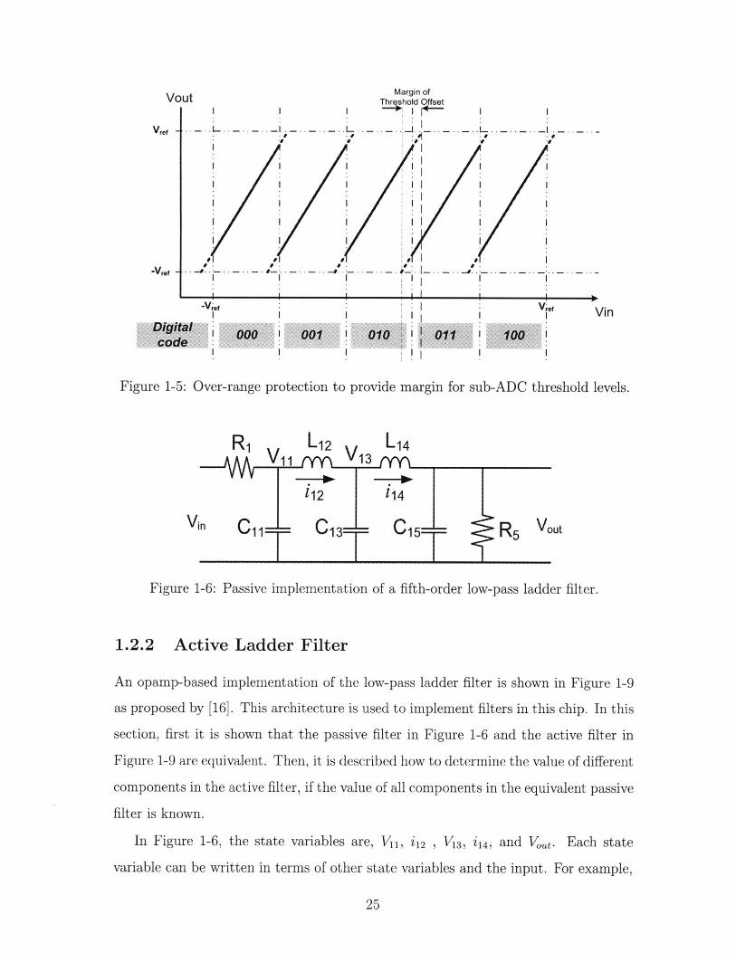
1-5 Over-range protection to provide margin for sub-ADC threshold levels. 25
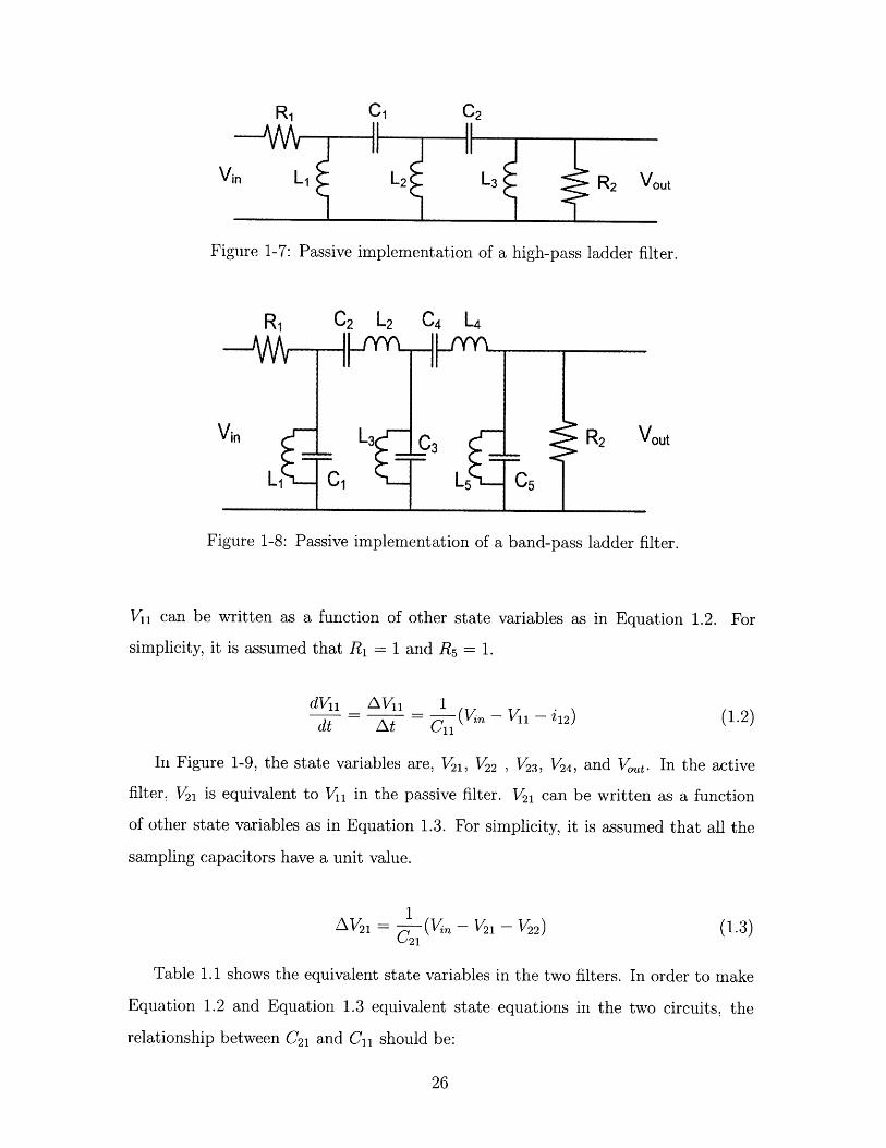
1-6 Passive implementation of a fifth-order low-pass ladder filter. . . . . . 25
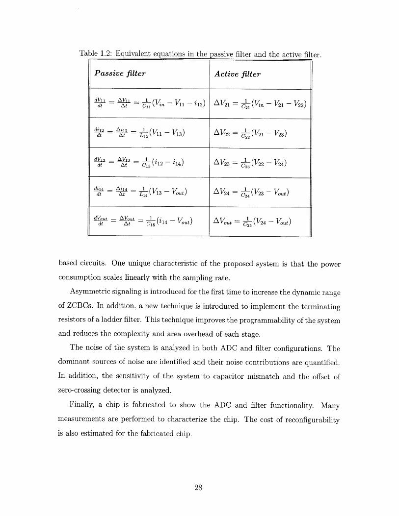
1-7 Passive implementation of a high-pass ladder filter. . . . . . . . . . . 26
1-8 Passive implementation of a band-pass ladder filter. . . . . . . . . . . 26
1-9 Passive implementation of a band-pass ladder filter. . . . . . . . . . . 27
2-1 Basic opamp-based amplifier. . . . . . . . . . . . . . . . . . . . . . . 32
2-2 Basic zero-crossing based amplifier. . . . . . . . . . . . . . . . . . . . 33
2-3 Spliting the output current source. . . . . . . . . . . . . . . . . . . . 36
3-1 Block Diagram of an Ideal System. . . . . . . . . . . . . . . . . . . . 38
3-2 Amplification and integration using the same switched-capacitor circuit. 40
3-3 Building block of a pipeline ADC. . . . . . . . . . . . . . . . . . . . . 40
3-4 Building block of an active ladder filter . . . . . . . . . . . . . . . . . 41
3-5 Schematic of an active ladder filter. . . . . . . . . . . . . . . . . . . . 41
3-6 Basic building block of reconfigurable stage. . . . . . . . . . . . . . . 42
3-7 Single-ended bottom-plate sampling circuit. . . . . . . . . . . . . . . 44
3-8 Possible switches for signal sampling. . . . . . . . . . . . . . . . . . . 45
3-9
3-10
3-11
3-12
3-13
3-14
3-15
3-16
3-17
3-18
3-19
3-20
3-21
3-22
3-23
3-24
3-25
4-1
4-2
4-3
4-4
4-5
4-6
4-7
4-8
4-9
4-10
4-11
4-12
A basic sampling circuit. . . . . . . . . . . . . . . . . . .
Circuit model of the noise of a sampling circuit. . . . . .
General block diagram of a system with transfer function
Thermal Noise of a MOSFET. . . . . . . . . . . . . . . .
Basic differential amplifier and its sources of noise. . . . .
The block diagram of signal sampling. . . . . . . . . . .
Time domain representation of the sampling signal. . . .
Frequency domain representation of the sampling signal.
Frequency domain presentation of the sampling signal.
Schematic of a switched-capacitor integrator. . . . . . . .
Noise model of the integrator. . . . . . . . . . . . . . . .
Block diagram of a third order low-pass filter. . . . . . .
. . . . . . . 66
. . . . . . . 67
of H(s). . . 69
. . . . . . . 71
. . . . . . . 72
. . . . . . . 72
. . . . . . . 73
. . . . . . . 73
. . . . . . . 74
. . . . . . . 77
. . . . . . . 78
. . . . . . . 79
Resistance variation of different switches. . . . . . . . . . . .
Schematic of bootstrap circuit. . . . . . . . . . . . . . . . . .
Simulation of the bootstrap circuit. . . . . . . . . . . . . . .
Schematic of zero-crossing detector. . . . . . . . . . . . . . .
Schematic of a basic current source. . . . . . . . . . . . . . .
Basic building block of reconfigurable stage. . . . . . . . . .
Schematic of a bit-decision-comparator. . . . . . . . . . . . .
Residue plot in ADC configuration. . . . . . . . . . . . . . .
Residue plot of the first stage in ADC configuration.....
The schematic of the analog buffer. . . . . . . . . . . . . . .
Implementation of terminating resistors in ladder filters. . .
Signal swing in zero-crossing based circuits. . . . . . . . . .
Timing of different phases of clock and pulses. . . . . . . . .
The power supply model. . . . . . . . . . . . . . . . . . . . .
Simulated ADC performance when a near Nyquist-rate input
Estimated INL of ADC from simulation. . . . . . . . . . . .
Third order Butterworth filter frequency response. . . . . . .
. . . . . 46
. . . . . 47
. . . . . 48
. . . . . 49
. . . . . 50
. . . . . 52
. . . . . 53
. . . . . 54
. . . . . 55
. . . . . 56
. . . . . 57
. . . . . 58
. . . . . 59
. . . . . 61
is applied. 62
. . . . . 63
. . . . . 63

4-13 Block diagram of a third order low-pass filter with sources of noise. .
4-14 Noise transfer function of integrators input noise in a third order But-
terworth filter . . . . . . . . . . . . . . . . . . . . . . . ... . . . . . . .
4-15 Noise transfer function of integrator output noise in a third order But-
terw orth filter .. . . . . . . . . . . . . . . . . . . . . . . . . . . . . . .
4-16 Noise of reference voltage based on simulation. . . . . . . . . . . . . .
4-17 The currents that passes through Vcm in a fully differential circuit. .
5-1 Residue plot of a stage with no gain error. . . . . . . . . . . . . . . .
5-2 Residue plot of a stage with gain error. . . . . . . . . . . . . . . . . .
5-3 ADC transfer function when the gain of each stage is larger than the
ideal gain . . . . . . . . . . . . . . . . . . . . . . . . . . . . . . . . .
5-4 ADC transfer function when the gain of each stage is smaller than the
ideal gain . . . . . . . . . . . . . . . . . . . . . . . . . . . . . . . . .
5-5 Transfer function of a third order butterworth filter with 20% mismatch
on only one integrating capacitor. . . . . . . . . . . . . . . . . . . . .
5-6 Transfer function of a third order butterworth filter with 20% mismatch
5-7
5-8
5-9
6-1
6-2
6-3
6-4
6-5
6-6
6-7
6-8
on terminating resistors. . . . . . . . . . . . . . . . . . . . . . . . . .
Passive implementation of a low-pass ladder filter. . . . . . . . . . . .
Active implementation of a low-pass ladder filter. . . . . . . . . . . .
Block diagram of an active low-pass filter with the corresponding input
referred offset of each integrator .. . . . . . . . . . . . . . . . . . . . .
The die photo of the core that consists of eight stages. . . .
The block diagram of the fabricated chip. . . . . . . . . . . .
Layout of one stage. . . . . . . . . . . . . . . . . . . . . . .
The chip configuration for test as an ADC. . . . . . . . . . .
FFT plot of the ADC output with a 1MHz sinusoidal input.
FFT plot of the ADC output at a near Nyquist rate.....
The INL of the ADC with 10-bit quantization levels. . . . .
The FFT plot of the ADC output with grounded inputs. . .
. . . . 98
. . . . 98
. . . . 99
. . . . 100
. . . . 101
. . . . 102
. . . . 103
. . . . 104
6-9 The ADC ENOB at different sampling rates............... 105
6-10 The power consumption and the FOM of the ADC as a function of the
sam pling frequency. . . . . . . . . . . . . . . . . . . . . . . . . . . . . 106
6-11 The ADC ENOB at different ramp rates. . . . . . . . . . . . . . . . . 107
6-12 The ENOB as a function of the input signal frequency. . . . . . . . . 108
6-13 The SFDR as a function of the input signal frequency. . . . . . . . . 109
6-14 The ENOB as a function of the input signal amplitude. . . . . . . . . 110
6-15 Comparison of state of the art non-reconfigurable ADCs (ISSCC 2007-
2010) with this work. . . . . . . . . . . . . . . . . . . . . . . . . . . . 111
6-16 The chip configuration for test as a second order filter. . . . . . . . . 112
6-17 Ideal and measured filter transfer function for a second order butter-
w orth filter. . . . . . . . . . . . . . . . . . . . . . . . . . . . . . . . . 113
6-18 The chip configuration for test as a third order filter. . . . . . . . . . 114
6-19 Ideal and measured filter transfer function for a third order butterworth
filter. . . . . . . . . . . . . . . . . . . . . . . . . . . . . . . . . . . . . 115
6-20 The main tone and its harmonic at the output of the ADC that mea-
sures the output of a third order low-pass filter. . . . . . . . . . . . . 116
7-1 Two stages of ZCBCs with the corresponding signals. . . . . . . . . . 123
7-2 Time-domain representation of Vsi and Vcont,o that send an analog
signal from one stage to the next stage. . . . . . . . . . . . . . . . . . 124
7-3 Programmable capacitor in the feedback of a ZCBC circuit. . . . . . 125
7-4 Alternate method to implement a programmable capacitor in the feed-
back of a ZCBC circuit. . . . . . . . . . . . . . . . . . . . . . . . . . 125
7-5 Simplified method to implement a programmable capacitor in the feed-
back of a ZCBC circuit. . . . . . . . . . . . . . . . . . . . . . . . . . 126
A-1 The script to program the chip Part 1. . . . . . . . . . . . . . . . . . 128
A-2 The script to program the chip Part 2. . . . . . . . . . . . . . . . . . 129
A-3 The script to program the chip Part 3. . . . . . . . . . . . . . . . . . 130
A-4 The script to program the chip Part 4. . . . . . . . . . . . . . . . . . 131
A-5 The script to program the chip
A-6 The script to program the chip
A-7 The script to program the chip
A-8 The script to program the chip
A-9 The script to program the chip
A-10 The script to program the chip
A-11 The script to program the chip
A-12 The script to program the chip
A-13 The script to program the chip
Part 5.
Part 6.
Part 7.
Part 8.
Part 9.
Part 10.
Part 11.
Part 12.
Part 13.
. . . . . . . . . . . . . . . . 132
. . . . . . . . . . . . . . . . 133
. . . . . . . . . . . . . . . . 134
. . . . . . . . . . . . . . . . 135
. . . . . . . . . . . . . . . . 136
. . . . . . . . . . . . . . . . 137
. . . . . . . . . . . . . . . . 138
. . . . . . . . . . . . . . . . 139
. . . . . . . . . . . . . . . . 140
B-1 Integral calculation by mathematica . . . . . . . . . . . . . . . . . .
C-1 Block diagram of a third order low-pass filter with sources of noise.
D-1 Schematic of an amplifier. . . . . . . . . . . . . . . . . . . . . . . .
D-2 Phase 2 of the amplifier. . . . . . . . . . . . . . . . . . . . . . . . .
142
144
146
146

16

List of Tables
1.1 Equivalent state variables in the passive filter and the active filter. . 27
1.2 Equivalent equations in the passive filter and the active filter. . . . . 28
1.3 The value of the components in the active filter based on the value of
their corresponding components in the equivalent passive filter. . . . . 29
3.1 Ratio of feedback capacitor to the sampling capacitor for each stage of
filter and different types of filters. . . . . . . . . . . . . . . . . . . . . 43
3.2 Offset adjustment of ZCBC detector based on the programmable load
of the first stage. ....... ............................. 50
3.3 Offset adjustment of bit-decision-comparator. . . . . . . . . . . . . . 53
4.1 Noise bandwidth of low-pass filters when all poles are located at the
sam e frequency. . . . . . . . . . . . . . . . . . . . . . . . . . . . . . . 70
6.1 Cost of Reconfigurability.. . . . . . . . . . . . . . . . . . . . . . 117
6.2 Summary of Measurements. . . . . . . . . . . . . . . . . . . . . . . . 117
B.1 Noise bandwidth of low-pass filters when all poles are located at the
sam e frequency. . . . . . . . . . . . . . . . . . . . . . . . . . . . . . . 141

18
Chapter 1
Introduction
While digital FPGAs provide a fast and cost-efficient method to prototype digital
circuits, the development of similar system for analog circuits is still limited because
it is difficult to realize a programmable analog system that can be configured to wide
variety of analog circuits. A highly programmable analog system that can be config-
ured for an arbitrary analog functionality is very valuable. Many electronic devices
use multiple communication standards. As the number of communication standards
are growing rapidly, electronic devices tend to incorporate more communication stan-
dards, which increases the cost of the system. To integrate multiple standards on the
same chip, a highly-programmable analog system can replace the analog blocks of all
these systems. In addition, highly-programmable analog systems can be used as the
analog core of software defined radios (SDR) to perform its required analog function-
alities such as analog to digital conversion (ADC), filtering, and programmable gain
amplification. Clearly, SDR requires programmable radio frequency circuits as well
(such as programmable mixer, low-noise amplifier, oscillator). Highly programmable
analog systems can also be used in fast prototyping of analog systems. They can
also be used for educational purposes (similar to digital FPGAs that are used in
educational implementation of digital systems).
Field programmable analog arrays (FPAA) have been previously proposed [1] . It
uses continuous-time blocks whose gain is programmable by changing transconduc-
tance of amplifiers. Programmable connectivity between analog circuits is a major
challenge in reconfigurable analog systems. It uses permanent connection between
adjacent blocks and sets the gain of adjacent blocks to zero to effectively discon-
nect them. Another implementation uses programmable transconductance and pro-
grammable capacitor to control the gain of stages [2]. A programmable ADC that
can be configured as sigma-delta or pipeline employs programmable capacitors, pro-
grammable connectivity, and adjustable biasing [3]. This project demonstrates a
highly-reconfigurable analog system that can be used to implement pipeline ADCs
and switched-capacitor filters. Zero-crossing based circuits (ZCBC) are utilized for
superior power efficiency and reconfigurability.
In the rest of this chapter, ADCs and switched-capacitor filters are reviewed. In
Chapter 2, zero-crossing based circuits are described. Chapter 3 describes how the
system is implemented. Chapter 4 analyzes the noise of the system and Chapter 5
reviews the sensitivity of the reconfigurable system to capacitor mismatch and to the
offset of the zero-crossing detectors. Chapter 6 describes the measurement results of
the fabricated chip and Chapter 7 concludes the thesis.
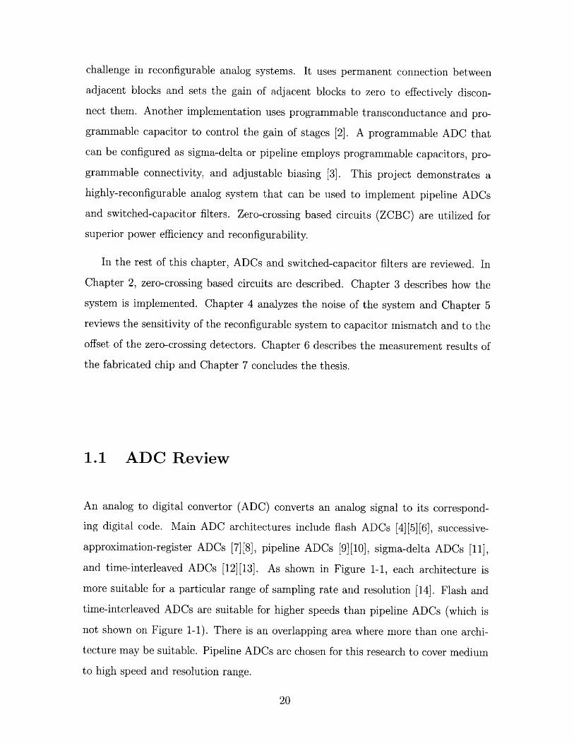
1.1 ADC Review
An analog to digital convertor (ADC) converts an analog signal to its correspond-
ing digital code. Main ADC architectures include flash ADCs [4][5][6], successive-
approximation-register ADCs [7][8], pipeline ADCs [9][10], sigma-delta ADCs [11],
and time-interleaved ADCs [12][13]. As shown in Figure 1-1, each architecture is
more suitable for a particular range of sampling rate and resolution [14]. Flash and
time-interleaved ADCs are suitable for higher speeds than pipeline ADCs (which is
not shown on Figure 1-1). There is an overlapping area where more than one archi-
tecture may be suitable. Pipeline ADCs are chosen for this research to cover medium
to high speed and resolution range.
INDUSTRIAL,-MEASUREMENT
2 4 --
22- -o"AU
20- -,AOUSTO
. . .. . ....... HIGH SPEED:Z18 INSTRUMENTATION,O VIDEO, IF SAMPLING,F 6 SOFTWARE RADIO, ETC.~16 -
(0W 14-
12-
MEASUREMENT
STATE OF THE ART10- (APPROXIMATE)
10 100 1 k 10k 100k IM I OM IlOOM 1G
SAMPLING RATE (Hz)
Figure 1-1: ADC Architecture for different sampling rates and resolution [14].
1.1.1 Pipeline ADC
Pipeline ADCs consist of several identical stages that are cascaded. The block dia-
gram of each stage is shown in Figure 1-2. Each stage is composed of four components,
a sub-ADC, a digital-to-analog convertor (DAC), an adder, and an amplifier. A sub-
ADC is usually an ADC with limited number of quantization levels, n. For example,
it may be a flash ADC with only one or two bits, while the overall pipeline ADC may
have 10-14 bits.
When an analog signal is converted to a digital code, there is a difference be-
tween the amplitude of the analog signal and the amplitude of the digital code. The
difference is due to the limited number of the bits in the digital code and is called
quantization error. As the number of the digital bits increases, the quantization error
reduces.
In pipeline ADCs, the sub-ADC has a limited resolution. To increase the overall
resolution of a pipeline ADC, the quantization error of the sub-ADC is sent to the
Vin sub-ADC -- DAC x A Vout
n
Digital Code
Figure 1-2: Block diagram of one stage of a pipeline ADC
subsequent stages. Subsequent stages convert the quantization error of earlier stages
to the corresponding digital codes and add it to the overall digital output. As a result,
each cascaded stage increases the resolution of the ADC. To find the quantization
error of each stage, V, the output of the sub-ADC is sent to a DAC and subtracted
from the input signal as shown in Figure 1-2. Since the amplitude of V is small, it is
typically amplified. If n is the number of the bits of the sub-ADC, the range of V is
smaller than the full-scale input range by a factor of -L. If it is desired that Vin and
Vst have the same range, the amplifier should have a gain of 2n. This is usually the
case for pipeline ADCs utilizing identical stages. Figure 1-3 shows the relationship
between the input and output of each stage and the corresponding digital code if the
sub-ADC has 2-bit resolution.
To construct the digital output code of a pipeline ADC, the output of each stage
should be multiplied by the gain of earlier stages and added to the final digital code.
If a pipeline ADC has k stages, and each stage has n quantization bits (Di for stage
i), the digital output code of the ADC is given by:
ADCcode D1 + D2 * 2n + D3 * 22n + ... + Dk * 2 (k-1) (1. 1)
1.1.2 Over-Range Protection in Pipeline ADC
The sub-ADC may have an offset in its threshold voltages for different digital codes
as shown in Figure 1-4. As a result, V0st may exceed the full scale input range (Vrej
Vout
-Vre -V A2 Vr 2 V,
00 1 01 1 10 11
Figure 1-3: The relationship between the input and output signals for each stage ofa pipeline ADC when the sub-ADC has 2-bit resolution (n=2).
or -Vef) of subsequent stages for some values of Vm,. In that case, the subsequent
stages cannot resolve the input voltage in the region that saturates the subsequent
stage. To avoid this problem, the threshold voltages of the sub-ADC are chosen so
that the output does not exceed Vef or -Vef as shown in Figure 1-5. If needed, the
number of threshold levels can be increased. This method provides some margin of
error for the threshold of the sub-ADC digital codes.
1.2 Filter Review
There are two main architectures to implement switched-capacitor filters, biquad
filters [15] and ladder architecture [16]. Since this chip is intended to implement
any arbitrary filter, the exact functionality of each stage is not known a priori. For
example, the order of the filter and its cutoff frequency are programmable. Since
biquad-based filters are sensitive to capacitor matching [16], ladder filter architecture
is used in this research.
Vout Threshold Offset Threshold Offset
IVe -V :f2I
-v 2'2fv/ Vin
Dgtl00 01 1 10 1code
Figure 1-4: The effects of the offset of the sub-ADC threshold levels on the outputvoltage.
1.2.1 Passive Ladder Filter
Figure 1-6 shows a passive ladder filter. The number of storage components (capaci-
tors, and inductors) determines the order of the filter and the type of the components
determines the type of the filter. For example, Figure 1-6 shows a low-pass filter. If
the capacitors are replaced with inductors, and the inductors are replaced with ca-
pacitors, a high-pass filter is obtained (Figure 1-7). Similarly, replacing capacitors in
Figure 1-6 with a parallel combination of a capacitor and an inductor, and replacing
the inductor with a series combination of a capacitor and an inductor results in a
band-pass filter (Figure 1-8). The value of the capacitors, inductors, and the resistors
determine the cut-off frequency of the filter and the shape of the filter (e.g. Butter-
worth, Chebyshev, and Elliptic). The design of ladder filters is researched extensively
[17][18]. The value of each component in the ladder filters can be easily determined
with software as well [19].
* .1
I I
I I
I I
I I 1/
I I
Margin ofThehold Offset
V:I
(.
~Vmf V00
000 010 011
Vin
Figure 1-5: Over-range protection to provide margin for sub-ADC threshold levels.
Vin Vout
Figure 1-6: Passive implementation of a fifth-order low-pass ladder filter.
1.2.2 Active Ladder Filter
An opamp-based implementation of the low-pass ladder filter is shown in Figure 1-9
as proposed by [16]. This architecture is used to implement filters in this chip. In this
section, first it is shown that the passive filter in Figure 1-6 and the active filter in
Figure 1-9 are equivalent. Then, it is described how to determine the value of different
components in the active filter, if the value of all components in the equivalent passive
filter is known.
In Figure 1-6, the state variables are, V11, i12 , V13 , i14 , and Vt. Each state
variable can be written in terms of other state variables and the input. For example,
Vout
Vref -
-Vret -'I
I.
R1 C
Vin L1 L2 R2 Vout
Figure 1-7: Passive implementation of a high-pass ladder filter.
C2 L2 C4 L4R1 C
Vin
L i~ C1
C3 Vout
L5 C5
1-8: Passive implementation of a band-pass ladder filter.
V11 can be written as a function of other state variables as in Equation 1.2. For
simplicity, it is assumed that R1 = 1 and R5 = 1.
dVnj _ AVn 1dt At C1 ( n- Vn i12 ) (1.2)
In Figure 1-9, the state variables are, %21, V2 2 , V23, V2 4, and V1 ot. In the active
filter, V21 is equivalent to V1 in the passive filter. V2 1 can be written as a function
of other state variables as in Equation 1.3. For simplicity, it is assumed that all the
sampling capacitors have a unit value.
1V%1 z= C(1K - V 1 -V 2 2)0A2 21 n 2 (1.3)
Table 1.1 shows the equivalent state variables in the two filters. In order to make
Equation 1.2 and Equation 1.3 equivalent state equations in the two circuits, the
relationship between C21 and C11 should be:
Figure
R2
L3

C 2 1 - Cn - fiAt
where At in the passive filter is equivalent to the period of each clock cycle in the
active implementation. Table 1.2 shows the equivalent state equations for the two
circuits. Since the state equations are equivalent, the two circuits are equivalent as
well. Table 1.3 shows the value of each component in the active filter based on the
value of its corresponding compoent in the passive filter.
V 2 V24
Figure 1-9: Passive implementation of a band-pass ladder filter.
Table 1.1: Equivalent state variables in the passive filter and the active filter.
Passive filter Active filter
Vn1 V21
i12 V2 2
V13 V23
i14 V 2 4
vout out
1.2.3 Thesis Contribution
In this research, a new architecture for a reconfigurable analog system is proposed.
This architecture is suitable to implement an ADC and low-pass ladder filters. Zero-
crossing based circuits are used for the first time to implement a reconfigurable sys-
tem. It is also the first time that filter functionality is achieved with zero-crossed
(1.4)
filter and the active filter.
based circuits. One unique characteristic of the proposed system is that the power
consumption scales linearly with the sampling rate.
Asymmetric signaling is introduced for the first time to increase the dynamic range
of ZCBCs. In addition, a new technique is introduced to implement the terminating
resistors of a ladder filter. This technique improves the programmability of the system
and reduces the complexity and area overhead of each stage.
The noise of the system is analyzed in both ADC and filter configurations. The
dominant sources of noise are identified and their noise contributions are quantified.
In addition, the sensitivity of the system to capacitor mismatch and the offset of
zero-crossing detector is analyzed.
Finally, a chip is fabricated to show the ADC and filter functionality. Many
measurements are performed to characterize the chip. The cost of reconfigurability
is also estimated for the fabricated chip.
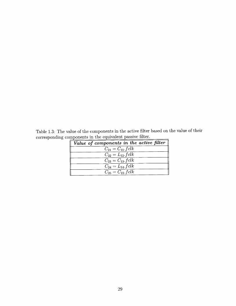
Table 1.3: The value of the components in the active filter based on the value of their
corresponding components in the equivalent passive filter.
Value of components in the active filterC 21 Cnl.f clkC22 = L 12.f clk
C23 = C13.f clkC24 = L 14 .f clkC25 = C 15.f clk

30
Chapter 2
Zero-Crossing-Based Circuits
(ZCBC)
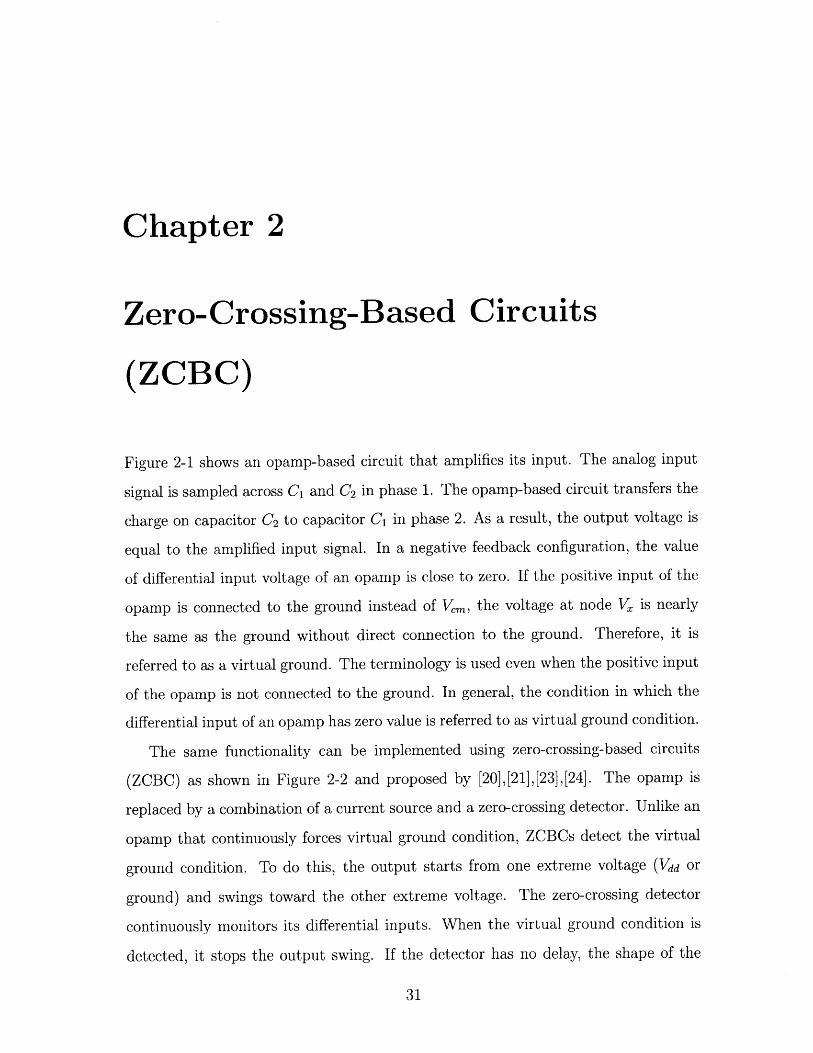
Figure 2-1 shows an opamp-based circuit that amplifies its input. The analog input
signal is sampled across C1 and C2 in phase 1. The opamp-based circuit transfers the
charge on capacitor C2 to capacitor C1 in phase 2. As a result, the output voltage is
equal to the amplified input signal. In a negative feedback configuration, the value
of differential input voltage of an opamp is close to zero. If the positive input of the
opamp is connected to the ground instead of V,,, the voltage at node V, is nearly
the same as the ground without direct connection to the ground. Therefore, it is
referred to as a virtual ground. The terminology is used even when the positive input
of the opamp is not connected to the ground. In general, the condition in which the
differential input of an opamp has zero value is referred to as virtual ground condition.
The same functionality can be implemented using zero-crossing-based circuits
(ZCBC) as shown in Figure 2-2 and proposed by [20],[21],[23],[24]. The opamp is
replaced by a combination of a current source and a zero-crossing detector. Unlike an
opamp that continuously forces virtual ground condition, ZCBCs detect the virtual
ground condition. To do this, the output starts from one extreme voltage (Vdd or
ground) and swings toward the other extreme voltage. The zero-crossing detector
continuously monitors its differential inputs. When the virtual ground condition is
detected, it stops the output swing. If the detector has no delay, the shape of the
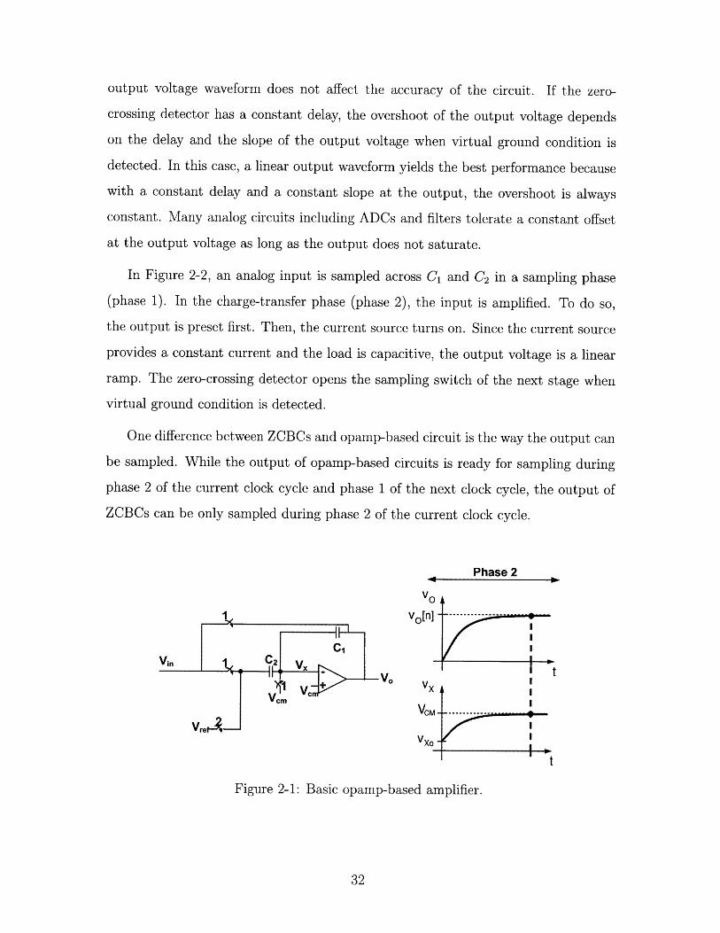
output voltage waveform does not affect the accuracy of the circuit. If the zero-
crossing detector has a constant delay, the overshoot of the output voltage depends
on the delay and the slope of the output voltage when virtual ground condition is
detected. In this case, a linear output waveform yields the best performance because
with a constant delay and a constant slope at the output, the overshoot is always
constant. Many analog circuits including ADCs and filters tolerate a constant offset
at the output voltage as long as the output does not saturate.
In Figure 2-2, an analog input is sampled across C1 and C2 in a sampling phase
(phase 1). In the charge-transfer phase (phase 2), the input is amplified. To do so,
the output is preset first. Then, the current source turns on. Since the current source
provides a constant current and the load is capacitive, the output voltage is a linear
ramp. The zero-crossing detector opens the sampling switch of the next stage when
virtual ground condition is detected.
One difference between ZCBCs and opamp-based circuit is the way the output can
be sampled. While the output of opamp-based circuits is ready for sampling during
phase 2 of the current clock cycle and phase 1 of the next clock cycle, the output of
ZCBCs can be only sampled during phase 2 of the current clock cycle.
Phase 2
V0
1 vo[n] ------- - ---Ii
C1Vin 1 C2 y -
-r v_+ V0VCM M>
VreVxO
i t
Figure 2-1: Basic opamp-based amplifier.
Phase 2
V0Vo[n] .......--- .--- .-
t
C1 y
Vin 1 C2 ... ........
1 +~ e
2 resett
reset,Sdd
0 t
Figure 2-2: Basic zero-crossing based amplifier.
2.1 Advantages of ZCBCs
ZCBCs have several advantages. One important advantage is its lack of explicit
feedback. Since opamp-based circuits have negative feedback and more than one
pole, the stability of the circuit is an important issue, and often requires large power
consumption. If the load or the feedback ratio of the circuit is variable, the frequency
compensation should be designed for the worst case situation. In ZCBCs, since there
is no explicit feedback, there is no stability concern even with widely varying load
and feedback condition.
While the speed of transistors improves in the new technology nodes, the intrinsic
gain of transistors degrades. Since large open-loop gain is desired for opamps, the
design of opamps is more challenging in new technology nodes. One method to
increase the gain is by cascading several gain stages which deteriorates the stability
of the system because of more poles. Another method to increase the gain of an
opamp is cascoding which is challenging with low supply voltage in new technology
nodes. As a result, opamp-based circuits are harder to design in new technology
nodes. ZCBC is more suitable for new technology nodes since the current source and
the zero-crossing detector can be optimized independently. Zero-crossing detector can
use cascaded stages for higher gain since stability is not a concern.
Finally, the power consumption of ZCBCs scale with the sampling frequency.
This is due to the fact that once virtual ground condition is detected, all parts of
the analog circuit including the current sources and zero-crossing detector turn off
and the circuits do not consume static power any longer. As a result, if the circuit
operates at a much lower speed, the power consumption scales accordingly. The power
consumption of opamp-based circuits can also scale by adjusting its bias currents.
However, the power consumption of ZCBCs can be adjusted for a very wide range of
sampling frequencies.
2.2 Sources of Nonlinearity
There are several sources of nonlinearity in ZCBCs [23]. The first source of nonlin-
earity is the delay of the zero-crossing detector. The delay causes an overshoot at the
output. If the output is a linear ramp, a constant delay of zero-crossing detector gen-
erates a constant overshoot and can be treated as a constant offset. However, delay
variation of zero-crossing detector from one clock cycle to another (for example, due
to common-mode variation) causes overshoot variation, which causes an error at the
output.
In new technology nodes, the output resistance of current sources are low. As
a result, when the output voltage changes, the current of the current source does
not stay constant and the slope of the output voltage does not stay constant either.
The nonlinearity of current sources causes signal-dependant overshoot variation. This
gives a similar effect to that of finite gain in opamps. In addition, voltage-dependent
capacitive load introduces nonlinearity at the output ramp, which causes overshoot
variation. In this chip, the size of the linear capacitive load is much larger than the
nonlinear parasitic capacitors. The delay of the zero-crossing detector is also sensitive
to the common mode voltage variation and the ramp rate at its input.
In opamp-based circuits, the current that passes through the sampling switches
approaches to zero with time. As a result, the voltage drop on the sampling switches
is negligible. In ZCBCs, the current that passes through the sampling switches stays
constant during the sampling period. As a result, there is a voltage drop across the
switches during the sampling time. If the output current source provides a constant
current and the switch has a constant resistance, the voltage drop is constant and
causes an offset. However, current sources have a limited output resistance (especially
in new technology nodes). In addition, the resistance of switches changes widely with
the input voltage; as a result, there is a variation on the voltage drop of the sampling
switches, which causes an error at the output and the corresponding nonlinearity.
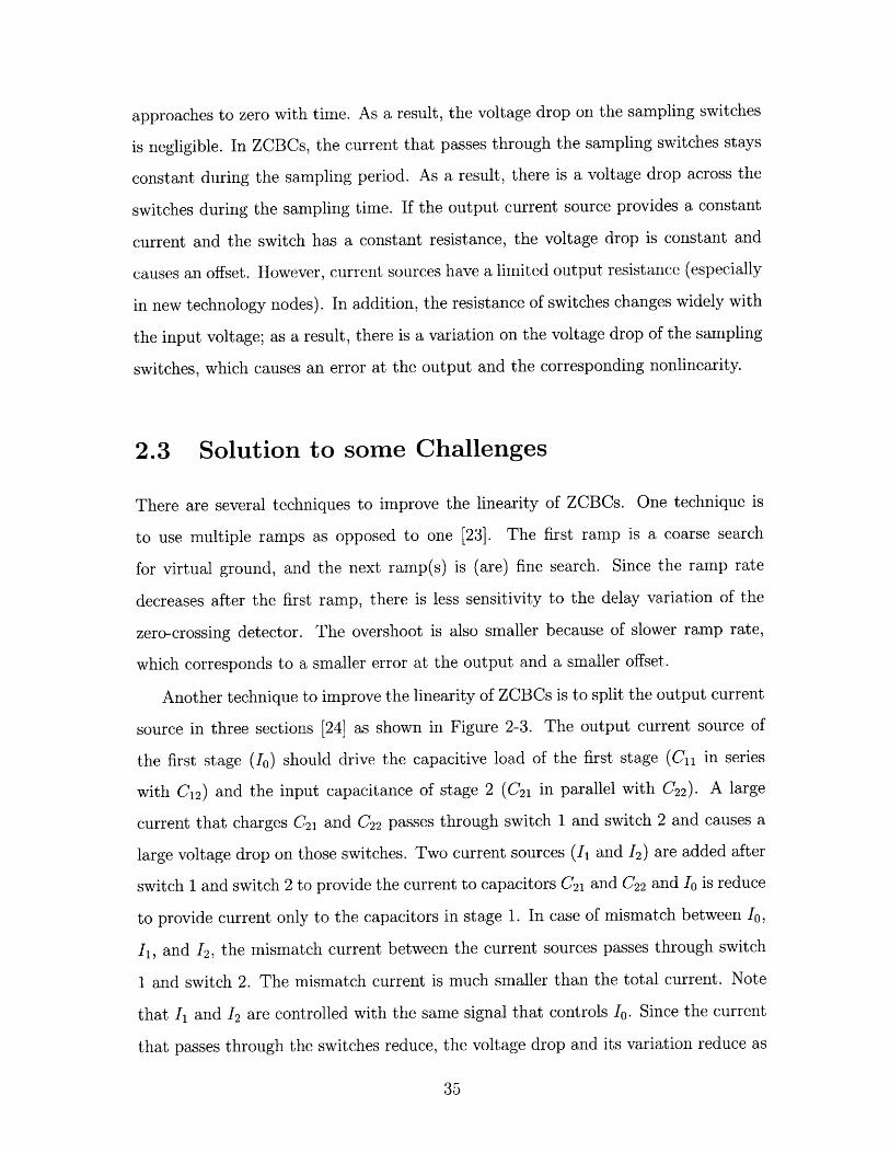
2.3 Solution to some Challenges
There are several techniques to improve the linearity of ZCBCs. One technique is
to use multiple ramps as opposed to one [23]. The first ramp is a coarse search
for virtual ground, and the next ramp(s) is (are) fine search. Since the ramp rate
decreases after the first ramp, there is less sensitivity to the delay variation of the
zero-crossing detector. The overshoot is also smaller because of slower ramp rate,
which corresponds to a smaller error at the output and a smaller offset.
Another technique to improve the linearity of ZCBCs is to split the output current
source in three sections [24] as shown in Figure 2-3. The output current source of
the first stage (10) should drive the capacitive load of the first stage (Cn in series
with C12) and the input capacitance of stage 2 (C21 in parallel with C22). A large
current that charges C21 and C22 passes through switch 1 and switch 2 and causes a
large voltage drop on those switches. Two current sources (I1 and 12) are added after
switch 1 and switch 2 to provide the current to capacitors C21 and C22 and 1o is reduce
to provide current only to the capacitors in stage 1. In case of mismatch between 1o,
I1, and '2, the mismatch current between the current sources passes through switch
1 and switch 2. The mismatch current is much smaller than the total current. Note
that I1 and I2 are controlled with the same signal that controls 1o. Since the current
that passes through the switches reduce, the voltage drop and its variation reduce as
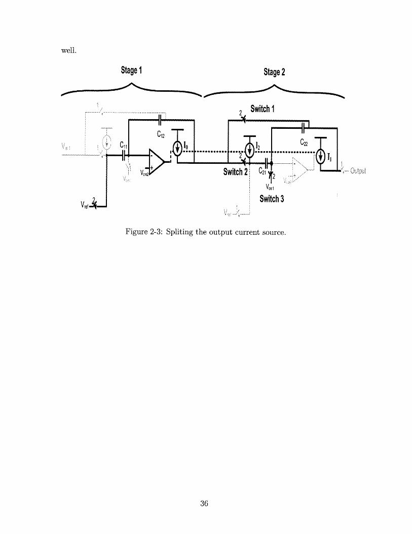
Stage 2
Switch 2 Gi'
Vc h
Switch 3
Figure 2-3: Spliting the output current source.
well.
Stage I
A-
tt

Chapter 3
System Architecture and
Implementation
In this chapter, the architecture of the system is described and it is shown how
different functionalities are implemented. Then, the implementation of individual
circuit blocks is reviewed. A new technique is described to implement the termination
resistor in the filter. In addition, asymmetric differential signaling is introduced which
increases the dynamic range of the signal. Finally, full system simulation for a 10-bit
ADC and a third-order Butterworth filter are presented.
3.1 System Description
Figure 3-1 shows the block diagram of the ideal system. It consists of configurable
analog blocks, programmable switches, and the configuration block. Configurable
analog blocks have both amplification and integration functionality. Unlike digital
FPGAs, the required connectivity of analog blocks is limited (both in terms of number
of connections and the distance between source and destination blocks). As a result,
the switches are placed only between adjacent blocks.
Figure 3-2 shows how an opamp-based switched-capacitor circuit can either am-
plify or integrate the input signal. If the input signal is sampled on both capacitors
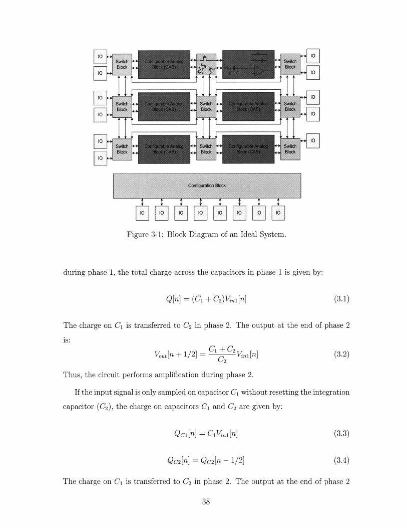
'411
EH"iH
T T
LJLLJrJHJ JLFigure 3-1: Block Diagram of an Ideal System.
during phase 1, the total charge across the capacitors in phase 1 is given by:
Q[n] = (C1 + C2 )1i[n] (3.1)
The charge on C1 is transferred to C2 in phase 2. The output at the end of phase 2
is:
Vot[n + 1/2] = 2V. 1 [n]C2
(3.2)
Thus, the circuit performs amplification during phase 2.
If the input signal is only sampled on capacitor C1 without resetting the integration
capacitor (C2), the charge on capacitors C1 and C2 are given by:
Qc1[n] = C1 V%1 [n]
Qc2[n] = Qc2[n - 1/2]
(3.3)
(3.4)
The charge on C1 is transferred to C2 in phase 2. The output at the end of phase 2
10
swfthNoCk
10A r- h L--j
is:
C1 Vi 1 [n] + QC2 [n - 1/2] -CVo0 tn-+ 1/2- 0 2 -C2%1[n] + Vut[n - 1/2] (3.5)
C2 C2
Thus, the circuit performs integration.
Figure 3-3 shows the building block of a pipeline ADC. It has a set of bit-decision-
comparators (BDC) and reference voltages in addition to the basic circuit of Figure
3-2. The circuit samples the input across both capacitors during phase 1. BDCs
operate as the sub-ADC for each stage of a pipeline ADC. The sampled input voltage
is amplified during phase 2. Vref1, Vef 2, and Vref 3 are related to the outputs of the
DAC in each stage of a pipeline ADC which are controlled by the outputs of BDCs
and added to the output. The output voltage is given by:
C1 + C2 []C C1 + C2(V[n]v) (36)Von + 1/2] 2C2 C2
where VDAC is the desired voltage of the DAC in each stage of a pipeline ADC, and
Vefx is one of Vref1, Vref 2 , and Kef 3 depending on the outputs of the BDCs. The
output of the BDCs are also used to generate the final digital code for the sampled
input.
Similarly, Figure 3-4 shows the building block of a low-pass filter. It samples
two inputs that are being added and integrated. With differential implementation of
these blocks, inverting a signal can be easily performed by switching the polarity of
the differential signal.
Figure 3-5 shows the connectivity of five integrating blocks that form a fifth-order
low-pass filter. The exact transfer function of the filter depends on the integration
coefficient of each block.
3.1.1 The Need for ZCBC Implementation
Implementing the system with opamps raises two concerns. One is that in a highly-
programmable system, the output load of the opamp is not known a priori. As a
Vin1 ,
VoutVCm
Figure 3-2: Amplification and integration using the same switched-capacitor circuit.
Vin1
Figure 3-3: Building block of a pipeline ADC.
result, the frequency compensation must be designed for the worst-case load and
feedback conditions. This greatly compromises speed and power consumption. An-
other concern with opamp-based circuits is the power consumption while the operat-
ing frequency changes. Opamps consume static power and are often optimized for a
particular speed. In a reconfigurable system, the required sampling rate may change
from one application to another. If the building blocks of the system use opamps, the
power consumption of the system does not scale with sampling frequency for a wide
range of sampling frequencies. To address both of these concerns with opamp-based
circuits, zero-crossing based circuits (ZCBCs) have been used in the proposed system.
Vin1
2 V mVCm ___j v
Vin2 CO
Vem 2 vem
Figure 3-4: Building block of an active ladder filter.
V nt+ + ++
Figure 3-5: Schematic of an active ladder filter.
3.1.2 Implementation of a Reconfigurable Stage
Figure 3-6 shows the basic building blocks of each reconfigurable stage. It includes
two sets of sampling capacitors (C1 and CO) as needed during the filter functional-
ity. During the ADC functionality, only C1 is active. A zero-crossing detector and
its corresponding current sources are used instead of an opamp. BDCs that con-
trol reference voltages are active for ADC functionality. For simplicity 3 BDCs and
reference voltages are shown, but the real implementation contains 5 BDCs and refer-
ence voltages. Seven programmable capacitors (Cfl-Cf7 ) are placed in the feedback,
which provide a reconfigurable integration coefficient. Gate-boosting blocks are used
to lower the resistance of the reconfigurable switches. The analog input of the gate-
boosting blocks is buffered to reduce the effects of its capacitive load on other blocks.
All circuit components are reviewed in the next sections. The schematic is shown as
single-ended for simplicity, but it is implemented differentially.
Figure 3-6: Basic building block of reconfigurable stage.
3.1.3 ADC Configuration
In the pipeline ADC configuration, 5 BDCs provide 2.6-bit quantization for each stage
(which includes 0.6 bit over-range protection). For example, cascading five stages
provides 10-bit resolution. Each stage has digitally-configurable feedback capacitors
(Cf I-Cf) which provide programmable integration-coefficients for filter functionality.
While these capacitors are not active in an ADC configuration, their parasitic capac-
itors increase the capacitive load at the output. As a result, the power consumption
increases too. The programmable capacitors for the filter may be 10 to 20 times
larger than the ADC capacitors, resulting in parasitic capacitors that are comparable
in value to the ADC capacitors. Configurable switches are placed on both sides of
the feedback capacitors to isolate their parasitics from the rest of the stage. Switches
are bootstrapped to reduce their size and parasitic capacitance since bootstrapping
reduces the ON resistance of the switch. To avoid any disturbance on the virtual-
ground node, it is buffered by a source follower before feeding into the bootstrap
block. While most circuits are shown as single-ended, the actual implementation is
differential.
3.1.4 Filter Configuration
In the filter configuration, Vi1 and Vi 2 are sampled across the sampling capacitors
C1 and Co. The binary-weighted reconfigurable feedback capacitors are connected
to configurable switches, which determine the integration ratio. Table 3.1 shows the
ratio of the integration capacitor to the sampling capacitor for several different filters
if the sampling frequency is 50MSPS and the cut-off frequency is at 1MHz. The BDCs
are turned off and only one of the reference voltages is used during the operation.
Table 3.1: Ratio of feedback capacitor to the sampling capacitor for each stage of
filter and different types of filters.
Filter Type Stage 1 Stage 2 Stage 3 Stage j Stage 5
1 st order Butterworth 15.9
2 nd order Butterworth 11.3 11.3
3rd order Butterworth 7.9 15.9 7.9
4 th order Butterworth 6 14.7 14.7 6
5 th order Butterworth 4.9 12.9 15.9 12.9 4.9
5th order Chebyshev 16 8 23 8 16
3.2 System Components
In this section, the main building blocks of each stage are reviewed.
3.2.1 Sampling Circuit
The main criteria for designing a sampling circuit are sampling noise, input band-
width, input voltage swing, and distortion. Bottom-plate sampling is used to reduce
signal-dependent distortion [25] as shown in Figure 3-7. In Figure 3-6, these are the
switches that are closed in phase 1.
Vin Voutld T
Figure 3-7: Single-ended bottom-plate sampling circuit.
The size of the sampling capacitor can be calculated based on the kT/C noise
budget of sampling circuit (which is reviewed in more detail in Chapter 4). The
3dB cut-off frequency of the sampling circuit is a function of switch resistance and
sampling capacitance as shown in Equation 3.7. The 3db frequency is set to be larger
than the signal bandwidth.
f3dB - (3.7)27rRswitchC
Another concern is the input-dependant resistance of the sampling switch. Smaller
input voltage swing causes less resistance variation at the cost of lower dynamic range.
In opamp-based circuits, the current that passes through the switches approaches zero,
but in ZCBCs, the current stays constant until the sampling moment. As a result,
resistance variation of the two switches causes output voltage variation in ZCBCs.
The resistance of the top-plate switch changes due to changes in V". The resistance
of the bottom-plate switch changes due to changes on common-mode voltage (here
shown as ground).
The top-plate and bottom-plate switches can be implemented in different ways, in-
cluding regular NMOS, high-voltage NMOS, regular transmission gates, transmission
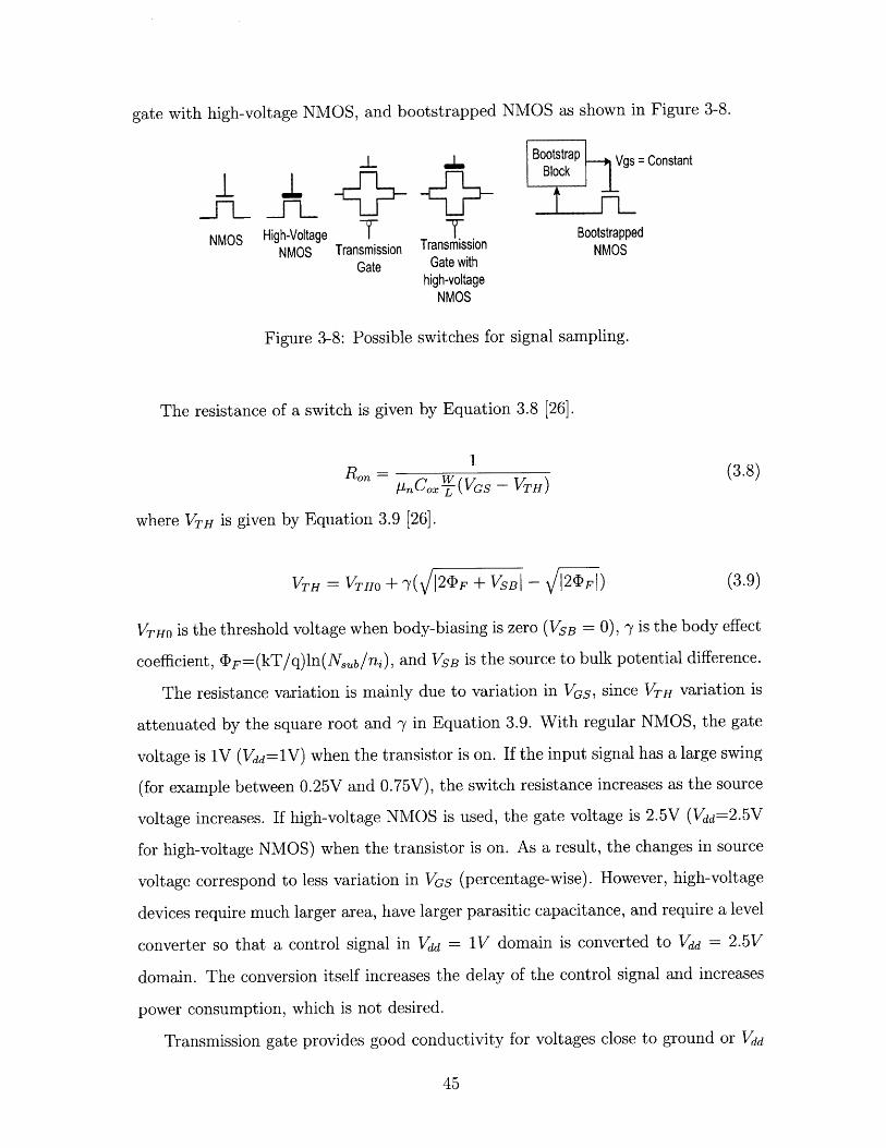
gate with high-voltage NMOS, and bootstrapped NMOS as shown in Figure 3-8.
_i_ Bootstrap Vgs = ConstantBlock
_n_ _n_ rLNMOS High-Voltage T T Bootstrapped
NMOS Transmission Transmission NMOSGate Gate with
high-voltageNMOS
Figure 3-8: Possible switches for signal sampling.
The resistance of a switch is given by Equation 3.8 [26].
1Ro = 1(3.8)
" pnCoxl (VGS - VTH)
where VTH is given by Equation 3.9 [26].
VTH =VTHO + I2 2FI) (3.9)
VTHO is the threshold voltage when body-biasing is zero (VSB = 0), y is the body effect
coefficient, 0F=(kT/q)ln(NSb/i), and VSB is the source to bulk potential difference.
The resistance variation is mainly due to variation in VGS, since VTH variation is
attenuated by the square root and -y in Equation 3.9. With regular NMOS, the gate
voltage is 1V (Vdd=1V) when the transistor is on. If the input signal has a large swing
(for example between 0.25V and 0.75V), the switch resistance increases as the source
voltage increases. If high-voltage NMOS is used, the gate voltage is 2.5V (Vda=2.5V
for high-voltage NMOS) when the transistor is on. As a result, the changes in source
voltage correspond to less variation in VGs (percentage-wise). However, high-voltage
devices require much larger area, have larger parasitic capacitance, and require a level
converter so that a control signal in Vdd 1V domain is converted to Vdd = 2.5V
domain. The conversion itself increases the delay of the control signal and increases
power consumption, which is not desired.
Transmission gate provides good conductivity for voltages close to ground or Vdd
where one of NMOS or PMOS are very conductive. However, for a signal near Vdd/ 2 ,
the transmission gate has a large resistance variation.
Bootstrapping provides a nearly constant VGS across the switch. This implies
that when the source voltage is large (for example 0.7V), the gate voltage exceeds
the supply voltage (for example 1.7V). Since V., and Vd do not exceed Vdd, the
large gate-voltage does not cause reliability problems. The switch resistance still
varies due to changes in the threshold voltage due to the back-gate effect. In this
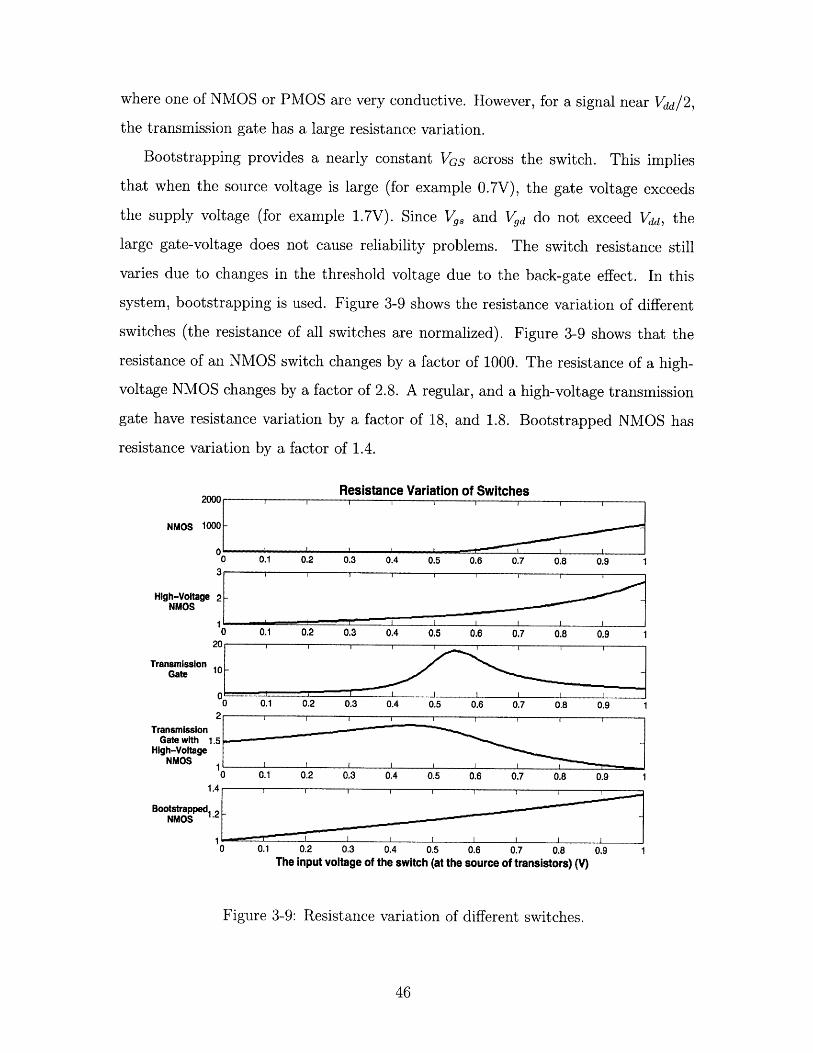
system, bootstrapping is used. Figure 3-9 shows the resistance variation of different
switches (the resistance of all switches are normalized). Figure 3-9 shows that the
resistance of an NMOS switch changes by a factor of 1000. The resistance of a high-
voltage NMOS changes by a factor of 2.8. A regular, and a high-voltage transmission
gate have resistance variation by a factor of 18, and 1.8. Bootstrapped NMOS has
resistance variation by a factor of 1.4.
Resistance Variation of Switches2000
NMOS 1000
0 0.1 0.2 0.3 0.4 0.5 0.6 0.7 0.8 0.9 13
High-Voltage 2 -NMOS
0 0.1 0.2 0.3 0.4 0.5 0.6 0.7 0.8 0.9 120
Transmission 1.7Gate 1
0 0 .0 0.1 0.2 0.3 0.4 0.5 0.6 0.7 0.8 0.9 1
TransmissionGate with 1.5
High-VoltageNMOS 1
0 0.1 0.2 0.3 0.4 0.5 0.6 0.7 0.8 0.9 11.4 FF F FF
Bootstrapped,NMOS
0 0.1 0.2 0.3 0.4 0.5 0.6 0.7 0.8 0.9 1The input voltage of the switch (at the source of transistors) (V)
Figure 3-9: Resistance variation of different switches.
3.2.2 Bootstrapping
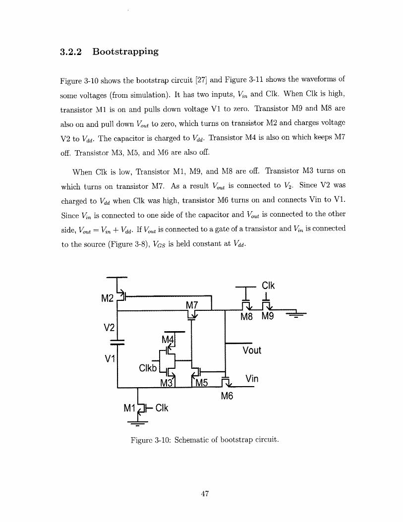
Figure 3-10 shows the bootstrap circuit [27] and Figure 3-11 shows the waveforms of
some voltages (from simulation). It has two inputs, V and Clk. When Clk is high,
transistor M1 is on and pulls down voltage VI to zero. Transistor M9 and M8 are
also on and pull down V0,t to zero, which turns on transistor M2 and charges voltage
V2 to Vdd. The capacitor is charged to Vdd. Transistor M4 is also on which keeps M7
off. Transistor M3, M5, and M6 are also off.
When Clk is low, Transistor M1, M9, and M8 are off. Transistor M3 turns on
which turns on transistor M7. As a result Vst is connected to V2. Since V2 was
charged to Vdd when Clk was high, transistor M6 turns on and connects Vin to V1.
Since V,, is connected to one side of the capacitor and V0st is connected to the other
side, V0ot = Vin + Vdd. If Vout is connected to a gate of a transistor and i, is connected
to the source (Figure 3-8), VGS is held constant at Vdd.
a
V2
V1
ClkIM9
Figure 3-10: Schematic of bootstrap circuit.
M7M8
-M4Vou
ClkbM3 1M5 mVin
M6M1 | Clk
t

Simulation of Bootstrapping Block
0.5> 0-
0 10 20 30 40 50 60
0.5
0 10 20 30 40 50 60
>0
0 10 20 30 40 50 60
> 0 .0 10 20 30 40 50 60
1
.j 0.5
0 0 10 20 30 40 50 60
Time (ns)
Figure 3-11: Simulation of the bootstrap circuit.
3.2.3 Zero-Crossing Detector
Zero-crossing detector replaces the opamp in opamp-based circuits to detect the vir-
tual ground condition. When it detects, zero-crossing detector turns off the sampling
switches of the next stage and the output current sources in its own stage. The
schematic of zero-crossing detector is shown in Figure 3-12 [24]. The first stage con-
sists of a differential amplifier and the second stage is a dynamic inverter [28]. Its
operation is based on the fact that V,, is pre-charged to a voltage larger than the
virtual ground and ramps down linearly, and Vi,, is pre-discharged to a voltage less
than the virtual ground and ramps up linearly. When /,p is high and Vi, is low, V 1
is high. As V,, ramps down and Vi,,n ramps up, the voltage at V 1 starts to reduce.
The second stage monitors V 1 and when it passes the threshold voltage of transistor
M21, it pulls up K72 and pulls down Kecont. The signal Enb is used to preset V 2 before
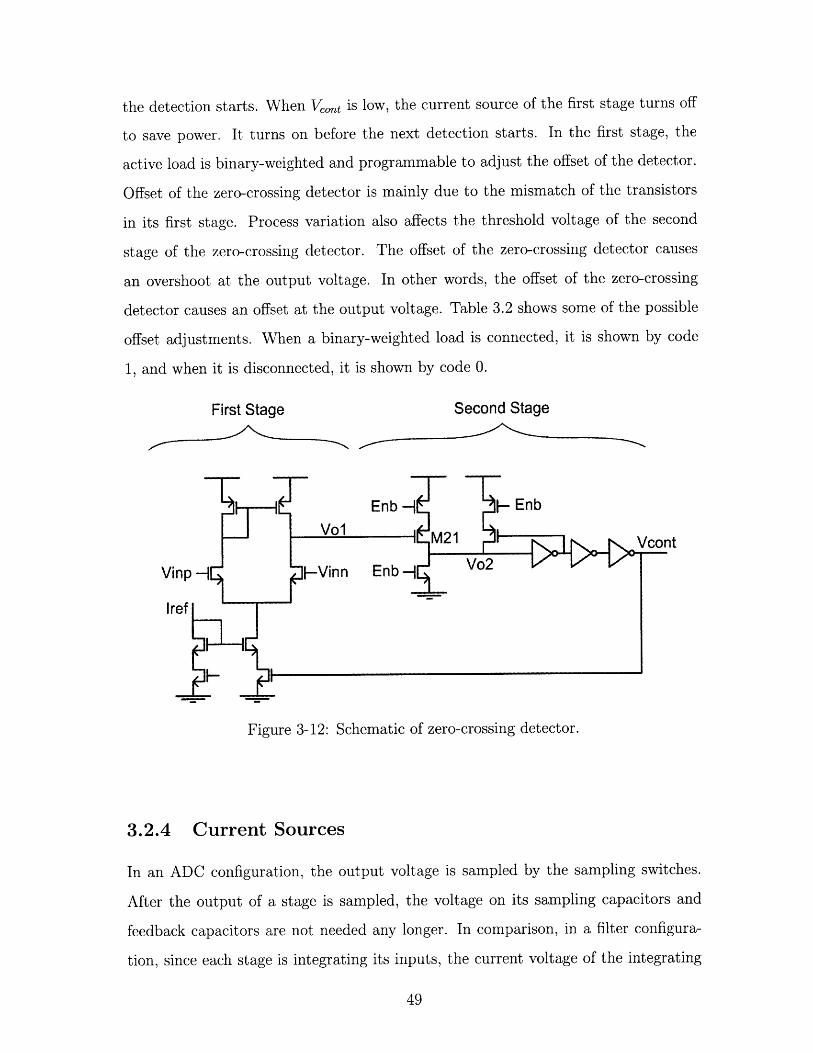
the detection starts. When V 0st is low, the current source of the first stage turns off
to save power. It turns on before the next detection starts. In the first stage, the
active load is binary-weighted and programmable to adjust the offset of the detector.
Offset of the zero-crossing detector is mainly due to the mismatch of the transistors
in its first stage. Process variation also affects the threshold voltage of the second
stage of the zero-crossing detector. The offset of the zero-crossing detector causes
an overshoot at the output voltage. In other words, the offset of the zero-crossing
detector causes an offset at the output voltage. Table 3.2 shows some of the possible
offset adjustments. When a binary-weighted load is connected, it is shown by code
1, and when it is disconnected, it is shown by code 0.
First Stage Second Stage
Enb - -Enb
Vo1 M21 M21 Vcont
Vinp -[ |-Vinn Enb -Vo2
Iref
Figure 3-12: Schematic of zero-crossing detector.
3.2.4 Current Sources
In an ADC configuration, the output voltage is sampled by the sampling switches.
After the output of a stage is sampled, the voltage on its sampling capacitors and
feedback capacitors are not needed any longer. In comparison, in a filter configura-
tion, since each stage is integrating its inputs, the current voltage of the integrating
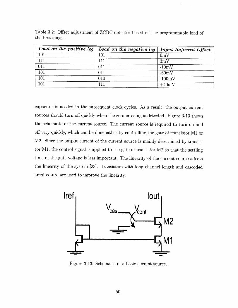
Table 3.2: Offset adjustmentthe first stage.
of ZCBC detector based on the programmable load of
capacitor is needed in the subsequent clock cycles. As a result, the output current
sources should turn off quickly when the zero-crossing is detected. Figure 3-13 shows
the schematic of the current source. The current source is required to turn on and
off very quickly, which can be done either by controlling the gate of transistor M1 or
M2. Since the output current of the current source is mainly determined by transis-
tor M1, the control signal is applied to the gate of transistor M2 so that the settling
time of the gate voltage is less important. The linearity of the current source affects
the linearity of the system [23]. Transistors with long channel length and cascoded
architecture are used to improve the linearity.
Iref
m ---- -
loutV \cas cont
M2
M1i
Figure 3-13: Schematic of a basic current source.
Load on the positive leg Load on the negative leg Input Referred Offset101 101 0mV111 111 3mV011 011 -10mV101 011 -60mV101 010 -100mV101 111 +40mV

3.2.5 The first Stage
The level of the input voltage in the first stage is 0.25V-0.75V for both inputs of the
differential signals. The input level of all other stages is 0.4V-0.91V on the positive
input and 0.09V-0.6V on the negative input. As a result, the threshold voltage of
BDCs and the reference voltages are adjusted accordingly for the first stage (it is
shown in the residue plots in Figure 3-16 and Figure 3-17).
Since the output of all stages are linear ramps, the sampling switches conduct a
relatively constant current to the sampling capacitor. As shown in Figure 3-14 and
proposed in [24], an additional current source is added after each switch to provide
a large portion of the current to the sampling capacitor. This technique reduces
the current that passes through the sampling switch and reduces the corresponding
voltage variation across the switch. Since the first stage samples its input from a
regular voltage source (without ZCBC operation), the corresponding current sources
are not needed.
3.2.6 Bit-Decision-Comparators (BDC)
Wide range of latched comparators have been developed [15],[29],[30]. Figure 3-15
shows the schematic of the bit-decision-comparator in this system (which is proposed
by [31]). The differential input is sampled across the sampling capacitors in phase 1
(Clk = 0), while all internal nodes are pre-charged to Vdd. In phase 2, the sampling
capacitors are connected to the reference voltages. Transistor M1 and M2 start to
discharge Vt and Vtb. If one of the output voltages is discharged more quickly
(for example Vutb), it disconnects the other output voltage (Vst) from the lower
transistors (M2). A regenerative action helps both V0st and Vtb to reach their final
voltage quickly. The mismatch of transistors and capacitors causes an offset in the
BDC. Two binary-weighted capacitors are added as the load to adjust the offset. Table
3.3 shows the offset for different load connection when the common-mode voltage is
500mV. The offset adjustment is to be used when the offset is larger than the over-
range protection. In this design, the BDC offset is adjusted manually for each stage.
Boosting
-- Output
b3
Vin2 CO
2 VM
Figure 3-14: Basic building block of reconfigurable stage.
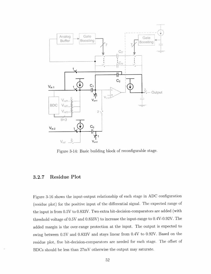
3.2.7 Residue Plot
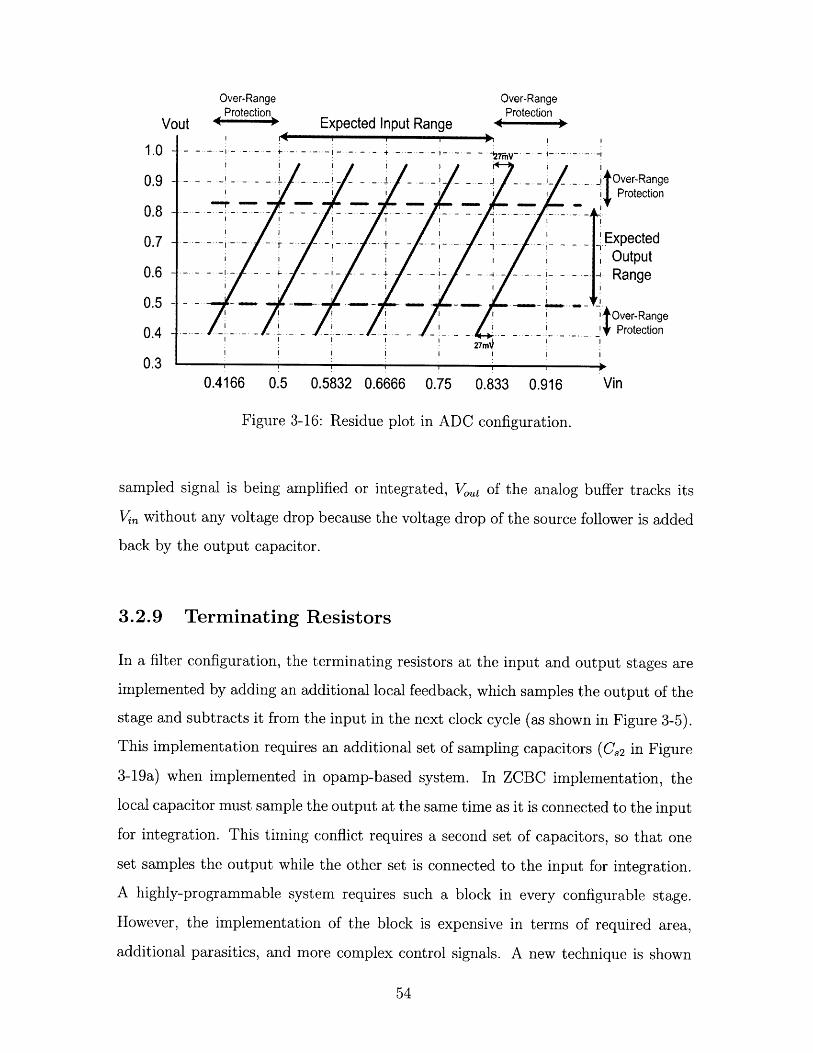
Figure 3-16 shows the input-output relationship of each stage in ADC configuration
(residue plot) for the positive input of the differential signal. The expected range of
the input is from 0.5V to 0.833V. Two extra bit-decision-comparators are added (with
threshold voltage of 0.5V and 0.833V) to increase the input-range to 0.4V-0.92V. The
added margin is the over-range protection at the input. The output is expected to
swing between 0.5V and 0.833V and stays linear from O.4V to 0.92V. Based on the
residue plot, five bit-decision-comparators are needed for each stage. The offset of
BDCs should be less than 27mV otherwise the output may saturate.
AnalogBuffer
6fF
Figure 3-15: Schematic of a bit-decision-comparator.
Table 3.3: Offset adjustment of bit-decision-comparator.
Load on the positive leg Load on the negative leg Input Referred Offset
OfF OfF 0mV3fF OfF -14mV
6fF OfF -27mV
9fF OfF -36mV
9fF 3fF -22mV
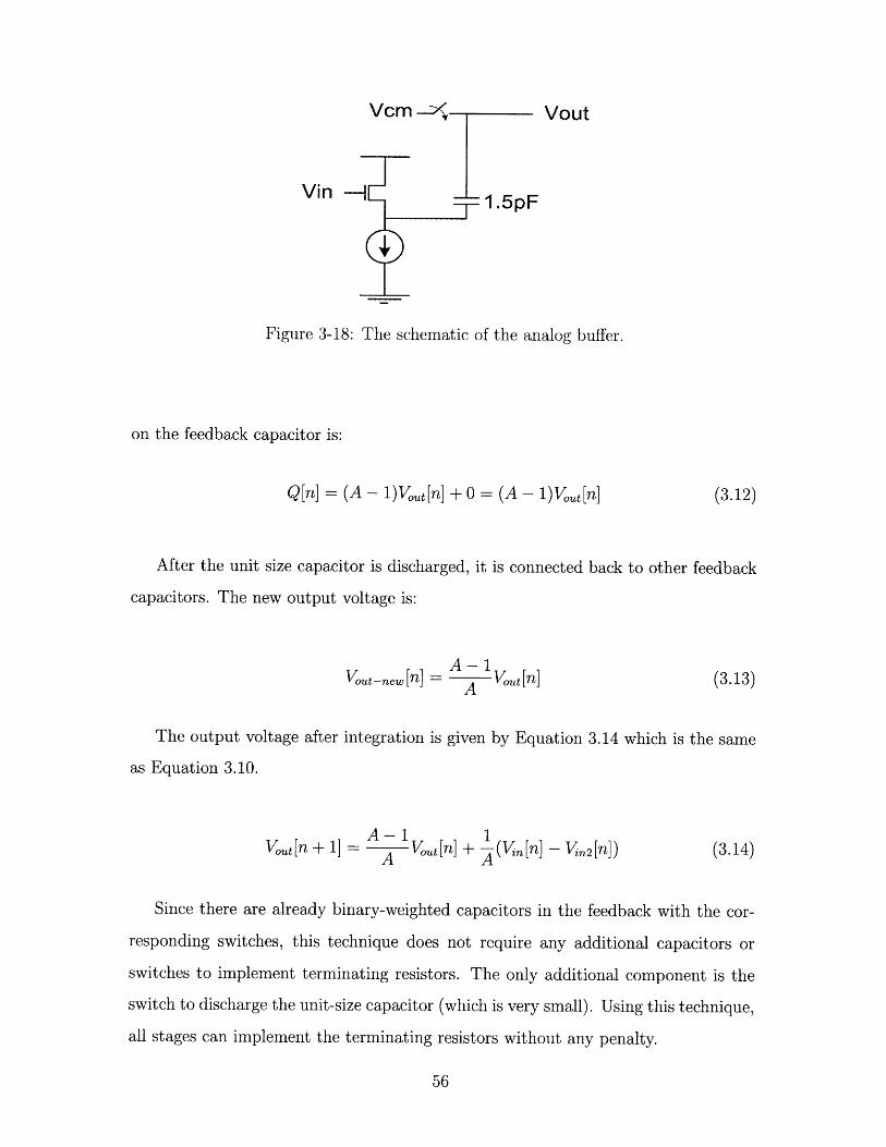
3.2.8 The Analog Buffer
The schematic of the analog buffer is shown in Figure 3-18. If a regular source follower
is used, the voltage drop of the source follower reduces the level of the output voltage.
The output of the analog buffer drives a bootstrapping block. If the analog buffer
has a voltage drop, the same voltage drop appears at the output of the bootstrapping
block, which drives the gate of a reconfigurable switch. As a result, the voltage drop of
the source follower in Figure 3-6 causes lower overdrive voltage for the corresponding
reconfigurable switch. A large capacitor is included in series at the output of the
analog buffer to adjust its output level. In phase 1, when each stage is sampling its
input, the input of the analog buffer is connected to Vcm (Figure 3-6). During this
phase, Vcm is also connected to the output capacitor of the analog buffer and samples
the voltage drop of the source follower across the capacitor. In phase 2, when the
6f
Over-RangeProtection
I /
--
-T
- ----- 4
Expected Input Range
Over-RangeProtection
1.0
0.9
0.8
0.7
0.6
0.5
0.4
0.3
Vo
Figure 3-16: Residue plot in ADC configuration.
sampled signal is being amplified or integrated, V0 t of the analog buffer tracks its
Vm without any voltage drop because the voltage drop of the source follower is added
back by the output capacitor.
3.2.9 Terminating Resistors
In a filter configuration, the terminating resistors at the input and output stages are
implemented by adding an additional local feedback, which samples the output of the
stage and subtracts it from the input in the next clock cycle (as shown in Figure 3-5).
This implementation requires an additional set of sampling capacitors (C, 2 in Figure
3-19a) when implemented in opamp-based system. In ZCBC implementation, the
local capacitor must sample the output at the same time as it is connected to the input
for integration. This timing conflict requires a second set of capacitors, so that one
set samples the output while the other set is connected to the input for integration.
A highly-programmable system requires such a block in every configurable stage.
However, the implementation of the block is expensive in terms of required area,
additional parasitics, and more complex control signals. A new technique is shown
- Over-RangeProtection
ExpectedOutputRange
Over-RangeProtection
Vin
-1
0.4166 0.5 0.5832 0.6666 0.75 0.833 0.916
Ab-
Over-Range Over-RangeProtection Protection
Expected Input Range
-- - - T - I--- ------- --- ------- I -
--------- -- - - ----
-- I- *--4 - - ----- -- --
----------
- -- -- -
Vout
1.0 -
0.9
0.8 -
0.7
0.6
0.5
0.4
0.3
- over-RangeProtection
Expected-- ~ Output
- Range
- Over-Range- ' Protection
Vin
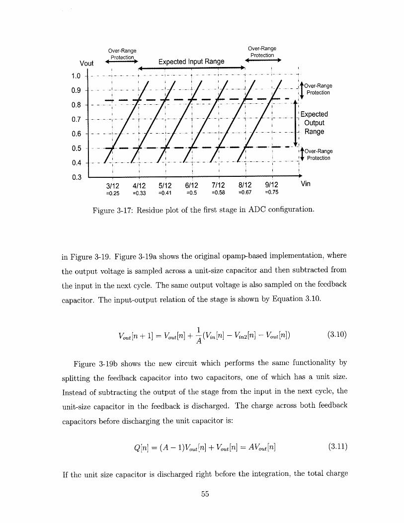
Figure 3-17: Residue plot of the first stage in ADC configuration.
in Figure 3-19. Figure 3-19a shows the original opamp-based implementation, where
the output voltage is sampled across a unit-size capacitor and then subtracted from
the input in the next cycle. The same output voltage is also sampled on the feedback
capacitor. The input-output relation of the stage is shown by Equation 3.10.
Vout[n + 1] = Vut[n] + -(Vin[[n] - Vin2[n] - Vout[n])A
(3.10)
Figure 3-19b shows the new circuit which performs the same functionality by
splitting the feedback capacitor into two capacitors, one of which has a unit size.
Instead of subtracting the output of the stage from the input in the next cycle, the
unit-size capacitor in the feedback is discharged. The charge across both feedback
capacitors before discharging the unit capacitor is:
Q [n] = (A - 1)Vot[n] + Vout[n] = AVut[n] (3.11)
If the unit size capacitor is discharged right before the integration, the total charge
3/12 4/12 5/12 6/12 7/12 8/12 9/12
=0.25 =0.33 =0.41 =0.5 =0.58 =0.67 =0.75
Vcm s Vout
Vin - 1.5pF
Figure 3-18: The schematic of the analog buffer.
on the feedback capacitor is:
Q[n] = (A - 1)Vot[n] + 0 = (A - 1)Vst[n] (3.12)
After the unit size capacitor is discharged, it is connected back to other feedback
capacitors. The new output voltage is:
Voutnew[n] = A -Vot[n] (3.13)
The output voltage after integration is given by Equation 3.14 which is the same
as Equation 3.10.
AjVn-i1-11n21lVout[n + 1] = A Vut[n] + (Vin[n] - Vin2[n]) (3.14)AA
Since there are already binary-weighted capacitors in the feedback with the cor-
responding switches, this technique does not require any additional capacitors or
switches to implement terminating resistors. The only additional component is the
switch to discharge the unit-size capacitor (which is very small). Using this technique,
all stages can implement the terminating resistors without any penalty.

vout vout
C1=+ + ' Cf2= 1
C,2=1
Vin CS=1 Vin2 Vin CS=1 Vin2
a) Traditional opamp-based b) The new method to implementimplementation the terminating resistors
Figure 3-19: Implementation of terminating resistors in ladder filters.
3.3 Asymmetric Differential Signaling
Traditionally, differential signals have the same swing on the positive and negative
direction. Figure 3-20 shows the signal swing at the output of each ZCBC block. If the
output current source stays on, the output ramps linearly till it reaches the saturation
region. ZCBCs are linear only if the output stays within the linear ramp region [23].
In Figure 3-20, Vst is linear when it ramps up from OV to 0.7V and Vst, is linear
when it ramps down from 1V to 0.3V. With symmetric differential signaling, each of
Vut, and Vutn can only swing between 0.3V and 0.7V. This indicates that the linear
output range where Vut, ramps from 1V to 0.7 and Votn ramps from OV to 0.3V is
not utilized. With supply voltage as low as 1V, the unutilized linear region makes up
42% of the total linear region. Asymmetric output swing is employed to utilize the
full linear range of the output. Reference voltages are chosen from the residue plots
(Figure 3-16 and Figure 3-17) so that they support the asymmetric signal range.
VoutLinear Range- 0.4 < Vout p - Voutn< 1V
Vdd= 1V
0 < Voutn < 0.7V
0.3 < Voutp < 1V
t
Figure 3-20: Signal swing in zero-crossing based circuits.
3.4 Programmability
The programmability of the system falls in three categories, functionality, calibration,
and power optimization.
3.4.1 Programmability for functionality
Each stage can be programmed to perform either integration or amplification. The
integration coefficient is determined by the ratio of the integrating capacitor to the
sampling capacitor. Programmable binary-weighted integration capacitors provide
the desired integration coefficient. In filter configuration, an additional local feedback
loop is required in the first and the last stage to implement the terminating resistor.
The terminating resistor can be programmed to be active or inactive as needed.
Similarly, BDCs can be turned off if not needed (for filters). Each stage has two
sets of sampling capacitors. Depending on the functionality, one or both sampling
capacitor is activated.
3.4.2 Programmability for Calibration
If the ramp rates at the output of one stage matches the ramp rate at the input of the
next stage, smaller current passes through the top-plate switches and the distortion is
reduced. The ramp rate depends on the ratio of current sources and load capacitors.
The ramp rate can be adjusted by programmable binary-weighted current sources to
compensate for changes in capacitive load in different configurations. In addition, the
offset of BDC and zero-crossing detector can be adjusted.
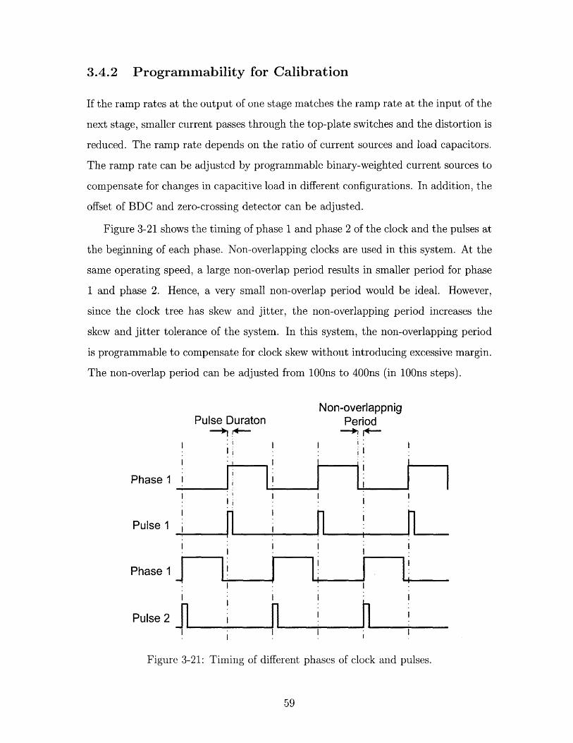
Figure 3-21 shows the timing of phase 1 and phase 2 of the clock and the pulses at
the beginning of each phase. Non-overlapping clocks are used in this system. At the
same operating speed, a large non-overlap period results in smaller period for phase
1 and phase 2. Hence, a very small non-overlap period would be ideal. However,
since the clock tree has skew and jitter, the non-overlapping period increases the
skew and jitter tolerance of the system. In this system, the non-overlapping period
is programmable to compensate for clock skew without introducing excessive margin.
The non-overlap period can be adjusted from 100ns to 400ns (in 100ns steps).
Non-overlappnigPulse Duraton Period
Phase 1
Pulse 1
Phase 1
Pulse 2
Figure 3-21: Timing of different phases of clock and pulses.
ZCBC architectures use short clock pulses at the beginning of both phase 1 and
phase 2 to initialize the operation. The strength of the switches that perform pre-
charging or pre-discharging may vary due to process variation. Similarly, the ca-
pacitive load of such nodes may vary. As a result, a programmable pulse period is
implemented to compensate for such variation. Each pulse can be programmed to be
from 100ns to 800ns (in 100ns steps).
The bias voltage for NMOS and PMOS transistors in cascode and the common-
mode voltage can be either generated on-chip or provided off-chip. It is more desirable
to generate these voltages on-chip to avoid the effects of bond-wire inductance. A
7-bit digital-to-analog convertor (DAC) generates each voltage.
3.4.3 Programmability for Power Optimization
If analog connectivity between some stages is not needed, the corresponding switches
can be programmed to stay off. In addition, the clock and reference currents of unused
stages can turn off to save power. The current source of any circuit block in each
stage can turn off if the block is not needed. For example, in the ADC configuration,
the zero-crossing detector of the last stage of pipeline ADC can turn off during the
whole operation. Finally, digital output of each stage can be turned off if not needed.
3.5 System Simulation
The system is simulated with Spectre and the output is sent to Matlab for more
analysis. In an ADC configuration, near Nyquist-rate sinusoid is applied to the input
of the system and transient simulation is performed. The output of the transient
simulation is sent to Matlab to analyze the frequency response.
To ensure that the simulation setup is appropriate, the system was first imple-
mented with ideal elements using VerilogA models. Simulation settings such as an
absolute and relative tolerance of voltages and currents and maximum time step are
adjusted in this phase for 13-bit accuracy. Then, different components are replaced
with the real implementation one at a time to evaluate the performance of each block.
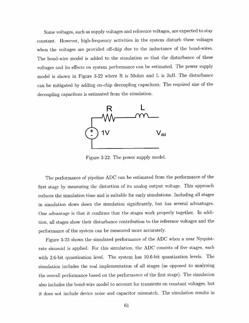
Some voltages, such as supply voltages and reference voltages, are expected to stay
constant. However, high-frequency activities in the system disturb these voltages
when the voltages are provided off-chip due to the inductance of the bond-wires.
The bond-wire model is added to the simulation so that the disturbance of these
voltages and its effects on system performance can be estimated. The power supply
model is shown in Figure 3-22 where R is 50ohm and L is 2nH. The disturbance
can be mitigated by adding on-chip decoupling capacitors. The required size of the
decoupling capacitors is estimated from the simulation.
R L
1V Vdd
Figure 3-22: The power supply model.
The performance of pipeline ADC can be estimated from the performance of the
first stage by measuring the distortion of its analog output voltage. This approach
reduces the simulation time and is suitable for early simulations. Including all stages
in simulation slows down the simulation significantly, but has several advantages.
One advantage is that it confirms that the stages work properly together. In addi-
tion, all stages show their disturbance contribution to the reference voltages and the
performance of the system can be measured more accurately.
Figure 3-23 shows the simulated performance of the ADC when a near Nyquist-
rate sinusoid is applied. For this simulation, the ADC consists of five stages, each
with 2.6-bit quantization level. The system has 10.6-bit quantization levels. The
simulation includes the real implementation of all stages (as opposed to analyzing
the overall performance based on the performance of the first stage). The simulation
also includes the bond-wire model to account for transients on constant voltages, but
it does not include device noise and capacitor mismatch. The simulation results in
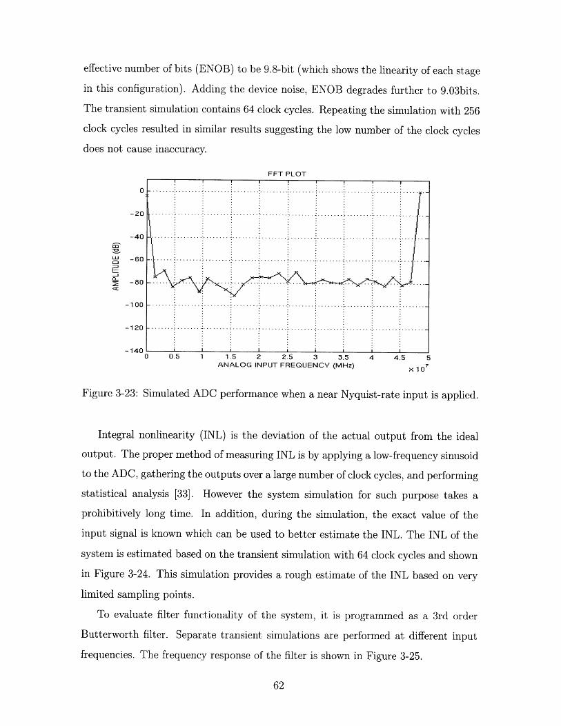
effective number of bits (ENOB) to be 9.8-bit (which shows the linearity of each stage
in this configuration). Adding the device noise, ENOB degrades further to 9.03bits.
The transient simulation contains 64 clock cycles. Repeating the simulation with 256
clock cycles resulted in similar results suggesting the low number of the clock cycles
does not cause inaccuracy.
FFT PLOT
-20.
-80.<C
-100
-120
-140 A0 0.5 1 1.5 2 2.5 3 3.5 4 4.5 5
ANALOG INPUT FREQUENCY (MHz)
Figure 3-23: Simulated ADC performance when a near Nyquist-rate input is applied.
Integral nonlinearity (INL) is the deviation of the actual output from the ideal
output. The proper method of measuring INL is by applying a low-frequency sinusoid
to the ADC, gathering the outputs over a large number of clock cycles, and performing
statistical analysis [33]. However the system simulation for such purpose takes a
prohibitively long time. In addition, during the simulation, the exact value of the
input signal is known which can be used to better estimate the INL. The INL of the
system is estimated based on the transient simulation with 64 clock cycles and shown
in Figure 3-24. This simulation provides a rough estimate of the INL based on very
limited sampling points.
To evaluate filter functionality of the system, it is programmed as a 3rd order
Butterworth filter. Separate transient simulations are performed at different input
frequencies. The frequency response of the filter is shown in Figure 3-25.
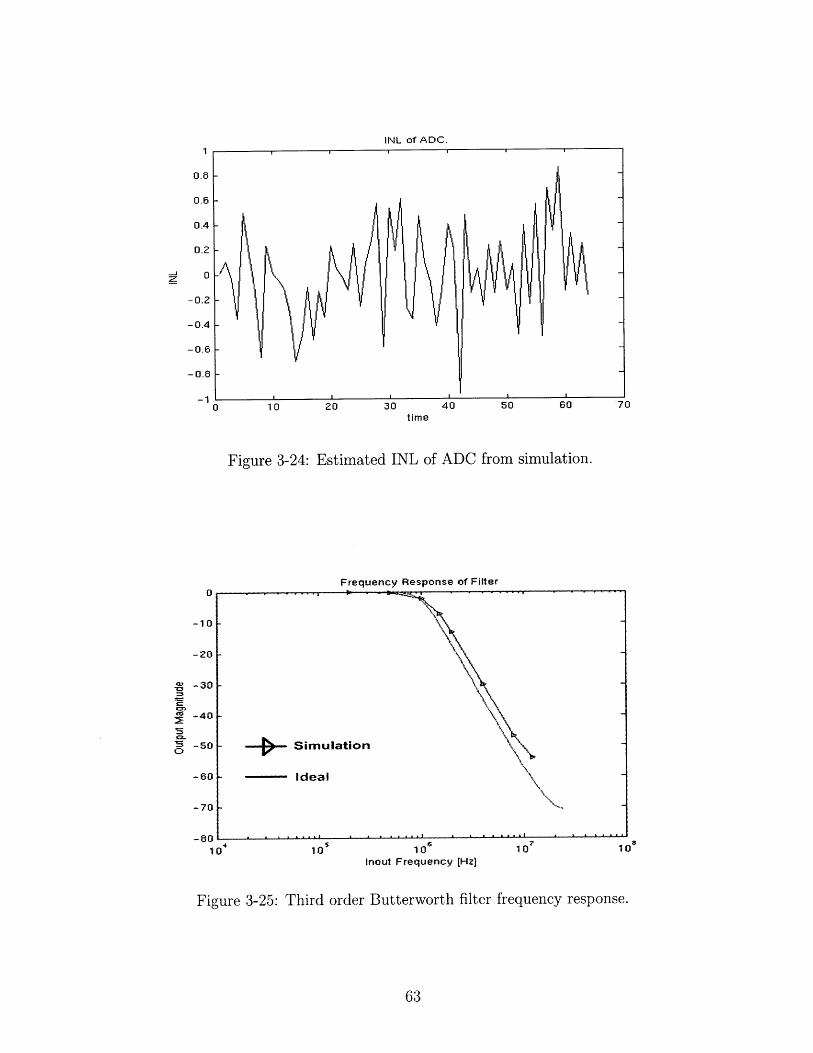
INL of ADC.
time
Figure 3-24: Estimated INL of ADC from simulation.
-60 -
-70 -
-80 -
10 4 10I 10
Inout Frequency [Hz)
Figure 3-25: Third order Butterworth filter frequency response.
-0.2
-0.4
-0.6
-0.8
-1
0
-10
-20
-30
-40
-50
10

64
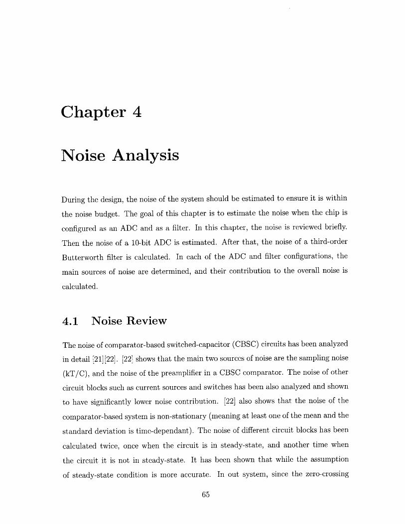
Chapter 4
Noise Analysis
During the design, the noise of the system should be estimated to ensure it is within
the noise budget. The goal of this chapter is to estimate the noise when the chip is
configured as an ADC and as a filter. In this chapter, the noise is reviewed briefly.
Then the noise of a 10-bit ADC is estimated. After that, the noise of a third-order
Butterworth filter is calculated. In each of the ADC and filter configurations, the
main sources of noise are determined, and their contribution to the overall noise is
calculated.
4.1 Noise Review
The noise of comparator-based switched-capacitor (CBSC) circuits has been analyzed
in detail [21] [22]. [22] shows that the main two sources of noise are the sampling noise
(kT/C), and the noise of the preamplifier in a CBSC comparator. The noise of other
circuit blocks such as current sources and switches has been also analyzed and shown
to have significantly lower noise contribution. [22] also shows that the noise of the
comparator-based system is non-stationary (meaning at least one of the mean and the
standard deviation is time-dependant). The noise of different circuit blocks has been
calculated twice, once when the circuit is in steady-state, and another time when
the circuit it is not in steady-state. It has been shown that while the assumption
of steady-state condition is more accurate. In out system, since the zero-crossing
detector is using a wide-band pre-amplifier, steady-state analysis is accurate.
Since the purpose of this chapter is a first-order estimate of noise in the system,
the noise is assumed to be stationary. In addition, only the dominant sources of noise
are taken into account.
4.1.1 Sampling Noise (kT/C Noise)
Figure 4-1 shows a basic sampling circuit where an NMOS transistor is used as a
switch. When the transistor is on, the voltage across the capacitor tracks the input
voltage. The resistance of the transistor creates thermal noise which can be expressed
by Equation 4.1 [15].
Sn,R(f) nR(f) = 4kTR (4.1)
where k is Boltzmann constant (1.38x10- 23 J/K), R is the ON resistance of the
transistor when it is on, and T is temperature in degrees Kelvin. The thermal noise
is a white noise and can be modeled as a voltage source of V,R(f) in series with a
noiseless resistor as shown in Figure 4-2. The total mean-square noise is the integral
of Sn,R(f) over all frequencies as shown in Equation 4.2. Note that the integral is
infinite if the noise is not filtered. In practice, the noise is always filtered either by
capacitive load at the output or by parasitic capacitances.
Sample
Vin r\VC
Figure 4-1: A basic sampling circuit.
V,2 = j SnR(f)df (4.2)
Noiseless Resistor
Vn,R Vout
Figure 4-2: Circuit model of the noise of a sampling circuit.
The input signal is suppressed in Figure 4-2 to calculate only the noise contribution
at the output. The noise of the resistor, Vn,R, is filtered by the low-pass RC circuit.
The transfer function from V,,R to V0ut is given by Equation 4.3.
Vo>s) R 1 (4.3)Vn, R ROs + 1
The noise power spectral density is shaped by the transfer function. The output noise
spectral density can be written as Equation 4.4 [26].
S0OU() - nR lvout 1j7f 2=4T (4.4)n R Sn,R(f) .(rf)| 2 4 kTR( 2,f RC)2 + -
The total mean-square noise is the integral of the output noise density over all fre-
quencies as shown in Equation 4.5.
/00 kT' j 4kTR (27f RC)2 + 1 df C(4.5)
While the noise is generated by the resistor, the overall noise is only a function of
the sampling capacitance. This is due to the fact that the noise spectral density is
proportional to the resistance value, but the cut-off frequency of the filter is inversely
proportional to the resistance value. It is important to note that while the total mean-
square noise only depends on the capacitance, the power spectral density (PSD) still
depends on the resistance of the switch. This is important if thermal noise is further
filtered by a subsequent circuit. In such cases, the total mean-square noise depends
on the power spectral density of the noise and the bandwidth of the whole circuit.
When the switch is still closed in Figure 4-1, kT/C noise appears across the
capacitor. When the switch is opened, the noise is sampled across the capacitor. The
sampling noise (kT/C) can be reduced either by lowering the temperature (which is
not typically a design option) or increasing the size of the sampling capacitor.
4.1.2 Effective Number of Bits (ENOB) and Figure of Merit
(FOM)
When an analog signal is quantized, a quantization error is introduced which is the
difference between the analog input signal and the digital output signal. For an ideal
ADC, the mean square quantization error is given by Equation 4.6 [34].
V2-(A/2 N2 246q 12
where A is the full-scale range of the ADC and N is the number of quantization bits.
The quantization error is one of the factors that limits the signal-to-noise ratio (SNR)
of an ADC. It is shown that for an ADC with large number of bits (for example 10
bits or higher), quantization error can be treated as white noise if sampling is non-
coherent [35]. If a sinusoidal signal with an amplitude of A/2 is applied to an ideal
ADC with N-bit quantization, the signal-to-noise ratio is shown by Equation 4.7 [34].
SNR = N * 6.02dB + 1.76dB (4.7)
Signal to noise and distortion ratio (SNDR) is the ratio of the signal power to the
total power of quantization error, noise, and harmonics. The effective number of bits
(ENOB) of an ADC is defined by Equation 4.8.
SNDR - 1.76dB (4.8)ENOB = 486.02dB/bit
To compare different ADCs with different bit-resolution, different sampling fre-
quency, and different power consumption, a figure of merit (FOM) is defined. The
FOM normalizes the power consumption with respect to the bandwidth of the input
signal and ENOB as shown in Equation 4.9 [36][37].
FOM = Pow erConsumption(2 fInputBandwidth * 2 ENOB
4.1.3 Noise Gain
Figure 4-3 shows a simple block diagram of a system with transfer function of H(s)
where Vin(s) is the input and Vot(s) is the output of the block. The input-output
relation is given by Equation 4.10.
Vot (s) = H(s) (4.10)Vin(s)
v (S) v (S)
S(S) H(s) S (S)
Figure 4-3: General block diagram of a system with transfer function of H(s).
Similarly, if Sin(s) = V,in(s)12 is the noise power spectral density (PSD) at the
input and Sout(s) = |K,0 t(s)12 is the noise PSD at the output, the relation of the
input and output noise is given by Equation 4.11.
Sout(s) _ VKOut(s)| 2 - |H(s)|2 (4.11)Sin(s) IKV,in(s)|12
If the transfer function from an internal node to the output is known, this equation
can be used to calculate the noise at the output due to the noise at the internal node.
Signal gain is the value of the transfer function for the in-band signal. If Equation
4.11 is used to refer the output noise to the input of the system, the signal gain should
be used so that the signal-to-noise ratio can be correctly calculated at the input.
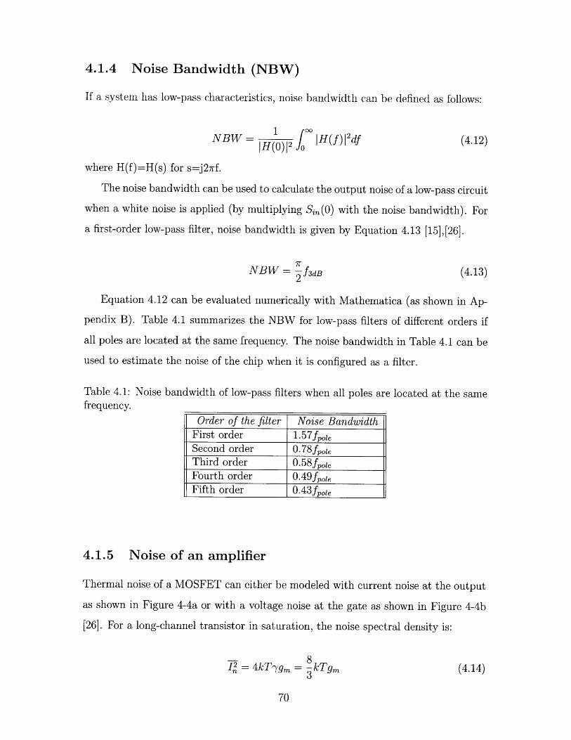
4.1.4 Noise Bandwidth (NBW)
If a system has low-pass characteristics, noise bandwidth can be defined as follows:
NBW= JH(f)}|2df (4.12)|H(0)|12 0
where H(f)=H(s) for s=j27rf.
The noise bandwidth can be used to calculate the output noise of a low-pass circuit
when a white noise is applied (by multiplying Sinm(0) with the noise bandwidth). For
a first-order low-pass filter, noise bandwidth is given by Equation 4.13 [15],[26].
7rNBW = f3dB (4.13)
2
Equation 4.12 can be evaluated numerically with Mathematica (as shown in Ap-
pendix B). Table 4.1 summarizes the NBW for low-pass filters of different orders if
all poles are located at the same frequency. The noise bandwidth in Table 4.1 can be
used to estimate the noise of the chip when it is configured as a filter.
Table 4.1: Noise bandwidth of low-pass filters when all poles are located at the samefrequency.
Order of the filter Noise BandwidthFirst order 1.57fpoleSecond order 0. 7 8 fpoleThird order 0.58fpoieFourth order 0.49fpoeFifth order 0.43fpoie
4.1.5 Noise of an amplifier
Thermal noise of a MOSFET can either be modeled with current noise at the output
as shown in Figure 4-4a or with a voltage noise at the gate as shown in Figure 4-4b
[26]. For a long-channel transistor in saturation, the noise spectral density is:
8I2 = 4kTygm = -kTgm (4.14)
3
4kTy _ 8 kT (4.15)n 9m 3 gm
where -y is 2/3 for long-channel transistors. Equation 4.14 suggests that an increase
in gm increases the current noise at the output and Equation 4.15 suggests that
an increase in gm decreases the voltage noise at the input. In many cases, since the
amplitude of the input signal is fixed, the signal-to-noise ratio is calculated by referring
the noise to the input. In these cases, an increase in gm improves signal-to-noise ratio.
Vn.121
a) b)
Figure 4-4: Thermal Noise of a MOSFET.
A basic differential amplifier is shown in Figure 4-5, which includes the transistor
noise. Transistors M3, M4, and M5 are biased with constant voltages and are used
as current sources. Since the output is fully differential, the noise of transistor M5
appears similarly at both V0st, and Vosn, and cancels out if the output is differential.
The input referred noise density of the amplifier is given by Equation 4.16, assuming
perfect matching between transistor M1 and M2, and between transistor M3 and M4.
V 2 (f) = 4kTy(2 + 2gm3 (4.16)9ml gm1
This is white noise and if the bandwidth is not limited, the mean-square noise is
infinite. In practice, the capacitive load at the output limits the bandwidth.
4.1.6 Noise Aliasing
The block diagram of a sampling system is shown in Figure 4-6, where x(t) is the
input signal which is sampled by p(t), a train of impulses. The time-domain and
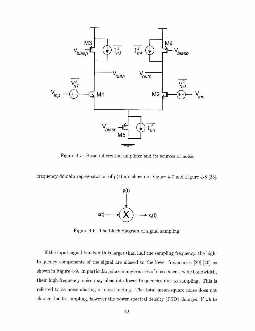
V - -biasp
nlV'np
I2n3
M1
Vbiasn
12n4 Vbiasp
V Voutn outp2
M2 V
2n5
Figure 4-5: Basic differential amplifier and its sources of noise.
frequency domain representation of p(t) are shown in Figure 4-7 and Figure 4-8 [38].
p(t)
x(t) x (t)
Figure 4-6: The block diagram of signal sampling.
If the input signal bandwidth is larger than half the sampling frequency, the high-
frequency components of the signal are aliased to the lower frequencies [39] [40] as
shown in Figure 4-9. In particular, since many sources of noise have a wide bandwidth,
their high-frequency noise may alias into lower frequencies due to sampling. This is
referred to as noise aliasing or noise folding. The total mean-square noise does not
change due to sampling, however the power spectral density (PSD) changes. If white
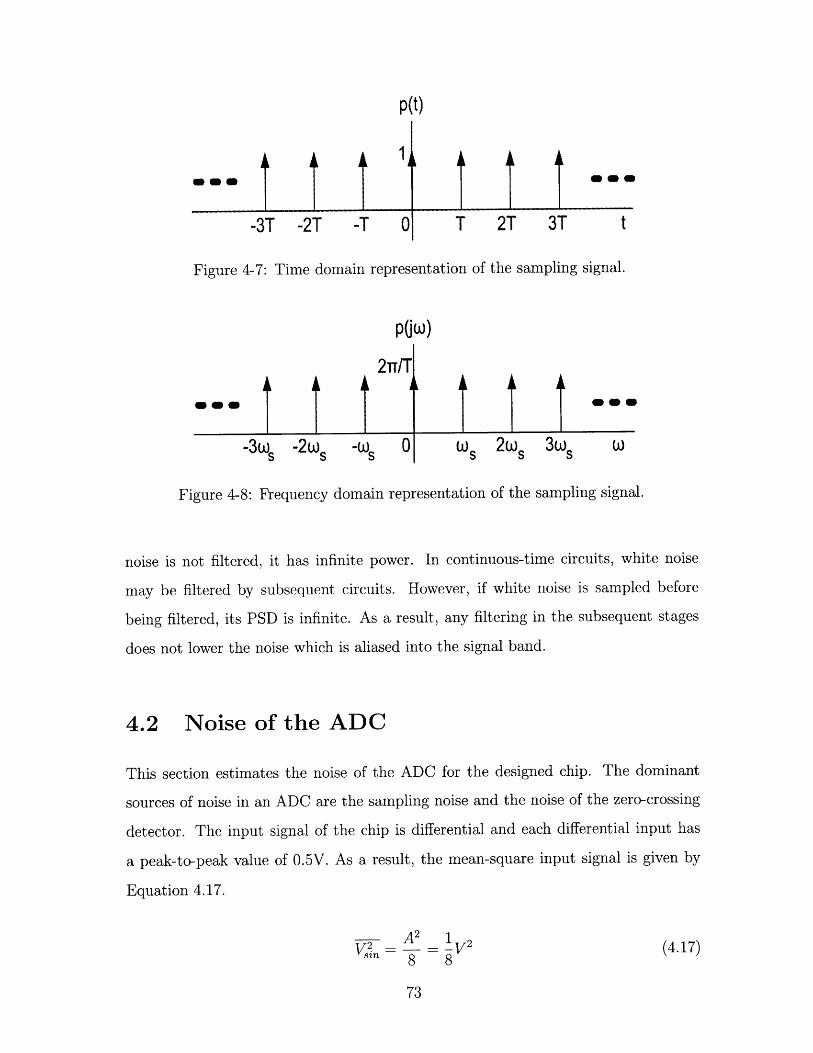
p(t)
1maw maw
-3T -2T -T 0 T 2T 3T t
Figure 4-7: Time domain representation of the sampling signal.
pow)
2TT/T
-3ws -2ws -ow 0 wo 2wo 3wo w
Figure 4-8: Frequency domain representation of the sampling signal.
noise is not filtered, it has infinite power. In continuous-time circuits, white noise
may be filtered by subsequent circuits. However, if white noise is sampled before
being filtered, its PSD is infinite. As a result, any filtering in the subsequent stages
does not lower the noise which is aliased into the signal band.
4.2 Noise of the ADC
This section estimates the noise of the ADC for the designed chip. The dominant
sources of noise in an ADC are the sampling noise and the noise of the zero-crossing
detector. The input signal of the chip is differential and each differential input has
a peak-to-peak value of 0.5V. As a result, the mean-square input signal is given by
Equation 4.17.
A 2 1V2_ - v2 (4.17)sin 8 8
73
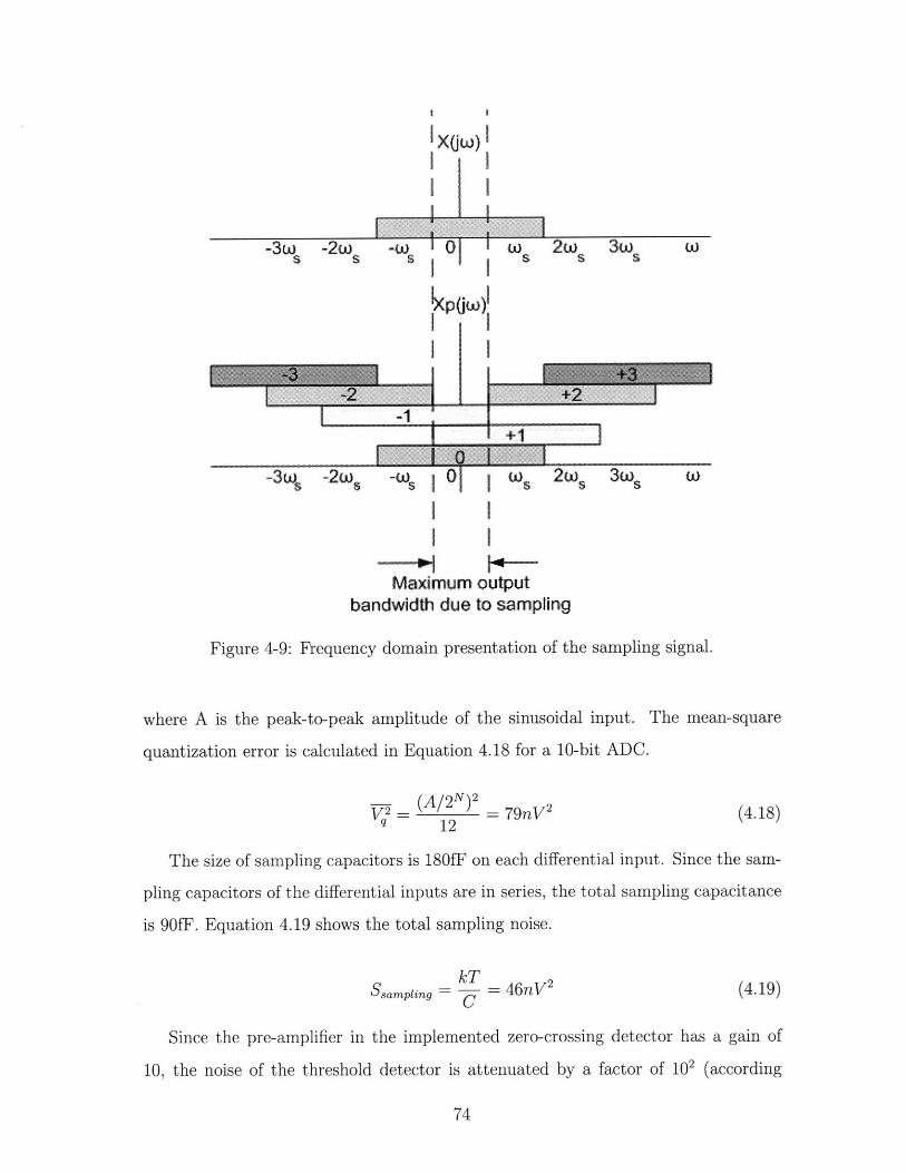
-3w -2wa s
-Wa
1X w)'I II I
0 wI s $
Xp(w)'I II I
2w, 3w W
Is W$ I||"I II I
Maximum outputbandwidth due to sampling
Figure 4-9: Frequency domain presentation of the sampling signal.
where A is the peak-to-peak amplitude of the sinusoidal input. The mean-square
quantization error is calculated in Equation 4.18 for a 10-bit ADC.
(4.18)- (A/2N)2 - 79rV 2
q 12
The size of sampling capacitors is 180fF on each differential input. Since the sam-
pling capacitors of the differential inputs are in series, the total sampling capacitance
is 90fF. Equation 4.19 shows the total sampling noise.
Ssamping =kT = 46nV 2
C(4.19)
Since the pre-amplifier in the implemented zero-crossing detector has a gain of
10, the noise of the threshold detector is attenuated by a factor of 102 (according
I
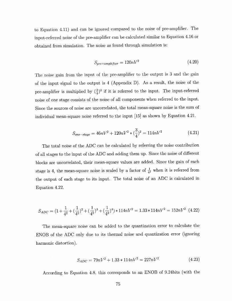
to Equation 4.11) and can be ignored compared to the noise of pre-amplifier. The
input-referred noise of the pre-amplifier can be calculated similar to Equation 4.16 or
obtained from simulation. The noise as found through simulation is:
Spre-amplifier = 120nV 2 (4.20)
The noise gain from the input of the pre-amplifier to the output is 3 and the gain
of the input signal to the output is 4 (Appendix D). As a result, the noise of the
pre-amplifier is multiplied by (3)2 if it is referred to the input. The input-referred
noise of one stage consists of the noise of all components when referred to the input.
Since the sources of noise are uncorrelated, the total mean-square noise is the sum of
individual mean-square noise referred to the input [15] as shown by Equation 4.21.
Sone-stage =46nV2 + 120nV 2 * 2 114nV 2 (4.21)4
The total noise of the ADC can be calculated by referring the noise contribution
of all stages to the input of the ADC and adding them up. Since the noise of different
blocks are uncorrelated, their mean-square values are added. Since the gain of each
stage is 4, the mean-square noise is scaled by a factor of - when it is referred from
the output of each stage to its input. The total noise of an ADC is calculated in
Equation 4.22.
SADC = (1+ +(-)2 1 )3+ )4) *114nV2 = 1.33*114nV 2 = 152nV 2 (4.22)42 42 42 42
The mean-square noise can be added to the quantization error to calculate the
ENOB of the ADC only due to its thermal noise and quantization error (ignoring
harmonic distortion).
SADC = 79nV 2 + 1.33 * 114nV 2 = 227nV 2 (4.23)
According to Equation 4.8, this corresponds to an ENOB of 9.24bits (with the
harmonic distortion being ignored). This can be compared with the measurement
results when the input is grounded. With grounded inputs, no harmonic distortion
is present and the measured mean-square noise is only due to noise and quantization
error. In Chapter 6, it is shown that the noise of the system with grounded inputs
corresponds to an ENOB of 9.26bits.
Note that in an ADC configuration, the sampling noise and the noise of the pre-
amplifier are aliased back to lower frequencies due to sampling. Noise aliasing does
not change the total noise, but changes the power spectral density of the noise. Since
the subsequent stages do not filter the noise, only the total mean-square noise is
important. As a result, noise aliasing can be ignored when calculating the total
noise.
4.3 Filter Noise
In this section, the noise of a filter is estimated. First, the noise model of an integrator
is provided. Then, the sampling noise and the noise of the amplifier are aliased into
the low frequencies due to sampling. The filter transfer function is used to filter
different noise components. The total noise is calculated by adding the contribution
of different components.
4.3.1 Noise of an Integrator
Figure 4-10 shows the schematic of a switched-capacitor integrator. Although an
opamp model is used for simplicity, all the following equations apply to ZCBCs as
well. The noise of an opamp (or zero-crossing detector) is represented by V. The
dominant component of V is the noise of the differential pair at the first stage of
an opamp (or the first stage of zero-crossing detector). This noise is estimated by
Equation 4.20 for the implemented zero-crossing detector. The relation of input and
output voltages is shown in Equation 4.24.
ClVout[n + 1] Vtj[n] + Vin[n] (4.24)
C2
V can be added to the equation as following:
Vo-t[n + 1] = Ost[n + 1] + V (4.25)
where Qout[n + 1] is given by:
QOst[n + 1) Qort[n] + C1(Vin[n] + V) (4.26)
QOst is the charge on capacitor C2. Vn appears both in Equation 4.25 and Equation
4.26. In Equation 4.25, V is added to the output voltage, but it is not integrated on
the feedback capacitor. However, in Equation 4.26, V, is also integrated across the
capacitor.
C2
1 C1 2Vin -- 2 Vout
2 1 CL- n
Figure 4-10: Schematic of a switched-capacitor integrator.
The noise directly adds both to the input voltage and to the output voltage. In
other words, the noise can be modeled with two components, one which is at the input
and one at the output as shown in Figure 4-11. Note that the two noise components
are correlated. Therefore, their noise voltage should be added (as opposed to adding
the mean-square noise). However, they experience different transfer functions to
the output. It is shown that only one of them is dominant for each stage. As a
result, adding the mean-square noise instead of noise voltages causes only a small
error. In the rest of the analysis, the two sources of noise are treated as uncorrelated
acknowledging that the total noise is underestimated. The sampling noise can also
be added to the input noise. As a results, V.,i. and V, 0st are shown by Equation 4.27
and Equation 4.28.
V2 = kT/C + Spre-ampif ier =(46 + 120)nV 2 = 166nV 2 (4.27)
Vout = Spre-amplifier = 120nV 2 (4.28)
Vo Vna ct
V - Vtou
Figure 4-11: Noise model of the integrator.
The 3dB frequency of the sampling circuit is at 60 MHz. With a sampling rate of
50 MSPS, high-frequency noise is aliased to the low frequencies. It can be assumed
that the total noise is uniform over the sampling bandwidth (0-25 MHz). Similarly,
the noise of the opamp (or zero-crossing detector) can be assumed to be uniform over
the sampling bandwidth (0-25 MHz).
4.3.2 Noise Transfer Function
The block diagram of a third-order low-pass ladder filter is shown in Figure 4-12. As
shown earlier, the noise of an integrator can be modeled with two sources of noise,
one at the input and one at the output. Figure 4-13 shows the block diagram of the
same filter when the sources of noise are added to each block.
The values of C1 = 159nF, L2 = 318nH, and C3 = 159nF are chosen that
correspond to a third-order Butterworth filter with a cut-off frequency of 1 MHz.
For each source of noise, the noise transfer function can be calculated (as shown in
Vout
Figure 4-12: Block diagram of a third order low-pass filter.
13
V2
11/sC1 1 /sL2 1/sC3 **u
Van Vn12 Vn2l Voz V22 V~n32
Figure 4-13: Block diagram of a third order low-pass filter with sources of noise.
Appendix C). For example, the transfer function from Vn11 to the output is:
Hn1s)=vout _ 1 2S
HnvnnS) n (C1 + C3+ L2)* S + (Cl L2 +C3 * L2)* S2 -+C1*C3*L2*S +2(4.29)
Figure 4-14 shows the transfer function between the input-noise of the integrators
(Vanl, V 21, and V 31) and the output. It is important to note that the three transfer
functions are low-pass filters at 1 MHz. In addition, both the input signal and the
noise are attenuated by a factor of two in low frequencies. This can be explained
easily based on the passive implementation of the ladder filter where the terminating
resistors at the input and the output determine the low-frequency gain. The mean-
square noise of Vn231 is 166nV 2 . After sampling at 50 MSPS, the noise is aliased
into the sampling bandwidth (0-25 MHz). The power-spectral-density of V 31 in the
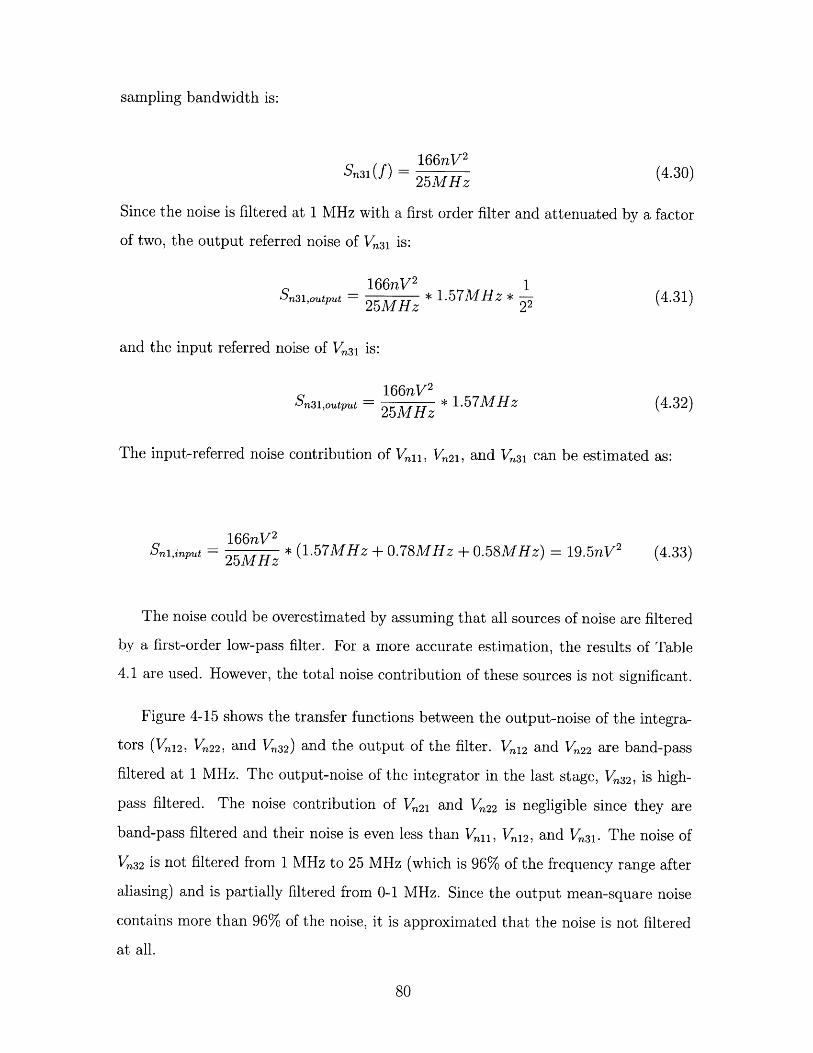
sampling bandwidth is:
166niV 2
Sn3 1 (f) = 25M (4.30)25MH z
Since the noise is filtered at 1 MHz with a first order filter and attenuated by a factor
of two, the output referred noise of Vn3 is:
166nV2 1Snai,output = * 1.57MHz * - (4.31)
25MHz 22
and the input referred noise of Vn3 is:
166nV 2
Sn3l,output = 25MH * 1.57MHz (4.32)
The input-referred noise contribution of Van1 , V 21 , and Vn3i can be estimated as:
Snl,input =5M z * (1.57MHz + 0.78MHz + 0.58MHz) = 19.5nV2 (4.33)25MH z
The noise could be overestimated by assuming that all sources of noise are filtered
by a first-order low-pass filter. For a more accurate estimation, the results of Table
4.1 are used. However, the total noise contribution of these sources is not significant.
Figure 4-15 shows the transfer functions between the output-noise of the integra-
tors (Vn12, V 22, and V 32) and the output of the filter. V 12 and V 22 are band-pass
filtered at 1 MHz. The output-noise of the integrator in the last stage, V 32 , is high-
pass filtered. The noise contribution of V 21 and V 22 is negligible since they are
band-pass filtered and their noise is even less than Van1 , V 12 , and V 31 . The noise of
Vn3 2 is not filtered from 1 MHz to 25 MHz (which is 96% of the frequency range after
aliasing) and is partially filtered from 0-1 MHz. Since the output mean-square noise
contains more than 96% of the noise, it is approximated that the noise is not filtered
at all.
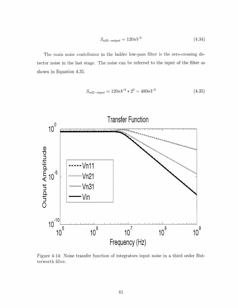
Sn32-output =120nV2
The main noise contributor in the ladder low-pass filter is the zero-crossing de-
tector noise in the last stage. The noise can be referred to the input of the filter as
shown in Equation 4.35.
Sn32 -input =120nV2 * 22 = 480nV 2 (4.35)
Transfer Function100
C)
E
0C
0
10
10"1
Frequency (Hz)Figure 4-14: Noise transfer function of integrators input noise in a third order But-terworth filter.
(4.34)
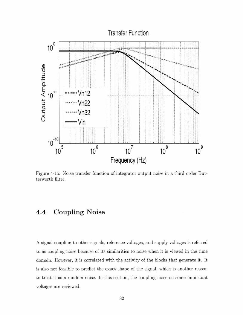
Transfer Function
6 110 8
Frequency (Hz)Figure 4-15: Noise transfer functionterworth filter.
of integrator output noise in a third order But-
4.4 Coupling Noise
A signal coupling to other signals, reference voltages, and supply voltages is referred
to as coupling noise because of its similarities to noise when it is viewed in the time
domain. However, it is correlated with the activity of the blocks that generate it. It
is also not feasible to predict the exact shape of the signal, which is another reason
to treat it as a random noise. In this section, the coupling noise on some important
voltages are reviewed.
100
-o
E
0
-11 9

4.4.1 Noise on Reference Voltages
Ripples on the reference voltage(s) can reduce the signal to noise ratio. In an ADC,
the reference voltage is connected to the capacitor that holds the input signal. Any
noise or ripple on the reference voltage in the first stage of a pipeline ADC is directly
added to the noise or ripple on the sampled signal. Therefore, even if the ADC is
designed with reasonably low noise and distortion, a poor reference voltage lowers
its SNDR significantly. In a pipeline ADC, only the first block is very sensitive to
the noise on the reference voltage, but in a filter, the noise couples directly to the
input signal in all stages. Depending on where the noise is injected, it is filtered
with the corresponding transfer function to the output. Therefore, low-frequency and
high-frequency ripples have different effects on the filter performance.
While reference voltages provide a constant voltage, their current flowing through
them contains high-frequency components. The high-frequency components is due to
the activity of all stages. In this chip, the reference voltage is provided externally.
When high-frequency current passes through the bond-wire inductance, a voltage drop
appears across the bond-wire. An on-chip decoupling capacitor is used to reduce the
voltage ripples.
Figure 4-16 shows the simulated noise on reference voltages if the bond wire has a
resistance of 20Q, inductance of 2nH, and is decoupled on-chip with a 4nF capacitor.
The reference voltage is provided differentially. The top signal in Figure 4-16 is the
differential signal and the next two signals are the negative and the positive sides of
the differential signal. The differential signal has a transient response at the beginning
where it drops from 1V to 991mV. This portion of the response can be ignored since
it happens during the power up. Each side of the differential signal has peaks on the
order of 70mV, which is large compared to 1LSB of the ADC (1LSB is on the order of
1mV). However, the differential reference voltage has a peak-to-peak ripple of 253uV.
The noise on the power supply also couples to the output and may decrease the
signal-to-noise ratio of the system. Simulation shows that the zero-crossing detector
has 40dB supply noise rejection. The supply noise is analyzed in detail in [24]. The
Figure 4-16: Noise of reference voltage based on simulation.
supply noise is attenuated by an on-chip decoupling capacitor. A more appropriate
method is to use an on-chip voltage regulator (as opposed to an off-chip regulator).
Common-mode voltage may also experience high-frequency current that creates
high-frequency ripples on it as shown in Figure 4-17. The ripple on the common mode
voltage tends to be much smaller because in differential circuits, since the positive
and negative sides of the circuit (I, and I) inject opposite currents to the common-
mode voltage that cancel out if the circuit is perfectly matched. In addition, the
common-mode rejection of the zero-crossing detector also attenuates the effects of
common-mode ripples at the output.
... .......
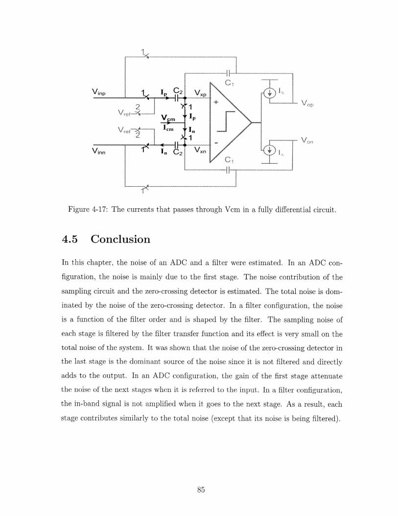
2 1 + VOP
Vref_ Vcm
1V
Vinn in C2 V
Figure 4-17: The currents that passes through Vem in a fully differential circuit.
4.5 Conclusion
In this chapter, the noise of an ADC and a filter were estimated. In an ADC con-
figuration, the noise is mainly due to the first stage. The noise contribution of the
sampling circuit and the zero-crossing detector is estimated. The total noise is dom-
inated by the noise of the zero-crossing detector. In a filter configuration, the noise
is a function of the filter order and is shaped by the filter. The sampling noise of
each stage is filtered by the filter transfer function and its effect is very small on the
total noise of the system. It was shown that the noise of the zero-crossing detector in
the last stage is the dominant source of the noise since it is not filtered and directly
adds to the output. In an ADC configuration, the gain of the first stage attenuate
the noise of the next stages when it is referred to the input. In a filter configuration,
the in-band signal is not amplified when it goes to the next stage. As a result, each
stage contributes similarly to the total noise (except that its noise is being filtered).

86
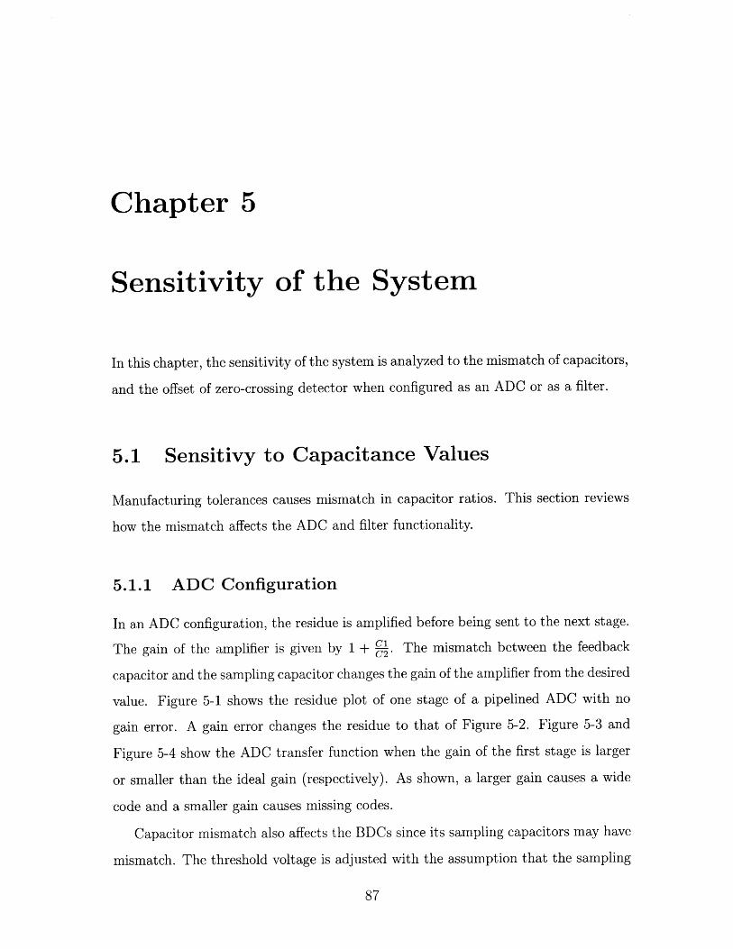
Chapter 5
Sensitivity of the System
In this chapter, the sensitivity of the system is analyzed to the mismatch of capacitors,
and the offset of zero-crossing detector when configured as an ADC or as a filter.
5.1 Sensitivy to Capacitance Values
Manufacturing tolerances causes mismatch in capacitor ratios. This section reviews
how the mismatch affects the ADC and filter functionality.
5.1.1 ADC Configuration
In an ADC configuration, the residue is amplified before being sent to the next stage.
The gain of the amplifier is given by 1 + Q. The mismatch between the feedback
capacitor and the sampling capacitor changes the gain of the amplifier from the desired
value. Figure 5-1 shows the residue plot of one stage of a pipelined ADC with no
gain error. A gain error changes the residue to that of Figure 5-2. Figure 5-3 and
Figure 5-4 show the ADC transfer function when the gain of the first stage is larger
or smaller than the ideal gain (respectively). As shown, a larger gain causes a wide
code and a smaller gain causes missing codes.
Capacitor mismatch also affects the BDCs since its sampling capacitors may have
mismatch. The threshold voltage is adjusted with the assumption that the sampling
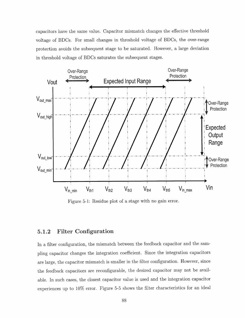
capacitors have the same value. Capacitor mismatch changes the effective threshold
voltage of BDCs. For small changes in threshold voltage of BDCs, the over-range
protection avoids the subsequent stage to be saturated. However, a large deviation
in threshold voltage of BDCs saturates the subsequent stages.
Over-RangeProtection'
Vout
XI.. 7- 4
-
Vouthigh
VoutIowVout mi-
Vout min-
Expected Input Range
Over-RangeProtection
+ - -+111111MNO 11110
'Over-RangeProtection
ExpectedOutputRange
Over-RangeProtection
Vin minI~ I
Vth1 Vth2 Vth3 Vth4 Vth5 Vinmax Vin
Figure 5-1: Residue plot of a stage with no gain error.
5.1.2 Filter Configuration
In a filter configuration, the mismatch between the feedback capacitor and the sam-
pling capacitor changes the integration coefficient. Since the integration capacitors
are large, the capacitor mismatch is smaller in the filter configuration. However, since
the feedback capacitors are reconfigurable, the desired capacitor may not be avail-
able. In such cases, the closest capacitor value is used and the integration capacitor
experiences up to 10% error. Figure 5-5 shows the filter characteristics for an ideal
Vout
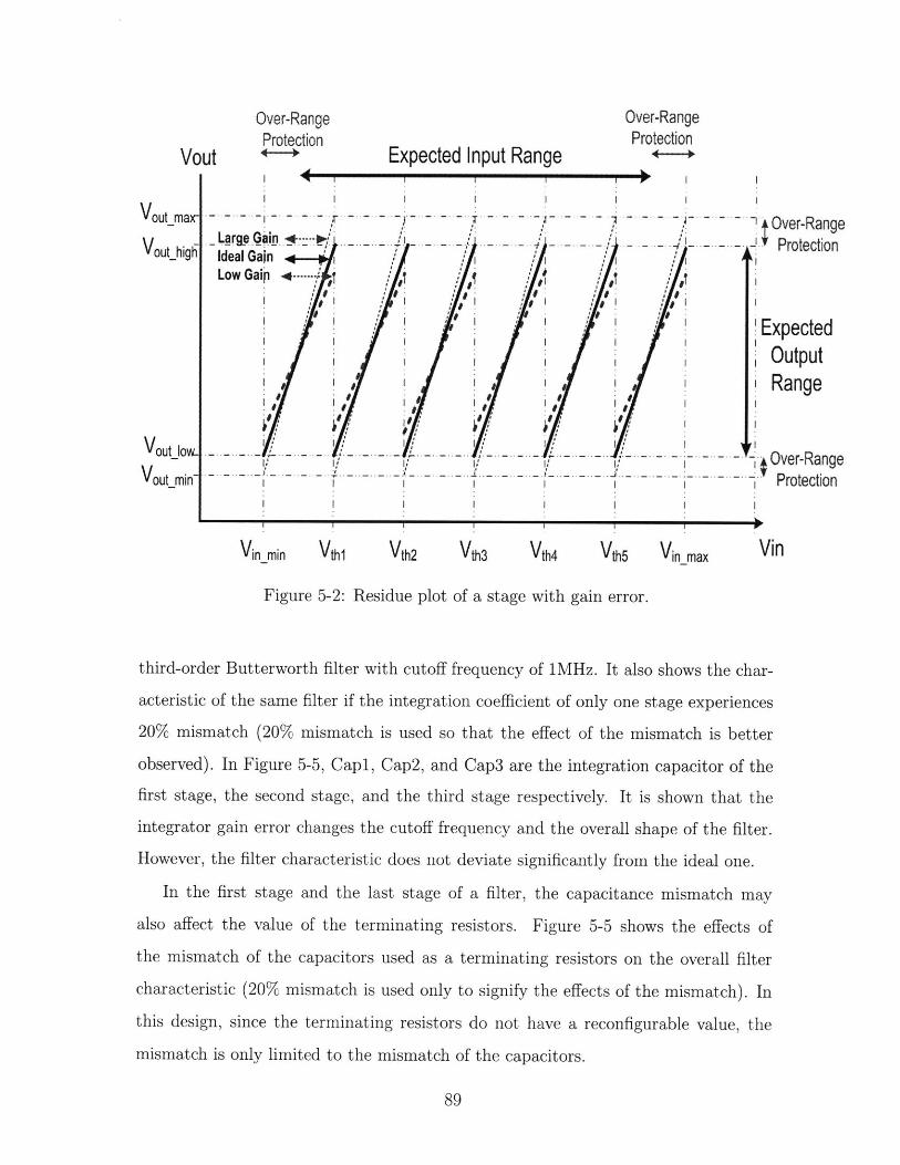
Over-Range Over-RangeProtection Protection
Vout Expected Input Range
VoOutputv-Range
Voutjo - - Over-Range
Lurg - -- - ----- - - -- - ProtectionVout high Ideal Gain V2 i V iLow Gaip 4 .......
i It i s t Expectede o a Outputi st Range
aloaet the value- of tetriaigrssosFiue55hwshefecsOe-ag
Voutin- I III
Vinmin Vthl Vth2 Vth3 Vth4 Vth5 Vinmax Vin
Figure 5-2: Residue plot of a stage with gain error.
third-order Butterworth filter with cutoff frequency of 1MHz. It also shows the char-
acteristic of the same filter if the integration coefficient of only one stage experiences
20% mismatch (20% mismatch is used so that the effect of the mismatch is better
observed). In Figure 5-5, Capi, Cap2, and Cap3 are the integration capacitor of the
first stage, the second stage, and the third stage respectively. It is shown that the
integrator gain error changes the cutoff frequency and the overall shape of the filter.
However, the filter characteristic does not deviate significantly from the ideal one.
In the first stage and the last stage of a filter, the capacitance mismatch may
also affect the value of the terminating resistors. Figure 5-5 shows the effects of
the mismatch of the capacitors used as a terminating resistors on the overall filter
characteristic (20% mismatch is used only to signify the effects of the mismatch). In
this design, since the terminating resistors do not have a reconfigurable value, the
mismatch is only limited to the mismatch of the capacitors.
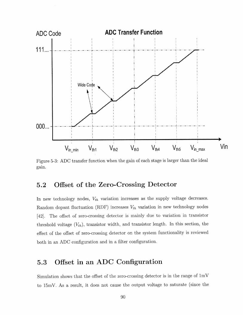
ADC Code
111...
ADC Transfer Function
Wide Coqe
in min Vthl Vth2 Vth3 Vth4 Vth5 Vin-max
Figure 5-3: ADC transfer function when the gain of each stage is larger than the idealgain.
5.2 Offset of the Zero-Crossing Detector
In new technology nodes, Vth variation increases as the supply voltage decreases.
Random dopant fluctuation (RDF) increases Vth variation in new technology nodes
[42]. The offset of zero-crossing detector is mainly due to variation in transistor
threshold voltage (Vth), transistor width, and transistor length. In this section, the
effect of the offset of zero-crossing detector on the system functionality is reviewed
both in an ADC configuration and in a filter configuration.
5.3 Offset in an ADC Configuration
Simulation shows that the offset of the zero-crossing detector is in the range of 1mV
to 15mV. As a result, it does not cause the output voltage to saturate (since the
Vin
Z00000",
00,
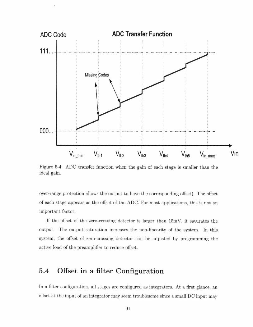
----------- --------- r
Missing(
Vin min
ode
Vthl
ADC Transfer Function
s
Vth2 Vth3 Vth4 Vth5 Vinmax
Figure 5-4: ADC transfer function when the gain of each stage is smaller than theideal gain.
over-range protection allows the output to have the corresponding offset). The offset
of each stage appears as the offset of the ADC. For most applications, this is not an
important factor.
If the offset of the zero-crossing detector is larger than 15mV, it saturates the
output. The output saturation increases the non-linearity of the system. In this
system, the offset of zero-crossing detector can be adjusted by programming the
active load of the preamplifier to reduce offset.
5.4 Offset in a filter Configuration
In a filter configuration, all stages are configured as integrators. At a first glance, an
offset at the input of an integrator may seem troublesome since a small DC input may
ADC Code
111... -
000... -
Vin
-
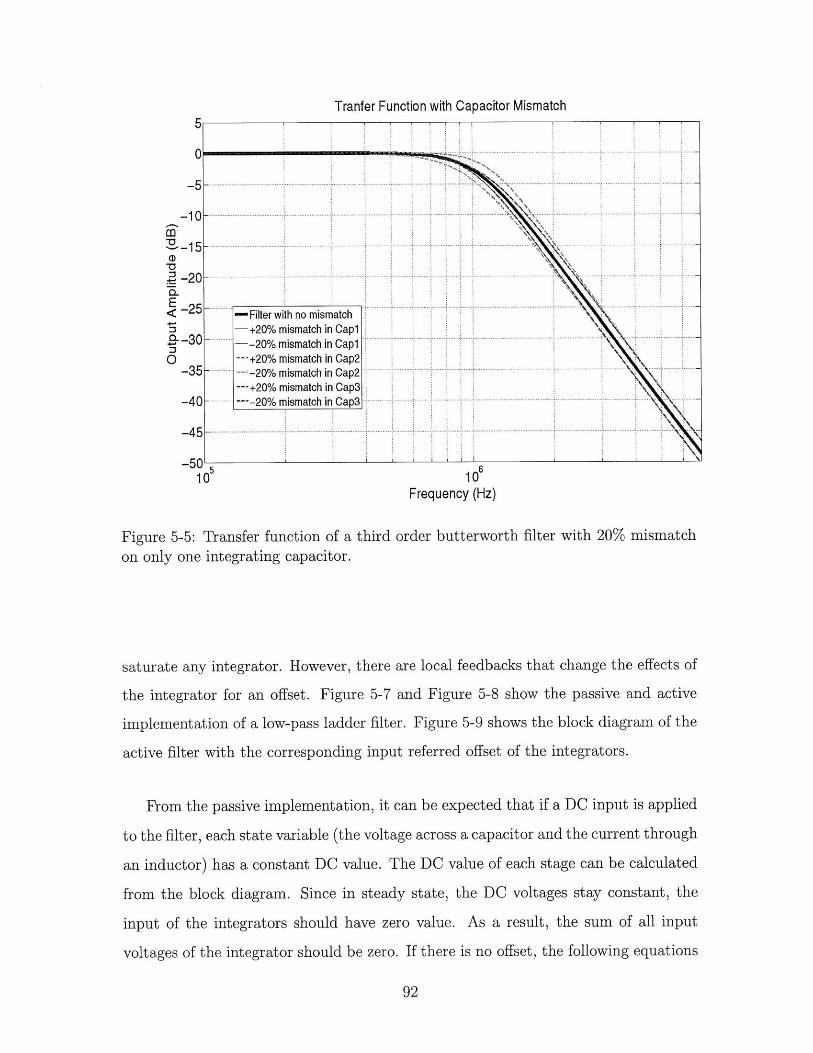
Tranfer Function with Capacitor Mismatch
0
-5
-10
15A.-1 20'a
< -25
0-300
-35
-40
-45
-501 106
Frequency (Hz)
Figure 5-5: Transfer function of a third order butterworth filter with 20% mismatchon only one integrating capacitor.
saturate any integrator. However, there are local feedbacks that change the effects of
the integrator for an offset. Figure 5-7 and Figure 5-8 show the passive and active
implementation of a low-pass ladder filter. Figure 5-9 shows the block diagram of the
active filter with the corresponding input referred offset of the integrators.
From the passive implementation, it can be expected that if a DC input is applied
to the filter, each state variable (the voltage across a capacitor and the current through
an inductor) has a constant DC value. The DC value of each stage can be calculated
from the block diagram. Since in steady state, the DC voltages stay constant, the
input of the integrators should have zero value. As a result, the sum of all input
voltages of the integrator should be zero. If there is no offset, the following equations
-Filter with no mismatch-+20% mismatch in Cap1-- 20% mismatch in Cap1
-+20% mismatch in Cap2-- 20% mismatch in Cap2-+20% mismatch in Cap3--20%/o mismatch in Cap3
................... ..............
.. ............................ ..........
...........
................
................
............
........................
7
.............................
..... ........ ......
..............
............... ....................
I ........... ............
..........
...........
............
I I -
-.. .........
-.. ...........
0 5
.......... .................... ..............
................................... ............
.............
..............................
...............
.........................
...............................
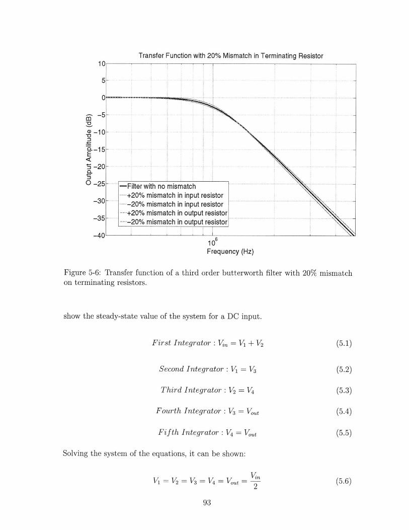
Transfer Function with 20% Mismatch in Terminating Resistor
-Filter with no n+20% mismat(
-20% mismat(___+20% mismat(-- 20% mismatc
ismatchh in input resistorh in input resistorh in output resistorh in output resistor
106Frequency (Hz)
Figure 5-6: Transfer function of a third order butterworth filter with 20% mismatchon terminating resistors.
show the steady-state value of the system for a DC input.
First Integrator : Vi = V1 + V2
Second Integrator: V1 = V3
Third Integrator: V2 = V4
Fourth Integrator: V3 =Vut
Fifth Integrator: V4 =Vut
(5.1)
(5.2)
(5.3)
(5.4)
(5.5)
Solving the system of the equations, it can be shown:
V1 = V2 = V3 = V4 = = " n (5.6)2
-
-F
-5
10
-15E
o -20C-
o -9r
-30--35 -..
-4C
(5.6)
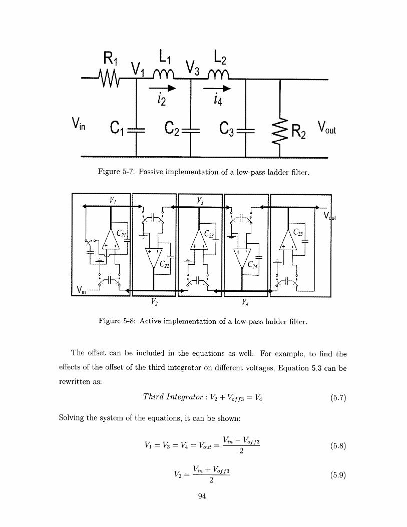
R1 L1 L2
vout
Figure 5-7: Passive implementation of a low-pass ladder filter.
V2 V4
Figure 5-8: Active implementation of a low-pass ladder filter.
The offset can be included in the equations as well. For example, to find the
effects of the offset of the third integrator on different voltages, Equation 5.3 can be
rewritten as:
Third Integrator : V2 + Vff 3 = V4 (5.7)
Solving the system of the equations, it can be shown:
V1 = V3 = V4
Vin + Voff 3
% = 2
Vin
= t V V n - V=0 ff3O~t = 2 (5.8)
(5.9)
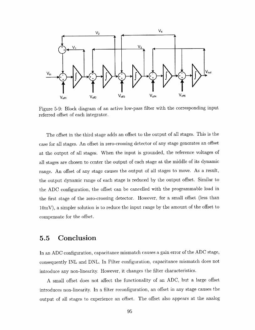
V2V4
v v2 Voff Vff4 VOff5
Figure 5-9: Block diagram of an active low-pass filter with the corresponding input
referred offset of each integrator.
The offset in the third stage adds an offset to the output of all stages. This is the
case for all stages. An offset in zero-crossing detector of any stage generates an offset
at the output of all stages. When the input is grounded, the reference voltages of
all stages are chosen to center the output of each stage at the middle of its dynamic
range. An offset of any stage causes the output of all stages to move. As a result,
the output dynamic range of each stage is reduced by the output offset. Similar to
the ADC configuration, the offset can be cancelled with the programmable load in
the first stage of the zero-crossing detector. However, for a small offset (less than
10mV), a simpler solution is to reduce the input range by the amount of the offset to
compensate for the offset.
5.5 Conclusion
In an ADC configuration, capacitance mismatch causes a gain error of the ADC stage,
consequently INL and DNL. In Filter configuration, capacitance mismatch does not
introduce any non-linearity. However, it changes the filter characteristics.
A small offset does not affect the functionality of an ADC, but a large offset
introduces non-linearity. In a filter reconfiguration, an offset in any stage causes the
output of all stages to experience an offset. The offset also appears at the analog
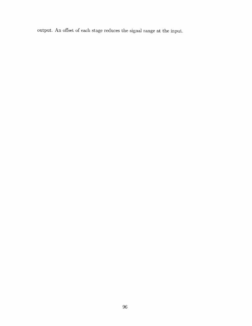
output. An offset of each stage reduces the signal range at the input.
Chapter 6
Measurements of the Fabricated
Chip
This chapter shows the measurement results of the fabricated chip and describes
the significance of each measurement. Figure 6-1 shows the die photo of the chip
fabricated in TSMC 65nm technology and Figure 6-3 shows the layout of each stage.
The block diagram of the chip is shown in Figure 6-2. The core is 340um x 900um
and consists of 8 identical stages (except for the sampling circuit of the first stage
which has minor differences). Each stage can be programmed as an amplifier or an
integrator with programmable coefficients. It can be used as a building block of a
pipeline ADC or a low-pass filter. To demonstrate the configurability, the chip is
configured as an ADC and filter for different sets of measurements (eight stages were
sufficient to show these functionalities). In all measurements, the input is sampled at
50MSPS (unless specified). The clock has a 300ps non-overlapping period and reset
pulses have 400ps pulse width. This corresponds to 1.4ns of the total clock period
(the clock period of 50MSPS is 20ns). The reference voltage is provided externally
and the power drawn from the external reference voltage is negligible.
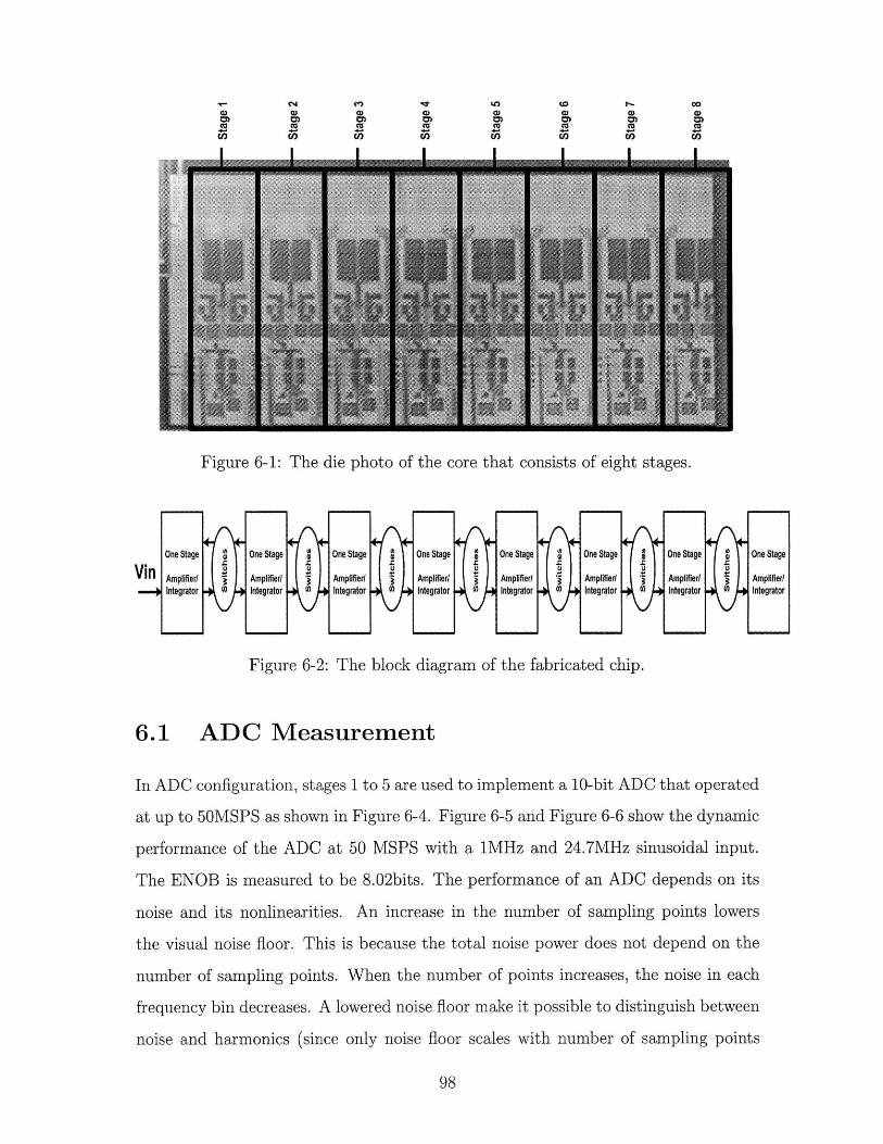
"TLAflt 00
0) )
in Cn (n rn 0) Cn U) Clo
Figure 6-1: The die photo of the core that consists of eight stages.
One Stage i One Stage One Stage One Stage One Stage One Stage 0 One Stage Q Oni
Vin Amplifier/ Amplifier/ Amplifier Amplifier/ Amplifier/ Amplifier/ Amplifier An-.J Integrator Integrator Inerao Integrator Integrator Integrator 9) Integrator Inti
Figure 6-2: The block diagram of the fabricated chip.
6.1 ADC Measurement
In ADC configuration, stages 1 to 5 are used to implement a 10-bit ADC that operated
at up to 50MSPS as shown in Figure 6-4. Figure 6-5 and Figure 6-6 show the dynamic
performance of the ADC at 50 MSPS with a 1MHz and 24.7MHz sinusoidal input.
The ENOB is measured to be 8.02bits. The performance of an ADC depends on its
noise and its nonlinearities. An increase in the number of sampling points lowers
the visual noise floor. This is because the total noise power does not depend on the
number of sampling points. When the number of points increases, the noise in each
frequency bin decreases. A lowered noise floor make it possible to distinguish between
noise and harmonics (since only noise floor scales with number of sampling points
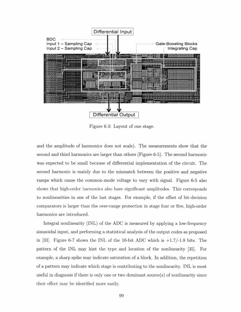
BDCInput 1 - Sampling CapInput 2 - Sampling Cap
Gate-Boosting BlocksIntegrating Cap
Differential Output
Figure 6-3: Layout of one stage.
and the amplitude of harmonics does not scale). The measurements show that the
second and third harmonics are larger than others (Figure 6-5). The second harmonic
was expected to be small because of differential implementation of the circuit. The
second harmonic is mainly due to the mismatch between the positive and negative
ramps which cause the common-mode voltage to vary with signal. Figure 6-5 also
shows that high-order harmonics also have significant amplitudes. This corresponds
to nonlinearities in one of the last stages. For example, if the offset of bit-decision
comparators is larger than the over-range protection in stage four or five, high-order
harmonics are introduced.
Integral nonlinearity (INL) of the ADC is measured by applying a low-frequency
sinusoidal input, and performing a statistical analysis of the output codes as proposed
in [33]. Figure 6-7 shows the INL of the 10-bit ADC which is +1.7/-1.8 bits. The
pattern of the INL may hint the type and location of the nonlinearity [35]. For
example, a sharp spike may indicate saturation of a block. In addition, the repetition
of a pattern may indicate which stage is contributing to the nonlinearity. INL is most
useful in diagnosis if there is only one or two dominant source(s) of nonlinearity since
their effect may be identified more easily.
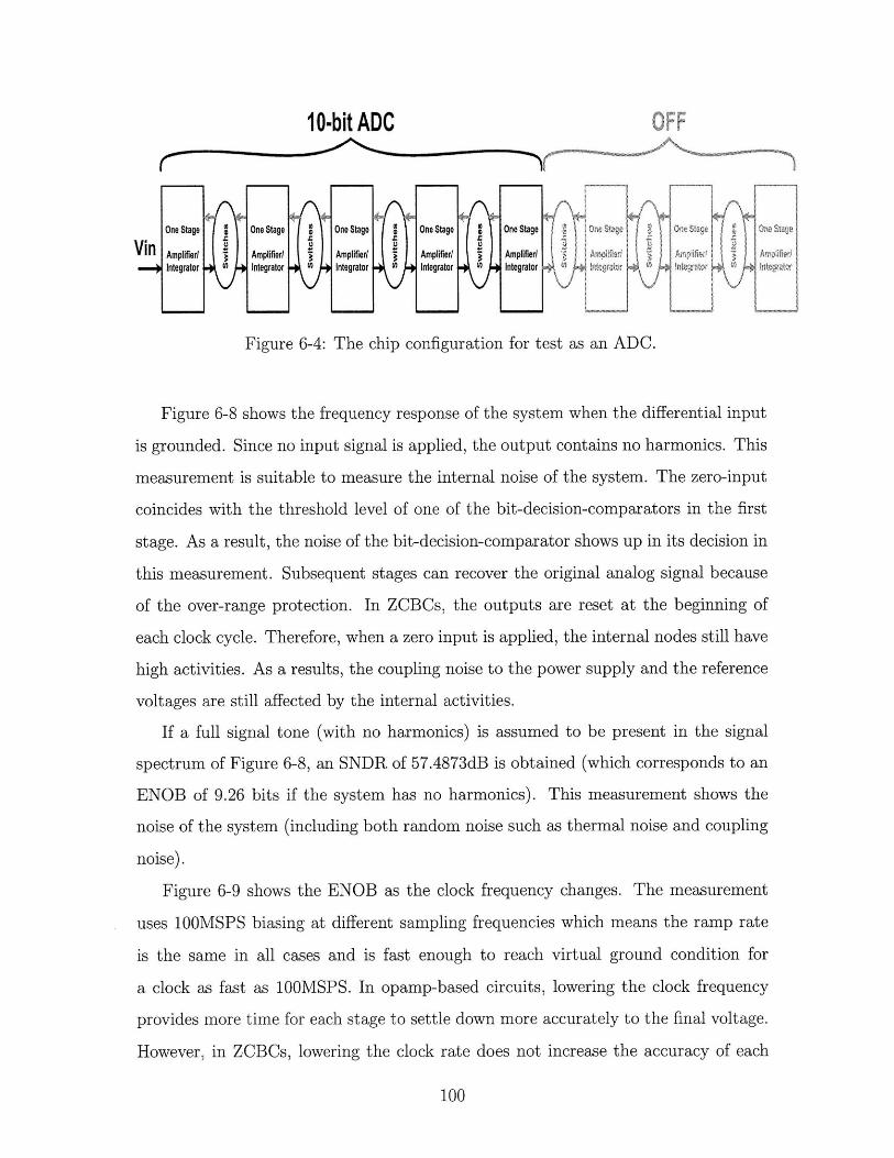
10-bit ADC
Figure 6-4: The chip configuration for test as an ADC.
Figure 6-8 shows the frequency response of the system when the differential input
is grounded. Since no input signal is applied, the output contains no harmonics. This
measurement is suitable to measure the internal noise of the system. The zero-input
coincides with the threshold level of one of the bit-decision-comparators in the first
stage. As a result, the noise of the bit-decision-comparator shows up in its decision in
this measurement. Subsequent stages can recover the original analog signal because
of the over-range protection. In ZCBCs, the outputs are reset at the beginning of
each clock cycle. Therefore, when a zero input is applied, the internal nodes still have
high activities. As a results, the coupling noise to the power supply and the reference
voltages are still affected by the internal activities.
If a full signal tone (with no harmonics) is assumed to be present in the signal
spectrum of Figure 6-8, an SNDR of 57.4873dB is obtained (which corresponds to an
ENOB of 9.26 bits if the system has no harmonics). This measurement shows the
noise of the system (including both random noise such as thermal noise and coupling
noise).
Figure 6-9 shows the ENOB as the clock frequency changes. The measurement
uses 100MSPS biasing at different sampling frequencies which means the ramp rate
is the same in all cases and is fast enough to reach virtual ground condition for
a clock as fast as 100MSPS. In opamp-based circuits, lowering the clock frequency
provides more time for each stage to settle down more accurately to the final voltage.
However, in ZCBCs, lowering the clock rate does not increase the accuracy of each
100
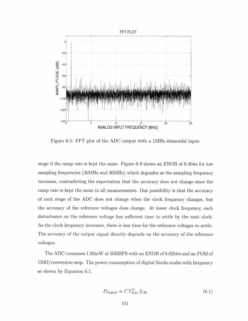
FFT PLOT
0-
-20 -
r-40-
-60o -
-80-10
-120
-1400 5 10 15 20 25
ANALOG INPUT FREQUENCY (MHz)
Figure 6-5: FFT plot of the ADC output with a 1MHz sinusoidal input.
stage if the ramp rate is kept the same. Figure 6-9 shows an ENOB of 8.4bits for low
sampling frequencies (20MHz and 30MHz) which degrades as the sampling frequency
increases, contradicting the expectation that the accuracy does not change since the
ramp rate is kept the same in all measurements. One possibility is that the accuracy
of each stage of the ADC does not change when the clock frequency changes, but
the accuracy of the reference voltages does change. At lower clock frequency, each
disturbance on the reference voltage has sufficient time to settle by the next clock.
As the clock frequency increases, there is less time for the reference voltages to settle.
The accuracy of the output signal directly depends on the accuracy of the reference
voltages.
The ADC consumes 1.92mW at 50MSPS with an ENOB of 8.02bits and an FOM of
150fJ/conversion-step. The power consumption of digital blocks scales with frequency
as shown by Equation 6.1.
PDigia 2 .D-fClk (6-1)
101
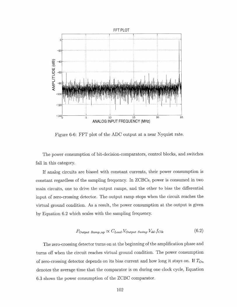
FFT PLOT
0
-20 -
M -40
W
oL -80F
-100
-120
-1400 5 10 15 20 25
ANALOG INPUT FREQUENCY (MHz)
Figure 6-6: FFT plot of the ADC output at a near Nyquist rate.
The power consumption of bit-decision-comparators, control blocks, and switches
fall in this category.
If analog circuits are biased with constant currents, their power consumption is
constant regardless of the sampling frequency. In ZCBCs, power is consumed in two
main circuits, one to drive the output ramps, and the other to bias the differential
input of zero-crossing detector. The output ramp stops when the circuit reaches the
virtual ground condition. As a result, the power consumption at the output is given
by Equation 6.2 which scales with the sampling frequency.
Poutput Ramp-up o CLoad- Voutput Swing Vdd. fcik (6.2)
The zero-crossing detector turns on at the beginning of the amplification phase and
turns off when the circuit reaches virtual ground condition. The power consumption
of zero-crossing detector depends on its bias current and how long it stays on. If Ton
denotes the average time that the comparator is on during one clock cycle, Equation
6.3 shows the power consumption of the ZCBC comparator.
102
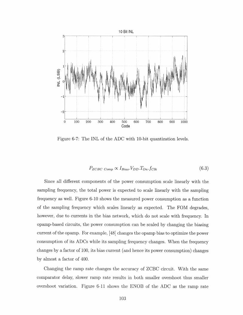
10 Bit INL3
2-
1-
0
-1-
-1........-....................
0 100 200 300 400 500 600 700 800 900 1000Code
Figure 6-7: The INL of the ADC with 10-bit quantization levels.
PZCBC Comp OC IBias-VDD-TOn-fClk (6-3)
Since all different components of the power consumption scale linearly with the
sampling frequency, the total power is expected to scale linearly with the sampling
frequency as well. Figure 6-10 shows the measured power consumption as a function
of the sampling frequency which scales linearly as expected. The FOM degrades,
however, due to currents in the bias network, which do not scale with frequency. In
opamp-based circuits, the power consumption can be scaled by changing the biasing
current of the opamp. For example, [48] changes the opamp bias to optimize the power
consumption of its ADCs while its sampling frequency changes. When the frequency
changes by a factor of 100, its bias current (and hence its power consumption) changes
by almost a factor of 400.
Changing the ramp rate changes the accuracy of ZCBC circuit. With the same
comparator delay, slower ramp rate results in both smaller overshoot thus smaller
overshoot variation. Figure 6-11 shows the ENOB of the ADC as the ramp rate
103
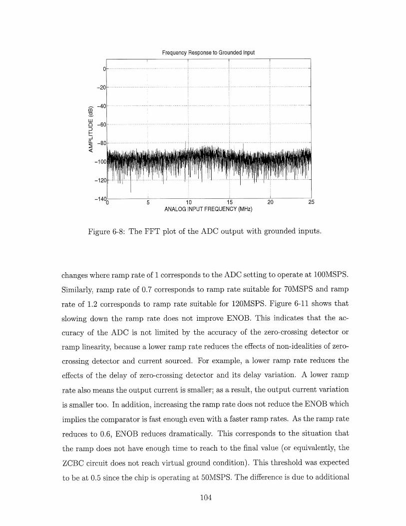
Frequency Response to Grounded Input
0
-20-
-40-
Q0-
-8
-10
-14005 10 15 20 25ANALOG INPUT FREQUENCY (MHz)
Figure 6-8: The FFT plot of the ADC output with grounded inputs.
changes where ramp rate of 1 corresponds to the ADC setting to operate at 100MSPS.
Similarly, ramp rate of 0.7 corresponds to ramp rate suitable for 70MSPS and ramp
rate of 1.2 corresponds to ramp rate suitable for 120MSPS. Figure 6-11 shows that
slowing down the ramp rate does not improve ENOB. This indicates that the ac-
curacy of the ADC is not limited by the accuracy of the zero-crossing detector or
ramp linearity, because a lower ramp rate reduces the effects of non-idealities of zero-
crossing detector and current sourced. For example, a lower ramp rate reduces the
effects of the delay of zero-crossing detector and its delay variation. A lower ramp
rate also means the output current is smaller; as a result, the output current variation
is smaller too. In addition, increasing the ramp rate does not reduce the ENOB which
implies the comparator is fast enough even with a faster ramp rates. As the ramp rate
reduces to 0.6, ENOB reduces dramatically. This corresponds to the situation that
the ramp does not have enough time to reach to the final value (or equivalently, the
ZCBC circuit does not reach virtual ground condition). This threshold was expected
to be at 0.5 since the chip is operating at 5OMSPS. The difference is due to additional
104
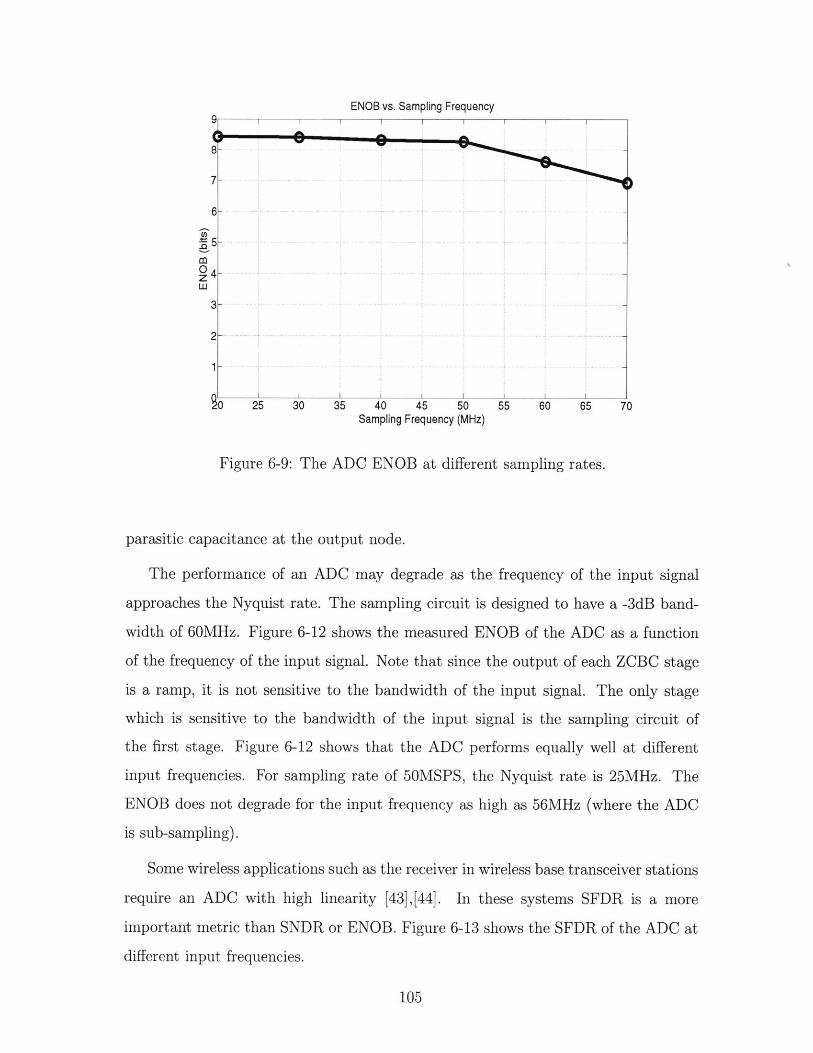
ENOB vs. Sampling Frequency9
7-
6--
04-z
3-
2-
25 30 35 40 45 50 55 60 65 70Sampling Frequency (MHz)
Figure 6-9: The ADC ENOB at different sampling rates.
parasitic capacitance at the output node.
The performance of an ADC may degrade as the frequency of the input signal
approaches the Nyquist rate. The sampling circuit is designed to have a -3dB band-
width of 60MHz. Figure 6-12 shows the measured ENOB of the ADC as a function
of the frequency of the input signal. Note that since the output of each ZCBC stage
is a ramp, it is not sensitive to the bandwidth of the input signal. The only stage
which is sensitive to the bandwidth of the input signal is the sampling circuit of
the first stage. Figure 6-12 shows that the ADC performs equally well at different
input frequencies. For sampling rate of 50MSPS, the Nyquist rate is 25MHz. The
ENOB does not degrade for the input frequency as high as 56MHz (where the ADC
is sub-sampling).
Some wireless applications such as the receiver in wireless base transceiver stations
require an ADC with high linearity [43],[44]. In these systems SFDR is a more
important metric than SNDR or ENOB. Figure 6-13 shows the SFDR of the ADC at
different input frequencies.
105
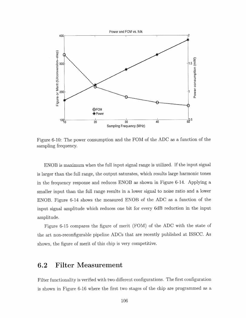
Power and FOM vs. fclk
0)
.o 300 - 1.5 E>(0
0)L
0 E(I)
O
()FOM4Power
og0
1090 20 30 40
Sampling Frequency (MHz)
Figure 6-10: The power consumption and the FOM of the ADC as a function of the
sampling frequency.
ENOB is maximum when the full input signal range is utilized. If the input signal
is larger than the full range, the output saturates, which results large harmonic tones
in the frequency response and reduces ENOB as shown in Figure 6-14. Applying a
smaller input than the full range results in a lower signal to noise ratio and a lower
ENOB. Figure 6-14 shows the measured ENOB of the ADC as a function of the
input signal amplitude which reduces one bit for every 6dB reduction in the input
amplitude.
Figure 6-15 compares the figure of merit (FOM) of the ADC with the state of
the art non-reconfigurable pipeline ADCs that are recently published at ISSCC. As
shown, the figure of merit of this chip is very competitive.
6.2 Filter Measurement
Filter functionality is verified with two different configurations. The first configuration
is shown in Figure 6-16 where the first two stages of the chip are programmed as a
106
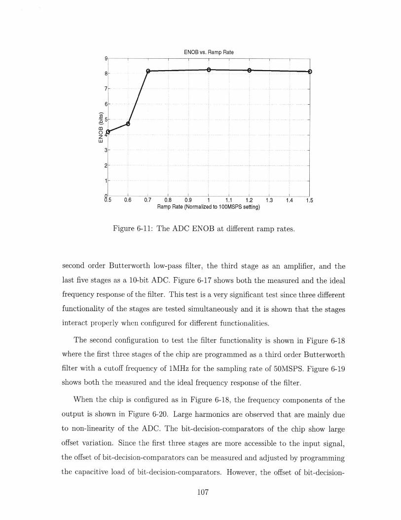
ENOB vs. Ramp Rate
0.8 0.9 1 1.1 1.2Ramp Rate (Normalized to 1 OOMSPS setting)
Figure 6-11: The ADC ENOB at different ramp rates.
second order Butterworth low-pass filter, the third stage as an amplifier, and the
last five stages as a 10-bit ADC. Figure 6-17 shows both the measured and the ideal
frequency response of the filter. This test is a very significant test since three different
functionality of the stages are tested simultaneously and it is shown that the stages
interact properly when configured for different functionalities.
The second configuration to test the filter functionality is shown in Figure 6-18
where the first three stages of the chip are programmed as a third order Butterworth
filter with a cutoff frequency of 1MHz for the sampling rate of 50MSPS. Figure 6-19
shows both the measured and the ideal frequency response of the filter.
When the chip is configured as in Figure 6-18, the frequency components of the
output is shown in Figure 6-20. Large harmonics are observed that are mainly due
to non-linearity of the ADC. The bit-decision-comparators of the chip show large
offset variation. Since the first three stages are more accessible to the input signal,
the offset of bit-decision-comparators can be measured and adjusted by programming
the capacitive load of bit-decision-comparators. However, the offset of bit-decision-
107
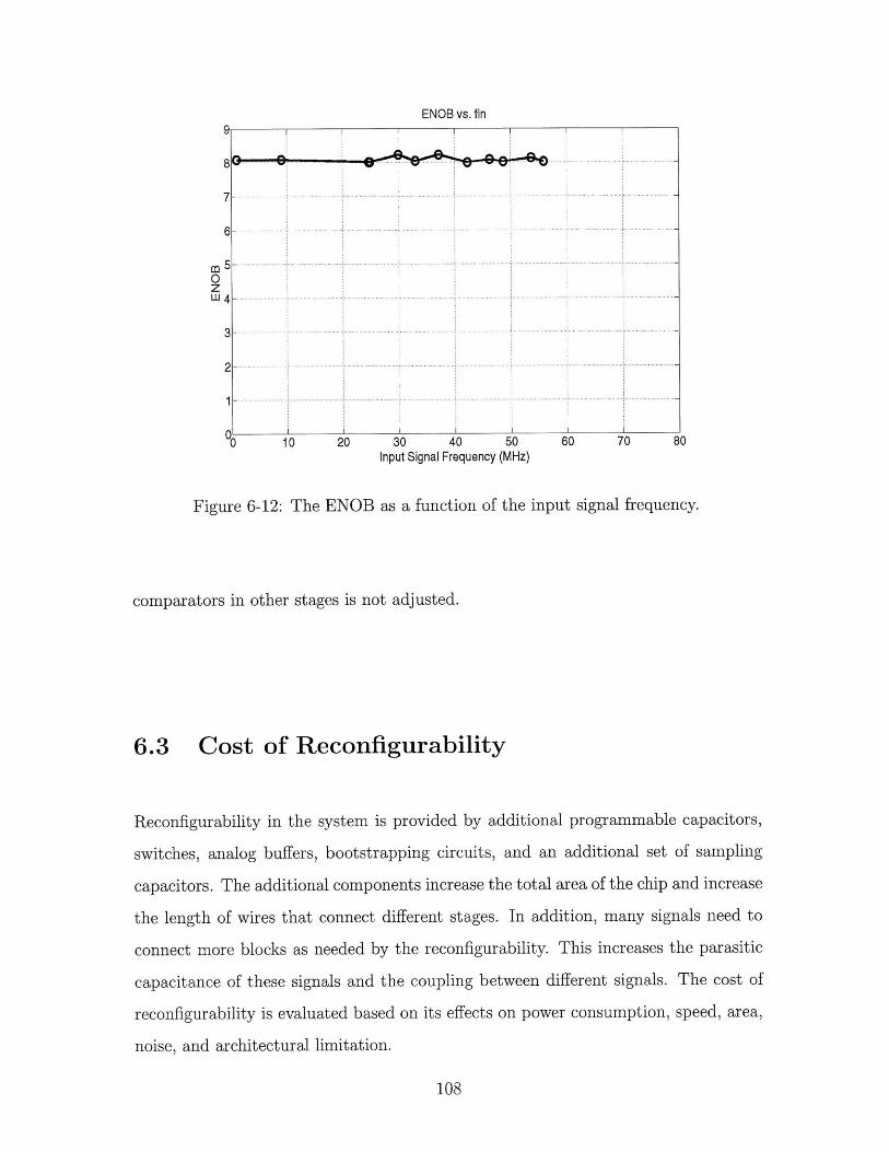
ENOB vs. fin9 -
80
6-
5-
4-
3-
2
1.... ... .. .
10 20 30 40 50Input Signal Frequency (MHz)
60 70 80
Figure 6-12: The ENOB as a function of the input signal frequency.
comparators in other stages is not adjusted.
6.3 Cost of Reconfigurability
Reconfigurability in the system is provided by additional programmable capacitors,
switches, analog buffers, bootstrapping circuits, and an additional set of sampling
capacitors. The additional components increase the total area of the chip and increase
the length of wires that connect different stages. In addition, many signals need to
connect more blocks as needed by the reconfigurability. This increases the parasitic
capacitance of these signals and the coupling between different signals. The cost of
reconfigurability is evaluated based on its effects on power consumption, speed, area,
noise, and architectural limitation.
108
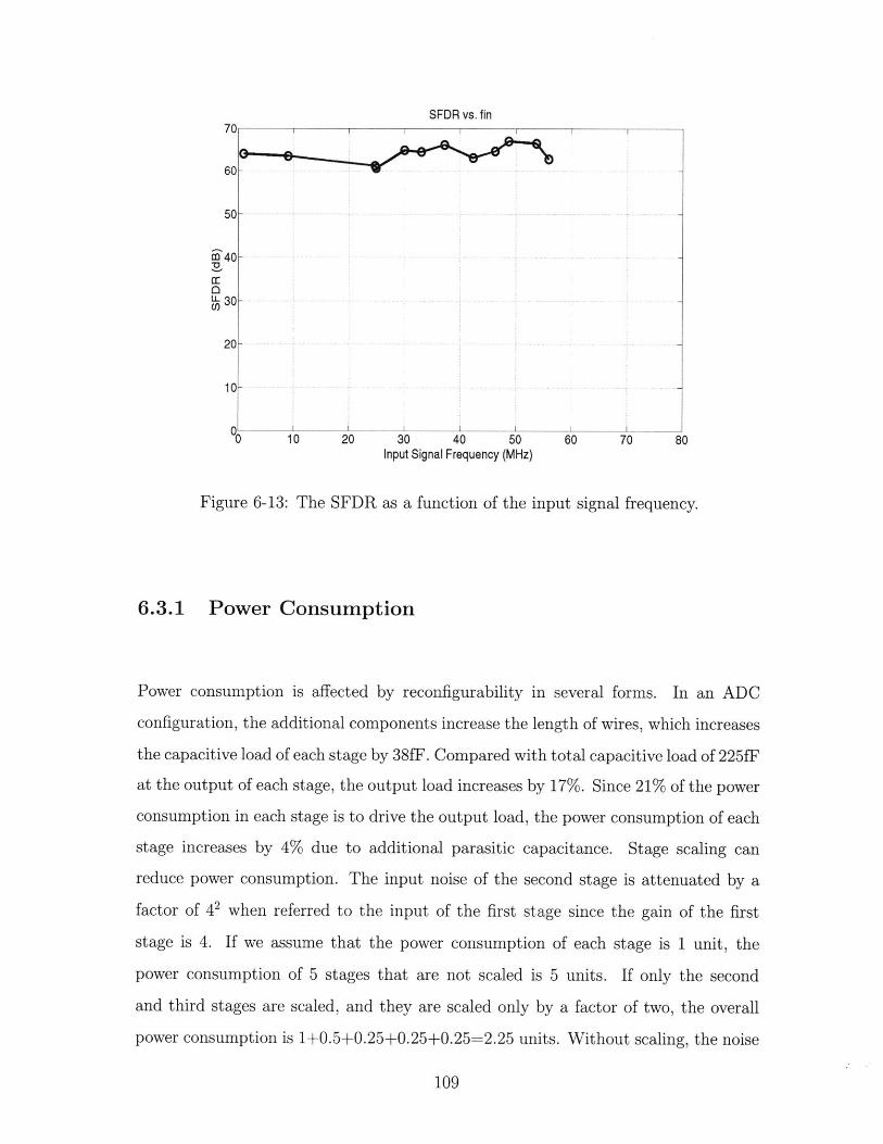
SFDR vs. fin70
60
50-
40--
u-30-
20-
10
0 10 20 30 40 50 60 70 80Input Signal Frequency (MHz)
Figure 6-13: The SFDR as a function of the input signal frequency.
6.3.1 Power Consumption
Power consumption is affected by reconfigurability in several forms. In an ADC
configuration, the additional components increase the length of wires, which increases
the capacitive load of each stage by 38fF. Compared with total capacitive load of 225fF
at the output of each stage, the output load increases by 17%. Since 21% of the power
consumption in each stage is to drive the output load, the power consumption of each
stage increases by 4% due to additional parasitic capacitance. Stage scaling can
reduce power consumption. The input noise of the second stage is attenuated by a
factor of 42 when referred to the input of the first stage since the gain of the first
stage is 4. If we assume that the power consumption of each stage is 1 unit, the
power consumption of 5 stages that are not scaled is 5 units. If only the second
and third stages are scaled, and they are scaled only by a factor of two, the overall
power consumption is 1+0.5+0.25+0.25+0.25=2.25 units. Without scaling, the noise
109
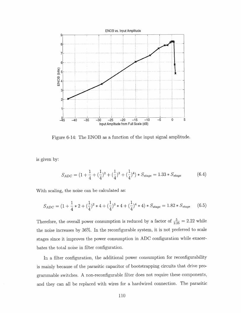
ENOB vs. Input Amplitude
8-
7-
6-
CO
04z
3-
2-
1 .. .. ..... . .. ..
-15 -40 -35 -30 -25 -20 -15 -10 -5 0 5Input Amplitude from Full Scale (dB)
Figure 6-14: The ENOB as a function of the input signal amplitude.
is given by:
SADC = (I+I + 2 13 4 * Sstage = 1.33 * Sstage (6.4)
With scaling, the noise can be calculated as:
SADC 2 3 4 *4)*Sstage = 1-82 * Sstage (6.5)
Therefore, the overall power consumption is reduced by a factor of 5 = 2.22 while
the noise increases by 36%. In the reconfigurable system, it is not preferred to scale
stages since it improves the power consumption in ADC configuration while exacer-
bates the total noise in filter configuration.
In a filter configuration, the additional power consumption for reconfigurability
is mainly because of the parasitic capacitor of bootstrapping circuits that drive pro-
grammable switches. A non-reconfigurable filter does not require these components,
and they can all be replaced with wires for a hardwired connection. The parasitic
110
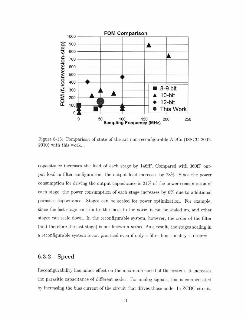
4)00=%
(Is
L
0
U
0U
1000
900
800
700
600
500
400
300
200
100
0
0
FOM Comparison
100 150Sampling Frequency (MHz)
200 250
Figure 6-15: Comparison of state of the art non-reconfigurable ADCs (ISSCC 2007-2010) with this work. .
capacitance increases the load of each stage by 146fF. Compared with 360fF out-
put load in filter configuration, the output load increases by 28%. Since the power
consumption for driving the output capacitance is 21% of the power consumption of
each stage, the power consumption of each stage increases by 6% due to additional
parasitic capacitance. Stages can be scaled for power optimization. For example,
since the last stage contributes the most to the noise, it can be scaled up, and other
stages can scale down. In the reconfigurable system, however, the order of the filter
(and therefore the last stage) is not known a priori. As a result, the stages scaling in
a reconfigurable system is not practical even if only a filter functionality is desired.
6.3.2 Speed
Reconfigurability has minor effect on the maximum speed of the system. It increases
the parasitic capacitance of different nodes. For analog signals, this is compensated
by increasing the bias current of the circuit that drives those node. In ZCBC circuit,
111
* 8-9 bitA A 10-bit
* 12-bit0 This Work
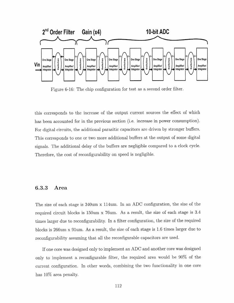
2"d Order Filter Gain (x4) 10-bit ADC
One Stage One Stage One Stage One Stage One Stage One Stage One Stage One Stage
Vin Amplifier Amplifier/ Amplifier/ Amplifier Amplifier Amplifier) ' Amplifier Amplifier-. Integrator Integrator Integrator Integrator Integrator Integrator Integrator Integrator
Figure 6-16: The chip configuration for test as a second order filter.
this corresponds to the increase of the output current sources the effect of which
has been accounted for in the previous section (i.e. increase in power consumption).
For digital circuits, the additional parasitic capacitors are driven by stronger buffers.
This corresponds to one or two more additional buffers at the output of some digital
signals. The additional delay of the buffers are negligible compared to a clock cycle.
Therefore, the cost of reconfigurability on speed is negligible.
6.3.3 Area
The size of each stage is 340um x 114um. In an ADC configuration, the size of the
required circuit blocks is 150um x 76um. As a result, the size of each stage is 3.4
times larger due to reconfigurability. In a filter configuration, the size of the required
blocks is 266um x 91um. As a result, the size of each stage is 1.6 times larger due to
reconfigurability assuming that all the reconfigurable capacitors are used.
If one core was designed only to implement an ADC and another core was designed
only to implement a reconfigurable filter, the required area would be 90% of the
current configuration. In other words, combining the two functionality in one core
has 10% area penalty.
112
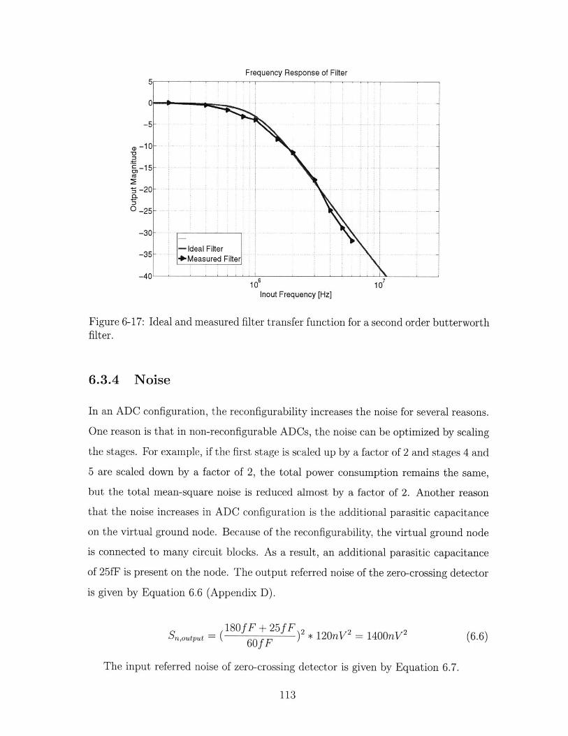
Frequency Response of Filter
106 10Inout Frequency [Hz]
Figure 6-17: Ideal and measured filter transfer function for a second order butterworthfilter.
6.3.4 Noise
In an ADC configuration, the reconfigurability increases the noise for several reasons.
One reason is that in non-reconfigurable ADCs, the noise can be optimized by scaling
the stages. For example, if the first stage is scaled up by a factor of 2 and stages 4 and
5 are scaled down by a factor of 2, the total power consumption remains the same,
but the total mean-square noise is reduced almost by a factor of 2. Another reason
that the noise increases in ADC configuration is the additional parasitic capacitance
on the virtual ground node. Because of the reconfigurability, the virtual ground node
is connected to many circuit blocks. As a result, an additional parasitic capacitance
of 25fF is present on the node. The output referred noise of the zero-crossing detector
is given by Equation 6.6 (Appendix D).
= 180 fF + 25fF F
Sn6ftput = F + 2 * 120nV 2 = 1400nV 2 (6.6)60ef F
The input referred noise of zero-crossing detector is given by Equation 6.7.
113
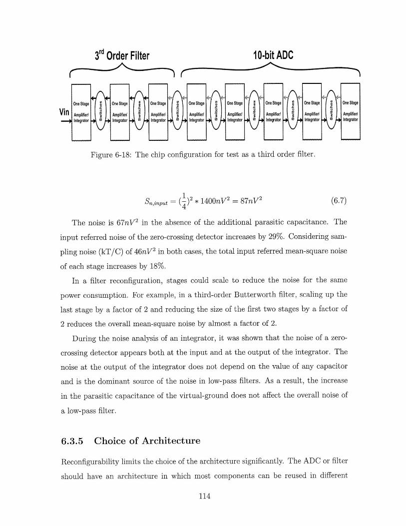
3rd Order Filter 10-bit ADC
One Stage One Stage One Stage One Stage One Stage One Stage One Stage One Stage
V Amplifier/ Amplifier/ Amplifierd Amplifier/ Amplifier/ Amplifier/ Amplifier/ Amplifier/
.-- Integrator Integrator Integrator Integrator Integrator Integrator U) Integrator W Integrator
Figure 6-18: The chip configuration for test as a third order filter.
SnnpYt ( )2 * 1400nV 2 = 87nV 2 (6.7)
The noise is 67nV 2 in the absence of the additional parasitic capacitance. The
input referred noise of the zero-crossing detector increases by 29%. Considering sam-
pling noise (kT/C) of 46nV 2 in both cases, the total input referred mean-square noise
of each stage increases by 18%.
In a filter reconfiguration, stages could scale to reduce the noise for the same
power consumption. For example, in a third-order Butterworth filter, scaling up the
last stage by a factor of 2 and reducing the size of the first two stages by a factor of
2 reduces the overall mean-square noise by almost a factor of 2.
During the noise analysis of an integrator, it was shown that the noise of a zero-
crossing detector appears both at the input and at the output of the integrator. The
noise at the output of the integrator does not depend on the value of any capacitor
and is the dominant source of the noise in low-pass filters. As a result, the increase
in the parasitic capacitance of the virtual-ground does not affect the overall noise of
a low-pass filter.
6.3.5 Choice of Architecture
Reconfigurability limits the choice of the architecture significantly. The ADC or filter
should have an architecture in which most components can be reused in different
114
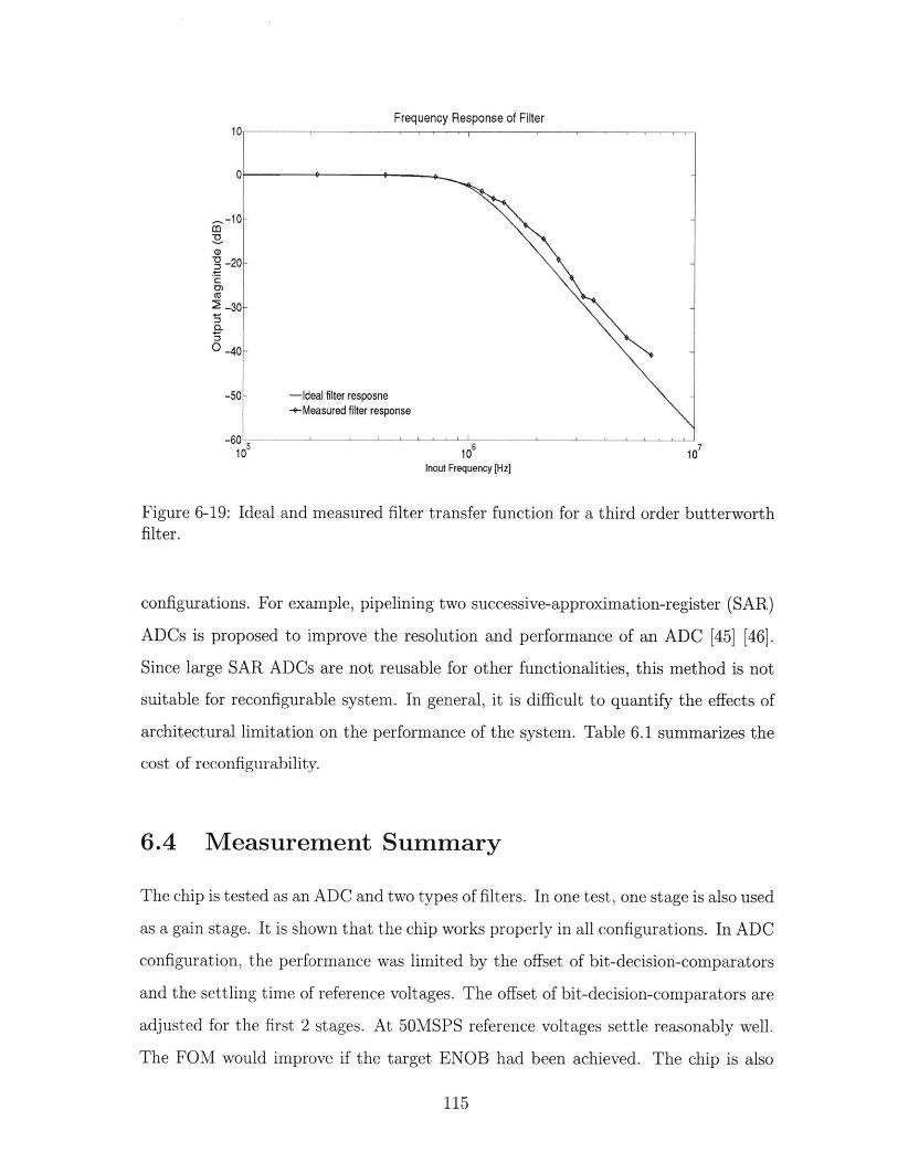
Frequency Response of Filter
g0 -21
(3
0.-A
Inout Frequency [Hz]
Figure 6-19: Ideal and measured filter transfer function for a third order butterworthfilter.
configurations. For example, pipelining two successive-approximation-register (SAR)
ADCs is proposed to improve the resolution and performance of an ADC [45] [46].
Since large SAR ADCs are not reusable for other functionalities, this method is not
suitable for reconfigurable system. In general, it is difficult to quantify the effects of
architectural limitation on the performance of the system. Table 6.1 summarizes the
cost of reconfigurability.
6.4 Measurement Summary
The chip is tested as an ADC and two types of filters. In one test, one stage is also used
as a gain stage. It is shown that the chip works properly in all configurations. In ADC
configuration, the performance was limited by the offset of bit-decision-comparators
and the settling time of reference voltages. The offset of bit-decision-comparators are
adjusted for the first 2 stages. At 50MSPS reference voltages settle reasonably well.
The FOM would improve if the target ENOB had been achieved. The chip is also
115
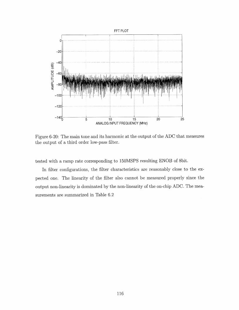
0
-20-
-40
al -60:D
-s-- 80
-100
-120
FFT PLOT
jh I L
... ... ... .. .... .. .. ... ... .... .. ..-
.. ..... ... .... .. .. .. .... .. ..... .. .... .... .. .. .. .... ... -
-14(0 5 10 15 20 25
ANALOG INPUT FREQUENCY (MHz)
Figure 6-20: The main tone and its harmonic at the output of the ADC that measuresthe output of a third order low-pass filter.
tested with a ramp rate corresponding to 150MSPS resulting ENOB of 8bit.
In filter configurations, the filter characteristics are reasonably close to the ex-
pected one. The linearity of the filter also cannot be measured properly since the
output non-linearity is dominated by the non-linearity of the on-chip ADC. The mea-
surements are summarized in Table 6.2
116
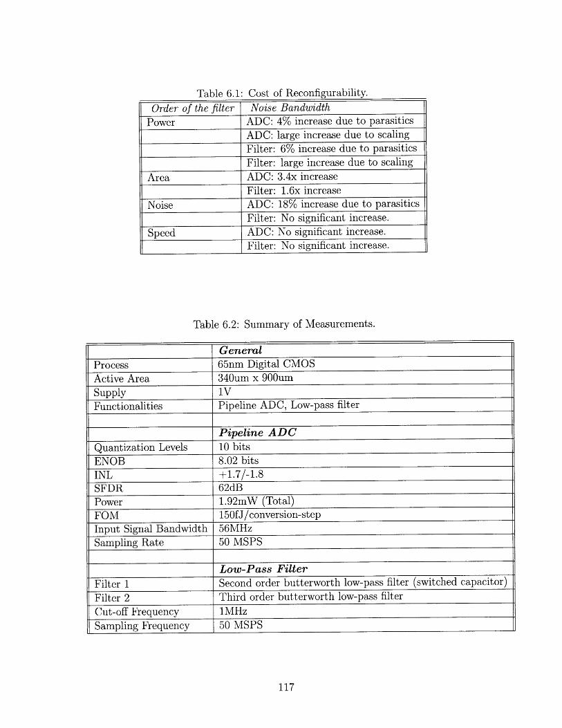
Table 6.1: Cost of Reconfigurability.
Order of the filter Noise BandwidthPower ADC: 4% increase due to parasitics
ADC: large increase due to scalingFilter: 6% increase due to parasiticsFilter: large increase due to scaling
Area ADC: 3.4x increaseFilter: 1.6x increase
Noise ADC: 18% increase due to parasiticsFilter: No significant increase.
Speed ADC: No significant increase.Filter: No significant increase.
Table 6.2: Summary of Measurements.
GeneralProcess 65nm Digital CMOSActive Area 340um x 900umSupply 1VFunctionalities Pipeline ADC, Low-pass filter
Pipeline ADCQuantization Levels 10 bitsENOB 8.02 bitsINL +1.7/-1.8SFDR 62dBPower 1.92mW (Total)FOM 150fJ/conversion-stepInput Signal Bandwidth 56MHzSampling Rate 50 MSPS
Low-Pass FilterFilter 1 Second order butterworth low-pass filter (switched capacitor)Filter 2 Third order butterworth low-pass filter
Cut-off Frequency 1MHzSampling Frequency 50 MSPS
117

118

Chapter 7
Conclusions
A highly-configurable analog system is presented. A prototype chip is fabricated
and an ADC and filter functionalities are demonstrated. The chip consists of eight
identical programmable stages (except for the first stage that has minor differences
in the sampling circuit). Each stage can either amplify or integrate its inputs. The
output can be sent to the adjacent stages. The chip can be configured as a pipeline
ADC, switched-capacitor filter, or a programmable gain amplifier (a gain of 4 is
demonstrated).
In an ADC configuration, the first five stages are programmed to implement a 10-
bit ADC. The ADC has ENOB of 8 bits at 50 MSPS. The ENOB improves to 8.5 bits if
the sampling rate is lowered to 30MSPS. The ADC has an FOM of 150fJ/conversion-
step, which is very competitive with the state of the art non-reconfigurable ADCs.
The performance of the ADC is limited due to the offset of bit-decision-comparators,
and the coupling noise and the ripples on the reference voltages. The offset of BDCs
were adjusted for the first two stages. In addition 50MSPS sapling rate was used
to allow enough time for the reference voltages to settle. Measurements show that
if the ramp rate of the ZCBCs increases, the ENOB of the ADC does not change.
This shows that the delay (or delay variation) of zero-crossing detector is not the
bottleneck. It also shows that the output resistance of the current sources, and the
resistance of the switches are not the bottleneck either (since their contribution to
the ADC non-linearity is more at higher ramp rates). The first stage is responsible
119
for 75% of the input-referred mean square noise. Sampling noise is responsible for
40% of the total mean-square noise and the zero-crossing detector is responsible for
60%. As a result, optimizing the mean-square noise of the zero-crossing detector of
the first stage is the most effective way in reducing the overall noise of the chip in the
ADC configuration.
In the filter configuration, several input stages are programmed as a filter and
the next stages are programmed as an ADC. The chip is tested in two different filter
configurations. In one set of tests, the first two stages of the chip are configured as a
second order Butterworth filter and the third stage is configured as an amplifier. The
remaining stages are programmed as an ADC. It was demonstrated that the desired
filter functionality is properly achieved in this configuration. In another test, the
first three stages of the chip are programmed as a third-order Butterworth filter and
the next stages are programmed as an ADC. The desired filter functionality is also
demonstrated in the configuration.
The noise of the system in a filter configuration is also analyzed. It is shown
that in a third order Butterworth filter, more than 90% of the noise is due to the
zero-crossing detector of the last stage. This is mainly due to the fact that the noise
of earlier stages is filtered with the filter transfer function in a similar way that the
input signal is filtered. The last stage of the filter contributes the most to the total
noise power since its noise is not filtered.
The ZCBC architecture has been used to avoid the stability problems of opamp-
based circuits and scale power consumption for a wide range of sampling frequencies.
It is shown that the power consumption of the chip scales linearly with the sampling
frequency.
A new technique is introduced to implement the terminating resistors in a ladder
filter. This technique is very compatible with the reconfigurable architecture and
does not have any area or power overhead. As a result, any stage can be programmed
to be the first stage or the last stage of a filter. The technique saves the area and
reduces the complexity of implementing the terminating resistors in a filter.
An asymmetric differential signaling is also introduced. This method improves the
120
dynamic range of the output signals which is particularly important in new technology
nodes with low supply voltage.
7.1 Future Work
The signal-to-noise ratio of the current chip was limited due to the coupling and the
ripples on the reference voltages. In particular, the bond-wire inductance introduces
oscillations of the reference voltage. An on-chip reference voltage can improve the
performance significantly and should be integrated in the future revisions of the chip.
Dual ramp-rate has been proposed for stand-alone ADCs [23]. The linearity of
the system improves with dual ramp rates. This technique should be considered for
the future revisions of the chip.
In this chip, only the feedback capacitors are reconfigurable and provide recon-
figurability for integration. In the future work, the sampling capacitors can also be
reconfigurable, which has two advantages. One advantage is that the sampling noise
of each stage can be changed based on the requirement. In addition, the gain of
each stage can be reconfigured as well to implement programmable gain amplifier.
Alternatively, several rows of reconfigurable stages can be implemented where the
size of all stages are the same in one row and scale from one row to another row. If a
larger (or smaller) stage is needed, the current stage can be connected to a stage in
a different row.
The connectivity of the stages in the current chip is limited to the adjacent stages
for the ADC and filter functionality. In the next revision of the chip, the research
can focus to provide more programmability for the switches.
The current chip architecture has most of the building blocks of a sigma-delta
ADC such as integrators, bit-decision-comparators, and adders. More connectivity
is required between different stages to implement a sigma-delta ADC. The future
work can examine how to extend the functionalities of the chip to sigma-delta ADC.
Similarly, the current architecture of the chip has most of the building blocks for
a time-interleaved ADC. In future research, such functionality can be added to the
121
system.
Finally, there are two more techniques that can be used to improve the function-
ality of reconfigurable analog systems as described next. However, each technique has
some challenges. In future work, these techniques can be researched more.
7.1.1 Pulse-Width Modulated Signals
Figure 7-1 shows a block diagram of two stages of the system that are configured to
amplify the signal. There are two signals that connect the two stages. One signal is
V 1ti which is the analog output of the first stage. The other signal is Vcontro, which
is the digital signal that controls the current sources of the next stage. Figure 7-1
shows the shape of signals in the time domain. As shown the pulse width of Vcont,oi
increases linearly with the amplitude of Vst. In fact, Vst can be reproduced in stage
2 using Vcontroi (if the ramp rate of the two stages are adjusted to be the same).
Since it is much easier to have a reconfigurable connection between different stages
for digital signals, Vcontro can be used as the output of each stage. This method
has several challenges. One challenge is that the ramp rate of the two stages should
match very well. Another challenge is that the jitter of the control signal increases
the noise significantly. In future work, this method can be researched more since it
provides better connectivity between different stages, but the matching of the ramp
rates and the jitter of Vcontrol should be addressed. Alternatively, this method can
provide connection between stages that don't require a large signal-to-noise ratio.
7.1.2 Programmable Feedback Ratio Using Programmable
Current Sources
Figure 7-3 shows a ZCBCs with a programmable capacitor in the feedback. Ideally,
the current source that drives the output node provides a constant current 11. The
current that passes through C 2 and C3 depends on their relative values. Once C3 is
programmed, its value stays the same for the rest of the operation. As a result, I2 and
13 also remain constant whenever I1 is on. Since 13 is constant, it can be replaced with
122
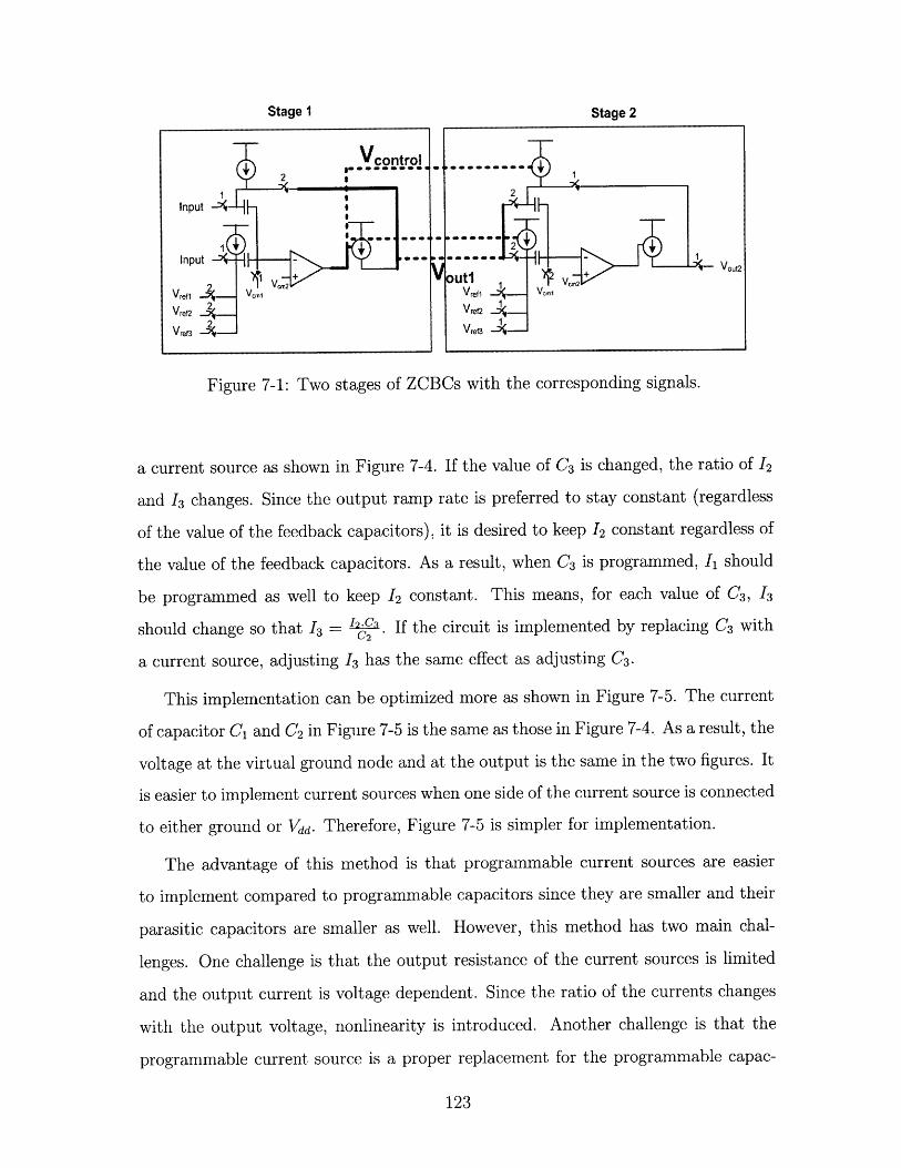
Stage 2
Figure 7-1: Two stages of ZCBCs with the corresponding signals.
a current source as shown in Figure 7-4. If the value of C3 is changed, the ratio of 12
and 13 changes. Since the output ramp rate is preferred to stay constant (regardless
of the value of the feedback capacitors), it is desired to keep 12 constant regardless of
the value of the feedback capacitors. As a result, when C3 is programmed, I1 should
be programmed as well to keep 12 constant. This means, for each value of C3, 13
should change so that 13 - I2.3' If the circuit is implemented by replacing C3 with
a current source, adjusting 13 has the same effect as adjusting C3.
This implementation can be optimized more as shown in Figure 7-5. The current
of capacitor C1 and C2 in Figure 7-5 is the same as those in Figure 7-4. As a result, the
voltage at the virtual ground node and at the output is the same in the two figures. It
is easier to implement current sources when one side of the current source is connected
to either ground or Vdd. Therefore, Figure 7-5 is simpler for implementation.
The advantage of this method is that programmable current sources are easier
to implement compared to programmable capacitors since they are smaller and their
parasitic capacitors are smaller as well. However, this method has two main chal-
lenges. One challenge is that the output resistance of the current sources is limited
and the output current is voltage dependent. Since the ratio of the currents changes
with the output voltage, nonlinearity is introduced. Another challenge is that the
programmable current source is a proper replacement for the programmable capac-
123
Stage I
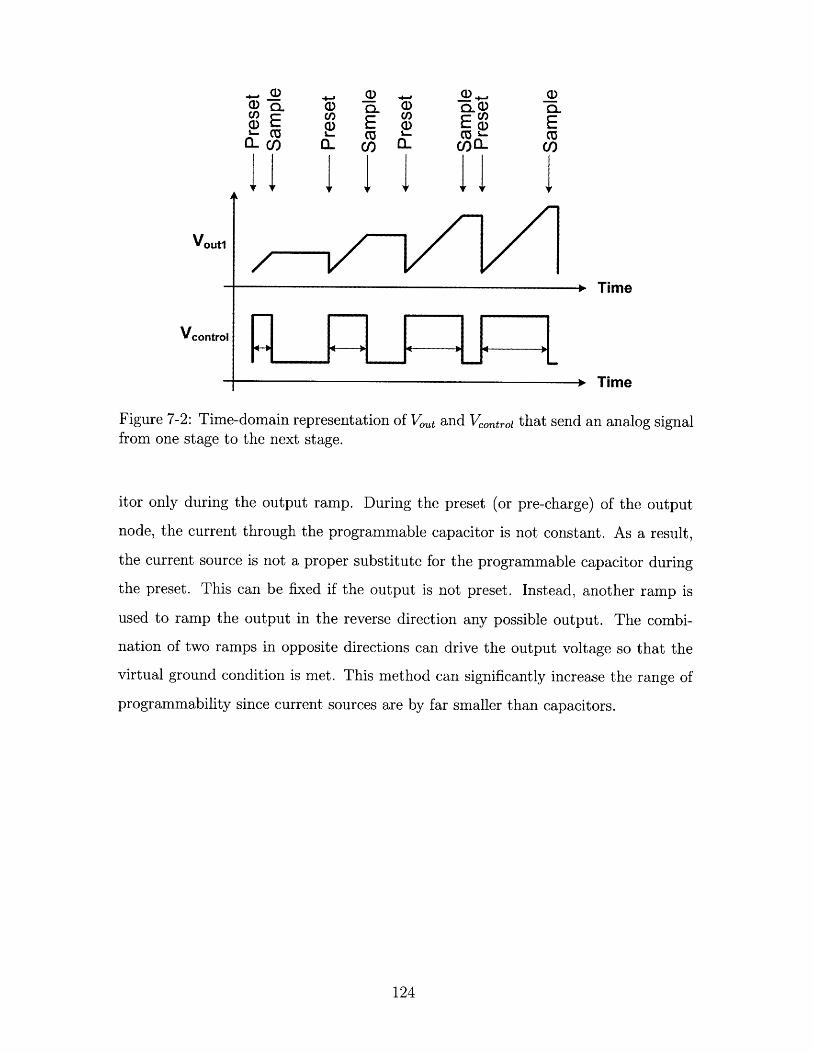
- U) U)
Vout1
> Time
Vcontroi
o Time
Figure 7-2: Time-domain representation of V,,t and Vcontroi that send an analog signalfrom one stage to the next stage.
itor only during the output ramp. During the preset (or pre-charge) of the output
node, the current through the programmable capacitor is not constant. As a result,
the current source is not a proper substitute for the programmable capacitor during
the preset. This can be fixed if the output is not preset. Instead, another ramp is
used to ramp the output in the reverse direction any possible output. The combi-
nation of two ramps in opposite directions can drive the output voltage so that the
virtual ground condition is met. This method can significantly increase the range of
programmability since current sources are by far smaller than capacitors.
124
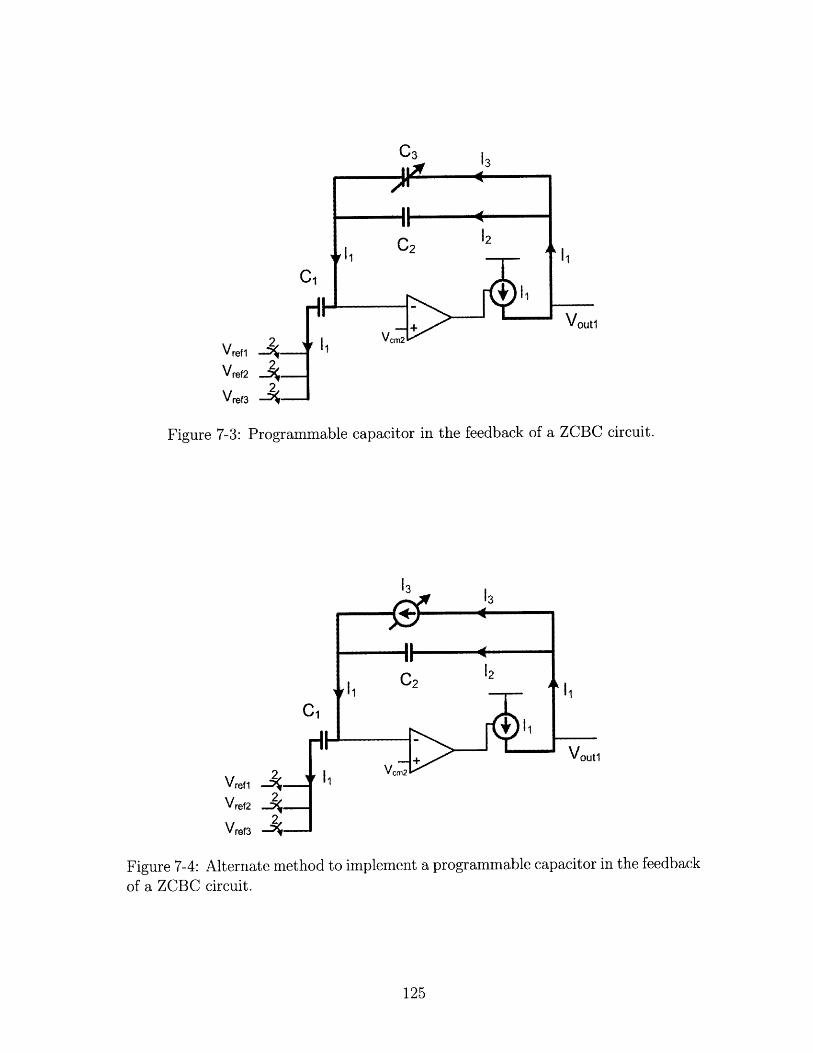
C3-NO 13
Vot1
Vre1 _s(5 11
Vref2 Vreis 2Vref3 3I
Figure 7-3: Programmable capacitor in the feedback of a ZCBC circuit.
Cla
13 13
1C2 12
C1
Vout1
Vrefi , -
Vref2 2
Vref3 -
Figure 7-4: Alternate method to implement a programmable capacitor in the feedback
of a ZCBC circuit.
125

+rf 1 ~ -L . . .. . 1 V U2 Vem Voce-
Vref2 1
Vref3
Figure 7-5: Simplified method to implement a programmable capacitor in the feedbackof a ZCBC circuit.
126
Appendix A
The Script to Program the Chip
A scan chain is used to program the chip. Since all stages are identical, their scan
chain is also identical. Tektronix pattern generator (TLA 7012) is used to send the
bit-stream to the chip. The following script is used to generate a bit-stream. The
output of this script can be directly loaded into the Tektronix pattern generator.
127
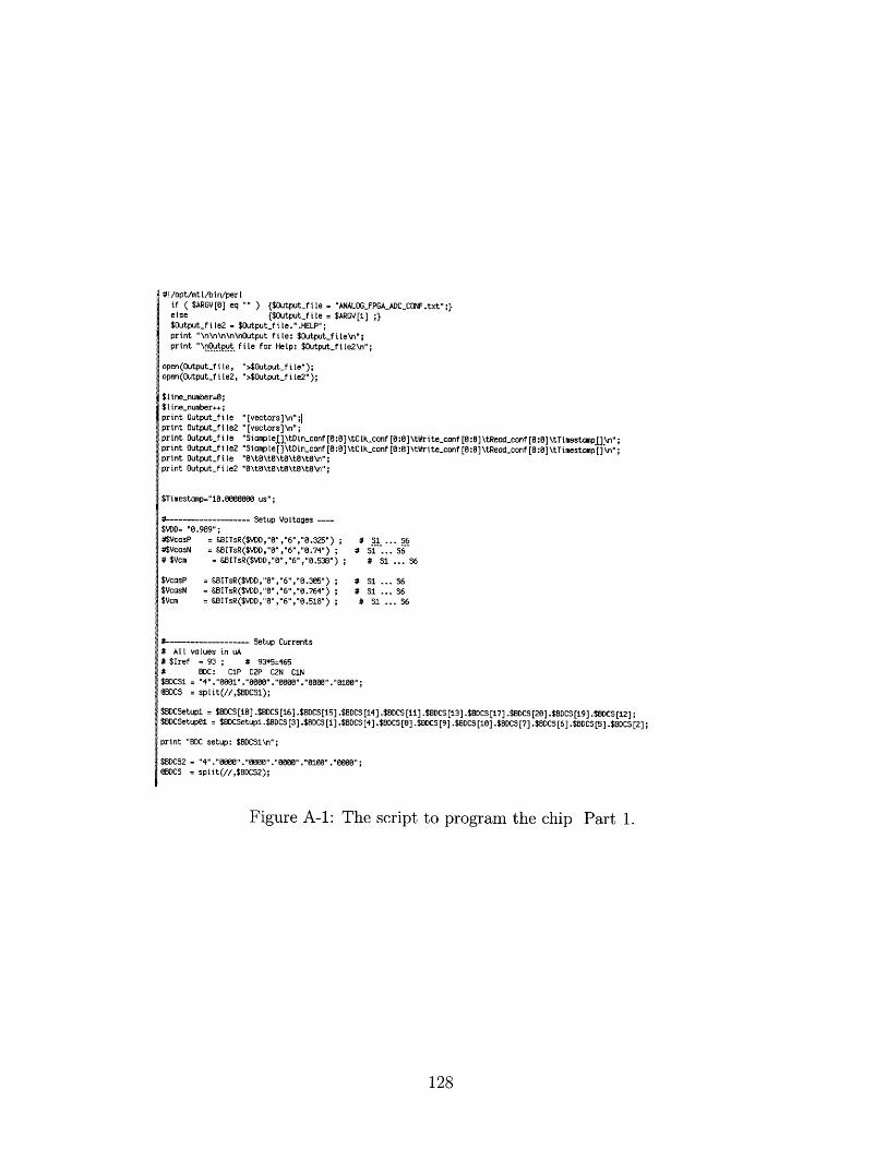
#!/opt/mt t/bin/pertif ( $ARGV(8] eq "" ) {$Outputfile = "ANALOGFPGAADCCONF.txt";}else {$Output-fjiLe = $ARGV[I] ;}$Output-fiLe2 = $Output-file.".HELP";print "\n\n\n\n\nOutput file: $Output-fiLe\n";print "\nOutput file for Help: $Gutput-file2\n";
open(Output-file, ">$Outputtfile");open(Outputfile2, ">$Output-file2");
$1ine-number=;$1ine-number++;print Output-file "[vectors]\n";print Output-file2 "[vectors]\n";print Output.fiie "SimpLel\tDin-conf [0:0]\tCLk-conf [0:0]\tWrite-conf [0:8]\tRead-conf (0:0]\tTimestampQJ\n";print Outputjf i1e2 "Siample[]\tDinconf[0:0]\tCk-conf[0:0]\tWrite-conf [0:0]\tReadconf[0:0]\tTimestamp[]\n";print Output-file "8\t8\t8\t8\t8\t\n";print Outputfile2 "8\tB\t8\t8\t8\t8\n";
$Timestamp="10.0000000 us";
#-------------------- Setup Voltages$VDD= "0.989";#$VcasP = 8BITsR($VDD,"","6","0.325") ; # 31 ... 36#$VcasN = 88ITsR($VDD,"8","6","0.74") ; # 31 ... 56# $Vcm = &8ITsR($VDD,"0","6","0.538") ; # 31 ... 56
$VcosP = S8ITsR($VDD,"0","6","0.305") ; # 31 ... 56$VcasN = SBITsR($VDD,"0","6","0.764") ; SI ... S6$Vcm = SBITsR($VDD,"8","6","0.518") ; # Si ... 36
#-------------------- Setup Currents# All vaLues in uA# $Iref = 93 ; # 93*5=465# BDC: CiP C2P C2N C1N$BDCSI = "4"" .8 1"."80000". .8 ". "8 . 80000.0100";@BDCS = split(//,$BDCS1);
$BDCSetupi = $BDCS[18].$BDCS[16].$BDCS[15].$BDCS[±4].$BDCS[11].$BDCS[13].$BDCS[17).$BDCS[20].$BDCS[19].$BDCS[12];$BDCSetup0i = $BDCSetupi.$8DCS [3].$BDCS [1].$BDCS[4].$BDCS [8].$BDCS [9].$BDCS [18].$BDCS [7].$BDCS [6].$BDCS[5].$BDCS [2];
print "BDC setup: $BDCSI\n";
$BDCS2 = "4"."0000"."8888"."'8888"".±10.."8888";BDCS = split(//,$BDCS2);
Figure A-1: The script to program the chip Part 1.
128
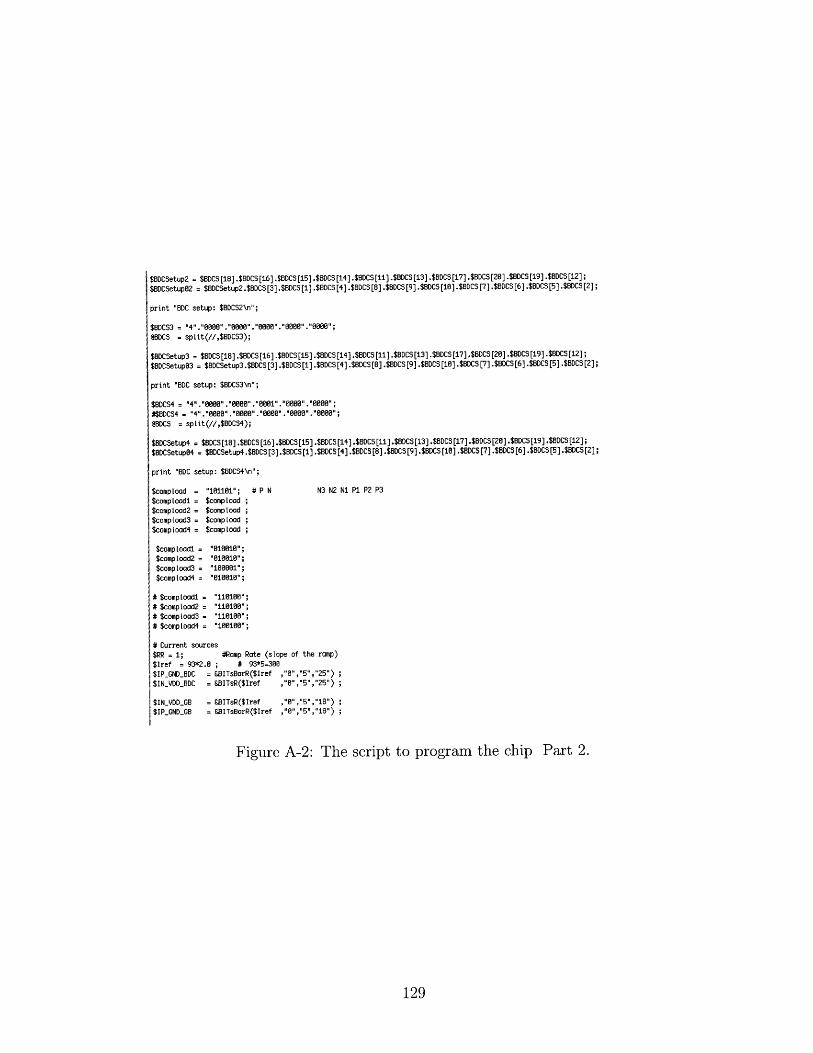
$BDCSetup2 = $BDCS [18] .$BDCS [16] .$BDCS [15].$BDCS [14] .$BDCS[11].$BDCS [13].$BDCS [±7] .$BDCS [20].$BDCS [19] .$BDCS [12];
$BDCSetup82 = $BDCSetup2.$BDCS[3].$BDCS[±].$BDCS[4].$BDCS[8].$BDCS[9].$BDCS[±8].$BDCS[7].$BDCS[6].$BDCS[5].$BDCS[2];
print "BDC setup: $BDCS2\n";
$BDCS3 = "4"."000"."80000". "8888"."0000" .."0000";@BDCS = split(//,$BDCS3);
$BDCSetup3 = $BDCS [18] .$BDCS [16].$BDCS [15] .$BDCS[14].$BDCS [11] .$BDCS[13].$BDCS [±7].$BDCS [20] .$BDCS [19] .$BDCS [12];
$BDCSetup03 = $BDCSetup3.$BDCS[3].$BDCS [1).$BDCS [4] .$BDCS[8].$BDCS [9] .$BDCS [18) .$BDCS [7] .$BDCS [6] .$BDCS [5] .$BDCS [2];
print "BDC setup: $BDCS3\n";
$BDCS4 = "4"."0000"."0000"."8001"."0000"."0000";#$BDCS4 = "4"."0000"."0000"."0000"."0000"."0000";@BDCS = split(//,$BDCS4);
$BDCSetup4 = $BDCS [18].$BDCS [16].$8DCS[15].$BDCS[14].$BDCS[11].$BDCS [13].$BDCS [17].$BDCS [20].$BDCS [19].$BDCS[12];
$BDCSetup84 = $BDCSetup4.$BDCS [3].$BDCS [1] .$BDCS[4].$BDCS [8] .$BDCS [9) .$BDCS [±0] .$BDCS [7].$BDCS [6].$BDCS[5].$BDCS [2);
print "BDC setup: $BDCS4\n";
$compLoad =$comploadi = $$compload2 = $$compload3 = $$compload4 = $
$compLoadl =$compload2 =$compLoad3 =$compLoad4 =
* $comploadl =* $compload2 =# $compload3 =# $compload4 =
180118"; # P Ncomploadcomploadcomploadcompload
"010010";"01001";"100001";"018810";
"110100";"110100";"110100";"10010±";
N3 N2 N± P1 P2 P3
* Current sources$RR = 1; *Ramp Rate (slope of the ramp)$Iref = 93*2.0 ; * 93*5=300$IPGNDBDC = 8BITsBarR($Iref ,"0","5","25")$IN_VDDBDC = O8ITsR($Iref ,"0","5","25")
= SBITsR($Iref ,"8","5","18")= SBITsBarP($Iref ,"8","S","18")
Figure A-2: The script to program the chip Part 2.
129
$INVDDGB$IPGNDGB
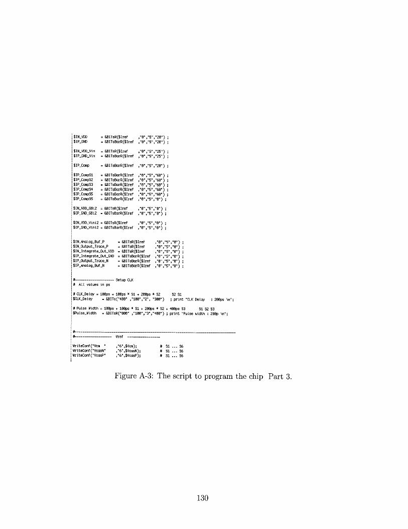
$INVDD = EBITsR($Iref ,"8","5","28")$IP.GND = SBITsBarR($Iref ,"",5,2")
$INVDDVin = &BITsR($Iref ,"8","5",25")$IPGNDVin = EBITsBarR($Iref ,"8",5","25")
$IPComp = 88ITsBarR($Iref ,"0","5","20")
$IP.CompSI$IP.Comp32$IPCompS3$IPCompS4$IPCompSS5$IPCompS5
= SBITsBarR($Iref= 8BITsBarR($Iref= 8BITsBarR($Iref= SBITsBarR($Iref= &BITsBarR($Iref= GBITsBarR($Iref
"8","5","60");"","5", "60")
$INVDD.GBi2 = BITsR($Iref ,"8","5","8")$IP.GNDGBi2 = &BITsBarR($Iref ,"8","5","8")
$INVDDVini2 = SBITsR($Iref ,"8","5","6")$IPGNDVini2 = EBITsBarR($Iref ,"8","","8")
$INAnaLogBufP$INOutputTraceP$INIntegrateOutVDD$IPIntegrate_OutGND$IPOutputTraceN$IPAnalog-BufN
#-------------------- Setup CLK# ALL values in ps
# CLKDelay = 100ps + 100ps * 51 + 200ps * 32$CLKDelay = 8EITs("400" ,"100","2", "300")
52 Si; print "CLK Delay : 200ps \n";
* Pulse Width = 100ps + 100ps * SI + 200ps * S2 + 400ps 53 31 52 53$PulseWidth = 88ITsR("800" ,"188","3","40"); print "Pulse width : 200p \n";
#------------------- Vref
WriteConf("Vcem " ,"6",$VCM);WriteConf("YcasN" ,"6",$VcasN);WriteConf("VcasP" ,"6",$VcasP);
#31 ... 3631 ... S6
# SI ... S6
Figure A-3: The script to program the chip Part 3.
130
= 8ITsR($Iref= 8BITsR($Iref= &BITsR($Iref= SBITsBarR($Iref= SBITsBarR($Iref= 8BITsBarR($Iref
,"", "5" ,"8")

#--------- -- Yref -
for ($StogeNumber= 1; $StageNumber <9; ++$StageNumber)
{# ----------------------------------------------------------------------------# - - - ---- Stage 1-8-------------
WriteConf("IntegratingCap P 1 ...7 ,"7" ,"0000000" ); Cap1.. .Cap7WriteConf("AnaLog Buf-En" ,"1","8" );
WriteConf("IP-AnaogBuf-N" "S",$IP-Ano og-uf-N * 5i ... 5WriteConf ("IPOutputTrace-N" "S",$IP-Output-Trace-N ; Si ... 5
WriteConf("IP.IntegrateOutGND" "5",$IP-Integrate-Out-GND * Si ... 5WriteConf("INIntegrateOutVDD" "5",$IN-Integrate-Out-VDD ) *S ... S5WriteConf ("INOutput-TraceP" "S",$IN-Output-Trace-P # 51 ... 5WriteConf("IN.AnlogOuf.P" ,"5",$INAnaLogBufP ); # S1 ... 35
WriteConf("Terminating Resistor" ,"1","8" );WriteConf("Integrating Cap Output En " ,"1","8" );WriteConf("IntegratingCap 1 ... 7" ,"7","8000000" ); # Cap1.. .Cap7
---- --- Stage 1-6-------------* -----------------------------------------------------------
I
for ($StageNumber= 8; $StageNumber >6; --$StageNumber){-----------------------------------------------------------------------------
#-------------- Stage 7-8----------------
WriteConf("In2 On " ,"1","0" ); *
WriteConf("Yin En " ,1,1" ); #WriteConf("Comparator Offset " ,"6","010010" ): #WriteConf ("Sample on Feedback Cap " ,"1","1" ); #
# WriteConf ("BDC-offsetWriteConf("BDC-offsetWriteConf("BDC-offsetWriteConf("BDC-offsetWriteConf("BDC-offsetWriteConf("BDC-offset
","2@","$BDCSetup" );,"4","0000" ); #,"4","0000" ); #,"4","8888" ); #,"4","0000" ); *,"4","0000" ); #
WriteConf("ConfBDC-en " ,"""" );WriteConf("ConfBDC " ,"5","00000" ); * D .... D
Figure A-4: The script to program the chip Part 4.
131
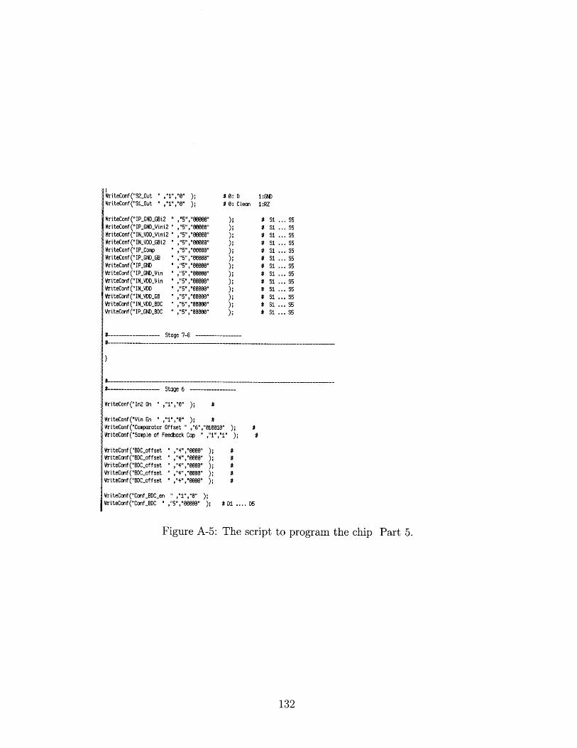
WriteConf("2_Out " ,"1","0" );WriteConf("SiOut " ,"i","8" );
WriteConf("IPGNDGBi2 "WriteConf("IPGNDVini2 "WriteConf("INVDDVini2 "WriteConf("INVDD.GBi2 "WriteConf("IPComp "WriteConf("IP.GNDGBWriteConf("IP.GNDWriteConf("IPGNDVinWriteConf("INVDDVinWriteConf ("INVDDWriteConf("IN.VDDGBWriteConf("INYDDBDCWriteConf("IP.GNDBDC "
,"5","0000","5","00000","5","00000","5",8 8"00000,"5","00000","5","00000""5", " "00000,5,"00000","5","00000","5", "88888","5","88888","5","88888",'"","88888"
# 0: D 1:GND# 0: Clean i:RZ
# St ... S5) 31 ... 5SSi ... S5SSi ... S5# S1... 35SSi ... 35SSi ... 53 1 ... 5SSi ... S5SSI ... 35
) # S ... 35Si ... 5
# Si... 35
* ---------- Stage 7-8
#-------- -- Stage 6 ------
WriteConf("In2 On " ,"1"" ); #
WriteConf("Vin En " ,"i","8" ); #WriteConf("Comparator Offset " ,"6 018010" ); #WriteConf("Sample of Feedback Cap " 1,1" ); #
WriteConf("BDCoffset " ,"4","0000" ); #WriteConf("BDC-offset " ,"4N 00"WriteConf("BDC-offset " ,"4","888" ); #WriteConf("BDC-offset " "4",0080" );WriteConf("BDC-offset " ,"4","0000" ); #
WriteConf("ConfBDC-en " ,"1","8" );WriteConf("ConfBDC " ,"5","00000" ); # Di .... D5
Figure A-5: The script to program the chip Part 5.
132
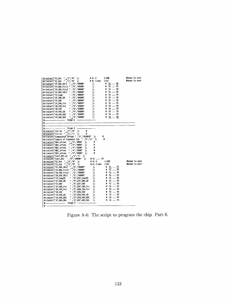
WitseCor("S2_out "": D I:GND Seems to workWriteConf("SiOut ","," );Clean i:RZ Seems to work
xitegg9f("IPGNDGBi2
"..,"S","00000" # S. 5WriteConf("IPGNDVini2 " "5","00000"1 5. S
WriteConf("INVDDVini2 " ,"5",8"00000" * i . S
WriteConf("IN.VDDG8i2 " ,"5","00000" S1. S5
WriteConf("IPComp " ,"5", " .
WriteConf("IPGNDGB " ,"1,"." S
WriteConf("IPGND " ,"5","88800000" Si S5
WriteConf("IPGNDVin ,"5',"00000" 1 ..S S5
WriteConf("INVDD_Vin " ,"5","00000" .S S
WriteConf("INVDD " ,"5","00000" Si ... 5
WriteConf("INVDDGB " ,","00000" # St ...
WriteConf("INVDDBDC " , .","00000". * Si ... S5
WriteConf("IPGNDBDC "'."," 8 # S1 ...-t :ge 6 1:GND--eems-o-wor
# ---------------------------------------------------------------------------I ---------------------------------------------------------------------------
* --------------Stage 5----------------WrtteCnfQIn2 On "1",".".5
#iteCon;("Yin EnWrie&ofQComparator Offset " ,"5',"0810i" )WriteConf("S;ple of Feedback Cap . #i
Writeonf('BOC-ffset "*);#,"31..5
WriteConf("BDC)offset "#4"3,"1.
WriteConf('BDC-offset ,4" ,'8"0 );WriteConf(BDC)offset "#4",1"...WriteCon);Con# .DC. n35WriteConf("Cnf.BDC "",18 00.1 * Di .... D5
Write~nf(S2Out '* 11'"i", 0: D8 0 iGND 43eems to work
WieGnt(-SIOut --1-- .8 .. 18 Clean ± RZ #Seems to work
WriteConY" IP..GND.GBi2 " 888881, ) I Si ... S5
WriteCan ("IP-..ND..Yini2 ,'5,Y.00088" ), IS 9..S
WriteConf("IN-VDDini2 "5%08800 ); # 31 ... 55
WriteConf(IN-.VDD-68i2 ' 5","00000" ), *Si ... S5
WriteCant( IP.CompS5 ",5E.,$IPCompS ) # S1 ... S5WriteCant(IP.GNDGB "5',$IP-GND-G ) # Si ... S5
WriteConf("IP# GND ",$IP--ND S Si ... S
WriteConf("IP-GND-.Vin ,"5",$IP-.GND-VYin ) ISi ... 5
WriteCont("IN-YDD.Yin '",,$IN-VYDD-Vin ), 1S ... 5
WriteCan ("IN-VDD ,S,$IN-YDD ), ISi ... S5
WriteCont ("IN-VDD-G8 "",$IN-V.DD-.GB ) ISi ... S5
WriteCont("IN-YDD.ODC " "5",$IN-VDL-BDC ), S ... S5
WriteConf("IP-ND.BDC ",5",$IP-GND-8DC ), 1S ... S5#-------------------Stage S -----------
#----------------------------------------------------------------------------------
Figure A-6: The script to program the chip Part 6.
133
------------- Stage 04 -WriteCnf.("Inz On "_"',"8" ); #WrteCGnf,("Vin En " 1","1" ); #WriteConf("Comparator Offset " ,"6",$compload4 ); #WriteConf("SampLe of Feedback Cap " ,"1","i" ); #
.ri grejf("BDC_offset ",, 20","$BDCSetup04" )
.99.RqR.("Conf_BDC_en """"")WrteCanf("Conf-BDC " J"5" "88888" ) #01 D5
IWriteCnfr("S2-Out " "1","0" ); #80D i:GND *WorksWriteConf("S1Out ","1","8" ); #0: CLean i:RZ #WorkslWriteConf("IP.GND_GBi2 l's",$IP_.NELGBt2 # Si S5SWriteCanf("IP_GND_Vini2 "5",$IPGNDVini2 # Si 5WriteConf("IN_VDD_Vini2 "5",$INVDDVini2 * Si 55WriteConf("IN_VDD_GBi2 "5',$INYDDG8i2 # * .i 5WriteConf("IP_CompS4 "5",$IPCamp54 # Si . 5WriteConf("IPGNDGB "5",$IP-GND-GB * Si ... S5WriteConf("IPGND """,$IRGND # Si ... 5WrtteCanf("IP-ND in ""5",$IP_GNDin ); # S ... SWrtteCnf("IN .Vin " ,"5",$INVDD_Vin ); # Si1 5WriteCanf("INDD " ,"5",$INVDD ); # Si ... 5WriteCant ("INDD8 " ,"5",$INVDDGB ); # 31 ... 55WriteCant ("INYDDBDC " ,"5",$IN-VDDBDC ); # Si 5WriteConf("IP.GNDBDC " ,"5",$IP.GNDVn ); # Si ... 5
-L----------Stage 84----------------
- ----------Stage 83----------------WriteConO("I n "Wi~tWGRt("Vin En " J. "I' ) *WriteConf("CNparat ffset " , "" ,$cop ad )WriteConf("Sampie af Feedback Cap,"5,$ iV B ); #WriteConf("BDCsffset ","
25","$DCSetup3" );
WriteConf("CInfDBDC " ,"5",$IP8GNDBD .... #5riteont("S2-Out " 8 ; # 8: D i:GND *Works
WriteCanf("SOut S"1 08: Cean i:RZ #WorksWriteCon("LP..GND5i2 "_," ,5,$IP.GND38i2 ) Si ... S5WitGaf("IP 0140_Yini2 " "5",VPGNDVini2 ): *Si . S5WriteCanf("IN_ Vini2 " ,"5",$INVDDVYini2 ) * Si ... 35WriteCnf("IN 8i2 " ,"5",$IN_.V00DG8i2 ); *Si... 35WriteCant("IPCampS3 " 5",$IPCampS3 1 Si... 55WriteCont("LPN B ""5" ,$IPGNDGB #; *51 ... S5WriteCant ("IP_0 " "5",$IP_0ND ) * Si ... S5WriteCanf("IP 0 Yin " "5",$IP_,GNDYin ) * 1 S ... 35WriteCnf("IN tn " "5",$INY0DDYin # * 1 Si... S5WriteCanf ("IN_ " "S",$IN-VDD #; * Si ... 35WriteCant ("INY008 " "5-,$IN-VDD-. ; * Si ... 35WriteCanf("IN.. OC " "5",$IN-VDD-BDC #; * 51... 35WriteCanf(" IP.GNO C ""5" ,$IP-GND-BDC #* Si ... 35
# ------------------------------------------
Figure A-7: The script to program the chip Part 7.
134
# - --- Stage 02 -
iteConf,("In2 On " ,'1","8" ); #Win f,("Vin En " 'i","1" ); #WriteConf("Comparator Offset ,"6", $compload2 ); #WriteConf("SampLe of Feedback Cap " ,"1"" ); #WriteConf("BDC-offset ";"20","$BDCSetup02" );Witeo ("ConfBDC-en " I'""")WriteConf("ConfBDC " ,5","00000" ); D1 .... D5WriteConf("S
2_Out t." ," " ); # 8: D 1:GND #Seems to work
W rI("oFQ'SiOut " ,"1","8" ); $0: Clean i:RZ #Seems to work
Wrtefl ("IPGNDGBi2
""5" ,$IP_GND_ 2 ); # S1 ... S5WrtteConf("IPGNDVini2 ",5",$IPGNDYini2 ); 1... 5
WriteConf("INVDDVini2 " ,"5",$INVDDVini2 ); ... S5
WriteConf("INVDDGBi2 " ,"5",$INVDDGBi2 ); 31 ... 55
WriteConf("IPCompS2 " ,"S",$IP.CompS2 ); 1... SWriteConf("IPGNDGB " ,"5-,$IPGNDGB ); ... Ss
WriteConf("IPGND " ,"5",$IP.GND ); # Si 5
WriteConf("IPGND.Vin " ,"5",$IPGNDVin ); ... S5
WriteConf("INVDDVin ,"5",$INVDDVin ); 51 ... 35WriteConf ("INVDD "t,'5",$INVDD );1 ... 35
WriteConf("INVDDGB " ,"5",$IN-VDDGB ); # 51 .WriteConf("INVDDBDC " ,"5",$INVDDBDC ); # Si . 5
WriteConf("IPGNDBDC " ,"5",$IPGNDBDC ); ... S5
# --- Stage 02 -------
# ---- Stage 01 ----- ---
WriteConf ("In2 On "I1","" ); #WiCon("Vin En " ,"1" ); #WriteConf("Comparator Offset " ,"6", $comploadi ); #WriteConf ("Sample of Feedback Cap ,"1","i" ); #WriteConf("BDC.offset "'"20","$BDCSetup01" );WrtteConf("ConfBDC-en ",'1","1" );WriteConf("ConfBDC " ,"5","00000" ); # D1 .... D5WriteConf("S2_Out " ,1,8 ); $0: D 1:GND #Seems to work
teonf("S1_Out ","1","8" ); $0: Clean 1:RZ $Seems to work
WriteConf("IPGNDGt2 *"E",$IPGNDGBi2 ); # S ... S5
teConf("IPGNDYini2 " ,"5",$IPGNDVini2 ); $ Si .. S5
WriteConf("INVDDVini2 " ,"5",$INVDDVini2 ); # S1 ... 35WriteConf("INVDDGBi2 " ,"5",$IN.VDDGi2 ); # 31 ... 35WriteConf("IPCompSi " ,"5",$IPCompSi ); # 31 ... 35WriteConf("IP.GNDGB " ,"",$IPGNDGB ); # S1 ... 35WriteConf("IPGND ,"5",$IPGND ); $ S1 ... S5
WriteConf("IPGNDVin " ,"5",$IPGNDVin ); $ Si ... S5
WriteConf("IN.VDDYin ,"5",$INVDDVin ); # Si ... S5
WriteConf("INVDD " ,"5",$INVDD ); # 31 ... 35
WriteConf("INVDDGB " ,"5",$IN-VDDGB ); # 51 ... 55WriteConf("INVDDBDC " ,5",$INVDDBDC ); # S1 ... 35WriteConf("IPGNDBDC " ,5",$IP.GNDBDC ); $ S1 ... S5
---------- Stage 01 ---------------
Figure A-8: The script to program the chip Part 8.
135
# ----------- Clock/Pulse Gen -
WriteConf ("Pulse Width" ,3",$PulseWidth); # = 18ps + i8Bps 51 + 28Bps 32 + 40Bps 33WriteConf ("CLK Enable 58" "i"1"8");WriteConf("CLK Enable 37" "1","0");WriteConf("CLK Enable S6" ,,.)WriteConf("CLK Enable 35"WriteConf("CLK Enable 54"WriteConf("CLK Enable 33"WriteConf("CLK Enable 32"WriteConf("CLK Enable ,"1","") Seems to workWriteCon("None Overlapping CLK delay" "2",$ClKDely);# = 100ps 1ps + 180ps * S2 + 200ps 3 S#--------------- Clock/Pulse Gen-------------# -----------------------------------------------------------Wr or("1-3" "1","1"); #S4-SB=8 31-55=1#-- --- END of Analog FPGA #2 -- --
#works
31 32 53
2 S2 Si
close (Output..f i le);close (Outputfile2);print "Configuration file created.\n\n";system "date";print "\n";print " -------- Campleted------------------------- n\n\n\n\n";sub WriteConf{
# Name of configuration bits# Number of bits* Value of bits$Comment = $4[0];$NofBits = $_[1];$BitValues = $4[2];@BitYal = split(//,$BitValues);for ($temp = $NofBits-1; $temp > -1; --$temp){print Output-file "$linenumber\t $BitYal[$temp]\t 8\t 8\t @\t $Timestamp\n";if ($NofBits>1){ print Outputfile2 "$1ine.number\t $BitVai[$temp]\t B\t 8\t @\t $Timestamp\t\t$Comment\t\tb$temp\n";else{ print Output-file2 "$linenumber\t $BitVal[$temp]\t 8\t B\t 8\t $Timestamp\t\t$Comment\n"; }$1inenumber++;print Output-file "$line-number\t $BitVal[$temp]\t 1\t B\t 8\t $Timestamp\n";print Outputfile2 "$line-number\t $BitYal[$temp]\t 1\t B\t 8\t $Timestamp\n";$1ine-number++;
Figure A-9: The script to program the chip Part 9.
136
sub BITs{
Full Scale.Maxfull Scale.MinAumber of Bits#Input Signal
$BjulLMax = $.[B];$8julLMin = $4[1];$B.Bits $4[2];$BInput $[3];$B-ulLMax $BFulL Max - $Bjull-Min;$BJnput $BJnput - $B-ulLMin;$Output =1"";for($temp..B=1; $tempB4BBits+i; ++$temp.B)
{$BulLMax = $B-ulLMax/2;if ($Binput 4cBtFulLMax)
{$Output = $Output."B";
}else
{$BJnput = $BJnput - $B-FuulLMax;$Output = $Output."i";
}}$Output;
Figure A-10: The script to program the chip Part 10.
137

sub BITsR
# The output of BITsR is in the reverse order of BITs
;Full ScaleMax4Full ScaIeMinNumber of Bits#Input Signal
$BFulLMax = $4[];$BjulLMin = $[1];$BBits = $4[2];$B.Input = $[3];$BjulljMax = $BulLMax - $B-ulL-Min;$BInput = $B.Input - $BFuLlMin;$Output = "";for($temp.B=i; $temp..8$BBits+1; ++$temp.B)
$BjulLMax = $BFulLMax/2;if ($BInput cB-FuLLMax)
$Output = "6".$Output;}else{
$BInput = $BInput - $B.ulLMax;$Output = "i".$Output;
}$Output;
Figure A-11: The script to program the chip Part 11.
138
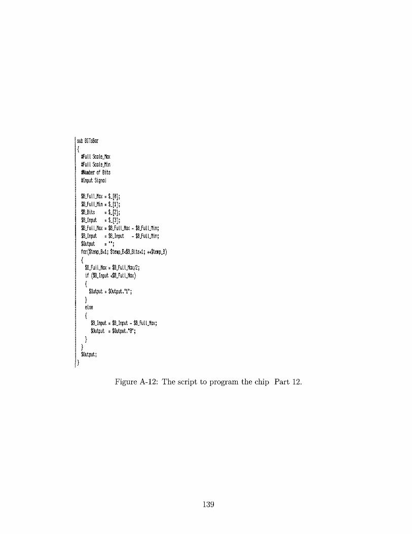
sub BITsBar
full Scale..Maxfull Scale.MinNumber of Bitstlnput Signal
$BFulLMax = $_[@];$BjulLMin = $41];$B.Bits $4[2];$BJnput $[3];$B-FulLMax $BjulLMax - $BjulLMin;$BJnput $BJnput - $BjulLMin;
$Output = ;for($tempB=i; $tempB<$B.Bits+1; ++$temp.B)
$BjulLMax = $BFull-Max/2;if ($BJnput <$8FulLMax)
$Output = $Output."i";
}else
$BJnput = $BJnput - $B-ulLjMax;$Output = $Output."B";
}}$Output;
Figure A-12: The script to program the chip Part 12.
139
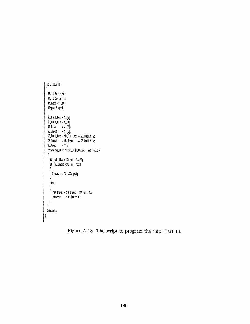
sub BITsBarR
full Scale.Maxfull ScaleMin#iumber of Bits#Input Signal
$BjulLMax = $_[0];$BFulLMin = $1];$B.Bits = $[2];$B.Input = $[3];$B-ulLMax = $BFull Max - $B-FutLMin;$BInput = $B.Input - $BJulLMin;$Output = "";for($temp.B=1; $temp..848.Bits+1; ++$tempB)
$BjulLMax = $BjulLMax/2;if ($B.Input 4cBtFulLMax){$Output = "i".$Output;
}else
$BInput = $B.Input - $BFulLMax;$Output = "B",$Output;
}}$Output;
}
Figure A-13: The script to program the chip Part 13.
140
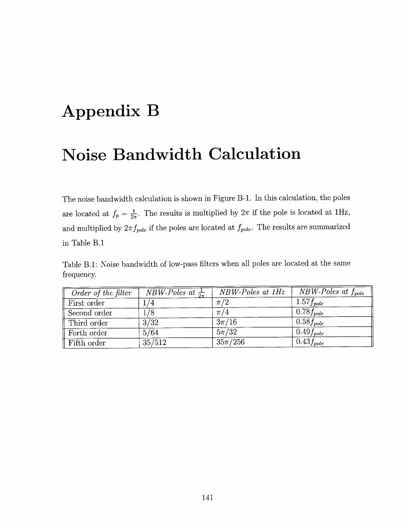
Appendix B
Noise Bandwidth Calculation
The noise bandwidth calculation is shown in Figure B-1. In this calculation, the poles
are located at fp = 'L. The results is multiplied by 27r if the pole is located at 1Hz,
and multiplied by 27fpoe if the poles are located at fpoie. The results are summarized
in Table B.1
Table B.1: Noise bandwidth of low-pass filters when all poles are located at the same
frequency.
Order of the filter NBW-Poles at b NBW-Poles at 1Hz NBW-Poles at fpoie
First order 1/4 7r/2 1.5 7 fpoe
Second order 1/8 7/4 0.78fpole
Third order 3/32 37r/16 0.58fpoleForth order 5/64 57r/32 0.49fpoleFifth order 35/512 357r/256 0. 4 3 fpoe
141
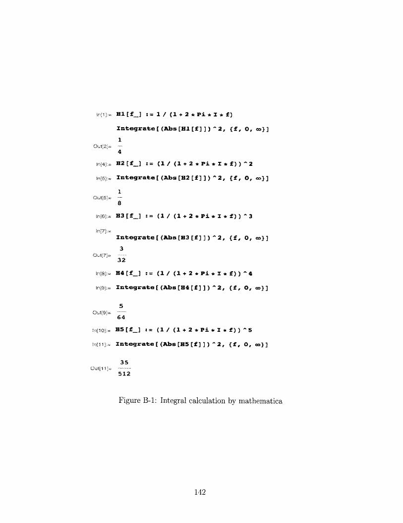
i=H1f =1 / (1 +2 *Pi *z * f)
Integrate((AbsCH[f] ^1 2, (f, 0, o}]
4
H2 (fk_) = (1 / (1 + 2 * Pi I *
Integrate [ (Abe [H2 [f ) ]) 2,
f)): )2
( f , 0, } )
I3[_ := (1 / (1+ 2 2 * Pi * ,* f)) ^3
integrate[((Abs[CB3[Cf ]] ) ^ 2, {f , 0, }
f)) ^4
( f, 0, ca} I
3
32
: E[f_ =(1/ (1+ 2 *Pi *I*
n§: Integrate [(Abs [H4 (f ])^2,
[411
35Cutl11 -
512
Figure B-1: Integral calculation by mathematica
142
5
64
HStfate(/ (1)+ 2 * P i * * f)0) ^S
Integrate [ (Abs [ES [ f ] ] ) ^ 2, ( f , 0,c}]
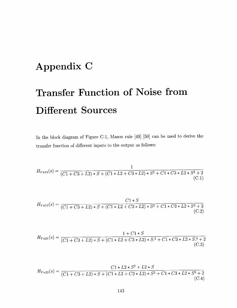
Appendix C
Transfer Function of Noise from
Different Sources
In the block diagram of Figure C-1, Mason rule [491 [50] can be used to derive the
transfer function of different inputs to the output as follows:
Hvn11(s) =
Hvn12 (8) =
(Cl+C3+ L2)* S + (Cl* L2 + C3* L2)* S 2 C1* C3* L2* S3 +2(C.1)
C1*S(Cl+C3 + L2)* S + (C1* L2 +C3* L2)* S 2 + C1* C3* L2 *S 3 +2
(C.2)
1+C1*SHvn21(s) = (C1 + C3 + L2) * S + (Cl * L2 + C3 * L2) * S.2 + C1 * C3 * L2 * S.3 + 2
(C.3)
C1* L2* S 2 + L2 S
(Cl+C3+ L2)* S +(Cl * L2+C3* L2)* S 2 +C1* C3* L2* S3 + 2
(C.4)
143
Hvn22 (S) =
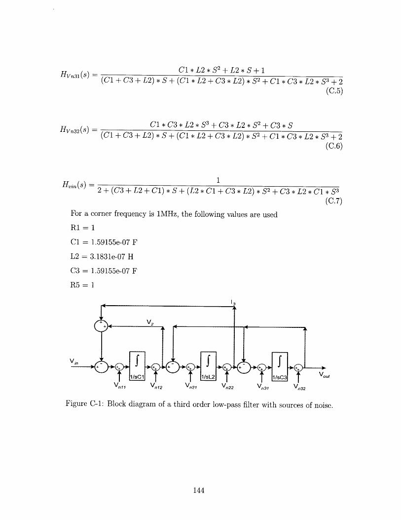
C1 L2*S 2 +L2*S+1(C1 +C3+ L2) * S + (Cl L2 +C3* L2) * S 2 +1* C3 * L2 *S3+2
(C.5)
C1*C3*L2* S 3 +C3*L2* S2 +C3*S(C1+C3+ L2)* S+(Cl * L2+C3 L2)* S2 +C1*C3* L2* S3+2
(C.6)
2+(C3+ L2+C1)* S+(L2*C1+C3 L2)* S2+C3 L2*C1 * S3(C.7)
For a corner frequency is 1MHz, the following values are used
R1 = 1
C1 = 1.59155e-07 F
L2 = 3.1831e-07 H
C3 = 1.59155e-07 F
R5 = 1
out
Figure C-1: Block diagram of a third order low-pass filter with sources of noise.
144
Hvn32(s) =
Hvin (s)=
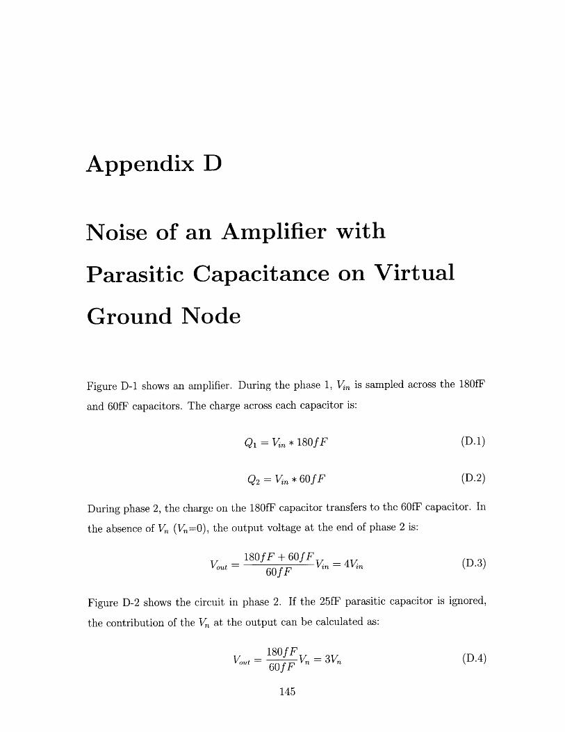
Appendix D
Noise of an Amplifier with
Parasitic Capacitance on Virtual
Ground Node
Figure D-1 shows an amplifier. During the phase 1, Vin is sampled across the 180fF
and 60fF capacitors. The charge across each capacitor is:
Q1 =1V* 180fF
Q2 Vi * 60f F
(D.1)
(D.2)
During phase 2, the charge on the 180fF capacitor transfers to the 60fF capacitor. In
the absence of V (VK=0), the output voltage at the end of phase 2 is:
(D.3)V 180f F + 60f FV n= 4V60f F
Figure D-2 shows the circuit in phase 2. If the 25fF parasitic capacitor is ignored,
the contribution of the V at the output can be calculated as:
Vout= 180fF K = 3 V60f Fn
(D.4)
145

Adding the parasitic capacitor, the output noise is:
180fF + 2 5 fFv60f F
180fF + 25fF 2 2out 60fF ) 2 V2
As a result:
Vin
2 60fF 2
V-i1 180fF
25f E~~>.= --- Vn
Figure D-1: Schematic of an amplifier.
60fF
180fF
Vn
Figure D-2: Phase 2 of the amplifier.
146
(D.5)
(D.6)
vout
Bibliography
[1] J. Becker, F. Henrici, et al., "A Continuous-Time Hexagonal Field-
Programmable Analog Array in 0.13um CMOS with 186MHz GBW," ISSCC
Dig. Tech. Papers, pp.70-71, Feb.,2008.
[2] B. Pankiewicz, M. Wojcikowski, S. Szczepanski, Y. Sun, "A Field Programmable
Analog Array for CMOS Continuous-Time OTA-C Filter Applications," IEEE
J. Solid-State Circuits, vol. 37, pp. 125-136 Feb. 2002.
[3] K. Gulati, H.-S Lee, "A low-power reconfigurable analog-to-digital converter,"
ISSCC Dig. Tech. Papers, pp.54-55, Feb.,2001.
[4] D.C. Daly, A.P. Chandrakasan, "A 6b 0.2-to-0.9V Highly Digital Flash ADC
with Comparator Redundancy," in IEEE International Solid-State Circuits Con-
ference Digest of Technical Papers, San Francisco, CA, Feb. 2008, pp.5 54 -5 5 5 .
[5] S. Park, Y. Palaskas, M.P. Flynn, "A 4GSs 4b Flash ADC in 0.18spl mum
CMOS," in IEEE International Solid-State Circuits Conference Digest of Tech-
nical Papers, San Francisco, CA, Feb. 2006, pp. 2 33 0 -2 3 39 .
[6] B. Verbruggen, J. Craninckx, M. Kuijk, P. Wambacq, G. Van der Plas, "A 2.2mW
5b 1.75GSs Folding Flash ADC in 90nm Digital CMOS ," in IEEE International
Solid-State Circuits Conference Digest of Technical Papers, San Francisco, CA,
Feb. 2008, pp. 2 52-2 53 .
147
[7] M. Yoshioka, K. Ishikawa, T. Takayama, "A 10b 50MSs 820uW SAR ADC with
On-Chip Digital Calibration," in IEEE International Solid-State Circuits Con-
ference Digest of Technical Papers, San Francisco, CA, Feb. 2010, pp.384-385.
[8] B.P. Ginsberg "Energy-Efficient Analog-to-Digital Conversion for Ultra-
Wideband Radio," PhD Thesis, Massachusetts Institute of Technology, 2007.
[9] I. Ahmed, "Pipelined ADC Design and Enhancement Techniques," Springer Sci-
ence + Business Media B.V. 2010.
[10] B. Murmann, B.E. Boser, "Digitally Assisted Pipeline ADCs: Theory and Im-
plementation," Kluwer Academic Publisher, 2004.
[11] R. Schreier, G.C. Temes, "Understanding Delta-Sigma Data Converters," Wiley-
IEEE Press, Inc. 2004.
[12] L.Y. Nathawad, R. Urata, B.A. Wooley, D.A.B. Miller, "A 20 GHz bandwidth,
4 b photoconductive-sampling time-interleaved CMOS ADC," in IEEE Interna-
tional Solid-State Circuits Conference Digest of Technical Papers, San Francisco,
CA, Feb. 2003, pp.320-321.
[13] S. Limotyrakis, S.D. Kulchycki, D. Su, B.A. Wooley, " A 150MSs 8b 71mW time-
interleaved ADC in 0.18m CMOS," in IEEE International Solid-State Circuits
Conference Digest of Technical Papers, San Francisco, CA, Feb. 2004, pp.258-
259.
[14] W. Kester, "Which ADC Architecture is Right for Your Applica-
tion," http://bbs.ednchina.com/Upload/Blog/2008/12/12/31e83bac-500f-4182-
acca-4d360295fd9c.pdf, Analog Devices, Analog Dialogue 39-06, June 2005.
[15] D. A. Johns, K. Martin "Analog Integrated Circuit Design," John Wiley & Sons,
Inc. 1997.
[16] D.J. Allstot, R. W. Brodersen, P.R. Gray, "MOS Switched Capacitor Ladder
Filters," IEEE J. Solid-State Circuits, vol. sc-13, no. 6, pp. 806-814, December
1978.
148
[17] H. Y-F. Lam, "Analog and Digital Filters, Design and Realization," Prentice-
Hall, 1979.
[18] L.P. Huelsman, "Active and Passive Analog Filter Design, an Introduction,"
McGraw-Hill, 1993.
[19] LC Filter Design, online tool to design passive ladder filters, http://www-
users.cs.york.ac.uk/ fisher/lefilter/
[20] T. Sepke, J. Fiorenza, C.G. Sodini, P. Holloway, and H.-S Lee, "Comparator-
based switched-capacitor circuits for scaled CMOS technologies," in IEEE Inter-
national Solid-State Circuits Conference Digest of Technical Papers, San Fran-
cisco, CA, Feb. 2006, pp. 2 20 -2 2 1 .
[21] T. Sepke. "Comparator Design and Analysis for Comparator-Based Switched-
Capacitor Circuits," PhD Thesis, Massachusetts Institute of Technology, 2006.
[22] T. Sepke, P. Holloway, C.G. Sodini, H.-S. Lee, "Noise Analysis for Comparator-
Based Circuits," IEEE Transactions on Circuits and Systems, vol. 56, no. 3, pp.
541-553, March 2009.
[23] J.K. Fiorenza "A comparator-Based Switched Capacitor Pipelined Analog-to-
Digital Converter," PhD Thesis, Massachusetts Institute of Technology, 2007.
[24] L. Brooks "Circuits and Algorithms for Pipelined ADCs in Scaled CMOS Tech-
nologies," PhD Thesis, Massachusetts Institute of Technology, 2008.
[25] W. Yu, B. Leung, "Distorion and noise performance of bottom-plate-sampling
mixers," IEEE International Symposium on Circuits and Systems, vol. 4, pp.
401-404, 1998.
[26] B. Razavi "Design of Analog CMOS Integrated Circuits," McGraw-Hill, Inc.
2001.
149
[27] A.M. Abo and P.R. Gray, "A 1.5-V, 10-bit, 14.3-MS/s CMOS Pipeline Analog-
to-Digital Converter," it IEEE J. Solid-State Circuits, vol. 34, no. 5, pp. 599-606
May 1999.
[28] J.M. Rabaey, A. Chandrakasan, B. Nikolic "Digital Integrated Circuits," Prentice
Hall, Inc. 2003.
[29] B. Goll, H. Zimmermann, "A clocked, regenerative comparator in 0.12m CMOS
with tunable sensitivity," in IEEE European Solid-State Circuits Conference,
2007, pp.408-411.
[30] R. Wang, K. Li, J. Zhang, B. Nie, "A High-Speed High-Resolution Latch Com-
parator for Pipeline Analog-to-Digital Converters," in IEEE International Work-
shop on Anti-counterfeiting, Security, Identification, 2007, pp.28-31.
[31] P. Nuzzo, F. Bernardinis, P. Terreni, and G. Plas, "Noise Analysis of Regener-
ative Comparators for Reconfigurable ADC Architectures ," IEEE TRANSA C-
TIONS ON CIRCUITS AND SYSTEMS, VOL.55, NO. 6, pp.1441-1454, July
2008.
[32] L. Brooks and H.-S Lee, "A zero-crossing-based 8b 200MS/S pipeline ADC," in
IEEE International Solid-State Circuits Conference Digest of Technical Papers,
San Francisco, CA, Feb. 2007, pp.4 6 0 -4 6 1 .
[33] J. Doernberg, H-S. Lee, D. A. Hodges "Full-Speed Testing of A/D Converters,"
IEEE J. Solid-State Circuits, vol. sc-19, no. 6, pp. 820-827, December 1984.
[34] M.C. Guyton "A Low-Voltage Zero-Crossing-Based Delta-Sigma Analog-to-
Digital Converter," PhD Thesis, Massachusetts Institute of Technology, 2010.
[35] B. Murmann, Course Handouts of EE315 at Stanford Univer-
sity, VLSI Data Conversion Circuits, https://ccnet.stanford.edu/cgi-
bin/course.cgi?cc=ee3 15&action=handout-menu
150
[36] R.H. Walden, "Analog-to-digital converter technology comparison," IEEE GaAs
IC Symposium, Technical Digest, pages 217-219, October 1994.
[37] R.H. Walden, "Analog-to-digital converter survey and analysis," IEEE Journal
on Selected Areas in Communication, pp. 539-550, April 1999.
[38] A.V. Oppenheim, A.S. Willsky, S.H. Nawab "Signals & Systems," Prentice Hall,
Second edition 1997.
[39] R. Schreier, J. Silva, J. Steensgaard, G.C. Temes, "Design-Oriented Estimation
of Thermal Noise in Switched-Capacitor Circuits," in IEEE Transactions on
Circuits and Systems, Nov. 2005, pp. 23 5 8 -2 3 6 8 .
[40] J.H. Fischer, "Noise Sources and Calculation Techniques for Switched Capacitor
Filters," IEEE J. Solid-State Circuits, vol. sc-13, no. 6, pp. 806-814, December
1978.
[41] S.-W. Sun, and P.G.Y. Tsui, "Limitation of CMOS supply voltage scaling by
MOSFET threshold-voltage variation," in IEEE J. Solid-State Circuits, vol. 30,
no. 8, pp. 947-949 May 1995.
[42] H. Mahmoodi, S. Mukhopadhyay, and K. Roy, "Estimation of delay variations
due to random-dopant fluctuations in nanoscale CMOS circuits," in IEEE J.
Solid-State Circuits, vol. 40, no. 9, pp. 1787-1796 May 2005.
[43] A.M.A. Ali, A. Morgan, C. Dillon, G. Patterson, S. Puckett, M. Hensley, R. Stop,
P. Bhoraskar, S. Bardsley, D. Lattimore, J. Bray, C. Speir, R. Sneed, "A 16b
250MSs IF-Sampling Pipelined AD Converter with Background Calibration," in
IEEE International Solid-State Circuits Conference Digest of Technical Papers,
San Francisco, CA, Feb. 2010, pp. 2 9 2-29 3 .
[44] R. Payne, M. Corsi, D. Smith, S. Kaylor, D. Hsieh, "A 16b 100-to-160MSs SiGe
BiCMOS Pipelined ADC with 100dBFS SFDR," in IEEE International Solid-
State Circuits Conference Digest of Technical Papers, San Francisco, CA, Feb.
2010, pp. 2 94 -2 9 5 .
151
[45] C. P. Hurrell, C. Lyden, D. Laing, D. Hummerston, M. Vickery "An 18b 12.5MHz
ADC with 93dB SNR," in IEEE International Solid-State Circuits Conference
Digest of Technical Papers, San Francisco, CA, Feb. 2010, pp.378-379.
[46] M. Furuta, M. Nozawa, T. Itakura "A 0.06mm8.9b ENOB 40MS/s Pipelined
SAR ADC in 65nm CMOS," in IEEE International Solid-State Circuits Confer-
ence Digest of Technical Papers, San Francisco, CA, Feb. 2010, pp.3 8 2-3 83 .
[47] E. Kusse, J. Rabaey, "Low-Energy Embedded FPGA Structure", International
Symposium on Low Power Electronics and Design, pp.155-160, Aug. 1996.
[48] K. Gulati, H.-S. Lee "A Low-Power Reconfigurable Analog-to-Digital Converter,"
in IEEE J. Solid-State Circuits, vol. 36, no. 12, pp. 1900-1911, December 2001.
[49] http://en.wikipedia.org/wiki/Mason
[50] R.C. Dorf, R.H. Bishop "Modern Control Systems," Prentice Hall. 2008.
152