Deposition of thin silicon layers on transferred large area graphene
12
Deposition of thin silicon layers on transferred large area graphene Grzegorz Lupina, 1, a) Julia Kitzmann, 1 Mindaugas Lukosius, 1 Jarek Dabrowski, 1 Andre Wolff, 1 and Wolfgang Mehr 1 IHP, Im Technologiepark 25, 15236 Frankfurt (Oder), Germany Physical vapor deposition of Si onto transferred graphene is investigated. At el- evated temperatures Si nucleates preferably on wrinkles and multilayer graphene islands. In some cases, however, Si can be quasi-selectively grown only on the mono- layer graphene regions while the multilayer islands remain uncovered. Experimen- tal insights and ab initio calculations show that variations in the removal efficiency of carbon residuals after the transfer process can be responsible for this behavior. Low-temperature Si seed layer results in improved wetting and enables homogeneous growth. This is an important step towards realization of electronic devices in which graphene is embedded between two Si layers. Keywords: large area graphene, silicon, physical vapor deposition, pmma residues, cleaning a) Electronic mail: [email protected] 1
-
Upload
independent -
Category
Documents
-
view
3 -
download
0
Transcript of Deposition of thin silicon layers on transferred large area graphene
Deposition of thin silicon layers on transferred large area graphene
Grzegorz Lupina,1, a) Julia Kitzmann,1 Mindaugas Lukosius,1 Jarek Dabrowski,1 Andre
Wolff,1 and Wolfgang Mehr1
IHP, Im Technologiepark 25, 15236 Frankfurt (Oder), Germany
Physical vapor deposition of Si onto transferred graphene is investigated. At el-
evated temperatures Si nucleates preferably on wrinkles and multilayer graphene
islands. In some cases, however, Si can be quasi-selectively grown only on the mono-
layer graphene regions while the multilayer islands remain uncovered. Experimen-
tal insights and ab initio calculations show that variations in the removal efficiency
of carbon residuals after the transfer process can be responsible for this behavior.
Low-temperature Si seed layer results in improved wetting and enables homogeneous
growth. This is an important step towards realization of electronic devices in which
graphene is embedded between two Si layers.
Keywords: large area graphene, silicon, physical vapor deposition, pmma residues,
cleaning
a)Electronic mail: [email protected]
1
Graphene-Si junctions1 gain increasing attention for applications in infrared photodetectors2,
solar cells3, and gate controlled variable Schottky barrier transistors4. Prototypes of such
devices are so far build by transferring graphene onto crystalline Si substrates. Although
transfer of graphene may be a viable option for some applications, it is not a generally pre-
ferred solution in microelectronic manufacturing where a direct deposition method would
be ideal5,6. Once available such a method will significantly accelerate the integration of
graphene into the mainstream Si technology, however, fabrication of high-quality graphene-
Si interfaces will most probably remain challenging due to high reactivity between C and
Si and SiC formation7. The opposite scenario, in which Si is deposited onto graphene to
form Si-graphene junction can thus be more attractive and inevitable to realize promising
terahertz electronic device concepts in which graphene is embedded between two Si layers
such as in the graphene-base heterojunction transistor8. As of this writing, the literature
reports on the attempts to grow Si on graphene are scarce.
Here, using physical vapor deposition we explore the growth of Si layers on Si/SiO2
substrates covered with transferred chemical vapor deposited (CVD) graphene. We find
that Si films grown directly at elevated temperatures are clearly discontinuous and that
application of a low-temperature seed layer improves wetting so that closed Si films can
be obtained. We show that there are significant differences in wettability of monolayer
regions and multilayer graphene islands which can be due to differences in the efficiency of
polymer residuals removal on these areas. Results presented in this work contribute to the
understanding and solution of problems associated with cleaning of CVD graphene and the
deposition of various materials on graphene.
Commercially available graphene was transferred from Cu using a standard poly(methyl
methacrylate) (PMMA)-assisted method9,10 onto patterned Si(100) substrates with Si pillars
embedded in SiO2. After transfer, PMMA layer was removed in acetone and the sample
was loaded into an ultra-high vacuum (UHV) molecular beam epitaxy system. Before Si
deposition samples were annealed in UHV at 550◦C for 10 min. Growth was performed at
a pressure of 2× 10⁻⁸ mbar from a high purity source heated by electron beam. Optical
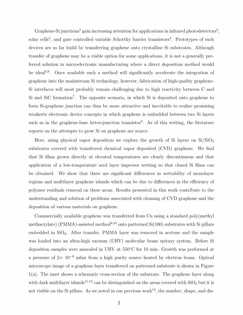
microscope image of a graphene layer transferred on patterned substrate is shown in Figure
1(a). The inset shows a schematic cross-section of the substrate. The graphene layer along
with dark multilayer islands11,12 can be distinguished on the areas covered with SiO2 but it is
not visible on the Si pillars. As we noted in our previous work13, the number, shape, and dis-
2
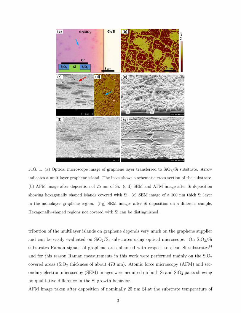
FIG. 1. (a) Optical microscope image of graphene layer transferred to SiO2/Si substrate. Arrow
indicates a multilayer graphene island. The inset shows a schematic cross-section of the substrate.
(b) AFM image after deposition of 25 nm of Si. (c-d) SEM and AFM image after Si deposition
showing hexagonally shaped islands covered with Si. (e) SEM image of a 100 nm thick Si layer
in the monolayer graphene region. (f-g) SEM images after Si deposition on a different sample.
Hexagonally-shaped regions not covered with Si can be distinguished.
tribution of the multilayer islands on graphene depends very much on the graphene supplier
and can be easily evaluated on SiO2/Si substrates using optical microscope. On SiO2/Si
substrates Raman signals of graphene are enhanced with respect to clean Si substrates14
and for this reason Raman measurements in this work were performed mainly on the SiO2
covered areas (SiO2 thickness of about 470 nm). Atomic force microscopy (AFM) and sec-
ondary electron microscopy (SEM) images were acquired on both Si and SiO2 parts showing
no qualitative difference in the Si growth behavior.
AFM image taken after deposition of nominally 25 nm Si at the substrate temperature of
3
550◦C is shown in Figure 1(b). The surface of the sample is very inhomogeneous. The ma-
jority of Si atoms is deposited on graphene wrinkles (bright irregular lines) and oval-shaped
areas which are associated with multilayer graphene islands. On the islands, growing Si
layer is relatively flat with rms roughness of 1-3 nm. Between the elevated islands rms
roughness is much larger (8-10 nm). This result is similar to the one obtained in our recent
experiments with CVD grown HfO2 on graphene13. The nucleation pattern on monolayer
graphene regions resembles formation of Si nanoclusters on highly oriented pyrolytic graphite
studied previously with AFM and scanning tunneling microscopy15–18. Depending on the
choice of graphene material, the multilayer islands preferentially covered with Si are either
oval-shaped (e.g. Fig. 1(b)) or regularly hexagonally-shaped as shown in Figures 1(c) and
(d). The shape of the latter features bear a close resemblance to the individual graphene
grains in the initial growth stage on Cu19. Regardless of the shape of the islands, the Si layer
nucleates much better on these areas than between them: on the monolayer regions growth
seems to proceed by an island-like Volmer-Weber mode and even a nominally 100 nm thick
Si layer is discontinuous as demonstrated by the SEM image in Fig. 1(e). Interestingly,
on some samples an exactly opposite nucleation scenario is observed. This is illustrated in
Figures 1(f) and (g). Here again 25 nm of Si is deposited at 550◦C on graphene sample
prepared in the same way as described above. However, in contrast to the case presented in
Fig. 1(c), Si grows mostly on the monolayer graphene regions and wrinkles leaving thicker
hexagonally-shaped graphene islands practically uncovered. Apparently in this case there
are no or only very few nucleation sites available on the islands. It has been shown, that
during atomic layer deposition (ALD) and CVD on graphene nucleation takes place prefer-
entially at the edges and wrinkles i.e. at the places where defects providing pinning sites are
expected to occur13,20. To verify if a similar mechanism is involved in the peculiar growth
behavior observed here we performed Raman spectroscopy measurements shown in Figure
2. Raman spectra presented in Figure 2(a) were acquired on the places indicated in Figures
2(b)-(d) showing microscope images of bare graphene substrate, sample with no Si deposit
on the islands, and sample with homogeneous nucleation on the islands, respectively.
Spectra labeled with odd numbers are acquired on the monolayer regions; those labeled
with even numbers are collected from the multilayer islands. Measurements on the graphene
islands systematically show lower 2D/G intensity ratios and broader 2D bands if compared
to the scans on the monolayers. However, there is no clear correlation between the intensity
4
FIG. 2. (a) Raman spectra acquired from the points indicated in optical microscope images shown
in panels b-d. Spectra are normalized to the same G mode intensity and vertically offset for clarity.
(b) graphene after transfer. (c) after Si deposition with no Si growth on the multilayer islands. (d)
after Si deposition resulting in uniform coverage of multilayer islands with Si. Scale bar in b-d is
5 µm.
of the defect-related D-band and the coverage of the islands with Si. In other words, a
homogeneous growth of Si on multilayer islands does not clearly correlate with a significantly
increased number of defects detectable by Raman on these sites.
To avoid non-representative spots and strengthen the above conclusion we performed
Raman mapping with high spatial resolution on area of 10×20 µm2 of two samples showing
different Si growth behaviors. These results are presented in Figure 3. There is a strong
correlation between the position of the covered/uncovered islands and the intensity of the
G (and 2D, not shown) mode: G peak is usually more intense on the islands regardless
of the analyzed case. For the D-mode the correlation, if any, is much weaker. According
to these results, the quasi-selective growth observed on some samples does not seem to be
a consequence of different defect distributions and/or concentrations. At least not defects
5
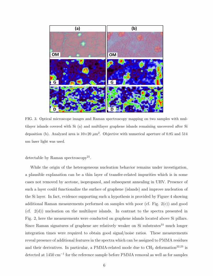
FIG. 3. Optical microscope images and Raman spectroscopy mapping on two samples with mul-
tilayer islands covered with Si (a) and multilayer graphene islands remaining uncovered after Si
deposition (b). Analyzed area is 10×20 µm2. Objective with numerical aperture of 0.85 and 514
nm laser light was used.
detectable by Raman spectroscopy21.
While the origin of the heterogeneous nucleation behavior remains under investigation,
a plausible explanation can be a thin layer of transfer-related impurities which is in some
cases not removed by acetone, isopropanol, and subsequent annealing in UHV. Presence of
such a layer could functionalize the surface of graphene (islands) and improve nucleation of
the Si layer. In fact, evidence supporting such a hypothesis is provided by Figure 4 showing
additional Raman measurements performed on samples with poor (cf. Fig. 2(c)) and good
(cf. 2(d)) nucleation on the multilayer islands. In contrast to the spectra presented in
Fig. 2, here the measurements were conducted on graphene islands located above Si pillars.
Since Raman signatures of graphene are relatively weaker on Si substrates14 much longer
integration times were required to obtain good signal/noise ratios. These measurements
reveal presence of additional features in the spectra which can be assigned to PMMA residues
and their derivatives. In particular, a PMMA-related mode due to CH2 deformation22,23 is
detected at 1450 cm−1 for the reference sample before PMMA removal as well as for samples
6
FIG. 4. Raman spectra around the G mode acquired for a reference sample before PMMA removal
in acetone compared with Raman spectra from two graphene samples covered with Si. For samples
covered with Si measurements were performed on Si pillars with long integration times to reveal
the presence of additional features possibly related to PMMA residues.
after PMMA removal, UHV cleaning, and Si deposition. On the islands where Si nucleates
well (cf. Fig. 1(c)), additionally a broad Raman band is visible which can be due to residual
carbons on the graphene layer24. The islands characterized by poor Si nucleation (cf. Fig.
1(g)) appear to be cleaner as the spectral features related to the residues are weaker. In
fact, the surface of these islands may resemble closely a clean graphite surface with a low
sticking probability and large diffusion length of adsorbed Si atoms. In such a case, since
there are no or very few nucleation sites available on the islands, Si atoms once adsorbed
can travel long distances to the nearest wrinkle or single layer graphene region. There,
suitable nucleation sites are available and the growth takes place. However, a limited spatial
resolution of our experimental setup does not allow us to confirm clearly that the surface of
multilayer graphene islands uncovered by Si is in fact completely free of PMMA residues.
This interpretation of the observations is corroborated by results of ab initio density
functional theory calculations. Si atoms barely stick to perfect graphene. For Si on undoped
graphene, the adsorption energy is 0.58 eV plus Van der Waals contribution (expected to be
of the order of 50 meV), and the energy barrier for surface diffusion is 60 meV, meaning that
7
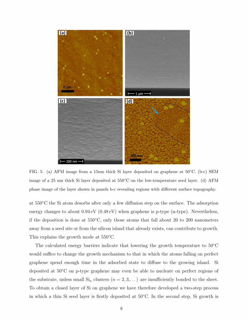
FIG. 5. (a) AFM image from a 15nm thick Si layer deposited on graphene at 50◦C. (b-c) SEM
image of a 25 nm thick Si layer deposited at 550◦C on the low-temperature seed layer. (d) AFM
phase image of the layer shown in panels b-c revealing regions with different surface topography.
at 550◦C the Si atom desorbs after only a few diffusion step on the surface. The adsorption
energy changes to about 0.94 eV (0.48 eV) when graphene is p-type (n-type). Nevertheless,
if the deposition is done at 550◦C, only those atoms that fall about 20 to 200 nanometers
away from a seed site or from the silicon island that already exists, can contribute to growth.
This explains the growth mode at 550◦C.
The calculated energy barriers indicate that lowering the growth temperature to 50◦C
would suffice to change the growth mechanism to that in which the atoms falling on perfect
graphene spend enough time in the adsorbed state to diffuse to the growing island. Si
deposited at 50◦C on p-type graphene may even be able to nucleate on perfect regions of
the substrate, unless small Sin clusters (n = 2, 3,. . . ) are insufficiently bonded to the sheet.
To obtain a closed layer of Si on graphene we have therefore developed a two-step process
in which a thin Si seed layer is firstly deposited at 50◦C. In the second step, Si growth is
8
continued at elevated temperatures. This is similar to the approach using a thin metal layer
to facilitate ALD growth of dielectrics on graphene25,26. AFM image in Fig. 5(a) shows
the surface of a 15 nm-thick seed layer. Beside occasionally occurring spots the surface is
relatively uniform and flat with rms roughness of 0.4-0.5 nm. Moreover, at this substrate
temperature there is no visible difference between the growth on multilayer islands and the
monolayer regions. This seed layer significantly improves wetting during further deposition
at 550◦C. Figure 5(b) and (c) show SEM images of a 25 nm Si layer deposited at 550◦C
on the low-temperature seed. The layer is continuous and relatively homogeneous. Some
inhomogeneity in surface topography is, however, observed in AFM images. Particularly,
in the phase images oval-shaped areas with the size corresponding to the size of multilayer
islands can be easily recognized as indicated in Fig. 5(d). The Si layer in these areas is
smoother (0.3-0.4 nm rms) than outside these regions (0.6-0.9 nm rms). Apparently, the
uniform seed layer undergoes reorganization during the high temperature step which results
in small differences in the growth on multilayer islands and on the monolayer regions. Despite
that the Si layer deposited at 550◦C is closed and free of pinholes.
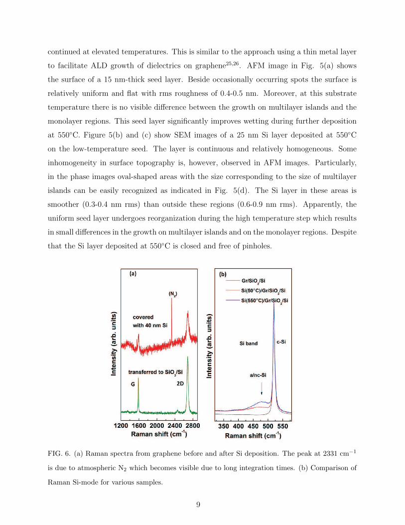
FIG. 6. (a) Raman spectra from graphene before and after Si deposition. The peak at 2331 cm−1
is due to atmospheric N2 which becomes visible due to long integration times. (b) Comparison of
Raman Si-mode for various samples.
9
Figure 6(a) compares Raman spectra of the graphene layer before and after Si deposition.
Although Raman signals after deposition are attenuated by the about 40nm thick Si layer, it
can be seen that graphene largely preserves its quality throughout the Si deposition process.
Scans performed around the position of the Si mode (Fig. 6(b)) indicate that the Si layer
deposited in the two-step process is of nanocrystalline/amorphous nature27.
In summary, physical vapor deposition of Si on transferred CVD graphene was investi-
gated. The presence of multilayer graphene islands and wrinkles results in a heterogeneous
nucleation scheme. Si nucleates poorly on the monolayer graphene regions and the growth
seems to proceed by an island-like Volmer-Weber mode while on the multilayer islands
growth is more two-dimensional with uniform coverage. Interestingly, in some cases the
growth on multilayer islands is not observed at all resulting in a quasi-selective deposition
only on the monolayer regions. According to the results presented here, it can be due to
a more effective removal of polymer residues from the surface of multilayer islands. Fur-
ther studies are under way to clarify the exact origin of this behavior which can potentially
lead to a solution of problems associated with deposition of various materials on graphene.
Meanwhile we have shown that a low-temperature seed layer is effective in improving Si
growth at elevated temperatures and enables closed and smooth Si layers on graphene. This
opens the way to the realization of novel electronic devices consisting of graphene embedded
between two Si layers.
The authors thank G. Morgenstern, H.-P. Stoll, H.-J. Thieme, G. Lippert, M. Fraschke,
and Y. Yamamoto for experimental support and discussions. Financial support by the Ger-
man Research Foundation (DFG, Project No. ME 4117/1-1) and the European Commission
through a STREP project GRADE (No. 317839) is gratefully acknowledged. We gratefully
acknowledge the computing time granted by the John von Neumann Institute for Computing
(NIC) and provided on the supercomputer JUROPA at Jlich Supercomputing Centre (JSC)
to the project hfo06.
10
REFERENCES
1S. Tongay, M. Lemaitre, X. Miao, B. Gila, B. Appleton, and A. Hebard, Physical Review
X 2, 011002 (2012).
2P. Lv, X. Zhang, X. Zhang, W. Deng, and J. Jie, IEEE Electron Device Letters 34, 1337
(2013).
3X. Miao, S. Tongay, M. Petterson, K. Berke, A. Rinzler, and B. A. A. Hebard, Nano
Letters 12, 2745 (2012).
4H. Yang, J. Heo, S. Park, H. Song, D. H. Seo, K.-E. Byum, P. Kim, I. Yoo, H.-J. Chung,
and K. Kim, Science 336, 1140 (2012).
5F. Bonaccorso, A. Lombardo, T. Hasan, Z. Sun, L. Colombo, and A. Ferrari, Materials
Today 15, 564 (2012).
6G. Lippert, J. Dabrowski, Y. Yamamoto, F. Herziger, J. Maultzsch, M. Lemme, W. Mehr,
and G. Lupina, Carbon 52, 40 (2013).
7R. Olesinski and G. Abbaschian, Bulletin of Alloy Phase Diagrams 5, 486 (1984).
8V. D. Lecce, R. Grassi, A. Gnudi, E. Gnani, S. Reggiani, and G. Baccarani, Transactions
on Electron Devices X, DOI:10.1109/TED.2013.2285446 (2013).
9X. Liang, B. A. Sperling, I. Calizo, G. Cheng, C. A. Hacker, Q. Zhang, Y. Obeng, K. Yan,
H. Peng, Q. Li, X. Zhu, H. Yuan, A. R. H. Walker, Z. Liu, L.-M. Peng, and C. A. Richter,
ACS Nano 5, 9144 (2011).
10J. Suk, A. Kitt, C. Magnuson, Y. Hao, S. Ahmed, J. An, A. Swan, B. Goldberg, and
R. Ruoff, ACS Nano 5, 6916 (2011).
11I. Kholmanov, C. Magnuson, A. Aliev, H. Li, B. Zhang, J. Suk, L. Zhang, E. Peng, A. K.
S. Hossein Mousavi, R. Piner, G. Shvets, and R. Ruoff, Nano Letters 12, 5679 (2012).
12L. Liu, H. Zhou, R. Cheng, W. Yu, Y. Liu, Y. Chen, J. Shaw, X. Zhong, Y. Huang, and
X. Duan, ACS Nano 6, 8241 (2012).
13G. Lupina, M. Lukosius, J. Kitzmann, J. Dabrowski, A. Wolff, and W. Mehr, Appl. Phys.
Lett. 103, 183116 (2013).
14D. Yoon, H. Moon, Y.-W. Son, J. Choi, B. Park, Y. Cha, Y. Kim, and H. Cheong, Phys.
Rev. B 80, 125422 (2009).
15P. Scheier, B. Marsen, M. Lonfat, W.-D. Schneider, and K. Sattler, Surface Science 458,
113 (2000).
11
16K. Ikuta, K. Tanaka, S. Yamasaki, K. Miki, and A. Matsuda, Appl. Phys. Lett. 65, 1760
(1994).
17T. van Buuren, L. Dinh, L. Chase, W. Siekhaus, and L. Terminello, Phys. Rev. Lett. 80,
3803 (1998).
18M. Matsuse, S. Tsuboi, M. Kawasaki, H. Koinuma, M. Eguchi, and H. Sakata, Phys. Rev.
B 53, 12585 (1996).
19Q. Yu, L. A. Jauregui, W. Wu, R. Colby, J. Tian, Z. Su, H. Cao, Z. Liu, D. Pandey,
D. Wei, T. F. Chung, P. Peng, N. P. Guisinger, E. A. Stach, J. Bao, S. S. Pei, and Y. P.
Chen, Nature Materials 10, 443 (2011).
20X. Wang, S. Tabakman, and H. Dai, J. Am. Chem. Soc. 130, 8152 (2008).
21A. Ferrari and M. Basko, Nature Nanotechnology 8, 235 (2013).
22H. Willis, V. Zichy, and P. Hendra, Polymer 10, 737 (1969).
23S. Szilasi, R. Huszank, D. Szikra, T. Vaczi, I. Rajta, and I. Nagy, Materials Chemistry
and Physics 130, 702 (2011).
24C. Gong, H. Floresca, D. Hinojos, S. McDonnell, X. Qin, Y. Hao, S. Jandhyala, G. Mordi,
J. Kim, L. Colombo, R. Ruoff, M. Kim, K. Cho, R. Wallace, and Y. Chabal, J. Phys.
Chem. C 117, 23000 (2013).
25S. Kim, J. Nah, I. Jo, D. Shahrjerdi, L. Colombo, Z. Yao, E. Tutuc, and S. Banerjee,
Applied Physics Letters 94, 062107 (2009).
26S. Vaziri, G. Lupina, C. Henkel, A. Smith, M. Ostling, J. Dabrowski, G. Lippert, W. Mehr,
and M. Lemme, Nano Letters 13, 1435 (2013).
27S. Gaisler, O. Semenova, R. Sharafutdinov, and B. Kolesov, Physics of the Solid State
46, 1528 (2004).
12