Delphine Misao Lebrun - Photonic crystals and photocatalysis
288
ACTA UNIVERSITATIS UPSALIENSIS Uppsala Dissertations from the Faculty of Science and Technology 126
-
Upload
khangminh22 -
Category
Documents
-
view
0 -
download
0
Transcript of Delphine Misao Lebrun - Photonic crystals and photocatalysis

ACTA UNIVERSITATIS UPSALIENSIS Uppsala Dissertations from the Faculty of Science and Technology
126

Delphine Misao Lebrun
Photonic crystals
and photocatalysis Study of titania inverse opals

Dissertation presented at Uppsala University to be publicly examined in ITC 2247,Lägerhyddsvägen 1, Uppsala, Monday, 3 October 2016 at 14:15 for the degree of Doctor ofPhilosophy. The examination will be conducted in English. Faculty examiner: Martyn Pemble(Tyndall National Institute, MicroNanoelectronics).
AbstractLebrun, D. M. 2016. Photonic crystals and photocatalysis. Study of titania inverse opals.Uppsala Dissertations from the Faculty of Science and Technology 126. 284 pp. Uppsala:Acta Universitatis Upsaliensis. ISBN 978-91-554-9650-0.
Due to an increase of human activity, an increase health risk has emerged from the presenceof pollutants in the environment. In the transition to renewable and sustainable life style,treatment of pollutants could support the shifting societies. A motivation behind materialresearch for environmental applications is to maximize the efficiency of the materials to alleviateenvironmental pollution.
In the case of titania, an increase of ultra-violet light absorption is needed to overcomeits bandgap to produce reactive radicals, which is the basis for photocatalysis. It has beenhypothesized that photonic crystal can enhance titania photocatalysis. They are structures madeof at least two dielectrics with a high refractive index contrast, ordered in a periodic fashion. Fora strong contrast, photonic band gaps emerge. The effect of the photonic band gap is to forcecomplete reflection of the incoming light within its range and multiple internal reflections at itsedges. By combining photonic and electronic band gap positions, it is possible to increase theabsorption at the photonic band gap edges.
In this thesis, fabrication method and structural analysis of titania and alumina/titaniaphotonic structures were presented. A thorough optical analysis was performed at all stepsof fabrication – beyond what previously has been reported. The photocatalytic activity wasmeasured with two setups. Fourier Transform Infrared spectroscopy combined with arc lampsand bandpass filters was used to monitor the degradation of stearic acid in ambient air. A home-built setup was used to degrade methylene blue in solution with ultra-violet illumination.
The results in this thesis show in general no correlation of the photocatalytic activity to thephotonic band gap position, even though absorbance data displayed an increase absorption inthis energy range. A more controlled environment might show the effect of the structure, asseen in some of the experiments.
Keywords: photocatalysis, titania, inverse opal, photonic crystal, optics
Delphine Misao Lebrun, Department of Engineering Sciences, Solid State Physics, Box 534,Uppsala University, SE-751 21 Uppsala, Sweden.
© Delphine Misao Lebrun 2016
ISSN 1104-2516ISBN 978-91-554-9650-0urn:nbn:se:uu:diva-300408 (http://urn.kb.se/resolve?urn=urn:nbn:se:uu:diva-300408)

Qu’est-ce qui me plait le plusdans la Science?L’humilité certainement.
Mais je sais que les scientifiquesne sont pas d’accord; parce queles scientifiques connaissent desautres scientifiques qui ne sontpas humbles, qui sont mêmechiants, et imbus de leurpersonne.Mais n’empêche que pour lenéophyte que je suis, la ligne duscientifique c’est de dire “je saispas”, et si je sais pas, je vaisessayer de comprendre, et je vaisfaire un pas après l’autre.[...] Et pour moi, la positionscientifique est naturellementhumble, et elle permet d’aller laoù on est aujourd’hui et la où onira demain.C’est à dire, “je ne sais pas”,
j’aime la phrase “je ne sais
pas”.
Et je trouve que les scientifiquessont ceux qui le disent le mieux.Voila.
Alexandre AstierUTOPIALES 2014, France

Cover by Kara Philippe Enseignant en dessin, story board, concept design - illustrateur / auteur de BD. Blog : http://karafactory.blogspot.fr/ Facebook : https://www.facebook.com/karafactory Galerie dessins et photos : http://karafactory.deviantart.com/ Twitter : https://twitter.com/KARAFACTORY Youtube : https://www.youtube.com/user/Karafactory

Contents
1 Introduction . . . . . . . . . . . . . . . . . . . . . . . . . . . . . . . . . . . . . . . . . . . . . . . . . . . . . . . . . . . . . . . . . . . . . . . . . . . . . . . . . . . . . . . . . . . . . . . . 11
2 Light and Photonic crystals . . . . . . . . . . . . . . . . . . . . . . . . . . . . . . . . . . . . . . . . . . . . . . . . . . . . . . . . . . . . . . . . . . . . . . . 142.1 Light . . . . . . . . . . . . . . . . . . . . . . . . . . . . . . . . . . . . . . . . . . . . . . . . . . . . . . . . . . . . . . . . . . . . . . . . . . . . . . . . . . . . . . . . . . . . . . . . 14
2.1.1 Definitions . . . . . . . . . . . . . . . . . . . . . . . . . . . . . . . . . . . . . . . . . . . . . . . . . . . . . . . . . . . . . . . . . . . . . . . . 142.1.2 Optical spectra . . . . . . . . . . . . . . . . . . . . . . . . . . . . . . . . . . . . . . . . . . . . . . . . . . . . . . . . . . . . . . . . . 152.1.3 Optical characterization . . . . . . . . . . . . . . . . . . . . . . . . . . . . . . . . . . . . . . . . . . . . . . . . . . 17
2.2 Structural colour . . . . . . . . . . . . . . . . . . . . . . . . . . . . . . . . . . . . . . . . . . . . . . . . . . . . . . . . . . . . . . . . . . . . . . . . . . . . . 192.2.1 Nature . . . . . . . . . . . . . . . . . . . . . . . . . . . . . . . . . . . . . . . . . . . . . . . . . . . . . . . . . . . . . . . . . . . . . . . . . . . . . . . 192.2.2 3D photonic crystals . . . . . . . . . . . . . . . . . . . . . . . . . . . . . . . . . . . . . . . . . . . . . . . . . . . . . . . . 21
2.3 Band structure . . . . . . . . . . . . . . . . . . . . . . . . . . . . . . . . . . . . . . . . . . . . . . . . . . . . . . . . . . . . . . . . . . . . . . . . . . . . . . . . 232.3.1 Electrons and phonons . . . . . . . . . . . . . . . . . . . . . . . . . . . . . . . . . . . . . . . . . . . . . . . . . . . . 232.3.2 Electronic band structure . . . . . . . . . . . . . . . . . . . . . . . . . . . . . . . . . . . . . . . . . . . . . . . . 272.3.3 Light band structure . . . . . . . . . . . . . . . . . . . . . . . . . . . . . . . . . . . . . . . . . . . . . . . . . . . . . . . . 31
2.4 Photonic effects . . . . . . . . . . . . . . . . . . . . . . . . . . . . . . . . . . . . . . . . . . . . . . . . . . . . . . . . . . . . . . . . . . . . . . . . . . . . . . 342.4.1 Total reflection . . . . . . . . . . . . . . . . . . . . . . . . . . . . . . . . . . . . . . . . . . . . . . . . . . . . . . . . . . . . . . . . . 342.4.2 Slow down of the light . . . . . . . . . . . . . . . . . . . . . . . . . . . . . . . . . . . . . . . . . . . . . . . . . . . . 362.4.3 Fragility of the photonic band gap . . . . . . . . . . . . . . . . . . . . . . . . . . . . . . . . . 372.4.4 State of art . . . . . . . . . . . . . . . . . . . . . . . . . . . . . . . . . . . . . . . . . . . . . . . . . . . . . . . . . . . . . . . . . . . . . . . . 37
3 Photocatalysis . . . . . . . . . . . . . . . . . . . . . . . . . . . . . . . . . . . . . . . . . . . . . . . . . . . . . . . . . . . . . . . . . . . . . . . . . . . . . . . . . . . . . . . . . . . . 403.1 Definition and general theory . . . . . . . . . . . . . . . . . . . . . . . . . . . . . . . . . . . . . . . . . . . . . . . . . . . . . . . . 40
3.1.1 Catalysis and photocatalysis . . . . . . . . . . . . . . . . . . . . . . . . . . . . . . . . . . . . . . . . . . . 403.1.2 Heterogeneous photocatalysis . . . . . . . . . . . . . . . . . . . . . . . . . . . . . . . . . . . . . . . . 41
3.2 Semiconductor photocatalysis . . . . . . . . . . . . . . . . . . . . . . . . . . . . . . . . . . . . . . . . . . . . . . . . . . . . . . . 423.2.1 Definitions . . . . . . . . . . . . . . . . . . . . . . . . . . . . . . . . . . . . . . . . . . . . . . . . . . . . . . . . . . . . . . . . . . . . . . . . 423.2.2 Mechanisms . . . . . . . . . . . . . . . . . . . . . . . . . . . . . . . . . . . . . . . . . . . . . . . . . . . . . . . . . . . . . . . . . . . . . 433.2.3 Transition metal oxides . . . . . . . . . . . . . . . . . . . . . . . . . . . . . . . . . . . . . . . . . . . . . . . . . . . 46
3.3 Degradation mechanisms . . . . . . . . . . . . . . . . . . . . . . . . . . . . . . . . . . . . . . . . . . . . . . . . . . . . . . . . . . . . . . . 493.3.1 Methylene Blue . . . . . . . . . . . . . . . . . . . . . . . . . . . . . . . . . . . . . . . . . . . . . . . . . . . . . . . . . . . . . . . . 493.3.2 Stearic Acid . . . . . . . . . . . . . . . . . . . . . . . . . . . . . . . . . . . . . . . . . . . . . . . . . . . . . . . . . . . . . . . . . . . . . . 50
3.4 Activity assessment . . . . . . . . . . . . . . . . . . . . . . . . . . . . . . . . . . . . . . . . . . . . . . . . . . . . . . . . . . . . . . . . . . . . . . . . 51
4 Experimental setup . . . . . . . . . . . . . . . . . . . . . . . . . . . . . . . . . . . . . . . . . . . . . . . . . . . . . . . . . . . . . . . . . . . . . . . . . . . . . . . . . . . . 534.1 Materials and chemicals . . . . . . . . . . . . . . . . . . . . . . . . . . . . . . . . . . . . . . . . . . . . . . . . . . . . . . . . . . . . . . . . 53
4.1.1 Chemicals . . . . . . . . . . . . . . . . . . . . . . . . . . . . . . . . . . . . . . . . . . . . . . . . . . . . . . . . . . . . . . . . . . . . . . . . . 534.1.2 Substrates . . . . . . . . . . . . . . . . . . . . . . . . . . . . . . . . . . . . . . . . . . . . . . . . . . . . . . . . . . . . . . . . . . . . . . . . . 564.1.3 Others . . . . . . . . . . . . . . . . . . . . . . . . . . . . . . . . . . . . . . . . . . . . . . . . . . . . . . . . . . . . . . . . . . . . . . . . . . . . . . . 56
4.2 Instruments . . . . . . . . . . . . . . . . . . . . . . . . . . . . . . . . . . . . . . . . . . . . . . . . . . . . . . . . . . . . . . . . . . . . . . . . . . . . . . . . . . . . . 564.2.1 Structure . . . . . . . . . . . . . . . . . . . . . . . . . . . . . . . . . . . . . . . . . . . . . . . . . . . . . . . . . . . . . . . . . . . . . . . . . . . 564.2.2 Spectrophotometry . . . . . . . . . . . . . . . . . . . . . . . . . . . . . . . . . . . . . . . . . . . . . . . . . . . . . . . . . . 604.2.3 Photocatalysis . . . . . . . . . . . . . . . . . . . . . . . . . . . . . . . . . . . . . . . . . . . . . . . . . . . . . . . . . . . . . . . . . . 65
5 Fabrication method . . . . . . . . . . . . . . . . . . . . . . . . . . . . . . . . . . . . . . . . . . . . . . . . . . . . . . . . . . . . . . . . . . . . . . . . . . . . . . . . . . . . 755.1 Templates . . . . . . . . . . . . . . . . . . . . . . . . . . . . . . . . . . . . . . . . . . . . . . . . . . . . . . . . . . . . . . . . . . . . . . . . . . . . . . . . . . . . . . . . 755.2 Atomic Layer Deposition . . . . . . . . . . . . . . . . . . . . . . . . . . . . . . . . . . . . . . . . . . . . . . . . . . . . . . . . . . . . . . 77
5.2.1 Description of the technique . . . . . . . . . . . . . . . . . . . . . . . . . . . . . . . . . . . . . . . . . . . 775.2.2 Depositions cycles . . . . . . . . . . . . . . . . . . . . . . . . . . . . . . . . . . . . . . . . . . . . . . . . . . . . . . . . . . . 79
5.3 Ion milling . . . . . . . . . . . . . . . . . . . . . . . . . . . . . . . . . . . . . . . . . . . . . . . . . . . . . . . . . . . . . . . . . . . . . . . . . . . . . . . . . . . . . . 835.4 Inversion . . . . . . . . . . . . . . . . . . . . . . . . . . . . . . . . . . . . . . . . . . . . . . . . . . . . . . . . . . . . . . . . . . . . . . . . . . . . . . . . . . . . . . . . . 84
6 Sample structure . . . . . . . . . . . . . . . . . . . . . . . . . . . . . . . . . . . . . . . . . . . . . . . . . . . . . . . . . . . . . . . . . . . . . . . . . . . . . . . . . . . . . . . . 856.1 Templates . . . . . . . . . . . . . . . . . . . . . . . . . . . . . . . . . . . . . . . . . . . . . . . . . . . . . . . . . . . . . . . . . . . . . . . . . . . . . . . . . . . . . . . . 85
6.1.1 Substrates . . . . . . . . . . . . . . . . . . . . . . . . . . . . . . . . . . . . . . . . . . . . . . . . . . . . . . . . . . . . . . . . . . . . . . . . . 856.1.2 Profilometry . . . . . . . . . . . . . . . . . . . . . . . . . . . . . . . . . . . . . . . . . . . . . . . . . . . . . . . . . . . . . . . . . . . . . 866.1.3 SEM . . . . . . . . . . . . . . . . . . . . . . . . . . . . . . . . . . . . . . . . . . . . . . . . . . . . . . . . . . . . . . . . . . . . . . . . . . . . . . . . . . 89
6.2 Metal Oxide structures . . . . . . . . . . . . . . . . . . . . . . . . . . . . . . . . . . . . . . . . . . . . . . . . . . . . . . . . . . . . . . . . . . . 986.2.1 GIXRD . . . . . . . . . . . . . . . . . . . . . . . . . . . . . . . . . . . . . . . . . . . . . . . . . . . . . . . . . . . . . . . . . . . . . . . . . . . . . 986.2.2 SEM . . . . . . . . . . . . . . . . . . . . . . . . . . . . . . . . . . . . . . . . . . . . . . . . . . . . . . . . . . . . . . . . . . . . . . . . . . . . . . . . 1046.2.3 ALD deposition rates . . . . . . . . . . . . . . . . . . . . . . . . . . . . . . . . . . . . . . . . . . . . . . . . . . . . 115
7 Optical characterization . . . . . . . . . . . . . . . . . . . . . . . . . . . . . . . . . . . . . . . . . . . . . . . . . . . . . . . . . . . . . . . . . . . . . . . . . . 1187.1 Templates . . . . . . . . . . . . . . . . . . . . . . . . . . . . . . . . . . . . . . . . . . . . . . . . . . . . . . . . . . . . . . . . . . . . . . . . . . . . . . . . . . . . . . 118
7.1.1 Thickness . . . . . . . . . . . . . . . . . . . . . . . . . . . . . . . . . . . . . . . . . . . . . . . . . . . . . . . . . . . . . . . . . . . . . . . 1187.1.2 Total, Specular and Diffuse spectra . . . . . . . . . . . . . . . . . . . . . . . . . . . . . . 1217.1.3 Opal qualification . . . . . . . . . . . . . . . . . . . . . . . . . . . . . . . . . . . . . . . . . . . . . . . . . . . . . . . . . . 127
7.2 Intermediates . . . . . . . . . . . . . . . . . . . . . . . . . . . . . . . . . . . . . . . . . . . . . . . . . . . . . . . . . . . . . . . . . . . . . . . . . . . . . . . . 1377.2.1 Total, specular and diffuse light . . . . . . . . . . . . . . . . . . . . . . . . . . . . . . . . . . . . 1407.2.2 Effect of ion milling . . . . . . . . . . . . . . . . . . . . . . . . . . . . . . . . . . . . . . . . . . . . . . . . . . . . . . 1457.2.3 Opal quality . . . . . . . . . . . . . . . . . . . . . . . . . . . . . . . . . . . . . . . . . . . . . . . . . . . . . . . . . . . . . . . . . . . 1457.2.4 Deposition rate . . . . . . . . . . . . . . . . . . . . . . . . . . . . . . . . . . . . . . . . . . . . . . . . . . . . . . . . . . . . . . . 1487.2.5 Al2O3 inverse opal . . . . . . . . . . . . . . . . . . . . . . . . . . . . . . . . . . . . . . . . . . . . . . . . . . . . . . . . 154
7.3 Photonic structures . . . . . . . . . . . . . . . . . . . . . . . . . . . . . . . . . . . . . . . . . . . . . . . . . . . . . . . . . . . . . . . . . . . . . . . 1647.3.1 TiO2 Inverse opals . . . . . . . . . . . . . . . . . . . . . . . . . . . . . . . . . . . . . . . . . . . . . . . . . . . . . . . . . 1647.3.2 Al2O3/TiO2 Inverse opals . . . . . . . . . . . . . . . . . . . . . . . . . . . . . . . . . . . . . . . . . . . . . 1737.3.3 Effect of baking . . . . . . . . . . . . . . . . . . . . . . . . . . . . . . . . . . . . . . . . . . . . . . . . . . . . . . . . . . . . . 185
8 Results in photocatalysis . . . . . . . . . . . . . . . . . . . . . . . . . . . . . . . . . . . . . . . . . . . . . . . . . . . . . . . . . . . . . . . . . . . . . . . . . 1908.1 Fourier Transform InfraRed spectroscopy: stearic acid
degradation . . . . . . . . . . . . . . . . . . . . . . . . . . . . . . . . . . . . . . . . . . . . . . . . . . . . . . . . . . . . . . . . . . . . . . . . . . . . . . . . . . . 1908.1.1 UV illumination . . . . . . . . . . . . . . . . . . . . . . . . . . . . . . . . . . . . . . . . . . . . . . . . . . . . . . . . . . . . . 1928.1.2 Solar spectrum . . . . . . . . . . . . . . . . . . . . . . . . . . . . . . . . . . . . . . . . . . . . . . . . . . . . . . . . . . . . . . . 2078.1.3 LED white lamp . . . . . . . . . . . . . . . . . . . . . . . . . . . . . . . . . . . . . . . . . . . . . . . . . . . . . . . . . . . . 224

8.2 Methylene blue degradation . . . . . . . . . . . . . . . . . . . . . . . . . . . . . . . . . . . . . . . . . . . . . . . . . . . . . . . . 2278.2.1 Typical results . . . . . . . . . . . . . . . . . . . . . . . . . . . . . . . . . . . . . . . . . . . . . . . . . . . . . . . . . . . . . . . . 2278.2.2 Dark phase . . . . . . . . . . . . . . . . . . . . . . . . . . . . . . . . . . . . . . . . . . . . . . . . . . . . . . . . . . . . . . . . . . . . . 2278.2.3 Illumination phase . . . . . . . . . . . . . . . . . . . . . . . . . . . . . . . . . . . . . . . . . . . . . . . . . . . . . . . . . 236
9 Discussion and conclusion . . . . . . . . . . . . . . . . . . . . . . . . . . . . . . . . . . . . . . . . . . . . . . . . . . . . . . . . . . . . . . . . . . . . . . 2449.1 Fabrication method . . . . . . . . . . . . . . . . . . . . . . . . . . . . . . . . . . . . . . . . . . . . . . . . . . . . . . . . . . . . . . . . . . . . . . 2449.2 Optical measures . . . . . . . . . . . . . . . . . . . . . . . . . . . . . . . . . . . . . . . . . . . . . . . . . . . . . . . . . . . . . . . . . . . . . . . . . . 2459.3 Photocatalysis . . . . . . . . . . . . . . . . . . . . . . . . . . . . . . . . . . . . . . . . . . . . . . . . . . . . . . . . . . . . . . . . . . . . . . . . . . . . . . . 2469.4 Futur prospects . . . . . . . . . . . . . . . . . . . . . . . . . . . . . . . . . . . . . . . . . . . . . . . . . . . . . . . . . . . . . . . . . . . . . . . . . . . . . 247
10 Summary . . . . . . . . . . . . . . . . . . . . . . . . . . . . . . . . . . . . . . . . . . . . . . . . . . . . . . . . . . . . . . . . . . . . . . . . . . . . . . . . . . . . . . . . . . . . . . . . . . 249
Appendices . . . . . . . . . . . . . . . . . . . . . . . . . . . . . . . . . . . . . . . . . . . . . . . . . . . . . . . . . . . . . . . . . . . . . . . . . . . . . . . . . . . . . . . . . . . . . . . . . . . . . 253
A List of inverse opals . . . . . . . . . . . . . . . . . . . . . . . . . . . . . . . . . . . . . . . . . . . . . . . . . . . . . . . . . . . . . . . . . . . . . . . . . . . . . . . . . 254A.1 TiO2 inverse opal . . . . . . . . . . . . . . . . . . . . . . . . . . . . . . . . . . . . . . . . . . . . . . . . . . . . . . . . . . . . . . . . . . . . . . . . . 254A.2 Al2O3/TiO2 inverse opal . . . . . . . . . . . . . . . . . . . . . . . . . . . . . . . . . . . . . . . . . . . . . . . . . . . . . . . . . . . . . 254
B Arc lamp, filters and mirror . . . . . . . . . . . . . . . . . . . . . . . . . . . . . . . . . . . . . . . . . . . . . . . . . . . . . . . . . . . . . . . . . . . . 256B.1 Xe lamp stability . . . . . . . . . . . . . . . . . . . . . . . . . . . . . . . . . . . . . . . . . . . . . . . . . . . . . . . . . . . . . . . . . . . . . . . . . . 256B.2 AM0 and AM1.5 filters . . . . . . . . . . . . . . . . . . . . . . . . . . . . . . . . . . . . . . . . . . . . . . . . . . . . . . . . . . . . . . . 256B.3 Gold mirror . . . . . . . . . . . . . . . . . . . . . . . . . . . . . . . . . . . . . . . . . . . . . . . . . . . . . . . . . . . . . . . . . . . . . . . . . . . . . . . . . . . 256
C Photocat parameters . . . . . . . . . . . . . . . . . . . . . . . . . . . . . . . . . . . . . . . . . . . . . . . . . . . . . . . . . . . . . . . . . . . . . . . . . . . . . . . . 260
D Matlab programs . . . . . . . . . . . . . . . . . . . . . . . . . . . . . . . . . . . . . . . . . . . . . . . . . . . . . . . . . . . . . . . . . . . . . . . . . . . . . . . . . . . . . . 262D.1 Photonic band gap theoretical position . . . . . . . . . . . . . . . . . . . . . . . . . . . . . . . . . . . . . . . 262D.2 Sample surface area . . . . . . . . . . . . . . . . . . . . . . . . . . . . . . . . . . . . . . . . . . . . . . . . . . . . . . . . . . . . . . . . . . . . . 264
E Calculated values . . . . . . . . . . . . . . . . . . . . . . . . . . . . . . . . . . . . . . . . . . . . . . . . . . . . . . . . . . . . . . . . . . . . . . . . . . . . . . . . . . . . . 265E.1 TiO2 inverse opal . . . . . . . . . . . . . . . . . . . . . . . . . . . . . . . . . . . . . . . . . . . . . . . . . . . . . . . . . . . . . . . . . . . . . . . . . 265E.2 Al2O3/TiO2 inverse opal . . . . . . . . . . . . . . . . . . . . . . . . . . . . . . . . . . . . . . . . . . . . . . . . . . . . . . . . . . . . . 265
References . . . . . . . . . . . . . . . . . . . . . . . . . . . . . . . . . . . . . . . . . . . . . . . . . . . . . . . . . . . . . . . . . . . . . . . . . . . . . . . . . . . . . . . . . . . . . . . . . . . . . . 270


1. Introduction
Vous, vous avez une idée derrièrela main, j’en mettrais ma tête aufeu!
Frank Pitiotas Perceval le Gallois in Kaamelott
Octopuses are impressive. They are very smart, aware of their surroundingsbut also playful and shy, which makes for interesting stories for aquariumkeepers to tell. They are well known for their association with the mythicalkraken and have enter our collective imagination with monstrous and vivid de-pictions in books, as 20 000 miles under the sea, and movies like Pirate of theCaribbean. Do not double check the cover title of the thesis, this work is notabout cephalopods. But this work has a purpose. As it is easy to forget whywe are doing research, beyond the thirst for knowledge.The major effect of carbon dioxide (CO2) in the atmosphere is to reflect infra-red (IR) light emitted by Earth - trapping heat efficiently. This is called green-house gas effect and it is a natural phenomenon. However, since the firstindustrial revolution in the XIXth Europe, an increase of energy consumptioncombined with a petrol-based energy source, the level of rejected CO2 in theatmosphere has increased considerably. One of the consequence is the in-creased CO2 absorption in the oceans, leading to an acidification. Octopusesare sensitive to water quality (notably oxygen concentration) and acidity, so wemight witness several subspecies disappearance in the next upcoming decades.This is why we are doing research. And this work, even in a small pretence,will help finding solutions to the biggest problem of the XXIst century: humanmade pollution.
There is another reason as for why octopuses are mentioned in this work,and this is also related to the drawing on the cover. An octopus is exper-imenting change of colours on a chameleon, with a source of light and anobject to record light. Why? Well, an octopus can change skin colour (andshape!) to an almost perfect camouflage in milliseconds and chameleons arewell-known colour-change animals. There is however a difference in the ex-planation behind the colour changes. To understand how an octopus change
11

colour, a chemist would be perfect. After observing the skin of an octopus witha microscope, one can identity several cells containing pigments. Pigmentsare molecules that can absorb light, and more specifically, that reflect certaincolours (what the observer see). Octopuses compress their cells to changethe morphology of the molecules, and switch the colour that is reflected. Butif a chemist would apply the same method to a chameleon, the only notableobservation would be the regular presence of tiny protuberances at regular in-terval, but no specific molecules reflecting a specific colour. So how does achameleon change colour then? To understand, it is necessary to switch for thepoint of view of physics: what does the light do upon reaching the chameleonskin? If observed in its natural environment, the chameleon will be exposedto visible light from the Sun. Visible light is actually composed of severalcolours (rainbow), and for each colour we can calculate a specific energy anda specific wavelength (how the light propagates). The colour observed on thechameleon will be the colour reflected by its skin - so that the sunlight willsplit in different energies and some will be able to go in the chameleon skin,while others will be reflected back (and therefore observed). The trick? Thosetiny protuberances. They are called guanine nanocrystals and do all the work:these nanocrystals are regularly placed on the skin and the distance separatingthe crystals are in the same order of magnitude as the wavelength of visiblelight (400 to 800 nm). Because of this regularity and the difference in en-ergy (3.1 to 1.55 eV), some colour (or wavelength) will be able to travel inthe nanocrystals, while another colour will be able to travel in the air, betweenthe nanocrystals. So, the colour that is reflected by the chameleon skin is ac-tually the one in between! As it cannot travel in the nanocrystals neither inthe air in between, because it has the wrong periodicity, it is reflected back.Now, we know that these nanocrystals can explain why certain colours are re-flected or not. How does the chameleon change the reflected colour? Simplyby stretching or compressing its skin. By doing so, the chameleon change thedistance between the nanocrystals - so the periodicity and therefore the wave-length (colour) of the reflected light. Chameleons are not the only one to havea structure in the nanometer range (visible light), countless of insects possesthis trait (butterflies, beetles, flies...), birds (feathers), molluscs, and even fruitsand minerals. These show a structural colour and have been denominated pho-tonic crystals.
Photonic crystals have interesting effects on the light, which can be exploitedfor several applications. This work focus on the fabrication of artifical pho-tonic crystals for photocatalysis. The word photocatalysis is composed of twolatin parts: photo (light) and catalysis (dissolution). Photocatalysis is the useof a material which can absorb light to accelerate an otherwise slow chemi-cal reaction. The advantages of a photocatalysis are the consomption of lessenergy to make chemicals react (catalysis) and the use of an energy source
12

readily available indoors and outdoors (photo). The shortcomings of photo-catalysis are usually the need of higher energy light (ultra-violet), which isnot abundant in the solar spectrum (most intense in the green) and the sur-face driven reaction, which can limit the efficiency of the material. The mostcommonly used photocatalysts are metal oxides, formed with a metal atomattached to a certain number of oxygen atoms. For instance, titanium dioxide(TiO2) posses a metal atom titanium and has two oxygen atoms attached toit, this form the base to build the entire material. Metal oxides are natural,usually cheap and environmentally safe. There is however drawbacks: certainmetal oxides will be photosensitive, meaning that they will deteriorate undersubsequent light exposition (like Iron Oxide Fe2O3) and others will be moreresiliant but will also absorb less light, so that the efficiency is low (like TiO2).These effects can be understood by studying the structure of the different ma-terials, and notably their electronic structure. To palliate on the defaults or tominimize them, it is possible to use photonic crystals. To summerize simply,different three dimentionnal structures can be used to minimize absorptiondamages or to increase absorption, by using photonic crystals effect on thelight.
Further explanations can be found in the following chapters: photonic crystals(chapter 2) and photocatalysis (chapter 3). Experimental details, materials andchemicals, fabrication methods and instruments will be presented in chapter4. The following chapters are dedicated to results and analysis of the samplestructure (chapter 5), optical characterization (chapter 6) and photocatalysis(chapter 7).
13

2. Light and Photonic crystals
Les rêves, ça se compare pas.
Alexandre Astieras Arthur Pendragon in Kaamelott
2.1 Light2.1.1 DefinitionsLight can be described both as a wave (with a periodicity called wavelengthλ ) and as a particle (a photon, with defined energy E). The experiments ofYoung, Arago and Fresnel demonstrated the wave nature of light [1], but thisnature could not explain black body radiation (light emission from a heatedobject). Planck suggested in 1900 that light was formed of indistinguishableenergy elements [2], which was confirmed in 1905 by Einstein’s reflexion onthe photo-electric effect [3], where electrons are emitted by objects after beingilluminated. This contradictive nature breaks down at the quantum level, inthe infinitesimally small, where any quantum object is described as a wave-packet. Thus the quantum object can become spatially localized, behaving asa particle, or if delocalized, behaving as a wave. It is convenient to refer tolight as a photon when dealing with light interaction with matter, where anenergy exchange takes place; whereas the wave nature is often employed fortheory and calculation.The relationship between the wave and particle nature is apparent in the ex-pression of the energy of light, depicted in the equation 2.1:
E = hcλ, (2.1)
where h is the Planck constant (value: 4.13×10⁻¹⁵ eV s), c the speed of lightin vacuum (value: 2.99×10⁸ ms−1) and λ the light wavelength (in m).The wavelength (λ ) is the spacial distance between two equivalent points of awave and wave frequency (ω) is the inverse of the wavelength. Classificationof the light by energy range - or wavelength range - creates the electromag-netic spectrum, shown in figure 2.1. Energy can be expressed in Joule (SIunit), or in eV (1eV = 1.6×10⁻¹⁹J), frequently used in solid state physics in-stead of Joule, due to its convenient number size from Mid Infra-Red (MIR) to
14

Figure 2.1. Electromagnetic spectrum of light: Infra-red (IR), visible (Vis) and Ultra-violet (UV). Wavelength (nm) scale above and energy (eV) scale below.
Mid Ultra-Violet (MUV). Infra-red (IR) light has the lowest energy, associatedwith room temperature heat, molecular vibrations and rotations. IR cannot bedetected by the human eye, as a special detector is needed (a pit organ), whichcan be found in some mammals (i.e. vampire bat Desmodontinae), reptiles(i.e. Crotaline snake Crotalinae) and insects (i.e. Melanophila acuminatabeetle) [4]. Visible light is the energy range that can be detected by the humaneye, and is associated with colors. Visible light used in lighting and comingfrom the sun, is made of the rainbow colors, from red to violet. Ultra-Violet(UV) light has the highest energy and the human eye cannot detect it, thougha lot of mammals (i.e. Rattus norvegicus rat [5]), birds (i.e. Eugenes fulgenshummingbird [5]), insects (i.e. Apis Mellifera bee [6]), reptiles (i.e. Pseude-mys scripta elegans turtle [5]) and arachnids (i.e. Salticidae jumping spider[7]) can.
2.1.2 Optical spectra
To have a visual representation of light, a spectrum is created. A spectrumis a graphical drawing of light intensity (I) on the y-axis, versus light wave-length (λ ) on the x-axis. Light intensity is usually the amount of count on alight detector - meaning the number of photons with a particular energy (orwavelength) measured by the detector. Depending on the type of measure-ment setup, light intensity can be defined differently. The measure of powerreceived per unit area is called irradiance (unit: Wm−2). If irradiance is plottedversus wavelength, the unit becomes Wm−2nm−1. It can be defined mathemat-ically by using the equations 2.2 and 2.3:
Φ = ∂Q∂ t
, (2.2)
where Φ is the radiant flux, Q the radiant energy detected and t the time, and
Eλ = ∂ 2Φ∂A∂λ
, (2.3)
where A is the area and Eλ , the irradiance per wavelength.
15

Figure 2.2. Solar irradiance before penetrating Earth atmosphere in black (AM0) andat sea level in blue (AM1.5), solar zenith angle 48.19○s.
There are several different setups for measuring light, depending on the sourceand energy range. The only natural light source on earth is evidently the sun.Solar irradiance is linked to the sun’s surface temperature (5778 K or 5500○C).The light emission for an object at this temperature (black body radiation), fitsrather well the irradiance of the sun. The solar spectrum is well known, as wellas the effect of earth’s atmosphere on solar irradiance [8–10]. Because of thecomposition of the atmosphere, irradiance is different before and after passingthrough the atmosphere. To take into account the optical path length into theatmosphere, the air mass coefficient (AM) is used, as described in equation2.4:
AM = LL0
, (2.4)
where L is the path length through the atmosphere and L0 the path length nor-mal to the earth’s surface.The solar spectrum recorded before the atmosphere is termed AM0, while thespectrum at sea level is referred to as AM1.5 (solar zenith angle 48.19○s). Bothspectra are displayed in figure 2.2. There is peak of emission around 500 nm(green), an IR tail and a sharp decrease in the UV range. In the visible, scatter-ing of photons by the molecules in the atmosphere can explain the diminutionof irradiance, while the IR decrease after passing through the atmosphere ismostly due to molecules absorption (CO2 and H2O), meaning that the IR lightis converted to molecular vibrations and rotations. The significant irradiancechange in the UV range is explained by ozone (O3) absorption, with a peak at250 nm [11].
16

2.1.3 Optical characterization
To classify media in relation to light propagation, the refractive index (n) isused. It defines how light propagates in the medium in comparison to thepropagation in vacuum and can be calculated using equation 2.5:
n(λ) = cv(λ) , (2.5)
where c is the speed of light in vacuum and v the speed of light in the mediumat a specific wavelength (or energy).The dependency of n with λ is called chromatic dispersion; it is common thata transparent material offers a quasi-constant refractive index in the visible.Refractive indices of different media can be used to explain the optical path atthe interface, using Snell’s law, described in equation 2.6:
n1
n2= sin(θ2)
sin(θ1) , (2.6)
where nX is the refractive index of medium X, and θX the angle to the normalin medium X.The refractive index of non-transparent materials is often complex, meaningthat absorption of light by the medium needs to be accounted for. The complexrefractive index is then written as in equation 2.7:
n = n− ik, (2.7)
where n is the real part of the refractive index and k the imaginary part (ex-tinction coefficient).
To formalize light-matter interaction, Maxwell’s equations can be used, whichconsiders light as an electromagentic wave:
∇⋅D = ρ (2.8)
∇⋅B = 0 (2.9)
∇×E = −∂B
∂ t(2.10)
∇×H = J+ ∂D
∂ t(2.11)
where D is the displacement field, ρ the total charge density, B the magneticfield, E the electric field, H the magnetizing field and J the current density.Simplifications of this system of equation can be made by considering thatno current sources are available (J = 0) and that no net charge densities on
17

the scale of a wavelength are present (ρ = 0). It is possible to combine allequations to obtain a single equation with only D and E.
∇2E = μ0μ∂ 2D
∂ t2 (2.12)
where μ0 is the permeability in vacuum, and μ the relative permittivity (mate-rial permittivity to vacuum permittivity).There is a relationship between E and D involving the wave frequency ω ,which can be written:
D(ω) = ε0ε(ω)E(ω) (2.13)
where ε0 is the permittivity of light in vacuum and ε the relative permittivityinside the material.Combining the two last equations, we obtain the wave equation
∇2E = μ0με0ε(ω)∂ 2E
∂ t2 (2.14)
where μ is the relative permeability, equal to 1 at optical frequencies.A solution to this equation is complex plane waves:
E(r,t) = E0ei(k●r−ω ⋅t) (2.15)
where E0 is the amplitude and k the wave vector.By combining equation 2.14 and 2.15, it is possible to derive a relationshipbetween the frequency and the wave vector, a dispersion relation:
ω2 = c2k2
ε(ω) (2.16)
where ε(ω) is also known as the complex dielectric function.
The colour of different materials can be explained by the interaction of lightwith an object and the sensitivity of the human eye. Indoors and outdoors,white light is the illumination source and provides the entire visible spectrum.As the light travels in air and encounters an obstacle, say a red object, thus allcolours with higher energy (or with shorter wavelength) than red have passedthrough or have been absorbed by the red object. The red light is thereforethe only colour reflected, so the object appears red. The human eye can detectcolours with specific light receptors (photoreceptors), called cones or rods,with different wavelength range sensitivity (short S, medium M and long L),with a dectection range of around 400 to 500 nm (S), 450 to 630 nm (M) and500 to 700 nm (L) for the cones and a selection peak around 505 nm for therods [12–14]. All cones and rods are made of pigments (Opsin and Rhodopsin,respectively) [15] and these pigments are responsible for selectively absorp-tion of part of the visible light.
18

Figure 2.3. Octopus colour change time frame. ©Roger T. Hanlon
Pigments are made up of a wide range of molecules; they can be found natu-rally in plants (i.e. indigo from Indigofera tinctoria) and inorganic materials(i.e. ultramarine from Lapis lazuli rock), as well as manufactured (i.e. Prussianblue from mixing potassium ferrocyanide and iron(III)-chloride). Biologicalpigments are very common; a beautiful exemple is the camouflage prowessof octopuses (Octopeda) [16], see figure 2.3. They possess chromatophores[17], which are elastic containers filled with different pigments (yellow, redand brown). The animal can contract or relax each individual chromatophore,cancelling the light interaction with the pigments or allowing the pigments toabsorb light, respectively. This allow octopuses to change skin colour in lessthan 100 ms. Moreover, on top of the chromatophores, octopus skin has twodifferent kind of cells (white leucophores and green iridophores), which arenot pigments but give colour using another type of light-matter interaction: astructural colour [18].
2.2 Structural colour2.2.1 NatureStructural colour is by definition a coloration that cannot be explained throughselective light absorption - from a pigment for instance. There are naturalexemples of structural colour in minerals, animals and plants.
Mineral opals are well-know for their opalescence (SIC); several vibrant coloursshine and switch when the opal is moved. The precious opals are used mostlyfor decoration purposes - and are mined principally in Australia. Opals arenaturally occuring hydrous silica (SiO2 ⋅nH2O), with various water content (1to 21 %). Opals were formed in weathered sedimentary rocks (exposed toslow corrosion), from diluted silica in water [19]. It is only in Australia thatopals can be found molding plants, molluscs, dinosaurs, birds etc from theEarly Cretaceous period (146 to 100 million years ago). The precious opalsare made of silica spheres periodically stacked, with a diameter of several hun-
19

Figure 2.4. Boulder opals with play ofcolors in the greens and blues, origi-nated from Australia. ©Bozhidar Ste-fanov
Figure 2.5. Butterfly from Brazil,exhibiting intense blue colours.Specimen Morpho Adonis, 1977.©Bozhidar Stefanov
dred nanometers. A photograph of boulder precious opals, originating fromAustralia (9.47 and 5.65 carats) can be seen in figure 2.4.
Animals, insects and plants with structural colour are actually very common[20]. From the Atlantic Ocean (with the comb jellyfish Beroe cucumis), to theearth of the Philippines (with the beetles Pachyrrhynchus), and the air of Eu-rope (with the common magpie Pica pica), displays of intense shining colourswithout pigments can be identified. A beautiful exemple of 3 dimensional (3D)structural colour is the male specimen of the butterfly Morpho Adonis, fromObidos Para in Brazil. Figure 2.5 shows photographs of a specimen capturedand conserved in 1977. The colour of the lower right wing looks differentfrom the upper right, while the contrary is true for the left side. This differ-ence in coloration is not seen if the entire specimen is observed from above.The zoomed-in inset shows the structure of the wings of the butterfly. Ob-served under a microscope, the specimen wing shows a 3D regular structurein the micrometer and nanometer range.
All specimens with structutal colours have a periodical structure of severalhundred nanometers range, with a stacking pattern and a dimensionality. A re-cent study of the panther chameleon (Furcifer pardalis) [21], shows that theselizards are able to change color thanks to their combination of pigments (chro-matophores) together with a structurated and elastic skin. The skin presentsa lattice of guanine nanocrystals in the several hundred nanometers range, asshown in figure 2.6. In a relaxed state, the chameleon is green, while in the ex-cited state it is orange. Observing the spacing between the nanocrystals shows
20
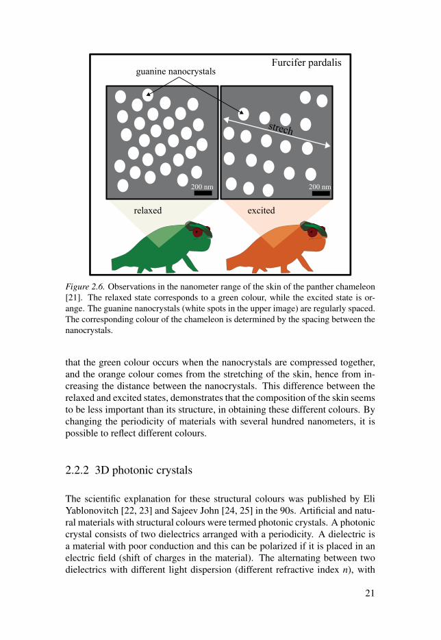
Figure 2.6. Observations in the nanometer range of the skin of the panther chameleon[21]. The relaxed state corresponds to a green colour, while the excited state is or-ange. The guanine nanocrystals (white spots in the upper image) are regularly spaced.The corresponding colour of the chameleon is determined by the spacing between thenanocrystals.
that the green colour occurs when the nanocrystals are compressed together,and the orange colour comes from the stretching of the skin, hence from in-creasing the distance between the nanocrystals. This difference between therelaxed and excited states, demonstrates that the composition of the skin seemsto be less important than its structure, in obtaining these different colours. Bychanging the periodicity of materials with several hundred nanometers, it ispossible to reflect different colours.
2.2.2 3D photonic crystals
The scientific explanation for these structural colours was published by EliYablonovitch [22, 23] and Sajeev John [24, 25] in the 90s. Artificial and natu-ral materials with structural colours were termed photonic crystals. A photoniccrystal consists of two dielectrics arranged with a periodicity. A dielectric isa material with poor conduction and this can be polarized if it is placed in anelectric field (shift of charges in the material). The alternating between twodielectrics with different light dispersion (different refractive index n), with
21

a periodicity in the wavelength-range of the incoming electromagnetic wave(light), creates a selective propagation of the light - the larger the differencebetween the two dielectrics, the stronger the effect on the light.
The electromagnetic wave minimizes its energy by concentrating its field (E)in the high dielectric region (ε), meaning in the high refractive index dielectric.To explain this behaviour, it should be mentioned that a highly dielectric ma-terial experiences easier polarization (an alignment of charged dipoles), facil-itating the propagation of an electric field (E). As light is an electro-magneticwave, the propagation in a highly dielectric material is energetically favoured.In the case of a continuous medium (no difference in ε(r)), the solutions toMaxwell’s equations are a continuum for all frequencies - see equation 2.16.But the introduction of two different dielectrics with boundary conditions (theperiodicity or alternance of the two materials) calls for Maxwell’s equationsto be combined with the Bloch-Floquet theorem (see section 2.3.3 for moredetails). The addition of periodicity (boundaries) forces the solutions to be adiscrete number of continuous functions in frequency, varying with the posi-tion in the material (so on the wavevector k). Thus a selection of propagationoccurs depending on the electromagnetic wave direction and frequency: w(k).Due to the nature of the light-matter interaction, the equation becomes an Her-mitian problem, which implies that propagating waves of different frequencieshave orthogonal fields at all k points. To satisfy the orthogonality of propaga-tion, the first and second allowed frequencies will travel each in one dielectric,the first in the highest dielectric material (higher refractive index) and the sec-ond in the lowest. All in all, because of the imposed periodicity and the natureof the electromagnetic wave, a selection of light frequencies imposes a fre-quency range where no propagation can occur. This creates a forced reflectionof the incoming light - and so a structural colour.
To create an artificial photonic crystal, it is necessary to impose a periodicity(in 1, 2 or 3-D) and to create a dielectric contrast. The periodicity influencesthe allowed and forbidden propagating frequencies the most (in defined prop-agating directions), while the refractive index difference between the two ma-terials has an influence on the width of the forbidden frequency range. Thefabrication of 1 and 2-D photonic crystals is simpler than a 3-D ones, sincethe periodicity has to remain defectless in all directions. The most commonlyused low refractive index material is air (n = 1.0), while high refractive indexmaterials are chosen depending on the fabrication goal.
22

2.3 Band structure2.3.1 Electrons and phononsElectrons
Electrons are charged particules in the sub-atomic range, and as such can bedescribed with a wave-packet, similar to a photon. The elementary quanta ofcharge of an electron can be determined experimentally and the standard valueis e = 1.6×10⁻¹⁹ C. Since electrons are fermions, they obey the Fermi statis-tics (see equation 2.17), which are derived from the Pauli exclusion principle:fermions cannot exist in the same quantum state if brought closely together(bound to a nucleus for instance). This means that electrons in an atom havediscrete levels of energy, which are particular for each type of atom. They areimportant to explain the properties of electrons.Fermi statistics is described by:
n(ε) = 1e(ε−μ)/kT +1
, (2.17)
where n is the probability of occupied state, ε the energy state, μ the so-calledchemical potential, k the Boltzmann constant and T the temperature. Thechemical potential μ can be defined as the equilibrium energy of the system(equivalent to potential energy). At T=0, the chemical potential becomes theFermi level εF , which defines the highest occupied energy level in the atom atrest.
Regarding electronic conduction, there are three different types of material:insulators, metals and semiconductors (SC). Metals are well-known materialsfor conducting electricity, for instance copper and gold; while insulators, likewood or plastics, have a very low conductivity (high resistance). Semicon-dutors have in-between conductivity. Metal-Oxides (MO) are semiconductorswith a metal heart connected to oxygen atoms. All MO have a specific crys-tal structure, meaning that the atoms are arranged in a periodic fashion. Byassembling atoms in a crystal, the common picture that arrises, regarding thespread of electrons in space and energy, is linked to their fermionic nature.
For now, assuming that electrons cannot have similar quantum states (linked toenergy and spin), each electron attached to an atom will experience a quantumconfinement. Carrying out a thought experiment with a particle trapped in apotential well can help figure out the electrical properties of materials. TheShrödinger equation is used to calculate the available energy states for theparticle, and shows that the particle can have a rest energy (E0) with furtherhigher energy states, multiples of (E0). The probability of finding the particle
23

at a specific energy state and specific location in the well, can be derived aswell. The energy of the particle can be expressed using equation 2.18:
E = h2
8ma2 n2, (2.18)
where h is the Planck constant, m the mass of the particle, a the well size andn an integer, the so-called principal quantum number, which determines theenergy level (E0, at n=1, to infinity). It can be seen that the particle mass andthe well size influence the value of the energy but not the number of energystates (taken as infinite, in a case of infinite well).A similar solution can be calculated for a hydrogen-like atom, which possessonly one electron, with the energies in eV defined by equation 2.19:
E = −13.6Z2
n2 , (2.19)
where Z is the number of protons and n the principal quantum number.The principal quantum number is a natural number representing the orbitalnumber of the electrons in an atom, similar to the integer n in the case of aparticle trapped in a potential well. Due to the Pauli principle, different typesof orbitals can be distinguished by the number of electrons they can accomo-date. This shows that energy is needed to change the orbital of an electron andthat adding an electron to the atom can only be done at orbitals with higherenergy. As for the case of a particle in a well, electrons have a spatial probabil-ity attached to their quantum state. There are classification of orbitals whichdepend on their spacial probability, which is linked to the number of allowedstates within the orbital. The most common orbitals in low Z atoms are s, with2 electrons, p accommodating 6 electrons and d allowing 10 electrons. Fig-ure 2.7 shows the associated contour surface defining the volume where theprobability to find an electron is above 90% for s orbital (a), p orbitals (b) andd orbitals (c). The spherical shape of the s orbital shows that the electronsare highly delocalized, while the narrow volume of d orbitals demonstratesthe more localized nature of these electrons. To form molecules, atoms bindtogether by sharing their electrons, creating new molecular orbitals. As moreand more atoms are packed together, the different orbitals are so energeti-cally packed that they are termed bands. The exclusion principle and stackingpreferences still apply, and so materials possess different levels of energy andforbidden electron energy ranges. This forbidden range is called the bandgapand is used to classify materials - and explain the conductivity of metal, semi-conductors and insulators. Figure 6.2 shows the differences between the threetypes of resistors. Metals possess a Fermi level that is always in a band (pos-sible states), and so it is easy to move the electrons in the conduction band -hence, metal are good conductors. Insulators have a high gap in energy, wherethe probability to find an electron with these energy states is close to zero, and
24

Figure 2.7. Probability density above 90% to find an electron in orbital s (a), p (b) andd (c). Note that orbital s is highly delocalized, while d has a narrower volume.
25

Figure 2.8. Difference of energy gap between metal, semiconductor (SC) and insu-lator. The band full of electrons is called the valence band, while the band empty ofelectrons is called the conduction band.
so it is difficult to introduce electrons in the conduction band. Semiconductors(SC) have an in-between situation, with the Fermi level situated in the bandgap, which allows electronic circulation under specific circumstances. Theband of energy state full of electrons at 0 K is called the valence band andthe band empty of electrons is called the conduction band. Electrons tightlybound to the nucleous are termed core electrons.
Phonons
Phonons are quasi-particules and are made of collective vibrations in a solid.They are associated with heat, and usually the number of phonons increaseswith temperature. Phonons propagate in the material with a defined frequency(w), direction of vibration (longitudinal or transverse) and vibrational mode(atoms vibrating in-phase or out-of-phase). Phonons can scatter electrons orbe absorbed by them. At 0 K, the probability to find a phonon is close tozero. They are bosons, and as such follow Bose-Einstein statistics, shown inequation 2.20:
n(ε) = 1e(ε−μ)/kT −1
, (2.20)
where n is the number of particles, ε the energy state, μ the chemical poten-tial, k the Boltzmann constant and T the temperature. The difference betweenfermions and bosons, is that bosons can have an unlimited number n in thesame quantum state.
26

Figure 2.9. Miller indices examples, withplanes (100) in yellow, (200) in green and(111) in blue. The directions in the crys-tal, if cubic, are defined by [hkl] and areperpendicular to the (hkl) planes.
Figure 2.10. First Brillouin zone for aface-centered cubic crystal lattice withhigh symmetry points.
2.3.2 Electronic band structure
Semiconductors have a crystal structure, which is formed using a unit (set ofatoms) repeated regularly (lattice). Lattices can be classified into 14 Bravaislattices on the basis of a 3-dimentional shape. Using this classification, it ispossible to define directions in the crystals and lattice planes using the Millerindices (h, k, l), as illustrated in figure 2.9. The directions [h, k, l] are perpen-dicular to the planes (h, k, l), for cubic crystals. These indices are common forall crystals and are used to position high symmetry points.Since a crystal is a repetition of a pattern, to facilitate calculations the recipro-cal space is used. Thus distances are inverted in real space, with the distancea (dimension m), becoming 2π/a (dimension m−1). In this space, the latticeplanes are represented by reciprocal lattice points. Furthermore, momentumis represented by a vector (k) in reciprocal space. To vizualize the electronicbands of a crystal, a 4-dimensional plot would be necessary: involving thethree spacial dimensions and energy. To allow graphical representation, it iseasier to do calculations of electrons energy states in reciprocal space, whichresults in the plot of the energy versus momentum. This is called a band struc-ture plot. In addition, since the crystal is a repetition of the same pattern, adefinition of minimum reciprocal space needed to determine all possible elec-tronic states is called Brillouin zone. If a 1 dimensional crystal has a latticeconstant a, it has a reciprocal lattice constant 2π/a and the Brillouin zone ex-
27

Figure 2.11. Schematic of anatase TiO2 first Brillouin zone, with specific symmetrypoints, as the center of the Brillouin zone Γ, M at the surface facet and X at an edge.[26, 27]
tends from −π/a to +π/a. The momentum values can even be halved, sincethe Brillouin zone is symmetrical by definition, so that calculations can bemade in the irreducible reciprocal space, from 0 to +π/a.Crystals possess symmetry and this can be used to limit the number of cal-culations needed to plot the band structure of the material, by, for example,choosing high symmetry points and specific directions (between symmetrypoints). The symmetry points of the Brillouin zone of a face-centered cubic(fcc) crystal are shown in figure 2.10. The center of the Brillouin zone iscalled Γ, X and L are in the center of the surface, while K, W and U are on theedges. The distance between the symmetry points is known and depends onthe reciprocal lattice constant.
The bandstructure, which can be measured or calculated, is used to classifytwo types of semiconductors. If the smallest bandgap in the SC is in thesame position in the reciprocal space, the bandgap is called direct, while ifthe smallest possible gap between the valence band and conduction band isin another position, the bandgap is indirect. Typical metal oxides, titaniumdioxide (TiO2) and zinc oxide (ZnO), have an indirect and direct bandgap re-spectively.Titanium dioxide can be found in three different main crystallographic forms:brookite, anatase and rutile. The last two forms are similar, and can be de-scribed as chains of TiO6 octahedra, but oxygen-titanium distances are shorterand titanium-titanium distance are longer for the anatase form. This meansthat the band structures of the three different crystallographic forms of titaniaare different. The band structure of anatase (TiO2) is presented in figure 2.12,in different crystallographic directions (Γ-X-R-Z-Γ-M-A-Z), with symmetrypoints shown in figure 2.11. The top of the valence band defines the zero en-ergy level. The conduction band is situated above the band gap, shown in redin the figure. The smallest gap is an indirect transition from the valence band
28

Figure 2.12. Schematic of anatase TiO2 band structure, with the bandgap in red be-tween the valence and conduction bands. The smallest gap is an indirect transitionfrom the valence band at M to the conduction band at Γ.
at M to the conduction band at Γ. The chemical bonding of anatase TiO2 isdisplayed in figure 2.13, with the participation of Ti and O electrons in thecreation of new orbitals in the crystal. The absence of an electron in an orbitalor a band is identified as a quasi-particle, termed hole, which has the elemen-tary charge of +e. The density of states (DOS) represents the number of statesper energy interval in the valence and conduction band. This is usually calcu-lated around the band gap and contributions from the different orbitals of theatoms in the crystal can be isolated. Figure 2.14 shows the total and projectedDOS for anatase. It can be seen that the conduction band is predominentlymade from the 3d-orbitals of Ti (Ti eg and Ti tg). The valence band is mainlyformed with the 2p orbitals of O. Defects and impurities in the crystals cancreate available states in the band gap. Introducing impurities volontarily iscalled doping.
The bandgaps of SCs are in the energy range 0.5 - 5 eV, corresponding to 248- 2480 nm. This means that SCs can absorb photons in this energy range,an electron from an occupied state in the valence band is excited to an unoc-cupied state in the conduction band by a photon (interband transition). Thisprocess promotes an electron at higher energy, leaving in the valence band ahole. These transitions can either be direct (conservation of the momentum) orindirect (change of momentum). To change momentum, the electron needs to
29

Figure 2.13. Schematic of anataseTiO2 building of molecular orbitals(MO), from the atomic orbitals (AO)of Ti and O. The core electrons are dis-played in yellow, the valence electronsin orange and the conduction electronsin green. The first MO in the conduc-tion band is mostly composed of Ti dorbitals. The valence electrons of Tiand O are displayed in the upper cor-ner. [28]
Figure 2.14. DOS of anatase TiO2,total (black, top) and projected forTi atoms (blue, middle) and O atoms(purple, bottom). The top of the va-lence band defines the zero energy.The red band shows the bandgap. Theconduction band is composed mainlyof Ti d electrons. [29]
30

absorb a phonon. The transitions depend on the coupling between the valenceand conduction bands, so not all transitions are allowed. Direct interbandtransitions have a higher probability, since indirect transitions are three-bodyinteractions (photon-electron-phonon). Therefore, direct bandgap SC has ahigher absorption rate than indirect band gap SC - which means that it is oftenexposed to photocorrosion (spontaneous destruction under illumination).
2.3.3 Light band structure
As seen earlier, the forced periodicity into a material has an influence on thetype of allowed light propagation. This is very similar to the case of electronsin a crystal: the regularly spaced nucleous, and the nature of the electrons(fermions), leads to the fact that electrons in the material have discrete energylevels. The plot of the different allowed frequency versus the wavevector k
creates a band structure for the light in a photonic crystal.To account for the alternation of materials with two different refractive indices,imposing boundary conditions (there are two different types of material withdifferent refractive indices, i.e. different phases) and periodicity, the Floquet-Bloch theorem is used within the Maxwell formalism as shown in equation2.21:
H = ei(k⋅r−wt)Hk, (2.21)
where Hk is a periodic function of position and k the wavevector. A periodicfunction H(r) follows equation 2.22:
H(r+G) =H(r), (2.22)
where G is a primitive lattice vector (the periodicity).The important aspect of the Floquet-Bloch addition, is the perfect periodicity.In this respect, the best 3-D photonic crystal has the exact same periodicityin different directions. When it comes to electrons, it is preferable to derivethe light band structure (the probability of finding light propagation at certainenergy) in the reciprocal space. Similarly, the light band structure for a 3-Dphotonic crystals is made by calculating the different w(k) and plotting themin strategic symmetry points in the reciprocal space, in the first Brillouin zone(BZ). In parallel to semiconductors, the frequency range forbidden in the ma-terial is called a photonic band gap (PBG). The higher the contrast betweenthe two dielectrics is, the stronger the periodicity effect is - and so the differ-ent bands (w(k)) are separated by a frequency gap, a photonic band gap. Toobtain an omnidirectional gap (in all k), the photonic band gap at all k shouldbe derived from the same frequency bands (upper and lower frequency bands),thus existing in the whole BZ. A strong dielectric difference ensures this over-lapping of the local photonic band gap by making it large. The closest to aspherical BZ- and so the most symmetrical - is generated by a crystal lattice
31

Figure 2.15. Illustrations of Bragg law’s in a crystal with spacing d between atomicplanes and an incoming light beam at an angle θB from the planes (left) and Snelllaw’s describing the change of direction for a light beam arriving at an angle θ1 fromthe normal at an interface between two materials with different refractive indices nX .
configuration called face-centered cubic (fcc). The most likely 3-D photoniccrystal should therefore exhibit an fcc structure in real space to obtain a com-plete photonic band gap [30], since the corresponding BZ is highly isotropic.
The fcc structure is an ordered close-packed structure of spheres. The close-packing means that for a cube with a volume equal to 100% - 74% of the spaceinside it is occupied by beads. It is a very common packing system for crys-tals, where atoms are fcc arranged, because it is an ideal packing of spheres,which creates the lowest void volume (filling factor of 0.74). It is possible toidentify three layers of stacking that are repeated in sequence: ABCABC... Itis energetically favorable for grouping spherical objects in space [31].
To some extent, it is possible to use Bragg-Snell’s law (2.24) to determine theposition of the photonic band gap (PBG). It derives from the combination ofBragg’s law (2.23) and Snell’s law (2.6), the first to take into considerationthe ordered structure and the second to implement the change in refractiveindices. Bragg’s law describes the interaction of a wave with a crystallineobject; it is often used to describe the X-ray diffraction pattern from a crystal.It determines constructive interferences of the diffracted waves. An illustrationof the law is displayed in figure 2.15, and can be written as:
2dsinθB = nλ (2.23)
where d is the distance between planes, θB the Bragg angle (from the planes), nthe order and λ the light wavelength. The Bragg-Snell law ignores absorptioneffects and considers both refractive indices and incidence angles to determinethe reflected wavelength.
λ = 2dxxx
√n2
e f f − sin2 θ , (2.24)
32

where dxxx is the distance between the planes (XXX), ne f f the refractive indexof the whole structure and θ the angle of incidence onto the surface of thematerial (from the normal). In the case where the close-packed (111) planesare parallel to the top interface (so in the [111] direction):
d111 =D×√23, (2.25)
where D is the periodicity or lattice constant, d111 the distance between the(111) planes in the crystal.The expression of ne f f is valid for materials with real refractive indices, usingequation 2.26:
ne f f =∑i
ni× fi, (2.26)
where n is the refractive index and f the filling factor of material i. If the ma-terial absorbs in the wavelength range of the photonic band gap, the refractiveindex becomes complex, and the Bragg-Snell law loses accuracy. If experi-mental data are available on the photonic band gap, it is possible to introducethe value of the real part of the refractive index of the absorbing material inequation 2.26 to increases equation 2.24 predictability.
Some differences of interpretations have to been made between an electronicband structure and a light band structure. As photons are bosons, all allowedfrequency states in the materials can be occupied - the band gap does notdelimit occupied and unoccupied energy states as for an electronic band struc-ture. Figure 2.16 shows a typical photonic band structure, with a high refrac-tive index difference, obtained at different symmetry positions in an fcc crys-tal, for a periodicity D and a light wavelength λ . The first band gap (PBG1, inyellow) is a local photonic band gap, between Γ and L, while the second bandgap (PBG2, in orange) is a complete photonic band gap in all probed directions(no propagation allowed). The bands below and above the complete photonicband gap are all allowed states. This means that light of these wavelengths canpropagate in the material in the specific direction.
Calculations of the band structure and optical spectra of artificial photoniccrystals can be made using the free MEEP program (MIT, Cambridge, U. S.A.) [32].
33

Figure 2.16. Schematic of a typical 3-D photonic material. The first band gap (PBG1,in yellow) is a local PBG, between Γ and L, while the second band gap (PBG2, inorange) is a complete photonic band gap in all probed directions (no propagation al-lowed). The periodicity a of the material is related to the wavelength λ of the light, asseen in equation 2.24
2.4 Photonic effects2.4.1 Total reflection
The photonic band gap (PBG) is by definition a forbidden energy range forwhich light cannot propagate in the photonic material - in other words, thelight is reflected by the material (observed by the eye/detector). As seen insection 2.1.2, it is possible to record the spectrum of light, to record the in-tensity I versus wavelength λ . Recording the spectrum of light allows themonitoring of light-matter interaction. Two geometries can be used: recordthe light intensity directly behind (in transmission T) or in front of (in reflec-tion R) the illuminated material. The variations in intensity, normalized to theoriginal light source, give insight into light-matter interaction. As a result of aphotonic band gap, part of the light is reflected by the photonic crystal - cre-ating a peak in the reflection spectra, which does not appear on a similar butdisordered material. For a perfect photonic crystal, with a complete photonicband gap, all the incoming light of the photonic band gap energy is reflected:the light intensity measured in front of the material is the light intensity ofthe source. Following a simple reasoning of energy conservation, the light in-tensity measured after the material has nothing to do with the light intensityof the source. Around the photonic band gap, the normal light-matter inter-action linked to the material nature prevails, and for a transparent material,the light intensity measured before the material is very low while the inten-sity measured behind the material is high (some absorption always occurs).By convention, the photonic band gap energy range is termed photonic bandgap width, while the middle of the width corresponds to the photonic band
34

Figure 2.17. Theoretical light spectra of a light source I0 measured before (reflection,right) and after (transmission, left) a transparent material, without order (a) and witha PBG (b). The PBG width and PBG position are marked in red (transmission) and inorange (reflection).
35

Figure 2.18. Graphical representation of a Gaussian curve, associated with an im-parfect photonic crystal, with PBG position in red and full-width-at-half-maximum(FWHM) in yellow.
gap position, as calculated by the Bragg-Snell law (equation 2.24). Figure2.17 shows the effect of the photonic band gap on the transmission and reflec-tion spectra of a disordered transparent material. Without order, low reflectionoccurs and the transmission is high - whereas with the same material with aphotonic band gap, the intensity of the light within the photonic band gap ishighly reflected, so that transmission dropped very low.
If the photonic crystal is not perfect, the photonic band gap width is not con-stant in all directions over the wavelength range. In consequence, the T andR spectra do not present square-shape line spectra in the vicinity of the pho-tonic band gap, but a bell-shaped line (close to a Gaussian curve). The def-inition of the photonic band gap position becomes the maximum (for R) andthe minimum (for T) of the bell-shaped curve. To calculate appropriately thephotonic band gap width, the full-width-at-half-maximum (FWHM) is used.The FWHM is the value of the spread of the bell-shaped curve at its middleheight, as displayed in figure 2.18.
2.4.2 Slow down of the light
A particular effect of the existence of the photonic band gap can be found at itsedges. The higher energy edge (higher frequency) is labeled blue edge, whilethe lower energy edge is the red edge. At the edges of the photonic band gap,the band structure is locally flat (on the small energy interval below and abovethe photonic band gap) - thus for a constant frequency (w), the wavevector (k)is the same. The consequence of this can be understood by considering thegroup velocity of light. The group velocity (Vg) can be defined as the velocityof the envelope of a wave packet propagating through space - here, light with
36

a frequency in the vicinity of the photonic band gap propagating in the mate-rial. Equation 2.27 defines the speed of a wave package by the fluctuations offrequency through fluctuations of wavevector, at a specific direction:
Vg = ∂w∂k⋅ (2.27)
Equation 2.27 is the partial derivative of the function w(k), and since w isconstant other the variation of k in the photonic band gap range, the derivativetends towards zero. In other words, the group velocity of light in the vicinity ofthe photonic band gap tends towards zero. The implication is that light speed(propagation) in the material is reduced, the light is slowed down. The effectis strong enough to be measured experimentally, by using femto-second laserpulses [33].
This remarkable effect of the photonic band gap can be found at the interfaceof the two dielectric materials composing the photonic crystal. Light in thevicinity of the photonic band gap undergo multiple reflections at each inter-face between the two materials. These multiple reflections can lead to theformation of a standing wave: a wave with a group velocity close to zero. Thelight is efficiently trapped by the material and the overall light path length isincreased.
2.4.3 Fragility of the photonic band gapThe photonic effects depend heavily on the peridiocity of the crystal. Li andZhang have calculated the effect of disorder in a photonic crystal composedof stacked spheres [34]. Differenciation between two sources of disorder wereanalyzed, the variation of sphere position (site randomness) and in sphere di-ameter (size randomness). Simulations show that photonic crystals are morefragile because of their size randomness than site randomness. In addition,fluctuations under 2% of the crystal periodicity close the photonic band gap,even for crystals with a high refractive index contrast - destroying any photoniceffects.
2.4.4 State of artAt the beginningThe first observations of play of colour were unsurprisingly made on colloids,which are suspensions of spheres in a liquid medium; usually the sphere wasin the micrometer range [35–37]. The most common method for immers-ing and ordering the spheres (silica, polystyrene and such) was the use of
37

the Langmuir-Blodgett technique [38, 39]. It consists of a trough with mo-bile floating arms (barriers) and a pressure sensor. To induce close-packing,beads are placed on the surface of the liquid and forced packing occurs bymechanically approaching the barriers until a set pressure is reached. It wassoon noticed that sphere stacking was preferentially in fcc [40], and this wascalled self-assembly [41, 42]. Analyses of the colloids aggregation were made[43–47] and self-assembly became the stepping-stone for building artificialphotonic crystals [48–51].Not all photonic crystals were made using colloids, as the crystals could beetched [52], built layer-by-layer by stacking dielectric materials [53] or byforced templating of colloids [54].
The bloomAfter the wave of simulations of photonic crystals [30, 55–58], experimentswere caried out using high refractive index materials. The creation of inverseopals, photonic crystals created from a sacrificial templated opal, was the keyto the multiplication and the increased complexity of photonic structures [59,60]. The Wijnhoven paper is often cited, as it demonstrateds the fabricationof an inverse opal with titania, using colloids of different diameters [61]. Newtechniques and new types of inverse opals were implemented and used [62–67].
Beyond the photonic effectThe next step was to use the properties of the photonic crystals [68–70], fromphotonic bandgap tuning [71], telecommunications [72], solar cells [73–75],magnetism [76], diodes [77], and photocatalysis [78–82].
Personal analysisSeveral fast-building techniques have been put forward regarding polystyrenetemplating, notably the spin-coating[83, 84], the doctor-blading[85] and drop-dry[86, 87] techniques. The doctor-blading technique consists of taping eachside of a substrate, adding a drop of the solution and sweeping it with a glassslide along the tape. The drop-dry technique is depositing a drop of solutiononto the substrate and letting it dry on a horizontal substrate. These tech-niques, however fast, provide only very small photonic areas. A much betterway of producing templates is volume dip coating (VDC)[69, 88], where asubstrate is dipped into the solution and withdraw at a determined speed. Theadvantages of this technique are multiple: the withdrawal speed allows thecontrol of the deposition thickness for a fixed solution concentration and theuniform withdrawal speed gives a uniform opal. The disadvantages are, how-ever, the need for a higlhy concentrated solution and the limit in productionnumbers (at the laboratory scale).The deposition of metal oxide on the template is a critical part of the inverseopal fabrication. The most common method is sol-gel deposition [89–91],
38

which is a chemical reaction, with gelification of a metal oxide in contact withwater vapor. But to obtain a crystalline sample, supplementary heat-treatmentis needed. The advantage is mostly that no tool is involved in the deposi-tion and that several depositions can be made at a time. The only problemis that control over the deposition is limited and the wet chemistry can be in-compatible with the template. Another way to reduce the number of steps tocreate inverse opals is co-deposition[92–94], which consists of self-assemblyof beads of different size and composition. The main idea is to use a solutionof polystyrene or silica spheres hundreds of nanometers in diameter, and tomix in a few nanometer in diameter metal oxide nanoparticles. The obviousadvantage is the reduction in the number of steps in the production of the pho-tonic crystals and the "on the bench" technique, requiring no specific tool, asfor the sol-gel method. This technique is however difficult to use, especiallythe creation of a well-mixed and stable solution of two different beads.
39

3. Photocatalysis
C’était quand la dernière foisqu’on s’est retrouvés tousd’accord sur un truc!?
Alexandre Astieras Arthur Pendragon in Kaamelott
3.1 Definition and general theory3.1.1 Catalysis and photocatalysis
A chemical reaction is obtained when chemical products change and/or dis-appear with time, and a final new stable product is found, under specific con-ditions (concentration, temperature, pH...). Depending on the stability of theoriginal chemical reactants, the chemical reaction kinetics can vary: stablechemicals will react slowly so to overcome the stability of the reactants, en-ergy need to be provided. However, some reactions are not energetically fa-vorable: there is a substantial energy barrier. The energy needed to force thereaction in a specific direction is high, and so drastic reaction conditions areused. A catalysis can be used to reduce the energy barrier and create eas-ier reaction conditions. A catalysis is therefore defined by a chemical reactionperformed on a catalyst. A catalyst is a material that accelerates the kinetics ofa reaction while remainig unchanged before and after the reaction. A schemaof the energy barrier for a reaction of products A and B, forming product C,with and without the use of a catalyst is shown in figure 3.1.
Photocatalysis is similar to catalysis, but the catalyst (photocatalyst) is used ina photo-reaction. A photo-reaction is the change of a reactant after absorptionof a photon. The photocatalyst absorbs a photon with an electron, which be-comes excited at higher energy and can interact with the reactants, transferringthe excess energy via the excited electron. The remaining hole can receive anelectron from the reactant on the catalysist surface. Similar to catalysis, pho-tocatalysis help to overcome the activation barriers. The photocatalyst remainun-changed after the reaction.
40

Figure 3.1. Schematics of a chemical reaction between products A and B, finalized byproduct C - without (black) and with (green) a catalyst.
3.1.2 Heterogeneous photocatalysis
Heterogeneous photocatalysis involves the use of a solid and its surface tocreate and break molecular bonds. The surface of the photocatalyst is an im-portant parameter, since reactants need to be in close proximity for the energyexchange to occur. The adsorption of molecules occurs on the surface andeach position where a molecule can be adsorbed is called a site. Two typeof adsorption can occur: physisorption and chemisorption. Physisorption is aweak bonding (Van der Waals forces), with no significant change in the elec-tronic density; while chemisorption is a strong bonding (a chemical bond),where the electronic density is significantly changed (exchange and sharringof electrons). There is an activation barrier for adsorption, which is influencedby the type of surface (open, flat, rough...), the type of medium (gas, liquid),the geometry and size of the molecule (angular orientation, bond length...) -and as such, an energy barrier for desorption also exists. The photocatalyticefficiency of a photocatalyst is therefore dependent on light absorption andmolecule adsorption capacity (electronic property and geometry of the photo-catalyst).
As described in section 2.3, molecules possess discrete energy levels formedby association of electronic orbitals of single atoms. The highest occupiedstate is termed HOMO and the lowest unoccupied state is LUMO - similarlyto the valence and conduction band of an SC, respectively. The relative po-sition of the molecular orbitals to the photocatalyst energy bands determinethe type of chemical reaction that can occur: the molecule receives an elec-tron (reduction) or/and gives away an electron (oxidation). The electron trans-fer favors the lowest final energy state, for both the chemisorb molecule andthe photocatalyst. The products of each reduction and oxidation processesare called redox couples. A standardization and classification of oxidation-
41

reduction processes is obtained by measuring the potential of each reactionagainst a reference electrode (electrochemisty). The standard hydrogen elec-trode (SHE) defines the potential zero (0V). The energy of a redox couple canthen be compared to the photocatalyst energy bands. A reduction reaction willbe driven only if the conduction band is higher than the redox potential andan oxidation reaction occurs only if the valence band is lower than the redoxpotential.
3.2 Semiconductor photocatalysis3.2.1 Definitions
The reactant concentration and photocatalyst surface area is expressed by thecoverage parameter θ , which is defined with equation 3.1:
θ = Number o f adsorbed moleculesNumber o f sites
, (3.1)
where the number of sites can be obtained from the maximum area occupiedby one adsorbant relative to the total surface area of the photocatalyst. Thenumber of adsorbed molecules can be obtained only from experimentation.
Degradation of the adsorbant A ( concentration or number of adsorbant molecules)with illumination time t is termed degradation rate (r). The photodegradationof A follows a differential rate law, seen in equation 3.2:
r = −dAdt= k[reactant]n, (3.2)
where k is the degradation rate constant and n the order of reaction. The reac-tion can be zero, first, second or third order, with n =0, 1, 2 or 3 respectively,and so the degradation rate constant can be zero (r = k), first, second and thirdorder constant.A zero order reaction rate is unvariant with concentration and rate constantcan be extracted from the slope of the plot of the measured adsorbant concen-tration versus time (linear plot).For a first order reaction, the differential law becomes equation 3.3, with reac-tant concentration measured between time t=0 and t:
∫ At
A0
dAA= −k∫ t
0dt,
ln(At) = ln(A0)−kt ⋅ (3.3)
To extract the rate constant, the plot of ln(A/A0) versus time leads to a straightline, with a slope equal to −k.
42

3.2.2 Mechanisms
Photon absorption has a varied cross-section depending on the material, lightwavelength and polarization. The absorption of a photon is local and very fast(femtosecond domain) and involves a transition of an electron to a higher en-ergy level or phonon creation. The small momentum of photons implies thata very small change of momentum occurs if an electron absorbs light, as themomentum of electrons is much greater than that of a photon. With this extraenergy, the electrons are then in an excited state.Several phenomena can happen after the absorption of light by semi-conductor:creation of an electron-hole pair and its separation; creation of an electron-holepair and its recombination (non-radiative transition: energy loss through heat,occuring in a few nanoseconds and radiative transition: re-emission of a pho-ton of lower energy) and finally trapping of the electron in an intermediatestate. Depending on the material, the recombination rate will be high (directband gap material) or the creation of an electron-hole pair low (indirect bandgap material). A hole is like a positive version of an electron and it is consid-ered as a particle and conducts in the valence band. Both electrons and holesare mobile and this is how metal oxides conduct. The radiative recombinationof an electron and a hole will produce a photon whose energy will match theexcess energy.Direct band gap materials have a high probability of light absorption and cre-ation of electron-hole pairs. This is unfortunately accompanied by a highrecombination rate. Indirect band gap materials have a lower probability ofsuccessful light absorption. Due to the shape of their band gap, an extra par-ticipant is required for an electron to absorb a photon. In fact, electrons inindirect band gap materials need both extra energy and momentum to reachan excited state. As was stated earlier, the momentum of light is not enoughfor an electron. Phonons on the other hand have similar momentum. Phononsare collective oscillations of the atoms in the material and are often treated asquasi-particles. To be promoted to the conduction band of an indirect band gapmaterial, an electron needs to absorb both photon and phonon. This is why theprobability of light absorption is lower than that of a direct band gap material.The advantage is reciprocal: the recombination rate is also lower than that ofa direct band gap material.The major problem of light absorption lies not in the electron-hole pair for-mation (the excitation of an electron), which happens within a few fs; but inthe competition between e-h recombination (tens to hundreds of ns) and thecharge transfer from the SC to the adsorbate (hundreds of ns up to ms scale);as displayed in figure 3.2. The charge carriers can also be trapped by local de-fects in the SC (crystal lattice variation, missing atoms, intruding atoms) andat the surface (steps, edges, vacancies, inert adsorbate). Depending on the typeof trap, the time scale can vary from hundreds of ps to hundreds of ns. The
43

Figure 3.2. Illustration of the time scale after photon absorption in an SC: electron(e) - hole (h) pair creation (dark blue), e and h trapping (purple), e-h recombination(magenta) and charge transfer to an adsorbate on the surface (orange). Uncertaintieson the time scale, which can vary experimentally [95–97].
trapped potential energy is lower for surface traps, so that it is energeticallyfavorable for the charge carriers to be transported towards the surface.
Both electrons and holes have a role in photocatalysis. Excited electrons thatreach an adsorb molecule (acceptor) can reduce it, and holes can receive elec-trons from an adsorb molecule (donor). An illustration of the basic semi-conductor photocatalysis is shown in figure 3.3. Simultaneous oxidation andreduction reaction at the surface ensure charge neutrality of the photocatalyst.Often, photocatalysis proceeds by several intermediate steps, and so interme-diate species are present on the surface of the catalyts, which in turn react withother more complex molecules. The most present molecules at room temper-ature and pressure are water (H2O) and oxygen (O2), and it has been shownthat only simple photodegradation can occur in the absence of either [98–102].Surface water can accept a hole, creating a highly reactive hydroxyl radical(⋆).Equation 3.4 shows the mechanisms for the creation of the hydroxyl radical⋆OH, after the trapping of a photogenerated hole by an oxygen atom of anMO:
M−O+hν →M−O⋆+H2O→M++2⋆OH, (3.4)
where M is the metal atom of the MO, ⋆O the oxygen atom of the MO withthe excited hole and M+ the positively charged metal atom.As for the role of O2 in photocatalysis, it is the reduction to a superoxide ionO⋆−2 [103], following the reaction described in equation 3.5:
O2+e−→O⋆−2 ⋅ (3.5)
In an acidic environment, hydrogen peroxide (H2O2) can be created from bothan oxidation of water and a reduction of the superoxide oxygen ion, following
44

Figure 3.3. Illustration of the major processes in a semiconductor, as light is absorbed.When a photon is absorbed, an electron-pair is created: the charges can undergorecombination (volume and surface) or reach the surface and react with chemisorbspecies. Electrons are noted as ⊖ and holes as ⊕.
equations 3.6 and 3.7:
O⋆−2 +H+→HO⋆2H++O−2 +HO⋆2 →H2O2+O2,
(3.6)
O⋆−2 +2H++e−→H2O2⋅ (3.7)
Furthermore, hydroxyl radicals can be obtained by reduction of H2O2, withthe donation of an excited electron by the photocatalyst. All in all, the hy-droxyl radical ⋆OH, the superoxide ion O⋆−2 and H2O2 are created by bothoxidation and reduction of surface water and oxygen directly by the photocat-alyst, following photon absorption. These species can then oxidize and reducea large number of different molecules[104–108], bacteria[109], oil spills[110]and even cancer cells[111].
Photocatalytic activity is influenced by pH, temperature and humidity, lightpower and coverage (initial reactants concentration) [97, 112, 113]. As seenealier, a more acidic environment leads to the increased formation of hydro-gen peroxide - which is a good intermediate for the decomposition of organicmaterials, but the influence on the activity is not straightforward, as it canvary depending on the material. The role of temperature and humidity is more
45

known, as the presence of water vapor greatly influences the photocatalyticactivity. At low a temperature and humidity, the photocatalytic activity drops.Light power has different effects on different photocatalysts [114], but threestages of power can usually be identified: too low power where the activ-ity increases linearly with increasing power; at the second power stage, thephotocatalytic activity grows with the square root of light power; finally, thethird stage defined by the saturation of the photocatalyst, with a constant ac-tivity - or even sometimes a decrease of activity as the residual products of thedegradation have not desorbed and do not allow the absorption of further pol-lutants. Finally, the initial coverage of the photocatalyst could have an effecton the photocatalytic activity, as if all adsorption sites are occupied, radicalscan be created and the activity relies solely on direct charge transfer betweenthe catalyst and the reactant. The influence of the effect of concentration is nottruly understood, as inhibition of the photocatalytic active sites due to adsor-bate reaction products blocking the charge tranfer, called deactivation. Severalexperiments have reported photocatalytic activity with several multilayers ofsimple molecules [115], or even several micrometer away from the actual cat-alyst surface [116].
3.2.3 Transition metal oxides
A good photocatalyst has to be photoactive, absorb light in the visible andnear UV range (to use direct sun light or indoor lightning), biologically andchemically inert (to not be degraded); but also, ideally, cheap, abundant andnon-pollutive. The best natural photocatalysts, so far, are transition metal ox-ides. Transition metal oxides are often semiconductors, with a transition metalheart surrounded by oxygen atom(s). A transition metal is an element with apartially filled d sub-shell, meaning that their valence electrons are composedof at least some d electrons. The most common transition metals are tita-nium, iron, manganese, copper and zinc as all can form MO with differentoxygen coordination. The presence of d -like bands in the MO crystals is thekey to their photocatalytic activity. As seen in section 2.3.1, d orbitals arehighly localized, meaning that the band structure generated by these orbitalswill be almost constant over the Brillouin zone (flat bands). Depending on thecrystal structure, at the surface of the MO different geometry can be found,where the stochiometry differs from the bulk. Due to this difference in thebulk, electronic states at the surface will be different than in the bulk. Thesurface states are either partially filled with electrons, or close enough to theconduction/valence band, so that an absorbed species can receive or donate anelectron to the surface state. For MO with partially filled d-bands, the surfacestates are close to the conduction or valence band. Thus surface metal atoms inMO are traps for photogenerated electrons and holes, and can therefore trans-
46

Figure 3.4. Position of the valence and conduction band of TiO2, Fe2O3 and ZnO vsNHE. Redox potentials for water splitting (blue), radicals generation (green) and otherspecies generation (black). All at pH=0.
fer photogenerated charges to adsorbed species.The valence and conduction bands of different MOs are displayed versus NHE(Normal Hydrogen Electrode - the experimental equivalent to the theoreticalSHE), as well as redox couples for water spliting, radicals and H2O2 genera-tion, in figure 3.4. The conduction band of the MO has to be above the lowestunoccupied molecular orbital (LUMO) of the acceptor molecule to create areduction reaction and the valence band has to be below the highest occupiedmolecular orbital (HOMO) of the donor molecule to drive an oxidation reac-tion. The conduction band of TiO2 is above the conduction band of Fe2O3, soTiO2 possesses a stronger reduction potential, while the valence band is at thesame energy level, so the oxidation potential is the same.
TiO2
Titanium dioxide is a natural mineral that can be extracted from ilmenite(FeTiO3) and is a wide-band gap n-type semiconductor. The appearance ofTiO2 powder is white, hydrophobic and fluffy[117]. As the refractive indexof this metal oxide is high and non absorbing in the visible[118], it has beenused as a pigment in paint, food, cosmetics and toothpaste. It is also used insuncreams for its capacity to absorb UV light. Some other applications canbe associated to this capacity, notably its photocatalytic effect. Titanium diox-ide can be found in three different main crystallographic forms, the anataseform being the most used in photocatalysis, since it has been shown to have
47

higher activity than the rutile form. Both forms are similar, and can be de-scribed as chains of TiO6 octahedra, but oxygen-titanium distances are shorterand titanium-titanium distance is longer for the anatase form. This affects theband structure of the metal oxide and therefore the band gap. Anatase TiO2has an indirect band gap of around 3.2eV. It is possible to dope with metals,such nitrogen, to increase the light absorption of the photocatalyst in the visi-ble range.As shown in figure 3.4, the electronic band edges of titanium dioxide are wellplaced: the valence band is situated below the oxidation potential of waterwhile the conduction band is just above the reduction potential of water. Sincewater plays a major role in the photocatalytic process, it can be seen from theenergy diagram that TiO2 has a strong photocatalytic effect. The reduction po-tential (H+/H2) is just below the conduction band and the oxidation potential(O2/H2O) is above the valence band of anatase.
Fe2O3
Iron (|||) oxide is one of the main oxides of iron which can be found naturallyin hematite. The colour of α −Fe2O3 powder is deep red and therefore it isalso used as a pigment (for instance in Falu red paint). But most commonly,it is used for industrial steel and iron production. The only phase that is usedas a photocatalyst is the α −Fe2O3, which is rhombohedral corundum. Ithas an indirect band gap of around 2.2eV. This metal oxide is not used asoften for photocatalysis as TiO2, with a similar solar corrosion resistivity astitania, if nano-structured, but having a lower oxido-reduction potential andholes length diffusion, as can be seen in figure 3.4. This is due to the positionof its valence band edge below the reduction potential of water; only holes willbe transferred to water chemisorb on the surface. Of course, any acceptor witha lower potential than the conduction band will be able to accept electrons;this is why Fe2O3 can nonetheless be used as a photocatalyst.
ZnO
Zinc oxide can be extracted from calamine, which is an ore of zinc, but itis usually chemically fabricated or derived from metallic zinc. It is a whitepowder with a refractive index of 2 and, as TiO2, is used as a pigment andUV light absorber. ZnO is often in hexagonal wurtzite. It has a direct bandgap of around 3.4eV. The position of the ZnO valance band and conductionband is similar to those of TiO2, as shown in figure 3.4. ZnO is, however, lesscommonly used as its direct band gap makes it vulnerable to photocorrosionthrough photogenerated holes.
48

Figure 3.5. Schematics of the Methylene Blue (MB) molecule.
3.3 Degradation mechanisms3.3.1 Methylene BlueMethylene Blue (MB) is synthetic basic dye (C16H18ClN3S), with a thiazolearomatic ring combined with two benzene rings, as displayed in figure 3.5.Methylene blue is a dark blue powder and is soluble in water (43.6 mg/L at25○C).
Degradation mechanics
The adsorption equilibrium of Methylene blue on TiO2 follows a Langmuirisotherm [119, 120], thus the plot of the adsorbate concentration versus solu-tion concentration follows equation 3.8.
θ = KadsC1+KadsC
, (3.8)
where θ is the surface coverage, Kads the equilibrium rate constant and C theinitial concentration of the molecule. The saturation coverage θsat is deter-mined at the adsorption equilibrium.The degradation of Methylene blue follows the mineralization process (or-ganic to inorganic) [121, 122] described in equation 3.9:
2C16H18N3S++51O2→32CO2+6HNO3+2H2SO4+2H++12H2O⋅ (3.9)
Usually, the first step of mineralization starts with the attack of the doublebond with the sulfur, by an OH⋆ radical, forming a sulfoxide. Then a secondoxidation reaction occurs on the sulfoxide, producing an unstable intermedi-ate (sulfone), which then dissociates into two benzenic rings. This leads tocomplete loss of coloration. A second route of discoloration can, however, befound, with the double reduction of Methylene blue, forming leuco-Methyleneblue (LMB) [123, 124]. This is possible because the redox potential of theMB/LMB couple is at 0.53 V vs NHE while the reduction potential of titaniais -0.25 V vs NHE, at pH 0. But the reaction rate constant is slow under neu-tral pH, since the redox potential of MB/LMB is as low as 0.011V vs NHE.
49

Figure 3.6. Schematics of the Stearic Acid (SA) molecule.
If LMB is created, it is unstable in an oxygen-rich solution, so that LMB canbe oxidized to Methylene blue by aerating the aqueous solution (extra oxygengas).The adsorption of Methylene blue is believed to follow a pseudo second-orderkinetics, as described by Ho [125] and used on samples with high surfacearea and rough surfaces [126–131]. The variation of the amount of dye (q)adsorbed on the catalyst surface with time can be expressed following:
dqdt=K2(qe−q(t))2, (3.10)
where q(t) and qe is the amount of dye absorbed at time t and equilibriumrespectively, and K2 is the rate constant in g/mgmin (or ppm/min). A plot of
tq(t) as a function of time should give a straight line, with a slope 1/qe and the
intercept 1/K2q2e .
Order
The degradation of Methylene blue is believed to follow a first order rate. Therate constant k can therefore be extracted from the record of reactant concen-tration with illumination time, by applying equation 3.3. To account for con-tinuous sorption kinetics, a power fit was made on the data in the dark (withoutillumination), and used to subsequently remove the Methylene blue moleculesadsorbed on the surface (and therefore disappearing from the solution) fromthe concentration value for each measured signal with time. This should leadto a more realistic determination of actual degraded Methylene blue molecules(removed from both surface and solution).
3.3.2 Stearic AcidStearic acid (SA) is a natural fatty acid that can be extracted from oils andfats (using saponification). It consists of a long carbonated chain with a dou-ble bond carbon-oxygen and an OH group, forming a "head" (C17H35CO2H),shown in figure 3.6.
Degradation mechanics
The use of stearic acid for photocatalytic activity monitoring has several ad-vantages [124, 132]: first, stearic acid is stable under UV-illumination in the
50

absence of a photocatalyst; second, stearic acid is easily diluted in methanoland therefore can be added on the photocatalyst surface, forming close-packingfilms on the surface of the catalyst; third, the mineralization process can bedirectly monitored with IR light. The overall mineralization of stearic acidfollows equation 3.11:
CH3(CH2)16CO2H +26O2→18CO2+18H2O⋅ (3.11)
Order
The kinetics of stearic acid degradation is expected to be zero order but forrather thick stearic acid films (more than 9 SA layers). In the case of lowstearic acid concentration, the degradation kinetics fit well the pseudo-firt or-der [133, 134]. First-order kinetics have been monitored, which follow equa-tion 3.12:
SAt = SA0 e−kobst , (3.12)
where SAt is the concentration of stearic acid at time t, SA0 the initial stearicacid concentration and kobs a pseudo-first-order rate constant.
3.4 Activity assessmentEfficiency
Photonic efficiency (ξ ) is by definition the fraction of the number of degradedmolecules and the rate of incident photons, at a given wavelength, as shown inequation 3.13:
ξ(λ) = d[x]/dtdNinc/dt
, (3.13)
where the numerator is the rate of degradation of reactant (molecules/s) andthe denominator is the rate of incident photons (number of photons/s). Therate of degradation can be obtained from the photocatalytic measurements,while the rate of incident photons can be extracted from the measured powerat the sample position by using a wattmeter and the tabulated irradiance dataof the light source . The total theoretical output power can be calculated,which then can allow the irradiance of the light source to be re-evaluated atthe sample position. From the known irradiance at the sample position, therate of incident photons can be integrated.The problem with efficiency is that not all incident photons will be absorbedby the photocatalyst. It has been proposed that the relative efficiency (ξr) canbe used instead [113, 132, 135, 136], defined by the equation 3.14:
ξr = ξξst
, (3.14)
51

where ξ is the photonic efficiency of the unknown reaction and ξst the photonicefficiency of a standard reaction. The standard reaction is the degradation ofphenol (C6H6O) diluted in a solvent with P-25 Degussa powder, using theexact same experimental setup[135].
Quantum Yield
To be able to compare the photocatalytic activity between different setups,two conditions are necessary [137]: (1) the reaction rate scales linearly withthe photon flow and (2) the reaction rate is independent of the concentrationof reactant. If these conditions are met, the calculation of the Quantum Yield(Φ) is given by equation 3.15:
Φ = d[x]/dtdNabs/dt
, (3.15)
where the numerator is the rate of degradation of reactant (molecule/s) andthe denominator is the rate of absorbed photons (number of photons/s). Thenumber of absorbed photons cannot be measured accurately on inverse opals,so the quantum yield can only be an approximation.
Enhancement factor
To compare samples within the same experimental setup, it is possible to usethe enhancement factor (EF) [138, 139], defined as the degradation rate of thereactant on a specific sample divided by the same rate on a standard sample.It was used to monitor the influence of an ordered sample versus a disorderedsample on the photocatalytic activity.
52

4. Experimental setup
Je suis le Roi Arthur, je nedésespère pas. Jamais je perdscourage. Je suis un exemple pourles enfants.
Alexandre Astieras Arthur Pendragon in Kaamelott
This chapter covers all experimental aspects of this work. There is a firstsection describing the materials and chemicals used and a second section re-viewing all tools and instruments used.
4.1 Materials and chemicals4.1.1 ChemicalsAll chemicals were used as purchased - unless otherwise specified. Threetypes of experimental setups, calling for different chemicals, were set up,which are described in the following section.
Templating
As it will be described further in chapter 5, a template was used to fabricatesamples. The templates were made of polystyrene (PS) beads of various di-ameters. Polystyrene is a synthetic plastic composed of long chains of styrene(C6H5CH =CH2) monomers, as illustrated in figure 4.1. It is an insulator, has aVicat Softening Point around 100○C and possesses a refractive index of 1.5516[140]. All PS solutions were water-based and purchased from ThermoScien-tific (Waltham, U.S.A.). Bead diameters were: 160, 170, 200 and 220 nm. Themolecular weight of a monomer is 104.1 g/mol.The concentrations of the PS solutions were determined from weight differ-ence tests on three 0.5 mL solutions, used as received, before and after totalwater evaporation. All PS concentrations are described in weight/volume per-cent (w/v%):
w/v% = weight of solute (in g)volume of solution (in mL)
×100⋅ (4.1)
To adjust the concentration, the PS solution was diluted using deionizedwater and ultra-sonicated for at least 15 minutes before and after dilution.
53

CH
CH
H
n
Carbon (C) atomHydrogen (H) atom
Polystyrene
×
Figure 4.1. Schematics of a polystyrene chain
Atomic Layer Deposition
Atomic Layer Deposition (ALD) was used to deposit metal oxides. This tech-nique is described further in chapter 5; it basically consists of a controlledreaction of two chemicals introduced via a carrier gas at regular intervals ina reaction chamber. All the precursors used were liquid at room temperature,had a purity of around 99% and were evaporated in the reaction chamber byusing N2 as a gas carrier.To deposit alumina (Al2O3), trimethylaluminium (TMA, C6H18Al2) (SAFCHitech, U.K.) and deionized water (H2O) were used. The reaction path forone Al site can be described by [141]:
(A) Al(OH)∗x +Al(CH3)3→ AlOxAl(CH3)∗3−x+xCH4(B1) AlOxAl(CH3)∗3−x+(3−x)H2O→ AlOxAl(OH)3−x+(3−x)CH4(B2) (2x−3)AlOH∗↔(x−1.5)AlOAl∗+(x−1.5)H2O
(4.2)
where ∗ represente the surface species and x is the number of hydroxil (OH∗)species reacting with a TMA molecule. Only one Al atom is deposited percycle. Reaction 4.2 (A) and (B1) produced Al2O3 when x = 1.5; otherwise,reaction 4.2 (B2) path occurs.For titania (TiO2) deposition, titanium tetrachloride (TiCl4) (SAFC Hitech,U.K.) and deionized water (H2O) were used. The following reaction is be-lieved to occur for one Ti site [142, 143]:
(A) (−O−)nTiCl4n(s)+(4−n)H2O(g)→ (−O−)nTi(OH)4−n(s)+(4−n)HCl(g)(B) Ti(−OH)−O−Ti(OH)(s) → Ti(−O−)2Ti(s)+H2O(g) (4.3)
where n=1-3 (depending on the type of reaction mechanism occuring duringthe deposition), (s) the adsorbed species and (g) the gas species. All precursors
54

Table 4.1. List of 20 mL stearic acid solutions, with total stearic acid powder weightand corresponding solution concentration.
DateSA
(mg)Concentration
(mM)
2015 05 26 4.6 8.02015 08 17 4.6 8.02015 09 07 4.7 8.32015 11 10 5.0 8.82015 12 14 5.0 8.82015 12 21 5.6 9.82016 01 13 8.2 14.52016 01 26 5.5 9.62016 02 09 4.95 8.72016 02 24 5.4 9.49
were kept at 20○C and the tubes connected to the containers were under apressure of around 8hPa.
Photocatalysis
Stearic acid was used as received (concentration of 284.48 g/mol, Merck ShuchardtOGH, Germany) and dissolved in methanol (VWR SA, France). 20 mL solu-tions with concentration of around 8 mM were obtained, by diluting a specificweight of stearic acid, calculated using equation 4.4:
SA(g) = 284.48×8 mM× 20 ⋅10−3⋅ (4.4)
Prior to use, the solution was mixed using a magnetic stirrer (240 rotation perminute - rpm) for at least 1 hour and was kept under stirring in a fumehoodwhile unused. Table 4.1 lists all stearic acid solutions prepared for the succes-sive photocatalytic measurements.
Methylene Blue was used as received (Aldrich Chemical Co Ltd, Missouri,U.S.A.) and a 1 L batch with a 100 parts-per-million (ppm) concentration wasobtained using 0.104 g of Methylene Blue powder in 1 L of deionized water.The solution was kept in a fumehood, under constant stirring (240 rpm) andcovered with thick aluminium foil. Photocatalytic measurements were madeusing 1 mL of the 100 ppm solution added to 100 mL of deionized water,which gave a solution with 1 ppm concentration.
55
4.1.2 SubstratesAll substrates were cleaned with Decon90 solution in an ultra-sonic bath forat least 30 minutes, rinsed with deionized water and dried with a N2 flow.
Quartz
Quartz substrates transparent in the UV and in the IR were used. All quartzglass was 1 mm thick, 2.5×7.5 cm (Saveen Werner, Limhamn, Sweden) and2.5×2.5 cm (Ted Pella INC, Redding, California, U.S.A.) wide.
Others
To make the PS templates, glass (ThermoScientific, Waltham, Massachusetts,U.S.A.), Kapton sheets (GoodFellow, Pittsburgh, Pennsylvania, USA), ITOcoated glass (PGO, Iserlohn, Germany), Kemafoil HHNW W (Coveme, SanLazzaro di Savena, Italy), Scotch tape (3M, St Paul, Minnesota, U.S.A.), andRevalpha thermal release tape (Nitto Americas, Teaneck, New Jersey, U.S.A.)were also used.
4.1.3 OthersTemplating was done using a 53 L forced air ventilated oven (model UFB 400,Memmert, Schwabach, Germany). A thermo-Hygrometer (TFA, Wertheim,Germany) was used to monitor relative humidity (RH) and temperature insidethe oven. To anneal and sinter, we used a Nabatherm S17 oven (Nabatherm,Lilienthal, Germany) with a 3000 cm3 chamber. Measurements of the outputpower of light sources were obtained using an optical power meter (modelPM160, Thorlabs, Newton, New Jersey, U.S.A.).
4.2 Instruments4.2.1 StructureElectron microscopy
Scanning Electron Microscopy (SEM) uses the interaction of accelerated elec-trons with a sample to create images. SEMs are composed of three essentialelements: an electron gun, electromagnetic lenses and detectors, as shown infigure 4.2. The electron gun provides the electron flux, the lenses create abeam with a specific diameter and help to focus the electron beam onto thesample. The electrons can interact strongly with the sample; inside the cham-ber a “factory” of signals is created. Electrons can backscatter (used for ele-mental mapping) or be absorbed and create secondary electrons (used for to-pography mapping) and Auger electrons (seldom used). The release of excessenergy can also be X-Rays, both as elemental-characteristics X-Ray (Energy
56

Figure 4.2. Schematics of an SEM: an electron gun produces an electron beam, whichis accelerated by the voltage bias in the anode and focused by the magnetic lenses.
Dispersive X-Rays or EDS) and as Bremsstrahlung X-rays. By controlling theacceleration voltage, it is possible to analyze the sample selectively, and byvarying the apertures and the working distance (the distance between the lastcondenser lens and the sample), the resolution and image quality can be varied.As electrons are used to create a signal, it is important to have a conductivesample, otherwise the charging effect will render all images flashy white. Themaximum resolution of an SEM depends of several factors but it is usuallybetween 20 nanometers to 2 nanometers. SEMs suffer from aberrations socareful adjustments of the beam position are necessary and corrections of theastigmatism are needed to obtain a clear image.
57

For this work, it was mostly the secondary electrons detectors and the EDS de-tector that were used. To avoid charging effects, all the samples were coatedwith gold-paladium (Au-Pd), using a Polaron sputter-coater. Two SEMs wereused: the FEI XL30 ESEM (FEI, Oregon, U.S.A.) and the Zeiss LEO1550SEM-EDS (Carl Zeiss Microscopy GmbH, Jena, Germany). The FEI is an en-vironmental SEM that allows higher pressure inside the chamber using watervapor. It is usually used for biological samples and was used occasionally fora fast check of the sample since the Au-Pd coating is unnecessary at higherchamber pressure. The Zeiss possesses an EDS detector with AZtec softwareanalysis and an in-lens secondary electron detector. This in-lens detector issituated just above the sample and therefore allows a better imaging process.Acceleration voltages between 2 keV to 10 keV were used, with the highestsurface sensitivity for the lower acceleration voltages but the highest resolu-tion for the highest acceleration voltages. It is possible to rotate and inclinethe sample to observe cross-sections for instance. SEM images are treatedwith the software ImageJ (NIH, Bethesda, Maryland, U.S.A.). We used SEMto observe the morphology of the sample and its periodicity. EDS was used tocharacterize qualitatively the composition of the samples.
X-Ray Diffraction
X-Ray Diffraction (XRD) is the process by which X-rays are sent towards thesample, penetrate the sample and are deviated out of the sample in reflectionwith a characteristic angle. X-rays with a characteristic wavelength can beused to scan the various angles at which they are reflected by the sample. If thesample is non-crystalline, features will be broad so that the XRD spectrum hasbroad peaks. If the sample is crystalline, however, atomic planes with specificorientation and specific atom species are repeated periodically and create anenhancement of the reflected X-ray at a particular angle. To obtain a highsignal from a thin film, it is usually the grazing incidence XRD configurationthat is used. A schematic of a grazing incidence XRD is displayed in figure4.3; an X-ray tube consists of a cathode emitting electrons, which bombard ananode, transforming the electron kinetic energy into heat and X-ray radiation.Göbel mirrors are used to obtain a beam. After diffraction by the sample, thesideways divergence of the beam is controlled by the Soller slit and finally, thediffracted beam is analysed by the X-Ray detector.
SIEMENS D5000 (Bruker, Billerica, U.S.A.) is an XRD with a theta-2thetaconfiguration, with a radiation CuKα1=1.541 Å. The angle θ between the X-Ray beam and the sample crystallographic planes defines the outgoing X-Raywave shifts at an angle of 2θB, following Bragg’s law of diffraction (equation
58

Figure 4.3. Schematics of the SIEMENS GIXRD principle components: an X-ray tubeemits divergent X-rays, which are Bragg diffracted by the Göbel mirrors. The X-raybeam is then reflected by the sample and passes through Soller slits, which limit thespreadimg of the diffracted beam out of the diffraction plane. The detector measuresX-ray intensity for each angle and converts it to a spectrum of counts number versusangle. Onset: Bragg’s law illustration, with lattice spacing d and incoming X-Ray atan angle θ .
2.23). So, to be able to measure the diffracted beams from different crystal-lographic planes, the detector needs to be positioned at different angles. Forthin films, the grazing incidence (GIXRD) is used, meaning that the incomingbeam is fixed at a low incidence angle - which maximises the diffraction (alarger area of the film is probed) and minimises the background signal (fromthe substrate). Diffractograms were obtained in the range 20○ − 80○ by mov-ing the detector by 0.2○ steps, at a fixed 1○ grazing angle. GIXRD was used todetermine if the samples were crystalline and what type of crystal phases theyrepresented. Built-in software can be used to treat the spectra and search thedata-bank of XRD spectra to identify species and crystalline phases.
Profilometry
Profilometry consists of a μm diameter stylus dragged on the surface with anadjustable force. It makes the determination of thickness and surface rough-ness of a sample possible. The resolution is based on the stylus type anddiameter, on the force used but also on the softness of the sample. Smallerstylus diameter, medium stylus force and a hard sample can provide an Å ver-tical resolution. A schematics of a profilometer can be seen in figure 4.4.Two profilometers were employed on the PS templates: a Dektak 150 anda Dektak XT (Bruker, Billerica, U.S.A.). The styluses are diamond-tippedand are mechanically coupled with a linear variable differential transformer,
59

Figure 4.4. Schematics of a profilometer. The stylus (zoomed in onset) rests on thesample, while the precision stage moves in the XY plane.
which monitors the vertical raise of the stylus (three solenoidal coils, the coreone moves with the stylus and creates a change in voltage for the top or bottomcoil). A precision stage displaces the sample in the horizontal plane (XY). It ispossible to make single line scans, fixing X and changing Y, or a map (repeatedline scans over changing X). The scanning speed influence on the resolution isdetermined by the time used for a certain probe length.
For all experiments, a stylus force of 1 to 8 mg and a resolution of around0.4μm/point were used. The stylus diameter in both profilometers was 12.5μm,which limits the XY resolution to few μm. The vertical (Z) resolution wasalso a few μm for the PS templates (stylus force of 1 mg combined with highsoftness). Map and line scans were performed and analyzed using build-insoftware Vision64, where height drift was automatically corrected (alignmentof the first and last points of the scan). Scan lines were made parallel andperpendicular to the sample edges.
4.2.2 Spectrophotometry
Spectrophotometry is the record of a spectrum following light interaction witha sample. The spectrophotometer consists of light sources, monochromators(mechanically selecting a particular wavelength) and detectors. It is possibleto measure different signals from the sample, depending on the geometry ofthe spectrometer. In transmission (T) the light detected has passed through thesample, while in reflection (R) the light detected is on the same side as thelight source. Spectrophotometry is very useful, as the optical characterization
60

of a sample, can provide information about the sample structure, compositionand surface features.A specific accessory, called an integrating sphere, allows the capture of alllight transmitted and reflected by the sample. The integrating sphere is an al-most spherical envelope painted with a highly diffuse reflective coating, whichinduces multiple reflections inside the sphere. The integrating sphere (or Ul-bricht sphere) has several openings for the sample positions (front for T andback for R), reference beam and the detectors. Three blocking objects can beused, two coated with the highly diffuse reflective coating (called Spectralon)and one highly absorbing beam trap.
The spectrophotometer used was a Lambda900 (Perkin Elmer, U.S.A.), equippedwith an integratin sphere from Labsphere. The spectophotometer posseses twodetectors, a photomultiplier (R6872) for the UV/Vis wavelength range and aPbS detector for NIR (Peltier cooled), both situated inside the sphere (see fig-ure 4.6 (a)). A deuterium arc lamp is the UV light source (190 to 370 nm)and a tungsten halogen lamp is the Vis-NIR source (320 to 1100 nm). Thedeuterium lamp were used from 200 to 350 nm and the halogen lamp from350 to 800 nm. Most of the spectra were recorded with 1 nm steps, a 1 nmdandwidth at the detection and an integration time of 0.28 s (correspondingto a scan speed of 187.5 nm/min). Several apertures were used to reduce theoriginal parallel beam size - all painted black - with a 5 and a 6 mm diametercircular hole. Built-in software was used to record the spectra (UV WinLab) ,which were divided by a common background spectrum for each measurementscan. The background (BKG) spectra were recorded with the light on, withoutany sample or substrate, and with (for T) and without (for R) the aperture. Thesoftware Matlab was used to plot and treat the spectra.
Both for transmission (T) and reflection (R), two sets of signals were mea-sured: total signal (St) and diffuse signal (Sd). Basically, the light interact-ing with the sample undergoes an elastic interaction, meaning that the lightchanges direction. Depending on the value of the direction change, the light islabelled as specular (SPEC) or diffuse (DIFF). The specular light is the resultof the light interaction with the entire sample and can be easily calculated byusing geometrical optics, while the diffuse light originates from surface rough-ness and defects in the sample. The total light is the combination of diffuse andspecular light. A schematic of the different signals is displayed in figure 4.5.To understand the fundamental optical properties of the sample, it is importantto know the specular light, while the diffuse light is used to understand sampledefects. The configuration to record the total and diffuse signals is displayedin figure 4.6 (b) for T and figure 4.6 (c) for R. As the specular signal cannotbe recorded by the spectrophotometer, the specular light spectrum has to be
61

Figure 4.5. Schematic of the formation of different signals from a light beam interact-ing with an object. The light can be reflected (R), with a determined angle (Rspec) andrandomly (Rdi f f ), transmitted (T) at a specific angle (Tspec) and at random (Tdi f f ); andabsorbed by the object.
calculated from the diffuse and total spectra. Note that the measured signal(for both diffuse and total) does not equal the light spectrum, as the instrumentand slit create systematic errors.
The equations used to extract TOT, SPEC and DIFF spectra for T and R mea-surements are shown in equation 4.5 for T, while equations 4.6 and 4.7 arefor R. Reference spectra for both Spectralons and aperture were made as de-scribed. A calibration spectrum of the Spectralon reflectance port was madeusing a reference from Perkin Elmer with another instrument; the spectrumdefines a correction factor k. It was calculated after every cleaning of theSpectralon reference samples from 350 to 800 nm and extended to the range200 to 350 nm, with a cubic interpolation using a Matlab program. All otherreferences spectra are displayed in figure 4.7. To account for the small re-flection of the beamtrap, a background spectrum is taken with the Spectralonreference sample, then the beam trap total reflection was measured. This spec-trum was called BT. A background spectrum without the aperture and withboth Spectralon reference samples was taken and then the spectrum with theaperture and the Spectralon reference samples was made (AREF), followedby the recording of the spectrum with the aperture, the Spectralon reflectanceexit port and the beam trap (ABT). Finally, the spectrum with the aperture, thebeam trap but without the exit port was registered (Ad). The last correctionfactor, m, is a calibration between the different Spectralon reference samples.
62

Figure 4.6. Schematic of the Ulbricht sphere of the L900 spectrophotometer. Theconfigurations for background measurements are displayed, with the slit for T andwithout for R (a), configuration for signal diffused and total for T (b) and configura-tion for signal diffused and total for R (c). The square and circles inside the sphererepresent the UV/Vis and NIR detector respectively.
63

Figure 4.7. Schematic of the configuration for reference measurements are shown.The first panel shows the reference spectrum for transmission, measuring the beamtrap small reflectance (a). The second panel displays reflectance references: AREF(aperture total transmission), ABT (aperture total reflectance) and Ad (aperture dif-fuse reflectance). All background spectra were measured similarly for the reflectancereferences (b).
64

For transmission signals:
TSPEC = (St −Sd)× kk−BT
,
TDIFF = (Sd −TSPEC ×BT)×k,TTOT = TSPEC +TDIFF ,
(4.5)
where k is the correction factor for the Spectralon and Ulbricht sphere, and BTthe beam trap total reflection, fixed at 0.3% for all wavelengths.For reflection signals:
RDIFF = (Sd −Ad)× kA,
RSPEC = [(St −ABT)−(Sd −Ad)]× km×A
,
RTOT = RSPEC +RDIFF ,
(4.6)
where Ad is the reference spectrum for the slit and beam trap (without the exitport), A the correction for the slit, ABT the reference spectrum for the beamtrap, and m the correction for the Spectralon exit port.The apperture correction was calculated with:
A = AREF −ABT, (4.7)
with AREF the reference spectrum for the slit and the Spectralon exit port.The reference spectra were measured only once and used for all further datatreatment.
As seen in section 2.3.2, a material can absorb light if the energy of the lightis equal to or above the electronic band gap. This absorption (A) can be cal-culated from spectrophotometry transmission (T) and reflection (R) data, dueto energy conservation, as follows:
A+T +R = 1⋅ (4.8)
The absorption reduces both total transmission and total reflection. From theabsorption, it is possible to calculate the optical density (OD) using equation4.9:
OD = ln(1−RT)⋅ (4.9)
Optical density can be used to calculate sample thickness, if the absorptioncoefficient α is known (varies with wavelength and material constitution).
4.2.3 PhotocatalysisTwo different photocatalytic setups were used: a liquid - phase setup (Pho-tocat) and a solid-phase setup (FTIR), degrading Methylene Blue and stearicacid respectively.
65

Photocat
The Photocat setup is a home-built setup [144] using home-built software totreat the data. It consists of a glass container coated with a dark film on theoutside, a set of two mirrors, a 4 W black-light UV tube (emission peak at365 nm), and a red laser (emission at 670 nm). A schematic of the Photocatcan be seen in figure 4.8. The working principle of this setup is simple: arecord of the laser intensity passing through the content of the glass containerthrough time. As Methylene Blue colors the water blue, the red laser is ab-sorbed and so the intensity measured is lower than without Methylene Blue.If photocatalytic activity occurs during UV illumination, the Methylene Blueloses its colour and the measured laser intensity increases. As mentioned insection 3.3.1, Methylene Blue can lose its coloration by reduction, withoutbeing degraded (bleaching). To ensure proper oxigenation and mass transfer,a magnetic stirrer was used during the entire experiment. The voltage appliedwas 220 V, creating a power of around 20 mW at the lamp and around 3.4 mWat the sample (corresponding to a distance of around 8.5 cm and measured inair).Measurements of laser intensity were made every 10 or 15 min in the dark (noillumination) for 600 or 900 min and then every 15 min in the UV phase (illu-mination) for 840 or 360 min, with each data point an average of 10 repeatedmeasurements. As described in section 4.1.1, 1 mL of a 100 ppm solution waspoured into 100 mL of deionized water, obtaining a concentration of 1 ppm.Prior to the addition of the Methylene Blue solution, a calibration for waterabsorption was made and automatically accounted for in the program. Themeasurement of pH was done using a HI2211 pH meter (Hanna Instruments,San Benedetto del Tronto, Italy) and was 8.5 at 22.2○C. To clean the samplesafter the measurements, the Nabatherm was used, heating them from roomtemperature to 380○C with 2○C steps and kept at 380○C for 4 hours.
The absorption rate (K2) and degradation rate (kMB) constants were calculatedusing a built-in R program. The absorption (ABS(t)) data were first normal-ized to the first absorption value measured at time t=0 (starting point of theexperiment). The data set was then separated into two time ranges: dark phaseand UV illumination phase.For the dark phase, a simple plot of ( t
ABS(t) ) versus t can be used to deter-mine (K2), following the pseudo second order kinetics. A linear fit was thenmade using the function lm. The absorption equilibrium was difficult to ob-tain, even after 15 hours in the dark. To take into consideration the continuousabsorption, after illumination, a power law was used to fit the dark phase data,following equation:
fABS(t) = a× tb, (4.10)
66
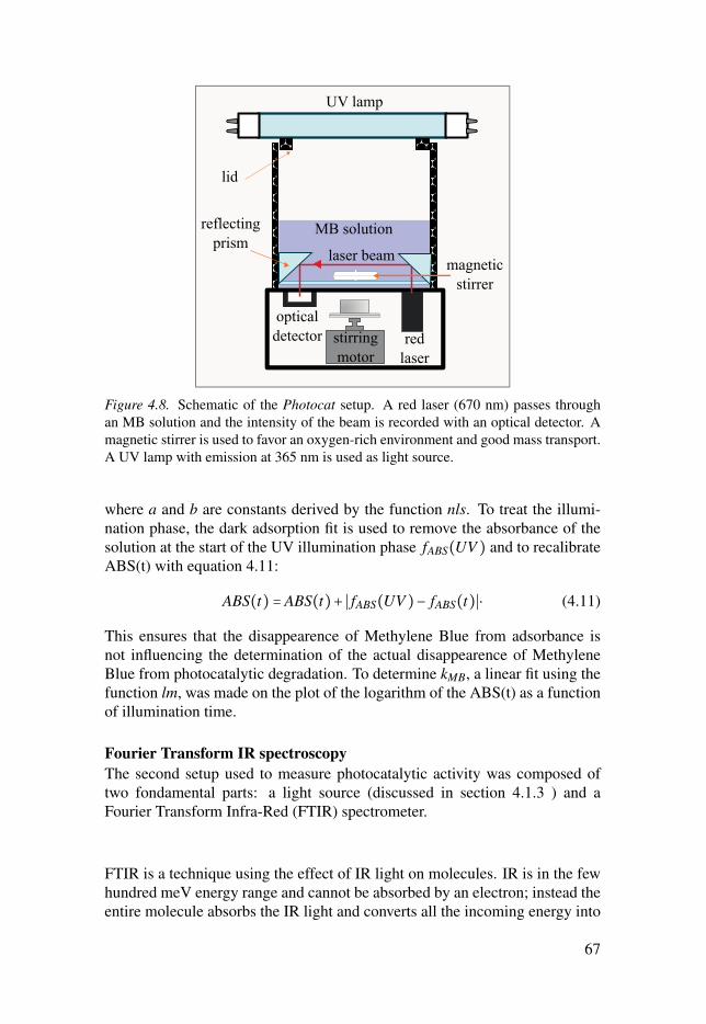
Figure 4.8. Schematic of the Photocat setup. A red laser (670 nm) passes throughan MB solution and the intensity of the beam is recorded with an optical detector. Amagnetic stirrer is used to favor an oxygen-rich environment and good mass transport.A UV lamp with emission at 365 nm is used as light source.
where a and b are constants derived by the function nls. To treat the illumi-nation phase, the dark adsorption fit is used to remove the absorbance of thesolution at the start of the UV illumination phase fABS(UV) and to recalibrateABS(t) with equation 4.11:
ABS(t) = ABS(t)+ ∣ fABS(UV)− fABS(t)∣⋅ (4.11)
This ensures that the disappearence of Methylene Blue from adsorbance isnot influencing the determination of the actual disappearence of MethyleneBlue from photocatalytic degradation. To determine kMB, a linear fit using thefunction lm, was made on the plot of the logarithm of the ABS(t) as a functionof illumination time.
Fourier Transform IR spectroscopy
The second setup used to measure photocatalytic activity was composed oftwo fondamental parts: a light source (discussed in section 4.1.3 ) and aFourier Transform Infra-Red (FTIR) spectrometer.
FTIR is a technique using the effect of IR light on molecules. IR is in the fewhundred meV energy range and cannot be absorbed by an electron; instead theentire molecule absorbs the IR light and converts all the incoming energy into
67

vibrational energy. Moreover, specific vibrational energy levels can be associ-ated to specific functional groups, so that a record of IR emission of a sampleafter IR illumination can be used to identify and fingerprint a sample. Theusual IR energies involved are in the mid-IR, between 155 to 413 meV. Com-pared to the band gap of a simple chain molecule like stearic acid (7.76 eV),it is clear that IR light cannot modify the fundamental structure of a molecule,so the FTIR technique is non-invasive. Also, the intensity of the vibrationalenergies is proportional to the number of functional groups, meaning that witha conversion factor, it is possible to obtain the number of molecules present onthe surface.The components of an FTIR spectrometer are: an IR source, an IR detector, anoptical setup and a sample holder. The most important part of the techniqueresides in the optical setup. It is comprised of mirrors and a beamsplitter,in a specific geometrical configuration forming a Michelson interferometer.A beamsplitter is an object that transmits 50% and reflects 50% of incom-ing light, effectively splitting the light beam into two with equal intensity. Aschematic of a Michelson interferometer is displayed in figure 4.9. The beam-splitter is used to direct the light into two different mirrors. After reflectionon the mirrors, the light is again passed and reflected by the beamsplitter andrecombined on the other side, towards a detector. One of the mirrors is heldin a fixed position (mirror 1), while the other is moved back and forth to-wards the beamsplitter (mirror 2). This produces a difference in the opticalpath length (δ ) between the beam reflected by the fixed mirror and the beamreflected by the moving mirror. This difference engenders an interference pat-tern after the recombination of the two beams. The interference pattern willshow a difference in light intensity (I), depending on whether the interferenceis constructive or destructive. A record of this interference pattern (change inlight intensity), versus movable mirror position, forms an interferogram. Tomonitor the displacement of the mirror, a laser beam is used (see figure 4.9),for which the interference pattern follows a sine-squared relation as a func-tion of mirror position, due to its monochromacity the laser beam amplitudeat each extreme position of mirror 2 changes from 0 to 1 and 1 to 0, as themirror 2 moves back and forth. The regularity of the interferogram created bythe laser allows the spectrophotometer to trigger the IR detector to measurethe IR interference pattern of the sample (forming an interferogram) at regularintervals (at regular movable mirror position).
An interferogram is the intensity of the IR light measured by the detectorversus mirror position (in cm), which is not ideal for interpretation. To obtaina spectrum, it is necessary to change domain (from cm to cm−1) by usinga mathematical operation called Fourier Transform. This operation allowsthe calculation of the measured IR intensity for each wavenumber (ν) usingequation 4.12:
I(ν) = ∫ +∞
−∞I(δ)cos(2πν dδ), (4.12)
68
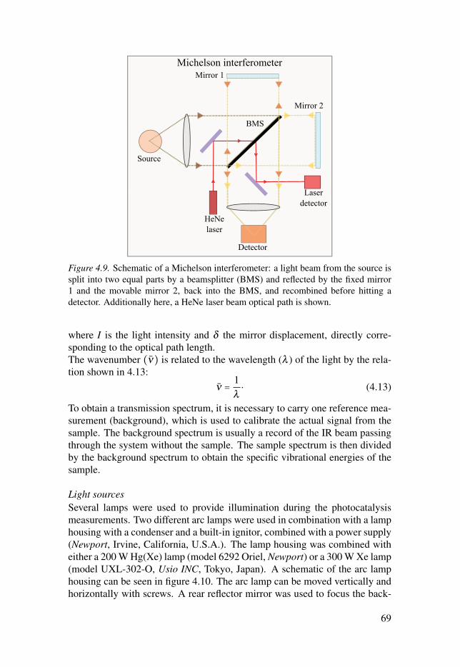
Figure 4.9. Schematic of a Michelson interferometer: a light beam from the source issplit into two equal parts by a beamsplitter (BMS) and reflected by the fixed mirror1 and the movable mirror 2, back into the BMS, and recombined before hitting adetector. Additionally here, a HeNe laser beam optical path is shown.
where I is the light intensity and δ the mirror displacement, directly corre-sponding to the optical path length.The wavenumber (ν) is related to the wavelength (λ ) of the light by the rela-tion shown in 4.13:
ν = 1λ⋅ (4.13)
To obtain a transmission spectrum, it is necessary to carry one reference mea-surement (background), which is used to calibrate the actual signal from thesample. The background spectrum is usually a record of the IR beam passingthrough the system without the sample. The sample spectrum is then dividedby the background spectrum to obtain the specific vibrational energies of thesample.
Light sourcesSeveral lamps were used to provide illumination during the photocatalysismeasurements. Two different arc lamps were used in combination with a lamphousing with a condenser and a built-in ignitor, combined with a power supply(Newport, Irvine, California, U.S.A.). The lamp housing was combined witheither a 200 W Hg(Xe) lamp (model 6292 Oriel, Newport) or a 300 W Xe lamp(model UXL-302-O, Usio INC, Tokyo, Japan). A schematic of the arc lamphousing can be seen in figure 4.10. The arc lamp can be moved vertically andhorizontally with screws. A rear reflector mirror was used to focus the back-
69

Figure 4.10. Schematic of the Arc Lamp housing system. An arc lamp is fitted inthe housing case, combined with a rear mirror and condensing lens system. The rearmirror can be moved to focus backward illumination onto the front illumination. Twoscrews allows the displacement of the arc lamp. The condensing lens system allowthe beam to be focused, as seen in the inset.
ward illumination from the lamp towards the exit port (forward). To focus thelight, the condensing lens assembly was used as follow: the arc lamp needleis positioned at the middle of the apparture and the assembly was moved untilthe tip of the needle lamp became sharp to the eye, see inset in figure 4.10.The focusing lever was then locked into position. After turning on the lamp,the position screws of the rear reflector were used to align the backward illu-mination to the forward illumination.A LED white illumination lamp was used as well, running on 1.8 W ( NORTH-LIGHT, Cheektowaga, New York, U.S.A.). Only three experiments of aroud2 hours each, were performed with it.
A IFS66vS FTIR spectrometer (Bruker, Billerica, U.S.A.) was used to mea-sure the stearic acid photodegradation on different samples. This spectrome-ter is equipped with a SiC glowbar mid-IR source, a liquid N2 (77 K) cooledDeuterated L-alanine doped Triglycine Sulfate (DLaTGS) detector with a KBrwindow, a Ge coated KBr and a CaF2 beamsplitters (situated in the instrumentcompartment), as well as a HeNe laser. It can operate between 7500 cm−1
and 370 cm−1 and has a claimed resolution of 0.25 cm−1. The IR beam has acircular shape, and the diameter is linked to the aperture size (16 apertures areavailable) with a dependency described in equation 4.14:
Beam = 1.2×Apperture⋅ (4.14)
70

The DLaTGS detector is guaranteed cooled for 18 hours by the manufac-turer of the dewar containing the liquid N2, and has a linear response over themid-IR range. The manufacturer specific detectivity is estimated at 2.7×10⁸
cmHz12 W−1. A pumping system can be used to create a low vaccum in the
FTIR detection and IR source compartment, as well as in the sample compart-ment. Low vacuum is preferable for FTIR measurements, as water moleculesare always present in the atmosphere and absorb a broad band of mid-IR (μband at 1650 cm−1 and X band at 3500 cm−1), which can coincide with themeasured sample vibrations. All measurements were performed with an opensample chamber (in air), and an instrument compartment under vacuum, whenthe pumping system was available (the CaF2 beamsplitter was used under at-mospheric conditions, while the KBr beamsplitter was used only in vacuumconditions). A N2 air flow maintained at around 1.2 mbar was introduced witha 5 mm diameter tube above the sample chamber (around 10 cm from the topof the sample). The laser beam is less than 1 mm in diameter and operates ata wavelength of 632.8 nm (red).
Two different types of measurement were performed: single and repeated mea-surements. For both types, each measurement was the average of 127 scans.All measured spectra had a resolution of 4 cm−1 and were recorded between4000 cm−1 and 1000 cm−1, with a scanned velocity of 40 KHz and a lowpass filter of 16 KHz. The aperture size of the FTIR was fixed at 1 mm, sothe IR beam diameter was around 1.2 mm (see equation 4.14), if the samplesurface was perpendicular to the IR beam. The acquisition mode was Forward-Backward, meaning that the scans were collected during both backward andforward mirror displacement, and were co-added separately - to be then cal-culated and added (better signal to noise ratio). For repeated measurements, adelay of 240 s was used.For arc lamp illumination, the sample holder was mounted on a pole with pre-cision rotation in the horizontal plane, and placed inside the sample chamber.Apertures with a 1.3 cm and a 2.0 cm diameter were placed on the sampleholder and the different samples were held in place with tape. The arc lampcasing used to host the Mg and Xe lamps was monted on an optical bench, out-side the sample chamber. To illuminate the sample, a mirror (either Silver orGold) was placed inside the chamber, at around 15 cm from the sample holder.The 0○ UV-Vis light illumination was assured by changing the sample holderposition until the light beam circularity after the aperture was found. Depend-ing on the experimental sets, the sample holder was either rotated in and out of0○ UV-Vis illumination for subsequent FTIR measurements (single measure-ment every 10 to 30 min), where the IR beam was perpendicular to the samplesurface as shown in figure 4.11(a); or kept at 0○ UV-Vis illumination (repeatedmeasurements) as displayed in figure 4.11(b), which means that the IR beam
71

Table 4.2. List of band pass filters, with position of the pass peak and peak width,and corresponding power at the sample position under the illumination of the Mg(Xe)lamp at 200 W. The power was measured using the Thorlab power meter.
Filter namePass peak
(nm)peak width
(nm)
Mg(Xe) 200 Wpower at sample
(mW)
56501 253 14 3.6957396 300 110 82.256511 312 16 2.8656531 366 12 3.4556541 405 14 4.14
AM0 & AM1.5 X X 40.6
was at an angle of around 38○ with the sample surface. By applying a simplecosine rule, the IR beam diameter was calculated to be around 1.5 mm in thisconfiguration. The total distance between the arc lamp casing and the samplewas 110 cm. A schematics of this setup is shown in figure 4.12. Togetherwith the arc lamps, several bandpass filters were used (see table 4.2) to selecta specific energy range. The bandpass filters effectively block all wavelengthsin the same energy range apart for a narrow window (peak width). Specificfilters, AM0 and AM1.5 (Thermo Oriel, now Newport, Irville, U.S.A.), wereused to reproduce a spectrum similar to that of a solar spectrum. Wheneverpossible, prior to each measurement set, the light power was measured at thesample holder, at the mirror and at the filters.
For LED illumination, the mirror was replaced by the lamp and the samplewas illuminated to the normal. The IR signal was measured every 5 minutesat a small angle, during illumination.To deposit stearic acid on the sample, 1 mL of the solution was spin-coatedat around 2000 rpm and dried with a 1 bar N2 flow for at least 30 s, with thesample kept at a distance of around 10 cm from the N2 exhaust. The back of thesample was cleaned with a tissue dipped in ethanol. To clean the samples afterthe measurements, the Nabatherm was used, heating from room temperatureto 380○C with 2○C steps and kept at 380○C for 4 hours.
Built-in software (OPUS) was used to generate the normalized spectra in trans-mission, by dividing the background transmission spectrum recorded withoutstearic acid loading. Then, the program was used to calculate absorbance spec-tra, cut inf the wavenumber range 3000 cm−1 to 2800 cm−1 and the bacgrounddrift over illumination time was removed using a rubberband correction. Thespectra were then exported into text files (a column with wavenumber and acolumn with intensity) and treated with a home-made R program. An analy-
72

Figure 4.11. Schematic of the FTIR measurements geometry: (a) single measurement,sample position 1 shows the position to measure the IR spectrum after illumination andsample position 2 is used for illumination time; (b) repeated measurement, the sampleposition is fixed, and the illumination is constant.
73

Figure 4.12. Schematic of the FTIR spectrophotometer and photocatalytic activitymeasurements geometry. A light source outside the FTIR instrument is reflected on asample by a mirror. The IR beam passes through the sample, the instrument measuresits intensity and calculates a spectrum of IR intensity versus IR wavenumber.
sis of the stearic acid specific bands area then provides an equivalence to theamount of stearic acid molecules degraded with illumination time, thereforeallowing the calculation of the degradation rate.The R program uses a built-in function (sintegral) to calculate the total area ofthe different stearic acid peaks (Area), from 3000 cm−1 to 2800 cm−1. To ac-count for the illumination time, a vector containing the time (t) at which eachspectrum was recorded was created. A normalization of Area is made by divid-ing each Area value by the value of the first spectrum after starting illumination(Area0). Following stearic acid degradation process, the logarithm of Area wastaken. To extract the degradation rate (kSA), a plot of log10(Area/Area0) onthe y-axis versus time on the x-axis, was linearly fitted with equation 4.15, asused in the program, with forced regression to zero:
y = kSA×x+0⋅ (4.15)
The transmission spectra before illumination were analyzed with the OPUSsoftware, and the peak areas between 3000 cm−1 and 2800 cm−1 were calcu-lated to determine the number of stearic acid molecules at the beginning of theexperiment.
74

5. Fabrication method
Ça vous fait pas mal à la tête deglandouiller vingt-quatre heuressur vingt-quatre?
Alexandre Astieras Arthur Pendragon in Kaamelott
To fabricate the photocatalytic active samples, a step by step procedure wasused. First a PS template was self-grown onto a substrate, then metal oxidewas deposited using ALD. Third, ion milling was performed and finally thePS beads were removed; as shown in figure 5.1.
5.1 Templates
To fabricate the PS template convective vertical evaporation (CVE)[145–147]in the memmert oven was used, with the evaporation as a driving force to self-assemble the PS beads. Due to this force, the beads assemble in fcc, as seenin figure 5.2 (a) and (b). Convective refers to the collective upwards flows ofwater vapor due to the forced evaporation in the oven. Vertical means thatthe substrates are vertically placed into the solution, and so that the evapora-tion drag competes with gravity. Convective evaporation occurs at a dryingfront between two phases; the water-based suspension and air. The dryingfront creates a flow within the solution, which carries the beads towards theevaporation front (also referred to as water front). As water recedes from thebeads, capillary forces drive the beads closer and a close-packed structure isformed. The entire fcc structure is deposited as the water evaporates, as de-picted briefly in figure 5.2(c), so that the thickness of the deposition dependsstrongly on evaporation conditions and bead availability. The size of the beadsis important for the fcc deposition. As the diameter of the bead increases, itis necessary to have a higher volume concentration to obtain a complete film.This is due to the gravitational effect, which competes with the Brownian mo-tion of the beads. As the diameter increases, so does the weight and thereforethe mobility of the beads decreases.
75

Figure 5.1. Schematic of the different deposition steps. 1: PS (beige) necks formation,2: MO (blue) ALD deposition, 3: Ion Milling & 4: PS removal. MO on PS depictedin green. Walls of inverse opals in dark blue.
Figure 5.2. Schematic of the fcc stacking of PS beads, side view (a) and top view(b), the central bead is surrounded by 6 neighbours in the same plane. The depositionmethod, called CVE, consists of a substrate introduced at a small angle into a PSsolution, with deposition at the air/water interface (c). After heat treatment, the beadsmelt slightly and create necks connecting the entire structure (d).
76

The preparation of the substrates and solutions was always the same, regard-less of the type of substrate and solution concentration. It is important firstto ultra-sonicate the bead suspensions so that the coagulation risk is reduced.While bead suspensions are sonicated, the substrates are sonicated in Decon90diluted with deionized water, to make the surfaces hydrophilic and clean. Af-ter at least 15 min, the substrates were rinsed copiously with deionized waterand dried by air flow. Then, diluted solutions were prepared from the beadsuspensions. The diluted solutions were kept in the ultrasonic bath for at least15 min to ensure complete mixing.
All glassware was cleaned with Decon90 (Decon Laboratories Limited, U.K.),a detergent containing potassium hydroxide. Deionized water was directlyobtained at the Ångström laboratory. Fifteen 25 mL beakers (2.5 cm diameter),eight 50 mL beakers (4.2 cm diameter), six 100 mL beakers (5.2 cm diameter)and one 200 mL beaker (8.2 cm diameter), corresponding to between 40 cm2
and 200 cm2 solution surface area, were used.
The memmert was kept at 50○C before and during the CVE process. Beakersof different volume capacity were used. After placing the beakers with thePS solutions into the oven, the substrates were inserted at a small angle to thevertical (less than 10○). At the beginning of the experiment, the temperatureof the oven had often dropped to 30○C and gradually increased to reach theset temperature in 1 to 2 hours. The experiment was carried on for at least 15hours.After deposition, the backside of the PS opals were cleaned with a tissuedipped in ethanol, as some deposition can occur close to the sides of the sub-strate. The opals were then annealed in the Nabatherm, heating from roomtemperature to 90○C with a 1○C step, and kept at 90○C for 2 hours. The heattreatment creates necks, where the PS beads are in contact with their neigh-bours, as shown schematically in figure 5.2(d).
5.2 Atomic Layer Deposition5.2.1 Description of the techniqueAtomic Layer Deposition (ALD) uses a similar technique as Chemical Va-por Deposition (CVD) but splits the deposition process. To deposit a certainmaterial on a substrate via ALD, it is necessary to find two precursors thatcan be vaporised. A schematic of a typical ALD is displayed in figure 5.3.It is composed of a series of precursor lines connected to a process chamber.
77

Figure 5.3. Schematic of an ALD: the process chamber is heated, N2 is used as car-rier and purge gas, four precursors lines with temperature and pressure regulators areavailable. Here, precursor 1 is introduced first, a N2 purge follow, then precursor 2 isactivated.
The process chamber is usually kept at constant temperature and pressure,the chamber is filled with N2. Precursor lines can be heated homogeneouslyand the precursors in gas form are carried by N2 at specific and chosen pres-sures. The precursors should not decompose too fast and should react witheach other. Usually the chamber is prepared a few hours before the actualdeposition, to ensure a stable temperature. When the chamber, as well as theprecursors, are at a stable temperature, the deposition process can start. Thefirst precursor is introduced into the chamber and a purge waiting time is setto let the physisorb and gas species out of the chamber. Then, the second pre-cursor is introduced and reacts with the first precursor, creating the desiredmaterial attached to the substrate surface.
A purge time is also necessary after this step, as shown in figure 5.4. Thetwo steps form a cycle and it is very common to repeat the cycle a hundredtimes for few nanometer deposition. The advantages of ALD are multiple.First, as the deposition happens in two steps, it is possible to deposit ontothree dimensional structures and into narrow spaces. Second, it is a very pre-cise deposition process and if the deposition rate is determined, it is possible tocontrol the deposition in the Ångström scale. Of course, the entire depositionprocess can be rather long, depending on the type of structure and the deposi-tion rate. Not all types of material are suitable for ALD, but metal oxides arethe most widely deposited materials.
78
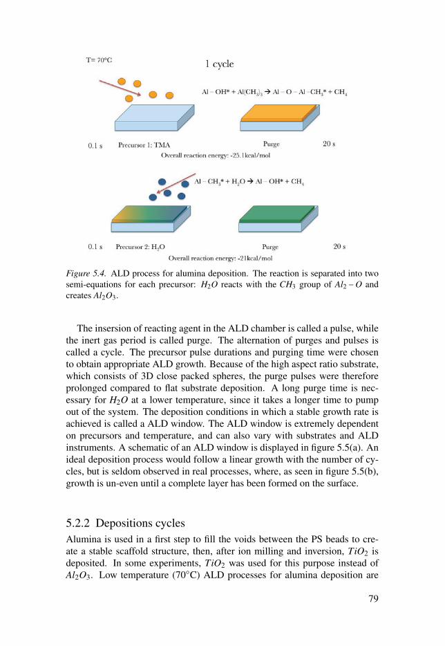
Figure 5.4. ALD process for alumina deposition. The reaction is separated into twosemi-equations for each precursor: H2O reacts with the CH3 group of Al2 −O andcreates Al2O3.
The insersion of reacting agent in the ALD chamber is called a pulse, whilethe inert gas period is called purge. The alternation of purges and pulses iscalled a cycle. The precursor pulse durations and purging time were chosento obtain appropriate ALD growth. Because of the high aspect ratio substrate,which consists of 3D close packed spheres, the purge pulses were thereforeprolonged compared to flat substrate deposition. A long purge time is nec-essary for H2O at a lower temperature, since it takes a longer time to pumpout of the system. The deposition conditions in which a stable growth rate isachieved is called a ALD window. The ALD window is extremely dependenton precursors and temperature, and can also vary with substrates and ALDinstruments. A schematic of an ALD window is displayed in figure 5.5(a). Anideal deposition process would follow a linear growth with the number of cy-cles, but is seldom observed in real processes, where, as seen in figure 5.5(b),growth is un-even until a complete layer has been formed on the surface.
5.2.2 Depositions cyclesAlumina is used in a first step to fill the voids between the PS beads to cre-ate a stable scaffold structure, then, after ion milling and inversion, TiO2 isdeposited. In some experiments, TiO2 was used for this purpose instead ofAl2O3. Low temperature (70○C) ALD processes for alumina deposition are
79

Figure 5.5. (a) Schematic of the ALD window, linked to the deposition temperature.Before the window, condensation can increase the adsorption or no reaction can occur.After the window, precursors can decomposed before reaching the reaction chamberor it can behave similarly to a CVD process. Higher temperature can also inducedesorbtion from the substrate. (b) Schematic of a realistic growth process inside aALD chamber, nucleation can take several cycles before finally becoming islands,which increases reactive surface area. As the islands coalesce, the growth becomesstable. A second nucleation can also occur, leading to a second change in depositionrate.
80

Table 5.1. Deposition of Al2O3 at 70○C with the Picosun R200 Standard, using thefollowing cycle, with pulse time for each precuror and alternated N2 purge time.
Order PrecursorPulse time
(s)Purge time
(s)
1 TMA 0.1 202 TMA 0.1 203 TMA 0.1 204 TMA 0.1 60
5 H2O 0.1 206 H2O 0.1 207 H2O 0.1 208 H2O 0.1 60
readily available and yield mechanically robust and chemically inert layers.Several low and high temperature depositions were performed with three dif-ferent ALD setups: a Picosun R200 Standard (Picosun, Lohja Oy, Finland), aPicosun R200 Advanced (Picosun, Lohja Oy, Finland) and a TFS200 (BeneqOy, Vantaa, Finland). The deposition temperature of TiO2 on Al2O3 inverseopals was chosen to be above 70○C, since it is known that low temperatureprocesses have a non-constant deposition rate, which varies with the numberof cycles and pulse time. Titania deposition was made at 200○C to avoid rutileformation and to allow a smoother deposition morphology.
The Picosun R200 Standard was used for Al2O3 deposition on the PS opaltemplates. The chamber temperature was set to 70○C, below the melting pointof PS, and the end temperature (cooling) was set to room temperature. Pres-sure inside the TMA tube was set to 5.1 mbar, to 4.6 mbar in the H2O tubeand 8.0 mbar in the N2 tube. The reaction chamber pressure was maintainedat around 6.0 mbar. The deposition cycle is described in table 5.1. The carriergas flow for both TMA and H2O was set to 100 Standard Cubic Centimeter perMinute (SCCM). Each pulse was followed by a purge and the cycle comprisedof 4 TMA pulses, followed by 4 H2O pulses.
This setup was mostly used to test the deposition of Al2O3 on PS, vary-ing the number of cycles employed. The deposition of Al2O3 is theory-likebehavior, meaning that alumina has a perfect ALD window. The depositionrate is believed to be around 0.1 nm/cycle. Some variations of this rate can beexpected, depending on the position of the PS opals in the reaction chamber(higher growth rate expected near the precursor input ports) and the nature ofthe opals (close-packing).
81

Table 5.2. Deposition of TiO2 at 200○C with the TFS200, using the following cycle,with pulse time for each precuror and alternated N2 purge time.
Order PrecursorPulse time
(s)Purge time
(s)
1 TiCl4 0.25 202 TiCl4 0.25 40
3 H2O 0.5 204 H2O 0.5 40
Table 5.3. Deposition of Al2O3 at 70○C with the Picosun R200 Advanced, using thefollowing cycle, with pulse time for each precuror and alternated N2 purge time.
Order PrecursorPulse time
(s)Purge time
(s)
1 TMA 0.1 102 TMA 0.1 40
3 H2O 0.1 104 H2O 0.1 40
The TFS200 was used to deposit TiO2 on the Al2O3 inverse opals. The de-position temperature was set at 200○C and no cooling was programmed. Thechamber and precursor tubes pressure was around 10 mbar. The depositioncycle is described in table 5.2. The carrier gas flow was set to 600 SCCM.
This instrument was used to make the first samples but the Picosun R200Advanced was preferred for further depositions.
The Picosun R200 Advanced was used for both Al2O3 and TiO2, at 70○C andTiO2 at 200○C. This instrument was used the most to produce the inverseopals. The chamber pressure was set at around 10 mbar, the TiCl4 and TMAtubes was around 7 mbar, while the H2O tube pressure was around 10 mbar.The cycle for Al2O3 deposition is described in table 5.3, where the carriergas flow of the precursors was maintained at 150 SCCM. The deposition ratemeasured with Quartz Crystal Microbalance (QCM) was around 0.1 nm/cycle.QCM is a quartz crystal with an induced oscillation. By monitoring the changeof frequency with mass, it is possible to monitor the thickness deposited duringthe ALD process [148].
The TiO2 deposition cycles can be seen in figure 5.6, with pulse time (a)and purge time (b). The carrier gas flow of the precursors was maintained at150 SCCM. The deposition rate at 70○C was determined to be around 0.09nm/cycle, while the deposition rate at 200○C was determined to be around0.08 nm/cycle, with the QCM (on a flat surface).
82

Figure 5.6. Purge (a) and pulse (b) time for TiO2 at 70○C and 200○C with the PicosunR200 Advanced.
Figure 5.7. Schematic of the principle of Ion Beam Etching using Ar gas.
5.3 Ion millingIon Beam Etching (IBE) was performed using Ar+ with an Oxford InstrumentsPlasma Technology Ionfab 300 Plus (Oxford Instruments, Oxfordshire, UK).The removal of material (ecth) occurs by physically dispatching the atoms ofthe surface (physical momentum transfer). The process is isotropic, as thesample holder rotates during the etching process. As shown in figure 5.7,argon gas was ionized using a voltage and a local solenoid magnetic field wasused to guide the plasma ions towards the target. The grids provide an highlycollimated beam and the neutralization filament forces each ion to capture anelectron and move it along. The resulting beam is therefore collimated andquasi-neutral.
The removal of alumina and anatase was performed using the same manu-facturer recipe, with the parameters depicted in table 5.4. The recipe etchingrate was more than 10 nm/min for a flat Al2O3 film. An etching time of be-tween 2 to 4 min was used - to enssure a complete removal of the cappingcreated during ALD deposition.
83
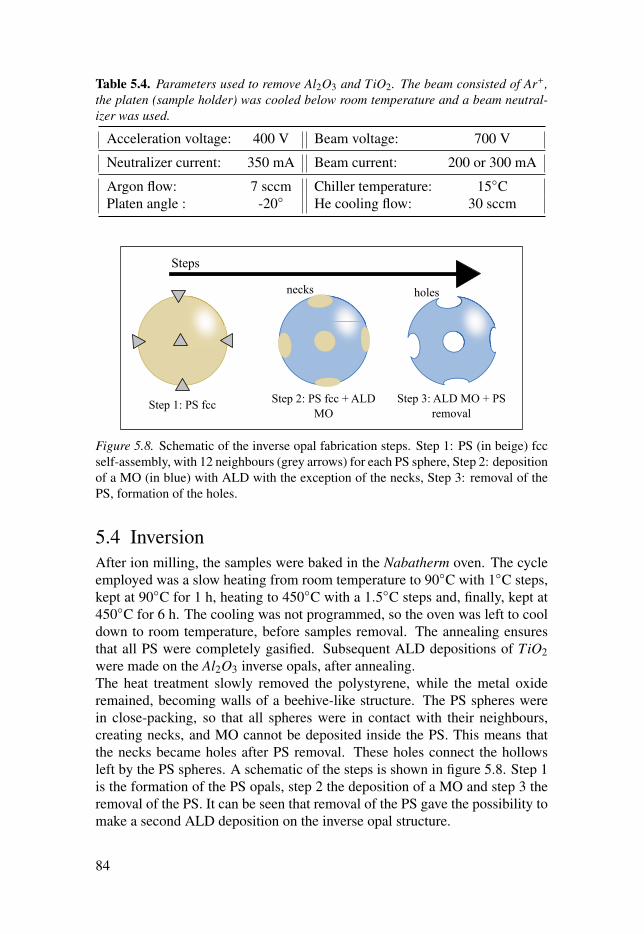
Table 5.4. Parameters used to remove Al2O3 and TiO2. The beam consisted of Ar+,the platen (sample holder) was cooled below room temperature and a beam neutral-izer was used.
Acceleration voltage: 400 V Beam voltage: 700 V
Neutralizer current: 350 mA Beam current: 200 or 300 mA
Argon flow: 7 sccm Chiller temperature: 15○CPlaten angle : -20○ He cooling flow: 30 sccm
Figure 5.8. Schematic of the inverse opal fabrication steps. Step 1: PS (in beige) fccself-assembly, with 12 neighbours (grey arrows) for each PS sphere, Step 2: depositionof a MO (in blue) with ALD with the exception of the necks, Step 3: removal of thePS, formation of the holes.
5.4 InversionAfter ion milling, the samples were baked in the Nabatherm oven. The cycleemployed was a slow heating from room temperature to 90○C with 1○C steps,kept at 90○C for 1 h, heating to 450○C with a 1.5○C steps and, finally, kept at450○C for 6 h. The cooling was not programmed, so the oven was left to cooldown to room temperature, before samples removal. The annealing ensuresthat all PS were completely gasified. Subsequent ALD depositions of TiO2were made on the Al2O3 inverse opals, after annealing.The heat treatment slowly removed the polystyrene, while the metal oxideremained, becoming walls of a beehive-like structure. The PS spheres werein close-packing, so that all spheres were in contact with their neighbours,creating necks, and MO cannot be deposited inside the PS. This means thatthe necks became holes after PS removal. These holes connect the hollowsleft by the PS spheres. A schematic of the steps is shown in figure 5.8. Step 1is the formation of the PS opals, step 2 the deposition of a MO and step 3 theremoval of the PS. It can be seen that removal of the PS gave the possibility tomake a second ALD deposition on the inverse opal structure.
84

6. Sample structure
Quel tas de merdier... Non maissérieusement, quel merdier!
Alexandre Astieras Arthur Pendragon in Kaamelott
6.1 Templates6.1.1 Substrates
It is interesting to note that the shape of the substrate does not influence thesuccess of the deposition. Round quartz substrates, broken glass substratesand broken ITO on glass substrates, all were successfully deposited. In ad-dition, deposition on quartz, glass, ITO on glass and Kapton was successful.However, Kapton required more concentrated solutions and the opals were notas well attached to the substrate. The unsuccessful depositions on Kemafoilfilms, which are hydrophilic plastic films, even after annealing or citric acidtreatment, demonstrated that a mere hydrophilic sample is not a sufficient cri-terium for successful deposition. This question was investigated further bychecking the roughness differences between the substrates.
Polystyrene bead deposition was tried on aluminium foil, photo-resist andPolymethyl methacrylate (PMMA) thin films. Surprisingly, it was possibleto deposit onto some parts of aluminium foil, but the foil was damaged duringthe deposition process. It could be interesting to try to deposit on an alu-minium plate for electrophoresis use. Some surface of the photo-resist wascovered with organized beads, but most of the substrate area was left empty orwith very thick and patchy depositions, see figure 6.1. Finally, spin-coated 200nm thick films of PMMA on quartz were used. The deposition was more uni-form than for the photo-resist, but only low concentrated solutions (0.1w/v%)gave positive results. Figure 6.1 shows the resulting successful deposition onPMMA, with beige areas PS opals. These samples can be used as template forcreating a free-standing structure after metal-oxide deposition.
85

Figure 6.1. Photography of 200 nm PS beads at 0.2 w/v% concentration, deposited onphotoresist, PMMA and quartz. Beige areas correspond to the PS opals.
6.1.2 ProfilometryDeposition trials
SubstratesProfiles of different substrates were measured with the Dektak XT. The re-sults are summarized in table 6.1. The standard deviation (root-mean-squareroughness) was calculated from each profilometry trace via a Matlab program.Specks of dust, inevitable after some manipulations, were cancelled out in thecalculations by removing data with heights exceeding 1μm. It can be seenthat both quartz and glass are smoother than the rest of the substrates. In ad-dition, deposition of 300 nm PS beads onto 0.125mm Kapton was sometimesuccessful, so a threshold of around 30% of the bead diameter was present. Asubstrate too rough in scale for the beads will hinder the deposition. It is notenough to have a hydrophilic substrate, it is also important for the beads togrow on a relatively smooth substrate.
Low concentrationAn interesting growing pattern was observed after profilometry on samplesfabricated at relatively low solution concentrations. Under these growing con-ditions, a few hundred micrometer wide bands of opals separated by a fewhundred micrometer wide band of bare substrate, were observed, as illustratedon figure 6.2. These bands also show a periodicity between the opal bands,which was defined by calculating the Fourier transform of the traces, usinga Matlab program. An exemple of profilometry traces on a 170 nm PS beadopal, fabricated with a solution concentration of 0.3 w/v%, can be seen infigure 6.3. The traces were made at different points on the sample, with theDektakt XT, shifted for clarity.
86

Table 6.1. Profiles of substrates. Standard deviation (δ ) of the mean height derivedfrom profilometry measurements. The equivalent 200 nm bead diameter percentage ofthe mean height, as well as the associated deposition success, are shown.
Substrate Averaged δ %200 nm Success
Type nm %
Glass 8.03 4 98Quartz 8.04 4 98
ITO/glass 41.97 21 90Kapton 0.125 mm 75.71 38 10
Kapton 1 mm 270.80 135 2Kemafoil 147.38 74 0
The periodicity of the bands depends slighlty on the PS beads diameter, butstrongly on the solution concentration. As seen in figure 6.4, the periodicityof 200 nm PS bead samples is similar for a fixed solution concentration, whilethe periodicity of the 170 nm PS bead samples changes from around 270 nm to570 nm, with increasing solution concentration. The difference clearly derivedfrom the difference in solution concentration.
Successful depositions
Type of tracesAt the beginning of the CVE process, the position of the substrate in the so-lution and the solution level, determined the position of the waterfront (WF),as shown in figure 6.5(a). The waterfront is therefore defined as the interfacebetween liquid and air, where opalization takes place. The waterfront recedeswith water evaporation, but the position with respect to the substrate remainsunchanged. The WF can be used as a point of reference for profilometry scans.The trace can either be parallel (PARA) or perpendicular (PERP) to the WF,as illustrated in figure 6.5(b). Typical traces of a 200 nm PS bead diameteropal made with 0.2 w/v% solution concentration, are shown in figure 6.6. Thetraces are taken at different places on the same opal, and shifted for clarity. ThePERP traces on different PS opals demonstrated that the thickness increaseswith retreating WF, which can be explained by the increases in concentrationas water evaporates during the CVE process. As for the PARA traces, theyshow that opal thickness decreases at the edges of the substrate, which derivesfrom the change of shape of the meniscus at the edges, providing less area atthe WF.
Typical PS opalCommon points in the deposition process were seen for all types of substrates.There are stripe-like growths, suggesting an island-growing type, and there isa deposition thickness gradient as the solvent volume decreases (thick deposi-
87

Figure 6.2. Schematics of the island-like growth at low PS concentration, formingbands of opals at regular intervals.
Figure 6.3. Profilometer traces on a 170 nm PS bead diameter with a concentration of0.3 w/v%. Traces shifted for clarity.
88

0
0,1
0,2
0,3
0,4
0,5
0,6
0,7
165
170
175
180
185
190
195
200
205
200 250 300 350 400 450 500 550 600
PS so
lutio
n co
ncen
trat
ion
(w/v
%)
PS b
eads
dia
met
er (n
m)
Periodicity of bands (nm)
170nm 200nm conc170 conc200
Figure 6.4. Opal band periodicity as a function of PS bead diameter (◻) and PS solu-tion concentration (○). Results obtained for 170 nm (blue) and 200 nm (red) PS beaddiameter opal bands.
tion in the bottom of the substrate as the volume concentration of the solutionincreases). The stripes are either parallel or perpendicular to the water front.This was verified by depositing polystyrene beads onto two similar glass slides(70∗ 25∗ 1 mm), one standing on the shortest edge (25mm side), the otherstanding on the longest edge (70 mm side). Both samples show stripes, but theshort-edge substrate had stripes parallel to the water front whereas the long-edge substrate had stripes perpendicular to the water front. It is likely thatsurface tension was responsible for this preferential orientation.
ThicknessAn example of thickness measurement is displayed in figure 6.7, where PERPtraces were made on four different areas of a 200 nm PS sample, grown at 0.2w/v% solution concentration. The traces were shifted for clarity. The meanthickness was estimated to be around 9.2±3.3μm, while optical density (OD)calculations set the averaged thickness of the film around 12.5 μm. The traceswere taken at the beginning of the waterfront (WF), to observe the step be-tween substrate and opal, and thickness increases slightly with receding WF;so the OD calculations give an accurate evaluation of PS opal thicknesses.
6.1.3 SEMAll PS opals were coated with Au-Pd to avoid charging during the imaging.
89

Figure 6.5. Schematic of the waterfront (WF) position during CVE process (a) andprofilometer traces parallel (PARA) and perpendicular (PERP) to the WF (b).
90

Figure 6.6. Profilometer traces parallel (a) and perpendicular (b) to the WF for a 200nm PS opal with 0.2 w/v% solution concentration, traces shifted for clarity. Illustra-tions of trends in the traces are displayed at the bottom. Dektakt 150
91

Figure 6.7. Profilometer traces perpendicular to the WF for a 200 nm PS opal with 0.2w/v% solution concentration, traces shifted for clarity. Dektakt 150
Face-centered cubic
PS self-assemble in fcc, as seen in figure 6.8, showing an SEM image takenon a 220 nm PS opal, which was deposited from a 0.2 w/v% concentrationsolution. The magnification was around 59K×, the working distance 9.1 mmand the acceleration voltage was set at 6 keV . The image shows that the opalhas an fcc pattern with 1 sphere surrounded by 6 neighbours. Defects canappear in the pattern such as missing PS sphere, PS sphere diameter variationand fcc stacking mismatch.
Cracks
During the drying process, the capillary forces the PS together and createscracks, which separate the opals in different areas [46, 47, 149]. The crackscan be separated depending on their orientation, parallel or perpendicular tothe WF. The cracks perpendicular to the WF are around 2 μm wide for the 200nm PS beads opal and run almost continuously along the opal, while the cracksparallel to the WF are an order of magnitude thinner, appear more randomlyand have less predictable orientation. The perpendicular cracks can reach thesubstrate, as seen in figure 6.9(a). They delimit long regular stripes with areasof around 1000 μm2, separated by the parallel cracks, which are similar to thedrying pattern of mud [150, 151], as displayed in figure 6.9(b). No periodicitywas found for either appearance of parallel and perpendicular cracks.
Moiré pattern
Moiré patterns are optical illusions that are created from the interference be-tween two patterns, as can be seen in figure 6.10. Since SEM uses an electronbeam, which follows a regular pattern to create an image, it is possible to ob-tain Moiré patterns if the observed sample has a periodicity [152, 153]. Interest
92

Figure 6.8. SEM image on the top layer of a 220 nm PS opal, made with 0.2 w/v%solution concentration. The red circle (bottom left) shows a defect from a missingPS sphere and the purple circle (top right) a defect from a PS sphere with a smallerdiameter. The blue hexagon shows the fcc pattern. The green rectangle follows astacking mismatch. Magnification (MAG): 59.41K× , working distance (WD): 9.1mm and acceleration voltage (EHT): 6.0 kV. Zeiss 1550
in Moiré patterns in SEM images is manifold; first, the presence of the patternsare the proof of periodicity, and second, the distance between the pattern canbe linked to the periodicity of the sample [154]. By definition, the sampleforms a model grid, with a periodicity p and the electron beam forms a mastergrid, with a periodicity a. The resulting Moiré patterns have periodicity d. Ifthe sample model grid is at an angle θ with the electron beam master grid,then the Moiré pattern appears at an angle φ with the electron beam mastergrid. The relationship between Moiré and sample periodicity can be describedusing equation 6.1:
θ = arctan±sinφ(d
a)±cosφ⋅ (6.1)
If the periodicity of the sample is greater than the beam periodicity, the rotat-ing direction of the Moiré patterns are opposite to the direction of the sampleorientation.Figure 6.11 shows the appearance and disappearance of Moiré patterns as themaster grid periodicity changes from 146 nm to 224 nm. The periodicity ofthe master grid can be tuned by the magnification (MAG) settings, with themagnification defined as the dimension of the raster on specimen by the di-mension of the raster on display. Lower magnification zooms into the sample,so the electron beam periodicity increases if both working distance and accel-eration voltage are kept constant. The MAG is changed by the SEM technician
93

Figure 6.9. SEM image on the top layer of a 220 nm PS opal, made with 0.2 w/v%solution concentration. (a) Perpendicular crack reaching the substrate. MAG: 12.2K×,WD: 9.0 mm and EHT: 6.0 kV (b) View of the perpendicular (horizontal in the image)and parallel smaller cracks (vertical in the image). MAG: 778×, WD: 9.0 mm andEHT: 7.0 kV Zeiss 1550
Figure 6.10. (a) Creation of Moiré patterns from parallel lines superposed with asmall angle. The Moiré lines are horizontal, while the patterns are vertical. (b) Moirépatterns from circles superposed with shifted centers.
94

Figure 6.11. SEM images with Moiré patterns of a 200 nm PS made with 0.2 w/v%solution concentration, at a fixed position, same WD: 9.0 mm and EHT: 6.0 keV, butdifferent MAG. Zeiss 1550
and is usually recorded directly on the SEM image. The periodicity a can beobtained from the attached data of the TIFF file produced by the SEM. In fig-ure 6.11, the Moiré patterns are most visible at around 2K×, corresponding toa = 180nm. To obtain information on the sample periodicity p, the equation6.2:
p−aa= a
d−a(6.2)
can be used, although it does not take into consideration the distortion of theMoiré pattern with the variation of the angle θ .
The Moiré patterns appearing on the PS opals were not delimited by thecracks, which suggests that the fcc arrangement was formed in the water atthe WF and that cracks developed after the WF had receded, during the dryingprocess, as mentioned earlier. The Moiré patterns form domains with differ-ent orientation (change in φ denoting a change in θ ), demonstrating a latticemismatch between the domains within the same sample. A 200 nm period-icity PS template was analyzed. The averaged distance between the Moirélines is around 1.4±0.2μm, corresponding to a structure periodicity of around192±10nm, according to equation 6.2. The measurements were made usingthe software ImageJ and due to the low resolution and limit in the magni-fication (the master grid should be around 200 nm, which corresponds to amagnification around 2K×), the measurements of the distance between theMoiré lines have a high uncertainty, close to 10 nm. The measure of the angleφ between the Moiré lines and the master grid is more accurate. Figure 6.12shows the calculated angle θ for 262 measured φ angle on different SEM im-ages. There is a small preferential orientation of the PS opal - relative to theMaster grid (the electron beam) - at around 11 degrees. The angle differencebetween the 11 degree orientation domain and the other domains therefore
95
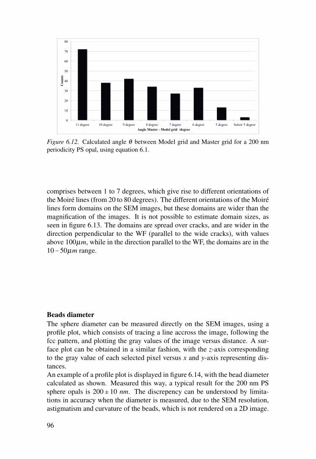
0
10
20
30
40
50
60
70
80
11 degree 10 degree 9 degree 8 degree 7 degree 6 degree 5 degree below 5 degree
Cou
nts
Angle Master - Model grid /degree
Figure 6.12. Calculated angle θ between Model grid and Master grid for a 200 nmperiodicity PS opal, using equation 6.1.
comprises between 1 to 7 degrees, which give rise to different orientations ofthe Moiré lines (from 20 to 80 degrees). The different orientations of the Moirélines form domains on the SEM images, but these domains are wider than themagnification of the images. It is not possible to estimate domain sizes, asseen in figure 6.13. The domains are spread over cracks, and are wider in thedirection perpendicular to the WF (parallel to the wide cracks), with valuesabove 100μm, while in the direction parallel to the WF, the domains are in the10−50μm range.
Beads diameter
The sphere diameter can be measured directly on the SEM images, using aprofile plot, which consists of tracing a line accross the image, following thefcc pattern, and plotting the gray values of the image versus distance. A sur-face plot can be obtained in a similar fashion, with the z-axis correspondingto the gray value of each selected pixel versus x and y-axis representing dis-tances.An example of a profile plot is displayed in figure 6.14, with the bead diametercalculated as shown. Measured this way, a typical result for the 200 nm PSsphere opals is 200± 10 nm. The discrepency can be understood by limita-tions in accuracy when the diameter is measured, due to the SEM resolution,astigmatism and curvature of the beads, which is not rendered on a 2D image.
96

Figure 6.13. SEM images of a 200 nm periodicity PS opal with unknown thickness,Moiré domains shown in different colors and in original gray of the SEM image. (a)MAG: 2.2K×, WD: 9.0 mm and EHT: 6.0 kV and (b) MAG: 2K×, WD: 9.0 mm andEHT: 7.0 kV. Zeiss 1550
97

Figure 6.14. Profile plot schematic of a 300 nm PS bead opal, accross an isolatedbead. Red horizontal marking show the determination of the bead diameter.
6.2 Metal Oxide structures6.2.1 GIXRDTo obtain the size and phase of the crystalline grains, it is possible to analyzethe GIXRD data, applying Scherrer’s equation 6.3:
τ = Kλβcosθ
, (6.3)
where τ is the crystal size, K a dimensionless shape factor, usually fixedaround 0.94, β is the Full Width at Half Maximum (FWHM) of a difractedpeak, λ the X-Ray wavelength and θ the diffraction angle.The analysis of the FWHM was made using DIFFRACplus BASIC EVA soft-ware (Bruker, Billerica, U.S.A.). The built-in correction for the backgroundconsists of a parabola with variable curvature. To account for the amorphousphase (Al2O3), the enhanced method for background correction was applied,which ensures that the parabola crosses the background region in the middleof its noise fluctuations.To evaluate the FWHM, the progam area computation was performed on thebackground corrected diffractogram. This computation is made from an inter-val between two points selected by the user, and statistical computations areused to create a profile for a single peak. The FWHM is calculated using aline equidistant from the background line and the identified maximum of thepeak. The number of crossings of the line with the diffractogram are checkedon both sides of the absolute maximum, so the FWHM is the output whenthese are reached.All diffractograms presented in this section are raw data, without backgroundcorrection.
98

Table 6.2. Diffraction angles from the different Miller indices for anatase TiO2.
Miller indices 2θ Miller indices 2θ
(101) 25.3 (213) 62.1(103) 36.9 (204) 62.7(004) 37.8 (116) 68.8(112) 38.6 (220) 70.3(200) 48.0 (107) 74.0(105) 53.9 (215) 75.0(211) 55.1 (301) 76.0
Alumina
Alumina is amorphous for annealing temperatures below 800○C, and crystal-lize in the γ-phase above [155, 156]. Figure 6.15 shows (a) a diffractogramof an alumina inverse opal baked at 300○C for 3 hours (with a heating rate of3.5○C/min), and (b) a diffractogram of the same alumina inverse opal bakedat 800○C for 4 hours (with a heating rate of 6.0○C/min). The sample was fab-ricated with the Picosun R200 Standard, with 200 cycles deposition on a PStemplate with 220 nm periodicity. The template thickness was not known, asno complete optical characterization was made before ALD deposition, but asimilar PS opal grown under the same conditions exhibits a thickness of 45layers. The alumina inverse opal is amorphous, before crystallization in theγ-phase after annealing. This phase belongs to the space group Fd3m, with astructure described as a fcc Oxygen atoms lattice with partial random distri-bution of Aluminium atoms. It has a high surface area, so it is often used as acatalyst in industry [157].
Titania
The different crystallographic planes of anatase have specific Bragg diffractionangles [158], specified in table 6.2. By analysing the FWHM of the most in-tense diffraction peak (101), of the different samples, the size of the crystallineplanes can be extracted. All inverse opal deposition and ion milling conditionscan be found in appendix A. A list of grain sizes for different inverse opals canbe seen in table 6.3.
Deposited at low temperatureThe crystallinity of two samples, June15PS200Q01C and July15PS200Q02T,were assessed with the D5000, after the 450○C annealing cycle. Both sam-ples were identified as crystalline anatase, with crystalline grain size of 12and 16 nm respectively, calculated using equation 6.3. Figure 6.16 shows thediffractograms of the June01C (a) and July02T (b). Both samples had TiO2deposited at 70○C with the R200 Advanced, and both samples had a templatesize of around 70 layers, which was calculated using their OD (see section
99

Figure 6.15. Diffractograms of Alumina inverse opal, (a) before and (b) after hightemperature annealing. Template periodicity 220 nm and template thickness guessedto be around 40 layers; ALD number of cycles: 200. The Miller indices definingdiffraction planes are displayed at the diffraction angle position in vertical dashedlines in (b). D5000
100

Figure 6.16. Diffractograms of (a) sample June01C and (b) sample July02T. BothTiO2 inverse opals with template periodicity 200 nm and template thickness 70 layers;ALD number of cycles indicated. The Miller indices defining diffraction planes aredisplayed at the diffraction angle position in vertical dashed lines in (b). D5000
7.1.1). The only difference between the samples was the number of ALD cy-cles used: 220 cycles for June01C and 275 cycles for July02T. As seen infigure 6.16, the diffraction peaks of sample July02T are more intense than forsample June01C and peaks with close diffration angles are discernable. Thisis expected because of the thickness difference between the films, which alsoaffects the crystalline grain size.
Deposited at high temperatureFigure 6.17 displays diffractograms of samples June15PS200Q02A (a) andJune15PS200Q01G (b). Both samples were made with a template periodicityof 200 nm and a template thickness of around 70 layers. Al2O3 was depositedat 70○C using the R200 Advanced, with 150 cycles for both samples. The
101

same ALD machine was used to deposit TiO2 at 200○C after ion milling andinversion, with 187 cycles for June02A and 232 cycles for June01G. Then,annealing was performed on the samples at 450○C for 6 hours. Both samplesdisplay an anatase crystalline phase, and using equation 6.3, the grain sizeswere calculated to be: 11.5 nm (June02A) and 14.4 nm (June01G). Similarly,for the samples deposited at 70○C, the sample with thicker TiO2 film has widercrystalline grains and more defined difraction peaks.
Table 6.3. Calculated grain size τ of anatase TiO2 in different samples, using equa-tion 6.3, at the position of the (101) diffraction peak from the GIXRD data. Top: TiO2inverse opals, bottom: Al2O3/TiO2 inverse opals, ordered by ascending number ofTiO2 ALD cycles.
Sample FWHM at (101) in ○ τ in nm
Avril15PS200Q02H 0.81 11.3June15PS200Q01C 0.80 11.5June15PS200Q02D 0.74 12.4July15PS200Q02T 0.59 15.8Fev15PS200Q02C 0.70 13.2July15PS200Q02O 0.52 17.7
NovO50Q200PS02E 0.58 16.0June15PS200Q02G 0.68 13.5Avril14PS200Q02D2 0.80 11.3June15PS200Q02A 0.84 10.8May14PS200Q02A 0.83 11.0June15PS200Q02J 0.51 18.1June15PS200Q01G 0.67 13.6June15PS200Q01J 0.66 13.9
Thin films
Films of Al2O3 and TiO2 were deposited on quartz substrates using the R200Advanced.
A thick Al2O3 film was made with a different deposition temperature and de-position cycles than the deposition on the PS opal templates. After each de-position at 70○C, the ALD machine could be contaminated with carbon-basedchemicals, from the PS, so a passivation run was made. A passivation runconsists of 1070 cycles at 200○C. In addition, a thin film of Al2O3 was madeat 70○C, with 150 cycles, on a quartz substrate. Both alumina thin films werefound to be amorphous, as seen in figure 6.18.
102

Figure 6.17. Diffractograms of (a) sample June15PS200Q02A and (b) sampleJune15PS200Q01G. Both Al2O3/TiO2 inverse opals with template periodicity 200nm and template thickness 70 layers; ALD number of cycles indicated. The Millerindices defining diffraction planes are displayed at the diffraction angle position invertical dashed lines in (b). D5000
103

Figure 6.18. Diffractograms of a passivation run, creating a Al2O3 thick film (bottom,black) and of a 70○C deposition of Al2O3 with 150 cycles (top, blue) on a quartzsubstrate, both deposited with the R200 Advanced, diffractogram shifted for clarity.D5000
Three thin films of TiO2 were deposited at 70○C with 110 and 167 cyclesand at 200○C with 585 cycles, all on quartz substrates. Figure 6.19 shows thediffractogram of the 585 cycles TiO2 thin film after annealing at 450○C for 6hours. Small diffraction peaks of the (100), (200) and (211) planes are ob-served, demonstrating the presence of anatase crystals. Similar diffractogramswere obtained for the other thin films. The crystal sizes of the 110 and 585cycles films were calculated to be 7.5 and 17.6 nm respectively.
6.2.2 SEMTo avoid charging effects, most of the images were made after Au-Pd coating.To observe the inner structure of the inverse opals, knife scraps of the sampleswere glued to a carbon tape and Au-Pd coated, so that broken fractions ofstructure positioned at different angles were visible.
Alumina deposition
Atomic layer deposition has high conformity, meaning that all surfaces avail-able to the precursors will be covered with the deposited material. The PSopals are a complex 3 D structure, but have 26% of empty space. The de-position cannot however reach 26% of the structure, because as an fcc, thePS opals display two type of voids: tetrahedral and octahedral [67, 159–161].The tetrahedral voids are smaller in volume than the octahedral voids (0.225and 0.414× PS radius maximum), they limit the deposition thickness. When
104

Figure 6.19. Diffractograms of a 585 ALD cycles TiO2 thin film, deposited with theR200 Advanced at 70○C and after annealing at 450○C.D5000
tetrahedral voids are closed by the ALD process, the octahedral voids remainpartially open [162], with a filling factor limit of 0.224% for alumina deposi-tion. This also means that a thin film capping of the structure occurs after allpossible voids have been filled, and a thin film grows on the top surface andon the sides (in the cracks as well) of the sample. Table 6.4 lists the size of thevoids, depending on the PS bead sizes, with the radius of an equivalent sphereinserted in the voids, and the tetrahedral radius the limit in ALD deposition.
Table 6.4. Calculated radius size of tetrahedral and octahedral sites in an fcc, fordifferent PS bead diameters. All values given in nanometers.
PS diameter Tetrahedral Octahedral
160 nm 18.0 33.1200 nm 22.5 41.4300 nm 33.8 62.1
Without any ion milling and annealing, the PS/Al2O3 opal looks like a PSopal, with the difference that ALD deposited alumina change the shape of thebeads from spheres to dodecahedra. Figure 6.20(a) shows the top view of aPS/Al2O3, while figure 6.20(b) is a side view. The sample was a trial sample,not listed in appendix A, as it was not used for further TiO2 deposition. It wasmade with a PS template with 500 nm diameter and with a thickness of around15 layers on a ITO glass. The R200 Standard was used to deposit 250 cyclesof alumina at 70○C. The SEM images show the conformity of the deposition,as well as the preservation of the fcc 3 D structure.
105

Figure 6.20. SEM images of a PS/Al2O3 opal with a 500 nm diameter template witharound 15 layers. Deposition of 250 cycles at 70○C with the R200 Standard. (a) topview, WD: 9.6 mm, MAG: 91K×, EHT: 9.0 kV and (b) side view, WD: 13.5 mm,MAG: 20K×, EHT: 9.0 kV. Zeiss1550
Ion milling
Ion milling is the mechanical removal of material by Ar ions: the targeted ma-terial is sputtered away in time, starting at the top surface. Measurements weremade on an annealed sample, where PS removal was successful, partially byopening the structure with a knife before heating. This means that the sampleunder ion milling was an Al2O3 inverse opal and not a PS/Al2O3 opal. Thedifference is significant, since the presence of the PS beads provides a supportof the MO film. The sample observed was made using 500 nm PS beads grownon quartz and with a thickness of 2 layers only. The Al2O3 was deposited withthe R200 Standard at 70○C, with 250 cycles. The sample was then annealed at300○C for 2 hours at a heating rate of 3.5○C/min, before the removal of the PSfrom appertures created before with a knife. The ion milling was done with abeam current of 300 mA and maintained for only 1 minute. It can be seen fromfigure 6.21 that the ion milling has forced the alumina film inwards on the sur-face, but not yet opened a hole, due to the elasticity of the alumina thin film.No further investigation with SEM was made on the effect of ion milling onPS/Al2O3 opals, but SEM images on inverted structures (Al2O3 inverse opals)after ion milling and annealing suggest successful opening of the top surface,allowing easy removal of the PS opal.
106

Figure 6.21. SEM images of an PS/Al2O3 opal with a 500 nm diameter template with2 layers. Deposition of 250 cycles at 70○C with the R200 Standard. WD: 13.1 mm,MAG: 114K×, EHT: 6.0 kV, 60○ observation angle. Zeiss1550
107

Figure 6.22. SEM image of an Al2O3 inverse opal with a 160 nm diameter templatewith unknown number of layers. Deposition of 150 cycles at 70○C with the R200Standard. WD: 16.0 mm, MAG: 158K×, EHT: 6.0 kV. Zeiss1550
Inversion
Top surface viewThe ion milling opens the structure. As we can see with the SEM after an-nealing treatment, the top surface shows that parts of alumina have been ac-cumulated at the sides, where the beads intersect. Figure 6.22 shows the topview of an Al2O3 inverse opal, fabricated from a 160 nm periodicity PS opal ofunknown thickness. Alumina was deposited at 70○C with the R200 Standard,with 150 cycles. Ion milling was performed using a current of 300 mA fora total exposure of 2 minutes. Not all the Al2O3 film was removed from thesurface, so more ion milling time was used in later experiments.
Holes and shrinkageTo observe the inside of the inverse opals, scraps of the inverse opals werecreated with a knife and deposited on a carbon tape. A view of a scrap ofan inverse opal can be seen in figure 6.23(a) and higher magnifications of thesample from (b to d). The sample was fabricated from a 160 nm PS templatewith unknown thickness, and alumina was deposited with the R200 Standardwith 150 cycles. Ion milling was done with a 300 mA current with 2 min-utes exposure. Figure 6.23(c) demonstrates that the inversion conserves the
108

fcc structure and (d) the presence of holes, which originate from the necksbetween the PS beads.
The size of the holes left from the necks and from the shrinkage of the struc-ture during inversion were assessed on the 160 nm periodicity Al2O3 inverseopal, using the software ImageJ. The shrinkage and the holes were measuredwith a circular shaped tool, defining a circle-like shape on the SEM imageon 104 features. Then, the area of the circle was extracted from the softwareand the radius calculated assuming no deviation from a circle. The processis illustrated in figure 6.24 (a). The shrinkage of the structure was evaluatedto be around 12% of the original PS bead size for measurements. This valueis similar to previously reported shrinkage percentages (2-20%) [64, 93, 163–169], with the averaged measured value of the radius at 70.6±4nm. However,an estimated measurement error of around 5 nm should be taken into consid-eration, from the low resolution of the SEM images and from the unknownobservation angle of a 3D sphere, projected onto a 2D image. It is likely thatthe actual diameter of the structure is higher than the evaluated one. Anotheranalysis on a similar sample, before titania deposition, gives a shrinkage ofaround 20%, with the average measured value of the radius 63.9±8nm (on 96measurements). The same errors have to be taken into consideration, as wellas the difficulty of finding SEM images with a cleavage of the structure at halfthe spherical voids (previously PS).The size of the holes (created from the necks at the inversion process) wascalculated using the measured total area A, which was identified as the capsurface area, defined in figure 6.24 (b), on 872 features. The area of the cap isrelated to the radius r of the sphere and the cap height h by using equation 6.4:
A = 2πrh⋅ (6.4)
The determination of the cap height allows the calculation of the cap radius a,which is the hole size, by equation 6.5:
a =√2hr−h2⋅ (6.5)
The calculated cap height h, with equation 6.4, was around 7±2nm, so around4% of the original PS bead diameter. The resulting hole radius was determinedwith equation 6.5, to be around 30±10nm, meaning that the hole size calcula-tion is less precise than the height. As for the shrinkage evaluation, uncertaintyfrom SEM image resolution adds ±5nm to the evaluated size. Since the heightevaluation is more reliable, it can be used to calculate the theoretical hole sizedepending on the PS bead diameter. Table 6.5 lists the theoretical hole sizeassuming a cap height of around 4% of the PS bead diameter.
Multi-layered inverse opal
Inside viewOnly a few multilayer inverse opals were observed with SEM, since the sampleis destroyed and good contrast between alumina and titania cannot be obtained
109

Figure 6.23. SEM images of an Al2O3 inverse opal with a 160 nm diameter templatewith unknown number of layers. Deposition of 150 cycles at 70○C with the R200Standard. (a) scraped part attached to a carbon tape, WD: 10.2 mm, MAG: 11.6K×,EHT: 2.8 kV, (b) zoom on the surface, WD: 9.2 mm, MAG: 65.8K×, EHT: 10 kV, (c)view of the fcc pattern, WD: 9.2 mm, MAG: 186K×, EHT: 10.0 kV, (d) presence ofthe holes, created from the PS necks, WD: 9.2 mm, MAG: 741.7K×, EHT: 10.0 kV.Zeiss1550
110

Table 6.5. Calculated hole size for different bead diameters, assuming a 4% capheight.
Size (nm) 160 nm bead 200 nm bead
Radius sphere 80 100Height 6.4 8.0Radius hole 31.4 39.2
Figure 6.24. (a) Schematic of the measurement of the bead shrinkage during inversion(in red) and of the holes size after PS removal (in gold). (b) Cap of a sphere withradius r. The cap height is indicated as h and the cap radius as a.
on the projected 3D structure, only on scraped area. Close to the substrate, suf-ficient contrast can be achieved for direct measurement of alumina and titaniathickness. Figure 6.25 demonstrates the problem clearly, displaying observa-tions of the same sample (Al2O3/TiO2: 200/800 cycles), as (a) a 3 D stuctureand (b) a bottom area.
Deposition thicknessThe 200/800 cycles multilayer SEM images were analyzed as shown in figure6.26, only SEM images of scraped areas near the substrate were used (see(a) and (b)). The analysis was made as follows: (1) the darker area of thecenter (marked in blue in figure 6.26(c) and (d)) was circled and its area wasmeasured using the built-in functions of ImageJ software; (2) the gray areawas then identified with a second circle and calculated similarly (associatedto TiO2 and marked in green in figure 6.26(c) and (d)); (3) the air pocketsfrom the octahedral voids of the fcc structure left empty from the filling of thetetrahedral voids, marked in gold in figure 6.26(c) and (d), were used to (4)determine the alumina area (marked in orange in figure 6.26(c) and (d)). Thedifferent areas calculated were: center at the substrate (A1), titania and center(A2) and, finally, alumina, titania and center (A3). Using equation 6.6, the radiiof the different circles were extracted (r1−3).
rx =√Ax
π⋅ (6.6)
111

Figure 6.25. SEM images of an Al2O3/TiO2 inverse opal with a 160 nm diametertemplate with unknown number of layers. Deposition of 200 cycles of alumina at70○C with the R200 Standard and of 800 cycles of titania at 200○C with the TFS200.(a) Opening of the structure, side view, WD: 6.5 mm, MAG: 30.9K×, EHT: 15.0 kVand (b) scraped area of the multilayer inverse opal, top view, WD: 9.2 mm, MAG:176.9K×, EHT: 6.0 kV. Zeiss1550
112

The thickness of titania deposition was calculated by using equation 6.7:
tTi = r2− r1, (6.7)
where tTiis the titania deposition thickness.Similarly, the thickness of alumina deposition was extracted using equation6.8:
tAl = r3−D, (6.8)
where tAl is the alumina deposition thickness and D the diameter of the Al2O3inverse opal (shrinkage included).The average titania thickness was 24.4±1.1nm and the average alumina thick-ness was 8.2±4.0nm, considering a 10% shrinkage of the initial structure peri-odicity during inversion. The radius of the holes (former necks) of the aluminainverse opal is predicted to be around 31 nm, following SEM analysis - withsome uncertainty. The area measurements also provide errors due to the lowcontrast in the images. Nonetheless, assuming that the holes were not entirelyblocked after the 800 cycles, it is possible to convert the deposition thicknessinto deposition rate: 0.03 nm/cycle. This is a possible deposition rate, com-pared to the deposition rate measured by QCM in the R200 Advanced ALDmachine (0.08 nm/cycle on a flat surface).The determination of the alumina thickness was, however, more delicate, asthe different deposition of neighbour spheres interlaced with the analyzedsphere. An important varience of the calculated thickness (9 nm), indicatedthe poor reliability of the measurements. If this deposition thickness is used,the deposition rate is 0.04 nm/cycle, which is far too low compared to theQCM measured rate of 0.1 nm/cycle. Unfortunately, no more precise data canbe extracted from the SEM images, due to the problem of 3 D projecting acomplex structure in a 2 D image, with poor contrast (due to the closeness ofthe materials in atomic number ZAl = 13 and ZTi = 22) and with limited reso-lution (from the non-conductivity of the materials). In addition, it is probablethat the maximum deposition thickness was reached before the end of the ALDcycles, so that the deposition rate might be underestimated.Comparison can be made using the grain size determination from the analy-sis of the GIXRD data, which provide an average crystalline size (assumedto be isotropic), by calculating the deposition rates of titania with the R200Advanced using equation 6.9:
rate = τNb
, (6.9)
where τ is the grain size and Nb the number of ALD cycles, assuming that thedeposition thickness cannot be more than the crystal grain size.For deposition at 70○C on polystyrene, the average rate was 0.06 nm/cycle,while for deposition at 200○C on alumina, the average rate was 0.08 nm/cycle.These rates are over-estimated, since the crystal grains are more likely to
113

Figure 6.26. Schematic of the analysis of thickness deposition on a multilayer inverseopal: (a) complete sphere on the substrate cut by a knife, (b) the scraped left-over ofthe sphere, (c) resulting top view of the scraped area compared to (d) a top view SEMimage from the same sample as in figure 6.25. The alumina is displayed in orange,the octahedral voids in gold, titania in green and the bottom of the sphere in blue(substrate area). The areas of the different circles were extracted with ImageJ.
have a preferential growth direction parallel to the surface (spherical). It isinteresting to see that the deposition on alumina seems to be faster than onpolystyrene, which is a possibility, due to the difference in nesting sites andsurface energy between polystyrene and alumina. Since alumina is an oxide,the deposition of titania should be facilitated due to the presence of the oxygenatoms. The SEM images provided a deposition rate of 0.03 nm/cycle at 200○Con alumina, albeit for a different ALD machine, which seems more probable.
EDS measurementsElectron dispersive spectroscopy (EDS) was performed on several inverse opals,on scraped areas, as EDS should be performed preferentially on a flat surface,without voids and without metallic coating. Since the complex 3 D structureof the inverse opal fulfills none of these conditions, EDS results were poor.
114

Notably, high energy peaks were not resolved since high electron beam volt-ages were avoided due to the charging nature of the materials.The interaction between the electron beam and the sample creates X-Rays withspecific energies, which are linked to the binding energy of the electrons foreach atom. Different energy levels can be probed, depending on the energyof the electron beam and the binding energies of the material involved. Table6.6 lists in ascending order the energy lines of the different materials presentin the inverse opals, and in a substrate (quartz). Figure 6.27 shows a typicalEDS spectrum of a multilayer inverse opal made with a 200 nm periodicityopal template of unknown thickness, using 200 cycles to deposit alumina at70○C and 135 cycles to deposit titania, after inversion, at 200○C; both with theR200 Advanced ALD machine.It can be seen that the oxygen and aluminium signals are the strongest and thatthe low energy peaks of titanium are superimposed on the oxygen peak. Inaddition, the higher energy peaks ( Kβ1 & Kα1,2) are barely identified in thespectrum. A board peak corresponding to gold (coating of the material) andsilicon (substrate) can also be pinpoint on the spectrum. The presence of car-bon is not surprising, since carbon contamination build-up occurs during SEMobservation, fixating carbon on the observed surface. Since no callibration ofthe EDS was made, no further quantification can be made using EDS spectra.
Table 6.6. Photon energy of emission lines for different elements, arranged in ascend-ing order.
Element Energy (eV) Line
Carbon 277 Kα1Titanium 395 L1Titanium 452 & 458 Lα1,2 & Lβ1Oxygen 543 Kα1,2Aluminium 1486 & 1557 Kα1,2 & Kβ1Silicon 1740 Kα1,2Gold 2123 Mα1Titanium 4505 & 4511 Kα1,2Titanium 4932 Kβ1
6.2.3 ALD deposition ratesTable 6.7 lists the different deposition rates obtained for the different ALD ma-chines and deposition temperatures. The QCM rates are overestimated, sincethe measurements are made on a flat quartz substrate, while the templates are3D complex structures of PS or alumina. The SEM rates are underestimateddue to the lack of resolution and the projection into a 2D image. The GIXRDrates should be slightly overestimated, as the crystals are more likely to be
115

Figure 6.27. EDS spectrum of an Al2O3/TiO2 inverse opal made with a 200 nmperiodicity template of unknown number of layers. 200 cycles of alumina at 70○C onPS and 135 cycles of titania at 200○C, all with the R200 Advanced. Zeiss1550
anisotropic and oriented parallel to the surface of the spherical shape (PS oralumina template). It is probable that the deposition of alumina on the PStemplate is close to the QCM rate, at around 0.07 nm/cycle. The depositionof titania at 70○C on the PS template is expected to be less than the deposi-tion at 200○C on alumina, which is confirmed from both QCM and GIXRDmeasurements. The 70○C deposition with the R200 Advanced can be expectedto be between 0.03 and 0.05 nm/cycle, while the deposition at 200○C can beestimated as between 0.04 and 0.06 nm/cycle. It should also be mentionedthat the deposition inside the chamber of an ALD machine is not 100% uni-form, since the deposition rate can decrease with distance from the precursorlines. More accurate deposition rates can be derived from simulations of thedifferent structures and comparison with measured photonic band gap (PBG)positions.
116

Table 6.7. Deposition rate of alumina and titania at different temperature inferredfrom QCM, SEM and GIXRD measurements, for different ALD machines: R200 Stan-dard, R200 Advanced and TFS200.
Deposition ALD machine Method Rate (nm/cycle)
Al2O3 at 70○C R200 Std SEM 0.04Al2O3 at 70○C R200 Adv QCM 0.1
TiO2 at 70○C R200 Adv QCM 0.08TiO2 at 70○C R200 Adv GIXRD 0.06
TiO2 at 200○C R200 Adv QCM 0.09TiO2 at 200○C R200 Adv GIXRD 0.08TiO2 at 200○C TFS200 SEM 0.03
117

7. Optical characterization
Mais c’est pas vrai, mais c’est pasvrai, mais c’est pas vraiiiiiiii!
Alexandre Astieras Arthur Pendragon in Kaamelott
7.1 Templates7.1.1 ThicknessAbsorption coefficient
Polystyrene has a low absorption in the visible and a peak of absorption ataround 262 nm in the UV. The absorption coefficient α reflects the thicknessof material at which light of a specific wavelength is absorbed. Measurementson polystyrene films between 0.6 and 82 eV by Inagaki et al [170] and onpolystyrene microspheres between 1.8 and 2.8 eV by Ma et al [171], allowedthe determination of the absorption coefficient α of PS in the UV/VIS, whichcan be seen in figure 7.1. The value of α at 262 nm is taken to be 4939.35cm−1
for the determination of sample thickness.
Optical density and thickness
The optical density OD was calculated at 262 nm using equation 4.9, andrelated to the mass thickness tm by equation 7.1:
tm = ODα⋅ (7.1)
The mass thickness tm is different to the geometrical thickness t, due to the fccnature of the structure, as seen in equation 7.2:
t = tm0.74⋅ (7.2)
The number of layers Nb of the PS opals can be used to compare samples withdifferent fcc planes distances d111, as defined by equation 7.3:
Nb = td111⋅ (7.3)
118

0
1000
2000
3000
4000
5000
250 300 350 400 450 500 550 600 650 700
Alp
ha (c
m-1
)
Wavelength (nm)
Inagaki 1977 Ma 2003
Figure 7.1. Absorption coefficient α according to measurements from Inagaki [170]and Ma [171]. Low absorption in the visible, and peak of absorption in the UV.
The calculated number of layers for 99 samples, where total transmittanceand reflectance were measured with the Lambda900, are plotted against to-tal transmittance at 262 nm in figure 7.2. Unsurprisingly, the transmittancedecreases with sample thickness, with increased incertainty for transmittanceand reflectance measured below 1%. All samples have between 20 and 80layers and no correlation was found with solution concentration, as seen infigure 7.3. This can be explained by the difference in evaporation rates in theoven, which was noticed by the difference in evaporated solution for a givendeposition time, depending on the position of the beaker in the oven. Closer tothe oven door, the evaporation rate is lower than close to the oven walls, suf-ficiently lower to create differences in resulting sample thickness. In addition,different total volume (total number of beakers in the oven, corresponding todifferent exposed surface area) can change the humidity in the oven, and soinfluence on the evaporation rate as well.
Optical characterization of polystyrene
To verify the absorbtion charcateristics of polystyrene, several experimentalprocedures were followed to make: (1) PS dissolved in chloroform solutionand (2) films of polystyrene. The optical densities were measured as describedearlier.(1) A PS solution, of 200 nm beads diameter, at 13 w/v %, was dried overnightin the Nabatherm at 50○C in a 10 mL vial. The total weight of the vial beforeand after baking was measured, allowing the calculation of the total PS weight.8 mL of chloroform (Aldrich Chemical Co Ltd, Missouri, U.S.A.) was added inthe vial, dissolving the PS beads, creating a solution with a PS concentration of0.045g/mL. To measure the total transmission signal, the solution was pouredin a quartz cuvette (type 100-QS, with a 10 mm light path, Hellma Analytics,
119

Figure 7.2. Calculated Nb for 160 (blue ◇), 170 (red ◻), 200 (green△) and 220 (purple○) nm PS bead diameter, versus total transmission at 262 nm.
Figure 7.3. Calculated number of layers for 200 nm PS bead diameter opals fabricatedwith different solution concentrations: 0.1 (purple ○), 0.2 (blue △), 0.3 (black ◻) w/v%.
120

Müllheim, Germany). The background measurement was taken with the lighton, passing through the empty cuvette. Then, the total transmittance signal ofa cuvette filled with chloroform was made (TC), followed by the record of thetotal transmission signal of the dissolved PS in chloroform (TPS). From thesespectra it was possible to monitor the absorption behaviour of PS, albeit dis-solved in a solvent. In theory, using the Beer-Lambert law (equation 7.4), theabsorption coefficient α could be calculated from the transmittance measure-ments, since absorbance (A) and α are linked, but it requires the knowledgeof the degree of polymerization (DP) of the polystyrene chains, which is un-known after the dissolution in chloroform.
A = −log10(TPS
TC)⋅ (7.4)
Figure 7.4(a) shows the value of absorbance (A) of the PS solution as a func-tion of wavelength. The peak is the absorption of polystyrene in the UV. Acut-off at 240 nm is present due to absorption by the quartz cuvette.(2) A PS opal sample with 260 nm bead diameter, deposited at 50○C with 0.3w/v % was annealed until no play-of-colors was observed, meaning that theperiodicity of the sample was removed and the PS opal became a PS film.The Nabatherm was used using two annealing cycles. The first cycle had aheating rate of 0.5○C/min to 85○C for 30 min and 0.75○C/min to 130○C for4 hours. The second cycle had a heating rate of 1.3○C/min to 100○C for 20min and 1.2○C/min to 170○C for 4 hours. Both transmission and reflectionsignals were measured with the Lambda900, which allowed for the calcula-tion of the total transmittance and reflectance, as well as the absorption of thefilm. As seen in figure 7.4(b), the film has a sharp drop of transmittance in theUV, combined with a small rise in reflectance, creating the absorbance peak at262 nm. The absorbance of the film can be linked to the thickness of the PSfilm and to α . The determination of the sample thickness is, however, difficultand so uncertain. With the Dektakt XT, the sample thickness d was averagedaround 22 μm, which gives an absorbtion coefficient α of 648 cm−1 at 262nm, using equation 7.5:
α = 1d× log(1−R
T)⋅ (7.5)
This absorption coefficient value is much lower than the Inagaki one, but asstated earlier, uncertainty about film homogeneity, as well as uncertainty re-garding film density, give rise to errors and will give an unrealistically highsample thickness. The optical characterization, however, is useful for display-ing the expected PS film response to UV-VIS illumination.
7.1.2 Total, Specular and Diffuse spectraAs described in section 4.2.2, both transmittance (T) and reflectance (R) dif-fuse and total signals were measured with the Lambda900. The analysis of
121

Figure 7.4. (a) Absorbance of PS dissolved in chloroform. The peak shows the absorp-tion range of polystyrene in the UV. (b) Calculated transmission (purple), reflection(blue) and absorptance (black) spectra of a melted PS opal.
122

these signals gives access to the specular transmittance and reflectance of thesamples.The measured spectra of a 200 nm periodicity PS opal, fabricated with a 0.2w/v % concentration, are displayed in figure 7.5: the transmittance and re-flectance diffuse, specular and total. It can be seen that the diffuse reflectanceis very small (under 1%), so that specular and total reflectance are similar.Both display a sharp drop close to 262 nm and a peak at around 458 ± 2 nm,superimposed on a slow increase from 800 nm to 300 nm. For the transmit-tance, however, the diffuse spectrum is above 10%, with a drop close to 262nm and an inverted peak at around 463 ± 2 nm and a slight increase from800nm to 400 nm. The specular spectrum of the transmittance steadily de-creases with lower wavelengths and displays a dip at the same position as thediffuse spectrum. So, the total spectrum is under 1% below 270 nm, possessesthe same dip, but has two different behaviours before and after the peak (inwavelength), which is typical for thick PS opals (above 60 layers). At lowerwavelengths (300 to 400 nm) the transmittance decreases steeply, while athigher wavelengths (550 to 800 nm), the decrease is slower. All in all, boththe reflected and transmitted light experience the photonic band gap (PBG) ofthe opal, with a peak in reflection and an inverted peak in transmission (theo-retically at the same position). The diffuse part of the transmitted light is alsoinfluences by the photonic band gap, while the diffuse part of the reflectedlight is too small to be measured accurately.
The small difference in photonic band gap position between tranmittanceand reflectance can be understood from first the measurement error and sec-ondly, from the fact that the peaks are not entirely symmetrical, so that thelowest value in transmittance or highest value in reflectance might not coin-cide specifically with the position of the middle of the photonic band gap.It is, however, a good approximation to compare the samples with differentperiodicities. The difference between samples with similar periodicities butdifferent layers, can be seen in figure 7.6, which shows the total transmittanceand reflectance, and the resulting absorbance. The thinner opal possess a moreuniform absorbance in the visible range than the thicker one, although, as seenin figure 7.1, the absorption coefficient slightly increases towards the blue.This does not account for the increased absorbance seen for thicker PS opals.Analysis of absorbance, diffusion and specular light at different wavelengthsis necessary to understand the optical behaviour of the PS opals.
Diffuse light shows the presence of surface roughness or/and scattering cen-ters in the material. To compare samples, the ratio between diffuse (Tdiff ) andtotal (Ttot) transmitted light was calculated for 103 PS opals with diametersbetween 160 to 220 nm. If the opal posseses a high diffuse scattering, theratio will be close to 1. The surface roughness of the PS opal is close to thelight wavelength, so that the film can be considered rough. Figure 7.7 showsthe diffuse/total ratio versus number of layers. Two behaviours can be found.Before 70 layers the ratio remains relatively constant and above 70 layers, the
123

Figure 7.5. Transmittance (left) and reflectance (right) of a 200 nm periodicity PSopal with 73 layers: experimental diffuse (top), specular (middle) and total (bottom)versus wavelength. Uncertainty of measurement below 1%. Absorption range of PSdisplayed in beige.
124

Figure 7.6. Total transmittance (black) and reflectance (blue) of 200 nm PS opalswith 43 layers (a) and 69 layers (b). Calculated absorptance (red). Uncertainty ofmeasurement below 1%.
125

Figure 7.7. Ratio between diffuse and total transmittance at 800 nm versus number ofPS opal layers.
ratio increases steeply with the number of layers. As the number of layers in-creases, the specular transmittance decreases; while the diffuse transmittanceincreases slowly with the number of layers, with a change before and after 70layers. From the first part of figure 7.7 and knowledge of the behaviour of dif-fuse and specular transmittance, it is known that the diffuse part is constant forPS opals with layers below 70, at around 20 % of the total transmitted light;and that in thicker opals the diffuse part increases up to 30% (opals with 80layers).
It is possible to assess the resulting absorption coefficient α at specificwavelengths, using the total transmittance (T) and reflectance (R) of all sam-ples with known thickness (t), and equation 7.5. The plot of ln((1-R)/T) versusthickness should give a straight line, of which the slope is α . It can then becompared to the known α values for specific wavelengths. Figure 7.8 showssuch a plot for λ = 800nnm, where two separate behaviours can be noticed: be-fore and after 11 μm, corresponding to PS opals made with around 70 layers.Below this threshold thickness, the absorption coefficient α800 is calculated tobe around 65 cm−1, which is close to the absorption coefficient α700 = 80cm−1
from Ma [171], showing a slight decrease of α towards higher wavelengths.However, the calculated α800 for PS opals with a higher number of layers isaround 13 times the lower thickness value (815 cm−1)! A similar pattern arisesfor α500, the PS opals with less than 70 layers give a α500 = 184cm−1, close tothe Ma [171] value α435 = 116cm−1, while the PS opals with more than 70 lay-ers give a α500 = 1639cm−1 (9 times the first value). It is unclear why a sharpthreshold is present in the data set, as a slowly building effect would havebeen expected, with each addition of PS layer. Similar behaviour is observedfor the extinction coefficient (using specular transmittance and reflectance to-
126

Figure 7.8. Plot of the ln((1-R)/T) versus thickness at 800 nm. The slope of the linesare α , R-squared values: 0.23 (blue) and 0.46 (red).
gether with equation 7.5), with an effect more pronounced at the edges of thephotonic band gap. This particularity could first come from the backscattering[64, 172, 173] of the PS opal upon itself, re-enforcing the photonic band gapand slow-light behaviour in the structure, and so increasing the absorption atthe photonic band gap, by inducing multiple scattering inside the structure.Second, the diffuse scattering present a similar behaviour, as seen in figure7.7, so that this increased background α would most likely infer from diffuse
forward scattering. As to why a thickness threshold appears specifically ataround 70 layers, further experimental investigations and scalar wave approxi-mation (SWA [174, 175]) simulations of optical behaviour would be necessaryto understand this.
7.1.3 Opal qualificationThe qualification of photonic band gap materials can be made via opticalcharacterization, from the monitoring of the photonic band gap position, theFWHM and the normalized peak depth (in transmission) and height (in reflec-tion). Figure 7.9 shows how the photonic band gap position, FWHM and peakvalues are extracted from transmittance (a) and reflectance (b) spectra. Similardata treatment can be made from all types of photonic band gap material.The normalization of the peaks follows equations 7.6 for transmittance (ΔT )and reflectance spectrum (ΔR):
127

ΔT = DepthBKG
,
ΔR = Height(100−BKG) , (7.6)
where Depth, Height and BKG are as defined in figure 7.9 (a) and (b) respec-tively. The normalized depth and height are linked with the quality of the opal;if the photonic band gap material is perfect, then ΔT = ΔR = 1.The FWHM can also be normalized by using equation 7.7:
Δλ = d√
2PBG+FWHM/2 − d
√2
PBG−FWHM/2 , (7.7)
where Δλ is the normalized FWHM, d the PS bead diameter and PBG theposition of the photonic band gap. This normalization allows a comparisonbetween opals with different periodicities and can be theoretically predictedfor a fcc PS opals [176, 177], with Δλ = 0.06. Similarly, it is possible tonormalize the photonic band gap position using equation 7.8:
ΔλPBG = d√
2λPBG
⋅ (7.8)
The theoretical position for a perfect fcc PS opal is ΔλPBG = 0.615. If thestructure shifts to a lower filling factor than the fcc one, the theoretical positionof the normalized photonic band gap position shifts to higher energies [176].It is possible to assess the quality of the opal by comparing the normalizedphotonic band gap to the theoretical one; if ΔλPBG is higher than around 0.6,then the structure is not fcc. The variation in the photonic band gap width (Δλ )can be obtained by variation of the refractive index of the PS (compared to theaveraged one used in simulations) and by introducing disorder in the structure.A higher refractive index value will increases Δλ , while high disorder will de-creases Δλ , as it closes the photonic band gap.However, the analysis of the optically measured Δλ (FWHM) is not straight-forward: the FWHM is an averaged value of the opal structure. This meansthat defects and imperfections can affect the resulting FWHM. For instance,if the PS bead diameter deviates, it can creates local disorder, allowing localstates within the photonic band gap. A more direct approach to the quality ofphotonic band gap structures is therefore the use of the fractional bandwidth(or peak broadening effect, pbe [84, 178]), calculated using equation 7.9:
pbe = FWHMλPBG
, (7.9)
where FWHM is the measured peak width on transmission or reflection spectraand λPBG the position of the photonic band gap measured at the minimum
128

Figure 7.9. Transmittance (top) and reflectance (bottom) of a 200 nm diameter PSopal: PBG (black), FWHM (orange), peak depth or height (green) and peak back-ground (BKG, in blue).
129

(transmittance) and maximum (reflectance) of the peak. Using the Bragg-Snellequation (2.24, 2.26) and the theoretical expression and value of Δλ (equation7.7), it is possible to evaluate the theoretical value of pbe for PS opals. Table7.1 shows the calculated values for a 200 nm PS opal, the theoretical value isequal to pbe = 0.098.
Table 7.1. Calculated values of PBG position, ΔλPBG, normalized red and blue edgesof the PBG, corresponding FWHM and pbe for a 200 nm PS opal. The calculationstarts from the top and goes downwards.
Equation Type Value
2.24 & 2.26 PBG position 460 (nm)7.8 ΔλPBG 0.615Value of Δλ Red edge 0.585Value of Δλ Blue edge 0.6457.7 FWHM 45 (nm)7.9 pbe 0.0978
A stacking mismatch (small angle difference) can also be present in the PSopals [179], which can be confirmed by the orientation change of Moiré lineswith change of magnification. This means that the orientation of the (111)lattice plane deviates from the normal to incident light. At a small angle, fromthe Bragg-Snell equation (2.24), it is known that a change in incidence angleshifts the photonic band gap to lower wavelengths. For instance, a stackingangle difference of 15○ shifts the photonic band gap position of around 8 nmtowards lower wavelengths. If the structure has domains forming as well a0.0○ incidence angle with the incident light, the measured FWHM will be thecombined theoretical FWHM, at different photonic band gap positions, whichcreates a total pbe = 0.113. The stacking angle shift cannot be too high, sincethe photonic band gap position shifts simultaneously. A stacking angle dif-ference of 40○ (incident angle of 50○) corresponds to a photonic band gapposition shift of around 50 nm, which should be easily detected in the opticalanalysis. It would be expected to measure these shifted photonic band gap inreflection (as part of diffuse light), but as seen in figure 7.5, no diffuse reflec-tion was detected. It might be that the diffuse reflectance from these differentstacking domains is too small, since the reflection shows the interaction withonly the first layers of the opal, while the transmission probes the entire struc-ture. Several sources of disorder have been cited in literature [178, 180–185],amongst which, the sphere diameter distribution seems to have the strongesteffect, followed by stacking mismatch (stacking default in the fcc structure)and differently oriented fcc domains. Kaliteevski et al [182] explain that dis-order allows scattering of the light, particularly in the vicinity of the photonicband gap, where light is present in an evanescent state. This means that eventhough disorder should destroy the photonic band gap structure, local disorder
130

or larger than the wavelength of light-scale disorder can increase the appar-ent FWHM of the photonic band gap by scattering light at the edges of thephotonic band gap. A cumulative effect from bead diameter variations, latticemismatchs, lattice defects and stacking angle differences provide the averagedmeasured FWHM, which differs from the theoretical Δλ .
Photonic band gap position
The position of the peak corresponding to the photonic band gap position canbe inferred by using the Bragg-Snell law (2.24) and the averaged refractiveindex of the structure (2.26), which remains the same for all periodicities(ne f f =1.41). The theoretical positions of the photonic band gap and experi-mental photonic band gap and ΔλPBG for different PS diameters can be seen intable 7.2. The total average ΔλPBG, for PS opals measured in reflection, wasdetermined from specular reflectance spectra to be ΔλPBG = 0.618±0.005, ingood agreement with theoretical predictions (ΔλPBG = 0.615).
Table 7.2. Calculated PBG and average experimental ΔλPBG from total transmittancefor different PS bead diameter (D), using equations 2.24 ,2.26 and 7.8.
PS beads (number) Theoric Experimental
Diameter (nm) PBG (nm) ΔλPBG
160 (20) 368 368.7 ± 1.5 0.614±0.002170 (13) 391.0 390.4 ± 2.5 0.616 ±0.004200 (169) 460.0 459.4 ± 2.2 0.616 ±0.003220 (13) 506.0 505.6 ± 2.1 0.615 ±0.002260 (11) 598 580.7 ± 3.4 0.633 ±0.004
The analysis of total transmittance from 140 PS opals with a 200 nm peri-odicity, gives an average photonic band gap position at 459 ± 2 nm, in goodagreement with the theoretical photonic band gap position displayed in table7.2. Figure 7.10 shows the photonic band gap position measured on calcu-lated total transmittance and reflectance of PS opals with different periodici-ties (from 160 to 220 nm). The position derived from transmission are slightlyhigher (few nm) than those derived from reflectance, due to the assymetry inthe transmission peak (minimum shift towards lower wavelengths).
The ratio between diffuse and total transmitted light at the photonic bandgap position was calculated and plotted versus number of layers, and is dis-played in figure 7.11. The diffuse part of the transmitted light increases slowlybefore 70 layers and increases more for samples with a thickness above 70layers. The diffuse scattering seems higher at the photonic band gap position,which can be explained by the fact that the surface roughness (bead diameter)is closer to the light wavelength (slightly more than twice the bead size), whichincreases the surface roughness, and so should increase the light diffusion.
131

Figure 7.10. PBG positions, in nanometers, from the total reflectance (on the x-axis)and transmittance (on the y-axis) for PS opals with different periodicities. Dotted linecorresponds to the equivalence of position.
Figure 7.11. Ratio between diffuse and total transmittance at the PBG position versusnumber of PS opal layers.
132

Normalized FWHM
The average value of Δλ and pbe for all PS opals is displayed in table 7.3, cal-culated from diffuse, specular and total transmittance and reflectance spectra,using equations 7.7 and 7.9. The average Δλ and pbe agree well with the-oretical values, within calculation errors, which could account for deviationof each sample. Figure 7.12 shows the values of pbe as a function of num-ber of layers. Surprisingly, the FWHM seems to increase with the number oflayers, after the aforementioned thickness threshold of 70 layers. Bertone etal [174] demonstrated, both with SWA calculations and experiments, that theFWHM should remain the same after a critical number of layers (Nc). ForPS/air opal, this critical number of layers can be calculated using the equation7.10, developed by Bertone et al [174]:
ε0 = φε +(1−φ)εint ;
Ψ = ε0
εint−1;
β = 2π√
23
;
K = 2β 3 ×(sinβ −βcosβ);
Nc = 1π×⎛⎝√
4+( KΨ1+Ψ
)2−2⎞⎠−0.5
(7.10)
where φ is the filling factor of the PS, ε the dielectric constant of PS and εintthe dielectric constant of air; and Ψ the dielectric constrast of the structure.The parameters K and β are introduced to simplify the expression of Nc. In-troducing ε = 2.4 and φ = 0.7405, leads to a critical number of layers equal toNc = 16. This means that, according to Bertone et al [174], the FWHM of PSopals with more than 16 layers should remain constant after further addition oflayers. Coincidently, their data shows a slight increase after 40 layers, whiletheir SWA simulations predict a slight decrease. The FWHM is expected to bebroader below Nc, due to the "intrinsic property of these strongly diffractingsystems"[174], but do not give more explanations as to what is this intrin-sic property. A similar analysis could be extended to the broadening of theFWHM at higher thickness than Nc. If the increased forward diffuse scatter-ing effect is assumed to appear at around 70 layers, the upcoming layers ofthe opal have a thickness of less than Nc, which would broaden the resultingFWHM. The effect is less strong on the reflected light than on the transmittedlight (as seen in figure 7.12), which is expected since the diffuse scattering isforward.
133

Table 7.3. Average value of Δλ for all PS opals, calculated by using equation 7.7 fromdiffuse, specular and total spectra. The diffuse reflected light was under the detec-tion resolution of the instrument, therefore specular and total signals were equivalent.Theoretical values: Δλ=0.06 & pbe=0.098.
Variable Type Diffuse Specular Total
Δλ Transmission 0.054 ± 0.012 0.066 ± 0.013 0.063 ± 0.012Reflection X 0.063 ± 0.027 0.063 ± 0.027
pbe Transmission 0.085± 0.008 0.108 ± 0.022 0.098 ± 0.016Reflection X 0.092± 0.012 0.092± 0.012
Figure 7.12. Calculated pbe for specular transmittance (blue ○) and reflectance (black◻), versus number of layers. Red dotted horizontal line represents the theoretical valueof pbe.
Normalized peak
The photonic band gap structure quality can also be assessed by the value ofthe normalized peak in tranmission (ΔT ) and in reflection (ΔR). In theory thephotonic band gap reflects perfectly all the incoming light, so that ΔR = ΔT =1. As can be seen in figure 7.13, ΔT increases with the number of layers,but ΔR remains relatively constant, below 0.3. This means that the qualityof the PS opal remains the same but the strength increases with layers, forthe transmitted light. The diffuse effect is noticeable too on the value of ΔT ,which saturated at 1 for samples with more than 70 layers. This is not the casefor ΔR, similarly to the effect of the number of layers on the FWHM of thephotonic band gap in the reflectance data.
134

Figure 7.13. Calculated ΔT using equation 7.6, for total transmittance versus numberof layers (a). ΔT versus ΔR calculated using equation 7.6, from total transmittance andreflectance, respectively (b).
135

Un résumé...
Polystyrene (PS) absorbs in the UV-range. The absorbance at 262 nmcan therefore be used to calculated the thickness of the PS opals. Thediffuse scattering inside the PS opals increases slightly with thickness,up to a threshold of around 70 layers, where a sharp increase is found.It is suggested that the photonic effect influence strongly on the opticalresponses of the PS opals, and that a strong diffuse forward scatteringeffect seems to appear after 70 layers (large increase of the absorptioncoefficient at 800 nm).Photonic quality can be checked with ΔλPBG and pbe, in comparisonto the theoretical values. The pbe was found to be on average close tothe theoretical one (pbe = 0.098), with the exception of samples withmore than 70 layers. The effect is not entirely understood. The averageΔλPBG is close to the theoretical prediction.
136

7.2 IntermediatesThree types of intermediate samples were produced: PS/Al2O3 and PS/TiO2opals, as well as Al2O3 inverse opals, using the R200 Standard and the R200Advanced. Total and diffuse transmitted and reflected light were measuredafter ALD deposition, after ion milling and inversion, with the Lambda900.
Precision of the Bragg-Snell lawThe Bragg-Snell law (2.24 has to be used together with equation 2.26), wherethe filling factor (f ) of the different components of the photonic structure ap-pear. The determination of filling factor is easy for a completely filled opal:the fcc filling factor of the PS conterpart is fixed (around 0.74), and so theavailable space is fixed too. As stated earlier, two types of void can be foundin the fcc structure, tetrahedral and octahedral voids. The tetrahedral voidsare smaller, so octahedral voids are never completely filled. This also fixedthe value of the maximum filling factor of the deposited MO to around 0.224.There is, however, more to it if the MO does not completely fill the tetrahedralvoids. The filling factor can be assumed to be linear, and therefore the influ-ence of the curvature of the PS beads can be ignored, which leads to highersurface area than a flat surface. This method considers the structure on av-erage, represented as a sandwich of films on top of each other, as illustratedin figure 7.14 (a). This can be corrected by taking into consideration the PSsurface area available to the MO, and calculating the total thickness as a spher-ical cap. This is possible however only if the size of the necks between the PSbeads is known, which can only be taken from experimental data. The sizeof the necks was evaluated using SEM images, after inversion, and estimatedto have a spherical cap with a height of 4% of the diameter of the original PSbead (see table 6.5). By removing the 12 surface areas obstructed by neigh-bours, it is possible to know the available surface area for MO deposition andobtain a corrected filling factor (for thin films). This is illustrated in figure7.14 (b). This "thin-film" evaluation of the MO filling factor is influenced bythe experimental errors, and as such has its own uncertainties.
Equation 7.11 shows the linearity used in the first theory:
fMO = 0.224× t0.225×(D/2) , (7.11)
where t is the deposited MO thickness, D the PS bead diamter and the denom-inator the maximum thickness that can be deposited due to the closing of thetetrahedral voids.To take into consideration the curvature of the PS surface, equations 7.12 were
137

Figure 7.14. Illustration of the evaluation of the filling factor of a PS/MO opal: (a)assuming linearity until full filling factor is reached (b) taking into consideration thecurvature of the deposited surface. PS in beige and MO in red.
derived:
V ps = 43
πR3,
V cell = ( 4R√2)3,
V cap1 = 13
π(h2)×(3R−h),V cap2 = 1
3π((h+ t)2)×(3(R+ t)−(h+ t)),
V cap =V cap2−V cap1,
V MO = 4(V cov−V ps−12V cap),f MO = V MO
V cell,
(7.12)
where Vps is the total volume of a PS sphere of radius R, Vcell is the totalvolume of an fcc cell, V cap1 is the total volume of a cap with height h on asphere with radius R and V cap2 is the total volume of a cap with height h+t ona sphere with radius R, with t the deposited thickness. Vcap is the total volumeof a film of thickness t deposited on a cap with height h on a sphere with radiusR. VMO is the total volume of MO deposited in the fcc cell and fMO the cor-responding filling factor. For thicker deposited films, another problem arriseswhich might increase the error in the linear approximation, that is the closingof the available surface area to deposit with increasing thickness. This can beunderstood by figuring out the tetrahedral void, made up by four close-packed
138

Figure 7.15. (a) Illustration of the different types of voids in an fcc structure: tetra-hedral (left) and octahedral (right). (b) Insertion of a sphere in an fcc void, with amaximum radius r.
PS beads, confining more and more after each deposition. The filling factorshould not follow a linear trend near the maximum deposited thickness butshould more slowly tend towards the maximum filling factor. If the closing-upof available surface for deposition is not taken into account, the estimation ofthe deposited thickness with the linear model will be too high. The differentvoids are displayed in figure 7.15(a) and the possible inserted sphere in an fccvoid (b). The maximum radius of an inserted sphere for tetrahedral (rtet) andoctahedral (roct) voids can be seen in equations 7.13.
roct = 2R√2−R,
rtet = √6R2−R,
(7.13)
where R is the radius of the original PS beads. The same equations (7.12) forthinner deposition can be used for thicker films, as the filling factor of MO islimited to 0.224.
The corrected equations (7.12) where similar to the linear approximation,suggesting that the effect of the curvature of the PS beads can and will beneglected in the first ALD deposition. This do not hold, however, for the
139

second ALD deposition, on an alumina inverse opal. Then, equations 7.14were used:
V cell = ( 4R√2)3,
Vti = (43
π(R2)3)−(43π(R2− t2)3),f ti = ( 4Vti
V cell+((0.224− f MO)× t2
maxD),
(7.14)
where R is the radius of the original PS beads and R2 is the radius after shrink-age, Vcell is the total volume of an fcc cell, Vti is the total volume of titaniadeposited on the alumina inverse opal, t2 is the titania thickness, fti is the fillingfactor of deposited titania, fMO the filling factor of alumina, calculated using7.12 and maxD is the maximum possible deposition in the tetrahedral voids,calculated using maxD = 0.225R. A strong difference was found between thelinear approximation, using equation f ti = 0.74t2
R2, and the use of equations 7.14
to obtain the photonic band gap position depending on the change of titaniafilling factor with titania thickness.
7.2.1 Total, specular and diffuse lightPS/Al2O3The effect of ALD deposition on the PS opals is illustrated with the sampleJune15PS200Q02A, which was fabricated with 200 nm PS beads with a con-centration of 0.2 w/v %, resulting in a PS opal with 69 layers. The R200Advanced was used to deposit Al2O3 at 50○C, from a total of 150 ALD cycles.Figure 7.16 shows the measured diffuse, specular and total spectra for trans-mitted and reflected light of the PS opal and the resulting PS/Al2O3 opal.Reflected diffuse light, as for the PS opal, is below the detection limit, sothat specular and total reflectance are similar. Polystyrene absorption at 262nm remains after Al2O3 deposition. The specular and total reflected light areslightly decreased, and the photonic band gap peak is shifted towards lowerenergy. As for transmitted light, the regular light also decreases after depo-sition, while diffuse light increases slightly, resulting into a slight decreasein total transmitted light. The photonic band gap peak shifts similarly as forthe reflected light. Amorphous Al2O3 has no absorption between 200 and 800nm. The refractive index increases from 1.58 (400 to 800 nm) to 1.68 (at 200nm). While for PS the refractive index is real above 280 nm and is around 1.6.Below 280 nm the PS refractive index (ñ) becomes complex. So, in theory,the alumina deposition should not affect absorption. But because of the opalstructure, it is the overall average refractive index (ne f f ) that needs to be takeninto consideration. For an fcc PS opal, ne f f = 1.41 and increases with aluminathickness (i.e. ne f f = 1.47 for a 10 nm deposition). This means that the reflec-tivity of the structure increases. Knowing that the PS/Al2O3 opals possess air
140

Figure 7.16. Calculated diffuse, specular and total transmitted (left) and reflected(right) light for a PS opal with 200 nm beads (black) and PS/Al2O3 opal made with150 cycles (blue).
pockets, this increases the possibility of absorption loss. This could explainthe slight increase of absorption in the UV range.The deposition of alumina increases the light scattering at 800 nm for all sam-ples, as can be seen in figure 7.17(a). This shows that disorder in the opal hasincreased, due to the complexity of the structure.
PS/TiO2
Figure 7.18 displays the diffuse, specular and total transmittance and reflectancespectra of a PS opal (sample Avril15PS220Q01C) and the corresponding PS/TiO2opal. The opal was fabricated with 200 nm diameter PS beads in a 0.1 w/v %concentration solution. Titania was deposited with the R200 Advanced using167 cycles. On reflection, the diffuse scattering is too low to be detected, sospecular and total signals are equivalent. The differences between the specu-lar signals of the PS and PS/TiO2 opals are the shift of the photonic band gap
141

Figure 7.17. Ratio of diffuse and total transmitted light at 800 nm, for PS andPS/Al2O3 opals (a); and for PS/Al2O3 opals before and after ion milling (b). Dot-ted line shows equivalent values.
142

Figure 7.18. Measured diffuse, specular and total transmitted (left) and reflected(right) light for a PS opal with 200 nm beads (black) and PS/TiO2 opal made with167 cycles (blue).
towards lower energy and the drop in reflection in the UV range. The diffusetransmittance decreases slightly after TiO2 deposition, while the specular in-creases in the visible range and decreases in the UV range. In the visible, thetotal transmittance signal is equivalent before and after titania deposition anddecreases in the UV range for the PS/TiO2 opal. Similar to the reflectancespectra, the photonic band gap is shifted to lower energy after titania deposi-tion in all transmittance spectra. Amorphous titania possesses an electronicband gap of higher energy (around 3.5 eV [186, 187]) than the titania phase.This means that the UV absorption increases with the addition of titania, whichis seen in the drop in transmittance and reflectance of the PS/TiO2 opal.For a lot of measured samples, as seen in figure 7.19, the diffuse transmittedsignal increases at 800 nm, after titania deposition. The increase of complex-ity, can change the light scattering of the structure, as the type of interfacechanges within the structure (air pockets).
143

Figure 7.19. Ratio of diffuse and total transmitted light at 800 nm, for PS and PS/TiO2opals (a); and for PS/TiO2 opals before and after ion milling (b). Dotted line showsequivalent values.
144

7.2.2 Effect of ion millingIon milling was performed on the PS/MO opals, with different beam currentand exposure time. As seen in figures 7.17(b) and 7.19(b), all samples witheither alumina or titania exposed to ion milling had an increased diffuse sig-nal in transmission at 800 nm. This is not surprising, as ion milling sputtersaway the material, so some re-deposition can occur and the surface roughnessincreases as well. Figure 7.20 shows the diffuse, specular and total transmit-ted spectra of a PS/Al2O3 opal (Avril14PS200Q02D2) and a PS/TiO2 opal(Avril15PS200Q02A) . For both samples, the photonic band gap effect seemsto have disappeared or has been extremely weakened. The diffuse signalsare important and mostly stronger than the specular signals. As for the ef-fect on reflection, figure 7.21 demonstrates the change in total reflectance fora PS/Al2O3 opal (Avril[...]D2) and a PS/TiO2 opal (Avril15PS200Q01C). Asseen in transmission, the photonic band gap effect is strongly reduced or evensupressed after ion milling, in this case after 4 minute exposure on both alu-mina and titania deposited samples. An interesting difference between beforeand after ion milling, for the PS/Al2O3 sample, is the disappearence of thepolystyrene - related reflection features. It might be that the re-deposition cov-ers the PS bead structure, and so the reflectance signal, probing only a shortway into the sample, does not show the result of polystyrene absorption at 262nm.
7.2.3 Opal qualityALD deposition is conformal, so that the fcc arrangement is respected for thePS/MO opals. However, the refractive index of amorphous alumina (around1.6) is close to the refractive index of PS (1.55), so that the photonic bandgap effect should be weaker than for a PS opal. For amorphous titania, therefractive index is around 2.5 [188, 189], which increases the refractive indexdifference of the structure, and so should in theory increase the photonic ef-fect. This can be assessed via the calculation of the pbe, using equation 7.9.A higher value corresponds to an increased FWHM, and a lower value to adecreased FWHM. Since most of the structure was made of fcc arranged PSbeads, the pbe of the PS/MO would be expected to be close to the theoreticalPS pbe. It was expected that the quality of the PS/Al2O3 opal decreases, whilethe quality of the PS/TiO2 opal is expected to increase.Table 7.4 contains the calculated pbe for PS/Al2O3 and PS/TiO2 opals, for dif-ferent number of ALD cycles. For alumina deposited opals, the average pbeis slightly lower than the PS opal one, and seems to decrease with the num-ber of ALD cycles. This means that the FWHM of the PS/Al2O3 decreasesslightly with alumina deposition, which was expected, with the decrease of re-fractive index difference and the variation to less perfect fcc structure leadingto the reduced photonic effect. The total average pbe for total transmission
145

Figure 7.20. Measured diffuse, specular and total transmittance measured on (a) aPS/Al2O3 opal (made with 150 cycles) and (b) a PS/TiO2 opal (made with 110 cycles)after 4 minutes ion milling with a 200 mA beam current.
146

Figure 7.21. Measured total reflectance measured on (a) a PS/Al2O3 opal (made with150 cycles) and (b) a PS/TiO2 opal (made with 167 cycles); before (black) and after(blue) 4 minutes of ion milling with a 200 mA beam current.
147

is 0.091±0.014 and for total reflection is 0.097±0.004, for the alumina de-posited opals.Table 7.4 shows that the FWHM roughly increases with the number of ALDcycles for the PS/TiO2 opals. Below 220 cycles, the pbe is lower than thetheoretical and experimental PS opals pbe, and above, the pbe is higher. Thetotal average pbe for total transmission is 0.110±0.03 and total reflection is0.088±0.02, for the titania deposited opals. The deposition of MO decreasesthe fcc quality of the opal, decreasing the FWHM, and the deposition of titaniare-enforces the photonic effect by increasing the refractive index difference inthe structure, increasing the FWHM. This could explain the change in pbe forthe different ALD cycles, where the increase of titania thickness balances thedecreased fcc opal quality and the change in average refractive index of thestructure (ne f f ), influences the photonic band gap effect. The standard devia-tions were expected due to some difference in deposition thickness inside theALD chamber, which is analyzed in section 7.2.4.
Table 7.4. Average value of pbe for all PS/MO opals, calculated with equation 7.9from total transmission (T) and reflection (R) spectra. Theoretical values of a PS opal:pbe=0.098.
Cycles pbe (T) pbe (R)
PS/Al2O3 opal
150 0.096 ± 0.015 0.091 ± 0.013200 0.084 ± 0.010 X
PS/TiO2 opal
110 0.088 ± 0.008 0.081 ± 0.006167 0.076 ± 0.009 0.072 ± 0.008205 0.095 ± 0.017 X220 0.140 ± 0.030 0.110 ± 0.009275 0.125 ± 0.014 0.096 ± 0.012
7.2.4 Deposition rateBy using the Bragg-Snell equation (2.24, together with equation 2.26), it ispossible to calculate the photonic band gap position of the PS and PS/MOopals. Depending on the thickness deposition of MO, the photonic band gapposition will differ, and the shift between the photonic band gap position ofPS and PS/MO will also differ. The shift in photonic band gap position beforeand after MO deposition can therefore be linked to MO thickness and be usedto calculate the thickness of MO for each PS/MO opal. In addition, the de-position rate of the ALD cycle changes the total deposition thickness, and sovaries the photonic band gap position of the PS/MO opal.
148

PS/Al2O3 opalThe theoretical photonic band gap positions of PS/Al2O3 opals, fabricatedfrom 200 nm diameter PS beads, as a function of deposition rate, for 50, 100,150 and 200 cycles, are displayed in figure 7.22(a). It can be seen that thetheoretical photonic band gap position for the PS opal is at 460 nm, and thatthe photonic band gap shifts to a higher wavelength with increasing aluminathickness. As expected, the higher the deposition rate, the more prominent thephotonic band gap shift is, and the increase of ALD cycles shifts the photonicband gap position faster. Figure 7.22(b) shows the calculated photonic bandgap position of the PS/Al2O3 opal versus alumina thickness. The depositionshifts the photonic band gap position steadily towards a higher wavelength, asexpected, due to the increase of the average refractive index of the structure(ne f f ) with alumina thickness.Figure 7.23(a) shows the experimental and theoretical values of the differencebetween the PS and PS/Al2O3 opals (shift) in photonic band gap position as afunction of photonic band gap position of the corresponding PS/Al2O3 opal,fabricated with 200 nm diameter PS beads. It demonstrates that the shift inphotonic band gap position depends on the MO thickness and can be used todetermine the experimental alumina deposition.Table 7.5 shows that the deposition rate of the R200 Standard is slightly higherthan the deposition rate of the R200 Advanced. The theoretical shift is linearwith deposition thickness and can be expressed as shift (nm)= 1.96× thickness(nm). The derived deposition rate of the R200 Standard is higher than theexpected rate (0.1 nm/cycle), but can be due to the presence of samples withtoo high deposition (for instance more than 25 nm for a sample fabricated with220 nm diameter PS beads), which can contribute to an abnormal shift in theresulting spectra. The values of the deposition rate for the R200 Advancedare more realistic, being lower than the measured QCM value (0.1 nm/cycle).The deposition rate differs between 150 and 200 cycles, showing that a seedingnumber of cycles is necessary prior to Al2O3 deposition on the PS surface. Thedifference in the deposition rates shows that the deposition is not uniform, andprobably slower at the beginning of the experiment. The standard deviationin determined thickness, demonstrates the non-uniformity of deposition underthe same experimental conditions.
PS/TiO2 opalFigure 7.24(a) shows the photonic band gap position of PS/TiO2 opal, madefrom 200 nm diameter PS beads, as a function of deposition rate, for a differentnumber of cycles. Similar to the case of PS/Al2O3 opals, the photonic bandgap shifts towards higher a wavelength with increasing titania thickness, asthe averaged refractive index of the structure (ne f f ) increases. The higher thedeposition rate, the stronger the shift, and, therefore, the higher the number ofcycles, the sooner the shift. Figure 7.24(b) gives the theoretical photonic bandgap position for these PS/TiO2 opals, with the dependency on titania thick-
149

Figure 7.22. Calculated PBG position of a PS/Al2O3 opals, fabricated from 200 nmPS beads, as a function of deposition rate for different number of cycles (a) and thecorresponding PBG position as a function of alumina thickness (b), using the Bragg-Snell law, equation 2.24, and equation 2.26. Maximum possible deposition thickness:22.5 nm.
150

Figure 7.23. Calculated versus experimental PBG position as a function of PBG shiftfrom the original PS opal, fabricated from 200 nm PS beads, of (a) PS/Al2O3 opalsand (b) PS/TiO2 opals; using the Bragg-Snell law (equation 2.24) and the total trans-mittance spectra, respectively.
151

Table 7.5. Average value of alumina thickness for all PS/Al2O3 opals, extracted fromPBG shift measured in total transmittance (T) spectra, before and after ALD depo-sition. Corresponding deposition rate, for different number of cycles and ALD ma-chines. Flat surface deposition rate of alumina using TMA and H2O: 0.1 nm/cycle.Maximum deposition thickness: 22.5 nm.
Cycles Thickness (nm) Deposition rate (nm/cycle)
R200 Standard
150 X X200 25.95 ± 5.0 0.13 ± 0.025
R200 Advanced
150 11.4 ± 4.1 0.076 ± 0.027200 16.99 ± 8.6 0.097 ± 0.06
ness, using the linear model. The photonic band gap shift is stronger than forthe alumina deposition, since amorphous titania possesses a higher refractiveindex than amorphous alumina.The shift in photonic band gap position between PS and PS/TiO2 opals, fabri-cated using 200 nm diameter PS beads, was analyzed in the total transmittanceand reflectance spectra, and used to calculate the titania deposition thickness.Figure 7.23(b) displays the experimental and theoretical photonic band gapshift before and after titania deposition, as a function of PS/TiO2 photonicband gap position. The experimental values, extracted from the total transmit-tance spectra on samples fabricated with the R200 Advanced, follow well thetheoretically predicted values, with an increasing shift with the photonic bandgap of the PS/TiO2 opal towards higher wavelengths.Table 7.6 shows the calculated titania thickness from the photonic band gapshift between PS and PS/TiO2 opals extracted from total transmittance and re-flectance spectra. The theoretical shift is linear with deposition thickness andcan be expressed as shift (nm)= 4.9× thickness (nm). In general, the depositionthickness increases with the number of cycles, with the exception of the resultfrom the 205 cycles data. Surprisingly, the deposition rates are consistentafter 110 cycles for both transmission and reflection data, with a depositionrate around 0.02 nm/cycle. This shows that a seeding on the PS surface oc-curs, before complete TiO2 deposition. Similar to the alumina deposition, thestandard deviation in the titania thickness demonstrates the variation of experi-mental conditions within the ALD chamber. The QCM value of the depositionrate is around 0.08 nm/cycle, which is much higher than the calculated one,but expected from the complexity of the structure and the closing of the airchannels with deposition.
152

Figure 7.24. Calculated PBG position of a PS/TiO2, fabricated from 200 nm PSbeads, as a function of deposition rate for different number of cycles (a) and the cor-responding PBG position as a function of titania thickness (b), using the Bragg-Snellequation 2.24 and equation 2.26. Maximum deposition thickness: 39 nm.
153

Table 7.6. Average value of alumina thickness for all PS/TiO2 opals, extracted fromPBG shift measured in total transmittance (T) and reflectance (R) spectra, before andafter ALD deposition with the R200 Advanced. Corresponding deposition rate, fordifferent number of cycles. Flat surface deposition rate of titania using TiCl4 andH2O: 0.08 nm/cycle. Maximum deposition thickness: 39.0 nm.
Cycles Thickness (nm) Deposition rate (nm/cycle)
Transmittance
110 0.87 ± 0.30 0.008 ± 0.003167 3.53 ± 0.81 0.021 ± 0.005205 5.10 ± 1.86 0.025 ± 0.009220 4.31 ± 1.35 0.019 ± 0.006275 4.69 ± 0.99 0.017 ± 0.004
Reflectance
110 0.96 ± 0.45 0.009 ± 0.004167 3.67 ± 0.72 0.022 ± 0.004205 X X220 4.53 ± 0.15 0.020 ± 0.001275 5.51 ± 1.18 0.020 ± 0.004
7.2.5 Al2O3 inverse opalDiffuse, specular and total light
Figure 7.25 displays the diffuse, specular and total transmitted (a) and reflected(b) spectra of an Al2O3 inverse opal (June15PS200Q02I), fabricated from a200 nm diameter PS template and 150 ALD cycles (R200 Advanced). It canbe seen that the diffuse reflection signal is again below the detection limit ofthe Lambda900 (1%); so that the specular and total signals are equivalent. Thephotonic band gap effect is present at around 338 nm. A small reflection peakcan be seen at around 705 nm; no explanation is advanced for its presence. Asfor the transmitted spectra, the diffuse light is rather constant in the visible anddecline at lower wavelengths than the photonic band gap, situated around 335nm. Similar, the specular transmittance declines at lower wavelengths than thephotonic band gap, and is constantly higher than the diffuse part. As a result,the total transmitted signal is constant and quite high in the visible and startsto decrease at lower wavelengths than the photonic band gapFigure 7.26(a) shows the total transmittance and reflectance spectra, as well asthe resulting absorptance, of theAl2O3 passivation film, fabricated with 1070ALD cycles (R200 Advanced). The absorptance is low and constant in thevisible and increases slightly in the UV range (after 4.1 eV). The bulk valueof the amorphous Al2O3 electronic band gap is often taken at 8.9 eV [190],but several analyses on thin films have demonstrated values comprising be-tween 3.2 to 7.1 eV [191, 192]. The lower electronic band gap of amorphous
154

alumina, compared to a crystalline form of alumina, was theoretically demon-strated [193] to come from the difference in coordination number of both Aland O atomic sites. The lower coordination number creates a potential dif-ference for the different atomic sites, compared to, for instance, the α-phaseof Al2O3. This potential difference lowers the CB and increases the VB, re-sulting in a band gap reduction of around 2.5 eV. Added to the lower valueof the band gap, the presence of oxygen vacancies within the gap lower theabsorbtion edge, which is structure-sensitive (depending on the fabrication),particularly for thin films [194, 195]. Perevalov et al. have shown that ALDdeposited alumina possess oxygen vacancies, acting as traps and therefore re-ducing the measured band gap [196]. Finally, it can be mentioned that non-crystalline materials have been shown to have localized states within the bandgap, continuously until a certain critical energy (mobility edge), where thestates become delocalized [195, 197]. It can therefore be understood that theabsorption edge of the alumina thin film is at such low energy, correspondingmost likely to oxygen vacancies situated within the band gap [198].Figure 7.26(b) shows the measured absorbance of Al2O3 inverse opals, fabri-cated from 200 nm diameter PS beads template and 150 ALD cycles with theR200 Advanced. The deposition rate seems to have been different between thesamples, and the calculated thickness, from the photonic band gap shift beforeand after ALD deposition, spread between 10 and 16 nm. This is of coursecorrelated to a photonic band gap position shift from 324 to 393 nm. Theabsorbance increases with alumina thickness, mostly in the UV range, with astrong increase for the thicker sample. To compare the different absorbance(ABS) values, it is easier to calculate the total area (A) in the 200 - 800 nmrange, using equation 7.15:
A = ∫ 800
200ABS(λ) dλ ⋅ (7.15)
The built-in function from the software Matlab (trapz), which uses the trape-zoidal method with a unit spacing to approximate the integral of a curve, wasused on the different calculated spectra. See table 7.7 for the different calcu-lated values of the inverse opals; the absorbance increases in alumina thick-ness. Together with the known absorbance of an alumina thin film and thevariation with alumina thickness, the increased absorbance could therefore beexplained by a difference in defects content and stoichiometry between thinfilms deposited on quartz at 200○C and alumina deposited on polystyrene opalsat 70○C .
Shrinkage
The heat treatment of the PS/MO opal creates a strain on the structure andresults in shrinkage during inversion, which has been shown to range from 1% and up to 40% of the original bead diameter [63, 67, 79, 167, 169, 199–201]. To assess the shrinkage of the Al2O3 inverse opals, the deposited thick-
155

Figure 7.25. Measured diffuse, specular and total transmittance (a) and reflectance (b)spectra for a Al2O3 inverse opal, fabricated with a 200 nm diameter PS beads template,and 150 ALD cycles.
156

Figure 7.26. Measured total transmitted (green), reflected (blue) and absorptance (red)spectra for the Al2O3 passivation film (a). Measured absorbance for Al2O3 inverseopals fabricated with 200 nm diameter PS beads templates and 150 ALD cycles (R200Advanced), with different PBG positions and calculated thicknesses: 10.2 nm (black),11.7 nm (dark blue), 13.2 nm (light blue) and 15.7 nm (purple).
157

Table 7.7. Experimental PBG position for different Al2O3 inverse opals, fabricatedwith 150 ALD cycles in the R200 Advanced, and calculated alumina thickness (seetable 7.5) and absorbance area, using equation 7.15, from UV-Vis spectrophotometrymeasurements.
Sample name PBG (nm) Thickness (nm) Area A
Avril14[...]D2 324 10.2 108.3June15[...]02G 331 11.7 107.1June15[...]02I 337 13.2 121.8June15[...]02J 393 15.7 239.7
ness calculated in section 7.2.4 was used together with: the shift in photonicband gap position before and after inversion and the resulting photonic bandgap position of the inverse opal. These values were compared to theoreticalvalues calculated using the Bragg-Snell law (2.24), as a function of aluminathickness and structure shrinkage (from 0 to 15 %). Figure 7.27(a) shows thecalculated photonic band gap position of an Al2O3, originating from a 200nm diameter PS bead template, as a funtion of alumina thickness, consideringdifferent shrinkage conditions. First, the photonic band gap shifts to higherwavelengths with thickness; secondly, the shrinkage reduces the periodicityof the structure, and so the the photonic band gap shifts to lower wavelengthswith higher shrinkage. The photonic band gap shift towards higher wave-length with increasing thickness is similar for all shrinkage percentages. Dif-ferent behaviour is observed for the photonic band gap difference between thePS/Al2O3 and Al2O3 structures. The difference in photonic band gap posi-tions remains constant for all thickness if there is no shrinkage present in thestructure, while the difference increases slightly with thickness and increasesmore with shrinkage (i.e. for 10 nm alumina, the photonic band gap differenceis equal to 133 nm for 0% shrinkage and 151 nm for 5% shrinkage). Figure7.27(b) shows the experimental results associated with the determination ofthe shrinkage from the shift in photonic band gap position before and after in-version (represented in red △) as a function of determined alumina thicknessand, similarly, the results if the photonic band gap position at the Al2O3 stageis taken into consideration (black ○). It is apparent that scattering is present inboth data sets, which is not surprising, as the thickness and photonic band gapposition determination is not without error. The two different sets give simi-lar behaviour, that is the shrinkage of the inverse opal increases with aluminathickness. It can be seen that thicker alumina films deposited on the surface ofthe closed-packed PS beads would be less elastic than a thinner film, and soinduce more strain on the structure with the PS gazification. From the inverseopal photonic band gap positions, a linear fit can be made, y = 0.39x− 0.13(R2 = 0.83), where y is the shrinkage in % and x the alumina thickness. TheR-squared value is indicated in parenthesis. Another linear fit on the photonic
158

band gap difference can also be made: y = 0.41x−0.27 (R2 = 0.80); with thesame notations. A comparison with SEM images of the structure would beneeded to confirm this analysis.
Photonic quality
The photonic band gap position of the Al2O3 inverse opal structures dependson the alumina thickness and the original periodicity of the templates. The-oretical calculations [202] show that ΔλPBG = 0.75 for an assumed refractiveindex of 1.7 for alumina. The pbe values are comprised between 0.11 and0.12, calculated using equation 7.9. If the Al2O3 inverse opal is created froma PS/Al2O3 without maximum filling of the available voids (22.5 % of the ra-dius of the PS beads), the filling factor varies with deposited thickness (whichis also linked to the radius of the PS beads), and so the resulting photonic bandgap position. This means that for inverse opal structures with less than maxi-mum alumina fill, the ΔλPBG and pbe vary directly with deposition thicknessand indirectly, through the filling factor, with the size of the air voids. The-oretical calculations, using the Bragg-Snell law (equation 2.24), of the valueof ΔλPBG as a function of alumina thickness, for different PS bead diameters(160, 200 and 220 nm) and alumina refractive indices (n=1.5, 1.6 and 1.7), areshown in figure 7.28. For completely filled tetrahedral voids (in the PS/Al2O3step), the value of ΔλPBG is constant for all PS bead diameters, and changeonly with alumina refractive index value: 0.78 (n=1.5), 0.76 (n=1.6) and 0.75(n=1.7). ΔλPBG decreases linearly with deposition thickness, for all cases,with different negative slopes for the different PS diameters and refractive in-dex values. The common link between the slope behaviour is a greater slopevalue with lower PS diameter and with a lower refractive index. Similarly, thepbe can be higher than 0.12 for lower alumina depositions, since the FWHMshould remain constant for the same materials used in the photonic structure.Only the photonic band gap position should, in theory and for a perfect pho-tonic structure, be affected by the difference in alumina thickness.
To assess the experimental values of ΔλPBG variation with thickness, itis necessary to know not only the deposited alumina thickness, but also theshrinkage of the structure (influencing the filling factor). Figure 7.29 showsthe experimental and theoretical ΔλPBG derived using the known periodicityafter shrinkage inferred from the photonic band gap shift (see figure 7.27) andthe known thickness (see table 7.5), which were all related to theory usingn=1.6. The data shows a linear decrease of ΔλPBG with increasing aluminathickness, with three outliers. Shrinkage value between 0% and 12% wereused for the theoretical calculations, and no difference in the ΔλPBG valuewith alumina thickness was seen.
Figure 7.30 represents the photonic band gap positions of Al2O3 inverseopals, inferred from the total transmission and reflection spectra, and the cor-responding pbe values. It can be seen that most of the samples possess a pbeclose to the theoretical one, for a fully filled PS/Al2O3 template. Few samples
159

Figure 7.27. Calculated PBG position for an Al2O3 inverse opal, with an originaltemplate of 200 nm diameter (D) PS beads, as a function of alumina thickness, fordifferent shrinkage % of D (a) and corresponding calculated shrinkage determinedfrom the PBG position of the Al2O3 inverse opals (black ○) and shift in PBG positionfrom PS/Al2O3 to Al2O3 (red△), for assessed alumina deposition (b).
160

Figure 7.28. Calculated ΔλPBG for Al2O3 inverse opals as a function of alumina thick-ness for: 160 nm (continuous lines), 200 nm (dashed lines) and 220 nm (dotted lines).The values were obtained using equation 2.24 and varying alumina refractive indexvalues: 1.5 (blue), 1.6 (black) and 1.7 (red). No shrinkage was used.
Figure 7.29. Experimental (black ○) and theoretical (red line) ΔλPBG versus aluminathickness.
161

Figure 7.30. Experimental PBG positions of different Al2O3 inverse opals and corre-sponding pbe, derived from reflectance data. The horizontal dotted lines represent thetheoretical interval of expected pbe.
possess a higher pbe, which could come from error in either or both measure-ments (assymetry of the transmittance peak) and defects in the structure. Noreal correaltion between pbe and alumina thickness was found however, whichmeans that either the derived thicknesses are wrong (but contradict the resultsobtained for ΔλPBG) or the error in FWHM determination is too important(high possibility).
The average value of the pbe for Al2O3 inverse opals fabricated with 150ALD cycles (template: 200 nm diameter PS beads) is 0.11±0.02 in reflectionand 0.15±0.03 in transmittance. The pbe in transmittance is higher due to theincreasing difficulty of accurately determining the FWHM in transmittance.
162

En resumé...
The MO deposition on the PS templates strongly influences the opti-cal response of the structure: (1) the photonic band gap is conserved,but shifted towards higher wavelengths with increasing MO thickness,(2) the diffuse signal increases after MO deposition; (3) absorptancechanges mostly in the UV-range.Ion milling decreases considerably the quality of the structure (as ex-pected and temporarily). From the experimental photonic band gap po-sitions, before and after MO deposition, it is possible to obtain a depo-sition thickness (and so a deposition rate). Once deposition thicknesshas been calculated, it is possible to obtain the structure shrinkage afterinversion (MO inverse opal).The photonic quality of the PS/MO opals and Al2O3 inverse opals canbe assessed similarly as for PS opals, albeit with the difficulty of varyingΔλPBG and pbe with deposition thickness.
163

200 300 400 500 600 700 8000
20
40
60
80
100
200 300 400 500 600 700 8000
20
40
60
80
100
200 300 400 500 600 700 8000
20
40
60
80
100
Wavelength(nm)
200 300 400 500 600 700 8000
20
40
60
80
100
200 300 400 500 600 700 8000
10
20
30
40
50
60
70
80
90
100
200 300 400 500 600 700 8000
20
40
60
80
100
Wavelength (nm)
Transmission Reflection(a) (b)
I/I0
I/I0
I/I0
I/I0
I/I0
I/I0
Diffuse
Specular
Total
Diffuse
Specular
Total
Figure 7.31. Measured diffuse, specular and total transmittance (a) and reflectance (b)spectra of a TiO2 inverse opal fabricated with a 200 nm diameter PS beads templateand 275 ALD cycles.
7.3 Photonic structures7.3.1 TiO2 Inverse opalsTotal, Specular and DiffuseFigure 7.31 shows the diffuse, specular and total transmittance and reflectancespectra for a TiO2 inverse opal (July15[...]02S) fabricated with a 200 nm di-ameter PS bead template and 275 ALD cycles with the R200 Advanced, afterbaking at 450○C. The diffusely reflected light is once again below the detectionthreshold of the Lambda900, so that total and specular reflectance are similar.The reflectance is constant in the visible and decreases in the UV range. Thephotonic band gap can be seen at around 398 nm. The transmitted signal con-sists of both diffuse and regular light: both are constant in the visible rangeand decrease considerably after the photonic band gap, in the UV range. Thephotonic band gap is situated around 394 nm, and is clearly assymetric, mostlydue to the strong absortion of titania.
Figure 7.32(a) shows the total reflected spectra for a TiO2 inverse opal(Fev15[...]01D: 220 ALD cycles with the R200 Advanced) at all fabricationsteps; PS opal, PS/TiO2 opal and TiO2 inverse opal. It shows that the pho-tonic band gap shifts to lower wavelengths after inversion and the photonic
164

band gap peak is relatively similar between the PS opal and the TiO2 inverseopal; ΔR = 0.28 and ΔR = 0.25, respectively (obtained using equations 7.6). Thephotonic effect is present in the inverse opal, despite the fact that the interme-diate PS/TiO2 opal shows a small photonic band gap effect. Figure 7.32(b)displays the total transmittance and reflectance spectra of the same inverseopal, and the resulting absorptance. As expected, strong absorptance appearsin the UV range, below 350 nm (3.5 eV), which declines slowly until reachinga plateau at around 470 nm (2.6 eV). The electronic band gap of bulk anataseis around 3.2 eV (388 nm), so the structure is expected to absorb stronglyabove. The structure seems not to be strongly absorbing at this value, whichcould mean that the electronic band gap of the thin film is slightly higher thanfor the bulk (to be discussed). The presence of the photonic band gap is alsoseen in the absorptance spectra, with a small bump at the photonic band gapposition.
Electronic band gap
To extract the electronic band gap of titania samples, it is possible to use theTauc law, as anatase is an indirect band gap semiconductor [203, 204]. Itshows that optical absorbance is related to the photon energy following equa-tion 7.16: (αhν)1/n =C(hν −Eg), (7.16)
where α is the absorption corefficient, h is the Planck’s constant, ν the pho-ton’s frequency, C a constant and Eg the electronic band gap. Depending onthe type of band gap, the coefficient n is expected to vary. For an indirectband gap and amorphous structures (allowed transitions), n = 2. The plot of√
α ×hν versus hν is called the Tauc plot and a linear dependence is expectedat the electronic band gap edge. The fitting of the Tauc plot with a linearregression in the corresponding linear energy range can be extrapolated to√
α ×hν = 0, crossing the x-axis (energy axis) at the Tauc value of Eg.The Tauc plot was made for an ALD deposited TiO2 thin film (585 cycles withthe R200 Advanced), with a thickness of around 11.7 nm, before and after bak-ing at 450○C. Figure 7.33(a) shows the absorptance spectra of the film before(amorphous) and after (anatase) baking. The absorptance is equivalent andconstant in the visible range, while it increases and differs slightly in the UVrange (below 400 nm). The total area A (see equation 7.15) is slightly higherfor the amorphous phase (around 1% more than the anatase phase). Figure7.33(b) displays the Tauc plots; the amorphous phase has an electronic bandgap value of around 2.89 eV and the anatase phase Eg is around 2.94 eV (422nm). It is not expected for the anatase phase to possess a higher electronicband gap [205], and the band gap values are lower than the bulk anatase value(around 3.2 eV). As XRD measurements on the film after baking revealed thepresence of anatase (see figure 6.19), it can be guessed that the film might be amix of anatase and amorphous (crystals of anatase imbedded in an amorphous
165

Figure 7.32. Calculated total reflectance spectra of a PS opal (red), fabricated with200 nm diameter beads, corresponding PS/TiO2 opal (blue) after 220 ALD cycles andTiO2 inverse opal (black) after inversion (a). Total transmittance (blue) and reflectance(beige) spectra for the same TiO2 inverse opal and the resulting absorptance (green),as a function of wavelength (b).
166

matrix), which could lower the band gap value. It has also been observed thatthe annealing temperature increases the band gap [206], which is assumed tobe a result of increasing crystallinity. This could explain the small increasein electronic band gap before and after annealing if small nanocrystals are al-ready present in the as-deposited film. In addition, similarly to amorphousAl2O3, oxygen vacancies in the ALD deposited TiO2 can be expected, withthe associated trap states in the band gap.
The Tauc law was applied to all TiO2 inverse opals after baking, and severalvalues of electronic band gap were found, between 2.1 to 3.2 eV. The presenceof the photonic band gap in the vicinity of the electronic band gap wouldlead to an underestimation of Eg calculated using the Tauc plot. Figure 7.34shows the Tauc plot of TiO2 inverse opals fabricated with 110 ALD cycles(Avril15[...]02C), 167 ALD cycles (Avril15[...]02H and Avril15[...]01P), aswell as 220 ALD cycles (Avril15[...]01I), using the R200 Advanced. The dif-ferent photonic structures have different values of Eg, which does not seemsto depend on the number of cycles. This is not surprising, as we have seenearlier that ALD deposition inside the chamber is not homogeneous, so thatsamples fabricated with the same number of layers can display different titaniathicknesses.
Figure 7.35 plots Eg as a function of TiO2 thickness. The thicknesses weredetermined using the shift of the photonic band gap positions before and afterALD deposition, using the total transmittance spectra, as summarized in table7.5. The band gap is, on average, higher for thinner TiO2 films. This could bea quantum size effect [207–210], where TiO2 nanoparticles with a diameterof up to 10 nm have been shown to display higher electronic band gaps thanthe bulk titania, due to the confinement of the electrons in the structure. Here,a confinement in the z-direction exists (TiO2 thicknesses below 10 nm) andperhaps a confinement exists in the xy-plane, due to the spherical shape of thestructure. The sector of circle (S) is proportional to the circle radius (r) andthe angle (θ ) creating the sector. For instance, with r=100 nm and θ = 6○, thecircle sector is defined by: S = r×θ = 10 nm. Locally, then, the TiO2 filmscould be confined in the plane as well as in the z-direction. It is possible thatsamples with thinner TiO2 layers have higher homogeneity and therefore havestronger absorption in the UV range.
Photonic band gap position and structure shrinkage
Figure 7.36 shows the total reflectance spectra of different TiO2 inverse opals,created with 110 (Avril[...]01L), 167 (Avril[...]02H), 220 (Avril[...]01I) and275 ALD cycles (July[...]02I), using the R200 Advanced. The calculated TiO2thicknesses, using the photonic band gap position shift before and after ALDdeposition (see table 7.6), were 1.0, 3.7, 5.1 and 6.3 nm respectively. Thereflectance spectra of samples with less than 2 nm thickness do not displayany photonic band gap peak, while the thicker deposited inverse opals displaystrong photonic band gap peaks, with a slight shift towards higher wavelength
167

Figure 7.33. Measured absorptance of a TiO2 thin film deposited with 585 ALD cycles(R200 Advanced: 0.02 nm/cycle) before (black) and after (blue) baking at 450○C for6 hours (a). Corresponding calculated Tauc plots for amorphous (black) and anatase(blue) phase, with linear extrapolation to calculate the electronic band gap of amor-phous (dotted blue) and anatase (dashed gold) structures.
168

Figure 7.34. Calculated Tauc plots for TiO2 inverse opals:110 cycles (green), 167cycles (red and blue) and 220 cycles (black). Linear extrapolation to calculate theelectronic band gap (dotted lines).
Figure 7.35. Tauc extracted band gap of TiO2 inverse opals versus inferred TiO2thickness from PBG shift measured in total transmittance (T) spectra, before and afterALD deposition with the R200 Advanced, see table 7.6.
169

Figure 7.36. Measured total reflectance spectra of TiO2 inverse opals after 110 (red),167 (blue), 220 (purple) and 275 (black) ALD cycles.
with increasing TiO2 thickness. Table 7.8 shows different calculated valuesof the samples in figure 7.36. The TiO2 thickness influences the value of theelectronic band gap (Eg), as shown previously, and the photonic band gap po-sition. The absence of photonic band gap peaks for lower titania thicknessesmight show that the structure has lost the large-scale order. It could be sug-gested that the photonic band gap is too far in the absorbance range of titania,and therefore no reflection occurs, but this does not hold when applied to theinverse opals with thicker titania films.
Table 7.8. Calculated PS template thickness (equations 7.1 and 7.2), TiO2 depositedthickness (see table 7.6), experimental PBG position and theoretical PBG positionwith 0% structure shrinkage and nTiO2 = 3.8 (Bragg-Snell law: 2.24), electronic bandgap (Eg) extracted from optical spectra using equation 7.16. All samples are TiO2inverse opals created with the R200 Advanced.
Number of cycles 110 167 220 275
template thickness (μm) 11.4 9.2 11.6 6.1TiO2 thikness (nm) 1.0 3.7 5.1 6.3Exp. PBG (nm) NA NA 377 387Theo. PBG (nm) 336 361 373 384Eg (nm) 397 392 459 409
Since the TiO2 deposited films might not be all crystalline, the refractiveindex could differ from the bulk anatase refractive index (n=3.8). To assessthe photonic band gap position shift before and after inversion with thickness,refractive index and shrinkage, the Bragg-Snell law (equation 2.24), together
170
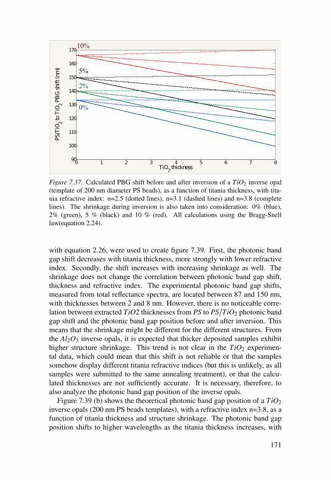
Figure 7.37. Calculated PBG shift before and after inversion of a TiO2 inverse opal(template of 200 nm diameter PS beads), as a function of titania thickness, with tita-nia refractive index: n=2.5 (dotted lines), n=3.1 (dashed lines) and n=3.8 (completelines). The shrinkage during inversion is also taken into consideration: 0% (blue),2% (green), 5 % (black) and 10 % (red). All calculations using the Bragg-Snelllaw(equation 2.24).
with equation 2.26, were used to create figure 7.39. First, the photonic bandgap shift decreases with titania thickness, more strongly with lower refractiveindex. Secondly, the shift increases with increasing shrinkage as well. Theshrinkage does not change the correlation between photonic band gap shift,thickness and refractive index. The experimental photonic band gap shifts,measured from total reflectance spectra, are located between 87 and 150 nm,with thicknesses between 2 and 8 nm. However, there is no noticeable corre-lation between extracted TiO2 thicknesses from PS to PS/TiO2 photonic bandgap shift and the photonic band gap position before and after inversion. Thismeans that the shrinkage might be different for the different structures. Fromthe Al2O3 inverse opals, it is expected that thicker deposited samples exhibithigher structure shrinkage. This trend is not clear in the TiO2 experimen-tal data, which could mean that this shift is not reliable or that the samplessomehow display different titania refractive indices (but this is unlikely, as allsamples were submitted to the same annealing treatment), or that the calcu-lated thicknesses are not sufficiently accurate. It is necessary, therefore, toalso analyze the photonic band gap position of the inverse opals.
Figure 7.39 (b) shows the theoretical photonic band gap position of a TiO2inverse opals (200 nm PS beads templates), with a refractive index n=3.8, as afunction of titania thickness and structure shrinkage. The photonic band gapposition shifts to higher wavelengths as the titania thickness increases, with
171

the same correlation for all shrinkages, following a similar correlation (PBGposition in nm ∼ 9× thickness + 327). The photonic band gap position shifts tolower wavelengths with increasing structure shrinkage, for all thicknesses. Forlower refractive indices, the photonic band gap position shifts towards higherwavelengths with thickness, but with a lower slope than for a refractive indexvalue of n=3.8. The experimental photonic band gap positions are located be-tween 336 and 404 nm. It is possible to relate photonic band gap position andPS/TiO2-TiO2 photonic band gap shift, which vary with structure shrinkage.By doing so, the shrinkage was found to be similar to that inferred from thePS/TiO2-TiO2 photonic band gap shift versus TiO2 thickness, extracted fromthe PS/TiO2-PS photonic band gap shift, using the Bragg-Snell law. Fromthis, it is possible to assess the titania thickness as a function of photonic bandgap position and shrinkage. This second thickness determination is similar tothe first, with thicker films in the second case (around 2 nm in average). Theshrinkage remains unlinked to the film thickness, with films as thick as 8.5 nmwithout any structure shrinkage and films with 5 nm having a shrinkage of upto 9 %. Only 5 sanples out of 22 display a structure shrinkage, according tothe determined film thickness from the PS/TiO2-PS photonic band gap shift.The resulting plot of photonic band gap position versus second film thickness(or corrected film thickness) can be seen in figure 7.38. This leads to the fol-lowing correlation: PBG position in nm ∼ 8.5× thickness + 323 (with a R2
value of 0.54). This shows that the TiO2 inverse opals follow, in general, theexpected theoretical behaviour for anatase films. For the films with seeminglydifferent behaviour, it is possible to consider that the refractive index is closerto amorphous titania (n=2.5), leading to smaller shrinkage values and slightlythicker films. As it is difficult to derive if such samples would have lower re-fractive indices, without making ellipsometry measurements. All thicknessesderived from the optical data are displayed in table 7.9.
Inverse opal quality
The theoretical value of ΔλPBG for a TiO2 inverse opal, was calculated byHwang et al. [202], using a refractive index value of n=2.5, and estimatedto be around 0.6, for completely filled tetrahedral voids (same reasoning asfor an Al2O3 inverse opal). Similarly, the size of the photonic band gap wasdetermined as around Δλ = 0.1, and the corresponding pbe value 0.17. Ascan be seen in figure 7.39 (a), ΔλPBG depends not only on titania thickness,but also on the refractive index, with increasing difference for thicker depo-sitions. For n=3.8, below 10 nm, ΔλPBG ∼ −0.02× thickness + 0.86; showingthat ΔλPBG decreases with increasing deposition thickness. By using the cor-rected thicknesses determined earlier (see table 7.9), it is possible to obtainfigure 7.40. The experimental data is as follows: ΔλPBG ∼ −0.018× thickness+ 0.85 (R2 = 0.99). The fit is not surprising, as the photonic band gap positionwas used to calibrate the deposited thicknesses. If the thickness determined
172

Figure 7.38. Experimental PBG of TiO2 inverse opals (template of 200 nm diameterPS beads), as a function of corrected titania thickness. Linear fit in red, correspondingequation shown on the top left of the figure.
from the PS/TiO2 −PS photonic band gap shift is used instead, the fit is lesslinear, with higher scattering: ΔλPBG ∼ −0.015× thickness + 0.82 (R2 = 0.54).
The average pbe is 0.12±0.02 (equation 7.9) and the average ΔR is 0.29±0.1 (equation 7.6). The pbe seems to increase slightly with increasing titaniathickness (using the corrected thickness for n=3.8), while ΔR displays no cor-relation. The increase in pbe with titania thickness can be expected, as theincreasing titania filling factor in the structure would strengthen the photoniceffect, and so increase the FWHM until the maximum photonic band gap widthis reached. For the thin film samples, the increasing thickness would also leadto a stronger long-range order, since the lower ALD cycles samples do notdisplay any photonic features on the optical data, which was suggested to be aresult of loss of order during inversion.
7.3.2 Al2O3/TiO2 Inverse opalsTotal, Specular and Diffuse
An example of diffuse, specular and total transmittance (a) and reflectance (b)spectra can be found in figure 7.41; from a 200 nm diameter PS bead template,fabricated with 150 and 166 ALD cycles for alumina and titania deposition,respectively (R200Advanced, sample June15[...]02H). The reflected diffuselight is below the detection limit of the Lambda900, so that, as seen for otherinverse opals, the specular and total reflected light are similar. The photonicband gap peak is clearly visible, situated around 393 nm, with the highest
173

Figure 7.39. (a) Calculated ΔλPBG of TiO2 inverse opals (template of 200 nm diam-eter PS beads), as a function of titania thickness, with titania refractive index: n=2.5(black), n=3.1 (purple) and n=3.8 (light blue). (b) Shrinkage during inversion influ-ence on PBG position as a function of titania thickness, with n=3.8. All calculationsusing the Bragg-Snell law.
174

Table 7.9. Experimental PBG and PBG shift (nm), TiO2 calculated thickness fromPS/TiO2 −PS PBG shift (see table 7.6), corrected using n=3.8 (and n=2.5), as wellas inferred shrinkage from PBG position and PS/TiO2−TiO2 PBG shift. All samplesare TiO2 inverse opals created with the R200 Advanced.
PBG position PBG shift thickness (nm) shrinkage (%)
TiO2 PS/TiO2−TiO2 PS/TiO2-PS n=3.8 (n= 2.5)
336 147 4.5 4.7 (4.8) 9 (4)350 138 5.5 5.5 (5.9) 7 (2)353 124 3.3 3.3 1353 134 5.7 5.8 (5.4) 7 (0)360 113 2.4 3.7 0360 132 6.3 6.6 (6.8) 7 (0)365 113 3.9 4.2 0365 115 4.1 4.2 0366 111 3.3 4.3 0368 108 3.1 4.6 0368 110 3.9 4.6 0369 109 3.5 4.7 0372 125 7.6 7.6 (9.3) 6 (0)373 108 3.9 5.1 0377 109 5.1 5.5 0378 102 3.9 5.7 0387 105 6.1 6.6 0390 90 3.5 7.0 0393 89 4.7 7.3 0397 87 4.9 7.7 0398 89 5.3 7.8 0404 94 6.5 8.5 0
reflected signal below 40 %. The reflected light is constant in the visible anddecreases slightly below 350 nm. As for the transmitted light, the diffusespectrum is constant in the visible range, up to the photonic band gap peak,after which the transmission goes to zero. A similar analysis can be madefor the regular part. The total spectrum has a constant transmitttance in thevisible, the presence of a photonic band gap peak at around 387 nm, with notransmittance below 350nm. The total transmittance photonic band gap peakis not complete, with the blue edge missing, due to the absorption by the titanialayer.
Photonic band gap position
It is possible to follow the photonic band gap position at each step of the fabri-cation, as illustrated from the total reflected spectra in figure 7.42(a) fabricated
175

0 1 2 3 4 5 6 7 8 9 100.65
0.7
0.75
0.8
0.85
0.9
TiO2thickness(nm)
∆λPB
G
Figure 7.40. Experimental versus calculated (light blue dashed line) ∆λPBG versusTiO2 thickness, for n=3.8, D=200 nm. Thickness derived from corrected (black ○)and PS/TiO2−PS PBG (purple △) shift described in table 7.9.
200 300 400 500 600 700 8000
20
40
60
80
100
200 300 400 500 600 700 8000
20
40
60
80
100
200 300 400 500 600 700 8000
20
40
60
80
100
Wavelength(nm)
200 300 400 500 600 700 8000
20
40
60
80
100
200 300 400 500 600 700 8000
20
40
60
80
100
200 300 400 500 600 700 8000
20
40
60
80
100
Wavelength(nm)
Transmission ReflectionI/I0
I/I0
I/I0
I/I0
I/I0
I/I0
(a) (b)
Diffuse
Specular
Total
Diffuse
Specular
Total
Figure 7.41. Measured diffuse, specular and total transmitted (a) and reflected (b)spectra of an Al2O3/TiO2 inverse opal fabricated with a 200 nm diameter PS beadtemplate and 150/166 ALD cycles respectively.
176

using a 200 nm diameter PS bead template, 150 and 232 ALD cycles to depositalumina and titania, respectively (R200Advanced, sample June15[...]01G).The photonic band gap shifts from 459 nm for the template, to 492 nm af-ter alumina deposition, then shifts to lower wavelengths after inversion (332nm), and to lower energies after titania deposition, with anatase phase, at 409nm. The photonic band gap peak shape is modified after titania deposition,seemingly with an increased FWHM. This is expected since the photonic bandgap effect from titania is stronger than for alumina, with an increased refrac-tive index difference. Figure 7.42(b) shows the total reflected and transmittedlight for the same sample, at the Al2O3/TiO2 stage, with the correspondingcalculated absorptance. The absorptance has a similar behaviour as the TiO2thin film, seen in figure 7.33, with a low absorption in the visible and a highand constant absorption in the UV range (below 350 nm). The only differenceis the presence of an extra absorptance peak at the photonic band gap posi-tion and around it. This is slighly surprising, as absorptance is expected toincrease at the edges of the photonic band gap, due to the presence of mul-tiple scattering in the photonic crystal. The center of the photonic band gap,in the presence of a perfect 3D gap should display zero absorptance (A=1-(R+T), with R=1 and T=0). The photonic band gap is, however, not perfect,and the total transmittance is not zero at the photonic band gap and the totalreflectance is below 40%, so that light at the photonic band gap withins thesample experiences multiple internal reflections.
The effect of the titania deposition thickness is the same as for a TiO2 in-verse opal: thicker titania films deposited on the Al2O3 structure, shift thephotonic band gap position to higher wavelengths. This is illustrated in fig-ure 7.43, where the total reflectance spectra of different photonic structures,fabricated from 200 nm diameter PS bead templates and 150 ALD cycles foralumina deposition, but different values of ALD cycles for titania deposition,are displayed. The inverse opals photonic band gap position shifts from 359nm (125 cycles), 393 nm (166 cycles), 406 nm (187 cycles) and finally to 420nm (232 cycles). This shift is expected, since the filling factor of titania in-creases with deposition, increasing the value of the photonic band gap position(Bragg-Snell law: 2.24, together with equations 2.26 and 7.14). The effect isstronger than for the alumina deposition, due to the higher value of the titaniarefractive index.
From the photonic band gap position shift before and after titania depo-sition, and annealing at 450○C, and using the Bragg-Snell equation (2.24),together with equations 2.26 and 7.14), it is possible to estimate the titaniathickness for each sample. The previously determined alumina thickness andstructure shrinkage were used, so that any error from these values will be foundin the TiO2 thickness. Table 7.10 summarizes the photonic band gap positionwith alumina and titania thicknesses, from transmittance and reflectance opti-cal data, as available.
177

Figure 7.42. Measured total reflectance spectra of a PS opal (pale blue), fabricatedwith 200 nm diameter beads, corresponding PS/Al2O3 opal (purple) after 150 ALDcycles, Al2O3 inverse opal (dark blue) after inversion and Al2O3/TiO2 inverse opalafter 232 ALD cycles (a). Total transmittance (blue) and reflectance (beige) spectrafor the same Al2O3/TiO2 inverse opal and resulting absorptance (green), as a functionof wavelength (b).
178

Figure 7.43. Measured total reflectance spectra of Al2O3/TiO2 inverse opals after150 ALD cycles and 125 (red), 166 (blue), 187 (purple) and 232 (black) ALD cycles,respectively.
Titania phase
The position of the photonic band gap, close to the absorption edge, with theaddition of the alumina layer, makes it difficult to obtain the electronic bandgap (Eg) of the samples using Tauc plot and equation 7.16. Figure 7.44 (a)shows the Tauc plot for an Al2O3/TiO2 inverse opal, fabricated using 150 and62 ALD cycles to deposit alumina and titania, respectively (R200 Advanced,sample Oct14[...]02F). The electronic band gap was determined to be around2.8 eV, for a titania thickness of 4 nm. Figure 7.44 (b) shows the Tauc elec-tronic band gap of the different inverse opal structure, as a function of calcu-lated titania thicknesses, from transmitted (T) and reflected (R) optical data(as described in table 7.10). The band gap decreases with increasing titaniathickness. This is similar to the results from the TiO2 inverse opals. It seemsthat the same analysis can be made, with a quantum confinment effect and apossibility of anatase crystals imbedded in a titania amorphous matrix. How-ever, for the thicker samples the photonic band gap is very close to the elec-tronic band gap, and even in the absorption tail just below it. This will causea systematic underestimation of Eg, because of the experimentally determinedenhanced absorption (of unclear origin) in the photonic band gap region.
A decreasing number of anatase crystals to amorphous matrix with increas-ing titania film thickness could explain a change in absorptance and thereforea change in the Tauc electronic band gap. This can be seen in figure 7.45,where absorptance before and after baking are shown.
179

Figure 7.44. (a) Tauc plot of Al2O3/TiO2 inverse opal fabricated from a 200 nm di-ameter PS beads template, 150 and 62 ALD cycles to deposit alumina and titania,respectively (sample Oct14[...]02F). (b) Tauc electronic band gap of Al2O3/TiO2 in-verse opals extracted from Tauc plots as a function of titania thickness, inferred fromPBG shift in reflectance (black ○), see table 7.10.
180

Table 7.10. Experimental PBG and PBG shift (nm), Al2O3 calculated thickness fromPS/Al2O3 −PS PBG shift (see table 7.5), using n=3.8, as well as inferred shrinkagefrom PBG position and PS/Al2O3−Al2O3 PBG shift. TiO2 calculated thickness fromequations 2.24, 2.26 and 7.14. All samples are Al2O3/TiO2 inverse opals created withthe R200 Standard and R200 Advanced.
PBG position (nm) PBG shift (nm) thickness (nm)
Al2O3/TiO2 Al2O3−Al2O3/TiO2 Al2O3 TiO2
from T or R from T (from R) from T or R from T or R
328 4 (4) 7.1 0.5353 12 (26) 8.1 1.15356 18 (22) 8.1 1.3372 X (42) 8.1 2.05373 35 (X) 3.6 1.75378 38 (X) 21.9 2.05385 47 (49) 8.1 2.7389 53 (X) 4.6 2.4392 61 (X) 14.7 3.1393 51 (X) 14.2 3.0396 57 (61) 8.1 3.15397 67 (69) 10.2 3.55399 59 (59) 13.2 3.15401 57 (67) 11.7 3.55406 65 (69) 7.1 3.25409 75 (77) 12.6 3.75412 74 (X) 19.3 3.85414 73 (X) 22.5 4.6420 84 (84) 6.1 3.95421 81 (X) 4.1 3.9456 68 (58) 15.7 5.45
Inverse opal quality
The quality of the multi-layer inverse opals is more difficult to assess, as bothΔλPBG and pbe are expected to decrease with increasing titania thickness, fora fixed alumina thickness and structure shrinkage. For a fixed structure shrink-age (0%), ΔλPBG first decreases with increasing alumina thickness, up to a ti-tania thickness of around 6 nm, and then increases with alumina thickness, asseen in figure 7.46(a). It decreases, for all alumina thickness, with increasingtitania thickness. For a fixed alumina thickness (10 nm), and a varying struc-ture shrinkage, ΔλPBG decreases slightly with increasing structure shrinkage,as seen figure 7.46(b).
Figure 7.47 shows the experimental ΔλPBG values as a function of tita-nia thickness (as defined in table 7.10), and several calculated ΔλPBG vari-
181

Figure 7.45. Measured absorptance for a Al2O3/TiO2 inverse opal, fabricated witha 200 nm PS beads template and 150/187 ALD cycles respectively, before (red) andafter (black) baking at 450○C.
ations with titania and alumina thicknesses and structure shrinkages, usingthe Bragg-Snell law (2.24), together with equation 2.26. It is difficult to il-lustrated the experimental data, but it follows the same trend as the theory,with surprisingly higher ΔλPBG values. This means that shrinkage values, ob-tained via optical characterization, might be unreliable. As for figure 7.48, itrepresents the experimental ΔλPBG values as a function of titania thickness,extracted from the optical data using the linear approximation (cross productbetween total filling of the voids with the known filling factor of the initial PSopal), together with several calculated ΔλPBG variations with titania and alu-mina thicknesses and structure shrinkages, using the Bragg-Snell law (2.24),together with equation 2.26.
No correlation between titania thickness and pbe was found, which is notsurprising, as few samples possess the same alumina thickness and display thesame structure shrinkage. However, for samples with similar alumina thick-ness and structure shrinkage (2 sets of two samples), the pbe decreases withincreasing titania thickness. The average value of pbe is around 0.13±0.03,calculated from the total reflectance spectra. Similarly, no correlation wasfound between ΔR (and ΔT ) with titania thickness. The average values are:ΔR = 0.27±0.04 and ΔT = 0.68±0.10, which are slightly lower than the aver-age ΔR for TiO2 inverse opals.
182
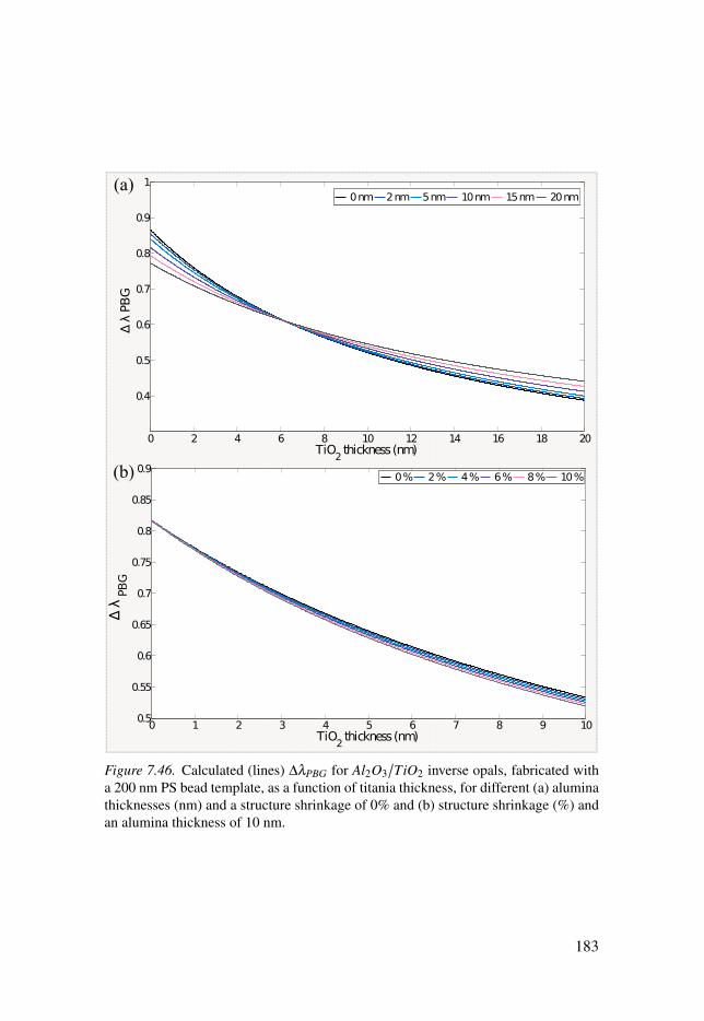
Figure 7.46. Calculated (lines) ΔλPBG for Al2O3/TiO2 inverse opals, fabricated witha 200 nm PS bead template, as a function of titania thickness, for different (a) aluminathicknesses (nm) and a structure shrinkage of 0% and (b) structure shrinkage (%) andan alumina thickness of 10 nm.
183

Figure 7.47. Measured (lines) and experimental (black ○) ΔλPBG for Al2O3/TiO2inverse opals, fabricated with a 200 nm PS bead template, as a function of titaniathickness calculated using equation 7.14, for different alumina thicknesses (nm) andstructure shrinkage (%).
0 5 10 15 200.55
0.6
0.65
0.7
0.75
0.8
0.85
0.9
0.95
TiO2 thickness (nm)
PBG
7 nm 4 %16 nm 7 %10 nm 5 %20 nm 8 %4 nm 0 %experiments
Figure 7.48. Measured (lines) and experimental (black ○) ΔλPBG for Al2O3/TiO2inverse opals, fabricated with a 200 nm PS bead template, as a function of titaniathickness calculated using the linear approximation, for different alumina thicknesses(nm) and structure shrinkage (%).
184

Table 7.11. Baking cycles: 4 hours at 380○C, with a heating rate of 1.5○C/min
Name Number of bakings
July15PS200Q02O 4Avril15PS200Q01B 4June15PS200Q01J 7May14PS200Q02A 15April14PS200Q02D2 24
7.3.3 Effect of bakingExperiments
To assess the effect of baking on the inverse opals, the Lamba900 was used torecord reflectance and transmittance spectra. These spectra were corrected asdescribed earlier to obtain the true transmittance and reflectance. Five spectrawere studied, with different ALD depositions and baking cycles. The sampleswere: Avril15[...]01B, July15[...]02O (TiO2 inverse opals), June15[...]01J,May14[...]02A, Avril14[...]D2 (Al2O3/TiO2 inverse opals). A list of the bak-ing cycles used can be seen in table 7.11. All samples were baked once at450○C for 6 hours, to form anatase.
Results
The effect on the absorption of the inverse opal can be visualized in figure 7.49,showing the intensity of July15[...]02O, before and after 5 baking cycles andAvril14[...]D2 before and after 24 baking cycles. The area values for differentwavelength ranges (A: 200 to 300 nm, B: 300 to 400 nm and C: 400 to 800 nm)of the absorption spectra of all the samples were determined, using the built-infunction trapz from the program Matlab, on the absorbance before and afterbaking. From this, the values of ΔABS were calculated using equation 7.17.
ΔABS = ∫ 300200 ABS(λ)dλ∫ 800200 ABS(λ)dλ
⋅ (7.17)
To verify the effect of baking (EB) on the different samples the followingequation 7.18 was used on the different wavelength ranges:
EB = ΔABSa f ter
ΔABSbe f ore⋅ (7.18)
The interpretation of the absorptance change is clear. If EB is equal to 1,there is no change in absorptance, if EB is below 1, the absorptance decreasesafter baking, whereas if EB is above 1, the absorptance increases after baking.Figure 7.50 shows the different values of EB as a function of baking number.For all samples, the visible wavelength range displays an increase in absorp-tance, while, for most samples, the UV range displays a small decrease ofabsorptance.
185

Figure 7.49. Calculated absorption intensity variation before (black) and after(red) baking, as a function of light wavelength. Samples July15[...]02O (a) andAvril14[...]D2 (b).
186
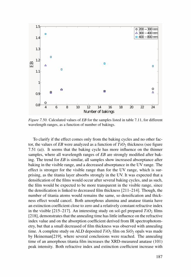
Figure 7.50. Calculated values of EB for the samples listed in table 7.11, for differentwavelength ranges, as a function of number of bakings.
To clarify if the effect comes only from the baking cycles and no other fac-tor, the values of EB were analyzed as a function of TiO2 thickness (see figure7.51 (a)). It seems that the baking cycle has more influence on the thinnersamples, where all wavelength ranges of EB are strongly modified after bak-ing. The trend for EB is similar, all samples show increased absorptance afterbaking in the visible range, and a decreased absorptance in the UV range. Theeffect is stronger for the visible range than for the UV range, which is sur-prising, as the titania layer absorbs strongly in the UV. It was expected that adensification of the films would occur after several baking cycles, and as such,the film would be expected to be more transparent in the visible range, sincethe densification is linked to decreased film thickness [211–214]. Though, thenumber of titania atoms would remains the same, so densification and thick-ness effect would cancel. Both amorphous alumina and anatase titania havean extinction coefficient close to zero and a relatively constant refractive indexin the visible [215–217]. An interesting study on sol-gel prepared TiO2 films[218], demonstrates that the annealing time has little influence on the refractiveindex value and on the absorption coefficient derived from IR spectrophotom-etry, but that a small decreased of film thickness was observed with annealingtime. A complete study on ALD deposited TiO2 film on SiO2 opals was madeby Heineman[219], where several conclusions were reached. The annealingtime of an amorphous titania film increases the XRD-measured anatase (101)peak intensity. Both refractive index and extinction coefficient increase with
187

anneal temperature, due to the densification of the films, and, finally, the de-crease in film thickness (the densification) was not uniform, with some filmsundergoing an increased thickness with anneal temperature.To summarize, baking time has an effect on the films, with increased absorp-tance in the visible and an increased effect with decreased TiO2 film thickness.The effect on the UV-range is small, and contradicts the expected increase ofabsorptance due to the increase in the extinction coefficient, from the densifi-cation of the films. However, the refractive index is also expected to increase,and if the increase is stronger than for the extinction coefficient (as seen in[216, 220]), it could result in increased reflectance without increased absorp-tion, leading to the small observed decrease in UV absorptance. This can beseen in figure 7.51 (b), where the total reflectance has increased in the UV-range, while the total transmittance is constant after 15 baking cycles.The increasing variation with decreasing titania film thickness is more intrigu-ing, and might originate from a faster change in crystalline morphology. Inaddition, it is expected that a very thin film of TiO2 on PS opal, with no de-tectable photonic band gap in the reflected spectrum, would have no photonicorder in the long range. It might be that the manipulation of the film, morethan the baking cycles, has increased the fragility of the structure and in ad-dition destroyed any remaining long-lasting titania films, so that the increaseddiffuse scattering would appear from increasing disorder to be due to the ma-nipulation of a fragile structure. The other samples possess stronger titania (oralumina/titania) skeletons and as such are expected to be sturdier. The pho-tonic band gap position and FWHM for the sample May14[...]02A for differentnumber of baking cycles can be seen in figure 7.51 (b). The photonic band gapposition shifts slightly to lower wavelengths (4 nm in transmission and 7 nmin reflection) and the pbe decreases from 0.13 to 0.10 after 15 baking cycles.There is a shift in the photonic structure due to multiple annealing, even ata fixed temperature, which could be explained by an increasing homegeneityin the titania film. A more detailed study is necessary, to assess the crystalsize from GIXRD measurements, film thickness and refractive index variation(ellipsometry and SEM) after each baking cycle; to be able to clearly explainthe apparent change in optical response of the photonic structures.
188

Figure 7.51. Calculated values of EB for the samples listed in table 7.11, for differentwavelength ranges, as a function of TiO2 thickness (a). Total reflectance (blue) andtransmittance (green) spectra and corresponding absorptance (red) for a Al2O3/TiO2inverse opal after 1 (complete lines) and 15 (dashed lines) baking cyles (b).
189

8. Results in photocatalysis
C’est pas faux.
Frank Pitiotas Perceval le Gallois in Kaamelott
8.1 Fourier Transform InfraRed spectroscopy: stearicacid degradation
Different sets of experimental setups were used to monitor the photocatalyticactivity using FTIR spectroscopy, with UV and visible illumination (Hg andXe lamps respectively). Different objectives were tried to experimentation:probe the photonic band gap (PBG) effect (UV illumination and filter change)and its limits (UV illumination and angle of illumination variation), assessthe effect of illumination power (UV and VIS illumination) and the possibilityof LED-based photocatalysis (LED illumination). For all samples, stearic acid(SA) loading was made prior to illumination, less than 10 minutes before start-ing the light source. The measure of the FTIR spectrum before illumination,after stearic acid loading, can be used to determine the coverage θ (3.1). If thelamp irradiance is known, the photon flux can be calculated and, together witha typical inverse opal transmittance, the quantum yield (Φ) can be determined(3.15). For all samples, the pseudo-first rate constant k was evaluated usingequation 3.3.
Determination of θTo be able to use equation 3.15, it is necessary to determine the total surfacearea of the inverse opals, which leads to the number of possible stearic acidloading sites. The surface area of the samples was not assessed experimen-tally (with the Brunauer–Emmett–Teller method for instance), as it impliesthe destruction of the samples. Instead, theoretical calculations were madeusing simple geometry: the inverse opals were treated as sphere of varyingdiameter (depending on MO thickness), where stearic acid molecules wouldadsorb only on the inside. This of course neglect the holes (removing surfacearea) and the outside of the spheres (adding surface area), which where takenas equivalent, from the difficulty of accessing the outside of the spheres due
190

to the close-packing structure. The fcc geometry was then used to pack thesphere and optically determined sample thicknesses were used to calculate thesurface area of the inverse opals on a 1cm2 area of the quartz substrate. Allsamples were treated with the same formula; so all defaults and inconsistencyin the surface area determination were similar for all samples. To obtain thenumber of possible adsorption sites for each sample, the total surface area ofeach sample was divided by the surface area of stearic acid. The determinationof the number of adsorb species on the sample for each experiment can be de-rived from the evaluation of the total area under the FTIR transmission peak,in the wavenumber range 3000 cm−1 to 2800 cm−1, using the conversion value([132]): 1cm−1 ≡ 9.7×1015cm2. This conversion value gives the total numberof stearic acid molecules per centimer square. It is also possible to calculatethe number of stearic acid layers from the possible number of adsorption sitesand the total number of stearic acid molecules.
Determination of photon fluxThe arc lamps are provided with the manufacturer irradiance, measured at 1m from the lamp and without back reflector. These data were provided in a.pdf format only, so that the irradiance (I, in Wm−2nm−1) was extracted usingthe software Matlab (home-made fonction grabit by user Jiro Doke). Thetotal output power of the lamps (P, in Wm−2), calculated from the irradiancedata sets, need to be calibrated to the actual experimental setup measured totaloutput power. It is necessary to modify the irradiance profile with the filtertransmittance (T) and mirror reflectance (R). This is shown in equation 8.1:
P = ∫ 800
200T ×R× I dλ ⋅ (8.1)
The comparison between the actual measured outpout power (Pm) and the tab-ulated (Pt) one gives a conversion factor f, as seen in equation 8.2:
Pm = f ×Pt ⋅ (8.2)
This factor is then applied to the irradiance, value per value, creating a newirradiance data set, corrected irradiance (IC).To obtain the photon flux (φP), it is necessary to use equation 8.3:
φP = IC(λ)hν
, (8.3)
with hν the photon energy in Ws and φP in m−2s−1nm−1.Finally, the transparency of the sample can be taken into account, to identifynot only the number of photons at the sample surface, but also the number ofphoton absorbed by the sample. A typical absorbance (A,) spectrum was used(May14[...]02A) as follow in equation 8.4:
φPC = φP(λ)×A(λ)⋅ (8.4)
191

The total number of absorbed photons, for anatase titania, per surface area andtime (NP in number of photons s−1m−2 ) can then be calculated using equation8.5:
NP = ∫ 400
200φPC dλ ⋅ (8.5)
8.1.1 UV illuminationTo perform UV illumination, the Hg arc lamp was used between 175 to 200 W.Several bandpass filters were used, and the power was measured at the sampleposition. Unfortunately, no systematic power measurements were conductedregularly during one experiment, so that no data are available to assess lampstabilization. This lack, regrettable, was due to the difficulty of use of an out-dated powermeter, before obtaining the Thorlabs powermeter.
Data
As stated earlier (see 4.2.3), the sample was introduced in the FTIR instru-ment, on a xy-rotary holder, while the arc lamp was outside the instrument, sothat the use of a mirror was needed to illuminate the sample. Few experimentswere conducted with the Al mirror, as its availability was limited, so that mostexperiments involved the Au mirror. The angle of illumination (normal equiv-alent to a notation of 0○) was by default normal, and should be thought as soif unspecified in the text. Two different sample holders were in fact used, withsimilar features apart that one did not allow simultaneous illumination andIR probing; requiring a regular switch between 0○ illumination and IR spec-troscopy. All data with more than 5 minutes interval between measurementswere made with it. This sample holder was discarded as soon as the moreflexible one was found. Due to the small background shift with time, data setsneed to be corrected first with the program OPUS. With a resolution of around4 cm2, a small deviation in the background correction can give a small shiftin the data set. This leads to a limit in the determination of the area under thestearic acid FTIR peaks, several data sets with a very low or zero degradationrate constants k reflects the detection limit of the change of FTIR signal withillumination time.
Steps of a FTIR experimentThe lamp was turned on at least 30 minutes before the measurements wereconducted and would typically be on for 7 to 8 hours. The IR detector wouldbe cooled down at the same time, so that it reached a stabilized temperatureduring the actual measurements. The sample was then spin-coated with 1 mLof stearic acid solution, cleaned on the back-side and sides with ethanol, anddried with a N2 flow (1 bar, 1 min). The next step was to position the sam-ple on the sample holder, with double-tape, and check the IR signal (to avoid
192

detector saturation). If the sample holder does not permit simultaneous il-lumination and IR measurements, the sample was regularly shifted from oneposition to another and single spectrum measurements were made. Ideally, thesample would not change position with manipulation and no extra moleculeswere introduced by the manipulator (water vapor for instance). Difference inphotocatalytic performances for the same sample under similar illuminationconditions could be traced to position change (as the samples were not ho-mogeneous), atmosphere variation between different days of experimentation(for instance with the major role of water vapor, measure of humidity in thelaboratory have shown large monthly differences) and a possible variation inillumination power (i.e. small change in distance between lamp and mirror,heating up of the arc lamp with time of use...). The change in sample holder,allowing simultaneous illumination and spectroscopy should reduce the risksof sample displacement and atmosphere change, within the same experimentalset.
Typical experimental setThe photocatalytic activity of the sample May14[...]01B (ALD cycles Al2O3/TiO2:150/125) was measured after 15 minutes normal illumination, with a lamp setat 175 W, which gave a total output power at the sample of 73 mW. The trans-mission spectra were recorded each after rotating the sample, and transformedto absorption spectra using the program OPUS. The FTIR absorption spectra,after background rubber-band correction, built-in function in the OPUS pro-gram, can be seen in figure 8.1, with the top vurve (red) at time t=0 and thebottom curve (purple) at time t=60 min. The area under the transmission spec-trum before illumination, gives a number of stearic acid molecules per cm−2
equal to 1.8×10¹⁷, corresponding to around 4 layers of stearic acid (coverageθ = 2.2×1026).The corresponding pseudo-rate constant (k) determination, using equation 3.3,can be found in figure 8.2, where the logarithm of the absorbance at time t di-vided by the absorbance at time t=0, was drawn against the time. The slope ofthe linear fit defines k. The grey area around the curve represents the closenessof the linear fit to the data (R2 = 0.98). The value of k for this sample, duringthis experimental set, was found to be 0.0016 min−1.
Angle dependence
SamplesSimilar experimental sets were made onto different samples, while the an-gle of illumination was changed, to probe the 3D photonic band gap. If thephotonic band gap is not complete, the higher the angle of illumination, theworst the photonic effect will be. Also, the photonic band gap position shiftswith the angle of illumination, as seen in the Bragg-Snell law. The samplesshown here are samples May14[...]01B (ALD cycles Al2O3/TiO2: 150/125)
193

Figure 8.1. Typical absorbance FTIR spectra of sample May14[...]01B measured ev-ery 15 minutes after illumination (red to purple) to the normal, with the filter BP57396.Total outpout power measured: 73 mW and determined NP = 2.5×10¹⁶, in number ofphotons s−1m−2 (equation 8.5). ALD cycles Al2O3/TiO2: 150/125, PBG position:385 nm, θ = 3.2×1026 or 6 SA layers.
194

Figure 8.2. Corresponding determination of the pseudo-rate constant k of sampleMay14[...]01B using equation 3.3. Grey represent the goodness of the linear fit: R2 =0.98. ALD cycles Al2O3/TiO2: 150/125, PBG position: 385, θ = 3.2×1026 or 6 SAlayers, NP = 2.5×10¹⁶, in number of photons s−1m−2.
195

and Oct14[...]02G (ALD cycles TiO2: 205). A test sample was created us-ing Degussa P25 nano powder (Aeroxide from Evonik industries, Hanau, Ger-many), on a quartz substrate with spin-coating. This sample (Degussa) wascreated using 3 mL of an ethanol based solution with a concentration of 18mg/mL. It was then baked to 380○C using 3○C/min and then to 450○C with0.6○C/min. The tabulated value[221] of surface area to the material weight(specific surface area: 50 m2/g) was used to estimate the total surface area ofthe sample, reaching a high surface area of 27000 cm2. To compare, sampleMay14[...]01B and Oct14[...]02G have a surface area of 88 cm2 and 202 cm2,respectively. The power of the lamp was kept at 175 W, for all angle measure-ments; with few extra measurements realized to at 0○ illumination, at 190Wand 200W, for sample May14[...]01B (see bottom panel of figure 8.4), whichgives a total power at the sample around 105 mW. The filter BP57396 wasused for all the data presented here. The FTIR measurements were performedevery 15 minutes.
ResultsAs the angle of illumination change from 0○ to 45○ in 15○ steps, the powerat the sample diminish, from 73 mW to 52 mW, respectively; as displayedin the bottom panel of figures 8.3, 8.4 and 8.5. The sample Degussa outper-formed, as expected, all types of inverse opals, with pseudo-rate constants es-timated between 0.013 min−1 and 0.067 min−1, while the highest k value was0.014 min−1 (Oct14[...]02G, 30○). But to compare the data sets, it is easier toshift to the comparison of the quantum yield (Φ). The top panels in figures 8.3,8.4 and 8.5, display the quantum yields determined at each angle of illumina-tion. The sample Degussa Φ values remain relatively stable between 0.0015and 0.0023 (28% variation), with one experiment at 0○ with a much lower Φvalue (0.0001), which could derived from the fact that very little stearic acidwas deposited on the sample, in comparison to the other experiments (num-ber of stearic acid layers: 0.0005 against 0,006 for the lowest loading). Thisdifference in stearic acid loading was not found in any of the other data sets.Samples May14[...]01B and Oct14[...]02G seems much more affected by theillumination angle, without clear conclusive trait. Figure 8.4 shows that Φdecreases with increasing illumination angle, but deviations were seen for thesame angle. For instance, at 15○, for a fixed 175 W lamp power, the valueof Φ has a 80% variation. Also, the data recorded at the normal with a lamppower of 190W and 200W, produced lower Φ values. As seen in figure 8.5,a similar observation can be made for sample Oct14[...]02G: a variation of Φcan be seen for similar experimental conditions (i.e. the normal illuminationhas a 45% variation). The trend of Φ with illumination angle is even less clear.
Unfortunately, no total output power measurements were performed system-atically, so that variation in outpout power could have been underestimated,
196

5 0 5 10 15 20 25 30 35 40 45 500
1
2
3x 10 3
0 5 10 15 20 25 30 35 40 4550
60
70
80
Angle (°)
pow
er (m
W)
Figure 8.3. Top: determined quantum yield (Φ) using 3.15. Bottom: measured powerat the sample position, as a function of illumination angle, for the Degussa P25 film.
Figure 8.4. Top: determined quantum yield (Φ) using 3.15. Bottom: measured powerat the sample position, as a function of illumination angle, for the May14[...]01B.ALD cycles Al2O3/TiO2: 150/125, PBG position: 385 nm. The highest Φ value at 0○
illumination is associeted with a measured power of 73 mW.
197

Figure 8.5. Top: determined quantum yield (Φ) using 3.15. Bottom: measured powerat the sample position, as a function of illumination angle, for the Oct14[...]02G. ALDcycles TiO2: 205, PBG position: not optically measureable.
and therefore influence the determination of NP, which in turn influence thevalue of Φ. It seems, however, that the inverse opals are more sensitive tothe angle of illumination than the film Degussa; which was expected due tothe imperfect photonic band gap in real 3D structures. A better approach tothis experimental set would be the use of a fiber optic, which would allow abetter control on the illumination angle and the output power (the mirror be-come obsolete), and a more systematic monitoring of the illumination power.Also, due to the fluctuations in the environment of the FTIR instrument and theinhomogeneity of the samples, an increase of the data set would be welcome.
With filters around the photonic band gap
SamplesThe idea of this experimental set was to probe a selectively in, near and outof the photonic band gap of different samples, using different filters, as il-lustrated in figure 8.6. A narrow band pass filter (less than 20 nm) can beuse to probe: at the PBG (in grey, centre of the peak), at the red and blueedges, and, finally, out of the blue edge (in purple) and red edge (in orange).It is expected that samples should exhibit higher Φ with filters at the edgesof the photonic band gap, than out of the photonic band gap range. In the-ory, probing the photonic band gap should decrease considerably Φ, close tozero, if the photonic band gap structure is perfect. Some out of red edgesband pass might be outside the absorption range of titania, and no photo-
198

Figure 8.6. Illustration of band pass filters choice to probe at the PBG (grey: PBG), atthe edges of the PBG, at lower energies (red: R) and higher energies (blue: B). Filterscan also be chosen to be outside the PBG range, corresponding to the FWHM mea-sured via photospectroscopy, at lower energies (orange: OUT R) and higher energies(purple: OUT B).
catalytic activity is then expected. Three samples were used: JuO50Q03J(ALD cycles Al2O3/TiO2: 150/25), May14[...]01B (ALD cycles Al2O3/TiO2:150/125) and Avril14[...]02D2 (ALD cycles Al2O3/TiO2: 150/187), with pho-tonic band gap position at 328, 385 and 397 nm, respectively. The sup-ply of band pass filters being limited, not all 5 positions were probed persample; but 4 repeated measurements were made for each band pass andeach sample. Sample JuO50Q03J was probed: out blue (BP 56501), blue(BP56511) and out red (BP56531). Band pass filters out blue (BP56511), blue(BP56531) and red (BP56541) were used for sample May14[...]01B. As forsample Avril14[...]02D2, the out blue (BP56511), blue (BP56531) and PBG(BP56541) position were probed. The measured total transmittance of theband pass filters are displayed in figure 8.7, with irradiance profiles, from thelamps after the filters, closely-related to their transmittance. The thickness ofthe filters limit strongly the transmittance of the filters, which decreases thetotal output power reaching the sample (refer to table 4.2), and that are shownin the bottom panels of figures 8.8, 8.9 and 8.10. The lamp power was fixedat 200W and the FTIR spectra were recorded simultaneously with on-goingillumination. The number of photons absorbed per m2s were determined to bebetween 3 ×10¹⁴ and 5 ×10¹⁵; the number of stearic acid layers for all datawere comprised between 0.7 and 8.0. The total surface areas of the differentsamples were calculated as: 194, 88 and 146 cm2 for Ju[...]03J, May[...]01Band Avril[...]D2, respectively.
199

Figure 8.7. Total transmittance of different band pass filters BP 56: 501 (black), 511(dark blue), 531 (blue), 541 (light blue) and 551 (pastel blue), from left to right.
ResultsAll data sets were analysed as previously described: the corrected irradiancewas found, allowing for the determination of the photon flux, the FTIR trans-mittance spectra before illumination were analysed to determine the numberof stearic acid molecules on the surface of the inverse opals, which gives thepossibility to calculate θ , and henceforth, the quantum yield Φ. The pseudo-first order rate constants k were not always consistent between experiments,for the same sample and same illumination conditions. Considering the re-sults provided from the previous experimental set, this is unsurprising; andderived from the same reasons: inhomogeniety of the sample itself and lampoutput power. Certain linear fits were far from ideal, with R2 values below0.70, meaning that the photocatalytic behaviour measured at the time was farfrom the ideal pseudo-first order. For sample Ju[...]03J, if all k with R2 valuesabove 0.91, the averaged over the different band pass filters can be listed as fol-low: OUT B=0.00025min−1, B=0.00019min−1 and OUT R=0.0min−1. It wasexpected that the blue edge probe would provide a higher photocatalytic activ-ity, and that the out red probe would have some activity (transmission peak at364 nm, within the absorption range of titania). Instead, the k for out blue andblue edges are rather similar and no detectable activity was monitored withthe out red filter. While for sample May[...]01B, k with R2 > 0.88 were usedto average over the different sets for this sample only: OUT B=0.00011min−1,B=8.56 ×10⁻⁵min−1 and R=0.00011min−1. As stated earlier, the blue edge
200

PBG: 328 nm
290 300 310 320 330 340 350 360 3700
1
2
3
4x 10 4
290 300 310 320 330 340 350 360 3702.5
3
3.5
4
PBG features (nm)
pow
er (m
W)
OUT B B OUT R
Figure 8.8. Top: Determined Φ as a function of band pass filters, with the positionof their transmission peak on the x-axis. The corresponding position of the band passfilter to the PBG position of the sample Ju[...]03J are shown: OUT B (purple), B(blue) and R (red). Bottom: Measured total output power at the sample for each bandpass filter for a 200W Hg lamp power, line added to guide the eye.
filter was theorized to have higher photocatalytic activity than the out bluefilter, similarly for the red edge filter. Instead, the out blue and the red bandpass gives an identical averaged k, while the blue band pass has a much loweractivity. Finally, sample Avril[...]D2, with R2 > 0.73, show average k valuesfor: OUT B=0.00018min−1, B=0.00012min−1 and PBG=6.12 × 10⁻⁵min−1.This time, it was expected that the photonic band gap band pass displays noactivity, and that the blue edge band pass outperformed the out blue and pho-tonic band gap band pass measurements. The photonic band gap band pass kis indeed lower than the two other data sets, but the out blue band pass has aslightly higher k. To be able to compare the samples, it is easier to switch toΦ, which takes into consideration the difference in photon flux at the sample.The top panels of figures 8.8, 8.9 and 8.10 represent all the determined Φ foreach band pass filter measurements, for samples Ju[...]03J, May[...]01B andAvril[...]D2, respectively.
Figure 8.8 shows that the quantum yield is rather spread with OUT B andB band pass filters data sets with similar behaviour, so that no measureableeffect on the Φ by the photonic band gap can be inferred for this sample.Figures 8.9 and 8.10 are slightly more promising: on average, the values of Φare different depending on the band pass choice. For sample May[...]01B, theband pass corresponding to the red edge of the photonic band gap position,
201

PBG: 385 nm
340 350 360 370 380 390 400 4100
1
2
3x 10 3
340 350 360 370 380 390 400 4102.5
3
3.5
4
4.5
PBG features (nm)
pow
er (m
W)
OUT B B R
Figure 8.9. Top: Determined Φ as a function of band pass filters, with the positionof their transmission peak on the x-axis. The corresponding position of the band passfilter to the PBG position of the sample May[...]01B are shown: OUT B (purple), B(blue) and R (red). Bottom: Measured total output power at the sample for each bandpass filter for a 200W Hg lamp power, line added to guide the eye.
display, on average, a higher Φ (8.0 ×10⁻⁴) than the other band pass ( in therange 3.0 ×10⁻⁵). The poorer performance using the blue edge band pass filteris surprising, but could be from an over-estimation of the photonic band gapwidth, shifting the blue edge to lower energies (the band pass filter emissionpeak was thought to be only 2 nm above the blue edge position). As for sampleAvril[...]D2, figure 8.10 show a surprising - and yet not so surprising - result:the photonic band gap band pass filter (emission peak situated 8 nm above themeasured photonic band gap position of the sample) has the highest average Φ(8.0 ×10⁻⁴), while the blue edge and out of blue edges have a similar averageΦ (8.0 ×10⁻⁵). In the previous chapter, the absorption of the different inverseopals shows that a small increase in absorbance was measured at the photonicband gap, thought to originate from the multiple reflections at the imperfectphotonic band gap borders.
Two samples displays different photocatalytic behaviour depending on thewavelength range probed, while one sample (with the lowest number of de-position cycles for titania) shows no detectable differentiation. It would beinteresting to obtain more band pass filters or lasers to probe very specificenergy ranges for more samples, notably for samples with only titania and
202

PBG: 397 nm
340 305 300 365 360 375 370 385 380 395 390 4555
510
2
210x 25 3
305 300 365 360 375 370 385 380 395 390 455. 10
3
310
4
410
PBG features (nm)
pow
er (m
W)
OUT B B PBG
33
Figure 8.10. Top: Determined Φ as a function of band pass filters, with the positionof their transmission peak on the x-axis. The corresponding position of the band passfilter to the PBG position of the sample Avril[...]D2 are shown: OUT B (purple), B(blue) and PBG (black). Bottom: Measured total output power at the sample for eachband pass filter for a 200W Hg lamp power, line added to guide the eye.
air as building materials. The determination of Φ allows the fair compari-son between samples, but is however, in this experimental set, limited fromthe negligence of power fluctuations of the lamp during use (the total outputpower at the sample positions were measured only once).
With filters AM0 and AM1.5
SamplesTo allows higher total output power at the sample position in the UV rangefor a modified solar spectrum, the filters AM0 and AM1.5 were used in com-bination with the Hg arc lamp (with a power maintained at 200W). The cor-responding corrected irradiance can be seen in figure 8.11, the UV range istherefore much less present than the visible part of the spectrum. The sam-ple’s May14[...]01A and May14[...]01B (ALD cycles Al2O3/TiO2: 150/125),May14[...]02A and Avril14[...]D2 (ALD cycles Al2O3/TiO2: 150/187) pho-tocatalytic activity was measured 3 times, apart for sample May14[...]02A (7times). Depending on the availability of the sample holder, the FTIR spec-trum were recorded after 15 minutes illumination (change of sample holderxy-plane angle necessary) or 5 minutes (simultaneous recording), see section4.2.3 for more experimental details. The total output power at the sample po-sition varied from 41 mW (3.0 ×10¹⁵ number of photons /m2s) and 96 mW
203

Figure 8.11. Corrected irradiance for the Hg arc lamp, after correction from thetransmittance of the filters AM0 and AM1.5, the reflectance of the gold mirror and themeasured total output power at the sample position. See appendix B for the originaldata sets.
(5.4 ×10¹⁷ number of photons /m2s). The number of stearic acid layers at thesurface of the samples were determined to be between 1 and 6, for total samplesurface areas between 88 and 166 cm2, corresponding to θ values comprisedbetween 1 and 6 ×1026. A single measurement was also conducted on a quartzsubstrate.
ResultsAll data sets were brought together to analyse the different photocatalytic be-haviour of the samples. Figure 8.12 display the determined pseudo-rate con-stant k (top) and quantum yield Φ (bottom) values as a function of total outputpower measured at the sample position. The k values are spread, mostly for thehigher total output power values, and seems to shows that higher power valueswould correspond to higher rate constants (at the exception of two data pointsat 68 mW, 83 mW and 93 mW corresponding to measurements on sampleMay14[...]02A, with an illumination angle of 45○, 30○ and 15○, respectively.As for Φ, no such trend can be seen, with 41 mW output power showing sim-ilar Φ values as for 96 mW output power.
Figure 8.13 show the same data sets but as a function of coverage θ , the toppanel shows the correlation with k , while the bottom panel with Φ. No cleartrend can be inferred from the two plots, which comply with the base hypoth-
204

Figure 8.12. Top: pseudo-rate constant k and Bottom: quantum yield Φ, as a functionof measured total output power at the sample position, for all measured samples.
esis of first order kinetics: the rate constant is independent on the pollutantconcentration.
Finally, figure 8.14 display the quantum yield Φ as a function of the posi-tion of the photonic band gap, obtained via photospectrometry. Samples withphotonic band gap close to or far from the expected electronic band gap oftitania (375 - 388 nm) have a lower Φ than samples with a photonic band gapwith a blue edge near the electronic band gap of titania. From the optical totalreflection measurements, the relative position of the blue and red edges areknown: May[...]01A B=344 nm & R=400 nm, May[...]01B B=363 nm & R=407 nm, May[...]02A B=373 nm & R=419 nm, and, Avril[...]D2 B=370 nm& R=424 nm. It can be seen that only the last two samples have the photonicband gap edges near titania electronic band gap. Though, from the band passfilter experimental set, it would be expected for sample May[...]01B to havehigher Φ, since its photonic band gap coincide with the electronic gap, andband pass at the photonic band gap have shown to possess a non-negligiblephotocatalytic activity. In average, the Φ can be classified, from the highestto the lowest: Avril[...]D2 (Φ=0.0019), May[...]02A (Φ=0.0009), May[...]01Band May[...]01A (Φ=0.0005). For reference, the Φ of the quartz substrate wasaround 4.3×10⁻⁵.
The data set shows encouraging signs of increased photocatalytic activity viastructuration, with the step up quantum yield (Φ) value of the samples Avril[...]D2
205

Figure 8.13. Top: pseudo-rate constant k and Bottom: quantum yield Φ, as a functionof determined coverage θ , for each photocatalytic experiment.
Figure 8.14. Determined quantum yield Φ values as a function of measured PBGposition of the inverse opals: 372nm (May[...]01A), 385nm (May[...]01B), 396nm(May[...]02A) and 397nm (Avril[...]D2).
206

and May[...]02A, with a blue edge at around 370 nm, near the window of pos-sible electronic band gap of titania (375 - 388 nm). As usual for these exper-imental sets, higher number of measurements and a more closely monitoringof the lamp stability would have been welcome to draw a clear conclusion.Instead, at this stage, the photonic band gap structure is not the direct visibleagent of systematic photocatalytic activity increase. Further experiments arenecessary to argument in favour of the hypothesis.
8.1.2 Solar spectrumData
This experimental set was conducted to assess the samples solar illuminationphotocatalytic activity and check if the photonic structure has a positive andmeasurable effect. The Hg arc lamp was therefore replaced by the Xe arc lamp,and filters AM0 and AM1.5 were used. The lamp power was set at 200 and300 W and the total output power at the lamp and at the sample were mea-sured hourly and daily with the Thorlab wattmeter. A summary of the lampstability can be seen in appendix B. All inverse opals samples (see appendixA for a complete list) were measured at least twice, several thin films, quartzsubstrate and a PS opal were also tested. Irradiance was corrected using adaily averaged output power at the sample, which varied between 7 and 15mW. The corrected irradiance for 15 mW sample output power can be seenin figure 8.15. The total irradiance in the UV range is 6.3 Wm−2, while thevisible range is 1.9× 10² Wm−2. From irradiance, photon flux and numberof absorbed photon per area and time (NP), can be calculated. The transmis-sion of the sample after stearic acid deposition, and before illumination, wasused to determine the number of stearic acid molecules per area and thereforethe coverage θ . From the decrease of absorbance with illumination time, thepseudo-rate constant (k) was inferred from the linear fit of the logarithm ofthe normalized absorption as a function of illumination time. From NP, θ andk, the quantum yield (Φ) for all measurements was determined. All data arepresented, from inverse opals without photonic band gap to MO thin films.Graphs with photonic band gap are of course concerning only inverse opalswith optically measureable photonic band gap. Average graphs of k excludethe linear fits with R2 values below 0.70. The sample holder used throughoutthe experimental set allowed FTIR spectrum record with illumination, whichmeans that FTIR interferograms were recorded every 5 minutes.
Typical FTIR absorbance spectra of sample Fev15[...]02C (ALD cycle TiO2:275), with a photonic band gap at 369 nm, at lamp power 200 W (averaged to-tal output power at the sample position: 8 mW), can be seen in figure 8.16. Forthis experiment, NP = 3.9×10¹⁴ photons /cm2s and θ = 6.0×1025 (0.5 layer ofSA molecules).
207

Figure 8.15. Corrected irradiance of theXe arc lamp together with filters AM0 andAM1.5, after reflection by the Au mirror, for a total output power measured 15 mW atthe sample position.
The corresponding linear fit is shown in figure 8.17, where the slope ofthe fit gives the pseudo-rate constant k: 0.0053min−1. All inverse opals filmsdisplayed a measurable photocatalytic activity, even films without an opticallydetermined photonic band gap, as seen in figure 8.18. The FTIR absorbancespectra are presented for sample Avril15[...]02A (ALD cycle TiO2: 110), withtotal output power 14 mW (NP = 7.3×10¹⁴ photons /cm2s). The total surfacearea of this sample is 138cm2, together with the area of the FTIR transmissionpeak, gives θ = 2.1×1025 (0.3 layer of SA molecules).
Similarly, the pseudo-rate constant k can be determined from the absorbancespectra, as shown in figure 8.19, which leads to k: 0.0153min−1.
Thin films and PS opal
The photocatalytic activity of a quartz substrate, of the MO films passiva-tion (Al2O3) and TiO2 with 585 ALD cycles, were measured for reference.All FTIR spectra are displayed in figure 8.20 recorded every 5 minutes un-der illumination, for 80, 105 and 85 minutes respectively. From the area ofthe transmission peak, θ was determined to be 2.6×1025 on quartz (19 lay-ers of SA molecules), 1.5×1026 on Al2O3 (109 layers of SA molecules) and4.5×1026 on TiO2 (330 layers of SA molecules). Similarly, the photon fluxwas determined, leading to the calculation of NP for the different experiments:NP = 3.9×10¹⁴ photons /cm2s for the quartz and Al2O3 film and NP = 4.9×10¹⁴
208

Figure 8.16. Absorbance FTIR spectra of sample Fev15[...]02C after 40 minutes ofillumination with the Xe arc lamp (200W). Spectrum measured every 5 minutes, yel-low to pink from top to bottom, corresponding to t=0 and t=40 min, respectively.NP = 3.9×10¹⁴ number of photons /cm2s, θ = 6.0×1025 (0.5 SA layers), ALD cycleTiO2: 275, PBG position: 369 nm.
209

Figure 8.17. Logarithm of the normalized absorbance shown in figure 8.16 as a func-tion of time, with the linear fit using using equation 3.3. The grey area represent thegoodness of the fit: R2 = 0.99.
photons /cm2s for the TiO2 film. As shown in figure 8.20, no visible changecan be detected after illumination, so that no clear photocatalytic activity waspresent. This result is of course unsurprising for the quartz substrate and theAl2O3 thin film. It was expected to be able to record some activity, notablyafter more than an hour illumination, for the TiO2 thin film. It is possible thatthe very thick stearic acid loading did not play in the favour of stearic aciddegradation, with limits in molecule diffusion, away from the film surface.
A PS opal (PS bead diameter 200 nm and concentration 0.2 W/v %, witha photonic band gap at 459 nm) was exposed to 100 minutes illumination,with a total output power at the sample position of 12 mW. The surface areaof the sample was calculated around 353 cm2 and the area under the trans-mission peak before illumination gave a value of θ = 2.9×1026 (1.3 layers ofSA molecules). No measureable photocatalytic activity was found, unsurpris-ingly.
Effect of lamp power
The daily averaged output power at the sample varied between 7 and 15 mW,so that several samples where measured at different values of NP. To assessthe effect of lamp power on the photocatalytic activity of the inverse opals, thelogarithm of the normalized absorption of four samples was plotted againstillumination time, allowing for the determination of the pseudo-rate constant
210

Figure 8.18. Absorbance FTIR spectra of sample Avril15[...]02A after 40 minutes ofillumination with the Xe arc lamp (300W). Spectrum measured every 5 minutes, red topink from top to bottom, corresponding to t=0 and t=40 min, respectively. ALD cycleTiO2: 110, NP = 7.3×10¹⁴ photons /cm2s, θ = 2.1×1025 (0.3 layer of SA molecules),PBG position: not measureable optically.
211

Time (min)0 10 20 30 40
-0.6
-0.4
-0.2
0.0ln
(At/A
0)
Figure 8.19. Logarithm of the normalized absorbance displayed in figure 8.18 as afunction of time, with the linear fit using using equation 3.3. The grey area representthe goodness of the fit: R2 = 0.99.
k. Three FTIR measurements were made per sample with 9 mW (or 7 mW),11 mW and 14 mW total output power. Figure 8.21 display the data set offour samples: Avril15[...]01A and Avril15[...]01B (ALD cycle TiO2: 167),July15[...]02S and July15[...]02T (ALD cycle TiO2: 275). For all samples,the photocatalytic activity seems to increase with lamp power. The coveragewas determined as before, and be found to be varying between θ = 9.1×1024
and θ = 5.4×1026, corresponding to 0.1 and 5 layers of stearic acid molecules,respectively.
Table 8.1 shows the determined k values from the data set in figure 8.21. Forall samples, k increases significantly for illumination powers below 10 mW,but seems rather stable above. It has already been stated earlier (see chapter 3)that low power illumination could influence on the speed of the photocatalyticreaction, until a more stable regime is reached at higher power. It seems thatpowers below 10 mW might be unreliable to assess the photocatalytic activityof the samples in the solar illumination experimental set.
Surface coverage θThe total surface area of the TiO2 inverse opals (138 to 251 cm2) are on aver-age larger than for Al2O3/TiO2 inverse opals (128 to 181 cm2). All coverage(θ ) values were obtained using the area underneath the FTIR transmissionpeak in the dark, and converted to number of stearic acid molecules per area,
212

Figure 8.20. Absorbance FTIR spectra recorded every 5 minutes (red to blue) of (a)a quartz substrate, (b) a Al2O3 film (1070 ALD cycles) and (c) a TiO2 (585 ALDcycles).
213

−0.075
−0.050
−0.025
0.000
0 10 20 30 40Time /min
ln(A
bs)
July02S
−0.25
−0.20
−0.15
−0.10
−0.05
0.00
0 10 20 30 40Time /min
ln(A
bs)
Avril01A
−0.15
−0.10
−0.05
0.00
0 10 20 30 40Time /min
ln(A
bs)
July02T
−0.3
−0.2
−0.1
0.0
0 10 20 30 40Time /min
ln(A
bs)
Avril01B
Figure 8.21. Different pseudo-rate constant k determination for four inverse opals,with different total output power: 9 mW - 7mW for Avril15[...]01B - (green ◻), 11mW (blue ◇)- 13mW for Avril15[...]01B and 14 mW (black ○). From top left to rightPBG positions: 398 and 397 nm, bottom: not measurable optically.
214

Table 8.1. Determined k values for different inverse opals with different total outputpower at the sample. R2=0.99 for all but Avril[...]A at 7 mW, where R2=0.88.
Sample Avril[...]A Avril[...]B July[...]S July[...]T
Power (mW) k (min−1)
7 or 9 7.8×10⁻⁵ 8.8×10⁻⁴ 5.3×10⁻⁴ 2.7×10⁻⁴
12 6.5×10⁻³ 7.9×10⁻³ 2.3×10⁻³ 3.9×10⁻³
14 3.4×10⁻³ 3.6×10⁻³ 1.3×10⁻³ 1.8×10⁻³
Figure 8.22. Top: number of SA layers and Bottom: coverage θ ; as a function ofAl2O3 ALD cycles for all inverse opal samples. All samples with ALD depositedtitania.
related to the number of possible stearic acid absorbing sites on each sample.To assess the difference in coverage depending on the presence or absenceof alumina, figure 8.22 shows θ as a function of number of Al2O3 ALD cy-cles. It shows that the TiO2 inverse opals (with number of Al2O3 ALD cyclesequal to zero) can harbour more layer of stearic acid, with the highest θ val-ues (θ = 7.5×1026), but it does not guarantee a high coverage. In average, forTiO2 inverse opals, θ = 2.33×1026; while on average for Al2O3/TiO2 inverseopals, θ = 2.19×1026, which is rather similar.
The effect of total titania surface area is also verified in figure 8.23, againstthe number of stearic acid layers. No correlation was found between avail-able surface and stearic acid loading, assuring homogeneous conditions for theevaluation of the photocatalytic activity of the different samples (with varying
215

Figure 8.23. Number of SA layers as a function of total surface area for all inverseopals.
stearic acid loading for similar samples). Since the number of layers remainsrelatively small (below 8), the diffusion of the molecules at the surface of thecatalyst should be similar for different loadings. It is possible however, that themultilayer inverse opals pose more difficulty for molecules diffusion, at leastin the liquid phase (stearic acid in methanol), due to the presence of thickerwalls.
Degradation rates
All FTIR spectra were used to determine the pseudo-rate constant k and thefinal results are plotted in figure 8.24. The k values are spanned between2.6× 10−5min−1 and 1.5× 10⁻²min−1. As seen earlier, total output powersbelow 10 mW display lower k, while higher powers do not show a specificcorrelation with k. More surprisingly, the coverage θ seems to influence k,mostly for lower coverage values, corresponding to higher k values. Though,not all low coverage leads to high k, due to the difference in total output power.Comparing samples illuminated with power above 10 mW, it is a recurrenteffect: lower θ leads to higher k for the same sample. Meaning that stearicacid loadings with θ below 1.0× 1026 (roughly 1 SA layer), would favourthe photocatalytic activity. The partial coverage of the total MO surface areawould allow faster diffusion and desorption within the inverse opals.
216

Figure 8.24. Pseudo-rate constant k for all inverse opals as a fonction of total outputpower at the sample position (top) and determined coverage θ (bottom).
Efficiency
In order to compare samples with different θ values and total output powerilluminations, the determination of the Quantum Yield Φ is necessary. Figure8.25 display the values of Φ for all experiments, as a function of total outputpower (daily averaged) and coverage θ . The values of Φ vary from 1.6×10⁻⁴ to 2.2×10⁻² and no correlation was found with power or coverage, asexpected.
To evaluate the importance of titania and mutilayering, Φ was plotted againstalumina and titania thickness in figure 8.26 and figure 8.27, respectively. Onaverage samples without alumina seems to perform better, with a total averageΦ= 0.0048, versus Φ= 0.0020 for Al2O3/TiO2 inverse opals. This corroboratethe previous finding of slightly more open structure of titania inverse opals,compare to their multilayer counterparts. It is clear from figure 8.27, that thetitania thickness play a role in the quantum yield of the different samples, butdo not warranty a higher Φ. It is now time to identify a possible influence ofthe photonic band gap structure on the overall photocatalytic activity of theinverse opals.
Photonic band gap effect
Comparison between inverse opalsFirst, the photocatalytic activity of Al2O3/TiO2 inverse opals is compared,in figure 8.28, where samples with similar total output power illumination,but different photonic band gap position (and so blue edge position), displays
217

Figure 8.25. Quantum Yield Φ for all inverse opals as a fonction of total output powerat the sample position (top) and determined coverage θ (bottom).
Figure 8.26. Average quantum Yield Φ for all inverse opals as a fonction of aluminathickness, for multilayer inverse opals.
218
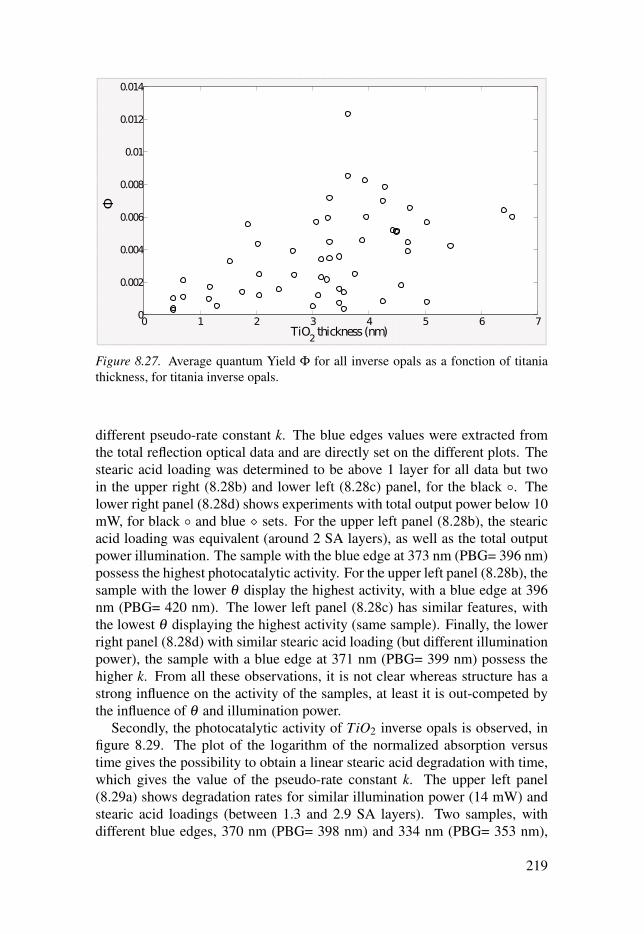
Figure 8.27. Average quantum Yield Φ for all inverse opals as a fonction of titaniathickness, for titania inverse opals.
different pseudo-rate constant k. The blue edges values were extracted fromthe total reflection optical data and are directly set on the different plots. Thestearic acid loading was determined to be above 1 layer for all data but twoin the upper right (8.28b) and lower left (8.28c) panel, for the black ○. Thelower right panel (8.28d) shows experiments with total output power below 10mW, for black ○ and blue ◇ sets. For the upper left panel (8.28b), the stearicacid loading was equivalent (around 2 SA layers), as well as the total outputpower illumination. The sample with the blue edge at 373 nm (PBG= 396 nm)possess the highest photocatalytic activity. For the upper left panel (8.28b), thesample with the lower θ display the highest activity, with a blue edge at 396nm (PBG= 420 nm). The lower left panel (8.28c) has similar features, withthe lowest θ displaying the highest activity (same sample). Finally, the lowerright panel (8.28d) with similar stearic acid loading (but different illuminationpower), the sample with a blue edge at 371 nm (PBG= 399 nm) possess thehigher k. From all these observations, it is not clear whereas structure has astrong influence on the activity of the samples, at least it is out-competed bythe influence of θ and illumination power.
Secondly, the photocatalytic activity of TiO2 inverse opals is observed, infigure 8.29. The plot of the logarithm of the normalized absorption versustime gives the possibility to obtain a linear stearic acid degradation with time,which gives the value of the pseudo-rate constant k. The upper left panel(8.29a) shows degradation rates for similar illumination power (14 mW) andstearic acid loadings (between 1.3 and 2.9 SA layers). Two samples, withdifferent blue edges, 370 nm (PBG= 398 nm) and 334 nm (PBG= 353 nm),
219

0.02
0.01
0.00
0 10 20 30 40Time /min
ln(A
bs)
14 mW
0.15
0.10
0.05
0.00
0 10 20 30 40Time /min
ln(A
bs)
9 mW
0.15
0.10
0.05
0.00
0 10 20 30 40Time /min
ln(A
bs)
12 mW
0.015
0.010
0.005
0.000
0 10 20 30 40Time /min
ln(A
bs)
10, 8, 6 mW
B= 365L=1.8
B= 335L=2.0
B= 373L=1.8
B= 396L= 1.0
B= 335L= 1.2
B= 383L= 1.4
B= 370L= 2.1
B= 375L= 3.6
B= 396L= 0.7
B= 371L= 2.0
B= 381L= 2.8
B= 335L= 2.7
(a) (b)
(d)(c)
Figure 8.28. Determination of the pseudo-rate constant k for Al2O3/TiO2 inverseopals with different PBG position under similar total output power. Blue edge (B)positions indicated on the different panels. Number of SA layers indicated with L.
220

possess a similar k value. It is interesting to note that the red edge of thegreen ◻ data set, is situated at 372 nm. For the upper right panel (8.29b),the illumination is kept at around 12 mW, but the stearic acid loading differs,around 1,5 layers for black ○ and green ◻ data set, it is at 0.7 for the blue ◇ dataset. Unsurprisingly, the blue ◇ set has a stronger photocatalytic activity thanthe other two samples. Note that otherwise, the sample with a blue edge at 376nm (PBG= 404 nm), perform better than the sample with similar coverage buta blue edge at 348 nm (PBG= 368 nm). The lower left panel (8.29c) shows thedegradation for samples exposed to the same illumination power (10 mW) andwith similarly high stearic acid coverage (between 2 and 5 SA layers). Thethree samples have similar behaviour, with relatively close blue edges (348,353 and 358 nm). Finally, the lower right panel (8.29d) shows the data setsfor a 8 mW illumination power, but two different coverage: black ○ data sethas the highest coverage (2.5 SA layers), while green ◻ and blue ◇ data setshas less than 1 monolayer of stearic acid (0.2 and 0.5 SA layers respectively).So, the sample with the highest coverage has the lowest k value, with a blueedge at 376 nm (PBG= 404 nm). Between the other two samples, with lowcoverage, the sample with an optically measurable photonic band gap showsthe highest photocatalytic activity, with a blue edge at 349 nm (PBG= 369nm), and a red edge at 389 nm. All in all, the coverage seems to out-powerany structural effect, at least for less than one monolayer data sets. The bestperforming samples posses photonic band gap edges around 370 - 380 nm,roughly in the expected electronic band gap value of titania. But all inverseopals data need to be compared before a conclusion can be reached.
Average k and ΦThe average pseudo-rate constant k and Quantum Yield Φ were calculated forinverse opals with an optically measurable photonic band gap and a stearicacid coverage above one monolayer. The results are shown in figures 8.30 and8.31, respectively. The photonic band gap edges are drawn in blue and red, totry understanding the influence of the photonic structure on the photocatalyticactivity. As seen in figure 8.30, no clear conclusion can be driven: someinverse opals with red or blue edges near the electronic band gap of anatasetitania possess both low and high k values.
As for the Quantum Yield Φ, the same observations can be made. Thedifferent experimental conditions might hide any photonic effect and was ap-parently not measureable with this experimental setup. It might be that thesolar illumination possess so few irradiance in the UV range, has to not makea difference with or without the photonic band gap structure, as seen in ta-ble 8.2. It is however still interesting to possess a high surface area with asponge-like structure, allowing greater loading of pollutants. It would havebeen better to assess the activity of a simple thick titania film and compare itto an inverse opal, but due to the low deposition rate of the ALD cycle used, itwas not realized.
221

0.05
0.04
0.03
0.02
0.01
0.00
0 10 20 30 40Time /min
ln(A
bs)
14 mW
0.015
0.010
0.005
0.000
0 10 20 30 40Time /min
ln(A
bs)
10 mW
0.20
0.15
0.10
0.05
0.00
0 10 20 30 40Time /min
ln(A
bs)
12 mW
0.20
0.15
0.10
0.05
0.00
0 10 20 30 40Time /min
ln(A
bs)
8 mW
B=370L= 2.5
B=334L= 1.3
B=345L= 2.9
B=376L= 1.2
B=348L= 1.4
B=365L= 0.7
B=376L= 2.5
no PBGL= 0.2
B=349L= 0.5
B=358L= 3.8
B=348L= 2.2
B=353L= 4.6
(a) (b)
(d) (c)
Figure 8.29. Determination of the pseudo-rate constant k for TiO2 inverse opals withdifferent PBG position under similar total output power. Blue edge (B) positions indi-cated on the different panels. Number of SA layers indicated with L.
222

300 350 400 450 500 5500
0.2
0.4
0.6
0.8
1
1.2
1.4
1.6
1.8x 10 3
PBG features (nm)
k (/m
in)
Figure 8.30. Average pseudo-rate constant k for all inverse opals with coverage above1 SA layer and an optically determined PBG and FWHM, as a function of PBG posi-tion with the blue edge and red egdes. Bulk anatase itania absorption in purple verticalline (388 nm).
300 350 400 450 500 5500
0.005
0.01
0.015
PBG features (nm)
Figure 8.31. Average quantum Yield Φ for all inverse opals with coverage above 1SA layer and an optically determined PBG and FWHM, as a function of PBG positionwith the blue edge and red egdes. Bulk anatase titania absorption in purple verticalline (388 nm).
223

Table 8.2. Surface power density over the range 200-400 nm for the arc lamps Hgand Xe, with corresponding filters, extracted from the corrected irradiance data. Thesurface power density measured at the sample position using the wattmeter is alsoshown.
Surface power density 200-400 nm Measured
Fiter (lamp) W/m2
BP56511 (Hg) 36.8 36.9BP56531 (Hg) 43.3 44.6BP56501 (Hg) 44.7 47.1BP56541 (Hg) 31.0 53.5BP57396 (Hg) 2.74 929.5AM0 & AM1.5 (Hg) 5.09 1222.3
AM0 & AM1.5 (Xe) 6.29 191.0
It can be précised also here the neglected influence of the absorption edgeof the different samples, which can slightly modifying the number of absorbedphotons per surface area and time. Since only one sample was used to calibratethe absorption, small variations are expected between the samples, notablybetween single and multi-layered samples. But this shift is rather small, andhas a neglectable influence on the final Φ value. For instance, for sampleFev15[...]01E (ALD cycle TiO2: 275), using the sample’s absorbance data,NP shift down of 0.37×10¹⁴ photons /cm2s (typical spectra: NP = 6.37×10¹⁴
photons /cm2s and with the specific spectra for Fev15[...]01E, NP = 6.50×10¹⁴
photons /cm2s), which leads to a shift up in Φ value of 4×10⁻⁴. A closer lookat the Tauc Eg positions, for averaged k and Φ values did not provide anyclear correlation, even compared to the bulk anatase electronic band gap value(Eg). If the absorption edge had a direct and strong influence on the final Φvalue, the closer the edges to the bulk Eg, the more efficient the sample shouldbe. Inverse opals with similar photonic band gap edges position relative to Eg,do not display a similar Φ, so that a closeness between absorption edge andphotonic band gap effect are not a warrantee of high photocatalytic activity, inthe case of solar illumination.
8.1.3 LED white lampThe LED white lamp was placed 13 cm away from the sample holder witha 0○ illumination, and spectra were recorded every 5 minutes. This meansthat the FTIR beam was at a small angle with the sample. The lamp powerwas measured at the sample position using the wattmeter, and was found rela-tively stable around 1.95±0.3mW. Of the three experiments realized on TiO2inverse opals, only one had a measureable photocatalytic activity. Unfortu-nately, it was one of the samples without optically measureable photonic band
224

Figure 8.32. Average Quantum Yield Φ for all inverse opals with coverage above1 SA layer and an optically determined PBG and FWHM, as a function of absolutedifference between their PBG edges and the Tauc determined electronic band gap.Blue edge data in blue ○ and red edge data in red ◻.
gap position. The absorbance spectra with white LED illumination on sampleAvril[...]01P (167 ALD cycles) are shown in figure 8.33.
The corresponding linear fit of the logarithm of the normalized absorbanceversus illumination time can be seen in figure 8.34. The extracted degradationrate was k = 0.00022/min, with a coverage of around 2 stearic acid layers (θ =2.23×1026).
Since these experiments were not reproduced and no photocatalytic activitywas measured on a titania film thin or on a quartz substrate, it is too early tostate that white LED photodegradation was proven to be possible. Although, itis encouraging results, and as such, it should lead to more probe on the effectof LED indoor illumination for photodegradation.
225

2700 2800 2900 3000 (cm-1)
0.15
0.10
0.05
0.00
Abs
orba
nce
time
Figure 8.33. FTIR absorbance spectra of sample Avril[...]01P, with white LED illu-mination. The arrow indicates the trend with illumination time.
0 5 10 15 20time (min)
0.000
-0.002
-0.004
ln(A
/A0)
Figure 8.34. Degradation rate constant determination for the absorbance displayed infigure 8.33. Grey area shows the goodness of the fit (R2 = 0.96).
226

8.2 Methylene blue degradationThe Photocat setup was used with and without illumination, to allows Methy-lene blue absorption stabilization before starting photocatalytic activity mea-surement. The voltage recorded at the laser beam detector was converted bythe Photocat program to solute concentration.
8.2.1 Typical resultsExamples of Photocat measurement on Al2O3/TiO2 and TiO2 inverse opals,with samples June[...]02J(ALD cycles Al2O3/TiO2:150/187) in figure 8.35and July[...]02T(ALD cycle TiO2:275) in figure 8.36, respectively. Both fig-ures represent the variation in Methylene blue concentration in the solutionfrom the starting concentration, C0 = 1.0 ppm. It can be seen in figure 8.35,that the absorption of Methylene blue is strong at the beginning of the ex-periment, with a concentration drop to around 0.6 ppm. The absorption ofMethylene blue continues in the dark, at a slower pace, without apparentlyreaching an equilibrium concentration. The UV illumination was started after15 hours and the concentration of Methylene blue drop sharply again, up to aslower decrease to 0.2 ppm. As for figure 8.36, the concentration of Methy-lene blue in the solution drop sharply at the start of the experiment, with theabsorption of Methylene blue on all surface available, to 0.75 ppm. The con-centration then decreases slightly and seems to reach equilibrium after around6 hours. The UV illumination was started after 500 min in the dark, whichinduced a sharp decrease of the solution concentration for few hours and thena slower decrease to around 0.2 ppm. This shows the importance to treat theabsorbance in the dark phase, to distinguish the slow disappearance of Methy-lene blue via adsorption, from the actual degradation of Methylene blue dueto photocatalytic activity.
8.2.2 Dark phaseTo treat the dark phase of the experiments, the adsorbed Methylene blue con-centration is extrated from the data, simply by removing from the initial con-centration the concentration in the solution at each measurement time.
Sorption kinetics
The sorption kinetics of a quartz substrate Photocat measurement was fittedwith a power or exponential law, as shown in figures 8.37 and 8.38, respec-tively. The power law fit clearly represent the sorption of Methylene blue withtime, while the exponential law over estimate the sorption concentration andreach the adsorption equilibrium too fast. Similar fits on dark phase measure-ments on inverse opal samples display the same trend.
227

Figure 8.35. Photocat measurement on sample June[...]02J with 900 min in the darkand 190 min illuminated. Red vertical line represents the start of UV illumination.ALD cycles Al2O3/TiO2:150/187, PBG position: 456 nm.
Figure 8.36. Photocat measurement on sample July[...]02T with 510 min in the darkand 510 min illuminated. Red vertical line represents the start of UV illumination.ALD cycle TiO2:275, PBG position: 397 nm.
228

Figure 8.37. Quartz substrate measured in the dark for 125 min. Red line represents apower fit: CABS = 0.099t0.15.
Figure 8.38. Quartz substrate measured in the dark for 125 min. Red line representsan exponential fit: CABS = 0.255×(1−e0.13t).
229

Figure 8.39. Sorption data fit with a power law CABS = 0.302t0.09 on dark phase ofsample June[...]02J. ALD cycles Al2O3/TiO2:150/187, PBG position: 456 nm, totalsurface area: 155 cm2.
An example of sorption data fit on a TiO2 inverse opal, June[...]02J (ALD cy-cles Al2O3/TiO2:150/187), is displayed in figure 8.39. The power law showsthat the sorption is sharp at the beginning and increases slowly with time. Thepower fit was used later on the UV illumination phase treatment, as seen insection 3.3.1.
To understand the sorption kinetics, it is however necessary to use thepseudo-second order adsorption kinetics (equation 3.10). Figure 8.40 showsthe application of equation 3.10, with the plot of the time divided by adsorbedspecies concentration as a function of time, for sample June[...]01C(ALD cy-cle TiO2: 220). The linear fit of the plot gives the value of the rate constantK2. All TiO2 inverse opals dark phase data sets were analysed similarly.
Similar data treatment was made on the multiplayer inverse opals. Figure 8.41displays the sorption power fit for the dark phase of sample July[...]02T(ALDcycle TiO2: 275), the fit was used to distinguish the possible effect from ad-sorption off the photocatalytic degradation of Methylene blue. Since the sorp-tion of Methylene blue is very slow and equilibrium is not often reach at thestart of the illumination, Methylene blue from the solution continue to get ad-sorbed on the surface of the catalyst and the Photocat instrument. However,
230

Figure 8.40. Pseudo-second order adsorption kinetics plot of sample June[...]01C.Linear fit in red line and experimental data as black dots. The extracted rate constant:K2 = 2.63 ppm/min. Grey area represents the goodness of the fit: R2=0.995. ALDcycle TiO2: 220, PBG position: 373 nm, total surface area: 214 cm2.
this adsorption removes the Methylene blue molecules from the solution butdo not degrade them. It is therefore necessary to account for the simultaneousdisappearance of Methylene blue from the solution from the sorption (tempo-rary) and the photocatalytic activity (permanent). The pseudo-second ordersorption kinetics (equation 3.10) was applied on all the samples. An exampleis shown in figure 8.42, which plot the time divided by adsorbate concentrationversus time, for sample June[...]01J(ALD cycles Al2O3/TiO2: 150/232).
No clear difference in behaviour was observed for the rate constant K2value, between TiO2 and Al2O3/TiO2 inverse opals.
Results
Table 8.3 displays the average values extracted from a pseudo-second ordersorption kinetics fit on a quartz substrate, the passivation Al2O3 film, the TiO2thin film (made with 585 ALD cycles) and the resulting trial with a polystyreneopal, sample July[...]02G. It can be emphasized here the high conformity ofthe linear fit to the experimental data, as displayed by the different values ofR2, all close to 1. The rate constant K2 value shows stronger fluctuation forthe quartz substrate and the passivation film, compared to the TiO2 thin film.The rate constant is of the same order range for all, but the PS opal and thepassivation film.
231

Figure 8.41. Sorption data fit with a power law CABS = 0.156t0.12 on dark phase ofsample July[...]02T.ALD cycle TiO2: 275, PBG position: 397 nm, total surface area:206 cm2
To ensure that no correlation was found between thorough cleaning of thePhotocat and sorption behaviour, a plot of the slope value 1/Qe as a function ofexperimental date and cleaning date can be found in figure 8.43. The cleaningusing ethanol are marked in red, while cleaning in Decon90 are displayedin green. No indication of correlation was found, speaking in favour of therepeatability of the experiments, as cleanliness of the Photocat varied in time.
Figure 8.44 shows the plot of the average (for each sample, measured twice)rate constant K2 as a function of sample’s surface area. No correlation wasfound.
Plots of the variation of the rate constant K2 with alumina and titania thick-ness of all the inverse opals can be found in figure 8.45 and figure 8.46, re-spectively. The average K2 for all samples and measurements was calculatedto be around 0.2 ppm/min. No clear correlation was found between alumina,titania thicknesses and K2.
The pseudo-second order kinetics are essentially used to extrapolate theamount of sorbate sorbed at equilibrium[125], which are reached sometimesafter days of interaction. The rate constant behaviour shows that the sorptionkinetics follow Methylene blue chemisorption, for all samples, in the Photocatsetup, regardless of the presence of titania, as seen in figure 8.47. This is con-sistent with the assumption of a Langmuir absorption equilibrium isotherm.
232

Figure 8.42. Pseudo-second order adsorption kinetics plot of sample June[...]01J.Linear fit in red line and experimental data as black dots. The extracted rate constant:K2 = 5.02 ppm/min. Grey area reprensents the goodness of the fit: R2=0.999.ALDcycles Al2O3/TiO2: 150/232, PBG position: 420 nm, total surface area: 147 cm2
Figure 8.43. Corresponding extracted 1/Qe with date of experimentation for all mea-surements. After cleaning with deionized water (blue), ethanol (red) and Decon90(green), before experimentation.
233

Figure 8.44. Plot of the average rate constant K2 as a function of total surface area forall samples.
Figure 8.45. Rate constants K2 as a function of alumina thickness for all multilayersamples.
234

Figure 8.46. Rate constants K2 as a function of titania thickness for all inverse opalsamples.
Figure 8.47. Calculated equilibrium solution concentrationCe and adsorbed speciesQe as a function of titania thickness, see equation 3.10 in section 3.3.1.
235

Table 8.3. Pseudo-second order sorption kinetics fits of different films: rate constantK2, equilibrium adsorption Qe and R2. The number in parenthesis displays the numberof experiments used for average.
Sample (number) K2 (ppm/min) Qe (ppm) R2
Quartz (4) 0.062 ± 0.012 0.36 ± 0.14 0.994Passivation (2) 3.05 ± 2.10 0.10 ± 0.05 0.988TiO2 585 cycles (2) 0.09 ± 0.005 0.29 ± 0.004 0.996opal July[...]02G (1) 0.42 0.42 0.999
8.2.3 Illumination phaseResults
The degradation of Methylene blue follows a first order rate, defined withequation 3.3, which means that a plot of the logarithm of the amount of Methy-lene blue adsorbed divided by the initial amount of Methylene blue adsorbedbefore illumination, as a function of time; shows a linear trend. The UV tubeused in the experiment had an emission peak around 365 nm, while Methyleneblue absorbs mainly at 663 nm and slightly at 292 nm.
SubstratesTable 8.4 shows the calculated degradation rate constants k of quartz substrate,the passivation Al2O3 film, the TiO2 thin film (made with 585 ALD cycles) andthe PS opal July[...]02G. A small photocatalytic activity was recorded for allsubstrates, with the TiO2 thin film being the most active. It is not surprisingto observe some photocatalytic activity, as Methylene blue could absorb someof the UV light and degrades with enough illumination time. Although, it ispossible as well that the sorption kinetics was under estimated and thereforethe degradation kinetics over estimated.
Table 8.4. First order degradation kinetics fits of different films: rate constant k andR2. The number in parenthesis displays the number of experiments used for average.
Sample (number) k (/min) R2
Quartz (3) 2.45×10⁻⁴±1.18×10⁻⁴ 0.953Passivation (2) 2.15×10⁻⁴±5.12×10⁻⁵ 0.980TiO2 585 cycles (2) 3.29×10⁻⁴±4.06×10⁻⁵ 0.979July[...]02G (1) 1.36×10⁻⁴ 0.985
TiO2 inverse opalAn example of the analysis of the Methylene blue degradation kinetics on aTiO2 inverse opal can be seen in figure 8.48. It shows the plot of the logarithmof the adsorbed Methylene blue concentration, normalised to the adsorbed
236

Figure 8.48. Plot to analyse the MB degradation kinetics for sample July[...]02T. Theslope of the linear fit (blue continuous line) defines the rate constant k = 4.11×10⁻³±4.15×10⁻⁵ (/min) and the grey area defines the goodness of the linear fit R2 = 0.999.ALD cycle TiO2: 275, PBG position: 397 nm
Methylene blue at the starting time of illumination, as a function of illumina-tion time for sample July[...]02T (ALD cycle TiO2: 275).
Al2O3/TiO2 inverse opalAn example of the analysis of the Methylene blue degradation kinetics on aAl2O3/TiO2 inverse opal can be seen in figure 8.49. It shows the plot of thelogarithm of the adsorbed Methylene blue concentration, normalised to theadsorbed Methylene blue at the starting time of illumination, as a function ofillumination time for sample June[...]02J (ALD cycles Al2O3/TiO2:150/187).
Thickness and degradation rate constantFigure 8.50 shows the correlation between titania thickness and degradationrate constant for all inverse opals. The only conclusion to be drawn is theslight increases of the degradation rate constant with titania thickness, com-paring samples with less and more than 3 nm titania thickness. But sampleswith similar titania thickness, for instance around 5 nm, have degradation rateconstants between 3.5×10⁻³ and 0.5×10⁻³.
237

Figure 8.49. Plot to analyse the MB degradation kinetics for sample June[...]02J. Theslope of the linear fit (blue continuous line) defines the rate constant k = 2.31×10⁻³±1.39×10⁻⁵ (/min) and the grey area defines the goodness of the linear fit R2 = 0.999.ALD cycles Al2O3/TiO2:150/187, PBG position: 456 nm
Figure 8.50. Average rate constants k for all inverse opal samples as a function oftitania thickness.
238

Figure 8.51. Rate constants k for all inverse opal samples as a function of Tauc derivedelectronic gap (black ○) and total surface area (black△).
Surface area and EgThe rate constants k were plotted against the calculated Tauc electronic gapand the total surface area of the inverse opal samples, as seen in figure 8.51.The degradation rate constant is found independent of sample gap and totalsurface area. Since the UV tube emits around 3.4 eV and all Tauc electronicgaps are below 3.3 eV, all the samples should be able to absorb the emittedlight. As for the influence of the total surface area, it should not be of conse-quence for the degradation rate constant of a first order kinetics.
Photonic band gap effect
Inverse opals with measurable photonic band gap are here analysed sepa-rately. The measured photonic band gaps are, however, not the actual pho-tonic band gaps when the inverse opals are immersed in the deonized waterand Methylene blue solution. A difference between the refractive index ofdeionized water (n=1.33) [222] and Methylene blue in water solution [223]is expected, therefore the photonic band gap of the inverse opal is expectedto shift. With time, the refractive index of the solute could also change withthe change in refractive index of the oxidised and reduced form of Methyleneblue [224]. To assess experimentally the shift in the photonic band gap, sampleMay[...]02A(ALD cycles Al2O3/TiO2: 150/187) was immersed for 10 days in100 mL deionized water solution with a Methylene blue concentration of 1ppm. The sample was then removed from the solution and directly measuredwith the Lambda900. The resulting total reflectance can be seen in figure 8.52.The photonic band gap shift from 396 nm to 449 nm, for the dry and wet sam-ple respectively. Similar experiments, with less waiting time, were made onsamples May[...]01A(ALD cycles Al2O3/TiO2: 150/125) , May[...]01B(ALD
239

Figure 8.52. Total reflectance of sample May[...]02A dry (black) and after 10 dayssoaking into a deionized water solution with a MB concentration of 1 ppm (light blue).ALD cycles Al2O3/TiO2: 150/187, PBG position: 396 nm.
cycles Al2O3/TiO2: 150/125) and Avril14[...]02D2(ALD cycles Al2O3/TiO2:150/187) . The photonic band gap shift was around 50 nm for all samples.The FWHM of all samples were roughly conserved. Simulations were madeusing parameters derived from sample May[...]02A(ALD cycles Al2O3/TiO2:150/187) , which possess an alumina thickness around 8 nm, a shrinkage dur-ing inversion around 4 % and a titania thickness around 3 nm. Figure 8.52shows the simulations for different refractive indices of the solute, betweenn=1.0 and n=1.40. The photonic band gap shifts to higher wavelengths, witha stronger shift for higher refractive index. However, the predicted photonicband gap position, for a 3 nm titania thickness, is around 464 nm (87 nmshift). This value does not reflect the experimentally measured photonic bandgap position (449 nm), the corresponding titania thickness for a similar pho-tonic band gap position is around 1 nm. There are, however, uncertainties onalumina thickness, sample shrinkage and titania thickness, due to the use ofthe Bragg-Snell law to determine these values.
To assess the effect of the shrinkage on the photonic band gap position, fora solute refractive index equal to 1.33, figure 8.54 was plotted. The shrinkageof the structure was varied between 0% and 10%. The photonic band gapposition shifts towards lower wavelengths with higher shrinkage values. Ifboth alumina and titania thicknesses are kept constants, the shrinkage shouldbe around 10% to display a photonic band gap position around the measuredphotonic band gap position. This shrinkage is much higher than expected(optically determined: 4%).
240

Figure 8.53. Bragg-Snell calculated PBG position for an Al2O3/TiO2 inverse opalwith 8 nm of alumina and 3.5 % shrinkage during inversion. With a refractive indexof the solute between 1.0 (black) to 1.40 (red), and the refractive index of titania at445 nm: 2.73[118].
Figure 8.54. Bragg-Snell calculated PBG position for an Al2O3/TiO2 inverse opalwith 8 nm of alumina with a refractive index of the solute at 1.33. And shrinkageduring inversion between 0% (black) to 10% (orange). The refractive index of titaniaat 445 nm: 2.73[118]
241

Figure 8.55. Bragg-Snell calculated PBG position for an Al2O3/TiO2 inverse opalwith 3.5 % shrinkage during inversion and with a refractive index of the solute at1.33. Alumina thickness between 1 nm (black) to 12 nm (green). The refractive indexof titania at 445 nm: 2.73[118]
The effect of alumina thickness on the final photonic band gap position, fora solute refractive index equal to 1.33, is shown in figure 8.55. For a tinaniathickness around 3nm, no clear effect of alumina thickness can be found, evenif changed between 0 and 16 nm (every 2 nm).
The smaller shift in the measured photonic band gap position compared tocalculated one can therefore derived from error in titania thickness and shrink-age values determination. However, it can be accepted that the shift of thephotonic band gap mostly comes from the deonized water, and is around 50nm for most samples. To be able to plot the effect of the photonic band gapposition on the degradation rate constant, the dry sample measured photonicband gap positions of all inverse opals were shifted by 50 nm. The FWHM,defining the red and blue edges, were kept constant as well. Figure 8.56 showsthe average degradation rate constants k for different photonic band gap posi-tions. No clear correlation can be found between photonic band gap featuresand degradation rate constant. Unfortunately, no sample has a blue edge atthe emission peak of the UV tube and few have the blue edge at the edge ofthe UV illumination (around 390 nm). The experimental set was nonethelessuseful to determine sorption kinetics and samples degradation kinetics.
242

Figure 8.56. Average degradation rate constants k as a function of PBG positions ofall inverse opal samples. Blue and red edges represented with blue and red gradiantsaround the PBG position (black dot).
243

9. Discussion and conclusion
C’qui compte, c’est les valeurs!
Frank Pitiotas Perceval le Gallois in Kaamelott
9.1 Fabrication methodPS opal templatesThe fabrication of the PS templates was easy but not entirely realiable to sys-tematically produce templates with similar thickness. The exchange of theventilated oven for an environmental chamber should help increase the repro-ducibility of the templates creation [225, 226]. The CVE method was pref-erentially used over the volume dip coating, for obvious considerations aboutdeposition time and costs. However, PS opals with less cracks were obtainedwith codeposition [147, 227] or home-built setups [228–230]. The choice ofgrowth setup should be determined by weighting parameters (time, chemistry,concentration...) and goals.
ALD deposition rateSeveral measurements methods were used to estimate the ALD depositionrates and are summarized in table 9.1. The ALD deposition was less homo-geneous as expected, with few nanometer variations in thickness depositionfor samples with similar structures, within the same deposition cycles. Thisdifference could be originated from local differences in pressures in the ALDchamber and accessibility. The PS opal thickness seems to influence slightlythe deposition rate, thicker samples having a lower deposition rate.
Table 9.1. Deposition rate (nm/cycle) for R200 Advanced (R200 Standard), extractedusing the built-in QCM, measurements on SEM images, evaluation of the GIXRD crys-tal sizes and the optical data treated with the Bragg-Snell law (equation 2.24).
Type of cycle QCM SEM GIXRD Bragg-Snell
Al2O3 0.1 (X) X (0.04) X (X ) 0.07 (0.14)TiO2 0.08 (X) X (X) 0.06 (X) 0.02 (X)TiO2 (200○C) 0.09 (X) X (X) 0.08 (X) 0.02 (X)
244

The use of ALD to deposit metal oxide on polystyrene allowed the cre-ation of photonic structures with a wide pannel of photonic band gap positions.However, better ALD deposition cycles could have been used, to increase thequality of the inverse opals [219]. As mentioned in the thesis of Philip [190],a longer precursor time would have increase the deposition rate, for instance.This deposition method has the possibility of multilayering and thin deposi-tion, which is an advantage on the sol-gel method.
9.2 Optical measuresPS opalsThe throughout optical characterisation and analysis on the polystyrene opalsled to interesting results. The polystyrene opals were slightly variying in thick-nesses, depending of their position duing the experiment. Most opals had ex-pected photonic band gap positions and width, with the exception of sampleswith more than around 70 layers. For these opals, a strong increase was foundin absorption coefficient (α), even at 800 nm, where polystyrene films areusually transparent. It might come from an increased in the forward diffusescattering, but further experimentation is needed to assess this effect quantita-tively. Also, simulations of optical spectra could perhaps help understandingthe apparent thickness threshold.
Inverse opalsThe optical characterisation of the inverse opals was difficult, particularly forthe titania inverse opals. Transmittance measurements did not allow the de-termination of the photonic band gap due to anatase titania absorption in theultra-violet, so that only reflectance data sets could be used for photonic bandgap characterisation. Also, it seems that some titania inverse opals who pos-sessed a photonic band gap in the polystyrene/titania opal form, lost the pho-tonic band gap effect. It can be advanced that the photonic band gap is belowthe measurement threshold of 200 nm or that the titania deposition was sothin that the structure collapsed during manipulation. However, determinationof titania thicknesses using the photonic band gap position shift between thepolystyrene opal and the polystyrene/titania opal, shows that some structureswith lower titania thicknesses did had a photonic band gap after inversion. Itwould be interesting to observe the ’failed’ or optically non measureable pho-tonic band gap structures under the scanning electron microscope, to verify ifthe fcc order has remain or if the structure has indeed collapsed.The presence of the photonic band gap complicated the analysis of the ab-sorbance, and led to under-estimated Tauc extracted electronic band gaps. Itwas possible to identify shrinkage during inversion by using the photonic bandgap position shift before and after inversion. Structure shrinkage was not en-tirely uniform, but followed a trend, with stronger shrinkage for thicker wall
245

inverse opals. The multilayer inverse opals were easier to manipulate and ob-serve, with photonic band gap positions closer to the red (400 nm). The effectof ion milling on the structure was interesting as well, with the almost dis-appearance of the photonic band gap peak/dip in the optical spectra. Extradiffusion at the surface might be responsible for it.Optical characterisation was essential to comprehend the samples. A system-atic analysis was performed on each sample, at each stage of fabrication andallows an insight into the complexity of the photonic structures.
9.3 PhotocatalysisStearic acid degradationStearic acid was used in ambient air, without any tight control on humidityand temperature conditions. The arc lamps used (Hg and Xe) were fluctuating,with time of use and with the experimental date (mostly the Xe, as the lampwas reaching its maximum consecutive working hours). Another factor moredifficult to control was the loading of stearic acid, with fluctuations betweenless than a monolayer to several layers (but less than 9 layers).The most important experiment with the Hg arc lamp, is the measure of thedegradation under different bandwidths, controlled by the bandpass filters. Ithinted to an effect of the photonic band gap on the activity of the samples, withsome unclear data points. The other experiment, using theXe lamp togetherwith the filters AM0 and AM1.5 (solar spectrum), did not show a correlationbetween photonic band gap position relative to the bulk anatase titania elec-tronic band gap. Though, it look as if the effect can be significant for similarstearic acid loadings (more than a monolayer) and lamp output power (morethan 10 mW).
Methylene blue degradationMethylene blue degradation was made using a home-built system, using a redlaser to monitor the transparency of the solution. The UV tube had an emis-sion peak around 365 nm. Both sorption and degradation kinetics were mon-itored. For all inverse opals, no true equilibrium was reached even after 18hours without illumination. The best sorption kinetic fit was the second orderkinetics (for chemically sorbed species), allowing for graphical the determi-nation of the sorption equilibrium and solute equilibrium. The continuoussorption of Methylene blue with time was taken into consideration, to distin-guished the degradation subsequent to illumination from the disappearance ofthe molecules from the solution by simple chemisorption. The degradationkinetics was first order, which was expected. No correlation was found againbetween degradation rate constants and photonic band gap positions. A smalluncertainty can be added regarding the real photonic band gap position, once
246

the inverse opal is immersed in the solution. It was optically measured to bearound 50 nm shifts to the red, but more simulations are necessary to assess it.
PBG effectIt is clear that no strong correlation was found between photocatalytic activ-ity and photonic effect. This could be bound to several causes. It can bethat, indeed, even with a small increase of UV absorption, the photonic bandgap effect is not significant under the illumination with the solar spectrum.It is possible also that more controlled environment is needed to observe andrecord the photonic effect, with an even wider range of photonic band gapstructures. Lastly, it can comes also from the difference in quality of the in-verse opals, as disorder can disrupt considerably the photonic effect and closesup the photonic band gap.Table 9.2 shows the first three best samples for titania and alumina/titania in-verse opals, for the stearic acid degradation using the solar spectrum and theXe arc lamp and for the Methylene blue degradation using the home-built setup(Photocat). The photonic band gap position, together with the blue edge of thephotonic band gap, is given for the best average degradation rate constants(average per sample, per experimental set). For the titania inverse opals, thetwo samples have similar photonic band gap positions close to the bulk anataseelectronic band gap, for stearic acid degradation, and similarly for the Methy-lene blue degradation. The blue edges are more spread. For the alumina/titaniainverse opals, no real order can be found for both stearic acid and Methyleneblue degradation.
9.4 Futur prospectsPhotonic band gap effectTo be able to measure accurately and assess the gain of using photonic struc-tures over thin films or nanoparticles, it is necessary to establish a standardisa-tion for photocatlytic activity measurement. Similar to solar cells efficiency in-vestigations, an international standardize measure of the photocatalytic activ-ity with stable instrumentation, controlled and defined environment and well-behaved molecules, would be helpful for inter-laboratories efficiency compar-isons. Since the measure of absorbed photons and molecules degradation isbound to uncertainties, even the quantum yield (Φ) is not entirely reliable forinter-laboratories comparisons. To go further into the effect of the photonicstructure onto the photocatalytic activity, it is preferable to use stable lightsources in the UV (strong LEDs for instance [231]) together with selectivebandpass filters. It could also be interesting to measure the activity in a closedchamber with mass spectrometry.
247

Table 9.2. Degradation rates k (/min) from the FTIR measurements with the Solarspectrum and the Photocat setup (UV tube emission peak at 365 nm). Titania elec-tronic band gap situated around 388 nm. An extra 50 nm shift need to be added forthe samples in the Photocat setup, due to the difference of refractive index between airand deionized water.
TiO2 Solar Photocat
PBG Blue edge PBG (in water) Blue edge (in water)
Rank nm
1 393 365 336 (386) 317 (367)2 366 346 353 (403) 334 (384)3 390 364 365 (415) 347 (397)
Al2O3/TiO2 Solar Photocat
PBG Blue edge PBG (in water) Blue edge (in water)
Rank nm
1 409 383 456 (506) 396 (446)2 456 396 396(446) 373 (423)3 396 373 396(446) 374 (424)
Indoor and outdoor photocatalysisThe sad conclusion of this thesis is that photonic structures might not be thenext generation of photocatalytic filtration and illumination. Although, theirinterest in the indoor application should not be ruled out, certainly not on thiswork alone. Working on the use of photonic crystals as a ’sidekick’ for othertypes of photocatalysts might be more interesting. The use of photonic crystalswith LEDs could also be helpful in specific indoor environments, as hospitals,infrastructures and industries. As for outdoor photocatalysis, using only thesolar spectrum, the inverse opals, as designed in this thesis, might be out com-peted with existing photocatalysts. In conclusion, this work unfortunately didnot solve the growing problem of human-made pollution, but it will hopefullyhelp others do so.
248

10. Summary
Summary in SwedishI den här avhandling har material som har påverkan på ljus fabricerats ochstuderats, optiskt och kemiskt. Dessa material kallas fotoniska kristaller. En-kla Maxwellekvationer kan lösas för att producera en specifik twist till ljusetsom inkommer på provet: ett fotoniskt bandgap. Detta fotoniska bandgaprepresenterar de delar av ljusspektrumet som helt reflekteras av den fotoniskakristallen. Selektiviteten hos det reflekterade ljuset härrör från blandningen av,åtminstone, två typer av material i en specifikt ordnad periodiskt struktur.De fotoniska kristaller som skapats med polystyrenkulor genom konvektiv av-dunstning självmonterades i en ytcentrerad kubisk struktur. De användes sommallar för att deponera metalloxider med hjälp av Atomic Layer DepositionALD. Två typer av strukturer skapades: aluminiumoxid/titandioxid och titan-dioxid inversa opaler. På grund av variationer i deponeringshastigheten fickstrukturerna bandgap i ett brett spektrum av våglängder (328 till 456 nm).Tanken var att kombinera den ökade reflektionen av de inversa opalerna medtitandioxids absorptionsintervall, för att öka den strukturella effektiviteten avskapandet av elektron-hål par, vilket skulle kunna öka den fotokatalytiska ef-fektiviteten för inomhus och utomhusapplikationer.Strukturell analys, främst genom svepelektronmikroskopi, gjorde det möjligtatt bekräfta deposition av metalloxid, och att polystyren/metalloxidstrukturernaframgångsrikt inverterats. Detta gör det möjligt att avgöra metalloxidens de-positionstjocklek och kristallinitet (med röntgendiffraktion).En viktig del av studien fokuserade på de fotoniska kristallernas optiska re-spons vid varje steg av fabrikationsprocessen. Intressanta beteenden påträf-fades hos polystyrenopalerna beroende av antalet skikt. En stark framåt diffusspridning identifierades också. Alla polystyren/metalloxidstrukturer hade ettfotoniskt bandgap, men det var inte all som resulterade i inversa opaler. Deslutliga strukturerna hade en ökad absorbans i det fotoniska bandgapets spän-nvidd och en Taucplot härledde det elektroniska bandgapet till något lägre änbulk-titandioxids (underestimerat).Slutligen, fotokatalytiska experiment utfördes på alla inversa opaler och met-alloxidstrukturer. Två olika typer av upplägg användes. FouriertransformationInfraröd Spektroskopi användes för att övervaka degraderingen av stearinsyramed belysningstid. Båglampor användes med bandpassfilter för att sonderadet fotoniska bandgapsintervallet, och tillsammans med filter för att efter-likna solspektrat för att förstå strukturens påverkan på den fotokatalytisk ak-tiviteten. En hemmabyggd uppställning användes för att analysera sorpsion
249

och degradering av färgämnet metylen blå. Ett ultraviolett rör med emissionrunt 365 nm användes för att belysa lösningen, och konstant omrörning säk-erställde syresättning genom hela experimentet. Degraderingen av stearinsyraverkade vara knuten till strukturen enbart om provets täckningsgrad var merän ett monolager, och enbart för kvicksilverbåglampan. Korrelation hittadesvarken för degraderingskonstant eller kvanteffektivitet när xenonbåglampanmed solspektrat användes. Den fotokatalytiska degraderingskonstant som ex-traherades med metylen blå experimenten var också oberoende av den fo-toniska bandgapspositionen.Sammantaget väcker denna avhandling mer frågor än vad den besvarar. Enbättre strategi för de fotokatalytiska mätningarna skulle inkludera standardis-ering av instrument, miljö, och kemikalier liknande de som finns för solcells-forskning. Endast då skulle den fotokatalytiska aktiviteten för inversa opalerkunna testas mot alternativa strukturer.
250

Summary in FrenchDans cette thèse, des matériaux avec une influence sur la lumière ont été fab-riqués et étudiés, avec de l’optique et de la chimie. Ces matériaux s’appellentles cristaux photoniques. Les équations de Maxwell peuvent être résolues etrévèlent une particularité spéciale s’appliquant à la lumière en interaction avecle matériel : la bande interdite photonique. Cette bande interdite photoniquereprésente la partie du spectre de la lumière qui est complètement réfléchie parle cristal photonique. La sélectivité de la partie réfléchie vient du mélange en-tre deux types de matériaux obéissant un arrangement périodique spécifique.Les cristaux photoniques créés avec des billes de polystyrène par évapora-tion convective se sont assemblées en une structure cubique à faces centrées.Elles ont été utilisées comme moule pour déposer des oxydes de métal avec latechnique atomic layer deposition. Deux sortes de structures ont été créées :opales inversées d’alumine/dioxyde de titane et dioxyde de titane. À cause desvariations dans le taux de déposition, ces structures ont des bandes interditesphotoniques entre 328 et 456 nanomètres.L’idée était de combiner l’effet des opales inversées sur la lumière avec lerange d’absorption du dioxyde de titane. Cela devrait augmenter l’efficacité dumatériel à créer des paires électron-trous, ce qui devrait augmenter l’efficacitéde l’activité photocalyse pour l’intérieur et l’extérieur.Une analyse structurelle, utilisant surtout la microscopie électronique à bal-ayage, a permis de confirmer la déposition d’oxydes de métaux et la réussitede l’inversion de la structure polystyrene/oxyde de métal. Cela a aussi permisla détermination de l’épaisseur des dépositions et la cristallinité (utilisant ladiffraction des rayons X).Une part importante de l’étude se concentrait sur la réponse optique des cristauxphotoniques, à chaque niveau du procédé de fabrication. Il a été trouvé queles opales de polystyrène avaient un comportement intéressant, qui dépendaitdu nombre de couches. Une forte présence de diffusion vers l’avant pendantla propagation de la lumière. Toutes les structures polystyrène/oxyde de métalavaient une bande interdite photonique, mais pas toutes les opales inversées.Les structures finales avaient une absorption augmentée à proximité et dans labande interdite photonique. Les valeurs de bande interdite électronique, trou-vées en utilisant le graphique de Tauc, étaient en dessous de la valeur macro-scopique du dioxygène de titane.Enfin, des expériences de photocatalyse ont étés faites sur les opales inver-sées et les structures d’oxyde de métal. Deux types d’installations ont étésutilisées. La spectroscopie infrarouge à transformée de Fourier a été utiliséepour vérifier la dégradation de l’acide stéarique avec le temps d’illumination.Des lampes à arc ont étés utilisées avec des filtres de bandes pour tester l’effetphotonique, et, avec des filtres reproduisant le spectre solaire, pour compren-dre l’influence de la structure sur la photocatalyse. Un système fait-maisona été utilisé pour analyser l’absorption et la dégradation de la teinture bleu
251

de méthylène. Une lampe à ultra-violets avec une émission autour de 365nanomètres a été utilisée pour illuminer la solution et un mélange constant aassuré l’oxygénation pendant toute la durée de l’expérience. La dégradation del’acide stéarique était apparemment liée à la structure (à l’effet photonique),mais seulement si les molécules formaient plus d’une couche sur la surfacedes échantillons et seulement avec l’utilisation de la lampe à arc au mercure.Pas de corrélation n’a été trouvée pour les constantes de taux de dégradationet l’efficacité quantique, en utilisant la lampe à arc au xénon et le spectre so-laire. La constant de taux de dégradation issues des expériences au bleu deméthylène, aussi, sont indépendantes de la position de la bande interdite pho-tonique.Dans l’ensemble, cette thèse fourni plus de questions que de réponses. Unemeilleure tactique concernant les mesures de photocatalyse serait d’introduireune standardisation des instruments, des conditions et des produits chimiques,comme dans la recherche sur les panneaux solaires. Seulement après stan-dardisation, l’efficacité de la photocatalyse des opales inversées pourront êtreexaminées contre d’autre type de structures.
252

Appendices
253

A. List of inverse opals
A.1 TiO2 inverse opalTable A.1 represent the list of all titania (TiO2) inverse opals, with the numberof cycles used; as well as ion milling conditions.
A.2 Al2O3/TiO2 inverse opalTable A.2 list all multi-layered inverse opals, with number of alumina (Al2O3)and titania (TiO2) ALD cycles; together with ion milling conditions.
254

Table A.1. Deposition of TiO2 at 70○C, number of cycles. Ion milling time and beamcurrent.
Name CyclesIon milling
(min)Beam current
(mA)
Oct14PS200Q02 (D,I,N,K,L,G) 205 6 200May14PS200Q01g 205 6 200
Avril15PS200Q02H 167 4 200Avril15PS200Q01 (A,H) 167 4 300Avril15PS200Q01 (B,C,M,P) 167 4 200
Avril15PS200Q02B 110 4 300Avril15PS200Q02 (A,C,G) 110 4 200Avril15PS200Q01G 110 4 300Avril15PS200Q01 (O,L,G) 110 4 200
Fev15PS200Q01D 220 4 300Avril15PS200Q01 (I,D) 220 4 300Q200PS02C 220 4 300June15PS200Q01C 220 4 300June15PS200Q02D 220 4 300
July15PS200Q02 (T, S, I, O, J) 275 4 300Fev15PS200Q01E 275 4 300Fev15PS200Q02C 275 4 300June15PS200Q01A 275 4 300
Table A.2. Deposition of Al2O3 at 70○C and TiO2 at 200○C, number of cycles; andbeam current. Ion milling time fixed at 4 minutes.
Name Al2O3 cyclesBeam current
(mA) TiO2 cycles
June15PS200Q02 (A, I, J) 150 300 187June15PS200Q01 (G, J) 150 300 232June15PS200Q02 (G,H) 150 300 166Oct14PS200Q02 (F,O) 150 200 62JuO50Q03J 150 x 25April14PS200Q02D2 150 200 187May14PS200Q02A 150 200 187May14PS200Q01 (A,B) 150 200 125
NovO50Q200PS (H,B) 200 300 135NovO50Q200PSJ 200 300 250NovO50Q200PS (F,G) 200 300 200NovO50Q200PS (A,C) 200 300 100NovO50Q200PSE 200 300 155
255

B. Arc lamp, filters and mirror
B.1 Xe lamp stability200 WFigure B.1 shows the power measured at the sample holder position with theoptical power meter PM 160 at 200 W power. The lamp power decreases withillumination time. The averaged power at the sample holder position is around8.5 mW, with a standard deviation around 1 mW.
300 WPower of the Xe lamp at the sample holder was measured at regular intervalwith the optical power meter PM 160 at 300 W power. Figure B.2 shows themeasured power in mW as a fonction of ON time (in minutes). It can be seenthat the power of the arc lamp decreases slightly with time ON. The averagedpower value at the sample holder is around 13 mW, with a standard deviationaround 1 mW.
B.2 AM0 and AM1.5 filtersThe total transmittance spetcra of filter AM0 and AM1.5 are shown in figuresB.3 and B.4, respectively. These data were used to corrected the irradiance ofthe Hg and Xe arc lamps.
B.3 Gold mirrorThe total reflectance of the gold mirror used in the FTIR setup can be seen infigure B.5. This data were used to correct the irradiance of the Hg and Xe arclamps.
256

y = -0,0014x + 8,4247 R² = 0,02348
0
2
4
6
8
10
12
0 50 100 150 200 250 300 350 400 450 500
Pow
er a
t sam
ple
/mW
Time ON /min
Figure B.1. Measured power of Xe lamp at 200 W at the sample holder at time on.Linear fit and R-squared value.
y = -0,0007x + 12,981 R² = 0,00589
0
2
4
6
8
10
12
14
16
18
0 100 200 300 400 500 600
Pow
er a
t sam
ple
/mW
Time ON /min
Figure B.2. Measured power of Xe lamp at 300 W at the sample holder at time on.Linear fit and R-squared value.
257

200 300 400 500 600 700 8000
20
40
60
80
100
Wavelength (nm)
I/I0
Figure B.3. Measured transmittance of the filter AM0.
200 300 400 500 600 700 8000
20
40
60
80
100
Wavelength (nm)
I/I0
Figure B.4. Measured transmittance of the filter AM1.5.
258

Figure B.5. Measured refectance of the gold mirror used in the FTIR experimentalsetup.
259

C. Photocat parameters
To normalize the measured signal of the Methylene Blue (MB) solution in thePhotocat setup to the background signal of deionized water, the voltage at thephotodiode was recorded at the beginning of each experiment, without water.Figure C.1 shows the measured voltage at each experimental date.
Cleaning of the setup was always made using deionized water prior to thestart of the experiment. To avoid further contamination from stagnant water,several cleanings with detergeants were used. The dates where cleaning of thePhotocat setup occurs were: 02sd , 09th, 11th february, 12th, 20th april and 17th
june with ethanol; and 07th mars and 27th may with Decon90. The UV lampwas replaced by a new one on the 25th of february and the cooling fan wasreplaced on the 19th of may.
260

325330335340345350355360365370
2015-11-242015-12-24
2016-01-242016-02-24
2016-03-242016-04-24
2016-05-242016-06-24
H2O /mV
Figure C.1. Measured voltage at the photodiode of the Photocat system, with dionizedwater, as a function of the date of experimentation. Cleaning with deionized water(blue), ethanol (orange) and Decon90 (red).
261

D. Matlab programs
Several programs were used to treat the different data and calculate theoreticalvalues of the samples.
D.1 Photonic band gap theoretical position% MATLAB code using Bragg-Snell equation and effective medium expres-sion to determine theoretical photonic band gap (PBG) position of opals andinverse opals.% Author: Delphine M. Lebrun% Date: 2016/08/05% Note: Polystyrene (PS) opals were used as templates and atomic layer de-position (ALD) was used to deposit metal oxides (MO).
clear;%parameters to fill in by the user
% Original template% Diameter of PS bead (template):D=200; R=D/2; % in nm% shrinkage from inversion (only for PS):D2=D-(10×D)/100; R2=D2/2;% maximum filling of a fcc opal:maxD=(11.25×D)/100;% Refractive indicesn1=1.0; % Airn2=sqrt(2.58); % Al2O3n3=3.136; % TiO2n4=1.5516; % PS
262

%ALD: first deposition of MO%number of cycles:cycle=150;% Deposition rate:rate=0.1; % nm/cycle% thickness deposited:thick=rate×cycle; % in nmif thick>maxD;thick=maxD;end
% ALD: second deposition of MO% number of cycles:cycle2=125;% Deposition rate:rate2=0.02; % nm/cycle% thickness deposited:thick2=rate2×cycle2; % in nm% max filling of a fcc inverse opal:maxD2=(19.6×D2)/100;if thick2>(maxD2/2);thick2=maxD2/2;end
% Calculations% (1) PS opal% filling factor of PSfPS=pi/(3×sqrt(2));% filling factor of airfao=1-fPS;%effective refractive indexneff4=n4×fPS+n1×fao;%PBG of the PS opallambda4=(2×D×sqrt(2/3)×sqrt(neff42);% (2) PS + Al2O3 opal%filling factor of Al2O3
fal=(thick* 0.224)/maxD;% filling factor of the air pocketsfhole=1-fPS-fal;% effective refractive indexneff3=n4×fPS+n2×fal+n1×fhole;%PBG of the PS/Al2O3 opallambda3=(2×D×sqrt(2/3)×sqrt(neff32);
% (3) Al2O3 inverse opalfair2=1-fal; %filling factor of air%effective refractive indexneff2=n1×fair2+n2×fal;%PBG of the Al2O3 inverse opallambda2=(2×D2×sqrt(2/3)×sqrt(neff22);
% (4) Al2O3/TiO2 inverse opal% Volume of 1 PS sphereVps=(4/3)×pi×R3;% Volume of an fcc unit cellVcell=(2R2/sqrt(2))3;% Volume of titaniaVti=(4/3)×pi×R23
-(4/3)×pi×(R2− thick2)3% Filing fraction of titaniafti=(4Vti/Vcell)+((0.224-fal)×(R2-thick2)3);%filling factor of airfair=1-fti-fal;%effective refractive indexneff1=n3×fti+n2×fal+n1×fair;%PBG of the Al2O3/TiO2 inverse opallambda1=(2×D2×sqrt(2/3)×sqrt(neff12);
263

D.2 Sample surface areaCalculation of the theoretical surface area of an inverse opal from number oflayer and original PS size.clear;%Variableslength=1.0; %in cmside=1.0; %in cmthickness=12.19385×10⁻⁴;%in cm
%ALD %diameter of original beadsD=200; % in nm%shrinkage from inversionD2=D-(10×D)/100;
%thickness deposited% Aluminatal=2; % in nm% Titaniat=2; % in nm
%Area of one TiO2 sphere in cm2
S=4× pi×((D2/2− t − tal)2)×10−14;
%Number of layersL=thickness/((D×(2/3)1/2)×10−7);
%Number of raws lengthR1=length/((D×(2/3)1/2)×10−7);
%Number of raws sideR2=side/((D×(2/3)1/2)×10−7);
%Total surface of TiO2 in m2
surfaceML=L×R1×R2×S
264

E. Calculated values
The photonic band gap position and fullwidth at half maximum (FWHM) ex-tracted from either transmittance or reflectance optical data, together with theextracted Tauc electronic band gap, experimentally measured degradation rateconstants from the FTIR solar spectrum measurements and the Photocat setup.
E.1 TiO2 inverse opalTable E.1 represent the list of all titania (TiO2) inverse opals with an opticallymeasureable photonic band gaps.
E.2 Al2O3/TiO2 inverse opalTable E.2 list all multi-layered inverse opals, with an optically measureablephotonic band gaps.
265

Table E.1. TiO2 inverse opals PBG position and FWHM from total reflectance spec-tra, extracted Tauc electronic band gaps, measured photocatalytic degradation ratesk, from the FTIR setup with the Solar spectrum and from the Photocat setup with theUV tube.
Name PBG FWHM Tauc Eg k (Solar) k (365 nm)
nm eV (×104) min−1
July15[...]02J 336 38 1.2 0.73 2.22Oct14[...]02G 350 48 3.1 13.7 8.75May14[...]01G 353 30 3.2 10.6 7.58Oct14[...]02L 353 60 3.1 3.70 9.24Oct14[...]02N 353 38 3.0 6.79 5.67Oct14[...]02D 360 44 3.1 4.13 19.0Oct14[...]02I 360 39 2.8 1.53 7.10Avril15[...]01D (b) 365 37 3.1 8.68 6.56Oct14[...]02K 365 39 3.0 3.88 13.4Q200PS02C 366 41 3.0 16.8 18.9Avril15[...]01D (a) 368 40 2.8 7.16 16.4June15[...]02D 368 40 2.7 14.1 15.4Fev15[...]02C 369 40 2.5 7.51 20.2Fev15[...]01D 372 39 2.8 9.36 26.4June15[...]01C 373 41 2.8 4.86 27.3Avril15[...]01I 377 42 2.7 12.3 33.2July15[...]02E 378 41 2.8 5.05 18.0July15[...]02I 387 46 3.0 11.6 27.7June15[...]01A 390 53 2.5 14.9 26.6Fev15[...]01E 393 56 3.0 20.0 15.7July15[...]02T 397 60 3.0 10.5 31.1July15[...]02S 398 57 3.0 13.8 31.3July15[...]02O 404 56 2.8 13.8 28.1
266

Table E.2. Al2O3/TiO2 inverse opals PBG position and FWHM from total reflectancespectra, extracted Tauc electronic band gaps, measured photocatalytic degradationrates k, from the FTIR setup with the Solar spectrum and from the Photocat setup withthe UV tube.
Name PBG FWHM Tauc Eg k (Solar) k (365 nm)
nm eV (×104) min−1
July[...]03J 328 33 2.9 X XOct14[...]02O 353 37 2.9 1.53 4.26Oct14[...]02F 356 42 2.8 1.38 3.70Sept[...]PS220D 364 41 2.0 X XMay14[...]01A 372 56 2.8 5.64 5.09Nov[...]C 377 47 2.5 2.48 6.72Nov[...]A 378 49 2.6 4.71 4.72May14[...]01B 385 43 2.6 X 5.05June15[...]02H 393 56 2.4 1.23 5.44May14[...]02A 396 46 2.5 7.26 12.7Nov[...]B 396 44 2.6 2.90 11.5Nov[...]H 396 79 X 1.85 5.13Avril14[...]02D2 397 54 2.4 2.76 9.47June15[...]02I 399 56 2.4 5.67 4.61Nov[...]E 399 52 2.6 2.70 5.83June15[...]02G 401 53 2.4 0.56 5.01June15[...]02A 406 50 2.4 2.47 6.31June15[...]01G 409 52 2.3 10.3 8.07June15[...]01J 420 48 2.3 X 5.60June15[...]02J 456 121 1.9 9.63 27.4
267


List of papers
This thesis is based on the following papers.
I D. M. Lebrun, G. A Niklasson and L. Österlund, Fabrication ofphotonic opal structures on different support materials by convectiveevaporation, Journal of Physics: Conference Series 55, 012007 (2014)
II D. M. Lebrun and L. Österlund, Demonstration of slow photonchemistry on multilayer inverse opals, Science of Advanced Materials,accepted for publication
III D. M. Lebrun, M. Fondell, G. A. Niklasson, and L. Österlund,Fabrication and Characterization of Polystyrene Opal Templates andMultilayer Metal Oxide Inverse Opal Photonic Bandgap Materials, inmanuscript
IV D. M. Lebrun, P. K Sahoo, A. Srinivasan, G. A Niklasson and L.Österlund, Multilayer metal oxide inverse opal bandgap engineeringfor efficient light harvesting, in manuscript
Reprints were made with permission from the publishers.
269

References
[1] H. Lloyd, Elementary treatise on the wave-theory of light. Dublin: Longmans,Green, and CO., trinity co ed., 1873.
[2] M. Planck, “Über die Natur der Wärmestrahlung,” Ann. Phys., vol. 378,no. 3-4, pp. 272 – 88, 1924.
[3] A. B. Arons, “Einstein’s Proposal of the Photon Concept - Translation of theAnnalen der Physik Paper of 1905,” Am. J. Phys., vol. 33, no. 5, pp. 367 – 74,1965.
[4] A. L. Campbell, R. R. Naik, L. Sowards, and M. O. Stone, “Biological infraredimaging and sensing,” Micron, vol. 33, no. 2, pp. 211 – 25, 2002.
[5] G. H. Jacobs, “Ultraviolet vision in vertebrates,” Integr. Comp. Biol., vol. 32,no. 4, pp. 544 – 54, 1992.
[6] R. Menzel and A. W. Snyder, “Polarised light detection in the bee, Apismellifera,” J. Comp. Physiol., vol. 88, no. 3, pp. 247 – 70, 1974.
[7] M. L. M. Lim and D. Li, “Behavioural evidence of UV sensitivity in jumpingspiders (Araneae: Salticidae),” J. Comp. Physiol. A Neuroethol. Sensory,Neural, Behav. Physiol., vol. 192, no. 8, pp. 871– 8, 2006.
[8] E. G. Laue, “The measurement of solar spectral irradiance at differentterrestrial elevations,” Sol. Energy, vol. 13, no. 1, pp. 43 – 57, 1970.
[9] E. Tajika and T. Matsui, “Degassing history and carbon cycle of the Earth:From an impact-induced steam atmosphere to the present atmosphere,” Lithos,vol. 30, no. 3-4, pp. 267 – 80, 1993.
[10] J. E. Hay, “Satellite based estimates of solar irradiance at the earth’s surface -II Mapping of Solar Radiation,” Renew. Energy, vol. 3, no. 4/5, pp. 395 – 8,1993.
[11] Y. Matsumi and M. Kawasaki, “Photolysis of Atmospheric Ozone in theUltraviolet Region,” Chem. Rev., vol. 103, no. 12, pp. 4767 – 81, 2003.
[12] M. Neitz, J. Neitz, and G. H. Jacobs, “Spectral tuning of pigments underlyingred-green color vision.,” Science, vol. 252, no. 5008, pp. 971 – 4, 1991.
[13] A. Roorda and D. R. Williams, “The arrangement of the three cone classes inthe living human eye.,” Nature, vol. 397, no. 6719, pp. 520 – 2, 1999.
[14] G. H. Jacobs, “Evolution of colour vision in mammals.,” Philos. Trans. R. Soc.Lond. B. Biol. Sci., vol. 364, no. 1531, pp. 2957 – 67, 2009.
[15] J. K. Bowmaker and H. J. A. Dartnall, “Visual pigments of rods and cones in ahuman retina.,” J. Physiol., vol. 298, pp. 501 – 11, 1980.
[16] R. Hanlon, “Cephalopod dynamic camouflage,” Curr. Biol., vol. 17, no. 11,pp. 400 – 4, 2007.
[17] J. L. Spudich, C. S. Yang, K. H. Jung, and E. N. Spudich, “Retinylideneproteins: structures and functions from archaea to humans,” Annu. Rev. CellDev. Biol., vol. 16, pp. 365 – 92, 2000.
[18] J. A. Mather, R. C. Anderson, and J. B. Wood, Octopus. London: TimberPress, 2010.
270

[19] E. Gaillou, A. Delaunay, B. Rondeau, M. Bouhnik-le Coz, E. Fritsch,G. Cornen, and C. Monnier, “The geochemistry of gem opals as evidence oftheir origin,” Ore Geol. Rev., vol. 34, no. 1-2, pp. 113 – 26, 2008.
[20] V. L. Welch and J.-P. Vigneron, “Beyond butterflies - the diversity of biologicalphotonic crystals,” Opt. Quantum Electron., vol. 39, pp. 295 – 303, jul 2007.
[21] J. Teyssier, S. V. Saenko, D. van der Marel, and M. C. Milinkovitch, “Photoniccrystals cause active colour change in chameleons,” Nat. Commun., vol. 6,p. 6368, 2015.
[22] E. Yablonovitch, “Photonic band-gap structures,” J. Opt. Soc. Am. B, vol. 10,pp. 283 – 95, feb 1993.
[23] E. Yablonovitch, “Photonic crystals,” J. Mod. Opt., vol. 41, no. 2, pp. 173 – 94,1994.
[24] S. John and J. Wang, “Quantum Electrodynamics near a Photonic Band Gap:Photon Bound States and Dressed Atoms,” Phys. Rev. Lett., vol. 64, no. 20,pp. 2418 – 21, 1990.
[25] S. John and T. Quang, “Localization of Superradiance near a Photonic BandGap,” Phys. Rev. Lett., vol. 74, no. 17, pp. 3419 – 22, 1995.
[26] S.-D. Mo and W. Y. Ching, “Electronic and optical properties of three phasesof titanium dioxide: Rutile, anatase, and brookite,” Phys. Rev. B, vol. 51,no. 19, pp. 13023 – 32, 1995.
[27] a. Thomas, W. Flavell, A. Mallick, A. Kumarasinghe, D. Tsoutsou, N. Khan,C. Chatwin, S. Rayner, G. Smith, R. Stockbauer, S. Warren, T. Johal, S. Patel,D. Holland, A. Taleb, and F. Wiame, “Comparison of the electronic structureof anatase and rutile TiO2 single-crystal surfaces using resonantphotoemission and x-ray absorption spectroscopy,” Phys. Rev. B, vol. 75, no. 3,pp. 1 – 12, 2007.
[28] E. Stoyanov, F. Langenhorst, and G. Steinle-Neumann, “The effect of valencestate and site geometry on Ti L3,2 and O K electron energy-loss spectra ofTixOy phases,” Am. Mineral., vol. 92, no. 4, pp. 577 – 86, 2007.
[29] R. Asahi, Y. Taga, W. Mannstadt, and A. J. Freeman, “Electronic and opticalproperties of anatase TiO2,” Phys. Rev. B, vol. 61, no. 11, pp. 7459 – 65, 2000.
[30] I. I. Tarhan and G. H. Watson, “Analytical expression for the optimized stopbands of fcc photonic crystals in the scalar-wave approximation,” Phys. Rev. B,vol. 54, no. 11, pp. 7593 – 7, 1996.
[31] L. V. Woodcock, “Entropy difference between the fcc and hcp crystalstructures,” Nature, vol. 385, pp. 141 – 3, 1997.
[32] MIT, “Photonic Crystal Research,” 2014.[33] “Femtosecond measurements of the time of flight of photons in a
three-dimensional photonic crystal.,” Phys. Rev. E, vol. 60, pp. 1030 – 5, jul1999.
[34] Z.-Y. Li and Z.-Q. Zhang, “Fragility of photonic band gaps in inverse-opalphotonic crystals,” Phys. Rev. B, vol. 62, pp. 1516 – 9, jul 2000.
[35] R. J. Carlson and S. A. Asher, “Characterization of Optical Diffraction andCrystal Structure in Monodisperse Polystyrene Colloids,” Appl. Spectrosc.,vol. 38, pp. 297 – 304, may 1984.
[36] A. P. Philipse, “Solid opaline packings of colloidal silica spheres,” J. Mater.Sci. Lett., vol. 8, pp. 1371 – 3, 1989.
271

[37] P. A. Rundquist, P. Photinos, S. Jagannathan, and S. A. Asher, “DynamicalBragg diffraction from crystalline colloidal arrays,” J. Chem. Phys., vol. 91,no. 8, p. 4932, 1989.
[38] P. G. de Gennes, “Deposition of Langmuir-Blodgett layers,” Colloid Polym.Sci., vol. 264, pp. 463 – 5, 1986.
[39] B. J. Ackerson and P. N. Pusey, “Shear-Induced Order in Suspensions of HardSpheres,” Phys. Rev. Lett., vol. 61, no. 8, pp. 1033 – 6, 1988.
[40] P. N. Pusey, W. van Megen, P. Bartlett, B. J. Ackerson, J. G. Rarity, and S. M.Underwood, “Structure of crystals of hard colloidal spheres.,” Phys. Rev. Lett.,vol. 63, pp. 2753 – 6, dec 1989.
[41] R. Kesavamoorthy, S. Tandon, S. Xu, S. Jagannathan, and S. A. Asher,“Self-assembly and ordering of electrostatically stabilized silica suspensions,”J. Colloid Interface Sci., vol. 153, pp. 188 – 98, oct 1992.
[42] A. D. Dinsmore, J. C. Crocker, and A. G. Yodh, “Self-assembly of colloidalcrystals,” Curr. Opin. Colloid Interface Sci., vol. 3, pp. 5 – 11, feb 1998.
[43] N. D. Denkov, O. D. Velev, P. A. Kralchevsky, I. B. Ivanov, H. Yoshimura, andK. Nagayama, “Mechanism of Formation of Two-Dimensional Crystals fromLatex Particles on Substrates,” Langmuir, vol. 8, pp. 3183–3190, 1992.
[44] V. N. Paunov, P. A. Kralchevsky, N. D. Denkov, and K. Nagayama, “Lateralcapillary forces between floating submillimeter particles,” J. Colloid InterfaceSci., vol. 157, pp. 100 – 12, 1993.
[45] C. D. Dushkin, H. Yoshimura, and K. Nagayama, “Nucleation and growth oftwo-dimensional colloidal crystals,” Chem. Phys. Lett., vol. 204, no. 5,6,pp. 455 – 60, 1993.
[46] O. D. Velev, N. D. Denkov, V. N. Paunov, P. A. Kralchevsky, andK. Nagayama, “Direct Measurement of Lateral Capillary Forces,” Langmuir,vol. 9, pp. 3702 – 9, 1993.
[47] P. A. Kralchevsky and K. Nagayama, “Capillary forces between colloidalparticles,” Langmuir, vol. 10, pp. 23 – 36, jan 1994.
[48] C. D. Dushkin, K. Nagayama, T. Miwa, and P. A. Kralchevsky, “ColoredMultilayers from Transparent Submicrometer Spheres,” Langmuir, vol. 9,pp. 3695 – 701, 1993.
[49] S. A. Asher, J. Holtz, L. Liu, and Z. Wu, “Self-Assembly Motif for CreatingSubmicron Periodic Materials. Polymerized Crystalline Colloidal Arrays,” J.Am. Chem. Soc., vol. 116, pp. 4997 – 8, 1994.
[50] A. S. Dimitrov and K. Nagayama, “Steady-state unidirectional convectiveassembling of fine particles into two-dimensional arrays,” Chem. Phys. Lett.,vol. 243, pp. 462 – 8, 1995.
[51] V. N. Bogomolov, S. V. Gaponenko, A. M. Kapitonov, A. V. Prokofiev, A. N.Ponyavina, N. I. Silvanovich, and S. M. Samoilovich, “Photonic band gap inthe visible range in a three-dimensional solid state lattice,” Appl. Phys. A,vol. 63, pp. 613 – 16, 1996.
[52] S. Fan, P. R. Villeneuve, R. D. Meade, and J. D. Joannopoulos, “Design ofthree-dimensional photonic crystals at submicron length scales,” Appl. Phys.Lett., vol. 65, no. 11, pp. 1466 – 8, 1994.
[53] K.-M. Ho, C. T. Chan, C. M. Soukoulis, R. Biswas, and M. M. Sigalas,“Photonic band gaps in three dimensions: new layer-by-layer periodic
272

structures,” Solid State Commun., vol. 89, no. 5, pp. 413 – 6, 1994.[54] A. van Blaaderen, R. Ruel, and P. Wiltzius, “Templated-directed colloidal
crystallization,” Nature, vol. 385, pp. 321 – 4, 1997.[55] R. D. Meade, A. M. Rappe, K. D. Brommer, J. D. Joannopoulos, and O. L.
Alerhand, “Accurate theoretical analysis of photonic band-gap materials,”Phys. Rev. B, vol. 48, no. 11, pp. 8434 – 7, 1993.
[56] H. S. Sözüer and J. P. Dowling, “Photonic Band Calculations for WoodpileStructures,” J. Mod. Opt., vol. 41, pp. 231– 9, feb 1994.
[57] W. M. Robertson, S. A. Boothroyd, and L. Chan, “Photonic Band StructureCalculations Using a Two-dimensional Electromagnetic Simulator,” J. Mod.Opt., vol. 41, no. 2, pp. 285 – 93, 1994.
[58] J. W. Haus, “A Brief Review of Theoretical Results for Photonic BandStructures,” J. Mod. Opt., vol. 41, no. 2, pp. 195 – 207, 1994.
[59] G. Subramanian, V. N. Manoharan, J. D. Thorne, and D. J. Pine, “OrderedMacroporous Materials by Colloidal Assembly: A Possible Route to PhotonicBandgap Materials,” Adv. Mater., vol. 11, no. 15, pp. 1261 – 5, 1999.
[60] M. Muller, R. Zentel, T. Maka, S. G. Romanov, and C. M. Sotomayor Torres,“Photonic Crystal Films with High Refractive Index Contrast,” Adv. Mater.,vol. 12, no. 20, pp. 1499 – 503, 2000.
[61] J. E. G. J. Wijnhoven, “Preparation of Photonic Crystals Made of Air Spheresin Titania,” Science, vol. 281, pp. 802 – 4, aug 1998.
[62] Z. Zhong, Y. Yin, B. Gates, and Y. Xia, “Preparation of Mesoscale HollowSpheres of TiO2 and SnO2 by Templating Against Crystalline Arrays ofPolystyrene Beads,” Adv. Mater., vol. 12, no. 3, pp. 206 – 9, 2000.
[63] A. Richel, N. P. Johnson, and D. W. McComb, “Observation of Braggreflection in photonic crystals synthesized from air spheres in a titania matrix,”Appl. Phys. Lett., vol. 76, no. 14, pp. 1816 – 8, 2000.
[64] J. E. G. J. Wijnhoven, L. Bechger, and W. L. Vos, “Fabrication andCharacterization of Large Macroporous Photonic Crystals in Titania,” Chem.Mater., vol. 13, pp. 4486 – 99, 2001.
[65] Y. Yin, Y. Lu, B. Gates, and Y. Xia, “Template-assisted self-assembly: apractical route to complex aggregates of monodispersed colloids withwell-defined sizes, shapes, and structures.,” J. Am. Chem. Soc., vol. 123,pp. 8718 – 29, sep 2001.
[66] J. D. Joannopoulos, “Self-assembly lights up.,” Nature, vol. 414, pp. 257 – 8,nov 2001.
[67] R. M. De La Rue, “Three-dimensional photonic crystals: Approaches tofabrication,” AIP Conf. Proc., vol. 560, no. 1, pp. 424 – 48, 2001.
[68] C. López, “Materials Aspects of Photonic Crystals,” Adv. Mater., vol. 15,pp. 1679 – 704, oct 2003.
[69] J. A. Lee, S. T. Ha, H. K. Choi, D. O. Shin, S. O. Kim, S. H. Im, and O. O.Park, “Novel fabrication of 2D and 3D inverted opals and their application.,”Small, vol. 7, pp. 2581 – 6, sep 2011.
[70] J. J. Xu and Z. Guo, “Biomimetic photonic materials with tunable structuralcolors.,” J. Colloid Interface Sci., vol. 406, pp. 1 – 17, sep 2013.
[71] Y. Iwayama, J. Yamanaka, Y. Takiguchi, M. Takasaka, K. Ito, T. Shinohara,T. Sawada, and M. Yonese, “Optically Tunable Gelled Photonic Crystal
273

Covering Almost the Entire Visible Light Wavelength Region,” Langmuir,vol. 19, no. 4, pp. 977 – 80, 2003.
[72] M. Deubel, G. von Freymann, M. Wegener, S. Pereira, K. Busch, and C. M.Soukoulis, “Direct laser writing of three-dimensional photonic-crystaltemplates for telecommunications.,” Nat. Mater., vol. 3, pp. 444 – 7, jul 2004.
[73] A. Mihi and H. Míguez, “Origin of light-harvesting enhancement incolloidal-photonic-crystal-based dye-sensitized solar cells.,” J. Phys. Chem. B,vol. 109, pp. 15968 – 76, aug 2005.
[74] L. I. Halaoui, N. M. Abrams, and T. E. Mallouk, “Increasing the conversionefficiency of dye-sensitized TiO2 photoelectrochemical cells by coupling tophotonic crystals.,” J. Phys. Chem. B, vol. 109, pp. 6334 – 42, apr 2005.
[75] S. Colodrero, A. Mihi, J. A. Anta, M. Ocana, and H. Miguez, “ExperimentalDemonstration of the Mechanism of Light Harvesting Enhancement inPhotonic-Crystal-Based Dye-Sensitized Solar Cells,” J. Phys. Chem. C,vol. 113, pp. 1150 – 4, 2009.
[76] W. Libaers, B. Kolaric, R. A. L. Vallée, J. E. Wong, J. Wouters, V. K. Valev,T. Verbiest, and K. Clays, “Engineering colloidal photonic crystals withmagnetic functionalities,” Colloids Surfaces A Physicochem. Eng. Asp.,vol. 339, pp. 13 – 9, may 2009.
[77] W. J. Hyun, H. K. Lee, S. S. Oh, O. Hess, C.-G. Choi, S. H. Im, and O. O.Park, “Two-dimensional TiO2 inverse opal with a closed top surface structurefor enhanced light extraction from polymer light-emitting diodes.,” Adv.Mater., vol. 23, pp. 1846 – 50, apr 2011.
[78] J. I. L. Chen, G. von Freymann, S. Y. Choi, V. Kitaev, and G. A. Ozin,“Amplified Photochemistry with Slow Photons,” Adv. Mater., vol. 18, pp. 1915– 9, jul 2006.
[79] Y. Li, T. Kunitake, and S. Fujikawa, “Efficient fabrication and enhancedphotocatalytic activities of 3D-ordered films of titania hollow spheres.,” J.Phys. Chem. B, vol. 110, pp. 13000 – 4, jul 2006.
[80] Q. Li and J. K. Shang, “Inverse Opal Structure of Nitrogen-Doped TitaniumOxide with Enhanced Visible-Light Photocatalytic Activity,” J. Am. Ceram.Soc., vol. 91, pp. 660 – 3, feb 2008.
[81] Y. Zhao, B. Yang, J. Xu, Z. Fu, M. Wu, and F. Li, “Facile synthesis of Agnanoparticles supported on TiO2 inverse opal with enhanced visible-lightphotocatalytic activity,” Thin Solid Films, vol. 520, pp. 3515 – 22, feb 2012.
[82] S. Guo, D. Li, Y. Zhang, Y. Zhang, and X. Zhou, “Fabrication of a Novel SnO2Photonic Crystal Sensitized by CdS Quantum Dots and Its EnhancedPhotocatalysis under Visible Light Irradiation,” Electrochim. Acta, vol. 121,pp. 352 – 60, mar 2014.
[83] Y. G. Ko, D. H. Shin, G. S. Lee, and U. S. Choi, “Fabrication of colloidalcrystals on hydrophilic/hydrophobic surface by spin-coating,” ColloidsSurfaces A Physicochem. Eng. Asp., vol. 385, pp. 188 – 94, jul 2011.
[84] A. Chiappini, C. Armellini, A. Chiasera, M. Ferrari, L. M. Fortes, M. ClaraGonçalves, R. Guider, Y. Jestin, R. Retoux, G. Nunzi Conti, S. Pelli, R. M.Almeida, and G. C. Righini, “An alternative method to obtain direct opalphotonic crystal structures,” J. Non. Cryst. Solids, vol. 355, pp. 1167– 70, jul2009.
274

[85] G. Ruani, C. Ancora, F. Corticelli, C. Dionigi, and C. Rossi, “Single-steppreparation of inverse opal titania films by the doctor blade technique,” Sol.Energy Mater. Sol. Cells, vol. 92, no. 5, pp. 537 – 42, 2008.
[86] H. Ma, J. Cui, J. Chen, and J. Hao, “Self-organized polymer nanocompositeinverse opal films with combined optical properties.,” Chemistry, vol. 17,pp. 655 – 60, jan 2011.
[87] Y. Liu, J. Chen, V. Misoska, G. F. Swiegers, and G. G. Wallace, “Preparationof platinum inverse opals using self-assembled templates and their applicationin methanol oxidation,” Mater. Lett., vol. 61, pp. 2887 – 90, jun 2007.
[88] A. Wang, S.-L. Chen, P. Dong, and Z. Zhou, “Preparation of photonic crystalheterostructures composed of two TiO2 inverse opal films with different fillingfactors,” Synth. Met., vol. 161, pp. 504 – 7, mar 2011.
[89] L. L. Hench and J. K. West, “The sol-gel process,” Chem. Rev., vol. 90, pp. 33– 72, jan 1990.
[90] J. W. Galusha, C.-k. Tsung, G. D. Stucky, and M. H. Bartl, “OptimizingSol-Gel Infiltration and Processing Methods for the Fabrication ofHigh-Quality Planar Titania Inverse Opals,” Chem. Mater., vol. 20, pp. 4925 –30, 2008.
[91] S.-L. Kuai, X.-F. Hu, and V.-V. Truong, “Synthesis of thin film titania photoniccrystals through a dip-infiltrating sol-gel process,” J. Cryst. Growth, vol. 259,pp. 404 – 10, dec 2003.
[92] J. Wang, S. Ahl, Q. Li, M. Kreiter, T. Neumann, K. Burkert, W. Knoll, andU. Jonas, “Structural and optical characterization of 3D binary colloidal crystaland inverse opal films prepared by direct co-deposition,” J. Mater. Chem.,vol. 18, no. 9, pp. 981 – 8, 2008.
[93] Q. Zhou, P. Dong, and B. Cheng, “Fabrication of SiO2/TiO2 and SiO2/Al2O3composite inverse opals,” J. Cryst. Growth, vol. 292, pp. 320 – 3, jul 2006.
[94] A. Emoto, E. Uchida, and T. Fukuda, “Fabrication and optical properties ofbinary colloidal crystal monolayers consisting of micro- and nano-polystyrenespheres,” Colloids Surfaces A Physicochem. Eng. Asp., vol. 396, pp. 189 – 94,feb 2012.
[95] G. Rothenberger, J. Moser, M. Graetzel, N. Serpone, and D. Sharma, “Chargecarrier trapping and recombination dynamics in small semiconductorparticles,” Journal of the American Chemical Society, vol. 107, no. 26,pp. 8054 – 9, 1985.
[96] X. Yang and N. Tamai, “How fast is interfacial hole transfer? In situmonitoring of carrier dynamics in anatase TiO2 nanoparticles by femtosecondlaser spectroscopy,” Phys. Chem. Chem. Phys., vol. 3, no. 16, pp. 3393 – 8,2001.
[97] M. A. Henderson, “A surface science perspective on TiO2 photocatalysis,”Surf. Sci. Rep., vol. 66, no. 6-7, pp. 185 – 297, 2011.
[98] H. Gerischer and A. Heller, “The Role of Oxygen in Photooxidation ofOrganic Molecules on Semiconductor Particles,” J. Phys. Chem., vol. 95,no. 13, pp. 5261– 7, 1991.
[99] A. L. Linsebigler, G. Lu, and J. T. J. Yates, “Photocatalysis on TiO2 Surfaces:Principles, Mechanisms, and Selected Results,” Chem. Rev., vol. 95, pp. 735 –58, 1995.
275

[100] J. Schwitzgebel, J. G. Ekerdt, H. Gerischer, and A. Heller, “Role of the oxygenmolecule and of the photogenerated electron in TiO2-photocatalyzed airoxidation reactions,” J. Phys. Chem., vol. 99, pp. 5633 – 8, 1995.
[101] L. M. Liu, P. Crawford, and P. Hu, “The interaction between adsorbed OH andO2 on TiO2 surfaces,” Prog. Surf. Sci., vol. 84, no. 5-6, pp. 155 – 76, 2009.
[102] T. Bak, W. Li, J. Nowotny, A. J. Atanacio, and J. Davis, “PhotocatalyticProperties of TiO2: Evidence of the Key Role of Surface Active Sites in WaterOxidation,” J. Phys. Chem. A, vol. 119, no. 36, pp. 9465 – 73, 2015.
[103] M. Hayyan, M. A. Hashim, and I. M. AlNashef, “Superoxide Ion: Generationand Chemical Implications,” Chem. Rev., vol. 116, pp. 3029 – 85, 2016.
[104] K. T. Ranjit, I. Willner, S. Bossmann, and A. Braun, “Iron(III)Phthalocyanine-Modified Titanium Dioxide: A Novel Photocatalyst for theEnhanced Photodegradation of Organic Pollutants,” J. Phys. Chem. B,vol. 102, pp. 9397 – 403, nov 1998.
[105] T. Wu, T. Lin, J. Zhao, H. Hidaka, and N. Serpone, “TiO2-AssistedPhotodegradation of Dyes. 9. Photooxidation of a Squarylium Cyanine Dye inAqueous Dispersions under Visible Light Irradiation,” Environ. Sci. Technol.,vol. 33, no. 9, pp. 1379 – 87, 1999.
[106] T. Minabe, D. A. Tryk, P. Sawunyama, Y. Kikuchi, K. Hashimoto, andA. Fujishima, “TiO2-mediated photodegradation of liquid and solid organiccompounds,” J. Photochem. Photobiol. a-Chemistry, vol. 137, no. 1, pp. 53 –62, 2000.
[107] C. Chen, W. Zhao, J. Li, J. Zhao, H. Hidaka, and N. Serpone, “Formation andidentification of intermediates in the visible-light-assisted photodegradation ofsulforhodamine-B dye in aqueous TiO2 dispersion.,” Environ. Sci. Technol.,vol. 36, pp. 3604 – 11, aug 2002.
[108] L. Zhang, P. Liu, and Z. Su, “Preparation of PAN-TiO2 nanocomposites andtheir solid-phase photocatalytic degradation,” Polym. Degrad. Stab., vol. 91,pp. 2213 – 9, sep 2006.
[109] E. J. Wolfrum, J. Huang, D. M. Blake, P.-C. Maness, Z. Huang, J. Fiest, andW. A. Jacoby, “Photocatalytic oxidation of bacteria, bacterial and fungalspores, and model biofilm components to carbon dioxide on titaniumdioxide-coated surfaces.,” Environ. Sci. Technol., vol. 36, pp. 3412 – 9, aug2002.
[110] A. Wold, “Photocatalytic properties of titanium dioxide (TiO2),” Chem.Mater., vol. 02912, no. 16, pp. 280 – 3, 1993.
[111] A. Fujishima, T. N. Rao, and D. A. Tryk, “Titanium dioxide photocatalysis,” J.Photochem. Photobiol. C Photochem. Rev., vol. 1, no. 1, pp. 1 – 21, 2000.
[112] M. A. Fox and M. T. Dulay, “Heterogeneous Photocatalysis,” Chem. Rev.,vol. 93, pp. 341 – 57, 1995.
[113] A. Mills and S. Le Hunte, “An overview of semiconductor photocatalysis,” J.Photochem. Photobiol. A Chem., vol. 108, pp. 1 – 35, 1997.
[114] J. Herrmann, “Heterogeneous photocatalysis: fundamentals and applications tothe removal of various types of aqueous pollutants,” Catal. Today, vol. 53,no. 1, pp. 115 – 29, 1999.
[115] A. Mills, G. Hill, S. Bhopal, I. P. Parkin, and S. A. O’Neill, “Thick titaniumdioxide films for semiconductor photocatalysis,” J. Photochem. Photobiol. A
276

Chem., vol. 160, no. 3, pp. 185 – 94, 2003.[116] A. Fujishima, X. Zhang, and D. A. Tryk, “TiO2 photocatalysis and related
surface phenomena,” Surf. Sci. Rep., vol. 63, no. 12, pp. 515 – 82, 2008.[117] Scientific Committee on Consumer Safety, Revision of the opinion on
Titanium Dioxide, nano form. No. April, 2013.[118] S. Tanemura, L. Miao, P. Jin, K. Kaneko, A. Terai, and N. Nabatova-Gabain,
“Optical properties of polycrystalline and epitaxial anatase and rutile TiO2 thinfilms by rf magnetron sputtering,” Appl. Surf. Sci., vol. 212-213, pp. 654 – 60,2003.
[119] N. K. Dey, M. J. Kim, K.-D. Kim, H. O. Seo, D. Kim, Y. D. Kim, D. C. Lim,and K. H. Lee, “Adsorption and photocatalytic degradation of methylene blueover TiO2 films on carbon fiber prepared by atomic layer deposition,” J. Mol.Catal. A Chem., vol. 337, no. 1-2, pp. 33 – 8, 2011.
[120] K.-J. Hwang, J.-W. Lee, W.-G. Shim, H. D. Jang, S.-I. Lee, and S.-J. Yoo,“Adsorption and photocatalysis of nanocrystalline TiO2 particles prepared bysol-gel method for methylene blue degradation,” Adv. Powder Technol.,vol. 23, no. 3, pp. 414 – 8, 2012.
[121] S. Lakshmi, R. Renganathan, and S. Fujita, “Study on TiO2-mediatedphotocatalytic degradation of methylene blue,” J. Photochem. Photobiol. AChem., vol. 88, no. 2-3, pp. 163 – 7, 1995.
[122] C. H. Kwon, H. Shin, J. H. Kim, W. S. Choi, and K. H. Yoon, “Degradation ofmethylene blue via photocatalysis of titanium dioxide,” Mater. Chem. Phys.,vol. 86, no. 1, pp. 78 – 82, 2004.
[123] A. Mills and J. Wang, “Photobleaching of methylene blue sensitised by TiO2:an ambiguous system?,” J. Photochem. Photobiol. A Chem., vol. 127, pp. 123– 34, 1999.
[124] A. Mills and M. McFarlane, “Current and possible future methods of assessingthe activities of photocatalyst films,” Catal. Today, vol. 129, no. 1-2 SPEC.ISS., pp. 22 – 8, 2007.
[125] Y. S. Ho, “Pseudo-Isotherms using a second order kinetic expression constant,”Adsorption, vol. 10, no. 2, pp. 151 – 8, 2004.
[126] K. V. Kumar, V. Ramamurthi, and S. Sivanesan, “Modeling the mechanisminvolved during the sorption of methylene blue onto fly ash,” J. ColloidInterface Sci., vol. 284, pp. 14 – 21, 2005.
[127] V. Vadivelan and K. Vasanth Kumar, “Equilibrium, kinetics, mechanism, andprocess design for the sorption of methylene blue onto rice husk,” J. ColloidInterface Sci., vol. 286, no. 1, pp. 90 – 100, 2005.
[128] B. H. Hameed, A. T. M. Din, and A. L. Ahmad, “Adsorption of methyleneblue onto bamboo-based activated carbon: Kinetics and equilibrium studies,”J. Hazard. Mater., vol. 141, no. 3, pp. 819 – 25, 2007.
[129] S. S. Ashour, “Kinetic and equilibrium adsorption of methylene blue andremazol dyes onto steam-activated carbons developed from date pits,” J. SaudiChem. Soc., vol. 14, no. 1, pp. 47 – 53, 2010.
[130] M. T. Yagub, T. K. Sen, and H. M. Ang, “Equilibrium, kinetics, andthermodynamics of methylene blue adsorption by pine tree leaves,” Water. Air.Soil Pollut., vol. 223, no. 8, pp. 5267– 82, 2012.
277

[131] M. B. Desta, “Batch sorption experiments: Langmuir and Freundlich isothermstudies for the adsorption of textile metal ions onto Teff straw (Eragrostis tef)agricultural waste,” J. Thermodyn., vol. 1, pp. 1 – 6, 2013.
[132] A. Mills and J. Wang, “Simultaneous monitoring of the destruction of stearicacid and generation of carbon dioxide by self-cleaning semiconductorphotocatalytic films,” J. Photochem. Photobiol. A Chem., vol. 182, no. 2,pp. 181 – 6, 2006.
[133] P. Sawunyama, A. Fujishima, and K. Hashimoto, “Photocatalysis on TiO2Surfaces Investigated by Atomic Force Microscopy: Photodegradation ofPartial and Full Monolayers of Stearic Acid on TiO2 (110),” Langmuir,vol. 15, no. 110, pp. 3551 – 6, 1999.
[134] M. N. Ghazzal, N. Barthen, and N. Chaoui, “Photodegradation kinetics ofstearic acid on UV-irradiated titania thin film separately followed by opticalmicroscopy and Fourier transform infrared spectroscopy,” Appl. Catal. BEnviron., vol. 103, no. 1-2, pp. 85 – 90, 2011.
[135] H. Tahiri, N. Serpone, and R. Le van Mao, “Application of concept of relativephotonic efficiencies and surface characterization of a new titaniaphotocatalyst designed for environmental remediation,” J. Photochem.Photobiol. A Chem., vol. 93, no. 2-3, pp. 199 – 203, 1996.
[136] N. Serpone, A. Salinaro, and A. S. N. Serpone, “Terminology, relative photonicefficiencies and quantum yields in heterogeneous photocatalysis. PART I:suggested protocol,” Pure Appl. Chem., vol. 71, no. 2, pp. 303 – 20, 1999.
[137] N. Serpone, “Relative photonic efficiencies and quantum yields inheterogeneous photocatalysis,” J. Photochem. Photobiol. A Chem., vol. 104,no. 1-3, pp. 1 – 12, 1997.
[138] J. I. L. Chen and G. A. Ozin, “Heterogeneous photocatalysis with inversetitania opals: probing structural and photonic effects,” J. Mater. Chem., vol. 19,no. 18, pp. 2675 – 8, 2009.
[139] J. Zhou, H. Li, L. Ye, J. Liu, J. Wang, T. Zhao, L. Jiang, and Y. Song, “FacileFabrication of Tough SiC Inverse Opal Photonic Crystals,” J. Phys. Chem. C,vol. 114, pp. 22303 – 8, dec 2010.
[140] E. F. Schubert, “Refractive index and extinction coefficient of materials,” 2004.[141] R. A. Wind and S. M. George, “Quartz crystal microbalance studies of Al2O3
atomic layer deposition using trimethylaluminum and water at 125 degreesC.,” J. Phys. Chem. A, vol. 114, pp. 1281 – 9, jan 2010.
[142] M. Ritala, M. Leskel, E. Nykfinen, P. Soininen, and L. Niinisto, “Growth oftitanium dioxide thin films by atomic layer epitaxy,” Thin Solid Films,vol. 225, pp. 288 – 95, 1993.
[143] R. Matero, A. Rahtu, and M. Ritala, “In Situ Quadrupole Mass Spectrometryand Quartz Crystal Microbalance Studies on the Atomic Layer Deposition ofTitanium Dioxide from Titanium Tetrachloride and Water,” Chem. Mater.,vol. 13, pp. 4506 – 11, 2001.
[144] B. I. Stefanov, N. V. Kaneva, G. L. Puma, and C. D. Dushkin, “Novelintegrated reactor for evaluation of activity of supported photocatalytic thinfilms: Case of methylene blue degradation on TiO2 and nickel modified TiO2under UV and visible light,” Colloids Surfaces A Physicochem. Eng. Asp.,vol. 382, no. 1-3, pp. 219 – 25, 2011.
278

[145] V. Kitaev and G. A. Ozin, “Self-Assembled Surface Patterns of BinaryColloidal Crystals,” Adv. Mater., vol. 15, no. 1, pp. 75 – 8, 2003.
[146] S.-L. Kuai, S. Badilescu, G. Bader, R. Brüning, X.-F. Hu, and V.-V. Truong,“Preparation of Large-Area 3D Ordered Macroporous Titania Films by SilicaColloidal Crystal Templating,” Adv. Mater., vol. 15, no. 1, pp. 73 – 5, 2003.
[147] Z. Cai, J. Teng, Y. Wan, and X. S. Zhao, “An improved convectiveself-assembly method for the fabrication of binary colloidal crystals andinverse structures.,” J. Colloid Interface Sci., vol. 380, pp. 42 – 50, aug 2012.
[148] J. R. Avila, E. J. Demarco, J. D. Emery, O. K. Farha, M. J. Pellin, J. T. Hupp,and A. B. F. Martinson, “Real-time observation of atomic layer depositioninhibition: Metal oxide growth on self-assembled alkanethiols,” ACS Appl.Mater. Interfaces, vol. 6, no. 15, pp. 11891– 8, 2014.
[149] P. A. Kralchevsky, V. N. Paunov, I. B. Ivanov, and K. Nagayama, “Capillarymeniscus interaction between colloidal particles attached to a liquid-fluidinterface,” J. Colloid Interface Sci., vol. 151, pp. 79 – 94, jun 1992.
[150] L. Goehring, R. Conroy, A. Akhter, W. J. Clegg, and A. F. Routh, “Evolutionof mud-crack patterns during repeated drying cycles,” Soft Matter, vol. 6,no. 15, p. 3562, 2010.
[151] L. Goehring, “Evolving fracture patterns: columnar joints, mud cracks andpolygonal terrain.,” Philos. Trans. A. Math. Phys. Eng. Sci., vol. 371, no. 2004,p. 20120353, 2013.
[152] D. R. Read and J. W. Dally, “Theory of electron beam moire,” J. Res. Natl.Inst. Stand. Technol., vol. 101, pp. 47 – 61, jan 1996.
[153] Y. M. Xing, S. Kishimoto, and Y. R. Zhao, “An electron moiré method for acommon SEM,” Acta Mech. Sin., vol. 22, pp. 595 – 602, nov 2006.
[154] S. Kishimoto and Y. Yamauchi, “The exploration of domain sizes andorientation directions in ordered assembled nanoparticles with electron Moiréfringes,” Phys. Chem. Chem. Phys., vol. 11, no. 27, p. 5554, 2009.
[155] X. Liang, N. H. Li, and A. W. Weimer, “Template-directed synthesis of porousalumina particles with precise wall thickness control via atomic layerdeposition,” Microporous Mesoporous Mater., vol. 149, no. 1, pp. 106 – 10,2012.
[156] L. Samain, A. Jaworski, M. Edén, D. M. Ladd, D. K. Seo, F. JavierGarcia-Garcia, and U. Häussermann, “Structural analysis of highly porousγ −Al2O3,” J. Solid State Chem., vol. 217, pp. 1 – 8, 2014.
[157] J. M. Andersson, Controlling the Formation and Stability of Alumina Phases.PhD thesis, Linkoping University, 2005.
[158] J. Morales, A. Maldonado, and M. d. l. L. Olvera, “Synthesis andCharacterization of Nanoestructured TiO2 Anatase-phase Powders obtained bythe Homogeneous Precipitation Method,” in 10th Int. Conf. Electr. Eng.,pp. 391– 4, 2013.
[159] S. G. Romanov, R. M. De La Rue, N. Johnson, M. E. Pemble, A. V. Fokin, andH. M. Yates, “Opal-based composites as photonic crystals,” IEE Proc. -Optoelectron., vol. 147, pp. 138 – 44, apr 2000.
[160] M. Scharrer, X. Wu, A. Yamilov, H. Cao, and R. P. H. Chang, “Fabrication ofinverted opal ZnO photonic crystals by atomic layer deposition,” Appl. Phys.Lett., vol. 86, no. 15, p. 151113, 2005.
279

[161] S. Kedia, “Photonic Crystal Based Direct and Inverse Heterostructures byColloidal Self-Assembly,” Opt. Photonics J., vol. 02, no. 03, pp. 242 – 8, 2012.
[162] S. Tsunekawa, Y. A. Barnakov, V. V. Poborchii, S. M. Samoilovich,A. Kasuya, and Y. Nishina, “Characterization of precious opals: AFM andSEM observations , photonic band gap , and incorporation of CdSnano-particles,” Microporous Mater., vol. 8, pp. 275 – 82, 1997.
[163] B. T. Holland, “Synthesis of Macroporous Minerals with Highly OrderedThree-Dimensional Arrays of Spheroidal Voids,” Science, vol. 281, pp. 538 –40, jul 1998.
[164] M. Campbell, D. N. Sharp, M. T. Harrison, R. G. Denning, and A. J.Turberfield, “Fabrication of photonic crystals for the visible spectrum byholographic lithography,” Nature, vol. 404, pp. 53 – 6, mar 2000.
[165] J. Rong, S. Liu, and Y. Liu, “Template synthesis of structured titania usinginverse opal gels,” Polymer (Guildf)., vol. 47, pp. 2677 – 82, apr 2006.
[166] G. I. N. Waterhouse and M. R. Waterland, “Opal and inverse opal photoniccrystals: Fabrication and characterization,” Polyhedron, vol. 26, pp. 356 – 68,jan 2007.
[167] A. Sinitskii, V. Abramova, T. Laptinskaya, and Y. Tretyakov,“Angle-dependent laser diffraction in inverse opal photonic crystals,”Superlattices Microstruct., vol. 44, no. 4-5, pp. 626 – 32, 2008.
[168] V. Abramova and A. Sinitskii, “Large scale ZnO inverse opal films fabricatedby a sol gel technique,” Superlattices Microstruct., vol. 45, pp. 624 – 9, jun2009.
[169] Y. Li, F. Piret, T. Léonard, and B.-L. Su, “Rutile TiO2 inverse opal withphotonic bandgap in the UV-visible range.,” J. Colloid Interface Sci., vol. 348,pp. 43 – 8, aug 2010.
[170] T. Inagaki, E. T. Arakawa, R. N. Hamm, and M. W. Williams, “Opticalproperties of polystyrene from the near-infrared to the x-ray region andconvergence of optical sum rules,” Phys. Rev. B, vol. 15, no. 6, pp. 3243 – 53,1977.
[171] X. Ma, J. Q. Lu, R. S. Brock, K. M. Jacobs, P. Yang, and X.-H. Hu,“Determination of complex refractive index of polystyrene microspheres from370 to 1610 nm.,” Phys. Med. Biol., vol. 48, no. 24, pp. 4165 – 72, 2003.
[172] A. F. Koenderink, M. Megens, G. van Soest, W. L. Vos, and A. Lagendijk,“Enhanced backscattering from photonic crystals,” Phys. Lett. A, vol. 268,pp. 104 – 11, 2000.
[173] Q. Li, Doped titanium oxide photcatalysts: Preparation, structure andinteraction with viruses. Dissertation/thesis, University of Illinois atUrbana-Champaign, 2007.
[174] J. F. Bertone, P. Jiang, K. S. Hwang, D. M. Mittleman, and V. L. Colvin,“Thickness Dependence of the Optical Properties of Ordered Silica-Air andAir-Polymer Photonic Crystals,” Phys. Rev. Lett., vol. 83, pp. 300 – 3, jul 1999.
[175] S. Reculusa and S. Ravaine, “Synthesis of Colloidal Crystals of ControllableThickness through the Langmuir - Blodgett Technique,” Chem. Mater., vol. 15,pp. 598 – 605, 2003.
[176] D. Comoretto, R. Grassi, F. Marabelli, and L. C. Andreani, “Growth andoptical studies of opal films as three-dimensional photonic crystals,” Mater.
280

Sci. Eng. C, vol. 23, pp. 61 – 5, jan 2003.[177] E. Pavarini, L. Andreani, C. Soci, M. Galli, F. Marabelli, and D. Comoretto,
“Band structure and optical properties of opal photonic crystals,” Phys. Rev. B,vol. 72, p. 045102, jul 2005.
[178] R. Rengarajan, D. M. Mittleman, C. Rich, and V. L. Colvin, “Effect of disorderon the optical properties of colloidal crystals,” Phys. Rev. E, vol. 71, p. 016615,jan 2005.
[179] B.-H. Huang, C.-C. Wang, C.-H. Liao, P.-W. Wu, and Y.-F. Song, “Structuralcharacterization of colloidal crystals and inverse opals using transmissionX-ray microscopy,” J. Colloid Interface Sci., vol. 426, pp. 199 – 205, 2014.
[180] Y. A. Vlasov, M. A. Kaliteevski, and V. Nikolaev, “Different regimes of lightlocalization in a disordered photonic crystal,” Phys. Rev. B, vol. 60, pp. 1555 –62, jul 1999.
[181] Y. A. Vlasov, V. N. Astratov, A. V. Baryshev, A. A. Kaplyanskii, O. Z.Karimov, and M. F. Limonov, “Manifestation of intrinsic defects in opticalproperties of self-organized opal photonic crystals,” Phys. Rev. E. Stat. Phys.Plasmas. Fluids. Relat. Interdiscip. Topics, vol. 61, pp. 5784 – 93, may 2000.
[182] M. A. Kaliteevski, J. Martinez, D. Cassagne, and J. P. Albert,“Disorder-induced modification of the transmission of light in atwo-dimensional photonic crystal,” Phys. Rev. B, vol. 66, p. 113101, sep 2002.
[183] M. Szekeres, O. Kamalin, R. A. Schoonheydt, K. Wostyn, K. Clays,A. Persoons, and I. Dekany, “Ordering and optical properties of monolayersand multilayers of silica spheres deposited by the Langmuir-Blodgett method,”J. Mater. Chem., vol. 12, pp. 3268 – 74, oct 2002.
[184] J. S. King, E. Graugnard, O. M. Roche, D. N. Sharp, J. Scrimgeour, R. G.Denning, A. J. Turberfield, and C. J. Summers, “Infiltration and Inversion ofHolographically Defined Polymer Photonic Crystal Templates by AtomicLayer Deposition,” Adv. Mater., vol. 18, pp. 1561– 5, jun 2006.
[185] M. Muldarisnur, I. Popa, and F. Marlow, “Angle-resolved transmissionspectroscopy of opal films,” Phys. Rev. B, vol. 86, p. 024105, jul 2012.
[186] S. Valencia, J. M. Marin, and G. Restrepo, “Study of the Bandgap ofSynthesized Titanium Dioxide Nanoparticules Using the Sol-Gel Method anda Hydrothermal Treatment,” Open Mater. Sci. J., vol. 4, no. 2, pp. 9 – 14, 2010.
[187] B. Prasai, B. Cai, M. K. Underwood, J. P. Lewis, and D. A. Drabold,“Properties of amorphous and crystalline titanium dioxide from firstprinciples,” J. Mater. Sci., vol. 47, no. 21, pp. 7515 – 21, 2012.
[188] M. Horprathum, P. Chindaudom, and P. Limsuwan, “A spectroscopicellipsometry study of TiO2 thin films prepared by dc reactive magnetronsputtering: Annealing temperature effect,” Chinese Phys. Lett., vol. 24, no. 6,pp. 1505 – 8, 2007.
[189] D. Mergel and M. Jerman, “Density and refractive index of thin evaporatedfilms,” Appl. Opt., vol. 8, pp. 67 – 72, 2010.
[190] A. Philip, Deposition and Characterization of Aluminum Oxide Thin FilmsPrepared by Atomic Layer Deposition. PhD thesis, Cochin University ofScience and Technology, 2012.
[191] I. Costina and R. Franchy, “Band gap of amorphous and well-ordered Al2O3on Ni3Al (100),” Appl. Phys. Lett., vol. 78, no. 26, pp. 4139 – 41, 2001.
281
[192] E. O. Filatova and A. S. Konashuk, “Interpretation of the Changing the BandGap of Al2O3 Depending on Its Crystalline Form: Connection with DifferentLocal Symmetries,” J. Phys. Chem. C, vol. 119, no. 35, pp. 20755 – 61, 2015.
[193] H. Momida, T. Hamada, Y. Takagi, T. Yamamoto, T. Uda, and T. Ohno,“Theoretical study on dielectric response of amorphous alumina,” Phys. Rev.B, vol. 73, no. 5, p. 054108, 2006.
[194] N. R. Council, “Fundamentals of Amorphous Semiconductors: Report,” tech.rep., National Academies, 1972.
[195] S. Lundqvist, Physics 1971-1980. World Scientific, reprint ed., 1992.[196] T. V. Perevalov, O. E. Tereshenko, V. A. Gritsenko, V. A. Pustovarov, A. P.
Yelisseyev, C. Park, J. H. Han, and C. Lee, “Oxygen deficiency defects inamorphous Al2O3,” J. Appl. Phys., vol. 108, no. 1, pp. 1 – 4, 2010.
[197] N. Mott, “Electrons in disordered structures,” Adv. Phys., vol. 16, no. 61,pp. 49 – 144, 1967.
[198] C. Arhammar, A. Pietzsch, N. Bock, E. Holmstrom, C. M. Araujo, J. Grasjo,S. Zhao, S. Green, T. Peery, F. Hennies, S. Amerioun, A. Fohlisch, J. Schlappa,T. Schmitt, V. N. Strocov, G. A. Niklasson, D. C. Wallace, J.-E. Rubensson,B. Johansson, and R. Ahuja, “Unveiling the complex electronic structure ofamorphous metal oxides,” Proc. Natl. Acad. Sci., vol. 108, pp. 6355 – 60, apr2011.
[199] T. F. Krauss and R. M. De La Rue, “Photonic crystals in the optical regime -past, present and future,” Prog. Quantum Electron., vol. 23, pp. 51 – 96, 1999.
[200] R. C. Schroden, M. Al-Daous, C. F. Blanford, and A. Stein, “OpticalProperties of Inverse Opal Photonic Crystals,” Chem. Mater., vol. 14, pp. 3305– 15, aug 2002.
[201] J. I. L. Chen, Amplified Photochemistry with Slow Photons. PhD thesis,University of Toronto, 2009.
[202] D.-K. Hwang, H. Noh, H. Cao, and R. P. H. Chang, “Photonic bandgapengineering with inverse opal multistacks of different refractive indexcontrasts,” Appl. Phys. Lett., vol. 95, no. 9, p. 091101, 2009.
[203] B. Stefanov, Photocatalytic TiO2 thin films for air cleaning. PhD thesis,Uppsala University, 2015.
[204] B. D. Viezbicke, S. Patel, B. E. Davis, and D. P. Birnie, “Evaluation of theTauc method for optical absorption edge determination: ZnO thin films as amodel system,” Phys. Status Solidi, vol. 11, no. 8, pp. 1700 – 10, 2015.
[205] J. Aarik, A. Aidla, A. Kiisler, T. Uustare, and V. Sammelselg, “Effect of crystalstructure on optical properties of TiO2 films grown by atomic layerdeposition,” Thin Solid Films, vol. 305, pp. 270 – 3, 1997.
[206] M. M. Hasan, A. S. M. A. Haseeb, R. Saidur, and H. H. Masjuki, “Effects ofAnnealing Treatment on Optical Properties of Anatase TiO2 Thin Films,” Eng.Technol., vol. 30, pp. 221 – 5, 2008.
[207] G. Riegel and J. R. Bolton, “Photocatalytic Efficiency Variability in TiO2Particles,” J. Phys. Chem., vol. 99, pp. 4215 – 24, 1995.
[208] A. M. Peiró, J. Peral, C. Domingo, X. Domènech, and J. A. Ayllón,“Low-temperature deposition of TiO2 thin films with photocatalytic activityfrom colloidal anatase aqueous solutions,” Chem. Mater., vol. 13, no. 8,pp. 2567 – 73, 2001.
282

[209] N. D. Abazovic, M. I. Comor, M. D. Dramicanin, D. J. Jovanovic, S. P.Ahrenkiel, and J. M. Nedeljkovic, “Photoluminescence of anatase and rutileTiO2 particles.,” J. Phys. Chem. B, vol. 110, no. 50, pp. 25366 – 70, 2006.
[210] D. M. King, X. Du, A. S. Cavanagh, and A. W. Weimer, “Quantumconfinement in amorphous TiO2 films studied via atomic layer deposition.,”Nanotechnology, vol. 19, no. 44, p. 445401, 2008.
[211] D. J. Kim, S. H. Hahn, S. H. Oh, and E. J. Kim, “Influence of calcinationtemperature on structural and optical properties of TiO2 thin films prepared bysol-gel dip coating,” Mater. Lett., vol. 57, no. 2, pp. 355 – 60, 2002.
[212] M. Bockmeyer and P. Lo, “Densification and Microstructural Evolution ofTiO2 Films Prepared by Sol-Gel Processing,” Society, no. 13, pp. 4478 – 85,2006.
[213] N. R. Mathews, E. R. Morales, M. A. Cortes-Jacome, and J. A. ToledoAntonio, “TiO2 thin films - Influence of annealing temperature on structural,optical and photocatalytic properties,” Sol. Energy, vol. 83, no. 9, pp. 1499 –508, 2009.
[214] A. Masuno, N. Nishiyama, F. Sato, N. Kitamura, T. Taniguchi, and H. Inoue,“Higher refractive index and lower wavelength dispersion of SiO2 glass bystructural ordering evolution via densification at a higher temperature,” RSCAdv., vol. 6, no. 23, pp. 19144 – 9, 2016.
[215] M. Mosaddeq-ur Rahman, G. Yu, T. Soga, T. Jimbo, H. Ebisu, and M. Umeno,“Refractive index and degree of inhomogeneity of nanocrystalline TiO2 thinfilms: Effects of substrate and annealing temperature,” J. Appl. Phys., vol. 88,no. 8, pp. 4634 – 41, 2000.
[216] R. Mechiakh, N. B. Sedrine, R. Chtourou, and R. Bensaha, “Correlationbetween microstructure and optical properties of nano-crystalline TiO2 thinfilms prepared by sol-gel dip coating,” Appl. Surf. Sci., vol. 257, no. 3, pp. 670– 6, 2010.
[217] Z.-Y. Wang, R.-J. Zhang, H.-L. Lu, X. Chen, Y. Sun, Y. Zhang, Y.-F. Wei, J.-P.Xu, S.-Y. Wang, Y.-X. Zheng, and L.-Y. Chen, “The impact of thickness andthermal annealing on refractive index for aluminum oxide thin films depositedby atomic layer deposition.,” Nanoscale Res. Lett., vol. 10:46, 2015.
[218] M. Burgos and M. Langlet, “Condensation and densification mechanism ofsol-gel TiO2 layers at low temperature,” J. Sol-Gel Sci. Technol., vol. 16, no. 3,pp. 267 – 76, 1999.
[219] D. Heineman, Optimization of ALD grown titania thin films for the infiltrationof silica photonic crystals. PhD thesis, Georgia Institute of Technology, 2004.
[220] D.-J. Won, C.-H. Wang, H.-K. Jang, and D.-J. Choi, “Effects of thermallyinduced anatase-to-rutile phase transition in MOCVD-grown TiO2 films onstructural and optical properties,” Appl. Phys. A Mater. Sci. Process., vol. 73,no. 5, pp. 595 – 600, 2001.
[221] EVONIK, “AEROXIDE®, AERODISP® and AEROPERL® TitaniumDioxide as Photocatalyst,” tech. rep., EVONIK, 2015.
[222] M. Daimon and A. Masumura, “Measurement of the refractive index ofdistilled water from the near-infrared region to the ultraviolet region.,” Appl.Opt., vol. 46, no. 18, pp. 3811 – 20, 2007.
283

[223] H. Kano and S. Kawata, “Surface-plasmon sensor for absorption-sensitivityenhancement.,” Appl. Opt., vol. 33, no. 22, pp. 5166 – 70, 1994.
[224] F. S. Damos, R. C. S. Luz, and L. T. Kubota, “Study of poly(methylene blue)ultrathin films and its properties by electrochemical surface plasmonresonance,” J. Electroanal. Chem., vol. 581, no. 2, pp. 231– 40, 2005.
[225] F. Li and R. N. Zare, “Molecular orientation study of methylene blue at anair/fused-silica interface using evanescent-wave cavity ring-downspectroscopy,” J. Phys. Chem. B, vol. 109, no. 8, pp. 3330 – 3, 2005.
[226] N. Pérez, F. J. Sanza, A. Rodríguez, and S. M. Olaizola, “Dependence of theorder and crack density of polystyrene opals on volume fraction, humidity andtemperature,” Cryst. Res. Technol., vol. 46, pp. 1044 – 50, oct 2011.
[227] B. Hatton, L. Mishchenko, S. Davis, K. H. Sandhage, and J. Aizenberg,“Assembly of large-area, highly ordered, crack-free inverse opal films.,” Proc.Natl. Acad. Sci. U. S. A., vol. 107, pp. 10354 – 9, jun 2010.
[228] T. Kanai and T. Sawada, “New route to produce dry colloidal crystals withoutcracks.,” Langmuir, vol. 25, pp. 13315 – 7, dec 2009.
[229] M. R. Kim, S. H. Im, Y.-S. Kim, and K. Y. Cho, “Transferable Crack-FreeColloidal Crystals on an Elastomeric Matrix with Surface Relief,” Adv. Funct.Mater., vol. 23, pp. 5700 – 05, dec 2013.
[230] H. Li, G. Vienneau, M. Jones, B. Subramanian, J. Robichaud, and Y. Djaoued,“Crack-free 2D-inverse opal anatase TiO2 films on rigid and flexibletransparent conducting substrates: low temperature large area fabrication andelectrochromic properties,” J. Mater. Chem. C, vol. 2, no. 37, pp. 7804 – 10,2014.
[231] L. H. Levine, J. T. Richards, J. L. Coutts, R. Soler, F. Maxik, and R. M.Wheeler, “Feasibility of ultraviolet-light-emitting diodes as an alternative lightsource for photocatalysis,” J. Air Waste Manage. Assoc., vol. 61, no. 9, pp. 932– 40, 2011.
284

Acta Universitatis UpsaliensisUppsala Dissertations from the Faculty of ScienceEditor: The Dean of the Faculty of Science
1–11: 1970–197512. Lars Thofelt: Studies on leaf temperature recorded by direct measurement and
by thermography. 1975.13. Monica Henricsson: Nutritional studies on Chara globularis Thuill., Chara zey-
lanica Willd., and Chara haitensis Turpin. 1976.14. Göran Kloow: Studies on Regenerated Cellulose by the Fluorescence Depolar-
ization Technique. 1976.15. Carl-Magnus Backman: A High Pressure Study of the Photolytic Decomposi-
tion of Azoethane and Propionyl Peroxide. 1976.16. Lennart Källströmer: The significance of biotin and certain monosaccharides
for the growth of Aspergillus niger on rhamnose medium at elevated tempera-ture. 1977.
17. Staffan Renlund: Identification of Oxytocin and Vasopressin in the Bovine Ade-nohypophysis. 1978.
18. Bengt Finnström: Effects of pH, Ionic Strength and Light Intensity on the Flash Photolysis of L-tryptophan. 1978.
19. Thomas C. Amu: Diffusion in Dilute Solutions: An Experimental Study with Special Reference to the Effect of Size and Shape of Solute and Solvent Mole-cules. 1978.
20. Lars Tegnér: A Flash Photolysis Study of the Thermal Cis-Trans Isomerization of Some Aromatic Schiff Bases in Solution. 1979.
21. Stig Tormod: A High-Speed Stopped Flow Laser Light Scattering Apparatus and its Application in a Study of Conformational Changes in Bovine Serum Albu-min. 1985.
22. Björn Varnestig: Coulomb Excitation of Rotational Nuclei. 1987.23. Frans Lettenström: A study of nuclear effects in deep inelastic muon scattering.
1988.24. Göran Ericsson: Production of Heavy Hypernuclei in Antiproton Annihilation.
Study of their decay in the fission channel. 1988.25. Fang Peng: The Geopotential: Modelling Techniques and Physical Implications
with Case Studies in the South and East China Sea and Fennoscandia. 1989.26. Md. Anowar Hossain: Seismic Refraction Studies in the Baltic Shield along the
Fennolora Profile. 1989.27. Lars Erik Svensson: Coulomb Excitation of Vibrational Nuclei. 1989.28. Bengt Carlsson: Digital differentiating filters and model based fault detection.
1989.29. Alexander Edgar Kavka: Coulomb Excitation. Analytical Methods and Experi-
mental Results on even Selenium Nuclei. 1989.30. Christopher Juhlin: Seismic Attenuation, Shear Wave Anisotropy and Some
Aspects of Fracturing in the Crystalline Rock of the Siljan Ring Area, Central Sweden. 1990.

31. Torbjörn Wigren: Recursive Identification Based on the Nonlinear Wiener Model. 1990.
32. Kjell Janson: Experimental investigations of the proton and deuteron structure functions. 1991.
33. Suzanne W. Harris: Positive Muons in Crystalline and Amorphous Solids. 1991.34. Jan Blomgren: Experimental Studies of Giant Resonances in Medium-Weight
Spherical Nuclei. 1991.35. Jonas Lindgren: Waveform Inversion of Seismic Reflection Data through Local
Optimisation Methods. 1992.36. Liqi Fang: Dynamic Light Scattering from Polymer Gels and Semidilute Solutions.
1992.37. Raymond Munier: Segmentation, Fragmentation and Jostling of the Baltic Shield
with Time. 1993.
Prior to January 1994, the series was called Uppsala Dissertations from the Faculty of Science.
Acta Universitatis UpsaliensisUppsala Dissertations from the Faculty of Science and TechnologyEditor: The Dean of the Faculty of Science
1–14: 1994–1997. 15–21: 1998–1999. 22–35: 2000–2001. 36–51: 2002–2003.52. Erik Larsson: Identification of Stochastic Continuous-time Systems. Algorithms,
Irregular Sampling and Cramér-Rao Bounds. 2004.53. Per Åhgren: On System Identification and Acoustic Echo Cancellation. 2004.54. Felix Wehrmann: On Modelling Nonlinear Variation in Discrete Appearances of
Objects. 2004.55. Peter S. Hammerstein: Stochastic Resonance and Noise-Assisted Signal Transfer.
On Coupling-Effects of Stochastic Resonators and Spectral Optimization of Fluctu-ations in Random Network Switches. 2004.
56. Esteban Damián Avendaño Soto: Electrochromism in Nickel-based Oxides. Color-ation Mechanisms and Optimization of Sputter-deposited Thin Films. 2004.
57. Jenny Öhman Persson: The Obvious & The Essential. Interpreting Software Devel-opment & Organizational Change. 2004.
58. Chariklia Rouki: Experimental Studies of the Synthesis and the Survival Probabili-ty of Transactinides. 2004.
59. Emad Abd-Elrady: Nonlinear Approaches to Periodic Signal Modeling. 2005. 60. Marcus Nilsson: Regular Model Checking. 2005.61. Pritha Mahata: Model Checking Parameterized Timed Systems. 2005.62. Anders Berglund: Learning computer systems in a distributed project course: The
what, why, how and where. 2005.63. Barbara Piechocinska: Physics from Wholeness. Dynamical Totality as a Concep-
tual Foundation for Physical Theories. 2005.64. Pär Samuelsson: Control of Nitrogen Removal in Activated Sludge Processes.
2005.

65. Mats Ekman: Modeling and Control of Bilinear Systems. Application to the Acti-vated Sludge Process. 2005.
66. Milena Ivanova: Scalable Scientific Stream Query Processing. 2005.67. Zoran Radovic´: Software Techniques for Distributed Shared Memory. 2005.68. Richard Abrahamsson: Estimation Problems in Array Signal Processing, System
Identification, and Radar Imagery. 2006.69. Fredrik Robelius: Giant Oil Fields – The Highway to Oil. Giant Oil Fields and their
Importance for Future Oil Production. 2007.70. Anna Davour: Search for low mass WIMPs with the AMANDA neutrino telescope.
2007.71. Magnus Ågren: Set Constraints for Local Search. 2007.72. Ahmed Rezine: Parameterized Systems: Generalizing and Simplifying Automatic
Verification. 2008.73. Linda Brus: Nonlinear Identification and Control with Solar Energy Applications.
2008.74. Peter Nauclér: Estimation and Control of Resonant Systems with Stochastic Distur-
bances. 2008.75. Johan Petrini: Querying RDF Schema Views of Relational Databases. 2008.76. Noomene Ben Henda: Infinite-state Stochastic and Parameterized Systems. 2008.77. Samson Keleta: Double Pion Production in dd→αππ Reaction. 2008.78. Mei Hong: Analysis of Some Methods for Identifying Dynamic Errors-invariables
Systems. 2008.79. Robin Strand: Distance Functions and Image Processing on Point-Lattices With
Focus on the 3D Face-and Body-centered Cubic Grids. 2008.80. Ruslan Fomkin: Optimization and Execution of Complex Scientific Queries. 2009.81. John Airey: Science, Language and Literacy. Case Studies of Learning in Swedish
University Physics. 2009.82. Arvid Pohl: Search for Subrelativistic Particles with the AMANDA Neutrino Tele-
scope. 2009.83. Anna Danielsson: Doing Physics – Doing Gender. An Exploration of Physics Stu-
dents’ Identity Constitution in the Context of Laboratory Work. 2009.84. Karin Schönning: Meson Production in pd Collisions. 2009.85. Henrik Petrén: η Meson Production in Proton-Proton Collisions at Excess Energies
of 40 and 72 MeV. 2009.86. Jan Henry Nyström: Analysing Fault Tolerance for ERLANG Applications. 2009.87. John Håkansson: Design and Verification of Component Based Real-Time Sys-
tems. 2009.88. Sophie Grape: Studies of PWO Crystals and Simulations of the pp → ΛΛ, ΛΣ0 Re-
actions for the PANDA Experiment. 2009.90. Agnes Rensfelt. Viscoelastic Materials. Identification and Experiment Design. 2010.91. Erik Gudmundson. Signal Processing for Spectroscopic Applications. 2010.92. Björn Halvarsson. Interaction Analysis in Multivariable Control Systems. Applica-
tions to Bioreactors for Nitrogen Removal. 2010.93. Jesper Bengtson. Formalising process calculi. 2010. 94. Magnus Johansson. Psi-calculi: a Framework for Mobile Process Calculi. Cook
your own correct process calculus – just add data and logic. 2010. 95. Karin Rathsman. Modeling of Electron Cooling. Theory, Data and Applications.
2010.

96. Liselott Dominicus van den Bussche. Getting the Picture of University Physics. 2010.
97. Olle Engdegård. A Search for Dark Matter in the Sun with AMANDA and IceCube. 2011.
98. Matthias Hudl. Magnetic materials with tunable thermal, electrical, and dynamic properties. An experimental study of magnetocaloric, multiferroic, and spin-glass materials. 2012.
99. Marcio Costa. First-principles Studies of Local Structure Effects in Magnetic Mate-rials. 2012.
100. Patrik Adlarson. Studies of the Decay η→π+π-π0 with WASA-at-COSY. 2012.101. Erik Thomé. Multi-Strange and Charmed Antihyperon-Hyperon Physics for PAN-
DA. 2012.102. Anette Löfström. Implementing a Vision. Studying Leaders’ Strategic Use of an
Intranet while Exploring Ethnography within HCI. 2014.103. Martin Stigge. Real-Time Workload Models: Expressiveness vs. Analysis Efficiency.
2014.104. Linda Åmand. Ammonium Feedback Control in Wastewater Treatment Plants.
2014.105. Mikael Laaksoharju. Designing for Autonomy. 2014.