D T I 91 - DTIC
303
AD-A237 056 RL-TR-91-156, Vol I (of two) In-House Report April 1991 PROCEEDINGS OF THE 1990 ANTENNA APPLICATIONS SYMPOSIUM Paul Mayes, et al. Sponsored by DIRECTORATE OF ELECTROMAGNETICS ROME LABORATORY HANSCOM AIR FORCE BASE AIR FORCE SYSTEMS COMMAND D T I JUN2O0 199 APPROVED FOR PUBLIC RELEASE DISTRIB/TON UNLIMTED. Rome Laboratory Air Force Systems Command Griffiss Air Force Base, NY 13441-5700 91-02469 91 4..
-
Upload
khangminh22 -
Category
Documents
-
view
1 -
download
0
Transcript of D T I 91 - DTIC

AD-A237 056
RL-TR-91-156, Vol I (of two)In-House ReportApril 1991
PROCEEDINGS OF THE 1990ANTENNA APPLICATIONSSYMPOSIUM
Paul Mayes, et al.
Sponsored byDIRECTORATE OF ELECTROMAGNETICS
ROME LABORATORYHANSCOM AIR FORCE BASE
AIR FORCE SYSTEMS COMMAND D T IJUN2O0 199
APPROVED FOR PUBLIC RELEASE DISTRIB/TON UNLIMTED.
Rome LaboratoryAir Force Systems Command
Griffiss Air Force Base, NY 13441-5700
91-0246991 4..

This report has been reviewed by the Rome Laboratory Public AffairsDivision (PA) and is releasable to the National Technical InformationService (NTIS). At NTIS it will be releasable to the general public,including foreign nations.
RL-TR-91-156, Volume I (of two) has been reviewed and is approvedfor publication.
APPROVED: / - "V
ROBERT J. MAILLOUXChief, Antennas & Components DivisionDirectorate of Electromagnetics
APPROVED: ,*
JOHN K. SCHINDLERDirector of Electromagnetics
FOR THE COMMANDER:
JAMES W. HYDE IIIDirectorate of Plans & Programs
If your address has changed or if you wish to be removed from the RomeLaboratory mailing list, or if the addressee is no longer employed by yourorganization, please notify Rome Laboratory (EEAS) Hanscom AFB MA01731-5000. This will assist us in maintaining a current mailing list.
Do not return copies of this report unless contractual obligations ornotices on a specific document require that it be returned.

REPO T D CUM NTATON AGEForm Approved
REPORT~~ ~ ~ DOUETTONPGOMB No 0704-0188pubic 'Pr .?r n 'le,11 , i Df *' r,1- S "S 're t ) 10 '.-q D.r er 'es0, e. including the time for revieing irstructions, searching eii$tvinq data soucflCi
zr. h-rlr~rq e *latl needed, 3nd .ccCroelr ino ro- - th :,w 2I erzcr of informration' Send <0omnments regarding this burden estima4te or anv other dwpe~t of tis- n' le.rudinq uqeslc''s to, red-Inq ir s ou.rcn -v.sh).qton tirdq.drteri Service%. Directorate for information Operations and~ Reports. 12 15 jefferson
D, si ql-.sr il Ir '2C4 ',r".nqton. J a 22202 4302 inrd tv. the 01f e t r., inar' re d qet, "Paer~o'i Reducion Project (0704-0188), Washington, C 20503
1. AGENCY USE ONLY (Leave blank) 2. REPORT DATE 3. REPORT TYPE AND OATES COVERED
April 1991 Scientific Interim Volume 14. TITLE AND SUBTITLE 5. FUNDING NUMBERSProceedings of the 1990 Antenna Applications Symposium PE 62702F
PR 4600 TA 14 WIT PE
6. AUTHOR(S)
Paul Mayes, et al
7. PERFORMING ORGANIZATION NAME(S) AND ADDRESS(ES) 8. PERFORMING ORGANIZATIONRome Laboratory REPORT NUMBER
Hanscom AFB, MA 01731-5000 RL-TR-91-156 (I)
Proj ect Engineer: John Antonucci/EEAS9. SPONSORING /MONITORING AGENCY NAME(S) AND ADDRESS(ES) 10. SPONSORING/ MONITORING
AGENCY REPORT NUMBER
11.SU jPPLEMEfi TA RY NOTESVolume I consists of pages 1 - 296; Volume 11 Consists Of pages 291 - 573
12a. DISTRIBUTION / AVAILABILITY STATEMENT 12b. DISTRIBUTION CODE
Approved fnir public release; distribution unlimited
13. ABSTRACT (Maximuim 200 words)The Proceedings of the 1990 Antenna Applications Symposium is a collection ofstate-of-the-art papers relating to phased array at~tennas, multibeam antennas,satellite antennas, microstrip antennas, reflector antennas, HF, VHF, UHF andvarious other antennas.
14. SUBJECT TERMS Microstrip Multibeam antennas 15. NUMBER OF PAGESAntennas Reflector Array antennas - 302Satellite antennas HF, VHF, UHF 16. PRICE CODEBroadband antennas
17. SECURITY CLASSIFICATION 18. SECURITY CLASSIFICATION 19. SECURITY CLASSIFICATION 20. LIMITATION OF ABSTRACTOF REPORT OF THIS PAGE j OF ABSTRACT
Unclassified I Unclassified I Unclassified SARNSJ 15'40.01 280-5500 Stanrdard Formn 298 (Rev 2 891
*~s tindfr, AN' 139 ,' S~
Accession For
NTIS ORA&IDTIC TAB 0Unannounced 0Justitfication
ByDIstribution!
AvaIability Codes
jAtall and/orDist special
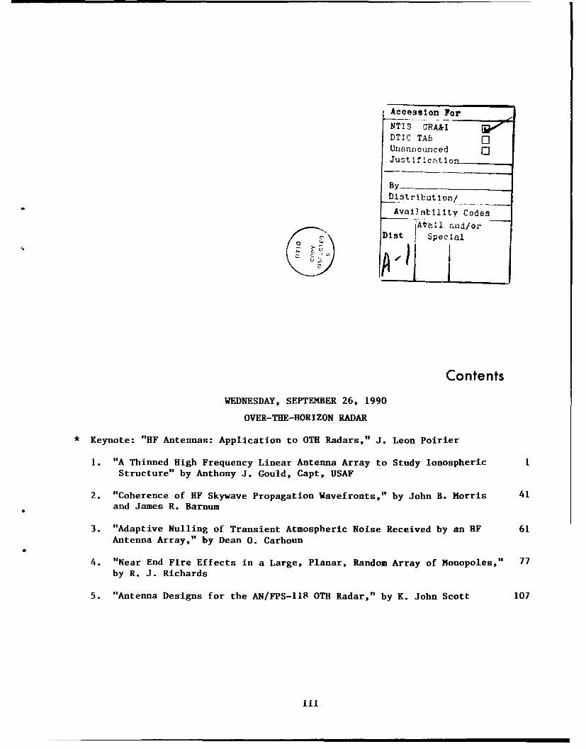
Contents
WEDNESDAY, SEPTEMBER 26, 1990
OVER-THE-HORIZON RADAR
Keynote: "HF Antennas: Application to OTH Radars," J. Leon Poirier
1. "A Thinned High Frequency Linear Antenna Array to Study Ionospheric IStructure" by Anthony J. Gould, Capt, USAF
2. "Coherence of HF Skywave Propagation Wavefronts," by John B. Morris 41and James R. Barnum
3. "Adaptive Nulling of Transient Atmospheric Noise Received by an HF 61Antenna Array," by Dean 0. Carhoun
4. "Near End Fire Effects in a Large, Planar, Random Array of Monopoles," 77by R. J. Richards
5. "Antenna Designs for the AN/FPS-118 0TH Radar," by K. John Scott 107
iii

Contents
ARRAYS
6. "Phased Array Calibration by Adaptive Nulling," by Herbert M. Aumann 131and Frank G. Willwerth
7. "Applications of Self-Steered Phased Arrays," by Dean A. Paschen 153
8. "Array Thinning Using the Image Element Antenna," by Joe Kobus, 172Robert Shillingburg and Ron Kielmeyer
9. "Distributed Beamsteering Control of Monolithic Phosed Arrays," by 202S. F. Nati, G. T. Cokinos and D. K. Lewis
10. "Analysis of Edge Effects in Finite Phased Array Antennas," by 217Steven M. Wright
11. "Multimode Performance From a Single Slotted Array Antenna," by 244
John Cross, Don Collier and Len Goldstone
12. "An Adaptive Array Using Reference Signal Extraction," by Jian-Ren E. 261
Rang and Donald R. Ucci
THURSDAY, SEPTEMBER 27, 1990
SHF/EHF ANTENNAS
13. "Optically Linked SHF Antenna Array," by Salvatore L. Carollo, Anthony 2754. Greci and Richard N. Smith
14. "A Modularized Antenua Concept for a Ku-Band Ferrite Phased Array," by 297F. Lauriente, A. Evenson and M. J. Kiss
15. "A Matrix Feed Beam Steering Controller for Monolithic EHF Phased 322Array Systems," by G. T. Wells, S. T. Salvage and S. R. Oliver
16. "Omnidirectional Ku-Band Data Link Antenna Design," by F. Hsu and 353
A. J. Lockyer
17. "A Retrospective on Antenna Design via Waveguide Modes," by K. C. Kelly 372
* 18. "Conformal Microstrip Antennas," by M. Oberhart and Y. T. Lo
19. "A Dual Polarized Horn With a Scanning Bean," by Zvi Frank 396
NOT INCLUDED IN THIS VOLUME
iv
Contents
ANTENNA ELEMENTS
20. "Multi-Octave Microstrip Antennas," by Victor K. Tripp and Johnson 414
J. H. Wang
21. "External Lens Loading of Cavity-Backed Spiral Antennas for Improved 444Performance," by George J. Monser
22. "A Compact Broadband Antenna," by Sam C. Kuo and Warren Shelton 457
23. "Reduced Profile Log Periodic Dipole Antenna Designed for Compact 486
Storage and Self Deployment," by G. D. Fenner, J. Rivera andP. G. Ingerson
24. "A Printed Circuit Log Periodic Dipole Antenna With an Improved 504Stripline Feed Technique," by Jeffrey A. Johnson
25. "Half Wave "V" Dipole Antenna," by Valentin Trainotti 512
FRIDAY, SEPTEMBER 28, 1990
ANALYSIS AND PROCESSING
26. "Compact Highly Integrated Dual Linear Antenna Feed," by Joseph 538
A. Smolko, Daniel X. Earley, Daniel J. Lawrence and Michael J. Virostko
27. "Shaped Beam Design With a Limited Sized Aperture," by F. Rabman 552
28. "Adaptive Algorithms for Energy Density Antennas in Scattering 558Environments," by James P. Phillips and Donald Ucci
* 29. "Finding the Sources of Momentary HF Signals From a Single Site,"by A. F. L. Rocke
* NOT INCLUDED IN THIS VOLUME
v

A Thinned High Frequency Linear Antenna Arrayto Study Ionospheric Structure
Capt Anthony J. Gould
RADC/EECP

A Thinned High Frequency Linear Antenna Arrayto Study Ionospheric Structure
ABSTRACT
This study reports on the design, modeling and performance
measurements of a high frequency (HF) linear antenna array with 36
sensors. The array was designed to achieve a narrow azimuthal
beamwidth while maintaining grating lobes 10 dB below the main beam
during a +/-30' scan in azimuth. The configuration chosen utilizes
two active vertical monopole elements and two parasitic backpoles to
form a subarray. The subarrays, or sensors, are spaced at distances
greater than half a wavelength to provide a large effective array
aperture while the elemental radiation pattern, provided by the
subarrays, suppresses the grating lobe as the array is scanned.
Radiation patterns for the array were determined using three
independent techniques; theoretical calculation, computer modeling
using the Numerical Electromagnetics Code (NEC), and measurement of
the fielded antenna. Results showed close agreement in antenna
performance among the three methods of pattern determination. The
three step process of theory, numerical modeling and measurement
appears to be an optimum approach to antenna design.
2

Table of Contents
1. Introduction1.1 RADC High Frequency Test Facility
2. Linear Array Antenna2.1 Design objectives2.2 Verona array description
3. Theoretical Methods and Considerations3.1 Calculation of theoretical radiation patterns
3.1.1 Simple vertical monopole element.
3.2 Two Element Subarray.3.2.1 Two active elements phased broadside3.2.2 Active element and backpole phased endfire
3.3 Design of Subarray Dimensions.3.4 Calculation of the array factor.3.5 Pattern multiplication of array factor and subarray pattern.3.6 Reducing grating lobes.
4. Calculations using Numerical Electromagnetics Code (NEC)4.1 Introduction to NEC.
4.2 Far-field Patterns Calculated with NEC.4.2.1 Vertical monopole over perfect ground4.2.2 Two active elements.4.2.3 Monopole with backpole.4.2.4 Full subarray4.2.5 Model of the full array.
5. Field Measurements5.1 Introduction and techniques5.2 Measurement of the subarray pattern5.3 Measurement of the array pattern
6. Array Description
7. Discussion
References
3

Illustrations:
1. Verona linear array coverage
2. Subarray configuration for the Verona linear array
3. Verona linear antenna array setup
4. Theoretical elevation patterns for a vertical monopole.
5. Theoretical azimuthal far-field pattern for twovertical monopoles phased broad-side.
6. Theoretical pattern for one active element and onebackpole phased end-fire.
7. Theoretical azimuthal far-field pattern for a subarraywith two active elements and two backpoles.
3. Array factor, subarray pattern, and resultantradiation pattern from pattern multiplication of arrayfactor with the subarray pattern.
9. Array factor, subarray pattern, and resultant radiationpattern for linear array scanned 20 deg. otf broadside.
10. Elevation radiation pattern for a simple vertical monopoleover perfect and finite ground planes calculated with the NECmodeling program.
!I. Azimuthal pattern for a two element subarray phasedbroadside calculated with NEC.
12. Azimuthal radiation pattern for a two element subarrayphased end-fire calculated using the NEC routine.
13. NEC azimuthal radiation pattern for a four elementsubarray including two active elements and two backpoles.
14. NEC radiation pattern for a linear array of 15 subarrays,including two active elements and two backpoles. Zero degreescan angle.
15. NEC radiation pattern for a linear array of 15 subarrays,with a 32 dB cosine squared weighting taper.
16. Measured azimuthal radiation pattern for the fielded fourelement subarray.
17. Measured 36 element linear array radiation pattern using theAva Tx. site as a source with a 32 dB cosine square weighting
18. Schematic of one active element.
19. Subarray schematic.
4

1. INTRODUCTION
1.1 RADC High Frequency Test Facility
RADC/EECP has assembled a high frequency (HF) radar and
communication test facility at the RADC Verona Test Annex, Verona
NY. The system consists of a set of 36 digital HF radio receivers
controlled by a DEC Micro-Vax II computer and an extended aperture
linear antenna array. The mission of the facility is two-fold.
First, investigate propagation mechanisms and limits imposed on HF
systems by the ionosphere. Second, explore digital processing
techniques such as adaptive sidelobe cancellation, narrowband
noise excision, and time domain noise excision that could lead to
improvement of current and future Air Force surveillance and
communications systems which use the HF frequency band.
The radar system at Verona converts the RF signals from the 36
antenna sensors of the linear array to a digital format using A/D
converters in each of 36 receivers. Antenna calibration,
beamforming, and all radar processing is carried out by the system
computer during post processing. This paper details only the
linear antenna array. Information concerning the receivers,
operational methods, and data processing will be presented in a
separate paper.
The purpose of equipping the test facility with an extended
aperture linear array was to create a high resolution probe to
study ionospheric structure and use this knowledge to improve
backscatter rada- techniques.
5

2. LINEAR ANTENNA ARRAY
2.1 Design Objectives
The objective of the HF test facility at Verona is to measure
ionospheric backscatter signals with high resolution and record
the receiver baseband digitally. There are many sources of
ionospheric clutter; radio aurora, f-region irregularities,
equatorial irregularities and others. All these mechanisms
contribute interference that is known to degrade HF propagation
performance. Measurements using the linear antenna array will
help provide the data needed to evaluate the effectiveness of
digital processing techniques to reduce interference caused by the
irregularities at the high latitudes. The backscatter data will
also be used to characterize or map ionospheric phenomena in the
high latitudes. This mapping will help determine the spatial and
temporal extent of ionospheric irregularities.
The frequency range of the receiver system is 5-30 MHz which
encompasses most of the HF band. However, high intensity
phenomena are usually present during nighttime operation when the
ionosphere dictates that the most effective operating frequencies
are at the low end of the HF band. Therefore, 6-12 MHz was used
as the design operating band for the linear array. While the
array will certainly work to some extent over a much larger
frequency band, the array was tuned to perform best in the 6-12
MHz region. With this criterion in mind, the 36 element linear
array was configured to obtain maximum resolution in azimuth while
still maintaining low sidelobe control over the operating
frequency band of 6-12 MHz.
A random array of elements spaced over a large aperture is
one way to approach this problem. However, it was decided not to
use this method for several reasons. First, increased signal
6

processing is necessary to reduce the sidelobes to levels
comparable to a periodic array. Secondly, the mainbeam pattern
and sidelobe levels are difficult to predict during all operating
situations and finally the array was to retain as much commonality
as possible with other existing HF antenna systems.
A linear array of widely spaced (greater than half wavelength)
directional elements was chosen as a practical solution to the
problem. Such an array provides a wide aperture that results in a
narrow beamwidth in azimuth and also provides good sidelobe
control. A wider aperture is possible using subarrays of monopole
elements that control grating lobes as the array is scanned.
Backpoles placed a quarter wavelength behind each active element
provide increased directivity of the array in the forward
direction. While a backscreen is more effective, environmental
concerns and colocation with other experiments on the selected
site u-rently prohibit use of a large backscreen. The geographic
coverage area of the array is shown in Figure 1. Note that the
coverage area includes a large overlap of the area associated with
the nighttime auroral oval.
2.2 Verona Array Description
The linear HF antenna array at Verona NY is composed of 36
subarrays with a spacing of 20 meters between centers of each
subarray. This elemental spacing corresponds to 0.8 wavelengths
at the upper design frequency of 12 MHz. The dimensions and
components of the subarrays are shown in Figure 2. The main idea
in the subarray design process was to use a given number of
monopoles as the basic components to create a directional element.
Two monopole elements, placed a half wavelength apart (D2=12.5 m),
7

in a broadside configuration provided forward directivity and
reduced the energy received from signals arriving from the
direction parallel to the array. The 6 meter height of these two
elements was chosen to keep the element length near a quarter
wavelength of the operating frequencies. A 12 meter backpole was
placed a quarter wavelength (Dl = 6.25 m) behind each of the 6
meter elements. A height of 12 meters was chosen to keep the
backpoles greater than a quarter wavelength even at the low end of
the operating band. The four monopoles acting together as a
subarray provide forward directivity and wide nulls at angles of
:90' and 130'. The spacing between the subarrays (D3) was
determined from the constraint of reducing the grating lobe by 10
dB when the array is scanned 30' at a frequency of 12 MHz.
A schematic of the linear array setup is shown in Figure 3.
Several parameters are included in this figure to point out the
major features of the array including its length, spatial
orientation, operating frequency band, scan limits, and minimum
beamwidth.
8i

3. THEORETICAL METHODS AND CONSIDERATIONS
3.1 Calculation of Theoretical Radiation Patterns
Far-field azimuthal radiation patterns were calculated at
several stages of the antenna array development. These stages
included a simple monopole element, two elements phased
broadside, two elements phased endfire, a four element subarray,
and the 36 element linear array.
A great deal of consideration was given to the effect of the
ground upon the vertical field patterns. While a finite ground
might have little effect on the input impedance of a vertical
monopole, the field pattern can be greatly influenced by the
ground conductivity. Fortunately for the antenna, (and
unfortunately for the experimenters), the land at Verona is for
all intents and purposes a swamp. Ground conductivity for this
area is very high. A conductivity value of a = 0.1 mhos/meter and
a relative dielectric constant of E = 30 were used for all
calculations. These values were chosen from literature as being
consistent for a marshy groundl" While this is by no means a
perfectly reflective ground it improves the antenna performance at
receive angles close to the horizon. In addition, a ground screen
was installed in front of the array to ensure a stable impedance
for the antenna. The ground screen consisted of two 22 gauge
aluminum clad wires extending 75 meters in front of each element.
Field calculations were made with the assumption of an infinite
and perfect ground plane.
3.2 Simple vertical moncpole element.
The first antenna structure investigated was a vertical
monopole over a perfect ground plane. This antenna has a radiation
9

pattern similar to a vertical dipole in free space and is
therefore omnidirectional in the azimuthal plane. The elevation
field pattern for a vertical monopole has been extensively
calculated in the past and verified for nearly all situations 2 .
Parameters that influence the pattern are ground conductivity,
element length, element radius, and operating frequency. Elevation
patterns are shown in Figure 4. for a thin, 6 meter monopole over
a perfect ground plane and also with a = 0.1 and e = 30. Note
that the loss in gain for the antenna over a finite conducting
ground becomes critical only at angles close to the horizon,
(greater than 85'). This strongly suggests good low angle
performance for the Verona linear antenna, which allows for long
range OTH radar operation.
3.3 Two Element Subarrays
3.3.1 Two Active Elements Phased Broadside
The next step in the pattern shaping process was to add a
second monopole and phase the resultant pair to increase the gain
broadside (0') while placing a null in the endfire (90',270 ° )
direction. The azimuth pattern for a two element broadside array
of point sources with D2 = 0.5 \ is described by Eq. 1.
[p
E(O) = 2.Sin(k. D2 .Cos(O)) EQ: 12
k= 27rA
The pattern resulting from Eq. 1 is shown in Figure 5. Note the
nulls in the ±90* directions and maximum directivity to the front
and rear of the array.
3.3.2 Active Element and Backpole Phased Endfire
10

The next step in the pattern shaping process was the addition
of parasitic backpoles placed a quarter wavelength (D1 = 6.25 m)
behind each active element. One active element and one parasitic
backpole were considered as an endfire array. A backscreen
greater than a quarter wavelength in height (at 6 MHz) and placed
one quarter wavelength behind the active radiators acts as a
reflector. This reflector increases gain in the forward direction
by several decibels and provides nulling of any signals arriving
from behind the array. Such a backscreen would be over 12 meters
in height and 700 meters long. Environmental constraints and
other on-going experiments conducted at the Verona test site
prevented building such a structure. However, the antenna gained
significant benefit by placing a passive or parasitic element one
quarter wavelength behind each active element. These "backpole"
e2ements are connected only to the ground screen and to a copper
grounding stake driven 1.2 meters deep into the earth beside each
backpole. The increase in electric field intensity as a function
of azimuth angle 0, of one active monopole with a parasitic
backpole, is derived by Kraus 3 and shown by Eq. 2.
RII + RIL EQ: 2
\ R1 1+ R1L - I Z' 1 2 /Z 2 2 1C~s(2"m- T 2 )
x I + 14 Le ± dr .Cos(0)]
R11 = self-resistance of a vertical antenna element
RL = effective loss resistance of a single element
R12 + jX1 2 = Z = Mutual impedance, elements 1 and 2.
R22 + jX2 2 = Z22= Backpoles self-impedance.
Tm = arctan X12 T = arctan X22
1R

dr = spacing between elements
Note in Eq. 2, that as the impedance of the back pole element
(Z22) is increased the effect of the backpole decreases and the
gain approaches that of a single active element (G(O)=l). The
effectiveness of the backpole therefore depends to a large extent
upon its len,th. Also, it can be shown from Eq. 2 that when the
backpole is made longer than \/4 it acts as a reflector, and when
it is shorter than /V4 it becomes capacitive and behaves as a
director. Changing frequency will alter the performance of the
array since this corresponds to changing the dimensions of the
arzay in terms of wavelength. Complete cancellation of the signal
arriving from 180' is possible only if dimensions and physical
orientation of the array are perfect. Signals arriving from
angles not exactly 180' are never completely cancelled. This
arrangemen]t does
nowever, predict a significant increase in the forward (0°)
directivity and a decrease in directivity to the rear (180'). The
tield pattern for one active element and one backpole in a two
element endfire configuration array of point sources with (01
4) is described by Eq. 3 and illustrated in Figure 6. The
0)Attern shows the largest gain in the forward direction and
indicates a null in the ±180 ° direction.
=() = 2'Eo'Cos(k.D Sin(4)) EQ: 3
DI = Distance in wavelength between elements.
= Azimuthal scan angle from broadside.
k = 2-r
A
12

3.4 Design of Subarray Dimensions
The last step in elemental beam shaping is to combine the
broad-side and end-fire configurations to create the final
subarray. Combination of the broadside and end-fire patterns
through pattern multiplication results in the subarray pattern
formed by the two active elements and the two passive backpoles.
The pattern for this setup is shown in Figure 7. The main
element gain is shown to be in the forward direction. Nulls are
located in the ± 90 ° and 1800 directions. This pattern is
considered to be the theoretical element pattern.
3.5 Calculation of the Array Factor
The far-field array factor for a linear array of 36 isotropic
point sources is described by the square of Eq. 4. The field
pattern for the array factor with N = 36, D3 = 0.8 X, and 0o = 0
is shown by the plot in Figure 8. This pattern is for a uniform
array where all 36 elements are weighted equally. The peak of the
first side-lobe is 13.2 dB below the main beam. The 3 dB
beamwidth is approximately 2.5°.
Sin(v.N.D3(Sin(o) - sin(00 ) ]Earray = ---------------------- EQ: 4
N-Sin[v.D3.[Sin(O) - Sin( 0o) ]
N = Total number of elements.
D3 = Distance between array sensors in wavelengths.
13

3.6 Pattern Multiplication of Array Factor and Subarray
Pattern
A broadside (00 scan) far-field array pattern for the thinned
linear antenna array is also shown in Figure 8. It was calculated
by multiplying the subarray (element) pattern (also shown in
Figure 8.) by the array factor. Uniform amplitude weighting was
used in calculating this pattern. Characteristic 13 dB sidelobes
':e seen on either side of the main beam. However, now a broad
subarray pattern has been placed over the array factor. This
results in higher directivity in the forward direction and nulls
at angles of ±90*,and 180'.
3.7 Grating Lobe Reductions
A plot of the array factor when the array is scanned off
broadside by 200 is shown in Figure 9. Note the grating lobes that
have moved into the pattern. They are located at -120 ° , -80 ° and
160' and are equal in amplitude to the main beam of the pattern
now at 20'. Another plot in Figure 9 shows the total array
pattern. Notice that the amplitude of the grating lobes relative
to the main beam has been lowered significantly by the element
pattern with the nearest one at -80* now lower by 16 dB. This
reduction in grating lobes of the array by using directive
subarrays has permitted the aperture of the array to be increased
from 437.5 meters for the usual A/2 spacing between elements to
700 meters or 0.8 wavelengths between elements. This corresponds
to a decrease in beamwidth from 40 to 2.5' at the 12 MHz design
f requency.
14

4. Calculations Using Numerical Electromagnetics Code (NEC)
4.1 Introduction to NEC
The Numerical Electromagnetics Code (NEC)4 is a computer
program that uses the Method of Moments technique to predict the
electromagnetic response of antennas and other metal structures.
The physical structure to be analyzed is modeled using wire
segments to approximate the correct shape and electrical
characteristics. The required integral equations are then solved
to determine the currents on an electromagnetically excited wire
or structure. Similar to the theoretical calculations a step by
step process using NEC was employed to model various monopole
combinations. These structures were then combined to obtain the
subarray and finally the complete array. All computations were
carried out on a Digital Equipment Corp. Micro-Vax II computer.
4.2 Far-field Patterns Calculated with NEC
4.2.1 Vertical Monopole Over perfect Ground
A simple vertical monopole antenna was modeled first using
NEC. The height of the antenna is 6 meters and the element is
driven by a 1 volt source close to the ground. A calculation
assuming a perfect ground plane was made to create a baseline and
verify that the model is accurate. Next an element over a finite
ground plane was modeled using NEC. An option available with the
NEC program to use Sommerfeld Integrals was employed. This method
allows simulation of a structure very close to the ground.
Various ground plane configurations and different frequencies were
15

examined. Resultant patterns are shown in Figure 10. for both the
perfectly conducting ground and a ground with finite conductivity
representative of the earth at the Verona test site (a=0.l
mhos/meter, E=30).
4.2.2 Two Active Elements
A simulation of two active elements phased for a broad-side
configuration was computed and the field patterns calculated.
This arrangement generates the common "figure-eight" pattern with
nulls at ±90' in relation to broadside. The resultant azimuth
pattern is shown in Figure 11.
4.2.3 Monopole with Backpole
Similar to the process using theoretical methods, a backpole
was paired with an active element to reduce the gain in the back
half plane. The backpole in the NEC model is again located a
quarter wavelength behind the active element. Ground wires are
connected from the front element to the backpole. The backpole is
not driven with a voltage but purely reacts in the passive manner
as described earlier in Section 3.3.2. This setup as in the
earlier theoretical case results in an endfire configuration. The
resultant pattern is shown in Figure 12. Note that nulls
approximately 6 dB below the forward direction are formed at 180 °.
In this and the following simulations the a perfectly conducting
ground plane model was used since only the azimuthal variation is
under consideration.
4.2.4 Full Subarray
The full subarray of two active elements and two backpoles was
modeled next. Both active elements are driven in phase by 1 volt
sources. The resultant pattern for azimuthal scan is shown in
Figure 13. This is the element pattern for the array. It is this
16

pattern that can be multiplied by the array factor to create the
full array pattern. The subarray pattern calculated using NEC
shows nearly 15 dB of increased directivity in the forward
direction (0') compared to behind the array (180').
4.2.5 Model of the Full Array
The final modeling effort is naturally the full array of 36
subarrays and calculation of the composite element-array far-field
patterns. Unfortunately, our version of the NEC code cannot
accommodate structures as large as the full array of 36 elements.
The largest array that could be handled in the program was 15
subarrays. The limitation of 15 subarrays should only decrease the
gain, beamwidth, and number of lobes in the patterns. The overall
response of the 15 element linear array model should still be a
good representation of the 36 element array.
All active elements were fed with a one volt source with no
phase difference between elements causing the main beam of the
pattern to occur in the broadside direction. The result is
identical to a plane wave arriving that is oriented parallel to
the array. The resultant azimuthal radiation pattern is shown in
Figure 14. In order to determine the expected side lobe behavior
of the array, an amplitude weighting taper was used during
calculation of the field pattern. This is done by factoring each
of the voltage sources with a 32 dB Cosine Squared amplitude
weight. The cosine squared function is only one of many possible
weightings and was chosen because it does not broaden the main
beam as much as other comparable weighting functions. The pattern
for this simulation is shown in Figure 15. Notice that the
sidelobe levels have been reduced from the uniform level of 13.2
dB shown in Figure 14 to 32 dB below the main beam. The main beam
17

has broadened by 1 degree and about 3 dB of main beam amplitude
loss has occurred. This loss and beam spread will cause a
reduction in array resolution but it does not prevent adequate
system performance.
5. Field Measurements
5.1 Introduction and Techniques
The HF test facility using the linear antenna array at Verona
NY is currently in operation. Calibration and testing are
complete and some preliminary clutter data have been collected.
The pertinent pattern measurements made were the subarray pattern
and the full 36 subarray, linear antenna pattern. The essential
antenna information gained from these measurements includes the
gain, average sidelobe level, beamwidth, grating lobe response,
front to back ratio and scan direction accuracy.
5.2 Measurement of the Subarray Pattern
The subarray pattern was determined by moving a continuous
wave probe across the subarray aperture and plotting the received
signal strength as a function of azimuth. Measurements were also
made behind the array to determine the element directivity to the
rear (1800). Figure 16 shows the azimuthal element pattern for all
the elements at a frequency of 10.205 MHz. Although not shown on
this plot the front to back ratio was also measured and is
approximately 12 dB. Note that the subarray or element gain falls
off rapidly for signals arriving at angles greater than 250 from
broadside. This is the mechanism that permits the array to scan
±30 ° with the grating lobes reduced to at least 10 dB below the
main beam.
5.3 Measurement of the Array Pattern
18
The field pattern for the full array was measured by scanning
the array main beam past a CW signal transmitted from Ava NY. Ava
is located 21 miles away at a bearing from Verona of 31' east of
true north which corresponds to 210 east of the array boresight.
The power of the transmitted signal was ten kilowatts and the
antenna used was a horizontal log periodic. The resultant full
array pattern is shown in Figure 17. This pattern was obtained
using measured data and applying a 32 dB cosine squared amplitude
weighting function. Sidelobe response to the test signal is less
than 32 dB RMS. Note that the beamwidth is greater than the 2.5
degrees available without the weighting taper but is still only
approximately 4 degrees. This method of course does not account
for the response of the subarray pattern but only the subarray
pattern at a single bearing. Therefore, the actual gain will fall
off as the scan angles become greater than 20' as shown in Figure
16 by the subarray pattern.
6. Array Description
The elements and pre-amplifiers for the linear antenna array
were designed and built at RADC "in-house". The elements are
constructed from electrical supply house materials including, 1
inch diameter rigid aluminum conduit, pvc pipe, pvc flanges, and
pvc junction boxes. A diagram of the element is shown in Figure
18.
The signal output of each active monopole element is fed to a
power combiner located halfway between the elements. The combined
output is then band-pass filtered and sent to the pre-amplifier.
Pre-amplifiers were deemed essential to overcome the sum of losses
from cables, filters, and power combiners, which was calculated to
be 15-20 dB. The gain of the pre-amps was chosen to be 20 dB. The
19

output of the pre-amplifier is carried through RG/215 coaxial
cable to the receivers located in a central receive building. The
building is located slightly off the middle of the array and 30
meters behind the array. The RG/215-U used for the co-axial feed
cable is low loss double shielded cable with an outside armor
sheath. A unique aspect of this array is that eacn one of the
cables, connecting a subarray back to one of the receivers, are of
different length. The longest cable is approximately 1600 feet,
while the shortest is 150 feet. Phase and amplitude differences
for all channels are accounted for and adjusted digitally during
the beamforming process. Figure 19 details the subarray
configuration including the elements, power combiners, filters,
and pre-amplifiers.
7. Discussion
Once the required operating properties of the antenna ie.
gain, beamwidth, frequency band, etc. were specified, the antenna
design effort and testing for this system consisted of a three
stage process. First, antenna theory was used to design an
antenna that would meet these specifications. Second, numerical
methods were used to test the theoretical designs and ensure that
the designs met the performance specifications. Finally, pattern
measurements of the fielded antenna were made to verify that the
array performed as designed. Table 1. contains some of the major
required specifications and the results obtained from each of the
three techniques used. Although there are some minor differences,
in general, the agreement between the numbers is quite good and
shows that the use of theory and modeling techniques leads to the
fabrication of an antenna with the properties needed for
conducting meaningful experiments.
20

Table 1. Parameter Values from Each of Three Techniques
Parameter Theoretical NEC FIELDCalculations Calculations Measurements
Gain (dB) 26 24 23
BW (dB) 2.5 2 2.5
AVE. SLL (dB) 32 30 32
FIB ratio (dB) > 20 15 12-14
References:
1. E. Jordan, Editor, "Re ren. Data for Radio Engineers",Howard W. Sams & Co., 1986
2. J. D. Kraus, "Electromagnetics", 3rd ed., McGraw Hill, 1984, p.518.
3. John D. Kraus, "Antennas", McGraw-Hill Book Company, 1988
4. G. J. Burke and A.J. Poggio, "Numerical Electromagnetics Code(NEC)", Tech. Doc. 116, Naval Oceans System Center, 1980.
21

0D0
I- 4
4
tN \ /
r~j\\ 22

LOC
C(C
-P
4-LU Z 0
0 <~~ --
LO (
< C E
C14C
coE
23

z - .
<0
C1)
C\J~jL_ -
- aU
LL 0
Zu -
LUJ0 0~

0
Icc
C~
CL-H
I C)
c'.J cI*
(S P) NLV
u-i 25

00 0
cu
)
-4 0
N eDotv 0
a:0 C_
--1 0
4)
-E >r
U) C)
rI m
26

0
Cu
7 (7)
4-)
Q7 C4
-4 -4
m
0 1
co) a) u
I 0)
4 0)
- u m
27

U)
04
0
m C: ~ 0
*Q) 1
C-)
C-PC
0c
I 4
rur
24-

4 -
V0
a:A
Cu
z-.
< z m 0rz~~L Z U u -
.4
N 41
(-U0 Cu4- I4
29

0
44
ru4-
U27)
cd )z 0 z (7) 0
P.- ui m
C.) V
P.--
Cu M ro
<3

rC.)
.i -z 0
aa
L. z
UUJ
cy0-
LJ
c--4
rcr
LUJ
000ni
Q0> Q
w0.
C
31

(U)
L zh:) :i(.0
.- 40
i N
Cu -Cu
32

'4
0 --4
4-)
0
4-4.
NJ
u-4
I IIrJ' E m
33

U)
0004
Lr) F-
0
.4-d
LrC)
I
(D a aK34-

0
Q.
0
-C:
J.-
M r
CC
35

U))
a)ncu
ZC)
co
IS)
a)
1 * 4CD cN
cu cu U'
36t

0
Q)
~4-4
-J .- 4-C
* -......................................... ... .... ................-.
. ~ ~ ~ .. . . . .
.. . . .. .. . .. .. .. .. ..
MiCJ~ .- .M
37)

-4 U
4jQ4
$-4
Ch-
- ___ _____ _ .cc
38t

LU0
x0 L
0 lz0 C., IL U C .) 0
C ;uj
L LU., z <0>
0 14 LU Z
010
(L)
.1j
L~LJ L
C~40
0 3 9

ICIO
* uj
I 0I 0 LU
< CLLJLU
W0 =* 1u
L 0 -LUJ o LU CjLLU I
LL *L mU0_0 a:=J l
C/) 0 Z2
rlr c. LULL
Z C-m
<
I __ ___ _o___Z_ L
I, II
-L 1~
-CL)
40

COHERENCE OF HF SKYWAVE PROPAGATED WAVEFRONTS
John B. MorrisRome Air Development Center
Hanscom AFB, MA 01731
James R. BarnumSRI International
Menlo Park, CA 94025
41

Abstract
HF skywave signals are propagated beyond the Earth's
curvature by refraction within the ionosphere. As a
result, over-the-horizon radars have an advantage in
providing advanced notice of targets of interest as well
as a much enhanced surveillance area when compared to
conventional line of sight radars.
After passing through the ionosphere signal wavefronts
may experience perturbations in both amplitude and phase.
The corrupted wavefront propagates and impinges on an
antenna aperture. If we consider the ionosphere and
antenna as a system, these ionospherically induced errors
will negatively influence the antenna's response and
consequently affect radar performance.
We have begun a measurement program to quantify
statistically the effects of ionospherically induced
errors on apertures up to 10 km in length. A complex
correlation of the signals received along spaced coherent
receivers is used to form a mutual coherence function
which is useful in evaluating antenna performance. We
examine limitations on the mutual coherence function in
two dimensions (laterally in space, and time) for four
different propagation paths. The various propagation
modes are easily separated using a 12.5 KHz bandwidth
42

swept frequency continuous waveform (SFCW); emphasis is
placed on F2 low ray propagation.
1. Introduction
Temporal coherence affects the spectral width of a
signal source and spatial coherence affects the apparent
size of a signal source. In our experiment, the source,
which simulates a target return, is coherent in both
these domains during a measurement period. The
intervening medium, namely the ionosphere, is responsible
for degrading the image of the source as seen by a six
element 10-km receive aperture. Ideally, the ionosphere
would reflect an exact image of this perfect source.
However, variations in the spatial distribution of
electron density cause the image to appear to have come
from and extended source. Also, the time variability of
this medium produces effects similar to those produced by
a source of finite spectral width.
If the errors induced by the ionosphere are considered
as antenna errors, the aperture becomes only partially
coherent. Techniques developed earlier[Il may be used to
analyze the performance of antennas with partially
coherent illumination. The corrupted wavefront is then
described in terms of a mutual coherence function.
Several authors, for example, Altshuler et. al. 2 and
43

Mitchell [33, have shown the degradation in the performance
of antennas with such illumination.
In figure 1, a computer simulation shows the ideal and
corrupted antenna patterns of a 100 element 10-km linear
array of isotropic radiators. Interelement spacing is 2
wavelenghts at 6 MHz, and a Hamming amplitude taper is
applied. The ideal pattern shows the expected 0.3-degree
beamwidth and -43 dB side lobe level. In the case of the
corrupted pattern, a 0.7-radian rms phase deviation and
a 1 km phase error correlation length were used. These
errors are assumed to have originated in the ionosphere,
however we consider the effective antenna performance as
though they were truely antenna errors. The averaged
power pattern of this antenna/ionosphere system
experiences gain loss, beam broadening, and an increase
in side lobe level.
Data have been recorded to quantify the spatial and
temporal variability of the ionosphere with diurnal,
seasonal, and latitude changes. This ongoing
experimental program is known as the Extended Coherent
Aperture Project (ECAP). In this paper, we present four
measured normalized mutual coherence functions for winter
nighttime conditions using F2 low ray propagation. These
data are considered typical for the conditions stated,
although they are snapshots or samples of this function.
44
m ME M M M |

2. Mutual Coherence Function
The mutual coherence function is a complex correlation
of the signals across an aperture, which can be written
after Born and Wolf [43 as:
P(x,,x21 ,) =r12 (r) =< 1 ( V (t)> (1)
where V refers to a scalar field component, x, and x2
refer to position, t refers to time, and T represents
a time delay. The sharp brackets indicate an infinite
time average and * denotes complex conjugation. A time
stationary ergodic process is assumed. In optics, it is
convenient to define a time average since practical
devices can only measure such an average. However, at
HF, measurements of the instantaneous fields are easily
made so that an ensemble average can be computed. We
choose to rewrite (1) as
r(8,t)=<V(x+6, t+.) V (x, t) > (2)
where 6 refers to a spatial delay and the sharp
brackets now indicate an ensemble average. That is, the
average is performed over a group of measured wavefronts.
Spatial and temporal stationarity are implied in (2)
since P(6,T) does not depend on space or time origin.
45

Each computed value of P(,t) is normalized by the
average value of r(0,o) for six individual receiving
elements.
Spatial coherence effects are described by r(8,0) and
may be measured perpendicular to the direction of
propagation with an array of antennas. r(o,o) is also
called the lateral coherence function [51 and can be
related to the angular spectrum of incident plane waves.
Temporal coherence effects are described by T(o,r) and
can be related to the power spectrum of the fluctuations
(Weiner-Khinchine theorem). We are primarily interested
in the lateral coherence function r(6,o) because it is
used to predict the average pattern of an arbitrary
antenna"3]. However, the two dimensional mutual coherence
function r(6,T) is useful in revealing limitations on
coherent integration time for operational radars.
Figure 2 shows how the various quantities of interest
are interrelated. The heavy two-way arrow represents a
Fourier transform pair and the one-way arrow represents
a nonreversible path. Nonreversible implies, for
example, that the aperture field A(x) cannot be uniquely
determined from knowledge of the autocorrelation alone.
With no wavefront perturbation, (6,o) is unity and
the effective antenna transfer function t(x) is the
unaltered autocorrelation of the field distribution. The
average power pattern P(O) ( 0 being the azimuthal
46

angle) is then simply the Fourier transform of the
coherent transfer function. Alternately, the Fourier
transform of the lateral coherence function r(v,O) ( v
is an angular coordinate and the A denotes a Fourier
transform) is a dirac delta function which must be
convolved with IE(O) i to produce the average power
pattern. In this case, the average power pattern is the
expected coherent power pattern.
With wavefront perturbation, P(O) can also be
considered in two ways. First, the average power pattern
is the Fourier transform of the product of F(8,O) and
<A(x)A'(x+6)> . Or equivalently, the average power
pattern is the convolution of the ideal power pattern
with P(v,O) . Knowledge of r(8,0) and its statistical
variation is necessary to predict average antenna
performance.
To determine the mutual coherence function for an
ionospheric propagation path, one can transmit a known
coherent (space, time) signal and directly measure the
complex correlation of the reflected skywave signal along
a series of spaced aerials. We then assign these
measured errors to the aperture, and treat the aperture
as being partially coherent. One could, in principle,
measure the angular power spectrum directly and Fourier
transform this spectrum to arrive at the lateral
coherence function. For an aperture approaching 10 km in
47

size, the former represents a more tractable approa,;r, nri
is the one used here.
3. Experiment
As shown in Figure 3, and east-looking six element
receive aperture was formed by the addition of two
portable elements to four fixed elements of the existing
Wide Aperture Research Facility (WARF) located in Los
Banos, CA. The portable receive elements are
relocateable and convey demodulated SFCW signals at
baseband to the WARF control center by FM modulation of
a UHF carrier. The fixed elements are wired directly to
the WARF. This array is easily reconfigured for north-
look measurements using four additional fixed elements
and by moving the two portable receive elements, as shown
in Figure 3. Each monopole element is a 5.5-m whip fed
against a set of eight 15.2-m radial wires. The location
of each whip was surveyed to a relative accuracy of ± 5
cm.
Assuming that the spatial statistics depend only on the
relative positions of the elements and not on their
absolute position (spatial stationarity), we generate
correlations for 15 separations using six coherent
receivers. Note, in figure 3, that the array was
48

desiqned to have some redundant spacings in order to
verify the above assumption.
The measurement process includes data collection for
three two-week periods throughout the year.
Specifically, data were collected for an autumnal equinox
(September 1989), a winter solstice (January 1990), and
a summer solstice (June 1990). Only data recorded for
the first two periods have been processed at the time of
this writing. In each period, the first week is
dedicated to east-look measurements, followed by a week
of north-look measurements. A complete diurnal cycle is
examined. Prior to data recording, a wide sweep (6-30
MHz) ionogram is recorded. This recording is a useful
presentation of range or time delay versus frequency; it
reveals the various ionospheric layers or modes that are
present.
During the measurements, a ground wave calibrator (GWC)
is situated approximately 5 km in front of the receive
array. It transmits an SFCW signal and is received in
parallel with a similar over-the-horizon (OTH) signal.
The GWC signal is common to all array elements and is
used as a coherent reference for the array.
Figure 4 shows the geographical locations of the WARF
receiver and four remote OTH signal sites. For the east-
look measurements, a transmitter in Lost Hill, CA excites
either a transponder in White Sands Missile Range, NM, or
49

a transponder in Little Rock Air Force Base, AR. The
ranges to the WARF are 1416 and 2585 km respectively.
For the north-look measurements, a remote transmitter is
situated in Langley, BC and Yellowknife NWT, both in
Canada. The ranges to the WARF are 1336 and 2851 km
respectively.
A 12.5 KHz bandwidth SFCW signal was used at each of
the four remote sites providing a range resolution of 12
km. This resolution is quite adequate to separate the
various time delayed multipath components that may exist.
Doppler resolution is achieved by Fourier transforming
across 32 consecutive sweeps. A waveform repetition
frequency of 20 Hz was selected. This implies 1.6
seconds of data are used to separate the GWC and OTH
signals in a range-Doppler (RD) map. The GWC and OTH
signals are offset in both time and frequency to allow
easy detection in the RD map. Hanning weights are
applied in both range and Doppler to suppress processing
sidelobes. The amplitude and phase of the OTH and GWC
signals are interpolated within the RD map for a better
estimate of their values.
4. Results
The results presented here represent four snapshots of
the two dimensional mutual coherence function during the
winter solstice (January 1990), one snapshot
50

corresponding to each of the four remote sites. Each
function was computed during nighttime conditions using
an F2 low ray propagation path. An average Kp index of
2 was reported at the time, which is indicative of
relatively quiet ionospheric conditions.
Figures 5, 6, and 7 display measured mutual coherence
functions for mid-latitude propagation paths, whereas
figure 8 displays this function for an auroral path.
Each of these curves are computed from a file containing
approximately 13 minutes of data during the universal
times indicated in the figures. The averaging was
performed on an ensemble of wavefronts, each corrected
for spherical curvature and slowly moving ionospheric
tilts.
For each sampled wavefront a coherence factor was
defined. This factor is the ratio of actual power that
the six element array would receive to the maximum power
if the errors were absent. Only the wavefronts that had
a coherence factor greater than the median for the file
were used to produce these curves. In this way, the
malignant effects of Faraday rotation or low signal to
noise ratio were removed form the results.
Most evident in the figures is that coherence degrades
with range foL both the north and east look directions.
The coherence is reduced significantly when looking
towards the long range north-look site, possibly due to
51

interaction with the auroral trough. There were several
occasions when coherence from the Yellowknife site
increased noticeably during the late afternoon.
The mutual coherence functions in figures 5 through 8
show the temporal properties of ionospheric errors as
well. In general, temporal coherence appears unrelated
to spatial coherence. Limitations on coherent
integration time may be inferred. A comprehensive
analysis of the seasonal and diurnal variation of the
mutual coherence function and its effects on radar
antenna performance will follow.
52

Acknowledgements
The authors would like to thank Dr. Erik Simpson, Mr.
Kevin Reeds, Mr. James Gaddie, Mr. Dennis Gaydos, and Mr.
James Binnion of SRI International for their technical
contributions. Also, we would like to thank Dr. Gerard
Nourry of the Communications Research Center in Ottawa,
the Department of Communications in Canada, the Royal
Canadian Mounted Police in Yellowknife NWT, the Science
Institute of the Northwest Territories, the personnel of
White Sands Missile Range NM, and the personnel of Little
Rock Air Force Base, AR for their cooperation and
support. Discussions with Drs. Peter Franchi and Leon
Poirier of Rome Air Development Center are also
appreciated.
53

References
1. Schell, A.C. (1967) A technique for the determination
of the radiation pattern of a partially coherent
aperture, IEEE Trans. on Antennas and Propagation,
January:187-188.
2. Altshuler, E.E., et. al. (1990) The effects of
an ionospherically induced partially coherent
wavefront on the performance of a thinned
random array, to be published in the IEEE Trans.
on Antennas and Propagation.
3. Mitchell, R.L. (1966) Antenna Radiation
Characteristics with partially coherent
illumination, IEEE Trans. on Antennas and
Propagation, (AP-14, No.3):324-329.
4. Born, M. and Wolf, E. (1980) Principles of Optics,
Pergamon Press, sixth edition.
5. Ko H.C. (1967) Coherence theory of radio astronomical
measurements, IEEE Trans. on Antennas and
Propagation, (AP-15, No.l):10-20.
54

partially,coherent
/\/ \\
/ \/ coherent
-5 -3 -2 -1 0 2 3 4 5
ANGLE (DEGREES)
Figure 1. Comparison between coherent and partiallycoherent antenna patterns for a 100 element10 km linear array.
55
A (x) E(0)
<A (x) A* (x+6) > JE() 12
4 1
r ______ t(V,0)*
Aperture Field, A(x)
Voltage Pattern, E(O)
Autocorrelation, <A(x)A"(x+6)>
Power Pattern, IE(O) 12
Lateral Coherence Function, r(8,o)
Effective Transfer Function, '(x)
Average Power Pattern, P(O)
Figure 2. Relationships between various parameters
56

EXISTING 2.55-kmNORTH-LOOK km WARF ARRAY
0.00NEW CABLES FOR C.'jtNORTILOK 0.63
5~2.501
0% 0
Figure 3. Receive element and ground wave calibratorlocations.
57

YK/NWVT
60
0
z B
404
Figure 4. Geographical locations of WARF receiver andremote sites.
58

White Salids Repeater, 7.39 Mz, 12 Jan 90, 07:45:46 UT
05
0 5 10 15 20 25 30T Time Differcjicc (sec)
Figure 5. mutual coherence function computed fromsignal transmitted via White Sands missileRange, NM.
Little Rock Repeater, 9.17 MHz, 12 Jan 90, 07:03:31 UT
r (6, r)
T Time Differcncc (scc)
Figure 6. Mutual coherence function computed fromsignal transmitted via Little Rock AirForce Base, AR.
59

Langley (BC) Trans., 6.78 MIIz, 19 Jan 90, 06:23:59 UT
0 5 10 15 20 25 30T Time IDifferencc(scc)
Figure 7. Mutual coherence function computed fromsignal transmitted via Langley, BC.
Yellowknife (hVT) Trans., 7.93 M4Hz, 19 Jan 90, 06:50:32 UT
r (6,,c)
05
l5000
0 5 10 15 20 25 30T Time Diffcrcncc (ee)
Figure 8. Mutual coherence function computed fromsignal transmitted via Yellowknife, NWT site.
60(

ADAPTIVE NULLING OF TRANSIENT ATMOSPHERIC NOISERECEIVED BY AN HF ANTENNA ARRAY
Dean 0. CarhounThe MITRE Corporation
Bedford, MA 01730
Summary
Impulsive noise transients at HF, presumably caused by atmospheric lightningdischarge, can be a severe source of interference that limits the sensitivity of an HFreceiver array that may be used in direction-finding or radar applications. To the extentthat such energy subtends a small angle at the receiving array aperture and is receivedin the sidelobe region, it would be useful to suppress this source of noise by adaptivespatial nulling. We have recently examined records of elemental signals recorded froma linear HF antenna array in which the occurrence of transient atmospheric noise isevident. Closer examination of some of the stronger transients reveals that they arehighly directional and provide a naturally occurring source of energy that is essentiallyphase-coherent across the array. These observations are based on the use of a verysimple, iterative, retrodirective beamforming algorithm that calculates an estimate of thephase steering vector corresponding to the angular direction of the observed transient.This simple technique is useful not only for establishing the array weight vector to beused for nulling the interference, but also for checking the phase coherence andpossibly compensating the array for calibration or propagation path phaseperturbations. Results of application of this technique to the recorded field test data willbe presented and the performance of the retrodirective nulling technique will becompared with an optimal baseline established by the computationally more costlymethod of adaptive sidelobe cancellation using a constrained least-squares algorithmemploying reduced-rank principal components analysis. Results will be compared interms of the amount of suppression of the transient noise and by the impact on theadapted array pattern.
This work was supported by the United States Air Force, Electronic Systems Division,
under Contract F19628-89-C-001 with the MITRE Corporation.
61

ADAPTIVE NULLING OF TRANSIENT ATMOSPHERIC NOISERECEIVED BY AN HF ANTENNA ARRAY
Dean 0. CarhounThe MITRE Corporation
Bedford, MA 01730
Abstract
Impulsive noise transients at HF, presumably caused by atmosphericlightning discharge, can be a severe source of interference that limits the sensitivityof an HF receiver array that may be used in direction-finding or radar applications.To the extent that such energy subtends a small angle at the receiving array apertureand is received in the sidelobe region, it would be useful to suppress this source ofnoise by adaptive spatial nulling. We have recently examined records of elementalsignals recorded from a linear HF antenna array in which the occurrence of transientatmospheric noise is evident. Closer examination of some of the stronger transientsreveals that they are highly directional and provide a naturally occurring source ofenergy that is essentially phase-coherent across the array. These observations arebased on the use of a very simple, iterative, retrodirective beamforming algorithmthat calculates an estimate of the phase steering vector corresponding to the angulardirection of the observed transient. This simple technique is useful not only forestablishing the array weight vector to be used for nulling the interference, but alsofor checking the phase coherence and possibly compensating the array forcalibration or propagation path phase perturbations. Results of application of thistechnique to the recorded field test data will be presented in terms of the amount ofsuppression of the transient noise and the performance of the retrodirective nullingtechnique will be compared with an optimal baseline established by the
computationally more costly method of adaptive sidelobe cancellation using aconstrained least-squares algorithm employing reduced-rank principal components
analysis.

1.0 Adaptive Nulling Fundamentals
Assume a linear array of N equally spaced omnidirectional antenna elements,with one-half wavelength element spacing, that is used to form a narrow beam in a
designated direction. Assume that T complex digital samples, representing ananalytic signal, are recorded from each array element and let X denote a T x N
matrix of elemental array data in which the jth column, xj, consists of T samplesrecorded from thejth element of the array. Denote by Wq the N x 1 quiescent
weight vector used to form and point a beam in the desired direction. Assume that
M < N array elements are used as the auxiliary elements of an adaptive sidelobe
canceller used for adaptive nulling. Denote the auxiliary array data matrix by A and
its adaptive weight vector, to be determined, as w. Denoting the mainbeam signalas y = Xwq, the sidelobe canceller output, z, is expressed as z = y-Aw where w is
obtained by minimizing zHz (H denotes conjugate transpose). The adaptive weight
vector is determined as (see [1])
w = (AHA)-IAHy (1)
from which it follows that the adapted output is
z = y-A(AHA)-IAHy = PA-ly. (2)
PAL = I-A(AHA)-IAH is a projection operator that projects the mainbeam vector
y onto the orthogonal complement of the vector subspace spanned by the columns
of A to produce the adapted output z. By assumption, the auxiliary array elements
receive negligible desired-signal energy and are dominated by the interference. The
adaptive sidelobe canceller output can be viewed geometrically as the projection of
63

the array output onto a subspace that is orthogonal to the subspace determined bythe interference. When the weak signal assumption is violated, the adaptive weight
vector may need to be modified in accordance with linear constraints imposed toprevent desired-signal suppression [2].
In order to preserve the main features desired from the antenna pattern, whilemaximizing the signal-to-interference-plus-noise ratio (SINR) when there are moreauxiliary elements than interfering sources, we have found it useful to use only the
dominant principal components obtained from a singular value decomposition
(SVD) of A in order to determine the adaptive weight vector [3]. Let A = USV bethe singular value decomposition of A and assume there are p principal componentsdistinguishing the p-dimensional interference subspace from the M-p dimensional
noise subspace, as determined from analysis of the singular values [3,4]. Then the
adapted output may be expressed as
z = (I-UUH)y (3)
or as
Zp =(I-UpUpH)y (4)
if the principal components method is used, where Up denotes the first p columns
of the matrix of left singular vectors, U, corresponding to the p dominant principal
components.
It follows directly from (1) and the SVD of A that the adapted auxiliary weightvector can be determined a., the projection of the quiescent weight vector onto the
r4

vector subspace spanned by the columns of V, which are determined principally bythe interference. Mathematically,
w = VVHwo (5)
where wo is the vector of quiescent auxiliary weights, or if the principal
components method is used,
Wp = (VpVpH)wo (6)
where Vp denotes the first p columns of the matrix of right singular vectors V (the
eigenvectors of the sample covariance matrix (AHA)/T), corresponding to the pdominant principal components.
Observe that the principal components method allows us to remove thedistinction between an adaptive sidelobe canceller and a fully adaptive array. Wemay use all the array elements for adaptation, using the phase information obtainedfrom all the elements, and choose the correct number of degrees of freedom asdetermined by the observed number of dominant principal components. In this casewe may equate A = X and wo = wq and we see that the adapted output can be
expressed as
Zp = X(I-VpVpH)wq. (7)
This allows us to interpret the projection operator, (I-VpVpH), not only as anoperator used to modify the quiescent weight vector, but also as a spatial filter that
65

could be applied to the array data matrix X to remove the interference components
prior to beamnforming. It is possible, therefore, to observe the effect of the adaptivespatial filter on the elemental signals.
2.0 The Complex Coherence Function
In the data analysis described later we have applied the principal componentsmethod of adaptation to a fully adaptive array, operating at HF, for the purpose of
suppressing observed transients. While this provides an optimum performance
baseline, we are also interested in simplifying the computations. We will describe acomputationally simple algorithm that, in effect, extracts the largest principalcomponent and we will show that it is effective in suppressing large transients ofshort duration. This algorithm is based on determining a normalized retrodirectivesteering vector vs from a measurement of the complex coherence function of the
received energy across the array, and using the measured vector in a projectionoperator vsvsH that can be used to project onto a one dimensional subspace or itsorthogonal complement using the operator (I-vsvsH).
Fundamental to all adaptive phased array processing is the measurement of thephase distribution across the array resulting from one or more incident wavefronts.While this phase information is contained in the eigenvectors (or right singularvectors) that we employ in the principal components method, it can also bemeasured directly, particularly from a computation of the complex coherence
function [5]. Let one of the array elements be used as a reference and let its analytic
signal vector be denoted as xr = ar&9Pr where xr and ar are complex vectors of T
samples and ej(Pr is a scalar constant dependent on the spatial phase of the
wavefront measured at the reference sensor. In our notation the phasor eijPr, which
we assume to be constant for the duration of T samples, multiplies each componentof the complex vector ar which contains the amplitude and temporal phase variation.
Similarly xk = akeJ(k denotes the analytic signal sampled at the kth element. If we
66

form the zero-lag cross-correlation between the reference signal and each of the
other elemental signals we obtain the complex coherence function
xrHxk = arHakeJ(¢Pk-Pr) k - 1..., N (8)
The real part of (8), 2arHakcos((Pk--Pr), measures the mutual coherence across the
array and the complex exponential eJ((Pk(Pr) describes the phase distribution across
the array. Notice that the measurement is taken over T samples of the data to reduce
the effects of background noise that is essentially uncorrelated, or phase incoherent,from one sensor to another. In our analysis we have ignored the noise contribution
since we are concerned with nulling interference that exhibits, by implication, ahigh per-element interference-to-noise ratio.
The complex phasor eJ((Pr'-Pk) can be used as a retrodirective steering vector
to focus the array to match, or cancel, the phase of the impinging wave fronts.
When there is only one incident wavefront, the phasor is the steering vector
estimate for that source. A better estimate of the incident phase can be obtained byforming a retrodirective beam and using the beamformed output as the reference in a
second measurement of the complex coherence function intended to improve thephase estimate. The process can be iterated several times if necessary. Finally, the
steering vector estimated after several iterations can be used in a one-dimensional
orthogonal projection operator for adaptive nulling or spatial filtering of the arraydata. The method is somewhat equivalent to extracting the largest principal
component of the array data, but without the necessity of computing a singularvalue decomposition.
When more than a single degree of freedom is required because of multiple
sources incident from distinctly different directions the simple algorithm describedwill not be adequate, although it may suppress a clearly dominant source of
67

interference. The technique can be useful in suppressing short transient bursts of
interference when only one source is clearly dominant in the observation interval.
3.0 Adaptive Nulling of Transient Interference
Figure 1 shows an 8.5 second record (16,384 complex samples) of theenvelope of the analytic signal recorded from a single element (number 41) of an
82-element narrowband linear HF antenna array tuned to the 30-meter band.Transient noise just before 2 seconds and between 6 and 7 seconds is clearlyevident. The behavior is suggestive of that observed from atmospheric lightningdischarge [6], but there is no corroborating evidence to firmly establish that these
transients are due to lightning discharge. Further analysis will show, however, thatthe largest spikes are spatially coherent and can be adaptively nulled by the
procedures described above.
70
s o . .... ..... .... ........... .. ... ................ .. . ................................. . .................. ........... ...... .................. ........ .
4 0 .................. .................................... ................... .................. ...... ........... .......... ... ... .................. .....
0 1 2 3 4 5 7
Time (seconds)
Figure 1. Detected Output from Element 41
68

We analyzed a 64-sample record containing the large transient at 1.9 seconds.
Figure 2 shows the mutual coherence measured across the array using element 41
as a reference. It is evident that the mutual coherence falls gradually across the
array and the low spatial frequency suggests a small angle of incidence with respectto boresight. Figure 3 shows the phase variation across the array (modulo 2n)
calculated from the complex coherence function after one iteration. The dashed line
plots the ideal phase distribution, calculated for a plane wave incident at 4.25
degrees, which closely matches the observed phase. In this measurement element 9
was inoperative, producing only receiver noise, accounting for the anomalous value
at element 9.
20
150 - .
1 0 0 -- .. .-.. . .. .. ... .. .... .. . .... ... . . . .
- . .... ... .. . ... .. .
-100
-500 10 20 30 40 50 60 70 80 90
Element Number
Figure 2. Mutual Coherence (4.25-Degree Transient)
69

2
. ............. ,. ... .! ... ... ... ......... .i .. ... . .. .............. i .. . ........ ......... ! ....i. ... .. ...
.. ... . .
. 0 . .. . .. ..5 ; ;. . .. . ...... ...... ... ....... ....... . ..... ;....... . ...... . ... .-
.. 0 .5 -; ... ~ . ...... .. .. ..... .. ....... .. . i..... . . . . . . . . . .05
-2'
10 20 30 40 50 60 70 so
Element Number
Figure 3. Element Phase Variation
Figure 4 shows the output envelope of the signal from a beam formed at 4.25
degrees, further supporting the conjecture that the transient is a spatially coherent
source incident at 4.25 degrees. Closer analysis reveals that there are actually two,
and perhaps three, distinct sources contained in the record. Figure 5 is a composite
plot of the beam scans formed from the first three principal components of the array
data; there appear to be distinct sources at 2.5 and 4 degrees and possibly a third
source at 5 degrees.
70

1 8. .... ... ..... .. .... .. .... ... ...... ... .... ..... .. ... ... .... ..
1600 .. . ..... ........
4 0 0 -.. . .. ................ ...... .......
0N
0 1 2 3 4 S 6 7 8
Tine (seconds)
Figure 4. Receiver Output for Beam Formed at 4.25 Degrees
6
5 .............
4-
3
2-
0-10 -8 -6 -4 -2 0 2 4 6 8 10
Azimuth (degres)
Figure 5. Beam Scan for First Three Principal Components
71

A similar analysis was performed using 64 samples enclosing the large
transient at 6.5 seconds; the mutual coherence function is shown in figure 6.
Again, spatial coherence is evident and the spatial frequency suggests a larger angle
of incidence. Fine-grained principal components analysis revealed a strong
transient at 49.25 degrees with an underlying narrow-band interferer at 46 degrees.
400
3 0 0 ........ .. ... ..................................... • ......................... ............... .................. ................
2 W0 .......... ..................... .. ............ .. .. . ............. . .. .- ............ .. ......................... ........ .
-300 '
-100 ......
-2 0 0 -1........ ........ ..... .. ...
-3000 10 20 30 40 50 60 70 so 90
Element Number
Figure 6. Mutual Coherence (49.25-Degree Transient)
72

Let the normalized retrodirective steering vector calculated for the 4-degree
transient be denoted as v4 and let the retrodirective vector for the 49-degree sourcebe denoted as v49. Then a product of orthogonal projections can be applied as aspatial filter to the array data matrix in order to suppress the transient events
X'= X(I-v 4v4 H)(I-v 49v49 H). (9)
Figure 7 shows the spatially filtered output for element 41. Although each ofthe components of the spatial filter were determined from 64 samples, the spatialfilter was applied to all 16,384 samples of the array data. Suppression of thetransient events is evident.
70
4 0 . ... ............. ................... .................... ................... .................. .................. .................. .... ............... ........
50
~4 ....................................... ......... ................. i................ i.................. ...
0 13 4 5 6
Time (seconds)
Figure 7. Spatially Filtered Output of Element 41(Retrodirective Steering Vector Method)
73

Figure 8 shows the spatially filtered output of element 41 when the 64-sample
records surro,.nding each transient are subjected to a principal components analysis,
using a singular value decomposition of the data, in order to determine the adaptive
spatial filter parameters. In this case five principal components were used informing the orthogonal projection for each transient record. Comparison of figure
7 with figure 8 clearly shows that the simple algorithm based on estimating aretrodirective steering vector is suboptimum. It does, however, produce significant
transient suppression and is computationally much less costly than the SVD-
dependent method of principal components.
70
60 - ....
50
' 40
~30 -...
20
10 -A
0 1 2 3 4 5 6 7
Time (seconds)
Figure 8. Spatially Filtered Output of Element 41(Principal Components Method)
74

4.0 Conclusion
In this paper we have described a computationally simple algorithm, useful
for adaptive nulling of spatially coherent transients received by a phased antenna
array, based on measurement of the complex coherence function to extract the phase
distribution from which a retrodirective steering vector is derived and used in anorthogonal projection. The effectiveness in suppressing transients was
demonstrated by an actual example using data recorded from a narrowband linear
HF array. The method was compared with an optimal procedure based on principal
components analysis and found to be nearly optimal for the example used.
Acknowledgment
This work was supported by the United States Air Force, Electronic Systems
Division, under Contract F19628-89-C-0001 with the MITRE Corporation.
References
1. Monzingo, R., and Miller, T. (1980) Introduction to Adaptive Arrays,
Wiley, N. Y.
2. Griffiths, L. J. and Jim, C. W. (1982) An Alternative Approach to Linearly
Constrained Adaptive Beamforming, IEEE Transactions on Antennas and
Propagation. AP-30: 27-34,
3. Carhoun, D. 0. and Williams, R. T. (1990) A Principal Components Sidelobe
Cancellation Algorithm, Twenty-fourth Annual Asilomar Conference on
Signals, Systems, and Computers, Monterey, CA.
4. Golub, G. H. and Van Loan, C. F. (1983) Matrix Computations, John Hopkins
University Press, Baltimore.
75

5. Born, M. and Wolf, E. (1980) Principles of Optics, Pergamon Press, London.
6. Zavoli, W. B. (1977) Observed Characteristics of lonospherically Propagated
HF Atmospherics from Normal and Severe Thunderstorms, Stanford
Research Institute Technical Report, Menlo Park, CA.
76

NEAR END FIRE EFFECTS IN ALARGE, PLANAR, RANDOM ARRAY OF MONOPOLES
R. J. RICHARDSElectromagnetics DirectorateRome Air Development CenterHanscom Air Force Base, MA
Abstract
An experiment, is described, to determine the
effects of mutual coupling, near end fire, on the array
gain of a large, random, planar array of monopoles. An
HF transmit antenna array 2.5 km in diameter with 4,000
randomly spaced elements is frequency scaled resulting
in a 1.8 m diameter model antenna array. The
mathematical technique and cL.J.puter based numerical
calculations used to approximate the expected array gain
loss are presented. The approximate array gain loss is
shown to be as much as 13 dB at 00 elevation angle.
Calculation of the actual array gain is prohibited by
the enormous amount of computer time and memory
requirements, for example calculation of a single
element pattern using a MicroVAX II takes approximately
47 hours of CPU time. Therefore, an experiment as
described offers a practical approach to determine the
array gain loss.
77
1. Introduction
A large, (approximately 2.5 km in diameter)
circular, planar, transmit antenna array which operates
in the High Frequency (HF) band (6-30 MHz) and consists
of 4,000 randomly spaced sleeve dipoles with array
element electrical spacing ranging from a half
wavelength, at the lowest frequency (6 MHz), to 5/2 of a
wavelength at the highest frequency (30 MHz) could be
useful for Over-The-Horizon (OTH) radar applications.
Such large planar arrays of closely spaced elements,
present several significant technical problems, when
phased to operate at low elevation angles (eel) near end
fire. One problem is due to the mutual coupling between
antenna elements that can cause a serious reduction in
array gain. The coupling effects become especially
critical at the low end of the HF operating band (for
wideband arrays) and at very low elevation angles near
end fire. The degree of mutual coupling increases as
the electrical spacing of the elements decreases and
when the elements are oriented such that the element's
free-space pattern exhibits a maximum in the direction
of its neighboring elements. The low HF frequency and
very low elevation angle capability is extremely
important for an OTH radar system. These systems must
78

operate at low elevation angle beam positions (5° to 30°
or corresponding polar angles 85* to 60°), to detect
targets at 3000 km ranges, and at low HF frequencies due
to ionospheric propagation limitations, especially when
looking north and Ouring a significant portion of the
winter night.
The coupling effect is maximum at the low HF
frequency end of the radar system's operating frequency
range where the transmit antenna elements are most
closely spaced electrically. Because of this potential
serious degradation in OTH radar system performance, it
is important that mutual coupling effects, near end
fire, for random planar arrays be identified and
quantified.
2. Mathematical Analysis
2.1 Introduction
Mutual coupling is the result of the complex
interaction between antenna elements in electrically
close proximity. The interaction between elements
changes the current distribution and thus the element
pattern of an array element from that which it would
have if it were isolated in free space. The element
pattern of an isolated element will in general be quite
different from the element pattern of an array element.
79

Furthermore, the element pattern of each element in a
randomly spaced array will be unique. The element
pattern is of interest because the superposition of all
the array element patterns yields the active array
radiation pattern. [1] [2]
The array under consideration consists of 4,000
identical, parallel, randomly located, matched-loaded,
quarter wavelength monopoles on an infinite ground
plane. This array is a good approximation to the 4,000
element sleeve dipole array described above. The
analytical method used to analyze this array is a
modification of the method of moments used by Fenn [3]
to analyze periodic arrays of monopoles. The theory of
images was used to replace the array of monopoles over
an infinite ground plane by an array of dipoles in free
space. The only factors that must then be accounted for
are that the equivalent dipole has twice the input
impedance and half the gain of the monopole. This
dipole image approach was adopted because the mutual
impedance between parallel dipoles in free space can be
easily calculated using an equation given by Castello
and Munk [4].
80

2.3 Mutual Coupling Calculations
Fenn of Lincoln Laboratories conducted a study to
estimate the mutual coupling effect in large
periodically spaced arrays [3]. Franchi (RADC) (private
communication) using Fenn's data derived two empirical
equations, one to estimate the depth of the gain null at
zero degrees elevation angle as a function of the number
of array elements and the element density and the other
to estimate the 3 dB width of the null. The depth of
the null is given by
f(Ne,P) = 1 / [1 + p (0.65 ./Ne - 1)] (1)
and the 3 dB width of the null is approximated by
w (NeP) = 126 ° [4p/Ne] 1/4 (2)
where p is the element density with respect to a unit
cell size of A/2 by X/2 and Ne is the total number of
elements. Predicted scan losses using this empirical
formula for an array with Ne = 4,000 and p = 1/2 and w
(Ne,P) z 19*, at 6 MHz are 13.2 dB and 3 dB for
elevation angles of 0* and 9.5 ° respectively. See
Figure 1 for a plot of predicted scan loss as a function
of elevation angle and frequency for a 4,000 element
81

periodically spaced antenna array using Equations (1)
and (2). Note that the scan loss increases as the
frequency and elevation angle decrease.
3. Computer Based Numerical Methods
3.1 Introduction
The usefulness of computer-based numerical methods,
such as Moment Method, to determine the mutual coupling
effect in a large array is limited by the amount of
available processor (CPU) time and computer memory.
Therefore, when an array is very large, on the order of
a few thousand elements, an experiment is the only
practical method to measure the expected reduction in
array gain.
3.2 Numerical Method Limitations
Although calculation of all 4,000 element array
gain patterns is prohibitive, it is useful to calculate
several element patterns to approximate the mutual
coupling effect on individual array elements and
calculate an average element pattern. To calculate
these element patterns, we must solve for the current
vector (I) in Equation 3 either by directly inverting
the previously calculated impedance matrix [Z] then
multiplying it by the applied voltage vector (V) or by
some other matrix solution technique.
82

(I) = [Z] -1 (V) (3)
The matrix inversion method is itself time consuming;
Fath and Terzuoli in 1978 [5] reported inverting an
impedance matrix of (3752 by 3752) using the
Electromagnetic Surface Patch (ESP) Code on a
VAX-II/780. The inversion took 120 hours of CPU time.
Rather than resorting to inverting the matrix to achieve
a matrix solution, an iterative method, the Conjugate
Gradient Method, was chosen. This method always
converges to the solution in a finite number of
iterations given an arbitrary initial guess, provided
the matrix is nonsingular and round-off errors are kept
negligible. Also, Conjugate Gradient Method requires
much less memory (5N) than Moment Method (zN2 ). In
comparison to the matrix inversion method above the
solution to Equation 3 where [Z] is a 4,000 by 4,000
array would only take approximately 35 hours of CPU time
on a VAX-11/780 [6],[7]. Calculation of the mutual
impedance matrix [Z], solving for the current vector (I)
and computing a single phi cut element gain pattern for
a 4,000 element random array such as the pattern shown
in Figure 3 (a) takes approximately 46 CPU hours on a
MicroVAX II.
83

3.3 Numerical Results
3.3.1 Element Gain Patterns
The element gain pattern of an isolated monopole on
an infinite ground plane is shown in Figure 2 (a) and
its 3-D equivalent plot is shown in Figure 2 (b). Since
an isolated monopole pattern does not vary as a function
of t, Figure 2 (b) is simply the revolution of Figure 2
(a) about its Z axis. Note in Figure 2 (a) that the
polar angles (8) between 90' to 70 and -90 ° to -70'
correspond to the near end fire, elevation angles (eel)
between 00 to 20 ° . Figu 3 (a) is the t=o cut, element
gain pattern for element # 1, located near the center of
the full array of 4,000 elements. The gain pattern of
an array element depends on the spacing between itself
and its neighboring elements and since the element
spacing is random, the gain pattern varies as a function
of the azimuth angle t as well as the polar angle e.
This effect is illustrated in the 3-D display in Figure
3 (b). Further calculation showed that there is a
significant difference between gain patterns of
different array elements.
3.3.2 Array Gain Loss
The array gain loss is approximated by calculating
84

the difference between the isolated element gain pattern
and the average element pattern of several elements
located near the center of the array.
A close look at Figure 4 (a) will show the
significant gain loss at the low elevation angles,
between the isolated element shown in Figure 2 (a) and
element # 1 shown in Figure 3 (a). Using the gain
patterns of several elements located near the center of
the array, an average element pattern was calculated and
is shown in Figure 4 (b). Note that the average element
pattern, unlike the individual element patterns, is not
a strong function of t, therefore, the element pattern
is completely described by the 2-D plot shown in Figure
4 (b). The array gain loss can be approximated by
determining the difference between the average element
pattern and the isolated element pattern. The
comparison between the isolated and average element
patterns is shown in Figure 5 (a) and the array gain
loss as a function of elevation angle (eel) in Figure 5
(b). Since only relatively few element patterns were
used to calculate the average element pattern the actual
gain loss may be significantly different from that shown
in Figure 5 (b). The approximation for the gain loss
can be improved by using an average element pattern
85

based on a larger number of element patterns, however,
calculating a large number of element patterns is
impractical, therefore, an experiment to measure the
actual array gain loss provides a practical approach.
4. Experiment Design
4.1 Background
The physical dimensions of the transmit array,
described in the introduction, and the prohibitive use
of computer time and memory requirements for calculating
the predicted mutual coupling effects, led RADC to
design and conduct an experiment using a frequency
scaled model. As mentioned previously, the effects of
mutual coupling are more serious at low HF frequencies,
therefore, the model array is scaled in frequency from 6
MHz to 8 GHz. Measurements where taken at 8 GHz.
4.2 Antenna Array Model and Ground Screen
The antenna array model constructed is a 1.875 m
diameter array with 4,000 randomly spaced monopole
elements. This is scaled in frequency for a 2.5 km
diameter array. The 4,000 monopole elements are
specially manufactured Straight Bulkhead Jack Receptacle
connectors with an extended center conductor equal to a
quarter wavelength at 8 GHz as shown in Figure 6. The
monopoles were installed in the array base plate and
86

match terminated in 50 n loads as shown in Figures 7 and
8 respectively.
It is a well documented fact that the element
pattern of a single monopole over a ground plane of
finite radius is affected by the size of the ground
plane [8]. Since we wish to measure the array element
gain patterns for near end fire, elevation angles eel
from 5° to 20° the ground plane must be sufficiently
large such that the isolated element gain pattern
maximum occurs at polar angles emax 85*. Element gain
patterns for a thin quarter wavelength monopole at the
center of a circular ground plane of normalized radii
(0a) were calculated and the angles of peak directivity
plotted. A least square approximaLion was applied to
the data to fit the curve
emax = 90 - B (i/(Pa)I/2 ) (4)
where B is a constant. A plot of the polar angle of
peak directivity versus Pa for B = 118.505 is shown in
Figure 9. Using the results illustrated in Figure 9 an
approximate normalized ground plane radius of fa z 2,500
is required so that emax ; 87.5 °. Therefore, the
effects of the finite ground plane on the element
pattern are negligible for e < emax.
87

Since the element gain pattern measurements will be
made for one azimuth angle, the ground plane does not
need to be circular, however the ground plane length in
the azimuthal direction of measurement must be
approximately equal to the normalized radius of fa =
2,500 and the width sufficiently large so as to contain
several Fresnel zones. Therefore, to minimize the
effects of a finite ground plane the model array is
placed on a 4.88 m X 23.16 m solid aluminum ground plane
such that the center of the array is 17.07 m from the
forward edge and 6.09 m from the rear edge. The ground
plane, shown in Figure 10, is constructed from thirty
eight, 1.22 m X 2.44 m sheets of 0.64 cm thick aluminum
plates bolted together with countersunk bolts and
mounted on top of 2.13 m high platform. Electrical
continuity between each sheet is maintained by inserting
an 0.64 cm X 0.32 cm aluminum knitted wire mesh with
mesh core gasket between the plates and covering the
seam with conductive adhesive aluminum tape. The ground
plane was leveled to a tolerance of ± 0.32 cm at each of
the 48 adjustment points using a transit.
4.3 Experiment Configuration
Far field measurements require that the transmit
and receive antennas be separated by a minimum range of
88

R = 2 D2/ (5)
where D is the diameter of the array and R is the range.
For D equal to the diameter of the array and a
wavelength of 2.5 cm at 12 GHz the range length (R)
required equals 290 m An artenna range of this size is
not readily available, therefore, an approximation for R
was made. Since element patterns will be measured
individually with all other elements match loaded the
coupling between elements should become negligible
within half the diameter of the array. For this case
then D is equal to D/2 and the range R becomes R/4 or
approximately 72 m. The elevation angles of interest
were determined by using Figure 1 and noting that the
scan loss becomes negligible at elevation angles greater
than 16 ° . However, for completeness measurements should
be made at as high an elevation angle as the antenna
range permits. Using an existing RADC tower and
locating the array 72 m from the tower, elevation angles
up to 10 ° can be measured. Figure 11 is a sketch of the
Experiment Configuration. Since the reciprocity theorem
applies for antenna radiation patterns [91, the transmit
antenna model and its ground plane is set up on the
ground and operated in the receive mode while a transmit
89

antenna horn is moved up and down the tower. A standard
gain monopole is mounted on the ground plane next to the
array and 4,000 monopole element gain patterns are made
by taking the difference in dB between the array test
element and the standard gain element received signal
levels.
4.4 Measurement Equipment Description
The equipment for this experiment consists of the
transmit, receive and antenna positioning equipment
controlled by a Hewlett Packard computer as shown in the
block diagram illustrated in Figure 12.
4.4.1 Transmit Equipment
The transmit equipment consists of a Backward Wave
Oscillator (BWO) source, 10 W Traveling Wave Tube (TWT)
amplifier, 100 ft of low loss coaxial cable and X-Band
horn antenna. The X-band horn antenna has elevation and
azimuthal patterns such that the gain (towards the
receive element under test) variation is less than 1 dB
as the horn travels the height of the tower.
4.4.2 Receive Equipment
The receive equipment consists of an SA 1711 receiver,
ratiometer, RF switch, and two mixers. The receive
equipment is set up in the shared mixer mode
configuration to provide synchronous switching in order
90

to time share the mixer between the standard gain
monorole and the array test monopole element while
maintaining phase lock of the RF signal through the
Automatic Phase Control (APC) mixer. Receiver channel A
is connected to the standard gain monopole and channel B
to the array element under test. The ratiometer
displays the difference in dB between these two
channels. Ten samples are averaged per quarter degree
of elevation angle and this average is recorded on disk
for later processing. Signal averaging is used to
minimize the local background environmental noise
effects.
4.4.3 Antenna Positioning Equipment
The antenna positioning equipment consists of a
controller card, microstep indexer card, driver card and
stepper motor configured as shown in Figure 13. The
system controller card is operated through the IEEE-488
bus by a program run on the HP computer. Signals from
the controller are sent to a microstep indexer which
provides the driver card with the correct number of
propeily sequenced phase control signals to accelerate,
drive and decelerate the stepper motor as well as
correct for backlash in the 10:1 gear reducer. The
driver card supplies power to a 2-phase stepper motor to
91

turn a 10:1 gear reducer and drive the drum and cable
assembly that is connected to the X-band horn cart. On
command from the HP computer the stepper motor drives
the transmitting X-band horn cart along the rail system
attached to the tower with a positional accuracy of
greater than 0.08 cm.
5. Element Gain Pattern Measurements
5.1 Reference Monopole Element Gain Pattern
The reference monopole element gain pattern was
measured in the conventional way using a standard gain
horn and the gain transfer measurement technique.
The reference monopole element is identical to the 4,000
elements in the array and is mounted on the ground plane
1.73 m (46 wavelengths) away from the center of the
array. The standard gain horn is located 0.5 m from the
reference monopole element next to the ground plane and
at the same distance from the transmitting horn as the
reference element. The reference element and the
standard gain horn are used in the receive mode with the
transmitting horn located on the tower at an elevation
angle of 10° with respect to the ground plane. Then a
complete reference element pattern measurement is made
from 0* to 19° at 1/4* increments. Transmitter power
fluctuations due to the 10 Watt TWT output and cable
92

flexing as the transmitting horn travels up the tower
are reduced by averaging 100 measurements at every 1/4*
increment. Also, a correction is made to the reference
element pattern measurement to account for the gain loss
as the transmitting horn travels straight up the tower
rather than at a constant distance from the reference
element. The resulting rcference monopole element gain
pattern is shown in Figure 11 (a) compared to the
calculated monopole gain pattern of a monopole on an
infinite ground plane. Notice the peak of the measured
element pattern is below eel = 2.5*, therefore,
measurements made at elevation angles greater than 2.5*
are only effected by the ± 1/2 dB ripple on the element
pattern. The reference monopole element pattern is not
greatly effected by the finite size of the ground plane
or the presence of the 4,000 element array.
5.2 Array Monopole Element Gain Patterns
The difference in dB between an array element and the
reference element received signals are measured
simultaneously and averaged over ten measurements for
each 1/4° of elevation angle from 0* to 190. Averaging
is used to minimize the local background environment
noise effects. Then, the difference must be added to
the previously measured reference element gain pattern
93

to produce an array element gain pattern in dBi. The
above procedure is repeated 4,000 times, manually
switching elements between measurements. A comparison
between the measured array element gain pattern for
element # 1 located near the center of the array and
calculated gain for element # 1 is shown in Figure 14
(b). The difference between the measured and the
calculated pattern may be due to several approximations
in the theory. Assuming a single sinusoidal current
distribution on the wire is probably the largest
contributor to the error, especially since the actual
elements have a length to diameter ratio (l/d) of 7.38.
The delta-gap voltage source model used for the feed
region may also have some effect. Also, the ripple on
the measured element pattern is due to the finite size
ground plane where the theory assumes an infinite ground
plane.
5.3 Array Gain Pattern
The array gain is calculated as the superposition of
all 4,000 array element patterns. The array gain
patterns calculated without mutual coupling, predicted
with mutual coupling and measured with mutual coupling
for ' = 0* and 5° eel 190 are shown in Figure 15.
In this figure, the calculated array gain without mutual
94

coupling effects is the top curve. The middle curve is
based on the predicted gain loss due to mutual coupling
given by equations (1) and (2) for a periodically spaced
array with Ne = 4,000 and p = 1/2. The bottom curve is
the measured array gain pattern including mutual
coupling. Note that the measured array gain (bottom
curve) is lower than predicted for a periodically spaced
array (middle curve). The array gain loss between the
calculated without mutual coupling (top) curve and the
measured with mutual coupling (bottom) curve at eel = 5*
is approximately 8 dB and is still as much as 2 dB at
eel = 19°.
6. Summary
The analytical technique used to analyze the
expected performance of a circular, randomly spaced
array of monopoles over an infinite ground plane was
presented. This analysis is valid for antenna elements
with sinusiodal current distributions such as monopoles
over an infinite ground plane. Excessive CPU time and
memory requirements prohibited using this method to
calculate the expected array gain based on 4,000 element
patterns. However, an approximate array gain loss was
calculated using an average element pattern based on
several elements located near the center of the array.
95

Due to the computational difficulty of calculating the
array gain and the physical dimensions of the proposed
transmit antenna array, RADC designed an experiment
using a scaled antenna array model. The antenna array
model and ground plane were constructed at the RADC
Hanscom AFB antenna test range. The measurement of all
4,000 transmit antenna array element patterns was
completed and the array gain pattern calculated. The
result of the measurements was compared to the predicted
array gain and the calculated array gain without mutual
coupling. The array gain loss between the calculated
without mutual coupling and the measured with mutual
coupling is approximately 8 dB at eel = 5° and 2 dB at
eel = 19°. Therefore the array gain loss, near end
fire, due to mutual coupling must be taken into account
when designing the transmit antenna array. Future
efforts to reduce the gain loss at low elevation angles
will include low coupling array element designs and
terminating array elements with the impedance of an
average element's input impedance when scanned near end
fire.
96

REFERENCES
1. Warren L. Stutzman and Gary A. Thiele, Antenna
Theory and Design. John Wiley & Sons, New York,
1981; pp. 154-155, 339-340.
2. R. C. Hansen, Microwave Scanning Antennas Volume II
Array Theory and Practice. Academic Press, Inc., San
Diego, CA, 1966; p.301
3. A. J. Fenn, "Theoretical and Experimental Study of
Monopole Phased Array Antennas," IEEE Trans. on
Antennas and Propagation, Vol. AP-33, pp. 1118-1126.
4. D. Castello and B. A. Munk, "Table of Mutual
Impedance of Identical Dipoles in Echelon," Report
2382-1, October 1968, The Ohio State University
ElectroScience Laboratory, Department of Electrical
Engineering; prepared under Contract
F33615-67-C-1507 for Air Force Avionics Laboratory,
Wright-Patterson Air Force Base, Ohio. (AD 822013).
5. J. L. Fath and A. J. Terzuoli, "Large Matrix
Problems in the Computation of Electromagnetic
Fields." IEEE Atennas and Propagation Society, 1987
Symposium Digest, pp. 502-504.
97

6. Margret B. Woodworth, "Large Matrix Solution
Techniques Applied to an Electromagnetic Scattering
Problem," Interim Report RADC7TR-88-268, November
1988, ARCON Corporation; prepared under Contract
F19628-86-C-0104 for the Rome Air Development Center
(EECT) Hanscom Air Force Base, Massachusettes. pp.
8,26. ADA206917
7. Tapan K. Sarkar and Ercumant Arvas, "On a Class of
Finite Step Iterative Methods (Conjugate Directions)
for the Solution of an Operator Equation Arising in
Electromagnetics," IEEE Trans. on Antennas and
Propagation, Vol. AP-33, pp. 1058-1066.
8. Melvin M. Weiner, Stephen P. Cruze, Cho-Chou Li and
Warren J. Wilson, Monopole Elements On Circular
Ground Planes, Artech House, Inc., Norwood, MA,
1987; pp. 297-304.
9. Constantine A. Balanis, "Antenna Theory Analysis and
Design,"Harper & Row, New York, 1982; pp. 94-99.
98

44~~ ~ 1-4-l4 -.. . . . .4 - .-. - . 41 - , - 4 . .,
Z 44
Z *
0
FREQUENCYN(Hz)
Figure 1. Predicted Scan Loss in dB for a 4,000 Element
Periodically Spaced Array as a Function of Frequency and
Elevation Angle.
10 - _ _ _ _ _ _ _ _ _ _ _ _
0
Z -20 . 4.
HP H
~ 30 PHI= 0
-40-7-M1
-90-70-50-30-10 10 30 50 70 90
THETA (DEG)
(a) (b)
Figure 2. (a) Element Gain Pattern for an Isolated
Monopole on an Infinite Ground Plane. (b) 3-D view.
99

0-
z
-30- PHIO0
-40-
-90-70-50-30-10 10 30 50 70 90
THETA (DEC)
(a) (b)
Figure 3. (a) Gain Pattern for Element # 1 in the 4,000
Element Array Environment. (b) 3-D view.
10 - ~~~~~~~10 - _________ ___
0 -. 0
rcl-10 M-l
z 20Z -20
-30 -~ ~ .. ELEMENT j I ~ 3 H
-ISOLATED-40 1 1F 1 1 11 1 1 1 1 -40 -- 1
-90-70-5G-30-10 10 30 50 70 90 -90-70-50-30- 10 10 30 50 70 90
THETA (DEG) THETA (DEG)
(a) (b)
Figure 4. (a) Gain Comparison Element Between an
Isolated Monopole and a Monopole Near the Center of the
Array. (b) Average Element Pattern.
100

10 0
-H5
Z -20HH -10
30 PHI- 0
-ISOLATED
-40- 1
-90-70-50-30-10 10 30 50 70 90 0 5 10 15 20
THETA (DEC) THETA (DEG)
(a) (b)
Figure 5. (a) Ccmparison Between Isolated Element
Pattern and Average Elemenit Pattern. (b) Array Gain
Loss as a Function of Elevation Angle (eel).
Figure 6. Monopole Element.
101

Figure 7. Top View of AOTH Transmit Antenna Array Model
with 4,000 Elements Installed.
Figure 8. Bottom View of the Transmit Antenna Array
Model with 4,000 Loads Attached.
102

80
LiUC-, .... CALCULATED DATA
70-- - - LEAST SQUARE APPROXIMATION
LJ
60
0 300 600 900 1200 1500 1800 2100 2400 2700 3000 3300 3600
NORMALIZED GROUND PLANE RADIUS
Figure 9. Least Square Approximation of Polar Angle of
Peak Directivity Versus Normalized Ground Plane Radius
for 15 5 #a 3600.
103

Figure 10. Ground Plane with the Model AOTH Transmit
Antenna Array Installed.
104

30mH 23.16 m
1 875
72C m
ANTENNA MODEL SPECIFICATIONS
DIAMETER -1.875 InELEMENTS -4000, 1/4 WAVELENGTH MONOPOLESELEMENT SPACING -RANDOMK 8/2 WAVELENGTH EXCLUSION ZONESFREQUENCY RANGE -8 - 12 GHz (6 - 9 MHz)GROUND PLANE -4.88 - 23.18 mi
Figure 11. Experiment Configuration
TRANSMIT SIG. CH. AANTENNA
RF-
SWITCH
UNIT __ -. SERIES 1771
SIG. CH. B YC[ OE CONTROL RECEIVER
I{-P- -ER
PROGRAMMABLE
APC CH. -
> CH. A CH. B
APCMIXER -y - -
SERIES 1833A- -- - - --- ~DIGITAL
ANTENNA AMPLITUDEHG 4HPIB DISPLAY
b -POSITIONIN
SYSTEM EXTENDER
TWT
13ACKWARD HPIB SYCMPTER
OSCILLATOR EXEDRHP SERIES
9836
Figure 12. Block Diagram of the Measurement Equipment.
105

SUPERIORSYSTEM ELECTRIC CO.
COMPUTER HPIB HPIS CONTOLLERHP SERIES 4 110 EXTENDER 4 EXTENDER -4 10 CARD
9836 TYPE IODDIO
SUPERIORSUPERIOR ELECTRIC CO.
DRUM AND STEPPER _ELECTRIC CO. MICROSTEPCABLE ASSEMBLY - MOTOR DRIVER INDEXER
-. -. TYPE DRD004 CARDTYPE IMD1288
XBA NDHORN CART
Figure 13. Antenna Positioning Equipment Block Diagram.
10 10 -
S5
0 z 0zH
... CALCUL.ATED ..... CALCULATED
-1 .. EASURED -1 ... MEASURED
-1- II 0 I =7 I I r7
0 5 10 is 20 0 5 10 15 20
THETA (DEC) THETA (DEG)
(a) (b)
Figure 14. (a) Gain Comparison Between a Monopole on an
Ifimite Ground Plane and the Reference Monopole. (b)
Comparison Between the Measured and the Calculated Gain
for Element # 1.
106

ANTENNA DESIGNS FOR THE
AN/FPS-118 OTH RADAR
K. JOHN SCOTT
GENERAL ELECTRIC COMPANY
SYRACUSE, NEW YORK
ABSTRACT
The AN/FPS- 118 Radar is a Frequency Modulation/Continuous Wave (FM/CW)
bi-static system having a transmit site, a receive site, and an operations site. The transmit
and receive sites are generally separated by approximately 100 miles to provide sufficient
isolation between the transmit and receive functions.
The transmit subsystem utilizes elemental transmitters and a low-level
beamformer which has amplitude and phase control for each transmitter. The elemental
transmitters drive a twelve-element dipole array for each of six bands with a backscreen
and groundscreen reflector. A calibration coupler is provided at each transmitter output to
sample amplitude and phase. An iterative calibration procedure is used to establish the
aperture illumination needed for the desired beamwidth, scan angle, and frequency.
107

The receive subsystem utilizes elemental receivers and a digital beamformer. The
elemental receivers are connected to a monopole array of 246 elements for three
interleaved bands with a backscreen and groundscreen reflector. A test signal is inserted
at each receiver input to provide amplitude and phase corrections for each receiver path.
An ionospheric backscatter sounder system provides the data needed to direct the
operation of the radar. The sounder uses a transmit antenna having a beamwidth
nominally equal to the 60-degree scan coverage of each radar segment. Eight narrow
receive beams, spaced in 7.5-degree increments, are provided by an analog beamformer
which utilizes a section of the radar receive antenna. This paper describes the transmit and
receive antenna designs which evolved from the system performance requirements.
1.0. OVERVIEW
The site ground conditions and the surrounding terrain are integral parts of a High
Frequency (HF) antenna design. At HF (long wavelengths), antennas are physically very
large and site groundslope, blockage in the "look" direction, and soil characteristics
(dielectric constant/conductivity) must be included in antenna performance tradeoffs. The
choice of polarization is dictated by the elevation angle coverage requirements and antenna
height constraints. The AN/FPS- 118 antennas use primarily vertical polarization and long
groundscreens to enhance pattem response at low elevation angles.
The CONUS OTH System will consist of an East Coast Radar (ECRS), A West
Coast Radar (WCRS), an Alaskan Radar (ARS), and a Central Radar System (CRS).
Figure 1 shows the total coverage of the CONUS OTH System.
108

Figure 1. ANIFPS-I18 Radar System Coverage
Six antennas are provided for the ECRS. Three broadside transmit arrays and
three broadside receive arrays located in the state of Maine are used to provide 180-degree
coverage along the Atlantic Coast of the North American continent. Figures 2 and 3 show
the transmit and receive antennas, respectively. A transmit/receive antenna pair covers a
60-degree segment in eight sequential 7.5-degree increments. The transmit beam for any
increment is overlaid with three 2.5-degree receive beams.
109

f- W"I -- w.
Figure 2. Transmit Antenna
-
Figure 3. Receive Antenna
110

A transmit antenna array consists of six sub-bands designated A through F in
ascending frequency order. Each sub-band is a 12-element broadside linear array of
dipoles, mounted in front of a backscreen and above a groundplane. The frequency
bandwidth ratio of each sub-band is 1.348, providing a 5-to 30-MHz total bandwidth.
Bands A through D have the radiating element canted at a 45- degree angle relative
to the vertical. This angle is chosen to provide coverage at both high and low elevation
angles using an elliptical polarization, which is primarily vertical at low angles and
horizontal at high angles. Bands E & F use a vertically-oriented/polarized element to
provide only low angle coverage. Subarray placement, element cant angle, and inter-
subarray spacings are chosen to minimize coupling between subarrays and minimize
transmission line loss. This results in a band A, C, E, D, F, B arrangement of subarrays.
The receive antenna is a broadside linear array of 246 equally spaced monopole
elements placed in front of a backscreen and driven against a groundplane. Each of the
246 elements covers a 5- to 30-MHz frequency band. The antenna array is used in three
bands designated as high, mid, and low band. Each band has 82 active elements, with the
high band using the 82 contiguous centrally located elements; mid-band using the 82
centrally located, even numbered elements; and the low band utilizing every third element
of the entire array. Table I shows the overall dimensions of the AN/FPS- 118 Antennas
and Figures 4 and 5 show detailed dimensions of the transmit and receive antennas,
respectively.
111

TABLE 1.ANTENNA CHARACTERISTICS
Ele- Maxi- Ground-ments Total Antenna mum Screen
Ele- Per Ele- Length Height LengthBands ment Band ments (ft) (ft) (ft)
Transmit 6 Dipole 12 72 3,640 135 750Antenna
Receive 3 Mono, 82 246 4,980 65 750Antenna pole
In Cov 1 Log 2 2 318 140 750Sounder PeriodicTx Ant Mono-
pole
In Coy 3 Mono- 24 72 2,880 65 750Sounder poleRcv Ant
Out of I Log 2 2 318 140 440Cov PeriodicSounder Mono-Tx Ant pole
Out of 2 Mono- 10 20 625 65 60Coy poleSounderRcv Ant
112

N. zw
0 0
c2
< Lj
LU 0
U -. C
JL 6. U.
co
00 z<
N
Figure 4. Transmit Antenna Dimensions
113

C.0
I.
0
40 z
0
inn
WC L J
6- C,'0. z
w Z!w~
>~0Ywa:a < I, < if
0Nw
inOmI0u
Figue 5 ReciveAntena imenion
w 114

Each segment has an in-coverage backscatter sounding antenna system. Two
additional out-of-coverage sounder antennas are provided for the East Coast Radar. One
is directed due west and the other pointed at geomagnetic north. The sounder transmit
antenna is a two-element array of Log Periodic elements. The in-coverage antennas have a
750-foot long groundscreen and the out-of-coverage antennas have only enough
groundscreen to stabilize the input impedance. The in-coverage receive sounding beams
are formed using 24 high, 24 mid, and 24 low band radar elements. The element signals
are obtained by a 3-dB power split after the first amplification stage in the receivers. An
analog beamformer for each group of 24 elements provides eight beams steered in 7.5-
degree increments to fixed angular positions which covers a 60-degree azimuth angle.
Full time delay is used for steering to obtain frequency independent beam pointing
directions. A switching matrix provides two simultaneous beams from any of the three
bands which can be routed to two sounder receivers. An out-of-coverage sounder receive
antenna can also be connected to one of the sounder receivers. Each of these antennas
consists of a high and low band with each band having ten elements. The elements are
positioned on the backside of the radar antenna backscreen and they use the radar
backscreen as a reflector. An analog beamformer is used to collimate a beam in the
desired direction, depending on the pointing direction of the companion radar antenna.
2.0. ARRAY DESIGN
The total 5- to 30-MHz frequency band is divided into six sub-bands for the
transmit antenna. The frequency bandwidth ratio of each band is 1.348 (fh/fl) The
azimuth element spacing is 0.62 X at the high end of each band, and each band has twelve
elements. This spacing is selected to place the azimuth grating lobe neak well into
115

imaginary space at a maximum scan of 27 degrees. This is necessary with a short aperture
(wide grating lobe) to minimize the grating lobe impact on average sidelobe levels. The
broadside azimuth beamwidth for uniform illumination varies from 7.0 to 9.6 degrees
over the band. A maximum scan angle of 27 degrees is chosen to place the outer -3-dB
point of the beam beyond the 30-degree coverage needed at the high band end of each
subarray.
The element height above the groundplane for bands A through D is 0.41 X at the
high end of each band. The height for bands E & F is 0.44 X at the high end of each
band. These heights and the element orientation are selected to provide the required
elevation angular coverage.
The receive antenna element spacing is 0.61 X (20 feet) at 30 MHz and is selected
to place the first null of the grating lobe at the edge of imaginary space for a maximum
scan of 36 degrees. This maximum scan angle is chosen to permit depointing the receive
antenna 6 degrees relative to the pointing angle of the transmit antenna, while still
providing a 60-degree angular coverage from each antenna pair. The reasons for
depointing the antenaas are: 1) to correct for parallax arising due to the transmit and
receive antenna physical separation and, 2) to ensure that the transmit and receive
backlobes are never in alignment. This improves the round-trip backlobc kVel and
provides backlobe auroral clutter suppression. The antenna has 246 total elements, of
which only 82 are used at any given time. The high band uses 82 contiguous elements at
the center of the array; in the mid band, 82 even-numbered central elements are employed
and, in the low band, every third element is used. The frequency bands are 5.0 to 9.7
MHz, 9.7 to 15.0 MIlz and 15.0 to 30.0 MHz. The azimuth beamwidth is held to 2.5
degrees across the frequency band (when not aperture limited) by adjusting the number of
116

elements used and the Taylor weighting on the aperture. At the lower end of the high and
low bands the beamwidth increases to a maximum of 3 degrees. This weighting, along
with the error sidelobes, provides the required sidelobe suppression to allow operation in
an auroral environment. For higher azimuth resolution the aperture weight can be changed
to provide a narrower beam.
3.0. BACKSCREEN AND GROUNDSCREEN DESIGN
The backscreen for the antennas is constructed of copper-coated steel wire. The
wire diameter and spacing is selected to reduce the leakage through the screen to a level
which is consistent with the required backlobe level. The backscreen height is chosen to
control backlobe levels due to diffraction at the screen truncation edge. Connected mesh
construction is used to control the vibrational characteristics of the backscreen rather than
unconnected wires which vibrate at high frequencies and may affect the subclutter
visibility of the radar. Three mesh openings are used for the transmit antenna. They are:
10" by 10" for band F; 14" by 14" for bands D and E; and 22" by 22" for bands A, B,
and C. The receive antenna uses a 20" by 10" mesh opening with the 10" spacing in the
horizontal direction. A galvanized steel structure consisting of towers and trusses
supports the backscreen. The backscreen material is fabricated in rolls of various widths.
The rolls of material are thermite-welded together at the site into panels. These are then
tensioned and thermite-welded to the support structure.
The steel structures are fabricated into the largest fully welded sections which can
be galvanized and shipped to site. During assembly, all mctal-to-metal joints in the
structure are coated with a conducting, anti-corrosive material to prevent any noise and/or
spurious frequency generation from the joints over the life of the system. The structures
117

arc galvanized to minimize non-linear effects due to the iron content of the steel, and to
prevent corrosion.
The groundscreen for the antennas is laid on the ground to provide a reflecting
surface to control elevation beamshape and ground losses. The screen material is an
aluminum-coated steel wire which is compatible with normal soils. The groundscreen is
constructed of 14 gauge wire welded into a 6" by 6" mesh. The material is fabricated in 6-
foot wide rolls, 380 feet in length. The rolls are installed in strips, normal to the antenna
line. The strips are spaced 8" apart, and are spot-welded together every 4 feet for the
transmit antenna and every 3 feet for the receive antenna.
A computer program was developed to calculate the elevation pattern performance
of the antennas. The analysis includes the diffraction from the backscreen top edge, the
groundscreen front edge, the leakage through the screen, and the effects of the ground
surrounding the antenna. A flat earth is assumed for the analysis. Good correlation has
been obtained between measured scale model patterns and patterns calculated for the scale
model using the computer program. Measured azimuth patterns for the ECRS transmit
antennas, taken at several elevation angles, show good correlation with calculated data.
The program integrates the patterns to calculate the directive gain. Figures 6 through 8
show the transmit elevation coverage, receive elevation coverage, and the antenna directive
gain, respectively.
118

35-
* 30-
Upper -3 dB Point
25-
S 20 -
< 15C:0
a,
10-Lower -3 dB Point
5-
0-5 10 15 20 25 30
R970/Fig-06 Frequency - MHz
Figure 6. Transmit Antenna Elevation Coverage
119

30
Upper -3 dB Point
25
20CD
0)
~15
> 10 Lower -3 dB Pointwu
5
0-5 10 15 20 25 30
R970/Fig-07 Frequency - MHz
Figure 7. Receive Antenna Elevation Coverage
120

35 -Receive Antenna
30
cL 25- /77L
20 Transmit Antenna
15
10 -' I I I I I
5 10 15 20 25 30
R970/Fig-08 Frequency - MHz
Figure 8. Antenna Directive Gain
4.0. ELEMENT DESIGN
The transmit element must provide a good impedance match (low VSWR) to the
transmitter to obtain efficient power transfer to space. Each array element has a broadband
transmitter which supplies 80 kW of power for VSWRs of less than 1.6. At a VSWR of
2.0, the power output falls to approximately 40 kW. To provide low VSWRs over the
frequency band and scan angle, a broad band dipole is chosen for the transmit element.
The dipole design uses a bazooka balun to provide the transition from a 50 ohm,
6-1/8" diameter coaxial feed line to the balanced current on the dipole arms. A square
aluminum truss structure provides the element support and also forms the X/4 shorted line
section for the balun. The radiating arms of the dipole are triangular aluminum truss
121

structures, which are isolated from the aluminum support by a dielectric structure. The 6-
1/8" coaxial input line proceeds through the aluminum support to the element feed point.
Each arm is fed through an open circuited 3-1/8" coaxial line located in the arm. This
provides a series capacitance, which is used in conjunction with a two-section impedance
transformer in the 6-1/8" input line, to match the active dipole impedance to 50 ohms.
Figure 9 shows dimensional data and the configuration of the transmit elements.
ELENT
,o-ACK SCAEN In.-
AW
BALUN ISHORT ARM
DIELECTRIC* SUPPORT 3 1/6' LINE
A CAPACITOR AL
AXF 1TRANSFORMER/
BALUN C
CR01114 SCREEN
BANDI ORIENTATION4 A(V) S/FT) I FT) D(FI) AL(FTIj AX/VT AWIFT) LG/FT) 7/VT)
A I CANTED 900 135 80.0 45.1 794 76 7.6 53.S 10
C CANTED 497 75 33.0 24.0 44.7 42 4.5 25.5 12,0
D CANTED 36.93 SS 24.5 164 32.6 3.1 3.4 17.0 9.0
S VERTICAL 27.40 45 19.51 13.6 247 3.6 2.1 12.0 7.0
", VERTICAL 203' 35 14.5 1 101 194 268 lb 7.0 6,0
Band F Tower Spacing is 61.0 Feel
Figure 9. Transmit Element Dimensional Data
Scale models of the elements were constructed without the impedance
transformers to measure the single element feed point impedance. Seven element scale
122

models were constructed of bands C and E to measure the mutual coupling coefficients in
the array environment for the two different polarizations. A computer program was
developed to calculate from the measured data the active input impedance of each element
versus scan angle and frequency. An impedance matching program, using an iterative
procedure, calculates the pl rameters of a two-section transformer which minimizes the
input VSWR for all scan angles, frequencies, and element positions in each subarray. The
band F VSWR is optimized from 22.25 to 28 MHz due to operational frequency
restrictions from 28 to 30 MHz. The scale model VSWR predictions are shown in Table
2. Full-scale VSWR measurements compare very well with the scale model predictions.
Figure 10 shows a comparison of measured and calculated data at broadside scan and 10.6
MHz for the band C sub-array. Figure 11 shows the F band subarray and construction
details of the transmit elements.
Each element in bands A through E is cantilevered from a backscreen support
tower. For band F, three elements are cantilevered from a truss which is supported by
towers. The element 6 1/8" transmission line is brought down the rear of the towers to
approximately 7 feet from the ground. A bi-directional coupler is provided for monitoring
element performance.
TABLE 2
TRANSMIT ANTENNA ACTIVE VSWR
Frequency Average MaximumBand (MHz) VSWR VSWR
A 5.00-6.74 1.30 1.73B 6.74 - 9.09 1.29 1.71C 9.09- 12.25 1.25 1.63D 12.25 - 16.51 1.27 1.65E 16.51 - 22.25 1.27 1.83F 22.25 - 28.00 1.25 1.64
123

2.00HZ3 O -O M.ASU.54 U i
* . * *................. .. .. ...................... .......... ........ i....... ........ i........ i........ .....
1.- ......... .. ..- ........ ........ .... ... ......... ........ ........ ........; ........ ........ .....1.60.z,, 1..40 .... ......... i ..... .... i ... ... ...... .... .-....... ........ !........ ........ I .....Il 140g ....................
00 -
. 2 3 4 5 6 7 8 9 10 11 12
BAND C ELEMENT NUMBER
Figure 10. OTHBIERS Transmit Array Performance Band C Broadside (Uniform Illumination)
Figure 11. Band F Transmit Elements
124

The receive antenna element is a 17.8-foot long monopole fabricated from
galvanized steel. The element has an 18" by 18" by 18" triangular cross section and is
isolated from the ground by three fiberglass dielectric insulators. The element is fed
against the groundscreen using an end terminal assembly which has a "Type N" coaxial
input connector. A surge protector is used to prevent receiver damage if lightning strikes
the antenna structure. Figure 12 shows the receive element.
Figure 12. Receive Antenna Element
125

The receive element must operate over the total 5- to 30 MHz frequency band.
The element length and distance from the backscreen are chosen to be as large as can be
used without developing an appreciable reduction in the element gain in the broadside
direction. This results in an electrical element height of 0.54 X above the ground plane
and a 0.28 X (9.2 feet) electrical distance to the backscreen at 30 MHz. These dimensions
provide an acceptable loss for operation at 5 MHz. The return loss of a typical element in
a loaded array environment is shown in Figure 13. This variation in return loss and the
resulting mismatch loss is compatible with the external noise characteristics at HF
frequencies.
I I I I
.37 d Note: Mismatch Loss In dB Is In brackets
0 (11.0)
1K2.04 dB 2.13 dB
(43) (4.1)2.0 -.. _
?.63 MHz 15.0 MHz3.0
4.0 ---
ECC 5.0
6.0 7.17 dB
7.0 \ T
28 MHz
8.0
2 5 8 11 14 17 20 23 26 29 32Frequency (MHz)
R970iFg- 13
Figure 13, Receive Element Return Loss
126

The complete array is filled with elements to maintain impedance similarity for all
elements in the three bands. Unused elements are terminated in 50-ohm loads. This is
necessary to meet element similarity error requirements for sidelobe control.
5.0. FEED SYSTEM
The transmit antenna feed system is designed for an input power of 100 kW CW
and a VSWR of 2 for each element. Semi-flexible 50-ohm coaxial transmission lines are
used to connect the transmitter outputs to the element inputs. Bands A & B use 3"
diameter line; bands C and D use 4" diameter line, while bands E & F use 5" diameter
line. An adapter is used to interface with the 6-1/8" rigid line element input. A total of
61,000 feet of coaxial line is used for the transmit antenna. Each line is long enough to
extend from the element to its transmitter terminal. The electrical length of the lines are
measured during installation and the data used in a beam forming and steering algorithm to
collimate the beam at the selected scan angle.
The receive feed lines are commercially available 0.412" diameter coaxial cables
which are used in the cable T.V. industry. The cable characteristic impedance is 75 ohms
and 164 cables are used to connect the active elements to the receivers. Equal length
cables are used to all the active elements which are enclosed by the mid-band aperture.
The outboard 14 low-band elements on each end of the antenna use just enough cable to
connect the elements to the receiver. The cables are installed and buried in a trench, 5-foot
deep, which provides a maximum temperature variation of 11 degrees C year round and
limits phase changes versus temperature to an acceptable level. The cable lengths are
measured and trimmed to a tolerance of 3.2 degrees. These measured phase differences
are then used as a phase correction in the beamforming and steering algorithm in the
127

receive digital beamformer. A total of 316,000 feet of cable is used for the receive
antenna.
6.0. Structural Design
The antennas are designed to survive a peak wind velocity of 90 knots at a 30-
foot elevation without ice loading. With 2 inches of rime ice or 1.5 inches of clear ice on
major support structures, the antennas must survive a 50-knot peak wind, acting at a 30-
foot elevation. The backscreen and elements are no: considered major support structures,
and 0.5 inches of clear ice is used as the ice loading requirement on these structures.
A finite element model of the transmit antenna is created for each band using the
ANSYS Engineering Analysis System. The structural members are represented as three-
dimensional elastic beams. The beam elements are capable of developing tension,
compression, and bending stresses. All of the joints in the structure are considered rigid.
The loads are applied to the structure as nodal forces.
The wind force on the structure is calculated by taking the given wind velocity as
the basic wind speed measured at 30 feet with the gust and importance factors included. A
velocity pressure profile is then developed as a function of height using the appropriate
exposure coefficient in accordance with American National Standards Institute (ANSI)
A58.1 - 1982. The total static wind force on the structure is calculated as a function of the
velocity pressure, the force coefficients for square towers, and the projected area of the
structure. The wind is considered to be approaching from the front, rear, and quartering
directions. The structure is designed to withstand the most severe of these cases.
The wind force on the backscreen is accounted for through the use of three-
dimensional shell elements. The shells are stretched across the area of the structure where
the backscreen is located. A pressure is then applied to the shells equal to the wind force
128

on the backscreen. The density of the shell elements is adjusted to account for the weight
of the backscreen and the modulus of elasticity is set to near zero in order to avoid the
backscreen contributing any stiffness to the structure.
The ice accumulation is taken into account by adjusting the density of the
members to include the ice and by increasing the projected area of each member by twice
the amount of radial ice present. The force coefficients are recalculated for the members
because the members are considered to have rounded comers for iced conditions. New
wind loads are then calculated based on the adjusted values for the projected areas and
force coefficients of the members.
The stresses calculated are compared with the allowable stres. es prescribed in the
American Institute of Steel Construction (AISC) Specification for the design of structural
steel buildings. The calculated stress for any member is not allowed to exceed the
allowable stress stated in the AISC Code for Tension, Compression, or Bending Stresses.
A structural dynamic analysis was performed to determine the mechanical
resonant frequencies of the structures. A wind gust profile is assumed and used to excite
the structures and determine their vibrational characteristics. A maximum vibration
amplitude of 0.185 inches is allocated to the antenna from the Subclutter Visibility Budget
for spectral noise density. This is in addition to the initial displacement due to wind
velocities (including gusts) of 40 knots at 30 feet above ground level.
7.0 SUMMARY
Six transmit and receive antenna pairs have been fabricated and installed, three for
the ECRS and three for the WCRS. The antennas have been integrated with the rest of the
129

radar equipment and are providing aircraft detection capabilities for ranges of 500 to 2000
nautical miles.
ACKNOWLEDGEMENT
The author wishes to acknowledge the contributions of all the people who have
participated in the design, fabrication, installation, analysis, and test of the antennas. The
design began in 1975 and involved a large number of people both at GE and the many
subcontraators who supplied materials for the antennas.
130

PHASED ARRAY CALIBRATION BY ADAPTIVE NULLING
Herbert M. Aumann and Frank G. Willwerth
Massachusetts Institute of Technology, Lincoln Laboratory
Lexington, MA 02173
ABSTRACT
The limitations of phased array sidelobe performance were explored with a
32-element linear array operating at L-band. With conventional far-field cal-
ibrations, the average sidelobe level of the array was about -40 dB. Since the
array contained T/R modules with 12-bit attenuators and 12-bit phase shifters,
considerably lower sidelobe performance had been expected.
Initially, array performance was thought to be limited by inadequate cali-
brations. An examination of individual array element patterns showed a mir-
ror symmetric ripple which could only be attributed to edge effects in a small
array. Simulations indicated that more precise calibrations would not have
significantly lowered the sidelobe level.
An adaptive calibration technique was developed which iteratively adjusted
the attenuator and phaser commands to create nulls in the antenna pattern
in th;, directio: of the nulls of a theoretical antenna patterns. With adaptive
calibr:2ion, 4 e average sidelobe levcl could be lowered to -60 dB. Array
patterns with deep nulls in specified directions can also be implemented.
131

1.0 INTRODUCTION
A phased array antenna with low sidelobes has advantages for both cluttcr
and interference suppression. However, besides of measurement range and
rnultipath effects, a variety of causes may make it difficult to achieve low
sidelobe performance.
Quantization effects are the most often claimed to limit array sidelobe
performance. By using attenuator and phase shifters with 12-bits of control,
quantization errors should become insignificant.
Obviously it would be desirable to build phased array components with
sufficient tight tolerances to make further alignment unnecessary. In practice,
amplitude and phase differences in the T/R modules and transmission lines
of the beamforming network are almost unavoidable. Array calibrations can
be used to compensate for these differences and relate digital commands to an
actually applied excitation function.
Usually, array element patterns are assumed to be uniform. Mutual cou-
pling and edge effects may distort array element patterns, thus compromising
the array calibrations and excitation function calculations.
Rather than attempting to minimize the various error sources, the phased
array calibration technique described in this paper concentrates on achieving
the best array pattern under the given conditions.
132

2.0 ANTENNA RANGE AND PHASED ARRAY CHARACTERISTICS
2.1 Antenna Test Range
Phased array calibrations and antenna pattern measurements were made
with the linear array in Figure 1 on a 100 ft. ground reflection antenna range.
The range geometry is shown in Figure 2. Since this range did not meet the
far-field criterion for the test array, focusing of the array was necessary.
2.2 Phased Array Characteristics
The experimental array operated at L-band and was about 15 ft. by 2 ft. in
size. It contained 36 identical waveguide radiating elements. Two elements on
either end of the array were terminated to reduce edge effects. The remaining
32 elements were connected to transmit/receive modules.
Half-height, open-ended waveguide radiating elements were chosen primar-
ily because they were inexpensive and they had a broad, aspect angle insen-
sitive pattern. Some typical elements patterns are shown in Figure 3. In the
center of the array, the element patterns were nearly identical. However at the
ends of the array, the element patterns exhibited a mirror symmetric ripple
which was attributed to edge diffraction. Ordinary array calibrations cannot
correct for this ripple.
Good sidelobe performance in a small array requires transmit/receive mod-
ules with very precise attenuation and phase control. Each of the modules used
in the test array had 12-bits of amplitude and phase control. This was achieved
by using voltage controlled devices operating at an intermediate frequency
133

[1]. Typical characteristics are shown in Figure 4 and Figure 5. A normi-
nal quadratic approximation adequately described the attenuator the phaser
characteristics. There is a weak attenuator and phaser interaction which is
not easily accounted for by a closed-form calibration.
2.3 Array Performance with Standard Calibrations
Standard array calibrations were carried out with the array at broadside.
That is, all elements, except the element under test, were terminated, and
the characteristics of the element under test were determined. Using such
calibrations, Figure 6 shows an antenna pattern of the test array with a 40
dB Chebychev taper. Although the measured average sidelobe level of -39 dB
was considered quite good, with 12-bit quantization the average sidelobe level
should have been -45 dB for a 40 dB Chebychev taper.
One way of determining the limits of array sidelobe performance is to
measure the average sidelobe level as increasingly more severe array tapers are
commanded. Figure 7 shows that the array sidelobe performance was limited
to about -40 dB.
A simulation was carried out using actually measured element patterns,
such as shown in Figure 3, and perfect calibrations. Of course, the measured
element patterns included range multipath as well as small array effects. Tile
resulting array sidelobe performance was only a few dB better than the per-
formance measured on the antenna range. This indicates that the array per-
formance with standard calibrations was about as good as could be expected.
134

3.0 ADAPTIVE CALIBRATION TECHNIQUE
A technique for calibrating a phased array from the far-field pattern has
been has been described by Patton [2]. Actually, the process consisted of first
calculating the far-field pattern of an array by Fourier transformation of planar
near-field measurements. The array element excitations were then computed
by inverse Fourier transformation of the far-field pattern back to the aperture
plane.
The array calibration technique described here is based on iteratively form-
ing nulls in the antenna pattern [3]. The calibrations are considered "adaptive"
in that the measured antenna pattern is adjusted to match a theoretical model.
When the specified nulls correspond to the nulls of an array with uniform il-
lumination, the technique yields the insertion attenuation and phase of the
array elements. By specifying other null directions, different array illumina-
tion functions can be implemented.
3.1. Theory
The excitation function of a phased array can be calculated from an ob-
served far-field pattern by the direct matrix inversion method [4]. The pattern
of a linear N-element array in the direction 0 is given by
N
P(O) E wz1(O)n=1
135

z.0_ E.(0.) *2iR expj--( , mod A),
where w, are the complex excitation coefficients and En(O,) are the element
patterns. Usually it is assumed that all array elements are identical and the
range geometry is such that
E1(01) = E 2 (02 ) E= En(O) . (2)
By measuring the antenna pattern in N directions, a set of linear equations
can be written and solved for the N excitation coefficients. These equations
can be expressed in matrix form as
W =Z - 1 P (3)
where
W1
W=[2]
WVN
z,(o0 ) Z2(01) ... ZN(02)
z = ZI(0 2 ) Z2(02) .. ZN(03). . . . . . . . . .. .
ZI(ON) Z 2 (ON) ". ZN(ON)
136

P(01)[ P(0 2 )
P(ON)
In theory, measurements of the antenna pattern in any N directions could
be chosen to determine the array excitation function. In practice, the quality
of results obtained from a single "back transformation" has not been very sat-
isfactory. The problem is that the assumption of ideiuicat element patterns
is of limited validity and the range geometry is not sufficiently well known.
However, an iterative solution, with careful selection of the measurement di-
rections, has been successful.
3.2 Measurement Selection
Any measured antenna pattern will obviously be affected by the specific
range geometry. Thus, Figure 2 should be used to carefully calculate the range
to each element, particularly to include focusing corrections. Equation (1) also
indicates that differences in the amplitude and phase of individual element pat-
terns and errors in the excitation function have similar effects on the antenna
pattern. This interaction can be minimized by making measurements in the
directions of the pattern nulls.
For commonly used array tapers, the excitation function can be written
in factored form. Consequently, the null locations of the far-field pattern are
explicitly known [5]. In fact, the null locations were probably used to specify
the array sidelobe level in the first place. For an N-element array, there can
137

be at most N - 1 nulls in the antenna pattern. Ideally, if the main lobe is at
OP and the nulls are at 01, 02,- , ON-1 then the normalized pattern values are
P(o1 0p~o,)(4)
P(Og-1)-
and the matrix inversion in Equation (3) will return the theoretical excitation
function WT.
As a result of the assumption made in Equation (2), the nulls in the antenna
pattern are entirely deterlnined by the array factor. The above calculation will
therefore not be affected by the shape of the element patterns.
Since the array under test and the measurement range are not perfect, the
measured antenna response will not be zero at the null locations, that is
[ P() IP(01) CI (5)
P(ON-I) (N-
However, Equation (5) and Equation (3) can be used to obtain an estimate
WE. of the actually applied excitation function. In the following calibration
procedure, attenuation and phase commands will be adjusted until differences
be:tween the estimated and theoretical excitation function are a minimum.
When this is accorriplished, the nulls of the measured and theoretical antenna
pattern have been matched.
138

The nulls of an antenna pattern are usually of no particular interest. How-
ever. by forcing the antenna pattern to have nulls in the proper directions, a
well formed antenna pattern is virtually assured.
It should be noted that the process is mathematically identical to adaptive
nulling by sample matrix inversion [6]. That is the array is required to receive a
desired signal from a given direction, and it is required to suppresses undesired
signals in N - 1 carefully specified other directions.
3.3 Calibration Procedure
Usually, the first step in the array calibrations is to correct for array element
insertion attenuation and phase differences. Initially, an excitation function
Wc is commanded without corrections to yield a uniform illumination WT
WC=WT= (6)
For example, the resulting antenna pattern of the uncalibrated test array is
shown in Figure 8. The amplitude and phase of the antenna pattern is mea-
sured at broadside and at the null locations corresponding to a uniform illu-
mination. From Equation (3) an estimate of the actually applied excitation
function WE(i) is obtained. This estimate is then used to update the com-
manded excitation function on the next iteration as follows
139

WTWc(i + 1) = Wc(i) (7)WE(i)
where k < 1 is a gain constant. The actual commands have to be expressed
in counts based on nominal attenuator and phaser characteristics. The above
process is repeated until
WE(Z) WT, (8)
and there is no further improvement in the null depths. For example, Figure 9
illustrates that after 4 iterations a nearly perfect pattern expected for an array
with uniform illumination has been achieved.
Under the above conditions, the array element insertion attenuation and
phase are given by the reciprocal of Wc. Shown in Figure 10 and Figure 11
are the insertion attenuation and phase as determined by standard calibrations
and as measured by adaptive calibrations. Standard array calibrations are
usually carried out with a source at broadside. It was shown in Figure 3
that the element patterns are not entirely identical at all angles. Adaptive
calibrations include element pattern differences and therefore yield slightly
different calibration results.
As with any feedback algorithm, there is concern with convergence. For
example, an instability may occur if the Z-matrix does not adequately model
the array and range geometry. Another cause for instability may be a lack of
140

monotonicity in the attenuator and phaser characteristics.
3.4 Array Performance with Adaptive Calibrations
3.4.1 Sidelobe Suppression by Chebychev Taper
The calibration technique is not limited to an array with uniform illumina-
tion. For example, shown in Figure 12 is the adaptively determined excitation
function required to implement a 40 dB Chebychev taper. A parabolic phase
distortion necessary to phase focusing is clearly evident. Although the dif-
ferences between standard and adaptively determined excitation function are
usually quite small, the resultant array pattern, in Figure 13, represents a
considerable improvement over the corresponding pattern with standard cali-
brations shown in Figure 6.
With adaptive calibrations exceedingly low sidelobe performance could be
demonstrated. Figure 14 shows an antenna pattern with a 60 dB Chebychev
taper. At that level, the 40 dB dynamic range of the attenuators becomes the
limiting factor.
Shown in Figure 15 is the sidelobe performance with adaptive calibrations.
With adaptive calibrations, the array performance comes much closes to the
theoretical array performance expected from an array with 12-bits of amplitude
and phase control.
3.4.2 Sidelobe Suppression by Null Placement
In the above section the antenna pattern null directions were chosen to
141

correspond to standard Chebychev tapers. This resulted in very predictable
array performance. However, uniformly low sidelobes may not be required in
all applications. Rather than accepting the loss in efficiency and broadening of
the mainlobe, selective null placement in the direction of a known interference
source may be the preferred approach.
For example, shown in Figure 16 is an adaptively calibrated array pattern
with a 30 dB Chebychev taper and an additional null at -30 degrees. Again,
sidelobes in the direction of the interference have been suppressed by 60 dB.
4.0 SUMMARY
An adaptive calibration technique for a phased array was described. Since
the algorithm derived array excitation function directly from the measured
far-field pattern, no build-in test capability is required.
The technique is applicable not only to implement standard array tapers,
but can also be used to implement antenna patterns with deep nulls in specified
directions.
5.0 ACKNOWLEDGEMENT
This work was sponsored by the Department of the Air Force under Con-
tract F19628-90-C-0002.
6.0 REFERENCES
1. Aumann, H. M. and Willwerth, F. G. (1988) Intermediate Frequency
Transmit/Receive Modules for Low Sidelobe Phased Array Application,
142

IEEE National Radar Conference, Ann Arbor, Michigan
2. Patton, W. T. (1981) Phased Array Alignment with Planar Near-Field
Scanning, or Determining Element Excitation from Planar Near-Field
Data, Antenna Applications Symposium, Allerton Park, Illinois
3. Aumann, H. M. and Willwerth, F. G. (1989) Measurement of Phased
Array Patterns by Near-Field Focusing, AMTA Conference, Monterey,
California
4. Hoffman, M. (1961) The Utility of the Array Pattern Matrix for Linear
Array Computations, IRE Trans. Ant. and Propag. AP-9:97-100
5. Elliot, R. S. (1981) Antenna Theory and Design Prentice-Hall, Engle-
wood Cliffs, New Jersey, ch.5
6. Monzingo, R. A. and Miller, T. W. (1980) Introduction to Adaptive Arrays,
Wiley, New York
143

Figure 1: Experimental Phased Array
R =100 ft SOUR~CED = 6in
d =4.3 in
N =32
A= 9.3 in
CETE O ROTTO
144

2
0
2-
(L -4
-6
-8FAR-FIELD MEASUREMENTSELEMENTS 1.2,3,4FREQUENCY 1.3 6Hz
-90 -60 -30 0 30 60 90AZIMUTH (dog)
0
-2
-4
~ 6
FAR-FIELD MEASUREMENTS
-90 -60 -30 0 30 60 90AZIMUTH (do,-)
2
0
- -D
-4
-6
-8 FAR-FIELD MEASUREMENTSELEMENTS 29.30,31.32FREQUENCY =1.3 GHz
-90 -60 -30 0 30 60 90AZIMUTH (dog)
Figure 3: Typical Array Element Patterns
145

0- . . . . . 10
QUADRATIC FIT
M - 10-
zATTENUATION
z V)
w .......... -------- ----------
(L
-30- PHASE >
ELEMENTS 1,2,3.4FREQUENCY = 1.3 GHz
-50- 1hh11111 11h1, uis -- 1001000 2000 3000 4000
D/A COUNTS
Figure 4: Typical AttenuatorCharacteristics
ELEMENTS 1.2.3.4-FREQUENCY =1.3 GHz
- -360
0.5z 300
:240 ujz -00ATTENUATION
-180w
PHASE 120 w
-60
-- QUADRATIC FIT-1 .0 1 , I .. r 0
0 1000 2000 3000 40000/A COUNTS
Figure .5: Typicil Pliaser Characteristics
146

0 2040 dB CHEBYCHEV - FAR-FIELD
-10 FREQUENCY 1.3 GHz MEASUREMENTS 10
'" -20 0 m
o-30 -10 0
,__ _
L -4-------- -- ------ ------ ------ ------- --------- 20- 4 0 2 0 o.
> -50 -30 >
-60 AVERAGE -40 ,SIDELOBE LEVEL
-70 -50
-80 -60-90 -60 -30 0 30 60 90
AZIMUTH (deg)
.Figure 6: Antenna Pattern with Standard Calibrations
-20 1 1 1 1,
o FAR-FIELD MEASUREMENTSi...., oSIMULATION
30 -10 m
. _ STANDARD"' "CALIBRATONS> L--..J >_n -- -- -- - - - - -- - - -JLi0 2
0 m
W -50 -30, 12-BIT W-
QUANTIZATION ""
> Li<-60 -40 >
FREQUENCY = 1.3 GHzAZIMUTH = 0 deg
-70 -5020 30 40 50 60
COMMANDED CHEBYCHEV TAPER (dB)
Figure 7: Array Sidelobe Performance with Standard Calibrations
147

-UNIFORM ILLUMINATION -WITHOUT
-FREQUENCY =1.3 GHz CALIBRATIONSNULL LOCATIONS
LJ
-20-
-30-
-40-. . . 1 . . .-90 -60 -30 0 30 60 90
AZIMUTH (dog)
Figure 8: Uncalibrated Array Pattern
0-:UNIFORM ILLUMINATION -WITH ADAPTIVEFREQUENCY =1.3 GHz CALIBRATIONS
---THEORY
-10-
LJ
IL
-30-
-40- 1-90 -60 -30 0 30 60o9
AZIMUTH (dog)
Figure 9: Arraiy Noatern with Uniiforml Illumination
148

FREQUENCY = 1.3 GHzAZIMUTH = 0 deg
• ."' 4 '--
z
o2-
z
A wo2
I--
-4--o STANDARD CALIBRATIONS
o ADAPTIVE CALIBRATIONS--6 1- ' III I I I I I I I I I -r--r r T T l I
0 4 '8 12 16 20 24 28.. 32ELEMENT NUMBER
Figure 10: Comparison of Insertion Attenuation
180-- FREQUENCY = 1.3 GHz
AZIMUTH =0 deg
1 20-
60-
W
"0
~-60-
-120-o STANDARD CALIBRATIONSo ADAPTIVE CALIBRATIONS
-- 180- . I I I i I ' W .I F
0 4 8 12 16 20 24 28 32ELEMENT NUMBER
Figure 11: Comparison of Insert ion Phase
149

0- 180
-150
10 ATTENUATION120
z0
-20 9
z
-300
0 4 8 12 16 20 24 28 .32ELEMENT NUMBER
* THEORY 40 dB CHEBYCHEV* ADAPTIVE CALIBRATIONS FREQUENCY =1.3 GHz
Figure 12: Excitation Function for a 40 dIB Chebychev Taper
0 -20:40 dB CHEBYCHEV - WITH ADAPTIVE
-10- FREQUENCY =1.3 GHz CALIBRATIONS -10- ---- THEORY
-20- 0
0 -30- -- 10 -
D-40 :-20o
-50 --30
-60- -40
-70- 50
-90 -60 -30 0 30 60 90AZIMUTH (dog)
F igure 13: A rray Palt erti %it il .10 ci B Chcebyclhev Taper
150

0 20
-~FREQUENCY= 1.3 GHz FAR-FIELD-10-MEASUREMENTS 10
C3-30 -10 Tt:
-40 AVERAGE LSIDELOBE LEVEL -2D
L~(L> -50 -30
LJcx-60------ ------------------------- -40
-70 11 -50
-80 -60-90 -60 -30 0 30 60 90
AZIMUTH (deg)
Figure 14: Array Pattern with 60 dB Chebychev Taper
-30 -10 am
Lj ~CALIBRATONS _> Li
_-40 -20 -i
uww
-J 0Li _
0ADAPTIVE w3012-BIT CALIBRATONS E
C, QUANTIZATION C
- 60>
FREQUENCY =1.3 GHzAZIMUTH = 0 dog
-70 1 1 1 1 1 1 -5020 30 40 50 60
COMMANDED CHEBYCHEV TAPER (dB)
Figure 15: Array Sidelobe Performance with Adaptive Calibrations
151

0- -20:30 dB CHEBYCHEV WITH ADAPTIVE
10FREQUENCY = 1.3 GHz CALIBRATIONS 1
-20- INTERFERENCE0
3-30- -- 10 -o
I. e l A I %.0I
D 40O -20
C L 4
-60- -40
-70- -50
-80 1 r r Ir IJ If 1--~.r -60-0 -60 -3 0 . 30 60 90
AZIMUTH (dog)
Figure 16: Adaptively Calibrated Antenna Pattern with Null
152

APPLICATIONS OF SELF-STEERED PHASED ARRAYS
Dean A. Paschen
Ball Communication Systems Division
Broomfield, CO 80038
ABSTRACT
Self-steered phased arrays were studied in the early
1960's to aid in communications with non-stationary low
earth orbit satellites. Introduction and widespread
use of geosynchronous satellites eliminated most of the
necessity for tracking, and active transponders reduced
the need for large earth stations. Consequently,
interest in self-steered arrays declined. In spite of
this decline, several uses for self-steered array
techniques still remain. The beneficial applications
range from lightweight, portable, quick erect antenna
systems to fixed installation, ultra high gain ground
stations. Antenna systems which operate in a disturbed
atmosphere also benefit from the automatic phasing
inherent in a self-steered array. The purpose of this
paper is to discuss some of these applications along
with methods of implementing the self-steered array.
153

1.0 INTRODUCTION AND HISTORY
Self-steered arrays were first investigated in the
early 1960's for use with low-earth orbit satellites.
Two types of self-steered arrays were studied for two
different problems. Retrodirective or Van Atta arrays
were studied for use in satellite communications to
minimize the problems of achieving high transmit and
receive gain at the satellite without tracking the
received signal. The other use of self-steered array
1technology was the approach presented by Eberle I . Four
30 foot diameter reflector antennas were combined
coherently to achieve the same performance as a 60 foot
diameter single parabolic reflector. The array was
designed for use with Echo I and Echo II passive
satellites, and this configuration is shown in Figure
1-1. Combination of the signals provided maximum array
gain in the direction of the signal source. Advantages
of the approach were that combination of several
smaller antennas was more cost effective than a single
larger antenna, that the acquisition of the satellite
was easier due to the larger beamwidth of the smaller
antennas, and that the system compensated for phase
variations due to atmospheric inhomogeneities.
154

The introduction of geosynchronous satellites using
earth coverage antennas eliminated the need for
tracking on the satellite, and the need for
retrodirective arrays disappeared. The use of active
transponders in these same satellites began to reduce
the requirement for very large reflector antennas, and
the study of self-steered arrays declined.
2.0 SELF-STEERED ARRAYS PROVIDE BENEFITS
The benefits which motivated the study of self-steered
arrays in the past still exist for large antenna
systems. Those benefits are lower cost, simplified
acquisition and tracking due to a wider field-of-view
(FOV), and compensation for atmospheric variations from
element to element. Some additional uses which have
been investigated more recently are highly portable
satellite ground terminals, large baseline arrays where
the source may not be in the far field, and arrays
which are resistant to multipath fading.
The cost benefit of self-steered arrays is based on the
property that very large reflector antennas have a cost
versus area which is exponential 2 . A study by Potter
et al. for deep space dishes found that cost was
roughly proportional to area to the 1.4 power for
constant surface tolerance 3 . Self-steering concepts
155

have a higher initial cost due to the electronics, but
the increase with total aperture is linear. Figure 2-1
shows this relationship with the assumption that the
electronics cost is equal to the cost of a single unit
of aperture area. The cost benefit for large total
aperture areas is obvious.
A self-steered array is made up of elements which are
combined in the manner of a phased array. The elements
may be any antenna type although parabolic reflectors,
planar fixed beam arrays, and phased arrays have been
the primary types considered. One advantage of
self-steering is that since each element or subarray
has a wider beamwidth than the composite array, the
required pointing accuracy for each element is reduced.
Also, the FOV of the system is actually the FOV of the
individual elements, so that acquisition of the signal
is simplified.
The benefit of compensation for atmospheric
inhomogeneities which was mentioned in the earliest
work is important for systems designed to operate in
nuclear battlefields, as the atmospheric scintillation
is a major concern for communications links. In this
type of operation, phase variations may occur which
cause the planar wavefront to be distorted such that
standard antenna techniques suffer signal reductions.
156

Based on the statistics of the environment, a single
aperture may be broken into pieces so that the phase
variation across each piece is relatively small. The
self-steering technique can then be used to compensate
for the larger variations from aperture to aperture.
One of the major incentives for the investigation of
self-steered phased arrays at Ball Communications
Systems Division (BCSD) was the potential for use in
highly portable satellite ground station antennas.
Figure 2-2 shows a conceptual drawing of a self-steered
array for use with the Defense Satellite Communications
System (DSCS). The goal is to provide the equivalent
performance of a 20 foot diameter reflector antenna and
allow for storage in the aisle of a S-250 or larger
shelter. Without self-steering, the panels which make
up the antenna system would have to be positioned very
accurately, and the cables, filters, amplifiers, and
other components would require phase matched
construction. All of these requirements are eliminated
in a self-steered system, and as a result, the
deployment time and cost of this type of antenna array
are reduced significantly.
If a very large baseline array were constructed, the
possibility would exist for a signal of interest to be
in the near field region of the array. Under this
157

scenario, a self-steered array would continue to
provide maximum gain by effectively compensating for
the incident spherical phase front.
A common problem for antennas operating at low
elevation angles or in urban environments is multipath
fading. A self-steered antenna array will provide the
best phase at each element for maximizing the total
signal to the receiver. Brennan showed that the
self-phased array is resistant to multipath fading, and
that under certain conditions may achieve total gains
which are higher than that obtained for the same array
in an isolated environment4. A good example would be
an array operated in the standard manner versus a
self-phased array operated in front of a reflecting
surface. Figure 2-3 shows how the capture of the
energy from the surface may provide higher gain than
for the array operated independently. One application
which takes advantage of the multipath rejection
bunefit, especially in urban areas, is the one
developed by Blaupunkt for use in high performance FM
systems for automobiles5 . The system uses four foil
antennas in the corners of the car body and combines
the antennas for maximum signal using self-steered
array techniques.
158

3.0 SELF-STEERED ARRAY TECHNIQUES
The motivation for self-steering of phased arrays
becomes apparent when some of the practical aspects are
considered. A conventional phased array is shown in
Figure 3-1. Here the phases are calculated under the
assumption that the position of the elements are known,
that the component insertion phases are also known, and
that the incoming signal has a wavefront which is
planar. Figure 3-2 shows a view of an array where all
of these characteristics are violated. In this case,
severe reductions in the signal level to the receiver
may result. One type of processing technique which is
analogous, is the code acquisition problem in
spread-spectrum systems. Figure 3-3 shows how the
autocorrelation of the spreading sequence with a
replica changes with the time offset. Maximum
autocorrelation indicates time alignment. The same
process can be used in an antenna array by using
signals from separate elements as the comparison
signals. The signal at each element is identical in
content with only displacement in phase (time). The
autocorrelation of the two signals as shown in Figure
3-4 provides the necessary information to compensate
for the phase difference using phase shifters.
159

All methods of self-steering must perform two basic
functions. First, the relative phase between the
elements must be measured, and second, the relative
phase difference must be eliminated. Figure 3-5 shows
one of the earliest methods of performing the phase
alignment necessary for self-steering. Each element of
the array performs a downconversion to intermediate
frequency (IF) such that the IF is phase-locked to an
internal reference frequency. The phase-locked loop
performs both the measurement and phase difference
elimination. Since the output phases of the IF outputs
will all have phase relationship to the reference
oscillator, the relative phase between the IF outputs
will be zero. This approach also has the ability to
compensate for differential frequency shifts between
elements due to doppler shift variations. One
potential disadvantage of this approach is that each
element becomes a duplicate receiver front end with the
combined output at the IF frequency. An alternative
approach which provides a combined output at the radio
frequency (RF) is shown in Figure 3-6. In this
example, signal from each element is coupled to both
sides of a phase detector or autocorrelator. One
element is chosen as the reference, and each of the
other elements is compared in sequence to determine the
change in the phase shifter setting to provide coherent
signal combination. The approach shown allows any160

element to be the reference to minimize single point
failures. Additionally, a single element can be fed
simultaneously to both sides of the phase detector for
calibration purposes.
A self-steered array built from aperture antenna
elements will have radiation patterns which are
dominated by the characteristics of the individual
apertures. The sidelobes of the composite array will
fall within the sidelobes of the aperture pattern, and
grating lobe formation which may occur will fall within
the main beam. The total antenna gain is independent
of the composite pattern and depends only on the total
aperture area which is combined. To illustrate this
principle, Figure 3-7 shows an eight element subarray
with 0.75 A spacing. Figure 3-8 shows the array factor
for eight of these subarrays with periodic spacing of
10 A. Figure 3-9 shows the same array factor as Figure
3-8 with a normally distributed random error in the
position having mean of zero and standard deviation of
two wavelengths. Practical systems will be of the
random type. Figure 3-10 and 3-11 show the product of
the array factor and the subarray element factor with
the element factor plotted for comparison. In both
cases, the maximum composite pattern falls within the
envelope of the subarray pattern. However, the
randomly positioned array will always tend to provide161

lower peak sidelobe and grating lobe levels due to the
reduced gain of auxiliary peaks in the array factor for
the subarray panels. Total energy in the sidelobe
region is the same in either case; the random
positioning of the panels simply reduces the peak
levels.
CONCLUSION
Self-steered phased arrays have several benefits which
should tind renewed interest in certain applications.
The potential for cost reduction in large antennas is
certainly strong motivation in an era of ever
tightening budgets. Simpler acquisition and tracking
also offer cost reduction benefits. Interest in
operation of large antennas in a disturbed atmosphere
or in the near field encourage the study of
self-phasing concepts. Portable operation is a major
new area for the development and use of self-steered
phased array techniques. Additionally, resistance to
multipath fading encourages self-steered array use in
low elevation or urban environments. In fact, the
combination of auto-tracking with multipath rejection
has already encouraged use in commercial mobile
communications. The self-steered phased array provides
increased flexibility in solving complex user
requirements for many types of applications.162

REFERENCES
1. Eberle, J. W. (1964) An adaptive phased,
four-element array of thirty-foot parabolic
reflectors for passive (Echo) communication
systems, IEEE Transactions on Antennas and
Propagation 12 (No. 2):169-176.
2. Hanson, R. C. (1981) Fundamental limitations in
antennas, Proceedings of the IEEE 69 (No.
2):170-182.
3. Potter, P. D. et al. (1965) Large antenna
apertures and arrays for deep space
communications, JPL TR 32-848.
4. Brennan, P. V. (1989) An experimental and
theoretical study of self-phased arrays in mobile
satellite communications, IEEE Transactions on
Antennas and Propagation 37 (No. 11):1370-1376.
5. Doherty, R. (1990) Four antennas are better than
one, Electronic Engineering Times, March 5th, 29.
163

Figure 1-1. Four thirty-foot reflectors combine for
Echo satellite communications.
:10
Single reflector - solid line
25-Self-steered array - dashed line
20 -
Ae15 --- "J "
L --- ;S b
L )
Figure 2-1. Reflector cost increases faster than the
cost of self-steered phased arrays.
164

Figure 2-2. Self-steered array for DSCS provides
increased mobility with lower volume.
WaveWront captured
Large structure
LDC 1S C5'
Figure 2-3. Additional energy may be captured using
self-steering concepts.
165

096C/05.007
Figure 3-1. Conventional phased array requires
knowledge of element positions.
WavefrontCurvature
[A 0
096C;05 006
Figure 3-2. Errors cause gain reduction in
conventional phased arrays.
166

LI I
00~
00
Ofse (I
1t 09 C/5.0
Figure 3-4. comparison of element phases provides
information to set phase shifters.
167

12 N
Elements
* * LNAs
VC0 f,%j VCO '\-) VCO r~ Phase-LockedLoops
LPF LPF LPF
ODE 100DE ODE
ToRciver (IF)240C,38.05 1
riaure 3-5. Phase!-locked loops combine elements.
168

2 N
Elements
0 . e * LNAs
To Receiver (RF)
Figure 3-6. Alternate method sets phases at RF.
51
0-
[0 I
-10
-0too -80 -60 -40 -20 0 20 40 60 80 100
Angle (degrees)
Figure 3-7. Subarray pattern provides an envelope for
the composite array radiation pattern.169

30 1'II'I-40
-100 -80 -60 -40 -20 0 20 40 60 80 100
Angle tdeg-rees)
Figure 3-8. Array factcr of periodic spaced panels has
full gain grating lobes.
5
-
- 2 --
- 100 -0 -60 -40 -20 0 20 40 60 80 100
A ngie (deg-rees)
Figure 3-9. Random positioning reduces grating lobe
peaks in the array factor.
170

5
0-
-15-
II ii hI, H
-30-
-40-100 -80 -60 -40 -20 0 20 40 60 30 100
Angle (degrees)
Figure 3-10. Composite pattern of periodic array is
constrained by subarray pattern.
5
0-
-15I
/ 204-21 5 -
I i
40,100 -80 -60 -40 -20 0 20 40 60 80 100
Angle (deg-rees)
Figure 3-11. Random array reduces peak levels.
171

SEPTEMBER 1990
ARRAY THINNINGUSING THE
IMAGE ELEMENT ANTENNA
PRESENTED AT THE 1990 SYMPOSIUM ON ANTENNA APPLICATIONSROBERT ALLERTON PARK, ILLINOIS
by
JOE KOBUS
ROBERT SHILLINGBURG
and
RON KIELMEYER
MOTOROLA INC.TACTICAL ELECTRONICS DIVISION
GOVERNMENT ELECTRONICS GROUPSCOTTSDALE, ARIZONA
172

I!
ABSTRACT
Current image-antenna array technology is presented. The dielectric-slabimage radiator, discovered by Von Trentini, was first incorporated into thinnedslot arrays at Motorola's Government Electronics Group (U.S. Patent No.3990078). This paper presents some previously unconsidered factors affectingimage-array performance. An excessively high Image-slab permittivity can,owing to enhanced Inter-slot coupling, compromise the efficiency and bandwidthof even a highly thinned array. Optimum performance (maximum gain, minimumsidelobes, and maximum bandwidth) In general demands active Impedancematching with Clavin-pin compensated slots. ThU Is illustrated for a speciflchardware application. A simple analytical extension of the pioneering work ofVon Trentlni [1] and Immell [2] Is outlined for analysis. In addition, a flold-theoretical solution is sketched which, a!,t aough not yet fully exploited, shouldultimately yield a sufficiently comprehensive analytical model for image arrays.
173

1. INTRODUCTIONVon Trentini [1] showed that the gain of a single radiating element could
be increased to arbitrarily large values simply by placing the element betweentwo reflecting planes, one of which is a semi-reflector and the other a perfectreflector. This configuration, using a slot as the radiating element and adielectric slab as the semi-reflector, is displayed in Figure 1. Bellee et al [31called It an Image Antenna since the gain enhancement can be explained interms of image theory. Immell and Sasser [2] introduced directional impedancesinto Von Trentini's model in order to calculate the reflection coefficient of thepartially reflecting dielectric sheet. Jackson [4] recently used a transmission lineanalogy to compute the gain enhancement of printed circuit antennas radiatingthrough partially reflecting sheets.
Subsequent to the pioneering efforts [1] - [3], modifications to optical andtransmission line analyses have been used as aids to image array design atMotorola (see for example [11]). While providing physical insights and first-order design relationships, they do not, however, yield adequate models forinter-element coupling. Mutual coupling becomes important In this type of gainenhancement scheme for thinned arrays when the permittivity of the partiallyreflecting dielectric screen becomes significantly large.
Section 2 gives an outline of the truncated Image element model, usefulas a simplified approach to array design. Section 3 sketches a field theoreticalsolution which will ultimately yield an adequate mutual coupling model.Performance of a specific hardware design Is discussed in Section 4.
2. TRUNCATED IMAGE-ELEMENT MODELFigure 2 presents the geometry basic to understanding broadside array
design. Fundamental theory dictates that no more gain can be realized from afinite apeluWre w
4 rr.=4, , (1)
where A Is Ihe total are. If A is divided into N equal S x S sub-apertures, then
174

clearly for (1) to hold we must have
QS / , (2)for each sub-aperture. Attempts to design an array for which element gains are
forced to be greater than G. will be frustrated by mutual coupling. On the other
hand, each gain must be nominally no less than that given by (2), else the
composite array gain will fall short of (1), i.e., excessive power will be radiated
into grating lobes.
Refer to Figure 1. The analysis of Von Trentini applies to dielectric slabs
of infinite extent. Clearly this Is not appropriate for arrays. An approach Is to
assume mutual coupling effectively truncates each sub-aperture in Figure 2 to
an area S x S. Thus we need to establish a relationship for the gain
enhancement G relative to its feed slot of an image antenna which is
constrained to a finite aperture. This is done by limiting the number M of the
equivalent "endfire Images" in Von Trentini's model (Figure 1). Analysis yields
where M (an integer) is the total number of sources,
S,.. LNP + SIN"
and (4 _SPco C .+p, (5)
S= free space wavelength
= angle off normal to dielectric slab
SP= spacing of the slab from the
groundplane
f = magnitude of the slab
reflection coefficient
= phase of the slab
reflection coefficient.
175

If Fo is the band center frequency, then it can be shown [2] that maximumgain occurs at i = 0 (Figure 1) when
.Sp -: /X0 (6)
and the dielectric sheet thickness is
where E is the dielectric constant. For any frequency F near F, it then followsfrom an analysis of directional Impedances that
El-, (8)f S(Fo) E (8
and T I + i -(9)
Clavin-compensated slots [51, [61, [7], [81, [91, are used to minimizeradiation along the groundplane. They have been found to reduce inter-elementcoupling as well as Brewster-angle and grating-lobe radiation. For Clavincompensation it is easily shown that a slot has 7.8 dBI gain. Thus the totalgain of an image radiator becomes
Qo - 0 LO- (G-) + 7.8 + .0 LOG.(CoCS ()I0 1 (10)
where G Is given by (3).
Refer to Figure 3. Calculation of field radiation patterns for an array ofN (here assumed Identical) Image antenna elements Is made from
E Z, (11)
where
EI U ) i "17 (12)
176

Here f(e) is the feed slot pattern sans dielectric, and G is given by (3); Eo(n) are
the amplitude weightings in the corporate (combiner) network. In terms of the
Figure 3 coordinate system we also have
2n1 R n)SINE co-S(O-0e ))
x (-)ix'n) co +Y(Tn)SIN ]SIN19(3Theoretical Image antenna E-plane patterns are displayed in Figure 4.
These patterns are computed at a frequency for which the image slab is X14
thick and spaced N2 from the ground plane. The slot illumination pattern is
assumed to obey f(G) Cos- - (14)
which requires Clavin pins. Observe that the untruncated patterns shown In
Figure 4 display considerably more variation with E than do the patterns
truncated at M = 15, a value corresponding to typical image element-to-element
spacings In practical broadside arrays. This variation is easily understood by
referring again to Figure 1. The effective amplitudes of successive virtual
images are given by = ET (15)
Thus, taking (8) into account, the V(m) are more rapidly attenuated for lower
E slabs. Consequently, the effect of removing Images is more dramatic for
higher dielectric constants than for lower. The physics of the situation is that
less power is radiated per "bounce" from higher E sheets than from lower. It
is also why, given a fixed average spacing, inter-element coupling becomes a
greater problem for higher 6 slabs; more power remains to be coupled to
neighbors in broadside arrays.
Comparison of E-plane patterns computed for a typical 24-element array
are presented In Figure 5. Observe that patterns obtained with untruncated
(incorrect) elements exhibit lower first (3dB) and second side lobes then do
patterns for truncated elements. Recorded patterns of arrays Iager than two
Image elements per quadrant commonly display higher sdelobes then those -
calculated using untruncated elements. Given Figure 4, these higher skldeobse
177

result from the broader truncated Image element patterns.
In conjunction with the truncation model, Motorola has pursued an
Intensive laboratory effort to understand array thinning. The paramount
techniques applied In this work were measurement and analysis of active
element patterns, gain, and impedance. An isolated corporate feed network,
Figure 6, with adjustable amplitude and phase weights was used as a
measurement tool for verification of low-sidelobe image array designs of up to
28 elements. Standard array theory was used to calculate sum and difference
patterns; first-order impact of coupling was approximated by truncation of
Individual element (sub) apertures. This model yields array gain in excellent
agreement with measurement when the average element gain (2) is assumed
to be equal to (10), but only for sufficiently low f image slabs. The truncation
model also yields patterns in reasonable agreement with those recorded for
arrays, but only for a number (M&15) of image elements different from that
(M " 8) required for gain computations. Clesrly this simplified approach is
useful, but also Incorrect, especially since, in any case, all elements in a small
array hardly have identical patterns or gain. Consequently a field-theoretical
solution to the problem of thinned arrays whose elements are modified with a
dielectric sheet is desired. An effort in this direction is outlined in Section 3.
As an example, however, of the research findings in the context of the
truncation model, consider the 24-element array of Figure 7. The gain
calculation is superimposed on the Figure 8 recorded data for image element
No. 1. Agreement is good if one recognizes that these data include impedance
mismatch loss and stripline feed loss as functions of frequency whereas the
computations do not. On the other hand, measurements for a dielectric sheet
with relative permittivity of 37 fall considerably short of similar calculations.
Evidently 6 =37 is too high whereas E =25 is probably close to optimum for the
average element spacing In this particular array. Further data support the
conclusion that a relative permittivity of 37 results in tighter slot-to-slot coupling
(Figure 9) than does E = 25. The truncation model clearly does not adequately
account for mutual coupling.
178

Element gains for the two permittivities are presented In Figures 10-11.Embedded gain was recorded at an SMA coaxial connector near each slotradiator. Series stripllne [101 Is used to couple to each slot in the groundplaneopposite an image slab supported by a hexagonal-cell honeycomb layer.
As expected, inner radiators display less gain than outer ones. Since theyare virtually surrounded, inner elements are much more affected by couplingthan are outer elements, exposing another shortcoming of the truncation model.Furthermore, these data constitute additional evidence in support of theconclusion that lowered permittivities yield less coupling.
Table 1 reveals the Impact of image-slab permittivity on aperture efficiency.These values are computed with the aid of the basic array relationship
- M 12' (16)
valid for generally dissimilar element gains G(n). Observe that when allradiators are equally weighted, (16) yields
Cr = N ' ( (-)2 1 (17)
which if all are identical reduces to (2). Recorded power (dBI) gains, given inFigures (10) and (11), respectively, were converted to voltage ratio gains
T and substituted into (17). Table 1 gains determined in this manner werealso compared with corporate-fed gains recorded using the universal testarrangement of Figure 6. After correction for feed network insertion loss, thetwo independently determined array gains are virtually identical (typically within+ .3dB).
Figure 12 shows E-plane patterns recorded for a 24-element array in theFigure 6 universal feed network. Comparison with theoretical patterns obtainedusing (10)-(13) together with (3)-(5) is excellent.
179

3. FIELD THEORETICAL ANALYSISThis section presents a field theoretical analysis of a single
Clavin pin compensated slot in an infinite ground plane with Mdielectric plates stacked in the z direction. The image antenna is aspecial case for which M=3. Normally, ErM would be air but the
analysis which follows is kept general at this point. Figure 13shows the specific case of M=3.
The single Clavin pin compensated slot solution is obtained bysolving two seperate problems. The first problem is that of a singlenarrow slot enhanced with the dielectric slabs. For this problem asolution to the fields is found in terms of the assumed Electric fielddistribution in the slot. The second problem is that of a monopoleantenna protruding into Erl in the z direction. A solution for thefields is found in terms of an assumed current distribution on themonopoles. A moment method solution is then applied to the problemto determine the current distribution along the monopoles in termsof the assumed Electric field distribution of the slot.
The solution to the first problem can be derived from theMagnetic (Hh) and Electric (ne) Hertzian potentials [12] which have
single components in the direction n ,ial to the surface of thedielectric (i.e. the z direction). The equations which must be solvedand their solutions are shown in Table 2, 3 and 4.
Table 2Starting Equations for the Image Antenna
Problem - Slot without Clavin PinsV2 H-h+k 2 rh=0 V2 -e+k2 he=0 (18)
E=-jwgL VXHh E'k 2 -e+ VVfle (1 9)
H=k 2H-h+ vvnh H=jto VX-e (20)
H(x,y,z)= [2n]-2 Jf9 f9j r1(a,0,z)e'j(ax+0Y)oaaD. (21)
fl(, ,z)=J9t J9t -(x,y,z)eJ(ax+0Y)axay. (22)
180

Table 3Solution to the Equations in Regions i*M
rlei=Bi{'Peicosh[yi(z-zi..i))1+sinhlyi(z-zii )]) (24)Y= a 23 2 -k i2 (25)
Ai={Pi-j~/pi){Ci-j +'1 hi-1 Si-i )Ai-i (26)Bi={yi-i /yi){Ci-1 +'Pei-i Si..l }Bji1 (27)C i=cosh~yi(zi-zi1)] (28)Si=sinh[yi(zi-zii1)] (29)
4ATi-l=i -l/ i- (30)T' hi-i ={'Phi-ZhiTi-j1)/{Zhi-Tii Whi} (31)T1 ei-1 =(tPei-ZeiTi-ji)/{Zei-fi..i 'ei) (32)Z hi = (Pi'P-ii Wyi -11yi) (33)
Ai {(jp)Ex(Ss)-jaEY(Ss))/joP- 1(a2 +J32 )) (35)B I =-{jaEx(Ss)+j3Ey(Ss)/Iyl (a2 +132 )} (36)
Table 4Solution to the Equations in Regions i=M
11hM= AMexp[-y~lz] (37)reM= BMexp[-y~z] (38)AM=(P-M-1 'PM){CM..1 +'h(M..i)SM-i }exp[YMzM-1 ]AM-i (39)BM{-YM-1'YM1{CM..i +'1 e(M-1 )SM-i )exp[YMZM-i IBM-i (40)ThM-1 =-T M-1 ZhM+i }/{ZhM+T(M..i)) (41)IIVeM-1 {-TM-1 ZeM+i I/{ZeM+T(M..i)) (42)
In the Tables above, 19t indicates integration over ±o- and El6x(Ss)and Ey(Ss) are the Fourier transforms of the fields in the slot.
The far field patterns can be obtained from the totaltransformed electric field in the Mth dielectric region given by
E(x,y,z)=[2n]-2J9t f9({-Pa(Qh-Q)x+{a2nih+32!ae~y
+{a2+p2}(jp)/yMQez}Ey(Ss)(a2+p2)-i ei(ax4oy)aaap. (43)
181

Sh =H- [{ Ci-1 +W h(i-1 )Si- 1}]exp[yM zM- 1] (44)
Se =r [ {C i-1 +'Pe(i-1 )Si-1 }]exp[yM ZM-1 ] (45)
The use of asymptotic techniques as outlined by Bleistein [13] to
evaluate this integral provides an explicit formula for the far fieldpattern of the configuration. Inserting the standard conversions
from rectangular to spherical coordinates into (43), an equation of
the following form resultsE(p,e, )lpg=kMCOS(g)[2gp]-le(ao,3o)exp[jp;(ao,o)-j/2] (46)
where a and P3o are
ao=+kMsin(O)cos(o) (47)
Po=+kMsin(O)sin(O). (48)
The function g(ao,o) is given by
g(ao,P3o)=Ey(Ss){ Qesin ()/cos(e) e+cos(O)QhO} (49)
Inserting these results into (46) we obtain for the far fieldE(pOO)Ip_.= -jkM[2np]- 1 Ey(Ss)
{ Qesin (O)+cos(O)cos(O)QhO } exp[-jpkM]. (50)
A similar route can be taken to obtain the field patterns of themonopole radiators when they are excited by a current distribution
with a single component in the z direction. For this type ofexcitation Hlh=O so only I e is considered. Table 5 shows the starting
equations for the regions where the monopoles do exist.
182

Table 5Starting Equations for the Image Antenna
Problem - Monopole Radiators
V2 ne+k2 I-e=(l/joEl)J (51)= jo)E. {f3 eX-jCley } (52)
= {k2 +a2 /az2 Mie z+ja /DzlreX+jla/azfley. (53)
r1 el =(-1/jCO e11) Jo,h cosh[y1 zj{'Pel cosh[yi z>]+
sinh[yl z>])Jz(zo)dzo (54)z< = min(zo ,z) (55)z>= max(zo , z) (56)
B1 =(-1/jwoe Y1 )Jo,h cosh(y1 Zo]Jz(zo)dzo (57)
Bi=exp[yizi-1 ]/(jcoe1Yi)
r- [(Ci. l+'Fe(i. 1)Si.l}]Jo,h cosh[ylzo]Jz(zo)dzo (58)
In Table 5, Jo,h indicates the integral from 0 to h . The B1 in Table
5 can be used in (45) instead of (36).In order complete the solution, the moment method must be
applied to the system so that the sum of the fields from the slot andthe scattered fields from the Clavin pins is zero on the surface ofthe pin. To this end we use basis functions of the formJzl (zo)=f 3lfx(z) (59)
whereJz2(Zo) =faO32fx(z) (60)
fx(z)=-n AnxS(z-zon) x=1,2 (61)
faP 1 =fo pexp(j~d) (62)
fa02-fa3exp(-jHd). (63)fc43= (wp/2) 2 sinc(pwp/ 2 )sinc(awp/ 2 ) (64)
183

Here d is the distance from the slot to the Clavin pin. Galerkin'smethod is used to reduce the integral equation to a matrix which inturn is solved for the amplitudes Anx. Due to the shifting propertiesof the Fourier transform, this method can easily be extended toinclude all of the slots in an array and all of the Clavin pins, yieldinga much bigger matrix, but all the coupling between the slots andClavin pins would then be accounted for.
Figure 14 shows the gain enhancement in the E-plane as afunction of angle for an uncompensated slot with an image platedielectric constant of 25 along with the predicted sidelobereduction due to the Clavin pins. Also shown in Figure 14 is acomparison between this theory and that of Immell and Sasser [2].As can be seen from the figures, the two theories yield identicalresults.
Experimental evidence shows the existence of waveguide typepropagation modes between the ground plane and the high dielectricconstant image plate. In order for these modes to exist, the integral(21) has residuals at values of a and 3 which would be determined
by the functions in (23)-(25) . The residuals could be obtained viagraphical methods or some other numerical technique (however theauthors have not yet completed this task). In order to meet theconstraints imposed by the continuity of the tangential fields at theboundarys between each of the dielectric plates, a and 13 must beequal in all dielectric regions. Suppose that residual values for aand P were found such that a 2 +p32 =k2 res. Since we are integratingalong the real axis, only real values of a and 13 are expected.Furthermore in order for the resulting solution to be physicallymeaningful, k2 air<k 2 res <k2 max where kmax is the wavenumber ofthe highest dielectric constant in the system (Cr2 in Figure 13).Since the wavenumbers are inversely proportional to the wavelength
kair>)res >Xmax. Therefore, if Erl in Figure 13 is equal to one,wavequide propagation in region 1 would be expected to occur, as itdoes experimentally.
184

4. DESIGN AND PERFORMANCE OF A SPECIFIC IMAGE ARRAY
A high gain, low sum and difference sidelobe, deep null antenna was
needed for a Motorola seeker application. Analysis revealed this could be
achieved with an optimum image array of 9 elements configured within a 5
wavelength diameter aperture. The antenna (Figure 15) consists of an image
plate with a dielectric constant of 16, a honeycomb spacer, a metal ground plane
and a triplate assembly containing the sum and difference channel stripline feed
network. Fasteners (not shown) and bonding films were used to produce a
rugged design. Coordination with the receiver and gimbal designers was
required to obtain an assembly that functions properly within the limited volume
available.
The number of slots and the dielectric constant were selected using the
truncated image-element model discussed above. The antenna schematic Is
shown In Figure 16 and the stripline feed circuit In Figure 17. Signals
Intercepted at each radiating slot pass along a triplate section. The two slots in
each quadrant are combined In an Isolated power divider and these outputs are
combined In a ring hybrid comparator to form sum, E-plane difference, and H-
plane difference channels. The center slot Is used only In the sum channel.
The reason why the center element is limited to the sum channel is
explained by noting aperture amplitude (as well as phase) distributions for
optimum sum patterns are considerably unlike those for optimum difference
patterns [14]. For given minor-lobe requirements and a fixed aperture, an
optimum sum-aperture distribution yields maximum gain, and an optimum
difference-aperture distribution provides maximum tracking sensitivity. Now the
analysis of Bayliss [14] Is limited to line-source arrays. However, It can be
generalized to circular apertures. The mathematics Is somewhat complicated for
Image arrays. Near-optimum difference patterns can be realized by not using
elements near the center of the array, while near-optimum sum patterns require
a center element. The separable sum and difference channel aperture
distributions provided by Motorola's design are thus its key performance
advantage. Motorola has successfully Incorporated this technique Into several
185

Image array designs.Because of high mutual coupling among the elements, active matching is
necessary to achieve the performance required. To illustrate the pattern
distortion which can arise from electromagnetic coupling between the center and
the outer elements, the array of nine described above was assembled with a
separate waveguide-to-coax adapter feeding each slot. Waveguide was selected
for simplicity of testing. The center element waveguide adapter was connected
to a receiver while the outer element adapters were terminated in phase shifters
and shorts. A pattern of the center slot was taken with all of the outer element
phase shifters set to the same position; this was repeated for a total of 4 phase
shifter positions. The results at a specific frequency are shown in Figure 18,
which clearly demonstrates considerable variation in gain for the center element.
To achieve the required low sidelobes the center element is weighted
heaviest. Consequently, substantial loss of array gain results if the center
element gain is reduced by excessive coupling to the outer elements. Additional
reduction to array gain can occur If this coupling also distorts element phase
relationships. Furthermore, to achieve the required sidelobes in the presence
of high coupling requires greater amplitude taper than without coupling. Thus
active impedance matching is necessary to achieve the performance
requirements.
Considerations for a good design are:
* Broadbanding demands active impedance matching at the radiators.
a Active Impedance matching must take into account amplitude weighting
of the elementsTable 6 presents a performance summary of the specific image array.
TABLE 6ANTENNA PERFORMANCE
PARAMETER GOAL TYPICAL WORSTGAIN CNTR FREQ >21.0 DBI +22.0 +22.0
FREQ BAND >21.0 DBI +21.9 +21.8SUM E-PL >21 DB 23 22SIDELOBES H-PL >21 DB 24 22
DIFF E-PL >22 DB 25 24SIDELOBES H-PL >22 DB 28 27NULL DEPTH _27 DB 35 33
186

REFERENCES
[1] Giswalt VonTrentini, "Partially Reflecting Sheet Arrays," IRE Trans. onAntennas and Propagation, October 1956; pp. 666-671.
[2] Raymond G. Immell and Bill H. Sasser, "A Highly Thinned Array Using theImage Element Antenna," Third Annual Antenna Applications Symposium,Robert Allerton Park, Illinois, September 1979.
[3] E. Bellee, R. Breithaupt, D. Godwin and S. Walker, U.S. Patent No. 3990078,November 1976, assigned to Motorola, Inc.
[4] D. Jackson and N. Alexopoulos, "Gain Enhancement Methods for PrintedCircuit Antennas", IEEE Trans. in Antennas and Propagation, Volume AP-33, No. 9, September 1985.
[5] Alvin Clavin, "A New Antenna Feed Having Equal E- and H- Planes", IEEETrans. on Antennas and Propagation, Vol. AP-2, July 1954.
[6] Alvin Clavin, "A Multimode Antenna Having Equal E- and H- Planes", IEEETrans. on Antennas and Propagation, September 1975, pp. 735-736.
[7] Alvin Clavin, "An Improved Element for Use in Array Antennas", IEEETrans. on Antennas and Propagation, Vol. AP-22, July 1974, pp. 521-526.
[8] A.B. Papierz, S.M. Sanzgiri, and S.R. Laxpati, "Analysis of AntennaStructure with Equal E- and H- Plane Patterns", Proc. lEE, Vol. 124,January 1977, pp. 25-30.
[9] R.S. Elliott, "On the Mutual Admittance Between Clavin Elements",IEEE Trans. on Antennas and Propagation. Vol. AP-28, pp. 864-870.
[101 Rolf O.E. Lagerlof, "Design of Cavity Backed Slot Antennas and SomeOther Related Microwave Components", Chalmers University of TechnologyTR No. 34, April 1973.
[11] Terry L. Gibbs, "Image Antenna Bandwidth Characteristics", Master ofScience Engineering Thesis, Arizona State University, December 1984.
[12] R. Collin, "Field Theory of Guided Waves", McGraw-Hill, 1960
[13] N. Bleistein, "Mathematical Methods for Wave Phenomena.", N.Y., AcademicPress, 1984
[14] E.T. Bayliss, "Design of Monopulse Difference Patterns with LowSidelobes", Bell System Tech. J., May-June 1968, pp. 623-650.
187

00
/ 0
r- 11, -1 0
- IT
I.- Io I :
I
z>0
LLI
LA.i I I II "j
HLAJ
188

0 z 0
0
cc'
,,,
T _+
1-.i - -1 - r - jl" "
I -4 + -I. + +
IA- i _---. - - - -- --
i- - . a I rI_9 + +
-4+ +. .I- -I- _
•~~ + _ii I
T I r * I I+
+' _ ' , i . # 4"418.9

0
16 UNTRUNCATEDui (INFINITE)o APERTURE
-30r
-J
-100 -50 0 50 100
6 DEGREES OFFBORES IGHT
-0
-100
APERTURE(dB) -20
ATUNCATE
-100 -50 0 50 100
FIGURE 4. COMPUTED E-PLANE PATITERNS OF AN ISOIAThDCLAVIN-Cat4PENSATEiD INIAGE-SLOT ANTENNA
190

0.
-10-
-20 - _____ ____ ___ _
F-30
Jn At '
-40
H
-100 -50 a5 100
(a) UNTRUNCATED
0-
-10 _ _ _ _ _____ _
-20 ______ ____
FL FH-
S-30..
-40
-100 -150 0 0o 1,00
9 (DEGREES)(b) TRUNCATED AT M=15
FIGURE 5. THEORETICAL E-PLANE PATTERNSOF ARRAY OF 24 UNIR)RMLYWVEIGHTED IDENTICAL INIAGEELD4ENTS WITHI CLAVIN COYMPENSATION
191

IMAGE RADIATORS
COAXIAL DUAL - DIRECTIONAL COUPLERS(NOTE: THESE ARE 6-PORT NETWORKS WITH TWO PORTSALWAYS TERMINATED)
COAXIAL 6dB PADS
COAXIAL SCREW - TYPE ADJUSTMENT PHASE SHIFTERS WITHLOCKING MECHANISMS
BROADBAND ISOLATINGPOWER DIVIDERS -
INPUT/OUTPUT
FIGURE 6. FIXTURE AND NETWORK SCHEMATICFOR ACTIVE RETURN-LOSS AND PATTERNMEASUREMENTS OF 24-ELEMIENT ARRAYS
192

11 10
7 6 m
44 .
20
a mo24 21
D =9. 38 X
FIGURE 7. 24-ELEENT IAGE ARRAY SLOT LOCATIONS
TABLE 1. GAIN AND APERTURE EFFICIENCY OF 24-ELEM-ENT CLAVIN-CCMPENSATED IMAGE ARRAY
GA C__ C-25~ _- E37-_ _
FREQUENCY 20L0G 1 fr~ G G* ii_(EI]G____ ii_____________(dBI) (CMl) J((BI"%,1 I) 1=
[FL ][29.3 J[28.41 .[81 [2o[.-3[ 74
[FC ][129.4 ][29.01 j ]9 1[76j-.8I 66
FH295 28.8 -.7 85 7. -2.3F 59--
*CALCULATED FROM (17) USING DATA OF FIGURES 10 AND 11.
193

20-
18.__ CALCULATED FRCtI
16.(3) -(10)
14.- 25
10
-196 -84 84 196F -F 0(Nffiz)
FIGURE 8. BORESIGIrT CAIN OF IMNGE RADIATOR NO. 1IN 24-ELIMENT ARRAY
-60 -tit .... -
a . 6 .. .
7* - 7 71 4( ;o-40
-30
S/ - SPACIN(; BETWEEN ILDIi\TS
1:1fIUE: 9. RECRDED COUPLIN ElENP~AIRS OF l\W ThL\ RADIATORSIN 24-1TIMENT ARRAjY
194

W4_ -4 z1 (.L. Lo
r,4 Z
0 ,z
LLL)
*lnn
Lffl
L-7
(TSPt NID1NnI
195 -

IL
v) 00
___~F F-_ _ z
(NI~ C ij~I~C-
0E z
Ice:
- n LLZ (
IT -,-
-F-- - Lfl
I 196

II
I II
CD4
In
tn
. . . . . . . .
7,-
CD2
Ij (n TZlaO Nd-
197

a) Side View
b) Top View of Slot and Clavin Pins
Figure 13. Illustration of the single Clavin pin compcnsated slot.
Enhanced---Gain(dB)0 - -- - - -
-5 --- -- - -
-10 -:iz :zi-15 -
-88 -72 -56 -40 -24 -8 8, 24 40 56 72 88
(degrees)
E -Plane with pins
E -Plane w/o pins
B-Plane Immell &~ Sasser
liguiro 14. Predicted L-planc patterns wi-Lth and without Clavin pinsajnd comparison of this theory with that of lIniell andS a s ser.
198
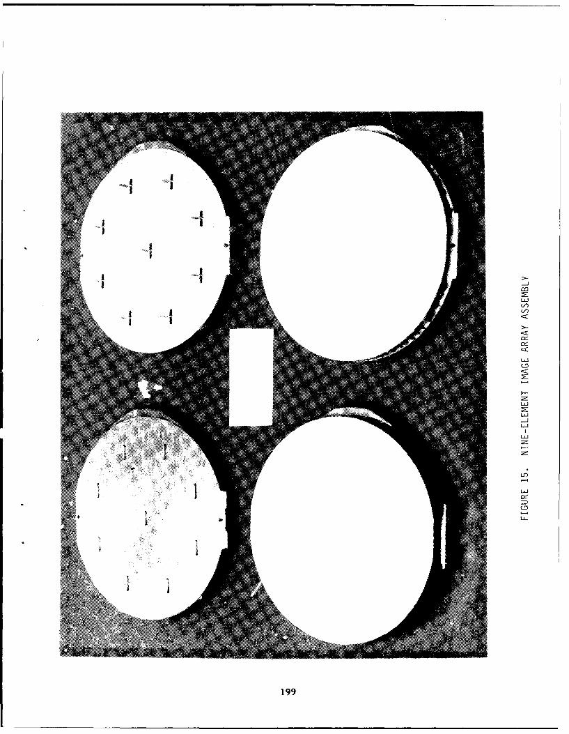
-o
LUJ
0-
LUJ
LUJ
LUJ
Lfl-
CD
UL-
199

C'4
m~ C3
0 2:
C4,cc CC<
a C4
200

0
4
6.
8
10
12.- 12
r 14©T
16
H 18
0 20
22
- e (DGREE)+7
2420
2 6 . .:7.
30.! +.. :STRETCHERi
3 TO-COAX
<4-- e (DEGREES)
FIGURE 18. CENTER IMAGE -ELEMENT GAINAS A FUNCTION OF OUTERELEMENT TERMINATION
201

DISTRIBUTED BEAMSTEERING CONTROL
OF MONOLITHIC PHASED ARRAYS
S.F. NATI, G.T. COKINOS, D.K. LEWIS
GENERAL ELECTRIC CO.
ELECTRONICS LABORATORY
P.O. BOX 4840
SYRACUSE, NEW YORK 13221
1.0 ABSTRACT
As satellite communication systems move to higher frequencies,
a great deal of effort is being directed at monolithic phased
arrays.' These arrays combine printed-circuit antenna technology
with monolithic amplifiers and phase shifters. While significant
advances in these areas are helping to make monolithic arrays a
reality, array control still presents a challenge.
Phased arrays traditionally have been controlled by a single
central computer that calculates a phase setting for each array
element. This architecture has worked well for arrays operating at
lower frequencies, having a small number of elements and modest
update rates. Distributed control of phased arrays has been used
for radar applications 2 and offers a solution to the problems of
202

array control for high frequency, monolithic arrays. Since each
element, or small group of elements, has its own control, the
bandwidth and number of connections to the central controller is
reduced. In addition, the computation hardware is distributed,
allowing the beamsteering calculations to occur in parallel,
providing the means for higher update rates. Compensation for
variation in element performance become possible with a distributed
control scheme. Distributed control architectures also offer the
potential for integration with the microwave components which would
result in a truly monolithic array.
This paper will discuss the design of a distributed
beamsteering controller (BSC) for high frequency phased array
applications. The controller is designed using AT&T's digital GaAs
HEMT technology. A review of the architecture and design for
digital HEMT implementation will be presented. Areas of future
development will also be discussed.
2.0 PROBLEM
The use of higher operating frequencies for satellite
communications systems is reducing the area available for the
antenna and related circuit elements such as amplifiers and phase
shifters. Figures la and lb show a block diagram of a typical
203

antenna element. Figure la shows a transmit element while Figure
lb shows a corresponding receive element.
F PaePlower nea
............ .. S if e r .. ... ............. ... ... ..
Figure la. Transmit Module
Figure lb. Receive Module
Figure 2 shows the available area as a function of frequency,
assuming a uniform element spacing of one half the wavelength.
This decrease in element spacing, in addition to reducing circuit
area, also limits the number of physical connections that can be
made to the antenna element and its control circuitry. Connections
must be provided for RF distribution, power, and control.
204

In addition to the smaller element spacing, the desire for
increased array performance is causing the number of elements per
array to increase. This combination has an effect on the number,
speed and interconnect density of the required control signals. An
architecture that minimizes the number of connections has a
distinct advantage as operating frequencies increase.
The need for highly manueverable platforms to maintain
communications results in a need to update the array beam pointing
direction at higher rates. In addition, the use of techniques for
improving security, such as spread spectrum communications, place
even greater demands on the beamsteering control function.
AREA VERSUS FREQUENCY (1/2 WAVELENGTH SPACING)
20.0
- 180.0
-LJ
] 0.(3 20.0 0.0 4.0 500 60.
FIGURE 2
205
wI I I

3.0 CONTROL ARCHITECTURES
There are several approaches to calculating and distributing
the phase setting for each element in a phased array. The most
simplistic approach is to compute the phase setting for each
element in a central computer and apply the phase settings for the
entire array simultaneously. This approach proves to be
impractical due to the enormous amount of interconnect that would
be needed for an array of any significant size. Additionally, the
amount of time needed to perform the calculations for the entire
array in a serial fashion would severely limit the update rate of
the array.
An alternative approach is to compute the phase settings for
each row and column and add the results at each element. This
approach reduces the number of interconnects required but is
restricted to arrays with uniform element spacing. The limiting
factor in this approach is the time needed for calculation and
distribution of each row and column phase setting. As the array
size increases, the update rate will become limited. This approach
also makes it difficult to provide compensation for element
variations.
A fully distributed approach. where the beamsteering
calculation is performed at the element or subarray level, has many
desirable features. By broadcasting the desired antenna direction
206

cosines from a central array controller to a beamsteering
controller located at each element, the number of interconnects can
be reduced significantly. Each beamsteering controller will
calculate the phase shifter settings in parallel, simultaneously,
reducing the amount of time needed for computation. In this type
of approach, the communication and computation time is basically
independent of the number of elements in the array. Variations in
element performance can be compensated by storing a correction
memory in the beamsteering controller and applying these
corrections on an element by element basis.
4.0 BSC ARCHITECTURE
The overall array control concept is shown in Figure 3. Each
beamsteering controller controls a subarray of the entire array.
The beamsteering controller receives commands from a central array
controller and based on the command performs the required
operations for each element in the subarray. These commands may be
broadcast to all BSCs simultaneously, as in a pointing angle
update, or may be addressed to an individual BSC, as in a
modification to a compensation table entry. The BSC is also
capable of performing a self test funrtion and reporting it's
status to the array controller.
207

j , • •One to each
BSCin array
B lrct ona Bidirectional Decoder
Data Da 32x3araatmnltisu rrlSs
Processor I interface pin required for each chip
Pr~ sso [) t -• : 32 x 32 array of m onolithic subarray/BSC's
Co'tro L'nes
Figure 3. Control Concept
A timeline of a typical beam update sequence is shown in
Figure 4. The sequence begins with the array controller
broadcasting to each BSC the direction cosines of the overall array
pointing angle. Upon receiving this command each BSC will
calculate the required phase shifter settings for each element of
its subarray. These settings will be stored within the BSC until
an update command is received. Next, the array controller selects
one BSC for testing. The selected BSC receives the test command
and compares the results of the previously calculated phase shifter
settings with those supplied by the array controller. The array
controller then broadcasts the update command to all the BSCs and
the new phase shifter settings are applied to each phase shifter in
the array. The BSC that was selected tor testing then transmits
the test results to the array controller.
208

5 Mb/s Manchester Oata50S MHz BSC Clock Rate
I l.a Isc 5a 11 ra c I's 516 lia .4
Data 3Processor
Calculate I Calculate Test Udt cBeam Steeing Command Command udt cVector
Calculation Timea
(50 MHz)BSC Sampling Clock
Figure 4. Beam Steering Timoline
Figure 5 shows a functional block diagram of the beamsteering
controller. The main functions include a single wire interface to
the main array computer, command decoding logic, beamsteeering
calculation logic, a compensation table, built in test logic, and
timing and control.
SrnOLE WIRE ICe OW
INTERFACE aARRAYis COMAD N BIL 1
INTERFACE ~ TO PI4AS6 CUbWT!TESLO
F~gur 5 BSC FuctionalBokAiara
209ER

5.0 BSC DEVELOPMENT
The number of elements that each BSC will control is based on
tradeoffs with regard to the required system update rate, the
processing capability of each BSC, along with area, power and
interconnect considerations. It was decided, based on the above
tradeoffs, to design the BSC to control up to sixteen elements.
The BSC receives its c-mmands from the array controller over a
single bidirectional interface. The bidirectional decoder that is
used to interface between the array controller and the BSCs
provides the capability for broadcast or individual addressing.
The BSC instruction set is shown in Figure 6. The CALCULATE,
UPDATE, and TEST commands are used during each beam update, while
the LOAD COMPENSATION TABLE, and the LOAD POSITION VECTOR commands
are used during array initialization or when changes in parameters,
such as temperature, require the values in the compensation table
to be adjusted. Each instruction is a fixed length and is divided
into a three bit command field and a twenty-four bit data field. A
single bit is provided for parity.
210

C A L C U L A T E - I A M T H L VA T O N PI
UPDATE Co
P
LOADCOMPENSATION ADOD DATA AIas I 0*TA ADD# DaT ATABLE
LOADPOSITIONd 7 y .-VECTOR
TEST MODE DATAP
Figure 6. BSC Instruction Set
The CALCULATE command contains the direction cosines for the
desired antenna pointing direction. This command is normally
broadcast to each BSC simultaneously. The BSC calculates the phase
shifter settings for its subarray based on these direction cosines
and the position of the BSC in the array.
The UPDATE command is also normally a broadcast command. The
BSC will update its phase shifter settings upon receipt of this
command. The data that has been calculated during the previous
CALCULATE command is transferred to the phase shifter control lines
for each element in the subarray.
211

The TEST command is used to perform a functional test on one
BSC during each beam update period. The data that has been
computed as a result of the CALCULATE command is compared on a bit
by bit basis with the data computed by the array controller for the
designated BSC. The BSC will report the result of the comparison
back to the array controller.
The LOAD COMPENSATTON TABLE command contains the information
to be loaded into the compensation table. This provides the
ability to adjust the phase shifter settings for each subarray
based on data obtained during an initial calibration sequence.
The LOAD POSITION VECTOR command gives each BSC its position
within the array. This information is used during the CALCULATE
command.
5.1 CALCULATIONS PERFORMED
The beamsteering calculation that is implemented in the BSC is
shown in Figure 7. The BSC assumes that the array is planar and
has uniform element spacing within the subarray. Although the BSC
could be extended to the more general case, these assumptions allow
the BSC to use two multiplies per beam update, minimizing the
amount of time needed for computation. In addition, the internal
logic for the beamsteering calculation is implemented using a
pipelined bit serial approach.
212

subarray/BSC 34
Given Data Processor
r 7I= 4tfnincO=no+n 0mi=
0,
AlmZ
Y 2
Figure 7. Phase Shift Command Calculation
This approach is highly eff ?:ent in area and power. A
compensation table provides the ability to adjust to varying phase
shifter performance between subaurayr. igure 8 shows an example
of an imperfect phase shifter and the benefits that can be obtained
through the use of the compensation table.
Without Compensation With Compensation
Phase Desired Output Phase Phase Table Output PhaseS.etin .21M Delay Error Selling Entry Delay f.rl
000 0 31.4 31.4 000 110 354.8 -6.2001 45 82.1 37.1 001 111 401.6 -3.4010 90 146.3 5%.3 010 001 82.1 -7.9011i 135 198.9 63.9 011 010 146,3 11.3100 180 249.1 69.1 100 011 198.9 18.9101i 225 301.5 76.5 101 100 249.1 24.1110 270 354.8 84.8 110 100 249.1 -20.9111 , 315 401.6 86.6 111 , 101 301,5 f -13.5
Figure 8. Effects of Compensation
213

5.2 FAULT MONITORING
The approach that is used for fault monitoring at the subarray
level is to test a single BSC during each beam update. This allows
the entire array of BSCs to be tested in a round-robin fashion. A
BSC is tested by comparing its calculated phase shifter data with
data that has been calculated by the array controller for the same
pointing angle. This will test a significant portion of the BSC,
including the array interface, command decode logic, calculation
logic, position registers, and compensation table. In addition,
parity and message format checks are performed on the incoming
command sequence. These errors, along with a test status are
reported back to the array controller at the conclusion of the test
sequence.
6.0 FUTURE DEVELOPMENT
The ultimate goal of incorporating the BSC with the phase
shifters, amplifiers and antenna in a monolithic array requires
that the BSC be capable of being integrated into a microwave
compatible process. For analog components at EHF, it is
anticipated that a gallium arsenide HEMT process will be used.
Vith this in mind, the BSC was designed to be implemented in AT&T's
digital GaAs HEMT process. This process, or similar processes,
214

although not intended for implementing analog components at EHF
frequencies at the present time, could conceivably be modified to
do so. A process using selective molecular beam epitaxy, would
provide the capability to produce devices optimized for analog or
digital functions on the same substrate. This would be the next
step in producing a truly monolithic array.
7.0 ACKNOWLEDGEMENTS
The authors would like to acknowledge the efforts of Steve
Taylor and Greg Barnett of the GE Advanced Technology Laboratories
in Moorestown, NJ. in the development of the BSC architecture, and
the efforts of Dr. Karl Wyatt and Dr. Perry Robertson of AT&T Bell
Laboratories, Reading PA.
8.0 SPONSORSHIP
This work was sponsored by the Air Force Systems Command, Rome
Air Development Center, RADC/EEAA, Hanscom AFB. MA., under contract
F19628-89-C-0054. The contract monitor is Dr. Boris Tomasic.
215

REFERENCES
1. McIllvenna, J. F. (1988) "Monolithic Phased Arrays for EHF
Communications Terminals," Microwave Journal, March 1988, p. 113-
125.
2. Waldron, T. P. et al., (1986) "Distributed Beamsteering
Control of Phased Array Radars," Microwave Journal, September 1986.
216

ANALYSIS OF EDGE EFFECTS IN FINITE PHASED ARRAY ANTENNAS
Steven M. Wright
Dept. of Electrical Engineering, Texas A&M University
College Station, Texas, 77843
ABSTRACT
An important concern in the design of phased array antennas
is the effect of mutual coupling between elements on the array
performance. For large periodic arrays, a common approach is to
use an infinite array formulation. This approach does not include
edge effects and is valid only for a uniform, periodic excitation
of the array. Alternatively, the element-by-element approach can
be used, but this may be impractical for large arrays. In this
paper a method for the analysis of finite, periodic arrays of
arbitrary size and excitation is discussed. The method is based
upon an efficient solution of the extended infinite periodic
array. In essence, the infinite array is excited with each of the
coefficients of the discrete Fourier transform of the desired
finite array excitation. The finite array behavior is then
obtained by superposition. After initial characterization of the
infinite array, finite arrays with arbitrary excitation and
number of elements can be solved by simple FFT operations on the
excitation and impedance matrices. Finally, by extracting an
217

approximate open-circuit impedance matrix for the array, the
solution for free or forced voltage excitation is also obtained.
1.0 INTRODUCTION
An important criteria in the design of any phased array
antenna is the behavior of the active element impedance as a
function of beam scan angle. For large arrays with a single beam,
this can often be sufficiently characterized either
experimentally, by constructing a small section of the array, or
theoretically, using infinite array theory [1].
This paper is concerned with the analysis of finite but
periodic phased arrays of arbitrary size and excitation, as might
be used for steering multiple beams and nulls. The analysis of
this type of array is more difficult, particularly for relatively
large arrays where the element-by-element approach can become
impractical due to the large size of the impedance matrices.
The method presented here for the analysis of finite arrays
is based upon an efficient solution for the active array impedance
of the infinite array created by continuation of the finite
periodic array. This approach allows arrays of essentially
arbitrary size to be analyzed. Importantly, storage requirements
are proportional to either the square of the number of basis
functions on each element or the total number of elements squared
(whichever is greater,) not the product of the two, as in the
element by element approach.
218

The method is simple to implement because it requires only
the computation of the impedance of an infinite array of the same
elements. A matrix of infinite array scan impedances is computed
over one period of scan (visible and invisible) space. This
matrix is multiplied by the discrete Fourier transform of the
desired current excitation to obtain the terminal voltages in the
finite array, from which the active element impedances are
obtained. In addition, the element impedances can be obtained for
the case of voltage excitation, either free or forced [1].
A brief formulation of the method is given in Section 2.
Computational efficiency is briefly discussed in Section 3, and
some examples are considered in Section 4. Comparisons are made to
element-by-element results for arrays in free space and microstrip
dipole arrays.
2.0 THEORY
It is well known that the impedance of a single element can
be obtained from integration of the impedance of an infinite array
of the same elements [2]. Additionally, Ishimaru and co-workers
have shown that the impedance of a finite array of current excited
elements can be expressed as a convolution integral of the
Fourier transform of the array aperture current distribution and
the infinite array active impedance as a function of scan angle.
A limitation in that work was slow numerical convergence in the
convolution integrals. The formulation here is entirely discrete,
219

and may be more straightforward conceptually, but the concepts
are very similar to those presented by Ishimaru [3]. The technique
is founded in the basic principles of the array scanning method
presented by Munk and Burrell [2]
Of particular interest here is a finite array of microstrip
dipoles, a section of which is illustrated in Fig. 1. The array
is periodic, represented by lattice vectors S, and S2 The
dipoles have width a and length b, and are printed on a substrate
of thickness t and relative permittivity z. For generality, the
solution allows a superstrate layer of arbitrary thickness and
relative permittivity, and loss tangents in both Zbe superstrate
and substrate. The method under consideration is based upon the
formulation of the active array impedance for a infinite, periodic
extension of such an array.
2.1 Infinite Array Impedance vs. Scan angle: Z(fi0).
The active impedance of the infinite array can be found using
well known methods [1,4,5,6]. In this work, a moment method
solution was used which uses subsectional basis functions with a
linear dependence (triangle) in the y direction (length) and an
edge condition in the x direction (width). The edge condition is
not necessary for very thin elements, but can give improved
results for wide strips when no x directed basis functions are
employed. The details of the moment method solution used here can
be found elsewhere [5,6]
220

For purposes of discussion only, the form of the infinite
array array impedance that obtains from a single mode
approximation to the current is considered here:
I OV 4 ^P 4Zin- E E yy (Kmn ) J y (K m) 1
in t1n yy m ymmaa
AA
A is the area of one unit cell in the array, G is the yy
component of the spectral-domain dyadic periodic Green's function
for the problem under consideration, and J is the Fouriery
transform of the single mode current approximation. The
summations are from -oo to +oo. Equation I is a summation of
Floquet modes defined by the vector K
K n" -6m. + .8O (2a)
where:
6rmn m 8 1 + n8 2 and 80 = mop , + n 0#2 (2b)
The vector f6i, represents the vector from the (0,0) Floquet mode
to the (m,n) Floquet mode. fl, and 2 are lattice vectors for the
reciprocal or periodic lattice, as shown in Fig. 2 for an
arbitrary array periodicity. For a rectangular array, .8 W2IS
and /2 = 2/S.2" .80 is an offset of each Floquet mode to allow
beam scanning, as discussed below. As indicated by Eq. 1, the
active array impedance is obtained by summing Floquet modes over
the reciprocal lattice; hence the active array impedance is
221

periodic over the reciprocal lattice just as the array structure
is periodic over the spatial lattice.
To scan the main beam of the array, the voltage source at
element (m,n), denoted V(Smn) is adjusted to give
S -jflo (mS + nS)WS) - V(S °0 )e 1 + 2). The constants m0 and no are
essentially the direction cosines, which for a rectangular array
become (following the conventions in [6]):
m° = -S, sinO coso (3a)
no = -S2 sin0 sing (3b)
where S1 = S, . One can alternatively excite element (m,n) with
-) ~ ~ S^)-fo( +nS ) . Teatv arya current source I(Smn) = I( J.0 (MS 2nv
impedance is the same in either case for an infinite array.
For notational convenience the active array impedance of the
infinite array is denoted Z(f8o), to indicate that it is a function
of fi, and that it can be considered a spectral domain quantity.
2.2 Finite Array Impedance: Arbitrary Current Excitation.
There are many applications where one would like to define
excitation coefficients for each element of a finite array. For
an N x N element array, this defines a discrete excitationx y
function 1"SaS ), which gives the excitation current at each of
the N N elements of the array, and where S = mS I + nS2. Having
defined an array geometry and the desired excitation currents, one
can analyze the array using the standard element-by-element
222

approach. However, one can proceed in an alternative manner as
follows. If the N x N array under consideration is periodic,x y
one can consider the hypothetical extension of the array to an
infinite structure. The goal is to synthesize the excitation of
the finite array by a sum of appropriately weighted, uniform
periodic excitations of the infinite structure. Those elements
with zero current can be considered open-circuited. For resonant
length elements, these elements have negligible effect, allowing
the finite q-? to be approximately recovered. For elements for
which e- -circuiting does not render them negligible, the current
would need to be forced to zero at additional points.
Unfortunately any finite array excitation is not
band-limited, and cannot be synthesized exactly with a finite set
of periodic excitations of the infinite array. However, one can
obtain approximate results as follows. Given an excitation
function for the finite array, one computes the discrete Fourier
transform (DFT) using LK samples of the array excitation:
1 ex(pn) = DFT X(S (4)
where the DFT pair for a discrete, periodic function defined by
LxK samples on the 2-D lattice defined by Slk given by [7]:
223

L-I K-I
-mn= D { ) f e-j2n(ml /L + nk /K) (5a)f0° 1 =dFrl(~) f(41k)1=0 k=0
f~s) = IDFT = L-I K-i (bf =z K-1 f(.8 o n) ej2)r(ml/L + nk/K)(5b)
1=0 k=0
where
= m f/L + n f/K 0 s m s L-1, 0 - n : K-1 (6)0 1 2
and IDFT denotes inverse discrete Fourier transform. LK, the
number of sampling points, will typically be much larger than
N N , the number of elements in the array. Thus I'x(S 1k ) will bex y
zero for all of the LK samples except for the N N whichx y
correspond to elements of the finite array.
Once the DFT of the excitation currents is calculated, the
DFT of the terminal voltages in the finite array can be determined
from:V (t m) Ie x (fran) Z fmn) 7
0 0 0
The element voltages for the N x N array, V(SMn), can beI y
obtained by inverse DFT:
V(Sm) - IDFT V (fto ) (8)mnf 0
This IDFT returns LK unique element voltages, which include the
voltages for the original N x N array. All other coefficients2 y224

should be approximately zero. Finally, the input impedance of
the element (m,n) in the finite array is obtained from:
4 V(Sm.)Z(Sm) -- Di (9)
I'X(S m)
The approach described here can be viewed as a superposition
technique. The DFT of the desired array excitation gives a finite
set of uniform periodic excitations of the infinite array. One
must keep in mind that the DFT of the excitation current is a
periodic function, with periods 1 and 82 It is defined at themn
LK sample points defined by the vectors f80". This set of LK
excitations, when summed, recovers a periodic version of the
desired excitation function, periodic over an array of LxK
elements. In essence, it creates an "array of arrays"; an
infinite, periodic array consisting of repetitions of the desired
finite array. It is necessary that this second periodicity be
large enough so that these repeated arrays would not affect the
current distribution on the original N x N element array. Thisx y
problem will be examined by comparison of results with the
element-by-element approach.
2.3 Open Circuit Impedance Matrix and Mutual Impedances.
It is of interest to obtain the open circuit impedance matrix
elements for the finite array. For an N x N array, elementx y
225

(p,q) of the N N by N N open circuit impedance matrix of thex y I y
array is as given by:
z 0C P (10)p Iq q=O, q*p
where p and q denote a single integer denumeration of the array
elements. For elements which have essentially no current when open
circuited, such as half-wave dipoles, one can obtain the open
circuit matrix for a finite array by choosing an excitation matrix
_> 1, m=0, n=0ex ( n) - 0, otherwise
In this case, the response at the unexcited elements of the array
are given by:
VOC(S) = IDFT { Z (# ) (12)
The open circuit impedance matrix elements, (the mutual
impedance between any two elements in the array with all other
elements open circuited) can be obtained from Eq. 9,
-) ---*.
Zm(Smn " Sk) = VOC(S i m-k i, -) (13)
Note that there are only N N unique values obtained by Eq. 13 forx y
an N x N array. Equation 12 returns an approximation to thex y
open circuit element voltage the finite array; the location in
the array is not taken into account. Thus, while edge effects are
226

included in the excitation matrix, they are not included in the
open circuit matrix. However, as stated earlier, this is a good
approximation for many practical elements.
2.4 Finite Array Impedance: Arbitrary Voltage Excitation.
For a voltage excited array, direct application of the above
formulation leads to impedance with all unexcited elements short
circuited (or terminated in the generator impedance). However,
the input impedance for the elements under voltage excitation
with all unused elements open circuited can be obtained using this
method by using the open-circuit impedance matrix. Once the
open-circuit impedance matrix is found, the element currents
under voltage excitation are determined by:
[I] = ([ZoCi + [Z ) I[V] (14)
where [Zr] is a diagonal matrix which contains the generator
impedances and any resonating elements. This gives the element
currents under "free" excitation. Setting [ZT] = 0 gives the
"forced" voltage excitation, according to the definition in [1].
In general, the inverse of the Z matrix is not found, but the
matrix equation is solved for the unknown currents. The input
impedance of the m,nth element is obtained from
Z(Smn) =V /I -ZT (16)mn mn mn
where the subscripts m,n indicate the dependence of all quantities
on their location in the array, given by S
227

3.0 NUMERICAL CONSIDERATIONS
Clearly the most time consuming aspect of the solution is the
filling of the Z(flo n) matrix. Filling this matrix requires
sampling the infinite array active impedance over one period of
the spectral lattice. For a rectangular array of center fed
dipole, symmetry reduces the number of samples by a factor of
four. Even with symmetry, a 256x256 DFT requires the computation
of 16,641 samples. Fortunately, the impedance matrix is filled
only once for a given (infinite) array. Having filled the
impedance matrix, the performance of any subset of the infinite
array can be evaluated for arbitrary excitation using the methods
of Sec. 2. Still, sampling the impedance matrix sufficiently to
allow the analysis of microstrip arrays can be quite time
consuming if not efficiently done. Two methods have been used to
reduce the fill time significantly.
First, the time required to compute each sample of the
impedance matrix can be reduced significantly by applying
acceleration techniques to the summations of Floquet modes
expansions. Many such summations can be required to compute the
moment method solution for the array impedance at each scan angle.
The method used here requires obtaining an asymptotic expansion
for the generalized impedance matri., elements. The asymptotic
form is subtracted from the original expression, leaving a rapidly
convergent summation. The asymptotic terms can be directly
accelerated using Poisson's summation formula. Details of the
228

method are given in [6].
The use of this method results in a rapidly convergent
series, typically giving a reduction in computation time of
approximately two orders of magnitude over a direct, unaccelerated
summation. This has allowed the routine use of 256x256 or 512x512
impedance matrices. High sampling densities are needed for
microstrip problems, where surface waves can lead to singularities
in the impedance vs. scan angle surface.
Second, an adaptive sampling routine, similar to adaptive
integration, combined with a birational interpolation technique,
has been used to reduce the number of scan angles at which the
array impedance is calculated. With this routine, the impedance
surface is sampled over a grid of 17x17 points. Next, the
impedance is calculated using a birational interpolation technique
at the center of each of the 16x16 subsections defined by the
initial gridding. If the interpolated result is sufficiently
close to the actual computed value at that point, that subsection
is designated as complete, and the remaining values filled by
interpolation. If the interpolated value does not meet tolerance,
that subsection is subdivided, and the testing procedure
continued. A birational interpolation routine was chosen because
of its performance near singularities [8]. This technique is
continued over each of the 16x16 subsections, reducing the grid
size in each subsection only as far as necessary to meet a
predefined tolerance.
229

The time savings obtained by the adaptive filling algorithm
could be improved by more sophisticated interpolation algorithms.
The time savings is also highly dependent on the nature of the
active array scan impedance. For arrays in free space or over
ground planes, where the scan impedance is relatively smoothly
varying, it can provide significant savings. For microstrip
arrays, it can be less effective. Table 1 shows the number of
impedance samples that were computed (as opposed to interpolated)
and the relative time savings compared to computing each sample
required to fill the impedance matrix for a microstrip dipole
array. The array had element width a = 0.011 0 , length b =
0. 3 9 1W array spacing S1 = S2 = 0.5A0, substrate thickness t =
0.19A0 and z r = 2.55. In addition, a loss tangent of j = 0.005 in
the substrate was used to eliminate singularities. As would be
expected, the effectiveness of the method improves with finer
sample grids.
Using these methods, fill times of 5 minutes for a 256x256
DFT are typical on a DECstation 5000.
4.0 RESULTS AND DISCUSSION
The method has been tested by comparing to results in the
literature and by comparing to results obtained using a standard
spatial domain moment-method code employing subsectional
sinusoidal basis and testing functions. Three examples will be
considered.
230

TABLE 1
Reduction in computation time resulting from adaptive sampling.
Savings is expressed as the ratio of the total sample points to
the actual number of calls to the impedance evaluation routine as
a function of the DFT resolution. Example is for a microstrip
dipole array, with spacing of 0.5k0 in x and y, element length b
= 0.39A0, width a = 0.01ko , on a substrate with t = 0.19, 0,
= 2.55, 6 = 0.005.r
DFT Total Actual Savings
Resolution Sample Points No. Calls. Factor
64 1,089 455 2.4
128 4,225 1,067 4.0
256 16,641 2,419 6.7
512 66,049 5,098 13.0
231

4.1 Mutual Impedance Calculations.
The mutual impedance between parallel and collinear
microstrip dipoles was computed using the present method and
compared to results computed by Alexopolous and Rana [9]. The
method described here is denoted the DFT method in the Figures.
The impedances were computed for dipoles with length 1 = 0.333Ao,
S1 = S2 = 0.5 A01 on a substrate with z = 3.25 and thickness
of t = 0.1016A0. No superstrate layer was included. A loss
tangent of 0.005 was included in the substrate layer to eliminate
the singularity in the impedance surface Z(.80). This small loss
tangent was found to have little effect on the numerical results.
Results for the mutual impedances are shown in Figs. 3a and 3b,
with good agreement.
4.2 Finite Arrays of Microstrip Dipoles with Voltage Excitation.
Next, the impedance of a 19x19 array of microstrip dipoles
was computed versus scan angle and compared to results calculated
in [10]. For this case, 1 = 0.39A0, $1 = $2 = 0.5A6 and the
substrate had sr = 2.55 and t = 0.19 0. Again, a loss tangent of
0.005 was included in the substrate layer, and a 256x256 point DFT
was used. The results in [10] were calculated using the
elemcnt-by-element approach, using a sinusoidal approximation to
the current on each element (I entire-domain mode was used on each
element). The results from the present method, also using a
single mode approximation to the element current, and the
232

element-by-element method approach are compared in Figs. 4a and
4b. The reflection coefficient of the center element in each row
along the E-plane is shown for scan angles of 0 and 30 degrees
(Fig. 4a) and 45 and 60 degrees (Fig. 4b).
It was found in [10] that little change in the reflection
coefficient vs. scan angle was seen when additional modes were
used to represent the current on the elements. This indicates
that the behavior of the array versus scan angle is well
represented using a single mode for the case of approximately
resonant length dipoles. However, it should be noted the
significant error in the actual impedance values can results from
this approximation. Using a single mode the input impedance of a
single isolated dipole was found in [10] to be Z = 105 + j72 0.
This compares well to the value of 103 + j65 0 found using the DFT
method and a single mode. However, using 19 subsectional modes
with the DFT method resulted in an impedance of 154 + j38 £, which
compares well to the result of 154 + j31 £ obtained by Michalski
and Zheng using a subsectional basis function moment method
solution with 51 unknowns [11].
4.3 19 Element Array with Two Beams.
As a final example, a 19 element linear array of y directed
0.5A dipoles in free space was considered. The dipole elements
were spaced 0.5A apart along the x axis. Initially, a
Tschebyscheff distribution with 30 dB sidelobes was selected. To
233

demonstrate the ability to handle arbitrary excitation, two beams
were created by superimposing on the original excitation the same
distribution phased to produce a beam at 45 degrees. The required
generator voltages needed to create the current excitations for
this array pattern were determined using the methods of Section
2.4, with ZT = 50 + jO 02 at each generator. The results are shown
in Figs. 5-7. Figures 5a and 5b compare the active element
impedances obtained with current generators using the present
method (DFT) and using a standard element-by-element approach. In
Figs. 6a and 6b, the active element impedances obtained with both
methods using voltage excitation are compared. In both cases a
generator impedance of ZT = 50 + jO 02 was used. The results
compare very well in both cases, demonstrating the ability of the
method to handle both voltage and current excitations. Finally,
the array patterns obtained using "uncorrected" and "corrected"
voltage excitations are shown in Fig. 7. The"uncorrected feeds"
simply used the desired current taper as the voltage excitation
taper. This method gives relatively good results but the lobe at
450 is several dB below the ideal pattern. The "corrected feeds"
were obtained by determining the terminal voltages obtained with a
current generator excitation with the desired taper. These
voltages were then used to excited the array. The ideal pattern,
simply the array factor of the desired element currents is not
shown, but it is indistinguishable from the pattern obtained using
the "corrected feeds".
234

5.0 CONCLUSION
The infinite array approach for analyzing large arrays can be
adapted to the efficient analysis of finite arrays with arbitrary
excitation. An important feature of the method is that at least
for the case of current excitation, the storage and computational
effort numerical effort is essentially independent of the number
of elements in the array. For voltage excitation, the method
requires only the storage and solution of an array of order
(NxxNY)2 , where NX and Ny are the number of elements in the array.
Fill time of the array is independent of the number of elements.
The method could find application in the design of large
phased arrays with arbitrary excitation, where the active element
impedance can vary significantly over the array, not just near the
edges. Currently, the method has been applied with good results
to arrays of microstrip dipoles. The method works for both free
and forced excitation, and can give good approximations to the
mutual impedance between array elements.
6.0 REFERENCES
[1] Hansen, R.C., Ed. (1966) Microwave Scanning Antennas. vol.
II. New York: Academic Press.
235

[2] Munk, B.A. and Burrell, G.A. (1979) Plane wave expansion
for arrays of arbitrarily oriented piecewise linear elements
and its application in determining the impedance of a single
linear antenna in a lossy half-space. IEEE Trans. Antennas
Propag., Vol AP-27, No. 3, pp. 331-343.
[31 Ishimaru, A., Coe, R.J., Miller, G.E. and Geren, W.P.
(1985) Finite periodic structure approach to large scanning
array problems. IEEE Trans. Antennas Propag., Vol. AP-33,
No. 11, pp. 1213-1220.
[4] Pozar, D.M. and Schaubert, D.H. (1984) Scan blindness in
infinite phased arrays of printed dipoles. IEEE Trans.
Antennas Propagat., Vol., AP-32, pp. 602-610.
[5] Wright, S.M. and Lo, Y.T. (1983) Efficient analysis for
Infinite Microstrip Dipole Array. Electron. Lett., Vol.
19., No. 24, pp. 1043-1045.
[6] Lo, Y.T., Wright, S.M., and Davidovitz, M. (1989) Microstrip
Antennas. in Chang, K. Ed., Handbook of Microwave and Optical
Components, vol. I. New York: Wiley. Chpt. 13.
[7] Dudgeon, D.E. and Mersereau, R.M. (1984) Multidimensional
Digital Signal Processing. New Jersey: Prentice-Hall.
[8] Press, W.H., Flannery, B.P., Teulkolsky, S.A., and
Vertterling, W.T. (1988) Numerical Recipes: The Art of
Scientific Computing. New York: Cambridge University Press.
236
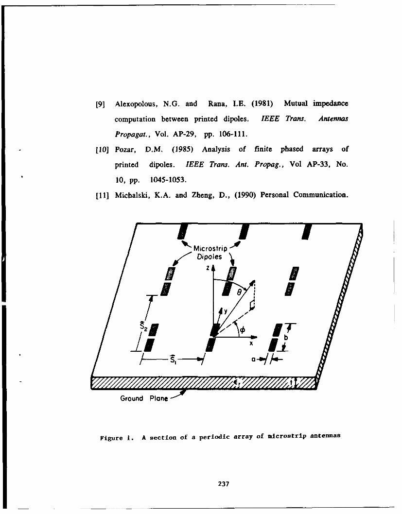
[91 Alexopolous, N.G. and Rana, I.E. (1981) Mutual impedance
computation between printed dipoles. IEEE Trans. Antennas
Propagat., Vol. AP-29, pp. 106-111.
[101 Pozar, D.M. (1985) Analysis of finite phased arrays of
printed dipoles. IEEE Trans. Ant. Propag., Vol AP-33, No.
10, pp. 1045-1053.
[11] Michalski, K.A. and Zheng, D., (1990) Personal Communication.
N" Microstrip j
Dipoles
z X
92'
bit xfLi
Ox"M /M/''/ -s/ u
Ground Plane
Figure 1. A section of a periodic array of mdcrostrip antennas
237

S 2
0 / /
i(a)
(b)
Figure 2. Periodic lattices in the spatial and spectral domains.
238

a2
en -4
~Cd
44
Suaa-
I239

*z
O4 4
-4
14)
400
if4-4a~~ 4t)0q
(;)pnlru~u) jjoj Ip1j, 2400

1-4 00
00
S C
4-J4-
* 00
4) 4
r-4 r-4
00
r0 0 00 0 00
0 00
__ _ _ _ __ _ _ _ _ 0 J3
U) ci
4 04
01
0 40 C> C)C4C
4-241

0 H 004..)
4)0
4)4
o 04 04
00
4..0 444
000
4j
@4 -)
C3 0.0
404
400
<o
(sinqo) IjurisPaJ 242

Array Pattern - Corrected Feeds..... Uncorrected Feeds
90"
1200 600-10
1500 °20 300°
/ -30 -20 -10
180" 0 "
210" / 30
240* ° . .300 °
270"
Figure 7. Array pattern for a 19 element array, with voltage generatorexcitation. Taper selected to form two beams, at 0 and 45degrees. Uncorrected taper is identical to the desired currents,and causes errors in the realized pattern. Corrected taper isthe excitation which gives the desired element currents.Generator impedance was 50 + jO £2.
243

MULTIMODE PERFORMANCE FROM A SINGLE SLOTTED ARRAY ANTENNA
by
John Cross, Don Collier and Len GoldstoneNorden Systems, Norwalk, Ct.
ABSTRACT:
Today's military aircraft must carry out various missions, some of them
simultaneously. Consequently, antennas must be designed with the capability
to function in a multiplicity of simultaneous as well as switchable modes. Slotted
flat-plate arrays, with their unique ability to divide available aperture space
among several antenna requirements, have become increasingly popular.
Several recent design innovations have advanced the state of the art in
attainable operational modes. Taking advantage of these approaches, one
multimode antenna can now perform air-to-air pulse-doppler monopulse,
ground mapping, terrain following, terrain clearance, terrain avoidance,
weapons transponder tracking, and ground target tracking.
Three multimode antenna designs will be presented, ranging fro'n the simplest
and therefore least expensive, to the most complex, namely a flat-plate array
design containing eight separate apertures and ten RF outputs. Measured
performance data, including far-field patterns when operating in the various
modes, will be shown.
1.0 THE LOW COST, MULTI-FUNCTION, FLATPLATE ARRAY ANTENNA
1.1 BACKGROUND: The Bandwidth Tradeoff
The slots on any flatplate antenna are excited by waveguide runs located
behind the front plate of the antenna aperture. RF energy travels through these
waveguides and is emitted from the slots whenever a component of H-field
within the waveguide is parallel to the slot center line. The slots are precisely
spaced to insure that the RF from each slot is in phase with that of its neighbor
244

[1]. The aperture is subdivided into resonant subarrays to simplify the feed
network. This simplification limits the operational frequency band,
however, and for this reason, antennas with good sidelobe characteristics at
center frequency show higher sidelobes and VSWR at the band edges. This
deterioration can be minimized by keeping the waveguide runs short. As
energy travels down the guide from the RF feed port, the phase error of the RF
increases as it reaches each successive slot. Therefore, if the antenna
aperture were divided into small subarrays, and each subarray were fed by a
separate RF feed port, the phase errors could be kept to a minimum. However,
this method is expensive, as it requires a complex feed network attached to
the back of the antenna.
Less expensive flatplate antennas must therefore be designed with fewer
subarrays and longer resonant waveguide runs in each subarray. To
compensate, a narrower frequency band and/or slightly higher sidelobe levels
are tolerated.
1.2 DESIRED MODES OF OPERATION:
Three isic modes are required for a number of aircraft radar antenna
applications; a pencil beam mode for long range target location; a Cosecant-
Squared (CSC 2 ) mode for mapping and ground target identification; and an
elevation monopulse mode for Terrain Following/Terrain Avoidance (TF/TA).
1.3 DESIGN:
Refer to Figure 1. In this "no-frills" economy design, a 12X14 element module
was chosen. In the 28 slot elevation plane, there was sufficient space for two
modules, and in the azimuth plane, space for four. This limited the required
number of RF corporate feed ports to eight, and simplified the structure of the
feed manifold on the back of the array. Equiphase summing the eight RF ports
245

with a corporate feed, in a manner similar to that described in Reference 2,
accomplishes the pencil beam performance.
P. Smith of Norden Systems developed and patented a means to create a
CSC 2 elevation beam from a flatplate aperture by 1) switching the power to only
the upper half the radiating aperture and 2) introducing a fixed phase shift
into the central row of the active aperture half.[3].
Power switching is accomplished by inclusion of an RF switch in the feed
manifold as shown in Figure 2. In more complex array designs, especially
in designs requiring low rms sidelobes in the pencil beam mode, the central row
of slots has its own feed port, with a phase shift section that can be switched in
or out as required. See Figure 8, for example.
In the simplified design (low cost array), a CSC 2 pattern is obtained by placing a
fixed phase shift in the central row of aperture slots. See Figure 3. The
resulting deterioration in rms sidelobe level in the pencil beam mode was
accepted as a consequence. See Figure 4. The azimuth beam is unaffected,
as can be observed in Figure 5.
The final mode, elevation monopulse for TF/TA operation, becomes possible
with the inclusion of a magic tee at the RF input/output port. See Figure 2. The
difference pattern is taken from the delta port, the pencil beam pattern from the
sum port. Figure 6 shows the resultant sum and difference patterns
superimposed.
2.0 A MORE COMPLEX MULTIMODE DESIGN:
The layout of this flatplate antenna is shown in Figure 7. The design contains
not only an Az/EI monopulse array, switchable to form a ground map
antenna, but also 3 interferometers and a guard aperture. The guard array
serves a sidelobe suppression function for both the interferometers and the
monopulse array. In addition, this antenna includes two BIT (built in test)
246

circuits that permit a reference signal to be injected into the array to calibrate
the waveguide runs during operation. The monopulse/ground map simplified
diagram is shown in Figure 8. The ground map phase shifters and RF switch
are shown as well as a T/R circulator. There are 8 waveguide ports (1 guard,
3 interferometer, receive sum, azimuth and elevation receive difference, and
transmit sum), plus 2 coaxial RF injection (BIT) ports. The
interferometer/guard BIT diagram is shown in Figure 9.
This more complex antenna is subdivided into smaller sized modules than the
simplified array previously described, to achieve a wider frequency
bandpass and lower pattern sidelobes. The modules are basically 4X4 slot
layouts. The array diagram illustrating the module breakdown is shown in
Figure 7. The monopulse array has 60 modules. Each interferometer has
10 modules. Each subarray or module is fed by a reactive power divider that
is sensitive to module-to-module impedance mismatch. Module impedance
thus becomes a critical design parameter if the desired sidelobes are to be
achieved. Any mismatches between modules lead to aperture phase and
amplitude errors which impact on the desired antenna patterns. Typical
module impedances are shown in Figure 10.
The complete aperture is covered by a layer of Kaptan which protects the
antenna face and holds waveguide pressure. The ability of the overall design
to perform within specifications depends upon manufacturing tolerances,
materials properties, and the quality of the bonding process. The array is
fabricated largely as machined and dip brazed subassemblies and bonded or
bolted in various manufacturing stages into one unit. In-process testing and
quality control are vital to the attainment of performance goals. Final
adjustment of the completed unit takes place on the antenna range, where the
8 monopulse sections are trimmed for equal phase, using shims in trombone
247
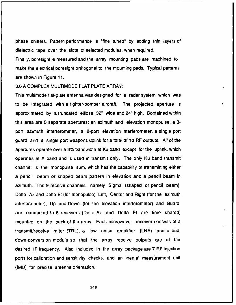
phase shifters. Pattern performance is "fine tuned" by adding thin layers of
dielectric tape over the slots of selected modules, when required.
Finally, boresight is measured and the array mounting pads are machined to
make the electrical boresight orthogonal to the mounting pads. Typical patterns
are shown in Figure 11.
3.0 A COMPLEX MULTIMODE FLAT PLATE ARRAY:
This multimode flat-plate antenna was designed for a radar system which was
to be integrated with a fighter-bomber aircraft. The projected aperture is
approximated by a truncated ellipse 32" wide and 24" high. Contained within
this area are 5 separate apertures; an azimuth and elevation monopulse, a 3-
port azimuth interferometer, a 2-port elevation interferometer, a single port
guard and a single port weapons uplink for a total of 10 RF outputs. All of the
apertures operate over a 3% bandwidth at Ku band except for the uplink, which
operates at X band and is used in transmit only. The only Ku band transmit
channel is the monopulse sum, which has the capability of transmitting either
a pencil beam or shaped beam pattern in elevation and a pencil beam in
azimuth. The 9 receive channels, namely Sigma (shaped or pencil beam),
Delta Az and Delta El (for monopulse), Left, Center and Right (for the azimuth
interferometer), Up and Down (for the elevation interferometer) and Guard,
are connected to 8 receivers (Delta Az and Delta El are time shared)
mounted on the back of the array. Each microwave receiver consists of a
transmit/receive limiter (TRL), a low noise amplifier (LNA) and a dual
down-conversion module so that the array receive outputs are at the
desired IF frequency. Also included in the array package are 7 RF injection
ports for calibration and sensitivity checks, and an inertial measurement unit
(IMU) for precise antenna orientation.
248

3.1 DESCRIPTION OF APERTURES AND FEED NETWORKS:
The outline of the monopulse, azimuth interferometer, elevation
interferometer, guard and uplink apertures is detailed in the array face-plate
drawing of Figure 12. The individual radiators of each of the 5 apertures are
horizontally polarized resonant slots which are grouped into subarrays of
resonant waveguide networks and fed by reactive 2-way power dividers. It
was not possible to use 4-port power dividers, because of space and weight
limitations.
The 4-quadrant monopulse is the most complicated antenna within the array,
not only because of the large percentage area that it occupies, but also due
to the complexity involved in the feed network to achieve either a pencil beam
or shaped beam in elevation. The aperture is divided into 4 main quadrants
with 16 subarrays each, combined by a reactive feed network and a comparator.
The center rows just above and below the azimuth center line have a
separate feed and comparator. The switching of the center rows provides
elevation beam shape diversity. In the pencil beam mode, the entire aperture is
illuminated with equal phase (Figure 14), while in the mapping mode, only the
lower half of the aperture (PW 6 and PW 7 of Figure 15) and the 2 center
rows are illuminated. Optimization of the shaped beam pattern is achieved by
advancing the phase of the center rows relative to the lower quadrants.
Transfer switches S2 and S3 in Figure 14 are used to switch in the
appropriate phases through line lengths to the center rows. The predicted
shaped beam elevation pattern and azimuth sum pattern with errors are
shown in Figures 16 and 17.
The feed networks for the remaining apertures are similar to those of the
monopulse antenna, but have no comparator assembly. Resonant waveguide
249

radiators are summed through a feed network to a single output for each of
these arrays.
3.2 MODES OF OPERATION:
The monopulse aperture, azimuth and elevation interferometers and guard
singly or in combination support all of the following radar modes. Air-to-
ground modes including ground mapping (real beam, doppler beam
sharpening and synthetic aperture), beacon and GMTI (pulse doppler and
clutter suppression interferometry), air-to-sea modes including sea surveillance
and ship classification, as well as air-to-air modes including air surveillance
and air combat, terrain clearance including terrain following and terrain
avoidance.
3.3 RF INJECTION:
RF injection is provided, mainly for in-flight calibration of the antenna system. As
shown in the block diagram of Figure 13, monopulse calibration is achieved
by single quadrant injection, while each of the azimuth and elevation channels
as well as the guard have individual injection points. In addition, each
interferometer injection line contains a variable phase trimmer for boresight
alignment.
4.0 CONCLUSIONS:
Today's complex mission requirements make flexibility and multimode
capability an operational imperative in modern radar systems. To support
these needs, apertures with one basic antenna pattern are no longer viable.
Until the long-awaited phased array becomes economically competitive, the
best solution to date has been the multimode, slotted flat-plate array antenna.
For cost-effective performance in a variety of scenarios, it is hard to beat.
250

5.0 ACKNOWLEDGEMENTS:
The authors wish to acknowledge the assistance of senior consultants Harold
Shnitkin and Peter Smith in the preparation of this paper. They also wish
to thank the respective Program Managers for facilitating the inclusion of
previously unpublished technical material.
6.0 REFERENCES:
1) Yee, H.Y. and Richardson, P.N. (1982) Slotted Waveguide Antenna Arrays,
IEEE Antennas and Propagation Society Newsletter.
2) Skolnik, M.I. (1970) Radar Handbook, McGraw-Hill, New York, pp. 21-13 to
21-21.
3) Smith, P.W. (1983) Multimode Array Antenna, U.S. Patent No. 4,376,281.
4) Moreno, T. (1948) Microwave Transmission Design Data, Dover, New
York, pp. 111- 120.
5) Wolff, E.A. (1967) Antenna Analysis, John Wiley & Sons, New York, pp.
169- 178.
6) Silver, S. (1949) Microwave Antenna Theory and Design, Peter Peregnnus
Ltd., London, pp. 286- 295.
7) Maxim, B.J. (July, 1960) Resonant Slots with Independent Control of
Amplitude and Phase, IRE Transactions on Antennas and Propagation.
8) Oliner, A.A. (January, 1957) The Impedance Properties of Narrow Radiating
Slots in the Broad Face of Rectangular Waveguide, IRE Transactions on
Antennas and Propagation.
9) Collin, R.E. and Kucker, F.J. (1969) Antenna Theory, Part I, McGraw-Hill,
New York, pp.587-617.
251

~~~ IWOII j
I g I~!!III.:III''
.............. ....... . . .
ROW OF ELMNS9FXDPH HF
Figur2. igurifed 1.cFrontiFce ofin Low-CStc rra Antenna. Psiton
252

ANTENNA PATTERNELPTN RA MIDR eff.-3.78dB
C4 RppffUDE
...... .... -I11.27
c 30* :...... .....
- ±. .. .... . *......... .......
50I R1:SL...... ..... ... .l. ...
50 f-1ON .-... 1-29
S4-1 P" .- 22.01
o *,MIv-N * E...V..LE PENIL '-.f07
10 J
.9- - ~ . . . .I .. 1 ... ... ...- 2 7..1j2 ..... ... .... . OU SD ...- '
- * 4 . ..4.........-2..3
..... . .... .... . . . ..... - .... .t~Rm -C I T O R
....... 1 ...... J ..... .. .
930-70-50-30-10 10 30 50 70 goScan Rng Ie (deg.)
Figure 4. Pencil Beam Pattern in Elevation Plane.253

ANTEN~qR PAFTTERN
o -MIO/NO ERRORmAZ PENCIL R . eff 1. O?dB
.~ . .. .. . ..
PHASE... . .... .. ... . .. ..... ..
~20 . -PEWK SLL
0
a-30 -
40 ..* ....... ~** ........ INSIDE +'-10
I I T OUTSIDIE-1
Z60 .I
-90 -70 -50 -3 0-10 10 30 50 7?0 9 0Scan Angle (deg.)
Figure 5. Azimuth Beam Pattern.
-~- - i - i -4 _1- a; , ___ I is is 1U i
CLI.EY.fltG. 4 CLEY.De..
ELEVATION P ERN
254

Figure 7. Front Face of Array Antenna.
RF i nJ(r) TL
SW 3
(AZ) T_ __ T_ _
DIFc (EL)
Figure 8. Simplified Diagram of Monopulse/Ground Map Array.
255

T sMALEFTE
INJ- h M S N ECTION - < A IN
TC [7 CIE06 EUDECU
A~ ~ AZ PiEDATE AO
OP u UTPU POP
POUS aUA TRMBN SETO
Figure 1. eFeor TpicaMdul BImpSceatc Cuares.
si256

* 4 4
U 2 0
* '-'
-r 44
- - .
rk 4* 0
00
toI~
~25

-j ( U -
0 <
S0 S2
.U) z
c. .J cr. Q
.... k
...... .. * * *.*...**...
. ...... . x ~ : & .. ~ .. k::*~.L.M.~j
.. ......
x. .o
MM4 -i' % .. : A. .. ! -*w. .~ ., *...... K .. % *~
ze ....... % -.. ." - V
~ ~.* * ...........
e4-.
-258

ANTENNA FLAT PLATE
BLOCK DIAGRAM-~SMA II~uT
IZhL/G MAGIC TEE MANIFOLDING;FPHASE ADJUST
X-GUIDE CDuPLER MONOPULSE COMPARATOR
MONOPUL SE-J DTAZ
- J aLT L
J5AZIMUTH. L J
AZIMUTH, C J
AZIMUTH, R J6J9
GUARDJ1
ELEVATION, U 1
ELEVATION, D 1I Zh ~j~{ IJ12
Figure 13. Functional Diagram of Array
MONOPULSE WAVEGUIDE COMPARATOR MONOPULSE WAVEGUIDE COMPARATOR
J2(elaA2 (Detta EL) J2 (Delta AZ) A3 (Detta EL)
J 4
4Su
r
5S StM~ThPULS M2l SUM2
Fi ur 4 M no ul e W a e ui eFi ur 5 M no S e av gu d
opatator Sc e ai Show in Co p r r Sc e ai S o n i
Monouls Su Moe 3C Mode.
S2259

MAPPING MODE
RANDOM ERRORS
m -OMm -Bs -Wm* &W w" U." 4&W m m
Figure 16. Simulated CSC 2 Elevation Pattern.
* -&W -000 -302 -4 CD -30M -10.O -100D OWD OWo 300W aOm eM 1W000 U
Figure 17. Simulated Azimuth Pencil Beam Pattern.260

AN ADAPTIVE ARRAY USING REFERENCE SIGNAL EXTRACTION
Jian-Ren E. Wang and Donald R. UcciDepartment of Electrical and Computer Engineering
Ellinios Institute of TechnologyChicago, IL 60616
ABSTRACT
This paper describes a new adaptive array which derives a reference signal from
frequency and angle of arrival information. The array employs a Reference
Acquisition Loop (RAL) consisting of an arbitrary filter and a nonlinear directional
gain constraint to ensure proper operation. The array is more flexible since
extremely accurate a priori information is not required. Simulation results are
presented.
1. INTRODUCTION
Adaptive beamformers, which have been widely discussed and applied in radar
and communication systems 4 , use two major algorithms (i.e., the Least Mean
Square (LMS) 5 and Applebaum algorithms6 ). For proper operation, an Applebaum
array needs a precise steering vector to point the beanformer toward the desired
signal source; the LMS algorithm requires a reference signal which is highly
correlated with the information signal to distinguish the unwanted components from
the desired signals.
To circumvent the dependency on a priori knowledge, several studies on self-
generated reference techniques have been proposed. These studies can be separated
into two categories: spread spectrum techniques 7- 10 and 'data-derived'
techniques". For both techniques, the required frequency ban4width is increased5' b1

and an accurate desired signal characteristic is needed.
We propose an Autorecursive Nonlinear Adaptive Array (ARENA) using a
Reference Acquisition Loop (RAL) to extract the reference signal. This array
requires, a priori, the frequency and Angle Of arrival of the Desired signal (AOD).
Thus, the proposed array is a more general system for most applications.
The general structure and the basic concept of the array are described in
Section 2, while the operation is explained in the Section 3. Computer simulation
results are presented in Section 4 and the Conclusion is in Section 5.
2. FORMULATION
Consider an m element half wavelength spaced LMS array with the self-
generated reference signal as shown in Fig. 1. The array consists of two parts: the
first is an m element LMS adaptive processor and the second is the RAL. Note
that the reference signal is derived from the output of the array. The RAL must
allow the desired signal component at the output of the array to pass through witi,
only limited distortion (thus retaining correlation between the desired signal and the
self-generated reference signal). Also, it must reduce the undesired signal
component content.
We define the input signal vector, X(k), at discrete time k, to be
X(k) = Xd(k) + X,(k) + N(k),
where Xd(k), X,(k) and N(k) represent the input desired signal, interference and
thermal noise vectors, respectively. Assume Xd(k) and X,(k) are not correlated to
262

each other. The thermal noise vector is a zero mean mutually independent random
vector. The LMS algorithm is used to adjust the weight vector , W(k),
W(k+l) = W(k) + -LKVwE[E(k)12] = W(k) + icE[e(k)X'(k)] (2)2
4where Pc is the gain constant of the adjustment loop, E['] denotes the expected
value and (')* denotes complex conjugation. e(k) represents the system residual
signal which is the difference bet",2en the self-generated reference signal and the
system output, y(k), i.e., e(k)=G[y(k)]-y(k), where G['] denotes the function of
the reference signal generator. V w represents the gradient with respect to the
weight vector. From Eq. (2), when the weight adjustment loop reaches steady
state, c(k) and the input signal are orthogonal to each other,
E[E(k)X'(k)]
= E[(gd(Xd(k)rW,)-XT (k) We,)X (k) + (gi*(Xi(k)TWa)-XT(k) W,)X*(k)
+ (gn*(NT(k) W, )-NT(k) W,,)X (k)]
=0, (3)
where W, represents the steady state weight vector, gd(f), gi(f) and g.(f) are the
RAL gains of the desired signal, interference and the thermal noise, respectively.
The superscript (.)T denotes the transposition. For simplicity, we assume that 9d,
g, and gi are constant over the appropriate frequency band.
When both the desired signal and interference are zero mean and uncorrelated
with each other, Eq. (3) can be further decomposed into
263

T T
E[(gd-I)Xd WsXd + (gi-I)XTWaX' + (gn,-)NTN #] = 0 (4)
To ensure that the steady state weight vector will converge and suppress the
undesired signal component the RAL is designed to have unity gain for the desired
signal but non-unity gain for the interference and thermal noise components.
Therefore, Eq. (4) becomes
(gi-1)E[X'XTI W,, + (g.-1)E[N° TI W88 = 0. (5)
Obviously, when both gi and g, are not unity, a null weight vector is able to satisfy
Eq. (5) which is a trivial solution. Therefore, a particular scheme is required in the
RAL to avoid this while minimizing the undesired signal power. In particular, it is
desirous to have g, gi<1 so that the weight adjusting loop will have a faster
convergent characteristic and better stability.
3. THE ARENA ARRAY
A type of adaptive array based on the general structure shown in Fig. 1 and a
nonlinear direction constraint in the RAL is proposed as shown in Fig. 2. The RAL
consists of a weight constraint, C(k), and a filter, F. To determine the design of the
weight constraint, first consider an output signal vector, y(k),
y(k) = Xd(k)+Xi(k)+N(k)]rW(k). (6)
Here
264

Xd(k) =ad(k)Sd (7)
X,(k) a,(kS (8)
and
N(k) = [n1 (k), n2 (k), -- , flm(k) IT, 9
with Sd and S1 (1= 1,2,...,p) the phase arrival vector of the desired and interference
signals, respectively. ad(k) is the waveform, of the desired narrowband signal. A
continuous (non-impulsive) type wide band interference, X,(k), is represented by
the sum of narrow band waveforms; a1(k), 1= 1, ... , p. n3(k), i=l, 2, * , m
represents the thermal noise component at i-th element. Substituting Eqs. (7)-(9)
into Eq. (6), the array output is given by
(k) = ad (k)S W(k)+F ai(k)S1TW(k)+NT k W (k) .(10)
We define the output of the RAL, r(k), to be
r(k) = C(Ic)Fjy(k)I
=C(k)[gdad(k)Sd W(k)+F, gla(k))SIfW(k)+gnN (k) W(k)) (11)1=1
265

where F[] is a filter function, C(k) is a directional constraint, and g, is the gain seen
by aL. Note that the output of the RAL is utilized as the reference signal and fed
back to the weight adjusting loop. We define the system residue, E(k), as
E (k) r r(k) - y(k)
(gdC(k)-l)ad(k)Sj W(k)+E (gIC(k)-1)at(k)S W(k)+(g.C(k)-l)N ) W(k) .1=1
(12)
In order to maintain a constant gain in the designated direction and also avoid
the zero weight convergence, we have
C(k) - W (13)
gd WT (k) Sd'
where g is a arbitrary gain constant. Note that C(k) is a nonlinear constraint and is
inversely proportional to the gain of the weight vector in the AOD. Substituting
Eq. (13) into Eq. (12), the system residue now becomes
f(k)=ad~g-d (k) W)+ , ( -l)al(k)S1 W(k)+( gg 1) N(k) W (k)= gSTWk gdST W(k)
(14)
266

3.1 Optimum Weight Vector
According to the complex LMS algorithm'2 , the weight vector which yields the
minimum E[ e(k) 2] can be obtained by solving
E[c(k)V we(k) 0] = . (15)
After some manipulations, Eq. (15) can be rewritten as
E[E(k)V WE (k)I
S (ST wk)-g)+ gt (SIS-sdST) W(k)-S,]( ' -1)S(W(k)1=1 g9d dW(k)) 9d dW(k)
+a2 9gn g*9n SW*(kW(k-Wt()WkS;-W()
+oC9dsdrW(k) 1( dWc(k)) )C 'k w2)w~)w~) -~
0, (16)
where (.)t denotes complex conjugate transpose. Note that the first, second, and
third terms in Eq.(16) correspond to the desired signal, interference, and noise
contributions, respectively.
It can be shown that the solution for the weight vector of Eq. (16) when
g=gn=0, for all I, and g9*0 is the optimal Wiener solution, i.e. W = $D'ISd where
4% is the correlation matrix of the undesired signals. Otherwise, W(k) will be a
sub-optimal weight vector. However, both optimal and sub-optimal weight vectors
tend to annihilate the undesired signal.
267

From the first term in Eq. (16) we see that Sd W(k)=g. This condition, drives
the weight to form a gain g at the AOD. Combining this requirement with the
constraint of Eq. (13), results in maintaining unity gain for the desired signal in the
RAL. Consequently, this structure offers a more flexible design of the filter in the
RAL and better system stability.
3.2 System Realization
To realize the ARENA structure, the gradient of the residual signal versus the
weight vector is required. However, this is not generally available in practice.
According to the orthogonality principle' 3 , in such situations, V WE(k) is replaced by
X(k). The weight adjusting equation, then, is written as
W(k+l) = W(k) + i[e(k)X*(k)] , (17)
where r. is a step size constant. Comparing Eqs. (17) and (2) we see that the
weight adjusting equation of the ARENA array is equivalent to the conventional
LMS array. Thus, the steady state weight vector can be solved in the same
manner, i.e.
2" P 2, 9'91 _ST W k)StW k) si, gng .1) W (k)O(g-Sr W(k))Sd+E t -d W ) W(k) gds dW(k)
1=1 9d
=0. (18)
268

From Eq. (18) we find that this practical weight adjusting algorithm has a
sii.lar solution as Eq. (16) which minimizes the residual signal power by letting the
weight vector approach ST W(k)=g and ST W(k)=0. Note we must ensure that
g1=gd and gnz*gd since if g=gd it means the RAL has completely lost its ability to
distinguish the interference and the desired signal or the interference has the same
characteristic as the desired signal, the interference will be treated as the desired
signal or vice versa. A matched filter can be used to accomplish this. For a wide
band noise, a white noise cancelor 14 can be utilized in the RAL to decrease the
RAL gain for noise and, consequently, avoid g,=gd.
4. SIMULATION RESULTS
In this section we look a. several examples which illustrate the results derived
above. We first examine a case :. :%i a desired signal and one narrow band
interference signal. We use a 5 element half wavelength spaced ARENA array.
The frequency of the desired signal is fd and the interference is 1.2 58fd. The input
Signal-to-Noise Ratio (SNR) and Interference-to-Noise Ratio (INR) are 10 dB and
20 dB, the AOD and the Angle Of arrival of the Interference (AOI) are 15 0 and
30 ° , respectively. We assume the gain of the RAL for the desired signal is
gd=0 dB. We consider two cases for the gain of the interferer, i.e. noise gain is
assumed to be gn=-ldB. Il the computer simulations, the initial weight values are
all set to zero except for the first element which is arbitrarily set to 0.01. The
output SINR of the array is illustrated in Fig. 3 for both cases. We see that the
weights converge as expected and drive the system to the optimal output
performance; however, the case of weaker suppression of the undesired signal by
the RAL filter results in the poorer output SINR performance as indicated by the
slower convergence and greater jitter.269

The major innovation of the proposed array is the empioyment of a Nonlinear
Direction Constrainer (NDC) in the RAL. The NDC prevents the weight vector
from converging to zero by constraining a constant gain in AOD. You may wonder
if the AOD is known why we need the reference signal? With a precise estimation
of the AOD an Applebaum array6 can be used to achieve satisfactory performance.
Previous study' 5 has shown, however, that the Applebaum array is extremely
sensitive to look direction error. The nonlinear direction constraint used in the
RAL is a soft constraint which allows for some error without causing significant
deterioration on the system performance. Because of this low sensitivity to steering
vector error, the performance of the ARENA array is superior to the Applebaum
array when a precise steering vector is not available. Simulations have been
o.nducted to verify the results. Consider a 5 element ARENA array with half
wavelength spacing at the center frequency, Id, of the desired signal. The AOD is
15 * and AOI is 300. The frequency of the interferer is 1.25 8fd. The loop gains of
the RAL are gd=0 dB, gi=-20 dB and g.=- dB. The input SNR and INR are 10
dB and 20 dB, respectively. The output rSINRs of the ARENA and Applebaum
arrays with an estimated AOD equal of 25 * are illustrated in Fig. 5. The
simulation results indicate that the ARENA array is much less sensitive to the
estimated error than the Applebaum array.
5. CONCLUSION
In this study we propose an adaptive array which employs a direction
constrained Reference Acquisition Loop (RAL) to extract the reference signal from
the array output without using spread spectrum or coding techniques. The a priori
knowledge required for the proposed array is the AOD and the frequency band of
the desired signal. It has been shown that the proposed array is less sensitive to the270

estimation error of the AOD. The theoretical analysis and the computer results
indicate that the proposed array successfully nulls the unwanted signal and
me;.-t s a constant gain in the arrival angle of the desired signal.
REFERENCES
[1] White, W. D., 'Low-Angle Radar Tracking in the Presence of Multipath,'IEEE Trans. Aerosp. Electron. Syst., Vol. AES-10, No.6, pp. 835-852,November 1974.
[2] Gabriel, W. F., "Adaptive Arrays-An Introduction,' Proc. IEEE, Vol. 64,No. 2, pp. 239-273, February 1976.
[31 White, W. D., 'Angular Spectra in Radar Applications,' IEEE Tran.Aerosp. Electron. Syst., Vol. AES-15, pp. 891-895, November 1979.
[4) Evans, J. E., Johnson, J. R. and Sun, D. F., 'High Resolution AngularSpectrum Estimation Techniques for Terrain Scattering Analysis and Angleof Arrival Estimation,' Proc. 1st ASSP Workshop Specturm Estimation,Hamilton, Ontario, Canada, August 17-18, 1981.
[5] Widrow, B., Mantey, P.E., Griffiths, L. J. and Goode, B.B., "AdaptiveAntenna Systems," Proc. IEEE, Vol. 55, No.12, pp. 2143-2158, December1967.
[6] Applebaum, S. P., 'Adaptive Arrays,' IEEE Trans. Antennas Propagat.,Vol. AP-24, pp. 585-598, Spetember 1976.
[71 Compton, R. T. Jr., 'An Adaptive Array in a Spread-Spectrum Communicaton System," Proceedings of the IEEE, Vol. 66, No.3, March 1978.
[81 Winters, J. H., *Spread Spectrum in a Four-Phase Communication SystemEmploying Adaptive Antennas,' IEEE Tran. Commnication, Vol. COM-30,No. 5, May 1982.
[9] Hudson, E. C., "Use of an Adaptive Array in a Frequency-Shift KeyedCommunication System,' Technical Report 712684-1, Ohio State UniversityElectroScience Laboratiory, Columbus, Ohio 43212; prepared under ContractN00019-80-C-0181 for Naval Air Systems Command, Ausust 1980.
[101 Ganz, M. W., 'On the Performance of an Adaptive Array in a FrequencyShift Keyed Communication System," M.Sc. thesis, Department of ElectricalEngineering, Ohio State University, August 1982.
[II] Compton, R. T. Jr., Adaptive Antennas:Concepts and Performance, NewJersey: Prentice-Hall 1988.
[12] B. Widrow, J. McCool, and M. Ball, 'The Complex LMS Algorithm,'Proceedings of the IEEE, Vol. 63, No.4, April 1975. (pp. 719)
[13] Papoulis, A., Probability, Random Variables, and Stochastic Processes 2ndEdition, McGraw-Hill Book Company 1984.
[14] Widrow, B. and Stearns, S.D., 'Adaptive Signal Processing,' New Jersey:Prentice-Hall 1985.
[15] Compton, R. T. Jr., 'The Effect of Random Steering Vector Errors in theApplebaum Adaptive Array,' IEEE Trans. Aerosp. Electron. Syst., Vol.AES-18, pp. 392-400, September 1982.
271

-~ Array Output
LMSY -Adaptive I
Processor G
£(k)'-'Reference
---------------------
RAL
Fig. 1 General Struture of an LMS array witha self-generated reference signal
Array Output----------- -------------- I
LMS *Non-Linear:
Adaptive C (k) _j Directioa* Processor W k 0,Constraint
(NDC)
RAL
Fig. 2 Struture of the ARENA
272

5 Eleuun ArrGT
10
Iwlut Se-to a
40
Fig. 3 The Output SINR of the ARENA with g,1=0 dB, gt =-20dB,g,=.1dB, AOD=1S* and AOI=30*
10
Vol, Lut SOWt d§
ge=-1dB, AOD=15* and AOI=306
273

A~lUS OPUuS"
-to a-= sdouaU
Fig. 5 The output SINR of the ARENA with gd=O dB, gl =20dB,gn =-1dB, AOD=150, AOI=30*, and estimated AOD=25
274

OPT ICALLY LINKED SHY ANTENNA ARAY
Salvatore L. Carollo, Anthony M. Greci, Richard N. Smith
ROME AIR DEVELOPMENT CENTER
GRIFFISS AFB, NY 13441
275

1.0 ABSTRACT
This report covers the work done under Task 5 of
Project 45194263, entitled, "Communications Adaptive
Array Processor Evaluation".
Adaptive antenna technology has been an area of
interest for many years. The progress to date can be
characterized by extensive research on algorithms and
processing architectures, development of a large number
of prototype systems and fielding of a few systems.
Adaptive antenna systems normally consist of two or
more antenna elements, two or more receivers, amplitude
and phase weighting nc forks for one or more elements
and a signal combiner. For some applications the size,
weight, power consumption and cost of multiple
receivers, antenna elements and associated radio
frequency (RF) cabling can be limiting factors. In spite
of these limitations, the impressive interference
cancellation capabilities of adaptive antenna systems is
highly desirable. Recent advances in photonics
technology could provide solutions to the limitations
described above. RF modulated lasers, optical cabling
and optical detectors could reduce much of the size,
weight, power consumption and cost of conventional
276
adaptive array systems.
Using the RADC/DC RF laboratory anechoic chamber and
the "Flexible Adaptive Spatial Signal Processor" (FASSP)
this effort was performed to established the feasibility
of using optical technology to implement an adaptive
antenna array system. This report covers the design,
implementation and testing of an optically linked
adaptive antenna array. The performance of the
optically linked array is evaluated by comparison to a
conventional adaptive array.
2.0 IN-HOUSE TEST FACILITIES
RADC/DC has an adaptive array processing test bed.
The test bed shown in Figure 1 consists of a rectangular
anechoic chamber, a flexible adaptive spatial signal
processor (FASSP), a antenna pattern recorder, various
types of jammer/desired signal sources and satellite
communication simulation and analysis programs.
The test bed simulation/analysis computer programs
are used to study and compare adaptive processing system
concepts, techniques and algorithms. This provides a
fast look approach to determine the merit and feasibility
of a concept. If the results show promise the concept
is further tested using real signals and adaptive
277

Figure 1. ADAPTIVE ARRAY PROCESSING TESTBED
processcr hardware to determine the actual benefit
attainable. The test bed is reconfigurable and functions
as a tool to support the development of methodologies
for comparing and evaluating new adaptive array
processing algorithms, architectures and techniques
suitable for meeting satellite communications
requirements (such as those for the Defense Satellite
Communications System [DSCS]).
2.1 ANECHOIC CHAMBER
The anechoic test chamber shown in Figure 2 is a
rectangular structure 40 ft. long, 28 ft. wide and 18
ft. high 2 . The inner chamber is isolated from RF fields
278

Figure 2. ANECHOIC CHAMBER
from 150 MHz to 18 GHz by at least 100 dB.
It has a six foot diameter spherical quiet zone
located at its longitudinal axis. The center of the
quiet zone is midway between the ceiling and the floor
and about 50 inches from the tips of the absorber on the
back wall. The receive element array is positioned in
the center of the quite zone to minimize reception of
all reflected signals. All chamber walls, ceilings and
floors, except walkways, are covered completely with
energy (RF) absorbing material. A Scientific Atlanta
model 5315C-5 antenna positioner is installed in the
chamber. The tip of the model tower (which supports the
279

array elements) is located in the center of the "quiet
zone". The chamber is wide enough and has provisions
so that several signal sources can be used
simultaneously at the front wall opposite to the "quiet
zone".
Six feet of the 40 ft. chamber is partitioned off
and is used as an equipment room to house the signal
sources and antenna positioner controls. Absorber
panels are removable to allow access for mounting
signal/jammer antennas. Signal and control connections
between the chamber and the laboratory equipment (FASSP
and Scientific Atlanta 2020 system) are provided through
bulkhead feed through panels at each end of the chamber.
All functions such as source power, frequency, mode and
receiver antenna position (pedestal rotation) are
controlled from outside of the chamber.
2.2 FLEXIBLE ADAPTIVE SPATIAL SIGNAL PROCESSOR (FASSP)
The FASSP4 test bed is shown in Figure 3. All
adaptive Spatial processing systems consist of three
generic components:
1. An array of receiving elements (spatial array)
to provide the degrees of freedom required to null out
a number of directional jamming signals,
280

Figure 3. FLEXIBLE ADAPTIVE SPATIAL SIGNAL PROCESSOR
2. An adaptive processor that uses the signal
samples from the array receive sensors to compute the
adaptive weights that produce the resultant spatial
response, and
3. Weighting networks that apply the adaptive
weights to the signals from the individual input
channels.
The design of adaptive spatial processing systems
is very complicated because of the close interaction
among these three basic components. Although computer
simulations can be used to compare the performance of
adaptive algorithms and techniques, the hardware
281

implementation effects cannot always be easily modeled.
With this in mind, RADC/DCCD conceived the ideas of
a Flexible Adaptive Spatial Signal Processor (FASSP),
which was designed and fabricated for RADC by Syracuse
Research Corp. The FASSP is a general purpose
flexible hardware adaptive array processor system that
supports the integration/test of adaptive processing
algorithms, architectures, techniques and real
components.
The FASSP system was fabricated with high
performance quality components and consists of 12 real
RF receivers and weighting networks that are
reconfigurable. The designer uses a computer based
operating system to select the adaptive algorithms and
hardware configuration and specify the necessary system
parameters. Adaptive processor performance can then be
evaluated against RF signal (desired) and jamming
signals using an antenna array and an anechoic chamber.
3.0 CONVENTIONAL ADAPTIVE ARRAY
The conventional adaptive array processing system
shown in Figure 4 was used as the baseline system
configuration. The receiver antenna was a line array of
four standard gain horns separated by 3/2 wavelength
282

Receive TransmitJammer
DOWN -i iV<EquipmentCONVERTER Room
Anechoic Chamber
FASSP tAMP FILTER .O.=PATTERN, RCR.
Figure 4. CONVENTIONAL ADAPTIVE ARRAY
spacing. The array was located on the positioner with
the elements centered in the chamber quiet zone. The
optically linked adaptive array configuration is shown
in Figure 5 and is described in Section 4.
The CW and wide band noise jammer antennas were
located at the opposite end of the chamber. One jammer
transmitter element was positioned broadside/boresight
(zero degrees azimuth, zero degrees elevation) to the
array and a CW signal was applied. Figure 6 is a plot
of the array steered to that CW source.
The array response plot shows that the main beam is
centered at zero degrees azimuth and the sidelobes are
283

Receive Transmit
A/0 A O/PTCL
Figure 5. OPTICALLY LINKED ADAPTIVE ARRAY CONPIGURATION
located at plus or minus fourteen degrees azimuth.
The second januner transmit element was positioned at
fourteen degrees centered on one of the side lobes.
Nulling tests were then performed using single
jammers at each position.
3.1 BASELINE PERFORMANCE
The performance measure used to compare the
performance of the optical implementation with that of
the standard coaxial implementation was cancellation
ration (CR)(
CR's for a given input jamming signal are measured
by comparing the adaptive and conventional output power
284

I :
I I ! r j
I . .. .
Figure 6. BEMXPORMID ARRAY PATTERN
of the adaptive processor. Usually, CR is used to
characterize the performance of the adaptive processor
against different jamming scenarios. It is a direct
measure of the adaptive processor nulling capability
and is shown in Equation (1) where Pa is the
CR(dB) = 10log(Pa/Pc) (1)
adaptive processor output power in the adaptive mode and
Pc is the adaptive processor output power in the
conventional or beamformed mode. Normally adaptive
processor output is measured in dbm and, thus, Equation
(2) is used to compute the CR ratio.
CR(dB) - Pa(dB) - Pc(dB) (2)
285

4.0 THE OPTICALLY LINKED ARRAY
An adaptive array usually consists of a number of
antenna elements, a receiver for each element and the
RF/IF cabling and connectors necessary to connect the
system together. One channel of such a system is shown
in Figure 7. The block marked "Flexible Adaptive Spatial
Signal Processor" (FASSP) indicates the equipment that
performs the adaptive signal processing tasks. Because
of the losses in the RF cabling, the SHF receivers are
co-located with the antenna elements in the anechoic
chamber. Along with the RF/IF cabling, the receivers
I............-----------. Anechoic Chamber --------------
Bulk He ad
Connector SHI Receiver Feadhorn
Flexible Adaptive Spatil Coaxial
Signal Processor Cable
Figure 7. CONVENTIONAL ADAPTIVE ARRAY CONFIGURATION
introduce another source of unwanted RF/IF radiation.
286

Shown in Figure 8 is an optically linked/connected
adaptive antenna array.
--------------------------- Anechoic Chamber --------------Biconic Optical
Transrnl t terConnector
Optical Ampliier isolatorIsolator Feedhotn
-- - - - - -- - - - -- - - -- -- - - - -- - - - -- - - - - - -- - - -- - - - -- - - - -- - - -- - - - - -- - - -- - - -- - - - -- - - - - --. :
Flexil1e Adaptive Spatial Fiber Optic
Signal Processor cabole
Phase Adjusting Optical
Device Detector
Figure 8. OPTICALLY TINKED ADAPTIVE ARRAY
Because of the very low losses in the optical fiber
it is possible to remove the SHF receivers from the
chamber and co-locate them with the FASSP. The optical
linkage also eliminates the IF cabling from t'.e chamber.
4.1 HARDWARE
Component selection was based on anechoic
chamber and associated equipment interface requirements.
Since the antenna system was designed to run at 8.41 GHz,
the task of optical link selection was significantly
simplified. The Ortel TSL-1000 optical transmitter and
287

the Ortel RSL-25 optical receiver were selected based
on their frequency range of 10 kHz to 10 GHz.
The maximum received signal likely to be seen at the
output of each antenna element (feedhorn) is less than
-40 dBm. Therefore, 50 dBm gain, narrow band (centered
at 8 GHz) Miteq amplifiers were selected to boost the
signal. This will supply the Ortel transmitters with
power near their maximum RF input level of 12 dBm and
thereby allowing us to maximize the usable dynamic range
of the links.
Other devices are incorporated in each elemental leg
of the antenna system (see Figure 8). These include
electrical and optical isolators to prevent impedance
mismatch reflections from the feedhorn, and optical
reflections to the laser, respectively, 50 meter lengths
of fiber and phase adjusting mechanisms to time match
the links are also integral parts of the system.
4.2 FUNCTIONAL DESCRIPTION
Each array link consists of the equipment described
in Section 4.1. An adaptive array is composed of two
or more links, usually one for each antenna element in
the array. In terms of a single link the RF signal
arrives at the array and is received by the antenna
288

element, in this case an SHF feedhorn. The low level
signals are amplified to provide an appropriate signal
level for the optical transmitters. The optical
transmitters put out a single frequency of light the
amplitude of which is modulated by the RF input signal.
The light is then transmitted along an optical cable to
the phase adjusting device where the electrical length
of the optical cable can be adjusted so that all the
links in the array can be time and phase matched5 . The
modulated and time and phase matched optical signal
then travels along the optical cable to the optical
detectors where the light is demodulated and the RF
signal is output to the SHF receivers through
conventional RF cabling.
5.2 TEST AND EVALUATION
The optically linked array was tested in a manner
identical to the conventional/baseline array as
described in Section 3.0. Data was collected to plot
cancellation ratio for three separate sensors3 . All of
the figures indicated below are identical in form. The
horizontal axis (Pe) is the ratio of signal plus noise
to noise power as measured at the antenna element. On
the vertical axis two quantities are plotted. The
289

quantity (Pc) is referred to as the
conventional/unadapted output power as measured at the
beamformer/residue output port of the adaptive
processor. When measuring this quantity the array is
beamformed to broadside and then the interference signal
is activated and again the signal plus noise to noise
ratio is measured. The quantity (Pa) is referred to
as output power after the adaptive processor is allowed
to adapt. Again the signal plus noise to noise ratio
is measured at the residue output. Using these graphs
the CR in dB can be read directly as the difference
between the two plotted lines on the graphs.
Shown in Figure 9a is a plot of the conventional and
adaptive response. Figure 9b is a plot of the optically
linked conventional and adaptive response. Both
Figures 9a and 9b are for a single continuous wave (CW)
signal broadside to the array.
Shown in Figure 10a is a plot of the conventional and
adaptive response. Figure 10b is a plot of the
optically linked conventional and adaptive response.
Both Figures 10a and 10b are for a single CW source in
the first sidelobe which is 14 degrees from broadside
for the antenna array in use.
290

Shown in Figure 11a is a plot of the conventional
and adaptive response. Figure llb a plot of the
optically linked conventional and adaptive response.
Both Figures lla and lb are for a wide band noise (WBN)
source broadside to the array.
6.0 CONCLUSIONS AND RECOMMENDATIONS
Analysis of the data presented in Section 5.0
indicates that the performance of the optical linked
array is as good as the baseline conventional array and
is in some cases better. During the design and
fabrication of the optically linked array it was
apparent that optical technology would provide reduced
size and weight over the conventionally linked array.
The RF cabling associated with a conventional link is
bulky and weighs about 15 - 20 lbs. as compared to the
optical link which is far less bulky and weighs only a
few pounds, including modulator and demodulator These
size and weight improvements are obtained with no loss
in performance and, in some cases, with even better
performance.
Further improvements are attainable by the following
means. An increase in the dynamic range of the optical
links could be obtained by using indirect modulation of
291

45 dB _____
36 dB
27 dB
1 dB -O
9 dB
0 dB__ _
0 dB 9 dB 18 dB 27 dB 38 dB 45 dB
- PC -4-pa
Figure 9a. CONVENTIONAL CW BROADSIDE CR
36 dB -
30 dBI
24 dB__
0 d8 6dB 12 dB 18 d8 24 dB 30 dB 36 dB
-PC -4-Pe
Figure 9b. OPTICAL CII BROADSIDE CR
292

45 dB 1 -
38 dB -_ _ __-_ _ _
27 dB
18 dB
9 dB
0 dBl0 dB 9d B 18 dB 27 dB 36 dB 45 dB
- PC -4- Pa
Figure loa. CONVENTIONAL CW BIDELOBE CR
36 dB p30 dB _________
24 dB _____
18 dB ____
12 dB ____
8 dB-_ _
0 dB ___
0 dB 86dB 12 dB 18 dB 24 dB 30 dB 36 dB
-- PC -+- Pa
Figure 10b. OPTICAL CW SIDELOBE CR
293

45 dB - - _ _ _ _ _ _ _ _ _
36 dB
27 dB ___
18 dB---- - -___
9 dB__- I0 d B - - - - _ _ _ _ _ - - -_ _ --
0 dB 9 dB 18 dB 27 dB 38 dB 45 dB
- PC -Pa
Figure lla. CONVENTIONAL lIEN BROADSIDE CR
36 dB - -__
30 dB - -
24 dB - _ -_ _ _ _
18 dB -- - _ _ ___
12 dB -- ---- - - - _ - ---
6 d B - I- -
0 dB 6 dB 12 dB 18 dB 24 d8 30 d8 36 dB
- PC -- pa
Figure lib. OPTICAL WEN BROADSIDE CR
294

the lasers verses the direct modulation used for these
tests. Single mode fiber optic cable should be used
instead of multimode to prevent cable losses due to
gradient effects when the fiber is bent or deformed in
any way. Using a single laser with external modulators
for each antenna element would ensure system coherence
and make the system even more cost effective. The single
laser technique would also allow all the elements to be
multiplexed on to a single fiber that could then be
demultiplexed at the adaptive processor. The
detector(s) could be RF biased to provide down
conversion, thereby eliminating the FASSP receivers.
Elimination of the FASSP receivers will result in a
reduction in size, weight and power of a complete
adaptive antenna system. These means of improvement
will be further investigated and verified in future
in-house efforts. This RADC/DCCD in-house initial
investigation of optical technology, as applied to
adaptive antenna systems, indicates that evolving
optical technology can and will provide important
enhancements especially for mobile platform systems.
295

REFERENCES
1. Carollo, S. L.; Greci, Anthony M.; Jackson, D.;
Smith, Richard N.; and Toughlian, Edward N. (1988).
"THE FLEXIBLE ADAPTIVE SPATIAL SIGNAL PROCESSOR".
Paper presented September 21, 1988 at the Antenna£
Applications Symposium.
2. Giangiulli, David (1978) TEST REPORT ON A RECTANGULAR
ANECHOIC CHAMBER, RANTEC Doc. No. 15032-TR.
3. Greci, Anthony M.; Kulon, Frank T. (1988),
PERFORMANCE MEASUREMENT OF A CASCADE ADAPTIVE ARRAY
PROCESSOR AND SPEECH ENHANCEMENT UNIT IN THE
PRESENCE OF INTERFERENCE, RADC-TM-88-7.
4. Hadley, Hugh W., FLEXIBLE ADAPTIVE SPATIAL SIGNAL
PROCESSOR (FASSP), RADC-TR-84-255. ADB092024
5. Johns, Steven T.; Schmitt, Mark C.; Toughlian, Edward
N. (1990), OPTICAL LINKS FOR MICROWAVE APPLICATIONS,
RADC-TR-90-12. ADA220574
6U.S. GOVERNMENT PRINTING OFFICE 1991-500-000/40006
296

MISSION
OF
ROME LABORATORY
Rome Laboratory plans and executes an interdisciplinary program in re-
search, development, test, and technology transition in support of Air
Force Command, Control, Communications and Intelligence (C31) activities
for all Air Force platforms. It also executes selected acquisition programs
in several areas of expertise. Technical and engineering support within
areas of competence is provided to ESD Program Offices (POs) and other
ESD elements to perform effective acquisition of C 31 systems. In addition,
Rome Laboratory's technology supports other AFSC Product Divisions, the
Air Force user community, and other DOD and non-DOD agencies. Rome
Laboratory maintains technical competence and research programs in areas
including, but not limited to, communications, command and control, battle
management, intelligence information processing, computational sciences
and software producibility, wide area surveillance/sensors, signal proces-
sing, solid state sciences, photonics, electromagnetic technology, super-
conductivity, and electronic reliability/maintainability and testability.