CYW43438 Single-Chip IEEE 802.11ac b/g/n MAC/Baseband ...
92
www.infineon.com Please note that Cypress is an Infineon Technologies Company. The document following this cover page is marked as “Cypress” document as this is the company that originally developed the product. Please note that Infineon will continue to offer the product to new and existing customers as part of the Infineon product portfolio. Continuity of document content The fact that Infineon offers the following product as part of the Infineon product portfolio does not lead to any changes to this document. Future revisions will occur when appropriate, and any changes will be set out on the document history page. Continuity of ordering part numbers Infineon continues to support existing part numbers. Please continue to use the ordering part numbers listed in the datasheet for ordering.
-
Upload
khangminh22 -
Category
Documents
-
view
1 -
download
0
Transcript of CYW43438 Single-Chip IEEE 802.11ac b/g/n MAC/Baseband ...

www.infineon.com
Please note that Cypress is an Infineon Technologies Company.The document following this cover page is marked as “Cypress” document as this is the company that originally developed the product. Please note that Infineon will continue to offer the product to new and existing customers as part of the Infineon product portfolio.
Continuity of document contentThe fact that Infineon offers the following product as part of the Infineon product portfolio does not lead to any changes to this document. Future revisions will occur when appropriate, and any changes will be set out on the document history page.
Continuity of ordering part numbersInfineon continues to support existing part numbers. Please continue to use the ordering part numbers listed in the datasheet for ordering.
PRELIMINARY CYW43438
Single-Chip IEEE 802.11 b/g/n MAC/Baseband/Radio with Integrated Bluetooth 5.1 Compliance
Cypress Semiconductor Corporation • 198 Champion Court • San Jose, CA 95134-1709 • 408-943-2600Document Number: 002-14796 Rev. *M Revised April 16,
The Cypress CYW43438 is a highly integrated single-chip solution and offers the lowest RBOM in the industry for smartphones,tablets, and a wide range of other portable devices. The chip includes a 2.4 GHz WLAN IEEE 802.11 b/g/n MAC/baseband/radio,and Bluetooth 5.1 compliance. In addition, it integrates a power amplifier (PA) that meets the output power requirements of mosthandheld systems, a low-noise amplifier (LNA) for best-in-class receiver sensitivity, and an internal transmit/receive (iTR) RF switch,further reducing the overall solution cost and printed circuit board area.
The WLAN host interface supports gSPI and SDIO v2.0 modes, providing a raw data transfer rate up to 200 Mbps when operating in4-bit mode at a 50 MHz bus frequency. An independent, high-speed UART is provided for the Bluetooth host interface.
Using advanced design techniques and process technology to reduce active and idle power, the CYW43438 is designed to addressthe needs of highly mobile devices that require minimal power consumption and compact size. It includes a power management unitthat simplifies the system power topology and allows for operation directly from a rechargeable mobile platform battery whilemaximizing battery life.
The CYW43438 implements the world’s most advanced Enhanced Collaborative Coexistence algorithms and hardwaremechanisms, allowing for an extremely collaborative WLAN and Bluetooth coexistence.
Cypress Part Numbering Scheme
Cypress is converting the acquired IoT part numbers from Broadcom to the Cypress part numbering scheme. Due to this conversion,there is no change in form, fit, or function as a result of offering the device with Cypress part number marking. The table providesCypress ordering part number that matches an existing IoT part number.
Table 1. Mapping Table for Part Number between Broadcom and Cypress
FeaturesIEEE 802.11x Key Features Single-band 2.4 GHz IEEE 802.11b/g/n.
Support for 2.4 GHz Broadcom TurboQAM® data rates (256-QAM) and 20 MHz channel bandwidth.
Integrated iTR switch supports a single 2.4 GHz antenna shared between WLAN and Bluetooth.
Supports explicit IEEE 802.11n transmit beamforming.
Tx and Rx Low-density Parity Check (LDPC) support for improved range and power efficiency.
Supports standard SDIO v2.0 and gSPI host interfaces.
Supports Space-Time Block Coding (STBC) in the receiver.
Integrated ARM Cortex-M3 processor and on-chip memory for complete WLAN subsystem functionality, minimizing the need to wake up the applications processor for standard WLAN functions. This allows for further minimization of power consumption, while maintaining the ability to field-upgrade with future features. On-chip memory includes 512 KB SRAM and 640 KB ROM.
OneDriver™ software architecture for easy migration from existing embedded WLAN and Bluetooth devices as well as to future devices.
Bluetooth Key Features Qualified for Bluetooth Core Specification 5.1 compliance
QDID: 100820 Declaration ID: D035240.
Supports Bluetooth 5.0's LE Secure Connections
Bluetooth Class 1 or Class 2 transmitter operation.
Supports extended Synchronous Connections (eSCO), for enhanced voice quality by allowing for retransmission of dropped packets.
Adaptive Frequency Hopping (AFH) for reducing radio fre-quency interference.
Interface support — Host Controller Interface (HCI) using a high-speed UART interface and PCM for audio data.
Low-power consumption improves battery life of handheld devices.
Supports multiple simultaneous Advanced Audio Distribution Profiles (A2DP) for stereo sound.
Automatic frequency detection for standard crystal and TCXO values.
Broadcom Part Number Cypress Part Number
BCM43438 CYW43438
BCM43438KUBG CYW43438KUBG

Document Number: 002-14796 Rev. *M Page 2 of 91
PRELIMINARY CYW43438
General Features Supports a battery voltage range from 3.0V to 4.8V with an
internal switching regulator.
Programmable dynamic power management.
4 Kbit One-Time Programmable (OTP) memory for storing board parameters.
Can be routed on low-cost 1 x 1 PCB stack-ups.
63-ball WLBGA package (4.87 mm × 2.87 mm, 0.4 mm pitch).
Security:
WPA and WPA2 (Personal) support for powerful encryption and authentication.
AES in WLAN hardware for faster data encryption and IEEE 802.11i compatibility.
Reference WLAN subsystem provides Wi–Fi Protected Set-up (WPS).
Worldwide regulatory support: Global products supported with worldwide homologated design.
Figure 1. CYW43438 System Block Diagram
VDDIO VBAT
2.4 GHz WLAN + Bluetooth TX/RX
CYW43438
WLAN Host I/F
BluetoothHost I/F
WL_REG_ON
SDIO*/SPI
WL_IRQ
BT_REG_ON
UART
BT_DEV_WAKE
BT_HOST_WAKE
BPF
CLK_REQ
PCM

Document Number: 002-14796 Rev. *M Page 3 of 91
PRELIMINARY CYW43438
Contents1. Overview ............................................................ 5
1.1 Overview ............................................................. 5
1.2 Features .............................................................. 6
1.3 Standards Compliance ........................................ 6
2. Power Supplies and Power Management ....... 8
2.1 Power Supply Topology ...................................... 8
2.2 CYW43438 PMU Features .................................. 8
2.3 WLAN Power Management ............................... 11
2.4 PMU Sequencing .............................................. 11
2.5 Power-Off Shutdown ......................................... 12
2.6 Power-Up/Power-Down/Reset Circuits ............. 12
3. Frequency References ................................... 13
3.1 Crystal Interface and Clock Generation ............ 13
3.2 TCXO ................................................................ 13
3.3 External 32.768 kHz Low-Power Oscillator ....... 15
4. WLAN System Interfaces ............................... 16
4.1 SDIO v2.0 .......................................................... 164.1.1 SDIO Pin Descriptions ........................... 16
4.2 Generic SPI Mode ............................................. 174.2.1 SPI Protocol ........................................... 184.2.2 gSPI Host-Device Handshake ............... 214.2.3 Boot-Up Sequence ................................ 22
5. Wireless LAN MAC and PHY.......................... 25
5.1 MAC Features ................................................... 255.1.1 MAC Description .................................... 25
5.2 PHY Description ................................................ 275.2.1 PHY Features ........................................ 28
6. WLAN Radio Subsystem ................................ 29
6.1 Receive Path ..................................................... 30
6.2 Transmit Path .................................................... 30
6.3 Calibration ......................................................... 30
7. Bluetooth Overview ........................................ 31
7.1 Features ............................................................ 31
7.2 Bluetooth Radio ................................................. 327.2.1 Transmit ................................................. 327.2.2 Digital Modulator .................................... 327.2.3 Digital Demodulator and Bit Synchronizer 327.2.4 Power Amplifier ..................................... 327.2.5 Receiver ................................................ 327.2.6 Digital Demodulator and Bit Synchronizer 327.2.7 Receiver Signal Strength Indicator ........ 327.2.8 Local Oscillator Generation ................... 327.2.9 Calibration ............................................. 32
8. Bluetooth Baseband Core.............................. 33
8.1 Bluetooth Standard Features .............................33
8.2 Bluetooth 5.0 Features .......................................33
8.3 Link Control Layer ..............................................33
8.4 Test Mode Support .............................................34
8.5 Bluetooth Power Management Unit ...................348.5.1 RF Power Management ..........................348.5.2 Host Controller Power Management ......348.5.3 BBC Power Management .......................368.5.4 FM Power Management .........................368.5.5 Wideband Speech ..................................368.5.6 Packet Loss Concealment ......................368.5.7 Codec Encoding .....................................378.5.8 Multiple Simultaneous A2DP Audio
Streams ..................................................37
8.6 Adaptive Frequency Hopping .............................37
8.7 Advanced Bluetooth/WLAN Coexistence ...........37
8.8 Fast Connection (Interlaced Page and Inquiry Scans) ................................................................37
9. Microprocessor and Memory Unit for Bluetooth ......................................................... 38
9.1 RAM, ROM, and Patch Memory .........................38
9.2 Reset ..................................................................38
10.Bluetooth Peripheral Transport Unit............. 39
10.1 PCM Interface ....................................................3910.1.1 Slot Mapping ...........................................3910.1.2 Frame Synchronization ...........................3910.1.3 Data Formatting ......................................3910.1.4 Wideband Speech Support .....................3910.1.5 PCM Interface Timing .............................40
10.2 UART Interface ..................................................44
11.CPU and Global Functions ............................ 46
11.1 WLAN CPU and Memory Subsystem ................46
11.2 One-Time Programmable Memory .....................46
11.3 GPIO Interface ...................................................46
11.4 External Coexistence Interface ..........................47
11.5 JTAG Interface ...................................................47
11.6 UART Interface ..................................................47
12.WLAN Software Architecture......................... 48
12.1 Host Software Architecture ................................48
12.2 Device Software Architecture .............................4812.2.1 Remote Downloader ...............................48
12.3 Wireless Configuration Utility .............................48
13.Pinout and Signal Descriptions..................... 49
13.1 Ball Map .............................................................49

Document Number: 002-14796 Rev. *M Page 4 of 91
PRELIMINARY CYW43438
13.2 WLBGA Ball List in Ball Number Order with X-Y Coordinates ...................................................... 50
13.3 WLBGA Ball List Ordered By Ball Name ........... 52
13.4 Signal Descriptions ........................................... 53
13.5 WLAN GPIO Signals and Strapping Options .... 56
13.6 Chip Debug Options .......................................... 56
13.7 I/O States .......................................................... 57
14.DC Characteristics.......................................... 59
14.1 Absolute Maximum Ratings .............................. 59
14.2 Environmental Ratings ...................................... 59
14.3 Electrostatic Discharge Specifications .............. 59
14.4 Recommended Operating Conditions and DC Charac-teristics 60
15.WLAN RF Specifications ................................ 62
15.1 2.4 GHz Band General RF Specifications ......... 62
15.2 WLAN 2.4 GHz Receiver Performance Specifications .................................................... 63
15.3 WLAN 2.4 GHz Transmitter Performance Specifications .................................................... 66
15.4 General Spurious Emissions Specifications ...... 67
16.Bluetooth RF Specifications .......................... 68
17. Internal Regulator Electrical Specifications.................................................. 74
17.1 Core Buck Switching Regulator ........................ 74
17.2 3.3V LDO (LDO3P3) ......................................... 75
17.3 CLDO ................................................................ 76
17.4 LNLDO .............................................................. 77
18.System Power Consumption ......................... 78
18.1 WLAN Current Consumption ............................. 78
18.1.1 2.4 GHz Mode ........................................78
18.2 Bluetooth Consumption ......................................79
19. Interface Timing and AC Characteristics ..... 80
19.1 SDIO Default Mode Timing ................................80
19.2 SDIO High-Speed Mode Timing .........................81
19.3 gSPI Signal Timing .............................................82
19.4 JTAG Timing ......................................................82
20.Power-Up Sequence and Timing................... 83
20.1 Sequencing of Reset and Regulator Control Signals ...............................................................8320.1.1 Description of Control Signals ................8320.1.2 Control Signal Timing Diagrams .............84
21.Package Information ...................................... 86
21.1 Package Thermal Characteristics ......................8621.1.1 Junction Temperature Estimation and PSI
Versus Thetajc ........................................86
22.Mechanical Information.................................. 87
23.Ordering Information...................................... 89
26.Additional Information ................................... 89
26.1 Acronyms and Abbreviations .............................89
26.2 IoT Resources ....................................................89
Document History........................................................... 90
Sales, Solutions, and Legal Information ...................... 91Worldwide Sales and Design Support ..............................91Products ...........................................................................91PSoC® Solutions ..............................................................91Cypress Developer Community ........................................91Technical Support .............................................................91

Document Number: 002-14796 Rev. *M Page 5 of 91
PRELIMINARY CYW43438
1. Overview
1.1 Overview
The Cypress CYW43438 provides the highest level of integration for a mobile or handheld wireless system, with integrated IEEE 802.11 b/g/n. It provides a small form-factor solution with minimal external components to drive down cost for mass volumes and allows for handheld device flexibility in size, form, and function. The CYW43438 is designed to address the needs of highly mobile devices that require minimal power consumption and reliable operation.
Figure 2 shows the interconnection of all the major physical blocks in the CYW43438 and their associated external interfaces, which are described in greater detail in subsequent sections.
Figure 2. CYW43438 Block Diagram
Common and
Rad
io Digital
SWREG
LDOx2
LPO
XTAL OSC.
BPF
WLAN
SDIO
gSPI
JTAG* ARM
CM3
Backp
lane
BT‐WLANECI
WDT
OTP
GPIO
UART
JTAG*RAM
ROM
PMUControl
MAC
LNPPHY
Rad
io
BT Clock Control
Sleep‐time
Keeping
Clock Management
PMUPMU Ctrl
POR
IFPLLBT PHY
Modem
Digital Demod. & Bit Sync
DigitalMod.
BPL
Buffer
APU
BT Clock/ Hopper
LCU
RX/TX
Buffer
WiMax Coex
PTU
UART
Debug UART
PCM
GPIO
Wake/Sleep Ctrl
I/O Port Control
AHB Bus Matrix
CortexM3 ET
M
JTAG*
SDP
RAM
ROM
Patch
InterCtrl
DMA
Bus Arb ARM IP
WD Timer
SW Timer
GPIOCtrl
APB
RF
PADigital
I/O
SDIO or gSPI
Debug
IEEE
802.11a/b/g/n
GPIO
UART
2.4 GHz
2.4 GHzPA
Shared LNA
Power
Supply
Sleep CLK
XTAL
WiMax Coex.
BlueRF Interface
LPOXO
Buffer
XTA
L
VBAT
VREG
s
BT_
REG
_ON
AHB to APB Bridge
AHB
Supported over SDIO or BT PCM
JTAG supported over SDIO or BT PCM
* Via GPIO configuration, JTAG is supported over SDIO or BT PCM
POR WL_REG_ON

Document Number: 002-14796 Rev. *M Page 6 of 91
PRELIMINARY CYW43438
1.2 Features
The CYW43438 supports the following WLAN and Bluetooth features:
IEEE 802.11b/g/n single-band radio with an internal power amplifier, LNA, and T/R switch
Bluetooth 5.1 with integrated Class 1 PA
Concurrent Bluetooth, and WLAN operation
On-chip WLAN driver execution capable of supporting IEEE 802.11 functionality
Simultaneous BT/WLAN reception with a single antenna
WLAN host interface options: SDIO v2.0, including default and high-speed timing. gSPI—up to a 50 MHz clock rate
BT UART (up to 4 Mbps) host digital interface that can be used concurrently with the above WLAN host interfaces.
ECI—enhanced coexistence support, which coordinates BT SCO transmissions around WLAN receptions.
PCM for BT audio
HCI high-speed UART (H4 and H5) transport support
Wideband speech support (16 bits, 16 kHz sampling PCM, through PCM interfaces)
Bluetooth SmartAudio® technology improves voice and music quality to headsets.
Bluetooth low power inquiry and page scan
Bluetooth Low Energy (BLE) support
Bluetooth Packet Loss Concealment (PLC)
Multiple simultaneous A2DP audio streams
1.3 Standards Compliance
The CYW43438 supports the following standards:
Bluetooth 5.1 compliance (Basic Rate, Enhanced Data Rate and Bluetooth Low Energy)
IEEE 802.11n—Handheld Device Class (Section 11)
IEEE 802.11b
IEEE 802.11g
IEEE 802.11d
IEEE 802.11h
IEEE 802.11i
The CYW43438 will support the following future drafts/standards:
IEEE 802.11r — Fast Roaming (between APs)
IEEE 802.11k — Resource Management
IEEE 802.11w — Secure Management Frames
IEEE 802.11 Extensions:
IEEE 802.11e QoS Enhancements (as per the WMM® specification is already supported)
IEEE 802.11i MAC Enhancements
IEEE 802.11r Fast Roaming Support
IEEE 802.11k Radio Resource Measurement
The CYW43438 supports the following security features and proprietary protocols:
Security:

Document Number: 002-14796 Rev. *M Page 7 of 91
PRELIMINARY CYW43438
WEP WPA™ Personal WPA2™ Personal WMM WMM-PS (U-APSD) WMM-SA WAPI AES (Hardware Accelerator) TKIP (host-computed) CKIP (SW Support)
Proprietary Protocols: CCXv2 CCXv3 CCXv4 CCXv5
IEEE 802.15.2 Coexistence Compliance — on silicon solution compliant with IEEE 3-wire requirements.
Document Number: 002-14796 Rev. *M Page 8 of 91
PRELIMINARY CYW43438
2. Power Supplies and Power Management
2.1 Power Supply Topology
One Buck regulator, multiple LDO regulators, and a power management unit (PMU) are integrated into the CYW43438. All regulators are programmable via the PMU. These blocks simplify power supply design for Bluetooth and WLAN functions in embedded designs.
A single VBAT (3.0V to 4.8V DC maximum) and VDDIO supply (1.8V to 3.3V) can be used, with all additional voltages being provided by the regulators in the CYW43438.
Two control signals, BT_REG_ON and WL_REG_ON, are used to power up the regulators and take the respective circuit blocks out of reset. The CBUCK CLDO and LNLDO power up when any of the reset signals are deasserted. All regulators are powered down only when both BT_REG_ON and WL_REG_ON are deasserted. The CLDO and LNLDO can be turned on and off based on the dynamic demands of the digital baseband.
The CYW43438 allows for an extremely low power-consumption mode by completely shutting down the CBUCK, CLDO, and LNLDO regulators. When in this state, LPLDO1 provides the CYW43438 with all required voltage, further reducing leakage currents.Note: VBAT should be connected to the LDO_VDDBAT5V and SR_VDDBAT5V pins of the device.
Note: VDDIO should be connected to the WCC_VDDIO pin of the device.
2.2 CYW43438 PMU Features
The PMU supports the following:
VBAT to 1.35Vout (170 mA nominal, 370 mA maximum) Core-Buck (CBUCK) switching regulator
VBAT to 3.3Vout (250 mA nominal, 450 mA maximum 800 mA peak maximum) LDO3P3
1.35V to 1.2Vout (100 mA nominal, 150 mA maximum) LNLDO
1.35V to 1.2Vout (80 mA nominal, 200 mA maximum) CLDO with bypass mode for deep sleep
Additional internal LDOs (not externally accessible)
PMU internal timer auto-calibration by the crystal clock for precise wake-up timing from extremely low power-consumption mode.
Figure 3 and Figure 4 show the typical power topology of the CYW43438.

Document No. Document Number: 002-14796 Rev. *M Page 9 of 108
PRELIMINARY CYW43438
Figure 3. Typical Power Topology (1 of 2)
Mini PMU
WL RF—LOGEN
WL RF—RX LNA
WL RF—ADC REF
WL RF—TX
WL RF—AFE and TIA
Internal VCOLDO80 mA (NMOS)
Internal RXLDO10 mA (NMOS)
Internal ADCLDO10 mA (NMOS)
Internal TXLDO80 mA (PMOS)
Internal AFELDO80 mA (NMOS)
LNLDO(100 mA)
1.2V
1.2V
1.2V
1.2V
CL LDOPeak: 200 mAAvg: 80 mA
(Bypass in deep‐sleep)
Core Buck Regulator
Peak: 370 mAAvg: 170 mA
LPLDO1(5 mA)
2.2 uH0603
1.35V
1.1V
1.2V
1.2V
SR_VDDBAT5V
VDD1P35
LDO_VDD_1P5
4.7 uF0402
SR_PVSS
SR_VLX
o_wl_resetbWL_REG_ON
o_bt_resetbBT_REG_ON
WCC_VDDIOWCC_VDDIO (40 mA)
PMU_VSSGND
SR_VBAT5V VBAT
Int_SR_VBAT
CYW434381.2V
VBAT:Operational: — VPerformance: — VAbsolute Maximum: 5.5V
VDDIOOperational: — V
WL RF—TX Mixer and PA(not all versions)
VOUT_LNLDO
2.2 uF0402
VDDC1
VDDC2(AVS)
VOUT_CLDO
1.3V, 1.2V, or 0.95V
WLAN/BT/CLB/Top, Always On
WL OTP
WL Digital and PHY
WL VDDM (SROMs & AOS)
BT VDDM
BT Digital
Mini PMU is placed in WL radio
VBAT
Supply ball Supply bump/pad
Ground ball Ground bump/pad
External to chip
Power switch
No power switch
No dedicated power switch, but internal power ‐down modes and block ‐specific power switches
BT/WLAN resetballs
(320 mA)SW1
WL RF—XTAL
FM LNA, Mixer, TIA, VCO
FM PLL, LOGEN, Audio DAC/BT PLL
600 @100 MHz
2.2 uF0402
0.1 uF0201
4.6 mA
WLRF_XTAL_VDD1P2
WL RF—RFPLL PFD and MMD
FM_RF_VDD
BTFM_PLL_VDD
10 mA average, > 10 mA at start‐up
BT LNA, Mixer, VCO
6.4 mA
BT ADC, Filter
BT_VCO_VDD
BT_IF_VDD

Document No. Document Number: 002-14796 Rev. *M Page 10 of 108
PRELIMINARY CYW43438
Figure 4. Typical Power Topology (2 of 2)
CYW434381.8V, 2.5V, and 3.3V
1 uF0201
4.7 uF0402
LDO3P3 withBack‐Power Protection
(Peak 450‐800 mA200 mA Average)
VOUT_3P3
3.3VLDO_
VDDBAT5V
VBAT WLRF_PA_VDD
BT_PAVDD
2.5V Cap‐less LNLDO(10 mA)
WL RF—PA (2.4 GHz)
WL OTP 3.3V
WL RF—ADC, AFE, LOGEN, LNA, NMOS Mini‐PMU LDOs
BT Class 1 PA
Peak: 70 mAAverage: 15 mA
6.4 mA
480 to 800 mA
Supply ball
External to chipPower switch
No power switch
No dedicated power switch, but internal power‐down modes and block‐specific power switches
Placed inside WL Radio
1 uF0201
22 ohm
WL BBPLL/DFLL
6.4 mA

Document Number: 002-14796 Rev. *M Page 11 of 91
PRELIMINARY CYW43438
2.3 WLAN Power Management
The CYW43438 has been designed with the stringent power consumption requirements of mobile devices in mind. All areas of the chip design are optimized to minimize power consumption. Silicon processes and cell libraries were chosen to reduce leakage current and supply voltages. Additionally, the CYW43438 integrated RAM is a high volatile memory with dynamic clock control. The dominant supply current consumed by the RAM is leakage current only. Additionally, the CYW43438 includes an advanced WLAN power management unit (PMU) sequencer. The PMU sequencer provides significant power savings by putting the CYW43438 into various power management states appropriate to the operating environment and the activities that are being performed. The power management unit enables and disables internal regulators, switches, and other blocks based on a computation of the required resources and a table that describes the relationship between resources and the time needed to enable and disable them. Power-up sequences are fully programmable. Configurable, free-running counters (running at the 32.768 kHz LPO clock) in the PMU sequencer are used to turn on/turn off individual regulators and power switches. Clock speeds are dynamically changed (or gated altogether) for the current mode. Slower clock speeds are used wherever possible.
The CYW43438 WLAN power states are described as follows:
Active mode— All WLAN blocks in the CYW43438 are powered up and fully functional with active carrier sensing and frame transmission and receiving. All required regulators are enabled and put in the most efficient mode based on the load current. Clock speeds are dynamically adjusted by the PMU sequencer.
Doze mode—The radio, analog domains, and most of the linear regulators are powered down. The rest of the CYW43438 remains powered up in an IDLE state. All main clocks (PLL, crystal oscillator) are shut down to reduce active power to the minimum. The 32.768 kHz LPO clock is available only for the PMU sequencer. This condition is necessary to allow the PMU sequencer to wake up the chip and transition to Active mode. In Doze mode, the primary power consumed is due to leakage current.
Deep-sleep mode—Most of the chip, including analog and digital domains, and most of the regulators are powered off. Logic states in the digital core are saved and preserved to retention memory in the always-on domain before the digital core is powered off. To avoid lengthy hardware reinitialization, the logic states in the digital core are restored to their pre-deep-sleep settings when a wake-up event is triggered by an external interrupt, a host resume through the SDIO bus, or by the PMU timers.
Power-down mode—The CYW43438 is effectively powered off by shutting down all internal regulators. The chip is brought out of this mode by external logic re-enabling the internal regulators.
2.4 PMU Sequencing
The PMU sequencer is used to minimize system power consumption. It enables and disables various system resources based on a computation of required resources and a table that describes the relationship between resources and the time required to enable and disable them.
Resource requests can derive from several sources: clock requests from cores, the minimum resources defined in the ResourceMin register, and the resources requested by any active resource request timers. The PMU sequencer maps clock requests into a set of resources required to produce the requested clocks.
Each resource is in one of the following four states:
enabled
disabled
transition_on
transition_off
The timer value is 0 when the resource is enabled or disabled and nonzero during state transition. The timer is loaded with the time_on or time_off value of the resource when the PMU determines that the resource must be enabled or disabled. That timer decrements on each 32.768 kHz PMU clock. When it reaches 0, the state changes from transition_off to disabled or transition_on to enabled. If the time_on value is 0, the resource can transition immediately from disabled to enabled. Similarly, a time_off value of 0 indicates that the resource can transition immediately from enabled to disabled. The terms enable sequence and disable sequence refer to either the immediate transition or the timer load-decrement sequence.
During each clock cycle, the PMU sequencer performs the following actions:
Computes the required resource set based on requests and the resource dependency table.
Decrements all timers whose values are nonzero. If a timer reaches 0, the PMU clears the ResourcePending bit for the resource and inverts the ResourceState bit.
Compares the request with the current resource status and determines which resources must be enabled or disabled.
Initiates a disable sequence for each resource that is enabled, no longer being requested, and has no powered-up dependents.
Initiates an enable sequence for each resource that is disabled, is being requested, and has all of its dependencies enabled.

Document Number: 002-14796 Rev. *M Page 12 of 91
PRELIMINARY CYW43438
2.5 Power-Off Shutdown
The CYW43438 provides a low-power shutdown feature that allows the device to be turned off while the host, and any other devices in the system, remain operational. When the CYW43438 is not needed in the system, VDDIO_RF and VDDC are shut down while VDDIO remains powered. This allows the CYW43438 to be effectively off while keeping the I/O pins powered so that they do not draw extra current from any other devices connected to the I/O.
During a low-power shutdown state, provided VDDIO remains applied to the CYW43438, all outputs are tristated, and most input signals are disabled. Input voltages must remain within the limits defined for normal operation. This is done to prevent current paths or create loading on any digital signals in the system, and enables the CYW43438 to be fully integrated in an embedded device and to take full advantage of the lowest power-savings modes.
When the CYW43438 is powered on from this state, it is the same as a normal power-up, and the device does not retain any information about its state from before it was powered down.
2.6 Power-Up/Power-Down/Reset Circuits
The CYW43438 has two signals (see Table 2) that enable or disable the Bluetooth and WLAN circuits and the internal regulator blocks, allowing the host to control power consumption. For timing diagrams of these signals and the required power-up sequences, see Section 20.: “Power-Up Sequence and Timing” .
Table 2. Power-Up/Power-Down/Reset Control Signals
Signal Description
WL_REG_ON
This signal is used by the PMU (with BT_REG_ON) to power-up the WLAN section. It is also OR-gated with the BT_REG_ON input to control the internal CYW43438 regulators. When this pin is high, the regulators are enabled and the WLAN section is out of reset. When this pin is low, the WLAN section is in reset. If BT_REG_ON and WL_REG_ON are both low, the regulators are disabled. This pin has an internal 200 k pull-down resistor that is enabled by default. It can be disabled through programming.
BT_REG_ON This signal is used by the PMU (with WL_REG_ON) to decide whether or not to power down the internal CYW43438 regulators. If BT_REG_ON and WL_REG_ON are low, the regulators will be disabled. This pin has an internal 200 k pull-down resistor that is enabled by default. It can be disabled through programming.

Document Number: 002-14796 Rev. *M Page 13 of 91
PRELIMINARY CYW43438
3. Frequency References
An external crystal is used for generating all radio frequencies and normal operation clocking. As an alternative, an external frequency reference driven by a temperature-compensated crystal oscillator (TCXO) signal may be used. No software settings are required to differentiate between the two. In addition, a low-power oscillator (LPO) is provided for lower power mode timing.
3.1 Crystal Interface and Clock Generation
The CYW43438 can use an external crystal to provide a frequency reference. The recommended configuration for the crystal oscillator, including all external components, is shown in Figure 5. Consult the reference schematics for the latest configuration.
Figure 5. Recommended Oscillator Configuration
The CYW43438 uses a fractional-N synthesizer to generate the radio frequencies, clocks, and data/packet timing so that it can operate using numerous frequency references. The frequency reference can be an external source such as a TCXO or a crystal interfaced directly to the CYW43438.
The default frequency reference setting is a 37.4 MHz crystal or TCXO. The signal requirements and characteristics for the crystal interface are shown in Table 3.Note: Although the fractional-N synthesizer can support many reference frequencies, frequencies other than the default require support to be added in the driver, plus additional extensive system testing. Contact Broadcom for further details.
3.2 TCXO
As an alternative to a crystal, an external precision TCXO can be used as the frequency reference, provided that it meets the phase noise requirements listed in Table 3.
If the TCXO is dedicated to driving the CYW43438, it should be connected to the WLRF_XTAL_XOP pin through an external capacitor with value ranges from 200 pF to 1000 pF as shown in Figure 6.
Figure 6. Recommended Circuit to Use with an External Dedicated TCXO
12 – 27 pF
12 – 27 pF
WLRF_XTAL_XON
WLRF_XTAL_XOP
C
C
R
Note: Resistor value determined by crystal drive level. See reference schematics for details.
TCXO
NC
200 pF – 1000 pF
WLRF_XTAL_XOP
WLRF_XTAL_XON

Document Number: 002-14796 Rev. *M Page 14 of 91
PRELIMINARY CYW43438
Table 3. Crystal Oscillator and External Clock Requirements and Performance
Parameter Conditions/NotesCrystal External Frequency Ref-
erence
Min. Typ. Max. Min. Typ. Max. Units
Frequency – – 37.41
1. The frequency step size is approximately 80 Hz. The CYW43438 does not auto-detect the reference clock frequency; the frequency is specified in the software and/or NVRAM file.
– – – – MHz
Crystal load capacitance – – 12 – – – – pF
ESR – – – 60 – – – Ω
Drive level External crystal must be able to tolerate this drive level. 200 – – – – – μW
Input Impedance (WLRF_X-TAL_XOP)
Resistive – – – 10k 100k – Ω
Capacitive – – – – – 7 pF
WLRF_XTAL_XOP input voltage AC-coupled analog signal – – – 4002
2. To use 256-QAM, a 800 mV minimum voltage is required.
– 1260 mVp-p
WLRF_XTAL_XOP input low level DC-coupled digital signal – – – 0 – 0.2 V
WLRF_XTAL_XOP input high level
DC-coupled digital signal – – – 1.0 – 1.26 V
Frequency toleranceInitial + over temperature – –20 – 20 –20 – 20 ppm
Duty cycle 37.4 MHz clock – – – 40 50 60 %
Phase Noise3, 4, 5
(IEEE 802.11 b/g)
3. For a clock reference other than 37.4 MHz, 20 × log10(f/37.4) dB should be added to the limits, where f = the reference clock frequency in MHz.
4. Phase noise is assumed flat above 100 kHz.5. The CYW43438 supports a 26 MHz reference clock sharing option. See the phase noise requirement in the table.
37.4 MHz clock at 10 kHz offset – – – – – –129 dBc/Hz
37.4 MHz clock at 100 kHz offset – – – – – –136 dBc/Hz
Phase Noise3, 4, 5
(IEEE 802.11n, 2.4 GHz)37.4 MHz clock at 10 kHz offset – – – – – –134 dBc/Hz
37.4 MHz clock at 100 kHz offset – – – – – –141 dBc/Hz
Phase Noise3, 4, 5
(256-QAM)37.4 MHz clock at 10 kHz offset – – – – – –140 dBc/Hz
37.4 MHz clock at 100 kHz offset – – – – – –147 dBc/Hz

Document Number: 002-14796 Rev. *M Page 15 of 91
PRELIMINARY CYW43438
3.3 External 32.768 kHz Low-Power Oscillator
The CYW43438 uses a secondary low-frequency sleep clock for low-power mode timing. Either the internal low-precision LPO or an external 32.768 kHz precision oscillator is required. The internal LPO frequency range is approximately 33 kHz ± 30% over process, voltage, and temperature, which is adequate for some applications. However, one trade-off caused by this wide LPO tolerance is a small current consumption increase during power save mode that is incurred by the need to wake up earlier to avoid missing beacons.
Whenever possible, the preferred approach is to use a precision external 32.768 kHz clock that meets the requirements listed in Table 4.Note: The CYW43438 will auto-detect the LPO clock. If it senses a clock on the EXT_SLEEP_CLK pin, it will use that clock. If it doesn't sense a clock, it will use its own internal LPO.
To use the internal LPO: Tie EXT_SLEEP_CLK to ground. Do not leave this pin floating.
To use an external LPO: Connect the external 32.768 kHz clock to EXT_SLEEP_CLK.
Table 4. External 32.768 kHz Sleep-Clock Specifications
Parameter LPO Clock Units
Nominal input frequency 32.768 kHz
Frequency accuracy ±200 ppm
Duty cycle 30–70 %
Input signal amplitude 200–3300 mV, p-p
Signal type Square wave or sine wave –
Input impedance1
1. When power is applied or switched off.
>100 kΩ
<5 pF
Clock jitter <10,000 ppm

Document Number: 002-14796 Rev. *M Page 16 of 91
PRELIMINARY CYW43438
4. WLAN System Interfaces
4.1 SDIO v2.0
The CYW43438 WLAN section supports SDIO version 2.0. for both 1-bit (25 Mbps) and 4-bit modes (100 Mbps), as well as high speed 4-bit mode (50 MHz clocks—200 Mbps). It has the ability to map the interrupt signal on a GPIO pin. This out-of-band interrupt signal notifies the host when the WLAN device wants to turn on the SDIO interface. The ability to force control of the gated clocks from within the WLAN chip is also provided.
SDIO mode is enabled using the strapping option pins. See Table 18 for details.
Three functions are supported:
Function 0 standard SDIO function. The maximum block size is 32 bytes.
Function 1 backplane function to access the internal System-on-a-Chip (SoC) address space. The maximum block size is 64 bytes.
Function 2 WLAN function for efficient WLAN packet transfer through DMA. The maximum block size is 512 bytes.
4.1.1 SDIO Pin Descriptions
Figure 7. Signal Connections to SDIO Host (SD 4-Bit Mode)
Figure 8. Signal Connections to SDIO Host (SD 1-Bit Mode)
Table 5. SDIO Pin Descriptions
SD 4-Bit Mode SD 1-Bit Mode gSPI Mode
DATA0 Data line 0 DATA Data line DO Data output
DATA1 Data line 1 or Interrupt IRQ Interrupt IRQ Interrupt
DATA2 Data line 2 NC Not used NC Not used
DATA3 Data line 3 NC Not used CS Card select
CLK Clock CLK Clock SCLK Clock
CMD Command line CMD Command line DI Data input
SD Host
CMD
DAT[3:0]
CLK
CYW43438
SD Host
CMD
CLK
DATA
IRQ
CYW43438

Document Number: 002-14796 Rev. *M Page 17 of 91
PRELIMINARY CYW43438
4.2 Generic SPI Mode
In addition to the full SDIO mode, the CYW43438 includes the option of using the simplified generic SPI (gSPI) interface/protocol. Characteristics of the gSPI mode include:
Up to 50 MHz operation
Fixed delays for responses and data from the device
Alignment to host gSPI frames (16 or 32 bits)
Up to 2 KB frame size per transfer
Little-endian and big-endian configurations
A configurable active edge for shifting
Packet transfer through DMA for WLAN
gSPI mode is enabled using the strapping option pins. See Table 18 for details.
Figure 9. Signal Connections to SDIO Host (gSPI Mode)
SD Host
DI
SCLK
DO
IRQ
CS
CYW43438

Document Number: 002-14796 Rev. *M Page 18 of 91
PRELIMINARY CYW43438
4.2.1 SPI Protocol
The SPI protocol supports both 16-bit and 32-bit word operation. Byte endianess is supported in both modes. Figure 10 and Figure 11 show the basic write and write/read commands.
Figure 10. gSPI Write Protocol
Figure 11. gSPI Read Protocol

Document Number: 002-14796 Rev. *M Page 19 of 91
PRELIMINARY CYW43438
Command Structure
The gSPI command structure is 32 bits. The bit positions and definitions are shown in Figure 12.
Figure 12. gSPI Command Structure
Write
The host puts the first bit of the data onto the bus half a clock-cycle before the first active edge following the CS going low. The following bits are clocked out on the falling edge of the gSPI clock. The device samples the data on the active edge.
Write/Read
The host reads on the rising edge of the clock requiring data from the device to be made available before the first rising-clock edge of the data. The last clock edge of the fixed delay word can be used to represent the first bit of the following data word. This allows data to be ready for the first clock edge without relying on asynchronous delays.
Read
The read command always follows a separate write to set up the WLAN device for a read. This command differs from the write/read command in the following respects: a) chip selects go high between the command/address and the data, and b) the time interval between the command/address is not fixed.
01027 11
Packet length - 11bits *Address – 17 bitsF1 F0C A
Command : 0 – Read1 – Write
_SPID Command Structure
28293031
Access : 0 – Fixed address1 – Incremental address
* 11’h0 = 2048 bytes
01027 11
Packet length - 11bits *Address – 17 bitsF1 F0C A
ction No: 00 – Func 001 – Func 110 – Func 211 – Func 3
Function No: 00 – Func 0: All SPI-specific registers01 – Func 1: Registers and memories belonging to other blocks in the chip (64 bytes max)10 – Func 2: DMA channel 1. WLAN packets up to 2048 bytes.11 – Func 3: DMA channel 2 (optional). Packets up to 2048 bytes.
Command : 0 – Read1 – Write
CYW_ I r
28293031
Access : 0 – Fixed address1 – Incremental address
* 11’h0 = 2048 bytes

Document Number: 002-14796 Rev. *M Page 20 of 91
PRELIMINARY CYW43438
Status
The gSPI interface supports status notification to the host after a read/write transaction. This status notification provides information about packet errors, protocol errors, available packets in the RX queue, etc. The status information helps reduce the number of interrupts to the host. The status-reporting feature can be switched off using a register bit, without any timing overhead. The gSPI bus timing for read/write transactions with and without status notification are as shown in Figure 13 below and Figure 14. See Table 6 for information on status-field details.
Figure 13. gSPI Signal Timing Without Status
C31 C30 C1 C0 D31 D30 D1 D0
Command 32 bits Write Data 16*n bits
SCLK
MOSI
C31 C30 C0
D31 D30 D0
Command32 bits
Read Data16*n bits
ResponseDelay
C31 C30 C0
D31 D30 D0
Command32 bits
Read Data 16*n bits
MISO
ResponseDelay
D1
C31 C30 C1 C0 D31 D30 D1 D0
Command 32 bits Write Data 16*n bits
CS
C31 C30 C1 C0 D31 D30 D1 D0C31 C30 C1 C0 D31 D30 D1 D0
Command 32 bits Write Data 16*n bits
C31 C30 C0
D31 D30 D0
Command32 bits
Read Data16*n bits
ResponseDelay
C31 C30 C0
D31 D30 D0
Command32 bits
Read Data16*n bits
ResponseDelay
C31 C30 C0
D31 D30 D0
Command32 bits
Read Data 16*n bitsResponseDelay
D1
C31 C30 C0
D31 D30 D0
Command32 bits
Read Data 16*n bitsResponseDelay
D1
Write
Write-Read
Read
CS
SCLK
MOSI
MISO
CS
SCLK
MOSI

Document Number: 002-14796 Rev. *M Page 21 of 91
PRELIMINARY CYW43438
Figure 14. gSPI Signal Timing with Status (Response Delay = 0)
4.2.2 gSPI Host-Device Handshake
To initiate communication through the gSPI after power-up, the host needs to bring up the WLAN chip by writing to the wake-up WLAN register bit. Writing a 1 to this bit will start up the necessary crystals and PLLs so that the CYW43438 is ready for data transfer. The device can signal an interrupt to the host indicating that the device is awake and ready. This procedure also needs to be followed for waking up the device in sleep mode. The device can interrupt the host using the WLAN IRQ line whenever it has any information to pass to the host. On getting an interrupt, the host needs to read the interrupt and/or status register to determine the cause of the interrupt and then take necessary actions.
Table 6. gSPI Status Field Details
Bit Name Description
0 Data not available The requested read data is not available.
1 Underflow FIFO underflow occurred due to current (F2, F3) read command.
2 Overflow FIFO overflow occurred due to current (F1, F2, F3) write command.
3 F2 interrupt F2 channel interrupt.
5 F2 RX ready F2 FIFO is ready to receive data (FIFO empty).
7 Reserved –
8 F2 packet available Packet is available/ready in F2 TX FIFO.
9:19 F2 packet length Length of packet available in F2 FIFO
C 31 C 0
D 31 D 1 D 0
R e ad D a ta 16 *n b its
S 0S 3 1
S ta tus 32 b its
C 31 C 0
D 31 D 1 D 0
C om m and 32 b its R ead D a ta 16 *n b its
S 0S 3 1
S ta tus 32 b its
C 31
S 0
C 1 C 0 D 31
S 31
D 1 D 0
C om m and 32 b its W rite D a ta 16 *n b its
S 1
S ta tus 32 b its
C 31 C 0
D 31 D 1 D 0 S 0S 3 1
C 3 1 C 0
D 31 D 1 D 0 S 0S 31
C 31 C 0
D 31 D 1 D 0 S 0S 3 1
C 3 1 C 0
D 31 D 1 D 0 S 0S 31
C 31
S 0
C 1 C 0 D 31
S 31
D 1 D 0
S 1
C 3 1
S 0
C 1 C 0 D 31
S 3 1
D 1 D 0
S 1
C om m and 32 b its
W rite
W rite -R ead
R ead
M IS O
C S
S C LK
M O S I
M IS O
C S
S C LK
M O S I
M IS O
C S
S C LK
M O S I

Document Number: 002-14796 Rev. *M Page 22 of 91
PRELIMINARY CYW43438
4.2.3 Boot-Up Sequence
After power-up, the gSPI host needs to wait 50 ms for the device to be out of reset. For this, the host needs to poll with a read command to F0 address 0x14. Address 0x14 contains a predefined bit pattern. As soon as the host gets a response back with the correct register content, it implies that the device has powered up and is out of reset. After that, the host needs to set the wake-up WLAN bit (F0 reg 0x00 bit 7). Wake-up WLAN turns the PLL on; however, the PLL doesn't lock until the host programs the PLL registers to set the crystal frequency.
For the first time after power-up, the host needs to wait for the availability of the low-power clock inside the device. Once it is available, the host needs to write to a PMU register to set the crystal frequency. This will turn on the PLL. After the PLL is locked, the chipActive interrupt is issued to the host. This indicates device awake/ready status. See Table 7 for information on gSPI registers.
In Table 7, the following notation is used for register access:
R: Readable from host and CPU
W: Writable from host
U: Writable from CPU
Table 7. gSPI Registers
Address Register Bit Access Default Description
x0000
Word length 0 R/W/U 0 0: 16-bit word length1: 32-bit word length
Endianess 1 R/W/U 0 0: Little endian1: Big endian
High-speed mode 4 R/W/U 1
0: Normal mode. Sample on SPICLK rising edge, output on falling edge.1: High-speed mode. Sample and output on rising edge of SPICLK (default).
Interrupt polarity 5 R/W/U 10: Interrupt active polarity is low.1: Interrupt active polarity is high (default).
Wake-up 7 R/W 0A write of 1 denotes a wake-up command from host to device. This will be followed by an F2 interrupt from the gSPI device to host, indicating device awake status.
x0002Status enable 0 R/W 1
0: No status sent to host after a read/write.1: Status sent to host after a read/write.
Interrupt with status 1 R/W 0 0: Do not interrupt if status is sent.1: Interrupt host even if status is sent.
x0003 Reserved – – – –
x0004 Interrupt register
0 R/W 0 Requested data not available. Cleared by writing a 1 to this location.
1 R 0 F2/F3 FIFO underflow from the last read.
2 R 0 F2/F3 FIFO overflow from the last write.
5 R 0 F2 packet available
6 R 0 F3 packet available
7 R 0 F1 overflow from the last write.
x0005 Interrupt register
5 R 0 F1 Interrupt
6 R 0 F2 Interrupt
7 R 0 F3 Interrupt
x0006, x0007 Interrupt enable register 15:0 R/W/U 16'hE0E7 Particular interrupt is enabled if a corresponding bit is
set.
x0008 to x000B Status register 31:0 R 32'h0000 Same as status bit definitions
Document Number: 002-14796 Rev. *M Page 23 of 91
PRELIMINARY CYW43438
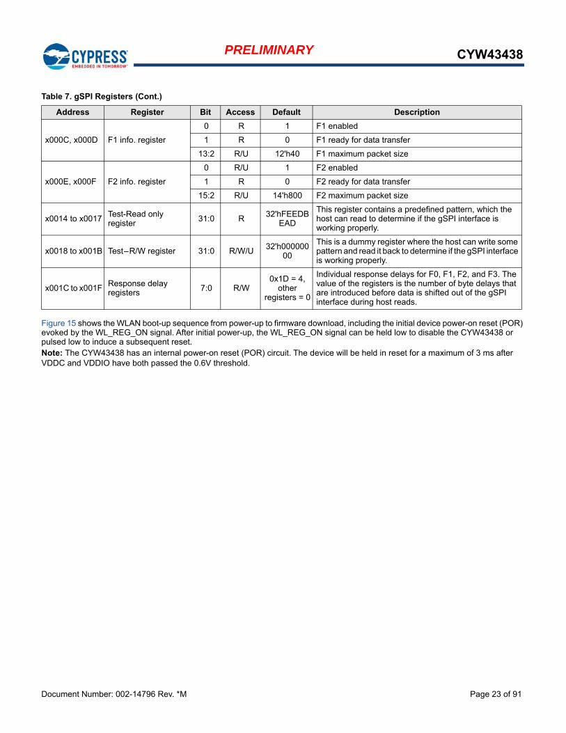
Figure 15 shows the WLAN boot-up sequence from power-up to firmware download, including the initial device power-on reset (POR) evoked by the WL_REG_ON signal. After initial power-up, the WL_REG_ON signal can be held low to disable the CYW43438 or pulsed low to induce a subsequent reset.Note: The CYW43438 has an internal power-on reset (POR) circuit. The device will be held in reset for a maximum of 3 ms after VDDC and VDDIO have both passed the 0.6V threshold.
x000C, x000D F1 info. register
0 R 1 F1 enabled
1 R 0 F1 ready for data transfer
13:2 R/U 12'h40 F1 maximum packet size
x000E, x000F F2 info. register
0 R/U 1 F2 enabled
1 R 0 F2 ready for data transfer
15:2 R/U 14'h800 F2 maximum packet size
x0014 to x0017 Test-Read only register 31:0 R 32'hFEEDB
EAD
This register contains a predefined pattern, which the host can read to determine if the gSPI interface is working properly.
x0018 to x001B Test–R/W register 31:0 R/W/U 32'h00000000
This is a dummy register where the host can write some pattern and read it back to determine if the gSPI interface is working properly.
x001C to x001F Response delay registers 7:0 R/W
0x1D = 4, other
registers = 0
Individual response delays for F0, F1, F2, and F3. The value of the registers is the number of byte delays that are introduced before data is shifted out of the gSPI interface during host reads.
Table 7. gSPI Registers (Cont.)
Address Register Bit Access Default Description

Document Number: 002-14796 Rev. *M Page 24 of 91
PRELIMINARY CYW43438
Figure 15. WLAN Boot-Up Sequence
< 1.5 ms
After 15 ms1the reference clock
is assumed to be up. Access to PLL registers is possible.
15 1ms
< 50 ms
< 3 ms
After a fixed delay following internal POR going high , the device responds to host F0 (address 0x14) reads.
VDDIO
WL_REG_ON
VDDC
(from internal PMU)
Internal POR
Device requests a reference clock.
SPI Host Interaction:
Host polls F0 (address 0x14) until it reads a predefined pattern.
Host sets wake‐up‐wlan bit
and waits 15 ms1, the
maximum time for reference clock availability.
After 15 1ms, the host
programs the PLL registers to set the crystal frequency.
Host downloads code.
Chip‐active interrupt is asserted after the PLL locks.
VBAT Ramp time from 0V to 4.3V > 40 µs
0.6V
> 2 Sleep Clock cycles
WL_IRQ
1 This wait time is programmable in sleep‐clock increments from 1 to 255 (30 us to 15 ms).

Document Number: 002-14796 Rev. *M Page 25 of 91
PRELIMINARY CYW43438
5. Wireless LAN MAC and PHY
5.1 MAC Features
The CYW43438 WLAN MAC supports features specified in the IEEE 802.11 base standard, and amended by IEEE 802.11n. The salient features are listed below:
Transmission and reception of aggregated MPDUs (A-MPDU).
Support for power management schemes, including WMM power-save, power-save multipoll (PSMP) and multiphase PSMP operation.
Support for immediate ACK and Block-ACK policies.
Interframe space timing support, including RIFS.
Support for RTS/CTS and CTS-to-self frame sequences for protecting frame exchanges.
Back-off counters in hardware for supporting multiple priorities as specified in the WMM specification.
Timing synchronization function (TSF), network allocation vector (NAV) maintenance, and target beacon transmission time (TBTT) generation in hardware.
Hardware off-load for AES-CCMP, legacy WPA TKIP, legacy WEP ciphers, WAPI, and support for key management.
Support for coexistence with Bluetooth and other external radios.
Programmable independent basic service set (IBSS) or infrastructure basic service set functionality
Statistics counters for MIB support.
5.1.1 MAC Description
The CYW43438 WLAN MAC is designed to support high throughput operation with low-power consumption. It does so without compromising on Bluetooth coexistence policies, thereby enabling optimal performance over both networks. In addition, several power-saving modes that have been implemented allow the MAC to consume very little power while maintaining network-wide timing synchronization. The architecture diagram of the MAC is shown in Figure 16.
Figure 16. WLAN MAC Architecture
Embedded CPU InterfaceHost Registers, DMA Engines
TX‐FIFO32 KB
WEP
WEP, TKIP, AES
TXETX A‐MPDU
RXE
PMQ PSM
Shared Memory6 KB
PSM
UCODE
Memory
EXT‐ IHR
IFS
Backoff, BTCX
TSF
NAV
IHR
BUS
SHM
BUS
MAC ‐ PHY Interface
RX‐FIFO10 KB
RX A‐MPDU

Document Number: 002-14796 Rev. *M Page 26 of 91
PRELIMINARY CYW43438
The following sections provide an overview of the important modules in the MAC.
PSM
The programmable state machine (PSM) is a microcoded engine that provides most of the low-level control to the hardware to implement the IEEE 802.11 specification. It is a microcontroller that is highly optimized for flow-control operations, which are predom-inant in implementations of communication protocols. The instruction set and fundamental operations are simple and general, which allows algorithms to be optimized until very late in the design process. It also allows for changes to the algorithms to track evolving IEEE 802.11 specifications.
The PSM fetches instructions from the microcode memory. It uses the shared memory to obtain operands for instructions, as a data store, and to exchange data between both the host and the MAC data pipeline (via the SHM bus). The PSM also uses a scratch-pad memory (similar to a register bank) to store frequently accessed and temporary variables.
The PSM exercises fine-grained control over the hardware engines by programming internal hardware registers (IHR). These IHRs are collocated with the hardware functions they control and are accessed by the PSM via the IHR bus.
The PSM fetches instructions from the microcode memory using an address determined by the program counter, an instruction literal, or a program stack. For ALU operations, the operands are obtained from shared memory, scratch-pad memory, IHRs, or instruction literals, and the results are written into the shared memory, scratch-pad memory, or IHRs.
There are two basic branch instructions: conditional branches and ALU-based branches. To better support the many decision points in the IEEE 802.11 algorithms, branches can depend on either readily available signals from the hardware modules (branch condition signals are available to the PSM without polling the IHRs) or on the results of ALU operations.
WEP
The wired equivalent privacy (WEP) engine encapsulates all the hardware accelerators to perform the encryption and decryption, as well as the MIC computation and verification. The accelerators implement the following cipher algorithms: legacy WEP, WPA TKIP, and WPA2 AES-CCMP.
Based on the frame type and association information, the PSM determines the appropriate cipher algorithm to be used. It supplies the keys to the hardware engines from an on-chip key table. The WEP interfaces with the transmit engine (TXE) to encrypt and compute the MIC on transmit frames and the receive engine (RXE) to decrypt and verify the MIC on receive frames. WAPI is also supported.
TXE
The transmit engine (TXE) constitutes the transmit data path of the MAC. It coordinates the DMA engines to store the transmit frames in the TXFIFO. It interfaces with WEP module to encrypt frames and transfers the frames across the MAC-PHY interface at the appropriate time determined by the channel access mechanisms.
The data received from the DMA engines are stored in transmit FIFOs. The MAC supports multiple logical queues to support traffic streams that have different QoS priority requirements. The PSM uses the channel access information from the IFS module to schedule a queue from which the next frame is transmitted. Once the frame is scheduled, the TXE hardware transmits the frame based on a precise timing trigger received from the IFS module.
The TXE module also contains the hardware that allows the rapid assembly of MPDUs into an A-MPDU for transmission. The hardware module aggregates the encrypted MPDUs by adding appropriate headers and pad delimiters as needed.
RXE
The receive engine (RXE) constitutes the receive data path of the MAC. It interfaces with the DMA engine to drain the received frames from the RX FIFO. It transfers bytes across the MAC-PHY interface and interfaces with the WEP module to decrypt frames. The decrypted data is stored in the RX FIFO.
The RXE module contains programmable filters that are programmed by the PSM to accept or filter frames based on several criteria such as receiver address, BSSID, and certain frame types.
The RXE module also contains the hardware required to detect A-MPDUs, parse the headers of the containers, and disaggregate them into component MPDUS.

Document Number: 002-14796 Rev. *M Page 27 of 91
PRELIMINARY CYW43438
IFS
The IFS module contains the timers required to determine interframe space timing including RIFS timing. It also contains multiple back-off engines required to support prioritized access to the medium as specified by WMM.
The interframe spacing timers are triggered by the cessation of channel activity on the medium, as indicated by the PHY. These timers provide precise timing to the TXE to begin frame transmission. The TXE uses this information to send response frames or perform transmit frame-bursting (RIFS or SIFS separated, as within a TXOP).
The back-off engines (for each access category) monitor channel activity, in each slot duration, to determine whether to continue or pause the back-off counters. When the back-off counters reach 0, the TXE gets notified so that it may commence frame transmission. In the event of multiple back-off counters decrementing to 0 at the same time, the hardware resolves the conflict based on policies provided by the PSM.
The IFS module also incorporates hardware that allows the MAC to enter a low-power state when operating under the IEEE power-saving mode. In this mode, the MAC is in a suspended state with its clock turned off. A sleep timer, whose count value is initialized by the PSM, runs on a slow clock and determines the duration over which the MAC remains in this suspended state. Once the timer expires, the MAC is restored to its functional state. The PSM updates the TSF timer based on the sleep duration, ensuring that the TSF is synchronized to the network.
The IFS module also contains the PTA hardware that assists the PSM in Bluetooth coexistence functions.
TSF
The timing synchronization function (TSF) module maintains the TSF timer of the MAC. It also maintains the target beacon trans-mission time (TBTT). The TSF timer hardware, under the control of the PSM, is capable of adopting timestamps received from beacon and probe response frames in order to maintain synchronization with the network.
The TSF module also generates trigger signals for events that are specified as offsets from the TSF timer, such as uplink and downlink transmission times used in PSMP.
NAV
The network allocation vector (NAV) timer module is responsible for maintaining the NAV information conveyed through the duration field of MAC frames. This ensures that the MAC complies with the protection mechanisms specified in the standard.
The hardware, under the control of the PSM, maintains the NAV timer and updates the timer appropriately based on received frames. This timing information is provided to the IFS module, which uses it as a virtual carrier-sense indication.
MAC-PHY Interface
The MAC-PHY interface consists of a data path interface to exchange RX/TX data from/to the PHY. In addition, there is a programming interface, which can be controlled either by the host or the PSM to configure and control the PHY.
5.2 PHY Description
The CYW43438 WLAN digital PHY is designed to comply with IEEE 802.11b/g/n single stream to provide wireless LAN connectivity supporting data rates from 1 Mbps to 96 Mbps for low-power, high-performance handheld applications.
The PHY has been designed to meet specification requirements in the presence of interference, radio nonlinearity, and impairments. It incorporates efficient implementations of the filters, FFT, and Viterbi decoder algorithms. Efficient algorithms have been designed to achieve maximum throughput and reliability, including algorithms for carrier sense/rejection, frequency/phase/timing acquisition and tracking, and channel estimation and tracking. The PHY receiver also contains a robust IEEE 802.11b demodulator. The PHY carrier sense has been tuned to provide high throughput for IEEE 802.11g/IEEE 802.11b hybrid networks with Bluetooth coexistence.

Document Number: 002-14796 Rev. *M Page 28 of 91
PRELIMINARY CYW43438
5.2.1 PHY Features
Supports the IEEE 802.11b/g/n single-stream standards.
Explicit IEEE 802.11n transmit beamforming.
Supports optional Greenfield mode in TX and RX.
Tx and Rx LDPC for improved range and power efficiency.
Supports IEEE 802.11h/d for worldwide operation.
Algorithms achieving low power, enhanced sensitivity, range, and reliability.
Algorithms to maximize throughput performance in the presence of Bluetooth signals.
Automatic gain control scheme for blocking and nonblocking application scenarios for cellular applications.
Closed-loop transmit power control.
Designed to meet FCC and other regulatory requirements.
Support for 2.4 GHz Broadcom TurboQAM data rates and 20 MHz channel bandwidth.
Figure 17. WLAN PHY Block Diagram
The PHY is capable of fully calibrating the RF front-end to extract the highest performance. On power-up, the PHY performs a full calibration suite to correct for IQ mismatch and local oscillator leakage. The PHY also performs periodic calibration to compensate for any temperature related drift, thus maintaining high-performance over time. A closed-loop transmit control algorithm maintains the output power at its required level and can control TX power on a per-packet basis.
Filters and Radio Comp
Frequency and Timing
Synch
Carrier Sense, AGC, and Rx
FSMRadio Control Block
Filters and Radio Comp
AFE and Radio
MAC Interface
Buffers
OFDM Demodulate
Viterbi Decoder
Tx FSM
PA Comp
Modulation and Coding
Modulate/Spread
Frame and Scramble
FFT/IFFT
CCK/DSSS Demodulate
Descramble and
Deframe
COEX

Document Number: 002-14796 Rev. *M Page 29 of 91
PRELIMINARY CYW43438
6. WLAN Radio Subsystem
The CYW43438 includes an integrated WLAN RF transceiver that has been optimized for use in 2.4 GHz Wireless LAN systems. It is designed to provide low power, low cost, and robust communications for applications operating in the globally available 2.4 GHz unlicensed ISM band. The transmit and receive sections include all on-chip filtering, mixing, and gain control functions. Improvements to the radio design include shared TX/RX baseband filters and high immunity to supply noise.
Figure 18 shows the radio functional block diagram.
Figure 18. Radio Functional Block Diagram
Gm
BT LOGEN
WL LOGEN
BT PLL
WL PLL
WLAN BB
BT BB
CLB
Voltage Regulators
BT
LPO/Ext LPO/RCAL
BT ADC
BT DAC
WL PA WL PGA
WL TX G‐Mixer WL TXLPF
WL RX G‐Mixer
SLNA WL G‐LNA12
BT LNA Load
BT LNA GM
BT PABT RX Mixer
BT TX Mixer
BT RXLPF
BT TXLPF
Shared XO
WL RXLPF
WL ATX
WL GRXWL GTXWL ARX
BT TXBT RX
BT ADC
BT RXLPF
BT DAC
WL ADC
WL ADC
WL RXLPF
WL DAC
WL DAC
WL TXLPF
WLRF_2G_eLG
WLRF_2G_RF4 ~ 6 nH
10 pF
Recommend Q = 40
Document Number: 002-14796 Rev. *M Page 30 of 91
PRELIMINARY CYW43438
6.1 Receive Path
The CYW43438 has a wide dynamic range, direct conversion receiver. It employs high-order on-chip channel filtering to ensure reliable operation in the noisy 2.4 GHz ISM band.
6.2 Transmit Path
Baseband data is modulated and upconverted to the 2.4 GHz ISM band. A linear on-chip power amplifier is included, which is capable of delivering high output powers while meeting IEEE 802.11b/g/n specifications without the need for an external PA. This PA is supplied by an internal LDO that is directly supplied by VBAT, thereby eliminating the need for a separate PALDO. Closed-loop output power control is integrated.
6.3 Calibration
The CYW43438 features dynamic on-chip calibration, eliminating process variation across components. This enables the CYW43438 to be used in high-volume applications because calibration routines are not required during manufacturing testing. These calibration routines are performed periodically during normal radio operation. Automatic calibration examples include baseband filter calibration for optimum transmit and receive performance and LOFT calibration for leakage reduction. In addition, I/Q calibration, R calibration, and VCO calibration are performed on-chip.

Document Number: 002-14796 Rev. *M Page 31 of 91
PRELIMINARY CYW43438
7. Bluetooth Overview
The CYW43438 is a Bluetooth 5.1 compliance, baseband processor and 2.4 GHz transceiver. It features the highest level of integration and eliminates all critical external components, thus minimizing the footprint, power consumption, and system cost of a Bluetooth plus WLAN solution.
The CYW43438 is the optimal solution for any Bluetooth voice and/or data application that also requires WLAN. The Bluetooth subsystem presents a standard Host Controller Interface (HCI) via a high speed UART and PCM interface for audio. The CYW43438 incorporates all Bluetooth 5.1 compliance features including secure simple pairing, sniff subrating, and encryption pause and resume. CYW43438 also supports Bluetooth 5.1 compliance LE Secure Connections.
The CYW43438 Bluetooth radio transceiver provides enhanced radio performance to meet the most stringent mobile phone temperature applications and the tightest integration into mobile handsets and portable devices. It is fully compatible with any of the standard TCXO frequencies and provides full radio compatibility to operate simultaneously with GPS, WLAN, NFC, and cellular radios.
The Bluetooth transmitter also features a Class 1 power amplifier with Class 2 capability.
7.1 Features
Major Bluetooth features of the CYW43438 include:
Supports key features of upcoming Bluetooth standards
Fully supports Bluetooth Core Specification 5.1 plus enhanced data rate (EDR) features: Adaptive Frequency Hopping (AFH) Quality of Service (QoS) Extended Synchronous Connections (eSCO)—voice connections Fast connect (interlaced page and inquiry scans) Secure Simple Pairing (SSP) Sniff Subrating (SSR) Encryption Pause Resume (EPR) Extended Inquiry Response (EIR) Link Supervision Timeout (LST)
UART baud rates up to 4 Mbps
Supports Bluetooth 5.1 compliance LE Secure Connections optional feature
Multipoint operation with up to seven active slaves Maximum of seven simultaneous active ACL links Maximum of three simultaneous active SCO and eSCO connections with scatternet support
Trigger Beacon fast connect (TBFC)
Narrowband and wideband packet loss concealment
Scatternet operation with up to four active piconets with background scan and support for scatter mode
High-speed HCI UART transport support with low-power out-of-band BT_DEV_WAKE and BT_HOST_WAKE signaling (see “Host Controller Power Management” )
Channel-quality driven data rate and packet type selection
Standard Bluetooth test modes
Extended radio and production test mode features
Full support for power savings modes Bluetooth clock request Bluetooth standard sniff Deep-sleep modes and software regulator shutdown
TCXO input and auto-detection of all standard handset clock frequencies. Also supports a low-power crystal, which can be used during power save mode for better timing accuracy.

Document Number: 002-14796 Rev. *M Page 32 of 91
PRELIMINARY CYW43438
7.2 Bluetooth Radio
The CYW43438 has an integrated radio transceiver that has been optimized for use in 2.4 GHz Bluetooth wireless systems. It has been designed to provide low-power, low-cost, robust communications for applications operating in the globally available 2.4 GHz unlicensed ISM band. It is fully compliant with the Bluetooth Radio Specification and EDR specification and meets or exceeds the requirements to provide the highest communication link quality of service.
7.2.1 Transmit
The CYW43438 features a fully integrated zero-IF transmitter. The baseband transmit data is GFSK-modulated in the modem block and upconverted to the 2.4 GHz ISM band in the transmitter path. The transmitter path has signal filters, an I/Q upconverter, an output power amplifier, and RF filters. The transmitter path also incorporates /4–DQPSK for 2 Mbps and 8–DPSK for 3 Mbps to support EDR. The transmitter section is compatible with the Bluetooth Low Energy specification. The transmitter PA bias can also be adjusted to provide Bluetooth Class 1 or Class 2 operation.
7.2.2 Digital Modulator
The digital modulator performs the data modulation and filtering required for the GFSK, /4–DQPSK, and 8–DPSK signal. The fully digital modulator minimizes any frequency drift or anomalies in the modulation characteristics of the transmitted signal and is much more stable than direct VCO modulation schemes.
7.2.3 Digital Demodulator and Bit Synchronizer
The digital demodulator and bit synchronizer take the low-IF received signal and perform an optimal frequency tracking and bit-synchronization algorithm.
7.2.4 Power Amplifier
The fully integrated PA supports Class 1 or Class 2 output using a highly linearized, temperature-compensated design. This provides greater flexibility in front-end matching and filtering. Due to the linear nature of the PA combined with some integrated filtering, external filtering is required to meet the Bluetooth and regulatory harmonic and spurious requirements. For integrated mobile handset appli-cations in which Bluetooth is integrated next to the cellular radio, external filtering can be applied to achieve near-thermal noise levels for spurious and radiated noise emissions. The transmitter features a sophisticated on-chip transmit signal strength indicator (TSSI) block to keep the absolute output power variation within a tight range across process, voltage, and temperature.
7.2.5 Receiver
The receiver path uses a low-IF scheme to downconvert the received signal for demodulation in the digital demodulator and bit synchronizer. The receiver path provides a high degree of linearity, an extended dynamic range, and high-order on-chip channel filtering to ensure reliable operation in the noisy 2.4 GHz ISM band. The front-end topology with built-in out-of-band attenuation enables the CYW43438 to be used in most applications with minimal off-chip filtering. For integrated handset operation, in which the Bluetooth function is integrated close to the cellular transmitter, external filtering is required to eliminate the desensitization of the receiver by the cellular transmit signal.
7.2.6 Digital Demodulator and Bit Synchronizer
The digital demodulator and bit synchronizer take the low-IF received signal and perform an optimal frequency tracking and bit synchronization algorithm.
7.2.7 Receiver Signal Strength Indicator
The radio portion of the CYW43438 provides a Receiver Signal Strength Indicator (RSSI) signal to the baseband so that the controller can take part in a Bluetooth power-controlled link by providing a metric of its own receiver signal strength to determine whether the transmitter should increase or decrease its output power.
7.2.8 Local Oscillator Generation
Local Oscillator (LO) generation provides fast frequency hopping (1600 hops/second) across the 79 maximum available channels. The LO generation subblock employs an architecture for high immunity to LO pulling during PA operation. The CYW43438 uses an internal RF and IF loop filter.
7.2.9 Calibration
The CYW43438 radio transceiver features an automated calibration scheme that is self contained in the radio. No user interaction is required during normal operation or during manufacturing to optimize performance. Calibration optimizes the performance of all the major blocks within the radio to within 2% of optimal conditions, including filter gain and phase characteristics, matching between key components, and key gain blocks. This takes into account process variation and temperature variation. Calibration occurs transpar-ently during normal operation during the settling time of the hops and calibrates for temperature variations as the device cools and heats during normal operation in its environment.

Document Number: 002-14796 Rev. *M Page 33 of 91
PRELIMINARY CYW43438
8. Bluetooth Baseband Core
The Bluetooth Baseband Core (BBC) implements all of the time-critical functions required for high-performance Bluetooth operation. The BBC manages the buffering, segmentation, and routing of data for all connections. It also buffers data that passes through it, handles data flow control, schedules SCO/ACL TX/RX transactions, monitors Bluetooth slot usage, optimally segments and packages data into baseband packets, manages connection status indicators, and composes and decodes HCI packets. In addition to these functions, it independently handles HCI event types and HCI command types.
The following transmit and receive functions are also implemented in the BBC hardware to increase the reliability and security of data before sending and receiving it over the air:
Symbol timing recovery, data deframing, forward error correction (FEC), header error control (HEC), cyclic redundancy check (CRC), data decryption, and data dewhitening in the receiver.
Data framing, FEC generation, HEC generation, CRC generation, key generation, data encryption, and data whitening in the transmitter.
8.1 Bluetooth Standard Features
The BBC supports all Bluetooth standard features, with the following benefits:
Dual-mode classic Bluetooth and classic Low Energy (BT and BLE) operation.
Low energy physical layer
Low energy link layer
Enhancements to HCI for low energy
Low energy direct test mode
128 AES-CCM secure connection for both BT and BLENote: The CYW43438 is compatible with the Bluetooth Low Energy operating mode, which provides a dramatic reduction in the power consumption of the Bluetooth radio and baseband. The primary application for this mode is to provide support for low data rate devices, such as sensors and remote controls.
8.2 Bluetooth 5.0 Features
CYW43438 supports Bluetooth 5.0’s new LE Secure Connections feature to enable secure connection establishment using the Elliptic-Curve Diffie-Hellman algorithm.
8.3 Link Control Layer
The link control layer is part of the Bluetooth link control functions that are implemented in dedicated logic in the link control unit (LCU). This layer contains the command controller that takes commands from the software, and other controllers that are activated or configured by the command controller, to perform the link control tasks. Each task performs a different state in the Bluetooth link controller.
Major states: Standby Connection
Substates: Page Page Scan Inquiry Inquiry Scan Sniff BLE Adv BLE Scan/Initiation

Document Number: 002-14796 Rev. *M Page 34 of 91
PRELIMINARY CYW43438
8.4 Test Mode Support
The CYW43438 fully supports Bluetooth Test mode as described in Core System Package [Host volume] Part D Test Support of the Bluetooth Core Specification. This includes the transmitter tests, normal and delayed loopback tests, and reduced hopping sequence.
In addition to the standard Bluetooth Test Mode, the CYW43438 also supports enhanced testing features to simplify RF debugging and qualification as well as type-approval testing. These features include:
Fixed frequency carrier-wave (unmodulated) transmission Simplifies some type-approval measurements (Japan) Aids in transmitter performance analysis
Fixed frequency constant receiver mode Receiver output directed to an I/O pin Allows for direct BER measurements using standard RF test equipment Facilitates spurious emissions testing for receive mode
Fixed frequency constant transmission Eight-bit fixed pattern or PRBS-9 Enables modulated signal measurements with standard RF test equipment
8.5 Bluetooth Power Management Unit
The Bluetooth Power Management Unit (PMU) provides power management features that can be invoked by either software through power management registers or packet handling in the baseband core. The power management functions provided by the CYW43438 are:
RF Power Management
Host Controller Power Management
BBC Power Management
FM Power Management
8.5.1 RF Power Management
The BBC generates power-down control signals for the transmit path, receive path, PLL, and power amplifier to the 2.4 GHz trans-ceiver. The transceiver then processes the power-down functions accordingly.
8.5.2 Host Controller Power Management
When running in UART mode, the CYW43438 can be configured so that dedicated signals are used for power management handshaking between the CYW43438 and the host. The basic power saving functions supported by those handshaking signals include the standard Bluetooth defined power savings modes and standby modes of operation.
Table 8 describes the power-control handshake signals used with the UART interface.
Table 8. Power Control Pin Description
Signal Type Description
BT_DEV_WAKE I
Bluetooth device wake-up signal: Signal from the host to the CYW43438 indicating that the host requires attention.
Asserted: The Bluetooth device must wake up or remain awake.
Deasserted: The Bluetooth device may sleep when sleep criteria are met.The polarity of this signal is software configurable and can be asserted high or low.
BT_HOST_WAKE O
Host wake-up signal. Signal from the CYW43438 to the host indicating that the CYW43438 requires attention.
Asserted: Host device must wake up or remain awake.
Deasserted: Host device may sleep when sleep criteria are met.The polarity of this signal is software configurable and can be asserted high or low.
CLK_REQ O
The CYW43438 asserts CLK_REQ when Bluetooth or WLAN directs the host to turn on the reference clock. The CLK_REQ polarity is active-high. Add an external 100 kΩ pull-down resistor to ensure the signal is deasserted when the CYW43438 powers up or resets when VDDIO is present.
Note: Pad function Control Register is set to 0 for these pins.

Document Number: 002-14796 Rev. *M Page 35 of 91
PRELIMINARY CYW43438
Figure 19. Startup Signaling Sequence
HostResetX
VDDIO
LPO
BT_GPIO_0 (BT_DEV_WAKE)
BT_UART_CTS_N
CLK_REQ_OUT
BT_GPIO_1 (BT_HOST_WAKE)
BT_REG_ON
BT_UART_RTS_N
Host IOs configuredHost IOs unconfigured
BTH IOs configuredBTH IOs unconfigured
T4
T5
T3
T2
T1
Notes : T1 is the time for host to settle it’s IOs after a reset.T2 is the time for host to drive BT_REG_ON high after the Host IOs are configured. T3 is the time for BTH (Bluetooth) device to settle its IOs after a reset and reference clock settling time has elapsed.T4 is the time for BTH device to drive BT_UART_RTS_N low after the host drives BT_UART_CTS_N low. This assumes the BTH device has already completed initialization.T5 is the time for BTH device to drive CLK_REQ_OUT high after BT_REG_ON goes high. Note this pin is used for designs that use an external reference clock source from the Host. This pin is irrelevant for Crystal reference clock based designs where the BTH device generates it’s own reference clock from an external crystal connected to it’s oscillator circuit.Timing diagram assumes VBAT is present.
DrivenPulled
BTH device drives this line low indicating transport is ready
Host side drives this line low

Document Number: 002-14796 Rev. *M Page 36 of 91
PRELIMINARY CYW43438
8.5.3 BBC Power Management
The following are low-power operations for the BBC:
Physical layer packet-handling turns the RF on and off dynamically within transmit/receive packets.
Bluetooth-specified low-power connection modes: sniff and hold. While in these modes, the CYW43438 runs on the low-power oscillator and wakes up after a predefined time period.
A low-power shutdown feature allows the device to be turned off while the host and any other devices in the system remain operational. When the CYW43438 is not needed in the system, the RF and core supplies are shut down while the I/O remains powered. This allows the CYW43438 to effectively be off while keeping the I/O pins powered, so they do not draw extra current from any other I/O-connected devices.
During the low-power shut-down state, provided VDDIO remains applied to the CYW43438, all outputs are tristated, and most input signals are disabled. Input voltages must remain within the limits defined for normal operation. This is done to prevent current paths or create loading on digital signals in the system and enables the CYW43438 to be fully integrated in an embedded device to take full advantage of the lowest power-saving modes.
Two CYW43438 input signals are designed to be high-impedance inputs that do not load the driving signal even if the chip does not have VDDIO power supplied to it: the frequency reference input (WRF_TCXO_IN) and the 32.768 kHz input (LPO). When the CYW43438 is powered on from this state, it is the same as a normal power-up, and the device does not contain any information about its state from the time before it was powered down.
8.5.4 FM Power Management
The CYW43438 FM subsystem can operate independently of, or in tandem with, the Bluetooth RF and BBC subsystems. The FM subsystem power management scheme operates in conjunction with the Bluetooth RF and BBC subsystems. The FM block does not have a low power state, it is either ON or OFF.Note: Cypress does not support FM. This section and other sections that refer to FM operation and pinout are retained in this document to provide customers data about the use of Bluetooth while keeping FM powered down.
8.5.5 Wideband Speech
The CYW43438 provides support for wideband speech (WBS) technology. The CYW43438 can perform subband-codec (SBC), as well as mSBC, encoding and decoding of linear 16 bits at 16 kHz (256 kbps rate) transferred over the PCM bus.
8.5.6 Packet Loss Concealment
Packet Loss Concealment (PLC) improves the apparent audio quality for systems with marginal link performance. Bluetooth messages are sent in packets. When a packet is lost, it creates a gap in the received audio bit-stream. Packet loss can be mitigated in several ways:
Fill in zeros.
Ramp down the output audio signal toward zero (this is the method used in current Bluetooth headsets).
Repeat the last frame (or packet) of the received bit-stream and decode it as usual (frame repeat).
These techniques cause distortion and popping in the audio stream. The CYW43438 uses a proprietary waveform extension algorithm to provide dramatic improvement in the audio quality. Figure 20 and Figure 21 show audio waveforms with and without Packet Loss Concealment. Broadcom PLC/BEC algorithms also support wideband speech.
Figure 20. CVSD Decoder Output Waveform Without PLC
Packet losses causes ramp-down

Document Number: 002-14796 Rev. *M Page 37 of 91
PRELIMINARY CYW43438
Figure 21. CVSD Decoder Output Waveform After Applying PLC
8.5.7 Codec Encoding
The CYW43438 can support SBC and mSBC encoding and decoding for wideband speech.
8.5.8 Multiple Simultaneous A2DP Audio Streams
The CYW43438 has the ability to take a single audio stream and output it to multiple Bluetooth devices simultaneously. This allows a user to share his or her music (or any audio stream) with a friend.
8.6 Adaptive Frequency Hopping
The CYW43438 gathers link quality statistics on a channel by channel basis to facilitate channel assessment and channel map selection. The link quality is determined using both RF and baseband signal processing to provide a more accurate frequency-hop map.
8.7 Advanced Bluetooth/WLAN Coexistence
The CYW43438 includes advanced coexistence technologies that are only possible with a Bluetooth/WLAN integrated die solution. These coexistence technologies are targeted at small form-factor platforms, such as cell phones and media players, including appli-cations such as VoWLAN + SCO and Video-over-WLAN + High Fidelity BT Stereo.
Support is provided for platforms that share a single antenna between Bluetooth and WLAN. Dual-antenna applications are also supported. The CYW43438 radio architecture allows for lossless simultaneous Bluetooth and WLAN reception for shared antenna applications. This is possible only via an integrated solution (shared LNA and joint AGC algorithm). It has superior performance versus implementations that need to arbitrate between Bluetooth and WLAN reception.
The CYW43438 integrated solution enables MAC-layer signaling (firmware) and a greater degree of sharing via an enhanced coexis-tence interface. Information is exchanged between the Bluetooth and WLAN cores without host processor involvement.
The CYW43438 also supports Transmit Power Control (TPC) on the STA together with standard Bluetooth TPC to limit mutual interference and receiver desensitization. Preemption mechanisms are utilized to prevent AP transmissions from colliding with Bluetooth frames. Improved channel classification techniques have been implemented in Bluetooth for faster and more accurate detection and elimination of interferers (including non-WLAN 2.4 GHz interference).
The Bluetooth AFH classification is also enhanced by the WLAN core’s channel information.
8.8 Fast Connection (Interlaced Page and Inquiry Scans)
The CYW43438 supports page scan and inquiry scan modes that significantly reduce the average inquiry response and connection times. These scanning modes are compatible with the Bluetooth version 2.1 page and inquiry procedures.

Document Number: 002-14796 Rev. *M Page 38 of 91
PRELIMINARY CYW43438
9. Microprocessor and Memory Unit for Bluetooth
The Bluetooth microprocessor core is based on the ARM Cortex-M3 32-bit RISC processor with embedded ICE-RT debug and JTAG interface units. It runs software from the link control (LC) layer up to the host controller interface (HCI).
The ARM core is paired with a memory unit that contains 576 KB of ROM for program storage and boot ROM, and 160 KB of RAM for data scratch-pad and patch RAM code. The internal ROM allows for flexibility during power-on reset (POR) to enable the same device to be used in various configurations. At power-up, the lower-layer protocol stack is executed from the internal ROM memory.
External patches may be applied to the ROM-based firmware to provide flexibility for bug fixes or feature additions. These patches may be downloaded from the host to the CYW43438 through the UART transports.
9.1 RAM, ROM, and Patch Memory
The CYW43438 Bluetooth core has 160 KB of internal RAM which is mapped between general purpose scratch-pad memory and patch memory, and 576 KB of ROM used for the lower-layer protocol stack, test mode software, and boot ROM. The patch memory is used for bug fixes and feature additions to ROM memory code.
9.2 Reset
The CYW43438 has an integrated power-on reset circuit that resets all circuits to a known power-on state. The BT POR circuit is out of reset after BT_REG_ON goes high. If BT_REG_ON is low, then the POR circuit is held in reset.

Document Number: 002-14796 Rev. *M Page 39 of 91
PRELIMINARY CYW43438
10. Bluetooth Peripheral Transport Unit
10.1 PCM Interface
The CYW43438 supports two independent PCM interfaces. The PCM interface on the CYW43438 can connect to linear PCM codec devices in master or slave mode. In master mode, the CYW43438 generates the PCM_CLK and PCM_SYNC signals, and in slave mode, these signals are provided by another master on the PCM interface and are inputs to the CYW43438. The configuration of the PCM interface may be adjusted by the host through the use of vendor-specific HCI commands.
10.1.1 Slot Mapping
The CYW43438 supports up to three simultaneous full-duplex SCO or eSCO channels through the PCM interface. These three channels are time-multiplexed onto the single PCM interface by using a time-slotting scheme where the 8 kHz or 16 kHz audio sample interval is divided into as many as 16 slots. The number of slots is dependent on the selected interface rate of 128 kHz, 512 kHz, or 1024 kHz. The corresponding number of slots for these interface rates is 1, 2, 4, 8, and 16, respectively. Transmit and receive PCM data from an SCO channel is always mapped to the same slot. The PCM data output driver tristates its output on unused slots to allow other devices to share the same PCM interface signals. The data output driver tristates its output after the falling edge of the PCM clock during the last bit of the slot.
10.1.2 Frame Synchronization
The CYW43438 supports both short- and long-frame synchronization in both master and slave modes. In short-frame synchronization mode, the frame synchronization signal is an active-high pulse at the audio frame rate that is a single-bit period in width and is synchronized to the rising edge of the bit clock. The PCM slave looks for a high on the falling edge of the bit clock and expects the first bit of the first slot to start at the next rising edge of the clock. In long-frame synchronization mode, the frame synchronization signal is again an active-high pulse at the audio frame rate; however, the duration is three bit periods and the pulse starts coincident with the first bit of the first slot.
10.1.3 Data Formatting
The CYW43438 may be configured to generate and accept several different data formats. For conventional narrowband speech mode, the CYW43438 uses 13 of the 16 bits in each PCM frame. The location and order of these 13 bits can be configured to support various data formats on the PCM interface. The remaining three bits are ignored on the input and may be filled with 0’s, 1’s, a sign bit, or a programmed value on the output. The default format is 13-bit 2’s complement data, left justified, and clocked MSB first.
10.1.4 Wideband Speech Support
When the host encodes Wideband Speech (WBS) packets in transparent mode, the encoded packets are transferred over the PCM bus for an eSCO voice connection. In this mode, the PCM bus is typically configured in master mode for a 4 kHz sync rate with 16-bit samples, resulting in a 64 kbps bit rate. The CYW43438 also supports slave transparent mode using a proprietary rate-matching scheme. In SBC-code mode, linear 16-bit data at 16 kHz (256 kbps rate) is transferred over the PCM bus.

Document Number: 002-14796 Rev. *M Page 40 of 91
PRELIMINARY CYW43438
10.1.5 PCM Interface Timing
Short Frame Sync, Master Mode
Figure 22. PCM Timing Diagram (Short Frame Sync, Master Mode)
Table 9. PCM Interface Timing Specifications (Short Frame Sync, Master Mode)
Ref No. Characteristics Minimum Typical Maximum Unit
1 PCM bit clock frequency – – 12 MHz
2 PCM bit clock low 41 – – ns
3 PCM bit clock high 41 – – ns
4 PCM_SYNC delay 0 – 25 ns
5 PCM_OUT delay 0 – 25 ns
6 PCM_IN setup 8 – – ns
7 PCM_IN hold 8 – – ns
8Delay from rising edge of PCM_BCLK during last bit period to PCM_OUT becoming high impedance 0 – 25 ns
PCM_BCLK
PCM_SYNC
PCM_OUT
12 3
4
5
PCM_IN
6
8
High Impedance
7

Document Number: 002-14796 Rev. *M Page 41 of 91
PRELIMINARY CYW43438
Short Frame Sync, Slave Mode
Figure 23. PCM Timing Diagram (Short Frame Sync, Slave Mode)
Table 10. PCM Interface Timing Specifications (Short Frame Sync, Slave Mode)
Ref No. Characteristics Minimum Typical Maximum Unit
1 PCM bit clock frequency – – 12 MHz
2 PCM bit clock low 41 – – ns
3 PCM bit clock high 41 – – ns
4 PCM_SYNC setup 8 – – ns
5 PCM_SYNC hold 8 – – ns
6 PCM_OUT delay 0 – 25 ns
7 PCM_IN setup 8 – – ns
8 PCM_IN hold 8 – – ns
9 Delay from rising edge of PCM_BCLK during last bit period to PCM_OUT becoming high impedance
0 – 25 ns
PCM_BCLK
PCM_SYNC
PCM_OUT
12 3
4
5
6
PCM_IN
7
9
High Impedance
8

Document Number: 002-14796 Rev. *M Page 42 of 91
PRELIMINARY CYW43438
Long Frame Sync, Master Mode
Figure 24. PCM Timing Diagram (Long Frame Sync, Master Mode)
Table 11. PCM Interface Timing Specifications (Long Frame Sync, Master Mode)
Ref No. Characteristics Minimum Typical Maximum Unit
1 PCM bit clock frequency – – 12 MHz
2 PCM bit clock low 41 – – ns
3 PCM bit clock high 41 – – ns
4 PCM_SYNC delay 0 – 25 ns
5 PCM_OUT delay 0 – 25 ns
6 PCM_IN setup 8 – – ns
7 PCM_IN hold 8 – – ns
8Delay from rising edge of PCM_BCLK during last bit period to PCM_OUT becoming high impedance 0 – 25 ns
PCM_BCLK
PCM_SYNC
PCM_OUT
12 3
4
5
PCM_IN
6
8
High Impedance
7
Bit 0
Bit 0
Bit 1
Bit 1

Document Number: 002-14796 Rev. *M Page 43 of 91
PRELIMINARY CYW43438
Long Frame Sync, Slave Mode
Figure 25. PCM Timing Diagram (Long Frame Sync, Slave Mode)
Table 12. PCM Interface Timing Specifications (Long Frame Sync, Slave Mode)
Ref No. Characteristics Minimum Typical Maximum Unit
1 PCM bit clock frequency – – 12 MHz
2 PCM bit clock low 41 – – ns
3 PCM bit clock high 41 – – ns
4 PCM_SYNC setup 8 – – ns
5 PCM_SYNC hold 8 – – ns
6 PCM_OUT delay 0 – 25 ns
7 PCM_IN setup 8 – – ns
8 PCM_IN hold 8 – – ns
9Delay from rising edge of PCM_BCLK during last bit period to PCM_OUT becoming high impedance 0 – 25 ns
PCM_BCLK
PCM_SYNC
PCM_OUT
12 3
4
5
6
PCM_IN
7
9
HIGH IMPEDANCE
8
Bit 0
Bit 0
Bit 1
Bit 1

Document Number: 002-14796 Rev. *M Page 44 of 91
PRELIMINARY CYW43438
10.2 UART Interface
The CYW43438 has a single UART for Bluetooth. The UART is a standard 4-wire interface (RX, TX, RTS, and CTS) with adjustable baud rates from 9600 bps to 4.0 Mbps. The interface features an automatic baud rate detection capability that returns a baud rate selection. Alternatively, the baud rate may be selected through a vendor-specific UART HCI command.
The UART has a 1040-byte receive FIFO and a 1040-byte transmit FIFO to support EDR. Access to the FIFOs is conducted through the Advanced High Performance Bus (AHB) interface through either DMA or the CPU. The UART supports the Bluetooth 5.1 compliance UART HCI specification: H4 and H5. The default baud rate is 115.2 Kbaud.
The UART supports the 3-wire H5 UART transport as described in the Bluetooth specification (Three-wire UART Transport Layer). Compared to H4, the H5 UART transport reduces the number of signal lines required by eliminating the CTS and RTS signals.
The CYW43438 UART can perform XON/XOFF flow control and includes hardware support for the Serial Line Input Protocol (SLIP). It can also perform a wake-on activity function. For example, activity on the RX or CTS inputs can wake the chip from a sleep state.
Normally, the UART baud rate is set by a configuration record downloaded after device reset or by automatic baud rate detection, and the host does not need to adjust the baud rate. Support for changing the baud rate during normal HCI UART operation is included through a vendor-specific command that allows the host to adjust the contents of the baud rate registers. The CYW43438 UARTs operate correctly with the host UART as long as the combined baud rate error of the two devices is within ±2% (see Table 13).
UART timing is defined in Figure 26 and Table 14.
Table 13. Example of Common Baud Rates
Desired Rate Actual Rate Error (%)
4000000 4000000 0.00
3692000 3692308 0.01
3000000 3000000 0.00
2000000 2000000 0.00
1500000 1500000 0.00
1444444 1454544 0.70
921600 923077 0.16
460800 461538 0.16
230400 230796 0.17
115200 115385 0.16
57600 57692 0.16
38400 38400 0.00
28800 28846 0.16
19200 19200 0.00
14400 14423 0.16
9600 9600 0.00

Document Number: 002-14796 Rev. *M Page 45 of 91
PRELIMINARY CYW43438
Figure 26. UART Timing
Table 14. UART Timing Specifications
Ref No. Characteristics Minimum Typical Maximum Unit
1 Delay time, UART_CTS_N low to UART_TXD valid – – 1.5 Bit periods
2Setup time, UART_CTS_N high before midpoint of stop bit – – 0.5 Bit periods
3 Delay time, midpoint of stop bit to UART_RTS_N high – – 0.5 Bit periods
UART_CTS_N
UART_RXD
UART_RTS_N
1 2
Midpoint of STOP bit
UART_TXD
Midpoint of STOP bit
3

Document Number: 002-14796 Rev. *M Page 46 of 91
PRELIMINARY CYW43438
11. CPU and Global Functions
11.1 WLAN CPU and Memory Subsystem
The CYW43438 includes an integrated ARM Cortex-M3 processor with internal RAM and ROM. The ARM Cortex-M3 processor is a low-power processor that features low gate count, low interrupt latency, and low-cost debugging. It is intended for deeply embedded applications that require fast interrupt response features. The processor implements the ARM architecture v7-M with support for the Thumb-2 instruction set. ARM Cortex-M3 provides a 30% performance gain over ARM7TDMI.
At 0.19 µW/MHz, the Cortex-M3 is the most power efficient general purpose microprocessor available, outperforming 8- and 16-bit devices on MIPS/µW. It supports integrated sleep modes.
ARM Cortex-M3 uses multiple technologies to reduce cost through improved memory utilization, reduced pin overhead, and reduced silicon area. ARM Cortex-M3 supports independent buses for code and data access (ICode/DCode and system buses). ARM Cortex-M3 supports extensive debug features including real-time tracing of program execution.
On-chip memory for the CPU includes 512 KB SRAM and 640 KB ROM.
11.2 One-Time Programmable Memory
Various hardware configuration parameters may be stored in an internal 4096-bit One-Time Programmable (OTP) memory, which is read by system software after a device reset. In addition, customer-specific parameters, including the system vendor ID and the MAC address, can be stored, depending on the specific board design.
The initial state of all bits in an unprogrammed OTP device is 0. After any bit is programmed to a 1, it cannot be reprogrammed to 0. The entire OTP array can be programmed in a single write cycle using a utility provided with the Broadcom WLAN manufacturing test tools. Alternatively, multiple write cycles can be used to selectively program specific bytes, but only bits which are still in the 0 state can be altered during each programming cycle.
Prior to OTP memory programming, all values should be verified using the appropriate editable nvram.txt file, which is provided with the reference board design package. Documentation on the OTP development process is available on the Broadcom customer support portal (http://www.broadcom.com/support).
11.3 GPIO Interface
Five general purpose I/O (GPIO) pins are available on the CYW43438 that can be used to connect to various external devices.
GPIOs are tristated by default. Subsequently, they can be programmed to be either input or output pins via the GPIO control register. They can also be programmed to have internal pull-up or pull-down resistors.
GPIO_0 is normally used as a WL_HOST_WAKE signal.
The CYW43438 supports a 2-wire coexistence configuration using GPIO_1 and GPIO_2.

Document Number: 002-14796 Rev. *M Page 47 of 91
PRELIMINARY CYW43438
11.4 External Coexistence Interface
The CYW43438 supports a 2-wire coexistence interface to enable signaling between the device and an external colocated wireless device in order to manage wireless medium sharing for optimal performance. The external colocated device can be any of the following ICs: GPS, WiMAX or UWB. An External IC is used in this section for illustration.
Figure 27 shows a 2-wire LTE coexistence example. The following definitions apply to the GPIOs in the figure:
GPIO_1: WLAN_SECI_TX output to an External IC.
GPIO_2: WLAN_SECI_RX input from an External IC.
Figure 27. 2-Wire Coexistence Interface to an External IC
See Figure 26 and Table 14: “UART Timing Specifications” for UART timing.
11.5 JTAG Interface
The CYW43438 supports the IEEE 1149.1 JTAG boundary scan standard over SDIO for performing device package and PCB assembly testing during manufacturing. In addition, the JTAG interface allows Broadcom to assist customers by using proprietary debug and characterization test tools during board bring-up. Therefore, it is highly recommended to provide access to the JTAG pins by means of test points or a header on all PCB designs.
11.6 UART Interface
One UART interface can be enabled by software as an alternate function on the JTAG pins. UART_RX is available on the JTAG_TDI pin, and UART_TX is available on the JTAG_TDO pin.
The UART is primarily for debugging during development. By adding an external RS-232 transceiver, this UART enables the CYW43438 to operate as RS-232 data termination equipment (DTE) for exchanging and managing data with other serial devices. It is compatible with the industry standard 16550 UART, and it provides a FIFO size of 64 × 8 in each direction.
WLAN
Coexistence Interface
LTE/IC
UART_IN
UART_OUT
BT
Notes: OR’ing to generate ISM_RX_PRIORITY for ERCX_TXCONF or BT_RX_PRIORITY is achieved by
setting the GPIO mask registers appropriately. WLAN_SECI_OUT and WLAN_SECI_IN are multiplexed on the GPIOs.
GPIO_1 WLAN_SECI_TX
WLAN_SECI_RXGPIO_2

Document Number: 002-14796 Rev. *M Page 48 of 91
PRELIMINARY CYW43438
12. WLAN Software Architecture
12.1 Host Software Architecture
The host driver (DHD) provides a transparent connection between the host operating system and the CYW43438 media (for example, WLAN) by presenting a network driver interface to the host operating system and communicating with the CYW43438 over an interface-specific bus (SPI, SDIO, and so on) to:
Forward transmit and receive frames between the host network stack and the CYW43438 device.
Pass control requests from the host to the CYW43438 device, returning the CYW43438 device responses.
The driver communicates with the CYW43438 over the bus using a control channel and a data channel to pass control messages and data messages. The actual message format is based on the BDC protocol.
12.2 Device Software Architecture
The wireless device, protocol, and bus drivers are run on the embedded ARM processor using a Broadcom-defined operating system called HNDRTE, which transfers data over a propriety Broadcom format over the SDIO/SPI interface between the host and device (BDC/LMAC). The data portion of the format consists of IEEE 802.11 frames wrapped in a Broadcom encapsulation. The host archi-tecture provides all missing functionality between a network device and the Broadcom device interface. The host can also be customized to provide functionality between the Broadcom device interface and a full network device interface.
This transfer requires a message-oriented (framed) interconnect between the host and device. The SDIO bus is an addressed bus—each host-initiated bus operation contains an explicit device target address—and does not natively support a higher-level data frame concept. Broadcom has implemented a hardware/software message encapsulation scheme that ignores the bus operation code address and prefixes each frame with a 4-byte length tag for framing. The device presents a packet-level interface over which data, control, and asynchronous event (from the device) packets are supported.
The data and control packets received from the bus are initially processed by the bus driver and then passed on to the protocol driver. If the packets are data packets, they are transferred to the wireless device driver (and out through its medium), and a data packet received from the device medium follows the same path in the reverse direction. If the packets are control packets, the protocol header is decoded by the protocol driver. If the packets are wireless IOCTL packets, the IOCTL API of the wireless driver is called to configure the wireless device. The microcode running in the D11 core processes all time-critical tasks.
12.2.1 Remote Downloader
When the CYW43438 powers up, the DHD initializes and downloads the firmware to run in the device.
Figure 28. WLAN Software Architecture
12.3 Wireless Configuration Utility
The device driver that supports the Broadcom IEEE 802.11 family of wireless solutions provides an input/output control (IOCTL) interface for making advanced configuration settings. The IOCTL interface makes it possible to make settings that are normally not possible when using just the native operating system-specific IEEE 802.11 configuration mechanisms. The utility uses IOCTLs to query or set a number of different driver/chip operating properties.
SPI/SDIO
BDC/LMAC Protocol
Wireless Device Driver
D11 Core
DHD Host Driver

Document No. Document Number: 002-14796 Rev. *M Page 49 of 108
PRELIMINARY CYW43438
13. Pinout and Signal Descriptions
13.1 Ball Map
Figure 29 shows the 63-ball WLBGA ball map.
Figure 29. 63-Ball WLBGA Ball Map (Bottom View)
A B C D E F G H J K L M
1BT_UART_
RXDBT_DEV_
WAKEBT_HOST_
WAKEFM_RF_IN
BT_VCO_VDD
BT_IF_VDD
BT_PAVDDWLRF_2G_eLG
WLRF_2G_RF
WLRF_PA_VDD
1
2BT_UART_
TXDBT_UART_
CTS_NFM_OUT1 FM_OUT2
FM_RF_VDD
BTFM_PLL_VDD
BTFM_PLL_VSS
BT_IF_VSSWLRF_
LNA_GND
WLRF_GENERAL_
GND
WLRF_PA_GND
WLRF_VDD_
1P352
3BT_UART_
RTS_NVDDC
FM_RF_VSS
BT_VCO_VSS
WLRF_GPIO
WLRF_VCO_GND
WLRF_XTAL_VDD1P2
3
4BT_PCM_
OUTBT_PCM_IN VSSC VDDC
WLRF_AFE_GND
WLRF_XTAL_GND
WLRF_XTAL_XOP
4
5BT_PCM_
CLKBT_PCM_
SYNCLPO_IN VSSC GPIO_2
WLRF_XTAL_XON
5
6 SR_VLX PMU_AVSSVOUT_CLD
OVOUT_LNL
DOBT_REG_O
NWCC_VDDI
OWL_REG_O
NGPIO_1 GPIO_0
SDIO_DATA_0
SDIO_CMD CLK_REQ 6
7 SR_PVSSSR_
VDDBAT5VLDO_VDD1
P5VOUT_3P3
LDO_VDDBAT5V
SDIO_DATA_1
SDIO_DATA_3
SDIO_DATA_2
SDIO_CLK 7
A B C D E F G H J K L M

Document Number: 002-14796 Rev. *M Page 50 of 91
PRELIMINARY CYW43438
13.2 WLBGA Ball List in Ball Number Order with X-Y Coordinates
Table 15 provides ball numbers and names in ball number order. The table includes the X and Y coordinates for a top view with a (0,0) center.
Table 15. CYW43438 WLBGA Ball List — Ordered By Ball Number
Ball Number Ball Name X Coordinate Y Coordinate
A1 BT_UART_RXD –1200.006 2199.996
A2 BT_UART_TXD –799.992 2199.996
A5 BT_PCM_CLK or BT_I2S_CLK 399.996 2199.996
A6 SR_VLX 799.992 2199.978
A7 SR_PVSS 1199.988 2199.978
B1 BT_DEV_WAKE –1200.006 1800
B2 BT_UART_CTS_N –799.992 1800
B4 BT_PCM_OUT or BT_I2S_DO 0 1800
B5 BT_PCM_SYNC or BT_I2S_WS 399.996 1800
B6 PMU_AVSS 799.992 1799.982
B7 SR_VBAT5V 1199.988 1799.982
C1 BT_HOST_WAKE –1200.006 1399.995
C2 FM_OUT1 –799.992 1399.986
C3 BT_UART_RTS_N –399.996 1399.995
C4 BT_PCM_IN or BT_I2S_DI 0 1399.995
C6 VOUT_CLDO 799.992 1399.986
C7 LDO_VDD15V 1199.988 1399.986
D2 FM_OUT2 –799.992 999.99
D3 VDDC –399.996 999.999
D4 VSSC 0 999.999
D6 VOUT_LNLDO 799.992 999.99
E1 FM_RF_IN –1199.988 599.994
E2 FM_RF_VDD –799.992 599.994
E3 FM_RF_VSS –399.996 599.994
E6 BT_REG_ON 799.992 599.994
E7 VOUT_3P3 1199.988 599.994
F1 BT_VCO_VDD –1199.988 199.998
F2 BTFM_PLL_VDD –799.992 199.998
F5 LPO_IN 399.996 199.998
F6 WCC_VDDIO 800.001 199.998
F7 LDO_VBAT5V 1199.988 199.998
G1 BT_IF_VDD –1199.988 –199.998
G2 BTFM_PLL_VSS –799.992 –199.998
G4 VDDC 0 –199.998
G6 WL_REG_ON 800.001 –199.998

Document Number: 002-14796 Rev. *M Page 51 of 91
PRELIMINARY CYW43438
H1 BT_PAVDD –1199.988 –599.994
H2 BT_IF_VSS –799.992 –599.994
H3 BT_VCO_VSS –399.996 –599.994
H4 WLRF_AFE_GND 0 –599.994
H6 GPIO_1 800.001 –599.994
H7 SDIO_DATA_1 1200.006 –599.994
J1 WLRF_2G_eLG –1199.988 –999.99
J2 WLRF_LNA_GND –799.992 –999.99
J3 WLRF_GPIO –399.996 –999.99
J5 VSSC 399.996 –999.999
J6 GPIO_0 800.001 –999.999
J7 SDIO_DATA_3 1200.006 –999.999
K1 WLRF_2G_RF –1199.988 –1399.986
K2 WLRF_GENERAL_GND –799.992 –1399.986
K6 SDIO_DATA_0 800.001 –1399.995
L2 WLRF_PA_GND –799.992 –1799.982
L3 WLRF_VCO_GND –399.996 –1799.982
L4 WLRF_XTAL_GND 0 –1799.982
L5 GPIO_2 399.996 –1799.991
L6 SDIO_CMD 800.001 –1799.991
L7 SDIO_DATA_2 1200.006 –1799.991
M1 WLRF_PA_VDD –1199.988 –2199.978
M2 WLRF_VDD_1P35 –799.992 –2199.978
M3 WLRF_XTAL_VDD1P2 –399.996 –2199.978
M4 WLRF_XTAL_XOP 0 –2199.978
M5 WLRF_XTAL_XON 399.996 –2199.978
M6 CLK_REQ 800.001 –2199.996
M7 SDIO_CLK 1200.006 –2199.996
Table 15. CYW43438 WLBGA Ball List — Ordered By Ball Number (Cont.)
Ball Number Ball Name X Coordinate Y Coordinate

Document Number: 002-14796 Rev. *M Page 52 of 91
PRELIMINARY CYW43438
13.3 WLBGA Ball List Ordered By Ball Name
Table 16 provides the ball numbers and names in ball name order.
Table 16. CYW43438 WLBGA Ball List — Ordered By Ball Name
Ball Name Ball Number
BT_DEV_WAKE B1
BT_HOST_WAKE C1
BT_IF_VDD G1
BT_IF_VSS H2
BT_PAVDD H1
BT_PCM_CLK or BT_I2S_CLK A5
BT_PCM_IN or BT_I2S_DI C4
BT_PCM_OUT or BT_I2S_DO B4
BT_PCM_SYNC or BT_I2S_WS B5
BT_REG_ON E6
BT_UART_CTS_N B2
BT_UART_RTS_N C3
BT_UART_RXD A1
BT_UART_TXD A2
BT_VCO_VDD F1
BT_VCO_VSS H3
BTFM_PLL_VDD F2
BTFM_PLL_VSS G2
CLK_REQ M6
FM_OUT1 C2
FM_OUT2 D2
FM_RF_IN E1
FM_RF_VDD E2
FM_RF_VSS E3
GPIO_0 J6
GPIO_1 H6
GPIO_2 L5
LDO_VDD1P5 C7
LDO_VDDBAT5V F7
LPO_IN F5
PMU_AVSS B6
SDIO_CLK M7
SDIO_CMD L6
SDIO_DATA_0 K6
SDIO_DATA_1 H7
SDIO_DATA_2 L7
SDIO_DATA_3 J7
SR_PVSS A7
SR_VDDBAT5V B7
SR_VLX A6
VDDC D3
VDDC G4
VOUT_3P3 E7
VOUT_CLDO C6
VOUT_LNLDO D6
VSSC D4
VSSC J5
WCC_VDDIO F6
WL_REG_ON G6
WLRF_2G_eLG J1
WLRF_2G_RF K1
WLRF_AFE_GND H4
WLRF_GENERAL_GND K2
WLRF_GPIO J3
WLRF_LNA_GND J2
WLRF_PA_GND L2
WLRF_PA_VDD M1
WLRF_VCO_GND L3
WLRF_VDD_1P35 M2
WLRF_XTAL_GND L4
WLRF_XTAL_VDD1P2 M3
WLRF_XTAL_XON M5
WLRF_XTAL_XOP M4
Ball Name Ball Number

Document Number: 002-14796 Rev. *M Page 53 of 91
PRELIMINARY CYW43438
13.4 Signal Descriptions
Table 17 provides the WLBGA package signal descriptions.
Table 17. WLBGA Signal Descriptions
Signal Name WLBGA Ball Type Description
RF Signal Interface
WLRF_2G_RF K1 O 2.4 GHz BT and WLAN RF output port
SDIO Bus Interface
SDIO_CLK M7 I SDIO clock input
SDIO_CMD L6 I/O SDIO command line
SDIO_DATA_0 K6 I/O SDIO data line 0
SDIO_DATA_1 H7 I/O SDIO data line 1.
SDIO_DATA_2 L7 I/O SDIO data line 2. Also used as a strapping option (see Table 20).
SDIO_DATA_3 J7 I/O SDIO data line 3
Note: Per Section 6 of the SDIO specification, 10 to 100 kΩ pull-ups are required on the four DATA lines and the CMD line. This requirement must be met during all operating states by using external pull-up resistors or properly programming internal SDIO host pull-ups.
WLAN GPIO Interface
WLRF_GPIO J3 I/O Test pin. Not connected in normal operation.
Clocks
WLRF_XTAL_XON M5 O XTAL oscillator output
WLRF_XTAL_XOP M4 I XTAL oscillator input
CLK_REQ M6 OExternal system clock request—Used when the system clock is not provided by a dedicated crystal (for example, when a shared TCXO is used). Asserted to indicate to the host that the clock is required. Shared by BT, and WLAN.
LPO_IN F5 IExternal sleep clock input (32.768 kHz). If an external 32.768 kHz clock cannot be provided, pull this pin low. However, BLE will be always on and cannot go to deep sleep.
FM Receiver1
FM_OUT1 C2 O FM analog output 1
FM_OUT2 D2 O FM analog output 2
FM_RF_IN E1 I FM radio antenna port
FM_RF_VDD E2 I FM power supply
Bluetooth PCM
BT_PCM_CLK or BT_I2S_CLK A5 I/O PCM or I2S clock; can be master (output) or slave (input)
BT_PCM_IN or BT_I2S_DI C4 I PCM or I2S data input sensing
BT_PCM_OUT or BT_I2S_DO B4 O PCM or I2S data output
BT_PCM_SYNC or BT_I2S_WS B5 I/O PCM SYNC or I2S_WS; can be master (output) or slave (input)

Document Number: 002-14796 Rev. *M Page 54 of 91
PRELIMINARY CYW43438
Bluetooth UART and Wake
BT_UART_CTS_N B2 IUART clear-to-send. Active-low clear-to-send signal for the HCI UART interface.
BT_UART_RTS_N C3 O UART request-to-send. Active-low request-to-send signal for the HCI UART interface.
BT_UART_RXD A1 I UART serial input. Serial data input for the HCI UART interface.
BT_UART_TXD A2 O UART serial output. Serial data output for the HCI UART interface.
BT_DEV_WAKE B1 I/O DEV_WAKE or general-purpose I/O signal.
BT_HOST_WAKE C1 I/O HOST_WAKE or general-purpose I/O signal.
Note: By default, the Bluetooth BT WAKE signals provide GPIO/WAKE functionality, and the UART pins provide UART functionality. Through software configuration, the PCM interface can also be routed over the BT_WAKE/UART signals as follows:
PCM_CLK on the UART_RTS_N pin
PCM_OUT on the UART_CTS_N pin
PCM_SYNC on the BT_HOST_WAKE pin
PCM_IN on the BT_DEV_WAKE pinIn this case, the BT HCI transport included sleep signaling will operate using UART_RXD and UART_TXD; that is, using a 3-Wire UART Transport.
Miscellaneous
WL_REG_ON G6 I
Used by PMU to power up or power down the internal regulators used by the WLAN section. Also, when deasserted, this pin holds the WLAN section in reset. This pin has an internal 200 k pull-down resistor that is enabled by default. It can be disabled through programming.
BT_REG_ON E6 I
Used by PMU to power up or power down the internal regulators used by the Bluetooth/FM section. Also, when deasserted, this pin holds the Bluetooth/FM1 section in reset. This pin has an internal 200 k pull-down resistor that is enabled by default. It can be disabled through programming.
GPIO_0 J6 I/O Programmable GPIO pins. This pin becomes an output pin when it is used as WLAN_HOST_WAKE/out-of-band signal.
GPIO_1 H6 I/O Programmable GPIO pins
GPIO_2 L5 I/O Programmable GPIO pins
WLRF_2G_eLG J1 I Connect to an external inductor. See the reference schematic for details.
Integrated Voltage Regulators
SR_VDDBAT5V B7 I SR VBAT input power supply
SR_VLX A6 OCBUCK switching regulator output. See Table 35 for details of the inductor and capacitor required on this output.
LDO_VDDBAT5V F7 I LDO VBAT
LDO_VDD1P5 C7 I LNLDO input
VOUT_LNLDO D6 O Output of low-noise LNLDO
VOUT_CLDO C6 O Output of core LDO
Bluetooth Power Supplies
BT_PAVDD H1 I Bluetooth PA power supply
BT_IF_VDD G1 I Bluetooth IF block power supply
BTFM_PLL_VDD1 F2 I Bluetooth RF PLL power supply
BT_VCO_VDD F1 I Bluetooth RF power supply
Table 17. WLBGA Signal Descriptions (Cont.)
Signal Name WLBGA Ball Type Description

Document Number: 002-14796 Rev. *M Page 55 of 91
PRELIMINARY CYW43438
Power Supplies
WLRF_XTAL_VDD1P2 M3 I XTAL oscillator supply
WLRF_PA_VDD M1 I Power amplifier supply
WCC_VDDIO F6 I VDDIO input supply. Connect to VDDIO.
WLRF_VDD_1P35 M2 I LNLDO input supply
VDDC D3, G4 I Core supply for WLAN and BT.
VOUT_3P3 E7 O 3.3V output supply. See the reference schematic for details.
Ground
BT_IF_VSS H2 I 1.2V Bluetooth IF block ground
BTFM_PLL_VSS G2 I Bluetooth/FM1 RF PLL ground
BT_VCO_VSS H3 I 1.2V Bluetooth RF ground
FM_RF_VSS1 E3 I FM RF ground
PMU_AVSS B6 I Quiet ground
SR_PVSS A7 I Switcher-power ground
VSSC D4, J5 I Core ground for WLAN and BT
WLRF_AFE_GND H4 I AFE ground
WLRF_LNA_GND J2 I 2.4 GHz internal LNA ground
WLRF_GENERAL_GND K2 I Miscellaneous RF ground
WLRF_PA_GND L2 I 2.4 GHz PA ground
WLRF_VCO_GND L3 I VCO/LO generator ground
WLRF_XTAL_GND L4 I XTAL ground
1. Cypress does not support FM on CYW4356.
Table 17. WLBGA Signal Descriptions (Cont.)
Signal Name WLBGA Ball Type Description

Document Number: 002-14796 Rev. *M Page 56 of 91
PRELIMINARY CYW43438
13.5 WLAN GPIO Signals and Strapping Options
The pins listed in Table 18 are sampled at power-on reset (POR) to determine the various operating modes. Sampling occurs a few milliseconds after an internal POR or deassertion of the external POR. After the POR, each pin assumes the GPIO or alternative function specified in the signal descriptions table. Each strapping option pin has an internal pull-up (PU) or pull-down (PD) resistor that determines the default mode. To change the mode, connect an external PU resistor to VDDIO or a PD resistor to ground using a 10 kΩ resistor or less.Note: Refer to the reference board schematics for more information.
13.6 Chip Debug Options
The chip can be accessed for debugging via the JTAG interface, multiplexed on the SDIO_DATA_0 through SDIO_DATA_3 (and SDIO_CLK) I/O or the Bluetooth PCM I/O depending on the bootstrap state of GPIO_1 and GPIO_2.
Table 19 shows the debug options of the device.
Table 18. GPIO Functions and Strapping Options
Pin Name WLBGA Pin # Default Function Description
SDIO_DATA_2 L7 1WLAN host interface select
This pin selects the WLAN host interface mode. The default is SDIO. For gSPI, pull this pin low.
Table 19. Chip Debug Options
JTAG_SEL GPIO_2 GPIO_1 Function SDIO I/O Pad Function BT PCM I/O Pad Function
0 0 0 Normal mode SDIO BT PCM
0 0 1 JTAG over SDIO JTAG BT PCM
0 1 0 JTAG over BT PCM SDIO JTAG
0 1 1 SWD over GPIO_1/GPIO_2 SDIO BT PCM

Document No. Document Number: 002-14796 Rev. *M Page 57 of 108
PRELIMINARY CYW43438
13.7 I/O States
The following notations are used in Table 20:
I: Input signal
O: Output signal
I/O: Input/Output signal
PU = Pulled up
PD = Pulled down
NoPull = Neither pulled up nor pulled down
Table 20. I/O States1
Name I/OKeeper2 Active Mode
Low Power State/Sleep (All Power Present)
Power-Down3 WL_REG_ON = 0 BT_REG_ON = 0
Out-of-Reset; (WL_REG_ON = 1; BT_REG_ON = Do Not Care)
(WL_REG_ON = 1 BT_REG_ON = 0) VDDIOs Present
Out-of-Reset; (WL_REG_ON = 0BT_REG_ON = 1)VDDIOs Present Power Rail
WL_REG_ON I N Input; PD (pull-down can be disabled)
Input; PD (pull-down can be disabled)
Input; PD (of 200K) Input; PD (200k) Input; PD (200k)
– –
BT_REG_ON I N Input; PD (pull down can be disabled)
Input; PD (pull down can be disabled)
Input; PD (of 200K) Input; PD (200k) Input; PD (200k)
Input; PD (200k) –
CLK_REQ I/O Y Open drain or push-pull (programmable). Active high.
Open drain or push-pull (programmable). Active high
PD Open drain, active high.
Open drain, active high.
Open drain, active high.
WCC_VDDIO
BT_HOST_WAKE
I/O Y I/O; PU, PD, NoPull (programmable)
I/O; PU, PD, NoPull (programmable)
High-Z, NoPull – Input, PD Output, Drive low WCC_VDDIO
BT_DEV_WAKE I/O Y I/O; PU, PD, NoPull (programmable)
Input; PU, PD, NoPull (programmable)
High-Z, NoPull – Input, PD Input, PD WCC_VDDIO
BT_UART_CTS I Y Input; NoPull Input; NoPull High-Z, NoPull – Input; PU Input, NoPull WCC_VDDIO
BT_UART_RTS O Y Output; NoPull Output; NoPull High-Z, NoPull – Input; PU Output, NoPull WCC_VDDIO
BT_UART_RXD I Y Input; PU Input; NoPull High-Z, NoPull – Input; PU Input, NoPull WCC_VDDIO
BT_UART_TXD O Y Output; NoPull Output; NoPull High-Z, NoPull – Input; PU Output, NoPull WCC_VDDIO
SDIO_DATA_0 I/O N SDIO MODE -> NoPull SDIO MODE -> NoPull SDIO MODE -> NoPull
SDIO MODE -> PU SDIO MODE -> NoPull
Input; PU WCC_VDDIO
SDIO_DATA_1 I/O N SDIO MODE -> NoPull SDIO MODE -> NoPull SDIO MODE -> NoPull
SDIO MODE -> PU SDIO MODE -> NoPull
Input; PU WCC_VDDIO
SDIO_DATA_2 I/O N SDIO MODE -> NoPull SDIO MODE -> NoPull SDIO MODE -> NoPull
SDIO MODE -> PU SDIO MODE -> NoPull
Input; PU WCC_VDDIO

Document No. Document Number: 002-14796 Rev. *M Page 58 of 108
PRELIMINARY CYW43438
SDIO_DATA_3 I/O N SDIO MODE -> NoPull SDIO MODE -> NoPull SDIO MODE -> NoPull
SDIO MODE -> PU SDIO MODE -> NoPull
Input; PU WCC_VDDIO
SDIO_CMD I/O N SDIO MODE -> NoPull SDIO MODE -> NoPull SDIO MODE -> NoPull
SDIO MODE -> PU SDIO MODE -> NoPull
Input; PU WCC_VDDIO
SDIO_CLK I N SDIO MODE -> NoPull SDIO MODE -> NoPull SDIO MODE -> NoPull
SDIO MODE -> NoPull
SDIO MODE -> NoPull
Input WCC_VDDIO
BT_PCM_CLK I/O Y Input; NoPull4 Input; NoPull4 High-Z, NoPull – Input, PD Input, PD WCC_VDDIO
BT_PCM_IN I/O Y Input; NoPull4 Input; NoPull4 High-Z, NoPull – Input, PD Input, PD WCC_VDDIO
BT_PCM_OUT I/O Y Input; NoPull4 Input; NoPull4 High-Z, NoPull – Input, PD Input, PD WCC_VDDIO
BT_PCM_SYNC I/O Y Input; NoPull4 Input; NoPull4 High-Z, NoPull – Input, PD Input, PD WCC_VDDIO
JTAG_SEL I Y PD PD High-Z, NoPull Input, PD PD Input, PD WCC_VDDIO
GPIO_0 I/O Y TBD Active mode High-Z, NoPull5 Input, SDIO OOB Int, NoPull
Active mode Input, NoPull WCC_VDDIO
GPIO_1 I/O Y TBD Active mode High-Z, NoPull5 Input, PD Active mode Input, Strap, PD WCC_VDDIO
GPIO_2 I/O Y TBD Active mode High-Z, NoPull5 Input, GCI GPIO[7], NoPull
Active mode Input, Strap, NoPull WCC_VDDIO
1. PU = pulled up, PD = pulled down.2. N = pad has no keeper. Y = pad has a keeper. Keeper is always active except in the power-down state. If there is no keeper, and it is an input and there is NoPull, then the pad should
be driven to prevent leakage due to floating pad, for example, SDIO_CLK.3. In the Power-down state (xx_REG_ON = 0): High-Z; NoPull => The pad is disabled because power is not supplied.4. Depending on whether the PCM interface is enabled and the configuration is master or slave mode, it can be either an output or input.5. The GPIO pull states for the active and low-power states are hardware defaults. They can all be subsequently programmed as a pull-up or pull-down.
Table 20. I/O States1 (Cont.)
Name I/OKeeper2 Active Mode
Low Power State/Sleep (All Power Present)
Power-Down3 WL_REG_ON = 0 BT_REG_ON = 0
Out-of-Reset; (WL_REG_ON = 1; BT_REG_ON = Do Not Care)
(WL_REG_ON = 1 BT_REG_ON = 0) VDDIOs Present
Out-of-Reset; (WL_REG_ON = 0BT_REG_ON = 1)VDDIOs Present Power Rail
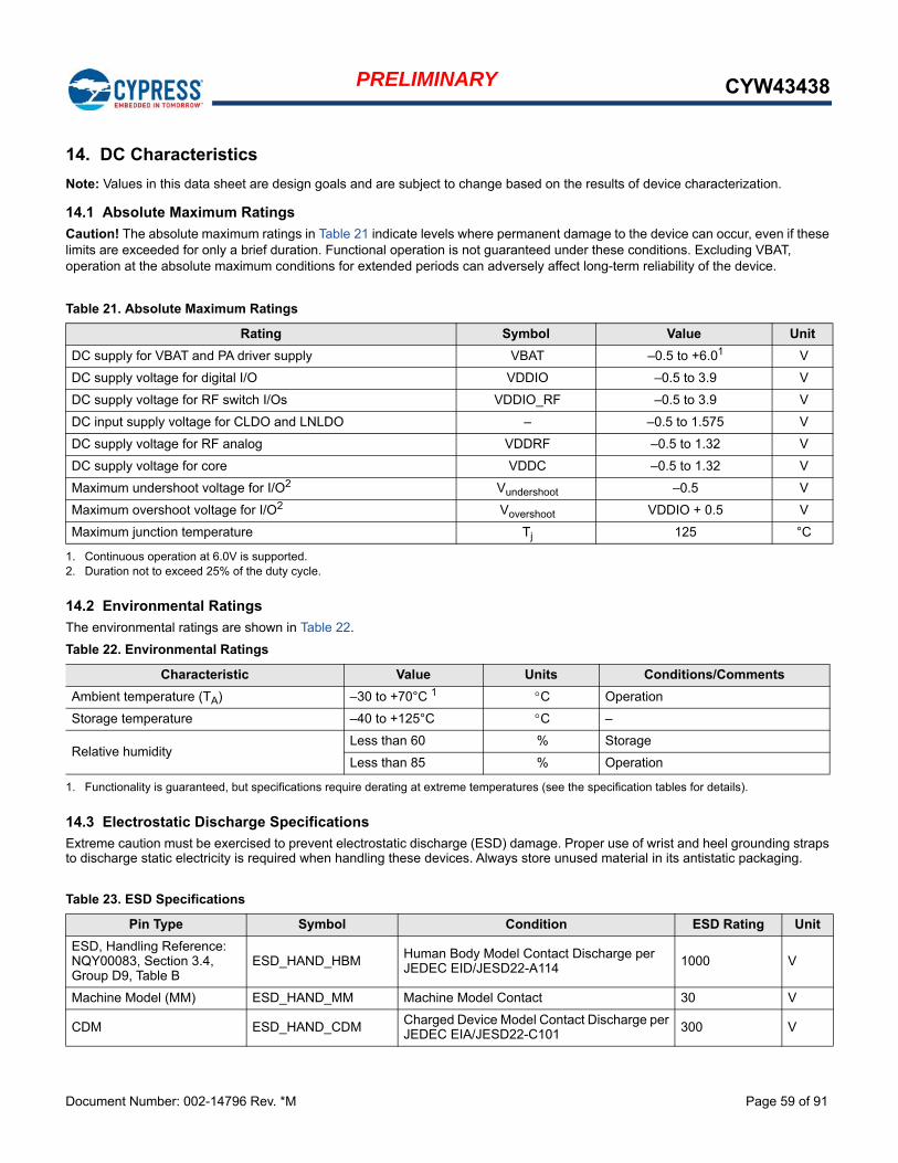
Document Number: 002-14796 Rev. *M Page 59 of 91
PRELIMINARY CYW43438
14. DC Characteristics
Note: Values in this data sheet are design goals and are subject to change based on the results of device characterization.
14.1 Absolute Maximum Ratings
Caution! The absolute maximum ratings in Table 21 indicate levels where permanent damage to the device can occur, even if these limits are exceeded for only a brief duration. Functional operation is not guaranteed under these conditions. Excluding VBAT, operation at the absolute maximum conditions for extended periods can adversely affect long-term reliability of the device.
14.2 Environmental Ratings
The environmental ratings are shown in Table 22.
14.3 Electrostatic Discharge Specifications
Extreme caution must be exercised to prevent electrostatic discharge (ESD) damage. Proper use of wrist and heel grounding straps to discharge static electricity is required when handling these devices. Always store unused material in its antistatic packaging.
Table 21. Absolute Maximum Ratings
Rating Symbol Value Unit
DC supply for VBAT and PA driver supply VBAT –0.5 to +6.01
1. Continuous operation at 6.0V is supported.
V
DC supply voltage for digital I/O VDDIO –0.5 to 3.9 V
DC supply voltage for RF switch I/Os VDDIO_RF –0.5 to 3.9 V
DC input supply voltage for CLDO and LNLDO – –0.5 to 1.575 V
DC supply voltage for RF analog VDDRF –0.5 to 1.32 V
DC supply voltage for core VDDC –0.5 to 1.32 V
Maximum undershoot voltage for I/O2
2. Duration not to exceed 25% of the duty cycle.
Vundershoot –0.5 V
Maximum overshoot voltage for I/O2 Vovershoot VDDIO + 0.5 V
Maximum junction temperature Tj 125 °C
Table 22. Environmental Ratings
Characteristic Value Units Conditions/Comments
Ambient temperature (TA) –30 to +70°C 1
1. Functionality is guaranteed, but specifications require derating at extreme temperatures (see the specification tables for details).
C Operation
Storage temperature –40 to +125°C C –
Relative humidityLess than 60 % Storage
Less than 85 % Operation
Table 23. ESD Specifications
Pin Type Symbol Condition ESD Rating Unit
ESD, Handling Reference: NQY00083, Section 3.4, Group D9, Table B
ESD_HAND_HBMHuman Body Model Contact Discharge per JEDEC EID/JESD22-A114 1000 V
Machine Model (MM) ESD_HAND_MM Machine Model Contact 30 V
CDM ESD_HAND_CDM Charged Device Model Contact Discharge per JEDEC EIA/JESD22-C101 300 V

Document Number: 002-14796 Rev. *M Page 60 of 91
PRELIMINARY CYW43438
14.4 Recommended Operating Conditions and DC Characteristics
Functional operation is not guaranteed outside the limits shown in Table 24, and operation outside these limits for extended periods can adversely affect long-term reliability of the device.
Table 24. Recommended Operating Conditions and DC Characteristics
Element SymbolValue
UnitMinimum Typical Maximum
DC supply voltage for VBAT VBAT 3.01 – 4.82 V
DC supply voltage for core VDD 1.14 1.2 1.26 V
DC supply voltage for RF blocks in chip VDDRF 1.14 1.2 1.26 V
DC supply voltage for digital I/OVDDIO, VDDIO_SD 1.71 – 3.63 V
DC supply voltage for RF switch I/Os VDDIO_RF 3.13 3.3 3.46 V
External TSSI input TSSI 0.15 – 0.95 V
Internal POR threshold Vth_POR 0.4 – 0.7 V
SDIO Interface I/O Pins
For VDDIO_SD = 1.8V:
Input high voltage VIH 1.27 – – V
Input low voltage VIL – – 0.58 V
Output high voltage @ 2 mA VOH 1.40 – – V
Output low voltage @ 2 mA VOL – – 0.45 V
For VDDIO_SD = 3.3V:
Input high voltage VIH 0.625 × VDDIO – – V
Input low voltage VIL – – 0.25 × VDDIO
V
Output high voltage @ 2 mA VOH 0.75 × VDDIO – – V
Output low voltage @ 2 mA VOL – – 0.125 × VDDIO V
Other Digital I/O Pins
For VDDIO = 1.8V:
Input high voltage VIH 0.65 × VDDIO – – V
Input low voltage VIL – –0.35 × VDDIO V
Output high voltage @ 2 mA VOH VDDIO – 0.45 – – V
Output low voltage @ 2 mA VOL – – 0.45 V
For VDDIO = 3.3V:
Input high voltage VIH 2.00 – – V
Input low voltage VIL – – 0.80 V
Output high voltage @ 2 mA VOH VDDIO – 0.4 – – V
Output low Voltage @ 2 mA VOL – – 0.40 V
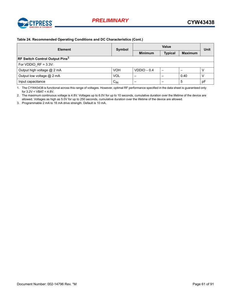
Document Number: 002-14796 Rev. *M Page 61 of 91
PRELIMINARY CYW43438
RF Switch Control Output Pins3
For VDDIO_RF = 3.3V:
Output high voltage @ 2 mA VOH VDDIO – 0.4 – – V
Output low voltage @ 2 mA VOL – – 0.40 V
Input capacitance CIN – – 5 pF
1. The CYW43438 is functional across this range of voltages. However, optimal RF performance specified in the data sheet is guaranteed only for 3.2V < VBAT < 4.8V.
2. The maximum continuous voltage is 4.8V. Voltages up to 6.0V for up to 10 seconds, cumulative duration over the lifetime of the device are allowed. Voltages as high as 5.0V for up to 250 seconds, cumulative duration over the lifetime of the device are allowed.
3. Programmable 2 mA to 16 mA drive strength. Default is 10 mA.
Table 24. Recommended Operating Conditions and DC Characteristics (Cont.)
Element SymbolValue
UnitMinimum Typical Maximum

Document Number: 002-14796 Rev. *M Page 62 of 91
PRELIMINARY CYW43438
15. WLAN RF Specifications
The CYW43438 includes an integrated direct conversion radio that supports the 2.4 GHz band. This section describes the RF characteristics of the 2.4 GHz radio.Note: Values in this data sheet are design goals and may change based on device characterization results.
Unless otherwise stated, the specifications in this section apply when the operating conditions are within the limits specified in Table 22: “Environmental Ratings” and Table 24: “Recommended Operating Conditions and DC Characteristics” . Functional operation outside these limits is not guaranteed.
Typical values apply for the following conditions:
VBAT = 3.6V.
Ambient temperature +25°C.
Figure 30. RF Port Location
Note: All specifications apply at the chip port unless otherwise specified.
15.1 2.4 GHz Band General RF Specifications
Table 25. 2.4 GHz Band General RF Specifications
Item Condition Minimum Typical Maximum Unit
TX/RX switch time Including TX ramp down – – 5 µs
RX/TX switch time Including TX ramp up – – 2 µs
TX
RX
C2
10 pF
L1
4.7 nH
C1
10 pF
Filter
Chip Port
Antenna Port
CYW43438

Document Number: 002-14796 Rev. *M Page 63 of 91
PRELIMINARY CYW43438
15.2 WLAN 2.4 GHz Receiver Performance Specifications Note: Unless otherwise specified, the specifications in Table 26 are measured at the chip port (for the location of the chip port, see Figure 30
Table 26. WLAN 2.4 GHz Receiver Performance Specifications
Parameter Condition/Notes Minimum Typical Maximum Unit
Frequency range – 2400 – 2500 MHz
RX sensitivity (8% PER for 1024 octet PSDU) 1
1 Mbps DSSS –97.5 –99.5 – dBm
2 Mbps DSSS –93.5 –95.5 – dBm
5.5 Mbps DSSS –91.5 –93.5 – dBm
11 Mbps DSSS –88.5 –90.5 – dBm
RX sensitivity (10% PER for 1000 octet PSDU) at WLAN RF port 1
6 Mbps OFDM –91.5 –93.5 – dBm
9 Mbps OFDM –90.5 –92.5 – dBm
12 Mbps OFDM –87.5 –89.5 – dBm
18 Mbps OFDM –85.5 –87.5 – dBm
24 Mbps OFDM –82.5 –84.5 – dBm
36 Mbps OFDM –80.5 –82.5 – dBm
48 Mbps OFDM –76.5 –78.5 – dBm
54 Mbps OFDM –75.5 –77.5 – dBm
RX sensitivity(10% PER for 4096 octet PSDU). Defined for default parameters: Mixed mode, 800 ns GI.
20 MHz channel spacing for all MCS rates (Mixed mode)
256-QAM, R = 5/6 –67.5 –69.5 – dBm
256-QAM, R = 3/4 –69.5 –71.5 – dBm
MCS7 –71.5 –73.5 – dBm
MCS6 –73.5 –75.5 – dBm
MCS5 –74.5 –76.5 – dBm
MCS4 –79.5 –81.5 – dBm
MCS3 –82.5 –84.5 – dBm
MCS2 –84.5 –86.5 – dBm
MCS1 –86.5 –88.5 – dBm
MCS0 –90.5 –92.5 – dBm

Document Number: 002-14796 Rev. *M Page 64 of 91
PRELIMINARY CYW43438
Blocking level for 3 dB RX sensi-tivity degradation (without external filtering).2
704–716 MHz LTE – –13 – dBm
777–787 MHz LTE – –13 – dBm
776–794 MHz CDMA2000 – –13.5 – dBm
815–830 MHz LTE – –12.5 – dBm
816–824 MHz CDMA2000 – –13.5 – dBm
816–849 MHz LTE – –11.5 – dBm
824–849 MHz WCDMA – –11.5 – dBm
824–849 MHz CDMA2000 – –12.5 – dBm
824–849 MHz LTE – –11.5 – dBm
824–849 MHz GSM850 – –8 – dBm
830–845 MHz LTE – –11.5 – dBm
832–862 MHz LTE – –11.5 – dBm
880–915 MHz WCDMA – –10 – dBm
880–915 MHz LTE – –12 – dBm
880–915 MHz E-GSM – –9 – dBm
1710–1755 MHz WCDMA – –13 – dBm
1710–1755 MHz LTE – –14.5 – dBm
1710–1755 MHz CDMA2000 – –14.5 – dBm
1710–1785 MHz WCDMA – –13 – dBm
1710–1785 MHz LTE – –14.5 – dBm
1710–1785 MHz GSM1800 – –12.5 – dBm
1850–1910 MHz GSM1900 – –11.5 – dBm
1850–1910 MHz CDMA2000 – –16 – dBm
1850–1910 MHz WCDMA – –13.5 – dBm
1850–1910 MHz LTE – –16 – dBm
1850–1915 MHz LTE – –17 – dBm
1920–1980 MHz WCDMA – –17.5 – dBm
1920–1980 MHz CDMA2000 – –19.5 – dBm
1920–1980 MHz LTE – –19.5 – dBm
2300–2400 MHz LTE – –44 – dBm
2500–2570 MHz LTE – –43 – dBm
2570–2620 MHz LTE – –34 – dBm
5G WLAN – >–4 – dBm
Maximum receive level@ 2.4 GHz
@ 1, 2 Mbps (8% PER, 1024 octets) –6 – – dBm
@ 5.5, 11 Mbps (8% PER, 1024 octets) –12 – – dBm
@ 6–54 Mbps (10% PER, 1000 octets) –15.5 – – dBm
Table 26. WLAN 2.4 GHz Receiver Performance Specifications (Cont.)
Parameter Condition/Notes Minimum Typical Maximum Unit

Document Number: 002-14796 Rev. *M Page 65 of 91
PRELIMINARY CYW43438
Adjacent channel rejection-DSSS.(Difference between interfering and desired signal [25 MHz apart] at 8% PER for 1024 octet PSDU with desired signal level as specified in Condition/Notes.)
11 Mbps DSSS –70 dBm 35 – – dB
Adjacent channel rejection-OFDM.(Difference between interfering and desired signal (25 MHz apart) at 10% PER for 10003 octet PSDU with desired signal level as specified in Condition/Notes.)
6 Mbps OFDM –79 dBm 16 – – dB
9 Mbps OFDM –78 dBm 15 – – dB
12 Mbps OFDM –76 dBm 13 – – dB
18 Mbps OFDM –74 dBm 11 – – dB
24 Mbps OFDM –71 dBm 8 – – dB
36 Mbps OFDM –67 dBm 4 – – dB
48 Mbps OFDM –63 dBm 0 – – dB
54 Mbps OFDM –62 dBm –1 – – dB
65 Mbps OFDM –61 dBm –2 – – dB
RCPI accuracy4 Range –98 dBm to –75 dBm –3 – 3 dB
Range above –75 dBm –5 – 5 dB
Return loss Zo = 50Ω across the dynamic range. 10 – – dB
1. Optimal RF performance, as specified in this data sheet, is guaranteed only for temperatures between –10°C and 55°C.2. The cellular standard listed for each band indicates the type of modulation used to generate the interfering signal in that band for the purpose
of this test. It is not intended to indicate any specific usage of each band in any specific country.3. For 65 Mbps, the size is 4096.4. The minimum and maximum values shown have a 95% confidence level.
Table 26. WLAN 2.4 GHz Receiver Performance Specifications (Cont.)
Parameter Condition/Notes Minimum Typical Maximum Unit

Document Number: 002-14796 Rev. *M Page 66 of 91
PRELIMINARY CYW43438
15.3 WLAN 2.4 GHz Transmitter Performance Specifications Note: Unless otherwise specified, the specifications in Table 26 are measured at the chip port (for the location of the chip port, see Figure 30).
Table 27. WLAN 2.4 GHz Transmitter Performance Specifications
Parameter Condition/Notes Minimum Typical Maximum Unit
Frequency range – – – – MHz
Transmitted power in cellular and WLAN 5G bands (at 21 dBm, 90% duty cycle, 1 Mbps CCK).1
776–794 MHz CDMA2000 – –167.5 – dBm/Hz
869–960 MHz CDMAOne, GSM850 – –163.5 – dBm/Hz
1450–1495 MHz DAB – –154.5 – dBm/Hz
1570–1580 MHz GPS – –152.5 – dBm/Hz
1592–1610 MHz GLONASS – –149.5 – dBm/Hz
1710–1800 MHz DSC-1800-Uplink – –145.5 – dBm/Hz
1805–1880 MHz GSM1800 – –143.5 – dBm/Hz
1850–1910 MHz GSM1900 – –140.5 – dBm/Hz
1910–1930 MHz TDSCDMA, LTE – –138.5 – dBm/Hz
1930–1990 MHzGSM1900, CDMAOne, WCDMA – –139 – dBm/Hz
2010–2075 MHz TDSCDMA – –127.5 – dBm/Hz
2110–2170 MHz WCDMA – –124.5 – dBm/Hz
2305–2370 MHz LTE Band 40 – –104.5 – dBm/Hz
2370–2400 MHz LTE Band 40 – –81.5 – dBm/Hz
2496–2530 MHz LTE Band 41 – –94.5 – dBm/Hz
2530–2560 MHz LTE Band 41 – –120.5 – dBm/Hz
2570–2690 MHz LTE Band 41 – –121.5 – dBm/Hz
5000–5900 MHz WLAN 5G – –109.5 – –
Harmonic level (at 21 dBm with 90% duty cycle, 1 Mbps CCK)
4.8–5.0 GHz 2nd harmonic – –26.5 – dBm/ MHz
7.2–7.5 GHz 3rd harmonic – –23.5 – dBm/ MHz
9.6–10 GHz 4th harmonic – –32.5 –dBm/ MHz
EVM Does Not Exceed
TX power at the chip port for the highest power level setting at 25°C, VBA = 3.6V, and spectral mask and EVM compliance2, 3
IEEE 802.11b (DSSS/CCK)
–9 dB 21 – – dBm
OFDM, BPSK –8 dB 20.5 – – dBm
OFDM, QPSK –13 dB 20.5 – – dBm
OFDM, 16-QAM –19 dB 20.5 – – dBm
OFDM, 64-QAM (R = 3/4)
–25 dB 18 – – dBm
OFDM, 64-QAM(R = 5/6) –27 dB 17.5 – – dBm
OFDM, 256-QAM (R = 5/6) –32 dB 15 – – dBm

Document Number: 002-14796 Rev. *M Page 67 of 91
PRELIMINARY CYW43438
15.4 General Spurious Emissions Specifications
TX power control dynamic range – 9 – – dB
Closed loop TX power variation at highest power level setting
Across full temperature and voltage range. Applies across 5 to 21 dBm output power range.
– – ±1.5 dB
Carrier suppression – 15 – – dBc
Gain control step – – 0.25 – dB
Return loss Zo = 50 4 6 – dB
Load pull variation for output power, EVM, and Adjacent Channel Power Ratio (ACPR)
VSWR = 2:1.
EVM degradation – 3.5 – dB
Output power variation – ±2 – dB
ACPR-compliant power level
– 15 – dBm
VSWR = 3:1.
EVM degradation – 4 – dB
Output power variation – ±3 – dB
ACPR-compliant power level – 15 – dBm
1. The cellular standards listed indicate only typical usages of that band in some countries. Other standards may also be used within those bands.
2. TX power for channel 1 and channel 11 is specified separately by nonvolatile memory parameters to ensure band-edge compliance. 3. Optimal RF performance, as specified in this data sheet, is guaranteed only for temperatures between –10°C and 55°C.
Table 28. General Spurious Emissions Specifications
Parameter Condition/Notes Minimum Typical Maximum Unit
Frequency range – 2400 – 2500 MHz
General Spurious Emissions
TX emissions
30 MHz < f < 1 GHz RBW = 100 kHz – –99 –96 dBm
1 GHz < f < 12.75 GHz RBW = 1 MHz – –44 –41 dBm
1.8 GHz < f < 1.9 GHz RBW = 1 MHz – –68 –65 dBm
5.15 GHz < f < 5.3 GHz RBW = 1 MHz – –88 –85 dBm
RX/standby emissions
30 MHz < f < 1 GHz RBW = 100 kHz – –99 –96 dBm
1 GHz < f < 12.75 GHz RBW = 1 MHz – –54 –51 dBm
1.8 GHz < f < 1.9 GHz RBW = 1 MHz – –88 –85 dBm
5.15 GHz < f < 5.3 GHz RBW = 1 MHz – –88 –85 dBm
Note: The specifications in this table apply at the chip port.
Table 27. WLAN 2.4 GHz Transmitter Performance Specifications (Cont.)
Parameter Condition/Notes Minimum Typical Maximum Unit

Document Number: 002-14796 Rev. *M Page 68 of 91
PRELIMINARY CYW43438
16. Bluetooth RF Specifications
Note: Values in this data sheet are design goals and are subject to change based on the results of device characterization.
Unless otherwise stated, limit values apply for the conditions specified in Table 22: “Environmental Ratings” and Table 24: “Recommended Operating Conditions and DC Characteristics” . Typical values apply for the following conditions:
VBAT = 3.6V.
Ambient temperature +25°C.Note: All Bluetooth specifications apply at the chip port. For the location of the chip port, see Figure 30: “RF Port Location,” on page 62
Table 29. Bluetooth Receiver RF Specifications
Parameter Conditions Minimum Typical Maximum Unit
Note: The specifications in this table are measured at the chip output port unless otherwise specified.
General
Frequency range – 2402 – 2480 MHz
RX sensitivity
GFSK, 0.1% BER, 1 Mbps – –94 – dBm
/4–DQPSK, 0.01% BER, 2 Mbps – –96 – dBm
8–DPSK, 0.01% BER, 3 Mbps – –90 – dBm
Input IP3 – –16 – – dBm
Maximum input at antenna – – – –20 dBm
Interference Performance1
C/I co-channel GFSK, 0.1% BER – – 11 dB
C/I 1 MHz adjacent channel GFSK, 0.1% BER – – 0.0 dB
C/I 2 MHz adjacent channel GFSK, 0.1% BER – – –30 dB
C/I 3 MHz adjacent channel GFSK, 0.1% BER – – –40 dB
C/I image channel GFSK, 0.1% BER – – –9 dB
C/I 1 MHz adjacent to image channel GFSK, 0.1% BER – – –20 dB
C/I co-channel /4–DQPSK, 0.1% BER – – 13 dB
C/I 1 MHz adjacent channel /4–DQPSK, 0.1% BER – – 0.0 dB
C/I 2 MHz adjacent channel /4–DQPSK, 0.1% BER – – –30 dB
C/I 3 MHz adjacent channel /4–DQPSK, 0.1% BER – – –40 dB
C/I image channel /4–DQPSK, 0.1% BER – – –7 dB
C/I 1 MHz adjacent to image channel /4–DQPSK, 0.1% BER – – –20 dB
C/I co-channel 8–DPSK, 0.1% BER – – 21 dB
C/I 1 MHz adjacent channel 8–DPSK, 0.1% BER – – 5.0 dB
C/I 2 MHz adjacent channel 8–DPSK, 0.1% BER – – –25 dB
C/I 3 MHz adjacent channel 8–DPSK, 0.1% BER – – –33 dB
C/I Image channel 8–DPSK, 0.1% BER – – 0.0 dB
C/I 1 MHz adjacent to image channel 8–DPSK, 0.1% BER – – –13 dB
Out-of-Band Blocking Performance (CW)
30–2000 MHz 0.1% BER – –10.0 – dBm
2000–2399 MHz 0.1% BER – –27 – dBm
2498–3000 MHz 0.1% BER – –27 – dBm
3000 MHz–12.75 GHz 0.1% BER – –10.0 – dBm

Document Number: 002-14796 Rev. *M Page 69 of 91
PRELIMINARY CYW43438
Out-of-Band Blocking Performance, Modulated Interferer (LTE)
GFSK (1 Mbps)
2310 MHz LTE band40 TDD 20M BW – –20 – dBm
2330 MHz LTE band40 TDD 20M BW – –19 – dBm
2350 MHz LTE band40 TDD 20M BW – –20 – dBm
2370 MHz LTE band40 TDD 20M BW – –24 – dBm
2510 MHz LTE band7 FDD 20M BW – –24 – dBm
2530 MHz LTE band7 FDD 20M BW – –21 – dBm
2550 MHz LTE band7 FDD 20M BW – –21 – dBm
2570 MHz LTE band7 FDD 20M BW – –20 – dBm
/4 DPSK (2 Mbps)
2310 MHz LTE band40 TDD 20M BW – –20 – dBm
2330 MHz LTE band40 TDD 20M BW – –19 – dBm
2350 MHz LTE band40 TDD 20M BW – –20 – dBm
2370 MHz LTE band40 TDD 20M BW – –24 – dBm
2510 MHz LTE band7 FDD 20M BW – –24 – dBm
2530 MHz LTE band7 FDD 20M BW – –20 – dBm
2550 MHz LTE band7 FDD 20M BW – –20 – dBm
2570 MHz LTE band7 FDD 20M BW – –20 – dBm
8DPSK (3 Mbps)
2310 MHz LTE band40 TDD 20M BW – –20 – dBm
2330 MHz LTE band40 TDD 20M BW – –19 – dBm
2350 MHz LTE band40 TDD 20M BW – –20 – dBm
2370 MHz LTE band40 TDD 20M BW – –24 – dBm
2510 MHz LTE band7 FDD 20M BW – –24 – dBm
2530 MHz LTE band7 FDD 20M BW – –21 – dBm
2550 MHz LTE band7 FDD 20M BW – –20 – dBm
2570 MHz LTE band7 FDD 20M BW – –20 – dBm
Out-of-Band Blocking Performance, Modulated Interferer (Non-LTE)
GFSK (1 Mbps)1
698–716 MHz WCDMA – –12 – dBm
776–849 MHz WCDMA – –12 – dBm
824–849 MHz GSM850 – –12 – dBm
824–849 MHz WCDMA – –11 – dBm
880–915 MHz E-GSM – –11 – dBm
880–915 MHz WCDMA – –16 – dBm
1710–1785 MHz GSM1800 – –15 – dBm
1710–1785 MHz WCDMA – –18 – dBm
1850–1910 MHz GSM1900 – –20 – dBm
Table 29. Bluetooth Receiver RF Specifications (Cont.)
Parameter Conditions Minimum Typical Maximum Unit
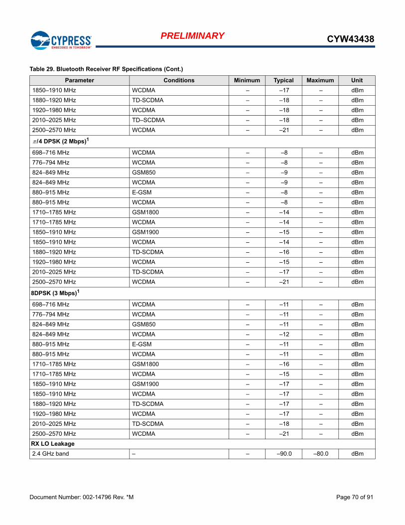
Document Number: 002-14796 Rev. *M Page 70 of 91
PRELIMINARY CYW43438
1850–1910 MHz WCDMA – –17 – dBm
1880–1920 MHz TD-SCDMA – –18 – dBm
1920–1980 MHz WCDMA – –18 – dBm
2010–2025 MHz TD–SCDMA – –18 – dBm
2500–2570 MHz WCDMA – –21 – dBm
/4 DPSK (2 Mbps)1
698–716 MHz WCDMA – –8 – dBm
776–794 MHz WCDMA – –8 – dBm
824–849 MHz GSM850 – –9 – dBm
824–849 MHz WCDMA – –9 – dBm
880–915 MHz E-GSM – –8 – dBm
880–915 MHz WCDMA – –8 – dBm
1710–1785 MHz GSM1800 – –14 – dBm
1710–1785 MHz WCDMA – –14 – dBm
1850–1910 MHz GSM1900 – –15 – dBm
1850–1910 MHz WCDMA – –14 – dBm
1880–1920 MHz TD-SCDMA – –16 – dBm
1920–1980 MHz WCDMA – –15 – dBm
2010–2025 MHz TD-SCDMA – –17 – dBm
2500–2570 MHz WCDMA – –21 – dBm
8DPSK (3 Mbps)1
698–716 MHz WCDMA – –11 – dBm
776–794 MHz WCDMA – –11 – dBm
824–849 MHz GSM850 – –11 – dBm
824–849 MHz WCDMA – –12 – dBm
880–915 MHz E-GSM – –11 – dBm
880–915 MHz WCDMA – –11 – dBm
1710–1785 MHz GSM1800 – –16 – dBm
1710–1785 MHz WCDMA – –15 – dBm
1850–1910 MHz GSM1900 – –17 – dBm
1850–1910 MHz WCDMA – –17 – dBm
1880–1920 MHz TD-SCDMA – –17 – dBm
1920–1980 MHz WCDMA – –17 – dBm
2010–2025 MHz TD-SCDMA – –18 – dBm
2500–2570 MHz WCDMA – –21 – dBm
RX LO Leakage
2.4 GHz band – – –90.0 –80.0 dBm
Table 29. Bluetooth Receiver RF Specifications (Cont.)
Parameter Conditions Minimum Typical Maximum Unit
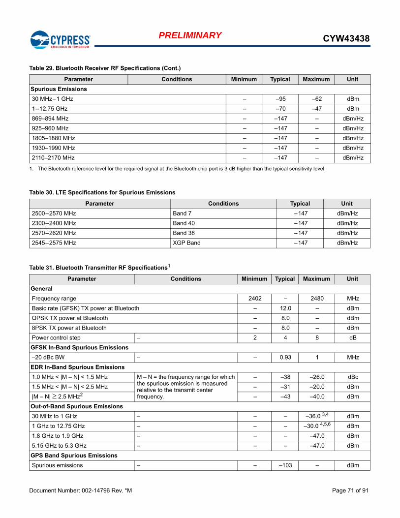
Document Number: 002-14796 Rev. *M Page 71 of 91
PRELIMINARY CYW43438
Spurious Emissions
30 MHz–1 GHz – –95 –62 dBm
1–12.75 GHz – –70 –47 dBm
869–894 MHz – –147 – dBm/Hz
925–960 MHz – –147 – dBm/Hz
1805–1880 MHz – –147 – dBm/Hz
1930–1990 MHz – –147 – dBm/Hz
2110–2170 MHz – –147 – dBm/Hz
1. The Bluetooth reference level for the required signal at the Bluetooth chip port is 3 dB higher than the typical sensitivity level.
Table 30. LTE Specifications for Spurious Emissions
Parameter Conditions Typical Unit
2500–2570 MHz Band 7 –147 dBm/Hz
2300–2400 MHz Band 40 –147 dBm/Hz
2570–2620 MHz Band 38 –147 dBm/Hz
2545–2575 MHz XGP Band –147 dBm/Hz
Table 31. Bluetooth Transmitter RF Specifications1
Parameter Conditions Minimum Typical Maximum Unit
General
Frequency range 2402 – 2480 MHz
Basic rate (GFSK) TX power at Bluetooth – 12.0 – dBm
QPSK TX power at Bluetooth – 8.0 – dBm
8PSK TX power at Bluetooth – 8.0 – dBm
Power control step – 2 4 8 dB
GFSK In-Band Spurious Emissions
–20 dBc BW – – 0.93 1 MHz
EDR In-Band Spurious Emissions
1.0 MHz < |M – N| < 1.5 MHz M – N = the frequency range for which the spurious emission is measured relative to the transmit center frequency.
– –38 –26.0 dBc
1.5 MHz < |M – N| < 2.5 MHz – –31 –20.0 dBm
|M – N| 2.5 MHz2 – –43 –40.0 dBm
Out-of-Band Spurious Emissions
30 MHz to 1 GHz – – – –36.0 3,4 dBm
1 GHz to 12.75 GHz – – – –30.0 4,5,6 dBm
1.8 GHz to 1.9 GHz – – – –47.0 dBm
5.15 GHz to 5.3 GHz – – – –47.0 dBm
GPS Band Spurious Emissions
Spurious emissions – – –103 – dBm
Table 29. Bluetooth Receiver RF Specifications (Cont.)
Parameter Conditions Minimum Typical Maximum Unit

Document Number: 002-14796 Rev. *M Page 72 of 91
PRELIMINARY CYW43438
Out-of-Band Noise Floor7
65–108 MHz FM RX – –147 – dBm/Hz
776–794 MHz CDMA2000 – –146 – dBm/Hz
869–960 MHz cdmaOne, GSM850 – –146 – dBm/Hz
925–960 MHz E-GSM – –146 – dBm/Hz
1570–1580 MHz GPS – –146 – dBm/Hz
1805–1880 MHz GSM1800 – –144 – dBm/Hz
1930–1990 MHz GSM1900, cdmaOne, WCDMA – –143 – dBm/Hz
2110–2170 MHz WCDMA – –137 – dBm/Hz
1. Unless otherwise specified, the specifications in this table apply at the chip output port, and output power specifications are with the temperature correction algorithm and TSSI enabled.
2. Typically measured at an offset of ±3 MHz.3. The maximum value represents the value required for Bluetooth qualification as defined in the 5.1 specification. 4. The spurious emissions during Idle mode are the same as specified in Table 31.5. Specified at the Bluetooth antenna port.6. Meets this specification using a front-end band-pass filter.7. Transmitted power in cellular and FM bands at the Bluetooth antenna port. See Figure 30 for location of the port.
Table 32. LTE Specifications for Out-of-Band Noise Floor
Parameter Conditions Typical Unit
2500–2570 MHz Band 7 –130 dBm/Hz
2300–2400 MHz Band 40 –130 dBm/Hz
2570–2620 MHz Band 38 –130 dBm/Hz
2545–2575 MHz XGP Band –130 dBm/Hz
Table 33. Local Oscillator Performance
Parameter Minimum Typical Maximum Unit
LO Performance
Lock time – 72 – s
Initial carrier frequency tolerance – ±25 ±75 kHz
Frequency Drift
DH1 packet – ±8 ±25 kHz
DH3 packet – ±8 ±40 kHz
DH5 packet – ±8 ±40 kHz
Drift rate – 5 20 kHz/50 μs
Frequency Deviation
00001111 sequence in payload1
1. This pattern represents an average deviation in payload.
140 155 175 kHz
10101010 sequence in payload2
2. Pattern represents the maximum deviation in payload for 99.9% of all frequency deviations.
115 140 – kHz
Channel spacing – 1 – MHz
Table 31. Bluetooth Transmitter RF Specifications1 (Cont.)
Parameter Conditions Minimum Typical Maximum Unit

Document Number: 002-14796 Rev. *M Page 73 of 91
PRELIMINARY CYW43438
Table 34. BLE RF Specifications
Parameter Conditions Minimum Typical Maximum Unit
Frequency range – 2402 – 2480 MHz
RX sense1
1. The Bluetooth tester is set so that Dirty TX is on.
GFSK, 0.1% BER, 1 Mbps – –97 – dBm
TX power2
2. BLE TX power can be increased to compensate for front-end losses such as BPF, diplexer, switch, etc.). The output is capped at 12 dBm. The BLE TX power at the antenna port cannot exceed the 10 dBm specification limit.
– – 8.5 – dBm
Mod Char: delta f1 average – 225 255 275 kHz
Mod Char: delta f2 max3
3. At least 99.9% of all delta F2 max. frequency values recorded over 10 packets must be greater than 185 kHz.
– 99.9 – – %
Mod Char: ratio – 0.8 0.95 – %

Document Number: 002-14796 Rev. *M Page 74 of 91
PRELIMINARY CYW43438
17. Internal Regulator Electrical Specifications
Note: Values in this data sheet are design goals and are subject to change based on device characterization results.
Functional operation is not guaranteed outside of the specification limits provided in this section.
17.1 Core Buck Switching Regulator
Table 35. Core Buck Switching Regulator (CBUCK) Specifications
Specification Notes Min. Typ. Max. Units
Input supply voltage (DC) DC voltage range inclusive of disturbances. 2.4 3.6 4.81
1. The maximum continuous voltage is 4.8V. Voltages up to 6.0V for up to 10 seconds, cumulative duration, over the lifetime of the device are allowed. Voltages as high as 5.0V for up to 250 seconds, cumulative duration, over the lifetime of the device are allowed.
V
PWM mode switching frequency CCM, load > 100 mA VBAT = 3.6V. – 4 – MHz
PWM output current – – – 370 mA
Output current limit – – 1400 – mA
Output voltage range Programmable, 30 mV steps.Default = 1.35V. 1.2 1.35 1.5 V
PWM output voltageDC accuracy
Includes load and line regulation.Forced PWM mode. –4 – 4 %
PWM ripple voltage, static
Measure with 20 MHz bandwidth limit.Static load, max. ripple based on VBAT = 3.6V, Vout = 1.35V, Fsw = 4 MHz, 2.2 μH inductor L > 1.05 μH, Cap + Board total-ESR < 20 mΩ, Cout > 1.9 μF, ESL<200 pH
– 7 20 mVpp
PWM mode peak efficiencyPeak efficiency at 200 mA load, inductor DCR = 200 mΩ, VBAT = 3.6V, VOUT = 1.35V – 85 – %
PFM mode efficiency 10 mA load current, inductor DCR = 200 mΩ, VBAT = 3.6V, VOUT = 1.35V
– 77 – %
Start-up time from power down
VDDIO already ON and steady.Time from REG_ON rising edge to CLDO reaching 1.2V
– 400 500 µs
External inductor 0603 size, 2.2 μH ±20%, DCR = 0.2Ω ± 25%
– 2.2 – µH
External output capacitor Ceramic, X5R, 0402, ESR <30 mΩ at 4 MHz, 4.7 μF ±20%, 10V 2.02
2. Minimum capacitor value refers to the residual capacitor value after taking into account the part-to-part tolerance, DC-bias, temperature, and aging.
4.7 103
3. Total capacitance includes those connected at the far end of the active load.
µF
External input capacitorFor SR_VDDBATP5V pin, ceramic, X5R, 0603, ESR < 30 mΩ at 4 MHz, ±4.7 μF ±20%, 10V
0.672 4.7 – µF
Input supply voltage ramp-up time 0 to 4.3V 40 – – µs

Document Number: 002-14796 Rev. *M Page 75 of 91
PRELIMINARY CYW43438
17.2 3.3V LDO (LDO3P3)
Table 36. LDO3P3 Specifications
Specification Notes Min. Typ. Max. Units
Input supply voltage, Vin
Min. = Vo + 0.2V = 3.5V dropout voltage requirement must be met under maximum load for performance specifications.
3.1 3.6 4.81
1. The maximum continuous voltage is 4.8V. Voltages up to 6.0V for up to 10 seconds, cumulative duration, over the lifetime of the device are allowed. Voltages as high as 5.0V for up to 250 seconds, cumulative duration, over the lifetime of the device are allowed.
V
Output current – 0.001 – 450 mA
Nominal output voltage, Vo Default = 3.3V. – 3.3 – V
Dropout voltage At max. load. – – 200 mV
Output voltage DC accuracy Includes line/load regulation. –5 – +5 %
Quiescent current No load – 66 85 µA
Line regulation Vin from (Vo + 0.2V) to 4.8V, max. load – – 3.5 mV/V
Load regulation load from 1 mA to 450 mA – – 0.3 mV/mA
PSRRVin ≥ Vo + 0.2V, Vo = 3.3V, Co = 4.7 µF, Max. load, 100 Hz to 100 kHz
20 – – dB
LDO turn-on time Chip already powered up. – 160 250 µs
External output capacitor, CoCeramic, X5R, 0402,(ESR: 5 mΩ–240 mΩ), ± 10%, 10V 1.02
2. Minimum capacitor value refers to the residual capacitor value after taking into account the part-to-part tolerance, DC-bias, temperature, and aging.
4.7 5.64 µF
External input capacitor
For SR_VDDBATA5V pin (shared with band gap) Ceramic, X5R, 0402, (ESR: 30m-200 mΩ), ± 10%, 10V. Not needed if sharing VBAT capacitor 4.7 µF with SR_VDDBATP5V.
– 4.7 – µF

Document Number: 002-14796 Rev. *M Page 76 of 91
PRELIMINARY CYW43438
17.3 CLDO
Table 37. CLDO Specifications
Specification Notes Min. Typ. Max. Units
Input supply voltage, VinMin. = 1.2 + 0.15V = 1.35V dropout voltage requirement must be met under maximum load. 1.3 1.35 1.5 V
Output current – 0.2 – 200 mA
Output voltage, Vo Programmable in 10 mV steps. Default = 1.2.V 0.95 1.2 1.26 V
Dropout voltage At max. load – – 150 mV
Output voltage DC accuracy Includes line/load regulation –4 – +4 %
Quiescent current No load – 13 – µA
200 mA load – 1.24 – mA
Line regulation Vin from (Vo + 0.15V) to 1.5V, maximum load – – 5 mV/V
Load regulation Load from 1 mA to 300 mA – 0.02 0.05 mV/mA
Leakage current Power down – 5 20 µA
Bypass mode – 1 3 µA
PSRR @1 kHz, Vin ≥ 1.35V, Co = 4.7 µF 20 – – dB
Start-up time of PMUVDDIO up and steady. Time from the REG_ON rising edge to the CLDO reaching 1.2V.
– – 700 µs
LDO turn-on time LDO turn-on time when rest of the chip is up. – 140 180 µs
External output capacitor, Co Total ESR: 5 mΩ–240 mΩ 1.11
1. Minimum capacitor value refers to the residual capacitor value after taking into account the part-to-part tolerance, DC-bias, temperature, and aging.
2.2 – µF
External input capacitor Only use an external input capacitor at the VDD_LDO pin if it is not supplied from CBUCK output. – 1 2.2 µF
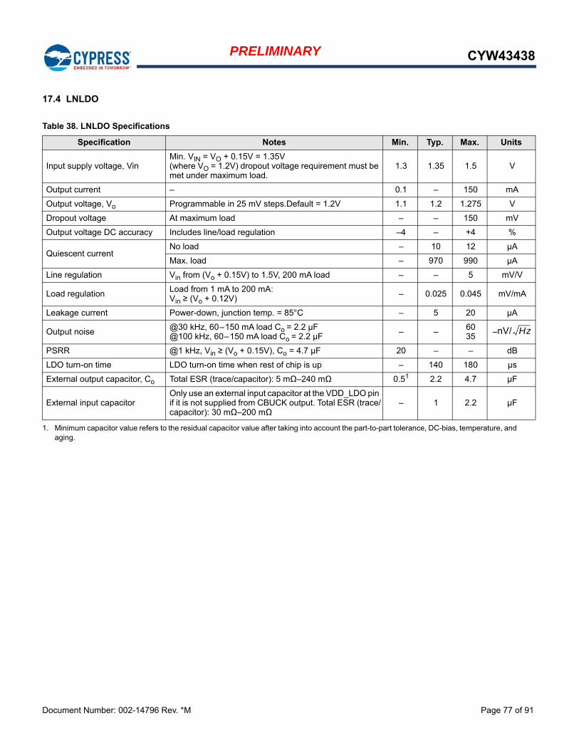
Document Number: 002-14796 Rev. *M Page 77 of 91
PRELIMINARY CYW43438
17.4 LNLDO
Table 38. LNLDO Specifications
Specification Notes Min. Typ. Max. Units
Input supply voltage, VinMin. VIN = VO + 0.15V = 1.35V (where VO = 1.2V) dropout voltage requirement must be met under maximum load.
1.3 1.35 1.5 V
Output current – 0.1 – 150 mA
Output voltage, Vo Programmable in 25 mV steps.Default = 1.2V 1.1 1.2 1.275 V
Dropout voltage At maximum load – – 150 mV
Output voltage DC accuracy Includes line/load regulation –4 – +4 %
Quiescent currentNo load – 10 12 µA
Max. load – 970 990 µA
Line regulation Vin from (Vo + 0.15V) to 1.5V, 200 mA load – – 5 mV/V
Load regulation Load from 1 mA to 200 mA: Vin ≥ (Vo + 0.12V)
– 0.025 0.045 mV/mA
Leakage current Power-down, junction temp. = 85°C – 5 20 µA
Output noise @30 kHz, 60–150 mA load Co = 2.2 µF @100 kHz, 60–150 mA load Co = 2.2 µF – – 60
35 –
PSRR @1 kHz, Vin ≥ (Vo + 0.15V), Co = 4.7 μF 20 – – dB
LDO turn-on time LDO turn-on time when rest of chip is up – 140 180 µs
External output capacitor, Co Total ESR (trace/capacitor): 5 mΩ–240 mΩ 0.51
1. Minimum capacitor value refers to the residual capacitor value after taking into account the part-to-part tolerance, DC-bias, temperature, and aging.
2.2 4.7 µF
External input capacitorOnly use an external input capacitor at the VDD_LDO pin if it is not supplied from CBUCK output. Total ESR (trace/capacitor): 30 mΩ–200 mΩ
– 1 2.2 µF
nV/ Hz

Document Number: 002-14796 Rev. *M Page 78 of 91
PRELIMINARY CYW43438
18. System Power Consumption
Note: The values in this data sheet are design goals and are subject to change based on device characterization.Unless otherwise stated, these values apply for the conditions specified in Table 24: “Recommended Operating Conditions and DC Characteristics” .
18.1 WLAN Current Consumption
Table 39 shows typical currents consumed by the CYW43438’s WLAN section. All values shown are with the Bluetooth core in Reset mode with Bluetooth is OFF.
18.1.1 2.4 GHz Mode
Table 39. 2.4 GHz Mode WLAN Power Consumption
Mode RateVBAT = 3.6V, VDDIO = 1.8V, TA 25°C
VBAT (mA) Vio (μA)
Sleep Modes
Leakage (OFF) N/A 0.0035 0.08
Sleep (idle, unassociated) 1
1. Device is initialized in Sleep mode, but not associated.
N/A 0.0058 80
Sleep (idle, associated, inter-beacons) 2
2. Device is associated, and then enters Power Save mode (idle between beacons).
Rate 1 0.0058 80
IEEE Power Save PM1 DTIM1 (Avg.) 3
3. Beacon interval = 100 ms; beacon duration = 1 ms @ 1 Mbps (Integrated Sleep + wakeup + beacon).
Rate 1 1.05 74
IEEE Power Save PM1 DTIM3 (Avg.) 4
4. Beacon interval = 300 ms; beacon duration = 1 ms @ 1 Mbps (Integrated Sleep + wakeup + beacon).
Rate 1 0.35 86
IEEE Power Save PM2 DTIM1 (Avg.) 3 Rate 1 1.05 74
IEEE Power Save PM2 DTIM3 (Avg.) 4 Rate 1 0.35 86
Active Modes
Rx Listen Mode 5
5. Carrier sense (CCA) when no carrier present.
N/A 37 12
Rx Active (at –50dBm RSSI) 6
6. Tx output power is measured on the chip-out side; duty cycle =100%. Tx Active mode is measured in Packet Engine mode (pseudo-random data)
Rate 1 39 12
Rate 11 40 12
Rate 54 40 12
Rate MCS7 41 12
Tx 6
Rate 1 @ 20 dBm 320 15
Rate 11 @ 18 dBm 290 15
Rate 54 @ 15 dBm 260 15
Rate MCS7 @ 15 dBm 260 15

Document Number: 002-14796 Rev. *M Page 79 of 91
PRELIMINARY CYW43438
18.2 Bluetooth Consumption
The Bluetooth current consumption measurements are shown in Table 40.Note:
The WLAN core is in reset (WLAN_REG_ON = low) for all measurements provided in Table 40.
The BT current consumption numbers are measured based on GFSK TX output power = 10 dBm.
Table 40. Bluetooth Current Consumption
Operating Mode VBAT (VBAT = 3.6V) Typical
VDDIO (VDDIO = 1.8V) Typical Units
Sleep 6 150 μA
Standard 1.28s Inquiry Scan 193 162 μA
500 ms Sniff Master 305 172 μA
DM1/DH1 Master 23.3 – mA
DM3/DH3 Master 28.4 – mA
DM5/DH5 Master 29.1 – mA
3DH5/3DH5 Master 25.1 – mA
SCO HV3 Master 11.8 – mA
BLE Scan1
1. No devices present. A 1.28 second interval with a scan window of 11.25 ms.
187 164 μA
BLE Adv. – Unconnectable 1.00 sec 93 163 μA
BLE Connected 1 sec 71 163 μA
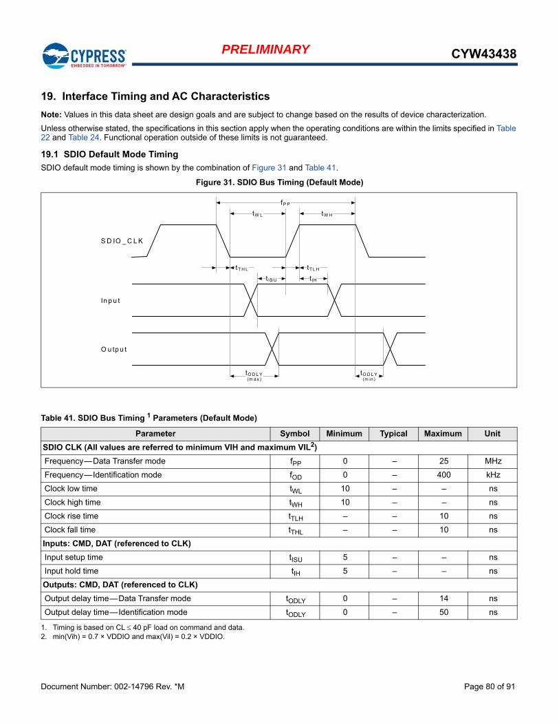
Document Number: 002-14796 Rev. *M Page 80 of 91
PRELIMINARY CYW43438
19. Interface Timing and AC Characteristics
Note: Values in this data sheet are design goals and are subject to change based on the results of device characterization.
Unless otherwise stated, the specifications in this section apply when the operating conditions are within the limits specified in Table 22 and Table 24. Functional operation outside of these limits is not guaranteed.
19.1 SDIO Default Mode Timing
SDIO default mode timing is shown by the combination of Figure 31 and Table 41.
Figure 31. SDIO Bus Timing (Default Mode)
Table 41. SDIO Bus Timing 1 Parameters (Default Mode)
1. Timing is based on CL 40 pF load on command and data.
Parameter Symbol Minimum Typical Maximum Unit
SDIO CLK (All values are referred to minimum VIH and maximum VIL2)
2. min(Vih) = 0.7 × VDDIO and max(Vil) = 0.2 × VDDIO.
Frequency—Data Transfer mode fPP 0 – 25 MHz
Frequency—Identification mode fOD 0 – 400 kHz
Clock low time tWL 10 – – ns
Clock high time tWH 10 – – ns
Clock rise time tTLH – – 10 ns
Clock fall time tTHL – – 10 ns
Inputs: CMD, DAT (referenced to CLK)
Input setup time tISU 5 – – ns
Input hold time tIH 5 – – ns
Outputs: CMD, DAT (referenced to CLK)
Output delay time—Data Transfer mode tODLY 0 – 14 ns
Output delay time—Identification mode tODLY 0 – 50 ns
tW L tW H
fP P
tT H L
t IS U
tT L H
tIH
tO D L Y(m a x )
tO D L Y(m in )
In p u t
O u tp u t
S D IO _ C L K

Document Number: 002-14796 Rev. *M Page 81 of 91
PRELIMINARY CYW43438
19.2 SDIO High-Speed Mode Timing
SDIO high-speed mode timing is shown by the combination of Figure 32 and Table 42.
Figure 32. SDIO Bus Timing (High-Speed Mode)
Table 42. SDIO Bus Timing 1 Parameters (High-Speed Mode)
1. Timing is based on CL 40 pF load on command and data.
Parameter Symbol Minimum Typical Maximum Unit
SDIO CLK (all values are referred to minimum VIH and maximum VIL2)
2. min(Vih) = 0.7 × VDDIO and max(Vil) = 0.2 × VDDIO.
Frequency – Data Transfer Mode fPP 0 – 50 MHz
Frequency – Identification Mode fOD 0 – 400 kHz
Clock low time tWL 7 – – ns
Clock high time tWH 7 – – ns
Clock rise time tTLH – – 3 ns
Clock fall time tTHL – – 3 ns
Inputs: CMD, DAT (referenced to CLK)
Input setup time tISU 6 – – ns
Input hold time tIH 2 – – ns
Outputs: CMD, DAT (referenced to CLK)
Output delay time – Data Transfer Mode tODLY – – 14 ns
Output hold time tOH 2.5 – – ns
Total system capacitance (each line) CL – – 40 pF
tWL tWH
fPP
tTHL
tISU
tTLH
tIH
tODLY
Input
Output
50% VDD
tOH
SDIO_CLK

Document Number: 002-14796 Rev. *M Page 82 of 91
PRELIMINARY CYW43438
19.3 gSPI Signal Timing
The gSPI device always samples data on the rising edge of the clock.
Figure 33. gSPI Timing
19.4 JTAG Timing
Table 43. gSPI Timing Parameters
Parameter Symbol Minimum Maximum Units Note
Clock period T1 20.8 – ns Fmax = 50 MHz
Clock high/low T2/T3 (0.45 × T1) – T4 (0.55 × T1) – T4 ns –
Clock rise/fall time T4/T5 – 2.5 ns –
Input setup time T6 5.0 – ns Setup time, SIMO valid to SPI_CLK active edge
Input hold time T7 5.0 – nsHold time, SPI_CLK active edge to SIMO invalid
Output setup time T8 5.0 – ns Setup time, SOMI valid before SPI_CLK rising
Output hold time T9 5.0 – ns Hold time, SPI_CLK active edge to SOMI invalid
CSX to clock1
1. SPI_CSx remains active for entire duration of gSPI read/write/write_read transaction (that is, overall words for multiple word transaction)
– 7.86 – ns CSX fall to 1st rising edge
Clock to CSXc – – – ns Last falling edge to CSX high
Table 44. JTAG Timing Characteristics
Signal Name Period OutputMaximum
OutputMinimum Setup Hold
TCK 125 ns – – – –
TDI – – – 20 ns 0 ns
TMS – – – 20 ns 0 ns
TDO – 100 ns 0 ns – –
JTAG_TRST 250 ns – – – –
T4 T5
T1
T2
T3
T7T6
T9T8
SPI_CLK
SPI_DIN
SPI_DOUT(falling edge)

Document Number: 002-14796 Rev. *M Page 83 of 91
PRELIMINARY CYW43438
20. Power-Up Sequence and Timing
20.1 Sequencing of Reset and Regulator Control Signals
The CYW43438 has two signals that allow the host to control power consumption by enabling or disabling the Bluetooth, WLAN, and internal regulator blocks. These signals are described below. Additionally, diagrams are provided to indicate proper sequencing of the signals for various operational states (see Figure 34 through Figure 37). The timing values indicated are minimum required values; longer delays are also acceptable.Note:
The WL_REG_ON and BT_REG_ON signals are OR’ed in the CYW43438. The diagrams show both signals going high at the same time (as would be the case if both REG signals were controlled by a single host GPIO). If two independent host GPIOs are used (one for WL_REG_ON and one for BT_REG_ON), then only one of the two signals needs to be high to enable the CYW43438 regulators.
The CYW43438 has an internal power-on reset (POR) circuit. The device will be held in reset for a maximum of 110 ms after VDDC and VDDIO have both passed the POR threshold (see Table 24: “Recommended Operating Conditions and DC Characteristics” ). Wait at least 150 ms after VDDC and VDDIO are available before initiating SDIO accesses.
VBAT and VDDIO should not rise faster than 40 µs. VBAT should be up before or at the same time as VDDIO. VDDIO should not be present first or be held high before VBAT is high.
20.1.1 Description of Control Signals
WL_REG_ON: Used by the PMU to power up the WLAN section. It is also OR-gated with the BT_REG_ON input to control the internal CYW43438 regulators. When this pin is high, the regulators are enabled and the WLAN section is out of reset. When this pin is low the WLAN section is in reset. If both the BT_REG_ON and WL_REG_ON pins are low, the regulators are disabled.
BT_REG_ON: Used by the PMU (OR-gated with WL_REG_ON) to power up the internal CYW43438 regulators. If both the BT_REG_ON and WL_REG_ON pins are low, the regulators are disabled. When this pin is low and WL_REG_ON is high, the BT section is in reset.
Note: For both the WL_REG_ON and BT_REG_ON pins, there should be at least a 10 ms time delay between consecutive toggles (where both signals have been driven low). This is to allow time for the CBUCK regulator to discharge. If this delay is not followed, then there may be a VDDIO in-rush current on the order of 36 mA during the next PMU cold start.

Document Number: 002-14796 Rev. *M Page 84 of 91
PRELIMINARY CYW43438
20.1.2 Control Signal Timing Diagrams
Figure 34. WLAN = ON, Bluetooth = ON
Figure 35. WLAN = OFF, Bluetooth = OFF
32.678 kHz Sleep Clock
VBAT
VDDIO
WL_REG_ON
BT_REG_ON
90% of VH
~ 2 Sleep cycles
32.678 kHzSleep Clock
VBAT
VDDIO
WL_REG_ON
BT_REG_ON
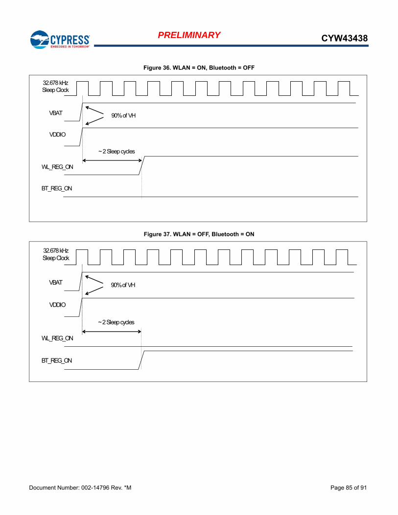
Document Number: 002-14796 Rev. *M Page 85 of 91
PRELIMINARY CYW43438
Figure 36. WLAN = ON, Bluetooth = OFF
Figure 37. WLAN = OFF, Bluetooth = ON
32.678 kHz Sleep Clock
VBAT
VDDIO
WL_REG_ON
BT_REG_ON
90% of VH
~ 2 Sleep cycles
32.678 kHz Sleep Clock
VBAT
VDDIO
WL_REG_ON
BT_REG_ON
90% of VH
~ 2 Sleep cycles

Document Number: 002-14796 Rev. *M Page 86 of 91
PRELIMINARY CYW43438
21. Package Information
21.1 Package Thermal Characteristics
21.1.1 Junction Temperature Estimation and PSI Versus Thetajc
Package thermal characterization parameter PSI-JT (JT) yields a better estimation of actual junction temperature (TJ) versus using the junction-to-case thermal resistance parameter Theta-JC (JC). The reason for this is JC assumes that all the power is dissipated through the top surface of the package case. In actual applications, some of the power is dissipated through the bottom and sides of the package. JT takes into account power dissipated through the top, bottom, and sides of the package. The equation for calculating the device junction temperature is as follows:
TJ = TT + P JT
Where:
TJ = junction temperature at steady-state condition, °C
TT = package case top center temperature at steady-state condition, °C
P = device power dissipation, Watts
JT = package thermal characteristics (no airflow), °C/W
Table 45. Package Thermal Characteristics1
1. No heat sink, TA = 70°C. This is an estimate based on a 4-layer PCB that conforms to EIA/JESD51–7 (101.6 mm x 114.3 mm x 1.6 mm) and P = 1.2W continuous dissipation.
Characteristic Value in Still Air
JA (°C/W) 54.75
JB (°C/W) 15.38
JC (°C/W) 7.16
JT (°C/W) 0.04
JB (°C/W) 14.21
Maximum Junction Temperature Tj (°C)2
2. Absolute junction temperature limits maintained through active thermal monitoring and dynamic TX duty cycle limiting.
125
Maximum Power Dissipation (W) 1.2

Document Number: 002-14796 Rev. *M Page 87 of 91
PRELIMINARY CYW43438
22. Mechanical Information
Figure 38 shows the mechanical drawing for the CYW43438 WLBGA package.
Figure 38. 63-Ball WLBGA Mechanical Information
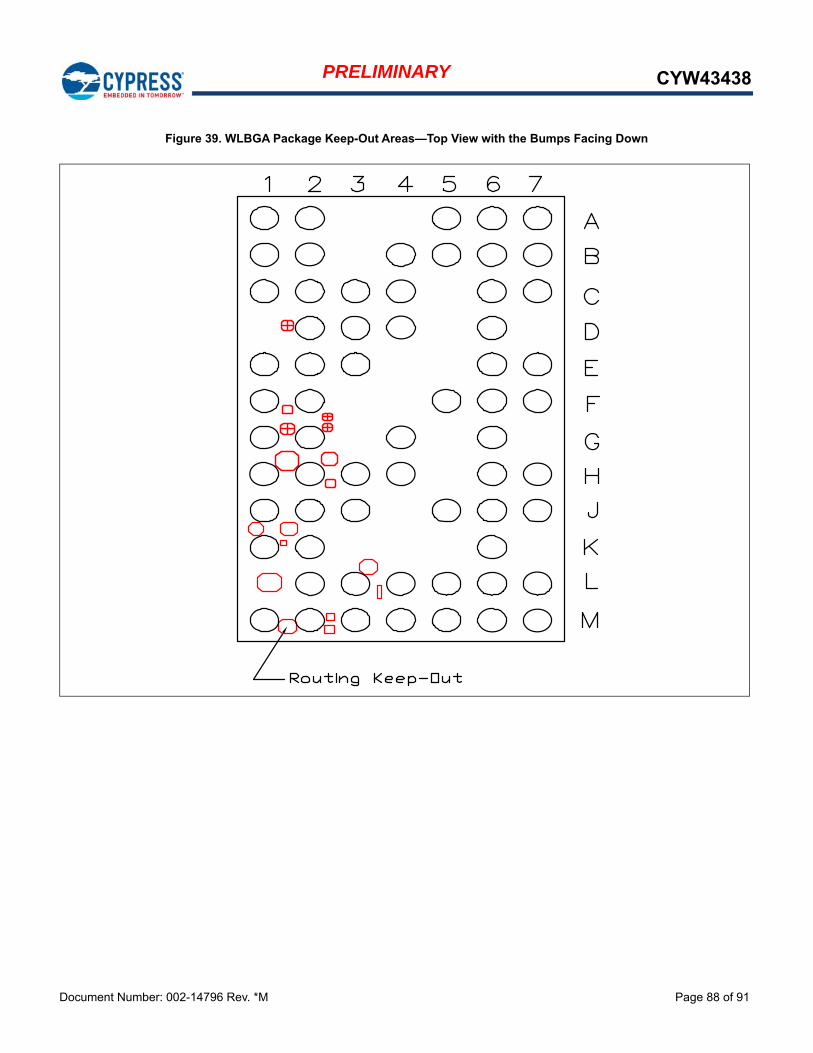
Document Number: 002-14796 Rev. *M Page 88 of 91
PRELIMINARY CYW43438
Figure 39. WLBGA Package Keep-Out Areas—Top View with the Bumps Facing Down

Document Number: 002-14796 Rev. *M Page 89 of 91
PRELIMINARY CYW43438
23. Ordering Information
Table 46. Part Ordering Information
Part Number 1
1. Add “T” to the end of the part number to specify “Tape and Reel.”
26. Additional Information
26.1 Acronyms and Abbreviations
In most cases, acronyms and abbreviations are defined upon first use. For a more complete list of acronyms and other terms used in Cypress documents, go to: http://www.cypress.com/glossary.
26.2 IoT Resources
Cypress provides a wealth of data at http://www.cypress.com/internet-things-iot to help you to select the right IoT device for your design, and quickly and effectively integrate the device into your design. Cypress provides customer access to a wide range of information, including technical documentation, schematic diagrams, product bill of materials, PCB layout information, and software updates. Customers can acquire technical documentation and software from the Cypress Support Community website (http://community.cypress.com/).
Package Description Operating Ambi-ent Temperature
CYW43438KUBG 63-ball WLBGA halogen-free package(4.87 mm x 2.87 mm, 0.40 pitch)
2.4 GHz single-band WLAN IEEE 802.11n + BT 5.1 compliance –30°C to +70°C
Document Number: 002-14796 Rev. *M Page 90 of 91
PRELIMINARY CYW43438
Document History
Document Title: CYW43438 Single-Chip IEEE 802.11 b/g/n MAC/Baseband/Radio with Integrated Bluetooth 5.1 Compliance Document Number: 002-14796
Revision ECN Submission Date Description of Change
** - 3/18/201443438-DS100-R
Initial release
*A - 4/07/201443438-DS101-R
Refer to the earlier release for detailed revision history.
*B - 4/18/201443438-DS102-R
Refer to the earlier release for detailed revision history.
*C - 6/09/201443438-DS103-R
Refer to the earlier release for detailed revision history.
*D - 09/05/201443438-DS104-R
Refer to the earlier release for detailed revision history.
*E - 10/03/201443438-DS105-R
Refer to the earlier release for detailed revision history.
*F - 01/12/201543438-DS106-R
Refer to the earlier release for detailed revision history.
*G - 07/01/2015
43438-DS107-R• Updated:• Table 20, “I/O States” .• Table 23, “ESD Specifications” .• Table 26, “WLAN 2.4 GHz Receiver Performance Specifications” .• Table 27, “WLAN 2.4 GHz Transmitter Performance Specifications” .• Table 35, “FM Receiver Specifications” .• Table 39, “2.4 GHz Mode WLAN Power Consumption” .
*H - 08/24/2015
43438-DS108-R• Updated:• Figure 3: “Typical Power Topology (1 of 2),” on page 9 (43438) on page 16 and• Figure 4: “Typical Power Topology (2 of 2),” on page 10 (43438) on page 16.• Table 3, “Crystal Oscillator and External Clock Requirements and Performance” .• Table 20, “I/O States” .
*I 5451420 10/04/2016Added Cypress Part Numbering Scheme and Mapping Table on Page 1.Updated to Cypress template.
*J 5600128 01/24/2017 Updated Figure 3
*K 5734075 05/11/2017 Updated Cypress logo and Copyright information.
*L 6259072 7/24/2018
Updated the title as “Single-Chip IEEE 802.11 b/g/n MAC/Baseband/Radio with Integrated Bluetooth 4.2 “.Replaced “Bluetooth 4.1” with “Bluetooth 4.2” in all instances across the document.Removed FM related contents from the document.
*M 6276274 04/16/2020
Replaced Bluetooth 4.1 and 4.2 with “Bluetooth 5.1 compliance”.Replaced the title as “Single-Chip IEEE 802.11 b/g/n MAC/Baseband/Radio with Integrated Bluetooth 5.1 Compliance”.Replaced “LTE IC” with “External IC” in the section External Coexistence Interface on page 47.

Document Number: 002-14796 Rev. *M Revised April 16, 2020 Page 91 of 91
PRELIMINARY CYW43438
© Cypress Semiconductor Corporation, 2014-2020. This document is the property of Cypress Semiconductor Corporation and its subsidiaries ("Cypress"). This document, including any software orfirmware included or referenced in this document ("Software"), is owned by Cypress under the intellectual property laws and treaties of the United States and other countries worldwide. Cypress reservesall rights under such laws and treaties and does not, except as specifically stated in this paragraph, grant any license under its patents, copyrights, trademarks, or other intellectual property rights. Ifthe Software is not accompanied by a license agreement and you do not otherwise have a written agreement with Cypress governing the use of the Software, then Cypress hereby grants you a personal,non-exclusive, nontransferable license (without the right to sublicense) (1) under its copyright rights in the Software (a) for Software provided in source code form, to modify and reproduce the Softwaresolely for use with Cypress hardware products, only internally within your organization, and (b) to distribute the Software in binary code form externally to end users (either directly or indirectly throughresellers and distributors), solely for use on Cypress hardware product units, and (2) under those claims of Cypress's patents that are infringed by the Software (as provided by Cypress, unmodified)to make, use, distribute, and import the Software solely for use with Cypress hardware products. Any other use, reproduction, modification, translation, or compilation of the Software is prohibited.
TO THE EXTENT PERMITTED BY APPLICABLE LAW, CYPRESS MAKES NO WARRANTY OF ANY KIND, EXPRESS OR IMPLIED, WITH REGARD TO THIS DOCUMENT OR ANY SOFTWAREOR ACCOMPANYING HARDWARE, INCLUDING, BUT NOT LIMITED TO, THE IMPLIED WARRANTIES OF MERCHANTABILITY AND FITNESS FOR A PARTICULAR PURPOSE. No computingdevice can be absolutely secure. Therefore, despite security measures implemented in Cypress hardware or software products, Cypress shall have no liability arising out of any security breach, suchas unauthorized access to or use of a Cypress product. CYPRESS DOES NOT REPRESENT, WARRANT, OR GUARANTEE THAT CYPRESS PRODUCTS, OR SYSTEMS CREATED USINGCYPRESS PRODUCTS, WILL BE FREE FROM CORRUPTION, ATTACK, VIRUSES, INTERFERENCE, HACKING, DATA LOSS OR THEFT, OR OTHER SECURITY INTRUSION (collectively, "SecurityBreach"). Cypress disclaims any liability relating to any Security Breach, and you shall and hereby do release Cypress from any claim, damage, or other liability arising from any Security Breach. Inaddition, the products described in these materials may contain design defects or errors known as errata which may cause the product to deviate from published specifications. To the extent permittedby applicable law, Cypress reserves the right to make changes to this document without further notice. Cypress does not assume any liability arising out of the application or use of any product orcircuit described in this document. Any information provided in this document, including any sample design information or programming code, is provided only for reference purposes. It is the responsibilityof the user of this document to properly design, program, and test the functionality and safety of any application made of this information and any resulting product. "High-Risk Device" means anydevice or system whose failure could cause personal injury, death, or property damage. Examples of High-Risk Devices are weapons, nuclear installations, surgical implants, and other medical devices."Critical Component" means any component of a High-Risk Device whose failure to perform can be reasonably expected to cause, directly or indirectly, the failure of the High-Risk Device, or to affectits safety or effectiveness. Cypress is not liable, in whole or in part, and you shall and hereby do release Cypress from any claim, damage, or other liability arising from any use of a Cypress productas a Critical Component in a High-Risk Device. You shall indemnify and hold Cypress, its directors, officers, employees, agents, affiliates, distributors, and assigns harmless from and against all claims,costs, damages, and expenses, arising out of any claim, including claims for product liability, personal injury or death, or property damage arising from any use of a Cypress product as a CriticalComponent in a High-Risk Device. Cypress products are not intended or authorized for use as a Critical Component in any High-Risk Device except to the limited extent that (i) Cypress's publisheddata sheet for the product explicitly states Cypress has qualified the product for use in a specific High-Risk Device, or (ii) Cypress has given you advance written authorization to use the product as aCritical Component in the specific High-Risk Device and you have signed a separate indemnification agreement.
Cypress, the Cypress logo, Spansion, the Spansion logo, and combinations thereof, WICED, PSoC, CapSense, EZ-USB, F-RAM, and Traveo are trademarks or registered trademarks of Cypress inthe United States and other countries. For a more complete list of Cypress trademarks, visit cypress.com. Other names and brands may be claimed as property of their respective owners.
Sales, Solutions, and Legal Information
Worldwide Sales and Design Support
Cypress maintains a worldwide network of offices, solution centers, manufacturer’s representatives, and distributors. To find the office closest to you, visit us at Cypress Locations.
Products
Arm® Cortex® Microcontrollers cypress.com/arm
Automotive cypress.com/automotive
Clocks & Buffers cypress.com/clocks
Interface cypress.com/interface
Internet of Things cypress.com/iot
Memory cypress.com/memory
Microcontrollers cypress.com/mcu
PSoC cypress.com/psoc
Power Management ICs cypress.com/pmic
Touch Sensing cypress.com/touch
USB Controllers cypress.com/usb
Wireless Connectivity cypress.com/wireless
PSoC® Solutions
PSoC 1 | PSoC 3 | PSoC 4 | PSoC 5LP | PSoC 6 MCU
Cypress Developer Community
Community | Code Examples | Projects | Video | Blogs | Training | Components
Technical Support
cypress.com/support
91


![[] IEEE 1120-2004 - IEEE Guide for the Planning, D(Book Fi org)](https://static.fdokumen.com/doc/165x107/63150fb6511772fe45103298/-ieee-1120-2004-ieee-guide-for-the-planning-dbook-fi-org.jpg)