CXAR/64 & 128 COAXIAL SWITCH MATRIX with IF-11 Control ...
128
CXAR/64 & 128 COAXIAL SWITCH MATRIX with IF-11 Control Module This information is proprietary to CYTEC Corp., and is not to be used, caused to be used, reproduced, published or otherwise used/or disclosed in any way that might be detrimental or compromising to CYTEC Corp.
-
Upload
khangminh22 -
Category
Documents
-
view
3 -
download
0
Transcript of CXAR/64 & 128 COAXIAL SWITCH MATRIX with IF-11 Control ...

CXAR/64 & 128
COAXIAL SWITCH MATRIX
with IF-11 Control Module
This information is proprietary to CYTEC Corp., and is not to be used,
caused to be used, reproduced, published or otherwise used/or disclosed
in any way that might be detrimental or compromising to CYTEC Corp.


CXAR/64 & 128 COAXIAL SWITCH MATRIX
SECT. # DESCRIPTION 1.0 ADDENDUM
2.0 GETTING STARTED 2.1 SHIPPED CONFIGURATION / TYPICAL CONTROL CONNECTIONS
3.0 GENERAL
3.1 CHASSIS DESCRIPTION
3.1.1 CXAR/64 and CXAR/128 MAINFRAME CHASSIS
3.1.2 CXAR/64 and CXAR/128 EXPANSION CHASSIS
3.2 SPECIFICATIONS
3.3 POWER SUPPLY
3.4 FRONT PANEL
3.4.1 LABELING AND PROGRAMMATIC REFERENCES
3.4.2 CP8 LATCHING DISPLAY MODULE
3.4.3 THUMBWHEEL MANUAL CONTROL OPTION
3.4.4 KEYPAD / LCD DISPLAY MANUAL CONTROL OPTION
4.0 CXR SWITCH MODULES
4.1 CXR/8x1-G-50, CXR/4x1-G-50, CXR/8x1-G-75 and CXR/4x1-G-75
4.2 CXR/8x1-GT-50, CXR/4x1-GT-50, CXR/8x1-GT-75 and CXR/4x1-GT-75
4.3 CXR/8x1-2A-N and CXR/8x1-2A-TBNC
4.4 CXR/2x1-FORM A-1 and CXR/2x1-FORM A-2
4.5 CXR/2x1-2C
4.6 CXR/8x1-1S, CXR/4x1-1S, CXR/8x1-1T and CXR/4x1-1T
4.7 CXR/8x1-1HT, CXR/4x1-1HT, CXR/8x1-1HS and CXR/4x1-1HS
4.8 CXR/2x1-G-50 and CXR/2x1-G-75 and CXR/2x1-G-75-F
4.9 CXR/2x1-GT-50 and CXR/2x1-GT-75
4.10 CXR/4x2-G
4.11 CXR/2(4x1)-1P-LL
4.12 CXAR REED RELAY SWITCH MODULE SPECIFICATIONS
4.13 COAXIAL BUS STRIPS
4.14 CXS/8x1-GT-75-BNC, CXS/8x1-GT-75-F, CXS/16x1-GT-75-F
5.0 IF-11 IEEE488/ RS232/LAN CONTROL MODULE
6.0 MAINTENANCE AND WARRANTY


DRAWINGS
DWG. # DESCRIPTION
2-073 THUMBWHEEL MANUAL CONTROL SCHEMATIC
2-101-1 CXR/2x1-FORM A-(1 and 2) SWITCH MODULE SCHEMATIC
2-190-5B POWER SUPPLY DIAGRAM
6-057 LCD KEYPAD MANUAL CONTROL SCHEMATIC
11-14-50 IF-11 CONTROL MODULE SCHEMATIC
12-00-50 CL8 MOTHERBOARD
12-01-50 CP64, 128 AND 256 MOTHERBOARD
12-02-50 CP MAINFRAME ADAPTER CARD
13-00-50 CL8 LATCHING DISPLAY MODULE SCHEMATIC
13-08-50 CP8-VHP DISPLAY MODULE SCHEMATIC
14-02-29 CXBS/2 (2x1 COAXIAL BUS BAR) ASSY
14-03-29 CXBS/3 (3x1 COAXIAL BUS BAR) ASSY
14-04-29 CXBS/4 (4x1 COAXIAL BUS BAR) ASSY
14-05-29 CXBS/8 (8x1 COAXIAL BUS BAR) ASSY
14-06-29 CXBS/16 (16x1 COAXIAL BUS BAR) ASSY
16-00-50 EXPANSION INTERFACE MODULE
16-00-53 EXP. IF-9 ADAPTOR SCHEMATIC
21-00-50 CXR/2x1-2C SWITCH MODULE SCHEMATIC
21-01-50 CXR/2x1-GT-50 SWITCH MODULE SCHEMATIC
21-02-50 CXR/8x1-2A-(N and TBNC) SWITCH MODULE SCHEMATIC
21-13-50 CXR/2(4x1)-1P-LL SWITCH MODULE SCHEMATIC
21-14-50 CXR/8x1-1T SWITCH MODULE SCHEMATIC
21-14-51 CXR/8x1-1S SWITCH MODULE SCHEMATIC
21-14-52 CXR/4x1-1T SWITCH MODULE SCHEMATIC
21-14-53 CXR/4x1-1S SWITCH MODULE SCHEMATIC
21-37-00 CXAR/128 MAINFRAME ASSY
21-18-00 CXAR/128 EXPANSION ASSY
21-24-50 CXR/8x1-1HT and CXR/8x1-1HS SWITCH MODULE SCHEMATIC
21-32-00 CXAR/128 CP MAINFRAME ASSY w/ IF-9 or IF-11
30-10-50-1 CXR/2x1-G-75 SWITCH MODULE SCHEMATIC
30-17-50 CXR/8x1-G-50 and CXR/4x1-G-50 SWITCH MODULE SCHEMATIC
30-18-50 CXR/8x1-G-75 and CXR/4x1-G-75 SWITCH MODULE SCHEMATIC
30-19-50 CXR/8x1-GT-75 and CXR/4x1-GT-75 SWITCH MODULE SCHEMATIC
30-21-50 CXR/4x2-G-50 SWITCH MODULE SCHEMATIC
30-22-50 CXR/4x2-G-75 SWITCH MODULE SCHEMATIC
30-25-50 CXR/2x1-G-50 SWITCH MODULE SCHEMATIC
30-29-50 CXR/8x1-GT-50-HP and CXR/4x1-GT-50-HP SWITCH MODULE SCHEMATIC
30-30-50 CXR/2x1-GT-75 SWITCH MODULE SCHEMATIC
30-31-50 CXR/2x1-G-75-F SWITCH MODULE SCHEMATIC
64-00-50 CXS/8x1-GT-75-BNC SCHEMATIC
64-01-50 CXS/8x1-GT-75-F SCHEMATIC
64-02-50 CXS/16x1-GT-75-F SCHEMATIC (use w/ CLE/16 Display Module Only)


1.0 ADDENDUM
This page is intentionally left blank


2.0 GETTING STARTED
Unpack the unit and make sure it has arrived undamaged. Inspect for dents, bent handles, major scratches
and missing or loose parts. Note that many of the items listed individually on the packing list are already
installed within the chassis, rather than being packed separately.
Compare the Shipped Configuration List@, on the next page, with the included packing slip to verify that all
components and ordered parts have been received. If any purchased items are missing please contact your
Sales Representative at 1-800-346-3117, 585-381-4740 or [email protected]. Utilize the Shipped
Configuration List to identify which drawings and diagrams refer to the specific unit ordered.
Next, set up the chassis on either a bench or rack. The front handles allow the unit to be bolted to a standard
19 inch rack. No special setup tools are needed.
For AC powered units, a Power Cord should be included in the box. Plug one end into the chassis and the
other into a three prong commercial AC outlet. The unit will operate from one of two AC voltage ranges:
100/140 or 200/260. There is a voltage selector fuse block built into the AC input module just below the
plug. The power supply on AC units may or may not be auto-ranging. It is important to set the correct Input
Voltage on the AC input module so that the system is fused correctly. See Section 3.3 below for more
information on setting the voltage.
For DC powered units connect the supplied power cable to the DC Power Distribution Chassis. The
appropriate voltages required will be supplied from this chassis, which has auto-ranging redundant power
supplies.
Install the appropriate remote control cable to the controlling computer: IEEE488, RS232 or UTP Ethernet.
Ethernet Control is optional and may not be included with your unit. This cable is typically not provided by
Cytec.
Turn the unit ON via the toggle switch located on the AC Input Module located at the chassis rear, or for DC
units turn the power on at the DC Power Chassis. The front panel Power LED should illuminate. If the
optional MC-2 Keypad Manual Control has been purchased, the LCD will display “CYTEC Corp. Ready”.
Study the sections of this manual which deal with your control interface (IEEE488, RS232, etc.), as well as
the controlling command syntax. A group of programming examples are included in appendices at the end
of the manual and provide a good structure to work from. Example driver programs may be included on a
disc if requested. Drivers can also be downloaded from Cytec’s web site at: http://www.cytec-
ate.com/support
You should now be able to begin writing useful code. Always write and debug code thoroughly before
hooking up live signals to the matrix! This equipment gives you full control over what is switched to
where and will not prevent you from making potentially harmful connections. That is, nothing in the system
prevents the switching of excessive power, which can damage or destroy the relay contacts or digital
switches.

2.1 SHIPPED CONFIGURATION
Chassis Type: Drwg.#__________
Serial Number:
Configuration:
Power Supply: Drwg.#__________
AC: 110V 220V Selectable Auto-Ranging
Fuse: 0.5 A 1.0 A 2.0 A 3.0 A Other: ___________
Manual Control: Keypad Pushbutton Thumbwheel None
Remote Control: Drwg.#__________
Switch Modules Qty: Drwg.#__________
Switch Modules Qty: Drwg.#__________
Switch Modules Qty: Drwg.#__________
Switch Modules Qty: Drwg.#__________
Switch Modules Qty: Drwg.#__________
Switch Modules Qty: Drwg.#__________
Switch Modules Qty: Drwg.#__________
Signal I/O Module Drwg.#__________
Miscellaneous Module Qty: Drwg.#__________
Miscellaneous Module Qty: Drwg.#__________

3.0 GENERAL
The CXAR Series are Computer Controlled Coaxial Switching Systems designed to be used for 50 or 75 ohm signals. These systems can switch signals ranging from DC to 1.6 GHz, depending on the type of switch modules installed in the chassis (See Section 4.0).
3.1 CHASSIS DESCRIPTION
The CXAR/64 and CXAR/128 include both Mainframe and Expansion chassis. A Mainframe is a single stand alone chassis which may be controlled either remotely via computer or locally via the optional Thumbwheel Manual Control (See Section 3.4.3) or LCD Keypad Manual Control (See Section 3.4.2). One or more Expansion Chassis can be controlled only from a dedicated MESA control chassis.
Refer to the “Shipped Configuration” sheet to determine which of the chassis assembly drawings pertains to the system purchased. This assembly drawing will include the placement and locations of the various modules.
3.1.1 CXAR/64 and CXAR/128 MAINFRAME CHASSIS
A typical CXAR/64 Mainframe can be seen in Drwg. #21-19-00, and a CXAR/128 Mainframe can be seen in Drwg. #21-17-00. The Mainframe is a 19" rack mounting chassis, 15" deep. Chassis height is determined by switch module selection and configuration but is typically either 5.25" or 7.0".
The CXAR Mainframe chassis contains:
(1) CL/128 Motherboard (Section 3.4.2)
(up to 16) CL8 display/driver modules (Section 3.4.2)
(up to) 16 Coaxial Switch Modules (Section 4.0)
(1) Control Module (Section 5.0)
(1) 12 Volt Power Supply (Section 3.3)
(1) 5 Volt Power Supply (Section 3.3)

3.1.2 CXAR/64 and CXAR/128 EXPANSION CHASSIS
An Expansion Chassis differs from the Mainframe in that it can not operate as a stand alone device and must be controlled remotely from a MESA. An example CXAR/64 Expansion chassis can be seen in Drwg. #21-20-00, and a CXAR/128 Expansion can be seen in Drwg. #21-18-00. Similar to the mainframe, the Expansion Chassis is also a 19" rack mounting chassis, 15" deep. Chassis height is determined by switch module selection and configuration but is typically 5.25" or 7.0".
The CXAR Expansion Chassis contains the same components as the CXAR Mainframe with the following exceptions:
The control module is replaced by the Expansion Interface Adaptor Module Drwg. #16-00-50.
There are no dedicated +5V and +12V power supplies. Instead power is supplied by the MESA.
For Expansion Chassis, control signals originate in the MESA Control Mainframe. These signals are routed from the MESA via the supplied Ribbon Expansion Cable to the Interface Connector located on the chassis’ rear panel. The Interface Connector in turn wires to Expansion Interface Adaptor Module located inside the chassis. The Expansion Interface Adaptor Module plugs into the motherboard, serving the same function as a Control Module (See Section 5.0).
3.2 SPECIFICATIONS
Dimensions: 19" Rack Mounting x 5.25", 7", or 8.75" High x 15" Deep
Weight: Maximum weight with full complement of modules less than 25 lbs.
Power: Less than 100 W @ 100-130 Vac or@ 200-260 Vac
Environment:
Operating: 0C to 50C @ 95% Relative Humidity
Storage: -25C to 65C @ 95% Relative Humidity
Capacity: Standard up to 16 Switch Modules
Expansion Capacity: Up to 16 Expansion Units with one MESA Unit
Display: One Power LED and up to 128 Drive Status LED’s
Control Mode: IEEE488 and RS232 standard; Ethernet TCP/IP as an option

3.3 POWER SUPPLY
The CXAR/64 and CXAR/128 Mainframe Chassis utilize two power supplies, one with a regulated +12 volt output for driving the relays and one with a regulated +5 volt output for the logic as shown in Drwg.#2-190-5B.
The CXAR/64 and CXAR/128 Expansion Chassis do not contain any power supplies. For Expansion Chassis, the +5 volts for the logic and the +12 volts for activating the relays are normally supplied from the MESA Controller via the Expansion Interface Module as shown in Drwg. #16-00-50.
The supplies are wired to the Selectable AC Input Module on the rear panel, which also holds the chassis’s ON/OFF Switch. The user can select one of two AC voltage ranges: 110/120 Volts or 220/240 volts AC. The power supplies will operate from 100-140 volts or 200-260 volts at 47-63 Hz. To change the selected voltage, remove the fuse cartridge using a small blade screw driver or a similar tool. Select the desired voltage by matching the arrow on the fuse cartridge to the arrow located on the Input Module’s lower right corner. Replace the fuse cartridge making sure the voltage selection arrow aligns with the arrow located on the Input Module.
Two fuses are held in the fuse cartridge, with 220/240 VAC fused separately from 110/120 VAC. See the “Shipped Configuration” section for fuse sizes.
3.4 FRONT PANEL
The front panels of the CXAR/64 and CXAR/128 have a power LED, up to 128 display LED’s (8 LED’s per CL8) and an optional thumbwheel or LCD manual control.

3.4.1 LABELING AND PROGRAMMATIC REFERENCES
The Front Panel of the CXAR/64 or CXAR/128 chassis is typically labeled to match the chassis’ built-in
switching configuration. Each switch point is assigned a single front panel status LED. Each column of
LED’s represents a logical switch module, and each LED in that column represents a single specific switch
within that module. The LED’s are visible through the panel.
Programmatically, any command references one switch point and its corresponding LED directly.
Commands are of the form: Command, Module, Switch, where:
Command - One letter mnemonic indicating function to be performed (L for Latch, U for
Unlatch, etc.)
Module - An integer specifying the logical module being address. Matches front panel configuration. (
0 - 15 for a 16x8 Matrix, 0 - 31 for a 32x4 matrix, etc.)
Switch - An integer that specifies logical switch being addressed. Also matches front panel labeling
and chassis configuration. (0 - 7 for 16x8 matrix, 0 - 3 for 32x4 matrix, etc.)
Examples:
16(8x1) Independent Multiplexers - “L 0 7"- Latches Module 0, Switch 7
“U 15 0" - Unlatches Module 15, Switch 0
See Section 5.0 for complete programming information.
Note that the Latch command causes the assigned front panel LED to illuminate, indicating that the switch
has been closed. Similarly, the Unlatch command will extinguish a LED if it is already illuminated
(indicating a closed switch has been opened).

3.4.2 CP8 LATCHING/DISPLAY MODULE
The CP8 Module (Drwg. #13-08-50) interfaces between the control bus on the CL/64, 128 & 256
Motherboard and the switch modules. The CP8 includes the logic to select and latch up to eight relays in
either Matrix or Multiplex modes. The output driver has diode suppression and energizes the relay coil via
an LED in parallel with the coil to give a positive indication that the relay is energized.
Additional logic checks whether the relay is energized and returns its Status to the computer.
Matrix/Multiplex Modes
There are two basic modes of operating the modules, either as a Matrix where any number of switches can
be latched, or as a Multiplexer where one and only one switch is latched.
Status Mode
A switch point is addressed for Status return the same way as it is addressed for any other operation (for
example, a Latch). If the switch is energized, a Status of "1" is returned. If de-energized, a "0" is returned.
CL/64, 128 & 256 MOTHERBOARD
This motherboard has 16 slots for the CP8 Latching/Display Modules and one slot for the Control Module,
as shown in Drwg. #12-01-50.
Power, consisting of regulated +12 volts for the relays, +5 volts regulated for the logic and ground, is bussed
to all the module slots. Also bussed to all the CP8 Module slots are the mode controls, which include
Latch/Unlatch, Matrix/Multiplex, Switch Strobe, Status Strobe and Status return.

3.4.3 THUMBWHEEL MANUAL CONTROL OPTION
The Optional Thumbwheel Manual Controls are used in older 11" deep chassis. They are located on the
front panel and are wired as shown on Drwg. #2-073. The controls wire out via a 16 pin DIP connector
which mates with the socket located on the control module.
Local/Remote
There are two front panel LEDs: a green LED marked Remote and a red LED marked Local. When the
>Local= LED is lit, the unit can be operated from the manual controls. When the >Remote= LED is lit, the unit
can only be operated via computer control.
Switch Select
This consists of two thumbwheel switches. The left thumbwheel selects the module and the right hand
thumbwheel selects the switch on that module. For example, a setting of 23 selects switch #3 on module #2,
however, the switch is not energized until after the selection has been Strobed. On the CXM/8x8, the two
thumbwheels select input and output.
Latch/Unlatch
With this control in the Latch position, the switch selected is latched (closed). In the Unlatch position, the
switch selected is unlatched (opened). Switching this control from Latch to Unlatch does not disturb the
status of the matrix, until the strobe button is pushed.
Mtx/Mux
With this switch in the MTX position, any number of switch points can be latched at the same time. In the
MUX position, only one switch point can be latched at any time. Switching between these two positions
does not change the status of the matrix. For example, if the matrix was in the MTX mode and eight
switches were closed, then after switching from MTX to MUX, the eight switches will remain closed until
the Strobe pushbutton is pushed. This will then clear all switches except the one selected by the
thumbwheels.
Strobe
This is a pushbutton which sends the necessary strobe pulse to the matrix to complete the switch and mode
selection indicated by the manual controls.
Clear
There is no single front panel button for clearing the matrix by opening all the switches. Clearing is
achieved by putting the MTX/MUX switch in the MUX position, the Latch/Unlatch switch in the Unlatch
position and then pressing the Strobe pushbutton. This sequence of required operations prevents the unit
from being cleared accidentally.

3.4.4 LCD DISPLAY/KEYPAD MANUAL CONTROL OPTION
The keypad/display option (Drwg.#6-057) supplies manual control from the chassis front panel. Keypad
operation is always enabled at power On but may be disabled by the remote command, >F= (See Section 5.4).
Display
The display shows two lines with sixteen characters per line. The top line displays matrix commands and
numeric entry. The bottom line displays the status of the entry or operation. The display will also show the
last command entered from the remote computer interface when the front panel is enabled.
Keypad
The keypad consists of ten numeric keys, four function keys, a space key and an enter key.
Key Function
0-9 Numeric entries.
space Delimits between numeric entries.
L Latch operation.
U Unlatch operation.
X Multiplex operation.
C Clear operation.
ENTR Execute displayed operation.
Operation
A matrix command key, L, U, X or C, MUST be pressed before numeric keys. Pressing any key except a
matrix command key causes the message Enter Cmd First to be displayed. After pressing a matrix
command key the command and a cursor are displayed. The switchpoint to be operated on may now be
entered with the numeric and space keys. The entry format is the same as described in the MATRIX
OPERATION section and described briefly by the following table:
Command Key Display Line 1 Line 2
L Lat _ Enter Point
U Unl _ Enter Point
X Mux _ Enter Point
C Clr _ Enter Matrix
The numeric keypad now allows selection of the Matrix, Module and Relay to be operated on. Each entry
may be multiple digits and a space must be pressed between selections.
Key Line 1 Line 2
L Lat _ Enter Point
1 Lat 1_
space Lat 1 _
2 Lat 1 2_
3 Lat 1 23_
space Lat 1 23 _
4 Lat 1 23 4_
Number of Entries Leftmost Entry 2nd Entry Rightmost Entry
1 Relay - -
2 Module Relay -
3 Matrix Module Relay

The ENTR key may now be pressed to execute the displayed operation. If the displayed entry is incorrect
or the operation is not desired, pressing any matrix command key will clear the display and restart the entry.
Status Display
After the ENTR key is pressed, the displayed operation is attempted to be executed by the control module.
If the execution is successful, a Point Closed or Point Open message will be displayed on line 2. If the
operation cannot be executed, an error message will be displayed.
Line 2 Message Status
Ready Displayed after power on.
Enter Point The ENTR key has not been pressed, command and selection mode.
Point Closed The selected point was closed.
Point Open The selected point was opened.
Points Open All points opened, Clear operation.
***Err: limits The selected point is outside the programmed size of the matrix.
***Err: entry An incorrect entry was selected.
Front Panel Disable
The remote >F= command allows enabling or disabling front panel operation. If the front panel is disabled,
no operation can be performed from the keypad.
Remote Command Line 1 Line 2
F 0 73 Panel Disabled
F 1 73 Panel Enabled
Contrast and LED Backlight Adjustment
Controls are provided to adjust the LCD contrast and LED backlight level. These controls should need
adjustment only in extremely bright or dim environments or for acute viewing angles. Both LCD and LED
circuits have temperature sensing elements that will automatically adjust the output level for changes in the
ambient temperature.

3.4.4 THUMBWHEEL MANUAL CONTROL OPTION
The Optional Thumbwheel Manual Controls are located on the front panel and are wired as shown on Drwg.
#2-073. The controls wire out via a 16 pin DIP connector which mates with the socket located on the
control module.
Local/Remote
There are two front panel LEDs: a green LED marked Remote and a red LED marked Local. When the
Local= LED is lit, the unit can be operated from the manual controls. When the Remote= LED is lit, the unit
can only be operated via computer control.
Switch Select
This consists of two thumbwheel switches. The left thumbwheel selects the module and the right hand
thumbwheel selects the switch on that module. For example, a setting of 23 selects switch #3 on module #2,
however, the switch is not energized until after the selection has been Strobed. (On the CXM/8x8, the two
thumb wheels select input and output.)
Latch/Unlatch
With this control in the Latch position, the switch selected is latched (closed). In the Unlatch position, the
switch selected is unlatched (opened). Switching this control from Latch to Unlatch does not disturb the
status of the matrix, until the strobe button is pushed.
Mtx/Mux
With this switch in the MTX position, any number of switch points can be latched at the same time. In the
MUX position, only one switch point can be latched at any time. Switching between these two positions
does not change the status of the matrix. For example, if the matrix was in the MTX mode and eight
switches were closed, then after switching from MTX to MUX, the eight switches will remain closed until
the Strobe pushbutton is pushed. This will then clear all switches except the one selected by the thumb
wheels.
Strobe
This is a pushbutton which sends the necessary strobe pulse to the matrix to complete the switch and mode
selection indicated by the manual controls.
Clear
There is no single front panel button for clearing the matrix by opening all the switches. Clearing is
achieved by putting the MTX/MUX switch in the MUX position, the Latch/Unlatch switch in the Unlatch
position and then pressing the Strobe pushbutton. This sequence of required operations prevents the unit
from being cleared accidentally.

4.0 CXR SWITCH MODULES
4.1 CXR/8x1-G-50, CXR/4x1-G-50, CXR/8x1-G-75 and CXR/4x1-G-75
Each CXR/8x1-G-50 module (Drwg.#30-17-50) and CXR/8x1-G-75 module (Drwg.#30-18-50) has seven single pole Form C relays arranged as an 8x1 tree switch multiplexer. The characteristic impedance is either 50 or 75 ohms. These modules are used in high frequency applications, up to approximately 1 GHz. and can be built with BNC, SMA or SMB connectors. The following table illustrates common specifications for the switch module:
CXR/8x1-G-50 and CXR/4x1-G-50 (50 Ohm Modules)
Bandpass (with SMA connectors): 1.6 GHz (-3 dB)
Isolation (with BNC or SMA connectors): -50 dB @ 1 GHz
Bandpass (with BNC connectors): 1.0 GHz (-3 dB)
CXR/8x1-G-75 and CXR/4x1-G-75 (75 Ohm Modules)
Bandpass (with SMB or BNC connectors): 1.2 GHz (-3 dB)
Isolation (with SMB or BNC connectors): -60 dB @ 1 GHz
Channel #0 is Normally Closed and is connected to the Common when the module is unenergized or when Drive #0 is latched. Channels #1 through #7 individually connect to Common when latched. Two (or more) channels can never be connected simultaneously. The relay control tables on the drawings indicate which relays are energized when a specific channel is latched (closed). Diodes on the modules or drive adaptor board ensure that the proper relays are selected for each channel. This module is available with SMA or BNC connectors, and it may be cut for 4x1 operation.
The format for the CXR/8x1-G Switch Module part number is:
CXR/8x1-G-Impedance-Connector
Impedance- Indicates 50 ohms (-50) or 75 ohms (-75) Characteristic Impedance
Connector- Indicates BNC (-N), SMA (-SMA) or SMB (-SMB) Signal Connectors
Example: The CXR/8x1-G-50-N has a characteristic impedance of 50 ohms and is built with BNC connectors.

4.2 CXR/8x1-GT-50, CXR/4x1-GT-50, CXR/8x1-GT-75 and CXR/4x1-GT-75
Both the CXR/8x1-GT-50 (Drwg. #30-29-50) and the CXR/8x1-GT-75 (Drwg. #30-19-50) are built with
nine single pole and three double pole, high frequency Form C relays arranged as an 8x1 tree switch
multiplexer. The characteristic impedance is either 50 or 75 ohms. These modules have a Form C relay at
each input that connects unlatched channels to terminating resistors. There is no normally closed path. The
following switch module specifications are typical:
CXR/8x1-GT-50 and CXR/4x1-GT-50 (50 Ohm Modules)
Bandpass (with SMA connectors): 1.5 GHz (-3 dB)
Isolation (with BNC or SMA connectors): -60 dB @ 1 GHz
Bandpass (with BNC connectors): 1.0 GHz (-3 dB)
CXR/8x1-GT-75 and CXR/4x1-GT-75 (75 Ohm Modules)
Bandpass (with SMB or BNC connectors): 1.0 GHz (-3 dB)
Isolation (with SMB or BNC connectors): -60 dB @ 1 GHz
Channels #0 through #7 individually connect to the common when energized. Two (or more) channels can
never be connected simultaneously. The relay control tables on the drawings show which relays are
energized when a specific channel is latched (closed). Diode logic on the modules ensures that the proper
relays are selected for each channel. This module is available with SMA, SMB or BNC connectors, and it
may be cut for 4x1 operations.
The part number format for CXR/8x1-GT Switch Modules is:
CXR/8x1-GT-Impedance-Connector
Impedance- Indicates 50 ohms (-50) or 75 ohms (-75) Characteristic Impedance
Connector- Indicates BNC (-N), SMA (-SMA) or SMB (-SMB) Signal Connectors
Example: The CXR/8x1-GT-50-N has a characteristic impedance of 50 ohms and is built with BNC
connectors.

4.3 CXR/8x1-2A-N and CXR/8x1-2A-TBNC
The CXR/8x1-2A switch modules have nine I/O connectors, eight inputs and one common, and are built
with either BNCs or Twin BNCS. The modules use double pole relays that switch both conductors of the
coaxial connectors as shown in Drwg #21-02-50.
When using Twin BNCs, the two inner conductors are switched and the connector shields are bussed to
ground. When BNC connectors are used, both the inner conductor and the shield are switched.
Two additional isolation relays switch the conductors of the COM connector. The isolation relays, K8 and
K9, are open until one of the two pole relays is energized. These modules are typically used to switch
balanced line 100 ohm differential pairs, and may be cut for 4x1 configurations.

4.4 CXR/2x1-FORM A-1 and CXR/2x1-FORM A-2
The CXR/2x1-FORM A module (Drwg.#2-101-1) consists of two Form A single or double pole relays which switch the common connector between either A, B, or OFF. The A Channel is jumper selectable to be driven as channel 0, 2, 4 or 6 while the B channel may be driven from channels 1, 3, 5 or 7. The following table illustrates common switch module specifications:
CXR/2x1-FORM A-1 and CXR/2x1-FORM A-2
Bandpass: 400 MHz (-3dB)
Crosstalk: -60dB @ 5 MHz
The CXR/2x1 is available in single or double pole configurations with standard dry or mercury wetted reeds. The part number format for the CXR/2x1-FORM A Switch Module is:
CXR/2x1-FORM A-#PolesRelayType-Connector Type
These switch modules are built with one of three different relay types, where:
#Poles- Is either 1 or 2.
RelayType- Indicates Standard Dry (-S) or Mercury (-M).
ConnectorType- Indicates BNC (-N), 3 Pin Headers (-H), Twin BNC (-TBNC) or
SMA (-SMA).
Example: A CXR/2x1-FORM A-2S-N is built with double pole Standard Dry Reed Relays and BNC connectors.
Modules built with single pole relays may have either BNC with grounded shields, SMA, or
3 Pin Headers.
Modules built with double pole relays may have either BNC with isolated shields, Twin BNC, or 3 Pin Headers.
4.5 CXR/2x1-C2
The CXR/2x1-C2 module, Drwg#21-00-50, has one Form C relay. The connector labeled NC is connected to the common when the module is in the un-energized state. When the module is latched, the connector labeled NO is connected to the common. The CXR/2x1-C2 is jumper selectable to be driven from one of eight channels allowing up to eight separate CXR/2x1-C2 modules to be driven from a single eight channel driver module. The CXR/2x1-C2 module is 50 Ohm and available with BNC or Twin-BNC or 3-pin header connectors.

4.6 CXR/8x1-1S, CXR/4x1-1S, CXR/8x1-1T and CXR/4x1-1T
The CXR/8x1-1S (Drwg.#21-14-51) and CXR/4x1-1S (Drwg.#21-14-53) Switch Modules function as
single pole 8x1 and 4x1 multiplexers. These modules have Single Pole Form A Dry Reed Relays located at
each input. Form A Relays typically have superior isolation when compared to their Form C counterparts.
Connector options are limited to either 50 or 75 ohm BNC connectors.
The CXR/8-1T (Drwg.#21-14-50) and CXR/4-1T (Drwg.#21-14-52) function the same as the two switch
modules mentioned above, however these switch modules have Form C relays on each input so that unused
inputs are terminated through resistors. Connector options are limited to either 50 or 75 ohm BNC
connectors. Both styles have isolation relays at the Common connector to improve bandpass. These switch
modules may be built with either 50, 75 or 1K ohm terminating resistors. The part number format for the
CXR/8x1-1T Switch Modules is:
CXR/8x1-1T-Termination Impedance
Termination Impedance- Indicates 50 ohms (-50), 75 ohms (-75) or 1000 ohms (-1K)
Example: The CXR/8x1-1T-50 is a CXR/8x1-1T built with 50 ohm terminating resistors.
The part number format of the CXR/4x1-1T Switch Modules is the same as the CXR/8x1-1T Switch Modules.

4.7 CXR/8x1-1HT, CXR/4x1-1HT, CXR/8x1-1HS and CXR/4x1-1HS
The CXR/8x1-1HT and CXR/4x1-1HT Switch Modules are built with eight (or four) single pole Form C
relays on the inputs. In the unenergized state, the inputs are connected to terminating impedances of 50, 75
or 1K ohms. A second set of eight (or four) Form C relays make up the Isolation Relays, and in the
unenergized state these relays connect the input Form C relay Normally Open contact to ground. This shorts
any leakage from the input Form C relay to ground and gives complete isolation to the output. When the
relays are energized, the terminating impedance is disconnected and the input is switched through to the
isolation relay which is connected to the output. Drwg. #21-24-50 (was #2-444-2) shows the Switch
Module in the un-energized state. Connector options are limited to either 50 or 75 ohm BNC connectors.
These switch modules may be built with either 50, 75 or 1K ohm terminating resistors. The part number
format for the CXR/8x1-1T Switch Modules is:
CXR/8x1-1HT-Termination Impedance
Termination Impedance- Indicates 50 ohms (-50), 75 ohms (-75) or 1 kOhm (-1K)
Example: The CXR/8x1-1HT-50 is a CXR/8x1-1HT built with 50 ohm terminating resistors.
The part number format for the CXR/4x1-1HT Switch Modules is the same as the CXR/8x1-1HT Switch
Modules.
The CXR/8x1-1HS and CXR/4x1-1HS Switch Modules are similar to the CXR/8x1-1HS and CXR/4x1-
1HS counterparts. However, eight (or four) single pole Form A relays are placed on the inputs instead of
Form C relays, In the unenergized state, the inputs are connected to ground and not a terminating resistor.
Form A Relays typically have superior isolation compared to their Form C counterparts.

4.8 CXR/2x1 SWITCH MODULES
The CXR/2x1 Series Switch Modules (Drwg.#30-25-50, 30-10-50 & 30-31-50) are built with passive reed
relays. Both single and two pole switch modules are available and they can be built with Type S Standard
Dry. The modules are bidirectional, and input and output connectors can be swapped as needed. The
CXR/2x1 jumper selectable to be driven from one of eight channels. Connectors are BNC, SMA or SMB,
and F for the 30-31-10.
#30-25-10 is a 50 Ohm Module.
#30-10-10 is a 75 Ohm Module.
#30-31-10 is a 75 Ohm Module with F connectors.
Common specifications when used as individual switch modules are:
CXR/2x1
Bandpass: 400 MHz (-3dB)
Isolation: -60dB @ 5 MHz
The CXR/2x1-G Switch Module part number format is:
CXR/2x1-#PolesRelayType-BNC
#Poles Specifies One (-1) or Two (-2) Poles Switched
Connector Type- Indicates BNC (-N), 3 Pin Headers (-H), Twin BNC (-TBNC) or
SMA (-SMA).
Example: The CXR/2x1-BNC is a two pole switch built with BNC connectors.

4.9 CXR/2x1-GT-50 and CXR/2x1-GT-75
The CXR/2x1-GT-50, Drwg#21-01-50, and the CXR/2x1-GT-75, Drwg#30-30-50, terminated switch
modules have two Form C coaxial relays. The following table illustrates common switch module
specifications:
CXR/2x1-GT-50 (50 Ohm Modules)
Bandpass (with SMA, SMB or BNC connectors): 2 GHz (-3dB)
Isolation (with SMA, SMB or BNC connectors): -50dB @ 1GHz
CXR/2x1-GT-75 (75 Ohm Modules)
Bandpass (with SMB or BNC connectors): 1.5 GHz (-3dB)
Isolation (with SMB or BNC connectors): -50dB @ 1.6GHz
The connectors labeled A and B are terminated into 50 ohms or 75 ohms when the module is in the
unenergized state. The CXR/2x1-G is jumper selectable to be driven from two of eight drive channels. The
CXR/2x1-GT is jumper selectable to be driven from two of eight channels. Depending on the jumper
settings, connector A is connected to COM when an even numbered drive is energized, and or connector B
is connected to COM when an odd numbered drive is energized. Refer to Drwg#21-01-50 for exact jumper
configuration. This module is available with SMA or BNC connectors.
The CXR/2x1-GT Switch Modules part number format is:
CXR/2x1-GT-Relay Impedance-Connector Type
Impedance- (-50) indicates 50 ohms or (-75) indicates 75 ohms
Connector Type- Indicates BNC (-N), SMA (-SMA) or SMB (-SMB).
Example: A CXR/2x1-GT-75-N has a characteristic impedance of 75 ohms and is built with BNC
connectors.
4.10 CXR/4x2-G
The CXG/4x2-1G module is built with ten single pole, high frequency Form C relays arranged as a 4x2 tree
switch as shown in Drwg.#30-21-50 (50 Ohm Module) and Drwg#30-22-50 (75 Ohm Module). The
following table illustrates common specifications:
CXR/4x2-G-50 (50 Ohm Module)
Bandpass (with SMA connectors): 2.1 GHz (-3dB)
Isolation (with SMA connectors): -60dB @ 2 GHz
CXR/4x2-G-75 (75 Ohm Module)
Bandpass (with SMB or BNC connectors): 1 GHz (-3dB)
Isolation (with SMB or BNC connectors): -60dB @ 1 GHz
Any of four inputs can individually be connected to either of two outputs. Input #0 is connected to Output
#0 when no channel is latched or when Channel 0,5, 6, or 7 is latched. Latching any other channel will
break the Input #0 to Output #0 connection. The table below shows which input/output pair is selected
when a specific drive is energized.
Channel Input Output
0 0 0
1 1 0
2 2 0
3 3 0
4 0 1
5 1 1
6 2 1
7 3 1
No input can be simultaneously latched to both outputs; however, it is possible to close two separate parallel
switch paths. This module is available with 50 or 75 ohm relays and SMA, SMB or BNC connectors.
The CXR/4x2-G Switch Modules part number format is:
CXR/4x2-G-Relay Impedance-Connector Type
Relay Impedance- (-50) indicates 50 ohms or (-75) indicates 75 ohms
Connector Type- Indicates BNC (-N), SMA (-SMA) or SMB (-SMB).
Example: A CXR/4x2-G-50-SMA has a characteristic impedance of 50 ohms and is built with SMA
connectors.

4.11 CXR/2(4x1)-1P-LL
The CXR/2(4x1)-1P-LL Switch Module, Drwg. #21-13-50, is intended for high insulation resistance
measurements or the switching of low currents, down to Femtoamps. The module is built with shielded, low
leakage relays, and all signal lines have Faraday Shields. The dual output Commons utilizes isolation relays
to further minimize leakage. The two Commons also allow multiple switch modules to be interconnected to
supply larger Nx1 multiplexers. Connector options are BNC (CXR/2(4x1)-1P-LL-BNC) or Triax
(CXR/2(4x1)-1P-LL-TRIAX). Jumper positions provide for Grounded Guard, Isolated Guard or Driven
Guard, as specified by the end user.
APPLICATIONS:
High Speed Driven Guard Testing – In this application, the outer conductor of the BNC or inner
concentric conductor of the Triax connector are driven to the test voltage to reduce the charge time on the
capacitance of the coaxial cable and thereby reduce leakage from signal to shield. For these applications, the
relay EMI shield is jumpered to ground, the Faraday shield is connected to the outer BNC or inner
concentric Triax conductor, and the outer conductor of the Triax is taken to chassis ground.
If using BNC connectors in a driven guard application, it is critical to remember that there will be
exposed voltages on the back of the chassis that could cause severe injury.
Low Noise – Recommended connector is Triax. The inner conductor is used to switch signals. The inner
concentric conductor of the Triax connector is isolated from both signal and CYTEC chassis ground. This
isolated conductor should only be tied to ground at a single point (usually common to the signal source) and
provides a shield from ground loop currents. The inner concentric is tied common across all of the switch
module connectors. The outer concentric conductor of the triax is tied to chassis ground everywhere
possible. This should be as low a noise and as high quality, a ground as possible. The switch module
Faraday shield and relay EMI shield should all be jumpered to chassis ground.
JUMPERING OPTIONS:
Relay EMI shield – A foil shield protects the relay contacts from noise generated in the relay drive coil. In
almost all applications this shield should be jumpered to chassis ground. Jumper holes are provided which
would allow this shield to be jumpered to the Faraday shield should test data prove this to be a better option
in rare cases.
Relay commons – Two relay commons are provided on each switch module. When left isolated, the
module operates as two separate 4x1 multiplexers. When jumpered together, the module is a single 8x1
multiplexer with dual commons which allows, multiple module to be cabled together to form larger
multiplexers.
Faraday Shield – A Faraday shield is provided on the switch module, mainly for driven guard applications,
but it may be used for other situations where an isolated shield is beneficial. If the isolated guard from the
BNC outer conductor or Triax inner concentric is left unconnected from the Faraday shield, the Faraday
shield should be taken to chassis (earth) ground. There are two holes on the top of the Faraday module
cover near the connectors. 3/4" long #4 screws may be screwed into these holes to connect the faraday
shield to earth ground. A set of screws should have been provided with the chassis. The module will need
to be removed from the chassis to install these screws.
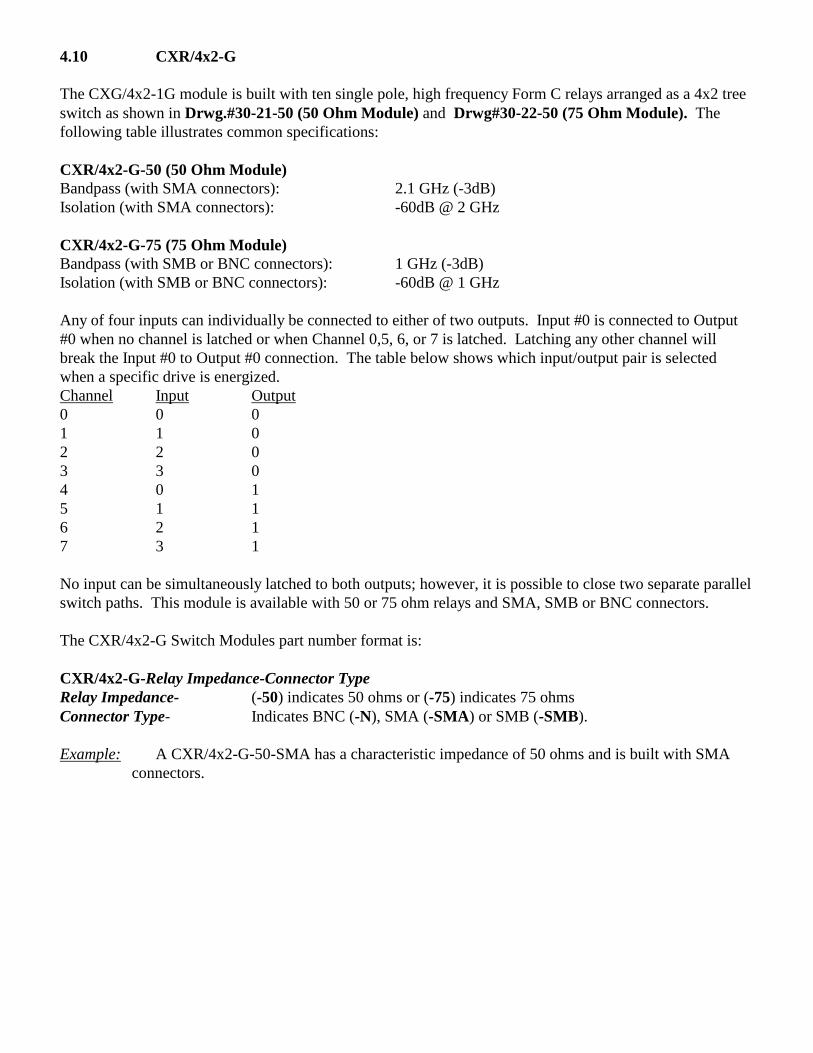
4.12 CXAR SWITCH MODULE SPECIFICATIONS

4.13 COAXIAL BUS STRIPS
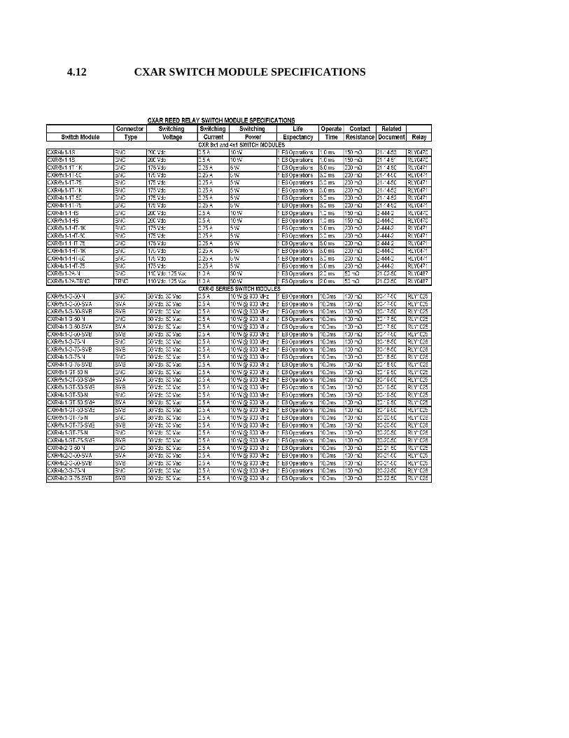
The Coaxial Bus Strips are used to interconnect the Common connectors of CXAR Coaxial Switch Modules, thereby creating larger multiplexers. The Coaxial Bus Strips are designed for maximum bandpass and minimum stub length.
The bus strips are available in the following five sizes :
CXBS/2 (2x1 Bus Bar) Drwg. #14-02-29
CXBS/3 (3x1 Bus Bar) Drwg. #14-03-29
CXBS/4 (4x1 Bus Bar) Drwg. #14-04-29
CXBS/8 (8x1 Bus Bar) Drwg. #14-05-29
CXBS/16 (16x1 Bus Bar) Drwg. #14-06-29
CXBS/8 Bus Bar shown in Drawing Below
NOTE- The Coaxial Bus Strips can not be used with Type G Switch Modules.

4.14 CXR/2x1-C-GT-75
The CXR/2x1-C-GT-75 terminated switch module, Drwg#30-30-50, have three Form C coaxial relays. The
following table illustrates common switch module specifications:
CXR/2x1-C-GT-75 (75 Ohm Modules) Bandpass (with SMB or BNC connectors): 1.4 GHz (-3dB)
Isolation (with SMB or BNC connectors): -60dB @ 1GHz
The connectors labeled NO and NC are terminated into 75 ohms. The CXR/2x1-C-GT is jumper selectable
to be driven from one of eight channels. Refer to Drwg#30-30-50 for exact jumper configuration. This
module is available with SMB or BNC connectors.
The CXR/2x1-C-GT Switch Modules part number format is:
CXR/2x1-C-GT-Relay Impedance-Connector Type Connector Type- Indicates BNC (-N), or SMB (-SMB).
Example: A CXR/2x1-C-GT-75-N has a characteristic impedance of 75 ohms and is built with BNC
connectors.

5.0 IF-11 GPIB / RS232 / LAN CONTROL MODULE
Contents 5.0 Introduction
5.1 RS232 INTERFACE
5.1.1 RS232 INTERFACE I/O CONFIGURATION
5.2 IEEE488 INTERFACE
5.2.1 IEEE488 INTERFACE TALK/LISTEN ADDRESS
5.2.2 IEEE488.2 SPECIFIC MATRIX COMMANDS
5.3 LAN INTERFACE
5.4 COMMAND FORMAT
5.4.1 End of Line Character ( EOL )
5.5 SWITCH COMMANDS
5.5.1 DELAYS TO PREVENT ERRORS
5.5.2 ANSWERBACK CHARACTER
5.5.3 SWITCH CONTROL COMMANDS
5.5.4 STATUS COMMANDS
5.5.4.1 Systems with 8 to 32 relays drives possible.
5.5.4.2 Systems with 64 to 512 relay drives possible.
5.5.4.3 RJV systems which are unique.
5.5.4.4 Large Matrix systems with over 512 switch points or solid state matrix systems.
5.5.5 INTERROGATE COMMAND
5.6 INPUT / OUTPUT vs MODULE / SWITCH NOMENCLATURE
5.7 MATRIX COMMAND SUMMARY
5.8 IF-9 / IF-11 (RS232/LAN/GPIB) DEFAULT CONFIGURATION SETTINGS
5.9 LCD DISPLAY/KEYPAD MANUAL CONTROL OPTION
APPENDIX B - QBASIC Program Example for RS232
APPENDIX C - Turbo C Program Example for IEEE488
APPENDIX E – C Program Example for LAN
APPENDIX F – Support Links
Cautions: 1) Cytec allows the user complete control over the switches and there is nothing built into the firmware
that prevents you from connecting things that shouldn’t be connected. You should always become
familiar with the switch and test your code without any live signals connected! Systems that switch
high voltage, high current, power supplies or high frequency signals are especially dangerous
since connecting the wrong things can result in damage to the switch, damage to other pieces of
expensive equipment, or personal injury to you or others!
2) Microwave relay systems present a particular problem since they will often allow you to turn on
more than one channel on a specific multi-port relay. In normal use, this would create a problem
since the relay would no longer maintain characteristic impedance, and the user would most likely
notice. But when testing the system or running code without signals connected this will not be
obvious and no warning will be issued. Many microwave relays will overheat and be damaged if
multiple ports on a single relay are turned on at once. Under certain circumstances this can
happen as quickly as 60 seconds. Please gain an understanding of your system before simply turning
switch points on and off!

Introduction
CYTEC's IF-11 RS232/LAN Control Module, Drwg. #11-14-50, is designed to control single chassis
mainframes. Three forms of control are available on the module: IEEE488 ( GPIB ), RS232 and Ethernet
LAN as well as an optional manual control. All four interfaces may be active and used simultaneously.
Interface options: GPIB, RS232 and LAN are standard but the Manual Control must be specified when
purchasing the system. On some systems where panel space is limited, only two of the three interface
connectors may be included.
Non-volatile RAM
The control module contains non-volatile memory allowing the system to be configured for various matrix
addressing combinations. Interface controls for Baud Rate, Answerback, Echo, Verbose, TCP/IP, Netmask
and Port numbers are also saved in this memory allowing these functions to be set-up once and then be
restored every time the power is turned on.
Memory Sanitation Procedure
This control module includes a RCM6700 core module which contains volatile and non-volatile RAM. No user
information other than switch configurations and interface settings are stored. If the system is ever removed
from service or needs to be sanitized for disposal all Volatile and Non-Volatile RAM can be erased using one of
the following methods. Refer to Drwg # 11-14-10.
1) Easiest with least damage. Remove cover. Locate IF-11, install Jumper JP1 across the pins. Cycle the
power. All memory will be erased and the system will be set to factory default values. Remove Jumper JP1 and
offset. System can be reset to user values when needed.
2) Permanent. Remove cove. Locate IF-11. Remove the RMC6700 core board by disconnecting the LAN
cable and prying the module off the IF-11 board. Destroy the RMC6700 board. Unit is non functional until
IF-11 has been replaced.

Basic Command Syntax
All commands are composed of alpha characters followed by a series of integer values separated by a white
space character. The alpha characters are not case sensitive and will accept whitespace or no whitespace
between the alpha characters and the first integer value.
There are two types of commands:
1) Set-up and Parameter commands which are used to establish control options and configuration set-
ups. Typically, the set-up and parameter commands are only used when you first get the system and
then the switch control commands are used to operate the switch. Some examples include P
commands for system parameters, snet commands for LAN set-up and E command for turning
RS232 Echo on and off. The integer value 73 is often used as an access control value on set-up
commands to prevent inadvertent or unintentional commands from being processed.
Examples:
P6 0 73 Turn off hardware handshaking for RS232 control.
Snettcpport 0 8088 set-up port number for TCP/IP socket 0.
2) Switch Control commands cause actions to occur at the connected switching system. These are the
commands that are used to control what gets connected to what through the switch. These
commands include L for latch, C for clear, etc..
Examples:
L0 2 17 Latch Matrix #0, Module #2, Switch #17
C 0 Clear all connections in Matrix # 0.
Numeric entries must always be separated from each other by spaces!
Some Cytec programming examples may refer to Mod #, Rly # ( Relay #).
The terms Switch (Sw) and Relay (Rly) mean the same thing.
Multiple commands may be sent as a single string but each command must be separated by a semi colon.
Up to 50 characters are allowed on one line so the number of commands will be dependent on the characters
required. Only the first 15 characters sent will actually show up on the front panel LCD display (if that
option has been included). Cytec does not encourage using this programming technique as it makes status
feedback almost unusable but we do recognize that there are specific instances where this can greatly speed
up operation of the system.
Commands are covered in detail throughout the rest of the Control sections 5.1 through 5.8.

5.1 RS232 INTERFACE
Signal Connections
The control module is pre-configured at the factory to operate as Data Communications Equipment (DCE)
per the EIA RS232D Standard. In this configuration, the module transmits on the RxD Pin and receives on
the TxD Pin. RTS is required to be high for the control module to transmit and CTS is output high by the
control module to indicate a ready for data state and low when busy. Jumpers on the module allow for
reversing the functions of these pins (TxD/RxD, RTS/CTS) and operating as Data Terminal Equipment
(DTE) although there is virtually no practical reason to do this anymore. The RS232 rear panel connector is
a D9P (male) and can be run directly from a D9 computer com port with a straight through (one to one) D9S
to D9S cable. A null modem cable will not work with the factory default settings! Adaptors are available at
any computer store to convert from D25 to D9. Do not use any adaptor that also acts as a null modem
converter. If you are building your own cables, consult CYTEC Corp., for D25 to D9 pin out conversion.
D9P (male) PIN OUTS
Pin Signal Function
1 DCD Control Module provides +V.
2 RxD Data out of Control Module.
3 TxD Data in to Control Module.
4 DTR Data Terminal Ready (not used)
5 Common Signal Ground.
6 DSR Control Module provides +V.
7 RTS Control Module requires + V to transmit.
8 CTS Control Module provides +V when ready
9 RI Ring Indicator (not used)
COM Port Default Values
As delivered from Cytec, the system uses the default Windows Com Port settings shown below:
Bits per second (Baud) 9600
Data bits 8
Parity None
Stop bits 1
Flow control Hardware
Only Baud rate (Bits per second) and Flow Control (Hardware handshaking) can be modified. See Section
5.1.1 for command syntax.

5.1.1 RS232 INTERFACE I/O CONFIGURATION
I/O Configuration
Module #11-14-50
Default values:
Baud Rate 9600
Hardware Handshaking On
Answerback On
Echo Off
Verbose Off
The RS232 interface can be accessed using any standard terminal emulation program such as Hyperterm
(Windows). Connect a one to one D9 female to D9 female cable between the computer and the Cytec
switch.
The first thing you should do is turn on Echo. This will enable you to see what you are typing. Make sure
you turn echo back off when you are done with the terminal session. Echo being left on will normally
interfere with programs written specifically to control the switch.
Echo
Echos the characters back to your screen while you type them so you can see what you type.
Command: “E 0 73” Turns Echo Off
“E 1 73” Turns Echo On
Answerback
Answerback allows the Control Module to return information to the com port. Answerback should almost
always be left on. If Answerback is enabled, the Answerback byte must be read back by the requesting
device. Failure to do so could have unpredictable results.
Command: “A 0 73” Turns Answerback Off
“A 1 73” Turns Answerback On
Verbose
Verbose causes the system to return more specific information when you request status or read answerback
characters. It is sometimes helpful when troubleshooting but it slows the interface down a lot. While there
may occasionally be a good reason to turn on Verbose during a Hyperterm session, it is almost never used in
a programmatic interface. All of the same information could be generated in code based on the non-verbose
responses without slowing down the RS232 interface.
Command: “V 0 73” Turns Verbose Off
“V 1 73” Turns Verbose On

Baud Rate
Baud rate is set at the factory at 9600 Baud. Change is under software control and the control module must
be connected to a serial interface to effect the change.
Baud Baud# n
2400 4
4800 5
9600 6
19200 7
38400 8
57600 9
115200 10
230400 11 (untested, you should consider LAN)
460800 12 (untested, you should consider LAN)
Command: "P19 n 73"
"P19 7 73" sets baud rate to 19200.
If the Baud rate is inadvertently set to an unknown rate, the default value may be restored. See the section
on Setting Defaults for procedure.
Obviously as soon as you reset the Cytec baud rate you will no longer be able to communicate with the
switch until you reset the baud rate on your computer or communication device.
CTS/RTS Handshake
The Clear to Send (CTS) and Request To Send (RTS) hardware handshaking functions may be
modified by the 'P6' command.
Command: "P6 handshake 73"
handshake = 0 Handshaking off
handshake = 1 Handshaking on (default)
Example
"P6 0 73" Turn handshaking off.
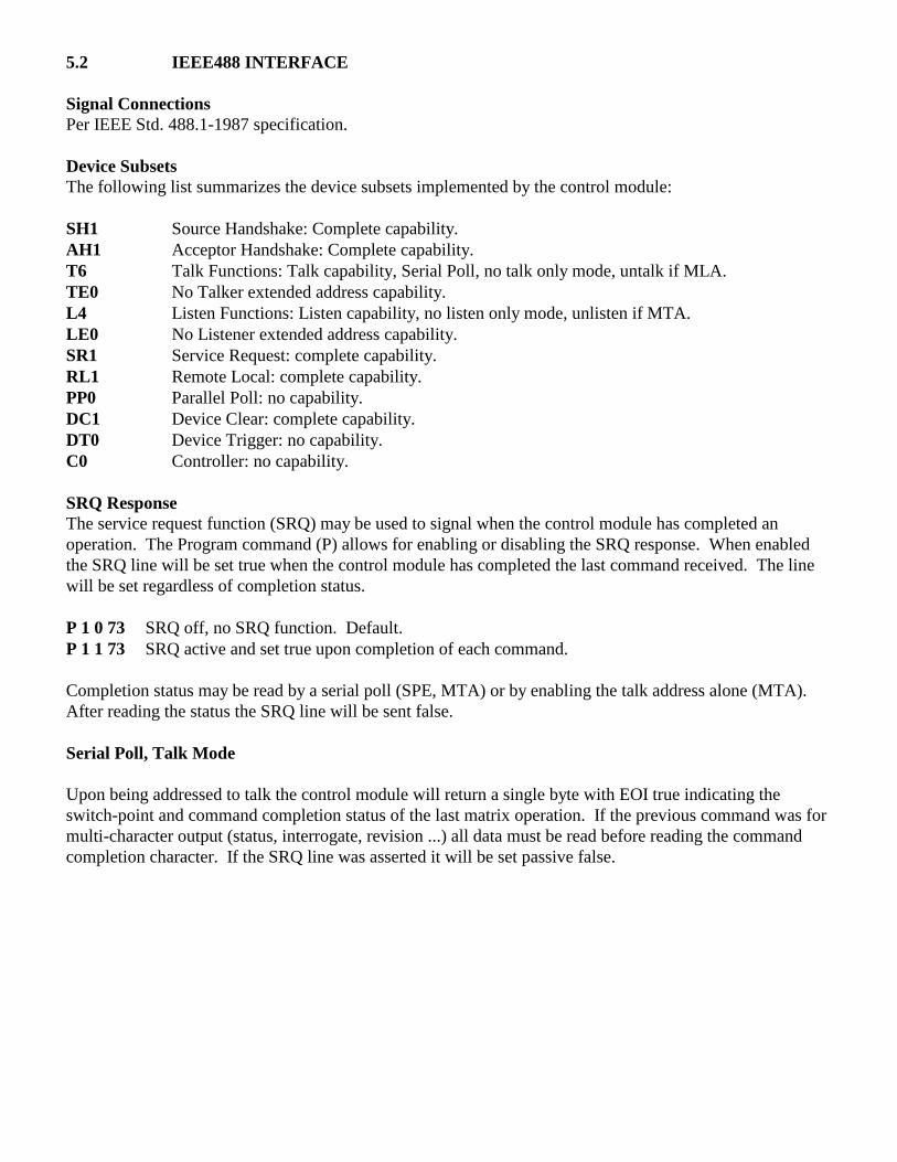
5.2 IEEE488 INTERFACE
Signal Connections
Per IEEE Std. 488.1-1987 specification.
Device Subsets
The following list summarizes the device subsets implemented by the control module:
SH1 Source Handshake: Complete capability.
AH1 Acceptor Handshake: Complete capability.
T6 Talk Functions: Talk capability, Serial Poll, no talk only mode, untalk if MLA.
TE0 No Talker extended address capability.
L4 Listen Functions: Listen capability, no listen only mode, unlisten if MTA.
LE0 No Listener extended address capability.
SR1 Service Request: complete capability.
RL1 Remote Local: complete capability.
PP0 Parallel Poll: no capability.
DC1 Device Clear: complete capability.
DT0 Device Trigger: no capability.
C0 Controller: no capability.
SRQ Response
The service request function (SRQ) may be used to signal when the control module has completed an
operation. The Program command (P) allows for enabling or disabling the SRQ response. When enabled
the SRQ line will be set true when the control module has completed the last command received. The line
will be set regardless of completion status.
P 1 0 73 SRQ off, no SRQ function. Default.
P 1 1 73 SRQ active and set true upon completion of each command.
Completion status may be read by a serial poll (SPE, MTA) or by enabling the talk address alone (MTA).
After reading the status the SRQ line will be sent false.
Serial Poll, Talk Mode
Upon being addressed to talk the control module will return a single byte with EOI true indicating the
switch-point and command completion status of the last matrix operation. If the previous command was for
multi-character output (status, interrogate, revision ...) all data must be read before reading the command
completion character. If the SRQ line was asserted it will be set passive false.

Char
Hex
Completion Status
>0'
30
Successful Operation, switch open.
>1'
31
Successful Operation, switch closed.
>2'
32
Unknown Command, the first character of the command string was
unrecognizable. >3’
33
Incorrect entries, the number or type of entries was incorrect.
>4’
34
Entries out of limits, a switch-point was requested that was outside the
limits of the specified matrix. >5’
35
Invalid access code, the code number 73 was not included or incorrect in a
command requiring the access code or in the wrong entry position.
As above with SRQ true. >p=
70
Success, Switch Open.
>q=
71
Success, Switch Closed.
>r=
72
Unknown Command.
>s’
73
Incorrect entries.
>t’
74
Limits Error.
>u’
75
Access Error.
Remote/Local Operation
The interface responds to the Go To Local (GTL) and Local Lockout (LLO) commands by enabling or
disabling front panel controls. Response to LLO, GTL, and REN signals may be disabled by the Program
command 'P 4 0 73' and enabled by 'P 4 1 73'. Enabling or disabling is stored in non-volatile memory and
will not be affected by turning power off then on. Factory default is disabled.
Device Clear, Selected Device Clear
The interface will respond to both device clear (DCL) and selected device clear (SDC) by clearing any
pending operations, aborting pending output and optionally clearing the control module.
The matrix clear feature may be disabled by the Program command 'P 3 0 73' and enabled by the command
'P 3 1 73'. Enabling or disabling is stored in non-volatile memory and will not be affected by turning power
off then on.

5.2.1 IEEE488 INTERFACE TALK/LISTEN ADDRESS
Talk/Listen Address
Set for P14 Command. See Section 5.6.1 Additional Matrix Programming/Setup, P Command, P14.
5.2.2 IEEE488.2 SPECIFIC MATRIX COMMANDS
These commands are ignored by the RS232 interface.
*IDN? - Revision Number (Same as Cytec “N” - Revision Command)
Syntax: A*IDN?@
The 'IDN?' command will cause the matrix to return its current revision number followed by an end
of line.
Send: "*idn?" Request revision number.
Receive: "Cytec VDX/32x32 11-01-13 1.0" eol Text string indicating revision.
*RST - Reset (same as C - Clear command)
The '*RST' command will clear (open all switches) in the matrix.
Send: "*rst" Reset.
Receive: "0" eol Returns >0'.

5.3 LAN INTERFACE
The Cytec LAN interface is a 10BaseT / 100BaseT auto-ranging Ethernet interface with an RJ45 connector.
A Category 5e or better cable is recommended.
Default settings:
IP Address: 10.0.0.144
Netmask: 255.0.0.0
Gateway 0.0.0.0
Telnet Port: 23
TCP/IP Port 0: 8080
TCP/IP Port 1: 8081
Telnet Lockout: 0 (disabled) Telnet Sessions allowed by default.
Telnet Echo: 0 (disabled) Telnet Sessions do not echo.
TCP Idle 60
The Default LAN settings may be modified by any control port (RS232 or LAN). The most common
methods are:
Telnet to default telnet port 23. Any Telnet program will work. Depending on the program you may have to
turn on Echo to see the commands that you type. Some Telnet programs automatically echo even with ours
turned off. If you turn on Echo, be sure to turn it back off when you are done. Telnet Echo is different from
RS232 Echo.
Telnet via Raw TCP/IP to ports 8080 or 8081. This works the same as above except it will probably never
automatically Echo.
Use Hyperterm, puTTy, Tera Term or any other terminal emulation program to communicate to the RS232
port from a com port on your computer. See section 5.1 for RS232 details.
Use Hyperterm, puTTy, Tera Term or any other terminal emulation program to Telnet to port 23 or speak
Raw TCP/IP to ports 8080 or 8081.

TCP/IP commands
D Display current settings
Typing the letter “d” and hitting enter will return a list of current settings:
A1, E1, V0 % Answerback = ON, Echo = ON, Verbose = OFF%
Baudnumber = 6, RS Handshaking = 1
IP Address = 10.0.0.26
Netmask = 255.255.255.0
Gateway = 0.0.0.0
Port0 = 8080, Port1 = 8081
TCP idle = 600
Telnetlock = 0, Telnet Echo = 0
Battery Ram = 0, Default List = 0
IFCONFIG Set IP Address and Netmask
ifconfig aaa.aaa.aaa.aaa nnn.nnn.nnn.nnn
a = ip address in dotted decimal format
n = subnet mask in dotted decimal format
Example: ifconfig 10.0.0.100 255.0.0.0
Typing ifconfig and hitting the enter key will return the current settings.
Since you may be connected via Telnet to do this, the IP address will not actually change until you
reboot the Cytec switch. This helps prevent anyone from mistakenly setting the IP to an unknown address
by accident. It is a good idea to double check the settings with the D command before you reboot.

SNET TCP PORT Set Port number for TCP/IP sockets
SNET TCP PORT n m where = equals one of two sockets and m is the port number
Example:
snet tcp port 0 8088 socket 0 is port #8088
snet tcp port 1 8089 socket 1 is port #8089
Port numbers must be between 1024 and 65535.
The Telnet port (23) may also be available. See TELNETLOCK command
TELNET LOCK Disable Telnet socket.
TELNETLOCK n where n = 0,1
Example:
telnet lock 0 Connections to Port 23 are allowed
telnet lock 1 Connections to Port 23 are not allowed
TELNET ECHO Echo characters sent to Telnet socket.
TELNET ECHO n where n = 0,1
Example:
telnet echo 0 Character are not echoed back to telnet application
telnet lock 1 Character are echoed back to telnet application
(May cause double characters).
GATEWAY
Hosts xxx.xxx.xxx.xxx // to set gateway
Hosts //display gateway
Gateway = 0.0.0.0

SOCKET LIFE
The LAN Interface uses a program called TCP Tick to tell whether or not the network connection is intact
between the computer that established the socket and the LAN interface. The socket will remain until the
requesting IP address terminates the socket or there is a break in the network connection. Sockets will
automatically terminate after a pre-determined period of inactivity. That period is set by the SNET TCP Idle
commands. Each open socket needs activity to stay alive.
SNET TCP Idle n (n=seconds) (1 to 3600 sec)
Default = 60 sec
SNET TCP Idle (display)
TCP Idle = 60
SNET TCP Idle 0 Socket never dies until the computer that established the socket kills it.
Caution!
Setting the TCP Idle to 0 will force the socket to stay alive until the program that established the socket kills
it. WARNING: This can lead to issues if there is a network disconnect or the computer that established the
socket locks up. If the computer that establishes the socket cannot kill the socket, no one will be able to
connect to the switch until the Cytec unit is rebooted.
TCPAnswerback - Answerback
Syntax: TCPANSWERBACK n n = 0, 1 or 2
Answerback will enable or disable the transmission of a single character followed by an end of line
upon the completion of all commands. The Answerback character will be a 1 or 0 depending on
what command is sent. It is used to verify that the command was accepted and can verify completion
of relay control commands. See Section
Eg. "TCPANSWERBACK 0 " Turn answerback off.
"TCPANSWERBACK 1 " Turn answerback on
"TCPANSWERBACK 2 " Turn answerback plus terminator on
Note: TCPANSWERBACK 2:
This setting appends a set of square brackets to the answerback byte.
Eg. Send: "L0 0" Latch Module 0 Switch 0.
Receive: "1[]" End of line follows the terminator

5.4 COMMAND FORMAT/COMPLETION
COMMAND FORMAT
All commands consist of at least one ASCII character indicating the command followed by optional values.
After the command string is sent, an End of Line Character must be sent to affect the command.
If values are included with the command, the first value does not need to be separated from the command;
all subsequent values MUST be separated by spaces or commas, eg. L1 2.
Multiple commands may also be sent on one line. Commands must be separated by a semi-colon character.
Command line length is limited to 19 characters.
Examples: "L2 7;C" Connects Input 2 to Output 7 then clear
"U4 7;L 1 2" Unlatch Mod 4, Sw 7 then Latch Mod 1, Sw 2
COMMAND COMPLETION
A code representing the last requested switch point status (open or closed) and command completion will be
stored by the matrix.
If the LAN or RS232 answerback function is enabled, a single character followed by end of line will be sent
upon completion of all commands. Answerback may also include a termination character. With IEEE488
interfaces enabling the talk address (MTA) will cause the single code byte to be transmitted along with the
END line true. This code is also available by a serial poll. DIO1 will indicate status from the last operation
affecting switch-point status and DIO2 through DIO4 will be the command completion code.
Note: Command Completion is NOT updated until the matrix finishes the requested operation.
Command Completion Codes
Char Hex Completion Status
‘0’ 30 Successful operation, switch open
‘1’ 31 Successful operation, switch closed
‘2’ 32 Unknown command, the first character of the command string was unrecognizable
‘3’ 33 Incorrect entries, the number or type of entries was incorrect
‘4’ 34 Entries out of limits, a switch point was requested that was outside the limits of the specified
matrix
‘5’ 35 Invalid access code, the code number 73 was not included or entered incorrectly
‘6’ 36 Setup error. Incorrect setup parameter

5.4.1 End of Line Character ( EOL )
A received end of line character will cause the control module to execute the ASCII command string. The
end of line character may be sent as a carriage return (CR) or New Line / Line Feed ( NL/LF ) for RS232
interfaces and a New Line / Line Feed ( NL/LF ) for IEEE488 interfaces or LAN interfaces. The IEEE488
also allows for the END control line being true with the last data character to initiate the command.
Valid end of Lines:
CR RS232 only
LF or NL LAN, RS232 or IEEE488
CR and END IEEE488
LF/NL and END IEEE488
DAB and END IEEE488
Note that the terms New Line and Line Feed are often used to mean the same thing.
Both are expressed as \n in most programming languages and are shown on the ASCII table as “LF”.
LF = Line Feed / New Line represented as \n, on ASCII table it is Decimal 10, or Hex A (0xA).
CR = Carriage Return represented as \r, on ASCII table it is = Decimal 13 or Hex D ( 0xD).
When any data is returned from the switch, the data will also be followed by an End Of Line
character (EOL).
RS232:
1. The end of line will be a carriage return with Echo disabled or a carriage return and
line feed if Echo is enabled.
2. If Answerback is enabled, the answerback character and end of line will follow the
status output and then the EOL.
3. If Answerback with terminator is enabled, the answerback and terminator character
will follow the status or interrogate output and then the EOL.
LAN:
1. The end of line character will be a new line ( /n ).
2. If Answerback is enabled, the answerback character and end of line will follow the
status output and then the EOL.
3. If Answerback with terminator is enabled, the answerback and terminator character
will follow the status or interrogate output and then the EOL.
IEEE488:
1. The end of line character will be a line feed.
2. A DCL or SDC command will abort output.
Notes - All Interfaces: Upon requesting status output characters MUST be received by the requesting
device. Failure to do this will prevent further use of the matrix.
Access Code
Some commands require an access code number to be included with the command. This code prevents
inadvertent operation of system modifying commands. The access code is 73.

5.5 SWITCH COMMANDS
General Notes
For LAN and RS232, after sending any command the Cytec control will return an integer Answerback
character if Answerback is ON. Answerback is turned on by default and is Cytec’s preferred operation since
it allows you to verify commands are accepted before continuing.
If the command was a switch operation command such as Latch ( L ) or Unlatch ( U ), the character will be a
meaningful status response where 1 = switch latched and 0 = switch unlatched. This may be used to verify
that the command was received correctly.
Any other commands sent will also generate an answerback character which may be either a 1 or 0 and
either character will indicate the command was received but the value is meaningless so either is acceptable.
Answerback may be turned off when using LAN or RS232 although it is not recommended.
Answerback can also include a termination character for the LAN or RS232 interface.
Error Characters
If a command is sent incorrectly, an error character will be generated and added to the answerback character.
Since the answerback character may be a 1 or 0, there may be two values for error characters as described
below.
Answerback returned:
Dec Hex
0 30 Latch completed without errors.
1 31 Unlatch completed without errors.
2 or 3 32 or 33 Unknown command, first character unrecognizable.
4 or 5 34 or 35 Incorrect entries, number or type of entries incorrect.
6 or 7 36 or 37 Entries out of limits, switch point out of usable range.
8 or 9 38 or 39 Invalid access code, number 73 not included when required.
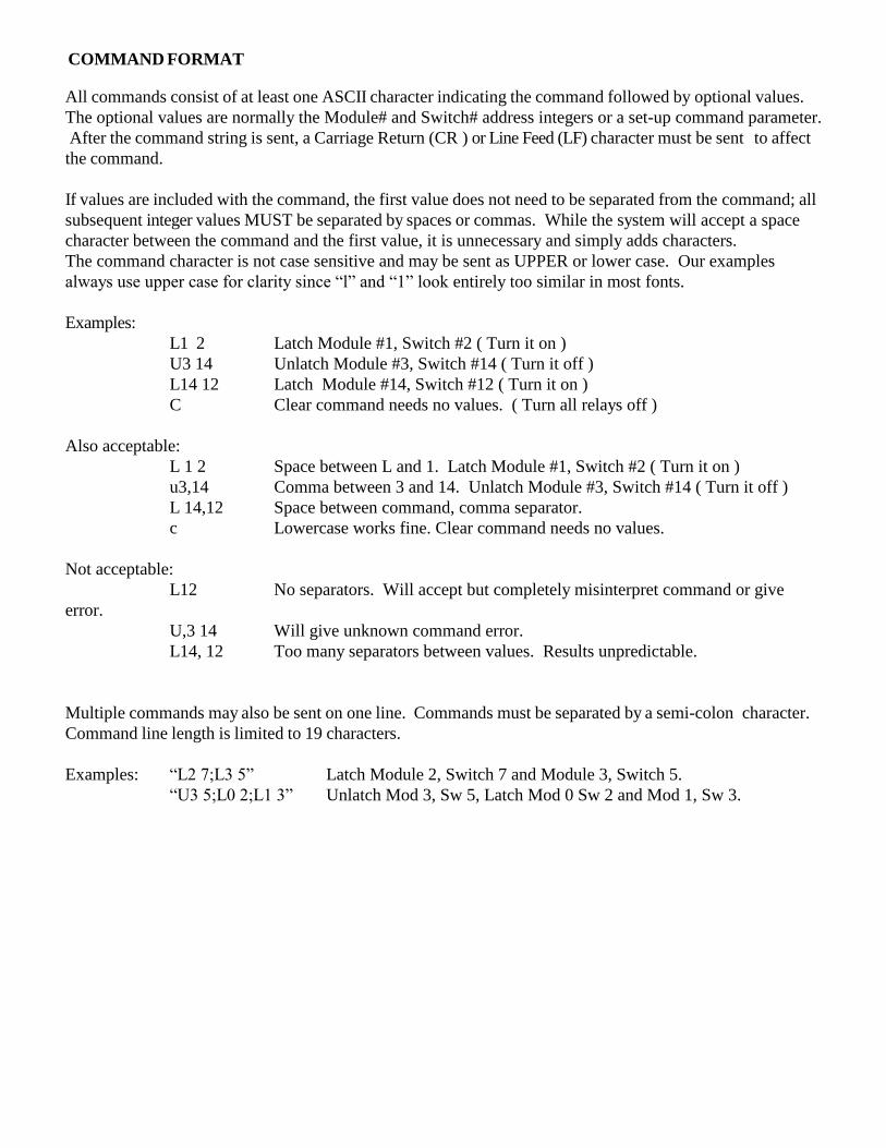
COMMAND FORMAT
All commands consist of at least one ASCII character indicating the command followed by optional values.
The optional values are normally the Module# and Switch# address integers or a set-up command parameter.
After the command string is sent, a Carriage Return (CR ) or Line Feed (LF) character must be sent to affect
the command.
If values are included with the command, the first value does not need to be separated from the command; all
subsequent integer values MUST be separated by spaces or commas. While the system will accept a space
character between the command and the first value, it is unnecessary and simply adds characters.
The command character is not case sensitive and may be sent as UPPER or lower case. Our examples
always use upper case for clarity since “l” and “1” look entirely too similar in most fonts.
Examples:
L1 2 Latch Module #1, Switch #2 ( Turn it on )
U3 14 Unlatch Module #3, Switch #14 ( Turn it off )
L14 12 Latch Module #14, Switch #12 ( Turn it on )
C Clear command needs no values. ( Turn all relays off )
Also acceptable:
L 1 2 Space between L and 1. Latch Module #1, Switch #2 ( Turn it on )
u3,14 Comma between 3 and 14. Unlatch Module #3, Switch #14 ( Turn it off )
L 14,12 Space between command, comma separator.
c Lowercase works fine. Clear command needs no values.
Not acceptable:
L12 No separators. Will accept but completely misinterpret command or give
error.
U,3 14 Will give unknown command error.
L14, 12 Too many separators between values. Results unpredictable.
Multiple commands may also be sent on one line. Commands must be separated by a semi-colon character.
Command line length is limited to 19 characters.
Examples: “L2 7;L3 5” Latch Module 2, Switch 7 and Module 3, Switch 5.
“U3 5;L0 2;L1 3” Unlatch Mod 3, Sw 5, Latch Mod 0 Sw 2 and Mod 1, Sw 3.

5.5.1 DELAYS TO PREVENT ERRORS
It is important to recognize that with modern computers and control interfaces, it is possible to stream
commands to the switch matrix faster than the relays can physically operate. Many electro-mechanical
relays may take between 2 to 20 ms to close or open. This can result in unpredictable results if certain
operations are streamed together without considering this delay.
A good example of this type of problem occurs if a Latch command is sent and is immediately followed by a
status request. Many of Cytec’s products actually base status on current flow through the relay drives so it is
possible to send a command and request status before the relay has physically operated, resulting in incorrect
status feedback.
Typically, a 5 to 20 ms delay between commands requiring feedback can ensure that this is never an issue.
5.5.2 ANSWERBACK CHARACTER
Both the LAN and RS232 controls allow an Answerback Character to be returned whenever a command is
sent.
Answerback is turned on by default so this character must be read back before any other commands can be
issued or there is a good chance that the control will hang. The answerback character is simply a “1” or “0”
followed by end of line.
Answerback may be turned off using the “A0 73” command. See sections 5.11 ( RS232 ) and 5.3 ( LAN )
for complete command syntax.
What does the Answerback Character Mean?
The answerback character simply confirms that the command was accepted and completed. It is useful for
verifying that the command you sent was processed.
For most commands, the character being a “1” or “0” does not matter. Either character simply means that
the command was processed and the value can be thought of as a “Don’t care” Boolean.
For the L ( Latch ) and U ( Unlatch ) commands, the value tells you the status of the switch point.
So when you send an L command, the answerback character should always be a “1”.
When you send a U command, the answerback should always be a “0”.

5.5.3 SWITCH CONTROL COMMANDS
L,U,X - Latch, Unlatch, Multiplex Commands
Syntax: Cmd Switch
Cmd Module, Switch
The specified switchpoint is operated on.
(Cmd = 'L', 'U' or 'X')
L = Latch = Turn switch ON Closes the specified point, all others unaffected.
U = Unlatch = Turn switch OFF Opens the specified point, all others are unaffected.
X = Multiplex = Clear + Latch Opens all points, then Latches the specified point.
Eg. "U2 3" Module 2, Switch 3 is opened. (OFF)
"L0 1" Module 0, Switch 1 is closed. (ON)
“L13 7” Module 13, Switch 7 is closed. (ON)
“X3 0” Clear all switch points ( turn them all OFF ) then Latch Module 3, Switch 0.
Note that the X command cannot be used if you need more than one switch on at a time. There is not a X
command that only works on a single module.
If a single integer value is sent, the control module assumes it is a switch value and defaults to the last
module value sent.
Eg. “L2 3” Module 2, Switch 3 is closed (ON). Then,
“L4” Assumes Module 2. Module 2, Switch 4 is closed (ON)
Note: For systems with less than or equal to 32 relay drives possible you may simply address them as 0 to
31 without using the Module #. These systems will accept either syntax.
Eg. “L3 5” Module 3, Switch 5 is closed (ON).
“L29” Module 3, Switch 5 is closed (ON). Same as above. Do the math.
Some Cytec programming examples may refer to Mod #, Rly # ( Relay #).
The terms Switch (Sw) and Relay (Rly) mean the same thing.
For Unidirectional matrix switches, specifically DX, DXM, VDX, VDM and TX, the Module # may be
thought of as Input #, and the Switch or Relay # may be thought of as the Output #. See section 5.6.
C - Clear Command
Syntax: C
All points in the chassis are opened.
Eg. "C" All switches in the chassis are opened.
There is not a Clear Module # function. Clear simply turns off every switch in the chassis.
If you need a Clear module function it can be written in code fairly easily.
For IEEE488.2, The C command is the same as the *RST (reset) function.

5.5.4 STATUS AND INTEROGATE COMMANDS
The Status and Interrogate commands return information to the user so they can tell what state each
switch point is in before proceeding. They can be used to simply check the switch configuration, to
verify connections, or to prevent unwanted connections.
The information returned by these commands can be different depending on what type of system you
have. Please find the Status or Interrogate section for your specific system before writing code that is
dependent on what is returned.
S - Status Command
Syntax: S
S Module, Switch
Status may be requested of a single switch point or for the entire chassis. After receipt of the Status
command the Matrix will return a character or string of characters representing the status, open or
closed, of a switch point or switch points. A one, '1', signifies a closed switch point (ON) and a zero,
'0', an open switch point (OFF).
In the case of a single switch point a single character is returned followed by an end of line.
For multiple switch points, a stream of 1’s and 0’s will be returned. How they are returned and what
they mean is dependent on the type of system.
Status return is broken down into four different groups:
Section 5.5.4.1 Systems with 8 to 32 relays drives possible.
Section 5.5.4.2 Systems with 64 to 512 relay drives possible.
Section 5.5.4.3 RJV systems which are unique.
Section 5.5.4.4 Large Matrix systems with over 512 switch points or solid state matrix systems.
Please see the sections on the following pages for the information for your particular system

5.5.4.1 Status Returned Values up to 32 drives
For systems with 8 to 32 relay drives ( any model designated as xxx/16 or xxx/32 )
These Models Include:
CXAR/16 and /32
CXM/16 and /32
HXV/16 and HXV/32
RS/8 or /16
GX/4 or /8 or /16 or /32
FO/16 or /32
Model #’s are shown on the rear panel label. If the model # is simply a # such as “6754” you should
see the addendum for the system or contact Cytec with questions if you do not know what it is
returning.
The S command sent by itself will return a continuous string of 16 or 32 1’s and 0’s followed
by the answerback character ( if on ) and the end of line character. The string is ordered from
lowest value switch to highest value switch.
Eg. 1 CXAR/32 chassis
Send: “S”
Receive: "000100010000000000001100000000010" eol 32 switch points + Answerback +
EOL
This is interpreted as Switches 3, 7, 20, 21 and 30 are ON, the rest are OFF.
In Module#, Switch # syntax this is:
Mod 0, Switches 3 and 7 are ON.
Mod 1, no switches are ON.
Mod 2, Switches 3 and 4 are ON.
Mod 3, Switch 7 is ON.
All other switches are OFF.
If the Answerback function is on, the last 1 or 0 before the EOL will be the Answerback character
and the value is a “don’t care”. If Answerback + termination character is ON, there will also be the
termination character [].

5.5.4.2 Status Returned Values 64 to 512 drives
For systems with 64 to 512 relay drives
( any model designated as xxx/64, xxx/128, xxx/256, xxx/512 )
These Models Include:
LXA or LXB ( all )
CXAR/64, /128 or /256
CXB systems ( all )
CXG, CXF, CXS systems ( all )
CXM/64, /128 or /256
HXV/96 or /128, or /256
RSM ( all )
RJM ( all )
JX ( all )
VX ( all )
PX ( all )
GX/64 or /128
FO/64 or /128
Model #’s are shown on the rear panel label. If the model # is simply a # such as “6754” you should
see the addendum for the system or contact Cytec with questions if you do not know what it is
returning.
The S command sent by itself will return a row / column pattern of 1’s and 0’s that mimic the
LED display on the front panel (if equipt ), where the columns are the Module # and the Rows
are the Switch #.
Eg. 2 A 16 Module, 8 Switch Matrix ( your configuration may be different):
Send: "S" Status of chassis
Receive: "0001000100000000" eol Switch 0, Module 3 and 7 closed
"0000000000000000" eol Switch 1, none closed
"1111111111111111" eol Switch 2, all closed
"1000000000000001" eol Switch 3, Module 0 and 15 closed
"1010101010101010" eol Switch 4, odd Modules closed
"0101010101010101" eol Switch 5, even Modules closed
"0110000000000000" eol Switch 6, Module 1 and 2 closed
"0000000000000110" eol Switch 7, Module 13 and 14 closed
“0”eol Answerback character
If the Answerback function is on, the last 1 or 0 before the EOL will be the Answerback character
and the value is a “don’t care”. If Answerback + termination character is ON, there will also be the
termination character [].
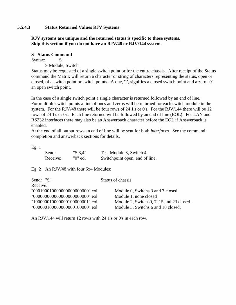
5.5.4.3 Status Returned Values RJV Systems
RJV systems are unique and the returned status is specific to those systems.
Skip this section if you do not have an RJV/48 or RJV/144 system.
S - Status Command
Syntax: S
S Module, Switch
Status may be requested of a single switch point or for the entire chassis. After receipt of the Status
command the Matrix will return a character or string of characters representing the status, open or
closed, of a switch point or switch points. A one, '1', signifies a closed switch point and a zero, '0',
an open switch point.
In the case of a single switch point a single character is returned followed by an end of line.
For multiple switch points a line of ones and zeros will be returned for each switch module in the
system. For the RJV/48 there will be four rows of 24 1's or 0's. For the RJV/144 there will be 12
rows of 24 1's or 0's. Each line returned will be followed by an end of line (EOL). For LAN and
RS232 interfaces there may also be an Answerback character before the EOL if Answerback is
enabled.
At the end of all output rows an end of line will be sent for both interfaces. See the command
completion and answerback sections for details.
Eg. 1
Send: "S 3,4" Test Module 3, Switch 4
Receive: "0" eol Switchpoint open, end of line.
Eg. 2 An RJV/48 with four 6x4 Modules:
Send: "S" Status of chassis
Receive:
"000100010000000000000000" eol Module 0, Switchs 3 and 7 closed
"000000000000000000000000" eol Module 1, none closed
"100000010000000100000001" eol Module 2, Switchs0, 7, 15 and 23 closed.
"000000100000000000100000" eol Module 3, Switchs 6 and 18 closed.
An RJV/144 will return 12 rows with 24 1's or 0's in each row.

RJV Module Status table:
Use this table to relate switch #’s to Input and Output Ports.
RJV/12x1-X-XX (any 12x1 module)
These modules only use the first 12 characters of the returned string of 24 1's or 0's.
The second set of 12 characters are “don’t cares” and may be returned as 1’s or 0’s.
They should be ignored.
Ports 0 to 11 NA
001000000000 000000000000
Indicates port 2 is on.
RJV/6x4-X-XX (all 6x4 modules)
These modules use all 24 characters and each common port has six associated 1's or 0's:
0 to 23 = Switch #’s Port Labels
0
1
2
3
4
5
C0
0
4
8
12
16
20
C1
1
5
9
13
17
21
C2
2
6
10
14
18
22
C3
3
7
11
15
19
23
So the 24 characters line up as:
C0/0 C1/0 C2/0 C3/0 C0/1 C1/1 C2/1 C3/1 C0/2 C1/2 C2/2 C3/2 C0/3 C1/3 C2/3 C3/3 etc...

RJV/6x2 Switch Modules
These modules only use every other 2 characters in the returned string of 24 1's or 0's.
0 to 23 = Switch #’s Port Labels
0
1
2
3
4
5
C0
0
4
8
12
16
20
C1
1
5
9
13
17
21
NA ignore!
2
6
10
14
18
22
NA ignore!
3
7
11
15
19
23
So the 24 characters line up as:
C0/0 C1/0 NA NA C0/1 C1/1 NA NA C0/2 C1/2 NA NA C0/3 C1/3 NA NA C0/4 C1/4 etc...
NA digits are floating and may return as 1's or 0's but must be ignored!
RJV/4(2x1)-X Switch Modules
These modules only use the first 4 characters of the returned string of 24 1's or 0's.
2x1 # 0 to 3 NA
0000 00000000000000000000 (0 = Normally Closed Position, 1 = Normally Open)
RJV/4(2x1)-X-Latching Switch Modules
These modules only use the first 8 characters of the returned string of 24 1's or 0's.
2x1 #’s
C0/0 C1/1 C2/2 C3/3 C0/4 C1/5 C2/6 C3/7 NA
0 0 0 0 0 0 0 0 0000000000000000

5.5.4.4 Status Returned Values Large Systems
For systems with more than relay drives, large matrices, or solid state switches
These Models Include:
VDX/16x16 or /32x32 ( all )
VDM/32x32 (all)
DX/64x64 or /256x256 ( all )
DXM/64x64 or /128x128
FX ( all )
TX ( all )
These systems do not make use of the S command but instead use the I command to return
information.
Some of these systems would return up to 65,536 characters if they accepted the S command which
becomes very difficult to deal with. Instead, they use the I command which only returns the address
of switch points which are on. This limits the amount of returned data to a maximum of 256
addresses which is much easier and quicker to deal with.
These systems will interpret any “S” command sent as an “I” command and respond accordingly.
See the Interrogate Command Section for details.
Any other modules not listed please see addendum or call factory.

5.5.5 I – Interrogate Command
Syntax: I
The Interrogate function will return a list of all closed ( ON ) switch points. Each switch point will
be followed by an “end of line” ( EOL ). The switch point is listed as the Module# and then
Switch#. For matrix applications such as a 16x16 this often translates into “Input # then Output #”
or “Output # then Input #”. Since many systems are bi-directional Input vs Output may be dependent
on how you are using it. For uni-directional systems, such as VDM, or DXM, the input vs output
relationship will be carved in stone and you should be familiar with it.
Send: <I> Request interrogation.
Receive: <Module#><comma><space><Switch#><EOL>
Eg. Send “I”
Receive “0, 0” eol Module 0, Switch 0 Closed. End of line.
“1, 6” eol Module 1, Switch 6 Closed. End of line.
“3, 2” eol Module 3, Switch 2 Closed. End of line.
“0” eol Answerback character (if enabled). End of line.
For system such as a DX/256x256 the “I” command may return up to 256 addresses. Be sure your buffer
size can handle the amount of returned data.
For Unidirectional matrix switches, specifically DX, DXM, VDX, VDM and TX, the Module # may be
thought of as Input #, and the Switch or Relay # may be thought of as the Output #. See section 5.6.
.

5.5.6 OTHER COMMANDS
F - Front Panel
Syntax: F n 73 n = 0 or 1
Front panel lock-out will be initiated by the receipt of a 0 character and enabled by the receipt of a 1
character followed by the access code. The access code prevents inadvertent lock-out from
occurring. Lock-out will prevent any operation of the system from the front panel until it is
terminated from the remote (F 1) or power is turned off then on. Preset to panel enabled at power
on.
Eg. "F 0,73" Lock-out local operation.
"F 1 73" Enable local operation.
P - Program
Syntax: P n1,n2,73
The program command allows the operator to setup matrix dependent variables. These include
matrix switch configuration and certain interface functions. Use of the P commands is complicated
and varies greatly between systems. Your system should have been provided with the correct P
command set-up.
If you need to change the matrix configuration, number of allowed modules, or other obscure set-up
configurations on your system we recommend you contact Cytec and we can walk you through the P
commands needed for your specific system. Please provide the serial # of your system when you
contact us.
N - Revision Number (Same as IEEE488 *IDN? )
Syntax: N
The 'N' command will cause the matrix to return its current revision number followed by an integer
identifier, followed by an end of line.
Eg. Send: "N" Request revision Number
Receive: "Cytec 11-14-10-1, 1.23 0" eol Text string indicating revision.
Where: ACytec@ = manufacturer.
A11-14-10-1" = control module board number.
A1.23" = Firmware Revision # (example).
A0" = Integer identifier.
Note: When requesting the Revision number, all characters must be received before the system can
be resumed.
*NOTE - The text string received from the >N= Command will vary depending on the type of system.

Integer identifier
The N command now includes a single byte which can be used as an identifier for Cytec systems. The
identifier is a single byte integer so it may 0 to 255. WE do not assign this and it has no meaningful
relationship to any product. It is simply a number which may be assigned to a chassis so that the end user
can acknowledge that a specific Cytec chassis is communicating. It is up to the customer to assign the
number and keep track of it. It allows them to poll multiple chassis and know that the one they are talking to
is, for example, the JX/256 that they assigned the identifier A13" to.
Command to enter or change the number:
P90 n 73 where n is the number from 0 to 255

5.6 INPUT / OUTPUT vs MODULE / SWITCH NOMENCLATURE
Most of the switching systems sold by Cytec are completely bi-directional and can be used in a variety of
ways by the customer so it is impossible for us to use the terms Input and Output, even though it is what
probably makes the most sense to the end user when connecting signals to the switch.
We label and control the switches using Module# and Switch# to avoid this confusion since for most
systems either can be considered an Input or an Output.
However some Cytec systems are uni-directional and do have assigned Inputs and Outputs:
Uni-directional Systems with defined Input and Output ports:
DX and DXM high speed digital switch matrix systems
VDX and VDM analog or digital switch matrix systems
TX analog systems
FX fiber optic systems
For all of these systems:
Module # = Input
Switch # = Output
Note that these systems will all allow multiple Outputs to be connected to a single Input, but will never
allow multiple Inputs to be connected to one Output. There are internal controls to prevent this and
attempting to do it will simply disconnect a previously set path.

5.7 MATRIX COMMAND SUMMARY
COMMAND FUNCTION
L sw Latch switch point.
L mod, sw
U sw Unlatch switch point.
U mod, sw
X sw Multiplex switch point.
X mod, sw
C Clear entire system.
S Return status.
S mod, sw
I Interrogate Closed Points.
F 0/1 73 Disable/Enable Front Panel.
P parameter value 73 Program parameter.
N Revision Number
RS232 Specific Commands
R baud, RTS/CTS 73 Baud Rate, RTS/CTS operation.
A 0/1 73 Disable/Enable Answerback.
E 0/1 73 Disable/Enable Echo.
V 0/1 73 Disable/Enable Verbose.
TCP/IP Specific Commands
TCPANSWERBACK 0/1/2 Disable/Enable Answerback/Termination
IFCONFIG aaa.aaa.aaa.aaa nnn.nnn.nnn.nnn a = ip address in dotted decimal format
n = subnet mask in dotted decimal format
SNET TCP PORT n m Where n = equals one of two sockets and m is the port number

5.8 IF-9 / IF-11 (RS232/LAN/GPIB) DEFAULT CONFIGURATION SETTINGS
Should the system=s non-volatile memory fail, default setup parameters will be placed in memory on power
up. The unit may then be properly set-up by P commands.
Forcing Defaults
Default values may be forced by setting the Jumper on the control module and toggling power.
See section 5.0, Memory Sanitation Procedure.
Default Values
P 0 1 One Matrix
P 7 0 NV RAM disabled
P 8 0 Load List #0 if NV RAM disabled
P 10 X X = 4 Logical Modules for RJV/48 or 12 for RJV/144
P 20 12 12 Logical Switches
P 24 0 0 to 31 addressing
P 19 6 Baud rate 9600
P 90 0 ID# = 0
E 0 Echo off
V 0 Verbose off
A 1 Answerback on
IP 10.0.0.144
Netmask 255.0.0.0
Gateway 0.0.0.0
Port 0 8080
Port 1 8081
Socket Timeout 60 seconds
GPIB Address 7

5.9 LCD DISPLAY/KEYPAD MANUAL CONTROL OPTION
The Keypad/Display option (Drwg.#6-057) allows manual control of the matrix from the front panel.
Keypad operation is always enabled at power on but may be disabled by the remote command, >F=.
Display
The display contains two lines with sixteen characters per line. The top line displays matrix commands and
numeric entry. The bottom line displays the status of the entry or operation. The display will also show the
last command entered from the remote computer interface when the front panel is enabled.
Keypad
The keypad consists of ten numeric keys, four function keys, a space key and an enter key. Key Function
0-9 Numeric entries.
space Delimits between numeric entries.
L Latch operation.
U Unlatch operation.
X Multiplex operation.
C Clear operation.
ENTR Execute displayed operation.
Operation
A matrix command key, L, U, X or C, MUST be pressed before numeric entry keys. Pressing any key
except a matrix command key causes the message Enter Cmd First to be displayed. After pressing a
matrix command key the command and a cursor are displayed. The switch point to be operated on may now
be entered with the numeric and space keys. The entry format is the same as described in the MATRIX
OPERATION section and described briefly by the following table:
Command Key Display Line 1 Line 2
L Lat _ Enter Point
U Unl _ Enter Point
X Mux _ Enter Point
C Clr _ Enter Matrix
The numeric keypad now allows selection of the Module and Relay ( Input and Output ) to be operated on.
Each entry may be multiple digits and a space must be pressed between selections.
Key Line 1 Line 2
L Lat _ Enter Point
1 Lat 1_
space Lat 1 _
2 Lat 1 2_
3 Lat 1 23_
Enter Key Lat 1 23_ 1

Number of Entries Leftmost Entry 2nd Entry
1 Relay -
2 Module Relay
The ENTR key may now be pressed to execute the displayed operation. If the displayed entry is incorrect or
the operation is not desired, pressing any matrix command key will clear the display and restart the entry.
Status Display
After the ENTR key is pressed, the displayed operation is attempted to be executed by the control module.
If the execution is successful, a Point Closed or Point Open message will be displayed on line 2. If the
operation cannot be executed, an error message will be displayed.
Line 2 Message Status
Ready Displayed after power on.
Enter Point The ENTR key has not been pressed, command and selection mode.
Point Closed The selected point was closed.
Point Open The selected point was opened.
Points Open All points opened, Clear operation.
***Err: limits The selected point is outside the programmed size of the matrix.
***Err: entry An incorrect entry was selected.
Front Panel Disable
The >F= command allows enabling or disabling front panel operation. If the front panel is disabled, no
operation can be performed from the keypad.
Remote Command Line 1 Line 2
F 0 73 Panel Disabled
F 1 73 Panel Enabled
Contrast and LED Backlight Adjustment
Controls are provided to adjust the LCD contrast and LED backlight level. These controls should only need
adjustment in extremely bright or dim environments or for acute viewing angles. Both LCD and LED
circuits have temperature sensing elements that will automatically adjust the output level for changes in the
ambient temperature.

APPENDIX B -QBASIC RS232 EXAMPLE PROGRAM
'Cytec Matrix Test Program for IBM-PC Compatibles using QBASIC and COM1 port.
' 16x16 (Change parameters X and Y for other configurations.)
'
' Matrix should be set up for:
' E 0 73 Echo off
' V 0 73 Verbose off
' A 1 73 Answerback on
' Set-up may be done by any Terminal emulation program or
' by adding these lines to the program, be sure to clear
' input buffer after set-up.
'The Answerback character is read after every write operation and can be
' tested for successful operation if desired.
'
CLS
OPEN "COM1:9600" FOR RANDOM AS #1
COM(1) ON
PRINT "Setting up and Clearing Matrix"
PRINT #1, "E0 73;V0 73;A1 73;C"
'Some delay gather Answers from the previous command
INPUT "Press ENTER to continue", a$
WHILE NOT EOF(1)
INPUT #1, a$
WEND
'----------------------------------------------------------
PRINT ""
PRINT "Cycling through 256 channels using Latch/Unlatch Commands"
FOR Y% = 0 TO 15 'Loop For Selecting Input
FOR X% = 0 TO 15 'Loop For Selecting Output
'Write Instruction To Matrix (Command,Input,Output)
PRINT #1, "L" + STR$(Y%) + STR$(X%): INPUT #1, a$
'Check Status (S module, relay)
PRINT #1, "S" + STR$(Y%) + STR$(X%): INPUT #1, a$
INPUT #1, Stat$
IF Stat$ = "0" THEN PRINT "Error latching"; Y%; X%
PRINT #1, "U" + STR$(Y%) + STR$(X%): INPUT #1, a$
PRINT #1, "S" + STR$(Y%) + STR$(X%): INPUT #1, a$
INPUT #1, Stat$
IF Stat$ = "1" THEN PRINT "Error unlatching"; Y%; X%
NEXT X%
NEXT Y%
'----------------------------------------------------------
CLOSE #1
END

APPENDIX C - TURBO C/IEEE488 TEST PROGRAM
/* CYTEC Matrix / National Instruments IEEE488 Test Program */
/* This program was compiled under TURBO C ver. 2.0 and linked */
/* with National Instruments file: TCIBS.OBJ. Though not */
/* tested with other compilers it has been written following */
/* ANSI C rules and should be compatible with other compilers. */
/* National Instruments configuration program IBCONF was used */
/* to assign dev7 listen and talk addresses of the matrix (7). */
#include <stdio.h>
#include "decl.h"
static int brd0, matrix; /* device ID variables */
static char cmd_line[10];
/* ------------- initialize I/O ---------------------------- */
int init_GPIB()
{
if ((brd0 = ibfind("gpib0")) < 0) /* 'Find' devices */
return(1); /* that were setup by */
ibsic(brd0); /* IBCONF program */
if ((matrix = ibfind("dev7")) < 0) /* dev7 setup for Matrix */
return(2);
matrix_clear();
return(0);
}
/* ------------- clear matrix ------------------------------ */
int matrix_clear()
{
ibwrt(matrix,"C",1); /* "C", alternate methods of */
/* ibcmd(brd0,"\x14",1); DCL, clearing the matrix */
/* ibclr(matrix); */
}
/* ------------- switchpoint operation --------------------- */
int switchpoint_operation(cmd, inp, outp)
int cmd, inp, outp;
{
int sp_status;
sprintf(cmd_line,"%c%d %d", cmd, inp, outp); /* build */
ibwrt(matrix,cmd_line,strlen(cmd_line)); /* and send */
ibrsp(matrix,&sp_status);
return(sp_status & 0x3f); /* ret status less SRQ bit */
}
/* ------------- switchpoint status ------------------------ */
int switchpoint_status(inp, outp)
int inp, outp;
{
lkjhljhsdfkljdfgsdfgsg sprintf(cmd_line,"S%d %d", inp, outp); /* Request status */
ibwrt(matrix,cmd_line,strlen(cmd_line));
ibrd(matrix,cmd_line,10); /* and read */
return(cmd_line[0] & 0x3f);
}
/* ************************************************************* */
#define N_INPUTS 16
#define N_OUTPUTS 8
#define RCV_BUFFER_SIZE N_INPUTS * N_OUTPUTS + N_INPUTS + 1
int main()

{
int i,inp,outp;
char rcv_buffer[RCV_BUFFER_SIZE];
printf("Cytec Matrix Test Program.\n\n");
/* initialize and trap errors */
if (init_GPIB()) {
printf("Initialize error.\n");
return(1);
}
/* Latch & Unlatch Switches */
for (inp=0; inp<N_INPUTS; inp++)
for (outp=0; outp<N_OUTPUTS; outp++) {
if (switchpoint_operation('L',inp,outp) != '1')
printf("Error: point %d %d not closed.\n",
inp,outp);
if (switchpoint_operation('U',inp,outp) != '0')
printf("Error: point %d %d not open.\n",
inp, outp);
}
/* Latch 'Random' switches */
for (outp=0; outp<N_OUTPUTS; outp++) {
switchpoint_operation('L',outp,outp);
/* direct status read */
if (switchpoint_status(outp,outp) != '1')
printf("Error: point %d %d not closed.\n",outp,outp);
}
/* request status of entire matrix */
ibwrt(matrix,"S",1);
ibrd(matrix,rcv_buffer,RCV_BUFFER_SIZE);
/* display status */
printf("Bytes read = %d.\n",ibcnt);
for (i=0; i<ibcnt; i++) {
if (rcv_buffer[i] == ';')
printf("\n");
else
printf("%c",rcv_buffer[i]);
}
ibloc(matrix); /* Leave local controls enabled when done */
}

/* Cytec Matrix Test Program for LAN */ /* This program uses Microsoft's WS2_32 Library */ /* and winsock2.h. These are available in the */ /* Microsoft SDKs and can be downloaded from */ /* Microsoft's Developer Network */ /* https://msdn.microsoft.com/en-us/default.aspx */ #include <stdio.h> #include <winsock2.h> #include <stdlib.h> /* for exit() */ int init_LAN(int sock); int point_ops(int sock,int cmd, int mod, int rly); int matrix_clear(int sock); void DieWithError(char *errorMessage); #define MAX_MOD 4 #define MAX_RLY 12 int main(int argc, char *argv[]) { int sock; char *servIP = "10.0.0.144"; /*Default IP Address*? struct sockaddr_in servAddr; /* IP address */ unsigned short servPort = 8080; /* Port */ int mod, rly,status; if (argc == 3) { servIP = argv[1]; servPort = atoi(argv[2]); } WSADATA wsaData; /* Structure for WinSock setup communication */ WSAStartup(0x202, &wsaData); /* Load Winsock 2.2 DLL */ /* Create a reliable, stream socket using TCP */ if ((sock = socket(PF_INET, SOCK_STREAM, IPPROTO_TCP))<0) DieWithError("socket() failed"); /* Construct the server address structure */ memset(&servAddr, 0, sizeof(servAddr)); /* Zero out structure */ servAddr.sin_family = AF_INET; /* Internet address family */ servAddr.sin_addr.s_addr = inet_addr(servIP); /* Server IP address */ servAddr.sin_port = htons(servPort); /* Server port */ /* Establish the connection to the server */ if (connect(sock, (struct sockaddr *) &servAddr, sizeof(servAddr))<0) DieWithError("connect() failed"); /* Initialize Device using init_LAN Function */
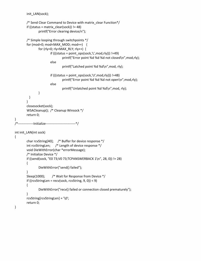
init_LAN(sock); /* Send Clear Command to Device with matrix_clear Function*/ if ((status = matrix_clear(sock)) != 48) printf("Error clearing device/n"); /* Simple looping through switchpoints */ for (mod=0; mod<MAX_MOD; mod++) { for (rly=0; rly<MAX_RLY; rly++) { if (((status = point_ops(sock,'L',mod,rly))) !=49) printf("Error point %d %d %d not closed\n",mod,rly); else printf("Latched point %d %d\n",mod, rly); if (((status = point_ops(sock,'U',mod,rly))) !=48) printf("Error point %d %d %d not open\n",mod,rly); else printf("Unlatched point %d %d\n",mod, rly); } } } closesocket(sock); WSACleanup(); /* Cleanup Winsock */ return 0; } /*--------------Initialize---------------------------*/ int init_LAN(int sock) { char rcvString[40]; /* Buffer for device response */ int rcvStringLen; /* Length of device response */ void DieWithError(char *errorMessage); /* Initialize Device */ if ((send(sock, "E0 73;V0 73;TCPANSWERBACK 1\n", 28, 0)) != 28) { DieWithError("send() failed"); } Sleep(1000); /* Wait for Response from Device */ if ((rcvStringLen = recv(sock, rcvString, 9, 0)) < 9) { DieWithError("recv() failed or connection closed prematurely"); } rcvString[rcvStringLen] = '\0'; return 0; }

/*-----------------Clear Matrix----------------------*/ int matrix_clear(int sock) { char rcvString[8]; /* Buffer for device response */ int rcvStringLen; /* Length of device response */ if ((send(sock,"C\n",2,0)) != 2) DieWithError("send() failed"); Sleep(200); /* Wait for Response /* Receive Response from Device */ if ((rcvStringLen = recv(sock, rcvString, 10, 0)) <= 0) DieWithError("recv() failed or connection closed prematurely"); rcvString[rcvStringLen] = '\0'; int status = rcvString[0] & 0x3f; return status; } /*-----------Switchpoint Operation------------------ */ int point_ops(int sock,int cmd, int mod, int rly) { char cmd_str[40]; /* Formatted command string */ char rcvString[8]; /* Buffer for device response */ int rcvStringLen; /* Length of device response */ /* Format String */ sprintf(cmd_str,"%c%d %d\n",cmd,mod,rly); /* Send Command to Device */ if ((send(sock,cmd_str,strlen(cmd_str),0)) != strlen(cmd_str)) DieWithError("send() failed"); Sleep(200); /* Wait for Response /* Receive Response from Device */ if ((rcvStringLen = recv(sock, rcvString, 10, 0)) <= 0) DieWithError("recv() failed or connection closed prematurely"); rcvString[rcvStringLen] = '\0'; int status = rcvString[0] & 0x3f; return status; } /*------------Error Handling Function---------------------*/ void DieWithError(char *errorMessage) { fprintf(stderr,"%s: %d\n", errorMessage, WSAGetLastError()); getchar(); exit(1); }

APPENDIX F – Programming Examples
Cytec can provide programming examples for almost any Language. With the numerous
programming languages available for the LAN interface, RS232 interface and GPIB interface it is
increasingly difficult to provide them in a text file.
Please go to the Cytec support page at
http://cytec-ate.com/support.htm
or e-mail us at:
for complete programming examples in the language needed.
For tech support:
Call 1-800-346-3117
Or 585-381-4740

6.0 MAINTENANCE AND WARRANTY
GENERAL
This switching system utilizes solid state control circuitry. Electro-mechanical reed, armature relays or solid
state switches are used for switching. The system has been burned in for over 72 hours to eliminate any
marginal solid state components. Electro-mechanical switches have been cycled and then individually
checked for resistance to ensure their rated life expectancy. When used within the published specifications,
no maintenance should be required for at least one year of operation.
The single largest cause of failure in electro-mechanical relay switching systems is excess current or power
being switched. This type of problem is indicated by relay contacts sticking closed, and it does not show up
with software diagnostics. Typically, contact welding is not a problem in communication systems where all
signals are low current and low voltage in nature. In the unlikely event that relay welding does ever does
occur, it should be reported to CYTEC, and we will help review your system for the most likely cause.
The following test procedure covers a complete check of the system both mechanically and electrically.
Some parts of the procedure may not apply to solid state switches. In addition, some aspects of the test
(such as cycling and resistance checking) may be extremely time-consuming without the proper fixtures or
test equipment. You may choose to ignore them. Sometimes the old adage, “if it ain’t broke, don’t fix it!”,
is the best rule to follow. If your system has been operating flawlessly for years, you are not switching high
signal levels and you have a quantity of spare parts on hand to prevent long downtime, it may be in your best
interest to avoid the complicated aspects of this test procedure. Please use your best judgment before
proceeding with any steps with which you are not completely comfortable.
If the switching application absolutely requires that full tests be run on a periodic basis, you may consider
sending the entire system back to Cytec for a complete once over. This normally takes two to three working
days (excluding shipping time) and costs $100.00 to $500.00 depending on the size of the system. Please
contact Cytec at 1-800-346-3117 or [email protected], if you prefer this type of arrangement.

MAINTENANCE TEST PROCEDURE
Should you decide to perform a periodic system check, or if the system has been in operation for over three
years without any maintenance, please refer to the following procedure to ensure proper operation:
1) Locate all physical layout drawings within the system manuals. This will help identify the components
you will need to check.
2) Remove the top panel from the Mainframe or MESA Control Chassis and check all components for
proper mechanical arrangement and connections. Check that all modular components are seated in
connectors and that all wiring is in good physical condition. Visually inspect both the power supply(ies) and
solid state components for any indication of burning or overheating. Check mechanical connectors (screws,
nuts, etc.) for tightness. In industrial environments, check for accumulation of dirt, dust, or other
contaminants on any electrical components. Clean these components if necessary. Repeat this procedure for
any included Expansion Chassis if necessary.
3) Check Voltage levels on all supplies. Adjustable supplies should be reset to their proper level if more
than 5% out of range. Check your manual or call Cytec to determine proper level. If the 5 Volt level is
provided through a 5 Volt regulator attached to a 12 Volt supply, the regulator will need to be replaced if out
of specification.
4) Replace any top covers which have been removed.
5) Set up the system and check for proper communication with the controller. If the system is operating
normally, cycle through all available switch-points either programmatically or via manual control if
provided. For systems with LED displays, step through the switch points one at a time while observing the
LED display. Check LEDs for proper operation.
6) Set up system programmatically via software to continuously cycle through all switch points one at a time
with a minimum of a 20ms delay between each switch closure. This test should only be done with all
external signals disconnected from the system. Allow the system to cycle a minimum of 1000 cycles but
not more than 10,000 cycles. This may take 24 hours on larger systems, so be prepared to have the system
down for the needed time. Cycling without signals connected serves two purposes: first, in electro-
mechanical systems, it wipes the relay contacts and may clean up any contacts which have become pitted or
dirty due to arcing of live signals while in normal operation, and second, it will cause any borderline
switches to fail mechanically during a scheduled maintenance period when it will be much more convenient
to perform repairs.

7) In relay based systems, once the switch points have been cycled they should be tested for path resistance.
On smaller systems this can simply be done with a handheld ohm meter. On larger systems testing can be a
lengthy procedure without test fixtures and automated resistance measurement equipment. Close each
switchpoint and measure the path resistance between the associated connectors. Typical on resistance for
reed relay systems from input to output should be in the range of 0.2 to 0.6 ohms. Any relays which exceed
this specification should be replaced since this is an indication that the relays are beginning to wear out.
8) Once the system has passed these tests it can be returned to normal operation with full confidence that it
should operate within specified parameters for another three years.
Turn the system on and check for proper operation.

TROUBLESHOOTING
If provided with the system, the front panel LED Indicators are an invaluable aid in debugging computer
programs and troubleshooting problems. These LEDs are in parallel with the switch coils, and are a very
positive indication of whether the coil is energized.
The Status mode also gives a simple method of checking switch operation, and a program can be written so
that the computer can operate each switch and check that the coil has been energized. This program latches
each switch in turn, checks for status, unlatches each switch in turn, checks for status, then multiplexes each
switch in turn, and checks for status again. Any error will be flagged by the computer, but the system can
also be monitored visually by observing the LEDs on the front panel.
No Switches Operating
The power should be checked by the Power LED on the front panel, and by measurements directly on the
motherboard. Check the fuse.
If power is available at the motherboard, then the control module or control inputs are most likely to be at
fault. These should be checked. If the IEEE488 interface is being used, then make sure the Listen Address
is set correctly. Similarly, with RS232, the baud rate must be correct.
Individual Switches Not Operating
The diagnostic program will isolate the failure to the particular relay driver and this can be confirmed by the
LED not being lit (if display LEDs are included). Replacing the LED Display Module should repair this
fault, if not and the LED is still not lit, the failure must be in the relay coil and the relay module should be
changed. If the LEDs and Diagnostic mode show that the logic is operating up to the relays and the contacts
are not closing, then the problem is in the relay and the Module should be changed.

REPAIRS
If the faulty switch module is under warranty, it should be returned to CYTEC for repair or replacement.
Modules out of warranty can also be returned to CYTEC for repair at a reasonable price, which will include
another 5 year warranty.
Repairs can also be made by any competent technician. If encapsulated relays are used, a solder sucker can
be utilized to remove all solder from the pins.
In older systems with open frame reed relays, the reed contacts can easily be replaced without damage to the
circuit board, however, the following method must be followed.
The reed is soldered at each end to terminal posts. Unsolder one end with a heat sink clipped to the terminal
post below the reed switch to prevent heat transfer to the circuit board. Remove all solder so that the reed
wire is free, then repeat with the other end and withdraw the reed.
Replace the reed by reversing the soldering process. Then cut the reed wires to length after soldering.
If mercury wetted reeds are used, ensure that the reeds are replaced with the mercury in the correct position,
i.e. the mercury must be low, and the contacts high, when the module is inserted in the motherboard.

*** WARRANTY ***
CYTEC Corp. warrants that all products are free from defects in material and workmanship and
perform to published specifications for five years from date of shipment. This warranty is in lieu of
any other warranty expressed or implied.
The liability of CYTEC Corp. shall be limited to replacement or repair of any defective units which
are returned F.O.B. to its factory. Units which have been subjected to abuse, misuse, accident,
alteration, neglect, or unauthorized repair are not covered by this warranty.
No liability is assumed for expendable items such as lamps or fuses.
CONTACT 1-800-346-3117
OR WWW.CYTEC-ATE.COM
FOR TECHNICAL ASSISTANCE

1
1
2
2
3
3
4
4
D D
C C
B B
A A
Title:Size:
Number:
Date:
Comments:
Sheet: ofRevision:
Drawn By:
CXR/2X1 SWITCH MODULEA
2-101-1
5/24/20051 1 RHHApproved:
FERRITEL1
CT/2 MODULE
+12
13579111315
2468
10121416
2X8,25SQRJP1
1234567891011121314151617181920
IDH-20-SR1
J1
DRV0DRV1DRV2
DRV3DRV4DRV5
DRV6DRV7
43
65
K0B
7
4 3
6 5
K1B
7
A
COM
B
A
COM
B
-1, SINGLE POLE
-2, TWO POLE
4 3K1B
43K0B
12
K0A
12
K1A
0.1uC1
0.1uC3
0.1uC2
K0 - DRIVES 0, 2, 4 OR 6K1 - DRIVES 1, 3, 5, OR 7

GND
A B C
D E F
Power Entry Mod
5EFLA2S
B
C
D
E
1
2
3
4
(NC) 5
Pin 1
GND
GND
BLK
BLUE
YEL
WHT
LINEAR SUPPLYTRANSFORMER
Power Entry Mod
SWITCHING SUPPLY(ie. MAP Supply)
OPTIONAL
Grounding Lug on Chassis
B
C
D
E
1
2
3
4
(NC) 5
GND
GND
BLK
BLUE
YEL
WHT
LINEAR SUPPLYTRANSFORMER
Power Entry Mod
SWITCHING SUPPLY(ie. MAP Supply)
OPTIONAL
Grounding Lug on Chassis
12
11
25
24
BLK
BLUE
BLK
BLUE
WH
T
BLK
WH
T
BLK
OPTIONALROCKER SWITCH
SWX1019
Remove any factoryinstalled jumpers
FOR THE AC SIDE ONLYREAR VIEW
AC SELECTABLE MOD
AC POWER SUPPLY WIRING
STANDARD WIRING
STANDARD WIRING w/ OPTIONAL ROCKER SWITCH
AC IN WIRING FOR 2-463-2 POWER SUPPLY
1
2
3
4
5
6
BLK
WHT
WHT
BLK
B
C
D
EP1
6 PinMolex
CON1108
20 Awg (typical)
GREEN 18 AWGWIR1040
GREEN 18 AWGWIR1040
N LG
Pin 1N LG
BLK
BLUE
YELWHT
GRN
GND
31 4 2
Power Entry Mod
FN393-605-11
REAR VIEW
AC SELECTABLE MOD
BLKYEL
BLUE
WHT
GRN1
4
3
2
1
4
3
2
Schaffner
AMP
New Old
New Old
New
Old
DATE: DRAWN BY:
DRAWING NUMBER:
SIZE: TITLE:
COMMENTS:
B
A
B
C
D
E
1 2 3 4 5 6 7 8
A
B
C
D
E
1 2 3 4 5 6 7 8
CAD FILE:
TOL. +/- .010" U.O.S.
Standard Power Supply WiringAC In Wiring
DR8/10/05 2-190-5B.dcd
2-190-5B 1/3

RELAY POWER
LOGIC POWER+5V
+12V or +15V or +24V or +28V
1
3
5
GRN
RED
CO
N1131
to CL8 M
.B or C
ON
TRO
L MO
D.
12V Yellow
15V Purple
24V Grey
28V Blue
GND
RELAY POWER
LOGIC POWER+5V
+12V1
3
5
GRN
RED
CO
N1131
to CL8 M
.B or C
ON
TRO
L MO
D.
12V Yellow
GND
4-40 x 5/16w/ Kemp NutMount to Power Supply Frame
7805/780-05CKCREG1000
DC POWER SUPPLY WIRING
V1 V1 G G G V2 V3 V4
MAP130 (single output)
V1 V1 G G V2 V3 V4
MAP80 (single output)
Pin
1
V1 G V2 V3 V428V @ V1 (Place 220 Ohm RES1270 across V1 to G)
MAP40 & 55 (single output)
5V @ V112V @ V1 (Place 50 Ohm RES1096 across V1 to G)
5
2
3
4
1GND
+5V
+12V or +15V or +24V or +28V
GRN
RED
12V Yellow
15V Purple
24V Grey
28V Blue
CON1131to CP M.B or CONTROL MOD.
DUAL SUPPLIES
ONE 12V SUPPLY & 5V REG
20 Awg (typical)
20 Awg (typical)
GND
+5V
GRN
RED
OPTIONAL
OPTIONAL
+
-
+
-
+
-
123
Pin
1
Pin
1
28V @ V1 (Place 220 Ohm RES1270 across V1 to G)
5V @ V112V @ V1 (Place 50 Ohm RES1096 across V1 to G)
28V @ V1 (Place 220 Ohm RES1270 across V1 to G)
5V @ V112V @ V1 (Place 50 Ohm RES1096 across V1 to G)
V+
V+
V+
RELAY POWER+12V or 28V
1
5
GRN
CO
N1131
to CL8 M
.B or C
ON
TRO
L MO
D.
12V Yellow
GND
SUPPLY (E-PS)20 Awg (typical)
+
-
28V Blue
ONE 12V or 28V
5V Power comes from the MESAthrough the Expansion Cable
Existing DC jumpersMUST be present
Existing DC jumpersMUST be present
Existing DC jumpersMUST be present
(sense)
(sense)
(sense)
1
2
3 +12V or +15V or +24V or +28V
+5VRED
GNDGRN
CON1102to CP M.B with
Thumbwheel Option
DATE: DRAWN BY:
DRAWING NUMBER:
SIZE: TITLE:
COMMENTS:
B
A
B
C
D
E
1 2 3 4 5 6 7 8
A
B
C
D
E
1 2 3 4 5 6 7 8
CAD FILE:
TOL. +/- .010" U.O.S.
Standard Power Supply WiringDC Wiring
DR8/10/05 2-190-5B.dcd
2-190-5B 2/3

GND
+5V
MISCELLANEOUS POWER SUPPLY WIRING
LAN DC POWER (INTERNAL)
RED
RCA Plug CP-3501
24 AWG
(SHORT, USE SHRINK CENTER)
+5V ONLY !! (Not 12V or 28V)
POWER INDICATORR
LEDLED0283GREEN
GND
+VSee Table
LED Resistor Table
Volts Ohms Part #
5V 390 Ohm RES1027
12V 680 Ohm RES1029
15V 2k Ohm RES1049
28V 5.1k Ohm RES1172
FRONT PANEL
2V 10.7 Ohm RES1066
2.5V 100 Ohm RES1085
3.3V 200 Ohm RES1141
Long Lead
24-28 AWG
DATE: DRAWN BY:
DRAWING NUMBER:
SIZE: TITLE:
COMMENTS:
B
A
B
C
D
E
1 2 3 4 5 6 7 8
A
B
C
D
E
1 2 3 4 5 6 7 8
CAD FILE:
TOL. +/- .010" U.O.S.
Standard Power Supply WiringMiscellaneous DC Wiring
DR8/10/05 2-190-5B.dcd
2-190-5B 3/3

1 2 3 4 5 6
A
B
C
D
654321
D
C
B
A
DRAWN BY:APPROVED BY
SHEET
REVISION:
DRAWING NUMBER
DATE: 3-Nov-2014
IF-11 Mainframe Ctrl Module
11-14-50/02
11-14-50-02.sch OF
SIZE: TITLE:B2 4
KJA
+5V
+5V
PA0PA1PA2PA3PA4PA5PA6PA7
PB2PB3PB4PB5PB6
+5V+5V
C240.1UF
SHEET 3SHEET 1
GN
D4
GN
D8
GN
D13
GN
D25
GN
D27
GN
D35
GN
D37
GN
D41
GN
D45
GN
D48
GN
D54
GN
D56
GN
D57
GN
D59
GN
D61
GN
D65
GN
D68
GN
D72
GN
D75
GN
D78
GN
D83
GN
D86
GN
D90
GN
D93
GN
D97
VD
D12
VD
D24
VD
D36
VD
D40
VD
D58
VD
D60
VD
D69
VD
D87
VD
D94
MODE53
DACKN33
DIO8N 71DIO7N 74DIO6N 77DIO5N 80DIO4N 88DIO3N 89DIO2N 91DIO1N 92
EOIN 85
RENN 70
DAVN 84
NRFDN 82NDACN 81
IFCN 79
SRQN 76ATNN 73
DATA039
DATA142
DATA243
DATA344
DATA446
DATA547
DATA649
DATA750
DATA811
DATA910
DATA109
DATA117
DATA126
DATA135DATA143
DATA152
ADDR015
ADDR116
ADDR217
ADDR318
ADDR419
ABUSN14
PAGED26
SWAPN29
BURST_RDN31
CSN55
BBUSN62
RDN63
WRN64
RESETN67
XTAL095
XTAL196
KEYDQ99
BBUS_OEN 1
ABUS_OEN 20
TADCS 21
CPUACC 22
TRIG 23
REM 28
FIFO_RDY 30
RDY 38
DRQ 32
INTR 34
DCAS 51
NC 52
KEYRSTN 100
LADCS 66
KEYCLKN 98
U16
TNT4882E/D1
GND2 OUTPUT 3
+5VDC 4Y1 40MHz
IEEE488 CONTROL
IOWRIORDSH 1
RES
PE1 SH 1
PE7
C190.1uF
C200.1uF
C210.1uF
C220.1uF
C230.1uF
R1110K
VCC
R1010K
1P2A
26 Pin Header
2P2B
3P2C
4P2D
5P2E
6P2F
7P2G
8P2H
9P2I
10P2J
11P2K
12P2L
13P2M
14P2N
15P2O
16P2P
17P2Q
18P2R
19P2S
20P2T
21P2U
22P2V
23P2W
24P2X
25P2Y26P2Z
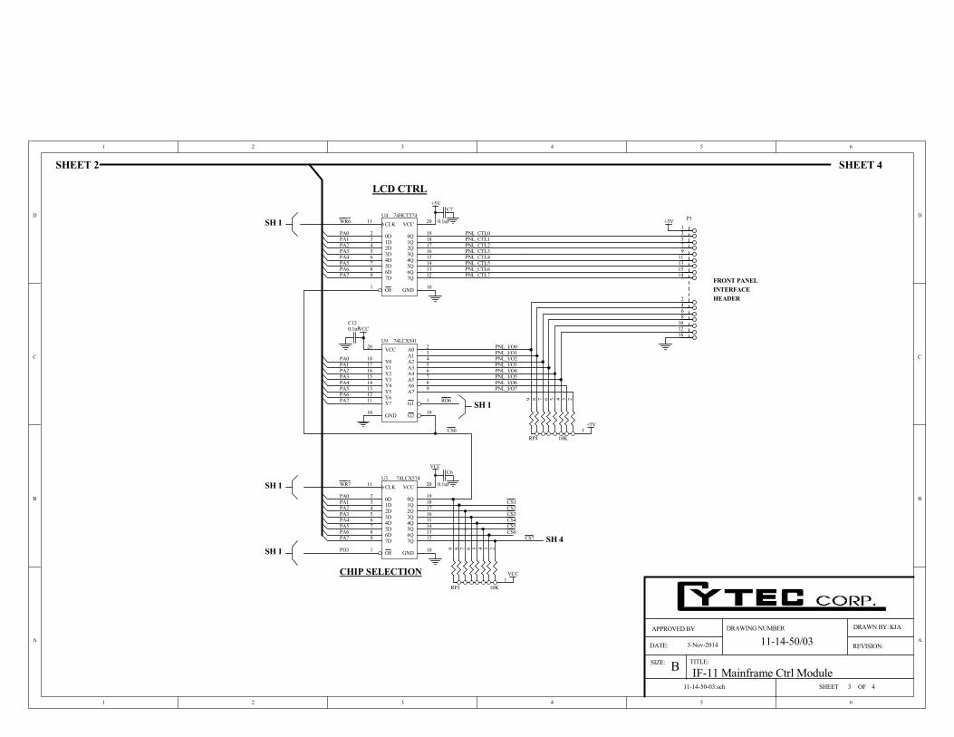
1 2 3 4 5 6
A
B
C
D
654321
D
C
B
A
DRAWN BY:APPROVED BY
SHEET
REVISION:
DRAWING NUMBER
DATE: 3-Nov-2014
IF-11 Mainframe Ctrl Module
11-14-50/03
11-14-50-03.sch OF
SIZE: TITLE:B3 4
KJA
OE1
CLK11
0D2 0Q 19
1D3 1Q 18
2D4 2Q 17
3D5 3Q 16
4D6 4Q 15
5D7 5Q 14
6D8 6Q 13
7D9 7Q 12
VCC 20
GND 10
U4 74HCT574
G1 1
G2 19
A7 9
Y711
A6 8
Y612
A5 7
Y513
A4 6
Y414
A3 5
Y315
A2 4
Y216
A1 3
Y117
A0 2
Y018
VCC20
GND10
U9 74LCX541
LCD CTRL
PA0PA1PA2PA3PA4PA5PA6PA7
PA0PA1PA2PA3PA4PA5PA6PA7
+5V
VCC
PNL_I/O0PNL_I/O1PNL_I/O2PNL_I/O3PNL_I/O4PNL_I/O5PNL_I/O6PNL_I/O7
PNL_CTL0PNL_CTL1PNL_CTL2PNL_CTL3PNL_CTL4PNL_CTL5PNL_CTL6PNL_CTL7
SH 1 WR6
1
23456789
RP4 10K
+5V
RD6 SH 1
C7
0.1uF
C120.1uF
SHEET 2
16
468
1012
1415
13
2
579
1113
P1+5V
FRONT PANELINTERFACEHEADER
OE1
CLK11
0D2 0Q 19
1D3 1Q 18
2D4 2Q 17
3D5 3Q 16
4D6 4Q 15
5D7 5Q 14
6D8 6Q 13
7D9 7Q 12
VCC 20
GND 10
U3 74LCX574
PA0PA1PA2PA3PA4PA5PA6PA7
SH 1 WR7
VCC
PD3SH 1
CS0
CS1CS2CS3CS4CS5CS6
CS7
1
23456789
RP3 10K
VCCCHIP SELECTION
C6
0.1uF
SH 4
SHEET 4

1 2 3 4 5 6
A
B
C
D
654321
D
C
B
A
DRAWN BY:APPROVED BY
SHEET
REVISION:
DRAWING NUMBER
DATE: 3-Nov-2014
IF-11 Mainframe Ctrl Module
11-14-50/03
11-14-50-04.sch OF
SIZE: TITLE:B4 4
KJA
CONTROL
SHEET 3
OE1
CLK11
0D2 0Q 19
1D3 1Q 18
2D4 2Q 17
3D5 3Q 16
4D6 4Q 15
5D7 5Q 14
6D8 6Q 13
7D9 7Q 12
VCC 20
GND 10
U5 74LCX/HCT574
G1 1
G2 19
A7 9
Y711
A6 8
Y612
A5 7
Y513
A4 6
Y414
A3 5
Y315
A2 4
Y216
A1 3
Y117
A0 2
Y018
VCC20
GND10
U10 74LCX541
PA0PA1PA2PA3PA4PA5PA6PA7
PA0PA1PA2PA3PA4PA5PA6PA7
VCC
SH 1 WR0
1
23456789
RP510K
+V
SH 1
C8
0.1uF
C130.1uF
OE1
CLK11
0D2 0Q 19
1D3 1Q 18
2D4 2Q 17
3D5 3Q 164D6 4Q 15
5D7 5Q 14
6D8 6Q 13
7D9 7Q 12
VCC 20
GND 10
U6 74LCX/HCT574
G1 1
G2 19
A7 9
Y711
A6 8
Y612
A5 7
Y513
A4 6
Y414
A3 5
Y315
A2 4
Y216
A1 3
Y117
A0 2
Y018
VCC20
GND10
U11 74LCX541
PA0PA1PA2PA3PA4PA5PA6PA7
PA0PA1PA2PA3PA4PA5PA6PA7
VCC
SH 1 WR1
1
23456789
RP610K
+V
SH 1
C9
0.1uF
C140.1uF
OE1
CLK11
0D2 0Q 19
1D3 1Q 18
2D4 2Q 17
3D5 3Q 16
4D6 4Q 15
5D7 5Q 14
6D8 6Q 13
7D9 7Q 12
VCC 20
GND 10
U7 74LCX/HCT574
G1 1
G2 19
A7 9
Y711
A6 8
Y612
A5 7
Y513
A4 6
Y414
A3 5
Y315
A2 4
Y216
A1 3
Y117
A0 2
Y018
VCC20
GND10
U12 74LCX541
PA0PA1PA2PA3PA4PA5PA6PA7
PA0PA1PA2PA3PA4PA5PA6PA7
VCC
SH 1 WR2
1
23456789
RP710K
+V
SH 1
C10
0.1uF
C150.1uF
OE1
CLK11
0D2 0Q 19
1D3 1Q 18
2D4 2Q 17
3D5 3Q 164D6 4Q 15
5D7 5Q 14
6D8 6Q 13
7D9 7Q 12
VCC 20
GND 10
U8 74LCX/HCT574
G1 1
G2 19
A7 9
Y711
A6 8
Y612
A5 7
Y513
A4 6
Y414
A3 5
Y315
A2 4
Y216
A1 3
Y117
A0 2
Y018
VCC20
GND10
U13 74LCX541
PA0PA1PA2PA3PA4PA5PA6PA7
PA0PA1PA2PA3PA4PA5PA6PA7
VCC
SH 1 WR3
123456789
RP810K +V
SH 1
C11
0.1uF
C160.1uF
+V
+V +V
+V
RD0
RD1 RD3
RD2
RD0
CS7 SH 3
1P6A
CON-16PIN2 P6B
3P6C
4 P6D
5P6E
6 P6F
7P6G
8 P6H
9P6I
10 P6J
11P6K
12 P6L
13P6M
14 P6N
15P6O
16 P6P
1P7A
CON-16PIN2 P7B
3P7C
4 P7D
5P7E
6 P7F
7P7G
8 P7H
9P7I
10 P7J
11P7K
12 P7L
13P7M
14 P7N
15P7O
16 P7P
1P8A
CON-16PIN2 P8B
3P8C
4 P8D
5P8E
6 P8F
7P8G
8 P8H
9P8I
10 P8J
11P8K
12 P8L
13P8M
14 P8N
15P8O
16 P8P
1P9A
CON-16PIN2 P9B
3P9C
4 P9D
5P9E
6 P9F
7P9G
8 P9H
9P9I
10 P9J
11P9K
12 P9L
13P9M
14 P9N
15P9O
16 P9P
1
23456789
RP2 10K
VCC
PA0PA1PA2PA3PA4PA5PA6PA7
JP3Voltage Select
VCC
+V
+5V
LCX HCT

1
1
2
2
3
3
4
4
5
5
6
6
D D
C C
B B
A A
+5V
JP2
JP1
123456789
101112131415
MOD15
123456789
101112131415
MOD14
123456789
101112131415
MOD13
123456789
101112131415
MOD12
123456789
101112131415
MOD11
123456789
101112131415
MOD10
123456789
101112131415
MOD9
123456789
101112131415
MOD8
123456789
101112131415
MOD7
123456789
101112131415
MOD6
123456789
101112131415
MOD5
123456789
101112131415
MOD4
123456789
101112131415
MOD3
123456789
101112131415
MOD2
123456789
101112131415
MOD1
123456789
101112131415
MOD0
A1BCDEFHJKLMNPRS
23456789
101112131415
CONTROL
0.156" X 5
MODULE SLOTS 8-15 NOT USED
CL/64
RLY-8 - OPEN ------------- JP1 OPEN
+12 TO PIN 14 ------------- JP2, JP3 TO 14
+12 TO PIN 14 ------------- JP2, JP3 TO 14
RLY-8 - OPEN ------------- JP1 OPEN
CL/128
+12 TO PIN 15 ------------- JP2, JP3 TO 15
RLY-8 - INSTALLED ---- JP1 INSTALLED
CL/256
VRLY
RLY-8
*RLY-8
ST-STBSW-STB
MUX/*MTX
STATUSGND
RLY-4RLY-2RLY-1LAT/*UNL+5V
*MOD-8MOD-8
MOD-0MOD-1MOD-2MOD-3MOD-4MOD-5MOD-6MOD-7
PIN 14
PIN 15
POWER
JUMPER CONNECTIONS
DRAWN BY:APPROVED BY
SHEET
REVISION:
DRAWING NUMBER
DATE: 10/7/2004
CL64, 128 AND 256 MOTHERBOARD
12-00-50
12-00-50.SchDoc OF
SIZE: TITLE:B
REVISED FROM:
1 1
6-012-2
1.2KR1
OPT.
RHB
JP3
1
2
3
4
5
P1
+5V
FERRITE
L1
R1 (1.2K) INSTALLED FOR PX/512 CHASSIS.P2
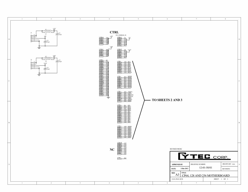
1 2 3 4 5 6 7 8
A
B
C
D
87654321
D
C
B
A DRAWN BY:APPROVED BY
SHEET
REVISION:
DRAWING NUMBER
DATE: 2-Dec-2013
CP64, 128 AND 256 MOTHERBOARD
12-01-50/01
OF
SIZE: TITLE:
1 3
APPROVED BY
DATE: 2-Dec-2013
SIZE: TITLE:A3
REVISED FROM:
KJA
12-01-50-01.SCH
12345
J1
12345
J2
L1
L3
+5V
+12V
+ C147uF
+ C247uF
L2
L4+3.3V
+28V
+ C347uF
+ C447uF
+5V+12V
MOD!8MOD8
Lat/Un*SW-STB*ST-STB*MUX
Rly1Rly2Rly4Rly8Rly16Rly32Rly64Rly128
*MBEN
STAT0
A1CTRLAPCI_EXPRESS_98
A2CTRLBA3CTRLC
A8CTRLH
A9CTRLI
A10CTRLJ
A11CTRLK
A12CTRLL
A14CTRLNA16CTRLPA18CTRLRA20CTRLTA22CTRLVA24CTRLXA26CTRLZA28CTRL\
A30CTRL^A32CTRL`A34CTRLbA36CTRLdA38CTRLfA40CTRLhA42CTRLjA44CTRLl
A45CTRLmA46CTRLnA47CTRLoA48CTRLpA49CTRLq
B1CTRLrB2CTRLsB3CTRLt
B8CTRLy
B9CTRLz
B10CTRL{
B11CTRL|
B12CTRL}
B13CTRL~
B14 CTRL
B15CTRL€
B16 CTRL
B17CTRL‚
B18CTRLƒ
B19CTRL„
B20CTRL…
B21CTRL†
B22CTRL‡
B23CTRLˆ
B24CTRL‰
B25CTRLŠ
B26CTRL‹
B27CTRLŒ
B28 CTRL
B29CTRLŽ
B30 CTRL
B31 CTRL
B32CTRL‘
B33CTRL’
B34CTRL“
B35CTRL”
B36CTRL•
B37CTRL–B38CTRL—B39CTRL˜
B40CTRL™
B41CTRLš
B42CTRL›
B43CTRLœ
B44 CTRL
B45CTRLžB46CTRLŸB47CTRL B48CTRL¡B49CTRL¢
STAT1STAT2STAT3STAT4STAT5STAT6STAT7
CTRL
SP1SP2SP3SP4SP5SP6SP7SP8
SP9
SP10SP11
SP12
A4CTRLDB4CTRLuA5CTRLE
A6CTRLFB5CTRLv
B6CTRLw
+3.3V
B7CTRLxA7CTRLG
+28V
A13CTRLMA15CTRLOA17CTRLQA19CTRLSA21CTRLUA23CTRLWA25CTRLYA27CTRL[
A29CTRL]A31CTRL_A33CTRLaA35CTRLcA37CTRLeA39CTRLgA41CTRLiA43CTRLk
MOD0MOD1MOD2MOD3MOD4MOD5MOD6MOD7
NC
TO SHEETS 2 AND 3

1 2 3 4 5 6 7 8
A
B
C
D
87654321
D
C
B
A DRAWN BY:APPROVED BY
SHEET
REVISION:
DRAWING NUMBER
DATE: 2-Dec-2013
CP64, 128 AND 256 MOTHERBOARD
12-01-50/02
OF
SIZE: TITLE:
2 3
APPROVED BY
DATE: 2-Dec-2013
SIZE: TITLE:A3
REVISED FROM:
KJA
12-01-50-02.SCH
+5V
+12V
MOD!8MOD7
Lat/Un*SW-STB*ST-STB*MUX
Rly1Rly2Rly4Rly8Rly16Rly32Rly64Rly128
*MBEN
STAT0
A1E7APCI_EXPRESS_98
A2E7BA3E7C
A8E7H
A9E7I
A10E7J
A11E7K
A12E7L
A13E7M
A14E7N
A15E7O
A16E7P
A17E7Q
A18E7R
A19E7S
A20E7T
A21E7U
A22E7V
A23E7W
A24E7X
A25E7Y
A26E7Z
A27E7[
A28E7\
A29E7]
A30E7^
A31E7_
A32E7`
A33E7a
A34E7b
A35E7c
A36E7d
A37E7e
A38E7f
A39E7g
A40E7h
A41E7i
A42E7j
A43E7k
A44E7l
A45E7mA46E7nA47E7oA48E7pA49E7q
B1E7rB2E7sB3E7t
B8E7y
B9E7z
B10E7{
B11E7|
B12E7}
B13E7~
B14 E7
B15E7€
B16 E7
B17E7‚
B18E7ƒ
B19E7„
B20E7…
B21E7†
B22E7‡
B23E7ˆ
B24E7‰
B25E7Š
B26E7‹
B27E7Œ
B28 E7
B29E7Ž
B30 E7
B31 E7
B32E7‘
B33E7’
B34E7“
B35E7”
B36E7•
B37E7–
B38E7—
B39E7˜
B40E7™
B41E7š
B42E7›
B43E7œ
B44 E7
B45E7žB46E7ŸB47E7 B48E7¡B49E7¢
BU
SSE
D S
PAR
ES
NC
STAT1STAT2STAT3STAT4STAT5STAT6STAT7
+5V
+12V
A1E6APCI_EXPRESS_98
A2E6BA3E6C
A8E6H
A9E6I
A10E6J
A11E6K
A12E6L
A13E6M
A14E6N
A15E6O
A16E6P
A17E6Q
A18E6R
A19E6S
A20E6T
A21E6U
A22E6V
A23E6W
A24E6X
A25E6Y
A26E6Z
A27E6[
A28E6\
A29E6]
A30E6^
A31E6_
A32E6`
A33E6a
A34E6b
A35E6c
A36E6d
A37E6e
A38E6f
A39E6g
A40E6h
A41E6i
A42E6j
A43E6k
A44E6l
A45E6mA46E6nA47E6oA48E6pA49E6q
B1E6rB2E6sB3E6t
B8E6y
B9E6z
B10E6{
B11E6|
B12E6}
B13E6~
B14 E6
B15E6€
B16 E6
B17E6‚
B18E6ƒ
B19E6„
B20E6…
B21E6†
B22E6‡
B23E6ˆ
B24E6‰
B25E6Š
B26E6‹
B27E6Œ
B28 E6
B29E6Ž
B30 E6
B31 E6
B32E6‘
B33E6’
B34E6“
B35E6”
B36E6•
B37E6–
B38E6—
B39E6˜
B40E6™
B41E6š
B42E6›
B43E6œ
B44 E6
B45E6žB46E6ŸB47E6 B48E6¡B49E6¢
+5V
+12V
A1E5APCI_EXPRESS_98
A2E5BA3E5C
A8E5H
A9E5I
A10E5J
A11E5K
A12E5L
A13E5M
A14E5N
A15E5O
A16E5P
A17E5Q
A18E5R
A19E5S
A20E5T
A21E5U
A22E5V
A23E5W
A24E5X
A25E5Y
A26E5Z
A27E5[
A28E5\
A29E5]
A30E5^
A31E5_
A32E5`
A33E5a
A34E5b
A35E5c
A36E5d
A37E5e
A38E5f
A39E5g
A40E5h
A41E5i
A42E5j
A43E5k
A44E5l
A45E5mA46E5nA47E5oA48E5pA49E5q
B1E5rB2E5sB3E5t
B8E5y
B9E5z
B10E5{
B11E5|
B12E5}
B13E5~
B14 E5
B15E5€
B16 E5
B17E5‚
B18E5ƒ
B19E5„
B20E5…
B21E5†
B22E5‡
B23E5ˆ
B24E5‰
B25E5Š
B26E5‹
B27E5Œ
B28 E5
B29E5Ž
B30 E5
B31 E5
B32E5‘
B33E5’
B34E5“
B35E5”
B36E5•
B37E5–
B38E5—
B39E5˜
B40E5™
B41E5š
B42E5›
B43E5œ
B44 E5
B45E5žB46E5ŸB47E5 B48E5¡B49E5¢
+5V
+12V
A1E4APCI_EXPRESS_98
A2E4BA3E4C
A8E4H
A9E4I
A10E4J
A11E4K
A12E4L
A13E4M
A14E4N
A15E4O
A16E4P
A17E4Q
A18E4R
A19E4S
A20E4T
A21E4U
A22E4V
A23E4W
A24E4X
A25E4Y
A26E4Z
A27E4[
A28E4\
A29E4]
A30E4^
A31E4_
A32E4`
A33E4a
A34E4b
A35E4c
A36E4d
A37E4e
A38E4f
A39E4g
A40E4h
A41E4i
A42E4j
A43E4k
A44E4l
A45E4mA46E4nA47E4oA48E4pA49E4q
B1E4rB2E4sB3E4t
B8E4y
B9E4z
B10E4{
B11E4|
B12E4}
B13E4~
B14 E4
B15E4€
B16 E4
B17E4‚
B18E4ƒ
B19E4„
B20E4…
B21E4†
B22E4‡
B23E4ˆ
B24E4‰
B25E4Š
B26E4‹
B27E4Œ
B28 E4
B29E4Ž
B30 E4
B31 E4
B32E4‘
B33E4’
B34E4“
B35E4”
B36E4•
B37E4–
B38E4—
B39E4˜
B40E4™
B41E4š
B42E4›
B43E4œ
B44 E4
B45E4žB46E4ŸB47E4 B48E4¡B49E4¢
+5V
+12V
A1E3APCI_EXPRESS_98
A2E3BA3E3C
A8E3H
A9E3I
A10E3J
A11E3K
A12E3L
A13E3M
A14E3N
A15E3O
A16E3P
A17E3Q
A18E3R
A19E3S
A20E3T
A21E3U
A22E3V
A23E3W
A24E3X
A25E3Y
A26E3Z
A27E3[
A28E3\
A29E3]
A30E3^
A31E3_
A32E3`
A33E3a
A34E3b
A35E3c
A36E3d
A37E3e
A38E3f
A39E3g
A40E3h
A41E3i
A42E3j
A43E3k
A44E3l
A45E3mA46E3nA47E3oA48E3pA49E3q
B1E3rB2E3sB3E3t
B8E3y
B9E3z
B10E3{
B11E3|
B12E3}
B13E3~
B14 E3
B15E3€
B16 E3
B17E3‚
B18E3ƒ
B19E3„
B20E3…
B21E3†
B22E3‡
B23E3ˆ
B24E3‰
B25E3Š
B26E3‹
B27E3Œ
B28 E3
B29E3Ž
B30 E3
B31 E3
B32E3‘
B33E3’
B34E3“
B35E3”
B36E3•
B37E3–
B38E3—
B39E3˜
B40E3™
B41E3š
B42E3›
B43E3œ
B44 E3
B45E3žB46E3ŸB47E3 B48E3¡B49E3¢
+5V
+12V
A1E2APCI_EXPRESS_98
A2E2BA3E2C
A8E2H
A9E2I
A10E2J
A11E2K
A12E2L
A13E2M
A14E2N
A15E2O
A16E2P
A17E2Q
A18E2R
A19E2S
A20E2T
A21E2U
A22E2V
A23E2W
A24E2X
A25E2Y
A26E2Z
A27E2[
A28E2\
A29E2]
A30E2^
A31E2_
A32E2`
A33E2a
A34E2b
A35E2c
A36E2d
A37E2e
A38E2f
A39E2g
A40E2h
A41E2i
A42E2j
A43E2k
A44E2l
A45E2mA46E2nA47E2oA48E2pA49E2q
B1E2rB2E2sB3E2t
B8E2y
B9E2z
B10E2{
B11E2|
B12E2}
B13E2~
B14 E2
B15E2€
B16 E2
B17E2‚
B18E2ƒ
B19E2„
B20E2…
B21E2†
B22E2‡
B23E2ˆ
B24E2‰
B25E2Š
B26E2‹
B27E2Œ
B28 E2
B29E2Ž
B30 E2
B31 E2
B32E2‘
B33E2’
B34E2“
B35E2”
B36E2•
B37E2–
B38E2—
B39E2˜
B40E2™
B41E2š
B42E2›
B43E2œ
B44 E2
B45E2žB46E2ŸB47E2 B48E2¡B49E2¢
+5V
+12V
A1E1APCI_EXPRESS_98
A2E1BA3E1C
A8E1H
A9E1I
A10E1J
A11E1K
A12E1L
A13E1M
A14E1N
A15E1O
A16E1P
A17E1Q
A18E1R
A19E1S
A20E1T
A21E1U
A22E1V
A23E1W
A24E1X
A25E1Y
A26E1Z
A27E1[
A28E1\
A29E1]
A30E1^
A31E1_
A32E1`
A33E1a
A34E1b
A35E1c
A36E1d
A37E1e
A38E1f
A39E1g
A40E1h
A41E1i
A42E1j
A43E1k
A44E1l
A45E1mA46E1nA47E1oA48E1pA49E1q
B1E1rB2E1sB3E1t
B8E1y
B9E1z
B10E1{
B11E1|
B12E1}
B13E1~
B14 E1
B15E1€
B16 E1
B17E1‚
B18E1ƒ
B19E1„
B20E1…
B21E1†
B22E1‡
B23E1ˆ
B24E1‰
B25E1Š
B26E1‹
B27E1Œ
B28 E1
B29E1Ž
B30 E1
B31 E1
B32E1‘
B33E1’
B34E1“
B35E1”
B36E1•
B37E1–
B38E1—
B39E1˜
B40E1™
B41E1š
B42E1›
B43E1œ
B44 E1
B45E1žB46E1ŸB47E1 B48E1¡B49E1¢
+5V
+12V
A1E0APCI_EXPRESS_98
A2E0BA3E0C
A4E0D
A8E0H
A9E0I
A10E0J
A11E0K
A12E0L
A13E0M
A14E0N
A15E0O
A16E0P
A17E0Q
A18E0R
A19E0S
A20E0T
A21E0U
A22E0V
A23E0W
A24E0X
A25E0Y
A26E0Z
A27E0[
A28E0\
A29E0]
A30E0^
A31E0_
A32E0`
A33E0a
A34E0b
A35E0c
A36E0d
A37E0e
A38E0f
A39E0g
A40E0h
A41E0i
A42E0j
A43E0k
A44E0l
A45E0mA46E0nA47E0oA48E0pA49E0q
B1E0rB2E0sB3E0t
B4E0u
B8E0y
B9E0z
B10E0{
B11E0|
B12E0}
B13E0~
B14 E0
B15E0€
B16 E0
B17E0‚
B18E0ƒ
B19E0„
B20E0…
B21E0†
B22E0‡
B23E0ˆ
B24E0‰
B25E0Š
B26E0‹
B27E0Œ
B28 E0
B29E0Ž
B30 E0
B31 E0
B32E0‘
B33E0’
B34E0“
B35E0”
B36E0•
B37E0–
B38E0—
B39E0˜
B40E0™
B41E0š
B42E0›
B43E0œ
B44 E0
B45E0žB46E0ŸB47E0 B48E0¡B49E0¢
MOD6MOD5MOD4MOD3MOD2MOD1MOD0
E0 E1 E2 E3 E4 E5 E6 E7
SP1SP2SP3SP4SP5SP6SP7SP8
SP9
SP10SP11
SP12
A5E0E
A6E0FB5E0v
B6E0w
+3.3V
B7E0xA7E0G
A4E1DB4E1uA5E1E
A6E1FB5E1v
B6E1w
+3.3V
B7E1xA7E1G
A4E2DB4E2uA5E2E
A6E2FB5E2v
B6E2w
+3.3V
B7E2xA7E2G
A4E3DB4E3uA5E3E
A6E3FB5E3v
B6E3w
+3.3V
B7E3xA7E3G
A4E4DB4E4uA5E4E
A6E4FB5E4v
B6E4w
+3.3V
B7E4xA7E4G
A4E5DB4E5uA5E5E
A6E5FB5E5v
B6E5w
+3.3V
B7E5xA7E5G
A4E6DB4E6uA5E6E
A6E6FB5E6v
B6E6w
+3.3V
B7E6xA7E6G
A4E7DB4E7uA5E7E
A6E7FB5E7v
B6E7w
+3.3V
B7E7xA7E7G
+28V +28V +28V +28V +28V +28V +28V +28V
TO SHEET 1
1
23456789
RP1 3.3K
1
23456789
RP2 3.3K
1
23456789
RP3 3.3K
+5V
+5V
1
2 3 4 5 6 7 8 9
RP4 3.3K
+5V

1 2 3 4 5 6 7 8
A
B
C
D
87654321
D
C
B
A DRAWN BY:APPROVED BY
SHEET
REVISION:
DRAWING NUMBER
DATE: 2-Dec-2013
CP64, 128 AND 256 MOTHERBOARD
12-01-50/03
OF
SIZE: TITLE:
3 3
APPROVED BY
DATE: 2-Dec-2013
SIZE: TITLE:A3
REVISED FROM:
KJA
12-01-50-03.SCH
+5V
+12V
MOD8MOD7
Lat/Un*SW-STB*ST-STB*MUX
Rly1Rly2Rly4Rly8Rly16Rly32Rly64Rly128
*MBEN
STAT0
A1E15APCI_EXPRESS_98
A2E15BA3E15C
A8E15H
A9E15I
A10E15J
A11E15K
A12E15L
A13E15M
A14E15N
A15E15O
A16E15P
A17E15Q
A18E15R
A19E15S
A20E15T
A21E15U
A22E15V
A23E15W
A24E15X
A25E15Y
A26E15Z
A27E15[
A28E15\
A29E15]
A30E15^
A31E15_
A32E15`
A33E15a
A34E15b
A35E15c
A36E15d
A37E15e
A38E15f
A39E15g
A40E15h
A41E15i
A42E15j
A43E15k
A44E15l
A45E15mA46E15nA47E15oA48E15pA49E15q
B1E15rB2E15sB3E15t
B8E15y
B9E15z
B10E15{
B11E15|
B12E15}
B13E15~
B14 E15
B15E15€
B16 E15
B17E15‚
B18E15ƒ
B19E15„
B20E15…
B21E15†
B22E15‡
B23E15ˆ
B24E15‰
B25E15Š
B26E15‹
B27E15Œ
B28 E15
B29E15Ž
B30 E15
B31 E15
B32E15‘
B33E15’
B34E15“
B35E15”
B36E15•
B37E15–
B38E15—
B39E15˜
B40E15™
B41E15š
B42E15›
B43E15œ
B44 E15
B45E15žB46E15ŸB47E15 B48E15¡B49E15¢
BU
SSE
D S
PAR
ES
NC
STAT1STAT2STAT3STAT4STAT5STAT6STAT7
+5V
+12V
A1E14APCI_EXPRESS_98
A2E14BA3E14C
A8E14H
A9E14I
A10E14J
A11E14K
A12E14L
A13E14M
A14E14N
A15E14O
A16E14P
A17E14Q
A18E14R
A19E14S
A20E14T
A21E14U
A22E14V
A23E14W
A24E14X
A25E14Y
A26E14Z
A27E14[
A28E14\
A29E14]
A30E14^
A31E14_
A32E14`
A33E14a
A34E14b
A35E14c
A36E14d
A37E14e
A38E14f
A39E14g
A40E14h
A41E14i
A42E14j
A43E14k
A44E14l
A45E14mA46E14nA47E14oA48E14pA49E14q
B1E14rB2E14sB3E14t
B8E14y
B9E14z
B10E14{
B11E14|
B12E14}
B13E14~
B14 E14
B15E14€
B16 E14
B17E14‚
B18E14ƒ
B19E14„
B20E14…
B21E14†
B22E14‡
B23E14ˆ
B24E14‰
B25E14Š
B26E14‹
B27E14Œ
B28 E14
B29E14Ž
B30 E14
B31 E14
B32E14‘
B33E14’
B34E14“
B35E14”
B36E14•
B37E14–
B38E14—
B39E14˜
B40E14™
B41E14š
B42E14›
B43E14œ
B44 E14
B45E14žB46E14ŸB47E14 B48E14¡B49E14¢
+5V
+12V
A1E13APCI_EXPRESS_98
A2E13BA3E13C
A8E13H
A9E13I
A10E13J
A11E13K
A12E13L
A13E13M
A14E13N
A15E13O
A16E13P
A17E13Q
A18E13R
A19E13S
A20E13T
A21E13U
A22E13V
A23E13W
A24E13X
A25E13Y
A26E13Z
A27E13[
A28E13\
A29E13]
A30E13^
A31E13_
A32E13`
A33E13a
A34E13b
A35E13c
A36E13d
A37E13e
A38E13f
A39E13g
A40E13h
A41E13i
A42E13j
A43E13k
A44E13l
A45E13mA46E13nA47E13oA48E13pA49E13q
B1E13rB2E13sB3E13t
B8E13y
B9E13z
B10E13{
B11E13|
B12E13}
B13E13~
B14 E13
B15E13€
B16 E13
B17E13‚
B18E13ƒ
B19E13„
B20E13…
B21E13†
B22E13‡
B23E13ˆ
B24E13‰
B25E13Š
B26E13‹
B27E13Œ
B28 E13
B29E13Ž
B30 E13
B31 E13
B32E13‘
B33E13’
B34E13“
B35E13”
B36E13•
B37E13–
B38E13—
B39E13˜
B40E13™
B41E13š
B42E13›
B43E13œ
B44 E13
B45E13žB46E13ŸB47E13 B48E13¡B49E13¢
+5V
+12V
A1E12APCI_EXPRESS_98
A2E12BA3E12C
A8E12H
A9E12I
A10E12J
A11E12K
A12E12L
A13E12M
A14E12N
A15E12O
A16E12P
A17E12Q
A18E12R
A19E12S
A20E12T
A21E12U
A22E12V
A23E12W
A24E12X
A25E12Y
A26E12Z
A27E12[
A28E12\
A29E12]
A30E12^
A31E12_
A32E12`
A33E12a
A34E12b
A35E12c
A36E12d
A37E12e
A38E12f
A39E12g
A40E12h
A41E12i
A42E12j
A43E12k
A44E12l
A45E12mA46E12nA47E12oA48E12pA49E12q
B1E12rB2E12sB3E12t
B8E12y
B9E12z
B10E12{
B11E12|
B12E12}
B13E12~
B14 E12
B15E12€
B16 E12
B17E12‚
B18E12ƒ
B19E12„
B20E12…
B21E12†
B22E12‡
B23E12ˆ
B24E12‰
B25E12Š
B26E12‹
B27E12Œ
B28 E12
B29E12Ž
B30 E12
B31 E12
B32E12‘
B33E12’
B34E12“
B35E12”
B36E12•
B37E12–
B38E12—
B39E12˜
B40E12™
B41E12š
B42E12›
B43E12œ
B44 E12
B45E12žB46E12ŸB47E12 B48E12¡B49E12¢
+5V
+12V
A1E11APCI_EXPRESS_98
A2E11BA3E11C
A8E11H
A9E11I
A10E11J
A11E11K
A12E11L
A13E11M
A14E11N
A15E11O
A16E11P
A17E11Q
A18E11R
A19E11S
A20E11T
A21E11U
A22E11V
A23E11W
A24E11X
A25E11Y
A26E11Z
A27E11[
A28E11\
A29E11]
A30E11^
A31E11_
A32E11`
A33E11a
A34E11b
A35E11c
A36E11d
A37E11e
A38E11f
A39E11g
A40E11h
A41E11i
A42E11j
A43E11k
A44E11l
A45E11mA46E11nA47E11oA48E11pA49E11q
B1E11rB2E11sB3E11t
B8E11y
B9E11z
B10E11{
B11E11|
B12E11}
B13E11~
B14 E11
B15E11€
B16 E11
B17E11‚
B18E11ƒ
B19E11„
B20E11…
B21E11†
B22E11‡
B23E11ˆ
B24E11‰
B25E11Š
B26E11‹
B27E11Œ
B28 E11
B29E11Ž
B30 E11
B31 E11
B32E11‘
B33E11’
B34E11“
B35E11”
B36E11•
B37E11–
B38E11—
B39E11˜
B40E11™
B41E11š
B42E11›
B43E11œ
B44 E11
B45E11žB46E11ŸB47E11 B48E11¡B49E11¢
+5V
+12V
A1E10APCI_EXPRESS_98
A2E10BA3E10C
A8E10H
A9E10I
A10E10J
A11E10K
A12E10L
A13E10M
A14E10N
A15E10O
A16E10P
A17E10Q
A18E10R
A19E10S
A20E10T
A21E10U
A22E10V
A23E10W
A24E10X
A25E10Y
A26E10Z
A27E10[
A28E10\
A29E10]
A30E10^
A31E10_
A32E10`
A33E10a
A34E10b
A35E10c
A36E10d
A37E10e
A38E10f
A39E10g
A40E10h
A41E10i
A42E10j
A43E10k
A44E10l
A45E10mA46E10nA47E10oA48E10pA49E10q
B1E10rB2E10sB3E10t
B8E10y
B9E10z
B10E10{
B11E10|
B12E10}
B13E10~
B14 E10
B15E10€
B16 E10
B17E10‚
B18E10ƒ
B19E10„
B20E10…
B21E10†
B22E10‡
B23E10ˆ
B24E10‰
B25E10Š
B26E10‹
B27E10Œ
B28 E10
B29E10Ž
B30 E10
B31 E10
B32E10‘
B33E10’
B34E10“
B35E10”
B36E10•
B37E10–
B38E10—
B39E10˜
B40E10™
B41E10š
B42E10›
B43E10œ
B44 E10
B45E10žB46E10ŸB47E10 B48E10¡B49E10¢
+5V
+12V
A1E9APCI_EXPRESS_98
A2E9BA3E9C
A8E9H
A9E9I
A10E9J
A11E9K
A12E9L
A13E9M
A14E9N
A15E9O
A16E9P
A17E9Q
A18E9R
A19E9S
A20E9T
A21E9U
A22E9V
A23E9W
A24E9X
A25E9Y
A26E9Z
A27E9[
A28E9\
A29E9]
A30E9^
A31E9_
A32E9`
A33E9a
A34E9b
A35E9c
A36E9d
A37E9e
A38E9f
A39E9g
A40E9h
A41E9i
A42E9j
A43E9k
A44E9l
A45E9mA46E9nA47E9oA48E9pA49E9q
B1E9rB2E9sB3E9t
B8E9y
B9E9z
B10E9{
B11E9|
B12E9}
B13E9~
B14 E9
B15E9€
B16 E9
B17E9‚
B18E9ƒ
B19E9„
B20E9…
B21E9†
B22E9‡
B23E9ˆ
B24E9‰
B25E9Š
B26E9‹
B27E9Œ
B28 E9
B29E9Ž
B30 E9
B31 E9
B32E9‘
B33E9’
B34E9“
B35E9”
B36E9•
B37E9–
B38E9—
B39E9˜
B40E9™
B41E9š
B42E9›
B43E9œ
B44 E9
B45E9žB46E9ŸB47E9 B48E9¡B49E9¢
+5V
+12V
A1E8APCI_EXPRESS_98
A2E8BA3E8C
A4E8D
A8E8H
A9E8I
A10E8J
A11E8K
A12E8L
A13E8M
A14E8N
A15E8O
A16E8P
A17E8Q
A18E8R
A19E8S
A20E8T
A21E8U
A22E8V
A23E8W
A24E8X
A25E8Y
A26E8Z
A27E8[
A28E8\
A29E8]
A30E8^
A31E8_
A32E8`
A33E8a
A34E8b
A35E8c
A36E8d
A37E8e
A38E8f
A39E8g
A40E8h
A41E8i
A42E8j
A43E8k
A44E8l
A45E8mA46E8nA47E8oA48E8pA49E8q
B1E8rB2E8sB3E8t
B4E8u
B8E8y
B9E8z
B10E8{
B11E8|
B12E8}
B13E8~
B14 E8
B15E8€
B16 E8
B17E8‚
B18E8ƒ
B19E8„
B20E8…
B21E8†
B22E8‡
B23E8ˆ
B24E8‰
B25E8Š
B26E8‹
B27E8Œ
B28 E8
B29E8Ž
B30 E8
B31 E8
B32E8‘
B33E8’
B34E8“
B35E8”
B36E8•
B37E8–
B38E8—
B39E8˜
B40E8™
B41E8š
B42E8›
B43E8œ
B44 E8
B45E8žB46E8ŸB47E8 B48E8¡B49E8¢
MOD6MOD5MOD4MOD3MOD2MOD1MOD0
E8 E9 E10 E11 E12 E13 E14 E15
SP1SP2SP3SP4SP5SP6SP7SP8
SP9
SP10SP11
SP12
A5E8E
A6E8FB5E8v
B6E8w
+3.3V
B7E8xA7E8G
A4E9DB4E9uA5E9E
A6E9FB5E9v
B6E9w
+3.3V
B7E9xA7E9G
A4E10DB4E10uA5E10E
A6E10FB5E10v
B6E10w
+3.3V
B7E10xA7E10G
A4E11DB4E11uA5E11E
A6E11FB5E11v
B6E11w
+3.3V
B7E11xA7E11G
A4E12DB4E12uA5E12E
A6E12FB5E12v
B6E12w
+3.3V
B7E12xA7E12G
A4E13DB4E13uA5E13E
A6E13FB5E13v
B6E13w
+3.3V
B7E13xA7E13G
A4E14DB4E14uA5E14E
A6E14FB5E14v
B6E14w
+3.3V
B7E14xA7E14G
A4E15DB4E15uA5E15E
A6E15FB5E15v
B6E15w
+3.3V
B7E15xA7E15G
+28V +28V +28V +28V +28V +28V +28V +28V
TO SHEET 1
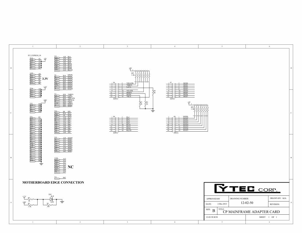
1 2 3 4 5 6
A
B
C
D
654321
D
C
B
A
DRAWN BY:APPROVED BY
SHEET
REVISION:
DRAWING NUMBER
DATE: 2-Dec-2013
CP MAINFRAME ADAPTER CARD
12-02-50
12-02-50.SCH OF
SIZE: TITLE:B1 1
KJA
MOTHERBOARD EDGE CONNECTION
DS1
LED
+5V
+12V
MOD!8MOD8
Lat/Un*SW-STB*ST-STB*MUX
Rly1Rly2Rly4Rly8Rly16Rly32Rly64Rly128
*MBEN
STAT0
A1E1APCI_EXPRESS_98
A2E1BA3E1C
A8E1H
A9E1I
A10E1J
A11E1K
A12E1L
A14E1NA16E1PA18E1RA20E1TA22E1VA24E1XA26E1ZA28E1\
A30E1^A32E1`A34E1bA36E1dA38E1fA40E1hA42E1jA44E1l
A45E1mA46E1nA47E1oA48E1pA49E1q
B1E1rB2E1sB3E1t
B8E1y
B9E1z
B10E1{
B11E1|
B12E1}
B13E1~
B14 E1
B15E1€
B16 E1
B17E1‚
B18E1ƒ
B19E1„
B20E1…
B21E1†
B22E1‡
B23E1ˆ
B24E1‰
B25E1Š
B26E1‹
B27E1Œ
B28 E1
B29E1Ž
B30 E1
B31 E1
B32E1‘
B33E1’
B34E1“
B35E1”
B36E1•
B37E1–
B38E1—
B39E1˜
B40E1™
B41E1š
B42E1›
B43E1œ
B44 E1B45E1žB46E1ŸB47E1 B48E1¡B49E1¢
STAT1STAT2STAT3STAT4STAT5STAT6STAT7
SP1SP2SP3SP4SP5SP6SP7SP8
SP9
SP10SP11
SP12
A4E1DB4E1uA5E1E
A6E1FB5E1v
B6E1w
B7E1xA7E1G
+28V
A13E1MA15E1OA17E1QA19E1SA21E1UA23E1WA25E1YA27E1[
A29E1]A31E1_A33E1aA35E1cA37E1eA39E1gA41E1iA43E1k
MOD0MOD1MOD2MOD3MOD4MOD5MOD6MOD7
NC
R1
390
R2
1KR3
3.3K
+12V
+28V
13579
111315
246810121416
P6
IDH16
13579
111315
246810121416
P7
IDH16
13579
111315
246810121416
P8
IDH16
13579111315
2468
10121416
P9
IDH16
*SW-STB*MBENLat/Un
*ST-STBMOD!8MOD8*MUX
1
2 3 4 5 6 7 8 9
RP13.3K
+5V
R42K
MOD0MOD1MOD2MOD3MOD4MOD5MOD6MOD7
Rly1Rly2Rly4Rly8Rly16Rly32Rly64Rly128
STAT0STAT1STAT2STAT3STAT4STAT5STAT6STAT7
1
2 3 4 5 6 7 8 9
RP23.3K
+5VR52K
R62K
3.3V


14-06-29
16x1 COVER PLATE
16x1 CHANNEL
.8 Grey Jumpers
1" long 20AWG Red WireCut Down This Center
#CON0064 (16)
2-56x1/2" HEX STAND OFF (2)
w/ 2-56 x 1/4" PFH (4)
#CON0089 (1)INSTALL FIRST
STAR LOCK WASHERS
MALE BNC
FEMALE BNC
BE SURE NO ANODIZE IS IN HOLES
OR THREADS
PUSH-ON
PLUG
JACK
LOCK NUT
NO LOCK NUT
14-06-29.dw2 DR12/22/03
CXBS/16 BUS BAR 16x1.5.75.25
1.00
4321
D
C
B
A
5 6 7 8
F
E
G
D
C
B
A
F
E
G
4321 5 6 7 8
DATE: DRAWN BY:
DRAWING NUMBER:
SIZE: TITLE:
COMMENTS:
C
CAD FILE:
TOL. +/- .010" U.O.S.

1 2 3 4 5 6
A
B
C
D
654321
D
C
B
A
DRAWN BY:APPROVED BY
SHEET
REVISION:
DRAWING NUMBER
DATE: 11-Oct-2013
EXP. IF ADAPTOR (For IF-9 Ctrl. Mod.)
16-00-53
16-00-53.SCH OF
SIZE: TITLE:B1 1
KJA
MUX(RST)
ST-STB
SW-STB
*MOD8MOD8
STAT
L/*U(DATA)
1234
67
26
MOD5MOD4
MOD3MOD2
MOD1
MOD0
RLY8
*RLY8
8
101112
1415
1718
RLY2
RLY1
MOD7
MOD6
RLY4
19
2122
2425
5
9
13
16
20
23
2728293031323334
GND
GND
GND
GND
GND
GND
GND
GND+5
+12
1 A 2 B 3 C 4 D 5 E 6 F 7 H 8 J 9 K 10 L 11 M 12 N 13 P 14 R 15 S
34 PIN HEADER
MOTHERBOARD EDGE CONNECTION
DS1
LED
R1VDD
1
2 3 4 5 6 7 8 9
RP1 10K 1
23456789
RP2 10K 1
23456789
RP3 10K
R2
390
VCC
VDD
SEE NOTE 1
NOTE 1. SEE CHART FOR VALUES FOR R1
CHART 1
STANDARD 12V 1K
HXV 5V 560
CXM 24V 3.3K
R1DES VOLTS
2P6B
CON-16PIN
6P6F10P6J
16P6P
2P7BCON-16PIN
4P7D
6P7F8P7H
10P7J12P7L14P7N16P7P
1P8A
CON-16PIN
2P8B4P8D
6P8F
8P8H10P8J12P8L14P8N
P6
P7
P8
R41.2K
R31.5K
VCC
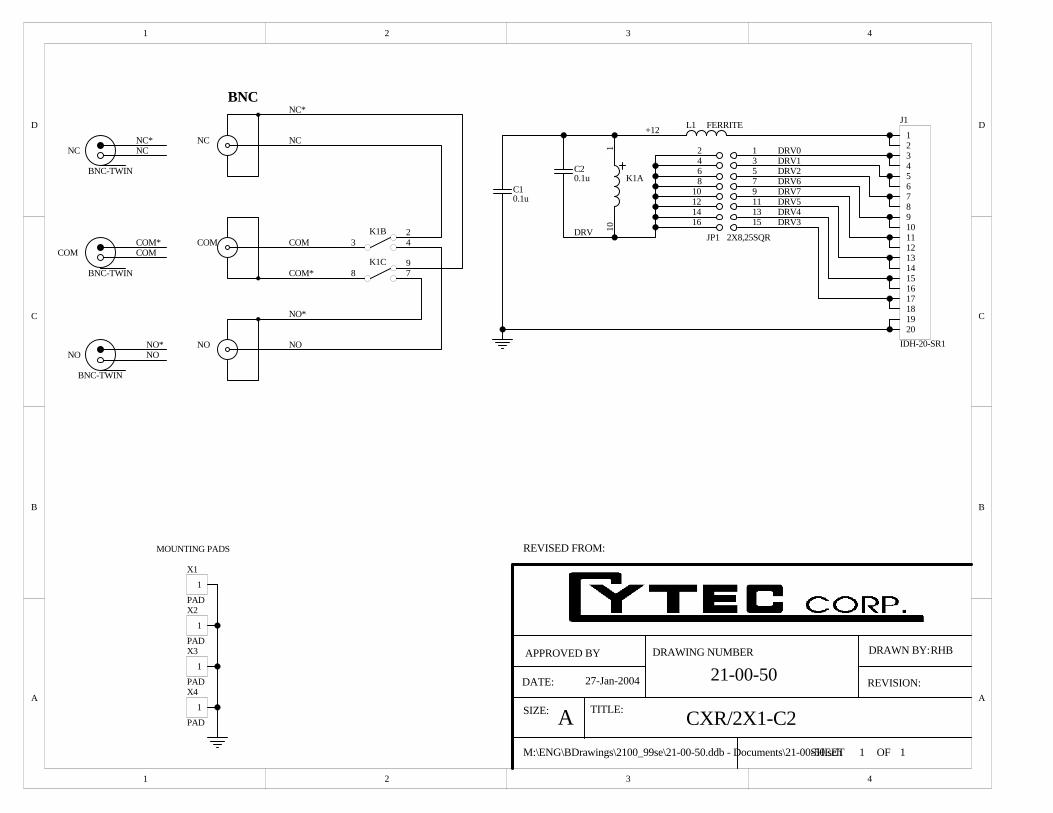
1 2 3 4
A
B
C
D
4321
D
C
B
A
DRAWN BY:APPROVED BY
SHEET
REVISION:
DRAWING NUMBER
DATE: 27-Jan-2004
CXR/2X1-C2
21-00-50
M:\ENG\BDrawings\2100_99se\21-00-50.ddb - Documents\21-00-50.sch OF
SIZE: TITLE:A
REVISED FROM:
11
C10.1u
L1 FERRITE
C20.1u
+12
1
X1
PAD
1
X2
PAD
1
X3
PAD
1
X4
PAD
MOUNTING PADS
13579111315
2468
10121416
JP1 2X8,25SQR
1234567891011121314151617181920
J1
IDH-20-SR1
DRV0DRV1DRV2
DRV3DRV4DRV5
DRV6DRV7
BNC
DRV3 4
2K1B
8 79K1C
110
K1A
NC
COM
NONO
COM
NC
RHB
NC*
COM*
NO*
NC
BNC-TWIN
COM
BNC-TWIN
NO
BNC-TWIN
NONO*
COMCOM*
NCNC*

1
1
2
2
3
3
4
4
D D
C C
B B
A A
DRAWN BY:APPROVED BY
SHEET
REVISION:
DRAWING NUMBER
DATE: 12/29/2004
CXR/2X1-GT-50 SW MODULE
21-01-50
M:\ENG\BDrawings\21-01-50.sch OF
SIZE: TITLE:A
REVISED FROM:
11
0.1uC1
L1
0.1uC3
+12
13579111315
2468
10121416
JP1
1234567891011121314151617181920
J1
DRV0DRV1DRV2
DRV3DRV4DRV5
DRV6DRV7
1615
+
K0A
0.1uC2
1615
+
K1A
K0 - DRIVES 0,2,4,OR 6
K1 - DRIVES 1,3,5,OR 7
A
4 17K0B
50
R1
4 17
K1B
11 148
K1C
50
R2
A
C
B
COM
B
1
PAD
X1
1
PAD
X2
1
PAD
X3
1
PAD
X4
MOUNTING PADS
2356
K0C
RELAY GROUNDS
2356
K1D
9101213
K1E
RHB
P0
P1
P2
2-101-1
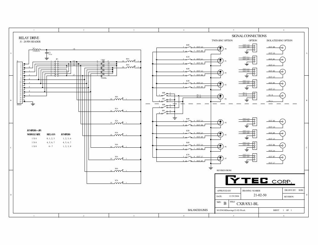
1
1
2
2
3
3
4
4
5
5
6
6
D D
C C
B B
A A
DRAWN BY:APPROVED BY
SHEET
REVISION:
DRAWING NUMBER
DATE: 12/29/2004
CXR/8X1-BL
21-02-50
M:\ENG\BDrawings\21-02-50.sch OF
SIZE: TITLE:B
REVISED FROM:
1 1
RELAY DRIVETWIN-BNC OPTION OPTION
BALANCED LINES
J1 - 20 PIN HEADER ISOLATED BNC OPTION
SIGNAL CONNECTIONS
RHB
3 4
78
K0B
3 4
78
K1B
3 4
78
K2B
3 4
78
K3B
3 4
78
K4B
3 4
78
K5B
3 4
78
K6B
3 4
78
K7B
3 42K8B
8 79K8C
3 42K9B
8 79K9C
OUT_H0
OUT_H1
OUT_H2
OUT_H3
OUT_H4
OUT_H5
OUT_H6
OUT_H7
OUT_H0
OUT_H1
OUT_H2
OUT_H3
OUT_H4
OUT_H5
OUT_H6
OUT_H7
OUT_H0
OUT_H1
OUT_H2
OUT_H3
OUT_H4
OUT_H5
OUT_H6
OUT_H7
OUT_L0
OUT_L1
OUT_L2
OUT_L3
OUT_L4
OUT_L5
OUT_L6
OUT_L7
OUT_L0
OUT_L1
OUT_L2
OUT_L3
OUT_L4
OUT_L5
OUT_L6
OUT_L7
OUT_L0
OUT_L1
OUT_L2
OUT_L3
OUT_L4
OUT_L5
OUT_L6
OUT_L7
IN_HIN_H IN_HIN_LIN_L
IN_L
P1
P2
P3
P4
P5
P6
P7
P8
P0
12345678 9
10111213141516
TND90x
CRP1
123
456789
1011121314151617181920
IDH20
J1
0
1
2
6
7
5
4
3
+12
0.1uC1
FERRITE
L1
3/7
2/61/50/4
JP112345678
110
K9A
110
K8A
110
K0A
110
K1A
110K2A
110
K3A
110
K4A
110K5A
110
K6A
110
K7A
JUMPERS --- JP1
MODULE SIZE RELAYS JUMPERS
1 X 4
1 X 4
1 X 8
0, 1, 2, 3
4, 5, 6, 7
0 - 7
1, 2, 3, 6
4, 5, 6, 7
1, 2, 3, 8

1 2 3 4 5 6
A
B
C
D
654321
D
C
B
A
DRAWN BY:APPROVED BY
A
SHEET
REVISION:
DRAWING NUMBER
DATE: 19-Oct-2006
CXR/2(4X1)-LL
21-13-50-1
21-13-50-1.sch OF
SIZE: TITLE:B1 1
KJA
8 9CRP1H
L1 FERRITE
C10.1u
1 16CRP1A
2 15CRP1B
3 14CRP1C
4 13CRP1D
5 12CRP1E
6 11CRP1F
7 10CRP1G
+12
J1 - RELAY DRIVE CONNECTION
DRV3
DRV2
DRV1
DRV0
DRV4
DRV5
DRV6
DRV7
+12V123456789
1011121314151617181920
J1
13579
111315
246810121416
JP1 DRV0/4DRV1/5DRV2/6
DRV3/7
8X1, 4X1 DRIVE JUMPERS
DRVA
DRVB
PLN
23K0A
1
K0B
23K1A
23K2A
23K3A
23K4A
23K5A
23K6A
23K7A
23K8A
23K9A
P0
PL0S0G0
PLN 1
K1BP1
PL1S1G1
PLN 1
K2BP2
PL2S2G2
PLN 1
K3BP3
PL3S3G3
PLN 1
K8BACOM
PL8S8G8
PLN 1
K9BBCOM
PL9S9G9
PLN 1
K4BP4
PL4S4G4
PLN 1
K5BP5
PL5S5G5
PLN 1
K6BP6
PL6S6G6
PLN 1
K7BP7
PL7S7G7
C2
0.1uF
C3
0.1uF
C4
0.1uF
C5
0.1uF
C6
0.1uF
C7
0.1uF
C8
0.1uF
C9
0.1uF
C10
0.1uF
C11
0.1uF+12
+12

1
1
2
2
3
3
4
4
5
5
6
6
7
7
8
8
D D
C C
B B
A A
DRAWN BY:APPROVED BY
SHEET
REVISION:
DRAWING NUMBER
DATE: 4/14/2005
CXR/8X1-1T SWITCH MODULE
21-14-50
O F
SIZE: TITLE:
1 1
APPROVED BY
DATE: 4/14/2005
SIZE: TITLE:
A3
REVISED FROM:2-442-2
RHB
21-14-50
8 9CRP1H
FERRITEL1
0.1UFC1
1 1 6CRP1A
2 1 5CRP1B
3 1 4CRP1C
4 1 3CRP1D
5 1 2CRP1E
6 1 1CRP1F
7 1 0CRP1G
+12J1 - RELAY DRIVE CONNECTION
DRV3
DRV2
DRV1
DRV0
DRV4
DRV5
DRV6
DRV7
+12V123456789
1011121314151617181920
J1
13579111315
2468
10121416
JP1
DRV0/4DRV1/5DRV2/6
DRV3/7
8X1, 4X1 DRIVE JUMPERS
DRVA
DRVBCOM
P 0
R0
P 1
R1
P 2
R2
P 3
R3
P 4
R4
P 5
R5
P 6
R6
P 7
R7
1 2K0A
4 35
K0B
4 35K1B
4 35K2B
4 35K3B
4 35K4B
4 35
K5B
4 35K6B
4 35K7B
1 2K7A
1 2K6A
1 2K5A
1 2K4A
1 2K3A
1 2K2A
1 2K1A
CHART
RESISTOR VALUETYPE
T1KT50T75
R0-R7R0-R7R0-R7
1K49.975
NOTES:1. UNLESS OTHERWISE SPECIFIED ALL RESISTORS ARE IN OHMS.
21K8A
21K9A
34 K8B
34 K9B

1
1
2
2
3
3
4
4
5
5
6
6
7
7
8
8
D D
C C
B B
A A
DRAWN BY:APPROVED BY
SHEET
REVISION:
DRAWING NUMBER
DATE: 4/14/2005
CXR/8X1-1S SWITCH MODULE
21-14-51
OF
SIZE: TITLE:
1 1
APPROVED BY
DATE: 4/14/2005
SIZE: TITLE:A3
REVISED FROM:2-442-2
RHB
21-14-51
8 9CRP1H
FERRITEL1
0.1UFC1
1 16CRP1A
2 15CRP1B
3 14CRP1C
4 13CRP1D
5 12CRP1E
6 11CRP1F
7 10CRP1G
+12J1 - RELAY DRIVE CONNECTION
DRV3
DRV2
DRV1
DRV0
DRV4
DRV5
DRV6
DRV7
+12V123456789
1011121314151617181920
J1
13579111315
2468
10121416
JP1
DRV0/4DRV1/5DRV2/6
DRV3/7
8X1, 4X1 DRIVE JUMPERS
DRVA
DRVBCOM
P0
P1
P2
P3
P4
P5
P6
P7
1 2K0A
1 2K7A
1 2K6A
1 2K5A
1 2K4A
1 2K3A
1 2K2A
1 2K1A
4 3K0B
4 3K1B
4 3K2B
4 3K3B
4 3K4B
4 3K5B
4 3K6B
4 3K7B
21K8A
21 K9A
34 K8B
34
K9B

1
1
2
2
3
3
4
4
5
5
6
6
7
7
8
8
D D
C C
B B
A A
DRAWN BY:APPROVED BY
SHEET
REVISION:
DRAWING NUMBER
DATE: 4/14/2005
CXR/4X1-1T SWITCH MODULE
21-14-52
OF
SIZE: TITLE:
1 1
APPROVED BY
DATE: 4/14/2005
SIZE: TITLE:A3
REVISED FROM:2-442-2
RHB
21-14-52
8 9CRP1H
FERRITEL1
0.1UFC1
1 16CRP1A
6 11CRP1F
7 10CRP1G
+12J1 - RELAY DRIVE CONNECTION
DRV3
DRV2
DRV1
DRV0
DRV4
DRV5
DRV6
DRV7
+12V123456789
1011121314151617181920
J1
13579111315
2468
10121416
JP1
DRV0/4DRV1/5DRV2/6
DRV3/7
8X1, 4X1 DRIVE JUMPERS
DRVA
COM
P0
R0
P1
R1
P2
R2
P3
R3
1 2K0A
4 35K0B
4 35K1B
4 35K2B
4 35K3B 1 2
K3A
1 2K2A
1 2K1A
CHART
RESISTOR VALUETYPE
T1KT50T75
R0-R3R0-R3R0-R3
1K49.975
NOTES:1. UNLESS OTHERWISE SPECIFIED ALL RESISTORS ARE IN OHMS.
21K8A
34 K8B

1
1
2
2
3
3
4
4
5
5
6
6
7
7
8
8
D D
C C
B B
A A
DRAWN BY:APPROVED BY
SHEET
REVISION:
DRAWING NUMBER
DATE: 4/14/2005
CXR/4X1-1S SWITCH MODULE
21-14-53
OF
SIZE: TITLE:
1 1
APPROVED BY
DATE: 4/14/2005
SIZE: TITLE:A3
REVISED FROM:2-442-2
RHB
21-14-53
8 9CRP1H
FERRITEL1
0.1UFC1
1 16CRP1A
6 11CRP1F
7 10CRP1G
+12J1 - RELAY DRIVE CONNECTION
DRV3
DRV2
DRV1
DRV0
DRV4
DRV5
DRV6
DRV7
+12V123456789
1011121314151617181920
J1
13579111315
2468
10121416
JP1
DRV0/4DRV1/5DRV2/6
DRV3/7
8X1, 4X1 DRIVE JUMPERS
DRVA
COM
P0
P1
P2
P3
1 2K0A
1 2K3A
1 2K2A
1 2K1A
4 3K0B
4 3K1B
4 3K2B
4 3K3B
21K8A
34 K8B

1
2
3
4
5
6
10
9
11 12 15.6" DEEP x 19" WIDE x 7" HIGH1 14-10-20 CHASSIS ASSY
2 CL8 HOLDDOWN ASSY3 CL/128 MOTHERBOARD4 CL8 DISPLAY MOD.5 CX POWER SUPPLY SHELF
w/ 12V-1.7A & 5V-1.2A P.S.
6 99-00-30 CABLE ASSY7 RS-232 & LAN Cables8 IF-9 Control Interface Module9 AC SELECTABLE POWER ENTRY
10 SWITCH MOD PER ORDER11 OPTIONAL KEYPAD M.C.12 16x8 OVERLAY FRONT PANEL
POWER WIRING #2-190-5B
12V pin 55V pin 3
GND pin 1
GND pins 1, 25V pins 3, 4
8
7
16 pin1:1 Cable
21-37-00
5V-1.2A12V-1.7A
Mount Here
Mount Here
POW
ERM
.C.
J4P
1
DATE: DRAWN BY:
DRAWING NUMBER:.5
.75.25
1.00
SIZE: TITLE:
COMMENTS:
D
A
B
C
D
E
1 2 3 4 5 6 7 8
A
B
C
D
E
1 2 3 4 5 6 7 8
CAD FILE:
TOL. +/- .010" U.O.S.
CXAR/128-MAINFRAME w/ IF-915" DEEP VERSION
PV8/5/13 21-37-00.dw2


1 2 3 4 5 6
A
B
C
D
654321
D
C
B
A
DRAWN BY:APPROVED BY
SHEET
REVISION:
DRAWING NUMBER
DATE: 18-May-2012
CXR/8x1-1H SWITCH MODULE
21-24-50
21-24-50.SCH OF
SIZE: TITLE:B1 1
KJA
P0
COM
12345678 9
10111213141516
CRP1
TND90x
R1
P1R2
P2R3
P3R4
P4R5
P5R6
P6R7
P7R8
123456789
1011121314151617181920
J1
IDH20
0
1
2
6
7
5
4
3
+12
C10.1u
L1
FERRITE
3/7
2/61/50/4
JUMPER12345678
JUMPERS
MODULE SIZE RELAYS JUMPERS 1 X 4 0,1,2,3 1,2,3,8 1 X 4 4,5,6,7 4,5,6,7 1 X 8 0 - 7 1,2,3,8
1 2K0A
435 K0B
1 2K1A
435 K1B
1 2K2A
435 K2B
1 2K3A
435 K3B
1 2K4A
435 K4B
1 2K5A
435 K5B
1 2K6A
435 K6B
1 2K7A
435 K7B
12 K8A
435 K8B
12 K9A
435 K9B
12 K10A
435 K10B
12 K11A
435 K11B
12 K12A
435 K12B
12 K13A
435 K13B
12 K14A
435 K14B
12 K15A
435 K15B
12 K16A
4 35K16B
12 K17A
4 35
K17B

1
3
4
5
6
10
9
11 12 15.6" DEEP x 19" WIDE x 7" HIGH1 14-10-20 CHASSIS ASSY
2 CP HOLDDOWN ASSY3 CP/128 MOTHERBOARD4 CP8 DISPLAY MOD.5 CX POWER SUPPLY SHELF
w/ 12V-1.7A & 5V-1.2A P.S.
6 99-00-30 CABLE ASSY7 IEEE-488, RS-232 & LAN CABLES8 CONTROL INTERFACE MODULE9 AC SELECTABLE POWER ENTRY
10 SWITCH MOD PER ORDER11 OPTIONAL KEYPAD M.C.12 16x8 OVERLAY FRONT PANEL
2-190-5B Power Wiring
12V pin 55V pin 3
GND pin 1
GND pins 1, 25V pins 3, 4
8
1:1 Cable16 pin
721-32-30 Control Wiring
13 CP MAINFRAME ADAPTER MOD(12-02-10)
13
2
21-32-00
5V-1.2A12V-1.7A
Mount Here
Mount Here
PO
WE
RM
.C.
J4P
1
DATE: DRAWN BY:
DRAWING NUMBER:.5
.75.25
1.00
SIZE: TITLE:
COMMENTS:
D
A
B
C
D
E
1 2 3 4 5 6 7 8
A
B
C
D
E
1 2 3 4 5 6 7 8
CAD FILE:
TOL. +/- .010" U.O.S.
CXAR/128-CP-MF w/ IF-9 or IF-11CP Motherboard Version
PV9/8/14 21-32-00.dcd
1/14/15 DRA Added IF-11 & New Holddown

1 2 3 4
A
B
C
D
4321
D
C
B
A
DRAWN BY:APPROVED BY
SHEET
REVISION:
DRAWING NUMBER
DATE: 1-Oct-2013
CXR/2X1-75 SW MODULE
30-10-50-1
OF
SIZE: TITLE:A11
1
X1
PAD
1
X2
PAD
1
X3
PAD
1
X4
PAD
MOUNTING PADS
KJA
C10.1u
L1 FERRITE
C20.1u
+12
13579111315
2468
10121416
JP1 2X8,25SQR
1234567891011121314151617181920
J1
IDH-20-SR1
DRV0DRV1DRV2
DRV3DRV4DRV5
DRV6DRV7
NC
COM
NO
NC
COM
NO
71
+
K0A
BNC
DRV11 814
K0B
ARE13129101213
K0C
Place Single Jumper Across JP1 At Desired Drive Location To Actuate Relay
Drive Numbers Are Labeled On PCB

1
1
2
2
3
3
4
4
5
5
6
6
D D
C C
B B
A A
DRAWN BY:APPROVED BY
SHEET
REVISION:
DRAWING NUMBER
DATE: 10/1/2013
CXG/8X1 (50 0HM) SWITCH MODULE
30-17-50
30-17-50.SchDoc OF
SIZE: TITLE:B
REVISED FROM:
1 1
71 +K1A
11814
K0B
1 16CRP1A
TND903-1 C30.1UF
L1 INDUCTOR
R1
68012
468
10121416
3579111315
123456789
1011121314151617181920
J1
P0
+
0
1
2
3
4
5
6
7
2 15CRP1B
TND903-1
C1
0.1UF
3 14CRP1C
TND903-1
4 13CRP1D
TND903-1
5 12CRP1E
TND903-1
6 11CRP1F
TND903-1
7 10CRP1G
TND903-1
8 9CRP1H
TND903-1
71 +K2A
C40.1UF
71 +K3A
C50.1UF
71 +K0A
C20.1UF
C60.1UF
C70.1UF
C80.1UF
71 +K4A
71 +K5A
71 +K6A
+12V
0/41/52/6
3/7
P1
11814
K2BP2
P3
11814
K4BP4
P5
11814
K6BP6
P7
9101213
K0C
9101213
K1C
9101213
K2C
9101213
K3C
9101213
K4C
9101213
K5C
9101213
K6C
11814
K5B
11814
K1B
11814
K3B
P8
SIGNAL/DRIVER RELAYS
01234567
NONEK0K1K1,K2K3K3,K4K3,K5K3,K5.K6
CXG/4X1
8X1, 4X1 DRIVE JUMPERS
RELAY DRIVE CONNECTOR
RELAY GROUNDS
JP1
IN0
IN1
IN2
IN3
IN4
IN5
IN6
IN7
COMCOM
IN0
IN1
IN2
IN3
IN4
IN5
IN6
IN7
RHB
IN8
IN9
IN10
IN11
IN12
IN13
JUMPERPINS DRIVE
1,23,45,615,16
0123
JUMPERPINS DRIVE
13,1411,127,89,10
4567
8x1 & 4x1 Using Drives 0-3 4x1 Using Drives 4-7
DRIVE JUMPER KEY
012
345
67

1
1
2
2
3
3
4
4
5
5
6
6
D D
C C
B B
A A
DRAWN BY:APPROVED BY
SHEET
REVISION:
DRAWING NUMBER
DATE: 10/1/2013
CXG/8X1 (75 0HM) SWITCH MODULE
30-18-50
30-18-50.SchDoc OF
SIZE: TITLE:B
REVISED FROM:
1 1
71 +K1A
11814
K0B
1 16CRP1A
TND903-1 C30.1UF
L1INDUCTOR
R1
68012
468
10121416
3579111315
123456789
1011121314151617181920
J1
P0
+
0
1
2
3
4
5
6
7
2 15CRP1B
TND903-1
C10.1UF
3 14CRP1C
TND903-1
4 13CRP1D
TND903-1
5 12CRP1E
TND903-1
6 11CRP1F
TND903-1
7 10CRP1G
TND903-1
8 9CRP1H
TND903-1
71 +K2A
C40.1UF
71 +K3A
C50.1UF
71 +K0A
C20.1UF
C60.1UF
C70.1UF
C80.1UF
71 +K4A
71 +K5A
71 +K6A
+12V
0/41/52/6
3/7
P1
11814
K2BP2
P3
11814
K4BP4
P5
11814
K6BP6
P7
9101213
K0C
9101213
K1C
9101213
K2C
9101213
K3C
9101213
K4C
9101213
K5C
9101213
K6C
11814
K5B
11814
K1B
11814
K3B
P8
SIGNAL/DRIVER RELAYS
01234567
NONEK0K1K1,K2K3K3,K4K3,K5K3,K5.K6
CXG/4X1
8X1, 4X1 DRIVE JUMPERS
RELAY DRIVE CONNECTOR
RELAY GROUNDS
JP1
IN0
IN1
IN2
IN3
IN4
IN5
IN6
IN7
COMCOM
IN0
IN1
IN2
IN3
IN4
IN5
IN6
IN7
RHB
IN8
IN9
IN10
IN11
IN12
IN13
JUMPERPINS DRIVE
1,23,45,615,16
0123
JUMPERPINS DRIVE
13,1411,127,89,10
4567
8x1 & 4x1 Using Drives 0-3 4x1 Using Drives 4-7
DRIVE JUMPER KEY
012
345
67

1
1
2
2
3
3
4
4
5
5
6
6
7
7
8
8
D D
C C
B B
A A
DRAWN BY:APPROVED BY
SHEET
REVISION:
DRAWING NUMBER
DATE: 10/1/2013
CXR/8X1-GT-75
30-19-50
Cannot open file Logo2.bmp
OF
SIZE: TITLE:
1 1
APPROVED BY
DATE: 10/1/2013
SIZE: TITLE:A3
REVISED FROM:
RHB
30-19-50
11814
K8B
L1INDUCTOR
12468
10121416
3579111315
123456789
1011121314151617181920
J1
P0
+
0
1
2
3
4
5
6
7
2 15CRP1B
TND903-1
C10.1UF
5 12CRP1E
TND903-1
6 11CRP1F
TND903-1
3 14CRP1C
TND903-1
1 16CRP1A
TND903-1
71 +K1A
C30.1UF
+12V
0/41/52/6
3/7 P1
11814
K9BP2
P3
11814
K10BP4
P5
11814
K11BP6
P7
9101213
K0C
9101213
K1C
9101213
K2C
9101213
K3C
9101213
K4C
9101213
K5C
9101213
K6C
11814
K13B
11814
K12B
11814
K14B
P8
SIGNAL/DRIVER RELAYS
01234567
K0K1,K8K2,K12K3,K9,K12
K5,K10,K14K4,K14
K6,K13,K14
CXR/4X1
8X1, 4X1 DRIVE JUMPERS
RELAY DRIVE CONNECTOR
RELAY GROUNDS
JP1
IN0
IN1
IN2
IN3
IN4
IN5
IN6
IN7
COMCOM
IN0
IN2
IN3
IN4
IN5
IN6
IN7
IN8IN9
IN10IN11
IN12
IN13
K7,K11,K13,K14
71 +K0A
C20.1UF
9101213
K7C
9101213
K8C
9101213
K9C
9101213
K10C
9101213
K11C
9101213
K12C
9101213
K13C
11 814K0B
11 814K1B
R1
75
R0
75
IN1
11 814K2B
11 814K3B
R3
75
R2
75
11 814K4B
11 814K5B
R5
75
R4
75
11 814K6B
11 814K7B
R7
75
R6
75
9101213
K14C
71 +K3A
C50.1UF
71 +K2A
C40.1UF
71 +K5A
C70.1UF
71 +K4A
C60.1UF
71 +K7A
C90.1UF
71 +K6A
C80.1UF
71 +K9A
C110.1UF
71 +K8A
C100.1UF
71 +K11A
C130.1UF
71 +K10A
C120.1UF
71 +K13A
C150.1UF
71 +K12A
C140.1UF
71 +K14A
C160.1UF
7 10CRP1G
TND903-1
4 13CRP1D
TND903-1
8 9CRP1H
TND903-1
IN14
IN15IN16
IN17IN18
IN19
IN20
IN21
JUMPERPINS DRIVE
1,23,45,615,16
0123
JUMPERPINS DRIVE
13,1411,127,89,10
4567
8x1 & 4x1 Using Drives 0-3 4x1 Using Drives 4-7
DRIVE JUMPER KEY
012
345
67

1
1
2
2
3
3
4
4
5
5
6
6
D D
C C
B B
A A
71 +K8A
11 814
K0B
0.1UFC9
INDUCTORL1
680
R1
123456789
1011121314151617181920
J1
P0
+
0
1
2
3
4
5
6
7
0.1UFC11
71 +K5A
0.1UFC6
71 +K0A
0.1UFC1
71 +K4A
0.1UFC5
0.1UFC2
0.1UFC7
0.1UFC3
71 +K1A
71 +K6A
71 +K2A
+12V
11 814
K1BP1
11 814
K2BP2
11 814
K3BP3
9101213
K0C
9101213
K1C
9101213
K2C
9101213
K3C
9101213
K4C
9101213
K5C
9101213
K6C
11814
K5B
11814
K4B
11814
K8B
P4
SIGNAL/DRIVER IN
01234567
01230123
RELAY DRIVE CONNECTOR
RELAY GROUNDS
IN0
IN1
IN2
IN3
OUT0OUT0
RHB
0.1UFC4
0.1UFC8
71 +K3A
71 +K7A
9101213
K7C
9101213
K8C118
14K7B
11814
K6B
11814
K9B
P5OUT10UT1
1N4148
CR1
1N4148
CR2
1N4148
CR4
1N4148
CR3
0.1UFC10
71 +K9A
9101213
K9C
IN0
IN1
IN2
IN3
OUT
00001111
RELAYS
NONEK4K8K5.K8K0K1,K6K2,K9K3,K7,K9
DRAWN BY:APPROVED BY
SHEET
REVISION:
DRAWING NUMBER
DATE: 8/7/2008
CXR/4X2-G-50 SWITCH MODULE
30-21-50
OF
SIZE: TITLE:B1 1
RHB
30-21-50.SchDoc
REVISED FROM: 2-473

1
1
2
2
3
3
4
4
5
5
6
6
D D
C C
B B
A A
DRAWN BY:APPROVED BY
SHEET
REVISION:
DRAWING NUMBER
DATE: 1/21/2014
CXR/4X2-G-75 SWITCH MODULE
30-22-50
OF
SIZE: TITLE:B1 1
RHB
30-22-50.SchDoc
71 +K8A
11 814
K0B
C90.1UF
L1INDUCTOR
R1
680
123456789
1011121314151617181920
J1
P0
+
0
1
2
3
4
5
6
7
C110.1UF
71 +K5A
C60.1UF
71 +K0A
C10.1UF
71 +K4A
C50.1UF
C20.1UF
C70.1UF
C30.1UF
71 +K1A
71 +K6A
71 +K2A
+12V
11 814
K1BP1
11 814
K2BP2
11 814
K3BP3
9101213
K0C
9101213
K1C
9101213
K2C
9101213
K3C
9101213
K4C
9101213
K5C
9101213
K6C
11814
K5B
11814
K4B
11814
K8B
P4
SIGNAL/DRIVER IN
01234567
01230123
RELAY DRIVE CONNECTOR
RELAY GROUNDS
IN0
IN1
IN2
IN3
OUT0OUT0
RHB
C40.1UF
C80.1UF
71 +K3A
71 +K7A
9101213
K7C
9101213
K8C118
14K7B
11814
K6B
11814
K9B
P5OUT10UT1
CR1
1N4148
CR2
1N4148
CR4
1N4148
CR3
1N4148
C100.1UF
71 +K9A
9101213
K9C
IN0
IN1
IN2
IN3
OUT
00001111
RELAYS
NONEK4K8K5.K8K0K1,K6K2,K9K3,K7,K9
REVISED FROM: 2-473
N1N2
N3N4
N5N6
N7N8
N9N10
N11N12
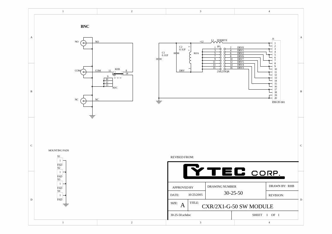
1
1
2
2
3
3
4
4
D D
C C
B B
A A
DRAWN BY:APPROVED BY
SHEET
REVISION:
DRAWING NUMBER
DATE: 10/25/2005
CXR/2X1-G-50 SW MODULE
30-25-50
30-25-50.schdoc OF
SIZE: TITLE:A
REVISED FROM:
11
RHB
1
PAD
X1
1
PAD
X2
1
PAD
X3
1
PAD
X4
MOUNTING PADS
0.1UFC1
FERRITEL1
0.1UFC2
+12
13579
111315
246810121416
2X8,25SQR
JP11234567891011121314151617181920
IDH-20-SR1
J1
DRV0DRV1DRV2
DRV3DRV4DRV5
DRV6DRV7
NC
COM
NO
NC
COM
NO
BNC
DRV11 814
K0B
71
+
K0A
9101213
K0C

1 2 3 4 5 6 7 8
A
B
C
D
87654321
D
C
B
A DRAWN BY:APPROVED BY
SHEET
REVISION:
DRAWING NUMBER
DATE: 27-Mar-2008
CXR/8X1-GT-50-HP
30-29-50
OF
SIZE: TITLE:
1 1
APPROVED BY
DATE: 27-Mar-2008
SIZE: TITLE:A3
REVISED FROM:
KJA
30-29-50.SCH
11814
K8B
L1INDUCTOR
12468
10121416
3579111315
123456789
1011121314151617181920
J1
P0
+
0
1
2
3
4
5
6
7
2 15CRP1B
TND903-1
C10.1UF
5 12CRP1E
TND903-1
6 11CRP1F
TND903-1
3 14CRP1C
TND903-1
1 16CRP1A
TND903-1
71 +K1A
C30.1UF
+12V
0/41/52/6
3/7
P1
11814
K9BP2
P3
11814
K10BP4
P5
11814
K11BP6
P7
9101213
K0C
9101213
K1C
9101213
K2C
9101213
K3C
9101213
K4C
9101213
K5C
9101213
K6C
11814
K13B
11814
K12B
11814
K14B
P8
SIGNAL/DRIVER RELAYS
01234567
K0K1,K8K2,K12K3,K9,K12
K5,K10,K14K4,K14
K6,K13,K14
CXR/4X1
8X1, 4X1 DRIVE JUMPERS
RELAY DRIVE CONNECTOR
RELAY GROUNDS
JP1 IN0
IN1
IN2
IN3
IN4
IN5
IN6
IN7
COMCOM
IN0
IN2
IN3
IN4
IN5
IN6
IN7
IN8IN9
IN10IN11
IN12
IN13
K7,K11,K13,K14
71 +K0A
C20.1UF
9101213
K7C
9101213
K8C
9101213
K9C
9101213
K10C
9101213
K11C
9101213
K12C
9101213
K13C
11 814K0B
11 814K1B
R1
50
R0
50
IN1
11 814K2B
11 814K3B
R3
50
R2
50
11 814K4B
11 814K5B
R5
50
R4
50
11 814K6B
11 814K7B
R7
50
R6
50
9101213
K14C
71 +K3A
C50.1UF
71 +K2A
C40.1UF
71 +K5A
C70.1UF
71 +K4A
C60.1UF
71 +K7A
C90.1UF
71 +K6A
C80.1UF
71 +K9A
C110.1UF
71 +K8A
C100.1UF
71 +K11A
C130.1UF
71 +K10A
C120.1UF
71 +K13A
C150.1UF
71 +K12A
C140.1UF
71 +K14A
C160.1UF
7 10CRP1G
TND903-1
4 13CRP1D
TND903-1
8 9CRP1H
TND903-1
IN14
IN15IN16
IN17IN18
IN19
IN20
IN21

1 2 3 4
A
B
C
D
4321
D
C
B
A
DRAWN BY:APPROVED BY
SHEET
REVISION:
DRAWING NUMBER
DATE: 2-May-2008
CXR/2X1-C-GT-75 SW MODULE
30-30-50
30-30-50.sch OF
SIZE: TITLE:A11
C10.1u
L1+12
13579111315
2468
10121416
JP1
1234567891011121314151617181920
J1
DRV0DRV1DRV2
DRV3DRV4DRV5
DRV6DRV7
C20.1u
K0-K2 - DRIVES 0-7
NCR1
75
R2
75
NC
COM
NO
COM
NO
RELAY GROUNDS
KJA
P0
P1
P2
71
+
K0A
11 814K0B
RLY-RK-1C
9101213
K0C
71
+
K1A
11 814K1B
RLY-RK-1C
9101213
K1C7
1
+
K2A
11 814
K2B
RLY-RK-1C
9101213
K2C
CR1
1N4936

1 2 3 4
A
B
C
D
4321
D
C
B
A
DRAWN BY:APPROVED BY
SHEET
REVISION:
DRAWING NUMBER
DATE: 17-Apr-2009
CXR/2X1-G-75-F SW MOD.
30-31-50
OF
SIZE: TITLE:A11
1
X1
PAD
1
X2
PAD
1
X3
PAD
1
X4
PAD
MOUNTING PADS
KJA
C10.1u
L1 FERRITE
C20.1u
+12
13579111315
2468
10121416
JP1 2X8,25SQR
1234567891011121314151617181920
J1
IDH-20-SR1
DRV0DRV1DRV2
DRV3DRV4DRV5
DRV6DRV7
NC
COM
NO
NC
COM
NO
71
+
K0A
F CONNECTORS
DRV11 814
K0B
ARE13129
101213
K0C

1 2 3 4 5 6
A
B
C
D
654321
D
C
B
A
DRAWN BY:APPROVED BY
A
SHEET
REVISION:
DRAWING NUMBER
DATE: 17-Mar-2006
CXS/8x1-GT-75 Switch Module
64-00-50-01
64-00-50-01.sch OF
SIZE: TITLE:B1 2
KJA
1
2 3 4 5 6 7 8 9
RP12.2k
DRV2
DRV3
DRV0
DRV1
DRV4
DRV5
DRV6
DRV7
+C1
10uF
C30.1uF
L1 FERRITE
+12V
Vin3 Vout 2
Adj
.1
U3 LD1084V
R1243
R2357
+ C210uF
+3V
13579
111315
246810121416
1719
1820
J1 HDR20
12345678
16151413121110
9
RP3 68k
1
23456789
RP22.2k
1
2345678910
RP422k
21U2A 74AC04
43U2B 74AC04
+3V
116CRP1A
215CRP1B
314CRP1C
413CRP1D
512CRP1E
611CRP1F
710CRP1G
89CRP1H
116CRP2A
215CRP2B
314CRP2C
413CRP2D
512CRP2E
611CRP2F
710CRP2G
89CRP2H
116CRP3A
215CRP3B
314CRP3C
413CRP3D
512CRP3E
611CRP3F
710CRP3G
89CRP3H
CHAN0
CHAN1
CHAN2
CHAN3
CHAN4
CHAN5
CHAN6
CHAN7
C40.1uF
CHAN0
CHAN1
CHAN2
CHAN3
CHAN4
CHAN5
CHAN6
CHAN7
CHAN0
CHAN1
CHAN4
CHAN5
CHAN2
CHAN3
CHAN6
CHAN7
CHAN0
CHAN6
CHAN1
CHAN7
CHAN2
CHAN4
CHAN3
CHAN5
SHEET 2
21U1A 74AC04
43U1B 74AC04
1011U1E 74AC04
1213U1F 74AC04
1011U2E 74AC04
1213U2F 74AC04
C12
0.1uF

1 2 3 4 5 6
A
B
C
D
654321
D
C
B
A
DRAWN BY:APPROVED BY
A
SHEET
REVISION:
DRAWING NUMBER
DATE: 17-Mar-2006
CXS/8x1-GT-75 Switch Module
64-00-50-02
64-00-50-02.sch OF
SIZE: TITLE:B2 2
KJA
GND1
GND2
RF1 3
GND4
GND5
GND6
GND7
RFC8
GND9
GND10
GND 11
GND 12
RF2 13
GND 14
GND 15
CTRL2 16CTRL1 17
VSS/GND 18GND 19
VDD20
GNDPAD 21
S0
PE42XX
GND1
GND2
RF1 3
GND4
GND5
GND6
GND7
RFC8
GND9
GND10
GND 11
GND 12
RF2 13
GND 14
GND 15
CTRL2 16CTRL1 17
VSS/GND 18GND 19
VDD20
GNDPAD 21
S1
PE42XX
GND1
GND2
RF1 3
GND4
GND5
GND6
GND7
RFC8
GND9
GND10
GND 11
GND 12
RF2 13
GND 14
GND 15
CTRL2 16CTRL1 17
VSS/GND 18GND 19
VDD20
GNDPAD 21
S2 PE42XX
GND1
GND2
RF1 3
GND4
GND5
GND6
GND7
RFC8
GND9
GND10
GND 11
GND 12
RF2 13
GND 14
GND 15
CTRL2 16CTRL1 17
VSS/GND 18GND 19
VDD20
GNDPAD 21
S3 PE42XX
GND1
GND2
RF1 3
GND4
GND5
GND6
GND7
RFC8
GND9
GND10
GND 11
GND 12
RF2 13
GND 14
GND 15
CTRL2 16CTRL1 17
VSS/GND 18GND 19
VDD20
GNDPAD 21
S4 PE42XX
GND1
GND2
RF1 3
GND4
GND5
GND6
GND7
RFC8
GND9
GND10
GND 11
GND 12
RF2 13
GND 14
GND 15
CTRL2 16CTRL1 17
VSS/GND 18GND 19
VDD20
GNDPAD 21
S5 PE42XX
GND1
GND2
RF1 3
GND4
GND5
GND6
GND7
RFC8
GND9
GND10
GND 11
GND 12
RF2 13
GND 14
GND 15
CTRL2 16CTRL1 17
VSS/GND 18GND 19
VDD20
GNDPAD 21
S6 PE42XX
P0
P1
P2
P3
P4
P5
P6
P7
COM
C5
0.1uF
C6
0.1uF
C7
0.1uF
C8
0.1uF
C9
0.1uF
C10
0.1uF
C11
0.1uF
DRV0DRV1
DRV2DRV3
DRV4DRV5
DRV6DRV7
+3V
+3V
+3V
+3V
+3V
+3V
+3V
DRV2DRV3
DRV4DRV5
DRV6DRV7
SHEET 1

1 2 3 4 5 6
A
B
C
D
654321
D
C
B
A
DRAWN BY:APPROVED BY
A
SHEET
REVISION:
DRAWING NUMBER
DATE: 22-Nov-2006
CXS/8x1-GT-75-F Switch Module
64-01-50-01
64-01-50-01.sch OF
SIZE: TITLE:B1 2
KJA
1
2 3 4 5 6 7 8 9
RP12.2k
DRV2
DRV3
DRV0
DRV1
DRV4
DRV5
DRV6
DRV7
+C1
10uF
C30.1uF
L1 FERRITE
+12V
Vin3 Vout 2
Adj
.1
U3 LD1084V
R1243
R2357
+ C210uF
+3V
13579
111315
246810121416
1719
1820
J1 HDR20
12345678
16151413121110
9
RP3 68k
1
23456789
RP22.2k
1
2345678910
RP422k
21U2A 74AC04
43U2B 74AC04
+3V
116CRP1A
215CRP1B
314CRP1C
413CRP1D
512CRP1E
611CRP1F
710CRP1G
89CRP1H
116CRP2A
215CRP2B
314CRP2C
413CRP2D
512CRP2E
611CRP2F
710CRP2G
89CRP2H
116CRP3A
215CRP3B
314CRP3C
413CRP3D
512CRP3E
611CRP3F
710CRP3G
89CRP3H
CHAN0
CHAN1
CHAN2
CHAN3
CHAN4
CHAN5
CHAN6
CHAN7
C40.1uF
CHAN0
CHAN1
CHAN2
CHAN3
CHAN4
CHAN5
CHAN6
CHAN7
CHAN0
CHAN1
CHAN4
CHAN5
CHAN2
CHAN3
CHAN6
CHAN7
CHAN0
CHAN6
CHAN1
CHAN7
CHAN2
CHAN4
CHAN3
CHAN5
SHEET 2
21U1A 74AC04
43U1B 74AC04
1011U1E 74AC04
1213U1F 74AC04
1011U2E 74AC04
1213U2F 74AC04
C12
0.1uF

1 2 3 4 5 6
A
B
C
D
654321
D
C
B
A
DRAWN BY:APPROVED BY
A
SHEET
REVISION:
DRAWING NUMBER
DATE: 22-Nov-2006
CXS/8x1-GT-75-F Switch Module
64-01-50-02
64-01-50-02.sch OF
SIZE: TITLE:B2 2
KJA
GND1
GND2
RF1 3
GND4
GND5
GND6
GND7
RFC8
GND9
GND10
GND 11
GND 12
RF2 13
GND 14
GND 15
CTRL2 16CTRL1 17
VSS/GND 18GND 19
VDD20
GNDPAD 21
S0
PE42XX
GND1
GND2
RF1 3
GND4
GND5
GND6
GND7
RFC8
GND9
GND10
GND 11
GND 12
RF2 13
GND 14
GND 15
CTRL2 16CTRL1 17
VSS/GND 18GND 19
VDD20
GNDPAD 21
S1
PE42XX
GND1
GND2
RF1 3
GND4
GND5
GND6
GND7
RFC8
GND9
GND10
GND 11
GND 12
RF2 13
GND 14
GND 15
CTRL2 16CTRL1 17
VSS/GND 18GND 19
VDD20
GNDPAD 21
S2 PE42XX
GND1
GND2
RF1 3
GND4
GND5
GND6
GND7
RFC8
GND9
GND10
GND 11
GND 12
RF2 13
GND 14
GND 15
CTRL2 16CTRL1 17
VSS/GND 18GND 19
VDD20
GNDPAD 21
S3 PE42XX
GND1
GND2
RF1 3
GND4
GND5
GND6
GND7
RFC8
GND9
GND10
GND 11
GND 12
RF2 13
GND 14
GND 15
CTRL2 16CTRL1 17
VSS/GND 18GND 19
VDD20
GNDPAD 21
S4 PE42XX
GND1
GND2
RF1 3
GND4
GND5
GND6
GND7
RFC8
GND9
GND10
GND 11
GND 12
RF2 13
GND 14
GND 15
CTRL2 16CTRL1 17
VSS/GND 18GND 19
VDD20
GNDPAD 21
S5 PE42XX
GND1
GND2
RF1 3
GND4
GND5
GND6
GND7
RFC8
GND9
GND10
GND 11
GND 12
RF2 13
GND 14
GND 15
CTRL2 16CTRL1 17
VSS/GND 18GND 19
VDD20
GNDPAD 21
S6 PE42XX
C5
0.1uF
C6
0.1uF
C7
0.1uF
C8
0.1uF
C9
0.1uF
C10
0.1uF
C11
0.1uF
DRV0DRV1
DRV2DRV3
DRV4DRV5
DRV6DRV7
+3V
+3V
+3V
+3V
+3V
+3V
+3V
DRV2DRV3
DRV4DRV5
DRV6DRV7
SHEET 1
P0
F Conn
P1F Conn
P2
F Conn
P3F Conn
P4
F Conn
P5F Conn
P6
F Conn
P7F Conn
COM
F Conn

1 2 3 4 5 6
A
B
C
D
654321
D
C
B
A
DRAWN BY:APPROVED BY
SHEET
REVISION:
DRAWING NUMBER
DATE: 23-Jan-2007
CXS/16x1-GT-75-F Switch Module
64-02-50-01
64-02-50-01.sch OF
SIZE: TITLE:B1 4
KJA
1
2 3 4 5 6 7 8 9
RP12.2k
+C1
10uF
C30.1uF
L1 FERRITE
+12V
Vin3 Vout 2
Adj
.1
U4 LD1084V
R1243
R2357
+ C210uF
+3V
12345678
16151413121110
9
RP3 68k
1
2345678910
RP522k
+3V
CHAN3
CHAN2
CHAN1
CHAN12
CHAN13
CHAN14
CHAN0
CHAN15
C40.1uF
SHEET 2
C21
0.1uF
C50.1uF
1J1A
IDH20
2J1B
4J1D6J1F8J1H10J1J12J1L14J1N16J1P18J1R
19J1S20J1T
INCHAN0INCHAN1INCHAN2INCHAN3
INCHAN12INCHAN13INCHAN14INCHAN15
21
U1A
1011
U1E
1213
U1F
43
U3B
89
U3D
1011
U3E
1213
U3F
DRV LINES
116CRP3A 215CRP3B 314CRP3C 413CRP3D 512CRP3E 611CRP3F 710CRP3G 89CRP3H
116CRP4A 215CRP4B 314CRP4C 413CRP4D 512CRP4E 611CRP4F 710CRP4G 89CRP4H
CHAN0
CHAN1
CHAN2
CHAN3
CHAN4
CHAN5
CHAN6
CHAN7
CHAN8
CHAN9
CHAN10
CHAN11
CHAN12
CHAN13
CHAN15
CHAN14
116CRP2A 215CRP2B 314CRP2C 413CRP2D
512CRP2E 611CRP2F 710CRP2G 89CRP2H
CHAN0
CHAN1
CHAN12
CHAN13
CHAN2
CHAN3
CHAN15
CHAN14
CHAN4
CHAN5
CHAN8
CHAN9
CHAN6
CHAN7
CHAN11
CHAN10
SHEET 2CHAN LINES
DRV0
DRV1
DRV4
DRV5
DRV6
DRV7
R810k
R910k
R510k
R610k
R1110k
R1210k
512CRP8E 611CRP8F 710CRP8G 89CRP8H
116CRP8A 215CRP8B 314CRP8C 413CRP8D
VCC
89
U1D
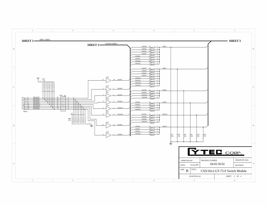
1 2 3 4 5 6
A
B
C
D
654321
D
C
B
A
DRAWN BY:APPROVED BY
SHEET
REVISION:
DRAWING NUMBER
DATE: 23-Jan-2007
CXS/16x1-GT-75-F Switch Module
64-02-50-02
64-02-50-02.sch OF
SIZE: TITLE:B2 4
KJA
1
2 3 4 5 6 7 8 9
RP22.2k
12345678
16151413121110
9
RP4 68k
1
2345678910
RP622k
116CRP5A 215CRP5B 314CRP5C 413CRP5D
512CRP5E 611CRP5F 710CRP5G 89CRP5H
116CRP6A 215CRP6B 314CRP6C 413CRP6D
512CRP6E 611CRP6F 710CRP6G 89CRP6H
CHAN7
CHAN6
CHAN5
CHAN8
CHAN9
CHAN10
CHAN4
CHAN11
CHAN0
CHAN1
CHAN2
CHAN3
CHAN8
CHAN9
CHAN10
CHAN11
CHAN4
CHAN5
CHAN6
CHAN7
CHAN12
CHAN13
CHAN15
CHAN14
SHEET 3
INCHAN4INCHAN5INCHAN6INCHAN7
INCHAN8INCHAN9INCHAN10INCHAN11
3J1C5J1E7J1G9J1I11J1K13J1M15J1O17J1Q
IDH20
65
U1C
21
U2A
43
U2B
65
U2C
1011
U2E
1213
U2F
21
U3A
SHEET 1 DRV LINES
116CRP1A 215CRP1B 314CRP1C 413CRP1D
512CRP1E 611CRP1F 710CRP1G 89CRP1H
CHAN0
CHAN4
CHAN10
CHAN14
CHAN1
CHAN5
CHAN15
CHAN11
CHAN2
CHAN6
CHAN8
CHAN12
CHAN3
CHAN7
CHAN13
CHAN9
SHEET 1 CHAN LINESDRV2
DRV3
DRV8
DRV9
DRV10
DRV11
R710k
R1010k
R310k
R410k
R1310k
R1410k
116CRP7A 215CRP7B 314CRP7C 413CRP7D
512CRP7E 611CRP7F 710CRP7G 89CRP7H
VCC
43
U1B

1 2 3 4 5 6
A
B
C
D
654321
D
C
B
A
DRAWN BY:APPROVED BY
SHEET
REVISION:
DRAWING NUMBER
DATE: 23-Jan-2007
CXS/16x1-GT-75-F Switch Module
64-02-50-03
64-02-50-03.sch OF
SIZE: TITLE:B3 4
KJA
GND1
GND2
RF1 3
GND4
GND5
GND6
GND7
RFC8
GND9
GND10
GND 11
GND 12
RF2 13
GND 14
GND 15
CTRL2 16CTRL1 17
VSS/GND 18GND 19
VDD20
GNDPAD 21
S1
PE4256
GND1
GND2
RF1 3
GND4
GND5
GND6
GND7
RFC8
GND9
GND10
GND 11
GND 12
RF2 13
GND 14
GND 15
CTRL2 16CTRL1 17
VSS/GND 18GND 19
VDD20
GNDPAD 21
S3
PE4256
GND1
GND2
RF1 3
GND4
GND5
GND6
GND7
RFC8
GND9
GND10
GND 11
GND 12
RF2 13
GND 14
GND 15
CTRL2 16CTRL1 17
VSS/GND 18GND 19
VDD20
GNDPAD 21
S4 PE4256
GND1
GND2
RF1 3
GND4
GND5
GND6
GND7
RFC8
GND9
GND10
GND 11
GND 12
RF2 13
GND 14
GND 15
CTRL2 16CTRL1 17
VSS/GND 18GND 19
VDD20
GNDPAD 21
S7 PE4256
GND1
GND2
RF1 3
GND4
GND5
GND6
GND7
RFC8
GND9
GND10
GND 11
GND 12
RF2 13
GND 14
GND 15
CTRL2 16CTRL1 17
VSS/GND 18GND 19
VDD20
GNDPAD 21
S8 PE4256
GND1
GND2
RF1 3
GND4
GND5
GND6
GND7
RFC8
GND9
GND10
GND 11
GND 12
RF2 13
GND 14
GND 15
CTRL2 16CTRL1 17
VSS/GND 18GND 19
VDD20
GNDPAD 21
S9 PE4256
GND1
GND2
RF1 3
GND4
GND5
GND6
GND7
RFC8
GND9
GND10
GND 11
GND 12
RF2 13
GND 14
GND 15
CTRL2 16CTRL1 17
VSS/GND 18GND 19
VDD20
GNDPAD 21
S10 PE4256
C7
0.1uF
C9
0.1uF
C10
0.1uF
C13
0.1uF
C14
0.1uF
C15
0.1uF
C16
0.1uF
DRV3DRV2
DRV4DRV5
DRV8DRV9
DRV10DRV11
+3V
+3V
+3V
+3V
+3V
+3V
+3V
DRV6DRV7
DRV10DRV11
DRV8DRV9
SHEET 2
P0
F Conn
P1F Conn
P2
F Conn
P3F Conn
P4
F Conn
P5F Conn
P6
F Conn
P7F Conn
COMF Conn
GND1
GND2
RF1 3
GND4
GND5
GND6
GND7
RFC8
GND9
GND10
GND 11
GND 12
RF2 13
GND 14
GND 15
CTRL2 16CTRL1 17
VSS/GND 18GND 19
VDD20
GNDPAD 21
S0
PE4256
C6
0.1uFDRV0DRV1
+3V
S2_COM
SHEET 4S2 COM
DRV LINES SHEET 4

1 2 3 4 5 6
A
B
C
D
654321
D
C
B
A
DRAWN BY:APPROVED BY
SHEET
REVISION:
DRAWING NUMBER
DATE: 23-Jan-2007
CXS/16x1-GT-75-F Switch Module
64-02-50-04
64-02-50-04.sch OF
SIZE: TITLE:B4 4
KJA
GND1
GND2
RF1 3
GND4
GND5
GND6
GND7
RFC8
GND9
GND10
GND 11
GND 12
RF2 13
GND 14
GND 15
CTRL2 16CTRL1 17
VSS/GND 18GND 19
VDD20
GNDPAD 21
S2
PE4256
GND1
GND2
RF1 3
GND4
GND5
GND6
GND7
RFC8
GND9
GND10
GND 11
GND 12
RF2 13
GND 14
GND 15
CTRL2 16CTRL1 17
VSS/GND 18GND 19
VDD20
GNDPAD 21
S5
PE4256
GND1
GND2
RF1 3
GND4
GND5
GND6
GND7
RFC8
GND9
GND10
GND 11
GND 12
RF2 13
GND 14
GND 15
CTRL2 16CTRL1 17
VSS/GND 18GND 19
VDD20
GNDPAD 21
S6 PE4256
GND1
GND2
RF1 3
GND4
GND5
GND6
GND7
RFC8
GND9
GND10
GND 11
GND 12
RF2 13
GND 14
GND 15
CTRL2 16CTRL1 17
VSS/GND 18GND 19
VDD20
GNDPAD 21
S11 PE4256
GND1
GND2
RF1 3
GND4
GND5
GND6
GND7
RFC8
GND9
GND10
GND 11
GND 12
RF2 13
GND 14
GND 15
CTRL2 16CTRL1 17
VSS/GND 18GND 19
VDD20
GNDPAD 21
S12 PE4256
GND1
GND2
RF1 3
GND4
GND5
GND6
GND7
RFC8
GND9
GND10
GND 11
GND 12
RF2 13
GND 14
GND 15
CTRL2 16CTRL1 17
VSS/GND 18GND 19
VDD20
GNDPAD 21
S13 PE4256
GND1
GND2
RF1 3
GND4
GND5
GND6
GND7
RFC8
GND9
GND10
GND 11
GND 12
RF2 13
GND 14
GND 15
CTRL2 16CTRL1 17
VSS/GND 18GND 19
VDD20
GNDPAD 21
S14 PE4256
C8
0.1uF
C11
0.1uF
C12
0.1uF
C17
0.1uF
C18
0.1uF
C19
0.1uF
C20
0.1uF
DRV3DRV2
DRV6DRV7
DRV10DRV11
DRV8DRV9
+3V
+3V
+3V
+3V
+3V
+3V
+3V
DRV4DRV5
DRV8DRV9
DRV10DRV11
SHEET 3
P8
F Conn
P9F Conn
P10
F Conn
P11F Conn
P12
F Conn
P13F Conn
P14
F Conn
P15F Conn
S2_COM
SHEET 3S2 COM
DRV LINES