Surface functionalization of cellulose by grafting oligoether chains
Upload
independentCategory
view
2download
0
Journal of Physics and Chemistry of Solids 81 (2015) 100–105
Contents lists available at ScienceDirect
Journal of Physics and Chemistry of Solids
http://d0022-36
n CorrE-m
journal homepage: www.elsevier.com/locate/jpcs
Enhanced thermoelectric performance of spark plasma sintered cop-per-deficient nanostructured copper selenide
Kriti Tyagi a, Bhasker Gahtori a, Sivaiah Bathula a,b, M. Jayasimhadri b, Niraj Kumar Singh a,Sakshi Sharma a, D. Haranath a, A.K. Srivastava a, Ajay Dhar a,n
a CSIR-Network of Institutes for Solar Energy, CSIR-National Physical Laboratory, Dr. K. S. Krishnan Road, New Delhi 110012, Indiab Department of Applied Physics, Delhi Technological University, Delhi, India
a r t i c l e i n f o
Article history:Received 3 November 2014Received in revised form23 January 2015Accepted 31 January 2015Available online 7 February 2015
Keywords:Electron microscopyMicrostructureThermal conductivityElectrical propertiesSpecific heat
x.doi.org/10.1016/j.jpcs.2015.01.01897/& 2015 Elsevier Ltd. All rights reserved.
esponding author. Fax: þ91 11 4560 9310.ail address: [email protected] (A. Dhar).
a b s t r a c t
We report the thermoelectric properties of nanostructured Cu-deficient Cu2Se, which was synthesized byhigh energy ball milling followed by spark plasma sintering. Our method obtained a significant enhancementin the thermoelectric figure of merit (ZT), i.e., �1.4 at 973 K, which was �30% higher than its bulkcounterpart. This enhancement in the thermoelectric performance was due mainly to a significant re-duction in the lattice thermal conductivity, which was attributed to enhanced phonon scattering atvarious length scales by nanoscale defects as well as abundant nanograin boundaries. The nanoscaledefects were characterized by transmission electron microscopy of the nanostructured Cu2�xSe samples,which formed the basis of the ZT enhancement.
& 2015 Elsevier Ltd. All rights reserved.
1. Introduction
The conversion of waste heat into electrical energy withoutinvolving any moving parts in an eco-friendly manner usingthermoelectric (TE) devices has received considerable attention inrecent years [1]. During the last three decades, efforts have fo-cused on the development of novel materials with high TE per-formance levels [2–4]. It is well known that the performance of aTE material is generally assessed based on its dimensionless figureof merit (ZT) ¼ S2sT/κ, where S, s, T, and κ are the Seebeck coef-ficient, electrical conductivity, absolute temperature, and thermalconductivity, respectively [4]. Furthermore, the total thermalconductivity (κ) is the sum of the lattice thermal conductivity (κl)due to phonons and the electronic thermal conductivity (κe) due tocharge carriers [5, 6] travelling through the lattice. However, thesimultaneous optimization of these physical parameters to obtaina high ZT is difficult because they are inter-dependent and achange in any one of these parameters affects the others adversely.
Several strategies have been employed to enhance the ZT of TEmaterials, which have focused on optimizing the power factor(S2s) through controlled doping [7,8], reducing the thermal con-ductivity using solid-solution alloying [9], or employing the na-nostructuring approach [10]. Indeed, remarkable progress has
been made in improving the ZT for several TE materials using thelatter approach [11,12]. Quantum confinement effects induced bynanostructuring tend to enhance the Seebeck coefficient while thepresence of numerous nanoscale interfaces tend to scatter pho-nons more effectively than charge carriers, thereby reducing thethermal conductivity significantly [13] and increasing the ZTconsiderably.
Various TE material nanostructures such as super-lattices [13–15], nanowires [16], and nanocomposites [17–20] have been de-veloped to improve the ZT appreciably. However, the high ZT inthese nanostructures is not very useful in practice because thesefabrication processes are expensive and their power handling ca-pacity is limited. By contrast, bulk nanostructured materials [21]fabricated using the conventional powder metallurgical technique[22] can be produced economically in large quantities and in aform that is compatible with commercially available devices.
Among the existing TE materials, Cu2Se-based materials are themost intriguing compounds because they exhibit a high TE per-formance due to the liquid-like behavior of Cu ions around the Sesub-lattice at high temperatures [23]. Stoichiometric and non-stoichiometric Cu2�xSe exists in different crystallographic formssuch as cubic [24], monoclinic [25], orthorhombic, and tetragonalconfigurations [26, 27]. However, it is well known that stoichio-metric Cu2Se becomes non-stoichiometric at high operating tem-peratures, thereby limiting its usage in actual device applications[23]. In the current study, we report the synthesis and transport

K. Tyagi et al. / Journal of Physics and Chemistry of Solids 81 (2015) 100–105 101
properties of copper-deficient Cu2Se, which is stable up to itsoperating temperature (973 K), where its ZT exhibits the max-imum value.
Liu et al. [23] reported a ZT of �1.1 at 1000 K for bulk Cu1.98Se.Later, Xiao et al. [28] reported the phase transition and TE prop-erties of Cu2�xSe synthesized by melt-quenching and using thespark plasma sintering (SPS) technique, which yielded a ZT valueof �0.38 at 750 K. However, there are no previous reports of na-nostructured Cu2�xSe. Thus, to optimize the electrical conductivityby creating Cu vacancies and the thermal conductivity by nanos-tructuring Cu2�xSe, we prepared several Cu2�xSe samples withvarious Cu concentrations and obtained the optimal TE propertiesin nanostructured Cu1.98Se. We observed that the enhancement ofthe ZT was primarily due to a drastic reduction in κ because na-nostructuring yielded abundant grain boundaries and micro-structural defects, which acted as scattering centers for phonons atvarious wavelength scales. Therefore, our nanostructuring ap-proach for producing Cu1.98Se obtained a ZT value of �1.4 at 973 K,which is �30% higher than its bulk counterpart.
Fig. 1. Differential scanning calorimetry measurements of nanostructured Cu2�xSewith different Cu compositions.
2. Experimental procedure
Cu (99.99%, Alfa Aesar) and Se (99.99%, Alfa Aesar) powderswere milled in a ball mill setup (Fritsch, Pulverisette-5) for anoptimized time period of �50 h. The containers used for the ball-mill and the milling media were made of stainless steel. The ball:powder ratio was optimized at 20:1 by weight. Milling was per-formed in an argon atmosphere at a speed of 400 rpm. In order toprevent re-welding and to promote fracturing of the powderparticles, 2 wt% of stearic acid was added as a process controlagent. Prior to sintering, the nanostructured alloy powders wereprocessed in a glove box (Mbraun, MB20) to avoid oxidation andother atmospheric contamination. Phase identification and crys-tallite size measurements were performed by X-ray powder dif-fraction (XRD) (Rigaku, MiniFlexII). The stoichiometric bulkCu1.98Se was synthesized using a vacuum melting process withhigh-purity Cu and Se powders, which were ground thoroughly ina glove box under a high-purity argon atmosphere. The powderswere then made into pellets and vacuum-sealed (10�4 Torr) inquartz tubes. The sealed quartz ampoules were placed in a boxfurnace, heat-treated at 800 °C for 96 h, and then cooled naturallyto room temperature (�25 °C). Next, the nanostructured and bulkalloy powders were consolidated and sintered under vacuum(� 4 Pa) using SPS (SPS Syntex, 725) at a pressure of 60 MPa at600 °C, with a heating rate of 300 °C/min and a soaking time of�4 min, respectively, where we employed a 12.7-mm diametergraphite die and punches. The actual compositions of the melt-processed bulk and nanostructured samples were determinedusing flame atomic absorption spectrometry (Analytik Jena,Vario-6), where both of the samples exhibited almost the same stoi-chiometry as the starting composition, i.e., Cu1.96Se for bulk sam-ples and Cu1.97Se for nanostructured samples. The density wasmeasured using the conventional Archimedes principle. Electronmicroscopy experiments were performed with a high-resolutiontransmission electron microscope (HRTEM) (Tecnai G2 F30STWIN) at an electron accelerating voltage of 300 kV using theelectron source as a field emission gun. HRTEM was used to studythe morphology, interfacial microstructural characteristics, andcrystallographic orientation of the as-sintered bulk and nanos-tructured samples. Specific heat measurements were obtainedusing a differential scanning calorimeter (DSC) (Mettler Toledo,DSC842). The thermal diffusivity was measured using polishedsample discs with a diameter of 12.7 mm and a thickness of 3 mmin a laser flash system (Linseis, LFA 1023). The thermal conductivitywas calculated as the product of the thermal diffusivity, specific
heat, and volume density. The Seebeck coefficient and resistivitywere measured using a commercial system (Ulvac, ZEM 3) withpolished sample bars that measured �3�3�11 mm3. The ac-curacies of the measurements were: 76% for thermal diffusivity,7 10% for electrical conductivity, 77% for the Seebeck coefficient,78% for specific heat, and 70.5% for density.
3. Results and discussion
In this study, we performed phase transition and thermal sta-bility analyses of Cu2�xSe with different Cu compositions based onDSC measurements. Fig. 1 shows clearly that the phase transitiontemperature decreased as the Cu concentration in Cu2�xSe alsodecreased. A similar behavior was observed by other researchersusing a Cu-deficient bulk Cu1.98Se material [28]. The XRD patternsof the bulk and nanostructured Cu1.98Se samples in Fig. 2 showthat there was significant peak broadening in the nanostructuredsample compared with its bulk counterpart, which was due pri-marily to its nanostructured grain features. The crystallite size wasevaluated based on the XRD data after accounting for instrumentalbroadening and we used the Williamson-Hall method to considerthe lattice strain [29,30]. The average crystallite size of the na-nostructured Cu1.98Se sample after SPS was found to be �12 nm.The XRD patterns that we obtained for the Cu1.98Se samples werecompared with previously reported data for Cu1.98Se [23,28],which confirmed the phase purity.
Our detailed microstructural characterization of the nanos-tructured and bulk samples of Cu1.98Se elucidated several inter-esting features in real and reciprocal space. In the nanostructuredalloy, we observed a uniformly distributed ultra-fine micro-structure at lower magnification, as shown in Fig. 3(a), where in-dividual grains with a boundary length of about 3–6 nm are clearlyvisible (indicated by the dotted line between grains A and B inFig. 3(a)). The individual grains sometimes exhibited a mottledcontrast due to the strain in the microstructure (A and B in Fig. 3(a)). There were significant Moiré fringes in the matrix of themicrostructure, presumably due to the overlapping of tiny nano-crystals. As an illustrative example, a region with Moiré fringes isindicated as C in Fig. 3(a). The magnified view of an individualgrain (A) in Fig. 3(b) shows that the entire nanocrystal comprisedplanes of hkl: 220, where the inter-planar spacing was 0.21 nm. Atthe interface of grains A and B (the region indicated by the dottedline in Fig. 3(a)), the boundary was clearly distinct with

Fig. 2. XRD patterns of Cu1.98Se nanostructured and bulk samples recorded at roomtemperature. The inset shows the significant peak broadening with nanostructuredCu1.98Se compared with the bulk sample.
K. Tyagi et al. / Journal of Physics and Chemistry of Solids 81 (2015) 100–105102
interpenetrating planes, i.e., hkl indices of 220 and 090 (inter-planar spacing: 0.23 nm), on either side of the microstructure(Fig. 3c). Interestingly, at higher magnifications, several regions ofthe microstructure such as region C in Fig. 3(a) exhibited layeredcontrasts due to certain types of modulations at the atomic scale(indicated by the set of arrows in Fig. 3(d)). It was also noted thatthese modulated microstructure regions (Fig. 3(d)) were incon-sistent in terms of their local periodic arrangement in the atomicsites (Fig. 3(e)), although the overall microstructure exhibited acrystalline state in the material. In reciprocal space, a fast Fouriertransform (FFT, Fig. 3(f)) detected the presence of the 220 and 090planes with inter-planar spacings of 0.21 and 0.23 nm, respec-tively. In general, several ultra-fine (2–10 nm) nanocrystalliteswere observed with random distributions throughout the matrix-microstructure of the material (Fig. 3(g)). The mottled contrastobserved in some of the grains (indicated by B in Fig. 3(a)) alsodemonstrated that there was a layered structure at the atomicscale (Fig. 3h) due to the strain induced by processing the material.Fig. 3(i) shows that another sharp interface evolved between the220 and 090 planes with inter-planar spacings of 0.21 and0.23 nm, respectively, at the atomic scale. The nanocrystals mea-sured 6–10 nm. The microstructural engineering that occurredduring nanostructuring (Fig. 3(a–i)) yielded several different types
Fig. 3. HRTEM images of nano-structured Cu1.98Se showing: (a) uniform fine-grained dbetween 020 and 090 planes, (d) magnified view of region C, (e) atomic scale image of reB, and (i) two nano-crystals with 220 and 090 planes separated by a sharp interface.
of interfaces and lattice scale modulations in the microstructure.These ultra-fine perturbations in an otherwise crystalline matrixinfluence the phonon scattering to a great extent. In addition,Maier et al. [31] proposed that the strain field domains in TEmaterials generally cause some changes in their band structure,thereby creating a shallow potential super-lattice structure thatcan scatter [15] acoustic phonons, i.e., the major carriers of heat ina material. As well as the nanoscale defects, nanostructured ma-terials exhibit excess free volume at the grain boundaries [32–34]due to severe plastic deformation associated with ball milling,which may also promote phonon scattering. In the current study, asimilar behavior may explain the reduced lattice thermal con-ductivity in the nanostructured sample compared with its bulkcounterpart. In our microstructural characterization of bulkCu1.98Se (Fig. 4), we detected a subtle difference compared with itsnanostructured counterpart (Fig. 3). The bulk sample had anoverall coarse-grained microstructure where the grain size was20–50 nm (Fig. 4(a)). A high magnification micrograph of a grain(indicated as D in Fig. 4(a)) shows clearly that the entire regionwas stacked with the hkl 090 planes with an inter-planar spacingof �0.23 nm (Fig. 4(b)). Interestingly, we observed no significantmodulation in terms of imperfection and strain at the atomic scalein this microstructure. The corresponding FFT also demonstratedthe presence of 090 planes in the reciprocal space (inset in Fig. 4(b)). Further investigations of the regions around the boundaries ofthese grains (indicates as E in Fig. 4(a)) showed that the atomicplanes had different hkl indices of 220, 090, and 311 (inter-planarspacing: 0.18 nm) with random orientations with respect to eachother (Fig. 4(c)). Some of these regions also possessed Moiré pat-terns, which evolved due to the overlapping of the tiny crystalspresent in the material.
The temperature dependencies of the thermal and electronictransport properties of the bulk and nanostructured Cu1.98Sesamples are shown in Fig. 5. The electrical resistivity of the bulkand nanostructured Cu1.98Se is shown in Fig. 5(a), where the be-havior was typical of a conducting material. An anomaly was ob-served at 373 K, which corresponded to an α to β transition in thenanostructured Cu1.98Se. There were significant increases in theresistivity values for nanostructured Cu1.98Se samples as thetemperature increased, which may be attributed to enhancedcharge carrier scattering due to the density of the interfaceboundaries. The electrical resistivity of the nanostructuredsample shown in Fig. 5(a) was 24.7 mΩm at 973 K, thereby in-dicating a �65% increase in the electrical resistivity comparedwith that of the bulk sample at 973 K. The Hall Effect measure-ments at room temperature determined carrier concentrations (ne)
ensely packed microstructure, (b) atomic scale image of region A, (c) an interfacegion C, (f) FFT showing the 220 and 090 planes, (h) strained microstructure of region
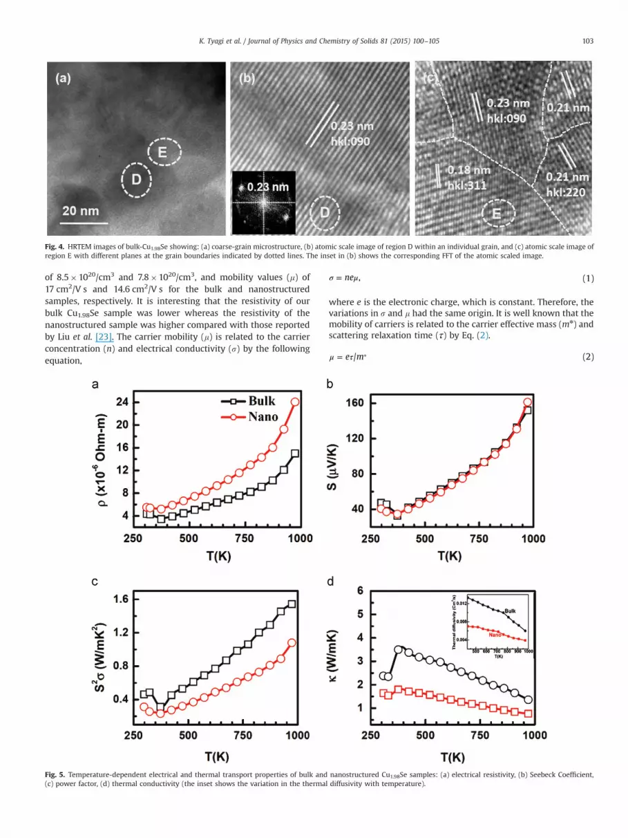
Fig. 4. HRTEM images of bulk-Cu1.98Se showing: (a) coarse-grain microstructure, (b) atomic scale image of region D within an individual grain, and (c) atomic scale image ofregion E with different planes at the grain boundaries indicated by dotted lines. The inset in (b) shows the corresponding FFT of the atomic scaled image.
K. Tyagi et al. / Journal of Physics and Chemistry of Solids 81 (2015) 100–105 103
of 8.5�1020/cm3 and 7.8�1020/cm3, and mobility values (m) of17 cm2/V s and 14.6 cm2/V s for the bulk and nanostructuredsamples, respectively. It is interesting that the resistivity of ourbulk Cu1.98Se sample was lower whereas the resistivity of thenanostructured sample was higher compared with those reportedby Liu et al. [23]. The carrier mobility (m) is related to the carrierconcentration (n) and electrical conductivity (s) by the followingequation,
Fig. 5. Temperature-dependent electrical and thermal transport properties of bulk and(c) power factor, (d) thermal conductivity (the inset shows the variation in the thermal
ne , (1)σ μ=
where e is the electronic charge, which is constant. Therefore, thevariations in s and m had the same origin. It is well known that themobility of carriers is related to the carrier effective mass (mn) andscattering relaxation time (τ) by Eq. (2).
e m/ (2)μ τ= ⁎
nanostructured Cu1.98Se samples: (a) electrical resistivity, (b) Seebeck Coefficient,diffusivity with temperature).

K. Tyagi et al. / Journal of Physics and Chemistry of Solids 81 (2015) 100–105104
Using Eqs. (1) and (2), s can be given as follows:
ne m/ (3)2σ τ= ⁎
Because the carrier concentration and electronic charge areexpected to be similar for both the bulk and nanostructuredsamples, the differences in their electrical conductivity and mo-bility are related to variations in the (τ/mn) ratio. Furthermore,according to this equation and based on assumptions of a singleparabolic band model and an energy-independent relaxation time,the Seebeck coefficient can be expressed as follows [4]:
⎜ ⎟⎛⎝
⎞⎠S
k
ehm T
n83 3
,(4)
2B2
2
2/3π π= ⁎
where kB is the Boltzmann constant and h is Planck’s constant.Eq. 4 estimates m* for a nanostructured sample as 2.70me and
for a bulk sample asm*¼2.68me which are comparable values. Thesimilar values of m* indicate that the variations in s and m in bothsamples were associated with the changes in τ. This may be due tothe high density of defects, such as the grain boundaries and na-noscale imperfections introduced during mechanical milling. Thus,we can conclude from this analysis that τ depends strongly on theprocessing method, which then affects the transport properties.
The temperature dependencies of the Seebeck coefficient inboth Cu1.98Se samples are shown in Fig. 5(b). The Seebeck coeffi-cients at room temperature were �46.2 mV/K and �40.64 mV/K forthe bulk and nanostructured samples, respectively, where thetrends were similar, especially at high temperature, although the
Fig. 6. Temperature-dependent thermoelectric properties: (a) lattice and electronic th(c) reproducibility of the ZT data.
magnitude was slightly higher for the nanostructured sample. Thisslight enhancement in the Seebeck coefficient may be attributed toa slight change in the density of the states near the Fermi level inthe nanostructured sample. For a particle in the nano-regime, theallowed energies within continuous bands separate into discretelevels when the separation between levels approaches the thermalenergy of the electrons. We observed a clear anomaly that corre-sponded to an α to β phase transition at 373 K. The power factor(S2s) (Fig. 5(c)) of the bulk sample was calculated as �1.55 W/m K2 compared with �1.08 W/m K2 at 973 K for the nanos-tructured sample, which was due to the high resistivity of thenanostructured sample.
The variations in the thermal conductivity with temperature(Fig. 5(d)) for the nanostructured and bulk samples were0.76 W m�1 K�1 and 1.36 W m�1 K�1, respectively, at 973 K.These are lower than the values reported by Liu et al. for bulksamples [23]. The reduction in the thermal conductivity of thenanostructured sample may be related to enhanced phonon scat-tering by dense grain boundaries and other microstructural im-perfections generated during ball milling. In order to quantify theeffect of nanostructuring, the lattice thermal conductivity (κl) wasdetermined by subtracting the electron contribution (κe) from thetotal thermal conductivity, where κe was calculated according tothe Wiedmann–Franz law. The lattice and electronic thermalconductivity plots for the bulk and nanostructured samples areshown in Fig. 6(a). To calculate the electronic thermal conductivity,the Lorentz number was taken as Lo¼1.5�10�8 V2 K�2 [28]. At
ermal conductivity, (b) ZT for the bulk and nanostructured Cu1.98Se samples, and

K. Tyagi et al. / Journal of Physics and Chemistry of Solids 81 (2015) 100–105 105
room temperature, the values of κe and κl for the bulk sample were1.06 W m�1 K�1 and 1.31 Wm�1 K�1, respectively, but0.84 W m�1 K�1 and 0.8 W m�1 K�1 for the nanostructuredsample, respectively (Fig. 6(a)). After the phase transition at�375 K in the bulk and nanostructured Cu1.98Se samples, κl de-creased significantly compared with κe, as shown in Fig. 6(a).However, we also observed that the reduced κe in the bulk andnanostructured samples may have been due to the charge carriersscattering with increasing temperature. Furthermore, the lower κlvalues for the nanostructured sample support a role for enhancedphonon scattering due to nanoscale defects and dense grainboundaries (HRTEM images shown in Fig. 3). Based on the mea-sured electrical and thermal transport properties, the temperaturedependence of ZT in the nanostructured Cu1.98Se led to a high ZTvalue of �1.4 at 973 K, which was 30% higher than its bulkcounterpart (Fig. 6(b)). In order to confirm the reproducibility ofour measurements, we determined the temperature dependenciesof the electrical and thermal transport properties experimentallybased on repeated thermal cycling at temperatures between roomtemperature and 973 K, where the ZT results for three consecutivescans are plotted in Fig. 6(c). These results clearly suggest that thereproducibility of the ZT values was quite good at all temperaturesand they were within the experimental error of ZT.
4. Conclusions
In this study, we successfully synthesized nanostructuredCu1.98Se using high energy ball milling followed by the SPS tech-nique. The rapid heating rates during SPS facilitated the retentionof the nanoscale features after sintering. HRTEM and XRD analysisof the nanostructured Cu1.98Se determined that the crystallite sizewas very small at �12 nm. The temperature-dependent electricalresistivity of the nanostructured Cu1.98Se sample was higher thanthat of its bulk counterpart due to the scattering of charge carriersat the grain boundaries and the atomic scale defects introducedduring ball milling. Thus, the Seebeck coefficient measured for thenanostructured sample was slightly higher than that of its bulkcounterpart. The enhanced phonon scattering due to low to highwavelength phonons caused by different types of nanoscale de-fects and abundant grain boundaries in the nanostructured matrixyielded a lower thermal conductivity. As a consequence, the na-nostructured Cu1.98Se exhibited a ZT value of �1.4 at 973 K, whichwas �30% higher than that of its bulk counterpart. This enhancedthermal stability suggests that Cu-deficient Cu2Se is a potentialcandidate for green energy generation.
Acknowledgments
This research was supported by the CSIR-TAPSUN (CSIR-NWP54) program entitled “Novel approaches for solar energy conversionunder technologies and products for solar energy utilization throughnetworking.” The authors are also grateful to Mr Radhey Shyamand Mr Naval Kishor Upadhyay for their technical support.
References
[1] G.J. Snyder, E.S. Toberer, Complex thermoelectric materials, Nature Materials 7(2008) 105–114.
[2] S. Ballikaya, H. Chi, J.R. Salvador, C. Uher, Thermoelectric properties of Ag-doped Cu2 Se and Cu 2 Te, Journal of Materials Chemistry A 1 (2013) 12478–12484.
[3] J.R. Sootsman, D.Y. Chung, M.G. Kanatzidis, New and old concepts in thermoelectricmaterials, Angewandte Chemie International Edition 48 (2009) 8616–8639.
[4] D.M. Rowe, CRC Handbook of Thermoelectrics, CRC Press, 1995.[5] M. Zebarjadi, K. Esfarjani, M. Dresselhaus, Z. Ren, G. Chen, Perspectives on ther-
moelectrics: from fundamentals to device applications, Energy & EnvironmentalScience 5 (2012) 5147–5162.
[6] T. Plirdpring, K. Kurosaki, A. Kosuga, T. Day, S. Firdosy, V. Ravi, G.J. Snyder,A. Harnwunggmoung, T. Sugahara, Y. Ohishi, Chalcopyrite CuGaTe2: A High‐Effi-ciency Bulk Thermoelectric Material, Advanced Materials 24 (2012) 3622–3626.
[7] Y. Pei, Z.M. Gibbs, B. Balke, W.G. Zeier, G.J. Snyder, Optimum Carrier Concentrationin n‐Type PbTe Thermoelectrics, Advanced Energy Materials (2014).
[8] S. Muthiah, J. Pulikkotil, A. Srivastava, A. Kumar, B. Pathak, A. Dhar, R. Budhani,Conducting grain boundaries enhancing thermoelectric performance in dopedMg2Si, Applied Physics Letters 103 (2013) 053901.
[9] G.-E. Lee, I.-H. Kim, Y.S. Lim, W.-S. Seo, B.-J. Choi, C.-W. Hwang, Preparation andThermoelectric Properties of Doped Bi2Te3-Bi2Se3 Solid Solutions, Journal of Elec-tronic Materials 43 (2014) 1650–1655.
[10] L. Bulat, V. Bublik, I. Drabkin, V. Karataev, V. Osvenskii, Y.N. Parkhomenko,G. Pivovarov, D. Pshenai-Severin, N.Y. Tabachkova, Bulk nanostructured poly-crystalline p-Bi-Sb-Te thermoelectrics obtained by mechanical activation methodwith hot pressing, Journal of Electronic Materials 39 (2010) 1650–1653.
[11] A. Minnich, M. Dresselhaus, Z. Ren, G. Chen, Bulk nanostructured thermoelectricmaterials: current research and future prospects, Energy & Environmental Science 2(2009) 466–479.
[12] S. Bathula, M. Jayasimhadri, N. Singh, A. Srivastava, J. Pulikkotil, A. Dhar, R. Budhani,Enhanced thermoelectric figure-of-merit in spark plasma sintered nanostructuredn-type SiGe alloys, Applied Physics Letters 101 (2012) 213902.
[13] B. Yu, W. Liu, S. Chen, H. Wang, H. Wang, G. Chen, Z. Ren, Thermoelectric propertiesof copper selenide with ordered selenium layer and disordered copper layer, NanoEnergy 1 (2012) 472–478.
[14] L. Hicks, T. Harman, X. Sun, M. Dresselhaus, Experimental study of the effect ofquantum-well structures on the thermoelectric figure of merit, Physical Review B 53(1996) R10493.
[15] R. Venkatasubramanian, E. Siivola, T. Colpitts, B. O'quinn, Thin-film thermoelectricdevices with high room-temperature figures of merit, Nature 413 (2001) 597–602.
[16] A.I. Boukai, Y. Bunimovich, J. Tahir-Kheli, J.-K. Yu, W.A. Goddard Iii, J.R. Heath, Siliconnanowires as efficient thermoelectric materials, Nature 451 (2008) 168–171.
[17] B. Poudel, Q. Hao, Y. Ma, Y. Lan, A. Minnich, B. Yu, X. Yan, D. Wang, A. Muto,D. Vashaee, High-thermoelectric performance of nanostructured bismuth antimonytelluride bulk alloys, Science 320 (2008) 634–638.
[18] W. Xie, J. He, H.J. Kang, X. Tang, S. Zhu, M. Laver, S. Wang, J.R. Copley, C.M. Brown,Q. Zhang, Identifying the specific nanostructures responsible for the high thermo-electric performance of (Bi, Sb) 2Te3 nanocomposites, Nano Letters 10 (2010)3283–3289.
[19] Y. Ma, Q. Hao, B. Poudel, Y. Lan, B. Yu, D. Wang, G. Chen, Z. Ren, Enhanced ther-moelectric figure-of-merit in p-type nanostructured bismuth antimony telluriumalloys made from elemental chunks, Nano Letters 8 (2008) 2580–2584.
[20] X. Yan, B. Poudel, Y. Ma, W. Liu, G. Joshi, H. Wang, Y. Lan, D. Wang, G. Chen, Z. Ren,Experimental studies on anisotropic thermoelectric properties and structures ofn-type Bi2Te2. 7Se0. 3, Nano Letters 10 (2010) 3373–3378.
[21] Y. Lan, B. Poudel, Y. Ma, D. Wang, M.S. Dresselhaus, G. Chen, Z. Ren, Structure studyof bulk nanograined thermoelectric bismuth antimony telluride, Nano letters 9(2009) 1419–1422.
[22] W. Liu, X. Yan, G. Chen, Z. Ren, Recent advances in thermoelectric nanocomposites,Nano Energy 1 (2012) 42–56.
[23] H. Liu, X. Shi, F. Xu, L. Zhang, W. Zhang, L. Chen, Q. Li, C. Uher, T. Day, G.J. Snyder,Copper ion liquid-like thermoelectrics, Nature Materials 11 (2012) 422–425.
[24] O. Milat, Z. Vučić, B. Ruščić, Superstructural ordering in low-temperature phase ofsuperionic Cu2Se, Solid State Ionics 23 (1987) 37–47.
[25] R.M. Murray, R.D. Heyding, The copper-selenium system at temperatures to 850 Kand pressures to 50 kbar, Canadian Journal of Chemistry 53 (1975) 878–887.
[26] V. Bhuse, P. Hankare, K. Garadkar, A. Khomane, A simple, convenient, low tem-perature route to grow polycrystalline copper selenide thin films, MaterialsChemistry and Physics 80 (2003) 82–88.
[27] S.K. Haram, K. Santhanam, Electroless deposition of orthorhombic copper(I) selenide and its room temperature phase transformation to cubic structure, ThinSolid Films 238 (1994) 21–26.
[28] X. Xing-Xing, X. Wen-Jie, T. Xin-Feng, Z. Qing-Jie, Phase transition and high tem-perature thermoelectric properties of copper selenide Cu2�xSe (0rxr0.25), Chi-nese Physics B 20 (2011) 087201.
[29] A. Khorsand Zak, W. Abd Majid, M. Abrishami, R. Yousefi, X-ray analysis of ZnOnanoparticles by Williamson–Hall and size–strain plot methods, Solid State Sci-ences 13 (2011) 251–256.
[30] S. Vives, E. Gaffet, C. Meunier, X-ray diffraction line profile analysis of iron ballmilled powders, Materials Science and Engineering: A 366 (2004) 229–238.
[31] D. Maier, Strain-field domain structure in Bi2Te3 thermoelectric materials, SolidState Communications 122 (2002) 565–568.
[32] Y. Kuru, M. Wohlschlögel, U. Welzel, E. Mittemeijer, Large excess volume in grainboundaries of stressed, nanocrystalline metallic thin films: Its effect on grain-growth kinetics, Applied Physics Letters 95 (2009) 163112.
[33] G.K. Rane, U. Welzel, S.R. Meka, E.J. Mittemeijer, Non-monotonic lattice parametervariation with crystallite size in nanocrystalline solids, Acta Materialia 61 (2013)4524–4533.
[34] G. Rane, U. Welzel, E. Mittemeijer, Grain growth studies on nanocrystalline Nipowder, Acta Materialia 60 (2012) 7011–7023.
Copyright © 2022 FDOKUMEN