Crossed Andreev reflection versus electron transfer in three-terminal graphene devices
10
arXiv:0909.4654v3 [cond-mat.mes-hall] 25 Feb 2010 Crossed Andreev reflection versus electron transfer in graphene nanoribbons H˚ avard Haugen, Daniel Huertas–Hernando, and Arne Brataas Department of Physics, Norwegian University of Science and Technology, N-7491 Trondheim, Norway Xavier Waintal SPSMS-INAC-CEA, 17 rue des Martyrs, 38054 Grenoble CEDEX 9, France (Dated: February 25, 2010) We investigate the transport properties of three-terminal graphene devices, where one terminal is superconducting and two are normal metals. The terminals are connected by nanoribbons. Electron transfer (ET) and crossed Andreev reflection (CAR) are identified via the non-local signal between the two normal terminals. Analytical expressions for ET and CAR in symmetric devices are found. We compute ET and CAR numerically for asymmetric devices. ET dominates CAR in symmetric devices, but CAR can dominate ET in asymmetric devices, where only the zero-energy modes of the zigzag nanoribbons contribute to the transport. PACS numbers: 74.45.+c, 73.63.-b, 73.23.-b, 74.25.Fy I. INTRODUCTION Graphene, a two-dimensional honeycomb lattice of car- bon atoms, has recently been experimentally realized. 1–3 It exhibits intriguing electron transport properties such as a very high mobility, 1–3 gate-voltage tun- able electron doping, 1 anomalous quantum Hall effect, 3 Klein tunneling, 4 “relativistic” Dirac-like linear energy- momentum dispersion, 5 and possible integration with other adatoms and electrical contacts. 6,7 Graphene can be contacted to superconductors and a supercurrent in graphene Josephson junctions has been measured. 8–10 Non-local transport in three-terminal devices with one superconducting lead and two normal metals has been extensively studied, both theoretically 11–16 and experimentally. 17–20 At energies lower than the supercon- ducting gap, the current in one normal terminal caused by a voltage applied between another normal terminal and the superconductor is governed by a competition be- tween electron transfer (ET) and crossed Andreev reflec- tion (CAR). ET is the emission of an electron from one normal metal terminal to another normal metal termi- nal, possibly after interacting with the superconductor. In CAR, an electron from one normal terminal enters the superconductor together with an electron from a second normal terminal or, equivalently, an electron is emitted into one normal terminal while a hole is emitted into an- other normal terminal. This process creates a spatially entangled electron-hole pair which has a fundamental in- terest and can be used as an entangler. 21–23 The relative magnitude of ET and CAR can be tuned by using fer- romagnetic contacts, 14,24 but our focus here is on their intrinsic relative value when normal metals are used. The ET and CAR processes contribute with opposite signs to the non-local current. Experimentally, it has been mea- sured that ET often dominates CAR, but at finite bias voltage a CAR dominated signal 20 was also seen. First theories in the lowest order tunneling limit predict that ET and CAR exactly cancel each other. 14 Also, relaxing the assumption of tunneling barriers by allowing barriers of arbitrary strength in semi-classical N-S circuits, ET generally dominates CAR. 15 Recent theoretical sugges- tions to explain the experiment in Ref. 20 are Coulomb interaction effects, 25 an external AC bias, 26 and quantum interference effects. 27 Theoretically, graphene-superconductor junctions have been investigated by several workers. 28–30 In graphene there is an additional new quasi-particle to supercurrent conversion process denoted specular Andreev reflection, where states above and below the Dirac point are coupled by Andreev scattering (inter-band coupling). 28 In spec- ular Andreev reflection, the holes emitted from the su- perconductor no longer follow the parallel time-reversed path of the incoming electron as they do in direct An- dreev reflection, but are specularly reflected at an angle which equals the angle of incidence. Although fundamen- tally interesting, as it could enhance CAR processes, 31,32 specular Andreev reflection is only visible in ultra clean and homogeneous systems, since the Dirac point must be well-defined throughout the region of interest, or the superconducting pair potential Δ must be much larger than the typical variation in the Dirac point. Also, it is necessary to control the doping such that the Fermi energy is considerably smaller than the superconducting gap. The small magnitude of the proximity induced su- perconducting gap in graphene, Δ ≈ 0.1 meV, 8 means this could only be realized in ultra small structures at very low doping level in well controlled systems. In this paper we investigate the influence of a supercon- ducting terminal on devices built from graphene zigzag ribbons. We are interested in studying how ET and CAR depend on the features of the nanoribbons e.g. on their widths, number of terminals, and relative angle where ribbons connected to various terminals intersect. The choice of zigzag ribbons is the most relevant one, as the boundary conditions for ribbons with generic boundaries have been shown to reduce to the boundary conditions for zigzag terminations in most cases. 33,34 Such nanorib- bons have some unique electronic features, such as sup- porting current carrying zero-modes localized along the
-
Upload
independent -
Category
Documents
-
view
0 -
download
0
Transcript of Crossed Andreev reflection versus electron transfer in three-terminal graphene devices
arX
iv:0
909.
4654
v3 [
cond
-mat
.mes
-hal
l] 2
5 Fe
b 20
10
Crossed Andreev reflection versus electron transfer in graphene nanoribbons
Havard Haugen, Daniel Huertas–Hernando, and Arne BrataasDepartment of Physics, Norwegian University of Science and Technology, N-7491 Trondheim, Norway
Xavier WaintalSPSMS-INAC-CEA, 17 rue des Martyrs, 38054 Grenoble CEDEX 9, France
(Dated: February 25, 2010)
We investigate the transport properties of three-terminal graphene devices, where one terminal issuperconducting and two are normal metals. The terminals are connected by nanoribbons. Electrontransfer (ET) and crossed Andreev reflection (CAR) are identified via the non-local signal betweenthe two normal terminals. Analytical expressions for ET and CAR in symmetric devices are found.We compute ET and CAR numerically for asymmetric devices. ET dominates CAR in symmetricdevices, but CAR can dominate ET in asymmetric devices, where only the zero-energy modes ofthe zigzag nanoribbons contribute to the transport.
PACS numbers: 74.45.+c, 73.63.-b, 73.23.-b, 74.25.Fy
I. INTRODUCTION
Graphene, a two-dimensional honeycomb lattice of car-bon atoms, has recently been experimentally realized.1–3
It exhibits intriguing electron transport propertiessuch as a very high mobility,1–3 gate-voltage tun-able electron doping,1 anomalous quantum Hall effect,3
Klein tunneling,4 “relativistic” Dirac-like linear energy-momentum dispersion,5 and possible integration withother adatoms and electrical contacts.6,7 Graphene canbe contacted to superconductors and a supercurrent ingraphene Josephson junctions has been measured.8–10
Non-local transport in three-terminal devices withone superconducting lead and two normal metals hasbeen extensively studied, both theoretically11–16 andexperimentally.17–20 At energies lower than the supercon-ducting gap, the current in one normal terminal causedby a voltage applied between another normal terminaland the superconductor is governed by a competition be-tween electron transfer (ET) and crossed Andreev reflec-tion (CAR). ET is the emission of an electron from onenormal metal terminal to another normal metal termi-nal, possibly after interacting with the superconductor.In CAR, an electron from one normal terminal enters thesuperconductor together with an electron from a secondnormal terminal or, equivalently, an electron is emittedinto one normal terminal while a hole is emitted into an-other normal terminal. This process creates a spatiallyentangled electron-hole pair which has a fundamental in-terest and can be used as an entangler.21–23 The relativemagnitude of ET and CAR can be tuned by using fer-romagnetic contacts,14,24 but our focus here is on theirintrinsic relative value when normal metals are used. TheET and CAR processes contribute with opposite signs tothe non-local current. Experimentally, it has been mea-sured that ET often dominates CAR, but at finite biasvoltage a CAR dominated signal20 was also seen. Firsttheories in the lowest order tunneling limit predict thatET and CAR exactly cancel each other.14 Also, relaxingthe assumption of tunneling barriers by allowing barriers
of arbitrary strength in semi-classical N-S circuits, ETgenerally dominates CAR.15 Recent theoretical sugges-tions to explain the experiment in Ref. 20 are Coulombinteraction effects,25 an external AC bias,26 and quantuminterference effects.27
Theoretically, graphene-superconductor junctions havebeen investigated by several workers.28–30 In graphenethere is an additional new quasi-particle to supercurrentconversion process denoted specular Andreev reflection,where states above and below the Dirac point are coupledby Andreev scattering (inter-band coupling).28 In spec-ular Andreev reflection, the holes emitted from the su-perconductor no longer follow the parallel time-reversedpath of the incoming electron as they do in direct An-dreev reflection, but are specularly reflected at an anglewhich equals the angle of incidence. Although fundamen-tally interesting, as it could enhance CAR processes,31,32
specular Andreev reflection is only visible in ultra cleanand homogeneous systems, since the Dirac point mustbe well-defined throughout the region of interest, or thesuperconducting pair potential ∆ must be much largerthan the typical variation in the Dirac point. Also, itis necessary to control the doping such that the Fermienergy is considerably smaller than the superconductinggap. The small magnitude of the proximity induced su-perconducting gap in graphene, ∆ ≈ 0.1 meV,8 meansthis could only be realized in ultra small structures atvery low doping level in well controlled systems.
In this paper we investigate the influence of a supercon-ducting terminal on devices built from graphene zigzagribbons. We are interested in studying how ET and CARdepend on the features of the nanoribbons e.g. on theirwidths, number of terminals, and relative angle whereribbons connected to various terminals intersect. Thechoice of zigzag ribbons is the most relevant one, as theboundary conditions for ribbons with generic boundarieshave been shown to reduce to the boundary conditionsfor zigzag terminations in most cases.33,34 Such nanorib-bons have some unique electronic features, such as sup-porting current carrying zero-modes localized along the
2
edges.34–36 Also, for low energies, states carrying currentin opposite directions along the zigzag ribbon is associ-ated with different eigenstates, and there is an absenceof backscattering due to the small overlap between thestates carrying current in opposite directions.37
The paper is organized as follows: In Sec. II we defineour model and in Sec. III we express the scattering ma-trix in terms of the normal state scattering matrix. Thisenables us to identify the ET and CAR contributions tothe non-local signal. Section IV describes the propertiesof symmetric three-terminal devices, and in Sec. VI wepresent numerical results showing a dominance of CARover ET in an asymmetric device. Finally we concludeour paper in Sec. VII.
II. MODEL AND METHOD
Our description of superconducting ribbons starts withthe nearest neighbor hopping Hamiltonian of graphene,
H = −∑
〈i,j〉,σ
γc†iσcjσ − EF
∑
i,σ
c†iσciσ , (1)
where γ ≈ 2.7 eV is the nearest neighbor hopping
energy,7,38,39 and c†iσ creates an electron with spin σ atsite i. In the superconducting terminal, we assume a su-perconductor on top of the graphene sheet which by prox-imity induces superconducting properties in graphene.We consider spin singlet pairing described by the BCSHamiltonian H .40 The superconducting pair potential ∆i
is local to site i and chosen to be real since we only haveone superconductor. We write H in Nambu form,
H =∑
i,j
Ψ†j
[(
Hij 00 −H∗
ij
)
+ δij
(
0 ∆i
∆i 0
)]
Ψi, (2)
where Ψ†i = (c†i,↑, ci,↓) and Hij are elements of the normal
state Hamiltonian in Eq. (1).
We are interested in the transport properties which canbe expressed via the scattering matrix of the system. Fol-lowing Ref. 41, we find that the differential conductancematrix is42
Gab(eVb) = (−1)(1−δab)∂Ia∂Vb
∣
∣
∣
∣
Vb
=
{
Nb −GERbb +GDAR
bb , b = a,
GETab −GCAR
ab , a 6= b..
(3)
where Nb(ε) is the number of propagating modes in leadb at energy ε, and the conductance matrix elements aredefined in terms of the Nambu space scattering matrix
S =
(
See Seh
She Shh
)
(4)
as
GERbb = Tr
[
Seebb (eVb)See†
bb (eVb)]
, (5)
GDARbb = Tr
[
Shebb (eVb)She†
bb (eVb)]
, (6)
GETab = Tr
[
Seeab(eVb)See†
ab (eVb)]
, (a 6= b) (7)
GCARab = Tr
[
Sheab (eVb)She†
ab (eVb)]
. (a 6= b) (8)
The conductances in Eqs. (5) – (8) describe, respectively,local electron reflection (ER), direct Andreev reflection(DAR), non-local electron transfer (ET), and crossed An-dreev reflection (CAR).All energies are measured with respect to the equilib-
rium chemical potential of the superconductor, and allconductances in this paper are in units of two times (forspin) the conductance quantum 2G0 = 2e2/h. The cur-rent Ia is defined as incoming from reservoir a.
III. SCATTERING MATRIX OF A
THREE-TERMINAL DEVICE WITH ONE
SUPERCONDUCTING TERMINAL
In the following we will study the non-local signal ina three-terminal device, where terminal 1 is supercon-ducting and terminals 2 and 3 are normal metals. Thenon-local conductance14,15
G32(eV2) = GET32 (eV2)−GCAR
32 (eV2) (9)
is positive when dominated by ET and negative whendominated by CAR.We compute GCAR
32 and GET32 in two ways: i) See and
She are computed directly in Nambu space using theHamiltonian (2), and GCAR
32 and GET32 are found from (7)
and (8). We refer to this as the Nambu approach. ii) Werelate See and She to the scattering matrix s in the nor-mal state and numerically compute the latter using theHamiltonian (1). We call this the Normal approach. Ourresults using both methods agree, when applicable. Letus first review how the scattering matrix can be relatedto the normal state properties.Following Ref. 43, if the scattering region is well sepa-
rated from the superconducting terminal, we can expressthe scattering matrix S when terminal 1 is superconduct-ing in terms of the scattering matrix
s =
s11 s12 s13s21 s22 s23s31 s32 s33
=
r11 t12 t13t21 r22 t23t31 t32 r33
(10)
when the whole device is in the normal state. As long asthe device is appreciably smaller than the superconduct-ing coherence length ξ, the normal approach is applica-ble. For graphene, the induced superconducting gap issmall, ∆ ∼ 0.1 meV,8 so that the coherence length ξ ison the order of micrometers.
3
With terminal 1 superconducting, the scattering ma-trix between the normal metal terminals 3 and 2 is43,44
See32 = t32 + t31ν
2r11Mt12, (11)
She32 = t31νMt12, (12)
where the matrix M is
M =[
I − ν2r11r11]−1
. (13)
The amplitude ν, associated with electron-hole conver-sion at the normal-superconducting interface, is44
ν =ε
∆− sign (ε)
√
( ε
∆
)2
− 1, (14)
and the bar (g) corresponds to time reversal, defined foran arbitrary quantity g(ε) as:
g = g(ε) = g∗(−ε). (15)
The matrix M corresponds to all orders of the processwhere a hole emitted from the superconductor returns tothe superconductor. At zero energy, holes propagatingwith amplitude r11 between successive interactions withthe superconductor retrace exactly the reverse path ofthe electrons with amplitude r11. Thus, at zero energyholes and electrons do not acquire a phase relative to eachother upon interacting with the scattering region. How-ever, at non-zero energy, there is a mismatch betweenthe wave vectors of electron-like and hole-like states, sothe time reverse paths described by the scattering matri-ces r11 and r11 will not be exactly opposite to each other.This means that the term r11r11 in M contains many dif-ferent phases, which will depend strongly on the disorderconfiguration. There is therefore some loss of coherenceat non-zero energy due to phase randomization.For the ET process, described by the scattering matrix
element in Eq. (11), there is an interference of two typesof processes: (1) Going directly from 2 to 3 without in-teracting with the superconductor, and (2) processes in-volving any number of electron-hole-electron conversionsat the interface to the superconductor. Similarly, theAndreev process described by Eq. (12) involves an oddnumber of electron-hole conversions at the NS interface.In the absence of a magnetic field, time-reversal sym-
metry dictates45
sab(ε) = s∗ab(−ε) = s†ba(−ε). (16)
The energy scale of the normal state scattering matrixsab is the subband energy, which is determined by thehopping energy γ and the width of the ribbon. For theribbons considered in this paper, the subband energy islarger than the superconducting pair potential ∆ by sev-eral orders of magnitude. The Fermi energy is compara-ble to the subband energies in magnitude. Since, in theregime we consider, sab is independent of energy on the
scale of ∆, we write sab(ε) = sab(0) = sab and sab = s†ba.
The non-local ET and CAR conductances thereforesimplify to
GET32 = Tr
[
t32t†32
]
+ 2Reν2Tr[
t12t†32t31r
†11M
]
+ |ν|4 Tr[
r11t†31t31r
†11Mt12t
†12M
†]
,
(17)
GCAR32 = |ν|2 Tr
[
t13t†13Mt12t
†12M
†]
, (18)
where all energy dependence is due to the electron-holeconversion amplitude ν.When ε ≫ ∆, Eq. (14) gives ν → 0, and we re-
cover the normal state behavior where only the first termof Eq. (17) contributes. However, in the subgap limitε ≪ ∆, ν → i, and the interaction with the superconduc-tor contributes. The second term in Eq. (17) is due tointerference between processes involving direct transferof electrons from 2 to 3, and interaction with the super-conducting terminal 1.In our numerical studies, we calculate the retarded
Green’s function matrix G = [EI − H − ΣR]−1 and ex-tract the elements Gab involving the terminals a and b.The calculation of G uses the recursive method describedin Ref. 46. In this method, the Green’s function of thewhole system is found by adding the sites of the Hamilto-nian (1) to the system one by one, updating all relevantGreen’s function elements via the Dyson equation. Themethod has the advantage that it can easily be appliedto structures of arbitrary geometry and any number ofterminals. After the Green’s function has been found,the scattering matrix Sab is extracted via the Fischer-Lee relations,45,47
Sab = −Iaδab + iΓ1/2a GabΓ
1/2b . (19)
Here Ia is the identity matrix (operator) and Γa =i(
Σa − Σ†a
)
is the linewidth/dephasing matrix which de-pends on the self energy Σa of terminal a.
IV. SYMMETRIC THREE-TERMINAL DEVICE
The simplest three-terminal device is completely sym-metric where the normal state scattering matrix (10),simplifies to
s =
r t tt r tt t r
. (20)
Unitarity of s gives rise to the relations
I = rr† + 2tt† and (21)
0 = tr† + rt† + tt†, (22)
that we make use of in Eqs. (17) and (18) to find thenon-local conductance. We can express the conductance
4
matrix of such a symmetric device in terms of the eigen-values 0 ≤ Rn ≤ 1 of the reflection probability matrixrr†:
GET32 =
∑
n
(1 −Rn)
4(1 +Rn)2(3 + 5Rn), (23)
GCAR32 =
∑
n
(1−Rn)2
4(1 +Rn)2. (24)
It follows from this that the non-local conductance of asymmetric structure,
G32 = GET32 −GCAR
32 =∑
n
(1−Rn)
2(1 +Rn)2(1 + 3Rn), (25)
is always ET dominated (positive). By a completely anal-ogous calculation we also find that the local conductance,
G22 =∑
n
(1−Rn)
2(1 +Rn)2[3 +Rn(2−Rn)] , (26)
is naturally also positive.A few simple conclusions can be drawn from these ex-
pressions. First, when the device is perfectly transparentfor the Nε contributing modes at the Fermi energy, thecontributing modes haveRn = 0, the others haveRn = 1.The local and non-local conductances become,
G22 =3
2N2, (27)
G32 =1
2N2, (28)
where N2 is the number of modes contributing to thecurrent at the Fermi energy. These results have the fol-lowing simple explanation: When the voltage is raised interminal 2, N2 conducting modes are injected into thestructure via this terminal. Since the device is symmet-ric, half of these modes go directly to terminal 3, pro-ducing a current N2/2 in this terminal. The other halfof the N2 incoming modes interact with the supercon-ductor at terminal 1, and are Andreev reflected back toterminal 2 as holes. These modes contribute 2 · (N2/2) tothe current in terminal 2. The total current in terminal2 is therefore (2 + 1)(N2/2) = 3/2N2. At low bias theAndreev reflected holes retrace exactly the trajectory ofthe incoming electrons because of time-reversal symme-try, and they therefore only contribute to the current interminal 2.When all the terminals are connected to the central
device with tunnel contacts, we can expand the local andnon-local conductances in the δ = (1 − Rn)/2 ≪ 1 forthe contributing modes. We find that
G22 = N2δ +O(δ2), (29)
G32 = N2δ +O(δ2), (30)
so we recover the normal state results, where both thelocal and non-local signals vanish linearly with δ. Trans-port between terminals 2 and 3 involving the supercon-ductor involves higher orders in δ and does therefore notcontribute in this limit.
0
10
20
30
Conduct
ance
(2e2
/h)
10 20 30 40
nW
GNormal22
GEigenv.22
GNormal32
GEigenv.32
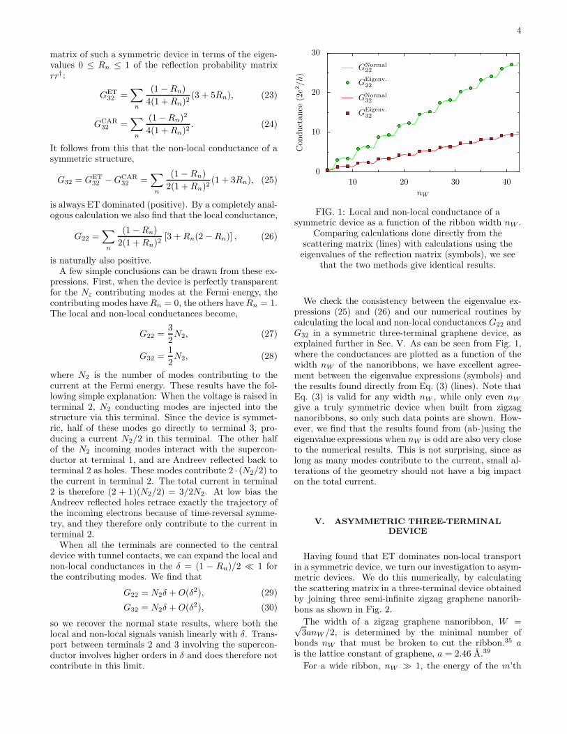
FIG. 1: Local and non-local conductance of asymmetric device as a function of the ribbon width nW .
Comparing calculations done directly from thescattering matrix (lines) with calculations using theeigenvalues of the reflection matrix (symbols), we see
that the two methods give identical results.
We check the consistency between the eigenvalue ex-pressions (25) and (26) and our numerical routines bycalculating the local and non-local conductances G22 andG32 in a symmetric three-terminal graphene device, asexplained further in Sec. V. As can be seen from Fig. 1,where the conductances are plotted as a function of thewidth nW of the nanoribbons, we have excellent agree-ment between the eigenvalue expressions (symbols) andthe results found directly from Eq. (3) (lines). Note thatEq. (3) is valid for any width nW , while only even nW
give a truly symmetric device when built from zigzagnanoribbons, so only such data points are shown. How-ever, we find that the results found from (ab-)using theeigenvalue expressions when nW is odd are also very closeto the numerical results. This is not surprising, since aslong as many modes contribute to the current, small al-terations of the geometry should not have a big impacton the total current.
V. ASYMMETRIC THREE-TERMINAL
DEVICE
Having found that ET dominates non-local transportin a symmetric device, we turn our investigation to asym-metric devices. We do this numerically, by calculatingthe scattering matrix in a three-terminal device obtainedby joining three semi-infinite zigzag graphene nanorib-bons as shown in Fig. 2.
The width of a zigzag graphene nanoribbon, W =√3anW /2, is determined by the minimal number of
bonds nW that must be broken to cut the ribbon.35 ais the lattice constant of graphene, a = 2.46 A.39
For a wide ribbon, nW ≫ 1, the energy of the m’th

5
23
1
FIG. 2: Three-terminal graphene fork consisting ofthree semi-infinite graphene zigzag nanoribbons
connected together. The top lead is allowed to becomesuperconducting by inserting a non-zero pair potential∆ in this region, according to the Hamiltonian in (2).
transverse subband is to a good approximation48
Em =
(
m+1
2
)
πγ
nW
, m = 1, 2, . . . , (31)
where γ is the nearest neighbor hopping energy on thegraphene lattice. The superconducting coherence length
ξ =~vF∆
=
√3
2
γ
∆a (32)
will typically be of the order of micrometers, so the nor-mal approach should be applicable for nanoribbons up to1 µm wide, or nW ∼ 104.
A. Consistency checks
In Fig. 3 we compare the conductance extracted fromthe normal state scattering matrix s to that found by di-rect evaluation of the full scattering matrix S in Nambuspace. The calculations are done for a device of the typeshown in Fig. 2. The leads are all semi-infinite zigzagribbons, and we set ∆ = 0 everywhere except in ter-minal 1 (shaded area in Fig. 2). As can be seen fromFig. 3, where we show the ratio between the conductancecalculated with the two methods, GNormal
ij /GNambuij , the
agreement between the two methods is excellent as longas W/ξ ≪ 10−1, where W is the width of the ribbonsand ξ is the superconducting coherence length.Also, since ξ ≫ W , the exact position of the bound-
ary between the normal (∆ = 0) and superconducting(∆ 6= 0) regions does not influence our results. Thiscan be seen explicitly from Figs. 4a and 4b, where wecompare the conductance matrices for systems when thescattering region is, respectively, entirely mixed with, or
0.8
1
1.2
1.4
GN
orm
al
32
/GN
am
bu
32
GN
orm
al
32
/GN
am
bu
32
0 0.5 1 1.5 2
eV/∆eV/∆
W/ξ ∼ 100
W/ξ ∼ 10−1
W/ξ ∼ 10−2
W/ξ ∼ 10−3
0.8
1
1.2
1.4
GN
orm
al
22
/GN
am
bu
22
GN
orm
al
22
/GN
am
bu
22
W/ξ ∼ 100
W/ξ ∼ 10−1
W/ξ ∼ 10−2
W/ξ ∼ 10−3
FIG. 3: Ratio of conductance calculated with thenormal method (extracted from the normal state
scattering matrix) to conductance calculated directlywith the Nambu space Hamiltonian. When W ≪ ξ the
two methods give identical results. The situationconsidered in this paper corresponds to W/ξ ∼ 10−4.Upper (lower) panel: local (non-local) conductance.
separated from, the superconducting region. There is nodependence on the exact position of the NS interface, asshould be expected.
B. Varying the width of the superconductor
We now turn to the numerical calculations of the lo-cal and non-local conductances for an asymmetric de-vice. We first vary the width W1 of the superconductinglead, keeping the width of the normal terminals fixed,W2 = W3. The doping throughout the device is setto a high value to ensure that many modes contributeto the transport. The conductances involving the nor-mal terminals are calculated when the top terminal issuperconducting (superscript S), and compared for ref-erence to the conductance when the whole device is inthe normal state (superscript N). As seen in Fig. 5,when the superconducting lead is very narrow, there isvery little coupling via the induced superconducting or-der parameter, so GS
22 ≈ GN22. However, as the width
of the superconducting lead increases, more of the in-

6
5
5.25
5.5
5.75
6
6.25
G32(2
e2/h)
0 0.5 1 1.5 2
eV/∆
(a)
(b)
12
14
16
18
G22(2
e2/h)
(a)
(b)
(a) (b)
FIG. 4: Dependence of local and non-local conductanceon the position of the normal-superconductor (NS)
interface. In (a), ∆ is non-zero in the whole scatteringregion, while in (b) ∆ is non-zero only in the top
terminal. The conductances calculated for the two casesare identical, implying that the exact position of the NS
interface is not important.
coming quasiparticles are coupled via the induced super-conducting order parameter, and the local conductanceasymptotically approaches twice the normal state con-ductance, GS
22 ≈ 2GN22. In other words, the interaction
with the superconductor essentially involves all the in-coming modes, which are therefore Andreev reflected.This resembles the situation in a strongly coupled two-terminal NS junction.43 From Fig. 5 we see that the con-tribution of Andreev reflection to the local conductancehas reached its asymptotic value when W1/W2,3 ≈ 2.The picture is essentially unchanged if we allow for dif-
ferent doping levels in the central device and the termi-nals (see Fig. 5b), as long as the number of contributingmodes in the central region is still large.Contrary to what is seen for the local conductance, the
non-local conductance G32 is only weakly influenced bythe presence of the superconductor. Except for a slight
0
10
20
30
Con
duct
ance
(2e2
/h)
0 1 2 3 4
W1/W2,3
GS22
GN22
GS32
GN32
(a) Equal doping the whole device, EF = Eleads
F= 0.9γ.
0
10
20
30
Con
duct
ance
(2e2
/h)
0 1 2 3 4
W1/W2,3
GS22
GN22
GS32
GN32
(b) Increased doping in terminals, EF = 0.9γ, Eleads
F= 1.1γ.
FIG. 5: Local and non-local conductances as functionsof the width W1 of the superconducting lead. W2 = W3
is kept fixed (nW2,3= 20). For comparison we show the
conductance both when the top lead is in the normalstate (dashed) and when it is superconducting (solid).
enhancement of the signal aroundW1/W2,3 ≈ 2, the non-local conductance remains essentially unchanged whenturning on the superconductor. This is in accordancewith what was found for the symmetric device in Sec. IV,namely that the Andreev reflected holes retrace the pathof the incoming electrons, giving a negligible contribu-tion to the non-local conductance. Again, different dop-ing levels in the central device and the terminals do notchange the picture qualitatively, as seen from Fig. 5b.
C. Varying the width of normal terminal 3
We also vary the width W3 of the normal terminal3, keeping the widths of the voltage terminal 2 and thesuperconducting terminal 1 fixed. As can be seen fromFig. 6 the non-local conductance, G32, is (nearly) zerowhen terminal 3 is very narrow. This is natural, since
7
0
5
10
15
20C
onduct
ance
(2e2
/h)
0 1 2 3 4
W3/W1,2
GS22
GN22
GS32
GN32
(a) Equal doping the whole device, EF = Eleads
F= 0.9γ.
0
5
10
15
20
Con
duct
ance
(2e2
/h)
0 1 2 3 4
W3/W1,2
GS22
GN22
GS32
GN32
(b) Increased doping in terminals, EF = 0.9γ, Eleads
F= 1.1γ.
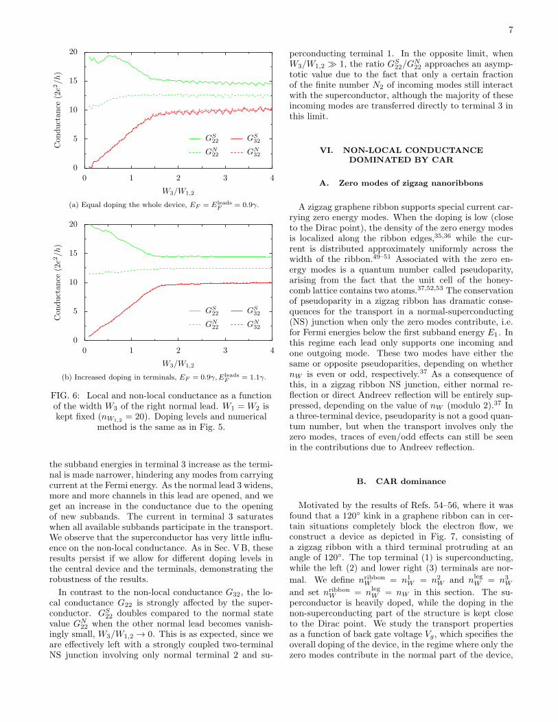
FIG. 6: Local and non-local conductance as a functionof the width W3 of the right normal lead. W1 = W2 iskept fixed (nW1,2
= 20). Doping levels and numericalmethod is the same as in Fig. 5.
the subband energies in terminal 3 increase as the termi-nal is made narrower, hindering any modes from carryingcurrent at the Fermi energy. As the normal lead 3 widens,more and more channels in this lead are opened, and weget an increase in the conductance due to the openingof new subbands. The current in terminal 3 saturateswhen all available subbands participate in the transport.We observe that the superconductor has very little influ-ence on the non-local conductance. As in Sec. VB, theseresults persist if we allow for different doping levels inthe central device and the terminals, demonstrating therobustness of the results.
In contrast to the non-local conductance G32, the lo-cal conductance G22 is strongly affected by the super-conductor. GS
22 doubles compared to the normal statevalue GN
22 when the other normal lead becomes vanish-ingly small, W3/W1,2 → 0. This is as expected, since weare effectively left with a strongly coupled two-terminalNS junction involving only normal terminal 2 and su-
perconducting terminal 1. In the opposite limit, whenW3/W1,2 ≫ 1, the ratio GS
22/GN22 approaches an asymp-
totic value due to the fact that only a certain fractionof the finite number N2 of incoming modes still interactwith the superconductor, although the majority of theseincoming modes are transferred directly to terminal 3 inthis limit.
VI. NON-LOCAL CONDUCTANCE
DOMINATED BY CAR
A. Zero modes of zigzag nanoribbons
A zigzag graphene ribbon supports special current car-rying zero energy modes. When the doping is low (closeto the Dirac point), the density of the zero energy modesis localized along the ribbon edges,35,36 while the cur-rent is distributed approximately uniformly across thewidth of the ribbon.49–51 Associated with the zero en-ergy modes is a quantum number called pseudoparity,arising from the fact that the unit cell of the honey-comb lattice contains two atoms.37,52,53 The conservationof pseudoparity in a zigzag ribbon has dramatic conse-quences for the transport in a normal-superconducting(NS) junction when only the zero modes contribute, i.e.for Fermi energies below the first subband energy E1. Inthis regime each lead only supports one incoming andone outgoing mode. These two modes have either thesame or opposite pseudoparities, depending on whethernW is even or odd, respectively.37 As a consequence ofthis, in a zigzag ribbon NS junction, either normal re-flection or direct Andreev reflection will be entirely sup-pressed, depending on the value of nW (modulo 2).37 Ina three-terminal device, pseudoparity is not a good quan-tum number, but when the transport involves only thezero modes, traces of even/odd effects can still be seenin the contributions due to Andreev reflection.
B. CAR dominance
Motivated by the results of Refs. 54–56, where it wasfound that a 120◦ kink in a graphene ribbon can in cer-tain situations completely block the electron flow, weconstruct a device as depicted in Fig. 7, consisting ofa zigzag ribbon with a third terminal protruding at anangle of 120◦. The top terminal (1) is superconducting,while the left (2) and lower right (3) terminals are nor-
mal. We define nribbonW = n1
W = n2W and nleg
W = n3W
and set nribbonW = nleg
W = nW in this section. The su-perconductor is heavily doped, while the doping in thenon-superconducting part of the structure is kept closeto the Dirac point. We study the transport propertiesas a function of back gate voltage Vg, which specifies theoverall doping of the device, in the regime where only thezero modes contribute in the normal part of the device,
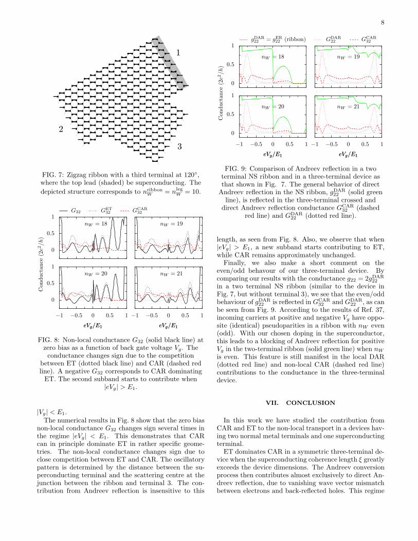
8
1
2
3
FIG. 7: Zigzag ribbon with a third terminal at 120◦,where the top lead (shaded) be superconducting. The
depicted structure corresponds to nribbonW = nleg
W = 10.
nW = 20
0
0.5
1
−1 −0.5 0 0.5 1
eVg/E1eVg/E1
nW = 18
0
0.5
1G32 GET
32 GCAR32
nW = 21
−1 −0.5 0 0.5 1
eVg/E1eVg/E1
nW = 19
Con
duct
ance
(2e2
/h)
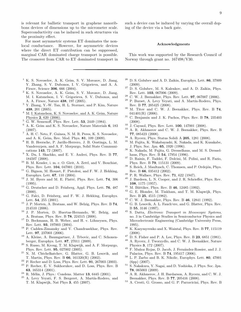
FIG. 8: Non-local conductance G32 (solid black line) atzero bias as a function of back gate voltage Vg. Theconductance changes sign due to the competition
between ET (dotted black line) and CAR (dashed redline). A negative G32 corresponds to CAR dominatingET. The second subband starts to contribute when
|eVg| > E1.
|Vg| < E1.The numerical results in Fig. 8 show that the zero bias
non-local conductance G32 changes sign several times inthe regime |eVg| < E1. This demonstrates that CARcan in principle dominate ET in rather specific geome-tries. The non-local conductance changes sign due toclose competition between ET and CAR. The oscillatorypattern is determined by the distance between the su-perconducting terminal and the scattering centre at thejunction between the ribbon and terminal 3. The con-tribution from Andreev reflection is insensitive to this
nW = 20
0
0.5
1
−1 −0.5 0 0.5 1
eVg/E1eVg/E1
nW = 18
0
0.5
1gDAR22 = gER
22 (ribbon) GDAR22 GCAR
32
nW = 21
−1 −0.5 0 0.5 1
eVg/E1eVg/E1
nW = 19
Con
duct
ance
(2e2
/h)
FIG. 9: Comparison of Andreev reflection in a twoterminal NS ribbon and in a three-terminal device asthat shown in Fig. 7. The general behavior of directAndreev reflection in the NS ribbon, gDAR
22 (solid greenline), is reflected in the three-terminal crossed and
direct Andreev reflection conductance GCAR32 (dashed
red line) and GDAR22 (dotted red line).
length, as seen from Fig. 8. Also, we observe that when|eVg| > E1, a new subband starts contributing to ET,while CAR remains approximately unchanged.Finally, we also make a short comment on the
even/odd behavour of our three-terminal device. Bycomparing our results with the conductance g22 = 2gDAR
22
in a two terminal NS ribbon (similar to the device inFig. 7, but without terminal 3), we see that the even/oddbehaviour of gDAR
22 is reflected in GCAR32 and GDAR
22 , as canbe seen from Fig. 9. According to the results of Ref. 37,incoming carriers at positive and negative Vg have oppo-site (identical) pseudoparities in a ribbon with nW even(odd). With our chosen doping in the superconductor,this leads to a blocking of Andreev reflection for positiveVg in the two-terminal ribbon (solid green line) when nW
is even. This feature is still manifest in the local DAR(dotted red line) and non-local CAR (dashed red line)contributions to the conductance in the three-terminaldevice.
VII. CONCLUSION
In this work we have studied the contribution fromCAR and ET to the non-local transport in a devices hav-ing two normal metal terminals and one superconductingterminal.ET dominates CAR in a symmetric three-terminal de-
vice when the superconducting coherence length ξ greatlyexceeds the device dimensions. The Andreev conversionprocess then contributes almost exclusively to direct An-dreev reflection, due to vanishing wave vector mismatchbetween electrons and back-reflected holes. This regime
9
is relevant for ballistic transport in graphene nanorib-bons devices of dimensions up to the micrometer scale.Superconductivity can be induced in such structures viathe proximity effect.For most asymmetric systems ET dominates the non-
local conductance. However, for asymmetric deviceswhere the direct ET contribution can be suppressed,marginal CAR dominated charge transport is possible.The crossover from CAR to ET dominated transport in
such a device can be induced by varying the overall dop-ing of the device via a back gate.
Acknowledgments
This work was supported by the Research Council ofNorway through grant no. 167498/V30.
1 K. S. Novoselov, A. K. Geim, S. V. Morozov, D. Jiang,Y. Zhang, S. V. Dubonos, I. V. Grigorieva, and A. A.Firsov, Science 306, 666 (2004).
2 K. S. Novoselov, A. K. Geim, S. V. Morozov, D. Jiang,M. I. Katsnelson, I. V. Grigorieva, S. V. Dubonos, andA. A. Firsov, Nature 438, 197 (2005).
3 Y. Zhang, Y.-W. Tan, H. L. Stormer, and P. Kim, Nature438, 201 (2005).
4 M. I. Katsnelson, K. S. Novoselov, and A. K. Geim, NaturePhysics 2, 620 (2006).
5 G. W. Semenoff, Phys. Rev. Lett. 53, 2449 (1984).6 A. K. Geim and K. S. Novoselov, Nature Materials 6, 183(2007).
7 A. H. C. Neto, F. Guinea, N. M. R. Peres, K. S. Novoselov,and A. K. Geim, Rev. Mod. Phys. 81, 109 (2009).
8 H. B. Heersche, P. Jarillo-Herrero, J. B. Oostinga, L. M.Vandersypen, and A. F. Morpurgo, Solid State Communi-cations 143, 72 (2007).
9 X. Du, I. Skachko, and E. Y. Andrei, Phys. Rev. B 77,184507 (2008).
10 B. M. Kessler, i. m. c. O. Girit, A. Zettl, and V. Bouchiat,Phys. Rev. Lett. 104, 047001 (2010).
11 G. Bignon, M. Houzet, F. Pistolesi, and F. W. J. Hekking,Europhys. Lett. 67, 110 (2004).
12 J. M. Byers and M. E. Flatte, Phys. Rev. Lett. 74, 306(1995).
13 G. Deutscher and D. Feinberg, Appl. Phys. Lett. 76, 487(2000).
14 G. Falci, D. Feinberg, and F. W. J. Hekking, Europhys.Lett. 54, 255 (2001).
15 J. P. Morten, A. Brataas, and W. Belzig, Phys. Rev. B 74,214510 (2006).
16 J. P. Morten, D. Huertas-Hernando, W. Belzig, andA. Brataas, Phys. Rev. B 78, 224515 (2008).
17 D. Beckmann, H. B. Weber, and H. v. Lohneysen, Phys.Rev. Lett. 93, 197003 (2004).
18 P. Cadden-Zimansky and V. Chandrasekhar, Phys. Rev.Lett. 97, 237003 (2006).
19 A. Kleine, A. Baumgartner, J. Trbovic, and C. Schonen-berger, Europhys. Lett. 87, 27011 (2009).
20 S. Russo, M. Kroug, T. M. Klapwijk, and A. F. Morpurgo,Phys. Rev. Lett. 95, 027002 (2005).
21 N. M. Chtchelkatchev, G. Blatter, G. B. Lesovik, andT. Martin, Phys. Rev. B 66, 161320(R) (2002).
22 P. Recher and D. Loss, Phys. Rev. Lett. 91, 267003 (2003).23 P. Recher, E. V. Sukhorukov, and D. Loss, Phys. Rev. B
63, 165314 (2001).24 R. Melin, J. Phys.: Condens. Matter 13, 6445 (2001).25 A. Levy Yeyati, F. S. Bergeret, A. Martın-Rodero, and
T. M. Klapwijk, Nat Phys 3, 455 (2007).
26 D. S. Golubev and A. D. Zaikin, Europhys. Lett. 86, 37009(2009).
27 D. S. Golubev, M. S. Kalenkov, and A. D. Zaikin, Phys.Rev. Lett. 103, 067006 (2009).
28 C. W. J. Beenakker, Phys. Rev. Lett. 97, 067007 (2006).29 P. Burset, A. Levy Yeyati, and A. Martın-Rodero, Phys.
Rev. B 77, 205425 (2008).30 M. Titov and C. W. J. Beenakker, Phys. Rev. B 74,
041401(R) (2006).31 C. Benjamin and J. K. Pachos, Phys. Rev. B 78, 235403
(2008).32 J. Cayssol, Phys. Rev. Lett. 100, 147001 (2008).33 A. R. Akhmerov and C. W. J. Beenakker, Phys. Rev. B
77, 085423 (2008).34 A. Rycerz, Phys. Status Solidi A 205, 1281 (2008).35 M. Fujita, K. Wakabayashi, K. Nakada, and K. Kusakabe,
J. Phys. Soc. Jpn. 65, 1920 (1996).36 K. Nakada, M. Fujita, G. Dresselhaus, and M. S. Dressel-
haus, Phys. Rev. B 54, 17954 (1996).37 D. Rainis, F. Taddei, F. Dolcini, M. Polini, and R. Fazio,
Phys. Rev. B 79, 115131 (2009).38 S. Reich, J. Maultzsch, C. Thomsen, and P. Ordejon, Phys.
Rev. B 66, 035412 (2002).39 P. R. Wallace, Phys. Rev. 71, 622 (1947).40 J. Bardeen, L. N. Cooper, and J. R. Schrieffer, Phys. Rev.
108, 1175 (1957).41 M. Buttiker, Phys. Rev. B 46, 12485 (1992).42 G. E. Blonder, M. Tinkham, and T. M. Klapwijk, Phys.
Rev. B 25, 4515 (1982).43 C. W. J. Beenakker, Phys. Rev. B 46, 12841 (1992).44 G. B. Lesovik, A. L. Fauch‘ere, and G. Blatter, Phys. Rev.
B 55, 3146 (1997).45 S. Datta, Electronic Transport in Mesoscopic Systems,
no. 3 in Cambridge Studies in Semiconductor Physics andMicroelectronic Engineering (Cambridge University Press,1995).
46 K. Kazymyrenko and X. Waintal, Phys. Rev. B 77, 115119(2008).
47 D. S. Fisher and P. A. Lee, Phys. Rev. B 23, 6851 (1981).48 A. Rycerz, J. Tworzydlo, and C. W. J. Beenakker, Nature
Physics 3, 172 (2007).49 F. Munoz Rojas, D. Jacob, J. Fernandez-Rossier, and J. J.
Palacios, Phys. Rev. B 74, 195417 (2006).50 L. P. Zarbo and B. K. Nikolic, Europhys. Lett. 80, 47001
(6pp) (2007).51 S. Nakakura, Y. Nagai, and D. Yoshioka, J. Phys. Soc. Jpn.
78, 065003 (2009).52 A. R. Akhmerov, J. H. Bardarson, A. Rycerz, and C. W. J.
Beenakker, Phys. Rev. B 77, 205416 (2008).53 A. Cresti, G. Grosso, and G. P. Parravicini, Phys. Rev. B

10
77, 233402 (2008).54 A. Iyengar, T. Luo, H. A. Fertig, and L. Brey, Phys. Rev.
B 78, 235411 (2008).55 M. I. Katsnelson and F. Guinea, Phys. Rev. B 78, 075417
(2008).56 A. Rycerz and C. W. J. Beenakker (2007),
arxiv.org:0709.3397.