Cross-FPGA Covert-Channel Attacks through Power Supply ...
14
C 3 APSULe: Cross-FPGA Covert-Channel Attacks through Power Supply Unit Leakage Ilias Giechaskiel University of Oxford Oxford, United Kingdom [email protected] Kasper Bonne Rasmussen University of Oxford Oxford, United Kingdom [email protected] Jakub Szefer Yale University New Haven, CT, USA [email protected] Abstract—Field-Programmable Gate Arrays (FPGAs) are ver- satile, reconfigurable integrated circuits that can be used as hardware accelerators to process highly-sensitive data. Leaking this data and associated cryptographic keys, however, can un- dermine a system’s security. To prevent potentially unintentional interactions that could break separation of privilege between different data center tenants, FPGAs in cloud environments are currently dedicated on a per-user basis. Nevertheless, while the FPGAs themselves are not shared among different users, other parts of the data center infrastructure are. This paper specifically shows for the first time that powering FPGAs, CPUs, and GPUs through the same power supply unit (PSU) can be exploited in FPGA-to-FPGA, CPU-to-FPGA, and GPU-to-FPGA covert channels between independent boards. These covert channels can operate remotely, without the need for physical access to, or modifications of, the boards. To demonstrate the attacks, this paper uses a novel combination of “sensing” and “stressing” ring oscillators as receivers on the sink FPGA. Further, ring oscillators are used as transmitters on the source FPGA. The transmitting and receiving circuits are used to determine the presence of the leakage on off-the-shelf Xilinx boards containing Artix 7 and Kintex 7 FPGA chips. Experiments are conducted with PSUs by two vendors, as well as CPUs and GPUs of different generations. Moreover, different sizes and types of ring oscillators are also tested. In addition, this work discusses potential countermeasures to mitigate the impact of the cross-board leakage. The results of this paper highlight the dangers of shared power supply units in local and cloud FPGAs, and therefore a fundamental need to re-think FPGA security for shared infrastructures. Index Terms—Power supply units, voltage regulators, ring oscillators, FPGAs, covert channels, power attacks I. I NTRODUCTION Field-Programmable Gate Arrays (FPGAs) implement re- configurable hardware which can speed up application-specific tasks. For example, they are used to process highly-sensitive data in cloud applications including genomic sequencing, cryptography, and financial modeling, among others [2]. Given the increasing proliferation of cloud FPGAs [44], interest in FPGA attacks has also risen. For example, prior work has shown that implementations of cryptographic and other algorithms are susceptible to reverse engineering [39], [46] as well as side-channel attacks [46]. As such research requires physical proximity to the FPGA board and external equipment (e.g., high-end oscilloscopes) to extract keys, it does not reflect modern-day environments, where FPGAs remain inaccessible in data center server racks. When considering cloud FPGAs, however, attacks must instead be performed remotely using only on-chip logic. Recent work has so far shown that remote fault, covert-channel, and side-channel attacks are indeed pos- sible between designs belonging to different users co-located within the same FPGA chip [8]–[11], [24], [26], [28]–[31], [47]. However, as boards are currently allocated on a per- user basis in commercial clouds, this multi-tenant threat model remains theoretical, with little practical impact. In this paper we instead tackle a more pressing scenario that is applicable to existing cloud FPGA deployments, where boards are co-located within the same server rack. Users renting FPGAs from such FPGA cloud providers assume that their designs are safely isolated from potentially malicious designs by other users running in the same data center. However, as we show in this paper, the assumption of isolation can be broken due to leakage through the shared use of power supply units (PSUs). Specifically, we introduce a new class of remote covert-channel attacks between single-tenant FPGAs on different FPGA boards that are merely powered through the same PSU. Moreover, we show that if this PSU also powers the host computer, the same sink FPGA (receiver) can detect high levels of CPU and GPU activity, creating new CPU-to- FPGA and GPU-to-FPGA channels. The first crucial observation of our work is that although causing variable power consumption to transmit information is easy, detecting voltage fluctuations without external equip- ment is non-trivial. However, the reconfigurability of FPGAs provides access to the hardware at a much lower level, and can be used to implement circuits that detect voltage changes which are imperceptible to fixed silicon chips such as CPUs and GPUs. Indeed, cloud providers are aware of the impact of such low-level hardware access, so besides allocating FPGAs on a per-user basis, they also keep several features such as voltage and temperature monitors inaccessible to end-users. The second key observation is that ring oscillators (ROs) are capable of both causing and sensing voltage fluctuations. This paper therefore introduces a novel way of monitoring changes in voltage caused by the source FPGA, CPU, or GPU. Specifically, both properties of ROs are used in the sink (receiver) FPGA, whereby stressing the voltage regulator of the sink FPGA allows one to detect transmissions by the source (transmitter) FPGA.
-
Upload
khangminh22 -
Category
Documents
-
view
0 -
download
0
Transcript of Cross-FPGA Covert-Channel Attacks through Power Supply ...
C3APSULe: Cross-FPGA Covert-Channel Attacksthrough Power Supply Unit Leakage
Ilias GiechaskielUniversity of Oxford
Oxford, United Kingdom
Kasper Bonne RasmussenUniversity of Oxford
Oxford, United Kingdom
Jakub SzeferYale University
New Haven, CT, USA
Abstract—Field-Programmable Gate Arrays (FPGAs) are ver-satile, reconfigurable integrated circuits that can be used ashardware accelerators to process highly-sensitive data. Leakingthis data and associated cryptographic keys, however, can un-dermine a system’s security. To prevent potentially unintentionalinteractions that could break separation of privilege betweendifferent data center tenants, FPGAs in cloud environments arecurrently dedicated on a per-user basis. Nevertheless, while theFPGAs themselves are not shared among different users, otherparts of the data center infrastructure are. This paper specificallyshows for the first time that powering FPGAs, CPUs, and GPUsthrough the same power supply unit (PSU) can be exploitedin FPGA-to-FPGA, CPU-to-FPGA, and GPU-to-FPGA covertchannels between independent boards. These covert channelscan operate remotely, without the need for physical access to,or modifications of, the boards. To demonstrate the attacks, thispaper uses a novel combination of “sensing” and “stressing” ringoscillators as receivers on the sink FPGA. Further, ring oscillatorsare used as transmitters on the source FPGA. The transmittingand receiving circuits are used to determine the presence of theleakage on off-the-shelf Xilinx boards containing Artix 7 andKintex 7 FPGA chips. Experiments are conducted with PSUs bytwo vendors, as well as CPUs and GPUs of different generations.Moreover, different sizes and types of ring oscillators are alsotested. In addition, this work discusses potential countermeasuresto mitigate the impact of the cross-board leakage. The results ofthis paper highlight the dangers of shared power supply unitsin local and cloud FPGAs, and therefore a fundamental need tore-think FPGA security for shared infrastructures.
Index Terms—Power supply units, voltage regulators, ringoscillators, FPGAs, covert channels, power attacks
I. INTRODUCTION
Field-Programmable Gate Arrays (FPGAs) implement re-
configurable hardware which can speed up application-specific
tasks. For example, they are used to process highly-sensitive
data in cloud applications including genomic sequencing,
cryptography, and financial modeling, among others [2]. Given
the increasing proliferation of cloud FPGAs [44], interest
in FPGA attacks has also risen. For example, prior work
has shown that implementations of cryptographic and other
algorithms are susceptible to reverse engineering [39], [46] as
well as side-channel attacks [46]. As such research requires
physical proximity to the FPGA board and external equipment
(e.g., high-end oscilloscopes) to extract keys, it does not reflect
modern-day environments, where FPGAs remain inaccessible
in data center server racks. When considering cloud FPGAs,
however, attacks must instead be performed remotely using
only on-chip logic. Recent work has so far shown that remote
fault, covert-channel, and side-channel attacks are indeed pos-
sible between designs belonging to different users co-located
within the same FPGA chip [8]–[11], [24], [26], [28]–[31],
[47]. However, as boards are currently allocated on a per-
user basis in commercial clouds, this multi-tenant threat model
remains theoretical, with little practical impact.
In this paper we instead tackle a more pressing scenario
that is applicable to existing cloud FPGA deployments, where
boards are co-located within the same server rack. Users
renting FPGAs from such FPGA cloud providers assume that
their designs are safely isolated from potentially malicious
designs by other users running in the same data center.
However, as we show in this paper, the assumption of isolation
can be broken due to leakage through the shared use of power
supply units (PSUs). Specifically, we introduce a new class of
remote covert-channel attacks between single-tenant FPGAs
on different FPGA boards that are merely powered through the
same PSU. Moreover, we show that if this PSU also powers
the host computer, the same sink FPGA (receiver) can detect
high levels of CPU and GPU activity, creating new CPU-to-
FPGA and GPU-to-FPGA channels.
The first crucial observation of our work is that although
causing variable power consumption to transmit information
is easy, detecting voltage fluctuations without external equip-
ment is non-trivial. However, the reconfigurability of FPGAs
provides access to the hardware at a much lower level, and
can be used to implement circuits that detect voltage changes
which are imperceptible to fixed silicon chips such as CPUs
and GPUs. Indeed, cloud providers are aware of the impact of
such low-level hardware access, so besides allocating FPGAs
on a per-user basis, they also keep several features such as
voltage and temperature monitors inaccessible to end-users.
The second key observation is that ring oscillators (ROs)
are capable of both causing and sensing voltage fluctuations.
This paper therefore introduces a novel way of monitoring
changes in voltage caused by the source FPGA, CPU, or
GPU. Specifically, both properties of ROs are used in the
sink (receiver) FPGA, whereby stressing the voltage regulator
of the sink FPGA allows one to detect transmissions by the
source (transmitter) FPGA.
Using these insights, we demonstrate the first cross-FPGA
covert channel between off-the-shelf, unmodified Xilinx Ar-
tix 7 and Kintex 7 boards in either direction of communication.
We also characterize the bandwidth-accuracy tradeoffs across
different measurement periods and sizes of the covert-channel
ROs on the source and sink FPGAs. We further test our covert
channel on two PSUs running under normal operating condi-
tions (i.e., without being overloaded), and introduce CPU-to-
FPGA and GPU-to-FPGA covert channels by modulating their
respective loads. We finally discuss potential countermeasures
to mitigate the effects of this leakage.
A. Contributions
Our contributions can be summarized as follows:
1) We identify sharing of PSUs as a new source of vul-
nerability, even for unprivileged FPGA designs without
access to voltage or temperature system monitors.
2) We introduce a novel measurement setup and classi-
fication metric that uses ring oscillators (ROs) on the
sink FPGA to stress its voltage regulator and therefore
reliably detect external voltage fluctuations.
3) We exploit this setup to create the first remote covert-
channel attack between FPGAs on distinct physical
boards that are dedicated on a per-user basis, reaching
accuracies of up to 100%.
4) We evaluate the strength of the information leakage
across different architectural choices, and perform a
bandwidth-accuracy tradeoff analysis.
5) We introduce the first CPU-to-FPGA and GPU-to-FPGA
covert channels using high loads of activity on their re-
spective processors, opening up new avenues for remote
FPGA attacks.
6) We propose hardware- and software-level countermea-
sures to reduce the impact of the leakage.
B. Paper Organization
The rest of the paper is organized as follows. Section II
introduces the threat model, while Section III details the
experimental setup, including hardware properties, the mea-
surement procedure, and the high-level architectural FPGA
design. Section IV then describes the need for our novel clas-
sification metric, and explains why it works where the naive
approach of looking at absolute ring oscillator counts fails.
Section V then evaluates cross-FPGA covert communication
over shared PSUs, varying the number of source and sink ring
oscillators used, and performing an analysis of bandwidth-
accuracy tradeoffs. Section VI then covers CPU-to-FPGA
and GPU-to-FPGA information leakage, while Section VII
discusses potential defense mechanisms. We place our work
in the context of related research in Section VIII, before we
conclude in Section IX.
II. THREAT MODEL
Prior work on remote FPGA attacks has primarily inves-
tigated security in the context of multi-tenant FPGAs. It has
shown that when a single FPGA chip is shared among multiple
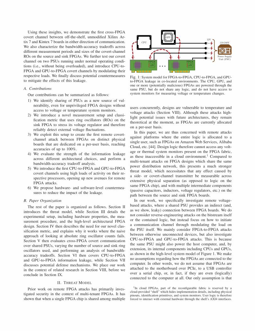
Fig. 1: System model for FPGA-to-FPGA, CPU-to-FPGA, and GPU-to-FPGA leakage in co-located environments. The CPU, GPU, andone or more (potentially malicious) FPGAs are powered through thesame PSU, but do not share any logic, and do not have access tosystem monitors for measuring voltage or temperature changes.
users concurrently, designs are vulnerable to temperature and
voltage attacks (Section VIII). Although these attacks high-
light potential issues with future architectures, they remain
theoretical at the moment, as FPGAs are currently allocated
on a per-user basis.
In this paper, we are thus concerned with remote attacks
against platforms where the entire logic is allocated to a
single user, such as FPGAs on Amazon Web Services, Alibaba
Cloud, etc. [44]. Design logic therefore cannot access any volt-
age or thermal system monitors present on the FPGA fabric,
as these inaccessible in a cloud environment.1 Compared to
multi-tenant attacks on FPGA designs which share the same
power distribution network, this presents a much stronger
threat model, which necessitates that any effect caused by
a side- or covert-channel transmitter be measurable across
extensive physical separation (as opposed to logic on the
same FPGA chip), and with multiple intermediate components
(passive capacitors, inductors, voltage regulators, etc.) on the
path between the source and sink FPGA boards.
In our work, we specifically investigate remote voltage-
based attacks, where a shared PSU provides an indirect (and,
as we show, leaky) connection between FPGA boards. We do
not consider reverse-engineering attacks on the bitstream itself
or the contained logic, but instead focus on how to initiate
a communication channel through modulating the load on
the PSU itself. We mainly consider FPGA-to-FPGA attacks
between otherwise unconnected devices, but also investigate
CPU-to-FPGA and GPU-to-FPGA attacks. This is because
the same PSU might also power the host computer, and, by
extension, its internal components including CPUs and GPUs,
as shown in the high-level system model of Figure 1. We make
no assumptions regarding how the FPGAs are connected to the
computer. In other words, we do not assume that FPGAs are
attached to the motherboard over PCIe, to a USB controller
over a serial chip, or, in fact, if they are even (logically)
connected to the computer at all. Our only assumption is that
1In cloud FPGAs, part of the reconfigurable fabric is reserved by acloud-provided “shell” which hides implementation details, including physicalpinouts, identification primitives, and system monitors. User logic is thereforeforced to interact with external hardware through the shell’s AXI4 interfaces.
of a shared PSU between the two communicating parties.
Within an FPGA, and in accordance with prior work,
(potentially adversarial) users can place and route any designs
of their choice, such as different types of ring oscillators.
This is allowed by current FPGA cloud deployments, as long
as the logic is placed outside of the cloud-provided shell.
In this paper, we show that by relying only on on-chip
FPGA logic (i.e., ring oscillators), we are able to demonstrate
FPGA-to-FPGA, CPU-to-FPGA, and GPU-to-FPGA covert
communication, without physical access to the FPGA boards.
One of the key contributions of our work is therefore the ability
to communicate across unmodified devices, without external
equipment or access to internal voltage monitors, which are
off-limits to unprivileged FPGA designs.
It should be noted that some cloud providers such as
Amazon Web Services (AWS) place restrictions on the types
of circuits that can be instantiated on their FPGAs, and prohibit
combinatorial loops including ring oscillators. Although in
this work we primarily use conventional ring oscillators,
Section V-E shows that they can be easily replaced by alternate
designs proposed in recent work [8], [10], [11], [34], which
bypass cloud countermeasures.
III. EXPERIMENTAL SETUP
In this section, we detail our experimental setup, starting
with the ring oscillators employed in the source and sink
FPGAs (Section III-A), and delving into the architectural
design of the FPGA transmission and reception circuitry
(Section III-B). We then describe the hardware properties of
the FPGA boards used (Section III-C), as well as the computer
PSUs, CPUs, and GPUs, which are effectively turned into
covert-channel transmitters (Section III-D). We finally discuss
the process followed for data collection (Section III-E).
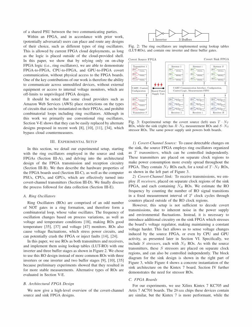
A. Ring Oscillators
Ring Oscillators (ROs) are comprised of an odd number
of NOT gates in a ring formation, and therefore form a
combinatorial loop, whose value oscillates. The frequency of
oscillation changes based on process variations, as well as
voltage and temperature conditions [18], making ROs good
temperature [35], [37] and voltage [47] monitors. ROs also
cause voltage fluctuations, which stress power circuits, and
can potentially crash the FPGA or inject faults [14], [24].
In this paper, we use ROs as both transmitters and receivers,
and implement them using lookup tables (LUT-RO) with one
inverter and three buffer stages as shown in Figure 2. We chose
to use this RO design instead of more common ROs with three
inverters or one inverter and two buffer stages [9], [10], [35]
because preliminary experiments showed that they resulted in
for more stable measurements. Alternative types of ROs are
evaluated in Section V-E.
B. Architectural FPGA Design
We now give a high-level overview of the covert-channel
source and sink FPGA designs.
Fig. 2: The ring oscillators are implemented using lookup tables(LUT-ROs), and contain one inverter and three buffer gates.
Fig. 3: Experimental setup: the covert source (left) uses T · NT
ROs, while the sink (right) has R ·NR measurement ROs and S ·NS
stressor ROs. The same power supply unit powers both boards.
1) Covert-Channel Source: To cause detectable changes on
the sink, the source FPGA employs ring oscillators organized
as T transmitters, which can be controlled independently.
These transmitters are placed on separate clock regions to
make power consumption more evenly spread throughout the
FPGA. They contain NT ROs each, for a total of T ·NT ROs,
as shown in the left part of Figure 3.
2) Covert-Channel Sink: To receive transmissions, we em-
ploy R receivers, placed on separate clock regions of the sink
FPGA, and each containing NR ROs. We estimate the RO
frequency by counting the number of RO signal transitions
in a fixed measurement interval of 2t clock cycles through
counters placed outside of the RO clock regions.
However, this setup is not sufficient to decode covert
transmissions, due to inherent noise in the power supply
and environmental fluctuations. Instead, it is necessary to
introduce additional circuitry on the sink FPGA which stresses
the board’s voltage regulator, making maintaining a constant
voltage harder. This fact allows us to sense voltage changes
induced by the source FPGA, or even by CPU and GPU
activity, as presented later in Section VI. Specifically, we
include S stressors, each with NS ROs. As with the source
transmitters, these S stressors are placed on separate clock
regions, and can also be controlled independently. The block
diagram for the sink design is shown in the right part of
Figure 3, while Figure 4 shows a concrete instantiation of the
sink architecture on the Kintex 7 board. Section IV further
demonstrates the need for stressor ROs.
C. FPGA Boards
For our experiments, we use Xilinx Kintex 7 KC705 and
Artix 7 AC701 boards. The 28 nm chips these devices contain
are similar, but the Kintex 7 is more performant, while the
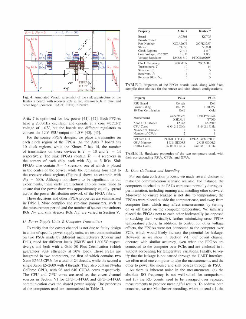
Fig. 4: Annotated Vivado screenshot of the sink architecture on theKintex 7 board, with receiver ROs in red, stressor ROs in blue, andother logic (counters, UART, FIFO) in brown.
Artix 7 is optimized for low power [41], [42]. Both FPGAs
have a 200MHz oscillator and operate at a core VCCINTvoltage of 1.0V, but the boards use different regulators to
convert the 12V PSU output to 1.0V [43], [45].
For the source FPGA designs, we place a transmitter on
each clock region of the FPGA. As the Artix 7 board has
10 clock regions, while the Kintex 7 has 14, the number
of transmitters on these devices is T = 10 and T = 14respectively. The sink FPGAs contain R = 4 receivers in
the corners of each chip, each with NR = 5 ROs. Sink
FPGAs also contain S = 5 stressors, one of which is placed
in the center of the device, while the remaining four next to
the receiver clock regions (Figure 4 shows an example with
NS = 500). Although not shown to be significant in our
experiments, these early architectural choices were made to
ensure that the power draw was approximately equally spread
across the power distribution network of the FPGA fabric.
These decisions and other FPGA properties are summarized
in Table I. More compile- and run-time parameters, such as
the measurement period and the number of source transmitters
ROs NT and sink stressor ROs NS , are varied in Section V.
D. Power Supply Units & Computer Transmitters
To verify that the covert channel is not due to faulty design
in a line of specific power supply units, we test communication
on two PSUs made by different manufacturers (Corsair and
Dell), rated for different loads (850W and 1,300W respec-
tively), and both with a Gold 80 Plus Certification (which
guarantees 90% efficiency at 50% load). These PSUs are
integrated in two computers, the first of which contains two
Xeon E5645 CPUs for a total of 24 threads, while the second a
single Xeon E5-2609 with 4 threads. They also contain Nvidia
GeForce GPUs, with 96 and 640 CUDA cores respectively.
The CPU and GPU cores are used as the covert-channel
sources in Section VI for CPU-to-FPGA and GPU-to-FPGA
communication over the shared power supply. The properties
of the computers used are summarized in Table II.
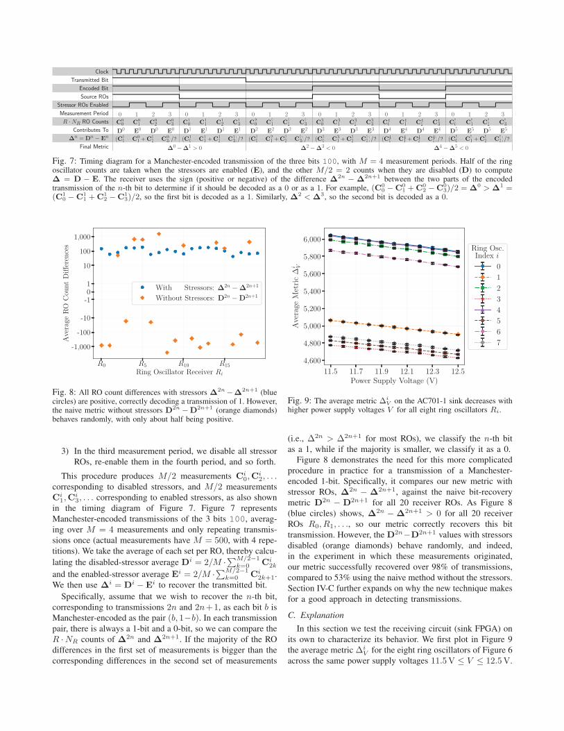
Property Artix 7 Kintex 7
Board AC701 KC705Boards Tested 2 2Part Number XC7A200T XC7K325TSlices 33,650 50,950Clock Regions 2× 5 2× 7Core Voltage, VCCINT 1.0V 1.0VVoltage Regulator LMZ31710 PTD08A020W
Clock Frequency 200MHz 200MHzTransmitters, T 10 14Stressors, S 5 5Receivers, R 4 4Receiver ROs, NR 5 5
TABLE I: Properties of the FPGA boards used, along with fixedcompile-time choices for the source and sink circuit configurations.
Property PC-A PC-B
PSU Brand Corsair DellPower Rating 850W 1,300W80 Plus Certification Gold Gold
MotherboardSuperMicro
X8DAL-iDell Precision
T7600Xeon CPU Model E5645 E5-2609CPU Cores 6 @ 2.4GHz 4 @ 2.4GHzNumber of Threads 12 4Number of CPUs 2 1
GeForce GPU ZOTAC GT 430 EVGA GTX 750 TiGPU Memory 1GB GDDR3 2GB GDDR5CUDA Cores 96 @ 0.7GHz 640 @ 1.0GHz
TABLE II: Hardware properties of the two computers used, withtheir corresponding PSUs, CPUs, and GPUs.
E. Data Collection and Encoding
For our data collection process, we made several choices to
make the communication scenario realistic. For instance, the
computers attached to the PSUs were used normally during ex-
perimentation, including running and installing other software.
Moreover, to ensure leakage is not due to temperature, the
FPGAs were placed outside the computer case, and away from
computer fans, which may affect measurements by turning
on or off based on the computer temperature. We similarly
placed the FPGAs next to each other horizontally (as opposed
to stacking them vertically), further minimizing cross-FPGA
temperature effects. In addition, to control for other voltage
effects, the FPGAs were not connected to the computer over
PCIe, which would likely increase the potential for leakage.
However, as we show in Section V-E, our covert channel
operates with similar accuracy, even when the FPGAs are
connected to the computer over PCIe, and are enclosed in it
without accounting for temperature variations. Finally, to ver-
ify that the leakage is not caused through the UART interface,
we often used one computer to take the measurements, and the
other to power the source and sink boards through its PSU.
As there is inherent noise in the measurements, (a) the
absolute RO frequency is not well-suited for comparison,
and (b) the RO counts need to be averaged over repeated
measurements to produce meaningful results. To address both
concerns, we use Manchester encoding, where to send a 1, the

11.5 11.7 11.9 12.1 12.3 12.5Power Supply Voltage (V)
5
10
15
20
25
30
35
40
Nom
inal
Voltage
Difference
(mV)
# of EnabledTransmitters T
0
2
4
6
8
10
12
14
Fig. 5: Voltage as set by the power supply and measured by theoscilloscope for various numbers of enabled transmitters T on theKC705-2 source, with 99% confidence intervals.
source transmitters are enabled for one measurement period
and disabled for the next (a 0 is similarly encoded by first
disabling transmitters during the first measurement period and
enabling them in the second period). These measurement
periods are M · 2t clock cycles long, where we average MRO counts collected by ROs enabled for 2t clock cycles (see
Section IV). The bandwidth can thus be calculated as:
b =fc
2 · 2t ·M (1)
where fc = 200MHz is the FPGA clock frequency.
In most experiments, we transmit the 20-bit number
0xf3ed1, which is Manchester-encoded in 40 bits to be sent
across the covert channel. Additional patterns are evaluated
in Section V-E. To ensure that perfect synchronization is not
needed between the source and the sink, for each of the 40
periods, we take four sets of M measurements, where Mis in the order of a few hundred counts (see Table III and
Section V-D). The four sets of repetitions create 42 = 16Manchester encoded pairs per bit to be transferred, for a total
of 16×20 = 320 pairs to estimate the covert-channel accuracy.
IV. CLASSIFICATION METRIC
This section introduces a novel methodology to detect
changes in the power supply voltage through the sink’s “stres-
sor” ROs. Section IV-A first motivates why the naive approach
of using the absolute ring oscillator counts is insufficient for
classification of transmissions in this scenario. Section IV-B
then introduces the metric using stressors, while Section IV-C
finally explains why our technique works.
A. Motivation
Broadly speaking, when the transmitters are activated on
the source FPGA, there is a voltage drop that is visible not
just at the board regulator, but also at the 12V rail PSU
input to the FPGA. Indeed, Figure 5 demonstrates this for a
11.5 11.7 11.9 12.1 12.3 12.5Power Supply Voltage (V)
650,000
675,000
700,000
725,000
750,000
775,000
Average
RO
Cou
ntC
i V
Ring Osc.Index i
0
1
2
3
4
5
6
7
Fig. 6: The average ring oscillator counts CiV (with 99% confidence
intervals) on the AC701-1 sink remain approximately the same fordifferent power supply voltages V and all eight ring oscillators Ri.
Kintex 7 source without a sink FPGA present across multiple
input voltages and different numbers of enabled transmitters
T . Specifically, we power the board using a Keithley 2231A
power supply, and measure the voltage at the power rail
of the board using a Tektronix MDO3104 Mixed Domain
Oscilloscope with TPP1000 1GHz passive probes, taking
10,000 data points. Figure 5 indicates that at any voltage level
provided by the power supply (11.5-12.5V), as the number of
enabled source transmitters T increases, the voltage measured
by the oscilloscope decreases. For example, at 12.5V, the
oscilloscope measures 12.539V when no transmitters are
enabled, but only 12.521V when 14 transmitters are enabled,
for a voltage drop of approximately 18mV. At 11.5V, the
measured voltage similarly drops from 11.525V to 11.507V.
Although one would expect RO frequency to increase with
higher voltages [18], this is not the case. For a ring oscillator
i, let its average count be CiV when the voltage provided by
the power supply is 11.5V ≤ V ≤ 12.5V. We would expect
that CiV1
> CiV2
whenever V1 > V2, but Figure 6 suggests that
the RO counts remain approximately the same for all eight
ring oscillators and voltages V tested on an Artix 7 sink. As
a result, the absolute RO frequency cannot be used to decode
cross-FPGA covert-channel transmissions.
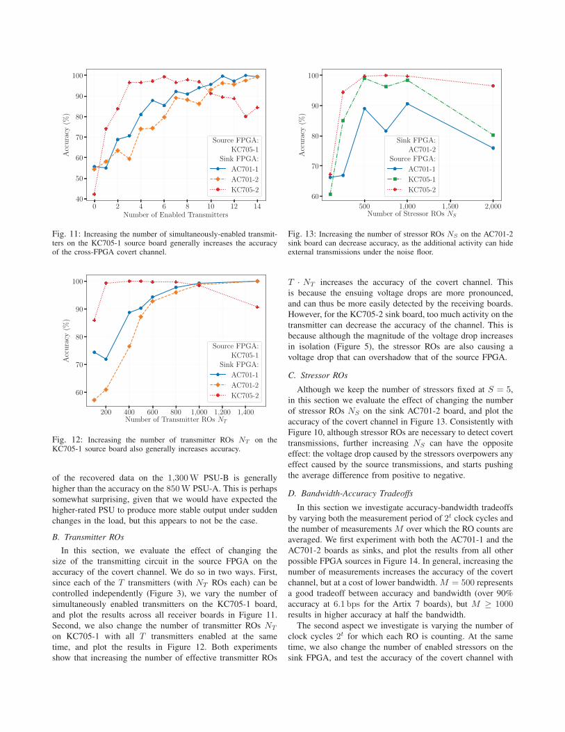
B. Description
To solve the issues identified above, we introduce ROs to
“stress” the voltage regulator and make external changes in
the power supply voltage measurable. For any bit transmission
(say the i-th one), we take M measurements as follows:
1) For the first measurement period, we disable all stressor
ROs, and let the receiver ROs run for 2t clock cycles,
producing counts Ci0 = (C0
0 , . . . , CR·NR−10 ).
2) In the second measurement period, we enable all (or
some, see Sections IV-C and V-D) stressor ROs, and
estimate the RO frequencies through their counts, Ci1.
0 1 2 3 0 1 2 3 0 1 2 3 0 1 2 3 0 1 2 3 0 1 2 3
C00 C0
1 C02 C0
3 C10 C1
1 C12 C1
3 C20 C2
1 C22 C2
3 C30 C3
1 C32 C3
3 C40 C4
1 C42 C4
3 C50 C5
1 C52 C5
3
D0 E0 D0 E0 D1 E1 D1 E1 D2 E2 D2 E2 D3 E3 D3 E3 D4 E4 D4 E4 D5 E5 D5 E5
(C00 −C0
1 +C02 −C0
3)/2 (C10 −C1
1 +C12 −C1
3)/2 (C20 −C2
1 +C22 −C2
3)/2 (C30 −C3
1 +C32 −C3
3)/2 (C40 −C4
1 +C42 −C4
3)/2 (C50 −C5
1 +C52 −C5
3)/2
C00 C0
1 C02 C0
3 C10 C1
1 C12 C1
3 C20 C2
1 C22 C2
3 C30 C3
1 C32 C3
3 C40 C4
1 C42 C4
3 C50 C5
1 C52 C5
3
(C00 −C0
1 +C02 −C0
3)/2 (C10 −C1
1 +C12 −C1
3)/2 (C20 −C2
1 +C22 −C2
3)/2 (C30 −C3
1 +C32 −C3
3)/2 (C40 −C4
1 +C42 −C4
3)/2 (C50 −C5
1 +C52 −C5
3)/2
Clock
Transmitted Bit
Encoded Bit
Source ROs
Stressor ROs Enabled
Measurement Period
R ·NR RO Counts
Contributes To
Δn = Dn − En
Final Metric Δ0 −Δ1 > 0 Δ2 −Δ3 < 0 Δ4 −Δ5 < 0
Fig. 7: Timing diagram for a Manchester-encoded transmission of the three bits 100, with M = 4 measurement periods. Half of the ringoscillator counts are taken when the stressors are enabled (E), and the other M/2 = 2 counts when they are disabled (D) to computeΔ = D − E. The receiver uses the sign (positive or negative) of the difference Δ2n − Δ2n+1 between the two parts of the encodedtransmission of the n-th bit to determine if it should be decoded as a 0 or as a 1. For example, (C0
0 −C01 +C0
2 −C03)/2 = Δ0 > Δ1 =
(C10 −C1
1 +C12 −C1
3)/2, so the first bit is decoded as a 1. Similarly, Δ2 < Δ3, so the second bit is decoded as a 0.
R0 R5 R10 R15
Ring Oscillator Receiver Ri
-1,000
-100
-10
-101
10
100
1,000
Average
RO
Cou
ntDifferences
With Stressors: Δ2n −Δ2n+1
Without Stressors: D2n −D2n+1
Fig. 8: All RO count differences with stressors Δ2n−Δ2n+1 (bluecircles) are positive, correctly decoding a transmission of 1. However,the naive metric without stressors D2n −D2n+1 (orange diamonds)behaves randomly, with only about half being positive.
3) In the third measurement period, we disable all stressor
ROs, re-enable them in the fourth period, and so forth.
This procedure produces M/2 measurements Ci0,C
i2, . . .
corresponding to disabled stressors, and M/2 measurements
Ci1,C
i3, . . . corresponding to enabled stressors, as also shown
in the timing diagram of Figure 7. Figure 7 represents
Manchester-encoded transmissions of the 3 bits 100, averag-
ing over M = 4 measurements and only repeating transmis-
sions once (actual measurements have M = 500, with 4 repe-
titions). We take the average of each set per RO, thereby calcu-
lating the disabled-stressor average Di = 2/M ·∑M/2−1k=0 Ci
2k
and the enabled-stressor average Ei = 2/M ·∑M/2−1k=0 Ci
2k+1.
We then use Δi = Di −Ei to recover the transmitted bit.
Specifically, assume that we wish to recover the n-th bit,
corresponding to transmissions 2n and 2n+1, as each bit b is
Manchester-encoded as the pair (b, 1−b). In each transmission
pair, there is always a 1-bit and a 0-bit, so we can compare the
R ·NR counts of Δ2n and Δ2n+1. If the majority of the RO
differences in the first set of measurements is bigger than the
corresponding differences in the second set of measurements
11.5 11.7 11.9 12.1 12.3 12.5Power Supply Voltage (V)
4,600
4,800
5,000
5,200
5,400
5,600
5,800
6,000
Average
MetricΔ
i V
Ring Osc.Index i
0
1
2
3
4
5
6
7
Fig. 9: The average metric ΔiV on the AC701-1 sink decreases with
higher power supply voltages V for all eight ring oscillators Ri.
(i.e., Δ2n > Δ2n+1 for most ROs), we classify the n-th bit
as a 1, while if the majority is smaller, we classify it as a 0.
Figure 8 demonstrates the need for this more complicated
procedure in practice for a transmission of a Manchester-
encoded 1-bit. Specifically, it compares our new metric with
stressor ROs, Δ2n − Δ2n+1, against the naive bit-recovery
metric D2n − D2n+1 for all 20 receiver ROs. As Figure 8
(blue circles) shows, Δ2n − Δ2n+1 > 0 for all 20 receiver
ROs R0, R1, . . ., so our metric correctly recovers this bit
transmission. However, the D2n−D2n+1 values with stressors
disabled (orange diamonds) behave randomly, and indeed,
in the experiment in which these measurements originated,
our metric successfully recovered over 98% of transmissions,
compared to 53% using the naive method without the stressors.
Section IV-C further expands on why the new technique makes
for a good approach in detecting transmissions.
C. Explanation
In this section we test the receiving circuit (sink FPGA) on
its own to characterize its behavior. We first plot in Figure 9
the average metric ΔiV for the eight ring oscillators of Figure 6
across the same power supply voltages 11.5V ≤ V ≤ 12.5V.

0.6μs 5.1μs 41.0μs 0.3ms 2.6ms 21.0msMeasurement Time
−600
−400
−200
0
200
Average
Difference
Δ11
.5−
Δ12
.5
# of Enabled Stressors S
1
2
3
4
5
Fig. 10: Difference between the average Δ metric as measured at11.5V and 12.5V for different measurement times and numbers ofstressors enabled on the AC701-1 sink.
As expected, for all ROs, ΔiV1
< ΔiV2
whenever V1 > V2:
when there is an external voltage drop (e.g., when the source
FPGA enables the transmitter ROs), the Δ metric increases
compared to when there are no external transmissions.
We additionally test the behavior of the receiver FPGA
across different measurement times of 2t clock cycles and
numbers of enabled stressors S. Specifically, we conduct
measurements on an Artix 7 sink, and calculate the average
value of our Δ metric over all 20 receiver ROs at two voltage
levels: 11.5V and 12.5V. Figure 10 plots our results, which
lead to several observations.
First of all, the average difference Δ = Δ11.5 − Δ12.5 is
close to zero for time periods up to 41 μs, indicating that
prolonged measurement times are necessary to distinguish
between transmissions of zero and one, which in practice
result in much smaller voltage drops of ≈ 20mV. Moreover,
until 2.6ms, Δ > 0 for all choices of how many stressors
S to enable simultaneously, with fewer stressors resulting
in a larger effect. However, for even larger time periods,
Δ < 0, with more stressors resulting in a bigger effect in
magnitude. Consequently, the choice of number of stressors
and measurement time is intricately linked with the accuracy
of the covert channel, and, in fact, helps explain why in some
experimental setups (e.g., the KC705-1 receiver on PSU-B
of Table III), the recovered pattern is flipped, i.e., a 0-bit is
identified as a 1-bit and vice-versa.
V. CROSS-FPGA COMMUNICATION
In this section, we explore FPGA-to-FPGA covert com-
munication, presenting a summary of our results with the
default experimental parameters in Section V-A. We then vary
the number of source transmitter ROs in Section V-B and
the number of sink stressor ROs in Section V-C. We further
evaluate bandwidth-accuracy tradeoffs in Section V-D, and the
performance of the covert channel across different patterns,
types of ROs, and measurement setups in Section V-E.
Property Artix 7 Kintex 7 Section
Transmitter ROs, NT 1,000 1,000 V-BEnabled Transmitters 10 14 V-BTransmitted Pattern 0xf3ed1 0xf3ed1 V-ETransmitter Types LUT-RO LUT-RO V-E
Stressor ROs, NS 500 500 V-CEnabled Stressors 1 5 V-DStressor & Receiver Types LUT-RO LUT-RO V-E
Measurement Cycles, 2t 215 221 V-DRepetitions per Bit, M 500 500 V-DChannel Bandwidth b (bps) 6.1 0.1 V-D
TABLE III: Default values for accuracy- and bandwidth-relatedparameters, and the sections of the paper in which they are varied.Bandwidth is calculated using Equation (1).
PSU ↓ T → R AC701-1 AC701-2 KC705-1 KC705-2
A AC701-1 - 79% 92% 100%A AC701-2 99% - 93% 100%A KC705-1 100% 86% - 100%A KC705-2 100% 98% 99% -
B AC701-1 - 100% †98% 100%B AC701-2 100% - †99% 100%B KC705-1 100% 95% - 100%B KC705-2 100% 100% †98% -
TABLE IV: Accuracy for cross-FPGA covert channels on PSUs Aand B, using the default experimental parameters. † signifies that therecovered bit-pattern is flipped.
A. Overview of Results
In this section, we give an overview of our cross-FPGA
results. The values for the default experimental parameters
used in these experiments and the corresponding covert-
channel bandwidths are summarized in Table III. These values
were chosen based on exploratory testing, as they represent a
good tradeoff between accuracy and bandwidth. However, in
some cases, better accuracy can be achieved at the cost of
bandwidth, or the same accuracy can be maintained despite
increasing the bandwidth (see Section V-D).
The results of our measurements across all 12 combinations
of source and sink FPGAs on both PSUs are summarized
in Table IV. As the table shows, covert communication is
possible with high accuracy between any two boards, in
either direction, and on both PSUs. The table also allows
us to draw various conclusions. First of all, the behavior
is not the same for identical boards. This is likely due to
both process variations internal to the FPGA chip (which
affect RO measurements), and because of different component
tolerances. As an example, the AC701-2 board is a worse sink
than the AC701-1 board, while the KC705-1 board is a worse
source than the KC705-2 board.
Moreover, the Kintex 7 boards are generally better sources
than the Artix 7 boards, due to the higher count of transmitters
they contain (T = 14 as opposed to T = 10). As we show
in Section V-B, more transmitters tend to improve the quality
of the covert channel. Finally, we notice that although the
information leakage remains strong in both PSUs, the accuracy
0 2 4 6 8 10 12 14Number of Enabled Transmitters
40
50
60
70
80
90
100
Accuracy
(%)
Source FPGA:KC705-1
Sink FPGA:
AC701-1
AC701-2
KC705-2
Fig. 11: Increasing the number of simultaneously-enabled transmit-ters on the KC705-1 source board generally increases the accuracyof the cross-FPGA covert channel.
200 400 600 800 1,000 1,200 1,400Number of Transmitter ROs NT
60
70
80
90
100
Accuracy
(%)
Source FPGA:KC705-1
Sink FPGA:
AC701-1
AC701-2
KC705-2
Fig. 12: Increasing the number of transmitter ROs NT on theKC705-1 source board also generally increases accuracy.
of the recovered data on the 1,300W PSU-B is generally
higher than the accuracy on the 850W PSU-A. This is perhaps
somewhat surprising, given that we would have expected the
higher-rated PSU to produce more stable output under sudden
changes in the load, but this appears to not be the case.
B. Transmitter ROs
In this section, we evaluate the effect of changing the
size of the transmitting circuit in the source FPGA on the
accuracy of the covert channel. We do so in two ways. First,
since each of the T transmitters (with NT ROs each) can be
controlled independently (Figure 3), we vary the number of
simultaneously enabled transmitters on the KC705-1 board,
and plot the results across all receiver boards in Figure 11.
Second, we also change the number of transmitter ROs NT
on KC705-1 with all T transmitters enabled at the same
time, and plot the results in Figure 12. Both experiments
show that increasing the number of effective transmitter ROs
500 1,000 1,500 2,000Number of Stressor ROs NS
60
70
80
90
100
Accuracy
(%)
Sink FPGA:AC701-2
Source FPGA:
AC701-1
KC705-1
KC705-2
Fig. 13: Increasing the number of stressor ROs NS on the AC701-2sink board can decrease accuracy, as the additional activity can hideexternal transmissions under the noise floor.
T · NT increases the accuracy of the covert channel. This
is because the ensuing voltage drops are more pronounced,
and can thus be more easily detected by the receiving boards.
However, for the KC705-2 sink board, too much activity on the
transmitter can decrease the accuracy of the channel. This is
because although the magnitude of the voltage drop increases
in isolation (Figure 5), the stressor ROs are also causing a
voltage drop that can overshadow that of the source FPGA.
C. Stressor ROs
Although we keep the number of stressors fixed at S = 5,
in this section we evaluate the effect of changing the number
of stressor ROs NS on the sink AC701-2 board, and plot the
accuracy of the covert channel in Figure 13. Consistently with
Figure 10, although stressor ROs are necessary to detect covert
transmissions, further increasing NS can have the opposite
effect: the voltage drop caused by the stressors overpowers any
effect caused by the source transmissions, and starts pushing
the average difference from positive to negative.
D. Bandwidth-Accuracy Tradeoffs
In this section we investigate accuracy-bandwidth tradeoffs
by varying both the measurement period of 2t clock cycles and
the number of measurements M over which the RO counts are
averaged. We first experiment with both the AC701-1 and the
AC701-2 boards as sinks, and plot the results from all other
possible FPGA sources in Figure 14. In general, increasing the
number of measurements increases the accuracy of the covert
channel, but at a cost of lower bandwidth. M = 500 represents
a good tradeoff between accuracy and bandwidth (over 90%
accuracy at 6.1 bps for the Artix 7 boards), but M ≥ 1000results in higher accuracy at half the bandwidth.
The second aspect we investigate is varying the number of
clock cycles 2t for which each RO is counting. At the same
time, we also change the number of enabled stressors on the
sink FPGA, and test the accuracy of the covert channel with

0 200 400 600 800 1,000 1,200 1,400Number of Measurements M
60
70
80
90
100
Accuracy
(%)
T: Source FPGA, R: Sink FPGA
T: AC701-1
T: AC701-2
R: AC701-1
T: KC705-1
T: KC705-2
R: AC701-2
Fig. 14: Increasing the number of measurements M improvesaccuracy to any AC701 sink R, from any FPGA source T .
1
2
3
4
5
0.6 �s
5.1 �s
41.0 �s
0.3 ms
0.7 ms
1.3 ms
2.6 ms
5.2 ms
10.5 m
s
21.0 m
s
Measurement Time
Num
ber
of E
nab
led S
tres
sors
0
25
50
75
100
Accuracy (%)
Fig. 15: Accuracy for different measurement times and number ofenabled stressors on the KC705-1 sink.
1
2
3
4
5
0.6 �s
5.1 �s
41.0 �s
81.9 �s
0.2 ms
0.3 ms
0.7 ms
1.3 ms
2.6 ms
21.0 m
s
Measurement Time
Num
ber
of E
nab
led S
tres
sors
0
25
50
75
100
Accuracy (%)
Fig. 16: Accuracy for different measurement times and number ofenabled stressors on the AC701-1 sink.
the AC701-2 FPGA source. The results for the KC705-1 and
AC701-1 sinks are shown in Figures 15 and 16 respectively.
These results indicate that the parameters for the receivers
need to be carefully tuned for different types of boards. For
example, the Artix 7 board necessitates that fewer stressors be
85
90
95
100
AC701-1 KC705-1 KC705-2
Receiver Board
Acc
ura
cy (
%) Pattern
0x00000000
0x8badf00d
0xdeadbeef
0xf0e1d2c3
0xffffffff
Fig. 17: The accuracy of the covert channel with the AC701-2 sourceremains similar across five different 32-bit patterns.
70
80
90
100
BB BL BR LB LR RB RL
Source and Sink Power Cable LocationA
ccura
cy (
%)
T-R Locations
Bottom-Bottom
Bottom-Left
Bottom-Right
Left-Bottom
Left-Right
Right-Bottom
Right-Left
Fig. 18: Accuracy of communication between the two Kintex 7boards in different cable arrangements.
driven, which is consistent with the results of Sections IV-C
and V-C. On the other hand, the KC705-1 sink remains
accurate across a wider range of enabled stressors, but requires
longer measurement periods for acceptable accuracies.
E. Other Parameters
We finally test the accuracy of the covert channel when
varying the patterns transmitted, changing the cable layout,
and using different types of ROs in more realistic conditions.
1) Transmitted Patterns: We test the transmission of longer
patterns by communicating five 32-bit patterns (64 encoded
bits). The patterns were chosen to have different Hamming
Weights and runs of zeros and ones to show that the channel
does not fundamentally depend on the values transmitted. The
results, plotted in Figure 17 for the AC701-2 source, indicate
that the covert channel remains similarly accurate for all three
sink boards and five transmitted patterns.
2) Measurement Layouts: In the majority of the previous
experiments, the source and sink FPGA boards were connected
to the same PSU output through a Corsair peripheral cable
with four Molex connectors. This cable was attached to one
of the “bottom” 6-pin outputs of the PSU. However, to verify
that the information leakage persists across different cable
setups, we also use a 12-pin output of the PSU splitting
into two 6-pin PCIe cables, denoted by “left” and “right”.
We then test communication from the KC705-1 board to
the KC705-2 board across different cable setups, using the
default measurement time of 221 clock cycles, enabling all 5
stressors, but also increasing the number of measurements to
M = 1, 000. The results of our experiments are summarized
in Figure 18, which demonstrates that a covert channel is
90.0
92.5
95.0
97.5
100.0
KC705-1�KC705-2 KC705-2�KC705-1
FPGA Boards
Acc
ura
cy (
%) Transmitter
RO Type
FF
LD
LUT
Fig. 19: The accuracy between the two Kintex 7 boards is consis-tently high for all types of source ROs tested.
90.0
92.5
95.0
97.5
100.0
FF LD LUT
Receiver RO Type
Acc
ura
cy (
%) Stressor
RO Type
FF
LD
LUT
Fig. 20: The accuracy from the KC705-1 source to the KC705-2sink using different receiver and stressor ROs also remains high.
possible in all setups tested. This is perhaps to be expected,
since the PSU uses a “dedicated single +12V rail” [5], but
the results further indicate that there are differences among
the ports tested. Specifically, the covert channel is most
accurate between FPGA boards on the same cable (as they
are at exactly the same electric potential difference) and least
accurate between the single location on the bottom of the PSU
and either of the dual outputs. Finally, it should be noted that
the recovered pattern is flipped in all setups, except when
sharing the cable on the bottom output.
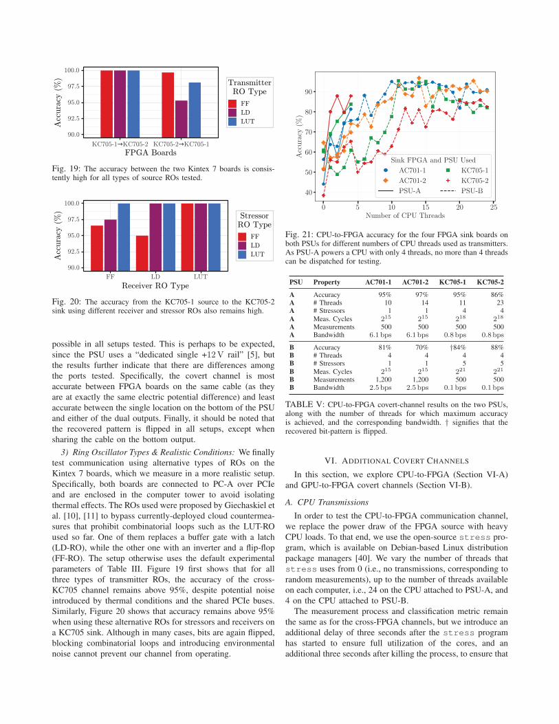
3) Ring Oscillator Types & Realistic Conditions: We finally
test communication using alternative types of ROs on the
Kintex 7 boards, which we measure in a more realistic setup.
Specifically, both boards are connected to PC-A over PCIe
and are enclosed in the computer tower to avoid isolating
thermal effects. The ROs used were proposed by Giechaskiel et
al. [10], [11] to bypass currently-deployed cloud countermea-
sures that prohibit combinatorial loops such as the LUT-RO
used so far. One of them replaces a buffer gate with a latch
(LD-RO), while the other one with an inverter and a flip-flop
(FF-RO). The setup otherwise uses the default experimental
parameters of Table III. Figure 19 first shows that for all
three types of transmitter ROs, the accuracy of the cross-
KC705 channel remains above 95%, despite potential noise
introduced by thermal conditions and the shared PCIe buses.
Similarly, Figure 20 shows that accuracy remains above 95%
when using these alternative ROs for stressors and receivers on
a KC705 sink. Although in many cases, bits are again flipped,
blocking combinatorial loops and introducing environmental
noise cannot prevent our channel from operating.
0 5 10 15 20 25Number of CPU Threads
40
50
60
70
80
90
Accuracy
(%)
Sink FPGA and PSU Used
AC701-1
AC701-2
PSU-A
KC705-1
KC705-2
PSU-B
Fig. 21: CPU-to-FPGA accuracy for the four FPGA sink boards onboth PSUs for different numbers of CPU threads used as transmitters.As PSU-A powers a CPU with only 4 threads, no more than 4 threadscan be dispatched for testing.
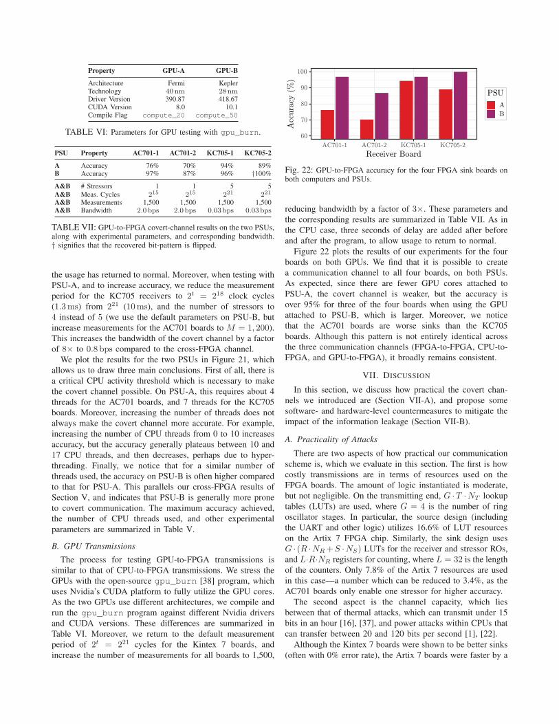
PSU Property AC701-1 AC701-2 KC705-1 KC705-2
A Accuracy 95% 97% 95% 86%A # Threads 10 14 11 23A # Stressors 1 1 4 4A Meas. Cycles 215 215 218 218
A Measurements 500 500 500 500A Bandwidth 6.1bps 6.1bps 0.8bps 0.8bps
B Accuracy 81% 70% †84% 88%B # Threads 4 4 4 4B # Stressors 1 1 5 5B Meas. Cycles 215 215 221 221
B Measurements 1,200 1,200 500 500B Bandwidth 2.5bps 2.5bps 0.1bps 0.1bps
TABLE V: CPU-to-FPGA covert-channel results on the two PSUs,along with the number of threads for which maximum accuracyis achieved, and the corresponding bandwidth. † signifies that therecovered bit-pattern is flipped.
VI. ADDITIONAL COVERT CHANNELS
In this section, we explore CPU-to-FPGA (Section VI-A)
and GPU-to-FPGA covert channels (Section VI-B).
A. CPU Transmissions
In order to test the CPU-to-FPGA communication channel,
we replace the power draw of the FPGA source with heavy
CPU loads. To that end, we use the open-source stress pro-
gram, which is available on Debian-based Linux distribution
package managers [40]. We vary the number of threads that
stress uses from 0 (i.e., no transmissions, corresponding to
random measurements), up to the number of threads available
on each computer, i.e., 24 on the CPU attached to PSU-A, and
4 on the CPU attached to PSU-B.
The measurement process and classification metric remain
the same as for the cross-FPGA channels, but we introduce an
additional delay of three seconds after the stress program
has started to ensure full utilization of the cores, and an
additional three seconds after killing the process, to ensure that
Property GPU-A GPU-B
Architecture Fermi KeplerTechnology 40nm 28nmDriver Version 390.87 418.67CUDA Version 8.0 10.1Compile Flag compute_20 compute_50
TABLE VI: Parameters for GPU testing with gpu_burn.
PSU Property AC701-1 AC701-2 KC705-1 KC705-2
A Accuracy 76% 70% 94% 89%B Accuracy 97% 87% 96% †100%
A&B # Stressors 1 1 5 5A&B Meas. Cycles 215 215 221 221
A&B Measurements 1,500 1,500 1,500 1,500A&B Bandwidth 2.0bps 2.0bps 0.03bps 0.03bps
TABLE VII: GPU-to-FPGA covert-channel results on the two PSUs,along with experimental parameters, and corresponding bandwidth.† signifies that the recovered bit-pattern is flipped.
the usage has returned to normal. Moreover, when testing with
PSU-A, and to increase accuracy, we reduce the measurement
period for the KC705 receivers to 2t = 218 clock cycles
(1.3ms) from 221 (10ms), and the number of stressors to
4 instead of 5 (we use the default parameters on PSU-B, but
increase measurements for the AC701 boards to M = 1, 200).
This increases the bandwidth of the covert channel by a factor
of 8× to 0.8 bps compared to the cross-FPGA channel.
We plot the results for the two PSUs in Figure 21, which
allows us to draw three main conclusions. First of all, there is
a critical CPU activity threshold which is necessary to make
the covert channel possible. On PSU-A, this requires about 4
threads for the AC701 boards, and 7 threads for the KC705
boards. Moreover, increasing the number of threads does not
always make the covert channel more accurate. For example,
increasing the number of CPU threads from 0 to 10 increases
accuracy, but the accuracy generally plateaus between 10 and
17 CPU threads, and then decreases, perhaps due to hyper-
threading. Finally, we notice that for a similar number of
threads used, the accuracy on PSU-B is often higher compared
to that for PSU-A. This parallels our cross-FPGA results of
Section V, and indicates that PSU-B is generally more prone
to covert communication. The maximum accuracy achieved,
the number of CPU threads used, and other experimental
parameters are summarized in Table V.
B. GPU Transmissions
The process for testing GPU-to-FPGA transmissions is
similar to that of CPU-to-FPGA transmissions. We stress the
GPUs with the open-source gpu_burn [38] program, which
uses Nvidia’s CUDA platform to fully utilize the GPU cores.
As the two GPUs use different architectures, we compile and
run the gpu_burn program against different Nvidia drivers
and CUDA versions. These differences are summarized in
Table VI. Moreover, we return to the default measurement
period of 2t = 221 cycles for the Kintex 7 boards, and
increase the number of measurements for all boards to 1,500,
60
70
80
90
100
AC701-1 AC701-2 KC705-1 KC705-2
Receiver Board
Acc
ura
cy (
%)
PSU
A
B
Fig. 22: GPU-to-FPGA accuracy for the four FPGA sink boards onboth computers and PSUs.
reducing bandwidth by a factor of 3×. These parameters and
the corresponding results are summarized in Table VII. As in
the CPU case, three seconds of delay are added after before
and after the program, to allow usage to return to normal.
Figure 22 plots the results of our experiments for the four
boards on both GPUs. We find that it is possible to create
a communication channel to all four boards, on both PSUs.
As expected, since there are fewer GPU cores attached to
PSU-A, the covert channel is weaker, but the accuracy is
over 95% for three of the four boards when using the GPU
attached to PSU-B, which is larger. Moreover, we notice
that the AC701 boards are worse sinks than the KC705
boards. Although this pattern is not entirely identical across
the three communication channels (FPGA-to-FPGA, CPU-to-
FPGA, and GPU-to-FPGA), it broadly remains consistent.
VII. DISCUSSION
In this section, we discuss how practical the covert chan-
nels we introduced are (Section VII-A), and propose some
software- and hardware-level countermeasures to mitigate the
impact of the information leakage (Section VII-B).
A. Practicality of Attacks
There are two aspects of how practical our communication
scheme is, which we evaluate in this section. The first is how
costly transmissions are in terms of resources used on the
FPGA boards. The amount of logic instantiated is moderate,
but not negligible. On the transmitting end, G ·T ·NT lookup
tables (LUTs) are used, where G = 4 is the number of ring
oscillator stages. In particular, the source design (including
the UART and other logic) utilizes 16.6% of LUT resources
on the Artix 7 FPGA chip. Similarly, the sink design uses
G · (R ·NR+S ·NS) LUTs for the receiver and stressor ROs,
and L·R·NR registers for counting, where L = 32 is the length
of the counters. Only 7.8% of the Artix 7 resources are used
in this case—a number which can be reduced to 3.4%, as the
AC701 boards only enable one stressor for higher accuracy.
The second aspect is the channel capacity, which lies
between that of thermal attacks, which can transmit under 15
bits in an hour [16], [37], and power attacks within CPUs that
can transfer between 20 and 120 bits per second [1], [22].
Although the Kintex 7 boards were shown to be better sinks
(often with 0% error rate), the Artix 7 boards were faster by a
Algorithm Key Size AC701 KC705
AES 256 0.7min 44.7minECDSA 521 1.4min 91.1minRSA 1,024 2.8min 179.0min
TABLE VIII: Time to leak cryptographic keys of different sizes totwo types of FPGA boards, without error correction.
factor of 7.6× (6.1 bps vs 0.8 bps). This difference is signifi-
cant in practice: Table VIII shows how long it would take to
transmit keys for different popular cryptographic algorithms.
Even assuming that the channel is not noisy, it would take
almost 45 minutes to transfer a 256-bit AES key to a KC705
board, and 3 hours to transfer a 1024-bit RSA key. However,
the AC701 board would need less than 3 minutes to transfer
the same RSA key, despite the potential drop in accuracy.
To increase accuracy, one can either tweak the parameters
of the source and sink FPGA designs (including the number
of measurements M over which RO counts are averaged), or
instead change the communication scheme itself. For example,
a 3-repetition code decreases bandwidth by a factor of 3, but
also lowers the error rate e to 3e2 − 2e3: a 10% error rate is
reduced to under 3%. The channel capacity is 1 − H(e) =1 + e log2 e + (1 − e) log2(1 − e), and for smaller bitflip
probabilities, other error correcting codes such as Hamming
and Golay codes can be used to improve accuracy.
B. Defense Mechanisms
In this section, we discuss potential software and hardware
defense countermeasures against voltage-based covert- and
side-channel attacks. To start with, some countermeasures
might revolve around preventing intentional transmissions
from the covert-channel source. However, doing so would be
particularly hard without huge sacrifices in terms of power
and performance. Although we used ring oscillators to cause
fluctuations in the voltage of FPGAs sharing the same PSU,
other switching activity can also result in voltage over- and
under-shoots. For example, prior work has shown that switch-
ing large sets of programmable interconnect points [48] or flip-
flops [12], [13] can cause voltage fluctuations outside of the al-
lowed operating voltage range for an FPGA device. Moreover,
we demonstrated CPU-to-FPGA and GPU-to-FPGA channels,
which show that the problem is not FPGA-specific, but can
be found in other types of activities which result in large
power draws. Consequently, unless power is equalized among
all possible algorithm implementations, some leakage which
can differentiate between levels of activity will persist.
To prevent side-channel attacks from being possible, de-
signers may remove the power-draw dependence on the data
being processed and increase the noise level. Although several
masking and hiding techniques have been proposed, leakage
on FPGAs persists due to variations in placement and rout-
ing [6]. Consequently, a better approach would be to prevent
the leakage from being measurable on the FPGA sinks.
Current FPGA cloud providers prevent voltage and tem-
perature monitors from being accessible by user logic and
prohibit traditional LUT-ROs from being instantiated on their
infrastructure [3]. However, alternative ring oscillator designs
can bypass cloud restrictions [8], [10], [11], [34], and can
also replace LUT-ROs (Section V-E). Moreover, time-to-digital
converters (TDCs) can also be used instead of ring oscilla-
tors to monitor voltage fluctuations and conduct side-channel
attacks [31], [32]. Although a compiler tool that checks for
combinatorial loops and latches [15] would prevent some of
the above monitoring logic, it would not catch FF-ROs.
Given that designing effective countermeasures against side-
and covert-channel receivers is an arms race, defense-in-depth
would dictate run-time solutions in addition to any preventive
approach. One feature of the covert channel is the high
switching activity on the receiver. Built-in voltage monitors
could thus be used by cloud providers to detect abnormal
fluctuations—with the caveat that legitimate circuits may also
cause similar patterns, and that, at least on the AC701 boards,
the number of enabled stressor ROs was small (NS = 500). In
fact, proposals to “detect the insertion of power measurement
circuits onto a device’s power rail” [25] are similar, though
the challenge is to reduce false positives.
Finally, better hardware (at a higher cost) can also help hide
the useful signal under the noise floor. For example, indepen-
dent, fully separate power supplies for different boards would
require that the leakage be detectable even over the AC power
line, and through two different AC-to-DC rectifiers. Moreover,
better isolation of power circuits within the same PSU, as well
as voltage regulators with better transient responses on both the
source and the sink FPGAs, or differently-designed powering
circuits with more filters and smoothing capacitors can also
reduce the signal available to an attacker.
Overall, with prior work showing that FPGA are vulnerable
to multi-tenants attacks [8], [9], [11], [28]–[31], [47] and
with this article demonstrating cross-FPGA attacks, better
architectural designs appear to be necessary both for FPGA
chips and for the boards on which they are deployed.
VIII. RELATED WORK
This section summarizes prior work in remote FPGA attacks
without physical access (Section VIII-A), as well as voltage-
and temperature-based covert channels (Section VIII-B).
A. Remote FPGA Attacks
Although attacks on FPGA systems have traditionally re-
quired physical access to the FPGA board [46], a recent class
of remote attacks has emerged. These attacks have used ROs as
covert- and side-channel receivers, and also as covert-channel
transmitters and fault attack inductors.
In the former category, Giechaskiel et al. showed that ROs
can detect the value of nearby long wires in Xilinx FPGAs,
and used this effect to create covert- and side-channel attacks
on shared FPGAs [8]–[10]. It was later shown that the same
phenomenon is present on Intel devices [29], [30], and that
it can be used to extract keys from AES cores using on-chip
Differential Power Analysis (DPA). These attacks have a weak
threat model, as the source and sink long wires are adjacent.

A stronger attack was performed by Zhao and Suh [47],
who used ring oscillators as voltage monitors. Zhao and Suh
conducted an intra-FPGA side-channel attack on RSA and
AES cores, even with physical isolation of the attacker and
victim circuits (on the same FPGA chip). Provelengios et al.
then characterized voltage drops internal to an FPGA due to
power waster RO circuits [28], while Giechaskiel et al. showed
that covert channels are possible between separate dies on
2.5D-integrated FPGA chips (“Super Logic Regions”) [11].
Schellenberg et al. similarly recovered keys from an AES core
in a multi-tenant setting, but used Time-to-Digital Converters
(TDCs) to do so instead of ROs [31].
To the best of our knowledge, the only work which has
considered cross-chip attacks is also by Schellenberg et al.,
where TDCs were used to conduct a cross-FPGA RSA key
recovery [32]. However, the chips were located on the same
FPGA board, and hence shared the same voltage regulator,
making them easier to influence directly, due to the lack
of additional intermediate components between their power
distribution networks. By contrast, we introduced a novel way
of using ring oscillators to detect FPGA-to-FPGA, CPU-to-
FPGA, and GPU-to-FPGA covert communications between
devices which are merely powered by the same power supply
unit, but do not share voltage regulators. Moreover, unlike
the work by Schellenberg et al., which used an FPGA board
that is explicitly “designed for external side-channel analysis
research” [32], we used off-the-shelf Xilinx-designed boards.
Ring oscillators have also been shown to be effective as
temperature monitors. This was first demonstrated for thermal
covert channels with physical access [35], but was later also
shown for intra-FPGA covert channels, where ROs were
used both as source heaters and sink monitors [19]. More
recently, it was also shown that temporal thermal channels
using ring oscillators are possible in cloud environments,
where different users get time-shared access to the same FPGA
fabric [37]. Ring oscillators can also be used to remotely cause
fault attacks on FPGAs. These attacks can merely crash the
FPGA [14], or cause timing violations, which can then be used
to extract cryptographic keys [24]. Moreover, they can also be
used to bias True Random Number Generators (TRNGs) [26].
B. Power and Temperature Covert Channels
It is well-known that data-dependent power consumption
can be used to recover cryptographic keys through differential
power analysis and other techniques by acquiring and ana-
lyzing power traces [23]. The same principles can be applied
to create covert communication, for example from a malware
app on a phone to a malicious USB charger [33], or from a
program that modulates CPU utilization to an attacker measur-
ing the current consumption of the computer [17]. Similarly,
measuring voltage ripple on the power lines can be used to
track the power usage pattern of other data center tenants [20].
Although these works exploit the same source of information
leakage, they require external equipment to detect these data-
dependent power variations, and are thus not applicable to
cloud environments in practice. However, as we showed in this
paper, it is possible to use the reconfigurable fabric of FPGAs
as a covert-channel sink, allowing for accurate transmission of
data remotely, without physical access.
Another category of power attacks which has recently been
discovered is related to Dynamic Voltage and Frequency
Scaling (DVFS) on modern processors, which regulates the
voltage and frequency of CPUs in accordance with usage
demands. Malicious software can exploit DVFS to cause faults
in computations [36], or create covert channels between CPU
cores, where the source core modulates frequency, and the sink
core measures a reduction in its own performance [22].
Thermal attacks can also be used to create covert channels
between CPU cores [27], but they require access to CPU
thermal sensors, and are slower than their power counterparts,
having a capacity of up to 300 bps [4]. Temperature-based
covert channels need not be limited to communication within
a single computer. Assuming computers are sufficiently close,
a covert channel between nearby yet air-gapped devices is
also possible with access to temperature sensors on the sink
computer [16]. Finally, thermal information can also be used
as a proxy estimate for power consumption in data centers.
This information can alert potential adversaries to opportune
moments to attack the availability of servers, either by exceed-
ing the power capacity [21], or by more generally degrading
performance [7]. Although these attacks require privileged
thermal sensors, FPGA ROs could also be used for similar
purposes, complementing our work in this paper.
IX. CONCLUSION
In this paper, we introduced the first FPGA-to-FPGA, CPU-
to-FPGA, and GPU-to-FPGA voltage-based covert channels,
achieving transmission accuracies of up to 100%. Unlike prior
work, which unrealistically assumes that different users share
the same FPGA fabric, our work considered a stronger threat
model, where the FPGA chip and board are allocated on a per-
user basis. Our covert channel exploited properties of the re-
sponse of power supply units (PSUs) and voltage regulators to
changes in their load. To detect these changes, we introduced
a novel architectural design and classification metric which
depends on stressor ring oscillators on the covert-channel sink
FPGA. We showed that ring oscillators also performed well
in the source FPGA, and further showed that heavy CPU and
GPU activity could also be used as an effective transmitter.
We demonstrated our covert channel on four Artix 7 and
Kintex 7 boards, creating a channel of communication between
any two of them in either direction, with high accuracy. We
also performed an analysis of bandwidth-accuracy tradeoffs,
and further explored the accuracy of the covert channel across
different sizes and types of the sink and source FPGA circuits,
different measurement patterns and setup layouts, and PSUs
with different power ratings from two manufacturers. We
finally also proposed potential countermeasures to prevent the
information leakage we discovered from being exploitable.
Overall, our remote covert-channel attacks highlight the dan-
gers of shared power supply units, and therefore a need to re-
think FPGA security, even for single-user monolithic designs.

REFERENCES
[1] M. Alagappan, J. Rajendran, M. Doroslovacki, and G. Venkataramani,“DFS covert channels on multi-core platforms,” in Very Large ScaleIntegration (VLSI-SoC), 2017.
[2] Amazon Web Services, “Amazon EC2 F1 instances,” https://aws.amazon.com/ec2/instance-types/f1/, Accessed: 2019-11-19.
[3] ——, “AWS EC2 FPGA HDK+SDK errata,” https://github.com/aws/aws-fpga/blob/master/ERRATA.md, Accessed: 2019-11-19.
[4] D. B. Bartolini, P. Miedl, and L. Thiele, “On the capacity of thermalcovert channels in multicores,” in European Conference on ComputerSystems (EuroSys), 2016.
[5] Corsair, “Professional series Gold AX850 – 80 PLUS Goldcertified fully-modular power supply,” https://www.corsair.com/p/CMPSU-850AX, Accessed: 2019-11-19.
[6] T. De Cnudde, M. Ender, and A. Moradi, “Hardware masking, revisited,”IACR Transactions on Cryptographic Hardware and Embedded Systems(TCHES), vol. 2018, no. 2, pp. 123–148, May 2018.
[7] X. Gao, Z. Xu, H. Wang, L. Li, and X. Wang, “Reduced coolingredundancy: A new security vulnerability in a hot data center,” inNetwork and Distributed System Security Symposium (NDSS), 2018.
[8] I. Giechaskiel, K. Eguro, and K. B. Rasmussen, “Leakier wires:Exploiting FPGA long wires for covert- and side-channel attacks,”ACM Transactions on Reconfigurable Technology and Systems (TRETS),vol. 12, no. 3, pp. 1–29, Sep 2019.
[9] I. Giechaskiel, K. B. Rasmussen, and K. Eguro, “Leaky wires: In-formation leakage and covert communication between FPGA longwires,” in Asia Conference on Computer and Communications Security(ASIACCS), 2018.
[10] I. Giechaskiel, K. B. Rasmussen, and J. Szefer, “Measuring long wireleakage with ring oscillators in cloud FPGAs,” in Field ProgrammableLogic and Applications (FPL), 2019.
[11] ——, “Reading between the dies: Cross-SLR covert channels on multi-tenant cloud FPGAs,” in International Conference on Computer Design(ICCD), 2019.
[12] D. R. E. Gnad, F. Oboril, S. Kiamehr, and M. B. Tahoori, “Analysisof transient voltage fluctuations in FPGAs,” in Field-ProgrammableTechnology (FPT), 2016.
[13] ——, “An experimental evaluation and analysis of transient voltage fluc-tuations in FPGAs,” IEEE Transactions on Very Large Scale IntegrationSystems (TVLSI), vol. 26, no. 10, pp. 1817–1830, Oct 2018.
[14] D. R. E. Gnad, F. Oboril, and M. B. Tahoori, “Voltage drop-based faultattacks on FPGAs using valid bitstreams,” in Field Programmable Logicand Applications (FPL), 2017.
[15] D. R. E. Gnad, S. Rapp, J. Krautter, and M. B. Tahoori, “Checking forelectrical level security threats in bitstreams for multi-tenant FPGAs,”in Field-Programmable Technology (FPT), 2018.
[16] M. Guri, M. Monitz, Y. Mirski, and Y. Elovici, “BitWhisper: Covertsignaling channel between air-gapped computers using thermal manip-ulations,” in Computer Security Foundations Symposium (CSF), 2015.
[17] M. Guri, B. Zadov, D. Bykhovsky, and Y. Elovici, “PowerHammer:Exfiltrating data from air-gapped computers through power lines,” arXiv1804.04014, 2018, http://arxiv.org/abs/1804.04014.
[18] A. Hajimiri, S. Limotyrakis, and T. H. Lee, “Jitter and phase noise inring oscillators,” IEEE Journal of Solid-State Circuits (JSSC), vol. 34,no. 6, pp. 790–804, Jun 1999.
[19] T. Iakymchuk, M. Nikodem, and K. Kepa, “Temperature-based covertchannel in FPGA systems,” in Reconfigurable Communication-CentricSystems-on-Chip (ReCoSoC), 2011.
[20] M. A. Islam and S. Ren, “Ohm’s law in data centers: A voltage sidechannel for timing power attacks,” in Conference on Computer andCommunications Security (CCS), 2018.
[21] M. A. Islam, S. Ren, and A. Wierman, “Exploiting a thermal sidechannel for power attacks in multi-tenant data centers,” in Conferenceon Computer and Communications Security (CCS), 2017.
[22] S. K. Khatamifard, L. Wang, A. Das, S. Köse, and U. R. Karpuzcu,“POWERT channels: A novel class of covert communication exploitingpower management vulnerabilities,” in High-Performance ComputerArchitecture (HPCA), 2019.
[23] P. Kocher, J. Jaffe, B. Jun, and P. Rohatgi, “Introduction to differentialpower analysis,” Journal of Cryptographic Engineering, vol. 1, no. 1,pp. 5–27, Apr 2011.
[24] J. Krautter, D. R. E. Gnad, and M. B. Tahoori, “FPGAhammer: Remotevoltage fault attacks on shared FPGAs, suitable for DFA on AES,” Trans-actions on Cryptographic Hardware and Embedded Systems (TCHES),vol. 2018, no. 3, pp. 44–68, Sep 2018.
[25] A. Le Masle and W. Luk, “Detecting power attacks on reconfigurablehardware,” in Field Programmable Logic and Applications (FPL), 2012.
[26] D. Mahmoud and M. Stojilovic, “Timing violation induced faults inmulti-tenant FPGAs,” in Design, Automation & Test in Europe (DATE),2019.
[27] R. J. Masti, D. Rai, A. Ranganathan, C. Müller, L. Thiele, and S. Cap-kun, “Thermal covert channels on multi-core platforms,” in USENIXSecurity Symposium, 2015.
[28] G. Provelengios, D. Holcomb, and R. Tessier, “Characterizing powerdistribution attacks in multi-user FPGA environments,” in Field-Programmable Logic and Applications (FPL), 2019.
[29] G. Provelengios, C. Ramesh, S. B. Patil, K. Eguro, R. Tessier, andD. Holcomb, “Characterization of long wire data leakage in deepsubmicron FPGAs,” in Field-Programmable Gate Arrays (FPGA), 2019.
[30] C. Ramesh, S. B. Patil, S. N. Dhanuskodi, G. Provelengios, S. Pillement,D. Holcomb, and R. Tessier, “FPGA side channel attacks withoutphysical access,” in Field-Programmable Custom Computing Machines(FCCM), 2018.
[31] F. Schellenberg, D. R. E. Gnad, A. Moradi, and M. B. Tahoori, “Aninside job: Remote power analysis attacks on FPGAs,” in Design,Automation & Test in Europe (DATE), 2018.
[32] ——, “Remote inter-chip power analysis side-channel attacks at board-level,” in International Conference on Computer-Aided Design (ICCAD),2018.
[33] R. Spolaor, L. Abudahi, V. Moonsamy, M. Conti, and R. Poovendran,“No free charge theorem: A covert channel via USB charging cable onmobile devices,” in Applied Cryptography and Network Security (ACNS),2017.
[34] T. Sugawara, K. Sakiyama, S. Nashimoto, D. Suzuki, and T. Nagatsuka,“Oscillator without a combinatorial loop and its threat to FPGA in datacentre,” Electronics Letters, vol. 15, no. 11, pp. 640–642, May 2019.
[35] J. Sun, R. Bittner, and K. Eguro, “FPGA side-channel receivers,” inField-Programmable Gate Arrays (FPGA), 2011.
[36] A. Tang, S. Sethumadhavan, and S. Stolfo, “CLKSCREW: Exposing theperils of security-oblivious energy management,” in USENIX SecuritySymposium, 2017.
[37] S. Tian and J. Szefer, “Temporal thermal covert channels in cloudFPGAs,” in Field-Programmable Gate Arrays (FPGA), 2019.
[38] V. Timonen, “Multi-GPU CUDA stress test,” http://wili.cc/blog/gpu-burn.html, Accessed: 2019-11-19.
[39] S. Trimberger and J. J. Moore, “FPGA security: Motivations, features,and applications,” Proceedings of the IEEE (JPROC), vol. 102, no. 8,pp. 1248–1265, Aug 2014.
[40] A. P. Waterland, “Stress,” https://web.archive.org/web/20190502184531/https://people.seas.harvard.edu/~apw/stress/, Accessed: 2019-11-19.
[41] Xilinx, Inc., “7 series FPGAs data sheet: Overview (DS180),”https://www.xilinx.com/support/documentation/data_sheets/ds180_7Series_Overview.pdf, Accessed: 2019-11-19.
[42] ——, “7 series product brief,” https://www.xilinx.com/publications/prod_mktg/7-Series-Product-Brief.pdf, Accessed: 2019-11-19.
[43] ——, “AC701 evaluation board for the Artix-7 FPGA (UG952),”https://www.xilinx.com/support/documentation/boards_and_kits/ac701/ug952-ac701-a7-eval-bd.pdf, Accessed: 2019-11-19.
[44] ——, “Accelerated computing partners,” https://www.xilinx.com/products/boards-and-kits/alveo/where-to-buy.html, Accessed: 2019-11-19.
[45] ——, “KC705 evaluation board for the Kintex-7 FPGA (UG810),”https://www.xilinx.com/support/documentation/boards_and_kits/kc705/ug810_KC705_Eval_Bd.pdf, Accessed: 2019-11-19.
[46] J. Zhang and G. Qu, “Recent attacks and defenses on FPGA-basedsystems,” ACM Transactions on Reconfigurable Technology and Systems(TRETS), vol. 11, no. 3, pp. 1–24, Sep 2019.
[47] M. Zhao and G. E. Suh, “FPGA-based remote power side-channelattacks,” in IEEE Symposium on Security and Privacy (S&P), 2018.
[48] K. M. Zick, M. Srivastav, W. Zhang, and M. French, “Sensingnanosecond-scale voltage attacks and natural transients in FPGAs,” inField-Programmable Gate Arrays (FPGA), 2013.