Contributions to Modeling, Simulation and Emulation of ...
18
IOSUD - Universitatea Politehnica Timişoara Şcoala Doctorală de Studii Inginereşti Contributions to Modeling, Simulation and Emulation of Application Specific Integrated Circuits for intelligent control of High Pressure Fuel Pumps in the automotive field. PhD thesis - Summary to obtain the scientific title of doctor at Polytechnic University of Timisoara in the field of doctorate __Engineering Electronics and Telecommunications__ author eng. _Laszlo MOLNAR______ scientific leader Prof.univ.dr.ing. _Aurel GONTEAN_________ luna_07_ anul_2019__ Chapter 1: Introduction Developing an ASIC is a complex and time consuming process. During the development phase and after manufacture, the engineers team must verify the digital and analog implementations of all the ASIC's specific functions. The development process is presented in Figure 1.1 and begins with the collection of specifications for the desired functions of the ASIC. The ASIC will work in a system so that the system architect and development team have to collaborate at this stage to better understand the necessary functions and interaction with the rest of the system. Specification of requirements analog/digital IC package definition VHDL coding Verification(FPGA) Simulation(Modelsim) NOK Analog block design Test Chip manufacturing (only analog) Test Chip Verification 1. Collection and correction of erratas 2. Top level simulation ASIC manufacturing (digital + analog) ASIC valiation NOK Final Silicon Fig.1. The block diagram of the development process of a dedicated CI.
-
Upload
khangminh22 -
Category
Documents
-
view
0 -
download
0
Transcript of Contributions to Modeling, Simulation and Emulation of ...
IOSUD - Universitatea Politehnica Timişoara
Şcoala Doctorală de Studii Inginereşti
Contributions to Modeling, Simulation and Emulation of Application Specific
Integrated Circuits for intelligent control of High Pressure Fuel Pumps in the
automotive field.
PhD thesis - Summary
to obtain the scientific title of doctor at
Polytechnic University of Timisoara
in the field of doctorate __Engineering Electronics and Telecommunications__
author eng. _Laszlo MOLNAR______
scientific leader Prof.univ.dr.ing. _Aurel GONTEAN_________
luna_07_ anul_2019__
Chapter 1: Introduction
Developing an ASIC is a complex and time consuming process. During the development
phase and after manufacture, the engineers team must verify the digital and analog
implementations of all the ASIC's specific functions.
The development process is presented in Figure 1.1 and begins with the collection of
specifications for the desired functions of the ASIC. The ASIC will work in a system so that
the system architect and development team have to collaborate at this stage to better understand
the necessary functions and interaction with the rest of the system.
Specification of requirementsanalog/digital
ICpackage definition
VHDL coding
Verification(FPGA)Simulation(Modelsim)
NOK
Analog block design
Test Chip manufacturing(only analog)
Test ChipVerification
1. Collection and correction of erratas2. Top level simulation
ASIC manufacturing(digital + analog)
ASIC valiation NOK
Final Silicon
Fig.1. The block diagram of the development process of a dedicated CI.

After completing this step, the physical implementation of the functions begins. There
are two parallel processes, one for the VHDL code design to implement the defined digital
functions, and the other for the implementation of low-power analogue circuits that cooperate
with digital functions. Low power circuits are comparators, current and voltage reference
sources, temperature sensors, Analog to Digital Converters, Digital to Analog Converters, and
so on. The high power circuits are MOSFET gate drivers, N-ch and P-ch MOSFET transistors,
integrated on the silicon die.
Both VHDL and analogue designers perform simulations to test their implementation.
In addition to simulation, verification of the VHDL code is performed on FPGA boards
to verify the digital function. If errors are found, the VHDL code is corrected and checked again
and again until a bug free implementation is achieved.
In the next step, a "test chip" is produced that contains only the analog block, and the
power electronics, which is used to verify the analog implementation. The digital block is
emulated by FPGA development boards to implement the digital interaction required for the
analog block.
All findings are collected as a list of errors and corrected in the implementation of the
new version of the CI.
At the end, a higher-level simulation is performed in which the digital and analog blocks
work together, but this time with annotations to the silicon layout to highlight the possible
parasitic effects of the specific implementation. The next step is the so-called "tape-out" and the fabrication of the Application Specific
Integrated Circuit begins, but in this phase only in a limited number, up to 100 pieces to be sent
back to the design team to verify them.
Chapter 2: Testing the VHDL code
In chapter 1 I have presented a simplified ASIC design process, an important step being
testing the VHDL code. in this chapter 2 will extend this process, insisting on my own approach
and personal contributions
The VHDL code is tested in the design phase by simulation and subsequently on FPGA
boards. After completion of the design phase, the VHDL code will be transferred to the silicon
die of the ASIC and will become a digital function implemented by predefined logic blocks
such as: logical gates, MUX (Multiplexer), LUT (Look Up Table), PLA (Programmable Logic
Array).
During the manufacturing process, it can happen that the bugless VHDL implementation
becomes a malfunction due to a manufacturing error - for example, when creating a
metallization layer for interconnections on the silicon die, a short circuit to the power line will
create a stack-at-failure.
There are two main types of fault detection methods: Injection of test vectors with
automatic test equipment, ATE (Automatic Test Equipment), and self-test, Built-In Self-Test
(BIST) implemented in ASIC.
Injecting test vectors requires a so-called fault simulation to define a set of test vectors
that are required for the test program that controls the ATE. Fault simulation is based on
artificial insertion of defects using predefined defect models into the fault-free VHDL code.
Each erroneous description is then simulated and compared to the fault-free code simulation
results. Based on this comparison, it is possible to analyze the effect of "injecting" a fault into
the error-free code.
The BIST is implemented in the ASIC silicon structure and is performed whenever the
ASIC is powered upt. This test is time consuming and usually tests only a limited part of the
ASIC logic (safety blocks).
The BIST is used to detect defects that occurred during the lifetime of components that
were considered "pass" components after all checks were made during the manufacturing
process. During the lifetime of the component, external events such as Electro-Static Discharge
(ESD) or a short circuit between its terminals may occur to an internal ASIC function; executing
the BIST procedure at each initialization of the ASIC tests these functions by deactivating the
ASIC if a test function is affected.
Chapter 3: Validation and simulation architectures of dedicated integrated circuits
Chapter 2 treated VHDL (gate level and behavioral) code testing that underlies the
digital block of any ASIC and testing the analog block by extracting behavioral patterns from
the analog transistor level schematic of the particular implementation of an ASIC; all these tests
are carried out in the pre-fabrication phase of the ASIC.
In this chapter I will present the methods currently used to test the ASIC when it is
already manufactured, but I will also propose an alternative test method when only the VHDL
code is available and the analog architecture is known but the silicon implementation is not yet
available, all the ASIC is being emulated by various components (for example the digital block
by an FPGA and the analog block by discrete components interconnected according to the ASIC
architecture).
In addition to physical testing by emulation, I present the current methods and propose
an alternative method of simulation of the digital block and the analog block, when neither
ASIC is yet manufactured nor the setup that emulates ASIC function are available.
The most important process in the development phase of an ASIC after the design phase
is the verification phase. For a complex ASIC, the verification process may take longer than the
design phase.
The proposal developed in the thesis is suitable for validating the entire system at an
early stage when only TC (Test Chip) is physically manufactured.
For this phase, I propose a Modular Test Platform (MTP) validation architecture with
individual platforms for each main component of the ECU, as shown in Fig. 3.1.
The validation platform is built on a main board, having the role of interconnection and
mechanical support for the various PCBs (Printed Circuit Board) implementing the various
blocks required. There is a main power supply card that generates 1V2, 3V3 and 5V power
supplies from an external power supply. Communication between the user and ASIC is
managed by the MDB (Microcontroller Development Board), which contains a CAN (Control
Area Network) transceiver. The user interface is a Microsoft Excel-based Graphical User
Interface (GUI) using Visual Basic macro commands.
A USB-CAN adapter generates the CAN differential differential CAN-to-MTP interface.

Fig. 3.1 Proposed Modular Test Platform.
ASIC emulation is performed by two components. The digital block is emulated by an
FPGA development board that implements the VHDL code. Two different options are available
to emulate the analog block.
The first option is to build a discrete component PCB that performs the functions of
ASIC analog block; the advantage of this option is testing the digital block before
manufacturing the TC (analog design). I propose a second option that could use the TC itself
that contains only ASIC's analog blocks, but this means that the digital and analog design has
to be done almost at the same time. The main advantage compared to the previous solution is
that the analog block is very similar to the ASIC, so the circuit behavior is the same.
In both cases, the analog block is connected to the FPGA development board, so to the
VHDL code that defines the functions of the digital block.

The advantage of using the TC as an analog block is that it contains the exact analog
circuitry that will be inside the ASIC and so all the parasitic effects will be reflected in the
analog functionality.
The ASIC may have different functions, for example as shown in Fig. 3.1 a closed loop
control circuit for HPFP (High Pressure Fuel Pump). The power circuit for the HPFP command
is designed on a PCB using discrete components. This module is a Half-Bridge topology that
contains a High Side Driver (HSD) and a Low Side Driver (LSD) MOSFET and additional
circuits, snubber, free-wheel on HS and active clamping on LS), current sensing resistors...
The second proposal is a system-level simulation, the "All-In-One" architecture using
only SaberRD®, as shown in Fig. 3.2.
The following chapters will present the implementation of a virtual HW validation
platform, the one proposed in Fig. 3.1, based on the simulation methodology of the All-In-One.
Fig. 3.2 The Proposed Simulation Architecture.
This methodology presents a promising simulation architecture based on my previous
experience of using SaberRD® as a VHDL code simulator. In addition, it is a specialized
electronic circuit simulator, including libraries containing a wide range of electronic
components.
Electronic (analog) models are built using MAST (Synopsys proprietary language) or
VHDL-AMS. It also allows automatic translation of Spice models into MAST to successfully
use electronic component models made available by their manufacturer.
Running a uC SystemC model together with the binary file (compiled software) in
SaberRD® is a completely new method. The simulator is able to call a C++ function; so it is
necessary to create the C++ function in advance and store it in the simulation folder as a ".dll"
file. My purpose is to implement the uC model along with the corresponding software running
it in a C++ function that has a list of parameters transferred from the simulation, after which
the function is executed and the results are returned to the simulation.
The simulation results of the subsystems are compared to the real circuit using the
MTP proposed in Fig. 3.1.
The ultimate goal of the comparison is to verify the accuracy and effectiveness of
system simulation compared to the software and hardware environment that also contains the
task (HPFP) to be used. Another challenge is to model the electro-mechanical load with respect to the essential and
relevant parameters in the hydraulic system, as they can reveal quantitative changes of the
HPFP valve inductance.
ASIC Digital Block
VHDL code
Binary FileC code
System CuC model
C++ function
ASIC Analog Block
VHDL-AMS and
MAST code
Power Electronics
VHDL-AMS/MASTcode
Load Model
VHDL-AMS/ MASTcode
Electrical(analog)/Mechanical CircuitsSoftware Digital
All-in-One: Synopsys SaberRD

Chapter 4: Control of the High Pressure Fuel Pump
In the automotive field, there are two types of internal combustion engines: gasoline and
diesel. The most commonly used passenger vehicles are the gasoline engine due to lower
exhaust emissions and better emission control to meet the pollution standards.
Modern gasoline engines are classified into two main categories: lower-cost and low-
performance engines with Single Point Injection or Multi-Point Injection and Gasoline Direct
Injection (GDI) better control of fuel consumption, offering more powerful engines at the same
cylindrical capacity.
The Single Point Injection and Multi Point Injection systems inject fuel into the intake
manifold for the Single Point Injection in the intake manifold zone and for the Multi Point
Injection in each individual intake manifold branch even upstream of the intake valve. In these
cases, the fuel is mixed with the air outside the cylinder. The injected fuel pressure is up to 4
bar and the injectors used are solenoid actuators with slow response time.
The GDI system is described by Sarwar, Sankavaram and Lu [17], with a special
emphasis on high-pressure fuel pump (HPFP).
The GDI system uses high-performance injectors to inject fuel directly into the
combustion chamber with a fuel pressure of up to 500 bar. Thanks to the direct injection, the
piston head is cooled by fuel, allowing for higher compression ratios and an earlier spark
ignition producing higher power.
GDI injectors can be operated via a solenoid or piezo actuators. Multiple injections are
possible with both, during one engine cycle, in each individual cylinder. In order to allow more
injections per engine cycle, the injectors must have a rapid response, as fuel dosing depends on
a time-based control procedure so that electronic injector control is important and must be fast,
effective and precise.
Piezoelectric and solenoid injectors are powered by voltages greater than the 12V. High
voltage switching mode power sources are used to increase the voltage to 65V for solenoid
injectors and 400V for piezo injectors, thus allowing a quick opening and quick closing by
limiting the clamping of the electromotive voltage induced solenoid injector to 65V.
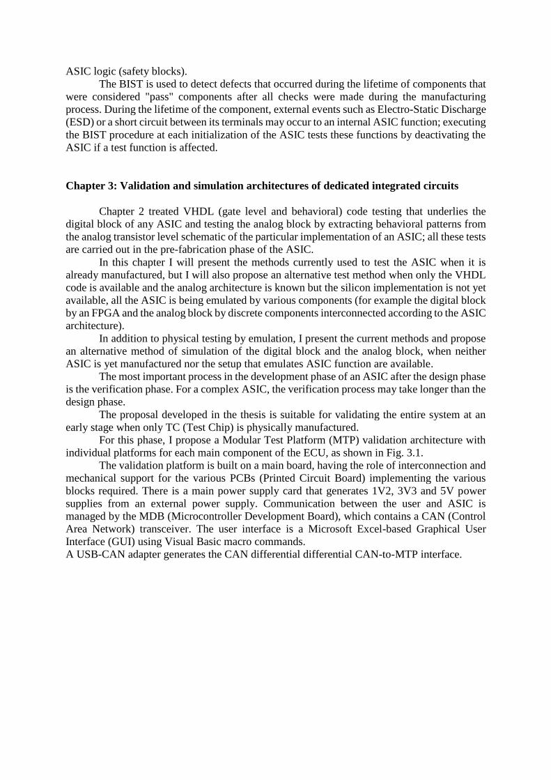
In Fig. 4.1 presents the basic components of a GDI system. Petrol in the fuel tank is
pumped by a low pressure fuel pump, LPFP (Low Pressure Fuel Pump) through 4 bar high
pressure pipes to the high pressure fuel pump, HPFP, which is activated by the camshaft of the
engine generating a pressure of up to 500 bar. High-pressure fuel is accumulated in the common
ramp (fuel buffer), and the injectors are fed by the common ramp.
Fig.4.1 GDI system architecure.
In order to have a precise injection of fuel, the pressure in the common rail system must
ideally be constant to always have the same amount of fuel sprayed in the cylinder by each
injector having a time defined activation duration.
In Fig. 4.2 is a simplified schematic diagram of a HPFP pump consisting of the pump
itself and a DIV (Digital Inlet Valve) valve controlling the amount of fuel.
Flow Control Valve(DIV)
Low Pressure FuelInput Valve Plate Pumping
Chamber
OutletCheckValve
HighPressure
FuelOutput
ToCommon Rail
Pressure Relief Valve
Plunger (Pump Piston)
Cam
Fol
low
er
T DC
BDC
Armature Rod
Cu Coil
Fig.4.2 HPFP details .
Text
Low Pressure Fuel
High Pressure Fuel
Fuel Tank &
Low Pressure
Pump
High
Pressure
Fuel Sensor
Engine Control
Unit
High Pressure Fuel Pump
3 lobe
cam
Cam follower

To maintain constant pressure in the common rail system, the pressure regulation starts
from the electro-mechanical valve control attached to the HPFP pump. In order to control the
amount of low pressure fuel entering the HPFP pressure chamber, the normally open electro-
mechanical valve (DIV) is activated after a time Δt1 from the top dead center (TDC) of the
pump piston position. LPFP pumps the fuel into the HPFP compression chamber, and then the
pressure control algorithm implemented in the engine control unit microcontroller (ECU)
calculates the amount of fuel required according to the load and engine speed.
The ECU controls the closing of the DIV electro-mechanical valve by means of a "peak
and hold" current profile, allowing the camshaft lobe rotation acting on the HPFP pump piston
to compress the fuel in the pressure chamber. If the DIV spill valve is not closed (active current
profile), the fuel will be pumped back into the low pressure system.
In the HPFP exit there is a pre-loaded mechanical check valve. When the HPFP pump
chamber pressure is greater than the common rail pressure, the fuel is transferred to the common
rail.
The fuel pressure control algorithm uses the information from a pressure sensor
mounted on the common rail.
Based on the speed and engine load, the ECU controls the individual injectors for each
cylinder; when the correct position of the thermal engine piston is detected, the induction coil
generates a spark in the combustion chamber by means of a spark plug, resulting in an explosion
of the fuel mixture.
In Fig. 4.3 shows the Continental High Pressure Pump, capable of producing a 350 bar
pressure on the common ramp (petrol).
High Pressure Fuel
Output
Low Pressure Fuel
Input
DIV coil Electrical
Connector
HPFPBody
Piston Rod & Preload Spring
Fig.4.3 Continental-350Bar High Pressure Fuel Pump.

Chapter 5: Experimental Results
In this chapter I analyze the implementation of the two platforms proposed in Chapter
3, the simulation platform with a single multi-domain simulator and the MTP ASIC emulation
platform.
Both platforms help the early testing in the ASIC development process by avoiding the
propagation of any conceptual / architectural errors / defects in ASIC production.
In the following I will present the global hierarchical simulation scheme, I will go into
specific details about each hierarchy component. An important topic will be the development
of the electric simulation model for the DIV electro-mechanical valve. The next step will be to
explain the physical implementation of the ASIC emulation platform also organized on
hierarchical blocks. Finally, I compare the simulation results with those of physical
implementation. According to the usual practice, I started by simulating in Saber® (Synopsys) mixed
simulator, as shown in Fig. 5.1. My goal was to organize the simulation on functional blocks
so that it is possible to migrate the blocks at any time into a process of developing mixed
integrated circuits. Each functional block can then be extended to a specific implementation in
the manufacturing process of integrated circuits.
Fig.5.1 Ierarhical simulation schematic. The simulation is organized into a hierarchical architecture that consists of a top level
schematic with a primary symbol (the ASIC symbol that performs the DIV valve control
function).
The top level scheme is divided into 5 blocks:
• Power supply and filter
• Emulation of uC
• ASIC behavioral block (Peak & Hold driver)
• Discrete power electronic components (not part of ASIC)
• The electric model of the DIV valve
The physical implementation of the circuit is shown in Figure 5.2.

Fig. 5.2 The physical implementation of the circuit.
In Fig.5.3 the real results are compared with the simulation results of the same signals
using identical configuration data for the FPGA.
Fig.5.3 Simulation results compared to experimental circuit results .
From the bottom, the "i_load" signal (representing the load current) fit very well
between them, there being a difference in the "hold" phase when the valve closes, the actual
current has a specific change in the inductance resulting in a phase longer ON time for HS
control. The load model is not capable of reproducing exactly the same effect, but changes its
inductance value, resulting in a faster switching exactly as in real validation.
The other difference is at the end of each current pulse, the slope of the current in the
clamping phase is differently replicated compared to the actual one (in simulation the power
dissipation due to the back EMF is faster even if the phenomenon started from the same current
indicating a lower inductance at the end of the current profile for the simulation model
compared to the actual DIV coil).
Chapter 6: Movement Detection, Noise Reduction and Electrical Diagnosis of the DIV
Valve
Chapter 6 deals with improving the DIV solenoid control methods, reducing the noise
caused by the DIV valve vibration at closing and opening, and finding a less costly, electric
diagnosis method for the DIV solenoid control circuit. Using the simulation platform and the
models developed in Chapter 5 I have proposed and simulated a DIV valve motion detection
algorithm; I also proposed and simulated a method of diagnosis and protection of the control
circuit. Finally, using the MTP platform, I have tested the implementation of the three original
contributions: the noise reduction algorithm, the motion detection algorithm, and the diagnosis
/ protection of the DIV solenoid control circuit.
Since the controlled load (DIV valve) is an electro-mechanical element with kinetic
elements, that move when the coil is energized, vibration phenomena occur when the moving
parts reach their end position / limits. These vibrations generate undesirable sound effects, so a
motion braking method has been proposed without affecting the normal valve function and at
the same time reducing vibration noise when the valve closes or opens.
To ensure that the noise reduction procedure does not affect normal valve operation,
I need to ensure that the valve is opened / closed to provide the amount of fuel required in the
common rail, so I have implemented an algorithm that detects this. The next two subchapters
will address the subject of reducing the noise produced by the DIV valve and the motion
detection algorithm.
Fig. 6.1 shows how to reduce noise by applying a current profile with two closed-loop
controlled pulses. It is visible that the vibration amplitude decreases when the valve closes and
that the noise at the valve opening almost disappears when the noise reduction algorithm is
applied.

Fig. 6.1 Noise generated by closing/opening of the DIV valve, with/without noise canceling
In addition, I propose a method of diagnosis; overcurrent detection (OC) and open load
(OL), suitable for, predominantly inductive but also for pure resistive loads. In the case of
resistive loads, the 8-bit DAC in the CLCC block is used (anyway not used for its intended
purpose because if a resistive load is controlled, the CLCC function cannot be used).
In Fig. 6.2 presents the proposed diagnostic method using a counter implemented in the
digital block instead of a digital-analog converter implemented in analog technology.
Fig. 6.2 The proposed diagnosis and protection architecture.
Without noise reduction
Noise at closing
Noise at opening
Lower noise at closingNo noise at opening
With noise reduction
DIV_current_1
DIV_vibration_1
DIV_vibration_2
DIV_current_2
HSD
LSD
FWD
TVS
DIV
HS shunt
LS shunt
Vbat
Gate driver
OCcomp
dif.OPA
dif.OPA
boot st rapcap.
boot st rap diode
8bit DAC
CCCcomp
OCcomp
Gate ctrl.
Gate ctrl.
SPI
VCC
GND
/LS_en
/HS_en
P&H driver ASIC
Inductive load
14 bitcounter
Interna l
Supply and
Reference
volta ges
OC & CCC threshold
DIGITAL
(VHDL)

The simulation played a very important role in the development of the movement
detection algorithm. Fig. 6.3 shows the state diagram of the DIV valve movement detection
algorithm.
The algorithm is implemented only for the DIV closing pulse and starts as soon as the
state machine (implemented in VHDL) that controls the CLCC blocks jumps from the “idle” to
the "peak" phase. All counters and variables used to implement the algorithm are initialized at
this time. The algorithm waits until the state machine jumps from "peak" to "hold". As soon as
the "hold" phase is active, there are two concurrent counters, one measuring the ON duration
of the HS transistor and the other OFF time duration.
The purpose of the algorithm is to detect in the "hold" phase the frequency shift from
the slower switching to faster of the HS transistor (to maintain the same programmed current
limits) due to the decrease of the inductance after the valve closure.
Start of current profile
Hold phaseStarted?
Wait until endof peak phase
“OFF” Counter running
End
Stop “OFF” counter
Save previous counter in auxiliary variable
Compare auxiliary variable with local OFF
max value
Current value > local OFF max ?
No
Update local OFF max with new value
Yes
Compare current value with local
OFF max and Delta values
Current value < (OFF max-Del ta)?
Valve movement detectedSet flag “o_mov_detect” to high
Yes
HS OFF?
No
YesHS ON?
Stop “ON” counter
Save previous counter in auxiliary variable
Compare auxiliary variable with local ON
max value
Current value > local ON max ?
Compare current value with local
ON max and Delta values
Current value < (ON max-Del ta)?
No
Update local ON max with new value
Yes
Yes
“ON” Counter running
Yes
No
NoNo
Check for HS state
Yes
Reset all countersand variables used for
algorithm
No
Fig.6.3 Valve movement detection algorithm: state diagram.

Due to the specific control profile, when the current drops from the "peak" to the
"hold" current, the first OFF time of the HS transistor is ignored, as it would result in a
maximum value that is too high compared to the remaining OFF times in the phase "hold".
Starting from the second OFF event and the first ON event of the HS transistor, the
algorithm constantly measures the OFF and ON times of the HS transistor.
To avoid false movement of the valve movement due to a small difference between
two consecutive measurements, a "delta value" is required, which is predefined in an ASIC
register.
When a delta value greater than the predefined one is found, valve movement is
detected.
Personal Contributions
Chapter 3
1. I propose on my own paper “3” the MTP validation platform which can improve the
validation performance due to the direct use of the TC to emulate the analog block of the
ASIC. MTP can easily be reused for new projects due to its modular structure.
2. I also propose, based on my own paper “3”, two simulation systems using a multi-domain
simulator to perform the ASIC architecture simulation when the MTP platform is not yet
available to emulate the ASIC and to perform tests and to validate the correct conceptual
functionality in early phases of ASIC development.
Chapter 4
3. I present and explain on the basis of my own work "6" the operation of GDI systems with
specific details regarding the mechanical drive and electronic control of the high pressure
fuel pump and of its constituent electro-mechanical valve.
Capitolul 5
4. I performed a significant number of test scenarios with different test environments and
analyzed the data as shown in my paper "4".
5. I proposed a new simulation model compared to the simple R-L model as shown in "4". The
new model is able to better track the shape of the current through the physical valve used
due to the structure of the search table.
6. I also modeled the saturation behavior of the inductance, increasing the overall performance
of the simulation.
7. The DIV coil electric simulation model proposed in "4" was improved by introducing the
temporal effect to simulate valve closure. Valve closure was introduced by varying the
inductance of the coil according to a signal synchronized with the start of the current profile
and is manifested by changing the switching frequency in the "hold" phase when using the
CLCC control strategy as shown in subchapter 5.1.5.7.
8. I have developed a simulation platform as suggested in my paper "3" and explained in
subchapter 3.2.3
9. I have developed a validation platform according to the one proposed in "3" and explained
in subchapter 3.1.1 except for the implementation of the step in which I proposed to replace
the analog block emulated by discrete components with a PCB containing the Test Chip
(Test Chip is an IC that only contains analog blocks to be implemented in ASIC).
10. I compared the results of the simulation platform with the validation platform results. The
comparison shows a good match of the results, demonstrating the effectiveness of the
validation platform.
Capitolul 6
11. I have analyzed the current state of the existing noise reduction methods, as shown in my
paper "6".
12. I have proposed an alternative noise reduction method, as shown in my paper "6".
13. The alternative method proposed by me and published in "6" is based on [19] but does not
require an ADC input for current monitoring of the DIV coil.
14. In the method proposed by me in "6", the required ADC in [19] is replaced by a counter
implemented in VHDL, much cheaper and simpler than an ADC. This is possible due to
closed-loop current control which almost doubles its switching frequency when the DIV
valve is closed. This switching frequency is monitored by the counter implemented in
VHDL which detects based on the algorithm shown in Fig. 6.3 the DIV valve movement.
15. The method proposed by me applies both pulses, the closing and the open ones with closed-
loop current control.
16. I tested on a DIV valve used in 250-bar systems the efficiency of the proposed noise
reduction method, as shown in my paper "6".
17. I have focused on problem solving (early valve movement and variation of natural valve
closing / opening point) found during implementation of the proposed noise reduction
method, as shown in "6".
List of Published papers
1. L. Molnar and A. Gontean, "Functional Simulation methodes," 2016 12th IEEE
International Symposium on Electronics and Telecommunications (ISETC), Timisoara,
2016, pp. 198-202.
(WOS:000390717800044)
2. L. Molnar and A. Gontean, "Fault simulation methodes," 2016 12th IEEE International
Symposium on Electronics and Telecommunications (ISETC), Timisoara, 2016, pp.
194-197. (WOS:000390717800043)
3. L. Molnar and A. Gontean, "ASIC validation architectures: Hardware versus
simulation," 2017 21st International Conference on System Theory, Control and
Computing (ICSTCC), Sinaia, 2017, pp. 671-676. (WOS:000427419900111)
4. L. Molnar, A. Gontean, A. Kotlar and P. Svasta, "Simulation model for automotive high
pressure fuel pump," 2017 IEEE 23rd International Symposium for Design and
Technology in Electronic Packaging (SIITME), Constanta, 2017, pp. 231-234.
(WOS:000428032300048)
5. L. Molnar, O. Luca and A. Gontean, "Simulation Method to Evaluate Thermal Runaway
of MOSFETs," 2018 41st International Spring Seminar on Electronics Technology
(ISSE), Zlatibor, 2018, pp. 1-6. (WOS:000449866600011)
6. L. Molnar and A. Gontean, "Hardware Difficulties and Improvements for High Pressure
Fuel Pump Solenoid Valve Noise Cancellation," 2018 IEEE 24th International
Symposium for Design and Technology in Electronic Packaging (SIITME), Iasi, 2018,
pp. 84-89. (WOS:000466960400015)
7. L. Molnar, A. Kotlar and S. Lica, "High Power Switch using IGBT and GaN MOSFET
A solution proposal," 2018 IEEE 24th International Symposium for Design and
Technology in Electronic Packaging (SIITME), Iasi, 2018, pp. 43-48.
(WOS:000466960400008)
List of citations
Citations for paper:
„2” L. Molnar and A. Gontean, "Fault simulation methodes," 2016 12th IEEE International
Symposium on Electronics and Telecommunications (ISETC), Timisoara, 2016,pp.194-197.
doi: 10.1109/ISETC.2016.7781089
1. Rahul Bhattacharya, S. H. M. Ragamai, Subindu Kumar, VLSI Design and Test, vol.
711, pp. 179, 2017.
2. V.I. HAHANOV, I.V. IEMELIANOV, M.M. LIUBARSKYI, S.V.
CHUMACHENKO, E.I. LITVINOVA, TAMER BANI AMER, "Qubit Method for
Deductive Fault Analysis of Logic Circuits.", Èlektronnoe modelirovanie, vol. 39,
pp. 59, 2017
List of submitted patents
1. L.Molnar, B.Komlosi, „High Pressure Fuel Pump Solenoid Valve Movement
Detection (2019)”, 2019E03508 RO
2. L.Molnar, B.Komlosi, „Time Constant Based Over current and Open Load
diagnostic for inductive loads”, 2019E03495 RO
3. L.Molnar, B.Komlosi, ” High Pressure Fuel Pump Solenoid Valve Noise cancelling
with two current controlled_current_pulses and soft landing featuring Movement
Detection”, 2019E04397 RO

Selective Bibliography:
[1] R. J. Hayne , “Presynthesis test generation using VHDL behavioral fault models”,
Southeastcon, 2011 Proceedings of IEEE, pp. 264-267, 2011
[2] C. Marino, M. Forliti, A. Rocchi, A. Giambastiani, F. Iozzi, M. De Marinis, L. Fanucci,
“Mixed signal behavioral verification using VHDL-AMS”, Research in Microelectronics and
Electronics, 2005 PhD (Volume:2 ), pp. 115-118, 2005
[3] V. Jusas; T. Neverdauskas, “Stimuli generator for testing processes in VHDL”, NORCHIP,
2014, pp.1-4, 2014
[4] Verification Methodology Manual 1.2 Standard Library User Guide, Version E-2011.03,
March 2011
[5] Verification Methodology Manual for SystemVerilog, Hunter, Alan, Nightingale, Andy,
Cerny, Eduard, Bergeron, Janick, Springer (2005), ISBN 10: 0028600789
[6] Universal Verification Methodology 1.1 User’s Guide, May 18, 2011
http://accellera.org/images/downloads/standards/uvm/uvm_users_guide_1.1
[7] Open Verification Methodology 2.0 https://www.doulos.com/knowhow/sysverilog/ovm/
[8] Jaehyun Park, Kyeongchan Ra, Younggwon Lee and Sungjoon Park, “Development of
mixed signal ESC system on chip”, 2015 IEEE 11th International Conference on Power
Electronics and Drive Systems, Pages: 143 - 147, DOI: 10.1109/PEDS.2015.7203571, 2015
[9] Eric Chesters, “Role of the verification team throughout the ASIC development life cycle”,
2009 46th ACM/IEEE Design Automation Conference, Pages: 216 - 219, DOI:
10.1145/1629911.1629971, 2009
[10] Fei Gong, Meenal Vaidya, Rishvanth Kora, Daniel Harshbarger, Brad Ulery and William
Meyer, “ FPGA based prototype verification in automotive mixed signal integrated circuit
development”, 2013 IEEE 56th International Midwest Symposium on Circuits and Systems
(MWSCAS), 2013
[11] Andreas Mauderer, Marvin Freier, Jan-Hendrik Oetjens and Wolfgang Rosenstiel,
“Efficient digital design for automotive mixed-signal ASICs using simulink”, 2012 IEEE 15th
International Symposium on Design and Diagnostics of Electronic Circuits & Systems
(DDECS), Pages: 372 - 377, DOI: 10.1109/DDECS.2012.6219090, 2012
[12] S. Alpe, G. Botto and M. De Giuseppe, “FPGA based ASIC fast prototyping system for
new generation piezo injectors control units”, 6th Conference on Ph.D. Research in
Microelectronics & Electronics, Pages: 1 – 4, 2010
[13] Alejandro Cook, Dominik Ull, Melanie Elm, Hans-Joachim Wunderlich, Helmut Randoll
and Stefan Döhren, “Reuse of Structural Volume Test Methods for In-System Testing of
Automotive ASICs”, 2012 IEEE 21st Asian Test Symposium, Pages: 1200 - 1203, DOI:
10.1109/MWSCAS.2013.6674869, 2013
[14] Yoichi Iihoshi, Shin Yamauchi, Ryusei Miura, Yoshikuni Kurashima, Toshio Hori,”
Model-Based Control for High-Pressure Fuel Pumps”, ICROS-SICE, Fukuoka, Japan, 2009,
pp. 4120-4123.
[15] Alessandro di Gaeta, Giovanni Fiengo, Angelo Palladino, Veniero Giglio, “A control
oriented model of a Common-Rail System for Gasoline Direct Injection Engine”, CDC,
Shanghai, China, 2009, pp. 6614 – 6619
[16] Tarek A. Tutunji a, Ashraf Saleem “A methodology for identification and control of
electro-mechanical actuators”, MethodsX, Volume 2, 2015, pp. 219-231
[17] A. Sarwar, C. Sankavaram and X. Lu, "Control adaptation approach for fault detection and
isolation in SIDI high pressure fuel pump," 2017 IEEE International Conference on Prognostics
and Health Management (ICPHM), Dallas, TX, 2017, pp. 117-123.

[18] Jaehyun Park, Kyeongchan Ra, Younggwon Lee and Sungjoon Park, “Development of
mixed signal ESC system on chip”, 2015 IEEE 11th International Conference on Power
Electronics and Drive Systems, Pages: 143 - 147, DOI: 10.1109/PEDS.2015.7203571, 2015
[19] Kraft T., Chia T. K. B., Sassler W. (2013), European Patent No. DE102013207162 (A1),
Retrieved from Google Patents.
[20] Takashi Okamoto, Hiroyuki Yamada, Kousaku Shimada, Koji Matsufuji (2002), US Patent
No. US7299790B2, Retrieved from Google Patents.