An FPGA-Based Accelerator for Analog VLSI Artificial Neural Network Emulation
8
An FPGA-based Accelerator for Analog VLSI Artificial Neural Network Emulation Barend van Liempd Department of Mixed-signal Microelectronics Faculty of Electrical Engineering Eindhoven University of Technology Eindhoven, The Netherlands Email: [email protected] Daniel Herrera and Miguel Figueroa Department of Electrical Engineering Faculty of Engineering University of Concepci´ on Concepci´ on, Chile Email: {danherrera,mifiguer}@udec.cl Abstract—Analog VLSI circuits are being used successfully to implement Artificial Neural Networks (ANNs). These ana- log circuits exhibit nonlinear transfer function characteris- tics and suffer from device mismatches, degrading network performance. Because of the high cost involved with analog VLSI production, it is beneficial to predict implementation performance during design. We present an FPGA-based accelerator for the emulation of large (500+ synapses, 10k+ test samples) single-neuron ANNs implemented in analog VLSI. We used hardware time- multiplexing to scale network size and maximize hardware usage. An on-chip CPU controls the data flow through various memory systems to allow for large test sequences. We show that Block-RAM availability is the main implemen- tation bottleneck and that a trade-off arises between emulation speed and hardware resources. However, we can emulate large amounts of synapses on an FPGA with limited resources. We have obtained a speedup of 30.5 times with respect to an optimized software implementation on a desktop computer. Keywords-Artificial neural networks, analog VLSI emulation, FPGA-based accelerators, hardware time-multiplexing, embed- ded systems I. I NTRODUCTION Artificial neural networks (ANNs) have learning capabil- ities that are used in a variety of applications, such as face recognition, motor control, automated medical diagnosis, signal decoding and data mining. ANNs simulate biological neural networks in order to model complex relations between inputs and outputs of a network [1]. According to the per- ceptron neuron model, ANNs consist of simple processing elements called artificial neurons, which in turn consist of artificial synapses. Mathematically, an artificial synapse multiplies a stored weight value with an input value. To use ANNs practically, an adaptive algorithm changes the weight values contained in artificial synapses so that the network output converges over time to a desired value. The desired value can be given to the network as an input (supervised learning) or the algorithm can determine these desired values for itself (non-supervised learning). This convergence of weight values represents the previously mentioned ANN capability to learn. Various implementation methods for ANNs exist to- day [2]. CPU implementations are an option, but imple- mentations on platforms that allow for parallel processing of data are more efficient due to the parallel nature of ANNs. Furthermore, the computational-intensive nature of ANNs and their algorithms implies that even custom digital Application-Specific Integrated Circuits (ASICs) solutions become constrained by power and size limitations [3]. Mixed-signal Very-Large-Scale Integration (VLSI) circuits have shown to be a feasible way of implementing ANNs [4]. The problem with the implementation of ANNs in mixed- signal VLSI is that the analog circuits used for the im- plementation of the neural network suffer nonlinearities in their current-voltage transfer characteristics due to Pro- cess/Voltage/Temperature (PVT) spread (device mismatch) and the network learning performance suffers from these variations [5]. We previously compensated for these prob- lems at the cost of chip area [4], which is not always possi- ble. Since design and production of analog VLSI circuits has high costs and performance is degraded by these nonlinear- ities, it is beneficial to predict implementation performance during design. A performance prediction tool (emulator) is thus required to foresee the influence of nonlinearities and device mismatch when implementing networks on analog VLSI. CPU implementation of such an emulator proved too slow for large networks and large input data test sets [6]. In order to speed up the implementation, various accelerator options arise due to the parallelism in large ANNs. We chose a Field Programmable Gate Array (FPGA) solution for massive parallelism, adaptivity and flexibility, which are all needed for the emulation of practical algorithms and circuits. Alternatives are Graphics Processing Unit (GPU) and Digital Signal Processor (DSP) solutions, which provide higher processing speeds, but do not offer the parallelism of an FPGA [7]. In this paper, we present an implementation of an FPGA- based emulator for analog VLSI large-size single-neuron ANNs to analyze and predict performance of operation for such implementations. Furthermore, we investigate the limits imposed by FPGA resources. We focus on the emulation of a single neuron consisting of a set of artificial synapses as a starting point, because neurons are the basic building blocks 2010 13th Euromicro Conference on Digital System Design: Architectures, Methods and Tools 978-0-7695-4171-6/10 $26.00 © 2010 IEEE DOI 10.1109/DSD.2010.20 771
-
Upload
independent -
Category
Documents
-
view
3 -
download
0
Transcript of An FPGA-Based Accelerator for Analog VLSI Artificial Neural Network Emulation

An FPGA-based Accelerator for Analog VLSI Artificial Neural Network Emulation
Barend van LiempdDepartment of Mixed-signal Microelectronics
Faculty of Electrical EngineeringEindhoven University of Technology
Eindhoven, The NetherlandsEmail: [email protected]
Daniel Herrera and Miguel FigueroaDepartment of Electrical Engineering
Faculty of EngineeringUniversity of Concepcion
Concepcion, ChileEmail: {danherrera,mifiguer}@udec.cl
Abstract—Analog VLSI circuits are being used successfullyto implement Artificial Neural Networks (ANNs). These ana-log circuits exhibit nonlinear transfer function characteris-tics and suffer from device mismatches, degrading networkperformance. Because of the high cost involved with analogVLSI production, it is beneficial to predict implementationperformance during design.
We present an FPGA-based accelerator for the emulationof large (500+ synapses, 10k+ test samples) single-neuronANNs implemented in analog VLSI. We used hardware time-multiplexing to scale network size and maximize hardwareusage. An on-chip CPU controls the data flow through variousmemory systems to allow for large test sequences.
We show that Block-RAM availability is the main implemen-tation bottleneck and that a trade-off arises between emulationspeed and hardware resources. However, we can emulate largeamounts of synapses on an FPGA with limited resources. Wehave obtained a speedup of 30.5 times with respect to anoptimized software implementation on a desktop computer.
Keywords-Artificial neural networks, analog VLSI emulation,FPGA-based accelerators, hardware time-multiplexing, embed-ded systems
I. INTRODUCTION
Artificial neural networks (ANNs) have learning capabil-ities that are used in a variety of applications, such as facerecognition, motor control, automated medical diagnosis,signal decoding and data mining. ANNs simulate biologicalneural networks in order to model complex relations betweeninputs and outputs of a network [1]. According to the per-ceptron neuron model, ANNs consist of simple processingelements called artificial neurons, which in turn consistof artificial synapses. Mathematically, an artificial synapsemultiplies a stored weight value with an input value. To useANNs practically, an adaptive algorithm changes the weightvalues contained in artificial synapses so that the networkoutput converges over time to a desired value. The desiredvalue can be given to the network as an input (supervisedlearning) or the algorithm can determine these desired valuesfor itself (non-supervised learning). This convergence ofweight values represents the previously mentioned ANNcapability to learn.
Various implementation methods for ANNs exist to-day [2]. CPU implementations are an option, but imple-
mentations on platforms that allow for parallel processingof data are more efficient due to the parallel nature ofANNs. Furthermore, the computational-intensive nature ofANNs and their algorithms implies that even custom digitalApplication-Specific Integrated Circuits (ASICs) solutionsbecome constrained by power and size limitations [3].Mixed-signal Very-Large-Scale Integration (VLSI) circuitshave shown to be a feasible way of implementing ANNs [4].
The problem with the implementation of ANNs in mixed-signal VLSI is that the analog circuits used for the im-plementation of the neural network suffer nonlinearitiesin their current-voltage transfer characteristics due to Pro-cess/Voltage/Temperature (PVT) spread (device mismatch)and the network learning performance suffers from thesevariations [5]. We previously compensated for these prob-lems at the cost of chip area [4], which is not always possi-ble. Since design and production of analog VLSI circuits hashigh costs and performance is degraded by these nonlinear-ities, it is beneficial to predict implementation performanceduring design. A performance prediction tool (emulator) isthus required to foresee the influence of nonlinearities anddevice mismatch when implementing networks on analogVLSI.
CPU implementation of such an emulator proved too slowfor large networks and large input data test sets [6]. Inorder to speed up the implementation, various acceleratoroptions arise due to the parallelism in large ANNs. Wechose a Field Programmable Gate Array (FPGA) solutionfor massive parallelism, adaptivity and flexibility, which areall needed for the emulation of practical algorithms andcircuits. Alternatives are Graphics Processing Unit (GPU)and Digital Signal Processor (DSP) solutions, which providehigher processing speeds, but do not offer the parallelism ofan FPGA [7].
In this paper, we present an implementation of an FPGA-based emulator for analog VLSI large-size single-neuronANNs to analyze and predict performance of operation forsuch implementations. Furthermore, we investigate the limitsimposed by FPGA resources. We focus on the emulation ofa single neuron consisting of a set of artificial synapses as astarting point, because neurons are the basic building blocks
2010 13th Euromicro Conference on Digital System Design: Architectures, Methods and Tools
978-0-7695-4171-6/10 $26.00 © 2010 IEEE
DOI 10.1109/DSD.2010.20
771
of larger, more complex neural networks.The first hardware implementation for the emulator [8]
showed that limited FPGA resources are the main bottleneckfor the amount of synapses that can be emulated. In thecurrent implementation, we define a new approach involvinghardware re-use that allows us to overcome this limitation.We give a detailed explanation on this technique in Sub-section III-A. Furthermore, we operate external memorysystems to enable emulation of large data sets and use aCPU for data processing.
The difference between this work and other work [9],[10] is that other work is focused on the implementationof ANNs in terms of speed and power usage, while wefocus on prediction of the influence of nonlinearities inanalog VLSI ANNs. To the best of our knowledge, noother work performing emulation of ANNs implemented onanalog VLSI with an FPGA has been published to date.
The rest of this paper is organized as follows. First,we present background information on neural networksimplemented on analog VLSI and the emulation of suchimplementations. Then, we present the proposed hardwaretime-multiplexing technique and the accelerator implementa-tion in Section III. In Section IV, we verify correct operationand present resource details. Finally, we draw conclusionsin Section V.
II. BACKGROUND
Our emulator emulates ANNs implemented in analogVLSI. As already noted, we focus on single-neuron ANNs.Furthermore, we focus on the implementation of the LeastMean Squared (LMS) algorithm as a proof of concept.Before exploring the implementation of the emulator, wepresent brief mathematical concepts for a single neuronin Subsection II-A. Also, we briefly present the transferfunctions of the analog VLSI circuits we used to imple-ment artificial synapses and emulation techniques for thesetransfer functions in Subsection II-B.
A. Neuron model
A single neuron with M synapses is modeled to havea transfer function as shown in (1). Here, yk denotes theneuron output value for sample k. Furthermore, wi,k denotesthe weight value and xi,k denotes the input value for synapsei and sample number k.
yk = wk · xk =M∑i=1
wi,k · xi,k (1)
(2) shows the supervised LMS weight update rule. Theweight updates for sample k + 1 denoted ∆wk+1 arecalculated from synapse inputs and neuron output data atsample k. Here, dk is the desired neuron output, representingthe supervisor of the algorithm. µ is a constant denoting thelearning rate which controls learning speed and resolution.
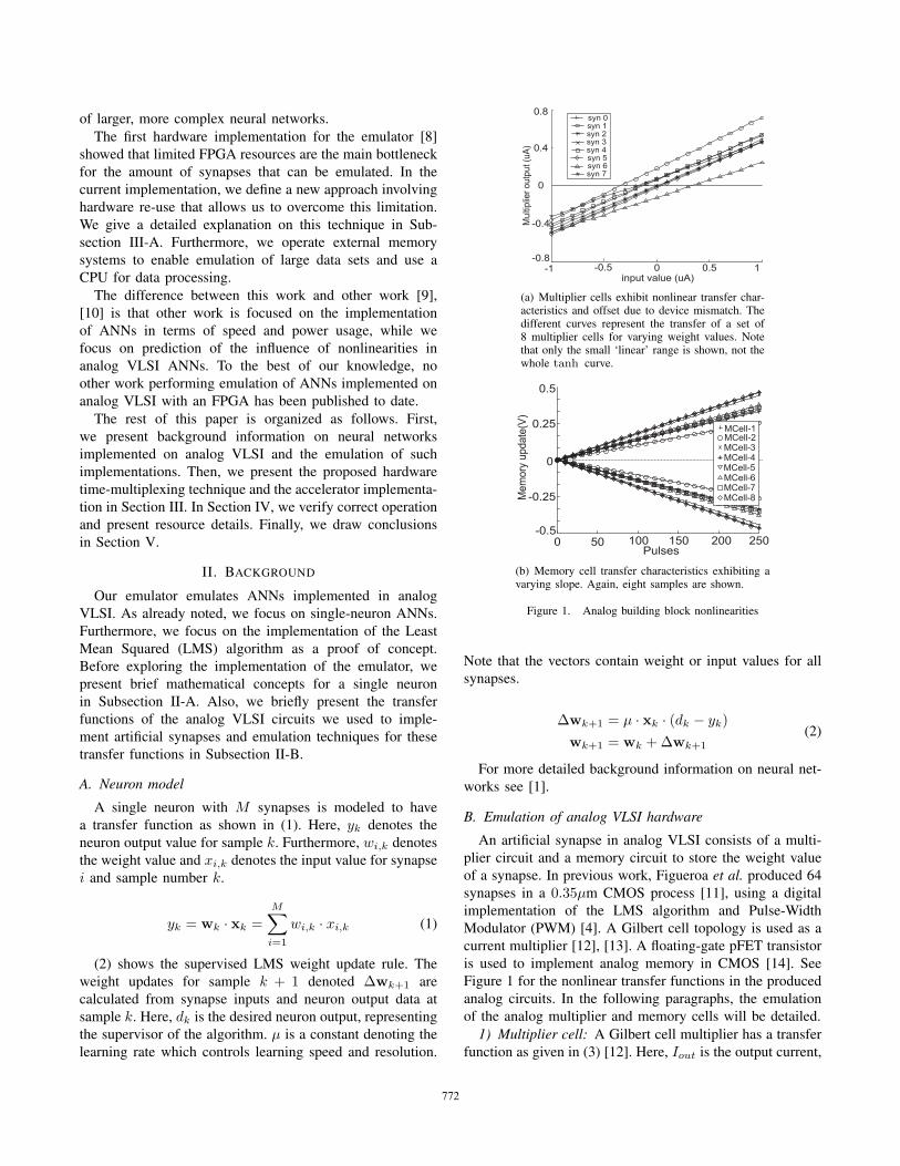
(a) Multiplier cells exhibit nonlinear transfer char-acteristics and offset due to device mismatch. Thedifferent curves represent the transfer of a set of8 multiplier cells for varying weight values. Notethat only the small ‘linear’ range is shown, not thewhole tanh curve.
(b) Memory cell transfer characteristics exhibiting avarying slope. Again, eight samples are shown.
Figure 1. Analog building block nonlinearities
Note that the vectors contain weight or input values for allsynapses.
∆wk+1 = µ · xk · (dk − yk)wk+1 = wk + ∆wk+1
(2)
For more detailed background information on neural net-works see [1].
B. Emulation of analog VLSI hardware
An artificial synapse in analog VLSI consists of a multi-plier circuit and a memory circuit to store the weight valueof a synapse. In previous work, Figueroa et al. produced 64synapses in a 0.35µm CMOS process [11], using a digitalimplementation of the LMS algorithm and Pulse-WidthModulator (PWM) [4]. A Gilbert cell topology is used as acurrent multiplier [12], [13]. A floating-gate pFET transistoris used to implement analog memory in CMOS [14]. SeeFigure 1 for the nonlinear transfer functions in the producedanalog circuits. In the following paragraphs, the emulationof the analog multiplier and memory cells will be detailed.
1) Multiplier cell: A Gilbert cell multiplier has a transferfunction as given in (3) [12]. Here, Iout is the output current,
772

I0 is the multiplier cell saturation current, UT is the thermalvoltage and Vw,x are the inputs of the multiplier. Figure 1(a)shows nonlinearities for eight analog multipliers for varyingweight voltages, keeping the input voltage constant.
Iout(t) = I0 · tanhVw(t)2UT
· tanhVx(t)2UT
(3)
In order to emulate an analog multiplier cell, we measuredthe transfer functions of the Gilbert cells by increasingVw with constant step size. We then fitted these measure-ments with tanh-curves (4). Here, the sampled versions ofIout(t), Vw(t), Vx(t) are denoted as yk, wk, xk, respectively.Furthermore, Aw,k, Bw,k and Cw,k are the fitting parameterswhich represent the analog VLSI transfer functions. Finally,the tanh is approximated with the first order Taylor approx-imation, which is sufficiently precise for small xk. Xx,k andYx,k are the first order Taylor approximation parameters.
yk(wk, xk) ≈ Aw,k · tanh(Bw,k · xk) + Cw,k
≈ Aw,k · (Xx,k ·Bw,k · xk + Yx,k) + Cw,k
(4)
2) Memory cell: The output voltage Vw of an analogVLSI memory cell depends linearly on the amount ofelectrons stored on the floating gate as can be seen fromFigure 1(b). However, each memory cell transfer functionhas a different slope due to PVT spread [11]. The amountof weight change per electron pulse is denoted slopeTF .The amount of electron pulses (denoted Npulses,k), neededfor the required voltage change ∆wk, is calculated by thealgorithm using (5). The memory cell weight voltage ischanged by adding the pulses to the floating gate using thedigitally implemented PWM.
Npulses,k =∆wreal,k
slopeTF(5)
To emulate the memory cell, we change the stored weightvalue relative to the change in the number of pulses in theanalog implementation. Mathematically, each memory cellchanges the weight value wk according to the weight change∆wk calculated by the algorithm. In (6), the required weightchange is then given by ∆wreal,k. The approximated versionof this weight change is denoted ∆wapprox,k. The remainderRk represents the difference between the required weightchange and the calculated weight change, which arises sincea finite amount of steps are used to represent the lineartransfer function.
∆wreal,k = ∆wk +Rk−1
∆wapprox,k = Npulses,k · slopeTF
Rk = ∆wreal,k −∆wapprox,k
(6)
Sample index #
Slice index #
1 1 1 2 2 2 K K K
1 2 M 1 2 M 1 2 M
.... .... ................... ....
.... .... ................... ....
t
Figure 2. This time-line shows how the sample index and slice indexincrease over time during operation. It shows the intended operating orderfor the temporally sliced synapses in the system for K samples and Mslices.
III. IMPLEMENTATION
In this section we show how the mathematical descriptionsfrom the previous section are mapped to an implemen-tation on a Xilinx Virtex 2 Pro (V2P) FPGA. First, weexplain our proposed hardware re-use technique in Sub-section III-A. Secondly, we describe system data flow andhardware/software interaction in Subsection III-B. Finally,we give an overview of the emulator hardware and describethe hardware implementation in Subsection III-C.
A. Temporal synapse slicing
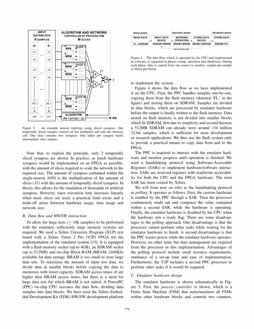
As noted in the introduction, we propose to solve resourceconstraints through the re-use of hardware blocks to enableemulation large-size networks. We will from now on referto this technique as temporal synapse slicing. A temporallysliced synapse consists of an emulated multiplier cell, anemulated memory cell and control hardware, which togetheremulate the function of one artificial synapse as imple-mented on analog VLSI. We re-use this single temporallysliced synapse, physically implemented on the FPGA, toemulate multiple artificial synapses over time. A temporalslice refers to all temporally sliced synapses in the systemtogether at a single point in time. For example, the firstslice are all physical synapses operating to emulate thefirst artificial synapse they represent. A combination of anumber of slices and a number of temporally sliced synapsescreates a neuron. For example, when we operate 5 sliceswith 5 physically implemented temporally sliced synapses,we emulate a 25-synapse neuron. See figure 2. For eachsample, all sliced synapses are operated sequentially: onesynapse is operated M ×K times.
Figure 3 shows (schematically) an example of the neuronstructure as it arises through the use of the synapse slicing.In this example we show M slices and 2 temporally slicedsynapses per slice to form a 2M -synapse neuron. Eachsynapse contains a memory cell emulator, a multiplier cellemulator and a slice adder. The synapse outputs y1,k andy2,k are intermediate slice results, added by a third adder toform the total network output yk. Furthermore, the input datablock shown in the figure contains a set of K input samplesfor each network input. One sample is fed to the networkinputs in parallel and samples follow each other sequentially,until the whole data block has been processed. Finally, thealgorithm processes network information to calculate weightupdates, using the LMS algorithm as given in (2).
773
INPUT
DATABLOCK
K SAMPLES
xK
dw
ALGORITHM AND NETWORKCONTROLLED BY PROCESS FSM
M SLICES
x1
SLICE 1
+
SLICE 2
x1x1
x2x2
x3x3
x4x4
x
M-1
x
M
yd1
y2
y1
ALGORITHM
dw = µ*x*(yd – y)
MEM
MEM
MEM
MEM
MEM
MEM
y
SLICE M
+
+
...
...
...
...
...
...................
...............
...............
...............
...............
x
M-1
x
M
...................
ydK
Figure 3. An example neuron topology using sliced synapses. Onetemporally sliced synapse consists of one multiplier cell and one memorycell. One slice contains two synapses. One adder per synapse tracksintermediate slice outputs.
Note that, to explain the principle, only 2 temporallysliced synapses are shown. In practice, as much hardwaresynapses would be implemented on an FPGA as possible,with the amount of slices required to scale the network to therequired size. The amount of synapses contained within thesingle-neuron ANN is the multiplication of the amount ofslices (M ) with the amount of temporally sliced synapses. Intheory, this allows for the emulation of thousands of artificialsynapses. However, since execution time increases linearlywhen more slices are used, a practical limit exists and atrade-off arises between hardware usage, time usage andnetwork size.
B. Data flow and HW/SW interaction
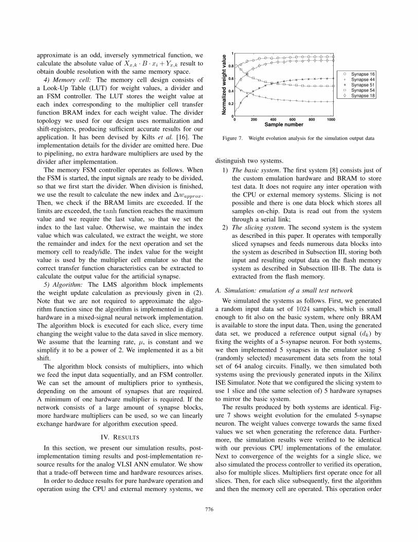
To allow for large tests (≥ 10k samples) to be performedwith the emulator, sufficiently large memory systems arerequired. We used a Xilinx University Program (XUP) testboard with a Xilinx Virtex 2 Pro (V2P) FPGA for theimplementation of the emulator system [15]. It is equippedwith a flash memory socket (up to 4GB), an SDRAM socket(up to 512MB) and on-chip Block-RAM (BRAM, 2448Kb)available for data storage. BRAM is too small to store largedata sets. To maximize the amount of input test data, wedivide data in smaller blocks before copying the data tomemories with lower capacity. SDRAM access times of arehigher then BRAM access times, but there is a need forlarge data sets for which BRAM is not suited. A PowerPC(PPC) on-chip CPU executes the data flow, dividing datasamples into data blocks. We have used the Xilinx Embed-ded Development Kit (EDK) HW/SW development platform
STORE DATAREAD DATA INPUT DATA
BLOCK
STORE DATA
BLOCK
NETWORK
OPERATION
DATA BLOCK LOOP
Operation phase Shutdown phaseSetup phase
SDRAMàBRAM BRAMàBRAM BRAMàSDRAMFL.àSDRAM SDRAMàFL.
Figure 4. The data flow, which is operated by the CPU and implementedin software, is separated in phases (setup, operation and shutdown). Duringeach phase, data is copied from one source to another, sample-per-sampleor block-per-block.
to implement the system.Figure 4 shows the data flow as we have implemented
it on the CPU. First, the PPC handles samples one-by-one,copying them from the flash memory (denoted ‘FL.’ in thefigure) and storing them on SDRAM. Samples are dividedin data blocks, which are processed by emulator hardwarebefore the output is finally written to the flash memory. Datastored on flash memory is not divided into smaller blockswhich fit SDRAM, first due to simplicity and second becausea 512MB SDRAM can already store around 134 million32-bit samples, which is sufficient for most developmentor research applications. We thus use the flash system onlyto provide a practical means to copy data from and to theFPGA.
The PPC is required to interact with the emulator hard-ware and monitor progress until operation is finished. Weused a handshaking protocol using Software-AccessibleRegisters (SARs) to implement hardware/software interac-tion. SARs are reserved registers with read/write accessibil-ity for both the CPU and the FPGA hardware. The termSAR has been coined by Xilinx.
We will from now on refer to the handshaking protocolas polling. It operates as follows. First, the custom hardwareis enabled by the PPC through a SAR. Then the processorcontinuously reads out and compares the value containedwithin a second SAR, while the hardware is operating.Finally, the emulator hardware is disabled by the CPU whenthe hardware sets a ready flag. There are some disadvan-tages to the polling approach. One disadvantage is that theprocessor cannot perform other tasks while waiting for theemulator hardware to finish. A second disadvantage is thatthe PPC wastes power while the emulator hardware operates.However, no other tasks but data management are requiredfrom the processor in this implementation. Advantages ofthe polling protocol include small resource requirements,omittance of a set-up time and ease of implementation.Furthermore, the V2P includes a second PPC processor toperform other tasks if it would be required.
C. Emulator hardware design
The emulator hardware is shown schematically in Fig-ure 5. First, the process controller is shown, which is aFinite State Machine (FSM) that starts/monitors all FSMswithin other hardware blocks and controls two counters.
774

hw/sw
interfaceSynapses
x w
dw Y1
ready Y2
start
slice_select
Algorithmdw
x
Y_d
Y
start
ready
Process FSMready_proc start
enable_proc ready
slice_cnt_enable slice_cnt
sample_cnt_enable sample_cnt
AdditionY Y1
Y2
Sample counter
sample_select
count_enable
#
Slice counter
slice_select
count_enable
#
data input vector (from BRAM)
network
outputs
Figure 5. Emulator hardware overview (schematic). Dashed lines representcontrol signals, bold signals contain multiple signals (vectors) and non-boldsignals contain single signals. The BRAM containing the input data is notshown.
Secondly, the Synapses block contains all temporally slicedsynapses. Thirdly, the Algorithm block consist of a numberof pipelined hardware multipliers, calculating all weightupdate values. Finally, the Addition block is simply an adderfor synapse outputs. In subsequent parts of this section,hardware designs for each block will be detailed.
1) Process controller: The process controller is the mainFSM for the hardware system. This controller implementsthe slicing system. The FSM diagram is shown schematicallyin Figure 6. The FSM starting state is denoted Idle and theFSM ending state is denoted Datablock ready. The flagsinvolved between states are indicated in the figure. Forexample, in state Await Alg, the ready signal is the readyflag from the algorithm, signaling the process controller itis ready operating.
First, the CPU enables the FSM through a SAR. Then,the multipliers retrieve the value stored in the memory andmultiply it with the first input sample for all slices (denotedslice loop 1). Then, outputs w and y are stored in an outputBRAM. The algorithm is started to calculate the weightupdates. When ready, the memory cells are started, updatingtheir weights to contain the new weight value calculated bythe algorithm (denoted slice loop 2). The system executesthe described process for all samples contained in the datablock (denoted sample loop), after which a ready flag is setin a SAR, notifying the CPU that the hardware is ready forthe next data block.
Throughout this process, the sample and slice indexvalues are updated to allow correct data selection from theinput data BRAM and control of the amount of loops inthe process FSM. The relative simplicity of the processcontroller FSM shows that our proposed temporal slicingtechnique can be used in practical systems. By increasing theamount of slice loops, we can linearly scale up the neuronsize.
2) Temporally sliced synapse: The hardware block emu-lating the artificial synapse consists a multiplier cell emula-
Await
Mults
Slice
Check
rea
dy
~ready
Await
Alg
slice_select++
~AllSlices
Alg
orith
m
sta
rt
~re
ady
AllS
lice
s
rea
dy
Output
W,Y
Start
Alg
Await
Mems
Start
Mems
Start
Mems
~ready
Slice
Check
ready
AllS
lice
s
rea
dy
Sample
Check
AllS
am
ple
s
rea
dy
~AllS
amples
sam
ple_
select++
~AllSlices
slice_select++
enab
led
disabled
enabled:
start
Mults
SLICE LOOP 2
SAMPLE LOOP
Datablock
ready
rea
dy
SLIC
ELO
OP
Idle
disabled
1
Figure 6. Process controller FSM diagram (schematic). The double linedstate is the starting state, the bold lined state the ending state.
tor and a memory cell emulator. Also, it contains a sliceBRAM. The slice BRAM contains for each slice in thesynapse:• the memory cell BRAM index nk−1 pointing to the
current weight;• the ∆w for the next sample;• the remainder value Rk arising from weight approxi-
mation.3) Multiplier cell: The multiplier cell is used to calculate
the yk value for a synapse, as seen in (4) (subsection II-B1).The hardware consists of two BRAMs, a single pipelinedhardware multiplier and an FSM controller.
The first BRAM contains Aw,k, Bw,k and Cw,k forN measurements for one analog multiplier cell transferfunction. Each multiplier cell emulates one of the measuredanalog VLSI multiplier cells. A disadvantage to this way ofimplementing the slicing system is that it does not accountwell for PVT spread if the amount of slices is much higherthen the amount of temporally sliced synapses. Therefore,it is essential that as much temporally sliced synapses aspossible are implemented. The second BRAM contains Xx,k
and Yx,k for M approximation points, so that a higher Mgives a higher resolution of the tanh approximation.
The multiplier FSM operates as follows. The multiplyingprocess starts with extraction of the Aw,k, Bw,k and Cw,k
parameters. Second, we extract the Xx,k and Yx,k param-eters from BRAM. In subsequent steps, we calculate theoutput using the extracted parameters. Because the tanh we
775
approximate is an odd, inversely symmetrical function, wecalculate the absolute value of Xx,k ·B · xi + Yx,k result toobtain double resolution with the same memory space.
4) Memory cell: The memory cell design consists ofa Look-Up Table (LUT) for weight values, a divider andan FSM controller. The LUT stores the weight value ateach index corresponding to the multiplier cell transferfunction BRAM index for each weight value. The dividertopology we used for our design uses normalization andshift-registers, producing sufficient accurate results for ourapplication. It has been devised by Kilts et al. [16]. Theimplementation details for the divider are omitted here. Dueto pipelining, no extra hardware multipliers are used by thedivider after implementation.
The memory FSM controller operates as follows. Whenthe FSM is started, the input signals are ready to be divided,so that we first start the divider. When division is finished,we use the result to calculate the new index and ∆wapprox.Then, we check if the BRAM limits are exceeded. If thelimits are exceeded, the tanh function reaches the maximumvalue and we require the last value, so that we set theindex to the last value. Otherwise, we maintain the indexvalue which was calculated, we extract the weight, we storethe remainder and index for the next operation and set thememory cell to ready/idle. The index value for the weightvalue is used by the multiplier cell emulator so that thecorrect transfer function characteristics can be extracted tocalculate the output value for the artificial synapse.
5) Algorithm: The LMS algorithm block implementsthe weight update calculation as previously given in (2).Note that we are not required to approximate the algo-rithm function since the algorithm is implemented in digitalhardware in a mixed-signal neural network implementation.The algorithm block is executed for each slice, every timechanging the weight value to the data saved in slice memory.We assume that the learning rate, µ, is constant and wesimplify it to be a power of 2. We implemented it as a bitshift.
The algorithm block consists of multipliers, into whichwe feed the input data sequentially, and an FSM controller.We can set the amount of multipliers prior to synthesis,depending on the amount of synapses that are required.A minimum of one hardware multiplier is required. If thenetwork consists of a large amount of synapse blocks,more hardware multipliers can be used, so we can linearlyexchange hardware for algorithm execution speed.
IV. RESULTS
In this section, we present our simulation results, post-implementation timing results and post-implementation re-source results for the analog VLSI ANN emulator. We showthat a trade-off between time and hardware resources arises.
In order to deduce results for pure hardware operation andoperation using the CPU and external memory systems, we
0 200 400 600 800 10000
0.2
0.4
0.6
0.8
1
Sample number
No
rma
lize
d w
eig
ht
va
lue
Synapse 16
Synapse 44
Synapse 51
Synapse 54
Synapse 18
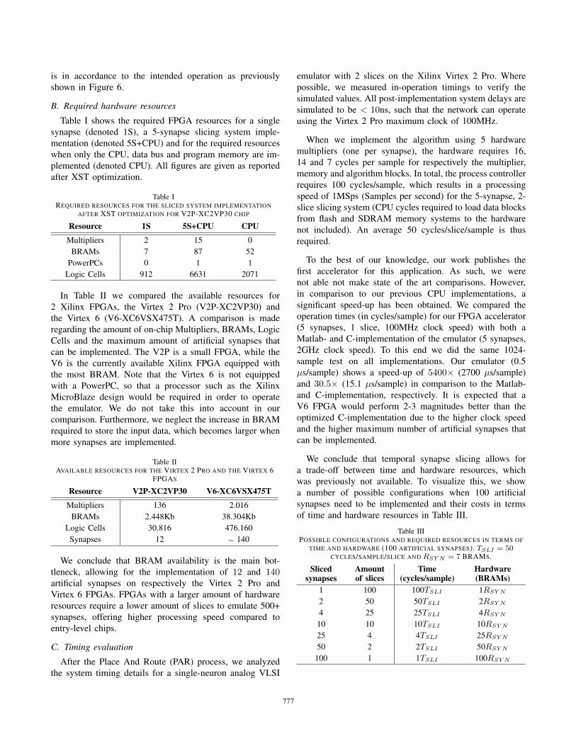
Figure 7. Weight evolution analysis for the simulation output data
distinguish two systems.1) The basic system. The first system [8] consists just of
the custom emulation hardware and BRAM to storetest data. It does not require any inter operation withthe CPU or external memory systems. Slicing is notpossible and there is one data block which stores allsamples on-chip. Data is read out from the systemthrough a serial link;
2) The slicing system. The second system is the systemas described in this paper. It operates with temporallysliced synapses and feeds numerous data blocks intothe system as described in Subsection III, storing bothinput and resulting output data on the flash memorysystem as described in Subsection III-B. The data isextracted from the flash memory.
A. Simulation: emulation of a small test network
We simulated the systems as follows. First, we generateda random input data set of 1024 samples, which is smallenough to fit also on the basic system, where only BRAMis available to store the input data. Then, using the generateddata set, we produced a reference output signal (dk) byfixing the weights of a 5-synapse neuron. For both systems,we then implemented 5 synapses in the emulator using 5(randomly selected) measurement data sets from the totalset of 64 analog circuits. Finally, we then simulated bothsystems using the previously generated inputs in the XilinxISE Simulator. Note that we configured the slicing system touse 1 slice and (the same selection of) 5 hardware synapsesto mirror the basic system.
The results produced by both systems are identical. Fig-ure 7 shows weight evolution for the emulated 5-synapseneuron. The weight values converge towards the same fixedvalues we set when generating the reference data. Further-more, the simulation results were verified to be identicalwith our previous CPU implementations of the emulator.Next to convergence of the weights for a single slice, wealso simulated the process controller to verified its operation,also for multiple slices. Multipliers first operate once for allslices. Then, for each slice subsequently, first the algorithmand then the memory cell are operated. This operation order
776
is in accordance to the intended operation as previouslyshown in Figure 6.
B. Required hardware resources
Table I shows the required FPGA resources for a singlesynapse (denoted 1S), a 5-synapse slicing system imple-mentation (denoted 5S+CPU) and for the required resourceswhen only the CPU, data bus and program memory are im-plemented (denoted CPU). All figures are given as reportedafter XST optimization.
Table IREQUIRED RESOURCES FOR THE SLICED SYSTEM IMPLEMENTATION
AFTER XST OPTIMIZATION FOR V2P-XC2VP30 CHIP
Resource 1S 5S+CPU CPU
Multipliers 2 15 0BRAMs 7 87 52
PowerPCs 0 1 1Logic Cells 912 6631 2071
In Table II we compared the available resources for2 Xilinx FPGAs, the Virtex 2 Pro (V2P-XC2VP30) andthe Virtex 6 (V6-XC6VSX475T). A comparison is maderegarding the amount of on-chip Multipliers, BRAMs, LogicCells and the maximum amount of artificial synapses thatcan be implemented. The V2P is a small FPGA, while theV6 is the currently available Xilinx FPGA equipped withthe most BRAM. Note that the Virtex 6 is not equippedwith a PowerPC, so that a processor such as the XilinxMicroBlaze design would be required in order to operatethe emulator. We do not take this into account in ourcomparison. Furthermore, we neglect the increase in BRAMrequired to store the input data, which becomes larger whenmore synapses are implemented.
Table IIAVAILABLE RESOURCES FOR THE VIRTEX 2 PRO AND THE VIRTEX 6
FPGAS
Resource V2P-XC2VP30 V6-XC6VSX475T
Multipliers 136 2.016BRAMs 2.448Kb 38.304Kb
Logic Cells 30.816 476.160Synapses 12 ∼ 140
We conclude that BRAM availability is the main bot-tleneck, allowing for the implementation of 12 and 140artificial synapses on respectively the Virtex 2 Pro andVirtex 6 FPGAs. FPGAs with a larger amount of hardwareresources require a lower amount of slices to emulate 500+synapses, offering higher processing speed compared toentry-level chips.
C. Timing evaluation
After the Place And Route (PAR) process, we analyzedthe system timing details for a single-neuron analog VLSI
emulator with 2 slices on the Xilinx Virtex 2 Pro. Wherepossible, we measured in-operation timings to verify thesimulated values. All post-implementation system delays aresimulated to be < 10ns, such that the network can operateusing the Virtex 2 Pro maximum clock of 100MHz.
When we implement the algorithm using 5 hardwaremultipliers (one per synapse), the hardware requires 16,14 and 7 cycles per sample for respectively the multiplier,memory and algorithm blocks. In total, the process controllerrequires 100 cycles/sample, which results in a processingspeed of 1MSps (Samples per second) for the 5-synapse, 2-slice slicing system (CPU cycles required to load data blocksfrom flash and SDRAM memory systems to the hardwarenot included). An average 50 cycles/slice/sample is thusrequired.
To the best of our knowledge, our work publishes thefirst accelerator for this application. As such, we werenot able not make state of the art comparisons. However,in comparison to our previous CPU implementations, asignificant speed-up has been obtained. We compared theoperation times (in cycles/sample) for our FPGA accelerator(5 synapses, 1 slice, 100MHz clock speed) with both aMatlab- and C-implementation of the emulator (5 synapses,2GHz clock speed). To this end we did the same 1024-sample test on all implementations. Our emulator (0.5µs/sample) shows a speed-up of 5400× (2700 µs/sample)and 30.5× (15.1 µs/sample) in comparison to the Matlab-and C-implementation, respectively. It is expected that aV6 FPGA would perform 2-3 magnitudes better than theoptimized C-implementation due to the higher clock speedand the higher maximum number of artificial synapses thatcan be implemented.
We conclude that temporal synapse slicing allows fora trade-off between time and hardware resources, whichwas previously not available. To visualize this, we showa number of possible configurations when 100 artificialsynapses need to be implemented and their costs in termsof time and hardware resources in Table III.
Table IIIPOSSIBLE CONFIGURATIONS AND REQUIRED RESOURCES IN TERMS OF
TIME AND HARDWARE (100 ARTIFICIAL SYNAPSES). TSLI = 50CYCLES/SAMPLE/SLICE AND RSY N = 7 BRAMS.
Slicedsynapses
Amountof slices
Time(cycles/sample)
Hardware(BRAMs)
1 100 100TSLI 1RSY N
2 50 50TSLI 2RSY N
4 25 25TSLI 4RSY N
10 10 10TSLI 10RSY N
25 4 4TSLI 25RSY N
50 2 2TSLI 50RSY N
100 1 1TSLI 100RSY N
777
V. CONCLUSIONS
The contributions of this work are twofold. We imple-mented an FPGA-based accelerator for practical emulationof analog VLSI neural networks and investigated the limitsthat availability of FPGA resources impose on the amountof synapses that we can emulate. First, we conclude that em-ulation of large analog VLSI neural networks is feasible onan FPGA platform. Secondly, we conclude that availabilityof on-chip memory limits the amount of test samples, butexternal memory systems overcome this limitation.
Our emulator allows for emulation of nonlinearities ofanalog VLSI implementations for artificial neural networks.The emulator enables convergence and performance analysisof large single-neuron ANNs. We show that it is possibleto implement 500+ synapses even on an entry-level FPGAwith limited resources. We use hardware efficiently throughtemporally slicing of synapse emulator blocks and showthere is a trade-off between resources and emulation speed.Furthermore, we show that external memory systems and aCPU for data flow control together overcome the limitationsposed by available on-chip memory regarding the amountof input samples, allowing for test sequences of more then10K samples. Finally, our Virtex 2 Pro accelerator obtainsa speedup of the order of one magnitude compared to aspecialized software implementation, while it is expectedthat a similar implementation on a state of the art FPGA suchas the Virtex 6 could obtain a speedup of 2-3 magnitudes.
Future work aims at emulation of multiple layer/neuronnetworks and the use of more complex algorithms such asIndependent Component Analysis (ICA). Also, the currentimplementation is not user friendly and the user requiresknowledge of the inner workings to modify the architecture.For future work, we want to create a user friendly emulatortool which can be used by designers of mixed-signal VLSIand researchers on ANNs in the field. This includes tools fordata generation, implementation and network analysis. Wewill work to enable implementation of different algorithmsand circuits by changing equations and measurement data,respectively.
ACKNOWLEDGMENTS
This work was partially funded by the Chilean gov-ernment through grants Fondecyt-1070485 and PFB-0824.Furthermore, this work was partially funded through theErasmus Mundus External Cooperation Window (EMECW)program from the European Commission.
REFERENCES
[1] C. M. Bishop, Pattern recognition and machine learning.Springer Science+Business Media, LLC, 2006.
[2] C. Diorio, D. Hsu, and M. Figueroa, “Adaptive CMOS: fromBiological Inspiration to Systems-on-a-Chip,” Proceedings ofthe IEEE, vol. 90, no. 3, pp. 345–357, 2002.
[3] G. Cauwenberghs and M. A. Bayoumi, Eds., Learning onSilicon: Adaptive VLSI Neural Systems, ser. The KluwerInternational Series in Engineering and Computer Science.Kluwer Academic Press, 1999.
[4] M. Figueroa, S. Bridges, and C. Diorio, “On-chip compen-sation of device-mismatch effects in analog VLSI neuralnetworks,” in Advances in Neural Information ProcessingSystems 17. Cambridge, MA: MIT Press, 2005.
[5] B. Dolenko and H. Card, “Tolerance to Analog Hardwareof On-Chip Learning in Backpropagation Networks,” IEEETransactions on Neural Networks, vol. 6, no. 5, pp. 1045–1052, 1995.
[6] E. Matamala, “Simulation of adaptive signal processing al-gorithms in VLSI (in Spanish). Civil Electrical Engineer’sthesis, Universidad de Concepcion,” 2006.
[7] D. B. Thomas, L. Howes, and W. Luk, “A Comparisonof CPUs, GPUs, FPGAs, and Massively Parallel ProcessorArrays for Random Number Generation,” in Proceedings ofthe ACM/SIGDA international symposium on FPGAs, 2009,pp. 63–72.
[8] D. Herrera and M. Figueroa, “FPGA-based Analog VLSINeural Network Emulator,” in Proceedings of the ChileanCongress on Computing, 2008.
[9] F. Yang and M. Paindavoine, “Implementation of an RBFNeural Network on Embedded Systems: Real-Time FaceTracking and Identity Verification,” in IEEE Transactions OnNeural Networks, vol. 14, 2003, pp. 1162–1175.
[10] V. Stopjakov, D. Miuk, L. Benuskova, and M. Margala,“Neural Networks-Based Parametric Testing of Analog IC,” inIEEE International Symposium on Defect and Fault Tolerancein VLSI Systems, vol. 17, 2002.
[11] M. Figueroa, E. Matamala, G. Carvajal, and S. Bridges,“Adaptive Signal Processing in Mixed-Signal VLSI withAnti-Hebbian Learning,” in IEEE Computer Society AnnualSymposium on VLSI. Karlsruhe, Germany: IEEE, 2006, pp.133–138.
[12] D. Coue and G. Wilson, “A four-quadrant subthreshold modemultiplier for analog neural-network applications,” NeuralNetworks, IEEE Transactions on, vol. 7, no. 5, pp. 1212 –1219, sep 1996.
[13] C. R. Schneider, “Analog CMOS Circuits for Artificial NeuralNetworks,” Ph.D. dissertation, University of Manitoba, 1991.
[14] C. Diorio, S. Mahajan, P. Hasler, B. A. Minch, and C. Mead,“A High-Resolution Nonvolatile Analog Memory Cell,” inIEEE International Symposium on Circuits and Systems,vol. 3, Seattle, WA, 1995, pp. 2233–2236.
[15] Digilent Inc., “Xilinx University Program, Virtex 2 Pro De-velopment Board, Curriculum on a Chip,” Accessed: March2010, http://www.digilentinc.com/Products/Detail.cfm?Prod=XUPV2P.
[16] S. Kilts, Advanced FPGA Design, Architecture, Implementa-tion and Optimization. Wiley-Interscience, 2007.
778