Conformal coverage of poly(3,4-ethylenedioxythiophene) films with tunable nanoporosity via oxidative...
10
Subscriber access provided by UNIV DE BURGOS ACS Nano is published by the American Chemical Society. 1155 Sixteenth Street N.W., Washington, DC 20036 Article Conformal Coverage of Poly(3,4-ethylenedioxythiophene) Films with Tunable Nanoporosity via Oxidative Chemical Vapor Deposition Sung Gap Im, David Kusters, Wonjae Choi, Salmaan H. Baxamusa, M. C. M. van de Sanden, and Karen K. Gleason ACS Nano, 2008, 2 (9), 1959-1967 • DOI: 10.1021/nn800380e • Publication Date (Web): 28 August 2008 Downloaded from http://pubs.acs.org on December 17, 2008 More About This Article Additional resources and features associated with this article are available within the HTML version: • Supporting Information • Access to high resolution figures • Links to articles and content related to this article • Copyright permission to reproduce figures and/or text from this article
Transcript of Conformal coverage of poly(3,4-ethylenedioxythiophene) films with tunable nanoporosity via oxidative...
Subscriber access provided by UNIV DE BURGOS
ACS Nano is published by the American Chemical Society. 1155 Sixteenth StreetN.W., Washington, DC 20036
Article
Conformal Coverage of Poly(3,4-ethylenedioxythiophene) Films withTunable Nanoporosity via Oxidative Chemical Vapor Deposition
Sung Gap Im, David Kusters, Wonjae Choi, Salmaan H.Baxamusa, M. C. M. van de Sanden, and Karen K. Gleason
ACS Nano, 2008, 2 (9), 1959-1967 • DOI: 10.1021/nn800380e • Publication Date (Web): 28 August 2008
Downloaded from http://pubs.acs.org on December 17, 2008
More About This Article
Additional resources and features associated with this article are available within the HTML version:
• Supporting Information• Access to high resolution figures• Links to articles and content related to this article• Copyright permission to reproduce figures and/or text from this article
Conformal Coverage of Poly(3,4-ethylenedioxythiophene) Films withTunable Nanoporosity viaOxidativeChemical Vapor DepositionSung Gap Im,† David Kusters,‡ Wonjae Choi,§ Salmaan H. Baxamusa,† M. C. M. van de Sanden,‡ andKaren K. Gleason†,*†Department of Chemical Engineering and Institute for Soldier Nanotechnologies, Massachusetts Institute of Technology, Cambridge, Massachusetts 02139, ‡Departmentof Applied Physics, Eindhoven University of Technology, Eindhoven, The Netherlands, and §Department of Mechanical Engineering, Massachusetts Institute ofTechnology, Cambridge, Massachusetts 02139
Nanostructured materials havedrawn significant research inter-est as their properties are often
unique with respect to bulk materials of
identical chemical composition.1 Control-
ling the properties of these materials re-
quires structural control on the nanometer
scale.2 A number of chemical and physical
methodologies have been applied to syn-
thesize nanostructured metals, inorganics,
polymers, and carbon nanotubes, having a
variety of potential applications, including
circuit integration, microfluidics, and bio-
medical devices.3,4
Conducting polymers are regarded as
one of the most promising materials for
nanostructured devices.5,6 Poly(3,4-
ethylenedioxythiophene) (PEDOT) is a par-
ticularly interesting conducting polymer
due to its excellent environmental stability
and high optical transparency in its electri-
cally conductive state.7,8 Moreover, since it
has a moderate band gap with low redox
potential and exceptionally high conductiv-
ity, PEDOT has been applied to various elec-
tronic devices such as electrochemical
cells,7 chemical sensors,9,10 and transpar-
ent, flexible electrodes for organic electron-
ics.11 Currently, nanostructured PEDOT has
been reported using various synthesis
schemes.5 For example, Jang et al. fabri-
cated PEDOT nanorods for a sensing appli-
cation by using micelle intermediated inter-
facial oxidative polymerization.9 Abidian et
al. synthesized PEDOT nanotubes for con-
trolled drug release by utilizing electrospun
fibers as a template in electrochemical po-
lymerization.12 However, these synthetic
methodologies require multistep proce-dures and strict control over reactionconditions.
Previously, we have demonstrated an insitu deposition of well-defined, opticallytransparent PEDOT films on a variety of sub-strates, including Si wafers, paper, alumi-num foil, and plastic substrates by using oxi-dative chemical vapor deposition(oCVD).13�16 The oCVD film growth wasachieved through vapor phase introduc-tion of both the oxidant, FeCl3, and themonomer, 3,4-ethylenedioxythiophene
*Address correspondence [email protected].
Received for review June 16, 2008and accepted August 19, 2008.
Published online August 28, 2008.10.1021/nn800380e CCC: $40.75
© 2008 American Chemical Society
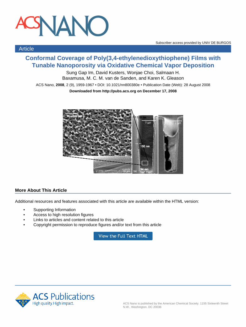
ABSTRACT Novel nanoporous poly(3,4-ethylenedioxythiophene) (PEDOT) films with basalt-like surface
morphology are successfully obtained via a one-step, vapor phase process of oxidative chemical vapor deposition
(oCVD) by introducing a new oxidant, CuCl2. The substrate temperature of the oCVD process is a crucial process
parameter for controlling electrical conductivity and conjugation length. Moreover, the surface morphology is also
systemically tunable through variations in substrate temperature, a unique advantage of the oCVD process. By
increasing the substrate temperature, the surface morphology becomes more porous, with the textured structure
on the nanometer scale. The size of nanopores and fibrils appears uniformly over 25 mm � 25 mm areas on the
Si wafer substrates. Conformal coverage of PEDOT films grown with the CuCl2 oxidant (C-PEDOT) is observed on
both standard trench structures with high aspect ratio and fragile surfaces with complex topology, such as paper,
results which are extremely difficult to achieve with liquid phase based processes. The tunable nanoporosity and
its conformal coverage on various complex geometries are highly desirable for many device applications requiring
controlled, high interfacial area, such as supercapacitors, Li ion battery electrodes, and sensors. For example, a
highly hydrophilic surface with the static water contact angle down to less than 10° is obtained solely by changing
surface morphology. By applying fluorinated polymer film onto the nanoporous C-PEDOT via initiative chemical
vapor deposition (iCVD), the C-PEDOT surface also shows the contact angle higher than 150°. The hierarchical
porous structure of fluorinated polymer coated C-PEDOT on a paper mat shows superhydrophobicity and oil
repellency.
KEYWORDS: poly(3,4-ethylenedioxythiophene) (PEDOT) · oxidative chemical vapordeposition (oCVD) · oxidant · CuCl2 · FeCl3 · nanostructure · conformalcoverage · superhydrophobicity · oleophobicity
ARTIC
LE
www.acsnano.org VOL. 2 ▪ NO. 9 ▪ 1959–1967 ▪ 2008 1959
(EDOT). The electrical conductivity, doping level, and
work function of the oCVD PEDOT could be controlled
by varying substrate temperature (Tsub),13,14 and the
maximum electrical conductivity achieved was greater
than 700 S/cm.13,15 The oCVD PEDOT could also be
grafted on various organic plastic substrates such as
polystyrene (PS), polycarbonate (PC), and polyethylene-
terephthalate (PET).15
In this report, we describe a new synthetic scheme
to fabricate nanoporous, basalt-like PEDOT films by in-
troducing a new oxidant, CuCl2, to the oCVD process.
Both CuCl2 and FeCl3 are oxidants which are catego-
rized as Friedel�Crafts catalysts.15 The surface mor-
phology and nanostructure of the resultant films could
be systematically controlled by changing Tsub. The
nanostructured PEDOT could also be conformally
coated on various geometries, including trenches with
high aspect ratio and complex, fragile surfaces without
damaging the subtle surface structure, which is difficult
to achieve via a non-CVD process.17 Water and ethanol
droplet contact angles on these nanoporous PEDOT
films showed that the contact angle was highly de-
pendent on surface morphology. Superhydrophobicity
and oleophobicity were also readily obtained via vapor
phase, initiative chemical vapor deposition (iCVD) of flu-
orinated polymer film on nanostructured oCVD PE-
DOT. The size-tunable nanoporous PEDOT film has a
high surface area and thus may find direct application
in various devices that require high interfacial areas
such as sensors, lithium secondary batteries, and super-
capacitors.8
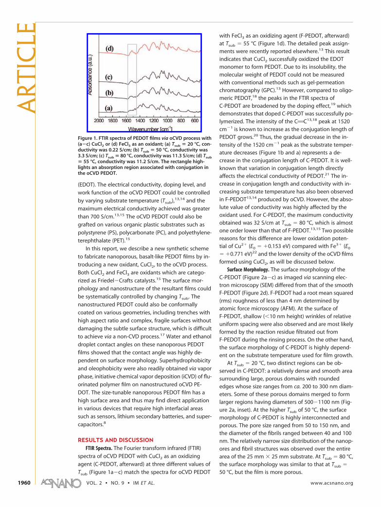
RESULTS AND DISCUSSIONFTIR Spectra. The Fourier transform infrared (FTIR)
spectra of oCVD PEDOT with CuCl2 as an oxidizing
agent (C-PEDOT, afterward) at three different values of
Tsub (Figure 1a�c) match the spectra for oCVD PEDOT
with FeCl3 as an oxidizing agent (F-PEDOT, afterward)at Tsub � 55 °C (Figure 1d). The detailed peak assign-ments were recently reported elsewhere.13 This resultindicates that CuCl2 successfully oxidized the EDOTmonomer to form PEDOT. Due to its insolubility, themolecular weight of PEDOT could not be measuredwith conventional methods such as gel-permeationchromatography (GPC).13 However, compared to oligo-meric PEDOT,18 the peaks in the FTIR spectra ofC-PEDOT are broadened by the doping effect,19 whichdemonstrates that doped C-PEDOT was successfully po-lymerized. The intensity of the CAC13,18 peak at 1520cm�1 is known to increase as the conjugation length ofPEDOT grows.20 Thus, the gradual decrease in the in-tensity of the 1520 cm�1 peak as the substrate temper-ature decreases (Figure 1b and a) represents a de-crease in the conjugation length of C-PEDOT. It is well-known that variation in conjugation length directlyaffects the electrical conductivity of PEDOT.21 The in-crease in conjugation length and conductivity with in-creasing substrate temperature has also been observedin F-PEDOT13,14 produced by oCVD. However, the abso-lute value of conductivity was highly affected by theoxidant used. For C-PEDOT, the maximum conductivityobtained was 32 S/cm at Tsub � 80 °C, which is almostone order lower than that of F-PEDOT.13,15 Two possiblereasons for this difference are lower oxidation poten-tial of Cu2� (E0 � �0.153 eV) compared with Fe3� (E0
� �0.771 eV)22 and the lower density of the oCVD filmsformed using CuCl2, as will be discussed below.
Surface Morphology. The surface morphology of theC-PEDOT (Figure 2a�c) as imaged via scanning elec-tron microscopy (SEM) differed from that of the smoothF-PEDOT (Figure 2d). F-PEDOT had a root mean squared(rms) roughness of less than 4 nm determined byatomic force microscopy (AFM). At the surface ofF-PEDOT, shallow (�10 nm height) wrinkles of relativeuniform spacing were also observed and are most likelyformed by the reaction residue filtrated out fromF-PEDOT during the rinsing process. On the other hand,the surface morphology of C-PEDOT is highly depend-ent on the substrate temperature used for film growth.
At Tsub � 20 °C, two distinct regions can be ob-served in C-PEDOT: a relatively dense and smooth areasurrounding large, porous domains with roundededges whose size ranges from ca. 200 to 300 nm diam-eters. Some of these porous domains merged to formlarger regions having diameters of 500�1100 nm (Fig-ure 2a, inset). At the higher Tsub of 50 °C, the surfacemorphology of C-PEDOT is highly interconnected andporous. The pore size ranged from 50 to 150 nm, andthe diameter of the fibrils ranged between 40 and 100nm. The relatively narrow size distribution of the nanop-ores and fibril structures was observed over the entirearea of the 25 mm � 25 mm substrate. At Tsub � 80 °C,the surface morphology was similar to that at Tsub �
50 °C, but the film is more porous.
Figure 1. FTIR spectra of PEDOT films via oCVD process with(a�c) CuCl2 or (d) FeCl3 as an oxidant; (a) Tsub � 20 °C, con-ductivity was 0.22 S/cm; (b) Tsub � 50 °C, conductivity was3.3 S/cm; (c) Tsub � 80 °C, conductivity was 11.3 S/cm; (d) Tsub
� 55 °C, conductivity was 11.2 S/cm. The rectangle high-lights an absorption region associated with conjugation inthe oCVD PEDOT.
ART
ICLE
VOL. 2 ▪ NO. 9 ▪ IM ET AL. www.acsnano.org1960
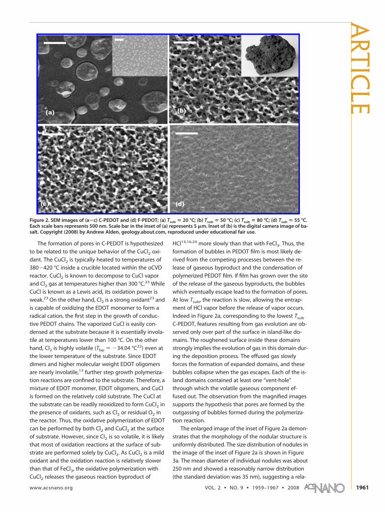
The formation of pores in C-PEDOT is hypothesized
to be related to the unique behavior of the CuCl2 oxi-
dant. The CuCl2 is typically heated to temperatures of
380�420 °C inside a crucible located within the oCVD
reactor. CuCl2 is known to decompose to CuCl vapor
and Cl2 gas at temperatures higher than 300 °C.23 While
CuCl is known as a Lewis acid, its oxidation power is
weak.23 On the other hand, Cl2 is a strong oxidant23 and
is capable of oxidizing the EDOT monomer to form a
radical cation, the first step in the growth of conduc-
tive PEDOT chains. The vaporized CuCl is easily con-
densed at the substrate because it is essentially invola-
tile at temperatures lower than 100 °C. On the other
hand, Cl2 is highly volatile (Tbp � �34.04 °C22) even at
the lower temperature of the substrate. Since EDOT
dimers and higher molecular weight EDOT oligomers
are nearly involatile,13 further step growth polymeriza-
tion reactions are confined to the substrate. Therefore, a
mixture of EDOT monomer, EDOT oligomers, and CuCl
is formed on the relatively cold substrate. The CuCl at
the substrate can be readily reoxidized to form CuCl2 in
the presence of oxidants, such as Cl2 or residual O2 in
the reactor. Thus, the oxidative polymerization of EDOT
can be performed by both Cl2 and CuCl2 at the surface
of substrate. However, since Cl2 is so volatile, it is likely
that most of oxidation reactions at the surface of sub-
strate are performed solely by CuCl2. As CuCl2 is a mild
oxidant and the oxidation reaction is relatively slower
than that of FeCl3, the oxidative polymerization with
CuCl2 releases the gaseous reaction byproduct of
HCl13,16,24 more slowly than that with FeCl3. Thus, the
formation of bubbles in PEDOT film is most likely de-
rived from the competing processes between the re-
lease of gaseous byproduct and the condensation of
polymerized PEDOT film. If film has grown over the site
of the release of the gaseous byproducts, the bubbles
which eventually escape lead to the formation of pores.
At low Tsub, the reaction is slow, allowing the entrap-
ment of HCl vapor before the release of vapor occurs.
Indeed in Figure 2a, corresponding to the lowest Tsub
C-PEDOT, features resulting from gas evolution are ob-
served only over part of the surface in island-like do-
mains. The roughened surface inside these domains
strongly implies the evolution of gas in this domain dur-
ing the deposition process. The effused gas slowly
forces the formation of expanded domains, and these
bubbles collapse when the gas escapes. Each of the is-
land domains contained at least one “vent-hole”
through which the volatile gaseous component ef-
fused out. The observation from the magnified images
supports the hypothesis that pores are formed by the
outgassing of bubbles formed during the polymeriza-
tion reaction.
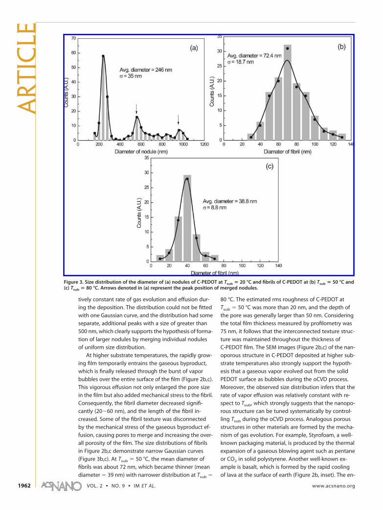
The enlarged image of the inset of Figure 2a demon-
strates that the morphology of the nodular structure is
uniformly distributed. The size distribution of nodules in
the image of the inset of Figure 2a is shown in Figure
3a. The mean diameter of individual nodules was about
250 nm and showed a reasonably narrow distribution
(the standard deviation was 35 nm), suggesting a rela-
Figure 2. SEM images of (a�c) C-PEDOT and (d) F-PEDOT; (a) Tsub � 20 °C; (b) Tsub � 50 °C; (c) Tsub � 80 °C; (d) Tsub � 55 °C.Each scale bars represents 500 nm. Scale bar in the inset of (a) represents 5 �m. Inset of (b) is the digital camera image of ba-salt. Copyright (2008) by Andrew Alden, geology.about.com, reproduced under educational fair use.
ARTIC
LE
www.acsnano.org VOL. 2 ▪ NO. 9 ▪ 1959–1967 ▪ 2008 1961
tively constant rate of gas evolution and effusion dur-
ing the deposition. The distribution could not be fitted
with one Gaussian curve, and the distribution had some
separate, additional peaks with a size of greater than
500 nm, which clearly supports the hypothesis of forma-
tion of larger nodules by merging individual nodules
of uniform size distribution.
At higher substrate temperatures, the rapidly grow-
ing film temporarily entrains the gaseous byproduct,
which is finally released through the burst of vapor
bubbles over the entire surface of the film (Figure 2b,c).
This vigorous effusion not only enlarged the pore size
in the film but also added mechanical stress to the fibril.
Consequently, the fibril diameter decreased signifi-
cantly (20�60 nm), and the length of the fibril in-
creased. Some of the fibril texture was disconnected
by the mechanical stress of the gaseous byproduct ef-
fusion, causing pores to merge and increasing the over-
all porosity of the film. The size distributions of fibrils
in Figure 2b,c demonstrate narrow Gaussian curves
(Figure 3b,c). At Tsub � 50 °C, the mean diameter of
fibrils was about 72 nm, which became thinner (mean
diameter � 39 nm) with narrower distribution at Tsub �
80 °C. The estimated rms roughness of C-PEDOT at
Tsub � 50 °C was more than 20 nm, and the depth of
the pore was generally larger than 50 nm. Considering
the total film thickness measured by profilometry was
75 nm, it follows that the interconnected texture struc-
ture was maintained throughout the thickness of
C-PEDOT film. The SEM images (Figure 2b,c) of the nan-
oporous structure in C-PEDOT deposited at higher sub-
strate temperatures also strongly support the hypoth-
esis that a gaseous vapor evolved out from the solid
PEDOT surface as bubbles during the oCVD process.
Moreover, the observed size distribution infers that the
rate of vapor effusion was relatively constant with re-
spect to Tsub, which strongly suggests that the nanopo-
rous structure can be tuned systematically by control-
ling Tsub during the oCVD process. Analogous porous
structures in other materials are formed by the mecha-
nism of gas evolution. For example, Styrofoam, a well-
known packaging material, is produced by the thermal
expansion of a gaseous blowing agent such as pentane
or CO2 in solid polystyrene. Another well-known ex-
ample is basalt, which is formed by the rapid cooling
of lava at the surface of earth (Figure 2b, inset). The en-
Figure 3. Size distribution of the diameter of (a) nodules of C-PEDOT at Tsub � 20 °C and fibrils of C-PEDOT at (b) Tsub � 50 °C and(c) Tsub � 80 °C. Arrows denoted in (a) represent the peak position of merged nodules.
ART
ICLE
VOL. 2 ▪ NO. 9 ▪ IM ET AL. www.acsnano.org1962
trapped water or air vapor in solidified lava results inthe characteristic porous structure of basalt, which hasmorphological similarity to the surface structure ofC-PEDOT.
In the case of F-PEDOT, the strong oxidant FeCl3can oxidize EDOT so quickly that the rate of gaseousbyproduct release is much faster than that of condensa-tion of PEDOT film. Therefore, gaseous HCl can easily es-cape at the surface of formed PEDOT, and smoothF-PEDOT is formed by the oCVD process (Figure 2d). Inother words, the nanoporous structure can be formedin the course of competing process of oxidation reac-tion and condensation, and it follows that the slow oxi-dation reaction with CuCl2 plays a critical role in form-ing this basalt-like structure.
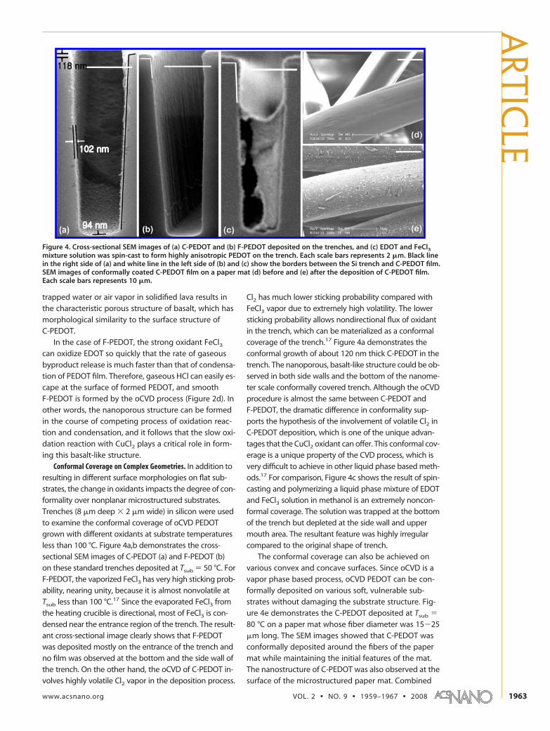
Conformal Coverage on Complex Geometries. In addition toresulting in different surface morphologies on flat sub-strates, the change in oxidants impacts the degree of con-formality over nonplanar microstructured substrates.Trenches (8 �m deep � 2 �m wide) in silicon were usedto examine the conformal coverage of oCVD PEDOTgrown with different oxidants at substrate temperaturesless than 100 °C. Figure 4a,b demonstrates the cross-sectional SEM images of C-PEDOT (a) and F-PEDOT (b)on these standard trenches deposited at Tsub � 50 °C. ForF-PEDOT, the vaporized FeCl3 has very high sticking prob-ability, nearing unity, because it is almost nonvolatile atTsub less than 100 °C.17 Since the evaporated FeCl3 fromthe heating crucible is directional, most of FeCl3 is con-densed near the entrance region of the trench. The result-ant cross-sectional image clearly shows that F-PEDOTwas deposited mostly on the entrance of the trench andno film was observed at the bottom and the side wall ofthe trench. On the other hand, the oCVD of C-PEDOT in-volves highly volatile Cl2 vapor in the deposition process.
Cl2 has much lower sticking probability compared withFeCl3 vapor due to extremely high volatility. The lowersticking probability allows nondirectional flux of oxidantin the trench, which can be materialized as a conformalcoverage of the trench.17 Figure 4a demonstrates theconformal growth of about 120 nm thick C-PEDOT in thetrench. The nanoporous, basalt-like structure could be ob-served in both side walls and the bottom of the nanome-ter scale conformally covered trench. Although the oCVDprocedure is almost the same between C-PEDOT andF-PEDOT, the dramatic difference in conformality sup-ports the hypothesis of the involvement of volatile Cl2 inC-PEDOT deposition, which is one of the unique advan-tages that the CuCl2 oxidant can offer. This conformal cov-erage is a unique property of the CVD process, which isvery difficult to achieve in other liquid phase based meth-ods.17 For comparison, Figure 4c shows the result of spin-casting and polymerizing a liquid phase mixture of EDOTand FeCl3 solution in methanol is an extremely noncon-formal coverage. The solution was trapped at the bottomof the trench but depleted at the side wall and uppermouth area. The resultant feature was highly irregularcompared to the original shape of trench.
The conformal coverage can also be achieved onvarious convex and concave surfaces. Since oCVD is avapor phase based process, oCVD PEDOT can be con-formally deposited on various soft, vulnerable sub-strates without damaging the substrate structure. Fig-ure 4e demonstrates the C-PEDOT deposited at Tsub �
80 °C on a paper mat whose fiber diameter was 15�25�m long. The SEM images showed that C-PEDOT wasconformally deposited around the fibers of the papermat while maintaining the initial features of the mat.The nanostructure of C-PEDOT was also observed at thesurface of the microstructured paper mat. Combined
Figure 4. Cross-sectional SEM images of (a) C-PEDOT and (b) F-PEDOT deposited on the trenches, and (c) EDOT and FeCl3
mixture solution was spin-cast to form highly anisotropic PEDOT on the trench. Each scale bars represents 2 �m. Black linein the right side of (a) and white line in the left side of (b) and (c) show the borders between the Si trench and C-PEDOT film.SEM images of conformally coated C-PEDOT film on a paper mat (d) before and (e) after the deposition of C-PEDOT film.Each scale bars represents 10 �m.
ARTIC
LE
www.acsnano.org VOL. 2 ▪ NO. 9 ▪ 1959–1967 ▪ 2008 1963
with the microstructure offered fromthe paper mat, the nanostructure fromC-PEDOT on the paper mat has a hierar-chical, huge surface area, advantageousfor various applications such as flexibleelectrodes with high surface areas andsupercapacitors.
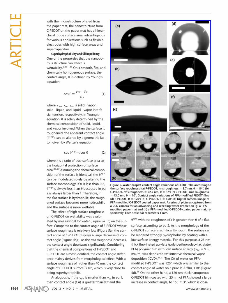
Superhydrophobicity and Oil Repellency.One of the properties that the nanopo-rous structure can affect iswettability.6,25�28 On a smooth, flat, andchemically homogeneous surface, thecontact angle, �, is defined by Young’sequation
cos θ)γSV - γSL
γLV(1)
where �SV, �SL, �LV is solid�vapor,solid�liquid, and liquid�vapor interfa-cial tension, respectively. In Young’sequation, � is solely determined by thechemical composition of solid, liquid,and vapor involved. When the surface isroughened, the apparent contact angle(�app) can be altered by a geometric fac-tor, given by Wenzel’s equation
cos θapp ) rcos θ (2)
where r is a ratio of true surface area tothe horizontal projection of surfacearea.25,27 Assuming the chemical compo-sition of the surface is identical, the �app
can be modulated solely by altering thesurface morphology. If � is less than 90°,�app is always less than � because r in eq2 is always larger than 1. Therefore, ifthe flat surface is hydrophilic, the rough-ened surface becomes more hydrophilicand the surface is more wettable.
The effect of high surface roughnesson C-PEDOT on wettability was evalu-ated by measuring � for water (Figure 5a�c) on the sur-face. Compared to the contact angle of F-PEDOT whosesurface roughness is relatively low (Figure 5a), the con-tact angle of C-PEDOT displays a large decrease of con-tact angle (Figure 5b,c). As the rms roughness increases,the contact angle decreases significantly. Consideringthat the chemical compositions of F-PEDOT andC-PEDOT are almost identical, the contact angle differ-ence mainly derives from morphological effect. With asurface roughness of higher than 40 nm, the contactangle of C-PEDOT surface is 10°, which is very close tobeing superhydrophilic.
Analogously, if the �SV is smaller than �SL in eq 1,then contact angle (CA) is greater than 90° and the
�app with the roughness of r is greater than � of a flat
surface, according to eq 2. As the morphology of the
C-PEDOT surface is significantly rough, the surface can
be rendered strongly hydrophobic by coating with a
low surface energy material. For this purpose, a 25 nm
thick fluorinated acrylate (poly(perfluorodecyl acrylate),
PFA) polymer film with low surface energy (�SV � 9.3
mN/m) was deposited via initiative chemical vapor
deposition (iCVD).26,27 The CA of water on PFA-
modified F-PEDOT was 120°, which was similar to the
contact angle of water on a pure PFA film, 118° (Figure
5d).26 On the other hand, a 120 nm thick nanoporous
C-PEDOT film coated with 25 nm of PFA showed a large
increase in contact angle, to 150 3°, which is close
Figure 5. Water droplet contact angle variations of PEDOT film according tothe surface roughness; (a) F-PEDOT, rms roughness � 3.7 nm, � � 84°; (b)C-PEDOT, rms roughness � 22.7 nm, � � 37°; (c) C-PEDOT, rms roughness� 43.0 nm, � � 10°. Contact angle variations of PFA-modified PEDOT film;(d) F-PEDOT, � � 120°; (b) C-PEDOT, � � 150°. (f) Digital camera image ofPFA-modified C-PEDOT coated paper mat. A series of pictures captured froma CCD camera for an advancing and receding water droplet on (g) a PFA-modified paper mat and (h) a PFA-modified C-PEDOT-coated paper mat, re-spectively. Each scale bar represents 1 mm.
ART
ICLE
VOL. 2 ▪ NO. 9 ▪ IM ET AL. www.acsnano.org1964
to a superhydrophobic surface (Figure 5e).27 Neitherthe surface morphology of the basalt-like structure northe conductivity of the C-PEDOT film was significantlyaltered by subsequent iCVD deposition. Since the iCVDPFA film was conformally covered with both C-PEDOTand F-PEDOT films, the chemical composition of surfaceis practically identical,26 and the increase of contactangle in C-PEDOT is solely due to the nanoporous, tex-tured morphology.
If a surface shows superhydrophobicity (� 150°),the water is believed to form a composite interfacewith the surface texture, termed the Cassie regime.25,27
In the Cassie regime, �app is calculated as the averageof � of the solid and the air, given by
cos θapp )-1 +�s(1 + cos θ) (3)
where �s is the fraction of solid�liquid contact area.25
When the surface texture is so rough that the water can-not penetrate into the valleys of the structure, smallpockets of air become entrapped and the water sits par-tially on air. If the area ratio of the air region over sur-face is close to 1, the composite interface between wa-ter/solid/air becomes practically air-like, which isextremely hydrophobic and exhibits very low hyster-esis. By combining our nanoscale roughness with themicroscale textures of the paper mat, the C-PEDOT sur-face could be made even more hydrophobic. This is ac-tually the technique used by the famous lotus leaf.28
As shown in Figure 4d, the one-step oCVD process caneasily form a hierarchical structure of nanometer scaleroughness of C-PEDOT on the micrometer scale rough-ness of the paper mat.
Although the exact value of �app was difficult to de-termine because the extremely rough surface of the pa-per mat made it difficult to obtain a flat baseline forthe contact angle measurement (Figure 5f), the mea-sured contact angle was higher than 163°. Moreover,the water droplet was not pinned on the C-PEDOTcoated paper mat and showed negligible hysteresis. Aseries of pictures were captured to elucidate the hyster-esis of advancing and receding water droplet on PFA-modified paper mat as a control (termed as control matafterward, Figure 5g) and C-PEDOT-paper mat (termedas sample mat afterward, Figure 5h). The highly mi-croporous control mat resulted in the Cassie state whena water droplet was applied. No increase in the advanc-ing contact angle was observed when the water drop-let was pressed on the mat. However, a decrease in thereceding contact angle was clearly observed when thewater droplet was siphoned from the control mat. Al-though the water sits on the air in the microscale poresbetween fibers, a considerable amount of control matarea was in contact with the water droplet. Hence, inspite of the low surface energy of PFA film, the wet areacan be pinned adhesively with a water droplet, whichpossibly caused the receding angle hysteresis in the
control mat.25 On the other hand, the sample mat has
an enormously tortured surface area in nanometer
scale, compared with the control mat. With this nano-
scale surface curvature, penetration of water into the
microscale is even further reduced, which greatly de-
creases the contact surface area, �s in eq 3. Conse-
quently, adhesive pinning25 is greatly depressed, and
the sequential CCD camera images clearly show no hys-
teresis between advancing and receding angles.
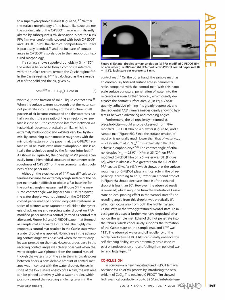
Furthermore, the oil repellencyOtermed as
oleophobicityOcould also be observed from PFA-
modified C-PEDOT film on a Si wafer (Figure 6a) and a
sample mat (Figure 6b). Since the surface tension of
most oil is generally much lower than that of water (�LV
� 71.99 mN/m at 25 °C),22 it is extremely difficult to
achieve oleophobicity.27,28 The contact angle of etha-
nol droplet (�LV � 21.97 mN/m at 25 °C)22 on PFA-
modified C-PEDOT film on a Si wafer was 88° (Figure
6a), which is almost 2-fold greater than the CA of flat
PFA-coated Si wafer (43°), which shows that the surface
roughness of C-PEDOT plays a critical role in the oil re-
pellency. According to eq 2, �app of an ethanol droplet
in Figure 6a should decrease since � of the ethanol
droplet is less than 90°. However, the observed result
is reversed, which might be from the metastable Cassie
state or local pinning effect in the Wenzel state.28 The
receding angle from this droplet was practically 0°,
which can occur also from both the highly hysteric
Cassie state or the strongly textured Wenzel state. To in-
vestigate this aspect further, we have deposited etha-
nol on the sample mat. Ethanol did not penetrate into
the fabrics, which conclusively supports the formation
of the Cassie state on the sample mat, and �app was
113°. The observed water and oil repellency of the
highly conductive PEDOT film can greatly enhance the
self-cleaning ability, which potentially has a wide im-
pact on anticorrosion and antifouling from polluted wa-
ter and fatty liquid.28
CONCLUSIONIn conclusion, a new nanostructured PEDOT film was
obtained via an oCVD process by introducing the new
oxidant of CuCl2. The obtained C-PEDOT film showed
high electrical conductivity up to 32 S/cm. Substrate tem-
Figure 6. Ethanol droplet contact angles on (a) PFA-modified C-PEDOT filmon a Si wafer (� � 88°) and (b) PFA-modified C-PEDOT coated paper mat (�� 113°). Each scale bar represents 1 mm.
ARTIC
LE
www.acsnano.org VOL. 2 ▪ NO. 9 ▪ 1959–1967 ▪ 2008 1965
perature was a critical process parameter in oCVD thatcontrols the conductivity of the C-PEDOT film, as was thesame in F-PEDOT. A basalt-like nanoporous structure wasuniformly obtained from C-PEDOT deposited at Tsub
higher than 50 °C. The pore size and porosity could be sys-tematically tuned by modulating substrate temperature.The C-PEDOT film showed ultimately improved confor-mality on the substrate. Conformal coverage on the stan-dard trench in Si and on the paper fiber mats was clearlyvisible in the SEM images with retention of the complexsurface structure. As an example of the effect of morphol-ogy, the contact angle decreases according to increaseof the surface roughness, and an extremely hydrophilic
surface was successfully obtained. Moreover, on micro-structured substrates, highly conductive and superhydro/oleophobic surfaces, such as nonwettable conducting pa-per, could also be obtained easily by subsequent oCVDand iCVD processes. The regularly nanostructured, hierar-chical nanostructure has great potential for a variety ofapplications. For instance, highly hydrophilic conductivePEDOT film can be used for advanced electrochemical ap-plications, such as biosensors. Achieving a high surfacearea layer on planar substrates and conformal coating ofhigh surface area substrates enable features for devicessuch as supercapacitor and batteries, where high interfa-cial area is desired.
METHODSThe detailed procedure of the oCVD process and the reac-
tor configuration are described in detail elsewhere.13�16 Si wa-fers, quartz plates, and paper were used as substrates for theoCVD of PEDOT. To monitor conformality, PEDOT was depos-ited on trenches with various aspect ratios patterned on a Si wa-fer, which were supplied from Analog Devices. Process pressurewas maintained between 50 and 100 mTorr, and the flow rate ofevaporated EDOT monomer was metered through a mass flowcontroller at 5 sccm. The substrate temperature was varied be-tween 20 and 100 °C by a PID controller. The oxidizing agent wasevaporated from a resistively heated crucible. For C-PEDOT films,the oxidizing agent was CuCl2 and was evaporated at a temper-ature greater than 380 °C. For F-PEDOT films, the oxidizing agentwas FeCl3 and was evaporated at 300 °C.
The total deposition time was 60 min. The thickness of PE-DOT was controlled by the loading amount of CuCl2 and thedeposition time. After deposition, the film was rinsed withmethanol for about 30 min to remove any residual oxidizingagent and EDOT monomer.
The iCVD process was also described in detail elsewhere.27
Perfluorodecyl acrylate monomer and tert-butyl peroxide initia-tor were vaporized at room temperature and introduced into theiCVD chamber at flow rates of approximately 0.3 and 1.3 sccm,respectively. The polymerization reaction was initiated by heat-ing a filament array to 280 °C. The process pressure was con-trolled at 100 mTorr by a throttling butterfly valve. Film thick-nesses were monitored in situ by interferometry; approximately25 nm of the PFA film was deposited in 10 min.
PEDOT film thickness was measured with a profilometer(Tencor, P-10), and the sheet resistance was measured with afour-point probe (MWP-6, Jandel Engineering Ltd.). The conduc-tivity was calculated from the sheet resistance and measuredthickness. FTIR spectra were collected on a Nexus 870, ThermoElectron Corporation. The surface morphology of PEDOT film wasimaged by both SEM (FEI/Philips XL30 FEG ESEM) and AFM (Di-mension 3100, Digital Instruments, Ltd.). The sampling size ofroughness of PEDOT film was fixed at 2 � 2 �m2. The static con-tact angle was measured within 30 s after placing 2�4 �L ofdeionized water and ethanol droplets on the substrates(VCA2000, AST Inc.).
All chemicals were purchased from Aldrich and used with-out any further purification.
Acknowledgment. This research was supported by the U.S.Army through the Institute for Soldier Nanotechnologies, underContract DAAD-19-02-D-0002 with the U.S. Army Research Of-fice. The authors thank Edward F. Gleason in Analog Devices forthe supply of trench wafers.
REFERENCES AND NOTES1. Murray, C. B.; Kagan, C. R.; Bawendi, M. G. Synthesis and
Characterization of Monodisperse Nanocrystals and Close-
Packed Nanocrystal Assemblies. Annu. Rev. Mater. Sci.2000, 30, 545–610.
2. Park, J.; An, K. J.; Hwang, Y. S.; Park, J. G.; Noh, H. J.; Kim,J. Y.; Park, J. H.; Hwang, N. M.; Hyeon, T. Ultra-Large-ScaleSyntheses of Monodisperse Nanocrystals. Nat. Mater.2004, 3, 891–895.
3. Langer, R.; Peppas, N. A. Advances in Biomaterials, DrugDelivery, and Bionanotechnology. AlChE J. 2003, 49, 2990–3006.
4. Sarikaya, M.; Tamerler, C.; Jen, A. K. Y.; Schulten, K.; Baneyx,F. Molecular Biomimetics: Nanotechnology throughBiology. Nat. Mater. 2003, 2, 577–585.
5. Jang, J. Conducting Polymer Nanomaterials and TheirApplications. Emissive Materials: Nanomaterials 2006, 189–259.
6. Chiou, N. R.; Lui, C. M.; Guan, J. J.; Lee, L. J.; Epstein, A. J.Growth and Alignment of Polyaniline Nanofibres withSuperhydrophobic, Superhydrophilic and OtherProperties. Nat. Nanotechnol. 2007, 2, 354–357.
7. Groenendaal, L.; Zotti, G.; Aubert, P. H.; Waybright, S. M.;Reynolds, J. R. Electrochemistry of Poly(3,4-Alkylenedioxythiophene) Derivatives. Adv. Mater. 2003, 15,855–879.
8. Groenendaal, B. L.; Jonas, F.; Freitag, D.; Pielartzik, H.;Reynolds, J. R. Poly(3,4-Ethylenedioxythiophene) and ItsDerivatives: Past, Present, and Future. Adv. Mater. 2000, 12,481–494.
9. Jang, J.; Chang, M.; Yoon, H. Chemical Sensors Based onHighly Conductive Poly(3,4-Ethylenedioxythiophene)Nanorods. Adv. Mater. 2005, 17, 1616–1620.
10. Sotzing, G. A.; Briglin, S. M.; Grubbs, R. H.; Lewis, N. S.Preparation and Properties of Vapor Detector ArraysFormed from Poly(3,4 Ethylenedioxy)thiophene-poly(styrene sulfonate) Insulating Polymer Composites.Anal. Chem. 2000, 72, 3181–3190.
11. Sirringhaus, H.; Kawase, T.; Friend, R. H.; Shimoda, T.;Inbasekaran, M.; Wu, W.; Woo, E. P. High-Resolution InkjetPrinting of All-Polymer Transistor Circuits. Science 2000,290, 2123–2126.
12. Abidian, M. R.; Kim, D. H.; Martin, D. C. Conducting-Polymer Nanotubes for Controlled Drug Release. Adv.Mater. 2006, 18, 405–409.
13. Im, S. G.; Gleason, K. K. Systematic Control of the ElectricalConductivity of Poly(3,4-Ethylenedioxythiophene) viaOxidative Chemical Vapor Deposition (oCVD).Macromolecules 2007, 40, 6552–6556.
14. Im, S. G.; Olivetti, E. A.; Gleason, K. K. Doping Level andWork Function Control in Oxidative Chemical VaporDeposited Poly(3,4-Ethylenedioxythiophene). Appl. Phys.Lett. 2007, 90, 152112.
15. Im, S. G.; Yoo, P. J.; Hammond, P. T.; Gleason, K. K. GraftedConducting Polymer Films for Nano-Patterning ontoVarious Organic and Inorganic Substrates by Oxidative
ART
ICLE
VOL. 2 ▪ NO. 9 ▪ IM ET AL. www.acsnano.org1966
Chemical Vapor Deposition. Adv. Mater. 2007, 19,2863–2867.
16. Lock, J. P.; Im, S. G.; Gleason, K. K. Oxidative ChemicalVapor Deposition of Electrically Conducting Poly(3,4-Ethylenedioxythiophene) Films. Macromolecules 2006, 39,5326–5329.
17. Gates, S. M. Surface Chemistry in the Chemical VaporDeposition of Electronic Materials. Chem. Rev. 1996, 96,1519–1532.
18. Tran-Van, F.; Garreau, S.; Louarn, G.; Froyer, G.; Chevrot, C.Fully Undoped and SolubleOligo(3,4-Ethylenedioxythiophene)s: Spectroscopic Studyand Electrochemical Characterization. J. Mater. Chem.2001, 11, 1378–1382.
19. Skotheim, T. A.; Elsenbaumer, R. L.; Reynolds, J. R.Handbook of Conducting Polymers; M. Dekker: New York,1998; pp1097�1225.
20. Im, S. G.; Olivetti, E. A.; Gleason, K. K. Systematic Control ofthe Electrical Conductivity of Poly(3,4-Ethylenedioxythiophene) via Oxidative Chemical VaporDeposition (oCVD). Surf. Coat. Technol. 2007, 201,9406–9412.
21. Baughman, R. H.; Shacklette, L. W. Conjugation LengthDependent Transport in Conducting Polymers from aResistor Network Model. J. Chem. Phys. 1989, 90,7492–7504.
22. Lide, D. R. CRC Handbook of Chemistry and Physics; Taylorand Francis Group, LLC: Boca Raton, FL, 2008.
23. Cotton, F. A.; Wilkinson, G. Advanced Inorganic Chemistry: AComprehensive Text; John Wiley and Sons: New York, 1998.
24. Sadki, S.; Schottland, P.; Brodie, N.; Sabouraud, G. TheMechanisms of Pyrrole Electropolymerization. Chem. Soc.Rev. 2000, 29, 283–293.
25. Lafuma, A.; Quere, D. Superhydrophobic States. Nat. Mater.2003, 2, 457–460.
26. Ma, M. L.; Gupta, M.; Li, Z.; Zhai, L.; Gleason, K. K.; Cohen,R. E.; Rubner, M. F.; Rutledge, G. C. Decorated ElectrospunFibers Exhibiting Superhydrophobicity. Adv. Mater. 2007,19, 255–259.
27. Ma, M. L.; Mao, Y.; Gupta, M.; Gleason, K. K.; Rutledge, G. C.Superhydrophobic Fabrics Produced by Electrospinningand Chemical Vapor Deposition. Macromolecules 2005, 38,9742–9748.
28. Tuteja, A.; Choi, W.; Ma, M. L.; Mabry, J. M.; Mazzella, S. A.;Rutledge, G. C.; McKinley, G. H.; Cohen, R. E. DesigningSuperoleophobic Surfaces. Science 2007, 318, 1618–1622.
ARTIC
LE
www.acsnano.org VOL. 2 ▪ NO. 9 ▪ 1959–1967 ▪ 2008 1967