
Conductive Trace Design in 3-D Circuit Architectures
170
CONDUCTIVE TRACE DESIGN IN 3-D CIRCUIT ARCHITECTURES: HEAT TRANSFER ANALYSIS AND EXPERIMENTS by Michael R. Guido B.S., Carnegie-Mellon University, 1976 M.Eng., Carnegie-Mellon University, 1981 Submitted to the Graduate Faculty of the School of Engineering in partial fulfillment of the requirements for the degree of Doctor of Philosophy University of Pittsburgh 2005
-
Upload
khangminh22 -
Category
Documents
-
view
4 -
download
0
Transcript of Conductive Trace Design in 3-D Circuit Architectures

CONDUCTIVE TRACE DESIGN IN 3-D CIRCUIT
ARCHITECTURES: HEAT TRANSFER ANALYSIS AND
EXPERIMENTS
by
Michael R. Guido
B.S., Carnegie-Mellon University, 1976
M.Eng., Carnegie-Mellon University, 1981
Submitted to the Graduate Faculty of
the School of Engineering in partial fulfillment
of the requirements for the degree of
Doctor of Philosophy
University of Pittsburgh
2005

UNIVERSITY OF PITTSBURGH
SCHOOL OF ENGINEERING
This dissertation was presented
by
Michael R. Guido
It was defended on
November 29, 2005
and approved by
Laura A. Schaefer, Ph. D., Assistant Professor, Mechanical Engineering
Michael A. Lovell, Ph. D., Associate Dean of Research, School of Engineering
Marlin H. Mickle, Ph. D., Nickolas A. DeCecco Professor, Electrical Engineering
Roy D. Marangoni, Ph. D., Associate Professor, Mechanical Engineering
Dissertation Director: Laura A. Schaefer, Ph. D., Assistant Professor, Mechanical Engineering
ii

ABSTRACT
CONDUCTIVE TRACE DESIGN IN 3-D CIRCUIT ARCHITECTURES: HEAT
TRANSFER ANALYSIS AND EXPERIMENTS
Michael R. Guido, PhD
University of Pittsburgh, 2005
Recent research efforts have been devoted to developing technologies for fabricating electronic
circuits in three dimensions using ink-jet processes. The management of generated heat in such
circuits is expected to be a critically important issue in their operation, which will require them to
incorporate specialized design features for promoting the removal of unwanted heat from key areas
and the limiting of component temperatures to safe levels. Hence, effective tools for predicting the
heat transfer characteristics of three-dimensional circuits are required in order to develop optimum
designs for such circuitry.
This research encompasses a course of investigation including the development of such design
tools and their verification using experimental methods. These experimental methods consisted of
thermal tests conducted with a variety of prototype circuits constructed in three dimensions, with
materials appropriate to the overarching design concept.
After the verification process, the investigation proceeded with the construction of numerical
models intended to comparatively assess the effectiveness of a range of design features proposed
for application in the design concept. These features included specialized extensions to the con-
ductive traces expected to enhance passive heat rejection, and thereby to limit the observed tem-
perature rise in the discrete resistive component. The relative impact of each of these structures is
comparatively evaluated using the developed tools. It is observed that the presence of these spe-
cialized structures do act to limit the observed temperature rise. However, the specifics of the basic
conductive trace design, namely the choice of material and the thickness of the trace, have by far
iii

the greater effect on the heat rejection from the discrete resistor and hence a much larger impact
on the peak temperature rise.
Further research centered on the fabrication and testing of a circuit which more fully incor-
porated the 3-D architecture by employing a surface-mount technology (SMT) resistor and by
embedding the resistor and conductive components within a cast polymer matrix. Experiments
with this circuit and corresponding finite-element models showed that for the power dissipation
levels investigated, the presence of the embedding medium actually results in lower temperatures
at the resistive component.
It was also shown that, in terms of convection modeling, film coefficients calculated by stan-
dard methods do not effectively account for interactions between adjacent convection surfaces of
these circuit architectures, giving numerical temperature results which correlated poorly with live
test data. It was further shown that a numerical model featuring thermal/fluid dynamics capability
and simplified geometry compared to the actual circuit can give resistor temperature results which
compare very well to the live tests. Taking the thermal/fluid model results as a data source, im-
proved values for the film coefficients can be calculated and applied to models not featuring fluid
capability. The models with improved film coefficients similarly provided resistor temperature
values which correlated well with the live test results.
iv

TABLE OF CONTENTS
1.0 BACKGROUND . . . . . . . . . . . . . . . . . . . . . . . . . . . . . . . . . . . . . 1
1.1 Energy Management in Electronic Circuitry. . . . . . . . . . . . . . . . . . . . 1
1.2 Heat Transfer Issues and Morphology of Electronic Circuitry. . . . . . . . . . . 3
1.2.1 Introduction . . . . . . . . . . . . . . . . . . . . . . . . . . . . . . . . . 3
1.2.2 2 1/2-D Circuit configurations. . . . . . . . . . . . . . . . . . . . . . . . 3
1.2.3 Discrete Integrated Circuits. . . . . . . . . . . . . . . . . . . . . . . . . 4
1.2.4 Hybrid Circuits . . . . . . . . . . . . . . . . . . . . . . . . . . . . . . . 4
1.3 Related Research in Electronics Packaging and Materials. . . . . . . . . . . . . 5
1.3.1 Electronic Packaging Strategies. . . . . . . . . . . . . . . . . . . . . . . 5
1.3.2 Single-Component and Composite Electronic Materials. . . . . . . . . . 5
2.0 OBJECTIVES OF THE RESEARCH . . . . . . . . . . . . . . . . . . . . . . . . . 10
2.1 Organization of this Dissertation. . . . . . . . . . . . . . . . . . . . . . . . . . 10
2.2 Fields of study relevant to the investigation. . . . . . . . . . . . . . . . . . . . 11
3.0 RELEVANT ASPECTS OF HEAT TRANSFER . . . . . . . . . . . . . . . . . . . 12
3.1 Principles of conduction heat transfer. . . . . . . . . . . . . . . . . . . . . . . 12
3.2 Principles of convection heat transfer. . . . . . . . . . . . . . . . . . . . . . . 14
3.2.1 Practical issues in modeling convection behavior. . . . . . . . . . . . . . 18
3.3 Principles of radiation heat transfer. . . . . . . . . . . . . . . . . . . . . . . . 19
4.0 THE PRELIMINARY VERIFICATION MODEL . . . . . . . . . . . . . . . . . . 23
4.1 Developing Tools for Evaluating Effectiveness of Heat Management Features. . 23
4.2 The 3-D Circuit: A Preliminary Live Test Model. . . . . . . . . . . . . . . . . 24
4.3 The sample test setup. . . . . . . . . . . . . . . . . . . . . . . . . . . . . . . .27
v

4.4 Results from live testing. . . . . . . . . . . . . . . . . . . . . . . . . . . . . .29
4.4.1 Results from the test sequence. . . . . . . . . . . . . . . . . . . . . . . . 29
4.4.2 Data reduction. . . . . . . . . . . . . . . . . . . . . . . . . . . . . . . .30
5.0 FEA OF THE PRELIMINARY CIRCUIT MODEL . . . . . . . . . . . . . . . . . 40
5.1 Finite element types and model geometry. . . . . . . . . . . . . . . . . . . . . 40
5.2 Considerations in selecting a commercial FEA package. . . . . . . . . . . . . . 42
5.3 Specific modeling parameters. . . . . . . . . . . . . . . . . . . . . . . . . . . 43
5.3.1 Physics environment and analysis type. . . . . . . . . . . . . . . . . . . 43
5.3.2 Material properties. . . . . . . . . . . . . . . . . . . . . . . . . . . . . .43
5.3.2.1 Conductive ink data. . . . . . . . . . . . . . . . . . . . . . . . . 45
5.3.2.2 Conductive epoxy data. . . . . . . . . . . . . . . . . . . . . . . 45
5.3.2.3 Experimentally determined material data. . . . . . . . . . . . . . 46
5.4 Boundary conditions. . . . . . . . . . . . . . . . . . . . . . . . . . . . . . . .46
5.4.1 A simplified model for assessing boundary conditions. . . . . . . . . . . 47
5.4.2 Applying convection to the finite-element model. . . . . . . . . . . . . . 50
5.5 Construction of the preliminary FEA model. . . . . . . . . . . . . . . . . . . . 50
5.5.1 Simplifying assumptions. . . . . . . . . . . . . . . . . . . . . . . . . . . 50
5.5.1.1 Resistor modeling. . . . . . . . . . . . . . . . . . . . . . . . . . 51
5.5.2 Results from the preliminary FEA model. . . . . . . . . . . . . . . . . . 52
5.6 The revised verification model. . . . . . . . . . . . . . . . . . . . . . . . . . . 53
6.0 PROPOSED METHODS FOR PROMOTING WASTE HEAT REMOVAL . . . . 66
6.1 Previous research. . . . . . . . . . . . . . . . . . . . . . . . . . . . . . . . . .66
6.2 Broad principles . . . . . . . . . . . . . . . . . . . . . . . . . . . . . . . . . .67
6.3 The general heat rejection problem for passive cooling methods. . . . . . . . . 67
6.4 Candidate methods for enhancing passive heat removal. . . . . . . . . . . . . . 68
7.0 EVALUATION OF PASSIVE HEAT REMOVAL FEATURES BY PARAMET-
RIC STUDY . . . . . . . . . . . . . . . . . . . . . . . . . . . . . . . . . . . . . . .70
7.1 Fixed parameters for the study. . . . . . . . . . . . . . . . . . . . . . . . . . . 70
7.2 Design parameters to be varied. . . . . . . . . . . . . . . . . . . . . . . . . . . 71
7.3 Results . . . . . . . . . . . . . . . . . . . . . . . . . . . . . . . . . . . . . . .71
vi

7.4 Statistical analysis. . . . . . . . . . . . . . . . . . . . . . . . . . . . . . . . .77
8.0 THE SURFACE-MOUNT DEVICE CIRCUIT MODEL . . . . . . . . . . . . . . 81
8.1 Features of the Fully-Embedded Circuit. . . . . . . . . . . . . . . . . . . . . . 81
8.2 Testing with the SMT model prior to embedding. . . . . . . . . . . . . . . . . 83
8.3 Completing the Embedded SMT Specimen. . . . . . . . . . . . . . . . . . . . 85
8.4 Test results from the embedded circuit sample. . . . . . . . . . . . . . . . . . . 87
9.0 FEA OF THE SMT VERIFICATION MODEL . . . . . . . . . . . . . . . . . . . 90
9.1 Construction of the numerical SMT circuit models. . . . . . . . . . . . . . . . 90
9.1.1 The non-embedded model. . . . . . . . . . . . . . . . . . . . . . . . . . 93
9.1.2 The embedded model. . . . . . . . . . . . . . . . . . . . . . . . . . . .98
9.2 Results from the basic numerical models. . . . . . . . . . . . . . . . . . . . .100
9.2.1 The non-embedded model. . . . . . . . . . . . . . . . . . . . . . . . . .100
9.2.1.1 Comparison with live test results. . . . . . . . . . . . . . . . . .103
9.2.1.2 Thermal contact resistance modeling. . . . . . . . . . . . . . . .104
9.2.1.3 Enhancement of convection modeling by numerical adjustment of
film coefficients . . . . . . . . . . . . . . . . . . . . . . . . . . .107
9.2.2 The embedded model. . . . . . . . . . . . . . . . . . . . . . . . . . . .118
9.2.2.1 Comparison with live test results. . . . . . . . . . . . . . . . . .118
10.0 CONCLUSIONS . . . . . . . . . . . . . . . . . . . . . . . . . . . . . . . . . . . .134
10.1 Implications of the Research. . . . . . . . . . . . . . . . . . . . . . . . . . . .135
10.2 Future Research. . . . . . . . . . . . . . . . . . . . . . . . . . . . . . . . . .136
APPENDIX. MACRO CODE FOR FILM COEFFICIENT ADJUSTMENT, UPPER
SUBSTRATE SURFACE . . . . . . . . . . . . . . . . . . . . . . . . . . . . . . . .138
BIBLIOGRAPHY . . . . . . . . . . . . . . . . . . . . . . . . . . . . . . . . . . . . . . .147
vii

LIST OF TABLES
1 Live test results from verification test sequence at 5V applied;τ = 2000s except as
noted.. . . . . . . . . . . . . . . . . . . . . . . . . . . . . . . . . . . . . . . . . .37
2 Live test results from verification test sequence at 10V applied;τ = 2000s. . . . . . 38
3 Reduced temperature rise data from verification test sequence.. . . . . . . . . . . . 38
4 Material properties used in the finite-element model.. . . . . . . . . . . . . . . . . 44
5 Element types used in the verification model.. . . . . . . . . . . . . . . . . . . . . 55
6 FEA sequence results from verification study at 5V and 10V applied.. . . . . . . . 58
7 Reduced temperature rise data from verification FEA sequence.. . . . . . . . . . . 58
8 Element types used in the revised model.. . . . . . . . . . . . . . . . . . . . . . . 61
9 FEA sequence results from new verification model at 5V and 10V applied.. . . . . 63
10 Reduced temperature rise data from revised FEA sequence.. . . . . . . . . . . . . 63
11 Element types used in the parametric model.. . . . . . . . . . . . . . . . . . . . . 71
12 Experimental Design and results.. . . . . . . . . . . . . . . . . . . . . . . . . . . 74
13 Processing of conductive ink traces for minimum resistance in SMT circuit model.. 82
14 Raw results from tests of SMT sample before embedding.. . . . . . . . . . . . . . 84
15 Temperature delta results from SMT sample tests before embedding.. . . . . . . . 85
16 Raw temperature data from embedded SMT sample tests.. . . . . . . . . . . . . . 87
17 Temperature delta results from SMT embedded sample tests.. . . . . . . . . . . . . 87
18 Additional material properties used in the SMT FEA models.. . . . . . . . . . . . 91
19 Element types used in the SMT model without embedding.. . . . . . . . . . . . . . 96
20 Element types used in the embedded SMT model.. . . . . . . . . . . . . . . . . . 99
21 Raw results from FEA of SMT circuit before embedding.. . . . . . . . . . . . . .100
viii

22 Temperature delta results from FEA of SMT circuit before embedding.. . . . . . . 100
23 Temperature delta results from the FEA of the SMT circuit before embedding with
contact resistance included.. . . . . . . . . . . . . . . . . . . . . . . . . . . . . .105
24 Element types used in the numerical convection model.. . . . . . . . . . . . . . .110
25 Numerical convection model, maximum resistor surface temperatures vs. applied
power. . . . . . . . . . . . . . . . . . . . . . . . . . . . . . . . . . . . . . . . . .114
26 Temperature and heat flux data from typical numerical convection FEA, with cal-
culatedhconv values. . . . . . . . . . . . . . . . . . . . . . . . . . . . . . . . . . .119
27 Temperature delta results from non-embedded SMT sample FEA with first-order
correction to film coefficients.. . . . . . . . . . . . . . . . . . . . . . . . . . . . .125
28 Temperature delta results from FEA of non-embedded SMT circuit with contoured
hconv adjustment.. . . . . . . . . . . . . . . . . . . . . . . . . . . . . . . . . . . .129
29 Raw results from FEA of SMT circuit with embedding.. . . . . . . . . . . . . . .131
30 Temperature delta results from FEA of SMT circuit with embedding.. . . . . . . . 132
ix

LIST OF FIGURES
1 Microphotograph of a miniature RFID tag.. . . . . . . . . . . . . . . . . . . . . . 2
2 Typical electronic hardware built according to 2 1/2-D principles.. . . . . . . . . . 8
3 Microphotograph of integrated circuit (IC) and typical IC packaging.. . . . . . . . 9
4 Typical printed-circuit board conductive traces.. . . . . . . . . . . . . . . . . . . . 9
5 Orthotropic conduction in Cartesian coordinates.. . . . . . . . . . . . . . . . . . . 13
6 Typicalhconv curves for heated upward-facing horizontal surfaces, @T∞ = 25.5C. . 17
7 Typicalhconv curve for heated downward-facing horizontal surface, @T∞ = 25.5C. 20
8 Typicalhconv curve for heated vertical surfaces, @T∞ = 25.5C. . . . . . . . . . . . 21
9 Typicalhconv curves for heated horizontal cylinders, @T∞ = 25.5C. . . . . . . . . 22
10 Aluminum guide for cutting conductive ink stencil.. . . . . . . . . . . . . . . . . . 25
11 Representative height scan for conductive ink trace.. . . . . . . . . . . . . . . . . 31
12 Comparison of calculated vs. measured trace resistances.. . . . . . . . . . . . . . . 32
13 Typical live test circuit fabricated on epoxy/glass substrate.. . . . . . . . . . . . . 33
14 Live test circuit sample, with power connections and thermocouples attached.. . . . 34
15 Microphotograph of a typical microthermocouple bead.. . . . . . . . . . . . . . . 35
16 Test enclosure for the heat dissipation experiments.. . . . . . . . . . . . . . . . . . 36
17 Time-temperature data for a typical live circuit test.. . . . . . . . . . . . . . . . . 37
18 Resistor temperature plotted as a function of resistor power for verification test
sequence.. . . . . . . . . . . . . . . . . . . . . . . . . . . . . . . . . . . . . . . .39
19 Schematics of typical 1-D, 2-D, and 3-D finite elements.. . . . . . . . . . . . . . . 41
20 Lumped model for comparing heat transfer modes.. . . . . . . . . . . . . . . . . . 47
x

21 Lumped model results, with and without radiation included, plotted with live test
data. . . . . . . . . . . . . . . . . . . . . . . . . . . . . . . . . . . . . . . . . . .55
22 Finite-element mesh for the numerical verification model, including detail of resis-
tor region. . . . . . . . . . . . . . . . . . . . . . . . . . . . . . . . . . . . . . . .56
23 Temperature contour data from the FEA model.. . . . . . . . . . . . . . . . . . . . 57
24 Linear regression of FEA results, plotted against live test data.. . . . . . . . . . . . 59
25 Detail of resistor region in revised FEA model.. . . . . . . . . . . . . . . . . . . . 60
26 Temperature contours from revised model.. . . . . . . . . . . . . . . . . . . . . . 62
27 Linear regression of revised model results, plotted against live test data.. . . . . . . 64
28 Time-dependent FEA data plotted with time vs. temperature data from correspond-
ing test. . . . . . . . . . . . . . . . . . . . . . . . . . . . . . . . . . . . . . . . . .65
29 Finite-element mesh of typical design combination for the numerical study.. . . . . 73
30 Resistor temperature rise vs. trace thickness, direct fin placement only.. . . . . . . 75
31 Combined plot of temperature rise data vs. Thermal Sheet Resistance.. . . . . . . . 76
32 Main Effects plot for resistor temperature rise data.. . . . . . . . . . . . . . . . . . 77
33 Main Effects plot, resistor data from copper trace runs only.. . . . . . . . . . . . . 78
34 Main Effects plot, resistor data from conductive ink trace runs only.. . . . . . . . . 78
35 3-D Surface plot, resistor data from direct fin placement runs only.. . . . . . . . . 80
36 SMT circuit model prior to embedding, in live test setup.. . . . . . . . . . . . . . . 83
37 SMT circuit model embedded in epoxy resin.. . . . . . . . . . . . . . . . . . . . . 86
38 Temperature delta measurements vs. voltage applied, before and after embedding.. 89
39 Structure of modeled discrete SMT resistor, viewed from underside.. . . . . . . . . 92
40 Complete FEA mesh for non-embedded SMT circuit model.. . . . . . . . . . . . . 93
41 Detail of FEA mesh for connecting pads.. . . . . . . . . . . . . . . . . . . . . . . 94
42 Detail of FEA mesh for SMT resistor region.. . . . . . . . . . . . . . . . . . . . . 95
43 Typical temperature contour plot of resistor region of SMT model without embedding.101
44 SMT model before embedding, correlation of live test data with FEA results.. . . . 102
45 SMT model before embedding, contact resistance included, correlation with live
test data. . . . . . . . . . . . . . . . . . . . . . . . . . . . . . . . . . . . . . . . .106
46 Axisymmetric analysis region for the FLOTRANTM convection model.. . . . . . . 108
xi

47 Half-symmetry model of the substrate and resistor volumes for the convection anal-
ysis.. . . . . . . . . . . . . . . . . . . . . . . . . . . . . . . . . . . . . . . . . . .109
48 Finite-element mesh for the numerical convection model.. . . . . . . . . . . . . .111
49 Typical temperature contours, solid region of numerical convection model.. . . . . 112
50 Typical temperature contours, fluid region of numerical convection model.. . . . . 113
51 Resistor temperature rise vs. power dissipated, live tests and numerical convection
model. . . . . . . . . . . . . . . . . . . . . . . . . . . . . . . . . . . . . . . . . .115
52 Nusselt number variation in numerical convection model, resistor top surface.. . . . 120
53 Nusselt number variation in numerical convection model, substrate top surface.. . . 121
54 Nusselt number variation in numerical convection model, substrate bottom surface.. 122
55 Nusselt number variation in numerical convection model, substrate outer edge surface.123
56 Nusselt number variation in numerical convection model, resistor and epoxy outer
edge surface.. . . . . . . . . . . . . . . . . . . . . . . . . . . . . . . . . . . . . .124
57 SMT model before embedding, first-orderhconvcorrection, correlation with live test
data. . . . . . . . . . . . . . . . . . . . . . . . . . . . . . . . . . . . . . . . . . .126
58 Fitted curve for film coefficient variation on upper substrate surface.. . . . . . . . . 127
59 Adjustedhconv contours on upper substrate surface.. . . . . . . . . . . . . . . . . .128
60 Correlation of FEA results with live test data, model with contouredhconvadjustment.130
61 Typical temperature contour plot of resistor region of embedded SMT model.. . . . 132
62 SMT model with embedding, correlation of live test data with FEA results.. . . . . 133
xii

NOMENCLATURE
Constants
α Thermal diffusivity, m2/s
β Coefficient of thermal expansion, K−1
C Heat capacity, J/(kg·K)
ε emissivity of a surface
g Gravitational acceleration, 9.81m/s2
γ Mass density, kg/m3
h Convection heat-transfer coefficient, or film coefficient, W/(m2·K)
k Conduction heat-transfer coefficient, W/(m·K)
µ Dynamic viscosity, N·s/m2
ν Kinematic viscosity, m2/s
ρ Bulk electrical resistivity, Ω·m
σ Stefan-Boltzmann constant, 5.670×10⁻⁸ W/(m2 ·K4)
Variables
A Area of exposed surface, or cross-sectional area, m2
χ Normalized distance from starting edge of convection surface
Fi j Radiation form factor for surfacei relative to surfacej
L Characteristic length for convection surface, or length of conductive path, m
m Mass of mixture component, kg
p Perimeter length of convection surface, m
Φ Combined shear terms in viscous dissipation, (m/s2)/m2
Q Heat flux vector, W/m2
q Net rate of heat transfer, any mode, W
xiii

q Rate of heat generation per unit volume, W/m3
Qx x-component of heat flux vector, W/m2
R Resistance, electrical, Ω
Rth Resistance, thermal, C/W
t Conductor thickness, m
τ Time, s
T Local temperature, C or K
u Local fluid velocity in the x-direction, m/s
v Local fluid velocity in the y-direction, m/s
V Volume of mixture component, m3
w Local fluid velocity in the z-direction, m/s, or conductor width, m
Subscripts
( )∞ “far” from the convection surface
( )convection or ( )conv, relating to or by convection
( )encl relating to the test enclosure surfaces
( ) f ilm in the convection boundary layer
( ) f luid for the surrounding fluid
( )Joule relating to or by Joule effects
( )kxx by thermal conduction
( )rad relating to or by radiation
( )res relating to a discrete resistor
( )sub relating to the circuit substrate
( )wall at the convection surface
( )xx or ( )yy or ( )zz, directionality of material property
Dimensionless Groups
Gr Grashof number,RaL
Pr
Nu Nusselt number,hconvLkf luid
Pr Prandtl number,να
RaL Rayleigh number,gβ∆TL3
αν
xiv

ACKNOWLEDGEMENTS
This research was funded in part by the National Science Foundation through Award Number
EEC02 03341.
The completion of this research would not have been possible without the support of many
individuals, a few of whom are named below. First of all, I wish to thank the members of my
committee, each of whom was instrumental to this effort in their own way. I have had a warm and
professional relationship with Dr. Roy Marangoni for over twenty years; his advice and advocacy
were crucial to my acceptance as a graduate student in this program. Dr. Mike Lovell was an
equally important figure in my acceptance into and progress through this academic program; his
recent appointment to the position of Associate Dean of Research was well-deserved. Before
I had any idea that he would be involved with this effort, I was fortunate to meet Dr. Marlin
Mickle, whose boundless energy and enthusiasm for the pursuit of knowledge could not fail to
be infectious. Finally I thank my advisor, Dr. Laura Schaefer, a determined advocate for me and
all of her research team, who was always available to provide advice and valuable insights to this
unconventional student.
Beyond my committee, several other individuals at the University of Pittsburgh were instru-
mental to this effort. I would like to thank Camilla Hick, J. Andrew Holmes, Scott MacPherson,
Eric Reiss, Jared Schoenly and Clint Morrow of the Swanson Center at the University of Pitts-
burgh for their valuable contributions to this research. I would especially like to thank Glinda
Harvey and Brittany Guthrie of the Mechanical Engineering Department staff; over the numer-
ous times I sought their guidance through the possible administrative pitfalls of this experience,
they always kept me on the right course. The friendship they extended to me was and is warmly
appreciated.
xv

A number of other professional associates provided invaluable support during this process. I
make a point to acknowledge my former colleague Jim Hendrickson, a first-rate engineer, an indi-
vidual of the highest integrity and a trusted friend, for both his technical insights and his example
as a professional. During this period I was also fortunate to develop associations with the organiza-
tions Daedalus Excel, Inc., and Alion Science and Technology; without their support this endeavor
would have been much more difficult.
The relationships with my friends and family were deeply important to me as I undertook the
tasks of this research. Daniel Armin Buls, my friend for thirty years, showed me by his example
that successfully returning to academia in one’s middle age was in fact possible, as well as a worthy
exercise of one’s talents. The cooperation of my former wife Cathleen Coudriet made this process
infinitely easier, for which fact I express my sincere appreciation. My brother Robert, though far
removed from me geographically, was always generously supportive of my efforts, as was my sister
Kathleen, now cheerfully resigned to being only the first of two PhD’s in the family. I especially
thank my mother and father, Margaret and Mike, who not only expressed their verbal support of
my decision to pursue this course but actively helped me in numerous ways, not the least of which
was their faith in my ability to succeed.
Finally, the support, enthusiasm and love of my daughter, Roberta Michelle Guido, who re-
mains forever confident that her Dad can accomplish anything he sets his mind to, has been a
source of solace and encouragement for which I could never hope to fully express my gratitude.
xvi

1.0 BACKGROUND
1.1 ENERGY MANAGEMENT IN ELECTRONIC CIRCUITRY
Current research at the University of Pittsburgh and other institutions has led to the conceptual-
ization of printing conductors and conductive mounting patterns directly on products. The overall
concept includes several interrelated approaches to electronic product fabrication. One of these
concepts is a conformable substrate that can be bent to fit certain spaces. The base (substrate)
for the conductors would become the products and the conductors themselves would be directly
printed on the interior (or possibly exterior) surfaces. Such a capability removes the need for a
printed circuit board and the associated mounting hardware. The electronic components could
be automatically inserted, leading to the possibility of a fully automated product with integrated
electronic circuitry.
The proposed process includes fabrication methods comparable to those used in the growing
field of rapid prototyping. This is a conceptual framework for another of the interrelated fabrica-
tion approaches, i.e. that the circuitry and components could be covered with insulating material
concurrently with the process of fabricating the circuit elements, forming a solid product. Such
a product would possess extremely rugged properties and could be designed to a shape that was
aesthetically pleasing, as well as more functional from a usability standpoint. While such exist-
ing processes as post-assembly encapsulation can achieve similar results in terms of ruggedness,
the proposed process would have the advantages of improved design flexibility and fewer manual
processing steps.
Suitable substrate and conductive materials for the applied circuitry are currently being re-
searched at some length. A number of processes are being developed for eventual mass automated
production of both conductors and semiconductors. Ink-jet techniques in particular, are a subject
1

of intense investigation [1] for possible use in fabricating circuits, and are integral to the practical
development of the approaches described above. These methods are being developed by the in-
vestigators for depositing conducting as well as semi-conducting materials [2, 3]. The techniques
being developed are intended to eventually permit fabrication of both passive and active circuit
elements within the 3-D architectures concept. An area of particular interest is the use of the pro-
posed methods for the production of Radio-Frequency Identification (RFID) tags [4], as shown
in Figure1. The mass-production of RFID devices will require a substantial expansion of elec-
tronics production capacity in the very near future. Investigators at the University of Pittsburgh
have devoted significant effort towards the development of such tags at increasingly small sizes.
Obviously, there are considerations of heat transfer as well as the interaction of the solid materials
Figure 1: Microphotograph of a miniature RFID tag.
with the electronic components to be quantified. Based on the current research, however, these
problems may be overcome by the incorporation of appropriate design rules into the design flow.
These rules allow a fully integrated software design that can directly fabricate the entire product,
as opposed to current processes where only the structure or form of the product is fabricated in
three dimensions.
2

1.2 HEAT TRANSFER ISSUES AND MORPHOLOGY OF ELECTRONIC CIRCUITRY
1.2.1 Introduction
The present investigation is specifically concerned with the issues involved with building a func-
tional device consisting of pure conductive/resistive elements or semiconductor elements within
the space available, while providing the necessary pathways for the transfer of electrical and ther-
mal energy. Electrical energy must be transferred from element to element with minimal losses
in order to allow the overall device to function. Thermal energy, in contrast, must be managed
(usually by passive or active heat rejection) to maintain the device within safe operating limits.
These issues of course are and have been of importance in the operation of all conceivable
electronic devices, since their earliest development up to and including representative samples of
the current art [5, 6]. These investigations encompass a wide range of specific concerns, all of
which contribute to the basic issue of controlling in one way or another the presence and effects of
generated heat within the electronic component structures.
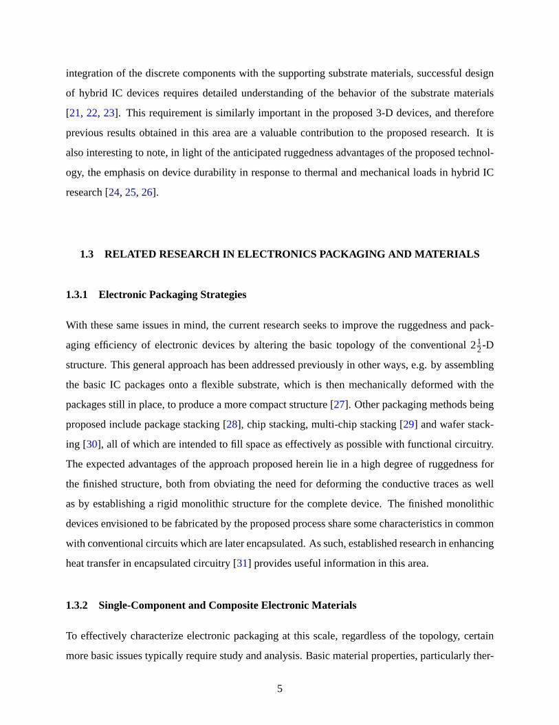
1.2.2 2 1/2-D Circuit configurations
Addressing these same issues at a deeper level of device design, we consider structures built ac-
cording to the 212-D configuration of discrete integrated circuits (Figure2) attached to circuit
boards. Such structures have been employed in manufactured products for several decades, and
structures of this type will surely remain in use in a wide variety of applications for the foresee-
able future. As such, heat management issues applicable to devices of this scale continue with
good reason to be investigated [7] by a number of approaches. As an example, the fundamental
heat-transfer mechanisms inherent in quantifying system behavior at this scale, such as the effect
of surface geometry on natural convection behavior [8], are still appropriate areas for detailed re-
search. Similarly, the parametric details of circuit design display influence on the interacting modes
of heat transfer which govern the temperature behavior [9] of these systems. Analysis of devices at
this system level are commonly undertaken by means of so-called compact thermal models, which
provide an alternative to finite-element analysis (FEA) in thermal analysis of multicomponent as-
semblies. For certain types of problems, compact thermal models can deliver quite useful results,
3

in both steady-state and dynamic analyses [10]. Compact thermal models are less complex math-
ematically than FEA for most given systems [11], but in order to achieve accurate results, care is
required as regards proper quantification of substrate properties as well as all appropriate modes of
heat transfer [12, 13].
1.2.3 Discrete Integrated Circuits
To further illustrate the point, we consider for the moment these issues at the scale of an individual
integrated circuit (hereafter IC), in which each package is a composite structure which can consist
of numerous sub-components, each carrying out a particular function in the operation of the device
(Figure3). Analyzing a single such device in detail is therefore a non-trivial undertaking [14], as
is the modeling of specific improvements to individual ICs intended to enhance heat removal [15].
Even with simplifying assumptions to reduce the number of different materials to be considered,
the geometric details and the presence of different modes of heat transfer introduce substantial
complexity to the effort [16, 17].
1.2.4 Hybrid Circuits
Much of the established research into the behavior of these materials and structures has been un-
dertaken in conjunction with the field of hybrid IC packaging. Per [18]:
Hybrid circuits are circuits in which chip devices of various functions are electrically interconnectedon an insulating substrate on which conductors or combinations of conductors and resistors havepreviously been deposited. They are calledhybrids because in one structure they combine twodistinct technologies: active chip devices such as semiconductor die, and batch-fabricated passivecomponents such as resistors and conductors. The discrete chip components are semiconductordevices such as transistors, diodes, integrated circuits, chip resistors, and capacitors. The batchfabricated components are conductors, resistors, and sometimes capacitors and inductors.
Successful design of hybrid circuitry requires detailed knowledge of the thermal and electrical
conductivity of specialized composites employed in their design and fabrication [19]. As such, the
proposed devices and their associated fabrication processes share many of the same concerns as
hybrid ICs in terms of component scale and material selection.
As is true with conventional IC packages, much work in quantifying the behavior of hybrid
IC packages is concentrated at the individual hybrid device level [20]. However, given the tight
4
integration of the discrete components with the supporting substrate materials, successful design
of hybrid IC devices requires detailed understanding of the behavior of the substrate materials
[21, 22, 23]. This requirement is similarly important in the proposed 3-D devices, and therefore
previous results obtained in this area are a valuable contribution to the proposed research. It is
also interesting to note, in light of the anticipated ruggedness advantages of the proposed technol-
ogy, the emphasis on device durability in response to thermal and mechanical loads in hybrid IC
research [24, 25, 26].
1.3 RELATED RESEARCH IN ELECTRONICS PACKAGING AND MATERIALS
1.3.1 Electronic Packaging Strategies
With these same issues in mind, the current research seeks to improve the ruggedness and pack-
aging efficiency of electronic devices by altering the basic topology of the conventional 212-D
structure. This general approach has been addressed previously in other ways, e.g. by assembling
the basic IC packages onto a flexible substrate, which is then mechanically deformed with the
packages still in place, to produce a more compact structure [27]. Other packaging methods being
proposed include package stacking [28], chip stacking, multi-chip stacking [29] and wafer stack-
ing [30], all of which are intended to fill space as effectively as possible with functional circuitry.
The expected advantages of the approach proposed herein lie in a high degree of ruggedness for
the finished structure, both from obviating the need for deforming the conductive traces as well
as by establishing a rigid monolithic structure for the complete device. The finished monolithic
devices envisioned to be fabricated by the proposed process share some characteristics in common
with conventional circuits which are later encapsulated. As such, established research in enhancing
heat transfer in encapsulated circuitry [31] provides useful information in this area.
1.3.2 Single-Component and Composite Electronic Materials
To effectively characterize electronic packaging at this scale, regardless of the topology, certain
more basic issues typically require study and analysis. Basic material properties, particularly ther-
5

mal and electrical behavior are the focus of much of this work in the relevant literature. Such
materials as required in an electronic device fall into different general categories which depend on
the specific uses of the substructures they comprise. The conductive paths which serve to trans-
mit information between and provide electrical power to the discrete components must of course
exhibit sufficiently high values of electrical conductivity to allow the complete device to function
efficiently. Some easily-recognized examples of these paths include the copper traces on a printed-
circuit board, the soldered deposits used to attach the discrete components to the traces, and the
individual leads which are parts of those components (Figure4). In each of the given examples, the
material in question is a metal alloy. As it turns out, these particular examples are a common focus
of efforts to enhance the performance, durability or economy of electronic devices, often by sub-
stituting a composite material for the metal [32]. These composites typically consist of particles of
metal suspended in a matrix of adhesive polymer or ceramic [33], which are applied to a suitable
substrate and (after curing by some means) exhibit sufficient electrical conductivity to support the
required functions of the device. In typical mass-fabrication processes used currently, the applica-
tion of these composites is performed by pad or screen printing. The reasonable extension of these
processes to ink-jet printing, being addressed by a number of investigators [34], is central to the
current research.
The electrical and thermal conductivity of these composites is not as well-understood as that
of typical metals, but varies considerably in response to a number of variables relating to the fabri-
cation processes commonly used [35]. Of course, focused efforts to enhance this property in these
composite materials [36, 37] are directly expected to provide improved device performance. In
other research, improved device reliability is sought along with acceptable electrical conductivity
[38, 39, 40].
Related to these materials are other types of composites currently used in electronics which,
although they also comprise components which are otherwise typically metal, are not expected to
provide maximal electrical conductivity. For example, carbon-black based composites are useful
in a number of applications relating to calibrated resistance and long-term durability, such as heat-
ing elements [41]. In other cases, the specific property to be enhanced is thermal conductivity,
which is of benefit in eliminating waste heat from the components [42]. These materials are use-
ful in maintaining a low-resistance pathway between a heat-generating component and a separate
6

heatsink [43]. In this application, it is typical to encounter non-intuitive behavior as regards the
thermal resistance exhibited by these composite structures; i.e. the measured thermal resistance is
typically much higher than the values that would be calculated from the bulk thermal resistance of
the materials [44]. This behavior (and the associated phenomenon of contact electrical resistance)
is commonly ascribed to surface-to-surface contact effects which are quantified by various pro-
posed mechanisms [45, 46], including purely theoretical models [47] subjected to varying degrees
of experimental verification [48].
7
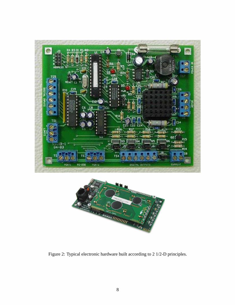
Figure 2: Typical electronic hardware built according to 2 1/2-D principles.
8
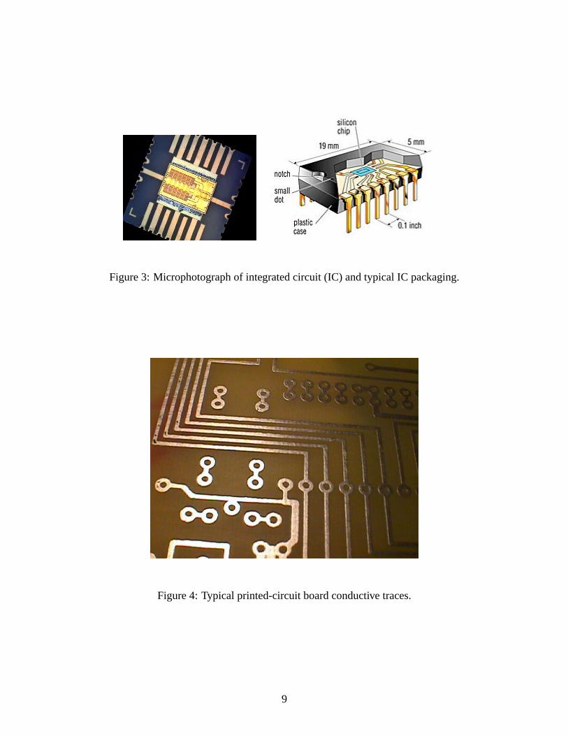
Figure 3: Microphotograph of integrated circuit (IC) and typical IC packaging.
Figure 4: Typical printed-circuit board conductive traces.
9

2.0 OBJECTIVES OF THE RESEARCH
This dissertation is concerned with the overall goal of designing and fabricating the proposed 3-D
circuit devices in such a way as to maintain or even enhance the dissipation of generated heat. To
achieve this goal, a methodology is required for predicting the heat-dissipation behavior of such
circuits during the product design phase. The organization of this dissertation then follows the
process of developing this methodology through several distinct steps.
2.1 ORGANIZATION OF THIS DISSERTATION
First of all, a verification regime is described in which simplified prototype circuits are fabricated
and tested to determine their heat-dissipation performance, followed by the development and anal-
ysis of numerical models intended to simulate the performance of the physical prototypes. The
correspondence between the physical and numerical results is evaluated as a measure of the accu-
racy of the numerical simulation.
Next, a theoretical framework is described in which methods for enhancing heat removal can
be proposed in the context of the overall device concept. The hypothesis evaluated is that the
configuration of the surface-applied conductive traces can be specified so as to increase the amount
of heat lost by convection to the surroundings.
This hypothesis is tested by incorporating specialized features of the conductive traces into an
experimental design which allows them to be compared with other design variations in a parametric
numerical model. The numerical results from the model are than analyzed by means of statistical
tools which permit the different parameters to be ranked in terms of their relative effectiveness in
enhancing heat removal.
10

Additionally, a more advanced prototype is fabricated and tested in both non-encapsulated and
fully-encapsulated forms, the latter intended to more accurately embody the proposed 3-D circuit
structures. Finite element models of this advanced prototype are then developed and analyzed
to provide additional information on circuit performance and to further assess the quality of the
numerical simulations.
2.2 FIELDS OF STUDY RELEVANT TO THE INVESTIGATION
To effectively pursue the proposed research, a base of knowledge is required in the fundamentals
of several engineering fields. Approaching the energy management issues requires understanding
of the principles of heat transfer (convection, conduction and radiation) as well as basic electrical
theory. Applying these principles leads naturally into the relevant aspects of materials behavior,
including the practical issues of materials fabrication as well as the modeling of electrical and
thermal material properties. Finally, a working knowledge of numerical methods is required to
effectively apply the proposed modeling techniques, and a reasonable grasp of statistical methods
is necessary to properly judge the significance of the analytical results.
11

3.0 RELEVANT ASPECTS OF HEAT TRANSFER
The energy management issues inherent in this research concern themselves in large part with heat
transfer theory. Conduction will be the dominant mode of heat transfer in monolithic circuits, but
convection is also relevant for the ultimate removal of heat from the device. The proportion of heat
rejected by radiation is not expected to be substantial, but it is useful to confirm this by means of a
simple comparative calculation.
3.1 PRINCIPLES OF CONDUCTION HEAT TRANSFER
In the sample circuits constructed for this investigation, heat generated in the circuit propagates
through the structure by conduction until it reaches the external surfaces. At any point in the
structure, the rate of heat transfer per unit area in a direction normal to the area (theheat flux,
W/m2) is directly proportional (and opposite in sign) to the local temperature gradient in the same
direction [49]. If the constant of proportionality is not directionally dependent (i.e. the material is
thermally isotropic), then the general statement of the conduction rate equation can be written in
vector form as
Q =−k∇T =−k
(i1
∂T∂x
+ i2∂T∂y
+ i3∂T∂z
), (3.1)
which is known asFourier’s Law. The constant of proportionalityk is a material property, the
thermal conductivityor conduction heat-transfer coefficient. Moving beyond the assumption of
isotropy, if the material in question can be modeled as having different values of thermal con-
ductivity which depend upon the three spatial coordinates, then the material exhibitsorthotropic
thermal behavior and the equation takes the slightly more complex form (for Cartesian coordinates)
12

Q =−∇(kT) =−(
kxx i1∂T∂x
+kyy i2∂T∂y
+kzz i3∂T∂z
). (3.2)
(Figure5). This orthotropic model is applicable to a number of structural composites consisting
of multiple oriented layers of different materials, such as plywood, graphite-reinforced structural
panels, or epoxy-glass circuit board stock.
Figure 5: Orthotropic conduction in Cartesian coordinates.
The flow of heat within a body is also governed by the principle of energy conservation, which
requires that heat flowing into a control volume, plus any heat generated in the volume, must
equal the amount of heat exiting the volume, plus the amount of heat stored in the volume. The
mathematical statement of this principle is theheat diffusion equation[50], written for a differential
volume as∂∂x
(k
∂T∂x
)+
∂∂y
(k
∂T∂y
)+
∂∂z
(k
∂T∂z
)+ q = γ C
∂T∂τ
, (3.3)
whereq is the rate of heat generation (W/m3) over the differential volume. If some location in the
body remains at a constant temperature, then the rate of heat storage at that location is zero, and the
right side of the equation can be eliminated. Then we have thesteady-stateform of the equation,
∂∂x
(k
∂T∂x
)+
∂∂y
(k
∂T∂y
)+
∂∂z
(k
∂T∂z
)+ q = 0 . (3.4)
13

Note that even with a non-zero heat generation term, all points in a body may eventually attain
steady-state temperature values. Solution of the heat diffusion equation is made possible by impo-
sition of the appropriateboundary conditionson the domain of interest.
3.2 PRINCIPLES OF CONVECTION HEAT TRANSFER
At the exposed surfaces of the circuits being considered, heat conducted to these surfaces through
the solid structure passes to the surrounding air by means of convection. Heat transfer by convec-
tion can be modeled by Newton’s Law of Cooling [51],
qconv= hconvA· (Twall−T∞) (3.5)
in which the constant of proportionalityhconv describes the relationship between the actual heat
entering the surrounding fluid from the given surface (of areaA), and the temperature difference
between the surface (Twall) and some characteristic temperature of the fluid. In this analysis, the
ambient air temperature at a point “far” from the model (T∞) is defined as the characteristic fluid
temperature.hconv is referred to as theconvection heat-transfer coefficientor film coefficient.
In the described experiments, the circuit samples are housed in an enclosure intended to limit
exposure of the apparatus to stray air currents. With no established airflow in the immediate vicin-
ity of the circuit sample, the appropriate mode of heat transfer is referred to asfree convection. For
free convection,hconv is a function of the geometry and orientation of the exposed surfaces, and the
physical properties of the fluid in theboundary layerregion of the exposed surface [52, 53, 54].
Since the fluid temperature (and for the most part, the intrinsic fluid properties) near the surface de-
pend(s) on the surface (wall) temperature,hconvat any surface is not a fixed quantity but a function
of temperature. In this mode, any movement of the surrounding fluid is a result of buoyant effects
generated by local heating or cooling of the fluid near the surface. By contrast, in the mode of heat
transfer referred to asforced convection, the fluid near the surface of interest is already moving
at some established velocity relative to the surface; e.g. the flow of fluid being pumped through a
pipe or duct.
14

The empirical expressions for convection behavior given above can be addressed more rig-
orously by considering heat diffusion behavior as in3.3 above, but for the more comprehensive
situation in which the diffusing medium is a non-static fluid. This situation is described by the so-
called3-D energy equation[55]. For steady-state behavior, withγ =constant, no heat generation
within the fluid, and neglecting pressure gradients, the 3-D energy equation reduces to the form
γC(
u∂T∂x
+v∂T∂y
+w∂T∂z
)=
∂∂x
(k
∂T∂x
)+
∂∂y
(k
∂T∂y
)+
∂∂z
(k
∂T∂z
)+µΦ , (3.6)
where the termµΦ ( = viscous dissipation) may also be neglected except in cases such as those
featuring sonic-velocity flows or high-viscosity lubricants. WithµΦ neglected,3.6describes ther-
mal transport behavior in a lossless, incompressible fluid with zero heat generation. The equation
above gives a theoretical basis for addressing the general case of convection, though exact solu-
tions of this simplified second-order expression can only be found for a limited range of situations.
However, as with other differential equations, the expression can be applied tonumerical analysis
of heat transfer in a fluid in a relatively wide range of geometries. Along with appropriate equations
for describing the momentum behavior [56], this is the basis for fluid analysis byfinite-difference
or finite-element methods. The latter method was in fact applied to specific issues in the described
research.
The theoretical approach for assessing free convection bears a number of significant differences
from that for assessing forced convection. At any rate, in the practical application of convection
theory, heat transfer is controlled by the the functional relationships among a number of dimen-
sionless groups. TheNusselt number[57]
Nu =hconvLkf luid
(3.7)
describes, for a particular case, the proportionality relationship between heat transfer defined as
by convection and that which would occur by conduction only, in a motionless fluid layer. The
length variableL represents a characteristic linear dimension appropriate for the size and shape of
the particular surface.
15

For the cases of free convection encountered in this investigation, Nu is a function of additional
dimensionless groups,
Nu = Nu(RaL,Pr) (3.8)
where
RaL = Rayleigh number =gβ∆TL3
ανand (3.9)
Pr = Prandtl number =να
, (3.10)
where∆T = Twall−T∞.
These dimensionless groups represent the comparative effects of physical phenomena which
are relevant to the process of convection. The Rayleigh number [58] is a ratio of buoyant forces
to viscous forces, and is particularly significant to the issue of determining the onset ofturbulent
behaviorin free convection. The Prandtl number [59] is a ratio of the momentum diffusivity to the
thermal diffusivity, and serves as a measure of the relative effectiveness ofmomentum transport to
thermal energy transportfor boundary layer phenomena in a given fluid.
Note that both Pr and RaL are functions of the local fluid properties, with RaL additionally
depending on the gravitational accelerationg and the characteristic length. The fluid properties
that determine the above quantities are those displayed at the so-calledfilm temperature, Tf ilm =
(Twall + T∞)/2. The specific form of Nu (RaL,Pr) depends on the order of magnitude of RaL and
Pr, and on the geometry and orientation of the exposed surface. The form of these functions has
been determined in part byscaling analysisapplied to boundary layer behavior [60] and in part
empirically, by curve fitting to experimental data. In determining these empirical expressions,
an inherent assumption is made either that the surface is essentiallyisothermal(i.e. uniform in
temperature across the entire surface), or alternatively, that the surface is experiencinguniform
heat fluxacross the entire area [61]. For the cases considered herein, neither of these assumptions
can be considered to be exclusively correct. For the purposes of this research, the isothermal
forms of the equations are used. Other practical concerns incurred while modeling convection are
discussed in3.2.1below.
16

For example, for a flat horizontal surface, facing upwards, where the surface temperature is
greater than the surrounding bulk fluid temperature, and 104 < RaL < 107, convection is character-
ized by the equation
NuL = 0.54 Ra1/4L (3.11)
whereNuL is the average Nusselt number over the given surface, andL = A/p for that surface.
Figure 6: Typicalhconv curves for heated upward-facing horizontal surfaces, @T∞ = 25.5C.
Figure6 shows a family ofhconv curves for increasing surface size as a function ofTf ilm, at T∞ =
25.5C, based on this equation. For a flat, heated horizontal surface, facingdownwards, the flow
pattern in the surrounding fluid as driven by buoyant forces is substantially different, and the proper
expression is (for 105 < RaL < 1010)
NuL = 0.27 Ra1/4L . (3.12)
17

See Figure7 for a typical curve ofhconv for this geometry. For the case of a vertical heated surface,
for GrL = Grasho f number[62] = RaL/Pr< 109 (laminar behavior), the appropriate equation for
NuL is
NuL = 0.68 +0.67 Ra1/4
L
[1 + (0.492/Pr)9/16]4/9. (3.13)
Figure8 gives a family of curves for vertical surfaces based on this formula. For heated cylindrical
bodies, oriented horizontally in the surrounding fluid, the flow pattern and hence the functional
relationship bears some resemblance to that for a horizontal surface:
NuD =
[0.6 +
0.387 Ra1/6D
[1 + (0.559/Pr)9/16]8/27
]2
(3.14)
This equation, which is plotted in Figure9, is valid for 10−5 < RaD < 1012. This particular ex-
pression is useful when characterizing the convective heat transfer from a number of structures
encountered in electrical and electronic devices, such as resistors and capacitors. Additional ex-
pressions have been derived for other geometries experiencing natural convection, but those given
above are specifically relevant to this dissertation.
3.2.1 Practical issues in modeling convection behavior
It is important to note that in all of the expressions above, no information is included regarding
the configurations of any surfaces adjacent to the particular surface of interest. From the literature
[61], it seems likely that significant inherent assumptions are included in several of the deriva-
tions. For the example of horizontal surfaces, the convection of heat from a heated surface facing
downwards was apparently occurring simultaneously with additional heat being convected from
the upper surface of the same body. Though it is not remarkable that the convection behavior
should differ significantly between such discrete surfaces on the same body, it is still worth noting
that surfaces of interest in convection problems, while readily describable as “horizontal” or “ver-
tical”, will commonly be situated in different configurations than those inherent in the derivation
of the expressions. One example would be that of a vertical prismatic structure situated atop a
larger horizontal flat surface. With the expressions above, one can readily calculate and apply film
18
coefficients to both the horizontal and vertical surfaces, but the interactions between these adja-
cent surfaces may well impact the actual heat transfer behavior in ways not readily anticipated.
Awareness of these issues must be a part of any application of convection theory.
3.3 PRINCIPLES OF RADIATION HEAT TRANSFER
The basic expression describing the net rate of heat transfer byradiation from surfacei to surface
j is given [63] by 3.15
(qi j )rad = εAiFi j σ(T4i −T4
j ) (3.15)
whereσ = Stefan-Boltzmann constant= 5.670×10⁻⁸W/(m2 ·K4). For net heat transfer from a
small convexblackbody(ε = 1) enclosed inside a large cavity, the expression simplifies to
(qi j )rad = Aiσ(T4i −T4
j ) . (3.16)
It is of particular interest in modeling heat transfer to compare the relative effects of radiation to
convection. ForT∞ ≈ Tj ≈ 300K, and values ofhconv≥ 50W/(m2·K), due to the small magnitude
of σ, convection heat transfer will exceed radiation heat transfer by a factor of five or more for val-
ues of(Ti−Tj)≤ 100K. In these circumstances, particularly for systems described by multiple heat
transfer paths between discrete thermal masses, the radiation effects may be neglected with mini-
mal loss of accuracy to the analysis. However, for many cases of free convection,hconvcommonly
falls below 50W/(m2·K). Furthermore,(qi j )rad also depends on the fourth power of the absolute
temperature, whereas convection and conduction are represented by functions of temperature of
lesser powers. Thus the magnitude of radiative heat transfer will increase much more rapidly as
a function of the object temperature than the convective and conductive heat transfer. Therefore,
even for some cases at near-room-temperature conditions, neglecting heat transfer by radiation will
give inaccurate results. Assessing the relative impact of the expected radiative effects is therefore
a necessary step in properly constructing the analysis (see5.4.1).
19

Figure 7: Typicalhconv curve for heated downward-facing horizontal surface, @T∞ = 25.5C.
20
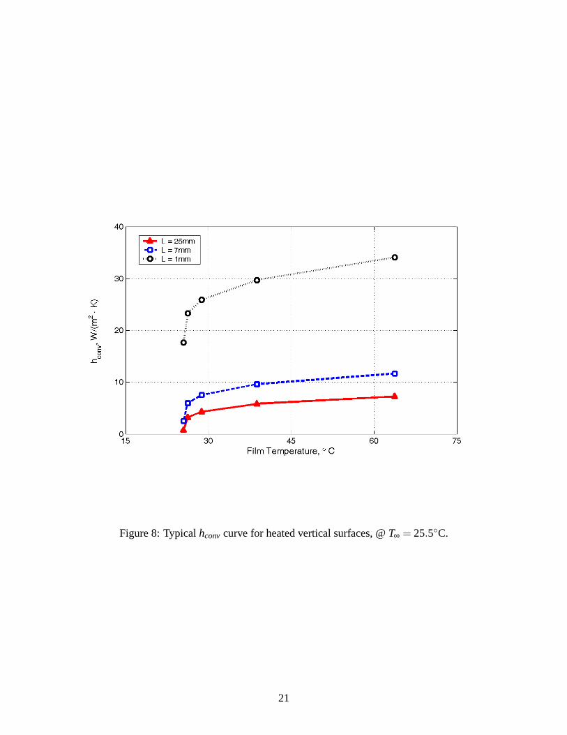
Figure 8: Typicalhconv curve for heated vertical surfaces, @T∞ = 25.5C.
21

Figure 9: Typicalhconv curves for heated horizontal cylinders, @T∞ = 25.5C.
22

4.0 THE PRELIMINARY VERIFICATION MODEL
4.1 DEVELOPING TOOLS FOR EVALUATING EFFECTIVENESS OF HEAT
MANAGEMENT FEATURES
Given the energy management concerns described in the previous chapters, a set of development
tools is required which will enable a designer to reasonably predict the temperature behavior in
3-D circuits. One obvious choice is finite-element analysis (FEA).
However, keeping in mind the limitations of FEA, the appropriateness of the analysis code
should be verified by comparison to a live test reflecting the general conditions of interest. The live
test should incorporate the same materials expected to be employed in later designs, be constructed
to a scale within reasonable proximity to that of the design cases anticipated, and be conducted with
energy throughputs of an order of magnitude representative of those designs.
This investigation therefore proceeds with the construction of sample circuits fabricated on
polymer substrates. For the intended use of the 3-D circuitry to be eventually designed, the cho-
sen polymers are representative of the typical engineering materials used in mass-manufactured
consumer products. Given the possible range of such materials currently in use, both reinforced
(i.e.composite) and unreinforced materials are used in constructing the sample circuits.
The conductive materials being considered for use in the proposed circuits, and the techniques
to be used for depositing them on the substrates, can be approximated for the purposes of this
investigation by commercially-available conductive materials and manual application methods.
Experiments conducted with the resulting prototype circuit structures are expected to give results
which serve as appropriate confirmation of the FEA methods being evaluated.
In developing the live test protocol, previous standardized methodologies [64] were noted
which are employed in determining the thermal resistance of electronic components. The cur-
23

rent research is not directed towards developing such data for discrete IC packages, but similar
concerns apply as to obtaining useful temperature data without inducing excessive measurement
error, e.g. establishing a uniform test environment, choice and placement of measurement instru-
mentation, etc. Appropriately, specific features of the live test protocol were established in order
to address such concerns as are inherent in the existing test methodologies.
4.2 THE 3-D CIRCUIT: A PRELIMINARY LIVE TEST MODEL
As described above, the envisioned technology consists of layers of circuit material printed on
surfaces of varied orientation and/or embedded in 3-D structures. In the experiments described
herein, simplified structures are employed consisting of stenciled conductive traces applied to flat-
surfaced blocks of polymer material. This approach simplifies the analysis and verification tasks,
although the experimental structures remain essentially 3-D in configuration.
As described in [65], the first phase of this research consisted of developing an experimental
procedure to verify the finite-element modeling technique to be described in Section5. This pro-
cedure included the construction of prototype circuit samples that could be subjected to applied
voltages, with the sample temperatures monitored at different locations. The sample circuits were
then modeled using FEA, and the temperatures from the numerical model were compared with the
live test data. The complete verification study consists of a sequence of experiments with varying
substrate materials, trace thicknesses, and applied voltages.
For the live experiments, basic structures were employed which consisted of stenciled conduc-
tive traces applied to flat-surfaced blocks of polymer material with dimensions 50mm x 65mm x
7mm. The blocks were cut either from epoxy resin with fiberglass reinforcement (a typical PC
board material), or acetal resin. Acetal was chosen as a commonly-used engineering polymer,
which might conceivably be used in devices incorporating the integrated 3-D fabrication tech-
niques being developed. This approach simplifies the analysis and verification tasks, although the
experimental structures remain essentially 3-D in configuration.
In place of the ink-jet techniques being developed separately, for the purposes of this investi-
gation a commercially-available conductive ink is applied to the substrates by a stenciling method.
24

Stenciling allowed effective control of trace widths. Post-fabrication measurement of trace thick-
nesses and resistances was necessary to allow the live trace performance to be appropriately mod-
eled using the finite-element method. The commercial ink used for the traces consists of finely-
divided silver particles suspended in a single-component epoxy matrix, which was chosen for high
conductivity and a relatively low curing temperature, with a quoted value of> 84% silver content
in the cured state. The conductive ink traces were applied with a brush, using a stencil cut from
adhesive-backed plastic sheet. To insure that the traces were applied with some degree of consis-
tency, a machined metal die (Figure10) was used to guide the cutting of the tape. The trace width
was determined to a nominal value of 2mm by the stenciling process. Additional areas cut away
from the plastic tape at each end of the trace allowed for connection pads to be applied.
Figure 10: Aluminum guide for cutting conductive ink stencil.
The cross-sectional area of the trace, along with the trace length and the resistivity of the ink,
determines the conductivity of the trace. The area is the product of the trace thickness times the
trace width. The chosen method employed allows the application of “nominally thick” or “nom-
inally thin” traces. “Thick” traces were produced by filling the exposed surfaces to overflowing
with ink, while “thin” traces were produced by brushing away as much excess ink as possible,
leaving a minimal residue. The samples were cured at 110C for 10 to 20 minutes with the tape
stencil in place, then the stencil was stripped away, leaving a raised trace on top of the substrate
block.
25

After fabrication, the cross-sectional areas of the traces were measured at a number of loca-
tions along each trace, using a profile-tracing instrument (Figure11). The measured profiles were
not flat, and typically displayed raised edges characteristic of a meniscus effect. Close inspection
during the measurement sequence also revealed the presence of residual adhesive along the trace
edges from the stencil, which may have affected the observed profile. To evaluate the validity
of the area measurements, actual measurements of the finished trace resistance were made, and
compared to calculations of the expected resistance based on the area measurements and the pub-
lished resistivity of the ink. The trace on each block includes a “short” leg and a “long” leg; five
area measurements were taken on each “short” leg and seven on each “long” leg. The first set
of calculations assumed that each trace was divided into a series of shorter segments of constant
area (the measured areas described above). This allowed the derivation of a series-calculated ge-
ometric trace area (not an arithmetic average) for each trace. Then, utilizing the published value
for the ink resistivity (5x10⁻⁷Ω· m), a calculated value for the expected resistance of each trace
was obtained. The predicted and measured trace resistances for the entire data set are charted in
Figure12. The dashed line represents the expected correlation, i.e. measured resistance equaling
predicted resistance.
The data for “thick” and “thin” traces are fairly well-grouped, indicating that the described
method gave fabricated traces of sufficient consistency to allow experiments with trace thickness
as a controlling variable. However, the calculated resistance values consistently underestimated
the measured resistance values, particularly for the “thin” traces. Assuming that the calculation
method is generally accurate, then either the ink resistivity value is inaccurate, or the measured
cross-sectional areas do not accurately represent the true effective areas permitting current flow.
To address this discrepancy, it was decided to assume that the ink resistivity was correct as
published, and that aneffectiveconducting area and trace thickness could be back-calculated given
the nominal trace width of 2mm. Using this method, the nominal calculated trace thicknesses were
0.34µ for the thin traces, and 5.0µ for the thick traces. This method of accounting for the resis-
tance discrepancy was sufficient to proceed with experimental evaluation and eventual numerical
modeling of the circuit samples.
In typical hybrid circuitry, discrete components are employed which are specifically designed
for assembly to substrates using reflow solder techniques or conductive adhesives. Many of these
26

discrete surface-mount (SMT) devices are, for reasons of space economy, very small in size and
packaged for automated assembly processes. This was a disadvantage for the current research, due
to serious difficulties encountered in manually placing and installing the components and mounting
the measurement instrumentation accurately. After some investigation, larger components suitable
for the research were located, but in the shorter term it was decided to defer using SMT devices
and instead employ components with conventional wire-lead packaging.
For each circuit sample, a discrete 500Ω resistor was attached electrically to the applied traces
(and mechanically to the substrate) by means of conductive epoxy. The irregular geometry of the
epoxy “terminals” posed a challenge in creating the analytical model, in terms of constructing
suitable solid-model geometry as well as in calculating the appropriate convection behavior. A
typical circuit fabricated as described above is shown in Figure13.
4.3 THE SAMPLE TEST SETUP
A detail of the circuit as incorporated into the test setup is shown in Figure14, with the thermo-
couples and power supply connections in place.
One thermocouple was mounted to the resistor, which was expected to exhibit the highest tem-
peratures. Other thermocouples were bonded to the top of the substrate at two locations along the
resistor axis, 10mm from the center of the resistor in opposite directions. Another thermocouple
was bonded to the substrate on the bottom side, immediately opposite the resistor. These mea-
surement locations were chosen to give an indication of the temperature distribution in the circuit
sample in the vicinity of the resistor, where temperature gradients were expected to be highest.
One additional thermocouple was placed inside the enclosure to measure the ambient air temper-
ature (T∞). The temperature probes were K-type (chromel/alumel) micro-thermocouples with
unshielded sensing beads (see Figure15). The sensing bead is approximately 0.1mm in diameter;
the small bead insured very rapid response to changes in the local temperature. The thermocouples
were attached to the sample with cyanoacrylate adhesive, which has thermal properties similar to
the substrate material.
27

Regarding thermocouples in general, the inherent assumption that the temperature reading for
a given thermocouple location must equal the actual temperature at that location deserves careful
consideration. A number of factors inherent in the nature of any thermocouple installation limit
the degree of certainty, including material discontinuity at the thermocouple bead/measurement
location, the presence of the thermocouple leads and the choice and placement of the bonding
medium. The latter can be minimized by exercising appropriate care in installation and test exe-
cution, such as proper attachment procedures to limit the amount of bonding medium that might
be interposed between the thermocouple and the substrate, and protecting the samples from abuse
during handling and testing. However, the former issues are essentially unavoidable and may only
be qualitatively addressed by other means, such as the eventual comparison with numerical models
included in this investigation.
Temperature monitoring of the samples during the tests was by means of a digital measurement
setup. Voltage signals from the temperature probes were monitored by a digital data acquisition
system, which accepts readings taken at fixed intervals and stores them on hard disk. The data
acquisition system used a PC running Windows software, with a CIO-DAS-TC 16-channel ther-
mocouple/voltage input board installed on the ISA bus. The input board included an onboard
microprocessor to handle cold junction compensation (CJC), thermocouple linearization and sig-
nal scaling to provide digital output inC. The board was interfaced to the thermocouples by
means of a screw terminal board including an isothermal block and sensor to provide information
to the onboard CJC function. The digital temperature outputs were written as columnar data to
standard Microsoft Excel files, including a time base channel written by the Measurement Com-
puting acquisition software. The acquisition software also includes calibration utilities, which are
double-checked manually by immersing the thermocouple sensing beads in ice water.
DC Voltage was applied to the samples with copper clips attached to the connection pads
of the ink traces. The clips were formed from thin segments of copper sheet, bent to grip the
substrate and make positive contact with the pads, with an extension to provide for attachment
of standard alligator clip leads from the DC power source. The power supply included a voltage
readout, but a separate digital multimeter was used to provide a calibrated indication of the applied
voltage. The test fixture is set up to provide nominally free convection behavior. It is important
that heat flow from the sample is not unduly hampered, while at the same time protecting the
28

sample from drafts, overriding heat sources, and substantial losses by conduction to the fixture.
To do this, the test sample is supported inside a paperboard enclosure, constructed so as to permit
as much free air circulation as possible, while shielding the sample from room air currents (see
Figure16). This arrangement was developed keeping in mind the similar considerations inherent
in the requirements of EIA/JEDEC Standard No. 51, for measurement of the thermal resistance
of semiconductor packages. Note the location of the thermocouple for monitoring the ambient
temperature inside the enclosure.
4.4 RESULTS FROM LIVE TESTING
Figure17 gives the results from a preliminary live test comparable to those described herein, with
temperature readings taken at 5-second intervals. The recorded temperature at the resistor rises
very quickly relative to the temperatures on the substrate, reflecting that the resistor (connected
to the circuit sample via two narrow wire leads and conductive epoxy) is thermally well-isolated
from the substrate. The slow temperature rise at the other measurement points is consistent with
the relatively large volume of the substrate serving as an effective heatsink. Note that the recorded
temperatures are nearly constant for time intervals in excess of 103 seconds.
4.4.1 Results from the test sequence
The test combinations selected for the verification study and their respective results are given in
Tables1 and2. Four different sample constructions were employed, which were tested at 5VDC
and 10VDC applied, with two duplicate runs for each test case. The measurements at 2000 seconds
were judged to be essentially steady-state values for the purposes of comparison with the FEA
results. However, it should be noted that the temperature data for the 5V tests with the thick
trace/epoxy-glass sample were actually taken at 1000 seconds. In this early test, the steady-state
temperature was defined as achieved at 1000 seconds, but later tests were continued for a full 2000
seconds or more. Examination of the complete data set showed that the 2000-second measurements
differed only minimally from those at 1000 seconds, and could be duplicated closely (toR2 =
29

0.998) by a simple extrapolation from the 1000-second measurements. This extrapolation is used
(for the thick trace/epoxy-glass data) in generating reduced data for the comparison between the
live tests and the FEA results, as described below.
4.4.2 Data reduction
Next, the raw temperatures were reduced to temperature difference data, by subtracting the ambient
temperature from each of the surface temperature readingsat that time point. The ambient tem-
perature never varied by more than 0.4C over any one test, and actually remained within a range
of 25.5±0.5C for all of the tests. A summary of the reduced data is given in Table3. The listed
values for the top surface temperatures are averages of the two top surface measurement points.
This reduced dataset is suitable for comparison with the finite-element model described below.
One observation made regarding the temperature difference data set was that a linear correlation
existed between the resistor temperature increase and the power expended in the resistor, based
on measurements of the trace resistance described previously (See Figure18). More specifically,
the specimens with thinner traces always exhibited lower resistor temperatures than the otherwise
similar specimens with thicker traces.
The impact of trace thickness on maximum resistor temperature is to be discussed and analyzed
later for a different range of trace properties. This discussion (6.3) explores the proposition that
aside from issues of power delivery to the resistive element, adding additional trace material to
provide exclusively thermal pathways can limit observed temperatures in the 3-D circuits under
development. Eventual research (7) sought to confirm this hypothesis.
30

Figure 11: Representative height scan for conductive ink trace.
31

Figure 12: Comparison of calculated vs. measured trace resistances.
32

Figure 13: Typical live test circuit fabricated on epoxy/glass substrate.
33

Figure 14: Live test circuit sample, with power connections and thermocouples attached.
34

Figure 15: Microphotograph of a typical microthermocouple bead.
35
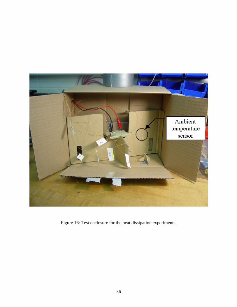
Figure 16: Test enclosure for the heat dissipation experiments.
36
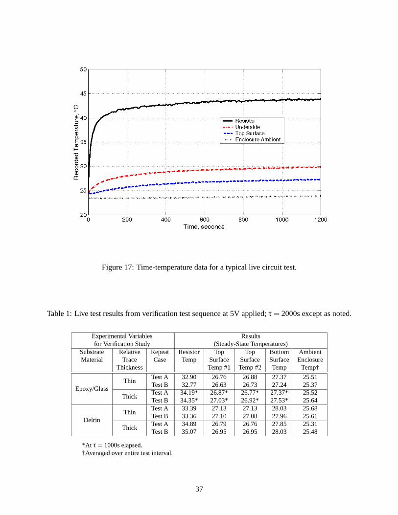
Figure 17: Time-temperature data for a typical live circuit test.
Table 1: Live test results from verification test sequence at 5V applied;τ = 2000s except as noted.
Experimental Variables Resultsfor Verification Study (Steady-State Temperatures)
Substrate Relative Repeat Resistor Top Top Bottom AmbientMaterial Trace Case Temp Surface Surface Surface Enclosure
Thickness Temp #1 Temp #2 Temp Temp†
Test A 32.90 26.76 26.88 27.37 25.51Thin
Test B 32.77 26.63 26.73 27.24 25.37Epoxy/Glass
Test A 34.19* 26.87* 26.77* 27.37* 25.52Thick
Test B 34.35* 27.03* 26.92* 27.53* 25.64Test A 33.39 27.13 27.13 28.03 25.68
ThinTest B 33.36 27.10 27.08 27.96 25.61
DelrinTest A 34.89 26.79 26.76 27.85 25.31
ThickTest B 35.07 26.95 26.95 28.03 25.48
*At τ = 1000s elapsed.†Averaged over entire test interval.
37

Table 2: Live test results from verification test sequence at 10V applied;τ = 2000s.
Experimental Variables Resultsfor Verification Study (Steady-State Temperatures)
Substrate Relative Repeat Resistor Top Top Bottom AmbientMaterial Trace Case Temp Surface Surface Surface Enclosure
Thickness Temp #1 Temp #2 Temp Temp†
Test A 54.25 30.16 30.46 32.51 25.69Thin
Test B 54.41 30.30 30.30 32.65 25.83Epoxy/Glass
Test A 59.69 31.10 30.74 33.17 25.42Thick
Test B 59.52 30.93 30.52 32.96 25.39Test A 55.46 30.83 30.92 34.30 25.72
ThinTest B 55.42 30.81 30.96 34.31 25.70
DelrinTest A 61.85 30.61 30.47 34.58 25.58
ThickTest B 61.96 30.72 30.57 34.70 25.67
†Averaged over entire test interval.
Table 3: Reduced temperature rise data from verification test sequence.
Epoxy/Glass Delrin Epoxy/Glass DelrinThick Thick Thin Thin
Test A Test B Test A Test B Test A Test B Test A Test B
Resistor 8.93* 8.96* 9.52 9.50 7.41 7.38 7.76 7.715V Data Top Surface 1.33* 1.36* 1.41 1.38 1.33 1.33 1.50 1.44
Bottom Surface 1.91* 1.94* 2.48 2.46 1.89 1.89 2.40 2.31
Resistor 34.09 33.98 36.14 36.09 28.45 28.47 29.66 29.7010V Data Top Surface 5.32 5.19 4.83 4.77 4.51 4.51 5.08 5.16
Bottom Surface 7.57 7.43 8.87 8.83 6.72 6.72 8.50 8.58
*Data atτ = 2000s extrapolated from 1000s data.
38

Figure 18: Resistor temperature plotted as a function of resistor power for verification test se-
quence.
39
5.0 FEA OF THE PRELIMINARY CIRCUIT MODEL
Several modeling techniques are available for evaluating the thermal behavior of structures, in-
cluding compact thermal modeling (a form ofnetwork analysis), finite-difference modeling [66],
and finite-element modeling. The latter was chosen for this research due to its applicability to heat
transfer phenomena within 3-D spatial domains, its ready availability from several commercial
sources, and its flexibility as an analytical tool.
5.1 FINITE ELEMENT TYPES AND MODEL GEOMETRY
In the finite-element method, the object or objects of interest are modeled as combinations offi-
nite elements, which, considered together, make up a complete structure (thefinite-element model
[67]). The finite elements are located in space bynode pointsdefined at specific coordinate lo-
cations within the modeled object. The type of element chosen depends on the general structure
of the object and the general assumptions that are made about its physical behavior. For example,
1-D elements would be appropriate for modeling structures expected to exhibit behavior which is
a function of only a single spatial dimension, such as a wire carrying current, heat flux, or ten-
sile/compressive loads. 2-D elements are used for modeling structures such as beams or plates
which exhibit behavior dependent on two orthogonal dimensions, while 3-D elements are used for
structures in which the behavior is dependent upon all three spatial dimensions, i.e. when assump-
tions of 1-D or 2-D behavior are not appropriate. Figure19 depicts typical node arrangements
for 1-D, 2-D, and 3-D finite elements. In some variants of FEA, the location of the grid points in
the spatial domain can self-adjust during the course of the mathematical solution to more closely
40

Figure 19: Schematics of typical 1-D, 2-D, and 3-D finite elements.
model the system behavior. Suchadaptive-gridmethods are especially useful when attempting to
model the behavior of fluid-flow fields [68].
In the finite-element model, the eventual goal is to establish the values of a variable such as
temperature or displacement at every node point in the model. The values to be determined are
referred to as thedegrees of freedomof the model. The values of the degrees of freedom are
determined consistent with the constitutive equations which provide the physical context for the
problem, e.g. the heat conduction equations in the case of a heat transfer problem. The values of
the degrees of freedom must also satisfy the elementshape functions. The shape functions, which
are characteristic of the element types chosen for the analysis, specify the allowable ”shape” or
functional form of the degrees of freedom over the spatial domain of the element (i.e. a degree of
freedom can vary linearly, quadratically, or cubically), and the level of consistency of the degrees of
freedom across element boundaries (i.e. between one element and the next, the values of a degree
of freedom and possibly its spatial derivatives are constrained to match at the element boundaries).
For the analysis described herein, the finite elements must also includecoupled-fieldeffects,
such that the current flow resulting from the electrical degrees of freedom (voltages at the nodes)
provides for internal heat generation through Joule effects, which then drives the solution of the
41

thermal degrees of freedom (the node temperatures). This coupled-field capability is crucial to the
effective modeling of physical phenomena such as fluid flows in natural convection, in which the
buoyancy effects which drive the fluid motion are characterized by fluid property variations as a
function of local temperature.
5.2 CONSIDERATIONS IN SELECTING A COMMERCIAL FEA PACKAGE
A number of well-established commercial finite-element codes are available, some with capabil-
ities in multiple physics environments, but the suitability of a given code in a given environment
is not guaranteed by the simple existence of those user options in the program. In some cases,
a code’s capabilities do allow for its use to model some phenomenon, but the cumbersome pro-
cedures required by the program to access those capabilities make such use impractical. In other
cases, the theoretical underpinnings of the code include various simplifying assumptions which
limit the code’s applicability in some subset of applications–and these assumptions are not always
transparent to the user.
Even if the chosen code has the necessary features to generate and accurately analyze a given
physical situation, the modeling process should be optimized around the best modeling choices
available in the code. A given code might well provide several different paths for analyzing the
situation, each having its own inherent assumptions and specific requirements for supporting infor-
mation, such as material data and boundary conditions. Developing an optimized approach to the
modeling problem will depend on the supporting information available at the time of the analysis,
the confidence of the analyst in the different options available in the commercial code, and the
relative degree of precision required in the results to give useful information.
ANSYSr [69] is a widely-used commercial finite-element modeling program with capabil-
ities including the simulation of heat transfer behavior in conductive, convective, and radiative
modes. Certain element types also include equations that provide for modeling of Joule heating
effects within materials, and others provide for the modeling of thermal transport effects in a fluid
dynamics context. These and other features of the program suggested it as an appropriate choice
for simulating the behavior of the circuits of interest.
42

5.3 SPECIFIC MODELING PARAMETERS
5.3.1 Physics environment and analysis type
The analysis type of the basic situation of interest is a steady-state, thermal-electric problem. The
initial steady-state analysis runs are to be compared with live tests conducted over a sufficient time
for the circuit temperatures to achieve steady values. Later analyses, intended as further confir-
mation of the steady-state results, are to be conducted as transient problems, in which temperature
solutions are derived and observed at discrete points over time and compared with time-based data
from live tests. Additional analyses are conducted using the fluid dynamics capabilities of the
package to confirm aspects of the system convection behavior.
5.3.2 Material properties
The accuracy of any finite-element analysis depends upon the proper modeling of the physical
properties of the materials used in the structure being considered. For the models to be used in the
proposed research, it was essential to obtain (and in some cases derive) the appropriate properties
of several classes of engineering materials. These classes include pure metals (e.g. copper), metal
alloys (stainless steel), ceramics, common engineering polymers (acetal), engineering composites
(epoxy/glass), and engineered materials (conductive ink and adhesives).
In the range of temperatures (0-100C) expected in the analysis and experiments, the proper-
ties of pure metals and most alloys are typically almost constant, so only room-temperature values
of the properties are required. These properties are also nearly isotropic in nature. The thermal and
electrical properties for metals, ceramics and single-component engineering polymers are fairly
widely available [70, 71]. In the case of the epoxy/glass composite, parallel research was per-
formed [72] to experimentally determine the directionality of the thermal conductivity, relative to
the layers of glass fiber mat. For the conductive ink and epoxy, a paucity of information available
in the literature [73, 74] required the extrapolation of thermal properties based on the published
properties of their constituent materials; i.e. pure silver and epoxy resin. Table4 gives a complete
listing of the material properties used in the proposed investigation.
43

Table 4: Material properties used in the finite-element model.
Electrical Heat ThermalMaterial Type Density, Resistivity, Capacity, Conductivity,
kg/m3Ω·m J/kg·C W/m·K
Copper, pure 8.90E+03 1.70E-08 3.85E+02 3.87E+02
Silver, pure 1.05E+04 1.55E-08 2.34E+02 4.19E+02
304 Stainless Steel 7.90E+03 7.20E-07 5.00E+02 1.63E+01
Nickel-Chromium resistance alloy 8.20E+03 1.11E-06 4.60E+02 1.30E+01
Alumina-Silica ceramic 2.30E+03 1.00E+11 9.50E+02 3.50E+00
Acetal Polymer 1.40E+03 6.00E+12 1.47E+03 3.30E-01
Cast Epoxy Resin 1.20E+03 1.00E+13 1.00E+03 2.00E-01
Epoxy Composite, Glass Filled 1.81E+03 2.00E+10 1.00E+03 6.00E-01
Epoxy Composite, directionGlass Filled 90 to layers – – – 6.50E-01
(from experiment) in layer plane – – – 7.80E-01
Silver Epoxy Ink(CMI 112-15F), cured 9.01E+03a 3.00E-07 3.57E+02a 2.16E+01b
Conductive Epoxy Adhesive @ 25C 2.50E+03 7.00E-05 8.93E+02c 6.10E+00(CMI 119-13), cured @ 120C – 1.00E-05 – 4.27E+01d
All data from published sources except as noted.
aCalculated by assuming 84% weight fraction silver, remainder epoxybExtrapolated from pure silver, using electrical resistivity datacCalculated by estimating 14% weight fraction silver, remainder epoxy (from density data)dExtrapolated from temperature change in electrical resistivity data
44

5.3.2.1 Conductive ink data The density and heat capacity of the conductive ink are derived
using the published figure of 84% silver by weight (minimum) for the cured material. With weight
fractions taken equal to mass fractions, and the non-silver mass fraction assumed to consist of
epoxy, we calculate
γink =γAgVAg+ γepoxyVepoxy
Vink= γAg
(1
Vepoxy/VAg+1
)+ γepoxy
(1
VAg/Vepoxy+1
), (5.1)
whereVAg
Vepoxy=
γepoxy
γAg
(0.84
1−0.84
). (5.2)
Similarly, assuming ideal mixing,
Cink =mAgCAg+mepoxyCepoxy
mink= CAg(0.84)+Cepoxy(1−0.84) . (5.3)
The thermal conductivity is extrapolated from the value for pure silver, assuming an inverse
proportional relationship based on the ratio of electrical conductivities, i.e.
(kxx)ink = (kxx)AgρAg
ρink. (5.4)
Although more comprehensive models of thermal conductivity in composites are available [75] ,
this linear model was expected to be sufficiently close to the true relationship for the purposes of
the simulation.
5.3.2.2 Conductive epoxy data The heat capacity of conductive epoxy was derived by first
using the published density value to calculate the weight fraction of silver, which was determined
to be 14%, with the remaining weight fraction assumed to be epoxy. This weight fraction was then
used to calculate the heat capacity as per (5.3). The variation in thermal conductivity from 25C
to 120C was extrapolated with the same linear model described above, based on the published
values of electrical conductivity over the temperature range for the same material.
45

5.3.2.3 Experimentally determined material data The data from commercial sources for the
conductivity of epoxy/glass composite includes no information on thermal effects that might inhere
from their non-uniform structure. As it seemed reasonable that these structural effects might be
significant, research was conducted [72] to experimentally quantify any non-isotropic effects on
thermal conductivity expected due to the layered structure of the epoxy/glass composite. The
experimental data is given along with the commercially-available thermal conductivity data in
Table4. In particular, note that the thermal conductivity parallel to the plane of the fiberglass mats
exceeds the published value by 30%.
5.4 BOUNDARY CONDITIONS
To solve the finite-element model, the conditions must be specified at the locations where the
model interfaces with its physical surroundings. These boundary conditions [76] can be held fixed
throughout the course of the analysis, or they may be made to vary over a number ofload steps, as
is required in a time-dependent analysis and some analysis modes requiring an iterative solution.
Dirichlet boundary conditionsare those for which the value of certain degrees of freedom (in
the case of this analysis, either temperature or voltage) are explicitly applied to specific nodes on
the model. In this model, DC voltages are fixed for the course of the entire analysis at the nodes
of the connection pads. The only boundary temperature specified is the bulk temperature of the
surroundings, a condition which is actually applied as part of the convection modeling described
below.
Neumann boundary conditionsrequire the specification of a rate variable at a given location on
the model, such as a value of the heat flux or electrical current. Such a rate variable can be imposed
directly on any model surface; for the case of heat flux, it can be calculated at exterior surfaces by
defining convection or radiation conditions (Chapter3).
46

5.4.1 A simplified model for assessing boundary conditions
With the data provided by the live tests, it is possible (and useful) to investigate by a first-order
calculation the relative impact of convection and radiation heat transfer at the exterior surfaces
on the eventual results. A lumped steady-state model is described which encompasses the circuit
Figure 20: Lumped model for comparing heat transfer modes.
sample, consisting of the discrete resistor, its connecting leads, and the substrate, located within
the test enclosure (Figure20). For this situation, it is clear that all heat generated in the sample by
Joule effects must eventually be taken up by convection in the surrounding air, or by radiation in the
enclosure walls. The total heat generation rate in the resistor is equal to the sum of all conduction,
convection and radiation from the resistor to the surroundings (including the substrate). A similar
equality can be written for the net heat exchange at the substrate:
qJoule = (qkxx)res→sub+(qrad)res→encl+(qrad)res→sub+(qconv)res→∞ (5.5)
0 = (qconv)sub→∞ +(qrad)sub→encl− (qkxx)res→sub− (qrad)res→sub (5.6)
47

Assuming that the enclosure walls are at a uniform temperature, we write equations to describe the
heat transfer between nodes by convection and radiation:
(qconv)res→∞ = hresAres(Tres−T∞) (5.7)
(qrad)res→encl = σεAres
2(Tres
4−Tencl4) (5.8)
(qrad)res→sub = σεAres
2(Tres
4−Tsub4) (5.9)
(qconv)sub→∞ = hsubAsub(Tsub−T∞) (5.10)
(qrad)sub→encl = σεAsub(Tsub4−Tencl
4) . (5.11)
The barred quantities are lumped values; i.e. the substrate and the resistor are each modeled as
having a uniform temperature, and the convection heat transfer coefficients will be taken as average
values over each complete surface. The resistor is assumed to be close enough to the substrate that
one-half of its area radiates to the substrate while the other half radiates to the enclosure walls. Gray
body behavior is also assumed for radiative heat transfer such that the emissivityε is retained.
The conduction of heat from the resistor to the substrate occurs over two parallel paths, each
consisting of a copper lead wire in series with the epoxy terminal bonded to the substrate. The
thermal resistance of each lead wire and epoxy terminal are respectively
Rwire =Lwire
kwireAwire(5.12)
Repoxy =tepoxy
kepoxyηAepoxy, (5.13)
whereη is a factor allowing for the sub-optimal geometry of the embedding of the lead wire in the
epoxy bond; i.e. the full area of the epoxy bond is not realistically available as a conductor, giving
a higher value for resistance. Then the total heat conducted from the resistor to the substrate is
written as
(qkxx)res→sub=(
2Rwire +Repoxy
)(Tres−Tsub) . (5.14)
48

Expanding (5.5) and (5.6) gives the following nonlinear simultaneous equations.
qJoule = hresAres(Tres−T∞)+σεAres
2(Tres
4−Tencl4) (5.15)
+σεAres
2(Tres
4−Tsub4)+
(2
Rwire +Repoxy
)(Tres−Tsub)
0 = hsubAsub(Tsub−T∞)+σεAsub(Tsub4−Tencl
4) (5.16)
−(
2Rwire +Repoxy
)(Tres−Tsub)−σε
Ares
2(Tres
4−Tsub4)
Given the appropriate physical properties taken from the live test samples, it is possible to solve
these equations to obtain a preliminary solution for the values ofTres andTsubas function ofqJoule.
The Mathcadr software package [77] was employed to automate the solution process.
From the fabricated sample dimensions, we takeAres = 34.6mm2, Asub= 8110mm2, Awire =
0.442mm2, Aepoxy= 12.57mm2, Lwire = 10mm,tepoxy= 1.0mm, and we takeη = 0.1 as a reason-
able guess based on the size and shape of the epoxy terminals relative to the wire leads. We also
assumeε = 0.9 for near-blackbody conditions. From Table4we obtainkwire = 3.87×10²W/(m·K)
andkepoxy= 6.1W/(m·K). From the test conditions, we choose as a representative valueTencl =
T∞ = 25.5C = 298.7K, and from Figures6 through9 we reasonably choosehres = 20W/(m2·K)
and hsub = 10W/(m2·K). Then usingqJoule = 0.198W as for the 10V applied case, we obtain
Tres = 317.3K=44.1C andTsub= 300.2K=27.0C. For the extreme simplicity of the model, these
results compare well with the live test data and are sufficient to serve as a further check on the qual-
ity of the eventual FEA results. However, it is also instructive to use the calculation to consider the
possibility of neglecting radiation in the analysis. This is beneficial because even with the tools
available within the FEA program, the process of applying radiation boundary conditions to the
model is somewhat tedious, and the numerical calculation of the highly non-linear radiation effects
is computationally time-intensive. With the radiation terms removed, the simultaneous equations
can be written in the simpler form
qJoule = hresAres(Tres−T∞)+(
2Rwire +Repoxy
)(Tres−Tsub) (5.17)
0 = hsubAsub(Tsub−T∞)−(
2Rwire +Repoxy
)(Tres−Tsub) (5.18)
and a comparison can be made between the temperature results obtained when considering con-
vection only as a thermal boundary condition, as opposed to both convection and radiation. Figure
49

21 plots the calculated values ofTres andTsub as a function ofqJoule for the calculations with ra-
diation included and neglected, along with the live test data (the test data points for the substrate
are an arithmetic average of the three measurement points). With or without radiation included,
the limitations of the lumped models are made clear as they diverge more and more from the live
test results as the dissipated power increases. However, the plots display a much smaller difference
(approximately 1.1K at the highest dissipated power) between the calculated results with radiation
neglected and those with radiation included, which supports the contention that the accuracy of
mathematical models of similar structures should not suffer unduly from neglecting radiation in
the analysis. Accordingly, radiation boundary conditions will not be applied to the finite-element
models constructed for this research.
5.4.2 Applying convection to the finite-element model
In this analysis, film coefficients must be specified for all such exposed surfaces of the model.
This is modeled by defininghconv for each discrete surface as a separatematerial property, with
temperature-dependent behavior as represented by curves such as those in Figure6. Note that
sincehconv at any point is a function of the local temperatureTwall–which is only determined by
solving the complete model–then this analysis requires an iterative solution as described above.
The finite-element code uses interpolation to derivehconv at temperature points intermediate to
those explicitly supplied. Where no Neumann boundary conditions are specified, the default for
the analysis is to apply a no-flux condition (i.e. a perfect insulator).
5.5 CONSTRUCTION OF THE PRELIMINARY FEA MODEL
5.5.1 Simplifying assumptions
In approaching a finite-element analysis, a recommended practice is to build a first model incor-
porating a number of simplifying assumptions regarding the structure under consideration. This
50

approach minimizes the amount of effort required in the preliminary stages of an investigation,
while often leading to valuable insights into the physical situation being modeled. The numerical
verification model of the test circuit block includes several such assumptions:
• that all heat transfer from the exterior surfaces of the model is by convection (see above),
• that the film coefficients for a specific model surface can be calculated assuming that the sur-
face is effectively independent of any adjacent surfaces, irrespective of the concerns raised in
3.2.1,
• that no significant electrical conduction occurs within the substrate,
• that there is no significant thermal resistance between the conductive traces and the substrate,
• that the resistor can be modeled as a monolithic structure with an equivalent bulk electrical
resistivity, which gives an appropriate total resistance,
• that the resistor leads can be modeled as simple beam structures,
• that any convective heat loss from the resistor leads to the ambient air is negligible,
• that the irregular epoxy terminals connecting the leads to the trace can be represented as simple
cylinders,
• that the trace thickness should be modeled by measuring the actual trace resistance, and ap-
plying an appropriate thickness in the numerical model to give a matching trace resistance,
and
• that the thermal conductivity behavior of the substrate can be assumed isotropic for both sub-
strate materials.
This model also takes advantage ofconstraint equationsto mathematically “glue” the trace, sub-
strate and epoxy terminals together, eliminating the need to exactly match the nodes from one
model section to another. In justifying these simplifications, some prior insight into the expected
system behavior is valuable. When live test data are available as a direct comparison to the numer-
ical results, judging the reasonableness of these assumptions is more straightforward.
5.5.1.1 Resistor modeling At this point no attempt is made to model the exact internal struc-
ture of the resistor; rather, the resistor is modeled as monolithic, constructed of a single material
51

with a bulk resistivity calibrated to give the appropriate resistance for the discrete resistor used in
the live test.
The resistor leads are the smallest structures in the model, representing sections of 0.75mm
diameter copper wire. Modeling the resistor leads with beam elements allows each lead to be
represented by a linear pattern of nodes and elements. This is simpler than using solid elements, but
makes the modeling of convection behavior more difficult. In the preliminary model, convection
from the leads was not modeled. The preliminary FEA model is shown in Figure22, including
a detailed view of the simplified resistor model. The element types used in the model are given in
Table5.
5.5.2 Results from the preliminary FEA model
A temperature contour plot from one of the finite-element analyses is shown in Figure23. Temper-
ature outputs were recorded at specific locations on the model duplicating the locations of the live
test measurements. These results from the finite-element model are given in Table6. The reduced
results, which include averaged data for the top surface temperatures withT∞ = 25.5C subtracted,
are given in Table7.
The overall fidelity of the numerical models in recreating the temperature behavior of the live
test models was evaluated by plotting all numerical data obtained as described against all of the
corresponding live test data (presented previously in Table3). Besides subtractingT∞ from the
measurements, the top surface temperatures were averaged and plotted as single values for each
test case. This represents very little loss of information since the two measurements (or values from
the FEA runs) never differed by more than one-half degree. This plot and a regression line through
the data points is given in Figure24. This regression plot clearly shows much better agreement
with the live tests than the lumped model.
52

5.6 THE REVISED VERIFICATION MODEL
After reviewing the initial results, several minor revisions were added to the preliminary models,
consistent with the goal of limiting the assumptions required for the analysis. These modifications
included:
• changing the thermal conductivity model of the epoxy/glass material to orthotropic behavior,
• modeling the resistor leads as full solid structures, permitting convection boundary conditions
to be more conveniently applied,
• employing a more complex model of the actual resistor structure, including a nickel-chromium
outer film surrounding a highly resistive ceramic barrel,
• using elements with electrical (voltage) degrees of freedom to model the substrate, thus al-
lowing for electrical conduction in the substrate block (although of course limited by the high
electrical resistivity of both substrate materials), and
• rebuilding the model with the trace element nodes matched exactly to the substrate mesh,
eliminating the need for constraint equations to “glue” the trace to the substrate.
Figure25 shows a detailed view of the resistor region of the revised model. The resistive film
is in the form of a spiral ribbon in the actual resistor geometry, which is a configuration well-suited
for fine-tuning the resistance in production by means of laser trimming. It was unnecessary to
duplicate this geometry in exact detail for the FEA; instead the resistive film was modeled as a
continuous cylinder whose thickness was selected to give the proper resistance value by first mod-
eling the resistor separately. The structure of the revised resistor model also included the steel end
caps, which were joined numerically to the copper wire leads by constraint equations to simplify
the meshing in this very constricted location. Table8 gives a summary of the element types em-
ployed. A typical results plot for the revised model, showing the temperature contours in the
resistor region is given in Figure26. Temperature results corresponding to the live test measure-
ments are given in Table9, and the reduced numerical data are given in Table10. A regression of
the data from the revised model plotted against the live test data is given in Figure27. Although the
quality of the regression is slightly improved in this case, it is clear that the improvement over the
original model is not substantial. The conclusion to be drawn from the revised model is that such
53

additions as were made to the original model are only slightly effective in improving the quality of
the results relative to the live tests. However, in later models including a leaded resistor construc-
tion, these revisions were retained, mainly because the constructed geometry was easily re-usable.
An additional measure of the quality of the FEA is given by conducting a time-dependent anal-
ysis using the revised numerical model. The analysis results are generated at a series of discrete
points in time following the imposition of a step increase in the applied voltage. For a typical time-
dependent FEA run, these discrete points are plotted alongside the actual time-temperature data
from the live model (Figure28). There is some overshoot in the resistor temperature data relative
to the live test during the initial temperature transient following the step increase in voltage, but in
general the time-varying numerical temperature results are still well-behaved relative to the actual
sample performance.
54
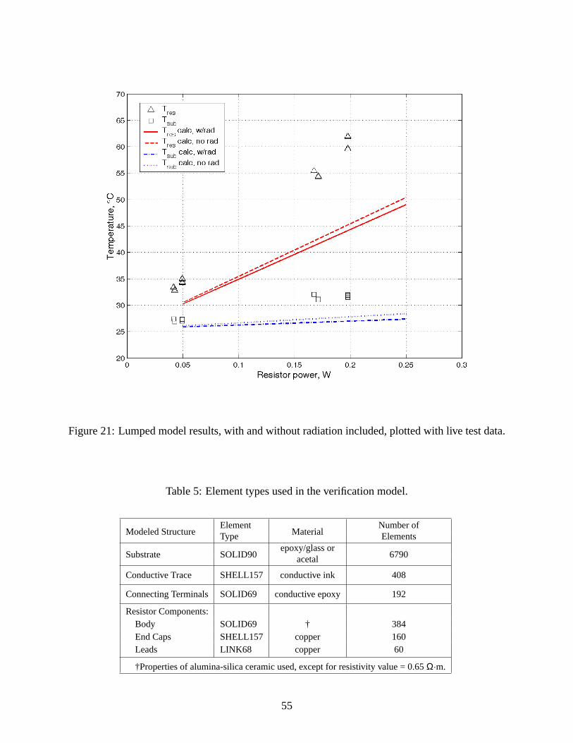
Figure 21: Lumped model results, with and without radiation included, plotted with live test data.
Table 5: Element types used in the verification model.
Element Number ofModeled Structure Type Material Elements
epoxy/glass orSubstrate SOLID90 acetal 6790
Conductive Trace SHELL157 conductive ink 408
Connecting Terminals SOLID69 conductive epoxy 192
Resistor Components:Body SOLID69 † 384End Caps SHELL157 copper 160Leads LINK68 copper 60
†Properties of alumina-silica ceramic used, except for resistivity value = 0.65Ω·m.
55

Figure 22: Finite-element mesh for the numerical verification model, including detail of resistor
region.
56
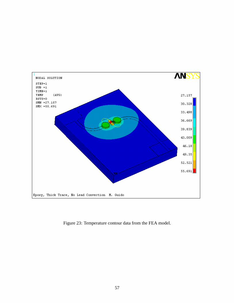
Figure 23: Temperature contour data from the FEA model.
57

Table 6: FEA sequence results from verification study at 5V and 10V applied.
Experimental Variables Resultsfor Verification Study (Steady-State Temperatures)
Substrate Relative Voltage Resistor Top Top BottomMaterial Trace Applied Temp Surface Surface Surface
Thickness Temp #1 Temp #2 Temp
5V 33.14 27.52 27.43 28.23Thin
10V 53.36 31.78 31.42 34.51Epoxy/Glass
5V 33.77 27.61 27.51 28.39Thick
10V 55.69 32.11 31.70 35.075V 34.62 27.63 27.55 28.75
Thin10V 58.51 31.97 31.68 36.16
Delrin5V 35.35 27.74 27.64 28.95
Thick10V 61.22 32.33 31.98 36.84
AmbientT∞ = 25.5C for all combinations.
Table 7: Reduced temperature rise data from verification FEA sequence.
Epoxy/Glass Delrin Epoxy/Glass DelrinThick Thick Thin Thin
Resistor 8.27 9.85 7.64 9.125V Data Top Surface* 2.06 2.19 1.97 2.09
Bottom Surface 2.89 3.45 2.73 3.25
Resistor 30.19 35.72 27.86 33.0110V Data Top Surface* 6.41 6.65 6.10 6.33
Bottom Surface 9.57 11.34 9.01 10.66
*Top surface data is average of two locations.
58

Figure 24: Linear regression of FEA results, plotted against live test data.
59
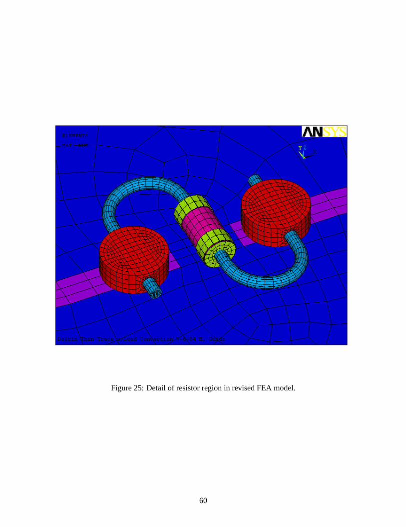
Figure 25: Detail of resistor region in revised FEA model.
60

Table 8: Element types used in the revised model.
Element Number ofModeled Structure Type Material Elements
epoxy/glass orSubstrate SOLID69 acetal 2892
Trace SHELL157 conductive ink 207
Connecting Terminals SOLID69 conductive epoxy 2016
Resistor Components:Body SOLID69 ceramic 384Resistive Film SHELL157 nichrome 64End Caps SHELL157 steel 160Leads SOLID69 copper 3552
61
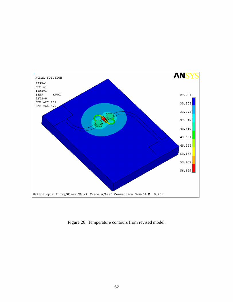
Figure 26: Temperature contours from revised model.
62

Table 9: FEA sequence results from new verification model at 5V and 10V applied.
Experimental Variables Resultsfor Verification Study (Steady-State Temperatures)
Substrate Relative Voltage Resistor Top Top BottomMaterial Trace Applied Temp Surface Surface Surface
Thickness Temp #1 Temp #2 Temp
5V 33.27 27.18 27.25 27.71Thin
10V 54.10 30.59 30.89 32.63Epoxy/Glass
5V 33.95 27.25 27.33 27.85Thick
10V 56.68 30.83 31.17 33.065V 34.66 27.33 27.39 28.34
Thin10V 58.89 30.95 31.23 34.74
Delrin5V 35.46 27.41 27.49 28.51
Thick10V 61.84 31.22 31.55 35.35
AmbientT∞ = 25.5C for all combinations.
Table 10: Reduced temperature rise data from revised FEA sequence.
Epoxy/Glass Delrin Epoxy/Glass DelrinThick Thick Thin Thin
Resistor 8.45 9.96 7.77 9.165V Data Top Surface* 1.79 1.95 1.72 1.86
Bottom Surface 2.33 3.01 2.21 2.84
Resistor 31.18 36.34 28.60 33.3910V Data Top Surface* 5.50 5.89 5.24 5.59
Bottom Surface 7.56 9.85 7.13 9.24
*Top surface data is average of two locations.
63

Figure 27: Linear regression of revised model results, plotted against live test data.
64
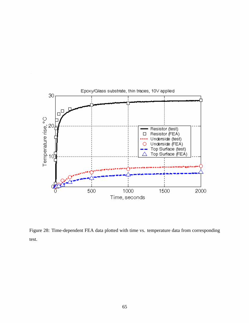
Figure 28: Time-dependent FEA data plotted with time vs. temperature data from corresponding
test.
65
6.0 PROPOSED METHODS FOR PROMOTING WASTE HEAT REMOVAL
6.1 PREVIOUS RESEARCH
Many of the previous and current investigations into the problem of removal of waste heat from
electronic systems are concerned with the application of active cooling methods [6, 78], at the
device scale and below. These methods are crucial to the development of new, modularized
high-powered electronic devices [79]; they include relatively straightforward heat-exchange sys-
tems [80] as well as more advanced methods employing heat-pipe technology [81]. Other re-
search is concentrated on the application of phase-change materials involving both liquid/gas and
solid/liquid phase transitions [82, 83, 84, 85]. Some effort has been made into establishing thermal
modeling schemes that can be used to compare the efficacy of a variety of active cooling methods
[86].
It is true that much previous research in this field is concentrated on the application of active
cooling schemes. However, the basic principles at work in passive cooling methods are the same
as those in active cooling, and significant recent research continues in general passive cooling
applications [87]. For passive cooling methods which employ mixed free and forced convection, it
has been shown that the free convection component contributes materially to efficient heat rejection
[88] in models of electronic devices. Indeed, in some specified circumstances the application of
purely natural convection has quantifiable advantages over forced convection [89].
66

6.2 BROAD PRINCIPLES
As an example of techniques suggested by previous research into the configuration of conductive
traces [90], the characteristic that good electrical conductors are generally good thermal conduc-
tors can be leveraged in design of the proposed 3-D circuits. In particular, separate thermally-
conductive elements can be fabricated with the same 3-D technology that is used to create the
electrical elements, e.g. to provide heat sinks or heat flow pathways. Furthermore, it is proposed
herein that the elements that are at first required only for electrical conduction in the product can
be configured specifically to enhance heat rejection from the circuits.
6.3 THE GENERAL HEAT REJECTION PROBLEM FOR PASSIVE COOLING
METHODS
In the circuits being investigated, the power dissipated as heat in the resistor is determined by the
total current in the circuit, i.e.
P = I2Rresistor , where I =Vtotal
Rtotal. (6.1)
The original tests conducted with conductive-ink traces indicated that at very small trace thick-
nesses, an increase in the thickness enhanced the delivery of electrical power to the resistor, with
the result thatup to a pointincreasing trace thickness resulted in higher temperatures in the resis-
tor. However, it can be shown that beyond that critical thickness (which should be dependent on
the specific trace material), the increasing electrical conductance of the trace does little to increase
the power delivery. This is because the total resistance of the circuit is a series combination of the
discrete resistor and the trace resistance:
Rtotal = Rresistor+Rtrace = Rresistor+(
ρLA
)trace
= Rresistor+(
ρL
t ·w
)trace
(6.2)
When the trace thickness is sufficiently high (and hence the trace resistance is sufficiently low), the
total resistance of the circuit (and the resulting current at a fixed applied voltage) is dominated by
the fixed resistor.
67
At the same time, thethermalresistance of the trace (which is the lowest-resistance pathway
for heat rejection from the resistor) will decrease inversely as the trace thickness is increased:
(Rth)trace =(
Lkxx ·A
)trace
=(
Lkxx · t ·w
)trace
(6.3)
As the trace thickness increases, this combination of effects causes the Joule heating in the resistor
to approach a maximum value, while the heat removal capacity of the trace increases linearly.
The total thermal resistance(Rth)total of the circuit model also depends on a combination of
several resistances, including(Rth)trace, (Rth)substrate, and(Rth)convection. This combination is not
a simple additive process as with the series combination of electrical resistances; in fact, each
of the above quantities properly should be subdivided and recombined in a thermal resistance
network model, as was done in verifying the relatively minor impact of radiation on the temperature
achieved. The finite-element model described herein is in fact a network model composed of many
smaller lumped thermal models represented by a large system of simultaneous equations.
6.4 CANDIDATE METHODS FOR ENHANCING PASSIVE HEAT REMOVAL
Before using such an analytical model to generate results, one can infer the effects of increasing
or decreasing the values of the individual thermal resistances, imagined as gross quantities. In
general, for a fixed power input to (and hence a fixed heat generation at) the discrete resistor,
decreasing any of the resistances should likewise decrease the temperature of the resistor relative
to the ambient air, which in this experiment is the eventual destination for all generated heat.
Furthermore, at any point in the circuit model, decreasing the resistances between that point and the
ambient air should reduce the temperature at that point, assuming that all of the other parameters
(including thermal capacitance) are held constant.
For example,(Rth)convectioncan be expanded as
(Rth)convection=(
1hconvAconv
), (6.4)
in which hconv is dependent upon the geometry of the surfaces exposed to the ambient air, the air
flow conditions imposed, and the air properties, as described in Section3.2. For the purposes of this
68

study, the bulk temperature is held fixed, and the surface temperatures are not explicitly imposed,
so the only available approach for exercising control over(Rth)convectionis to modify the geometry
of the exposed circuit surfaces. One way to do this would be to add a conductive protrusion or
protrusions–similar to a fin–to the circuit model, thereby increasing its total surface area.
However, it is possible to increase the amount of heat rejected to the ambient fluid without
increasing the overall volume envelope of the block structure. One is to decrease(Rth)trace, either
by increasing the bulk thermal conductivity (kxx) of the trace, or the trace width or thickness. This
will more effectively couple the heat source (the resistor) to the other surfaces exposed to the
ambient air. This is analogous to improving the performance of a heat sink by making the fins
from aluminum or copper instead of iron or lead.
This heat sink analogy also suggests that(Rth)total might be decreased by adding trace material,
not on the primary electrical conduction path, but on blind extensions to it. These extensions also
serve to more tightly couple the heat source to the ambient air, so the increase in conductive trace
area provided by these extensions is analogous to adding fins to a heat sink. In this analogy, both
the size and location of these trace “fins” should impact the efficiency of heat rejection from the
heat source. One likely supposition would be that placing the “fins” closer to the heat source,
should result in improved heat rejection and lower temperatures at the source.
69

7.0 EVALUATION OF PASSIVE HEAT REMOVAL FEATURES BY PARAMETRIC
STUDY
Various possible circuit architectures are investigated by parameterizing the finite-element model,
to compare a number of different design variations. The methodology chosen for this part of the in-
vestigation is typically described as adesign of experimentsor DOE. DOE methods are frequently
used in the contexts of both live test programs and numerical simulations [91] to investigate the rel-
ative impact of several different proposed design features on the resulting performance of a system,
and to guide the optimization of such a system for the best performance [92].
7.1 FIXED PARAMETERS FOR THE STUDY
For the parametric finite-element analyses, the numerical model is constructed with provisions for
adding trace extensions near the resistor. In performing the parametric analysis, the following
conditions will be applied to all analysis combinations:
• Block material - Epoxy/glass composite, with the glass layers arranged parallel to the x-y
plane,
• Resistor element - Resistor model constructed to provide 500Ω discrete resistance,
• Trace width - 2mm,
• Applied voltage - 10V applied across the circuit model, and
• Bulk air temperature (and initial circuit temperature) - 25.5C.
70

7.2 DESIGN PARAMETERS TO BE VARIED
The following four parameters are chosen to be parametrically varied within the model, to generate
a comprehensive results set covering a range of possible designs.
• Trace thickness - 10, 30, or 90µm,
• Trace materials - Conductive silver ink (CMI 112-15F) or metallic copper,
• Location of trace extensions - Directly under the epoxy terminals (Direct) or placed 4mm
further from the epoxy (Offset), and
• Size of trace extensions - 20mm, 10mm, or zero mm (i.e., no fin) long x 4mm wide.
Overall, thirty distinct parameter combinations were modeled and solved by FEA. The number and
types of elements used in the parametric model are included in Table11, and the finite-element
mesh for a typical combination is shown in Figure29.
Table 11: Element types used in the parametric model.
Element Number ofModeled Structure Type Material Elements
Substrate SOLID69 epoxy/glass 8852
copper or 288 (no fin)Trace SHELL157 conductive ink 568 (w/fin)
Connecting Terminals SOLID69 conductive epoxy 2016
Resistor Components:Body SOLID69 ceramic 384Resistive Film SHELL157 nichrome 64End Caps SHELL157 steel 160Leads SOLID69 copper 3552
7.3 RESULTS
The results of the numerical simulation experiment are listed in Table12. It can be seen that the
current through the resistor (the quantity in the right-hand column) varies by less than 0.2% over all
of the design combinations. This illustrates that in the range of trace thickness being considered,
71
the trace characteristics have very little affect on power consumption of the resistor. Hence, the
observed variations in temperature rise can be assumed to be due to thermal resistance effects
only. Further analyzing the results, Figure30 shows resistor temperature rise data for analysis
combinations with “Direct” fin placement, plotted as a function of trace thickness. As illustrated,
the graph shows a lower temperature rise behavior for the copper traces in general and a significant
reduction in the temperature rise due to the presence of a trace fin. Little difference is seen in the
temperature rise when increasing the fin length from 10mm to 20mm. In fact, for the conductive
ink traces, the temperature rise difference between 10mm and 20mm fins is negligible.
From Section6.3, it is reasonable to expect that the quantity(Rth)trace will have a significant
impact on the results. As described in (6.3), this quantity depends upon the bulk thermal conductiv-
ity, the trace thickness, and the length and width of the printed trace. Because the length and width
of the trace are the same for all of the analysis combinations, it is useful to consider the results as a
function of a single quantity depending only on the bulk thermal conductivity and trace thickness.
This quantity, which will be defined as theThermal Sheet Resistance, is a measure of the thermal
conductivity of the circuit trace, incorporating both bulk thermal conductivity and thickness:
Thermal Sheet Resistance=(
1kxx · t
)trace
(7.1)
This quantity is the thermal resistance (in the plane) of a sheet of material whose length is equal to
its width; the units are therefore written as (K/W)/square. This derived quantity is similar to one
used to quantify electrical resistance in a circuit trace, theSheet Resistance:
Sheet Resistance=(ρ
t
)trace
, having units ofΩ
square. (7.2)
The combined dataset is plotted in Figure31, with the Thermal Sheet Resistance on the abscissa.
Note that the data points on the right side of the “Copper Trace Data” box are for 10µm copper
traces, while the points on the far left side of the “Conductive Ink Trace Data” box are for 90µm
conductive ink traces. The latter are nearly an order of magnitude thicker than the former, but are
still less thermally conductive because of the much lower bulk thermal conductivity of the ink.
72
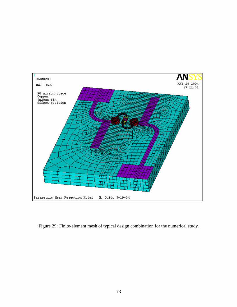
Figure 29: Finite-element mesh of typical design combination for the numerical study.
73

Table 12: Experimental Design and results.
Experimental Design forEnhanced Heat Transfer FEA Results
Trace Trace Fin Fin Resistor Epoxy Base Resistorthickness material Length location Temp Temp Current
(µm) (mm) (C) (C) (A)10 CMI 112-15F 10 Direct 57.510 40.680 0.01984230 CMI 112-15F 10 Direct 57.139 40.224 0.01986890 CMI 112-15F 10 Direct 56.314 39.303 0.01987790 Copper 10 Direct 52.761 35.435 0.01988130 Copper 10 Direct 54.138 36.929 0.01988010 Copper 10 Direct 55.561 38.468 0.01987910 Copper 20 Direct 55.492 38.394 0.01987930 Copper 20 Direct 53.887 36.667 0.01988090 Copper 20 Direct 52.252 34.911 0.01988190 CMI 112-15F 20 Direct 56.286 39.273 0.01987730 CMI 112-15F 20 Direct 57.131 40.216 0.01986810 CMI 112-15F 20 Direct 57.508 40.678 0.01984210 CMI 112-15F 20 Offset 57.648 40.828 0.01984330 CMI 112-15F 20 Offset 57.452 40.561 0.01986890 CMI 112-15F 20 Offset 56.875 39.907 0.01987790 Copper 20 Offset 52.890 35.581 0.01988130 Copper 20 Offset 54.741 37.571 0.01988010 Copper 20 Offset 56.244 39.202 0.01987910 Copper 10 Offset 56.283 39.243 0.01987930 Copper 10 Offset 54.884 37.719 0.01988090 Copper 10 Offset 53.233 35.928 0.01988190 CMI 112-15F 10 Offset 56.892 39.925 0.01987730 CMI 112-15F 10 Offset 57.456 40.567 0.01986810 CMI 112-15F 10 Offset 57.650 40.829 0.01984310 CMI 112-15F 0 - 57.697 40.883 0.01984230 CMI 112-15F 0 - 57.590 40.713 0.01986890 CMI 112-15F 0 - 57.214 40.276 0.01987790 Copper 0 - 54.262 37.011 0.01988130 Copper 0 - 55.754 38.641 0.01988010 Copper 0 - 56.795 39.800 0.019879
74
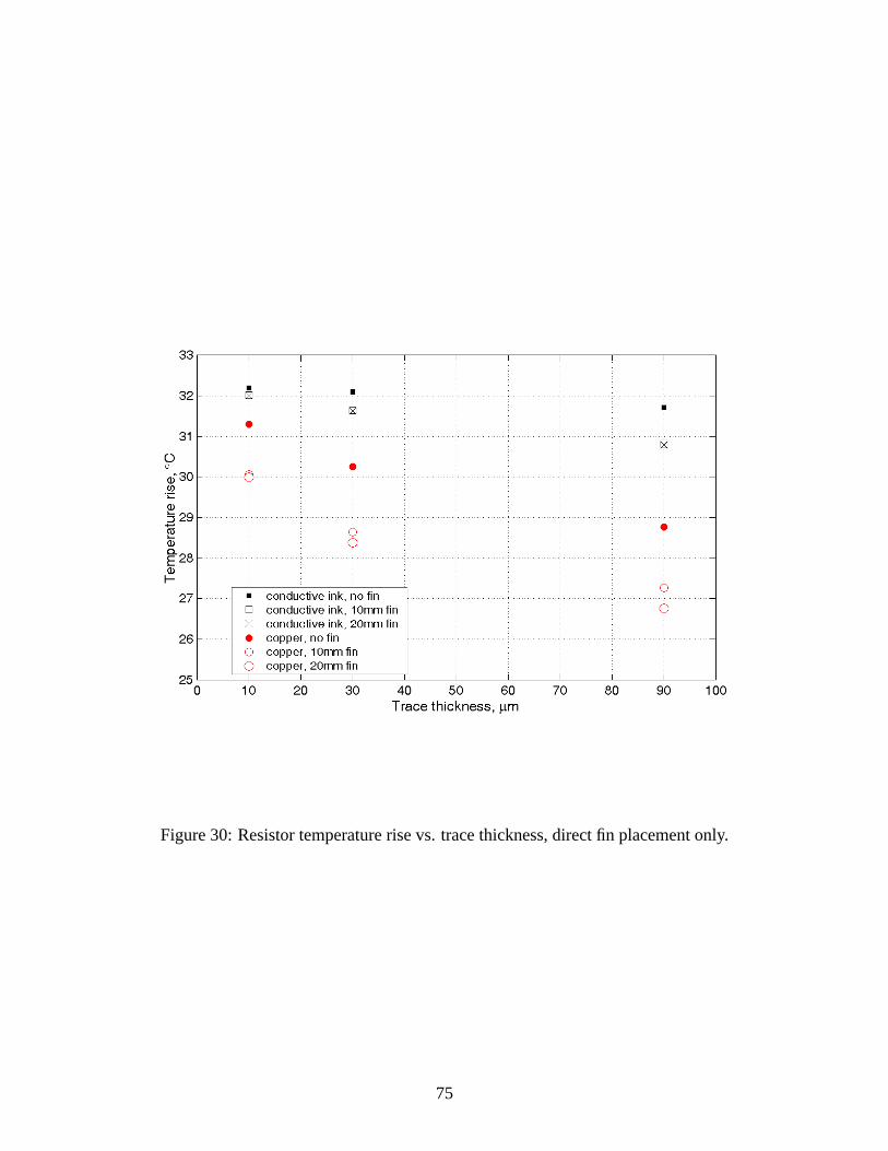
Figure 30: Resistor temperature rise vs. trace thickness, direct fin placement only.
75

Figure 31: Combined plot of temperature rise data vs. Thermal Sheet Resistance.
76

7.4 STATISTICAL ANALYSIS
To obtain more information about the relationships between the parameters in Table12, a statistical
analysis of the FEA results dataset was performed with the MINITABR© program [93]. MINITAB R©
can be used to plot the mean values for collections of data points having common factor values;
i.e. a plot of temperature rise vs. Factor A, comparing the mean of all points with Factor A at its
highest with the mean of all points with Factor A at its lowest, and so on for all factors. This is
referred to as a plot ofmain effects. Figure32 is a main effects plot for the resistor temperature
rise (the plot for the epoxy temperature rise is quite similar).
Figure 32: Main Effects plot for resistor temperature rise data.
The main effects plot clearly indicates the overriding effect on temperature rise of varying the
bulk thermal conductivitykxx. In decreasing order of impact, the relative effects of trace thickness,
trace fin length, and trace fin location are also shown. The main effects plot also reveals non-linear
effects in both the plots for the trace thickness and the fin length. It is of course only possible to
observe non-linear effects in this way for the effect of three-level (or greater) factors.
What this main effects plot does not show is the effect ofinteractionsbetween two or more
factors. Statistically speaking, an interaction is the variation among the differences between means
77
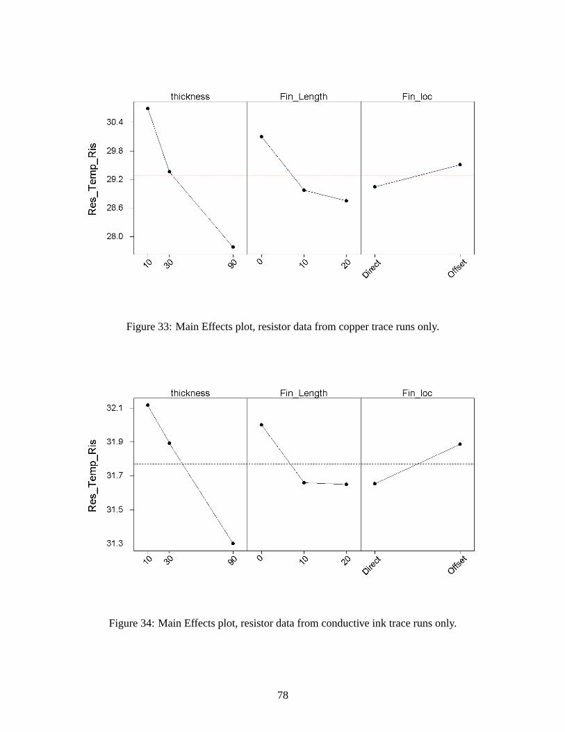
Figure 33: Main Effects plot, resistor data from copper trace runs only.
Figure 34: Main Effects plot, resistor data from conductive ink trace runs only.
78

for different levels of one factor over different levels of the other factor [94]. More to the point,
an interaction can be described as an observed effect which cannot be explained as a simple com-
bination of the effects of two or more single factors. This type of observed effect can be made
apparent in a number of ways; a simple method is to make separate plots for different subsets of
data. Figure33 is a main effects plot only using the data for all runs with copper traces while
Figure34 is a plot only using all runs with conductive ink traces. A strong difference in the form
of the three-level factor plots is immediately apparent. First, in the thickness effects plot for copper
data, the non-linear effect is quite noticeable whereas the same effects plot for the conductive ink
data is nearly linear. In the fin length effects plots, there is some indication of nonlinearity for both
sets of data, but in the plot for conductive ink data there appears to be almost no difference for
10mm fins compared to 20mm fins, i.e. the temperature rise flattens out above 10mm.
The phenomenon causing this observed difference becomes clear in a three-dimensional plot
of the resistor temperature rise, Figure35. In this plot, data from the runs with direct fin placement
only are used, and the bulk thermal conductivity and thickness are combined in the single variable,
Thermal Sheet Resistance, described previously. Plots for the epoxy temperature rise and for
indirect fin placement have a similar form.
Figure 35 shows that for any of the fin lengths analyzed, the temperature rise is a smooth,
continuous (although nonlinear) function of the Thermal Sheet Resistance. The plot also shows
that the function appears nearly linear at high values of resistance (i.e. when trace thickness or bulk
thermal conductivity is low), but the deviation from linearity becomes more and more pronounced
for lower values of resistance. Thus it appears that considering the effect of trace thickness on the
temperature rise behavior is best done only while simultaneously considering the effect of the bulk
thermal conductivity.
79

Figure 35: 3-D Surface plot, resistor data from direct fin placement runs only.
80

8.0 THE SURFACE-MOUNT DEVICE CIRCUIT MODEL
Because of the widespread use of discrete surface-mount devices (SMTs) in mass-manufactured
electronic packaging, it was considered of vital interest in this investigation to confirm the rele-
vance of the information developed to this particular field of technology. To more fully address
these concerns, the next iteration of FEA construction and experimental validation included a
surface-mount resistor.
8.1 FEATURES OF THE FULLY-EMBEDDED CIRCUIT
The circuit specimen described herein includes both conductive-ink current pathways and discrete
components, fully embedded in a polymer matrix. This specimen represents the eventual devices
which are expected to use the design and fabrication methods envisioned in the 3-D circuit archi-
tecture concept; e.g., monolithic fabrication of circuit elements in an otherwise electrically inert
block structure. In one embodiment of the concept as proposed, circuits are to be built up layer-by-
layer using methods analogous to current rapid prototyping techniques; e.g. stereolithography and
3-D printing. In the specimens produced and analyzed herein, generally manual fabrication meth-
ods are employed, including specialized tooling for casting a functional circuit (with temperature
probes) in the chosen embedding medium.
A number of experimental design issues were considered in designing and fabricating the em-
bedded circuit specimen required for this phase of the investigation. As the purpose of the em-
bedded specimen (as with the previously-described specimens) is to evaluate the utility of finite-
element modeling as a tool for prediction of circuit behavior, the specimen is designed such that it
can (as accurately as possible) be represented by the associated FEA model. This design direction
81

suggested employing the simplest geometry possible while including circuit features relevant to a
meaningful investigation.
The chosen embedding medium is as transparent as practical, so as to insure by visual inspec-
tion that the circuit components and sensing probes are maintained in operable condition after the
embedding process. The embedding medium is also chosen for the ready availability of its thermal
properties, not to mention its similarities to materials already used in current electronic devices, or
anticipated for use in the 3-D architecture concept.
The use of a surface-mount-technology (SMT) resistor in the embedded circuit specimen
served to address several of the above concerns. As there are no wire leads, the geometric complex-
ity of the specimen is reduced, with corresponding benefits for construction of the FEA model. A
template was used to control the thickness of the conductive epoxy terminals connecting the SMT
resistor to the circuit traces. This served to give the terminals a uniform hexahedral shape, further
minimizing the geometric complexity of the specimen.
As with the previous specimens, the conductive ink traces were applied using a stenciling
process and cured at elevated temperature. The ink was applied in such a way as to generate
the thickest possible trace within the capability of the stenciling process, and then the sample
was cured at progressively higher temperatures until the measured resistance achieved a minimum
value (Table13). The SMT specimen also included copper contact pads applied to the conductive-
ink pads that were stenciled onto the substrate. This was done to provide a more durable contact
surface, which would withstand the casting process and the eventual need to clean excess casting
medium from the finished specimen. These copper pads were bonded in place with the same
conductive epoxy used to attach the surface-mount resistor to the circuit trace.
Table 13: Processing of conductive ink traces for minimum resistance in SMT circuit model.
Curing Curing Time Trace ResistanceTemperature at Temperature (Long Leg)
70C 30 min 16Ω120C 20 min 8Ω150C 20 min 4Ω175C 20 min 3.5Ω
82

The location of the microthermocouples mounted to the SMT specimen was chosen as a com-
promise between the concerns of acquiring measurements at points of interest and avoiding inter-
ference with the embedding procedure. The measurement points chosen were located
• on the surface-mount resistor,
• 10mm from the center of the resistor, towards the longer end of the sample,
• 20mm from the resistor center, in the same direction, and
• on the underside of the sample immediately below the resistor center.
Figure 36: SMT circuit model prior to embedding, in live test setup.
8.2 TESTING WITH THE SMT MODEL PRIOR TO EMBEDDING
To glean as much information as possible during the course of the live experimental procedures,
a series of temperature tests were completed using the SMT circuit specimen before proceeding
83

Table 14: Raw results from tests of SMT sample before embedding.
Applied Test Test LocationsVoltage ID Resistor 10mm Top 20mm Top Bottom Ambient*
10 a 32.46 25.12 23.35 26.25 22.5615 a 45.86 29.49 25.82 31.91 23.5715 b 45.35 29.46 25.83 31.93 23.4518 a 55.55 32.12 27.04 35.61 23.9918 b 54.83 32.03 26.99 35.56 23.6320 a 62.21 33.48 27.36 37.80 23.7220 b 61.38 33.45 27.34 37.79 23.3522 a 70.09 35.66 28.43 40.77 24.0924 a 78.19 37.71 29.09 43.48 23.9024 b 73.88 37.55 29.12 43.62 23.5926 a 87.24 39.97 30.04 46.62 23.9726 b 85.60 39.49 29.87 46.65 23.5128 a 96.23 41.43 30.32 48.74 23.5130 1 106.03 43.60 31.16 51.82 23.5430 a 106.34 43.59 31.48 51.65 23.6430 b 97.96 44.05 31.74 53.34 23.64
Temperatures inC atτ = 2000s.*Average measurement over entire test interval.
on to the embedding process (Figure36). These test results provided useful comparisons to the
previous verification tests as well as to the eventual cast specimen tests, as discussed below. These
test results are summarized in Tables14and15.
Note that observed resistor temperatures for the SMT circuit sample are distinctly lower than
those observed in the preliminary circuit sample for the equivalent 10V test case. The obvious rea-
son for this behavior is the reduced power dissipation in the higher-resistance SMT component, as
expected from the expressionP= V2/R. The observed resistor temperature did increase monoton-
ically (and nearly linearly) with dissipated power, as did the observed resistor temperature in the
preliminary sample. Other general trends in the observed temperature behavior appeared similar
to those observed in the preliminary circuit sample tests.
In the tests that were repeated at the same voltage, most of the results track well between trials.
However, for the third trial at 30V a distinct reduction in the measured resistor temperature (over
10%) is seen. A hypothesis for this behavior is that the repeated trials at high power dissipation
as well as wear and tear on the samples from routine handling began to degrade the thermocou-
84

Table 15: Temperature delta results from SMT sample tests before embedding.
Applied Test Test LocationsVoltage ID Resistor 10mm Top 20mm Top Bottom
10 a 10.09 2.75 0.98 3.8815 a 22.02 5.65 1.98 8.0815 b 21.85 5.96 2.33 8.4418 a 31.41 7.98 2.89 11.4618 b 31.05 8.25 3.21 11.7820 a 38.22 9.49 3.37 13.8120 b 37.91 9.99 3.87 14.3222 a 45.83 11.41 4.18 16.5224 a 54.12 13.64 5.01 19.4124 b 50.29 13.97 5.53 20.0426 a 63.01 15.75 5.82 22.3926 b 61.80 15.69 6.06 22.8428 a 72.40 17.60 6.49 24.9130 1 82.26 19.83 7.39 28.0430 a 82.58 19.83 7.72 27.8930 b 74.05 20.14 7.83 29.42
Temperature difference over ambient inC atτ = 2000s.
ple/sample bond; this possibility is addressed in9.2.1.1below in conjunction with a discussion of
correlation with the numerical circuit model.
8.3 COMPLETING THE EMBEDDED SMT SPECIMEN
The casting procedure developed for embedding the specimens takes into account several other
concerns. In order to maintain visibility of the discrete components and temperature probes, a
water-clear, two-component epoxy resin was chosen as the casting medium. To avoid degrada-
tion in visibility through the epoxy, the casting tool was designed and built to minimize surface
roughness on the finished specimen. After some early experiments with a glass-walled tool, the
final tool was constructed with acetal polymer walls held rigid within a polycarbonate frame. After
mixing, the resin was degassed in a vacuum chamber before pouring, to minimize bubbles in the
casting. This further protected the transparency of the casting as well as limiting non-homogeneity
of properties in the cast epoxy volume.
85

Figure 37: SMT circuit model embedded in epoxy resin.
To produce a cast specimen, the substrate, with the discrete resistor and temperature probes
in place, was inverted and placed in the top of the tool. The thermocouples were mounted to the
substrate and resistor using the same two-part epoxy to be used for the eventual casting. Rubber
spacer blocks were inserted between the connection pads on the substrate and the far wall of the
tool, with a light clamping force applied to hold the setup in place. These blocks served to mask
off the connection pads from contamination by the epoxy, while also controlling the height of the
finished casting.
The finished embedded specimen is shown in Figure37. The presence of some air bubbles
in the epoxy matrix was noted, so the results of the live tests and of the subsequent numerical
modeling were regarded carefully with an eye towards the possible impact of these bubbles.
86

8.4 TEST RESULTS FROM THE EMBEDDED CIRCUIT SAMPLE
The raw and reduced results from the temperature tests conducted on the embedded SMT cir-
cuit are summarized in Tables16 and17. A general comparison between the non-embedded and
embedded SMT circuit results is presented in Figure38. The comparison plot shows that the in
the embedded case the resistor and bottom substrate temperatures are consistently lower, while
Table 16: Raw temperature data from embedded SMT sample tests.
Applied Test LocationsVoltage Resistor 10mm Top 20mm Top Bottom Ambient*
15 39.90 29.75 26.35 31.30 23.8218 46.35 31.64 26.85 33.87 23.5320 51.52 33.39 27.50 36.15 23.4422 57.16 35.44 28.35 38.67 23.5224 63.70 37.92 29.54 41.71 23.6826 70.48 40.26 30.50 44.64 23.7828 77.96 42.96 31.70 47.95 23.9930 85.75 45.53 32.60 51.18 23.74
Temperatures inC atτ = 2000s.*Average measurement over entire test interval.
Table 17: Temperature delta results from SMT embedded sample tests.
Applied Locations on the CircuitVoltage Resistor 10mm Top 20mm Top Bottom
15 15.96 5.81 2.41 7.3718 22.73 8.01 3.23 10.2420 27.69 9.56 3.67 12.3322 33.46 11.74 4.66 14.9724 39.81 14.03 5.64 17.8126 46.40 16.18 6.43 20.5728 53.91 18.91 7.65 23.9030 61.67 21.44 8.52 27.10
Temperature difference over ambient inC atτ = 2000s.
the remaining substrate temperatures are nearly equal to (if consistently higher) than in the non-
embedded case. One explanation is that the substrate is serving as a heat sink (and heat spreader)
for the resistor, where the heat is ultimately generated. When the casting epoxy is added, the ef-
fective mass of the heatsink is increased, increasing the the heat spreading effect and reducing the
87

resistor temperature. Furthermore, since in the embedded sample none of the generated heat can be
immediately transferred to the surroundings by convection, the average temperature in the sample
outside of the resistor must be higher. The bottom temperature location is, however, exposed to
ambient conditions even in the embedded case. Additionally, being more or less in the center of the
sample, this location benefits from the heatsink properties provided by the surrounding substrate.
Given the above results, it appears that in cases similar to that represented by the test sam-
ple, the effect of embedding the circuitry is to reduce the maximum temperature of the power-
consuming discrete component. One characteristic of importance would appear to be the relatively
low power density within the circuit (in this case,P/V ≈ 0.91W/36.4cm3 = 0.025W/cm3). How-
ever, it would seem reasonable to infer that with even simple techniques applied to enhance the
heat dissipation (e.g. a more conductive casting medium, and/or forced convection on the exte-
rior surfaces) power densities several orders of magnitude higher could be sustained with minimal
thermal impact.
88

Figure 38: Temperature delta measurements vs. voltage applied, before and after embedding.
89

9.0 FEA OF THE SMT VERIFICATION MODEL
9.1 CONSTRUCTION OF THE NUMERICAL SMT CIRCUIT MODELS
The numerical models constructed for the SMT circuit sample include several basic differences
from the verification models constructed to represent the leaded-resistor circuit model. As was
previously noted, the geometry of the SMT circuit was planned to allow simpler FEA modeling in
the region near the discrete resistor. The replacement of the leaded resistor with the SMT device
required several additional material properties to be researched and tabulated to properly charac-
terize the resistor structure. The SMT resistor is a rectangular section of alumina ceramic with a
printed pattern of conducting materials applied to its underside, as determined by dissection of one
of the representative SMT devices and information from commercial hybrid materials literature.
The calibrated resistance (for the chosen device,R= 980Ω) is established by the size and shape of
an undulating printed pattern of thick-film resistive material, coated with an electrically-insulating
paint to prevent short-circuiting to the mounting substrate. The connecting terminals at the ends
are made of a lower-resistance material. Palladium-silver paste was defined in the vendor’s speci-
fications as the material employed here.
The properties of these additional materials (some estimation was required) are presented in
Table18. The estimates made for the the density and heat capacity of the thick-film materials
were not considered critical to the accuracy of the analysis, because the impact of those properties
depends on the relative quantity of those materials within the model (which is an extremely small
percentage). The estimate of the thermal conductivity of this region was also considered to be
non-critical, given that these very small circuit structures are embedded within much larger masses
of well-characterized material.
90

Table 18: Additional material properties used in the SMT FEA models.
Electrical Heat ThermalMaterial Type Density, Resistivity, Capacity, Conductivity,
kg/m3Ω·m J/kg·C W/m·K
Air, 23C 1.19E+00 1.00E+24† 1.01E+03 2.57E-02
Air, 62C 1.04E+00 1.00E+24† 1.01E+03 2.88E-02
Palladium-Silver Thick Film 1.00E+04† 5.00E-08 3.00E+02† 1.30E+02†
Resistive Thick Film 1.00E+04† 2.00E-04 1.00E+03† 2.00E+00†
Alumina Ceramic, 96% pure 3.70E+03 1.00E+11 8.80E+02 2.47E+01
All data from published sources except as noted.
†Estimated.
91

Figure 39: Structure of modeled discrete SMT resistor, viewed from underside.
92

Figure39 shows a detailed view of the modeled resistor structure. The insulating paint was
omitted to simplify the task of modeling, though this did require an adjustment to the electrical
properties of the modeled epoxy terminals to properly model the total device resistance (see9.1.1
below). As for the previous models, the modeled thickness of the ink traces was adjusted (assuming
a bulk electrical resistivity equal to the published value as was done previously) to provide a value
for the total trace resistance as close as possible to that of the fabricated circuit.
9.1.1 The non-embedded model
Figure 40: Complete FEA mesh for non-embedded SMT circuit model.
93

Figure 41: Detail of FEA mesh for connecting pads.
94

Figure 42: Detail of FEA mesh for SMT resistor region.
95

Table 19: Element types used in the SMT model without embedding.
Element Number ofModeled Structure Type Material Elements
Substrate SOLID69 epoxy/glass 9376
Conductive Trace SHELL157 conductive ink 534
Connecting Pads SOLID69 copper 408
Pad Bonding Layers SOLID69 conductive epoxy 408
Connecting Terminals SOLID69 conductive epoxy 432†
Air Gap SOLID69 air 162
Resistor Components:Body SOLID69 Alumina 432Resistive Element LINK68 thick-film resistive paste 62Terminals SHELL157 PdAg thick-film paste 54
†Includes elements withρ set = 0 as explained in (9.1.1).
96
Table19 gives a listing of the element types and materials employed in the non-embedded
model. The completed finite-element mesh for the non-embedded model is shown in Figure40.
Figure41 shows a detail of the modeled connecting pads, bonded to the conductive ink pads with
conductive epoxy. The element mesh representing the epoxy consists of two layers of very thin
elements; elements with such an extreme aspect ratio are typically not desirable in an analysis,
as (for this element type) linearity in the temperature solution is enforced from one side of an
element to the other, and such an extreme difference in length between the element dimensions
can introduce inaccuracies into the total solution. However, in this case the exact details of the
temperature solution in this region were not deemed to be of major interest, and reducing the in-
plane size of the element mesh to improve the aspect ratio would have greatly increased the total
number of elements required without significantly improving the quality of the results.
Figure42 shows a detail of the model structure representing the SMT resistor mounted to the
substrate with conductive epoxy. On the epoxy terminals, three rows of elements on the upper
inboard edge of each were assigned an artificially high value for their bulk electrical resistivity.
As alluded to above, this was done to avoid having to model the insulating layer applied to the
conductive elements. The thermal properties in this region were maintained at the typical values
for the chosen conductive epoxy.
In the narrow air gap under the resistor, heat transfer by convection was expected to be minimal.
This expectation is supported by a calculation of the Rayleigh number for the gap. For the geometry
of interest, assumeTh = 106C = 379K andTc = 44C = 317K (from the live test results) and take
H = gap thickness = .001m. Then atTf ilm ≈ 350K,∆T ≈ 60K,
RaH =gβ∆TH3
αν
=(9.8)(2.86×10⁻³)(60)(.001)3
(29.9×10⁻⁶)(20.92×10⁻⁶)= 2.7 .
For fluid constrained within parallel walls defining a narrow cavity, the onset of heat transfer by
convection occurs at a critical value of RaH [95, 96]. For a horizontal cavity heated from the
bottom, RaH(critical) <≈ 1708. It seems reasonable to suggest that for a cavity heated from
the top, the critical value for convection due to buoyancy-induced flow should be no less than
97

this value, since buoyancy effects induce convective flows in an upward direction. Therefore heat
transfer in this region is characterized by conduction only, and as such was simply modeled with
solid elements assigned the temperature-dependent properties of air.
The convection boundary conditions applied to the SMT model before embedding required
some calculation ofhconv for the small areas associated with the resistor structure and the connec-
tion pads. As with the original verification models, heat transfer by radiation was neglected, and
convection from individual surfaces was assumed independent of the configuration of any adjacent
surfaces.
9.1.2 The embedded model
Compared with the non-embedded FEA model, the embedded model of course includes a layer of
cast epoxy material comprising roughly the upper half of the modeled volume. The region under
the resistor is also modeled with epoxy elements instead of air.
The element mesh for the cast epoxy at opposite corners of the model does not match exactly
with that defined for the adjacent connecting pads and their conductive epoxy bonding layer. If
the mesh in these regions had been matched exactly, the very small element dimensions of the
conductive epoxy in the through-thickness dimension would have necessitated an extremely fine
element mesh in the cast epoxy as well. Instead, constraint equations were employed (as described
in 5.5.1above) to numerically link the pad edges with the adjacent cast epoxy elements. Convec-
tion boundary conditions for the embedded model were somewhat less complex to calculate and
apply to the model, due to the simpler surface geometry of the cast specimen structure. A listing
of the element types used in the embedded SMT model is given in Table20.
98

Table 20: Element types used in the embedded SMT model.
Element Number ofModeled Structure Type Material Elements
Substrate SOLID69 epoxy/glass 9376
Conductive Trace SHELL157 conductive ink 534
Connecting Pads SOLID69 copper 408
Pad Bonding Layers SOLID69 conductive epoxy 408
Connecting Terminals SOLID69 conductive epoxy 432†
Transparent Embedding SOLID69 cast epoxy 18396
Resistor Components:Body SOLID69 Alumina 432Resistive Element LINK68 thick-film resistive paste 62Terminals SHELL157 PdAg thick-film paste 54
†Includes elements withρ set = 0 as explained in (9.1.1).
99

9.2 RESULTS FROM THE BASIC NUMERICAL MODELS
9.2.1 The non-embedded model
Temperature results from the FEA of the SMT circuit before embedding are given in Tables21and
22. A temperature plot from a typical run is given in Figure43, showing a close-up of the contours
in the resistor region.
Table 21: Raw results from FEA of SMT circuit before embedding.
Applied Locations on the ModelVoltage Resistor 10mm Top 20mm Top Bottom
10 31.88 27.91 27.08 28.1515 40.68 30.28 27.79 32.6218 47.25 32.60 29.09 35.9120 52.13 34.31 30.03 38.3522 57.47 36.16 31.04 41.0124 63.28 38.14 32.13 43.8826 69.48 40.23 33.26 46.9228 76.08 42.41 34.43 50.1130 83.05 44.67 35.63 53.45
AmbientT∞ = 23.8C for all FEA runs.
Table 22: Temperature delta results from FEA of SMT circuit before embedding.
Applied Locations on the ModelVoltage Resistor 10mm Top 20mm Top Bottom
10 8.08 4.11 3.28 4.3515 16.88 6.48 3.99 8.8218 23.45 8.80 5.29 12.1120 28.33 10.51 6.23 14.5522 33.67 12.36 7.24 17.2124 39.48 14.34 8.33 20.0826 45.68 16.43 9.46 23.1228 52.28 18.61 10.63 26.3130 59.25 20.87 11.83 29.65
The general trends in the temperature results are comparable to those from previous model
runs. However, the quality of the results is best evaluated by comparison with the live test data
from the non-embedded circuit sample. This comparison is discussed in9.2.1.1below.
100

Figure 43: Typical temperature contour plot of resistor region of SMT model without embedding.
101

Figure 44: SMT model before embedding, correlation of live test data with FEA results.
102
9.2.1.1 Comparison with live test results A correlation of the temperature delta data from
the live tests with the corresponding FEA data for the SMT circuit without embedding is given in
Figure44. The log-log format was used to more clearly discriminate the individual temperature
data points from locations on the substrate. It is immediately apparent from this plot that for
the resistor data, the numerical results fall significantly below the live test results. Conversely,
the numerical results from the 20mm position atop the substrate are significantly higher than the
corresponding live test results. The FEA results taken from the other two substrate locations (which
are much closer to the heat source) show fairly high correlation with the test data. This is a marked
departure from the high quality of the correlation observed between the leaded resistor samples
and their corresponding FEA models.
It is important to address this low level of agreement between the live tests and the FEA model
representation of the SMT model. Such an inquiry offers the possibility of gaining new insights
into heat transfer behavior under similar circumstances. This necessarily requires consideration of
the range of assumptions made in developing the FEA model, as well as the extent of differences
between the SMT model and the leaded resistor models.
The list enumerated in5.5.1includes a number of assumptions that remain a part of the model
even for the SMT circuit. Viewed in light of the research conducted so far, the list can be re-
evaluated to suggest a number of reasonable avenues for inquiry, while rendering other assumptions
as moot, and accepting other original assumptions as now having been proved appropriate. For
example, one issue that might be raised concerns the assumption of heat flux by convection only
from the exterior surfaces. Since the simplified network analysis that justified neglecting radiation
was only developed for low levels of power dissipation, it could be argued that including radiation
might be required for accurate modeling at higher power dissipation levels. However, a review of
the correlation data leads to a rejection of this possibility, given that the hottest part of the model
(the resistor) showed lower temperatures for the FEA, which would imply (if anything) that the
modeled heat transfer mechanisms areover-estimating the amount of heat lost from the resistor to
its surroundings.
Degradation of the live sample from repeated testing and handling, described in8.2 was also
considered as a source of error. As discussed in4.3, loosening of the thermocouple/sample bonds
would result in live test results which underreported the actual sample temperatures achieved,
103

providing some explanation for the substrate result sets in which the FEA results exceeded the live
test measurements. However, the lack of correlation is apparent in all of the tests, not just the later
ones. Furthermore, this same explanation does not account for the resistor rise FEA results, which
are consistently lower than their corresponding live test measurements.
Given the large variety of materials that are modeled in the FEA, discrepancies in certain of
the defined material properties might be another reasonable area for consideration as a source of
error. The most obvious possibility to investigate is a higher than actual value for thermal conduc-
tivity of the conductive epoxy, which if true would give both understated resistor temperatures and
overstated substrate temperatures (as were demonstrated in the correlation). However, a sensitivity
analysis performed by successively decreasing the value ofkxx applied to the epoxy elements indi-
cated that reductions of this parameter by up to an order of magnitude could account for barely half
of the discrepancy between the model and the live tests. Such a significant error in the supplier’s
material data seems unlikely, and could not be confirmed or rejected without extensive additional
effort.
9.2.1.2 Thermal contact resistance modeling Evaluating the initial assumptions in this way,
a number of avenues for further inquiry were chosen. The first correction to be considered dealt
with the presence or absence of thermal resistance effects not inherent to the conductive paths of
the circuit (which were considered in the network analysis of5.4.1). As per the research cited
previously, it is apparent that the thermal resistance behavior of circuits constructed with materials
comparable to those used in this research cannot be completely characterized by bulk resistivity
effects alone. Therefore it is reasonable to consider whether omitting interfacial thermal resistance
might be a source of the poor correlation.
Based on the previous research cited, an appropriate thermal resistance parameter can be cal-
culated for selected interfaces in the model. The expected value of the interface resistance as
determined in the previously-cited research [44] is dependent upon the bulk material forming the
bonded joint, as well as upon the processing parameters. Given the results previously reported,
values ranging from 0.25 to 0.8 K/W would be expected for the interfacial component of thermal
resistance in a representative joint of (2.5×2.5) cm2. If the parameter is instead expressed as a
specific conductance, the expected values range from 1.9×10⁻³ to 6.3×10⁻³ W/mm2·K. This spe-
104
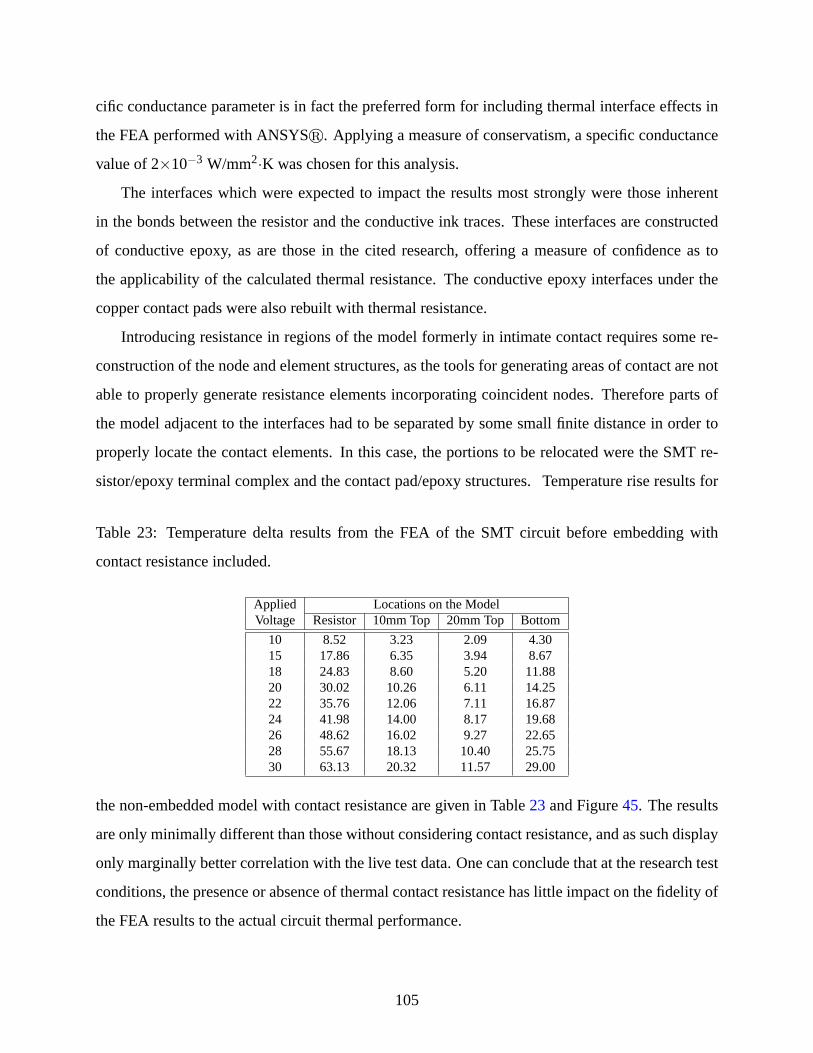
cific conductance parameter is in fact the preferred form for including thermal interface effects in
the FEA performed with ANSYSr. Applying a measure of conservatism, a specific conductance
value of 2×10⁻³ W/mm2·K was chosen for this analysis.
The interfaces which were expected to impact the results most strongly were those inherent
in the bonds between the resistor and the conductive ink traces. These interfaces are constructed
of conductive epoxy, as are those in the cited research, offering a measure of confidence as to
the applicability of the calculated thermal resistance. The conductive epoxy interfaces under the
copper contact pads were also rebuilt with thermal resistance.
Introducing resistance in regions of the model formerly in intimate contact requires some re-
construction of the node and element structures, as the tools for generating areas of contact are not
able to properly generate resistance elements incorporating coincident nodes. Therefore parts of
the model adjacent to the interfaces had to be separated by some small finite distance in order to
properly locate the contact elements. In this case, the portions to be relocated were the SMT re-
sistor/epoxy terminal complex and the contact pad/epoxy structures. Temperature rise results for
Table 23: Temperature delta results from the FEA of the SMT circuit before embedding with
contact resistance included.
Applied Locations on the ModelVoltage Resistor 10mm Top 20mm Top Bottom
10 8.52 3.23 2.09 4.3015 17.86 6.35 3.94 8.6718 24.83 8.60 5.20 11.8820 30.02 10.26 6.11 14.2522 35.76 12.06 7.11 16.8724 41.98 14.00 8.17 19.6826 48.62 16.02 9.27 22.6528 55.67 18.13 10.40 25.7530 63.13 20.32 11.57 29.00
the non-embedded model with contact resistance are given in Table23 and Figure45. The results
are only minimally different than those without considering contact resistance, and as such display
only marginally better correlation with the live test data. One can conclude that at the research test
conditions, the presence or absence of thermal contact resistance has little impact on the fidelity of
the FEA results to the actual circuit thermal performance.
105

Figure 45: SMT model before embedding, contact resistance included, correlation with live test
data.
106
9.2.1.3 Enhancement of convection modeling by numerical adjustment of film coefficients
Given the apparent insignificance of thermal resistance phenomena at the conditions of interest,
other possible refinements to the model need to be considered. Apropos of the issues raised in
3.2.1, an inquiry is warranted as to the appropriateness of the film coefficient values applied to the
FEA model. Relevant to this line of inquiry is the observation that in the leaded-resistor model,
with results that correspond much more closely to the live tests, the resistor and substrate are
less intimately connected, such that an argument can be made that the film coefficients of these
individual surfaces might be more reasonably treated as independent from each other.
The experimental determination of film coefficients for local conditions on other than the most
primitive substrate geometries is clearly a non-trivial undertaking. A formal consideration of this
issue would, ideally, require the construction of complex live test samples including instrumenta-
tion for the measurement of both local temperature and local heat flux values, which might well
vary considerably over small spatial distances. Within the scope of this research, a more efficient
numerical approach employed the FLOTRANTM component of the ANSYSr software package.
The approach taken was to construct a fluid-dynamics model of the convection problem which
could provide temperature and heat flux results in specific localized regions on the substrate/air
interface. Using the results from a sequence of analyses with varying heat energy inputs, localized
film coefficient values were calculated that could be compared with the surface-averaged values
generated from expressions in the cited literature. Given the large increase in computational com-
plexity incurred in solving the appropriate equations for fluid phenomena (3-D energy equation
3.6, continuity, and the Navier-Stokes equations), a simplified model was developed which incor-
porated the most significant geometric aspects of the circuit tests while limiting the time and effort
required to execute the analyses and interpret the results.
A schematic of the chosen configuration for the fluid model is given in Figure46. A cylindrical
analysis region was specified with the same volume and height as the test enclosure, which could
be modeled as a 2-D axisymmetric geometry. Within the modeled region, a cylindrical solid region
was situated with the same area footprint and volume as the non-embedded circuit sample (Figure
47). A volume representing the SMT resistor was located atop the substrate portion of the solid
region, with a specified rate of heat generation corresponding to the Joule heat dissipated in the
resistor for a given test. The heat-generating volume was connected to the substrate region by
107
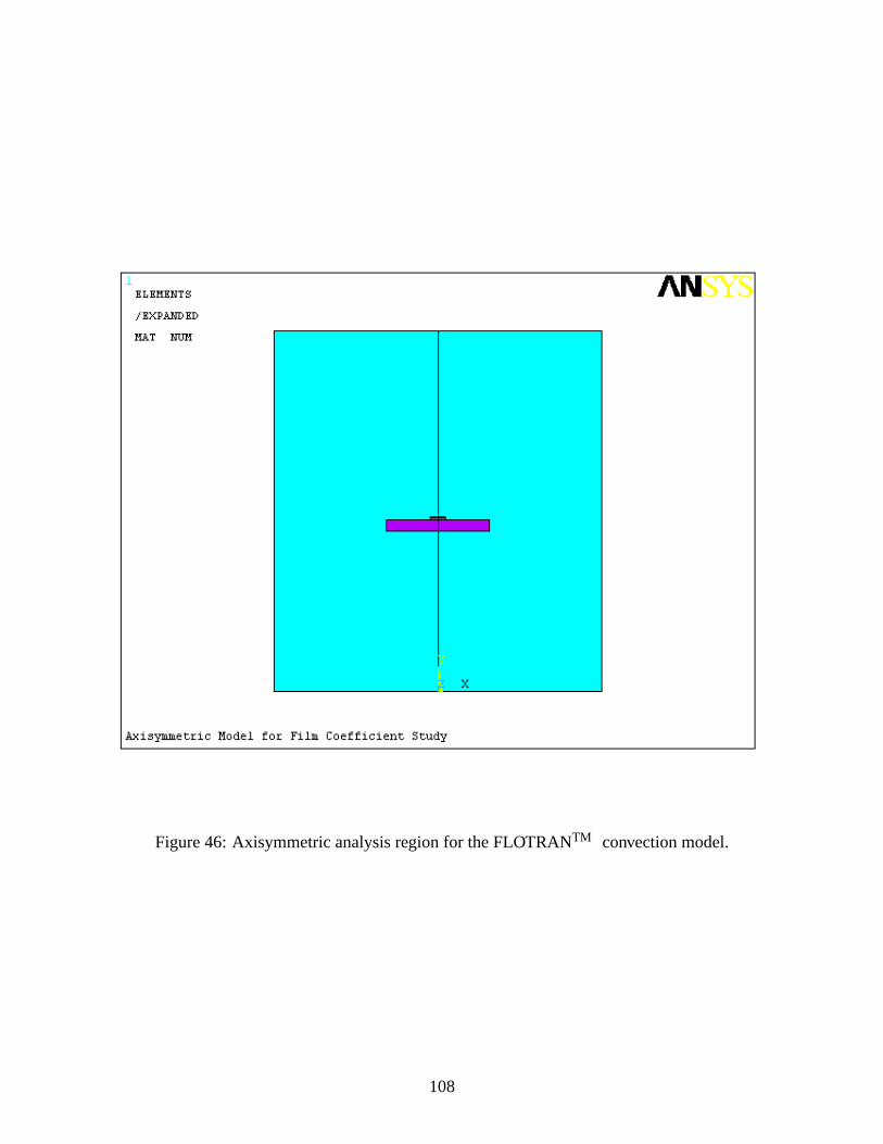
Figure 46: Axisymmetric analysis region for the FLOTRANTM convection model.
108

Figure 47: Half-symmetry model of the substrate and resistor volumes for the convection analysis.
109

a layer which represented the conductive-epoxy terminals of the circuit sample. A detail of the
finite-element mesh in the solid region and the surrounding fluid region of the model is shown in
Figure48. The element types used in the model are given in Table24.
Table 24: Element types used in the numerical convection model.
Modeled Structure (Material) Number of Elements
Substrate (epoxy/glass) 402Resistor (alumina) 32
Conductive epoxy layer 32Air 3790
All elements are type FLUID141.
The same thermal material properties used in the 3-D models were employed for the solid
portions of the 2-D axisymmetric fluid model. For the fluid region, the standard material model
for air incorporated into the FLOTRANTM component of ANSYSr was used. The enclosure
walls were fixed at a uniform temperature of 298K = 24.85C. Given that the situation being
simulated was natural convection at relatively low temperatures, the program options were set to
calculate the fluid behavior under an assumption of purely laminar flow conditions. The validity
of the laminar flow assumption was checked using the flow velocity results from the analyses.
The described model was used to execute a sequence of analyses over a range of values of
generated Joule heat applied to the modeled resistor volume. The extent of the computational
resources required for the fluid dynamics models is illustrated by the time elapsed to execute these
2-D axisymmetric cases, compared with that required for the previous 3-D models. Those previous
models typically converged to steady-state results in less than 100 seconds, while the fluid dynamic
models consistently required elapsed times at least an order of magnitude greater to iterate to
convergence (convergence was verified by summing the total heat transferred at the solid/fluid
interface and at the enclosure boundary, and comparing both of these values with the applied heat
dissipation). A 3-D fluid dynamics model of the SMT sample within a modeled region duplicating
the actual enclosure would require a finite-element mesh including many more degrees of freedom
and would therefore require much longer times to solve.
Figures49 and50 give the temperature contours in the solid and fluid regions respectively
for a typical analysis case. Maximum surface resistor temperatures are given in Table25. The
110

Figure 48: Finite-element mesh for the numerical convection model.
111

Figure 49: Typical temperature contours, solid region of numerical convection model.
112

Figure 50: Typical temperature contours, fluid region of numerical convection model.
113
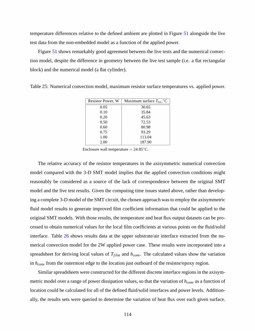
temperature differences relative to the defined ambient are plotted in Figure51 alongside the live
test data from the non-embedded model as a function of the applied power.
Figure51shows remarkably good agreement between the live tests and the numerical convec-
tion model, despite the difference in geometry between the live test sample (i.e. a flat rectangular
block) and the numerical model (a flat cylinder).
Table 25: Numerical convection model, maximum resistor surface temperatures vs. applied power.
Resistor Power, W Maximum surfaceTres,C
0.05 30.650.10 35.840.20 45.630.50 72.530.60 80.980.75 93.291.00 113.042.00 187.90
Enclosure wall temperature= 24.85C.
The relative accuracy of the resistor temperatures in the axisymmetric numerical convection
model compared with the 3-D SMT model implies that the applied convection conditions might
reasonably be considered as a source of the lack of correspondence between the original SMT
model and the live test results. Given the computing time issues stated above, rather than develop-
ing a complete 3-D model of the SMT circuit, the chosen approach was to employ the axisymmetric
fluid model results to generate improved film coefficient information that could be applied to the
original SMT models. With those results, the temperature and heat flux output datasets can be pro-
cessed to obtain numerical values for the local film coefficients at various points on the fluid/solid
interface. Table26 shows results data at the upper substrate/air interface extracted from the nu-
merical convection model for the 2W applied power case. These results were incorporated into a
spreadsheet for deriving local values ofTf ilm andhconv. The calculated values show the variation
in hconv from the outermost edge to the location just outboard of the resistor/epoxy region.
Similar spreadsheets were constructed for the different discrete interface regions in the axisym-
metric model over a range of power dissipation values, so that the variation ofhconvas a function of
location could be calculated for all of the defined fluid/solid interfaces and power levels. Addition-
ally, the results sets were queried to determine the variation of heat flux over each given surface.
114

Figure 51: Resistor temperature rise vs. power dissipated, live tests and numerical convection
model.
115

In each case, observation showed that the heat flux varies significantly over the surface of interest.
This is useful in judging the original decision to employ the isothermal forms of the convection
equations (see3.2). Given the observed variation inQ, it is clear that an assumption of uniform
heat flux in choosing the convection equations is not justified.
The value ofkf luid was also obtained for each local value ofTf ilm, such that a local value of the
Nusselt number could be calculated based onhconv (Nu = hconvL/kf luid, with L = A/p taken for the
entire interface of interest). This local value of Nu was compared with the values of NuL(Tf ilm)
calculated from3.11through3.13, and the ratio plotted against the normalized locationχ relative
to the edge of the particular interface (Figures52 through56).
The Nusselt number variation curves in Figures52 through56 share a number of interesting
features. The different curves, which were drawn for widely varying power dissipation levels,
were associated with local values ofTf ilm which likewise varied over a considerable range. From
this, it is immediately apparent that given the relatively compact spread of the data points despite
the temperature variation, the observed variations in Nu(χ)/NuL(Tf ilm) are almost uniformly a
function of location on the surface. The only significant departure from this behavior is found for
the substrate top surface at the lowest power dissipation. At this low rate of heat energy input, the
driving impetus for convection is very low, and heat transfer by convection is likely to be lower
than the local conduction heat flux in the adjacent substrate. Even including this case, an average
Nu ratio can be calculated which is only dependent on the dimensionless quantityχ, and which
falls very close to all of the other datasets.
It can also be seen that for all surfaces except the substrate underside, the Nu ratio is less than
1 for nearly all locations. The highest values are typically found at the locations near the exposed
surface edges, and the lowest values are found near re-entrant corners and at the central axis of the
model. An inspection of Figure50 offers an explanation in that these variations correspond well
to the variations in the thermal boundary layer thickness (thinner boundary layer=higher Nu ratio)
as the convection-driven flow passes over the exterior solid boundaries.
The mean values of Nu(χ)/NuL(Tf ilm) calculated from the convection model can be used as a
first-order correction to the film coefficients calculated for the SMT model from3.11through3.13.
These corrected values were applied to the non-embedded SMT model and results were generated
116

for the same applied voltages as previously. Table27 gives the temperature delta results for the
first-order correction, and Figure57shows the correlation with the live test data.
The FEA model including a first-orderhconv correction shows a dramatic improvement in the
correlation between the resistor test temperatures and the corresponding FEA results. This type
of correction is very useful in a situation where accurate prediction of the power-dissipating com-
ponent temperature is the most important model result. However, accompanying this desirable
outcome is a degradation in the correlation for the other measurement points, most notably those
for the substrate temperature at a point 20mm from the resistor. Since the first-order correction
served to reduce the efficacy of convection for all of the model surfaces except the substrate under-
side, this outcome could perhaps have been expected. From a component durability standpoint, a
model result such as this one which overstates the circuit temperature is certainly more conserva-
tive than the opposite case. However, model results more faithful to the live test results for these
measurement locations would obviously be desirable.
The results given in Table27 and Figure57 were generated by applying a uniform first-order
correction to thehconv values previously calculated. But as the convection model reveals, the local
values ofhconv(Tf ilm) are not uniform over any of the surfaces, but instead vary as a function of
distance from the surface edges. A higher-order correction can be applied which takes this variation
into account, by using a fitted function to adjust the previously-uniform film coefficients before
applying them to the model. A fitted curve for the upper substrate surface is shown in Figure58.
This function was incorporated into an ANSYSr macro which generated incrementally-adjusted
film coefficients to be applied to the model surface over contoured segments of the surface. The
macro code for this surface type is given in Appendix, and a contour map of the surface with
applied film coefficients is given in Figure59. Similar adjustment schemes were applied to all of
the model convection surfaces. It would have been desirable to apply adjusted film coefficients on
a node-by-node basis, but ANSYSr requires that any discrete film coefficient definition (which is
input as a material property; see5.4.2) can only be applied to complete contiguous element faces.
The temperature delta results from the model with contoured film coefficient adjustment are
given in Table28 and shown correlated with the live results in Figure60. The correlation plot is
virtually identical to that for the first-order corrected model, with a majority of the delta values
from the two tables agreeing to within 1%. Clearly, for this case the higher-orderhconv adjustment
117

scheme offers little improvement in accuracy over the first-order scheme. The demonstrated im-
provement in the accuracy of the modeled resistor temperature data is apparently all that could be
delivered by even more sophisticated adjustment methods.
9.2.2 The embedded model
With the extensive investigation described above as a background, the temperature results from the
FEA of the fully-embedded SMT circuit are given in Tables29and30. A temperature contour plot
from a typical analysis run is shown in Figure61, with a fraction of the cast epoxy region cut away
to more clearly show the contours near the resistor.
9.2.2.1 Comparison with live test results A correlation of the live test data with the FEA for
the embedded SMT circuit is given in Figure62. For the embedded model with standard film coef-
ficient values applied, the resistor temperature deltas from the FEA track the live test results more
closely than for the non-embedded model. However, the FEA results for the substrate locations still
exceed those for the live tests by an increasing degree as the locations fall farther from the ultimate
heat source (the resistor). It is reasonable to expect that if one of the film coefficient adjustment
schemes in9.2.1.3were applied, the overall effect would be a general increase in modeled circuit
temperatures. Thus any improvement in the quality of the resistor temperature correlation would
be accompanied by a degradation in the quality of the correlation for the remaining measurement
points, as was indicated for the non-embedded model.
118
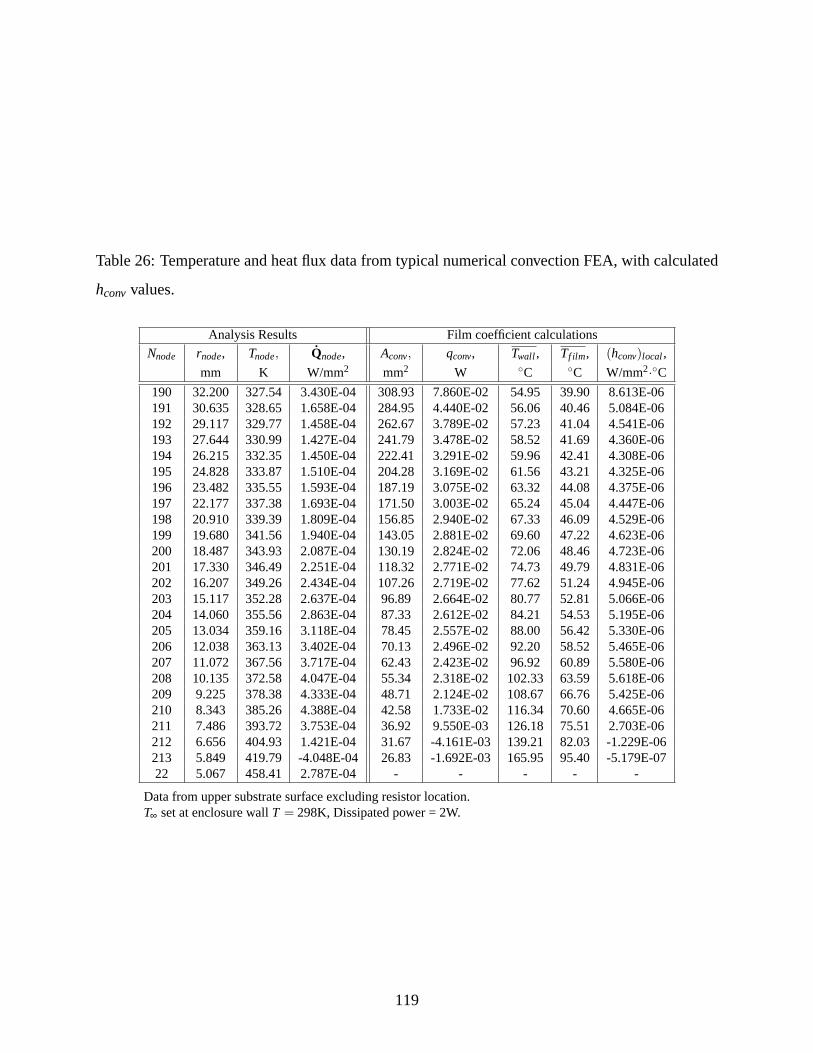
Table 26: Temperature and heat flux data from typical numerical convection FEA, with calculated
hconv values.
Analysis Results Film coefficient calculations
Nnode rnode, Tnode, Qnode, Aconv, qconv, Twall , Tf ilm, (hconv)local,
mm K W/mm2 mm2 W C C W/mm2·C190 32.200 327.54 3.430E-04 308.93 7.860E-02 54.95 39.90 8.613E-06191 30.635 328.65 1.658E-04 284.95 4.440E-02 56.06 40.46 5.084E-06192 29.117 329.77 1.458E-04 262.67 3.789E-02 57.23 41.04 4.541E-06193 27.644 330.99 1.427E-04 241.79 3.478E-02 58.52 41.69 4.360E-06194 26.215 332.35 1.450E-04 222.41 3.291E-02 59.96 42.41 4.308E-06195 24.828 333.87 1.510E-04 204.28 3.169E-02 61.56 43.21 4.325E-06196 23.482 335.55 1.593E-04 187.19 3.075E-02 63.32 44.08 4.375E-06197 22.177 337.38 1.693E-04 171.50 3.003E-02 65.24 45.04 4.447E-06198 20.910 339.39 1.809E-04 156.85 2.940E-02 67.33 46.09 4.529E-06199 19.680 341.56 1.940E-04 143.05 2.881E-02 69.60 47.22 4.623E-06200 18.487 343.93 2.087E-04 130.19 2.824E-02 72.06 48.46 4.723E-06201 17.330 346.49 2.251E-04 118.32 2.771E-02 74.73 49.79 4.831E-06202 16.207 349.26 2.434E-04 107.26 2.719E-02 77.62 51.24 4.945E-06203 15.117 352.28 2.637E-04 96.89 2.664E-02 80.77 52.81 5.066E-06204 14.060 355.56 2.863E-04 87.33 2.612E-02 84.21 54.53 5.195E-06205 13.034 359.16 3.118E-04 78.45 2.557E-02 88.00 56.42 5.330E-06206 12.038 363.13 3.402E-04 70.13 2.496E-02 92.20 58.52 5.465E-06207 11.072 367.56 3.717E-04 62.43 2.423E-02 96.92 60.89 5.580E-06208 10.135 372.58 4.047E-04 55.34 2.318E-02 102.33 63.59 5.618E-06209 9.225 378.38 4.333E-04 48.71 2.124E-02 108.67 66.76 5.425E-06210 8.343 385.26 4.388E-04 42.58 1.733E-02 116.34 70.60 4.665E-06211 7.486 393.72 3.753E-04 36.92 9.550E-03 126.18 75.51 2.703E-06212 6.656 404.93 1.421E-04 31.67 -4.161E-03 139.21 82.03 -1.229E-06213 5.849 419.79 -4.048E-04 26.83 -1.692E-03 165.95 95.40 -5.179E-0722 5.067 458.41 2.787E-04 - - - - -
Data from upper substrate surface excluding resistor location.T∞ set at enclosure wallT = 298K, Dissipated power = 2W.
119

Figure 52: Nusselt number variation in numerical convection model, resistor top surface.
120

Figure 53: Nusselt number variation in numerical convection model, substrate top surface.
121

Figure 54: Nusselt number variation in numerical convection model, substrate bottom surface.
122

Figure 55: Nusselt number variation in numerical convection model, substrate outer edge surface.
123

Figure 56: Nusselt number variation in numerical convection model, resistor and epoxy outer edge
surface.
124

Table 27: Temperature delta results from non-embedded SMT sample FEA with first-order correc-
tion to film coefficients.
Applied Test LocationsVoltage Resistor 10mm Top 20mm Top Bottom
10 10.526 5.180 3.707 6.38615 21.610 10.069 6.950 12.63918 29.814 13.462 9.087 17.10520 35.946 15.952 10.603 20.42322 42.610 18.634 12.204 24.01224 49.893 21.552 13.927 27.93026 57.811 24.710 15.785 32.18528 66.255 28.036 17.732 36.68230 75.214 31.516 19.755 41.407
AmbientT∞ = 23.8C for all FEA runs.
125

Figure 57: SMT model before embedding, first-orderhconv correction, correlation with live test
data.
126

Figure 58: Fitted curve for film coefficient variation on upper substrate surface.
127

Figure 59: Adjustedhconv contours on upper substrate surface.
128
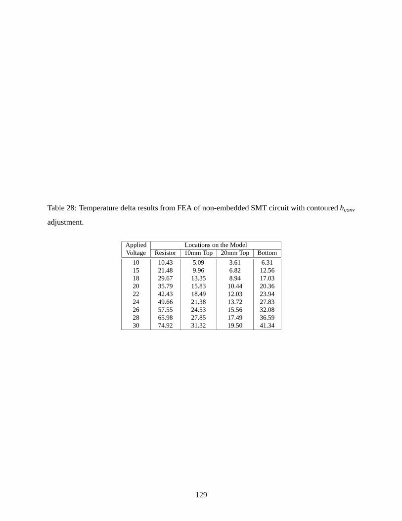
Table 28: Temperature delta results from FEA of non-embedded SMT circuit with contouredhconv
adjustment.
Applied Locations on the ModelVoltage Resistor 10mm Top 20mm Top Bottom
10 10.43 5.09 3.61 6.3115 21.48 9.96 6.82 12.5618 29.67 13.35 8.94 17.0320 35.79 15.83 10.44 20.3622 42.43 18.49 12.03 23.9424 49.66 21.38 13.72 27.8326 57.55 24.53 15.56 32.0828 65.98 27.85 17.49 36.5930 74.92 31.32 19.50 41.34
129

Figure 60: Correlation of FEA results with live test data, model with contouredhconv adjustment.
130
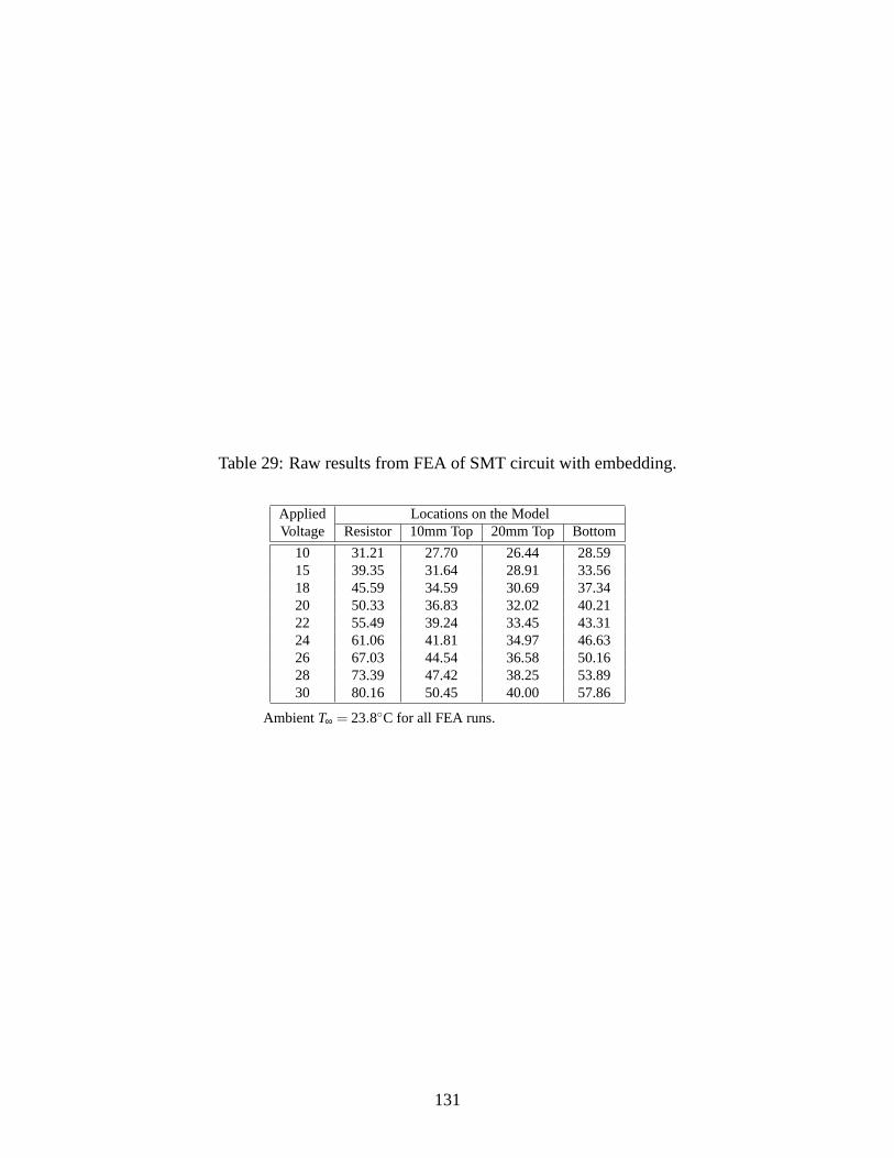
Table 29: Raw results from FEA of SMT circuit with embedding.
Applied Locations on the ModelVoltage Resistor 10mm Top 20mm Top Bottom
10 31.21 27.70 26.44 28.5915 39.35 31.64 28.91 33.5618 45.59 34.59 30.69 37.3420 50.33 36.83 32.02 40.2122 55.49 39.24 33.45 43.3124 61.06 41.81 34.97 46.6326 67.03 44.54 36.58 50.1628 73.39 47.42 38.25 53.8930 80.16 50.45 40.00 57.86
AmbientT∞ = 23.8C for all FEA runs.
131
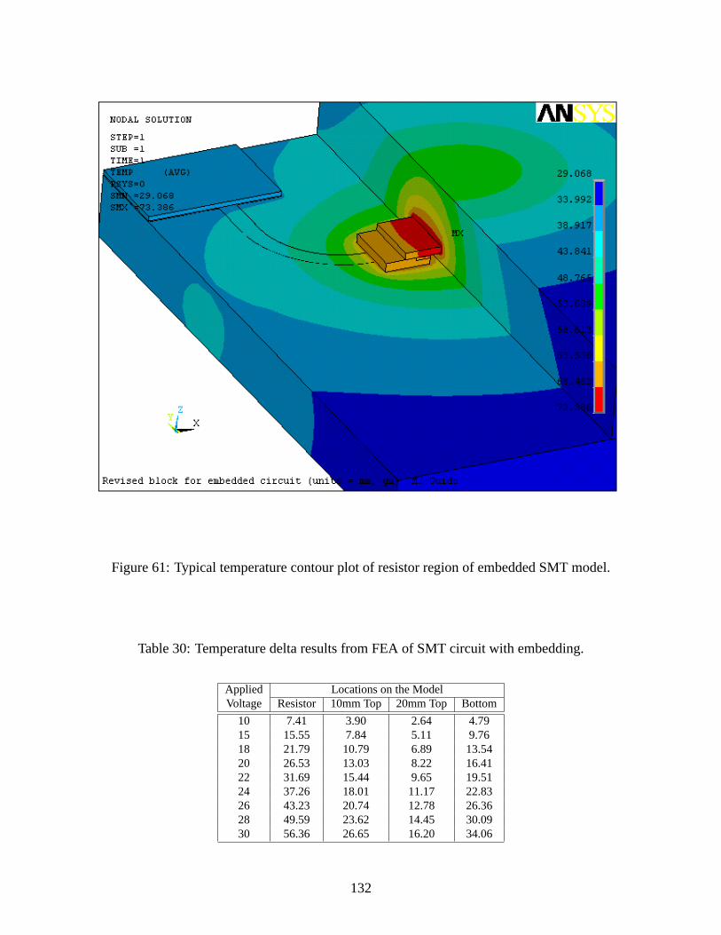
Figure 61: Typical temperature contour plot of resistor region of embedded SMT model.
Table 30: Temperature delta results from FEA of SMT circuit with embedding.
Applied Locations on the ModelVoltage Resistor 10mm Top 20mm Top Bottom
10 7.41 3.90 2.64 4.7915 15.55 7.84 5.11 9.7618 21.79 10.79 6.89 13.5420 26.53 13.03 8.22 16.4122 31.69 15.44 9.65 19.5124 37.26 18.01 11.17 22.8326 43.23 20.74 12.78 26.3628 49.59 23.62 14.45 30.0930 56.36 26.65 16.20 34.06
132

Figure 62: SMT model with embedding, correlation of live test data with FEA results.
133

10.0 CONCLUSIONS
The investigations described in this thesis, employing live samples and associated numerical mod-
els, have successfully shown that selected passive heat rejection methods can reduce the observed
temperature rise at or near the location of a Joule heating source in a sample three-dimensional
circuit. Of the issues considered, the single most important factor affecting the temperature rise is
the bulk thermal conductivity of the trace material. High values of bulk thermal conductivity will
effectively limit the peak temperatures in the circuit sample.
Aside from its influence as an independent factor, the bulk thermal conductivity of the trace
material directly influences the relative effect of other passive measures. The Thermal Sheet Resis-
tance of the trace, a variable resulting from a combination of trace thickness with the bulk thermal
conductivity, exerts a strong effect on the observed temperature rise.
Blind extensions to the conducting trace (“trace fins”) can significantly reduce the temperature
rise. In this investigation, the trace fins were either placed directly at the connection between the
discrete Joule heating source or immediately adjacent to that connection. Minimal differences
were seen in the observed temperature rise as a consequence of the different fin locations.
For traces with the properties of copper, increasing the length of the trace fins resulted in steady
reduction of the temperature rise up to a fin length of 20mm. On the other hand, traces defined with
the properties of conductive ink exhibited increasing effectiveness only up to lengths of 10mm.
Further research was conducted with a surface-mount technology (SMT) resistor circuit and
associated FEA models, including a sample featuring complete embedding of the resistive com-
ponent and the conductive paths. Based on this research, a number of additional observations
regarding circuit thermal performance and the modeling of convection behavior could be made.
At the power dissipation levels represented in this research, the presence of an embedding
medium results in reduced temperatures at the resistive component. This is apparently due to the
134
higher heat capacity of the embedding medium compared to the surrounding air, which controls
the overall heat dissipation from the circuit.
For circuits of this general configuration, FEA modeling with convection film coefficients cal-
culated from standard sources give poorer correlations with live test results than were achieved
with FEA models of leaded resistor circuits. This discrepancy is believed to be due to interactions
between convective surfaces of varying geometries, which are not accounted for in all standard
convection models available in the literature.
A thermal-fluid numerical model of the sample SMT circuit with substantial geometric simpli-
fications can generate results that correlate very well with the live measurements, at least for the
resistor temperatures. Interpretation of the heat flux data from this model gives calculated values
for the film coefficient that vary considerably from the standard calculations, both in average mag-
nitude and functional form. This finding is consistent with the reasoning that interactions between
adjacent convective surfaces may limit the applicability of standard film coefficient calculations
under similar circumstances.
The thermal-fluid numerical model results can be employed to generate both quantitative and
qualitative corrections to the standard film coefficient calculations. These corrections are appli-
cable to more geometrically exact (but less computationally-intensive) FEA models not featuring
fluid dynamics capabilities. The FEA models with corrected film coefficients give results showing
improved correlation with live resistor test temperatures. However, the improvement in resistor
temperature correlation is not accompanied by improved correlations for temperature values on
the surrounding substrate. These correlation trends are almost identical for both the quantitative
and qualitative adjustment methods.
10.1 IMPLICATIONS OF THE RESEARCH
The new information discovered within the scope of this research is of significant value at a number
of levels of specialization.
At the level of the 3-D devices that are the primary focus of the research, it is demonstrated that
component temperatures in the fabricated devices can be limited significantly by the manipulation
135
of a relatively small number of design factors. The research points out that the conductive elements
themselves are of primary importance in achieving the process of conducting heat away from the
components. As much as their material properties, geometric configuration and relative size are
crucial to the basic electronic performance, they are also of significant value in promoting effective
heat rejection from the proposed devices and as such deserve renewed attention in the overall
heat management effort. Additionally, the polymer matrix which will encapsulate the proposed
monolithic circuits appears to act to limit component temperatures as well, at the power dissipation
levels addressed herein.
Regarding heat transfer within the field of general electronic devices, many of the principles
revealed above have similar implications for the larger research area. As an example, the research
further emphasized previous findings that indicated that the properties of the embedding materials
employed in encapsulating more conventional circuitry are important in promoting waste heat
removal. The research also adds to a growing body of knowledge asserting that applying free
convection principles can contribute materially to improved heat removal from electronic circuits.
As to heat transfer issues in general, the research provides additional insight into the relative
effects of fluid/solid interface geometry on the magnitude and functional form of derived convec-
tion film coefficients, particularly as regards the effects of nearby convective surfaces. This insight
further develops the view of predicted convection behavior beyond that established for the basic
theoretical cases, which are limited to constant surface temperature or uniform heat flux.
10.2 FUTURE RESEARCH
The research presented herein implicitly suggests a number of areas suitable for further investi-
gation. If 3-D circuit architectures are to be successfully designed and implemented in practical
devices, the insights into the heat removal principles already achieved need to be supplemented
by testing and modeling of more elaborate configurations, such as arrangements of fully three-
dimensional heat removal pathways to be embedded in the polymer matrix. These more advanced
prototypes can serve to establish the effectiveness of the heat removal principles in a wider range
136

of design alternatives, and hopefully provide additional basic principles for guiding the thermal
design of the devices.
The numerical thermal/fluid modeling portion of the research had the immediate practical ben-
efit of a straightforward correction method for adjusting conventionally-calculated film coefficients
employed in non-fluid thermal modeling. This correction directly resulted in a much-improved cor-
relation of the modeled component temperatures with those measured during live testing. However,
the lack of correspondence between the temperature results at other model locations suggests an
ongoing need to improve these adjustment techniques. A worthwhile approach is to develop more
elaborate thermal/fluid submodels which can capture other significant details of the live test spec-
imens, but which will still maintain sufficient computational simplicity to preserve the advantages
of using a finite-element approach rather than the more computationally expensive full multiscale
fluid modeling schemes.
The research directions proposed above suggest a larger effort to understand the nature of con-
vection in contexts beyond the most fundamental modeled cases. One approach is to focus more
detailed attention on the underlying conduction properties of the solid object convecting to the
surrounding medium; i.e. to investigate the underlying principles of conjugate heat transfer inher-
ent to the heat removal process. Another worthwhile research direction is to apply the method of
thermal/fluid and non-fluid models alongside live test specimens to establish a first-order empiri-
cal adjustment expression. This expression could be used to adjust conventionally-calculated film
coefficients based on a set of general rules governed by the base material properties and geomet-
ric configuration of a set of interacting convection surfaces, similar to the geometric expressions
derived for quantifying heat interchange behavior among a set of interacting radiative surfaces.
Further precision experimental testing is also proposed to ensure that there are no additional
sources (whether numerical or experimental) of error that would lead to poor test/model correla-
tions. The new information obtained by such an investigation would provide necessary improve-
ments within the specialized area of studying 3-D devices, and would also be useful in the wider
field of electronics temperature measurement.
137

APPENDIX
MACRO CODE FOR FILM COEFFICIENT ADJUSTMENT, UPPER SUBSTRATE
SURFACE
! routine for adjusting convection per Bejan by ratios
! per Flotran calculations
! top surface excluding resistor area
tbulk = 23.8
! Define (hconv)i = hconv(Ti) for the surface of interest per Bejan
*DIM,hcon_vs_t,ARRAY,5
hcon_vs_t(1)=0,4.286E-06,8.224E-06,1.065E-05,1.286E-05
/prep7
MPTEMP, 1, tbulk, tbulk + 0.5, tbulk + 7, tbulk + 21, tbulk + 50
! set up nodal components for h values with a dummy node
allsel
nsel,s,loc,z,0
nsel,r,loc,y,0
nsel,r,loc,x,0
cm,dummynode,node
138

cm,h_comp_1,node
cm,h_comp_2,node
cm,h_comp_3,node
cm,h_comp_4,node
cm,h_comp_5,node
cm,h_comp_6,node
cm,h_comp_7,node
cm,h_comp_8,node
! select component containing surface nodes for substrate
! excluding nodes under the resistor
cmsel,s,top_surf_nodes ! must be defined previously
! define parameters for calculating h(conv) adjustment
A_con = 0.403
B_con = 2.4
k_con = 7
m_con = 12
n_con = 28.6
! Get minimum and maximum node numbers for nodes in surface set
*get,min_node_num,node,,num,min
*get,max_node_num,node,,num,max
! define extent of top and bottom surfaces (min x and y = 0)
surf_x_max = 50
surf_y_max = 65
139

! define the max and min x and y for the resistor
resist_x_min = 18
resist_x_max = 35
resist_y_min = 37.825
resist_y_max = 44.175
! Define the "edge distance parameter" (EDP)
! for all nodes on the surface
! edge-to-center distance is the length
! from the edge to the center (or to the resistor)
! in the same direction as the node distance to the closest edge
! n = number of EDP steps for the adjusted film coefficients
num_edp_steps = 8
nodenum = min_node_num
*dowhile, nodenum
nsel,r,node,,nodenum
*if, nx(nodenum), ge, resist_x_max,then
x_edge_2_ctr = surf_x_max - resist_x_max
x_dist_2_edge = surf_x_max - nx(nodenum)
*else
x_edge_2_ctr = resist_x_min
x_dist_2_edge = nx(nodenum)
*endif
EDP = (x_dist_2_edge)/( x_edge_2_ctr)
*if, ny(nodenum), ge, resist_y_max, then
140

y_edge_2_ctr = surf_y_max - resist_y_max
y_dist_2_edge = surf_y_max - ny(nodenum)
*else
y_edge_2_ctr = resist_y_min
y_dist_2_edge = ny(nodenum)
*endif
y_EDP = (y_dist_2_edge)/( y_edge_2_ctr)
*if, y_EDP, lt, EDP, then
EDP = y_EDP
*endif
! sort the current node into proper component by its value of EDP
*if, EDP, le, 1/num_edp_steps,then
cmsel, a, h_comp_1
cm, h_comp_1, node
*elseif, EDP, le, 2/num_edp_steps
cmsel, a, h_comp_2
cm, h_comp_2, node
*elseif, EDP, le, 3/num_edp_steps
cmsel, a, h_comp_3
cm, h_comp_3, node
*elseif, EDP, le, 4/num_edp_steps
cmsel, a, h_comp_4
cm, h_comp_4, node
*elseif, EDP, le, 5/num_edp_steps
cmsel, a, h_comp_5
141

cm, h_comp_5, node
*elseif, EDP, le, 6/num_edp_steps
cmsel, a, h_comp_6
cm, h_comp_6, node
*elseif, EDP, le, 7/num_edp_steps
cmsel, a, h_comp_7
cm, h_comp_7, node
*else
cmsel, a, h_comp_8
cm, h_comp_8, node
*endif
cmsel, s, top_surf_nodes
*if, nodenum, eq, max_node_num, exit
nodenum = ndnext(nodenum)
*enddo
! remove the dummy node from each h_comp
cmsel, s, h_comp_1
cmsel, u, dummynode
cm, h_comp_1, node
cmsel, s, h_comp_2
cmsel, u, dummynode
cm, h_comp_2, node
cmsel, s, h_comp_3
142

cmsel, u, dummynode
cm, h_comp_3, node
cmsel, s, h_comp_4
cmsel, u, dummynode
cm, h_comp_4, node
cmsel, s, h_comp_5
cmsel, u, dummynode
cm, h_comp_5, node
cmsel, s, h_comp_6
cmsel, u, dummynode
cm, h_comp_6, node
cmsel, s, h_comp_7
cmsel, u, dummynode
cm, h_comp_7, node
cmsel, s, h_comp_8
cmsel, u, dummynode
cm, h_comp_8, node
! Define the material prop for each (hlocal)i
delt_EDP = 1/num_edp_steps
*do, mat_cnt, num_edp_steps, 1, -1
h_mat_number = mat_cnt + 100
143

EDP = mat_cnt*delt_EDP - delt_EDP/2
fact = A_con + (1-EDP)**n_con - EDP**m_con + (EDP**k_con)/B_con
*do, coef_ct, 1, 5
mpdata, hf ,h_mat_number, coef_ct, fact*hcon_vs_t(coef_ct)
*enddo
! Apply film coefficient (mat_number) and Tbulk to selected nodes
*if, mat_cnt, eq, 1, then
cmsel, s, h_comp_1
esln, s, 0
nsle, s, all
cmsel, r, top_surf_nodes
sf, all, conv, -h_mat_number, tbulk
*elseif, mat_cnt, eq, 2
cmsel, s, h_comp_2
esln, s, 0
nsle, s, all
cmsel, r, top_surf_nodes
sf, all, conv, -h_mat_number, tbulk
*elseif, mat_cnt, eq, 3
cmsel, s, h_comp_3
esln, s, 0
nsle, s, all
cmsel, r, top_surf_nodes
sf, all, conv, -h_mat_number, tbulk
144

*elseif, mat_cnt, eq, 4
cmsel, s, h_comp_4
esln, s, 0
nsle, s, all
cmsel, r, top_surf_nodes
sf, all, conv, -h_mat_number, tbulk
*elseif, mat_cnt, eq, 5
cmsel, s, h_comp_5
esln, s, 0
nsle, s, all
cmsel, r, top_surf_nodes
sf, all, conv, -h_mat_number, tbulk
*elseif, mat_cnt, eq, 6
cmsel, s, h_comp_6
esln, s, 0
nsle, s, all
cmsel, r, top_surf_nodes
sf, all, conv, -h_mat_number, tbulk
*elseif, mat_cnt, eq, 7
cmsel, s, h_comp_7
esln, s, 0
nsle, s, all
cmsel, r, top_surf_nodes
sf, all, conv, -h_mat_number, tbulk
*else
cmsel, s, h_comp_8
esln, s, 0
145

nsle, s, all
cmsel, r, top_surf_nodes
sf, all, conv, -h_mat_number, tbulk
*endif
cmsel, s, top_surf_nodes
*enddo
allsel
146

BIBLIOGRAPHY
[1] Sawyer B. Fuller, Eric J. Wilhelm, and Joseph M. Jacobson. Ink-jet printed nanoparticlemicroelectromechanical systems.Journal of Microelectromechanical Systems, 11(1):54–60,February 2002.
[2] Daniel J. Ulinski. Organic diode and other circuit element creation through variations ofpoly(3,4-ethylenedioxythiophene) synthesis. Master’s thesis, University of Pittsburgh, 2004.
[3] Junfeng Mei, Marlin H. Mickle, Michael Lovell, and Steve Heston. Continuous ink-jet print-ing electronic components using novel conductive inks. InFifteenth Solid Freeform Fabrica-tion Symposium, Austin, Texas, August 2004.
[4] D. Redinger, S. Molesa, Shong Yin, R. Farschi, and V. Subramian. An ink-jet-depositedpassive component process for RFID.IEEE Transactions on Electron Devices, 51(12):1978–83, December 2004.
[5] Christian Belady. Cooling and power consideration for semiconductors into the next century.In ISLPED ’01: Proceedings of the 2001 international symposium on Low power electronicsand design, pages 100–105, New York, NY, USA, 2001. ACM Press.
[6] Dan Faulkner, Mehdy Khotan, and Reza Shekarriz. Managing electronics thermal manage-ment.Heat Transfer Engineering, 25(2):1–4, 2004.
[7] Randy D. Weinstein, Amy S. Fleishcher, and Kimberly A. Krug. Natural convection andpassive heat rejection from two heat sources maintained at different temperatures on a printedcircuit board. Journal of Electronic Packaging, Transactions of the ASME, 126(1):14–21,March 2004.
[8] Ingrid Martorell, Joan Herrero, and Francesc X. Grau. Natural convection from narrow hori-zontal plates at moderate Rayleigh numbers.International Journal of Heat and Mass Trans-fer, 46(13):2389–2402, June 2003.
[9] K. Azar, S. S. Pan, J. Parry, and H. Rosten. Effect of circuit board parameters on thermalperformance of electronic components in natural convection cooling. InSEMI-THERM X.,Semiconductor Thermal Measurement and Management Symposium, pages 32, 163–169, Pis-cataway, NJ, USA, February 1994. IEEE.
147

[10] G. Farkas, S. Haque, F. Wall, P.S. Martin, A. Poppe, Q. van Voorst Vader, and G. Bognar.Electric and thermal transient effects in high power optical devices. InTwentieth AnnualIEEE Semiconductor Thermal Measurement and Management Symposium, pages 168–76,Piscataway, NJ, USA, March 2004. IEEE.
[11] Jesse Galloway and Sarang Shidore. Implementing compact thermal models under non-symmetric trace routing conditions. In20th Annual IEEE Semiconductor Thermal Measure-ment and Management Symposium - Proceedings, volume 20, pages 255–261, Piscataway,NJ, USA, March 2004. IEEE.
[12] V. H. Adams, D. L. Blackburn, Y. Joshi, and D. W. Berning. Issues in validating packagecompact thermal models for natural convection cooled electronic systems. InSEMI-THERMXIII. Thirteenth Annual IEEE. Semiconductor Thermal Measurement and Management Sym-posium, pages 10–23, Piscataway, NJ, USA, January 1997. IEEE.
[13] J. DeVoe and A. Ortega. An investigation of board level effects on compact thermal models ofelectronic chip packages. InSemiconductor Thermal Measurement and Management, 2002.Eighteenth Annual IEEE Symposium, pages 8–14, Piscataway, NJ, USA, March 2002. IEEE.
[14] Li Shang, Li-Shiuan Peh, Amit Kumar, and Niraj K. Jha. Thermal modeling, characterizationand management of on-chip networks. InMICRO 37: Proceedings of the 37th annual Inter-national Symposium on Microarchitecture, pages 67–78, Washington, DC, USA, 2004. IEEEComputer Society.
[15] Brent Goplen and Sachin Sapatnekar. Thermal via placement in 3D ICs. InISPD ’05:Proceedings of the 2005 International Symposium on Physical Design, pages 167–174, NewYork, NY, USA, 2005. ACM Press.
[16] J. P. Fradin, L. Molla, and B. Desaunettes. Analysis of 3D conjugate heat transfers in elec-tronics. InEDTC ’97: Proceedings of the 1997 European Conference on Design and Test,page 190, Washington, DC, USA, 1997. IEEE Computer Society.
[17] B. Chambers, T. Y. Tom Lee, and W. Blood. Steady state and transient thermal analysis ofchip scale packages. InSixth Intersociety Conference on Thermal and ThermomechanicalPhenomena in Electronic Systems, pages 68–75, 1998.
[18] J. J. Licari and L. R. Enlow. Hybrid Microcircuit Technology Handbook, pages 11–12.William Andrew Publishing/Noyes, Park Ridge, NJ, USA, 2nd edition, 1998.
[19] R. F. Peluso. Material and design considerations for power hybrid packages.InternationalJournal for Hybrid Microelectronics, 6(1):302–306, 1983.
[20] F. Christiaens and E. Beyne. Transient thermal modeling and characterization of a hybridcomponent. InProceedings of the IEEE 46th Electronic Components & Technology Confer-ence, ECTC, pages 154–164, Piscataway, NJ, USA, May 1996. IEEE.
148

[21] R. H. Jensen, G. A. Andrejack, D. P. Button, and B. A. Bydel. Comparative thermal per-formances of various substrate materials in a simple packaging application: Actual versuspredicted. IEEE Transactions on Components, Hybrids and Manufacturing Technology,12(4):537–542, December 1989.
[22] Chester W. Waldvogel. Computer designed multilayer hybrid substrate using thick film tech-nology. In DAC ’77: Proceedings of the 14th Conference on Design Automation, pages351–353, Piscataway, NJ, USA, 1977. IEEE Press.
[23] Liu Chen, Anders S. G. Andræ, Gang Zou, and Johan Liu. Characterization of substrate mate-rials for system-in-a-package applications.Journal of Electronic Packaging, 126(2):195–201,June 2004.
[24] Ngon Binh Nguyen and Franklin B. Jones. Hybrid packaging technique for high powerdensity circuit. InSEMI-THERM VII. Proceedings, Seventh Annual IEEE SemiconductorThermal Measurement and Management Symposium, pages 105–109, Piscataway, NJ, USA,February 1991. IEEE.
[25] A.S. Manning and S. Fuchs. Finite element analysis of thermal stresses in high-power sub-strates for hybrid circuits.Materials and Design, 18(2):61–72, April 1997.
[26] Shigekatsu Uchida and Keiji Yamamoto. High reliability thick film hybrid circuit for au-tomotive thermal cycle applications. InProceedings of the 1994 International MechanicalEngineering Congress and Exposition, volume 195, pages 203–210, New York, NY, USA,November 1994. ASME.
[27] S. Krishnan, Y.-G. Kim, and I. Mohammed. Thermal performance characteristics of foldedstacked packages. InEighteenth Annual IEEE Semiconductor Thermal Measurement andManagement Symposium. Proceedings 2002, pages 42–49, Piscataway, NJ, USA, March2002. IEEE.
[28] Sridhar Krishnan, Young-Gon Kim, and K M Bang. A 3-D stacked package solution forDDR-SDRAM applications. In20th Annual IEEE Semiconductor Thermal Measurementand Management Symposium - Proceedings, volume 20, pages 64–69, Piscataway, NJ, USA,March 2004. IEEE.
[29] Li Zhang, Noella Howard, Vijaylaxmi Gumaste, Anindya Poddar, and Luu Nguyen. Thermalcharacterization of stacked-die packages. In20th Annual IEEE Semiconductor Thermal Mea-surement and Management Symposium - Proceedings, pages 55–63, Piscataway, NJ, USA,March 2004. IEEE.
[30] M. Furmanczyk, P. Wilkerson, and A. Przekwas. Multiphysics modeling of integratedmicrofluidic-thermoelectric cooling for stacked 3D ICs. InNineteenth Annual IEEE Semi-conductor Thermal Measurement And Management Symposium, pages 35–41, Piscataway,NJ, USA, March 2003. IEEE.
149

[31] C.P. Wong and R.S. Bollampally. Comparative study of thermally conductive fillers for usein liquid encapsulants for electronic packaging.IEEE Transactions on Advanced Packaging,22(1):54–59, February 1999.
[32] D. Lu and C.P. Wong. Conductive adhesives for solder replacement in electronics packag-ing. In Proceedings of the International Symposium and Exhibition on Advanced PackagingMaterials Processes, Properties and Interfaces, pages 24–31, Piscataway, NJ, USA, March2000. IEEE.
[33] Ye. P. Mamunya, V. V. Davydenko, P. Pissis, and E. V. Lebedev. Electrical and thermalconductivity of polymers filled with metal powders.European Polymer Journal, 38(9):1887–1897, September 2002.
[34] J. Zhang, P. Brazis, Roy Chowdhuri, Szczech A., J., and D. Gamota. Investigation of usingcontact and non-contact printing technologies for organic transistor fabrication. InProceed-ings of the Materials Research Society Symposium on Organic and Polymeric Materials andDevices - Optical, Electrical and Optoelectronic Properties, 2002.
[35] D. Klosterman, Li Li, and J.E. Morris. Materials characterization, conduction development,and curing effects on reliability of isotropically conductive adhesives.IEEE Transactions onComponents, Packaging, and Manufacturing Technology, Part A, 21(1):23–31, March 1998.
[36] W. Jia, R. Tchoudakov, R. Joseph, M. Narkis, and A. Siegmann. The role of a third com-ponent on the conductivity behavior of ternary epoxy/ag conductive composites.PolymerComposites, 23(4):510–519, August 2002.
[37] Kyoung-Sik Moon, Jiali Wu, and C. P. Wong. Improved stability of contact resistance of lowmelting point alloy incorporated isotropically conductive adhesives.IEEE Transactions OnComponents And Packaging Technologies, 26(2):375–381, June 2003.
[38] Quinn K. Tong, Deanna Markley, Gerry Fredrickson, and Richard Kuder. Recent advancesin surface mount conductive adhesives (SMCAs) for solder replacement. InNational Elec-tronic Packaging and Production Conference-Proceedings of the Technical Program (Westand East), volume 1, pages 350–358, Norwalk, CT, USA, February 1999. Reed ExhibitionCompanies.
[39] Daniel Cavasin, Ken Brice-Heames, and Anwar Arab. Improvements in the reliability andmanufacturability of an integrated RF power amplifier module system-in-package, via imple-mentation of conductive epoxy adhesive for selected SMT components. In53rd ElectronicComponents and Technology Conference, Proceedings 2003, pages 1404–1407, Piscataway,NJ, USA, May 2003. IEEE.
[40] Michael A. Gaynes, Russell H. Lewis, Ravi F. Saraf, and Judith M. Roldan. Evaluationof contact resistance for isotropic electrically conductive adhesives.IEEE Transactions OnComponents, Packaging, And Manufacturing Technology–Part B, 18(2):299–304, May 1995.
150

[41] F. El-Tantawy, K. Kamada, and H. Ohnabe. In situ network structure, electrical and thermalproperties of conductive epoxy resin-carbon black composites for electrical heater applica-tions. Materials Letters, 56(1-2):112–126, September 2002.
[42] V. Nieberlein. Thermal conductivity enhancement of epoxies by the use of fillers.IEEETransactions on Components, Hybrids, and Manufacturing Technology, 1(2):172 – 176, June1978.
[43] K. Fukushima, H. Takahashi, Y. Takezawa, M. Hattori, M. Itoh, and M. Yonekura. Highthermal conductive epoxy resins with controlled high-order structure [electrical insulationapplications]. InAnnual Report of the Conference on Electrical Insulation and DielectricPhenomena, CEIDP, pages 340–343, October 2004.
[44] S. Haque and Guo-Quan Lu. Characterization of interfacial thermal resistance for packaginghigh-power electronics modules. InProceedings of the 49th Electronic Components andTechnology Conference, pages 1103 – 1110, Piscataway, NJ, USA, June 1999. IEEE.
[45] A. Bjorneklett and H. Kristiansen. The effect of the volume fraction of silver on the thermalresistance of die attach adhesives.Hybrid Circuits, (33):28–31, January 1994.
[46] D. Lu and C.P. Wong. A study of contact resistance of conductive adhesives based onanhydride-cured epoxy systems.IEEE Transactions on Components and Packaging Tech-nologies, 23(3):440 – 446, September 2000.
[47] J. J. Salgon, F. Robbe-Valloire, J. Blouet, and J. Bransier. A mechanical and geometricalapproach to thermal contact resistance.International Journal of Heat and Mass Transfer,40(5):1121–1129, 1997.
[48] Melida Chin, Kaushik A. Iyer, and S. Jack Hu. Prediction of electrical contact resistancefor anisotropic conductive adhesive assemblies.IEEE Transactions On Components AndPackaging Technologies, 27(2):317–326, June 2004.
[49] Frank P. Incropera and David P. DeWitt.Introduction to Heat Transfer, pages 44–45. Wiley,New York, 3rd edition, 1996.
[50] Frank P. Incropera and David P. DeWitt.Introduction to Heat Transfer, pages 55–57. Wiley,New York, 3rd edition, 1996.
[51] Frank P. Incropera and David P. DeWitt.Introduction to Heat Transfer, pages 5–8. Wiley,New York, 3rd edition, 1996.
[52] B. Munson, D. Young, and T. Okiishi.Fundamentals of Fluid Mechanics, page 859. Wiley,New York, 2nd edition, 1994.
[53] Frank P. Incropera and David P. DeWitt.Introduction to Heat Transfer, pages 456–469.Wiley, New York, 3rd edition, 1996.
[54] A. Bejan.Convection Heat Transfer, page 603. Wiley, 1995.
151

[55] Louis C. Burmeister.Convective Heat Transfer, page 743. Wiley, 1983.
[56] B. Munson, D. Young, and T. Okiishi.Fundamentals of Fluid Mechanics, page 999. Wiley,1994.
[57] Frank P. Incropera and David P. DeWitt.Introduction to Heat Transfer, pages 306–307.Wiley, New York, 3rd edition, 1996.
[58] A. Bejan.Convection Heat Transfer, page 163. Wiley, New York, 2nd edition, 1995.
[59] Frank P. Incropera and David P. DeWitt.Introduction to Heat Transfer, pages 304–305.Wiley, New York, 3rd edition, 1996.
[60] A. Bejan.Convection Heat Transfer, pages 32–38, 161–168. Wiley, 1995.
[61] A. Bejan.Convection Heat Transfer, pages 192–202. Wiley, 1995.
[62] A. Bejan.Convection Heat Transfer, pages 166–168. Wiley, New York, 2nd edition, 1995.
[63] Frank P. Incropera and David P. DeWitt.Introduction to Heat Transfer, pages 8–10. Wiley,New York, 3rd edition, 1996.
[64] EIA/JEDEC Standard No. 51: Methodology for the Thermal Measurement of ComponentPackages (Single Semiconductor Device). Electronic Industries Alliance, 1995.
[65] Michael R. Guido, Laura A. Schaefer, Michael Lovell, and Marlin H. Mickle. Heat dissipationin 3-D circuit architecture - modeling and experiments. December 2003.
[66] Linzhi Wu. The thermoelastic analysis of chip-substrate system.Journal of Electronic Pack-aging, Transactions of the ASME, 126(3):325–332, September 2004.
[67] Paul E. Allaire. Basics of the Finite-Element Method: Solid Mechanics, Heat Transfer, andFluid Mechanics. Wm. C. Brown Publishers, College Division, Dubuque, IA, 1985.
[68] A.J. Przekwas, Y. Jiang, M.M. Athavale, Z.J. Wang, and J. van der Zijp. Virtual prototyp-ing environment for multi-scale, multi-disciplinary simulation of electronics packaging ofmcms. InThermomechanical Phenomena in Electronic Systems -Proceedings of the Interso-ciety Conference, pages 352–358, Piscataway, NJ, USA, June 1996. IEEE.
[69] SAS IP, Southpointe, PA.ANSYSrFinite-Element Analysis Software, Release 8.0.
[70] Automation Creations Inc., Blacksburg, VA. Matwebc© materials database.www.matweb.com.
[71] E.I. DuPont de Nemours & Co. (Inc.). Design handbook for duPont engineering plastics,module III: DelrinR©.
152

[72] Laura A. Schaefer, Michael R. Lovell, Marlin Mickle, Raymond Brush, and Mike Guido.Temperature-based variation in substrate materials used in the production of 3-D electronics.2004.
[73] Creative Materials Inc., Tyngsboro, MA. Datasheet for #119-13 electrically conductive epoxyadhesive.
[74] Creative Materials, Inc., Tyngsboro, MA. Datasheet for #112-15 extremely conductive ink.
[75] G. M. Tsangaris and M. C. Kazilas. Conductivity and percolation in epoxy resin/conductivefiller composites.Materials Science and Technology, 18(2):226–30, February 2002.
[76] John C. Tannehill, Dale A. Anderson, and Richard H. Pletcher.Computational Fluid Me-chanics and Heat Transfer, page 34. Taylor & Francis, Washington, DC, 2nd edition, 1997.
[77] MathSoft, Inc., 101 Main Street, Cambridge, MA 02142, USA.Mathcadr 2001 Profes-sional, 1986-2001.
[78] Donald C. Price. A review of selected thermal management solutions for military electronicsystems. IEEE Transactions On Components And Packaging Technologies, 26(1):26–39,March 2003.
[79] Shatil Haque, William A. Stinnett, Douglas J. Nelson, and Guo-Quan Lu. Thermal manage-ment of power electronics modules packaged by a stacked-plate technique.Microelectronicsand Reliability, 39(9):1343–1349, September 1999.
[80] Bao-Min Liu and Y.C. Mui. Multi-physics simulation of a microprocessor package underwater cooling.Journal of Electronic Packaging, Transactions of the ASME, 126(3):384–389,September 2004.
[81] Jake Kim and Eric Golliher. Steady state model of a micro loop heat pipe. InSemiconductorThermal Measurement and Management, 2002. Eighteenth Annual IEEE Symposium, pages137–144, Piscataway, NJ, USA, March 2002. IEEE.
[82] Issam Mudawar. Assessment of high-heat-flux thermal management schemes.IEEE Trans-actions On Components And Packaging Technologies, 24(2):122–141, June 2001.
[83] M. H. Nurmawati, K. S. Siow, and I. J. Rasiah. Analysis of phase change material for use asthermal interface material.International Journal of Polymer Analysis and Characterization,9(4):213–228, JulyAugust 2004.
[84] F. L. Tan and C. P. Tso. Cooling of mobile electronic devices using phase change materials.Applied Thermal Engineering, 24(2):159–169, February 2004.
[85] T. J. Lu. Thermal management of high power electronics with phase change cooling.Inter-national Journal of Heat and Mass Transfer, 43(13):2245–2256, July 2000.
153

[86] Poorya Sabounchi and Ali Heydari. Lumped capacity thermal circuit diagram of active chipcooling schemes. InNineteenth Annual IEEE Semiconductor Thermal Measurement AndManagement Symposium, pages 151–155, Piscataway, NJ, USA, March 2003. IEEE.
[87] A. Dewan, P. Mahanta, K. Sumithra Raju, and P. Suresh Kumar. Review of passive heattransfer augmentation techniques. InProceedings of the I MECH E Part A Journal of Powerand Energy, volume 218, pages 509–527. Professional Engineering Publishing, December2004.
[88] T. C. Hung and C. S. Fu. Analysis for the passive enhancement of electronic cooling throughgeometric modification in a mixed convection domain.Numerical Heat Transfer Part A:Applications, 35(5):519–535, April 1999.
[89] T. C. Hung. A conceptual design of thermal modeling for efficiently cooling an array ofheated devices under low Reynolds numbers.Numerical Heat Transfer, Part A, 39(4):361–382, March 2001.
[90] Johannes Adam. New correlations between electrical current and temperature rise in pcbtraces. In20th Annual IEEE Semiconductor Thermal Measurement and Management Sym-posium - Proceedings, pages 292–299, Piscataway, NJ, March 2004. IEEE.
[91] Vinod K. Maudgal. Thermal phenomena in compact electronic enclosures: A numericalstudy. IEEE Transactions On Components, Packaging, And Manufacturing TechnologyPartA, 20(3):286–294, September 1997.
[92] Thomas Stewart and David W. Stiver. Thermal optimization of electronic systems using de-sign of experiments based on numerical inputs. In20th Annual IEEE Semiconductor ThermalMeasurement and Management Symposium - Proceedings, volume 20, pages 135–142, Pis-cataway, NJ, USA, March 2004. IEEE.
[93] Minitab Inc., State College, PA. MinitabR© statistical software.
[94] Valerie J. Easton and John H. McColl. Statistics glossary, v1.1, revised and updated by Stu-art G. Young.http://www.stats.gla.ac.uk/steps/glossary/index.html, September1997.
[95] Jesse E. Galloway. Thermal analysis of portable electronic products. InProceedings of the1998 6th Intersociety Conference on Thermal and Thermomechanical Phenomena in Elec-tronic Systems, ITHERM, pages 1–7, Piscataway, NJ, May 1998. IEEE.
[96] A. Bejan.Convection Heat Transfer, page 252. Wiley, 1995.
154