Computer Organisation and Assembly Language - PTU (Punjab ...
241
Self Learning Material Computer Organisation and Assembly Language (MCA-103) Course: Master in Computer Applications Semester-I Distance Education Programme I.K. Gujral Punjab Technical University Jalandhar
-
Upload
khangminh22 -
Category
Documents
-
view
0 -
download
0
Transcript of Computer Organisation and Assembly Language - PTU (Punjab ...

Self Learning Material
Computer Organisation andAssembly Language
(MCA-103)
Course: Master in Computer Applications
Semester-I
Distance Education Programme
I.K. Gujral Punjab Technical University
Jalandhar

SyllabusI.K. Gujral Punjab Technical University
MCA-103 Computer Organization and Assembly Language
Objectives: The objective of the course is to provide students with a solid foundation in
computer design. Examine the operation of the major building blocks of a computer system.
To introduce students to the design and organization of modern digital computers & basic
assembly language.
Section-A
Computer Organization: Basic Computer Organization, Bus & Memory Transfer, Stored
Program Organization, Computer Registers, Computer Instructions, Timing and Control,
Hardwired based design of Control Unit, Instruction Cycle, Formats of Various types of
Instructions- Memory Reference Instructions, Register Reference Instructions & I/O
Instructions , General Register Organization-Control word, Design of Adder & Logic Unit,
Stack Organization-Register Stack, Memory Stack, Reverse Polish Notation, Addressing
Modes, RISC vs CISC Architectures, Interrupts & types.
Section-B
Pipeline & Vector Processing: Parallel Processing, Pipelining-Arithmetic & Instruction
Pipeline, Vector Processing-Vector operations, Memory Interleaving, Array Processors.
Input – Output Organization: Input-Output Interface- I/O vs Memory Bus, Isolated vs
Memory mapped I/O, Synchronous Data Transfer , Asynchronous Data Transfer-Strobe Control,
Handshaking, Asynchronous Communication Interface, Modes of Transfer-Programmed I/O,
Interrupt Initiated I/O, Interrupt Cycle, Priority Interrupt Controller, DMA Controller & DMA
Transfer.
Section-C
Memory Organization: Main Memory-Memory Address Map, Memory connection to
CPU, Associative Memory-Hardware organization, Match Logic, Cache Memory-Levels of
Cache, Associative Mapping, Direct Mapping, Set-Associative Mapping, writing into Cache,
Cache coherence, Virtual Memory-Address space & Memory space, Address mapping using
pages, Associative memory page table, Page replacement . Memory Management Hardware –
Segmented page mapping, Multiport memory, Memory protection.

Section-D
Multiprocessors: Characteristics of Multiprocessors, Interconnection structures-Time
Shared Common Bus, Crossbar switch, Multistage Switching Network, Hypercube
interconnection, Interprocessor communication & synchronization.
Assembly Language Programming: Example of a typical 8 bit processor (8085
microprocessor)—Registers, Addressing modes, Instruction Set-Data transfer
Instructions, Arithmetic Instructions, Logical Instructions, Program Control Instructions,
Machine Control Instructions, Use of an Assembly Language for specific programmes
: Simple numeric manipulations, Sorting of a list and use of I/O instructions.

Table of Contents
Chapter No. Title Written By Page No.
1 Basics of Computer Organization Er. Sukhpreet Kaur (SUSCET,Tangori, Mohali)
1
2 Control Unit Design Techniques andInstruction format
Er. Ranbir Singh Batth(SUSCET, Tangori, Mohali)
17
3 Computer Registers and StackOrganization
Er. Sushil Kamboj (SUSCET,Tangori, Mohali)
33
4 Addressing Modes, Instruction sets andInterrupts
Er. Sushil kamboj (SUSCET,Tangori, Mohali)
47
5 Pipeline and Vector Processing Dr. Satish Kumar (PanjabUniv. SSGRC, Hoshiarpur)
59
6 Input/Output (I/O) Interface Er.Gurpreet Singh (PanjabUniv. SSGRC, Hoshiarpur)
77
7 Data Transfer Dr. Satish Kumar (PanjabUniv. SSGRC, Hoshiarpur)
88
8 Modes of Data Transfer Dr. Satish Kumar (PanjabUniv. SSGRC, Hoshiarpur)
101
9 Memory Organization Mr. Rajinder Singh (PanjabUniv. SSGRC, Hoshiarpur)
120
10 Cache Memory and Mapping Methods Mr. Rajinder Singh (PanjabUniv. SSGRC, Hoshiarpur)
132
11 Virtual Memory Mrs. Neeru Mago (PanjabUniversity Swami SarvanandGiri Regional Centre,Hoshiarpur )
142
12 Memory Management Hardware Mrs. Neeru Mago (PanjabUniversity Swami SarvanandGiri Regional Centre,Hoshiarpur )
151
13 MULTIPROCESSORS Mr. Rahul Jassal (PanjabUniv. SSGRC, Hoshiarpur)
160
14 MULTIPROCESSORS Mr. Rahul Jassal (PanjabUniv. SSGRC, Hoshiarpur)
171

15 Assembly Language Programming Er. Balwant Raj (Panjab Univ.SSGRC, Hoshiarpur)
181
16 Use of an Assembly Language forSpecific Programmes
Er. Balwant Raj (Panjab Univ.SSGRC, Hoshiarpur)
209
Reviewed by:Dinesh Gupta
DAVIET, Jalandhar
© IK Gujral Punjab Technical University JalandharAll rights reserved with IK Gujral Punjab Technical University Jalandhar

1 | P a g e
Lesson 1. Basics of Computer Organization.
1.0 Introduction1.1 Objective1.2 Basic computer organization1.3 Bus and memory transfer1.4 Stored Program organization1.5 Computer Registers1.6 Computer Instructions1.7 Timing and control1.8 Check your1.9 Summary
1.0 INTRODUCTION
In this chapter we are concerned with basic architecture and the different operations
related to explain the proper functioning of the computer. The computer includes CPU
(which includes Arithmetic Logic Unit (ALU), Control Unit (CU), and Registers), memory
devices, input devices and output devices. Registers are special – purpose, high-speed temporary
memory units. In this chapter, we will study the different types of Registers used in Computer
Organization also how we can specify the operations with the help of different
instructions. There are various instructions with the help of which we can transfer the data
from one place to another and manipulate the data as per our requirement. we will also study
about the organization of the Computer. We have included all the instructions, how they are
being identified by the computer, what are their formats and many more details regarding the
instructions.

2 | P a g e
1.1 Objective
. Main objective of this lesson is to get familiar with following:
Basic operations performed by all types of computer systems. Basic organization of a computer system Input/output and storage units and their functions Bus and memory transfer Storage program organization Various computer registers and their functions Various computer instructions Timing and control
1.2 Basic computer organization
INPUT UNIT
An input unit performs the following functions:
1. It accepts (or reads) instructions and data from outside world
2. It converts these instructions and data in computer acceptable form
3. It passes the converted instructions and data to the computer system for further processing.
OUTPUT UNIT
An output unit of a computer system performs the following functions:
1. It accepts the result produced by the computer, which are in coded form and hence, cannot
be easily understood by us (human).
2. It converts these coded results to human acceptable (Readable) form.
3. It passes the converted results to outside world.

3 | P a g e
Basic computer organization
STORAGE UNIT
1. Data and instructions required for processing (received from input devices)
2. Intermediate results of processing.
3. Final results of processing ,before they are released to an output device
Two Types of Storage
Primary Storage
Used to hold running programs instructions
Used to hold data, intermediate results, and result of ongoing processing of Jobs
Fast in operation
Expensive
Volatile (looses data on power dissipation)
Example of primary storage is RAM (Random Access memory)
Secondary Storage

4 | P a g e
Used to hold stored program instructions
Used to hold data and information of stored jobs
Slower than primary storage
Large capacity
Lot cheaper than primary storage
Retain data even without power
Example of Secondary Storage is HARD DISK, MAGNETIC TAPES, and FLASH
DRIVES
ARITHMETIC LOGIC UNIT (ALU)
Arithmetic Logic Unit of a computer system is the place where the actual executions of
instructions take place during processing operation. It is the part of a computer processor (CPU)
that carries out arithmetic and logic operations on the operands in computer instruction words.
CONTROL UNIT
Control unit of a computer system manages and coordinates the operations of all other
components of computer system.
Central Processing Unit (CPU)
It is the brain of computer System .It is responsible for controlling the operation of all other units
of a computer system.
1.3 BUS AND MEMORY TRANSFERS

5 | P a g e
A typical digital computer has many registers, and paths must be provided to
transfer in formation form one register to another. The number of wires will be excessive if
separate lines are used between each register and all other registers in the system.
A more efficient scheme for transferring information between registers in a
multiple-register configuration is a common bus system. A bus structure consists of a
set of common lines, one for each bit of a register, through which binary
information is transferred one at a time. Control signals determine which register
is selected by the onus during each particular register transfer
One way of constructing a common bus system is with multiplexers. The multiplexers select the
source register whose binary information is then placed on the bus. The construction of a bus
system for four registers is shown in figure below. Each register has four bits, numbered 0
through 3. The bus consists of four 4 × 1 multiplexers each having four data inputs, 0 through 3,
and two selection inputs, S1 and S0. In order not to complicate the diagram with 16 lines
crossing each other, we use labels to show the connections from the outputs of the registers to the
inputs of the multiplexers. For example, output 1 of register A is connected to input 0 of MUX 1
because this input is labeled A1. The diagram shows that the bits in the same significant position
in each register are connected to the data inputs of one multiplexer to form one line of the bus.
Thus MUX 0 multiplexes the four 0 bits of the registers, MUX 1 multiplexes the four 1 bits of
the registers, and similarly for the other two bits.
The two selection lines S1 and S0 are connected to the selection inputs of all four
Multiplexers. The selection lines choose the four bits of one register and transfer them into the
four-line common bus. When S1 S0 = 00, the 0 data inputs of all four multiplexers are selected
and applied to the outputs that form the bus. This causes the bus lines to receive the content of
register A since the outputs of this register are connected to the 0data inputs of the multiplexers.
Similarly, register B is selected if S1 S0 = 01, and so on. the register that is selected by the bus
for each of the four possible binary values of the selection lines.
In general, a bus system will multiples k registers of n bits each to produce an n-line common
bus. The number of multiplexers needed to construct the bus is equal to n, the number of bits in
each register. The size of each multiplexer must be k ×1 since it multiplexes k data lines. For
example, a common bus for eight registers of 16 bits each requires 16 multiplexers, one for each

6 | P a g e
line in the bus. Each multiplexer must have eight data input lines and three selection lines to
multiplex one significant bit in the eight registers.
1.4 Stored Program organizationThe simplest way to organize a computer is to have one processor register and instruction
Code format with two parts. The first part specifies the operation to be performed and the second
specifies an address. The memory address tells the control where to find an operand in memory.
This operand is read from memory and used as the data to be operated on together with the data
stored in the processor register.
Figure 1.1 depicts this type of organization. Instructions are stored in one section of
memory and data in another. For a memory unit with 4096 words we need 12 bits to specify an
address since 212 =4096. If we store each instruction code in one16-bit memory word, we have
available four bits for the operation code (abbreviated op code) to specify one out of 16 possible
operations, and 12 bits to specify the address of an operand. The control reads a 16-bit
instruction from the program portion of memory. It uses the 12-bit address part of the instruction
to read a 16-bit operand from the data portion of memory. It then executes the operation
specified by the operation code.

7 | P a g e
Figure 1.1
Computers that have a single- processor register usually assign to it the name accumulator and
label it AC. The operation is performed with the memory operand and the content of AC.
If an operation in an instruction code does not need an operand from memory, the rest of the bits
in the instruction can be used for other purposes. For example, operations such as clear AC
complement AC, and increment AC operate on data stored in the AC register. They do not need
an operand from memory. For these types of operations, the second part of the instruction code
(bits 0 through 11) is not needed for specifying a memory address and can be used to specify
other operations for the computer.

8 | P a g e
COMPUTER REGISTERS
1.5 Computer Registers
Register is a very small amount of very fast memory that is built into the CPU (central
processing unit) in order to speed up its operations by providing quick access to commonly used
values. Registers refers to semiconductor devices whose contents can be accessed (i.e., read and
written to) at extremely high speeds but which are held there only temporarily (i.e., while in use
or only as long as the power supply remains on).
Registers are the top of the memory hierarchy and are the fastest way for the system to
manipulate data. Registers are normally measured by the number of bits they can hold, for
example, an 8-bit register means it can store 8 bits of data or a 32-bit register means it can store
32 bit of data.
Registers are used to store data temporarily during the execution of a program. Some of the
registers are accessible to the user through instructions. Data and instructions must be put into
the system. So we need registers for this.
The basic computer registers with their names, size and functions are listed below:
Various Computer Registers

9 | P a g e
Data Registers are used for temporary scratch storage of data, as well as for data Manipulations
(arithmetic, logic, etc.). In some processors, all data registers act in the same Manner, while in
other processors different operations are performed are specific registers.
Address Registers (AR) store the addresses of specific memory locations. Often many integer
and logic operations can be performed on address registers directly (to allow for computation of
addresses).Sometimes the contents of address register(s) are combined with other special purpose
registers to compute the actual physical address. This allows for the hardware implementation of
dynamic memory pages, virtual memory, and protected memory.
Accumulator Register (AC):- This Register is used for storing the results those are produced by
the system. When the CPU will generate some results after the processing then all the results will
be stored into the AC Register. This is a 16-bit general purpose register and it can be referred to
in the instructions. For example, Load AC, 20 is instructed to load the accumulator with the
contents of memory address 20.
Instruction Register (IR) is the part of a CPU's control unit that stores the instruction currently
being executed or decoded.
Program Counter (PC): The program counter (PC), commonly called the instruction pointer
(IP) in Intel x86 microprocessors, and sometimes called the instruction address register, or just
part of the instruction sequencer in some computers, is a processor register. It is a 12 bit special
function register in the 8085 microprocessor. It keeps track of the next memory address of the
instruction that is to be executed once the execution of the current instruction is completed. In
other words, it holds the address of the memory location of the next instruction when the current
instruction is executed by the microprocessor.
Temporary Register (TR) : The CPU uses this 16 – bit register to store intermediate results of
operations. It is not accessible by the external programs. It is loaded, incremented and cleared
like the other registers
Input Register (INPR):- It receives an 8 – bit character from an input device.
Output Register (OUTR):- It receives an 8-bit character from an output device.

10 | P a g e
Basic common registers connected to a common bus

11 | P a g e
1.6 Computer Instructions
All Basic Computer instruction codes are 16 bits wide. There are 3 instruction code formats:
Memory-reference instructions take a single memory address as an operand, and have theformat:
15 14 12 11 0+-------------------+| I | OP | Address |+-------------------+
If I = 0, the instruction uses direct addressing. If I = 1, addressing in indirect.
Register-reference instructions operate solely on the AC register, and have the followingformat:
15 14 12 11 0+------------------+| 0 | 111 | OP |+------------------+
Input/output instructions have the following format:
15 14 12 11 0+------------------+| 1 | 111 | OP |+------------------+
A computer should have a set of instructions so that the user can construct machine language
programs to evaluate any function that is known to be computable.
Instruction Types
Functional Instructions
Arithmetic, logic, and shift instructions
- ADD, CMA, INC, CIR, CIL, AND, CLA
Transfer Instructions
Data transfers between the main memory and the processor registers
- LDA, STA
Control Instructions
Program sequencing and control - BUN, BSA, ISZ
Various computer instructions

12 | P a g e
1.7 Timing and control

13 | P a g e
All sequential circuits in the Basic Computer CPU are driven by a master clock, with the
exception of the INPR register. At each clock pulse, the control unit sends control signals to
control inputs of the bus, the registers, and the ALU.
Control unit design and implementation can be done by two general methods:
A hardwired control unit is designed from scratch using traditional digital logic design
techniques to produce a minimal, optimized circuit. In other words, the control unit is like
an ASIC (application-specific integrated circuit).
A microprogrammed control unit is built from some sort of ROM. The desired control
signals are simply stored in the ROM, and retrieved in sequence to drive the
microoperations needed by a particular instruction
Timing and signal

14 | P a g e
CHECK YOUR PROGRESS

15 | P a g e
Question 1: Explain various basic units of computer system.
Question 2: What is the difference between primary storage and secondarystorage?
Question 3: Explain the various computer registers.
Question 4: What are various types of computer instructions?
Question 5: Explain Timing and control signal.
1.9 SUMMARY

16 | P a g e
The computer includes CPU (which includes Arithmetic Logic Unit (ALU), Control Unit (CU),
and Registers), memory devices, input devices and output devices. Arithmetic Logic Unit of a
computer system is the place where the actual executions of instructions take place during
processing operation. Control unit of a computer system manages and coordinates the
operations of all other components of computer system. Input Unit gets input from outside world
and send to processor for processing. Computers employ many different types of memories
(semi-conductor, magnetic disks and tapes, DVDs etc.) to hold data and programs. Each type has
its own characteristics and uses.
Registers are special purpose, high-speed temporary memory units. A register is used to store
the data or information. It is made up of flip – flops and each flip-flop can store one bit of
information. They are used for temporary storage areas for holding various types of information
such as data, instructions, addresses and the intermediate results of calculations. Different types
of registers are required in CPU for the efficient processing. The different registers are Memory
Address Register, Memory Buffer Register, Program Counter, Instruction Register, Data
Register, Accumulator, Input Register, Output Register etc. All the different registers can
communicate with each other and also with the processor using the bus system.
GLOSSARY1) ALU : Arithmetic logic unit2) CU : Control unit3)CPU : Central processing unit4)RAM : Random Access memory5)REGISTER: A register is a group of flip-flops with each flip-flop capable of
storing one bit of information.
6) MAR: Memory Address Register7) PC: Program Counter8) AC: Accumulator Register9) MDR: Memory Data Register
10) IR : Index Register11) MBR: Memory Buffer Register12) DR : Data Register13) IR : Instruction Register14) TR : Temporary Register15) SP: Stack Pointer

17 | P a g e
Lesson 2. Control Unit Design Techniques and Instruction formatStructure
2.0 Introduction2.1 Objectives2.2 What is a Control Unit?2.3 Control Unit Design Techniques
2.3.1 Hardwired Control Unit2.3.2 Microprogrammed Control Unit2.3.3 Hardwired vs Microprogrammed Computers
2.4 Instruction Cycle2.5 What is an Instruction Format? Why is it needed?2.6 Types of Instruction Format
2.6.1 Register Reference Instruction Format2.6.2 Memory Reference Instruction Format2.6.3 Input-Output Instruction Format
2.7 Summary2.8 Model Answers
2.0 INTRODUCTION
In the previous chapter, we have studied about the organization of the Computer. The computer includesCPU ( which includes Arithmetic Logic Unit (ALU), Control Unit (CU), Registers), memory devices, inputdevices and output devices. The control unit helps the Central Processing Unit that is CPU to performcertain control steps for every instruction. For every control step, some microoperations are executed thatare issued by the control unit in the form of a set of signals. This all working of control unit is directed byprocessor block. The set of signals issued at some control step depends on:-
- the control step to be executed- the value of flags of the processor for e.g. condition and status flags,- the instruction to be executed actually,- various signals received on the system bus (e.g. interrupt signals).
In this block, we will study about the Control Unit and its different design techniques. Also in this chapterwe will study the Instruction Cycle and the different formats of instructions.
2.1 OBJECTIVES
This block being the part of first unit will introduce the basics of Computer Organization. At the end of thisblock you will be able to:-
explain what is Control Unit. identify the different techniques of designing Control Unit. explain the Instruction Cycle identify the different forms of instructions.
2.2 WHAT IS CONTROL UNIT?
The unit which checks the exactness of the sequence of the operations is known as the Control Unit.
The various operations executed by the control unit are:-- the instructions are fetched from the memory as in Fetch phase of instruction cycle- then the instructions are decoded by the control unit as in Decode phase of Instruction cycle,

18 | P a g e
- after that the execution of the instructions of the program is performed as in Execute phase ofInstruction cycle. It also controls the input/output devices and directs the overall functioning of the otherunits of the computer.The control unit consists of different circuits that help in executing stored program instructions. Thesecircuits consist of electrical signals that give the drive the computer system. The control unit only guidesthe other parts of the computer system to execute instructions by communicating with CPU and memory.That is why this unit is named as Control unit as it guides or controls the input/output devices and transferof data to and from the primary storage. An analogy can be considered between the CU and the trafficpolice. The CU decides which action will occur just as the traffic police takes decisions on which lanestraffic will move to stop. It also regulates various decisions about the data which is required, the positionof storage for data and the results of the operation. It also helps in the execution of the instruction bysending the control signals to the devices involved. It administers the movement of large amount ofinstructions and data used by the computer. In order to maintain the proper sequence of events requiredfor any processing task, the CU uses clock inputs.2.3CONTROL UNIT DESIGN TECHNIQUES
The different sequence of microoperations are originated by the control unit in any digital computer. Thecontrol unit helps the Central Processing Unit that is CPU to perform certain control steps for everyinstruction. . For every control step, some microoperations are executed that are issued by the controlunit in the form of a set of signals. This all working of control unit is directed by processor block. The setof signals issued at some control step depends on:-
- the control step to be executed- the value of flags of the processor for e.g. condition and status flags,- the instruction to be executed actually,- various signals received on the system bus (e.g. interrupt signals).
There are finite numbers of different types of microoperations available for a given system. The differentnumber of microoperations available for any digital system gives the complexity of that particular system.
Control unit design and implementation can be done by two general methods:
A hardwired control unit is designed from scratch using traditional digital logic designtechniques to produce a minimal, optimized circuit. In other words, any control unit is known ashardwired , when the hardware having different circuits, logic design is used in the generation ofthe control signals.
A microprogrammed control unit is built from some sort of ROM. The desired control signalsare simply stored in the ROM, and retrieved in sequence to drive the microoperations needed bya particular instruction. The systematic method for controlling the microoperation sequences in adigital computer is the fundamental of microprogramming.
2.3.1 HARDWIRED CONTROL UNIT
In hardwired organization, different hardware is used for the implementation. The hardware includesgates, decoders, logic designs with gates etc and other circuits. As it is implemented with the help ofwires and hardware, so if there is a requirement of change in design, then the wiring among the differentcomponents will be changed.
For any simple computer, the organization of gates, decoders etc in hardwired control unit are shown by ablock diagram given in Figure 2.1. The input to the controller consists of the 4-bit opcode of the instructioncurrently contained in the instruction, register and the negative flag from the accumulator. The controller'soutput is a set of 16 control signals that go out to the various registers and to the memory of the

19 | P a g e
computer, in addition to a HLT signal that is activated whenever the leading bit of the op-code is one. Thecontroller is composed of the following functional units: A ring counter, an instruction decoder, and acontrol matrix.
The ring counter provides a sequence of six consecutive active signals that cycle continuously.Synchronized by the system clock, the ring counter first activates its T0 line, then its T1 line, and so forth.After T5 is active, the sequence begins again with T0. Figure 2.2 shows how the ring counter might beorganized internally.
Figure 2.1: A block diagram of the computer’s Hardwired Control Unit
Figure 2.2: The Internal Organization of the Ring Counter
The 4-bit input from the opcode is given to the instruction decoder in the field of the instruction registerand the control unit activates one and only one of its 8 output lines. Each line corresponds to one of theinstructions in the computer's instruction set. Figure 2.3 shows the internal organization of this decoder.

20 | P a g e
The control matrix being the very important part of the hard-wired control unit receives input from the ringcounter and the instruction decoder and provides the proper sequence of control signals. Table 2.1 showswhich control signals must be active at each ring counter pulse for each of the instructions in thecomputer's instruction set (and for the instruction fetch operation). The table was prepared by simplywriting down the instructions in the left-hand column. (In the circuit these will be the output lines from thedecoder). The various control signals are placed horizontally along the top of the table. Entries into thetable consist of the moments (ring counter pulses T0, T1, T2, T3, T4, or T5) at which each control signalmust be active in order to have the instruction executed.
Figure 2.3: The Internal Organization of the Hardwired Instruction Decoder
Table 2.1: A Matrix of times at which each Control Signal must be active in order to execute thehardwired basic Computer’s Instructions
ControlSignalInstruction IP LP EP LM R W LD ED LI EI LA EA A S EU LB
“Fetch” T2 T0 T0 T1 T2 T2
LDA T3 T4 T5 T3 T5
STA T3 T5 T4 T3 T4
MBA T3 T3
ADD T4 T3 T4
SUB T4 T3 T4
JMP T3 T3
JN T3 * NF T3 *

21 | P a g e
NF
Once Table 2.1 has been prepared, the logic required for each control signal is easily obtained. For eachan AND operation is performed between any active ring counter (Ti) signals that were entered into thesignal's column and the corresponding instruction contained in the far left-hand column. If a column hasmore than one entry, the output of the ANDs are ORed together to produce the final control signal. Forexample, the LM column has the following entries: T0 (Fetch), T3 associated with the LDA instruction,and T3 associated with the STA instruction. Therefore, the logic for this signal is:
LM = T0 + T3*LDA + T3*STA
This means that control signal LM will be activated whenever any of the following conditions is satisfied:(1) ring pulse T0 (first step of an instruction fetch) is active, or (2) an LDA instruction is in the IR and thering counter is issuing pulse 3, or (3) and STA instruction is in the IR and the ring counter is issuing pulse3.
The entries in the JN (Jump Negative) row of this table require some further explanation. The LP and EIsignals are active during T3 for this instruction if and only if the accumulator's negative flag has been set.Therefore the entries that appear above these signals for the JN instruction are T3*NF, meaning that thestate of the negative flag must be ANDed in for the LP and EI control signals.
It should be noticed that the HLT line from the instruction decoder does not enter the control matrix,Instead this signal goes directly to circuitry (not shown) that will stop the clock and thus terminateexecution.
2.3.2 MICROPROGRAMMED CONTROL UNIT
In the previous control unit design technique, the organization includes various flip-flops, gates, and otherdifferent hardware and the control matrix is responsible for sending out the required sequence of signals.The hardware controller helps in the execution of the instruction by issuing a set of control signals at eachand every change of the timing signal in the system clock. Every control signal that is issued is associatedwith any one basic microoperation.
One more technique for the generation of the control signals is known as micro-programmed control. Inthis design technique the sets of control signals cause specific micro-operations to occur as being"microinstructions" that could be stored in a memory. Each bit of a microinstruction might correspond toone control signal. If the bit is set it means that the control signal will be active; if cleared the signal will beinactive. Sequences of microinstructions could be stored in an internal "control" memory. Execution of amachine language instruction could then be caused by fetching the proper sequence of microinstructionsfrom the control memory and sending them out to the data path section of the computer.
A sequence of microinstructions that implements an instruction on the external computer is known as amicro-routine. The instruction set of the computer is thus determined by the set of micro-routines, the"microprogram," stored in the controller's memory. The control unit of a microprogram-controlledcomputer is essentially a computer within a computer.
The micro-programmed control unit that can be used for the implementation of the program instruction setof any computer is shown as a block diagram in Figure 2.4. The most important part of the controller isthe control 32 X 24 ROM memory in which upto 32 24-bit long microinstructions can be stored. Each is

22 | P a g e
composed of two main fields: a 16-bit wide control signal field and an 8-bit wide next-address field. Eachbit in the control signal field corresponds to one of the control signals. The next-address field contains bitsthat determine the address of the next microinstruction to be fetched from the control ROM. Wordsselected from the control ROM feed the microinstruction register. This 24-bit wide register is analogous tothe outer machine's instruction register. Specifically, the leading 16 bits (the control-signal field) of themicroinstruction register are connected to the control-signal lines that go to the various components of theexternal machine's data path section.
The control ROM is given by the addressed from a register named as micro-counter. The micro-counter,in turn, receives its input from a multiplexer which selects from : (1) the output of an address ROM, (2) acurrent-address incrementer, or (3) the address stored in the next-address field of the currentmicroinstruction.
The 16 x 5 address ROM is inputted by the instruction register. The instruction register has an op-codefield that is mapped to the starting address of the corresponding microroutine in the control ROM.
The 5-bit CRJA (Control ROM Jump Address) sub-field that holds a microinstruction address. Thus, theaddress of the next microinstruction may be obtained from the current microinstruction. This permitsbranching to other sections within the microprogram.
The combination of the MAP bit, the CD (condition) bit, and the negative flag from the accumulator of theexternal machine provide input to the logic that feeds the select lines of the multiplexer and therebydetermine how the address of the next microinstruction will be obtained

23 | P a g e
Figure 2.4: Microprogrammed Control Unit
The value of the MAP bit helps in the selection of the address ROM and the multiplexer logic by theproduction of the value of CD (unconditional branch value). If the value of MAP is 1, the logic attached tothe multiplexer's select lines produces a 01 which selects the address ROM. If the MAP bit is zero and theCD bit is zero, (unconditional branch), the multiplexer logic produces a 10, which selects the CRJA field ofthe current instruction. Therefore, the next instruction will come from the address contained in the currentinstruction's next-address field.
The HLT bit is used to terminate execution. If it is set, the clock that synchronizes activities within theentire machine is stopped.
2.3.3 HARDWIRED vs. MICRO-PROGRAMMED COMPUTERS

24 | P a g e
From the two different control unit design techniques – that is Hardwired and Microprogrammed Designtechnique, that most computers today are using micro-programming. The reason is basically one offlexibility. Once the control unit of a hard-wired computer is designed and built, it is virtually impossible toalter its architecture and instruction set. In the case of a micro-programmed computer, however, we canchange the computer's instruction set simply by altering the microprogram stored in its control memory. Infact, taking our basic computer as an example, we notice that its four-bit op-code permits up to 16instructions. Therefore, we could add seven more instructions to the instruction set by simply expandingits microprogram. To do this with the hard-wired version of our computer would require a completeredesign of the controller circuit hardware.
The simplified design of the microprogrammed computers is also one of the advantages of worldwide useof microprogramming in the computers today. The process of specifying the architecture and instructionset is now one of software (micro-programming) as opposed to hardware design. Nevertheless, for certainapplications hard-wired computers are still used. If speed is a consideration, hard-wiring may be requiredsince it is faster to have the hardware issue the required control signals than to have a "program" do it.
CHECK YOUR PROGRESS 1Question 1: What is a Contol Unit?____________________________________________________________________________________
____________________________________________________________________________________
________________________________________________________________________________
Question 2: What are two different Control Unit Design Techniques?____________________________________________________________________________________
____________________________________________________________________________________
Question 3: Differentiate between Hardwired and Microprogrammed Control Unit.
____________________________________________________________________________________
____________________________________________________________________________________
2.4INSTRUCTION CYCLE
For any program that resides in the memory unit of the computer, there is a requirement of its execution.For its execution, it need to be decoded and acted upon in turn until the program is completed. This isachieved by the use of what is termed the 'instruction execution cycle', which is the cycle by which eachinstruction in turn is processed. However, to ensure that the execution proceeds smoothly, it is alsonecessary to synchronize the activites of the processor.
The clock of the CPU is used to synchronize the different events of the Instruction-Execution cycle. Theclock produces regular pulses on the system bus at a specific frequency, so that each pulse is an equaltime following the last. This clock pulse frequency is linked to the clock speed of the processor - thehigher the clock speed, the shorter the time between pulses. Actions only occur when a pulse is detected,so that commands can be kept in time with each other across the whole computer unit.
Every program consists of some set of instructions and in turn for program execution, each and everyinstruction needs to be executed or in other words, every instruction goes through the phases of

25 | P a g e
Instruction cycle. The CPU has the address of the program that needs execution and also the address ofthe first instruction of that program. Each instruction cycle in turn is subdivided into a sequence ofsubcycles or phases. In the basic computer each instruction cycle consists of the following phases:-
1. Fetch an instruction from memory.2. Decode the instruction.3. Read the effective address from memory if the instruction has an indirect address.4. Execute the instruction.
These four steps are performed in the cycle as shown in Figure 2.5 until either all the instructions areexecuted and the END, STOP or HALT instruction incurs or there is some error.
Figure 2.5 The Basic Instruction Cycle
The generic instruction cycle for an unspecified CPU consists of the following stages:
1. Fetch instruction: Read instruction code from address in PC (Program Counter) and place in IR(Instruction Register). (IR ← Memory[PC])
2. Decode instruction: Hardware determines what the opcode/function is, and determines whichregisters or memory addresses contain the operands.
3. Fetch operands from memory if necessary: If any operands are memory addresses, initiatememory read cycles to read them into CPU registers. If an operand is in memory, not a register,then the memory address of the operand is known as the effective address, or EA for short. Thefetching of an operand can therefore be denoted as Register ← Memory[EA]. On today'scomputers, CPUs are much faster than memory, so operand fetching usually takes multiple CPUclock cycles to complete.
4. Execute: Perform the function of the instruction. If arithmetic or logic instruction, utilize the ALUcircuits to carry out the operation on data in registers. This is the only stage of the instructioncycle that is useful from the perspective of the end user. Everything else is overhead required tomake the execute stage happen. One of the major goals of CPU design is to eliminate overhead,and spend a higher percentage of the time in the execute stage.
5. Store result in memory if necessary: If destination is a memory address, initiate a memorywrite cycle to transfer the result from the CPU to memory. Depending on the situation, the CPUmay or may not have to wait until this operation completes. If the next instruction does not needto access the memory chip where the result is stored, it can proceed with the next instructionwhile the memory unit is carrying out the write operation.
An example of a full instruction cycle is provided by the following instruction, which uses memoryaddresses for all three operands.
add s, k, addition
i. Fetch the instruction code from Memory[PC].

26 | P a g e
ii. Decode the instruction. This reveals that it's a addition instruction, and that the operands arememory locations s, k, and addition.
iii. Fetch s and k from memory.iv. Multiply s and k, storing the result in a CPU register.v. Save the result from the CPU to memory location addition.
The specific cycle for a load instruction is:
1. Fetch instruction from memory to IR2. Decode3. Fetch operand from memory to a register
The specific cycle for a store instruction is:
1. Fetch instruction from memory to IR2. Decode3. Store operand from register to memory
CHECK YOUR PROGRESS 21. Which cycle refers to the time period during which one instruction is fetched and executed by the CPU:
a. Fetch cycle b. Instruction cyclec. Decode cycle d. Execute cycle
2. Which amongst the following are the stages of the Instruction cycle:a. Fetch b. Decodec. Execute d. Storee. All of these
3 The count of the stages in the Instruction-Execution cycle is:a. 5 b. 6c. 4 d. 7
27 | P a g e
2.5WHAT IS AN INSTRUCTION FORMAT? WHY IT IS NEEDED?
Instructions are stored in the memory unit of the computer. For their execution, the address is given to theCPU. But for the interpretation of the instructions by the CPU, there is a requirement of the standardformat of the instructions and that format is known as an instruction format or instruction code. It is agroup of bits that is depicts about the data and the particular operation to be performed on the data storedon the computer. Processor fetches an instruction from memory and decodes the bits to execute theinstruction. Different computers may have their own instruction set.
An instruction consists of an operation code given by opcode and the addresses of one or moreoperands. The operands may be addressed implicitly or explicitly. To define the layout of the bitsallocated to these elements of instructions, an instruction format is used. It also indicates the addressingmode used for each operand in that instruction.
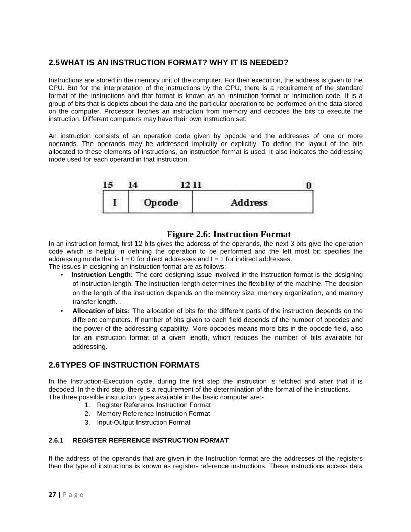
Figure 2.6: Instruction FormatIn an instruction format, first 12 bits gives the address of the operands, the next 3 bits give the operationcode which is helpful in defining the operation to be performed and the left most bit specifies theaddressing mode that is I = 0 for direct addresses and I = 1 for indirect addresses.The issues in designing an instruction format are as follows:-
Instruction Length: The core designing issue involved in the instruction format is the designingof instruction length. The instruction length determines the flexibility of the machine. The decisionon the length of the instruction depends on the memory size, memory organization, and memorytransfer length. .
Allocation of bits: The allocation of bits for the different parts of the instruction depends on thedifferent computers. If number of bits given to each field depends of the number of opcodes andthe power of the addressing capability. More opcodes means more bits in the opcode field, alsofor an instruction format of a given length, which reduces the number of bits available foraddressing.
2.6TYPES OF INSTRUCTION FORMATS
In the Instruction-Execution cycle, during the first step the instruction is fetched and after that it isdecoded. In the third step, there is a requirement of the determination of the format of the instructions.The three possible instruction types available in the basic computer are:-
1. Register Reference Instruction Format2. Memory Reference Instruction Format3. Input-Output Instruction Format
2.6.1 REGISTER REFERENCE INSTRUCTION FORMAT
If the address of the operands that are given in the Instruction format are the addresses of the registersthen the type of instructions is known as register- reference instructions. These instructions access data

28 | P a g e
and manipulate the contents of registers. They do not access memory. These instructions are executed inone clock cycle.
A processor has many registers to hold instructions, addresses, data, etc.The processor has a register, the Program Counter(PC) that holds the memory address of the nextinstruction. Since the memory in the basic computer only has 4096 locations, the PC only needs 12 bits.The Address Register(AR) is a 12-bit register that is used when there is a need to check the memorylocations that are addressed by the processor. It is used in a direct or indirect addressing.
The Data Register(DR) is also a 12-bit register that is used for the storage of operand when an operandis found, using either direct or indirect addressing. The processor then uses this value as data for itsoperation. The Basic Computer has a single general purpose register–the Accumulator(AC).Often a processor will need a scratch register to store intermediate results or other temporary data; in theBasic Computer this is the Temporary Register(TR).The Basic Computer uses a very simple model of input/output (I/O) operations. Input devices areConsidered to send 8 bits of character data to the processor. The processor can send 8 bits of characterdata to output devices. The Input Register(INPR) holds an 8 bit character gotten from an input device.The Output Register(OUTR) holds an 8 bit character to be send to an output device
An operand from the memory is not needed therefore the other 12 bits are used to specify the operationto be executed. These instructions use bits 0 through 11 of the instruction code to specify one of 12instructions. These bits are available in IR(0-11). The format of Register – reference instruction is givenby Figure 2.7.
Figure 2.7: Instruction Format of Register – Reference InstructionsThe different control functions that can be performed by the register –reference instructions are listed inTable 2.2.
Table 2.2: Execution of Register – Reference InstructionsSymbol Description
CLA Accumulator (AC) is clearedCLE Clear ECMA Accumulator (AC) is complementedCME Complement ECIR Circulate right AC and ECIL Circulate left AC and EINC Increment ACSPA Skip next instruction if AC is positiveSNA Skip next instruction if AC is negativeSZA Skip next instruction if AC is zeroSZE Skip next instruction if E is zeroHLT Halt computer
2.6.2 MEMORY – REFERENCE INSTRUCTION FORMAT
In complement to the Register-reference instructions, the memory reference instructions are those thatreference memory. Some read data from memory, others write data to memory, and one instruction doesboth. For these instructions, the most significant bit is the indirect bit. If this bit is 1, the instruction must

29 | P a g e
use indirect memory addressing. That is, the address given is not the address of the operand. It is theaddress of a memory location which contains the address of the operand.
The bits from 12 to 14 specified the OPCODE field, or operation field. These three bits may take on anyvalue except for 111; that is reserved for other instructions. The OPCODE field tells the CPU whichinstruction is to be performed. Finally, the 12 low order bits from 0-11 contain the memory address to beused by this instruction (or in the case of indirection the address of a memory location which contains theaddress to be used by this instruction). The format of the memory – reference is shown in Figure 2.8
Figure 2.8: Memory – Reference Instruction FormatSome of the Memory – Reference Instructions are shown in Table 2.3:-
Table 2.3: Memory – Reference InstructionsInstruction Description
AND AND memory word to AC (Performsbitwise Logical AND)
ADD Accumulator is added by memory wordLDA Accumulator is loaded by the memory
wordSTA the content of accumulator is stored in
memoryBUN Branch unconditionallyBSA Branch and Save Return AddressISZ Increment and Skip if zero
2.6.3 INPUT-OUTPUT INSTRUCTION FORMAT
Another category of instructions formats are known as Input and Output instructions. These instructionsare needed for transferring information to and from the accumulator( AC) register, for checking the flagbits, and for controlling the interrupt facility. An input – output instruction does not need a reference tomemory and is recognized by operational code 111 with a 1 in the left most bit of the instruction and theremaining 12 bits are used to specify the type of input output operation or test performed. The Figure 2.9shows the format of Input- Output Instruction:
Figure 2.9: Input-Output Instruction FormatThe different Input-Output Instructions are given below:-
Table 2.4: Input - Output InstructionsInstruction Description
INP Any character is inputtedOUT Any character is outputtedSKI Skip on input flagSKO Skip on output flagION Interrupt enable onIOF Interrupt enable off

30 | P a g e
The INP instruction transfers the input information from the input register into the accumulator into itseight low-order bits and also clears the input flag to 0. The OUT instruction do the vice versa case andtransfers eight low-order bits of accumulator into the output register OUTR and clears the output flag to 0.The next two instructions in the table check the status of the flags and cause a skip of the next instructionif the flag is 1. The instruction that is skipped will normally be a branch instruction to return and check theflag again. The branch instruction is not skipped if the flag is 0. If the flag is 1, the branch instruction isskipped and an input or output instruction is executed. ION and IOF are used to set and clear respectivelythe interrupt enable flip-flop IEN.CHECK YOUR PROGRESS 3
1) Micro-programmed control unit is ________________ than hardwired but __________________?
a. cheaper, more error proneb. faster, more error pronec. less error prone, slowerd. faster, harder to change
2) Hardwired control unit is ________________ than micro-programmed but __________________?
a. cheaper, more error proneb. faster, more error pronec. less error prone, slowerd. faster, harder to change
3) The goals of both hardwired control and microprogrammed control units is to?
a. access memoryb. generate control signals
c. access the ALUd. cost a lot of money
4) Any instruction format containsa. Opcodeb. Operandc. Only ad. Both a & b
5) Each operation has its _____ opcode:a. Uniqueb. Twoc. Threed. Four

31 | P a g e
6) _______specify where to get the source and destination operands for the operation specified by the_______:
a. Operand fields and opcodeb. Opcode and operandc. Source and destinationd. Cpu and memory
2.7SUMMARY
The Control Unit (CU) being the part of the CPU is used to depict the exactness of the sequence ofoperations. The Control Unit fetches the program instructions from the memory unit, and ensures correctexecution of the program. It also controls the input/output devices and directs the overall functioning ofthe other units of the computer. The Control Unit can be designed by two methods: a) Hardwired DesignTechnique b) Microprogrammed Design Technique. The hardwired design technique consists of digitallogic that is circuits, gates for designing and the microprogrammed design technique is built from ROM.Nowadays, microprogrammed based design technique is used in computers.
Instruction cycle is the process of executing any instruction in the CPU. Every instruction goes throughthis cycle which consists of Fetch, Decode, Execute and Store.
We have different types of Instruction formats according to the location of the operands mentioned in theinstructions. And these instruction format categories include : a) Register Reference Instructions b)Memory Reference Instructions c) Input Output Instructions. Register Reference Instruction format is usedif the operands are in register. Memory Reference Instructions are used if the operands are in thememory. And Input Output instructions are used to transfer the information to and from Accumulator (AC)register.
2. 8 MODEL ANSWERSYour Progress 1
1) The Control Unit (CU) checks the correctness of the sequence of operations. It fetches theprogram instructions from the memory unit, interprets them, and ensures correct execution of theprogram. It also controls the input/output devices and directs the overall functioning of the otherunits of the computer.
2) a) Hardwired Control Unit Design Technique
b) Microprogrammed Control Unit Technique
3) A hardwired control unit is designed from scratch using traditional digital logic designtechniques to produce a minimal, optimized circuit. In other words, when the control signals aregenerated by hardware using conventional logic design techniques, the control unit is said to behardwired.
A microprogrammed control unit is built from some sort of ROM. The desired control signalsare simply stored in the ROM, and retrieved in sequence to drive the microoperations needed bya particular instruction. The principle of microprogramming is an elegant and systematic methodfor controlling the microoperation sequences in a digital computer.

32 | P a g e
Your Progress 21. B 2. E 3. C
Your Progress 31. C 2. D 3. B 4. D 5. A 6. A
Glossary1) Control Unit (CU): The Control Unit (CU) checks the correctness of the sequence of operations. Itfetches the program instructions from the memory unit, interprets them, and ensures correct execution ofthe program.2) Hardwired Control Unit Design Technique: When the control signals are generated by hardwareusing conventional logic design techniques, the control unit is said to be hardwired design technique.3) Instruction Cycle: A cycle that every instruction has to undergo while it is being processed.4) Instruction Format: An instruction format or instruction code is a group of bits used to perform aparticular operation on the data stored on the computer.5) OPCODE: Operation Code, gives the operation that need to be performed on the instruction. It givesthe code assigned to particular operation. It is given in the instruction format.6) PC : Program Counter7) AR: Address Register8) DR: Data Register9) AC: Accumulator10) TR: Temporary Register11) INPR: Input Register12) OUTR: Output Register

33 | P a g e
Lesson 3. Computer Registers and Stack OrganizationStructure
3.0 Introduction3.1 Objectives3.2 What is a Register?3.3 Different Types of Registers3.4 Communication between the Registers3.5 General Register Organization3.6 What is a Control Word?3.7 Design of Adder and Logic Unit3.8 Stack Organization
3.8.1 Register Stack3.8.2 Memory Stack3.8.3 Reverse Polish Notation
3.9 Summary3.10 Model Answers
3.0 INTRODUCTION
In the previous chapter, we have studied about the organization of the Computer. The computer includesCPU (which includes Arithmetic Logic Unit (ALU), Control Unit (CU), and Registers), memory devices,input devices and output devices. Registers are high-speed, temporary storage areas for storing differentdata, instructions, addresses etc. In this chapter, we will study the different types of Registers used inComputer Organization and their organization. We will also study the design of Adder and Logic Unit. TheStack Organization is also discussed in this chapter in which a brief introduction of Register Stack,Memory Stack and Reverse Polish Notation is given.
3.1 OBJECTIVES
This block being the part of first unit will introduce the basics of Computer Organization. At the end of thisblock you will be able to:-
explain what is a Register? identify the different types of Registers explain what is a Control Word? trace the design of adder and logic unit define what is stack organization. Identify the different types of stack organizations
3.2 WHAT IS A REGISTER?
Any register is a discrete holding device consists of a group of flip-flops with each flip-flop capable ofstoring one bit of information. If any register is of n-bit then it will consists of group of n flip-flops and alsothe register can store n bits of information. These are special – purpose, high-speed temporary memoryunits.
The register can hold various types of information such as data, instructions, addresses, and theintermediate results of calculations. In other words, the registers are used to hold all the data upon whichthe CPU is working at that time. That is why, registers are also known as CPU’s working memory. Also,the registers have an additional advantage of speed. The registers perform under the supervision of thecontrol unit to accept, hold, and transfer instructions or data and perform arithmetic or logical

34 | P a g e
comparisons at high speed. The control unit uses a data storage register in the similar way a store owneruses a cash register as a temporary, convenient place to store the transactions. As soon as a particularinstruction or piece of data is processed, the next instruction immediately replaces it, and the informationthat results from the processing is returned to the main memory.
3.3DIFFERENT TYPES OF REGISTERS
There are different types of Registers:-1) MAR stand for Memory Address Register : MAR is a 12-bit register that carries the memory
addresses of data and instructions. This register is used when there is a need to access data andinstructions from memory during the execution phase of an instruction. It is used in both thecases that are either the user wants to read data from the memory or the user wants to write datainto the memory from the CPU.
2) Program Counter (PC):- PC is also a 12-bit register which always contains the address of thenext instruction that is to be executed by the CPU. This register is also known as the instructionpointer (IP) and sometimes called the instruction address register, or just part of the instructionsequencer in some computers, is a processor register. Once the program containing number ofinstructions started with the execution, then the starting address is given to the CPU. After that,the next address of the instruction is stored in the Program Counter, so that execution of theprogram can be done smoothly.
3) Accumulator Register (AC):- Accumulator is a 16-bit register and it can be referred to in theinstructions. Generally, it is used to store the intermediate results and also the final results thatare produced by the CPU. For example, Load AC, 20 is instructed to load the accumulator withthe contents of memory address 20.
4) Memory Data Register (MDR):- MDR is the 16-bit register of a computer's control unit thatcontains the data to be stored in the computer storage (e.g. RAM), or the data after a fetch fromthe computer storage. It acts like a buffer and holds anything that is copied from the memoryready for the processor to use it. MDR hold the information before it goes to the decoder, whichcontains the data to be written into or readout of the addressed location. For example, to retrievethe contents of cell 123, we would load the value 123 (in binary, of course) into the MAR andperform a fetch operation. When the operation is done, a copy of the contents of cell 123 wouldbe in the MDR. The MDR can also work in both ways that is data can be fetched from memoryand written into MDR and also data can be placed into MDR from any other register and then canbe put into memory.
5) Index Register (IR):- Index Register (IR) carries the value of some number that is used toevaluate the address portion of any instruction of the program. It is used to calculate the effectiveaddress. Sometimes it is also known as base register. When any program is given for executionto the CPU, then it is checked for the value of base address stored in the base register. If there isany value in the base register then that value is added to the address given to the CPU to find theeffective address.
6) Memory Buffer Register(MBR):- MBR stand for Memory Buffer Register. This register holds thecontents of data or instruction read from, or written in memory. It means that this register is usedto store data/instruction coming from the memory or going to the memory.

35 | P a g e
7) Data Register (DR):- A register used in microcomputers to temporarily store data beingtransmitted to or from a peripheral device.
8) Instruction Register (IR):- IR is a 16-bit register that is used to generate timing signals and othercontrol signals. This register can only be loaded with the instruction but we cannot perform anyoperation to it.
9) Temporary Register (TR):- This 16-bit register is used to store the temporary results that comeswhen the CPU is executing some instructions.
10) Input Register (INPR):- INPR, the input register is used to receive an 8 – bit character from aninput device.
11) Output Register (OUTR):- OUTR, the output register receives an 8-bit character from an outputdevice.
CHECK YOUR PROGRESS 1
Question 1: What is a Register?____________________________________________________________________________________
____________________________________________________________________________________
________________________________________________________________________________
Question 2: Differentiate between INPR and OUTR.____________________________________________________________________________________
____________________________________________________________________________________
________________________________________________________________________________
Question 3: Define the work of MBR and MAR Registers____________________________________________________________________________________
____________________________________________________________________________________
________________________________________________________________________________
3.4COMMUNICATION BETWEEN THE REGISTERS

36 | P a g e
As discussed in previous section, every computer have eight registers that are given by AC, IR, MDR,MAR, PC, TR, INPR, OUTR), a memory unit, and a control unit. So, there is a need of communicationbetween them. So, it is necessary to provide the paths to transfer information from one register to anotherand between memory and registers. The number of wires will be excessive if connections are madebetween the outputs of each register and the inputs of the other registers. A more efficient scheme fortransferring information in a system with many registers is to use a common bus. A bus system isestablished which is common between the basic computer registers and other units which is shown inFigure 3.1 and this system is commonly known as Common Bus System.
The outputs of seven registers and memory are connected to the common bus. The specific output that isselected for the bus lines at any given time is determined from the binary value of the selection variablesS2, S1 and S0. The number along each output shows the decimal equivalent of the required binaryselection. For example, the number along the output of DR is 3. The 16-bit outputs of DR are placed onthe bus lines when S2S1S0 = 011 since this is the binary value of decimal 3. The lines from the commonbus are connected to the inputs of each register and the data inputs of the memory. The particularregister whose LD(Load) input is enabled receives the data from the bus during the next clock pulsetransition. The memory receives the contents of the bus when its write input is activated. The memoryplaces its 16-bit output onto the bus when the read input is activated and S2S1S0 = 111.
Four registers DR, AC, IR, and TR, have 16 bits each. Two registers, AR and PC, have 12 bits each sincethey hold a memory address. When the contents of AR or PC are applied to the 16-bit common bus, thefour most significant bits are set to 0’s, When AR or PC receive information from the bus, only the 12 leastsignificant bits are transferred into the register.
The input register INPR and the output register OUTR have 8 bits each and communicate with the eightleast significant bits in the bus. INPR is connected to provide information to the bus but OUTR can onlyreceive information from the bus. INPR is used when the system has to receive a character from an inputdevice and OUTR is used when any character is to be outputted to any output device.
The 16 lines of the common bus receive information from six registers and the memory unit. The bus linesare connected to the inputs of six registers and the memory. There are three control inputs: LD (Load),INR (increment), and CLR (Clear) that are connected to different five registers.
The input data and output data of the memory are connected to the common bus, but the memoryaddress is connected to AR. Therefore, AR must always be used to specify a memory address. By usinga single register for the address, we eliminate the need for an address bus that would have been neededotherwise. The content of any register can be specified for the memory data input during a writeoperation. Similarly, any register can receive the data from memory after a read operation except AC.

37 | P a g e
Figure 3.1: Basic common registers connected to a common busThe 16 inputs of AC come from an adder and logic unit (ALU) circuit. This circuit has three set of inputs.One set of 16-bit inputs come from the outputs of AC. They are used to implement registermicrooperations such as complement AC and shift AC. Another set of 16-bit inputs come from the dataregister DR. The inputs from DR and AC are used for arithmetic and logic microoperations, such as addDR to AC or AND DR to AC. The result of an addition is transferred to AC and the end carry-out of theaddition is transferred to flip-flop E (extended AC bit). A third set of 8 –bit inputs come from the inputregister INPR.The clock transition at the end of the cycle transfers the content of the bus into the designated destinationregister and the output of the adder and logic circuit into AC. For example, the two microoperations
DR AC and AC DRcan be executed at the same time. This can be done by placing the content of AC on the bus, enablingthe LD (load) input of DR, transferring the content of DR through the adder and logic circuit into AC, andenabling the LD (load) input of AC, all during the same clock cycle. The two transfers occur upon thearrival of the clock pulse transition at the end of the clock cycle.
CHECK YOUR PROGRESS 21) The register that keeps track of the instructions in the program stored in memory is_______
A) Control register B) Program counterC) Status register D) Direct register
38 | P a g e
2) Data transfer between the main memory and the CPU register takes placethrough two registers namely.......
A) general purpose register and MDR B) accumulator and programcounterC) MAR and MDR D) MAR and Accumulator
3) In every transfer, selection of register by bus is decided by:
A) Control signal B) No signalC) All signal D) All of above
4) The index register in a digital computer is used for:-
A) Pointing to the stack addressB) Indirect addressingC) Keeping track of number of times a loop is executedD) Address Modification
3.5GENERAL REGISTER ORGANIZATION
Memory locations are needed for storing pointers, counters, return addresses, temporary results, andpartial products during multiplication. Having to refer to memory locations for such applications is timeconsuming because memory access is the most time – consuming operation in a computer. It is moreconvenient and more efficient to store these intermediate values in processor registers. When a largenumber of registers are included in CPU, it is most efficient to connect them through a common bussystem. The registers communicate with each other not only for direct data transfers, but also whileperforming various microoperations. Hence it is necessary to provide a common unit that can perform allthe arithmetic, logic, and shift microoperations in the processor.The seven CPU registers can be organized using the bus as shown in Figure 3.2. Two multiplexers(MUX) are used that are connected to the output of each register and they form two buses given by A andB.

39 | P a g e
Figure 3.2 : Block Diagram of General Register OrganizationThe input to the ALU is from the buses A and B. When any operation is to be preformed then that isselected by the arithmetic or logic microoperation. The result of the microoperation is available for outputdata and also goes into the inputs of all the registers. The register that receives the information from theoutput bus is selected by a decoder. The decoder activates one of the register load inputs, thus providinga transfer path between the data in the output bus and the inputs of the selected destination register.The control unit that operates the CPU bus system directs the information flow through the registers andALU by selecting the various components in the system. For example, to perform the operation
R1 R2 + R3
(1) MUX A selection (SEL A): to place the content of R2 into bus A
(2) MUX B selection (SEL B): to place the content of R3 into bus B
(3) ALU operation selection (OPR): to provide the arithmetic addition (A + B)
(4) Decoder destination selection (SEL D): to transfer the content of the output bus into R1
The four control selection variables are generated in the control unit and must be available at thebeginning of a clock cycle. The data from the two source registers propagate through the gates in themultiplexers and the ALU, to the output bus, and into the inputs of the destination register, all during theclock cycle interval. Then, when the next clock transition occurs, the binary information from the outputbus is transferred into R1. To achieve a fast response time, the ALU is constructed with high-speedcircuits.
3.6WHAT IS A CONTROL WORD?

40 | P a g e
There are 14 binary selection inputs in the unit, and their combined value specifies a control word. The14-bit control word is defined in Figure 3.2(b). It consists of four fields. Three fields contain three bitseach, and one field has five bits. The three bits of SELA select a source register for the A input of theALU. The three bits of SELB select a register for the B input of the ALU. The three bits of SELD select adestination register using the decoder and its seven load outputs. The five bits of OPR select one of theoperations in the ALU. The 14-bit control word when applied to the selection inputs specify a particularmicrooperation.
The encoding of the register selections is specified in Table 3.1.
Table 3.1 Binary codes for Register Selection Fields
BinaryCode
SELA SELB SELD
000 Input Input Input001 R1 R1 R1010 R2 R2 R2011 R3 R3 R3100 R4 R4 R4101 R5 R5 R5110 R6 R6 R6111 R7 R7 R7
The 3-bit binary code listed in the first column of the table specifies the binary code for each of the threefields. The register selected by fields SELA, SELB, and SELD is the one whose decimal number isequivalent to the binary number in the code.
3.7DESIGN OF ADDER AND LOGIC UNIT
The ALU that is Arithmetic and Logic Unit of CPU can perform arithmetic and logic operations.
ALU performs two types of operations:-
i) Fixed Point Operationsii) Floating Point Operations
Some of the arithmetic operations are:-
i) Addition, Subtractionii) Addition-with-carryiii) Subtraction with borrow from a previous operationiv) Divisionv) Increment and Decrementvi) Logical shift left and logical shift rightvii) Arithmetic shift left and logical shift right
Some of the logic operations are:-i) NOTii) AND, OR and XORiii) Compare
The general design of adder and logic unit is shown in Figure 3.3

41 | P a g e
Figure 3.3 : Design of Adder and Logic Unit
3.8 STACK ORGANIZATION
A useful feature that is included in the CPU of most computers is a stack or last-in, first –out (LIFO) list. Astack is a storage device that stores information in such a manner that the item stored last is the first itemretrieved. The operation of a stack can be compared to a stack of trays. The last tray placed on top of thestack is the first to be taken off.
The stack in digital computers is essentially a memory unit with an address register that can count only(after an initial value is loaded into it). The register that holds the address for the stack is called a stackpointer (SP) because its value always points at the top item in the stack. Contrary to a stack of trayswhere the tray itself may be taken out or inserted, the physical registers of a stack are always availablefor reading or writing. It is the content of the word that is inserted or deleted.
Two operations are defined for stack:-
i) Push :- The operation of insertion is called push because it can be thought of as the result ofpushing a new item on top.
ii) Pop:- The operation of deletion is called pop because it can be thought of as the result ofremoving one item so that the stack pops up.
3.8.1 REGISTER STACK
When the stack is implemented using a finite number of memory words or registers then this technique isknown as Register Stack. The register stack can be implemented using 32-word ,64-bit or more than thatregister stack. In Figure 3.4 64-word register stack is shown. It uses a stack pointer named as SP thatcontains the address of the word that is currently on top of the stack.

42 | P a g e
Figure 3.4: Block diagram of 64-word Register StackThree items are placed in the stack: A, B, and C, in that order. Item C is on top of the stack so that thecontent of SP is now 3. To remove the top item, the stack is popped by reading the memory word ataddress 3 and decrementing the content of SP. Item B is now on top of the stack since SP holds address2. To insert a new item, the stack is pushed by incrementing SP and writing a word in the next – higherlocation in the stack. Note that item C has been read out but not physically removed. This does not matterbecause when the stack is pushed, a new item is written in its place.In a 64-word stack, the stack pointer contains 6 bits because 26 = 64. Since SP has only 6 bits, it cannotexceed a number greater than 63 (111111 in binary). The one-bit register FULL is set to 1 when the stackis full, and the one-bit register EMPTY is set to 1 when the stack is empty of items. DR is the data registerthat holds the binary data to be written into or read out of the stack.Initially, SP is cleared to 0, EMPTY is set to 1, and FULL is cleared to 0, so that SP points to the word ataddress 0 and the stack is marked empty and not full. If the stack is not full ( if FULL = 0), a new item isinserted with a push operation. The push operation is implemented with the following sequence ofmicrooperations:-PUSH SP SP + 1 increment stack pointer
M [SP] DR unit item on top of the Stack
It (SP = 0) then (FULL 1) check it stack is full
EMPTY 0 mask the stack not empty.
The stack pointer is incremented so that it points to the address of the next-higher word. A memory writeoperation inserts the word from DR into the top of the stack. M[SP] denotes the memory word specified bythe address presently available in SP. The first item is stored in the stack at address 1. The last item isstored at 0. If SP reaches 0, the stack is full of items, so FULL is set to 1.
A new item is deleted from the stack if the stack is not empty (if EMPTY = 0). The pop operation consistsof the following sequence of microoperations:-
POP DR M[SP] read item trans the top of stack
SP SP –1 decrement SP
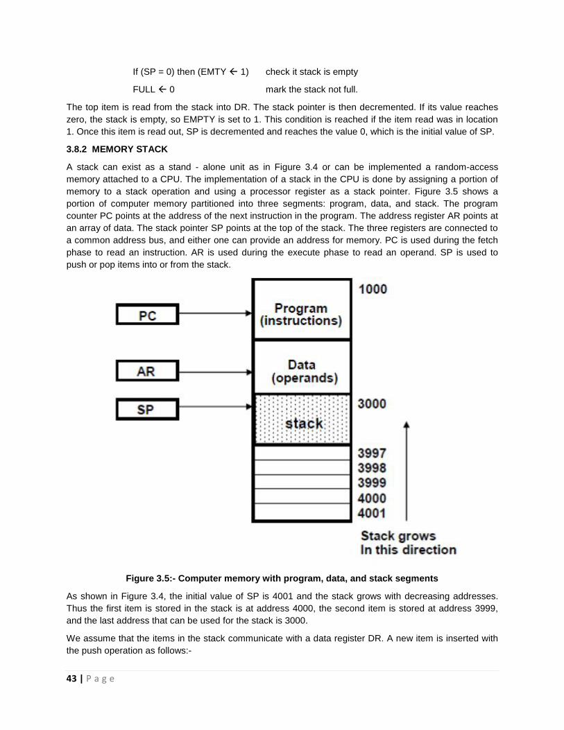
43 | P a g e
If (SP = 0) then (EMTY 1) check it stack is empty
FULL 0 mark the stack not full.
The top item is read from the stack into DR. The stack pointer is then decremented. If its value reacheszero, the stack is empty, so EMPTY is set to 1. This condition is reached if the item read was in location1. Once this item is read out, SP is decremented and reaches the value 0, which is the initial value of SP.
3.8.2 MEMORY STACK
A stack can exist as a stand - alone unit as in Figure 3.4 or can be implemented a random-accessmemory attached to a CPU. The implementation of a stack in the CPU is done by assigning a portion ofmemory to a stack operation and using a processor register as a stack pointer. Figure 3.5 shows aportion of computer memory partitioned into three segments: program, data, and stack. The programcounter PC points at the address of the next instruction in the program. The address register AR points atan array of data. The stack pointer SP points at the top of the stack. The three registers are connected toa common address bus, and either one can provide an address for memory. PC is used during the fetchphase to read an instruction. AR is used during the execute phase to read an operand. SP is used topush or pop items into or from the stack.
Figure 3.5:- Computer memory with program, data, and stack segments
As shown in Figure 3.4, the initial value of SP is 4001 and the stack grows with decreasing addresses.Thus the first item is stored in the stack is at address 4000, the second item is stored at address 3999,and the last address that can be used for the stack is 3000.
We assume that the items in the stack communicate with a data register DR. A new item is inserted withthe push operation as follows:-

44 | P a g e
SP SP - 1
M [SP] DR
The stack pointer is decremented so that it points at the address of the next word. A memory writeoperation inserts the word from DR into the top of the stack. A new item is deleted with a pop operationas follows:-
DR M[SP]SP SP + 1
The top item is read from the stack into DR. The stack pointer is then incremented to point at the nextitem in the stack.
3.8.3 REVERSE POLISH NOTATION
A stack organization is very effective for evaluating arithmetic expressions. The common mathematicalmethod of writing arithmetic expressions imposes difficulties when evaluated by a computer. The commonarithmetic expressions are written in infix notation, with each operator written between the operands. Forexample, A + B as ‘ + ‘ operator is placed between two operands A and B.The Polish mathematician Lukasiewicz showed that arithmetic expressions can be represented in prefixnotation. This representation, often referred to as Polish notation, places the operator before theoperands. The postfix notation, referred to as Reverse Polish notation (RPN), places the operator afterthe operands. The following examples demonstrate the three representations:-
A + B Infix Notation+ A B Prefix or Polish NotationA B + Postfix or Reverse Polish Notation
The Reverse Polish Notation is in a form suitable for stack manipulation. The expressionA * B + C * D
is written in Reverse Polish Notation asA B * C D * +
and is evaluated as follows:1) The expression is scanned from left to right until an operator is reached.
2) Perform the operation with the two operands found on the left side of the operator. Replace thetwo operands used in immediate evaluation with the number obtained by the result of theoperation.
3) Continue further scanning according to Step No 1 until there are no more operators.
Evaluation of Arithmetic Expressions:- Reverse Polish Notation, combined with a stack arrangementof registers, is the most efficient way known for evaluating arithmetic expressions. This procedure isemployed in some electronic calculators and also in some computers. The stack is particularly useful forhandling long, complex problems involving chain calculations. It is based on the fact that any arithmeticexpression can be expressed in parentheses-free Polish notation.The procedure consists of first converting the arithmetic expression into its equivalent reverse Polishnotation. The operands are pushed into the stack in the order in which they appear. The followingmicroooperations are executed with the stack when an operation is entered:-
i) The two topmost operands in the stack are used for the operation, andii) The stack is popped and the result of the operation replaces the lower operand.
By pushing the operands into the stack continuously and performing the operations as defined above, theexpression is evaluated in the proper order and the final result remains on top of the stack.The following numerical example may clarify this procedure. Consider the arithmetic expression
(3 * 4) + (5 * 6)In Reverse Polish Notation, it is expressed as
34 * 56 * +

45 | P a g e
Figure 3.5: Stack operations to evaluate 34 * 56 * +Scientific calculators that employ an internal stack require that the user convert the arithmetic expressionsinto Reverse Polish Notation. Computers that use a stack-organized CPU provide a system program toperform the conversion for the user. Most compilers, irrespective of their CPU organization, convert allarithmetic expressions into Polish notation anyway because this is the most efficient method fortranslating arithmetic expressions into machine language instructions. So in essence, a stack – organizedCPU may be more efficient in some applications than a CPU without a stack.CHECK YOUR PROGRESS 3Q1. A stack is a data-structure in which elements are stored and retrieved by:
a. FIFO method b.LIFO methodc. FCFS method d. None of the above
Q2. The insertion/deletion operations on a stack are respectively known as:a: insert and delete b: enter and exitc: push and pop d: none of the above
Q3: The expression A * B + C * D in Reverse Polish Notation can be written asa. AB * CD *+ b. A*BCD*+
c. AB*CD+* d. A*B*CD+
Q4: Postfix notation is also known as:a: polish notation b: reverse polish notationc: post notation d: post-operator notation
Q5: Prefix notation is also known as:a: polish notation b: reverse polish notationc: pre notation d: post-operator notation
3.9 SUMMARYA register is used to store the data or information. It is made up of flip – flops and each flip-flop can storeone bit of information. They are used for temporary storage areas for holding various types of informationsuch as data, instructions, addresses and the intermediate results of calculations. Different types ofregisters are required in CPU for the efficient processing. The different registers are Memory AddressRegister, Memory Buffer Register, Program Counter, Instruction Register, Data Register, Accumulator,Input Register, Output Register etc. All the different registers can communicate with each other and alsowith the processor using the bus system.All the different registers can communicate with organization consisting of multiplexers. They are selectedusing the control word.Stack organization is used to for efficient processing of CPU. Stack can be implemented using a Registeror it can be implemented in the memory. Stack is a LIFO (Last in First Out) data structure using theoperators Push and Pop for insertion and deletion respectively. Reverse polish notation is used toevaluate the arithmetic expressions in stack.3.10 MODEL ANSWERSYour Progress 1
1. A register is a group of flip-flops with each flip-flop capable of storing one bit of information. Theseare temporary storage areas for holding various types of information such as data, instructions,addresses, and the intermediate results of calculations.

46 | P a g e
2. Input Register (INPR) receives an 8 – bit character from an input device. Output Register(OUTR):- It receives an 8-bit character from an output device.
3. MAR stand for Memory Address Register : This register holds the memory addresses of dataand instructions. This 12 bit register is used to access data and instructions from memory duringthe execution phase of an instruction.
MBR stand for Memory Buffer Register. This register holds the contents of data or instructionread from, or written in memory. It means that this register is used to store data/instructioncoming from the memory or going to the memory.
Your Progress 21. B 2. C 3. A 4. DYour Progress 31. B 2. C 3. A 4. B 5. AGLOSSARY
1) REGISTER: A register is a group of flip-flops with each flip-flop capable of storing one bit ofinformation.
2) MAR: Memory Address Register
3) PC: Program Counter
4) AC: Accumulator Register
5) MDR: Memory Data Register
6) IR : Index Register
7) MBR: Memory Buffer Register
8) DR : Data Register
9) IR : Instruction Register
10) TR : Temporary Register
11) INPR : Input Register
12) OUTR : Output Register
13) MUX : Multiplexer
14) SP : Stack Pointer

47 | P a g e
Lesson 4. Addressing Modes, Instruction sets and InterruptsStructure
4.0 Introduction4.1 Objectives4.2 What is an Addressing Mode?4.3 Types of Addressing Modes
4.3.1 Direct Addressing Mode4.3.2 Immediate Addressing Mode4.3.3 Indirect Addressing Mode4.3.4 Multi Component Addressing Mode4.3.5 Implied Addressing Mode
4.4 Instruction Sets4.4.1 Complex Instruction Set Computer (CISC)4.4.2 Reduced Instruction Set Computer (RISC)
4.5 What is an Interrupt?4.5.1 Types of Interrupts
4.6 Summary4.7 Model Answers
4.0 INTRODUCTION
In the previous chapters, we have studied about the organization of the Computer. The computer isorganized using different internal registers, and the working of the computer is controlled by timing andcontrol structure of CPU and the various instructions that are used by the CPU to perform the operations.Computer Organization is a logical arrangement of the hardware components and how they areinterconnected. To almost all the users of the computer, the computer is a device to perform instructionson the operands in the memory; they are not clear about how it works? To use the computer effectively,we need to give instructions of different forms to the computer. And also there are different ways ofaccessing the operands in the memory.
In this block, we will introduce the different forms of instructions to be issued to the computer, differenttypes of Addressing Modes, types of instruction sets and introduction to Interrupts.
4.1 OBJECTIVES
This block being the part of first unit will introduce the basics of Computer Organization. At the end of thisblock you will be able to:-
define the term Addressing Mode. identify the different types of Addressing Modes. define different types of Instruction Sets. define the term Interrupt. explain how interrupt works? identify the different types of Interrupts.
4.2 WHAT IS AN ADDRESSING MODE?
Instructions are used to perform the functions as they are the part of the program. Also, the instructionsrequire the addresses to access the data from the memory. Addressing modes are used when there is arequirement to access the data from the memory or anywhere else. As the size of the memory isincreased, the size of the addresses tends to be long.

48 | P a g e
Addressing mode gives the location of the data required by an operation. As the addresses are very longso it is impossible for the instruction to contain the full address. It only contains the Effective Address(EA) which is defined as the actual address of the operand.
An operand of an instruction is either at a register or is the immediate operand (part of instruction after theoperation bits) or at a memory address.
4.3 TYPES OF ADDRESSING MODESMost of the instructions must refer to the address or content of a specific memory location. These so-called memory reference instructions must somehow identify the address of a location as part of theinstruction encoding. This section describes the common addressing modes used in computerorganization:-
4.3.1 DIRECT ADDRESSING MODE
When the instruction itself states the location of an operand or a destination (either in memory or aprocessor register), the addressing mode is known as Direct Addressing. The effective address itself isincluded in the subsequent words of the instruction.
Two sub - classifications within the direct addressing mode are often recognized. When the location is inmemory, the mode may be referred as Absolute Addressing. When the location is a processor register itmay be referred to as Register Direct Addressing.
Figure 4.1 : (a) Absolute Addressing (b) Register AddressingIn Figure 4.1 (a) the instruction specifies the address of the operand and Figure 4.1 (b) specifies theregister that contains the operand. For example, in case of Absolute Addressing, there can be instructionof the form LD R2, [100] which states to load the contents of the memory with address 100 to the registerR2.In case of Register Addressing, there can be instruction of the form MOV R3, R2 which states to movethe contents of register R2 into register R3.Direct addressing is used when the memory address or the selected register is to be fixed in the program.4.3.2 IMMEDIATE ADDRESSING MODE
The mode of including a bit pattern as a part of an instruction is called the Immediate addressing mode.In the immediate addressing mode, the instruction does not state explicitly the location of the operand, itstates the operand itself. The operand becomes the integral part of the instruction.

49 | P a g e
Immediate addressing is used when a particular constant value is to be fixed within the program itself.The value is found in memory “immediately” after the instruction code word and may never change at anytime. Figure 4.2 shows the instruction for Immediate addressing.
Figure 4.2 Immediate AddressingFor example, in case of Immediate Addressing, there can be instruction of the form MOV R2, 123 whichstates to move the operand with value ‘123’ to the register R2.4.3.3 INDIRECT ADDRESSING MODE
In the indirect addressing mode the instruction tells the processor neither the address of the operand northe operand itself. Instead, it tells the processor where to go to find the address of the operand. Theinstruction may explicitly state either the address of a location in memory or a name of a processorregister, but the binary number which is found there is not the operand. Instead, it is the effective address,the address of a location in memory to which the processor must go to find the operand. The result is thatthe processor must take one extra step in order to locate the operand.The op-word of the instruction includes a group of bits which identifies this mode of addressing, and the(indirect) address is specified in one or more additional post – words. If the instruction names a processorregister as the source of the effective address, then the register identification number may fit into the op-word itself.Indirect addressing is used when a program must operate upon different data values under differentcircumstances.

50 | P a g e
Figure 4.3 (a) Memory Indirect Addressing (b) Register Indirect AddressingFor example, in case of Memory Indirect Addressing mode we can have the instruction of the form ADDR2, 120, which states to add the two operands, one operand is in register R2 and the second one is inaddress specified by memory location 120. Similarly, in case of Register Indirect Addressing Mode, therecan be instruction of the form MOV R3, [R2] which states to move the contents of the memory locationspecified by the register [R2] into the register R3.Note: In immediate mode, instruction includes the operand, in the direct mode it includes the address ofthe operand and in the indirect mode it includes the address of the address of the operand.4.3.4 MULTI – COMPONENT ADDRESSING MODE
Each of the following related addressing modes requires that the processor assemble two or morecomponents together during the execution of the program in order to create the effective address. In eachcase the effective address itself is that of a memory location. However, at least one of the components isfound in a processor register.
Instructions which use indexed addressing specify two registers, often by coding within the op-word itself and known as “indexed addressing”. During program execution the processor temporarilyadds the contents of these registers to generate the effective address. One of the registers is an addressregister and it is said to hold the base address. The other is commonly a data register – thedisplacement or index register.
Based addressing is a similar mode wherein the instruction specifies an address register and afixed constant (an offset or displacement). The register designation often fits within the op-word and theoffset usually requires post-words. In this mode the content of the register is the base and the constant isthe displacement. During execution the processor adds the constant and the value in the register togenerate the effective address. This addressing mode is also known as “Relative Based Indexed” mode.

51 | P a g e
Figure 4.4 : Indexed Based Offset AddressingThe relative addressing mode permits the writing of “position-independent code”, programs which areproperly executed by the processor regardless of where they are located in memory. The entire program(together with any necessary data) may be picked up from one region of memory and moved to anotherwith no adverse effect. In order to be location – independent, a program may not refer to any specificlocation by address. All references to the memory must be through the use of relative addressing.4.3.5 IMPLIED OR INHERENT ADDRESSING MODE
Certain instructions allow no choice of register or location but always cause the processor to refer to thesame registers. In implied addressing mode, opcode specifies the address of the operands. For example,CMA instruction states to complement the contents of accumulator, CLRA states to clear the contents ofA.Check Your Progress 1Question 1: What is an Addressing Mode?____________________________________________________________________________________
____________________________________________________________________________________
__________________________________________________________________
Question 2: Differentiate between Direct and Indirect Addressing Mode?____________________________________________________________________________________
____________________________________________________________________________________
__________________________________________________________________
Question 3: Give examples of Instructions included in Register Direct Addressing Mode andMemory Direct Addressing Mode (Absolute Addressing).

52 | P a g e
____________________________________________________________________________________
____________________________________________________________________________________
__________________________________________________________________
4.4 INSTRUCTION SETS
An important aspect of computer architecture is the design of the instruction set for the processor. Theinstruction set chosen for a particular computer determines the way that machine language programs areconstructed. Early computers had small and simple instruction sets, forced mainly by the need tominimize the hardware used to implement them. As digital hardware became cheaper with the advent ofintegrated circuits, computer instructions tend to increase both in number and complexity. The trend intocomputer hardware complexity was influenced by various factors, such as upgrading existing models toprovide more customer applications, adding instructions that facilitate the translation from high-levellanguage into machine language programs, and striving to develop machines that move functions fromsoftware implementation into hardware implementation.A computer with a large number of instructions is classified as a Complex Instruction Set Computer,abbreviated CISC. A number of computer designers recommended that computers use fewer instructionswith simple constructs so they can be executed much faster within the CPU without having to usememory as often. This type of computer is classified as a Reduced Instruction Set Computer (RISC).4.4.1COMPLEX INSTRUCTION SET COMPUTER (CISC)
The earlier generations of the computer was 1G and 2G in which programming is done in machinelanguage and assembly language respectively that is in low level languages. These languages wereexecuted very quickly on computers, but were not easy for programmers to understand and code. Due tothese shortcomings, high-level languages came into existence. But for the instructions to be executed,the high-level language programming were required to be converted into their equivalent low-levellanguages before the processor can execute them. This conversion process was performed by thecompiler. Writing compilers for such high – level languages became increasingly difficult. To makecompiler development easier, CISC was developed.
The sole motive of manufactures of CISC – based processor was to manufacture processors with moreextensive and complex instruction set.The major characteristics of CISC architecture are:-1)A large number of instructions – typically from 100 to 250 instructions.2)Some instructions that perform specialized tasks and are used infrequently.3)A large variety of addressing modes – typically from 5 to 20 different modes.4)Variable – length instruction formats.5)Instructions that manipulate operands in memory.
The various merits of CISC architecture are as follows:-1)At the time of its initial development, CISC machines used available technologies to optimize thecomputer performance.2)It uses general – purpose hardware to carry out commands. Therefore, new command can be addedinto the chip without changing the structure of the instruction set.3)Microprogramming is as easy as assembly language to implement and much less expensive thanhardwiring a control unit.4)As microprogram instruction sets can be written to match the constructs of high – level languages, thecompiler does not have to be very complex.

53 | P a g e
Although the CISC architecture did much to improve computer performance, it still had some demerits.They are as follows:-1) The instruction set and the chip hardware became complex with each generation of computers.2) Different instructions take different amount of clock time to execute, and thus slow down the overallperformance of the machine.3) It requires continuous reprogramming of on-chip hardware. Its design includes the complexity ofhardware needed to perform many operations.
4.4.2 REDUCED INSTRUCTION SET COMPUTER (RISC)
RISC is a processor architecture that utilizes a small, highly optimized set of instructions. The conceptbehind RISC architecture is that a small number of instructions are faster in execution as compared to asingle long instruction. To implement this, it simplifies the instruction set of the processor, which helps inreducing the execution time. The optimization of each instruction in the processor is done through atechnique known as pipelining. Pipelining allows the processor to work on different steps of theinstruction at the same time that is why; more instructions can be executed at a single point of time. Thisis achieved by overlapping the fetch, decode, and execute cycles of two or more instructions. The RISCdesign contains a larger number of registers so that the memory interactions can be prevented. As eachinstruction is executed directly using the processor, no hardwired circuitry (used for complex instructions)is required. This allows RISC processors to be smaller, consume less power, and run cooler than CISCprocessors, Due to these advantages, RISC processors are ideal for embedded applications such asmobile phones, PDAs, and digital cameras. In addition, the simple design of a RISC processor reduces itsdevelopment time as compared to a CISC processor.The major characteristics of a RISC processor as follows:-
Relatively few instructions. Relatively few addressing modes. Memory access limited to load and store instructions. All operations done within the registers of the CPU. Fixed – length, easily decoded instruction format. Single – cycle instruction execution. Hardwired rather than microprogrammed control. A relatively large number of registers in the processor unit. Use of overlapped register windows to speed-up procedure call and return. Efficient instruction pipeline.
The advantages of RISC architecture are as follows:-
The RISC processor achieved 2-4 more times the performance than the CISC processor. Theinstruction set allows a pipelined, super-scalar design for a RISC processor.
As the instruction set of a RISC processor is simple, it uses less chip space. Since RISC architecture is simpler than CISC architecture, it can be designed more quickly.
But on the other hand, RISC got few disadvantages also. They are as follows:- The performance of a RISC processor depends largely on the code that it is executing. Instruction scheduling makes the debugging process difficult. RISC machines require very fast memory systems to feed instructions. RISC-based systems
typically contain large memory cache usually on the chip itself.
Check Your Progress 2

54 | P a g e
1) ________ is a type of processor architecture that utilizes a small, highly optimized set ofinstructions.
a) RISC b) CISC c) ISA d) ANNA
2) RISC processors are ideal for embedded applications, such as mobile phones and PDAs because_________________a) They are smaller in size and consume less power.b) They are larger in size and consume less power.c) They are smaller in size and consume more power.d) They are larger in size and consume large amount of power.
3) Pipe-lining is a unique feature of _______.a) RISCb) CISCc) ISAd) IANA
4.5 WHAT IS AN INTERRUPT?
An interrupt is a signal that causes the computer to alter its normal flow of instruction execution. e.g.divide by zero, time out, I/O operation. The interrupt automatically transfers control to an interruptprocessing routine which takes some action in response to the condition that caused the interrupt, andthen control is returned to the program at which its execution was interrupted.
The interrupt causes the CPU to temporarily suspend the current program being executed. Thecontrol is subsequently transferred to some other program referred to as interrupt service routine whichspecifies the actions to be taken if the exceptional event occurs. Interrupts may be generated by a varietyof sources internal and external to the CPU. They are used by the different Input-Output devices to usethe services of the CPU. They greatly increase the performance of the computer by allowing the I/Odevices direct and rapid access to the CPU and by freeing the CPU from the task of continually testingthe status of its I/O devices. Interrupts are used primarily to request the CPU to initiate a new I/Ooperation, to signal the completion of an I/O operation, and to signal the occurrence of hardware andsoftware errors.4.5.1 TYPES OF INTERRUPTS
There are three major types of interrupts that cause a break in the normal execution of a program. Theycan be classified as:-
External Interrupts:- External interrupts come from input – output (I/O) devices, from a timingdevice from a circuit monitoring the power supply, or from any other external source. Examplesthat cause external interrupts are I/O device requesting transfer of data, I/O device finishedtransfer of data, elapsed time of an event, or power failure. Timeout interrupt may result from aprogram that is n an endless loop and thus exceeded its time allocation. Power failure interruptmay have as its service routine a program that transfers the complete state of the CPU into anondestructive memory in the few milliseconds before power ceases.
Internal Interrupts:- Internal interrupts arise from illegal or erroneous use of an instruction ordata. Internal interrupts are also called traps. Example of interrupts caused by internal errorconditions are register overflow, attempt to divide by zero, an invalid operation code, stackoverflow, and protection violation. These error conditions usually occur as a result of a prematuretermination of the instruction execution. The service program that processes the internal interruptdetermines the corrective measure to be taken.

55 | P a g e
The difference between internal and external interrupts is that the internal interrupt is initiated bysome exceptional condition caused by the program itself rather than by an external event. Internalinterrupts are synchronous with the program while external interrupts are asynchronous. If theprogram is rerun, the internal interrupts will occur in the same place each time. External interruptsdepend on external conditions that are independent of the program being executed at the time.
Software Interrupts:- A software interrupt is initiated by executing an instruction. Softwareinterrupt is a special call instruction that behaves like an interrupt rather than a subroutine call. Itcan be used by the programmer to initiate an interrupt procedure at any desired point in theprogram. The most common use of software interrupt is associated with a supervisor callinstruction. This instruction provides means for switching from a CPU user mode to the supervisormode. Certain operations in the computer may be assigned to the supervisor mode only, as forexample, a complex input or output transfer procedure. A program written by a user must run inthe user mode. When an input or output transfer is required, the supervisor mode is requested bymeans of a supervisor call instruction. This instruction causes a software interrupt that stores theold CPU state and brings in a new PSW (Program Status Word) that belongs to the supervisormode. The calling program must pass information to the operating system.
Check Your Progress 3
1. The instruction, Add #45,R1 does,a) Adds the value of 45 to the address of R1 and stores 45 in that addressb) Adds 45 to the value of R1 and stores it in R1c) Finds the memory location 45 and adds that content to that of R1d) None of the above
2. The addressing mode which makes use of in-direction pointers is ______ .a) Indirect addressing modeb) Index addressing modec) Relative addressing moded) Offset addressing mode
3. The addressing mode, where you directly specify the operand value is _______ .a) Immediateb) Directc) Definited) Relative
4. In which addressing the simplest addressing mode where an operand is fetched from memoryis_____:
a. Immediate addressingb. Direct addressingc. Register addressing
d. None of these
5. In length instruction some programs wants a complex instruction set containing more instruction,more addressing modes and greater address range, as in case of_____:
a. RISC

56 | P a g e
b. CISCc. Bothd. None
6. In length instruction other programs on the other hand, want a small and fixed-size instruction setthat contains only a limited number of opcodes, as in case of_____:

57 | P a g e
a. RISCb. CISCc. Bothd. None
4.6 SUMARRY
Addressing mode refers to the specification of the location of the data required by an operation. Anoperand of an instruction is either at a register or is the immediate operand (part of instruction after theoperation bits) or at a memory address. There are different types of addressing modes used in computerorganization. This includes direct addressing, indirect addressing, immediate addressing mode, impliedaddressing, indexed addressing mode, relative addressing mode, base addressing mode etc. Thisaddressing mode is decided according to the organization of computer and instruction set of the particularcomputer.
Different types of instruction sets are defined as RISC (Reduced Instruction Set Computer) and CISC(Complex Instruction Set Computer). RISC includes a small and fixed size instruction sets that containsonly a limited number of opcodes but CISC includes a instruction set containing more instruction, moreaddressing modes and greater address range.
An interrupt is a signal that causes the computer to alter its normal flow of instruction execution. eg.divide by zero, time out, I/O operation. The interrupt automatically transfers control to an interruptprocessing routine which takes some action in response to the condition that caused the interrupt, andthen control is returned to the program at which its execution was interrupted. Then there are differenttypes of Interrupts – External, Internal and Hardware Interrupts.
4. 7 MODEL ANSWERSYour Progress 1
4) Addressing mode refers to the specification of the location of the data required by an operation.An operand of an instruction is either at a register or is the immediate operand (part of instructionafter the operation bits) or at a memory address.
5) In Direct Addressing mode, instruction includes the address of the operand and in the indirectmode it includes the address of the address of the operand.
6) In case of Absolute Addressing, there can be instruction of the form LD R2, [100] which states toload the contents of the memory with address 100 to the register R2. In case of RegisterAddressing, there can be instruction of the form MOV R3, R2 which states to move the contentsof register R2 into register R3.
Your Progress 22. A 2. A 3. A
Your Progress 32. B 2. A 3. A 4. B 5. B 6. A
GLOSSARY

58 | P a g e
a. Addressing mode refers to the specification of the location of the data required by anoperation
b. An interrupt is a signal that causes the computer to alter its normal flow of instructionexecution. e.g divide by zero, time out, I/O operation
c. CISC : COMPLEX INSTRUCTION SET COMPUTER
d. RISC : REDUCED INSTRUCTION SET COMPUTER

59 | P a g e
UNIT 2: Chapter-5Pipeline and Vector Processing
Structure5.0 Objectives5.1 Introduction5.2 Parallel Processing5.3 Pipeline Processing
5.3.1 Speedup with pipeline implementation5.3.2 Arithmetic Pipeline
5.3.2.1 Speedup for Adder5.3.3 Instruction Pipeline Processing
5.4 Vector Processing5.4.1 Vector Operations
5.4.1.1 Simple Addition of two vectors5.5 Memory Interleaving5.6 Array Processors5.7 Summary5.8 Glossary5.9 Answer to check your progress/Suggested Answers to Questions (SAQ)5.10 References/ Bibliography5.11 Suggested Readings5.12 Terminal and Model Questions
5.0 ObjectivesThe main objectives of this chapter are:
Define parallel processing and explanation of its logic structure
Classification of parallel processing by M. J. Flynn
Define pipeline processing and explanation of its logic structure
Speed-up with pipeline over without pipeline
Pipeline implementation of arithmetic computation and instruction execution
Define vector processing and explanation of its logic structure
Addition of two vectors using vector processing
Concept of memory interleaving
Define array processing and explanation of its logic structure
5.1 Introduction
There is high demand of computers that can handle scientific andengineering computations efficiently with least time. The computationalspeed of a computer system can be enhanced by implementing techniques
60 | P a g e
that uses simultaneous data-processing either at instruction level or atprocessor level. Parallel processing is used to increase the throughput of acomputer by increasing its processing capability. M. J. Flynn categorizedthe computers with parallel processing capability into four categories.Pipeline processing is a way of incorporating parallel processing incomputers. In scientific and engineering applications, vector and matrixprocessing requires vast computation that is handled by vector processing.To speedup memory access in parallel processing the concept of memoryinterleaving is used. Array processing is one more way of incorporatingparallel processing in systems by installing several processing elementsunder the control of a host computer.5.2 Parallel Processing
A program consists of sequence of instructions. In conventional way ofcomputing these instructions are executed sequentially i.e. one afteranother. The next instruction can be executed only if previous one iscompleted. The performance of a computer can be increased by executingmany instructions simultaneously or in parallel. The objective of parallelprocessing is to increase the throughput of a computer by increasing itsprocessing capability by decreasing the elapsed time required for theoverall computation of a job. The parallel processing can be achieved byincorporating more than one processor in a computer. Where there is onlyone processor available in a computer, either it can be achieved byincorporating more than one ALU in a processor or by allowing a processorto run each process in turn for a short time. In general, the parallelism canbe carried out at instruction-level or at processor-level.
The common way of categorizing computers with parallel processingcapability is coined by M. J. Flynn. The classification is based on thenumber of instruction and data streams simultaneously managed byprocessor during program execution. The instruction stream means theflow of instructions from memory to processor and data stream means the

61 | P a g e
flow of data from memory to processor or processor to memory. The fourbroad categories are:
Single Instruction Stream, Single Data Stream (SISD): A computer with single processorthat executes single instruction stream to process data available in single memory. VonNeumann architecture based PC generally having uniprocessor falls under thiscategory.
Single Instruction Stream, Multiple Data Stream (SIMD): A computer with multipleprocessing units work under the guidance of single control unit. Each processing unitreceives and process single instruction on different data using a common memorydivided into various components so as to communicate with all processorssimultaneously. Vector processors and array processors fall under this category.
Multiple Instruction Stream, Single Data Stream (MISD): A computer with multipleprocessing units each of which receives different instructions for same data set. Nosuch implementation is available commercially yet.
Multiple Instruction Stream, Multiple Data Stream (MIMD): A computer with multipleprocessing units work under the guidance of single control unit. Each processing unitreceives and processes multiple instructions on different data set using a sharedmemory or distributed memory so as to communicate with all processors.Multiprocessor in case of shared memory and multicomputer in case of distributedmemory falls under this category.
The parallel processing applications nowadays are in many areas suchas scientific, medical, artificial intelligence, image processing, remotesensing, communication and engineering etc.
Check Your ProgressQ. 1 : The purpose of parallel processor is to _ __ __ __ _ _ _ __ __ __
_ _ __ of system.Answer options: a) Increase throughput b). Decrease throughput c).Decrease Cost d). Enhance memory.Q. 2 : The term SIMD stands for _ __ __ __ __ __ __ ___ __ __.Answer options: a) System input, memory data. b). Straight
instruction, multiple datac). Single instruction stream, multiple data stream. d). Simple
instruction stream, memory data stream.Q 3 : As per M. J. Flynn’s parallel processing computers are classified
in _ __ __ _ _ categories.Answer options: a). 5 b). 4 c). 3 d).
2

62 | P a g e
5.3 Pipeline ProcessingPipelining is a technique used to enhance throughput of a system similar toassembly line technique used in manufacturing plant. In pipelineprocessing a sequential process is decomposed into various sub-processes each of which is processed in a dedicated segment concurrentlywith all other segments. Suppose we want to design a circuit to solve thefollowing arithmetic computation. The computation is required to performon five sets of data.
Ui / Vi * Si + Ti + 1 for i = 1, 2, 3, 4, 5;The pipelining used to compute this arithmetic equation is given in Figure 1.
Figure 1: Pipelining used to compute an arithmetic equation.The space-time diagram for above said arithmetic computation which isdivided into four sub-processes i.e. division, multiplication, addition andincrement is shown below:
Task\clockcycle
1 2 3 4 5 6 7 8
Division i =1 i =2
i =3
i = 4 i =5
Multiplication i = 1 i =2
i =3
i =4
i =5
Addition i =1
i = 2 i =3
i =4
i =5
Increment i =1
i =2
i =3
i =4
i =5

63 | P a g e
Figure 2: Space time diagram for arithmetic computation using 5-segmentpipelining.
In first clock cycle, divisor will perform the division for data set 1 i.e. for i =1. In second clock cycle, the multiplier will perform the multiplication fordata set 1 and divisor will perform the division for data set 2. Continuing, inthis manner, the arithmetic computation of data set 1, 2, 3, 4 and 5 will becompleted after 4, 5, 6, 7 and 8 cycles respectively.5.3.1 Speedup with pipeline implementationSuppose we have n number of jobs and each of which is required to passthrough a k-segment pipeline. Let the time taken to complete a job is T andhence the time required to complete n jobs in a non-pipelining process isnT. Since a job is required to pass through a k-segment pipeline to getcompleted, then each segment will take T / k time to complete a job. Timerequired to complete n jobs with a pipeline of k-segments,
= T + ( n - 1) ( T / k)= T ( k + n -1) / k
Speed up of pipeline processing over non-pipeline processing is given as:n T / [T ( k + n -1) / k ]k / [ 1 + ( k -1 ) / n ]
If the number of jobs n is much larger than the number of segments kin a pipeline, then ( k -1 ) / n << 1 and the speed up is near k i.e. thenumber of segments in a pipeline used to process the jobs. Here weassume that the time taken to process a complete job is same in a pipelineand non-pipeline process.5.3.2 Arithmetic PipelineArithmetic pipeline divides an arithmetic process into various sub-processes. Each sub-process is handled in a separate pipeline segment.The purpose of arithmetic pipelining is to increase the computational speedof a machine by implementing fixed-point or floating-point computationssuch as addition, subtraction, multiplication and division through pipelining.A block diagram of floating point addition performed through pipelining isgiven in Figure 3. The components Rm and Re shows the registers used tostore mantissa and exponent of two numbers in each segment.

64 | P a g e
Figure 3: Block diagram of 4-segment pipeline process for floating-pointaddition or subtraction.
The four steps required to add two floating-point numbers are : Exponentcomparison, mantissa normalization, addition operation, resultnormalization.a). Exponent comparison: In first segment, the exponents of two numbersare compared with each other, by subtracting one from another, toascertain which exponent is smaller.b). Mantissa normalization: The mantissa of the number which has smallerexponent is shifted to align the decimal point in mantissa part of twonumbers.c). Addition operation : In third segment, the addition operation isperformed on two numbers if we want to add two numbers or the substationoperation is performed on two numbers if we want to subtract one fromanother.e). Result normalization: In fourth segment, the results are normalized byshifting the mantissa to left or right depending upon result from thirdsegment so as to obtain a fraction with a non-zero first digit in mantissa andthe exponent is incremented or decremented accordingly.5.3.2.1 Speedup for AdderSpeedup for four segment arithmetic pipeline processor is almost 4 timesthe speed of arithmetic non-pipeline processor if the number of data set isvery large as compared to the number of segments in pipelining.
5.3.3 Instruction Pipeline Processing
A program consists of sequence of instructions. During processing timeeach instruction is executed one by one after fetching it from memory. In

65 | P a g e
general an instruction processing is considered two stage step: fetchinstruction and execute instruction. During execution there may be asituation when memory cycle is not used and this time is used to fetchinstruction from memory and place it in a buffer. This action is also calledas instruction prefetch. If these two steps are further break down intosmaller steps so that each one can be processed simultaneously to speedup instruction execution. This method of breaking instruction executioncycle into smaller steps and process them in parallel is known asinstruction pipelining. Generally following six steps are used to executeinstruction in a pipeline process:
i). Fetch instruction: Read next instruction from memory to buffer.
ii). Decode Instruction: Opcode and operand details are determined.
iii). Calculate effective address of operands: The effective address ofeach operand is computed based on various forms of addresscalculations such as displacement, indirect and indirect register etc.
iv). Fetch operands: Each operand from memory is fetched usingeffective address.
v). Execute instruction: The operation on operands is performed andresults are stored in desired operand.
vi). Store result: The results available in registers are stored in memory.
A five segment instruction pipeline processing is given in Figure 4. Thevarious steps mentioned in diagram are abbreviated as: Fetch instruction(FI), Decode Instruction (DI), Calculate effective address of operands (EA),Fetch operand (FO), and Execute instruction and store results (ES). Herein this case, the time period to perform computation for each instruction inall segments is same and all segments can perform computation in parallel.If each segment contains one unit time to finish its task, then the firstinstruction is completed in five time units and remaining each instruction isbeing processed in one time unit. The total time required to process eight

66 | P a g e
instructions in 5 segment instruction pipeline is 12 units whereas timerequired to process eight instructions in non-pipeline process is 45 units.
Figure 4: Five segment instruction pipeline.The timing sequence for instruction pipeline process is given in Figure 5:
Segments 1 2 3 4 5 6 7 8 9 10 11 12 13Instruction1
FI
DI EA
FO
ES
Instruction FI DI E F E

67 | P a g e
Figure 5: Timing sequence for instruction pipeline processwithout branch.On the other hand if a conditional branch occurs at third instruction andalters the execution sequence to ninth instruction. The results are shown inFigure 6.
2 A O SInstruction3
FI DI EA
FO
ES
Instruction4
FI DI EA
FO
ES
Instruction5
FI DI EA
FO
ES
Instruction6
FI DI EA
FO ES
Instruction7
FI DI EA FO
ES
Instruction8
FI DI EA
FO
ES
Segments 1 2 3 4 5 6 7 8 9 10 11 12 13Instruction1
FI
DI EA
FO
ES
Instruction2
FI DI EA
FO
ES
Instruction3
(Branch)
FI DI EA
FO
ES
Instruction4
FI DI EA
FO
Instruction5
FI DI EA
Instruction6
FI
Instruction9
FI DI EA FO
ES

68 | P a g e
Figure 6: Timing sequence for instruction pipeline process with branch atthird instruction.Here in this case, although instruction 4, instruction 5, and instruction 6are fetched and proceed through various stages, but after the execution ofinstruction 3 ( where branch occurs), instruction 4, instruction 5, andinstruction 6 are no longer needed. Only after time period at segment 6,when the branch has executed, can the next instruction to be executed(instruction 9) be fetched, after which, the pipe refills. From time period atsegment 6 through 11, only one instruction has executed. This causesdelay in processing instructions through instruction pipelining.There are some situations that cause the instruction pipeline to divergefrom its normal process and slow down its performance. The situations are:resource conflicts, data dependencies and branch statements.
Resource conflicts arise when two instructions access the same memory at same time.The conflict can be resolved by incorporating two ways from memory, one for data andanother for instruction.
Data dependencies arise when the result of one instruction is to be used as an operandin the following instructions which is not available yet. The conflict can be resolved byadding special hardware or complier in a system. The special hardware is used toidentify the instructions having source operands are destinations for instructions fartherup the pipeline. This causes a brief delay, for a few required clock cycles, into thepipeline allowing enough time to pass to resolve the conflict. This technique is called ashardware interlocks. In some systems, compilers are incorporated to manage pipeliningthat reorder instructions, resulting in a delay of loading any conflicting data that have noeffect on the system performance. This technique is called as delayed load.
A branch instruction also alters the flow of execution of instructions in pipelining. Amongthe various techniques to solve the conditional branch problems are: prefetch branchinstruction, branch prediction, loop buffer and delayed branch.
Instruction10
FI DI EA
FO
ES
Instruction11
FI DI EA
FO
ES

69 | P a g e
5.4 Vector Processing
The vectors and matrices may consist of large number of element andrequire vast computations for their processing. Vector processors arepipelined processors that perform necessary operations on entire vectorsand matrices at same time. This kind of processing is suited forapplications such as aerodynamics, seismology, image processing,weather forecasting and meteorology etc. These kinds of applicationsrequire high degree of parallelism, high precision and repetitive floatingpoint operations. A general block diagram for vector processing is given inFigure 7.
Figure 7: General block diagram of Vector Processor.
5.4.1 Vector Operations
Check Your ProgressQ 4: Suppose we have n number of jobs and each of which is required
to pass through a k-segment pipeline. The speedup withpipeline-processor over non-pipeline processor is __ ___ ______ ___ ___ ___.
Answer options: a). n times b). k times c). kn
times d). nk timesQ 5: The effective address is calculated after processing __ ___ ___
___ ___ ___ ___ instruction.Answer options: a). branch b). fetch c). decode
d). execute

70 | P a g e
A vector is an ordered set of one dimensional array of data elements. Avector V of N data elements is represented as:
V = [ V1, V2 , V3, … VN ]
The number of operations ranging from the simple addition to specializedcomputations can be performed on vectors using vector processing.
5.4.1.1 Simple addition of two vectors
Suppose we want to add two vectors X and Y and store the result invector Z. The codes in C to do this are as:
for ( int i =1; i<=N; i++){
Z[ i ] = X [ i ] + Y [ i ] ;}
The vector processor code to do this will be like given below:
LDV X R1 ;Load vector X into vector register R1LDV Y R2 ; Load vector Y into vector register R2ADDV R3 R1 R2 ; Add the contents of vector registers
R1, R2 and store the result in vector registerR3
STV R3, Z ; Store contents of vector register R3 invector Z
Vector registers are special purpose registers where numerous vectorelements can be stored at a time. The vector instructions contains theinformation about number of data elements in each vector, initial address ofvector operands and the operations to be performed on vector operands.

71 | P a g e
5.5 Memory Interleaving
The access to a single shared memory module is sequential whereaspipeline or vector processing require simultaneously access to a memorymodule from different sources. A memory may be divided into number ofmodules each of which contains its own address and data registers, andshare a common address and data bus. Each module is independentlyable to handle a memory read or write request, so that a system with nmodules can handle n requests simultaneously. In Figure 8, memory isorganized into 8-modules. Memory interleaving is a technique that assignsdifferent sets of addresses to different memory modules. The Figure 9shows the memory of 16 addresses organized into four modules eachhaving four addresses.
Figure 8: Memory organized into modules.
Check Your ProgressQ 6 Vector processing is a kind of ___ __ __ __ ___ ___ __
parallel computers.Answer options: a). SIMD b). MISD c). MIMD
d). SISD

72 | P a g e
Figure 9: Four memory modules with different address each.Interleaved memories maximize parallelism as a majority of memoryreferences are to consecutive addresses.
5.6 Array Processors
The vector computation can be performed through an array processor byincorporating number of processing elements in a system. The opcode ofinstruction is transmitted to all the processing elements and they performthe desire operation on operands stored in them simultaneously. Arrayprocessing is sometimes used to refer to a parallel ALU that uses dataparallelism to perform computation. The performance of array processor isachieved by incorporating several processing elements (PEs) in a system.An array processor is generally attached to a host computer that transmitsthe sequence of instructions to be executed to all the processing elementsof an array processor along with data. All the processing elementsindependently execute the instructions and perform processing on datastored in local memory of each of them simultaneously. A block diagram ofsuch an organization is given in Figure 10. In this Figure M1, M2, M3, . . . ,
Check Your ProgressQ 7 The concept of memory interleaving is used to __ __ __ ___
___ __ ___ ___Answer options: a). Maximize memory size b). Maximize
parallelismc). Increase cost of memory d). Slowdown
processing speed

73 | P a g e
MN represents the local memory for PE1, PE2, PE3, . . . , PEN respectively inan array processor.
Figure 10: A block diagram of array processor.As earlier quoted, SIMD (Single instruction stream and multiple data stream) model of processing is also an array processing. In SIMD main controlunit controls the operations of array processor. Each processing elementcan be activated or deactivated by adding a status flag in it. Suppose thereare 32 elements in an array processor and we require only 20 for vectorprocessing then remaining 12 processing elements are deactivated byinserting appropriate flag bit in status flag.
5.7Summary
The computational speed of a computer system can be enhanced byadding parallelism in computations. The parallel processing applicationsnowadays are in many areas such as scientific, medical, artificialintelligence, image processing, remote sensing, communication andengineering etc. Parallel processing capability has been classified intofour categories by M. J. Flynn and these are: SISD, SIMD, MISD andMIMD. Pipeline processing decomposes a process into sub-processes
Q 8: In array processor , __ ___ ___ ___ is or are attached with hostcomputer to enhance its processing capability
Answer options: a). Memory b). array processor c). I/Odevices d). smart chip
Q 9: Array processors is a kind of ___ __ __ __ ___ ___ __parallel computers.
Answer options: a). SIMD b). MISD c). MIMDd). SISD

74 | P a g e
each of which is processed in dedicated segment. The vector computationcan be performed through array processor by incorporating number ofprocessing elements in a system. Array processors are pipelinedprocessors that perform necessary operations on entire vectors andmatrices at same time. To speedup memory access in parallel processingthe concept of memory interleaving is used. Interleaved memoriesmaximize parallelism as a majority of memory references are toconsecutive addresses.
5.8 Glossary
Bus - Data is transmitted from one part of a computer to another throughshared group of wires known as bus.
Flynn’s classification - A classification method of computer architecturesbased on the numberof data streams and the number of instruction steams allowed parallel forprocessing.Memory Interleaving - Memory interleaving is a technique that assignsdifferent sets of addresses to different memory modules.
Opcode - A part of an instruction that specifies the operationto be executed.Pipeline processing - A sequential process is decomposed into varioussub-processes each of which is processed in a dedicated segmentconcurrently with all other segments.
Vector Processing - A kind of pipelined processing in which requiredoperations on entire vectors or matrices are performed at same time.
Von Neumann Architecture - An architecture where a computercomprises of a CPU having an ALU & registers and main memory.5.9 Answer to check your progress/Suggested Answers to Questions (SAQ)
Answers to Questions: 1 to 9.1). a 2). c 3). b 4). b 5). c
6). a 7). b 8). b 9). a

75 | P a g e
5.10 References/Bibliography
Stallings, W. Computer Organization and Architecture, 8th ed., PHI Pvt, 2010. Tanenbaum, Andrew s. Structured Computer Organization, 4th ed., Pearson Education
Asia, 1999. Mano, M. Morris, Computer System Architecture, 3rd ed.,Pearson Education, Inc. Hennessy J. L., Patterson D. A., Computer Architecture, 4th ed., ELSEVIER, Reprint
2011. Hayes J. P., Computer Architecture and Organization, McGrawHill, International edition. Rajaraman V., Radhakrishnan, Computer Organization and Architecture, PHI, 2007. Hennessy J. L., Patterson D. A., Computer Organization and Design, ELSEVIER, 2012.
5.11 Suggested Readings
Journal of Systems Architecture: Embedded Software Design, ELSEVIER Parallel Computing, Systems and Applications, ELSEVIER ACM Transactions on Architecture and Code Optimization, ACM Journal of Parallel and Distributed Computing, ScienceDirect Computer Architecture Letters, IEEE Computer Society The Journal of Instruction-Level Parallelism
5.12 Terminal and Model Questions
1) What is the need of parallel processing? Explain.2) Flynn’s classify parallel processing computers into various categories. Write and explain
all.3) What does SIMD stand for as per Flynn’s Classification? Explain.4) Explain pipeline processing.5) Explain various factors that slowdown the performance of instruction pipeline.6) What is the speedup for a 4-segment pipeline arithmetic processor over non-pipeline
processor?7) What is vector processor? In what respect it is different from pipeline processor.8) Explain the concept of memory interleaving.9) What is array processor? In what respect it is different from pipeline processor and
vector processor.10) Write various applications of parallel processor.11) Explain five segment instruction pipeline processor with diagram.12) Define interlocks and delayed load.

76 | P a g e
13) Which situation that slow down instruction pipeline is handled through branchprediction?

77 | P a g e
UNIT-2Chapter 6. Input/Output (I/O) Interface
Structure6.0 Objectives6.1 Introduction6.2 Interface Problems Resolved Between CPU and Other Peripherals6.3 Single Bus Structure for Accessing Input/output Devices6.4 Input/output Bus and Interface Modules
6.5 Functions of an Input/output Interface
6.6 Input/output Commands6.7 Input/output Mapping
6.7.1 Memory-Mapped Input/output6.7.1.1 Advantages of Memory-mapped input/output6.7.1.2 Disadvantages of Memory-mapped input/output
6.7.2 Input/output Mapped Input/output method (or Isolated Input/output)
6.7.2.1 Advantages of Input/output Mapped Input/output method (or IsolatedInput/output)
6.7.2.2 Disadvantages of Input/output Mapped Input/output method (or IsolatedInput/output)
6.8 Input/output and Memory Interfacing
6.9 Input/output mapped I/O Vs Memory-mapped I/O
6.10 Summary
6.11 Glossary
6.12 Answer to Check Your Progress/Suggested Answers to SAQ
6.13 Bibliography/References
6.14 Suggested Readings
6.15 Terminal and Model Questions
6.0 ObjectivesAfter studying this chapter you will understand
The problems related to interfacing the computer and the outside world.
Structure of bus for input/output interface.
Interface modules and their functions.
Commands related to input/output interface.
Different mapping methods.
Basic concepts of memory-mapped I/O and I/O mapped I/O.

78 | P a g e
Advantages, disadvantages and differences of mapping methods.
6.1 IntroductionAn interface of computer system is basically its interface to the outside world. This means it is a connection
between two or more devices which provides a means of controlling interaction with the outside world. Interface oftwo or more peripheral devices (keyboard, printer, mouse, sensors, modems, magnetic disc or tapes etc.) requiresone or more wires and is dependent upon the information or data requirements. Due to input/output interface it ispossible to communicate throughout the world. Few of the applications where these interfaces are mostly used arehome appliances, banking, manufacturing various types of equipments, transportation systems that include railwaysand buses etc.
6.2 Interface Problems Resolved Between CPU and Other PeripheralsThere are various problems exists between central processing unit (CPU) and other peripherals. The role ofinput/output interface is to resolve these problems. Few of the major problems are:
(a) Peripherals are electromechanical/electromagnetic devices where as CPU and memory are electronicdevices thus, there is requirement of conversion of signal values.
(b) Data transfer rate in case of other peripherals are slower than the CPU and memory thus, there isrequirement of synchronization mechanism between CPU and other peripherals.
(c) Data or information make use of different units. In case of peripherals the units used are byte or blockwhere as in case of CPU and memory units used are in word format.
(d) Operating modes used in case of each peripheral is different and it must be controlled in such a way so thatother peripherals connected to CPU and memory should not be disturbed.
By the use of input/output interface between CPU and other peripherals, these major problems can be resolved. Thecentral processing unit (CPU) and other peripherals will communicate with each other through an input/outputinterface.
6.3 Single Bus Structure for Accessing Input/output DevicesA bus is a shared communication link that uses one set of wires to connect different subsystems. Most moderncomputers make use of single bus arrangement in order to connect I/O devices to CPU and the memory. In case ofsingle-bus structure as shown fig.1, the information or data is exchanged with the help of bus that enables all thedevices connected to it.
Figure 1. Single-bus Structure
Single bus structure is used to connect input/output devices to a computer. Typically, the input/output bus consists ofthree sets of lines used to carry data, address, and control signals. These lines are known as data lines, address linesand control lines. Each input/output device is provided by a unique set of address. When the CPU places a particular

79 | P a g e
address on the address lines, the interface device recognizes this address. With the help of control lines it responds tothe commands. The CPU requests either a read or a write operation. Then data lines are used to transfer that data.Versatility and low cost are the two major advantages of the bus organization.
6.4 Input/output Bus and Interface Modules
The fig. 2 shows the connections of CPU with other peripheral devices.
Figure 2. Connections of CPU with other Peripheral Devices.
The input/output bus consists of three lines i.e. data lines, address lines and control lines. The main function of thebus is to provide a communication path for the transfer of data or information. The bus enables all the devicesconnected to it to exchange information or data. The peripheral devices such as keyboard, printer, mouse, magneticdisc or tapes etc. are associated with interface unit that decodes the address. The input/output bus not only controlbut also synchronizes the data or information flow between the CPU and other peripherals. It is important to notethat there is a particular controller for each peripheral device that operates a particular input/output device.
The input/output bus consists of data, address and control lines. The function of each line is described as follows:
Data lines: As the name indicates ‘data’ that means the information. Thus data lines are used to transfer the databetween central processing unit and other peripheral devices.
Address lines: In order to select a particular peripheral device, address lines are used by the CPU. Thus uniqueaddress is used for each input/output device to differentiate them from each other. The circuit which is associatedwith any of the input/output device can read the information (data) from or place data on the data lines dependingupon the address for a particular I/O device.
Control lines: The function of control lines is to provide synchronization and timings for the flow of data orinformation between the CPU and other peripheral devices.
Each peripheral has an interface module associated with it. Peripheral communications are handled with input/outputmodules. Its main function is to interface with CPU or memory through bus and with one or more peripheralsthrough data or information links. The CPU views input/output operations in a similar manner as memory operationsand each device has given a unique identifier or address. Then CPU issues commands that contains device address.
6.5 Functions of an Input/output Interface

80 | P a g e
There are various functions which an input/output interface must perform, few of them are :(a) For at least one word of data an input/output interface should provides a storage buffer.(b) An input/output interface should have one status flags accessed by the CPU such that it will
determine whether the buffer is full or empty.(c) It should have a circuitry for address-decoding for the determination of address by the CPU.(d) It should generate an appropriate timing signal which is needed by the bus control scheme.(e) It should be capable to perform any format conversion which is required to transfer data between
the bus and the input/output device.
6.6 Input/output CommandsThe CPU must issue an address in order to execute any input/output instruction. It will be for a particularinput/output interface (module) specifying an external device with an input/output command. Thus commands arerequired for a particular interface whenever addressed by the CPU. The main types of commands used are control,test, read and write. The control command is provided by CPU to a peripheral for a particular task to perform. Thetest command is provided by CPU to check the status conditions such as different errors, on/off status etc. Similarly,read and write commands are provided by the CPU read and write the data or information associated with particularperipheral connected.Self Assessment 1Q1. Explain single bus structure. How it will access I/O devices?Sol. _____________________________________________________
_______________________________________________________________________________________________________________________________________________________________
Q2. What are the major problems to interface CPU and other peripherals?Sol. _____________________________________________________
__________________________________________________________________________________________________________
Q3. Explain the role of data, address and control lines.Sol. _____________________________________________________
__________________________________________________________________________________________________________
6.7 Input/output MappingIn a computer system there are two types of methods used to perform input/output task between the CPU and otherperipheral devices. These methods are:(a) Memory-mapped input/output (MMIO)
(b) Isolated input/output (or) peripheral input/output (or) Port-mapped input/output (PMIO) (or) I/O mapped I/O.
6.7.1 Memory-Mapped Input/outputIn memory mapped input/output method there is only one address space which is shared by devices and memory. Itis a technique in which a CPU addresses an input/output device just like a memory location and thus named asmemory mapped input/output. Some of the addresses are assigned to memories and some addresses to theinput/output devices. The same address cannot be possible to assign to both a memory location as well as aninput/output device. For example, the addresses from 0000 to 2FFF are assigned by memory locations. Then anyone of these addresses cannot be assigned to an input/output device. Thus some other addresses which have notbeen assigned to memory locations can be assigned to the input/output devices such as 4000, 4001, 4002 ...etc.When input/output devices and the memory share the same address space, then this arrangement is known asmemory-mapped input/output.
Let us consider a simple example, if the input buffer of the keyboard has the address as DATAIN. Then we haveMOV DATAIN, R1
and if the output buffer of the display unit or printer has the address as DATAOUT.Then we have

81 | P a g e
MOV R1, DATAOUTThis sends the contents of register R1 to location DATAOUT, which may be the output data buffer of a display unitor a printer.The memory-mapped input/output method is suitable for a small system. Most of the computer systems usememory-mapped input/output method. Few processors have special input/output instructions to perform input/outputtransfers. Fig.3 shows the hardware required to connect an input/output device to the bus.
Figure 3. Hardware required for connecting an input/output device to the bus.In memory-mapped input/output looks just like memory read/write and it doesn’t use any special commands forinput/output. There is a large selection of memory access commands available in memory-mapped input/output. Forexample: Motorola 68000 family.
6.7.1.1 Advantages of Memory-mapped input/output
The following are the advantages of memory-mapped input/output:(a) The port address used by each input/output device is of 16-bits wide.(b) To access input/output module same memory type instructions are used.(c) Through input/output devices, number of CPU registers can exchange the transfer of data.(d) Arithmetic and logical operations can be directly performed with input/output.(e) It increases the speed of data transfer in few applications by simplifies the programs.
6.7.1.2 Disadvantages of Memory-mapped input/output
The following are the disadvantages of memory-mapped input/output:(a) As the memory locations available are limited, the number of input/output ports are also limited.(b) The maximum size of memory becomes less than CPU’s address space.(c) The program length is increased.(d) Complex hardware is used due to wider port address.
6.7.2 Input/output Mapped Input/output method (or Isolated Input/Output)
In mapped input/output method there are two separate address spaces are used. One for memory locations and otherfor input/output devices. It is a technique in which input/output address space is much smaller than the memory

82 | P a g e
address space. Since the same address may be assigned to any memory location or any of the input/output device,the CPU must issue a signal that will distinguish whether the address on the address bus is meant for a memorylocation or for an input/output device. The Intel 8085 microprocessor issues a signal having high input for an I/Odevice and low for a memory location. There are two instructions which can be used to address an I/O device theseare simply the IN and OUT instructions. In order to read the data from an input device, IN instruction is usedwhereas OUT instruction is meant for sending the data to an output device. The input/output mapped input/outputmethod is suitable for a larger system.
Isolated input/output method uses separate address spaces and requires input/output or memory select lines. It usesspecial commands for input/output but are of limited set. For example: Intel 8086 family has IN and OUT as specialcommands.
6.7.2.1 Advantages of Input/output Mapped Input/output method(or Isolated Input/output)
The following are the advantages of I/O mapped input/output:(a) As different instructions are used for input/output, the program becomes easier.(b) Address space available is the total memory address.(c) The instructions used in the input/output type are less than the memory type.(d) The data transfer is only between accumulator and the input/output port.(e) Complex hardware is not used due to small port address.
6.7.2.2 Disadvantages of Input/output Mapped Input/output method(or Isolated Input/output)
The following are the disadvantages of I/O mapped input/output:(a) Arithmetic and logical operations cannot be directly performed with input/output.(b) Due to independent of memory map, limited ports can be interfaced.(c) Requires two extra control lines for accessing I/O write and I/O read cycle.
Self Assessment 2
Q1. Peripherals are ___________ devices.
(a) Electronic(b) Electromechanical/Electromagnetic(c) Mechanical(d) Logical
Q2. Input/output Mapped Input/output method is also known as ___________.
(a) Isolated mapped I/O(b) peripheral input/output(c) Port-mapped input/output (PMIO)(d) All of the above
Q3. The port address used by each input/output device is _________ bit wide.
(a) 4(b) 8(c) 16(d) 32
Q4. In memory mapped input/output method there is only one address space which is shared

83 | P a g e
by
(a) Devices and memory(b) CPU and address bus(c) Buses and hardware(d) I/O interface
Q5. There are two instructions which can be used to address an I/O device for Isolated mappedI/O method, these are
(a) IN and OUT instructions(b) Move instructions(c) Read and write instructions(d) None of the above
6.8 Input/output and Memory Interfacing
In a microprocessor there are many memory chips and I/O devices connected together. The schematic diagram forthe interface of various memory chips and I/O devices is as shown in fig. 4.
Figure 4. Schematic diagram for the interface of various memory chips and I/O devices.
In order to select any memory chip or any input/output device a decoder circuit is required. Fig. 5 shows a decodercircuit to interface with memory and I/O device.
Figure 5. Interfacing of Memory and Input/output devices.
There are two casesCase 1

84 | P a g e
The Second Decoder is activated and the I/O device is selected as per requirement.Case 2
The First Decoder is activated and the memory chip is selected as per requirement.In order to select an I/O device or a memory chip, few most significant bits of the address lines are applied to thedecoder.
The main difference between I/O and memory buses is
Input/Output Bus Memory BusThe main function of I/O bus is to transferinformation between CPU and input/outputdevices through their input/output interface.
The main function of memory bus is to transferinformation between CPU and main memory.
6.9 Input/output mapped I/O Vs Memory-mapped I/O
There are few differences between I/O mapped I/O and memory-mapped I/O and are as shown in table
I/O mapped Input/output Memory-mapped Input/output(1) The main function of I/O mapped
Input/output is to transfer informationbetween accumulator and input/output port.
(1) The main function of Memory-mappedInput/output is to transfer informationbetween general purpose register andinput/output port.
(2) I/O mapped Input/output is not treated asmemory location.
(2) Memory-mapped Input/output is treated asmemory location.
(3) It uses 8-bit device address. (3) It uses 16-bit device address.(4) The hardware requirement for I/O mapped
Input/output is less because it has to decode8-bit address.
(4) The hardware requirement for Memory-mapped Input/output is more because it has todecode 16-bit address.
(5) As it is independent of memory map, thusonly 256 I/O devices can be connected.
(5) It can share 64K memory map betweensystem memory and input/output device.
(6) It requires special instruction such as IN andOUT in order to access input/output module.
(6) It doesn’t require any special instructionbecause it can access input/output module byusing memory instructions.
(7) It cannot perform arithmetic and logicaloperations directly with input/output data.
(7) It can perform arithmetic and logicaloperations directly with input/output data.
(8) With I/O mapped Input/output only 256number of input/output ports can beinterfaced.
(8) With memory- mapped Input/output a largenumber of input/output ports can beinterfaced.
(9) In case of 8086, it requires 16 address lines. (9) In case of 8086, it requires 20 address lines.(10) There is a requirement of special instruction
signals such as input-output/write.(10) There is no such requirement of special
instruction signals.
Self Assessment 3
Q1. The main function of I/O bus is to transfer information between ___________ and input/outputdevices through their input/output interface.
(a) Memory(b) Control bus

85 | P a g e
(c) Address bus(d) CPU
Q2. The main function of ________ bus is to transfer information between CPU and main memory.
(a) Data(b) Address(c) Memory(d) Control
Q3. With I/O mapped Input/output only _______ number of input/output ports can be interfaced.
(a) 64(b) 256(c) 128(d) 512
Q4. Memory-mapped Input/output can share ______ memory map between system memory andinput/output device.
(a) 16K(b) 32K(c) 64K(d) None of the above
Q5. I/O mapped Input/output cannot perform _______________ operations directly withinput/output data.
(a) Arithmetic and logical(b) Only arithmetic(c) Only logical(d) Memory
6.10 Summary
An interface of computer system is a connection between two or more devices which provides a means ofcontrolling interaction with the outside world. Interface of two or more peripheral devices (keyboard, printer, mouse,sensors, modems, magnetic disc or tapes etc.) requires one or more wires and is dependent upon the information ordata requirements. By the use of input/output interface between CPU and other peripherals, these major problemscan be resolved. The central processing unit (CPU) and other peripherals will communicate with each other throughan input/output interface.
A bus is a shared communication link that uses one set of wires to connect different subsystems. Mostmodern computers make use of single bus arrangement in order to connect I/O devices to CPU and the memory. Theinput/output bus consists of three lines i.e. data lines, address lines and control lines. The main function of the bus isto provide a communication path for the transfer of data or information. The bus enables all the devices connected toit to exchange information or data. The input/output bus consists of data, address and control lines. Commands arerequired for a particular interface whenever addressed by the CPU. The main types of commands used are control,test, read and write.
In a computer system there are two types of methods used to perform input/output task between the CPUand other peripheral devices. These methods are Memory-mapped input/output (MMIO) and Isolated input/output(or) peripheral input/output (or) Port-mapped input/output (PMIO) (or) I/O mapped I/O. In memory mappedinput/output method there is only one address space which is shared by devices and memory whereas in mappedinput/output method there are two separate address spaces are used. One for memory locations and other forinput/output devices.Few of the applications where these interfaces are mostly used are home appliances, banking, manufacturing
various types of equipments, transportation systems that include railways and buses etc.

86 | P a g e
6.11 Glossary
Address Bus: In order to select a particular peripheral device, address bus is used by the CPU, it uses aunique address for each input/output device to differentiate them from each other.
Bus: A bus is a shared communication link that uses one set of wires to connect different subsystems. Control Bus: The function of control bus is to provide synchronization and timings for the flow of data or
information between the CPU and other peripheral devices. Data Bus: Data bus is a shared communication link used to transfer the data between central processing
unit and other peripheral devices. Data lines: The lines which are used to transfer the data between central processing unit and other
peripheral devices are referred as data lines. Input/output Bus: The input/output bus controls and synchronizes the data or information flow between
the CPU and other peripherals. Input/output Commands: I/O commands are required for a particular interface whenever addressed by the
CPU. There are control, test, read and write commands. Input/output Interface: An interface of computer system is a connection between two or more devices
which provides a means of controlling interaction with the outside world. Input/output Mapping: In a computer system input/output mapping methods are used to perform
input/output task between the CPU and other peripheral devices. I/O mapped Input/output: In mapped input/output method there are two separate address spaces are used
in which one is for memory locations and other is for input/output devices. Thus, it is a technique in whichinput/output address space is much smaller than the memory address space.
Memory Bus: The memory bus is used to transfer information between CPU and the main memory. Memory-Mapped Input/output: It is a technique in which a CPU addresses an input/output device just like
a memory location and thus named as memory mapped input/output. Peripheral Devices: These are electromechanical/electromagnetic devices such as keyboard, printer,
mouse, sensors, modems, magnetic disc or tapes etc.
6.12 Answer to Check Your Progress/Suggested Answers to SAQ
Self Assessment 1
Sol. 1. Most of the modern computers make use of single bus arrangement in order to connect I/Odevices to CPU and the memory. Single bus structure is used to connect input/output devicesto a computer. Typically, the input/output bus consists of three sets of lines used to carry data,address, and control signals. These lines are known as data lines, address lines and control lines.
Sol. 2. (i) Peripherals are electromechanical/electromagnetic devices where as CPU and memory areelectronic devices thus, there is requirement of conversion of signal values.(ii) Data transfer rate in case of otherperipherals are slower than the CPU and memory thus, there is requirement of synchronization mechanism betweenCPU and other peripherals.(iii) Data or information make use of different units. In case of peripherals the units usedare byte or block where as in case of CPU and memory units used are in word format.(iv) Operating modes used incase of each peripheral is different and it must be controlled in such a way so that other peripherals connected toCPU and memory should not be disturbed.Sol. 3. Data lines: As the name indicates ‘data’ that means the information. Thus data lines are used to transfer thedata between central processing unit and other peripheral devices.Address lines: In order to select a particular peripheral device, address lines are used by the CPU. Thus uniqueaddress is used for each input/output device to differentiate them from each other. The circuit which is associatedwith any of the input/output device can read the information (data) from or place data on the data lines dependingupon the address for a particular I/O device.Control lines: The function of control lines is to provide synchronization and timings for the flow of data orinformation between the CPU and other peripheral devices.

87 | P a g e
Self Assessment 2
Q1. (d) CPUQ2. (d) All of the aboveQ3. (c) 16Q4. (a) Devices and memoryQ5. (a) IN and OUT instructions
Self Assessment 3
Q1. (b) Electromechanical/ElectromagneticQ2. (c) MemoryQ3. (b) 256Q4. (c) 64KQ5. (a) Arithmetic and logical
6.13 Bibliography/References:
(1) Carl Hamacher, Zvonko Vranesic, Safwat Zaky, Computer Organization, fifth edition,Mc-graw Hill higher education.
(2) Mano, M.M , Computer System Architecture, 1986: Prentice Hall of India.(3) John Paul Hayes , Computer Architecture and Organization, McGraw-Hill,International Edition.(4) Tanenbaum, A.S.,Structured Computer Organization, Prentice Hall of India.
6.14 Suggested Readings
(1) Advanced Reliable Systems (ARES) Lab by Jin-Fu Li, EE, NCU.(2) Computer Organization, Computer Architectures Lab.
6.15 Terminal and Model QuestionsQ1. What are input/output devices?Q2. Explain the interface problems that are resolved between CPU and other peripherals.Q3. How single bus structure is used for accessing I/O devices?Q4. What is the role of Input/output bus and interface modules?Q5. Explain various functions of an input/output interface.Q6. What types of input/output commands are used in I/O interface?Q7. What is I/O mapping? Explain its types.Q8. Explain memory-mapped input/output method. Give its merits and demerits.Q9. Why input/output mapped input/output method is also known as isolated input/output?Q10. Give advantages and disadvantages of input/output mapped input/output method.Q11. Differentiate between:
(a) Input/output and memory bus.
(b) Input/output mapped I/O and Memory-mapped I/O.
Q12. How I/O and memory interfacing is done?

88 | P a g e
UNIT 2: Chapter-7Data Transfer
Structure7.0 Objectives
7.1 Introduction7.2 Synchronous and Asynchronous Data Transfer
7.2.1 Strobe Control7.2.2 Handshaking
7.3 Asynchronous Serial Transfer7.4 Asynchronous Serial Interface7.5 Summary7.6 Glossary7.7 Answer to check your progress/Suggested Answers to Questions (SAQ)7.8 References/ Bibliography7.9 Suggested Readings7.10 Terminal and Model Questions
7.0 ObjectivesThe main objectives of this chapter are:
To define synchronous data transfer.
To define asynchronous data transfer.
To draw and explain the block diagram of asynchronous data transfer and its timing
sequence.
To explain the strobe and handshaking techniques.
To go through the strobe control limitations.
To discuss the advantages of asynchronous data transfer
To define the asynchronous serial transfer
To explain the asynchronous serial interface
To draw and explain the block diagram of asynchronous serial interface and its timingsequence.
7.1Introduction
In order to process and store data, the CPU required to communicate withI/O devices and memory. The speed of I/O devices is slow as compared toCPU speed. The synchronization between CPU and I/O devices is made

89 | P a g e
through a special hardware device called as an interface. In asynchronousmode of data transfer, the registers of CPU and the registers of the deviceinterface do not share a common clock for timing. The main advantage ofasynchronous mode is that it is flexible and efficient. In asynchronous serialtransfer, the data is transmitted only if it is available on data line fortransfer. Asynchronous Serial Interface is an integrated circuit that is usedto receive or transmit serial data in asynchronous mode.
7.2 Synchronous and Asynchronous Data Transfer
The word synchronization means matching the speed of CPU with variousI/O devices attached to it. The synchronization between various devices ina system is made using a clock pulse. The interface converts the signalreceived or transmitted on a system bus to a format that is acceptable tothe I/O devices. Data registers are used to store data in an interface. Insynchronous mode of data transfer, the registers of CPU and the registersof the device interface share a common clock for timing i.e. both the senderand the receiver share a common clock for timing. On the other hand, inthe asynchronous mode of data transfer, the registers of CPU and theregisters of the device interface do not share a common clock for timing i.e.each device interface has its own clock signal generator and is able togenerate clock signal independently. This causes a disparity in timingbetween CPU and I/O device.
The system in which each I/O device has its own clock signal generatorrequire a common control signal that must be transmitted betweencommunicating devices to give the indication of initiation of data transfer.Two techniques used for this purpose are: 1) Strobe, 2) Handshaking.
7.2.1 Strobe Control
In this technique, a dedicated strobe control line is installed to indicate thedata transfer time. The strobe may be activated or deactivated by a sourceor a destination device in which data transfer to take place. The strobe

90 | P a g e
control is given in Figure 1. To start data transfer, the source device placesits data (a word) on the data bus and strobe is activated by CPU beingsource device. The data transfer occurs when the data bus is loaded andthe stroke line is activated as given in Figure 2. Actually, stroke line isactivated after some delay after loading data so that the stability of data ismaintained on the data bus. In this case, the source device is generallyCPU and destination device is memory or output (write operation).
Figure 1: Strobe control where source activates strobe .
Figure 2: Timing in strobe control where source activates strobe.The situation may be reverse, where CPU acts as a destination, whereasmemory or I/O acts as a source (read operation). In this case, the data isloaded by memory or input, whereas strobe is activated by CPU beingdestination device. The strobe control in which destination activates strobeis given in Figure 3 and its timing sequence is given in Figure 4.

91 | P a g e
Figure 3: Strobe control where destination activates strobe .
Figure 4: Timing in strobe control where destination activates strobe.The read / write operation either from CPU or memory or I/O device isconsidered only in situation, the strobe line is activated otherwise no suchoperation is carried.Limitation: In case of write operation, the CPU (source device) has no wayto know that whether Memory or I/O (destination) device has actuallyreceived data or not. Similar situation arises in case of the read operation,the destination device (CPU) has no way to know whether memory or I/O(source) device actually placed data on data bus or not.7.2.2 HandshakingThe handshaking method consists of two dedicated lines instead of one. Asdiscussed earlier that the data transfer may be initialized by a sourcedevice or a destination device.Case 1 (Source device initialize data transfer): The line 1 ( ) is used toinform destination that whether data on the data bus is valid data and theline 2 ( ) is to inform source that it has received data. The situation isdepicted in Figures (5-7). The sequence of steps, mentioned inside blackcircles numbered from 1-5, are given in Figure 6.
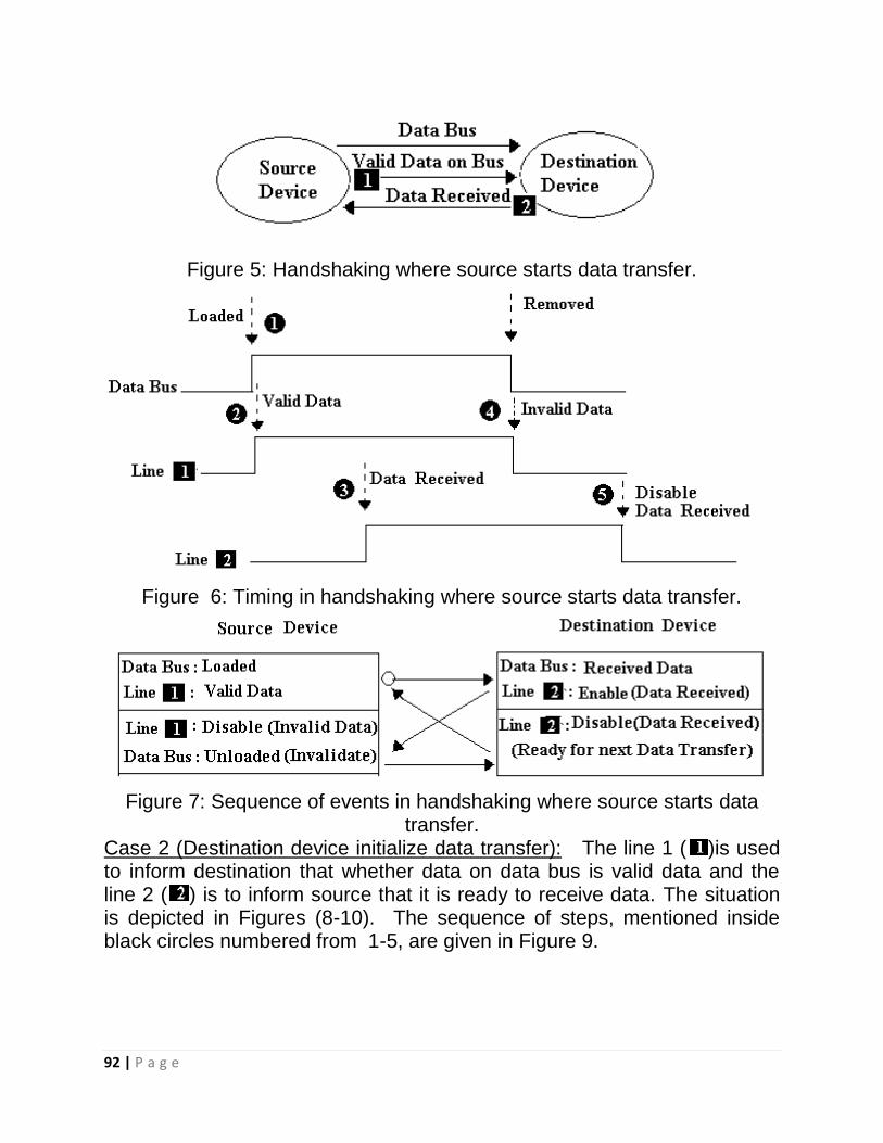
92 | P a g e
Figure 5: Handshaking where source starts data transfer.
Figure 6: Timing in handshaking where source starts data transfer.
Figure 7: Sequence of events in handshaking where source starts datatransfer.
Case 2 (Destination device initialize data transfer): The line 1 ( )is usedto inform destination that whether data on data bus is valid data and theline 2 ( ) is to inform source that it is ready to receive data. The situationis depicted in Figures (8-10). The sequence of steps, mentioned insideblack circles numbered from 1-5, are given in Figure 9.

93 | P a g e
Figure 8: Handshaking where destination starts data transfer.
Figure 9: Timing in handshaking where destination starts data transfer.
Figure 10: Sequence of events in handshaking where source starts datatransfer.
Advantage: 1). It provides a high degree of flexibility and efficiency.2). Less chances of error as a timed out signal is used to detect
error in transfer.If any delay occurs in transfer, the problem is resolved through timed-outmechanism that makes the use of internal clock. The clock is started whendata transfer starts and if the destination device does not respond within

94 | P a g e
stipulated time, the source device assumes that an error has occurred andtakes appropriate measures to avoid an error.
7.3 Asynchronous Serial TransferThe communication mode of data between two devices may be serial andparallel. In serial communication only one data line is used, whereas inparallel communication, the number of lines are equivalent to the numberof data bits transferred in a single clock cycle. During data transmission,only one bit in sequence is transmitted at a time in case of serial. Theserial transmission can be synchronous and asynchronous. Insynchronous serial transfer, two communicating device share a commonclock and bits are transmitted at clock pulse rate. The synchronous signalsare transmitted between communicating devices periodically to keep clocksteps parity between them. In asynchronous serial transfer, the data istransmitted only if it is available on data line for transfer. The special bitsare inserted at start and end of a character code. Suppose we want to
Check Your ProgressQ. 1 : The main advantages of asynchronous mode is _ __ __ __ _ _
and _ __ __ __ _ _ __ .Answer options: a) low cost, high throughput b). flexible, efficient c).high throughput, less memory d). less memory, multiple processor.Q. 2 : In synchronous mode of data transfer, both the sender and thereceiver share a _ __ __ __ _ _ _ __ __ __ _ _ for timing.Answer options: a) different clock b). common clock c).common bus
d). common interface.Q 3: The word synchronous means matching the speed of CPU with
various __________ devices attached to it.Answer options: a). Memory b). I/O c). Co-processor
d). None
Q 4: The synchronization between CPU and I/O devices is made througha special hardware device called as ________________ .
Answer options: a). Internet b). Interface c). Memoryd). Monitor

95 | P a g e
transfer a character code (a byte), say 10110110, then for transfer wehave three components: a start bit, character code (a byte), and stop bits.Such an arrangement is given in Figure 11. Though a start and stop bitscarry no data, but are essentially required for transfer.Asynchronous transfer is used in low speed transmission. The baud isused to express data transfer rate and is defined as the number of bits ofdata transferred between two devices per second.
Figure 11: Asynchronous serial transfer with a frame.
7.4 Asynchronous Serial InterfaceAn integrated circuit consisting of a transmitter and a receiver where atransmitter accepts a character code (a byte) from CPU, converts it to aframe (11-bits) then transmits it onto the printer line and a receiver acceptsa frame (11-bits) from keyboard line converts it to a character code (a byte)and passes it to CPU. Asynchronous Serial Interface is also called asUART (Universal Asynchronous Receiver and Transmitter). A blockdiagram of asynchronous serial interface is given in Figure 12:
Check Your ProgressQ 5: The asynchronous serial transfer technique uses ___________
and ___________ to know the start and end of a character code.Answer options: a). strobe control, handshaking method b).
green flag, red flagc). start bit, stop bit d).
even parity , odd parityQ 6: Baud is used to express
________________________________________Answer options: a). Temperature rate b). Data transfer rate c).
Data conversion rate d). Timing sequence

96 | P a g e
Figure 12: Block diagram of asynchronous communication interface.
CS RS Operation Register Function0 x x None0 0 WR Transmitter
Register0 1 WR Control Register1 0 RD Receiver
Register1 1 RD Status Register
Figure 13: Various operations along with register and control selection inasynchronous communication interface.
The diagram consists of various components such as a transmitter, areceiver, and their controls and data registers, internal bus, timing & R/Wcontrol, and data buffer. In addition, it also consists of a status register, acontrol register and the clock signal generators.The timing & R/W control unit is used to control the R/W operation. Thechip select (CS) makes the choice of interface through address bus. Thecombination of CS and RS makes the choice of operation performed and

97 | P a g e
the two signals are associated with the CPU. The various registers used,and operation performed are given in Figure 13 in tabular form.On the transmitter side, the following operations are carried out:
1) Check transmitted register: CPU reads status register flag to check whether thetransmitter register is empty or not.
2) Move Data: If empty, move data to transmitter register and sets status register flag tomark that transmitter register is filled.
3) Append extra bits & Move data to shift register: Move data to the shift register. Beforemoving, the first bit in shift register is generated to zero i.e. start bit and after movingdata ( a byte) to shift register two more bits (1,1) are appended to shift register. Now thetotal numbers of bits in shift register are eleven and the interface sets status register flagto mark that transmitter register is empty.
4) Transmit Data on line : Data from shift register is transmitted one by one at required rate.
Initially, data input at receiver from external line is at 1 which indicates thatline is idle. On the receiver side following operations are carried out assoon as 0 signal is spotted on data input:
1) Shift character from line to shift register: The frame is shifted from line to shift register atthe required rate.
2) Check parity or start & stop bits (Error check): The interface checks that whether first &last bits are same as desired. Also interface check for a parity bit. There may be apossibility of error in transmission of received data and these are: parity bit error due towrong parity bit received, framing error due to wrong number of start or stop bitsreceived and overrun error due to loss of bits in receiving data.
3) Move data from the shift register to receiver register: Data from shift register to receiverregister is shifted.
4) Set status flag for receiver : The flag in the status register of receiver is set to mark thatreceiver is full i.e. data arrived.
5) Read Data : CPU checks status flag for receiver and if data arrived, it reads data fromreceiver register.

98 | P a g e
7.5 Summary
In synchronous mode of data transfer, the registers of CPU and theregisters of the device interface share common clock. In asynchronousmode of data transfer, the registers of CPU and the registers of the deviceinterface do not share a common clock for timing. The systems in whichtwo communicating device have their private clock signal generator eitheruse strobe or handshaking technique to make parity between steps.Asynchronous serial transfer technique uses start and stop bits to know thestart or end of a character code. Asynchronous serial interface usestransmitters and receivers along with shift registers to make asynchronousserial transfer possible.
7.6Glossary
Baud - The unit of measure for the number of bits transmitted over a mediausing some medium.
Check Your ProgressQ. 7 : The term UART stands for _ __ __ __ __ __ __ ___ __ __.Answer options: a) Universal asynchronous receiver transmitter. b).
Universal asynchronous recovered transfer. c). Uploaded and raretask . d). upper and recovered throughput .
Q 8 : Asynchronous serial interface is a_______________________________________
Answer options: a). circuit b). software c). data busd). memory device
Q 9: A frame in asynchronous serial interface consists of__________________________ bits.
Answer options: a). 64 b). 16 c). 9 d). 11

99 | P a g e
Data Bus - The portion of a bus that is used to transfer the data betweentwo units.
Parallel Communication - Communication in which an entire byte (orword) is transmittedat same time over the communication medium.
Serial Communication - A method of transmitting data where a data byteis sent one bit at a time over the communication medium. Serialcommunication is asynchronous.
Status Register - A special register that monitors and records the status ofvarious situations such as overflow, carries, borrows, etc.
7.7 Answer to check your progress/Suggested Answers to Questions (SAQ)
Answers to Questions: 1 to 9.1). b 2). b 3). b
4). b5). c 6). b 7). a
8). a9). d7.8 References/Bibliography
Stallings, W. Computer Organization and Architecture, 8th ed., PHI Pvt, 2010. Tanenbaum, Andrew s. Structured Computer Organization, 4th ed., Pearson Education
Asia, 1999. Mano, M. Morris, Computer System Architecture, 3rd ed.,Pearson Education, Inc. Hennessy J. L., Patterson D. A., Computer Architecture, 4th ed., ELSEVIER, Reprint
2011. Hayes J. P., Computer Architecture and Organization, McGrawHill, International edition. Rajaraman V., Radhakrishnan, Computer Organization and Architecture, PHI, 2007. Hennessy J. L., Patterson D. A., Computer Organization and Design, ELSEVIER, 2012. Godse A. P., Godse D.A., Computer Organization And Architecture, Technical
Publications.
7.9 Suggested Readings
Journal of Systems Architecture: Embedded Software Design, ELSEVIER

100 | P a g e
Parallel Computing, Systems and Applications, ELSEVIER ACM Transactions on Architecture and Code Optimization, ACM Journal of Parallel and Distributed Computing, ScienceDirect Computer Architecture Letters, IEEE Computer Society The Journal of Instruction-Level Parallelism
7.10 Terminal and Model Questions
14) What is synchronous data transfer? Explain.15) What is asynchronous data transfer? Explain.16) Differentiate between synchronous and asynchronous data transfer.17) What does UART stands for? Describe its various components.18) Explain the role of strobe control and handshaking in asynchronous data transfer.19) What are the limitations of strobe control in asynchronous data transfer?20) Write down some advantages of handshaking.21) Draw block diagram of asynchronous serial interface. Explain the working of it.22) Write sequence of events in handshaking where source starts data transfer.23) Explain timing sequence in handshaking where destination starts data transfer.24) Define baud.

101 | P a g e
UNIT 2: Chapter-8Modes of Data Transfer
Structure8.0 Objectives
8.1 Introduction8.2 Modes of Data Transfer
8.2.1 Programmed I/O8.2.2 Interrupt Driven
8.2.3 Direct Memory Access (DMA)8.2.3.1 Cycle stealing
8.3 Priority Interrupts8.3.1 Single Level Interrupt8.3.2 Multiple Level Interrupt
8.3.2.1 Polling8.3.2.2 Bus Arbitration
8.3.2.3 Daisy Chaining8.3.2.4 Interrupt Cycle
8.4 Summary8.5 Glossary8.6 Answer to check your progress/Suggested Answers to
Questions (SAQ)8.7 References/ Bibliography8.8 Suggested Readings8.9 Terminal and Model Questions
8.0 ObjectivesThe main objectives of this chapter are :
To discuss various modes of data transfer.
To explain the working of programmed I/O data transfer.
To explain the working of interrupt driven data transfer.
To draw and explain the block diagram of DMA controller.
To know, what is cycle stealing. In what situation it is used.
To know, the concept of priority interrupt.
To explain the various techniques used to resolve priority in interrupts.
To know, the concept of polling, bus arbitration and daisy chaining.

102 | P a g e
8.1 Introduction
In order to process data, there is need for movement of data betweenmemory and I/O devices. The data transfer to or from memory to I/O maybe done by involving the CPU or without involving the CPU. There arevarious modes to carry out such data transfer. The modes are hardware orsoftware oriented. The various modes of transfer are: programmed I/O,interrupt driven and DMA. The former two makes the active use of CPU,whereas later works without the CPU for data transfer. Priority interrupt isused to detect the priority of the I/O device, to use a CPU, if number of I/Odevices are interrupting the CPU to process their job.
8.2 Modes of Data Transfer
In order to process data, there is a need of movement of data between
memory and I/O devices. This data transfer between memory and I/O
devices may be carried using numerous of modes. In some modes, CPU is
used as an intermediate device for transfer and others do not involve CPU
for transfer. The main modes of transfer are: programmed I/O, interrupt
driven and direct memory access (DMA).8.2.1 Programmed I/O
In this case, an I/O device has not direct access to memory. Duringprogram execution, when I/O instruction is encountered, the CPU takesover the control of I/O operation and sends a read or write command to I/Ointerface. After issuing command to I/O interface, it waits till I/O operation iscomplete. The CPU constantly monitors the status flag of I/O deviceavailable in interface to which I/O command is issued. As soon as data iscollected by interface in its data buffer, it sets its status flag indicating thatthe data is ready for the CPU (read operation) to transfer.

103 | P a g e
In case of a write operation, the CPU places data in the I/O interface bufferand proceeds to the next instruction. A block diagram of an I/O devicewith CPU and Memory is given in Figure 1.
Figure 1: Block diagram of I/O devices with CPU and Memory.
The programmed I/O mode for reading data from a device is given inFigure 2.

104 | P a g e
Figure 2: Flow Diagram of Programmed I/O Data Transfer.
Disadvantage: As earlier said, after issuing command to I/O interface, theprocessor waits till I/O operation is completed. If CPU is faster than I/O, thetime of CPU is wasted a lot. The data transfer using this mode is slow.

105 | P a g e
8.2.2 Interrupt DrivenIn case of interrupt driven data transfer, after issuing R/W commands toI/O interface, the CPU continues executing its own process. Afterprocessing I/O command, the interface moves data from I/O device tointerface data register and issues an interrupt to CPU by setting anappropriate status flag in the status register. As the CPU has been alreadybusy in executing its own process, after receiving interrupt, it saves theaddress of process it was already executing. It then proceeds to processinterrupts issued by I/O for R/W data from interface data register and storeit to memory. After completing transfer, it again starts executing itsprevious process. The flow diagram for reading data using interrupt drivenscheme is given in Figure 3.
Disadvantage: The data from I/O to or from memory is transferred byinvolving the CPU. In this move, the data is transferred byte by byte. Theprocessor fetches and executes many instructions even to transfer a byteof data. The data transfer using programmed I/O or interrupt driven modesis slow. The speed of data transfer can be increased if data betweenmemory and I/O devices be transferred without involving CPU.8.2.3 Direct Memory Access (DMA)
DMA is a technique used to transfer data between fast storage andmemory without involving CPU. The CPU only initiates the data transfer byinitializing DMA and then DMA starts and continue to transfer between I/Oand memory until the entire block of data is transferred. A block diagram ofDMA controller is given in Figure 4. The following operations are generallyperformed either at the CPU or DMA controller level:
a). DMA Initialization: As soon as I/O instructions are encountered by CPU,the following actions are taken by it:

106 | P a g e
1). It sends to DMA controller, the I/O device address, I/O command,memory address from or to where a byte is to retrieve or store, andthe numbers of byte to transferred.
2). It also sends the DMA controller whether to perform read or writeoperation.
b). DMA Transfer: During data transfer in DMA, the following steps areperformed:
1). A request is sent to DMA controller from I/O to get its control for datatransfer. The DMA controller requests the control of bus from CPU byactivating BR (bus request) line and CPU responds by activating BG(bus grant) line indicating that it has relinquished the control of the busand DMA can use it for transfer.
2). The DMA performs the following steps to initiate actual transfer:
i). Sends DMA acknowledge signal to I/O to inform that bus requesthas been granted.
ii). Initialize RD or WR signal. See, the RD or WR bus is available tocommunicate between DMA and memory only if BG is 1 otherwiseRD or WR bus is available to communicate between CPU andDMA registers.
3). As soon as I/O receives a bus acknowledge signal, it shifts a wordon the data bus from I/O interface data register in case of writeoperation or receive data from data bus and place it onto I/O dataregister in case of read operation. Each time a word is transferred, theDMA increments address register and decrements data count totransfer next word. DMA continuously checks the value of data countand if it is zero, the data transfer is complete and it disables the BR bydeactivating it.
The details of various signals to memory, CPU and I/O devices from or toDMA has been illustrated in Figure 5.

107 | P a g e
8.2.3.1 Cycle stealing
Generally, a high speed peripheral uses the DMA to transfer and it takesthe control of bus till entire block of data is transferred. Such a transfer iscalled as burst. If the slow speed peripheral intends to use DMA fortransfer, then cycle stealing technique is used so that CPU time may beutilized properly. It allows one word to transfer at a time after which itreturns the control of bus to CPU. Here, DMA controller steals a cycle ofCPU for data transfer.
Advantages: The various advantages of data transfer using DMA controllerare:
1). Fast transfer of data between storage and memory i.e. almost at thespeed of high speed storage.
2). The technique is convenient to use.
Applications: The DMA is used in various applications. The two suchapplications are:
1). Fast transfer of information between magnetic disk and memory.2). Updating display in interactive terminals.

108 | P a g e
Figure 3: Flow Diagram of Interrupt Driven Data Transfer.

109 | P a g e
Figure 4: Block diagram of DMA controller.
Figure 5: Detail Diagram of DMA controller with Memory and CPU.
Check Your ProgressQ. 1 : In polling , a _ __ __ __ _ _ monitors the interrupt status flag to
check if any interrupt issued by an I/O device.Answer options: a) hardware chip b). a process c). a processor d). I/Odevice.Q. 2 : The term DMA stands for _ __ __ __ __ __ __ ___ __ __.Answer options: a) Digital Memory Access. b). Direct Memory Access.c). Direct Memory Arbitration . d). Daisy Memory Allocation .Q 3: Cycle stealing technique is used in
________________________________________Answer options: a). Priority Interrupt b). DMA c). Interrupt
Drivend). Programmed I/O
Q 4: The data transfer rate using programmed I/O or interrupt driven modesis __________ if it is compared with DMA.
Answer options: a). almost same b). fast c). slowd). Not none

110 | P a g e
8.3 Priority Interrupts
Whenever there is a need of data transfer between CPU and I/O device,The CPU initiates the transfer. There may be a situation that I/O device isnot ready for transfer when CPU takes initiative. This situation is handledusing interrupts. When I/O interface is ready for data transfer to or frommemory, an interrupt signal is sent by the I/O interface to CPU. The CPUresponds to interrupt request by executing an interrupt service routine.Prior to this, it completes the instruction it is already executing and savesthe address of instruction on a stack.In general, there are a number of I/O devices attached to a computer andeach is able to generate an interrupt. There must be a mechanism toresolve the conflict if the number of interrupts occurs at the same time.Now, we have two situations: 1). Single level Interrupts 2). Multiple LevelInterrupts.8.3.1 Single level InterruptConsider there is only one interrupt to CPU at a time, whether it is due tothe single I/O device of multiple I/O devices. The various steps shall be as:
1). To start with, an I/O interface sends an interrupt signal to CPU.
2). The CPU completes current instruction execution.
3). The CPU stores the contents of program counter (PC), program statusword (PSW) and contents of other general purpose registers availablein CPU onto stack.
4). The CPU jumps to interrupt service routine. It also sendsacknowledgement signal to the I/O interface before jumping.
5). The CPU transfer data from or to I/O device on the direction ofinterrupt service routine.
6). After transferring data as desired by I/O device, the CPU reloads thecontents of PC, general purpose registers and PSW from stack andstarts executing previous instructions.
A memory map of interrupt handling is given in Figure 6.
8.3.2 Multiple Level InterruptsSuppose more than one I/O devices intends to issue interrupts to CPU fortheir respective transfer. Then there must be a way to resolve priority. This

111 | P a g e
can be managed through software or hardware and to do so threetechniques exists: 1) Polling 2) Bus Arbitration 3) Daisy Chaining8.3.2.1 PollingIn polling, a process periodically monitors the state of the interrupt statusflag to check if any interrupt is issued by any I/O device. If a number of I/Ointerface issue the interrupt, then an I/O device having higher priority getsthe control of CPU. In polling, the priority of I/O interface is determined onthe basis of the order in which they are polled. Since, polling is softwareoriented, the selection priority can be altered through codes. It is timeconsuming8.3.2.2 Bus Arbitration
If an I/O interface intends to issue interrupt, first it gains the access to databus and then sends its address to CPU. When the CPU receives theinterrupt, it responds to I/O interface on interrupt acknowledge line. Therequesting I/O interface, then places a word on the data bus for transfer. Incase of bus arbitration : 1) Only one I/O device can issue interrupt at a time2) The CPU can mask the interrupt by using appropriate instruction tointerrupting I/O interface.8.3.2.3 Daisy ChainingIt is hardware oriented. In daisy chaining, there is a serial connectionbetween all the interrupting I/O interfaces. The I/O interface with higherpriority is placed near the CPU and with least priority is placed at the end ofthe chain. The block diagram of this arrangement is given in Figure 7. Theinterrupt request line is common to all I/O interface, whereas interruptsacknowledging line is chained serially. If any high priority I/O interfaceissues the interrupt and CPU responds it by using interrupt acknowledgesignal, then this disables the devices from issuing the interrupts havinglower priority. After getting address from I/O interface, the CPU jumps toappropriate interrupt service routine. However, during this course, if anydevice having higher priority issues the interrupt, the CPU again suspendsdata transfer of current I/O interface and responds to the interrupt of thehigh priority I/O interface.

112 | P a g e
If a device has PI equals 0 then it sets its PO to 0 stating that the nextdevice (low priority) to it has granted no permission for the transfer. Whenan I/O device issues interrupt request, its PI is set to 1. If this device (PI =1) has pending interrupt, it sets PO to 0 and places its word on the data bussince this is the device with the highest priority that is requesting the controlof CPU for transfer. If this device has no pending interrupt, then it sets POto 1 indicating that the device with low priority to it can use the CPU fortransfer.

113 | P a g e
Figure 6: Interrupt Handling along with memory chart.

114 | P a g e
Figure 7: Daisy Chain Priority Interrupt.
In case of daisy chaining: 1) few control lines are required 2). The priority ofany I/O device can’t be changed. 3) One can attach an unlimited numberof I/O interface 4). A high priority I/O device can block the chances ofgetting CPU to low priority if it frequently issues interrupts. 5) It isvulnerable to the failure in chaining.An interrupt priority encoder with four I/O devices is given in Figure 8.

115 | P a g e
Figure 8: Priority Interrupt Encoder with four I/O devices.In Figure 8, I/O device 1 has highest priority and I/O device 4 has lesspriority. If any I/O device issues interrupt then its input (I) in interruptregister is set to 1. For example, when input I0 is 1, regardless the inputbits of other lower priority I/O in interrupt register, the output combinationab will be 00. This shows that I/O device 1 has priority over the othershaving lower priority to it. When input I1 is 1, regardless the input bits ofother two low priority I/O in interrupt register, the output combination ab willbe 01. The I/O device 2 has priority over the other two having low priority toit. See, in this situation I/O device 1 has not interrupt. The various othercombinations are given in Figure 9 in tabular form. The output INF hasvalue 1 only if atleast one I/O device on line has interrupt otherwise itsvalue will be 0. The AND Gate-4 will have 1 only if INF = 1, INTA = 1 andIE = 1. These are the interrupt flag status bit, interrupt acknowledgementbit and interrupt control bit respectively. The device having higher priority,output combination ab on priority encoder, will load its word (addressvector) onto the CPU.
Input Output
I0 I1 I2 I3 a b INF
1 × × × 0 0 1
0 1 × × 0 1 1
0 0 1 × 1 0 1
0 0 0 1 1 1 1
0 0 0 0 × × 0
Figure 9: Truth table priority encoder.The below given Boolean functions show the output of variouscombinations.

116 | P a g e
8.3.2.4 Interrupt CycleIn Figure, the Gate-5 can be enabled or disabled to issue or block interruptrequest to CPU. In program controlled interrupts, IE bit allows theprogrammers to choose whether to use interrupt facility. Generally, at theend of each cycle, a CPU monitors the IE and INF bits to check if anyinterrupt is pending from the I/O. If both are equal to 1, then CPU goes tointerrupt the cycle and performs the following operations.
1). Pushes PC, PSW and general register contents onto stack.
2). Enables interrupt acknowledgement (INTA).
3). PC of the CPU is loaded with the address of interrupt service routineof interrupting I/O device.
4). Clears EN and starts transferring data after execution interruptservice routine.
8.4 Summary
Check Your ProgressQ 5 : Daisy chaining technique is a ____________________ orientedAnswer options: a). memory b). software c). hardware
d). programQ 6: PSW is called as __________________________ .Answer options: a). Password Status Weight b). Program Status
Word c). Priority Straight Word d). Parallel Status WatchQ 7: In case of Daisy Chaining, the priority of any I/O device
________________________ .Answer options: a). Can be changed b). Can’nt be changed c).
Some times can be changed and sometimes can’ nt be changedQ 8: In case of multiple level interrupts, to resolve priority, three
techniques are used and out of which ___________________ ishardware oriented.
Answer options: a). Polling b). Bus arbitration c). Daisy chainingd). None

117 | P a g e
The data transfer to or from memory to I/O may be transferred withoutinvolving CPU. The DMA is such a technique which is hardware oriented.In systems where DMA controller is used to data transfer, CPU onlyinitiates the transfer. The technique is used for transfer data to or frommemory to the high speed I/O processor. If low speed I/O intends tocommunicate data using DMA, then cycle stealing technique is used.Priority interrupt is used to detect the priority of the I/O device, to use CPU,if a number of I/O device are interrupting CPU to process their job. Threetechniques are used for the said purpose and these are: bus arbitration,polling and daisy chaining. The later is hardware oriented and requiresless number of control line.
8.5 Glossary
Burst Data – An I/O mode of data transfer where data is sent in blocksinstead a steady stream.
Data Bus - The portion of a bus that is used to transfers data between twounits.
Daisy Chaining – A techniques of priority interrupt handling where theinterrupt acknowledgement input of one device is cabled serially from theoutput of another.
Interrupt – An event that alters the normal control of CPU to process ananother job.
Interrupt Cycle – A part of the instruction cycle in which the CPU monitorsthe interrupt flags to check if an interrupt is pending, and if so, invokes aninterrupt-handling routine.
Status Register - A special register that monitors and records the status ofvarious situations such as overflow, carries, and borrows.
System Bus – An internal bus in a system that connects the CPU,memory, and all other internal components.

118 | P a g e
8.6 Answer to check your progress/Suggested Answers to Questions (SAQ).
Answers to Questions: 1 to 7.1). b 2). b 3). b 4). b 5). c
6). b7). b 8). C
8.7 References/Bibliography
Stallings, W. Computer Organization and Architecture, 8th ed., PHI Pvt, 2010. Tanenbaum, Andrew s. Structured Computer Organization, 4th ed., Pearson Education
Asia, 1999. Mano, M. Morris, Computer System Architecture, 3rd ed.,Pearson Education, Inc. Hennessy J. L., Patterson D. A., Computer Architecture, 4th ed., ELSEVIER, Reprint
2011. Hayes J. P., Computer Architecture and Organization, McGrawHill, International edition. Rajaraman V., Radhakrishnan, Computer Organization and Architecture, PHI, 2007. Hennessy J. L., Patterson D. A., Computer Organization and Design, ELSEVIER, 2012. Godse A. P., Godse D.A., Computer Organization And Architecture, Technical
Publications.
8.8 Suggested Readings
Journal of Systems Architecture: Embedded Software Design, ELSEVIER Parallel Computing, Systems and Applications, ELSEVIER ACM Transactions on Architecture and Code Optimization, ACM Journal of Parallel and Distributed Computing, ScienceDirect Computer Architecture Letters, IEEE Computer Society The Journal of Instruction-Level Parallelism
8.9 Terminal and Model Questions
25) Write the names of different data transfer modes.26) What is Programmed I/O mode of data transfer? Explain.27) Differentiate between programmed I/O and interrupt driven data transfer mode.28) What does DMA stands for? Describe its various components.29) Explain the role of cycle stealing in DMA.30) What are the advantages and applications of DMA?31) Write down some advantages of daisy chaining.32) What do you mean by priority interrupt?

119 | P a g e
33) Explain interrupt driven data transfer with flow diagram.34) Draw block diagram of DMA controller and explain its working.35) Discuss various techniques used to handle priority interrupt.36) Discuss polling and bus arbitration.37) Daisy chain technique is hardware based technique. Explain.38) What are the disadvantages of programmed I/O data transfer?

120 | P a g e
Chapter 9Memory Organization
Structure of the Lesson,9.1 Objective9.2 Introduction9.3 Main Memory
9.3.1 RAM (Random Access Memory)9.3.2 ROM (Read Only Memory)
9.4 RAM Chip9.5 ROM Chip9.6 Memory Address Map9.7 Memory Connection to CPU9.8 Associative Memory9.8.1 Hardware Organization9.9 Summary9.10 Glossary1.8 Answer to check your progress/Suggested Answers to SAQ1.9 References/Bibliography1.10 Suggested Readings1.11 Terminal and Model Questions
9.1 CHAPTER OBJECTIVESAfter reading this chapter you will be able to understand Main memory and different types of main memory Random Access Memory and its different types Read Only Memory and Different types of ROM Block diagram of RAM and ROM chips Memory Connection to Processor Associative Memory Associative memory match logic
9.2 IntroductionMain memory is an essential unit in a computer system that is directly accessed by the CPU. In this unitof the computer, currently running programs and their data needed by the CPU are stored. Mainlycomputer memory can be divided into two categories i) primary memory and ii) secondary memory.Primary memory is small in size, but expansive. Secondary memory is that part of computer systemwhere we store programs which can be used in future for example operating system programs, data files,system programs, application programs and backup files. It is non-volatile in nature. The maindisadvantage of primary memory is that it is volatile in nature. Data is lost when there is no power. In thischapter a detailed discussion about primary memory and its different types is made.9.3 Main memoryMain memory or physical memory is the fundamental storage unit of the computer. It is that part of thecomputer that is directly accessed by CPU (Central Processing Unit). It is also called RAM (Randomaccess memory). CPU communicates directly with main memory. It is that part of the computer wherecurrently running programs and current data are stored. Most of the computer's primary memory is madeof RAM. The CPU reads instructions stored there and executes them as needed. Main memory is builtfrom semiconductor integrated circuits and it can be located on the motherboard of the computer system

121 | P a g e
or it can be located on a small circuit board which is attached to the motherboard of the computer system.It needs electrical power to maintain its information. Information is lost when there is no power.Mainly main memory consists of two types i) RAM and ii) ROM.
Figure 1 Different types of Main Memory
Main memory and its different types are shown in figure 1.9.3.1 RAM (Random Access Memory)Main constituent of main memory is RAM. It is used to store instructions of the currently running userapplications programs and data. It is volatile in nature means data is lost when the computer is switchedoff. In random access memory data items are searched from any random location. The time required toaccess any memory location is same in random access memory. A block diagram of RAM is shown belowin figure 2. The n data input lines are used to store data in memory. The n data output lines are used
Figure 2 Block diagram of RAMto supply information from memory. The k address lines are used to choose a word from among 2K
available in memory. Operations performed by random access memory are read and write operations.Read and write control signals are used to read data and write data from memory.

122 | P a g e
Types of RAMThere are mainly two forms of RAM.i) Dynamic RAM ii) Static RAM
Dynamic RAM:Dynamic RAM is made of many capacitors and transistors. It is a type of RAM that stores each bit of datain a separate capacitor. But capacitors leak charges so they are refreshed periodically to maintaininformation. Due to this refresh operation it is called dynamic RAM.Static RAM:Static RAM is based on flip flops or latching circuitry. It is very fast and expansive as compared toDynamic RAM. Here static means that it is not refreshed periodically like DRAM. But it is still volatile innature and data is lost in the absence of power.9.3.2 ROM (Read Only Memory)Read only memory (ROM) is non volatile in nature and it is used to store programs and data permanentlyin the computer system. ROM is also random access memory. Main function of ROM is to store thoseprograms which are frequently used by the computer. An example of such a program is bootstrap loaderwhich is used to load operating system from hard disk when the computer is turned on. As the nameindicates a read only memory (ROM) is used to perform the read operation only. As an example an m х nROM means an array of binary cells having m words of n bits each. A ROM has k address input lines toselect one word from memory. n data output lines each for one bit of word are used to read from memoryas shown in figure 3 given below.
Figure 3 Read only memory
Types of ROMMain types of ROM arei) PROM ii) EPROM iii) Flash ROMProgrammable read-only memory (PROM)In PROM data is written only once via a special device known as PROM programmer. Once data iswritten then it can not be changed. PROM is non volatile means PROM retain contents when thecomputer is turned off.Erasable programmable read only (EPROM)An EPROM is a special type of PROM and its contents can be erased by exposing it to ultraviolet light fora given period of time. Ultraviolet light is used to erase EPROM’s content. Once it is erased, it can berewritten. EPROM is programmed like PROM.Flash ROMFlash ROM is also called flash memory. It can be reprogrammed and erased in blocks. It is widely used indigital cameras and gaming consol. Modern USB drives are examples of Flash ROMs.Q.1. What is the difference between RAM and ROM? Discuss differenttypes of ROM.Answer:_______________________________________________________________________________________________________________

123 | P a g e
______________________________________________________________________________________________________________________________________________________________________________________________________________________________________________________________________________________________________________________________________________________________________________________________________________________________________________________________________________________________________________________________________________________________________________________________________________________________________________________________________________________________________________________________________________________________________________________________________________________________________________________________________________________________________________________________________9.4 RAM ChipA typical RAM chip consists of control inputs to select a chip, a bidirectional data bus that allows transferof data from memory to CPU during read operation and transfer of data from CPU to memory during writeoperation, read and write operations and address bits. The block diagram of a RAM chip of capacity 128× 8 is shown in figure 4 given below which contains 128 words of 8 bits per word. It requires 7-bit addresssince 128=27, 8-bit bidirectional data bus, two chips select (CS) control inputs CS1 and CS2 for enablingthe chip only when CS1=1 and CS2 = 0.
Figure 4 Block Diagram of RAM chip
The function table shown in the figure 5 gives the various operation of RAM chip. This chip in operationonly when CS1 = 1 and CS2 = 0. From the table it is clear that memory is inhibited or restrained in twoconditions. First if the chip select inputs are not enabled and secondly if they are enabled but the readand write inputs are not enabled.

124 | P a g e
Figure 5 Function Table for RAM Chip
9.5 ROM ChipA ROM chip has the similar external structure having two control inputs CS1 and 2 , unidirectional databus and address bits. Since a ROM can only read there is no need for a read control and when the chip isenabled, the byte selected by the address lines is transferred by the data bus. The block diagram of ROMchip having the capacity of 512 × 8 is shown in figure 6 given below. It requires 9 address lines since512=29.
Figure 6 ROM chip of capacity 512 × 8
Function table for ROM is shown figure 7. Since a ROM chip is in read only mode so data bus is only inoutput mode. ROM chip will be in read operation when CS1 = 1 and CS2 = 0. Separate read and writeinputs are not needed because ROM chip can only used in read operation. When ROM chip is madeenabled, then the byte selected by the address lines is transferred on the data bus.

125 | P a g e
Figure 7 Function Table for ROM Chip
When CS1 = 0 and 2 = 0, then state of data bus is in high impedance and memory performs nooperation. Read operation is performed only when CS1 = 1 and 2 = 0.
9.6 Memory Address MapA memory address map is a pictorial representation of assigned address space for each chip (RAM andROM) in the system. It is a table which tells memory addresses of each chip. As an example suppose thata computer needs 512 bytes of RAM and 512 bytes of ROM, a total of 1024= 210 bytes of memory. Thenmemory address map for this is shown in figure 8. The component column identifies whether a RAM orROM chip is used. The address bit 10 is used to distinguish between a RAM and ROM chip and addressbits 9 and 8 are used to select between the four RAM chips. When line 10 is 0, then a RAM chip isselected by CPU and when it is equal to 1, CPU selects the ROM chip. The hexadecimal address columnis used to allocate equivalent hexadecimal addresses for each chip.
Figure 8 Memory Address MapQ.2. What is an Address memory map?Answer:___________________________________________________________________________________________________________________________________________________________________________________________________________________________________________________________________________________________________________________________________________________________________________________________________________________________

126 | P a g e
___________________________________________________________________________________________________________________________________________________________________________________________________________________________________________________________________________________________________________________________________________________________________________________________________________________________________________________________________________________________________________________________________________________________________________________________________________________________________________________________________________________________________________________________________________________________________________
9.7 Memory Connection to CPUCPU in computer system is connected to RAM and ROM chips through data and address buses. Low
order lines select the byte within chips and other lines are used to select a particular chip through chipselect input. The memory connection of chips to the CPU is shown in figure 9. Each RAM chip receivesthe seven low-order bits of the address bus. A 2 × 4 decoder is used to select a particular RAM chip.Decoder’s outputs are used to give CS1 inputs in each RAM chip. The RD and WR lines from the CPUare used to give inputs to each RAM chip. Bus line 10 is used to select between a RAM chip and ROMchip. Other chip select input (CS1) in the ROM is connected to the RD line which is connected to CPU.This input makes ROM chip enabled only during a read operation. Address lines 1 to 9 go directly to AD9lines of ROM chip.

127 | P a g e
Figure 9 Memory connection to CPU
9.8 Associative MemoryMany data processing applications use a table to store data because searching of data in table is easy.This table is stored in main memory. For example an assembler program uses symbol table to storebinary equivalent of a symbol and this symbol table is stored in main memory. Till now many searchalgorithms have been developed to access an item from main memory. Basic method to search an item isto choose a sequence of addresses, read the content of the addresses and then comparing the contentwith the item to be found, until a match occurs.

128 | P a g e
But in case of associative memory, memory is accessed by the content of the data and not by theaddress. Since here data item is searched on the content of data and not by address, it reduces accesstime to memory considerably. This memory is also called content addressable memory (CAM).9.8.1 Hardware OrganizationA block diagram of an associative memory is given below (figure 10). Main parts of associative memoryare i) Argument Register ii) Key Register iii) Memory array and logic iv) Match Register
Figure 10 Associative MemoryArgument Register: Argument Register contains n bits, one for each bit of a word. It contains theinformation to be searched or a word which have to be written in associative memory.Key Register: It also contains n bits, one for each bit of a word. Key register is used to give a mask forchoosing a particular key in argument register. If it contains all 1’s then entire argument is compared.Otherwise only those bits having value 1 in their corresponding position of the key register are compared.Memory array and logic: It consists of a memory array and logic (m words with n bits per word). Since itconsists of storage capability and logic circuit for matching, that is why associative memory is moreexpansive as compared to main memory (RAM).Match Register: It contains m bits one for each memory word. The words that match the bits of theargument register set the corresponding bit in the match register.As an example suppose content of Argument Register (A) is 101 111100. Content of Key register (K) is111 000000. Since content of K has three 1’s only at three leftmost positions, only these bits are used tocompare.
A 101 111100K 111 000000
Word1 100 111100Word2 101 000001 match

129 | P a g e
Word2 matches because the three leftmost bits of the argument and the word are equal. A diagramshowing associative memory is shown below (figure 11). The cells in the associative memory are markedby the letter C with two subscripts. The first subscript gives the word number and second tells the bitposition in the word. So cell Cij means it is cell for bit j in word i. A bit A j in the argument register will becompared in all the bits in column j if Kj =1. If a match occurs between all the unmasked bits of argumentregister and the bits in word i then the corresponding bit in match register Mi is set to 1. In case of nomatch Mi is set to 0.
Figure 11 Example of Associative memory having m words with n cell.
Match LogicSuppose A1, A2 and An are n-bits of argument register and K1, K2 and Kn are n- bits of key register.Suppose there are m words in the memory each of n bits. Then two bits are equal if they both are 0 or 1.Boolean function for the equality of these two bits isxj = AjFij + Aj’Fij’Where Fij is flip-flop storage element used in cell Cij as shown in above figure 11. Now xj=1 if bits inposition j are equal, otherwise xj=0.Now if Kj = 0 then bits of Aj and Fij are not compared and if Kj =1 then they will be compared. So xj + Kj’ =xj if Kj = 1 and xj + Kj’ = 1 if Kj = 0. So now match logic for word i can be expressed by Boolean functionasMi = (x1+ K1’) (x2+ K2’) (x3+ K3’)........ (xn+ Kn’). By substituting value of xj from aboveMi = ∏ (AjFij + Aj’Fij’ + Kj’). The circuit for matching one word using this Boolean function is given belowin the diagram. Symbol π is used for product.

130 | P a g e
Figure 12 Match Logic for associative memory (one word)9.9 SummaryPrimary memory consists of RAM and ROM and is used to increase the performance of CPU. RAM isvolatile in nature whereas ROM is non-volatile. ROM is useful to store those programs permanently thatare frequently needed by the computer system. Major part of primary memory is made of RAM chips buta portion of primary memory can be made of ROM chip also. The designer must give a memory map thatassigns addresses to various RAM and ROM chips. Associative memory is expansive. Due to its fastnature it is used in those applications where the search time is critical. Main application areas ofassociative memory are database engines, artificial neural networks and intrusion prevention systems.9.10 GlossaryAccess Time: It is the speed of memory measured in nano seconds.Array: It is that area of the RAM that is used to store the bits.Auxiliary Memory: Devices that are used for backup storage are called auxiliary memory. For examplemagnetic disks.Bidirectional Bus: A bus is called Bi-directional bus if the same bus is used for transfer of data betweenCPU and memory or input / output devices in both the direction.Bootstrap Loader: Bootstrap loader is a program that resides in the computer's ROM and is used to startthe computer's operating system.CAM: Content Addressable Memory

131 | P a g e
Refresh Rate: It is the speed with which DRAM is refreshed. Refresh Rate refers the size of data thatmust be recharged.
9.11 PROBLEMSQ.1. How many lines of address bus must be used to access 1024 bytes of memory?Ans: Since 210 = 1024 So 10 address lines are used.Q.2. How many 128 x 8 RAM chips are needed to provide a memory capacity of 2048 bytes?Ans: 16 ChipsQ.3. What is the hardware organization of associative memory. Why associative memory is fasterthan other memories?Q.4. What are the advantages and disadvantages of associative memory?Q.5. Draw the logic diagram of all cells along one vertical column in an associative memory.Q.6. Describe how multiple matched words can be read out from an associative memory.Q.7. Describe memory connection to CPU with one example.
9.12 References/Bibliography1. Mano, M.M., Computer System Architecture, 3rd ed., PHI..2. Mano, M.M: Digital Logic and Computer Design, Prentice Hall of India.3. Stalling, W, Computer Organization and Architecture, 8th ed., PHI.4. Hayes: Computer Architecture and Organization, McGraw-Hill International Edition.5. Tanenbaum, A.S., Structured Computer Organization 5th ed., Prentice Hall of India
9.13 Suggested Readings1. http://www.webopedia.com/TERM/M/main_memory.html
2. http://en.wikipedia.org/wiki/Computer_data_storage
3. http://computer.howstuffworks.com/ram3.htm
4. http://virtual-labs.ac.in/labs/cse10/memory.html
5. http://whatis.techtarget.com/definition/memory-map

132 | P a g e
CHAPTER 10Cache Memory and Mapping Methods
Structure of the Lesson,10.1 Objective10.2 Introduction10.3 Cache Memory10.4 Working of Cache10.5 Levels of Cache10.6 Mapping
10.6.1 Associative Mapping10.6.2 Direct Mapping10.6.3 Set Associative Mapping
10.7 Writing into Cache10.7.1 Write-through method10.7.2 Write-back method
10.8 Cache Coherence10.9 Summary10.10 Glossary10.11 PROBLEMS
10.1 CHAPTER OBJECTIVESAfter reading this chapter you will be able to understand The basic concept of Cache memory. Why cache memory is needed in modern computers Different levels of cache Performance of cache Basic mapping used in cache Cache coherence.
10.2 INTRODUCTIONCache memory is a very high speed and expensive memory as compared to primary memory and it isavailable inside the CPU. Cache memory is small in size and expansive as compared to main memory.Cache is used to store frequently used data from main memory locations. The main function of cachememory is to speed up the access of data and instructions stored in main memory. Without cachememory CPU has to wait while fetching data and instructions from the main memory.10.3 Cache MemoryCPU access main memory and registers present within the processor directly. These registers are fastand can be accessed within one cycle of the CPU clock. Modern CPUs can decode instruction with veryhigh speed. CPU can perform operations at the rate of one or more per clock tick. But main memory isslow with respect to these registers, means memory access may take many cycles to complete. So CPUnormally waits since it does not have the sufficient data to complete the instruction. Therefore speed ofthe Processor is depending on the speed of the primary memory access. The solution to this problem isto add a small, faster memory between CPU and primary memory. This high speed memory is calledcache memory. Cache memory is very high speed memory and it is used to increase the processingspeed of CPU by making the currently running program instructions and related data available to CPU ata very high speed. So cache is a technique which is used to compensate the mismatch of speeds of CPUand primary memory. Cache is used to store those parts of the programs that are currently running. It isalso used to store temporary data used by these programs for calculation. So this technique is used inmodern computer systems to increase the performance of the system.10.4 Working of CacheWhen CPU makes a request to access memory first cache memory is searched. If the desired word isfound in the cache memory then it is read from the cache. If the word requested by CPU is not found inthe cache memory, then main memory is searched to read that word. At the same time the block of the

133 | P a g e
words containing the one just searched is then also transferred from main memory to cache memory. Inthis way some amount of data is transferred to cache memory so that future reference to same data(phenomenon of locality of reference) can be accessed from Cache memory. The figure given belowshows single level cache.
Figure 1 Single level cache
Performance of the cache memory is measured by a quantity called hit ratio. When CPU makes a requestto data and finds that data in the cache memory then it is called a cache hit. If the requested data is notfound in the cache memory but it is in main memory then it is called a miss. The ratio of the number ofcache hits divided by the total number of CPU references to main memory is called the hit ratio.10.5 Levels of CacheCache memory can be categorized into three levels i) L1 Cache ii) L2 Cache iii) L3 Cache.L1 Cache: L1 cache is the fastest cache and it is very near to the central processing unit. This cache isimplemented in SRAM (Static RAM). L1 cache does not require refresh cycles. It is generally split into twohalves, with one half used for instruction code and the other half is used for data.L2 cache: It is external to the processor and is implemented in DRAM or Dynamic RAM. It is refreshedmany times a second to retain its memory contents. Its speed is not as fast as L1 cache and it is bigger insize than L1 cache.L3 cache: It is the extra cache which is built into motherboard between the processor and the mainmemory. L3 cache is bigger than L2 cache but slower than L2.If the requested data is not found in L1 cache then it will be searched in L2 cache and if it is not foundthere then it will be searched in L3 cache.
Figure 2 Different level caches
Q.1. How cache memory is used to increase the performance of CPU?Answer:___________________________________________________________________________________________________________________________________________________________________________

134 | P a g e
_______________________________________________________________________________________________________________________________________________________________________________________________________________________________________________________________________________________________________________________________________________________________Q.2. Discuss different levels of cache memory.Answer:__________________________________________________________________________________________________________________________________________________________________________________________________________________________________________________________________________________________________________________________________________________________________________________________________________________________________________________________________________________________________________________________________________
10.6 MappingMain features of Cache memory are that it is very small in size and it has got very fast access time. Whena memory request is generated, then very little time or no time must be wasted during searching of datain cache memory. The shifting of contents from main memory to cache memory is called mapping. Cachedeals with main memory as a set of blocks. Since size of cache memory is smaller than main memory sothe numbers of cache lines are very less as compared to the number of main memory blocks. So amethod is needed for mapping main memory blocks into cache memory lines.Mainly there are three mapping techniques are used in cache.i) Associative Mappingii) Direct Mappingiii) Set Associative MappingTo discuss these three mapping techniques an example is given. Suppose main memory has capacity tostore 32K words of 12 bits each and Cache memory has capacity to store 512 words of 12 bits each atany given time the computer system is powered in. Since 32K = 32х1024 = 32768 = 215. So CPUgenerates a 15-bit address to refer cache memory as shown in Figure 3. If there is a cache hit meansdata found in cache memory, then CPU accepts 12-bit of data from cache and if there is miss means datais not in the cache memory, CPU reads data from main memory and then data is also transferred tocache memory. So next time a reference to same data can be found in the cache memory.

135 | P a g e
Figure 3 Cache memory example
10.6.1 Associative MappingAssociative memory stores both the address as well as contents of the memory word. So this type ofmapping is very flexible as well as very fast. In this mapping data from main memory can be stored in anylocation in the cache memory. An argument register is used to store CPU address of 15 bits andassociative memory is searched for a matching address. If there is a cache hit then matched data (12bits) is read from the cache and transferred to CPU. If data is not in the cache memory then it is a cachemiss and then main memory is searched for the given word. After data found in the main memory thesame address-data pair is transferred to the associative cache memory also, as shown in Figure 4.
Figure 4 Associative cache mapping(Address is in 5 Digit Octal Number and Data is in 4 Digit octal number)
If the cache memory becomes full of address-data pair entries then an entry must be replaced to make aroom for the new pair. The decision as to what pair is to replace is determined from the replacementalgorithm that the designers choose for the cache.
10.6.2 Direct MappingIn this mapping CPU address of 15 bits is divided into two fields. The last 9 bits are used in the index fieldand the remaining six bits are used in a tag field. Note that index field bits number is equal to the numberof address bits necessary to read the cache memory. This is shown in Figure 5.

136 | P a g e
In general if there are 2k words in the cache memory and 2n words are there in main memory then n-bitmemory address is divided into two fields. k-bits are used in the index field and remaining n-k bits areused in the tag field. So in this example k bits for index field = 9 because size of cache memory is 512х12. Size of main memory is 32Kх12. So n = 15. So n-k = 6 bits are used as tag field. Now when amemory request is generated by CPU index field contents are used for the address to search in the cachememory. The contents of tag field of the CPU address are compared with the tag in the word read fromthe cache memory. If the two tags match then there is cache hit and the desired data is in cache memory.If there is a cache miss then the required data is not in the cache memory and it is read from the mainmemory. It is then stored in the cache memory also, with the new tag replacing the previous value.Consider an example shown in the Figure 6. The data at address zero is currently stored in the cachememory with index = 000, tag =00, and data is=2333. So if CPU generates an address request 00000then it is a cache hit. Now suppose the request generated by CPU is 02000. Now index is 000 so it isused to search cache memory. Now two tags are compared but the cache tag is 00 and address tag is02. So it is a cache miss and now main memory is searched for the desired data and data word 5670 istransferred to the CPU. At the same time cache word at index 000 is also replaced with a tag of 02 anddata of 5670.
Figure 5 Direct mapping example

137 | P a g e
Figure 6 Direct mapping cache method
10.6.3 Set Associative MappingIn this type of memory organization each word of cache memory is used to store two or more words ofmain memory under the same index address. Each data word is stored along with its tag value. Thenumber of tag-data items in one word of cache memory forms a set. An example of a set associativecache organization for a set size of two is shown in the figure given below. Each index address is used torefer two data words and their linked tags. Since each tag requires six bits and each data word has 12bits so the word length is 6+12+6+12 = 36 bits. An index address of 9 bits can accommodate 29= 512words. So size of cache memory is 512х36 and it can hold 512+512 = 1024 words of main memory. Asshown in the Figure 5 the words which are stored at address references 01000 and 02000 of mainmemory are stored in the cache memory at index 000. Similarly the words stored at address 02777 and00777 of main memory are stored in cache memory at index 777. When a memory request is generatedby CPU, the index field value of the address is used to search cache. The value of tag field is thencompared with both the tags in the cache memory to find whether the required data is in cache ( a cachehit) or not. The comparison logic is similar to an associative memory search. That is a reason it is calledset associative mapping.

138 | P a g e
Figure 5 Two way Set-Associative mapping Cache
Q.3. What are the differences between Associative Mapping and SetAssociative Mapping?Answer:__________________________________________________________________________________________________________________________________________________________________________________________________________________________________________________________________________________________________________________________________________________________________________________________________________________________________________________________________________________________________________________________________________
10.7 Writing into CacheIn case of CPU has generated a read operation then main memory is not involved into the transfer. Incase of a write operation, a CPU can proceed in two ways. i) write-through method ii) write-back method10.7.1 Write-through methodIn write through method data is written or updated into the cache as well as in the corresponding mainmemory location at the same time. The advantage of this method is that main memory as well as cachecontains the same data (figure 6). So there is no risk of data loss in case of a system crash. Thedisadvantage of this method is that there is write operation in the memory as well as in cache so there isdecrease in the system speed.

139 | P a g e
Figure 6 Cache write-through
10.7.2 Write-back methodIn this caching method there is updation or modification of data in the cache, but this modification orupdation of data is not done in main memory untill it is absolutely necessary. Updation of data in mainmemory is done only at under certain conditions. For example one condition is that when a word isremoved from the cache, then it is copied into memory as shown in figure 7 given below. Whether data isupdated in the memory or not request of that data is served from the cache where it is already updatedand not from the memory. The advantage of this method is that this method optimizes the systemperformance because there is write operation only in cache. But there is risk of data loss in case ofsystem crash.
Figure 7 Cache write - back

140 | P a g e
10.8 Cache CoherenceMultiprocessing means using two or more central processing units (CPUs) within a single computersystem. These CPUs has their internal registers as well as their local cache memory. So in such anenvironment a copy of a variable may exist simultaneously in several caches. Since various CPUsexecute concurrently so if there is an update in the value of that variable in one cache then that updationof value of the variable must be reflected in all other caches where that variable resides. This problem iscalled cache coherency as shown in figure 8 given below.Solution to cache coherence problem can be achieved through combination of hardware and software orby hardware only. For example in case of hardware only solution snoopy cache controller is used tocheck all the caches.
Figure 8 Cache Coherence
10.9 SummaryTo compensate speed differences between the CPU and main memory one or more intermediatememories called caches are used. Generally three levels of caches are used in modern systemdepending upon their size. When the CPU refers to an address and it is found in the cache then it iscalled cache hit. Due to the locality of reference property hit ratio of 0.9 and higher have been reported.So cache memory enhances the performance of computer system.
10.10 GlossaryCache Hit: when a word is found in cache it is called cache hit.Hit Ratio: It is used to measure the performance of cache.Locality of Reference: It is the property of programs in which references to memory at any give intervalof time are constrained to a few localized area of memory.Mapping: Transfer of data from main memory to cache memory is called mapping.
10.11 PROBLEMSQ.1. Which cache mapping technique is the fastest?
a) Direct mapping b) Set associative mapping c) Fully associative mappingQ.2. Cache memory works on the principle of
a) Locality of reference b) Locality of data c) Locality of memory d) Locality ofreference and data

141 | P a g e
Q.3. A digital computer has a memory unit of 64K × 16 and a cache memory of 1Kwords. The cache memory uses direct mapping with a block size of four words.Answer the following:
a) How many bits are there in tag and index ?b) How many blocks can the cache accommodate?
Ans: a) tag = 6 bits, index = 10 bits b) 256 blocks of 4 words eachQ.4. Explain different mappings used in cache memory.
Q.5. What are the disadvantages of each mapping technique?
Q.6. How data can be written into cache?
Q.7. Explain cache coherence.
References/Bibliography1. Mano, M.M., Computer System Architecture, 3rd ed., PHI..2. Mano, M.M: Digital Logic and Computer Design, Prentice Hall of India.3. Stalling, W, Computer Organization and Architecture, 8th ed., PHI.4. Hayes: Computer Architecture and Organization, McGraw-Hill International Edition.5. Tanenbaum, A.S., Structured Computer Organization 5th ed., Prentice Hall of India
Suggested Readingshttp://www.hardwaresecrets.com/printpage/How-The-Memory-Cache-Works/481http://en.wikipedia.org/wiki/CPU_cachehttp://www.cpu-world.com/Glossary/L/Level_1_cache.htmlhttp://www.cpu-world.com/Glossary/L/Level_2_cache.htmlhttp://electronicstechnician.tpub.com/14091/css/14091_122.htm

142 | P a g e
Chapter 11 :Virtual Memory
11.1 Objective11.2 Introduction
11.2.1 Benefits of Virtual Memory11.3 Address Space and Memory Space11.4 Address Mapping using Pages
11.4.1 How Mapping is done?11.5 Associative Memory Page Table
11.5.1 Steps for mapping using Associative memory:11.6 Page Replacement
11.6.1 FIFO Algorithm11.6.2 Second-chance algorithm11.6.3 LRU Algorithm11.6.4 NFU Algorithm
11.7 Summary11.8 Glossary11.9 Answer to check your progress/Suggested Answers to SAQ11.10 References/Bibliography11.11 Suggested Readings11.12 Terminal and Model Questions
11.1 Objective
The main objective of this chapter is to introduce the concept of virtual memory which is a technique thatallows the execution of processes that may not be completely in memory. Various benefits of virtualmemory, the concept of address space and memory space, how mapping is performed using paging andvarious page replacement algorithms are discussed in this chapter.
11.2 IntroductionIn many computer systems, programmers often realize that some of their large programs cannot fit inmain memory for execution. The usual solution is to introduce management schemes that intelligentlyallocate portions of memory to users as necessary for the efficient running of their programs. Virtualmemory gives programmers the illusion that there is a very large memory at their disposal, whereas theactual physical memory available may be small. This illusion can be accomplished by allowing theprogrammer to operate in the name space while the architecture provides a mechanism for translating thevirtual addresses into memory locations during execution. This translation or mapping is handledautomatically by the hardware by means of a mapping table. In other words, only part of a program needsto be in memory for execution in a virtual memory. The rest of program can be resident in disk. As aresult, it is able to address a storage space much larger than that available in the main storage of acomputer system.The idea behind virtual memory is to expand the use of the physical memory among many programs withthe help of an auxiliary memory. Virtual memory provides the users with almost unfounded memory spaceto work with which helps to develop the multi programmed or timesharing computer systems.

143 | P a g e
11.2.1 Benefits of Virtual Memory Only part of the program needs to be in memory for execution. More Programs could be run at the same time. Increase in CPU utilization and throughput. Allows for more efficient process creation. Limited amount of physical memory could not affect the program’s execution.
11.3 Address Space and Memory Space
Virtual memory is the separation of user logical memory from physical memory. Some terminology usedfor virtual memory is as follows:
Virtual address: an address used by the programmerAddress space: the set of all virtual addressesPhysical Address: an address in main memory, also called locationMemory space: the set of all physical addresses
The virtual addresses must be translated into physical addresses at runtime for which the translationtables and mapping functions are used.
Address mappingLet N be the set of virtual addresses (address space) generated by a program running on a processor.Let M be the set of physical addresses allocated to run this program. A mapping function
ft: N->M ∪ {∅}is a time function which varies from time to time because the physical memory is dynamically allocatedand deallocated. Consider any virtual address v ∈ N. The mapping ft is formally defined as follows:
m, if m ∈ M has been allocated to store the data identified byvirtual address v∅,if data v is missing in M.
In other words the mapping ft(V) uniquely translate the virtual address v into a physical address m if thereis a memory hit in M. When there is a memory miss the value returned, ft(v)= ∅, signals that thereferenced item has not been brought into the main memory at the time of reference.
The address space is allowed to be larger than the memory space in computers with virtual memory. Letus consider an Address Space denoted by N=8K=2111 and Memory Space denoted by M=4K=212 . Thus,111 bits are needed to specify a virtual address which is translated to 12 bits which is required to specifya physical address of main memory. This translation is performed by Memory Mapping table as shown infig 11.1.
ft(v)=

144 | P a g e
The mapping is a dynamic process where every address is translated immediately as a word isreferenced by CPU.
11.4 Address Mapping using PagesPaging is a technique for partitioning both the physical memory and virtual memory into fixed size pages.Page tables are used to map between pages and blocks. These tables are implemented in main memoryupon creation of user processes.
The mapping of virtual address to physical address can be simplified if we split address space andmemory space into groups of fixed size.
Blocks: the physical memory is broken down into groups of equal size calledblocks
Pages: the term page refers to groups of address space of the same size
Consider the same example with an address space of 8K and a memory space of 4K. if we divide eachinto groups of 1K words, we obtain eight pages and four blocks as shown in fig 11.2

145 | P a g e
The mapping from address space to memory space in a paged system is shown in fig11.3. A virtualaddress is represented by two numbers:
- a page number- a line number
Figure 11.3 Memory Table in a Paged System
In general, a computer with 2p words per page has p bits to specify a line number and remaining high-order bits to specify the page number. For example, the virtual address having 111 bits would have 10bits to specify line number since 1K=210 and remaining 11 high-order bits to specify page number.Memory page table consists of eight words, one for each page. A presence bit indicates whether the pagehas been transferred from auxiliary memory to main memory.
11.4.1 How Mapping is done?

146 | P a g e
The CPU references a word in memory with a virtual address of 111 bits. The page number of 11 bits in virtual address is matched with table address. The content of that word in memory page table is read out. If presence bit is 1, the block number thus read is transferred to 2 high-order bits of main memory
address register. The line number from the virtual address is transferred into 10 low-order bits. Thus, generating a 12 bit physical address to specify a particular block in main memory. If presence bit of that word is 0, a call to Operating System is generated to bring the required
page from auxiliary memory and place it into main memory.
11.5 Associative Memory Page TableTo organize the page table more efficiently, it is better to construct it by means of an associative memoryinstead of random access memory page table, with a number of words equal to the number of blocks inmain memory. The main advantages of this type of organization are as follows:
- size of the memory is reduced.-each location is fully utilized.
Figure 11.4 Associative memory Page Table
11.5.1 Steps for mapping using Associative memory:
The virtual address is placed in the argument register. The page number of 11 bits is compared with all page numbers in the page field of associative
memory. If the page number is found, the 5-bit word is read out from memory.

147 | P a g e
The corresponding block number is transferred to the main memory address register. If no match occurs, a call to OS is generated to bring the required page from auxiliary memory.
11.6 Page ReplacementPage replacement refers to the process in which a resident page in main memory is replacement by anew page transferred from the disk. Since the number of available blocks is much smaller then thenumber of pages, the blocks will eventually be fully occupied. in order to accommodate a new page, oneof the resident page must be replaced.
When a program starts execution, some pages are transferred into main memory and the page table isset to indicate their position. If a program attempts to reference a page that is still in auxiliary memory, thiscondition is called page fault. When a page fault occurs in a virtual memory system, it signifies that thepage referenced by the CPU is not in main memory. If main memory is full, it would be necessary toremove a page from a memory block to make room for the new page. The policy for choosing pages isdetermined by replacement algorithm. There are many different page-replacement algorithms. Some ofthe popular page replacement algorithms are:
3.6.1 FIFO Algorithm
The simplest page-replacement algorithm is a FIFO algorithm. The first-in, first-out (FIFO) pagereplacement algorithm is a low-overhead algorithm that requires little book-keeping on the part of theoperating system. The idea is obvious from the name – the operating system keeps track of all thepages in memory in a queue, with the most recent arrival at the back, and the oldest arrival in front.When a page needs to be replaced, the page at the front of the queue (the oldest page) is selected.While FIFO is cheap and intuitive, it performs poorly in practical application.
3.6.2 Second-chance algorithm
A modified form of the FIFO page replacement algorithm, known as the Second-chance pagereplacement algorithm, is relatively better than FIFO at little cost for the improvement. It works bylooking at the front of the queue as FIFO does, but instead of immediately paging out that page, itchecks to see if its referenced bit is set. If it is not set, the page is swapped out. Otherwise, thereferenced bit is cleared, the page is inserted at the back of the queue (as if it were a new page) andthis process is repeated. This can also be thought of as a circular queue. If all the pages have theirreferenced bit set, on the second encounter of the first page in the list, that page will be swapped out,as it now has its referenced bit cleared. If all the pages have their reference bit set then secondchance algorithm degenerates into pure FIFO. As its name suggests, Second-chance gives everypage a "second-chance" – an old page that has been referenced is probably in use, and should notbe swapped out over a new page that has not been referenced.
3.6.3 Least Recently Used (LRU) Algorithm
LRU works on the idea that pages that have been most heavily used in the past few instructions aremost likely to be used heavily in the next few instructions too. While LRU can provide near-optimalperformance in theory (almost as good as Adaptive Replacement Cache), it is rather expensive toimplement in practice.
3.6.4 Not Frequently Used (NFU) Algorithm

148 | P a g e
The not frequently used (NFU) page replacement algorithm requires a counter, and every page hasone counter of its own which is initially set to 0. At each clock interval, all pages that have beenreferenced within that interval will have their counter incremented by 1. In effect, the counters keeptrack of how frequently a page has been used. Thus, the page with the lowest counter can beswapped out when necessary.
11.7 SummaryTo execute a program whose logical address space is larger than the available physical address space, atechnique called virtual memory is introduced in which only part of a program resides in main memory andthe remaining part resides in auxiliary memory which is transferred to main memory when referred by theCPU. This process of translation of logical/ virtual address to its corresponding physical address is calledMapping and is done by its hardware implementation technique through Memory Page table. Animprovement over this technique is mapping through Associative memory to reduce size of memory andbetter utilization of memory. To handle a page fault condition, which occurs when CPU refers a pagewhich is not currently present in main memory, various page replacement algorithms can be used such asFIFO, Second chance, LRU and NFU,etc. Thus, virtual memory gives programmers the illusion that thereis a very large memory at their disposal, whereas the actual physical memory available may be small.
11.8 Glossary
Virtual address: an address used by the programmer
Address space: the set of all virtual addresses
Physical Address: an address in main memory, also called location
Memory space: the set of all physical addresses
Mapping : translating the virtual addresses into memory locations during execution
Blocks: the physical memory is broken down into groups of equal size called blocks
Pages: the term page refers to groups of address space of the same size
FIFO: First in First out
LRU : Least Recently Used LRU
NFU : Not Frequently Used
11.9 Answer to check your progress/Suggested Answers to SAQ
1) Choose correct or the best alternative in the following:Q.1 In a virtual memory system, the addresses used by the programmer belongs to(A) memory space.(B) physical addresses.(C) address space.(D) main memory address.Ans: CAn address used by programmers in a system supporting virtual memory concept iscalled virtual address and the set of such addresses are called address space.
2) In a multiprogramming system, which of the following is used(A) Data parallelism

149 | P a g e
(B) Paging concept(C) L1 cache(D) None of the aboveAns. (B)
3) Memory interleaving technique is used to address the memory modules in order to have(A) higher average utilization(B) faster access to a block of data(C) reduced complexity in mapping hardware(D) both (A) & (B)Ans. (C)
4) A more efficient way to organize a Page Table is by means of an associative memory having(A) Number of words equal to number of pages(B) Number of words more than the number of pages(C) Number of words less than the number of pages(D) Any of the aboveAns. (A)
5) A process in which a resident page in main memory is replacement by a new page transferredfrom the disk is called:(A) Page fault(B) Page replacement(C) Demand paging(D) None of the aboveAns. (B)
6) Set of all physical addresses is called
(A) memory space.(B) physical addresses.(C) address space.(D) main memory address.Ans: A
7) Virtual address is broken into…...... parts.(A) 3(B) 2(C) 4(D) 5.Ans: B
11.10 References/Bibliography
[1] M.Morris Mano, Computer system Architecture, Third edition, Pearsons Education.
[2] Kai Hwang and Faye A.Briggs,Computer Architecture and Parallel Processing, PDP-11 edition,McGraw Hill International Editions

150 | P a g e
[3] Silberschatz Galvin, Operating System Concepts, Fifth Edition, Addison Wesley
[4] Madnick and Donovan, Operating Systems, McGraw Hill International Editions
11.11 Suggested Readings
1. en.wikipedia.org/wiki/Virtual_memory
2. cse.unl.edu/~jiang/cse4110/Lecture%20Notes/.../Memory-VMem.ppt
3. webcourse.cs.technion.ac.il/2114267/Spring20111/ho/.../7-ca-vmem.pdf
4. https://www.ece.cmu.edu/~ece548/handouts/05vmarch.pdf
11.12 Terminal and Model Questions
1) Why page-table is required in a virtual memory system. Explain different ways oforganizing a page table.
2) Discuss the main features of associative memory Page Table. How does it work inmapping the virtual address into Physical memory address?
3) A Virtual memory has a Page Size of 1K words. There are eight Pages and fourblocks. The associative memory page table contains the following entries.Page Block6 01 14 20 11Give the list of virtual addresses in decimal that will cause a Page fault if used byCPU.
4) How LRU technique is implemented?
5) A virtual memory system has an address space of 8k words, memory space of 4kwords and Page & Block size of 1k words. The following page reference changesoccur during a given time interval.4, 2, 0, 1, 2, 6, 1, 4, 0, 1, 0, 2, 11, 5, 7Determine the four pages that are resident in main memory after each Pagereference change if the replacement algorithm used is (i)FIFO (ii) LRU.

151 | P a g e
Chapter 12 :Memory Management Hardware
12.1 Objective12.2 Introduction12.3 Segmentation
12.3.1 Difference between Paging and Segmentation12.4 Segmented-Page Mapping
12.4.1 How Mapping is done?12.5 Multi-port memory
12.5.1 Uses of Multi-port memory:12.6 Memory Protection
12.6.1 Copy-on-Write Protection12.7 Summary12.8 Glossary12.9 Answer to check your progress/Suggested Answers to SAQ12.10 References/Bibliography12.11 Suggested Readings12.12 Terminal and Model Questions
12.1 ObjectiveIn this chapter, memory management scheme through segmentation and its hardware design isdiscussed. Although segmentation is closely related to partition models of memory management but it ismore complex concept than paging. Some differences between paging and segmentation, how mappingis performed using segmented page table, the concept of multi-port memory and memory protection arealso discussed.
12.2 IntroductionA memory management system is a collection of hardware and software procedures for managing thevarious programs residing in memory. Various components of memory management unit are:
- Mapping of logical memory references into physical memory addresses.- Sharing of common programs stored in memory by different users.- Protection of information against unauthorized access between users.
The fixed page size used in the virtual memory system causes certain difficulties with respect to programsize and the logical structure of programs. It is more convenient to divide programs and data into logicalparts called segments.
12.3 SegmentationA large number of pages can be shared by segmenting the virtual address space among multiple userprograms simultaneously. A segment of scattered pages is formed logically in the virtual memory space.Segments are defined by users in order to declare a portion of the virtual address space.In a segmented memory system, user programs can be logically structured as segments. Segments caninvoke each other unlike pages, Segments can have variable lengths. The management of a segmentedmemory system is much more complex due to nonuniform segment size. Each virtual address has twofields:
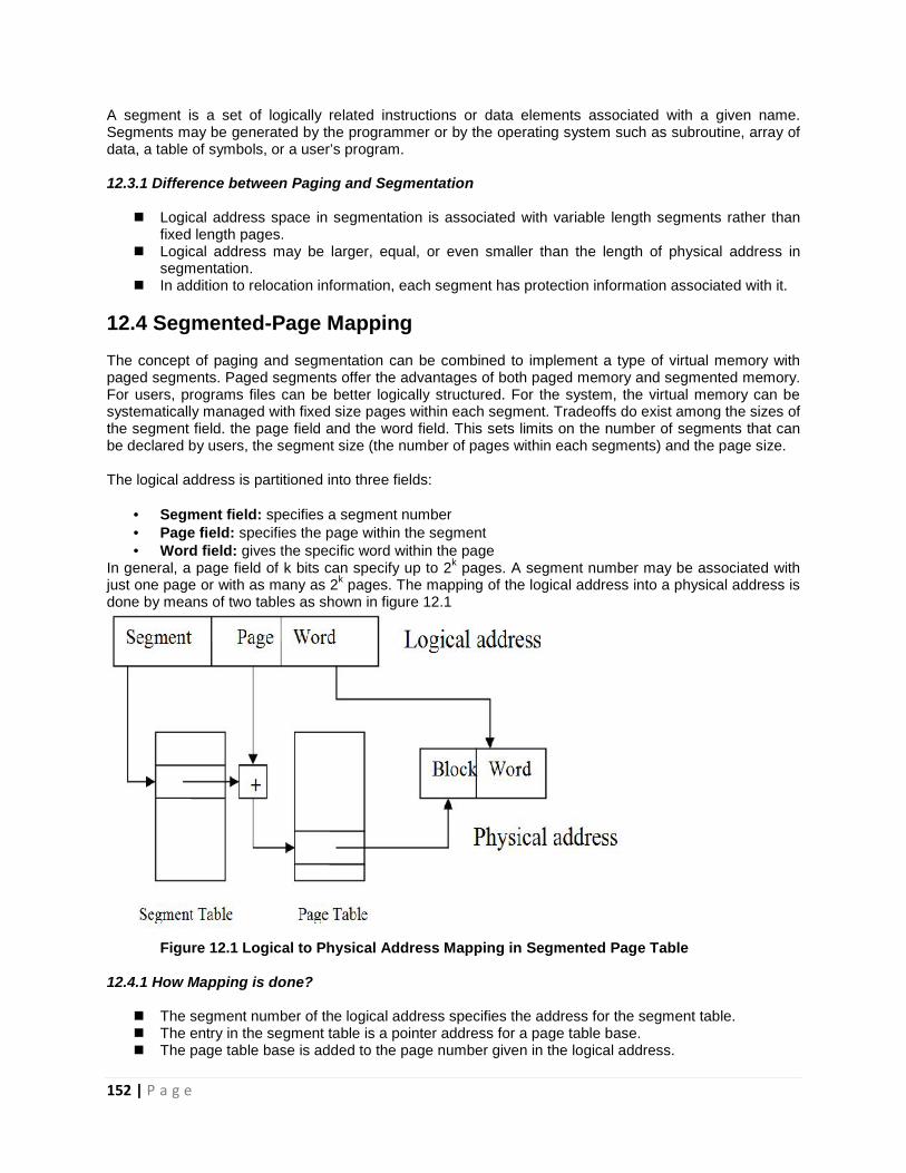
152 | P a g e
A segment is a set of logically related instructions or data elements associated with a given name.Segments may be generated by the programmer or by the operating system such as subroutine, array ofdata, a table of symbols, or a user’s program.
12.3.1 Difference between Paging and Segmentation
Logical address space in segmentation is associated with variable length segments rather thanfixed length pages.
Logical address may be larger, equal, or even smaller than the length of physical address insegmentation.
In addition to relocation information, each segment has protection information associated with it.
12.4 Segmented-Page MappingThe concept of paging and segmentation can be combined to implement a type of virtual memory withpaged segments. Paged segments offer the advantages of both paged memory and segmented memory.For users, programs files can be better logically structured. For the system, the virtual memory can besystematically managed with fixed size pages within each segment. Tradeoffs do exist among the sizes ofthe segment field. the page field and the word field. This sets limits on the number of segments that canbe declared by users, the segment size (the number of pages within each segments) and the page size.
The logical address is partitioned into three fields:
Segment field: specifies a segment number Page field: specifies the page within the segment Word field: gives the specific word within the page
In general, a page field of k bits can specify up to 2k pages. A segment number may be associated withjust one page or with as many as 2k pages. The mapping of the logical address into a physical address isdone by means of two tables as shown in figure 12.1
Figure 12.1 Logical to Physical Address Mapping in Segmented Page Table
12.4.1 How Mapping is done?
The segment number of the logical address specifies the address for the segment table. The entry in the segment table is a pointer address for a page table base. The page table base is added to the page number given in the logical address.

153 | P a g e
The sum produces a pointer address to an entry in the page table. The value found in the page table provides the block number in physical memory. The concatenation of the block field with the word field produces the final physical mapped
address.
12.5 Multi-port memoryMultiprocessor hardware system organization is determined by the interconnection structure to be usedbetween the memories and processors and between memories and I/O channels. Three differentinterconnections are: Time-shared common bus, Crossbar switches network and Multi-port memories.Multi-port memory comes with 3 different organizations:
i) Multi-port memory organization without fixed priority assignment
Multi-port memory organization without fixed priority assignment is performed when thecontrol, switching and priority arbitration logic is distributed at the interfaces to thememory modules. This organization is well suited to both uni and multiprocessor systemorganizations.
Figure 12.2 Multi-port memory organization without fixed priority assignment
There can be a problem of memory access conflict in this organization which can beresolved in next organization.
ii) Multi-port memory organization with assignment of port priorities
This method assigns permanent priorities at each memory port. The system can then beconfigured as necessary at each installation to provide the appropriate priority access tovarious memory modules for each functional unit.

154 | P a g e
Figure 12.3 Multi-port memory organization with assignment of port priorities
iii) Multi-port memory organization with private memories
It is also possible to designate portions of memory as private to certain processors, I/Ounits or combinations of both. Advantages of this organization are:- increased protection against unauthorized access- permit the storage of recovery routines in memory areas that are susceptible to
modification by other processors
There can be a serious problem of system recovery in this organization if the otherprocessors are not able to access control and status information in a memory blockassociated with a faulty processor.
Figure 12.4 Multi-port memory organization with private memories
12.5.1 Uses of Multi-port memory:
Multi-port memories are commonly used components in VLSI systems, such as register files inmicroprocessors, storage for media or network applications. The content of a multi-port memory can be

155 | P a g e
accessed through different ports simultaneously. This feature is especially valuable for high speedprocessors, media processors, and communication processors. Multi-port memoriesrequire more testing effort since all ports have to be verified.
12.6 Memory Protection
Memory Protection is the capability for the hardware to prevent a program from accessing anotherprogram's memory except under very carefully controlled conditions. An unauthorized access to memorynot owned by a particular program causes an interrupt. This interrupt causes the operating system to shutdown or reset the offending task. This provides a security measure to prevent an ill-behaved programfrom demolishing other programs. The memory protection function is often performed by a separate chipthat is managed by the operating system.Memory protection can be assigned to the physical address or the logical address but better place toapply is in the logical address space which can be done by including protection information within thesegment table or segment register of memory management hardware.
The content of each entry in the segment table or segment register is called a descriptor as shown infigure 12.5.
Base address field: gives the address used in mapping from a logical to the physical address. Length field: gives the segment size Protection field: specifies the access rights available to the particular segment. Some of the
access rights are:- full read and write privileges- read only- execute only- system only
12.6.1 Copy-on-Write Protection
Copy-on-write protection is an optimization that allows multiple processes to map their virtual addressspaces such that they share a physical page until one of the processes modifies the page. This is part ofa technique called lazy evaluation, which allows the system to conserve physical memory and time by notperforming an operation until absolutely necessary.
For example, suppose two processes load pages from the same DLL into their virtual memory spaces.These virtual memory pages are mapped to the same physical memory pages for both processes. Aslong as neither process writes to these pages, they can map to and share, the same physical pages, asshown in the following diagram.

156 | P a g e
Figure 12.6 Virtual memory pages mapped to the same physical memory pages for the processes
If Process 1 writes to one of these pages, the contents of the physical page are copied to anotherphysical page and the virtual memory map is updated for Process 1. Both processes now have their owninstance of the page in physical memory. Therefore, it is not possible for one process to write to a sharedphysical page and for the other process to see the changes.
Figure 12.7 Processes having their own instances of the page in physical memory
12.7 Summary
There are many memory management schemes range from the simple single user system approach topaged segmentation which differs in many aspects mainly its hardware implementation. Every memoryaddress generated by the CPU must be mapped to a physical address. Segmented page table mappingis one of the ways where logical address is divided into three parts: segment, page and word. Multi-portmemories are commonly used components in VLSI systems, such as register files in microprocessors,storage for media or network applications. It comes with 3 different organizations: Multi-port memoryorganization without fixed priority assignment, Multi-port memory organization with assignment of portpriorities and Multi-port memory organization with private memories. Memory protection provides asecurity measure to prevent an ill-behaved program from demolishing other programs.

157 | P a g e
12.8 GlossarySegment: a set of logically related instructions or data elements associated with a given name.
Segment field: specifies a segment number
Page field: specifies the page within the segment
Word field: gives the specific word within the page
Base address field: gives the address used in mapping from a logical to the physical address
Length field: gives the segment size
Protection field: specifies the access rights available to the particular segment.
12.9 Answer to check your progress/Suggested Answers to SAQ
1) A ……….. is a set of logically related instructions or data elements associated with a givenname.
(A) page(B) segment(C) paged-segment(D) segmented pageAns. (B)
2) A page field of k bits can specify up to
(A) 2 pages(B) k2 pages(C) 2k pages(D) NoneAns. (C)
3) Logical address may be
(A) larger(B) equal(C) smaller(D) AllAns. (D)
4) The content of a multi-port memory can be accessed through
(A) different ports(B) same ports(C) single port(D) multiple portsAns. (A)
5) Protection field of desciptor specifies the access rights such as:
(A) full read and write privileges(B) read only(C) system only(D) All

158 | P a g e
Ans. (D)
6) A ………………is a collection of hardware and software procedures for managing the variousprograms residing in memory.
(A) memory management system(B) Paging(C) Segmentation(D) Paged-segmentAns. (A)
7) An unauthorized access to memory not owned by a particular program causes
(A) error(B) interrupt(C) deadlock(D) system failureAns. (B)
12.10 References/Bibliography
[1] M.Morris Mano, Computer system Architecture, Third edition, Pearsons Education.
[2] Kai Hwang and Faye A.Briggs,Computer Architecture and Parallel Processing, PDP-11 edition,McGraw Hill International Editions
[3] Silberschatz Galvin, Operating System Concepts, Fifth Edition, Addison Wesley
[4] Madnick and Donovan, Operating Systems, McGraw Hill International Editions
12.11 Suggested Readings
1. www.fb9dv.uni-duisburg.de/vs/en/education/dv3/.../lecture11-net.pdf
2. academic.udayton.edu/SaverioPerugini/courses/.../paging.html
3. csciwww.etsu.edu/tarnoff/ntes4717/week_08/mem_mgmt.ppt
4. www.webopedia.com/TERM/M/multi_port_memories.html
5. microcom.kut.ac.kr/labs/comarc-3rd/ch13.pdf
6. www.cis.upenn.edu/~milom/cis501-Fall05/lectures/04_memory.pdf
12.12 Terminal and Model Questions

159 | P a g e
1) The logical address space in a computer system consists of 128 segments. Each segment can haveup to 32 pages of 4K words in each. Physical memory consists of 4K blocks of 4K words in each.Formulate the logical and physical address formats.
2) How segmentation differs from paging technique from the aspect of their hardware support?
3) Design various organizations of multi-port memory with 8 memory units, 4 processors and 4 I/Odevices.
4) How memory protection scheme can be optimized?
5) What is the role of descriptor in segmentation?
6) Briefly describe how memory protection is achieved through Segmentation.
7) What are the three modes of user authentication? Give an example of each. Discuss the pros and consof each mode.

160 | P a g e
Unit-4Chapter-13
MULTIPROCESSORS13.0 Objectives13.1 Introduction13.2Multiprocessor versus System with I/O Processor13.2.1 Characteristics of Multiprocessor13.2.2Multiprocessor Scheduling13.2.3 Classification of Multiprocessor13.3Interconnection Structures
13.3.1 Time Shared Common Bus13.3.2 Crossbar Switch
13.4Summary13.5Model Questions and Answers
13.0 OBJECTIVES To understand where the difference lies in Multiprocessors and system with I/O Processors Structure of Multi-processors. To know the working of Multiprocessor Classification of Multiprocessor
13.1 INTRODUCTIONSince, so far we come across many examples of the structure and behavior ofthe various functional modules of the computer, and moreoff how componentsconnected together to form a computer system. Man invented the idea of amachine, which could perform the basic operations of addition, movement ormathematical operations. Auxiliary goals are to optimize the results througheither an algorithm or installing the processor’s core to emphasize strongresults.
Before going in the definitions of multiprocessor it’s better to understandwhere the difference lies, a system with a processors and adjoining memoryblocks or a system with processor associating itself with I/O Processor Blocks. Inthe early 1960 computer, based controllers were used. In contrary after theadvent of microprocessor, cost of controlling the plant goes down. And, inactual a microprocessor is a computer on a chip, with high-density memorieswith reduced costs which finally increased application flexibility. Thesecontrollers’ measure signals from sensors, perform control routines in software

161 | P a g e
programs, and take corrective action in the form of output signals to actuators.Since the programs are in digital form, the controllers perform what is known asdirect digital control (DDC). Microprocessor can directly control the plantdigitally.
(CPU with attach memory Blocks) (Independent CPU Blocks)Figure-1 Figure-2
13.2 Multiprocessor versus System with I/O Processora). Multiprocessor: - as the name suggests is a system with more than oneprocessor assembled in some core concept with their adjoining memory forrecent usage so that a task can converge towards results sooner or properoptimization of devices can be sorted out through designed architecture.b). System with Single CPU or Adjoining I/O Processor: Other way out foraccomplishing the results for a given task is to remain dependent on a singleCPU and calls for the input and output devices can be made through processorsattached with them, this all can be simulated with some algorithms that isrunning behind these hard coded devices.Extending our discussion, multi processor systems are also known as parallelsystems or tightly coupled systems, so now question comes in mind what is theneed of increasing the number of processors, all of us thinking we justaccomplish a task in less time. All transactions of system depends upon thespeed up ratio with k processors and it always comes below k. So when weworking with a environment with more than one processors a small overhead isincurred in keeping all the parts working correctly. As multiprocessors shareperipherals so save more money than multiple single processor systems. As verysimply said how is it like keeping our data on single device and other processorssharing the data, rather to upload that data on each machine. If functions ortasks can be hand over to each of the processors, then failure of one system will

162 | P a g e
not halt the whole process. But how come this thing is possible that continuinga operation in the presence of failures, so this requires a mechanism to allowthe failure to be detected, corrected and again make it to work. Lets take aexample to know how this all is possible under a single umbrella, so nowadaysmost common multiple processor systems now use symmetric multiprocessing,in which each adjoined processor runs a copy some operating system andcommunication of these copies linger on with another as needed. More off, itsno master-slave architecture, the benefit of this model is that many processorscan run simultaneously, so k processes can be run if there are k processors13.2.1 Characteristics of Multiprocessora). The machine on the network are interconnected with communication linesand constitute computer networks.b). It is not always possible machines adjoins or joining on the lines maycommunicatec). To run a multiprocessor one should need a computer operating system tointeract between processor and components.d). One advantage of multiprocessing is it improves the reliability of systems, iffault causes a processor to fail, a second comes into picture with no loss ofintegrity to the combined system.
13.2.2 Multiprocessor SchedulingBefore having our hands in colors of scheduling, let discuss what the need oforganizing a structure of multiprocessor is1). Run parallel many jobs in the system2). Module based programmingAll wrapped tasks for each processor can handle individually. There is categoryfor special purpose processors executing out system tasks whose aim is tooptimize processing elements. Lets start discussing what so happen if weschedule the CPU in a system with a single processor, but id multiple processorsare available, the scheduling is correspondingly more complex. So for a systemwhere the processors are identical in terms of their doings, any availableprocessor can then used to run any processes in the queue
If a several identical processors are in existence, then load sharingcan be occurred, so for each processor a separate queue is provided for eachprocessor. A situation might comes among that processors some of them sittingidle or some are busy with their tasks, so to prevent from the situation alike, acommon queue is formed where all processes are dropped and are scheduled

163 | P a g e
onto any available processor. There are two approaches, first one carries aprocessor which is self scheduled. Each processor examines the common readyqueue and selects a process to execute, or in the case of multiple processorstrying to access and update a common data structures, and each processor isprogrammed successfully.
13.2.3 Classification of Multiprocessora). Tightly Coupled Microprocessor or Shared memory
(Tightly Coupled Microprocessor)Figure-3
This particular system adopts each particular processor as independent identity,no memory block acts as local memory, rather a common shared memory blockis used by all the processors. Amongst these processor array some of them areused for specific Input and output devices whereas some play role with systemtasks and rest of them are reserved for core parallel processing.a). Distributed memory or loosely Coupled.

164 | P a g e
(Loosely Coupled)Figure-4
An alternative approach is distributed –memory systems, here each processorvertex is assigned own private memory. The processor is tied together byswitches that help the segment in routing the information throughout thenetwork. The processors communicate with other processors through packets. Apacket consists of an address, the data content, and other specific errordetection code.
13.3 Interconnection StructuresMultiprocessor systems provided an environment where the various system
resources (for example, CPU, memory, peripherals) were utilized effectively butit does not provide a channel for user intervention with systems. Theinterconnection between components for different physical configuration variesfor machine to machine more off depends upon number of transfers paths thatare their between memory and processor. Some of the similar schemes arefollows:
13.3.1 Time Shared Common BusThis particular category falls with common bus attached with many of theprocessors to a memory unit. On each iteration or at time interval t1, a

165 | P a g e
processor can communicate with the memory or another processor at giventime. If during the flow, a processor wants to communicate with the otherprocessor or memory, it has to check the status of bus and if the bus is available,processor address the destination unit to initiate transfer.
(Common Bus)Figure-5
Algorithm (Pk, C1, array_data, llist, array2x4){Set of processors: {P1, P2, P3, C1} Status: {0, 1} Final States {P5} Data :{ “aab”,“bbc”}, Structure {p1: null, P2: null…………}, Bus Controller: {C2, C3}Address available at Common bus {&p1, &p1, &p3, &p5}//except to these fallsoutsideP1M.U, to conversant, processor check the availability of C1If (C1==1) // at time interval t1{Busy…C2 C30 // Processor 1 Selected1// Processor 2 Selected0// Processor 3 Selected1 1// Processor 4 Selected}Else perform{P1M.U

166 | P a g e
Command {p5, Write}// read and Write operationP5? (&p5∞C1)// address of p5 is available on Common bus(P5: aab)//data reached}}
Points to Remember1). A processor can interact either of with processor or memory at time intervalat t1 with the availability of common bus.2). before communication, the processor ensures the status of common bus.3). Common bus checks the authentication of address through bus and dependsupon sender control for initializing traversal.
The system works with restriction that at a time one transfer can be made, thismeans when one processor is communicating with memory, rest of them areeither busy with internal operations or must be waiting for the bus. So overallefficiency of the system depends on the common bus availability, but limitationof such system is processors has to wait for common bus, to overcome this, onecan go for change like each local bus may be connected with local bus to acommon system bus. In addition to this a system bus controller links each ofthese buses with common system bus.13.3.2 Crossbar SwitchA crossbar switch organization supports simultaneous transfers from allmemory modules because their is a separate path associated with each module.However, the hardware required to implement the switch can become quitelarge and complex.

167 | P a g e
(Context Switch)Figure-6
A crossbar switch is a matrix of points that staying at a position where memorymodule or processor request coincides known by switch. The switch helps indesigning context logic to set up transfer walk between memory or processormodule. With the help of MUX, a switch is sandwich from Memory/CPUmodule. Some programming construct is hard coded the arbitration logic side sothat at particular iteration level it is determined which memory is allowed withwhich processor.

168 | P a g e
Figure-7
13.4 SummaryThe context helps in knowing how multiprocessor are constructed or what is theground difference between in designing a multiprocessor and adjoining aprocessor with Input Output devices. While going through examples or theoriesof multiprocessor one can know how to predict mapping of streamingapplication and the ways of efficient scheduling for soft real time applications.GlossaryMultiprocessor: Interconnection of two or more CPUs
MIMD: Multiple data stream systemsMSN: Multistage NetworkIA: Interprocessor ArbitrationMapping: translating the virtual addresses into memory locations during
executionCBR: Common Bus RequestSBC: System Bus ControllerFrequently asked Questions-1. When a cache is 10 times faster than main memory &cache can be used 90%of the time, how much speed we gain by using the cache?Solution: Let M=main memory access time

169 | P a g e
C = cache memory access timeC = M/10(given) Total access time using cache =0.9+0.1M=0.9(M/10)+0.1M =0.1MSpeed up= M/ (0.19M) ~ 5.3
2. Consider the unpipelined machine with 10ns clock cycles. It uses 4 cycle’s foeALU operations& branches whereas 5 cycles for memory operations. Assumethat the relative frequencies of these operations are 40%, 20% & 40%respectively. Let due to clock skew & setup pipelined, the machine adds 1ns ofoverhead to the clock. How much speed in the instruction execution rate will wegain from a pipeline?Solution: Average instruction execution time=clock cycle* average CPI= 10ns *[(40%+20%)*4+40%*5]=10ns*4.4 =44nsin pipelined implementation, clock must run at the speed of slowest stageoverhead, which will be 10+1 0r 11ns; this is the average instruction executiontime.Thus, speed up from pipelining,(Speed up)pipelined= avg.instruction timeunpipelined/(avg.instruction time pipelined)=44ns/(11ns) = 4times
3. An Asynchronous serial communication controller which uses a start stopscheme for controlling the serial I/O of a system, is programmed for a string oflength 7bits, 1 parity bit (odd parity) & 1 stop bit. The transmission rate is 1200bits/second.a. What is the complete bit stream that is transmitted for the string ‘0110101’?– 1011010101b. How many strings can be transmitted per second? – 120
4. Consider multiplication of 2 (40*40) matrices using a vector processor.a. How many product terms are there in each inner product & how many innerproducts must be evaluated?b. How many multiply add operations are needed to calculate the productmatrix.Solution: = a. 40 product terms in each inner product. 40^2=1600 inner productmust be evaluated, 1 for each element of the product matrix.b. 40^3=64,000

170 | P a g e
5. Consider a computer with 4 floating point pipeline processors. Let eachprocessor uses a cycle time 40ns.How long it will take to perform 400 floating –point operations? Is there a difference if the same 400 operations are carriedout using a single pipeline processor with a cycle time of 10ns?Solution: Divide the 400 operations into each of the 4 processors, processingtime=400/4*40=4000ns using pipeline, processing time=4000*10=4000nsReferences/Bibliography[1] M.Morris Mano, Computer system Architecture, Third edition, PearsonsEducation.[2] Kai Hwang and Faye A.Briggs, Computer Architecture and Parallel Processing,PDP-11 edition, McGraw Hill International Editions[3] Silberschatz Galvin, Operating System Concepts, Fifth Edition, AddisonWesley[4] Madnick and Donovan, Operating Systems, McGraw Hill InternationalEditions

171 | P a g e
Unit-4Chapter-14
MULTIPROCESSORS14.0 Objectives14.1 Introduction to Interconnection Structures14.2 What is Multistage Switching Network?
14.2.1 Omega Network14.3Hypercube Interconnection14.4Interprocessor communication14.5 Interprocessor synchronization14.6 Mutual Exclusion with Semaphores14.7 Summary14.8 Model Question and Answers
14.0 Objectives To understand term Interconnection Structures in Multiprocessor System. To determine the Multistage Switching Network and its types To know working of Hypercube processors Difference between Interprocessor communication and Interprocessor synchronization Mutual Exclusion with semaphores.
14.1 Introduction to Interconnection StructuresMulti Switching Stage Network are also called by the name toggle or interchange switches”,“The basic component of this network is a two input, two output interchange switches.
(Multi Switching Stage Network)Figure-1
As specified in the diagram, the components are with two inputs and two outputs, sometimesinputs are alligned to 0/1. These switches have control signals, helping in establishinginterconnection between input/ output terminals. If X, Y requests for same output and terminalsfor a time then one stay connected and the other stay resumed for the time interval when first

172 | P a g e
completes the task. Using such latches, one could build a multistage network to lay down aplatform for communication between number of sources and destinations.
14.2 What is Multistage Switching Network?Even in old versions of architecture likely 8086/8088 their is one more support type to externalprocessors, referred to as independent procesor which executes its own stream for instruction.For the minimizing the cost, the processor is coupled with CPU to form a tightly coupledmicroprocessor system in which both share the same clock and bus control logic and its all doneunder the umbrella of shared memory space. King processor then accesses the shared memory tobe assigned the task and executes the task in parallel with the host.
(Omega Network)Figure 2
14.2.1 Omega NetworkIn such a network, there is path from each source to any particular destination. Many of therequests cannot be resolved simultanesously. A request is initiated by the source in the switchingnetwork, and in response, the network generates the three bits pattern representing thedestination number. As each small module carries a switching pattern, so data flows in binarypattern, level one inspects the most significant bit, level two inspects the middle, but at levelthree inspects the least significant bit. In tightly coupled multiprocessor system the destination isa memory module. During first pass, the addresses are transfered to memory then the flow ismade bidirectional. On the other hand, in a loosely coupled multiprocessors system both sourceand destination is having processing elements. After path establishment, the source transfers amessage to the destination processor.
14.3 Hypercube InterconnectionThese systems falls in loosley coupled system, composed of n=2n processors interconnected in ndimenional binary cube. Each node of the cubiod act as a processor. The node not only carries

173 | P a g e
procesor but also stay with memory and I/O Components. Each processor has alongside to theirkins in the form of edges.As per placed processors on the cube, there are 2n distinct n-bit binaryaddress that can allocated to the processors, where each processor address differs from its kin byone-bit position.
(All-to-all broadcast on an eight-node hypercube.)Figure 3
A three cube structure has eight node interconnected as a cube. An n cube structure has 2n nodeswith a processor residing in each node. Each node on the cube is assoiciated with binary addressin a way that the address of two kins differs exactly with one bit. Providing routes for messagethrough n cube structure may vary from one to n links from source to destination node.
14.4 Interprocessor communication & synchronizationIn multiprocessor system, the processor has hardcoded logic so that they can communicate witheach other. A path of conversant can be created through I/O channels. In shared memorymultiprocessor systems, the way out is independent from memory cell that is globalised andaccessible to all processors, or more off known as centralized place for all processors, where theycan left packets or pick up message intended for it.

174 | P a g e
(Interprocess Communication)Figure 4.
The sender processor structure {request, message, procedure ()} throws the packets to memorymailbox. A status bit determines the conditions of mailbox, whether any meaningful informationreceived for which processor is intended. The recipent processor can check the mailbox inconsecutive intervals, if there are valid messages. The response time is delayed as processor willrecognize request on polling messages. The other way out for doing this, is to ping the systemwith the help of interrupts. The software made interprocessor interrupt model interrupts bymeans of instructions in the program of processor which when executed becomes externalinterrupt condition for other processors.Their must be some provision to assign resources to several processors and this all kept under theumberalla of operating system. Their are three ways out for designing such operating system formultiprocessor i.e. master slave configuration, separate operating system and distributedoperating system. In master slave, always master executes the operating system functions, restover systems remain their slaves and if any slave wants to put up a request, it has to be done byfiring a intterupt informing master for the said purpose. In seperate operating systemorganisation, any of the processor can execute the operating system routines it needs and moresuitable is with loose couples systems where every processor keeps copies for operating systemwhereas the distributed operating systems organisation routines are avaliable among variousprocessors. However, each particular system is assigned to processor for some interval. Thecommunication among processor is by means of message passing through input output channels.If p1 wants to communicate with P2, it calls the procedure of p2 that is residing in p2 memoryand connection is established.14.5 Interprocessor synchronization

175 | P a g e
(Synchronization)Figure 5.
Sometimes processes tries to prevent casual exchange of information, however occasionally iftwo processes need not want to communicate with each other. One process that binds twoprocesses to communicate is called interprocessor synchronization.Because multiple processescan handles same event or mutex object, these objects can be used to accomplish interprocesssynchronization.The process that creates an object can use the handle returned by theEventCreated or the Semaphore function. Other processes can open a handle to the object byusing the object name in another call to the EventCreated or Semaphore functions.The namespecified by the creating process is limited to the number of characters that are defined byNOCHARS. It can include any character except the backslash (\) path-separator character.After aprocess creates a named event or mutex object, other processes can use the name to call theappropriate function, either EventCreated or Semaphore, to open a handle to the object.Eachobject type, such as memory maps, semaphores, events, message queues has its own separatenamespace. Empty strings ("") are handled as named objects. On Windows desktop-basedplatforms, synchronization objects all share the same namespace.The following code exampleshows how to use object names by creating and opening named objects. The first process usesSemaphore to create the mutex object. The function succeeds even if an existing object has thesame name.HANDLE MakeMyMutex (void){
HANDLE var;var = Semaphore(
NULL, // No security attributesFALSE, // Initially not ownedTEXT ("MutexToProtectDatabase")); // Name of mutex objectif (NULL == var){
// Your code to deal with the error goes here.}
return var;}
}14.6 Mutual Exclusion with Semaphores

176 | P a g e
Semaphores are things intended to pass signals between independent threads or processes. Aprocess can wait on a semaphore: this means it is suspended until some other process signals thesemaphore. If the semaphore has already been signaled, however, when the process waits, it doesnot actually suspend, but just continues right on through.Semaphores for mutual exclusion are a sub-category of all semaphores. They are used to blockaccess to a resource, usually. If you have a socket that only one process can use at a time, andyou have multiple processes that use the socket, then each process can have code like this(pseudocode):
socket_semaphore wait().code_to_use_socket().socket_semaphoresignal().
14.7 SummaryThere must be paths for connecting the Processor, Memory, or I/O modules. The collection ofpaths is called the interconnection structure or the Bus structure. We have introduced differenttypes of transfers between different modules like Memory to processor (CPU), CPU to memory,or I/O to CPU. There are different buses called address, data, or control bus depending uponinformation they carry, that is, address, data, or controlling signals respectively. These buses canbe dedicated to one type of information they carry or can be multiplexed, they can be centralizedor distributed, or synchronous or asynchronous.
GlossaryMultiprocessor: Interconnection of two or more CPUsHI: Hypercube InterconnectionSB: Synchronous BusSAP: Serial Arbitration ProcedureMapping: translating the virtual addresses into memory locations during executionIC: Interprocessor CommunicationIS: Interprocessor SynchronizationTS: Time SliceMES: Mutual Exclusion with Semaphores
14.8 Model Questions and Answers

177 | P a g e
1. Write an ALP for shifting a 16-bit number left by 2-bits.Solution: number is stored in the memory locations 2501 & 2502H. Result to be storedin memory locations 2503 & 2504H.ADD MACHINE CODES MEMORIES OPERANDS2000 2A, 01, 25 LHLD 2501H2003 29 DAD A2004 29 DAD A2005 22, 03, 25 SHLD 2503H2008 76 HLTDATA
2501-96, LSBs of number2502-’15, MSBs of number
Result2503-58, LSBs of result2504-56, MSBs of result
2. Consider a CRT display that has next mode display format 80*25 characters with a 9*12character cell. What is video buffer RAM for display to be used in monochrome (1 bitpixel) graphics mode?Solution: No. of bits required = No. of characters * cell size=80*25*9*12=21, 6000 bitsSize of RAM= 27,000 bytes
3. Write a program to transfer the entire block of data bytes from(**50 to **5E) to a newlocation starting at **70H.Solution:
START LXIH, **50HLXID, **70HMVIB, 10H
NEXT MOVA, MSTA DINX DINX HDCR BJNZ NEXTHLT
4. Write instructions to load number 2050H in the register pair B,C. Increment no. usingthe instructions INXB & illustrate whether INX B instruction is equivalent to instructionINR B & INR C.Solution: LXI B, 2050 B C

178 | P a g e
20 50INX B B C
21 51
5. Assume that the time required for 5 functional units, which operates in each of 5 cyclesare: 10ns, 8ns, 10ns, 10ns, & 7ns.Assume pipeline adds 1ns of overhead. Find the speed up vs. single cycle data path.Solution: AS average time per instruction is simply the clock cycle time.Clock cycle time = sum of times for each step in execution:Avg. instruction execution time=10+8+10+10+7 =45nsClock cycle time on pipelined machine must be largest time for any stage in pipelined +overhead of 1ns , total of 11ns.Since, CPI is 1, avg. instructions execution time of 11ns.Speed from pipelined=Avg. instruction time unpiplined/avg. instruction time pipelined=45ns/11ns=4.1ns
Problems without solution1.What is the final value of AL in this series of Instructions?
MOV AL, 27HMOV BL, 37HADD AL, BLDAA
2.What is the interrupt vector table address for an INT 21H?3.Compute – Average memory access time from the following information-
RAM access time=80nsCache access time=10nsHit Ratio=0.92
4.How does port addressing differs from memory addressing?5.How can all general purpose registers can be pushed/popped from stack with a singleinstruction?6.What advantages does a microcontroller have over microprocessor? What disadvantages doesit have?7.A certain hard disk transfers data at the rate of 8million bits per seconds. Explain why the CPUmay not be able to perform the transfer itself, thus requiring the use of DMA Controller.8. Suppose the 3 microprocessors are used in design of new video games containing colorgraphics & complex sounds. How might each microprocessor function?9.In a Computer –
a. PUSH instruction is used to push data contained in S register to stack.b. POP instruction is used to pop data contained in R register.c. Present value in 8085 microprocessor needs to be performed 2 KB ROM chip.
10. The following network is asymmetric:[a] Hypercube[b] 2D Mesh

179 | P a g e
[c] Ring11. If the main concern in the design of the interconnection network is configurability (ability toeasily add more nodes), then which multistage network should be used:[a] Bus[b] Omega network[c] Crossbar network12. The number of permutations in 8x8 crossbar network is:[a] 256[b] 40320[c] 1677721613. In a single-bus system that uses split transactions:[a] Both masters and slaves have to compete for the bus by arbitration[b] Only the masters have to compete for the bus by arbitration[c] No arbitration is necessary14. Compute the diameter and bisection width for 3D mesh with p=64 processors15. Compute the diameter and bisection width for 2D torus with p=64 processors (assume thatrouting is bidirectional).16 . Construct an 8-input Omega network using 2 x 2 switch modules in multiple stages. Showthe routing of the message from input 010 to output17. Consider the following 16x16 Omega network
a). Number of stages.b). Number of 2 x 2 switches needed to implement the network.c). Draw a 16-input Omega network using 2 x 2 switches as building blocks.d). Show switch settings for routing a message from node 1101 to node 0101 and from node0111 to node 1001 simultaneously.e). Does blocking exist in this case?
References/Bibliography[1] M.Morris Mano, Computer system Architecture, Third edition, Pearsons Education.[2] Kai Hwang and Faye A.Briggs,Computer Architecture and Parallel Processing, PDP-11 edition,McGraw Hill International Editions

180 | P a g e
[3] Silberschatz Galvin, Operating System Concepts, Fifth Edition, Addison Wesley[4] Madnick and Donovan, Operating Systems, McGraw Hill International Editions

181 | P a g e
CHAPTER 15Assembly Language Programming
Contents15.0 Objectives
15.1 Introduction
15.2 Microcomputer
15.2.1 Input/output Devices
15.2.2 Memory
15.2.3 Microprocessor
15.3 The 8085 Microprocessor
15.3.1 Salient features of 8085
15.4 Architecture of 8085 microprocessor
15.4.1 Timing and Control Unit
15.4.2 Arithmetic/Logic Unit (ALU)
15.4.3 Registers
15.4.4 Accumulator
15.4.5 Program Status Word (PSW)
15.4.6 Stack and Stack Pointer (SP)
15.4.7 Program Counter (PC)
15.4.8 Instruction Register and Instruction Decoder
15.4.9 Address Buffer
15.4.10 Address/Data Buffer
15.5 Pin Description of 8085 Microprocessor
15.5.1 Power Supply and Clock Frequency Signals
15.5.2 Address Bus: A8 – A15 (pins 21-28)
15.5.3 Multiplexed Address/Data bus (AD0 - AD7)
15.5.4 Control and Status Signals
15.5.5 Interrupts
15.5.6 Reset Signals
15.5.7 Serial Communication Signal
15.5.8 DMA Signals
15.6 Instruction Format
15.6.1 Instruction Word Size

182 | P a g e
15.6.2 One byte/word Instructions
15.6.3 Two-Byte Instructions
15.6.4 Three-Byte Instructions
15.7 The 8085 Microprocessor Instruction Set
15.7.1 Data Transfer Instructions
15.7.2 Arithmetic Instructions
15.7.3 Logical Instructions
15.7.4 Program Control Instructions
15.7.5 Machine Control Instructions
15.8 Addressing Modes
15.8.1 Immediate Addressing Mode
15.8.2 Direct Addressing Mode
15.8.3 Register Addressing Mode
15.8.4 Register Indirect Addressing
15.8.5 Implicit Addressing
15.9 How Microprocessor Executes a Program
15.10 Summary
15.11 Glossary
15.12 Answers SAQs
15.13 References/Suggested Readings
15.14 Model Questions and Problems
15.0 Objectives
To study block diagram and pin out diagram of 8085 microprocessor
To study functions of various registers
Classification of instruction set and function of various instructions of 8085 microprocessor
To study Various Addressing modes in 8085 microprocessor

183 | P a g e
After the completion of this chapter students will be able to understand the basic concepts of 8085
microprocessor and its instruction set that will help them to proceed for the skill development to write the
assembly language programming.
15.1 IntroductionA microprocessor is one of the most exciting innovations in the field of electronics. It contains a central
processing unit (CPU), which is of little use unless interfaced with memories and various other
input/output devices. This wonder device has entered into almost every sphere of human life.
A microprocessor which is abbreviated as µP is designed with millions of transistors embedded
on a single semiconductor chip called integrated circuit (IC).
Inside the microprocessor chip, there is an arithmetic logic unit (ALU). The ALU executes all
arithmetic and logic programs.
An electronic system which is centered on a microprocessor will often be referred as a
microprocessor – based system.
Now a day, microprocessors have become the most important thing in our life. It controls the logic
of almost all digital devices, right from the toys, to household appliances and various sensor
systems for automobiles; it is essential part for controlling the various parameters.
A system designed around a microprocessor needs to be programmed. A sequence of
instructions used to perform a particular task is known as a program.
A set of programs written for a microprocessors based system is known as software for that
system. The systems having microprocessors as central processing unit are called
microcomputers.
15.2 MicrocomputerA computer that is designed using a microprocessor as its CPU is called microcomputer. As shown in
figure 15.1, microcomputer consists of a microprocessor, I/O devices and memory interfaced through bus
systems. A microcomputer was primarily designed for machine control and instrumentation. With the
decline of prices of microprocessors, the applications mushroomed in almost all areas such as, video
games, word processing, PCs, workstations or notebook computers.
Micro-Processor
(CPU)
Data BusInput/Output
Devices
Data BusData Bus
Address BusAddress Bus
Memory(RAM/ROM)

184 | P a g e
Figure 15.1 Block diagram of microprocessor based microcomputer system15.2.1 Input/output DevicesInput devices such as keyboards, sensors etc. are used to enter data from the outside world to the
microprocessor for its processing and output devices such as seven segment display, LCD, printer etc.
are used to deliver the processed data from microprocessor to the outside world. If input data is in analog
form then analog to digital converter IC (Integrated Circuit) is used in between input device and
microprocessor (as CPU is a digital device) and digital to analog converter is used in between
microprocessor and output device to convert data back to original analog form.
15.2.2 MemoryMemory is used to store the temporary data and programs while execution of a program. Two types of
memory is required to be interfaced with the microprocessor i.e. random access memory (RAM) also
called temporary memory and read only memory (ROM) also called program memory. Memory devices
(also called memory chips) are available in various word sizes. The maximum capacity of memory that
can be interfaced with the microprocessor depends on the number of address lines.
Data and stack memories are the part of same RAM. The total memory size is 64 KB can be
interfaced with the 8 bit processor having 16 address lines.
In the program memory, program can be saved anywhere in memory.
In Data memory, 16-bit addresses are used so that data can be saved anywhere within 64 k
bytes of memory space.
Stack memory is used to save temporary data which is limited only by the size of RAM. Stack
follows Last in First out (LIFO) method to save data and it grows in downward direction.
First 64 memory locations are kept reserved for vectors to be used by Restart instructions.
15.2.3 MicroprocessorThe microprocessor is a programmable digital integrated circuit which is designed with arithmetic logic
unit (ALU), registers, timing and control unit, status flag bits, latches, buffers etc. to perform computing
tasks as defined by the instructions in the memory. A microprocessor performs the functions of
a computer's central processing unit (CPU). Microprocessors use numbers, alphabets and symbols
represented in the binary number system. This binary language is called the machine language.
15.3 The 8085 MicroprocessorThe 8085 microprocessor is an 8 bit processor which is the enhanced version of its predecessor, the
8080A and the instruction set of both is compatible with each other, meaning that 8085 instruction set
includes all the 8080A instructions with some additional ones.
15.3.1 Salient features of 8085

185 | P a g e
The salient features of 8085 µp are:
It is an 8 bit processor.
It is manufactured by Intel Corp. with N-MOSFET technology.
It has Sixteen-bit address lines and hence can address up to 216 = 65536 bytes (64KB) memory
locations by using address lines A0-A15.
The first eight address lines and eight data lines are multiplexed and are denoted as AD0 – AD7.
Data bus is a group of eight lines i.e. D0 – D7.
It can process external interrupt request.
It has a sixteen bit program counter (PC) and sixteen bit stack pointer (SP)
Six eight-bit general purpose registers B, C, D, E, H, and L. These general purpose registers
can be arranged in three register pairs: BC, DE, HL as 16 bit registers.
Figure 15.2: 8085 microprocessor
It operates on +5V power supply and crystal of 3 to 6 MHz for providing a single phase clock.
It is designed with 40 pins Dual in line package (DIP) plastic pack as shown in figure 15.2.
It performs four basic operations: Memory read, memory write, I/O read and I/O write.
15.4 Architecture of 8085 microprocessor8085 microprocessor architecture consists of interrupt controller, Accumulator, Six 8 bit general purpose
registers, serial I/O control, Sixteen bit stack pointer, Sixteen bit program counter , Arithmetic Logic Unit,
Instruction register, instruction decoder, timing and control unit, buffers, latches, decoders and
multiplexers etc. as shown in figure 15.3. Detailed explanation of each block is given as follows:
15.4.1 Timing and Control Unit
Called brain of microprocessor, synchronizes and controls all the internal and external operations
with the clock.
Control unit generates control signals (I/OR, I/OW, MEMR, MEMW etc.) necessary for data
transfer between the microprocessor and peripheral devices to perform the operation as per
instruction decoded by instruction decoder.
Establishes the connections between various blocks of the microprocessor to be opened or
closed, so that the data is transferred where it is required.
It operates with reference to the clock and uses a quartz crystal to determine clock frequency.

186 | P a g e
The speed of microprocessor is directly proportional to the speed of the crystal clock.
15.4.2 Arithmetic/Logic Unit (ALU)
The ALU performs the computing functions and logic operation such as ‘addition’, ‘Subtraction’,
‘AND’, ‘OR’, ‘XOR’, ‘Compliment’, ‘Increment’, ‘Decrement’, ‘Rotate’ etc.
It includes the accumulator, the temporary register, arithmetic/logic circuits and five flags.
The flags are affected by the arithmetic and logic operations in the ALU.
Uses data from memory, registers or immediate and from Accumulator to perform arithmetic or
logical operations. After operation it stores result of 8 bit arithmetic/logical operation in
Accumulator.
15.4.3 Registers
The 8085 microprocessor includes six registers i.e. B, C, D, E, H, L, accumulator (A), and one
flag register called program status word (PSW).
These register are combined as pairs - BC, DE, and HL - to perform 16-bit operations.
These registers can be used by the programmer to store or copy data by using data transfer
instructions.
It has two 16-bit registers: the stack pointer (SP) and the program counter (PC).
Program counter holds the address of next instruction to be executed. On reset it sets to 0000H
address.
In case of Call and Jump instructions, the address followed by these instructions (if condition is
satisfied, in case conditional Jump/Call) is loaded to the PC and starts execution of program from
this address onwards.
Two additional registers, called temporary registers W and Z are used to hold eight bit data during
the execution of some instructions; however, because they are used internally, they are not
available to the programmer.
15.4.4 Accumulator (A)
The accumulator (A) is an 8-bit special function register and is a part of ALU.
It holds one of the 8 bit operand out of two operands on which arithmetic and logical operations
are performed.
After the operation 8 bit result is stored in the accumulator.
It also holds 8 bit data to be read from input device or to be written into the output device while
executing IN and OUT instructions.
15.4.5 Program Status Word (PSW)

187 | P a g e
The ALU includes PSW that holds status of five flags, which are set or reset after an operation according
to the result stored in the accumulator and other registers after the operation. These flags are called Zero
(Z), Carry (CY), Sign (S), Parity (P), and Auxiliary Carry (AC). The bit positions in the flag register (PSW)
are shown in the Figure 15.4. The most commonly used flags are Zero flag, Carry flag, and Sign flag. The
microprocessor uses the status of these flags to test various data conditions. For example, after an
addition of two numbers, if the sum in the accumulator is larger than eight bits, the Carry flag (CY) is set
to one. When an arithmetic operation’s result is zero, the flip-flop called the Zero (Z) flag is set to one.
Figure 15.3 Block diagram of 8085 microprocessor

188 | P a g e
The figure 15.3 shows an 8-bit register, called the program status Register or PSW, adjacent to ALU.
However, it is not used as a general purpose register by the programmer but the five bit positions out of
D7 D6 D5 D4 D3 D2 D1 D0
S Z --- AC --- P --- CY
Figure 15.4 Bit positions reserved in program status word (PSW) for flags
eight are used to store the outputs of the five flags as shown in figure 15.4. These flags are important for
the decision-making process by the microprocessor .The conditions (set or reset) of these flags are
checked through the conditional Jump or Call instructions. For example, the instruction JC (Jump on
Carry) is used to alter the sequence of a program when CY flag is set to one. The thorough
understanding of flags bits is necessary for writing assembly language programs.
15.4.6 Stack and Stack Pointer (SP)
Stack is a portion of R/W memory reserved for temporarily storage of data while writing and execution of
a program. PUSH instruction is used to write onto stack and POP instruction is used to read back from
the stack. Stack can be accessed by using register pairs such as BC, DE, HL and pair of A and PSW.
The stack pointer is a 16-bit register used to hold address for the stack memory. It points to a memory
location in the stack. The beginning of the stack is defined by the programmer by loading a 16-bit address
in the stack pointer. In the stack pointer address is automatically decremented twice while writing into the
stack using PUSH instruction and similarly incremented twice while reading from the stack using POP
instruction.
15.4.7 Program Counter (PC)This 16-bit register performs the function of sequencing the execution of instructions. Memory locations
have sixteen bit addresses, and thus the PC is a16-bit register .The microprocessor uses program
counter to sequence the execution of the instructions .The function of the PC is to point to the memory
location from where the next byte is to be fetched and executed. When microprocessor fetches a byte
(machine code), the program counter is automatically incremented by one to point to the next memory
location.
15.4.8 Instruction Register and Instruction Decoder
Instruction Register is used by the microprocessor to store the current instruction of a program
temporarily before being decoded. ALU and control section uses this register for temporary storage of
data and hence it cannot be used by the programmer. Instruction decoder then accepts the instruction
from the instruction register and then decodes or interprets it. Decoded instruction then passed to the

189 | P a g e
timing and control section that provides the control signals for further performing the task according to this
instruction.
15.4.9 Address Buffer
This is an 8-bit unidirectional buffer used to isolate the microprocessor from the high current in
the other peripherals.
This buffer is used to tri-state the higher order address lines when these are not in use.
15.4.10 Address/Data Buffer
This is an 8-bit bidirectional buffer used for the lower order address/data bus.
This buffer is used to tri-state the lower order address/data lines when these are not in use.
15.5 Pin Description of 8085 Microprocessor8085A is an 8 bit general purpose microprocessor having 40 pins. This IC (µP) is capable of addressing
64K bytes of memory space. It operates on single +5 V power supply. Pin out diagram of 8085
microprocessor is shown in figure 15.5. Signals from all the pins can be grouped in six sub groups and
description of each is explained as follows:
1. Power supply and clock frequency
2. Address Bus
3. Multiplexed Address/Data Bus
4. Control and status signals
5. Externally initiated signals, including interrupts
6. Serial I/O ports
15.5.1 Power Supply and Clock Frequency Signals
VCC (pin 40): + 5 V power supply
VSS (pin 20):: Ground Reference
X1, X2 (pin 1, 2): : A Crystal or R/C network or LC network is connected at these two pins to set
the frequency of internal clock generator. The crystal frequency is internally divided by two. For
the basic operating frequency of 3 MHz, a 6 MHz crystal is connected externally.
CLK (out) (pin 37): -This pin is used as the system clock for the other peripheral devices
interfaced with the microprocessor.
15.5.2 Address Bus: A8 – A15 (pins 21-28):The 8085 microprocessor has 16 address lines that are used as address bus; however these lines are
divided into 2 parts as: A8 – A15 (Higher order address lines) and AD0 - AD7 (lower order Multiplexed

190 | P a g e
Address/Data lines). Address lines are used to carry the 16 bits of the memory address or the 8 bits of the
I/O devices address.
15.5.3 Multiplexed Address/Data bus (AD0 - AD7) (pins 12 - 19)
These multiplexed Address/Data lines are used to carry the lower order 8 bit address as well as 8 bit
data. During the opcode fetch operation in the first clock cycle (in opcode fetch machine cycle), these
lines deliver the lower order address A0 - A7 i.e. act as address bus. After the 1st clock pulse these lines
are demultiplexed by applying a positive pulse at ALE pin (pin 30), these lines are used as data lines.
These lines are multiplexed to decrease the count of number of pins which reduces its complexity size
and weight.
Figure 15.5 Pin Out diagram of 8085 microprocessor
15.5.4 Control and Status Signals:ALE (Pin 30) - Address Latch Enable.
It is an output signal used to separate (demultiplex) address/data bus from AD0 - AD7 to A0 - A7
and D0 - D7 contents.
A positive going pulse is applied to this pin by the processor when a new operation is started.

191 | P a g e
When pulse at this pin goes high it indicates that AD0-AD7 acts as address bus.
When pulse at this pin is low it indicates that AD0-AD7 acts as data bus.
RD (active low) (Pin 32):
It is an active low output control signal.
This pin is used to generate control signal to read from the selected memory location or Input
device.
Logic level 0 on this pin indicates that read operation is in process
WR (active low) (Pin 31):
It is an active low output control signal.
This pin is used to generate control signal to write into the selected memory location or to the
output device.
Logic level 0 on this pin indicates that write operation is in progress
IO/M – Input Output/Memory (Pin 34):
This is output status signal which indicates that the read/write operation will be related to
the memory or Input/output device.
Logic 0 at this pin indicates that the read/write operation is of memory related.
Logic 1 at this pin indicates that the read/write operation is of Input/output device related.
Status Signals – S0 (Pin 29), S1 (Pin 33):
These are the output status signals.
Microprocessor sets or resets S0 and S1 status signals according to the operation to be
performed as shown in the table 15.1.
Table 15.1 Operations according to the status signals
OPERATION IO/M S1 S0
Opcode fetch 0 1 1
Memory read 0 1 0
Memory write 0 0 1
I/O read 1 1 0
I/O write 1 0 1
Interrupt acknowledge 1 1 0
Halt Z (High Impedance) 0 1

192 | P a g e
Hold Z (High Impedance) X (Unspecified) X (Unspecified)
Reset Z (High Impedance) X (Unspecified) X (Unspecified)
When S0, S1 are combined with IO/M, the status of the operations (i.e. machine cycles) is obtained
as shown in table 15.1.
15.5.5 Interrupts
Interrupt is a process that is initiated by the external devices to have the attention of the microprocessor
to perform some specific task. The 8085 microprocessor has 5 interrupts. These interrupts are as given
below in order of their priority from the highest to lowest one. Explanation of these interrupts is as follows:
TRAP is a non-maskable interrupt. When this interrupt is generated the processor completes the
execution of the current instruction and then saves the contents of the program counter (i.e.
address of next instruction to be executed when interrupt is generated) onto the stack and starts
execution of next instruction written at memory address 24H onwards i.e. interrupt service routine
(ISR) of this interrupt. This interrupt is used by the processor itself for its internal operations.
TRAP is generally used for such critical events as power failure and emergency shut-off.
RST7.5 is a maskable interrupt. When this interrupt is generated the processor completes the
execution of the current instruction and then saves the contents of the program counter (i.e.
address of next instruction to be executed when interrupt is generated) onto the stack and starts
execution of next instruction written at memory address 3CH onwards i.e. interrupt service routine
(ISR) of this interrupt.
RST6.5 is a maskable interrupt. When this interrupt is generated the processor completes the
execution of the current instruction and then saves the contents of the program counter (i.e.
address of next instruction to be executed when interrupt is generated) onto the stack and starts
execution of next instruction written at memory address 34H onwards i.e. interrupt service routine
(ISR) of this interrupt.
RST5.5 is a maskable interrupt. When this interrupt is generated the processor completes the
execution of the current instruction and then saves the contents of the program counter (i.e.
address of next instruction to be executed when interrupt is generated) onto the stack and starts
execution of next instruction written at memory address 2CH onwards i.e. interrupt service routine
(ISR) of this interrupt.
INTR is maskable interrupt. When this interrupt occurs the processor fetches from the bus one
instruction, usually one of the 8 restart (RST) instructions (RST0 – RST7). The processor saves
current program counter onto the stack and starts execution from the memory location specified
for the given RST instruction supplied by the external hardware .

193 | P a g e
Maskable interrupts can be enabled or disabled using EI and DI instructions respectively. RST 5.5, RST
6.5 and RST 7.5 interrupts can be enabled or ignored individually using SIM instruction. RIM instruction
can be used to check for any pending interrupts.
15.5.6 Reset SignalsRESET IN (Pin 36):When this logic level at this pin goes low, the program counter (PC) is set to Zero, microprocessor is also
reset and it resets the interrupt enable and HLDA flip-flops. The data bus, address bus and the control
lines are all tri-stated during reset and because of asynchronous nature of RESET signal, the processor’s
internal registers and flags may be altered by the unpredictable results.
Upon power-up, RESET IN pin must remain at logic low for at least ten milliseconds after VCC has
reached its minimum value.
For the proper reset operation, RESET IN pin should be kept low for a minimum of three clock
cycles.
RESET OUT (Pin 3):
This signal indicates that µP is being reset.
This signal can be used to reset other peripheral devices.
The signal is synchronized to the processor clock.
15.5.7 Serial Communication SignalSID (Pin 5) - Serial Input Data:
Serial Input Data Line: Whenever RIM instruction is executed, data on SID line is loaded into the
accumulator bit D7.
SOD (Pin 5) – Serial Output Data Line:
Whenever SIM instruction is executed, the value of bit D7 bit of the accumulator gets loaded into
the SOD latch provided that the bit D6 (SOE) of the accumulator is set to 1.
15.5.8 DMA SignalsHOLD (Pin 39):
HOLD is an active high signal which indicates that DMA (IC 8237) is requesting the use of the
address data and control bus.
The CPU, Upon receiving the hold request, the microprocessor relinquishes the control of buses
as soon as the completion of the current data transfer.
The processor can regain the control of these three buses only after the active high status of the
HOLD pin is removed by the DMA.
HLDA (Pin 38) - Hold Acknowledge:

194 | P a g e
Logic 1 at this pin indicates that the processor has received the HOLD request initialized by the
DMA and that it will gave up control of buses in the next clock cycle.
HLDA goes low after the Hold request is removed.
The processor takes the control of the buses one half-clock cycle after the HLDA pin goes low.
READY (Pin 35):
This signal synchronizes the fast CPU with the slower memory and the peripherals.
It is used by the processor to detect whether a peripheral is ready for the data transfer or not.
When READY pin is high during a read or write cycle, it indicates that the memory or peripheral is
ready to send or receive data.
If READY is low, the processor will wait for number of clock cycle till READY pin goes high before
completing the read or write cycle.
Self Assessment Questions (Section 15.1 to 15.5)1. Stack pointer is a .......... bit register.
2. Program counter is a ......... bit register.
3. Accumulator is a ......... bit register.
4. Instruction register is a ........bit register.
5. An example for non maskable interrupt is........
6. ………..interrupt is having the highest priority.
7. ALE pin is used for………..
8. 8085 microprocessor has ………..flags.
9. Two registers…….and……..are not accessible to the programmer.
10. The first machine cycle of any instruction is always……….
11. The Z flag of 8085 microprocessor sets when………..
12. Stack pointer holds address of next instruction to be executed. True/False
15.6 Instruction FormatAn instruction is a command given to the microprocessor to perform a particular task on a specified
data. Each instruction can be divided into two parts: First is task to be performed, called the operationcode (opcode), and the second is the data to be operated on, called the operand. The operand (or data)
can be specified as:
i) 8-bit data or 16-bit data immediate in the instruction,
ii) 8-bit data or 16-bit data in general purpose registers,
iii) 8-bit data or 16-bit data from memory locations.
iv) In some instructions, the operand is implicit.
15.6.1 Instruction Word Size

195 | P a g e
The 8085 instructions can be classified into the following three groups according to the length of
the instruction: Instructions are commonly referred in terms of bytes rather than words. In 8085
microprocessor byte and word is one is the same thing.
One byte or one word instructions
Two byte or two word instructions
Three byte or three word instructions
15.6.2 One byte/word Instructions
In the 1-byte instruction the opcode and the operand are included in the same byte. In these instructions
the operand(s) are in general purpose registers and are part of the instruction in hexadecimal code form.
Examples of one byte/word instructions are given in table 15.2.
Table 15.2 One-byte instructions
Op code Operand Hex Code Comments
ADD B 80 HAdd the contents of the accumulator with the
contents of register B.
SUB D 92 HSubtract the contents of register D from the
contents of accumulator.
The instructions given in table 15.2 are 1-byte instructions and are stored in the one byte memory
location. ADD B instruction, operand register B is added with the accumulator contents and after addition
the result is stored in accumulator by the processor itself. In the second instruction, the operand D is
subtracted from the accumulator and after subtraction the result is stored in accumulator by the processor
itself.
15.6.3 Two-Byte InstructionsThe two-byte instruction includes one byte of hexadecimal code for the instruction and one byte of the
data or I/O address. The first byte specifies the operation code and the second byte is the operand. In two
byte instructions, left operand is source and right operand is destination in case of data transfer
instructions. Examples of two byte instructions are given in table 15.3.
Table 15.3 Two-byte instructions
Op code Operand Hex Code Comments
MVI E, 57 H1E H First Byte
57 H Second ByteLoads an eight bit data byte 57 H in the register E
ADI 9B H C6 H First Byte Add the immediate data as given in the operand to
Opcode
Opcode 8 bit data/address
Opcode Lower byte of data/add. Higher byte of data/add.

196 | P a g e
9B H Second Byte the contents of the accumulator.
Above instructions would require two memory locations (i.e. one for hexadecimal code of instruction and
second for data) to store them in memory. Hence these types of instructions are called two byte
instructions.
15.6.4 Three-Byte InstructionsIn the 3-byte instruction, the first byte is opcode, and the following 2 - bytes represents the 16-bit address.
Here you should note that the second byte is the lower-order address and the third byte is the higher-
order address.
Table 15.4 Three-byte instructions
Op code Operand Hex Code Comments
LXI H, 2050 H
21 H First Byte
50 H Second Byte
20 H Third Byte
Loads sixteen bit contents 2050 H in the HL
register pair
STA 3000 H
32 H First Byte
00 H Second Byte
30 H Third Byte
Stores accumulator contents in the memory
location 3000 H.
The instructions given in the table15.4 would require three memory locations (i.e. one for hexadecimal
code of instruction, second and third byte for address) to store them in memory.
15.7 The 8085 Microprocessor Instruction SetAn instruction is a command given to the microprocessor to perform a specific operation on the given
data. The collection of instructions that a microprocessor executes is called Instruction Set. The 8085
have 74 basic instructions and 246 total instructions. The instruction set of 8085 is defined by the
manufacturer Intel Corporation. Each instruction is represented by an 8-bit binary number (1 - byte
hexadecimal code). These 8-bits of binary numbers are called Op-Code or Hex code. Entire instruction
set can be divided into five groups:
1. Data transfer group
2. Arithmetic group
3. Logical group
4. Program control group
5. Machine control group

197 | P a g e
15.7.1 Data Transfer Instructions
These instructions transfers data in between the registers, or in between the memory and
registers.
Data is copied from source to destination.
In the data transfer operation, the contents of source remains the same.
Data transfer instructions of 8085 µP are as follows:
MVI R, 8 bit data ; load immediate data to 8 bit register (R mean register A, B, C, D, E, H, L)
MOV R1, R2 ;Copy contents of source register to destination register where R2 is source and
R1 is destination for Example MOV B, A (R mean register A, B, C, D, E, H, L)
MOV R, M ; Copy contents of Memory (address in HL pair) to any of the 8 bit register.
MOV M, R ; Copy contents from any of the 8 bit register to Memory (address held in HL pair)
MVI M, 8 bit data ; load immediate 8-bit data to Memory (address in HL pair).
LDA 16 bit address ; load contents to Accumulator (A) from memory address (16bit)
STA 16 bit address ; Store contents of A to memory address (16bit)
LDAX RP ; load contents to Accumulator (A) from memory address in RP i.e. Register Pair
STAX RP ; Store contents of Accumulator (A) to memory address in RP i.e. Register Pair
LXI RP 16bit address ; load immediate sixteen bit number to RP i.e. Register Pair
IN 8bit port address ; Accept data to A from input port address (8bit)
OUT 8 bit port address ; Send data of A to output port address (8bit)
LHLD 16 bit address ; Load HL pair from memory i.e. L from given address and H from next address.
SHLD 16 bit address ; Store HL pair to memory i.e. L to given address and H to next address.
PCHL ; Loads contents of HL register pair to program counter
SPHL ; Loads contents of HL register pair to stack pointer
XCHG ; Exchange contents of H and L with D and E registers
XTHL ; Exchange contents of H and L with top of stack i.e. L with stack top and H with
next location of stack
PUSH RP ; Contents of register pair are saved to stack i.e. lower order register to stack
location pointed by Stack Pointer (SP) and Higher order register to stack location
pointed by SP+1
POP RP ; Contents are loaded from stack in the register pair i.e. lower order register from
the stack location pointed by SP and Higher order register to stack location
pointed by SP+1.
15.7.2 Arithmetic Instructions
ADD R ; Add contents of Accumulator (A) with 8 bit register (R) given in the instruction.
ADI 8bit ; Add contents of Accumulator (A) with 8 bit immediate data given in the instruction.
ADD M ; Add contents of Accumulator (A) with memory contents (address in HL register pair)

198 | P a g e
ADC R ; Add contents of Accumulator with 8 bit register along with addition of carry flag status.
ADC M ; Add contents of Accumulator (A) with memory (address pointed by HL register pair)
along with the addition of carry flag status.
ACI 8 bit ; Add contents of Accumulator with 8 bit immediate data given in the instruction along
with the addition of carry flag status.
DAA ; Decimal- Adjust Accumulator, converts the binary value in accumulator to BCD form.
DAD RP ; Add sixteen bit contents of register pair with HL pair and after addition saves result in
HL pair i.e. lower byte of result in register L and higher byte of result in register H.
SUB R ; Subtract contents of 8 bit register from the contents of Accumulator.
SUI 8bit ; Subtract contents of 8 bit immediate data from the contents of Accumulator.
SBB R ; Subtract contents of 8 bit register from the contents of Accumulator with borrow (Note
that CY flag acts as borrow in case of subtraction operation).
SBB M ; Subtract contents of memory (address in HL register pair) from the contents of
Accumulator with borrow.
SBI 8bit ; Subtract contents of 8 bit immediate data from the contents of Accumulator with borrow
INR R ; Increment contents of 8 bit register by one
INR M ; Increment contents of memory (address in HL register pair) by one
DCR R ; Decrement contents of 8 bit register by one
DCR M ; Decrement contents of memory (address in HL register pair) by one
INX RP ; Increment contents of 16 bit register pair by one
DCX RP ; Decrement contents of 16 bit register pair by one
15.7.3 Logical Instructions
ANA R ; logical AND contents of accumulator with the contents of 8 bit register.
ANI 8bit ; logical AND contents of accumulator with the 8 bit immediate data given in the
instruction.
ANA M ; logical AND contents of accumulator with the contents of memory (pointed by HL
register pair)
ORA, R ; logical OR contents of accumulator with the contents of 8 bit register
ORI 8 bit ; logical OR contents of accumulator with 8 bit immediate data
ORA M ; logical OR the contents of accumulator with the contents of memory (pointed by HL
register pair)
XRA R ; logical XOR contents of accumulator with the contents of 8 bit register
XRI 8 bit ; logical XOR contents of accumulator with 8 bit immediate data
XRA M ; logical XOR contents of accumulator with the contents of memory (pointed by HL
register pair)
CMP R ; Compare contents of accumulator with the contents of 8 bit register

199 | P a g e
CPI 8bit ; Compare contents of accumulator with 8 bit immediate data
CPI M ; Compare contents of accumulator with memory (pointed by HL register pair)
After comparison of register/immediate data/memory with the contents of Accumulator:
i) If (A) < (register/immediate data/ memory): carry flag is set
ii) If (A) = (register/immediate data/ memory): zero flag is set
iii) If (A) > (register/immediate data/ memory): Both carry and zero flags are reset.
RLC ; Rotate contents of accumulator to left side by the position of 1 bit i.e. D0 to D1, D1 to D2,
D2 to D3, D3 to D4, D4 to D5, D5 to D6, D6 to D7, D7 to D0 and carry flag.
RAL ; Rotate contents of accumulator to left side by the position of 1 bit through carry flag i.e.
D0 to D1, D1 to D2, D2 to D3, D3 to D4, D4 to D5, D5 to D6, D6 to D7, D7 to carry flag and
carry flag to D0
RRC ; Rotate contents of accumulator to right side by the position of 1 bit i.e. D7 to D6, D6 to
D5, D5 to D4, D4 to D3, D3 to D2, D2 to D1, D1 to D0, D0 to D7 and carry flag.
RAR ; Rotate contents of accumulator to right side by the position of 1 bit through carry flag i.e.
D7 to D6, D6 to D5, D5 to D4, D4 to D3, D3 to D2, D2 to D1, D1 to D0, D0 to carry flag and
carry flag to D7
CMA ; Complement contents of accumulator
CMC ; Complement the status of carry flag
STC ; Set carry flag to logic level 1
15.7.4 Program Control InstructionsJMP 16 bit address ; Jump unconditionally to memory location specified by the 16 bit address
JZ 16bit address ; Jump conditionally to memory location specified by the 16 bit address if
` Zero (Z) flag = 1
JNZ 16bit address ; Jump conditionally to memory location specified by the 16 bit address if
` Zero (Z) flag = 0
JC 16bit address ; Jump conditionally to memory location specified by the 16 bit address if
` carry flag (CY) flag = 1
JNC 16 bit address ; Jump conditionally to memory location specified by the 16 bit address if
` carry flag (CY) flag = 0
JP 16bit address ; Jump conditionally to memory location specified by the 16 bit address if
` Sign flag (S) flag = 0
JM 16bit address ; Jump conditionally to memory location specified by the 16 bit address if
` Sign flag (S) flag = 1
JPE 16bit address ; Jump conditionally to memory location specified by the 16 bit address if
` Parity is even i.e. Parity flag (P) flag = 1

200 | P a g e
JPO 16bit address ; Jump conditionally to memory location specified by the 16 bit address if
` Parity is Odd i.e. Parity flag (P) flag = 0
CALL 16 bit address ; Unconditional subroutine call. The program sequence is changed to specified
address but before change of sequence, the address of instruction next to CALL
instruction is saved to the stack by the processor itself.
CC16 bit address ; Call subroutine conditionally to memory location specified by the 16 bit address
if carry flag (CY) flag = 1
CNC16 bit address ; Call subroutine conditionally to memory location specified by the 16 bit address
if carry flag (CY) flag = 0
CZ16 bit address ; Call subroutine conditionally to memory location specified by the 16 bit address
if Zero flag (Z) flag = 1
CNZ16 bit address ; Call subroutine conditionally to memory location specified by the 16 bit address
if Zero flag (Z) flag = 0
CPO16 bit address ; Call subroutine conditionally to memory location specified by the 16 bit address
if Parity is Odd i.e. Parity flag (P) flag = 0
CPE16 bit address ; Call subroutine conditionally to memory location specified by the 16 bit address
if Parity is even i.e. Parity flag (P) flag = 1
CP 16 bit address ; Call subroutine conditionally to memory location specified by the 16 bit address
if Sign flag (S) flag = 0
CM 16 bit address ; Call subroutine conditionally to memory location specified by the 16 bit address
if Sign flag (S) flag = 1
RET ; Return from subroutine unconditionally to the instruction next to the CALL
instruction in the main program
RC ; Return from subroutine if carry flag (CY) flag = 1
RNC ; Return from subroutine if carry flag (CY) flag = 0
RZ ; Return from subroutine if Zero flag (Z) flag = 1
RNZ ; Return from subroutine if Zero flag (Z) flag = 0
RPO ; Return from subroutine if Parity is Odd i.e. Parity flag (P) flag = 0
RPE ; Return from subroutine if Parity is Odd i.e. Parity flag (P) flag = 1
RSTN ; Restart Instructions (RST0 to RST7) are equivalent to 1 byte CALL instructions.
These transfer program execution to one of the eight locations of RST0 to RST7.
15.7.5 Machine Control InstructionsHLT ; Halt or stop further execution of instructions.
NOP ;No Operation. The instruction is fetched and decoded but no operation is
performed.

201 | P a g e
RIM ; Read Interrupt Mask. A multipurpose instruction used to read the status of
pending interrupts RST 7.5, RST 6.5, RST 5.5 and to read serial data input bit.
D7 D6 D5 D4 D3 D2 D1 D0
SID I7.5 I6.5 I5.5 IE M 5.5 M 5.5 M 5.5
Figure 15.6 Interpretation of accumulator contents for the RIM instruction
RIM loads eight bits in the accumulator with the interpretation as shown in figure
15.6.
SIM ; Set Interrupt Mask. A multipurpose instruction used to enable or disable
interrupts RST 7.5, RST 6.5, RST 5.5 and to transfer serial data to output. SIM
instruction interprets eight bits in the accumulator as shown in figure 15.7.
D7 D6 D5 D4 D3 D2 D1 D0
SOD SDE ---- R7.5 MSE M 5.5 M 5.5 M 5.5
Figure 15.7 Interpretation of accumulator contents for the SIM instruction
Self Assessment Questions (Section 15.6 to 15.7)1. The instruction which can load either 16 bit data or 16 bit address in the register pair is...
2. What will be the contents of register A and carry flag after the following instructions has been
executed?
MOV B, 8C H
MOV A, 7E H
ADD B
a) 0A and carry flag is set
b) 0A and carry flag is reset
c) 1A and carry flag is set
d) 1A and carry flag is reset
3. What is SIM?
a) Select interrupt mask
b) Sorting interrupt mask
c) Set interrupt mask
d) Serial interrupt mask
4. RIM is used to check whether----------------
a) The write operation is done.

202 | P a g e
b) The interrupt is masked or not.
c) The read operation is done.
d) There are pending interrupts.
5. Write down the instructions to load D register from memory location 3500H and then move these
contents to register C.
6. Memory location 3050 H is specified by HL pair and contains data FE H. Accumulator contains 14 H.
Write instructions to add the contents of this memory location with accumulator and store the result in the
memory location 2050 H.
7. Write down the result of EX–OR operation on accumulator and register B. Assume ACC = 18 H and B
= 27 H.
8. Contents of H, L and SP registers are A0 H, B2 H and 3062 H. Memory locations 3062 H and 3063 H
contain 52 H and 16 H respectively. Indicate the contents of these registers after XTHL operation.
9. What is the significance of ‘XCHG’ and ‘SPHL’ instructions?
15.8 Addressing ModesEvery instruction of a program has to operate on a data. There are various techniques to specify data for
the instructions. The various method of specifying the operands or data to be operated by the instructions
is called addressing modes. The 8085 microprocessor has the following 5 different types of addressing
modes:
1. Immediate addressing modes
2. Direct addressing modes
3. Register addressing modes
4. Register indirect addressing modes
5. Implicit addressing modes
15.8.1 Immediate Addressing Mode
In immediate addressing mode, the data is specified within the instruction itself. The instructions that have
last letter ‘I’ in the mnemonics are in the category of immediate addressing mode. Instructions in this
addressing mode are of 2 byte (one byte opcode followed by 1 byte of data) or of 3 bytes (one byte
opcode followed by 2 bytes of data) in size.
For example:
MVI B, 3EH – Move the immediate data 3EH given in the instruction to B register.
LXI H, 3050H – load immediate sixteen bit number 3050 H to HL Register Pair i.e. 50 to L and 30 to H
ADI 57H – Add immediate number 57H to the contents of A. And saves result in A after addition.
SUI 78H – Subtract number 78H from the contents of A. And saves result in A after addition.
15.8.2 Direct Addressing Mode

203 | P a g e
In direct addressing mode, the 16 – bit address of the data lying at memory is directly available in the
instruction itself. In this addressing mode, the instructions are of three bytes (2 bytes in case of I/O
instructions i.e. 1 byte opcode and one byte address) where one byte is opcode followed by two bytes of
address. Thus instructions of this type of addressing mode can be identified by 16-bit (8 bit in case I/O
instruction) address present in the instruction.
For example:
LDA 2050H - Load data from the memory location 2050H in accumulator
STA 1570H - Stores data of accumulator in memory location 1570H.
IN 25H – Reads data from input device having 8 bit address 25H and loads into the accumulator.
IN 25H – Reads data from input device having 8 bit address 25H and loads into the accumulator.
OUT F4H – Writes data present into the accumulator to the output device having 8 bit address F4H.
15.8.3 Register Addressing Mode
In register addressing mode, the operand is specified in the general purpose registers. This type of
addressing can be identified by register names (such as register A, B, C, D, E, H, and L) in the
instruction. Instructions in this addressing mode are of 1byte wide.
For example:
MOV A, B – Move the content of register B to register A.
MOV H, D – Move the content of register D to register H.
MOV E, C – Move the content of register C to register E.
ADD L – Add contents of accumulator to contents of register L and saves result in A after addition.
15.8.4 Register Indirect Addressing
In register indirect addressing mode, the memory address (from where data is required or to be saved) is
given in the register pair i.e. the data will be in the memory and the address of this memory is available in
the register pair specified in the instruction. This type of addressing can be identified either by letter ‘M’ or
by register pair present in the instruction.
For example:
MOV A, M - The data of memory (whose address is available in the HL register pair) is moved to
accumulator.
MOV M, B - The data of register B is moved to the memory, whose address is available in the HL register
pair.
STAX B – Accumulator data is saved into the memory which is addressed by BC register pair
LDAX D – The data of memory (whose address is available in the DE register pair) is moved to
accumulator.
15.8.5 Implicit Addressing

204 | P a g e
In implied addressing mode, the instruction itself specifies the type of operation and location of data to be
operated upon. This type of instruction does not have any address, register name, immediate data
specified along with it.
For example:
CMA – Complement the content of accumulator.
RAL – Rotate accumulator bits by one bit position towards left through carry flag.
CMC – Compliment carry flag.
NOP – No operation
15.9 How Microprocessor Executes a Program All instructions (of a program) are stored in the memory in hexadecimal form.
To execute a program, the microprocessor picks individual hexadecimal code of the instruction
from memory (address pointed by program counter) in sequence.
Program counter loads the 16 bit memory address of the instruction to be executed, on the
address bus.
Control unit generates the Memory Read control signal (MEMR active low) to access the
memory.
The 8 bit hex code of the instruction stored in memory is placed on the data bus and transferred
to the instruction decoder.
Instruction is decoded and executed to perform the task.
Objective Type Questions1. Data bus is........ .
a) uni-directional b) bi-directional c) tri-directional d) none of these
2. The 8085 microprocessor has ......... bits of flag register
a) 4 b) 8 c) 16 d) 5
3. Read/write memory is.......
a) Volatile b) non volatile c) read only d) none of these
4. Which one of the following is a data transfer operation?
a) ADD B b) SUB B c) CMA d) MOV A, B
5. In which T-state of opcode fetch machine cycle, the CPU sends a high pulse to the ALE pin for
demultiplexing of Address/data lines.
a) T1. b) T2. c) T3. d) T4.

205 | P a g e
6. Which interrupt has the highest Priority?
a) INTR b) TRAP c) RST 7.5 d) RST6.5
7. In 8085, which is the 16 bit register?
a) Stack Pointer b) Accumulator c) IR d) D and H
8. Stack in 8085 is executed in the fashion:
a) FIFO b) LIFO c) LILO d) none of these
9. Ready pin of a microprocessor is used
a) To indicate that the microprocessor is ready to receive inputs.
b) To indicate that the microprocessor is ready to send outputs.
c) To introduce wait states.
d) None of these
15.10 SummaryThis chapter described the architecture, pin out diagram, instruction set and addressing modes of 8085
microprocessor. Some important concepts are summarized as follows:
8085 microprocessor signals can be classified in six groups: Power and frequency, address bus,
data bus, Control and status signals, Interrupts and externally initiated signals, Serial I/O signals.
Data bus and low order address bus are multiplexed and are demultiplexed by applying a pulse
signal at ALE pin.
IO/M (M active low) is a status signal to indicates that the read / write operation relates to whether
the memory or I/O device. When high it indicates an I/O operation and when low it indicates a
memory operation.
8085 performs these basic steps: Places address of instruction to be executed on address bus,
generates control signals, reads instruction (Hex code) from memory, decodes it and performs
task accordingly.
All instructions can be classified in five groups: Data transfer instructions, Arithmetic instructions,
Logical instructions, Program control instructions and Machine control instructions.
The 8085 microprocessor has 5 interrupts. These are TRAP, RST 7.5, RST 6.5, RST 5.5 and
INTR in the order of their priority from the highest to lowest.
There are five addressing modes in 8085 µP: Immediate Addressing, Direct Addressing, Register
Addressing, Register Indirect Addressing and Implicit Addressing mode.

206 | P a g e
Each instruction of 8085 microprocessor is executed by dividing in one or more machine cycles
and each machine cycle has three or more T states.
In each instruction cycle, the first operation is always Opcode Fetch.
15.11 Glossary Bandwidth: The number of bits processed in a single instruction.
Clock speed: Given in megahertz (MHz), the clock speed determines how many instructions per
second the processor can execute.
T- State: Defined as one subdivision of the operation performed in one clock period.
Machine Cycle: Defined as time required to complete one operation of accessing memory, I/O or
acknowledging an external request. One Machine Cycle consists of 3 to 6 T– States.
Instruction Cycle: Defined as time required to complete the execution of an instruction
completely. One Instruction Cycle consists of 1 to 6 Machine Cycles.
MPU: Microprocessor Unit.
ALE: Address Latch Enable.
BIT: A binary digit, 0 or 1
Byte: A group of eight bits
Nibble: A group of four bits
ASCII: American Standard Code for Information Interchange
Buffer: A logic circuit that amplifies current or power
Latch: A logic circuit that stores 1 bit
15.12 Answers of SAQsAnswers of Self Assessment Questions (SAQs) (Section 15.1 to 15.5)
1. 8 bit 2. 16 bit
3. 8 bit 4. 8 bit
5. TRAP 6. TRAP
7. To demultiplex address/data bus 8. 5 flags
9. W and Z 10. Opcode fetch
11. Accumulator data is equal to zero after the arithmetic/logic operation. 12. False
Answers of Self Assessment Questions (Section 15.6 to 15.7)
1. LXI RP, 16 BIT address
2. a
3. c

207 | P a g e
4. d
5. LXI 3500 H
MOV D, M
MOV C, D
6. LXI H, 3050H
MVI M, EFH
MVI A, 14H
ADD M
STA 2050H
7. 3FH
8. L = 52H
H = 16 H
3062 = B2H
3063 = A0H
9. XCHG ; Exchange contents of H and L registers with D and E registers
PCHL ; Loads contents of HL register pair to program counter
Answers of Objective Type Questions1. b 2. d 3. a 4. d 5. a 6. b
7. a 8. b 9. c
15.13 References/Suggested Readings1. Microprocessor Architecture Programming and Applications with the 8085 by Ramesh S.
Gaonkar Penram International Publishing (India).
2. Introduction to Microprocessors by Aditya P Mathur, Tata McGraw-Hill Publishing.
3. Intel Corp., “8080/8085 Assembly Language Programming Manual”
4. Microprocessor Principles and Applications by Charles M. Gilmore, Tata McGraw-Hill Publishing
5. www.nptel.iitm.ac.in
6. http://iete-elan.ac.in
7. www.intel.com
15.14 Model Questions and Problems1. What are the control and status signals of 8085?
2. With the help of a schematic diagram, explain how the bus AD0 –AD7 is demultiplexed.
3. Specify the functions of address and data bus.
4. Explain the functions of ALE and IO/M signals of the 8085 microprocessor.
5. What are the functions of accumulator?

208 | P a g e
6. Describe the execution of PUSH and POP instructions.
7. Enumerate the data transfer instructions of 8085.
8. List the interrupts of 8085.
9. Illustrate SIM and RIM instructions.
10. Draw the pin diagram of 8085 and explain the functions of each pin.
11. List the internal registers in 8085 microprocessor and their abbreviations and lengths. Describe the
primary function of each register.

209 | P a g e
CHAPTER 16Use of an Assembly Language for Specific Programmes
Contents16.0 Objectives
16.1 Introduction
16.2 Flow Chart
16.3 Assembly language programming
16.3.1 Programmes based on Data transfer Instructions
16.3.2 Programmes based on Arithmetic and logic Instructions
16.3.3 Programmes based on Data transfer, Arithmetic and logic Instructions
along with branch instructions
16.4 Programmes Based on I/O Instructions
16.5 Summary
16.6 Glossary
16.7 Answers of SAQs
16.8 References/Suggested Readings
16.9 Model Questions and Problems
16.0 Objectives
To learn programming in assembly language
Programming based on data transfer instructions
Programming based on arithmetic and logical instructions
Programming based on branch, machine and I/O instructions

210 | P a g e
After the completion of this chapter students will be able to understand the basic concepts of
programming of 8085 microprocessor in assembly language. They will learn the use of various
instructions for writing programmes based on data transfer, arithmetic, logical and branch
instructions.
16.1 IntroductionThe last chapter showed the instruction set of 8085 microprocessor. Writing a program, however,
requires more than just writing down a series of instructions. When we want to build a house, it is
good idea to formulate a complete set of plan for the house. From the plans we can see whether
all rooms are placed efficiently and whether the house is structured so that we can easily add on
to it if required in future. Likewise, when we write a program, it is good idea to start by developing
a plan or outline for entire program. A good plan helps us to break down a large program into
small modules which can easily be written, tested and debugged.
16.2 Flow ChartThe thinking process and the steps necessary to write the program can be represented in a
pictorial format, called a flow chart. Flow chart is an art. It should represent a logical approach
and sequence of steps for writing a program. Generally a flow chart is used i) to assist and clarify
the thinking process and ii) to communicate the programmer’s thoughts to others. Symbols
commonly used for drawing a flow chart are shown below:
i) Arrow: Indicates the direction of the program execution.
ii) Rectangle: represent a process or an operation.
iii) Diamond: Represents a decision making block.
iv) Oval: Indicates the beginning or end of a program.

211 | P a g e
v) Circle with an arrow: Represents continuation to a different page.
vi) Double – Sided rectangle: Represents a subroutine.
Self Assessment Questions (Section 16.1 to 16.2)1. Flow chart can be defined as……………
2. In flow chart rectangular block represents …………...
3. In flow chart double sided rectangular block represents ………….. process.
4. In flow chart diamond block represents ………….. process.
5. In flow chart oval represents ………….. process.
6. HLT is the first instruction of any program
True/False
7. Circle with arrow indicate……………. of flow chart.
8. ORG is always written at the end of a program.
True/False
9. Subroutine can be written anywhere within the available memory space.
True/False
16.3 Assembly language programming16.3.1 Programmes based on Data transfer InstructionsProgram 1:- Write a program to load immediate data 05H to accumulator, transfer datafrom accumulator to register B and register C.
Explanation:
We have immediate data 05 H. To load this data into the accumulator we will use the MVI
A, 05 H instruction. To transfer the data to B register we will use the instruction MOV B, A.
To transfer the data to C register we will use the instruction MOV C, A.
Algorithm:
Step I: Load the accumulator with immediate data 05 H
Step II: Copy the contents of accumulator to the register B.

212 | P a g e
Figure 16.1 Flowchart for loading immediate data in registers
Step III: Copy the contents of accumulator to the register C.
Program:
Instruction CommentsMVI A, 05 H ; Initialize A reg = 05 H
MOV B, A ; Transfer contents of A to B reg.
MOV C, A ; Transfer contents of A to H reg.
HLT ; Stop further execution of program
Program 2:- Write a program to transfer contents from 2000 H and 2001 H memorylocations to 3001 H and 3002 H memory locations.
Explanation:We have to move the contents of memory locations 2000 H and 2001 H to the contents of
memory location 3000 H and 3001 H. for this we will use instruction LDA to load contents and
STA to store contents to memory.
Algorithm:
Step I : Load the accumulator with the contents of memory location 2000 H.
Step II : Load HL pair with address 3001H.
Step III : Store the contents of accumulator to memory location 3000 H.
Step IV : Load the accumulator with the contents of memory location 2001 H.
Start
Load immediate data to accumulator
Transfer contents of Register A to Register B
Transfer contents of Register A to Register C
Stop
Start
Load data from 1st source memory
Move data to 1st destination memory

213 | P a g e
Figure 16.2 Flow chart For transfer of block of bytes from and to memoryStep V : Increment HL pair by one.
Step VI : Store the contents of accumulator to memory location 3001 H.
Step VII : Stop.
Program:Instruction Comment
LXI H 3000 H ; Load address of destination memory in HL pair
LDA 2000 H ; Load data from 1st source memory location into A
MOV M, A ; Store data from accumulator to 1st destination memory
LDA 2001 H ; Load data from second memory location into A
INX H ; Increment HL pair to 2nd destination memory address
MOV M, A ; Store data from accumulator to 2nd destination memory
HLT ; Stop further execution of program
16.3.2 Programmes based on Arithmetic and logic InstructionsProgram 3:- Write a program to add two numbers lying at memory and save result at
memory.Explanation:
We are given two numbers at memory locations 2000 H and 2001 H. Let these numbers be 22
H and 65 H. We have to add the byte at memory location 2000 H ( 22 H ) with the byte at
memory location 2001 H ( 65 H). Initially we will load the first number from memory in the
accumulator. Using ADD instruction two numbers will be added. After addition the result of
addition will be stored in the A register automatically.
Store the result at memory location 2002 H.

214 | P a g e
Figure 16.3 Flowchart for addition of two numbers
For example: 1st number at 2000 H = 22H
2nd number at 2001 H = 65 H
Result at 2002 = 87 H
Algorithm:Step I : Start
Step II : Get the first number in A register.
Step III : Increment memory pointer.
Step IV : Add the two numbers.
Step V : Store the result at memory location 2002 H.
Step VI : Stop
Program:Instruction Comment
LXI H, 2000 H ; HL points to the memory location 2000 H
MOV A, M ; Get the contents of location 2000 H into the accumulator.
INX H ; Increment HL to point to next memory location i.e. 2001H
ADD M ; A = A +M i.e. addition of contents of A and memory pointed by
HL pair
INX H ; Increment HL to point to next memory location i.e. 2002H
MOV M, A ; Store the result at memory location i.e. 2002H
Start
Load data from 1st memory location
Initialize address of 2nd number
Stop
Add numbers
Save result at memory

215 | P a g e
HLT ; Stop further execution of program
Program 4:- Write a program to Subtract two 8-bit numbers.Explanation:
We are given two numbers at memory locations 3000 H and 3001 H. Let these numbers be 9B
H and 79 H. We have to subtract the byte at memory location 3001 H (79 H) from the byte at
memory location 3000 H (9B H). Initially we will load the first number from memory in the
accumulator. Using SUB instruction two numbers will be subtracted. After subtraction (i.e. A-M)
the result of subtraction will be stored in the A register automatically. Store the result at memory
location 3002 H.
For example: 1st number at 3000 H = 9BH
2nd number at 3001 H = 79 H
Result at 3002 = 22 H
Algorithm:
Step I: Start
Step II: Get the first number in A register.
Step III: Increment memory pointer for second number.
Step IV: Subtract the numbers.
Step V: Store the result at memory location 3002 H.
Step VI: Stop
Figure 16.4: Flowchart for subtraction of two numbers
Start
Load data from 1st memory location
Initialize address of 2nd number
Stop
Subtract numbers
Save result

216 | P a g e
Program:Instruction Comment
LXI H, 3000 H ; HL points to the memory location 2000 H
MOV A, M ; Get the contents of location 2000 H into the accumulator.
INX H ; Increment HL to point to next memory location i.e. 2001H
SUB M ; A = A +M i.e. addition of contents of A and memory pointed by
HL pair
INX H ; Increment HL to point to next memory location i.e. 2002H
MOV M, A ; Store the result at memory location i.e. 2002H
HLT ; Stop further execution of program
Program No. 5:- Write a program to Find 1's complement of a number.Explanation:One’s complement of number means to invert each bit of that number. For that we will first load
the number whose 1’s complement is to be found in the accumulator. Using the CMA instruction
we will complement the accumulator. This is 1’s complement of the number. The result now can
be saved from accumulator to memory.
Algorithm:
Step I: Get the number into the accumulator
Step II: Complement the number
Step III: Store the result.
Figure: 16.5 Flow chart for finding 1’s compliment of a numberProgram:
Start
Load number from memory
Find 1’s compliment
Save result
Stop

217 | P a g e
Instruction Comments
LDA 0300H ; Get the number into accumulator
CMA ; Complement number
STA 0100H ; Store the result
HLT ; Stop further execution of program
Program 6:- Write a program find 2's complement of a number.Explanation:
2’s complement of number means to add 1 to the 1’s complement of that number. We will first
load the number whose 2’s complement is to be found in the accumulator. Using the CMA
instruction we will complement the accumulator. This is 1’s complement of the number. Add 1 to
this complemented number to get the 2’s complement of the number. Store the result at memory
location 0100 H.
Algorithm:
Step I: Get the number
Step II: Complement the number
Step III: Add one to the 1’s compliment of the number.
Step IV: Store the result.
Figure: 16.6 Flow chart for finding 1’s compliment of a number
Start
Load number from memory
Find 1’s compliment
Save result
Stop
Add 01

218 | P a g e
Program:Instruction CommentsLDA 0300H ; Get the number
CMA ; Complement the number
ADI 01H ; Add 01 in the number
STA 0100H ; Store the result.
HLT ; Stop execution of the program
Program 7:- Write a program to add two 16-bit numbers.Explanation:We are given two 16 bit numbers at memory locations i.e. 1st at 4000 H, 4001 H and 2nd at 4002
H, 4003 H. Assume numbers be 2110 H and 4AB9 H. We have to add the 16 bit number at
memory locations 4000 H and 4001 H (2110 H) with the 16 bit number at memory locations
4002 H and 4003 H (4AB9 H).
There are two methods for writing this program.In the first method we add the LSBs and MSB’s of the two numbers separately.
In the second method we will store the two numbers in register pairs DE and HL. Then using
the instruction DAD we will add the two 16 bit numbers. The result of addition will be stored in
the HL register pair. Store the result from HL register pair to memory locations 4004 H and 4005
H.
Algorithm for 1st method:
Step I: Start
Step II: Get the LSB of first 16 bit number in A.
Step III: Get the MSB of the first number in register B.
Step IV: Get the LSB of the second number in register C
Step V: Get the MSB of the second number in register D

219 | P a g e
Figure: 16.7 (a) Flow chart for addition of two 16 bit numbers
Step VI: Add the LSB of two numbers.
Step VII: Store the result of LSB addition in register L.
Step VIII: Load the MSB of the first number in accumulator.
Step IX: Add the MSB of two numbers with carry.
Step X: Store the result of MSB addition in register H.
Step XI: Store the result at memory locations 4004 H and 4005 H.
Step XII: Stop
Program by 1st method:Instruction Comment
LXI H, 4000 H ; Load HL pair with address of lower byte of 1st number i.e. 4000
H
MOV A, M ; Get the contents of lower byte of 1st number into the
accumulator.
INX H ; Increment HL to point to next memory location i.e. 4001H
Start
Stop
Load lower byte of 1st number
Add lower byte of 1st and 2nd number
Save sum of lower byte
Load higher byte of 1st number
Add higher byte of 1st and 2nd number
Save sum of higher byte

220 | P a g e
MOV B, M ; Get the contents 4001 H into register B i.e. MSB of first
number.
INX H ; Increment HL to point to next memory location i.e. 4002H
MOV C, M ; Get the contents 4002 H into register C i.e. LSB of 2nd number.
INX H ; Increment HL to point to next memory location i.e. 4003H
MOV D, M ; Get the contents 4003 H into register C i.e. MSB of 2nd
number.
ADD C ; Compute LSB addition A= A + C
MOV L, A ; Store the result in register L.
MOV A, B ; Copy the contents of MSB of first number to the accumulator.
ADC D ; Compute MSB addition along with addition of Carry i.e. A= A +
D + CY
MOV H, A ; Store the result in register H.
SHLD 4004 H ; Store the result at memory locations 4004 H and 4005 H.
HLT ; Stop execution of the program
Figure: 16.7 (b) Flow chart (method 2) for addition of two 16 bit numbersAlgorithm for method 2:
Step I: Start
Start
Stop
Load 1st number in HL pair
Store 1st number in DE pair
Load 2nd number in HL pair
Add the 16 bit numbers
Save result

221 | P a g e
Step II: Get the first 16 bit number.
Step III: Exchange the contents of register pair HL with the contents of DE register pair.
Step IV: Get the second 16 bit number.
Step V: Add the two numbers.
Step VI: Store the result at memory locations 4004 H and 4005 H.
Step VII: Stop
Program 2nd method:Instruction Comment
LHLD 4000 H ; Get the first number
XCHG ; Store the first number in DE register pair
LHLD 4002 H ; Get the second number
DAD D ; Add the two numbers
SHLD 4004 H ; Store the result 4004 H and 4005 H.
HLT ; Stop program execution.
Program 8:- Write a program to perform subtraction of two 16-bit numbersExplanation:We are given two 16 bit numbers at memory locations i.e. 1st at 4000 H, 4001 H and 2nd at 4002
H, 4003 H. Assume numbers be 2ABC and 1AB9 H. We have to subtract the 16 bit number at
memory locations 4002 H and 4003 H (1AB9 H) from the 16 bit number at memory locations
4000 H and 4001 H (1ABC H).
Algorithm:
Step I: Start
Step II: Get the LSB of first 16 bit number in A.
Step III: Get the MSB of the first number in register B.
Step IV: Get the LSB of the second number in register C
Step V: Get the MSB of the second number in register D
Step VI: Subtract the LSB of two numbers.
Step VII: Store the result of LSB subtraction in register L.
Step VIII: Load the MSB of the first number in accumulator.
Step IX: Subtract the MSB of two numbers with borrow.
Step X: Store the result of MSB subtraction in register H.
Step XI: Store the result at memory locations 4004 H and 4005 H.
Step XII: Stop

222 | P a g e
Figure: 16.8 Flow chart for subtraction of two 16 bit numbers
Program:Instruction Comment
LXI H, 4000 H ; Load HL pair with address of lower byte of 1st number i.e. 4000
H
MOV A, M ; Get the contents of lower byte of 1st number into the
accumulator.
INX H ; Increment HL to point to next memory location i.e. 4001H
MOV B, M ; Get the contents 4001 H into register B i.e. MSB of first
number.
INX H ; Increment HL to point to next memory location i.e. 4002H
MOV C, M ; Get the contents 4002 H into register C i.e. LSB of 2nd number.
INX H ; Increment HL to point to next memory location i.e. 4003H
MOV D, M ; Get the contents 4003 H into register D i.e. MSB of 2nd
Start
Stop
Load lower byte of 1st number
Subtract 2nd no. lower byte from 1st
Save result of lower byte
Load higher byte of 1st number
Subtract 2nd no. higher byte from 1st
Save result of higher byte

223 | P a g e
number.
SUB C ; Compute LSB subtraction i.e. A= A - C
MOV L, A ; Store the result in register L.
MOV A, B ; Copy the contents of MSB of first number to the accumulator.
SBB D ; Compute MSB subtraction along with subtraction of borrow A=
A-D-CY
MOV H, A ; Store the result in register H.
SHLD 4004 H ; Store the result at memory locations 4004 H and 4005 H.
HLT ; Stop execution of the program
16.3.3 Programmes based on Data transfer, Arithmetic and logic Instructions along withbranch instructions
Program 9:- Write a program to transfer a block of 8 bytes from 2050 H memory locationsonward to 3050 H memory locations onward.
Explanation:
Consider that a block of data of 8 bytes is present at source location i.e. 2050 H memory
locations onward. Now this block of 8 bytes is to be moved from source location (2050H) to a
destination location i.e. 3050 H memory locations onward. We will have to initialize 09 H as
count in the C register. We know that source address is in the HL register and destination
address is in the DE register. Get the byte from source memory block and store the byte in the
destination memory block. Transfer data byte by byte from source to destination block till all the
bytes are transferred.
Algorithm:
Step I: Initialize the register C with count.
Step II: Initialize HL and DE with source and destination address.
Step III: Get the byte from source memory block.
Step IV: Transfer the data to destination block.
Step V: Increment source memory pointer
Step VI: Increment destination memory pointer.
Step VII: Decrement Count.
Step VIII: Check for count in C, if not zero go to step III
Step IX: Stop.
Program:

224 | P a g e
Label Instruction Comment
MVI C, 09H ; Initialize counter
LXI H, 2050H ; Initialize source memory pointer
LXI D, 3050H ; Initialize destination memory pointer
BACK: MOV A, M ; Get byte from source memory block
STAX D ; Store byte in the destination memory block
INX H ; Increment source memory pointer
No
Yes
Start
Stop
Initialize count in register B=9
Load HL with 1st source mem.address
Load DE with 1st dest. mem. Address
Load byte from source memory
Store byte to destination memory
Increment both memory pointers
Decrement Count
Iscount
=0

225 | P a g e
Figure: 16.9 Flow chart for shifting block of bytes from one to another memory
INX D ; Increment destination memory pointer
DCR C ; Decrement counter
JNZ BACK ; If count ≠ 0 then jump to label ‘BACK’ otherwise move next
HLT ; Terminate program execution
Program 10:- Write a program to mask the upper nibble of a byte.Explanation:
Let the 8 bit number be 98 H and is stored at 2000 H memory location. load it the number from
memory to the A register. We have to mask the upper nibble, for that logical AND the number
with immediate data 0F H. Thus in the result only lower nibble will be present. Save the result at
memory location 2001 H
For example A = 98 1011 1000
Logical AND with 0F H 0000 1111
-----------------
Result = 0000 1000
------------------
i.e. Result = 08 H, and upper nibble 9 is masked.
Algorithm:
Step I: Load the number in A from 2000H.
Step II: Mask the upper nibble.
Step III: Store the result at 2001 H.
Step IV: Stop.
Figure: 16.10 Flow chart for masking a higher nibble
Start
Load the number in accumulator
Mask upper nibble
Store the result
Stop

226 | P a g e
Program:Instruction Comments
LDA 2000 H ; Load the number in A from 2000H.
ANI 0F H ; Logically AND the number with immediate data 0F H
STA 2001 H ; Store the result at 2001 H memory location.
HLT ; Terminate the execution
Program 11:- Write a program to find largest number from the array of ten numbers.Explanation:Let we have an array of 10 numbers lying at memory location 2000 H onwards. So we initialize
the counter with 10. Also we initialize the initial memory address or memory pointer to point
these numbers. Compare first number with initial maximum number i.e. zero. If number >
maximum number, save number otherwise increment pointer to compare next number.
Decrement counter, compare till all the numbers are compared. Store the largest number in
memory location 3000 H.
Algorithm:Step I: Initialize pointer.
Step II: Initialize counter.
Step III: Initialize maximum number =0
Step IV: Compare number with maximum. If no carry i.e. if number is smaller, do not
interchange and go to step VI
Step V: Save the maximum number.
Step VI: Decrement Counter.
Step VII: Increment pointer.
Step VIII: Check if count = 0. If not go to step IV. If yes go next.
Step IX: Store the maximum number.
Step X: Stop.
Program:Label Instructions Comments
MOV C, 0A H ; Initialize counter
XRA A ; Clear Accumulator
LXI H, 2000H ; Initialize memory pointer
REPEAT: CMP M ; compare the number at memory with accumulator

227 | P a g e
JNC NEXT ; Jump to label ‘NEXT’ if CY Flag = 0 i.e. if A > M
MOV A, M ; If M > A then interchange A and number in
memory.
NEXT: INX H ; Increment memory pointer
DCR C ; Decrement count
JNZ REPEAT ; If count ≠ 0 then jump to ‘REPEAT’ label

228 | P a g e
No
Yes
No
Yes
Figure 16.11 Flow chart for finding largest number from series of ten numbers
Increment the memory pointer
Decrement counter
Initialize counter = 10
Compare number
Is A<M
Start
Save the number
Iscount
=0
Save Result
Initialize memory address
Stop

229 | P a g e
STA 3000H ; Store maximum number
HLT ; Terminate program execution
Program 12:- Write a program to find smallest number from the array of ten numbers.Explanation:
Left for exercise
(Hint: Same as program 10 but only one command will be changed i.e. in place of JNC here JC
will be used)
Program 13:- Write a program to sort a series of given numbers in ascending order.
Explanation :
Consider that a block of 8 numbers is present. Now we have to arrange these 8 numbers in
ascending order. We will use HL as pointer to point the block of 10 numbers. Initially in the first
iteration we compare first number with the second number. If first number < second number,
don’t interchange the contents, otherwise if first number > second number swap the contents.
In the next iteration we go on comparing the first number with third number. If first number < third
number, don’t interchange the contents. If first number > third number then swapping will be
done.
Since the first two numbers are in ascending order the third number will go to first place, first
number in second place and second number will come in third place in the second iteration only
if first number > third number. In the next iteration first number is compared with fourth number.
So comparisons are done till all N numbers are arranged in ascending order. This method
requires approximately n comparisons.
Algorithm:
Step I: Initialize the number of elements counter.
Step II: Initialize the number of comparisons counter
Step II: Compare the elements. If first element < second element go to step VIII else go to
step V.
Step IV: Swap the elements.
Step V: Decrement the comparison counter.
Step VI: Is count 1 = 0? if yes go to step VIII else go to step IV.
Step VII: Insert the number in proper position
Step VII: Decrement counter 2.
Step IX: Is count 2= 0? If yes, go to step X else go to step II

230 | P a g e
Step X: Store the result.
Step XI : Stop.
NOYes
No
Yes
No
Yes
Initialize Counter 2=09
Get and compare the number
Is A>M
Start
Interchange the numbers
Increment the memory pointer
Decrement counter 2
Is count2 = 0
Decrement Counter 1
Initialize counter 1 = 09
Stop
Is count1 = 0
Initialize memory address

231 | P a g e
Figure: 16.12 Flow chart for sorting a series of ten numbers in ascending order
Program:Label Instruction Comment
MVI B, 09 ; Initialize counter 1
REPEAT: LXI H, 4000H ; Initialize memory pointer
MVI C, 09H ; Initialize counter 2
AGAIN: MOV A, M ; Get the number in accumulator
INX H ; Increment memory pointer
CMP M ; Compare number with next number
JC END ; If less, don’t interchange
JZ END ; If equal, don’t interchange
MOV D, M ; Otherwise swap the contents i.e. M to D
MOV M, A ; Transfer A to M
DCX H ; Decrement memory pointer
MOV M, D ; Transfer D to M
` INX H ; Increment pointer to next memory location
END: DCR C ; Decrement counter 2
JNZ AGAIN ; If register C is not zero, then go back to the label
AGAIN.
DCR B ; Decrement counter 1
JNZ REPEAT ; If not zero, repeat
HLT ; Terminate program execution
Self Assessment Questions (Section 16.3)1. If A=0 then after ADI 89H, A will have the value……………..
2. If A=60H, B=60 then after ADD B, A will have the value……………..
3. After execution of XRA A, what will be contents of accumulator…………….
4. If A = 00 then after execution of CMA, what will be contents of accumulator…………….
5. The multiplication operation in 8085 is performed by……………………technique.
6. If A = 00 then after execution of CPI 05H, what will be the status of carry flag…………….
7. After execution of DAD B, result will be available in………………..register(s).
8. If A = 00 then after execution of CPI 00H, what will be the status of zero flag…………….
9. To mask bits of a register ……………..logic operation is used.
10. To set bits of a register…………… logic operation is used
16.4 Programmes Based on I/O Instructions

232 | P a g e
Program 14:- Write a program to read status 8 switches connected at input port andtransfer the same to the 8 LED’s connected at output port continuously.
Explanation:
Let switches are connected at input port address 09 H and LED’s are connected at output port
address 78 H. Data from input port can be read by using “IN Port Address” instruction and output
port can be written using “OUT Port Address” instruction. When IN command is executed data
from input device is loaded to accumulator and when OUT instruction is executed data present
in accumulator is written to the output device. These instructions are then executed continuously
by using indefinite loop to display the status of switches on the LED’s continuously.
Algorithm:
Step I: Read input port.
Step II: Write data in accumulator to output port
Step III: Repeat continuously the process
Step XI: Stop.
Figure 16.13 Flow chart for accessing input and output ports
Program:Label Instruction CommentSTART: IN 09 H ; Read status of switches into the accumulator.
OUT 78 H ; Write the contents of accumulator to output port i.e.
status of switches to LED’s
Start
Read input port
Write output port
Repeat process continuously
Stop

233 | P a g e
JMP START ; Do it continuously
HLT ; Terminate the program
Self Test Questions (Section 16.4)1. To read input device data…………Control signal generated by 8085 microprocessor.
2. After execution of OUT F5H ……..…register’s contents are moved to output port F5H.
3. After execution of IN A5H, input port data is available in ……..…register.
4. To interface I/O devices …………….chip is used
5. For I/O mapped I/O ……………..instructions are used to access the ports.
6. For memory mapped I/O, LDA/STA instructions are used.
True/False
16.5 SummaryThis chapter gives in depth details of the assembly language programming of 8085
microprocessor and programming techniques – such as looping, counting, and indexing-
were discussed using memory related data transfer instructions, 8 and 16 bit arithmetic
instructions and logical instructions. Some important points are summarized here:
Flow chart is basic building block of the programming
Flow chart represents a logical approach and sequence of steps for writing a program.
Data transfer instruction instructions copy the contents of source to destination without
affecting the source contents.
The result of arithmetic and logical operations are usually placed in the accumulator.
Conditional jump instructions are executed according to the status of flags after the
operation.
Data transfer instructions do not affect the flags.
To execute a program, instructions are translated to machine codes (Hexadecimal
codes).
16.6 Glossary Opcode – Operation code
Opcode Fetch – First operation performed by the microprocessor while executing a
instruction.
Memory Read - Operation performed by the microprocessor to read data/hex code from
memory.
Memory Write - Operation performed by the microprocessor to write data into the
memory.
I/O Read - Operation performed by the microprocessor to read data from input device.

234 | P a g e
I/O Write - Operation performed by the microprocessor to write data to the output device.
ISR – Interrupt Service Routine
Subroutine – Sub part of the main program can be written anywhere in the available
memory.
ORG Directive – Origin of the program.
END Directive – End of a program
DAA – Decimal Adjust Accumulator
PPI – Programmable Peripheral Interface
16.7 Answers of SAQsAnswers of Self Assessment Questions (SAQs) (Section 16.1 to 16.2)
1. Art to represent various actions graphically to perform a particular task.
2. Process or operation
3. Subroutine
4. Decision making
5. Start/End of a program
6. False
7. Continuity of flow chart
8. False
9. True
Answers of Self Assessment Questions (Section 16.3)
1. 89 H
2. C0 H
3. 00H
4. FFH
5. Repetitive addition
6. 1
7. H, L
8. 1
9. AND
10. OR
Answers of Self Assessment Questions (Section 16.4)
1. IOR
2. Accumulator
3. Accumulator

235 | P a g e
4. 8255 (PPI)
5. IN/OUT
6. True
16.8 References/Suggested Readings1. Microprocessor Architecture Programming and Applications with the 8085 by Ramesh S.
Gaonkar Penram International Publishing (India).
2. Introduction to Microprocessors by Aditya P Mathur, Tata McGraw-Hill Publishing.
3. Intel Corp., “8080/8085 Assembly Language Programming Manual”
4. Microprocessor Principles and Applications by Charles M. Gilmore, Tata McGraw-Hill
Publishing
6. Fundamentals of Microprocessors & Microcomputers by B. Ram Dhanpat Rai Publications
5. www.nptel.iitm.ac.in
16.9 Model Questions and Problems1. Write down the instructions that load H-L register pair by the contents of memory location
3500 H. Then move the contents to register C.
2. Memory location 3050 H is specified by HL pair and contains data FE H. Accumulator
contains 14 H. Add the contents of memory location with accumulator. Store the result in
2050 H.
3. Write down the result of EX–OR operation on accumulator and register B. Assume ACC
= 18 H and B = 27 H.
4. Contents of H, L and SP registers are A0 H, B2 H and 3062 H. Memory locations 3062 H
and 3063 H contain 52 H and 16 H respectively. Indicate the contents of these registers
after XTHL operation.
5. Draw the flow chart and write down the program to add two numbers 16 H and D2 H.
Store the result in memory location 3015 H.
6. Write a program, along with flowchart, to find the 2’s complement of the number FF H,
stored at memory location 2000 H. Store the result in memory location 3015 H.
7. Ten 8-bit numbers are stored starting from memory location 2100 H. Add the numbers,
store the result at 3500 H memory location and carry at 3501 H. Draw the flowchart also.
8. Ten 8-bit numbers are stored starting from memory location 3100 H. Find the greatest
of the ten numbers and store it at memory location 3500 H.
9. Ten number 8-bit data are stored starting from memory location 2100 H. Transfer this
entire block of data to memory location starting from 3100 H
10. Write down the program to add two sixteen bit numbers. Draw the corresponding
flowchart also.

236 | P a g e
11. Ten 8-bit numbers are stored starting from memory location 2100 H. Add the numbers,
store the result at 3500 H memory location and carry at 3501 H. Draw the flowchart also.
12. Nine 8-bit numbers are stored starting from memory location 3100 H. Rearrange
numbers in descending order. Draw the flowchart also.
13. Ten 8-bit numbers are stored starting from memory location 3100 H. Find the greatest of
the ten numbers and store it at memory location 3500 H.
14. Write program to switch on all LED’s connected in common anode configuration at port
2.
15. Write a program to read the status of switches connected at D0 and D1 at port 3 and
send to D6 and D7 of port 5.