Collective fabrication of all-organic microcantilever chips based on a hierarchical combination of...
12
Preprint - Journal of Micromechanics and Microengineering, vol. 21, 2011, 095021, 9 pages. (doi: 10.1088/0960-1317/21/9/095021). Collective fabrication of all-organic microcantilever chips based on a hierarchical combination of shadow-masking and wafer- bonding processing methods Georges Dubourg, Ludivine Fadel-Taris, Isabelle Dufour, Claude Pellet and Cédric Ayela Université de Bordeaux, CNRS UMR 5218, IMS, 351 Cours de la Libération F-33405 Talence Cedex, France. Abstract. This paper describes a new collective microfabrication process of all-organic microcantilever chips. This method is based on the hierarchical combination of shadow-masking and wafer-bonding processes. The shadow-masking combines deposition and patterning in one step thanks to spray-coating through a polymer microstencil that gives the opportunity of patterning thermosensitive material such as PMMA. The shadow-masking parameters have been optimized to obtain suspended microcantilevers characterized by a convenient thickness profile. The resulting PMMA structures were then transferred onto SU-8 chips by using an SU-8 wafer- bonding process. The effect of the UV exposure dose of both SU-8 layers in contact on the bonding quality has been investigated and optimized. With the optimized bonding process we have achieved the large scale transfer of microstructures with a yield of 100% and a bond strength of 50 MPa. These microcantilevers were also tested at resonance, to determine Young’s moduli of patterned polymers. The low values obtained (below 5 GPa) make these organic MEMS structures strong candidates for highly sensitive sensing applications when used in the static mode. 1. Introduction Silicon-based free-standing microcantilevers are widely used as micro- and nanoelectromechanical systems. More specifically, silicon cantilevers have shown great potential for sensing applications such as, molecular recognition [1, 2] or virus detection [3] in liquid media. These cantilevers generally operate in either the dynamic mode, where analytes binding on the cantilevers increase mass and thus decrease the resonant frequency, or in the static deflection mode, where analytes binding on one side of the cantilevers causes unbalanced surface stress resulting in a measurable mechanical deflection. In the dynamic mode, the operation of silicon microcantilevers in viscous fluids is limited by the fact that the quality factor (Q factor) is very low because of viscous damping and squeezing effects [4]. The static mode is usually preferred in liquid media but the deflection measurement may be difficult due to intrinsic rigidity of silicon, resulting in mechanical deflections that rarely exceed hundreds of nanometers. In this context, the introduction of polymers in microcantilever fabrication as an alternative solution to silicon is particularly promising. In fact, they are attractive for sensitive sensing applications in the static mode (bi- layer effect) as single-use sensors due to their low cost, good processability, bio-compatibility [5] and tunable properties that may be achieved by an appropriate design of the materials [6]. Indeed, an organic free-standing structure is more flexible than a silicon one. Thus, the use of such low Young’s modulus materials will enhance the transduction of molecular recognition using, for instance, an organic biomimetic sensitive layer, thus improving limits of detection of analytes. SU-8 epoxy negative photoresist is widely employed for organic microcantilever fabrication due to its high achievable aspect ratio, its chemical compatibility [7] and its versatility due to tunable properties obtained by mixing SU-8 with other materials. For instance, SU-8 may be made piezoresistive by mixing it with black carbon [8]. Generally, standard organic microcantilever fabrication methods are: (i) using a sacrificial layer, or (ii) sealing a free structure by transferring it to another layer (Figure 1) [9]. For (i), different polymers can be used as a sacrificial layer, including positive photoresists [10], metals [10] or thermally decomposable materials [11]. But this method is mostly limited by the chemical compatibility between the structural and sacrificial layers. For example, solvents used to remove the sacrificial layer [12] can also elute the structural one. Also, no concrete examples were found in the literature where thick films (> 50μm) of positive photoresists, metals or thermally decomposable materials were used as a sacrificial layer. This is not desirable for organic microcantilevers where large deflections are expected in the static mode. For this, using uncrosslinked SU-8 as the sacrificial layer shows great potential. Indeed, it can maintain a flat
-
Upload
univ-bordeaux -
Category
Documents
-
view
2 -
download
0
Transcript of Collective fabrication of all-organic microcantilever chips based on a hierarchical combination of...

Preprint - Journal of Micromechanics and Microengineering, vol. 21, 2011, 095021, 9 pages. (doi: 10.1088/0960-1317/21/9/095021).
Collective fabrication of all-organic microcantilever chips based on a hierarchical combination of shadow-masking and wafer-bonding processing methods
Georges Dubourg, Ludivine Fadel-Taris, Isabelle Dufour, Claude Pellet and Cédric Ayela
Université de Bordeaux, CNRS UMR 5218, IMS, 351 Cours de la Libération F-33405 Talence Cedex, France.
Abstract. This paper describes a new collective microfabrication process of all-organic microcantilever chips. This method is based on the hierarchical combination of shadow-masking and wafer-bonding processes. The shadow-masking combines deposition and patterning in one step thanks to spray-coating through a polymer microstencil that gives the opportunity of patterning thermosensitive material such as PMMA. The shadow-masking parameters have been optimized to obtain suspended microcantilevers characterized by a convenient thickness profile. The resulting PMMA structures were then transferred onto SU-8 chips by using an SU-8 wafer-bonding process. The effect of the UV exposure dose of both SU-8 layers in contact on the bonding quality has been investigated and optimized. With the optimized bonding process we have achieved the large scale transfer of microstructures with a yield of 100% and a bond strength of 50 MPa. These microcantilevers were also tested at resonance, to determine Young’s moduli of patterned polymers. The low values obtained (below 5 GPa) make these organic MEMS structures strong candidates for highly sensitive sensing applications when used in the static mode.
1. Introduction Silicon-based free-standing microcantilevers are widely used as micro- and nanoelectromechanical systems. More specifically, silicon cantilevers have shown great potential for sensing applications such as, molecular recognition [1, 2] or virus detection [3] in liquid media. These cantilevers generally operate in either the dynamic mode, where analytes binding on the cantilevers increase mass and thus decrease the resonant frequency, or in the static deflection mode, where analytes binding on one side of the cantilevers causes unbalanced surface stress resulting in a measurable mechanical deflection. In the dynamic mode, the operation of silicon microcantilevers in viscous fluids is limited by the fact that the quality factor (Q factor) is very low because of viscous damping and squeezing effects [4]. The static mode is usually preferred in liquid media but the deflection measurement may be difficult due to intrinsic rigidity of silicon, resulting in mechanical deflections that rarely exceed hundreds of nanometers. In this context, the introduction of polymers in microcantilever fabrication as an alternative solution to silicon is particularly promising. In fact, they are attractive for sensitive sensing applications in the static mode (bi-layer effect) as single-use sensors due to their low cost, good processability, bio-compatibility [5] and tunable properties that may be achieved by an appropriate design of the materials [6]. Indeed, an organic free-standing structure is more flexible than a silicon one. Thus, the use of such low Young’s modulus materials will enhance the transduction of molecular recognition using, for instance, an organic biomimetic sensitive layer, thus improving limits of detection of analytes. SU-8 epoxy negative photoresist is widely employed for organic microcantilever fabrication due to its high achievable aspect ratio, its chemical compatibility [7] and its versatility due to tunable properties obtained by mixing SU-8 with other materials. For instance, SU-8 may be made piezoresistive by mixing it with black carbon [8]. Generally, standard organic microcantilever fabrication methods are: (i) using a sacrificial layer, or (ii) sealing a free structure by transferring it to another layer (Figure 1) [9]. For (i), different polymers can be used as a sacrificial layer, including positive photoresists [10], metals [10] or thermally decomposable materials [11]. But this method is mostly limited by the chemical compatibility between the structural and sacrificial layers. For example, solvents used to remove the sacrificial layer [12] can also elute the structural one. Also, no concrete examples were found in the literature where thick films (> 50µm) of positive photoresists, metals or thermally decomposable materials were used as a sacrificial layer. This is not desirable for organic microcantilevers where large deflections are expected in the static mode. For this, using uncrosslinked SU-8 as the sacrificial layer shows great potential. Indeed, it can maintain a flat

Preprint - Journal of Micromechanics and Microengineering, vol. 21, 2011, 095021, 9 pages. (doi: 10.1088/0960-1317/21/9/095021). surface (when crosslinked SU-8 is used for the supporting layer) for subsequent surface patterning of the structural layer, and can be etched selectively in the presence of different organic materials. However, at the moment, methods using uncrosslinked SU-8 as the sacrificial layer require a metallic UV-blocking coating between the structural and the sacrificial layers to protect this layer from UV radiation [13], or the use of complementary light absorption properties for the structural polymer [14]. Other reported fabrication methods that include the use of adhesive PET lamination to create three-dimensional flexible microfluidic networks [9]. Although the authors suggest that this technique could be used to fabricate suspended microstructures, no fabricated devices were reported. An alternative solution is to use the transfer method (ii) that can be combined with several processing methods such as nanoimprint lithography for the patterning of thermoplastics and biopolymers [9] or photolithography. However, a manual, one-by-one transfer of microstructures is most often observed in the literature [15, 16]. Only two examples showed promising results for the wafer level fabrication of such organic devices. In a first approach, non-reticulated SU-8 was used to transfer SU-8 cantilevers, allowing an integrated readout of cantilevers behavior thanks to single-mode waveguides [17]. This process was then improved by using a partially reticulated SU-8 layer where the transferring layer could be patterned individually before bonding [18]. These pioneering works demonstrated the large scale fabrication of free-hanging organic microcantilevers. However, based on this approach, further improvements are necessary since: (i) a transparent wafer is mandatory for precise alignment of both substrates in contact during transfer, restricting the choice of substrates, (ii) qualitative characterization of bonding quality does not ensure a strong bond of transferred microstructures, with possible consequences on organic microcantilevers behavior, as already observed for resonant silicon ones [19, 20] and (iii) the fabrication process was validated only on SU-8 microcantilevers. Thus, the wafer level microfabrication of organic free-standing structures clamped on a substrate must be optimized to define a standard fabrication process. In this context, we have combined two hierarchical processing methods to achieve the large-scale fabrication of all-organic microcantilever chips. First, the solution inspired from the wafer-level bonding of organic materials has been optimized for the rapid and collective microfabrication of organic free-standing cantilevers. Then, it is particularly interesting to combine this transfer method with a versatile patterning method where photosensitivity of materials is no longer mandatory for the structural layer. Indeed, some classes of organic materials such as biomaterials, gels, and thermoplastics are difficult or impossible to be structured with standard microfabrication methods based on optical lithography. To overcome this challenge, we have developed a shadow-masking approach dedicated to organic materials to create organic microcantilevers that remains compatible with other processing methods. Shadow-masking is a powerful method used for the micro- and nanopatterning of metals [21]. This method is based on the fabrication of a stencil where mechanical apertures allow the deposition and patterning of materials in one step. To our knowledge, only one example of the combination of shadow-masking with organic materials can be found in the literature for the fabrication of organic thin film transistors [22]. Thermal evaporation of an organic semiconductor was used for deposition, which is not compatible with higher molecular weight polymers, such as those used in the field of organic microsystems. In the present work, we propose a method where the organic structural material is spray-coated through a polymer microstencil, combining deposition and patterning in one step. This shadow masking approach does not require photo-masking of materials and allows patterning of most organic materials, i.e., photo- or thermosensitive ones, showing the great potential of this method in the field of organic microsystems. Moreover, using a flexible polymer microstencil, it can be easily adapted for the patterning on topographically rough, curved and unconventional surfaces [23, 24]. Flexible stencils made of PDMS [24], parylene [25] or SU-8 [23] have shown great potential for metals patterning. Also, hybrid parylene-SU-8 microstencils have been used for the patterning of nontraditional materials [26]. In the present work, the microstencil is made of SU-8 photoresist and requires only two photolithography steps, making this solution consistent with the low-cost characteristic of organic MEMS. Also, SU-8 is a suitable material for microstencils fabrication since high aspect ratios can be obtained easily, combining high resolution with mechanical robustness. Thus, thanks to the hierarchical combination of shadow-masking and wafer-bonding processing methods, we have achieved the wafer level fabrication of PMMA suspended microcantilever chips characterized by a low Young’s modulus and suitable for further integration in industrial processes, due to collective fabrication at low-cost.

Preprint(doi: 10
Figur
2. Fabri The proillustratecoating thas beenfree-stan2.g) whiprocess mechaniaccuracyonto the dissoluti
Figure 2substrateof PMMfor 2 msupportinalignmenRemova 2.1 Subs Prior to
t - Journal o0.1088/0960
re 1. Genera
ication
ocess sequened in Figure to pattern thn combined nding microsile SU-8 traresults from
ical self aligny of 50 μm (F
top wafer (Fion (Figure 2
2. Fabricatioes (c) Deposi
MA microstrucminutes. (f) C
ng layer andnt jig structu
al of omnicoa
strate prepar
fabrication
of Microme0-1317/21/9
al scheme of
nce for the 2. The proc
he polymer stwith the wa
structures. Foansferring lay
m compressinnment of botFigure 2.i). TFigure 2.c),
2. j). The nex
on process ofition of omnctures by sprCoating of d alignment pures. (i) Bonat layer for m
ration
process, two
chanics and/095021).
organic free-pr
fabrication cess uses an tructural layeafer-bondingor this, SU-8yers are patt
ng both wafeth wafers hasTo complete tallowing the
xt sections de
f organic micicoat sacrificray-coating tthe transferrpin structure
nding of wafemicrostructure
o silicon sub
d Microengi
-standing mirocessing me
of organic all-organic
er on a tempg inspired tec8 supports aterned on a ers with a cos been introdthe fabricatio
e release of metail the proc
crocantilevercial layer (20through polyring layer oes characterifers with a cores release
bstrates mus
ineering, vo
crocantileveethod.
free-standinshadow-mas
porary top wchnique to a
are introducebottom waf
onstant pressduced by patton process, amicrostructurcess sequence
rs: (a) and (b00 nm) on thymer microsteonto the botzed by a thionstant press
t be prepare
ol. 21, 2011,
rs obtained v
ng microstrusking metho
wafer (Figureachieve the ed above thefer (Figure 2sure and temterning pin aa sacrificial lres after the es.
b) Initial cleae top silicon encil. (e) Baktom wafer. ckness of 10sure and tem
ed: a bottom
, 095021, 9
via the wafer
uctures is scod combined e 2.d). Then, collective fa
e structural l2.f). The wa
mperature (Fand jig structlayer was initransferring
aning of topn substrate. (dking of PMM(g) Patterni
00 μm. (h) Pmperature for
m substrate o
pages.
r-bonding
chematicallywith spray-this method
abrication ofayer (Figureafer bondingigure 2.i). Atures with anitially coated step by wet
p and bottomd) PatterningMA at 180°Cing of SU-8Patterning ofr 30 min. (j)
on which the
y -d f e g A n d t
m g C 8 f )
e

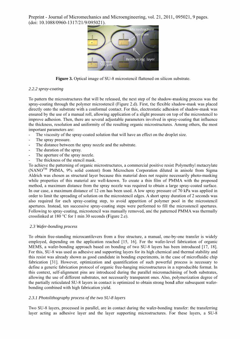
Preprint - Journal of Micromechanics and Microengineering, vol. 21, 2011, 095021, 9 pages. (doi: 10.1088/0960-1317/21/9/095021). structures will be clamped and a temporary top substrate used for structural layer patterning. Single side polished 4 inches silicon wafers with a thickness of 525 µm were used as substrates. The two substrates were cleaned by using UV-Ozone for 10 minutes to improve adhesion of subsequent deposited layers (Figure 2.a and b). These substrates were rinsed with deionized water and dehydrated at 200 °C for 2 h. On the top substrate, two thin layers of OmnicoatTM were successively spun at 1000 rpm and baked at 200 °C for 1 min that result in an omnicoat thickness of 200 nm (Figure 2.c). This layer will act as a sacrificial layer to release microstructures after transferring step. 2.2 Shadow-masking process The next step to be considered is the patterning of the structural layer on the top substrate. The present work proposes a versatile method to fabricate organic microcantilevers that does not require photo-masking of materials as currently used [9] and thence, allows patterning of most organic materials, i.e., photo- or thermosensitive ones. For this, the proposed technique combines deposition and patterning in one step thanks to spray-coating through polymer microstencils. 2.2.1 Organic microstencil fabrication Polymers are attractive materials to fabricate miniaturized microstencils for their low cost, good processability and flexibility [23-26]. Indeed, the polymer microstencil fabrication process proposed in this work requires only two photolithography steps. Also, flexible polymer microstencil can be adapted to several varieties of substrates such as flexible or non-flat ones. The process fabrication starts by the spin-coating of a 200 nm omnicoat sacrificial layer on a silicon wafer to allow the release of microstencil from substrate after fabrication. The microstencil process results from the structuration of two levels of SU-8 epoxy-based negative photoresist (SU-8® 3005 and 3050) (Figure 3). SU-8 is a suitable material for this two steps device since several layers having different thicknesses (0.5–200 µm) can be stacked-up by multiple spin-coating and UV-exposures to define high aspect ratio structures. In the present work, a first thin film of SU-8 was patterned to create apertures with high resolution. The influence of microstencil thickness was studied and chosen in order to obtain the most suitable PMMA thickness uniformity used as structural layer. For this, an 8 µm thick SU-8 layer was spun, baked at 95 °C for 3 min and UV-exposed with a dose of 150 mJ/cm2 by using a manual mask aligner (MJB4, Suss Microtec. Corp, Germany). After, the layer was post-exposure baked at 65 °C for 1min and 2 min at 95 °C. But with this thickness, microstencil handling without cracking is challenging. Thus, circular apertures characterized by a diameter of 1 mm were patterned with a 100 µm thickness of SU-8 that encircle the microstructure apertures on the thin layer, to strengthen the microstencil. This 100 µm thick layer of SU-8 was successively spun and baked at 95 °C for 45 min. Then, this layer was exposed with a dose of 250 mJ/cm2
and baked at 65 °C for 1min and 3 min at 95 °C. After, both layers were simultaneously developed with propylene-glycol-monoether-acetate (PGMEA, Microchem Corporation). A low stress microstencil was required to allow a flat and conformal contact with the substrate during the spray-coating. In fact, a gap between the microstencil and the substrate would induce a loss of resolution in the geometries of the designed microstructures. Highly cross-linked SU-8 is known to induce residual stress in the patterned films. Several sources have been identified [27, 28] including residual solvent in the polymeric matrix [27], UV exposure dose [29], heating temperature for soft [28] and post-exposure bakes [27] and induced stress due to CTE mismatch between SU-8 and the substrate [30]. This can result in buckling of polymer microstencil and thus, gap increase during deposition. An efficient solution was proposed by introducing a hard-bake at the end of the SU-8 process, reducing residual stress gradient in highly cross-linked SU-8 films [27]. The hard-bake must be adapted to the thickness layer. For our process, a hard-bake step at 150 °C for 7 min was optimal. To finish the microstencil fabrication, the substrate was dipped in the omnicoat developer (MF 319) for 2 h to release the organic microstencil.
Preprint(doi: 10
2.2.2 spr To patterspray-codirectly ensured improve the thickimportan- The - The - The - The - The - The To achie(NANOT
Aldrich while prmethod, In our caorder to also reqaperturesFollowincrosslink 2.3 Wafe To obtaiemployeMEMS, For this,this resisfabricatidefine a this contallowingthe partibonding 2.3.1 Ph Two SUlayer ac
t - Journal o0.1088/0960
Figur
ray-coating
rn the microoating througonto the subby the use o adhesion. T
kness, resolunt parametersviscosity of spray pressudistance betwduration of taperture of tthickness of
eve the patterTM PMMA, was chosen roperties of a maximum
ase, a maximlimit the spr
quired for eas. Instead, teng to spray-cked at 180 °C
fer-bonding p
in free-standed, dependin
a wafer-bon SU-8 was ust was alreadon [31]. Hogeneric fabrtext, self-ali
g the use of dally reticulatcombined w
otolithograp
U-8 layers, prcting as adh
of Microme0-1317/21/9
re 3. Optical
structures thgh the polymbstrate with aof a manual rThen, there arution and unis are: the spray-co
ure. ween the sprthe spray. the spray nozf the stencil mrning of orga9% solid cas structuralthis materia
m distance fromum distancereading of soach spray-coen successivcoating, micrC for 1 min 3
process
ding microcang on the apnding approaused as adhesdy shown as owever, optirication protognment pinsdifferent subted SU-8 lay
with high fabr
phy process o
rocessed in phesive layer
chanics and/095021).
image of SU
hat will be remer microstena conformal roll, allowingre several adformity of th
oated solution
ray nozzle an
zzle. mask. anic microstrcontent) froml layer becaual are well-kom the spraye of 12 cm holution on theoating step,
ve spray-coatrostencil was30 seconds (F
antilevers fropplication reach based onsive and supgood candidmization anocol of organs are introdubstrates, not yers in contacrication yield
of the two SU
parallel, are iand the la
d Microengi
U-8 microste
eleased, the nncil (Figure 2contact. For
g applicationdjustable parhe resulting o
n that will ha
nd the substr
ructures, a com Microcheuse this mateknown. To cy nozzle washas been usede microstenc
to avoid ating steps ws manually reFigure 2.e).
om a free streached [15, n bonding ofpporting layedate in bondind quantificanic free-hanguced during necessarily tct is optimizd.
U-8 layers
in contact duayer support
ineering, vo
encil flattened
next step of t2.d). First, ththis, electro
n of a slight prameters invoorganic micr
ave an effect
ate.
ommercial poem Corporaterial does nocreate a thins required tod. A low spracil edges. A sapparition of
were performeemoved, and
ructure, a ma16]. For thef two SU-8 lrs for its higing experimeation of suchging microstthe parallel transparent o
zed to obtain
uring the wafing microstr
ol. 21, 2011,
d on silicon s
the shadow-mhe flexible shstatic adhesi
pressure on tolved in sprarostructures.
on the dropl
ositive resistion diluted
ot require nefilm of PMobtain a lar
ay pressure ohort spray du
f polymer ped to fill the
d the patterne
anual, one-be wafer-levelayers has be
gh chemical aents, in the ch powerful tructures in amicromachi
ones. Also, pstrong bond
fer-bonding ructures. Fo
, 095021, 9
substrate.
masking prohadow-maskion of shadotop of the miay-coating thAmong othe
let size.
t Polymethylin anisole
ecessarily phMMA with thrge spray-coaof 70 kPa wauration of 2
pool in the e microstenced PMMA w
by-one transfel fabricationeen introducand thermal case of microprocess is n
a reproduciblining of bothpolymerizatiod after subseq
transfer: theor these laye
pages.
cess was thek was placedw-mask wasicrostencil tohat influenceers, the most
l metacrylatefrom Sigmaoto-maskinghe proposedated surface.as applied inseconds wasmicrostencil
cil apertures.was thermally
fer is widelyn of organicced [17, 18].stability andofluidic chipnecessary tole format. Inh substrates,on degree ofquent wafer-
e transferringers, a SU-8
e d s o e t
e a g d . n s l .
y
y c . d p o n , f -
g 8

Preprint(doi: 10photolithseveral eprocess. baked at1 min anSU-8 walayer reqperformecharacte 2.3.2 Waf Alignmetransferr31], restrmechanirequiredsupportinThese alprocess. was pattµm thickpin struc(Figure 2
Figure micro
2.3.3 Bo To allowtogether pressure transfer pressure A tempewas also
t - Journal o0.1088/0960hography proexposure doConcretely,
t 95 °C for 45nd 3 min at as spin-coatequired an oped at 65°C rized by a si
afers alignme
ent of top andring chips. Cricting fabricical self-alig
d. The self-aling layer witlignment pattConcerning
terned by phokness for jig ctures are m2.i and Figur
4. Optical imocantilever ch
onding proces
w the complin order to
and a tempewas realize of 300 kPa
erature of 110o recommend
of Microme0-1317/21/9ocess was opses were tesfor the supp
5 min. Next,95°C (Figur
ed on the botptimal UV-efor 1 min aze of 25 mm
ent: introduc
d bottom waCurrently, a Pcation proces
gnment of wignment wasth the transfeterns ensure
g alignment potolithographstructures w
mechanically re 4).
mage of tranship (coated w
s
ss
lete release transfer mierature in ordd by using was given as0 °C, that is ded by [7] du
chanics and/095021).
ptimized to ensted and studporting layer, this layer wre 2.g). The ttom wafer. Texposure dosand 4 min at
m2 were obtain
ction of mech
afers correspoPyrex top wass to the use
wafers so ths performed berring one. Tin plane self
patterns fabrhy at the sam
was patterned clipped into
sferred microwith a thin gosupport conta
of the free-icrostructureder to bond ta bonding d
s optimal valabove the gl
uring 30 min.
d Microengi
nsure their bdied before , a 100 µm t
was exposed wlayer was th
The soft-bakese of 160 m
at 95°C befoned with this
hanical self-a
onds to the aafer is used te of at least ohat any specby incorpora
The pin area f-alignment rication, firstme time as th
onto the trano the jig one
ostructures oold layer for ains four PM
-standing mis. Top and bthe supportindevice (Spelue to bond tlass transitio. In this case
ineering, vo
bonding durindetermining
thickness of with a dose ohen developee was carried
mJ/cm2. A poore developms layer.
alignment pin
accurate placto allow aligone transparecific propertiating alignme
is 25 mm2 twith an accut, a 100 µm he supportingnsferring lay
es to ensure
on 4-inches wobservation)
MMA cantilev
icrostructurebottom wafeng layer on tcac’s Atlas two SU-8 layn temperatur
e, both SU-8
ol. 21, 2011,
ng transfer. Athe optimal
SU-8 was spof 190 mJ/cmed. In paralled out at 95 °Cost-exposure
ment (figure
ns
cement of thegnment on thent wafer. In ies for the ent pin and jthat can easiuracy of 50µthickness of
g layer (Figuyer (Figure 1hself-alignme
wafer. Inset s) composed overs.
s, the aligneers were comthe transferriSeries Manuyers as showre of the partlayers becam
, 095021, 9
Among otherl SU-8 photopun on the tom2 and bakedel, a 40 µm C for 18 min
e bake was 2.f). Transf
e supporting he bottom w
this work, wsubstrates u
jig structuresily fit into ji
µm that is enof SU-8 for pure 2.f). In pah). With thisent between
shows a zoomof four suppo
ed wafers wmpressed bying one (Figual Hydraul
wn in previoutially polyme
me strongly b
pages.
r parameters,olithographyop wafer andd at 65 °C for
thickness ofn. This SU-8successively
ferring chips
layer on theafer [17, 18,
we propose aused are nots to align theg structures.ough for ourin structuresarallel, an 80 method, theboth wafers
m view on a orts. Each
were bondedy applying aure 2.i). Thelic Press). Aus work [31].erized SU-8,bonded.
, y d r f 8 y s
e , a t e . r s 0 e s
d a e A . ,

Preprint - Journal of Micromechanics and Microengineering, vol. 21, 2011, 095021, 9 pages. (doi: 10.1088/0960-1317/21/9/095021). 2.3.4 Sacrificial layer release To finish the fabrication process, the top wafer must be removed to obtain chips composed of polymer free-standing microstructures clamped on the bottom substrate obtained by collective fabrication. The omnicoat layer initially deposited was etched by using MF319 developer (Figure 2.j). The low gap between both wafers (about 150 µm) can prevent the release. Thus, to accelerate structures release, channels characterized by a width of 500µm were introduced on the transferring layer to enhance access to the sacrificial layer, reducing the release duration from 24 h to 6 h. Last, the resulting wafer, containing free-standing microcantilevers, was cleaned according to a protocol where successive batches of omnicoat developer (to remove residual omnicoat), isopropanol, ethanol and deionized water were used. Cantilevers chips were then dried using a hotplate (40 °C), ensuring rapid evaporation of water and thus, avoiding stiction of cantilevers onto the transferring layer. 3. Results and discussion 3.1 Organic microcantilevers characterization By combining shadow-masking and wafer-bonding processing methods, we have successfully achieved the fabrication of free-standing PMMA cantilevers (Figure 4 and 5) characterized by a length ranging from 100 to 700 μm and a width ranging from 50 to 250 μm. The geometries are in agreement with the design (maximum standard deviation of 2% for geometry with respect to designed mask), but the thickness profile is not uniform: the bottom surface of the cantilevers is not perfectly flat. In fact, protrusions at the microcantilever edges appear during the spray-coating through the shadow-masks (Figure 6). This effect has already been observed with other printing methods, such as screen-printing, nanoimprint or microfountain pen [32]. In our case, one origin of the phenomenon is capillary interactions that occur between the PMMA solution and SU-8 due to the wettability of anisole used as solvent for the PMMA solution [33]. To confirm this wettability effect, the SU-8 microstencil surface was made hydrophilic by submitting it to a short plasma oxygen event, resulting in the formation of PMMA clusters in the microstencil apertures after subsequent spray-coating, showing repulsive interactions between anisole and SU-8. At the moment, no concrete solution was found to avoid completely the edge effect, but the combined spray-coating/ shadow-masking process was optimized to obtain a convenient PMMA profile. For this, by using a mechanical profiler, the influence of the microstencil thickness and the solid content of the PMMA solution on the polymerized PMMA thickness profile has been studied (Figure 6.a). From this figure, it can be seen that at the center of the cantilever, the thickness is thin while at the edges it is increased, resulting in a thickness gradient with a parabolic profile. Also, the height of protrusions is defined by microstencil thickness: protrusions height increases with the microstencil thickness (Figure 6.a). A thin microstencil is thus required to limit this effect. But with a too thin SU-8 microstencil, there is not any PMMA material at the center of the structure and thus the whole microstructure surface cannot be covered. In this context, to restrict the protrusions height to a few micrometers, a microstencil characterized by a thickness of 8 µm has been used while apertures have been then filled thanks to ten successive spray-coatings. For this, a homemade polymer solution that contains 4.5 % of PMMA diluted in anisole has been used to reduce size of droplets. In this case, the thickness at the center of the cantilever is 5 μm, while at the edges it is 7.5 µm (figure 6.b). With the optimized process, the aspect ratio between the height at the edge and the height at the center of the structures was clearly reduced, since an improvement from 8.3 to 1.5 was obtained.

Preprint(doi: 10
Figure 5thicknes
Figure 6spray-coof 25 µmmicrostePMMA Scanningcoating p 3.2 Bond Using thorganic cprocesseWith thithe transthe pressallows a Temperamicrofluarea. A blower temthe SU-8bonding on the trdatashee
t - Journal o0.1088/0960
5. Scanning s of 10 μm, a
6. Profile meoating step bm and 40 µ
encil charactmicrocantile
g electron mparameters b
ding process
he wafer-boncantilevers o
es since a fabs method, th
sferring layersure that encrosslinking
ature and pruidic chips [3bonding tempmperature co8 crosslinkinprocess. The
ransfer qualiet. Figure 7 s
of Microme0-1317/21/9
electron mia length of 5
easurement by using PMM
µm. (b) Canterized by a ever fabrica
microscopy (by using micr
characteriza
nding methodon 4-inches wbrication yielhe transfer rers to ensure sures contacg reaction beressure have34, 31]. Obta
mperature of 1ould be interng level, resuence, it is paity. For this, shows the bo
chanics and/095021).
icroscopy (S20 μm and a
before transfMA commer
ntilever fabrithickness of
ated with a SEM) imagerostencil cha
ation
d, we have awafers. The tld of 100% wequires a SUtheir bondin
ct between latween both s
e already beained results 110 °C is genresting if the ulting mainlyarticularly im
the exposuronded area a
d Microengi
SEM) imagea width of 10
fer of PMMrcial solutionicated with of 8 µm. (c) microstenci
e of PMMAaracterized by
achieved the transferring
was obtained U-8 crosslinkng. This reactayers, the tesurfaces in coeen investigrecommend
nerally usede structural my from UV-e
mportant to inre dose was and the bond
ineering, vo
e of PMMA 00 μm.
A cantilevern and microsoptimal spraScanning ell characteriz
A microcantily a thickness
large scale technique is(figure 4).
king surface rtion results femperature aontact.
gated in prevd a pressure od [7] that is cmaterial is noexposure dosnvestigate thvaried aroun
d strength for
ol. 21, 2011,
microcantil
rs (a) Cantilestencils charay-coating pectron microzed by a thlever fabricas of 8 µm.
fabrication o suitable for
reaction betwfrom associatand the SU-8
vious worksof 300 kPa tocompatible wot resistant atse, is also a e influence ond the valuer several UV
, 095021, 9
lever charact
ever fabricatracterized byparameters anoscopy (SEMhickness of ated with op
of clamped fr integration
ween the suption of three8 crosslinkin
s for the fato obtain optwith PMMA.t 110 °C [34critical paraof the UV-exe recommendV-exposure d
pages.
terized by a
ted with oney thicknessesnd by usingM) image of40 µm. (d)
ptimal spray-
free-standingin industrial
pporting ande parameters:ng level that
abrication ofimal bonded However, a]. Moreover,
ameter in thexposure doseded by SU-8doses applied
a
e s g f ) -
g l
d : t
f d a , e e 8 d

Preprint(doi: 10to the trlayer. UVcontact. a high yiSU-8 theDage 20strength this casesupportinbond, a dto be optUsing laoccur throbustnebondinglayer duoptimal To summstrong borespectivlayers isSU-8 layprocess h
Figure
Figure 8
t - Journal o0.1088/0960ransferring laV-exposure dFrom figure ield was assoermal polym000 shear stvalue aroun
e, the exposung layer belodose of 160 timal, since iayers with lohat damages ess, inducing. Figure 8.a
ue to too lowexposure domarize, to imond and a limvely the transs avoided befyers are nevhas been thu
7. Bonded ar
8. Scanning
of Microme0-1317/21/9ayer and thedoses were th7, it can be
ociated to a lmerization dur
ation. Resulnd 10 MPa isure dose forow 270 mJ/cmJ/cm2 for t
it correspondow crosslinkthe patterne
g a possible shows the s
w UV-exposuses, a clean amprove the wmited reflow,sferring and fore transfer vertheless po
us optimized
rea and bond
electron mi
chanics and/095021).
e supporting hus chosen iseen that thelow crosslinkring the translts confirm ts recommendr the transfercm2. Howevthe transferrids to a bond sking levels dud layers. In damage of
spreading of ure doses thaand strong bowafer-bondin, the optimalthe supportithat ensures
olymerized eto standardiz
d strength ve
croscopy (SE
d Microengi
one. The Uin order to hae bond area dking level of sfer. Also, ththat the bonded to ensurrring layer m
ver, to obtaining layer andstrength of 5
during the bofact, a decrethe structureSU-8 transf
at are respectond occurs bng process bl UV-exposuing layers. Ws a strong adenough to pze large-scal
ersus UV explayer.
EM) image
ineering, vo
UV-exposure ave the samedecreases witf SU-8 layershe bond strennd strength ire strong bonmust be belo
n a maximumd 190 mJ/cm
50 MPa. onding proceease of crosses under theferring layer tively 80 andbetween the tbased on SUre doses mus
With these valdhesion of boprevent theire microfabri
posure doses
of SU-8 tran
ol. 21, 2011,
dose is defie crosslinkingth dose incres before transngth has beenis high for and between tow 240 mJ/c
m bonded arem2 for the sup
ess, a reflowslinking levee pressure anand the flatt
d 110 mJ/cmtwo SU-8 lay
U-8, with a bst be 160 mJ/lues, the oveonded layersr damage (Fcation of org
of SU-8 sup
nsferring an
, 095021, 9
ined by thickg level for b
ement. This insfer that allown investigatea low expostwo SU-8 laycm2 and the ea of 100% pporting one
w of the SU-el causes a lnd temperatuttening of the
m2. On the coyers (figure 8bonded area J/cm2 and 190erly level of s during the Figure 8.b). Tganic microc
pporting and
nd transferred
pages.
kness of theoth layers inndicates thatws complete
ed by using asure dose. Ayers [31]. Inone for the
and a stronge were found
8 layers canloss of SU-8ure used fore supportingontrary, with8.b).
of 100%, a0 mJ/cm2 forpolymerizedtransfer. ButThe transferantilevers.
transferring
d supporting
e n t e a A n e g d
n 8 r g h
a r d t r
g

Preprint(doi: 10layers fo 3.3 Preli To confimeasurebending modulus In this emode, Ldensity charactekHz wasdemonststandardcharacteA simila[10]. Vaobtainedother woobtainedmechani
Figure 9transferrof 8 μm, 4. Concl A versamicrostrushadow-photosenthrough Moreovesecond aas microhave a faseveral pPMMA bonding mechani
E= 4π2
t - Journal o0.1088/0960or respectivel
iminary mech
irm the potenment of meresonant m
s of the struct
equation, E rL and h are r
of the materized by a les measured ftrate the versd photolithogrized by a le
ar method walues obtained in present orks [27, 36d show a gical deflectio
9. Scanning red SU-8 mic, a length of
lusion
atile all-orgaructures was-masking andnsitive polym
a flexible er, introductiapproach is pocantilevers, fabrication yipatterning mmicrocantileapproach, S
ical character
fn 2 L4 12ρ
λn4 h2
of Microme0-1317/21/9ly (a) UV-ex
hanical char
ntial of such chanical pro
modes were stured layer w
represents threspectively erial, and λength of 200for the first fsatility of thegraphy. A reength of 490
was already ped ranged frowork are in ], validating
great potentions for a vari
electron microcantilever640 μm and
anic processi proposed. Td wafer-bonmer materiamicrostenci
ion of polymparticularly abridges, or mield of 100 %ethods such
evers have bSU-8 microcrization of re
chanics and/095021). posure doses
racterization
organic micoperties of thstudied usinwas then calc
he cantileverthe length a
n the eigenvµm and an
flexural mode transferringesonance freµm and a th
proposed for om 3.5 GPa
agreement the methodial for thesety of applic
icroscopy (Srs. (b) Zooma width of 14
ing method This method
nding. The fials. This mel. Thereby,
mers in microsadapted for imicrochannel% with a bonas photolithoeen successf
cantilevers wesulting PMM
(1)
d Microengi
s of 80 and 1
n.
crocantileverhe patterned
ng a laser Dculated thank
r Young’s mand thicknesvalue of theaverage thic
de, giving a Yg process, SUequency of hickness of 8r the determia and 4.5 GPwith those p
d for both PMse organic fcations, inclu
SEM) image m view of SU
40 μm.
for the lard results frofirst approachethod consis
deposition stencil fabricindustrial intls. Indeed, thnd strength oography and fully obtaine
were fabricateMA and SU-
ineering, vo
110 mJ/cm2 a
s as flexible d structural loppler vibro
ks to equation
modulus, fn isss of the mie nth resonackness of 16 Young’s modU-8 cantilev10.7 kHz w
8 µm, givingination of YoPa, dependinpreviously dMMA and Sfree-standing
uding chemic
of SU-8 miU-8 microcan
rge scale fam the assoch is coheren
sts in the spand pattern
cation makestegration of ohe process traof 50 MPa. Ananoimprint
ed. Then, to ed using stan-8 cantilevers
ol. 21, 2011,
and (b) 160 a
devices, thelayer. For thometer (Polyn (1) [35]:
s the resonancrocantilevernce mode. µm, a reson
dulus value overs (Figure 9was obtained a Young’s moung’s modu
ng on the thidescribed [10SU-8 materiag microcantcal sensing in
icrocantileventilevers char
abrication ofciation of twnt for the papray-coating ning were ps this processopen microstansfer has beAlso, this meting. By comconfirm the ndard photols are in agree
, 095021, 9
and 190 mJ/c
e next step cohis, out-of-plytec MSA50
nce frequencr, ρ represenFor PMMA
nance frequenof 3.7±0.5 G9) were fabr
d for a SU-modulus of 4ulus of SU-8ickness of S0] and thoseals. Also, thetilevers to on static mode
ers. (a) Generacterized by
f free-standiwo different atterning of
of the struperformed ins simple at lotructure fabreen optimizeethod is com
mbining bothversatility olithography. ement with t
pages.
cm2 .
oncerned thelane flexural00); Young’s
cy of the nth
nts the massA cantileversncy of 122.8
GPa. Also, toricated using8 cantilever
4.0±0.5 GPa.8 cantileversSU-8. Values
obtained ine low valuesobtain largee.
eral view ofy a thickness
ing polymerapproaches:thermo and
uctural layern one step.ow-cost. Therication suched in order tompatible with
approaches,of the wafer-
Preliminarythe literature
e l s
h s s 8 o g r . s s n s e
f s
r : d r . e h o h , -y e

Preprint - Journal of Micromechanics and Microengineering, vol. 21, 2011, 095021, 9 pages. (doi: 10.1088/0960-1317/21/9/095021). values. These organic cantilevers, characterized by a low Young’s modulus, have the potential to serve as highly sensitive transducing devices in biological and chemical sensing applications. Indeed, for a 200μm long bi-layered cantilever, the static deflection due to swelling effects in an organic sensitive layer will be thirty times higher when using these organic materials instead of silicon (theoretical calculation using a modified Stoney equation [37]). Based on this approach, work is now in progress for the development of tuned Young’s modulus organic materials for highly sensitive biological and chemical sensing applications in static mode. References
[1] Burg T P, Mirza A R, Milovic N, Tsau C H, Popescu G A, Foster J S and Manalis S R 2002, J. Microelectromech. Syst. 15 1466-1476
[2] Burg T P, Godin M, Knudsen S M, Shen W, Carlson G, Foster J S, Babcock K, and Manalis S R 2007 Nature 446 1066-1069
[3] Hwang K S, Lee S M, Eom K, Lee J H, Lee Y S, Park J H, Yoon D S, and Kim T S 2007 Biosensors and Bioelectronics 23 459-465
[4] Kim S J, Onob T and Esashi M, 2007 J. Appl. Phys. 102 104-304
[5] Van Oosten C L, Cees W. Bastiaansen M and Broer J D 2009 Nature Materials 8 677- 682
[6] Matyjaszewski K 2005 Prog. Polym. Sci. 30 858
[7] Agirregabiria M, Blanco F J, Berganzo J, Arroyo M T, Fullaondo A, Mayoraa K and Ruano-Lopez J M 2005 Lab on a chip 5 545–552
[8] Seena V, Rajorya A , Pan P, Mukherji S, Ramgopal Rao V, 2009, Solid State Sciences 11 1606-1611
[9] Abgrall P, Conedera V, Camon H, Gue A M and Nguyen N T 2007 Electrophoresis 28 4539-4551
[10] Ezkerra A, Fernandez L J, Mayora K and Ruano-Lopez J M 2007 J. Micromech. Microeng. 17 2264-2271
[11] Bhusari D, Reed H. A, Wedlake M, Padovani A M and al. 2001 J. Microelectromech. Syst. 10 400-408
[12] Oh K W and Ahn C H 2006 J. Micromech. Microeng. 16 R13-39
[13] Chung C and Allen M 2005 J. Micromech. Microeng. 15 N1–N5
[14] Dubourg G, Fadel-Taris L, Dufour I, Pellet C and Ayela C 2010 Proceedings of the MNE conference (Micro and Nano Engineering) Ginoa, Italy
[15] Johansson A, Blagoi G and Boisen A 2006 Appl. Phys. Lett. 89 173505
[16] Greve A, Keller S, Vig A L, Kristensen A, Larsson D, Yvind K, Hvam J M, Cerruti M, Majumdar A and Boisen A 2010 J. Micromech. Microeng. 20 009015
[17] Nordström M, Calleja M, Hübner J and Boisen A, 2008 J. Micromech. Microeng. 18 015017
[18] Murillo G, Davis Z J, Keller S, Abadal G, Agusti J, Cagliani A, Noeth N, Boisen A and Barniol N 2010 Microelec. Eng. 87 1173-1176

Preprint - Journal of Micromechanics and Microengineering, vol. 21, 2011, 095021, 9 pages. (doi: 10.1088/0960-1317/21/9/095021). [19] Guillon S, Saya D, Mazenq L, Perisanu S, Vincent P, Lazarus A, Thomas O and Nicu L 2011
Nanotechnology 22 245501
[20] Fadel-Taris L, Ayela C, Josse F, Heinrich S, Brand O, Saya D and Dufour I 2011, Proceedings of IEEE International Frequency Control Symposium San Francisco, USA
[21] Selvarasah S, Chao S H, Chen C L, Sridhar S , Busnaina A , Khademhosseini A and Dokmeci M R 2008 Sensors and Actuators A 145–146 306-315
[22] Sidler K, Cvetkovic N V, Savu V, Tsamados D, Ionescu A M and Brugger J 2009 Procedia chemistry 1 762
[23] Kim G, Kim B and Brugger J 2003 Sensors and Actuators A 107 132-136
[24] Choi J H and Kim G M 2011 International J. Precision engineer. And Manufacturing 12 165-168
[25] Atsuta K, Suzuki H and Takeuchi S 2004 Proceedings of the 8th International Conference on Miniaturized Systems for Chemistry and Life Sciences, Malmo, Sweden
[26] Pal R, Sung K E and Burns M A 2006 Langmuir 22, 5391-5397
[27] Keller S, Haefliger D and Boisen A 2010 J. Micromech. Microeng. 20 045024
[28] Anhoj T A, Jorgensen A M, Zauner D A and Hubner J 2006 J. Micromech. Microeng. 16 1819
[29] Lee K Y, LaBiance N, Rishton S A, Zolgharnain S, Gelorme J D, Shaw J and Chang T H P 1995, J. Vac. Sci. Technol. B 13 3012
[30] Keller S, Blagoi G, Lillemose M, Haelfiger D and Boisen A 2008 J. Micromech. Microeng. 18 125020
[31] Blanco F J, Agirregabiria M, Garcia J, Berganzo J, Tijero M, Arroyo M T, Ruano J M, Aramburu I and Mayora K 2004 J. Micromech. Microeng. 14 1047-1056.
[32] Gilles S, Matthias Meier M, Prömpers M, Van der Hart A, Kügeler C, Offenhäusser A and Mayer D 2009 Microelectronic Engineering 86 661–664
[33] Low H L, Dumond J, Chong K, Yamamoto K and Amamiya S 2010 United States Patent Application Publication US2010/0291723 A1
[34] Pang C, Zhao Z, Du L and Fang Z 2008 Sensors and Actuators A 147 672–676
[35] Blevins R D 1979 Robert E Kieger Publihing Compagny
[36] Ferrell N and Hansford D 2005 Journal of vacuum science and technology 23 811-819
[37] Wenzel M J, Josse F, Heinrich S M, Yaz E and Datskos P G 2008 J. Appl. Phys. 103, 064913