Software, silicon chips and structured lighting for image ...
220
Software, Silicon Chips and Structured Lighting for Image Processing A thesis presented for the degree of Doctor of Philosophy in the Department of Electrical and Electronic Engineering at the University of Canterbury by M.J. Naylor B.E.(Hons) 1990
-
Upload
khangminh22 -
Category
Documents
-
view
1 -
download
0
Transcript of Software, silicon chips and structured lighting for image ...

Software,
Silicon Chips and
Structured Lighting
for Image Processing
A thesis presented for the degree
of
Doctor of Philosophy
in the
Department of Electrical and
Electronic Engineering
at the
University of Canterbury
by
M.J. Naylor B.E.(Hons)
1990

( </ q , I
A stract
This thesis describes three projects, each of which addresses a limitation of current
image processing technology. The projects comprise the development of software that
provides a user friendly means of manipulating images on an interactive image pro
cessing system; the design of a prototype integrated circuit, and the subsequent design
of a set of integrated circuits that perform rank filtering; and a way in which lighting
can be used to rapidly acquire three dimensional information from a scene. These
projects address the need for an easy to use image processing system, the need for a
high speed means of filtering images, and the need in robotics applications for rapid
three dimensional image acquisition. Conclusions are drawn from these developments,
and suggestions are made for future work.

Cont nts
Abstract
Contents
List of Figures
List of Tables
Acknowledgements
1 Introduction
2 Advanced Software Written for Interactive Image Processing Sys
tems
2.1 Introduction.
2.2 An Introduction to HIPS and iRMX86
.. II
VB
. IX
X
1
8
8
9
2.3 The LET Command - An Equation Parser for the Serendip Command
Language on HIPS . . . . . . . . . . . . . . . . . . . . . . . . . . . .. 11
2.3.1 Introduction.................
2.3.2 The Specification for the LET Command.
2.3.3 The Development of the LET Command
2.3.4 The New LET Command ....... .
2.3.5 The Definition of a Syntax for LET Expressions
2.3.6 The LET Program
2.3.7 Discussion... ..
2.4 CLEAN - A Rou tine to Sort iRMX86 Directories
2.5 DIRTREE - A Program to List iRMX86 Directory Trees
11
11
12
14
15
18
20
24
24
26

2.6 A HIPS Utility for Transferring Files Over a Serial Link. 27
2.6.1 Introduction . . . . . . . . . 27
2.6.2 A Description of KERMIT . 28
2.6.3 How the HIPS Version of KERMIT is Used 28
2.6.4 The Modules that Constitute HIPS KERMIT 32
2.7 Conclusion . . . . . . . . . . . . . . . . . . . . . . . . 34
3 Architectural Considerations for the Prototype Rank and Range Fil-
ter 35
3.1 Introduction . . . . . . . . . . . . . . . . . . . . . . . . . . . . . . . . . 35
3.1.1 The Reason for Building the Rank and Range Filter as an Inte-
grated Circuit . . . . . . . . . . . . . . . . . . . . . . . . .. 36
3.2 Global Architectural Considerations for the Rank and Range Filter 38
3.3 Obtaining the Windowed Values from the Image. 41
3.3.1 A Pipelined Windowing Technique 42
3.3.2 Windowing Images of Variable Size 43
3.4 Determining the Rank '"' .. " .. .. . .. .. 45
3.4.1 Bit-wise Rank Determination 45
3.4.2 An Approach Using Merge Sorting 46
3.4.3 Histogram Method ....... 48
3.4.4 Threshold Decomposition 48
3.4.5 Bitonic Sorting . . . .. .. .. 49
3.4.6 Odd Even Transposition Sorting . 50
3.4.7 The Approach Used ........ 52
3.5 Specifications for a Prototype Rank and Range Filter Chip 52
4 The Design of the Prototype Rank and Range Filter Chip 55
4.1 Introduction . . . . . . . . . . . . . . . 55
4.1.1 The NMOS fabrication process 55
4.1.2 Fabrication versus design . 57
4.1.3 The design cycle .. .. .. .. ... 58
4.2 Computer Aided Design Tools Used in the Prototype Chip Design 61
III

4.3
4.4
4.5
4.2.1 Imported Design Software
4.2.2 In-House Design Software
Circuit Description of the Prototype Chip
4.3.1 The Variable Length Shift Register
4.3.2 The Window
4.3.3 The Sorter ..
4.3.4 The Dual Channel Rank Selector
4.3.5 Clocking Circuitry . . . . Operation of the Prototype Chip
Testing the Prototype Chip
4.5.1 The Test Jig. . . . .
4.6 Using the Prototype Chip in Image Processing .
5 A Chip Set for a Bit-Serial Rank and Range Filter
5.1 Introduction ...................... .
5.2 A Chip Set Implementation of the Rank and Range Filter
61
64
65
65
67
69
71
73
75
77
77
80
82
82
82
5.3 Improvements to the Suite of Integrated Circuit Design Software. 86
5.4 The Bit-Serial Rank and Range Filter Chip
5.4.1 The Sorter ..
5.4.2 The Selector .
5.4.3 The Rank Select Latches .
5.4.4 Reset Logic . . . . .
5.4.5 The Clocking Logic .
5.4.6 Floorplan Considerations .
88
88
92
93
94
95
96
5.4.7 Operating and Testing the Bit-Serial Rank and Range Filter Chip 97
5.4.8 Simulation and Test Results . . . . . .
6 An Overview of Range Mapping Techniques
6.1 Introduction.................
6.2 Passive Optical Range Finding Techniques
6.3 Active Optical Range Finding Techniques
6.3.1 Active Stereoscopy ........ .
IV
99
101
101
103
105
106

6.3.2 Time of Flight Techniques
6.3.3 Triangulation Methods ..
6.3.4 Structured Lighting Approach
6.3.5 Moire Fringe Techniques
6.4 Discussion ........... .
106
108
114
119
120
7 Grey Scale Ranging - A Real Time Range Mapping Technique 122
7.1 Introduction............. 122
7.2 Description of Grey Scale Ranging
7.3 Determination of the Patterns Used.
7.4 A Look at Some of the Assumptions Made
7.5 Determination of Accuracy . . . . . . .
7.6 What Grey Scale Ranging Cannot Do .
7.7 Experimental Grey Scale Ranging Results
7.8 Conclusion ................. .
8 Conclusions and Suggestions for Future Work
8.1 Software for Image Processing ....
8.2 Improvements to the LET Command
8.3 KERMIT and its Implications
8.4 Chips for Image Processing.
8.5 Ideas for Future Chips ...
8.6 Three Dimensional Imaging
8.7 Improving the Grey Scale Ranging Technique
8.8 Suggestions for Further Range Mapping Research
8.9 Conclusion .
References
Appendices
A Summary of the KERMIT File Transfer Protocol
A.I Introduction. . . . . . . . . . . ....... .
A.2 The Format of the Packets Used by KERMIT
v
122
124
129
132
134
136
138
140
140
142
144
144
146
148
149
150
150
152
165
166
166
166

A.3 The Packet Handling Protocol Used by KERMIT ............ 166
B Description of the Prototype Rank and Range Filter Chip and Eval-
uation Board
B.l Introduction.
B.2 Description of the Integrated Circuit
B.3 The Prototype Rank Filter Evaluation Board
174
174
174
180
C Description of the BISERF Chip and an Evaluation Board for the
Bit Serial Rank and Range Filter Chip Set 184
C.1 Introduction. . . . . . . 184
C.2 Description of BISERF . 184
C.3 The Bit-Serial Rank and Range Filter Chip Set Evaluation Board 189
. VI

ist of ill
19ures
3.1 Operation of a rank filter employing a nine element square window 36
3.2 Operation of a pipelined window employing a shift register 43
3.3 Operation of Danielsson's variable length shift register 44
3.4 Operation of a five element, systolic array, merge sorter 47
3.5 A bitonic sorter for eight elements. . . . . . . . . . 50
3.6 An odd-even transposition sorter for eight elements 51
3.7 Block diagram of the circuit for the rank and range filter 54
4.1 The design cycle for integrated circuit design. 59
4.2 The multiplexer cell circuit. . . . . . . . . . . 66
4.3 Block diagram of the variable length shift register 67
4.4 Block diagram of the window 68
4.5 Circuit diagram of the window . 69
4.6 Circuit diagram of one bit of a four-bit comparator 70
4.7 Circuit diagram of one bit of one switch of the rank selector 72
4.8 Block diagram of the dual channel rank selector 73
4.9 Block diagram of the clock distribution scheme. 75
4.10 Circuit diagram of a cross-coupled clock driver pair 76
4.11 Noise suppression using the rank filter board .... 81
5.1 Multi-chip partitioning for the eight-bit wide rank and range filter 83
5.2 Architecture of the bit-serial rank and range filter chip set 85
5.3 Architecture of the bit-serial rank and range filter chip 89
5.4 Moore diagram for the comparator cell 90
5.5 Circuit diagram of the comparator cell 91
Vll

5.6 Circuit diagram of the selector cell
5.7 Moore diagram for the reset circuitry
5.8 Floorplan of the bit-serial rank and range filter chip
6.1 The principle of triangulation ....
6.2 Light stripe ranging using a conveyor
6.3 The use of an LCD to project patterns onto a scene
6.4 Setup for range mapping using grid coding . . . . . .
93
95
97
109
111
112
116
6.5 Determining the orientation of a plane from grid element distortion 118
7.1 The principle of triangulation . . . . . . . . . . . . . . . . . . . 123
7.2 Determination of the patterns for parallel ray grey scale ranging 125
7.3 Determination of the patterns for diverging ray grey scale ranging
7.4 Some of the distortions that can be removed by normalisation
7.5 Range ambiguity due to spatial resolution of the patterns.
7.6 Multiple illumination paths in a concave scene . . . . .
7.7 The object used to test the grey scale ranging method.
7.8 Experimental setup for grey scale ranging. . . . .
7.9 Range map of the test scene before normalisation
B.1 Prototype rank and range filter board.
B.2 Prototype chip pinouts . . . . .
C.1 DMA circuit for BISERF board
C.2 Custom chip interconnections for BISERF board.
C.3 Custom chip pinouts for BISERF board .....
Vlll
128
131
132
135
137
138
139
182
183
194
195
196

Li f Tables
2.1 Microsyntax for the LET command .
2.2 Macrosyntax for the LET command.
2.3 A Summary of the Commands Available in HIPS KERMIT.
4.1 Functionality of the rank and range filter chips supplied.
A.l The format of each packet sent by KERMIT ..... .
A.2 The format of each packet sent by KERMIT continued
A.3 KERMIT state flow table ..... .
A.4 KERMIT state flow table continued .
A.5 KERMIT state flow table continued .
A.6 KERMIT state flow table continued .
B.l RAFI pin functions ..... .
B.2 RAFI pin functions continued
B.3 RAFI pin functions continued
B.4 RAFI pin functions continued
C.1 BISERF pin functions ....
C.2 BISERF pin functions continued.
C.3 BISERF pin functions continued.
IX
19
21
29
79
167
168
170
171
172
173
175
176
177
178
186
187
188

cknowledge nts
I would like to convey my sincere thanks to the following people for their support
during the course of this work.
• Dr. R.M. Hodgson l for his unfailing support, endless enthusiasm and help
ful comments as my supervisor.
• Mr L.N.M. Edward for his useful suggestions and willingness to assist with
technical problems. Mr Edward is solely responsible for the integrated
circuit design facilities at the university.
• The staff and post-graduate students of the department for their friend
ship and constructive comments. In particular, Mr M.J. Cusdin for his
hardware and software expertise in maintaining the department's High
Resolution Image Processing System; Mr A.R. Cox for his software skills,
and his help with the KERMIT program; and Miss D.J. Robertson for her
meticulous work in wire-wrapping the prototype and bit-serial rank and
range filter boards. Also, Mr J.C. Wilson and Mr S.J. McNeill for their
suggestions regarding the development of software on the High Resolution
Image Processing System; Mr D.G. Bailey for his helpful comments, and
his proposal for an integrated circuit implementation of the rank filter; Mr
A.L.M. Ng for his part as co-designer of the prototype rank and range filter
chip; Mr S.D. MacKenzie and Mr R.D. Clarke for their contributions to
the bit-serial rank and range filter chip set; and Mr R.F. Browne, and Mr
W.K. Kennedy for many fruitful discussions. 2
1 Dr. Hodgson has since been appointed Professor of Information Engineering a.t Massey University.
2Me.ssers Wilson, McNeill, Bailey and Browne ha.ve since ha.d their PhD degrees conferred.
x

• The students who worked on final year projects under my joint supervision.
These included Mr M.G. Feickert and Mr J.B. Purdey who worked on the
Fourier analysis of images of grid coded scenes; Mr A. Ling who worked on
the geometrical analysis of images of grid coded scenes; and Mr R. McKay,
Mr J. Van den Broek, and Mr W.P. Vickery, who worked on hardware and
software for an LCD projection system.
II Austek Microsystems and Mr P.D. Crawley for their assistance in the com
pletion of this thesis.
• My friends, for their understanding and support.
• My parents and sister, for their love, patience, and encouragement, without
which this thesis would not have been possible .
. Xl

Chapter
Introductio
Far from being expensive tools that were only to be found in well-funded research
establishments, computers and computerised machines are now commonplace. They
are used in applications ranging from children's toys, domestic appliances, and other
consumer goods to desk-top publishing systems, process controllers and industrial
parts handlers. Even in the street, computerised machines such as phone boxes capable
of charging the correct tariffs for international calls, automatic teller machines that
provide banking services 24 hours a day, and petrol pumps that issue precise amounts
of petrol are now familiar sights. Yet, the computer is not present everywhere, cannot
do everything, and there are many tasks still performed better by humans. Why is this
so? What limits the application of computerised machines to tasks? How can these
limitations be overcome? To answer these questions, it is useful to see what computers
and computerised machines currently do well, what they do poorly, and why. This
will illustrate the importance of image processing, and highlight its deficiencies. The
work described in this thesis addresses some of these deficiencies.
Consider a modern assembly plant for cars. A factory produces hundreds of copies
of one product so similar that parts can be swapped between them. This requires
precision machining to produce the parts, and accurate placement to position and
assemble the parts correctly. However, since each copy of a part is machined the same
way, the sequence of operations can be programmed into a numerically controlled
machine that repeatedly cycles through the sequence. Many other tasks such as spray
painting, seam welding, and some assembly work are also well defined and repetitive,
and can be performed by robots following pre-programmed command sequences. For
1

this reason, computer controlled machinery is being widely used in car assembly plants.
By contrast, the processing of primary produce, such as meat, fruit and timber,
involves tasks that are not easily automated. For example, gutting and skinning a
carcass requires human intervention to guide the process for the different shapes and
sizes of carcass. In the same way, skilled labour is required to pick and sort fruit
without damaging it. In each case, it is necessary to analyse the situation, and act
according to the results of the analysis. The tasks are therefore non-repetitive, and
automation is both difficult and unreliable.
Computers and computerised machines are also prevalent in offices and the home.
At the office, high quality documents are quickly produced on desk-top computers, and
rapidly disseminated to overseas destinations through computer networks, or computer
controlled facsimile machines. High speed lifts that record and seek the desired desti
nations of several passengers are common-place, and salaries can now be direct credited
to employees bank accounts - all under computer control. At home, video recorders
automatically record broadcasts while the owners are elsewhere, and microwave ovens
perform pre-programmed cycles as they defrost, and then cook the roast for tea. Again,
however, there are areas' that computers have not penetrated. Word processors still
use keyboard entry, since computers are unable to reliably interpret either spoken or
written messages, and household chores such as cleaning still require human effort.
It is evident that current machines and robots are well suited to performing repet
itive tasks with high precision. They are also capable of performing these tasks in
environments that are unpleasant or unsuitable for humans, such as in the extreme
pressures of deep sea, or the hostile environment of deep space. However, non-repetitive
tasks are not easily automated.
One difficulty in automating manual tasks is that the environment is likely to
have been tailored to suit humans, and may therefore be unsuitable for computerised
machinery. For example, it is difficult to automate the process of driving a car because
the road markings, road signs and traffic lights are designed to be interpreted by
humans. There are two possibilities for bridging this gap between the environment that
humans have adapted for themselves, and the environment that current computerised
machines are capable of working in; One is to adapt the environment to suit the
machine, and the other is to adapt the machine to mimic humans.
2

Good examples of the adaptation of the environment to the machine are automatic
factories in which work pieces are transported under computerised control from one
machine to another as they are shaped and assembled. Typically, each machine has a
receiving bay in which a trolley can park in a known position, so that the machine can
acquire parts or materials from the trolley and return completed parts to it. Buried
cables in the floor of the factory identify 'roads' that the self-powered trolleys can then
follow when seeking the next machine. Being under computer control, there is little
need for human intervention.
In many situations, machinery must work alongside humans, so the environment
cannot be adapted to ideally suit the machine. Under these circumstances, if the tasks
are non-repetitive, the machines need human attributes to perform well. In particular,
they need the information that humans receive through listening, touching, tasting,
smelling, and seeing. With this information, an ability to think, and an ability to act,
computerised machines would be able to do almost all the chores currently performed
by humans. However, each of these attributes is difficult to mimic in a machine, and
despite much research, developments in these areas are still in their infancy.
Of the five senses, sight is one of the most useful for operating in the environ
ment that humans operate in. The fact that much of the human brain is devoted
to processing information received by the eyes is strong evidence of this. However,
the remaining senses would provide useful input to an autonomous robot also. Taste,
for example, would be useful in the quality control of food, and touch would permit
controlled gripping of hard, soft, or slippery objects, as well as temperature sensing.
Advanced warning of fire or gas leaks, could be achieved if the machine could smell,
and if it could hear, it may be able to accept spoken commands, or detect the grating
of gears in a machine in need of service. However, sight allows far more diversity. It
has the potential to allow a robot to roam freely without colliding with obstacles or
stumbling over uneven terrain; to navigate by identifying and seeking landmarks; to
locate, acquire, and assemble objects; to inspect products for imperfections; and ·to
grade objects by size or shape. It would also be possible for the machine to recognise
when an object is mis-placed or mis-orientated, and to take corrective action.
Machine vision, a branch of image processing, therefore has tremendous potential
to widen the scope of applicability of computer controlled machines. Much research
3

has been done in image processing in the last decade, but despite the development of
many practical systems to solve particular problems, a single system capable of solving
any problem that the human visual system can solve, has not yet been created. It is not
difficult to see why, when one realizes the limitations that current technology imposes
on practical systems. To mimic human vision, it would be necessary to have an image
sensor with 100 million light-sensitive elements, and the processing and reasoning
power of the human brain. However, many currently available image sensors have
no more than 256 thousand elements, and the image data is processed by computers
that are far less capable than the brain. Getting such a system to understand what
is in the image, and use that knowledge to extract relevant information to solve any
particular problem is therefore difficult. The practical systems that do exist, have
relied on simplifying the problem to levels that are achievable with current technology.
One approach is specialisation, where the system is only required to understand
a limited variety of images. This simplifies the problem since it removes the necessity
of differentiating between similar scenes if it is known that many of these scenes will
never occur in the application. This approach has been used in industry to recognise
and determine the orientation of parts, where the number of possible parts is limited.
Since only a few parts exist, they can be uniquely and quickly identified by the number
of holes in them, the area of their silhouettes, or by other quickly found features.
Another option is to process the image to enhance, rather than identify, features
in the image. A human operator can then make decisions based on the enhanced
image. This technique is common in the medical field to enhance X-ray photographs
and Computer Assisted Tomography (CAT) scans. A simple example is to map image
intensity to colour so that subtle differences in image intensity are more detectable by
an observer. In these situations, the image processing system is used as a tool, rather
than as a complete diagnostics package.
To experiment with these approaches, or to develop new algorithms to perform a
task, it is essential to have a good general purpose image processing system. Such a
system would perform image capture, allow the images to be processed by the software
being developed, and display the resultant image so that the effects of the processing
can be observed. However, such a system made with current technology would be slow
and may not be suitable where high speed image processing is required.
4

When a general purpose image processing system is used, factors such as the size
of the image in terms of the computer memory required, the processing speed of the
host computer, and the amount of code that the computer must run to process an
image, determine the speed at which the image can be processed. On such a system,
a functionally correct algorithm may not run quickly enough for the application. To
overcome these problems, machine vision systems have made use of contrived lighting
and dedicated hardware. Contrived lighting simplifies the processing task by present
ing only relevant information to the sensor, while dedicated hardware can be optimised
to perform a particular task quickly. Again, both techniques rely on specialisation for
success.
It is evident that significant technological advances will need to be made before
machine vision systems approach the versatility of the human visual system, and
thereby give machines a useful degree of autonomy. The research performed by the
author, and described in this thesis, represents contributions to three areas of image
processing. These include the development of software for interacti ve image processing,
the design of two integrated circuits and support hardware for rapid image filtering,
and a contrived lighting technique for obtaining three dimensional information from a
scene.
Chapter 2 describes programs written for the various interactive image processing
systems used in the Electrical and Electronic Engineering department of the University
of Canterbury. The most ambitious of these was the LET command, which was written
to fulfill a need for a user friendly means of manipulating images and other variables
on the High Resolution Image Processing System [McNeill 1987]. With the inclusion
of this program, the system now operates as a powerful tool for the development of
image processing algorithms.
Chapters 3 to 5 describe the development of dedicated hardware for the High
Resolution Image Processing System. The hardware is in the form of two integrated
circuits that were designed by the author to perform rank and range filtering at high
speed. The need for such hardware arose from the requirements of the kiwifruit in
spection project [Hodgson 1986]. Chapter 3 describes the approaches to rank filtering
that were considered when designing the chips, while chapters 4 and 5 describe the
prototype and bit-serial rank filter chips respectively.
5

The remaining chapters describe the development of a lighting scheme for deter
mining three dimensional information from convex scenes. Chapter 6 surveys current
methods for obtaining three dimensional information, and provides the background
for chapter 7, which describes the technique developed by the author.
This thesis therefore describes a collection of projects, each of which addresses one
aspect of a limitation of current image processing technology.
During the course of this research, the author wrote or contributed to the following
papers.
CD L.N.M. Edward, R.M. Hodgson, M.J. Naylor, A.L.M. Ng, Design of a VLSI
Rank Filter Chip for Real Time Digital Image Processing, Proceedings of
the 5th Australian and Pacific Region Microelectronics Conference, Tech
nology for Industry, Adelaide, 13-15 May, 1986.
«I R.M. Hodgson, D.G. Bailey, M.J. Naylor, A.L.M. Ng, S.J. McNeill, Proper
ties, Implementations and Applications of Rank Filters, Image and Vision
Computing, Vol 3, No 1, February, 1985, pp 3-14 .
• R.M. Hodgson, M.J. Naylor, D.G. Bailey, L.N.M. Edward, A Rank and
Range Filter for Image Processing Applications, 2nd International Confer
ence on Image Processing and its Applications, lEE, London, 24-26 June,
1986 .
• R.M. Hodgson, M.J. Naylor, L.N.M. Edward, The Development of a VLSI
Rank Filter Chip for use in Applied Digital Image Processing, IPENZ
Conference Proceedings, Auckland, 10-14 February, 1986. Also published
as How a Custom Silicon Chip was Designed for an Image Processing
Task - the Design of a Rank Filter Chip, IPENZ Transactions, Vol 14,
Part 2/EMCh, July, 1987, pp 65-70.
@II R.M. Hodgson, J.C. Wilson, M.J. Naylor, (Very) Applied Image Process
ing at the University of Canterbury, 1st New Zealand Image Processing
Workshop, Division of Information Technology, Department of Scientific
and Industrial Research, Lower Hutt, New Zealand, 10-11 July, 1986.
6

• M.J. Naylor, Book review of E.E. Swartzlander(Jr}, VLSI Signal Pro
cessing Systems, Kluwer Academic Publishers, 1986, 188pp, International
Journal of Electrical Engineering Education, Vol 24, No 3, July, 1987,
pp 280-281.
• M.J. Naylor, The Use of Structured Lighting in 3D Image Capture, 2nd
New Zealand Image Processing Workshop, University of Canterbury,
Christchurch, New Zealand, 20-21 August, 1987.
• M.J. Naylor, Sensors, Image Capture and Preprocessing, Point and Local
Operators, notes for Image Processing for Industry, Agriculture and Sci
ence, a series of seminars arranged by the Department of Extension Studies,
University of Canterbury, 27-28 November, 1986.
• M.J. Naylor, R.M. Hodgson, An Overview of Range Mapping Techniques,
to be submitted to Image and Vision Computing.
ell M.J. Naylor, R.M. Hodgson, Grey Scale Ranging - A Real Time Range
Mapping Technique, to be submitted to Image and Vision Computing.
7

Chapt
Advanced Software ritten for
ractive e ro " sSlng
Syste
.. 1 Introduction
When studying image processing, it is desirable to have access to a good interactive
image processing system. This is useful both for learning the principles of digital
image processing, and for heuristically developing new algorithms to solve image pro
cessing problems. At the time of my work with the Department of Electrical and
Electronic Engineering at the University of Canterbury, there were three such sys
tems. These were the original University of Canterbury Image Processing System or
UCIPS [Cady and Hodgson 1980], the High Resolution Image Processing System or
HIPS [McNeill 1987] and the VAX Image Processing System or VIPS [Bailey 1985]. In
addition to these, two dedicated systems had been developed. One was to determine
the size and analyse the shape of kiwifruit [Browne 1986], and another to identify
knot-free sections of sawn timber [Clarke 1987J.
UCIPS was initially developed to study the feasibility of using solid-state sensors
for remote sensing from aircraft. It consisted of a camera based on a 100 row by 100
column charged coupled device, and used an 8080 based microcomputer for storing and
processing the results. Since then, UCIPS has been used as a general purpose image
8

processing system, and it now has software for a variety of image processing operations
[Cadyet al 1981]. However, since UCIPS does not have a high level language compiler,
writing new routines for it is tedious.
HIPS was created as a stand-alone system for the development of machine vision
systems. Since HIPS is modular in both hardware and software, it was envisaged that
the system could be used to determine the modules needed for a particular applica
tion. Furthermore, the high level language support offered by HIPS would aid the
development of software for each application. In practice, HIPS has been used as a
general purpose image processing system, and now has a powerful image processing
orientated operating system [Wilson 1987]. In addition, it has proved useful as a test
bed for image processing hardware developed at the university, such as the rank and
range filter boards described in appendices Band C.
The third image processing system, called VIPS, was originally developed to al
low the characteristics of the rank and range non-linear filters to be investigated
[Hodgson et al1985,Bailey and Hodgson 1985]. VIPS uses a VAX minicomputer to
process the images and an intelligent monitor to display the results. The software
consists of a collection of procedures, including a command line parser that allows
users to add their own commands. It is therefore possible to write programs that pro
cess images without user intervention, or to add application specific routines to those
available to the interactive VIPS user. These features provide a useful environment
for the development of image processing algorithms [Bailey and Hodgson 1988].
The following sections describe routines that were written by the author for HIPS.
2.2 . An Introduction to HIP and iRMX86
The High Resolution Image Processing System is a stand-alone computer system de
veloped solely for use in image processing. The details of the system, and the phi
losophy behind its design are described by both McNeill and Wilson [McNeill 1987,
Wilson 1987], but the following paragraphs are a summary.
The HIPS hardware consists of a Multibus-I card frame and a selection of boards
to capture, store, process, and display images. All processing is performed by a single
board computer containing an 8086 microprocessor and an 8087 maths co-processor.
9

Other boards include a set of three boards that allows images from a television camera
to be stored and displayed on a monitor, memory boards that provide one megabyte
of RAM, a four channel serial communications board and a disk controller board that
controls two eight inch floppy disk drives and a twenty megabyte hard disk drive. In
addition to the commercial boards, custom built boards have been built and tested on
the system. These include the two rank and range filter boards described in appen
dices B and C, and a linear filter board [Hollows 1988].
The operating system used on HIPS is iRMX86 [Intel 1984], which is a real-time,
mu1ti~tasking system for the 8086 microprocessor family. Real-time operation essen
tially means that the system can be asynchronously driven by interrupts, so that
events can be acted upon as soon as they occur. Multi-tasking means that the oper
ating system can support several tasks, or routines that perform specific operations,
at one time. Since there is only one processor on HIPS, multi-tasking involves con
trolling the tasks using a mechanism of priorities and interrupts to ensure that only
one task is executing at a time. However, it must also maintain the states of the other
tasks so that when conditions allow, those tasks may continue execution without loss
of data. These two features make iRMX86 ideally suited to industrial control appli
cations where different external events require different responses by the computer.
This was one reason for incorporating it into HIPS which is a prototyping system for
industrial image processing systems. Another important feature of iRMX86 is that it
is modular. In situations where a computer and software are to be installed to control
a certain process, only that part of the operating system that is necessary to run the
program needs to be installed. The total cost for the installation is therefore lower.
Release six of iRMX86, which is installed on HIPS, offers support for directory
trees, provides a simple but powerful set of commands, and uses a command line
interpreter that supports type-ahead buffering, and recall of previously entered com
mands. In addition to the operating system, HIPS has a screen editor, and facilities
for compiling, linking and debugging programs. The languages currently installed are
PASC86, PL/M86 and ASM86, which are iRMX86 versions of Pascal, PL/M, and the
8086 assembler.
Each of the commands in the iRMX environment has the following syntax.
10

command inpuLpathname [preposition outpuLpathname [options}}
or
command inpuLpathname [options}
This provides the user with the option of redirecting the results of operations performed
on the file or device specified by inpuLpathname to the file or device specified by
outpuLpathname. Devices include the terminal, the printer, and the floppy disk drives.
Preposition specifies how the results will be sent to the output, and options specify
program parameters. For example,
dir :home:naylor to :Ip: short
performs a directory listing of the directory naylor, which exists in the directory spec
ified by the logical name :home:, and sends the output to the printer, which has the
logical name :Ip:. The short option specifies that the listing should only include a short
description of each file entry. If instead, the following was typed,
dir :home:naylor after tmp.dir short
then the same directory listing would be appended to the end of an already existing file
called tmp.dir. If the preposition over was specified, then the old contents of tmp.dir
would have been overwritten by the directory listing.
When a program is written, it is executed simply by typing its name, so new com
mands can quickly be added to the basic set. System calls exist to parse the command
line so that users can write programs that use the standard command structure. The
author wrote several commands and utilities for HIPS. The most ambitious was the
LET command, which forms part of the Serendip Command Language.
2. The LET Command - Equation Parser for
the Serendip Command Language on S
2.3.1 Introd uction
One of the utilities on HIPS is the Serendip Command Language, or SCL, which was
written by J.C. Wilson as part of his doctoral research [Wilson 1987]. When run,
11

this program acts as a shell between the user and the iRMX86 operating system. The
program contains its own interpreter, but those commands that are not recognised can
pass through to the operating system for interpretation. This means that standard
iRMX86 commands, user created commands, and SCL specific commands can all be
executed from within SCL.
The commands that SCL interprets are placed in memory when SCL is invoked, so
these commands do not have to be loaded from disk whenever they are activated. This
provides a quicker response to the user, and is one reason for constructing the SCL
shell. Included in the SCL shell are commands to display images, read and write to the
terminal, set and show the operation modes, and control the flow of SCL programs.
There are other image processing commands that must be loaded from disk when
run, but these tend to be used less frequently during an interactive session. One SCL
command is LET, and the parser for this was designed and written by the author.
This command, which inherited its name from the BASIC language function, parses
and evaluates arithmetic expressions involving functions of one, two, or more variables
of any of the ten SCL variable types.
2.3 the
An important feature of any image processing system is the ability to perform image
arithmetic. This raises the question of what is the most user friendly method of
expressing what operations are to be performed. After discussions held with potential
users of HIPS, the format used in VIPS, where one operation is used per command,
and both the destination of the result and the order of operands is not always clear, was
discarded in favour of a new approach. The new approach would obey the following
criteria .
• The command should accept expressions entered in algebraic form.
@ Allowance should be made to accommodate expressions with more than
one operation, and different operator precedences .
• Operations should be as operand independent as possible.
12

• The command must comply with SCL, by using symbolic references for
images and other variables, and supporting SCL syntax for the symbolic
references and string constants.
• There should be support for operators that reqUIre one, two, or more
operands.
• There should be provision to allow parameters to be specified for the op
erators.
• Users must be able to add their own operators.
It Error checking should be performed, and error reporting should be as help
ful as possible.
The overall aim of the LET command was to make manipulation of images and
other variables simple and straightforward. It was envisaged that most users of HIPS
would be familiar with the Pascal programming language, so the expression syntax
of LET was designed to conform to the Pascal expression syntax. This syntax uses
algebraic notation, supports expressions having several operators, and permits the use
of parentheses to change the order of execution. Furthermore, the destination of the
result is explicitly stated, and there is no confusion as to what order the operands
should be in. Provided that the precedence of operators is understood, the order of
execution is also clear. This syntax is therefore ideal for the LET command.
One feature that is desirable in expression evaluation is to have operators that
can operate on operands of different types. For example, consider the addition op
erator. It should be able to add integers, reals and images without generating er
ror messages. Adding an integer to an image for example would add the integer to
each pixel in the image. This idea is used exclusively in the language Smalltalk-80
[Goldberg and Robson 1983], and is a powerful concept. In the case of image pro
cessing however, some operators are not appropriate for some operand types, so the
principle cannot be applied. Nevertheless, LET should use the concept where possible.
Since LET will be part of the SCL shell, it should conform to the SCL protocol.
That is, it should use the same syntax for constants, and variable names. Secondly,
13

LET should make calls to SCL to create, access and delete variables. This ensures
that SCL, which is effectively an environment in which LET and other commands will
reside, has full control of the variables. Both of these requirements place restrictions
on LET, but are necessary for compatibility.
Another requirement of LET is that it should be able to handle functions of one,
two, or more variables. Image processing functions such as inverting an image, and
expanding the contrast of an image require only one operand, but functions such as
addition require two, and an operation to average several images requires an unknown
number of operands. The syntax of LET should be designed to accommodate each
of these function types. Related to this is the need to specify parameters for some
functions. As an example, if an image is to be thresholded, the threshold value needs to
be specified. Similarly, if a convolutional filter is to be applied to an image, the weights
and size of the filter window need to be specified. LET should allow parameters of
any type to be specified for operators.
User friendliness and expandability should also be designed into LET. User friend
liness is achieved to some extent by employing a familiar format for expressions, but
when errors occur, LET should also provide useful error messages. To be expandable,
there should be provision for adding new operators to LET and for extending the
syntax. These features should give LET the necessary flexibility to be modified rather
than rejected by future users.
2.3.3 The Development of the Command
Although iRMX86 has operating system calls for parsing command lines, these are
designed for file handling, and are not suitable for the LET command. For example,
there are commands to obtain the input filename, the preposition and the output
filename from the command, but an algebraic expression does not obey this syntax.
The LET command therefore had to perform its own parsing, and used the operating
system only to get characters from the command line.
The first attempt at writing the LET command used the concept of 'entity swap
ping' to convert the algebraic expression to reverse polish notation before evaluation.
Reverse polish notation has the advantages that the operations appear in the order
14

they are to be executed and the operands of each operation are encountered before
the operation itself. In this form, the expression can be evaluated strictly from left to
right, since the order of the operations determines their precedence.
A prototype parser was developed that accepted an expression, identified the vari
ables, constants and operations, and shuffled these to place them into reverse polish
order. This approach is effectively a bottom up approach that successively groups en
tities into larger entities until only one remains. This remaining entity is the processed
expression. An expression such as A + B * C would initially be broken down into the
entities A, +, B, *, and C. The parser would then identify * as the highest priority
operand, and swap its position with C. The expression BC* would then be treated
as a single entity for the next swapping operation involving the next highest priority
operation. In this case, A + BC* would become the single entity ABC * + which is a
reverse polish form of the en tire expression.
Although the program worked, it was not well structured, its operation was diffi
cult to follow, and adding new functions or altering the allowed syntax was not easy.
However, the program highlighted problem areas such as differentiating between vari
ables and operations, and error handling, and this information was useful for designing
the second program.
2.3 New
An important step in the design of the new LET command was the realization that
it performs the same basic functions as a compiler for high level languages such as
Pascal. The command must group the characters in the command line into symbols
representing variables, constants, or operations; determine the value of the variables
and constants and the precedence of the operations; check the syntax of the expression;
and then evaluate the expression according to the rules specified by the syntax. These
functions are closely related to four of the six stages of compilation that are identified
by Aho and Ullman [Aho and Ullman 1972] - the generation of intermediate code and
optimisation being less important for compiling a single expression.
~ Lexical analysis which groups the characters in the expression into entities
such as variable names, constants, and command names.
15

• Bookkeeping, which stores or updates information about the entities.
Ie Parsing or syntax analysis, which checks the syntax of the expression.
• Translation to an intermediate code.
• Code optimisation that optimises the intermediate code.
iii Final code generation that generates executable code.
Having established the similarity between the LET command and compilers, the
next step was to determine what compilation method should be used. The parsing
stage was of most interest, since this determines the type of syntax that can be sup
ported. Aho and Ullman describe several parsing methods, including both full and
limited backtracking aJgorithms, table directed algorithms, and one-pass, no backtrack
algorithms.
In full backtracking algorithms, the allowed syntax is described in terms of a tree.
Each node in the tree describes the type of entity allowed at this point. A path from
the root node to a leaf on the tree therefore describes a list of entities that form a
valid expression. In top-down parsing, the first entity in the expression being parsed
is compared to each of the nodes beneath the root node of the tree. If a match is
found, then the second entity is compared to each of the options beneath this node,
and so on. If a node is reached where no match is found, then backtracking takes
place. This is done by moving back to the previous entity and the previous node,
and seeking alternative matches at this level. If no matches are found here, then
the algorithm backtracks further up the tree. If the entire tree is searched without
successfully matching the expression, then there is an error.
Two problems are evident with this technique. Firstly, searching an entire tree
is extremely inefficient, and secondly, if the syntax is recursive, then the syntax tree
is infinitely long. The latter problem can be solved by limiting the search depth to
the length of the input string, but the first problem still remains. For these reasons,
top-down full backtracking is used only when no other alternative exits. A variation
on this method is bottom-up processing, where the tree is scanned from the leaves to
the root, and the expression is scanned from right to left, but the same problems exist.
16

In tabular parsing methods such as that of Earley [Aho and Ullman 1972], the
syntax is represented by a set of rules, or productions. One or more of these produc
tions defines a valid equation in terms of other entities. The remaining productions
define single entities in terms of other entities and/or symbols such as character strings.
The parsing starts by forming a table from the set of productions. One table is then
produced for each of the entities in the expression to be parsed. Each table contains
productions that describe the expression parsed so far, and the entity about to be
parsed. A parse is considered valid if the table corresponding to the last entity of the
expression contains one production that defines a valid equation, provided that the
production does not expect any further entities. This table directed parsing is superior
to full backtrack parsing since it permits recursion, works for all context free grammars,
and is efficient. However, the algorithm is not easily programmed, and the resulting
code would not be self explanatory. For this reason it was dismissed in favour of a
more elegant technique called recursive descent compiling [Davie and Morrison 198:1.].
The type of recursive descent compiler to be described is a one-pass no-backtrack
compiler. It is an LL(l) parser, which means that it scans the input from left to right,
expands the productions describing the syntax from left to right, and looks ahead only
one symbol into the expression being parsed. Although this places restrictions on the
type of syntax that can be parsed, it simplifies the construction of the parser. Pascal
is one example of a language that can be parsed by this type of parser.
In recursive descent compiling, each production in the syntax specification is rep
resented by a procedure. Each procedure defines the syntax of its entity in terms of
other entities, by making calls to the definitions of these other entities. Therefore when
an expression is being parsed, execution descends recursively through the procedure
calls until a match is found with the current entity of the input expression. Once a
match is found, the next entity in the current production is expanded as necessary
and comparisons made with the next entity in the input expression. Note that if a
production is entirely sated, then the procedure exits, and control returns to the call
ing procedure, so that parsing can continue at the higher level. If the input expression
is entirely parsed, and the production describing an expression as a whole is satisfied,
then the input expression is valid.
17

The main advantage of this method is the direct relationship between the pro
ductions describing the syntax, and the procedures in the program. If the procedures
are given names that describe the entities they define, then the program is self ex
planatory, and is easily adapted to accommodate changes to the syntax. A second
advantage is that since procedure calls are used to expand each entity, the context of
the parsing before the entity was expanded is restored as soon as control returns from
the procedure describing the expansion. This frees the programmer from this task.
The third advantage is that error checking can be performed easily.
2.3.5 The Definition of a Syntax for LET Expressions
When defining a language, it is useful to consider the syntax at two levels of complexity
[Davie and Morrison 1981]. The microsyntax defines the combinations of ASCII char
acters that form valid symbols such as constants, variable names and operator names.
The macrosyntax of a language defines the combinations of symbols that form valid
entities such as expressions, binary operations, or vectors. Both syntax types can be
described in terms of the Backus Naur Form [Berry 1982]. In this form, angle brackets
<> surround names that represent the symbols or entities being defined, ::== reads
as is defined as, and I separates alternative definitions. Braces {} surround items that
can be repeated zero or more times.
Table 2.1 gives the microsyntax for LET. There are five main symbols: string
constants, numbers, operators, identifiers, and the null terminator. String constants
must be enclosed in single quotes, or double quotes, or start with a dollar sign. The
latter form is for compatibility with Serendip. Numerical constants can be either
integer or real, but must start with a numeral. Identifiers are alphanumeric strings
that must start with an alphabetical character. The null terminator is the character
that marks the end of the string, and is usually the carriage return character. Finally,
operators consist of single characters that are not alphanumeric. Note that since the
first character of a symbol determines its type, the microsyntax is an LL(l) grammer.
This means that recursive descent parsing can be used even at this low level of parsing.
The macrosyntax for the LET command is given in table 2.2. This syntax defines
18

<string> ::== '<str1>' {, <str1»} 1"<str2>"{I<str2>"} I $<str3>
<num> ::== <int> I <reI>
<op> ::== I I-I! 1<01 # I $1 % I A I&; I * I ( I) I-I = I + I [I {I] I} 1 \ I > 1<1 , 1/ I? I :
<id> ::== <letter>{ <idtail>}
<null> ::== ; 1 <null_char> 1 <ret_char>
<str1> ::== {<char> I"}
<str2> ::== {<char> 1 )}
<str3> ::== {<char> I" 1 ,}
<int> ::== <digit>{ <digi t>}
<reI> ;:== <int>.{<int>}I<int>.{<int>}E<int>l<int>.{<int>}E-<int>
<letter> ::== AIBI ... YIZlalbl ... ylzl_
<idtail> ::== <digit>{ <idtail>} I <letter>{ <idtail>}
<null_char> ::== the character with ASCII value 0
<ret_char> ::== the character with ASCII value 13
<char> ::== <letter> 1 <digit> I <symbol>
<digit> :: 0111213141516171819
<symbol> ::== <op> I; I .
Table 2.1: Microsyntax for the LET command
the valid form for an expression, and for the entities that make up the expression. The
syntax supports unary, binary and nary operations.
Unary operations are functions of one operand, but there is provision for speci
fying parameters, to make the functions more versatile. The format consists of the
function name, a list of parameters separated by commas and enclosed in parentheses,
a preposition, and finally the operand. The list of parameters can consist either of
a list of values, if the order in which the parameters are read is known, or a list of
labelled values, where each value is preceded by the parameter's name followed by the
assignment operator. The latter form allows parameters to be entered in any order
provided that the user knows the names of the parameters. In both cases, the values
of the parameters can themselves be expressions. The preposition helps to make the
19

expression more readable since it clearly specifies that the operation operates on the
operand.
Functions of two variables, or binary operations, are also supported by LET. The
syntax requires that the operation be placed between the operands, and that there be
no parameters. However, there is provision for setting up to four levels of precedence
on the operators. This allows, for example, the multiply operator to be given higher
precedence than the addition operator, so that expressions execute in the order used
in Pascal expressions.
The final type of function supported by LET is the unary operator. This type of
function was included to accommodate functions of an unknown number of operands.
As an example, an nary operator might be used to find the average of several images,
or the best match between a template and a set of samples. In this case the syntax
requires that the nary operator be followed by a list of operands separated by commas,
and enclosed in parentheses. Again, each of the operands may be an expression.
Another feature to note is that LET supports the use of parentheses to change
the order of execution of an expression. Again, this is to maintain compatibility with
Pascal expressions.
2.3.6
The LET program consists of four parts. They are initialisation, microsyntax parsing,
macrosyntax parsing, and expression execution.
One of the aims of the LET command was to make it versatile, and adaptable. In
particular, it should allow users to add new operators. The initialisation phase finds the
names of these new operators, determines what type of operation they are, determines
their precedence, and determines the names and types of any parameters used. The
initialisation is performed by reading a text file that contains this information. The file
is accessed through the logical name :let..seLup:, so that individual users can specify
their own set of commands if required. When adding commands to LET, users are
encouraged to place a brief description of the command as a comment in the set-up
file. This can then be used as a help file. A further feature is that all the system
commands are contained within this file, which means that users can override the
20

<let_proc> ::== <any_var><assign_op><exp><null>
<any _ var> ::== <id>
<assign_op> ::== = <exp> ::== <exp1>{ <bin4><expl>}
<bin4> ;:== <id>
<exp1> ::== <exp2>{ <bin3><exp2>}
<bin3> ::== <id>
<exp2> .. <exp3>{<bin2><exp3>}
<bin2> ::== <id>
<exp3> ::== <exp4>{ <bin1><exp4>}
<bin1> ::== <id>
<exp4> ::== <var_const> I «vect_exp»
<var_const> ::== <string> I <num> I<id> I <special_op>
<vect_exp> ::== <exp> I <exp» <exp> I <exp> ) <exp» <exp>
<special_op> ::== <unary_op><param_list><prep><exp4> I <nary_op><var_list>
<unary_op> ::== <id>
<param_list> ::== «param_exp>{,<param_exp>}) 1()I«exp>{,<exp>})
<prep> ::== <id>
<nary_op> ::== <id>
<var_l > ::== «exp>{,<exp>}) I <var_const>
<param_exp> ::== <param_name><assign_op><exp>
<param_name> ::== <id>
Table 2.2: Macrosyntax for the LET command
system commands with their own commands if desired.
Once initialisation is performed, parsing commences. This is started by calling
the procedure that defines an expression. This then calls the relevant procedures in
recursive descent fashion to parse the input expression.
The microsyntax is parsed using a rudimentary form of recursive descent. Each
time a symbol is required, the parser reads a character from the command line, ignoring
21

unnecessary space characters, and uses the character to determine the type of symbol
being read. It then calls the appropriate proced ure to parse the rest of the symboL A
special case is the parsing of string constants. In this case, LET permits a variety of
forms for strings, but SCL only permits one form. The microsyntax parser therefore
performs the necessary conversion. Since the language being parsed is LL(l), the
parser reads one symbol ahead of the macrosyntax parsing state.
The macrosyntax parser performs most of the work. It takes the expression syntax
definition, and expands it by procedure calls until a production is reached where a
symbol is expected. Since the parser knows what it expects, it can interrogate the
microsyntax parser to see if the next symbol is the correct one, or to see if it is one
of several, if options exist. The latter case occurs when the way in which an entity is
expanded depends on the type of the next symbol. An additional responsibility of the
macrosyntax compiler is the handling of parameters for unary operators. Since the
set-up file for LET contains information on the names of the parameters, the order in
which they should occur, and the variable types that are permitted for each parameter,
the parser can check the syntax, perform type checking, and place the parameters in
the correct order for the unary operator procedure.
Execution of the operations occurs as soon as the operator and its operands are
known. This avoids generating intermediate code that must then be executed. It
also simplifies type checking of parameter values for unary operators, when those
values are themselves expressions. Since the expression is evaluated as it is parsed,
the result, and therefore the type, is known before the unary operator is executed.
The operators themselves are procedures that have been linked to the LET and SCL
programs. They are executed indirectly through generic routines that represent each
of the three operator types. These routines use the unique number, specified in the
LET set-up file, that identifies the operator, to execute the relevant procedure. The
operands and parameters for the operator are accessed by popping them off a global
stack that LET sets up as it performs the parsing. Most of the system operators were
written by Purdey and Wilson [Wilson 1987], although the author added a rank filter
routine, and a routine to interface to the custom built board for the prototype rank
filter chip.
The link between the microsyntax and the macrosyntax is through the procedures
22
musLbe and have. These routines operate on symbols only, and serve as a means of
flagging an error if the symbol is not the expected one, or simply checking to see if
the symbol is the expected one. It will be seen from the syntax diagram that many
of the productions have optional expansions. The way in which these productions are
expanded is determined by the type of the next symbol in the input string. The have
function checks to see if the next symbol in the input string is what is desired. If it
is, the function returns TRUE, and forces the next symbol to be read. If the string is
not what is expected, then have returns FALSE, and the next symbol is not read. The
musLbe routine is used when there is no other valid choice in the production. If the
next symbol is the one that is expected, then musLbe forces it to be read, and returns
control to the calling procedure. If the next symbol is not the required one though,
then an error is flagged. A version of the have and musLbe routines is described in the
text by Davie and Morrison.
The final consideration of the LET command is error handling. The most common
forms of errors when running LET are incorrect syntax, and incorrect parameter types.
Incorrect syntax occurs when the musLbe routine finds that the next symbol is not
what is expected. The error handler could flag this by simply notifying the user of
what was expected, but this is insufficient. Often the musLbe routine is only called
after several calls to have have failed. This means that more than one option is valid,
not just the one that caused the error. LET solves this problem by maintaining a list
of symbols that have been specified in the calls to have. If have is successful, then
this list is cleared, so that only the relevant information is retained. Now if musLbe
fails, the error handling routine prints out the list of all suitable options. Another
nicety is that the routine also prints out the expression as far as it has parsed so far,
and identifies the point at which the error occurred. Incorrect parameter types are
identified by printing out the name of the parameter, so that the user knows which
of the parameters caused the problem. This is important since the user may have
entered the parameters in the wrong order. LET also notifies the user if insufficient
parameters have been supplied, if the set-up file contains errors, or if variables do not
exist.
23

2.3.7 . . ISCUSSIOn
The LET program now occupies over 200 kilobytes, but it is well structured. One
drawback is that it takes fifteen seconds to load the LET set-up file. This is because
the set-up file now contains entries for over sixty commands, and each of these must
be interpreted and stored internally by LET. However, the setting up of LET is now
performed when SCL is invoked, so that this overhead is not incurred each time the
LET command is run. The execution speed of the LET command is largely dependent
on the operations being performed. Adding two integers takes half a second, while
adding two images of 256 by 256 by eight bits takes sixteen seconds. When performing
image operations therefore, the parsing time, which is less than half a second, is
insignificant.
2.4 CLEAN - A Rout to Sort iRMX86
irectories
In addition to the LET command, the author also wrote several utilities for HIPS, one
being the CLEAN routine. One of the problems with the HIPS operating system is
that directory listings are not alphabetically sorted, so it is often difficult to locate the
file of interest in a listing. The CLEAN routine was written to overcome this difficulty.
The routine converts all filenames in the specified directory to lower case, and all
directory names in the directory to upper case. It also puts the entries in alphabetical
order. The program was written in PASC86, which is Intel's version of Pascal, and is
invoked by typing
clean inpuLpathname
where inpuLpathname is the name of the directory to be cleaned.
The directory files in iRMX contain a fixed number of bytes per entry, and each
entry contains the file name that is printed when the directory is listed. It would
seem therefore that to change the case and sort the entries, only this file would need
to be altered. Unfortunately, since the operating system does not allow explicit write
operations to directory files, this approach is not feasible. The approach taken is to use
24

the system call for renaming files to perform the operation. In this case, the operating
system performs the update on the directory file, so an explicit write is not needed.
To change the case of a directory entry in the iRMX environment requires an
intermediate step. Since the operating system does not differentiate between upper
and lower case when reading a file name, renaming a lower case name to an upper
case name causes an error and the operation is not performed. To force the change,
the user must change the name to some different temporary name, and then change it
back to the correct name with the desired case.
Changing the order of entries in the directory listing is even more difficult. Re
naming files to the same directory has no effect on the order in which the files are
listed. One way around this is to create a new directory, rename the files to this di
rectory, then rename the new directory over the old directory. \tVhen a new directory
is created, any files that are added to that directory are listed in the order in which
they were added. This therefore gives the key to a method of cleaning up directory
listings.
The program CLEAN operates by first moving to the directory that contains the
directory file specified by the input pathname. It then reads the directory entries from
the directory file, and puts them into a linked list. This list is sorted into alphabetical
order, and then information on each file in the list is obtained using calls to the
operating system. If the entry specifies a directory file, then the list entry is converted
to upper case, otherwise it is converted to lower case. At this stage, if any of the
files are protected so that information on them cannot be read, or the file cannot be
renamed, then the program aborts with an error message specifying the file that caused
the problem. This prevents the program from aborting part way through renaming
files. The program then instructs the operating system to create a temporary directory
called R?CLEAN. The R? specifies that the directory is an invisible file, so it will not
appear in a directory listing unless the invisible option is invoked. The next step is to
rename the entries from the input directory to the temporary directory. This is done
in the order of the entries in the linked list so that files are added to the temporary
directory in alphabetical order. The final step renames the temporary directory back
to the input pathname, and moves back to the directory from which the command
was invoked. The whole process is repeated for ep.ch directory specified.
25

The program is slow to run because it has to access the hard disk to get information
on each file, and to rename each file. To clean a directory containing ten files takes
fifteen seconds.
2.5 IRTREE - A Program to List iRMX86
Directory Trees
Another weakness of the iRMX operating system is the inability to perform a recursive
directory listing on directories within directories. Such a feature is useful for main
taining a large system containing many files, because it allows the operator to locate
particular files of interest. DIRTREE, which was written in PL/M86 by the author,
performs this operation.
The program is invoked by typing
dirtree inpuLpathname [preposition outpuLpathname]
where inpuLpathname is the name of the root directory that encompasses all the files
to be listed, and preposition specifies how the listing will be sent to the destination
specified by outpuLpathname. DIRTREE lists the names of the files in each directory
in five columns. It does not list invisible files, and does not support any options.
The first step in the DIRTREE program is to move to the directory specified by
the input pathname. A re-entrant procedure then checks to see if the current file is a
directory. If it is, then the procedure lists the entries in the directory, and calls itself
repeatedly with the current file set to each of these entries in turn. After the last file in
the list has been processed, control is returned to the calling procedure. If the current
file is not a directory, then control is immediately returned to the calling procedure.
This recursive routine therefore lists all files in all directories below that specified by
the input pathname. The program sends the results to the destination specified by
outpuLpathname, and then operates on each remaining inpuLpathname in turn.
An attempt was made to allow the usual options for the DIR command to be
incorporated into DIRTREE. However, it was found that the additional time required
to acquire all the information about each file, so that this information could be listed,
was exceSSIve. Another approach tried was to use the operating system to invoke the
26

DIR command with the specified options for each directory found. However, each
time DIR was invoked, it was loaded in from disk, which again meant the operation
was unacceptably slow. The simple DIRTREE command that is currently in use lists
eighty files from a directory with three sub-directories in 23 seconds.
2.6 A S Utility for Transferring Files Over
erial Link
2.6.1 Introduction
A feature that was added to HIPS at an early stage was a serial communications
link between HIPS and the VAX. A program called ACL, for Asynchronous Com
munications Link, allowed the user to pass files between the two computers, and a
second program called ONLINE allowed HIPS to be used as a terminal for the VAX
[McNei111987]. ACL was initially used to transfer files that had been written using
the screen editor on the VAX down to HIPS. It also permitted files on HIPS to be
transferred to the VAX for printing. However, HIPS now has its own printer and a
screen editor, so these uses of the link are less common. The main use of the link now
is for transferring image files from HIPS to the VAX for use by VIPS. Since HIPS is
the only facility in the department for capturing high resolution images in computer
readable form, the HIPS to VAX link is essential.
Unfortunately, ACL had two drawbacks. Firstly, it took several minutes to transfer
an image, and during this time it made heavy use of the VAX processor. This is
unacceptable in a multiuser environment, so transfers were restricted to times when
there were few users on the system. At these times, it typically took ten minutes to
transfer an image of 256 by 256 bytes. Secondly, ACL was not very reliable. Although
it could detect errors, it would abort rather than retransmit the data. The command
to send the file then had to be invoked again. The author upgraded and installed on
HIPS a version of the program KERMIT to overcome these limitations.
27

2.6.2 A Description of KERMIT
KERMIT is a public domain program for transferring files between computers over a
serial link. The original protocol was defined by Frank da Cruz and Bill Catchings in
1981 at Columbia University, New York, but additions have been made to it by several
people. Since it is public domain software, there is no charge for copying or modifying
the program, provided it is not used to make a profit. Versions of the program exist
for several machines, and can be obtained from the Centre for Computing Activities,
Columbia University, New York 10027, USA.
The University of Canterbury obtained a large number of versions, but none were
directly suited to iRMX and HIPS. The author therefore took a rudimentary PL/M80
version of the program, corrected several errors in it that were incompatible with
the KERMIT protocol, made it suitable for running on HIPS, and upgraded it to
incorporate several more KERMIT features.
The full KERMIT protocol is available from Columbia University [Cruz 1984a],
but it is summarised in appendix A. Briefly, data is sent in packets that consist of a
few bytes of header information, followed by the data itself. The sending computer
sends a packet, and then waits for a response. If the receiving computer responds by
sending the correct response packet, then the sending computer sends the next packet.
If the response is incorrect, or no response is received within the timeout period, then
the current packet is sent again. Only if the number of retries exceeds the retry limit,
will the computer abort the attempt to send the file. In practise, this situation usually
means that either the serial link has been unplugged, or the receiving computer has
not been set up to receive the file. Provided the link is operating, the packet headers
contain sufficient information for both computers to exit gracefully from fatal errors
such as insufficient room to create the destination file, or insufficient privilege to read
the source file.
2.6.3 How the HIPS Version of KERMIT is Used
The human interface to KERMIT is described in the user manual [Cruz 1984b]. The
version of KERMIT written for HIPS contains a subset of these commands, and two
additional commands that simplify the transfer of images, but are not standard KER-
28

,
BYE Exits host server and logs out
CONNECT Links terminal to selected port
EXIT Exits from iRMX-KERMIT
FINISH Exits host server to operating system
GET pl[ TO p2] Receives a file from host server
GIMG pl[ TO p2] Receives a file from VAX operating system
HELP Prints out this table
LOGOUT Exits host server and logs out
RECEIVE Receives a file SENT from host
SEND Sends a file to host server
SET BAUD num Sets baud rate from 300 to 9600
SET DEBUG mode ! Sets debug mode ON or OFF
SET PORT num Sets port number from 1 to 4
SIMG pl[ TO p2] Sends a file to V AX operating system
Where pl, p2 are source and destination file lists, and p2 = pl by default.
Table 2.3: A Summary of the Commands Available in HIPS KERMIT
MIT commands. These commands are described in the next few paragraphs.
The file transfer utility is invoked by typing KERMIT without any pathnames
or options specified. The program responds by prompting the user with iRMX
KERMIT>. Commands are typed in upper or lower case, and are entered by typing
the <return> key. Only as many letters as are necessary to uniquely define a com
mand need be typed in. The commands available are those listed in table 2.3, which
can be obtained by entering the HELP command.
There are two methods of sending files, depending on the sophistication of the
KERMIT programs being used. The simpler versions of KERMIT do not support
SERVER commands, so the SEND-RECEIVE pair of commands must be used. In
this case, the HIPS user enters CONNECT, and logs onto the other computer as if
HIPS was acting as a terminal to it. KERMIT is then invoked on the other machine,
and RECEIVE is entered. While that computer waits for data to be sent, the user
29

types AE to exit back to iRMX-KERMIT, and enters SEND srefile, where srefile is the
name of the file to be sent. This establishes the link, and transfers the file to a file
with the same name on the other computer. When complete, both machines return
to the prompt mode of KERMIT. A file can be received from the other computer by
entering SEND srefile after connecting to the other computer, and then returning to
HIPS and entering RECEIVE before the other computer times out.
The second method is for transferring files to or from a computer that has a version
of KERMIT that supports SERVER commands. In this case, the HIPS user enters
CONNECT and logs on to the other computer as before. KERMIT is then invoked
on the other machine, and SERVER entered. The user then types AE to return to
iRMX-KERMIT. If the user then enters SEND filename, then filename is read from
HIPS and sent to the other computer, where a file with the same name is created.
Alternatively, the user may enter GET filename to transfer the contents of filename
on the other computer to a new file of the same name on HIPS. In both cases, the
SERVER on the other computer interprets the packets being sent, and automatically
switches to the appropriate mode. On completion of the transfer, the other computer
reverts to the SERVER mode.
The HIPS version of KERMIT is enhanced in that it allows the user to specify
both the source and destination file names for the SEND and GET commands. For
example, SEND srefile TO dstfile reads srefile and sends the contents to dstfile on
the other computer. Similarly, GET srefile TO dstfile reads srefile form the other
computer, and sends the results to dstfile on HIPS. This is useful if different filenames
are required, or if directories other than the default directories are to be used.
At the completion of a transfer, the user must CONNECT to the other computer,
exit from KERMIT, and log off. If however the other computer is in SERVER mode,
then the user can simply enter BYE or LOGOUT from iRMX-KERMIT instead. An
other command FINISH causes the other computer to exit from KERMIT if it was in
SERVER mode, but it does not log off.
The default transfer rate of KERMIT is 9600 baud, but this can be altered using
the SET BAUD num command where num is a standard baud rate from 300 to 9600
baud. The SET PORT num command is a HIPS specific command that allows the
user to specify which of the four serial ports the transfer is to be made through. By
30

default, port one is selected.
There are two classes offile that KERMIT can transfer. These are text files, which
contain only printable characters, such as document files and program sources, and
binary files such as executable code. To support these two types of file, KERMIT has
a TEXT mode of operation and a BINARY mode.
In TEXT mode, the aim is to send the file so that it can be printed out on
the destination machine. Since different machines have different text file formats,
the KERMIT protocol specifies an intermediate text file format for transmitting the
data. In this format, data consists of seven-bit ASCII characters arranged in lines
that are terminated by carriage-return line-feed pairs. KERMIT converts between
this intermediate standard, and the text file structure used on the computer it runs
on. The net result is that if a file can be printed out on one machine, then after
transferring it to another machine using KERMIT, it will appear the same if it is
printed out on that machine.
The other mode of operation is BINARY mode. In this mode, data consists of
eight-bit characters, so the state of the eighth bit must be maintained. In this mode,
the data is not modified so that if the file is transferred to a different system and back
again, the returned file is the same as the original.
On HIPS, text files conform to KERMIT's intermediate format, so no conversion
is necessary. For this reason, HIPS KERMIT does not differentiate between TEXT
and BINARY modes. However, in VAX text files, each line contains a word indicating
the length of the line, and a null character at the end of the line if the length is
odd. This null character is used to pad out the number of bytes in the line to an
even number. Since this differs greatly from the intermediate KERMIT format, VAX
KERMIT performs the necessary conversions between the two formats when in TEXT
mode.
A difficulty arises when transferring images for VIPS. VIPS expects the image to
be stored as a text file, with each line of text corresponding to a line in the image.
However, each pixel value is represented by eight bits. This means that the file cannot
be transferred in TEXT mode, so BINARY mode must be used. The result is that
the carriage-return line-feed pairs that mark the ends of records in the HIPS file
are scattered throughout the VAX file, and the line lengths in the VAX file bear no
31

resemblance to the image line lengths. To overcome this difficulty, the author wrote a
conversion program that reads the BINARY file produced by KERMIT and converts
it to the correct formaL It does this by reading the characters into a buffer, and when
it detects a carriage-return line-feed pair, it writes out the buffer as one line of a text
file. The program is called INTEL2VAX, and was written in Pascal on the VAX.
So, to send an image to the VAX in the correct format for VIPS, the user must
SET FILE BINARY at the VAX end of the link before activating SERVER mode,
transfer the file, and then run the INTEL2VAX conversion program. Since transferring
images is now frequently performed, and often by users who are not experienced with
KERMIT, the command SIMG has been added to HIPS KERMIT. To use it, a user
enters KERMIT, types CONNECT and logs onto the VAX, types AE to return to
iRMX-KERMIT, and then enters SIMG srcfile[ TO dstfile] to send the file. This runs
KERMIT at the VAX end, sets the BINARY mode, enters the SERVER mode, sends
the file, and then exits out of KERMIT at the VAX end. The user is then prompted
with the command that should be typed in on the VAX to run INTEL2VAX. GIMG
srcfile[ TO dstfile] performs a similar function for getting image files from the VAX,
but this command is seldom used.
2.6.4 The Modules that itute S KERMIT
The original code that formed the basis of HIPS KERMIT was well structured, but
had many errors, and it had to be modified to drive the HIPS serial port board. The
current version of HIPS KERMIT consists of six modules, each in a separate file.
The files are KERMIT.PLM, CONN.PLM, RECV.PLM, SEND.PLM, INOUT.PLM,
and RESOLVE.PLM. The first four of these routines are system independent, and
control the command syntax, and the communication protocol. INOUT.PLM contains
the hardware dependent routines that drive the terminal and serial port. Finally,
RESOLVE.PLM contains operating system dependent routines for accessing files.
All the command parsing is performed by the routines in KERMIT.PLM. The
main program prompts the user for a command, determines which command has been
specified, and then calls the procedure associated with the command. Control is re
turned back to the main program on completion of the procedure. If a command is
32

spelt incorrectly, or is not supported, then an error message is sent to the terminal,
and the user is prompted again. Commands may be abbreviated by typing only as
many characters as are necessary to uniquely identify the command. If there is ambi
guity, then the command that is first alphabetically is used. This module was largely
rewritten by the author, although some of the original structure was maintained.
The module that resides in CONN.PLM connects the terminal to the serial port
of the other computer. It is called from the main program in KERMIT.PLM, and
its purpose is to transfer characters from the terminal to the serial port, and vice
versa. When the routine detects that a AE character has been typed at the terminal,
it returns control to the main program.
SEND.PLM and RECV.PLM contain routines for sending and receiving files re
spectively. They are responsible for generating the packets sent, checking the packets
received, and determining what packets should be sent in response to those received.
The original routines were used to generate and check the packets, but the remaining
routines had to be significantly modified so that the KERMIT protocol for sending
and receiving the packets was adhered to. Due to these modifications, the send mod
ule now responds correctly to received packets, and performs retries when non-fatal
errors occur. If a fatal error occurs, then the module exits gracefully back to the
main program, and sends an appropriate message to the screen. In addition, the GET
command is now supported, as are the BYE, LOGOUT and FINISH commands.
The remaining two modules were created by the author to isolate the system
dependent routines from the system independent ones. INOUT.PLM contains the
driver and initialisation routines for the serial port, and the routines that access the
terminal. It should be noted here that operating system calls are not used to transfer
data through the serial port. Although there are calls to perform this task, the use of
them resulted in excessive retries by KERMIT, indicating that characters were being
missed. Because of this, direct access to the input and output ports via PL/M86
function calls is used. However, the command line is read using system calls so that
the operating system features of type-ahead and command recall are available to the
user. Another advantage of this approach is that a command file can be used to run
KERMIT. RESOLVE.PLM contains the routines for opening and closing files, reading
and writing to files, and trapping "C exceptions. These routines make calls to the
33

operating system, and check for errors.
Together these routines constitute HIPS KERMIT, which has proven to be a re
liable program for transferring both images and files between HIPS and the VAX.
The speed is twice that of ACL, with an image of 256 by 256 bytes taking just over
five minutes to be transferred. Also, since VAX KERMIT uses significantly less VAX
processing power than ACL did, file transfers can be made at any time without incon
veniencing other users.
2. Conclusion
The routines described in this chapter have been written by the author in Pascal
and PL/M. The utilities have been used frequently without complaint, indicating that
they perform satisfactorily. The LET command in particular has been well received,
especially by new users of HIPS. It is hoped that in future, other users will find the
time to add new and useful commands to further enhance the HIPS software.
34

C er 3
A chitect Consid .. Ions
t rot Rank ange
Fi
.. 1 Introduct
One of the fundamental tools used in signal processing is the filter. Its purpose is
to take an input and modify it in some predefined way to produce an output. In
image processing, the input data is usually a two dimensional spatial array of intensity
information that is the image of some scene. An image processing filter therefore
produces an output image in which each point is a function of samples taken from
this two dimensional input array. The type of function, and the size and shape of the
region, or window, from which the samples are taken determine the nature of the filter
[Rosenfeld and Kak 1982].
Both the rank and the range filters are non-linear local operators. This means
that a small window, such as a three by three square, is used, and that the function
performed disobeys the following equations for one or more X a1 Xb.
Yb (3.1)
Ya + Yb
In a rank( n) filter [Hodgson et al 1985], each intensity in the output image is the nth
35

entry of a non-decreasing ordered list of the intensities taken from the corresponding
window in the input image. Figure 3.1 shows how this applies to a filter that employs
a three by three square window. For each position of the window, a rank(9) returns
the largest of the samples, while a rank( 5) returns the median. A range( m, n) filter,
returns the difference, between rank(m) and rank(n) for each window position. The
name range was coined by Bailey [Bailey and Hodgson 1985] since the operation is
analogous to taking the statistical range of the samples.
4 6
5
- ~ - ~ -:-: - -, , , , ,
9
3 ,2 . . , , ' .. __ ._.-_. ~ ... __ ._- ... _ .. _:
...............
1 1 4
RANK(3) of
RAN K( 3) of
'l I I
;""=:',
9 '4" 6 I I , , , , • , t , , , ....... : : .. _ ..
i
5
~~------- .. _------ ~~--------- .. --- --- ---
2 3 4 5 6 6 9: IS ------ -- - .. - - --- - --- --------
----- -- ~ - - - .. ..
5 6 7 7 9 9: 6 ------- -' - - - --- .
Figure 3.1: Operation of a rank filter employing a nine element square window
3.1.1 The Reason for Building the Rank and Range Filter
as an Integrated Circuit
One of the image processing projects undertaken at the University of Canterbury was
the development of a system to detect visual defects in kiwifruit [Hodgson 1986]. The
system was to capture an image of a kiwifruit, and through the use of a computer,
36

determine the area of surface blemishes on the fruit and hence the quality of the fruit.
Such blemishes included water stains, and the effects of the fruit rubbing against the
branches of the vine it grows on.
Unfortunately, the highly reflective hairs on the surface of the fruit cause highlights
in the images that reduce the reliability of the defect detection process. However, since
the highlights are surrounded by the low intensity of the skin of the fruit, they can
. -be removed by median filtering the image. It was.found that two passes of a median
filter employing a three by three window was sufficient to increase the defect detection
reliability to an acceptable level.
The defect detection algorithm was successfully implemented in software, but when
running on a single 8086 microprocessor, the desired processing rate of four images per
second could not be achieved. When the software was analysed, it was found that the
median filter accounted for half of the total processing time. It was therefore suggested
that a faster implementation of the filter, such as a dedicated piece of hardware, be
designed.
Furthermore, Bailey had shown the usefulness of the rank filter in its ability
to suppress noise, detect clusters of points, skeletize images, enhance and detect
edges, low pass, band pass and high pass filter images, and erode and dilate images
[Hodgson et aI1985J1, [Bailey and Hodgson 1985]. Since many of these operations use
the difference between two rank filtered images, the range filter would also be useful. A
high speed hardware implementation of a rank and range filter was therefore desirable.
The decision was made to develop hardware to implement both the rank and the
range filter. This hardware could then be used as a median filter for the kiwifruit
project. Two approaches were considered; a board level design employing standard
74LS series integrated circuits, and a custom NMOS integrated circuit or circuits
that could be designed using the computer aided design facilities at the university.
Programmable logic devices were also considered, but the department did not have
the facilities to simulate or program these devices. A preliminary board level design
revealed that over 300 74LS series integrated circuits would be required to build the
rank filter. Since these would occupy several circuit boards, and the author was
1 A copy of this paper, which is co-a.u!hored by Naylor, is included a.t the ba.ck of this thesis
37

interested in gaining experience in integrated circuit design, the custom integrated
circuit approach was opted for.
3.2 Global Architectural Considerations for the
Rank and Range Filter
Due to the complicated nature of integrated circuits, it is essential that
they be designed methodically. One approach, advocated by Mead and Conway
[Mead and Conway 1980], is hierarchical design, which involves subdividing the de
sign process so that at each level in the design, the complexity is managable. The
first, or top level is the overall structure of the circuit, and from this a block diagram
is determined. Each block in the diagram is then treated as a separate circuit for
subsequent levels of design. The circuit details are determined at the lowest level.
This section looks at selecting a suitable top level, or global architecture for the rank
and range filter integrated circuit.
Existing architectures for systems that solve image processing problems range from
arrays of general purpose processors, down to single processor implementations. A
useful survey on parallel computer architectures for image processing has been written
by Reeves [Reeves 1984].
Multi-processor systems have the potential to perform several operations simulta
neously. Each processor can ei ther be assigned its own instructions, and operate on
common data, use common instructions and operate on its own data, or use its own
instructions and data. The difficulty in multi-processor systems is the assignment of
data and instructions to each processor so that the best use is made of the resources.
A second consideration is oommunication between processors. Since some oper
ations require the results of other operations, direct communication links between
processors is desirable. However, for large arrays of processors, this is impractical, and
so a compromise must be made. Often, each processor will have several communica
tion links to it, with these links being used to join the processors into some regular
network. If each processor has the ability to route data from one of its links to another,
then communication between non-adjacent processors can be established.
38

One example of a multi-processor system is the connection machine [Hillis 1985],
which was developed by Hillis for artificial intelligence applications. It is based on
a twelve dimensional hypercube, and employs 65536 processors on 4096 CMOS inte
grated circuits. Each processing element is general purpose, has its own memory, and
uses its own data and instructions. However, many image processing applications do
not require this flexibility, and a simpler structure is more appropriate.
Two dimensional arrays of processors are suitable for many image processing oper
ations. The processors would have local memory to store data, and would communicate
with neighbouring processors via communication links. If the array is large enough,
then an image, which is a two dimensional array of intensity values, or pixels, could be
stored so that there is a one to one correspondence between data values and processors.
In this case, processing is straightforward. Images can also be processed by smaller
arrays of processors if they are split into sub-images. One sub-image is loaded into
the array at a time and processed before the next is loaded. Difficulties arise at the
boundaries of sub-images when the processing is dependent on local regions of pixels,
but these can often be overcome by overlapping the sub-images. The processing is less
efficient in the second case, since the array must repeat the processing cycle several
times to process one image. However, the method has the advantage that it requires
less hardware.
Several two dimensional arrays of processor elements have been implemented for
image processing tasks. Solomon [Slotnik et al 1962] was one of the first such ma
chines. It consisted of 256 processing elements in a sixteen by sixteen array. Other pub
lished implementations include the Distributed Array Processor or DAP [Hunt 1981]
which is an array of 64 by 64 processors, each with 4096 bits of memory; the Cellular
Logic array for Image Processing or CLIP [Duff 1976], a 96 by 96 array of processors;
the Massively Parallel Processor or MPP [Batcher 1980], a 128 by 128 array; GEC's
Rectangular Image and Data processor or GRID [McCabe et al 1982] which contains
an eight by eight array of processors in a single integrated circuit; and the Geomet
ric Arithmetic Parallel Processor or GAPP [Hannawayet al 1984], which contains 72
processors each with 128 bits of RAM, all in a single integrated circuit. These single
integrated circuit implementations form building blocks for constructing large arrays
39

of processing elements.
A problem with arrays of processors is that the time taken to load and unload
data from the array often far exceeds the time taken to process the data. For image
processing applications, a suitable throughput may be achieved with an array size of
around 64 by 64 processing elements [McCabe et al 1982]. However, since this requires
a large number of integrated circuits, such an array is expensive. A slower but cheaper
alternative is to use a one dimensional array of processors with as many elements as
there are pixels in an image row. To process the image, the data is scrolled through
the array row by row. Storage associated with each processing element can be used
to store a column of data so that the entire image is stored. This storage can also
be used for any partial results of calculations on the image. Again, if the length of
the array is shorter than the length of the image row, the image can be divided into
sub-images that are processed separately. A linear array requires fewer processors than
a two dimensional array, but there is a reduction in speed since the image can only be
processed one row at a time. A typical example of such an array is the Linear Array
Processor or LAP developed by Plummer at NPL in England. This consists of 256
processors with 256 bits of storage per processor [McCollum et al 1986].
The majority of computers currently employ the Von Neumann architecture, in
which there is one processor, one memory unit and a single data path between the two.
Even if the processor is dedicated to a particular task, so that it has no need to use the
data path to receive instructions from memory, it must still use the data path twice
per operation if it is to acquire data, process it, and return it to memory. Often mem
ory accesses across the data path take longer than the processing, so that the overall
speed is limited by these accesses. This is referred to as the 'Von Neumann bottleneck'
[Fisher 1982J. A way around this problem is to pipeline the processor so that data
enters the processor through one port, and leaves through another. If the input mem
ory is separated from the output memory, then the two data paths are independent,
so the two memory accesses can occur simultaneously. Furthermore, it is possible to
chain several processors together to multiply process the data as it passes from one
memory to the other. This is the basis behind the Cytocomputer [Sternberg 1983],
which consists of a pipeline of 88 processors, and Kiwivision [Bowman 1986], which
consists of two data paths, a number of memory units to store images, and several
40

different pipelined processors. An important point here is that if the data can be pro
cessed at video rates, then it can be processed as it is being captured by the camera.
Thi~ avoids having to store the original data. For a resolution of 512 pixels per line
and a rate of 25 frames of 625 lines every second, the video rate is eight million pixels
per second. A pipelined processor must therefore produce one pixel of data every 125
nanoseconds.
To minimise costs, it was decided to build a pipelined implementation of the rank
and range filter on a single integrated circuit. It would be used with existing hardware
that could capture images of up to 512 by 512 pixels, with each pixel being represented
by eight bits. To match existing software, it would also need to employ a three by
three square window. In addition, to allow the circuit to be placed in the data stream
from the camera, it would have to produce data at ten million pixels per second. The
circuit can be divided into two main sections - the window, and the rank and range
selector.
3.3 Obtaining the Windowed Values from the
Image
A problem that occurs with local filters is that for every position of the window, all
the samples in the region have to be available. To produce the desired ten million
pixels per second, a filter employing a three by three window therefore requires ninety
million eight-bit values every second. If the data could be entered in parallel as a 72-bit
word, then the filter could read the data at an achievable ten million words per second.
However, for cost reasons, the method is unsuitable since it requires a large number of
pins to support the parallel data entry. One alternative is to multiplex the data onto
eight pins, but the data reading rate would then exceed ten million pixels per second,
which was considered to be a suitable maximum data rate for the circuit complexity
involved. Neither of these approaches is therefore suitable. Furthermore, the host
computer would not be able to send data to the filter at this rate. The solution to
this problem is to exploit redundancy in the input data. Since each pixel in the input
image is used in each of the nine positions within the window at some stage during
41

the filtering, if it is stored in the filter, then it need only be sent to the filter once in
every nine times it is used. The input data rate, and hence the host computer data
rate, is then reduced to ten million pixels per second. This can be achieved through
the use of pipelining.
3.3.1 A Pipelined Windowing Technique
Pipelining requires some form of storage on the integrated circuit that
performs the filtering. One integrated circuit design that performs median filtering
[Demassieux et al 1985] contains storage for an entire 512 by 512 by eight bit image,
but this is unnecessary. Since the window is only three by three pixels, only two rows
and three pixels of storage space is needed. If the storage is in the form of a shift
register, then the window can be emulated by tapping three-pixel stretches of the shift
register at the start of each of the two rows, and the extra three pixels of storage.
Data clocked into the shift register moves through the first row, the second row, and
finally through the extra three pixels of storage before being discarded. For each new
pixel moved into the shift register, the window effectively moves across the image by
one pixel. When the window reaches the end of a row, it wraps around to the next
row.
Figure 3.2 illustrates the operation of the pipelined window for a small test image.
There is an initial delay, or latency, which is the time taken to load two rows and
three pixels into the shift register. At the end of this time, the window is positioned
at the second row, second column in the image. On the next clock cycle, data from
the third row, fourth column is read into the shift register, and the data from the first
row, first column is discarded. Since all the data propagates through the shift register,
the window effectively moves to the second row, third column.
Wrap-around occurs when the window reaches the end of a row. When the centre
of the window is in the last column, the three values in the first column of the following
rows are used to make up the neighbourhood. When the centre of the window is in the
first column, the three values in the last column of the previous rows are used. Since
the right hand side of an image is generally unrelated to the left hand side, the edge
pixels produced by the filter will have irrelevant values. There is no satisfactory way
42

c d e h c d e f 9 h
I ) k I m n
0 p q r s
First window position Second window position
s
Figure 3.2: Operation of a pipelined window employing a shift register
of determining what values these pixels should take, but they are usually assigned the
values of the pixels one pixel in from the edge, or alternatively, the values are ignored,
or set to zero. Since these operations can be performed quickly by software, they were
not incorporated into the integrated circuit design.
3.3.2 Windowing Images of Variable Size
Another aspect of the window design, is the need to cater for Images of different
sizes. In the pipelined window technique, the number of rows that can be processed is
unlimited. However the lengths of the shift registers, on which the window is based,
must equate to the lengths of the rows they are storing for correct operation. Therefore,
the length of the shift registers must be programmable. In the case of the three by
three window, two variable length shift registers are needed. The design of these was
largely carried out by Ng as part of his post-graduate course in integrated circuit
design [Ng 1985], but a summary of the approaches investigated is given here.
43

x
y
d.e,f
c
b
a
A B
Mode 0
a
b
c
d
e
f
Mode 1
a.b.c
f
e
d
Mode 0
d.e.f
Mode 1
Figure 3.3: Operation of Danielsson's variable length shift register
A paper by Danielsson [Danielsson 1983] described a method based on a bidirec
tional shift register. The shift register consists of two parts A and B, each of which
has two ends X and Y. In mode zero, AY and BY are connected together, and data
is fed into AX and out of BX. In mode one, AX and BX are connected together, and
data is fed into AY and out of BY. These modes are illustrated in figure 3.3. If n is
the row length - assumed to be even for simplicity - then the incoming data is clocked
into AX in mode zero for n/2 clock cycles, and then into A Y in mode one for n/2 clock
cycles. At this stage, part A contains the most recent n/2 values with the last value
being at end Y, while part B contains the previous n/2 values with the earliest value
being at end X. If the next set of n values is fed into A in the same way, then the data
coming out of B will be the previous set of n values. By changing n, a different row
length can be accommodated, so the two parts together make a variable length shift
register.
Another approach is to use a two dimensional array of shift register cells connected
44

together to form a single shift register. The input is permanently connected to the
first cell, but the output may be taken from any cell in the array. The length of the
shift register is determined by specifying the row and column of the cell in the array
from which the output should be taken.
In a third method [Danielsson 1983], the shift register is broken down into sections
of lengths one, two, four, eight. .. stages. A switch, that is controlled by a single
bit, is placed at the end of each section and allows that section to be selectively
bypassed. The setting of the switches therefore determines the length of the shift
register. Furthermore, since the sections that are bypassed have lengths that form a
binary sequence, the bits of a binary number can be used to control the switches so
that the length of the shift register matches the value of the binary number. This
avoids the need to explicitly decode the number, and therefore simplifies the circuitry.
Of these methods, the third offers the simplest solution, and was therefore chosen
for the prototype chip design.
3.4 Determining the Rank
Having obtained the values in the window, the next step is to extract rank(m) and
rank(n) from them, where m and n are integers and can take on values from one to the
number of pixels in the window. The literature revealed several algorithms suitable
for hardware implementation.
3.4.1 Bit-wise Rank Determination
One algorithm of interest made use of the binary representation of the values in the
window to determine the median [Ataman et al1980]. Another version of this that
was developed for rank filtering, arose from some investigations into bucket sorting al
gorithms [Danielsson 1981]. The median filter algorithm is described here in a slightly
modified form.
Assume there are n values in the window, where n is odd and each value is repre
sented by I bits. Initially i is set to (I - 1), which is the most significant bit position,
and if the median is required, j = (n + 1)/2. Bit i of the median is determined by
45

counting the number of window values having zero in the ith bit position, and com
paring this to j. If the number of values is larger than or equal to j, then the ith
bit of the median is set to zero, and those window values that have one in the ith bit
position can be discarded. Since the discarded values have no effect on the median,
j is left unaltered. However, if the number of values is less than j, then the ith bit
of the median is set to one, and those window values with zero in the ith bit position
are discarded. Since these values were less than the median, the number of values
discarded must be subtracted from j.
The process is repeated for each bit from the most significant to the least signif
icant, using the remaining values, and the new j at each stage. The last remaining
value is the median. It can be seen that if j is initialised to the required rank, then
this median filter becomes a rank(j) filter.
This algorithm has been implemented in several configurations including a five
element by three bit median filter [Nguyen and Forward 1985], a 25 element by eight
bit median filter [Roskind 1985] and a. rank filter [Nakayama et al 1986].
3.4 Sorting
In moving the window across the image, it will be realized that for each new position
of the window, six of the pixels remain in the window. The oldest three values are
discarded, and three new values are acquired. If the six remaining values are left sorted,
then the new values can be merged into the list. This is simpler than re-sorting all
nine values. Fisher [Fisher 1982] employs a systolic array of processors to do just this.
In the systolic array used by Fisher, identical processors are connected together
such that the output of each processor is connected to the input of the processor on
its right. During the first half of each machine cycle, a message is passed into each
processor from the output of the previous one. During the second half of the machine
cycle, each processor processes its message and prepares the result for output during
the next half cycle.
Each message consists of a value and an action, where the action informs the
processor what to do with the value. The processors have the ability to store a value,
and to perform one of four operations each machine cycle. The operations supported
46

are DELETE, PULL, INSERT and WAIT. DELETE compares the stored value with
the message value. If the values differ, then nothing happens and the same message is
passed on. If the values are the same, then DELETE replaces the stored value with the
stored value of the processor to the right, and issues a PULL message. PULL replaces
the stored value with the stored value of the processor to the right, and issues a PULL
message. INSERT performs the merge sort. If the message value is greater than the
stored value then the same INSERT message is re-issued. Otherwise, the message
value and stored value swap places and an INSERT action with the old stored value
is issued. WAIT does nothing except re-issue itself.
DATA
2 :4 ;5 5 4 3 5 6
INS 4
3
WAIT
3
INS 2
4
DEL 5
INS 4
4
PULL
4
WAIT INS 5 DEL 6
5 6
~ Old RANK(3)=5
DEL 5 WAIT INS 5
5 5 *
WAIT INS 5 PU
4 5 5
New RANK(3)=4
Figure 3.4: Operation of a five element, systolic array, merge sorter
To perform rank filtering using a three by three window, an array of nine cells
IS needed. For each window movement, a sequence of three messages is repeated
three times. The sequence is DELETE the oldest value, INSERT a new value, and
WAIT. Rank(n) can then be read from cell n when that cell contains the third WAIT
instruction. The messages for the next window position can follow immediately so
47

that the data flow is continuous. Note however that three machine cycles are needed
per pixel, so nine cycles are needed for each window position. Figure 3.4 illustrates the
operation for a five element window. Fisher goes on to develop a more sophisticated
systolic array which employs processors that support two additional instructions. The
array processes several windows at once to reduce the number of times each pixel is
accessed, and therefore achieves higher efficiency.
3.4.3 Histogram Method
A variation on the merge sorting approach is the histogram method [Huang et al 1979].
In this algorithm, an array is set up that contains a counter for each possible input
value. For eight-bit values, the array has 256 counters. A number is added to the
sorter by incrementing the count associated with the value of the number. A number
is removed by decrementing the count. To determine rank(n), the array is scanned
starting at zero, and the counts are summed until the sum equals or exceeds n. The
position of the last count added is the value of the rank.
Although this algorithm has become popular in software implementations, it is
not easily implemented in hardware. One factor that precludes it from pipelined
applications is that the delay or latency between data being entered and results being
ready, is data dependent.
3.4.4 Threshold Decomposition
An interesting approach was recently proposed by Fitch and co-authors
[Fitch et al 1984]. It employs an intermediate format for storing the window values
that is easily manipulated to produce the required rank.
Assume the window has nine values, each of which can range from zero to 255,
and that rank( n) is required. A column of 256 one-bit latches is assigned to each of
the values in the window. The latches in each column are labelled zero to 255. Those
latches whose label is less than or equal to the corresponding value in the window are
set to one, while those whose label is greater than the value are set to zero. This forms
a nine column bar graph of intensity. A tenth column of 256 one-bit latches is used
to store rank( n). For each label, the latch in the tenth column is set to zero if n or
48

more of the nine other latches with that label are set to zero. Otherwise, it is set to
one. The result is the intensity bar graph of the required rank. The value of the rank
equals the highest of those labels whose latches in the tenth column are set to one.
Since the values of each of the 256 latches in the tenth column can be determined in
parallel, a hardware implementation of the algorithm is potentially very fast. Harber
and co-authors [Harber et al 1985], designed a rank filter chip based on this technique
of threshold decomposition that extracts ranks from up to nine values, each being in
the range zero to 63. The chip has been designed so that several of them can be ganged
together to process values in the range zero to 255.
3.4.5 Bitonic Sorting
Another approach to selecting a rank is to completely sort the numbers and then select
the nth element from the sorted list. One way of sorting numbers is to use the bitonic
sort proposed by Batcher [Batcher 1968]. This method has the advantage of minimum
path length between input and output of the sorter.
If an ascending monotonic sequence of numbers is appended to a descending mono
tonic sequence, then the resulting sequence is said to be bitonic. A bitonic sorter sorts
such a sequence into a monotonic sequence. The basic element of a bitonic sorter is
the comparator cell. This cell takes two inputs A and B, and puts the larger on output
H and the smaller on output L. If a bitonic sequence of 2n numbers is presented to
n comparators such that inputs A and B of comparators one to n are connected to
data pairs (1, n + 1), (2, n + 2), ... , (n, 2n) respectively, then the L outputs and the H
outputs of the comparators each form bitonic sequences. Furthermore, no number in
the L sequence is greater than any number in the H sequence. If this process is applied
recursively to the two subsequences, then eventually the subsequence length will be
reduced to one. Since all values in the lower sequence are less than those in the upper
sequence, the two bitonic sequences form one monotonic sequence.
To build a sorter, the bitonic sequence must first be generated. This can also be
done using bitonic sorters. A sequence of two numbers is bitonic, so these can be
sorted by a bitonic sorter to produce a monotonic sequence. If this is appended to
an opposing sequence formed by sorting the adjacent pair of values in the opposite
49

direction, then a bitonic sequence of four elements is formed. This process is applied
recursively to produce the required bitonic sequence of 2n elements which can be sorted
by a final bi tonic sorter. Figure 3.5 shows a sorter for eight elements based on this
principle.
Stage 1
Stage 2
Stage 3
Stage 4
Stage 5
Stage 6
7
8
5 6
1 2
UNSORTED INPUTS
6 5 4 3 2
5 6 3 4 1
7 8 1 2 3
I I
13 4 5 6 7
SORTED OUTPUTS
Figure 3.5: A bitonic sorter for eight elements
2
I 4
8
Batcher proposed that this algorithm is suitable for implementation III large
scale integration, but conceded that the topology of the network is complicated.
A recent implementation [Ja'Ja' and Owens 1984] employs 'shuffle memory' to
reduce the complexity. A second architecture is that of Bilardi and Preparata
[Bilardi and Preparata 1984], which they claim is optimum for VLSI implementations.
3.4.6 Odd Even Transposition Sorting
Generally in integrated circuit design, the circuit is easiest to implement if the ar
chitecture is regular. One of the simplest sorters, the odd even transposition sort,
[Knuth 1973], is also one of the most regular.
50

UNSORTED INPUTS
8 7 6 5 4 3 2 Stage
Stage 2
Stage 3 7 5 8 3 6 1 4 2
Stage 4
Stage 5 5 3 7 1 8 2 6 4
Stage 6
Stage 7 3 1 5 2 7 4 8 6
Stage 8 1 2 3 4 5 6 7 8
SO OUTPUTS
Figure 3.6: An odd-even transposition sorter for eight elements
Like the bi tonic sorter) the basic cell for the odd even transposition sorter is the
comparator cell. However, the implementation is different. To sort n numbers where
n is odd, an array of (n + 1)/2 columns by n rows of comparators is needed. The
first row of comparators compares numbers in the odd positions of the input list with
numbers in the next higher even positions. The second row compares numbers in the
even positions of the partially sorted list with the numbers in the next higher odd
positions. This pattern is repeated for a total of n layers. Since all interconnections
are between adjacent cells, the architecture is ideally suited to VLSI implementation.
Figure 3.6 illustrates the method for an eight value sorter.
Oflazer [Oflazer 1983] and Demassieux [Demassieux et a1 1985] have both pro
duced median filter chips based on odd even transposition sorters.
51

3.4.7 The Approach Used
Of the methods outlined above, the odd even transposition sort was chosen for the
rank and range filter. One reason for this is that two rank values can be selected
simultaneously from a sorted list, so range filtering is easily implemented. Secondly,
the architecture consists of only one replicated cell- the comparator, and interconnec
tions between these cells are short. Finally, the delay through the sorter is not data
dependent, so the chip can easily be incorporated into a pipeline.
One reservation in choosing this method is that the chip area is proportional to the
square of the number of values in the window. This means that for large windows, the
method is not as area efficient as other approaches such as the bit-wise determination.
However, since the comparator cell is small, and the three by three window is small,
the odd even transposition sort occupies the least area in this instance.
The sorter is combined with a nine input, two output selector to select the required
two rank values from the nine sorted values.
3.5 o
Ions otype
Filter C
The rank filter chip was designed to meet the following requirements.
III The shift register should consist of two variable length registers of up to
512 stages each, and a third register of three stages. It should be able to
shift eight- bit data at a rate of ten million pixels per second.
" Taps on the shift register should extract values corresponding to the three
by three window in the image.
• The sorter should take the nine values from the window, and produce a
sorted output of nine values every 100 nanoseconds .
• A selector should select two values from specified positions in the sorted
list.
52
• The control circuitry should interface the chip to the outside world, and
include provision for testing, clock generation, and storage for the rank and
shift register length information.
Estimates of chip area showed that the full chip would be expensive to build, so
a less expensive prototype was proposed. Experiments on several images showed that
two passes of a filter employing a five element '+' shaped window produced similar
results to a single pass of a filter with a nine element window. Furthermore, it was
found that the effects of rank and range filtering operations could be clearly seen on
grey scale images having only four bits per pixeL The final compromise was to employ
a shift register of only sixteen stages. This is sufficient to illustrate the functionality of
the chip, but provision was made to allow external memory to be used for processing
larger images. The result was an integrated circuit that allowed the functionality of
all the cells to be tested without the cost of a full scale implementation. The block
diagram for the circuit is shown in figure 3.7
53

SORTER
Figure 3.7: Block diagram of the circuit for the rank and range filter
54

Chapter 4
The Design of the Prototype Rank
and Range Filter Chip
4.1 Introduction
An integrated circuit designer is faced with an entirely different design environment
to the discrete circuit designer. Instead of resistors, capacitors, inductors, and several
types of transistors, the designer is limited to using one type of transistor, and min
imising or employing parasitic capacitance as needed. The transistor becomes the key
to the design, and for this reason, the designer must have control over its characteris
tics. To do this effectively, the structure and method of fabrication of the circuit must
be understood. Since the rank and range filter was fabricated in NMOS, this is the
technology that will be discussed.
4.1.1 The NMOS fabrication process
Many of the books on integrated circuit design also describe how the circuits are fabri
cated [Mead and Conway 1980,Mavor et al 1983,Glasser and Dobberpuhl 1985]. How
ever, the following few paragraphs provide a useful summary.
An integrated circuit consists of a silicon base or substrate on which alternate
layers of conductor and insulator are formed. Each conductive layer is patterned to
provide an interconnection mesh between devices on the chip. Each insulating layer is
also patterned to allow connections between conductive layers. In the NMOS process,
55

the active devices are n-channel metal oxide semiconductor field effect transistors. The
drain and source terminals of these transistors are formed by diffusing n-type impurities
into the p-type silicon substrate. The diffused region forms the first conductive layer
called diffusion. The second conductive layer is formed from polycrystalline silicon,
and is insulated from the first by a thin layer of oxide. This layer is referred to as
polysilicon and is used to form the gates of the field effect transistors. In single metal
processes, the third and final conductive layer is metal, and is insulated from the
second layer by a thick layer of oxide.
The patterning of each of the layers is performed by a mask. The surface of the
integrated circuit is first coated with a photosensitive etch resist. This resist is then
either exposed to ultraviolet light, or X-radiation, through the mask containing the
desired pattern, or the mask pattern is 'written' onto the resist using a guided electron
beam. The exposed resist is developed to leave resist only in those places that are not
to be etched away and the surface is then exposed to the etchant to pattern the layer.
Finally the resist is removed before the next layer is deposited.
The first step in the fabrication process is to coat the silicon substrate with a thick
layer of silicon dioxide. This layer is then exposed to etchant through a pattern of
etch resist to selectively remove the oxide where diffusion tracks are required. The
pattern is determined by the diffusion mask. A second mask specifies the placement of
depletion transistors by controlling the implantation of ions into the silicon substrate.
A very thin layer of silicon dioxide is then formed over the whole chip. This is the
gate oxide which insulates the diffusion from the polysilicon layer. The third mask
specifies where this insulation will be etched to form buried contacts which connect the
polysilicon and diffusion layers. A thin coating of polysilicon forms the next layer, and
the fourth mask determines the pattern of tracks on this layer to be left by the etchant.
The polysilicon forms the gates of all the transistors and provides a conductive layer
for interconnections. The diffusion layer is now formed by first removing the thin oxide
where it is not covered by polysilicon, and then diffusing n-type impurities into the
exposed silicon substrate. In this case, the polysilicon and thick oxide layers control
the positioning of the diffusion layer. Since the polysilicon and underlying gate oxide
prevent diffusion into the gate region of a transistor, the gate is self-aligned with the
source and drain. This removes the need for critical alignment of masks to correctly
56

define gate regions, and is one advantage the polysilicon gate has over the metal gate
process [Mavor et al 1983]. Notice that the channel width and length of a transistor
correspond to the widths of the diffusion and polysilicon layers respectively, so the
transistor 'on' resistance is a function of mask geometry.
After the transistors have been fabricated, the surface of the chip is coated in
another layer of oxide. The fifth mask determines the position of holes in the oxide
that allow the lower layers to be connected to the metal layer. The chip is then
coated in metal, and a sixth mask determines how the metal is used to make the
interconnections. Finally the overglassing layer, a thick coating of oxide, provides
protection for the chip. This coating is etched using a seventh mask to allow external
connections to be made to bonding pads that are patterned on the metal layer of the
chip.
4.1.2 Fabrication versus design
There are two distinct phases to the manufacture of an integrated circuit. The fabrica
tion phase concerns the precise deposition and etching of layers on the silicon substrate
in such a way that the electrical characteristics of, and physical dimensions of features
in, the process fall within pre-defined tolerances. The design phase involves designing
the masks that will be used to pattern the layers in the integrated circuit in such a way -
that they will form a functional circuit. This phase requires prior knowledge of the
electrical and physical parameters of the process so that the circuit can be simulated
and its performance estimated.
When a fabrication process is established, the parameters of the process are made
available to the designer. These parameters take two forms. Firstly, the manufacturer
specifies the patterning constraints of the process. This is done by way of design
rules that specify the minimum spacing between tracks, the minimum track width,
and the minimum overlaps between layers that are required to overlap. The latter
rule applies when forming transistors and connections between layers. Often these
rules are parameterised in terms of a minimum feature size called lambda, and the
rules are said to be lambda based. As a process is refined, lambda may be reduced,
while maintaining the design rules, so that few modifications need to be made to the
57

design to take advantage of the higher packing density. The process that was used for
the rank and range filter chip had a lambda of 2.5 micro metres , and used the Mead
and Conway design rules [Mead and Conway 1980]. The minimum transistor size was
therefore five micrometres by five micrometres.
The second set of specifications concerns the electrical characteristics of the pro
cess. The capacitance per area of overlap between layers and between layers and
substrate, the resistance per square of each layer, the resistance of connections be
tween layers, and the characteristics of transistors must all be specified. With these
parameters, a designer can simulate the process and therefore identify and correct
circuit design errors before fabrication. Error margins must be incorporated into the
simulation to allow for variations in the parameters during fabrication.
The design phase of integrated circuit manufacture is concerned solely with spec
ifying the patterns for the masks that are used to fabricate the chip. These patterns
determine the sizes and positions of transistors and the connections between them.
The aim is to produce patterns that obey the design rules and utilise the electrical
parameters of the process to produce the desired circuit.
Due to the complexity of the design process, computer aids are essential, so a
machine readable representation of the design is necessary. At the University of Can
terbury the Caltech Intermediate Form or ClF [Mead and Conway 1980] format is
used since this is supported by our design software, and can be read directly by the
mask generators used to fabricate our chips.
4.1.3 The design cycle
The design cycle consists of converting the architectural design into a circuit de
scription and generating the mask description for the circuit. At each step, soft
ware allows the design to be simulated to check that it is performing as required
[Hodgson et aI1986b].
A typical design cycle is illustrated in figure 4.1. Firstly, the requirements of
the chip are outlined in a design specification. From this, and specifications for the
interface to external circuitry, an architecture is established. This takes the form of a
block diagram of the inner workings of the chip. The block diagram is then successively
58

Block subdivision
Primitive
cell
design
Block recomposition
Design specification I
Architectural description (block diagram)
i ,----x---;o. Circuit design
~-----
Analogue simulation
Layout design I
Design rule check
Logical simulation
I I
Logical simulation I
Design rule check I
Final layout description
Library cells
I
Figure 4.1: The design cycle for integrated circuit design
subdivided until primitive cells are identified. Where possible, these primitive cells are
cascadable to form larger cells that in turn butt together to form the integrated circuit.
Often, the internal architecture of the chip will be modified at this stage to optimise
the use of primitive cells. This may be to reduce the number of cells needed, or to
reduce their complexity. The resulting set of primitive cells must then be designed.
The design of the primitive cells starts with the circuit design. The aim here is to
design the cell so that when it is connected to other cells in the layout, the complete
circuit will conform to the original specifications. Analogue simulation can be done at
this stage to assess the voltage levels throughout the circuit, and to check functionality.
However, since the parasitic capacitances and resistances of interconnections can only
be estimated, circuit timing cannot be accurately determined.
Having designed the primitive circuits, they must then be transformed into pat
terns for the masks for each of the layers. At the university, with few exceptions, this
is done manually, and takes most of the design time. The objectives of this part of
59

the design are to produce functional cells, and to minimise the overall chip area. It
is important to realize that minimising the area of a particular cell may not minimise
the overall chip area. Often, it is more area efficient to have larger primitive cells with
interconnections that butt directly to adjacent cells, than to have smaller cells that
require untidy interconnections between cells.
Another aim is to minimise unwanted parasitic capacitances and resistances since
these degrade the speed performance of the cell. This is most readily achieved by .
keeping the interconnections short, and avoiding long diffusion tracks where possible.
Since diffusion lines are diffused into the substrate, the area comprising the depth
of the diffusion multiplied by the length of the side of the track contributes to the
track to substrate capacitance. This capacitance is referred to as sidewall capacitance
[Mead and Conway 1980], and becomes significant when long edges of diffusion are
present.
The layout of the primitive cells involves a large amount of computer aided design.
Firstly, each cell must pass through a design rule checker to ensure that there are no
unwanted violations of the design rules. Secondly, once laid out, the cells can be
more accurately simulated since the dimensions of the interconnections are known.
Using analogue simulation, the rise and fall times of voltages at nodes throughout
the cell can be found, and the effects of charge sharing between capacitive nodes
examined. Using logical simulation, in which the voltage levels are classed as either
high, low, or unknown, the logical function of the circuit can be examined. Logical
simulation is quicker to implement since it involves fewer calculations, but it provides
less information about the circuit. The results of the simulations guide the designer
in redesigning the primitive cells to meet the performance specifications.
Having designed the primitive cells, the next task is to build the circuit by com
posing these cells into larger functional units, and further composing these units to
produce the complete design. As the functional units are constructed, the layouts
must again be checked to ensure that the tracks at the boundaries of adjacent cells
obey the design rules. Logical simulations also need to be run to determine whether
or not connections between cells have been correctly made. At this level of the design,
analogue simulation is impractical due to the large number of nodes in the subcircuits.
In addition to the custom designed primitives, the designer has access to previ-
60
ously designed and tested cells contained in cell libraries. Typically, these libraries
contain cells such as input and output pads that permit connections to the pins of the
integrated circuit package.
Once the integrated circuit has been fully composed, the completed design can be
simulated logically, and checked for design rule errors. When the designer is satisfied,
the design can be sent to the mask makers, where masks are made for the fabrication
phase.
4 .. 2 Computer esign Too Used in the
totype C • eSlgn
Having described the design cycle, it is appropriate to outline the computer aided
design facilities that were available at the university at the time of the prototype rank
and range filter chip design. The software comprised a Pascal based layout description
language, a layout plotter) a design rule checker) a circuit extractor to extract a circuit
from its layout, an analogue simulation package and a logical simulation package, In
addition, an electrical rule checker, a power estimator, and some in-house software was
used [Edward et al 1986]. These tools are primitive when compared to more recent
software [VLSI Tools 1983], but are sufficient to design and simulate a circuit and its
layout .
. 1 Imported Software
The layout description language used to enter the layout into the computer is called
BELLE [CSIRO 1983]. It is a set of Pascal procedures that provides a user friendly
interface to CIF. It gives the user full use of the Pascal constructs) such as variable
declaration and looping, that are not available in CIF. These constructs allow fea
ture dimensions and positions to be parameterised so that cells can be stretched and
placed in regular patterns to build up the full circuit. Predeclared procedures such as
DEFINE, LAYER, BOX, and DRAW can be called to write the corresponding CIF
statements to an output file. Since BELLE is not interactive, the designs of the cells
for the rank and range filter were done using water based pens on mylar sheets against
61

a backing sheet of graph paper. The coordinates of the boxes representing the pat
tern were then entered into the computer using the BELLE constructs. The BELLE
program was compiled and run to generate the ClF code. One advantage of BELLE
over interactive layout generation is that BELLE provides a powerful environment for
writing silicon compilers. If written in BELLE these compilers can prompt users for
input, and generate ClF code according to the responses. BELLE also contains a
programmable logic array generator, that can generate logic from a truth table.
To visually inspect ClF layouts, a second program called VlEWHP was used.
This program, which was derived from PLOTClF [CSlRO 1983], plots the layout on
a plotter, or displays it on a graphics screen. Prompts allow the user to scale the plot,
select which masks to plot, and to select which part of the layout to view.
The design rule checker accepts a ClF file and checks to see if it obeys the Mead and
Conway design rules [Mead and Conway 1980]. Again, the program is non-interactive.
The output from this utility is a list of the errors found, their coordinates in the layout,
and a file that can be merged with the ClF file to identify the errors by drawing boxes
around them on the plot or graphics display terminal.
To analyse and simulate the circuit represented by the layout, it is necessary to
extract the circuit from the layout. This is done by determining the degree of overlap
between each of the layers, and from this deducing the sizes of each of the transis
tors, the circuit connectivity, and the capacitances between the layers. Evidently, the
values of the capacitances depend on the parameters of the process being used. The
author has since modified the circuit extractor software to allow these parameters to
be changed, but for the rank and range filter design, the default values supplied by the
program were used. The circuit extractor provides output files that are compatible
with the logical simulation package.
The analogue simulation package used at the university is SPlCE2G [Nagel 1975].
The input to this package is a file of statements that describe the components and any
input voltage or current sources to the circuit. Each connection in the circuit is given
a node number, so components are connected by specifying the same node number
in the entries for the two components. It was found that the program performed
well on simple circuits, but often suffered from convergence problems when simulating
circuits containing feedback. Also, it was impractical to simulate large circuits of 100
62

transistors or more since the processing time was excessive. For this reason, SPICE
was used exclusively for primitive cell simulation, using estimates of capacitances and
voltages on external nodes.
MOSSIM [CSIRO 1983] is the logic simulator used at the university. It takes
the circuit description file produced by the circuit extractor, and allows the user to
interactively examine the logical states of nodes throughout the circuit. Input vectors
can be entered that specify the logic value of input nodes for each cycle of the clock.
Since the simulation is at a logic level only, the computation time is much less than
that taken by the analogue simulator. It is feasible, for example, to simulate the entire
chip using the logical simulator. If this is done, then the functionality of the chip as
viewed from the pins of the package can be determined. This means that tests on
fabricated chips can be directly compared with results of the logical simulation. One
problem with MOSSIM is that it does not simulate timing delays through the circuit.
All connections are assumed to have zero resistance, and the voltage on each capacitor
in the circuit is that voltage that would be there after infinite time. The program does
however model charge storage on capacitive nodes, which is essential for simulating
dynamic circuits.
If the simulation is not successful, then it is useful to know whether or not the
layout describes an electrically correct circuit. MOSERC is an electrical rule checker
that reports electrically strange occurrences in the extracted circuit. Nodes that can
not be pulled up, nodes that cannot be pulled down, transistor connections that are
unusual, inverter ratios that are unusual and two threshold drop situations, where
the gate of an enhancement transistor is connected to the source or drain of a second
enhancement transistor, are all reported. The designer can then determine whether
or not these are errors.
If the simulation is successful, then it is useful to have an estimate of the power
dissipation for cells in the layout. POWEST is a utility that produces this estimate
based on the transistor types and sizes in the circuit.
63

4.2.2 In-House Design Software
In addition to the previously described programs, several utilities have been written
by students and staff at the university. The programs include silicon compilers and
general aids to the designer.
Of the silicon compilers, DYNSHIFT [Edward 1985] is the most ambitious. It
was written using BELLE and allows the user to interactively generate serpentine
arrays of shift register cells. The width of the shift register in bits, the number of
stages in the shift register, and the number of switchbacks in the serpentine can be
specified by responding to appropriate prompts. The program then generates the CIF
code directly. The advantage of this approach is that the resultant layout is free from
design rule errors. One feature of DYNSHIFT is that it provides a log file of the replies
made to the prompts. If the shift register needs to be modified, the log file can be
edited and submitted as input to DYNSHIFT.
Other silicon compilers at the university are much less versatile. One example is
ROUTEvVIRES, which is a utility to connect two parallel rows of points in a layout.
The program prompts the user for the positions of the points to be joined, and performs
river routing between the points on the layer specified. The program is limited in that
it does not support crossovers, the wires must all be on the same layer and the shortest
route is always taken. This last point means that the wires cannot be made to thread
through a path defined by obstacles. PADPLACE, which has recently been renamed
to COMPOSER, is another silicon compiler that was used to construct the rank and
range filter chip. The program allows the designer to interactively extract cells, or
blocks of cells, from libraries and position these in the final chip layout. Since the
custom designed cells can also be incorporated into libraries, PADPLACE can be
used to assemble the entire circuit layout. This is how the rank and range filter was
assembled.
Although the computer aided design tools mentioned in the previous section do
not form an integral package, the different tools are compatible with one another. For
example, the output from BELLE is CIF code, which can be read directly by the design
rule checker and the circuit extractor. The output from the circuit extractor can then
be read directly by the logical simulator, the electrical rule checker, and the power
64

estimator. However, there was no direct method of using the circuit extractor output,
which contains information on the transistors and capacitors in the circuit, as input to
the analogue simulator. The author wrote a translation program, called SIMSPICE,
to do this automatically. It generates a SPICE input file from the data produced by
the circuit extractor, and also provides a table showing the correspondence between
the circuit node labels and the SPICE node numbers. The node labels are the ones
specified by the user when the circuit is laid out, so this equivalence table is useful
when analysing the SPICE results. The program will translate a sixty-node circuit
in less than a minute. It is now therefore possible, to process data using all of the
computer aids without having to manually alter any of the files. This promotes a high
degree of confidence in the finished design since it avoids human generated errors.
4.3 Circuit Description of the Prototype Chip
vVith the software tools available, the design of the filter chip was greatly simplified.
The aim of the design was to produce a functional circuit whose primitive cells could be
used to build a full scale chip if funds ever permitted. A prototype chip was therefore
proposed consisting of a variable length shift register, a window, a sorter, a two of fi ve
selector, some control circuitry, and clocking circuitry. A block diagram of this chip
appeared in figure 3.7.
4.3.1 The Variable Length Shift Register
The variable length shift register consists of only two cells. The multiplexer cell, which
selects between the output of the last shift register cell, or the last cell of the previous
set, and the shift register cell itself.
The multiplexer cells were hand designed. The work done by Ng [Ng 1985] indi
cated that to build a full 512 element long shift register, the maximum multiplexer
bypass line would stretch 32 shift register cells long. This is because longer bypass
lengths can be achieved by folding the shift register back on itself, and using a bypass
link across the two ends. The circuit for the multiplexer cell is given in figure 4.2. It
consists simply of a two way selector followed by a super buffer - a circuit that provides
65

a faster rise-time than an inverter of equivalent
BYPASS
INPUT
BYPASS
1:1
1 : 1 '-----t---......,
INPUT ---------'
[Mead and Conway 1980].
+----OUTPUT
Figure The multiplexer cell circuit
The basic shift register cell is simply an inverter with a pass transistor, which is
effectively a voltage controlled switch, in series with its input. When the switch is
on, data is fed to the inverter, and is stored on the parasitic input capaci tance of the
inverter. When the switch is off, data on the output of the inverter can be read. This
data remains valid until leakage current discharges the input capacitance sufficiently
to change the output state. A complete shift register stage requires two cells, since
each cell inverts the incoming signal. The switch of the first stage is controlled by
phase one of a two phase clock, while the switch of the second is controlled by phase
two of the clock. Provided the two switches are never on simultaneously, and the clock
frequency is high enough, data shifts uncorrupted through the shift register one stage
per full clock cycle. Since only two inverters and two pass transistors are required per
shift register cell, the dynamic shift register is compact.
The shift register for the chip consisted of several sections connected together by
66

Shift register cell
bit 0 bit 1 bit 2
INPUT
Multiplexer cell
bit 3
OUTPUT -------1
Figure 4.3: Block diagram of the variable length shift register
the multiplexer cells. Each of the sections of the shift register was laid out and placed
using DYNSHIFT, and these were combined with the multiplexer cells using
to form the variable length shift register block. The completed block is shown in
figure 4.3.
4.3.2 Window
The window is an extension of the variable length shift register, so again, much of
the preliminary design was performed by Ng. The block diagram for the window is
shown in figure 4.4. It will be seen that although the window cells are not connected
in series with the variable length shift register, the circuit still functions correctly. The
advantage of duplicating the first few stages of the shift register in this way is that
fewer interconnections to the variable length shift register are required. The window
uses ratio-less dynamic logic [Pucknell and Eshraghian 1985], since this type of logic
requires no static current, has faster rise times than ratioed inverters, and if designed
67

carefully can occupy less chip area.
Window o to 15 stage shift register
r ~ r ~
INPUT I ~D L H
Figure 4.4: Block diagram of the window
Since the window stores the input data for the sorter, it is useful to be able to
view this data for test purposes. One method of doing this is to have a test mode in
which all the shift register cells in the window are chained together, so that the data
can be clocked through them bit-wise fashion to an output pin. The data could then
be cycled back into the shift register through another pin connected to the start of the
chain. This method of testing is referred to as scan path testing, and in this case is a
Level Sensitive Scan Design or LSSD [Aylor and Johnson 1986,Bennetts 1984]. Two
pass transistors are used to select between the normal inputs to the shift register cells,
and the scan path inputs. These transistors are controlled by TEST and TEST lines.
The circuit diagram for one complete stage of the window is shown in figure 4.5.
68

SeAl\) PATH
II\IPUT
INPUT
4.3
PHI1 PHI2 PHI2 PHI1
1:1 I----L--J 1: 1
o
~IMlL ___ --l
Figure 4.5: Circuit diagram of the window
Sorter
To sort the five four-bit numbers, an odd-even transposition sorter is used. This
consists of ten compare-swap units, each of which contains a comparator, a swap unit
that swaps the two values based on the comparator result, and a shift register stage
that stores the results of the compare-swap operation. The shift register stage allows
the sorter to be pipelined [Capello et al 1984J as well as providing scan path testing
for the block. The effect of pipelining is that each compare-swap unit has half a clock
cycle in which to process the data on its input and pass the result. to its shift register.
The shift register stores the result and passes this to the next compare-swap unit
during the next clock cycle. If the shift registers were not present, data would ripple
uncontrolled through the sorter cells. The input data would then have to remain valid
until the last result was calculated. This means that the data throughput is low. In
the pipelined case, although the results take five clock cycles to propagate through the
sorter, new data can be input in the time it takes for one comparator cell to generate
69

a result.
INPUT A
INPUT 8
CARRY 1:2 ________________ ~ L ________ ~----
INPUT CARRY OUTPUT
Figure 4.6: Circuit diagram of one bit of a four-bit comparator
The four-bit comparators used in the compare-swap units themselves consist of
four one-bit comparators. The circuit diagram of a one-bit comparator is shown in
figure 4.6. Each bit-comparator generates a carry if the left hand bit is less than the
right hand bit, and generates no carry if it is greater. If the left and right hand bits
are equal, then the bit-comparator passes the carry from the bit-comparator on its
left. The two four-bit values enter the four-bit comparators with the least significant
bit on the left. It can be seen that if the most significant bits differ, then the carry
output is set by these bits. However, if these two bits are the same, then the carry
decision is relegated to the next left bit-comparator. If the two four-bit values are the
same, then the carry which is forced onto the input of the first bit-comparator, passes
right through to the output.
The aim of the compare-swap unit is to place the larger of the two four-bit values
on the right hand output. The swap cell performs the swap if there is no carry from
70

the comparator. The carry and its inverse are generated and buffered and drive pass
transistors that perform the swapping operation. Again, the swap unit is made from
bit-wide cells.
The results of the compare-swap operation are fed to one stage of a ratio-less
shift register. This register stores the incoming value on phase one of the clock, and
passes the data to its internal node on phase two. On the next phase one, the data is
available at the output, and is passed onto the following compare-swap unit. Again,
when in test mode the shift register stages are chained together so that data from the
compare-swap unit may be read out bit-serially.
One problem with using a ratio-less shift register is that the output can only be
pulled as high as VG VT , where VG is the gate voltage, and VT is the threshold voltage
for the enhancement pull-up transistor. This is because the transistor turns off when
the gate to source voltage reduces to VT • If the shift register output is used to drive
the gate of another enhancement transistor, as in the case of the bit-comparator, then
the source of that transistor can only be pulled as high as 2VT below the gate of the
first transistor. If VG is equal to the supply voltage, then logic driven by the source
of the second transistor will respond more slowly than if driven by a true high signal.
However, since the gate of the enhancement pull-up in the shift register is driven by
one phase of the clock, VG can be increased by increasing the supply voltage to the
clock circuitry, to overcome the two threshold drop loss.
The whole sorter is assembled by concatenating ten of these compare-swap units.
Since only four of the five values can be compared at a time, the fifth value in each
row passes straight to a shift register cell. This ensures that each value arrives at the
right time for the next stage of the sorter. During test mode, the shift registers of all
the compare-swap units are strung together to form a long shift register. This can be
clocked to read the partially sorted values, or preset them to some known value. In
this way, the entire sorter can be tested.
4.3.4 The Dual Channel Rank Selector
The output from the sorter is a sorted list of the elements in the window. To perform
a. range(m,n) filter on these values, the mth and nth values from this list must be
71

selected. This function is performed by a two channel selector.
PHI2 PHI1
IN~
A0 A 1 A2 .1 .1 .1
80 B1 .1 .1
B2 .1
PHI1 PHI2 PHI1 PHI2
1:1
1:1
A BUS
B BUS
Figure 4.7: Circuit diagram of one bit of one switch of the rank selector
Each channel of the selector consists of five four-bit wide switches that switch
one of the inputs onto a bus. Figure 4.7 shows a diagram of one bit of one switch.
The input is firstly inverted by a dynamic ratio-less inverter, and then fed through
three pass transistors to a dynamic ratio-less latch. The output of this latch drives
the output bus. During one phase of the clock, both ends of the pass transistor chain
are pulled high. Therefore, if one of the pass transistors is off, then data will not pass
through the chain, and the input to the latch will remain high. The output of the
latch that drives the bus is also ratio-less, so the bus is pulled high during one clock
phase, and is only pulled low during the other clock phase if the data in one of the
latches on the bus is low. Since this can only occur if all the pass transistors driving
that latch are on, only data on the selected channel will be present on the bus. The
output from each bus line is inverted to restore the original signal.
A block diagram of the entire selector is shown in figure 4.8. The two channels are
72

INPUTS
11111111111111111111 ~ ~
~ ~
~ ~
*--~
~ \<--~ ~
I I I I I
Figure 4.8: Block diagram of the dual channel rank selector
BUS A
CONTROL
BUS B
CONTROL
OUTPUT
BUS A
OUTPUT
BUS B
interleaved to eliminate long interconnection lines. The pass transistors are controlled
by the bits of the desired rank value and their inverses. Thus for rank values from
one to five, three bits are needed, and twelve lines are required to represent the bits
and their inverses for each of the two buses. As an example, channel one will have
one pass transistor gated by the least significant bit, and the other two transistors by
the inverses of the other two bits. All transistors will therefore only be on when the
binary representation for one is placed on the lines.
4.3.5 Clocking Circuitry
A major problem when designing clocked logic, is the generation of clock signals. For
a two phase clocking scheme, the two phases must be non-overlapping and must have
fast rise and faU times. There is also the problem of clock skew, where the clock at one
part of the circuit may be delayed with respect to the clock at another part. Finally,
since the clock drivers must be strong to drive clock lines across the whole chip, power
73

dissipation becomes a major consideration.
Two phase clocks are usually generated from a clock signal and its inverse. These
two signals are buffered by clock drivers that are cross coupled such that the output of
one disables the input of the other. In this way, if one phase is high, it disables the other
phase until it goes low again. At this point, the second phase is permitted to go high.
However, if the drivers have many stages of buffering, the delay between clock phases
can be large with respect to the 'on' time of the phases (Mead and Conway 1980].
This is undesirable since it means that the active period, during which results are
calculated, is reduced. This can be overcome by distributing the clock drivers so that
only small drivers are required, and therefore only small inactive periods exist. But this
compounds the clock skew problem since the distributed drivers may drive different
capacitances and hence have different rise and fall times. A large single clock driver
with cross coupling of the final few stages is one answer to the problem. This could
then drive metal clock lines to avoid the clock skew present in polysilicon and diffusion
lines due to large resistance-capacitance time delays. However a single large driver will
have a high power dissipation, that can cause a local hot-spot on the integrated circuit,
and may cause eventual failure of the device.
The clock driver developed for the rank and range filter chip uses distributed clock
ing with global cross-coupling to avoid both local hot-spots and clock skew. Figure 4.9
shows a block diagram of the clocking scheme, and figure 4.10 gives the circuit dia
gram for a single driver pair. A single clock driver pair drives the array of distributed
clock drivers. The outputs of the drivers in the array are connected together so that
they effectively form one large driver. Each driver is locally cross-coupled to these
outputs to prevent overlap, and minimise the inactive period between clocks. To give
full control over the clocking, the two phases are generated off-chip and fed to the
PHil and PHI2 pins. It is therefore possible to ensure non-overlapping clocks, and to
control the period of each phase if necessary. As a further aid to testing, the positive
supply for the clocks is separate from the chip supply, so that the clock voltage can
be increased to improve rise times.
74

CLOCK INPUTS
Non-overlapping clock driver
CLOCKED
CIRCUITRY
Figure 4.9: Block diagram of the clock distribution scheme
4.4 Operation t
The operation of the chip is governed by the control circuitry. There are two normal
modes of operation, and one test mode. The chip can also be deselected so that the
chip does not read invalid data.
When the chip is operating in normal mode, it may use the internal shift register
to store two rows of the image, or use external storage. If internal storage is used,
then the length of the on-chip shift register must be written to the length register,
and the rank values m and n must be written to the rank select register, before data
processing commences. Data is then entered one value at a time, and is clocked through
the variable length shift register. The chip contains a '+' shaped window, and once
the shift register is full, each new value written to the chip causes this window to move
across the image by one column.
If external storage mode is used, then the length register is ignored. However,
75

11
PHI11N
PHI2
PHI21N
Figure 4.10: Circuit diagram of a cross-coupled clock driver pair
the rank values m and n must still be written to the rank select register before data
processing starts. In this mode, data is entered three values at a time, one of these
values being clocked into a three stage shift register. The five window values are then
taken from this shift register, and the other two inputs. This configuration was chosen
to support a '+' shaped window, with the shift register representing the horizontal
bar of the' +', but other configurations are possible. For the' +' shaped window, each
time a new set of three values is entered, the window moves across the image by one
column.
When in test mode, the docks to the variable length shift register are disabled to
stop it overwriting data in the window. Also, the shift register stages in the window,
sorter, and selector are chained together to form a scan path. Data can therefore be
written serially into this scan path to load the cells in the chip, and read out from the
scan path to observe the states of these cells. By alternating between test mode and
normal mode, the way in which test data is processed can be checked, and therefore
76

the chip can be tested.
4.5 Testing the Prototyp
The final chip consisted of 4192 transistors and occupied an area of silicon of 5.28 by
2 .. 88 millimetres. The design was sent to the University of New South Wales where it
was placed alongside other designs on a multiproject chip. Since the multi project chip
is a standard size, the cost of fabrication can be kept low. Also, since several designs
are on the one mask, the large quantity of chips produced by one fabrication run can
be divided up among the customers. The same chip with all the designs on is sent to
every customer, but the pins on each customer's package are only connected to that
customer's circuit. The chip was fabricated by Amalgamated Wireless Australasia
(AWA) Limited in Australia.
A statistical analysis of the process was made to determine the percentage of
chips that were expected to work, considering the purity of the silicon and the area
of the chip. For the rank and range filter, a yield of sixteen percent was expected.
A sample size of five was considered suitable for testing purposes, so 32 chips were
ordered. Of the 28 chips supplied, five were packaged, and the remainder were not.
The unpackaged devices were wired onto thick film substrates using the department's
thick film facilities.
4.5.1 The Jig
Testing was performed using an SDK-85 8085 based microprocessor kit. This supplied
data to the three input buses, read data from the two output buses, interfaced with
the control input/output bus, and supplied signals to the control lines including DEN
and CEN. The packaged chips were tested by plugging them into a socket on the test
board. The unpackaged chips were tested using a test jig constructed by the workshop
personnel. This jig clamps test prods onto the thick film substrates, and avoids the
cost of putting pins on the substrates.
The microprocessor was programmed to exercise the chip in both serial load mode
in which the on-chip shift register is used, and parallel load mode in which external
77

memory is used to emulate the shift register. A further program was written to perform
scan path testing of the chip. The results of the tests are discussed below.
Preliminary tests on the five packaged chips showed that a higher clock voltage
was necessary to overcome the two threshold drop in the sorter cells. It was also found
that the scan path was incorrectly implemented. The outputs of the shift register
stages in the two channel selector were designed to be valid during phase two of the
clock and not during phase one. This means that when in test mode, data is lost in
passing from these shift register cells to the shift register cells in the sorter, where the
clock phases are not reversed. However, when not in test mode, the cells are clocked
correctly. The remainder of the tests were performed with a clock voltage of six volts.
The first stage of the chip testing involved writing to and reading from the control
latches to see if they were functional. Of the 28 devices, only sixteen had completely
functional control latches, and one had a functional rank latch, but a non-functional
length latch. Most of the faults with the other devices were nodes stuck either high,
or low, or nodes in the rank and length registers equating to one another.
The chips with functional rank latches were then tested in parallel load mode to
see if they could filter incoming data correctly. Of the seventeen chips tested, only
four of them could. The remaining chips again suffered from 'stuck at' faults on one or
more of the output bits. Since one of the four chips was the one with a non-functional
length register, only three chips were available for testing in serial load mode. Two of
these worked. The results of these tests are summarised in table 4.1.
Speed tests were performed on the successful chips using pulse generators to gen
erate data and clocks, and a logic analyser to compare expected results with actual
results. It was found that one chip could process values in parallel load mode at nine
million per second. However, in serial load mode, this dropped to 7.5 million per sec
ond due to the capacitive loading of the long lines from the shift register. Above these
speeds, repeatable results could not be obtained. Simulations had predicted that the
chip would filter data at a throughput of around seven megahertz. However, this was
a rough estimate since it was based on the default settings of the circuit extractor,
which were found to be incorrect.
The non-overlapping clock generators were tested by deliberately overlapping the
clock phases to the chip. This had no effect on the performance, and therefore indicated
78

chip number control latch parallel load serial load
1 y n n
Packaged 2 y n n
3 y y Y
chips 4 y n n
5 y y n
6 n N/A N/A
7 n N/A N/A
8 y n N/A
9 n N/A N/A
10 n N/A N/A
11 y n N/A
12 n N/A N/A
13 y n N/A
Unpackaged 14 y n N/A
15 y n N/A
16 rank, not length y N/A
17 y n N/A
18 Y n N/A
19 n N/A N/A
chips 20 y n N/A
21 n N/A N/A
22 y y y
23 n N/A N/A
24 n N/A N/A
25 n N/A N/A
26 y n N/A
27 y n N/A
28 n N/A N/A
Typical supply current = 144mA
Table 4.1: Functionality of the rank and range filter chips supplied
79

that the clock drivers were functional.
4.6 Using the Prototype Chip in Image
Processing
Having determined that the rank and range filter chip worked, it was then installed
with support circuitry on a Multibus-I board in HIPS. The circuit was designed by
the author, but constructed by the electronic workshop staff. A diagram of the circuit
appears in appendix B.
Software was written to allow the board to process images generated by SeL,
which is the image processing command language used on HIPS. The software uses
the integrated circuit in parallel load mode, and takes the four-bit values from the
lower four bits of the eight-bit image intensities. Although the speed of the filter
board is limited by the time taken to transfer data to and from the microprocessor,
it and its support software still perform five times faster than software alone. The
software algorithm used in this comparison was a four-bit rank filter based on the
Histogram Method [Huang et al1979].
Figure 4.11 illustrates noise suppression using the filter board and support soft
ware. The first image was created by taking an eight-bit image having a uniform
distribution of intensities, thresholding it at an intensity of 250 to produce white
points on a black background, and logically 'oring' this with an image of a face. The
image was then scaled to reduce the maximum intensity to fifteen. The second image
is the result of median filtering this with the filter board. Note that since only sixteen
levels of grey can be represented by four-bit pixels, the image appears to be contoured.
This effect is referred to as false contouring [Ballard and Brown 1982].
80

Figure 4.11: Noise suppression using the rank filter board
81

Chapt 5
A Chi Set r Bit- erial ank
ilt r
5 .. 1 Introduction
The prototype rank and range filter chip was designed as an inexpensive trial chip to
test sub-circuits that could later be used in a second chip suitable for the kiwifruit
project and inclusion in HIPS. The success of the prototype encouraged the author to
continue with the project, and design the second filter. This would process eight-bit
data, employ a three by three window, and filter images of up to 512 by 512 elements.
Unfortunately, size constraints prevented a single chip implementation of the sec
ond filter. If the cells from the prototype chip were used, the second filter would occupy
a total area of 100 square millimetres, which exceeds the maximum multi-project chip
size of 5.5 millimetres by 5.5 millimetres. It was therefore decided to distribute the
architecture over a set of chips.
5.2 A Chip Set Implementation of the Rank and
Range Filter
When distributing a circuit over several chips) it is sensible to partition the circuit into
blocks in such a way that the number of connections between blocks is small and each
block is of a size suitable for chip implementation. In the case of the rank and range
82

filter, a possible partition is between the shift register and the window that loads the
sorter, as shown in figure 5.1. However, the window, sorter and rank selector would
occupy most of a multi-project chip and would therefore be expensive, and the dual
eight-bit by up to 512 stage shift register would have to be split across four chips due
to its large size. To reduce this expense, it was decided to employ bit-serial processing.
INPUT Variable length I
I 8
r-- -J shift registers ~ -
8 - 1 I
CONTROL J Window I
I DATA J
8
Sorter-selector
l OUTPUT
Figure 5.1: Multi-chip partitioning for the eight-bit wide rank and range filter
In bit-serial processing, each operand is processed one bit at a time. This has sev
eral advantages for the rank and range filter circuit. Firstly, since single-bit processing
rather than eight-bit processing is used, the sorter and rank selector cells are smaller.
Secondly, since a bit-serial data value can be entered through a single pin, only nine
pins are required to access all data inputs to the sorter. This means that the shape of
the window used in the rank and range filter can be determined off-chip. Finally, data
values may consist of any number of bits. The filter can therefore be used to process
twelve-bit or sixteen-bit data if necessary. Bit-serial signal processing can therefore
83

perform high precision calculations using little circuitry, and few interconnections. It
has been suggested that this may well be an effective way to utilise the high speed of
VLSI to emulate the slow but highly interconnected neurons of the brain [Cleary 1987].
In contrast to these advantages, a significant disadvantage is that bit-serial pro
cessing is slower than bit-parallel processing. A bit-serial processor takes as long to
process a single bit as a bit-parallel processor takes to process all bits of a data item.
In the case of the rank and range filter, this means that instead of processing data at
ten million eight-bit values per second, the filter will achieve a maximum throughput
of 1.25 million values per second. The filter will therefore be unable to process data
at video rates, and will be unsuitable for inclusion in the kiwifruit project. However,
the filter would still be able to process a 512 by 512 image in less than a second, so
its use in an interactive image processing system would be highly desirable. Also, the
slower data rate allows the shift register to be emulated using inexpensive and readily
available eight-bit wide memory chips.
The chip set therefore consists of a memory-based shift register, a window that
takes the parallel data from the memory and converts it to bit-serial data, and the
sorter, rank selector and subtractor that perform the rank and range filtering. Fig
ure 5.2 shows the overall architecture of the chip set, and appendix C describes an
evaluation circuit that the author designed to incorporate the chip set into HIPS.
The rank and range filter requires two eight-bit wide shift registers with up to 512
stages each. Since eight-bit wide read/write memory chips are readily available and
inexpensive, it was decided to use these to implement the shift registers. The memory
addresses are generated by a modulo-n counter that counts in binary to n 1, and
then resets itself to zero on the next count. If the memory is read and then written
to before the counter advances to the next address, then the value that is read will be
that which was written n cycles previously. In this way, the memory emulates an n
stage shift register.
Although a modulo-n counter can be constructed from industry standard chips,
such as the CD4526, several are required to allow counts of up to modulo-512. Addi
tionallogic would also be needed to store the value of n. The author therefore proposed
a design specification for a programmable single chip modulo-n counter. This counter
would permit counts of up to modulo-1024 to allow for future expansion, and contain
84

INPUT
8 Window generator
Wi ndow generator
Window generator
I-
o Bit-serial
-7"---lo> 0 UTP U T rank filter
Figure 5.2: Architecture of the bit-serial
RAM
RAM
Modulo-n counter
and range filter chip set
an internal register into which the value n would be written to program it. The chip
was designed as part of a masters course by Clarke [Clarke 1987]. It has been fab
ricated and tested, and was found to function correctly at clock speeds of up to five
megahertz.
The purpose of the window is to take the eight-bit bit-parallel values from the
variable length shift registers, and convert them into bit-serial values. Again, although
industry standard chips are available to perform parallel to serial conversion, several
are needed to cope with the nine sorter values. The author therefore proposed a
design specification for a second custom integrated circuit. This chip would contain
a 24 stage by one-bit shift register, with parallel load ability on the first eight bits.
Bit-serial outputs would be available from the eighth, sixteenth, and final stages of the
shift register. In addition, the chip would contain circuitry to indicate to the sorter
and rank selector when each bit-serial value is being clocked out, and to load a new
eight-bit value every eight clock cycles. The chip would therefore act as the controller
85

for the rank and range filter chip set. MacKenzie [MacKenzie 1987] designed the chip
as part of his masters course, and the fabricated chip was found to function correctly.
Appendix C illustrates a rank and range filter circuit in which three of these chips are
used to generate a three by three window.
There were two reasons for separating the windowing circuitry from the sorter and
rank selector. Firstly, the same windowing circuitry can be used with other window
based filters that may be designed in future. Secondly, the shape of the window is
independent of the sorter and rank selector chip. The advantage of this is that the
window shape can be selected at the board design stage to best suit the intended
application. For example, by using a nine by one median filter in conjunction with a
one by nine median filter, it is possible to approximate a nine by nine square median
filter [Oflazer 1983]. The flexibility offered by using separate windowing circuitry is
therefore potentially useful.
The final chip in the set is the rank and range filter chip, which contains the sorter
and rank selector. It was intended to include a subtractor in this chip to perform range
filtering. However, since bit-serial comparisons, which are necessary for sorting, require
data to be entered most significant bit first, while bit-serial subtractions are performed
least significant bit first, both functions could not easily be accommodated on the same
chip [Irwin and Owens 1987]. The author chose to provide two rank outputs from the
chip so that range filtering could be performed using an off-chip subtractor. The rank
and range filter chip was designed by the author after some improvements had been
made to the design software. The details of these improvements and the chip design
are presented in this chapter .
. 3 Improvements the Suit of Integrated
Circuit Design oftware
Since the completion of the prototype rank and range filter design, two improvements
to the suite of design software occurred. One was the arrival of a graphics package for
interactively entering circuit layouts. The second was the arrival of a C compiler so
that the code for the circuit extractor could be modified to allow user entry of process
86

parameters.
The graphics package is called KIC2 [DECUS 1983]. It allows a graphics terminal
with a digitising tablet to be used to enter layouts interactively. The user is presented
with a screen of selectable resolution, and a menu of options. The options may be
selected using the pen on the graphics tablet, or by typing the first few letters of the
option. At the fundamental level, a user may specify a mask layer, and proceed to
draw rectangles, or boxes, on this layer by specifying diagonally opposite corners with
the pen on the tablet. Changes may be made by selecting individual boxes, or groups
of boxes on selected layers, and either moving, rotating, reflecting, or deleting them
as required. In addition to boxes, wires, which link a chain of specified points, and
polygons can also be drawn. Cells can be saved and later edited if desired. Another
feature is that cells can be incorporated into new layouts simply by specifying their
filename, and placing the cell using the pen on the tablet. Since each cell can contain
other cells, a hierarchical structure can easily be implemented. Furthermore, the cells
lower down the hierarchy can be modified without leaving KIC2 by 'pushing' into
them. This is extremely useful for correcting cells that do not line up when butted
together.
With KIC2, the speed at which cells may be laid out is three to four times faster
than when using mylar sheets and BELLE. However, since KIC2 is interactive, it
cannot replace BELLE as an environment for designing silicon compilers. It is also
easier to make positional errors in KIC2 where the coordinates are determined by the
position of the hand, than in BELLE, where the coordinates are specified by numbers.
KIC2 overcomes this to some extent though by allowing the user to zoom in on the
point of interest, and alter the position of the feature appropriately.
To further improve the suite of design software, the author modified the circuit
extractor software. Previously, the extractor determined layout capacitance using de
fault values for the process parameters. This gave approximate results since these
values were significantly different to those representing the AWA process used to fab
ricate the multi-project chips. The circuit extractor now reads two configuration files
that specify the layer-to-substrate capacitance per perimeter length, and the layer-to
substrate capacitance per area, for each of the layers. They also specify the polysilicon
to diffusion capacitance per overlapping perimeter length and per overlapping area.
87

The first configuration file is placed in the VLSI directory, so that the VLSI software
manager can set the defaults for the process being designed for. The second configu
ration file is placed in the user's top directory. This file can be used by the designer
to override the default values to simulate a different process, or to test the robustness
of the circuit to process variations.
With these improvements, the software now represents a complete design and
simulation package for the VLSI designer. The bit-serial rank and range filter chip set
was designed using this package.
The Serial and Range Filter Chip
In addition to specifying the chips and coordinating the design of the chip set, the
author also designed the bit-serial rank and range filter chip. This chip had to take
nine bit-serial inputs, sort them, select the nth and mth largest, and output these two
results in bit-serial form. On-chip support circuitry for storing the values m and n,
and for testing the chip, also had to be designed.
The architecture of the chip is shown in figure 5.3. The main functional blocks
are the sorter, the selector, and the control logic.
5 .1 The
As in the prototype, the sorter is based on the odd-even transposition sort algorithm
[Knuth 1973]. For nine data values, 36 comparator cells are required, where each cell
takes two bit-serial values, and outputs them so that the larger is to the right of the
smaller value. The bits are entered most significant bit first since this allows data
values with an unknown number of bits to be sorted.
Since the result of a bit-serial comparison may depend on all the bits of both
data values, and only one pair of bits is available at a time, some form of storage
must be employed in the comparator. In the bit-serial rank and range filter chip, each
comparator cell consists of a three state finite state machine. The three states are
'undecided', 'swap' and 'no-swap'. When the cell is reset, the state is determined by
the most significant bits of the two data values. If they are the same, then the state is
88

o 0:::
o u
SORT R
SEL C OR
Figure 5.3: Architecture of the bit-serial rank and range filter chip
'undecided'. If they differ, then 'swap' or 'no-swap' is chosen to send the larger value
to the right. If the cell is in either the 'swap' or 'no-swap' state, then it remains in this
state until it is reset. If it is in the 'undecided' state however, the next most significant
pair of bits can alter the state. Figure 5.4 gives the Moore diagram for the finite state
machine.
The result of the comparison determines whether or not to swap the bits. If
the state is 'undecided' then the bits are not swapped, since they are identical. The
swapping takes place as the values are stored so that the values are on the correct
output lines at the start of the next clock cycle. This storage provides one stage
of delay, so the sorter is bit-serially pipelined. Furthermore, data can be entered
continuously, since the reset signal identifies the first bit of the new set of values. The
net result is that every clock cycle produces a bit from each of the nine sorter outputs.
Figure 5.5 gives the circuit diagram for the comparator cell. It can be seen that
during PHIl, data is written to the cell, and the values and their inverses applied
89

RESET A B INPUT INPUT INPUT
~I/ X00
CURRENT STATE
X 11
0XX
X01
X10
101
110
Figure 5.4: Moore diagram for the comparator cell
to ratio-less NAND/NOR gates. Ratio-less logic was again chosen for its high speed,
and zero static current consumption. These gates each drive a pair of inverters, and
with the feedback paths, create dynamic latches. These are the latches that make
up the finite state machine. During PHI2, the outputs from the gates are applied
to the inverters, and the latches acquire the new machine state. This state controls
the pull-down paths in the ratio-less dynamic output latches, and thereby determines
whether the bits are swapped or not. At the same time, the data bits are applied to
the output latches, and the output lines are precharged. During the next PHIl, the
output data is valid for writing to the next stage.
In addition to the normal mode of operation, the cell has two test modes. These
modes are selected by enhancement transistors on the input to the latch that controls
the swapping action. In one test mode, the latch is set so that none of the data is
swapped, while in the other test mode, the latch is set so that all data is swapped.
These modes of operation were designed to allow the user to determine whether or not
90

RESET II\J PUT
B INPUT
1:1
A II\JPUT PHI2 PHI1
.---~-----+-----r----------+-----+------+------~ 1:1
00
PH 12 --"1-': 1+1-------1 1:1
L-______ ---.J
1 : 1 L-__ >--______ -4
PHI1 ---,
B OUTPUT
A OUTPUT
PHI1
Figure 5.5: Circuit diagram of the comparator cell
91
(5
P

data can be clocked through the cell, and are independent of the finite state machine
operation.
5.4.2 The Selector
The sorter produces nine sorted bit-serial values. To realize a range filter from these
nine values, the mth and nth largest must be selected. This is done by the selector.
Figure 5.6 gives the circuit diagram for one of the nine selector cells. It is based
on the design used in the prototype rank and range filter chip. The input circuitry
consists of half a ratio-less dynamic latch that serves to buffer the data and delay it by
half a clock cycle. The half latch drives two chains of pass transistors that in turn feed
two full ratio-less dynamic latches that drive the two output buses. A third ratio-less
dynamic latch is connected to the output of the half latch for testing purposes.
If we consider one channel of one cell, it will be seen that all four pass transistors
must be on to pass data to the full latch. These transistors are controlled by the bits
of the four-bit control word that selects the rank. Each of the nine cells has its own
code so that only one set of pass transistors per channel is on at one time. Data is
propagated through the pass transistor chain by first precharging both ends of the
chain high, and then allowing the output of the half latch to pull the chain low if
appropriate. If one of the transistors in the chain is off, then the input to the full latch
will be high. The output of the full latch follows the input, but a full clock cycle later.
Again, it is a ratio-less latch, so the output bus is precharged high, and then pulled
low if the data in the latch is low. Of the nine latches driving each output bus, those
that are not selected will aid in precharging the bus, but will not attempt to pull the
bus low, since the inputs to those latches will be high. Therefore, only the selected
channel is able to pull the bus low, and does so only if the data in that latch is low.
The data from the bus is clocked into an inverting superbuffer that drives the output
pad. This final inverter restores the data to its true sense.
In addition to the two output buses, the selector has one latch per channel that is
connected permanently to the output of each half latch. Each of these full latches drives
its own inverting superbuffer and output pad during test mode. This arrangement
was incorporated to allow the results of the sorter to be observed directly. The same
92

PHI2 PHI1
A0 A1 1.. 1..
80 81 1.. .1
A2 A3 1.. 1..
B2 B3 1.. .1
PHI1 PHI2 PHI1 PHI2
Figure 5.6: Circuit diagram of the selector cell
IS. BUS
8 BUS
TEST
OUTPUT.
number of delay stages as the path through the output bus was used, so that all the
outputs appear simultaneously.
5.4.3 The Rank Select Latches
The selector is controlled by two four-bit values that specify which ranks to select for
each of the output buses. These two values are stored in the rank select latches. The
latches are controlled by the IOWCBAR and RFCSBAR pins which allow data to be
93

written to, or read from them. Ratioed static logic is used so that once loaded, the
latches generate a valid output with no precharge cycles. The latches each drive an
inverting and a non-inverting superbuffer that in turn drive the rank select lines that
stretch across the chip.
To reduce the pin count, the inputs to the latches use the same pins as the test
outputs from the selector. The function of these pins is determined by the state of
TESTO and TEST!. During test mode, the pins act as outputs from the selector,
while during normal operation, data written to these pins using IOWCBAR is stored
in the rank select latches. The rank select data may also be read from the latches
during normal operation, to confirm that data has been stored correctly.
5.4.4 Reset Logic
To perform bit-serial comparisons, it is necessary to know which of the bits is the most
significant bit. This is done by identifying the most significant bit with a reset signal.
The reset circuitry is responsible for generating this signal. It is implemented as a
finite state machine, and employs a PLA. The Moore diagram for the machine is given
in figure 5.7.
There are two modes of reset supported by the chip. These modes are the reset and
strobe modes, and are selected by the MODE pin being pulled high or low respectively.
To be compatible with the bit-serial chip set, the rank and range filter chip is normally
used in strobe mode. In this mode, the reset circuitry detects the rising edge of the
STROBE input, and generates a reset pulse for the duration of the next clock cycle.
Since this pulse is one clock cycle too late for the comparators, the incoming data is
delayed by one cycle with respect to the reset pulse by on-chip shift registers. In reset
mode, the STROBE pin is used to input the reset pulse. In this mode, it is possible
to process one-bit wide values, since the reset input can be held high continuously.
However, since the strobe mode of the circuitry relies on the STROBE pin falling for
a clock cycle and then rising again, the minimum data length for strobe mode is two
bits.
Since the sorter is pipelined, the reset signal cannot be applied globally. Instead, it
must clock through the sorter at the same rate as the data so that it remains aligned
94

STROBE
MODE INPUT
INPUT '" / RESET
X1 X0 1 1
CURRENT 2/1
STATE X0
01
00
4/X 3/0
01
Figure Moore diagram for the reset circuitry
with the most significant bit. This is done by clocking the reset signal into a shift
register that has the same number of stages as there are in the sorter. The buffered
output from each shift register stage is used to reset the comparators of that stage. In
addition, the output of the shift register, which identifies the most significant bit of
the outgoing data, is available through the OUTRST pin.
In addition to stimulating the generation of the reset pulse, the STROBE input
also enables the clocking of the chip when the chip is in strobe mode. This means
that when in this mode, if the STROBE input is low, then data entry is inhibited.
However, in reset mode, the clock, and therefore data entry, is always enabled.
5.4.5 The Clocking Logic
A necessary part of any clocked circuit is the clock generator itself. The rank and
range filter requires a two-phase non-overlapping clock signal,that must be distributed
across the chip with minimum clock skew.
95

The clocking logic generates the necessary two-phase non-overlapping clock from
a single input clock signal. It does this by feeding the input clock and its inverse into
clock buffers. These buffers, which are the same cells that were used in the prototype
chip, are cross coupled so that a high output from one buffer prevents the other buffer
output from going high. In this way, only one phase can be high at a time, so the
phases are non-overlapping. The clock signal is distributed throughout the chip using
the same approach as for the prototype chip. One non-overlapping clock generator
drives an array of thirteen clock generators, whose outputs are connected in parallel.
Since the array of clock drivers spans across the chip, and metal clock lines are used,
the power dissipation is well distributed, and there is negligible clock skew.
One point of concern in many high speed digital signal processors is that the delay
between the external clock signal and the internal clock signal may cause invalid data
to be clocked in. This problem can be overcome by using a phase locked loop to lock
the phases of the two clocks together [Jeong et al 1987]. However, in the rank and
range filter chip there is a delay of about forty nanoseconds between the clock signals,
which is only significant if the chip is operated at full speed.
5 .6 Floorplan
One of the difficulties in designing an integrated circuit is to create the cells so that
when they are positioned in the final layout, there is little wasted area within the
boundaries of the design. Achieving this aim is greatly assisted by previous experience,
since the sizes of cells can be closely estimated, and potential layout difficulties quickly
identified. With this experience, an accurate preliminary floorplan of the layout can
be proposed, and the cells designed to fit.
With the experience gained from designing the prototype rank and range filter
chip, the author produced a preliminary floorplan that was later found to be a good
estimate of the final plan. One feature of the floor plan is the matching of the cell
sizes to the input and output pad widths. The comparator cells were designed to span
across two input pads so that these pads could be butted directly onto the cells. Both
the selector cells, and rank select latch cells had a width of half that of the comparator
cells so that they could butt directly between the output of the sorter and the pins
96

100 to 107 and OUTl. Pins OUTO and OUTRST bracketed these pins to create a
symmetrical and compact floorplan. The control circuitry was placed down one side
of the chip, and the array of clock drivers down the other side to complete the design.
The final floorplan is shown in figure 5.8.
o I-
c o ()
Sorter (f) l-
V > I-
" ~ o o ()
Figure 5.8: Floorplan of the bit-serial rank and range filter chip
5.4.7 Operating and Testing the Bit-Serial Rank and Range
Filter Chip
The rank and range filter chip has a normal operating mode, and three test modes.
Each of these will be described in turn.
When operating in normal mode, the chip accepts nine bit-serial input values,
and outputs two bit-serial output values. The output values are the mth and nth
entries from a sorted list of the input values. Data is clocked through the chip only
in the presence of a strobe signal, and the start of this strobe is used to identify the
97

most significant bit of the input data. The most significant bit of the output data is
indicated by a pulse that appears on the reset output of the chip. The values m and
n are written to an on-chip register before data processing commences. This register
can be read if necessary to recall the stored values. If all the chips fail to work in
normal mode, then it is likely that the design is faulty, and more elaborate testing is
necessary.
The author's philosophy on testing changed after the experiences gained in testing
the prototype chip. Originally, it appeared necessary to trace faults to individual cells
within the circuit. It is now felt however, that since the fabrication process being
used is fully established, such testing is not essential. What is necessary is to identify
which types of cell are faulty, so that in future, these cell types can be modified to
correct design errors, or improve the yield. If only one cell in an array of identical
cells appears faulty, then it is likely that the error is due to a fabrication defect, rather
than a design error. This philosophy was used in the design of the rank and range
filter chip, by making provision for the testing of blocks of identical cells rather than
individual cells.
The main block in the rank and range filter chip is the sorter, which consists of 36
identical comparator cells. In each of the three test modes supported by the chip, the
outputs from the sorter are made available through external pins, so that the sorter
can be tested directly. In addition, since the outputs of the sorter are the inputs to
the selector, the selector can also be tested.
The first test mode, test mode one, sets all the cells in the sorter to swap mode.
It is used to check that data can propagate through the swap mode of the comparator
cell. If the input data consists of a sorted sequence of sixteen-bit numbers, then the
output data should be the same data but in reverse order. If this is recirculated back
to the input, then after a further sixteen clock cycles, the data should be in the correct
order again. This 32 cycle pattern should repeat indefinitely, so that an oscilloscope
can be used to view the results. In this test mode, the reset signal is not used by the
comparators, but it is propagated through the reset shift register. The selector can
also be tested since its output should be the same as the nth sorter output.
In test mode two, the sorter operates as normal, but all its outputs are observable.
Therefore, if the input data consists of a reversed sorted sequence of sixteen-bit values,
98

then the output data should be sorted in the correct order. Also, if the data is recir
culated, then it should remain sorted in the correct order. In this mode of operation
the comparator cells must be reset at the start of each data value. The reset signal is
therefore essential.
The final mode is test mode three, in which the comparators are set to the no-swap
state. This mode is used to check that the comparators can propagate data in the
no-swap mode. If the cells are functional, then the input data should appear on the
output pins sixteen clock cycles later. If the data is recirculated, then a stable pattern
with a fundamental period of sixteen clock cycles should be observed. Again, the reset
signal is not used, but it does propagate through the reset shift register.
To test a batch of chips, all chips should initially be run in normal mode. If any
chips run perfectly, then the design is functionally correct. It is only if all the chips
fail that the different test modes need be tried.
5 .8 Simulation and Test Results
The simulation of each of the cells in the rank and range filter played an important part
in the circuit design. At the cell level, simulations were carried out using SPICE2G
[Nagel 1975] to give an indication of the analogue performance of each cell. From
these simulations, rise and fall times and expected output voltage levels from the cells
were estimated. Since the simulation inputs were derived directly from the layout by
way of a circuit extractor, the results were expected to compare well with those of the
fabricated chip.
The second stage of simulation is the switch level simulation of blocks of cells. Here,
the voltage levels are simulated as being either high, low, or undefined, and propagation
delays through cells are not considered. The simulator is supplied with a description of
the circuit from the circuit extractor, and sequences of binary patterns to represent the
inputs and clock signals to the circuit. From these the simulator determines the output
at each of the specified nodes in the circuit. Using this, the designer can evaluate the
functionality of a block of cells, and ultimately the functionality of the entire chip.
For the rank and range filter chip, most of the cells were designed for a ten mega
hertz non-overlapping clock. The rank select latches were designed so that the read
99

and write access times are less than 250 nanoseconds. The analogue simulations ver
ified these timing constraints. The switch level simulations verified the functionality
of each cell type, and the functionality of the entire chip.
The chip was fabricated at the Department of Scientific and Industrial Research
in Lower Hutt. It was the largest NMOS design to be submitted to this facility, and
was viewed as a test run. Unfortunately, none of the 22 chips that were tested were
found to be completely functional in normal mode, and time constraints prevented
further analysis of the nature of the failures. Since the simulations indicated that the
chip should be functional, it was assumed that the failures were due to significant
differences between the simulation parameters and the process parameters.
100

Chapter 6
A Overview of Range Mappi
• que
6.1 Introduction
One of the banes of image processing is that an image is only a two dimensional rep
resentation of a three dimensional scene. This means that operations such as object
recognition must work with two dimensional projections of the objects. In many prac
tical situations, the objects being analysed will be partly occluded by other objects,
or the camera angle will be such that the view obtained is not the required projection
of the object. Attempts to identify the boundaries of objects from variations in the
intensity of the scene are also hampered since shadows can cause false edges to be
registered. If information was available on the three dimensional position of every
point in an image, then the true edges of objects could be determined. The occluded
parts problem could then also be reduced by extrapolating the visible parts in three
dimensions.
Another field where information derived from the reflectance of objects in the
scene is inadequate is in mensuration based on machine vision. Since the faces of
objects are seldom parallel to the image plane, their true shape and size cannot be
determined. With three dimensional information however, the true shape of each face
can be calculated so that measurements of length, surface area and volume can be
made.
Robotics is a third area where three dimensional vision is useful. Robot arms
101

operating in constrained workspaces, or mobile robots roaming around unknown or
changing territories, would both benefit from knowing the three dimensional positions
of nearby objects,· so that collisions can be avoided. Furthermore, if the position of
the destination is known, then it may be possible to determine the optimum path to
that destination, taking into account the positions of obstacles.
Evidently, three dimensional information for every point in an image is useful. If
this information is available, then a convenient way of storing it is to create an image
the same size as the original where the value at each point in the image corresponds to
the distance from the camera to that point in the scene. Such an image is sometimes
called a rangepic [Jarvis 1983], or a distance map [Batchelor et al 1985], but will be
referred to here as a range map, since it is a map of the range from the camera to each
point in the scene.
Since range maps are images, they can be displayed and processed as images. This
has some interesting consequences. Firstly, when a range map is displayed, the inten
sity in the image represents distance to the scene rather than reflectance information
about the scene. Reflectance information is not available in a range map. Secondly,
image processing operations such as filtering, thresholding, and determining extrema
take on new meaning. Edge detection filters detect edges in range, and therefore true
edges can be found without problems caused by shadows. Thresholding identifies those
parts of the scene that are closer or further than a given distance which may be useful
for obstacle avoidance algorithms. Finally, the minimum and maximum values in the
range map identify the extremes in range of the observed scene. Other functions such
as adding constants to give range offsets, expanding the contrast or using pseudocolour
to allow small variations in depth to be viewed more readily, taking a histogram to
identify what proportion of the scene is at what range, and smoothing the image to
reduce the effects of noise are also usefuL Before these techniques can be applied
however, a range map must be obtained.
Many techniques exist for determining range, but few have the necessary resolu
tion in all three dimensions required to obtain a range map. Also, for many robotic
applications, the range map must be obtained quickly if it is to be usefuL Actual
times depend on the application, but times of less than one second are desirable. Ex
amples of non-optical techniques include tactile sensors used by robot manipulators
102

to determine object positions, radar for long distance ranging, and systems based on
ultrasonics. Ultrasonic rangers using a single transducer have limited directional con
trol, but more recent techniques employing phased arrays allow quite detailed range
maps to be produced [Brown 1985]. Unfortunately, the width of an ultrasonic beam
means that high resolution range maps of the order of 256 by 256 elements cannot
be achieved, and the time taken to acquire the map exceeds one second due to the
limited speed of sound in air. Optical techniques have the potential to overcome these
problems.
This chapter describes in some detail several techniques that use optically acquired
images to construct a range map. The methods covered include passive ranging, which
makes use of available light to determine the range to points in the scene, and active
ranging where the scene is actively illuminated by known light sources, and range is
determined from this knowledge. Experiments were carried out by the author on some
of the methods described, and the results of these experiments are also presented. This
work formed the basis for the development of the author's grey scale ranging technique
described in chapter 7.
Several review papers have been written on range finding techniques. Of these, one
of the most comprehensive is a paper by Jarvis, [Jarvis 1983], but the interested reader
is also referred to Strand, [Strand 1985] for descriptions of some novel interferometric
techniques.
6 .. 2 Passive Optical Range Finding Techniques
Passive range finders rely on ambient illumination. The human visual system is a
well known but little understood example of a passive range finder. It uses several
techniques to determine range, and although it does not produce precise range mea
surements, it operates quickly and can cope with a large dynamic range of light levels.
The human visual system uses stereopsis, movement of the 'cameras', perspective and
shadowing cues, and a comprehensive data base of the shapes of objects and the con
texts in which they exist to determine ranges to points in the scene [Jarvis 1983]. Many
passive range finding systems are also based on these techniques. The following few
paragraphs describe some real systems and their principles of operation. The principles
103

involved are stereopsis, movement, shape from shadow, and shape from perspective.
Stereopsis uses two images of a scene to determine range. These images must be
taken from two different viewpoints, and the positions and orientations of the camera
for each of these views must be known. If there is a feature of the scene that appears
in both images, then the range to that feature can be determined from the relative
positions of the feature in each of the two images. The problems with this method
are firstly that the feature may be occluded in one image, and secondly it is difficult
to match features found in one image with those found in the other. Correlation is
frequently used, but is computationally expensive for large areas, and relies on the
two images of the feature being similar. In practise, for accurate range measurements,
the two viewpoints must differ greatly [Verri and Torre 1986,McVey and Lee 1982],
so this approach requires much computation. To achieve real time operation, it is
necessary to reduce this computation by performing the correlation only on those
areas of the image that are local to the features, or increase the computation speed
by using dedicated hardware. Image processing boards are currently available that
perform convolutions at video rates [Data Translation 1986J. Typical range finding
systems employing stereopsis include one by Spacek [Spacek 1986] that extracts edges
from a scene, and uses these as features for matching, and one by vVu and co-authors
[Wu et al 1984] that uses multiple stereo views to obtain three dimensional data from _
a scene.
A second approach is to use camera movement to determine range. If a camera
is aimed at some point in the scene, and is then moved to the left for example, then
the images of objects nearer to the camera than the point of interest will move to
the right, while images of objects beyond the point of interest will move to the left.
Furthermore, the closer the objects are to the point of interest, the slower will be the
movement of their images. This information can be represented by velocity vectors
at each point in the scene, and results in what is referred to as an optical flow map
[Hildreth 1984]. A range map can be derived from this information.
In practise, the image is sampled in time as the camera moves, and so features in
the scene must be tracked from image to image. This requires correlation in the same
way as stereopsis, but the task is less difficult because many samples can be taken so
that the differences between successive images is small. Several images are needed to
104

build up an optical flow map, but in a situation such as guiding a mobile robot, the
range analysis can be performed as the robot moves about.
Another approach to three dimensional scene analysis is to determine shape from
shadow. The principle behind this method is to determine the edges of objects in the
scene from the way the shading varies. The method is susceptible to erroneous edges
being detected due to harsh shadows caused by direct lighting. It also suffers from
problems with differences in the reflectances of objects. However, limited success has
been achieved with this method.
The final passive range finding method to be described is the shape-from-perspective
approach. If several lines in a scene are parallel to one another, and they are extended
to infinite length, then the image of the scene will contain a point through which the
images of all these lines will pass. This point is referred to as a vanishing point, and
the position of this point in the image determines the orientation of the parallel lines.
If the image contains several sets of parallel lines, then several vanishing points will
exist, and the orientation of planes and hence objects in the scene can be determined.
If models of the objects exist in a data base, then range information can be determined
by comparing the model size with sizes measured from the image. Nelson and Young,
[Nelson and Young 1986} describe a system in which the perspective information is
used to identify a primary face in the scene. Model comparison is then performed to
identify the object.
6 .. 3 Active Optical Range Finding Techniques
In active range finding systems, the scene is illuminated in a known way. This knowl
edge is then used to interpret images of the scene to determine range information.
Unknown or ambient illumination can reduce the reliability of the technique, but the
method is capable of accurate and rapid range measurements, and is therefore popular
in the robotics field.
There are many ways of using active illumination to determine range, but they
can be grouped under a few headings. The methods to be discussed include active
stereoscopy, time of flight, and structured lighting.
105

6.3.1 Active Stereoscopy
One of the problems of conventional stereoscopy is that of extracting from a scene
features that can easily be identified in both images. Faugeraus and co-authors
[Faugeras et al 1983] describe a system that circumvents this problem by using a laser
to illuminate a single point in the scene. Since there is only one bright point, it is easily
found in both images and there is no need for correlation. The laser beam is scanned
across the scene and two linear array cameras are used to determine the position of the
point in the horizontal plane. By moving the object vertically, the three dimensional
shape of the object can be determined.
In photometric stereoscopy, the scene is illuminated from three directions in turn,
and a single fixed camera is used to capture an image for each illumination angle. The
method can be used to determine the orientations of surfaces in the scene using shading
information, since the light sources are in known positions. By using two cameras and
obtaining a stereo view for each of the three illumination angles, depth information
can also be determined. This is the method described by Ikeuchi [Ikeuchi 1987], who
claims that the system is faster than passive stereoscopy. Ikeuchi's system takes sixty
seconds to generate a 128 by 128 pixel range map.
Shirai and Tsuji [Shirai and Tsuji 1971] use four illumination sources, and one
camera, but their output is a line drawing of the scene rather than a range map.
6.3.2 Time of Flight Techniques
Another approach to determining range information is to measure how long it takes
a signal to reach the scene and return to the detector. In sonar systems [Elfes 1987,
Brown 1985], the signal is transmitted as sound, so the speed of sound in air determines
the relationship between the time taken and the distance. In the case of radar and
optical time of flight techniques, the determining factor is the speed of light.
The conceptually simplest approach to time of flight ranging is to transmit a single
short pulse of radiation and measure how long it takes to hit the object and return.
Such techniques are used to measure the range to distant objects such as the moon
or satellites to accuracies within one metre [Rueger 1982]. However, for distances of
a few metres, the time of flight is very short, and difficult to measure accurately. For
106

example, a range resolution of fifteen millimetres requires a timing resolution of 100
picoseconds. Other techniques are more suitable over these shorter distances.
Since light has wave properties, the wavelength of light can also be used in range
measurements. Instead of sending pulses of light, a constant beam of narrow band
width light is sent, and the light that is reflected back is mixed with the transmitted
light. If the coherence length of the light is greater than the distance to the scene and
back, then mixing the signals produces a stationary interference pattern consisting of
peaks and dips in intensity. If the path length of the reflected light changes, then the
interference pattern moves. If a sensor is positioned so that it records the fluctuations
in intensity as the interference pattern moves across it, then the change in range can be
determined from the number of fluctuations. In practise, narrow band lasers are used
as the light source, and accuracies of the order of the wavelength of light over a range
of eighty metres are possible. However, this is degraded to about 0.1 parts per million
by the uncertainty in the refractive index of air over these distances [Rueger 1982]. A
problem with this method is that since it relies on the movement of the interference
pattern to determine range, the sudden changes in range that occur when scanning
across a scene are not registered correctly.
A third approach is to illuminate the scene with modulated light and use the
wavelength of the modulation to determine range. The time of flight and hence the
range to the scene can be determined by comparing the phase of the modulation of
the reflected light with the current phase of the modulation signaL This can be done
by using the current modulation signal to demodulate the reflected light. Since the
wavelength of the modulation can be chosen to be greater than the variations in range
to be measured, ambiguities due to range discontinuities can be avoided.
Time of flight techniques can achieve accuracies approaching the wavelength of
light over tens of metres of range. However, the techniques described extract range
to a point rather than extracting a complete range map. To obtain a range map, the
range finding beam of light must be scanned over the entire scene, and must be narrow
enough to give sufficient resolution in the x and y directions. This requires the use
of a laser and an accurate scanning mechanism such as a mirror mounted on electro
restrictive actuators. The system is therefore expensive. Furthermore, since the beam
must be scanned across the entire scene, the method is slow. Nitzan and co-authors
107

[Nitzan et al 1977] describe a system based on a modulated laser beam that takes two
hours to obtain a 128 by 128 range map with up to eight bits resolution over a five
metre range.
6.3.3 Triangulation Methods
In many situations, such as robotic parts handling, high range resolution is unneces
sary, and the expense of a time of flight range finder is not justified. Instead a lower
resolution, lower cost approach, such as triangulation, is more suitable.
Triangulation is the determination of distance based on the geometric properties
of the triangle. Figure 6.1 illustrates the principle. A light source at point A projects
light onto the scene, illuminating a spot at point B. The camera is positioned at a
third point C such that ABC forms a triangle. If the angle between lines AB and AC
is 0, and the angle between lines VB and VA is /3, and the distance between camera
and light source is d, then the distance or range from the camera to the spot on the
scene can be expressed as
d * sin ° (6.1) range = -------
The angle Q and the distance d are known, so only the angle /3 needs to be determined.
This can be found directly from the position of the spot in the image of the scene, and
knowledge of the camera geometry.
There are two important points to note with this arrangement. Firstly, the range
measurement is independent of the elevation of the projected spot, so, if several spots
were projected simultaneously in a vertical line, the range to each spot could be de
termined unambiguously. Secondly, a characteristic handicap of triangulation is that
there may be points in the scene that are obscured from either the light source, or the
camera. Since the range to these points cannot be determined, there will be gaps in the
range map. However, the method produces good results with inexpensive equipment.
Range mapping systems based on triangulation often employ a scanning line of
light rather than a scanning spot. Since one left to right sweep of a scanning line
covers the whole scene, the scanning process is much faster than for a scanning spot
that must use a raster scan.
108

Scene
B
ex y A ~--~----------------------------------------~----~ C
Projector Camero
Figure 6.1: The principle of triangulation
Some early work on a scanning line range finder was carried out at the Electrotech
nical Laboratory in Japan in the early 1970s [Shirai and Suwa 1971]. The system used
a projector mounted on a horizontal turntable to project a vertical line onto the scene.
For each angle of the projector, an image was captured. The image was then thresh
oided so that the parts illuminated by the stripe had an intensity of one, while the
parts not illuminated by the stripe had an intensity of zero. A computer then calcu
lated the range to points in the scene for each of the images, and used this information
to recognise polyhedrons.
Agin and Binford [Agin and Binford 1976] described a similar system. They used
a laser and a cylindrical lens to produce a plane of light, and scanned this across the
~.cene using a movable mirror. Two scans were made, one with a vertical plane of
light, and another with a horizontal plane. Images were captured for each position
of the mirror, but these images were manipulated so that only the points illuminated
by the light stripe were stored. Range information could then be extracted from this
109

description.
In many robot handling applications, the scene being analysed consists of parts
that can be moved. This suggests a second approach to the scanning plane idea.
Instead of scanning the plane of light across the scene, the plane of light can be
fixed, and the object moved. If the object is placed on a turntable, then all sides
of the object can be scanned, so more information is available to the range mapper.
Furthermore, since the light source is fixed, the angle 0:' is constant, and does not
need to be calculated for each image. The system developed by Sato and co-authors
[Sato et al 1982], uses two vertical planes of light that illuminate the scene from either
side of a single camera. A computer controls the rotation of the object, and switches
between each of the light sources. By using two light stripes, the problem where parts
of the scene are not illuminated is reduced.
One computationally expensive operation in calculating the range map from im
ages of light stripes is locating the stripes themselves. The system used by Agin and
Binford [Agin and Binford 1976], for example, takes five to ten minutes to capture
the images and extract all the stripes. To overcome this problem, it is necessary
to use dedicated hardware, such as that described by Popplestone and co-authors
[PoppIes tone et al 1975]. In their system the light stripes are vertical and the camera
is orientated so that the video frame lines are scanned horizontally. The hardware
determines how long it takes for the camera to scan from a specified reference point on
the line to the point where the intensity exceeds a specified threshold. If the threshold
is chosen so that only the light stripe exceeds it in intensity, then the hardware effec
tively extracts the position of the stripe on that line. The hardware is fast enough to
determine the position of the stripe for every line in the image at the American video
frame rate of sixty frames per second. PoppIes tone and others use this information to
form plane and cylinder models of the objects in the scene.
Another example that uses hardware to pre-process the light stripe information
is the system developed by Cotter and Batchelor [Cotter and Batchelor 1986]. In this
method a plane of light is projected at some angle onto a conveyor on which the
objects are placed. A camera views the scene from above, and again it is orientated
so that the video frame lines are scanned perpendicularly to the line produced by the
plane of light. The conveyor moves the objects through the plane of light, and the
110

position of the light stripe is calculated in hardware at video rates. The system, which
is illustrated in figure 6.2, can extract a range map of an object in four seconds.
Conveyor belt
. , · · · ·
Line scan direction
Camera view
Figure 6.2: Light stripe ranging using a conveyor
In these methods, it is necessary to scan a plane of light across the scene. If this
is done mechanically with gears and linkages, then as these parts wear, the accuracy
diminishes. A non-mechanical approach is needed to overcome this limitation.
One method is to use a liquid crystal display, or LCD. In this technique, the LCD
is placed in a projection system so that the pattern on the LCD is projected onto the
scene. Figure 6.3 shows the setup. By using a computer to control the LCD pattern,
it is possible to scan a stripe of light across the scene. Note however that with this
method, an image must be taken for every position of the light stripe. A more efficient
approach is to use binary coded stripes.
The aim of a triangulation based range mapping system is to determine the po
sition of the light stripe in the image} and the angle at which the light stripe was
projected. In an LCD system, the angle at which the light stripe is projected is a
111

Pro jector
, , , I , , I , , I , , I , , I , , I , • I , I " I , I ,
, I ,
./ I! \ LCD
~
. ' . .' .
cene
Figure 6.3: The use of an LCD to project patterns onto a scene
function of which column in the LCD is active. Therefore, if the scene is illuminated
with all the stripes that the LCD can produce, then it is only necessary to uniquely
identify each stripe. This can be done by assigning a binary number to each stripe,
and then capturing as many images as there are bits in the binary value. For each
image, each stripe would be either on or off depending on the current bit of its binary
value. To produce a range map with 256 possible stripe positions, for example, would
require only nine images, one to locate all the light stripes, and eight to uniquely iden
tify each stripe. This approach requires fewer images than the single scanning light
stripe method, and may therefore be useful in situations where the scene is moving.
However, since the images contain information from more than one stripe, they must
be interpreted to produce range data. This can take some time.
A system based on this binary coded stripes approach was developed by Altschuler
and co-authors [Altschuler et al 1981]. It used a laser beam that was spread in two
dimensions by cylindrical lenses, and masked to produce an array of dots. These
112

dots were then projected through an LCD onto the scene. The LCD was used to
binary encode the dots so that they could be identified and the range map determined.
A similar system using a projector and LCD was developed by Alexander and Ng,
[Alexander and Ng 1985].
The author supervised an undergraduate project to construct an LCD proJec
tion system, and investigate its use in active triangulation. The project was di
vided into two parts, one to construct hardware to interface a Seiko F2426 240 by
64 dot LCD module to the department's High Resolution Image Processing System
[McNeill 1987], and the other to write software to generate a range map of a scene
using the LCD projection system and a camera. The hardware was constructed to
drive the LCD, and was tested on a test jig consisting of switches and discrete logic
[McKay 1987,Van den Broek 1987]. Although the driver worked, the Multibus-I in
terface was incomplete when the project was terminated. Had it been completed, the
LCD would have been used on an overhead projector to illuminate a scene with a
computer generated pattern. The software, being written by a third student, would
then have used the LCD system to project a sequence of binary coded patterns onto
a scene, and after capturing the corresponding sequence of images, would generate a
range map from the information [Vickery 1987]. In practise however, the software was
also incomplete when the project was terminated.
Instead of using a binary code to identify each stripe in the image, another ap
proach is to use colour encoding [Boyer and Kak 1987]. Here, all stripes are projected
simultaneously onto the scene, but each has a different colour to identify it. A colour
image of the scene is captured, and from this image, the stripes are identified and
the range to each point determined. In practise, since it is difficult to uniquely iden
tify 256 colours, only a few colours are used, and the projected pattern consists of
sub-patterns of these colours. The detection algorithm searches for these sub-patterns
using correlation. The two advantages of this system are that there are no moving
parts and only one image is required. Therefore the information for determining range
can be acquired in a single video frame period, allowing the range to moving objects
to be found. However, the use of colour means that to minimise errors, the scene
must not contain any objects with strong colours. The authors of the paper claim
that projection grids having 300 stripes are easily obtainable, so high resolution depth
113

maps should be possible with this scheme.
Another interesting variation of the scanning light stripe technique is being inves
tigated at Osaka University in Japan, [Yamamoto et al 1986]. Instead of scanning a
narrow stripe of light across the scene, this method gradually stretches a band of light
from one side of the scene to the other until the entire scene is illuminated. For each
position of the edge of this band, an image is captured and thresholded so that the
image is one where there is light and zero where there is not. As the images are cap
tured, they are accumulated into one image. The value of each pixel in the resultant
image therefore specifies how long that point in the scene was illuminated for, and this
in turn indicates the angle a for that point. Although the method takes as long as
the scanning light stripe to capture a range image, the authors of the paper show how
a multilayer VLSI sensor could be made to perform the accumulation automatically.
They also suggest that an electro-optic device such as an LCD would scan the band
of light more accurately than their present mechanical scanner.
Although the principle of triangulation is simple, the range finders based on it
produce results with accuracies to within a few percent of the range being imaged.
Systems based on this method are also inexpensive, and are therefore good candidates
for use in both industry and universities. However, with the exception of the colour
encoding method, all these approaches require several images to acquire enough data
to determine a range map. This means that scenes that change rapidly cannot be
imaged, and this is a disadvantage in many robotics situations.
6.3.4 Structured Lighting Approach
The principle behind structured lighting is to illuminate the scene with a known pat
tern of light, and use the knowledge about the pattern and the information in the
image of the scene to determine range to points in the scene. The patterns used vary
in complexity, and this leads to a variety of techniques for analysing them.
A simple form of structured lighting is a tapered light beam, [Wei and Gini 1983].
In this system a conical beam of light, that tapers to a point at the maximum permitted
range from the light source, is projected onto the scene. If the scene consists of a plane
placed so that it is perpendicular to the axis of this beam, and the spot on the plane
114

is viewed from a point coaxial to the beam, then the spot will appear as a circle. If
the plane is moved closer to the light source, then the spot will get larger, and if it is
moved further away, then it will get smaller. Secondly, if the orientation of the plane
is changed so that it is no longer perpendicular to the axis of the light beam, then the
shape of the spot will become elliptical. If the light beam crosses a boundary of the
plane such that there is a change of slope or a step in the range, then the image of the
spot will have kinks in it where it crosses the boundary. All this information can be
used to determine the range to, and shape of, the part of the scene being illuminated
by the spot. Unfortunately, the spot must be scanned across the scene to build up
a range map, so several images are required. The method is therefore unsuitable for
movmg scenes.
Another approach is to illuminate the entire scene with a known pattern such as
a grid of squares. In this method, the camera is positioned off-axis to the projector.
If the scene is far enough away from both the camera and the projector, then parallel
projection theory can be assumed. This means that the size of the pattern is indepen
dent of both the distance from the projector to the scene and the distance from the
scene to the camera [Wang et al 1987]. Assume further that the axes of the projector
and the camera lie on plane P, and that the grid is orientated such that the lines of
the grid are perpendicular to P and the axis of the projector is perpendicular to the
plane of the grid. Figure 6.4 illustrates the setup.
If the scene consists of a plane positioned so that it is perpendicular to the axis
of the projector, then the view from the camera is a grid of rectangles. If the plane
is tipped about the normal of plane P, then the rectangles will stretch or contract
depending on which way the plane is tilted. Another way of considering this is that
the spacing between the grid lines that are perpendicular to the plane P increases or
decreases depending on the direction of tilt. If the spacing varies in this way, then
the spatial frequency, which corresponds to the number of lines per unit distance, is
said to decrease or increase respectively. If instead, the plane tilts about its line of
intersection with plane P, then from the camera's viewpoint, the rectangles appear to
shear. In this case, the grid lines that are perpendicular to plane P appear skewed,
and again the spacing between them changes. In general, if the plane in the scene is
twisted in any direction, the image of the grid will be distorted, and the orientation
115

"
"
Pro jector
Figure 6.4: Setup for
, ,
........
, ,
\Scene
, ,
, , ,
, , ,
Camera
, ,
. , , . . , , , , , .
, , ,
mapping using grid coding
and spatial frequency of the lines that make up the grid will change. This suggests
two ways of analysing the grid coded scene.
One approach is to analyse the spatial frequency content of the image of the scene
by taking its two dimensional Fourier transform. The magnitude of this transform
is an image representing a two dimensional graph with the origin at the centre. For
each point in the image, the radius from the origin represents frequency, the angle
from the positive x-axis is the direction in which the frequency is measured, and the
intensity is a measure of how common that frequency is in that direction [Purdey 1984,
Feickert 1984]. Note that in addition to a point representing a particular fundamental
frequency, there may be other points at this angle and at integer multiples of this
radius that correspond to harmonic frequencies.
The Fourier transform can be used to analyse a grid coded image. As noted earlier,
the orientation and spacing between the lines of the grid as seen by the camera depends
on the orientation of the surface in the scene. The magnitude of the Fourier transform
116

of the image of such a scene will therefore have a line of points through the origin at a
different angle for each surface orientation present in the scene. By removing all but
one of these lines of points, and inverse Fourier transforming the result, an image is
produced of only those planes in the scene that are at the selected orientation. Work
in this field has shown that it is possible to extract each planar surface from a scene in
this way [Will and Pennington 1971,Will and Pennington 1972]. Although this does
not provide range information, the edges of these planes can be found, and a model of
the scene constructed. From such a model, and knowledge of what objects are likely
to be in the scene, object recognition and finally orientation and size information can
be determined [Bolles and Horaud 1987].
The author proposed and supervised a final year project at the University of Can
terbury to write software that would find the edges in a scene based on this planar
extraction method. Although the edge extraction stage was not reached, the students
successfully wrote programs that could be used to extract planes having grid coding
of any chosen orientation. The programs were accessed via a menu, and allowed the
user to perform the Fourier transform and its inverse, display images, including the
magnitude and phase of the Fourier transform, extract lines of points of any orien
tation, and suppress harmonic frequencies [Purdey 1984,Feickert 1984J. It was found
that although only one image was needed to determine relative range information, the
method was computationally expensive.
A second approach to analysing an image of a grid coded scene is to mathematically
analyse how each grid element has been distorted, and from this determine the orien
tation of the surface in that part of the scene. Wang and co-authors [Wang et al 1987]
use transformation matrices to project the distorted image of the grid back onto the
scene and find its intersection with the undistorted projected grid. The intersection
defines the orientation of that region of the scene. Hall and co-authors [Hall et al 1982]
use a calibration process to determine transformation matrices for the projection and
imaging systems and use these to transform points in the image back to points on the
scene.
This approach to grid coding analysis was investigated in a second" project proposed
and supervised by the author. The aim of the undergraduate project was in this case
to determine the orientation of a plane in a grid coded scene given the geometry of the
117

equipment being used. The software developed by the student located three corner
points of a grid element and determined the orientation of the plane in the scene from
this information [Ling 1985]. The geometry and associated equations are shown in
figure 6.5. Although the method was successful, it was found that high accuracy could
only be obtained by using large grid elements, and that locating the corner points of
a grid element was computationally expensive.
:::: GH SIN(O< + p) ond KL:::: SINP
• CD _ SIN(O<+,B)
lit. KL - SINP
= SINO< COTP + COSO<
and COT P COSEC 0< ( ~~ - COS 0< )
also COS ($ = ML JL
G
0< ''''
C D :;:J,"'/ ""-------"'"
Projected grid
Scene ---
F
---
Observed grid
Figure 6.5: Determining the orientation of a plane from grid element distortion
J
Although grid coding has the advantage that only one image is required to deter
mine range to points in the scene, it has several disadvantages. Firstly the method as
described relies on diffuse reflection from the scene. If the surfaces of objects in the
scene are specular, then the camera will not detect the projected grid and the method
will not work. However, a grid coding system has been devised that relies on specular
reflection for detecting dents and scratches in sheet metal [Lippincott and Stark 1982].
Secondly, as in the triangulation approaches, occlusion can occur leaving some areas
without range information. Thirdly, if the projected grid crosses a step in range, it is
118

possible that the observed grid on each of the two planes will line up so that the step
in range is undetected. Finally, if the orientation of a plane is to be determined from
one element of the grid, then the grid element must cover several pixels of the image
to achieve an accurate measure. However, a larger grid element size means that small
planes in the scene will be overlooked. There is therefore a trade-off between range
accuracy and the size of feature that can be ranged for a given camera resolution.
6 .5 Moire Fringe Techniques
The final method to be described employs Moire fringes. If a scene is illuminated
through a pattern and observed from a different angle through a second pattern,
then the interference between the projection of the first pattern and the second pat
tern can be used to determine range. This method has been used in various ap
plications from measuring the small depth variations across the surface of a coin
[Tsuruta and Itoh 1969], to measuring the size and shape of the human body
[Takasaki 1970,Takasaki 1973].
Moire fringes that represent range contours directly can be produced using sinu
soidal gratings as the patterns. When a plane is illuminated through a sinusoidal
grating that is parallel to the plane, the intensity of the projected pattern varies si
nusoidally in one direction. There is no variation in intensity in the other direction.
Consider a situation where the projected pattern varies sinusoidally in the horizontal
direction, and the scene is viewed through a second identical grating also orientated
such that its density varies horizontally. Assume that the second grating is offset hor
izontally from the first and that the normals of both gratings pass through a point
in the scene. Finally, assume that the scene is far enough away from both the light
source and camera that parallel ray theory can be used. If the scene consists of a plane
orientated so that its normal bisects the angle between the normals of the gratings,
then the image of the scene as seen by the camera through the second grating will be
uniform in intensity. This is because the projected pattern of the first grating will be
exactly cancelled by the second grating so that there is no net variation in intensity.
If the plane in the scene is now rotated about a vertical axis, then the apparent
spatial frequency of the pattern on the scene from the camera's viewpoint changes.
119

When viewed through the second grating, there appears to be a sinusoidal variation in
the horizontal direction having a spatial frequency equal to the difference between the
frequency of the scene and the frequency of the grating. The peaks in this sinusoidal
variation can be treated as contour lines. The same is also true if the scene is rotated
about the horizontal axis. In this case, from the camera's viewpoint, the pattern on
the scene appears to shear horizontally. When viewed through the second grating,
peaks in intensity occur where the sinusoids in the two patterns reinforce one another.
These peaks form ~orizontallines which again can be treated as contour lines.
From this description, it is evident that the method can be applied to any general
scene. Sinusoidal gratings are not necessary either. Systems exist that use a frame
strung with parallel wires as the grid through which the scene is both illuminated
and viewed [Blazek and Muzik 1978,Takasaki 19701. In practise anyone dimensional
periodic grid can be used to generate Moire fringes representing contour lines, and in
all cases the distance between the fringes is a function of the spatial frequency of the
grids [Meadows et al 1970]. Range resolutions of 25 micrometres have been reported,
although the depth of view, which is limited by the number of fringes that can be
resolved by the camera [Brooks and HeRinger 1969], is small at this resolution.
Although the method provides instantaneous range information, it does have some
limitations. Firstly, contours can only be generated for those parts of the scene that _
are not obscured from either the camera or the light source. Secondly, ambiguity
exists in determining changes in depth across any range discontinuities in the scene.
Finally, there is ambiguity regarding the sense of local extrema in the scene. These
extrema could either be humps or hollows since the contours are not labelled. Other
information such as the local reflectance properties of the scene is needed to determine
the nature of these extrema [Pekelsky 19871.
6.4 Discussion
Of the methods described, the time of flight techniques have the greatest achievable
range resolution. Furthermore, they are not subject to occlusion problems. However,
the equipment required for such systems is expensive, so other techniques such as stere
oscopy, triangulation, and Moire contouring are often more viable in manufacturing
120

applications.
Stereoscopy, triangulation, structured lighting, and Moire contouring suffer from
a common problem in that the range cannot be calculated for points that are occluded
from either viewpoint in stereoscopy, or the viewpoint and the light source in the other
methods. Stereoscopy also suffers from a high computational overhead but it has the
advantage that it does not need contrived lighting to work. With the exception of
the colour encoded light stripe technique, the triangulation methods that have been
described require a scanning stripe of light, and are therefore inappropriate for imaging
rapidly moving objects. However, the simplicity of the system combined with the
absolute range measurements obtained has made this approach popular. Grid coding
was also investigated, but although it requires only one image, and can therefore be
used to image rapidly moving scenes, it only generates relative range information,
and cannot determine the depth difference across range discontinuities in the scene.
Furthermore, it was found by experiment to be computationally expensive. Similarly,
Moire contouring also requires only one image, but again it generates relative range
information.
The next chapter describes a method developed by the author that generates a
range map from only two images of the scene. The method is based on triangulation,
is computationally efficient, and does not use any moving parts.
121

Chapter
yS Ranging .. eal
Mappi echnique
7.1 Introduction
Although several practical range mapping systems have been developed [Jarvis 1983],
many of them use scanning mechanisms, or require intensive computation to determine
range. These systems therefore tend to be slow. A desirable goal for a range mapping
system is to determine the range to every point in a scene in the time it takes to capture
an image. This would make range information as readily available as information on
the intensity of points in the scene, and should open the way to more widespread use
of three dimensional imaging.
This chapter describes a method developed by the author that approaches this
ideal. Only two images are required, and the range map is determined simply by
dividing one image by the other. Although restricted to convex scenes, the method is
inexpensive to implement, and lends itself to real time applications. It has been coined
'grey scale ranging' by the author owing to the nature of the scene illumination.
7.2 Description Grey Scale Ranging
Before discussing the operation of the grey scale ranging technique, it is helpful to
review the principle of triangulation. Figure 7.1 illustrates the geometry involved. A
projector at point A illuminates point B on the scene, and this point is observed by
122

a camera at point C. The camera is offset horizontally from the projector such that
the angle between lines AB and is a and the angle between lines and CB is
/3. Since /3 can be found from the position of the image of point B, and the distance
d between the camera and the projector is fixed, only a needs to be determined to
calculate the range to each poin t in the scene.
Scene
ex
A
Projector Camera
Figure 7.1: The principle of triangulation
One approach to this problem is to illuminate the entire scene with a known pattern
that can be used to identify a for each point. Boyer and Kak [Boyer and Kak 1987]
describe a system that projects a pattern of coloured vertical stripes onto the scene.
Each stripe has a unique pattern of colours around it so that its horizontal position in
the projected pattern can be found. From this a can be determined. The advantage
of the approach is that only one image is required to determine range. However, this
implementation is complicated by the need to correlate the patterns with templates to
identify stripes. The grey scale range mapping technique also projects a pattern onto
the scene, but the pattern is a function of intensity rather than colour, and correlation
123

is unnecessary.
To simplify the description of grey scale ranging, the following assumptions are
made. Firstly, the surfaces in the scene are assumed to reflect light diffusely. This
ensures that surfaces that are not occluded will reflect light from the projector to the
camera. Secondly, the scene is assumed to be convex. This is to ensure that each
ray of light reaching the camera has been reflected off only one point in the scene.
Thirdly, assume that the scene is far enough away from the camera and projector that
variations in intensity throughout the depth of the scene due to the inverse square law
are insignificant. Fourthly, assume that the projector projects a uniform beam through
the pattern and that the camera has uniform response over the field of view. Finally,
assume that the scene consists of a single plane of uniform reflectance orientated so
that the camera receives light from the projector via the plane.
In the grey scale ranging method, a pattern is projected onto the scene, and the
scene is observed through a second pattern. The intensity of the projection of the
first pattern is a monotonically increasing function of 0::. This means that 0:: can
be determined for each point in the scene directly from the intensity of that point.
The attenuation of the second pattern is a monotonically increasing function of {3.
Therefore the image obtained by observing the scene through the second pattern is
a function of both 0:: and {3. If the patterns are selected correctly, then the resultant
image is a range map of the scene, and no computer processing is required. This means
that the range map is determined at the speed of light.
The determination of the pat terns, and ways of improving the method so that
it can be used with scenes other than a single plane are described in the following
sections.
1 .. 3 D ermination of the Patterns Used
The success of the grey scale range mapping technique depends on a suitable choice
for both the projected pattern and the pattern through which the scene is viewed.
The patterns used depend on what assumptions are made about the illumination of
the scene. Two derivations are given here: one for a system in which the scene is far
enough away that parallel ray theory can be used both for the projector beam and for
124

the light rays received by the camera; and one for a system where this restriction does
not apply.
If the light rays illuminating a scene are parallel, and the rays entering the camera
from the scene are also parallel, then the angles a and f3 are constant. A different
approach, based on similar triangles, is therefore needed to determine range. The
geometry for this technique is shown in figure 7.2. Here, the scene is illuminated
through a pattern having an attenuation function f(x,y), and is observed through
a second pattern having an attenuation function 9((, TJ). The projector and camera
patterns are on the same plane, and range is measured perpendicularly from this plane
to the scene. If the scene consists of two planes that are parallel to the patterns, then
the range map should consist of a unique uniform intensity for each of the planes.
Scene
Projector Camero
Figure 7.2: Determination of the patterns for parallel ray grey scale ranging
A single ray emanating from the projector passes through point A on the first
pattern and illuminates point B on the scene. The reflection of the ray in the direction
of the camera passes through the second pattern at point C. Since a and f3 are fixed,
125
the position of point C is a function of the distance to the scene. If the distance
between C and A is I, and the distance from B to C is b, then the range r from the
patterns to point B is
r == bsin!3 (7.1)
and since b can be expressed in terms of I, a and 13 as
b = I sin a sin(180 - (a + 13))
(7.2)
the range r can be expressed as
I sin a sin 13 r = --:--;----;:-:-
sin(a +13) (7.3)
It is evident from equation 7.3 that the range r is proportional to the length I. It
will also be evident that the functions are independent of y and Tf. The attenuation
functions of the two patterns f(x,y) and g((,Tf) therefore reduce to f(x) and g(()
respecti vely.
Consider the case where the scene consists of a single plane such that a ray from
the projector passing through x reflects off the scene and passes through the second
pattern at ( + ~(I where ~(I is a function of the range to the plane. If the plane is
parallel to the patterns, then ~(l is constant, and the range map should have uniform
intensity. If the distance to the plane is changed so that the ray now passes through
the second pattern at ( + ~(2 then again, ~(2 will be a constant, although different
to ~(1! and the range map should have a different uniform intensity. If this applies to
any ~(n' then a general relationship for the two patterns is
(7.4)
One solution to this equation is to use exponential expressions for the functions,
such as
f(x) - emlx+cl
g(() - em2 (+C2
where mIX - -m2( (7.5)
These attenuation functions must now be converted to optical density functions
so that slides representing the patterns can be generated. If a slide attenuates light
126

by a factor of two, then light passing through three such slides will be attenuated by
a factor of eight. Attenuation is therefore exponentially related to density, and the
densities, dJ(x) and dg ((), of the slides representing the attenuation functions f(x)
and g( C) respectively are
dJ(x) - mIX + Cl
dg(C) m2(+c2 (7.6)
where the constants C} and C2 are chosen so that the density is positive over each of
the slides.
It should be noted that although a range map can be generated directly using
these slides, the intensity of the received range map is exponentially related to the
actual range to the scene. For example, if a ray of light emanating from position X is
received by the camera through position ( + 6.(, then the received intensity will be
proportional to
(7.7)
where em2~' is the range dependent part of the expression. However, this exponential
dependency does not detract from the usefulness of the range map, since range is still
a monotonic function of the intensity of the image.
The second derivation for the patterns does not assume parallel ray theory. In this
case, a and f3 are used to determine range, and the patterns are therefore functions of
these angles. Figure 7.3 illustrates the setup.
A projector at point A illuminates point B on the scene, through a pattern having
an attenuation function f(a). The function is such that the angle a can be uniquely
determined from the intensity projected onto the scene. The scene is observed by a
camera at point C through a second pattern with attenuation function g(f3). This
pattern is such that the attenuation through it can be used to uniquely identify f3.
The projector and camera are offset from one another along the X axis by a distance
d, and the distance from the xy plane to the scene is r. If the attenuation functions
for the patterns are chosen correctly, then it is possible to detennine r to each point
in the scene from the intensity received by the camera from that point. Consider now
127

Scene
B
f(ex) g(j3)
A C
Projector Camera
Figure 7.3: Determination of the patterns for diverging ray grey scale ranging
a perpendicular dropped from point D on the x axis such that it intersects with point
B on the scene. If the length of line is d1 ! and the length of line is d2 , then
the following three expressions can be obtained.
r tanCt
d1
tanf3 r
d2
and d - d1 + d2 (7.8)
By substituting for d1 and d2 in the expression for d, and dividing through by r, an
expression in terms of Ct and f3 is obtained.
d - = cot Ct + cot f3 r
(7.9)
Recall that density is an exponential function of attenuation, and that if light
passes through two slides, it is attenuated by the product of the attenuations of the
two slides. Alternatively, the equivalent density through which the light passes IS
128

the sum of the individual densities of the two slides. Furthermore, note that the
attenuation function of the projector slide should be independent of (3 and that the
attenuation function of the camera slide should be independent of 0:. It is evident
therefore that the density functions d J (0:) and dg ((3) can be mapped directly to the
addends of equation 7.9. Generalising the expressions gives
dJ(o:) mcoto:+cl
dg ((3) - m cot (3 + C2 (7.10)
Therefore, the received intensity for some point B in the scene will be proportional to
(7.11)
Again, it is evident that the received intensity is not proportional to r, but is a mono
tonic function of it.
Both choices of slides provide a means for extracting a range map in real time.
However, the restrictions imposed by the assumptions regarding the scene and the
lighting must be overcome if the method is to be used in practical applications. The
following section addresses this problem.
A ok at the A Made
The key to grey scale ranging is that the range to a point in the scene is determined
from the intensity of the corresponding point in the received image. Any alterations to
this intensity will therefore cause an error in the range map. This section introduces
possible causes for such errors, and describes a normalisation technique that overcomes
some of them.
One of the assumptions made in describing the grey scale ranging technique, was
that the scene consisted of a single plane that reflected light uniformly and diffusely.
In practise however, a scene is likely to have several surfaces, some planar and some
curved, and these surfaces may have different colours, textures and orientations. The
reflected light will therefore be a function of the surface properties as well as the pro
jected pattern. Another assumption was that the variation in intensity of the projected
129

light rays due to the inverse square law would be insignificant across the scene. In
practise however, if a non-parallel beam is used to illuminate the scene, these varia
tions may reduce the achievable resolution of the system. Finally, both the projector
beam and the camera sensitivity may vary across the scene due to irregularities in the
optics, or other causes. Some method is therefore needed to remove the effects of these
distortions from the range map.
A common feature of all these distortions is that they are multiplicative. That is,
the intensity of each ray of light received by the camera is the product of the intensity
of the projected ray, the inverse square of the distance from the projector to the point
on the scene, the reflectivity of the scene, the inverse square of the distance from the
point on the scene to the camera, and the sensitivity of the camera. If the patterns
are in place, then the rays of light are further attenuated. To remove the effects of the
distortions and determine the true range map of the scene, the intensity received with
the patterns in place should be divided by the intensity received with the patterns
removed. The following discussion illustrates this mathematically.
Figure 7.4 shows the grey scale range mapping system and identifies some of
the distortions that corrupt the range map. The source illumination, Io( x, y), which
includes non-uniformities in the optics of the projector, illuminates the scene through
the first pattern which has an attenuation function f( x). The scene then reflects
this light towards the camera according to the function R( x, y, (, 7]). This function
incorporates the reflectivity of the object and variations in intensity across the scene
due to the effect of the inverse square law on the different path lengths of the light
rays. The reflected light is then modulated by a second pattern g( () and the camera
distortions h((, 1}), so that the received intensity is Ir((, 7]). Equation 7.12 shows the
relationship between these functions.
(7.12)
If a second image is taken without the projector or receiver patterns in place, then the
received intensity I~((, 1}) is
(7.13)
Dividing equation 7.12 by equation 7.13 therefore results in an expreSSlOn that is
130

Scene
gO)
f( x)
Projector Camero
Figure 7.4: Some of the distortions that can be removed by normalisation
independent of the distortions introduced earlier.
(7.14)
With this normalisation process, the grey scale ranging tec~nique can be used for
scenes containing surfaces of different reflectivities, and can accommodate variations
in intensity owing to the inverse square law and non·uniform fields in the projector
and camera optics. However, it should be realized that normalisation assumes that the
full range of intensities in the scene can be imaged; both when the grey scale patterns
are in position and when they are not.
The normalised range map will have intensities over a range specified by the pat
terns used. However, before normalisation, the image may contain intensities outside
this range due to the reflective properties of different surfaces in the scene. The same
may also be true for the image captured without the patterns in place. The camera
should therefore be capable of handling a larger dynamic range than that of the final
131

range map.
7.5 Determination of Accuracy
A feature of the grey scale range mapping method is that it can be used to extract three
dimensional information from either large or small scenes depending on the equipment
used. Accuracy must therefore be expressed as a ratio rather than an absolute value.
Since the range map is normalised, the principle source of distortion is in the slides
containing the patterns.
The intensity of each point in the range map of the scene is proportional to the
product of the attenuations of the two slides through which the light passes. Therefore,
any deviation in the attenuation of the slide causes a corresponding deviation in the
range map of the scene. The relative error is therefore the ratio of the deviation in
attenuation to the ideal attenuation for that point in the slide.
Scene
A
Projector C
Camero
r
Figure 7.5: Range ambiguity due to spatial resolution of the patterns
132

The second influence that the slide may have on the range map is related to
the spatial resolution of the pattern on the slide. If the pattern is produced from a
computer generated image, then the size of the pixels in the pattern will affect the
accuracy of the range map. Figure 7.5 illustrates the situation for the projector slide.
Here, the projector at point A illuminates a point B on the scene through the slide.
It is observed by the camera at point C through a second slide. If one pixel in the
projector slide subtends an angle Da, then the projected intensity will be constant over
that angle. If one pixel in the receiverslide subtends an angle Dj3, then the attenuation
of the received light will be constant over that angle. The net result is that if point
B is within the region of intersection of these two beams, then the range to it will be
assumed to be r. The range ambiguity is therefore Dr. If r is the range to the scene
for the case where the angles are a and 13, then from equation 7.9, we have
d - = cot a + cot 13 r
(7.15)
If the angles are increased to a + Da and 13 + D 13 respectively, then the new range r + Dr
IS
d -~c = cot( a + Da) + cot(j3 + Dj3) r + ar
The ratio of error in range to actual range can therefore be found.
d cot a + cot 13 r cot( a + 5a) + cot(j3 + (13)
therefore 5r
( cot a + cot 13 )
cot( a + DO:) + cot(j3 + (13) - 1 r
(7.16)
(7.17)
From figure 7.5 it can be seen that the error decreases as the pixel size decreases.
Ideally if the slides are continuous, then the error due to this effect is eliminated. Such
slides can be used with the grey scale range mapping technique, since the density
functions are continuous. However, methods such as that proposed by Boyer and Kak
[Boyer and Kak 1987] rely on stripes of finite width and therefore their accuracy is
limited by this effect.
If the spatial resolution of the pattern is finite, then figure 7.5 also shows that
reducing the angles a and 13 reduces the error [Verri and Torre 1986]. It should be
noted though, that this also increases the chance that parts of the scene will be oc
cluded from either the camera or the projector, and that range information will not
133

be available for these regions. A compromise between accuracy and coverage would
therefore have to be made.
The third source of uncertainty is the quantization error introduced by the ana
logue to digital converter. If each image is quantized to 256 levels, then there is an
uncertainty of plus or minus half a level in each. Since the range map is determined
from the ratio of two images, the total percentage uncertainty for each point in the
range map will be the sum of the percentage uncertainties of the contributing points in
each of the two images [Bevington 1969]. To minimise the total absolute uncertainty
it is therefore desirable to capture high contrast images in which the full 256 levels
are used. If the division could be performed prior to digitization, then only one image
would be digitized, and the absolute error would be plus or minus half a level. Alter
natively, the absolute error could be reduced by increasing the number of quantization
levels.
What Grey Cannot D
Although normalisation extends the scope of the grey scale range mapping technique
to many practical scenes, it does not eliminate all restrictions on the types of scene
that may be analysed. Firstly, the surfaces of the scene must reflect light diffusely. If
this is not the case, then the camera may not receive light from some parts of the scene,
and without this intensity information, the range to these parts cannot be determined.
Secondly, ambient illumination must be insignificant. Since this light would add to the
illumination of the scene, it would not be removed by the normalisation procedure.
Thirdly, the scene must be convex. More explicitly, each point in the scene must receive
only direct illumination from the projector. If the scene is not convex, then some point
in the scene may receive light indirectly from reflections off several surfaces. The net
intensity at the point is therefore the sum of these intensities, and the normalization
scheme described earlier will not work.
Consider the concave scene depicted in figure 7.6. Here, a point B is illuminated
directly by intensity f(xb)Io(xb, Yb), where f(x) is the projected pattern. However,
points A and C also reflect some of the projected light onto B, which increases the
total intensity at B. If the scene is observed through the second pattern, then the
134

A
Projector
Diffuse Reflector
R(x.y.) .r;)
Camera
Figure 7.6: Multiple illumination paths in a concave scene
intensity received from B is
IB((b, TJb) = g((b)h((b, TJbH!(xa)Io(xa, Ya)RAB
+!(xb)lo(xb,Yb)RB + !(xc)lo(xc,Yc)RcB} (7.18)
where Rpq is the proportion of light reflected towards the camera from the projector
via points p and q, and Rp is the proportion of light reflected towards the camera from
the projector via point p. If the scene is now illuminated without the patterns in place,
then the received intensity, 18 is
h((b' TJbH1o(xa! Ya)RAB
+lo(xb, Yb)RB + lo(xc, Yc)RCB } (7.19)
It can be seen that even in this case, dividing equation 7.18 by equation 7.19 does
not produce the required normalised result. This approach cannot therefore be used
to determine the range map of an entire scene if the scene contains concavities.
135

In practise, each point may be illuminated by single or even multiple reflections
from an infinite number of points, so the received intensity, with the patterns in place,
IS
(7.20)
where R( x, y, (, 17) incorporates both single and multiple path reflections from the
scene. With the patterns removed, the received intensity is
(7.21)
and again, it can be seen that the range map cannot be extracted by dividing equa
tion 7.20 by equation 7.21. The grey scale ranging technique is therefore unsuitable
for determining range maps of concavities in a scene.
7.7 Experimental Grey Scale Ranging Results
To test the grey scale ranging theory, an experimental range map was captured. The
scene for the experiment consisted of parallel planes of white card assembled as shown
in figure 7.7. This object was chosen because it tests both the uniformity of a range
map across a plane parallel to the xy reference plane, and the relationship between
the intensity of the range map and the distance to the scene.
The experiment was carried out on the assumption that parallel ray theory ap
plied. The patterns used were therefore those described by the density functions in
equation 7.6. The two patterns were generated by computer and stored as images of
512 by 512 pixels by eight bits. These images were then written onto monochromatic
photographic film by the staff of the Division of Information Technology, or DIT, at
the Department of Scientific and Industrial Research, or DSIR, in Lower Hutt. The
images, which were forty millimetres by forty millimetres, were placed in slide mounts
for handling convenience. The linearity of each slide was checked using the Physics
department's densitometer and found to be within one percent over two thirds of the
width and within ten percent over the entire slide.
A slide projector was used to project the first slide onto the scene. The projector
had a focal length of 180 millimetres so that it could be placed far enough away from
the scene for parallel ray theory to be used. The scene was imaged through a free
136

E ()
til
Figure 7.7: The object used to test the grey scale ranging method
standing lens onto the second slide. The image on this slide was then recorded by a
CCD camera placed behind the slide. The experiment was conducted in a dark-room
using the setup illustrated in figure 7.8.
There were experimental difficulties in obtaining a true range map of the scene.
Firstly, the camera aperture and the scale and offset of the analogue to digital converter
had to be adjusted for each scene to make full use of the eight-bit quantization range.
Secondly, misregistration between the image captured with the slides in place and the
image captured with the slides removed, caused uncharacteristic bright and dark spots
in the range map. The scaling of the range map, which is based on the minimum and
maximum intensities in the image, was therefore not optimal for the range information,
which occupied a small subrange of the image intensities. The poor scaling meant that
the range map contained fewer than 256 range steps. If a method could be developed
to perform the normalisation before image capture, then these problems would be
overcome.
137

Pro jector with grey scale slide in place
cene
lens "0" grey scale D"\ slide
Camero
Figure 7.8: Experimental setup for grey scale ranging
Figure 7.9 illustrates a range map of the test scene before normalisation. Although
the intensity of each plane is a function of the distance to the plane as expected, the
non-uniformity of the intensity across each plane indicates the need for normalisation.
7.8 Conclusion
The grey scale range mapping technique is an inexpensive technique for determining
range maps in real time. It does not use moving parts, and is not computationally
expensive. However, it can only extract range information from those parts of the scene
that are convex and that reflect light diffusely. If the slides used have a continuous
density distribution, then the accuracy of the method is a function of the accuracy of
the slides, and the number of levels that the images are quantized to. If image division
could be performed before digitization, then for eight-bit quantization, the uncertainty
138

Figure 7.9: Range map of the test scene before normalisation
in the range would be p1us or minus one part in 512 over the volume of interest.
Note however that normalisation of the image is essential for true range mapping,
and precise registration between the range map and the normalisation image is neces
sary for this. Since blooming can cause unwanted differences between the images, it
causes difficulties when normalising the range map. These difficulties were experienced
by the author.
A useful aspect of the grey scale ranging method is that since the volume of interest
is not constrained, the method can be used for a variety of different tasks. Applications
may include large scale tasks such as determining the external dimensions and volume
of cargo for optimum packing, or smaller scale functions such as inspecting and grading
fruit. By changing the lenses used in the system, it is also possible to determine a
coarse range map of a scene, and zoom in on areas of interest to determine finer detail.
139

C er 8
Co lusions dS • Ions
Wo
It has often been said that research generates more questions than it answers simply
because practical limits often constrain the scope of the research. However, since
further research is stimulated by such questions, it is hardly a problem. This chapter
outlines what has been achieved in the author's research, and indicates how he sees
the work continuing.
.1 Software Image &
cesslng
Despite much research, there is no broad, deterministic algorithm that can be applied
to the solution of any image processing problem. The vast majority of new problems
are therefore solved on a trial and error basis, where the result of each action needs to
be seen before alternative or subsequent actions can be selected. A good interactive
image processing system, or interactive workstation is indispensable for this style of
problem solving.
The question that this raises, is what makes a 'good' image processing system?
There are many features that are desirable, but the following prioritized list gives the
author's preferences based on experience with the several image processing systems at
the University of Canterbury .
• Utility. Regardless of how friendly the software is, or how quickly it runs,
it must have the capability to perform simple arithmetic and logical oper-
140

ations on images, and provide a simple mechanism for users to add extra
functions to the basic set. The latter is essential for performing application
specific tasks.
• User Friendliness. Given that many image processing operations are com
putationally intensive and take considerable time to execute, it is desirable
for the computer to do the right thing the first time. A user friendly inter
face helps to achieve this by presenting a well defined, easily understood
method for instructing the computer. The interface should be flexible
enough to accommodate user written routines so that there is no need to
learn a new format for each new command.
It High Speed. Since the system is interactive, high speed is desirable. In
many instances, the results of the last operation need to be displayed be
fore an intelligent decision can be reached regarding the next operation.
Therefore, the less time taken to process and display the image, the better .
., Hardware Flexibility. Although not essential, it is desirable for the system
to allow dedicated hardware to be added. Such hardware may accelerate
existing software, or may be application specific hardware for acquiring,
displaying, or using the image data .
• Hardware Independence. Since hardware is continually being superceded
by faster and more sophisticated versions, it is possible that the hardware
in an image processing system will be replaced during the life of the soft
ware. A similar situation exists if the software developed for one machine
is transferred to a second machine - the software remains the same, but
the hardware changes. To facilitate such changes, the software should be
insulated from the hardware by low level interface routines. Changing the
hardware then requires a change of only these routines, and not the entire
software suite. With this mechanism in place, it is also possible for the
same software to use other hardware in a networked environment.
The image processing facilities at the University of Canterbury, at the time of my
departure in 1988, are examples of interactive image processing systems that meet
141

most of these criteria. Of these, HIPS is perhaps the most advanced. Being a stand
alone microprocessor based system, with a card cage able to accept a selection of
Multibus-I boards, it has the flexibility to acconunodate both commercial and custom
built hardware. The rank and range filter boards developed by the author are examples
of the latter. It also has a versatile, interrupt driven interface to the image capture
and display hardware. This allows new hardware and associated driver routines to be
added without major changes to the image processing software.
On the software side, the image processing environment provided by the Serendip
Conunand Language [Wilson 1987J is user friendly in the sense that the conunands are
readable as english words, rather than terse uninformative abbreviations or acronyms.
The LET command enhanced this user friendliness by allowing images to be manipu
lated by operators and functions in the same way that simple variables are manipulated
in general purpose programming languages. The interface is therefore quickly grasped
by people having progranuning skills, and was well received by new users of HIPS. The
LET conunand also provided a means for adding new routines. The prototype rank
and range filter board was controlled by a routine that was added by this mechanism.
8. s t t
Although the LET command achieved its objectives, and was well received, there are
several improvements that could be made.
One significant drawback is the lack of integration between the LET conunand and
the environment that it operates in. To display the sum of two images for example,
requires the user to load each image, use LET to add them, and then display them.
Ideally, each command should allow arguments to be expressions. Then, adding two
images and displaying them would require only one conunand instead of four, and
there would be no need for an explicit command to perform the addition. This could
be achieved with LET by incorporating its expression interpretation routines into the
parsing stage of the Serendip Conunand Language.
Another drawback is that LET has its own unique syntax. Although it was based
on Pascal, in that expressions involving numbers and variables follow the Pascal al
gebraic syntax, the handling of functions was non-standard. This was due to the
142

simple nature of the compiler, and the need to accommodate several different function
formats. Ideally, the syntax would exactly match that of a common programming
language, such as Pascal, without inconsistencies that can confuse or frustrate the
user.
A further enhancement would be to maintain a list of variable, type, and function
definitions. A default set could be loaded in when starting up an image processing
session, as is done in Serendip, and the user could then augment this set by declaring
and writing new functions, or declaring variables and types in terms of existing decla
rations. The functions could then be called interactively to operate on images. Note
that since image processing problems are often solved heuristically, it is desirable to be
able to see the results of calling one function before calling the next. This style of pro
gramming lends itself to an interpretive environment, where commands are interpreted
and executed one at a time. However, writing new functions involves a different style
of programming. Many image processing routines are unwieldy in program form, and
are not straightforward to write. It is likely to be more efficient to have the ability to
switch to a screen editor for creating such programs, and to switch back and read the
created file as a sequence of input commands. A further enhancement, if the overhead
of calling a function can be kept low, would be to declare and use low level functions to
make the program more readable. Routines that move a window across an image, and
perform a calculation for each position of the window for example, would be greatly
simplified if an efficient, low level, window moving function was used. Such routines
could be interpreted on a line by line basis, but if these functions could be compiled,
there would be the potential to produce more efficient code. Function compilation
could be performed by calling a 'compile' function with the function to be compiled
as its argument. This could then be the default when loading functions.
As a final suggestion, it is often useful to be able to re-execute sequences of com
mands. One method would be to permit screen editing of the past commands, so that
blocks of commands could be selected by the cursor for re-use.
Many of these ideas are already in use in high level screen editors for program
development, but, to the author's knowledge, they have not been applied to image
processing. A human interface of this nature would certainly facilitate image process
ing algorithm development.
143

8 .. 3 KERMIT and its Implications
Many image processing applications rely on images from sources other than cameras
connected to the host computer system. For example, the images may be supplied
by outside customers, or may need to be captured by special equipment that is not
available near the image processing system. Satellite images, electron microscope
images, and X-ray images are typical examples of these.
To transfer the images from one system to another requires some form of link
between the two systems. One possibility is to use floppy diskettes, but since different
machines often have different disk formats, this is unsatisfactory. One interface that
is common to a large variety of computers is the RS232 serial interface. KERMIT,
an asynchronous communications program, was written to allow files to be transferred
through such an interface, and since images can be stored as files, KERMIT provides
a means of transferring images between systems as well. It was this that prompted
the author to write the version of KERMIT used on HIPS.
Interoperability between different computers is an issue here. KERMIT succeeds
because it translates the file format of its host to an intermediate serial data protocol
that can be accepted by other KERMIT programs. Thus, a file in one format on one
system is transferred and stored as a file in the correct format on the other system.
This allows images to be transferred as files, but does not convert between the different
image formats that may exist on different machines. Currently, separate conversion
programs are written to convert between the host image format, and the image format
of each machine from which images are to be acquired. However, a better approach
would be to establish a world-wide intermediate standard similar in principle to the
KERMIT protocol. Each host would then need only to convert between its own
format and the intermediate standard. Such a standard would greatly improve access
to images from a wide variety of sources.
8.4 Chips for Image Processing
Processing a high resolution digital image inevitably requires intensive computing.
The traditional Von Neumann architecture, employing a single processor and a sin-
144

gle data bus between memory and processor, while having the versatility to perform
complicated tasks, can only operate at a rate limited by what has been coined the
'Von Neumann bottleneck'. This is a function of the slow speed of memory, and the
need to read an instruction and data from memory, execute the instruction, and then
return the result to memory for every element in the image. Faster alternatives include
piping data from one memory through a processor into another memory, using arrays
of processors, and providing local memory for each processor in the array.
The rank and range filter chips can be considered as small arrays of processors
organised in a pipeline. Although the system into which they were designed does not
have two-port memory, so the data must be written and read over the same bus, the
processors are dedicated to rank and range filtering the data, and therefore do not
need new instructions for every data value entered. This significantly increases the
throughput.
The optimum number and arrangement of processors is extremely problem de
pendent. There are many operations where a single, high speed, dedicated, pipelined
processor is more than adequate. In other cases, a two or more dimensional array of
processors may be more appropriate. A compromise between the two is a linear array
of processors, that can process a line of the image at a time. With line-wide parallel
access to local memory, such a system has the potential to perform image processing
functions at video rates without the expense of a two dimensional array of processors.
Another consideration is the use of chip sets to perform operations. The bit-serial
rank and range filter chip was built as part of a chip set due to the limitations on
the available chip area. However, an alternative use of chip sets is to have each chip
in the set specialise in a different function. The set would then behave as a super
processor. Data could be piped through the processor to achieve high throughput,
and potentially video rate processing. Furthermore is the consideration' of bit-serial
versus bit-parallel designs. The prototype rank and range filter chip was designed
with a bit-parallel interface since it was intended to achieve video rates with this chip.
However, to implement a full eight-bit bit-parallel rank and range filter would have
required a large area of silicon, and been too expensive to build. For this reason a
bit-serial approach, where speed is traded off in favour of reduced silicon area, was
adopted for the second rank and range filter.
145

8. Ideas for Future Chips
The design of the rank and range filter chips served to illustrate that such designs
are not beyond the scope of the university facilities. Indeed, there exists considerable
potential to design many more of these chips at the university. The following is a list
of chips that the author feels would be useful.
., Linear Filter. Although a linear filter can be implemented using discrete
components, it would be a tidy implementation to have it available in chip
form. The chip set used by the bit-serial rank and range filter could be
used as the framework to present a moving window of data to the filter
chip. Again, a bit-serial implementation is likely to be more viable due to
the area constraints imposed on fabrication runs for universities.
• Fast Fourier Transform. The Fast Fourier Transform is a powerful tool
for image processing. It allows frequency domain filtering of images, and
is useful for operations such as phase recovery. However, it has not seen
much use in video rate processing due to the slow speed of Von Neumann
implementations of it. A chip implementation of this filter, that could
operate at video rates would allow experimentation into its use in real
time machine vision.
• Image Mixing and Masking. Often, when the image data is noisy, it is
useful to average several images to produce one with less noise. In other
cases, the ability to mix images, or use one image to mask out another
is useful. These operations are simply performed by discrete components,
but could be incorporated into a chip that performs other functions as well,
such as the linear filter.
• Region Growing. This task often employs a recursive algorithm, which can
be expensive in terms of execution time when implemented in a program
for a Von Neumann machine. A region growing chip should cut down
considerably on the execution time of the algorithm, but an efficient way
of implementing it would need to be found. The chip should be able to
146

grow regions having intensities within a given range, and return information
abou t those regions such as their posi tion, size, aspect ratio, and direction
of major axis. This would provide information for higher level operations
such as object tracking.
1\1;\ Statistics Extraction. Another useful chip would be one that can extract
statistical information from the image. For example, the chip could return
information about the grey level distribution, perhaps in the form of a
histogram, or as single results in response to commands requesting average,
median, minimum, or maximum intensities. This information could then
be used to directly control some external device, such as the gain and offset
of the video to digital converter, or trigger a warning device if these values
get out of range.
• General Purpose Processor. Many of the operations described above could
be performed by an array of general purpose processors. As mentioned
previously, it is the author's feeling that a line of processors with parallel
access to local memory is a cost effective solution to array processing of im
ages. A single chip could contain 32 or more processors linked by bit-serial
communications, and have sufficient pins for each processor to communi
cate with external memory simultaneously. This configuration would allow
an entire row of an image to have one processor per pixel, with only a hand
ful of chips. A two dimensional image could then be stored in the memory,
and rolled through the linear array of processors to process it. Such chips
exist, but there is still scope for improved versions.
Note that most of the operations described here are well understood, low intelli
gence functions that often operate on raw image data. It is therefore appropriate to
use high speed dedicated hardware for these tasks. This frees the computing power
of the host computer for the development of the more sophisticated, and less well
understood aspects of image processing algorithms.
147

8.6 Three Dimensional Imaging
The third area of research addressed by this thesis was the problem of capturing three
dimensional information from a scene, and storing it as a range map of distances to
each point in the scene. Such information allows true shapes and measurements to
be determined, and is therefore useful in object recognition, and robot navigation.
Techniques using both ambient and active lighting have been described.
Comparing the various methods revealed limitations in all cases. Stereopsis and
methods using camera movement require correlation of points between images which
is computationally expensive. They are also unable to provide range information
to points that are only visible in one image. Triangulation, in which the scene is
illuminated from one angle and viewed from another, avoids correlation difficulties
but is prone to errors when points visible to the camera are not illuminated due to
shadowing. In both these methods the degree of occlusion can be reduced by reducing
the angle between the cameras or between the camera and light source, but this also
reduces the accuracy. In contrast, the methods employing time of flight are accurate,
and do not suffer occlusion problems. However, since the scene has to be scanned,
the method is slow, unsuitable for real time applications, and expensive. The grey
scale ranging technique was developed by the author to overcome limitations of each
of these approaches.
Being based on triangulation, grey scale ranging does have problems. It does
not resolve the occlusion problem, or the inverse relationship between occlusion and
accuracy. The obtained range map must also be normalised, which requires precise
alignment between images. Thirdly, the surfaces to be mapped must reflect light
diffusely, and not be concave. However, the only processing required is normalisation,
there are no scanning mechanisms, the accuracy is potentially limited only by the
accuracy of the grey scale slides, the equipment is inexpensive, and a range map
can be obtained in real time. These features make the approach ideal for robotics
applications.
148

8.7 Improving the Grey Scale Ranging Technique
The grey scale ranging technique has many advantages over other range mapping
techniques, but some aspects of the method could be improved. The normalisation of
the range map, and the generation of the grey scale slides are two such aspects.
The problem with normalising the image after it has been digitised is that accu
racy suffers due to loss of significance in the finite precision numbers representing the
intensities. One solution is to perform the normalisation by analogue means prior to
digitisation. This could be achieved by incorporating circuitry in each pixel of the sen
sor to perform analogue division between a previously stored charge and the present
charge corresponding to the normalising and grey scale slide images respectively. The
resultant image could then be read out of the sensor, and digitised. Another approach
may be to use light sensitive material between the camera and the scene. When illu
minated with the normalising light, the opacity of the light sensitive material would
adapt to illuminate the camera uniformly. A brief exposure through the grey scale
slides would then illuminate the camera with a range map of the scene. Evidently
the success of such an approach is very dependent on the makeup and linearity of the
photosensitive material.
Improvements could also be made in the generation of the grey scale slides used.
The accuracy of the method depends on the accuracy of the slides, so good quality
slides are desirable. The slides used in this research were generated photographically
from a digital image, and therefore had steps in intensity, and finite resolution. A more
accurate approach may be to fasten a tapered sheet of glass to an identically tapered
sheet of smoked glass to produce a uniform thickness slide having the desired intensity
gradient. The accuracy of this approach is dependent on the accuracy of both tapers,
and the uniformity in the density of the smoked glass, but such slides are available
and in use in densitometers.
Overcoming these limitations should make the method practically viable in an
industrial environment.
149

8.8 Suggestions for Further Range Mapping
Research
The main limitation of the grey scale range mapping method is that it is based on
triangulation, and therefore suffers from the problem that points in the scene may be
obscured from the light source. This will cause shadows in the range map for that area,
which will then be incorrectly registered as being at some fixed range. To overcome
this error, it is necessary for the illumination source and camera to coincide. This can
be achieved through the use of half silvered mirrors as used in time of flight systems.
To achieve real time operation however, it is necessary to avoid scanning the scene.
This suggests the use of methods such as holography.
In holography, coherent light illuminates a scene and a photographic plate. The
plate is arranged so that it also receives the light reflected from the scene. Since the
light is coherent, an interference pattern is set up where the intensity on the plate is a
function of the phase difference between the light rays from the two sources. However,
since the wavelength of light is small, there are several wavelengths difference between
the two paths, and the produced photographic plate does not reveal much information
about absolute distances in the scene. One proposal for a future project is to investigate
modulated light holography. In this scheme, incoherent light would be modulated by a
frequency having a wavelength at least twice the maximum distance to the scene. The
interference pattern should then give an indication of absolute range to points in the
scene, and a true range map of all visible points should be producible. Inaccuracies
wi11 exist, such as incorrect range measurements caused by multiple reflections from
concave surfaces, but the method would be one step closer to a perfect range mapping
system.
8.9 Conclusion
Many autonomous machines of the future will be dependent on image processing for
guidance. However, considerable research in image processing is required since current
technology is inadequate for many tasks potentially suited to autonomous machines.
150

This thesis describes research that contributes to three areas of image processing: user
friendly interactive image processing systems, integrated circuits for image processing
systems, and real time range mapping. It is hoped that this work will spur others on
to further research in this field.
151

References
[Agin and Binford 1976] G.J. Agin, T.O. Binford, Computer Description of Curved
Objects, IEEE Transactions on Computers, Vol C-25, No 4, April, 1976, pp 439-
449.
[Aho and Ullman 1972] A.V. Aho, J.D. Ullman, The Theory of Parsing, Translation,
and Compiling, Vol 1, Parsing, Prentice-Hall, New Jersey, 1972, 542pp.
[Alexander and Ng 1985] B.F. Alexander, K.C. Ng, A Liquid Crystal Projection Sys
tem for 3D Imaging, Proceedings of the Fifth International Conference on
Robot Vision and Sensory Controls, RoViSeC 5, Amsterdam, 29-31 October,
1985, pp 211-222.
[Altschuler et al 1981] M.D. Altschuler, B.R. Altschuler, J. Taboada, Laser Electro
Optic System for Rapid Three Dimensional (3D) Topographic Mapping of Sur
faces, Optical Engineering, Vol 20, No 6, November/December, 1981, pp 953-
961.
[Ataman et al 1980] E. Ataman, V.K. Aatre, K.M. Wong, A Fast Method for Real
Time Median Filtering, IEEE Transactions on Acoustics Speech and Signal
Processing, Vol ASSP-28, No 4, August, 1980, pp 415-421.
[Aylor and Johnson 1986] J .H. Aylor, B.W. Johnson, Structured Design for Testability
in Semicustom VLSI, IEEE Micro, February, 1986, pp 51-58.
[Bailey 1985] D.G. Bailey, Hardware and Software Developments for Applied Digital
Image Processing, PhD Thesis, Department of Electrical and Electronic Engi
neering, University of Canterbury, 1985, 266pp.
152

[Bailey and Hodgson 1985] D.G. Bailey, R.M. Hodgson, Range Filters,' Local Inten
sity Subrange Filters and Their Properties, Image and Vision Computing, Vol 3,
No 3, August, 1985, pp 99-110.
[Bailey and Hodgson 1988] D.G. Bailey, R.M. Hodgson, VIPS An Interactive Algo
rithm Development Environment, Image and Vision Computing, In press, 1988.
[Ballard and Brown 1982] D.H. Ballard, C.M. Brown, Computer Vision, Prentice
Hall, New Jersey, 1982, 523pp.
[Batchelor et a11985] B.G. Batchelor, D.A. Hill, D.C. Hodgson, Automated Visual
Inspection, IFS Publications, 1985, 561pp.
[Batcher 1968] K.E. Batcher, Sorting Networks and their Applications, AFIPS Pro
ceedings of the Spring Joint Computer Conference, Vol 32, Atlantic City, New
Jersey, April/May, 1968, pp 307-314.
[Batcher 1980] K.E. Batcher, Design of a Massively Parallel Processor, IEEE Trans
actions on Computers, Vol C-29, No 9, September, 1980, pp 836-840.
[Bennetts 1984] R.G. Bennetts, Design of Testable Logic Circuits, Addison-Wesley,
Massachusetts, 1984, 164pp.
[Berry 1982J R.E. Berry, Programming Language Translation, Ellis Horwood, Chich
ester, England, 1982, 175pp.
[Bevington 1969] P.R. Bevington, Data Reduction and Error Analysis for the Physical
Sciences, McGraw-Hill, New York, 1969, 336pp.
[Bilardi and Preparata 1984] G. Bilardi, F.P. Preparata, An Architecture for Bitonic
Sorting with Optimal VLSI Performance, IEEE Transactions on Computers,
Vol C-33, No 7, July, 1984, pp 646-651.
[Blazek and Muzik 1978] V. Blazek, J. Muzik, Exploitation of an Optical Coding
Method in Scene A nalysis, Optical and Quantum Electronics, Vol 10, 1978,
pp 441-444.
153

[Bolles and Horaud 1987] R.C. Bolles, P. Horaud, 3DPO: A Three Dimensional Part
Orientation System, The International Journal of Robotics Research, Vol 5,
No 3, Fall, 1986, pp 3-26.
[Bowman 1986] C.C. Bowman, High Speed Image Processing for Machine Vision, PhD
Thesis, University of Wales Institute of Science and Technology, 1986.
[Boyer and Kak 1987] K.L. Boyer, A.C. Kak, Colour Encoded Structured Light for
Rapid Active Ranging, IEEE Transactions on Pattern Analysis and Machine
Intelligence, Vol PAMI-9, No 1, January, 1987, pp 14-28.
[Brigham 1974] E. Brigham, The Fast Fourier Transform, Prentice-Hall, New Jersey,
1974, 252pp.
[Brooks and Heflinger 1969] R.E. Brooks, 1.0. Heflinger, Moire Gauging Using Opti
cal Interference Patterns, Applied Optics, Vol 8, No 5, May, 1969, pp 935-939.
[Brown 1985] M.K. Brown, Feature Extraction Techniques for Recognizing Solid Ob.
jects with an Ultrasonic Range Sensor, IEEE Journal of Robotics and Automa
tion, Vol RA-1, No 4, December, 1985, pp 191-205.
[Browne 1986] R.F. Browne, A Prototype Kiwifruit Sorling and Grading System, Mas
ters Report, Department of Electrical and Electronic Engineering, University
of Canterbury, 1986, 278pp.
[Cady and Hodgson 1980J F.M. Cady, R.M. Hodgson, Microprocessor-Based Interac
tive Image-Processing System, lEE Proceedings, Vol 127, Pt E, No 5, Septem
ber, 1980, pp 197-202.
[Cady et al 1981J F.M. Cady, R.M. Hodgson, D. Pairman, M.A. Rodgers, G.J. Atkin
son, Interactive Image-Processing Software for a Microcomputer, lEE Proceed
ings, Vol 128, Pt E, No 4, July, 1981, pp 165-171.
[Capello et al 1984] P.R. Capello, A. la Paugh, K. Steiglitz, Optimal Choice of Inter
mediate Latching to Maximise Throughput in VLSI Circuits, IEEE Transactions
on Acoustics Speech and Signal Processing, Vol ASSP-32, No 1, February, 1984,
pp 28-33.
154

[Clarke 1987] R.D. Clarke, A Design Study of an Optical Defect Detection System for
the Finger-Jointing of Timber, Masters Report, Department of Electrical and
Electronic Engineering, University of Canterbury, 1987, 140pp.
[Cleary 1987] J.G. Cleary, Connectionist Architectures, Proceedings of the Inter
national Conference on Future Advances in Computing, Christchurch, 17-
21 February, 1986, pp 75-90.
[Cotter and Batchelor 1986] S.M. Cotter, B.G. Batchelor, Deriving Range Maps at
Real Time Video Rates, Sensor Review, Vol 6, No 4, 1986, pp 185-192.
[Cruz 1984a] F. da Cruz, KERlvfIT Protocol Manual, Fifth Edition, Centre for Com
puting Activities, Columbia University, New York, 1984, 95pp
[Cruz 1984b] F. da Cruz (ed), KERMIT User Guide, Fifth Edition, Centre for Com
puting Activities, Columbia University, New York, 1984, 116pp.
[CSIRO 1983] Commonwealth Scientific and Industrial Research Organisation, Divi
sion of Computing Research, VLSI program software distribution to AUSMPC
participants, 1983.
[Danielsson 1981] P.E. Danielsson, Getting the Median Faster, Computer Graphics
and Image Processing, Vol 17, 1981, pp 71-78.
[Danielsson 1983] P.E. Danielsson, A Variable Length Shift Register, IEEE Transac
tions on Computers, Vol C-32, No 11, November, 1983, pp 1067-1069,
[Data Translation 1986] DT2858, Auxiliary Frame Processor, from Data Translation
1987 Catalog of Microcomputer I/O Boards and Software, Data Translation
Incorporated, 100 Locke Drive, Marlborough, Massachusetts 01752-1192, 1986.
[Davie and Morrison 1981] A.J.T. Davie, R. Morrison, Recursive Descent Compiling,
Ellis Horwood, Chichester, England, 1981, 195pp.
[DECUS 1983] DECUS,I([C2: Integrated Circuit Layout Program, Digital Equipment
Users Society, P.O. Box 384, Chatswood, New South Wales 2067, 1983.
155

[Demassieux et al 1985] N. Demassieux, F. Jutand, M. Saint-Paul, M. Dana, VLSI
Architecture for a One Chip Video Median Filter, International Conference on
Acoustics Speech and Signal Processing, Tampa, Florida, March 26-29, 1985,
pp 1001-1004.
[Duff 1976) M.J.B. Duff, CLIP4: A Large Scale Integrated Circuit Array Parallel
Processor, 3rd International Joint Conference on Pattern Recognition, 1976,
pp 728-732.
[Edward 1985] L.N.M. Edward, DYNSHIFT: A Versatile Cell Compiler, Proceedings
4th Australian Microelectronics Conference, Migrating Systems to Silicon, Syd
ney, 1985.
[Edward et al 1986) L.N.M. Edward, R.M. Hodgson, M.J. Naylor, A.L.M. Ng, De
sign of a VLSI Rank Filter Chip for Real Time Digital Image Processing, Pro
ceedings of the 5th Australian and Pacific Region Microelectronics Conference,
Technology for Industry, Adelaide, 13-15 May, 1986.
[Elfes 1987] A. Elfes, Sonar Based Real World lvlapping and Navigation, IEEE Journal
of Robotics and Automation, Vol RA-3, No 3, June, 1987, pp 249-265.
[Faugeras et al 1983] O.D. Faugeras, F. Germain, G. Kryze, J.D Boissonnat, M. Her
bert, J. Ponce, E. Pauchon, Towards a Flexible Vision System, from A. Pugh
(ed), Robot Vision, Springer-Verlag, Berlin, 1983, 356pp.
[Feickert 1984] M.G. Feickert, Non-Anthropomorphic Pattern Recognition, Final Year
Undergraduate Project Report, Department of Electrical and Electronic Engi
neering, University of Canterbury, 1984.
[Fisher 1982] A.L. Fisher, Systolic Algorithms for Running Order Statistics in Signal
and Image Processing, Journal of Digital Systems, Vol 6, Nos 2-3, Summer/Fall,
1982, pp 251-264.
[Fitch et a11984] J.P. Fitch, E.J. Coyle, N.C. Gallagher Jr, Median Filtering by
Threshold Decomposition, IEEE Transactions on Acoustics Speech and Signal
Processing, Vol ASSP-32, No 6, December 1984, pp 1183-1188.
156

[Glasser and Dobberpuhl 1985J L.A. Glasser, D.W. Dobberpuhl, The Design and
A nalysis of VLSI Circuits, Addison-Wesley, Massachusetts, 1985, 473pp.
[Goldberg and Robson 1983J A. Goldberg, D. Robson, Smalltalk-80 The Language and
its Implementation, Addison-Wesley, Massachusetts, 1983, 714 pp.
[Hall et al 1982] E.L. Hall, J.B.K. Tio, C.A. McPherson, F.A. Sadjadi, Measuring
Curved Surfaces for Robot Vision, IEEE Computer, Vol 15, December, 1982,
pp 43-54.
[Hannaway et a11984] G.W. Hannaway, G. Shea, W.R. Bishop, Handling Real-Time
Images Comes Naturally to Systolic Array Chip, Electronic Design, Novem
ber 15, 1984, pp 289-300.
[Harber et a11985] R.G. Harber, S.C. Bass, G.W. Neudeck, VLSI Implementation of
a Fast Rank Order Filtering Algorithm, International Conference on Acoustics
Speech and Signal Processing, Tampa, Florida, March 26-29, 1985, pp 1396-
1399.
[Hildreth 1984] E.C. Hildreth, Computations Underlying the Measurement of Visual
Motion, Artificial Intelligence, Vol 23, No 3, August, 1984, pp 309-354.
[Hillis 1985] w.n. Hillis, The Connection Machine, MIT Press Series in Artificial
telligence, London, 1985, 190pp.
[Hodgson 1986J R.M. Hodgson, Research into the Automated Inspection and Grading
of [(iwifruit, New Zealand Kiwifruit Authority Scientific Conference, Rotorua,
July, 1986.
[Hodgson et al 1985] R.M. Hodgson, D.G. Bailey, M.J. Naylor, A.L.M. Ng, S.J. Mc
Neill, Properties) Implementations and Applications of Rank Filters, Image and
Vision Computing, Vol 3, No 1, February, 1985, pp 3-14.
[Hodgson et al1986aJ R.M. Hodgson, M.J. Naylor, D.G. Bailey, L.N.M. Edward, A
Rank and Range Filter for Image Processing Applications, 2nd International
Conference on Image Processing and its Applications, lEE, London, 24-26 June,
1986.
157

[Hodgson et al 1986bJ R.M. Hodgson, M.J. Naylor, L.N.M. Edward, The Development
of a VLSI Rank Filter Chip for use in Applied Digital Image Processing, IPENZ
Conference Proceedings, Auckland, 10-14 February, 1986.
[Hollows 1988] A.D. Hollows, Design of a Digital Linear Filter for Image Processing
Applications, Masters Report, Department of Electrical and Electronic Engi
neering, University of Canterbury, 1988, 81pp.
[Huang et al 1979J T.S. Huang, G.J. Yang, G.Y. Tang, A Fast Two-Dimensional Me
dian Filtering Algorithm, IEEE Transactions on Acoustics Speech and Signal
Processing, Vol ASSP-27, No 1, February, 1979, pp 13-18.
[Hunt 1981J D.J. Hunt, The ICL DAP and its Application to Image Processing, in
M.J.B. Duff, S. Levialdi, (eds), Languages and Architectures for Image Pro
cessing, Academic Press, London, 1981.
[Ikeuchi 1987] K. Ikeuchi, Determining a Depth Map Using a Dual Photometric Stereo,
The International Journal of Robotics Research, Vol 6, No 1, Spring, 1987,
pp 15-31.
[Intel 1984J iRMX86, Intel's Real-Time Multi-Tasking Operating System for the 8086
Microprocessor Family, Intel Corporation, 3065 Bowers Avenue, Santa Clara,
California 95051, 1984.
[Irwin and Owens 1987] M.J. Irwin, R.M. Owens, Digit Pipelined Arithmetic as Illus
trated by the Paste-Up System: A Tutorial, IEEE Computer, Vol 20, No 4,
April, 1987, pp 61-73.
[Ja'Ja' and Owens 1984] J. Ja'Ja', R.M. Owens, VLSI Sorting With Reduced Hard
ware, IEEE Transactions on Computers, Vol C-33, No 7, July, 1984, pp 668-
671.
[Jarvis 1983] R.A. Jarvis, A Perspective on Range Finding Techniques for Computer
Vision, IEEE Transactions on Pattern Analysis and Machine Intelligence,
Vol PAMI-5, No 2, March, 1983, pp 122-139.
158

[Jeong et al 1987] D.-K. Jeong, G. Borriello, D.A. Hodges, R.H. Katz, Design of PLL
Based Clock Generation Circuits, IEEE Journal of Solid State Circuits, Vol SC·
22, No 2, April, 1987, pp 255-261.
[Knuth 1973] D.E. Knuth, Sorting and Searching, Vol 3 of The Art of Computer Pro
gramming, Addison-Wesley, Massachusetts, 1973.
[Ling 1985] A. Ling, Structured Lighting for Image Processing, Final Year Undergrad
uate Project Report, Department of Electrical and Electronic Engineering, Uni
versity of Canterbury, 1985.
[Lippincott and Stark 1982] H.W. Lippincott, H. Stark, Optical-Digital Detection of
Dents and Scratches on Specular Metal Surfaces, Applied Optics, Vol 21, No 16,
15 August, 1982, pp 2875-2881.
[MacKenzie 19871 S.D. MacKenzie, A !vfultiprocessing Kiwifruit Area Defect Detection
Demonstration System, Masters Report, Department of Electrical and Elec
tronic Engineering, University of Canterbury, 1987, 170pp.
[Mavor et al 19831 J. MAVOR, M.A. JACK, P.B. DENYER, Introduction to MOS LSI
Design, Addison- Wesley, London, 1983, 242pp.
[McCabe et al 1982] M.M McCabe, A.P.H. McCabe, B. Arambepola, LN. Robinson,
A.G. Corry, New Algorithms and Architectures for VLSI, GEC Journal of Sci
ence and Technology, Vol 48, No 2, 1982, pp 68-75.
[McCollum et al 1986J A.J. McCollum, D.E. Kelly, B.G. Batchelor, A High Speed Im
age Processing System, Proceedings of the International Federation of Auto
matic Control, Helsinki, June, 1986
[McKay 1987] R. McKay, Structured Lighting Developments - The development of a
Liquid Crystal Light Valve for Image Processing Applications, Final Year Un
dergraduate Project Reports, Department of Electrical and Electronic Engi
neering, University of Canterbury, 1987.
159

[McNeil11987] S.J. McNeill, A System for the Development of Machine Vision Sys
tems, PhD Thesis, Department of Electrical and Electronic Engineering, Uni
versity of Canterbury, 1987, 206pp.
[McVey and Lee 1982] E.S. McVey, J.W. Lee, Some Accuracy and Resolution Aspects
of Computer Vision Distance Measurements, IEEE Transactions on Pattern
Analysis and Machine Intelligence, Vol PAMI-4, No 6, November, 1982, pp 646-
649.
[Mead and Conway 1980] , C. Mead, 1. Conway, A n Introduction to VLSI Systems,
Addison-Wesley, London, 1980, 396pp.
[Meadows et al 1970] ,D.M. Meadows, W.O. Johnson, J.B. Allen, Generation of Sur
face Contours by Moire Patterns, Applied Optics, Vol 9, No 4, April, 1970,
pp 942-947.
[Nagel 1975] 1.W. Nagel, SPICE2: A Computer Program to Simulate Semiconductor
Circuits, Memorandum number ERL-M520, Electronics Research Laboratory,
University of California, 1975.
[Nakayama et al 1986J T. Nakayama, S. Yokoi, J. Toriwaki, An Algorithm to Perform
the Rank Filter and its Applications, Systems and Computers in Japan, Vol 17,
No 1, 1986, pp 19-25.
[Nelson and Young 1986] R.N. Nelson, T.Y. Young, Determination of Three
Dimensional Object Shape and Orientation from a Single Perspective View,
Optical Engineering, Vol 25, No 3, March, 1986, pp 394-401.
[Ng 1985] A.L.M. Ng, Defect Assessment in Sawn Timber Using Optical Images, Mas
ters report, Department of Electrical and Electronic Engineering, University of
Canterbury, 1985, 118pp.
[Nguyen and Forward 1985] T.Q. Nguyen, K.E. Forward, A Real-Time Systolic Digital
Median Filter, Proceedings of the 4th Australian Microelectronics Conference,
Sydney, May 13-15, 1985, pp 27-34.
160

[Nitzan et al 1977] D. Nitzan, A.E. Brain, R.O. Duda, The Measurement and Use of
Registered Reflectance and Range Data in Scene A nalysis, Proceedings of IEEE,
Vol 65, No 2, February, 1977, pp 206-220.
[Nussbaumer 1981] H.J. Nussbaumer, Fast Fourier Transform and Convolution Algo
rithms, Springer-Verlag, Berlin, 1981, 248pp.
[Ofiazer 1983] K. Ofiazer, Design and Implementation of a Single Chip lD Median Fil
ter, IEEE Transactions on Acoustics Speech and Signal Processing, Vol ASSP-
31, No 5, October, 1983, pp 1164-1168.
[Pekelsky 1987J J.R. Pekelsky, Automated Contour Ordering in Moire Topograms, Op
tical Engineering, Vol 26, No 6, June, 1987, pp 479-486.
[Popplestone et al 1975] R.J. Popplestone, C.M. Brown, A.P. Ambler, G.F. Crawford,
Forming Models of Plane and Cylinder Faceted Bodies from Light Stripes, Pro
ceedings of the 4th International Joint Conference on Artificial Intelligence,
1975, pp 664-668.
[Pucknell and Eshraghian 1985] D.A. Pucknell, K. Eshraghian, Basic VLSI Design -
Principles and Applications, Prentice-Hall, Sydney, 1985, 31Opp.
[Purdey 1984] J.B. Purdey, Non-Anthropomorphic Pattern Recognition, Final Year
Undergraduate Project Report, Department of Electrical and Electronic En
gineering, University of Canterbury, 1984.
[Reeves 1984] A.P. Reeves, SURVEY - Parallel Computer Architectures for Image
Processing, Computer Vision, Graphics and Image Processing, Vol· 25, 1984,
pp 68-88.
[Rosenfeld and Kak 1982] A. Rosenfeld, A.C. Kak, Digital Picture Processing, Vol I,
2nd edition, Academic Press, London, 1982, 435pp.
[Roskind 1985] J.A. Roskind, A Fast Sort-Selection Filter Chip with Effectively Linear
Hardware Complexity, International Conference on Acoustics Speech and Signal
Processing, Tampa, Florida, March 26-29, 1985, pp 1519-1522.
161

[Rueger 1982] J.M. Rueger, Introduction to Electronic Distance Measurement, School
of Surveying, University of New South Wales, Sydney, 1982, 134pp.
[Sato et al 1982] Y. Sato, H. Kitagawa, H. Fujita, Shape Measurement of Curved Ob
jects Using Multiple Slit-Ray Projections, IEEE Transactions on Pattern Anal
ysis and Machine Intelligence, Vol PAMI-4, No 4, November, 1982, pp 641-646.
[Shirai and Suwa 197:1.] Y. Shirai, M. Suwa, Recognition of Polyhedrons with a Range
Finder, Proceedings of the 2nd International Joint Conference on Artificial
Intelligence, 1971, pp 80-87.
[Shirai and Tsuji 1971] Y. Shirai, S. Tsuji, Extraction of the Line Drawings of Three
Dimensional Objects by Sequential Illumination from Several Directions, Pro
ceedings of the 2nd International Joint Conference on Artificial Intelligence,
1971, pp 71-79.
[Slotnik et al 1962] D.L. Slotnick, W.C. Borck, R.C. McReynolds, The SOLOMON
Computer, Proceedings of the Fall Joint Computer Conference, 1962, pp 97-
107.
[Spacek 1986J L.A. Spacek, The Detection of Contours and Their Visual Motion, Im
age and Vision Computing, Vol 4, No 1, February, 1986, pp 43-56.
[Sternberg 1983] S.R. Sternberg, Biomedical Image Processing, IEEE Computer,
Vol 16, No 1, January, 1983, pp 22-34.
[Strand 1985] T.C. Strand, Optical Three Dimensional Sensing for Machine Vision,
Optical Engineering, January/February, 1985, Vol 24, No 1, pp 033-040.
[Takasaki 1970] H. Takasaki, Moire Topography, Applied Optics, Vol 9, No 6, June,
1970, pp 1467-1472.
[Takasaki 1973] H. Takasaki, Moire Topography, Applied Optics, Vol 12, No 4, April,
1973, pp 845-850.
[Tsuruta and Itoh 1969] ,T. Tsuruta, Y. Itoh, Interferometric Generation of Contour
Lines on Opaque Objects, Optics Communications, Vol 1, No 1, April, 1969,
pp 34-36.
162

[Van den Broek 1987] J. Van den Broek, An LCD Light Valve for Structured Light
ing, Final Year Undergraduate Project Reports, Department of Electrical and
Electronic Engineering, University of Canterbury, 1987.
[Verri and Torre 1986] A. Verri, V. Torre, Absolute Depth Estimate in Stereopsis,
Journal of the Optical Society of America, Vol 3, No 3, March, 1986, pp 297-299.
[VLSI Tools 1983] Special Issue on VLSI Tools, IEEE Computer, Vol 16, No 12, De
cember, 1983.
[Vickery 1987] W.P. Vickery, Structured Lighting Developments, Final Year Under
graduate Project Reports, Department of Electrical and Electronic Engineer
ing, University of Canterbury, 1987.
(Wang et a11987] Y.F. Wang, A. Mitiche, J.K. Aggarwal, Computation of Surface
Orientation and Structure of Objects Using Grid Coding, IEEE Transactions
on Pattern Analysis and Machine Intelligence, Vol PAMI-9, No 1, January,
1987, pp 129-137.
[Wei and Gini 1983] D. Wei, M. Gini, The Use of a Tapered Light Beam for Object
Recognition, from A. Pugh (ed), Robot Vision, Springer-Verlag, Berlin, 1983,
356pp.
[Wilson 1987] J.C. Wilson, Models of the Human Visual System Applied to Pattern
Recognition, PhD Thesis, Department of Electrical and Electronic Engineering,
University of Canterbury, 1987, 311pp.
[Will and Pennington 1971] P.M. Will, K.S. Pennington, Grid Coding: A Preprocess
ing Technique for Robot and Machine Vision, Artificial Intelligence, Vol 2, 1971,
pp 319-329.
[Will and Pennington 1972] P.M. Will, K.S. Pennington, Grid Coding: A Novel Tech
nique for Image Processing, Proceedings of IEEE, Vol 60, No 6, June, 1972,
pp 669-680.
163

[Wu et al1984] C.K. Wu, D.Q. Wang, R.K. Bajcsy, Acquiring 3D Spatial Data of a
Real Object, Computer Vision, Graphics and Image Processing, Vol 28, 1984,
pp 126-133.
[Yamamoto et a11986] H. Yamamoto, K. Sato, S. Inokuchi, Range Imaging System
Based on Binary Image Accumulation, Proceedings of the 8th International
Conference on Pattern Recognition, Paris, October, 1986, pp 233-235.
164

A endices
165

Appendix
Summary t E MIT • 1
Trans col
A .. l Introduction
This appendix describes the protocol that is used by KERMIT to transfer data across
a serial link. It has been extracted from the full protocol manual that is available from
Columbia University [Cruz 1984a].
A.2 of the s by KERMIT
The KERMIT protocol is based on the exchange of packets of ASCII characters be
tween the source computer and the destination computer. These packets contain both
the data being sent and information that is used to control the transfer. The fields
contained in each packet are described in tables A.l and A.2 in the order in which
they are sent.
A.3 The Packet Handling rotocol Used by
KERMIT
KERMIT can be considered to operate as a state machine in which the next state
is determined by the information in the next received packet. This section of the
166

MARK This character marks the beginning of the packet. It IS normally
ASCII(O), but may be redefined.
LEN This character represents the number of ASCII characters in the remain-
der of the packet, including the block check character. It is therefore two
less than the packet length. This character can only represent values
from zero to 94 due to the way in which it is encoded before transmis
sion to ensure that it is not sent as a control character. The maximum
packet length is therefore 96 characters.
SEQ This is the sequence number of the packet, modulo-64. Its value will
therefore be in the range zero to 63.
TYPE This identifies the type of packet being sent. The following packet types
should be supported.
TYPE Description
D Data packet
Y Acknowledge (ACK)
N Negative acknowledge (N AK)
S Send initiate (exchange parameters)
B Break transmission (EOT)
F File header
Z End of file (EOF)
E Error
T Reserved for internal use
Table A.I: The format of each packet sent by KERMIT
167

DATA The data in this field is interpreted according to the packet type. Note
that some packet types do not require a data field. All characters in this
field lie in the range 32 to 126 so that the data sent does not contain
any control characters. Any data outside this range, is represented in
the packet by a prefix character, normally '#', followed by an encoded
form of the data, which does lie in the range. This pair of characters
may not be broken across a packet boundary.
CHECK This character is the final character in the packet. It is calculated from
the sum of the ASCII values of all the characters in the packet, includ-
ing prefix characters, but excluding the MARK and the CHECK char
acters. It is computed by both the source computer and the destination
computer. If these computations agree, then the destination computer
interprets the data and responds accordingly, but if they disagree, then
the destination computer disregards the packet, and responds with a
NAK packet. If s is the arithmetic sum of the ASCII characters in the
packet, then CHECK is determined by the following equation.
CHECK := (s + s A~~ 192 AND 63
Table A.2: The format of each packet sent by KERMIT continued
appendix describes the order in which states occur, and how information in the packets
received affects this order.
There are three types of states supported by KERMIT. The send states, which are
identified in the state table by 'Send_', always send a packet each time they are entered,
while the receive states, which are identified by 'Rec_' always wait for a packet, up
until the timeout period, and then process the received packet. Those states which are
neither send nor receive states perform local operations that do not affect the packets
directly.
When KERMIT is run, the user enters a command at the terminal in response to a
prompt. The command entered determines which state KERMIT starts in. Tables A.3
168

to A.6 describe the operation of KERMIT in terms of the different states. Each state
in the table has a column for the packet received, the action taken, and the next
state to be entered. The packet received column contains the type of the received
packet followed by the packet number modulo-64 contained in parentheses. This may
be followed by a character that indicates some special signal in the data field. The
current packet number is indicated by (n), while the previous and next packets are
indicated by (n - 1) and (n + 1) respectively. The first packet is packet (0). In
the action column, nand r are the packet number modulo-64 and the retry count
respectively. 'r+' indicates that the retry count is incremented and compared with a
threshold. If the threshold is exceeded, then an error packet is sent and the abort state
is entered. 'n+' indicates that the packet number is incremented modulo-64, and r is
reset to zero.
Server commands determine the next state of the destination server as follows
• If the command is not supported, then an error packet is sent and the
abort state is entered.
IIil If the command generates a response which can fit into the data portion
of an ACK, then an ACK is sent with the text in the data portion.
IIil If the command generates a large response or requires a file, then nothing
is sent from the Rec..serverJdle state, and the next state is either SendJnit
if no I message was received, or Open..File if an I message was received .
• If the command is Logout, an ACK is sent and the logout state is entered .
.. If the command is Exit, an ACK is sent and the new state is Exit.
169

SendJnit Entry for SEND command
Set n and r to zero, send S(O) with parameters
Received packet Action Next State
Y(O) Process params, n+ OpenYile
N, Timeout r+ SendJnit
Other r+ SendJnit
SendYile - Send file or text header
Send For X(n)
Received packet Action Next State
Y(n), N(n + 1) Get first buffer of data, n+ SendJ)ata or Send.Bof if
empty file or text
N, Timeout r+ SendYile
Other Abort
SendJ)ata Send contents of file or textual information
Send D(n) with current buffer
Received packet Action Next State
Y(n), N(n + 1) n+, Get next buffer SendJ)ata or Send.Bof if at
end of file or text
Y(n)jX or Z n+ Send.Bof
N, Timeout r+ SendJ)ata
Other Abort
Send...Eof - Send end of file indkator
Send Z(n); if interrupting send Z(n)jD
Received packet Action Next State
Y(n), N(n 1) Open next file, n+ Send-Break if no more, or
SendYile if more or 'Z' if in-
terrupt
N, Timeout r+ Send.Bof
Other Abort
Table A.3: KERMIT state flow table
170

SendJ3reak - End of Transaction
Send B(n)
Received packet Action Next State
Y(n), N(O) Complete
N(n), Timeout SendJ3reak
Other Abort
Send_Server.lnit - Entry for Server commands which expect large response.
Send 1(0) with parameters
Received packet Action Next State
Y(O) Process params Send_Gen_Cmd
N, Timeout r+ Send'-server .lni t
E Use default params Send_Gen_Cmd
Other Abort
Send_Gen_Cmd - Entry for Server commands that expect short response (ACK)
Send G, R or C(O)
Received packet Action Next State
S(O) Process params, ACK with RecYile
params, n+
X(I) Setup to type on screen, n+ RecData
Y(O) Type data on screen Complete
N, Timeout r+ Send_Gen_Cmd
Other Abort
Open-File - Open file or set up text to send
Enter SendYile state
Table A.4: KERMIT state flow table continued
171

Complete - Successful Completion of Transaction
Set nand r to zero
If server, reset params and enter Rec..5erverJdle. Otherwise exit
Abort - Premature Termination of Transaction
Reset any open file, set nand r to zero
If server, reset params, enter Rec..5erverJdle otherwise exit
Exit, Logout states
Exit or Logout
RecJnit - Entry point for non-server RECEIVE command
Set nand r to zero
Received packet Action Next State
S(O) Process params, ACK with Rec..File
params, n+
Timeout Send NAK(O), r+ RecJnit
Other NAK Abort
Rec..File - Look for a file header or EOT message
Recei ved packet Action Next State
F(n) Open file, ACK, n+ Rec..Data
X(n) Setup to type on screen, Rec..Data
ACK, n+
B(n) ACK Complete
S(n - 1) A CK with params, r+ Rec..File
Z(n - 1) ACK, r+ Rec..File
Timeout NAK, r+ Rec..File
Other NAK Abort
Table A.5: KERMIT state flow table continued
172

RecData - Receive data up to end of file
Received packet Action Next State
D(n) Store data, ACK, n+. If in- RecData
terruption wanted include X
or Z in ACK
D(n - 1) ACK, r+ Rec-Data
Z(n) Close file, ACK, n+ RecFile
Z(n)/D Discard file, ACK, n+ RecFile
F(n - 1) ACK, r+ RecData
X(n - 1) ACK, r+ RecData
Timeout Send NAK, r+ RecData
Other Send E Abort
RecServer.Jdle - Entry point for SERVER command
Set nand r to zero
Received packet Action Next State
1(0) ACK Rec..8erver .Jdle
S(O) Process params, ACK with Rec..File
params, n+
R(O) Save file name Send.Jnit
K, C or G(O) Short reply: ACK(O)/reply Rec..8erver.Jdle
Long reply: Send.Jnit
File reply: n+ Open..File
Timeout Send NAK(O) Rec..8erver .Jdle
Other Error Rec..8erver .Jdle
Table A.6: KERMIT state flow table continued
173

Appendix B
Description of the Prototype Rank
and Range Filter Chip and
Evaluation Board
B.l Introduction
The prototype RAnk and range FIlter (RAFI) chip was designed by the author at
the University of Canterbury during 1984-6. It performs rank or range filtering on
two dimensional data such as image data. This appendix describes the chip and an
evaluation board that employs the chip to filter images.
B.2 Description of the Integrated Circuit
The prototype filter is a 48 pin chip that contains a zero to fifteen stage variable length
shift register, a sorter for five four-bit values, a four-bit wide two of five selector, and
control and clocking circuitry. The pins and their functions are described in tables B.1
to BA.
The control circuitry is used to determine the length of the variable length shift
register, and which two of the five sorted values are chosen by the rank selector. This
information is held in two static control registers. The shift register length register
is accessed by bringing LEN/RANK and DE"N high, and pulling CEN low. The rank
value register is accessed by pulling LEN/RANK and CEN low, and bringing DEN
174

Label
SUBSTRATE
GND
VDD
CLKVDD
101 to 106
Pin
1
3, 18
5, 28
4
I Function
This is the connection to the substrate of the
chip. It should be grounded.
Both these pins must be grounded for correct
operation.
Both these pins must be at five volts with re
spect to ground for correct operation.
This is the positive supply rail for the clocl<
drivers. It should be at six volts with respect
to ground.
8, 9 These are the chip enable pins. When CEN is
12 to 17
low and DEN is high, the control registers may
be written to, or read from. Data processing is
disabled in this mode, and the data input pins
are ignored. When CEN is high and DEN is
low, the data in and data out pins are oper
ational, and the chip filters the data. In this
mode, the control inputs are ignored. If DEN
and are both high, or both low, then the
chip is deselected, the internal clock drivers are
disabled, and the data and control inputs are
ignored.
These pins are the inputs to the control registers
during a control register write, and are outputs
from the control registers during a control reg
ister read.
Table B.1: RAFI pin functions
175

Label
EXT/INT
TEST
LEN/RANK
Pin
10,11
23
33
34
Function
When CEN IS low and DEN is high, CWR
should be pulsed low for at least 250nS to en
ter the data on pins 101 to 106, into the control
registers. Alternatively, if CEN is low and DEN
is high, bringing CRD low for at least 250nS
reads data from the control registers onto pins
101 to 106. LEN/RANK determines which reg
ister is written to or read from.
If this pin is pulled high, and data processing is
enabled, then the internal variable length shift
register is disabled, and input pins INA1 to
INA4, INB1 to INB4, and INC1 to INC4 are
enabled. If this pin is pulled low, and data
processing is enabled, then only the input pins
INA1 to INA4, and the internal variable length
shift register are enabled. When in test mode,
this pin is the scan path output pin.
This pin is pulled low to select test mode. It
should be pulled high for normal operation.
If this pin is high then the register that deter
mines the length of the variable length shift reg
ister will be accessed during a control register
read or write. If this pin is low, then a control
register read or write will access the rank select
register. When in test mode, this pin acts as
the scan path input.
Table B.2: RAFI pin functions continued
176

Label
PHIl, PHI2
INA1 to INA4
INB1 to INB4
INCI to INC4
Pin I Function
7, 6 These pins supply the two phase clock when
data processing is enabled. Both pins are nor-
mally low. PHil is brought high to create the
first phase of the two phase clock. During this
phase, the data output pins are pulled high, and
the data input pins are ignored. PHIl should be
high for at least lOOnS. After PHIl is brought
low again, PHI2 is brought high, also for at least
lOOnS. During PHI2, which is the second phase
of the clock cycle, data is read into the data in-
put pins, and data is valid on the data output
pms.
32, 31, 30, If data processing is enabled, and EXT lINT is
29 low, these pins act as data input pins to the in-
ternal variable length shift register. If data pro-
cessing is enabled, and EXT lINT is high, then
these pins act as data input pins to the rank se-
lector. If test mode is selected, then IN Al acts
as an output from part way along the scan path.
27, 26, 25, If data processing is enabled, and EXT lINT is
24 low, these pins are disabled. If data processing
is enabled, and EXT lINT is high, then these
pins act as data input pins to a three stage fixed
length shift register that supplies three inputs
to the rank selector.
22, 21, 20, If data processing is enabled, and EXT lINT is
19 low, these pins are disabled. If data processing
is enabled, and EXT lINT is high, then these
pins act as data input pins to the rank selector.
Table B.3: RAFI pin functions continued
177

Label Pin Function
OUTA1 to OUTA4 35, 36, 37, When data processing is enabled, these pins act
38 as data output pins.
OUTB1 to OUTB4 39, 47, 48, When data processing is enabled, these pins act
2 as data output pins.
N.C. 40, 41, 42, These pins may be internally connected to test
43, 44, 45, structures on the chip. No external connection
46 should be made to them.
Table B.4: RAFI pin functions continued
high. Writing to either register is performed by placing valid data on pins 101 to 106,
and bringing pin high and CWR low. Each register may be read by bringing
CWR high and low, and reading the data from pins 101 to 106.
When accessing the length register for the variable length shift register, the binary
length value b3b2b1bo, should be placed on pins 103, 104, 101, and 102 respectively.
vVhen accessing the rank select register, a binary value b'lb1bo placed on pins 104, 105,
and 106 respectively will determine the rank of the data on OUTA1 to OUTA4. A
binary value b2b1 bo placed on pins 101, 102, and 103 respectively will determine the
rank of the data on OUTB1 to OUTB4. In each case, bo represents the least significant
binary digit of the value.
The chip was designed to operate in either serial load mode, or parallel load
mode. Serial load mode uses the internal shift register, and is selected by bringing
the EXT lINT pin low. Parallel load mode is selected by bringing the EXT lINT pin
high. To process data in either mode, should be held high, and DEN should be
pulled low. This enables the clock drivers for the window, sorter, selector and variable
length shift register. Pulses should be applied alternately to PHIl and PHI2 to supply
these dock drivers. When PHil is high and PHI2 is low, the outputs are pulled high.
When PHIl is low and PHI2 is high, the chip reads the values on the input pins, and
presents results on the output pins. One clock cycle comprises a high going pulse on
PHIl followed by a high going pulse on PHI2.
178

Serial mode assumes that the data is a two dimensional array of values, having
r rows and c columns. This data is entered into the chip in raster fashion, so that
all values of a row are entered before the next row is accessed. The on-chip variable
length shift register stores these values in such a way that for every clock cycle, a new
value is read into the chip, and the '+' shaped window of the filter moves across one
column of the data array.
In serial mode, the four-bit input data is applied to pins INA1 to INA4, and the
two rank outputs are read simultaneously from OUTA1 to OUTA4 and OUTBl to
OUTB4. The least significant bits of these values are associated with pins INAl,
OUTA1, and OUTB1 respectively. Since the filter is pipelined, the output data is not
available until several clock cycles after the corresponding input data. This delay is
referred to as latency, and for the filter, which must have the length of its variable
length shift register set to c - 1, this delay is 2c + 8 clock cycles. This means that if
the first input value is entered during the first clock cycle, then the first valid output
will appear during clock cycle 2c + 9. Furthermore, the filter will have to be clocked
for 2c + 8 clock cycles after the last valid input value has been entered to obtain the
remaining outputs.
In parallel load mode, the internal variable length shift register is not used. In
stead, the data for the filter is entered through three four-bit input ports. Two of
these ports are directly connected to the input of the filter, but the third is connected
to a three stage fixed length shift register. This configuration was chosen to support a
'+' shaped window, with the shift register representing the horizontal bar of the '+', but other configurations are possible. To perform two dimensional filtering using a
'+' shaped window, one value from each of three consecutive rows must be applied to
the inputs simultaneously. Data from the centre row would be applied to the input
connected to the shift register. In this way, a new pair of rank values can be calculated
every clock cycle. Again, since the filter is pipelined, the output data lags the input
data by several clock cycles. In this case, the latency is ten clock cycles.
Data is entered through pins INA1 to INA4, INB1 to INB4 and INC1 to INC4, and
the two rank outputs are read from pins OUTA1 to OUTA4 and OUTB1 to OUTB4.
The least significant bits of the data correspond to pins INAl, INB1, INC1, OUTA1,
and OUTB1 respectively. Input pins INB1 to INB4 are connected to the three stage
179

fixed length shift register.
In addition to the normal modes of operation, the chip also has a test mode. If
is pulled low, then the chip goes into the test state, which disables the clocks to
the variable length shift register to stop it overwriting data in the window. Also, the
shift register stages in the window, sorter, and selector are chained together to form
a scan path. During this mode, the LEN/RANK pin acts as the input to the scan
path, and the EXT /INT pin acts as the output. The scan path is also tapped where
it enters the window and this output is available on pin INAl. Unfortunately, due to
a design error, the scan path circuitry does not work correctly.
.. 3 The Prototype Rank Filt Evaluation Board
A rudimentary circuit was designed by the author to allow the prototype rank and
range filter chip to be used in HIPS. The circuit, which employs seven integrated
circuits, appears in figures B.I and B.2. It operates as follows.
The majority of the circuit relies on the presence of the board select signal that
is generated by IC4. This signal indicates that the address on lines ADR4 to ADR7
matches the address of the board, which is set by the switches on pins BO to B3 of
IC4. When the board is selected, IC5b, IC6c, and IC6a decode the address line ADR2
to enable ICI in either control load mode, or data processing mode.
In control load mode, ADRI determines whether the length register is accessed, or
the rank value register. Data is written to these registers through IC3 by performing
an 10 write, and is read back through IC3 by performing an 10 read.
In data processing mode, has no effect. In this mode, data is written to
ICI, which is set up in parallel load mode, by performing an 10 write. Since this
generates PHI2, data is also present on the output of ICI during this time. IC2, which
is a transparent latch, latches this data at the conclusion of the write pulse. If an
10 read is then performed, the data. on IC2 can be read. Since the 10 read signal
generates PHIl, a clock cycle is generated by performing an 10 read followed by an
10 write.
In all 10 accesses, the bus expects the XACK line to be pulled low to indicate
successful transfer of data. This signal is generated by IC6b, IC6d, IC5g, and IC5h,
180

whenever the board is selected and an 10 read or 10 write is being performed. If either
condition is false, then the output of IC5g and IC5h is tri-stated and the bus pulls the
XACK line high.
Another point to note is that the bus uses active low data and address lines. This
means that the data should be inverted before writing it out to the bus, and after
reading it from the bus for correct operation.
No provision has been made on this board for hardware determination of the
range for each window position. However, IC1 determines two ranks simultaneously,
and these may be read from the chip through IC2. It is therefore a trivial task to
modify a rank filter program that uses the board, into a range filter program.
181

4
D
()AT0--('M.Tll
I-:!j oq" ~ o-s (1)
to
Ie: lORe
I--'
'"'0 IOWC c::>-o-s 0 ".... 0 ""'" "....
'<: ""0 (1)
1"'1 I--' o-s """" 00 P> ~ i::1
:r." P> i::1 0... o-s I B 1 4OrfH-AOoFP P> i::1
Qq (1)
~ f-' "....
~ cr' 0
~ 0...
A
4
3
t f1 14~ .e.
3
+ 2
O;i,lS-M1
------------------------------------------~c==> .~"
'05 IC. IC1
AU R(SI$TOR'S 10k uNlCSS OTH(RWlSe SfAf(O
Alt (,IoP"ClTORS HH'm UNlCSS OiH(R"W'lS( sTAye/)
+ 2
PROTOTYPE RANK FILTER
1) CIRcwr OM-Cf{AU
1.4. NAYlOR
12 APR!l ae 1 or z
D
c
...
A

4 3 .. 2
D D
1 GND OUTB3 48
2 OUT84 OUT82 47 3- GND N.C. 46 4 CLKVDD N.C. 45 5 VDD NL 44 6 PHI2 N.C. 43 7 PHil N.C. 42
"':rj oq" ~
8 ern N.C. 41
C 9 DEN N.C. 40 C ..., ('l) 10 CWR OUT8l 39
to 11 eRD OUTA4 38 ~ 12 101 OUTA3 37
13 102 OUTA2 36 14 103 OUTAl 35
I---" .. ...
15 104 34 00 W 16 105 33
17 106 INA1 32
("'l 18 GND INA2 31 -.... -d" 19 INC4 INA3 30 8 20 INC3 INA4 29
'" ..... ~ 0
21 INC2 VDD 28 22 INC1 IN81 27
~ .,...... en
23 EXTjTNT IN82 26 24 IN84 INB3
RAFI
A PROTOTYPE RANK FILTER A
2) RAft PINOuT
I.!. N,I"YlOR
11 APRIL 88 'lor 'Z
4 3 + 2

endix C
ription IS hip
Evaluati oard fo t
it erial Rank d Range er
C et
.. 1 e
Ion
The BIt SErial Rank and range Filter (BISERF) chip was designed by the author
at the University of Canterbury during 1986-7. It was designed as part of a chip set
to perform rank or range filtering on two dimensional data such as image data. The
chip set was proposed and specified by the author, and comprised a programmable
modulo-n counter (PCNT) designed by Clarke, [Clarke 1987]; a 24-stage shift register
(WIGE) designed by MacKenzie, [MacKenzie 1987]; and BISERF. The author also
designed a board for HIPS, that uses the chip set to filter eight-bit images having up
to 1024 columns. This appendix describes the BISERF chip and the circuit of the
evaluation board that employs the chip set.
C .. 2 Description of BISERF
The BISERF chip is a 48 pin device containing a nine input bit-serial sorter, a two
of nine programmable rank selector, and control and clocking circuitry. The pins and
184

their functions are described in tables C.l to C.3.
The chip has one normal operating mode, and three test modes. In all of these
modes, the following conditions apply
• A clock signal of up to ten megahertz should be applied to pin CLK.
lit Input data to pins WINDO to WINDS, MODE and STROBE must be valid
during the high period of CLK, which corresponds to PHIl of the internal
two phase clock.
• Output data on pins OUTO, OUTl, OUTRST, and 100 to 107 during test
operation will be valid for the duration of the high period of CLK.
• The inputs TESTO, TESTl, lOWe and are independent of CLK.
Before data processing commences, the on-chip rank select register must be pro
grammed. This is done by placing data on pins 100 to 107, and bringing IO\NC and
RFCS low for at least 250nS. The value written to pins 100 to 103 determines the
rank of the OUTO output, while the value written to pins 104 to 107 determines the
rank of the OUTI output. The least significant bits of these values are written to pins
100 and 104 respectively. If a rank value other than one to nine is entered, then none
of the sorter outputs will be selected, and data from the corresponding output pin will
read as zero. To verify that the rank select data is correctly entered, the rank select
register can be read through pins 100 to 107 by bringing 10WC high, and RFCS low
for at least 250nS.
For normal operation, TESTO, TESTl and MODE should be held low. The chip
expects nine bit-serial values to be clocked simultaneously into the input pins WINDO
to WINDS. STROBE must be brought high before the most significant bits of the
incoming data can be entered, and must remain high until the least significant bits·
have been entered. STROBE must then go low for at least one clock cycle before the
next set of data values is entered. The rank outputs, determined by the rank select
register, appear on pins OUTO and OUTl, most significant bit first. A high pulse also
appears on OUTRST while the most significant bits of the results are clocked out.
Due to the latency of the chip, the most significant bits of the results appear sixteen
clock cycles after the most significant bits of the corresponding input data are entered.
lS5

Label
SUBSTRATE
GND
VDD
Pin
1
Function
This is the connection to the substrate of the
chip. It should be grounded.
17, 35, 39 All these pins must be grounded for correct op-
5,25
eration.
Both these pins must be at five volts with re
spect to ground for correct operation.
MODE, STROBE 37, 38 The MODE pin controls the action of the
STROBE pin. If MODE is high, then STROBE
must be brought high only while the most sig
nificant bits of the input data values are being
entered. If MODE is low however, STROBE
must remain high while all bits of the input data
values are entered, and must then go low for at
least one clock cycle, during which time no data
will be accepted by the chip.
TEST1, TESTO 40, 2 These pins determine the chip's mode of opera
tion. The mode is selected using a two-bit value,
with the most significant bit being written to
TEST1 and the least significant to TESTO. The
following table illustrates the available modes.
Mode Description
00 Normal operation
01 Swap and view sorter outputs
10 Normal but view sorter outputs
11 No swap and view sorter outputs
Table C.l: BISERF pin functions
186
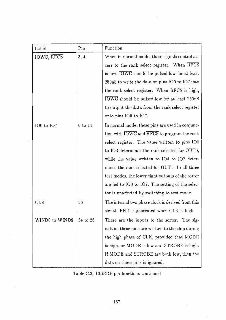
Label Pin
10WC, RFCS 3, 4
100 to 107 6 to 14
CLK 36
WINDO to WIND8 34 to 26
Function
When in normal mode, these signals control ac
cess to the rank select register. When RFCS
is low, 10WC should be pulsed low for at least
250nS to write the data on pins 100 to 107 into
the rank select register. When RFCS is high,
IOWC should be pulsed low for at least 250nS
to output the data from the rank select register
onto pins 100 to 107.
In normal mode, these pins are used in conjunc
tion with 10WC and RFCS to program the rank
select register. The value written to pins 100
to 103 determines the rank selected for OUTO,
while the value written to 104 to 107 deter
mines the rank selected for OUTl. In all three
test modes, the lower eight outputs of the sorter
are fed to 100 to 107. The setting of the selec
tor is unaffected by switching to test mode.
The internal two phase clock is derived from this
signal. PHil is generated when CLK is high.
These are the inputs to the sorter. The sig
nals on these pins are written to the chip during
the high phase of CLK, provided that MODE
is high, or MODE is low and STROBE is high.
If MODE and STROBE are both low, then the
data on these pins is ignored.
Table C.2: BISERF pin functions continued
187

Label Pin Function
OUTO 6 This is one of the outputs from the selector. It
is available during all modes of operation. The
rank of this output is determined by the value
written to pins 100 to 103.
OUTI 15 In normal mode this is one of the outputs from
the selector. The rank of this output is deter-
mined by the value written to pins 104 to 107.
In all three test modes this pin is connected di-
rectly the largest of the sorter outputs.
OUTRST 16 This pin is the output of the internal reset shift
register. It is high when the most significant
bits of the output values appear on pins OUTO
and OUTl, and if in test mode, pins 100 to 107
as well.
Table C.3: BISERF pin functions continued
If the chips fail to work in the normal mode, then they can be tested in each of
three test modes. Each of these modes connects the nine outputs of the sorter to
pins 100 to 107 and OUTI respectively. OUTO and OUTRST behave the same as in
the normal mode. The rank select latches must be loaded using the 100 to 107 pins
before the chip is put into test mode. It is desirable in all the test modes to set the
chip to reset mode by bringing MODE high. It is also recommended that 100 to 107,
OUTI and OUTRST are fed back to WINDO to WIND8 and STROBE respectively
through ten kilohm resistors so that the test data is recirculated. Sixteen-bit data
can be written through buffers onto the input pins, and the buffers tri-stated once the
data is loaded.
Test mode one sets all the cells in the sorter to swap mode. This mode is selected
by setting TESTO high and TESTI low. It is used to check that data can propagate
through the swap mode of the comparator cell. Since the state of the comparator
188

cells is independent of the data, the reset signal is not used. However, this signal is
propagated through the reset shift register, so a reset pulse applied to the STROBE
pin should appear at the OUTRST pin sixteen clock cycles later.
Test mode two is selected by setting TESTO low and TESTI high. In this mode,
the sorter operates as normal, but all its outputs are observable. A reset signal is
therefore necessary, and must be applied to the STROBE pin in phase with the most
significant bit of the data, so that the comparators are reset when necessary.
In test mode three, the comparators are set to the no-swap test mode. This mode is
selected by setting TESTO and TESTI high, and is used to check that the comparators
can propagate data in the no-swap mode. Again, the reset signal is not used, but it
does propagate through the reset shift register.
Since the chip has not been fully tested, the timing for the rank select register
access, and the suggested clock speed of ten megahertz are estimates only.
C.3 The Bit and Range Filter Chip
Set
A circuit was designed by the author to use the rank and range filter chip set to
filter images. The circuit, which was assembled on a Multibus-I wire-wrap board by
technical staff at the university, interfaces the chip set to HIPS. A circuit diagram for
the board appears in figures C.l to C.3, and its operation is described in the following
paragraphs.
The circuit for the board can be divided into two parts, the Direct Memory Access,
or DMA, controller circuitry which transfers data between the chip set and the system
bus, and the rank and range filter chip set itself.
The heart of the DMA controller circuitry is ICI, which is a Motorolla dual channel
DMA controller chip. This chip has the ability to transfer a given number of bytes from
one block of consecutive locations in memory to another block of consecutive locations.
The number of bytes, and the source and destination addresses are programmable. The
Motorolla device was chosen because it is readily available and can generate a 24-bit
address, which is sufficient to drive the twenty address lines used on HIPS.
189

The DMA controller chip has two modes of operation. In MPU mode, it acts as a
peripheral on the system bus, and can be programmed by selecting it and writing data
to its internal registers. In DMA mode, it takes control of the system bus, performs
the data transfer, and then releases the bus back to the system. Because the Motorolla
convention, where a word stored in memory has its least significant byte at the higher
address, differs from the Intel convention used on HIPS, this circuit uses byte transfers
to the DMA controller rather than word transfers.
When in MPU mode, lC6 decodes the address lines to ADRF, and selects
the DMA controller when these lines match the address on switches Sl to S8. Pin
OWN is pulled high since the DMA does not own the bus. The DMA controller then
decodes the address lines ADRO to ADR7, which pass through IC2, to select one of
the on-chip registers. Data is written to the DMA controller by performing an 10
write to the correct address, and can be read from the DMA's registers by performing
an 10 read. The completion of a write or read operation is indicated by the DTACK
pin on IC1, which is used to drive the bus signal XACK through lC30b and a PNP
transistor.
Once the DMA controller is programmed, and a DMA cycle initiated, the chip
requests control of the bus. Discrete logic is used to interface the DMA controller bus
arbitration signals to those of the system bus. Once control has been obtained, the
OWN pin goes low, and the data transfer commences.
For correct operation of the board, the DMA controller must be programmed for
continuous byte transfers from memory to memory. In a conventional circuit, the DMA
would read a value from the source location in memory, store the value internally, and
then write the value to the destination location in memory. The source and destination
addresses would then be incremented, and the transfer count decremented. Data
transfer would stop when the transfer count reached zero. However, in the rank and
range filter circuit, the data read from memory is isolated from IC1 by IC5, and is
instead written to the window of the filter, IC13, through IC12. Similarly, the data
written to the destination address in memory is not data from IC1, but the result of
the filter operation, which is stored in IC24. Operation of the circuit assumes that
IC1 is programmed so that the lines FCO to FC2 are held high during both the read
and write operations. These lines are decoded by IC8 to enable the filter. Note that
190

if FCO to FC2 are programmed to some other value, the filter will be disabled, so the
DMA controller may be used for conventional memory to memory transfers.
The remainder of the circuitry is associated with the rank and range filter chip
set. Before filtering can commence, IC9 and IC19, must both be programmed. IC18
decodes the address lines ADR8 to ADRF, so that 10 writes to these chips can be
performed when these address lines match the settings on switches 89 to 816. IC9 is
the modulo-n counter, which must be programmed with one less than the row length
of the image to be filtered. This value can be written as a word, although only ten bits
are used. IC19 is the rank and range filter chip, and must be programmed with the
two rank values required. These values are contained in a single byte that is written
to the chip. When writing to either chip, a XACK signal is generated by IC27b, IC32a
and IC32b.
The circuit for the rank and range filter chip set consists of the modulo-n counter,
IC9, which generates addresses for the two byte-wide memory chips, IClO and ICIL
The window consists of three 24-bit shift registers, IC13, IC15, and IC17, and two
buffers IC14 and IC16, which allow the outputs of IC13 and IC15 respectively to be
tri-stated. Data is loaded into the window through IC13, by performing a memory
read when FLTEN is low. Data from the window is clocked bit-serially into IC19,
which filters the data and presents the results on pins OUTO and OUTL The rank
value from OUTI is inverted by IC29f, and then added to the output from OUTO
using the serial to parallel converters IC20 and IC22, and the adders IC2l and IC23.
The result, which is the one's complement of OUT 1 - OUTO, is latched by IC24, and
is written back to memory during the DMA memory write provided that FLTEN is
low. Note that if the rank chosen for OUTO is not one to nine, then OUTI - OUTO
will be the same as OUTl, and therefore a rank filter will be implemented.
The prog~amming of the board depends on the switch settings of Sl to S16, since
these determine the addresses of the control registers. As an example, assume that
switches 82 and S9 are on, and the remainder are off, and that it is desired to perform
a median filter using a three by three square window on an image of six rows by
four columns. Assume that the image is stored contiguously from address 40000H to
400l7H, with the first row starting at 40000H, the second at 40004H, and so on. The
following is a list of iSBC957B monitor instructions that program the board to filter
191

the image.
ow 100,03 * Set modulo-n counter to row length-l
0 102,50 >I< Set rank filter to perform rank(5) (0)
0 207,10 * Reset DMA channel 0
0 247,10 * Reset DMA channel 1
0 20F,OO * Data source address
0 20E,OO * " 0 20D,04 *
II
0 20C,OO '" II
0 217,20 * Data destination address
0 216,00 '" " 0 215,04 '"
II
0 214,00 * " 0 229,FF * FCO to FC2 output during memory read
0 231,FF * FCO to FC2 output during memory write
0 20A,OO * Number of elements in + f er chip latency
0 20B ,lA * "
0 22D,00
0 2FF,OO
0 204,00
0 205,01
0 206,05
0 200,FF * Clear DMA error
0 207,80 * Initiate transfer
The results of the filter are written to consecutive memory locations starting at
40020H. However, since the shift register has a latency of 2r 3, where r is the row
length, and the filter chip has a latency of two bytes, the first valid output byte,
corresponding to the second row and second column of the output image, is written
to 4002DH, while the last valid byte, corresponding to the third column and fifth row,
is written to 4003AH.
It should be noted that since some Multibus-I boards do not fully decode the 10
192

address space, conflicts with the rank and range filter board address may occur. If the
rank and range filter is to operate successfully, the offending boards must be removed
from the system. The iSBC534 four channel communications expansion board is one
such board.
193

3 .. 2
liUsY
DI II --C> ctK ID
OOR
'JU;K "-C0 :u """0 sme
rei :u fe:; 3i/I
'<>'IT ,.
AC'tf'I~~ ,t,OR&-AOR7
~- 21.
lei ., '" ,. ... 53 ","
(1 e '" III II II tm::ij~ .,," :t~70 70~ Ie Jio.'!_OO 48 sa _'L_~~)-_ Al!o f8 8Il b.) 19 i'1 ____ lMJ!-AUW ...... 49_o1
'.1S 02 .IS
t:I AI 1:03 ,,~ 41:l'_it'!
s;:; "l]_OS "1
"l.~!H' .. " I I I I I j I I00:q+-t ~ 8H[N
>- AI50_07
r.. - I I I I I I I I 7.o1tS~0 l...-fl 1+ ...... ;:; . (.0 n ..,. E .
e-+
0' '.oll56el'l
• '0 >-j • o. I I I I II II~-"-I" "I" or A iL> 0>\10-0.1017
b:I • P7 ,......, B ,,- ,: P)
en 13 p" I I III II AOR10-~1~
tr1 t5 PO 1-*L'i3)'3
::0 17 P7
I-:rj J ""
L' Dr ,I; :16 L21; ~m:i L) l'i:lCN
0-' 5 01
l06b , 0' 0 ~ OJ 1C15<
~ " '" IC2f1d >-j ,. 0'5
p.. I. co le2ae
AORe-AORf 07
1T.m:' 10'llle
"ROC
10K
AI 1C2~ '''l'Sl2 le,l:) Hl'SZ"1 81T SERIAL RANK FILTER I A le26 7.lS}2 lell 14l$Z<ll le?7 Hl'S02 102 ''''lS2<1, IC26 1AlSO" lel} HlSH 1) OLeA CONTROLLER' CIRC\.IIT IC29 ?.IILSO" Ie, .. '''l'50a
All F!t.S~STORS ,.,k ~. NAYlOR
12 '&'PRll as
4 3 .. 2

4 3 + 2
QS,
o:m p~CCNr >«0161 16~~~ . '" 1 .. . '"
01 Oifg 0 1C29b I I t--J-!{O' ' ., i/Ol 10 'fOl _!0 , '" '/0> .. 1/03 _.1 AS i/O' '/0' ' .. '/0' " 'lOS '., 'lOS
" .. '/00 'S " .. '/0<1 'S 1C1' 1C.~e: '.lS2.1
" n ... " 1(28 IC31 14lS2.ct
~ ~A4 ~:"RO .. 1/07 1/07 1(21 102 7.lSi'"
--;~ ~~ AI@ I{OO 19 Mil 1/06 " ,,,. K:J.3 7.l$7C oq. ~ "" _HI t"S '01' tel" 7.l506 , ..
C=> or " WI: ~ A7 I lela I lell ... u R'(SISTOR') },:'ok >-j O .. JO-DAT7 1 AI'I: 7 rr'i<T or 2<1 or ('l)
Q L-----J I ,--J---I WrNG(N 5'1.'59' _G£N
tv
Q ~
II ~~~ Ie', Cfl <C" ,. M- e ~~ 016 ~;~~ ~~111J ~"8 ;;;\ll Ie 0 S ~
g.. iii'
..e. CtK .... i51ilf i:l M- .. mm 1-...... ('l)
<:.0 >-j SfR1l (')
C.n 0 AWl i:l i:l = ('l) (')
7"l~_I~ ".... o· = 6I'5ERf
B 7.lSVl i:l 'Cl~ '. '0 1 Cfl
:Ill ro' 0' C06
'" :!O'
] I_OT .. ••• >-j C02 100 so ." "
to " I_O} 11
'" '" "
, .. =, " '_0<1 12 7t) 10 16 ....... '_O!!. .. '" ' . OATe-VAn CIJ " '" "'" '. 1_o6
C Ia' M 15 pe '_07 1C19t W
?J 17 p1
~ 1 ". ICI.
0'" ' 0'
G I' ,-DUCK 1 02
0 9_ 03
~ "", >-j OS p,. l~ 06
A "'-OO6-i.tifit- 1$ 01 I: 11 L) 81T SERIAL RANK FILTER I A
2) CVSTOU CHIP CONNECTIONS
u, NAYlOR
11 APRil sa I~t Nj .. 1\tU1 '2 or ,
4 3 .. 2

4 3 + 2
01 10
1 GND TESTI 48 1 N.C. N.C. 48 1 GND DOl 48 2 TEST0 GNO 47 2 N.C. N.C. 47 2 D02 D00 47 3 10WC STROBE 46 3- N.C. GND 46 3 D03 lAND 46
'":r:l 4 RFCS MOOE 45 4- N.C. TC 45 4 004 lENB 45 ~.
5 VOO ClK 44 5 N.C. TC 44 5 N.C. lENA 44 ~ '"1 6 OUT0 GND 43 6 N.C. A9 43 6 N.C. VOO 43 (l)
7 WIN00 42 7 TEST A8 42 7 N.C. 010 42 8 WINOl 41 8 D9 A7 41 8- N.C. 011 41
e 9 WIN02 40 9 08 A6 40 9 DOS 012 40 Ie 10 WIND3 39 10 D7 AS 39 10 D06 013 39 11 1/04 WIN04 38 11 06 A4 38 11 D07 014 38 12 1/05 WIr~05 37 12 05 A3 37 12 WIN00 DIS 37
g.. 13 1/06 WIN06 36 13 04 A2 36 13 N.C. 016 36 14 1/07 WIN07 35 14 D3 Al 35 14 N.C. 017 35 ..... .... 1-
...... '1j 15 OUTl WIN08 34 15 02 A0 34 15 N.C. STROBE 34 CD ~. 16 OUTRST VOO 33 16 01 N.c. 33 16 N.C. WRON 33 Ol
::l 17 GNO N.C. 32 17 N.C. N.C. 32 17 N.C. RAMRO 32 0 ~ 18 N.C. N.c. 31 18 N.C. N.C. 31 18 N.C. S0 31 M-oo 19 N.C. N.C. 30 19 N.C. N.c. ·30 19 N.C. S1 30 0' B 20 N.C. N.C. 29 20 N.C. N.C. 29 20 N.C. S2 29 '"1
to 21 N.C. N.C. 28 21 N.C. N.C. 28 21 N.C. S3 28 ....... 22 N.C. N.C. 27 22 00 N.C. 27 22 WIND1 DACKIN 27 t..r.J tr:i 23 N.C. N.C. 26 23 VDO RAMRD 26 23 WIND2 RESET 26 :;::l 24 N.C. N.C. 25 24 CNTRCS 10WR 25 24 ClK GNO 25 '":r:l Ci' 0 ~ BIS F P '"1 0...
A BIT SERIAL RANK FILTER A J) CUSiOIJ CHIP PINOuTS
lA, NAYlO~
12 .l;PRIL as I")o(,o(.c N/A t"'" ~ or ~
4 3 t 2

III
I
n p
Ii!
I nt ti f ra
RM Bailey, M J Nayl S J McNeiff
A l M Ng and
The results ofresearch on rank filters are presented. The relationship of rank filters with other filters is briefly discussed. The main properties of rank filters are listed and an explanation is given for these properties. Several software and hardware implementations of the filter are described. Major applications to image processing are discussed, including noise smoothing, cluster detection, skeletization. enhancement and edge detection.
Keywords: rank filters, local filters, nonlinear filters
A local operator is a filter Whose output at a pixel is a function of the input values within the neighbourhood of that pixel l
. This neighbourhood can be thought of as a window since, for each output pixel. only the pixel values within the window are used. The window is scanned across the input image, each position contributing to one pixel in the output image. The window can be of any shape, although it is almost always symmetrical qbout a centre point2
, and is us.ually square. Some common windows are shown In Figure 1. Local operators tend to have short calculation times since generally only a small number of input pixel values are operated on for each output pixel.
With linear filters, the output value is a linear combination or weighted average of the input pixel values from within the window. The choice of weights depends on the application of the filter. The theory of this class of filter is well understood l
. However, linear filters are not suitable for many image processing tasks 3 A linear low-pass filter is often used to reduce noise, but has the disadvantage that edges are blurred 2.4. The use of a linear high-pass filter to sharpen or detect edges has the disadvantage that high-spatial
University of Canterbury. Private Bag, Christchurch. New Zealand
frequency noise is amplified 5.6 and spurious oscillations are produced near edges 5
.6
.
Nonlinear filters can be devised to overcome some of the disadvantages inherent in the use of linearfilters 3
.7
The calculation time for local nonlinear filters is of the same order of magnitude as that for local linear filters since the same number of pixel values are processed. There are two broad classes of nonlinear filters 3
: those which are simple modifications of linear filters, and those which are not. Examples of filters from the first category are
• 'trimmed' filters • 'gated' filters • nonlinear combinations of linear filters
An example of a filter from the second category is the moment-based filter. Trimmed filters 8 are linear filters from which pixel values which are far removed in intensity from the central pixel or the median value of the window are excluded, reducing the noise sensitivity of the filter. Gated filters 3 use some function of the pixel values within the window to determine which of several linear filters will provide the resultant pixel value; eg a pixel is compared with the average of its neighbours and, if this difference is than a certain threshold, the centre pixel is replaced by the average B An example of a nonlinear combination of
a c
Figure 7. Commonly used windows: a, 5 x 5 square; b, 5 x 5 cross; c, 7 x 5 strip; d, 3 x 3 square, e, 3 x 3 hexagonal; f, 5 x 7 strip
vol 3 no J february 1985 0262-8856/85/01003-12$03.00 © 1985 Butterworth & Co (Publishers) Ltd. 3

linear filters is the Sobel filter 39 , where the output is a nonlinear combination of the outputs of two linear edge detection filters. The moment-based filter uses the 'centre of gravity' or other moment of the pixel values within the window to detect edges!O
A class of nonlinear filters of particular interest are the rank filters. With rank filters, all the pixel values within the window are ranked according to value, regardless of physical location within the window. The output of the filter is the pixel. value selected from a spec ified position in this ranked list. Let the pixel values within a window of area N pixe.ls be sorted into numerical order as
(fl ' f2' f 3, . . . , f N )
where
f1 ~f2~· .. fN
The output is then selected as follows
rank(i) =0 1 ~i~N
(1 )
(2)
( 3)
When this is done for all possible Window positions, it can be represented as
g=R;(f) (4 )
where fis the input image, g is the processed image and i is the rank position selected. A special case of the rank filter when N is odd is the median filter, where the median rank position is selected. The other two special cases correspond to extreme rank position selection. These are catled min and max filters !! and are defined as follows
min(f) o=:RI (f)
max(f)=RN(f)
REVIEW OF PROPERTIES
(5a)
(5b)
A summary of important results follows . Most of the reported work on rank filters has concentrated on the median filter.
Property 1: Rank filters smooth noise l213
The effect of applying a rank filter to a region of nominally constant intensity I and variance V is to reduce the variance. This effect can be observed in Figure 2, where the narrowing of the intensity histogram is indicative of the reduced variance. The high spatial frequencies associated with the noise are attenuated; in particular, oscillations in intensity with a period less than the window width willi be smoothed 13
In this case, since within the window there are pixel values at various stages in the cycle, pixels of approximately the same intensity are selected as the window moves across the oscillation. The exception to this is where rank positions near the median are used and the osci ll ation is binary or two valued. Then each of the two values is selected in different window positions and so the oscillation persists
Filters that use rank positions near the median are especially useful for eliminating impulse noise 2 !3 !4 This noise is usually caused by bit errors that occur during data capture or transmission . Since only a small proportion of pixel,s within a window are likely to be noise pixels and tend to occupy the extreme rank
4
. ORIGItfAL.
Figure 2. The effect of rank filters on a noise image using a 3 x 3 square window. The images and intensity histograms for ranks 2, 5 and 8 are shown
positions, these pixels will not be selected if rank positions near the median are used.
Much has been written on the noise smoothing properties of median filters 24914-19 and many of the authors have provided statistical results.
Property 2: Application of a rank filter will change the mean intensity
The important exception to this generalization is the case that occurs when a median filter is used in a region where the noise distribution is symmetrical. In this case, the median filter does not change the mean intensity I in the region 12. Se1lecting a rank position less than or greater than the median will reduce or increase I respectively. These effects are demonstrated in Figure 2, where the mean intensity can be seen to shift. With a symmetrical input distribution, the use of rank positions other than the median skews the output distribution, as shown in Figure 2.
The general effect of applying a rank filter to an image with a skewed noise distribution, when compared with the effect of the same filter on an image with a symmetrical noise distribution of the same mean and variance, is to shift the mean intensity in the direction of the skew. This shift can be explained as
image and vision computing

follows. When the mean value is calculated . outlying pixel values have a I'arger effect in determining the position of the mean than those closer in. When the median value is calculated. each pixel carries the same weight. and the median value is nearer the bulk of the intensity values than the mean value . This result also applies to other rank values near the median. but rank values near the extremes are determined main1ly by the nature of the tails of the noise distribution.
Property 3: Rank filters preserve the shape of edges 2
.20
The shape of an intensity step. or ramp. between two adjacent regions of uniform but different intensities is preserved. Figure 3 shows the one-dimensional case. In general. this result carries over to two dimensions. as shown in Figure 4. When linear low-pass filters are applied to edges. step edges are blurred to ramps and the width of ramp edges is increased 4 If the two regions are noisy. however. slight blurring does occur when a rank filter is applied 2.20
To explain this effect a particular example will be used (see Figure 5). Consider a nine-element window positioned near an edge so that it contains five pixels from the region on one side of the edge and four from the region on the other side. The two regions have intensities of 110 and 80 respectively. The expected value of the median in this case is 110. If uniformly distributed noise is added to this edg,e. the pixel values are distributed uniformly between 100 and 120 on one side of the edge and between 70 and 90 on the other side. The median. corresponding to a rank position of 5. selects the minimum intensity of the five pixels between 100 and 120. This has an expected value of 103. whereas if there is no noise the expected value is 110. This is effectively a slight blurring of the edge.
Property 4: Application of a rank filter will shift the position of edges
Selecting a rank position less than or greater than the median will propagate the edge in the direction of the reQ'ion of higher or lower intensity respectivel1y13 21 since the pixel values from one side of the edge will be sellected wh ile the window is sti lion the other side. Th is effect is illustrated in Figures 3 and 4.
Only the median filter will preserve the position of the edge if the window is symmetrical about its centre.
Figure 3. Shape preservation and edge propagation: a. a complex one-dimensional edge: b. the edge after filtering with a five-element max filter
vol 3 no 7 februarv 7985
Figure 4. The effect of rank filters on edges. using a 9 x 7 strip window. The images and line profiles for ranks 2. 5 and 8 are shown
120 1 Uniform noise 110 f'
between 100 and 120 :=- 100
<J) I c 90 ~
c t Uniform nalse 80 between 70
and 90 70
Window position
Figure 5. The blurring effect of noise on a onedimensional edge subject to median filtering with a nine-element window: •. no noise: x. expected value for noisV data
This is because. when the window is on an edge. there are just as many points on one side of the centre pixel that are greater than the centre pixel value as there are on the other side (see Figure 6). Thus the median value is the value of the centre pixel . and no modification is made to the edge 13 Any irregularities in the edge less than the width of the window will be smoothed by filters with rank positions close to the median.
5

Property 5: A rank filter will change aU signals except a constant13
Repeated application of a rank filter will continue to change the image. This happens because the only fixed points for rank filters other than the median are images of uniform intensity. Thus. for rank filters in general. the only solution to the equation
f=R , (f) is
f= constant
a a a a a a a a a a
b b b b b
(6)
(7)
Figure 6. Straight edge preservation property of median filtering
This pmperty is an extension of property 2 and is implici.t in property 4. After any edges or intensity steps in the image have propagated to the edges of the image. there w ill be no edges left to propagate; therefore the image must be constant. With the median filter. edges do not propagate since edges are invariant; thus the fixed points of the median filter image consist of edges. regions of locally monotonic slope 8.22 ~25 . and certain types of saddle point 23 The fixed-point. or root. images for two different window shar~~ and sizes are shown in Figure 7.
Property 6: Min and max filters have specific properties ll12
The properties of min and max filters can be written as
min (max (m ~n (f)) = min (f)
max (min (max(f)) = max(f)
min (max (f) ~ f~ max (min (f)
(8a)
(8b)
(9) These properties are not he1d in common with the non min or max rank filters. However. for rank positions close to the extremes. equations (8) and (9) may be
Figure 7. The fixed points of an image subject to median filtering. The lower left-hand image is the fixed~point image of a 3 x 3 square window. and the lower right ~ hand image is the fixed~point image of a 3 x 3 cross window
6 image and vision computing

* 1--
~~ I - 1-x
1*'* * : I
1--1 a
b Figure 8, Local maximum from a max-filtered image: a, T-shaped filter; b, its effect on the local maximum before filtering (~) and after filtering ("'): ~--, one window position
considered to hold approximately, the approximation becoming less valid for positions towards the median,
Property 7: In a max-filtered image, all regions of local maxima contain the , window rotated by 180°12
This property can be explained by considering the Tshaped window shown in Figure 8, If there is a pixel whose intensity is a local maximum (as determined by the window size and shape) then this pixel will be selected by the max filter when the window is in the positions marked by asterisks. The dotted lines show one such window position. In this way, the pixel which is a local maximum is selected from different positions from within the window, giving a local maximum the shape of the window rotated by 180°. A similar property holds for min filtering with regard to the local minima.
Property Monotonically increasing functions of greyscale commute with rank filters 12
Given a monotonically increasing function M defined as
g=M(1)
then
Rj (M (I)) = M(R j (I))
(10)
(11 )
Since the order of the pixel values from within the window does not change, selecting the same rank position will select the same pixel. The function M may be applied either before or after rank filtering since Mis a point operator, ie the resultant value at a pixel is independent of the value of neighbouring pixels. This property is of particu lar use in delayi ng some image processing decisions (eg selecting a threshold level) until the image is in a more suitable form (eg less noisy) 11
An extension of this property is that any monotonically increasing function commutes with any series of rank filters 12, ie
Rj(R/(Rk (M(I)))) =M(R, (Rj(R k (I))))
Property 9: Complement property
(12)
Rank filtering a complemented image (ie an image which has its intensity range reversed) with a rank
vol 3 no 1 february 1985
posit,ion i is equivalent to rank filtering the original image using the rank position N+ 1 -i and complementing the result 11
.12 Since complementing an image
reverses the order of the ranked pixel values from within the window, the same pixel will be selected if the ranking is reversed. Thus
fN+1 _ j=(-I)/ (1 3)
or when performed for the whole image
-RN+l (I)=Rj(-1) (14 )
The consequence of this property and property 8 is that rank filters are commutative with monotonically decreasing functions of greyscale provided that the rank position used is modified appropriately.
Property 10: In the application of a rank filter, no new intensity values are generated
This property holds because at each window position one of the intensity values from within the window is selected for the output image. Thus the intensity values appearing in the output image will be a subset of those in the input image. This property is important when only a few of the available intensities appear in an image. With linear filters in general, new values are generated.
FAST M
Several efficient methods have been devised for applying median filters to an image8.2528. Two of these 26
.27 use a histogram modification scheme to make
use of the overlap from one window position to the next (only one pixel value changes in the onedimensional case, while a small fraction of the window area changes in higher dimensions-see Figure 9). In this method, a histogram is taken of the window in the first position, and the median is derived from that. For subsequent window positions, the pixels which move out of the window are removed from the histogram and the new pixels are added, The median is then modified to represent the distribution in the new window position. This is repeated for all possible window positions. The method can be shown to be considerably faster than conventional sorting algorithms,
Iy for larger window sizes 27
Bednar et al. 8 have reported a simplification of this method, using a sorted list rather than a histogram.
Position before moving Position before moving - -Ixlxlxlxl x X - X X
--1--1 X
Position ofter moving
a -Position ofter moving
b Figure 9. Overlap in the pixels sorted as the window moves: a, one-dimensional case (five-element window); b, two-dimensional case (3 x 3 window); X, overlapping or redundant pixels
7

Step 1 2 3 4 '5
6=00110 0 25=11001 1 1 19=10011 1 0 0 1 1 16=10000 1 0 0 0 23=10111 1 0 1
8=01000 0 20=10100 1 0 1 30= 1111 0 1 1 15=01111 0
MEDIAN 1 0 0 1 1 Value wanted 5th 2nd 2nd 2nd 1 st Number of Os 3 4 2 1 0
Figure 10. Ataman 's median sorting algorithm shown for nine elements
Their method is good for one-dimensional rank filtering, but in higher dimensions no real advantage is gained since several values in the sorted list need to be changed when moving from one window position to the next. If more than one rank position is required, this metho'd has the advantage that all rank positions are readily available.
Another method 28 calculates the median value within a window by sorting the pixel values 1 bit at a time and discarding the values which will not be used. This is Illustrated in the following example to find the median of nine 5-bit numbers (see Figure 10). In the first step the most significant bit is examined. Of the nine values, three begin with a 'O';,therefore the median value begins with a '1' and those numbers beginning with a '0' are discarded. Of the six values that are left the second is the median. The second most significant bit is now examined. Since four of the values that are left have a '0' and the second is required, the next bit in the median is a '0'. Values with a '1' are discarded. As this process is repeated for each bit. the median is built up 1 bit at a time. Although these methods are given for the median filter, they can be easily modified to perform rank filtering.
HARDWARE SYSTEMS FOR MEDIAN OR RANK FILTERING
Several hardware systems have been proposed or constructed for rank filtering. The earliest of these is an analogue circuit for selecting a particular ranked position from several voltages 29,30. Although this circuit is fast since it uses parallel circuitry to perform the processing, it is impractical in digital image processing applications because of the inconvenience and limited accuracy of DIA conversion, analogue processing and AI D conversion. To select a different rank position, the circuitry needs to be significantly modified making this method unsuitable for general rank filtering.
Ataman et al. 28 have described an implementation of the median filter using the successive refinement method described earlier. The hardware they discussed should be able to perform rank filtering with only minor modifications. However. it can provide only one rank at a time. In applications where more than one rank position is required, as in the applications suggested by
8
Bednar et al. 8 and Bovik et al. 31, this would be a
disadvantage since it would require duplication or significant modification of the circuit. The main advantage of this method is the relatively low component count when compared with other possible discrete implementations,
Rank filtering is ideally suited to implementation by VLSI techniques since the filter can be designed using regular circuit structures 32
, Several methods have been proposed to apply VLSI techniques to onedimensional median filtering 32- 34 , These can be applied to two-dimensional processing using what is known as a 'separable median' filter 17
.25 . With this filter. first the rows then the columns are median filtered, giving the median of medians (both one-dimensional operations), This is equivalent to median filtering with a horizontal strip window (eg as in Figure 1 f) followed by median filtering with a vertical strip window (eg as in Figure 1 c). Although this has similar properties to the conventional median filter 17,25 it cannot be easily extended to filters of arbitrary rank.
Fisher 35 has presented algorithms for one- and twodimensional filtering. These methods use a linear pipeline of identical cells. Each cell hasa stored value and receives a message action and a message value from the previous cell. The message action is performed and at the next cycle the message action and value are passed to the next cell. As the window moves, the values of the pixels which move out of the window are deleted from the sorted list, and the val ues of the pixels which move into the window are inserted. In this way the total overall processing is minimized. being spread efficiently among all the cells. The processing performed by each cell consists of comparing and swapping two intensity values. The area of silicon required to implement this algorithm is proportional to the number M of pixels within the window, an advan tage over alternative algorithms which require an area of silicon proportional to M2. For larger windows this property of the Fisher algorithm becomes a major advantage.
The authors of this paper have proposed a VLS I chip which will perform rank and other related filtering on a two-dimensional image using a 3 x 3 square window. This will use a conventional parallel bubble sorting algorithm. a method which becomes impractical for larger window sizes 32
. At the time of writing, the design for the prototype chip is nearing completion. This chip will be capable of processing images with pixel rates of the order of 100 ns per pixel, enabling images with up to 512 pixels per row to be processed at video rates.
APPLICATIONS OF RANK FI
Application 1: Noise suppression
Rank and other nonlinear filters may be used with advantage for noise suppression where the information in'the image being filtered is destroyed by conventional low-pass filtering, The filters mentioned in this section all have the property that to some extent they preserve edges in the original image.
The main application of the median filter is in noise suppression and much has been written in this field 2.4.9.15-2o.36.37 The median filter works best on heavily tailed noise distributions (eg uniform dis-
image and vision computing
tribution or exponential distribution) 2,31, and is very effective at removing spike noise13,36,
Combinations of rank filters can also be used for noise suppression 8.11,21.31.3B There are two main ways rank filters can be used
• sequential filter passes 11 ,21.38
• in a weighted sum of values from different rank positionsB.31
An algorithm that eliminates spike noise effectively using sequential passes is
g= min (max(max(min (f)))) (1 5)
This can be considered as one of a family of filters. If we consider
mi nn (f) = min (min ( ... min (f) » (16 )
where the min filter is applied sequentially n times, then the following are all noise suppression filters 11
,21
g=minn(maxn(f)) (17a)
g=maxn(minn(f) (17b)
g=maxn(min2n(maxn(f)) (17c)
g=minn (max 2n (minn (f)) (17d)
The filters represented by equations (17a) and (17b) eliminate negative and positive going features respectively; the size of the featl'Jre eliminated depends on the parameter n. Rank positions other than the extremes give similar results. The main disadvantage of these filters is that in general. the mean intensity level is not maintained if the input images are noisy. This can be inferred from property 6 above, which also suggests that the filters represented by equations (17c) and (17d) will be better in this respect.
A linear combination of rank filters also eliminates noiseB
,31. In general this type of filter may be represented as
N
g= L W,R,(f) 1
N
where L Wi =1 '-1
(18 )
Different schemes for selecting the weights give different families of filters which are optimal in a particular sense 31
. In both cases found in the literature, the weights are symmetrical about the median as in the equation
Wi 1 ~i~N/2 (19)
Application 2: Low-pass, band-pass and high-pass filtering
Equations (17a)-(17d) represent a type of spatial lowpass filter, the cut frequency being dependent on n. In general, as n increases, the cut frequency decreases since larger features are eliminated. These are not true low-pass filters 12 since edges are preserved. When using these filters in two or higher dimensions, the frequency response is direction dependent but this limitation can be overcome to a certain extent by using rank positions other than the extremes 3B An example of this for a 3 x 3 window is
g=R1 (R2(R, (Rg(Rs(Rg(f))))) (20)
This corresponds to equation (17a) with n= 3.
vol 3 no 1 february 1985
Since these filters are generically low pass in their response (apart from edge preservation), band-pass and high-pass filters may be derived 21.38 from them in the same way as for linear band-pass and high-pass filters 1. An example of a band-pass filter is
g=minn (max2n (minn (f)))
-mindmax2k(mindf)) n<k (21)
where the results from two low-pass filters with different cut frequencies are subtracted. When a lowpass-filtered image is subtracted from the original as in
g=f- minn (max2n (minn (f)) (22)
a high-pass"filtered image is obtained. Similar equations may be derived for the low-pass filters given in equations (17a)-(17c). Low-pass-, band-pass- and high-pass-filtered images based on equation (17d) are shown in Figure 11.
Application 3: Shrinking and expanding, skeletiiing
Min and max filters have been proposed as substitutes for shrink and expand operators when processing multivaluedimages 2.11 ,21. RanldHters irrgeneral may be used, since they also propagate edges (property 2). Rank positions greater or less than the median ~ill expand or shrink regions of high intensity respectively.
Several algorithms have been proposed for skeletizing images using min and max filters 21.3B One of these 21 uses 'gated' min and max over several different window shapes and positions to extend the skeletiza tion algorithms used with binary images. The other algorithm 39 uses min and max filters to shrink and expand the image in the following way. The image is shrunk using the iterated min filter for several different iteration lengths. Each of these is expanded once using the max filter, and subtracted from the previous shrunk image according to
gn=minn_1 (f) -max(minn (f) (23)
This result is nonzero as a result of property 6; the points in the resultant image are those which are a distance n -1 from the edge of the object and are not adjacent to any points at a distance n from the edge. When the results for several n are summed the resultant image contains the skeleton of f
m
h= L gn (24) n-l
These steps may be combined as follows to give what will be referred to as a 'skelet' filter. This filter combines the residue from one shrink/expand operation with the original image. Let
g=f-max(min(f)
Then
skelet(f) = min (max (min (f) + g»
(25)
(26)
Each time the skelet filter is iterated, the image is shrunk by a single layer of pixels, that layer being replaced by the skeleton. This process is repeated until no more change is made to the image (or until any changes made are insignificant). The fixed point of the skelet
9

Figure 11. Low-pass, band-pass and high-pass filtering of an image. The low-pass filter is described bV equation (17 d) with n = 1. The band-pass filter is described bV equation (21) with n = 1 and k == 2. The high -pass filter is described bV equation (22) with n =2
filter is the skeleton of the image. Figure 12 shows an image after successive passes of the skelet filter.
Application 4: Streak and spot/cluster detection
Batchelor has used the min and max filters to detect spots and streaks in images, without detecting step edges 40 He uses the equation
g=f~ max(min (f)) (27a)
to detect streaks and spots which have a higher intensity than the surrounding pixels. while use of the equation
g= min (max (f)) - f (27b)
detects streaks and spots of lower intensity. The equation
g= min (max (f)) - max (min (f)) (27c)
(being the sum of equations (27a) and (27b)) will detect both sets of streaks and spots. The size of the detected features can be increased by using the iterated min and max filters given by equation (16). After the
10
filtering has been done. the resultant image g may be thresholded to obtain a feature map.
These equations can be used in a similar way to detect clusters II . Consider an image containing several small isolated regions of high intensity. The max filter is used repeatedly to expand these regions until some of them merge or fuse together. The min filter is then used to shrirlk the regions back to their original size. The regions which merged remain connected and may be detected by subtracting the original image. These interconnecting lines may be expanded again to select the original points that are clustered. This process is shown in Figure 13.
Application 5: Edge detection
If regions of interest. which are different in intensity from the surrounding pixels. are shrunk then the difference between the result and the original image will represent edge activity. This IS because the edges between regions shift when the shrink operator is used. giving higher-intensity regions in the difference image where the edges have moved. Min and max filters as
image and vision computing

, ORIGINAL
PASS 3
Figure 72. Successive passes of a skelet filter on a binary image. Note that, after pass 4, no further changes are made in the image
shown in the equations
g=f~ min(f)
g=max(f) -f
(28a)
(28b)
have been used to do this 2141 and the results are demonstrated In Figure 14. These filters may be gener31lized, using any rank positions. in the form
i<} (29)
The two rank filters are used to shrink or expand the regions of interest by differing amounts (property 4) The difference image then has higher intensity where the borders of the regions of interest have been shifted as demonstrated in one dimension in Figure 14. Because of the noise smoothing properties of rank filters (property 1) these filters are reasonably insensitive to noise, especially spike or other heavy-tailed nOise.
When }=N and i= 1 in equation (29), the filter gives the statistical range of the pixel values within the window: for other values of i and} a subrange is given. For this reason these fiHers are ca liled range filters and are represented as
Raj, (f) =RJ (f) - R, (f) (30)
This can be computed in a single pass of the window, rather than as a difference between two rank-fi,ltered images, as follows
rangeU i) =~-f, (31 )
The result of range filtering an image with several values of i and} is shown in Figure 15. A companion paper describing the properties of this filter in more detail is in preparation 42
vol 3 no 7 february 7985
Figure 73. The use of rank filters for cluster detection. The second row shows one iteration of the max min filters and detects closely grouped clusters. The third row shows two iterations of the max min filters
J->+--_x- Original edge
a x-x-x-x-x-x jY<-X-K-K Rank I
b X-Y<-X-X-X-X-_ X-K_-~-K-X Rank 3
C >+-x-X->4-xJ x-x
/ \ Range (rank 3- rank I)
d x-x-x-_x-x X-X--K-X-X
Figure 74. Edge detection by a range filter
Application 6: Edge enhancement
When an image is blurred, whether in the optical system forming the image, or as a result of low-pass filtering to remove noise, it is often desirable to sharpen or enhance the edges in the image. A gated rank filter may be used for this task. This filter compares the intensity of the centre pixel of the window with the mean of two rank values. If the centre pixel value is greater than the mean then the larger rank value is
11

Figure 75. Edge detection using three different range filters
selected . otherwise the smaller is used. This may be represented as follows
new value=~
new value=f,
if fcentre > (~+ f,)!2
if fcenue ~ (~+ f,) / 2
(32a)
(32b)
An alternative viewpoint is to compare the centre pixel value with each of two rank values. selecting the nearer. This can be expressed as
new value=~ if 1(,- feenuel > If, - fcentrel (33a)
new value=!;
When the window is in the vicinity of an edge. the two rank values are considered to represent the regions on either side of the edge. The centre pixel is assigned the value of the region that it is nearer to in intensity. It has been found that the use of extreme rank positions gives the best edge enhancing properties; however. such a filter also emphasizes the noise. Using rank positions somewhere between the median and the extreme positions is better in that noise enhancement is minimized. With this method of edge enhancement.
12
ringing is prevented since no new pixel values are generated (property 10) . Figure 16 shows the effect of this filter on several blurred and noisy-edges.
SUMMARY AND CONCLUSIONS
In all the applications presented here rank filters perform as wel l as.or better than. conventional linear filters. When used for noise suppression. most of the edge information in the image is retained. When applied to streak and spot detection. features up to a desired size may be extracted . without detecting edges. For edge detection. range filters are less sensitive to noise than linear f ilters and perform about as well as the commonly used Sobel filter. With edge enhancement. the gated rank filter is less sensitive to noise than linear filters. and ringing is prevented.
The other applications or tasks discussed in this paper cannot be performed by conventional linear filters. The shrink and expand operators are restricted to binary image processing. and rank filters may be used as substitutes for these when processing greyscale images. Skeletization normally requires specialpurpose algorithms but may be performed with
image and vision computing

Figure 16. The use of the gated rank filter for edge enhancement. The top row shows the original image enhanced using ranks 8 and 2. The bottom row shows a blurred image enhanced using ranks 9 and 1
general- pu rpose ran k fi Iters at the expense of increased computation time.
Several implementation schemes for rank filtering. in both software and hardware. have been presented . No real comparison has been made between the methods since there is not enough published data for a comp lete assessment of the merits of each scheme.
Overall it has been shown that rank filters have many properties that make them a useful tool in image processing . The general nature of this tool has been shown through its application to a wide variety of tasks .
ACKNOWLEDGEMENTS
D G Bailey, M J Naylor and S J McNeill are supported by University Grants Committee postgraduate scholarships. A L M Ng is supported by a grant from the Forest Research Institute and a Christchurch City Counci l postgraduate scholarship.
REFERENCES
Castleman. K R Digital image processing Prentice-Hall , Englewood Cliffs, NJ, USA (1979)
2 Justusson. B I 'Median filtering : statistical
vol 3 no 1 february 1985
properties ' in Huang. T S (ed.) Two dimensional digital signal processing II, Top. App/. Phys. Vol 43 (1981) pp 161-196
3 Bailey. 0 G. Hodgson. R M and McNeill. S J ' Local filters in digital image processing' Proc. 21st Natl Electronics Cant. , Christchurch, New Zealand 22-24 August 1984 pp 95-100
4 Chin. R T and Yeh. C L 'Quantitative evaluation of some edge preserving noise smoothing techniques' Comput. Vision, Graphics, Image Process. Vol 23 (1983) pp 67-91
5 Frieden. B R 'Image restoration by discrete convolution of minimal length ' J. Opt. Soc. Am. Vol 64 (1974) pp 682-686
6 Frieden. B ' R 'A new restoring algorithm for the preferential enhancement of edge gradients' J. Opt. Soc. Am. Vol 66 (1976) pp 280-283
7 Frieden. B R ' Image enhancement and restoration' in Huang. T S (ed .) Picture processing and digital filtering, Top. Appl. Phys. Vol 6 (1975) pp 179-248
8 Bednar. J B and Watt. T L 'Alpha trimmed means and their relationship to median'filters' IEEE Trans. Acoust., Speech, Signal Process. Vol 32 (1984) pp 145-153
13

9 Pratt, W K Digital image processing Wiley, New York, USA (1978)
10 Suciu. R E and Reeves, A P 'A comparison of differential and moment based edge detectors' Proc. Conf on Pattern Recognition and Image Processing (1982) pp 97-102
11 Nakagawa. Y and Rosenfeld, A 'A note on the use of local MIN and MAX operations in digital picture processing IEEE Trans. Svst.. Man, Cybern. Vol 8 (1978) flP 632-635
12 Heygster, G 'Rank filters in digital image process .. ing' Comput. Graphics Image Process. Vol 19 (1982) pp 148-164
13 Nodes, T A and Gallagher. 1\1 C 'Median filters: some modifications and their properties' IEEE Trans. Acoust., Speech. Signal Process. Vol 30 (1982) pp 739-746
14 Ataman, E, Aatre, V K and Wong, K M 'Some statistical properties of median filters' IEEE Trans. Acoust., Speech. Signal Process. Vol 29 (1981) pp 1073-1075
15 Velleman, P F 'Robust non-linear data smoothers: definitions and recommendations' Proc. Natl Acad. Sci. USA Vol 74 (1977) pp 434-436
16 Tukey, J W Exploratory data analvsis AddisonWesley, Reading, MA. USA (1977)
17 Narendra, P M 'A separable median filter for image noise smoothing' IEEE Trans. Pattern Anal. Mach. Intel!. Vol 3 (1980) pp 20-29
18 Frieden, B R 'Some statistical properties of the median window' in Rhodes, W Fienup, J R and Saleh. B E A (eds) Transformations in optical signal processing, SPIE Vol 373 (1981) pp 219-224
19 Kuhlman. F and Wise. G L 'On second moment properties of median filtered sequences of independent data' IEEE Trans. Commun. Vol 29 (1981) pp 1374-1379
20 Yang. G J and Huang. T S 'The effect of median filtering on edge location estimation' Comput. Graphics Image Process. Vol 15 (1981) pp 224-245
21 Goetcherian, V 'From binary to grey tone image processing using fuzzy logic concepts' Pattern Recognition Vol 12 (1980) pp 7-15
22 Gallagher. N C and Wise. G L 'A theoretical analysis of the properties of median filters' IEEE Trans. Acoust., Speech. Signal Process. Vol 29 (1981) pp 11 36-1141
23 Tyan, S G 'Median filtering: deterministic properties' in Huang, T S (ed.) Two dimensional digital signal processing II, Top. Appl. Phvs. Vol 43 (1981) pp 197-217
24 Arce, G A and Gallagher. N C 'State description for the root signal set of median filters' IEEE Trans. Acousl., Speech, Signal Process. Vol 30 (1982) pp 894-902
25 Nodes, T A and Gallagher, N C 'Two dimensional root structures and convergence properties of the separable median filter' IEEE Trans. Acoust., Speecb, Signal Process. Vol 31 (1983)
14
pp 1350-1365 26 Garibotto, G and Lambarelli, L 'Fast on-line
implementation of two dimensional median filtering Electron. Lett. Vol 15 (January 1979) pp 24-25
27 Huang, T S, Yang, G Y and Tang. G Y 'A fast two dimensional median filtering algorithm' IEEE Trans. Acoust., Speech, Signal Process. Vol 27 (1979) pp 13-18
28 Ataman. E. Aatre, V K and Wong, K M 'A fast method for real time median filtering' IEEE Trans. Acoust" Speech, Signal Process, Vol 28 (1980) pp 415-420
29 Morgan, D R 'Analogue sorting network ranks inputs by amplitude and allows selection' Electron. Des. Vol 21 No 2 (18 January 1973) pp 72-74
30 Morgan, D R 'Correction to analogue rank sorting network' Electron. Des. Vol 21 No 17 (16 August 1973) p7 .
31 Bovik. A C. Huang. T S and Munson. D C 'A generalisation of median fi using linear com-binations of order statistics' Trans. Acoust., Speech, Signal Process. Vol 31 (1983) pp 1342-1349
32 Oflazer, K 'Design and implementation of a single chip 1 d median filter' IEEE Trans, Acoust., Speech, Signal Process. Vol 31 (1983) pp 1164-1168
33 Eversole, W L, Mayer, D J, Frazee, F Band Cheek. T F. Jr 'Investigation of VLSI technologies for image processing Proc. ARPA Workshop on Image Understanding (November 1978) pp 191-195
34 Shamos. M I 'Robust picture processing operators and their implementation as circuits' Proc. ARPA Workshop on Image Understanding (November 1978) pp 127-129
35 Fisher, A L 'Systolic algorithms for running order statistics in signal and image processing' J. Digital Syst. Vol 6 (1982) pp 251-264
36 Rabiner. L R, Sambar. M R and Schmidt, C E 'Applications of a nonlinear smoothing algorithm to speech processing IEEE Trans. Acoust., Speech, Signal Process. Vol 23 (1975) pp 552-557
37 Jayant, N S 'Average and median based smooth ing techniques for improving digital speech quality in the presence of transmission errors' IEEE Trans. Commun. Vol 24 (1976) pp 1 0;J-3-1 045
38 Preston, K 'Xi filters' IEEE Trans. Acoust., Speech, Signal Process. Vol 31 (1983) pp 861-876
39 Peleg. S and Rosenfeld. A 'A MIN-MAX medial axis transformation' IEEE Trans. Pattern Anal. Mach. Intell. Vol 3 (1981) pp 208-210
40 Batchelor, B G 'Streak and spot detection in digital pictures' Electron. Lett. Vol 15 (1979) pp 352-353
41 Pal. S K and King, R A 'On edge detection of Xray images using fuzzy sets' IEEE Trans. Pattern Anal. Mach. Intell. Vol 5 (1983) pp 69-77
42 Bailey, D G and Hodgson, R M 'Range filters: local intensity subrange filters and their properties' in preparation
image and vision computing