Clock Solutions Data Distribution
28
-
Upload
khangminh22 -
Category
Documents
-
view
0 -
download
0
Transcript of Clock Solutions Data Distribution

Page 2 Networking & Telecom Solutions
Crystal
ReferenceClock
Backplane
LoopFilter
Discrete PLL Blocks
Data
Processor
Processor
ASICLatches
Fanout
Divider/Counter
Skew Delay
Receivers
Equalization
MUX
ZDB
Gates
Pre-Emphasis
Crosspoint
PLL ClockGenerator
Gates
Latches
Flip-Flop
ZDB
ASIC
ASIC
Processor
I/O
I/O
I/O
Translator
Flip-Flop
Latches
Gates
PLL ClockGenerator
PLL ClockModule
PLL ClockSynthesizer
VCODivider/
Prescaler
PhaseDetector
MUX
Crosspoint
Pre-Emphasis
Equalization
Fanout
Translator
CMOS/TTLHCSLLVDSPECLCML
PLL ClockModule
TranslatorCMOS/TTL
HCSLLVDS
PECL/CMLPE/EQ
Drivers
Skew Delay
Clock Solutions Data Distribution
ON Semiconductor provides a complete portfolio of timing and data management solutions for all aspects of the clock tree. System designers can optimize their clock circuits with industry leading clock distribution devices, demonstrating the industry’s lowest jitter and skew. A broad product portfolio, with multiple output and interface options, allows system designers to build clock circuits that satisfy their specific application requirements. ON Semiconductor utilizes CMOS, Bipolar, and SiGe technology to leverage the best performance for any given application. For further details by device, function, or parametrics, refer to our website at www.onsemi.com.
Expanding on more than 30 years of experience as the world’s leader in high performance ECL-based clock distribution, ON Semiconductor has extended its expertise into ultra low jitter PLL clock synthesis and generation. The new PureEdge™ PLL devices utilize a fully differential architecture that enables performance that satisfies the timing requirements for the most demanding applications.
Performance Capabili t ies• Differential design for reduced noise• ECL, PECL, CML, LVDS, M-LVDS, HSTL, HCSL, LVTTL/LVCMOS outputs for
flexible interfacing• Maximum clock rates >10 GHz• Maximum data rates >12 Gbps• Typical additive phase RMS jitter, as low as 30 fs for buffers• Typical phase RMS jitter of 200 fs for clock generators• Integrated termination resistors for simplified circuit design• Edge rates as low as 28 ps• Low phase noise floor ≤ –174 dBc/Hz• Low output-output skew
Timing and Data Distribution Subsystem

Page 3ON Semiconductor
Programmable Multi-Rate Clock Generators
PLL Clock Synthesizers/GeneratorsFeatures
• Based on phase-locked-loop techniques with zero PPM synthesis error• Low jitter for high accuracy clock signals• Available in industrial temperature range -40°C to +85°C• Supports output interfaces: LVPECL, LVDS, HCSL, LVTTL/LVCMOS• Multiple PLLs and multiple output options
NB3H5150, NB3H5150-01 Features • Uses 25 MHz Crystal or reference input • External Loop Filter is not required • User programmable frequencies with four independent
output pairs• Each output pair can be configured either as two
LVCMOS outputs (or) a differential LVPECL pair • Supports 3.3 V or 2.5 V supply voltage operation • Each output pair has an independent supply voltage
rail (VDDOx); 3.3 V, 2.5 V, 1.8 V• I2C enabled PLL Bypass Mode and Power Down Mode • Free GUI software to configure device for different
frequencies and output types using evaluation board • Each device preconfigured with different default
frequencies, that may be overridden using I2C/SMBus interface
Synthesizer/Generator
DeviceInput (MHz)
Output (MHz)
Input Level Output Level
VCC Typ (V)Application XTAL CML CMOS LVPECL TTL Package(s)
NB3N3002 25 25/125/200 CPU/DIMM, PCIe Gen 1, 2, 3, 4 3 3 3 HCSL 3.3 TSSOP-16 NB3N5573 25 25/100/125/200 CPU/DIMM, PCIe Gen 1, 2, 3, 4 3 3 3 HCSL 3.3 TSSOP-16 NB3N51032 25 25/100/125/200 CPU/DIMM, PCIe Gen 1, 2, 3, 4 3 3 3 HCSL 3.3 TSSOP-16 NB3N3020 5 to 27 5 to 210 Network GigE 3 3 3 3 ECL, LVTTL 3.3 TSSOP-16 NB3N501 2 to 50 13 to 160 Networking, Consumer, STB 3 CMOS 3.3, 5 SOIC-8NB3N502 5 to 27 14 to 120 Networking, Consumer, STB 3 3 LVCMOS 3.3 SOIC-8NB4N507A 10 to 27 50 to 200 Networking, Consumer, STB 3 3 ECL 3.3, 5 SOIC-16NB3N508S 27 216 VCXO Set Top Box 3 3 LVDS 3.3, 5 TSSOP-16 NB3N511 1 to 50 14 to 200 Networking, Consumer, STB 3 CMOS 3.3, 5 SOIC-8NB3N51034 25 100/200 CPU/DIMM, PCIe Gen 1, 2, 3, 4 3 3 HCSL 3.3 TSSOP-20NB3N51044 25 100/125 CPU/DIMM, PCIe Gen 1, 2, 3, 4 3 3 HCSL 3.3 TSSOP-28NB3N51054 25 100 CPU/DIMM, PCIe Gen 1, 2, 3, 4 3 HCSL 3.3 TSSOP-24NB3H5150 25 25 to 250 Networking, Telecom 3 3 3 3 3 ECL, CMOS 3.3, 2.5 QFN-32NB3H5150-01 25 25 to 250 Networking, Telecom 3 3 3 3 3 ECL, CMOS 3.3, 2.5 QFN-32
VDDO1
CLK1A
CLK1B
Integer NDIV1
VDDO2
CLK2A
CLK2B
Integer NDIV2
VDDO3
CLK3A
CLK3B
Integer NDIV3
LDOs
XTALOSC
PLL
REF (I2C Mode)
ConfigurationTable &
I2C InterfaceVDDO4
CLK4A
CLK4B
LDO4
Integer N orFracational N
DIV4
LDO3LDO2LDO1
VDD AVDD1 AVDD2 AVDD3
FS
4B
FS
4A
FS
3
FS
2
FS
1
FTM
REFMODE
MMC
SCL/PD
SDA
CLK_XTAL1
CLK_XTAL1

Page 4 Networking & Telecom Solutions
Features• Differential SRC clock support• DB800ZL, DB1200Z/ZL, DB1900Z/ZL compliant with
8, 12, and 19 HSCL/low-power NMOS push-pull output pairs respectively
• Optimized for 100 MHz and 133.33 MHz to meet PCIe Gen 2/3/4 and QPI/UPI phase jitter specifications
• Spread-spectrum compatible for low EMI• Pseudo-external fixed-feedback for low input-to-output
delay variation• Individual OE control pin for each output• SMBus programmability for frequency selection, power
down mode, PLL BW modes, and PLL/Bypass mode
General Purpose Zero Delay Buffers
PCIe-Compliant Zero Delay Buffers
FBK
CLKA1
CLKA2
CLKA3
CLKA4
PLL
MUX
CLKB1
CLKB2
CLKB3
CLKB4
SELECTINPUT
DECODING
REF
S2
S12
2
2
Features• Industry standard functions and pin-outs• Zero input-output propagation delay, adjustable by
capacitive load• Multiple configurations available for maximum flexibility• Operating frequency to 133 MHz for CPU and PCI
compatibility
NB2308AFunctional Diagram
Zero DelayBuffer PLL
DeviceInput Level
Output Level
VCC Typ (V)
fMax Typ (MHz) Channels
tSkew O-O Max (ps) Package(s)
NB3N2302 CMOS CMOS 3.3, 5 133 2 250 SOIC-8
NB2304A CMOS CMOS 3.3 133.3 4 200 SOIC-8
NB2305A CMOS CMOS 3.3 133.3 5 250 SOIC-8, TSSOP-8
NB2308A CMOS CMOS 3.3 133.3 8 200 SOIC-16, TSSOP-16
NB2309A CMOS CMOS 3.3 133.3 9 250 SOIC-16, TSSOP-16
IREF**
FB_OUT*
DIF_[11:0]
ControlLogic
CLK_INSSC Compatible
PLL
12
SA_0SA_1
SDASCL
MUX
* FB_OUT pins are for NB3N1200K only; they are NC for NB3W1200L** IREF pin is for NB3N1200K only; it is NC for NB3W1200L
100M_133M#
PWRGD/PWRDN#
HBW_BYPASS_LBW#
OE_[11:0]#
CLK_IN#
DIF_[11:0]#
RREF
FB_OUT#*
NB3N1200K/NB3W1200L Simplified Block Diagram
Device Channels OutputtJitter(Cy-Cy) Typ
(ps)tskew(I-o) Max
(ps)tskew(o-o) Max
(ps)Edge Rate Max
(V/ns) Package
NB3W800L 8 Low power NMOS push-pull 34 ±100 50 4 QFN-48
NB3N1200K 12 HCSL 50 ±100 50 4 QFN-64
NB3W1200L 12 Low power NMOS push-pull 50 ±100 50 4 QFN-64
NB3N1900K 19 HCSL 50 ±100 85 4 QFN-72
NB3W1900L 19 Low power NMOS push-pull 50 ±100 85 4 QFN-72

Page 5ON Semiconductor
Clock and Data Distribution
Clock and DataDistribution
Features• Complete portfolio of fanout buffers, multiplexers, cross point switches• Supporting frequencies from DC to 12 GHz/Gbps• PCIe buffers with 1:2, 1:4, 1:6, 1:8, 1:10 and 1:21 fanouts• PCIe Gen 1, Gen 2, Gen 3, Gen 4 Jitter Compliant• Pre-Emphasis and Equalization blocks available • Offer new direct X-tal interface capabilities • Industry leading additive jitter as low as 30 fs typical• Device noise floor as low as -174 dBc• Industry leading output-to-output skew as low as 3 ps minimum• Direct device interface eliminates external termination components and simplifies BOM
DeviceOutputs per
Channel Output Level
Input Level VCC Typ (V)
tSkew O-O (ps)
fMax Typ (GHz) Package(s)CML CMOS LVPECL HCSL HSTL LVDS XTAL TTL
NB3N106K/108KNB3N111K/121K
6, 8, 10, 21 HCSL 3 3 3 3 3 3 3.3 100 0.4 QFN-52, QFN-32, QFN-24
NB3L202K/204K 2, 4 HCSL 3 3 3 3 3 3 2.5, 3.3 100 0.4 QFN-16NB3L208K 8 HCSL 3 3 3 2.5, 3.3 100 0.35 QFN-32NB3M8T3910G 10 HCSL, CMOS,LVDS, ECL 3 3 3 2.5, 3.3 50 1.4 QFN-48NB6L11S 2 LVDS 3 3 3 3 3 3 2.5 25 2 QFN-16NB6L14S/6N14S 4 LVDS 3 3 3 3 3 3 3 2.5/3.3 20 2 QFN-16NB3L8504S 4 LVDS 3 3 3 3 2.5, 3.3 50 0.7 TSSOP-16NB3L8543S 4 LVDS 3 3 3 3 3 2.5, 3.3 40 0.65 TSSOP-20NB3V1102C/1103CNB3V1104C/1106C
2, 3, 4, 6 CMOS 3 1.8, 2.5, 3.3 50 0.25 TSSOP-14, TSSOP-8
NB3M8302C/8304C 2, 4 CMOS, LVTTL 3 3 2.5, 3.3 45, 85 0.2 SOIC-8NB3U1548C 4 CMOS, LVTTL 3 3 1.5, 1.8, 2.5, 3.3 250 0.16 TSSOP-8, SOIC-8NB3N4666C 4 CMOS, LVTTL 3 3 3 3.3 250 0.2 TSSOP-16NB3F8L3005C 5 CMOS 3 3 3 3 3 3 3 1.5, 1.8, 2.5, 3.3 55 0.2 QFN-24NB3H83905C 6 CMOS, LVTTL 3 3 3 1.8, 2.5, 3.3 80 100 TSSOP-16, SOIC-16, QFN-20NB3F8L3010C 10 CMOS 3 3 3 3 3 3 3 1.5, 1.8, 2.5, 3.3 55 0.2 QFN-32NB3L83948C 12 CMOS 3 3 3 3 3 3 2.5, 3.3 100 0.35 LQFP-32NB3V8312C 12 CMOS 3 3 1.8, 2.5, 3.3 150 0.25 LQFP-32, QFN-32NB4N11M 2 CML 3 3 3 3 3 3.3 25 2.5 TSSOP-8 NB6L11M 2 CML 3 3 3 3 3 2.5, 3.3 15 4 QFN-16NB7L11M 2 CML 3 3 3 3 3 2.5, 3.3 15 8 QFN-16NB7L72M 2 CML 3 3 3 3 3 2.5, 3.3 10 7 QFN-16NB7VQ572M 2 CML 3 3 3 1.8, 2.5, 3.3 15 6 QFN-32NB6HQ14M 4 CML 3 3 3 3 3 2.5 15 5 QFN-16NB7HQ14M 4 CML 3 3 3 2.5 15 7 QFN-16NB7V585M 6 CML 3 3 3 1.8, 2.5 30 7 QFN-32NB7V586M 6 CML 3 3 3 1.8 30 6 QFN-32NB7VQ1006M 6 CML 3 3 3 1.8, 2.5 25 7.5 QFN-24NB7L111M 10 CML 3 3 3 3 3 2.5, 3.3 20 5.5 QFN-52NB6L14/6L14M 4 ECL/CML 3 3 3 3 3 2.5, 3.3 20 3 QFN-16NB7L14/7L14M 4 ECL/CML 3 3 3 3 3 2.5, 3.3 15 7/8 QFN-16NB7L1008/7L1008M 8 ECL/CML 3 3 3 2.5, 3.3 20/25 7/8 QFN-32NB6L56 1 ECL 3 3 3 2.5, 3.3 25 2.5 QFN-32NBSG11 2 ECL 3 3 3 3 3 2.5, 3.3 15 12 QFN-16NB6L11 2 ECL 3 3 3 3 3 2.5, 3.3 15 6 TSSOP-8, SOIC-8NB6L611 2 ECL 3 3 3 3 3 2.5, 3.3 15 3 QFN-16NB7L572 2 ECL 3 3 3 3 3 2.5, 3.3 15 7 QFN-32NBSG14 4 ECL 3 3 3 3 3 2.5, 3.3 15 12 QFN-16NB3N853501E 4 ECL 3 3 3.3 30 0.266 TSSOP-20NB3N853531E 4 ECL 3 3 3 3.3 30 0.266 TSSOP-20NB4L339 4 ECL 3 3 3 2.5, 3.3 60 0.7 QFN-32NB3L8533 4 ECL 3 3 3 3 3 2.5, 3.3 30 0.65 TSSOP-20NB3L853141 5 ECL 3 3 3 3 3 3 2.5,3.3 30 700 TSSOP-20

Page 6 Networking & Telecom Solutions
Dividers and Counters
Features• Low jitter and skew for highly accurate phase matching• Multiple outputs and ratios combined for integrated circuit designs• Supports interface and voltage translation
NB4L339 Functional Diagram
DeviceInput Level Output
LevelVCC Typ
(V)fMax Typ
(GHz) Div Ratios Package(s)CML CMOS LVPECL LVDSNB4L339 3 3 3 3 ECL 2.5, 3.3 0.7 1 or 2; 2; 4; 8 QFN-32NB7V32M 3 3 3 3 CML 1.8, 2.5 10 2 QFN-16NB7N017M 3 3 3 3 CML 3.3 3.5 2 to 256 QFN-52NB7L32M 3 3 3 3 CML 2.5, 3.3 14 2 QFN-16NB6N239S 3 3 3 3 LVDS 3.3 3 1/2/4/8; 2/4/8/16 QFN-16NB6L239 3 3 3 3 ECL 2.5, 3.3 3 1/2/4/8; 2/4/8/16 QFN-16
Counters/Dividers
DIVSEL
CLKSEL
CLKAVTA
CLKA
CLKBVTB
CLKB
EN
MR
5050
5050
EXAMPLE: fin = 622.08 MHz
A÷1 / ÷2
R
B÷2R
C÷4R
D÷8R
EN
QA0QA0QA1QA1
A foutA = 622.08 MHzor 311.04 MHz
QB0QB0QB1QB1
B foutB = 311.04 MHz
QC0QC0QC1QC1
C foutC = 155.52 MHz
QD0QD0QD1QD1
D foutD = 77.76 MHz

Page 7ON Semiconductor
Cascadable I/O Expanders
Key Features• I2C and SMBus interfaces• 1 MHz SCL clock frequency• 30 mA SDA sink capability
Vext
Hot-PlugController
Hot-PlugController
ADM1033Thermal Sensor
andFan Controller
Slot 2 Slot 3
GPIO
PCA96xxEPCA95xxE
I/O Expander
I/O
I/O
I/O
I/O
SDAμC
SDASCL
PWRFLTAUXEN
SCL I/O
12 V
MOSFETs
3.3 V
PWRFLTAUXEN
I/OI/O
I/O
PRSNT2I/OPRSNT2I/O
I/O I/O I/O
I/O 12 V
3.3 V
12 V
3.3 V
I/O
ButtonLED
TemperatureControl
KeypadControl
LEDs
BackplaneSystems
INT
Device I/O CascadableVCC Min
(V)VCC Max
(V)Interrupt Output
I/O Pullups
Package
PCA9535E 16 64 Programmable Slave Addresses 1.65 5.5 4 QFN-24, SOIC-24, TSSOP-24
PCA9655E 16 64 Programmable Slave Addresses 1.65 5.5 4 QFN-24, SOIC-24, TSSOP-24
PCA9654E 8 8 Slave ID Addresses 1.65 5.5 4 4 SOIC-16, WQFN-16, TSSOP-16

Page 8 Networking & Telecom Solutions
Logic TranslatorsDual supply voltage logic translators connect ICs and PCBs together that operate at different supply voltages.
Key Features• Industry’s first devices with independent power
supplies (VL < VCC, VL = VCC, or VL > VCC)• High 100 pF capacitive drive capability • Overvoltage tolerant enable and I/O pins • Non-preferential power-up sequencing • Power-off protection
Unidirectional Translator
Autosense BidirectionalTranslator
(Push-Pull Output)
Autosense BidirectionalTranslator
(Open-Drain Output)
BidirectionalTranslator
(with Direction Pin)
Block Diagram
VCCA VCCB
B
OE
A
POne−Shot
NOne−Shot
POne−Shot
NOne−Shot
VL
I/O VL I/O VCC
VCC
R1
R2
1k
1k
PU1
RPullup10 k
VL
I/O VL I/O VCC
VCC
One−ShotBlock
One−ShotBlock
PU2
GateBias
N
RPullup10 k
EN ENB
A
DIR
VCCA VCCB
Attributes• High Data Rate• Low Power Consumption
• High Data Rate• Low Power Consumption
• High Data Rate• Low Power Consumption• Flexible PCB Design
• High Data Rate• Low Power Consumption• Flexible PCB Design
Trade-Offs • Fixed Input & Output Pins • Modest Output Current • Modest Bandwidth • Directional Control Pin Required
Applications
• SPI• GPIO
• SPI• GPIO
• I2C, SMBus, PMBus• GPIO• SDIO Cards• 1-Wire Bus
• GPIO
Sample Device (I/O Channels, Package)
• NLSV1T34 (1-Bit, ULLGA-6)• NLSV1T240/244 (1-Bit, UDFN-6)• NLSV2T240/244 (2-Bit, UDFN-8)• NLSV4T240/244 (4-Bit, UDFN-12)• NLSV4T3234 (4-Bit, CSP-11)• NLSV8T240/244 (8-Bit, UDFN-20)
• NLSX3013 (8-Bit, CSP-20)• NLSX3018 (8-Bit, UDFN-20)• NLSX5011 (1-Bit, UULGA-6, UDFN-6)• NLSX5012 (2-Bit, UDFN-8)• NLSX5014 (4-Bit, UDFN-12)
• NLSX4373 (2-Bit, UDFN-8)• NLSX4378 (4-Bit, CSP-12)• NLSX4401 (1-Bit, UDFN-6)• NLSX4402 (2-Bit, UDFN-8)
• NLSV1T45 (1-Bit, ULLGA-6)• NLSV2T245 (2-Bit, UQFN-10)• NLSV2T3236 (2-Bit, UQFN-10)• NLA16T245 (16-Bit, TSSOP-48)
Translator
EEPROM
Translator
Translator
On-boardtranslations• SPI• I2C• SMBus
PCB-to-PCBTranslation
PCB #1 PCB #2
μC #1 μC #2

Page 9ON Semiconductor
Digital Potentiometers (POTs) for Trimming and Calibration
Features• No drift over time or temperature• No changes due to mechanical stress or shock• Systems can be calibrated real-time, in the field• Broad portfolio provides for selection of optimal
number of pots and tapsNONVOLATILE
DATAREGISTERS
WIPERCONTROL
REGISTERS
CONTROLLOGIC
PC BUSINTERFACE
SCL RW0
RH0 RH1 RH2 RH3
RL0 RL1 RL2 RL3
RW1
RW2
RW3
SDA
A0
WP
A1A2A3
DeviceNumber of
PotsNumber of
Taps Resistance
(kΩ)Buffered
Wiper Interface VolatileNon-
Volatile Packages
CAT5120/1/2 1 16 10, 50, 100 UP/DOWN 3 SOT-23–6, SC-70–6CAT5110 1 32 10, 50, 100 UP/DOWN 3 SOT-23–6, SC-70–6CAT5112 1 32 10, 50, 100 3 UP/DOWN 3 PDIP–8, SOIC–8, MSOP–8, TSSOP–8CAT5114 1 32 10, 50, 100 UP/DOWN 3 PDIP–8, SOIC–8, MSOP–8, TDFN-8, TSSOP–8CAT5115 1 32 10, 50, 100 UP/DOWN 3 PDIP–8, SOIC–8, MSOP–8, TSSOP–8CAT5118/9 1 32 10, 50, 100 UP/DOWN 3 SOT-23–5, SC-70–5CAT5123/4 1 32 10, 50, 100 UP/DOWN 3 SOT-23–5CAT5125 1 32 10, 50, 100 UP/DOWN 3 SOT-23–6CAT5126 1 32 10, 50, 100 UP/DOWN OTP MSOP-8, TDFN-8CAT5127 1 32 10, 50, 100 UP/DOWN 3 MSOP-8, TDFN-8CAT5128 1 32 10, 50, 100 UP/DOWN 3 SOT-23–8CAT5129 1 32 10, 50, 100 UP/DOWN 3 TSOT-23–6N57M5114 1 32 UP/DOWN 3 SOIC–8, MSOP–8, TDFN-8, TSSOP–8N57L5125 1 32 UP/DOWN 3 SOIC–8, MSOP–8, TDFN-8, TSSOP–8N57M5127 1 32 UP/DOWN 3 SOIC–8, MSOP–8, TDFN-8, TSSOP–8N57L5128 1 32 UP/DOWN 3 SOT-23-8CAT5111 1 100 10, 50, 100 3 UP/DOWN 3 PDIP–8, SOIC–8, MSOP–8, TSSOP–8CAT5113 1 100 1, 10, 50, 100 UP/DOWN 3 PDIP–8, SOIC–8, MSOP–8, TSSOP–8CAT5116 1 100 32 (Log Taper) UP/DOWN 3 PDIP–8, SOIC–8, MSOP–8, TSSOP–8CAT5132 1 128 10, 50, 100 I²C 3 MSOP–10CAT5133 1 128 10, 50, 100 UP/DOWN 3 MSOP–10CAT5137 1 128 50 I2C 3 SC-88-6, SC-70-6CAT5138 1 128 10 I2C 3 SC-88-6, SC-70-6CAT5140 1 256 50, 100 I2C 3 MSOP-8CAT5171 1 256 50, 100 I2C 3 SOT-23-8CAT5172 1 256 50 SPI 3 SOT-23-8CAT5221 2 64 2.5, 10, 50, 100 I²C 3 SOIC–20, TSSOP–20CAT5411 2 64 2.5, 10, 50, 100 SPI 3 SOIC–24, TSSOP–24CAT5419 2 64 2.5, 10, 50, 100 I²C 3 SOIC–24, TSSOP–24CAT5261 2 256 50, 100 SPI 3 SOIC–24, TSSOP–24CAT5269 2 256 50, 100 I²C 3 SOIC–24, TSSOP–24CAT5271 2 256 50, 100 I2C 3 MSOP-10CAT5273 2 256 50 I2C 3 MSOP-10CAT5241 4 64 2.5, 10, 50, 100 I²C 3 SOIC–20, TSSOP–20CAT5401 4 64 2.5, 10, 50, 100 SPI 3 SOIC–24, TSSOP–24CAT5409 4 64 2.5, 10, 50, 100 I²C 3 SOIC–24, TSSOP–24CAT5251 4 256 50, 100 SPI 3 SOIC–24, TSSOP–24CAT5259 4 256 50, 100 I²C 3 SOIC–24, TSSOP–24

Page 10 Networking & Telecom Solutions
Power over EthernetIEEE 802.3at, 40 W
• Delivers 25.5 W for PoE+ IEEE 802.3at (Draft 4.0) and up to 40 W in proprietary applications• Supports IEEE two event classification• Integrated multi-topology dc-dc converter controller implements highly efficient power conversion at low output voltages• Best in-class cable ESD and thermal characteristics
IEEE 802.3at + Auxiliar y, 40 W• Auxiliary input voltage range from 9.0 V to 57 V• Integrated multi-topology dc-dc converter controller implements highly efficient power conversion at low output voltages in
conjunction with auxiliary voltage input• Delivers 25.5 W for PoE+ IEEE 802.3at (Draft 4.0) and up to 40 W in proprietary applications• Supports IEEE two event classification• Best-in-class cable ESD and thermal characteristics• Additional external components may be required depending on the voltage of the auxiliary
NCP1081
nCLASS_AT
GATE
RTNCOMP
VDDL
VOUT
CLASS
INRUSH
ILIM1
UVLO
VPORTIN
VPORTP
TL431
MBRS1100
FDMQ8205
FDMQ8205
1SM
A58A1
2
3
6
4
5
7
8
FDMQ8205
FDMQ8205
1
2
3
6
4
5
7
8
NCP1083
nCLASS_AT
GATE
RTNCOMP
VDDL
VAUX(+)
VOUT
VAUX(–)
CLASS
INRUSH
ILIM1
UVLO
AUX
VPORTIN
VPORTP
TL431
MBRS1100
NDDP010N25AZ
1SM
A58A

Page 11ON Semiconductor
Power over EthernetIEEE 802.3at ( Non-Isolated ) , up to 40 W
• Non-isolated application for simple cost effective solution• Programmable overcurrent protection• Flexibility to scale output MOSFETs for power requirement
IEEE 802.3af, 3 W• Integrated PWM controller and Power Device for up to 7.5 W
requirements• Up to 1 MHz switching frequency for high power density design• Can be configured in any single-ended topology such as
forward or flyback
NCP1031
MUR110
MBR340
TL431
NCP1090/1/2
VPORTN RTN
VPORTP
NCP1090/1/2
VPORTN RTN
VPORTP
NCP1034
MMSD4148
COMP
FB
LORV
VS
GND
SS/SD
UVLO
HDRVVBDRVVCC

Multiphase Controllers with Dual Control Loopsfor Powering CPUs, FPGAs, Core Processors, DSPs, and DDR Memory
Features• Delivers single output (4 phases) or dual output with 8 combinations for
greater flexibility• Remote voltage sense for output accuracy• Compatible with NCP81162 phase doubler for higher current capability• Fixed frequency architecture (voltage mode with dual edge modulation) with
excellent load transient response• Dual differential current sensing supports DCR sensing or Iout from DrMOS
Multi-phase controller can be configured as4+0, 3+0, or 3+1 (dual output) for design optimization
Multi-phase controller in a 2+2 configuration (up to 4 phases) driving DrMOS power stages
12 V
1.0 V/150 A
PWM1
PWM2
PWM3
PWM4
NCP81232
NCP5339
NCP5339
NCP5339
NCP5339
12 V
PWM1
PWM2
PWM3
PWM4
NCP81232
NCP5339
NCP5339
NCP5339
NCP5339
1.2 V/40 A
0.9 V/50 A
SINGLE OUTPUT DUAL OUTPUT
Page 12 Networking & Telecom Solutions
Device Function Package
NCP81232 4-Phase Dual Loop Controller QFN-40
NCP81234 2-Phase Dual Loop Controller QFN-28
NCP5338 40 A DrMOS QFN-40
NCP5339 50 A DrMOS QFN-40

ARM® Core DC-DC ConvertersKey Features
• High regulating performance from 0.6 V to 1.4 V• Modular efficiency with fragmented power stage• Dynamic voltage scaling per output steps of 6.25 mV by I2C• Tight accuracy of ±1%, due to differential sensing
• Fast transient response• Proprietary PFM to PWM transition with equivalent performance to PWM only• Thermally handle high peak current demands up to 10 ms• Flexible design to transient handling output capacitor from 22 µF to 100 µF
DeviceVIN(V)
VOUT(V)
IOUT(A)
fSW(MHz) Control Features Package
NCP6338 2.3 – 5.5 0.6 – 1.4 6.0 3.0 I²C; VSEL Modular power stage; Differential sensing WLCSP-30
NCP6336B 2.3 – 5.5 0.6 – 1.4 5.0 2.74 I²C Transient load helper WLCSP-20
NCP6335 2.3 – 5.5 0.6 – 1.4 4.0 3.0 I²C; VSEL Transient load helper WLCSP-20
NCP6343 2.3 – 5.5 0.6 – 1.4 3.5 3.0 I²C Dynamic voltage scaling WLCSP-15
0.95
0.9
0.85
0.8
0.75
0.70.10 1.00
Effici
ency
(%)
Load Current (A)
PWM Efficiency DCDC Converter Modular OutputVin = 3.6 V, Vout = 1.20 V, Fsw = 3.0 MHz, Lossless Inductor(s)
Number of Modules
1 2 3 5 10
Page 13ON Semiconductor
Page 14 Networking & Telecom Solutions
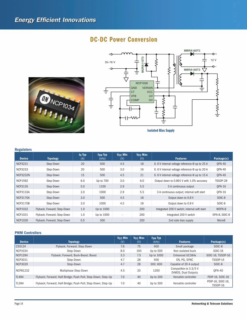
DC-DC Power Conversion
Isolated Bias Supply
+
35--76 V
--
+
--
MBRA160T3
MBRA160T3
12 V
MU
RA
110T
3
GND
COMP
VCCVDRAIN
UVOV
CTVFB
NCP1030
PWM Controllers
Device TopologyVCC Min
(V)VCC Max
(V)fSW Typ (kHz) Features Package(s)
CS5124 Flyback; Forward; Step-Down 7.6 75 400 Small package SOIC-8NCP1034 Step-Down 8.0 100 Up to 500 Non-isolated buck SOIC-16NCP1294 Flyback; Forward; Buck-Boost; Boost 3.3 7.5 Up to 1000 Enhanced UC384x SOIC-16, TSSOP-16NCP3011 Step-Down 4.7 28 400 EN, PG, SYNC TSSOP-14NCP3020 Step-Down 4.7 28 300; 600 Capable of 20 A output SOIC-8
NCP81232 Multiphase Step-Down 4.5 20 1200Compatible to 3.3/5 V DrMOS, Dual Outputs
QFN-40
TL494 Flyback; Forward; Half-Bridge; Push-Pull; Step-Down; Step-Up 7.0 40 Up to 200 Versatile controller PDIP-16, SOIC-16
TL594 Flyback; Forward; Half-Bridge; Push-Pull; Step-Down; Step-Up 7.0 40 Up to 300 Versatile controllerPDIP-16, SOIC-16,
TSSOP-16
Regulators
Device TopologyIO Typ
(A)fSW Typ (kHz)
VCC Min (V)
VCC Max (V) Features Package(s)
NCP3231 Step-Down 20 500 4.5 18 0. 6 V internal voltage reference @ up to 25 A QFN-40
NCP3233 Step-Down 20 500 3.0 16 0. 6 V internal voltage reference @ up to 20 A QFN-40
NCP3232N Step-Down 15 500 4.5 21 0. 6 V internal voltage reference @ up to 15 A QFN-40
NCP1592 Step-Down 6.0 Up to 700 3.0 6.0 Output down to 0.891 V with 1.0% accuracy TSSOP-28
NCP3135 Step-Down 5.0 1100 2.9 5.5 5 A continuous output QFN-16
NCP3133A Step-Down 3.0 1000 2.9 5.5 3 A continuous output; internal soft start QFN-16
NCP3170A Step-Down 3.0 500 4.5 18 Output down to 0.8 V SOIC-8
NCP3170B Step-Down 3.0 1000 4.5 18 Output down to 0.8 V SOIC-8
NCP1032 Flyback; Forward; Step-Down 1.0 Up to 1000 - 200 Integrated 200 V switch; internal soft start WDFN-8
NCP1031 Flyback; Forward; Step-Down 1.0 Up to 1000 - 200 Integrated 200 V switch DFN-8, SOIC-8
NCP1030 Flyback; Forward; Step-Down 0.5 300 - 200 2nd side bias supply Micro8

Page 15ON Semiconductor
Linear Voltage Regulators
Device IO Typ Function Features Package
NCP2399 — Hot Swap -36 to -80 V Supply Voltage MSOP-8
NCP785A 10 mA High Voltage LDO Up to 450 V VIN; High PSRR SC-89
NCP715 50 mA Ultra-low Quiescent Current LDO Ultra-low quiescent current; Wide input voltage range SC-70-5, DFN-6
NCP716 80 mA Ultra-low Quiescent Current LDO Ultra-low quiescent current; Wide input voltage range WDFN-6
NCP700B 200 mA Ultra-low Noise LDO High PSRR; Ultra-low noise SOT-23-5, WDFN-6
NCP702 200 mA Ultra-low Noise LDO High PSRR; Ultra-low noise SOT-23-5, WDFN-6
NCP160 250 mA Ultra-high PSRR 92 db PSRR; Low Noise WLCSP-4, XDFN-4
NCP703 300 mA Ultra-low Noise LDO Ultra-low noise; High PSRR SOT-23-5, WDFN-6
NCP161 450 mA Ultra-high PSRR 92 db PSRR; Low Noise WLCSP-4, XDFN-4
NCP163 450 mA Ultra-low Noise 92 db PSRR; 6.5 µVrms Noise WLCSP-4, XDFN-4
NCP133 500 mA Ultra-Low Dropout Voltage Regulator with Bias RailTypical dropout: 140 mV @ 500 mA; High PSRR;
Very fast transient responseXDFN-6
NCP705 500 mA Ultra-low Noise LDO Ultra-low noise; High PSRR WDFN-6
NCP59800 1 A Low Noise, RF LDO Typical dropout: 200 mV @ 1 A; High PSRR; Ultra-low noise DFN-8
NCP59748 1.5 A Ultra-Low Dropout Voltage Regulator with Bias RailTypical dropout: 60 mV @ 500 mA; High PSRR;
Very fast transient responseDFN-10, QFN-20
NCP51200 3 A DDR3 Termination Regulator Fast load transient response; Soft start; Remote sensing DFN-10
NCP51401 3 A DDR4 Termination Regulator Fast load transient response; Soft start; Remote sensing DFN-10
NCP58302 3 A Adjustable True LDO Linear Voltage RegulatorTypical dropout: 250 mV @ 3 A, 370 mV @ 3 A; Maximum voltage input
18 V; Stable with tantalum capacitors on the outputD2PAK-5
NCP59744 3 A Ultra-Low Dropout Voltage Regulator with Bias Rail Typical dropout: 115 mV @ 3 A; High PSRR; Very fast transient response QFN-20
NCP59749 3 A Ultra-Low Dropout Voltage Regulator with Bias Rail Typical dropout: 120 mV @ 3 A; High PSRR; Very fast transient response DFN-10, QFN-20
System, 5 V, 3 A
LVDS Clock Gen., 2.5 V, 0.2 A
CPLD Sys. Controller, 1.8 V, 0.3 A
System, 3.3 V, 34A
XFP, 1.8 V, 1 A
FPGA I/O VAUX, 2.5 V, 5 A
FPGA XADC, 1.8 V, 0.2 A
FPGA Core, 1.2/1.0/0.9 V, 5 A
FPGA I/O Bank, 2.5 V, 5 A
Flash Memory, 1.8 V, 0.5 A
GbE Transceiver, 2.5 V, 0.5 A
GbE Transceiver, 1.0/1.2 V, 0.5 A
FPGA GTP Termination, 1.2 V, 2 A
FPGA GTP, 1.0 V, 2 A
DDR3 VTT, 0.75 V, 1.5 A
DDR3 Core, 1.5 V, 3 A
DC/DC
12V
NCP705
DC/DC
48 or 24 V
NCP59744DC/DC
NCP133
DC/DC
DC/DC
NCP59151
NCP700B
Hot-SwapController
NCP705
NCP700B
NCP781 DC/DC BiasAlways-On Circuits
DC/DC
NCP59744
NCP51200
Switch
Isolated DC/DC BusConverter
5.0 V
2.5 V
1.8 V
3.3 V3.3 V
1.8 V
2.5 V2.5 V
1.8 V
1.2/1.0/0.9 V
2.5 V
1.8 V
2.5 V
1/1.2 V
1.2 V
1.0 V1.5 V
0.75 V
1.5 V

Page 16 Networking & Telecom Solutions
Configuration PolarityVDS (V)
VGS (V)
RDS(ON) mΩ
Qg (nC)
Qgd (nC)
RG (Ω)
VGS= 10 V VGS= 4.5 V
Device Typ Typ PackageNTMFS4H01N Single N 25 20 0.55 0.76 39 8.5 1.2 SO8-FLNTMFS4H01NF Int. Schottky N 25 20 0.56 0.79 37.8 8 1.3 SO8-FLNTMFS4H013NF Single N 25 20 0.72 1.1 26 5.8 1 SO8-FLNTMFS4H02N Single N 25 20 1.1 1.7 18 4.2 1 SO8-FLNTMFS4H02NF Int. Schottky N 25 20 1.1 1.6 18.7 4.3 1 SO8-FLNTMFS4C01N Single N 30 20 0.71 0.94 63 13 1 SO8-FLNTMFS5C404NL Single N 40 20 0.56 0.85 81 23.8 — SO8-FLNTMFS5C410NL Single N 40 20 0.71 1 66 22 — SO8-FLNTMFS5C604NL Single N 60 20 0.93 1.25 52 12.7 — SO8-FLNTMFS5C612NL Single N 60 20 1.2 1.65 41 10.9 — SO8-FLFDMS86181 Single N 100 20 4.2 — 42 — — PQFN-8L
ORing MOSFETs
Isolated Topology DC-DC (Bricks)
Features• Low RDS(on) for low
conduction loss• 30 V for IM bus ORing• 100 V for 48 V bus ORing
Features• Low RDS(on) for low conduction loss• Low capacitance for low switching loss• Integrated Schottky for low diode loss
Vout48 V
ForwardFlyback
Push PullHalf BridgeFull Bridge
MOSFETs as ORing Diodes
=
MOSFETs for Power Conversion
Configuration PolarityVDS (V)
VGS (V)
RDS(ON) mΩ
Qg (nC)
Qgd (nC)
Ciss (pF)
Crss (pF)
RG (Ω)
VGS= 10 V VGS= 4.5 V
Device Typ Typ Application PackageNTMFS4H01N Single N 25 20 0.55 0.76 39 8.5 5693 212 1.2
Secondary Synchronous
SO-8FLNTMFS4H01NF Int. Schottky N 25 20 0.56 0.79 37.8 8 5538 175.3 1.3 SO-8FLNTMFS4H013NF Single N 25 20 0.72 1.1 26 5.8 3923 114 1 SO-8FLNTMFS4H02N Single N 25 20 1.1 1.7 18 4.2 2651 103 1 SO-8FLNTMFS4H02NF Int. Schottky N 25 20 1.1 1.6 18.7 4.3 2652 94 1 SO-8FLNTTFS4H05N Single N 25 20 2.5 3.8 8.7 1.88 1205 45 1 u8FLNTTFS4H07N Single N 25 20 3.8 5.8 5.7 1.26 771 34 1 u8FLNTMFS4C05N Single N 30 20 2.7 4 14 5 1972 59 1 SO-8FLNTMFS4C06N Single N 30 20 3.2 4.8 11.6 4 1683 40 1 SO-8FLNTMFS4C08N Single N 30 20 4.6 6.8 8.4 3.3 1113 39 1 SO-8FLNTTFS4C05N Single N 30 20 2.9 4.1 14.5 5.5 1988 71 1 u8FLNTMFS5C404NL Single N 40 20 0.56 0.85 81 23.8 12168 79.8 — SO-8FLNTMFS5C410NL Single N 40 20 0.71 1 66 22 8862 116 — SO-8FLNTMFS5C430NL Single N 40 20 1.2 1.7 32 9 4300 72 — SO-8FLNTMFS5C423NL Single N 40 20 1.6 2.4 23 6.7 3100 60 — Control/Synchronous SO-8FLNTMFS5C442NL Single N 40 20 2.2 3.4 22 6.7 3000 28 —
Primary/Secondary Synchronous
SO-8FLNTMFS5C604NL Single N 60 20 0.93 1.25 52 12.7 8900 40 — SO-8FLNTMFS5C612NL Single N 60 20 1.2 1.65 41 10.9 6660 45 — SO-8FLNTMFS5C646NL Single N 60 20 3.8 5 15.7 5.1 2164 17 — SO-8FLNTMFS5C670NL Single N 60 20 5.4 7.2 9.2 1.5 1400 15 — SO-8FL

Page 17ON Semiconductor
ConfigurationVDS (V)
VGS (V)
RDS(ON) mΩ
Qg (nC)
Qgd (nC)
Ciss (pF)
Crss (pF)
RG (Ω)
VGS= 10 V VGS= 4.5 V
Device Typ Typ Application PackageNTMFS4H01N Single 25 20 0.55 0.76 39 8.5 5693 212 1.2 Synchronous Side SO-8FL
NTMFS4H01NF Int. Schottky 25 20 0.56 0.79 37.8 8 5538 175.3 1.3 Synchronous Side SO-8FL
NTMFS4H013NF Single 25 20 0.72 1.1 26 5.8 3923 114 1 Synchronous Side SO-8FL
NTMFS4H02N Single 25 20 1.1 1.7 18 4.2 2651 103 1 Synchronous Side SO-8FL
NTMFS4H02NF Int. Schottky 25 20 1.1 1.6 18.7 4.3 2652 94 1 Synchronous Side SO-8FL
NTTFS4H05N Single 25 20 2.5 3.8 8.7 1.88 1205 45 1 Synchronous Side u8FL
NTTFS4H07N Single 25 20 3.8 5.8 5.7 1.26 771 34 1 Synchronous Side u8FL
ATP202 Single 30 20 9 14 27 4 1650 160 — Control Side ATPAK
NTMFS4C05N Single 30 20 2.7 4 14 5 1972 59 1 Synchronous Side SO-8FL
NTMFS4C06N Single 30 20 3.2 4.8 11.6 4 1683 40 1 Synchronous Side SO-8FL
NTMFS4C08N Single 30 20 4.6 6.8 8.4 3.3 1113 39 1 Synchronous Side SO-8FL
NTMFS4C09N Single 30 20 4.6 6.8 10.9 5.4 1252 126 1 Synchronous Side SO-8FL
NTMFS4C10N Single 30 20 5.8 8.9 9.8 3.7 987 162 1 Synchronous Side SO-8FL
NTMFS4C13N Single 30 20 7.3 11.4 7.8 3.7 770 127 1 Synchronous Side SO-8FL
NTTFS4C05N Single 30 20 2.9 4.1 14.5 5.5 1988 71 1 Control Side u8FL
NTTFS4C08N Single 30 20 4.7 7.2 8.4 3.3 1113 39 1 Control Side u8FL
NTTFS4C10N Single 30 20 5.9 8.8 10.1 6.1 993 163 1 Control Side u8FL
NTTFS4C13N Single 30 20 7.5 11.2 7.8 3.7 770 127 1 Control Side u8FL
NTMFS5C404NL Single 40 20 0.56 0.85 81 23.8 12168 79.8 — Synchronous Side SO-8FL
NTMFS5C410NL Single 40 20 0.71 1 66 22 8862 116 — Synchronous Side SO-8FL
NTMFS5C423NL Single 40 20 1.6 2.4 23 6.7 3100 60 — Control/Synchronous SO-8FL
NTMFS5C430NL Single 40 20 1.2 1.7 32 9 4300 72 — Control/Synchronous SO-8FL
NTMFS5C442NL Single 40 20 2.2 3.4 22 6.7 3000 28 — Control Side SO-8FL
Non-Isolated Topology “Buck” DC-DC
Features• Low RDS(on) for low conduction loss• Low capacitance for low switching loss• Integrated Schottky for enhanced light load efficiency
Sync Cout VoutVin Cin
Control
PWMController
MOSFETs for Power Conversion

Page 18 Networking & Telecom Solutions
T(4:1)
36 - 75 V 12 V
GND
Typical Application Diagram
Configuration PolarityVDS (V)
VGS (V)
RDS(ON) Max mΩ Qg Typ (nC)
Qgs Typ (nC)
Qgd Typ (nC)
RG Typ (Ω)Device VGS= 10 V VGS= 8 V VGS= 6 V VGS= 4.5 V Package
FDMS86300DC Single N 80 20 3.1 4 — — 72 26 14 1.2 PQFN-8L
FDMS86300 Single N 80 20 3.9 5.5 — — 72 28 15 1.2 SO-8FL
FDMS86310 Single N 80 20 4.8 6.7 — — 66 24 14 1.3 SO-8FL
FDMS86320 Single N 80 20 11.7 15 — — 29 10 6.9 0.5 SO-8FL
FDMC86340 Single N 80 20 6.5 8.5 — — 38 14 8 0.7 u8FL
FDMC86320 Single N 80 20 11.7 16 — — 29 10 6.9 0.5 u8FL
FDMS86181 Single N 100 20 4.2 — 12 — 42 13 9.3 1.3 SO-8FL
FDMS86152 Single N 100 20 6 — 11 — 36 10.7 7.2 0.9 SO-8FL
FDMS86101 Single N 100 20 8 — 13.5 — 39 9.5 10.8 1 SO-8FL
FDMS86101DC Single N 100 20 7.5 — 12 — 31 8.3 7 1.4 PQFN-8L
FDMS86103L Single N 100 20 8 — — 11 43 7.5 7 1.3 SO-8FL
FDMC86160 Single N 100 20 14 — 23 — 15 4.4 3.5 0.6 u8FL
FDMC86102 Single N 100 20 24 — 38 — 13 3.7 3.6 0.5 u8FL
FDMC86102LZ Single N 100 20 24 — — 35 15.3 2.4 2.5 0.4 u8FL
FDMS86255 Single N 150 20 12.4 — 15.5 — 45 14 8.8 0.7 SO-8FL
FDMS86200DC Single N 150 20 17 — 25 — 30 9.7 5.6 1.5 PQFN-8L
FDMS86200 Single N 150 20 18 — 21 — 33 7.7 7.7 1.2 SO-8FL
FDMS86250 Single N 150 20 25 — 33 — 25 7.4 5.5 0.5 SO-8FL
FDMC86260 Single N 150 20 34 — 44 — 15 4 3.1 0.6 u8FL
FDMC86240 Single N 150 20 51 — 70 — 11 2.8 2.3 0.5 u8FL
MOSFETs for Power Conversion
Synchronous Rectification, Primary DC-DC

Advanced Load Switches
• Copackaged MOSFET plus CMOS controllers – value-added features plus high performance• Monolithic CMOS smart load switches – value added features, low cost• Discrete MOSFETs – simple, high performance
ON Semiconductor provides a comprehensive range of load switches, suitable for a variety of different power trees.
NCP45x x x Integrated Load Switch Feature• Simple/clean design• No current consumption in standby power mode• Small PCB footprint• Low RDS(ON) due to charge pump driving NMOS• Adjustable soft-start time (SR)• Adjustable integrated discharge• Fault protection• Power rail monitoring & sequencing
Thermal,Undervoltage
&Short-CircuitProtection
ControlLogic
Bandgap&
Biases
Delay andSlew Rate
Control
ChargePump
VIN
VOUTBLEEDGNDSR
PGENVCC
Type Deviceron
(mΩ) I Max
(A) VI Min
(V) VI Max
(V) IQ
(mA) DischargeSlew Rate
(ms) Features Package(s)
Smar
t Loa
d Sw
itch
NCP330 26 at 3.3 V 3 1.8 5.5 100 - 2000 Reverse blocking TDFN-4
NCP333 55 at 3.3 V 1.5 1.2 5.5 1 Auto 95 - WLCSP-4
NCP334 47 at 3.3 V 2 1.2 5.5 1 - 71 - WLCSP-4
NCP335 47 at 3.3 V 2 1.2 5.5 1 Auto 71 - WLCSP-4
NCP336 23 at 3.3 V 3 1.2 5.5 1 - 810 - WLCSP-6
NCP337 23 at 3.3 V 3 1.2 5.5 1 Auto 810 - WLCSP-6
NCP338 27 at 1.8 V 2 1 3.6 0.6 Auto 20 - WLCSP-6
NCP339 26 at 3.3 V 3 1.2 5.5 2 - 2700 Reverse blocking WLCSP-6
NCP432 50 at 1.8 V 1.5 1 3.6 0.6 - 20 - WLCSP-4
NCP433 50 at 1.8 V 1.5 1 3.6 0.6 Auto 20 - WLCSP-4
NCP434 43 at 1.8 V 2 1 3.6 0.6 - 61 - WLCSP-4
NCP435 43 at 1.8 V 2 1 3.6 0.6 Auto 61 - WLCSP-4
NCP436 23 at 1.8 V 3 1 3.6 1 - 27 - WLCSP-6
NCP437 23 at 1.8 V 3 1 3.6 1 Auto 27 - WLCSP-6
ecoS
WIT
CH™
Inte
grat
ed
Load
Sw
itch
NCP45524 18.0 6 0.5 13.5 - Adj - Power good DFN-8
NCP45525 18.0 6 0.5 13.5 - Adj Adj - DFN-8
NCP45560 2.4 24 0.5 13.5 - Adj Adj Power good; Fault DFN-12
NCP45540 3.3 20 0.5 13.5 - Adj Adj Power good; Fault DFN-12
NCP45541 3.3 20 0.5 13.5 - Adj Adj Power good DFN-12
NCP45520 9.5 10.5 0.5 13.5 - Adj - Power good; Fault DFN-8
NCP45521 9.5 10.5 0.5 13.5 - Adj Adj Fault DFN-8
Page 19ON Semiconductor

Page 20 Networking & Telecom Solutions
Thermal Management
Ex tensive Por t folio Local Sensors provide temperature information at the device location
Remote Sensors provide temperature information of a transistor located at a different position on the board; also includes local sensor capability
Fan Controllers integrate the temperature sensor with a fan controller/monitor
System Monitors integrate combinations of remote and/or local temperature sensing, voltage monitoring, fan control & monitoring, reset control, and GPIO functions
SystemVoltages +12 V
+5 V
+3.3 V
+2.5 V
+1.8 V
+1.5 V
+1.25 V
+0.9 V
VBatt
Chassis Intrusion
ALERT O/P
Bi-directionalTHERM Pins
TDM3
TDM1
TDM2
8 GPIOs
SMBus Interface
RESET I/O
Fan Drive and Control
• 4 PWM Fan Drive Outputs• 8 Tach Inputs
4 PWM O/Ps
8 Tach Inputs
Fan2Max
Temperature• Measures 4 Temp Zones
1 Local3 RemoteTHERM I/O
Device
Supply Range
(V)
Temperature Range(°C )
LocalAccuracy
(°C) Interface
Numberof
AddressesSRC(Ω)
RemoteAccuracy
RemoteChannels
FanChannels
TACHChannels
Voltage Monitoring Channels GPIOs Package
System Monitors
ADM1026 3 - 5.5 -40 to +120 ±3 I2C/SMBUS 3 — ±3 2 8 8 19 17 LQFP-48
ADT7462 3 - 5.5 -40 to +125 ±2.25 I2C/SMBUS 2 2 k ±2.25 3 4 8 13 8 LFCSP-32
NCT80 2.8 - 5.75 -40 to +125 ±2 I2C/SMBUS 8 — — — — 2 7 1 TSSOP-24
ADT7476 3 - 3.6 -40 to +120 ±1.5 I2C/SMBUS 3 — ±1.5 2 3 4 5 — QSOP-24
Fan Controllers
ADT7473 3 - 3.6 -40 to +120 ±1.5 I2C/SMBUS 3 3 k ±1.5 2 3 4 QSOP-16
ADT7475 3 - 3.6 -40 to +120 ±1.5 I2C/SMBUS 1 — ±1.5 2 3 4 QSOP-16
ADM1033 3 - 3.6 -40 to +120 ±1 I2C/SMBUS 8 1 k ±1 1 1 1 QSOP-16
ADM1034 3 - 3.6 -40 to +120 ±1 I2C/SMBUS 8 1 k ±1 2 2 2 QSOP-16
Remote Sensors
NCT72 2.8 - 3.6 -40 to +125 ±1 I2C/SMBUS 2 1.5 k ±1 1 DFN-8, WDFN-8
NCT218 1.4 - 2.75 -40 to +125 ±1.75 I2C/SMBUS 2 150 ±1 1 WDFN-8, WLCSP-8
NCT210 3 - 5.5 -55 to +125 ±1 I2C/SMBUS 9 — ±3 2 QSOP-16
ADM1032 3 - 5.5 -40 to +125 ±3 I2C/SMBUS 2 — ±1 1 SOIC-8, MSOP-8
ADT7461 3 - 5.5 -40 to +125 ±3 I2C/SMBUS 2 3 k ±1 1 SOIC-8, MSOP-8
ADT7481 3 - 3.6 -40 to +125 ±1 I2C/SMBUS 2 — ±1 2 MSOP-10
ADT7483 3 - 3.6 -40 to +125 ±1 I2C/SMBUS 9 — ±1 2 QSOP-16
Local Sensors
NCT375 3 - 5.5 -55 to +125 ±1 SMBUS 8 DFN-8, SOIC-8, Micro8
NCT475 3 - 5.5 -55 to +125 ±1 SMBUS 4 WLCSP-6
NCT203 1.4 - 2.75 -40 to +125 ±1.75 I2C/SMBUS 1 DFN-8, SOIC-8, Micro8

Page 21ON Semiconductor
Zero-Drift Operational Amplifiers
Zero-Drift Amplifiers
Device ChannelsVS Min
(V)VS Max
(V)Input CM Range
(V)IQ /Chan-nel (mA)
GBW(kHz)
VOS Max(mV)
VOS Drift (mV/°C)
CMRR(dB)
ep-p(mVpp) Features Package
NCS325 1 1.8 5.5 VSS–0.1 to VDD+0.1 21 350 50 0.02 110 1 Low VOS SOT-23
NCSx333 1, 2, 4 1.8 5.5 VSS–0.1 to VDD+0.1 21 350 10 0.03 120 1 Low VOSSOT-23, SC-70, DFN-8,
Micro8, SOIC-8, SOIC-14
Zero-Drift Current-Sense Amplifiers
Device ChannelsVS Min
(V)VS Max
(V)Input CM Range
(V)IQ /Channel
(mA)GBW(kHz)
VOS Max(mV)
VOS Drift (mV/°C)
Gain Error (%)
CMRR(dB)
ep-p(mVpp) Features Package
NCS21x 1 2.7 26 2.7 to 26 65 14 35 0.5 1 140 — Low VOS SOT-363
NCS701x 1 4.0 5.5 4.0 to 80 800 500 200 0.1 0.35 110 23 Low VOS Micro8
Device Gain R3 – R4 R1 – R2
NCS213 50 20 kΩ 1 mΩ
NCS215 75 13.3 kΩ 1 mΩ
NCS214 100 10 kΩ 1 mΩ
NCS210 200 5 kΩ 1 mΩ
NCS211 500 2 kΩ 1 mΩ
NCS212 1000 1 kΩ 1 mΩ
NCS21x R1
IN–
IN+OUT
REF
GNDV+
R3
R4
R2
NCS701x R4
–IN
+INOUT
LDO
GNDREF
R1
R2
R3
VS
END
As part of a complete portfolio of operational amplifiers, ON Semiconductor offers zero-drift operational amplifiers that are ideal for current sensing in system monitoring, and provide high precision over time and temperature for signal conditioning.
NCS21x R1
R2
IN–
IN+
OUTOutput
ReferenceVoltage
0.01 μFto 0.1 pF
+2.7 to +26 V
Supply Load
GNDVS
R1
RSHUNT
R2
REF
Device Gain R3 – R4 R1 – R2
NCS7011* 14 1050 kΩ 75 kΩ
NCS7012* 20 1.5 MΩ 75 kΩ
NCS7013* 50 1.5 MΩ 30 kΩ
NCS7014* 100 1.5 MΩ 15 kΩ
* Pending 1Q17.
Current Sense Application

Switching Devices
Page 22 Networking & Telecom Solutions
ON Semiconductor offers a range of switching devices for high speed interface in servers, desktop computing, notebook and netbook computers. Applications include PCI Express, DisplayPort, Gigabit Ethernet and USB 2.0.
Processor
Gigabit LANTransceiver
InternalGraphics
Processor
ExternalGraphics
Processor
North Bridge(ICH)
South Bridge(MCH)
VGA Switch
Do
ckin
g S
tati
on
Co
nn
ecto
r PCIeSwitch
HDMI/DVISwitch
LAN Switch
USB Power/Data Switch
Codec
Stereo Switch
Mic Switch
TMDSDisplayPort
Switch
2nd LCDDisplay
LCDPanel
AudioAmp
Server Implementation
Device Interface Data RateNo
ChannelsQuiescent Current
NCN3612B PCIe 3.0, DisplayPort 1.2 8 Gb/s 12 250 μA
NCN3411 PCIe 3.0 8 Gb/s 8 200 μA
NCN2612B PCIe 2.0, DisplayPort 1.1 5 Gb/s 12 250 μA
NS3L500 Gigabit Ethernet 1 Gb/s 11 250 μA
NCN1188 USB 2.0 / MHL 2.25 Gb/s 2 21 μA
NS5S1153 USB 2.0 480 Mb/s 2 21 μA
NLAS7242 USB 2.0 480 Mb/s 2 1 μA
NLAS52231 Audio 36 MHz 2 1 μA
NLAS4684 Audio 9.5 MHz 2 180 nA

Electronic Fuses for Inrush Current Limiting on Power Buses3–12 V Power Bus Hot Plug Protection
Features• Low RDS(ON), high operating and trip currents
(IOP, ITRIP)• Overvoltage protection• Precise ITRIP control• Slew rate control• Thermal shut-down • EN pin for synchronizing multiple eFuses• Outperforms poly-fuses:
– Tighter spec tolerances– Lower resistance– Shorter trip-time– Superior repeatability
• High efficiency with high current capability• eFuses in parallel achieve practically any desired level of
IOP and ITRIP
ChargePumpEnable
Enable/Fault
GND
Source
ILimit
dV/dt
CurrentLimit
VoltageClamp
dV/dtControl
ThermalShutdown
UVLO
VCC
Typical Feature Set for eFuse
Hard Drive/Solid State Drive ApplicationNetwork Interface Card Application
5 V Power Bus
SATAPower
NIS545x
NIS5232
RLIM
ENABLE
12 V Power Bus
RLIM
3 V Power Bus
NIS5431
RLIMENABLE
12 V
12 V
12 V
GND
GND
5 V
5 V
5 V
GND
GND
GND
3.3 V
3.3 V
3.3 V
Small Form FactorPluggable Module
NIS5431
3.3 VPCIe
NIC - Media Type Independent
3 V Power
Page 23ON Semiconductor
DeviceInput Voltage
(V)Output Clamping Voltage
(V)ITRIP Trip Current
(A)RDS(ON)
(mΩ) Adjustable ITRIP Auto Recovery Latching PackageNIS5112 -0.6 to 18 15 2.5 28 Yes Yes Yes SOIC-8
NIS5132 -0.6 to 18 15 3.5 44 Yes Yes Yes DFN-10
NIS5232 -0.6 to 18 15 4 44 Yes No Yes DFN-10
NIS5135 -0.6 to 18 6.65 3.5 68 Yes Yes Yes DFN-10
NIS5452 -0.6 to 14 5.85 2.1 40 Yes No Yes WDFN-10
NIS5431 -0.6 to 14 3.85 1.6 45 Yes No Yes WDFN-10

Page 24 Networking & Telecom Solutions
Ethernet : 10/100BASE-T, 1000BASE-TX, and GigabitSurge/ESD Protection for Four Pairs
Line-to-Line Surge
Line Side : LC03-6 (optional)Transformer Side: TVS8818
Protection against metallic (transverse) strikes
Typical ApplicationFeatures• Line-to-line capacitance < 3 pF• Vclamp (25 A surge) < 11 V• IEC 61000-4-2 rating > 30 kV• No latching danger• Surge rating maintained to 125°C
Benefits• Compatible with Gb Ethernet and beyond• Enhanced protection for downstream electronics• Accommodates operating transients above 3.3 V• Small form-factor allows integration into connectors
The 1000BASE-T or Gigabit Ethernet interface operating at higher bitrates is susceptible to ESD strikes, cable-discharge events and lightning-induced transients. Our products help meet IEC 61000-4-5, GR-1089-CORE and other Standards.
C5VDDC1
C2
TVS8818
LC03
C3
C4
C6VDD
LC03
C7VDD
LC03
C8VDD
LC03
TPOPA
TPONA
TPOPB
TPONB
TPOPC
TPONC
TPOPD
TPOND
A+
A-
B+
B-
C+
C-
D+
D-
1000
BA
SE
-TE
TH
ER
NE
T T
RA
NS
CE
IVE
R
TR
AN
SF
OR
ME
R
RJ4
5
1 8
1 8
1 8
1 8
-10 00
5
10
15
20
25
30
10 20 30Time (μs)
Vo
ltag
e (V
), C
urr
ent
(A)
40 50 60
8/20 μsSurge Current
ON SemiconductorVoltage
CompetitorVoltage
1
2
3
4
5
6
7
8
RJ-
45 C
on
nec
tor
Flow ThroughRouting
TVS8818
Surge Protection Devices
DeviceVDC Max
(V)
Line Transient
Max (V)
Surge IPP, 8/20 ms
(A)
Typical Line-Line
Capacitance(pF)
ESD Contact Rating
(kV) PackageLC03-6 6.7 7.0 100 8.0 ±30 SOIC-8TVS8814 3.0 3.2 35 1.5 ±30 UDFN-8TVS8818 3.0 3.2 35 1.5 ±30 UDFN-10SRDA3.3 3.3 5.0 25 4.0 ±8 SOIC-8SRDA05 5.0 7.0 23 5.0 ±8 SOIC-8NUP4114H 5.0 5.0 12* 0.4 ±13 TSOP-6
* On Pin 5.

T1/E1, T3/E3, and xDSL PortsSurge protection for GR-1089, TIA-968-A, ITU-T and IEC 61000-4-5
Surge Protection Features• Capable of all T1/E1 and xDSL voltages with a variety of
capacitance values, for driver-side protection
TSPD Features• Cline <14 pF for 50 A surge under 8/20 ms (NP0080TA
series)
Benef it s• Required data-rates are supported by TSPDs• Surge protection devices provide high levels of tertiary
protection without latching
T1/E1 links (< 2 Mbps), T3/E3 links (< 43 Mbps) and xDSL lines (< 52 Mbps) are susceptible to ESD strikes, cable-discharge events and lightning-induced transients.
SL15x 2
TIP
RING
VOICE(POTS)
xDSLMODEM
Typical xDSL + POTS Application
Surge Protection Devices
DeviceVDC Max
(V)
Surge IPP, 8/20 ms
(A)
Line-Line Capacitance
(pF)
ESD Contact Rating
(kV) PackageSRDA3.3 3.3 25 4.0 ±8 SOIC-8SRDA05 5.0 23 5.0 ±8 SOIC-8LC03-6 5.0 100 8.0 ±30 SOIC-8SL05 to SL24 5 to 24 5 to 17 3.5 ±8 SOT-23
Thyristor Surge Protection Devices
DeviceVDRM
(V)VBO (V)
VT (V)
CO (pF)
IH (mA)
Surge IPP, 10/1000 ms
(A) PackageNP0080TA Series 8-16 9.5-18 — 11-13 50 50 (8/20 ms) TSOP-5
Page 25ON Semiconductor

Page 26 Networking & Telecom Solutions
EEPROMs for Configuration and Calibration
EasyPRO™ is a user-friendly, portable programming tool for ON Semiconductor
serial EEPROMs (I2C, SPI, Microwire)
Features• Broad density range: 1 kb to 2 Mb• Wide operating Vcc range: 1.8/1.7 V to 5.5 V• High endurance: 1 million program/erase cycles• Wide temperature range: industrial and extended
EEPROMsData
Transmission Standard Device Density Organization*
VCC Min(V)
VCC Max(V)
fCLK Max(MHz) Package(s)
I2C
CAT24M01 1 Mb 128k x 8 1.8 5.5 1 SOIC-8, TSSOP-8, UDFN-8CAT24C512 512 kb 64k x 8 1.8 5.5 1 SOIC-8, TSSOP-8, UDFN-8CAT24C256 256 kb 32k x 8 1.8 5.5 1 SOIC-8, TSSOP-8, UDFN-8CAT24C128 128 kb 16k x 8 1.8 5.5 1 SOIC-8, TSSOP-8, UDFN-8CAT24C64 64 kb 8k x 8 1.7 5.5 1 SOIC-8, TSSOP-8, UDFN-8
N24C64 64 kb 8k x 8 1.7 5.5 1 US-8
CAT24C32 32 kb 4k x 8 1.7 5.5 1 SOIC-8, TSSOP-8, UDFN-8; WLCSP-5N24C32 32 kb 4k x 8 1.7 5.5 1 US-8
CAT24C16 16 kb 2k x 8 1.7 5.5 0.4 SOIC-8, TSSOP-8, UDFN-8, TSOT23-5, WLCSP-4, WLCSP-5N24C16 16 kb 2k x 8 1.7 5.5 0.4 US-8
CAT24C08 8 kb 1k x 8 1.7 5.5 0.4 SOIC-8, TSSOP-8, UDFN-8, TSOT23-5, WLCSP-4, WLCSP-5N24C08 8 kb 1k x 8 1.7 5.5 0.4 US-8
CAT24C04 4 kb 512 x 8 1.7 5.5 0.4 SOIC-8, TSSOP-8, UDFN-8, TSOT23-5, WLCSP-4, WLCSP-5N24C04 4 kb 512 x 8 1.7 5.5 0.4 US-8
CAT24C02 2 kb 256 x 8 1.7 5.5 0.4 SOIC-8, TSSOP-8, UDFN-8, TSOT23-5, WLCSP-4, WLCSP-5N24C02 2 kb 256 x 8 1.7 5.5 0.4 US-8
SPI
CAT25M02 2 Mb 256k x 8 1.7 5.5 10 SOIC-8CAT25M01 1 Mb 128k x 8 1.8 5.5 10 SOIC-8, TSSOP-8CAT25512 512 kb 64k x 8 1.8 5.5 20 SOIC-8, TSSOP-8, UDFN-8CAT25256 256 kb 32k x 8 1.8 5.5 20 SOIC-8, TSSOP-8, UDFN-8CAT25128 128 kb 16k x 8 1.8 5.5 20 SOIC-8, TSSOP-8, UDFN-8CAT25640 64 kb 8k x 8 1.8 5.5 20 SOIC-8, TSSOP-8, UDFN-8CAT25320 32 kb 4k x 8 1.8 5.5 20 SOIC-8, TSSOP-8, UDFN-8CAT25160 16 kb 2k x 8 1.8 5.5 20 SOIC-8, TSSOP-8, UDFN-8CAT25080 8 kb 1k x 8 1.8 5.5 20 SOIC-8, TSSOP-8, UDFN-8CAT25040 4 kb 512 x 8 1.8 5.5 20 SOIC-8, TSSOP-8, UDFN-8CAT25020 2 kb 256 x 8 1.8 5.5 20 SOIC-8, TSSOP-8, UDFN-8CAT25010 1 kb 128 x 8 1.8 5.5 20 SOIC-8, TSSOP-8, UDFN-8
Microwire
CAT93C86 16 kb 2k x 8 / 1k x 16 1.8 5.5 3 SOIC-8CAT93C86B 16 kb 2k x 8 / 1k x 16 1.8 / 1.65 5.5 4 SOIC-8, TSSOP-8, UDFN-8CAT93C76 8 kb 1k x 8 / 512 x 16 1.8 5.5 3 SOIC-8, TSSOP-8
CAT93C76B 8 kb 1k x 8 / 512 x 16 1.8 / 1.65 5.5 4 SOIC-8, TSSOP-8, UDFN-8CAT93C66 4 kb 512 x 8 / 256 x 16 1.8 5.5 2 SOIC-8, TSSOP-8CAT93C56 2 kb 256 x 8 / 128 x 16 1.8 5.5 2 SOIC-8, TSSOP-8CAT93C46 1 kb 128 x 8 / 64 x 16 1.8 5.5 2 SOIC-8, TSSOP-8
CAT93C46B 1 kb 128 x 8 / 64 x 16 1.8 / 1.65 5.5 4 SOIC-8, TSSOP-8, UDFN-8* Organization for Microwire devices is selectable.

Page 27ON Semiconductor
Voltage Supervisors with I2C Serial EEPROM and Watchdog Timer
Supervisor y Features• Precision power supply voltage monitor• Available voltage thresholds: 4.50 V, 4.25 V,
3.0 V, 2.85 V, 2.55 V• Active High or Low Reset, Manual Reset• Watchdog Timer (N84C161, N84C163)
16 kb Serial EEPROM Features• Supply Voltage: VCC = 2.7 to 6.0 V• 400 KHz, 100 KHz I2C Serial Protocol• Endurance: 1 million Write cycles• Retention: 100 years• Hardware Write Protect
Device Watchdog Timer Manual Reset Write Protect Package
N84C161 SDA 3 3 SOIC-8
N84C162 — 3 3 SOIC-8
N84C163 — 3 3 SOIC-8
DelayGenerator
RESETVCC
I2C Bus
WP
WDI
WriteProtect
VREF
WatchdogTimerEEPROM

BRD8077/DBRD8077-5 PRINTED IN USA 10/16 IRONWOOD XXXX 1K
EasyPRO, ecoSWITCH, and PureEdge are trademarks of ON Semiconductor. ARM is a registered trademarks of ARM Limited (or its subsidiaries) in the EU and/or elsewhere. All other brand names and product names appearing in this document are trademarks of their respective holders.
ON Semiconductor and the ON Semiconductor logo are trademarks of Semiconductor Components Industries, LLC dba ON Semiconductor or its subsidiaries in the United States and/or other countries. ON Semiconductor owns the rights to a number of patents, trademarks, copyrights, trade secrets, and other intellectual property. A listing of ON Semiconductor’s product/patent coverage may be accessed at www.onsemi.com/site/pdf/Patent-Marking.pdf. ON Semiconductor reserves the right to make changes without further notice to any products herein. ON Semiconductor makes no warranty, representation or guarantee regarding the suitability of its products for any particular purpose, nor does ON Semiconductor assume any liability arising out of the application or use of any product or circuit, and specifically disclaims any and all liability, including without limitation special, consequential or incidental damages. Buyer is responsible for its products and applications using ON Semiconductor products, including compliance with all laws, regulations and safety requirements or standards, regardless of any support or applications information provided by ON Semiconductor. “Typical” parameters which may be provided in ON Semiconductor data sheets and/or specifications can and do vary in different applications and actual performance may vary over time. All operating parameters, including “Typicals” must be validated for each customer application by customer’s technical experts. ON Semiconductor does not convey any license under its patent rights nor the rights of others. ON Semiconductor products are not designed, intended, or authorized for use as a critical component in life support systems or any FDA Class 3 medical devices or medical devices with a same or similar classification in a foreign jurisdiction or any devices intended for implantation in the human body. Should Buyer purchase or use ON Semiconductor products for any such unintended or unauthorized application, Buyer shall indemnify and hold ON Semiconductor and its officers, employees, subsidiaries, affiliates, and distributors harmless against all claims, costs, damages, and expenses, and reasonable attorney fees arising out of, directly or indirectly, any claim of personal injury or death associated with such unintended or unauthorized use, even if such claim alleges that ON Semiconductor was negligent regarding the design or manufacture of the part. ON Semiconductor is an Equal Opportunity/Affirmative Action Employer. This literature is subject to all applicable copyright laws and is not for resale in any manner.
LITERATURE FULFILLMENT: Literature Distribution Center for ON Semiconductor 19521 E. 32nd Pkwy, Aurora, Colorado 80011 USA Phone: 303-675-2175 or 800-344-3860 Toll Free USA/Canada Fax: 303-675-2176 or 800-344-3867 Toll Free USA/Canada Email: [email protected]
N. American Technical Support: 800-282-9855 Toll Free USA/Canada.Europe, Middle East and Africa Technical Support:
Phone: 421 33 790 2910Japan Customer Focus Center Phone: 81-3-5817-1050
ON Semiconductor Website: www.onsemi.com
Order Literature: http://www.onsemi.com/orderlit
For additional information, please contact your local Sales Representative
PUBLICATION ORDERING INFORMATION
Sales and Design Assistance from ON Semiconductor
AMERICAS REP FIRMSAlabama Huntsville e-Components (256) 533-2444Brazil Countrywide Ammon & Rizos (+55) 11-4688-1960California Bay Area Electec (408) 496-0706
Southern California Tech Coast Sales (949) 305-6869Canada Eastern Canada Astec (905) 607-1444Connecticut Statewide Paragon Electronic Systems (603) 645-7630Florida Statewide e-Components (888) 468-2444Georgia Atlanta e-Components (888) 468-2444Illinois Statewide Matrix – Design Technology (952) 400-1070Indiana Fishers Bear VAI (317) 570-0707Iowa Statewide Matrix – Design Technology (319) 362-6824Maine Statewide Paragon Electronic Systems (603) 645-7630Maryland Columbia Mechtronics Sales (410) 309-9600Massachusetts Statewide Paragon Electronic Systems (603) 645-7630Mexico Countrywide Ammon & Rizos (+55) 11-4688-1960Michigan St. Joseph Bear VAI (440) 526-1991Minnesota Eden Prairie Matrix – Design Technology (952) 400-1070Missouri Belton Matrix – Design Technology (816) 589-2308Nebraska Statewide Matrix – Design Technology (816) 589-2308New Hampshire Statewide Paragon Electronic Systems (603) 645-7630New Jersey Statewide S.J. Metro (516) 942-3232New York Binghamton TriTech - Full Line Rep (607) 722-3580
Jericho S.J. Metro (516) 942-3232Rochester TriTech - Full Line Rep (585) 385-6500
North Carolina Raleigh e-Components (888) 468-2444North Dakota Statewide Matrix – Design Technology (952) 400-1070Ohio Brecksville Bear VAI Technology (440) 526-1991Puerto Rico Countrywide e-Components (888) 468-2444Rhode Island Statewide Paragon Electronic Systems (603) 645-7630South Dakota Statewide Matrix – Design Technology (952) 400-1070Vermont Statewide Paragon Electronic Systems (603) 645-7630Wisconsin Statewide Matrix – Design Technology (952) 400-1070
ON Semiconductor Distribution PartnersAllied Electronics www.alliedelec.com (800) 433-5700
Altima Corp. www.altima.co.jp (81) 45 476 2155
Arrow Electronics www.arrow.com (800) 777-2776
Avnet www.em.avnet.com (800) 332-8638
Chip One Stop, Inc. www.chip1stop.com/maker/on (81) 45 470 8771
Daiwa Distribution Ltd. www.daiwahk.com (852) 2341 3351
Digi-Key www.digikey.com (800) 344-4539
EBV Elektronik www.ebv.com/en/locations.html (49) 8121 774-0
Future & FAI Electronics www.futureelectronics.com/contact 1-800-FUTURE1 (388-8731)
Mouser Electronics www.mouser.com (800) 346-6873
Newark/Farnell www.farnell.com/onsemi (800) 4-NEWARK
OS Electronics Co., Ltd. www.oselec.jp Japanese: (81) 3 3255 5985Other Languages: (81) 3 3255 6066
Promate Electronic Co. www.promate.com.tw (886) 2 2659 0303
RinnoVent Co., Ltd. (Ryosan Group)
www.ryosan.co.jp (81) 3 3862 2635
RS Components www.rs-components.com (44) 153 644 4414
Segyung Britestone Co. www.britestone.com (82) 2 3218 1511
Serial Microelectronics, HK www.serialsys.com.hk (852) 2790 8220
World Peace Industries Co. www.wpi-group.com (852) 2365 4860
WT Microelectronics Co. www.wtmec.com (852) 2950 0820
Yosun Electronics www.yosun.com.tw (886) 2 2659 8168
ON SEMICONDUCTOR INTERNATIONAL SALES OFFICESGREATER CHINA Beijing 86-10-8577-8200
Hong Kong 852-2689-0088Shenzhen 86-755-8209-1128Shanghai 86-21-5131-7168Taipei, Taiwan 886-2-2377-9911
FRANCE Paris 33 (0)1 39-26-41-00GERMANY Munich 49 (0) 89-93-0808-0INDIA Bangalore 91-98-808-86706ISRAEL Raanana 972 (0) 9-9609-111ITALY Milan 39 02 9239311JAPAN Tokyo 81-3-5427-3055KOREA Seoul 82-31-786-3700MALAYSIA Penang 60-4-6463877SINGAPORE Singapore 65-6484-8603SLOVAKIA Piestany 421 33 790 2450UNITED KINGDOM Maidenhead 44 (0) 1628 244326
www.onsemi.com/supportON Semiconductor Technical Support
For a comprehensive listing of ON Semiconductor Sales Offices, Distributors,
and Rep Firms, please visit:
Americas & EMEA: www.onsemi.com/salesChina: www.onsemi.cn/salesJapan: www.onsemi.jp/sales
Oct-16