cleaning technology in semiconductor device manufacturing
384
CLEANING TECHNOLOGY IN SEMICONDUCTOR DEVICE MANUFACTURING Proceedings of the Seventh International Symposium Editors J. Ruzyllo The Pennsylvania State University University Park, Pennsylvania, USA T. Hattori Sony Corporation Atsugi, Japan R. L. Opila University of Delaware Newark, Delaware, USA R. E. Novak Akrion LLC Allentown, Pennsylvania, USA n ELECTRONICS DIVISION Proceedings Volume 2001-26 THE ELECTROCHEMICAL SOCIETY, INC. 65 South Main St., Pennington, NJ 08534-2839, USA
-
Upload
khangminh22 -
Category
Documents
-
view
0 -
download
0
Transcript of cleaning technology in semiconductor device manufacturing

CLEANING TECHNOLOGY IN SEMICONDUCTOR DEVICE MANUFACTURING
Proceedings of the Seventh International Symposium
Editors
J. Ruzyllo The Pennsylvania State University University Park, Pennsylvania, USA
T. Hattori Sony Corporation Atsugi, Japan
R. L. Opila University of Delaware Newark, Delaware, USA
R. E. Novak Akrion LLC Allentown, Pennsylvania, USA
n ELECTRONICS DIVISION
Proceedings Volume 2001-26
THE ELECTROCHEMICAL SOCIETY, INC. 65 South Main St., Pennington, NJ 08534-2839, USA

Copyright 2002 by The Electrochemical Society, Inc. All rights reserved.
This book has been registered with Copyright Clearance Center, Inc. For further information, please contact the Copyright Clearance Center,
Salem, Massachusetts.
Published by:
The Electrochemical Society, Inc. 65 South Main Street
Pennington, New Jersey 08534-2839, USA
Telephone 609.737.1902 Fax 609.737.2743
e-mail: [email protected] Web: www.electrochem.org
ISBN 1-56677-359-8
Printed in the United States of America

PREFACE
The Seventh International Symposium on Cleaning Technology in Semiconductor Device Manufacturing was held during the Fall Meeting of the Electrochemical Society in San Francisco in September 2001. This series of symposia was initiated in 1989 during the Society Fall Meeting in Hollywood, Florida. Since then, the "ECS Cleaning Symposium" has become a bi-annual event of interest to all the members of the semiconductor community involved with advanced wafer cleaning technology. Reaching back we can identify several important new developments in silicon wafer cleaning science and engineering that were first introduced during the ECS Cleaning Symposia. Reflecting this trend the proceedings volumes from these symposia are consistently among the most popular proceedings published by the Electrochemical Society.
We hope the current edition will meet these high expectations in spite of the fact that the 2001 ECS Cleaning Symposium was not as well attended as symposia in this series in the past. The number of submitted papers was also lower. Both these facts are an obvious result of the slowdown the semiconductor industry was experiencing during 2000-2001. With drastic cuts in travel funds much fewer researchers and engineers from the industry were attending symposia and conferences. In those terms the 2001 ECS Cleaning Symposium was no exception. Fortunately, the scientific and technical quality of the papers presented during the symposium turned out to be immune to this overall negative trend.
We are very pleased that all papers presented during the symposium in San Francisco are included in this volume. They cover a broad range of topics of importance in state-of-the-art wafer cleaning technology and are divided into sections reflecting the distribution of emphasis in the contributed papers.
We would like to take this opportunity to thank all symposium authors and participants who turned this into a very informative and productive meeting. In particular, we would like to thank those among the authors who were involved in the preparation of the final camera-ready version of the respective manuscripts. Their responsiveness and willingness to cooperate with the editors is the main reason for which this volume appears in a timely fashion and in a shape hopefully meeting expectations of both readers and contributors. Our thanks are also due to the invited speakers for their excellent contributions and to all the participants for their encouragement and support. We are looking forward to the next symposium in this series in the Fall of 2003.
Jerzy Ruzyllo Takeshi Hattori Robert Opila Richard E. Novak
/'//


TABLE OF CONTENTS
Preface
ADVANCES IN WET CLEANING 1
SINGLE-WAFER SPIN CLEANING WITH REPETITIVE USE OF OZONIZED WATER AND DILUTED HF ("SCROD")
T. Osaka, A. Okamoto, H. Kuniyasu, and T. Hattori (Invited) 3
EVALUATION OF NEW MEGASONIC SYSTEM FOR SINGLE WAFER CLEANING
K. Takeuchi, A. Tomozawa, A. Onishi, A. Tanzawa, T. Azuma, S.-I. Umemura, Y. Wu, M. Bran, and B. Fraser 15
ADVANCED SINGLE CHEMISTRY ALKALINE CLEANING IN A SINGLE TANK TOOL
B. Onsia, E. Schellkes, R. Vos, S. De Gendt, O. Doll, A. Fester, B. Kolbesen, M. Hoffman, Z. Hatcher, K. Wolke, P. Mertens, and M. Heyns 23
NEW SHORT CYCLE WET CLEANING CONCEPT FOR 300 mm FABRICATION LINE S. Verhaverbeke and K. Truman 31
ORGANICS 37
IMPACT OF ORGANIC CONTAMINATION ON DEVICE PERFORMANCE D. Riley, J. Guan, G. Gale, G. Bersuker, J. Bennett, P. Lysaght, and
B. Nguyen 39
INFLUENCE OF MOLECULAR WEIGHT OF ORGANIC CONTAMINANTS UPON ADSORPTION BEHAVIORS ONTO SILICON SURFACES M. Nagase, M. Kitano, Y. Wakayama, Y. Shirai, and T. Ohmi 47
THE REMOVAL OF ORGANIC CONTAMINATION BY O3/DI-WATER PROCESSES: A THEORETICAL STUDY F. De Smedt, H. Vankerckhoven, C. Vinckier S. De Gendt, M. Claes, and M. Heyns. 54
v

REMOVAL OF LIGHT AND HEAVY ORGANICS BY OZONE PROCESSES A. Sehgal and M. R. Yalamanchili 61
EFFECT OF pH VALUES IN OZONIZED ULTRAPURE WATER ON CLEANING EFFICIENCY I. Yokoi, G.-M. Choi, and T. Ohmi 69
REMOVAL OF PHOTORESIST BY 03 DI-WATER PROCESSES: DETERMINATION OF DEGRADATION PRODUCTS H. Vankerckhoven, F. De Smedt, C. Vinckier, B. Van Herp, M. Claes, S. De Gendt, and M. Heyns 77
METALS 85
ENGINEERING TOOLS FOR DESIGNING A METALLIC REMOVAL SOLUTION S. Verhaverbeke (Invited) 87
REDUCTION OF SURFACE METALLIC CONTAMINATION THROUGH OPTIMIZED RINSING AND SINGLE-WAFER DRYING W. Fyen, F. Holsteyns, J. Lauerhaas, T. Bearda, P. Mertens, and M. Heyns 91
DIFFERENT ADSORPTION BEHVIORS OF PLATINUM GROUP METALS ONSILICON SURFACES I. Yokoi, K. Kitami, G.-M. Choi, and T. Ohmi 102
CO-DEPOSITION MECHANISM OF TRACE Cu AND Fe ON H-Si (100) SURFACE IN BUFFERED FLUORIDE SOLUTIONS T. Homma, T. Kono, T. Osaka, M. Chemla, and V. Bertagna 110
A STUDY OF METALLIC CONTAMINANTION REMOVAL AND ADDITION USING MODIFIED SC-1 SOLUTIONS
C. Beaudry, H. Morinaga, and S. Verhaverbeke 118
MICRO-CONTAMINATION OF COPPER AND SILVER ON SILICON WAFER SURFACES X. Cheng, C. Gu, and Z.-D. Feng 126
IONIC CONTAMINATION OF THE SILICON WAFER FROM WAFER CLEANING PROCESS H. O. Omoregie, S. J. Buffat, and D. Sinha 135
VI

PARTICLES 145
SUB lOOnm PARTICLE REMOVAL WITH DEIONIZED WATER AND A MEGASONIC FREQUENCY OF 835kHz J. Lauerhaas, Y. Wu, K. Xu, G. Vereecke, R. Vos, K. Kenis, P. Mertens, T. Nicolosi, and M. Heyns 147
EFFECT OF H202 AND IPA ADDITION IN DILUTE HF SOLUTION ON SURFACE ETCHING AND PARTICLE REMOVAL EFFICIENCY D.-H. Eom, S.-H. Lee, K.-S. Kim, C.-H. Lee, and J.-G. Park 156
ACTIVITY OF HF SOLUTIONS AND PARTICLE REMOVAL USING HF SOLUTIONS S. Nelson, J. Sabol, and K. Christenson 164
EFFECT OF WAFER BACKSIDE ON PARTICLE ADDITION BEHAVIOUR OF HF-RCA SEQUENCE M. Strada, D. Lodi, E. Bellandi, and M. Alessandri 172
NEW APPROACH FOR STUDY OF PARTICLE ADHESION AND REMOVAL RELEVANT TO POST CMP CLEANING
S.-Y. Lee, S.-H. Lee, D.-H. Eom, K.-S. Kim, H.-S. Song, and J.-G. Park 180
OPTIMIZATION OF A BRUSH SCRUBBER FOR NANO-SIZED PARTICLES
K. Xu, R. Vos, S. Arnauts, M. Lux, W. Schaetzlein, U. Speh, P. Mertens, M. Heyns, and C. Vinckier 187
NATIVE OXIDE 195
INFLUENCE OF AMBIENT OXYGEN AND MOISTURE ON THE GROWTH OF NATIVE OXIDE ON SILICON SURFACES IN MINI-ENVIRONMENTS K. Saga, H. Kuniyasu, and T. Hattori 197
SPECTROSCOPIC AND ELECTROCHEMICAL STUDIES OF THE GROWTH OF CHEMICAL OXIDE IN SCI AND SC2
S. Petitdidier, F. Guyader, K. Barla, D. Rouchon, N. Rochat, R. Erre, and V. Bertagna 205
ELECTROCHEMICAL STUDY OF ULTRA-THIN SILICON OXIDES V. Bertagna, R. Erre, S. Petitdidier, D. Levy, and M. Chemla 211
VII

DRY CLEANING 219
A SURFACE CHEMISTRY APPROACH TO THE DEVELOPMENT OF GAS-PHASE WAFER CLEANING PROCESSES A. J. Muscat, A. Thorsness, G. Montano-Miranda, and C. Finstad (Invited) 221
VACCUM CLUSTERED DRY CLEANING FOR PRE-GATE SURFACE PREPARATION
B. Schwab, R. Gifford, and J. Butterbaugh 233
GAS-PHASE SURFACE CONDITIONING IN A HIGItk GATE CLUSTER P. Roman, D.-O. Lee, J. Wang, C.-T. Wu, V. Subramanian, M. Brubaker, P.
Mumbauer, R. Grant and J. Ruzyllo 241
ETCHING OF SILICON NATIVE OXIDE USING ULTR-SLOW MULTICHARGED Arq+ IONS V. Le Roux, G. Machicoane, G. Borsoni, M. Korwin-Pawlowski, N. Bechu, S. Kerdiles, R. Laffitte, L. Vallier, P. Roman, C.-T. Wu and J. Ruzyllo 249
CRYOKINETIC CLEANING ON Cu/LOW-k DUAL DAMASCENE STRUCTURES B. Kirkpatrick, E. Williams, S. Lavangkul, and J. Butterbaugh 258
BACK-END CLEANS 267
SURFACE PREPARATION CHALLENGES WITH Cu/Low-k DAMASCENE STRUCTURES B.K. Kirkpatrick (Invited) 269
POST ETCH/ASH CLEANING OF DUAL DAMASCENE STRUCTURES: SINGLE WAFER MEGASONICS WITH STG DRY
Y.Fan,Y.Wu, andB.Fraser 281
IMPROVED POST-ETCH VIA CLEAN WITH FLUORIDE BASED SEMI-AQUEOUS CHEMISTRY USING INTERMEDIATE RINSE J. Diedrick, M. Fussy, S.R. Small, and W. Robertson 287
CORROSIVE BEHAVIOR OF TUNGSTEN IN POST-ETCH RESIDUE REMOVER
H. Zhang, B.H. Chen, J.H. Ye, S.Y.M. Chooi, R. Cha, and L. Cha 295
vih

EMERGING TECHNOLOGIES 303
EFFECTS OF SUPERCRITICAL CQz ON THE ELECTRICAL CHARACTERISTICS OF SEMICONDUCTOR DEVICES C. O'Murchu, A. Mathewson, and E. Francais 305
OZONATED HF APPLICATIONS IN A SPRAY PROCESSING M. Claes, E. Rohr, S. De Gendt, S. Lagrange, E. Bergman,
andM. Heyns 314
THE EFFECT OF SURFACTANTS IN DILUTE HF SOLUTIONS M. Leahman, M.Simmons, M. Jackson, C. Spivey, B. Hong,
and E. J. Mori 322
IMPROVEMENT OF SC-1 BATH STABILITY BY COMPLEXING AGENTS H. Saloniemi, T. Visti, S. Eranen,. Kiviranta, and O. Anttila 329
PREVENTION OF Si ETCHING IN DILUTED SCI SOLUTIONS E. Bellandi, M. Alessandri, D. Lodi, M. Strada, S. Pipia, S. Petitdidier, and D. Levy 337
In Situ PRE-EPI CLEAN PROCESS FOR NEXT GENERATION DEVICES I. Kashkoush, G. Chen, R. Ciari, and R. Novak 345
ADVANCED PRE-GATES FOR HIGH QUALITY THIN OXIDES AND NITRIDED OXIDES E. Baiya, J. Rosato, D. Acock, and J. Smythe 352
EFFECT OF COMPOSITION AND POST-DEPOSITION ANNEALING ON THE ETCH RATE OF HAFNIUM AND ZIRCONIUM SILICATES IN DILUTE HF
J.J. Chambers, A.L. Rotondaro, M.J. Bevan, M.R. Visokay, and L. Colombo 359
AUTHOR INDEX 367
SUBJECT INDEX 371
IX

FACTS ABOUT THE ELECTROCHEMICAL SOCIETY
The Electrochemical Society is an international, nonprofit, scientific, educational organization founded for the advancement of the theory and practice of electrochemistry, elec-trothermics, electronics, and allied subjects. The Society was founded in Philadelphia in 1902 and incorporated in 1930. There are currently over 7,000 scientists and engineers from more than 70 countries who hold individual membership; the Society is also supported by more than 100 corporations through Contributing Memberships.
The technical activities of the Society are carried on by Divisions and Groups. Sections of the Society have been organized in a number of cities and regions. Major international meetings of the Society are held in the spring and fall of each year. At these meetings, the Divisions and Groups hold general sessions and sponsor symposia on specialized subjects.
The Society has an active publications program that includes the following:
Journal of The Electrochemical Society — The Journal is a monthly publication containing technical papers covering basic research and technology of interest in the areas of concern to the Society. Papers submitted for publication are subjected to careful evaluation and review by authorities in the field before acceptance, and high standards are maintained for the technical content of the Journal Papers are published online as available at www. electrochem.org/publications/jes/journal.htm.
Electrochemical and Solid-State Letters — Letters is the Society's rapid-publication, electronic journal . Papers are published as available at www.electrochem.org/ publications/esl/letters.htm. This peer-reviewed journal covers the leading edge in research and development in all fields of interest to ECS. It is a joint publication of ECS and the IEEE Electron Devices Society.
Interface — Interface is a quarterly publication containing news, reviews, advertisements, and articles on technical matters of interest to Society Members in a lively, casual format. Also featured in each issue are special pages dedicated to serving the interests of the Society and allowing better communication among Divisions, Groups, and Sections.
Meeting Abstracts (formerly Extended Abstracts) — Meeting Abstracts of the technical papers presented at the spring and fall Meetings of the Society are published in serialized softbound volumes.
Proceedings Series — Papers presented in symposia at Society and topical meetings are published as serialized Proceedings Volumes. These provide up-to-date views of specialized topics and frequently offer comprehensive treatment of rapidly developing areas.
Monograph Volumes — The Society sponsors the publication of hardbound Monograph Volumes, which provide authoritative accounts of specific topics in electrochemistry, solid-state science, and related disciplines.
For more information on these and other Society activities, visit the ECS website:
www.electrochem.org
x

ADVANCES IN WET CLEANING
Electrochemical Society Proceedings Volume 2001-26 1

2 Electrochemical Society Proceedings Volume 2001-26

SINGLE-WAFER SPIN CLEANING WITH REPETITIVE USE OF OZONATED WATER AND DILUTE HF
("SCROD")
Tsutomu Osaka, Akira Okamoto, Hitoshi Kuniyasu, and Takeshi Hattori Sony Corporation, Atsugi 243-8585, Japan
We have developed a new single-wafer spin cleaning technique that alternately cycles between ozonated water and dilute HF at room temperature and have implemented it in our advanced LSI production. During this cleaning, each solution is sequentially applied for only a few seconds onto a rotating silicon wafer using jet nozzles, and repeating the sequence to achieve the desired surface cleanliness. This process can efficiently remove particulate, metallic and organic contaminants from the silicon surface in a short time without any additives to the chemicals as well as without megasonic aids. This technique meets the requirements for stricter wafer cleanliness, larger diameter wafer processing, and greater respect for the environment. The mechanisms for the contaminant removal will be discussed with emphasis on the importance of the repetitive use of ozonated water and dilute HF.
INTRODUCTION
As semiconductor device geometries continue to shrink and die sizes grow, microcontaminants, such as particles, metallic impurities, and trace organic contaminants, will have an ever-increasing detrimental impact on device yield and reliability. Every wafer-processing step in ULSI manufacturing is a potential source of both particulate and metallic contaminants, which may lead to defect formation and device failure [1-3].
Scrupulous maintenance of the clean wafer surfaces throughout the wafer processing cycle is essential to obtain high yields during the manufacture of semiconductor devices [1-3]. Rigorous wet cleaning is known to be effective in reducing these contaminants from the wafer surfaces, making it the most frequently repeated step in any LSI manufacturing sequence [4-6].
Wafer-cleaning chemistry has remained essentially unchanged for more than 30 years [4, 5]. The most prevalent method worldwide is still hydrogen peroxide-based — most notably the RCA standard cleaning [7] — in which wafers are sequentially immersed for minutes in an NH4OH-H202-H20 mixture (or SC-1) and a HC1-H202-H20 mixture (or SC-2) at elevated temperatures, as well as in dilute HF at room temperature. In some cases, a hot H2S04-H202 mixture is added at the beginning of the sequence. In such immersion-type wet chemical cleanings, even if ultra-pure chemicals are introduced and then disposed of after each wafer cleaning treatment, the metal removal efficiency is
Electrochemical Society Proceedings Volume 2001-26 3

dominated by impurities brought into the fresh solution by the wafers to be cleaned [6, 8].
To meet the stricter wafer-cleanliness requirements, new cleaning methods, in which fresh chemicals are continuously supplied, such as single-wafer spin cleaning, have to be used. Single wafer processing equipment has the advantage of a much smaller footprint compared to a conventional wet bench, and is most suitable for short-cycle-time "minifab" operations for system LSI (or system-on-a-chip) production, to where the paradigm in semiconductor manufacturing has been being shifted from traditional high-throughput megafabs for dynamic RAM production. The throughput of the single-wafer processing equipment, however, must be increased and its chemical consumption reduced [9]. To solve this concern, the best approach is a technique using alternative cost-effective chemicals, rather than those conventionally used, and fewer chemicals to shorten the cleaning period and reduce chemical consumption. This also reduces the quantity of effluents from the wafer cleaning.
Not only particles and metallic contamination but also trace organic contamination, adsorbed on the surface of silicon wafers, is increasingly detrimental to semiconductor performance and yield. When silicon wafers are exposed to the atmosphere in a regular cleanroom, gaseous organic molecules in the air quickly adsorb on the wafer surface [10]. In addition, while wafers are stored in plastic boxes to protect them from airborne contaminants [10, 11], organic volatiles outgas from the plastic and are adsorbed onto the wafer surfaces [10-12]. Such organic contaminants have deleterious effects not only on the gate oxide integrity [13, 14], but also on the chemical vapor deposition [15]. It is as important to remove the organic contaminants as it is to remove particles and metallic contaminants from the silicon surfaces prior to subsequent processing [10].
In addition, as a trend in LSI device shrinkage, gate-insulator materials and their formation methodologies are to be changed from silicon dioxides thermally grown in a batch to silicon nitride/oxide gate stacks formed in a batch or with a single-wafer, and finally toward high-k dielectrics deposited by single-wafer atomic layer CVD. In accordance with this trend, pre-gate cleaning will naturally be changed from batch processing to single-wafer processing.
All these challenges are the reasons for the new single-wafer spin cleaning process we have developed. This process is low cost and environmentally friendly, has high performance at room temperature, and requires a short amount of time, alternating only ozonated DI water and dilute HF, for removing particles, metallics, and organics from the wafer surfaces [16, 17]. We call the process SCROD — single-wafer spin cleaning with repetitive use of ozonated water and dilute HF (Figure 1). In this paper, we will focus on the mechanisms of the particle, metal, and organic removals, with emphasis on the importance of the alternately cycling between ozonated water and dilute HF.
PARTICLE REMOVAL
To evaluate the SCROD process for particle removal, we used both A1203 and SiN particles as well as polystyrene-latex (PSL) spheres. The A1203 particles were chosen
4 Electrochemical Society Proceedings Volume 2001-26

because they are frequently found in wafer processing lines where equipment components are made from aluminum. A1203 particles are much more difficult to remove from a silicon surface than the PSL spheres and Si3N4 particles.
We used a standard sphere deposition system to deposit the PSL spheres onto 200mm diam. wafers. To deposit the A1203 or SiN particles on the wafers, we immersed the wafers in dilute HF, dipped them in deionized water in which the A1203 or SiN particles had been intentionally added, and then rinsed with DI water.
Following the preparation of the wafers, we subjected them to our SCROD single-wafer spin cleaning process, checking contamination levels and microroughness before and after cleaning. We detected the number of particles on the wafer to be > 0.10 um using an automated light-scattering inspection system.
SCROD applies ozonated water onto the center of a rotating wafer surface through a jet nozzle followed by the application of dilute HF through another nozzle. We varied the application time to determine the shortest time that provided acceptable results with a high reproducibility for volume production; this turned out to be 10 sec each for the ozonated water and dilute HF — a total of 20 sec for one cycle, but repeating this sequence as many times as needed. The concentrations of ozonated DI water and dilute HF were kept at 20ppm and 1%, respectively, throughout this study unless otherwise mentioned.
After the last dilute HF treatment, the wafer is rinsed with DI water and then spin dried in a nitrogen atmosphere to prevent water-mark (or drying spot) formation on the patterned wafer surface, as shown in Fig.2. All the cleaning and drying procedures were performed at room temperature (23 °C). No additives to the chemicals, such as surfactants and chelating agents, as well as megasonic aids are needed for the SCROD cleaning.
We found that particles on the silicon wafer surface were very efficiently removed using this method. Figure 3 compares the particle removal efficiencies between the single-wafer spin SC-1 and SCROD. While one or three minute SC-1 spin cleaning can not remove the particles very well, the 1 min SCROD cleaning can remove the A1203, SiN and PSL particles very well —87%, 97%, and 99.5%, respectively. Thus, both the PSLs and SiN particles on the wafer surface were much more easily removed from the wafer surface than the A1203 particles. Even a one cycle repetition can remove the A1203, SiN, PSL particles by 79%, 86%, and 98%, respectively. The particle removal efficiency does not depend on the particle diameters down to 0.10 um, the minimum size we detected.
Let us now consider the mechanisms of particle removal. Figure 4 schematically summarizes the mechanism of particle removal. During the ozonated-water treatment, a chemical oxide film grows very rapidly on the wafer surface, becoming almost saturated at ~0.7nm after 10 sec of ozonated water application, as can be seen in Fig. 5. This chemical oxide can be completely etched from the wafer surface within 10 sec by the subsequent application of 1% HF and within 3 sec by 3% HF. The particle removal efficiency reaches its highest efficiency when the chemical oxide is completely "lifted-off' the wafer during the dilute HF treatment, as shown in Fig. 6. We have found that the particle removal efficiency depends on the etching depth of the chemical oxide, regardless of the HF concentration. The particle removal efficiency almost saturates
Electrochemical Society Proceedings Volume 2001-26 5

when a chemical oxide is completely etched from the silicon substrate. Therefore, applying the chemicals for a longer time (>10 sec each) does not increase the particle-removal efficiency [16, 17]. The particles removed from the wafer surface immediately flow away during spin cleaning so redeposition, which is often observed in the immersion-type wet chemical cleaning, is not observed even after the HF treatment. If some particles remain on the wafer surface, these particles are removed by the next cycles.
In addition to the silicon substrate, the SCROD single-wafer spin cleaning process can be successfully applied to thin films formed on the silicon surface, including silicon dioxide, silicon nitride, tungsten silicide, and polycrystalline silicon, by appropriately controlling the cleaning conditions such as the number of cleaning cycles and the dilute HF pouring time.
METAL REMOVAL
For the metal removal evaluation, Cu-, Fe- and Al- contaminated wafers were used. To prepare the Cu-contaminated wafers, test wafers were immersed in a dilute HF solution that was spiked with lOppm Cu by adding a standard Cu-containing solution originally prepared for atomic adsorption spectroscopic analysis [17]. To prepare the Fe or Al-contaminated wafers, the test wafers were immersed in a contaminated SC-1 solution (NH4OH-H202-H20) that was spiked with lppb Fe or Al by adding a standard Fe or Al containing solution. The contamination levels of Cu, Fe, and Al on the wafer surface were controlled within 1012 to 1014 atoms/cm2 for each metal, and the metal contamination level and wafer surface were compared before and after the cleaning.
We measured the metallic contaminants on the wafers before and after spin cleaning using TXRF or flameless atomic absorption spectrometry (FL-AAS) after liquid phase decomposition of the contaminants. The detection limits for this technique are 1.5xl08 atoms/cm2 for Cu, 4.0xl08 atoms/cm2 for Fe, and 4.0xl08 atoms/cm2 for Al.
The Fe contaminants on a wafer surface as high as 1012 to 1013 atoms/cm2 were reduced to the <109 atoms/cm2 with only one repetition of the 20-sec ozonated water and dilute HF treatment. Likewise, with just one repetition of the 20-sec treatment, the Al contamination was reduced to the 4.0 x 10⁸ atoms/cm2 detection limit.
The mechanism of metal removal is now discussed. Most of the Fe and Al atoms on the wafer surface were ionized and dissolved into the ozonated water. Some Fe and Al atoms remained in the chemical oxide grown during the ozonated water treatment because these atoms have a higher oxide generation enthalpy than silicon. However, the oxide-trapped atoms are dissolved when the chemical oxide on the wafer surface is removed with dilute HF. The Fe and Al ions dissolved in the dilute HF are not re-deposited on the wafer surface because these metals have a lower electronegativity than silicon. This accounts for the very high removal efficiencies of both Fe and Al.
The Cu contamination removal efficiency by only the initial ozonated water treatment as a function of ozonated water pouring time, is shown in Fig. 8(a). During the ozonated water treatment, the Cu contaminants are rapidly reduced on the wafer surface,
6 Electrochemical Society Proceedings Volume 2001-26

becoming almost saturated after 30 seconds of ozonated water application. Ozone has a higher oxidation-reduction potential than Cu, so ozone first oxidatively dissolves Cu, but the Cu contaminants are covered with a chemical oxide grown after a prolonged ozonated water pouring. The chemical oxide obstructs the dissolution of the Cu atoms by the ozonated water. Therefore, the Cu removal efficiency gradually decreases and finally saturates.
The Cu atoms remaining on the wafer surface after the ozonated water treatment are uncovered by etching of the chemical oxide during the subsequent dilute HF treatment. This treatment also removes Cu atoms incorporated into the chemical oxide by lifting off the chemical oxide. The uncovered Cu atoms are easily dissolved by the ozonated water treatment in the next cleaning cycle. Therefore, more ozonated water and dilute HF cleaning repetitions are effective in removing Cu compared to the longer chemical application time [16, 17]. Cu ions dissolved in the solution will not be redeposited onto the wafer surface because dissolved Cu ions immediately flow away from the wafer surface with spin cleaning. As the number of cleaning cycles increased, the surface contamination gradually decreased as seen in Fig. 7(b). Thus, Cu contamination is finally reduced to the 1 x 10⁹ atoms/cm2 level or lower using this repetitive cleaning method.
ORGANIC CONTAMINATION REMOVAL
To evaluate the organic-removal efficiency of the repetitive single-wafer spin cleaning using ozonated water and dilute HF, we prepared silicon wafers contaminated with butylhydroxytoluene (BHT) — one of the common antioxidants contained in plastic boxes. We also used silicon wafers stored in a plastic box for a long time in order to examine the ability to remove organic contaminants.
We analyzed the organic contaminants on the wafer using gas chromatography and mass spectrometry following thermodesorption (TD-GC/MS) [11], thus identifying the resultant molecular structures of the desorbed organic compounds by comparing the spectra from the mass spectrometer with library spectra data. To obtain a quantitative estimate of the residual organic molecules/cm2 on the wafers, the peak areas for BHT in the resultant chromatograms were compared with those for standard samples of BHT whose concentrations were known.
We detected a large amount of 2,6-di-t-butyl-2, 5-cyclohexadiene-l, 4-dione (the oxidation product of BHT) and dibutyl phthalate (a plasicizer used in polymer molding) on the wafer stored in a plastic box before cleaning [11]. These organics were not detected after just one application of the ozonated water during the spin cleaning.
Intentionally contaminated BHT on wafer surfaces was reduced to <109
molecules/cm2 (the detection limit of the TD-GC/MS) after one application of dilute HF following the ozonated water cleaning. Ozonated water has a sufficiently high oxidation potential to oxidatively degrade organic contaminants, while dilute HF is capable of removing them by lifting off the native oxide film on which the organic contaminants are adsorbed [11].
Electrochemical Society Proceedings Volume 2001-26 7

SURFACE ROUGHNESS
To evaluate the silicon surface roughness, we prepared highly doped surfaces by implanting and annealing As, producing a concentration of ~1020 atoms/cm3. Microroughness occurs more readily on an impurity-doped n+-type surface [18]. We measured the microroughness on the silicon surface before and after the spin cleaning using an atomic force microscope (AFM).
The RMS measurements of the surface roughness before and after as many as 30 cycles of cleaning were 0.32nm and 0.33nm, respectively, thus virtually no difference. On the other hand, the simultaneous application of HF and ozonated water in a mixture causes a significant surface roughness, which is similar to the case of the SC-1 clean, a mixture of ammonia and hydrogen peroxide.
We concluded that repetitive SCROD spin cleaning did not produce a surface roughness compared to the simultaneous application of HF and ozonated water in a mixture that causes significant a surface roughness [19].
SEQUENCE MODIFICATION
When the initial native oxide film on wafers is >1 nm, due to prolonged exposure to ambient conditions, we recommend the application of dilute HF for more than 10 sec before applying any ozonated-water dilute-HF cycles. This will remove the thick native oxide and expose noble metals on the silicon surface and enhance the metal removal efficiency during subsequent cleaning. In our tests, Cu contaminants at ~1014 atoms/cm2
on a wafer with a relatively thick native oxide were removed to the 7xl013 atoms/cm2
level by the ozonated water application. On the other hand, the same Cu contamination was reduced to 7x10¹¹ atoms/cm2 when we used dilute HF before the ozonated water application.
The final step of the SCROD cleaning process, after the last dilute HF treatment, includes two alternatives: • A final DI water rinse renders a wafer with a hydrophobic silicon surface. • A final ozonated water rinse renders a hydrophilic silicon surface.
GATE OXIDE INTEGRITY
Use of this cleaning technology, where fresh chemicals and water are continuously supplied, improves the gate oxide integrity of the MOS transistors compared to the conventional immersion-type RCA cleaning, where metallic contaminants accumulate in the solution. Figure 8 shows the time zero dielectric breakdown and time dependent dielectric breakdown (TDDB) of gate oxides prepared with the conventional-type RCA cleaning and SCROD cleaning. For both the TZDB and TDDB, SCROD gave better
8 Electrochemical Society Proceedings Volume 2001-26

results than the immersion-type RCA cleaning. This indicates that fresh chemicals and water are key factors in achieving a high gate-oxide integrity [8].
CHEMICAL AND WATER CONSUMPTIONS
SCROD markedly reduced the chemical and DI water consumptions compared to the traditional immersion-type RCA cleaning. As shown in Fig. 9(a), the liquid-chemical consumption for spin cleaning with three cycles of ozonated water and dilute HF is only 2.5 % of that used in the traditional RCA cleaning and 14 % of that used in an immersion-type dilute RCA in a single-bath system in which the chemicals must be renewed for each step.
In the standard immersion-type wet cleaning, the chemical solutions can be repetitively used to minimize chemical consumption, but metals accumulate in the solution, thus lowering the metal removal efficiency. Chemical solutions must be disposed of after each cleaning cycle to meet future metallic-contamination wafer-cleanliness requirements [8].
SCROD also reduces the volume of DI water required for wafer cleaning, which includes the water for rinsing the wafers and for diluting the chemicals and making ozonated water. If we assume that the water flow rate for wafer rinsing in the immersion-type systems is 25 liters/min, the DI water for spin cleaning with 3 cycle repetitions is 4% of the water required for the traditional immersion-type RCA cleaning and less than 2% for the spin cleaning with only one cycle (Fig. 9(b)). RCA cleaning, using both alkali and acid chemicals, needs a thorough DI water rinse for typically 10 min after each chemical treatment. Such rinsing is not necessary between the treatments of ozonated water and dilute HF in the spin cleaning.
EFFLUENT CONTROL
Hot liquid chemicals, such as NH4OH, H202, and HC1, are used in the immersion-type RCA cleaning, so a large amount of highly concentrated gaseous chemicals are exhausted from large cleaning equipment. On the other hand, in a small spin-cleaning system that uses ozonated water and dilute HF at room temperature, the amount of exhaust is small and contains a low concentration of gaseous chemicals.
The effluents that do occur can be easily controlled in our spin-cleaning system. • Disposed ozonated water spontaneously decomposes into oxygen and water. • Disposed HF can be used to manufacture pure HF and other fluoride chemicals in the
form of fluorite (CaF2) in the chemical industry.
CONCLUSION
These are several driving forces toward single-wafer cleaning, such as more
Electrochemical Society Proceedings Volume 2001-26 9

stringent contamination control requirements, paradigm shifts in semiconductor manufacturing to shorter cycle-time minifabs for system LSIs, and changes in the gate-insulator materials and formation methodology.
We have developed a single-wafer spin cleaning at room temperature using only ozonated water and dilute HF without any additives to the chemicals as well as without megasonic aids. The spin-cleaning sequence consists of alternately applying ozonated water and dilute HF onto a wafer surface for typically 10 sec with 1% HF. This short-time cycle cleaning can efficiently remove particles and metallic contaminants as well as organic contamination without increasing the microroughness of the surface. This cleaning cycle can be repeated as many times as needed until the surface cleanliness reaches the required level. Furthermore, the 10-sec cycle can be shortened to a few seconds to save time, and chemical and water consumptions, if the concentrations of the ozonated water and dilute HF are increased.
In the final cleaning step, after the last dilute HF treatment, DI water is applied to the wafer to obtain a hydrophobic silicon surface or ozonated water to obtain a hydrophilic silicon surface.
This low-cost, high-performance, room-temperature treatment in which fresh liquids are continuously supplied will meet the requirements for stricter wafer cleanliness, larger-diameter wafer processing, and greater respect for the environment. We have already implemented this single-wafer cleaning procedure in our 200 mm and 300 mm fabs at Sony.
REFERENCES
1. T. Hattori (ed.): Ultraclean Surface Processing of Silicon Wafers, Springer-Verlag, Berlin and New York, 1998.
2. T. Hattori (ed.): Silicon Wafer Hyomen-no Clean-ka Gijutsu, New Edition, Realize Inc., Tokyo, 2000 <in Japanese language>.
3. T. Hattori: "Particle Reduction in VLSI Manufacturing", in Contamination Control and Defect Reduction in Semiconductor Manufacturing III, 94-9, pp.3-14, The Electrochemical Society, Pennington (1994).
4. T. Hattori: Solid State Technology, 38, no.5, pp. S7-S10 (May 1995). 5. T. Hattori: "Trends in Wafer Cleaning Technology," in Ultra Clean Surface
Processing of Silicon Wafers, pp.437-450, Springer-Verlag, Berlin and New York, 1998.
6. T. Hattori: "Key Issues in Wet Chemical Cleaning of Silicon Surfaces," in Cleaning Technology in Semiconductor Device Manufacturing V, 97-35, pp. 3-14, The Electrochemical Society, Pennington (1997).
7. W Kern and D.A. Puotinen: RCA Review, 31, pp. 187-206 (June 1970). 8. T. Osaka and T. Hattori: IEEE Trans, on Semiconductor Manufacturing, SM-11,
pp.20-24 (1998). 9. N. Yonekawa, S. Yashi, F. Kunimoto, T. Ohmi, and EW. Kern: "Contamination
10 Electrochemical Society Proceedings Volume 2001-26

Removal by Wafer Spin Cleaning Process with Advanced Chemical Distribution System," in Cleaning Technology in Semiconductor Device Manufacturing III, 94-7, pp. 94-101, The Electrochemical Society, Pennington (1994).
10. T. Hattori: "Chemical Contamination Control in ULSI Wafer Processing," in Characterization and Metrology for ULSI Technology 2000, AIP Conference Proceedings vol.550, pp. 275-284, American Institute of Physics, New York(2001).
U . K . Saga and T. Hattori: J. Electrochem. Soc, 143, pp. 3279-3284 (1996). 12. K. Saga and T. Hattori: J. Electorchem. Soc, 144, pp. L250-L252 (1997). 13. S. R. Kasi, M. Liehr, PA. Thiry, H. Dallaporta, and M. Offenberg: Appl Phys. Lett,
59, pp. 108-110(1991). 14. K. Saga and T. Hattori: Appl. Phys. Lett, 71, pp.3670-3672 (1997). 15. K. Saga and T. Hattori: J. Electrochem. Soc, 144, pp. L253-L255 (1997). 16. T. Osaka, and T. Hattori: "Contamination Removal by Single-Wafer Spin Cleaning
with Repetitive Use of Ozonated Water and Dilute HF," in Cleaning Technology in Semiconductor Device Manufacturing V, 97-35, pp. 256-263, The Electrochemical Society, Pennington (1997).
17. T. Hattori, T. Osaka, A. Okamoto, K. Saga and H. Kuniyasu: J. Electrochem. Soc, 145, pp. 3278-3284 (1998).
18. T. Ohmi, T. Imaoka, T. Kezuka, J. Takano, and M. Kogure: J. Electrochem. Soc, 140, pp. 811-818(1993).
19. T. Hattori: Unpublished data. (Partly presented at the Spring Meeting of the Applied physics Society of Japan, 29p-ZT-9, March 1999).
Electrochemical Society Proceedings Volume 2001-26 11

SCHEMATIC
SCROD
Ozonated water Dilute HF
SCROD
Ozonated Wate
| DHF |
SEQUENCE
Traditional RCA
Zl iSso^ozHAOfSi
L5CWa|erRjnsej
1 NH4OHm2Q2/H2O(60-80°C) |
f PI Water Rinse] (Repeating the above sequence) ^ y ^ p ^ p ^ ^
DI Water Rinse
1 PI (or Ozonated) Water Rinse I 1 DI Water Rinse 1
Figure 1. Schematic and sequence of the SCROD single wafer spin cleaning process.
SiN PSL
(Not to scale)
Figure 2. Schematic cross section of the single-wafer spin cleaning tool
% * .m JI^A . *<$& Initial I
Ozonated water ^^Mfc™^™*p8M™
r*m rr^.m DHF | ' * - » ' '
# (^ Ozonated water p*--*----""-""-"—-
A rm m DHF |
., ^ £&,
>rf i
X' ™ n
I
1 mim. 3 mim. Imin. (= 3 cycles)
SC-1(60°C) SCROD (R.T.)
Figure 3. Comparison of the particle removal efficiencies between the single-wafer spin SC-1 cleaning and the SCROD.
• Chemically growing oxide • Oxidatively dissolving of metals • Oxidatively decomposing of organics • Lifting-off particles, metals, and organics with oxide films • Uncovering metal contaminants • Chemically growing oxide • Oxidatively dissolving of metals • Oxidatively decomposing of organics • Lifting-off particles, metals, and organics with oxide films • Uncovering metal contaminants
Figure 4. Schematic of the contaminant removal mechanisms.
12 Electrochemical Society Proceedings Volume 2001-26

100
60
73 20
10 20 30 40 50 60
Ozonated water application time [sec.]
L 1 ^ /
1 , J | v—•— •
< 1%HF i I
1 1 SiN particles
0 5 10 ] DHF pouring time after ozonated water [sec]
Figure 5. Thickness of chemical oxide on the silicon surface measured, using X-ray photoelectron spectrometry, as a function of ozonated-water application time.
Figure 6. Particle removal efficiency after 1 cycle cleaning as a function of dilute HF pouring time.
Ozonated water _
treatment \
2H+ 9*
0 10 20 30 40 50 60 70 Ozonated water pouring time [sec.
(a) (b) (c)
Figure 7. Cu concentration on a wafer surface before and after ozonated water pouring as a function of the application time (a). Cu concentration on the wafer surface before and after SCROD as a function of the number of cleaning cycles (b). Schematic representation of Cu removal from the silicon substrate (c).
Electrochemical Society Proceedings Volume 2001-26 13

TZDB yield
Immersion-type RCA cleaning
Repetitive spin cleaning
TDDB
• Immersion-type RCA cleaning
o Repetitive spin cleaning
0.1 Qbd [C]
Figure 8. Comparison of gate oxide integrity for RCA immersion and SCROD repetitive spin cleaning.
10 100
= 4.6nm
Immersion -type
traditional RCA
cleaning
Immersion -type dilute RCA
cleaning
SCROD SCROD (3 cycles) (1 cycle)
SCROD SCROD Immersion Immersion
-type -type traditional dilute 0 cycles) (1 cycle)
RCA RCA cleaning
Figure 9. Liquid chemical (a) and DI water (b) consumption for a 25-wafer lot for the immersion-type RCA cleaning and SCROD spin cleaning. Assumptions include 3.5 x 104 cm3 bath volume; traditional RCA cleaning steps of 10-min 1:1:5 SC-1, 10-min 1:1:6 SC-2, and 1-min 1% dilute HF; and dilute RCA cleaning steps of 10-min 1:1:50 SC-1, 10-min 1:1:60 SC-2, and 1-min 1% dilute HF.
14 Electrochemical Society Proceedings Volume 2001-26

EVALUATION OF NEW MEGASONIC SYSTEM FOR SINGLE WAFER CLEANING
Kouki Takeuchi, Akihiro Tomozawa, Akihiro Onishi, Ariyoshi Tanzawa, Takashi Azuma*, Shin-ichiro Umemura*, Yi Wu**, Mario Bran**,
Brian Fraser * *, Hiroshi Eguchi * * *
Device Center, Hitachi Tohbu Semiconductor Ltd. 1-1, Nishiyokote-machi, Takasaki-shi, Gunma-ken 370-0021, Japan
* Central Research Laboratory, Hitachi Ltd. 1-280 Higashi-Koigakubo, Kokubunji-shi, Tokyo 185-8601, Japan
**Verteq, Inc. 1241 E. Dyer Road, Suite 100, Santa Ana, CA 92705, USA
***SEKI TECHNOTRON CORP. 5-6-35, Kiba, Koto-ku, Tokyo 135-0042, Japan
As for a megasonic single wafer cleaning system, we evaluated a "new" system in comparison with a conventional system. The main characteristics of this new system are that a quartz rod is set parallel to a rotating wafer and the megasonic wave is transmitted from the rod to the wafer through water. Although the new system has the same cleaning efficiency as the conventional system in the case of un-patterned wafer cleaning, it has a higher cleaning efficiency and lower damage than the conventional system in the case of high aspect ratio patterned wafer cleaning. We analyzed our data with the visualization of megasonic transmission using the Schlieren method and with the simulation using the Finite Difference Time Domain (FDTD). We found that in this new system, the megasonic wave propagates cylindrically from the quartz rod. Therefore, the wafer receives megasonic waves from perpendicular and various directions, resulting in higher cleaning efficiency. The gap between the quartz rod and the wafer to obtain this energy highest under limitation of mechanical accuracy is set at around 1 wavelength of megasonic wave in water. Furthermore, we found that lower damage of this system is caused by lower power density. However, the new kinds of damage caused by "edge effect" were observed. Therefore, to eliminate this damage will be the future issue of this new megasonic single wafer cleaning system.
Electrochemical Society Proceedings Volume 2001-26 15

INTRODUCTION
In recent years, we mainly use a scrubber type single wafer cleaning system for semiconductor manufacturing. This system has a high cleaning efficiency on flat or hydrophilic wafers. However, in the case of patterned or hydrophobic wafers, there is the possibility that "re-contamination" happened in this contact type system. This means that particles removing from a brush re-adhere onto a wafer. In a non-contact type single wafer cleaning system, for example, we use a megasonic and a water-jet system. As we used an immersion type megasonic cleaning system, we thought this system is "damage-free". When we moved toward a single-wafer type megasonic cleaning system, however, the damage happened at some conditions [1], This phenomenon is explained with the cavitation, as seen in Fig. 1.
Fig. 1 shows the cavitation threshold curve [2]. The upper area of this curve is the cavitation zone and sometimes aluminum patterns of LSIs are damaged [1]. On the other hand, we had some information that a "new" megasonic system was designed at lower power density and had higher cleaning efficiency than a conventional megasonic system [3], Fig. 2 shows schematics of the conventional megasonic system and the new megasonic system. As for the conventional megasonic system, a transducer vibrates vertically to a wafer and megasonic waves are propagated to a rotating wafer through water. On the contrary, in the new megasonic system, a quartz rod is set parellel to a wafer and a transducer vibrates horizontally. As a result of preliminary test, we found that this system makes no damage on aluminum patterns of LSIs. Therefore, we investigated the cleaning efficiency and damage in detail by this system. The results are also confirmed with the visualization of ultrasonic transmission using Sclieren method [4] and the simulation using Finite Difference Time Domain (FDTD) [5].
EVALUATION OF CLEANING EFFINCIENCY
We prepared the following two kinds of samples for the evaluation of cleaning efficiency: (1) Silicon nitride (Si3N4) films (without patterns) on silicon wafers, contaminated with polystyrene latex particles (PSL) with a diameter of 0.3 um. (2) Silicon dioxide (Si02) films (with hole patterns) on silicon wafers, contaminated with PSL. There are three kinds of samples that the hole depth is 0.5 um, 1.0 um, and 1.5 um respectively with a diameter of 0.5 um. We measured the number of PSL on each sample using a particle inspection system, before cleaning and after cleaning with both the new megasonic system and the conventional one. The cleaning efficiency is defined as the particle removal ratio obtained through these measurements. The specifications of each system are shown in Fig. 2. The particle removal ratio for un-patterned wafers is shown in Fig. 3. We can see the new megasonic system has the same cleaning efficiency as the conventional one. On the other hand, for hole-patterned wafers, we found that the new
16 Electrochemical Society Proceedings Volume 2001-26

megasonic system has much higher particle removal ratio than the conventional one (Fig. 4). Obviously, in the conventional system, the particle removal ratio decreases drastically in proportion to the aspect ratio. On the contrary, in the new one, the particle removal ratio does not change even in a patterned wafer with a higher aspect ratio (e.g. aspect ratio is 3).
E^HJATION OF DAMAGE
We prepared samples of polysilicon (poly-Si) line patterns on silicon wafers for evaluation of the damage. Poly-Si patterns are seemed more sensitive to damage than aluminum patterns. There are four kinds of samples that the line height is 0.5 um, 1.0 um, 1.5 um, and 2.0 um respectively with a line width of 0.5 um. We measured the defect patterns of each sample using a defect inspection system, before cleaning and after cleaning with both the new megasonic system and the conventional one. The damage is defined as the defect density obtained through these measurements. The process specifications are the same as that of the evaluation of cleaning efficiency as previously described. The defect densities on poly-Si line patterned wafers are shown in Fig. 5. In the case of the conventional megasonic system, the defect density increases drastically in proportion to the aspect ratio. On the other hand, the defect density of the new one is very few. However, even for the new one, there are small defects distributed at the wafer edge and wafer center. We will discuss these phenomena later.
The results of cleaning efficiency and defect density indicate that the new megasonic system has a higher cleaning efficiency and lower damage on high aspect ratio patterns (Table 1).
VISUALIZATION USING SCHLIEREN METHOD
The visual observation of the megasonic transmission was achieved using the Schlieren method (Fig. 6) [4]. In this system, the deviation of refractive index caused by the megasonic wave in the water was optically observed with a charge coupled device (CCD) camera [6]. The Schlieren image in the case of only the quartz rod was set vertically in the water tank is shown in Fig. 7. The direction of megasonic wave is cylindrical from the quartz rod. It seems that the megasomc wave propagated parallel to the quartz rod, changed in the direction inside of the quartz rod. Furthermore, it also passes through from the quartz rod tip. Fig. 8 shows the Sclieren images when the quartz rod and a wafer were set vertically in the water tank. We changed the gap between the quartz rod and the wafer. When the gap is narrow, the strong wave is observed. The gap of this system is designed as around 1 wavelength, calculated by the megasonic frequency and the sound velocity in water.
Electrochemical Society Proceedings Volume 2001-26 17

SIMULATION USING FDTD METHOD
This simulation is to calculate the acoustic wave equation as how the megasonic wave propagates on the mesh divided quartz rod. The results of the simulation by FDTD [5] are as follows: (1) Megasonic waves are propagated in cylindrical direction from the quartz rod, as confirmed by the Schlieren image shown in Fig. 7. (2) The power density is calculated to be about 4 to 20 W/cm2. Concerning the former, we will explain in detail. Fig. 9 shows the mechanism of megasonic wave generation from the quartz rod. First, the incident waves from the transducer are propagated parallel to the quartz rod (Step 1). Next, the incident waves reflect at the quartz rod tip. The standing waves occur when this reflection waves interfere with the incident waves (Step 2). At the loops of the standing waves, the quartz rod is deformed toward cylindrical direction. When the quartz rod contacts to water, megasonic waves are propagated into water toward perpendicular direction from the deformed points (Step 3).
DISCUSSION
As we mentioned before, the megasonic waves are propagated into water in cylindrical direction from the quartz rod. Therefore, the wafer are received them from various directions. Furthermore, the gap between the quartz rod and the wafer is set at 1.8 mm where the megasonic energy is strong. The combination of these two factors allows a higher cleaning efficiency for the new megasonic system (Fig. 10). As for the damage, the power density being calculated about 4 to 20 W/cm2 is located inside of no cavitation zone in the cavitaion threshold curve (Fig. 11). This implies low damage. However, we found that more sensitive patterns on the damage, like poly-Si patterns on high aspect ratio are broken even in this new megasonic system. It appears that the damage at wafer edge is caused by the local high power density at the boundary between water and air, and wafer center damage is caused by the strong megasonic waves passed through from the quartz rod tip (Fig. 12).
CONCLUSION
We found that the new megasonic system has a higher cleaning efficiency than the conventional megasonic system for high aspect ratio patterns and has also lower damage for fragile patterns, such as poly-Si patterns. Therefore, we will call this system "Soft Megasonic" system. However, the new kinds of damage caused by "edge effect" were observed. The new megasonic system should be controlled the power density both at the tip and at the other end of the quartz rod. To eliminate these damages will be the future issue of this new megasonic single wafer cleaning system.
18 Electrochemical Society Proceedings Volume 2001-26

REFERENCES
[1] A. Tomozawa, H. Kinoshita, Y. Sakata, A. Onishi, A. Harada, and N. Hiraoka: "The Evaluation of Ultrasonic Damage caused by Single Wafer Cleaning System", pp. 79-86, Proc. Vol. 97-35,192nd ECS Meeting, Paris, Aug., 1997
[2] R. Esche, Acustica, Vol. 2, p. AB 208,1952 [3] Y Wu, C. Franklin, M. Bran, and B. Fraser: "Acoustic Property Characterization of a
Single Wafer Megasonic Cleaner", pp. 360-366, Proc. Vol. 99-36,196th ECS Meeting, Honolulu, Oct., 1999
[4] "Iwanami Dictionary of Physics and Chemistry", Iwanami-shoten, Tokyo, 1998(in Japanese)
[5] Najib N. Abboud, et al.: "Finite Element Modeling for Ultrasonic Transducers", Proc. SPIE International Symposium on Medical Imaging, San Diego, Feb. 21-27,1960
[6] A. Tomozawa, H. Kinoshita, A. Onishi, T. Nakano, T. Azuma, and S. Umemura: "The Visualization and The Simulation of Ultrasonic Transmission through Si in Mega-sonic Single Wafer Cleaning System", pp. 537-544, Proc. Vol. 99-36,196th
ECS Meeting, Honolulu, Oct., 1999 Thresholds
10K 100K 1M Frequency [Hz]
Fig. 1 Cavitation Threshold Curve
I Conventional megasonic system |
Transducer C D
New megasonic system
Watei \ Vibration
Quartz rod
Wafer Conventional
Frequency Power
Power density
1.5 MHz 48 W
380 W/cm2
New 0.835 MHz
125 W 4 W/cm2
Fig. 2 Comparison of two Kinds of Megasonic Systems
Electrochemical Society Proceedings Volume 2001-26 19

£ 100
| 60
| 40
£ 20
? 0
New
Conventional LJ
Aspect Ratio
Fig. 3 Particle Removal Ratio on Si3N4 Fig. 4 Particle Removal Ratio in Hole Pattern
Defects distribution of Wafer Fig. 5 Defect Density on Poly-Si Pattern
Table 1
Evaluation
item 1 Cleaning
Efficiency
Damage
Comparis
Pattern
Nothing
Hole
Fine
on of Clear
Film
S i 3 N 4
sio2
Poly-Si
ling Efficiencies and Damage
Aspect
ratio
1.0
2.0
3.0
1.0
2.0
3.0
4.0
Conven
tional
o o X X A A X X
New
o o o o o 1 A O O 1
O— Good A . . . Poor X— No Good
20 Electrochemical Society Proceedings Volume 2001-26

Hg Lamp
/ 1 A,
Transducer
^ Quartz rod
Lens Ring Knife Edge
Amplifier
Power Supply
CCD Camera
Water Tank I Image 1
Fig. 6 Observation Setup of the Schlieren Method
Quartz rod
. • . * • " " ' ''•
1 " » . » » • ' , r ' * " '
• . , , • ' •
<-« • ' • ' * *
• • , / , - : • < - • |
. . - v • - ' * • • *
:.-*5.V. .*':"'
W*aVs\ ; .
^®:- *.-
l i tf--iswvJ*lll | | ^ . ^ r . - * * ^
| | ' ' " ^ "Wy, .
il * - • «; i*^, | S • "* * • > ' * " * • . ^ ^
j S --^*» . ^ ^ ^ ^ | | ; • • - ^ ? * W ^
II v •'• *«.,. ̂ ^ 1 -^Z^H
11 *--»**'<•** , j j
• :'>:;̂ raH
Vibration (Parallel) W W^
a- CCD Camera
| Cylindrical Wave |
Fig. 7 Schlieren Image of Megasonic Propagation without a Silicon Wafer
Quartz rod
High Energy
Gap
2.^01= - ino
i .ao i .+nn
1.20F-rOG
B.oof--n I
1.64E-07
B.OOE CM
- I.2DE + GC
- i . a o r * n n
- 5 . i o r - n n • • •
Low Energy
Wafer Quartz rod/
Wide Gap
2T
Wafer
Oh" -CCD Camera
(Sound ,- . Velocity) ( F r e ^ e n c y )
"k = 1500 m/s -T- 835 KHz = 1.8 mm
(Designed Gap)
Fig. 8 Schlieren Image of Megasonic Energy Level with a Silicon Wafer
Electrochemical Society Proceedings Volume 2001-26 21

Incident Wave
Stepl
Step 2
ZXZ5Z535JJ Reflection Wave
"""•Tl Quartz rod
Particle
s t e P 3 l ^ e f w ^ ^ ! F i § ' 1 0 High Cleaning Efficiency Model
Fig. 9 Mechanism of Megasonic Wave Generation
1000
100
10
1
A 1
1 Threshold
| Conventional [-• A
Cavitation Zone
——*p
, / j
/ 1 iNewl
/ ] No Cavitation Zone 1
i ; i 1
IK 10K 100K 1M 10M Frequency [Hz]
Fig. 11 Cavitation Threshold Curve
Quartz rod tip
Water
V [Wafer centerl
Quartz rod
hw Air \ ' ^ Water
IWafer edge|
• Damage is caused by "Edge Effect" (1)" Wafer Edge Damage " is caused by
critical distribution of megasonic energy at the boundary between water and air.
(2)" Wafer Center Damage " is caused by megasonic energy passing through the quartz rod tip.
Fig. 12 Model of the Damage at Wafer Center and at Wafer Edge
22 Electrochemical Society Proceedings Volume 2001-26

ADVANCED SINGLE CHEMISTRY ALKALINE CLEANING IN A SINGLE TANK TOOL
B. Onsia1, E. Schellkes2, R. Vos*, S. De Gendt1, O. DolP, A. Fester3, B. Kolbesen3, M. Hoffman4, Z. Hatched, K. Wolke2, P. Mertens1 and M. Heyns1
1 Imec, Kapeldreef 75, B-3001 Heverlee (Leuven), Belgium 2 Mattson Wet Products, Carl-Benz-Strasse 10, D-72124 Pliezhausen, Germany
3Johann Wolfgang Goethe University, Marie Curie Strasse 11, D-60439 Frankfurt, Germany
4 Ashland Specialty Chemical, Blazer Parkway 5200, OH 43017 Dublin, USA 5 previously with 4, now with SEZ America, 40th street 4824 S., AZ 85040 Phoenix, USA
As dimensions scale down and government regulations are becoming stricter, the industry is moving to dilute single step cleaning, preferably with low etching and re-usable chemicals. In combination with a single tank tool this provides a high throughput process that can be run on a low footprint tool, economically translated: a low Cost of Ownership. This article shows that APM+ -a chelating agent modified APM- run in a Single Tank Tool, is a good alternative for traditional cleaning sequences. APM+ is able to remove metals without risk for redeposition, without altering other APM properties like particle neutrality and removal. Electrical data show that a yield of almost 100 % is easily attained, compared to 0 % for the same chelating agent free APM solution with added metal contaminants, proving the possibilities of APM+ as an alternative for future cleaning.
INTRODUCTION
With regard to shrinking device size and ES&H demands becoming more and more stringent, the traditional RCA-clean (1, 2), has been subject of many changes. The cleaning roadmap is one of smaller footprints and diluted chemistries, e.g. replacing the SPM step by a SOM step or even an Ozone-DI-water step (3). While Single Tank Tools are conquering the market we are now moving on to Single Chemistry Cleaning. This reduction of steps combined with a reduction of the number of baths (STT) should lead to a high throughput process that can be run on a small footprint tool, meaning a further reduction in Cost of Ownership. The conventional RCA-clean is an SCI (APM or Ammonia Peroxide Mixture) step followed by an SC2 (HPM or Hydrochloric acid Peroxide Mixture) step. The first step is known to remove organic contamination and particles by continuously forming and dissolving a hydrous Si-oxide film. However a drawback of this solution is that it is prone to deposit metals on the wafer surface. This is due to the fact that some metals are insoluble in this caustic solution. The subsequent SC2 step is known to remove these residual metals. If the SCI solution could be modified in such a way that metal deposition
Electrochemical Society Proceedings Volume 2001-26 23

is prevented, while maintaining good metal removal performance, it would ultimately enable us to omit the SC2 step. This leads to a Single Chemistry Clean with the above mentioned benefits. Extensive research has already been done modifying the APM-step for single chemistry cleaning purposes (4, 5, 6, 7, 8). This report aims at proving some recent and most promising progress in this field, on a commercially available Single Tank Tool for 200mm wafers.
EXPERIMENTAL
The final metal concentration on the wafer surface after cleaning is determined by the equilibrium between precipitation of metals from the cleaning solution onto the wafer surface and removal of metals from the wafer surface. In order to study the impact of APM+ versus APM, we investigated these two processes separately by on the one hand processing clean wafers in a contaminated solution and on the other hand processing contaminated wafers with clean chemicals. We used 200mm-wafers (Cz, <100>, p-type) and an imec-clean (03-HF-03) as preclean and reference blank. Metal contamination on the wafer surface was done using a spin-approach and yielded approximately 1012 at /cm2 of Ca, Al, Zn, Cr, Ni, Fe and Cu. Alternatively the cleaning solution was in some cases contaminated with 1 w-ppb of the previous metals, which corresponds to a bath load after cleaning 50 wafers from 1012 to 1011 at/cm2 in a 10 1 bath. The cleaning solution was APM with volume ratio varying between 1/1/80 and 1/4/20 either as it is or modified by adding chelating agents (10-12 w-ppm, APM+). Subsequently the clean was followed by an acidic rinse (pH ~ 2) and Marangoni drying. All cleaning was done in a Mattson Single Tank Tool (STT200) installed in a clean room class 1. Surface metal concentration was evaluated by means of TXRF (Total X-ray Reflection Fluorescence) and AAS for Al (Atomic Absorption Spectroscopy) (9). The modification of the APM solution should have no harmful impacts on the other properties of this mixture. Therefore also particle neutrality and removal was checked. The latter was measured using Si02-particle contaminated wafers (>20000 LPD's/wafer, size > 0.12umLSE] and a KLA-Tencor SP1-TBI. Finally APM+ was used as a pre-gate clean before capacitor fabrication (oxide thickness: 5 nm). Ramped voltage stress (Ebd, gate injection) was used for evaluating the gate oxide integrity (GOI). A breakdown field of 12 MV/cm was used as a yield criterion.
PROCESS EVALUATION
Metal deposition In an APM metals tend to deposit metals onto the wafer surface due to the formation
of less soluble metal hydroxides at high pH. However for some metals like Cu, Ni and Zn deposition is low because of relatively stable complex formation with ammonia (10). When moving to more dilute APM solutions, less ammonia is available for complex formation, resulting in an increased deposition of those metals. Figure 1 shows that in the
24 Electrochemical Society Proceedings Volume 2001-26

case of a contaminated 1/1/48 APM solution, bath loading or level of contamination in the bath, is more of an issue than in the case of 1/4/20 APM. An increase in deposition is observed for Cu, Fe and Zn. A contamination level of 1 w-ppb results in a re-deposition of ± 1012 at/cm2 (Zn and Fe) when using 1/1/48 APM. The chelating agents should be strong enough to prevent not only the deposition in "concentrated" APM, but in addition to compensate for the loss of NH3-based complexing potential in the case of diluted chemistries. Figure 1 shows that APM+ (1/1/48 +) significantly lowers the re-deposition compared to a 1/1/48 APM without complexing agents. Re-deposition is prevented to the same level when using 1/4/20 APM+ (no data shown). As temperature has already been shown to
Figure V Deposition of metals in different APM solutions at 35°C (dashed: detection limit, solid: blank)
have an influence on the deposition behavior (8), temperature was varied. Generally increasing the temperature has almost no influence on the deposition behavior of non-modified APM. Figure 2 shows that also for the APM+ the influence of increasing the
t 0.01 [r
Ca Al Zn Cr Ni Fe Cu Ca Al Zn Cr Ni Fe Cu
Figure 2- Deposition of metals in 1/1/48 APM at Figure 3 : Deposition of metals in 1/4/20 APM at different temperatures (dashed: detection limit, different temperatures (dashed: detection limit, solid: blank) solid: blank)
temperature is negligible compared to the impact APM+ has in general. The level of deposition remains unaffected for most metals except for Al, where there is a small further reduction in deposition observed. These data show that, from a metal deposition point of view, there is no real benefit working at higher temperatures. Figure 3 shows that
Electrochemical Society Proceedings Volume 2001-26 25

at a higher concentration of APM (1/4/20), deposition is prevented upon adding chelating agents to the solution. At this APM concentration however, an increase in temperature means also an increase in deposition. Likely the chelating agents are not stable enough to resist the relatively "aggressive" solution of 1/4/20 APM at 50 °C. Thus for the higher concentrations of APM, increasing the temperature is certainly no benefit with regard to deposition. The optimum in deposition prevention seems to be an APM solution of 1/1/48 at 35 °C.
Metal removal In order for APM+ to have a future as a single chemistry clean, not only deposition of
metals from the solution onto the wafer has to be prevented, but metal contamination must also be removed from the wafer surface. In a non-modified APM the equilibrium between both is more towards deposition, but with APM+ the metals, once removed, are kept in solution, which causes the equilibrium to shift more towards removal. Figure 4 shows that changing the concentration of the APM solution has no pronounced effect on the metal removal except for Zn, where the more concentrated APM shows better results. In general net removal is rather poor except for Ca. However if chelating
Ca Al Zn Cr Ni Fe Cu
Figure 5: Removal of metals in 1/1/48 APM at different temperatures (dashed: detection limit, solid: reference 1012 at/cm2)
26 Electrochemical Society Proceedings Volume 2001-26
5 o.oi
Ca Al Zn Cr
Figure 4: Removal of metals in different APM solutions at 35 °C (dashed: detection limit, solid: reference 10 at/cm )
$ 0.01 F
Ca Al Zn Cr
Figure 6: Removal of metals in 1/4/20 APM at different temperatures (dashed: detection limit, solid: reference 1012 at/cm2)

agents are added to the solution, metal removal is improved and there is a clear APM-concentration effect observed. The combination of a higher APM concentration and adding chelating agents yields an increase in removal for almost all metals except for Al, and for Cu (only minor effect). Also here temperature was varied to check for effects on the kinetics of the reactions. Figure 5 and Figure 6 show that increasing the temperature for the non-modified APM is beneficial for all investigated metals except Ca, Zn and Ni. When chelating agents are added to a 1/1/48 solution, the same temperature dependence (see Figure 5) is observed and removal is improved. However an increase in temperature for the more concentrated APM (1/4/20 see Figure 6) is not bringing an additional benefit. On the contrary, the net removal of 1/4/20 APM+ at 50 °C is lower than at 35 °C. This confirms the observation for deposition where the assumption was made that the chelating agents are not stable enough in this more "aggressive" solution (see also Figure 3). As a rule of thumb, chelating agents improve metal removal independent of APM-concentration. However processing at elevated temperatures and concentrations adversely affects the performance and reduces the benefit of using APM+ over a standard APM.
Further dilution Previous chapters have shown that APM+ works excellent, compared to APM, for low
temperature and relatively high concentrated APM mixtures. Also for more diluted mixtures (1/1/48), APM+ shows a good performance. In this chapter we will evaluate whether this dilution can be further scaled. Figure 7 and Figure 8 show the deposition and removal behavior for 1/1/80 APM and APM+ solutions. In general for APM, the more
Ca Al Zn Cr Ni Fe Cu
Figure 7: Deposition of metals in 1/1/80 APM or APM+ (fresh or after 4h) at 35 °C (dashed: detection limit, solid: blank)
Figure 8: Removal of metals in 1/1/80 APM or APM+ (fresh or after 4h) at 35 °C (dashed: detection limit, solid: blank)
dilute, the more deposition of metals. As such the importance of adding chelating agents is prominent. Figure 7 shows that the APM+ is also for the 1/1/80 solution very effective in reducing the deposition below acceptable levels. More than 1 order of magnitude improvement for APM+ compared to APM for most metals. Even with a 4-hour-old
Electrochemical Society Proceedings Volume 2001-26 27

mixture the performance is unaffected, which proves the stability of the chelates for at least 4 hours (a typical bath lifetime). For Al a further reduction in surface contamination is observed after 4 hours, which indicates that the reaction of the chelating agent with Al is slow. Figure 8 shows that metal removal is improved when adding chelating agents to the solution. The removal of Zn, Ni and Fe is tremendously improved, Ca, Al and Cr respond more moderately to the modification. A 4-hour-old mixture shows the same removal behavior as a fresh mixture, which again confirms the stability of APM+.
PROCESS QUALIFICATION
Particle behavior Modifying the APM solution to improve metal cleaning performance should not
adversely affect the other properties. Therefore particle neutrality and removal efficiency was investigated for APM+ and compared to the non-modified APM.
removal
0 20 40 60 80 100
initial
100 |
95^,
PRE (%)
1 • • ' •
-• -£-
90 "IMEC A P M A P M +
Figure 9 : Particle neutrality for 1/1/80 APM+ at 35 °C (0LPD >0.12 jumLSE)
Figure 10: Particle removal efficiency for different cleans (APM: 1/1/80 at 35 °C) initial SiO2 particle count - 25000/wfr, measured at 0LPD>O.12/mLSE
Figure 9 shows the post-clean particle count (final) plotted versus the pre-clean particle count (initial). Everything above the 1:1-line indicates that particle addition occurred and under this line removal occurred. As only a few points are above the line, one can state that the APM+ process is at least particle neutral. Figure 10 shows the particle removal efficiency for the APM+ clean compared to the removal efficiency for a non-modified APM and for the imec-clean. It is obvious that the modification of the APM has no influence on the particle removal efficiency.
28 Electrochemical Society Proceedings Volume 2001-26

Electrical Qualification The final test for every clean is the electrical qualification. We used an APM+ clean as
a pre-gate clean in a capacitor lot. To enhance the effect of the chelating agents, cleaning was done with 1 w-ppb contaminated chemicals. As a reference condition capacitors were also grown on imec-cleaned wafers and on non-modified and non-contaminated APM and APM+ cleaned wafers.
yield
(%) Clean
1/1/48
Cont. 1/4/20
1/1/48 1/1/80
imec APM
APM+
APM APM+ APM+ APM+
9.7
97.6 98.8 98.8
0.0 98.8 98.8 97.6
Acap (mmz) 2.8
mo 98.8 98.8
0.0 98.8 100 100
0.9
"TOO 100 100
0.0 100 100 98.8
Table V Yield for capacitors grown on wafers which received different pre-gate cleans (EBD, gate injection, yield criterion: 12 MV/cm, 84 capacitors per size)
Table 1 shows that for non-intentional contaminated (i.e. clean chemicals) solutions, behavior is identical to the standardized imec-clean. This shows that the addition of chelating agents itself has no influence on the gate oxide integrity. It is only when bath loading (metal contamination) is present that chelating agents offer an advantage. Table 1 shows that when using contaminated chemicals (1 w-ppb) and a non-modified APM solution every device is defective. However if an APM+ is used a yield of almost 100 % is obtained, and this for every dilution investigated (even the ultra-dilute 1/1/80). This proves that the APM+ is a worthy alternative for standardly used pre-gate cleans and can hence be used as a single chemistry clean.
CONCLUSIONS
The purpose of adding chelating agents to an APM solution is to improve the metal behavior of the APM solution, allowing us to omit the HPM step, without altering the other properties of the solution. In this paper we reported that metal deposition is prevented when adding complexing agents. Upon dilution APM loses part of its metal complexing properties. Adding chelating agents effectively recovers this property. A big improvement was observed for Fe and Zn, but also for the other metals (re-)deposition is below acceptable levels. Metal dissolution is not improved for APM+ compared to APM, but metals, once removed from the wafer surface are kept in solution and prevented from re-deposition. The overall result is an improvement in cleaning efficiency or removal. Metal removal scales with increased APM concentration (e.g. 1/4/20). It is shown that the combination
Electrochemical Society Proceedings Volume 2001-26 29

of a 'higher' APM concentration and the use of chelating agents improves metal removal. Also in the case of very dilute APM (e.g. 1/1/80) a good metal removal was observed. APM+ improves metal performance, while the clean remains particle neutral and the particle removal efficiency is unaffected. Particle removal efficiency was shown to be almost 100%. Ramped voltage stress tests have shown that adding chelating agents has no influence on oxide breakdown characteristics when clean chemicals are used. However if bath loading is present (metal contamination) a clear difference is observed. The APM clean yields only defective capacitors even at very low chemical contamination levels (lw-ppb). APM+ however shows a yield of almost 100 %, even when contaminated chemicals are used. The yield numbers show that even a 1/1/80 APM+ solution at 35 °C can effectively be used as a single chemistry pre-gate clean. The feasibility of APM+ as a single chemistry alkaline cleaning method has been shown in a single tank tool. This yields a high throughput process that can be run on a low footprint tool. This new solution provides advantages on both the ES&H side and on the economical side. Cost reduction and 'green' cleaning go together well.
REFERENCES
1. W. A. Kern and D. A. Puotinen, RCA review, 31, 187-206, (1970) 2. W. A. Kern, Handbook of semiconductor wafer cleaning technology: Science, Technology and Applications, p. 19, Noyes Publications, New Jersey, (1993) 3. M. M. Heyns, S. Verhaverbeke, M. Meuris, P. W. Mertens, H. Schmidt, M. Kubota, A. Philipossian, K. Dillenbeck, D. Graf, A. Schnegg and R. de Blank, MRS Symposium Proceedings/1993, 315, p. 35, Pittsburgh, Pennsylvania, CA, (1993) 4. M. Baeyens, W. Hub, B. O. Kolbesen, A. R. Martin and P. W. Mertens, Proceedings of the Fourth International Symposium on Ultra Clean Processing of Silicon Surfaces,^. 23, Switzerland, (1999) 5. A. R. Martin, M. Baeyens, W. Hub, P. W. Mertens and B. O. Kolbesen, Microelectronic engineering, 45, p. 197, (1999) 6. C. Beaudry, S. Kuppurao and S. Verhaverbeke, Proceedings of the 20th Annual Semiconductor Pure Water and Chemicals Conference, p. 345 (2001) 7. H. Morinaga, M. Aoki, T. Meada, M. Fujisue, H. Tanaka and M. Toyoda, in Proceedings of the Science and Technology of Semiconductor Surface Preparation Symposium, p. 35, Mater. Res. Soc, Pittsburgh, PA, USA, (1997) 8. R. Vos, O. Doll, A. Fester, B. O. Kolbesen, M. Lux, K. Kenis, B. Onsia, S. De Gendt, E. Schellkes, Z. Hatcher, P. Mertens and M. Heyns, in Solid State Phenomena/2001, M. Heyns, P. Mertens and M. Meuris, Editors, 76-77, p. 119, Scitec Publications, Switzerland, (2001) 9. SEMI Doc. 2468, Semiconductor Equipment and Materials International, Mountain View, CA, (1997) 10. D. A. Skoog, D. M. West and F. J. Holler, Fundamentals of Analytical Chemistry, p. A.l 1, International Edition, 6th edition, Saunders College Publishing, 1992.
30 Electrochemical Society Proceedings Volume 2001-26

NEW SHORT CYCLE WET CLEANING CONCEPT FOR A 300 mm FABRICATION LINE
Steven Verhaverbeke and Kelly Truman
Applied Materials Santa Clara, CA, USA
A new concept for short cycle time wet cleaning is investigated. It was found that using this concept, a typical 64 min HF-SC1-SC2 process can be reduced down to 2 min. The chemistry of this concept consists of a single step modified SCI which replaces the dual step SC1-SC2. We have named this new cleaning concept, the AMAT clean.
INTRODUCTION
Shorter cycle times are necessary for a variety of reasons, such as rapid prototyping, smaller WIP and faster ramp of new technologies, tool qualifications and fab upstarts. Wet cleaning is the most recurring process step in a VLSI manufacturing process. This process step suffers from very long cycle times. The example used is a traditional HF-SCl-SC2-dry cycle used in pre-thermal clean applications. This step currently has typically a 64 min cycle. This step by itself is usually repeated roughly 12-15 times in an entire VLSI process flow. The same applies to other similar wet cleaning steps such as SPM-SCl-SC2-dry. There are about 60-120 wet cleaning steps depending on the process flow. In this paper, we will use the HF-SCl-SC2-dry cycle as a case study, but the results apply to most wet cleaning steps. We present here a new concept for short cycle wet cleaning that reduces the cycle time for this process down to 2 min, instead of 64 min. Surprisingly, even though the concept is a single wafer cleaning concept, the CoO of this new concept is similar or lower than the current conventional bathe wet bench HF-SC1-SC2 processing, which allows it to be used not only for rapid prototyping, but for volume manufacturing as well. Single wafer cleaning offers a variety of advantages in a production environment such as reduced cycle time & WEP, improved fab flexibility, reduced queue time management through matching of the throughput with other single wafer tools, reduced footprint and reduced water consumption. On top of that, there are a number of technical advantages to single wafer cleaning such as the elimination of the
Electrochemical Society Proceedings Volume 2001-26 31

cross contamination from the edge and the back of wafers, improved HF etching uniformity, reduced processing time and thus reduced side effects such as oxide loss, poly-Si loss, low-k absorption of liquids, improved contamination removal efficiency, improved interface control and last but not least integration potential with other tools.
AMAT CHEMICAL SINGLE WAFER CLEAN CONCEPT
The chemical concept of the AMAT clean is shown in fig. 1.
Wet Bench : oxide etch + hydrophilic clean (RCA Clean)
Fig. 1. Chemical concept to reduce the cycle time of HF-SC1-SC2 from 64 to 2 min.
The cycle time can be reduced as follows. The DHF etch can be reduced from 5 min to 30 s by using a horizontal spin and dispense/spray concept. Horizontal spin and dispense/spray allows very short etch times with very good uniformity. High concentration HF with very short exposure times can be used. The rinse can be reduced from 8 min to 20 s, by using the same concept and using centrifugal forces to reduce the boundary layer. In immersion wet benches, boundary layers of the order of 150 urn lead to rinse times of 8 min. In a horizontal spin system, the boundary layers are of the order of 10 Jim, resulting in rinse times of the order of 20 s. The traditional SC1-SC2 cycle, where each step takes about 10 min, can be reduced into a single step of 30 s, by using the following concepts: the metal removal function of the SC2 can be combined into the SCI, by using a modified SCI, that includes chelating agents. The chelating agents take over the traditional metallic impurity removal function of the HO, but work at high pH [1]. The SCI itself can be reduced from 10 min down to 30 s, by using a much more efficient megasonics unit. Additionally, we have added surfactants to the SCI to avoid any redeposition of particles and to achieve a total process time of 30 s. Finally, the drying relies mainly on the centrifugal forces to dry a wafer in 20 s. This concept makes rapid prototyping possible.
32 Electrochemical Society Proceedings Volume 2001-26

PARTICLE REMOVAL EFFICIENCY
We evaluated the particle removal efficiency, using a modified SCI for only 30 s with this single wafer system. We added chelating agents and surfactants to the SCI to make 30 s processing successful. We evaluated the Si3N4 particle removal at 0.12 jum and above both on the front side and the backside. We deposited Si3N4 particles in a random mode and in a spot. Starting Si3N4 particle counts were of the order of 2300 particles. A typical result on the
front side before and after a 30 s clean is shown in fig. 2 and 3 (front and backside) measured >0.12 jiim.
Front side: Starting count = 2385 After 30 s cleaning = 7
Fig. 2. Si3N4 particles before and after cleaning on the front side.
Back side: Starting count = 2259 After 30 s cleaning = 14
Fig. 3. Si3N4 particles before and after cleaning on the backside.
We also measured the thermal oxide loss. Due to the short process times, the thermal oxide loss is extremely small. In all cases, the thermal oxide loss for the modified SCI in a single wafer mode is less than 0.1 nm.
Electrochemical Society Proceedings Volume 2001-26 33

METALLIC IMPURITIES
3
3 - - -
1—1
1 1
llll
o
j
» $m& saQL_ *
0 Q
H 1 h -
0 Average of 5 wafers 11 a Error Bars
ICPMS detection limit
•-» — - - . - » „ « - - . » - « . « » » - „
.4.. m
T 3 0
— I 1 1 h
._.
6 I 1
We measured the metallic impurities after this clean to validate the combination of SCI-SC2 into a single step. The metallic impurities after this clean are shown in fig. 4.
1.E+12
11.E+11
i c 11.E+10
| l .E+09 1
1£KB
^ C r C u F e M g N i T i Z h
Fig. 4. Metallic impurities after the modified SCI process
As can be seen from fig. 4, all common metallic impurities are below the VPD-ICPMS detection limit, which is of the order of le8 at/cm2 to le9 at/cm2.
ORGANIC RESIDUES
We have selected chelating agents and surfactants, which can be completely rinsed. First, we measured the characteristic peaks in a TOFSIMS spectrum of the chelating agent and the surfactant, by depositing a concentrated solution on the wafer and letting it dry to the air. This is shown in fig. 5. Then we looked for these peaks after the short cycle clean (modified SCI) followed with a rinse. No organic residues were found with TOFSIMS as shown in fig. 6.
VPD-ICPMS Det. Limits (1E1 Oat/cm2* AI Cr Cu Fe Mg Ni K Na 71 Zn
0.3 0.03 0.05 0.05 0.1 0.05 0.3 0.3 0.2 0.1
34 Electrochemical Society Proceedings Volume 2001-26

MS
Chelate: Organic Residue
^g§g§0;gMgm
l i l l f l l t ^ j$eW Surfactant: Organic Residue
Fig. 5. TOFSDVIS spectra from the chelate and the surfactant residue on the wafer.
10QCH
^^^mGG.iommm2esBmiii&amtzmiMAmmmmrm i^m^vamf
Fig. 6. TOFSDVIS spectra after modified SCl+rinse.
SUMMARY
In this paper we have presented a new concept, called the AMAT clean and the feasibility data of this short cycle wet cleaning process that is equivalent or better than a conventional batch wet cleaning. We have shown that the particle removal efficiency is better or equivalent to a 10 min conventional wet bench process. At the same time, no damage to 0.1 Jim poly-lines was observed and less than 0.1 nm of thermal oxide loss was measured. Metallic impurities are below the detection limits and no organic residues were found with TOFSMS.
REFERENCES
1. S. Verhaverbeke et al, in Tech. Dig. IEDM (1991), p.71.
Electrochemical Society Proceedings Volume 2001-26 35

36 Electrochemical Society Proceedings Volume 2001-26

ORGANICS
Electrochemical Society Proceedings Volume 2001-26 37

3 8 Electrochemical Society Proceedings Volume 2001 -26

IMPACT OF CARBON CONTAMINATION ON DEVICE PERFORMANCE
Deborah Riley*, Jay Guan Advanced Micro Devices
Austin, TX 78741 * on assignment to International SEMATECH
Glenn Gale Tokyo Electron America
Austin, TX 78741
Gennadi Bersuker, Joe Bennett, Pat Lysaght, Billy Nguyen International SEMATECH
Austin, TX 78741
For 130 nm technologies, the 1999 ITRS Roadmap indicates that the level of organic contamination after critical cleans should not exceed 5.3E13 carbon atoms/cm2. This paper explores the validity of this roadmap value through a quantitative evaluation of carbon impact on device performance. The evaluation utilizes a methodology for controlled carbon introduction into a gate dielectric film together with a SIMS measurement for quanifying organic levels; electrical characteristics of transistors are then compared. Results suggest that high carbon levels are detrimental, but that lower levels (IE 13 atoms/cm2) have minimal device impact. Data in this study support the values proposed in the ITRS Roadmap.
INTRODUCTION
Organic contamination of wafer surfaces remains a serious concern within the microelectronics industry due to the ability of organics to degrade gate oxide integrity. The 1999 ITRS Roadmap indicates that organic contamination after critical cleans should be below 5.3E13 carbon atoms/cm2 for 130 nm technologies. Roadmap values, however, are based on interpretation of limited experimental data in the literature [1,2].
Numerous researchers have explored the impact of organic contamination on devices [3-7]. These past studies concentrated on identifying organics on wafer surfaces, and have relied upon the techniques of time-of-flight secondary ion mass spectroscopy (TOF-SBVIS) and thermal desorption - gas chomatograph - mass spectroscopy (TD-GCMS). These techniques, however, don't allow a quantitative assessment of carbon trapped at oxide-poly interfaces after gate stack formation. It is the amount of carbon incorporated into the dielectric which impacts device performance, and this does not always correlate well with the amount of carbon detected on bare surfaces prior to high temperature gate stack processing.
Electrochemical Society Proceedings Volume 2001-26 39

Guan, et al. [8] recently discussed the use of SIMS depth profiling to probe carbon contamination in oxide-polysilicon gate stacks. A SIMS methodology was utilized to explore the amount of carbon trapped within a gate stack after various pre-gate clean strategies, but carbon impact on device response was not addressed. In the current investigation, quantitative levels of entrained carbon are correlated with electrical performance of transistors.
EXPERIMENTAL
Wafer Preparation
This evaluation utilized unpatterned test wafers and NMOS transistor wafers. All processing occurred at International SEMATECH. Carbon was intentionally introduced to wafers by ion implantation through a 15 nm sacrificial oxide layer; the possible impact of implantation damage was not explored. Four different doses of carbon (0, IE 13, IE 14, 5E14 atoms/cm2) were evaluated in the study; implantation energy was 10 keV in all cases. After the sacrificial oxide was stripped in the pre-gate clean, an oxynitride gate dielectric was grown. On unpatterned wafers used for SIMS profiling, the dielectric was 4.5 nm thick. NMOS transistors used in the evaluation were fabricated with gate dielectric thicknesses of either 2.5 nm or 4.5 nm. In all instances, oxidations were performed with an in-situ steam generation (ISSG) technique; the 2.5 nm films were grown at 950 C, while 4.5 nm films were grown at 1050 C. O2 was set to 4.95 slpm, and H2 was 50 seem regardless of film thickness. All wafers were subjected to a post deposition anneal at 900 C with 2 slpm of NO.
SIMS Profiling
Profiles of carbon in 4.5 nm oxynitride films were obtained using dynamic SIMS depth profiling. For the analysis, a Physical Electronics ADEPT-1010 was utilized. Carbon (C) was monitored as a negative ion under Cs+ bombardment at an impact energy of 10 keV and a 60° angle of incidence. Secondary ions were collected from the center 2% of a 400 Jim x 400 Jim rastered area. A 1 cm2 piece was taken from the center of each wafer, and three profiles were acquired from each piece. Atomic concentrations of C were determined using a relative sensitivity factor (RSF) for C in Si calculated from an implanted standard. The raw data was normalized to the 30Si signal before doses were measured. Stylus profilometry was used to determine the depth scale for the profiles.
RESULTS AND DISCUSSION
Carbon Profiles
Figure 1 shows a SIMS depth profile for a sample implanted with 5E14 atoms/cm2 of carbon. No carbon is detected in the the polysilicon cap (top 200 nm). There is a clear
40 Electrochemical Society Proceedings Volume 2001-26

concentration of carbon in the oxynitride film, but the image also indicates that some C may remain in the silicon under the oxynitride film with this contamination methodology. Table 1 provides a summary of the carbon dose detected by SIMS for each implantation dose; values are obtained by averaging the results for all wafers at that dose. The SIMS technique did not find any carbon in the oxide of samples which were not implanted, and a detection limit of IE 12 carbon atoms/cm has been estimated. Precision improves at higher implantation doses due to the diminishing impact of the background signal. Note that some of the C implant would have been retained by the sacrificial oxide and then lost during oxide removal; it's also speculated that the calibration standard used (C implanted into Si) may not be completely accurate for a sample that is largely C contained within oxide.
Transistor Electrical Performance
Transistor parameters were measured on devices with a 10 p,m gate width at gate lengths varying between 0.15 fim and 1.00 \im. Threshold voltage (Vt) values for various channel lengths are presented in Figure 2; each symbol represents an average of values obtained from three wafers at the given dielectric thickness and carbon dosage. Error bars represent +/- one standard deviation. Vt is seen to decrease with increasing carbon dosage, with a dramatic drop as C dose moves from 1E14 to 5E14. The C-V data (below) helps clarify that for low carbon levels, the primary mechanism for Vt variation is a carbon-induced film thickness variation. At the highest C doses, Vt is also influenced by positive charge build-up.
Figure 3 shows transconductance for 0.25 |nm channel length devices. While a difference between Gm in 2.5 nm dielectrics and 4.5 nm dielectrics is noted, a strong impact from carbon is not apparent with the 4.5 nm dielectrics. High carbon doses have greater effect on Gm for the thinner dielectric devices since positive charges associated with carbon ions are effectively closer to the dielectric/silicon interface.
Breakdown voltages (Vbd) were measured for 4.5 nm and 2.5 nm oxide films using positive bias (inversion) voltage sweep in 0.1 V step increments. Breakdown was considered to have occurred when a current of 1 \iA was reached. Figure 4 shows the distribution of breakdown voltages found on the tested wafers; three wafers of each dielectric thickness/carbon dosage combination were measured. Figure 4 indicates that the wafers with the largest carbon doses had the lowest breakdown voltages.
Gate leakage current was measured in inversion at Vg = 1.8 V. Results of gate leakage measurements are shown in Figure 5. Figure 5 suggests that the introduction of carbon may increase gate leakage current, but it is possible that this effect is driven mostly by the influence of carbon on electrical oxide thickness (see below).
Electrical oxide thicknesses were calculated from C-V data using a quantum effects correction methodology [9]. Results suggest that the presence of carbon in silicon
Electrochemical Society Proceedings Volume 2001-26 41

significantly suppresses oxide growth. Figure 6 shows results of electrical oxide thickness (EOT) measurements for all carbon doses; Figure 7 focuses in on the 2.5 nm devices to give greater resolution to the data. For both dielectric thicknesses, the data shows reduced EOT with increased carbon content. Physical measurements of the oxide thickness were not made.
Figure 8 is a C-V curve for 10"4 cm2 capacitors with 2.5 nm dielectric films. The shift in the curve at a dosage of 5E14 indicates a build up of positive charge in the oxide. Recall (Figure 2) that a significant Vt shift at doses beyond IE 14 is consistent with a carbon-related charge build-up. Another feature of note in the C-V curve is the 'kink' towards the bottom of the curve for high doses. This suggests the existence of interface states. This observation is in agreement with the transconductance observation; Gm will be sensitive to interface states, and Figure 3 indicated a reduced Gm for high carbon doses on 2.5 nm devices. Evidence of interface state generation appears stronger with 2.5 nm dielectrics than with 4.5 nm dielectrics (Figure 9) in this study.
Transistor Reliability
Reliability testing involved constant voltage Qbd and Stress Induced Leakage Current (SILC) measurements. During SILC testing, a sense voltage of 1.5 V was applied; the stress voltage in the test was 4.7 V for 2.5 nm dielectrics and 6.9 V for 4.5 nm dielectrics. Data indicate that leakage current increases as the amount of carbon increases. Figures 10 and 11 illustrate the yield trends from SILC testing; the graphs show the % of passing die that exist after each sequentially longer stress event. For this evaluation, a SILC failure is considered to have occurred if the current increases more than 10X after a stress event. These data indicate that 4.5 nm devices are more sensitive to carbon implantation than 2.5 nm devices due to greater film thickness reduction. Time to dielectric breakdown was also considered in this study. A 'breakdown' in this case occurs when the current measured during a stress event (Jstress) increases more than 10X over the previous measurement. As with SILC failures, carbon is found to degrade reliability.
Finally, charge to breakdown was considered for each combination of oxide thickness and carbon dose. Figure 12 summarizes the average charge to breakdown for each condition. This plot shows the charge at which a hard failure occurs and the charge at which a 'first' failure (hard or soft) occurs. A hard breakdown is said to occur when the stress current increases more than 10X over two consecutive measurements; a soft breakdown is reported when the variance for a group of five consecutive data points increases by more than 100X. Figure 12 demonstrates that carbon is detrimental for device reliability even at a dose of 1E13.
CONCLUSIONS
This evaluation indicates that carbon contamination can significantly degrade gate oxide quality and gate oxide reliability. While the primary effect from small doses of
42 Electrochemical Society Proceedings Volume 2001-26

carbon is suppression of electrical oxide thickness, higher doses of carbon show the generation of interface states and positively charged centers in bulk oxide.
With the oxide growth process used in this study, the quality of thinner oxides appears to be more sensitive to substrate carbon contamination than the quality of thick oxides. Interface state generation was an issue for 2.5 nm dielectrics but less for 4.5 nm dielectrics. In part this could be caused by the use of different oxidation temperatures for the two dielectric thicknesses.
Overall, this study indicates that high carbon content (dose of 5E14) is detrimental while doses closer to IE 13 have minimal impact. While some parameters (EOT and charge-to-breakdown) showed carbon impact at low doses, the impact doesn't become dramatic until doses exceed IE 14. These data would therefore indicate that the values proposed in the 1999 ITRS Roadmap for allowable organic contamination are reasonable. Even if all of the carbon on a wafer surface after pre-gate clean becomes trapped within a dielectric layer (a worst-case scenario), El3 levels of contamination on a wafer may be tolerable.
REFERENCES
1. International Technology Roadmap for Semiconductors, 1999 edition; Semiconductor Industry Association
2. S.R. Kasi, M. Liehr, P.A. Thiry, H. Dallaporta and M. Offenberg, AppL Phys. Lett., 59(1), 108, (1991)
3. S. Degendt, D.M. Knotter, K. Kenis, M. Depas, M. Meuris, P.W. Mertens and M. Heyns, Jpn. J. AppL Phys., 37, 4649 (1998)
4. J.S. Jeon, S. Watanabe, M. Tanishima, F. Sugimoto and B. Ogle, 1999 ECS Spring Sym. Proc. Session Dl, 149 (1999)
5. F. Tardif, G. Quagliotti, T. Baffert and L. Secourgeon, Proceedings of the Third Int. Symp. Ultra-clean Processing of Silicon Surfaces (UCPSS), 309 (1996)
6. K. Saga and T. Hattori, J. Electrochem. Soc, 144, 1250 (1997)
7. K. Saga and T. Hattori, J. Electrochem. Soc, 143, 4279 (1996)
8. J J. Guan, G. W. Gale and J. Bennett, Jpn. J. AppL Phys., 39, 3947 (2000)
9. J.R. Hauser and K. Ahmed, in Characterization and Metrology for ULSI Technology, D.G. Seiler, editor, p. 235, AIP Conference Proceedings 449, Woodbury, NY (1998)
Electrochemical Society Proceedings Volume 2001-26 43

1E19
Table 1: Average implanted dose vs. SIMS-measured dose in gate stack
Implant Dose
0 1.00E+13 LOOE+14 5.00E+14
Average Measured SIMS Dose
0 3.96E+12 4.35E+13 3.04E+14
std dev
-3.68E+11 2.63E+12 7.73E+12
Figure 1: SIMS depth profile of C*2 in a 1000 sample with a 5E14 implantation dose
Figure 2: Threshold voltage
Transistor Channel Length
100
90
_ 80
•S I 60 '& § 50
= 40
I 3° 20
10
0 ]
45 A
«—25A,5E14carbon „f— 25 A, no carbon
& 25 A, 1E13 carbon - ¥ - - 2 5 A, 1 El 4 carbon ~4---45A,5E14 carbon -><—45 A, no carbon -K—45 A, 1E13 carbon - • — 4 5 A, 1E14 carbon
Figure 3: Transconductance
Amps/V
Electrochemical Society Proceedings Volume 2001-26
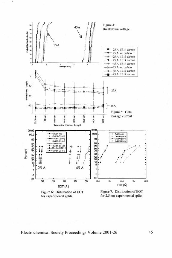
90
80
£ 70
I 60̂
tri
M 50 a •JU
f 40-# S 3° a.
20
10-
n
S » *
• T "
I J
• ;
| 1 | § r i
i i h ' i J si
—L_I a
' *." * **• **. !
t: » «lK^
• ̂ l: \ • \ * \ \ 25A
45A \ \ \ ̂1
i
i 1 I * s *
f .•" ?*"
1 : r + 8 *;".
* s *
t I 1 * S S'
4 • * .
* 5 : '
• .i
- —^fc
± i ™ i * ^
Figure 4: Breakdown voltage
-*•—25 A, 5E14 carbon - # — 25 A, no carbon • 4 - - 2 5 A, 1E13 carbon - f - - 2 5 A , 1E14 carbon . 4 — 4 5 A, 5E14 carbon ~M —45 A, no carbon _ ^ _ 45 A, 1E13 carbon - • - - -45 A, 1E14 carbon
25A
•45A
Figure 5: Gate leakage current
Transistor Channel Length
CL
99.99
99.9
99F
95 90
: 80 > 70
50 30 20 10 5
—•—Ox-25A-noC --&-Ox-25A-C(1e13) -••--Ox-25A-C(5e14) --x--Ox-25A-C(1e14) —I—Ox-45A-noC —•— Ox-45A-qie13) --§*-Ox-45A-C(5E14)| ••-Ox-45A-C(1e14)
25 A
30
45 A
35 40
EOT(A°)
45 50
99.99 j
99.9
99 [
95 90 80 70 50 30 20 10 5
1
.1 .01
28.5
Figure 6: Distribution of EOT for experimental splits
r B
k- »
r B
r "'
[• •
T • 1
- * -Q*25A-noC - -&-- Q*25A-C(1e13) •••••c»aA-q5ei4) --x-Q*25A-C(1e14)
J : » —
— 1
H
1
29 29.5
EOT (A)
30 30.5
Figure 7: Distribution of EOT for 2.5 nm experimental splits
Electrochemical Society Proceedings Volume 2001-26 45

1.40E-10
1.20E-10
l.OOE-10
8.00E-11
6.00E-11
4.00E-11
2.00E-11
0.(X)E+00
-2.5 -1.75 -1 -0.25 0.5 1.25 2
Bias (V)
Figure 8: C-V curve (25 A dielectrics) Figure 9: C-V curve (45 A dielectrics)
1
f-"^^fc-—*— 25A - no C I
-*-25A-C(lel3)
-*—25A-C(5el4)
- A 25A-C(lel4) |
i
100
90
80
"0
60
50
40
M)
20
10
0
»-. .
H
- -*
- # v
No Carbon 1E13 Carbon
- IE 14 Carbon 5E14 Carbon
8?
».
• \
4
S v
V- • - -SB
mo 00
so
"0
60
M)
40
M)
20
10
»-- - a. s
" * a- No Carbon
IE 13 Carbon • -1E14 Carbon * 5E14 Caibon
s
\ \ \ \
\ \ \
\ \ \ \ \ \ \ \ \ \ ^-^
Stress Duration Stress Duration
Figure 10: SILC Yield (25 A dielectrics) Figure 11: SILC Yield (45 A dielectrics)
55-
50
45-
40
35
30
25-
20
15
10
5
0
0
2.5 nm dielectric
1 Hard Failure _ # _ First Failure
1E13 1E14 5E
f
14
8
t
4.5 nm dielectric
k !
3 1E1
{
3 1E14 5E14
Carbon Dose (atoms/cm2)
Figure 12: Charge to breakdown
Electrochemical Society Proceedings Volume 2001-26

INFLUENCE OF MOLECULAR WEIGHT OF ORGANIC CONTAMINANTS
UPON ADSORPTION BEHAVIORS ONTO SILICON SURFACES
Masaaki Nagase1,Masafumi Kitano1, Yoshihide Wakayama , Yasuyuki Shirai1 and Tadahiro Ohmi2
1Dept. of Electronic Eng., Graduate School of Eng., Tohoku University New Industry Creation Hatchery Center, Tohoku University
Aza-Aoba, Aramaki, Aoba-ku, Sendai, 980-8579, Japan
The adsorption behaviors of organic contaminants on wafer substrate surfaces have been investigated. We found the adsorption enthalpy of organic hydrocarbons onto the silicon surface becomes large as the molecular weight (MW) of contaminants increases. Based on these research results, we will explain the influence of the molecular weight of organic hydrocarbons upon adsorption behaviors onto silicon surfaces and suggest a model of adsorption behaviors of various hydrocarbons onto wafers.
INTRODUCTION
Many organic materials are used in clean rooms and with equipment. Almost all of organic materials release many kinds of volatiles (out-gases) such as hydrocarbons, phthalic ester, cyclic siloxanes, and moisture. Therefore, it is a fact that many out-gases, such as moisture or organic compounds frequently existed as contaminants everywhere in a clean room. The out-gases are most likely adsorbed onto a silicon wafer's surface.
Recently, it has become known that organic contaminants on wafer substrate surfaces cause many detrimental effects, such as electrical property degradation, yield losses, and so on [1]. As process temperature for giga scale integrated device manufacturing decreases, to prevent silicon wafer surfaces from organic contamination becomes more important for improving the process yield [2]. Since then, several kinds of reduction methods of organic contaminants have been appli ed at semiconductor fabs, for example, the adoption of chemical filters with active carbons to reduce organic contaminants concentration in a clean room. On the other hand, the mini -environmental process is a new semiconductor manufacturing concept to reduce contamination, and a wafer-carrying pod is a typical mini environmental tool to prevent silicon surfaces from organic contaminants. However, these consist mainly of plastics and even these plastics release organic contaminants themselves. So it is a fac t that being completely free from
Electrochemical Society Proceedings Volume 2001-26 47

organic contaminants is very difficult. Therefore, it is very important to figure out what the mechanism of organic contaminant adsorption onto silicon wafer surfaces is.
We have reported adsorption behaviors with organic contaminants onto silicon surfaces using gas chromatography-mass spectrometry (GC-MS) shown in Figure 1 [3]. In this experiment, a silicon wafer was exposed various hydrocarbons in vessel for 24hours. Figure 1 indicates the comparison of the amount of adso rbed various organic contaminants with different molecular weights (MW) of linear aliphatic hydrocarbons. It was considered that the amount of organic contaminants on silicon surfaces depended on its molecular weight.
In order to further explain the behavior, we continued to study the adsorption behavior of hydrocarbons onto silicon surfaces to determine the enthalpy of organic hydrocarbons onto Si-H and Si(>2 surfaces.
EXPERIMENTAL
Figure 2 shows a schematic diagram for the enthalpy of organic molecules on Si surfaces. Si and Si02 surfaces were formed on an electropolished stainless steel tube surface by S1H4 gas. First, the inner surface of the stainless tube (1/4", 2m) was directly passivated by the Si film that was deposited at 450 °C for 48 hours using lOOppm SiH4 in argon ambiance. Second, in case of forming Si02, oxygen gas was supplied to the Si deposited surface at 600°C with a flow rate of 100 cc/min. For Si-H formation, the Si deposited surface was annealed at 400°C [4]. The contaminant was generated from organic compound vaporizer using argon purge gas with the flow rate of 100 cc/min, supplied to the sample tube line, and then detected by atmospheric pressure ionization mass spectrometer (API-MS). The sample line was adjusted at 25, 60, 100, 150 and 200°C, respectively. Figure 3 shows a typical adsorption property on the flowing time. From the starting of the test, we confirmed that all of the tested hydrocarbon adsorbed onto the silicon surface until the surface was saturated by the hydrocarbon. And then, the hydrocarbon was detected by API-MS. All amounts of the adsorbing hydrocarbon onto silicon surface Q are shown in the following scheme.
Q = Cxfxt [1] C: The concentration of hydrocarbon added in Ar gas (lOOppb) / : Ar gas flow rate (lOOcc/min.) t: Initial detection time of hydrocarbon in Ar gas by API-MS.
In order to find the temperature dependency of the amount of the adsorption, the enthalpy of hydrocarbons onto the silicon surface was calculated using the scheme above.
RESULTS AND DISCUSSION
Figure 4 indicates the dependency of the C14H30 and C20H42 adsorption
48 Electrochemical Society Proceedings Volume 2001-26

properties on the flow time. When the hydrocarbons were supplied to the Si surface, it was adsorbed onto the Si surface. Therefore, a time lag was observed until it was detected by API-MS. The amount of adsorbed hydrocarbons decreases in accordance with the temperature rise, since the surface was immediately saturated in case of high temperature.
Figure 5 shows the dependence of various hydrocarbon adsorption properties. The temperature of the silicon surface was fixed at 60 °C. This figure shows that the detection time of each organic molecule differed and that the amounts of adsorbed hydrocarbons increased while the MW increased. The amounts of adsorbed C10H22, C14H30, and C20H42 onto the Si-H surface were 4.6, 90, and 3600 times respectively for that of C6H14, respectively. The adsorption of hydrocarbon onto the silicon surface was depended on its MW.
Figure 6 shows the Arrhenius plot of various hydrocarbons onto the Si-H and Si02 surfaces obtained. This indicates that the amount of adsorbed hydrocarbons is higher as the temperature decreases and MW increases. The enthalpy of hydrocarbon onto a silicon surface was calculated by each slope. Figure 7 shows the correlation between enthalpy and MW of hydrocarbons. This figure indicates that in each case the enthalpy increases along with the increase of the MW.
Judging from our data, the amount of the adsorbed hydrocarbons with the MW can be determined by the correlation between the vapor pressure of the hydrocarbons and the enthalpy onto the Si surface, not only the vapor pressure of the organics. Figure 8 is the model of adsorption behaviors of hydrocarbon onto wafer surfaces. Molecules with low MW are not adsorbed onto the surface. On the other hand, regarding molecules with high MW, the amount of adsorbed molecule decreased. This is attributed to the enthalpy increase, though the vapor pressure decreases with the increase of the MW, therefore, these molecules are not adsorbed onto the surfaces. Base on our results, we proposed linear aliphatic hydrocarbons with the MW between 170 and 370 should not be used in process surface.
CONCLUSION
In this study, the enthalpy of hydrocarbons onto Si-H and Si02 surfaces was experimentally determined. According to the results, it was found that the amount of adsorbed lower molecular weight hydrocarbon onto silicon wafer surfaces gets smaller because the enthalpy gets lower.
On the other hand, it is understandable that higher molecular weight hydrocarbon gets more difficult to volatile because the vapor pressure gets lower. So, the amount of adsorbed higher molecular weight hydrocarbons onto silicon wafer surfaces should be smaller because the existence probability of them in the atmo sphere around the surfaces is lower.
From these results, the influence of the molecular weight of hydrocarbons upon adsorption behaviors onto silicon surfaces is depended on the relationship between the enthalpy onto silicon surfaces and the vapor pressure. Finally, we propose a Model of adsorption behaviors of various organics onto wafer surfaces shown in Figure 8.
Electrochemical Society Proceedings Volume 2001-26 49

REFERENCES
1. T.Iwamoto andT.Ohmi, Appl.Surf.Sci,117,237(1997). 2. T.Ohmi, J.Electrochem.Soc.,143,2957(1996). 3. Wakayama, Abstract, American Vacuum Society 46 th International Symposium, 232(2000). 4. M Nakamura and T.Ohmi,180th ECS Meeting 534,798(1991).
--3000-
| o>2500-a. B 2000. c CO
1 1 5 C > o i CD I
•S 1000i
I 500-I Of 100
C 1 0 H 2 2 C 1 2 ' ' : PsaHra , C o n H , '28' '58 w30" '62
300 "26 m 400 Molecular Weight (Mw)
500
Figure 1. Comparison of the amount of adsorbed various organic contaminants with different molecular weights (MW) of aliphatic hydrocarbons
50 Electrochemical Society Proceedings Volume 2001-26

[ Si film J directly passivated on SUS tubej
poly-Si: 100ppm Si4/Ar,45CfCx 48hrs
Si-H: 100%H2, 400°Cx0.5hr
S i0 2 ; 100%02,600°c x lohrs
Figure 2. Schematic diagram for the enthalpy of hydrocarbon onto Si surfaces.
120
g = Cx / x t C: concentration / : Flow Rate [ cc/min ]
o. Q_
C O
rat
c O C Q O
100
80
60
40
20
mmmmm. 20 80 40 60
Time [ min ] Figure 3. A typical adsorption property on the flowing time
100
poly-Si: 100ppm Si^/Ar, 100cc/min, 45tfCx48hrs
Si-H : 100%H2,100cc/min, 40CfCx0.5hr
;p oo
i m\ 5 60
O 40
£ 2 0
if Uioot M150°C f200°C
'
1
f |60°C
1 1
C 1 4 H 3 0
WOppb
r I250C
/ /
Time [ min ]
ConH/K
Time [ min ]
Figure 4. Time dependence of C14H30 and C20H42 concentration detected by APIMS
Electrochemical Society Proceedings Volume 2001-26 51

Si-H Surface(@60°C)
poly-Si: lOOppmSil-^/Ar, 100co/min, 450*Cx48hrs Si-H: 100%H2,I00cc/mir», 40O*Cx0.5hr
S i 0 2 Surface (@60°C)
poiy-Si: lOOppmSiHj/Ar, 100cc/min,450°Gx48hrs SiOa: 100%O2,100co/min, 600°Cx iohrs
120
J 100
[ I | C10Ha4
I I pCeH,4
II f
100ppb
J C u H 3 0
-L+-fcacHK
1 1 20 2815 2820
Time [ min ] Time [ min ]
Figure 5. Time dependence of various hydrocarbons concentration detected by APIMS
Si-H Surface Temperature [°C ]
150 100 60 25
Si02 Surface Temperature [°C ]
100 60 25
• | 1 0 1 ' o
| 1 0 , !
101:
E <
r > —
r
r
1 1 T 1 1
g r ~ ~ ~ ~ ' T r
y=<B.86* l o V " 6 * ! 1 Car t . * Ha=0.71eV I
y=(1.S3x10^e4 8*M"
C H * , : Ha=0.42eV
y-(4.13x mezsm:*
C,„H„: Ha=0,25eV
ym-eSxIO' iJe 0* 1 1 5*
G r t 4 : Ha-0.02eV
« E «, OJ o101
2.5 3 3.5
1 / T [ 1 0 0 0 X 1 / K ]
4 <
1011
f t i i i
r . .
IT ^ ^ ^ ^
( y=(1.B9 10«)e5C74&
CjnHj,: Ha=0.35eV
y=(2.45 1 0 V ° ' H
C u H „ Ha=0 26eV I
y=(3.24x 10^e2 Z i 1 4*
C«r t . :Ha=0.19eV |:
y=(1.89x 1 0 " ) e t t * " " j
C H „ : Ha=0.04oV I
2.5 3 3.5
1 / T [ 1 0 0 0 X 1 / K ]
Figure 6. Arrhenius plot of various organic molecules onto the SiH and SiO 2
-
• C 1 0 H 2 2
f • C6H1 4
, 1 *
m
Si-H Surface
C2 0H4 2
• ^ 1 4 ^ 3 0 ^ ,
S i 0 2 Surface
, 0 100 2 0 0 3 0 0
M W ( g / m o l )
Figure 7 Relationship between enthalpy and MW of hydrocarbon
52 Electrochemical Society Proceedings Volume 2001-26

Fieure 8.
Molecular Weight
Model of adsorotion behaviors of hvdrocarbon onto wafer surfaces
Electrochemical Society Proceedings Volume 2001-26 53

THE REMOVAL OF ORGANIC CONTAMINATION BY O3/DI-WATER PROCESSES: A THEORETICAL STUDY.
F. De Smedt, H. Vankerckhoven, C. Vinckier, S. De Gendt1, M. Claes1 and MM. Heyns1
Department of Chemistry, KU Leuven, Celestijnenlaan 200 F, B-3001 Heverlee, Belgium 1IMEC, Kapeldreef 75, B-3001 Heverlee, Belgium
The removal of organic contamination is one of the important cleaning steps during IC manufacturing. Ozone/DI-water processes are more often used as an alternative for the SPM-cleaning concepts to remove this type of contamination from the silicon wafer surface. In order to further improve the efficiency of ozone/DI-water processes, fiindamental understanding of the ongoing chemical processes is needed. Therefore a modelling study of the ozone decomposition was initiated to gain insight in the generation of radicals during the decay of ozone in water. With this information reaction parameters can be selected in such a way that either direct or indirect oxidative degradation of organics can be achieved.
INTRODUCTION
The use of ozone in wet and dry cleaning processes of silicon wafer surfaces is a fact these days. In wet cleaning processes, ozonated solutions are used as an alternative for the SPM-cleaning concepts (H2SO4/H2O) and this for various applications, e.g. the removal of organic contamination I1,2,3J and the oxidation of silicon surfaces l4'5,6l The removal of organic contamination by means of ozone/DI-water is currently investigated thoroughly and this both for contamination originating from the cleanroom ambient ^ as for organic residues from previous process steps (e.g. photoresist). Even photoresist layers of more than one micrometer thickness can be removed by ozone/DI-water l8l To further improve the efficiency of these cleaning processes, fiindamental knowledge on the reaction mechanisms of the removal of organic contamination is needed. In general, the organic contamination can be divided into two classes: saturated and unsaturated organic compounds. For each type a specific reaction pathway is recommendable, namely a radical-based reaction pathway for the saturated organic species (the so-called indirect oxidation) and an 03-based reaction pathway for the unsaturated species (direct oxidation): Figure 1. Note that the radical species are intermediates formed in the ozone decomposition process.
54 Electrochemical Society Proceedings Volume 2001-26

Figure 1; Representation of the two reaction pathways for the removal of organic contamination by ozone in water m .
The direct oxidation occurs by reaction with ozone itself and it can therefore not be applied to saturated organic species as the rate constant for these reactions is too small to be applicable in semiconductor cleaning processes. The reaction rate constant of these saturated organic compounds with radical species (e.g. the OH-radical) is several orders of magnitude higher than with ozone, thus the indirect oxidation is more reeommendable. For unsaturated organic species, e.g. aromatic structures, the reaction rate constant with ozone is comparable to that of radical reactions. Here the direct oxidation is favourable because the ozone concentration exceeds the radical concentration by orders of magnitude. It may be clear that the reaction pathway that has to be chosen depends on the nature of the organic contamination that has to be removed. Reaction parameters of the ozone/DI-water system can be selected in such a way that the appropriate reaction pathway is achieved: a direct or indirect oxidative degradation of the organic species.
OBJECTIVES
When selecting the appropriate reaction pathway, one has to keep in mind two fundamental characteristics of ozone in water: its solubility and decomposition rate in an aqueous solution. The first parameter is important to achieve maximised ozone concentrations in the solution (direct oxidation) and the second parameter determines the generation of radical species. The ozone solubility in aqueous solutions [Cbliiq is already investigated in detail [9,1°3 and its dependence on pH, temperature and nature of the additive is well documented. The decomposition of O3 has also been looked at as a function of pH, temperature and nature of the additives l9'!1l To correlate the experimental results with the build-up of radical species in the solution, the ozone decay has to be modelled. In literature two models are often cited, namely the model of Hoigne et al. (HEA) and the model of Gordon et al. (TFG) l l2l Based on these two models which both imply complex radical chain mechanisms, the ozone decay will be simulated using the Facsimile software [13l By this approach it is possible to gain insight in the radical pathway because the simulations will result in concentration-time profiles of the various
Electrochemical Society Proceedings Volume 2001-26 55

radical species. This information is vital for further optimisation of the silicon surface cleaning processes.
RESULTS AND DISCUSSION
In a first step the ozone decomposition model of Hoigne et al. (HEA) was evaluated at room temperature. This mechanism consists of 32 reactions and 13 different species. First a reduction procedure was performed yielding a reduced HEA-model (RHEA) which only contains 14 reactions and 13 species [12l Figure 2 shows the essential steps. Among the 13 species involved, the following radical species are withheld: HO2, HO3, HO4, 62", O3" and OH. It is known that these radical species are highly reactive, even towards saturated C-C bonds.
INITIATION REACTION
0 3 H0 4
^ J) n HO, • O H - ^ 3
V -Oj
Figure 2; Schematic representation of the ozone decomposition mechanism (RHEA) (the termination steps are not shown on the figure).
The Facsimile software [13] not only simulates the ozone decay (and allows a comparison with experimentally obtained decomposition data l9slll)9 but also results in the concentration-time profiles of the radical intermediate species: Figure 3.
As one can see from Figure 3, the concentration-time profiles of the radical species are not all the same: some shown an initial fast build-up to a maximum concentration (Cmax) followed by a decrease during the ozone decay (e.g. O3") and other radical species reach a maximum concentration at the moment where all ozone has disappeared, namely at t = 7 seconds for pH 7 (e.g. OH and O2").
56 Electrochemical Society Proceedings Volume 2001-26

1.2E-03 -.
1.0E-03 t
I 8.0E-04H
I 6.0E-04H <= o
g 4.OE-04J
2.0E-04 J
O.OE+00 4
\
s. 2 3 4 5 6 7
time (seconds)
B
5.0 7.5 time (seconds)
12.5
Figure 3: Simulated concentration-time profiles of ozone (A) and some intermediate radicals (B and C) at pH 7 and at room temperature.
As we are interested in the dependence of the concentration of all radical species on pH, temperature and nature of the additive, one can define an additional parameter: the 'Radical Pool' or RP. It is the sum of the maximum concentrations Cmax of all radicals in the solution (RP = £Cmax,i). This 'Radical Pool' is clearly dependent on pH as is illustrated in Figure 4. At low pH not only the ozone decomposition is slow [9,11\ but also the RP-value remains low. From pH 4 to 5 on, a (fast) increase in RP is observed whereby RP is more than two orders of magnitude larger at pH 7 than at pH 2. There are thus far more radicals present in the solution at near neutral pH than under acidic conditions. Calculations have shown that this trend continues at higher pH-values.
Electrochemical Society Proceedings Volume 2001-26 57

^ 1.E-08
r 8.E-09 o o 2: 6.E-09 # 4.E-09
2.E-09
O.E+00 pH2.0 pH3.0 pH4.0 pH 5.0 pH 7.0
Figure 4: Radical Pool (expressed in mole/1) as a function of pH at room temperature and at initial ozone and oxygen concentrations in the solution of lO-3 M: [O3]o = 10"3 M = [O2]o
The dependence of RP on [Os]o is also different for acidic and alkaline pH conditions. At low pH almost no dependence of RP on [Os]o is observed, e.g. RP is 6.5 10"11 M and 7.3 10'11 M at 0.5 mg/1 and 50 mg/1 ozone respectively. At pH 9, RP is strongly correlated with the initial ozone concentration with an increase from 2.7 10"8 M at 5 mg/1 ozone to 1.1 10"7 M at 50 mg/1 ozone.
From the above it is clear that for achieving a radical reaction pathway in the removal of organic contamination, one needs to work at near-neutral to alkaline pH-values and high initial ozone concentrations.
Finally the simulations allowed to determine the dominant radical species in the solution at acidic and alkaline pH-values. This strongly depends on the pH as shown in Table I where the relative contributions of the various radicals to RP is given. The most abundant species at low pH is the H02-radical and the (V-radical at a pH of 9.
One sees that the HO2 and O3" radicals are the most abundant species at respectively pH 2 and 9.
It should be noted here that the OH-radical is only of minor importance and probably does not play a major role in the degradation of organic contamination.
58 Electrochemical Society Proceedings Volume 2001-26

Table I: Relative contribution to the RP of the radical species (%) at pH 2 and 9 and [Oslo = 10"3 M.
H02
H03
H04
o2-03-OH
pH2 89.8 2.0 7.9
0.10 4 10"4
0.11
pH9 1.6 2.3 8.8 1.0
85.4 0.8
Future research includes the search for correlations between the ozone cleaning and oxidising efficiency with the magnitude and the composition of RP at various experimental conditions such as pH, initial ozone concentration and temperature. The removal of organic contamination from silicon wafer surfaces and in process rinse waters will be investigated both by experimental work and by modelling. Also the effect of the addition of ozone decomposition promoters and scavengers will be looked at.
ACKNOWLEDGEMENTS
F.D.S. acknowledges the Institute for Science and Technology (IWT) for a doctoral grant and the 'Research Council' of the K.U.Leuven for a postdoctoral grant.
REFERENCES
1. T. Ohmi, T. Isagawa, M. Kogure and T. Imaoka, J. Electrochem. Soc, 140 (3), 804-810(1993) 2. S. De Gendt, P. Snee, I. Cornelissen, M. Lux, R. Vos, P.W. Mertens, M. Knotter, M. Meuris and M. Heyns, Solid State Phenomena, 65-66, 165-168 (1999) 3. C. Kenens, S. De Gendt, M. Knotter, L. Loewenstein, M. Meuris, W Vandervorst and M.M. Heyns in Cleaning Technology in Semiconductor Device Manufacturing, J. Ruzyllo and R. Novak (Eds), Electrochem. Soc. Proc. Series, Pennington, USA (1997) 4. M.M.Heyns, M. Meuris, P.W. Mertens, H.F. Schmidt, S. Verhaverbeke, H. Bender, W. Vandervorst, M. Caymax, A.L.P. Rotondaro, Z. Hatcher and D. Graf, Proc. 40th Annual Technical Meeting, Chicago, May 1-6 (1994) 5. F. De Smedt, S. De Gendt, I. Cornelissen, M.M. Heyns and C. Vinckier, J. Electrochem. Soc, 147, 1124-1129 (2000) 6. J. Park, Jpn. J. Appl Phys., 36 (9A): 5416-5420 (1997) 7. M. Claes, S. De Gendt, C. Kenens, T. Conard, M. Bender, W. Storm, T. Bauer, P.Mertens and M.M. Heyns, J. Electrochem. Soc, 148 (3), G118-125 (2001)
Electrochemical Society Proceedings Volume 2001-26 59

8. S. De Gendt, M. Lux, M. Claes, J. Van Hoeymissen, T. Conard, W. Worth, S. Lagrange , E. Bergman, A.S. Jassal, P.W. Mertens and M.M. Heyns, Cleaning Technology in Semiconductor Device Manufacturing VI, J. Ruzyllo and R. Novak (Eds), Electrochem. Soc. Proc. Series, Pennington, USA (2000) 9. F. De Smedt, Fundamental study of the behaviour of ozone in water: application in the cleaning of semiconductor devices, PhD-thesis, Department of Chemistry, University of Leuven (K.U.L.), 2000 10. F. De Smedt, S. De Gendt, M.M. Heyns and C. Vinckier, J. Electrochem. Soc, 148 (9), G487-G493 (2001) 11. F. De Smedt, S. De Gendt, I Cornelissen, M. Heyns and C. Vinckier, Solid State Phenomena, 76-77, 211-214 (2001) 12. A. Virdis, A. Viola and G. Cao, Ann. Chim., 85 (11-12), 633-647 (1995) 13. Facsimile for Windows V3.0, UES Software Inc.
60 Electrochemical Society Proceedings Volume 2001-26

REMOVAL OF LIGHT AND HEAVY ORGANICS BY OZONE PROCESSES
Akshey Sehgal and M. Rao Yalamanchili SCP Global Technologies, Inc.
255 N. Steelhead Way Boise, ID 83704
Organics adsorbed onto the wafer surface cover a large range of compounds and are classified in two broad classes: heavy organics (photoresists and post-ash residue) and light organics (all other organics that are not heavy organics). In this work, a method is presented to show the uniformity of light organic removal from the wafer surface by an ozonated DI water process. A bare silicon wafer was coated with a challenge organic (hexamethyl disilazane; HMDS) which was then removed by ozonated DI water. Contact angle measurements and AFM scans of the post process wafer showed a clean, organic free wafer surface with no HMDS islands. The difference between light and heavy organic removal is discussed with emphasis on the theoretical requirements for a heavy organic removal process. Hardware challenges for a heavy organic cleaning process are discussed and preliminary resist strip rates are presented.
INTRODUCTION
Volatile organics can adsorb on silicon wafers in clean rooms and introduce severe defects during semiconductor manufacturing steps [1]. The volatile organics that adsorb on silicon wafer are classified differently from photoresist and resist residues left on the wafer surface after ashing. The latter are defined as heavy organics while the volatile organics are defined as light organics. In other words, any organic contaminants on the wafer that are not resists or resist-residue are defined as light organics [2].
Typically, organics (light and heavy) are removed from a wafer surface in a sulfuric acid and hydrogen peroxide mixture (SPM) at high temperatures. This is an aggressive chemistry as it mixes concentrated sulfuric acid (98 wt%) with hydrogen peroxide (31 wt%) in a 4:1 ratio [3]. High temperatures (120 °C or more) are needed for the SPM to be effective with periodic additions of hydrogen peroxide. While the SPM process can remove any type of organic from the wafer surface, the process is expensive in terms of chemicals and DI water usage. It also reduces the wet process equipment life and introduces metal and inorganic contaminants such as sulfate onto the wafer surface.
With emphasis on reduced cost of ownership and improved performance, removal of light organics by ozonated DI water has been proposed. It is a reduced consumable cost process that has fewer processing steps and is carried out at room temperature with
Electrochemical Society Proceedings Volume 2001-26 61

minimal environmental impact. Because hydrogen peroxide is not used, metal contamination is significantly reduced in a dissolved ozone process. Particle additions are reduced in an ozonated DI water process as well [4-6]. Because of these advantages, light organic removal by ozonated DI water is increasingly being used in the industry.
In this work, a combination of a simple technique (contact angle measurements) and an advanced surface analytical technique (atomic force microscopy, AFM) has been used to assess the uniformity of the light organic cleaning process. These methods provide information on the macro level (contact angle measurements) and at the molecular level (AFM imaging of the wafer surface provides a visual observation of light organics) to characterize the complete removal of light organics. The results from both of these measurements will be used to show the complete removal of light organics from the wafer surface using a single pass of ozonated DI water.
In order to demonstrate the effectiveness of the ozonated DI water clean, wafers were coated with a challenge light organic material (hexamethyl disilazane, HMDS) and were then cleaned using a single pass of bubble-free ozonated DI water. HMDS is commonly used as a photoresist adhesion promoter and is a difficult organic residue to remove from a silicon oxide surface [7]. Removal of HMDS by various cleaning chemistries was used as a process benchmark for light organic removal by many researchers in the past [4,7-10]. The reaction between HMDS and the surface silanol groups results in the formation of a trimethyl siloxane, TMS, monolayer on the wafer surface (Figure 1). It is the TMS layer that is the challenge light organic layer; attack of the TMS layer by ozone restores the silanol termination on the wafer surface. The reaction between HMDS and the surface silanol groups is written below:
(CH3)3-Si-NH-Si-(CH3)3 + 2(Si-0"-H+) O 2(Si-0-Si(CH3)3) + NH3 (1)
In this work, light organic removal from the wafer surface was characterized by contact angle and AFM measurements using a simple method. The difference between light and heavy organic removal is discussed with emphasis on the theoretical requirements for a heavy organic removal process. Hardware challenges for a heavy organic cleaning process are discussed and preliminary cleaning results are presented.
EXPERIMENTAL
Prime silicon wafers (200 mm, boron doped p type, 100 orientation, CZ grown) were used in the light organic removal study. A simple method, as outlined in Figure 2, has been established to further characterize the light organic removal using AFM. The native oxide was stripped with HF and an ozone passivation oxide grown in its place. After being vapor deposited with HMDS, the wafer was cleaned using either a SPM bath or ozonated DI water. The oxide on the wafer surface was etched in HF to produce a contrast between the bare Si surface and any post-process remaining HMDS on the wafer
62 Electrochemical Society Proceedings Volume 2001-26

surface. An AFM analysis of the wafer surface was then done to verify complete removal of the HMDS.
Contact angle measurements were made using a Kruss goniometer. Ozonated DI water was generated using a Liquozon 100 system (ASTeX, Wilmington, MA). A flow rate of 5 liters per minute, a process time of 10 minutes and a single pass of ozonated DI water were used to remove the light organics. AFM measurements were done using Dimension 5000 and Nanoscope IIIA atomic force microscopes (Digital Instruments, Santa Barbara, CA) in both the tapping and force modes.
For heavy organic removal experiments, Shipley DUV 6 photoresist was blanket coated on 200 mm wafers. The DUV photoresist was deposited to a thickness of 7500 A, step baked at 110 and 160 °C and stabilized with an UV lamp to cross link the photoresist. Ozone gas was generated using a SEMOZON 90 generator (ASTeX, Wilmington, MA).
The heavy organic removal process used is a proprietary process involving ozone gas, ozonated DI water and water vapor. All the cleaning and etching experiments were carried out in a commercial automated wet bench (SCP Global Technologies, Boise, ID).
RESULTS AND DISCUSSION
Light Organic Removal Pre- and post- ozone process contact angle measurements indicated complete
removal of HMDS from the wafer surface as shown in Table I. AFM scans were done on wafers subjected to the test procedure outlined in Figure 2. This method allows for an AFM image to reveal any light organic not removed in the cleaning process at the molecular level. This method is specially useful when facilities to measure electrical properties of the wafer are not available. In summary, this procedure is a short loop process sequence to provide fast feedback on the cleaning process.
The AFM images shown in Figure 3 (a) are typical of a clean wafer surface and these results clearly indicate the absence of any light organic residue left over after the ozone cleaning process. In contrast, Figure 3(b) shows an AFM scan of a HMDS monolayer on the wafer surface. It is a very roughened surface with peaks, ridges and partial caldera rims visible over the entire surface. None of these are visible in Figure 3(a) showing the complete removal of the HMDS by the ozonated DI water. The uniformity of light organic cleaning, at the molecular level, is further demonstrated by the sub-Angstrom rms surface roughness measured (Table I) on these wafers after the removal of challenge organic materials.
Differences Between Light And Heavy Organic Removal Some of the main differences between light and heavy organics are summarized in
Table II. While removal of both types of organics is critical in obtaining a pristine
Electrochemical Society Proceedings Volume 2001-26 63

surface for the next processing step, removal of heavy organics is far more challenging. This is because the heavy organics are present in much larger amounts on the wafer surface and should take a longer time for the same removal chemistry. In addition, heavy organics may have undergone processing steps such as implantation (produces a hard crust on the wafer surface that is difficult to remove) or baking (cross-links the photoresist) or may have been created in very severe conditions (such as post-ashing residues). So immersion of the wafers in an overflow bath containing a small amount of ozone dissolved in DI water may completely remove light organics [4-6], but a similar approach fails miserably for heavy organics for the reasons discussed above. Ozone dissolves the photoresist layer by layer so the presence of a hardened crust slows the heavy organic removal down considerably. Given that one can dissolve only a hundred ppm of ozone or so in water and that tens of thousands of ppm of ozone are available in the gas phase, theoretical and experimental results [11] verify that vapor phase ozone processes are the obvious choice for heavy organic removal.
Critical Factors Affecting Heavy Organic Removal by Ozone Since heavy organics are polymeric in nature, higher processing temperatures will
swell, soften and/or breakdown the intra- and inter- chemical bonds in the polymer chains. Higher process temperatures are expected to increase the kinetics of the ozone attack of the heavy organic as well. This has been experimentally observed by many research groups [5,6,11,12].
A synergistic effect of water is also found to increase the heavy organic rates of attack by ozone [11,12]. However, too much water injection during the vapor phase process allows for condensation of water on the wafer and leaves photoresist intact beneath the condensed water. Therefore, an optimum amount of water needs be used in the process.
As ozone is one of the reactants in the heavy organic removal process, increasing its concentration in the tank will only increase the rates of heavy organic attack by ozone. This can be done by delivering more ozone to the tank or by additives that help maintain ozone concentration by reacting with the OH* radical (produced during indirect breakdown of ozone) and preventing any further chain breakdown of ozone. However, it would be more beneficial to have an additive that attacks the photoresist than one that maintains ozone concentration. Attack of the implanted crust by the additive would result in a much larger increase in the rates of heavy organic attack by ozone.
Hardware Challenges for a Heavy Organic Process Chamber All the critical factors discussed above need to be optimized in order to obtain
reasonable PRS rates. Unfortunately, designing a process chamber to accomplish an optimized process is not trivial. While its high reactivity makes ozone a powerful oxidizing agent, requiring ozone in tens of thousands of ppm in the heavy organic chamber at elevated temperatures causes ozone to attack a wide range of materials used in chamber construction and makes it a severe ESH hazard that needs to be contained.
64 Electrochemical Society Proceedings Volume 2001-26

For example, an environment of > 10 ppm of ozone is an IDLH (immediately dangerous to life and health) hazard. So ozone needs to be safely and quickly exhausted from the process chamber (that contains tens of thousands of ppm of ozone) into an ozone destruct. This is countered by the need to ensuring sufficiently long residence times of ozone gas in the tank to attack the heavy organics. Also an adequate number of ambient ozone safety monitors need to be placed at various locations around the process chamber and/or the ozone generator to detect any ozone leaks.
In addition, high process temperatures have to be maintained in the chamber despite the condensation of water on the wafer and chamber walls and the introduction of room temperature ozone gas. This requires providing sufficient thermal energy to the wafer and chamber while making sure that the ozone gas and any additives used in the process are selectively attacking the heavy organics and not the materials used to construct the chamber. These factors require careful optimization of the flow distribution of ozone gas, water vapor and ozonated water.
Based on the considerations listed above, a heavy organic process chamber has been built and preliminary test results obtained. The heavy organic removal process used is a proprietary process involving ozone gas, ozonated DI water and water vapor. Stripping rates of heavy organics from wafer surfaces were found to be accelerated by using an optimum amount of water, high ozone gas concentration using additives and high process temperatures. Initial test results indicate a strip rate of 700-800 A/min. for a hard baked, cross-linked DUV 6 photoresist. Further testing is in progress with a strip rate goal of 2500 A/min. PR stripping rates and results of continued optimization of the factors discussed above will be presented at a later date.
SUMMARY
Light organic removal from the wafer surface by ozonated DI water was characterized by a combination of contact angle and AFM measurements. This method provides a quick confirmation of the effectiveness of light organic removal before the electrical results are obtained. Results from the characterization methods used in this work clearly indicate that the ozonated DI water process is capable of replacing the SPM bath for light organic removal. Differences between light and heavy organic removal was discussed with emphasis on the critical factors affecting the heavy organic removal process. Hardware challenges for a heavy organic process chamber were also discussed.
REFERENCES
1. E. Oilier, S. Marthon, G. Quagliotti and F. Tardif, Cleaning Technology in Semiconductor Device Manufacturing V, J. Ruzyllo, R. E. Novak, C. M. Appel, T, Hattori and M. Heyns Editors, PV 97-35, p. 447, The Electrochemical Society Proceeding Series, Pennington, NJ (1998).
Electrochemical Society Proceedings Volume 2001-26 65

2. J. J. Guan, International SEMATECH, Private Communication, 2000. 3. J. Wei and S. Verhaverbeke, Cleaning Technology in Semiconductor Device
Manufacturing V, J. Ruzyllo, R. E. Novak, C. M. Appel, T. Hattori and M. Heyns Editors PV 97-35, p. 496, The Electrochemical Society Proceeding Series, Pennington, NJ, (1998)
4. A. Sehgal and M. R. Yalamanchili, Future Fab, 10, 199 (2001). 5. Various Articles on Ozonated Water in Cleaning Technology in Semiconductor
Device Manufacturing Volumes HI-VI, The Electrochemical Society Proceeding Series, Pennington, NJ.
6. Various Articles on Ozonated Water in Third and Fourth Ultra Clean Processing of Silicon Surfaces Symposium, Trans Tech Publications, Switzerland.
7. T. Riihisaari, A. Kiviranta, S. Lehto, J. Likonen, S. Eranen, E. Sandell, J. Virtanen and M. Viitanen in Cleaning Technology in Semiconductor Device Manufacturing VI, T. Hattori, R. E. Novak and J. Ruzyllo Editors, PV 99-36, p. 601, The Electrochemical Society Proceeding Series, Pennington, NJ (2000).
8. K. Christenson and S. Nelson in 18th Annual Semiconductor Pure Water and Chemicals Conference, p. 319, Semiconductor Pure Water and Chemicals Conference, Santa Clara, CA (1999).
9. N. Porfiris, J. Newby, A. M. Gundlach, R. Pethrick, S. Affrosmann and A. Tannahill in Second Ultra Clean Processing of Silicon Surfaces Symposium, Bruges, Belgium, Sep. 1994.
10. M. M. Heyns, T. Bearda, I. Cornelissen, S. De Gendt, R. Degraeve, G. Groeseneken, C. Kenens, D. M. Knotter, L. M. Loewenstein, P. W. Mertens, S. Mertens, M. Meuris, T. Nigam, M. Schaekers, I. Teerlinck, W. Vandervorst, R. Vos and K. Wolke, IBM J. Res. Develop., 43, 339 (1999).
11. A. Sehgal and M. Rao Yalamanchili, Unpublished work. 12. T. Riedel, K. Wolke, S. De Gendt and B. Onsia, Solid State Phenomena, 76-77, 227
(2001).
ACKNOWLEDGEMENTS
The authors would like to thank Vamsi Krishna Paruchuri at University of Utah and Dr. Jeff McMurran at SCP Global Technologies for their help with the AFM analysis of silicon wafers.
Table I Contact angles and surface roughness of silicon wafer under different conditions
Sample
Silicon wafer with HMDS monolayer Silicon wafer after HMDS strip by ozonated DI water
Silicon wafer after HMDS strip by SPM
Contact Angle* 76 ±1° <10° <10°
RMS Roughness
3.39 A 7.27 A 0.92 A
* Average of 25 points over the wafer surface
66 Electrochemical Society Proceedings Volume 2001-26

Table II A comparison of heavy and light organics
Light Organics Heavy Organics Generally present as a sub monolayer, monolayer or few|to layers in thickness (3 to 20 A)
photoresists are present as many layers (a few thousand] tens of thousands of Angstroms in thickness)
Post-Ash residue(s) are less than a monolayer in] thickness
completqPhotoresist
Unintentionally adsorbed Iwafer surface. Adsorbed layerjsurface maybe partial or depending upon the wafer' exposure to the light organic^ source Viewed as contaminant on wafer|. surface.
on|Photoresists are intentionally deposited on waferj for masking parts or the entire wafer surface
processing may require implantation] slresulting in formation of highly carbonized, cross linked surface layer that may be a few hundred of] Angstroms in thickness
Post-Ash residue(s) are created as a by-product of the] ashing step
|Can be completed removed in aTThermal removal at 400 °C not possible furnace at 400 °C.
Easily removed by a single [processing step
Require much more aggressive removal chemistries; wetkome heavy organics may require a dry and a wet|
[processing step
(CH3)3
(CH3)3
H H H (CH3)3 | |
I / o o Si N Si +
£ Si Si
H (CH3)3 (CH3)3 (CH3)3 H
. \ fs/ H5+ I \ r \ l / H
Si N"*—Si**-^ I Si s i + _ _ > N -
\ o- o8- ^ I ^ • I
Si Si % S1
(CH3)3 (CH3)3
I I *} S,1 + NH3
Si Si
Figure 1. HMDS bonding mechanism with a hydrophilic Si wafer surface (from ref. 4)
Electrochemical Society Proceedings Volume 2001-26 67

i I H F
| HFEtch J S iOyTW^yrT Dissolve native oxide
I O3 Passivation Oxide Growth I S i 0 2 / H f l f ^ 0. ? r o w d e , n s e ' d e f e c t 1 I 1 / / / / / / / / Si free oxide
1 HMDS jHMDS Deposition | Si02 • — — ™ Dei Deposit a challenge light organic
i H M D S *» Measure contact angles ! Contact Angle Measurement j S i 0 ^—ip—p _ a t different locations
f̂ . V ™ i l ~ * "« • • 1 ' 1 Remove challenge I Piranha Clean 11 Ozone Stripping | siQtJflfiffl S{ H g h t o r g a n i c
"~" Measure contact angles V7////// Si
HF
Contact Angle Measurement sio, m m * m e a s u r c u o n u t t ; i ^ 1 / / / / / / / / Si a t different locations
1 HFEtch I S i 0 2 J J ^ ^ T ^ Dissolve passivation oxide
AFM . . yt X Observe wafer for light organic / / / / / / / / Si remnants in AFM image
Figure 2. HMDS test plan showing the changes taking place at the Si surface corresponding to the various processing steps in the plan.
Figure 3. Typical three-dimensional AFM scans of wafer shown in Figure 2. (a) after ozonated DI water cleaning and (b) after HMDS priming and before stripping. Note the 30 A z scale in 3(a) and the 60 A z scale in 3(b) showing the much smoother surface in 3(a).
68 Electrochemical Society Proceedings Volume 2001-26

EFFECT OF pH VALUES IN OZONIZED ULTRAPURE WATER
ON CLEANING EFFICIENCY
Ikunori Yokoi 1>2, Geun-Min Choi3'4, and Tadahiro Ohmi1
1 New Industry Creation Hatchery Center, Tohoku University, Aza-Aoba, Aramaki, Aoba-ku, Sendai-shi, 980-8579, Japan
2 UPW Development Team, R&D Dept, Plant Division, Kurita Water Industries Ltd., 1-1, Gotyoyama, Kawada, Nogi, Shimotuga-gun, Tochigi, 329-0105, Japan
3 Dept. of Electronic Eng., Graduate School of Eng., Tohoku University, Aza-Aoba, Aramaki, Aoba-ku, Sendai-shi, 980-8579, Japan
4 Advanced Process 4, Memory R&D Div., Hynix Semiconductor Inc. San 136-1, Ami-Ri, Bubal-Eub, Ichon-Si, Kyungki-Do, 467-701 Korea
We have investigated the effect of pH values in ozonized ultrapure water (03-UPW) on cleaning efficiency. The metallic removal efficiency from the surface has a big difference with the times. Even though the 03-UPW is well known to chemicals with the impurity removal efficiency, the cleaning on the surfaces with delaying time after contamination is not effective in our study. The strong relationship between metallic removal efficiency and pH and oxidation-reduction potential (ORP) values in solution is also clear when examining an 03-UPW cleaning. The cleaning with a pH 4 can remove the metallic impurities below 1011 atoms/cm2
which are just existed in or on native oxide. Still more, the organic removal efficiency of 03-UPW with pH value of 4 is best superior to that of other cleanings.These results lead to the conclusion that acid added to 03-UPW is very effective for removal of metallic impurities and organic contaminants.
INTRODUCTION
With down scaling of ultra large scale integrated (ULSI) devices, contamination-free Si surface is essential to realize the high performance of devices since contaminants cause electrical defects, device degradation and yield losses. Now, the time will soon come when the semiconductor industry is required to manufacture the superfine pattern of less than 0.13 microns on 12 inches wafers. Extended conventional technology just as yet, factory scale is very hypertrophied, and semiconductor industry can not advance steadily. It is very important to simplify wet cleaning processes in terms of productivity, energy
Electrochemical Society Proceedings Volume 2001-26 69

saving and cost performance. The cleaning method that in 1970 was proposed by Werner Kern of the RCA Company (the so-called RCA cleaning)[l] has been largely used in the semiconductors processes for a quarter of century and it is still. However, the RCA cleaning process uses chemicals and ultrapure water (UPW) in large volume at high temperature. As a result, it generates a huge amount of chemical vapor that requires the use of a large amount of exhaust capacity to separate cleanroom air from chemical vapors. Therefore, to remove chemical components from exhaust air, the load on the scrubbers is also raised. As chemicals and UPW are evaporated in large volume, the chemical composition of the cleaning solution can not be maintained at a constant level, which inevitably deteriorates accuracy and re-producibility of the cleaning process. The most important issue for mass production is that all cleaning processes have high reproducibility at anytime. In order to suppress chemical vapor generation from wet stations, wafer surface cleaning should be carried out at room temperature, conclusive. Several requirements for future wet cleaning technology should be satisfied for developing an effective cleaning technology, which are; 1) room temperature process, 2) reduction in process steps, 3) reduction in chemical and UPW consumption, and 4) system footprint reduction [2], [3]. We scholarly clarified the mechanism of the removal of the adhered contamination such as metallic impurities, particles and organic. At the base of the mechanism, we propose room temperature wet cleaning process that consists of only 4 process steps in this article.
The 4-step room temperature cleaning reveals a drastic reduction of chemical and UPW use as well as promotion of ESH (Environment, Safety and Health) in semiconductor manufacturing, and clearly indicates that using the room temperature cleaning process to replace conventional RCA cleaning yields equivalent or better cleaning performance for all impurities. A small amount of specific gases dissolved in UPW such as 03-UPW and NH3 added to hydrogenated ultrapure water (H2-UPW) based on cleaning target is only used for wafer surface cleaning. Compared to RCA cleaning, no chemical vapors are generated during the process because cleaning is been processed at room temperature and the cleaning solution is based on very dilute chemicals. In the 4-step cleaning, fresh liquids are continuously supplied but with low-cost and high-performance. This eventually will meet the requirement for coming severe cleanliness, larger diameter wafer processing and greater respect for the environment.
The O3-UPW with the economic benefits became to play an important part in current wet cleaning [4]. However, the cleaning efficiencies for removing contaminants such as noble metals and organic contaminants, and etc, should be much improved, compared to those of typical cleanings [5]. The present work focuses on an effect of pH values in 03-UPW on cleaning efficiency in great detail.
EXPERIMENTAL
Two types of crystalline silicon (c-Si) wafers used were type A [8-in. p-type (100) oriented wafers with resistivity of 10 Qcm] and type B [8-in. n-type (100) oriented wafers with 3 to 5 Q cm]. The samples are pre-cleaned by a sequential cleamng of sulfuric
70 Electrochemical Society Proceedings Volume 2001-26

acid-hydrogen peroxide mixture (SPM: 4:1, 90°C) for 10 min., a 0.5% HF for 30 sec, and post ultrapure water (UPW) rinse with a resistivity of 18.2 MQ cm for 10 min.
In order to investigate the removal efficiency of metallic impurities and organic contaminants, the wafers are contaminated using various contaminants. Following, these contaminated wafer surfaces were cleaned in pH controlled 03-UPW. In every cleaning process, the cleaning time was set to 10 min. and dried with ultrapure nitrogen gas.
The amount of deposited metallic impurities is analyzed with an incident angle of 0.05 degree by Total Reflection X-ray Fluorescence Spectroscopy (TRXRF) system using W x-ray source of 30 kV and 200 mV.
The amount of organic contaminants is determined by use of fourier transform infrared reflectance-attenuated total reflection (FTIR-ATR) with germanium as a prism material. The hydrocarbon signals from the Si surface are observed around the wave number of 2900 cm1.
RESULTS AND DISCUSSION
Figure 1 shows the dependence of copper (Cu) removal efficiency of 03-UPW on exposing time in cleanroom after contamination. The Cu concentration in the contamination solution was set to 1 mg/1 Cu using CuCl2 in UPW with a resistivity of 18.2Q cm for all dipping solutions. Then the samples were exposed at cleanroom air. Cu removal efficiency from surface has been found to be totally different as a function of exposure time. 03-UPW cleaning is not efficient on Cu impurity removal when samples after contamination are stored for long time, while Cu impurity on surface is easily removed when no delay takes place after contamination [6].
Figure 2 compares the x-ray photoelectron spectroscopy (XPS) spectra of the Cu contaminated Si surfaces. Judging from the ghost peaks on increasing exposure time, the surface of contaminated copper seems to be oxidized more and more. We point out that the surface oxidation on the Cu strongly affects the removal efficiency of the cleaning method. That is, the 03-UPW with a high oxidation-reduction potential (ORP) value doesn't have the capability to remove the oxidized Cu impurities from the surface. This is attributed to the pH value of the solution, which has almost neutral pH value of 6.5: close vicinity to phase boundary of Cu ions and CuO in solution. It is therefore mandatory to decrease the pH value to improve the impurity removal efficiency from substrates.
Figure 3 shows the dependence of etch rate of Cu and CuO films on various chemical concentrations in UPW. CuO film in acidic solutions with a low pH value has a fast etch rate, while Cu film is not etched in all concentrations. CuO film can be only dissolved to Cu2+ ions in solution with a high ORP and low pH value. Therefore, authors suppose that an acidic solution is added to 03-UPW to decrease the pH value, so that all Cu compositions such as metallic Cu, Cu oxide, and Cu hydroxide can be removed from silicon substrate. When adjusting pH value in 03-UPW, ORP values are in total accord irrespective of the species of acidic solutions. However, It is reported that CI ion residues promote Cu adsorption on substrate at the post cleaning step and particle generation during next deposition [7]. This is because stable states of silicon surface are partially
Electrochemical Society Proceedings Volume 2001-26 71

replaced by active states of CI termination. According our results, since C02 added 03-UPW does not remain chemical residues after cleaning, we replace HC1 with C02 in 03-UPW.
Figure 4 represents the influence of pH and ORP values in the solution on the removal efficiency on Cu contaminated silicon surfaces, which were exposed in cleanroom ambiance after contamination for 2 days. The pH value of the solution was controlled by method of adding C02 to 03-UPW. C02 in the 03-UPW was dissolved with a hollow fiber type membrane. The strong relationship between removal efficiency and those values in solution is also clear when examining an 03-UPW cleaning. After 03-UPW cleaning with a pH 4, Cu impurities on silicon substrate are below 1011 atoms/cm2, which are just existed in or on native oxide.
Figure 5 shows the removal efficiency of organic contaminants with various cleaning solutions. The amount of organic contaminants is determined by use of a fourier transform infrared reflectance-attenuated total reflection (FTIR-ATR) with germanium as a prism material. The hydrocarbon signals from the silicon surface are observed around the wave number of 2900 cm"1. The removal efficiency of new C02 added 03-UPW is best superior to that of other cleanings.
Figure 6 is showing the pH and ORP values of various solutions. In general, the ORP values in solutions increase with the decrease of pH value at same solution. The 03-UPW has much high ORP value on adding C02 to the solution. The increase can affect the organic contaminants removal from Si surface (fig.5). Based on our results from metallic impurities and organic contaminants removal from wafer surface, we propose C02 added 03-UPW instead of 03-UPW only, so that, the 4-step room temperature cleaning is changed into Table 1;
1st step: C02 added 03-UPW cleaning for removing of organic and metallic impurities. 2nd step: NH3 added H2-UPW + Megasonic (MS) cleaning for removing of particles. 3rd step: FPM cleaning for removing of metallic impurities. 4th step: H* radical added UPW rinse for removal of chemical residues, prevention of
particle re-adhesion, suppression of native oxide growth, and enhancement of H-termination.
The room temperature cleaning, based on the pH controlled 03-UPW, can be easily applicable for the state-of-art cleaning.
CONCLUSION
We have investigated the effect of pH values in 03-UPW on cleaning efficiency. An 03-UPW cannot remove surface oxidized copper particles, even though it has high ORP value. In order to remove all copper impurities on Si surface irresp ective of contaminated conditions such as metallic Cu, Cu oxide, and Cu hydroxide, therefore, the pH value of 03-UPW should be controlled less than 4. Still more, the organic removal efficiency of 03-UPW with pH value of 4 is best superior to that of other cleanings.
72 Electrochemical Society Proceedings Volume 2001-26

A pH controlled 03-UPW (C02 added 03-UPW) is newly added to 4 steps room temperature cleaning, resulting in improving the removal efficiency of copper impurities and organic contaminants. The room temperature cleaning based on using pH controlled functional water is a good candidate for future cleaning in this article.
ACKNOWLEDGMENTS
This research has been carried out in the Mini Super Clean Room at Faculty of Engineering and in Laboratory for Microelectronics attached to The Electronic Communication Laboratory in Tohoku University.
REFERENCES
[1] W. Kern and D. A. Puotien, RCA Rev., 31, p.187 (1970). [2] W. Kern, Handbook of semiconductor wafer cleaning technology, No yes Publications,
New Jersey, Chap. 2, p.102 (1993). [3] M. Miyashita, M. Itano, T. Imaoka, I. Kawanabe, and T. Ohmi, in proceeding of the
1991 Symposium on VLSI Technology, p.45, Oiso (May 1991). [4] T. Ohmi, in Proc. of the 19th Annual Semiconductor Pure Water and Chemicals
Conference, p.l, Santa Clara, March (2000). [5] I. Yokoi, G. M. Choi, and T. Ohmi, Extend. Abst. of the 2000 Int'l Conf. on SSDM,
p.172, Sendai, Oct. (2000). [6] T.Ohmi, J. Electrochem. Soc., 143, p.2957 (1996). [7] H. Morinaga, M. Suyama, and T. Ohmi, J. Electrochem. Soc, 141, p.2834 (1994).
1 S
03:5mg/l Cleaning time :10min.
as'Contamination No time delay Iday 2days
Fig.l. The dependence of Cu removal efficiency of 03-UPW.
Electrochemical Society Proceedings Volume 2001-26 73

Contamination UPW spiked with 10 mg/1 CuCb for 3min
No time delay
960 930 950 940
Binding energy (eV)
Fig.2. XPS spectra of Cu contaminated silicon surface on exposing time in cleanroom.
Cu film
CuO film
100 1000 10000
Consentration (mg/L)
Fig.3. The dependence of etch rate of Cu and CuO films on various chemical concentration s in UPW.
s
=
as-contamination pH 6.5
UPW
only
pH5.0 pH4.0
CO 2 concentration
Fig.4. The dependence of Cu removal efficiency on pH and ORP values in CO, added O.-UPW.
74 Electrochemical Society Proceedings Volume 2001-26

As - received wafer
Os-UPW Cleaning
3040 3000 2960 2920 2880 2840 2800 3020 2980 2940 2900 2860 2820
Wavenumbers (cm-1)
Fig.5. FTIR-ATR spectra of remaining hydrocarbon on silicon surface.
2.5 with Cu:lmg/I (using CuCh)
• UPW A 03-UPW • H,S04
# HNO,
m NH4OH
IJOW 0 2 UPW
A H,-UPW <•• H C 1
# KOH
0 2 4 6 8 10 12 14
pH
Fig.6. pH and ORP values of various solutions.
Electrochemical Society Proceedings Volume 2001-26 75

Target
Organic Metal fill
Cleaning Sequence
COi + 03-UPW (pH=4.0)
NH3 + H2-UPW with MS (pH=9.3-10.0)
FPM (HF/H2O2)
II* Radical added UPW
(MS:Megasonic)
Table 1. 4-step room temperature wet cleaning.
76 Electrochemical Society Proceedings Volume 2001-26

REMOVAL OF PHOTORESIST BY O3/DI-WATER PROCESSES: DETERMINATION OF DEGRADATION PRODUCTS
H. Vankerckhoven, F. De Smedt, C. Vinckier, B. Van Herp1, M. Claes1, S. De Gendt1
and M.M. Heyns1
KU Leuven, Department of Chemistry, Celestijnenlaan 200 F, B-3001 Heverlee, Belgium
1IMEC, Kapeldreef 75, B-3001 Heverlee, Belgium
ABSTRACT
Since a few years the use of 03/DI-water processes in photoresist (PR) removal is under investigation. This work reports the determination of the most important degradation products formed after the stripping of two different types photoresist (I-line and DUV) by ozone processing. From the obtained experimental data, it was clear that the largest fraction of carbon present in the photoresist is converted to organic compounds in the process water. Samples of this process water were analyzed with Ion Chromatography and Headspace GC-MS techniques. Twenty different compounds were identified as degradation products for the I-line resist and eighteen compounds for the DUV resist. Carboxylic acids were found as the most important degradation products. A large fraction of the organic carbon in the process water could not be identified with the used analytical techniques.
INTRODUCTION
Organic contamination in IC-manufacturing is characterized by a large number of sources and a large variety of chemical structures of the contaminants. Concerning this organic contamination a distinction can be made between two groups. The first class includes these organics which adsorb from the environment on the substrate(1). Main sources of these contaminants are the clean room air, clean room construction materials, wafer storage and shipping materials. Important contaminants are for example additives (sensitizers, anti-oxidants, flame inhibitors,...) in plastic materials(2l In the second class organics are implied which originate from the IC-processing itself. One of the most important sources of this latter organic contamination is the photolithographic process. After each photolithographic step, remaining photoresist residues must be completely removed from the silicon surfaces or otherwise they lead to organic contamination. Since a few years, the application of ozonated Dl-water (De-Ionized) for the removal of PR residues is under study (3,4,5'6'7). These processes form an alternative for the sulfuric acid based stripping solutions like SPM and SOM(8'9), and they
Electrochemical Society Proceedings Volume 2001-26 77

combine an effective cleaning with a lower cost of ownership. The strength of these ozone based processes is that ozone dissolved in water is characterized by a very high redox potential and therefore is likely able to oxidize all types of organic material.
The aim of the performed experiments was to determine possible degradation products which are formed in the removal of photoresist material by ozonated processes. The identification of these compounds generates valuable information for a fundamental understanding of the oxidative degradation of photoresist material by ozone in ultra pure water. Also it is hoped that identification and quantification of the organic loading of the process water will allow efficient regeneration and re-use of the rinse water.
EXPEMMENTAL
Batches of 24 wafers were coated with two different types of photoresist: I-line IX 845 resist and DUV TOK022 resist. For the I-line resists a standard thickness of about 1200 nm is applied to the wafers while for the DUV resist it was about 650 nm.
For the PR stripping a Spray Acid Tool (SAT) from Semitool, equipped with an ASTEX AX8400 ozone generator, was used. The tool consists mainly out of a heated process chamber in which a cassette of wafers can be placed. During processing, the chamber is saturated with ozone and the wafers are rotated under continuous spraying of water. With this technique, a thin "boundary" water layer is maintained on the wafer surface and the process water is recirculated through a reclaim tank(10l The overall process includes a stripping, rinsing and drying step and lasts about thirty minutes. The temperature of the Dl-water was 85°C and no additives were added. The gas phase ozone concentration was approximately 185 g/m3. Samples were taken from the reclaim tank and analyzed. The sampling sequence is presented in Figure 1.
Fresh water in the reclaim tank In a first step, a tool blank was taken from ^ % Blank fresh water in the reclaim tank. After the
Stripping full batch of I-line wafers stripping of a batch of I-line resist coated *¥ % Sample I-line wafers, a first sample was taken. The water
Fresh water in the reclaim tank was drained and after refilling the reclaim 4* ^ Blank 2 tank with fresh DI water a second blank was
Stripping full batch of DUV wafers taken. Then two batches of DUV wafers ^ were stripped and after the stripping of the
Stripping a 2nd full batch of DUV wafers second one, a sample was taken. Between >̂ Sample DUV the two stripping processes, the process
water remained in the reclaim tank. Figure 1: Sampling procedure
The samples were analyzed with a Sievers 820 TOC analyzer. This tool measures the Total Organic Carbon (TOC) and Total Inorganic Carbon (TIC) content in the samples
78 Electrochemical Society Proceedings Volume 2001-26

(expressed in ppm). The samples were subsequently analyzed with Ion Chromatography (LC.) and Dynamic Headspace GC-MS (HS GC-MS).
For the LC. analyses, a DX 500 tool from Dionex was equipped with an AS11-HC analytical column preceded by an ATC column and a GS11 guard column. An ASRS I suppressor unit and a CD20 conductivity detector were used. For sample analysis, a gradient elution method is used with DI water, a 10 mM and 100 mM NaOH solution as eluents. These eluents were freshly prepared every day and stored in a polyethylene flask. The column pressure was always between 1700 and 1800 psi, the flow rate of the eluens was 0.38 mL/min. and the suppressor current 100 mA.
Headspace analysis was performed at DCMS (Development Center for Chromatography & Mass Spectrometry) in Bierges, Belgium. The samples were analyzed with a Tekmar LSC2000 Purge and Trap system coupled to a Fisons MD 800 GC-MS, according to a method based on the EPA 524.2 protocol.
RESULTS AND DISCUSSION
TOC After the PR stripping of 1 batch of I-line wafers, a TOC of 35.15 ppm and a TIC of 3.57 ppm was measured in the process water (Sample I-line). After striping two batches of DUV resist a comparable TOC of 33.15 ppm was measured. The TOC content in both blank samples (Blank 1-Line, Blank DUV) was very low (below 50 ppb), typical for DI-water.
Calculations In order to investigate the PR stripping process quantitatively, an approximate calculation of the amount of carbon present in each batch PR wafers was made and compared with the experimental TOC and TIC data. In a first step the total mass of photoresist (m(pR)) in a full wafer batch was calculated using equation (1):
mm) = p . Ei (IT. R2) . di (1)
with p the density of the PR-layer in g/cm3 and (Ej (n . R2) . d*) the total volume PR in the batch. The latter is given by the sum of the PR volume on each wafer (i = 24), R the radius of the circular PR layer, and d the thickness of the PR layer each in cm. The value of R was 9.74 cm and d was determined with a Spectramap 3400 ellipsometer.
Values of PR layer densities were estimated to be between 1.0 and 1.2 g/cm3 <n'12'13'14) and our calculations were made with these two limit values. From the calculated value of ni(PR), the total amount of carbon present in a batch of PR wafers mc (PR)Can was determined following the equations (2) and (3):
MIC (PR) = U l c (Resin) + 1**C (PAC) ( 2 )
n*C(resin) = ( (m(pR). fr(resi0)) / Mr(FU) ) . x . 12,0 (3)
Electrochemical Society Proceedings Volume 2001-26 79

The total amount carbon in the PR can be considered as the sum of the carbon present in the resin structure of the PR and the amount of carbon present in the Photo-Active Compound (PAC). The amount carbon in the solvent, ethyllactate for the I-line resist and a mixture of ethyllactate and PGMEA for the DUV resist, was not considered in first instance because only a very small amount of solvent remains after the spinning procedure.
The total mass of carbon present in the resin of the PR (mc(resin) in g) can be calculated from the number of moles functional units in the resin (calculated by multiplying m(PR) with the fraction of resin fr(resin) present in the PR and dividing by the molar mass of one functional unit (Mr(FU)). Once the number of moles is known, one has to multiply by the number of carbon atoms in one functional unit (x) and the atomic mass of carbon (12,0 g/mole). The calculation for the PAC is similar.
For I-line resist, one functional unit in the resin contains 8 carbon atoms and the molar mass Mr was 120 g/mole corresponding to the structure of the Novolak resin(15'16,17'18). Typical mixing ratios lay in the range of 75 % to 85 % resin, leaving 25 % to 15 % PAC. One functional PAC unit (diazonaphtoquinone structure) had a molar mass of 284.6 g/mole and contains 10 carbon atoms. For DUV resists only small amounts of PAC were present, typically ranging between 95 and 99 %. Following parameter values were used in the calculations: FU(Resin): 13 carbon atoms, Mr = 220.0 g/mole and FU(PAC): 14 carbon atoms, Mr = 354.5 g/mole.
The results for the calculations for the I-line resist are given in Table 1. In this table [C] is the total concentration of carbon in ppm present in the reclaim tank, %CTOC is the fraction of photoresist carbon converted to TOC in the process water, %CTIC is the fraction converted to TIC in the process water and % CGAS is the remaining fraction PR carbon which can be assumed to be converted to CO2 and volatile organic carbons.
Table 1: Distribution of the I-line photoresist carbon in the various fractions TOC, TIC and in the gas phase
Pp (g/cm3) 1.00
1.20
% Resin 85 75 85 75
% PAC 15 25 15
,2 5 ,
[C] (ppm) 50.15 47.60 60.18 57.12
% CTOC
70.08 73.84 58.40 61.54
%CTIC
7.12 7.50 5.93 6.25
1 % CGAS |
22.80 18.66 35.67
J 32.21
From this table it is clear that the largest fraction of the carbon present in the PR ends up in the process water under form of organic compounds. Also a considerable amount of the carbon is converted to gaseous compounds. For the DUV resist similar results were obtained.
80 Electrochemical Society Proceedings Volume 2001-26

Chromatographic Analysis The I.C. chromatogram of the 1-Line sample is shown in Figure 2. The major compounds were acetic acid, formic acid and oxalic acid while glyoxilic acid and pyruvic acid are of minor importance and ketomalonic acid is near the detection limit.
10 15
Time (minutes)
Figure 2:1.C. Chromatogram of the I-line sample
For the DUV sample similar results were obtained, except for the absence of pyruvic and ketomalonic acid.
In both the I-line and DUV samples, a large variety of compounds were identified with Dynamic Headspace GC-MS. All these compounds were present in very low concentrations (below 100 ppb) and almost the same compounds were seen for the two types of PR as is shown in Table 2.
Table 2: Identified compounds with Headspace GC-MS
Aldehydes Formaldehyde
Ketones Di acetyl
Acetaldehyde || 2-Butanone Propanal || 2-Pentanone Butanal
2-Propenal 1 2-Me-Propanal 1 2-Me-2-Propenal
Alcohols Ethanol
t-Butanol
CairbTEsters | Me-Formiate | Et-Formiate \ Me-Acetate Et-Acetate
The compounds printed in Italic, Propanal and Et-Formiate, were only identified in the I-line sample while the compounds printed in bold were only determined in the DUV sample.
Carbon balance On the basis of a quantitative analysis, the total amount of carbon present in these compounds was calculated. In combination with the TOC measurements, a carbon balance was made. It is clear that carboxylic acids are the most important
Electrochemical Society Proceedings Volume 2001-26 81

degradation products of PR after O3 processing. The compounds identified with HS GC-MS only form a minor fraction.(Table 3)
| 1-Line DUV
% Carb. Ac. 42.56 25.84
% HS GC-MS 0.38 1.47
% Missing 57.06 72.69
Table 3: Distribution of the categories of identified compounds related to the total amount of PR carbon
From these data it is also clear that the largest fraction of the organic carbon present in the process water could not be identified yet. Possible reasons for the large gap in the carbon balance could be the presence of compounds with a number of carbon atoms higher than 5, which would mean that not all PR is converted to small fragments with a number of C-atoms lower then 5. Another possibility is that some compounds show a very poor sensitivity with the Headspace GC-MS detection techniques. In general, compounds with high Henry Coefficients tend to remain in the solution and are not easily outgassed. As such detection with HS GC-MS is not a suitable technique for this type of compounds. Characteristic examples are glyoxal, formaldehyde and methanol.
ACKNOWLEDGEMENT
H.V. acknowledges the Institute for Science and Technology (IWT) for a doctoral grant
REFERENCES
(1) Wolf S., Tauber R.N., Silicon processing for the VLSI era, Vol. 1: Process technology, (California, USA: Lattice Press, 1986), p.407-455 (2) Hattori T.(ed.), Ultraclean Surface Processing of Silicon Wafers - Secrets of VLSI Processing (London, U.K.: Springer, 1998), p.474 (3) Haug R., Cornelissen I , Claes ML, De Gendt S., Wolke K., Meuris M., Heyns M.M., "Application of Moist Ozone Gasphase for Removal of Resist and Organic Contamination in a novel Tank-type Processor", Cleaning Technology in Semiconductor Device Manufacturing III (Proc.) (1999) (4) De Gendt S., Lux M., Claes M., Van Hoeymissen J., Conard T., Worth W., Lagrange S., Bergman E., Jassal A.S., Mertens P.W. and Heyns M.M. "Evaluation of Ozonated Water Spray for Resist Cleaning Applications", Cleaning Technology in Semiconductor Device Manufacturing VI (Proc.) (2000) (5) Kern W. and Puotinen D. "The RCA-clean", RCA Review, 31: 197 (1970) (6) Christenson K., Nelson S., Fussy M., "Optimizing a hot DI-O3 resist strip process", Cleaning Technology in Semiconductor Device Manufacturing III (Proc.) (1999)
82 Electrochemical Society Proceedings Volume 2001-26

(7) Ojima S., Kubo K., Kato M., Toda M. and Ohmi T. "Megasonic Excited Ozonized Water for the Cleaning of Silicon Surfaces", J. Electrochem. Soc, 144 (4): 1482-1487 (1997) (8) Rotondaro A.L., Contamination Control in Submicron CMOS Devices, PhD thesis, IMEC, 1996 (9) Chooi S.Y.M., Ee P.Y., Seah B.M., Zhou M.S., "Application of Ozonated Aqueous Solutions to Photoresist Strip and Ash Residue Removal following Plasma Polysilicon Etch", Cleaning Technology in Semiconductor Device Manufacturing III (Proc.) (1999) (10) Bergman E., Castle H., Melli M., Magrin M., "Photoresist Strip Process Using Ozone Diffusion Through a Controlled Aqueous Boundary Layer", Cleaning Technology in Semiconductor Device Manufacturing III (Proc.) (1999) (11) Handbook of Microlithography, Micromachining and Microfabrication, Vol. 1: Microlithography, P. Rai-Choudhury, (Washington, USA, SPIE Optical Engineering Press, 1997) (12) H. Ito, "Deep-UV Resists: Evolution and Status", Solid State Technology, 164-173 (July 1996) (13) R. Dammel, Diazonaphtoquinone-based Resists, Tutorial Texts in Optical Engineering: TT11 (Washington, USA, SPIE Optical Engineering Press, 1993) (14) L.F. Thompson, C.G. Willson, S. Tagawa, Polymers for Microelectronics (Washington, USA, American Chemical Society, 1994) (15) Handbook of Microlithography, Micromachining and Microfabrication, Vol. 1: Microlithography, P. Rai-Choudhury, (Washington, USA, SPIE Optical Engineering Press, 1997) (16) H. Ito, "Deep-UV Resists: Evolution and Status", Solid State Technology, 164-173 (July 1996) (17) R. Dammel, Diazonaphtoquinone-based Resists, Tutorial Texts in Optical Engineering: TT11 (Washington, USA, SPIE Optical Engineering Press, 1993) (18) L.F. Thompson, C.G. Willson, S. Tagawa, Polymers for Microelectronics (Washington, USA, American Chemical Society, 1994)
Electrochemical Society Proceedings Volume 2001-26 83

84 Electrochemical Society Proceedings Volume 2001-26

METALS
Electrochemical Society Proceedings Volume 2001-26 85

86 Electrochemical Society Proceedings Volume 2001-26

ENGINEERING TOOLS FOR DESIGNING A METALLIC REMOVAL SOLUTION
Steven Verhaverbeke
Applied Materials Santa Clara, CA, USA
In this paper, an overview and an analysis is given of the different engineering tools that are at our disposal for designing a metallic removal solution
INTRODUCTION
Wet chemistry is the most powerful and the most versatile process available today to remove metallic impurities from surfaces. The state of the elements in the solution is the first important aspect of any wet cleaning chemistry. There are quite a few engineering tools available to predict any contaminants' state in any kind of solution. The next important aspect is the state of the surfaces on wafers. Almost all surfaces of interest can be divided in 2 main groups: the hydroxide terminated oxide or the hydride terminated silicon surface. Both surfaces react very differently with metallic impurities and therefore, the adhesion mechanisms, the adsorption forces and the cleaning solutions should be understood. Different engineering tools exist to approach these questions.
ENGINEERING TOOLS
The important parameters for cleaning metallic impurities from surfaces are: - State of the elements in the solution - State of the surface to be cleaned - Interactions between the surface and metallic ions All of the interactions can be understood and modeled by using the following engineering tools: - Pourbaix diagram - Standard Reduction Potential Table - Solubility Product Table - Reaction constants with silica gel - Analogy with hydrolysis behavior - Hydrolysis prediction
Electrochemical Society Proceedings Volume 2001-26 87

- Hydroxides solubility contstants - Evans diagram - Chelating agent constants It is important to understand the usefulness and the information provided by each different engineering tool. The first engineering tool is the Pourbaix diagram. An example of the Pourbaix diagram for Cu is shown in fig. 1.
Cu : 1ppm in Water
0 2 4 6 8 10 12 14
pH
Fig. 1. Pourbaix diagram for Cu.
The Pourbaix diagram is useful in many ways. E.g. in order to review the state of the elements or impurities in solution. The Pourbaix diagram represents the State of the elements ai.o. pH, redox potential, interacting anions. One has to remark however that it is important to review the interactions that are taken into account when constructing the diagram. The second engineering tool is the standard reduction potential table. This is shown in table 1. The disadvantage of this table is that it only provides a 1-dimensional cut of the Pourbaix diagram. The advantage is that more reactions/interactions can be taken into account than in the Pourbaix diagram.
Electrochemical Society Proceedings Volume 2001-26

Table 1. Standard reduction potential table.
0 3 + 2H++2e"
H202 + 2 H+ + 2e"
Au3+ + 3e" <=> Au
0 2 + 4H+ + 4e" «•
Ag+ + e"<=>Ag
Cu* + e" <=> Cu
Cu2+ + e" <=> Cu
2H+ + 2e- <=> H2
Pb2+ + 2e" «=> Pb
Ni2+ + 2e <=> Ni
Fe2+ + 2e" <=> Fe
Si02 + 4H+ + 4e"
A3++3e<=>Al
Mg2* + 2e" <=* Mg
Na+ + e" <=> Na
<=>02 + H20
<=>2H20
2H20
» Si + 2H20
E°(Vvs.NHE)
2.07
1.776
1.50
1.229
0.799
0.521
0.337
0.000
-0.126
-0.257
-0.440
-0.857
-1.662
-2.37
-2.714
The 3rd engineering tool is the solubility product table shown in table 2 for the hydroxides.
Table 2. Solubility product table for the hydroxides. Solubility of selected metal hydroxides at pH=7 and pH=10
Metal AT* Ca++
Cu^ Co4* Fe++
Fe+++ Pb++
Mg-" Mn^ H g " Ni++
Sn++
Zn++
Solubility (ppb) 5 * 1 0 -4
Very high 1*103
6*106
2*105
1*10"10
300 Very high Very high 6*10-* 3*106
6*10"5
4*105
atpH=7 Solubility (ppb) atpH=10 5 * 1 0 - i3
Very high 1*10"3
6 0.2
1*1019
3*10"4
1*104
1*103
6*10"10
3 6*10-° 0.4
The solubility product table of the hydroxides can be used to read out the hydrolysis tendency and therefore the reaction of metallic ions with the silanol groups on the wafer surface. It also shows the precipitation behaviour of metal hydroxides.
C
Electrochemical Society Proceedings Volume 2001-26 89

Tool nr. 4 are the literature values for silica gel. These constants provide a numerical value to calculate the coverage of the Si02 surface with metallic ions. Tool nr 5 are the hydrolysis constants. Reaction constants of metallic ions with the silanol surface can be derived from its hydrolysis constant, which can be found in the 1 i tpvft f i i t*e Tool nr \ is the hydrolysis constant prediction. If the hydrolysis constants are not available or not easily looked up, one can use the charge number and the ionic radius to predict a metals hydrolysis constant. The hydrolysis constant can also be predicted by using engineering tool nr 7, which provides us with a prediction based on the hydroxide precipitation table or alternatively the Pourbaix diagram. The 8th tool available to a cleaning engineer is the Evans diagram. The Evans diagram can be used to calculate the potential of the surface and is important when dealing with bare silicon surfaces. An example of the Evans diagram is shown in fig. 2.
> •
0
•0.2
-0.4
•0,6
" . - " - ' " ' , ' t "••• , • . . . , , , , . , , , ,
- ;: : f ' ; " ; ' : ; - ^ V ' :
; .'•••'
- : N_
• - ' . / • ' ' ' • ' ' • ' • • ' : - ' " : . - : : "
"—-——-- — *
. 1 1 ! " ;.'.'
. . ' • : ; . : • . - : : ' . ' • ; . - ' -
: • ' , ; . • • • ' • ' • • . ' ' -
.̂ Sc ' . 'corr
corr.: ""*£*>?
• • - ' ' » • ' t
•;iog i A - c i t i " 2 i
Fig. 2. Evans diagram for Fe in H2O.
The last tool available is the chelating agent constant tables. These should be used when engineering cleaning solutions with chelating agents.
SUMMARY In this paper the different engineering tools for approaching metallic impurity interactions with the wafer surface are presented. A thorough understanding of all these tools is fundamental for any cleaning engineer.
90 Electrochemical Society Proceedings Vo lume 2001-26

REDUCTION OF SURFACE METALLIC CONTAMINATION THROUGH OPTIMIZED RINSING
AND SINGLE-WAFER DRYING W. Fyen, F. Holsteyns, J. Lauerhaas*, T. Bearda, P.W. Mertens and M.M. Heyns
Imec, Kapeldreef 75, B-3001 Leuven, Belgium * on leave: Verteq, inc., Santa Ana, CA, USA
The increasing trend towards clustering of processing tools calls for fast and efficient rinsing and drying techniques for single wafer processing. Classical single wafer spin dryers still leave a film of several micron to evaporate. All non-volatile contaminants still left in this film will re-deposit on the wafer surface. It is therefore crucial to minimize the amount of evaporated liquid during the drying step. A novel drying technique (Rotagoni™) that can be used at low rotational speeds was recently proposed. Tests with concentrated KC1 solutions showed that after Rotagoni drying the evaporated film thickness is at least two decades lower when compared to classical spin drying. Tests with Ni salt in lower concentrations indicated that adsorption of metallic contamination during the rinse step prior to drying can become dominant. Very low levels of surface metallic contamination can be obtained by combining the Rotagoni drying technique with an acidified rinsing step.
INTRODUCTION
In semiconductor device fabrication, it is crucial to keep surface metal and particle concentrations extremely low to ensure optimum yield [1]. This is usually accomplished by a sequence of wet cleaning, rinsing and drying steps. The rinsing step is nothing else than a dilution of residues left behind after the last cleaning step. Therefore very long times are required to allow for transport of these residues into the bulk of the rinsing liquid [1,2]. For finite rinsing times a residual fraction of contaminants can remain in a liquid film close to the wafer surface. Upon evaporation of this film in the drying step these contaminants will redeposit on the wafer surface. It is therefore crucial that rinsing and drying procedures are optimised in order to minimize the residual amount of surface contamination.
In batch type systems, wafers are often dried in a spin dryer [1,3]. However, the spin drying process is very sensitive to what is commonly denoted by the term "drying marks", "stains" or "streaks". These drying marks are believed to be residues (from suspended particulate matter, dissolved silica or salts) that deposit when liquid droplets evaporate from the surface [3-7]. For more critical process steps, IPA vapour dryers were introduced. They showed a significant improvement in particle performance when compared to the spin dryers. However, IPA consumption and safety
Electrochemical Society Proceedings Volume 2001 -26 91

issues (boiling IPA) were a major drawback [1,3]. Current state-of-the-art tools also use some soluble surface tension reducing agent (often still IPA) but in considerably less amounts [3].
Recent trends in industry predict more and more clustering of cleaning tools with production equipment. This calls for faster and more efficient single wafer cleaning equipment. For single wafer drying, however, one still uses in most cases a high speed spinning process. Since very few alternatives are available to overcome the problems associated with spin drying, we recently proposed the Rotagoni™drying technique [8]. It has the advantage of being able to operate at low rotational speeds. This can significantly reduce the amount of splash back and entrainment of airborne particulates [9] when compared to spin drying. Further details on the process can be found elsewhere [8,10-12]. In this paper we will use spin drying as a benchmark to evaluate the performance of the Rotagoni™drying technique. The figure of merit is the amount of liquid that is evaporated from the wafer surface after the drying step. This will be done both theoretically and experimentally using tests with concentrated KCl solutions. Metallic contamination, however, can also occur during the final rinse step. Therefore the effect of pH during the rinse and the interaction with the drying technique applied will be investigated as well. This is done using tests with dilute nickel solutions.
PROCEDURE
Model
The amount of surface metallic concentration Csurf present after a final rinse and drying step can be written as
O s u r f = /lfilmC/liquid ~r ^adsorption \±)
where ha.m represents the thickness of the film that evaporates during the drying step, l̂iquid is the metallic concentration in the rinsing liquid and Cadsorption represents the
amount of adsorbed metallic contamination. The first term in the right hand side of equation (1) is due to the drying process, while the second term can be attributed to the rinsing step.
When a high concentration of ions is present in the liquid, the first term is dominant and we can write equation (1) as
^liquid
Using this equation we can calculate the thickness of the liquid film that evaporates provided that Ciiqujd and Csurf are known. This was done in this work for spin drying and Rotagoni drying using a 1000 ppm KCl solution.
92 Electrochemical Society Proceedings Volume 2001-26

For low concentration of ions, such as e.g. during a rinse step with UPW, the second term in equation (1) can be the dominant term. This was investigated in this work by using dilute Ni solutions.
Experimental
All tests were performed on 200 mm <100> p-type Cz silicon wafers obtained from Wacker Siltronic. Wafers were precleaned using an Imec clean [13] in a Steag-Mattson automated wetbench. This clean consists of a sequential treatment in H2S04/H202 and dilute HF, followed by a dilute HCI/O3 rinse and an acidified Marangoni dry step. The ozone added to the final rinse renders the Si wafer surface hydrophilic.
KC1 solutions were prepared from high purity (> 99.9%) KC1 salt (Aldrich) in UltraPure Water (UPW) water. Ni solutions were prepared from 1000 ppm standard solutions in 0.5M HN03 (Merck). The pH was adjusted by adding ppb grade HCl (37 w%, Ashland) and measured using a double junction sleeve glass electrode with a model 477 pH meter from Metrohm.
Spin dry and Rotagoni tests were performed on two platforms. The first platform was based on a bench top wafer spinner onto which a moveable arm was mounted. Two dispense tubes mounted on this arm deliver IsoPropylAlcohol (IPA) vapour and UPW water respectively. The IPA vapour was generated by bubbling N2 gas through a bubbler filled with liquid IPA at room temperature. In line measurements with an IR sensor (IRS 2000 NDIR analyzer, ORB analytical company) indicated that the IPA weight concentration was approximately 5%. UPW flow was in the order of 100 ml/min. It should be noted that for the salt tests the UPW was replaced with the same salt solution as for the spin dry tests. Delivery of the salt solution to the nozzle was done using a N2-pressurized canister. The second system consisted of a Verteq Goldfinger™platform onto which also a moveable arm was mounted. Dispense of IPA vapour and liquid was done in a similar way as on the first system.
Analysis of surface metals was done using an Atomika XSA 8010 Total Reflection X-Ray Fluorescence spectroscopy tool (TXRF). The operating settings were 50 kV at 50 mA using the i£"a-line of a Mo tube for excitation. The incident angle of the X-rays was 1.3 mrad and the total measurement time was 1000 seconds per point.
RESULTS AND DISCUSSION
Theoretical considerations on drying
Spin drying The starting point for calculations of a residual liquid film is the well-known Landau-Levich equation [14]. This equation gives the thickness h of a liquid film entrained by a solid that is withdrawn from a solution as
h = 0.946, f^Ca2^ (3) V P9
Electrochemical Society Proceedings Volume 2001-26 93

Where Ca = rj v/a is the capillary number and a, p and 77 denote the liquid surface tension, density and dynamic viscosity, respectively. The term g is the gravitational constant and v denotes the speed of withdrawal. (Note that this equation strictly is only valid for low values of the capillary number). Applying equation (3) to typical process conditions one finds that the resulting film thickness when wafers are taken from a bath of water (or likewise in a quick dump tank, where the liquid is drained from the bottom) is in the order of 20 fim [1,2]. This thickness can be significantly decreased by spinning the wafers at high speed. Models describing the flow of a liquid film on a rotating substrate are readily available in the literature and are usually concerned with the photoresist spin coating process. The earliest of such analysis is due to Emslie et. al. [15]. This model gives the film thickness of a non-volatile newtonian liquid on an infinite rotating disk:
h(t) = ho (4)
where ho is the initial film thickness and UJ is the wafer rotation speed. Equation (4) shows that the final film thickness goes to zero for infinite spinning times. However, since this model does not take evaporation into account, this behaviour is only true for liquids with extremely low vapour pressure. In practical cases (and also for the case of spin drying of water films) evaporation should definitely be taken into account. Meyerhofer [16] extended Emslie's model to include the effect of evaporation on film thinning. In his calculations he found that the spinning process can actually be divided in two subsequent phases: (i) a first phase where convective outflow dominates and (ii) a second phase where evaporation takes over. As a result of this, Meyerhofer was able to derive an equation for the dependence of final film thickness on spin speed u, initial viscosity 77 and evaporation rate e:
lim h(t) oc a r 2 / y / V / 3 (5)
Assuming that evaporation e is proportional to the air flow over the disk (derived by Cochran [17] as being proportional to y/uj) one then obtains:
a hfilm — —j= (6)
where h&\m is the evaporated film thickness, i.e. hfi\m = lim^oo h(t). This equation is in agreement with empirical data of various other researchers [18-21]. Equation 6 indicates that the final film thickness only depends on the wafer spinning speed and no longer on initial film thickness, as was the case with equation (4).
Rotagoni drying The mechanism of the Rotagoni drying process is believed to be a manifestation of interfacial turbulence [22] due to a surface tension gradient (also
94 Electrochemical Society Proceedings Volume 2001-26

commonly denoted as the Marangoni-effect). A qualitative description can be found in the literature on Marangoni drying of silicon wafers. In their pioneering work in 1990, Leenaars et. al. [23] already explained the effect of a soluble tensioactive vapour on the drying process. When a meniscus exists at a solid substrate immersed in liquid, the tensioactive vapour that starts dissolving in the liquid will diffuse away to the bulk. In the thin part of the meniscus, however, the concentration of tensioactive compound will increase very fast compared to the bulk liquid away from the meniscus. This results in a surface tension gradient that causes a convective liquid flow from the thin part of the meniscus toward the bulk of the liquid. Experimental values on the remaining film thickness after vertical withdrawal from a C0CI2 solution were obtained by Marra and Huethorst [24]. For 2-propanol they measured thicknesses between 14 and 160 nm, depending on experimental conditions. A mathematical model describing Marangoni drying was also recently developed [25]. In this model a fixed surface tension gradient r was imposed as a boundary condition. The entrained film thickness is then found to decrease monotonically from the Landau-Levich result (see equation (3)) to zero, as function of r . Since a comparison of this model with experimental data [24] indicate that the Marangoni force is by far dominant over viscous forces it is our belief that as a first approximation it can also qualitatively describe the Rotagoni process. We therefore expect the final film thickness after Rotagoni drying to be of the same order of magnitude as obtained by Marra and Huethorst [24].
E x p e r i m e n t a l ver i f icat ion
Spin drying The film thickness during spin drying was experimentally determined based on equation (2). A solution containing 1000 ppm KCl was dispensed for 5 seconds on a wafer and spun at 500 rpm for a certain time after which the spinner was stopped. The remaining film was left to evaporate in the ambient air and the surface concentration of K and CI was analysed by TXRF on 12 points per wafer.
These measurement points were equally spaced at 90 degree angles on concentric circles of different radii. No significant influence of radius was observed and the resulting error bar calculated for all measurement points is below the marker size. The horizontal error due to spinner acceleration and deceleration is taken as 3 seconds. The result of two independent tests is given in figure 1, together with some fits following equation (4) for various values of h0. The experimental points in figure 1 show a rapid decrease in film thickness in the first 20 seconds, after which the thickness remains more or less constant. It is clear that the model without evaporation is inadequate to describe this data. A full description of the spin drying process would require various modifications of this model [16,26,27]. Since we are mainly interested in the resulting film thickness after the drying process is complete, the validity of equation (6) was verified experimentally. A 1000 ppm KCl solution was dispensed for 5 seconds and wafers were spun at different rotation speeds until visually dry (see figure 2). Each marker represents the average of four equally spaced measurement
Electrochemical Society Proceedings Volume 2001-26 95

03 > LU
20 40 60 80 100
Spinning time (sec)
120
Figure 1: Evaporated thickness (based on K-signal from TXRF) for 2 tests at 500 rpm. Solid lines represent model from equation (4) for different values of ho.
points on a circle of radius 50 mm. Error bars are comparable to the marker size. One can see that the experimental data can be well fitted by equation (6) where a = 127.8[/imy¥pm] with a standard deviation of 2.5. This equation allows us to predict the evaporated thickness for a given spinning speed.
E
U 4-
Fit to a/sqrt(co) Experimental
0 500 1000 1500 2
spin speed (rpm)
Figure 2: Final film thickness after spindrying
Rotagoni drying To estimate the evaporated film tickness for the Rotagoni process a similar test with a 1000 ppm KCl solution was performed. A wafer was prewet-ted with KCl solution and dried with the Rotagoni process. It should be noted that during the drying step the liquid dispensed was spiked with the same concentration of KCl. This avoids any dilution effects. A comparison between Rotagoni and spin drying is made in figure 3. In this figure, each marker represents a TXRF measurement.
96 Electrochemical Society Proceedings Volume 2001-26

J I I l_
I o Spin I • Rotagoni |
o o o o o o o
• • • • •
20 40 60 80
Radial position on wafer (mm)
Figure 3: Evaporated thickness values (based on K signal) for spin dry at 1800 rpm and rotagoni at 300 rpm (nozzle speed=lmm/s).
We can estimate the thickness after Rotagoni dry to be between 20 and 50 nm, which is about two decades lower than spin drying. This value is in very good agreement with the results obtained by Marra and Huethorst [24] who found 14 nm when a directed IPA vapour was used at a withdrawal speed comparable to the Rotagoni nozzle speed.
Adsorption
Low metal concentration In all preceding tests described in this paper, a highly concentrated KC1 solution was used (> 100 ppm). In that case one can safely use equation (2) to calculate the film thickness. For very dilute solutions, the resulting surface coverage becomes very low and metal adsorption can be the dominant mechanism [28]. This was evidenced by repeating the experiments with Ni solutions in a lower concentration range (lOOppb - lOOppm). The solutions were prepared by diluting a standard solution of 1000 ppm Ni+ + 0.5M HN03 with UPW. It was found that the calculated thickness values from the Ni data using equation (2) were systematically overestimated when compared to the KC1 tests. This deviation became more and more pronounced for lower Ni concentrations. The reason is that with decreasing Ni concentration the first term in equation (1) decreases and the adsorption term becomes more and more important. In this case equation (2) can no longer be used. Instead of the calculated film thickness, we therefore plot the measured surface concentration vs the concentration of Ni in solution (see figure 4).
The dashed lines represent the predicted amount of Ni due to evaporation for typical film thickness values obtained for spin drying (h/#m ~ 3/im) and for Rotagoni™drying (h/^m ~ 50nm) as can be taken from figure 3. For high Ni concentrations in the liquid we can see again the two decade difference between both drying techniques. At this point the experimental points coincide with the dashed
Electrochemical Society Proceedings Volume 2001-26 97
T3
B 03 O QL
> UJ

,-' Evap (50 nm)
0.1 1 10 Ni liquid concentration (ppm)
100
Figure 4: Surface concentration of Ni vs amount of Ni in liquid phase. The dashed lines represent calculated Ni concentrations for evaporated film thickness of 3 /im and 50 nm (see also figure 3.
lines, indicating that the measured surface contamination is primarily due to evaporation. For the conditions with less Ni in solution the experimental data deviate more and more from these curves and for the lowest concentration tested the amount of adsorbed metals completely dominates for both spin dry and Rotagoni dry. It should be noted that because the Ni solutions were prepared by dilution with UPW the pH of each dilution was different. This is plotted on the top axis. Therefore one can not distinguish whether the observed phenomenon has to be attributed to the Ni concentration, the solution pH, or both.
Effect of pH The adsorption of cations on hydrophilic Si wafers has already been studied by other researchers [28-31]. They assumed that the Si-OH groups at the Si02-surface act as weakly acidic ion-exchange sites with the cations from solution. The equilibria governing this process can be written as:
= SiCT(s) 4- H+(aq) ^ SiOH(s)
: SiO-(s) + Mn+(aq) ^ SiOM(n -D+(
(7)
(8)
where K^ and KM are the reaction constants that describe the adsorption of H+
and Mn+ onto the surface, respectively. Furthermore it is assumed that there is a finite concentration, a0, of common available adsorption sites on the surface and that cations (Mn + but also H+) attach singly to these surface sites. In case only one cation is present in addition to H+ we can write the following surface concentration balance:
a0 : OSiOM + CTSiOH + C>"SiO- 0)
98 Electrochemical Society Proceedings Volume 2001-26

where OSIOM is the surface concentration of the metal on the wafer surface. Combining equations (7), (8) and (9) one obtains the following expression for the metal surface concentration:
KM[M+] asi0M ~ l + 7fH[H+]+irM[M+] ao ( 1 0 )
Equation (10) is equivalent to the Langmuir model for gas adsorption [32]. It shows that the H+-ions are competing with the metal ions in the solution. Increasing the relative amount of H+ vs M+ - by lowering the pH - will decrease the amount of M +
on the oxide surface. Solutions containing 100 ppb of Ni with various pH-values were used to compare spin dry with Rotagoni (see figure 5). It can be seen that lowering the pH results in a decreased amount of metals on the wafer surface. For the higher
io13i
10 , 2 1
10" 1
101°T
1 1 1
Q G f ^ _ -
Rotagoni below LDL //
F " — i I "' "i
o i 1
spin dry E Rotagoni | \
Evap (3 urn) I
Evap (50 nm) i
i — F
pH
Figure 5: 100 ppb Ni rinsing test at low pH. Each marker represents a TXRF measurement point. One wafer was used per condition.
pH values both curves coincide since the adsorption of Ni at the oxide surface is the dominant mechanism. This corresponds well with the data from figure 4 where both curves also coincide at low Ni concentrations. At low pH (< 3) the measured surface concentration is below the lower detection limit (~ 10nat/cm2) for Rotagoni drying while for spin drying the surface concentration remains constant. This is because deposition from the evaporated layer is now dominant. These results clearly indicate that a combination between acidified rinsing and Rotagoni drying can drastically reduce surface metallic contamination.
ACKNOWLEDGEMENTS
The authors wish to acknowledge fruitful scientific discussions on Marangoni effects with prof. J. Fransaer (Dept. Material Sciences, K.U.Leuven) and assistance sample preparation and in performing numerous TXRF measurements by S. Arnauts,
Electrochemical Society Proceedings Volume 2001-26 99

K. Kenis and D. Hellin (IMEC). Technical assistance in setting up the Rotagoni tests by G. Doumen is also gratefully acknowledged.
CONCLUSIONS
The amount of surface metallic contamination present after a wet cleaning step is given by the adsorption during the rinsing step and the deposition from the evaporated liquid film during the drying step. The latter can be reduced by using a drying technique that minimizes the evaporated film thickness. Test with a tracer solution indicate that spin drying leaves residues from a film of several micron thick, while after the Rotagoni™a film of only a few tens of nanometer thick evaporates. This is an improvement by approximately two decades. This also significantly reduces the risk of drying marks since less water containing dissolved silica is left to evaporate from the wafer. The adsorption of metallic species can be reduced by lowering the pH of the rinsing step. It was found that the combination of acidified rinsing with Rotagoni drying can significantly decrease the residual amount of surface metallic contaminants after a wet cleaning step.
REFERENCES
[1] W. Kern, Handbook of Semiconductor Wafer Cleaning technology, Noyes Publications, Park Ridge, NJ (1993).
[2] A. Tonti, Proc. 2nd Int. Symp. Cleaning Technol. in Semic. Dev. Manfu., ECS, 92-12, 41 (1992).
[3] L. Peters, Semicond. Int., (August 1998). [4] M.M. Heyns, K. Maex and R. Schild, Semiconductor Fabtech, 3, ICG Publishing,
London, 213 (1995). [5] W. Fyen, R. Vos, K. Devriendt, M. Meuris, P. Mertens and M. Heyns, Solid
State phenom. (Proc. UCPSS) 76-77, 195-198 (2001). [6] S. Mackinnon, Microcontamination, conf. Proc, 174-184 (1994). [7] G.W. Gale, W.A. Syverson and J.A. Brigante, Electrochem. Soc. Proc. Vol.,
97-35, 31-37 (1997). [8] P.W. Mertens, G. Doumen, J. Lauerhaas, K. Kenis, W. Fyen, M. Meuris, S. Ar-
nauts, K. Devriendt, R. Vos and M. Heyns, Dig. Tech. papers, 2000 Symposium on VLSI-Technology, Widerkehr and asses., Gaithersburg, MD, 56-57 (2000).
[9] D.E. Bornside and R.A. Brown, J. Appl. Phys. 73, 585-600 (1993). [10] J. Lauerhaas, P.W. Mertens, T. Nicolosi, K. Kenis, W. Fyen and M. Heyns, Solid
State phenom. (Proc. UCPSS) 76-77, 251-254 (2001). [11] F. Holsteyns, W. Fyen, J. Lauerhaas, S. Arnauts, P.W. Mertens and M. Heyns,
proc. SCP 8th international symposium, May 21-23 2001 , Boise, ID, USA. [12] P.W. Mertens and K. Marent, Solid State Technol, 43, 13 (2000).
100 Electrochemical Society Proceedings Volume 2001-26

[13] M. Meuris, P.W. Mertens, A. Opdebeeck, F.H. Schmidt, M. Depas, G. Vereecke, M.M. Heyns and A.A. Philipossian, Solid State TechnoL, 38, 109 (July 1995).
[14] L.D. Landau and V.G. Levich, Acta Physieochim. URSS 17, 42 (1942). [15] A.G. Emslie, F.T. Bonner and L.G. Peck, Jpn. J. Appl. Phys. 29, 858-862 (1958). [16] D. Meyerhofer, Jpn. J. Appl. Phys. 49, 3993-3997 (1978). [17] W.G. Cochran, Proc. Cambridge Philos. Soc. 30, 365-375 (1934). [18] P.C. Sukanek, J. Imag. TechnoL 11, 184-190 (1985). [19] J.H. Lai, Polym. Eng. and Sci., 19, 1117-1121 (November 1979). [20] W.J. Daughton and F.L. Givens, J. Electrochem. Soc. 126, 269 (1979). [21] T. Ohara, Y. Matsumoto and H. Ohashi, Phys. Fluids A 1, 1949-1959 (1989). [22] J. Berg, Canadian Metall. Quart., 21, 121-136 (1982). [23] A.F.M. Leenaars, J.A.M. Huethorst and J.J. van Oekel, Langmuir 6, 1701-1703
(1990). [24] J. Marra and J.A.M. Huethorst, Langmuir 7, 2748-2755 (1991). [25] A. Tess and W. Boos, Phys. Fluids 11, 3852-3855 (1999). [26] F. Ma and J.H. Wang, J. Appl. Phys. 68, 1265-1271 (1990). [27] S. Middleman, J. Appl. Phys. 62, 2530-2532 (1987). [28] L. Loewenstein, F. Charpin and P.W. Mertens, J. Electrochem. Soc. 146, 719-727
(1999). [29] P.W. Mertens, T. Bearda, M. Houssa, L.M. Loewenstein, I. Cornelissen, S. De
Gendt, K. Kenis, I. Teerlinck, R. Vos, M. Meuris and M.M. Heyns, Microelectronic Engineering, 48, 199-206 (1999).
[30] L.M. Loewenstein and P.W. Mertens, J. Electrochem. Soc. 145, 2841-2847 (1998).
[31] L.M. Loewenstein and P.W. Mertens, Solid State phenom. (Proc. UCPSS) 65-66, 1-6 (1999).
[32] See e.g. A.W. Adamson, Physical Chemistry of Surfaces, 5th ed., John Wiley and sons (1990).
Electrochemical Society Proceedings Volume 2001-26 101

DIFFERENT ADSORPTION BEHAVIORS OF PLATINUM GROUP
METALS ON SILICON SURFACES
Ikunori Yokoi12, Katsunobu Kitami2, Geun-Min Choi34, and Tadahiro Ohmi1
1 New Industry Creation Hatchery Center, Tohoku University, Aza-Aoba, Aramaki, Aoba-ku, Sendai-shi, 980-8579, Japan
2UPW Development Team, R&D Dept, Plant Division, Kurita Water Industries Ltd., 1-1, Gotyoyama, Kawada, Nogi, Shimotuga-gun, Tochigi, 329-0105, Japan
3 Dept. of Electronic Eng., Graduate School of Eng., Tohoku University, Aza-Aoba, Aramaki, Aoba-ku, Sendai-shi, 980-8579, Japan
4 Advanced Process 4, Memory R&D Div., Hynix Semiconductor Inc. San 136-1, Ami-Ri, Bubal-Eub, Ichon-Si, Kyungki-Do, 467-701 Korea
We have investigated the adsorption behaviors and the removal efficiency of platinum group metals on single crystalline silicon surfaces. The impurities contaminated on the surfaces are hardly removed even by the acidic solutions with high oxidation-reduction potential values. Moreover, a number of large-sized metallic induced pits are observed on the entire surface after cleaning of hydrofluoric acid containing solution. When the various noble metals are contaminated on the surfaces, the contamination levels of metals such as Cu, Ag, and Au are proportional to the contaminants concentration on the surfaces, while the deposited amount of Pt group metals (Pt, Ir, Ru) is very low. However, the Pt contamination level in NH4OH solution with high pH value is two orders magnitude higher than other impurities (Ir and Ru). The pH value control in the chemical containing solutions is mandatory to avoid Pt contamination onto the substrate surface. These results lead to the conclusion that wet cleaning methods cannot remove Pt group metallic impurities from the silicon; the amount of adsorbed metallic impurities on the surfaces can be minimized by optimum selection of cleaning solutions.
INTRODUCTION
With process of semiconductor industry, new device is becoming more integrated and cell structure is becoming more complicated, so that, this brings in many difficult challenges [1]. The basic requirements for future gigascale integration (GSI) devices are the reduction of minimum feature size with device integration and high-speed operation
102 Electrochemical Society Proceedings Volume 2001 -26

with sufficient cell capacitance. Many films comprising electrodes and dielectric materials should be altered to meet device requirements. Moreover, as the allowance level of contaminants on substrate surfaces becomes more stringent, the cleaning importance for removing them becomes even more important. This is because the semiconductor process for high quality device fabrication will never be realized without perfect cleaning on all surfaces. When the conventional cleanings are applied to the exposed surfaces of various metal films, they caused serious problems such as rapid etching rate of metal films and pattern lifted off from the surface [2], [3]. Therefore, we pointed out that the target of wet cleaning should be beginning the transition from GSI device fabrication employing various new metals and dielectric films to avoid the serious problems. That is, future wet cleaning is required to aim for not only lowering cost of ownership (CoO) and promoting Environment, Safety and Health (ESH), but improving cleaning performance on metal film exposed surfaces or tiny patterned surface structure [4] ~ [6]. In addition, we should pay attention to the control of the newly introduced noble metals such as Cu, Pt, Ir, Ru, and etc [1]. It is reported that the metal impurities with an electronegativity higher than the silicon (Si) take electrons from the surface, and hence forming direct chemical bonds with surface [7]. They are easily contaminated onto the surfaces and their removal is very difficult using various cleaning solutions.
The platinum group metals are strong candidates for electrode films of high dielectric films in the future, but the adsorption behaviours and the removal efficiency are not clear yet. The present work focuses on a method to avoid the Pt group metal contamination on the substrate surfaces in great detail.
EXPERIMENTAL
Two types of crystalline silicon (c-Si) wafers used were type A [8-in. p-type (100) oriented wafers with resistivity of 10 Qcm] and type B [8-in. n-type (100) oriented wafers with 3 to 5 Qcm], The samples are pre-cleanedby a sequential cleaning of sulfuric acid-hydrogen peroxide mixture (SPM: 4:1, 90°C) for 10 min., a 0.5% HF for 30 sec, and post ultrapure water (UPW) rinse with a resistivity of 18.2 MQcm for 10 min. In order to investigate the relationship between the amount of adsorbed metals and metal impurity concentration in wet bath, the wafers are contaminated using various contaminants, and hence dried by a blowing using an ultrapure nitrogen gas. Following, these contaminated wafer surfaces were cleaned in various chemical solutions. In every cleaning process, the cleaning time was set to 10 min followed by a UPW final rinse for 10 min., and dried with ultrapure nitrogen gas.
The amount of deposited metallic impurity is analyzed with an incident angle of 0.05 degree by Total Reflection X-ray Fluorescence Spectroscopy (TRXRF) system using W x-ray source of 30 kV and 200 mV and Mo x-ray source of 40 kV and 40 mV. The source selection of W or Mo depends on the kinds of metal impurities.
Electrochemical Society Proceedings Volume 2001-26 103

RESULTS AND DISCUSSION
Figure 1 compares the dependence of metals removal efficiency on various chemicals with high oxidation-reduction potential (ORP) value. It is well known that the removal of noble metal impurities from silicon substrate is very difficult [8], The platinum (Pt) impurities on silicon surface are intentionally contaminated by use of spinner system using PtHCl (lmol/1) solution. In other words, the others were deposited by dipping into UPW spiked with different metal contaminants such as CuCl,, Ag2S04, and Au (in 10% HCl solution). This is due to the fact that the Pt impurities on the surface are not deposited by conventional dipping method with comparing to the case of the other metals. The cleaning methods with high ORP value have a good efficiency to remove metallic impurities such as Cu and Ag, but the amount of Pt and Au residues does not change so much. The different removal rates from the contaminated surfaces by various solutions can be attributed to the difference of electronegative value with the species of noble metals. Figure 2 is typical SEM pictures of Pt contaminated c-Si surfaces for 10 min before and after FPM (HF/H202 = 0.5 w~%/0.5 w-%, RT) cleaning. We point out that the number of Pt particles on the surface after the cleaning are not decreased so much. Moreover, a number of large-sized metallic induced pits (MIPs) are observed on the entire Si surface after the cleaning, which well agrees with the contamination level measured using a TRXRF system (fig.l). In order to prevent the impurity contaminated substrates from formatting them, much more attention should be given for wet cleaning process.
Figure 3-a and -b represents the etching rates of metal films as a function of increasing HF concentration in dilute HF (dHF) only and H202 concentration in FPM, respectively. The data are calculated from the sheet resistance measurement using the four points probe technique and -when indicated- the results can be extended to other materials. When the concentration in dHF being increased (fig. 3-a), the etch rates of light metals (Co, Al and Ti) and silicide films (WSi,, CoSi2 and TiSi2) of 13 metal samples are increased In other words, the others (Cu, TiN, W, and WN) including platinum group metals (Pt, Ir, and Ru) have low etching rate less than 0.1 nm/min. In case of Cu film, even though ionic state is stable at high HF concentration range, the rate is very low to be ignored. Both W and WN films are not etched at all because they exist in surface immunity or passivated state in the solution, not ionic state. However, the rates of the metals except Pt groups also increase with the increase of H202 concentration in a 0.1% HF solution (fig. 3- b). It is important to note that adding oxidant even at constant HF concentration can control the etching rates of metallic films. The H202 addition in HF solution leads to increasing ORP value without changing pH value, so that, it supplies driving force to promote ionization of metallic films. In other words, platinum group metals such as Pt, Ir, and Ru act as a catalysis of H2Oz decomposition, which is directly dissolved without proceeding etching reaction from their surfaces. The metals are not etched in solutions even with very high ORP and low pH values such as SPM and SC-2 (HC1-H202-H20 with a mixing ratio 1:1:6 at 85 °C) solutions [2]. We observed a large number of bubbles generation from the Pt film surface in I^02
containing HF solution instead. The required electrons for oxidant decompositions in solution are not generated from the metal surfaces; rather, the decomposition of H20 molecules can give the electrons to the surface, due to high elctronegativity value of the
104 Electrochemical Society Proceedings Volume 2001-26

metallic Pt group. Judging from the results between the removal efficiency (fig.l) and the etching rate (fig.3), a lager number of the Pt particles after FPM cleaning were found on the surfaces (fig.2) -as expected- since the solution doesn't have dissolution capability for the particles from the substrate [3]. A new chemical that has a function to dissolve the impurities onto the surfaces should be studied for removing them from substrates. In order to avoid the contamination onto the surfaces, it is therefore mandatory to perfectly separate the wafers from the contaminants during process.
Figure 4 represents the adsorption characteristics of noble metal impurities including Pt group metals. The hydrophobic silicon surface that is characterized by hydrogen termination [9] is contaminated by dipping into UPW spiked with different metallic contaminants. The contamination level of the metals such as Cu, Ag, and Au is proportional to the contaminants concentration, while the deposited amount of Pt group metals is very low. That is, the Pt group impurities in wet solutions appear to be not deposited on the c-Si surfaces. We point out that the amount of deposition of the Pt group metals is smaller than that of Cu, even though their electronegative values are higher than that of Cu.
Figure 5 shows the dependence of 3 metals adsorption behaviours on adding 1 ppm contaminants to various chemicals, where the concentration of the added chemicals in this study is fixed at 1 mol/1. The amount of adsorption after 3 min is not so high regardless of added acidic solutions. However, the amount of Pt impurity in NH4OH solution is uniquely increased by 2 orders of magnitude larger than those in acidic solutions. From the result, it is recognized that the adsorption behavior of Pt contaminants is different from those of Ru and Ir impurities. The tight pH value control in wet cleaning solution seems to be very important to avoid Pt contamination onto Si surface.
Figure 6 exhibits the amount of adsorbed Pt impurity for 1 hr as a function of alkali additive concentration in UPW containing the 1 ppm contaminant. The contamination in the NH4OH solution increases with the increase of the concentration; no other solutions (KOH or NaOH) caused the increase of contamination level in the range from ppm to w-% addition into the contaminants. It seems evident that the pH value in Pt containing NH4OH solution has only a strong influence on the amount of the deposition onto the surfaces.
Figure 7 illustrates the effect of pH value in Pt containing NH4OH solution on the amount of Pt impurities deposition on silicon surface for lhr. In order to investigate the influence of the pH in the range between strong acid and alkali, various quantities of HC1 or NH4OH were added into the contaminants with 10 ppm concentration. The pH value in Pt containing solution is proportional to the amount of added NH4OH. The contamination level on the surface drastically increases with the increase of pH range higher than 9, and being saturated. Following, when HC1 chemical is added in the 10000 ppm NH4OH containing contaminants that maintains a high pH value more than 11 by use of NH4OH, the amount of contaminants at the same pH range is decreased. The total amount of contaminants on silicon surface seems to depend on pH value in NH4OH containing the contaminants. Correspondingly, the deposition onto the surface is not possible from the Pt containing aqueous solution in the absence of NH4OH.
Figure 8 compares the concentration in the Pt contaminant solution before and after filtrating through an ion exchange resin such as anion (R(NR3)2(OH)2) or cation
Electrochemical Society Proceedings Volume 2001-26 105

(R(S03)2(H)2), which was made on an Inductively Coupled Plasma Mass Spectroscopy (ICPMS) system with a detection limit of ppt level The pH values in solutions were also adjusted by adding HC1 or NH4OH to Pt contaminant solution. We postulate that the concentration in solution is decreased after filtrating through an anionic ion exchange resin, and hence the Pt contaminants in solution have the negative charge in solution. The Pt impurities in the solution are not deposited to silicon surface, because they cannot take electrons from the substrate. In other words, when the difference of the concentration is a big before and after filtrating the solution by use of cationic ion exchange resin, we suppose that the impurities in the solution still have positive charge on the condition of electronegativity value decrease, compared to that of individual state. Data show that the concentration of Pt impurities has a big difference before and after filtrating through an anionic ion exchange resin, but it is almost same in case of a cationic ion exchange resin. It is, hence, concluded that Pt impurity in solution has negative charge irrespective of pH value, even though it is well known for the metal with electronegativity higher than Si. On increasing the NH4OH concentration in Pt contaminant, however, the charge is changed into positive polarity. The Pt impurities in the solution are capable of taking electrons in the Si valance band, so that, the contamination level increases due to the oxidation reduction reaction between Pt ions and Si surface.
CONCLUSION
Various cleaning methods with high ORP value cannot remove the Pt group metals from the Si surfaces, so that, the wafer surfaces should be perfectly separated from the contaminants during process. When the Pt group metals are contaminated onto the surfaces with various chemicals, they are not deposited on the surface in spite of the fact the redox potential of the Pt group metals are much higher than that of Si. In case of the metals containing NH4OH solution with high pH value, the contamination levels of the Pt impurities only are 2 orders of magnitude higher than those of other impurities (Ir and Ru).
This is attributed to the difference of their ionic state in various solutions. Much more attention should be given for wet chemical selection to prevent the noble metal impurities from contaminating the surfaces.
ACKNOWLEDGMENTS
This research has been carried out in the Mini Super Clean Room at Faculty of Engineering and in Laboratory for Microelectronics attached to The Electronic Communication Laboratory in Tohoku University.
REFERENCES
106 Electrochemical Society Proceedings Volume 2001-26

[1] International Technology Roadmap for Semiconductors, p.105 (1999). [2] G. M. Choi, F. Pipia, and T. Ohmi, Extend. Abst. of Int'l conference on the Int'l
Conf. on SSDM, p.174, Sendai, Oct. (2000). [3] F. Pipia, G. M. Choi, and T. Ohmi, in Proc. of 5th Int'l Symp.on Ultra Clean Processing
of Silicon Surfaces, p.35, Oostende, Sep. (2000). [4] T. Ohmi, in Proc. of Semiconductor Pure Water and Chemicals Conf., p.l, Santa
Clara, March (2000). [5] M. Merius, S. Verhaverbeke, P.W. Mertens, H.F. Schmidt, A.L.P. Rotondaro, and
M.M. Heyns, in 3rd Int'l. Symp. on Cleaning Tech. in Semicond. Device, vol.94-7, p.15, Pennington, NJ, (1994).
[6] F. Tardif, T. Lardin, Y. Abolafia, A. Dane], P. Boelen, C. Cowache, I. Kashkoush, and R. Novak, in Proc. of the 4th Int '1 Symp. on UCPSS, p.19, Belgium, Sep. (1998).
[7] H. Morinaga, M. Suyama, and T. Ohmi, J. Electrochem. Soc, 141, p.2834 (1994). [8] J.S. Kim, H. Morita, J.D. Joo, and T. Ohmi, J. Electrochem. Soc, 144, p.3275 (1997). [9] T. Ohmi, J. Electrochem. Soc, 143, No.9, p.2957, Sep. (1996).
10 1 S
1 0 14
10"
1012
10"
1010
w*
on c-Si (n Cleaning
o
I 8 r v
-type) surface 10 min.
• 4 as-contamination
C §
V FPM (HF/Hj02 = 0.5 wt% /0.5 wt% atRT)
*& SC-2 (HC1/H2OJ/HJO = 1:1:6 at S0°C)
<Q> Oj-UPW (5 ppm at RT) O SPMPjSO^jO^^latJHJ-C)
Cu Ag Pt Ail
Fig. 1 Noble metals removal efficiency from c-Si surface with various cleanings
as-contamination on c-Si 2.7E13 atoms/cm2 After FPM cleaning
Fig. 2 SEM Photos of as-contaminated Pt particles and after FPM cleaning.
Electrochemical Society Proceedings Volume 2001-26 107

a) ••%•'" 0
, A
*-—^—^~
<>-
:-_7V
i~~^
£ -
Aluuinuin l,\li
~~T»anium<TO
CopperrOi)
- n -
/ /
—̂
- r -
^
— t V -
CoteJt rCA
TuigitHifW)
- I M I n C f t l
"' .,.--<£>
-fr
b)
;::=^>
tr
H202 concentration (ppm: mg/1)
Fig. 3 Various film etch rate of a) dilute HF (dHF) and b) H202 in a 0.1% HF solutions.
!i F
ato
fi
trat
i
i c o
"3
s
l(f5
in14
itfs
iff2
1 0 "
itfl
on c-Si( n-type) -contamination
-O
O-
&
X7
surface : 3 min.
<>
• &
V
0
0 & V
Ttontaminafion 11 ( ) in 10 ppm (mg/l)
O «n 1 PPm (mg^) | ^ in 0.1 ppm (mg/1) |
%/ in 0.01 ppm (mg/1) I
V
o S £ * . 7__. L Cu Ag Au Pt I r Ru
Fig. 4 Noble metals deposition behaviors on c -Si surfaces as a function of varying contaminant concentration.
on c-Si (n-type) surface
contamination : 1 ppm (mg/1) Pt; 3 n D Ir A Ru
0 Pt
# *° r <r / / Added 1 mole/liter chemicals to 1 ppm (mg/l) contaminants
Fig. 5 Dependence of Pt adhesion on c-Si surface with the additive species in contaminants.
108 Electrochemical Society Proceedings Volume 2001-26

101 10° 101 102 103 104
Additive alkali concentration (ppm: ng/1) in contaminants
Fig. 6 The effect of alkali additives to the contaminant on Pt deposition behavior.
pH value in 10 ppm (mg/I) Pt solution
Fig. 7 The Influence of the pH value in Pt contaminants on the amount of deposition on c-Si surface.
Filtration of contaminants containing Platinum (Ft)
Be for v fi tinning
Anion ion exchange Filtrating
(RCNR^OH)^
Cation ion exchange Filtrating
Pt concentration (ppm: mg/liter)
pH2
1.00
0.01
0.95
P H 7
0,97
0.01
0.92
pHIO
i.3©
0.07
1.09
Fig. 8 The charge characteristics of Pt impurities with pH values.
Electrochemical Society Proceedings Volume 2001-26

CO-DEPOSITION MECHANISM OF TRACE Cu AND Fe ON H-Si(lOO) SURFACE IN BUFFERED FLUORIDE SOLUTIONS
Takayuki Homma,1 Tadahiro Kono,1 Tetsuya Osaka,1 Marius Chemla,2 Valerie Bertagna3
1 Dept. of Applied Chemistry, Waseda University, Shinjuku, Tokyo 169-8555, Japan 2 LI2C, University P. & M. Curie, 4 Place Jussieu, 75005 Paris, France 3 University of Orleans, CRMD, rue de Chartres, BP 6759, 45067 Orleans, France
The mechanism of co-deposition of trace metal ion species onto silicon wafers immersed into aqueous fluoride solution was investigated. It was found that the spontaneous deposition of iron onto the wafer surface was enhanced in the presence of copper for the buffered fluoride solution such as NH4F. On the other hand, such an effect was not observed for DHF solution. The open circuit potential (OCP) of the wafers immersed in the NH4F solution possessed further negative potential compared with that obtained with the DHF solution due to higher corrosion rate of silicon surface, indicating the high reducibility for the metallic ions to enhance their deposition. Furthermore, cathodic polarization behavior of the wafers in iron spiked NH4F solution indicated that the deposition potential of iron shifted toward positive direction in the presence of copper nanoparticles on the wafer surface. The results of anodic stripping voltammetry indicated that the deposited nanoparticles formed alloy of iron and copper. It was suggested that the copper nanoparticles formed on the wafer surface act as catalytic sites for the electron transfer to the iron species under the negative OCP condition, resulting in the enhancement of their deposition.
INTRODUCTION
Wet treatment of silicon wafers with aqueous fluoride solution is a fundamental process for silicon device manufacturing. In this process, spontaneous deposition of trace metal contaminants included in the solutions is one of the critical issues and numbers of studies have been carried out to elucidate its mechanism, mainly focusing upon the deposition processes of single metal species [1-3]. On the other hand, we have found the interaction on the deposition of two trace metal species co-existing in the solution onto H-Si(lll) surfaces [4]. We have also investigated the deposition mechanism of trace metals on the silicon wafers as well as the corrosion mechanisms of the wafers in aqueous fluoride solutions [5-8].
110 Electrochemical Society Proceedings Volume 2001-26

Based upon these results, in the present work, interaction effect and co-deposition mechanism of trace metals, such as iron and copper species, on silicon wafer surface in buffered fluoride solution was investigated in detail.
EXPERIMENTAL
P-Si(lOO) (9-18 Q cm) and n-Si(lOO) (18-22 Q cm) wafers were used in the present work. The wafers were precleaned with a mixture of 4:1 96% H2SO4 : 30% aqueous H2O2 for 10 min at 120°C, followed by rinsing with ultra pure water. Then they were immersed in 0.5 % aqueous fluoride (DHF) solution (Ultrapu/R) or SLSI grade) for 1 min to prepare clean, hydrogen terminated surface, followed by immersing into the DHF or 40% NH4F solution (Ultrapur(R) or SLSI grade) containing controlled amount of Cu(NOs)2 and/or Fe(N03)2- The wafers were then observed using a tapping mode atomic force microscope (TMAFM). Amounts of the metals deposited on the wafer surface were measured by radiochemical tracer method [5, 8] using 64Cu and 55Fe species. Electrochemical analyses such as anodic stripping voltam-metry (ASV) and open circuit potential (OCP) measurements were carried out for detailed investigation of the interaction mechanism of the trace metal species, using either silicon wafers or a glassy carbon electrode. An Ag/AgCl or SCE electrodes were used as a reference electrode. All the electrochemical potentials shown below are reported with respect to the standard hydrogen electrode (SHE).
RESULTS AND DISCUSSION
Figures 1(a) and 1(b) show representative TMAFM images of n-Si(lOO) wafers immersed into the NH4F solution containing either 50 ppb of iron or 20 ppb of copper species, respectively. In these figures, difference in the amounts of deposited metal nanoparticles on the surface can be seen; larger amount of deposits are formed on the wafer immersed into the solution containing copper, whereas few amount of deposits are observed on the wafer immersed in the solution containing iron. As is well known, this can be explained by the difference in the redox potential of the metal species. The potentials for Fe2+/Fe and Cu2+/Cu are -440 mV and +337 mV, respectively; thus the copper possessing noble redox potential forms larger amount of deposits on the surface.
Figure 1(c) shows TMAFM image of the wafer treated with the NH4F containing 50 ppb of iron plus 20 ppb of copper species. The amount of deposits seems to be larger than simple summation of those seen in the cases prepared from the NH4F solutions containing single metal species described above.
Such a trend is also observed with p-Si(100) wafers as is seen in Fig. 2, and these are consistent with the previous results by Homma et al. in which trace iron deposition onto Si(lll) immersed in NH4F was enhanced in the presence of trace copper species whereas no significant increase in the deposited amount of copper was ob-
Electrochemical Society Proceedings Volume 2001-26 111

served regardless of the coexisting iron species [4]. Figure 3 shows time dependence of the deposited amount of iron onto the wafer
surface in iron spiked NH4F in the presence or the absence of the copper. It is clearly seen that the amount of the iron linearly increased with an increase in the immersing time in the presence of the copper, indicating the interaction effect of two species.
In the same manner, the wafers immersed into iron, copper, or iron plus copper spiked DHF were observed. However, it was found that the overall amount of the metal deposits was smaller compared with the case with NH4F solution and the enhancement of iron deposition by copper described above was not seen, suggesting that the enhancement effect is characteristic to the NH4F solution.
In order to elucidate its origin, various analyses were carried out. Figure 4 shows the dependence of trace copper deposition on the pH of the solutions. As is seen in the figure, the rise in pH increases the deposited amount of copper, which is known as the pH effect. As is seen in Table 1, the OCP for the wafers immersed in NH4F solution becomes further negative compared with the ones in the HF solutions, which corresponds to previous reports [9, 10], and is thermodynamically negative enough to reduce both copper and iron ions. The OCP can be expressed as
C{OCP) 2 F i ' '
where (Ei+E2)/2 corresponds to the averaged thermodynamic potentials of all electron transfer reactions simultaneously occurring at the electrode surface. The ic and za are cathodic and anodic currents corresponding to following reactions;
Cathodic reactions: Cu++ + 2e" -» Cu (2) Si(s) + H+ + e" -* Si-H (3) Vi02 + H20 + 2e" -* 20H" (4) H+ + e" -* %H2 (5)
Anodic reactions: Si(S) + OH" -* Si-OH + e" (6) Si(s) + 6F -* SiF6
2" + 4e" (7)
In the case of higher pH solution, the anodic reactions such as Eqs. (6) and (7) are enhanced to increase the corrosion rate of silicon, which pushes the OCP toward negative direction, as is expected from Eq. (1). Such a negative OCP is a driving force to proceed the deposition of metallic species. However, this factor alone cannot explain the "enhancement" of the deposition of iron in the presence of copper. Therefore further investigation is required.
Since it is known that higher overpotential is required for the electrodeposition of iron [11], it is expected that the rate of electron transfer from the surface sites to the iron species plays a key role for the deposition enhancement. Furthermore, Bertagna et al. [5, 12] pointed out that the copper nanoparticles deposited at the silicon surface act as a catalytic sites for the reactions such as hydrogen reduction in aqueous fluoride solution. Based upon these issues, cathodic polarization behavior
112 Electrochemical Society Proceedings Volume 2001-26

of the wafers in iron spiked NH4F solution was examined. Prior to the polarization, some of the wafers were treated with separate solution containing copper or iron species to form metal nanoparticles at the wafer surface in order to evaluate their catalytic effect on the subsequent deposition process of trace iron.
Figure 5 shows representative cathodic polarization curves for the wafers in the NH4F solution containing 50 ppb of iron species. The working electrodes are n-Si (100) wafers with either iron or copper nanoparticles on them, which are the same conditions shown in Figs. 1(a) and 1(b), respectively. In this figure, the deposition potential of iron is shifted toward positive direction and the higher current density is observed when the wafer surface has copper nuclei on it, suggesting that the iron deposition is enhanced in the presence of the copper nanoparticles. It is considered that the rate constant for electron transfer leading to the electrochemical deposition of iron is higher on copper nuclei than on silicon surface, which could be one of the origins of the enhancement effect. It should be also noted that the illumination further enhances such a tendency. This seems to be reasonable since the concentration of electrons at the surface is increased by illumination in the case of n-type Si wafers, although detailed investigation is required to elucidate its mechanism.
As described, it is considered that the copper nanoparticles act as catalytic sites for the iron deposition. Since the redox potential of copper is further positive as mentioned above, it is expected that the deposition of copper mainly takes place at very initial stage of the immersion of the wafer into the NH4F solution containing both copper and iron, and then act as catalytic sites to enhance the iron deposition. By assuming this, it is considered that the deposits form alloy consisting of copper and iron, rather than forming copper and iron particles separately. In order to investigate such a deposition condition, the ASV was carried out. Since the silicon surface is very reactive in the NH4F solution as described above, glassy carbon electrode was used to focus the interaction between two metallic ion species and to eliminate the effect of silicon surface reactions. First the electrode was maintained at -1060 mV where the deposition of the metallic species were found to take place for 10 min and then the anodic scan was carried out up to +340 mV to observe the profile of anodic currents correspond to the dissolution of the deposits.
Figure 6 shows representative results for the ASV. The anodic dissolution peak for the deposits prepared from the solution containing copper plus iron species shows not the separate peaks which correspond for copper and iron species but the complex feature, suggesting that the formation of an alloy with interacting species. In addition, such dissolution peaks are observed at positive potentials compared with that for their deposition described above, also indicating the formation of alloys.
SUMMARY
In the present work, the mechanism of co-deposition of trace metals onto silicon wafer surfaces in aqueous fluoride solution was investigated. It was found that the deposition of trace iron onto the wafer surface was enhanced in the presence of cop-
Electrochemical Society Proceedings Volume 2001-26 113

per in the case of the NH4F solution. It is suggested that the copper nanoparticles initially formed on the wafer surface act as catalytic sites to enhance the deposition of the iron under negative open circuit potential of the silicon surface in the NH4F solution, resulting in the increase in its deposited amount. It is also indicated that the deposits forms an alloy of copper and iron species, which supports this mechanism.
Such an interaction or enhancement effect in the deposition process could be expected to take place for various combination of trace metal species which include copper and other noble species, thus should be an important issue for understanding the overall mechanism of the trace metal contamination in the wet device processes.
ACKNOWLEDGEMENTS
This work was financially support in part by Industrial Technology Research Grant Program in '00 from the New Energy and Industrial Technology Development Organization (NEDO) of Japan and also by Waseda University Grant for International Joint Research Project.
REFERENCES
[I] H. Morinaga, M. Suyama, M. Nose, S. Verhaverbeke, T. Ohmi, IEICE Trans. Electronics, E79-C, 343 (1996).
[2] A. L. P. Rotondaro, T. Q. Hurd, A. Kaniava, J. Vanhellemont, E. Simoen, M. Heyns, C. Claeys, J. Electrochem. Soc, 143, 3014 (1996).
[3] G. Li, E. A. Kneer, B. Vermeire, H. G. Parks, S. Raghavan, J. Electrochem. Soc, 145, 241 (1998).
[4] T. Homma, J. Tsukano, T. Osaka, Electrochem. Soc. Proc, 99(34), 95 (1999). [5] V. Bertagna, F. Rouelle, G. Revel, M. Chemla. J. Electrochem. Soc, 144, 4175
(1997). [6] V. Bertagna, R. Erre, F. Rouelle, M. Chemla. J. Electrochem. Soc, 146, 83 (1999). [7] T. Homma, C. P. Wade, C. E. D. Chidsey, J. Phys. Chem B, 102, 7919 (1998). [8] V. Bertagna, F. Rouelle, R. Erre, M. Chemla, Semicond. Set Technol, 15, 121
(2000). [9] P. Allongue, V. Kieling, and H. Gerisher, ElectrochimActa, 40,1353 (1995). [10] L. Mouche, F. Tardif, J. Derrien, J. Electrochemical Soc, 142, 2395 (1995). [II] T. Akiyama, H. Fukushima, and N. Sunachi, Trans. MMIJ, 111, 867 (1995). [12] V. Bertagna, F. Rouelle, and M. Chemla, ZNaturforschung, Sect. A-A, 52a, 465
(1997).
114 Electrochemical Society Proceedings Volume 2001-26

Figure 1 TMAFM images of n-Si(lOO) wafers treated lor 5 min with NH4F solution containing (a) 50 ppb of Fe(N03)2; (b) 20 ppb of Cu(N03)2; (c) 50 ppb of Fe(N03)2 plus 20 ppb of Cu(NOs)2. Scan area: 1.0 urn x 1.0 urn; Z scale: Onm (black) to 40 nm (white).
Figure 2 TMAFM images of p-Si(100) wafers treated for 5 min with NH4F solution containing (a) 50 ppb of Fe(N03)2; (b) 20 ppb of Cu(N03)2; (c) 50 ppb of Fe(N03)2 plus 20 ppb of Cu(N03)2. Scan area: 1.0 urn x 1.0 um; Z scale: Onm (black) to 40 nm fwhitel
Electrochemical Society Proceedings Volume 2001-26

10 20 30
Immersing time / min
Figure 3 Time dependence of the deposited amount of iron in NH4F solution containing (•Jl.O ppm of iron species, or (o) 1.0 ppm of iron plus 5.0 ppm of copper species.
12
I 10 tn
E 1 8
• A
I A
500 1000 1500 2000 Cu amount in solution / ppb
2500
Figure 4 Deposited amount of copper onto p-Si(100) wafer surface from NH4F based solutions with various pH after 30 sec immersion; ( • ) NH4F + HF, pH 6.3; ( A ) NH4F, pH 7.8; ( • ) NH4F + NH3, pH 8.8
Table 1
inDHF in NH4F
OCP for the wafers in DHF and NH4F solutions OCP / mVvs. SHE
n-Si(100) p-Si(100) -270 -240
-1180 -1130
116 Electrochemical Society Proceedings Volume 2001-26

-1.05 -1 -0.95
Potential/V vs. SHE
Figure 5 Cathodic polarization curves for (i) iron-deposited, and (ii) copper-deposited n-Si(lOO) in 40% NH4F solution containing 50 ppb of Fe(N03)2
under dark (0.02 lux) condition. The scans were started from the OCP with the rate of 0.5mV/sec. Curves (iii) and (iv) are obtained with the same wafer and solution condition as (i) and (ii), respectively, with illuminating (55 lux) condition.
-0.4 -0.2 0.0
Potential / V vs. SHE
Figure 6 Anodic stripping voltammety profiles of glassy carbon electrode in 40% NH4F solution; (a) after forming metal deposits at -880 mV for 10 min with (i) pure Cu(II), (ii) Cu(II) + Fe(II); (b) after forming metal deposits at -1180 mV for 30 min with (i) Fe(II), (ii) Fe(II) + Fe(ffl), (iii) Fe(II) + Fe (III) + Cu(II). Concentrations of metal species: 2.0 ppm.
Electrochemical Society Proceedings Volume 2001-26 117

A STUDY OF METALLIC CONTAMINATION REMOVAL AND ADDITION USING MODIFIED SC-1 SOLUTIONS
C. Beaudry1, H. Morinaga2, and S. Verhaverbeke1
applied Materials Sunnyvale, CA 94086 USA
2Mitsubishi Chemical Corporation Kitakyushu 806-0094 Japan
The RCA clean is widely used in the semiconductor industry during various wet-chemical cleaning processes. The RCA clean consists of a particle removal step, the Standard Clean 1 or SC-1 step and a metallic impurity removal step, the Standard Clean 2 or SC-2 step. In this work, we have investigated the addition of chelating agents in SC-1 solutions to (i) prevent metallic deposition and (ii) remove metallic impurities during the SC-1 step, resulting in a very fast RCA replacement clean, opening the door for single wafer wet cleaning.
INTRODUCTION
Although SC-1, a mixture of NH4OH/H2O2/H2O, is an efficient particle removal solution, it inherently allows some metallic impurities in solution to deposit on the wafer surface. For this reason a conventional SC-1 is typically followed by SC-2, a mixture of HCI/H2O2/H2O, which exhibits excellent metallic impurity removal efficiency. In aqueous solutions, such as SC-1, a silicon wafer surface is hydroxide terminated (hydrophilic). The interaction of the metal ions in solution and the silanol surface groups can be described by a surface ion exchange mechanism represented by the following equation:
-Si-0-H + Mx+ <£> -Si-0-M(x4)+ +H+ [l]
Where Mx+ is the metallic ion. From equation 1, we can see that in SC-1 metal ions in solution tend deposit on the wafer surface under conditions of high pH (low [H+]). The pH dependence of the adsorption for most metals follow this trend and deposit in SC-1 solutions. Al, Fe, and Zn deposit most readily (1). On the other hand, increasing the proton concentration (higher [H+]) or decreasing the free metal ions in solution will tend to remove metallic contamination from the wafer surface (lower [Mx+]). Unfortunately, acidifying SC-1 will degrade the particle removal effectiveness of the solution. For many years, suppliers have been trying to reduce the free metal ions concentration by the
118 Electrochemical Society Proceedings Volume 2001-26

development and use of ultrapure materials, chemicals, and de-ionized water. Due to the increasingly stringent requirements of wafer cleanliness, this approach is quickly approaching its limitations. To meet and even exceed the current surface metal specifications, it is necessary to not only use ultrapure components, but to add chelating agents to bind free metal ions present forming complexes which will remain soluble in solution. Typical chelating agents can reduce the free metal ions in SC-1 solution by at least 6 orders of magnitude.
An advantage of adding an appropriate chelating agent to SC-1 is to prevent the deposition of metallic impurities during the particle removal step, eliminating the need for a follow-up metallic impurity removal step. Not only does this reduce the number of chemical cleaning steps required, saving money and time, it also avoids the adverse effect of particle re-deposition during typical metallic impurity removal steps, such as SC-2 or dilute HF. An additional benefit of adding a chelating agent to SC-1 is to improve the metallic impurity removal efficiency. A carefully selected chelating agent can provide an "all in one" chemical solution which can clean particles, metals, and organics. Recently, the use of chelating agents in SC-1 based chemistries has gained momentum in the industry (2,3). In fact, such chemistries are now commercially available from several chemical manufactures. The focus of this work is to study the effect on metallic ion deposition and removal by the addition of carboxylic acids to SC-1 solutions.
EXPERIMENTAL
We carried out experiments using a modified SC-1 solution with two concentrations (1:2:40 and 1:2:80 NH4OH: H2O2: H2O). The concentration of chelating agent was varied from 12ppm to 200ppm. The measured pH value was approximately 9.6. Megasonic energy was applied during the chemical step (power density 1.13 W/cm2). The process time was 30 or 60 seconds up to 10 minutes at a temperature of 50°C or 80°C followed by a rinse at the same temperature and a spin dry. Two methods of cleaning were studied, immersion and spin cleaning, both in single wafer mode. When used, a HF step consisted of an exposure time of <5 seconds (1:100 HFiIfeO). Additionally, when combined with surfactant, <0.2% was used.
Samples for metal removal experiment were prepared with an immersion method. Wafers were dipped for 10 minutes in a SC-1 solution contaminated with known amount of metals (Fe, Al, Cu, Ni, and Zn). Sample wafers for particle removal studies were prepared with an MSP particle deposition tool. The particle deposition pattern was a combination of full random coverage and a spot. In total, approximately 2300 Si3N4 particles with a target size of 0.2um were deposited on prime 300mm wafers. The particle measurements were performed on a Tencor SP-1.
Electrochemical Society Proceedings Volume 2001-26 119

Surface metal measurements were obtained with the VPD-ICPMS technique. TOF-SIMS was used to assess if any residual chelating agent remained on the surface (after rinsing and drying).
RESULTS
Metal Deposition in Modified SC-1 Solution:
The addition of an appropriately chosen chelating agent clearly reduces metallic ion deposition in SC-1 solutions (Figure 1). In particular, it is interesting to look at the level for Al, Fe, and Zn. These are the metals that readily deposit from conventional SC-1 solutions. For reference, a typical level for a conventional SC-1 clean with a 1 ppb metal impurity level last clean is also shown. All surface trace metals were at or near the VPD-ICPMS detection limits. It is clear that the chelating agent under investigation is efficiently binding the free metal ions in solution reducing deposition onto the wafer surface. Most importantly, the necessity of a SC-2 step can be eliminated with respect to metallic addition.
1.B-12
i 1.E+-11
11.&-10 1
i H1.&09 f s
1.&08
° Average of 5 wafers f 1a error bars
ICPMS detection limit H Typical SC-1 last level (1 ppb impurity level)
4—m—
j
| 3 />.. 1 ~ I i
H 1
.$
|
V
,
n
<wf
| 1
0
i
<.ip...„
| L
*lh
•©•• •0'-'
1
VPD-ICPMS Det. Limits (1E1 Oat/cm2) AI Ca Cr Cu Fe Mg Na Ni Ti Zn
0.3 0.5 0.03 0.05 0.05 0.1 0.3 0.05 0.2 0.1
M Ga Q Cu Fe Na N Ti Zh
Figure 1. Metal Deposition - Surface trace metal level after modified SC-1 clean (single wafer cleaning for 30s @ 80°C).
Metal Removal in Modified SC-1 Solution (Immersion Cleaning):
In order to create a single step RCA replacement solution, it is critical to characterize metal removal as well. It is important that the effectiveness of the modified
120 Electrochemical Society Proceedings Volume 2001-26

SC-1 solution must be equivalent or better than SC-2 solution. Figure 2 shows the surface metal concentration remaining as a function of chelating agent concentration after a 10 minutes (a typical time for immersion cleaning).
Figure 2. Metal Removal - Surface trace metal level after modified SC-1 clean for different concentrations of chelating agent (immersion clean for lOmin @ 80°C).
After 10 minutes, all metals studied were reduced close to or below the 1E+10 level. In most cases this is a 2-4 orders of magnitude of reduction. It is also apparent that the metal cleaning efficiency does not appear to be a function of chelating agent concentration. For short processing times the metal removal efficiency is significantly reduced (Figure 3). After 30 seconds of cleaning, the remaining levels of all metals are higher than for a 10 minute clean. Fe shows a strong dependence on chelating agent concentration, while Al and Zn are only reduced to the IE +11 level for all concentrations tested. Exposure time is obviously a significant factor for metal removal efficiency.
Figure 3. Metal Removal - Surface trace metal level after modified SC-1 clean for different concentrations of chelating agent (immersion clean for 30s @ 80°C).
Electrochemical Society Proceedings Volume 2001-26 121

Metal Removal in Modified SC-1 Solution (Spin Cleaning):
The metal removal results discussed so far have been for immersion cleaning. We also wanted to investigate the effectiveness of modified SC-1 solutions for spin cleaning. Figure 4 and 5 shows the metal removal efficiency for 60 and 30 seconds, respectively.
Fe Ni Cu Zn
Figure 4. Metal Removal - Surface trace metal level after modified SC-1 clean for different concentration of chelating agent (spin cleaning for 60s).
1E+15
Figure 5. Al Fe Ni Cu Zn
Metal Removal - Surface trace metal level after modified SC-1 clean for different concentration of chelating agent (spin cleaning for 30s).
Figures 4 and 5 clearly show that Fe removal is a function of time and chelating agent concentration. Although Ni removal is quite easy, the removal is greater for 60 seconds. It is interesting to compare a Figure 3 (30s immersion clean) and Figure 5 (30s spin cleaning). Although both Al and Fe are poorly removed in 30 seconds, immersion cleaning performs slightly better than spin cleaning. On the other hand, for metals that are generally easier to remove, such as Ni, Cu, and Zn, spin cleaning outperforms
122 Electrochemical Society Proceedings Volume 2001-26

immersion cleaning. In any case, the effectiveness of the modified SC-1 to remove metals can be realized for both immersion and single wafer cleaning methods.
In addition to chelating concentration the effect of temperature was also studied (for shorter processing times only). The temperature levels studied were 50°C and 80°C, typical boundaries for SC-1 cleaning. For equivalent chelating concentrations 80°C was much more effective for metal removal than 50°C (Figure 6).
Cu Zn Figure 6. Metal Removal - Surface trace metal level after modified SC-1 clean for
different temperatures (spin cleaning for 60s).
All metals studied were reduced by more than order of magnitude by increasing the temperature to 80°C, with Al as the exception.
All of the results clearly show that the removal of Al is a key challenge. In SC-1 solutions, Al has been shown to deposit on the wafer surface, but also to be partially included in the chemical oxide (4). The only way to remove Al with a modified SC-1 solution is to partially etch the chemical oxide. The amount of chemical oxide etched for a 30 second exposure to the modified SC-1 solution was measured to be <lA. Although a small amount of etching during cleaning is a technological advantage for fabricating dual and triple gate structures (conventional SC-1 cleans etch 5-50A), it does not etch sufficiently to remove Al from chemical oxide. This explains the difficulty for the modified SC-1 solution to remove Al for short exposure times.
As the concept of single wafer technology requires fast processing to reduce cycle time, it was apparent that a small amount of etching was necessary to remove all surface metals faster. In order to improve the Al removal for short process times we investigated the use HF to slightly etch the top surface layers of the oxide. Figure 7 illustrates the effectiveness of this approach. Not only is the Al removal improved, such a cleaning sequence can reduce all metal levels to 1E+10 level in under 30 seconds. The most robust processing sequence is HF followed by modified SC-1. This process also resulted in the lowest surface metal levels for all of our testing. The HF step will efficiently
Electrochemical Society Proceedings Volume 2001-26 123

remove most of the metal contamination (Cu being the exception), and the SC-1 with chelating agent will effectively remove the remaining Cu and prevent metal deposition from solution. The HF followed by modified SC-1 last process sequence provides a very efficient particle and metal clean.
1E+09*
D Mod. SC-1 Jj_|!H=(5s)
• H=(5s) + Mod.SC-1
fj-|l]Mod.SC-1+rt=(5s)
Figure 7. Metal Removal - Surface trace metal level after modified SC-1 clean for different temperatures (single wafer clean for 60s).
The addition of a HF step clearly improves the metal removal efficiency for all metals for very short processing times. It should be noted that the amount oxide etched for the sequence was very small -2-4A. This result also supports the conclusion of M. Tsuji et al. (4) that small percentage of Al is in fact incorporated in the near surface chemical oxide when immersed in contaminated SC-1 solutions (containing Al).
One of the concerns with the use of chelating agents and or surfactants in SC-1 last cleans is the potential of organic contamination remaining on the surface of the wafer. However, in modern wet cleaning equipment, the rinse process can be optimized to eliminate such concerns. The use of heated DI water rinse and high spin rates during rinsing can effectively remove all traces of the chelating agent. TOF-SIMS measurements were carried out to confirm the absence of the both the chelating agent and surfactants (when used). No trace of chelating agent or surfactant specific residues was observed on the processed wafers (5,6).
Finally, as a check we confirmed that the particle removal efficiency of the optimized chemistry. For one lot, consisting of 13 wafers, the average particle removal efficiency was 99.5% (1G=0.28%; measured at > 0.12um). The particle cleaning performance for the modified SC-1 solution was excellent.
124 Electrochemical Society Proceedings Volume 2001-26

CONCLUSIONS
In this paper we have shown that an appropriately chosen chelating agent can prevent metal deposition SC-1 solutions. When combined with a slight HF etch, the modified SC-1 solution can effectively remove metal contamination to less than 1E+10 in less than 30 seconds. It was also shown that an optimized process can easily rinse away any chelating agent and surfactant residue. The most robust process sequence with regards to particles and all metals (including Cu) is HF followed by modified SC-1.
REFERENCES
1. H. Hiratsuka, M. Tanaka, T. Tada, R. Yoshimura, and Y. Matsushita, Ultra Clean Tech. Vol. 3, No 3, p.18 (1991).
2. S. Verhaverbeke, M. Meuris, P. Mertens, H. Schmidt, M.M. Heyns, A. Philipossian, D. Graef, A. Schnegg, in Tech. Dig. IEDM, p. 71, IEEE, Piscataway, NJ (1991)
3. M. Moringa, T.Hoshino, Y.Omura, K.Kitagawa, and M.Aoki, in Semiconductor Cleaning Technology / 1999, PV 99-36, p. 585, Electrochemical Society Proceeding Series, Pennington, NJ (2000)
4. M. Tsuju, Y. Muramatsu, and N. Aoto, in Fourth International Symposium on Cleaning Technology in Semiconductor Device Manufacturing, J. Ruzyllo and R.E. Novak, Editors, PV 95-20, p. 316, The Electrochemical Society Proceedings Series, Pennington, NJ (1995).
5. C. Beaudry, S. Kuppurao, and S. Verhaverbeke, in 20th Annual Semiconductor Pure Water and Chemical Proceedings, M. Balazs, Editor, p. 345, Semiconductor Pure Water and Chemicals Conference (2001).
6. S. Kuppurao, C. Beaudry, and S. Verhaverbeke, in 20th Annual Semiconductor Pure Water and Chemical Proceedings, M. Balazs, Editor, p. 336, Semiconductor Pure Water and Chemicals Conference (2001).
Electrochemical Society Proceedings Volume 2001-26 125

MICRO-CONTAMINATIONS OF COPPER AND SILVER ON SILICON WAFER SURFACES
Xuan Cheng, Chi Gu, and Zu-De Feng* Department of Chemistry
"Department of Materials Science & Engineering State Key Laboratory for Physical Chemistry of Solid Surfaces
Xiamen University, Fujian 361005, China
Micro-contaminations of copper and silver on n-type silicon wafer surfaces were investigated by performing a series of electrochemical polarization measurements in 5% hydrofluoric acids and ethanol solutions in the absence and presence of various concentrations of copper and/or silver. The metallically contaminated wafer surfaces were characterized by scanning electron microscopy (SEM). It was revealed that the open-circuit potentials shifted to a more anodic direction and the corrosion current densities significantly increased when either copper or silver was present in solutions, and these became more pronounced when both copper and silver were simultaneously introduced into solutions. The polarization resistance showed a sensitive linear decrease with an increase of copper or silver concentrations, a strong indication of an accelerated electrochemical reaction. The contaminated wafer surfaces were covered by metallic nano-crystallites due to copper and silver deposition from solutions. When both copper and silver were present, the nano-crystallites tended to be coagulated each other and various clusters were formed by combing metallic atoms. As the concentration of copper and/or silver became larger, the amounts of metallic nano-crystallites remarkably increased, this in turn further promoted metallic micro-contaminations and ultimately led to rougher wafer surfaces.
INTRODUCTION
Metallic contamination in silicon represents one of the major causes for low yields and poor performance of semiconductor devices. Transition metals with rapid diffusion in silicon such as copper, iron, and nickel, have deleterious effects on device characteristic^. Trace amounts of noble and transition metals such as gold, silver and copper dissolved in dilute hydrofluoric acid (HF) or buffered HF solutions tend to contaminate wafer surfaces by plating out from solutions during wet cleaning and etching processes[2"7], while iron and nickel contaminants are found not to be deposited onto silicon surfaces[8"9]. Although single metallic contamination has been extensively studied with particular attention being paid on copper due to its wide presence in IC fabrications and serious contamination for silicon devices, contaminations involving two or more than two metals have not yet been
126 Electrochemical Society Proceedings Volume 2001-26

probed so far. In fact, contaminations from metals other than copper such as silver, iron and nickel often occur simultaneously in device manufacturing. It is, therefore, important to identify multiple metallic contaminations and furthermore to understand their behaviors.
In this work, micro-contaminations of copper and silver on n-type silicon wafer surfaces were investigated individually or jointly by performing a series of electrochemical polarization measurements in 5% HF and ethanol solutions. Various concentrations of copper and silver were intentionally added into the solutions. The nature of copper and silver micro-contaminations was studied by analyzing electrochemical behaviors of silicon, and the morphologies of metallically contaminated wafer surfaces were obtained by scanning electron microscopy (SEM).
EXPERIMENTAL
The silicon wafer samples used in this study were n(100) single crystal with a resistivity ranging 2~4 Q-cm. The chemicals used were of ultra-pure analytic grade. Different concentration levels of copper and silver were prepared by diluting from 1000 ppm Cu2+ and Ag+ standard solutions (in HNO3), respectively, down to the desired values. The electrochemical cell body was made of Teflon. The working and counter electrodes were silicon wafer and platinum flake, both were held vertically and facing each other. The exposed area of silicon to electrolytes was fixed at 1 cm2. The reference electrode was saturated calomel electrode (SCE). All the tests were performed at room temperature and under normal room light condition.
Electrochemical polarization measurements were carried out using an EG&G model 273 A Potentiostat in 5% HF and ethanol solutions in the absence and presence of various concentrations of copper or/and silver. The cleaning and drying procedures of wafer samples before measurements were the same as previously described7. The morphologies of metallically contaminated wafer surfaces were studied by SEM technique using a Hitachi S-520 scanning electron microscope. The accelerating energies ranged 20~25 KeV. All the samples were examined by SEM without coatings.
RESULTS AND DISCUSSION
Typical polarization curves of n-type silicon in 5% hydrofluoric acid and ethanol solutions containing different concentration levels of copper and silver indicated on each curve are shown in Fig. 1, respectively. The curve labeled as "blank" was obtained in the solution without intentionally adding copper and silver for comparison. It is evident from the figures that in both cases the open-circuit potentials shifted to a more anodic direction and the corrosion current density, which is a direct measure of electrochemical reaction rate, increased considerably when either copper or silver was individually added into solutions.
Electrochemical Society Proceedings Volume 2001-26 127

It is generally believed that in dilute HF solution silicon is subject to anodic dissolution which causes surface roughness, while hydrogen evolution is the possible cathodic reaction accompanying silicon dissolution.
Si + 6HF -> H2SiF62" + 4H+ + 4e
2H+ + 2e->H2 E° = 0.00V
(1)
(2)
In the presence of copper or silver, metal deposition will take place and compete with hydrogen evolution.
Cu2+ + 2e -> Cu
2Ag+ + 2e -> 2Ag
E° = 0.34 V
E° = 0.80 V
(3)
(4)
Previous related studies indicate that hydrogen evolution (Reaction (2)) was actually enhanced by copper deposition6"7. Hence, the silicon oxidation (Reaction (1)) is accelerated since redox potentials of silver and copper deposition are more anodic than that of hydrogen evolution, implying that either copper or silver is more readily reduced than hydrogen. The deposition of copper and silver from solutions also leads to changes in cathodic slopes, variations in corrosion current densities and open-circuit potentials as evident in Fig. 1. In the absence of metallic contamination (the curve indicated as "blank" in Fig. 1), the cathodic slope of n-type silicon showed a typical linear behavior corresponding to Reaction (2). When either 1 ppm copper or silver was intentionally added
» -.3
£°
100
I blank
:
1000
"m'ZZ.
i :
\ w \ -\ \ \ V
10"8 10-7 10-* lO"5 10-» i(A/cm2)
W- 10"5
i(A/cm2)
Fig. 1 Typical polarization curves of n-type silicon in the absence and presence of metal contaminants (a) copper and (b) silver (Numbers on each curve indicate the copper or silver concentrations in ppm)
128 Electrochemical Society Proceedings Volume 2001-26

into the solution, the polarization curve shifted to a more anodic direction, and the corrosion current density notably increased. As the contaminant concentrations further increased, these became more pronounced.
io-8 io-7 io-6 io-5 10-4 10-3
i (A/cm2)
Fig. 2 Polarization curves of n-type silicon in solutions containing 100 ppb silver and various copper concentrations indicated on each curve
-.1
-.2
-.3
-.4
-.5
" blank
I J
^=^^^^ _^.-^\
X' \ 100 ppb Ag \ \ :
1 ppm Ag \ \ ~ -lOppmAg \
io-6 io-5
i(A/cm2)
Fig. 3 Polarization curves of n-type silicon in solutions containing various concentrations of copper and silver contaminants (a) 1 ppm copper with variation of silver (b) 10 ppm copper with variation of silver
Electrochemical Society Proceedings Volume 2001-26 129

In an effort to investigate the nature of micro-contaminations of copper and silver when they are simultaneously present in solutions, polarization curves were measured in solutions containing 100 ppb silver with variations in copper concentrations, and the results are given in Fig. 2. For a comparison polarization curve obtained without intentionally adding copper and silver contaminants (indicated as "blank" curve) is also included in the figure. When trace amount of silver (100 ppb) was initially present in solutions while no copper was added (Curve labeled as "0"), the curve shifted to a more anodic direction and the reaction rate increased due to silver deposition. The additions of copper into solutions containing 100 ppb silver further promoted the corrosion rate and increased the open-circuit potential. The cathodic slope became steeper.
Polarization curves were also obtained in solutions containing 1 ppm and 10 ppm copper, respectively, and various silver concentrations as provided in Fig. 3. If either 1 ppm or 10 ppm copper was initially present in solutions, the addition of trace amount of silver (100 ppb) also significantly increased the corrosion rate and the open-circuit potential similar to what were observed in Fig. 2. However, further additions of silver into solutions containing 1 ppm or 10 ppm copper appeared to have minimal effects on the polarization responses. This suggests that copper will more detrimentally influence the wafer surface in silver-contaminated solutions than silver in copper-contaminated solutions. The following reaction is thermodynamically possible to occur when both copper and silver are simultaneously present in solutions.
Cu + 2Ag+ -> Cu2+ + 2Ag (5)
o.o
-.i
-.2 m o
> -.4
-.5
-.6 10-8 10-7 10-6 10-5 10-* 10-3
i ( A / c r n 2 )
Fig. 4 Polarization curves of n-type silicon in the absence and presence of various concentrations of copper and silver contaminants
; . - __ -<=«=_-
-- Cu
- lOOppb 100 ppb
'. 50 ppm Oppm
— - ——•--=*-£m
••[//
\ \ Ag V.
100 ppb \ l ppm 100 ppb Oppm
/ L
\
M
^
\ -v •
J -
\ \ : \ \ -.
^ _ -
130 Electrochemical Society Proceedings Volume 2001-26

The concentrations of Cu2+ and Ag+ in solutions are critical to metal deposition as indicated by Reaction (5). If Cu2+ is initially present at a concentration higher than Ag", copper deposition takes place more favorably and becomes predominant; slightly increasing Ag+
concentration would not effectively affect copper deposition. Similarly, if Ag+
concentration is initially larger than Cu2" concentration, silver deposition occurs preferentially, copper deposition takes place only when Cu2+ concentration is much higher than Ag+ concentration. These are consistent with the polarization behaviors observed in Fig. 2 and Fig. 3.
To further clarify the electrochemical nature of copper and silver deposition on n-type silicon, more polarization curves were obtained through electrochemical measurements, and the results are illustrated in Fig. 4. The dashed line in the figure represents the polarization response observed in "clean" situation (no metal contaminants were intentionally added), which exhibits typical Tafel slops on both anodic and cathodic branches. The dotted line was recorded when both 100 ppb copper and 100 ppb silver were simultaneously added into solutions. The accelerated reaction rate was apparent with larger corrosion current density and the steeper cathodic slop. The solid line denotes a case for larger silver concentration and smaller copper concentration, while the solid-dot line denotes larger copper but smaller silver concentrations. As compared the solid line with the dotted line (a case for equal amounts of copper and silver additions), slight increase in the corrosion rate was observed when silver concentration changed from 100 ppb to 1 ppm. By comparing the dotted line with the dot-solid line, the increase in copper concentration from 100 ppb to 50 ppm significantly enhance the corrosion rate. Evidently, simultaneous additions of copper and silver into solutions more pronouncedly affected the reaction rate, in particular with high concentrations of both copper and silver; accordingly, the wafer surfaces became more seriously contaminated.
0 lO"1 10° 101 102 103
[Cu] (ppm)
0 10"1 10° 101 102 103
[Ag](ppm)
Fig. 5 Polarization resistance as a function of copper and silver concentrations in solutions (a) copper (b) silver
Electrochemical Society Proceedings Volume 2001-26 131

Fig. 6 Micrographs of metallically contaminated silicon wafer surfaces (a) 10 ppm copper (b) 100 ppm silver (c) 10 ppm copper and 1 ppm silver (d) 1 ppm copper and 10 ppm silver
Fig. 7 Micrograph of contaminated silicon wafer in solutions containing 10 ppm copper and 1 ppm silver showing various clusters by combining metallic atoms
132 Electrochemical Society Proceedings Volume 2001-26

The polarization resistance (Rp), which is an inverse of electrochemical reaction rate, can be calculated from each polarization measurement and is plotted against copper or/and silver concentrations on a logarithmic scale in Fig. 5. A linear decrease with an increase of contaminant concentrations is observed no matter whether copper and silver are individually or simultaneously present in solutions. The values of Rp dropped rapidly as copper and silver concentrations increased, indicating an accelerated reaction at the silicon/solution interface. The values of Rp obtained when copper or silver was individually present in solutions were smaller than those obtained when both copper and silver were added into solutions. This re-confirms that more serious metallic contamination occurred when both copper and silver were simultaneously present in solutions.
Surface morphologies of copper or/and silver contaminated silicon wafer samples are compared in Fig. 6. The SEM micrographs clearly showed the deposited nano-metallic crystallites. It is evident that the wafer surfaces became rougher as copper and silver nano-crystallites were deposited from contaminated solutions. When both copper and silver were present in different concentrations (Fig. 6(c) & (d)), the nano-crystallites tended to be coagulated each other at the wafer surfaces, various clusters were formed by combining metallic atoms, and this became more pronounced in the case of larger copper smaller silver concentrations (Fig. 6(c)). Fig. 7 provides strong evidence for the formation of clusters and reveals the detailed features of clusters with a more expanding view of Fig. 6(c). Copper and silver micro-contaminations produced larger amounts of nano-crystallites than single copper or silver contamination did, leading to heavier formation of clusters at the wafer surfaces.
CONCLUSION
It was demonstrated from this study that electrochemical polarization measurements were sensitive to different levels of copper or/and silver contaminations on wafer surfaces, as strongly indicated by a linear decrease in polarization resistance with an increase of contaminant concentrations. In addition, anodic-shifting in open-circuit potentials and increase in corrosion current densities were also observed from polarization curves. It was also found that copper had more detrimental effect than silver when both were simultaneously present in solutions. Single copper or silver contamination mainly caused the deposited nano-crystallites being more deeply diffused into silicon substrates and resulted in rougher surfaces, while micro-contaminations of copper and silver produced heavier clusters on wafer surfaces by combining metallic atoms in addition to metallic diffusion, which ultimately led to more serious contamination.
ACKNOWLEDGEMENT
The authors wish to thank the National Natural Science Foundation of China for the financial support of this work under Grant Number 20073036.
Electrochemical Society Proceedings Volume 2001-26 133

REFERENCES
1. I P . Ojoly, and L. C. Grenoble, Microelec. Engineer., 40,285 (1998). 2. K. K. Yoneshige, H. G Parks, S. Ragaavan, J. B. Hiskey and P. J. Resnick, J.
Electrochem. Soc, 142,671 (1995). 3. J. S. Jeon, S. Raghavan, H. G Parks, J. K. Lowell, and L. AH, J. Electrochem. Soc, 143,
2870(1996). 4. H. Morinaga, M. Suyama, M. Nose, S. Verhaverbeke, and T. Ohmi, IEICE Trans.
Electron., E79-C, 343 (1996). 5. T. Homma, C. P. Wade, and C. E. D. Chidsey, J. Phys. Chem. B, 102,7919 (1998) 6. G Li, E. A. Kneer, B. Vermerire, H. G Parks, S. Raghavan, and J. S. Jeon, J.
Electrochem. Soc, 145,241 (1998). 7. X. Cheng, G Li, E. A. Kneer, B. Vermeire, H. G Parks, S. Raghavan, & J. S. Jeon, J.
Electrochem. Soc, 145,247 (1998). 8. L. Mouche, F. Tardif, and J. Derrien, J. Electrochem. Soc, 142,2395 (1995) 9. T. Ohmi, T. Imaoka, I. Sugiyama, and T. Kezuka, J. Electrochem. Soc, 139, 3317
(1992).
134 Electrochemical Society Proceedings Volume 2001-26

IONIC CONTAMINATION OF THE SILICON WAFER FROM WAFER CLEANING PROCESS
Henryson O. Omoregie, Stephen J. Buffat and Drew Sinha SCP Global Technologies, Incorporated
Boise, Idaho 83704
A number of anions and selected water-soluble cations have been investigated following their deposition from sulfuric-peroxide mixture (SPM) process and subsequent removal by DI water rinsing and dilute SCI processes. Particular attention has been paid to sulfate anion. The objective of the current study is to evaluate the factors affecting removal of these ions from the wafer surface following SPM process. The surface concentration of the anions and cations on the wafer surface was identified with ion-chromatography (IC). A number of observations have been made regarding rinse characteristics of these anions and cations. The information can be used to control ionic contamination and optimize RCA based cleaning process. Additional benefits include reduced water and chemical consumption, reduction of cycle time with higher wafer throughput that results into lower cost of ownership.
INTRODUCTION
Control of ionic contamination of the silicon wafer is important for the prevention of haze, organic contamination, particle contamination, metallic contamination and metallic corrosion, Better understanding of the deposition and rinse behavior of the ionic contamination is important for optimizing the overall cleaning process.
A number of anions including sulfate and selected water-soluble cations have been investigated following their deposition and subsequent removal by DI water rinsing and dilute SCI processes. Particular attention has been paid to sulfate anion. However, rinse behavior of other anions and selected cations are also indicated. SPM is probably one of the best oxidants used in wet processing of wafer. It was originally introduced to remove photoresist from surfaces but now in most cases that is done by ashing (plasma). SPM is still used for organic and resist removal.
However, the resist removal is pursued only when the structure on the wafer surface is believed or proven to be susceptible to plasma damage. However, the ashing processes are not perfect and can leave residual resist or carbonized resist, especially if the resist has been used as a mask for implantation. Furthermore, it may still contains metallic contaminants that will be concentrated on the surface when the resist is ashed off. So additional wet process is needed to clean such surface.
Electrochemical Society Proceedings Volume 2001 -26 135

SPM is frequently used, at temperatures of 120°C, to remove organics from wafer surfaces in the semiconductor industry [1]. Because of the high viscosity of the mixture, even at elevated temperature, it takes significant large volume of rinse water to lower the concentrations of residual anions and cations. Furthermore, surface chemistry studies of the standard SPM solutions reveal that these solutions tend to be chemophilic implying the attractive behavior of the ion species to the wafer surfaces during and after immersion in a process tank [2]. Additionally, high level of residual sulfate anion known to produce excessive light-point-defect (LPD) on wafer surface when stored in cleanroom environment [3]
The objective of the current study is to evaluate the factors affecting removal of these anions from the wafer surface following SPM process. Silicon wafer processed in SPM solution subsequently rinsed either with hot DI water or hot DI water followed by dilute SCI. Variation of ion rinse efficiencies as a function of rinse type, immersion times in sulfuric acid and rinse parameters are investigated in the present study. In addition, some of the wafers treated with sulfuric acid and rinsed were exposed to the cleanroom environment to allow for particle growth from residual contamination. It is a challenge and often beneficial to develop optimized rinsing processes that include but not limited to better performance, reduced water consumption, shorter cycle times, higher tool utilization, and higher throughputs. This was verified experimentally using an automated wet tool. The information can be used to control ionic contamination and optimize RCA based cleaning process.
EXPERIMENTAL
The experimental setup was conducted with 8-inch n-type bare silicon wafers (resistivity 14-20 ohm-cm) with chemical mixture of sulfuric acid and hydrogen peroxide at a ratio of 6 : 1. Spiking of the mixture with hydrogen peroxide was done at an interval of 240 ml every hour to minimize wafer surface etching. Following SPM treatment wafers were rinsed either with hot DI (50 C) water or hot DI water followed by dilute SCI (1:2:100) at 50 C. They were subsequently dried in IPA vapor in an automated wet bench with 50-wafer cassette. The temperature of the chemical bath was kept constant at 120C and the residence times were 5 and 10 minutes. Both the SPM and the SCI processes are carried out in a recirculated bath employing O.lmicron chemical filtration. Rinsing process included quick dump rinse (QDR), overflow rinse (OFR), and combination of both modes to examine the residual sulfate ion (SO"24 ) other ions on bare silicon wafers. Multiple QDR were employed with 60 seconds duration between the dumps.
Approximate OFR flow rate used here is 13 gallons per minute (gpm). The test matrix involved fourteen different test runs as shown in Table 1 and was carried out using SCP-E200 automated wet bench linear tool. The variables studied here were number of quick dumps, retention time of bare silicon wafers in SPM chemistry, and rinse time in overflow rinse tank. Pre and post particle measurements were determined using the KLA
136 Electrochemical Society Proceedings Volume 2001-26

Tencor TBI Water leachable anions and cations from wafer surfaces were determined by Ion Chromatography (IC). Residual SPM contaminants resulting into growth of particle on wafer surface after the wafers have been exposed into clean room environment, for 31 hours, were measured with KLA Tencor TBI. Measurement of anions and cations in the DI water is made using ion-chromatography close to the point-of-use.
RESULTS AND DISCUSSIONS
The effect of process parameters on the rinse and particle level on the wafers is provided below with the discussion.
Residence Time in SPM Bath
Multiple experiments with different retention time in SPM bath. This is shown in Table 1. Run #s 1 through 6 were conducted with 10 minutes retention time while runs 7 through 14 were retained for 5 minutes in the chemical bath. Only OFR is used for run # 13 and run #14. The corresponding amount of residual sulfate anion on the wafers are shown in Table 2.1t was observed that the longer bare silicon wafers are exposed to the SPM mixture the more SO42" anions are on the wafer surfaces after the rinse step. Overflow rinse time has some impact on the residual sulfate ions on the wafer. However, increasing the number of QDR reduced the amount of residual sulfate on the wafer for both 10-min and 5-min. duration of wafer in SPM bath. Average particle level on the wafer following similar amount of rinsing is less with 5-min SPM compared with 10-min. SPM residence time. This indicates a higher level of residual contaminants remain on the wafer when exposed to longer period of SPM. Furthermore, the rinse rate of the wafer is higher for 5-min. chemical treatment compared to 10-min chemical treatment and can result into reduced water usage for depending on the process requirement.
Ion Level following DIW Rinse
The level of selected anions and cations on the wafer surface as measured by ion chromatography for the different process conditions, indicated in Table 1, is provided in Table 2. Only selected ions are indicated here, though a number of additional anions and cations are measured. Detection limits for the anions varied between 1.0 to 2.5 E+ll atoms/cm2 and is lower than the detection limits for cations. The detection limits for the cations by IC is nearly twice that of the anions. It is also expected that there are some variations in percent recovery of the each individual ion by DI water. The levels of anions and cations on the control wafer are shown in the same table. Following observations can be made with regard to the effect of rinsing on these anions as shown in Table 2.
The level of sulfate ion on the wafers is increased significantly following treatment of the SPM process. The residual sulfate level tends to increases with the increased retention time in the SPM bath. Additional rinsing do not significantly alter the level of sulfate on the wafer. The sulfate level in the rinse water was below the detection
Electrochemical Society Proceedings Volume 2001-26 137

limits of 50 ppt. Increased retention time in SPM bath results into higher level of nitrate ion in water. However, additional rinsing tends to lower the residual nitrate ion from the surface of the wafer. The nitrate level in the rinse water is below the detection limit of 20 ppt.
The concentration of the nitrite ion on the wafer surface is increased by nearly 2-3 times that of the initial concentration and is independent of the residence time in the SPM bath. This indicates a partial recontamination of the nitrite ion by the rinse DI water. The level of nitrite ion in the water is below the detection limit of 20 ppt.
The level of chloride ion on the wafer surface is decreased following rinsing for each of the processes. This indicates that the DI water is effective in reducing the chloride ion. The level of chloride ion in the rinse water is 30 parts per trillions (ppt).
The level of fluoride on the wafer surface is nearly 3-5 times the level of fluoride on the control wafer. Increased retention time in SPM and rinse water tend to increase the residual fluoride ion on the wafer surface. It is possible that the chemophilic nature of sulfuric treated surface trapped fluoride ion, present in DI water, on the wafer. The level of fluoride ion in rinse water is less than its detection limit of 100 ppt.
Among the cations only the level of sodium and ammonium ions are shown in Table 2. Sodium ion is highly soluble in DI water. The level of sodium on the wafer controls the level of sodium ion on the wafer surface. The level of sodium in the rinse DI water is less than its detection limit of 7 ppt. Ammonium ion tends to increase following treatment of sulfuric acid. Again the rinse water is likely the source of increased level of NH/ observed on the wafer surface. The level of ammonium ion in DI water is less than its detection limit of 50 ppt.
Additional ions like bromide, phosphate, lithium, magnesium and calcium are also measured. The levels of these ions are low and unaffected by the rinse process following sulfuric acid treatment. Residue of these ions on the wafer is considered to be in equilibrium to the amount present in rinse DI water. It is important to realize that the amount of ionic level in DI water though measured near point-of-use but might not be same in the rinse bath. The amount of ions in the rinse water bath is normally more than that indicated here. The equilibrium contaminants on the wafer surface are more closely related to level of ions present in DI water rinse bath.
Ion Level following SCI rinse
In a separate experiment the SPM treated wafers were first treated with SCI solution followed by DI water rinsing. The process sequence is shown in Table 3. The corresponding residual ions on the wafer surface are shown in Table 4. From Table 4 it is observed that the level of sulfate ion on the wafer is reduced by more than an order. Recontamination of wafer from other ions was kept at a minimum level except for
138 Electrochemical Society Proceedings Volume 2001-26

chloride ion that showed a small increase. From this observation it can be concluded that SCI process cleans up effectively residual sulfate anions. Furthermore, the nature of the surface and the chemical oxide following SCI process tends to maintain low ionic contamination. The level of other leachable ions, such as bromide, phosphate, calcium and magnesium were unchanged with SCI treatment.
Furthermore, we also observed better particle performance on wafer following SCI rinse compared to rinse without SCI as expected. This particle addition on the wafer following SCI cleans is found to be inversely related to the OFR rinse time. OFR time was varied between 2 to 14 minutes following same number of QDR rinse in each case. Particle level reaches a minimum at about 12 minutes of OFR. This is shown in Table 5. The result clearly indicates the benefit of OFR following QDR.
LPD Growth in Cleanroom Environment
Residual sulfate anion known to produce excessive light-point-defect (LPD) on wafer surface when stored in cleanroom environment [3]. Experimental results correlate with investigation [4] indicating that growth of light-point-defect (LPD) on wafer immediately following an SPM clean. Figure 1 shows LPD growth for particle sizes > 0.16jim with OFR times of 1, 2, and 4 minutes, at constant QDR time of 5.5 minutes, after 31 hours of exposure in a class-10 clean room. From Figurel it is seen that particle level is decreased as OFR time is increased. In our data, shown in Table 2, we have not seen a significant variation in residual sulfate concentration with increase in OFR time. However, there might be some uncertainty in the measurement of leachant ions. Furthermore, variation in sulfate concentration of the starting materials might have resulted into lower level of sulfate concentration on the actual wafers during this rinse experiment. An empirical fit to the particle growth rate data is shown in Figure 2.
CONCLUSION
The chemical composition of wafer surface after SPM clean depends on the chemical solutions and process conditions used to perform the clean. The results discussed show that the amount of deionized water rinse in conjunction with the rinse type played an important role in determining the amounts and nature of surface impurities. In this study the post-SPM wafer surfaces were characterized for particles and leachable ionic impurities. Incomplete rinsing following SPM treatment results into particle and sulfate ionic densities on wafers. Particle adders are reduced with additional rinse time (QDR) followed by longer OFR rinse. Residual sulfate ions from inadequate rinsing act as a trap for both ionic contaminants [5] Further rinsing tends to reduce the level of these impurities. The results from this study show that a reduction of S04 anions on the wafer surface with reduced retention time and particularly with SCI treatment for SPM treated wafer. A quantitative understanding is provided about the dynamics of ionic contamination and their subsequent removal by different rinse processes. This information can be combined with conductivity measurement of the rinse water to
Electrochemical Society Proceedings Volume 2001-26 139

develop process specific rinsing process. Based on the process tolerance for ionic contamination, hot DI water rinse for water at low ionic contamination can be used to optimize RCA based wafer cleaning process. Benefits from such process improvement include reduced water and chemical usage, reduction in cycle time. This in turn will result into higher throughput and lower cost of ownership for wet cleaning process.
REFERENCES
1. Thomas S. Roche, NSF/SRC Engineering Research Center for Environmentally Benign Semiconductor Manufacturing, Surface Preparation and Wet Processing (1999).
2. W. Syverson, M. Fleming, P. Schubring, Electrochemical Society Proceedings, Volume 95-20, (1995).
3. P. J. Clews, G. C. Matlock, P. J. Resnick, C. L. J. Adkins, N. C. Korbe, Electrochemical society proceedings, volume 95-20, (1995).
4. R. M. Hall et al.; Proceedings of Semiconductor Pure Water and Chemical Conference, pg. 101, (1995).
5. L. C. Zazzera, L. S. Becker, W. J. Beery, P. E. Soboi, and W. Chat, Semiconductor Cleaning Technology, Volume 90-9, (1989)
140 Electrochemical Society Proceedings Volume 2001-26

Table 1. Process conditions and sequence for SPM treatment studies
Test Run#
1 2 3
4 5 6 7 8
9 10 11 12 13 14
Chemistry
SPM 6: 1
120C
QDR
4 Dumps 4 Dumps 4 Dumps
6 Dumps 6 Dumps 6 Dumps 4 Dumps 4 Dumps
4 Dumps 6 Dumps 6 Dumps 6 Dumps NO QDR NO QDR
OFR, min.
1 2 4
1 2 4 1 2
4 1 2 4 11 12
Wafer Retention in SPM Bath, minutes
10 10 10
10 10 10 5 5
5 5 5 5 10 10
NOTE: An untreated wafer was set aside as control wafer.
Table 2% Ion Chromatography data for selected anions and cations concentration on wafer surfaces after SPM clean and rinse steps from Table 1.
Test Run#
Control 1 2 3 4 5 6 7 8 9 10 11 12 13 14
Anions (x 10 u atoms/cm2) F 3.1 8.4 13 16 17 14 15 12 11 8.9 7.1 6.0 6.6 9.0 9.7
cr 12 5.2 4.5 4.0 2.8 4.4 4.5 2.7 5.0 4.0 9.0 4.5 2.3 2.9 2.2
N02" <2.0 6.3 7.2 5.9 13 4.3 7.4 5.4 5.4 5.6 5.7 5.6 5.7 5.7 5.1
N03" 8.3 30 33 6.7 5.2 5.6 7.4 5.4 5.4 5.6 5.7 5.6 5.7 5.7 5.1
S04"2
<1.0 50 50 47 32 27 32 32 33 33 26 26 23 35 37
Cations.(x 10 n atoms/cm2) Na+
4.9 <2 <2 2.9 <2 3.5 <2 <2 3.0 2.4 5.5 5.9 <2 <2 <2
NH4+
48.0 110 110 77 93 61 68 65 68 67 61 57 54 65 63
Electrochemical Society Proceedings Volume 2001 -26 141
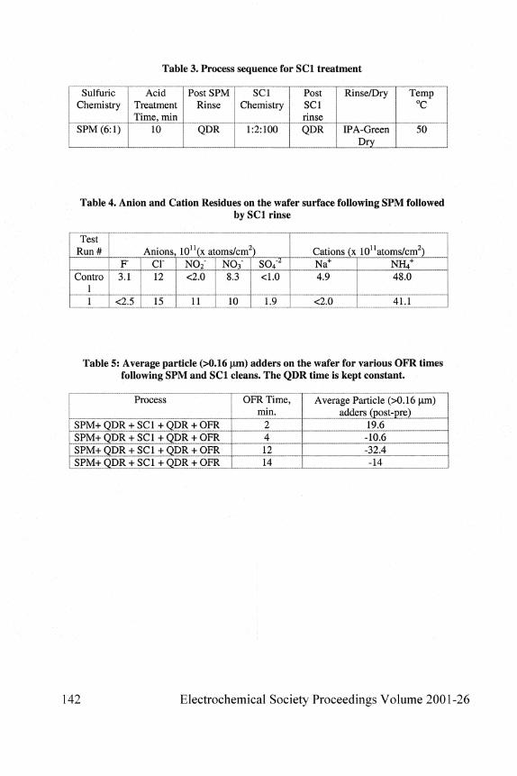
Table 3. Process sequence for SCI treatment
Sulfuric Chemistry
SPM (6:1)
Acid Treatment Time, min
10
Post SPM Rinse
QDR
SCI Chemistry
1:2:100
Post SCI rinse QDR
Rinse/Dry
DPA-Green Dri ..
Temp °C
50
Table 4. Anion and Cation Residues on the wafer surface following SPM followed by SCI rinse
Test Run#
Contro 1 1
Anions, 10u(x atoms/cm2) F 3.1
<2.5
CI" 12
15
N02" <2.0
11
N03 ' 8.3
10
SO4"2
<1.0
1.9
Cations (x 1011 atoms/cm2) Na+
4.9
<2.0
NH4+
48.0
41.1
Table 5s Average particle (>0.16 jam) adders on the wafer for various OFR times following SPM and SCI cleans. The QDR time is kept constant.
Process
SPM+ QDR + SCI + QDR + OFR | _ _ ^ ^ _ + SC1 + QDR + OFR r .^^ ~ ^ ^ _ . ^ _ _ . ^ _ _ f _ _ + ^ ^ ^ „ _ ^ _ _ ^ _ _
OFR Time, min.
2 4 j2 14
Average Particle (>0.16 |im) adders (post-pre)
19.6 -10.6 -32.4 -14
142 Electrochemical Society Proceedings Volume 2001-26

Figure 1. LPD Growth after 31 hours in class-10 clean room vs OFR at constant QDR of S.5 minutes following SPM treatment of wafer.
" Experimental Growth Rate
"""" M Predicted Growth Rate d(GR)/dt = 6.371 l(OFR time)
R2 = 0.9723
Figure 2. Growth rate of contaminants in class-10 clean room (after an SPM clean) as a function of OFR time.
Electrochemical Society Proceedings Volume 2001-26 143

144 Electrochemical Society Proceedings Volume 2001-26

PARTICLES
Electrochemical Society Proceedings Volume 2001-26 145

146 Electrochemical Society Proceedings Volume 2001-26

SUB 100NM PARTICLE REMOVAL WITH DEIONIZED WATER AND A MEGASONIC FREQUENCY OF -835KHZ
Jeff Lauerhaas1, Yi Wu2, Kaidong Xu3, Guy Vereecke3, Rita Vos3, Karine Kenis3, Paul W. Mertens3, Tom Nicolosi2, and Marc Heyns3
1IMEC Industrial Resident from Verteq, Inc., Kapeldreef 75, B-3001 Leuven, Belgium 2 Verteq, Inc., 1241 E. Dyer Road, Suite 100, Santa Ana, CA 92705
3 IMEC vzw, Kapeldreef 75, B-3001 Leuven, Belgium
Theoretical and experimental investigations have demonstrated the ability of a single wafer megasonic cleaning system to remove particles less than lOOnm in size from a wafer surface. The acoustic streaming forces created at the particle-wafer interface are the primary forces considered for particle removal. These forces are large enough to overcome the Van der Waals adhesion force for particle sizes less than lOOnm. Experimentally, the Verteq Goldfinger single wafer megasonic cleaning system removed particles from O3 last wafer surface using only room temperature de-ionized water and a megasonic frequency of -83 5kHz. The particle sizes removed with this cleaning system include 80 ± 9nm Si02, 60 ± 3nm PSL and 36 ± lOnm Sid . Cleaning efficiencies ranged from a low of 97 ± 1% for the 36 ± lOnm Si02 and a high of 99.994 ± 0.002% 80 ± 9nm Si02 for a sixty-second megasonic cleaning time.
INTRODUCTION
It is well known that as device dimensions shrink, so will the size of the defect that need to be removed from the wafer surface to prevent device failure. A common cleaning technique to remove particles involves megasonic agitation during the cleaning cycle [1]. Particle sizes down to lOOnm have commonly been removed by megasonics even though theoretical papers on megasonics (frequency ~ 1MHz) indicate removal of particles this small should not be possible [2]. It is believed that the dominant mechanisms of particle removal in megasonic cleaning include cavitation, microstreaming, and Schlichting streaming. By controlling the combination of these factors, finer particle removal could be realized in megasonic cleaning. Theoretical models and calculations which consider these mechanisms have been developed to predict removal rates of particles from silicon wafers, even below 1 OOnm in particle size [3]. The purpose of this paper is to provide a theoretical explanation of megasonic particle removal and direct experimental evidence that megasonics is indeed capable of removing particles below lOOnm.
Electrochemical Society Proceedings Volume 2001-26 147

The exact mechanism behind the megasonic removal of particles from wafer surfaces is still under investigation. Continued progress has been made to better understand the physical forces involved in removing particles with acoustic agitation. Various theories have been proposed in the past with claims to a fundamental size barrier to particle removal. A limiting factor to these claims has been the absence of experimental evidence within the same work to confirm or deny the existence of a fundamental size barrier. This paper will not only provide an up to date theoretical explanation of particle removal but also provide experimental evidence to confirm the theory. The main conclusion to result from this work is the absence of any fundamental size barrier to particle removal using acoustic forces.
Megasonic cleaning has been widely used in semiconductor wafer manufacturing for many years. The mechanism of fine particle removal has also been investigated for equally as long. Figure 1 shows a comparison between Van der Waals force to various removal forces for a PSL particle based on a few investigators' models [4]. According to Figure 1, megasonic cleaning can not remove fine particles.
Figure 1. PSL particle removal by sliding and lift forces and by forces due to pressure gradient and acoustic streaming in the bulk region. Plotted are the ratios of adhesion Van der Waals forces to removal forces as a function of a particle size (PA = 3 atm, f = 850 kHz, cited from (4))
However, in practice, megasonic cleaning can easily remove submicron PSL and SisN4 particles as well as slurry particles from silicon wafer surfaces. The reason why the models in Figure 1 have conflicts with real tests is that these models only consider liquid flow behaviors in the bulk region under a megasonic field. In megasonic cleaning, a silicon wafer surface has a very thin boundary layer called the acoustic boundary layer. Within this boundary layer (-0.60 um at 1MHz) fluid motion with vortices (Schlichting streaming) and many micron size bubbles are generated (microstreaming and cavitation) which contribute significantly to particle removal. The theory presented in this paper will include the particle removal effects within the acoustic boundary layer.
To experimentally verify the theory, wafers were contaminated with slurry sizes below lOOnm and cleaned with a Verteq Goldfinger™ single wafer megasonic [5-7]
10000^
1000
100
10
1
0.1
*-.>„ Fvdw/Fsl
• Fvdw/Fuf
-»^ Particles Not - - T ^ - w Removed
-Fvdw/Fa,str. (Zhang 1993) -Fvdw^presgrad. (Zhang 1993)
L Particles Removed •*•>- """^H
Particle Diameter C,m)
148 Electrochemical Society Proceedings Volume 2001-26

shown in Figure 2. The transducer was operated at -835kHz delivering' the wafer surface.
0.04 W/mm2 to
"v| •* Quartz Rod :^?f >:"~P\ i t - ' * „
Sonic Energy Liquid
Meniscus
Wafer
Figure 2: Cross sectional view of a Verteq Goldfinger™ Single Wafer Megasonic Cleaner. The wafer is held horizontally and rotated below the quartz megasonic transducer while liquid is applied to the top and bottom of the rotating wafer surface. The megasonic energy is transferred from the quartz rod to the wafer through the liquid meniscus.
The metrology to measure particle sizes below lOOnm is possible with the KLA Tencor SP1-TBI. Particle sizes down to 60 nm can be measured using conventional LPD bin sizes while LPD sizes below 60 nm can be detected with the average haze channel. Both the LPDs and haze are detected with the dark field wide oblique (DWO) channel in this work [8,9].
EXPERIMENTAL
Both Si02 and polystyrene latex (PSL) particles were investigated to verify the megasonic removal theory. The 36 ± lOnm and 80 ± 9nm particles were Si02 and the 60 + 3nm particle was composed of PSL. All particles were deposited on O3 last silicon wafers (0.6 - 1 nm thick oxide) and were cleaned before contamination with a hydrophilic IMEC clean.
The particle contamination procedure consisted of a slurry bath at low pH containing the desired particles. Wafers were dipped in the particle bath, rinsed and then Marangoni dried. The contaminated wafers were then analyzed on the KLA Tencor SP1-TBI before megasonic cleaning. Typically, the particles were allowed to dry on the wafer surface after contamination to increase the adhesion force of the particles to the wafer surface. Particle removal efficiencies were then determined after a sixty-second megasonic clean, five-second rinse and Sahara surface tension gradient dry [10].
Electrochemical Society Proceedings Volume 2001-26 149

The particle removal is quantified by the percent of LPDs removed as determined by equation [1]:
n / T ™-* ™ 1 (LPD added by contamination - LPD after megasonic clean) . . . % LPD Removal = -) - f x 100 [ l ]
(LPD added by contamination - LPD before contamination)
For the 36 ± lOnm SiC>2 particle, the average haze was used to determine removal efficiency [9]. In this case, equation [l] is modified to monitor the change in average haze instead of LPD removal on the wafer surface. Additionally, for the 80 ± 9nm and 60 ± 3nm particles the amount of LPDs on the wafer surface before and after the clean will be reported. The inclusion of this quantity will give a better understanding of the cleanliness of the wafer surface after the megasonic clean.
It should also be noted that no chemistry or heating was used during the megasonic cleaning, rinsing or drying of the wafers in any of these experiments. The megasonic transducer was operated at -835 kHz and delivered ~ 0.04 W/mm2 to the wafer surface.
RESULTS
Theory for Small (<l00nm) Particle Removal by Megasonics
In megasonic cleaning, a silicon wafer surface has a very thin boundary layer called the acoustic boundary layer [ l l ] . The thickness of this layer is proportional to the square root of the ratio of fluid dynamic viscosity to the frequency of the sound (about 0.6um at l MHz). In this layer, the fluid is compressible and rotational so that the Reynolds stress is very large and many vortices occur. The scales of these vortices are determined by the thickness of the boundary layer, and their dimensions are much smaller than the sound wave length. The fluid motion with vortices in this boundary layer is called Schlichting streaming. In general, due to these vortices in the acoustic boundary layers, the velocity gradients of Schlichting streaming are much higher than the flow in the bulk region. In addition, many micron size bubbles are generated adjacent to deposited particles in this acoustic boundary layer, which results in microstreaming and cavitation.
The dominant mechanism of particle removal in megasonic cleaning results from the Schlichting streaming, the microstreaming, and the cavitation. Due to acoustic boundary layers and large Reynolds stress, streaming driving body forces (the source terms in the Navier-Stokes equation) in the local region of the particles deposited on
150 Electrochemical Society Proceedings Volume 2001-26

wafer surfaces are very large. Using Nyborg's theory [12], increasing power and frequency are effective ways to increase this kind of driving body forces in the acoustic boundary layer. These force gradients in an acoustic boundary layer in DI water for the power of 250 watts at the frequency of 850 kHz will be about 2.8x10⁹ dyne/cm4. For the power of 5 watts at the frequency of 3.4 MHz, the force gradients will be about 2xl010
dyne/cm4 [13]. The subsequent Schlichting streaming velocity gradients in the layers also are very large, which result in strong drag forces. The drag force (Fdrag) can be estimated using Stokes law as in Equation [2]:
Fdrag=37E|J.dpVave P ]
Where \x is dynamic viscosity of the medium (0.01 g/cm-s for water) dp is the diameter of the particles (cm) Vave is the averaged flow velocity in the acoustic boundary layer (cm/s).
For the particles of 0.1 jam in diameter, if the Schlichting streaming velocity exceeds 25 cm/s, the ratio of the adhesion force to the removal force (only the drag force) will be less than 1 [14]. A ratio less than one indicates particle removal. It is possible to increase Vave of Schlichting streaming in acoustic boundary layers up to reasonable values using higher megasonic frequency. However, simply increasing megasonic frequency will bring a negative impact by reducing microstreaming and cavitation.
Microstreaming and cavitation in megasonic cleaning depend upon many factors. These factors include acoustic pressure, frequency, liquid viscosity, liquid surface tension, heat conductivity, contents and size of the nuclei, for example. For small nuclei of less than 0.5 urn in diameter, surface tension effects are dominant for bubble motion and cavitation threshold. For large nuclei, the inertial and viscous effects are dominant. Bubble formation actually is a process of nucleation under negative sound pressure cycles. On the other hand, once the bubbles are generated from nucleation in a megasonic field, these bubbles will undergo a pulsating motion causing microstreaming to occur around these bubbles. Microstreaming continues to bring fresh air dissolved in the water or water vapor in the local region of these bubble surfaces. This speeds up rectified diffusion, which involves gas from the liquid diffusing into the bubble [15]. Rectify diffusion and megasonic pulsating motion result in a bubble growing. Once the bubble surface tensions can not undergo megasonic pressure in a positive sound cycle, the bubble will collapse causing cavitation.
In general, the scale of microstreaming velocity due to the pulsating bubble motion is above an order of magnitude greater than Schlichting streaming. Microstreaming is generated in a dynamic acoustic-moving-boundary layer by the pulsating bubble. At the moment of bubble collapse, the scale of microstreaming is
Electrochemical Society Proceedings Volume 2001-26 151

around one hundred meters per second due to shock wave generation. Rayleigh inferred the bubble collapsing time (T) given by equation [3].
T«0.915Rmax(p/Po)a5 [3]
Where Rmax is the maximum radius of a bubble before collapse p is air density Po is pressure.
For a bubble with a micron diameter under one atmosphere at 20°C, the bubble collapsing speed is 345 m/sec. Since acoustic pressure in megasonic cleaning is higher than one atmosphere, the bubble collapsing speed should actually be higher than the value above. Therefore, based on the description above and Equation [3], the ratio of the Van der Waals force to the drag force generated by microstreaming for a 0.1 um PSL particle is lower than 0.25 during the bubble pulsating period and lower than 0.00068 during the bubble collapsing.
Acoustic cavitation has two important characteristics. First is its non-linear property between bubble radius and sound pressure. Second is that the potential energy installed in bubbles can be accumulated by abstracting sound energy [3]. When the bubbles collapse, this energy transfers into kinetic energy and is concentrated in a very tiny volume. This process causes very high pressures and temperatures (1,000 K) resulting in sonoluminescence which can be detected using a photomultiplier tube. Also, this process initiates or speeds up some chemical reaction.
It is possible to obtain several thousands atmospheres of pressure in a collapsed bubble region from cavitation in megasonic cleaning. In general, due to extremely high pressures, temperatures, shock waves, and microstreaming (generated from bubble cavitation) megasonic cleaning is able to remove fine particles with sizes below 0.1 um. Along with these forces, there is danger for megasonic bubble cavitation to destroy fine structures on patterned wafers. Increasing frequency is an effective way to reduce cavitation as well as pattern damage with a price of reducing the cleaning efficiency. According to Holland and Apfels' theory [16], if acoustic frequency increases from 1 MHz to 4 MHz, the cavitation thresholds will increase from 7 atm to 9.2 atm for the nuclei radii of 0.1 um. Theoretically if higher frequency is used in megasonic cleaning for removing particles smaller than 0.1 um in diameter, the corresponding power inputs for the megasonic transducer should be increased to generate cavitation bubbles due to higher cavitation thresholds. It is not too difficult to run a cleaning process to remove fine particles at frequencies up to 5 MHz provided that the megasonic transducer is specially designed and acoustic power, chemical components, and temperature are well controlled.
152 Electrochemical Society Proceedings Volume 2001-26

It is possible to decrease cavitation thresholds at lower frequencies by increasing the temperature of the liquid medium or by changing the liquid viscosity by controlling the chemical components in the liquid medium. These methods are actually used for bubble size and density control in megasonic cleaning.
Experimental Results: Removal of Small Particles (<100nm) by Megasonics
The data to confirm the megasonic removal of small particles is presented below. Table I contains the particle or haze levels for the 80 ± 9nm Si02, the 60 ± 3nm PSL, and the 36 ± lOnm SiC>2 particles added to an O3 last silicon wafer.
Table I: The particle levels before contamination, after contamination, and after a single wafer megasonic clean with de-ionized water. The 80 ± 9nm and the 60 ± 3nm particles were measured with LPD bin sizes and the 36 ± lOnm particles were measured with the average haze.
Particle Size
80±9nm 60±3nm
36±10nm
KLASP1TBIDWO
60nm<(|)LSE< 120nm 60nm<(|)LSE< 120nm Average Haze (ppm)
Before
2899±111 2956 ± 67
0.025 ±0.001
With Contamination
~3 x 10° -96,000 0.25ppm
After Megasonic
Clean 3062 ± 68 3584 + 89
0.033 ± 0.003
The lower LPD size limit of the KLA Tencor SP1-TBI is 60nm. Monitoring the average haze on the wafer surface can lower the size range even farther. As contamination is added to the wafer surface, the average haze will change in response to the change in surface roughness. Typically, a large number of particles are required to change the average haze significantly enough for analysis. In the 36 ± lOnm SiC>2 case, ~3 x 10¹⁰ particles are added to the wafer surface during the contamination procedure [8].
The particle removal efficiencies for each particle size cleaned off of the wafer surface is shown in figure 3. Extending the cleaning time for the smallest sized particles results in complete removal of the 36 ± lOnm particles. The average haze values were returned to the original starting level with the additional cleaning time (100 + 1% removal efficiency).
Clearly, the single wafer megasonics used in these cleaning studies is capable of removing nano-particle contamination in agreement with the proposed theory.
Electrochemical Society Proceedings Volume 2001-26 153

tnov
al
H P4
Pen
1UU -.
80
60 -
40 -
20 -
0 -
1 * • • 1
20 40 60
Particle size (nm)
80 100
Figure 3: Removal efficiencies of 80 ± 9nm Si02 particles 60 ± 3nm PSL and 36 ± lOnm Si02
calculated from the data listed in Table 1. The removal efficiencies are 99.994 ± 0.002% for the 80 ± 9nm Si02 particles, 98.6 ± 0.2% for the 60 ± 3nm PSL, and 97 ± 1% for the 36 ± lOnm Si02
particles.
CONCLUSIONS
The current theoretical explanation examines different forms of acoustic streaming caused by megasonic agitation. The most important form of acoustic streaming for sub-micron particle removal is microstreaming caused by cavitation. These forces occur at the particle-wafer interface. Accounting for these forces clearly shows megasonics can provide the removal force necessary to clean sub-lOOnm particles from the wafer surface. Only accounting for bulk effects will result in an inaccurate estimation of megasonic particle removal ability.
The verification of the theory was provided experimentally with the Verteq Goldfinger single wafer megasonic system discussed in this work. All particle sizes examined (36 ± lOnm Si02, 60 ± 3nm PSL, and 80 ± 9nm Si02) were cleaned off of the wafer surface using a megasonic frequency of ~835 kHz and a power level of ~0.04W/mm2 with only room temperature, de-ionized water. The LPD and average haze measurements clearly proves megasonics can removes nano-particle sizes efficiently and effectively.
REFERENCES
1. G. W. Gale and A. A. Busnaina, Removal of Particle Contaminations Using Ultrasonics and Megasonics: a Review, Particulate Science and Technology, p. 197 (1995).
154 Electrochemical Society Proceedings Volume 2001-26

2. M. Olim, J.Electrochem. Soc, 144, 3657 (1997). 3. D. Zhang, Fundamental Study of Megasonic Cleaning, Ph.D. Dissertation, University
of Minnesota, St. Paul, MN (1993). 4. R. Gouk, Experimental Study of Acoustic Pressure and Cavitation Fields in a
Megasonic Tank, Master Thesis, University of Minnesota, St. Paul, MN (1996). 5. M. Bran, Wafer Cleaning System, Verteq, Inc., U. S. Patent 6,039,059, (2000). 6. J. Lauerhaas, P. W. Mertens, T. Nicolosi, K. Kenis, W. Fyen, and M. Heyns, in Ultra
Clean Processing of Silicon Surfaces 2000, M. Heyns, P. Mertens, and M. Meuris, Editors, p. 251, Scitec Publications, Switzerland (2001).
7. K. Takeuchi, A. Tomozawa, A. Onishi, A. Tanzawa, T. Azuma, S. Umemura, Y. Wu, M. Bran, B. Fraser, Evaluation of New Megasonic System for Single Wafer Cleaning, to be in ECS Seventh Annual Symposium on Cleaning Technology in Semiconductor Device Manufacture (2001).
8. K. Xu, R. Vos, S. Arnauts, W. Schaetzlein, U. Speh, and P. Mertens, Optimization of a Brush Scrubber for Nano-Particles, to be in ECS Seventh Annual Symposium on Cleaning Technology in Semiconductor Device Manufacture (2001).
9. S. H. Yoo, B. Y. H. Liu, J. Sun, N. Narayanswami, and G. Thomes, in Ultra Clean Processing of Silicon Surfaces 2000, M. Heyns, P. Mertens, and M. Meuris, Editors, p. 259, Scitec Publications, Switzerland (2001).
10. P. Mertens and K. Marent, Solid State Technology, 43(9), 113 (2000). 11. A. A. Busnaina and T.M. Elsawy, J. Electron. Mat., 27(10), 1095 (1998). 12. W. L. Nyborg, "Acoustic Streaming", in Physical Acoustics, Vol. IIB Ch.ll, Ed. W.
P. Mason, Academic Press, London/New York, (1965). 13. Y. Wu, Development of an Experimental Validated Model of Megasonic Cleaning,
Ph.D. Dissertation, University of Minnesota, St. Paul, MN, (1997). 14. M. B. Ranade, Aerosol Sci. Technol, 7, 161, (1987). 15. F. R. Young, Cavitation, p. 56, Imperial College Press, London (1999). 16. C. K. Holland, and R. E. Apfel, "An Improved Theory for Prediction of
Microcavitation Thresholds", IEEE Trans. UFFC, 36(2), 204 (1989).
Electrochemical Society Proceedings Volume 2001-26 155

EFFECTS OF H202 AND IPA ADDITION IN DILUTE HF SOLUTION ON SURFACE ETCHING AND PARTICLE REMOVAL EFFICIENCY
Dae-Hong Eom, Sang-Ho Lee, Ky-Sub Kim*, Choong-Hun Lee** and Jin-Goo Park, Department of Metallurgy and Materials Engineering, Center for Electronic Materials and
Components, Hanyang University, Ansan, 425-791, Korea * Dong-Woo Fine Chem. Co., Ltd., Research Center, Iksan, 570-140, Korea
** Division of Electric and Electronic Engineering, Wonkwang University, Iksan, 570 - 749, Korea
The purpose of this study was to evaluate the etch mechanism and particle removal efficiency in dilute HF solutions added with H2O2 and IPA. The etch rate of SiC^ in HF solution was dependent on the etching time and concentrations of HF. As the concentration of H2O2 increased, the etch rate of SiC>2 increased. However, the etch rate of SiC>2 decreased as the concentration of IPA in HF solution increased. The etch rate of SiC>2 in HF-H2O2-IPA solution was very similar to that in HF-IPA solutions. The etch rate was dominantly dependent on IPA concentration not on H2O2. No significant difference in etch rate of silicon was observed in HF solutions with and without the addition of IPA. However, the etch rate of silicon increased in HF solution with the addition of H2O2. Higher contact angles were observed in the presence of IPA in HF solution. It might be due to the prevention of surface re-oxidation by IPA in HF solutions. Particle removal over 90% was achieved when Si wafers were cleaned in HF-H2O2 and HF-H2O2-IPA solutions.
INTRODUCTION
The dilute HF last cleaning has been widely used for the removal of native or chemical oxide on silicon wafer surface grown during wet treatment, especially before gate oxide growth because the reliability of oxide is degraded by the presence of native oxide [1]. As the thickness of gate oxide decreased to about several angstroms, however, the generation of micro-roughness [2] and particle contamination [3] and formation of water mark [4] during DHF step have been risen issues. Also it was reported that severe metal species, especially copper, contamination occur during DHF treatment by several authors [5-7]. All of these defects and contaminants are detrimental to the reliability of device characteristics and result in the failure of device. Thus, it is essential to reduce the contamination and monitor the state of the silicon surface and thin films at an atomic level by using proper cleaning chemistry that render the surface inert and leave an atomically flat surface after the cleaning process.
156 Electrochemical Society Proceedings Volume 2001-26

HF last cleaning can remove the native oxide and metallic contamination included in oxide. However, this step cannot remove the noble metal, such as Cu and Au, because the noble metals contaminated on Si surface electrochemically. It was proposed [8] that the addition of H2O2 in HF can remove the noble metal due to high oxidizing power of H2O2. However, the micro-roughness of Si surface can be increased in HF-H2O2 solutions because of local oxidation of Si surface and metal impurities [9].
In recent days, various methods have been proposed and examined to prevent these problems as mentioned above. The addition of surfactant or alcohol in dilute HF solution was effective for decreasing the surface micro-roughness [7, 8] and reducing the particle contamination [9]. It is very important to study the etch behavior of silicon dioxide and silicon wafer in dilute HF solution mixed with the additives, such as IPA and H2O2 for the process development. However, it has not yet completely understood the chemistry of HF solution with additives.
In this paper, we report the effect of the addition of isopropyl alcohol (IPA) and H2O2 on etch dynamics of silicon dioxide and silicon wafer. The surface was characterized by AFM and contact angle after the treatment in various HF solutions. The removal efficiency of particles was evaluated in various HF solutions with and without the addition of H202 and IPA.
EXPERIMENTAL MATERIALS AND PROCEDURES
In this study, 8" p-type (100) silicon wafers (resistivity : 3-11 Q* cm) and silicon dioxide wafers (thermally grown oxide, ~ 4000 A) were cut into 13 mm x 19 mm. Both types of wafers were cleaned in a 4:1 mixture of H2SO4 and H2O2 for 10 min and followed by 0.5% HF dipping in order to remove native oxide layer on wafer surface. The semiconductor fabrication grade chemicals, NH4OH (28 wt% NH3), H2S04 (98 wt%), IPA (99 wt %) and H2O2 (32 wt%) were provided by Dong-Woo Fine Chem., used for the experiments. HF (49 wt%) was provided by Hashimoto chemicals.
The etch rates of silicon wafers in cleaning solutions were measured by analyzing the silicon concentrations in the solutions using an Inductively Coupled Plasma Mass Spectrometer (ICP-MS). The silicon wafers were immersed in 100 ml of various HF solutions for lhr. The etch rates of silicon dioxide were measured by a Nanospec AFT 200 of Nanometrics. The HF solutions with IPA and H2O2 were stirred for 20 min before the experiments to make sure the homogeneous mixture. The contact angle was measured using Kriiss G10 drop shape analyzer as functions of HF treatment time and DI water rinsing time.
Alumina (50 nm in diameter) and Si02 (14 nm) particles purchased from Deggusa and Beulher were used for the particle removal test and particles were contaminated on
Electrochemical Society Proceedings Volume 2001-26 157

silicon surface using the aerosol method. The particle removal efficiency was evaluated by a Surfscan (Tencor 5500) in various HF solutions.
RESULTS AND DISCUSSIONS
Even though the removal of silicon dioxide films via dissolution in aqueous HF solution is a key process step in practically all silicon-based micro-fabrication technologies, the etch mechanism of Si02 in HF solution are still disputed.
The following reactions have been generally accepted to be the chemical reactions of HF for the etching of Si02 [10].
HF = H+ + F ki= 0.0013 (1) HF + F = HF2" k2 = 0.104 (2)
The dissociation constant of HF (ki) is larger than formation constant of HF2" (k2). So, the kl determined an overall reaction. HF and HF2" concentrations were the important species to decide the etch rate of Si02 in HF solution. In these reactions, HF2" concentration plays an important role in controlling the etch rate of Si02.
Figure 1 (a) shows the etched Si02 thickness as a function of etch time at various HF concentrations. The etched thickness of Si02 linearly increased as the etching time increased. Figure 1 (b) shows the etch rate of Si02 as a function of etch time. For 30 second, the etched thickness was 20 A and the etch rate was about 40 A/min. As the etch time was increased, the etch rate was decreased drastically and then reached a constant rate of 23 A. The high etch rate at the initial stage of etching mighty be due to a faster diffusion of etching species. According to the etch reaction described above, reaction (1) is thought to be the rate limiting reaction, because it requires diffusion of HF molecules onto reaction surface [11].
Figure 2 shows the etch rate of Si02 as a function of H202 concentration in 0.5 wt% HF solutions. The etched thickness of Si02 also linearly increased as the etch time increased when H202 was added in HF solution. It was very interesting that the etch rate of Si02 in HF solution was increased from 23 A/min to 31 A/min when 20 wt% H202
was added. The mechanism of the increase of etch rate when hydrogen peroxide was added in HF solution is not still understood clearly. As shown in Figure 3, the addition of IPA to HF solutions decreased the etch rate of Si02. The etch rate was decreased from 23 A/min to 10 A/min as the IPA concentration increased to 30 wt% in HF. The decrease of etch rate was due to the decrease of HF dissociation constant by the addition of IPA [12].
In the case of HF-H202-IPA solution, the effect of H202 addition on etch rate of Si02
was negligible and the etch rates were very similar to those of HF solutions added with IPA. Figure 4 shows the etch rate of Si02 as a function of IPA concentrations when 5 and
158 Electrochemical Society Proceedings Volume 2001-26

10 wt% H2O2 were added in 0.5 wt% HF solutions. IPA should more dominant effect on HF etch rate of oxide than H202.
To study the effect of H202 and IPA addition in HF solution on the reaction with silicon wafer, etch rate of silicon wafer in HF solution was measured. As shown in Figure 5, no significant difference in etch rates was observed among HF solutions with and without the presence of IPA. The addition of H2O2, however, increased the etch rate of silicon. The increase of etch rate may be due to the two competitive reactions, surface oxidation by oxidizing agent, H2O2, and the etch of silicon oxide by HF. However, the addition of IPA in HF-H2O2 solution decreased the etch rate of silicon wafer down to ~0.5 A/min which was almost the same etch rate as that in HF-IPA solution. It was very important result that the HF-H2O2-IPA solution can control the etch rate by mixing the proper concentration of EPA. The control of etch rate in cleaning solution is very important because the thickness of thin film is directly influence the device characteristic and the over etched surface often results in generation of surface roughness. Two theorems were reported to explain the decrease of etch rate as IPA was added in HF solution. It was reported that IPA reacted with hydrogen halides. As IPA react with HF, isopropyl fluoride was formed as by-products. Because F- ions were consumed with EPA, formation reaction of HF2- was decreased. Finally, the etch rate of S1O2 was decreased as dissociation rate of HF and HF2" concentration was decreased [12]. Also, Ohmi reported that etch rate was dependent on the dielectric constant of solution. From the coulomb force, when relative dielectric constant decreased with EPA addition, attractive force between H+ and F" is strengthened and dissociation of HF decreases and then etch rate is decreased [13].
To study changes of wettability after the treatment of wafers in HF-H2O2-IPA solution, the static contact angle was measured. Contact angle has been known to be very sensitive to the surface hydrophobicity. It is well known that the silicon wafer, conditioned in HF, passivated by hydrogen and it has a contact angle about 75°. As shown in Figure 6, the contact angle of silicon wafer that conditioned in HF-H2O2 solution was 73° without DI water rinsing. This contact angle was slightly lower than that of silicon wafer conditioned in HF solution. It might be attributed to a higher oxygen concentration in H2O2 containing HF solutions that in HF only. When the IPA added in HF solution, the contact angle increased to 83°. When wafer was treated in the case of HF-H2O2-IPA mixture, the contact angle was measured to be -77° and higher than that in HF-H2O2 solution. This result indicates that the surface re-oxidation is prevented by IPA addition. This enhancement of contact angle is very important because it might represent the perfect hydrogen passivated Si surface and less residual oxygen on surface. The native and chemical oxide could give detrimental effect on thin gate oxide integrity [14].
The hydrogen passivated Si surface is stable against oxidation in air or in water [15], but the back bond of Si-Hx, Si-Si, is attacked and broken by oxygen. This oxygen forms a
Electrochemical Society Proceedings Volume 2001-26 159

SiOx bond on silicon wafer surface. As this reaction is processed, the contact angle is decreased and wafer surface looses its hydrophobicity.
Figure 7 shows the changes of contact angle as a function of rinsing time after the treatment in HF, HF-H202, and HF-IPA solutions. The samples, conditioned in HF-IPA, show slightly higher contact angle than that in HF and HF-H202 solutions. After 60 minutes rinsing, the contact angle conditioned in HF-IPA solution was -70°. This contact angle is higher than that of HF conditioned silicon wafer. Based on these results, it could be said that the silicon wafer, treated in HF-IPA solution, has more stable hydrogen passivated surface than the wafer treated in HF solution. The silicon wafer, treated in HF-H202, showed a relatively low contact angle.
Figure 8 shows the particle removal efficiency on wafers in HF-H202 and HF-H202-IPA solutions. Si02 and AI2O3 particles were intentionally contaminated on Si surface using aerosol method. Particle removal efficiencies over 90% were measured in both cleaning solutions. Because etch rate of Si02 was 25A/min in 0.5 wt% HF, it was expected that the Si02 (140 A in diameter) particles might be dissolved in HF solutions. When the cleaning was performed for 10 min, the etch rate of Si02 was 250A/min. because we used to 140 A silica particles in this study, the particles were almost dissolved in HF solution. It was assumed that particles were removed and etched at the same time in HF solutions.
SUMMARY AND CONCLUSIONS
The etch rate of Si02 in HF solution was dependent on the etching time and concentrations of HF and additives such as H202 and IPA. The etch rate of Si02 was changed as the dissociation of HF and concentration of HF2" were controlled by the addition of additives. The etch rate of Si02 in HF-H202-IPA was similar to that in HF-IPA solution. The etch rate was affected by the presence of IPA in HF-H202-IPA mixture. The effect of H202 on etch rate was minimal. No significant difference in etch rate of silicon was observed in HF solutions with and without the addition of IPA. However, the etch rate of silicon increased in HF solution with the addition of H202. When Si was treated in HF-H202-IPA, the contact angle was higher than that in HF-H202 solution. It indicates that the surface re-oxidation is prevented by IPA addition in HF solutions. And Micro-roughness of Si surface was dependent on the addition of H202 and IPA. Finally, HF-H202 and HF-H202-IPA solutions can remove the Si02 and A1203 particles effectively.
ACKNOWLEDGEMENT
This research was supported by Dong-Woo Fine Chem.Co.Ltd.
160 Electrochemical Society Proceedings Volume 2001-26

REFERENCES
1. J. Yugami, T. Itoga and M.ohkura, IEDM Tech. Dig., pp. 855-858, 1995 2. M. Miyashita, K. Makigara and T. Ohmi, J. Electrochem. Soc, 139 (8), 2133 (1992) 3. E. Bellandi, M. Alessandri and A. Tonti, Solid State Phenomena, 65-66, 35 (1999) 4. J. S. J. and S. Ragavan, J. Electrochem. Soc, 143 (9), 2870 (1996) 5.1. Teerlmck, P. W. Mertens, H. F. Schmidt and A. A. Heyns, J. Electrochem. Soc, 143
(10), 3323 (1996) 6. G. J. Norga, M. Platero, K. A. Black, A. J. Reddy, J. Michel and L. C. Kimerling, J.
Electrochem. Soc, 144 (8), 2801 (1997) 7. M. Miyamoto, N. Kita, S. Ishida and T. Tatsuno, J. Electrochem. Soc, 141, 2899
(1994) 8. D. B. Fenner, D. K. Biegelsen and R. D. Briugans, J. Appl. Phys., 66, 419 (1989) 9. M. M. Heyns, S. Verhaverbeke and M. Meuris, Mat. Res. Soc. Symp. Proc, 315, pp.
35-45(1993) 10. M. Hirose, T. Yasaka, M. Hiroshima, M. Takakura and S Miyazaki, J. Electrochem.
Soc, 143, 38(1994) 11. A. Somashekhar and S. O'Brien, J. Elecrochem. Soc, 143, 2885 (1996) 12. B. Garrido, J. Montserrat and J. R. Morante, J. Elecrochem. Soc, 143 (12), 4059
(1996) 13. T. Kezuka, M. Itano and T. Ohmi, Proceedings of the Sixth International Symposium
on Cleaning Technology in Semiconductor Device Manufacturing, Electrochemical Society, PV99-36, 244, Hawaii (1999)
14. B. C. Lin, W. J. Chen, Y B. Lin, and C. Tsai, IEEE, Electron Device Letters, 11, November (1998)
15. T. Takahagi, I. Nagai, A. Ishitani, H. Kuroda, and Y Nagasawa, J. Appl. Phys., 64, 3516(1988).
Electrochemical Society Proceedings Volume 2001-26 161

—«-0.1wt%HF • - • 0.3wt% HF *• 0.5wt% HF
— • - 0.7wt% HF « 1.0wt%HF
Etch Time (sec)
(a)
E
3
Etch Time (sec)
(b)
Figure 1. (a) The etched thickness of Si02 as a function of the HF concentrations and (b) the etch rate in HF solutions as a function of etch time
£ 3
1 0.5wt% HF 4 Etch Time : 20 min
]
j M' j ^""
X
i : •
. :
Concentration of H202 (wt%)
Figure 2. The etch rate of Si02 as a function of H2O2 concentration in 0.5 wt% HF solutions
E
0.5wt% HF aqueous solution Etch Time: 20 min
Concentration of I PA (wt%)
Figure 3. The etch rate of Si02 as a function of IPA concentration in 0.5 wt% HF solutions
E <
0.6wt% HF aqueous solution —•— 5wt% H202
* 10wt% H.O.
Concentration of IPA (wt%)
Figure 4. The etch rate of Si02 as a function of IPA concentrations at 5 and 10 wt% H202
Figure 5. The etch rate of Si in various HF solution
162 Electrochemical Society Proceedings Volume 2001-26

5 wt% H202
5 wt% I PA 5 wt% H,0+5 wt% I PA
Dipping Time (min)
Figure 6. The change of contact angles as a function of dipping time in HF-FbCh; HF-IPA and HF-H202-IPA solutions
0 5wt% HF 0 5wt%HF+ 5wt%IPA 0 5wt% HF+ 10wt% I PA 0 5wt% HF + 5wt% H.O, 0 5wt% HF+ 10wt% H~0,
Time (min)
Figure 7. The changes of contact angle as a function of rinsing time when treated in HF, HF-H202 and HF-IPA.
100
90
80
70
60
50
40
30
20
10
0
ft
p n St
1
1
1?
fa
Si02 Particle
AI203 Particle
Si02 Particle
m
DO.5-1 E31-2 D 2 - 5 D 5 - 1 0
I BBM -J L
AI203 Particle
HF-H2O2 solutions HF-H2O2-IPA solutions
Figure 9. The particle removal efficiency in HF-H2O2 and PIF-H2O2-IPA Solutions
Electrochemical Society Proceedings Volume 2001-26 163

ACTIVITY OF HF SOLUTIONS AND PARTICLE REMOVAL USING HF SOLUTIONS
S. Nelson, J. Sabol, K. Christenson FSI International
Chaska,MN 55318-1096
Removal of particles from silicon wafers by wet chemical processes generally involve etching the surface, and possibly the particle, by the cleaning chemical and the electrical potentials of the surface and the particle in solution (zeta potential). The etching of the materials and the zeta potential are themselves dependent on the pH, other ionic species present in solution and the ionic strength. This paper incorporates activity coefficients in the chemical calculations to model the pH and ionic strength of 1000:1 HF that has been spiked with HC1 or NH4OH. Experiments were performed to study the effect of pH, ionic strength, and etching on removal of Si02, Si, and S13N4 particles from silicon wafers.
INTRODUCTION
HF solutions have been shown to be effective at removing particles from silicon wafers (1) due to slight etching of the native oxide on the wafer surface. Prevention of particle deposition onto silicon wafers in HF has been reported to be dependent on pH and ionic strength (2). Knotter and Dumesnil found that a solution pH > 2 resulted in lower particle deposition as long as the ionic strength was below about 0.5 moles/liter. This work investigates the converse, is the particle removal efficiency in HF solutions dependent on pH and ionic strength? Minimizing particle re-attachment during particle removal is necessary in order to have high particle removal efficiency. At least a small effect could be expected if any particles are removed from the surface in the first place.
In order to test the particle removal with an HF solution at different pH values we needed to know how to mix the solutions. The species in HF solution are H+, HF, HF2~, F~, and H2F2 (3) and the equilibrium constants for these species at 25 degrees Celsius are:
7(H+)[H+]r(F_)[F-]/[HF] = 6.85 x 10"4 [1]
7(HF2-)[HF21/[HF] r(F_)[F-] = 3.963 [2] [H2F2]/[HF]2 = 2.7 [3]
Where /denotes the activity coefficient for an ionic species. Using these equilibrium equations with charge balance and mass balance equations and assuming all the activity coefficients are unity, the concentration of each species can be calculated given the initial
164 Electrochemical Society Proceedings Volume 2001-26

amount of HF and other chemicals put into solution. Once the concentration of each species is known then the solution ionic strength, ju, is calculated using equation [4].
M = ̂ I> , . z , 2 [4]
Where c is the concentration of an ion in moles/liter and z is the charge of the ion. For low ionic strength solutions (|i < 0.001), assuming activity coefficient are unity is reasonable. In our experiments where we have changed the pH of the solution by adding HCl or NH4OH, the ionic strength of the solution is higher and including the activity coefficients becomes more important to calculating an accurate model of the solution. We have used the extended Debye-Huckel equation [5] to calculate ion activity coefficients.
7 = 10A -0.5l2z24Ji l + r^/T/305
[5]
Where z is the ion charge, and r is the hydrated radius of the ion. The hydrated radii used were 900 pm for H+, 350 pm for F , and OH", 300 pm for HF2" and CL", and 250 pm for NH4+(4). Four iterations are made to refine the calculation of the activity coefficients and equilibrium equations until the solution converged.
From the constraining equations including activity coefficients we calculate the amount of buffer to mix with HF to get the desired pH at various species concentrations. We used a 1000:1 HF solution at various pH values to remove Si02, Si, and SisN4 particles from Si substrates. The effect on the particle removal efficiency by the amount of oxide etched, pH, and ionic strength will be reported for each particle material.
EXPERIMENT
HF and pH adjustment chemicals were mixed to the ratios shown in Table I for the particle removal tests. Cleanroom grade 49% HF was used and volumes were measured in a Teflon volumetric flask. Cleanroom grade 37% HCl and 29% NH4OH were used with these volumes being measured by burettes. The chemicals were placed into a 1 L volumetric flask and mixed with DI water. The resulting chemical mixture was placed into a chemical canister of a Mercury® spray processor system to be dispensed onto wafers after going through a 0.05 micron particle filter. The etching chemical was dispensed onto the wafers for 3 or 5 minutes at a flow rate of 2.0 liters/minute. Ozonated DI water (DIO3) was dispensed onto the wafers for 3 minutes before the etching chemical to remove any organic contamination. DIO3 was also dispensed onto the wafers for 5 minutes after the etching chemical to regrow a chemical oxide on the wafers and protect the wafers from particle contamination during the dry.
Electrochemical Society Proceedings Volume 2001-26 165

HF (ml) 1.0 1.0 1.0 1.0 1.0
Table I HC1 (ml) 10.1 0.75 0.0 0.0 0.0
: Chemical mixtures used in experiments NH4OH (ml) 0.0 0.0 0.0 0.76 1.71
DI water (ml) 988.9 998.25 999.0 998.24 997.29
Mixture 1000:1 HF,pHl 1000:1 HF,pH 2 1000:1 HF,pH 2.4 1000:1 HF,pH 3 1000:1 HF,pH 4
Wafers were contaminated with particles by preparing a slurry of particles suspended in a liquid and then dipping the wafers into it and spin drying the wafers leaving a controlled number of particles on the wafer surface. Approximately 2000 SisN4 particles >0.12 jLtm size were deposited onto the wafers by preparing a slurry of 2 mg of dry S13N4 particles in 100 ml of DI water and then diluting 87 (il of the particle slurry into 20 L of DI water and dipping the wafers for 2 minutes. Approximately 2000 Si particles >0.12 jim size were deposited onto the wafers by preparing a slurry of 60 mg of dry Si particles in 100 ml of DI water and then diluting 75 JLLI of the particle slurry into 20 L of DI water with 20 ml HC1 and dipping the wafers for 4 minutes. Approximately 2000 Si02 particles >0.12 Jim size were deposited onto the wafers by preparing a slurry of 45 mg of dry SiC^ particles in 100 ml of DI water and then diluting 75 }il of the particle slurry into 20 L of DI water with 20 ml HC1 and dipping the wafers for 3.5 minutes. For the Si and SiC>2 particles very low particle counts were achieved on the wafers in only DI water at pH 7, requiring the addition of a small amount of acid. Each particle type was contaminated onto the wafers in a dedicated tank and each tank was tested for particle cleanliness and was found to add less than 5 particles at >0.12 micron. Therefore, more than 99.75% of the particles added onto the wafers were made of the desired contamination material. The wafers were stored in a dry nitrogen environment for 15-20 hours before performing the particle removal tests.
Particles were measured on bare silicon wafers using a Tencor SP1-TBI inspection system using the oblique laser to illuminate the particles. The Tencor recipe placed the particles into bins of PSL sphere equivalent particles sizes 0.12|xm - 0.16|im, 0.16jim -0.2jLim, 0.2jxm - 0.25jim, 0.25fxm - 0.3(im, 0.3jim - 0.5jim, and area counts larger than 0.5jnm. Particles were measured on clean wafers before contamination (pre), the particles were measured after the wafers were contaminated (challenge), and the particles were measured after cleaning with the various processes (clean). The particle removal efficiency was calculated using equation 6. The particles added onto clean silicon wafers were measured for each cleaning process to ensure that the particle removal data was not affected by particle addition. In all cases very few particles were added onto the wafers and the contribution of particle addition on the particle removal efficiency was negligible.
Efficiency = 100 x (challenge - pre) —(clean - pre)
(challenge - pre) [6]
166 Electrochemical Society Proceedings Volume 2001-26

RESULTS AND DISCUSSION
Knowledge of the amount of chemicals to use to achieve a certain mixture is very important for a mixture of three chemicals because adjustments of the pH cannot be made after the mixture is prepared without affecting the concentration of HF and other species in solution. Figure 1 shows that for the more acidic mixtures inclusion of activity coefficients in the calculation of the chemical mixture is important. To make a pH 1 solution you should add 10.1 ml of HC1 to make 1 L of solution if the calculation includes activity coefficients. If activity coefficients were not included in the calculation then one would naively add only 8.25 ml of HC1 to make a 1 L solution. Because the pH is a log scale this difference in the amount of HC1 would make a small difference in the pH of the solution. Figure 2 shows the concentration of species in solution calculated using our model for 1000:1 HF with the pH adjusted with HC1 or NH4OH.
Figure 3 shows the measured thermal oxide etch rate of the solutions used in the particle removal tests. Because the thermal oxide etch rate is very low some of the differences in the data could be attributed to noise in the oxide thickness measurement. Figure 3 also shows the calculated ionic strength of the solution in moles/liter. The ionic strength of the solution is lowest when no pH buffering chemicals are added to the 1000:1 HF. The ionic strength of these solutions are relatively low, except at pH 1, compared to the 0.1 - 0.5 moles/liter ionic strength solutions that are seen to affect particle addition onto wafers (2).
The effects on particle removal that we explored in our experiments are the amount of oxide etched, solution pH, and solution ionic strength. Our data for 1000:1 HF at pH 2 (HC1 added) for three etch times, and for 1000:1 HF at pH 2.4 (no chemicals added) for two etch times, are plotted in figure 4 as the particle removal efficiency versus the amount of thermal oxide etched. It was assumed that if a 0 minutes etch process was performed that no particles would be removed. It appears that the particle removal depends on how much oxide is etched with very little particle removal occurring if less than 3 Angstroms of oxide is removed. This data supports the conclusion that the particles must be undercut and lifted off the surface before they can be removed.
It is apparent from figure 4 that S13N4 particles are the most difficult to remove. This could be due to how hard the particles bond onto the wafer surface. Or it could be related to the fact that the particle removal solution is HF and this does not etch the Si3N4 particles while it will etch the Si02 particles and may perform some etching of the native oxide layer on the Si particles.
A clear trend in the data in figure 5 shows the effect on particle removal efficiency by changing the pH of the 1000:1 HF solution for a five minute etch time. However this trend in the pH data is not what we expected. We expected that the particle removal would improve as the solution pH became higher, just as the particle deposition becomes lower at higher pH values (2). Instead we found that the particle removal efficiency
Electrochemical Society Proceedings Volume 2001-26 167

peaked when no pH adjustment chemical was added to the 1000:1 HF. For all three particle types, when either HC1 or NH4OH was added to the 1000:1 HF, the particle removal efficiency decreased. The data point for SisN4 particles at pH 3 was removed because for some unknown reason the particle removal efficiency was highly negative.
In order to change the pH of the 1000:1 HF solution, HC1 or NH4OH was added, which has the side effect of also changing the solution ionic strength as was shown in figure 3. Because of the confounding of pH and ionic strength figure 6 was made from the data with the arbitrary distinction between acidic and caustic chemicals added to the 1000:1 HF. Again the data point for SisN4 particles at pH 3 was removed. Like figure 5, figure 6 shows that the particle removal efficiency peaks when no chemicals are added to the 1000:1 HF. For all three particle types, when either HC1 or NH4OH was added to the 1000:1 HF, the particle removal efficiency decreased. Additionally shown in figure 6 is data were the ionic strength of the 1000:1 HF solution is increased by adding a salt while not changing the pH of the solution. This data confirms that if the ionic strength of the solution is increased that the particle removal efficiency decreases.
The common property of the HF solutions with either HC1 or NH4OH added is that the ionic strength of the solution is increased when the chemicals are added and this has resulted in a decrease in the particle removal efficiency. The ionic strength is the main property of the solution that explains why the particle removal efficiency peaks when no chemicals are added to the HF and decreases when either a buffering acid or a caustic are added. It is interesting to note that the ionic strength of the solution affects the particle removal efficiency at lower values than it affects the particle addition. Where particle addition does not begin to occur until the ionic strength of a solution reaches 0.1 - 0 . 5 moles/liter (2), there does not appear to be such a threshold value for ionic strength on the affect of particle removal.
Figure 7 shows that for Si02 particles the larger particles are easier to remove from the wafers for all the tests that were performed. Figure 8 shows that for Si particles the larger particles are easier to remove from the wafers for all but one of the tests that were performed. Figure 9 shows that for SisN4 particles the larger particles are easier to remove from the wafers for all the tests that were performed.
If increased ionic strength of the HF solution has the effect of reducing the particle removal efficiency, as shown above, then one way to improve the particle removal efficiency of HF solutions is to reduce the concentration of the HF. Figure 10 shows how the ionic strength of HF solutions is affected by dilution of the HF. Most HF etch steps are performed at concentration of 10:1 to 100:1. The ionic strength of these HF mixtures is fairly high and can be significantly reduced by going to concentrations of 500:1 to 1000:1 for steps were particle removal is a concern. If this is done then longer process times will be needed in order to etch enough oxide to remove the particles as the oxide etch rate is reduce when the concentration is lower.
168 Electrochemical Society Proceedings Volume 2001-26

CONCLUSIONS
We have found that several types of particles can be removed from silicon wafers with HF solutions with SisN4 particles being the most difficult to remove. The more thermal oxide that is etched the higher the particle removal efficiency will be with several Angstroms or more needing to be etched. The particle removal efficiency was decreased if either HCl or NH4OH was added to the 1000:1 HF. The reason for this is that the ionic strength of the solution is increased when these chemicals are added.
REFERENCES
1. K. K. Christenson, In Semiconductor Pure Water and Chemicals Conference Proceedings, M. K. Balazs, Editor, pg. 289-300 (1996).
2. D. M. Knotter, Y. Dumesnil, In Ultra Clean Processing of Silicon Surfaces, M. Heyns, P. Mertens, and M. Meuris, Editors, Solid State Phenomena, Vol. 76-77, pg. 255 (2001).
3. S. Verhaverbeke, I. Teerlinck, C. Vinckier, G. Stevens, R. Cartuyvels, M. M. Heyns, J. Electrochem. Soc. Vol. 141, No. 10, pg. 2852, (1994).
4. D. C. Harris, Quantitative Chemical Analysis, 4th ed. W.H. Freeman, pg. 128 (1995).
HCl with correction HCl without correction NH4OH with correction NH.OH without correction
Figure 1: Volumes of HCl and NH4OH added to shift the pH of 1000:1 HF solutions calculated with and without the inclusion of the effects of ionic strength.
0.030
& 0.025
• i 0.020 i I ^0.015 -] .2 10.010 • c § 0.005 • o o
0.000
j - * - [ H F ]
— [HF21
- « - IH2F2]
-rtrtfj 1 2 3 4
Solution pH
Figure 2: Calculated concentration of species of 1000:1 HF at different pH values.
Electrochemical Society Proceedings Volume 2001-26 169
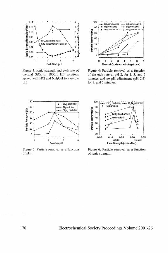
£ 0.04 CO .2 0.02
Figure 3: Ionic strength and etch rate of thermal S i0 2 in 1000:1 HF solutions spiked with HC1 and NH4OH to vary the pH.
Si02 particles, pH 2.4 Si particles, pH 2.4 Si3N4 particles, pH 2.4
0 1 2 3 4 5 6 7 Thermal Oxide etched (Angstroms)
Figure 4: Particle removal as a function of the etch rate at pH 2, for 1, 3, and 5 minutes and no pH adjustment (pH 2.4) for 3, and 5 minutes.
120-
100-
¥ 80" 1 •; £ 6 0 -0 ) <
cc © 40 -,o I 20-Q. i
0 -
9 Si02 particles |
- " f - Si particles f • Si3N4 particles
2 3 Solution pH
Figure 5: Particle removal as a function ofpH.
|I 60
| 40 tz I 20 "•E
a. 0
-20
Si02 particles Si particles
Si3N4 particles
0.02 0.10 0.05 0.00 0.05 Acidic Caustic
Ionic Strength (moles/liter)
Figure 6: Particle removal as a function of ionic strength.
170 Electrochemical Society Proceedings Volume 2001-26

120
^100
1 80
60 E
1 20
^
- • - P H I ^-* J~-<r- pH 2 -* i-m~ pH2.39
— pH3\' ' ' ' — pH4 _ ^ _ _ _ _ | -
Particle size (microns)
Figure 7: Removal of SiC>2 particles as a function of size and pH.
Particle size (microns)
Figure 8: Removal of Si particles as a function of size and pH.
Particle size (microns)
Figure 9: Removal of S13N4 particles as a function of size and pH, excluding pH 3.
0.05-
*s
J8 0.04-1
* | 0.03 -
w JZ
B0.02 -G)
g 0.01-0
0.00-
1 1_ 1 1 L
—•— Ionic strength —•— Oxide etch rate f-L
\ ^__V b
\ * \ f
— 7 ~ ^ ~ f — - f — 4
• 7
6 ^
5 J 4 ©
2 3 € 2 3 18 0
10 20 50 100 200 500 1000 HF Dilution (x:1)
Figure 10: Solution ionic strength and calculated thermal oxide etch rate for dilutions of 49% HF.
Electrochemical Society Proceedings Volume 2001-26 171

EFFECT OF WAFER BACKSIDE ON PARTICLE ADDITION BEHAVIOUR OF HF-RCA SEQUENCE
M.Strada, D.Lodi, E.Bellandi and M.Alessandri STMicroelectronics, Central R&D,
Via C.Olivetti 2, 20041 Agrate B.za (MI), ITALY corresponding authonMassimo. [email protected]
During the IC manufacturing process, some fabrication steps require an oxide removal before RCA cleaning. This etching step clearly appears to be very critical because any residual contamination left on the silicon surface can modify the critical oxide quality and affects the Qbd results, on gate and tunnel oxides. Particle tests were carried out directly on production EPI wafers and showed an increase in contamination of 1000 particles at 0.15 um
per wafer. Most of the added particles were stuck at the bottom of the wafer and the RCA cleaning was not able to remove them. This paper summarises
the results achieved in the study of HF steps and the wafers backside on particle contamination behaviour of HF-RCA and introduces the solutions
found.
INTRODUCTION
The wafer cleaning process has been one of the most important and critical steps in semiconductor manufacturing for over 30 years since W. Kern and D. Poutien developed the well-know concept RCA cleaning in 1960 at RCA Laboratories [1]. Diluted HF chemistries (1 to 4%-w) are widely used for oxide etching on wafers, before critical gate oxidations, because of the high selectivity with silicon and the high etching rate that can be obtained with relatively low HF concentrations, at room temperature. Very often the Si02 removal step is integrated in the wet cleaning tool for surface preparation: wafers go through a diluted HF treatment followed by a RCA cleaning. This step is very critical, because any residual surface contamination can have a detrimental impact on the electrical device properties.
In many real manufacturing cases, when wafers are dipped in the HF bath for an oxide stripping sequence, it is possible to see a huge particle addition on both oxidised and bare silicon surface after the etching step (Figure 1). Previous investigations [2] carried out on conventional wet benches using multi-tank tool and re-circulated chemistries, showed that particle contamination is intrinsic to the HF etching in a recirculated bath and that the amount of contamination is tool or tank dependent. Moreover a major role is played by wafer backside status during the very first process steps. If the subsequent RCA cleaning is not efficient, severe gate oxide integrity (GOI) and device defectivity problems may arise.
In this paper the influence of HF steps and the wafer backside on the particle contamination behaviour of HF-RCA sequence will be investigated.
172 Electrochemical Society Proceedings Volume 2001-26

EXPERIMENTAL
All reported tests were carried out using a Dainippon Screen (DNS) FC821L. This tool features re-circulated tanks (CHB) and one-step, multi-chemistry modules (ONB). In ONB modules, as well as for other single tank tools, chemicals are not recirculated but injected into a DIW flow. Therefore, only diluted chemistries, such as HF, NH4OH, HC1, H202, can be used.
HF etching can be performed in both modules, while the rinse step and the following RCA cleaning are performed only in ONB modules. HF concentration was 1% wt in re-circulated tank or 0.3 % wt in ONB modules. SCI mixing ratio was 1:2:100 at 50 °C.
This "hybrid tool" is able to load 50 wafers at half pitch face to face (polished side are opposite to the other polished side) or back to front configuration as well as 25 wafers at normal pitch (polished side opposite to the rear side of the previous wafer), as shown in Figure 2.
In order to study the effect of the backside surface, several kinds of prime wafers were used: • epitaxially grown silicon with 3000 ± 1000 A of LTO oxide on the back side and about
200 A of thermal oxide on front side • epitaxially grown silicon with 3000 ± 1000 A of LTO oxide on the back side • epitaxially grown silicon with 8000 ± 1000 A of poly and 3000 ± 800 A LTO oxide on
the back side and about 200 A of thermal oxide on front side • epitaxially grown silicon with 8000 ± 1000 A of poly on the back side
The experiments were performed loading three test wafers in the first three slots of the batch in full or half pitch configuration and then filling the remaining 22 slots with silicon dummies.
The measurement tool used for particle contamination is a KLA-Tencor SP1 , measuring defects whose size is larger than 0.15 urn or a KLA-Tencor AIT/7. Edge exclusion was 5mm. Haze measurement was also carried out using the SPlrB/. SEM analyses were performed on the Applied Material SEM Vision with an automatic review system. AFM measurements were made on a Park Scientific Autoprobe LS.
RESULTS AND DISCUSSION
The first test was performed loading 25 wafers, front to rear in full pitch. HF step was tuned to remove about 220A of thermal oxide leaving a hydrophobic surface on wafer front side. Particle addition map is reported in Figure 1: the total number of defects was one hundred times higher than the typical defectivity-upper-control limit for a cleaning process. The amount of defects depends on the loading position, the first two wafers, which are facing an oxidised back-side, are heavily contaminated, while the third one, that faces the backside of a silicon dummy, is far less contaminated, even if not clean (see Figure 3). Further tests show that a certain contamination level is surprisingly found even if wafers are loaded front to front, at half pitch.
Electrochemical Society Proceedings Volume 2001-26 173

A possible explanation of the front side contamination mechanism has been reported in reference 2: it may be due to the different surface state of a hydrophobic (backside) and a hydrophilic wafer (front-side), since in these two states the meniscus formed during the wafer extraction from the HF bath is very different (Figure 4). Particles on the liquid surface move from the hydrophilic wafer to the hydrophobic one, with enough speed to win the repulsive force (Figure 5). The source of the particles can be either the wafer backside or the HF and DIW baths themselves.
In order to better understand the problem, bare epitaxially grown silicon wafers were processed using the same recipe and procedure. Total amount of added particles was about 200 at 0.15jim (see Figure 6). Similar results were obtained on another tool of the same model running 0.5 %-wt HF, and 40°C SCI and on a tool from another manufacturer using a similar cleaning concept. On this tool the test were performed without the SC2 step, but with the same testing conditions (50 wafers loaded in half pitch, front side opposite to front side). Results reported in Figure 7 show a similar particle pattern, demonstrating that the problem is almost independent of the tool set-up.
At SEM review, the particles are different in shapes and sizes (see Figure 8), and the Auger analysis showed that the most relevant peaks are related to silicon and oxygen (see Figure 9). Furthermore AFM analysis reported in Figure 10 and Figure 11 did not show any roughness difference between the HF-RCA treated surface and the RCA one.
This kind of problem can be related to the previous one, considering the presence of an oxide layer on the EPI wafer backside. To verify this hypothesis, different wafer substrates were tested. Results are reported in Figure 12. For EPI wafers with an oxide layer on the backside the particle addition is very high, while for the ones with a single poly-silicon layer there is no addition. Another experiment was performed removing the oxide from the wafer backside using a SEZ spin etcher, and performing the HF-RCA clean in the configuration described above. As illustrated in
Figure 13, AIT analysis did not show any anomalous defectivity. Anyway, sometimes it is not possible to avoid or to remove the oxide from the
wafer backside, without major changes to the process flow or device characteristics. In this case it is suitable to use a very effective SCI process, with more concentrated chemistry and much higher megasonic energy or to add a surfactant to the HF bath as recommended in reference 2.
Alternatively it is possible to completely overcome all particle deposition issues by avoiding to cross the air/liquid interface and performing the etching and the cleaning step in the same tank. In this case a more diluted HF solution (0.3% wt) has been used, in order to keep reasonable chemical consumption.
In this case the particle deposition mechanism shown in Figure 4 cannot occur anymore because the liquid/air interface is crossed only after an oxidizing treatment (SCI), and hence when all wafers exhibits the same surface state, on both front and back sides. The drawback of this approach can be a longer process time, and a consequent lower equipment throughput.
Particle deposition of the single tank etch has been compared with the conventional approach in Figure 14. The latter does not show any particle addition after the HF-
174 Electrochemical Society Proceedings Volume 2001-26

RCA process, showing a very clean surface, with no hazing, roughening and pitting problems.
CONCLUSIONS
During the oxide layer etch in a HF tank, a large amount of the rear oxide is also removed, since the LTO oxide on the rear side of the wafer is etched in HF more rapidly than the thermal oxides on the front side. This creates a layer of floating particles in the solution. During the unloading step from the HF bath to the rinsing tank these particles stick on the hydrophobic wafer surface, for an electrostatic attraction mechanism.
These adhered particles can be removed by using a very effective SCI step, with a high-energy megasonic treatment and a high concentration.
Since a strong SCI is not always feasible, a different approach to the problem was needed. We have showed that removing the oxide from the wafer backside or performing the whole HF-RCA in the same tank can avoid this large particle adhesion.
REFERENCES
1 W.Kern and D. Poutien, RCA Rev 31,187 (1970) 2 E.Bellandi, M.Alessandri, F.Pipia and A. Tonti, Proc 4th Intl. Symp. UPCSS, Oostende, Belgium, 35(1998)
Electrochemical Society Proceedings Volume 2001-26 175

Polish side
Non Polish side
Figure 2: Wafer handling. Face to face (left) and Figure 1: Particle contamination face to back (right) loading, after HF strip observed at AIT 11
14000
12000
10000
•§ 8 000 a, ~2 6000
4000
2000
0
3
| 1 E x p e r
ESSSSExper | _ ] F, x p c r
m e n t 1
m e n t 2
m e n t 3
S l o t 1 S l o t 2 S l o t 3
Figure 3: Particle count Vs wafer position
176 Electrochemical Society Proceedings Volume 2001-26

J
Extraction Immersion
Hydrophobic (front) side
Hydrophilic (back) side
1 ,&1
J 1&2
SlE-3
.5 1E4
"Sb £ 1E-5 is
§ 1E-6 3
IE-7
Attraction No interaction
Repulsion
1E-8 2E-8
f^ra'cle-snrface distance (m)
^ ^ ^ ^ ^ ^ ^ ^ ^ ^ ^ ^ ^ ^ ^ ^ ^ ^ ^ ^ ^ ^ B Figure 5: Simplified chart of particle to Figure 4; Mechanism of particle addition surface interaction (Z-potential is -lOmV, during wafer extraction wafer potential -300V)
V/i W
y r A; •*, t
Figure 6: HF-RCA on a prime EPI wafer Figure 7: HF-SC1 on an oxidized EPI wafer performed on a tool from another brand.
Electrochemical Society Proceedings Volume 2001-26 177

Figure 8: SRM image of the adhered particles
> 05 1
•
g -05
-1
-15
-z
10*
SI
5rsJq_l9.spe
0 '
c
TTfl iOD 3U ^Tl 10DD 12H] 1*03 1SH S B
Figure 9: Auger analysis of the adhered particles, silicon and oxygen peaks are clearly evident
Figure 10: AFM analysis after HF-RCA clean
178 Electrochemical Society Proceedings Volume 2001-26

Figure 11: AFM analysis after RCA clean
14000,-
12000 L
icoool
I BOCoL
\ 600ot
! 400oL
200ot
I
T
1 Poly Poly-Ckide
Figure 12: Particle count vs. wafer backside
Figure 13: AIT analysis of a wafer whose rear oxide has been removed by an SEZ spin etcher
IMe*e BDt:
r #t te*e
BDt:
I M e f e DBt:
K
W e f t BBfc:
5 1 c t s : 3 .009
—'-\\
c t s : 3 .009
: > .0x2
A •J
c t s : 5 .0X5
Figure 14 particles counts after recirculated HF (left) and single tank etch (right)
Electrochemical Society Proceedings Volume 2001-26 179

New Approach for Study of Particle Adhesion and Removal Relevant to Post CMP Cleaning
Su-Youn Lee, Sang-Ho Lee, Dae-Hong Eom, Ky-Sub Kim*, Hyung-Soo Song* and Jin-Goo Park
Department of Metallurgy and Materials Engineering, Hanyang University, Ansan, 425-791, Korea
* Dongwoo Fine Chem, R&D Center, Iksan, 570-140, Korea
The purpose of this study was to investigate the interaction force between slurry particles and wafer surfaces for the development of effective post Chemical Mechanical Planarization(CMP) cleaning process. Silica slurry has been most commonly used in the final step of Cu polishing to reduce scratches, Cu dishing and oxide erosion. The calculation and measurement of interaction forces between silica particles and TEOS, TaN and Cu surfaces have been performed in this study. DLVO theory was used to calculate the interaction force between the slurry particle and the wafer by measuring zeta potentials of particles and surfaces. The interaction force was directly obtained by measuring the force on the particles as a function of distance between the particle and surface using an Atomic Force Microscope. The strongest adhesion force was measured on TaN surfaces in both calculation and measurements. The magnitude of particles contamination on wafers was measured by FESEM after polishing. Highest number of particle observed on TaN surfaces after polishing.
INTRODUCTION
Due to its low resistivity and high electromigration performance, copper is considered to be a much better metallization than the currently used aluminum based alloys [1]. While the advantage of using Cu, as an alternative material to Al is clear, there are several challenges that must be overcome. One such challenge is the difficulty involved with Cu patterning by the dry etching (RIE). The damascene technology using Chemical Mechanical Planarization (CMP) is the only technology that can provide global planar surfaces and patterned copper with a large process window [2]. Other problem of Cu CMP is Cu contamination. Copper is considered as a very serious metallic contaminant for silicon devices. Also, detrimental effects of Cu contamination into the inter-metal and inter-level dielectrics were well known. Because Cu CMP give rise to many scratches, large dishing and easy erosion, two-step polishing has been applied in Cu CMP. In the first step, alumina slurry in acidic pH has been used for a faster removal of Cu until TaN surface just exposed. Alkaline silica slurry has been commonly used to meet the polishing selectivity of Cu : TaN : TEOS to 1 : 1 : 1.
After the 2nd step polishing, Cu, TaN and TEOS surfaces will be exposed to silica slurry particles. The interaction of silica particles with these polished surfaces will determine the level of particle contamination after Cu CMP.
In this paper, the interaction forces, between particles and surfaces were calculated
180 Electrochemical Society Proceedings Volume 2001-26

based on DLVO theory at different pH ranges [3]. Also, experimental measurements of adhesion forces between them were performed using an AFM. The magnitude of particle contamination on Cu, TaN and TEOS surfaces was observed after polishing them in order to confirm the calculated and measured interaction forces.
EXPERIMENTAL MATERIALS AND PROCEDURES
For the experiment, TEOS (Tetraethylorthosilicate), TaN and Cu deposited wafers were used as substrates. TEOS wafers were cleaned in the mixture of H2S04 and H2O2 (4:1) followed by DHF treatment. The semiconductor-grade wet chemicals were provided by Dong Fine Chem. Co. and used for the experiment. The zeta potentials of all materials used in this study were measured as a function of pH. Zeta potentials were analyzed using a LEZA 600 (Otsuka Electronics) zeta potential analyzer. The adhesion force has been measured by analyzing the force on the cantilever as a function of distance between cantilever and surfaces using an Atomic Force Microscope (AutoProbe^ CP Research, Park Scientific Co.) in liquid. The adhesion force was measured in solution as a function of pHs in 10~3 M KC1 solutions using an electrochemical liquid cell. For the interaction force measurements, a glass particle of a radius of 20 urn (Duke Scientific Co.) was attached on a tipless AFM cantilever. Figure 1 shows the optical micrograph of a silica particle on the tipless cantilever. The wafers were polished with silica particles on a polisher. (PM5 polisher, Logitech Co.) The rotation speeds of the head and platen were set at 30 rpm. The pressure of the carrier was 3 psi. Polishing time was set for 1 min. A constant slurry flow rate of 120 ml/min was used for the polishing. For the preparation of slurry, the shaker and ultrasonic power were applied for 60 min and 30 min, respectively. Copper CMP slurry was prepared by mixing 10 wt% fumed silica abrasive and corrosion inhibitor (BTA, 10"2mol) in 10"3 KG solutions, which is the same used for AFM measurements. The polished wafer surfaces were observed by FESEM for the particle contamination.
RESULTS AND DISCUSSIONS
The zeta potentials of slurry particles and wafers were measured as shown in Figure 2. The zeta potential of Cu surface was analyzed with that of Cu particle because the zeta potential of general metal surface could not be measured due to the high conductivity and cell constant.
DLVO theory estimates the repulsive and attractive force due to the overlap of electric double layers and London-van der Waals force in terms of inter particle distance, respectively. The fundamental interactions occurring between particles and the wafer surface in solution are the van der Waals force(VA) and electrostatic force (VR) as shown in equation [4].
VT = VA + VR (1)
If a small interparticle separation is assumed, van der Waals forces for a sphere and substrate can be expressed to
Electrochemical Society Proceedings Volume 2001-26 181

VA = - 4 2 3 7T7T w h e r e ' (Ai32 = (An1/2 - A331/2 )(A22
1/2 - A331/2)) (2)
6H0
A132 is the Hamaker constant of two particles 1 and 2 in dispersion medium 3 and calculated based on An value and R is the radius of a sphere. The Hamaker constants of unknown metals were calculated based on their definition as shown below
An=7i2n2C, = 3/4hv(0.1)2 (3)
Where n is number of atoms per unit volume, Q is (3/4) hv0a2, hv0 is ionization potential and a is polarizability. Hamaker constants used for this study were summarized in Table 1. Table 1. Hamaker constants used for van der Waals force calculation
Materials
Si
Si02
Cu
TaN
* = based on eq
An(X10-2 0J).
•(3)
25.6 [5]
50 [5]
28.4 [6]
25.9*
The calculation of electrostatic force due to the overlapping of the diffuse double layer between two surfaces is complex. It must rely on numerical solutions or various approximations. Overbeek's approximation [7] was used for the calculation of electrostatic forces due to diffused double layer interaction as shown in below.
T / , r r , 64nsala7k2T2r1r-> r „. , v exp[ze^/2fcr]-l
fiiH)= (a|'+a2)eV ^ ^ Wh6re' r = exp[**/2*ri + l
where z is the counter ion charge number, ai and a2 are particle radius, K is (87inv2e2/skT)l/2.
Figure 3 shows the DLVO total interaction energy between a silica particle and wafers as a function of pHs. The stronger attractive force was calculated for silica particles and wafers in acidic than in alkaline solution. In acidic, neutral and alkaline solution, attractive interaction force between silica particle and TaN wafer was the strongest, attractive interaction force between silica particle and Si02 wafer was the weakest.
The change of interaction force between the particle and surface was measured as
182 Electrochemical Society Proceedings Volume 2001-26

the cantilever approached to the substrate [8]. The AFM probes the surface of a sample with a sharp tip, a couple of microns long and often less than 100 A in diameter. The tip is located at the free end of a cantilever that is 100 to 200 urn long. Forces between the tip and the sample surface cause the cantilever to bend or deflect. A detector measures the cantilever deflection as the tip is scanned over the sample. Several forces typically contribute to the deflection of an AFM cantilever. The force most commonly associated with atomic force microscopy is an inter-atomic force called the van der Waals force. Figure 4 shows a typical force-versus-distance curve or force curve. Force curves show the deflection of the free end of the AFM cantilever as the fixed end of the cantilever is brought vertically towards and then away from the sample surface. Figure 4 (a) shows the cantilever shapes at several marked along the force curve. (A) in Figure 4 (b) is with the movements cantilever at each point. In the case shown, there is minimal long-range force, so this part of the force curve shows no deflection. (B) in Figure 4 (b) is that as the probe tip is brought very close to the surface, it may jump into contact if it feels sufficient attractive force from the sample. (C) in Figure 4 (b) is that once the tip is in contact with the surface, cantilever deflection will increase as the fixed end of the cantilever is brought closer to the sample. (D) in Figure 4 (b) is that after loading the cantilever to a desired force value, the process is reversed. A key measurement of the AFM force curve is the (C) in Figure 4 (b) at which the adhesion is broken and the cantilever comes free from the surface. This can be used to measure the rupture force required to break the bond or adhesion. The bigger the jump out point, the more attractive interaction force [9].
Figure 5 shows the measured interaction forces between particles and surfaces. Figure 5 (a) shows the interaction forces in alkaline solution of pH 11. The attractive forces of Si02, Cu and TaN wafers were measured to be - 0.776 nN, - 2.019 nN and - 2.04 nN, respectively. The strongest interaction force on TaN wafers and the weakest interaction force on SiOi were measured. Figure 5 (b) shows the interaction forces in neutral solutions. The attractive forces of Si02, Cu and TaN wafers were measured to be - 4.977 nN, - 14.456 nN and - 15.11 nN, respectively. The attractive force in acidic solutions was relatively stronger than alkaline solution on all wafers. Figure 5 (c) is the measured of the interaction forces in acidic solution. The attractive forces of Si02, Cu and TaN wafer were measured to be - 10.1 nN, - 18.78 nN and - 20.18 nN, respectively. The attractive force in acidic solutions was the strongest among solutions with different pHs. In all pHs the measured interaction force showed the same results as calculated one. TaN surfaces tend to have the strongest adhesion of silica particles in all pH ranges even though there are significant differences in their magnitudes.
In order to know how much the interaction force is important in the development of post CMP cleaning process, the wafers were polished with silica particles on a polisher. The least number of particles were found on the Cu wafer when polished alkaline slurry and the greatest on TaN wafer in using acidic slurry. It indicates that the interaction force plays a major role in determining the level of contamination on wafer surfaces during CMP.
SUMMARY AND CONCLUSIONS
The zeta potentials of slurry particles and wafer surfaces were measured to calculate
Electrochemical Society Proceedings Volume 2001-26 183

the total interaction force between them based on DLVO theory. The strongest attractive force was calculated between silica particle and TEOS, Cu and TaN wafers in acidic, neutral and alkaline pHs. Even the repulsive forces were calculated on TEOS, Cu, TaN wafers in alkaline pH. However, the strong attractive forces were calculated in other pH ranges. The adhesion force was measured between silica particle on cantilever and wafers by AFM. It was found the strongest adhesion of silica particles on TaN surface and the weakest on SiC^ surface. As a result, both the calculated and the measured interaction forces were agreed well each other. In other to compare these results, particles on substrates were observed by FESEM after CMP. The least number of particles was observed a Si02 wafer and the greatest on TaN. The particles on Cu wafers were more difficult to remove than those on other wafers. Alkaline slurry was more desirable for a better control of particles on wafer surfaces after CMP than acidic slurry.
REFERENCES
1. J. Torres, J. Palleau and F. Tardif, Microelectronic Engineering, 50, 425-431 (2000) 2. S. P. Murarka, Metallization, p. 100, Butterworth-Heinemann, Boston (1993) 3. A. W. Adamson and A. P. Gast, Physical Chemical of Surfaces, p.250-276, John Wiley
& Son, Inc., New York, (1997) 4. T. Hattori, Ultraclean Surface Processing of Silicon Wafers p. 1139, Springer, New
York (1998) 5. J. Visser, Adv. Colloid Interface Sci., 3, 331 (1972) 6. G. Bohme, H. Krupp and W. Schnabel, Molecular Process at Solid Surface, McGraw
Hill, New York, 611(1969) 7. H. Reerink and J. Th. G Overbeek, Discuss Faraday Society, 18, 77 (1954) 8. R. Wiesendanger, Scanning Probe Microscopy and Spectroscopy, p.345-350
Cambridge University Press (1994) 9. T. J. Senden and C. J. Drummond, Colloids and Surfaces A: Physicochemical and
Engineering Aspects, 94, 29-51 (1995)
184 Electrochemical Society Proceedings Volume 2001-26

J 3 * -
\--i' 1 ~ T "
j
~"T
* ~*~
- * - •
\ ~ V -
TaN wafer Cu paricle Colloidal silica TEOS wafer
Figure 1. The optical micrograph of a silica particle on a tipless cantilever
Figure 2. The zeta potential of Cu and colloidal silica particles and TEOS and TaN wafers as a function of solution pH
h—
_*: ^ <-n ti) r CD
ion
o CVS
CD
C
75
50
^h
U
-25
-50
-75
-100 50 75
H ( A ) (a)
r -J ^
>> CD)
CD C CD
C o o CO CD
c
100
75
SO
Vh
U
-25
-50
-75
-100
150
>, a> CD c CD C
_o "o CO
CD
75
50
25
0
-25
-50
-75
-100 150
nf^nrrfff}
Figure
0 25 50 75 100
H ( A )
(G)
3. DLVO total interaction energy between silica particle and wafers at (a) pH 11, (B) pH 7 and (c) pH 3
Electrochemical Society Proceedings Volume 2001-26 185

Force
Total tracking
A
(cp \ ( D )
Jurnj!
(B)
Set Point
(A)
d •*
i k J Adhesion F
inV r jump out
: • Distance
(a)
l
•*s
l£T
(A)
(B)
(C)
(D)
(E)
(b)
Figure 4. The change of (A) force curve and (B) cantilever shape as a function of applied force on a cantilever
l ln teract io force in pH11 solution
(a) J Interactio force in pH3 solution J
(b)
(c)
Figure 5. Interaction forces between silica particles and TEOS, Cu and TaN wafers measured in solution of (a) pH 11, (b) pH 7 and (c) pH 3 by AFM
186 Electrochemical Society Proceedings Volume 2001-26

OPTIMIZATION OF A BRUSH SCRUBBER FOR NANO-SIZED PARTICLES
K. Xu, R. Vos, S. Arnauts, M. Lux, W. Sehaetzlein1, U. Speh1, P.W. Mertens, M.M. Heyns, C. Vinckier2
IMEC, Kapeldreef 75, B-3001 Leuven, Belgium ^at tson, Carl-Benz 10, D-72124, Pliezhausen, Germany
2Chem. Dept., K.U. Leuven, B-3001 Leuven, Belgium
The article describes the optimization of a brush scrubber clean for nano-sized slurry particles. The removal of Clariant SiC>2 slurry particles with average size of 35nm from nitride substrates was studied, and the removal efficiency was determined. To measure nano-sized particles on wafers, the haze signal was used instead of the individual light point defects. The cleaning was done using a single double-sided brush cleaning station followed by a Lineagoni ™ dry on a Damasclean ™ tool from Mattson. The effect of different process parameters, which were varied using a design-of-experiment software, upon the particle removal efficiency is evaluated. The brush-wafer distance appears to be the most important parameter, and is further optimized. Finally, the brush loading effect was investigated with substrates highly contaminated with slurry particles. This effect can be greatly decreased by using adequate chemistries such as diluted NH4OH.
INTRODUCTION
With shrinking dimensions of the IC structures, the impact of particles upon device yield becomes more and more important. To ensure high device yields, wafer surface contamination and defects must be monitored and controlled at several points in the semiconductor manufacturing process. Brush scrubbers are among the tools used to achieve such control and they have become one of the dominant instruments for wafer cleaning applications nowadays. Although we can find some publications about the principles of brush scrubber clean (1), the detailed analysis and optimization of it are not well reported, especially for nano-sized particles. Counting the nano-sized particles depositing on substrates is a big challenge because the state-of-the-art instruments allow only inspection of particles down to 80nm (KLA-Tencor SP1 TBI) or 50nm (SP1 DLS). However, it has been reported that the haze signal can be used in order to monitor high-density particles on a wafer surface (2, 3). This article describes the evaluation and optimization of a brush scrubber for the removal of nano-sized particles. The particle removal is determined on nitride and thermal oxide substrates using different particles.
Electrochemical Society Proceedings Volume 2001 -26 187

The brush loading with particles during brush scrubber clean is investigated by processing highly contaminated wafers.
EXPERIMENTAL
An overview of the different particles used is given in Table I. Particle removal is studied on 200mm nitride wafers with 150nm nitride layer on 15nm pad-oxide and 200mm thermal oxide wafers with SOOnni thermal oxide layer.
Table I: Overview of particles used and purchasing details. Particle Size (nm) Vendor
Clariant Klebosol PL30S25 (Si02-slurry) S13N4
Rodel ILD1300 (Si02-slurry) Cabot EPG4200A (Al203-slurry)
PVPS - poly(l-vinylpyrrolidone-co-styrene) PSL - Polystyrene latex spheres
35 ±10 100-200 100-200 100-200
-500 258 ± 20
Clariant Alfa Johnson
Rodel Cabot
Aldrich Duke Sci.
After Imec-clean (4), wafers were intentionally contaminated with particles using an immersion based contamination procedure (approximately 4x10 Light Point Defects (LPDs)Avafer, measured in the range 0.1-0.2 um). Particle contamination on the wafer surface is determined by light scattering measurements using a KLA Tencor SP1 TBI
apparatus with a Dark Field Oblique illumination and a Wide collection configuration (DFWO). Particle Removal Efficiency (PRE) is calculated from the LPD counts or average haze signal before and after contamination and after the clean under investigation using
PRE= 1 After_Clean - Before_Cont ^ Before Clean - Before Cont 1
x 100 [1]
Contaminated wafers were processed using PVA brushes (Texwipe TX5322) followed by a Lineagoni ™ dry on Damasclean ™ tool from Mattson. Prior to processing the particle-contaminated wafers, the brashes were preconditioned to have a negligible background of particles deposited on clean wafers using 2% dNHUOH (pH - 12). The effect of different process parameters of brush scrubber such as brush speed, wafer speed,
188 Electrochemical Society Proceedings Volume 2001-26

brush-wafer distance, pH and cleaning time upon PRE was evaluated using a design-of-experiment software Echip6 with a linear design:
PRE = Const. + a! x Waferspeed + a2 x Brushspeed + a3 x
Brush-wafer_distanee + a4 x Cleaning_time + a5 x pH [2]
with a1? a2, a3, a4 and a5 the coefficients corresponding to the five process parameters. The settings used to vary the different process parameters are summarized in Table II.
Table II: Overview of process parameter ranges of design-of-experiment p r o c e s s parameter ' Setting
Wafer speed : 60-100ipm(*) Brush speed 150 - 300 rpm()
Brush-wafer distance - 2.4 —1.6 mm Cleaning-time 10-91 sec.
pH 6 -12 () Real values for wafer speed and brush speed corresponding to the set values when there is no brush/wafer contact. The Real values are much lower when the contact exists.
In order to optimize the brush-wafer distance, PRE is determined at different brush-wafer distances between -1.8mm and -2.6mm. When the brush-wafer distance is 0, the brushes just touch the wafer; the negative brush-wafer distances in this report mean that the brushes have contacted the wafer and are compressed on the wafer surface. In order to make a good comparison between different brush-wafer distances, the cleaning time was adjusted to have a fixed number of wafer rotations during the cleaning, i.e. 60 wafer rotations for each brush-wafer distance. As a control, after each particle-contaminated wafer, the particle counts are determined on a blank wafer to check for possible cross-contamination, which shows that there is no significant brush loading effect when low controlled contaminated (+ 4X10⁴ LPD/wafer) wafers are processed.
The effect of loading the brushes with particles was assessed by running nitride wafers highly contaminated with Clariant Si02 slurry particles (approximately 4x10⁶
LPD measured in the range 0.1-0.2ym). Totally one box of 25 wafers is processed, including 3 dummy wafers to precondition the brushes followed by a blank wafer to measure initial cleanliness of the brushes and 7 times a set of wafers consisting of 2 highly contaminated wafers followed by a blank.
The re-deposition of particles from brushes to wafers was investigated by contaminating the brushes with 5ml Clariant Si02 slurry particles. During the processing,
Electrochemical Society Proceedings Volume 2001-26 189

always the same recipe was selected: brush-wafer distance was set at -2.4mm and each wafer was cleaned with a fixed number of wafer rotations for each wafer processed (i.e. 60 wafer rotations/clean).
RESULTS
The removal efficiencies of different particles from thermal oxide and nitride substrates are summarized in Figure 1. In general, for most particles the removal efficiency is very high: the particle counts after brush cleaning are comparable to the levels obtained on 'clean' non-contaminated reference wafers. Whenever this is the case, the PRE is indicated as -100 %. The SiC^-slurry particles are found to be the most difficult challenge to remove. One further particle removal experiment was done using a patterned STI wafer contaminated with Si02-Clariant slurry particles after the CMP process. The wafer received a post-CMP brush scrubber clean using dNLLjOH. The particles were removed from thermal oxide field, but not from the nitride field (Figure 2).
Since the KLA-Tencor SP1 can not measure a real 3 Onm slurry particle but only measures in the tail of the particle distribution or particle agglomerates, an indirect method to measure the particles was used. The added average haze of the wafers as a function of the count of added LPDs between 0.1 - 0.2 fim on the wafers is depicted in Figure 3. The slopes of the linear fit are close to 1, showing that the haze of the wafer is proportional to the number of LPDs on the wafer. Using these curves, we can easily measure the number of particles depositing on the substrate indirectly by measuring the haze value of the substrate.
The effect of brush speed, wafer speed, brush-wafer distance, pH and cleaning time upon the removal of Si02 slurry particles from nitride substrates is summarized in Figure 4. The particle removal efficiencies are calculated using average haze values and LPD-counts in the ranges of 0.125-0.2 and 0.2-2.0 urn. In general, the particle removal efficiencies calculated using average haze values are smaller than the those calculated using LPD-counts for the small and the big range, suggesting that the small particles are relatively more difficult to remove compared to the bigger particles. Obviously, the brush-wafer distance is the most important parameter and is becoming more and more important as the particle size becomes smaller. Cleaning time is also important compared to the other process parameters. It also becomes more important as the particle becomes smaller. All the effects of other process parameters are minor compared to brush-wafer distance and cleaning time.
Since the brush-wafer distance is the most important parameter that influences the particle removal, it is further optimized. The particle removal efficiency calculated using
190 Electrochemical Society Proceedings Volume 2001-26

the haze of the wafer and the number of LPDs after brush scrubber clean as a function of brush-wafer distance are summarized in Figure 5. In general, particle removal efficiency increases when the brush-wafer distance becomes smaller. When it is reduced below -2.2mm, no real improvement is observed. For removal efficiencies determined using average haze values, they are close to 100%. However, when LPD counts between 0.1-0.2um are used to calculate the removal efficiency, it is impossible to obtain 100% removal because of a rather high background addition of particles while the added haze on blank wafers amounts to zero. It is observed that an optimal removal is obtained if the brush is close enough (below -2.2 mm) to the wafer surface. The wafer rotation speed decreases greatly when decreasing the brush-wafer distance (see Figure 6) because of bigger friction between brushes and wafers. It can be easily concluded that the brush scrubber clean is a physical friction process.
Brush loading effects are assessed by continuously processing highly contaminated wafers, and the results are depicted in Figure 7. When UPW is used while processing the highly contaminated wafers, the particle removal efficiencies calculated using average haze values and LPD-counts decrease corresponding to an observed increase in added LPDs on the blank wafers (Figure 6a). These data show that the brushes can be contaminated when processing wafers with high particle contamination levels and the particles are released and re-deposit during further cleaning. This is also illustrated by processing a box of clean nitride wafers using the brushes intentionally contaminated with 5ml Si02 slurry particles. The first wafers processed have very high numbers of particles, which strongly confirm the re-deposition of particles from the brushes to wafer.
After processing the same wafers using dNL^OH instead of UPW, the results are somewhat different (Figure 6b). The added LPD-counts on blank wafers processed with dNEL̂ OH in between the highly contaminated wafers are much lower than on blank wafers processed with UPW. The particle removal efficiencies for dNFLjOH are much higher than for UPW, especially when the average haze is concerned, in which case a removal near 100% is observed. It can be easily concluded that brush loading effects can be eliminated greatly by using the proper chemicals, such as dNFLjOH.
CONCLUSIONS
It is demonstrated that for high-density of nano-sized particles on a wafer surface, a linear relationship exists between the haze of the wafer and the added LPD-counts on the wafer. This haze signal can be used to study these very small particles that can not be measured otherwise.
Electrochemical Society Proceedings Volume 2001-26 191

The effects of different process parameters that influence the particle removal efficiencies during brush scrubber clean are studied using design-of-experiment. The brush-wafer distance appears to be the most important parameter among the process parameters studied, which confirms that the brush scrubber clean is a physical mechanical friction process.
When wafers with high particle levels are processed, the brushes can be loaded with particles, which reduces the cleaning efficiency: when the brushes are contaminated, the overall removal efficiency decreases because of re-deposition of particles from brushes to wafers. However, if the proper chemicals, such as dNt^OH, are used during the brush clean, these loading problems can be eliminated greatly.
REFERENCES
1 . F. Zhang, A. A. Busnaina and G. Ahmadi, J. Electrochem. Soc, 146(7), 2665 (1999). 2 . S. H. Yoo, J. Sun, N. Narayanswami and G. Thomes, 5th UCPSS, Oostende,
Sept 2000. 3 . K. Xu, R. Vos, F. Holsteyns, K. Kenis, G. Vereecke, P. W. Mertens and
M. M. Heyns, Sematech YMS meeting in Singapore and Taiwan, Aug. 2001. 4 . M. Meuris, P.W. Mertens, A. Opdebeeck, H.F. Schmidt, M. Depas, G.Vereecke,
M.M. Heyns and A. Philipossian, Solid State Technology, 8, 109 (1995).
192 Electrochemical Society Proceedings Volume 2001-26

LU
Q_
• OxJJPW E Nit_dNH40H| 5 Ox dNH40H
Figure 1: The particle removal efficiency (PRE) of different particles from nitride and oxide substrates using a UPW or dNH4OH brush scrubbing clean.
Oxide
Figure 2: SEM picture of a patterned STI wafer cleaning by brush scrubbing using dNH4OH after CMP.
Wide -3.72 + 0.985X R= 0.998 -4.54 + 0.979X R= 0.998
60
3 4 log (LPD-Count)
Figure 3: The haze measured on particle contaminated nitride wafers as a function of LPD-count on nitride wafers for both narrow and wide illumination (KLA Tencor SP1 measurements).
3
LU DC o_ c o
40 p
20
0
-20
-40
-60
•o (D 0 Q.
CO
• PRE_Avg_Haze M PRE_LPD_0.125-0.2um F3 PRE_LPD_0.2-2.0um
Ifch r f t j
T3 CD
(D O C CD tn
x: w 3
0) LU
**l O)
anin
0
o
X Q.
Figure 4: The effects of different process parameters upon particle removal efficiency during brush scrubber clean.
Electrochemical Society Proceedings Volume 2001-26 193

PRE LPD 0.1-0.2 um - P R E Average Haze
PRE_LPD (std. recipe) PRE_Haze (std. recipe)
* - o - . * . .
T-t-'f Initial backgroum
Initial background added liPDs «
1000 T3 CD T3
5 -2.6 -2.4 -2.2 -2 -1.8 -1.6
Brush-wafer distance (mm)
Figure 5: The particle removal efficiency calculated using haze and LPD-count (left y-axis) and the added LPDs on blank wafers (right y-axis) after brush clean as a function of brush-wafer distance.
-2.6 -2.4 -2.2 -:
Brush Distance (
Figure 6: The wafer rotation speed as a function of brush-wafer distance.
-0.2-2.0 um -Average Haze
0.1-0.2 um 0.2-2.0 um
80
60
40
20
• • •
; I/
o-© o '-© ^ / 1
A-H ,
' *» . . i
0
# wafers processed
100
10
12 16 20
# wafers processed
(a) (b) Figure 7: The particle removal efficiency (lefty-axis) and the added LPD-counts on blank wafers (right y-axis) after processing wafers using brush scrubber clean
with UPW (a) and dNH4OH (b) on the scrubbers.
194 Electrochemical Society Proceedings Volume 2001-26

NATIVE OXIDE
Electrochemical Society Proceedings Volume 2001-26 195

196 Electrochemical Society Proceedings Volume 2001-26

INFLUENCE OF AMBIENT OXYGEN AND MOISTURE ON THE GROWTH OF NATIVE OXIDE ON SILICON SURFACES
IN MINI-ENVIRONMENTS
Koichiro Saga, Hitoshi Kuniyasu, and Takeshi Hattori Sony Corporation, Atsugi 243-8585, Japan
The influence of ambient gas concentration as well as wafer-storage time on the growth of the native oxide on silicon surfaces in a mini-environment has been investigated. The contribution of oxygen and moisture to the native oxide growth in the mini-environment is discussed based on equations to determine the rate constants in kinetics of the native oxide growth. The growth of the native oxide on silicon surfaces has been successfully suppressed by employing the hermetically sealed pod which can maintain the ambient oxygen and moisture in low concentrations without continuously purging the pod with nitrogen during wafer storage.
INTRODUCTION
As semiconductor devices continue to be highly integrated and their geometries also continue to shrink, not only trace organic contamination[l,2] but also thin native oxides on silicon surfaces have been shown to degrade device characteristics[3-5].
Native oxide grown on silicon surfaces has been shown to be able to cause incubation before film growth during low-pressure chemical vapor deposition[4] and to hinder the silicidation reaction[5] as well as epitaxial growth.
A silicided shallow junction in the low resistance source/drain of MOS transistors has been required to produce high-speed and low power transistors. Hence, a silicon surface in the source/drain is heavily implanted with dopants such as arsenic before the formation of a metal silicide. It is known that a native oxide grows extremely faster on the heavily doped surface than on a normal silicon surface[6-8]. Therefore, the growth of a native oxide on such surfaces should be stringently controlled.
Meanwhile, the native oxide grows on the surface of silicon wafers during wafer transport from the wafer-cleaning equipment to the film deposition equipment. Hence, silicon wafers must be isolated from cleanroom air which causes the growth of native oxides during wafer transport. The cleanroom air containing oxygen and moisture still exists in wafer containers even if silicon wafers are stored in wafer boxes or the standard mechanical interface (SMIF) pods.
It is known that the growth of a native oxide on a normal silicon surface is prevented by wafer-storage in nitrogen with no more than a 0.1 ppm moisture concentration^]. However, it will not be feasible to maintain such a low concentration in mini-
Electrochemical Society Proceedings Volume 2001-26 197

environments, wafer stockers, or wafer containers for a prolonged period, and the effect of the wafer-storage in nitrogen on the native oxide growth on the heavily doped surface has not been reported.
In this study, we have investigated the relationship between the thickness of the native oxide and ambient gases, such as oxygen and moisture, as well as the elapsed time during wafer-storage in mini-environments to examine the inhibition of the native oxide growth from a practical point of view. closed Pod
Nitrogen Single-Wafer Spin X Cleaning unit *
Shutter
Figure 1. Schematic diagram of the nitrogen purged mini-environment system integrated with a cleaning unit.
EXPERIMENTAL
The mini-environment system we developed consists of a wafer-transfer unit and a hermetically sealed pod which can store 25 slices of 200mm-diam. wafers and is integrated with single-wafer spin-cleaning equipment, as shown in Fig. 1. It is capable of purging the interior of the system with nitrogen during transferring the silicon wafers to the pod. After wafer cleaning, the shutter between the cleaning chamber and the wafer-transfer unit is opened to transfer a wafer from the cleaning chamber to the transfer unit. The transfer unit is capable of keeping both oxygen and moisture concentrations in the wafer-transfer unit at no more than 0.1% by purging it with nitrogen.
The hermetically sealed pod used in most of the experiments consists of an aluminum body which has a flange and an aluminum bottom lid which has O-rings at its periphery to hermetically seal the pod when closed by keeping a vacuum in the gap between the flange and the lid[5]. The pod can be purged with pure nitrogen in order to replace the interior atmosphere with nitrogen and the concentrations of both oxygen and moisture in the pod can be less than 10 ppm within 10 minutes and 30 minutes, respectively, depending on the nitrogen supply rate.
An ordinary SMIF pod was also used for comparison with the hermetically sealed pod in terms of maintaining the ambient nitrogen and inhibiting the native oxide growth.
198 Electrochemical Society Proceedings Volume 2001-26

Silicon wafers used in this study were prepared from an n-type, 8-120cm Czochralski crystal with (100) orientation. The silicon wafers were implanted with 40 keV arsenic ions to a dose of 3 x 10¹⁵/em2, and then subjected to rapid thermal annealing (RTA) in nitrogen at 1000 °C for 10 seconds to activate the implanted dopant impurities. Native oxides on the silicon surfaces were completely removed using a 3.6% HF solution in a cleaning unit equipped with the mini-environment system. The silicon wafers were then transferred to either a hermetically sealed pod or a conventional SMIF pod[10] in nitrogen through the transfer unit of the mini-environment without exposure to air immediately after the HF treatment.
The closed pod we newly developed or an ordinary SMIF pod was next purged with pure nitrogen until both the oxygen and moisture concentrations of the pod decreased to less than 10 ppm. After the pods were sealed and removed from the wafer-transfer unit, some groups of wafers were stored in the closed pod or the SMIF pod without additional nitrogen supply for one week after the pods were purged with nitrogen. The oxygen and moisture concentrations in pods during wafer storage were measured by a zirconia type oxygen analyzer and a capacitance type moisture analyzer, respectively. Another groups of wafers were stored in the closed pod where nitrogen containing different concentrations of oxygen and moisture was continuously supplied for one week. The flow velocity was 1 1/min. Other wafers were, as control samples, exposed to the atmosphere of the cleanroom without the mini-environment for several hours after the HF treatment.
The surface composition of the silicon wafers exposed to ambient air or stored in pods was analyzed by X-ray photoelectron spectrometry (XPS). The thickness of the native oxide on the silicon surface was computed from the intensity ratios of the Si 2p peak corresponding to the Si-0 bonding and the elemental Si 2p attributed to the substrate using the take-off angle and the escape depth of the Si 2p photoelectron by assuming it stoichiometric. The take-off angle of the photoelectrons was 55° relative to the wafer surface normal in order to enhance the surface sensitivity. The escape depth of the Si 2p photoelectron from Si02 of 2.836 nm was used to compute the thickness.
RESULTS AND DISCUSSION
Figure 2 shows the change in the concentrations of both oxygen and moisture in a conventional SMIF pod and in a closed pod (a hermetically sealed pod) without additional nitrogen supply after these pods were purged with nitrogen. The concentrations of oxygen and moisture in the pods increased with time. This increase is considered to be due to the emission of absorbed water from the inner wall of the pods and permeation of oxygen from the exterior to interior of the pods through a gap between the flange and of pod lid. Both the oxygen and moisture concentrations in a conventional SMIF pod quickly increased close to the concentrations of the ambient air. In contrast, the concentrations in the closed pod slowly increased and seemed to saturate below a concentration of 700 ppm for both the moisture and oxygen.
Electrochemical Society Proceedings Volume 2001-26 199

Oxygen(in a closed pod) Moisture(in a closed pod) Oxygen(in a conventional SMIF pod) Moisture(in a conventional SM1F pod)
Oxygen in the ambient air
Moisture in the ambient air
Figure 2.
2 3 4 5 6 7 Elapsed time (days)
Time dependence of oxygen and moisture concentrations in two different types of pods.
1
1,0.8
thic
knes
s o O
N
•g 0.4 X
o 0.2
A
- /
[
/ x
... I _
(a) ^
I
X
m 1
1
(by
X
( 7 / /
/Mr A / /(e)
f / \
' \
1
-
1 10 m 100 1000 10" Wafer-storage time (min.)
Figure 3. Time dependence of the thickness of native oxide grown in various environments: (a)in ambient air, (b)in lOOOppm oxygen and lOOOppm moisture in nitrogen, (c) in lOOOppm oxygen and lOOppm moisture, (d) in lOOppm oxygen and lOOOppm moisture, and (e) in lOOppm oxygen and lOOppm moisture.
Figure 3 shows the time dependence of the thickness of native oxides on the surface of silicon wafers stored in various environments. The native oxide growth is suppressed less than 0.3nm for two-hour or shorter storage times even if both the oxygen and moisture concentrations are maintained at 1000 ppm, in contrast, a native oxide grows to 1.0 nm to saturate within two hours in ambient air. The lower the concentrations of both oxygen and moisture in the pods, the slower the growth rate of the native oxide gets.
200 Electrochemical Society Proceedings Volume 2001-26

In other words, the growth rate of a native oxide depends on the concentrations of the oxygen and moisture as well as on the surface-exposure time. The rate constant of the growth of a native oxide is considered to be a function of the concentration of oxygen and moisture. Particularly, the oxygen concentration will significantly affect the oxide growth compared to the moisture concentration. This suggests that even plastic materials can be used as pod materials if adequate sealing methods to isolate the silicon surfaces from oxygen are developed, while plastics with a low water absorption rate should be chosen as the plastic pod materials. The influence of the concentrations of oxygen and moisture on the native oxide growth will be discussed based on the kinetics of the native oxide growth as follows:
The model suggesting that the oxidation in ambient air consists of two stages and is a first order process was proposed by T. Miura et al.[ll]. Water molecules in the ambient air are adsorbed onto a silicon surface and covers the surface in the first stage.
At the first stage, the rate equation for moisture adsorption onto a silicon surface can be simply given by
dOj/dt = hO-Oj) (1)
where 6\ is the coverage of the oxidized surface and hi is the rate constant. Oxygen is consecutively adsorbed onto the surface on which moisture is adsorbed and
diffuses into a silicon substrate to form Si-0 bonds at the backbonds of the surface silicon atoms.
At the second stage, the rate equation for the oxide growth on a silicon surface due to the oxygen adsorption and diffusion can be given by
d92/dt = fe(0i-&) (2)
where 62 is the coverage of the laterally grown oxide layer and k2 is the rate constant of the oxidation. The oxidation proceeds laterally on the surface until the thickness of the native oxide saturates during these stages. This saturation is explained by the incubation for oxygen penetration from the oxide surface into the silicon substrates[6]. According to T. Miura et al.[ll], the first saturated thickness of a native oxide can be determined by the product of the first saturation value of the thickness and the oxide coverage^) obtained by integrating Eqs. (1) and (2). The oxidation curves exhibit plateaus about 0.76 nm where the oxide thickness saturates in Fig. 3. We assume that the first saturation value of the native oxides is about 0.76 nm based on a structural model of the silicon dioxide / silicon interface proposed by Herman et al.[12].
In addition, we considered the oxidation after the first saturation of the native oxide to determine the finally saturated thickness of the native oxide.
After the thickness of the native oxide first saturates, the rate equation for the further oxide growth on silicon surface due to the oxygen diffusion can be given by
dQs/dt = ks(l-Qs) (3)
Electrochemical Society Proceedings Volume 2001-26 201

where 63 is the coverage of the oxidized surface and fe is the rate constant. We assume that the final saturation value of native oxides is about 1.0 nm. We assume that the rate constant for the further oxidation after the initial saturation is about 1/200 that of first oxidation because the oxide growth rate is proportional to the inverse of the thickness of the already grown oxide [13].
Thus, the thickness of the native oxide on the arsenic heavily implanted silicon surface can be given by
Tox = 62(t)'li + ftWCTs-Ti) (4)
where Ti is the first saturated thickness of the native oxide and Ts is the final saturated thickness of the native oxide.
It has been reported that the growth rate of native oxides on silicon surfaces strongly depends on the humidity in the air in which silicon wafers are stored[ll]. Our findings show that the oxygen concentration as well as the humidity have a significant influence on the growth rate and the decrease in the oxygen concentration is more effective for suppressing the oxide growth than the humidity. We considered the greater contribution of oxygen to the oxide growth to propose a model that the rate constant of moisture adsorption is a function of both the oxygen and moisture concentrations and the rate constant of the oxide growth due to oxygen diffusion after water adsorption is a function of only the oxygen concentration.
ki= 1 5 - C H 2 O0 - 6 ' C O 2 0 - 8 (4)
k2= 0.01 • CO22+10 • C02+O.OOI (5)
k3= 5 - 1 0 ' 3 - k 2 (6)
where Cmo and C02 are the moisture and oxygen concentrations in ambient nitrogen, respectively. Equation 4 shows that oxygen can contribute to the moisture adsorption onto silicon surfaces. It is considered that the oxidation on the top surface due to oxygen adsorption plays a role in accelerating the moisture adsorption onto the silicon substrates. The thickness of the oxide grown on silicon surfaces under ambient conditions with five different kinds of constant concentrations of oxygen and moisture based on Eqs. (1), (2), (3), (4), (5), and (6) are calculated with the initial conditions of 61=62=63=0. The values of the calculated oxide thicknesses are plotted as a function of elapsed time in Fig. 3. This model is almost consistent with the experimental results.
For the general use of nitrogen-filled pods, both the oxygen and moisture concentrations in the pods are not constant, but they change with time, as shown in Fig. 2. This shows that the rate constants themselves depend on the elapsed time based on the change in both the oxygen and moisture concentrations. The thickness of the oxide grown
202 Electrochemical Society Proceedings Volume 2001-26

on silicon wafers stored in a conventional SMIF pod or the closed pod filled with nitrogen are calculated based on Eqs. (l)-(6) and other equations obtained by the time dependence of both the oxygen and moisture concentrations in the pods shown in Fig. 2. The calculated values of the oxide thickness are plotted in Fig. 4. It shows that the simulated curves of thickness of the oxide grown in both pods have a sharp rise at certain storage times and the growth of the native oxide in the closed pod is retarded. The simulated curve satisfies the experimental value of thickness of the native oxide grown in a closed pod for one week.
1
1> 0.8 c w S 0.6 c o £ o.4 "2 "x ° 0.2
" 1 10 100 1000 104 105
Wafar-storage time (min.) Figure 4. Relationship between the calculated thickness of native oxide grown on
silicon substrates and the storage time in a conventional SMIF pod as well as the new closed pod.
SUMMARY
The influence of the oxygen and moisture concentrations as well as wafer-storage time in mini-environment pods purged with nitrogen, on the growth of the native oxide has been investigated. It has been found that the rate constant of the growth of the native oxide is a function of the concentration of both the oxygen and moisture.
Particularly, the oxygen concentration will be predominant in the growth of the oxide compared with the moisture concentration. Even plastic materials can be used as pod materials in mini-environments if adequate sealing methods to isolate the silicon surfaces from oxygen are developed.
The growth of the native oxide as well as the adsorption of organic contaminants on the silicon surfaces after wafer cleaning has been successfully inhibited by storing the silicon wafers in a hermetic pod purged with nitrogen.
Conventional SMIF pod
Electrochemical Society Proceedings Volume 2001-26 203

References
[I] T. Hattori, "Chemical Contamination Control in ULSI Wafer Processing" in Characterization and Metrology for ULSI Technology 2000, AIP Conference Proceedings vol. 550, American Institute of Physics, New York, p.p. 275-284 (2001).
[2] K. Saga and T. Hattori, J. Electrochem. Soc, 143, 3279 (1996). [3] K. Saga and T. Hattori, Appl. Phys. Lett, 71, 3670 (1997). [4] K. Saga and T. Hattori, J.Electrochem.Soc, 144, L253 (1997). [5] K. Saga, H. Kuniyasu, and T. Hattori, Electrochemical and Solid-State Letters, 2,
300(1999). [6] M. Hirose, T. Yasaka, K. Kanda, M. Takakura, and S. Miyazaki, in Proceedings of the
second international symposium on cleaning technology in semiconductor manufacturing, J. Ruzyllo and R. E. Novak, Editors, PV 92-12, p. 1, The Electrochemical Society Proceedings Series, Pennington, NJ (1992).
[7] F. Yano, A. Hiraoka, T. Itoga, H. Kojima, K. Kanehori, and Y. Mitsui, Appl. Surf. ScL, 100/101, 138, (1996).
[8] E. Kondoh, M. R. Baklanov, F. Jonckx, K. Maex, Materials Science in Semiconductor Processing, 107, (1998).
[9] M. Morita, T. Ohmi, E. Hasegawa, M. Kawakami, and K. Suma, Appl Phys. Lett, 55, 562 (1989).
[10] R. J. Miller, L. B. Rothman, J. T. Yeh, J. Hoffman, C. Smith, E. Spaulding, J. Todoroff, J. J. Wu, F. Kern, S. Silverman, in Proceedings of 11th Symposium on Contamination Control, 193 (1993).
[II] T. Miura, M. Niwano, D. Shoji, andN. Miyamoto, J. Appl Phys., 79,4373 (1996). [12] F. Herman, J. P. Batra, and V. Kasowski, "Electronic Structure of a Model Si/Si02
Interface", in The Physics of Si(?2 and Its Interface ed., by S. Pantelides, p. 333, Pergamon Press, New York (1978).
[13] Y. Kamigaki and Y. Ito,J. Appl. Phys., 48, 2891 (1977).
204 Electrochemical Society Proceedings Volume 2001-26

SPECTROSCOPIC ANB ELECTROCHEMICAL STUDIES OF THE GROWTH OF CHEMICAL OXIDE IN SC-1 AND SC-2
S.Petitdidier1, F.Guyader1, K.Barla\ D.Rouchon2, N.Rochat2, R.Erre3, V.Bertagna3.
1 STMicroelectronics, 850 rue Jean Monnet,38926 Crolles 2 DTS / SCPC, CEA Grenoble,17 rue des martyrs, 38054 Grenoble cedex 9 3 CRMDS University of Orleans, rue de Chartres, BP 6759,45067, Orleans
By combining spectroscopic and electrochemical measurements, the growth of chemical silicon oxide in oxidizing solutions SC-1 and SC-2 has been studied during several hours. On one hand, the SC-1 oxidation is always in quasi-stationary equilibrium between oxidation of the substrate and the dissolution of oxide layer. The analysis of the whole results shows that the structure of the oxide built is evolving. In the other hand, it was found that the growth in SC-2 is in agreement with a mechanism of a spreading oxide layer.
INTRODUCTION
In alkaline oxidizing solutions SC-1, the growth of a passivating oxide layer and its dissolution by hydroxide ions occur in the same time1,2. The mechanism of particle removal from the surface is based on this under etching. SC-2 solutions also oxidize the Si surface but the main difference is that the oxide formed is not soluble in acid media except for HF. The understanding of the chemical surface structure is taking most attention for different applications (High K, gate stack...) as it constitutes a more important part of the final material. In order to have a better comprehension of the structure and the growth of the chemical oxide, we have followed in situ by impedance spectroscopy (IS) and ex situ by optical techniques the surface evolution in SC-1 and SC-2 solutions. Chemical surface bonds were evidenced with ATR and ARXPS. The correlation between electrochemical, optical and spectroscopic methods for the characterization of the chemical oxide growth in these two medias are discussed in this paper,
EXPERIMENTAL
This study was carried out using p-type silicon wafers (boron doped, 1015
at/cm3) (100) oriented, 200 mm diameter. The wafers were deoxidised by DHF 0,1% for 5min, rinsed in deionised water and oxidised in SC-1 or SC-2 solutions both at a ratio of 1:1:50 at room temperature or 65°C. An Opti-Probe Thermawave 5220 ellipsometer was used to monitor the thickness evolutions of the chemical oxide on bare wafers and the dissolution rate of thermal oxide (the refiactive index of pure silicon
Electrochemical Society Proceedings Volume 2001-26 205

oxide n=1.46 has been assumed). The etch rate of the substrate was measured by spectroscopic ellipsometry using SOI substrates as described by Celler et al3.
The electrochemical measurements were obtained by using an EG&G PAR Model 273A potentiostat and an impedance analyser Solartron 1260. The whole of our experiments were conducted in an electrochemical cell, described in a previous publication 4. To follow the impedance variation versus time during the oxide growth, the frequency range was chosen to record one Nyquist plots in less than 2.5min, typically from 40 Hz to 0.05 Hz, which was checked to correspond to the oxide layer RC loop5.
Angle resolved X-ray photoelectron spectroscopy (AR-XPS) and infrared spectroscopy in attenuated total reflection mode (ATR) were performed on the samples to extract structural information of the oxide layer. The XPS measurements were performed on SSI spectrometer equipped with a monochromatic Al Ka source at a takeoff angle of 35° and a concentric hemispherical analyser. The ATR set up consists of a germanium prism pressed against the silicon sample. A p polarized IR beam coming from a Bruker IFS 55 FTIR spectrometer is directed on the prism base, with an angle of 71°, which ensures a total reflection on the germanium prism diopter.
RESULTS AND DISCUSSION
1) Oxide growth in SC-1 solutions
In SC-1, a limiting thickness is obtained immediately after the treatment and is increasing with the temperature from 6.6 A to 7.5 A (figl). In the same time, the corrosion rate of silicon substrate was found to be O.lA/min at 25°C(fig2). The quasi-stationary state between oxidation and dissolution is immediately reached. The dissolution of thermal oxide is 0.03A/min, strictly constant for more than 3 hours probing that the concentrations and temperature of the solution are constant during the experiment.
6 " &
0 1000 2000 3000 4000 Q gQ m m m ^ m
t i m eI s e c l time [min] Figure 1: Optical thickness evolution during SC-1 2 . D i s s o l u t i o n r a t e s o f t h e m a l o x i d e a n d ffl
and SC-2 oxidations substrate in SC-1 at 25°C
206 Electrochemical Society Proceedings Volume 2001-26

The Nyquist plots followed for more than 3 hours in SC-1 show that the shape of the semicircles increases with time (fig3) indicating that a silicon oxide is growing up on the surface. Experimental results fit an almost ideal RC circuit5. The polarization resistance Rp, which is equal to the charge transfer resistance RT plus the ohmic drop through the oxide layer, is proportional to the diameter of the semicircles. It decreases rapidly during the first 30min and level off with time according to the diffusion of
reactant through the oxide-protecting layer. After the first stage of 30min, Rp is slowly increasing (fig 2). The corrosion current is inversely proportional to RT with the following relationship: icoir = RT / FRT
where R is the ideal gas constant, T the temperature and F the faraday's constant. The capacity of the oxide layer is decreasing and then reaching a plateau of 1 u.F/cm2. These results can be interpreted as resulting from higher insulating properties of the oxide with time.
-75000
-50000
-25000
25000 1000
Figure 3: Nyquist plots for the oxide growth in SC-1 solution
The ATR spectra of figure 4 reveal that the surface oxidation by SC-1 treatment is evidenced by the 2 bands of the oxide network corresponding to the transverse (TO) and longitudinal (LO) mode of vibration of the Si-O-Si bonds6 between 1000 and 1250 cm"1. Moreover, the LO mode of the Si-O-Si bonds becomes more refined and is shifted of 20 cm"1. This indicates that the oxide is more structured7. SC-1 oxidation also removes the surface hydrogen coating at early stages as shown by the disappearances of Si-H stretching vibrations between 2000 and 2300 cm"1.
* ' / _ r — - ~
sc-1 iisrcmt/^ SC-125°C7min \
1 ' ' ' l • • ' ' 1 • • ' ' 1
-- • ^ ^ ^
^ - A //SC-265°C3h30
1 / \^TsC-265°C7min
\ / « — — HF-last
1 ' ' ' 1 ' ' • • 1 • ' • '
1200 1100 1000
wavenumber [OTT 2250 2200 2150 2100 2050
wavenumber [cm"1]
Figure 4: ATR spectra data in p polarisation for SC-1 and SC-2 oxides
Electrochemical Society Proceedings Volume 2001-26 207

The Si 2p3/2 spectra of the oxide surface show a main component due to the Si substrate and a broad one due to oxidized levels. These levels correspond to Si(>2 separated of nearly 4 eV with respect to Si-Si bonds and to other different suboxides SiOx with a concentration of less than 10% of the total Si amount. With time, we have recorded an increase of the quantity of the SiCh bonds.
10000-
8000-
| 6000-3 5 4CKXH
2000 -j
oJ
I Si"
k
\fv i/V-
• • • • •SC1 25°C 7 mln I
SC125'C210 mln
Si
W0*"*^^iammm
100 102 104
Binding energy [eV]
100 102 104 106
Binding energy [eV]
Figure 5: Si2p3/2 spectra for SC-1 and SC-2 oxides at different time
The surface is continuously evolving because of the solubility of the generated oxide in alkali media, and both ATR and ARXPS data show that the oxide gets more structured. These results are in good agreement with the plateau of the capacity after 3 hours and also with the evolution of the Rp.
2) Oxide growth in SC-2 solutions
In SC-2 solution, the oxide is very slowly thickening at 25°C but grows following a logarithm shape at 65°C (fig 1). The Nyquist plots show that the center of the semicircles is not located on the real axis in SC-2 (fig 5). So the capacity of the oxide layer has been replaced by a non-ideal frequency-dependent capacitor called constant phase element (CPE). This behavior is generally attributed to heterogeneities of the current distribution at the surface. Rp is hundred times higher
because of much higher insulating properties of the interface as compared with SC-1 at the same temperature.
-3e6
-2e6
-1e6
Increased time
HCl
/
with H202
1e6 2e6
Z real (Ohms) 3e6
Figure 6: Nyquist plots for the oxide growth in SC-2 solution
208 Electrochemical Society Proceedings Volume 2001-26

In contrast with SC-1, the ATR spectra from figure 3 in SC-2 solutions at 65°C reveal that the oxidation takes longer time. For short treatment, low stretching vibration of the Si-O-Si bonds is visible while the Si-H bonds are not removed. After 210 min, the silicon back bonds are oxidized leaving 03$i-H bonds on the surface and also Si-O-Si surface groups. XPS spectra (fig 5) show that the coverage is less than one monolayer for short SC-2 treatment 8, This low coverage of the oxide layer and the presence of Si-H bonds evidenced by ATR show that the surface has a mixed structure. Thus, the CPE behaviour linked to heterogeneities of the current distribution at the surface could result from this mixed surface structure. The coverage is lower because the hydroxide peroxide H2O2 is less efficient in acidic media like SC-2 and also because the Si-Hx bonds are more stable. At longer time with SC-2 treatment, the results are in agreement with more coverage and suggest a mechanism of a spreading oxide layer. The growth of the chemical oxide can be thus modelled as island-like in SC-2 acid solutions.
CONCLUSION
IS has been applied to the evolution of the interface of silicon in SC-1 and SC-2 solutions. In SC-1, it allows a good comprehension of the interface evolution with the different electrochemical process involved. We have demonstrated that the silicon oxide gets more insulating with the variation of the electrochemical parameters and correlate to the change in the structure by spectroscopic and optical methods.
In SC-2, the mechanism of a spreading oxide has been evidenced both by the behaviour of the interfacial electrochemical properties and the characterization of the interfacial structural composition. The equivalent circuit is more complicated because the evolution of the Si-H bonds to an oxide layer takes longer time.
ACKNOWLEDGMENTS
We are much indebted to Pr. M. Chemla (University of Paris VI, France), P. Besson, N.Emonet and M. Gros-Jean (ST Microelectronics, Crolles, France) for many fruitful
discussions.
REFERENCES
1 T. Hattori, K, Takase, H. Yamagishi, R, Sugino, Y. Nara, T. Ito, Jpn. J. Appl. Phys., 28,L296(1989).
2 S. Adachi, K. Utani, Jpn J. Appl. Phys., 32, LI 189 (1993).
3 G.K.Celler, DX. Barr, J.M. Rosamilla, Electrochem. Solid State Lett., 3, 47 (2000).
4 V. Bertagna, F. Rouelle, M. Chemla, J. Appl. Electrochem. 27, 1179 (1997).
Electrochemical Society Proceedings Volume 2001-26 209

5 V. Bertagna, R.Erre, F. Rouelle, D.Levy, S.Petitdidier, M. Chemla, J.Solid State.Electrochem. 5,306, (2001).
6 J.Samtheta, A.Pasquarello, R.Car, Science, 27S, 1925 (1997).
7 K.T.Queeney, YJ Chabal, M.K. Weldon, K.Raghavachari, Phys. Stat Sol. 17S, 77 (1999).
8 Z.HXu, MJ.Graliam, D.TJiang, K,H.Tan, Appl. Phys, Lett., 63,2941 (1993).
210 Electrochemical Society Proceedings Volume 2001-26

ELECTROCHEMICAL STUDY OF ULTRA-THIN SILICON OXIDES
V. Bertagna1, R. Erre1, S. Petitdidier2, D. Levy2, M. Chemla3
1 : CRMD, University of Orleans, rue de Chartres, BP 6759, 45067, Orleans, France, 2 : STMicroelectronics, 850 rue Jean Monnet,38926 Crolles, France
3 : LI2C, University P. & M. Curie, 4 Place Jussieu, 75005 Paris, France.
Wet ultra-thin silicon oxides, resulting from the oxidation of hydrophobic monocrystalline silicon surfaces in oxidizing cleaning solutions, were investigated with electrochemical methods. We used SCI (NH4OH: H2O2: H20) and SC2 (HC1: H202 : H20) media, and the build-up of the silicon oxide on the surface was monitored in situ, by electrochemical impedance spectroscopy (EIS). In SCI solution, the Nyquist plot reached a limiting semi-circle after ca 3 hours, leading to a resistance value tenfold less than in acidic SC2 solution, leading to the conclusion that the oxide layer was much more permeable to ions in SCI electrolyte than in SC2 solution. Ellipsometric determination of the oxide thickness indicated that a limiting value was attained after only a few minutes in SCI solution. These results let us to infer that the SCI media affected both the thickness and the structure of the ultra-thin silicon oxide, a conclusion supported by infra-red spectroscopic investigations.
INTRODUCTION
Research in the field of ultra-thin silicon oxide layers commonly used in microelectronics industry as dielectric materials, was very active during these last years, because of the constant decrease of the elemental components dimensions. They are generally obtained by thermal oxidation at a temperature near 900°C. On the other hand, Si oxide is generated after a chemical treatment in an appropriate oxidizing solution such as SCI, ammonia solution, or SC2, acidic solution, currently used for many years to clean the silicon wafer surfaces, and get rid of inorganic and metallic nanoparticles (1,2). These cleaning steps are carried before the thermal oxidation and the build up of a 12 A thermal silicon oxide. Recently, it was demonstrated that the surface state resulting from the cleaning sequences could deeply influence the thermal oxide quality (3), and be responsible for dielectric breakdown. This is the reason why we aim at a better understanding of the growth mechanisms of the ultra-thin chemical silicon oxide resulting from the treatment in SCI and SC2 solutions. We mainly used electrochemical investigation techniques, which were successful in our previous studies (4) to detect the
Electrochemical Society Proceedings Volume 2001-26 211

very first stages of silicon surface contamination. Mainly the open-circuit potential (OCP) and the electrochemical impedance spectroscopy (EIS), were used to follow in situ, the growth of the chemical silicon oxide on a bare hydrophobic surface, under zero current conditions. An equivalent circuit model leads to the electrical parameters of the layers, suggesting that the oxide grown in SCI solutions is much more homogeneous than those grown in SC2. For a more accurate interpretation, these experiments were analyzed on the basis of other data such as ellipsometrie and infra-red spectroscopic results.
EXPERIMENTAL
The monocrystalline silicon wafers were p- or n-type doped, (100) oriented, 200 mm diameter and mirror polished. The experiments were carried on in a specially designed electrochemical cell where the parameters leading to reliable results were carefully controlled. Most of the results were obtained in the dark at room temperature, and a few experiments were carried at 65°C to study the effect of an increase of the temperature. The solutions were prepared using SLSI grade (Sub Large Scale Integrity, metal impurities below 1 ppb) reagents, NH4OH (28%), HCl (37%), H202 (30%) diluted in ultra-pure water. The composition of SCI mixture was (1:1 :20) by volume and SC2 (1 :1 :50) either at room temperature or at 65°C.
The electrochemical parameters were reached by using an EG&G PAR potentiostat, model 273A, in connection with an impedance analyser Solartron 1260. Open-circuit measurements were recorded alternately with Nyquist plots, obtained in the frequency range from 100 kHz to 5.10"2 Hz, the amplitude of the sinusoidal signal being 10 mV, superimposed to the open circuit potential An impedance spectrum was recorded, with such a configuration, in 2 min. 30 s. Then the SOE interface was modeled in terms of an equivalent circuit (fig.2) where resistance and capacity values were derived by fitting the experimental data to the model using the Zplot software included in the device.
Z real (Ohms)
Fig. 1 Sucessive impedance plots recorded on p-Si solution during 3h30min.
I">H
212 Electrochemical Society Proceedings Volume 2001-26

RESULTS
Oxide growth in SCI solutions
We have investigated the behavior of a bare hydrophobic silicon surface in contact with the SCI solution, during the chemical oxide growth. Impedance plots were recorded alternately with the simultaneous open-circuit potential variation. The duration of the experiments at room temperature was 3h30min to reach a steady state. The Nyquist diagram, representing the imaginary impedance component versus the real part, lead to well-shaped semicircles as indicated in the figure 1. The experimental data from the diagrams were adjusted to fit at the best the equivalent circuit, as already proposed by Morrison (5), for the semiconductor/electrolyte interface. It is constituted of two (RC) parallel circuits, one related to the space charge layer of the semiconductor and the other to the SOE structure.
4 R el 1 | 1
Csc
—1 R sc
H h Cox
— | R OX |—1
Fig.2. Equivalent circuit for the
Si/electrolyte interface.
For p-type silicon samples, the contribution of the space charge layer was poorly visible, because the depletion process did not appear as the potential was shifted to more positive values. Only one semicircle corresponding to one RC time constant clearly appeared on the Nyquist plots. The charge transfert resistance, highly influenced by the oxide ohmic resistance, is equal to the diameter of the semi-circle, and was observed to gradually increase with time, as revealed by the successive diagrams on the figure 1 describing the evolution of the surface reactivity. The R and C components were assumed to directly depend on the thickness and the dielectric properties of the silicon oxide layer growing in the SCI solution. Moreover, the center of the semi-circles was observed to be located on the real axis, indicating that the imaginary term identified as a constant phase element (CPE), could be considered as an almost pure capacitance. Indeed, this CPE is expressed as Q (jco) ~ n with 0< n < 1. The coefficient n can be related to the uniformity of the dielectric layer controlling the electrochemical reactions on the surface. When the value of n is in the vicinity of 1, the equivalent component is identified as a pure capacitor. In our experiments concerning the Si oxide growth in SCI, n was found to be equal to almost 1 (0.98).
Electrochemical Society Proceedings Volume 2001-26 213

The impedance plots reported on the figure 1, reached a limiting diameter value after 3h30 immersion time in oxidizing ammonia solution (6, 7). The regeneration of the solution did not change significantly the impedance diagram, suggesting that a stationary regime was reached at this time, much more related to the surface oxide properties than to a possible change of the solution composition.
On the other hand samples 0 50000 100000 150000 0f n . type Si were processed
Z real (Ohms) under quite the same Fig.3 Nyquist plots recorded on n-type Si, in SCI experimental conditions. Then solution, in the dark the evolution of the Nyquist
plots showed a somewhat different behaviour due to the gradual emergence of a depletion layer with an icreasing impedance value as the potential gets more positive. The fig. 2 depicts the successive impedance diagrams, obtained in the dark, at zero curent potential. Two time constant appeared in this case. The first one, in the high frequency range, was attributed to the generation of a space charge layer within the silicon material due to the depletion of electrons near the interface. The second one was attributed to the passivating oxide layer, growing on the silicon surface during almost 3 hours. The R and C values associated to this second impedance loop were calculated and confirmed the similarity of the plots related to the oxide layer, in the case of p and n-type silicon. Such results suggested that both n- and p- type Si substrates have common properties connected to their chemical reactivity.
Oxide growth in SC2 solutions
A p-type Si sample was used to approach a better interpretation of the oxide growth mechanism, and of the effect of pH. A chemical oxide was built up in an acidic SC2 solution, (HC1, Hi02? H2O), in the dark, at OCP. First the impedance plots of the bare hydrophobic surface were recorded in pure diluted HC1, and then, hydrogen peroxyde was introduced in the electrochemical cell. The Nyquist plots recorded as a function of time, are depicted in the figure 3. Upon the addition of H2O2 a sudden drop of the polarization resistance appeared showing the contribution of the electron transfer electrochemical reaction, and then was followed by a gradual increase of the impedance
-1UUUUU
-50000
c;nnnn
214 Electrochemical Society Proceedings Volume 2001-26

related to the hindered access of reactants to the silicon surface through the generated silicon oxide.
£
m c O) CO
E N
•3e6
•2e6
1e6
Increased time
• At '- - - A = = i.
HCl
/
withH202
1 I - . . . !
1e6 2e6
Z real (Ohms) 3e6
Figure 4 : Impedance diagrams evolution on p-type sample, in SC2 solution.
A steady regime was reached after more than 20 hours immersion time, indicating that the silicon oxide growth was much slower than in the case of SCI media. Moreover, the constant phase element associated to each impedance loop was significantly different from 1 (typically 0.65) at the beginning of the oxide growth. This result suggested that the primary oxidation process lead to the formation of oxide nuclei. Thus the electrochemical properties could result from a mixed surface structure made of dielectric islands separated by an electrochemically active surface. It is interesting to note that as
the Si surface coverage by the oxide increases, the n coefficient of the CPE approaches unity, and the SOE system behaves like an almost pure capacitor.
All the results obtained in SCI and in SC2, for both p-and n-type silicon substrates can be summarized as showing a gradual increase of the impedance during the chemical reaction with the oxidizing solution. Even though the mechanism is different in acidic solutions due to the insulating
0,90 h
1300
VSC1 7 min, 25°C
*^SC1 7min,40°C
- SC1 3h30, 25°C
1200 1100 1000
Waxenumber (cm"1) 900 800
Fig.5 : Infra-red ATR spectra for Si oxides grown in SCI
Electrochemical Society Proceedings Volume 2001-26 215

properties of the oxide in acidic media, the general trend of the impedance growth could be assigned in a first approximation to a gradual increase of the oxide thickness. For this reason, the electrochemical experiments were complemented by independent determinations of the thickness value by ellipsometric measurements, for Si oxides grown both in SCI and in SC2 as a function of the immersion time. Surprisingly, results obtained with a Opti-Probe Therma-Wave model 5220 ellipsometer were at variance with the facts observed by EIS studies although a qualitative agreement appeared in the comparison of SCI and SC2 reagents. In fact during the treatment by the SCI solution, ellipsometry indicated that the silicon oxide grown in SCI at room temperature reached a limiting thickess value of 7.5 A after just a few minutes. On the other hand the treatment by SC2 solution lead to approximately a 2 A passivating layer thickness, reaching hardly 3 A after 3 hours immersion time. Finally another test was necessary to decide whether the duration for the growing oxide to reach the steady state thickness is as long as derived by EIS diagrams or much shorter as indicated by ellipsometry. New informations came from the IR ATR spectra recorded with Si oxides grown in a SCI solution at different time intervals. Fig.5 shows the main spectral peak at 1220 cm'1 assigned to the LO vibration of Si-0 bonds in silicon oxide lattice. Fig. 5 clearly shows that this peak gets higher and sharper as time or temperature is raised, thus revealing a more ordered structure after 3h30mn treatment in SCI at room temperature. Naturally, it is worth to recall that the EIS data were obtained in situ during the wet oxidation reaction, while ellipsometric measurements and infrared spectra were recorded under dry conditions after the samples were extracted from the SCI solution.
DISCUSSION
It is generally accepted that the oxide growth in SCI solutions results from two competing steps, one is the oxide generation by reaction with H2O2, the second being the simultaneous dissolution of this oxide in the ammonia alkaline solution. This mechanism takes place by dipping the wafers into the processing vessels, where the substrate is necessarily under zero current conditions. From our electrochemical experiments, the Si samples in SCI are spontaneously submitted to the OCP whose value is shifted towards more positive values as a function of time. EIS measurements reval a simultaneous increase of the impedance values, i.e. a gradual lessening of the capacitance, together with a steep increase of the surface resistance. This resistance term must be assigned to a charge transfer at the interface. Indeed the zero current situation is generally considered as the resulting from exactly equal currents due to oxidation/reduction electron transfer reactions, so that the exchange current is directly related to the corrosion current through:
Rp = RT/(nF (a+ ?)!«„) where n is the number of electrons involved in the reaction, F the Faradaic constant, and R the perfect gas constant. Several interesting informations can be derived from EIS measurements at the OCP. Indeed the reduction current of H2O2 being strictly compensated by the oxidation of Si
216 Electrochemical Society Proceedings Volume 2001-26

substrate, the corrosion current gives an evaluation of the loss of matter per time unit, the method leading to the silicon etching rate under the pre-existing oxide. We obtained an average value of 0.1 A/min at room temperature in agreement with data obtained with a SOI structure by Celler et al. (7). Moreover this etching rate should decrease with time as the resistance component of the impedance gets higher, provided the conditions remain at zero current.
In a deeper analysis, we must recall that the higher value of R is tightly bound to the shift of potential to more positive values. In our electrochemical representation the OCP should be equal to the mixed potential resulting from two redox couples :
Si + 6 OH" => SiOf- + 3 H20 + 4 e" Ei (1)
H202 + 2 e" => 2 OH" E2 (2) As the Si oxide layer grows the variation of the resistance term can characterize the more or less hindered diffusion of the reactants to the Si substrate surface. The OCP is then given by the relation :
E(OCP) = VKE1+E2) +(RT/nF)ln(ired/ioX) At this stage, the shift of the potential to more positive values should be interpreted as revealing a change of the Si oxide structure, resulting in more hindrance for the difiusion of Si-OH groups than for H202 molecules. Although in situ ellipsometric measurements are desirable, this remark can be a sound explanation of the apparent discrepancy between EIS and ellipsometric measurements. Our studies on the electrical properties of Si oxides (8), evidenced that the primary generated silanol Si-OH groups are partly ionized in alkaline solutions as Si-O" bringing the conductance properties of these systems. But with time, it is likely that most of the silanol groups will be transformed into siloxane Si-O-Si bridges, leading to a more ordered lattice structure, and making more difficult the difiusion of these oxidized species. Such an interpretation, supported by the IR spectra of fig. 5, makes a reliable synthesis of the whole experimental results.
REFERENCES
(1) W. Kern, RCA Review, 31, 207, (1970). (2) W. Kern, D.A. Puotinen, RCA Review, 31, 187, (1970). (3) V. K. Bhat, KN Bhat, A. Subrahamanyam, Semicond. Set TechnoL, 14, 705, (1999). (4) V. Bertagna, F. Rouelle, G. Revel, M. Chemla, J. Electrochem. Soc, 144, 175,(1997). (5) S. R. Morrison, Electrochemistry at Semiconductor and Oxidized Metal Electrodes, Plenum Press, New York, (1980). (6) V. Bertagna, R. Erre, F. Rouelle, D. Levy, S. Petitdidier, M. Chemla, J. Sol. State Elect., 5, 306, (2001). (7) G.K. Celler, DL Barr, J.M. Rosamilla, Electrochem. Solid. State Lett. 3, 47, (2000). (8) V. Bertagna, R. Erre, F. Rouelle, M. Chemla, S. Petitdidier, D. Levy, Electrochim. Acta, (in press), (2001).
Electrochemical Society Proceedings Volume 2001-26 217

218 Electrochemical Society Proceedings Volume 2001 -26

DRY CLEANING
Electrochemical Society Proceedings Volume 2001 -26 219

220 Electrochemical Society Proceedings Volume 2001-26

A SURFACE CHEMISTRY APPROACH TO THE DEVELOPMENT OF GAS PHASE WAFER CLEANING PROCESSES
Anthony J. Muscat, Adam G. Thorsness, Gerardo Montaiio-Miranda, and Casey Finstad Department of Chemical and Environmental Engineering
University of Arizona, Tucson, AZ 85721
Transmission FTIR was used to investigate the removal of residue layers on doped oxide films and to monitor the etching mechanism of thermal oxide films in real time. Partial removal of the residue on BPSG films containing a mixture of boric and phosphoric acids was possible with a low pressure/low temperature UV-CI2 process. Both direct and indirect UV illumination removed a portion of the residue, but the direct process produced an opaque residue on the surface of the doped oxide that could not be rinsed off immediately afterward. In low pressure HF/vapor etching of thermal oxide films, HF hydroxylates and fluorinates the Si surface atoms during the induction time forming groups of H-bonded silanols. After induction, etching begins when HF attacks SiF2(OH)2 moieties, which contain weaker Si-0 bonds than in siloxane, producing molecular water which activates the oxide surface and S1F4, which is volatile.
INTRODUCTION
The International Technology Roadmap for Semiconductors (ITRS) (1) identifies technical challenges for front-end of line (FEOL) surface cleaning in the areas of particle removal, hydrophobic and hydrophilic surface termination, and high K compatible cleans. Options for both liquid and gas phase FEOL cleaning processes are shown in Table 1. Liquid phase cleaning is a mature and robust technology that offers the advantages of an aqueous solvent medium and high throughput, but is resource intensive. In addition to liquid chemicals, this process requires large amounts of water (60-80 million gallons per month for 20,000 wafer starts), cleanroom space for benches, and energy to run exhaust blowers. Moreover, wafer cleaning and CMP are the only semiconductor manufacturing processes that are carried out in a liquid phase, making them difficult to integrate with vacuum-based steps.
Gas phase or dry cleaning processes offer the potential to reduce the environmental impact of wafer cleaning in the fab and provide technology options for the next generation of front-end processing. Compared to aqueous based cleans, dry cleans improve narrow geometry penetration, use much less chemistry, are vacuum compatible, and, in principle, use little or no water (2). In spite of these obvious benefits, gas phase cleaning has not developed as initially envisioned due in large part to the continued improvement in liquid phase cleaning technology to meet industry needs. However, several developments are driving new cleaning strategies. These include larger wafer
Electrochemical Society Proceedings Volume 2001 -26 221

sizes, single wafer processing in cluster tools, the introduction of new materials in device manufacture, environmental regulations set by government and environmental targets set by the ITRS Roadmap, and the increasing demands on contamination control and the associated rise in the number of wafer cleaning steps (3,4). The new cleaning strategies frequently incorporate dry cleans used in combination with aqueous based cleans for final surface conditioning before deposition. Whether dry cleaning is used to complement liquid phase cleaning or replace it, knowledge of the chemistry of gas/solid surface reactions is key to process and reactor design as well as process control and optimization.
Table 1: FEOL Surface Cleaning Challenges and Processing Options Adapted from 1999 ITRS (1).
Challenge
Particle Removal
Hydrophobic Surface Termination
Hydrophilic Surface Termination
New High K Dielectrics
Processing Options Liquid Phase
Dilute Chemistries Alternative Chemistries Integrated Final Rinse/Dry pH Adjusted Rinses Modified HF Chemistry SC-1 + Chelating Agents Ozonated DIW Rinses Under development
Gas Phase Cryo Aerosol Laser HF/vapor UV-C12
Ozone UV-Ozone Under development
Two projects each of which involves etching silicon dioxide films demonstrate the potential benefits of understanding the surface chemistry. The first examines the removal of etching residues formed on doped oxide films. Doped SiC>2 films are used as insulating and sacrificial layers in the manufacture of microelectronic and MEMS devices. Gas phase HF etching of these films produces a residue with a low volatility. The residue layer is typically rinsed off with water before further processing. This water rinse, depending on the type of device structure produced, is often followed by an alcohol and/or supercritical C02 rinse and drying. The development of a completely gas phase etching process sequence for doped oxides would eliminate these extra rinsing steps, thus decreasing the waste produced and, potentially, the processing time. Previous work has shown that the primary etching products in the residue on borophosphosilicate glass (BPSG) films are a mixture of phosphoric, H3P04, and boric, B(OH)3, acids and water (5). A UV-CI2 process has been investigated using transmission Fourier transform infrared (FTIR) spectroscopy that removes a portion of the mixed acid residue. The second project examines the mechanism of etching thermally grown Si02 films using a mixture of anhydrous HF and water vapor with in situ FTIR spectroscopy done in real time. Previous studies have identified an induction time for oxide etching to begin, mass transfer and film charging effects, and various etching regimes using water and alcohol vapor (6-12). The results presented in this study suggest that HF attacks siloxane (Si-O-Si) bonds during induction producing groups of H-bonded silanols (SiO-H). After the induction period, etching of the Si02 lattice starts when HF attacks a Si atom that has bonds to F and OH, that is, no siloxane (Si-O-Si) bonds.
222 Electrochemical Society Proceedings Volume 2001-26

EXPERIMENTAL
Doped Silicon Dioxide Etching
Etching of as deposited BPSG (4.0 wt% B and 3.5 wt% P) films on 200 mm wafers in a commercial etching tool (Excalibur ISR, FSI International) has been described in detail elsewhere (5). The BPSG films used in this study were nominally 5000 A thick and deposited by plasma enhanced chemical vapor deposition at 350°C on a 2000-2400 A tetraethoxysilane (TEOS) buffer layer, then annealed at 500°C for 60 min. The films were etched at 55°C in a FSI Excalibur ISR tool at approximately 1 atm with a process consisting of a 120 second purge of 60 SLM of 55°C N2, followed by a 400 s etch step by adding 0.05 SLM of anhydrous HF to the 60 SLM N2 flow. This process etched approximately 3000 A of the BPSG layer and produced a residue layer approximately 1000 A thick. The wafers were removed immediately after etching from the Excalibur without rinsing, and diced manually into 1.5 cm x 1.5 cm samples. The samples were mounted on stainless steel pucks and processed in a research cluster apparatus by transfer at 10"8 Torr through a load lock to a vertical hot wall quartz tube reactor with a diameter of 35 mm. Samples were processed at 750 mTorr in the hot wall reactor at temperatures from 20 to 200°C in gas flows containing N2 (from liquid boil off) and Cl2 (99.998% VLSI-grade, Air Products) and illuminated with ultraviolet (UV) light produced by a high pressure Xe arc lamp (Spectral Energies, 1000 watts) located 20 cm from the outside of the quartz reactor. Either direct UV illumination perpendicular to the sample face or indirect illumination parallel to the sample was possible. Sample temperature was calibrated to the outside wall temperature of the quartz tube near the reaction zone in separate experiments. The UV lamp heated the sample differently in perpendicular and parallel orientations, which was accounted for in the calibration. Transmission FTIR spectroscopy scans of samples were taken before and after processing in the N2-purged compartment of a Nicolet Magna 760 spectrometer at a 30° angle of incidence using a MCTA detector. All FTIR spectra were referenced to a clean, bare Si sample and baseline subtracted, and gas phase water peaks were subtracted.
HF/Water Vapor Etching of Thermal Silicon Dioxide Films
The etching of thermal silicon dioxide films was carried out in a reactor using a mixture of HF and water vapor and probed with in situ FTIR spectroscopy in real time. The samples were cleaved from a 200 mm double-sided polished wafer into 5 x 2 cm pieces. The pieces were dipped into a dilute HF solution and oxidized in a furnace at 1000°C using dry 0 2 to grow a film 2000 A thick. Following oxidation, the samples were cleaned with a standard liquid phase SC-1, SC-2, and Piranha sequence and rinsed with ultrapure water. A sample was mounted on a transfer puck and moved to the HF/vapor reactor through the research cluster apparatus under 10"8 Torr vacuum. The sample was aligned to allow the infrared beam from a Nicolet Magna 760 FTIR spectrometer to pass through one edge of the Si sample, reflect off of the stainless steel process gas showerhead, and pass through the other edge of the Si sample to a remote MCTA
Electrochemical Society Proceedings Volume 2001-26 223

detector mounted just outside of the reactor. The infrared beam was passed into and out of the reactor through ZnSe windows purged to keep process gas from condensing. This unconventional FTIR path probed the gas phase directly above the sample surface as well as both the Si sample and process gas showerhead surface. A gas handling system under computer control using Lab View delivered metered amounts of process gas to the reactor. The Lab View control system also allowed HF and water to be introduced into the gas flow without disturbing the pressure in the reactor (Ap < 0.2 Torr). FTIR spectra were recorded as a function of time during the flow of process gases into the reactor.
RESULTS AND DISCUSSION
Removal of Doped Silicon Dioxide Etching Residues
Anhydrous HF (AHF) etching of 500°C annealed BPSG films at 55°C produced a stable residue on the surface of the film approximately 1000 A thick that contained a mixture of phosphoric acid, boric acid and water. The transmission FTIR spectrum shown in Figure la contains vibrational features at 2866, 3330, 3445, and 3650 cm"1 which are indicative of the PO-H (13), BO-H (5), HO-H (14), and SiO-H stretches of H-bonded silanols (15), respectively. The O-H stretches at 2334 and 3060 cm"1 have not yet been identified. The spectrum in Figure la was taken 10 min. after etching and changed shape over time from 6 hr to 3 days with storage in a wafer box in the cleanroom as shown by spectra b-d. A clean Si surface was used as a background for all spectra. The changes are marked by a loss of boric acid from the film and a shift in the 3330 cm'1 peak to lower frequency, which indicates a weakening of the bond, likely a result of increased hydrogen bonding due to uptake of water by the film.
A water rinse removes the acid residue leaving adsorbed water on the surface. The FTIR spectrum of a sample 2 hr after AHF etching and a sample 2 hr after etching and rinsed with ultrapure water for 20 s at 20°C in the cleanroom are shown in Figures 2c and 2e respectively. The rinse removes both the boric and phosphoric acids as shown by the absence of the BO-H and PO-H stretches. The SiO-H groups are unaffected by the rinse, and the broad peak at 3445 cm"1 is indicative of molecular water on the surface. The residue can also be removed by heating either in the cleanroom or under vacuum but a temperature of approximately 180°C over 1 hr is required to produce an FTIR spectrum comparable to the water-rinsed surface. This temperature correlates well with the boiling and decomposition temperatures of boric and phosphoric acids, which are between 135 and 185°C (16). Heating to 50°C under vacuum for 1 hr reduced the FTIR peak area by only 18.2% in the interval from 3750 to 2460 cm"1. Moreover, exposure of a residue-covered BPSG sample at 22°C to a 10"8 Torr vacuum for 1 hr produced no apparent change in the FTIR features. Storage of a residue-covered sample in the cleanroom over several days does result in the gradual disappearance of the residue both visually and in the FTIR and generally causes the residue to agglomerate on the surface of the BPSG film.
224 Electrochemical Society Proceedings Volume 2001-26

0.04r
3500 3000 2500
Wavenumber cm
2000
0.03
5 0.02
Figure 1: Transmission FTIR spectra after etching 3000 A of BPSG using AHF at 55°C and 1 atm. Samples were stored in a standard wafer carrier in a class 100 cleanroom at 23°C (a) 10 min, (b) 6 hr, (c) 24 hr, (d) 3 days after etching. A clean Si surface was used as a background for all spectra.
3500 3000 2500 2000
Wavenumber cm
Figure 2: Transmission FTIR spectra after etching 3000 A of BPSG using AHF at 55°C and 1 atm (a) aged 24 hours, (b) film in a) after exposure to 100°C, 750 mTorr N2, and direct UV only for 1 hr, (c) aged 2 hrs, (d) film in c) after exposure to 150°C, 750 mTorr 10% Cy90% N2, and direct UV for 1 hr, (e) ultra pure water rinse for 20 s at 20°C and 760 Torr.
Chlorides of both B and P boil at lower temperatures than the respective acids and the formation of these chlorides is thermodynamically favorable so the mixed acid residue was exposed to atomic chlorine to investigate whether this was a viable removal pathway. Boron trichloride, BC13, boils at 12.5°C and phosphoryl chloride, POCI3, boils at 105°C (17). The formation of these chlorides from CI atoms is thermodynamically favorable at the boiling points
B(OH)3(aq) + 3Cl(g) + 3e~ = BCl3(l) + 30H~(aq) AG° (293K) =-209 Jd/mole (1.1)
H3P04(l) + 3Cl(g) + 3e- = POCl3(l) + 30H~(aq) AG°(313 K) = -132 UI mole (1.2)
where AG is the change in Gibbs free energy. Exposing dichlorine gas, CI2, to UV light from a 1000-watt high pressure Xe arc lamp, formed chlorine atoms. The gas phase photolysis of Cl2 occurs in the UV in a peak centered at 335 nm (18). Both direct and indirect illumination of the sample surface was tried. Direct exposure to radiation from the lamp heated the surface of the sample to approximately 100°C. The FTIR spectrum in
Electrochemical Society Proceedings Volume 2001-26 225

the O-H stretching region after exposing a residue layer on BPSG aged for 24 hours (Figure 2a) to the UV lamp alone for 1 hr in a N2 gas flow at 750 mTorr reduced the area of the peaks associated with the B and P-bearing acids by 66.4% (Figure 2b). The shoulder at 3330 cm"1 characteristic of the BO-H stretch decreased indicating loss of boric acid. Heating a sample in the cleanroom to 103°C reduced the peak area by 38.8% and heating to 178°C reduced the area by 86.2%, which shows that loss of the residue in the UV only experiment is thermally driven. Heating the reactor walls and adding 10% CI2 to the gas phase with direct UV illumination of the sample surface removed more of the residue (89.5%) than in either the vacuum UV only or atmospheric heating experiments (Figure 2d). The residue used was aged for 2 hr (Figure 2c) and the sample surface temperature of 150°C was substantially higher than in the UV only experiment, which may explain the greater removal. The constancy of the BO-H stretch, however, shows that the chemical environment of the boric acid molecules in the residue remained the same, suggesting that there is a component of the removal due to CI atoms reacting with the acids. The sample surface, however, was covered with an opaque film that could not be rinsed off with water immediately after processing (Figure 4a).
Indirect exposure of a residue to UV-CI2 removed a portion of the layer without producing an opaque film. Starting with a residue layer on BPSG that had been stored in a wafer carrier in the cleanroom for 2 days prior to removal, the FTIR spectrum indicated that the 3330 cm"1 BO-H stretch shifted to lower frequency (Figure 3a) as described previously due to loss of boric acid and uptake of water (Figure 1). Exposing the 2 day old residue to a gas flow containing 10% Cl2 and 90% nitrogen at 750 mTorr with the sample oriented parallel to the UV light for 1 hr reduced the FTIR peaks in the O-H stretch region by 38.4% and shifted the boric acid peak to higher frequency indicating that the bond was strengthened, most likely to decreased H-bonding with other components in the residue layer (Figure 3b). The temperature of the sample was 50°C. The sample surface after processing was clear as shown in Figure 4b. A comparable experiment with the reactor walls heated to achieve a sample temperature of 50°C in a pure nitrogen flow at 750 mTorr removed only 18.2% of the residue. Increasing the CI2 to a mole fraction of 0.35 reduced the peak area by 47.5%. Rather than due to thermal desorption alone, these results combined with the shift in the BO-H stretch to higher frequency suggest that there is a chemical component to the indirect UV-CI2 removal process. Leaving the sample in the cleanroom for 1 day resulted in a further reduction in the O-H stretching peaks without shifting the BO-H stretch (Figure 3c). One interpretation of the data is that CI atoms react with the acids in the residue to produce volatile products. Further development of this process is required to completely remove the residue layer at low temperatures and to reduce the processing time. A low temperature process is necessary to make residue removal compatible with oxide removal, which is a strong function of temperature (9), so that the two could possibly be integrated into a single reactor and run simultaneously. Preventing the residue layer from forming during the oxide film etch would eliminate sticktion (19) and lead to an all-dry doped oxide removal process.
226 Electrochemical Society Proceedings Volume 2001-26

0.03
3500 3000 2500
Wavenumber cm
2000
Figure 3: Transmission FTIR spectra after etching 3000 A of BPSG using AHF at 55°C and 1 atm and storing for 2 days (a) aged residue, compare to Figure 1, (b) after exposure to 50°C, 750 mTorr 10% CU/90% N2, and indirect UV for 1 hr, (c) storage in wafer carrier in class 100 cleanroom at 23°C and 760 Torr for 1 day after spectrum b was taken.
Figure 4: Sample surfaces after 1 hr exposure to (a) direct UV-C12 at 150°C and 750 mTorr (10% Cy90% N2) and (b) indirect UV-C12 at 50°C and 750 mTorr (10% Cy90% N2). Scribe marks were made in the upper left hand corner of each sample to distinguish them. The size of the samples is approximately 1.5 cm x 1.5 cm.
HF/Water Vapor Etching of Thermal Silicon Dioxide Films
The removal of SiO and the production of SiF4 in the gas phase were monitored in real time using FTIR during the etching of a 2000 A thick thermal oxide film at 40°C and 250 Torr using a gas phase mixture containing a water partial pressure of 17 Torr and HF of 36 Torr. Nine FTIR scans at a resolution of 4 cm"1 were co-added every 2 s to obtain the spectra as a function of processing time shown in Figures 5 (750-1200 cm"1) and 6 (3200-4000 cm"1). Time zero is defined as the time that HF entered the reactor. The 17 Torr water vapor partial pressure and 197 Torr nitrogen streams were run for 5 minutes prior to HF entering the reactor. Computer control of the gas handling system allowed HF to be admitted to the reactor without disturbing the total pressure. The spectra at -0.8 s just before HF entered are shown at the bottom of Figures 5 and 6. All FTIR spectra in these figures were backgrounded to a clean Si sample. Gas phase water and HF were also subtracted from each spectrum for clarity. The Si-0 stretching vibration at 1080 cm"1
decreased and the Si-F vibration at 1026 cm"1 increased as a function of time (Figure 5).
Electrochemical Society Proceedings Volume 2001-26 227

The 1080 cm"1 Si-O vibration is characteristic of the solid Si02 lattice (20) so can be used to monitor etching. The 1026 cm"1 is characteristic of the Si-F stretch in gas phase S1F4 (21). Integrated peak areas for these features are shown in Figure 7. Production of SiF4 began at approximately 7 s, but SiC>2 did not start etching until approximately 14 s after HF entered the reactor. The delay in etching or induction time is a well known phenomenon in oxide etching and is used to selectively etch oxide films (6-9). The difference in the time for SiF4 production and the start of etching suggest that even though Si atoms are removed from the surface another process must occur before etching can begin.
U W ^ w - - ^ ; ^ ^ 3 h ^ ^ ^ ^ 7.9
3.3
1200 1100 1000 900 800
Wavenumber cm
Figure 5: In situ, real time transmission FTIR difference spectra in the range 750-1200 cm"1
recorded during etching of a 2000 A thick thermal oxide film at 40 °C with 17 Torr of water vapor and 36 Torr HF (250 Torr total p). The time from -0.8 to 59.7 s after HF entered the reactor is shown on the right. All spectra are referenced to a clean Si sample and the FTIR spectrum at zero time. Gas phase water and HF were also subtracted from each spectrum.
4000 3800 3600 3400 3200
Wavenumber cm
Figure 6: In situ, real time transmission FTIR difference spectra in the range 3200-4000 cm"1
recorded during etching of a 2000 A thick thermal oxide film at 40°C with 17 Torr of water vapor and 36 Torr HF (250 Torr total p). The time from -0.8 to 61.8 s after HF entered the reactor is shown on the right. All spectra are referenced to a clean Si sample and the FTIR spectrum at zero time. Gas phase water and HF were also subtracted from each spectrum.
The production of H-bonded silanol groups (SiO-H) occurs as soon as HF enters the reactor. The FTIR difference spectra in the O-H stretching region from 3200 to 4000 cm"1 shows a peak at 3650 cm"1 that grows continually from the time that HF is introduced into the reactor (Figures 6 and 7). Both the surface of the oxide film and the gas showerhead are probed in this experiment, but the 3650 cm"1 vibration is characteristic of silanol groups hydrogen-bonded together (15). Note that these groups are
228 Electrochemical Society Proceedings Volume 2001-26

also present in the doped oxide films described earlier (Figures 1-3) but in that case they were present on both the surface and in the bulk of the oxide layer. With thermal oxide etching these groups are created on the surface by the presence of HF as shown schematically in Figure 8a. HF breaks a siloxane bond fluorinating the Si atom and transferring an H atom to the O forming a silanol group. A majority of the SiO-H groups are H-bonded to one another rather than existing as isolated SiO-H groups, which appear at 3700 cm"1 (15). Whether the attack on siloxane bonds by HF is random or activated by the process water requires further study. What is clear from these results is that during the induction period before etching starts silanol groups are created on the surface and, as a consequence, surface Si atoms must be fluorinated. Evidence for Si-F bond formation on the surface is expected at 950 cm"1 (21), but the spectra in Figure 5 do not show any features in this range. Even if Si atoms in the first layer, perhaps those that have been hydroxylated before processing, were completely fluorinated to produce SiF4, which is suggested by the appearance of SiF4 before etching starts, Si-F bonds are expected on the surface during etching of the bulk oxide film. Previous work showed that F was present on the Si surface after stripping thermal oxides (22).
H-F O O" H """o" H """0" H """0^ H """0" H O i O
/ \ / F A F A F A F A F A \ / \ s,\ A A A A A A A /Si
o o o o o o o o a
o-H o-H'""<o-H'lo-H <o-H'-o-H-'<<Q^-<crH'''
•sp= a<.F s«CF s|CF siCF siCF siCF s iC
crH 6-H crH 6\HF""o-H <o-H crH o-H ',
b
> ~ F F
0 - H " ' " 0 - H 0M 0 - H ,0-~H...,((<rH 0^H-.„ ( / 0 .H.„ F V A V / F . / H'FX / F N / F . A * /
s.pF s.̂ F siCF H siCF siCF s«CF siCF
crH i r H o"H o-H J , - H - . . ^ H » 4 ' H l rH- ,
Figure 8: Model HF/vapor gas phase thermal silicon dioxide etching mechanism (a) initiation showing HF unzipping Si-O lattice forming H -bonded silanols, (b) completion of initiation with hydroxylated surface and start of bulk etching regime, (c) production of SiF4 gas and surface water (center, bold) during bulk etching.
/ Si-OH
0 10 20 30 40 50 60 Time (sec)
Figure 7: Integrated FTIR peak areas for the 3650 cm 1 SiO-H, 1026 cm 1 Si-F, 1620 cm1
HO-H, and 1080 cm"1 Si-O vibrations as a function of etching time at 40°C and 250 Torr in a mixture of HF and water vapor. The Si-O areas were scaled to 10% of their original values. A total of 2000 A was stripped.
Electrochemical Society Proceedings Volume 2001-26 229

The start of etching coincides with the production of molecular water on the surface. The FTIR difference spectra in the range of molecular water at 1620 cm"1 (14) are not shown, but the integrated areas for the 1620 cm"1 peak indicate that water production is timed to the start of etching (Figure 7). The 1620 cm'1 peak could be water adsorbed on the gas showerhead but would unlikely be timed with the start of etching since the production of water by the reaction is a small addition to the 17 Torr partial pressure already in the reactor due to the water vapor flow. One interpretation of these results and the creation of H-bonded silanol groups on the surface during induction is that each Si atom in the surface region of a patch of the oxide lattice is doubly fluorinated and hydroxylated as shown schematically in Figure 8b. This step completes the induction period. Bulk oxide etching begins when the Si-0 bonds in silanol Si-OH are attacked by HF producing water that remains on the surface and liberating a SiF4 molecule, which desorbs into the gas phase. A schematic of the result of HF attack at the beginning of the bulk oxide etching regime is shown in Figure 8c. Etching is fast since H-bonding with silanol or molecular water weakens the Si-O bonds. Water is continually produced on the surface as etching proceeds and builds up as shown by the increase between approximately 14 and 30 s in Figure 7. At 30 s when approximately one-half of the oxide film has been etched, the etching rate (slope of the integrated Si-0 FTIR peak area) achieves a maximum as does the production of molecular water. The production of SiF4 also peaks near this time. As the etching rate slows down the rate of molecular water decreases and the rate of S1F4 produced drops. The reason for the etching rate slowing down well before the underlying Si surface is reached is not clear from these results. These conclusions, however, rest on the assumption that the FTIR peak area is linearly related to the oxide thickness, which may not be true. All of the Si02 was etched 36 s after the Si-0 stretch started to decrease and the molecular water appeared on the surface, which yields a nominal etching rate of 56 A/s. A recent ab initio calculation assumed that the oxide was terminated with geminal silanol groups (two OH groups attached to one Si atom) and showed that HF attack of one of these silanols to fluorinate Si and produce a water molecule was the lowest energy reaction pathway (23). This mechanism is comparable to the bulk oxide etching mechanism proposed in Figures 8b and c. Liquid phase etching mechanisms differ from gas phase mechanisms in the species responsible for etching (24-26). Most studies show a dependence of the etching rate on such species as HF2~ in solution. One study shows that the replacement of the first O atom by an F ion in liquid phase etching is the rate determining step and subsequent reactions to remove SiF are at least an order of magnitude faster (27), which is similar to the induction time and subsequent bulk etching mechanisms proposed in Figure 8 for gas phase etching.
Further experiments are planned to combine an in situ ellipsometer with the FTIR, which will provide real time measurements of the oxide thickness. In addition, a different infrared light path will be added by using attenuated total reflection (ATR) crystals made from Si wafers. The latter addition will probe only the silicon oxide bulk and surface, which will exclude the gas phase and showerhead. Si absorbs in the infrared below 1500 cm'1, however, depending on the path length. The light path in the ATR samples will be
230 Electrochemical Society Proceedings Volume 2001-26

more than 5 cm long, which is enough to hide the Si-O and Si-F features in ATR mode. Future work with real time FTIR will be done using the rapid scan option of the spectrometer, which will improve the signal to noise of interferograms recorded on a much shorter time scale.
CONCLUSION
Removal of the liquid-like residue layer produced by anhydrous HF etching of BPSG films was accomplished without bulk water rinsing using both direct and indirect UV-CI2 processes at low pressure and below the boiling and decomposition temperatures of the acids in the layer. The indirect process is the most promising since it could be used to remove residues that are out of the line of sight of the UV lamp owing to mean free paths on the order of 150 jim in the 1 Torr range. Further development is needed with both CI2 processes to ensure that the residue can be removed completely and to reduce the processing time. Moreover, other Cl-bearing gases could be used in place of dichlorine that would lead to B and P-bearing products with higher volatilities. The real time FTIR results for low pressure HF/vapor etching of thermal silicon dioxide films suggest that HF hydroxylates siloxane bonds in the surface layer during the induction time fluorinating Si atoms and creating patches of H-bonded silanols, SiO-H. Attack of SiF2(OH)2 moieties formed during induction by HF produces SiF4, which is volatile, and molecular water. The attack of the SiF2(OH)2 moieties, which contain much weaker Si-0 bonds than in siloxane, marks the beginning of oxide etching. The film etches at a linear rate until approximately 1000 A (estimated with the integrated FTIR peak absorbance) is left, when the rate suddenly decreases. Whether this is characteristic of the oxide film or the etching process needs further investigation.
ACKNOWLEDGEMENTS
We are indebted to FSI, International for contributing and supporting the Excalibur ISR etching tool, Motorola for deposition of the BPSG films, MEMC for 200 mm starting Si wafers, Air Products for the anhydrous HF, UNIT Kinetics for the high temperature mass flow controllers, and Nicolet Instrument Corp. for FTIR support. We are grateful for the encouragement and support of Dr. Vic Wells and Sarah Dahl in the Microelectronics Lab at the University of Arizona. The National Science Foundation (DMR-9703237) and the NSF/SRC Engineering Research Center for Environmentally Benign Semiconductor Manufacturing supported this work.
Electrochemical Society Proceedings Volume 2001-26 231

REFERENCES
1. International Technology Roadmapfor Semiconductors (ITRS), (Sematech, Austin, TX, 1999).
2. J. Ruzyllo, in Handbook of Semiconductor Wafer Cleaning Technology, edited by W. Kern (Noyes Publications, Park Ridge, N.J., 1993), p. 201.
3. A. Hand, Semicond. Int., 24, 62 (2001). 4. K. E. Mautz, Semicond. Int., 23, 112 (2000). 5. A. J. Muscat, A. G. Thorsness, and G. Montafio-Miranda, J. Vac. Sci. TechnoL A, 19,
1854(2001). 6. R. Mcintosh, T.-S. Kuan, and E. DeFresart, J. Elec. Mats., 21, 57 (1992). 7. N. Nakanishi and N. Kobayashi, in International Conference on Solid State Devices
and Materials (Yokohama, Japan, 1995), p. 255. 8. M. Wong, M. M. Moslehi, and D. W. Reed, J. Electrochem. Soc, 138, 1799 (1991). 9. M. Wong, M. M. Moslehi, and R. A. Bowling, J. Electrochem. Soc, 140, 205
(1993). 10. K. Torek, J. Ruzyllo, R. Grant, and R. Novak, J. Electrochem. Soc, 142, 1322
(1995). 11. J. Ruzyllo, K. Torek, C. Daffron, R. Grant, and R. Novak, J. Electrochem. Soc, 140,
L64 (1993). 12. Y.-P. Han, Thesis, Massachusetts Institute of Technology, 1999. 13. G. Socrates, Infrared Characteristic Group Frequencies, (Wiley, New York, 1980). 14. Y. J. Chabal, Surf. Sci. Rep., 8, 211 (1988). 15. The Colloid Chemistry of Silica; Vol. 234, edited by H. E. Bergna (American
Chemical Society, Washington, D.C., 1994). 16. Handbook of Chemistry and Physics; edited by D. R. Lide (CRC Press, 2000). 17. N. N. Greenwood and A. Earnshaw, Chemistry of the Elements, 2nd ed.
(Butterworth-Heinemann, Oxford, England, 1997). 18. H. Okabe, Photochemistry of Small Molecules, (Wiley, New York, 1978). 19. A. Witvrouw, B. Du Bois, P. De Moor, A. Verbist, C. A. Van Hoof, H. Bender, and
C. Baert, Proceedings of the SPIE, 4174, 130 (2000). 20. B. C. Smith, Infrared Spectral Interpretation: A Systematic Approach, (CRC Press,
1999). 21. C. J. Pouchert, The Aldrich Library ofFT-IR spectra, (Aldrich Chemical Company,
Milwaukee, Wis., 1985). 22. A. J. Muscat, A. S. Lawing, H. H. Sawin, J. Butterbaugh, D. Syverson, and F. Hiatt,
in 4th International Symposium on Cleaning Technology in Semiconductor Device Manufacturing, Chicago, IL, 1995 (Electrochemical Society Proceedings, Pennington, NJ), PV 95-20, p. 371.
23. T. Hoshino and Y. Nishioka, J. Chem. Phys., I l l , 2109 (1999). 24. J. S. Judge, J. Electrochem. Soc, 118, 1772 (1971). 25. A. Somashekhar and S. O'Brien, J. Electrochem. Soc, 143, 2885 (1996). 26. K. Osseo-Asare, J. Electrochem. Soc, 143, 1339 (1996). 27. M. Knotter, /. Am. Chem. Soc, 122,4345 (2000).
232 Electrochemical Society Proceedings Volume 2001-26

VACUUM CLUSTERED DRY CLEANING FOR PRE-GATE SURFACE PREPARATION
B. D. Schwab, R.W. Gifford, J.W. Butterbaugh FSI International, Inc.
3455 Lyman Boulevard, Chaska, MN 55318
An all dry gas phase pre-gate cleaning process is studied. This process removes light organic contamination, silicon oxide and metal contamination with minimal roughening of the silicon surface. Surface cleaning is achieved through a sequence of ultraviolet illumination, chlorine gas exposure and anhydrous hydrogen fluoride exposure using a hydroxyl-bearing catalyst for silicon oxide removal. Final surface termination may also be controlled by ending with exposure to ultraviolet illumination and oxygen gas. The process is performed in a cross flow vacuum chamber in which the wafer is stationary and both sides can be illuminated and cleaned selectively or simultaneously. Silicon oxide removal with non-uniformity of less than 2% on 200mm wafers has been demonstrated. Removal of trace metal contamination has also been studied and demonstrated while minimizing surface roughening.
INTRODUCTION
As gate dielectric manufacturing progresses towards very thin silicon oxide films and high-k gate dielectrics, it becomes very important to control the silicon surface prior to the gate dielectric step. The surface needs to be clean and free from contamination as well as smooth in order to get the performance needed for 0.1 urn technology transistors and beyond. It is also important to transport the surface to the subsequent gate oxidation or deposition step after cleaning as quickly and cleanly as possible to avoid recontamination of the surface. An all dry gas phase pre-gate cleaning module enables both the cleaning and the rapid, controlled transport of the surface by allowing direct clustering with a single wafer deposition system.
Pre-gate cleaning in vacuum-based dry systems has been studied for several years (1,2). However, the extendability of silicon oxide, furnace oxidation and atmospheric aqueous cleaning has delayed the insertion of gas phase dry cleaning into production. It is now clear that the industry is reaching the limit of silicon oxide gate dielectric thickness as it is reduced below 15 angstroms (3-5). While the growth and integrity of silicon oxide gates as thin as 7 angstroms have been demonstrated experimentally, it is likely that below 15 angstroms of equivalent gate oxide thickness (EOT) new materials will be required with dielectric constants greater than 10 (3,4). Several of these materials,
Electrochemical Society Proceedings Volume 2001-26 233

referred to as high-k dielectrics, have already been studied and rejected due to integration difficulties, including tantalum pentoxide and barium strontium titanate (4,5). Materials recently under consideration include zirconium oxide and hafnium oxide (6-8). These materials are also displaying some degree of integration difficulty and will require more study.
Cleaning and surface preparation for these new dielectric materials will be critical. It has been shown that zirconium oxide tends to intermix with silicon at the interface and thus will require a thin barrier (6,7). However, this thin barrier must be tightly controlled so that it does not affect the overall gate capacitance. In addition, it is likely that materials such as zirconium oxide will be deposited by atomic layer deposition methods. Both of these aspects will require a clean and carefully engineered surface for successful integration of the dielectric film.
An all dry gas phase pre-gate cleaning process that removes light organic contamination, silicon oxide and metal contamination with minimal roughening of the silicon surface has been developed and studied. The process chamber and the process will be described. Effectiveness of the cleaning process has been evaluated through thermal oxide etching control, particle performance, metals performance, removal of trace metal contamination, silicon surface smoothness, and final surface termination
PROCESS CHAMBER AND TEMPERATURE CONTROL
A schematic of the vacuum chamber along with gas supplies and vacuum pumps is shown in Figure 1. The process chamber is a simple cross flow configuration with the wafer supported by three pins at the edge. Identical ultraviolet (UV) flash lamps are mounted above and below the chamber and illuminate the top and bottom wafer surfaces through sapphire windows. This configuration allows simultaneous processing of both sides of the wafer. The pulse rate and the discharge voltage are variable and controlled for the UV flash lamps. Process gases are supplied through mass flow controllers (MFC) mounted on a heated gas panel. Nitrogen (N2), oxygen (O2) and chlorine (CI2) are supplied from standard high purity, high pressure cylinders. Anhydrous hydrogen fluoride (HF) is supplied from a high purity, nickel-plated cylinder which is heated to 30 °C in order to create a cylinder pressure of 7 psig. The oxide etch catalyst is derived from a liquid mixture of isopropanol (IPA: 88%) and water (H2O: 12%). The catalyst vapor is formed by heating a canister of the liquid mixture to 60 °C and then metering the vapor through a heated MFC. In this work a standard dry vacuum pump with mechanical booster is used, but the system can also be configured with a turbomolecular pump to achieve lower base pressure.
This system takes advantage of the fact that the silicon wafer at near room temperature will absorb UV radiation, while the process chamber absorbs very little. Because of this
234 Electrochemical Society Proceedings Volume 2001-26

characteristic of silicon, the wafer can be heated by the UV lamps and cooling of the chamber is not required, as would be the case with IR heating. In fact the chamber temperature is held at 45 °C by cartridge heaters placed at each of the four corners. This allows the wafer temperature to be determined in two different regimes.
Silicon oxide etching takes place in a low temperature regime. In this regime the wafer temperature must be highly uniform and highly repeatable. To achieve this level of control, the incoming wafer temperature is gently boosted by exposure to 7 seconds of high power UV followed by a 15 second stabilization step. At this point the wafer temperature is regulated by the chamber temperature which is tightly controlled at 45 °C and uniform silicon oxide etching can be achieved.
A high temperature regime is required for efficient treatment with chlorine for metals removal and final surface preparation before gate oxidation. This temperature is typically 100 °C to 200 °C. Although the wafer temperature cannot be directly monitored by non-contact techniques at this levels, the programmed UV exposure is highly repeatable and produces a highly repeatable wafer temperature as measured by a wafer with affixed thermocouples.
PROCESS RESULTS AND DISCUSSION
The pre-gate cleaning process consists of four basic steps. The first step is a preconditioning step using UV and CI2 during the initial wafer heating ramp. Preconditioning is required in order to achieve uniform and repeatable silicon oxide etching. Figure 2 shows a comparison of silicon oxide etch uniformity for 200 angstroms oxide removal with and without the UV/CI2 pre-conditioning step. Oxide etching is suppressed at the edges of the wafer due to cassette outgassing and other contaminants on the wafer surface resulting in a non-uniformity of over 16% (standard deviation divided by mean) for a 200mm wafer. Pre-conditioning the oxide surface with UV/CI2 reduces the non-uniformity of the oxide etch to less than 1.6%.
The second step is the oxide removal step. Oxide removal is achieved by flowing a mixture of N2, anhydrous HF and IPA/H2O vapor catalyst. The temperature of the wafer is allowed to stabilize with the chamber temperature before starting the flow of HF and catalyst vapor. This insures a uniform and repeatable oxide etch. In addition, the incoming gas temperature is controlled to prevent wafer heating or cooling by the flow of process gases over the wafer surface. The total thickness of oxide removed is determined by the exposure time to HF flow. Figure 3 is a plot of oxide removed as a function of HF flow time. The oxide removal rate is very stable at 5 angstroms/second after an initial induction time of 12 seconds.
Electrochemical Society Proceedings Volume 2001-26 235

The third step is a higher temperature step using UV illumination and CI2. The wafer temperature is raised about 100 °C by a 15 second exposure to high power UV from the top and bottom lamps. The bottom UV lamp is then turned off and the top UV lamp is turned on at a reduced power level while CI2 is flowed over the wafer surface. Figure 4 shows how the silicon surface roughness of epitaxial silicon is affected by exposure to UV and CI2. In general, final surface roughness increases as exposure time to UV and CI2 increases. However, we have found that silicon doping as well as initial surface roughness play a role in determining final surface roughness. Several different experiments are plotted in Figure 4. In each case, a control wafer from the same lot of silicon wafers was sent for baseline surface roughness measurements. Before and after measurements were not taken on each wafer. Data indicated by the open symbols was collected from wafers of unknown dopant level. Data indicated by the filled symbols was collected from wafers with a better known level of dopant in the epitaxial layer (14-19 ohm-cm, boron doped, 5-7 microns thick). It is believed that the silicon roughness indicated by the open triangle symbols was collected with more highly doped epitaxial silicon. Given the appropriate dopant level, silcon surface roughening can be maintained at less than 1.5 angstroms RMS, with UV/CI2 exposures up to 30 seconds. Figure 5 shows the AFM images from the tests indicated by filled circles in Figure 4. In this test, the 30 second process resulted in a surface roughness of 1.5 angstroms RMS. In Figure 5 we can see that darker areas are starting to form at 30 seconds, which are the precursors to pitting seen at longer exposure times.
Ma and co-workers (2) have shown that UV/CI2 treatment before gate oxidation produces better gate oxide integrity. The exact reason for the improvement in gate oxide integrity is not understood, but it is believed to be the result of trace metals removal. Previous studies (9,10) have shown the ability of UV/CI2 processes to remove high levels of metal contamination. However, those processes tended to leave unacceptable levels of surface roughening. We have attempted to measure metal contaminant removal capability of the low power UV/CI2 processes which minimize silicon roughening. At this time we have measured metal contaminant removal for UV/CI2 steps as short as 60 seconds. Future work will examine even shorter processes. Achieving repeatable low levels of metal contamination is very difficult. As indicated in Table I, we have had some success with chrome (Cr), nickel (Ni), and Zinc (Zn), achieving challenge levels of less than lxl010
atoms/cm2. We also show data for aluminum (Al) and iron (Fe) in Table I, but were only able to achieve challenge levels as low as 2-5x10¹¹ atoms/cm2. Table I shows that the low power UV/CI2 process is effective at removing low levels of Zn and Ni contamination to below detection limit. Even the high levels of Fe contamination were reduced significantly. Mixed results are indicated for Al and Cr and are probably due to variability in the challenge technique (immersion in metal salt solution, followed by spin dry). The process control in Table I also indicates that the process does not add measurable metal contamination to a clean wafer.
The fourth step in the pre-gate cleaning process is optional and may not be required for a fully clustered gate stack system. After UV/CI2 treatment, the bare silicon surface is
236 Electrochemical Society Proceedings Volume 2001-26

highly reactive and can easily become contaminated and roughened by exposure to ambient conditions. Therefore, the surface is oxidized by further heating the wafer and then flowing O2 before removing the wafer from the chamber. Further exposure of the top surface to UV or simultaneous exposure of the top surface to UV and O2 is avoided for fear of continued etching by adsorbed Cl2, however this must be studied further. We have found acceptable passivation by continuous heating with the bottom UV lamp while flowing O2 at 100 torr for 25 seconds. Table II shows measurements of the surface reoxidation by contact angle and spectroscopic ellipsometry for various oxidation processes.
SUMMARY
An all dry gas phase cleaning process has been characterized for pre-gate cleaning. The ability of this process to clean the surface and control the final surface termination at a desired condition may make it applicable to integration with high-k gate dielectric deposition. In addition, the single wafer vacuum chamber can be directly integrated to a single wafer deposition platform so that surface integrity can be maintained during wafer transfer from the cleaning to the deposition chamber.
REFERENCES
1. J. Ruzyllo, Microcontamination, 6(3), 39(1988).
2. Y. Ma, MX. Green, K. Torek, J. Ruzyllo, R. Opila, K. Konstadinidis, D. Siconolfi and D. Brasen,J. Electrochem. Soc, 142(11), L217(1995).
3. M.L. Green, T.W. Sorsch, G.L. Timp, D.A. Muller, B.E. Weir, PJ. Silverman, S.V. Moccio and Y.O. Kim, Microelectronic Engineering, 48, 25(1999).
4. M.C. Gilmer, T-Y. Luo, H.R. Huff, M.D. Jackson, S. Kim, G. Bersuker, P. Zeitzoff, L. Vishnubhotla, G.A. Brown, R. Amos, D. Brady, V.H.C. Watt, G. Gale, J. Guan and B. Nguyen , in Ultrathin SiC>2 and High-K Materials for ULSI Gate Dielectrics, H.R. Huff, M. L. Green, T. Hattori, G. Lucovsky, and C. A. Richter, Editors, vol. 567, p. 323, Mat. Res. Soc. Symp. Proa, Warrendale, PA (1999).
5. G. Lucovsky, H. Yang, H. Niimi, J.W. Keister and J.E. Rowe, J. Vac. Sci. Technol B, 18(3), 1742(2000).
6. C.H. Lee, H.F. Luan, W.P. Bai, S J. Lee, T.S. Jeon, Y. Senzaki, D. Roberts and D.L. Kwong, IEDM Technical Digest 2000, 27(2000).
7. S.-W. Nam, J.-H. Yoo, H.-Y. Kim, S.-K. Kang, D.-H. Ko, C.-W. Yang, H.-J. Lee, M.-H. Cho and J.-H. Ku, J. Vac Sci. Technol. A, 19(4), 1720(2001)
Electrochemical Society Proceedings Volume 2001-26 237

8. S.J. Lee, H.F. Luan, W.P. Bai, C.H. Lee, T.S. Jeon, Y. Senzaki, D. Roberts and D.L. Kwong , IEDM Technical Digest 2000, 31 (2000).
9. J.W. Butterbaugh, D.C. Gray, C. F. Hiatt, H.H. Sawin and A.S. Lawing, in Proceedings of the Second International Symposium on Ultra-clean Processing of Silicon Surfaces, p. 229, (Acco Leuven, 1994).
10. A.S. Lawing, H.H. Sawin and T. Fayfield, in Cleaning Technology in Semiconductor Manufacturing V, J. Ruzyllo and R.E. Novak, Editors, PV 97-35, p. 299, The Electrochemical Society Proceedings Series, Pennington, NJ (1998).
Table I. Metals peformance and metals removal. VPD-ICPMS: 1010 atoms/cm2
det. limit
control
process control
challenge
chal.+60s UVC1
chal.+90s UVC1
Al
0.5
<0.5
<0.5
48
61
57
Fe
0.1
<0.1
<0.1
24
9.1
4.3
Cr
0.05
<0.05
<0.05
0.90
0.06
1.0
Ni
0.1
<0.1
<0.1
0.40
0.20
<0.1
Zn
0.2
<0.2
<0.2
0.40
<0.2
<0.2
Table II. Oxide regrowth processes after native oxide removal
no 02 process
no 02 process
both lamps - 30 sec w/02
both lamps - 30 sec w/02
both lamps - 60 sec w/02
both lamps -120 sec w/02
both lamps -120 sec w/02
bottom lamp - 120 sec w/02
bottom lamp - 120 sec w/02
DI water drop
contact angle
(degrees)
72.3
70.8
41.4
42.3
22.3
24.7
17.9
20.3
20.2
oxide thickness
by ellipsometer
(A)
6.9
6.5
10.2 !
9.4
10.9
11.4
10.7
10.0
10.4
238 Electrochemical Society Proceedings Volume 2001-26

Lamp Controller
vacuum pump
Figure 1. Schematic diagram of vacuum process chamber with gas feeds and vacuum pump.
(a) 16.5%, l a
(b) 1.6%, l a
Figure 2. Etch uniformity maps for silicon oxide films exposed to anhydrous HF and catalyst. Wafer (a) was processed directly without pretreatment after being held under vacuum in a plastic cassette for several hours. Wafer (b) was also held in the cassette, but received a short UV/CI2 pretreatment before the oxide etch.
Electrochemical Society Proceedings Volume 2001-26 239

300
200 oxide etch
depth (A)
20 40 60 80 HF exposure time (s)
Figure 3. Etch depth of silicon oxide as a function of HF exposure time in an HF/catalyst process.
4
surface roughness ^ (A, RMS)
1 1
0
A A
0 100 20 40 60 80 UV/C12 exposure time (s)
Figure 4. Silicon surface roughness as a function of UV/C12 exposure time. Open symbols represent epitaxial silicon layers of unknown doping levels. Filled symbols represent a known epi resistance of 14-19 ohm-cm, boron.
(a) (b) (c)
Figure 5. AFM images showing surface roughness of (a) a control wafer with no processing, (b) after 15 seconds UV/C12, and (c) after 30 seconds UV/C12. The precursors to pit formation for this surface are evident after 30 seconds UV/C12.
240 Electrochemical Society Proceedings Volume 2001-26

GAS-PHABE SURFACE CONDITIONING IN A HIGH-k GATE CLUSTER
P. Roman*, D-O. Lee, J. Wang, C-T. Wu, V. Subramanian, M. Brubaker*, P. Mumbauer*, R. Grant* and J. Ruzyllo
Department of Electrical Engineering, Penn State University, University Park, PA J 6802
*Primaxx Inc., Allentown, PA 18106
This paper introduces a sequence of gas-phase processing steps that is shown to be effective as a treatment applied in situ prior to deposition of high-k dielectrics. It produces a chemically clean Si surface which is then subjected to a UV/NO treatment meant to form a film of nitrided oxide about 0.5 nm thick immediately prior to deposition of the high-k dielectric. In this experiment the effect of UV/NO exposure is investigated in conjunction with subsequent mist deposition of SfTaaOe films.
INTRODUCTION
Due to the critical role an interfacial oxide plays in a Mgh-k dielectric/silicon gate stack structure the control of the Si surface condition prior to gate dielectric deposition is of fundamental importance. On one hand with the low dielectric constant of SiOx any interfacial oxide about 1 nm thick or thicker will result in too large a value of equivalent oxide thickness (EOT) defeating the purpose of introducing the alternative dielectric featuring a higher dielectric constant k. On the other hand, however, a thin interfacial oxide may be needed to reduce the interface trap density and by smoothing the transition from single-crystal Si to the amorphous high-k gate dielectric to improve electron mobility in the channel of the MOSFET. It has been postulated [1] that an interfacial oxide of about 0.5 nm should be enough to meet these requirements. In addition, it is highly desirable that the interfacial oxide be nitrided to increase its dielectric constant and also to minimize possible boron penetration of the oxide from p-type poly-Si gate contacts as well as additional oxidation of silicon during Mgh-k dielectric deposition.
It is postulated that such precise control of the interfacial oxide can be best acMeved by means of gas-phase surface treatments. The use of gas-phase chemistries for pre-processing of Si surfaces was considered a long time ago [2] and specific recipes for pre-gate oxidation surface cleans were explored (e.g.[3-6]). However, in spite of their mostly adequate performance none of them was adopted into mainstream batch manufacturing mainly due to the continued improvement of wet cleaning technology in light of wMch any drastic changes of manufacturing procedures were not warranted. It appears, however, that in the specific case of Si surface treatments prior to deposition of Mgh-k gate dielectrics, dry surface treatments are better suited than their wet counterparts to address emerging challenges.
Electrochemical Society Proceedings Volume 2001-26 241

It is important to stress that any sequence preparing Si surfaces for high-k deposition should start with ex situ wet cleaned Si wafers free from particles and metallic contaminants. The subsequent gas-phase surface conditioning sequence should be integrated with a high-k deposition step in an adequately configured cluster tool. In the sequence explored in this study the native/chemical oxide is removed first. This step can be implemented using a well-established AHF/methanol process (e.g. [7]). Then, chemical residues remaining on the surface, specifically fluorine, should be removed. Due to the strength of the Si-F bond the most effective technique may be slight etching of the Si surface which can be accomplished by exposing the Si surface to UV/Q2 irradiation [8]. This particular process was evaluated for pre-gate oxidation applications [5,9] and, if properly performed, is expected to produce a chemically clean, smooth Si surface [10]. At this point the Si surface is considered to be ready for the regrowth of the 0.5 ran thick nitrided silicon oxide. In this experiment this process is implemented by UV/NO exposure at temperatures of 200 °C or lower. The feasibility of this process was originally demonstrated at 500 °C [11] which is too high to assure controlled growth of an oxide in the thickness regime from 0.5 to 1.0 nm. The NO was selected over N2O for its better ability to passivate interface states [12].
In this experiment the proposed method of gas-phase Si surface conditioning is investigated as an integrated process implemented in a commercial cluster prior to high-k gate dielectric deposition. It is postulated that by incorporating a complete surface preparation sequence into high-k dielectric gate stack manufacturing the resulting process may allow better control of interface characteristics than approaches considered earlier (e.g. [13]). The use of the photo-stimulation of the NO oxidation process may also allow control of nitrided oxide thickness below 1.0 nm which is very difficult to accomplish using elevated temperature NO or N20 oxidations (e.g. [14]).
EXPERIMENTAL
150 mm and 200 mm, p-type, (100), prime Si wafers were used in this study. The experiments were performed using a commercial cluster tool [15] consisting of a 200 mm compatible gas-phase surface conditioning module, a Liquid Source Msted Chemical Deposition (LSMCD) module and a low-temperature RTF module (Fig. 1). The surface conditioning module is equipped with UV/Oa, anhydrous HF/methanol, UV/G2 and UV/NO capabilities and was described in detail earlier (e.g. [5,7]). The module uses a broadband Xenon lamp to generate UV radiation and IR lamps to heat the wafer.
Following completion of the gas-phase surface conditioning sequence, the wafers are transferred via an ultra-pure nitrogen filled central module to the high-k dielectric deposition module (Fig.la). The deposition is carried out by means of the LSMCD method [15] which uses liquid metal organic precursors and deposits a controlled amount of liquid onto the surface in the form of a fine mist (Fig. lb). Following mist deposition wafers are transferred to a low temperature rapid thermal process module for annealing.
242 Electrochemical Society Proceedings Volume 2001-26

RTP
Surface Prep.
Li / m afers
a) Shower Head
LSMCD
-Mist
Wafer
^^m^^^m|gg^g^rf /
High Voltage Connection
x":":::::—~ Lmni^l '
L N J-Clean Room
Fig. 1 Schematic diagram of (a) cluster tool and (b) LSMCD module.
The annealing sequence includes low-temperature steps at 160 °C and 240 °C in oxygen and a brief 700 °C anneal in either oxygen or nitrogen.
The high-k dielectric used in this study was SrTaaOe. This particular material was selected for its good coverage of hydrophilic surfaces during mist deposition, as well as its expected limited thermal stability resulting in the release of oxygen atoms which can then grow interfacial oxide at the Si-high-k dielectric interface. The degree to which the growth of an interfacial oxide can be prevented by the interfacial oxide formed using the sequence ending with UV7NO exposure is used as a measure of its effectiveness. Material characterization was carried out in this study using Transmission Electron Microscopy (TEM), X-ray Photoelectron Spectroscopy (XPS) and Atomic Force Microscopy (AFM). Thicknesses of the oxide stacks were determined by means of ellipsometry as well as cross-sectional TEM. In addition, Pt or Pt/Ti-gate MOS capacitors were formed on processed wafers and conventional C-V and Jg-V characterization was carried out to determine key electrical characteristics of the gate stacks investigated.
RESULTS AND DISCUSSION
It was demonstrated that the AHF/methanol oxide etching process is very sensitive to the starting condition of the etched oxide [16,17], and hence, it is appropriate to verify its kinetics for any given set of experimental conditions. In this experiment the process was qualified by etching thermal oxides on wafers stored in closed containers in a clean room ambient. Figure 2 shows the results obtained which were found in agreement with results obtained earlier using a different module from the same manufacturer [7]. For the next stage of this experiment a wafer temperature of 45 °C and ambient pressure of 150 torr was selected for the AHF/methanol oxide etching step. A similar process qualification was performed in the case of the subsequent UV/CI2 irradiation. Here, the
Electrochemical Society Proceedings Volume 2001-26 243

40-I
35 • • 7
| 30
1 25 c "? 20 £ 5 15-"§ 10 2 -
5 n -u
(
_ , 1 min
.». )
., 45 °C
T
T f X
•
T ~1
200
i
"' "r-
400
Pressure [Torr]
1
!
600
Fig. 2 Oxide etch rate of AHF/methanol step.
16
14 • — •
i 12 E ^ 10 c •=• 8 J S 6
« 4 Ul
2
0
F%
•j
I i
1
i I ;
UV/CI2
10 torr
— T — »
50 100 150 200
Temperature [°C]
Fig. 3 Si etch rate of UV/C12 step.
thickness of Si etched during UV/Ck exposure following AHF/methanol treatment was used as a measure of process performance. As shown in Fig. 3 a few nm of Si can be removed during a short exposure at temperatures between 50 and 100 °C. The wafer temperature of 75 °C and pressure of 10 torr were selected as parameters of the UV/O2 process in pre-gate dielectric deposition surface treatments used later in this study. The mechanics of UV/CI2 Si etching are suggested to be such that CI attacks the Si-Si back bond and removes residual F from the surface as SiC^F. Hence, an assertion is being made that the Si surface at this point is mostly free of any chemical residues, including chlorine, although we don't have direct evidence to support this contention. Indirect support was provided by SIMS depth profiling across a Si epi layer and its interface with a substrate exposed prior to epi growth to an AHF/methanol + UV/CI2 sequence. The results of this characterization did not show CI present at the epi-substrate interface [10].
In the next part of this investigation the kinetics of UV/NO oxidation were studied. Wafers prior to UV/NO exposure were in situ subjected to AHF/methanol and UV/CI2 steps applied in sequence. As shown in Fig. 4 UV/NO exposure at 10 torr without any wafer heating results in the formation of an oxide about 1 nm thick as determined by standard ellipsometric measurements. Oxide thickness is increased to about 1.3 nm when the wafer temperature during UV/NO exposure is increased to 200 °C. It is understood that standard eUipsometric measurements of ultra-thin oxides may not give an accurate estimate of the oxide thickness particularly when its composition is likely to be somewhat different from stoichiometric Si02. To address this uncertainty wafers processed in the cluster with the sequence ending with UV/NO exposure were evaluated by XPS. Table 1 summarizes the results of XPS characterization. As seen in the table the process without any IR heating results in an effective oxygen coverage amounting to less than 0.1 nm of
244 Electrochemical Society Proceedings Volume 2001-26

mean oxide thickness with no detectable nitrogen content. This indicates that without any thermal enhancement the UV/NO process effectively is not growing any coherent oxide
1.4
1.2 -
7 0.8-(ft
a> S 0.6 o
. "JE . *- 0.4-
0.2
0 0 5 10 15
Exposure Time [min.]
Fig. 4 Kinetics of UV/NO oxidation.
film on the surface in spite of the fact that ellipsometric measurements may indicate otherwise. However, when the wafer temperature during the UV/NO exposure is increased to 200 °C, formation of an oxide about 0.5 nm thick with nitrogen atomic concentration over 2% was determined by XPS (Table 1). Considering that the XPS measurement is carried out in high vacuum which removes species weakly adsorbed on the surface while ellipsometric measurements are carried out in an air ambient the former is considered to produce a more accurate picture of the chemical condition of the Si surface following UV/NO exposure. While the XPS determined thickness of the oxide is ideal for the oxide to act as an interfacial oxide in a high-k dielectric gate stack the nitrogen content in the oxide may not be sufficient to provide an effective barrier against uncontrolled additional oxidation of the Si surface during high-k dielectric deposition. The nitrogen content can be increased by increasing wafer temperature and/or process pressure during UV/NO exposure but any such modification will invariably result in an undesired increase of the oxide thickness.
In order to evaluate the effectiveness of the discussed procedure in high-k dielectric gate oxide formation the next step in this investigation was the integration of the introduced above surface conditioning sequence with mist deposition of SrTa206. Because wafer transfer from the surface preparation module to the mist deposition module (Fig. la) takes place in the cluster in ultra-high purity nitrogen it was expected that the chemical condition of the Si surface is not altered during the wafer transfer. In earlier experiments with Sfl^Oe mist deposited on ex situ HF-last treated surfaces an interfacial oxide of thickness in the range of 2.5 nm was consistently observed using
IR200°C \
Electrochemical Society Proceedings Volume 2001-26 245

Table 1. XPS measurements for UV/NO processes.
Process UV/02 UV/NO (No IR) UV/NO (IR 200 °C)
Relative Cone. (Atom %) Si
62.3 60.6
54.2
C 10.5 7.4
18.5
0 21.7 30.9 25.0
N 0.0 0.0 2.3
XPS Thick, (nm) 0.2 0.2 0.5
cross-sectional TEM characterization (Fig. 5). In an attempt to determine what step of the process is mainly responsible for the growth of this oxide various post-deposition thermal treatments ending with a brief treatment at 700 °C in either oxygen or nitrogen were considered. Invariably the same interfacial oxide resulted indicating that the Si at the interface becomes oxidized by oxygen from the Srl^Oe during the 700 °C step. Capacitance-voltage (C-V) measurements at 1 MHz (Fig. 6a) did confirm an EOT value similar to the thickness of the interfacial oxide revealed by TEM. This provided a good situation to test the effectiveness of the pre-deposition sequence involving UV/NO exposure. If it is successful in blocking oxidation of the Si and decreasing thickness of an interfacial oxide then reduction of the EOT should be observed.
Following the above reasoning, the next step in this experiment was deposition of SrTa206 carried out under the exact same conditions as earlier, but on Si surfaces which were in situ subjected to the full surface conditioning sequence described above. As shown in Fig. 6a, the MOS capacitors obtained in this way display higher capacitance in accumulation which, under the conditions of this particular experiment is an indication of reduced EOT (1.4 nm as compare to 1.8 nm for the HF-last surface). Furthermore, the leakage current across the gate stack was reduced (Fig. 6b) when the UV/NO step was incorporated into the process. As the total thickness of the gate oxide stack did not change significantly the changes observed are likely due to the different band alignment suggesting a composition of the interfacial oxide possibly different than in the previous case.
PH0-10
Fig. 5 TEM cross-sectional picture of SrTa206 film deposited on HF-last surface.
246 Electrochemical Society Proceedings Volume 2001-26

(a)
2.5
ffl O
0.5
J ^ ^ UV/NOfast
1 ^ — — - ^ l
T /\1 HF-last |
I I t SrTa206 1
7.4 nm \
(b) 1.00E+02 -I
1.00E+01 -
«C* 100E+00 -
J 1.00E-01 -
j £ 1.00E-02-
S 1.00E-03 -m ^ 1.00E-04 -
| 1.00E-06-
O 1.0OE-O6-
1.00E-07 -
HF-last ^^~~^
/ yS
/ / ^ 1 J^ UV/NO-last
/ / SrTa206
r 7.4 nm 4——H 1 1 T f — '"'-'''i • "-". ' I , i.uutr-uo f t - t i i - 3 - 2 - 1 0 1 2 3 0 1 2 3 4 £
©ate Voltage 00 ©at® voitag* (-v>
Fig. 6 (a) C-V and (b) I-V characteristics of SrTa206 MOS capacitors on HF-last and UV/NO-last treated surfaces.
SUMMARY
The results of this investigation indicate that the surface conditioning treatments explored in this study may be a right step on the way to finding solutions to the problems associated with alternate Mgh-k dielectric/Si interfaces. The concern is a relatively low concentration of nitrogen in the interfacial oxide. Still, experimental evidence obtained in this study shows that the pre-deposition surface treatment employed results in improvements in EOT as well as leakage current of the high-k dielectric MOS gate stacks.
REFERENCES
1. G. Lucovski and J.C. Philips, Proc. Uitmthin S1Q2 ami High- k Materials for ULSI Gate Dielectrics, Eds. H.R. Huff, C.A. Richter, M.L. Green, G. Lucovsky, and T. Hattori, Mat. Res. Soc. Symp. Proc. vol. 567,1999, p.201.
2. J. Ruzyllo, Microcontamination, 60(3), 39 (1988). 3. J. Ruzyllo, A.M. Hoff, D.C. Frystak and S.D. Hossain, J. Electrochem. Soc., 136, 1474
(1989). 4. J. Ruzyllo, D. Frystak, and R.A. Bowling, Technical Digest, IEEEIEDM, 1990, p.409. 5. Y. Ma, M.L.Green, K. Torek, J. Ruzyllo, R. Opila, K. Konstandinidis, D. Siconolfi,
and D. Brasen, J. Electrochem. Soc, 142, L217 (1995).
Electrochemical Society Proceedings Volume 2001-26 247

6. J. Ruzyllo, E. Rohr, M. Baeyens, T.Bearda, P. Mertens and M. Heyns, Proa Fourth Inter. Symp. on Ultra Clean Proa of Si Surfaces, UCPSS1998, Eds. M. Heyns, M. Mauris and P. Mertens, Scitec PubL, 1999, p.85.
7. K. Torek, R, Grant, R. Novak and J. Ruzyllo, J. Ekctrochem. Soc, 142, 1323 (1995) 8. T. Ito, R. Sugino, S. Watanabe, Y. Nara, and Y.Sato, Proa First Intern. Symp.
Clean. Technol in Semicon. Dev. Manufacturing, Eds. J. Ruzyllo and R. E. Novak, The Electrochem. Soc. Proc. Vol. 90-9, 1990, p. 114.
9. G. Timp et al, Technical Digest, IEEEIEDM, 1997, p. 930. 10. J. Ruzyllo, E. Rohr, M. Caymax, M. Baeyens, T. Conard, P. Mertens and M. Heyns,
Proa Fourth Inter. Symp. on Ultra Clean Proa of Si Surfaces, UCPSS 1998, Eds. M. Heyns, M. Meuris and P.Mertens, Scitec Pubi, 1999, p.233.
11. P. Jamet, P. Tanner, H.B. Harrison and S. Dimitrijev, Proa Ultrathin Si02 and High-Is Materials for ULSI Gate Dielectrics, Eds. H.R. Huff, C.A. Richter, M.L. Green, G. Lucovsky, and T. Hattori, Mat. Res. Soc. Symp. Proc. vol. 567, 1999, p. 57.
12. A.P. Caricato, F. Cazzaniga, G. F. CerofoW, B. Crivelli, M.L. Polignano, G. Tallarida, S. Valeri, and R. Zonca, Proa Ultrathin S1O2 and High-k Materials for ULSI Gate Dielectrics, Eds. H.R. Huff, C.A. Richter, M.L. Green, G. Lucovsky, and T. Hattori, Mat. Res. Soc. Symp. Proc. vol. 567, 1999, p. 135.
13. S. V. Hattangady, H. NMmi, S. Gandhi and G. Lucovsky, m Rapid Thermal and Integrated Processing IV, Eds. S.R.J. Brueck, J.C. Gelpey, A. Kermani, J.L. Regolim And J.C.Sturm, Mat. Res. Soc. Symp. Proc, 387, 1995, p.213.
14. L.K. Han, M. Bhat, J. Yan, D. Wristers, and DX. Kwong, Rapid Thermal and Integrated Processing IV, Eds. S.RJ. Brueck, J.C. Gelpey, A. Kermani, JX. Regolini And J.C.Stunn, Mat. Res. Soc. Symp. Proc, 387, 1995, p.221.
15. Technical Literature, Primaxx, Inc., Allentown, PA. 16. J. Staffa, S. Fakhouri, M. Brabaker, P. Roman, and J. Ruzyllo, J. Electrochem. Soc,
146, 321 (1999). 17. K. Torek, Ph. D. Thesis, Penn State University, University Park, PA, 1996.
248 Electrochemical Society Proceedings Volume 2001-26

ETCHING OF SILICON NATIVE OXIDE USING ULTRA-SLOW MULTICHARGED Arq+IONS
V. Le Roux, G. Machicoane, S. Kerdiles, R. Laffitte, N. Bechu, L Vallier, G. Borsoni, M. L. Korwin-Pawlowski , P. Roman*, C.-T Wu* and J. Ruzyllo*
X-ion, S.A., 1 rue Guynemer, 78114 Magny-les-Hameaux, France
* Department of Electrical Engineering, Penn State University,
University Park, PA 16802, USA
Etching of native silicon oxide on the silicon surface using ultra-slow multicharged Arq+ (q>l) ions is investigated. As opposed to "kinetic sputtering" using singly charged argon ions (Ar1+) oxide removal using multicharged ions is accomplished primarily by a "potential sputtering" mechanism. The ion dose needed to obtain complete oxide removal for different ion charge state is determined. It is demonstrated that by using ultra-slow multicharged Arq+ ions instead of singly charged ions with higher kinetic energy native oxide can be removed essentially without any damage to the Si surface and sub-surface region.
INTRODUCTION
Removal of native/chemical oxide is a key step in the conditioning of silicon surfaces in a variety of processes in silicon device manufacturing. Several methods of native oxide etching are available. Wet etching using dilute HF has been in use for many years in this application, but the trend toward process integration calls for improved methods of native oxide control using gas-phase processing. Each of the currently available dry methods of native oxide etching has some limitations. Purely chemical methods, such as anhydrous HF/methanol processes may leave excess fluorine on the surface [1] while purely physical methods, such as ion sputtering using single-charge Ar1+ ions tend to damage the surface as certain minimum kinetic energy of impinging ions is needed to sputter off an oxide [2]. The hydrogen reduction process on the other hand requires a temperature of 900 °C to be effective which renders it incompatible with low-temperature epitaxial deposition processes. In the case of remote plasma H2 reduction pitting of Si surface during oxide etching may be a problem.
In this study etching of native silicon oxide using multicharged argon ions (Arq+, q>l) with a kinetic energy in the order of a few eV/q is explored. In contrast to singly charged ions, Ar1+, the interaction of slow multicharged or highly charged ions (MCI or HCI) with a surface is dominated not by the ion's kinetic energy, but by its potential
Electrochemical Society Proceedings Volume 2001-26 249

energy, i.e. the energy needed to excite atom from the ground state to the ionized state. Depending on the charge state the potential energy of the ion can vary from tens to hundreds of eV and can even be as high as few keV for highly ionized atoms. The way this potential energy is released over the solid surface is related to a new type of sputtering, or desorption process referred to as "potential sputtering"[3]. By using ultra-slow multicharged ions with high potential energy instead of singly charged ions which require certain minimum kinetic energy to etch the oxide, the effectiveness of ion beam etching can be extended to the kinetic energy regime below 30 to 40 eV. Studies of the various processes and phenomena involved in "potential sputtering" along with more fundamental aspects are discussed in details elsewhere [4] and other applications beside etching are currently under development [5].
The purpose of this investigation was to study etching on native oxide spontaneously grown on Si surface oxide using multicharged argon ions (Arq+, q>l). Included in this investigation is a thorough analysis of Si surface following etching with singly charged and multicharged Ar ions.
EXPERIMENTAL
In this experiment wafers were irradiated in the X-ion's commercial PEXS-1 eV system (Fig.l). The strong magnetic confinement of Electron Cyclotron Resonance (ECR) ion source combined with a high frequency RF heating make it very efficient in producing multicharged ions. Currents obtained range from uA to mA depending on the desired charge state. In this experiment multicharged argon ions (Arq+, q>l) were produced with a SuperNanogan ECR ion source powered by a 14.5 GHz klystron. Charge states up to Ar11+ were used. After extraction and charge selection with a bending magnet , the ions were directed toward the silicon substrate. Before reaching the wafer, ions are decelerated to a kinetic energy close to 1 eV/q via a deceleration platform (Fig. 1). Ion beam monitoring is done with an in situ beam imaging technique [6]. Singly charged ions were also extracted from the same ECR ion source and were used at a kinetic energy of 1 keV. All irradiation were carried out with the ion beam impinging normally on the surface and at room temperature. The base pressure of 10"9 torr is maintained in the process chamber.
The Si wafers subjected to MCI irradiation in this experiment were 100 mm, (100), p-type, directly "out of the box " i.e. as received from the manufacturer. Before and after irradiation wafer surface was analyzed using an in situ Auger Electron Spectroscope (AES) (Fig. 1). After samples were removed from the MCI reactor wafer surface was further characterized using Atomic Force Microscope (AFM) and Spectroscopic Ellipsometry (SE) . m addition, electrical characterization of etched surfaces was carried out by measuring electrical characteristics of thermally evaporated, 1 mm in diameter Al-gate MOS capacitors formed on irradiated surfaces. The gate oxides were thermally grown at 900 °C in O2 to the thickness of about 12 nm.
250 Electrochemical Society Proceedings Volume 2001-26

RESULTS AND DISCUSSION
The Auger spectra obtained in this experiment are presented in Fig. 2. The spectra show the derivative of the LVV silicon Auger lines. Considering the inelastic mean free path for electrons of a few hundreds eV of kinetic energy , the spectra represent only the first few atomic layers. A clear peak originating from the oxidized silicon and seen around 75 eV was observed before irradiation. This peak is gradually replaced during the irradiation by a silicon-silicon peak at 92 eV indicating a gradual removal of the silicon oxide layer. In this study the complete disappearance of oxidized silicon peaks was taken as a measure of a full oxide removal.
The next point of interest in this investigation was the determination of the ion dose needed to accomplish complete etching of native oxide using ions featuring different charge state. With singly charged ions, the dose necessary to etch off the native silicon oxide is mainly a function of the kinetic energy of the ion and to a lesser extent of the ion species and the angle of incidence [7]. For kinetic energy below 30 to 40 eV it usually ranges from 10 ion/cm to 10 ion /cm . In the case of multicharged ions we found that the dose depends mainly on the ion charge state (Fig. 3). Specifically, it was determined that the ion dose needed to remove the oxide layer decreases while increasing the ion charge. The lowest dose of about 3xl015 ion/cm2 was found for Ar11+ ions which was the highest charge state used in that study. It has to be noted that singly charged ions can also etch oxide at such low doses, however, they can only do it at the kinetic energy in the range of 1 keV. In the case of Ar1+, ions are damaging the surface even if they are impinging on the surface at the glancing angle [8].
In order to evaluate surface damage incurred during oxide etching the AFM images of the surface were taken before and after irradiation. As images in Fig. 4 illustrate, an increase of the surface roughness of 0.05 nm rms was observed following MCI irradiation. This result was reproduced for Si(l 11) wafers as well as for Si(100) epitaxial wafers. Though this increase is not negligible it is considered to be significantly lower than the one expected in the case of irradiation with high kinetic energy Ar1+ ions.
In addition to AFM measurements, spectroscopic ellipsometry was used to evaluate surface damage. Although qualitative in nature, the SE characterization allows direct monitoring of the variation of the pseudo-dielectric function which provides physically meaningful information regarding condition of the Si surface. Figure 5 a/ illustrates changes of the imaginary part of the pseudo-dielectric function (<S2>) for Ar ions with different charge states at the irradiation dose selected to accomplish complete removal of native oxide. As a reference, readings from the dHF (1% HF, lmin dip) etched Si surface are used. Consistent with an observation that a lower ion dose is needed to etch off the native silicon oxide layer when increasing the ion charge state (Fig.3), the departure from the reference curve decreases when increasing the ion charge indicating a less damaged surface. The results from Ar1+ irradiation are also shown in Fig.5 a/. A much more
Electrochemical Society Proceedings Volume 2001-26 251

pronounced departure of the dielectric function from the one of the reference surface is observed in this case. Not only the maximum of the 4.3 eV peak is significantly reduced, but also a global shift toward lower energy, characteristic of at least partial surface amorphization is depicted in Fig.5.
In order to better understand the nature of surface damage inflicted by ion interactions, a vacuum anneal at 600 °C for 30 min. was performed after irradiation and subsequently the SE spectra were taken again. As Fig.5 b/ illustrates only minor improvement is observed for Ar1+ irradiated surface following an anneal. In the case of Ar 11+ irradiation, however, the same anneal results in almost complete recovery of the irradiated Si surface. These results indicate different nature of the Si surface damage in the case of singly charged and multicharged ions. In the latter case, a reversible displacement of the Si atoms from their original lattice sites may be taking place. In the former case, however, mostly irreversible change in the structure of the Si surface is observed.
In the last part of this experiment the electrical characterization of the MOS test structures formed on the Si surfaces from which native oxide was etched using singly charge and multicharged ions was carried out. The typical current density vs. electric field, J-E, characteristics of MOS capacitors in the case of etching with fully decelerated Ar11+ ion beam and 1 keV Ar1+ ion beam are shown in Fig.6. A distinct difference in the shape of the plots shown can be observed. First, a catastrophic oxide breakdown is taking place at the lower electric field of about 3 MV/cm in the case of "kinetic sputtering" using singly charged ions. Second, in contrast to singly charge ions etching, oxides formed following MCI "potential sputtering" display a distinct signature of the Fowler-Nordheim tunneling across the oxide before its catastrophic, irreversible breakdown takes place (Fig.6). The latter behavior is expected for the MOS structures with oxides in the 10-12 nm thickness regime indicating that the Si surface before thermal oxidation was not altered by MCI etching in any major way. In contrast, the Si surface subjected to Ar1+
"kinetic sputtering" sustained a damaged which did not allow formation of the gate oxide displaying adequate electrical integrity. These results further underscore a significant difference in the nature of interactions with Si surfaces between singly charged and multicharged ions.
SUMMARY
The use of ultra-slow multicharged ions for the purpose of native oxide etching has been investigated. It was demonstrated that the native silicon oxide can be sputtered off the Si surface using multicharged Ar ions (Arq+, q>l) with significantly less surface damage then in the case of singly charged argon ions Ar1+ etching. It was found that not only the extend, but also the nature of the damage of the Si surface in these two cases is very different. These results exemplify the difference between "potential sputtering" and "kinetic sputtering" implemented using multicharged and singly charge Ar ions
252 Electrochemical Society Proceedings Volume 2001-26

respectively. Using the former, a physical etching of a native oxide can be accomplished with almost no damage to the Si surface.
REFERENCES
[1] K. Torek, R. Grant, R. Novak, and J. Ruzyllo, J. Electrochem. Soc.,142,1322 (1995). [2] J.C. Bean, G.E. Becker, P . M. Petroff, and T . E. Seidel, J. Appl. Phys 48, 907 (1977) [3] M. Sporn, G. Libiseller, T. Neidhart, M. Schmid, F. Aumayr,. H.P Winter, P. Varga, M. Grether, D. Nieman, and N. Stolterfoht, Phys. Rev. Lett., 79, 945 (1997) [4] J.-P. Briand, S. Thuriez, G. Giardino, G. Borsoni, M. Froment, M. Eddrief and C. Sebenne, Phys. Rev. Lett. 77, 1452 (1996) [5] G. Borsoni, M. Gros-Jean, M. L. Korwin-Pawlowski, R. Laffitte, V. Le Roux and L.Vallier, J. Vac. Sci. and Technol. B, 18, 3535 (2000). [6] L. Vallier, V. Le Roux, G. Borsoni, M. L. Korwin-Pawlowski, SPIE 2001 Intl. Symp. On Microelectronic and MEMS Technologies, 30 May -1 June 2001, Edinburgh, UK [7] Y. Z. Hu et al. Appl. Phys. Lett. 58, 589 (1991) [8] P.C. Zalm, App. Phys Lett. 76, 1887 (2000).
Electrochemical Society Proceedings Volume 2001-26 253

Process Chamber
Fig. 1. Experimental set-up used in this study
100 110 120
KindicBiengy(eV) Fig. 2. Auger spectra showing native silicon oxide removal using ultra-slow
Ar11+ ions : before processing (bottom), half removed (middle) and completely removed (top).
Electrochemical Society Proceedings Volume 2001-26

1.E+19
1.E+18
E o 1.E+17
o Q
1.E+16
1.E+15 4 6 8
Ar charge state
10 12
Fig. 3. Ion dose (Arq+/cm2) needed to remove the silicon native oxide layer versus ion charge state.
m» M" \A I "
0 ̂ ^ 0 Before irradiation : rms = 0.155 nm
um 04"
After irradiation : rms = 0.206 nm
Fig. 4. AFM pictures of Si surface before and after irradiation with Ar11+ resulting in the removal of native oxide.
Electrochemical Society Proceedings Volume 2001-26 255

o
40
2ft -\
1S
0
- • >
' -T - , ' -T - ,
- A r "•" 1*Vfa
- A r " 1*Vfa
- A r " 1*Vfo
- A r * 10&0*-V
i i i I i i i i | i i i i | i i i i | i i i i | i i i i | i i i i | i
1.S 2.5 2.S 2..C- J .S 4.5 4.4
P h a l a n c n c r g y . E ( « V )
i i I i i i i i ' ' i
Fig. 5a Modification of the imaginary part of the pseudo-dielectric (<E2>) function after irradiation with various Ar charge state (Ar1+, Ar4+, Ar8+ and Ar11+) with respect to a HF treated surface.
a*. "c-o. 13
ts;
.Q. •I'
XZ
'S "C «S
2? c as G
40
ao J
.2S.J
20 J
IS -J
10
s
o
I I I I I I I I I I I I I I I I I I I I I I I I I I I I I I I I I I I I I I I I I I I I
A f " ' 1 «V/q a l a r a n nes ling
A r " 1000cV
A r " lOOOaVaOf l ranrHal i ig
-5 I i | i i i i | i i i i | i i i i | i i i i | i i i i | i i i i | i i i i | i i i i | i i 1 5 2J0 2JS QJO OS 4J0 dJS SJO ZS
Photon energy, E (eV)
Fig. 5b Effect of a 600 °C anneal on the pseudo-dielectric function for the recovery of the etched surface irradiated with Ar11+ at leV/q kinetic energy and Ar1+ at 1 keV.
256 Electrochemical Society Proceedings Volume 2001-26

m*mnmt%mtomt*mmnmm>w$>
Ar1+at1KeV
/ Ar11+at1eV/q
8 9 10
Fig. 6 Current density - electric field characteristics showing typical breakdown characteristics of oxides grown on Ar1+ and Ar11+
irradiated Si surface.
Electrochemical Society Proceedings Volume 2001-26 257

CRYOKINETIC CLEANING ON CU/LOW-KDUAL DAMASCENE STRUCTURES
B. K. Kirkpatrick, E. C. Williams, S Lavangkul Texas Instruments, Silicon Technology Development
P.O.Box 650311, MS 3701, Dallas, TX 75265
J. W. Butterbaugh FSI International, Inc.
3455 Lyman Boulevard, Chaska, MN 55318
Particle removal with a cryogenic aerosol of argon and nitrogen has been successfully implemented in the fabrication of integrated circuits with copper dual damascene interconnects. Cryogenic aerosol is particularly useful with copper and low-k dielectrics because it achieves efficient particle removal while avoiding many of the problems of traditional liquid chemical cleans. We have demonstrated the cleaning efficiency of cryogenic aerosol on polished surfaces and surfaces with open vias. The process has been shown to have no effect on low-k films, through FTIR spectra and ellipsometry measurements, while maintaining film integrity. Low-k, very low-k, and ultra low-k (porous) films have been investigated.
INTRODUCTION
When cleaning wafers that use Cu dual damascene interconnects with low-k dielectrics, a whole host of problems can be encountered. These include the standard Back End of Line (BEOL) cleaning problems of low cleaning efficiency and excessive etch rates leading to shifts in critical dimensions and metal corrosion. In addition, one must deal with shifts in dielectric constant, compatibility with Cu, corner rounding, collapsing trench walls, film delamination, and Photo diode Induced Copper Redeposition (PICR) (1,2). One clean that avoids all these pitfalls, is the Ar/N2 cryogenic aerosol (CryoKinetic) clean. In those instances where particle cleaning is the main issue, wet chemistries, and their inherent issues with Cu and low-k dielectrics, can be avoided by using CryoKinetic cleaning.
Copper dual damascene can be implemented many ways. The four most common integration schemes are labeled Self-Aligned, Partial (or half) Via First, Via (or Full) First, and Trench First. Of these, the most common are Partial or Full Via First. All of these schemes utilize a stack with a Via Etch Stop that doubles as a Cu diffusion barrier and some sort of ILD/IMD stack. Within this ILD/IMD stack there may or may not be a Trench etch stop and a top Hardmask layer. Each of these potential changes to the
258 Electrochemical Society Proceedings Volume 2001-26

integration scheme have implications on what constitutes the best cleans process. In all cases, there are at least four cleans (Figure 1) and as many as six cleans required to complete one interconnect level with associated Vias. Cleaning opportunities include post CMP (Cu and possibly ILD polish), Pre-ILD, Pre-IMD, post Via, post Trench, post Etch stop, and pre-PVD. Each of these opportunities may be a single or a multi-step clean sequence. CryoKinetic cleans can be used at both post Via (Fig. la) and pre-ILD (Fig Id) clean steps.
Typical removable defects on the wafer surface before ILD deposition are shown in Figure 2. Defects can range in size from several microns (Figure 2a) to only a few hundred nanometers (Figure 2b). These defects originate from the polishing process, transport cassettes, and general handling. There are some defects that are not cleanable or repairable with CryoKinetic cleaning. These defects are shown in Figure 3 and include dried slurry residue and scratches or ripouts. In as much as ripouts are often caused by particles that were left on the wafer at a previous level, CryoKinetic cleaning will help reduce ripouts by preventing them in the first place.
CryoKinetic cleaning efficiency has been demonstrated on polished surfaces and surfaces with open vias. The process has also been shown to have no effect on low-k films through FTIR spectra and dielectric constant measurements, while maintaining film integrity. In previous studies CryoKinetic cleaning has been shown to be non-damaging and non-charging to the wafer surface (3). Defect removal and yield improvement using this process for Al/TEOS BEOL has also been previously reported (4).
CRYOKINETIC CLEANING
CryoKinetic cleaning was introduced to IC wafer manufacturers in 1996. In CryoKinetic cleaning, the wafer surface is cleaned by an aerosol of microscopic argon/nitrogen ice crystals in a nonchemical, nondamaging process (3,5). A mixture of argon and nitrogen gases at approximately 70 psi is cooled to form a liquid/gas mixture. This mixture flows into a tube and is injected through small holes into the vacuum chamber. The flow is directed toward the wafer surface. As the liquid/gas mixture is injected into the vacuum chamber, the liquid portion expands and breaks up into small fragments. The fragments undergo evaporative cooling causing them to freeze into solid crystals which range in size from under 0.5 urn to over 5 um and which can attain velocities of up to 100 m/s.
Contaminants are dislodged from the wafer surface mainly through momentum transfer from the ice crystal to the contaminant particle. Once dislodged, the contaminant particle is carried away from the surface of the wafer by thermophoretic and convective forces and is swept out of the cleaning chamber by a carefully engineered laminar flow field (6,7). Contaminant particles and ice crystals are carried into the exhaust where the ice crystals simply undergo sublimation back to gas-phase argon and nitrogen.
Electrochemical Society Proceedings Volume 2001-26 259

CLEANING EFFICIENCY
The cleaning efficiency of the CryoKinetic process has been demonstrated on a number of particles and surfaces. Figure 4 shows the cleaning efficiency on 300mm wafers for silicon nitride particles greater than 0.09 micron on a bare silicon surface. The starting challenge count was approximately 5000 at 0.09 micron and above, and the CryoKinetic process removed over 98% of those defects. Cleaning efficiency has also been measured on other surfaces. Butterbaugh and co-workers have shown over 99% removal of oxide particles from an oxide patterned tungsten silicide wafer and over 99% removal of broken wafer particles from a metal patterned wafer (8)
CryoKinetic cleaning is also effective at removing many defects that are generated during the Cu dual damascene processing sequence. As previously discussed, Figure 2 shows typical defects on the surface of the intermetal dielectric (IMD) following copper damascene polishing and cleaning. These defects are easily removed with the CryoKinetic process. Removal of these and many other types of defects significantly improves electrical yields in the Cu/Low-k dual damascene integrated process. Figure 5 compares cleaning efficiency and particle additions for various pre-ILD cleans. CryoKinetic cleaning matches the removal efficiency of the best wet clean with fewer particle additions while avoiding PICR, changes to critical dimensions, and changes to the dielectric constant.
NON-DAMAGING TO LOW-K FILMS
Several tests have been carried out to determine what effect, if any, CryoKinetic processing has on low-k films. We studied several low-k films, including fluorine-doped silica glass (FSG), as well as very low-k films, such as organic-doped silica glass (OSG), and ultra low-k films, such as porous hydrogen silsesquioxane (HSQ) and porous methyl silsesquioxane (MSQ). Measurements included FTIR and ellipsometry on blanket films before and after CryoKinetic processing. For comparison, these measurements were also made on films subjected to liquid cleaning processes.
FTIR measurements before and after CryoKinetic cleaning for undoped silica glass (USG) along with FSG and OSG are shown in Figures 6. FTIR measurements before and after CryoKinetic cleaning for porous MSQ and porous HSQ are shown in Figure 7. The FTIR spectra are virtually identical in all cases indicating that CryoKinetic cleaning has no impact on the chemical structure of the films. In contrast, Figure 8 shows the effect on FTIR spectra of liquid chemical cleaning for porous MSQ. In Figure 8, the FTIR difference spectra are shown. These spectra are obtained by first normalizing each spectrum according to the range of the absorbance value over the entire spectrum. Then a difference spectrum is calculated by subtracting the normalized value at each wavelength
260 Electrochemical Society Proceedings Volume 2001-26

of the spectrum taken before cleaning treatment from that taken after the cleaning treatment. It is evident from Figure 8 that CryoKinetic cleaning has little or no effect on the FTIR spectrum, whereas the various chemical cleans are affecting the Si-0 bonding and Si-H bonding.
Blanket films were also characterized by ellipsometry. Table I shows the ellipsometric results before and after CryoKinetic processing. Again, no changes in the film are detected. Table II shows the ellipsometric results before and after ashing and liquid chemical cleaning. It is evident that ashing and wet chemical cleaning can have a significant impact on low k film properties whereas CryoKinetic cleaning has no effect.
SUMMARY
CryoKinetic cleaning has been successfully implemented as part of the Cu/low-k dual damascene BEOL. It has been proven to remove defects and improve final test yields in production when implemented as a pre-ILD clean. CryoKinetic cleaning is an effective technique for reducing defects and increasing product yields at many points in the IC manufacturing process without risk of damage or chemical attack.
REFERENCES
1. Y. Homma, S. Kondo, N. Sakuma, K. Hinode, J. Noguehi, N. Ohashi, H. Yamaguchi and N. Owada, J. Electrochem. Soc, 147(3), 1193(2000).
2. A. Beverina, H. Bernard, J. Palleau, J. Torres and F. Tardif, Electrochem. Solid-State Lett., 3(3), 156(2000).
3. J. F. Weygand, N. Narayanswami, and D. J. Syverson, Micro, 15(4), p. 47 (1997). 4. J.W. Butterbaugh, D. Sheu, S. Loper and G. Thomes, Micro, 17(6), p. 33(1999). 5. J.J. Wu, D.J. Syverson, T. Wagener and J.F. Weygand, Semiconductor International,
19(9), p. 113(1996). 6. N. Narayanswami, in Cleaning Technology in Semiconductor Device
Manufacturing V, J. Ruzyllo and R. Novak, Editors, PV 97-35, p.350, The Electrochemical Society Proceedings Series, Pennington, NJ (1997).
7. N. Narayanswami, in Cleaning Technology in Semiconductor Device Manufacturing V, J. Ruzyllo and R. Novak, Editors, PV 97-35, p.357, The Electrochemical Society Proceedings Series, Pennington, NJ (1997).
8. J.W. Butterbaugh, S. Loper and G. Thomes, in Cleaning Technology in Semiconductor Device Manufacturing VI, J. Ruzyllo and R. Novak, Editors, PV 99-36, p.335, The Electrochemical Society Proceedings Series, Pennington, NJ (2000).
Electrochemical Society Proceedings Volume 2001-26 261

Table I. Ellipsometry measurements on films treated with the CryoIOnetic process.
USG
FSG
OSG
porous MSQ
porous HSQ
film thickness (angstroms)
pre
2640.15
4618.47
4337.38
4127.0
4106.3
post
2640.06
4619.36
4337.39
4125.6
4105.4
refractive index 1
pre
1.258
1.227
post
1.465
1.434
1.392
1.258
1.227
Table II. Ellipsometry measurements on films treated with reducing ash and chemicals
porous MSQ
+ reducing ash
porous MSQ
+ reducing ash
+ chemical C
film thickness (angstroms)
pre
5710
5710
post
5314
4746
refractive index
pre
1.2625
1.2625
post
1.2808
1.2447
262 Electrochemical Society Proceedings Volume 2001-26

D
EStop * Layers^-
Low-k Photo-IMP resist Low-k ILD
IFcu
Plug Material8
t Etch Via, Stop on SiN, Via Cleanup
Trench Etch
Etch SiN, Cleanup
Post Copper CMP and/or Pre-ILD Clean
Figure 1. Clean opportunities with a Via-First, Cu/Low-k dual damascene integration scheme
(a) (b)
Figure 2. Typical defects that are removed by Ar/N2 cryogenic aerosol cleaning. The defect on the left is approximately 10 microns wide while the defect on the right is approximately 0.2 microns wide
, • ,• -^^ , .
Figure 3. Non-cleanable defects include dried slurry residues and scratches or "ripouts".
Electrochemical Society Proceedings Volume 2001-26 263

100%"
95%* particle
removal 90%" efficiency
85%*
Z\ A Z\
>90nm >120nm >150nm defect size
Figure 4. Particle removal efficiency measured on 300mm challenge wafers purposely contaminated with silicon nitride particles. Average nitride particle starting counts on fours wafers = 5177@>90nm, 4659@>120nm, 4149@>150nm.
Cleaning Efficiency
(%)
80 J 60 f
4 0 1
20 f
5000
Adders
"•Efficiency "Adders
2 3 4 5 6 Clean Type
Figure 5. Cleaning efficiency for various pre-ILD cleans. Clean 1 is the CryoKinetic cleaning process. The other cleans are various standard wet cleans and brush cleans.
Absorbance (arb. units)
Si-OH C-H
I I jQ^G^pre jQgG^post
FSG - pre FSG - post
USG - pre lUSG-post
Si-CH3
——/ j y
A : _ /
ASi-0
ISi-O
3400 2400 1400 Wavenumber (cm-1)
400
Figure 6. FTIR Spectra for films subjected to CryoKinetic Cleaning
264 Electrochemical Society Proceedings Volume 2001-26

Absorbance (arb. units)
3400 2400 1400 400 Wavenumber (cm'1)
Figure 7. FTIR Spectra for porous MSQ and HSQ subjected to CryoKinetic cleaning.
Cryo
Chemical A
Si-OH
Chemical B
Chemical C
Si-H
Si-0
Si-CB hf—
f-
+0.2
"0
.-0.2 +0.2
0
.-0.2 relative change +0.2 in normalized
IR absorbance 0 (post-pre)
-0.2
-0.2 4000 3400 2800 2200 1600
wavenumber (cm-1) 1000 400
Figure 8. FTIR difference spectra for porous MSQ. Each FTIR spectrum is normalized and then the post spectrum is subtracted from the pre spectrum. CryoKinetic cleaning effects on the FTRI spectrum is compared to that of three liquid chemicals.
Electrochemical Society Proceedings Volume 2001-26 265

266 Electrochemical Society Proceedings Volume 2001-26

BACK-END CLEANS
Electrochemical Society Proceedings Volume 2001-26 267

268 Electrochemical Society Proceedings Volume 2001-26

SURFACE PREPARATION CHALLENGES WITH CU/LOW-K DAMASCENE STRUCTURES
B. Kirkpatrick, Texas Instruments, Silicon Technology Development P.O.Box 650311, MS 3701, Dallas, TX 75265
Competition is continuously driving die size smaller while at the same time customer demand drives higher levels of performance. In the recent past, these competitive forces resulted in metal pitch shrinking below 0.40um. At this pitch, subtractive aluminum metallization schemes ran into fundamental problems with Electro Migration (EM) performance which significantly impacted interconnect delay time. To meet these challenges, semiconductor companies are switching to copper dual damascene with low-k dielectrics. This paper will lead you through an explanation of what the industry has been doing for interconnect, listing some of the standard problems that occur, the fundamentals of Cu/low-k dual damascene and how this method modifies those same surface preparation challenges. In addition, a few of the new challenges this interconnect scheme creates will be identified. Documentation will be provided for specific challenges, the defects each challenge creates and the equipment and process design considerations required to avoid these defects.
INTRODUCTION
When cleaning wafers that use Cu dual damascene interconnects with low-k dielectrics, a whole host of problems can be encountered. These include the standard Back End of Line (BEOL) cleaning problems of low cleaning efficiency and excessive etch rates leading to shifts in critical dimensions. In addition, one must deal with preventing fab contamination, interface adhesion of new materials, dielectric stability, barrier integrity, Photo diode Induced Copper Redeposition (PICR) (1,2), and fundamental mechanical strength of 7+ layers of interconnect. Surface preparation interacts in new ways with each one of these issues creating significant challenges. The industry has a long way to go to make up for the 25+ years of maturity that was enjoyed with Al-Si02 interconnect.
WHAT HAS THE INDUSTRY BEEN USING FOR INTERCONNECT?
In order to understand where the industry is going, it is important to fully understand where the industry has been. Subtractive A1-S102 interconnect integration schemes have
Electrochemical Society Proceedings Volume 2001-26 269

been used across the industry for over 25 years. To form a metal stack, in its simplest form, all manufacturers did the following: Deposit a metal film, pattern a metal film, etch the metal film, post etch clean (dry + wet), deposit an insulator, planarize the surface, and then start over. The metal film was typically Al-0.5%Cu sandwiched between TiN, Ti/TiN, or Ti, with either organic or lately, inorganic BARC (Bottom Anti-Reflective Coating) on top. These stacks were optimized for sidewall profile, sheet resistance, corrosion susceptibility, film adhesion, stress, EM performance and overall dielectric stability.
Contacts and vias were formed using a tungsten (W) plug process. W-plugs were created by etching a dielectric hole, performing a post etch clean, placing a barrier material down into this hole using physical vapor deposition (PVD), filling the hole with W by chemical vapor deposition (CVD), and then polishing the top surface off using Chemical Mechanical Polish (CMP). The CMP step serves to both separate the filled holes as well as planarize the surface. Even with Cu damascene integration schemes, W-plugged contacts are still in use. Figure 1 shows both the typical metal stacks as well as the cross-sections of W-plugged contacts.
Post etch cleans for both the metal stack and the via were combinations of ash, followed by solvents and/or dilute acids, many times followed by another ash. In some specific cases, the wet portion was a low temperature, concentrated acid mixture. Ash was dominated by oxidizing chemistries. Besides oxygen, additional gases such as nitrogen (as a dilutent), forming gas (3%H2/N2), and most recently fluorocarbons were sometimes used. In most cases, the wet portion of the surface cleaning was performed utilizing an etch mechanism. In other words, etch the top surface of the film in question off (Al-0.5%Cu or dielectric), taking with this film the defects. For subtractive Aluminum metallization, this ended up driving slightly higher line resistance but fewer shorts and generally higher yield. From the via perspective, via size increased while resistance decreased. Negative impact on yield from via to unrelated metal shorting was not typically seen given the metal design rules used. In fact, contact and via cleans utilizing etch cleaning mechanisms usually resulted in higher yields.
WHY CHANGE TO CU/LOW-K DUAL DAMASCENE?
Given the 25+ years of experience with Al-SiC>2 integration schemes, why change? The answer is simple: To achieve higher device performance with shrinking geometries. Three major factors drive this performance increase. These factors are line resistance, intra-line capacitance, and EM performance. The combination of metal line resistance from Al-0.5%Cu, and intra-line capacitance from standard k dielectrics, has become a significant factor in circuit delay. Sheet resistance of Cu is approximately 33% lower than sheet resistance of Al. Dielectric permittivity directly feeds into capacitance. Since time for a circuit to propagate through an interconnect route is proportional to Resistance
270 Electrochemical Society Proceedings Volume 2001-26

multiplied by Capacitance (R*C), decreasing both R and C creates a faster device. Figure 2 shows a plot of circuit delay time versus metal pitch.
Cu dual damascene also benefits from changing from W-plugged vias to vias filled with Cu. In this case, the change in resistance is even more dramatic. Figure 3 shows a comparison of via resistance between Cu and W-plugged vias. Note, even though the Cu via resistance is >5X lower than W, the comparison is not even. The Cu via is both smaller and has a higher aspect ratio than what was measured for the W via. Both factors tending to enhance the apparent performance of the W-plugged via shown in Figure 3. This same performance improvement can be seen when comparing Cu to Al-0.5%Cu vias for EM performance. Figure 4 shows approximately a 10X improvement (for the entire distribution) in EM performance for Cu vias relative to Al-0.5%Cu. The best vias show nearly an 80x improvement.
When Cu dual damascene was originally proposed, there was yet another reason stated as to why the industry should change. Lower Cost of Ownership (CoO). While it was hoped that Cu dual damascene would result in lower CoO, from a supposedly simpler process flow, this has not been the case. As it turns out, the increased complexity in several areas including surface preparation have resulted in some increase in CoO along with the increased performance.
POTENTIAL DUAL DAMASCENE INTEGRATION METHODS
Copper dual damascene can be implemented many ways. The four most common integration schemes are labeled self-aligned, partial (or half) via first, via (or full) first, and trench first. Of these, the most common are partial or full via first. All of these schemes utilize a stack with a via etch stop that doubles as a Cu diffusion barrier and some sort of ILD/IMD stack. Within this ILD/IMD stack there may or may not be a trench etch stop and a top hardmask layer. Each of these potential changes to the integration scheme have implications on what constitutes the best cleans process. In all cases, there are at least four cleans (Figure 5) and as many as six cleans required to complete one interconnect level with associated Vias. Cleaning needs include post CMP (Cu and possibly ILD polish), pre-ILD, pre-IMD, post via, post trench, post etch stop, and pre-PVD. Each of these cleaning needs may be a single or a multi-step clean sequence.
KEY CU/LOW-K CHALLENGES WITH ASSOCIATED DEFECTS
Cu/Low-k dual damascene requires fundamental change to past cleaning strategies. Besides the standard cleaning issue with minimizing defectivity, there are many new
Electrochemical Society Proceedings Volume 2001-26 271

challenges and old challenges requiring very different solutions. Rather than attempt to prioritize which challenge is most important, challenges with associated defects will be addressed in no specific order.
Copper does not self-passivate as Al-0.5%Cu does. Where Al builds up a passivating oxide, copper continues to oxidize whenever exposed to an oxidizing ambient. Unfortunately, copper oxide is not a good conductor. This requires a specific strategy to deal with oxidized Cu. Multiple solutions exist. Some of these solutions include minimizing the number of times Cu is exposed to cleans, using reducing chemistries instead of oxidizing chemistries, using reducing chemistries after oxidizing chemistries, removing oxidized Cu using wet chemistries that are selective to Cu while maintaining high etch rates on copper oxide, or physically removing oxidized Cu with a pre-sputter etch (pre-PVD) clean. The best solution is largely dependant on the integration scheme used.
In addition to the oxidation type of corrosion phenomena, Cu is susceptible to PICR (1, 2). Whenever Cu lines are in close proximity, are connected to a large silicon photo-diode, and have any light present (Si bandgap is leV, all visible light exceeds leV energy level) the possibility for PICR exists. Figure 6 illustrates how Cu(2+) can drift and/or diffuse away from a Cu anode redepositing on a cathode. Since the electric-field lines in the dielectric are primarily perpendicular to the Cu(2+), the drift component is negligible. Where the same is largely true for the diffusion component in a dry environment, diffusion can be significant in a wet environment. Figure 7 shows top down SEM pictures with Cu-leads connected across a large photo-diode. Several solutions can be implemented to meet this challenge. By far the simplest is to perform all wet processing in the dark thus insuring no light reaches the photo-diode. Of course, this can have significant tool implications. This approach can be modified to use standard tools that are not dark whenever Cu is not exposed. However by doing so, there is risk of accidental exposure with associated damage due to any process excursions.
Preventing Fab cross-contamination has been an on-going challenge for years. Everyone has heard of Fabs that have been completely shut down by contamination incidents resulting in thousands of scrapped wafers, numerous tool wet cleans, replacing most if not all of the Fab's quartzware, many-many hours of downtime and millions of dollars in lost revenues. In the past, these incidents were mostly related to accidental contamination from unknown metals or sodium (Na) contamination. Now, Cu is being deliberately introduced into the process flow. Since Cu has a higher diffusion constant than Na, this can be a challenge. Solutions must take into account both prevention and mitigation. Prevention takes the form of strict limitations for equipment usage between Cu portions of the flow and non-Cu portions (including Al). The criteria to not process both Cu and Al based interconnects in the same processing tools assumes barriers capable of preventing Cu diffusion are not implemented on Al based process flows. Rigorous cross-contamination testing should be performed on any tools that are shared. Mitigation most often takes the form of cleans targeted exclusively at the wafer backside. Backside
272 Electrochemical Society Proceedings Volume 2001-26

copper removal cleans enable additional tool sharing. This significantly eases restrictions on many low temperature tools such as metrology and photolithography.
Interface adhesion of new materials has also been an on-going challenge for years. The difference with Cu/low-k dual damascene is the number of new materials, the generally reduced adhesion of almost all low-k materials and the increased number of interfaces involved. Other process areas tend to be primarily responsible for basic material properties. Surface Preparation can impact the situation by controlling the frequency, duration, and chemical selectivity of those cleans exposed to the interfaces in question. Figure 8 shows top down SEM and cross-section TEM photos of a SiN barrier delaminating off the top of a large Cu area. By controlling the chemistry, duration, and frequency of cleaning chemistry exposure, delamination was eliminated.
The significance of fully drying the wafers has never been so acute. Ultra-Low-k (ULK) dielectrics tend to be porous by nature. Though suppliers of some of these materials claim to have materials with closed pores, most acknowledge some percentage of open pores. To further exacerbate the situation, many of these ULK materials have organic functional groups such as methyl added to reduce k. Methyl groups cause the surface to be hydrophobic. Combine open pores with a hydrophobic surface and most forms of conventional drying become obsolete. Figure 9 shows a FTIR spectra of wafers treated with a reducing ash, then various wet chemistries followed by commercially available dryer. As can be seen, the Si-OH peak around 3400 wavenumbers is still noticeable. The addition of water to these films increases the k values.
Barrier integrity is critical to prevent Cu migration to transistors. Any process (such as etch, ash, pre-sputter etch,...) using a strong physical component may tend to sputter Cu onto feature sidewalls. If this occurs before the barrier layer is deposited, this Cu is effectively under or outside the barrier at time zero. The surface preparation challenge is to remove Cu containing residues from the feature sidewalls while preserving any exposed Cu at the bottom.
Critical Dimension (CD) control is another one of those on-going challenges. The first few layers of interconnect (signal leads) typically are designed at minimum photo capability. In the past, most wet portions of the surface cleaning was performed utilizing an etch mechanism. In other words, etch the top surface of the film in question off (Al-0.5%Cu or dielectric), taking with this film the defects. For subtractive aluminum metallization, this ended up driving slightly higher line resistance but fewer shorts and generally higher yield. This phenomena works exactly the opposite for dual damascene. Now, etch mechanisms increase metal and via CDs. This increases capacitance and decreases yield from increased via chain and comb-serpent shorting. This tends to focus cleans on mechanisms that utilize solvation or swings in surface charge to clean the surfaces.
Electrochemical Society Proceedings Volume 2001-26 273

Dielectric damage from dry cleans is one of the new challenges with Cu/low-k dual damascene. Many materials utilize doping additions of F or C and/or the addition of methyl groups (-CH3) to decrease k values. Unfortunately, many etch and ash processes tend to remove these additions from the materials while degrading electrical properties. The result is enhanced wet etch rate, increased k and increased leakage. This same plasma damage further exacerbates film etch rates impacting CD control Table 1 shows the impact from dry and wet clean steps on VLK wet etch rates. The major impact on wet etch rates comes from previous dry plasma processing. The proposed goal for shift in k per level in the 2001ITRS is 5.0% from all processing. This same proposal suggests cleans can account for no more than 50% of this or a 2.5% change.
Finally, the last challenge for Cu/Low-k dual damascene is increased susceptibility to surface defects. In the past, once a particle landed on the surface of a wafer it could be immediately classified as either a "killer" or a "benign" defect. For dual damascene, this is not the case. If at time zero, surface particles do not create shorts or opens, these particles can still be encapsulated by the dielectric. The encapsulated particle can then interact with the CMP steps possibly leading to rip-out defects. Figure 10 tracks both a particle and a micro-scratch through the process flow illustrating how these become shorts or "killer" defects.
TYPICAL DEFECTS
Cu/Low-k dual damascene can have many different kinds of defects. Ten of the most common types are shown in Figure 11. Some of these defects are shown as they would appear in-line at the point of occurrence (Figure 11 e, h-j). Others defects are shown as detected after end of line Physical Failure Analysis (Figure 11 a-d, f). Common defects include electrochemical deposition voids, missing via patterns, ILD/metal rip-outs, floating or incomplete vias, missing trench patterns, missing contacts, incomplete Cu CMP, surface particles, surface flakes, and polymer strands. Only one of these defects does not have a potential tie-in to surface preparation. That is incomplete Cu CMP. All the other defects, have potential surface preparation mechanisms.
For ECD voids, one mechanism is to have incomplete polymer strips. These residual polymers then block or shadow the PVD barrier/seed deposition. Without a seed, the Cu will not plate into that feature. Missing contact, via, or trench patterns can have many causes. Surface preparation itself may impact missing patterns multiple ways. Everything from leaving surface particles or flakes, leaving chemical residues that later poison DUV photoresist, or by the use of nitrogen in the dry-clean plasma that can lead to later amine out-gassing and poisoning of DUV photoresist and even our old nemesis watermarks (circular drying residues on hydrophobic surfaces). ILD/metal ripouts has already been discussed above. Floating or incomplete vias is another one of the common defects that can have many causes. From a surface preparation perspective, floating vias
274 Electrochemical Society Proceedings Volume 2001-26

is most likely due to some sort of blockage. Besides the particle, flake and poisoning mechanism discussed already, simple incomplete residue removal from a previous post etch clean can create this defect.
SUMMARY
Copper, low-k damascene integration is starting to be implemented industry wide. It has shown to be an effective integration scheme that enables increased device performance but at a higher CoO due to process complexity. Some of this increased complexity negatively impacts surface preparation. Negative impact takes the form of decreased compatibility with cleans based upon etch mechanisms, increased yield sensitivity to both surface and embedded defects, and less multi-node cleaning solutions due to different surface chemistry accompanying different low-k materials.
In response surface preparation strategies are shifting. For ashing, temperatures and pressure are being reduced, chemistry is shifting from oxidizing to reducing, and possibly for the first time etch selectivity has become a fundamental performance metric at ash. For wet cleans, process control requires the control of ambient gas mixtures and light conditions along with some form of enhanced drying. Chemistries are increasingly using exotic buffering agents to enable fluoride introduction. These changes create opportunity for fundamental shifts in tool strategies. Batch moving toward single wafer. Immersion going to spray (or vice versa). Introduction of novel clean methods that fundamentally address these challenges such as cryogenic aerosol or electro hydro dynamics. Or is this the time for the leap to combined dry and wet cleaning? Only time will tell. No matter what else happens, with the introduction of ultra low-k materials, wafer drying will never be the same again.
ACKNOWLEDGEMENTS
I would like to acknowledge the following people who have assisted with data collection and analysis: Bill Dostalik, Dick Guldi, Paul Gillespie, Qi-Zhong Hong, Satish Lakshmanan, Sudtida Lavangkul, Andrew McKerrow, Joe McPherson, Heungsoo Park, Abha Singh, Trish Smith, Alwin Tsao, Jeff West, and Scott Young.
REFERENCES
1. Homma, Y. et al., /. Electrochem. Soc.y 147(3), 1193(2000).
2. Beverina, A. et al., Electrochem. Solid-State Lett, 3(3), 156(2000).
Electrochemical Society Proceedings Volume 2001-26 275
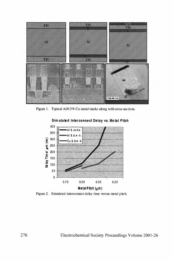
Figure 1. Typical Al/0.5 % Cu metal stacks along with cross-sections.
Sim ulated Interconnect Delay vs. Metal Pitch
400
350
a
300
250
•AI& ox be
^Al&bw-k
»Cu& bw-k
0.70 0.50 0.35 025
Metal Pitch(nm) Figure 2. Simulated interconnect delay time versus metal pitch.
276 Electrochemical Society Proceedings Volume 2001-26

• g 90%
B 80% £ 70%
"5 60% P 50%
£ 40% * 30% 4> 20%
TS 10%
^ 0.1%
Figure 3. Al-W (0.
I * Al-W Via Resistance I « Qi Via Resistance
Resistance, Ohm/via Comparison of via resistance withCu (0.24 um, 4.7:1 AR) and with
26 um, <4:1 AR). Cu vias show 5X lower resistance than W vks.
bab
0 Q. 70 -
ure
u.
ive
a
uin
u
1 • Cu 1 - AI(Cu)
o
0
0 °
0
o
o
lT_r_m r T x l__T_
•
• *
• * •
* Elapsed Stress Time [hrs]
Figure 4. Cu versus Al-0.5%Cu Electro-Migration performance. Cu shows significant improvement in EM performance even with an immature process.
EStop; Layers'
D
Material
Etch Via, StoponSiN, Via Cleanup
EtchSiN, Cleanup
Post Copper CMP and/or Pre-ELD Clean
Figure 5. Cleaning needs with a Via-First, Cu/Low-k dual damascene integration scheme
Electrochemical Society Proceedings Volume 2001-26

• Liquid containing Cu ions ©
Bat-Cave Vias
- i i Cu redeposition on side-^ J ^ w a " s opens channel for
* Cu into ILD
Figure 6. Photodiode-Induced Cu Redeposition (PICR) inside a via.
Figure 7. PICR example. Cu trenches contacting N-well, photo diode turned on.
Figure 8. Top down SEM and cross-section TEM showing interface adhesion problems on a Cu/Lo w-k device. Barrier delaminating off the top of Cu.
278 Electrochemical Society Proceedings Volume 2001-26

MSQ FTIR Before and After Treatment
2500 2000 1500 Wavenumber [cm-1]
Figure 9. Porous MSQ film change versus cleans by FTIR. Significant film change apparent versus clean treatment
Figure 10. Partitioning test fromM2 to M3 CMP showing how particles top) and scratches (bottom) can cause shorts.
Electrochemical Society Proceedings Volume 2001-26 279

a. ECD b. Missing c. ILD/Metal d. Floating e. Missing voids Via Pattern Rip-out Vias Trench Pattern
f. Missing g. Incomplete h. Surface L Surface j . Polymer Contacts CuCMP Particle Flake Strand
Figure 11. Ten of the most common C u/low-k dual damascene defect types.
III^BHIIB
IllSIKil
HHtoHBi H^IHIil
IIIII^IIIP IIIIIHBIi
5056
5054
5057
l l l l j l ^ l l l l IIIUJI^HI
5054
4830
4803
-2
-224
-254
Table 1. Impact from plasma steps on VLK wet etch rate. Data shows majority of impact from plasma step. Dry step film modification increased wet etch rate by~15X.
280 Electrochemical Society Proceedings Volume 2001 -26

POST ETCH/ASH CLEANING OF DUAL DAMASCENE STRUCTURES: SINGLE WAFER MEGASONICS WITH STG DRY
Yan Fan, YiWu and Brian Fraser Verteq, Inc.
Santa Ana, CA 92705
Megasonics and surface tension gradient (STG) dry technology have been integrated into a single wafer cleaner. Post etch/ash cleaning of dual damascene structures has been enhanced by both technologies. In addition to the advantages of a single wafer cleaner, the megasonics and STG dry improves cleaning efficiency by: (1) increased chemical transport rates to and away from the surfaces inside the via, resulting in significantly decreased process times, (2) improved particle and residue removal and (3) drying without rinse residue in the via. SEM and electrical results are shown to illustrate the impact of the integrated technologies.
INTRODUCTION
In Cu processing, a wet clean is commonly used after etching and ashing of the dual damascene structure. Removal of etch and ash residue as well as copper contamination sputtered on the sidewalls is required. Without the clean, a significant yield impact is observed. A number of semiaqueous solvents have been designed for these purposes. The chemicals are used in both batch (spray and immersion) and single wafer cleaning tools. For sub 0.18um technologies, there is an increased use of single wafer tools due to improved process control, reduced cross contamination and reduced process cycle time.
Megasonics are widely used in batch cleaning to improve particle removal performance [1] A new single wafer megasonics was developed to expand this technology to single wafer cleaners. Advanced dual damascene cleaning has an additional challenge: the megasonic energy must be controlled in order to avoid damage of the sensitive dielectric between the trenches.
Surface tension gradient dry is also widely used in batch immersion cleaning [2]. Introduced here is a single wafer drying method [3] which relies on the rotational and Marangoni forces to dry the wafer without evaporation. Eliminating evaporation allows drying without leaving residue that was dissolved in solution.
Electrochemical Society Proceedings Volume 2001-26 281

EXPERIMENTAL
The megasonic assembly (figure la) consists of a piezoelectric transducer attached to the end plate of a quartz rod. The rod is placed slightly above a horizontally positioned wafer. Sound transfer occurs through a liquid meniscus between the wafer and rod. Liquid is also sprayed on the backside to allow the energy to pass through the wafer and remove particles on the backside. The wafer is dried using a surface tension gradient method (figurelb). A mixture of nitrogen, isopropyl alcohol is directed to the wafer center through a nozzle. Water is dispensed through a second nozzle just outside the N2/IPA nozzle. As the wafer rotates, the nozzles are moved towards the wafer edge to complete the dry.
Dual damascene patterned wafers with different dielectrics (k = 4 to sub 2.6), via dimensions (0.4um to sub 0.15um openings), and aspect ratios were cleaned on the single wafer megasonic cleaner (Goldfinger). A typical process is: step 1 - megasonic clean with commercially available semi-aqueous solvent (chemical A or chemical B) dispensed on the wafer at low rotation speed (20 rpm); step 2 - high speed spin to remove majority of chemicals; step 3 - rinse at high speed, followed by lower speed meg rinse; step 4 -STG dry. Wafers results were evaluated with SEM and via contact resistance. SEM (top-down, angled and cross-section views) were taken before and after cleaning.
Figure la . Megasonic schematic
Tensioactive vapor
Liquid
Figure lb . STG dry schematic
282 Electrochemical Society Proceedings Volume 2001-26

RESULTS AND DISCUSSIONS
Via and trench cleaning examples Figure 2 shows the impact of megasonics on the removal of contamination from the via bottom. Experiments had identical conditions (rinse and dry recipe and chemical type and temperature), with the exception of megasonics (on or off) and chemical process time. Cleaning of the 0.15 urn vias was accomplished more effectively and in a shorter time than the non-megasonics case.
1 £W
60 sec. Chemical A without megasonics
37 sec. Chemical A with megasonics
Figure 2. Cross-section via SEMs of pre-clean and post-clean samples. The SEM pictures were taken at tilted angles.
Figure 3 shows the impact of megasonics on contamination at the top of the via, around the edge. Top-down view SEMs of (a) un-cleaned, (b) 5 min immersion clean in chemical B, (c) 90s megasonic clean in chemical B.
y# F * •.'*• : # :
<&•'••••&& ^ '
;'<# m m '••* * •
•* v & tf,*.
(a) Un-cleaned
v!>'
. » * .
*
%
•4
^ K * • • . ; . .• ., ^
(b) 5 min. immersion in chemical B, 1 min. IPA rinse and 3 min. DI rinse
(c) 90 sec. Chemical B with megasonic, 30 sec. DI rinse
Figure 3. Top-down view SEMs of un-cleaned and cleaned samples.
Electrochemical Society Proceedings Volume 2001-26 283

Figure 4 demonstrates the ability of the single wafer cleaner to remove contamination remaining after silicon nitride breakthrough. The contamination at the bottom of the sub 0.18um vias was removed following a 90s megasonic clean process. The process time was not optimized, but is expected to be in the 30s range.
znsrsi&«£HSK ,
Post-clean (90sec. Chemical A with megasonics, 30sec. DI rinse)
Figure 4. pre and post clean cross-section SEMs of vias in dual damascene structures.
Mass transport Megasonics improves both mass transport of the chemicals to the surface and removal of the chemicals and rinse agent away from the surface. The impact of megasonics on the boundary layer is shown in table 1 [4]. It has also been physically modeled that rinse flow with megasonic pulsation can greatly improve rinse efficiency on sub-micron size trenches compared to steady rinse flow [5]. More efficient transport of chemicals to the surface and contamination away from the surface can significantly reduce process times leading to higher throughput and therefore lower cost of ownership.
Condition Typical recirculation bath Very strong stirring Megasonics @ 850 kHz
Boundary Layer thickness 3000 Jim 300 um 0.6 um
Table 1. boundary layer with and without megasonics
Surface tension gradient dry Drying by surface tension gradient (STG) rather than by spin or evaporative methods has been shown to give improved results in batch systems. STG dry offers the complete removal of the solution. Spin drying removes much of the liquid by evaporation, which causes some dissolved materials to remain on the wafer and form watermarks. The resulting watermark from spin drying can cause masking problems in subsequent steps,
Pre-clean
284 Electrochemical Society Proceedings Volume 2001-26

and the chemical residue can increase the via contact resistance. It is especially true for narrow, high aspect ratio vias which are more prone to trap chemical residues inside during spin dry, if the rinse does not completely eliminate chemical residues from vias. As the aspect ratio of the via increases, the performance difference between the STG dry and the spin dry increases. Table 2 summarizes the 0.19um and 0.38urn via contact resistance results. The same process was used for all, with the exception of the dry method. Although the recipe was not optimized, it allows for demonstration of the difference in dry methods. The electrical results have shown that when the STG dry was used, better performance is obtained for both via sizes in terms of reduced contact resistance and improved process uniformity. SEM results seem to support the electrical results. Figure 5 shows the cross sectional SEMs of 0.19um vias that were spin dried and STG dried after a 60 sec chemical process and a 20 sec DI rinse. Visible contamination was observed at the via bottom in the spin dry case.
(a) Spin dried (b) STG dried
Figure 5. Cross sectional SEMs of 0.19 |im vias that were dried with (a) spin-dry and (b) STG dry after a 60 sec. Chemical process and a total 20 sec DI rinse.
2 min chemical A + 20sec DI rinse
Spin dried STG
dried
0.19 nm Mean 1.53
1.00
IQR 0.68
0.26
0.38 nm Mean 1.20
1.00
IQR 0.27
0.18
Table 2. single via resistance measurement results (normalized) of differently dried wafers
Damage-control tests Although megasonics improves particle removal and mass transport, it can also cause damage to sensitive structures, including the low-k dielectric material between trenches. Single wafer megasonics allows for significantly more sound uniformity control than a batch methods [6]. However, even single wafer megasonic system used incorrectly can cause structural damage. Proprietary methods and configurations have allowed for the
Electrochemical Society Proceedings Volume 2001-26 285

cleaning advantages without damage. Shown in figure 6 is an experiment on sensitive low-k serpentine line structures. Two different conditions were used. An example of the potential damage is shown in figure 6a. The undamaged dielectric obtained when using the controlled megasonic process condition B is shown in figure 6b. Development work is being performed to provide damage-free cleaning for advanced porous low k materials.
(a) Condition A (b) Condition B
Figure 6. Top-down view SEMs of samples tested under (a) non-controlled condition A, and (b) controlled condition B.
CONCLUSIONS
Cu dual damascene cleaning has been enhanced by single wafer cleaning with integrated megasonic and STG dry technology. The technology is most critical for advanced devices with small vias. Shorter process times and improved cleaning is provided by the megasonic technology. Controlled megasonics conditions and configurations are required to provide the cleaning benefits without structural damage to the wafer. STG drying provides a significant improvement in residue-free drying as compared with spin drying.
ACKNOWLEDGEMENT
The authors would like to thank our colleagues Mike Olesen, Tom Nicolosi, and Rich Wiley for valuable advice and support on this work.
REFERENCES
1. S. Cohen et al., MRS Symp. Proc, 386, 13 (1995).
2 . A.F.M. Leenaars et al., Langmuir, 6, 1701 (1990)
3 . P.W. Mertens et al, VLSI Technology Symp Proc, 56 (2000).
4 . A. Tonti, ECS Symp Proc, 92-12, 41 (1992). 5. H. Lin, et al, proceedings of ETC, 2000. 6. Y. Fan and B. Fraser, AVSICMC 2001.
286 Electrochemical Society Proceedings Volume 2001-26

IMPROVED POST-ETCH VIA CLEAN WITH FLUORIDE-BASED SEMI-AQUEOUS CHEMISTRY USING AN INTERMEDIATE RINSE
J. Diedrick, M. Fussy, FSI International, 322 Lake Hazeltine Dr., Chaska, Minn. 55318, USA
S. R. Small, W. Robertson EKC Technology 2520 Harrington Ct, Hayward, CA 94545 USA
An improved post-etch via cleaning process is studied using a fluoride-based semi-aqueous chemistry in a multi-position spray processing tool. The process uses two separate dispense steps of the semi-aqueous chemistry, with an intermediate deionized water rinse. Inclusion of the intermediate rinse significantly improves the removal of post etch residues. This improved cleaning is likely due to a diffusion process by which a layer of initial by-products is rinsed away by the intermediate rinse. The underlying contaminants are then exposed to the second chemical dispense step allowing complete removal. The combined time of the two separate chemical dispenses is much less than the time required for a single chemical dispense process.
INTRODUCTION
Over the past ten years hydroxylamine-based chemical systems have become industry standard in post etch residue removal. While standard amine-based and hydroxylamine-based chemistries have shown good cleaning performance, they require elevated temperatures (-60° C) and extended process times (15-45 minutes). Also, rinsing with alcohol or a buffered solution is required before water rinsing to avoid a pH spike which can lead to metal corrosion. These conditions and requirements are challenging for cleaning equipment design and control.
Recently, fluoride-based semi-aqueous cleaning (SAC) chemistries have been introduced for both post metal etch residue removal and post via etch residue removal. Fluoride based chemistries have been designed for both wet benches and spray tools. These chemistries can be used for low- or room-temperature processes with shorter process times, are able to be rinsed in water and can reduce water-rinse volumes. Most of the semi-aqueous fluoride chemistries can be used at near ambient temperatures (23 to
Electrochemical Society Proceedings Volume 2001-26 287

30° C) with process times varying between 2 to 30 minutes. Semi-aqueous fluoride chemistries are composed of organic solvents, water, low concentrations of fluoride species and buffering agents to control the fluoride chemical activity. These semi-aqueous chemistries have pH ranges between 9 to 10. This class of chemistries is showing good cleaning ability not only on metal (Al, Ti, W and Cu) and via structures but also with many new low k materials and unlanded metal lines on W plugs (1).
Usually, the wet chemical cleaning process for post- etch residue (PER) removal is optimized as two separate steps - cleaning and rinsing. The first step involves removing the etch residue with an active chemistry (such as a hydroxylamine system or a fluoride-based system). The second step involves rinsing away the cleaning chemical and reaction byproducts. In the case of hydroxylamine systems, if the process tool cannot efficiently remove chemical from the wafer surface before water rinsing, a two step rinsing process of alcohol followed by water is required. Commonly, the cleaning and rinsing steps are separately optimized to first remove residues without attacking the desired structures and then to remove the chemistry without causing pH excursions.
This approach to process optimization has been successful for traditional amine-based and hydroxylamine-based chemistries since they operate by dissolving the post etch residues from the outer surface inward to the walls of the via structure. In contrast, semi-aqueous fluoride chemistries tend to clean IC metal structures by a diffusion process. As the chemistries diffuse into the PER, the "polymeric" inorganic/organic residues are converted into smaller subspecies. Because of the low water content in the chemistry only a small portion of these "subspecies" is dissolved. Most of this converted material remains in place until the DI water rinse step (2). As this layer builds up, the cleaning reaction slows down and can lead to extended process times in order to achieve complete residue removal.
It has been found that introducing an intermediate rinse, between two separate chemical dispense steps, is an effective means for efficiently removing cleaning byproducts and reducing overall chemical exposure time. The use of a spray acid processor for PER removal enables the simple introduction of this intermediate rinse.
EXPERIMENTAL
A chemical recirculation system is used to dispense the SAC from a temperature controlled reservoir (3). Figure 1 shows a schematic of the spray acid processor with an integrated recirculation system.
The initial test involved a one step chemical dispense ambient temperature (23° C). Chemical was dispensed for 5 minutes. A DI rinse and dry sequence followed. SEM inspection showed residue remaining on the bottom of the via. In the next test, an
288 Electrochemical Society Proceedings Volume 2001-26

intermediate DI water rinse was inserted between 2 chemical dispense steps of 2 minutes each. SEM analysis show that the residue had been removed from the via. Each test above was repeated twice with similar results. An hydroxyl-amine based chemistry was also evaluated in this experiment. It proved capable of cleaning the residue in the via with a chemical dispense time of 20 minutes at 75° C. A buffered (pH~4) intermediate rinse solution was used between the chemical dispense and the final rinse.
The optimized process involves two chemical dispense steps with an intermediate DI water rinse step between them. It ends with a final DI water rinse and dry. The first chemical dispense uses a 90 second dispense of the recirculated semi-aqueous chemistry, followed by a chemical reclaim step. The chemical reclaim step conserves the recirculated chemical and reduces the interaction between the chemical and the DI water. The intermediate rinse is a 30 second rinse with DI water and is followed by a high speed spin step to remove DI water. As with the chemical reclaim step, the DI water is spun off in order to minimize the interaction between the water and the chemical. The second chemical dispense is identical to the first chemical dispense. The process then finishes with a "ramped rinse" and dry sequence. The chemicals are dispensed at a high rate of flow (10 liters/minute) while the wafers are rotating at a high spin rate (500-rpm). The intermediate DI rinse is also dispensed on wafers at a high spin rate. The combination of high spin rate and high flow rate enables a rapid turnover of solution in the via holes.
RESULTS
SEM Analysis •
Figure 2 shows the initial condition of a via wafer after etch and ash processing. The polymer is raised up from the bottom of the via. This is the result of the back sputtering and redeposition of material onto the eroding photoresist of the via mask during the plasma etch. The bulk of the photoresist is removed in the ashing process, leaving the polymer residue behind. At this stage the polymer is composed of inorganic aluminum and titanium metal oxides and silicon oxide along with a mixture of organic material not removed in the ash (4, 5).
The results of the improved process, shown in figure 3, can be contrasted with the results of a process in which the semi-aqueous chemical was dispensed continuously for 5 minutes and then rinsed and dried. (Figure 4.) The continuous dispense process chemical dispense time longer, yet it does not remove the post etch residue. The intermediate rinse process is faster and more efficient than the continuous dispense process. There is no obvious corrosion damage to the underlying metal in either process. Via dimensional gain, due to interlayer dielectric etch, is also minimal.
Electrochemical Society Proceedings Volume 2001-26 289

Intermediate DI Rinse Theory
As stated above, semi-aqueous fluoride chemistries clean IC metal structures by a diffusion process. As the chemistries diffuse into the PER, residues are chemically modified and the cleaning process slows as reaction byproducts accumulate. By removing the soluble residue, the intermediate DI rinse enables this process to continue more efficiently during the next chemical dispense.
During the intermediate rinse, DI water is dispensed on to the wafers from a center spray post at a high flow rate. The wafers are set in a turntable spinning at a high spin speed. The "carry over layer" - the liquid layer of process residue on the surface of the wafer - is around 2um thick. This is due to the centrifugal force generated by the highspeed rotation of the turntable. The thin carry over layer leads to rapid dilution of the residual SAC chemistry and dissolved PER on the wafer surface and in the via as the intermediate rinse is initiated. The carry over layer is continuously refreshed with clean DI water (6). Analysis has shown that deep trenches (4 um deep x 0.5 um wide) are easily rinsed to equilibrium in less than 1 second time (7). Also the SAC contain no significant amine species to form additional corrosive hydroxide species in rinse water. Adding water to these SAC formulations does not increase the pH above its initial value. The formulation of the semi-aqueous fluoride chemistry, along with quick chemical dilution, reduces the potential for corrosion of the aluminum/copper metal at the bottom of the via. The HDA chemistries, on the other hand, can experience pH shifts up to 10.7 to 11.5 which can be corrosive to Al metal and many low k materials
The final rinse sequence is also critical. It starts after the second semi-aqueous chemical dispense with a high spin speed and a high DI flow rate. This is followed by "ramped" rinsing sequence and then the wafer dry. Again, the rinsing sequence focuses on rapid solution turnover in the via along with the diluting and cleaning properties of the "ramped" rinse. The final rinse time is kept to a minimum in order to balance the exposure of the metal at the bottom of the via to the DI water with the necessary cleaning of chemicals from the process chamber.
SUMMARY
The use of an intermediate DI rinse in a post-etch via cleaning process using fluoride-based semi-aqueous chemistry has been demonstrated. The improved via clean process uses the intermediate rinse to take advantage of the diffusion activity of the cleaning chemistry. This process sequence has proven to be faster and more efficient than a single step dispense process. The improved post-etch via clean process with semi-aqueous chemistries Is a viable option to the standard hydroxylamine-based processes.
290 Electrochemical Society Proceedings Volume 2001-26

REFERENCES
1. R. Small, S. Kirk, and M. Cernat, The Effect ofDI Water Parameters Rinse on Post Metal Etch Residue Removal Using Semi-aqueous Cleaning Chemistries, 2" Inter. Conf. For Microelectronics and Interfaces. Santa Clara, CA. ,Feb. 7, 2001
2. S. Kirk and R. Small, Solid State Phenomena, 76-77, p. 307-310 (2001) 3. S. Loper, W. Ma, L. Chang, K.H. Lee, and D. Peter-Kini, Solid State Technology,
44(6), p. 68 (2001) 4. D. Skee, in Cleaning Technology in Semiconductor Device Manufacturing, J.Ruzyllo
and R. Novak, Eds., PV 99-36, p. 437, The Electrochemical Society, Pennington, NJ, (1999)
5. K. Honda, D. Perry, J. O'Neil, R. Molin, G. Hansen, V. Leon, and D. Peterson in Cleaning Technology in Semiconductor Device Manufacturing, J.Ruzyllo and R. Novak, Eds., PV 97-35, p. 617, The Electrochemical Society, Pennington, NJ, (1997)
6. Christenson, K., Proc. 3r Intl. Symp. On Cleaning Technology in Semiconductor Device Manufacturing, J.Ruzyllo and R. Novak, Eds., PV 94-7, p. 153, The Electrochemical Society, Pennington, NJ, (1994)
7. Olim, M., Ultra Clean Processing of Silicon Surfaces, p. 213 (1996)
Electrochemical Society Proceedings Volume 2001-26 291

teflon cassette
temp probe
exhaust
drain
aux. 4 drains *
Fresh Chemical
spraypost
temp probe
heating cooling
Figure 1. Spray Processor Configuration for RIE residue removal
292 Electrochemical Society Proceedings Volume 2001-26

• ^ • ^ > n
•.J*J
Figure 2. Initial condition after via etch and ash process
Figure 3. Dispense/rinse/dispense process
Electrochemical Society Proceedings Volume 2001-26

Figure 4. 5-min. one step dispense process
294 Electrochemical Society Proceedings Volume 2001-26

CORROSIVE BEHAVIOR OF TUNGSTEN IN POST-ETCH RESIDUE REMOVER
H. Zhang1, B. H. Chen1, J. H. Ye2, S. Y .M. Chooi3, R. Cha3, L. Chan3
Department of Chemical & Environmental Engineering, National University of Singapore, 10 Kent Ridge Crescent, Singapore 119260, Singapore
institute of Materials Research and Engineering, 3 Research Link, Singapore 117602, Singapore
department of Technology Development, Chartered Semiconductor Manufacturing Ltd., 60 Woodland Industrial Park D, Street 2, Singapore 738406, Singapore
Wet cleaning for resist strip and polymer removal has become more challenging with the continuous increases in density and number of interconnections and shrinkage of feature sizes in semiconductor industry. Tungsten (W)-plug via failure has become the main reliability issue in metal etching and post-etch cleaning due to the amine or hydroxylamine ingredients in the cleaning solution and chloride residues from chlorine-based etching process. The prevention of corrosion of tungsten plug requires understanding of the interaction between H+ ions, chloride residue and the metal and also the effect of various process parameters such as processing temperature and photo resist stripping conditions. In our efforts to understand tungsten plug corrosion, the electrochemical behavior of W in EKC265 solution at room temperature and 65°C in the presence of DI water and/or CI" was investigated using Tafel curve, AC impedance measurement and scanning electron microscopy (SEM). The results show that CI" and DI water play very important role in enhancing the W corrosion. High PH value and temperature make the corrosion more severe, which is consistent with literature.
INTRODUCTION
Miniaturization of device features present on an integrated circuit, including isolation, gates, storage nodes, interconnects, and metallization, is essential for advanced device technologies. Each area is expected to continue reducing feature sizes, while maintaining or improving production yields. One of the device features is the tungsten plug which links the upper interconnects to the underlying layers, in particular, from the metal layers defining digit lines and periphery circuits to highly doped underlying silicon nodes. The fabrication of tungsten plug typically comprises the sequence of the pre-metal dielectric (PMD), deposition of Ti and TiN films, a rapid thermal anneal (RTA) and a CVD W deposition. The tungsten filled via plug process is commonly used in sub-0.5 jam CMOS process technologies, where it has been successfully implemented to provide aggressive contacted metal pitch. Increasing demands on the interconnect system to provide the
Electrochemical Society Proceedings Volume 2001-26 295

maximum density possible at the 0.25 urn and beyond device technologies require the overlaying metal pitch to be pushed to the limits of the lithography process. To achieve this in conjunction with low via resistance requires the metal-via overlap design rule to be reduced to zero. Such an approach called borderless contact, however, leads to unavoidable exposure of the tungsten filled vias due to misalignment and variation in critical dimension of the via and metal features (1, 2). When the tungsten plugs were exposed to hydroxylamine-based cleaning solutions, corrosion of the tungsten vias resulted (3, 4, 5). Figure 1 shows the corrosion originates at the tungsten that is exposed to the cleaning solution. Corroded tungsten vias led to the drastic increase in resistances and has become one of the key reliability issues for metal interconnects as feature size shrinks to 0.18 urn and beyond where zero-overlap design rule is applied (6).
Figure 1. SEM micrographs shows the EOL (end-of-the-linc) of a via chain cleaned in EKC265 solution during post-metal etch strip.
Undoubtedly knowledge of the electrochemical behavior of tungsten in the various cleaning solutions is critical to solve this corrosion problem and improve the device reliability. EKC265, which is a catechol-based alkaline solution, is one of the widely used post-etch residue strippers in semiconductor industry. Thus an attempt to study and investigate the corrosion behavior of tungsten in EKC265-based electrolytes was made and results are presented in this paper.
EXPERIMENTAL
Low-pressure chemical vapor deposited (LPCVD) tungsten film of approximately 0.4 urn thick was deposited over a Ti/TiN bilayer on 200 mm diameter silicon substrate. The tungsten deposited wafers were sliced into lxl cm samples for experiments. 0.1 M HC1 and electronic grade DI water (resistivity 18 GO.cm) are used as additives for EKC265 so that the effect of chloride ion and DI water on tungsten corrosion can be investigated. A JEOL field emission scanning electron microscope (FESEM) was used to image the tungsten films. Open circuit potential (ECOrr)5 Tafel and AC impedance measurements on tungsten films were performed on an EG&G Princeton Applied Research Model 273A
296 Electrochemical Society Proceedings Volume 2001-26

potentialstat/galvanostat interfaced to an EG&G model 5210EC lock-in-amplifier. All the electrochemical measurements were performed in the dark area. The electrochemical investigations were performed by using a glass flask with three separate necks for reference, counter and working electrodes and an inlet/outlet for water. Stoppers made of Teflon were used for each neck. The sliced tungsten sample was fitted onto a Teflon holder and held tightly between an O-ring leaving a surface of area 0.283 cm2 exposed to the electrolytes. Electrochemical studies were carried out on tungsten films at room temperature subjected to the following conditions: (i) no treatment (reference); (ii) EKC265; (iii) EKC265:HC1 (8:1 in volume); (hi) EKC265:DI water (1:1 in volume); (iv) EKC265:DI water(l:l):HCl. The same set of experiments were then repeated at 65°C because EKC265 is typically used at high temperature in the industry.
RESULTS AND DISCUSSION
Figure 2 shows the FESEM micrograph of the surface of CVD tungsten without any treatment. From the figure one can see the tungsten surface has a high degree of roughness due to grains with irregular sizes.
Figure 2. FESEM micrograph of the top surface of a CVD tungsten film taken at 30,000 times magnification
The first set of electrochemical experiments was done at room temperature and consisted of measuring the corrosion currents (Icorr) from Tafel plots and the charge transfer resistance (Ret) from AC impedance measurements. Figure 3 shows the Tafel plots for tungsten films exposed to pure EKC265 and EKC265 solutions added with DI water, 0.1M HCl and both DI water and 0.1M HCL Figure 3 shows that the addition of HCl or DI water increases the corrosion rate of tungsten slightly and makes the open circuit potential (ECOrr) less noble in the solutions. However, the addition of both HCl and
Electrochemical Society Proceedings Volume 2001-26 297

DI water raises the corrosion rate dramatically and shifts the Ecorr to a much more negative value (-122.6 mV compared to -90.58 mV in pure EKC). Table 1 lists the corrosion current densities, Ecorr determined by Tafel extrapolation and charge transfer resistance values from impedance measurements. The resistance values display an opposite trend with the corrosion current data. This is understandable since high charge transfer resistance meant less reactivity of the electrolytes and higher stability of tungsten in the solutions.
600
400
200
I o UJ
-200
-400 -600
-10 -9 -8 -7 -6 -5 -4 -3 Log(current density), A/cm2
Figure 3. Tafel curves for CVD tungsten films in the absence or presence of DI water and HCl in EKC265 solutions at room temperature
Table 1. Tafel and charge transfer resistance data for CVD tungsten tested in EKC based electrolytes
Electrolytes EKC EKC + HCl EKC+H20(1:1) EKC+H20(1:1)+HC1
Icorr (uA/cm2) 0.6427 0.7673 1.505 3.948
ECOrr (mV)
-90.58 -109.1 -100.3 -122.6
Ret (KO) 90 84 16.5 14.6
The experiments were repeated at 65°C and the resulting Tafel plot is shown in Figure 4. It may be seen from the plots that the corrosion currents are higher than those measured at room temperature for all the four electrolytes. This shows that at high temperature the electrochemical reaction between tungsten and the electrolytes is accelerated and the corrosion is faster. We also find that the enhancing effects of HCl /DI water on tungsten corrosion are much more significant at 65°C than at room temperature. Addition of HCl or DI water increased the corrosion current by 4-5 fold. The corrosion current, Ecorr and charge transfer resistance data at 65°C are tabulated in Table 2.
298 Electrochemical Society Proceedings Volume 2001-26
-EKC -EKC+DIW(1:1)
EKC+DIW(1:1)+HC1 EKC+HC1

600
400
200
^ 0
§ -200
-400
-600
-800
-10 -8 -6 -4 -2 0
Log(current density), A/cm2
Figure 4. Tafel curves for CVD tungsten films in the absence or presence of DI water and HC1 in EKC265 solutions at 65°C
Table 2. Tafel and charge transfer resistance data for CVD tungsten tested in EKC based Electrolytes
Electrolytes EKC EKC + HC1 EKC+H20(1:1) EKC+H20(1:1)+HC1
Icorr, (A/cm2) 0.884 3.421 4.525 4.829
Ecorr, mV
-83.53 -134.6 -97.04 -138.1
Rp (KQ) 78.8 21 18.7 11.9
Open circuit potential (Ecorr) is important in evaluating the corrosion behavior since it reflects the driving force of the corrosion reaction. The more negative Ecorr is, the metal is more prone to corrosion in the solutions. The Ecorr data extrapolated from Tafel plots do not take into consideration the fact that Ecorr will vary with time due to change of surface states of tungsten films after interacting with electrolytes. Thus the variation of Ecorr vs. time in the four electrolytes at 65°C was monitored for 1 hour and the results were shown in Figure 5. It was observed that the Ecorrs were strong functions of time in the early stage, which means the tungsten surface stage changed significantly due to dissolution or pitting formation. It is obvious that the Ecorr were much more negative with the presence of HC1 and /or DI water than that in EKC only. So tungsten is more prone to corrosion when DI water and HC1 are present, which is consistent with the previous corrosion current data.
-EKC EKC+DIW(1:1 EKC+HCI EKC+DIW(1:1
) - -)+HCI_ -/
^ - — — " " ^ l L-—* ' '
— ^ T > ^
V \
Electrochemical Society Proceedings Volume 2001-26 299

0 -10 -20 -30 -40 -50 -60 -70 -80 -90 -
-100
- E K C -EKC+HC1
HKC<DIW(1 1) KKC'DIW(1 1)+HC1
time(xlOOOsec)
Figure 5. Ecorr plot for W in EKC-based electrolytes at 65°C
To characterize the surface changes of tungsten films after treatment in EKC-based electrolytes and study the tungsten removal mechanism in these electrolytes, the samples were characterized by FESEM (Figure 6 (a)-(d)). When compared to the surface morphology before treatment (Figure 2), Fig 6(a) and 6(b) did not show significant difference and the grains can be clearly seen. This may suggest that tungsten was removed layer by layer. However, in Fig 6(c) it can be seen that the grain structures are distorted. After treatment in EKC together with DI water and HC1, total morphological change and corrosion pits are observed (Fig 6(d)). These results show there is area/volume loss of W owing to surface reaction with cleaning solution. There is also localized corrosion (pitting) owing to higher surface energy. The mechanism is a combination of surface removal plus pitting when HC1 and DI water are present.
CONCLUSION
The electrochemical behavior of tungsten in EKC265 containing HC1 or/and DI water was investigated to elucidate the effect of HC1 and DI water on tungsten dissolution in the cleaning solutions. The electrochemical data obtained using different electrolytes at different temperature were compared. These data include Tafel plots, ac impedance spectra, Ecorr plots and FESEM characterization. Addition of HC1 and DI water increased the corrosion current and made Ecorr more negative. So, HC1 and DI water significantly enhance the W corrosion. High temperature enhanced the electrochemical reaction. Thus operation at room temperature is suggested. It was concluded that the W removal mechanism in EKC was a combination of pitting and bulk removal based on the FESEM data.
300 Electrochemical Society Proceedings Volume 2001-26

. l *>*• ' . « & *
. , • / . :
8 . ; * ^ ; ^ ' ^ ^ ^ ^ ^ ^ ^ ^ ^ # i ^
* « • ' . >•, S i • • «
Figure 6. FESEM photographs of W treated in (a) HC1; (d) EKC+DI water (1:1)+HC1
EKC; (b) EKC+DI water (1:1); (c) EKC +
ACKNOWLEDGEMENT
The first author is grateful to the National University of Singapore (NUS) and Chartered Semiconductor Manufacturing/EDB for financial support in the postgraduate research. The authors would further thank Dr. Alex See and Dr. Xu Yuan for technical discussion.
Electrochemical Society Proceedings Volume 2001-26 301

REFERENCES
1. S.Bothra, H. Sur, V. Liang, Microelectronics Reliability 39, 59-68 (1999), 2. R. J. Small, M. L. Peterson, A. M. Gorman, SEMICON China 98 Technical
Symposium, (1998) 3. D. A. Banner, M. Balvie and B.W Hess, J. Electrochem. Soc, 134, 669 (1987) 4. G. Munoz, J.B. Bessone, Corros. Sci, 41, 1447 (1999) 5. Z. Szklarska-Smialowska, Corros. Sci, 41,1743 (1999) 6. S. Y. M. Chooi, Z. Ismail, P. Y. Ee, M. S. Zhou, Part of the SPIE Conference on
Multilevel Interconnect Technology II, (1998)
302 Electrochemical Society Proceedings Volume 2001-26

EMERGING TECHNOLOGIES
Electrochemical Society Proceedings Volume 2001-26 3 03

304 Electrochemical Society Proceedings Volume 2001-26

EFFECTS OF SUPERCRITICAL C0 2 ON THE ELECTRICAL CHARACTERISTICS OF SEMICONDUCTOR DEVICES
Cian O'Murchu, Alan Mathewson, Eric Francais* NMRC, Lee Maltings, Prospect Row, Cork, Ireland
*Separex, 5 rue J Monod, F 54250 Champigneulles, France
Despite implementation and cost constraints of high pressure equipment, supercritical carbon dioxide is becoming one of the most attractive substitutes for chlorinated and CFC solvents, volatile organic compound (VOC's) and RCA based chemistries which are currently used in the semiconductor industry. In this study the effects of supercritical fluid conditions of temperature and pressure on the electrical properties of various devices have been investigated. No difference was observed in the properties of the devices before and after treatment in supercritical carbon dioxide.
INTRODUCTION
Wafer cleaning is a significant contributor to the cost of ownership of IC manufacturing. In fact wafer cleaning now comprises of about 30% of all process steps, since cleaning of wafers must take place after each major processing step and before each high temperature operation.
In all cleaning applications, the increasing demand is for greater efficiency and effectiveness in contaminant removal. There is a market drive for environmentally conscious semiconductor and electronic parts cleaning. In particular due to aggressive scheduling imposed by legislative bodies, there is a requirement to phase out the production and use of ozone-depleting substances such as CFCs and a reduction in volatile organic compounds (VOC) emissions from of organic solvents use. In addition, reducing worker exposure to VOC's has also become increasingly important in the electronic industry. Existing cleaning processes available to the industry e.g. RCA (wet chemical) based cleans for semiconductors [1], flux cleaning for oxides in semiconductor devices and solvent cleaning of flux residues in electronic systems, are limited in their environmental capabilities. In particular these cleans generate large volumes of waste solvents, increase worker exposure to solvents, and require costly chemicals and expensive equipment. As such, there is a requirement for the development and integration of a closed loop, environmentally and substrate compatible, cost effective technology resulting in significant savings in solvent and associated energy costs. The use of supercritical fluids in cleaning applications is one such solution.
Supercritical fluids act with the properties of a liquid and a gas. This can be explained by reference to Fig 1. which is a phase diagram for carbon dioxide. In the diagram we
Electrochemical Society Proceedings Volume 2001-26 305

can see the areas where the substance exists as a solid, liquid or gas. The curves represent coexistence between two of the phases. The vapour pressure (boiling) starts at the triple point (TP) and ends at the critical point (GP). The critical region has its origin at the critical point. We can therefore define a supercritical fluid as any substance that is above its critical temperature (Tc) and critical pressure (Pc).
Figure 2 illustrates the disappearance in distinction between the liquid and gas phases as the substance approaches the critical point in a given cell volume. Shown in the diagram are three schematic representations of a view cell in which the experiment is conducted at appropriate points on the gas-liquid coexistence curve. Cell a is at the lowest temperature with the meniscus between the gas and liquid phase being quite distinct. As the temperature and pressure are increased, the density difference between the two phases reduces and the meniscus becomes less distinct (cell b). When the critical point has been passed the meniscus disappears altogether as shown in cell c.
Naturally occurring carbon dioxide gas, which in its supercritical state, acts as a powerful solvent , can penetrate just about everywhere. Carbon dioxide gas is inexpensive, recyclable, and is environmentally benign. Although it is a greenhouse gas it is not a net addition as it is obtained in large quantities as a by-product of fermentation, combustion and ammonia synthesis and would eventually be released into the atmosphere if it was not used in as a supercritical fluid. Other advantages are that it is not considered to be a volatile organic compound, an ozone-depleting compound, a hazardous air pollutant (HAP) nor is it flammable.
Supercritical fluids are in widespread use across many industries - the food industry uses supercritical fluids to decaffeinate coffee and to extract the flavoring of hops for beer; the textile industry uses supercritical fluids to clean materials and garments; and waste treatment firms use supercritical fluid for advanced hazardous waste extraction and nuclear waste management.
Recent work on supercritical fluids indicate that as well as successively removing organic contaminants, the technology may also be used to remove or extract metals by using metal complexing ligands.[3] These discoveries open the potential for a multipurpose (organic and metallic or ionic contaminant removal) cleaning process which is compatible with environmentally conscious manufacturing and the process requirements of contaminant-sensitive materials and form the basic innovation of this work.
In the past few years a number of research groups have been investigating the use of supercritical fluids for various cleaning applications in the electronics industry. There are already a number of commercially available instruments for supercritical fluid drying of MEMS devices and there is also some work being done on particle and photoresist removal from semiconductor wafers. [4],[5].
306 Electrochemical Society Proceedings Volume 2001-26

EXPERIMENTAL DETAILS
A test chip for a 15 volt, Sum CMOS process, which is capable of evaluating the impact of process steps on contacts, gate oxide integrity, diode leakage, field device leakage, line-width, contact resistance, inter layer and intra layer isolation, electromigration, transistors, capacitors and resistors was used in this work. This device was used to evaluate the impact of supercritical carbon dioxide cleaning process on these parameters.
This device was fabricated in wafer form and evaluated after passivation. Each wafer contained approximately 60 process monitoring chips.
The electrical characteristics of each wafer were first determined using the measurement setup shown in Fig 3 and wafer maps were generated for each wafer and each of the parameters shown below. These parameters were measured for both n and p devices.
• P- and n-channel transistors of various W/L These transistors have common source, gate and bulk connectors. The following parameters were tested: Vt, maximum transconductance, gate current, drain current and substrate current.
• Different sized pn junctions were used to measure source/drain leakage current along the field oxide edge.
• Metal-poly isolation resistance • Gate oxide monitor structures
The objective is to measure the integrity of the gate oxide in the gate oxide planar region. This is achieved by maximizing the gate oxide planar area and creating a large gate oxide capacitor using polysilicon and metal as the top plate. Breakdown voltage of the gate material is used as a measurement of the quality of the gate oxide.
A simplified schematic of the supercritical fluid instrument used in these experiments is shown in figure 4. It consists of a storage vessel for the carbon dioxide, a syringe pump, an extraction vessel housed in an oven, a pressure control valve and a collection vessel for any extracted components. In this case the carbon dioxide was vented to the atmosphere as nothing was extracted.
Following device fabrication, the wafers were placed in the extraction vessel and then subjected to various conditions of time, temperature and pressure as shown in the graphs in figure 5. The highest pressure used was 200bar and the highest temperature used was 80°C.
Electrochemical Society Proceedings Volume 2001-26 307

Finally the same electrical tests as before were then carried out on the wafers and wafer maps were generated for 19 different electrical parameters for each chip. The goal of this experiment was to see if any of the parameters had significantly increased or decreased resulting in chip failure and to determine the effect of the various supercritical fluid conditions on the performance of the devices.
RESULTS AND DISCUSSION
Six wafer maps are shown in figure 6. They show three wafers before and the same three wafers after supercritical fluid processing. The first two wafer maps , (la) and (lb), give measurements of Vt for a p-channel transistor before and after the supercritical fluid process (A) in Fig.5. The second two wafer maps, (2a) and (2b), give measurements of the leakage capacitor voltage applied to an n-channel device at breakdown before and after supercritical fluid process (C). This provides a measurement of the gate oxide integrity. The third pair of wafer maps, (3a) and (3b), give the leakage current values for a p+n diode before and after supercritical fluid process (D).
As can be seen from the wafer maps, there is no observable difference between the devices after treatment in supercritical carbon dioxide. Although space constraints prevent inclusion of wafer maps for the other electrical characteristics mentioned in the previous section, results have shown that neither of the four supercritical fluid processing steps used affected these values.
CONCLUSION
Preliminary results indicate that CO2 based supercritical fluids have no measurable effect on silicon microelectronic structures and therefore it can be assumed that these devices can be cleaned using supercritical carbon dioxide without a reduction in yield. This is a good indication to commence further work on supercritical fluid cleaning technologies as a substitute for the typical cleans used in semiconductor manufacturing. In particular, such processes as pre oxidation cleans, resist stripping and pre metal deposition. Cleans could possibly strongly benefit from this technique. Finally the environmental benefit and cost savings of supercritical fluid processing would be substantial.
ACKNOWLEDGMENTS
The authors would like to acknowledge the financial support from the European Commission. This work is part of the EC02Clean Project number GRDI-1999-10846
308 Electrochemical Society Proceedings Volume 2001-26

REFERENCES
1. W.Kern and D.Puotinen, RCA Rev. 31,187(1970) 2. Clifford, T., Fundamentals of Supercritical Fluids , Oxford Science Publications
1999 3. Extraction of Metal Ions from Liquid and Solid Materials by Supercritical Carbon
Dioxide. KE Laintz, CM Wai, CR Yonker, and RD Smith. Anal. Chem. 64:2875-2878 (1992).
4. Farmer, L. et al, Supercritical phase wafer drying/cleaning system, US Patent 6,067,728
5. GT Equipment Technologies Inc, 472 Amherst Street, Nashua, NH 03063, USA
Electrochemical Society Proceedings Volume 2001-26 309

Temperature (°C)
Fig 1. Phase (pressure-temperature) diagram for CO2: TP = Triple Point, CP = Critical Point, Tc = critical temperature, Pc = critical pressure
Cell a > ^ * \
/ Gas \ ~
\ Liquid y
Critical Point
/ Gas
-—-*^*^^\v Liquid
k (
Cellb
Fluid )
CellC
Temperature
Fig 2. Disappearance of the meniscus at the critical point [2]
310 Electrochemical Society Proceedings Volume 2001-26

HP4142B Modular DC Source/Monitor
SMUs
1 1 1 1 1 1 s\
\s
^ H
AWP 1080 HP Controller
S> HP 408 5 A Switching Matrix
HP 4084B Switching Matrix Controller
Fig 3 . ; Automatic DC measurement setup.
Extraction Vessel containing a wafer
Fig 4.: Supercritical fluid instrumentation setup
Pressure relieving valve
3 ampl e Collection
Electrochemical Society Proceedings Volume 2001-26 311

Plot of Pressure & Temperature vs Time (Process A)
Plot of Pressure & Temperature vs Time
100 150
Time (minutes)
(Process B)
P(bar) |
T(C)
110 90 &
70 5 50 2 30 £ 10 £
.A-10 250
100
1*80
^ 6 0
| 40 a 2 0 i
£ 60
| 40
* 2 0
0<
Plot of Pressure & Temperature vs Time
-Pressure (Dar)
Temp (C)
100 150 200 Time (minutes)
Plot of Pressure & Temperature vs Time
•—Pressure (bar)
'--•TerrpfC)
(Process C)
(Process D)
\ 150 200 Time (minutes)
Fig 5.Experimental conditions of temp, and pressure for wafers 1-4 (process A-D)
312 Electrochemical Society Proceedings Volume 2001-26

Before After
(la)
KM I N
K u FH y\] \\\] H ••• N 4 • r ' 1 / 1 M 1 I-
\ \ •'-•] K i r
M ' • 1 M X I5' M 1 \ V\
m 1 1 1 m PN44 4441
Volts
Si
(lb)
15
(2a) Volts
1 I 44T 1 114441 K i m v\]\\ H M i
1 n H Ml N 1 M r K M 1 M M Inr N 1 m
IN. M TS-J L-rf
Binl
(3a) Amps/cm
11111141111111111 It H i I N •
W 1 i WWW y\\ M M M 1 N H 4 i M HJ:
M 1 M in \ 1 1 \ l\ M M \ 1 M M M I M ; MB ml m 1 1m -ml 1
i i i i fTi i irni i i i i i
1H3 le-12
I
/
1 ^
/ 1
N
\
X
\
/
/
\
/
\ ^
t
/
Volts
I 125 15
il IS
(2b) Volts
KM I N
m u m / i H M M \ 1 -/ • 4 V M ' M M ' "I M M M 1 M 1 M
N M M M 11414 1 I444l
(3b)
111444111 r t r l l 111 K K KM M M 1 N 4 r r U i l i i 'in
I • ' • • • • • • • • "
i r 1 M M 1 M 1 M
IN M
14441 1114444
Amps/cm
Fig. 6. : Wafer maps for wafers before and after supercritical fluid processing
Electrochemical Society Proceedings Volume 2001-26 313

OZONATED HF APPLICATIONS IN A SPRAY PROCESSING TOOL
M. Claes, E. Rohr, S. De Gendt, S. Lagrange1, E. Bergman1 and M. Heyns
IMEC vzw, Kapeldreef 75, B-3001 Leuven, Belgium ^emitool, Inc., 655 West Reserve Drive, Kalispell MT 59904, USA
A HydrOzone™ process combined with an ozone-HF step, applied in a spray-processing tool, is feasible in removing both resist and post-etch polymer residues after polysilicon etch on CMOS and NVM wafers. With this method, the chemical use and process time are reduced significantly. In addition, this HydrOzone™ process extended with an ozone-HF step provides an effective comprehensive pre-gate clean with no significant adverse impact of surface roughness on the gate oxide properties.
INTRODUCTION
With dimensions scaling down, more polymerizing chemistries (such as hydrogen bromide (HBr)) for polysiMcon etch are necessary to obtain a better selectivity towards the gate oxide. This also implies difficulties in polymer removal after etch. Frequently, HF and SCI-based wet chemistries are used in combination with oxidative chemistries for the removal of polysilicon etch residues (including resist layers) (1), (2). Initial experience indicates that HydrOzone™ (3), i.e. mixture of ozone/DIwater, is feasible for resist removal, however the etch (and ash) polymers are more resistant. Development of a wet process based on HydrOzone™ for removal of etch polymers would be effective from a cost, environmental and throughput point of view. This is realized for standard CMOS and NVM (non-volatile memory) processes by extending the HydrOzone™ method with an additional step containing a mixture of ozone and diluted HF.
The ozone-HF extended HydrOzone™ process also shows potential for pre-gate clean applications in a spray-processing tool (4), (5), (6). The performance of this clean in terms of oxide, organic contamination, particle and metal removal was previously investigated (4). Additional experiments on particle removal efficiency, wafer surface roughness and electrical characterization will be described in this paper.
EXPERIMENTAL
Strip after polysiMcon etch was performed on CMOS wafers (8", p-type, Cz, <100>) with a standard C025 poly/gate (250 nm/5 nm thickness) stack deposition. Deep
314 Electrochemical Society Proceedings Volume 2001-26

Ultraviolet (DUV) photoresist and a bottom antireflective coating (BARC) are used for patterning. Strip after NVM poly etching was done on 8 inch wafers, which got a 250 nm poly on top of a 100 nm thermal oxide followed by a non critical I-line print (C035). Etching chemistries comprises a combination of HBr and oxygen (BARC etch), followed by chlorine, hydrogen bromide and oxygen (main etch) and finally HBr for over-etching. After etch, both wafer types were exposed either to an EV1EC standard strip (served as reference), a HydrOzone™ strip with NH4OH as additive or HydrOzone™ strip followed by an ozone-HF step. The MEC standard strip (ca. 20') features an ammonium hydroxide peroxide step (70°C) followed by a sulfuric acid/peroxide mixture (SPM) at 90°C. The HydrOzone™ (ozone (185 g/m3,101pm) and Dlwater (5 1pm)) strip for CMOS wafers is performed for about 6' at 85°C and high rotational speed (800 RPM) with NH4OH (1/2500) as additive. Previous experience showed a higher removal efficiency of resist/polymers if additives are used during ozonated processes (3). The new strip sequentially processes wafers, first through HydrOzone™ (6 minutes for CMOS and 8 minutes for NVM) and then through an ozone-HF (1.5 minutes for CMOS and 8 minutes for NVM) step at low rotational speed (50 RPM). A HF concentration of approximately 0.1%(v/v), an ozone concentration of 185 g/m3 and a working temperature of 95°C are defined as the standard ozone-HF process. At high temperatures, a better particle removal efficiency was observed (5). The combined process steps are sequentially performed in the same chamber of a spray-processing tool. Ozone and HF/water are separately inserted in the process chamber. Ozone concentrations are monitored by means of a BMT 963 ozone analyzer.
Cleanliness was inspected with a Scanning Electron Microscope (PHILIPS SEM XL 30). After stripping, the charge (Q) to break down (QBD) and transistor parameters were investigated on a C025 integration lot,
Pre-gate clean capabilities, more specifically particle removal, surface roughness and electrical parameters, of the combined process were also investigated on p-type silicon wafers. For this purpose, both the HydrOzone™ (2 min.) and ozone-HF (4 min.) step operate at a low rotational speed of 50 RPM. Si3N4 and silica slurry (Si02) particle removal on bare silicon and thermal oxide (500 nm) was studied using an immersion based controlled contamination procedure, followed by rinse and dry. Approximately, 30,000 and 6,000 Si3N4 particles were deposited on bare silicon and thermal oxide wafers, respectively. Around 10,000 Si02 particles were deposited on both bare and thermal oxide wafers. The LPD levels were measured with a KLA Tencor SP1-TBI tool in dark field wide oblique (DWO) detection mode from 0.12 (mm size on. Wafer surface roughness was determined with atomic force microscopy (AFM, Nanoscope III dimension 3000) scans over 1 Jim length. Field (E) dependent break down (EBD) was performed on three sizes of capacitors (9.7, 2.8,0.9 mm2).
Electrochemical Society Proceedings Volume 2001-26 315

RESULTS AND DISCUSSION
Strip after polysilieon etch
Polysilicon stripping in ozone-HF solutions is a simultaneous process of poly oxidation and poly-oxide etching. Preceding experiments have shown that this is a competition process between the oxidation and etching reaction (7). The slowest reactions would be the rate-limiting step and determines the overall poly etching kinetics. The objective is to maintain hydrophilic surfaces during processing and thus low HF (0.1%) concentrations and high ozone concentrations (185 g/m3 O3) are applied. Under these conditions, polysilicon is not significantly etched.
The novel process, HydrOzone™ followed by ozone-HF, is demonstrated for cleaning post-etch polymer residues after polysilicon etch. Figure 1 shows SEM pictures of CMOS structures after a conventional and ozone-HF extended HydrOzone™ treatment. The ozone HF extended HydrOzone™ process is able to remove both resist and polymers, while with the conventional HydrOzone™ strip, applying NH4OH, polymers still remain on the structures and the surface. The HydrOzone™ step at high rotational speed (800 RPM) removes the resist layer but not the polymers or polymer-etch residues. To remove these polymers, an additional step, using ozone-HF, is used at a low rotational speed (50 RPM). In this way, a thicker boundary layer is present on the wafer and thus the polymer etch residues are restrained to re-adsorb on the wafer surface. Therefore, formation of polymer clusters does not occur. Also, at low rotational speed a longer contact time of the solution with the polymers on the wafer exists.
Figure 1: SEM photographs of a CMOS structure after a conventional HydrOzone™ strip with NH4OH (left) and a HydrOzone™ strip extended with ozone-HF (right).
For NVM processing, more highly polymerizing etch chemistries are used compared to CMOS processing. Therefore, slightly longer process times are needed to remove resist and polymer-etch residues. Results are depicted in Figure 2. With a conventional HydrOzone™ clean applying NH4OH, the resist could even not be completely removed.
316 Electrochemical Society Proceedings Volume 2001-26

However, extending the same clean with an ozone-HF step shows enormous enhancement achieved; both resist and post-etch polymer residues are stripped.
Figure 2. SEM photographs of a NVM stiucture after a HydrOzone™ strip with NH4OH (left) and a HydrOzone™ strip extended with ozone-HF (right).
Electrical characterization of capacitors and transistors is also investigated. If any influence of strip after polysilicon etch is expected on the quality of the gate oxide, the non-overlapping meander capacitor will be the most sensitive. The current density used for measurements is 2000 A/m2. A Weibull plot of large meander n-well and p-well capacitors is represented in Figure 3. In order to calculate the parameter F (median rank), the QBD data are sorted from low to high. After that, each QBD value is given a rank (starting from 1 to ...). F is then defined by (Rank - 0.3)/(Total number of data + 0.4). No significant differences were seen between the JMEC standard and the ozone-HF extended HydrOzone™ strip, based on the measurement of 26 dies on each wafer.
?
1
0
-1
-?
-s
.4
-^ - 6
:
CAP-GME
e--—
-&—
_NWn ,m! • • '
Standard Strip
Ozontst®d HF s
, ...I . ' , ,
' TD
J
" "1 ™H
,3 3
trip I
l!llJ4-d
CAP-GME_PWn
QRn [G/cm2; QBD[C/cm1
Figure 3. QBD distribution for standard IMEC strip and HydrOzone™ extended with ozone-HF strip on n-well (left) and p-well (right) capacitors. (CAP: capacitor; GME:meander; NWn: n-well poly non-overlapping on field).
Electrochemical Society Proceedings Volume 2001-26 317

No influence of the strip after polysilicon etch was seen on the intrinsic transistor performance (both NMOS (not shown) and PMOS); see Figure 4 (left side). Figure 4 (right side) shows the threshold voltage rolloff (i.e. threshold voltage as function of device length) independency of the strip after poly etch on NMOS transistors.
10*
10'7|
I 1<f 3 10"10
0)
f 10"11
3 10-12
10"13
10*"
PMOS transistor
Standard strip Ozonated HP strip
_j0.2jjmj
®® 0.35 pnj ; ; m l i i n l i i i , I . M . I.
0.7 r
0.6 F
0.5 F
0.4F
0.3 h
0.2 F
0.1
NMOS transistor
" ' '' "'! ' ' ' j
: *j«Faxr$ - ' - " I
: D i 1
: Q i 1
: n i j
: , ,
O Standard strip 1 j
D Ozonated HF strip i j
,,,,,! , , -1 -150 -200 -250 -300 -350 -400 -450
Drive current |iA4im] Design Length [tm]
Figure 4. Leakage current versus drive current for different transistor lengths on PMOS (left) and threshold voltage as function of device length on NMOS (right) transistors after standard BVIEC strip and HydrOzone™ extended with ozone-HF strip.
Pre-gate clean
Previously, cleaning capability oi this clean in terms of etch rate/uniformity, organic contamination, particle and metal removal efficiency were already investigated (4). Additional information on nitride particle removal efficiency, roughness and electrical characterization is given below.
In this study, SiaNi and Si02 particles removal efficiency on bare silicon and thermal oxide (500 nm) wafers are determined. Results are given in Figure 5 (left). Si02 particles are easily removed on thermal oxide (96%) wafers as well as on bare silicon wafers (99.8 %). The removal efficiency of nitride particles on thermal oxide is around 99.4%. However, results are somewhat erratic, with removal efficiency of around 40%, for silicon nitride particles on bare silicon substrates. Probably, the nitride particles are somehow modified after the ozone-HF process and therefore more difficult to remove from the bare silicon surface. This problem is also observed in other processes using ozone de-ionized water (8). When the ozone supply in the ozone-HF step is intermittenly cycled on and off (9) during the course of the cleaning step, cleaning efficiency increased to > 99% (6).
To investigate silicon surface roughening by the ozone-HF process described in this study, bare silicon as well as epitaxial (EPI, more sensitive towards surface roughness)
318 Electrochemical Society Proceedings Volume 2001-26

wafers are exposed for 4 minutes to ozone-HF and compared with JMEC cleaned (10) control wafers. Results are depicted in Figure 5 (right hand side).
BtMECdean
® ozonated HF (185 g/mS 03)
I o.o5o | l l n 111] 1111
o Aon -I •MHHtama . J i l l l l l j
wafertype ^ ^
Figure 5. (Left) Removal efficiency 6f Si3N4 and Si02 on bare silicon and thermal oxide wafers after a HydrOzone™ process extended with an ozone-HF step and (Right) average roughness (nm RMS) on Si and EPI wafers after different cleans, measured with AFM (right).
On both EPI and bare silicon wafers, an increase (~ 0.7 A RMS) in surface roughness is observed when wafers are exposed to the ozone-HF process. In principle, if the balance between oxidation/etching is lost and etching predominates, micro-roughness increases. This increase is more pronounced when the starting wafer surface roughness is lower than 0.1 nm RMS. For a starting surface roughness >0.1 nm RMS, no significant increase is seen after an ozone-HF treatment (6).
The impact of increased roughness on the dielectric breakdown is experimentally verified. P-type silicon surfaces were exposed to different cleans, where after a 5 nm/250 nm gate oxide/polySi stack was deposited. Ramped voltage stress (e- injection through poly) is used for evaluating the gate oxide integrity (GOI) on 84 capacitors from 3 different sizes. The intrinsic EBD yield is defined as the fraction of capacitors that survives a field stress of 12 MV/cm over the gate oxide (i.e. 7 V over the entire capacitor). Figure 6 contains ramped voltage EBD area yield results from p type wafers as function of pre-gate clean. For the ozonated HF clean, a few break downs (4%) are observed in low field (< 2 MV/cm) and mid field area (between 2 and 12 MV/cm), while for the EV1EC clean a mid field yield of only 3% is observed. Consequently, the intrinsic EBD yield for the ozonated HF and BVIEC clean amounts 92% and 97%, respectively. On small capacitors (2.8 and 0.9 mm2), an EBD yield of 100 % is obtained for all cleans under study (not shown). Hence, no significant adverse impact of surface roughness on device performance is observed. This is in conformity with previous results showing that moderate roughness (i.e. < 0.4 nm RMS) does not have an influence on the current
Electrochemical Society Proceedings Volume 2001-26 319

voltage characteristics and charge-to-breakdown distributions of MOS capacitor structures with ultra-thin Si(>2 layers (11), (12). Note, that for transistors, a surface roughness of around 0.3 nm RMS already causes a decrease in electron channel mobility (13). Therefore, transistor parameters still need to be checked for this type of clean.
120% -r *
100% 4
2 80% |
> 60% 4-Q co w 40% 4
20% 4
0% 4-ozonatedHF ARM Imec clean
clean
Figure 6. The 5 nm thick oxide EBD yield as function of applied voltage for different pre-gate cleans (Capacitor area is 9.7 mm2 and 84 capacitors tested).
CONCLUSIONS
An ozone-HF process, applied in a spray-processing tool is feasible in removing both resist and post-etch polymer residues after poly silicon etch, without influencing the gate oxide properties. Compared to standard strip procedures, both the chemical use and process time are reduced significantly. Furthermore, this process can be used as an effective comprehensive pre-gate clean with no significant adverse impact of surface roughness on the gate oxide properties. However, the effect on transistor parameters still needs to be investigated.
ACKNOWLEDGEMENT
The authors would like to thank Sonja Van der Groen and Bart Onsia from IMEC for performing electrical characterization.
U >12 MV/cm U 2-12 MV/cm U <2 MV/cm I
320 Electrochemical Society Proceedings Volume 2001-26

REFERENCES
1. S.Y.M. Chooi, P.-Y. Ee, B.-M. Seah and M.-S. Zhou, in Proceedings of the Fourth International Symposium of Ultra Clean Processing of Silicon Surfaces, M. Heyns, M. Meuris and P. Mertens, Editors, p. 113, Solid State Phenomena 65/66, Scitec Publications Ltd, Switzerland (1999). 2. C.W. Lee, S.J. Choi, JJ. Kim, H.S. Kim, W.S. Kim, J.D. Lee and J.W. Lee, in Cleaning Technology in Semiconductor Device Manufacturing TV, PV 95-20, p. 243, The Electrochemical Society Proceedings Series, Pennington, NJ (1996). 3. S. De Gendt, M. Lux, M. Claes, A.S. Jassal, J. Van Hoeymissen, S. Lagrange, E. Bergman, P. Mertens, M. Heyns, in Cleaning Technology in Semiconductor Device Manufacturing VI, R.E. Novak, J. Ruzyllo and T. Hattori, Editors, PV 99-36, p. 391, The Electrochemical Society Proceedings Series, Pennington, NJ (1999). 4. E. Bergman, S. Lagrange, M. Claes, S. De Gendt and E. Rohr, in Proceedings of the Fifth International Symposium of Ultra Clean Processing of Silicon Surfaces, M. Heyns, P. Mertens and M. Meuris, Editors, p. 85, Solid State Phenomena 76/77, Scitec Publications Ltd, Switzerland (2001);. 5. E. Bergman, S. Lagrange and M. Claes, European Semiconductor, p. 81, March 2001. 6. E. Bergman and S. Lagrange, Solid State Technology, p. 115, July 2001. 7. G. Chen, I. Kashkoush and R. Novak, in Cleaning Technology in Semiconductor Device Manufacturing VI, R.E. Novak, J. Ruzyllo and T. Hattori, Editors, PV 99-36, p. 296, The Electrochemical Society Proceedings Series, Pennington, NJ (1999). 8. EV1EC internal communication, 2001. 9. T. Hattori, T. Osaka, A. Okamoto, K. Saga and H. Kuniyasu, J. Electrochem. Soc, 145 (1998)3278. 10. M. Heyns, T. Bearda, I. Cornelissen, S. De Gendt, L. Loewenstein, P. Mertens, S. Mertens, M. Meuris, M. Schaekers, I. Teerlinck, R. Vos and K. Wolke, in Cleaning Technology in Semiconductor Device Manufacturing VI, R.E. Novak, J. Ruzyllo and T. Hattori, Editors, PV 99-36, p. 3, The Electrochemical Society Proceedings Series, Pennington, NJ (1999). 11. M. Houssa, T. Nigam, P. Mertens and M. Heyns, Solid State Electronics, 43 (1999) 159. 12. M. Depas et al, in Proc. of the 26th IEEE Semiconductor Interface Specialists Conference (Charleston), 1995. 13. T. Ohmi, M. Miyashita, M. Itano, T. Imaoka and I. Kawanabe, IEEE Electron Device Letters, vol. 12, no.12 (1991) 652.
Electrochemical Society Proceedings Volume 2001-26 321

THE EFFECT OF SURFACTANTS IN DILUTE HF SOLUTIONS Michael Leahman, Mark Simmons, Michael Jackson
Rochester Institute of Technology 82 Lomb Memorial Dr., Rochester, NY 14623
Christopher Spivey, Brian Hong, Erik J. Mori General Chemical Corp.
501 Nichols Rd., Pittsburg, CA 94565
The effect of adding surfactants to dilute-HF containing solutions was investigated. It was determined that surfactants have an impact on particle and metals levels and may consequently affect properties such as minority carrier lifetime and thermal oxide thickness. The results also indicate that wafer particulate levels on bare silicon wafers decrease upon thermal oxide growth. Other parameters such as surface micro roughness, interface trap density and breakdown voltage have also been studied.
INTRODUCTION
Dilute hydrofluoric acid (DHF) is used in etching, stripping and cleaning thin silicon dioxide (<500 A) films. Although diluted HF is employed to decrease the etch rate it is not as controllable in thick oxides since hydrogen ions generated during the reaction of silicon with HF readily adsorb onto the silicon surface leading to non-uniform etching through micromasking [1]. However, the use of diluted hydrofluoric acid as a cleaning solution and moreover as a primary etchant for thin gate oxides has gained widespread use [2-3]. In addition, the incorporation of surfactants has been recently introduced since they have been employed to improve surface wetting and etch uniformity [4], porous silicon [5-6] properties, and to reduce particulate and trace metals contamination after cleaning [7]. This study examines commercially available surfactanated dilute HF effects on cleaning, oxide properties and electrical behavior.
EXPERIMENTAL
Prime 100-mm p-type silicon wafers were immersed sequentially in a modified RCA-1 followed by RCA-2 and finally in dilute HF (100:1) containing different surfactants. The table below provides the general composition of the surfactants present in dilute HF.
Table 1. Surfactanated Dilute HF Compositions Group
A B C D
Surfactant type Fluorosurfactant 1
amine/alcohol co-surfactant 1 Fluorosurfactant 2
Alcohol/amine co-surfactant 2
322 Electrochemical Society Proceedings Volume 2001-26

Metal and particle contamination levels were monitored prior to and following a nominal 170 A thermal oxide growth. Surface metallics were identified using Total Reflection X-ray Spectrometry (TXRF), while particles on wafers were quantified by laser scattering. Oxide thickness was measured using ellipsometry. Surface roughness was determined using Atomic Force Microscopy (AFM). A surface charge analyzer (SCA) was utilized to determine minority carrier lifetime and interface trap density of oxidized wafers. Aluminum gate MOS capacitors were fabricated and used in a voltage ramp test to determine dielectric breakdown strength. A control group processed identically with the dilute HF groups, but without the surfactant was included for comparison testing.
RESULTS
After immersion in dilute HF, iron levels were most elevated for Group B wafers as shown in Figure 1.
1 0 0 0
**"* * * y ^ . • O ^ * * "
6<« <*»
<P O
G * $*
• 0*
Figure 1. Wafer surface trace metal by TXRF
Certain wafer surface trace metal impurities exhibit opposite trends after dilute HF clean and thermal oxidation. TXRF analysis indicates that iron levels increase following oxide growth. On the other hand, copper levels vary with different surfactants, which is consistent with mixed results from earlier studies [4,8-9]. Although surfactants in Group A and C, and Group B and D share similar chemical nature, the surface metallic contributions can vary widely. As shown in Figure 2, particles were also most elevated wafers for Group B after immersion in a dilute HF with surfactant.
Electrochemical Society Proceedings Volume 2001-26 323

1 a
5
25 00 "
20 00 -
15 0 0 -
10 00 -
50 0 -
i H H I " A f t e r c le a n
1 •
R a f t e r o x d ' n |
• H L _
Figure 2. Particles on wafers
Particulate levels also decreased following thermal oxide growth for most groups. The effect is most pronounced with Group B. Figure 3 reveals that a significantly thicker oxide is grown with Group B wafers. Group A oxide thickness is similar to the control group while Group C and D oxides approach the targeted 170 A thickness.
1 8 5
.§
1 170
8 165 1 6 0
1
_l 1
\
I
\
] 1
(
I 1
G rp A G rp B G rp C G rp D
Figure 3. Thermal oxide thickness
324 Electrochemical Society Proceedings Volume 2001-26
In addition, the electrical characterization of the thermal oxide indicates reduced minority carrier lifetime associated with Group B wafers as shown in Figure 4.
2 5 0
E *| 1 0 0
C o n t r o I G rp A G rp B G rp C G rp D
Figure 4. Minority carrier lifetime
Other electrical and physical parameters such as interface trap density (Da), oxide breakdown voltage (VBD) and surface micro roughness have been investigated and the results tabulated.
Table 2. Electrical Testing and AFM Data Test Interface trap density, Dit
(xEll/eV-cm2) uroughness, Ra (A) RMS (A) Breakdown Voltage, VBD median (MV/cm)
Cntrl 0.95
1.2 1.5 10
GrpA 1.16
1.2 1.6 9.8
GrpB 1.65
1.1 1.4 9.8
GrpC 0.99
1.2 1.5 9
GrpD 0.96
1.2 1.5 9.7
No major differences are observed in surface micro roughness for various surfactanated hydrofluoric acid solutions although earlier studies indicated that other types of surfactants assist in minimizing surface roughness [4]. However, the interface trap density, which is an indirect indicator of surface microroughness is most notable for Group B.
Metal-on-semiconductor (MOS) aluminum capacitors were also built and tested for oxide breakdown. Again, no significant differences were observed between the test groups. The mean values of the dies tested shown to be at or above 9 MV/cm.
DISCUSSION
Only lifetime, particles and high trace metals, particularly iron appear to be significant for the various surfactanated dilute HF solutions tested. The reduced lifetime may be the
Electrochemical Society Proceedings Volume 2001-26 325

result of higher iron concentration at above 1012 atoms/cm2 found on bare silicon. However, an attempt to compare the iron levels on silicon vs. iron analyzed in the surfactanated solution shows no clear correlation as shown in the following table.
Table 3. Iron levels
Surface Fe (xlO10 at/cm2) Solution Fe
1(PPb)
Cntrl 1.6
<1
GrpA 1.2
13
GrpB 106
10
GrpC 0.8
<1
GrpD 2.3
4
Interestingly, while Group A and Group B have similar iron levels in their respective HF solutions, the deposition amount can vary over two orders of magnitude. Several authors eluded to an interaction between surfactants and silicon wafer prevent deposition of metallic contaminants [2,4]. On the other hand, it may also be possible that surfactants complexate or bind with the free metallic ion. Lifetime degradation is typically associated with iron thermally diffusing into bulk silicon. It also appears from the data above that the iron in the oxide film and bare silicon stems from two potentially different sources. The iron found in the oxide is more likely the result of additional contamination from the oxidation furnace.
Another interesting finding was that Group B wafers exhibited particle patterns detected using the wafer laser scattering particle scanner as exemplified in the figure 5 below.
Figure 5. Typical wafer particle scan for Group B
A more detailed analysis using the AFM reveals "ring-like" residues shown in the micrograph.
326 Electrochemical Society Proceedings Volume 2001-26
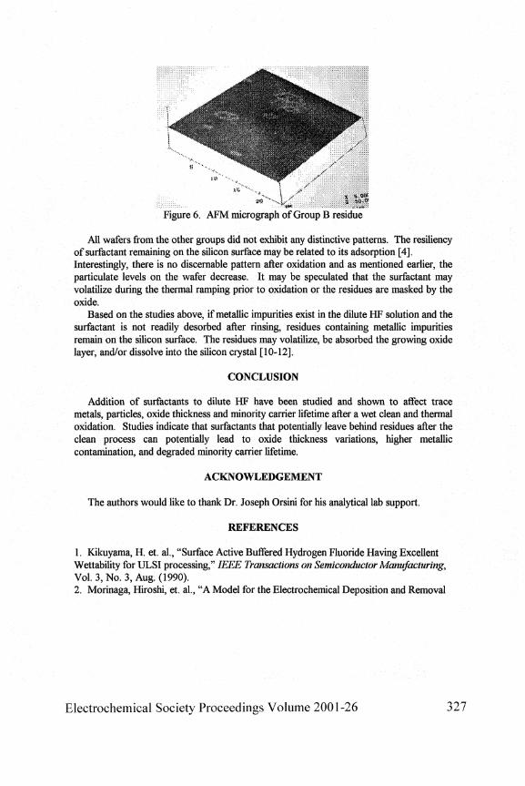
All wafers from the other groups did not exhibit any distinctive patterns. The resiliency of surfactant remaining on the silicon surface may be related to its adsorption [4]. Interestingly, there is no discernable pattern after oxidation and as mentioned earlier, the particulate levels on the wafer decrease. It may be speculated that the surfactant may volatilize during the thermal ramping prior to oxidation or the residues are masked by the oxide.
Based on the studies above, if metallic impurities exist in the dilute HF solution and the surfactant is not readily desorbed after rinsing, residues containing metallic impurities remain on the silicon surface. The residues may volatilize, be absorbed the growing oxide layer, and/or dissolve into the silicon crystal [10-12].
CONCLUSION
Addition of surfactants to dilute HF have been studied and shown to affect trace metals, particles, oxide thickness and minority carrier lifetime after a wet clean and thermal oxidation. Studies indicate that surfactants that potentially leave behind residues after the clean process can potentially lead to oxide thickness variations, higher metallic contamination, and degraded minority carrier lifetime.
ACKNOWLEDGEMENT
The authors would like to thank Dr. Joseph Orsini for his analytical lab support.
REFERENCES
1. Kikuyama, H. et. al., "Surface Active Buffered Hydrogen Fluoride Having Excellent Wettability for ULSI processing," IEEE Transactions on Semiconductor Manufacturing, Vol. 3, No. 3, Aug. (1990). 2. Morinaga, Hiroshi, et. al., "A Model for the Electrochemical Deposition and Removal
Electrochemical Society Proceedings Volume 2001-26 327

of Metallic Impurities on Si Surfaces," IEICE Trans. Electron., Vol E79-C, No. 3, March, (1996), pp. 343-62. 3. Weddington, Darryl, et. al., "An Assessment of a Dilute Hydrofluoric Acid Purifier," Semiconductor International, June (1999), pp. 151-8. 4. Sotgiu, Giovanni et. al., "On the Use of Surfactants in the Electrochemical Preparation of Porous Silicon," Thin Solid Films, 297 (1997), pp. 18-21. 5. O'Halloran, G.M., et. al., "The Effect of Additives on the Adsorption Properties of Porous Silicon," Sensors and Actuators A 61 (1997), pp. 415-20. 6. Jeon, S. et. al., "Electrochemical Investigation of Copper Contamination on Silicon Wafers from HF Solutions," J. Electrochem Soc, Vol. 143, No. 9, Sept. (1996), pp. 2870-5. 7. Itano, M. et. al., "Minimization of Particle Contamination During Wet Processing of Si Wafers," J. Electrochem. Soc, Vol. 142, No. 3, March, (1995), pp. 971-7. 8. Torcheaux, L. et. al., J. Electrochem. Soc, 142 (1995), p. 2037. 9. Ohmi, T., J. Electrochem.Soc, 139 (1992), p. 3317. 10. S.R. Kasi, M. Liehr, "Hydrocarbon reaction with HF-cleaned Si(100) and effects on metal-oxide-semiconductor device quality,"^/?/?/. Phys. Lett., 59(1), 1991, pp. 108-110. 11. Kasi, M. Liehr, P. A. Thiry, H. Dallaporta, M. Offenberg, "Hydrocarbon reaction with HF-cleaned Si(100) and effects on metal-oxide-semiconductor device quality," J. Vac Sci. Technol A, 10(4), 1992, pp. 795-801. 12. S.D. Hossain, C.G. Pantano, J. Ruzyllo, "Removal of Surface Organic Contaminants during Thermal Oxidation of Silicon," J. Electrochem. Soc, Vol. 137, No. 10, (1990), pp. 3287-91.
328 Electrochemical Society Proceedings Volume 2001-26

IMPROVEMENT OF SC-1 BATH STABILITY BY COMPLEXING AGENTS
Heini Saloniemi1, Taru Visti1, Simo Eranen1, Arto Kiviranta2, and Olli Anttila3
VTT Electronics, P.O.Box 1101, FIN-02044 VTT, Finland 2VTT Chemical Technology, P.O.Box 1400, FIN-02044 VTT, Finland
3Okmetic Oyj, P.O.Box 44, FIN-01301 Vantaa, Finland
The effect of six different complexing agents, HEDP, TEA, EDTA, CDTA, DTP A and DTPMP, on the hot SC-1 bath stability was studied. Decomposition of hydrogen peroxide in the baths was monitored in situ by optical analyzer. The baths were intentionally contaminated with multimetal standard solution. Adsorption of metals onto wafers was studied using TXRF and GFAAS combined with VPD sample preparation. HEDP, CDTA and DTPMP were found to increase the bath lifetime as well as to decrease the adsorption of metals onto wafers.
INTRODUCTION
One of the major drawbacks of the SC-1 type (NH3-H2O2-H2O) silicon wafer cleaning solution is the continuous need of refreshment of the solution. The temperature of the cleaning solution is usually between 60 - 80 °C where NH3 and H2O evaporate as H2O2 decomposes according to Eq. [1]:
2H202 (aq) <-> 0 2 (g) + 2H20 [ 1 ]
The evaporation may be suppressed to a large extent by using proper covers, whereas the decomposition is mainly caused by trace metal contamination, especially by Fe3+
and Cu2+.(1) The metal contamination originates primarily from the chemicals, and therefore the continuous refreshment of the bath even accelerates the decomposition of hydrogen peroxide. As H2O2 normally constitutes the largest expense of the bath, its stability has significant economic value.
The decomposition of H2O2 can be prohibited by complexing the metals in the solution.(2) The complexing prevents the metals from reversibly changing their oxidation state. For example change between Fe3+ and Fe2+ causes the catalytic decomposition of H2O2 according to reactions [2] and [3].
2Fe3+(aq) + H202 + 20H" <-» 2Fe2+(aq) + 0 2 (g) + 2H20 [2]
2Fe2+(aq) + H202 <-> 2Fe3+(aq) +2 OH" [3]
The net reaction for [2] and [3] is [1]. Another benefit of the complexing agents is that the formation of soluble metal complexes also decreases the adsorption of metals to
Electrochemical Society Proceedings Volume 2001-26 329

wafer surfaces.(2,3) Without complexing agents metals often form complexes with OH" ion in an alkaline solution. Especially neutral OH" complexes such as Fe(OH)3 and Al(OH)3 are slightly soluble (4) and tend to deposit onto the wafers. Some metals form complexes also with NH3 in the SC-1 bath, but those complexes are soluble and are not likely to adsorb on the wafers.
In the present study the stability of SC-1 solution was investigated by adding different complexing agents and simultaneously monitoring H202 lifetime in the bath by an infra red analyzer. The adsorption of metals was also studied by immersing wafers into solutions. In our previous paper (5) the adsorption was analyzed by spinning SC-1 solutions which contained metals and complexing agents on wafers.
The complexing agents which were tested are easily commercially available: hydroxy ethylene diphosphonic acid (HEDP), ethylenediaminetetraacetic acid (EDTA), 1,2-cyclohexanediaminotetraacetic acid (CDTA), diethylenetriaminopentaacetic acid (DTPA) triethanolamine (TEA), and diethylenetriaminepenta methylenephosphonic acid (DTPMP). EDTA and DTPMP have been studied earlier (2) as well as for CDTA some data exists (6). All these complexing agents are known to fonn stable, soluble complexes with metals, especially with Fe3+. Logarithmic values of room temperature stability constants are presented in the Table I. Constants of EDTA, CDTA, DTPA and TEA are from (4) and HEDP are from both (7) and (8). DTPMP constants are from (7), and the constant of Fe3+-DTPMP -complex is from ref. (9). Two values for HEDP are shown because of contradictions in the data. Though the stability constants of TEA are rather low it was tested since it is a widely used complexing agent and in the literature it was stated that it might prevent Fe3+ from forming OH" complexes.(10) Also in our previous studies TEA diminished the adsorption of iron.(5)
Table I Logarithmic values of stability constants ((3 values) of different complexing agents at room temperature.
c ^ Cr3+
Mn2+
Co2+
Zn2+
Ni2+
Cu2+
Fe3+
Al3+
EDTA 10.7 13.6 13.9 16.5 16.5 18.4 18.8 25.1 16.4
CDTA 13.1 23.0 17.5 19.7 19.3 20.2 22.0 30.0 19.5
DTPA 10.8
-15.2 18.8 18.2 20.1 21.2 28.0 18.6
TEA 0.8
---
2.1 2.8 4.1
--
DTPMP 6.7
--
17.3 19.1 19.0 19.5 27.3
-
HEDP 6.8 (7)/6.5 (8)
-9.2 (8)
17.3 (7)/9.4 (8) 16.7 (7) /10.7 (8) 15.8 (7) / 9.2 (8)
18.7 (7) /12.5 (8) 16.2 (8) 15.3 (8)
330 Electrochemical Society Proceedings Volume 2001-26

EXPERIMENTAL
The SC-1 cleaning solution consisted of 25 % NH3 (VLSI, Merck), 31 % H202 (VLSI, Merck) and DI water. The ratio NH3:H202:H20 was 1:1:5. Adsorption of Al was tested also with a 1:10:50 solution. The volume of the bath was 30 1 and the final temperature 65 °C.
The complexing agents were: HEDP (Wilson & Albright), TEA (p.a., Merck), EDTA (> 99 %, Fluka), CDTA (p.a., Fluka), DTPA (> 99 %, Fluka) and DTPMP (Solutia). The concentrations were 1-100 ppm. In the bath stability tests, metals were added from multielement (Cu, Fe, Ni, Mn, Ti, Zn) standard (J.T.Baker). The effect of Al, Fe, Mn and Cu was also studied separately with single element standards (J.T.Baker). The final concentration of each metal in the bath was 10 ppb. Al was tested also with 1 ppb. The deliberate contamination of the baths was essential in order to detect differences between chemicals more clearly.
A Horiba CS220 optical near infra red analyzer was used for the simultaneous and continuous monitoring of the concentrations of hydrogen peroxide and ammonia in the SC-1 cleaning baths. Metal adsorption studies were carried out by immersing wafers into the solutions for 10 minutes. Wafers were rinsed with DI water and dried with spindryer. The analysis of the metals heavier than z = 14 was carried out using Total Reflection X-ray Fluorescence Spectroscope (TXRF) (Atomika, TXRF8030W), equipped with tungsten X-ray tube and SiLi-detector. Aluminum was measured with Graphite Furnace Atomic Absorption Spectrophotometer (GFAAS) (PerkinElmer, AAnalyst600). The sample preparation was performed using Vapor Phase Decomposition (VPD) droplet collection system (GeMeTec, PADScan). In a VPD system, native Si02 layer is decomposed and the wafer is made hydrophobic by HF vapor in a polyvinyldifluoride chamber with open HF containers.(ll) The sample is then collected from the wafer surface by automatically scanning a 50 \xl droplet of either HF and H2O2 for TXRF analysis, over the wafer, or using a dilute HNO3 droplet for GFAAS analysis. For TXRF the droplet is dried on the wafer whereas GFAAS samples are collected to vials and diluted to 200 - 2000 jul.
Residues of CDTA and DTPMP on the wafers were measured in separate experiments by Secondary Ion Mass Spectrometry (SIMS) with Ga+ ions in the static mode. The samples were taken from the wet bench where about 400-700 wafers were cleaned during 3-4 hours. Samples were taken in the beginning and in the end of the period and the cleaning time was 8 minutes. 10 ppm of complexing agents was added only in the beginning, whereas NH3 and H2O2 were added also during the cleaning period.
Electrochemical Society Proceedings Volume 2001-26 331

RESULTS AND DISCUSSION
Bath stability
Figure 1 shows the changes in the hydrogen peroxide concentration as 10 ppm (c(HEDP) was 100 ppm) of different complexing agents were added to the SC-1 bath. The bath was contaminated with the 10 ppb multimetal standard.
Warming up of the bath took about 50 minutes but the measurements were started from the cold solution. Without any complexing agents H2O2 decomposed about in an hour (curve labeled as "Metal"). For comparison, in uncontaminated bath 50 % decrease in hydrogen peroxide concentration took over 4lA hours. CDTA, DTPMP and HEDP stabilize the bath. With CDTA the concentration of H2O2 has decreased very slightly in three hours. The measurement was stopped after that. HEDP and DTPMP had a less complete effect. When copper was studied separately it was found that even 30 ppm of DTPMP does not fully stabilize solution which contains copper.
time / min
Figure 1. Change of the H2O2 concentration after the addition of complexing agents to the SC-1 bath.
Although in our previous spinning experiments TEA seemed to complex Fe3+ (5), in this study, as the temperature was raised to 65 °C, it did not work at all and hydrogen peroxide decomposed as fast as without any complexmg agents. EDTA and DTPA inhibited the decomposition for 50 minutes but as soon as the bath was warm the concentration of H2O2 started to collapse. Therefore EDTA and DTPA were studied further by adding them also in the middle of the measurement (Fig. 2). After the addition of fresh complexing agent, H2O2 concentration stabilized for a while but started to decrease soon again. The temperature remained constant during the experiment.
332 Electrochemical Society Proceedings Volume 2001-26

Figure 2. Change of H2O2 concentration when 10 ppm EDTA and DTP A were added during the measurement to the SC-1 bath. Additions are marked by arrows.
In our previous spinning experiments at room temperature it was found that pH of the SC-1 solutions with EDTA, DTPA and TEA increased in the process of time. On the other hand pH in SC-1 solutions with CDTA and DTPMP remained constant at least for 24 hours. It is concluded that EDTA and DTPA decompose in hot bath. Decomposition of EDTA has been mentioned also in Ref. (2). Although according to our previous experiments (5) TEA, EDTA and DTPA decreased the adsorption of metals onto the wafers they can not be used in the SC-1 baths due to their fast decomposition.
When the effects of iron, copper, and manganese were studied separately without complexing agents (Figure 3), it was seen that Fe3+ is almost alone responsible for the H2O2 decomposition and Cu2+ takes part to a lesser extent, as expected.(l) Manganese did not affect on the H2O2 concentration under the present conditions. H2O2 decomposition curve which is caused by copper correlates well with DTPMP curve in Figure 1.
5.5
S 5
4.5
4
3.5 30
oW8N$ *?
Fe3+
x_
^ 4 4 *
T •
A*4A*\4AA
Metal
V MiT
Cu"
40 50 Time / min
60
Figure 3. Effect of different metals on H2O2 concentration in the SC-1 bath. "Metal" denotes multimetal (Cu, Fe, Ni, Mn, Ti, Zn) standard + Al standard.
Electrochemical Society Proceedings Volume 2001-26 333

Adsorption of metals
The adsorption of metals was studied by immersing wafers into the stability test baths. Only the complexing agents which increased the bath stability, i.e. CDTA, DTPMP and HEDP were studied. Wafers were added as soon as the bath was hot i.e. about 50 minutes after the solution preparation.
The surface concentrations of adsorbed metals in SC-1 which contained 10 ppb multimetal standard without complexing agents are shown in Table II. The amounts of adsorbed metals are similar to earlier experiments where Al, Cu, Ca and Fe were studied.(12)
Table II Surface concentration of metals adsorbed from SC-1 contaminated with 10 ppb metal standard.
1 Fe Cu Mn Ni Zn Ca Al c(xl010at./cm2) | 150-770 0.4-2.0 0.2-0.7 5.0-8.5 73-123 11-19 1500-2000
Table III represents the effects of the complexing agents on the metal residue on the wafers compared to the uncomplexed bath. 100 at.% residue means that the same amount of metal was analyzed from the wafer in the presence of complexing agent as without it. The residues are rather expected on the basis of stability constants (Table I) and they are congruent with our spinning experiments (5). Manganese residues seem to be rather large but those values are a bit uncertain since the total amount of adsorbed Mn is small (c.f. Table II). Adsorption of Ca and Al is difficult to diminish. Especially for Al the total adsorbed amount is large.
Table III Metal residue on the wafers.
Complexing agent in the bath
CDTA 10 ppm
DTPMP 10 ppm
HEDP 100 ppm
concentration (xl0_6mol/l)
29
8.7
243
Fe at.%
4
0.1
0.1
Cu at.% <0.9
430
3
Mn at.% 50
20
20
Ni at.%
2
2
2
Zn at.% 0.2
110
0.2
Ca at.% 20
30
45
Al at.% 34
26
51
The amount of adsorbed copper is larger in the presence of DTPMP than without it if Cu was added using multielement standard. Similar behavior was not observed when it was added using single element standard. The same has been observed also in Ref. (2)
Fe and Cu, which effect on the bath stability, and Al, which adsorbs the most efficiently, were studied also separately using single element standards. The adsorbed metal concentrations were measured from the wafers in stable baths. In all cases the concentration of iron or copper was 10 ppb which is about 0.2 jumol/l. For iron 1.6 ppm (1.4 j^nol/l) of DTPMP, 5 ppm (14.5 jumol/l) of CDTA or 30 ppm (72.8 fimol/1) of
334 Electrochemical Society Proceedings Volume 2001-26

HEDP was enough to prevent H2O2 decomposition and decrease the metal residue on the wafer to below 0.5 % of the original level. In the case of copper 2.4 ppm (6.9 jimol/1) of CDTA was enough to prevent H2O2 decomposition and decrease the metal residue on the wafer below the detection limit of TXRF. 100 ppm (243 |amol/l) HEDP decreased the adsorption to 3 at. %. 30 ppm (26.2 |umol/l) DTPMP decreased the residue only to 50 at.%. Cu-DTPMP-bath was not stable either.
The adsorption of aluminum was found to be the most difficult to prevent. When the temperature was lowered from 65 to 30-50 °C or the metal concentration was decreased from 10 to 1 ppb the total amount of adsorbed Al decreased but the residue with the complexing agent remained always above 20 at.%. The increase of the complexing agent concentration from 10 to 100 ppm did not decrease the residue either. But when SC-1 was diluted and pH of the solution was lowered from about 11 (NH3:H202:H20 = 1:1:5) to about 10 (NH3:H202:H20 = 1:10:50) the residue diminished to below 3 at.% in 10 ppm DTPMP bath. This behavior can be explained on the basis of aluminum hydroxide (4) and Al-DTPMP stability constants. The Al-DTPMP complex is more stable at lower pH.
Residues on the wafers
The analysis of complexing agent residues on the wafers has been started from baths which contains CDTA or DTPMP. In preliminary studies no organic contamination was detected from wafers in the DTPMP bath neither at the beginning nor at the end of the cleaning period. On the other hand small amounts of organic contamination were found from some wafers in the CDTA bath at the end of the cleaning period. The residue could not be identified as being from CDTA and the samples were very unlike, i.e. the result was not reproducible. SIMS studies will continue and, in addition, the residue will be studied by capillary electrophoresis. For comparison, in Ref. (2) DTPMP residues were not detected on wafers either.
CONCLUSIONS
The use of complexing agents is a very promising method to improve the SC-1 bath lifetime and decrease the chemical costs. In the present study the effect of complexing agents on the SC-1 bath stability and adsorption of metals were tested with six different chemicals. CDTA, DTPMP and HEDP prohibited the decomposition of hydrogen peroxide and increased the bath stability effectively. In addition they decreased the adsorption of metals onto the wafers if relatively large excess of complexing agent was used. Adsorption of Al may be prevented by DTPMP by using more diluted solution than the conventional 1:1:5 SC-1. In order to achieve true savings in chemical costs the stability of metal complexes in hot, alkaline and oxidative SC-1 baths is a very important issue. Therefore our further studies will be focused on stability tests of complexing agents. In addition chemical residues need to be studied carefully.
Electrochemical Society Proceedings Volume 2001-26 335

ACKNOWLEDGEMENTS
Dr Tero Lehtinen at Okmetic Oyj is acknowledged for help in bath stability tests. The work is supported by the Finnish National Technology Agency (Tekes), Okmetic Oyj, Micro Analog Systems Oy, VTI Hamlin Oy, and Planar Systems Oy.
REFERENCES
1. Schmidt, H.F., Meuris, M., Mertens, P.W., Rotondaro, A.L.P., Heyns, M.M., Hurd, T.Q., and Hatcheer, Z., Jpn. J. Appl Phys., 34, 727, (1995). 2. Bayens, M. et al Solid State Phenomena, 65-66, 23, (1999). 3. Anttila, O., Tilli, M.V., Schaekers, M., and Claeys, C.L., J. Electrochem. Soc, 139, 1180(1992). 4. Smith, R.M., and Martell, A.E., NIST Critically Selected Stability Constants for Metal Complexes Database, version 4.0, (1997). 5. Saloniemi, H., Visti, T., Eranen, S., Kiviranta, A., and Anttila, O., Physica Scripta, submitted. 6. Cooper, E.I., Estes, S.A., Gale, G.W., Jagannathan, R., Okom-Schmidt, H.F., and Rath, D.L., U .S. Patent 5962384, (1999). 7. Gledhill, W.E., and Feijtel, T.C.J., in The Handbook of Environmental Chemistry. O. Hutzunger, Editor, vol. 3, p.261, Springer-Verlag, Berlin (1992). 8. Wilson & Albright, data sheet. 9. Bruecken, A.J., Dissertation, Univ. Missouri-Columbia, (1987). 10. Hancock, R. and Martell, A.E., Chem. Rev., 89, 1875, (1989). 11. C. Neumann and P, Eichinger, Spectrochimica Acta 46B, 1369 (1991) 12. Mouche, L., Tardif, F., and Derrien, J.,J. Electrochem. Soc, 142, 2395 (1995).
336 Electrochemical Society Proceedings Volume 2001-26

PREVENTION OF Si ETCHING IN DILUTED SCI SOLUTIONS
E.Bellandi, M.Alessandri, D.Lodi, M.Strada, F.Pipia1
S.Petitdidier, D.Levy2
STMicroelectronics, Central R&D, 1 Via C.Olivetti 2, 20041 Agrate Bm (MI), ITALY
2 850 rue J.Monnet, FR-38926 Crolles Cedex, FRANCE
Very diluted SCI solutions at low concentrations (1:1:50 or more) are used to maintain a reasonable chemical consumption in single tank or single wafer tools. In these conditions, SCI behaviour is different from conventional high concentration chemistries used in re-circulated systems, and severe de-fectivity and electrical issues may arise due to silicon etching. In this paper we show that it is possible to overcome this problem by a strong oxidising
step before SCI, performed injecting ozonised water. This step grows a relatively thick and robust chemical oxide that prevents direct silicon etching by OH- ions, reducing the amount of etched silicon, without compromising the
electrical characteristics and the particle removal efficiency.
INTRODUCTION
In wet cleaning process, SC-1 is commonly used in the semiconductor industry to remove light organics and particles. During this step, the silicon is oxidised and dissolved at the same time. In order to reduce the cross-contamination risk from one lot to the next one and to simplify the hardware configuration of last generation single tank and single wafer processors, several equipment manufacturers propose to use a "one-shot", always fresh chemicals. In order to ensure an acceptable chemical consumption, it is therefore necessary to use very diluted solutions, such as: 1:1:50, 1:3.3:80, 1:2:50, 1:1:>200... These conditions become very different from the re-circulated chemistries used on conventional wet benches, where DlW/ammonia ratio is usually 10-20 and peroxide/ammonia ratio 2-4.
In a previous study1, the evaluation of a diluted SC-1 in an industrial environment was presented, both on full sheet wafers -i.e. particle removal, roughness and silicon consumption- and on real MOS structures. Several pitting and electrical issues were found, when using diluted SCI, especially for low peroxide/ammonia ratios or high temperatures and when SCI was preceded by a HF step. A strong correlation was also confirmed (Figure 1) between the amount of etched silicon and the number of COPs (Crystal Originated "Particles"), revealed as particles by particle measurement tools based on light scattering . Particle addition is also very sensitive to the substrate quality, and it is anyway much less if EPI substrates are used.
Electrochemical Society Proceedings Volume 2001-26 337

K. Yamamoto et al. explained this phenomenon3 claiming a kinetic reaction model of Si substrate with APM, where the etching reaction of Si substrate proceeds along two paths (path-1 and path-2). In path-1, the silicon surface is oxidised by HO2 and then the SK>2 layer is etched by OH". In path-2, OH" directly etches the Si surface. We can hence assume that path-2 reactions occur when the oxide grown by HO2" ions is thin or weak enough to allow the diffusion of OH- ions. This happens in case of low H2O2 concentration mixtures, such as diluted APM solutions. Path-2 reaction has a much higher Si etch rate than the oxidation-etching reaction, and according to reference 2, it generates a higher amount of defects.
It was also observed1 that the number of defects is much higher when SCI is preceded by an HF step. Figure 2 reports the number of defects at 0.12fim, as a function of the number of cleanings for a diluted SCI, with and without a preceding HF, and for a conventional recirculated 1:4:20 SCI, with the same process temperature and time. A high concentration SCI has a very low particle addition with respect to a diluted one and the HF step clearly enhances the defect growth rate. These defectivity data are correlated with the amount of silicon etched, as shown in Figure 1.
In this paper, we will study the differences between SCI and HF-SC1 treatments, and we will propose a way to overcome the excessive silicon etching that is the cause of the severe defectivity problems mentioned above.
EXPERIMENTAL
Etching of silicon surface is a very challenging measurement, because it cannot be carried out using the conventional optical methods, without SOI substrates. Anyway, a good approximation1 can be obtained using amorphous silicon (oc-Si) on an oxidised substrate and measuring the oc-Si thickness by Spectroscopic Ellipsometry (SE), by the three-layer model illustrated in Figure 3. SE can provide the thickness of the bottom oxide layer, of the oc-Si and of the top oxide layer as well as information on oc-Si/poly-Si crystalline degree. Repeatability of the measurement of the oc-Si layer is usually of the order of 0.1 A. The thickness of the three layers was measured on 13 points per wafer. Therefore, SE technique provides a direct measurement of the amount of Si etched.
A Design of Experiment (DOE) was performed to evaluate the amount of silicon etched as a function of chemical concentration, bath temperature and dip time, for both SCI and HF-SC1. A short recipe description is reported in Table 1. Experiments were executed on a DNS FC821L wet station, using an ONB tank. In this tool -as well as in other single tank tools-, chemicals are injected into the bath, than wafers are dipped in a static solution and rinsed in-situ. During the dip, the temperature of the bath slightly decreases, because the quartz tank is not heated. In all the experiments SCI chemical ratio was kept constant at 1:2:100 (NH4OH:H202:H20). dHF concentration was 0.3%-wt.
338 Electrochemical Society Proceedings Volume 2001-26

Step
1 2 3 4 5 6 7 8
SCI
Hot DIW 1:2:100 SCI injection SCI dip with megasonics QDR/OFR Drying
HF-SC1
0.3% dHF injection dHFdip(180") OFR Hot DIW 1:2:100 SCI injection SCI dip with megasonics QDR/OFR Drying
Table 1: SCI (left) and HF-SC1 (right) sequences
RESULTS AND DISCUSSION
Figure 4 shows the amount of a-Si etched at 60°C as a function of dipping time for SCI and HF-SC1 treatments. The "0" value on the x-axis refers to the end of the chemical injection and the beginning of the dip time (step 6 in Table 1). After chemical injection about 13A of a-Si are already removed by HF-SC1 treatment, while only a few A are removed by SCI without any preceding HF step.
To explain the different etching and defectivity behaviours of HF-SC1 and SCI only treatments, it can be supposed that after an HF treatment, silicon is hydrogen pas-si vated and it is exposed to APM without any protecting native oxide (Figure 5). Therefore, at the beginning of the APM process, there is a relatively short time (hereafter referred as t\) when silicon is exposed directly to OH" ions before being oxidised. In these conditions {t<t\), path-2 reaction prevails, because there is no oxide -or at least a very weak and porous chemical oxide- acting as a barrier for the OH" diffusion towards the silicon surface. After this phase (t>h), silicon is oxidised by HO2" ions, and path-2 reaction becomes less important while path-1 reaction becomes dominant. In these conditions, there is a stable oxidation-etching reaction, only determined by temperature and chemical concentration and the behaviour turns out to be the same of an SCI treatment without any preceding HF step. This explains why SCI and HF-SC1 curves are parallel -same etching rate- in Figure 4. Because the silicon oxidation rate by HO2" ions is very fast even at low temperature4, it can be supposed that t{ is very short at usual process temperature, of the order of few seconds at 50°C.
In order to avoid path-2 reactions during the initial phase it is necessary to protect silicon against OH- direct etch by creating a protective chemical oxide. The first attempt was carried on using 1:50 hydrogen peroxide injection for 300" at both room temperature and 50°C. Anyway, as shown in Figure 6, the insertion of a peroxide pre-injection step does not provide any benefit. Indeed, as reported in reference 5, in case of H2O2 oxidation the surface is not completely oxide covered even after a long exposure period. By in-situ infrared spectroscopy, it was demonstrated that oxide on a HF treated surface growth is
Electrochemical Society Proceedings Volume 2001-26 339

compatible with an "island like" model, and Si-H2 bonds are present even after several minutes of exposure to 3% H2O2. In our experiments, we used more diluted (0.6%) peroxide than the one in reference 5, and when the surface is exposed to APM it is still mostly hydrogen passivated and hence path-2 direct etch mechanism takes place. Oxide thickness grown by 50°C, 1:50 H2O2: H2O is reported in Figure 7.
In the same paper (ref. 5), it is also reported that just 2ppm of ozonated water produce a much faster surface coverage and that Si-H2 bonds disappear after about 5', and the surface becomes completely covered by chemical oxide in a relatively short time. In our test, the ozone was generated by a membrane type diffuser, with a concentration of 15ppm in 201/min water flow. In these conditions, a high quality chemical oxide grows in a very short time. A similar approach was also used in reference 6 to reduce silicon etching for SOI substrates.
Thickness as a function of DIW/O3 injection time was measured by SE on bare silicon wafers and it is reported in Figure 7. In the same chart, it is also plotted the thickness grown by peroxide at 50°C.
Oxide grows very quickly in ozonised DIW and a relatively thick oxide can be obtained in about 50-100", while in diluted peroxide, oxide thickness is much lower, even at 50°C and after 300" injection.
When a recipe has to be implemented on single tank or single wafer tools, process time is inversely proportional to the equipment throughput; therefore, the passivation and subsequent rinse steps must be as short as possible. This can be easily achieved using ozonised DIW. In fact, as shown in Figure 8, about 60" of DIW/O3 injection are already enough to reduce Si etch. In this figure, the amount of a-Si etched during an HF-D1W/O3-SCI treatment is reported as a function of DIW/O3 injection time, at SCI temperature of 50°C and 60°C. In the same chart it is also reported the amount of a-Si that is oxidised by DIW/O3 (about 4-5A).
In case of SCI at 50°C for 300", any etching by the SCI itself is almost completely avoided. In fact, the amount of a-Si etched (~6A) is very close to the one consumed by the Si oxidation mechanism of D1W/O3. In case of a standard HF-SC1 process, without any intermediate D1W/O3 injection, about 20 A of a-Si are etched. When SCI is performed at higher temperatures, such as 60°C, the chemical oxide grown by DIW/O3 is completely removed and silicon starts to be etched by SCI. In Figure 9 is reported the amount of a-Si etched by HF-DIW/O3-SCI treatment, with DIW/O3 injection time of 300", as a function of SCI temperature. SCI dip time has been kept constant to 300". Dashed line shows the amount of Si consumed by the DIW/O3 oxidation itself. If a low silicon etching is required, APM temperature should not be more than 50°C.
Another confirmation of the capability of the D1W/O3 treatment to reduce silicon etching has been obtained substituting the SCI step with diluted ammonia (dNH4OH ). In this way, we could exclude any influence of H2O2 and focus only on the quality of the DIW/O3 oxide. In Figure 10 is reported the amount of a-Si etched by 0.03% NH4OH at 50°C preceded by a HF step, with and without an ozonised water passivation treatment. In these process conditions ammonia can remove about 400A, which means an etch rate of l.lA/s. Such a high etch rate can explain why tx is so small. In case of the HF-D1W/O3-
340 Electrochemical Society Proceedings Volume 2001-26

dNH40H process, the amount of etched a-Si is reduced to about 200A; this means that pure ammonia takes about 3 minutes to remove the chemical oxide grown in the ozonised DIW. The effect of the ozone pre-injection step on the LPD addition is reported in Figure 11. The experiments were carried out using CZ wafers and SCI temperature of 50°C and 60°C, with and without a DIW/O3 intermediate-injection step. In the chart, it is reported the number of LPDs measured after three sequential cleaning treatments.
The HF-SCl treatment at 60°C is much more critical than the 50°C one. DIW/O3 injection step, allows a significant reduction of the amount of added defects, and at 50°C there is almost no increase in LPD counts after the cleaning sequence. In Figure 12, the treatments with diluted SCI are compared with a HF-SCl standard sequence at higher SCI concentrations, but with the same temperature (50°C) and process time (300").
When the HF-SCl sequence is performed using a concentrated SCI solution, the amount of etched silicon is considerably less then the one etched by the same sequence, using a diluted APM mixture. HF-DIW/0,-SCl allows a further reduction of silicon etching to the level of an APM step itself.
CONCLUSIONS
The excessive amount of etched silicon by diluted SCI (and the consequent generation of silicon defects) very often causes electrical and defectivity problems when preceded by a HF step. In order to overcome this problem, diluted SCI is sometimes used at relatively low temperature, but this have a detrimental effect on particle removal efficiency. In this paper, we have summarised the Si etching mechanism in SCI and introduced a way to avoid, or at least to reduce this problem by inserting a DIW/O3 injection step in the standard HF-SCl sequence. The shielding capability along with the perfect cleaning efficiency of the ozonated water was proven and compared with H2O2.
Moreover, due to the short time required by the DIW/O3 step, there is not any meaningful increase in the cleaning cycle time.
ACKNOWLEDGMENTS
Authors would like to acknowledge DNS engineers for the support and the useful discussions.
REFERENCES
1. S.Petitdidier, H.Bernard, E.Bellandi, F.Landa, H.Shirakawa, D.Levy, Proceedings of the 5th UCPSS, Oostend, Be, September 2000
2. E.Morita, H.Okuda, F.Inoue and K.Akiyama, "Micro roughness and COPs created by SC-F\ in "Ultraclean Surface Processing of Silicon Surface, secrets of VLSI manufacturing", Takeshi Hattori (editor), Springer Verlag, Berlin 1998
Electrochemical Society Proceedings Volume 2001-26 341

3. K.Yamamoto, A.Nakamura and U.Hase, IEEE transactions on semiconductor manufacturing, Vol. 12, No.3, August 1999
4. V.Bertagna, R.Erre, F.Rouelle, D.Levy, S.Petitdidier, M.Chemla, J Solid State Electro-chem5,306(2001)
5. Y.Sugita, S.Watanabe, Jpn. J. Appl. Phys., Part 1 37, 3272 (1998)
6. P.Besson, C.Cowache, J.M.Fabbri, F.Tardif, A.Beverina, Proceedings of the 5th
UCPSS, Oostend, Be, September 2000
_ 1000
-§ 80° • | 600
.© 400
| 200
0
0 50 100 150 200 250 300
Si consumption [A]
2000F 1 * - RCA, diluted SCI
1800f- - • - - R C A . s t d . SCI * - H F RCA, diluted SCI
, 1600h
t 1400H
1 120o[- /
i looof
Number of cleanings [#]
Figure 1: LPD number @0.12^m as a Figure 2: LPD addition @0.12fxm as a function of silicon etching function of the number of cleanings
Native Si02
ot-Si
Si02
Si substrate
Figure 3: Model used for SE Figure 4: Etched a-Si for 1:2:100 SCI at 60°C and measurements. HF-SC1.
342 Electrochemical Society Proceedings Volume 2001-26

Initial phase: Path-2 Steady state: Path-1
Hydrogen passivated surface
H H If H H H
\ / \ / \ /
Si substrate
H H
Figure 5: Reaction paths for t<t\, (left) and for t>t\ i (right)
S©2 layer
45
40
3 % 35
Etc
hed
25
. *»2,is» =** •WW- c£=
»•»•§<»•»» —*—
a 101
-8 8 f-
[ DIW/03 /] 1 I / I H202 1
| ^—- / V_ * |
L i """ J
No peroxide 300" at RT 300" at 50°C
Figure 6: Etched a-Si for 1:2:100 SCI at Figure 7: Oxide growth by 15ppm 60°C as a function of peroxide pre- DIW/O3 and H 2 0: H 2 0 2 ( 1:50, 50°C). injection in the sequence HF-H2O2-SC1.
0 50 100 150 200 250 300
D I W / 0 3 injection time (s)
Figure 8: a-Si etching by HF-DIW/O3- Figure 9: a-Si etching by HF-DIW/O3-SC1 Vs DIW/O3 injection time. SCI as a function of SCI temperature.
Electrochemical Society Proceedings Volume 2001-26 343

Si (
A)
8 -d-
Etc
h 400
300
200
100
1 . -
\
•• 1 i
50°C 6(TC •
HF-NH.OH:H,0 HF-DIW/O.-NH OH:H , 0 HF-SC1 HF-DIW/O-SCl HF-SC1 HF-DIVC70-SCI
Figure 10: a-Si etching by HF-NH40H:H20 Figure 11: Average LPD addition at 50°C and HF-DIW/03-NH40H:H20. T=50°C, and 60°CHF-SC1 processes. NH40H:H20 ratio 1:50.
20
(A)
6 3 io
m 5 "^mtm =#-
%»>»*# <=*=
M W _*_
-
W^A- -*- -
-
R „̂
Figure 12: a-Si etching by 1:2:100 SCI, HF-SC1 and HF-DIW/O3-SCI at 50°C, compared to HF-SC1 (1:2:20).
344 Electrochemical Society Proceedings Volume 2001-26

INSITU PRE-EPI CLEAN PROCESS FOR NEXT GENERATON DEVICES I. Kashkoush, G. Chen, R. Ciari, and R. Novak
Akrion LLC, 6330 Hedgewood Dr., Allentown, PA 18106, USA
Advanced ULSI devices require replacement of current high temperature dry cleaning steps, that are used to remove the native oxide, with lower temperature processes. As a result, prior wet-cleaning steps must yield the lowest defects possible on the wafer surface. In the present study, different pre-epitaxial cleaning processes are investigated. A conventional multi tank HF-last process is compared to a single step insitu HF-last process. Experiments showed that the use of dilute chemicals and insitu HF/Rinse/Drying yield better results than conventional multi-tank wafer processing.
INTRODUCTION
With further reduction of the dimensions of the microelectronic devices into the low nm scale, the cleaning procedures play an increasingly important role in IC manufacturing. The process chemicals, sequence and number of cleaning steps are becoming more critical in determining the desired end results [1,2]. High temperature (>1050° C) gas phase cleaning is typically used to dissolve the native oxide and any other contaminants on the wafer surface prior to epitaxial growth [3]. Advanced low temperature epitaxial processes for advanced ULSI devices require this high pre-epitaxial thermal budget be lowered considerably [3]. However, the lower the temperature the lower the desorption rate of Si02. To alleviate this problem, an HF-last process is typically used to produce an H-terminated surface. This process when done properly would yield a surface with the lowest defects [4] and therefore allow the pre-bake and desorption temperature to be substantially lower than 1050° C. In the present study, different pre-epitaxial cleaning processes were investigated. A conventional multi-tank HF-last process was compared to a single step insitu HF-last process. Results showed that dilute chemicals and insitu HF/Drying are key factors to successful wafer processing for IC manufacturing.
EXPERIMENTAL
Experiments were conducted on Akrion's GAMA-1™ automated wet station. The tool is capable of running two process sequences; multi-tank and single tank insitu process. Wafers were processed in the tool prior to the epitaxial growth steps. To simulate a patterned wafers situation, silicon wafers were sandwiched between the dummy oxide wafers. This provided the most challenging contamination levels to the silicon wafers from the oxide wafers since etch byproducts are deposited from the oxide wafers onto the bare silicon wafers. Different cleaning techniques were used to remove this high contamination level. The conventional sequence of SCl/Rinse/HF/Rinse/Dry was used
Electrochemical Society Proceedings Volume 2001-26 345

first to remove the contaminants. Surfactant was mixed with HF as part of the process development. A modified insitu cleaning sequence was developed for minimum particle deposition. Details of experimental procedure and materials used are shown in Tables 1 and 2.
RESULTS AND DISCUSSION
In order to reduce the thermal budget for Si epitaxial growth, the surface conditioning step has been shown to be critical. Typically, a high temperature H2 prebake is used to desorb the native oxide and to prepare an ideal surface for epitaxial layer deposition. However, for advanced next generation devices, temperatures as low as 700° C are required [5,6] to ensure isothermal processing.
Tests were conducted to ensure the process steps and equipment are particle neutral. Even in the presence of the oxide wafer fillers, particle addition was kept at an absolute minimum. As shown in figure 1, the average particle addition is - 6 (1 or = 11). When using only bare silicon wafers, the conventional HF-last process yields low particle addition, as shown in figure 2. The average particle addition was less than 40 particles at 0.12 jam. In addition, post-epi defects were also fairly low (~ 1.26 defects/cm2), as shown in Figure 3.
In IC manufacturing wafers are typically mixed with oxide wafers or the wafers are patterned. Typically, exposed silicon is adjacent to oxide or nitride areas. In HF solutions, etch byproducts will be transported from the hydrophilic surface to hydrophobic surfaces. This results in high particles counts on the exposed silicon. The process has to be designed to overcome these issues. As explained in the experimental section, silicon wavers were sandwiched between oxide fillers to simulate typical wafer manufacturing.. Results show that conventional HF-last process used in this situation (SCl/Rinse/HF/Rinse/Dry) produces high particle counts at 0.12 urn (> 10,000) as shown in figure 4. Consequently, the post epitaxial defects were also high (>30 000, not shown). These LPDs (light point defects) are considered to be nucleation sites during the epitaxial deposition. Conventional wafer transfer between tanks plays a significant role in increasing silicate deposition into silicon wafers.
Two approaches were taken to prevent particle deposition during the etch process. In the first method, surfactant was added to the HF bath as a way to improve the wettability of wafers and hence reduce particle deposition onto the wafers. Better process results were obtained when compared to conventional process. However, the presence of any trace amounts of the surfactant remained problematic in the epitaxial growth process. Additional chemistries would have to be added, e.g. ozone, to remove any trace amounts of the surfactants. A second process needed to be developed; one that eliminates the need to use surfactant. The approach taken was to minimize exposing the wafer to an air/liquid interface where contaminants may reside. These contaminants will deposit on the wafers
346 Electrochemical Society Proceedings Volume 2001-26

during insertion into or pulling out of the liquid. A chemical injection scheme was used to process the wafers in the dryer. When wafers were processed with no transfer between cleaning steps, much lower particle deposition was obtained. As shown in figures 5 and 6, an average of less than 50 particles were added to the wafers. It is important to mention here that the use of ozonated rinse after HF and before going to the SCI step is very critical in eliminating any potential for metal-induced pitting on the hydrophobic surface [7]. As reported by Knotter [7], Fe for example in the SCI can induce pitting on hydrophobic surface. The oxide chemically grown in the ozonated rinse is stable and thick enough (7-10 A, see figure 7) to protect the silicon surface from any metal roughening effects. The post-epi cleaning results for the insitu method are shown in Figure 7. The average LPD density per wafer is about 0.89 defects/cm2. This level is significantly lower than any published data at 0.12 urn. Clearly, the lower the HF-last defects the lower the post-epi deposition defects as shown in figure 8.
The results of different cleaning recipes are summarized in table 3. Different wafer types were used also as fillers to investigate if the filler wafer type has any negative impact on the results. The results showed that the most critical step to achieve extremely low post epi deposition defects is the insitu HF/Rinse/Dry with no wafer transfer between steps. Measurements were also taken to characterize the background oxide thickness as a measure of the [O] content on the wafer surface. Time constraints prevented the use of more sophisticated analytical techniques e.g. EDX, Auger,. . .etc. to characterize the [O] concentration in a timely fashion. It is equally important to notice that the amount of [O] present on the wafer surface could significantly increase the particles deposited on the wafer. The lower the [O] content on an H-passivated surface the lower the particle deposited as shown in figure 9.
CONCLUSIONS
A modified insitu cleaning procedure was developed for pre epitaxial growth. Results show significant improvement when compared to a conventional HF-last cleaning process. The insitu processing (one step etch/rinse/dry) has shown to be a key factor in eliminating particle deposition on exposed silicon areas on the wafer surface. Experiments showed that the use of dilute chemicals and insitu HF/Rinse/Drying yields significantly lower defects (post clean and epitaxial deposition) than those obtained during conventional multi-tank wafer processing.
Electrochemical Society Proceedings Volume 2001-26 347

REFERENCES [1] Besson, P. et al, UCPSS '2000, Vols. 76-77 (2001) pp. 199-202. [2] Kashkoush, I., et al, Mat. Res. Soc. Symp. Proe., Vol. 477,1997, pp. 311-316. [3] Caymax, M. et. al, Solid State Phenomena Vols. 65-66 (1999) pp. 237-240, 1999 Scitec Publications, Switzerland. [4] Patrano, P., Fleury, A., Andre, E., and Tardif, F., UCPSS '94 Proc, pp. 247-250. [5] Mouche, M., et al, UCPSS '96 Proc. Pp 269-272. [6] Verhaverbeke, S and Pagliaro, B., Electrochem Soc. Proc. Vol. 99-36, pp. 445-451. [7] Knotter, M. and Dumensil, Y., UCPSS '2000, Vols. 76-77 (2001) pp. 255-258.
348 Electrochemical Society Proceedings Volume 2001-26

Table 1: Experimental Procedure Table 2: Experimental Material
Fully Automated GAMA (50x200 mm)
LuCID dryer w/ HF controlled injection
3 mm EE (Omega composite carrier)
KLA-Tencor Surfscan calibrated at 0.12 pm
Low count Si wafers were placed between oxide dummy wafers
HF ~ 100:1 @ ambient temp.
, DHF ~ 400:1 @ ambient temp.
• dSC1 ~ 1:2:50 @ 50 C and 800 W
» DI03 rinse - 5 ppm at ambient temp.
• D0 2 was controlled < 1 ppb
• ASML Reactor
dSCI 1 Rinse 1 HF 1 Rinse Dry
Table 3: Critical Step => In-Situ HF-Last in Dryer
Cleaning Recipe
SC1/OCR/HF(+surft)/OCR/LuCID(inj HF+R+Dry)
SC1/OCR/LuCID(HF+R+Dry)
OCR/LuCID(HF+R+Dry)
HF/OCR/SC1/OCR/LuCID(inj HF+R+Dry)
HF/OCR/SC1/OCR/LuCID(stg HF+R+Dry)
48 Filler Wafs TOX
TOX TOX
TOX TOX
TOX TOX
TOX
TOX TOX
TOX TOX
poly & ntrd
poly & ntrd
poly & ntrd
poly & ntrd
poly & ntrd
TOX TOX
TOX TOX
LPD Sum Pre-
Clean 3
15 8
9 10
4 8 8
3 10
33 28
5 5 6
26 5
3 4
2 14
5>>0.12um Post-Clean
16 27 45
73 12
30 40 87
57 62
87 16
16 91
20
9 10
29 62
12 32
Delta 13 12 37
64 2
26 32
79
54 52
54 -12 11 86 14
-17 5 26 58
10 18
ill
4.390
4.275 4.201
4.728 4.553
4.805 4.7
4.51
4.459 4.362
4.351 4.37
4.389 4.341
4.334
4.288 4.258
4.584 4.501
4.252 4.325
Rudolph post-cin 1 Sigma
0.256
0.188 0.234
0.414 0.294
0.133 0.117
0.191
0.107 0.142
0.095 0.124
0.095 0.129
0.112
0.087 0.134
0.18 0.231
0.113 0.126
Post-EpTI LPD
>0.12um |
66
379 211 329 267
377 250 241
125 185
243 524 227 430
158
141 257
242 335 207 322
Electrochemical Society Proceedings Volume 2001-26 349
dSC1 Rinse HF
surfactant
D103 Rinse
DHF
HF DI03 Rinse
dSC1 Rinse
I DHF
D*ry

Process: HF/OCR/SC1/OCR/LuCID{rinse + dry) (200 mm bate Si wafers sandwiched with TOX wafers)
I S 10o * f t .15«A 20
Avg Deisa = - 6 @ > 0.12 um Std Dev {1 sigma) = 11 3 mm EtiQfc Exclusion
25
• 30
O30A TOX etch
AWOATOXetctl
40 45 S
*
Initial Particle Count IB! > 0.12 ui
Figure 1: Particle Performance with Simulated Pattern Oxide Etch (Hydrophilic at End)
Process: HF/OCR/SC1/OCR/LuCID{HF + rinse + dry) (2 bare SI wafers per test sandwiched with TOX, poly and nitride fillers)
100-
1 -
•
# «. * •
+
• 4 +
+ • •
+
*
+ * *
'
f
+ Pro-Clean
• Post-Clean
3mm Edge Exclusion
•
» * ^ +
+ +
0 1 2 3 4 S 6 7 S 12 13 14 15 16 17 18 19 Wafer Number
Figure 2: Conventional HF-Last without TOX Pattern in Presence (Bare Si Only)
200 mm bare Si wafers without any TOX fillers
f A > - 8 T t - t - ^ %z^r f+- » - * " '
Process: SC1/R/HF/R/LuCID(dry only) (2 bare Si wafers per test sandwiched with TOX wafers)
£ 1000
® 100
3mm Edge Exclusion)
0 1 2 3 4 5 6 7 12 13 14 15
Figure 3: Post-Epitaxial (900C Bake) LDP after Conventional HF-Last Process
Figure 4: Conventional HF-Last with Simulated Pattern Oxide Etch (silicate contamination)
Process: HF/OCR/SC1/OCR/LuCID(HF + rinse + dry) (200 mm bare Si wafers sandwiched with TOX wafers)
Avg Delta* 3@> 0.12u Std Dev (1 slgma) « 14 3 mm Edge Exclusion
8a a « * * & « * « • » '
Initial Particle Count (B > 0.12 ui
Process: HF/OCR/SC1/OCR/LuC!D(HF + rinse + dry) (2 bare Si wafers per test sandwiched with TOX, poly and nitride fillers)
• Post-Clean
3mm Edge Exclusion
6 7 8 9 10 11 12 13 14 15 16 17 18 19
Figure 5: Particle Performance with Simulated Pattern Oxide Etch (Hydrophobic at End)
Figure 6: In-Situ HF-Last with Simulated Pattern Oxide Etch
350 Electrochemical Society Proceedings Volume 2001-26

Process: SC1/OCR/HF/OCR/LuCID
l̂ --̂ -.-...̂ ^̂ .̂̂ .̂..,,,̂ ^̂ .̂.̂ .̂-̂ .̂.̂ .,̂ __ —*
I
xHH*
Q ^ •*-• ^ - a 4
t——::;:°: t
200 mm bare Si wafers sandwiched with TOX, Poly or Nitride fil
'II 5 J | 4 Oo>
Figure 7: Oxide Regrowth Uniformity by OCR
Bare Silicon Wafer Number
Figure 8: Post-Epitaxial (900C Bake) LDP after In-Situ HF-Last in the Dryer
Low Temp Post-EpI Defects after In-Situ HF Last Process in Dryer
1000
100
10
All post-clean LPDs here are less than 90 @> 0.12um
a*-*--
/, i;
. Jll^&] M o r e C°]. h j9her poly c
© i
U s s [ 0 ] , J good results (
Baseline Oxide Reading on
A Fully H Terminated Surface
1 * H-Si)" *-°°7 Angstroms
Normalized Residual Oxide Thickness ( t /1 )
Figure 9: Low Silicate Particles and Low Residual Oxide Content on Surface are Crucial
Electrochemical Society Proceedings Volume 2001-26 351

ADVANCED PRE-GATES FOR HIGH QUALITY THIN OXIDES AND NITRIDED OXIDES
Evanson G. Baiya, John J. Rosato SCP Global Technologies
400 Benjamin Lane Boise, ID 83704
Debra R. Acock, John A. Smythe ZiLOG, Inc
1401 N. Kings Rd, Nampa, ID 83687
In this paper we report on the effect of pre-gate cleaning techniques on the Gate-oxide Integrity (GOI) of thin oxides and nitrided oxides. Test wafers were prepared to compare the GOI of several pre-gate wet immersion cleaning techniques for 40-65A thin oxides and nitrided oxides. The cleaning efficacy was evaluated by characterizing particle contamination levels, surface roughness, charge to breakdown, and oxide thickness. The effect of particles, micro-surface roughness, and metallic contamination on GOI was also revisited. Dilute RCA pre-gate cleans demonstrated better electrical performance than conventional RCA and HF-last processes.
INTRODUCTION
Device scaling laws require thinning of the gate dielectric in a MOS transistor to maintain the device transconductance(l). With 180nm and 130nm devices currently in full production, gate oxide thicknesses of 40A or less are routinely used. In these thickness ranges, it becomes difficult to produce a Si02 film with consistent and reliable operating characteristics.
Nitrided oxides, SiOxNy> with their higher dielectric constant, have been routinely used to decrease the equivalent oxide thickness, thereby increasing the transistor drive current (2, 3). In addition, it is proposed that the pile up of nitrogen at the Si/SiOxNy
interface acts as a strain relief mechanism which reduces the density of interface traps, DIT, and improves the oxide reliability (4).
While the effects of oxide growth conditions in furnaces have been thoroughly investigated, (5) the role of wafer surface preparation on thin oxide characteristics is not as well understood. The impact of high levels of particle contamination on film deposition and growth have long been known, (5, 6) and several studies have identified the role of specific metal ion contaminants on GOI (7, 8). This paper studies the impact
352 Electrochemical Society Proceedings Volume 2001-26

of wafer cleaning on both the electrically measured gate oxide integrity (GOI) and the physical characteristics of the Si surface. The effect of wet chemical immersion pre-gate cleans, were first investigated using conventional linear wet benches with stand-alone process and rinse tanks. These were then compared to SCP's new platforms that incorporate advanced cleaning processes with combined ultra-dilute process/rinse/dry steps in a single chamber. This type of system is highly desirable because it offers greater control over the environmental conditions in which the wafers are exposed to. In addition, it reduces the wet bench footprint and Cost of Ownership (CoO).
EXPERIMENTAL
Device Fabrication
P-type <100> wafers with an initial resistivity of 6-9 O-cm were processed using the sequence shown in Figure 1 to fabricate electrical GOI test devices. The advanced CMOS process flow incorporated a double retrograde well with a recessed field oxide. The gate oxidation process was performed in a vertical furnace. After the thermal oxidation process, the wafers were annealed at a higher temperature in an RTP under a nitrous oxide environment. After the RTP process, the wafers were further processed to define poly-Si gate electrodes and metal contacts for electrical probing.
Pre-Gate Cleans
The pre-gate cleans investigated in this study fall within three major categories. 1. Standard RCA cleans (9) using concentrated SCI and SC2 chemistries; 2. Dilute RCA(dRCA) cleans using ultra dilute SCI and SC2 chemistries ; 3. HF-last passivation cleans which result in a hydrogen-terminated surface state.
Ref. RCA (standard RCA clean): This pre-gate cleaning process is performed in a traditional linear wet bench that uses a spin dry technique at the end of the process sequence. This clean was included as a benchmark since it is currently used in a high yielding CMOS process line.
DRCA (dilute RCA): This pre-gate clean utilized a SCP linear wet bench with advanced processes that uses an IPA vapor displacement drying technique combined with a final rinse step in a single chamber (SCP GreenDry technology (GD) (10). This rinse/dry chamber also incorporated the option to inject dilute chemistries (CI) during the final rinse phase (GD-CI). This was used to inject dilute HC1 prior to the final rinse/dry in the dRCA process. It was also used to inject 03 gas and dHF for final passivation steps prior to rinse/dry.
Electrochemical Society Proceedings Volume 2001-26 353

HF-last splits all involved HF-last cleans performed in a small footprint platform which included an HF recirculated process tank (used for sacrificial oxide strip) and a second tank with an integrated rinse/IPA vapor dry (GD), This rinse/dry chamber also incorporated the option to inject dilute chemistries (CI) during the final rinse phase for surface passivation/clean.
Prior to the pre-gate cleaning step, a HF etch to strip the 300A sacrificial oxide was performed. After each of the pre-gate cleans, the staging time prior to oxide growth was carefully controlled to less than an hour.
Surface Characterization
Particle contamination levels before and after pre-gate cleans were monitored using a KLA-Tencor Surfscan SPl at a threshold diameter of 0.12um. Particle contamination levels were measured with a threshold diameter of 0.12um.
Si surface roughness measurements following the pre-gate cleaning splits were performed using a Digital Instruments NanoScopeSOOO AFM.
Metallic contamination levels on bare Si wafers after the pre-gate clean splits were evaluated using VPD-ICP-MS. The metal species analyzed, (detection limit at 1010
atoms/cm2), were Al(0.3), Ca(0.2), Cr(O.l), Cu(0.05), Fe(O.l), Mg(0.3), Ni(0.05), K(0.2), Na(0.2) and Zn(0.06). It should be noted that all the chemicals used in the study were ppb grade chemicals.
Ellipsometry was used to measure the thickness of the oxide after the furnace oxidation and RTP processes.
Electrical Characterization
Electrical GQI Testing: GOI was characterized with automated probing of the fabricated MOS test structures as described below.
Field: represents the breakdown voltage under constant current stressing (CCS) of a large area flat plate gate oxide capacitor with multiple active areas and a LOCOS field edge.
Poly: represents the breakdown voltage of a flat plate gate oxide capacitor with a large perimeter gate edge.
Area represent the breakdown voltage a flat plate gate oxide capacitor with a single field edge.
354 Electrochemical Society Proceedings Volume 2001-26

RESULTS AND DISCUSSION
Ellipsometry: Oxide thickness values measured by ellipsometry for the different cleaning splits showed values within 5% of the targeted oxide thickness. As expected pre-gate cleans which produced a hydrophilic surface by growing a chemical oxide resulted in slightly thicker films than HF-last cleans which removed any surface oxides.
Particle Contamination: All the pre-gate cleans showed a reasonable number of particle adders for this threshold level. However, it is evident that the RCA clean using standard concentrations produced the highest contamination levels. The dilute RCA with dHCl inject to replace the SC2 step showed the best particle performance with less than 10 adders per run while the standard RCA process showed higher particle counts ~25@ 0.12pm. The particle contamination results are summarized in Figure 2.
Metallic Contamination levels were also comparable among splits, with the one exception being the Ref. RCA pre-gate clean showed a higher levels of Al, Zn, and Na. This might be due to using standard/high concentrations of SCI and SC2. dRCA showed the best metal contamination levels for all metals at detection limit or lower than detection limit levels. For the dRCA, HF-last and HF-last w/HCl, the contamination levels met the ITRS roadmap for the 130nm technology node (11)
Surface Roughness: Surface uniformity is important, since it reduces large gate leakage currents through weak points where the oxide is thinner. Smoothness is also critical to higher carrier mobility. Gong and coworkers have also reported QBD differences for injection from Si/Si02 interface as compared to the Poly-Si/Si02 interface based on roughness differences (12). The surface roughness values measured after each of the major clean splits are summarized in Table I. The dRCA clean was the only one which met the ITRS roadmap specification for the 130nm technology node. Figure 3 below shows an AFM image after a dilute RCA pre-gate clean.
Gate Oxide Integrity
Charge to Breakdown Measurements: Ramped voltage was performed on the fabricated test devices to determine the total charge to breakdown value, QBD, for each of the cleaning splits (13). These results demonstrate a statistically significant improvement in QBD with the dRCA clean. Additional manual probing was performed using Constant Voltage Stressing (CVS) and Constant Current Stressing (CCS) to characterize the nature of charge trapping occurring. These results correlated well with the ramped voltage data. These results are summarized in Figures 4-6.
Electric Field Breakdown Measurements: The breakdown electric field strength, EBD, was measured on the fabricated test devices using the standard ramped voltage technique to determine the breakdown voltage at a pre-determined current level. This testing was
Electrochemical Society Proceedings Volume 2001-26 355

performed using an automated probe station. The breakdown electric field strength was calculated using the measured oxide thickness to account for variations in final oxide thickness that were noted with the different pre-gate cleans. A higher EBD value indicates a better quality oxide, since a high EBD implies that the film contains a smaller number of charge trapping defects which enhance the internal electric field and result in earlier breakdown.
Results of these measurements for the different test structures are summarized in Figure 7. The EBD averaged ~ 15 MV/cm for all the pre-gate clean splits, which is high for a typical 40A gate oxide. This is most likely due to the presence of nitrogen in the oxy-nitride stack, which has been shown to reduce charge trapping via stress reduction at the interface. 2
CONCLUSION
Extensive characterization of the impact of pre-gate cleans on the GOI of nitrided oxides has shown that these dielectrics are relatively insensitive to surface preparation conditions. However, a slight improvement was demonstrated using advanced dilute RCA (dRCA) pre-gate cleaning processes that incorporated combined process/rinse/dry in the same chamber. The dRCA resulted in the lowest particle contamination levels, lowest surface roughness, and best charge to breakdown values. There was no dramatic difference between the dRCA Vs Ref. RCA for the very-thin oxides, however, as the device geometries became smaller and into the high-K materials, the effect of different surface preparation method can be anticipated to become more critical for device reliability. This is due to higher leakage currents and soft Vs hard breakdown mechanisms.
REFERENCES
1. J. P. Uyemura, Fundamentals of Mos Digital Integrated Circuits, Addison-Wesley (1988).
2. Y. Wu, Y. Lee, G. Lucovsky, IEEE Elect. Dev. Let, Vol. 21, 3, 116 (2000). 3. A. B. Joshi, J. Ann, D.L. Kwong, IEEE Elect. Dev. Let, Vol. 14,12, 560 (1993). 4. Y. Wu, G. Lucovsky, Y. Lee, IEEE Trans. Electron Devices, Vol. 47 ,1 , 1361 (2000). 5. S. Wolf, R. N. Tauber, Silicon Processing for VLSI Era, Volume 1: Process
Technology, Lattice Press, Sunset Beach, Ca (1986). 6. P. Van Zant, Microchip Fabrication: A Practical Guide to Semiconductor
Processing, 3rd ed., McGraw-Hill (1997). 7. M. Heyns, et al, Electrochem. Soc. Proc, Vol. 99-36, 3, (1999). 8. M. Heyns, et al, IBM J. Res. Develop. Vol. 43, 3, 339 (1999).
356 Electrochemical Society Proceedings Volume 2001-26

9. W. Kern and D. Poutinen, RCA Rev. 31, 187 (1970). 10. M. R. Yalamanchili, J. Rosato, E. Baiya, Future Fab Int. 199, (July 2000). 11. International Technology Roadmap for Semiconductors, SIA, 119 (1999). 12. S. S. Gong, M. E. Bumham, N.D. Theodore, D.K. Schroder, IEEE Trans. Electron
Devices, Vol. 40, 7 (1993). 13. E. Baiya, J. Rosato, J. Smythe, D. Acock, 8m
ID, (May 2001). SCP International Symposium, Boise,
Isolation (LOCOS)
Channel (Implants)
Pre-gate cleans (Different splits)
Metallization -d ^
Poly gate formation
-^ ^
Gate Oxidation - Steamed oxide - Nitrous oxide RTP process
Figure 1: Fabrication Process flow
Table I : Rougness values for the different pre-gate cleans
Pre-gate Clean
dRCA
Cone. RCA HF-last
(HF+HCl)-last
RMS Roughness(A)
dRCA HF-last
Pre-gate Clean
Figure 2: Particle performance for the different pre-gate cleans. dRCA is best
Sample size = 2 X 2 ^m, (Rq) = 0.108, Ra = 0.087
Figure 3: AFM Image of wafer surface after a dRCA clean
Electrochemical Society Proceedings Volume 2001-26

ra 3.50 4 " "
Figure 4: Average charge to breakdown by ramped voltage. dRCA is best
Figure 5: Average charge to breakdown by constant current
stressing. dRCA is best
Figure 6: Charge to breakdown for the different cleaning splits after constant voltage stressing. dRCA is best
Figure 7: Breakdown electrical field strength MV/cm for the 3 different
capacitors
358 Electrochemical Society Proceedings Volume 2001-26

EFFECT OF COMPOSITION AND POST-DEPOSITION ANNEALING ON THE ETCH RATE OF HAFNIUM AND ZIRCONIUM SILICATES IN DILUTE HF
J. J. Chambers, A. L. P. Rotondaro, M. J. Bevan, M. R. Visokay and L. Colombo Silicon Technology Research, Texas Instruments Incorporated, Dallas, TX 75243
The etch behavior of hafnium and zirconium silicates in dilute hydrofluoric acid (0.49%) was investigated with respect to film composition and post-deposition annealing. The etch rate of hafnium and zirconium silicate ranges from 23 A/min to 1.2 A/min depending on composition and thermal history. In general, the metal silicate etch rate decreases as the silicon dioxide fraction decreases and the thermal budget increases. The low etch rates are attributed to the densification and crystallization of the silicates after anneal and the low etch rate of the metal oxide component of the metal silicates. After over-etching metal silicate films, post-etch surface analysis indicates residual metal remaining on the silicon surface. Selectivities of metal silicate to silicon dioxide of <0.1 were measured, indicating the need for alternative high-k wet etch chemistries with high selectivity to silicon dioxide and silicon.
INTRODUCTION
As the gate dimensions of complementary-metal-oxide-semiconductor (CMOS) devices approach sub-100 nm, the thickness of the silicon oxynitride dielectric pushes the gate leakage farther into direct tunneling.[l] In this regime, tunneling current increases exponentially as the dielectric thickness decreases. Aggressively scaled devices would benefit from an alternate high dielectric constant (high-k) gate material that enables a thicker dielectric to reduce gate leakage for a given equivalent oxide thickness while also maintaining the high mobility of the silicon dioxide/silicon interface. Silicate materials are being investigated as high-k dielectrics to take advantage of the high permittivity of a binary metal oxide combined with the thermal stability and excellent interfacial properties of Si02-[2-3] Hafnium and zirconium silicates are particularly interesting materials, since they are expected to be stable on silicon, exhibit bonding similar to Si02 and possess reasonably high-k (-15). [2-3] Although high-k dielectrics may offer some advantages over Si02, integration of these materials into a standard CMOS flow remains a challenge. For instance, the knock-on of metal into the source/drain regions may demand the removal of the high-k film before ion implantation, and silicidation of the source/drain regions requires its removal. A wet chemistry to etch high-k dielectrics would be advantageous to avoid plasma damage during a dry etch. Therefore, the wet etch behavior of high-k dielectrics needs to be addressed.
The objective of this work was to investigate the etch rate of hafnium and zirconium silicates in dilute hydrofluoric acid (HF), since HF etches silicon slowly and is commonly used in CMOS process flows. The etch rates were determined as a function of film
Electrochemical Society Proceedings Volume 2001-26 359

composition and annealing and are compared to the etch rates of thermal SiC^ and physical vapor deposited hafnium oxide. The etch rate of hafnium and zirconium silicates are found to decrease with decreasing SiC>2 fraction and increasing thermal budget. The selectivity (high-k to Si02 etch rate ratio) of silicates in dilute HF ranges from 4.0 for an as-deposited silicate to <0.1 for a film subjected to a 1000 °C N2 anneal.
EXPERIMENTAL
Zirconium silicate films (-180 A) were deposited using chemical vapor deposition (CVD), and hafnium silicate films (-40-180 A) were deposited using CVD and physical vapor deposition (PVD). PVD hafnium silicate films were deposited at a nominal Hf02:SiO2 ratio of 50:50, and CVD hafnium silicate and zirconium silicate films were deposited at nominal metal oxide (M02) to Si02 ratios of 20:80, 30:70 or 60:40. The films presented here are pseudo-binary alloys, but for simplicity are referred to as either metal silicates or M-O-Si. Hafnium oxide films (-40 A) were deposited by PVD. Some high-k films underwent a post-deposition rapid thermal anneal (RTA) in 1 atm N2 at 1000 °C for 30s or 60s. Thermal Si02 (1000 A), as-deposited high-k films and annealed high-k films were etched in dilute (0.49 %) HF using a spray processor. Pre- and post-etch film thickness was measured by ellipsometry using a single-layer model with a fixed refractive index of 2.1. The etch rate is defined as the slope of a least squares fit to the etched film thickness versus time data. Selectivity is defined here as the high-k etch rate divided by the silicon dioxide etch rate.
Table I. Etch rate and selectivity to Si02 of hafnium silicate, zirconium silicate and H1O2 ranked according to decreasing SiC>2 fraction.
„.. Composition _,„. _ .„. x. Etch Rate Selectivity Film ,ik.*r\ vn\ RTA Densmcation / X / . x . 0.~ (MQ2: SiQ2) (A/mm) to SiQ2 Si02
CVDZr-O-Si
CVD Hf-O-Si CVD Hf-O-Si
PVD Hf-O-Si PVD Hf-O-Si
CVD Hf-O-Si CVD Hf-O-Si
CVD Zr-O-Si
PVD HfD2
PVD HfD2
0:100
20:80
30:70 30:70
50:50 50:50
60:40 60:40
60:40
100:0 100:0
-
1000 °CN2 30s
_ 1000 °CN2 30s
_ 1000 °CN2 30s
_ 1000 °CN2 30s
1000 °CN2 30s
_ 1000 °CN2 30s
-
N/A
_ 8.6 %
_ 12.9 %
_ 6.5 %
N/A
_ N/A
23
23
91 16
85 2
88 1.2
2.6
33 <0.1
-
1.0
4.0 0.7
3.7 0.08
3.8 0.05
0.1
1.4 -0.004
360 Electrochemical Society Proceedings Volume 2001-26

RESULTS AND DISCUSSION
In order to investigate the effect of composition and post-deposition RTA on the etch rates of high-k films, as-deposited and annealed PVD and CVD silicates, PVD hafnium oxide and thermal SiC>2 were etched in dilute HF. Table I summarizes the film, post-deposition treatment, film densification post-RTA, etch rate and selectivity data presented in this work. To provide a baseline for comparison of the high-k dielectric etch rates, the etch rate of thermal SiC>2 in dilute HF is presented in Fig. 1. Consistent with literature values, the thermal SiC>2 etch rate is measured at 23 A/min.[4]
The effect of post-deposition RTA on the etch rate was studied for PVD hafnium silicate and hafnium oxide. Figure 2 demonstrates the dependence of the PVD hafnium silicate etch rate on thermal budget. The measured etch rate of an as-deposited PVD hafnium silicate is 85 A/min. Figure 2 shows that annealing reduces the etch rate to 2 A/min. As presented in Table I, subjecting the hafnium silicate to a 1000 °C anneal densifies the film by -13%. Figures 3 and 4 display high-resolution TEM images of as-deposited and post-RTA PVD hafhium silicate. The two images clearly indicate a structural change upon RTA, since the as-deposited film is amorphous and the post-RTA film exhibits lattice fringes characteristic of its crystallinity. The etch rate dependence on thermal budget of PVD hafhium oxide is presented in Fig. 5. As-deposited hafnium oxide etched at a rate of 33 A/min, however the etch rate diminished to <0.1 A/min after a 1000 °C anneal. Post-deposition annealing noticeably increased the etch resistance of both PVD hafnium silicate and hafnium oxide.
In order to test the effects of film composition on high-k etch rates, CVD hafhium silicate and zirconium silicate with M02:Si02 ratios of 20:80, 30:70 or 60:40 were etched in dilute HF. Figure 6 presents the effect of composition on the CVD hafnium silicate etch rate. The hafhium silicate etch rate was reduced from 16 to 1.2 A/min when the
120
100
40
20
0 0 50 100 150 200 250 300
Etch Time (s)
Figure 1. Removal of thermal Si02 in dilute HF.
1 1 1 1 —
-s
Thermal Si02 ^ ' 23 A/min , "
- s
yW - y •
X •
J •
• •
> I 1 1 1
1 •
y -s s
_ _ J
XI
H
120
100
80
60
40
20
1
/ f
k 1
1 1 /
- J 1
1
i\ i i i
/ f
Hf-O-Si (50:50) as-dep 85 A/min
Hf-O-Si (50:50) + 1000 °CN2 30s 2 A/min
h- - - - J r I I i i
0 50 100 150 200 250 300
Etch Time (s)
Figure 2. Effect of annealing on the etch rate of PVD hafhium silicate in dilute HF.
Electrochemical Society Proceedings Volume 2001-26 361

•:M''<ff£ii
Figure 3. High resolution TEM image of as-deposited PVD Hf-O-Si (50:50).
120
100
o
. ; . . . . i
' Hf02as-dep / 33 A/min / / / /
/ /
J HfD2+1000 °CN2 30s h/ <0.1 A/min P * A_ - - A - -
"
"
200 400 600 800
Etch Time (s)
1000
Figure 5. Effect of annealing on the etch rate of PVD hafnium oxide in dilute HF.
120
100
80
60
40
20
0
Hf-O-Si (30:70) + 1000 °CN2 30s s
16 A/min
Hf-O-Si (60:40) '• 1000 °CN2 30s j2< 1.2 A/min
I - "ATI 100 150 200 250 300
Etch Time (s)
Figure 6. Effect of composition on the etch rate of CVD hafnium silicate in dilute HF.
Figure 4. High resolution TEM image of post-RTA (1000 °C, N2, 60s) PVD Hf-O-Si (50:50).
hafhium silicate composition was changed from silicon-rich (30:70) to metal-rich (60:40). A similar dependence on composition is observed in the CVD zirconium silicate etch rate illustrated in Fig. 7. When the nominal ZrC^SiC^ ratio was increased from 20:80 to 60:40, the zirconium silicate etch rate dropped from 23 to 2.6 A/min. CVD hafnium silicates exhibit similar as-deposited etch rate, densification behavior and post-RTA etch rate as PVD hafhium silicate. As-deposited CVD hafhium silicates etches at -90 A/min for both compositions measured, and post-deposition annealing densified the silicon-rich and hafnium-rich hafhium silicates by 8.6% and 6.5%, respectively (see Table I). Furthermore, post-deposition annealing reduces the etch rates of silicon-rich and hafnium-rich hafnium silicate to 16 A/min and 1.2 A/min, respectively. Decreasing silicon dioxide fraction and increasing thermal budget clearly reduces the etch rates of CVD silicates.
In general, high-k etch rate significantly decreases with decreasing silicon dioxide fraction, as displayed in Fig. 8. Figure 8 presents the etch rate of hafnium and zirconium silicate, hafhium oxide and SiC>2 as a function of silicon dioxide fraction.
362 Electrochemical Society Proceedings Volume 2001-26

The etch rate decreased by over two orders of magnitude when the Si02 fraction was changed from 100% to 0%, and the etch rate closely followed an exponential dependence on the Si02 fraction.
As-deposited and annealed (1000 °C, N2, 60s) PVD hafnium silicate films (-40 A) were etched to test the ability of dilute HF to completely clear silicate from a silicon wafer. The films were etched for a fixed time that represents an over-etch of 10X and 4X for the as-deposited and annealed films, respectively. Bulk film removal was confirmed by ellipsometry, and the post-etch wafers measured <5 A optically. The post-etch wafers
^
mes
s
o
Th
00
O
N
§ U T3
120
100
80
60
40
20
. 1 . W 1 Zr-G-Si (20:80) *
~+1000 °CN2 30s / 23A/min /
M
/ / / Zr-O-Si (60:40) g + 1000 °CN2 30s
, 2.6 A/min
' . . -A- ' ""* ~r~\ I I I i
-
"1
100 p-
0 50 100 150 200 250 300
Etch Time (s)
Figure?. Effect of composition on the etch rate of CVD zirconium silicate in dilute HF.
K, 10
J, IO11 h! or1
io10
io9 As-Deposited PVD Hf-O-Si
Post-RTA PVD Hf-O-Si
Figure 9. TRXRF hafnium concentration on the silicon surface of etched as-deposited and post-RTA (1000 °C,N2, 60s) PVD hafnium silicate wafers.
t3
0.1
0.01
PVD HfD2
CVD Hf-O-Si CVD Zr-O-Si PVD Hf-O-Si Thermal Si02
20 40 60
% Si02
Figure 8. Effect of the silicon fraction on the etch rate of hafnium and zirconium silicate, Hf02 and Si02 in dilute HF.
10'
U 12
« io1
1 io11
iolc
-
H • As-Deposited PVD Hf-O-Si
Post-RTA PVD Hf-O-Si
Figure 10. ICP-MS hafnium concentration on the silicon surface of etched as-deposited and post-RTA (1000 °C,N2, 60s) PVD hafnium silicate wafers.
Electrochemical Society Proceedings Volume 2001-26 363

were analyzed for hafnium contamination by total reflection x-ray fluorescence (TRXRF) and inductively coupled plasma mass spectrometry (ICP-MS). Figure 9 displays the TRXRF results analyzed at five sites per wafer across two wafers. TRXRF showed hafnium contamination at 3xlOH and 3xl013 cm"2 for the etched as-deposited and annealed hafnium silicate wafers, respectively. ICP-MS results for post-etch wafers are presented in Fig. 10. ICP-MS showed 4xlOu and lxlO13 cm"2 of hafuium contamination for the etched as-deposited and annealed hafnium silicate wafers, respectively. Since a monolayer on Si(100) represents a concentration of ~1014 cm"2, sub-monolayer coverage of hafnium exists on the surface of the post-etch wafers, however the concentrations are still high enough to possibly inhibit silicide formation or result in knock-on during implantation.
The results presented above illustrate that the etch rate of silicates in dilute HF can be much greater or much less than that of thermal SiCh depending on the composition and the thermal history of the film, as indicated by the selectivity data compiled in Table I. For example, the selectivity (3.7) of as-deposited PVD hafnium silicate to Si02 dropped sharply to 0.08 after a 1000 °C anneal. The densification [5, 6] and crystallization upon high temperature annealing of the silicate explains the resultant decrease in the etch rate. The selectivity of annealed CVD hafnium and zirconium silicate decreased by an order of magnitude from ~1 to ~0.1 when the composition was changed from silicon-rich to metal-rich. The low etch rate of metal-rich silicate films can be attributed to the low etch rate of the metal oxide component, as demonstrated here for hafnium oxide. Furthermore, the etch rate of silicates can be similar to SiC>2 when the SiC>2 fraction is high, as in the case of annealed 30:70 CVD hafnium silicate and 20:80 CVD zirconium silicate where the selectivities to SiC>2 are 0.7 and 1, respectively. Although dilute HF achieves the bulk removal of metal silicates, aggressive over-etching is insufficient at completely removing the residual metal contamination from the wafer surface.
The etch rate of PVD hafnium oxide exhibits a stronger dependence on thermal budget compared to PVD hafnium silicate. The selectivity of as-deposited PVD hafnium oxide changed from 1.4 to -0.004 after a 1000 °C anneal. The 1000 °C anneal crystallized the hafnium oxide (TEM not shown), which in part accounts for the drastic drop in the etch rate. Comparing the etch rates of annealed PVD hafnium silicate and hafnium oxide (2 and <0.1 A/min, respectively) reveals the chemical inertness of HfC>2 in dilute HF and illustrates the difficulty of integrating metal oxides into a standard CMOS process flow.
Low selectivity of high-k dielectrics to Si02 can be problematic when attempting to clear high-k films from silicon and SiC>2 regions simultaneously. Without high selectivity to both SiC>2 and silicon, over-etching high-k dielectrics under these conditions could lead to excessive removal of SiC>2 from the isolation or silicon from the substrate regions of a device. Integration of high-k dielectrics may require new etch processes with high selectivity to SiC>2 and silicon.
364 Electrochemical Society Proceedings Volume 2001-26

CONCLUSIONS
This work reports on the effects of composition and post-deposition RTA on the etch rates of hafnium and zirconium silicates in dilute HF. In general, the etch rate decreases as the silicon content decreases and the thermal budget increases. Also, the degree of densification and crystallization play important roles in determining the etch behavior of high-k films. If a silicate has a high Si02 fraction and/or a low thermal budget, then HF may be an appropriate silicate etch. However, if a silicate has a low Si02 fraction and/or a high thermal budget, then HF may not be a suitable etch, since a significant amount of the isolation may be removed during silicate over-etch. These results indicate that the composition and thermal history of hafnium and zirconium silicates must be taken into account when choosing a wet etch process, and that alternate etch chemistries may need to be developed for high-k dielectrics.
ACKNOWLEDGEMENTS
The authors thank Lancy Tsung of the Kilby Physical Analysis Laboratories at Texas Instruments for the TEM results.
REFERENCES
1. Semiconductor Industry Association, The International Technology Roadmap for Semiconductors, 1999 edition. (Austin, TX, 1999).
2. G. D. Wilk and R. M. Wallace, Appl. Phys. Lett. 74 (19), 2854 (1999). 3. G. D. Wilk, R. M. Wallace, and J. M. Anthony, J. Appl. Phys. 87 (1), 484 (2000). 4. A. Somashekhar and S. O'Brien, J. Electrochem. Soc. 143 (9), 2885 (1996). 5. S. Rojas, R. Gomarasca, L. Zanotti A. Borghesi, A. Sassella, G. Ottaviani, L.
Moro and P. Lazzer, J. Vac. Sci. Technol. B 10 (2), 633 (1992). 6. S. C. Deshmukh and E. S. Aydil, J. Vac. Sci. Technol. B 14 (2), 738 (1996).
Electrochemical Society Proceedings Volume 2001-26 365

366 Electrochemical Society Proceedings Volume 2001-26

AUTHOR INDEX
Acock, D., 352 Alessandri, M, 172, 337 Anttila, O., 329 Amauts, S., 187 Azuma, T., 15
Baiya, E., 352 Barla,K., 205 Bearda, T., 91 Beaudry, C, 118 Bechu, N., 249 Bellandi, E., 172, 337 Bennett, J., 39 Bergman, E., 314 Bersuker, G., 39 Bertagna,V., 110,205,211 Bevan, M.J., 359 Borsoni, G., 249 Bran,M., 15 Brubaker, M, 241 Buffat, S.J., 135 Butterbaugh, J., 233, 258
Cha, R., 295 Cha, L., 295 Chambers, J.J., 359 ChemlmM.,110,211 Chen, B.H., 295 Chen, G., 345 Cheng, X., 126 Choi, G-M., 69, 102 Chooi, S.Y.M., 295 Christenson, K., 164 Ciari, R., 345 Qaes,M., 54, 77,314 Colombo, L., 359
DeGendt, S., 23, 54, 77, 314 De Smedt, F., 54, 77 Diedrick, J., 287
Doll, O., 23
Eguchi, H., 15 Eom, D.-H., 156, 180 Eranen, S., 329 Erre, R., 205,211
Fan, Y., 281 Feng, Z.-D., 126 Fester, A., 23 Finstad, C, 221 Franeais, E., 305 Fraser,B., .15,281 Fussy, M., 287 Fyen,W.,91
Gale, G., 39 Gifford, R., 233 Grant, R., 241 Gu, C, 126 .Guan, J., 39 Guyader, F., 205
Hatcher, Z., 23 Hattori, T., 3, 197 Heyns, M.., 23, 54, 77, 91, 147, 314 Hoffinan, M„ 23 Holsteyns, F., 91 Hamma, T.j 110 Hong, B., 322
Jackson, M, 322
Kashkoush, I , 345 Kenis, K., 147 Kerdiles, S., 249 Kim, K.-S., 156, 180 Kiviranta, A., 329 Kirkpatrick, B., 258, 269 Kitami, K., 102
Electrochemical Society Proceedings Volume 2001-26 367

Kitano, M, 47 Kolbesen, B., 23 Kono,T., 110 Korwin-Pawlowski, M., 249 Kuniyasu, H , 3, 197
Laffitte, R., 249 Lagrange, S., 314 Lauerbaas, I , 91, 147 Lavangkul, S., 259 Leahman, M , 322 Lee, C.-HL, 156 Lee, D.-O., 241 Lee, S.-H., 156, 180 Lee, S.-Y., 180 Le Roux, V., 249 Levy, D., 211, 337 Lin, C.-J., ????? Lodi, D., 172, 337 Lux, ML, 187 Lysaght, P., 39
Machicoane, G., 249 Mathewson, R., 305 Mertens, P., 23, 91, 147, 187 Moirtano-Mranda, G., 221 Mori,E.L, 322 Morinaga, H., 118 Mumbauer, P., 241 Muscat, R.J., 221
Nagase, M., 47 Nelson, S., 164 Nguyen, B., 39 Nicolosi, T., 147 Novak, R., 345
Ohm, T., 47, 69, 102 Okamoto, A., 3 Omoregie, H.O., 135 O'Murchu, C, 305 OnlsM, A., 15 Onsia, B., 23
Osaka, T., 3, 110
Park. J.-G, 156, 180 Petitdidler, S., 205, 211, 337 PIpia, F., 337
Riley, D., 39 Robertson, W., 287 Rochat, N., 205 Rohr,E., 314 Roman, P., 241, 249 Rosato, I , 352 Rotondaro, A.L., 359 Roucbon, D., 205 Ruzyllo, I , 241, 249
Sabol, J , 164 Saga, K., 197 Saloniemi, ft, 329 Schaetzlein, W., 187 Schellkes, E., 23 Schwab, B., 233 Sebgal, R., 61 Shtrai, Y., 47 Simmons, M., 322 Sinha, D., 135 Small, S.R., 287 Smyttie, J., 352 Song, H.-S., 180 Speb, U., 187 Spivey, C, 322 Strada, M., 172, 337 Subramanian, V., 241
Takeechi, K,, 15 Tanzawa, A., 15 Tomozawa, A, 15 Thorsness, A., 221 Truman, K., 31
Umemura, S.-L, 15
368 Electrochemical Society Proceedings Volume 2001-26

VanHerp,B., 77 Vankerckhoven, H., 54, 77 Vereecke, G., 147 Verhaverbeke, S., 31, 87, 118 Vmdder, C , 54, 77, 187 Visokay, MR., 359 Visti, T , 329 Vos, R., 23, 147, 187
Wakayama, Y., 47 Wang, J., 241 Williams, E., 258 Wolke, K, 23 Wu, C.-T., 241, 249 Wu, Y., 15,147, 281
Xu, K., 147, 187
Ydamancnili, M.R., 61 Ye, J.H., 295 Yokoi, I , 69, 102
Zhang, HL, 295
Electrochemical Society Proceedings Volume 2001-26 369

370 Electrochemical Society Proceedings Volume 2001-26

SUBJECT INBEX
Activity coefficient, 165 adsorption, 97 adsorption Al, 334 AFM, 62, 157,181 AFM cantilever, 183 aionic ion exchange, 105 aliphatic hydrocarbons, 50 ammonium fluoride solution, 110 anhydrous HF, AHF, 227, 242 anodic stripping voltammetry, 113 API-MS, 48 APM,23 APM+, 28 arsenic, 199 ARXPS, 208 ATR, 206 attractive force, 183 Auger Electron Spectroscopy, 250
Backside surface, 172 barrier integrity, 273 bath stability, 329 boundary layer, 148 BPSG, 223 Borderless contact, 296 boric acid, 224 breakdown voltage, 325 brush
- scrubber, 187 - loading, 187
bubble -collapse, 152 - pulsation, 151
Carbon, 39, 81 carbob dioxide, 306 carboxylic acid, 119 carry-over layer, 296 catalytic effect, 113 cavitation, 147 charge to breakdown, 42, 356
charge transfer resistance, 207, 216, 298 chelating
-agents, 23,119 - concentration, 123
chemical consumption, 9 chemical oxide, 5, 205 chlorides, 225 cluster, 132,233,241 CMP, 270 complexing agent, 330 contact angle, 66, 157 corrosion
- current, 297 - rate, 130 - reaction, 299
cost of ownership, 271 CPE, 213 cryogenic aerosol, 258 Cu, 258, 269
- contamination, 6, 71, 110,126 - CMP, 180 - damascene, 270
cyclic siloxanes, 47
Damascene, 269 - defects, 280 - integration, 271 - structures, 269
Debye-Huckel equation, 165 dilute
-APM,27 -HF,4,32,156,322, 359 - RCA, 357
DLVO theory, 181 doped silicon oxide, 223 drag force, 151 drying, 275, 345
- mark, 91 - spot, 5
dual damascene, 258, 271, 281
Electrochemical Society Proceedings Volume 2001-26

EBD chelating agents, 29 EBD yield, 320 ECR ion source, 251 effluent control, 9 electrical oxide thickness, 41 electrode films, 103 electromigration, 271, 277 electronegativity value, 106 electrostatic force, 182 etch uniformity, 239 Evans diagram, 88
FESEM, 184 floating particles, 174 fluorination, 229 front side contamination, 173 FTM spectroscopy, 223, 265, 279
Gate leakage current, 45 gate oxide integrity, 8, 320, 353 gigascale integration, 102 GC-MS, 48
Hafnium oxide, 364 hafnium silicate, 359 Hamaker constants, 182 haze, 153,187 HF-last process, 345 HF2° species, 158 high-k dielectric, 234 Highly Charge Ions, 249 HMDS, 63 H202s 156 H2O2 decomposition, 331 HSQ, 260 humidity, 201 hydrogen bonding, 228 hydrolysis behavior, 87 hydroxides solubility, 88 hydrophilic,8 hydrophobic, 8, 160, 174
IGP-MS, 363 immersion clean, 121 impedance, 213 induction time, 228 infra-red spectra, 215 interconnect delay, 276 interfaciai oxide, 241 ionic contamination, 135 ionic strength, 168 ions - ultra-slow, 249 - milticharged, 249 ion chromatography, 79, 137 isopropyl alcohol, 156 ITRS Roadmap, 39
Kinetic sputtering, 252 kinetics, 200
Langmuir, 98 leachable anions, 135 leachable cations, 135 liquid meniscus, 282 low-k dielectric, 269 LPD growth, 139 LSMCD, 242
Marangoni, 95 mass transport, 284 megasonic, 147 megasonic transducer, 281 MEMS, 222 metal co-deposition, 110 metal deposition, 24,128 metalnanoparticles, 111 • metal pitch, 276 metal removal, 6, 26 metallic
- induced pits, 104 -ion, 118
microstreaming, 147
372 Electrochemical Society Proceedings Volume 2001-26

mini-environment, 203 misted deposition, 242 modified SCI, 31, 120 moisture, 202 molecular
- water, 230 - weight, 47
MSQ, 260
Nano-crystallites, 133 nano-particles, 149 native oxide, 203, 249, 345 NH4OH, 105 nitrided oxide, 353,241 nitrogen, 197 Nyquist, 214
OCP, 214 OH-radical, 58 open circuit potential, 112, 130, 299 organic
- adsorption, 49 - organic contamination, 54, 72, 77 - removal, 7, 61
organics - heavy, 61 - light, 61
ORP,71 overflow rinse, 136 ozone, 77, 346 ozonated water, 3, 54, 68 ozone attack, 64 ozone decay, 56 ozone-HF, 315 ozone spray tool, 78 ozone -UFW, 70, 337
Particle - behavior, 28 -nano-sized, 187 - redeposition, 189 - removal, 4, 147, 160, 166, 264 - removal efficiency, 33, 124
passivation, 237 pH effect, 113, 167 PICR, 272 phosphoric acid, 224 photoresist, 78 phthalic ester, 47 PICR, 272 pitting, 230, 346 platinum impurities, 104 pod, 198 polarization, 127
- curve, 129 - resistance, 131, 207
polymer, 317 post-etch
- cleaning, 295 - residue, 288
potential sputtering, 252 Pourbaix diagram, 87 pre-gate clean, 233, 318, 354 quick dump rinse, 136
Radical pool, 57 Rayleigh, 152 RCA clean, 3, 69, 140,337 reaction pathway, 55 rectified diffusion, 151 Reynolds stress, 150 rinsing, 92 rinse
- intermediate, 287 - ramped, 296
Rotagoni, 94
SCI, 118, 138, 205, 212, 337, 345 SC2, 205, 212 SCROD, 3 SEM, 127 Semi-aqueous chemicals, 287 silanol, 217, 228 silicon etching, 337 siloxane, 217, 227 silver, 126
Electrochemical Society Proceedings Volume 2001-26 373

single -tanktool, 23, 172 - wafer, 91, 149 - wafer cleaning, 15 - wafer spin clean, 4
SMIF, 197 soft megasonic, 18 solution reactivity, 298 spectroscopic ellipsometry, 250 SPM,138 spin cleaning, 122 spin drying, 93 SrTa206, 241 standard reduction potential, 87 stiction, 226 Stokes law, 151 stress induced leakage current, 42 sulfate ion residuals, 137 supercritical carbon dioxide, 307 supercritical fluid, 306 surface
- chemistry, 221 - defect, 274 - evolution, 205 - surface morphology, 133, 230 - roughness, 8, 236, 251, 297, 319,
355 -tension, 281
surfactant, 322
van der Waals force, 182 via etch, 287 via resistance, 277 volatility, 231 VPD-ICP-MS, 120, 355
Water mark, 5 wet bench, 32 wettability, 159
Yield APM+, 30
Zeta potential, 164 zirconium silicate, 359
TEM, 361 TMAFM, 111 TMS, 62 threshold voltage, 41 throughput, 31 transconductance, 41 tungsten corrosion, 295 tungsten plug, 270 TXRF, 323,363
Ultraviolet, 233 ultra-low-k, 273 UV/C12, 242 UV/NO, 241
374 Electrochemical Society Proceedings Volume 2001-26