
CL degradation of Y2SiO5:Ce thin films coated with SnO2 - UFS
130
CL degradation of Y 2 SiO 5 :Ce thin films coated with SnO 2 by Elizabeth (Liza) Coetsee (B.Sc Hons) A dissertation submitted in fulfilment of the requirements for the degree MAGISTER SCIENTIAE in the Faculty of Natural and Agricultural Sciences Departme nt of Physics at the University of the Free State Republic of South Africa Supervisor: Prof. H.C. Swart Co-supervisor: Prof. J.J. Terblans May 2006
-
Upload
khangminh22 -
Category
Documents
-
view
0 -
download
0
Transcript of CL degradation of Y2SiO5:Ce thin films coated with SnO2 - UFS

CL degradation of Y2SiO 5:Ce thin films coated with
SnO2
by
Elizabeth (Liza) Coetsee
(B.Sc Hons)
A dissertation submitted in fulfilment of the requirements for the degree
MAGISTER SCIENTIAE
in the
Faculty of Natural and Agricultural Sciences
Department of Physics
at the
University of the Free State
Republic of South Africa
Supervisor: Prof. H.C. Swart
Co-supervisor: Prof. J.J. Terblans
May 2006

2
This thesis is dedicated to my father, mother, twin brothers , 2
sisters, Stafford, Master Godfrey and Cindy
Acknowledgements:
3
Before I express my appreciation and gratitude to the following people I first of all
want to thank our beloved Father in Heaven for the gift of living.
• Prof. H. C. Swart for his professional leadership as my supervisor and for his
wisdom, patience and energy that encouraged me.
• Prof. J. J. Terblans for his special contribution, always understanding and
professional attitude .
• Paul Ripley from Phosphor Technology Ltd for supplying the Y2SiO5:Ce
phosphor.
• Martin Ntwaeaborwa for his phosphor discussions on phosphors.
• My friends and personnel at the University of the Free State . Dr. C. Theron for
RBS analysis at Ithemba labs in Cape Town.
• Ulrich Buttner for his guidance and assistance in growing thin films with the
PLD technique at Stellenbosch University.
• Dr. K. T. Hillie for his help.
• Werner Jordaan for his assistance in doing XPS, SEM and EDX at the CSIR-
NML.
• Ina Claasens for doing AFM on the thin films at Mintek, Johannesburg.
• Prof. P.W.J. van Wyk of the electron microscopy unit at UFS.
• Prof. W. van der Westhuizen from Geology, UFS for XRD measurements.
• The CSIR and NRF for financial assistance.
• My wonderful father, Gert, for being the best role model as a father there
could ever be and dearest mother, Marie, for her endless love and for being my
guardian angel, twin brothers Andries and Gert, two sisters Marleen and
Emmie, Ina van Wyk (father’s sister) and David Collett.
• Grand Master Eddie Jacobsen for his respect, consideration, mentorship,
energy and professional leadership while training to also achieve a Masters
degree in martial arts.
• Masters Melanie, Jan, Godfrey and Cindy and the rest of my martial arts
family for their endless discussions, encouragements and interest in physics.
• Last but not least, my friend, Stafford Mew.
Abstract

4
The degradation of the cathodoluminescence (CL) intensity of cerium-doped yttrium
silicate (Y 2SiO 5:Ce) phosphor thin films and commercially available Y2SiO5:Ce
phosphor powders from Phosphor technology, England, were investigated for possible
application in low voltage field emission displays (FEDs). Thin films of Y2SiO5:Ce
were pulsed laser ablated on Si (100) substrates by using a XeCl (308 nm) excimer
laser, in an oxygen (O) ambient gas pressure of 7.5 x 10⁻⁴ Torr, with laser energy of
81.81 mJ, repetition rate of 10 Hz, substrate temperature of 400°C, target to substrate
distance of 3.7 cm and by using 6600 pulses. Some of the phosphor thin films were
coated with tin oxide (SnO2), with the same deposition parameters as for the
Y2SiO5:Ce phosphor layer except for the amount of pulses that was reduced to 1200
pulses. A SnO2 layer was ablated onto some of the thin films in order to investigate
the effect of the coated layer on the surface and on the degradation of the CL
intensity.
Rutherford backscattering (RBS) was used to measure the film thicknesses. The
results showed a non uniform Y2SiO5:Ce layer covered with a 58 nm thick SnO2
layer. Scanning electron microscopy (SEM), atomic force microscopy (AFM) and
energy dispersive spectroscopy (EDS) were use to study the surface morphology of
the thin films. The results indicated that the Y2SiO 5:Ce phosphor was ablated onto
the Si (100) substrate surface as micron-sized spherical particles and that the SnO2
layer was ablated as a uniform coated layer covering the surface of the substrate and
the randomly distributed spherical Y2SiO5:Ce particles. SEM was also use to study
the surface morphology of the Y2SiO 5:Ce phosphor powders and the results showed
that the particles were agglomerated. X-ray diffraction (XRD), that was used to
measure the crystal planes of both the thin films and the powders, revealed the
monoclinic crystal structure of Y2SiO5:Ce.
Auger electron spectroscopy (AES), X-ray photoelectron spectroscopy (XPS) and CL
spectroscopy were used to monitor changes in the surface chemical composition and
luminous efficiency of the Y2SiO5:Ce phosphor powders and thin films (coated and
uncoated) . AES and CL spectroscopy measurementswere done with 2 keV energy
electrons and with beam current densities between 26.3 mA.cm-2 and 52.63 mA.cm-2,
in high vacuum and in oxygen pressures of 1 x 10⁻⁸, 1 x 10⁻⁷ and 1 x 10⁻⁶ Torr. AES
indicated adventitious carbon (C) on the surface before CL measurements were made.
5
C was depleted from the surface during electron bombardment. Residual gas mass
analysis (RGA) showed that C was removed from the surface as volatile gas species.
RGA with the electron beam on resulted in a higher intensity of CO2, CO and H2O
gas species, compared to when the electron beam was off. This is consistent with the
electron stimulated surface chemical reaction (ESSCR) model, whereby the electron
beam dissociates the oxygen gas species into reactive atomic species, which then
reacts with the carbon on the surface to form the volatile CO2 and CO gas species.
Auger peak to peak heights (APPH) for oxygen and silicon on both the uncoated thin
film and the powder surface stayed almost constant. The CL intensity (measured at
440 nm) increased within the first 300 C.cm-2, which is the result of the depletion of
the carbon from the surface, and then it stayed constant for prolonged electron
bombardment. The carbon results in an extra layer on the thin film surface that
increases the energy loss of the incoming electrons. This results in the creation of
fewer electron – hole pairs for photon emission during radiative recombination.
The CL emission spectrum resulted in the characteristic double shoulder peak of
Y2SiO5:Ce with the two main peak positions at 440 and 500 nm (blue light) before
and after 24 hrs of electron bombardment for the uncoated thin film, coated thin film
and for the powders. Light emission in the rare earth, Ce3+, is due to the 5d ? 4f
transition due to the splitting effects of the 4f energy level. The 4f energy level splits
due to the effect of the crystal field in Y2SiO 5 as the host material, into the 2F7/2 and
the 2F5/2 energy levels. The broad band emission of Y2SiO5:Ce is the result of the
different splitting effects due to the crystal field.
The relatively high CL intensity of the thin films is attributed to the spherically
shaped phosphor particles grown on the surface of the Si (100) substrate. The SnO2
was also successfully ablated as a coating layer. The SnO 2 coating layer increases the
energy loss of the incoming electrons which results in a lower CL intensity. The CL
intensity for the uncoated thin film was therefore higher than for the coated thin film.
The CL intensity stayed almost constant for the 24 hr s of electron bombardment of
both the coated and uncoated thin films.
The CL intensity for the phosphor powders, however, behaved differently. The
intensity showed an increase after about 300 C.cm-2. The CL emission spectrum

6
showed an increase in a second broad band at a wavelength of 650 nm after 24 hr
electron bombardment. It was proved with XPS that this second broad band is due to
the formation of a luminescent silicon dioxide (SiO2) layer on the surface of the
Y2SiO5:Ce phosphor powders, as a result of the electron surface stimulated reactions
(ESSCR). The increase in the CL intensity is thus due to the luminescent SiO2 layer
that was formed as a result of electron beam irradiation that causes the Si-O bonds to
break and to form intrinsic defects at 1.9 eV (650 nm) and 2.7 eV (459 nm). XPS also
indicated that the Ce concentration on the surface layer increased during the
degradation process and the formation of CeO2 and CeH 3 also resulted from the
degradation process. The phosphor powders degraded from a blue light emitting
phosphor before electron bombardment to a whit ish light emitting phosphor after 24
hr, as a result of the luminescent SiO2 layer formed during degradation.
Keywords
Y2SiO5:Ce: An inorganic phosphor, intentionally doped with the rare earth, Cerium,
for blue light emission.
Cathodoluminescence: A phenomenon whereby the emission of light occurs due to
electron beam irradiation.
Degradation: Reduction of the efficiency of a phosphor material through prolonged
electron bombardment.
ESSCR: Electron Surface Stimulated Chemical Reaction (ESSCR).
SiO2: A wide band gap semiconductor that only emits light due to defects or
intentionally doped impurities.
Coated layer: An extra layer intentionally grown onto the phosphor surface to
investigate the effect on the degradation of the CL intensity.
Table of Contents

7
Acknowledgements:....................................................................................................... 2 Abstract .......................................................................................................................... 3
Keywords ................................................................................................................... 6 Chapter 1......................................................................................................................11
1. Introduction..........................................................................................................11 2. Aim of this study..................................................................................................13 3. Layout of the thesis..............................................................................................13 References ................................................................................................................15
Chapter 2......................................................................................................................16 Phosphors .....................................................................................................................16
2.1 Cathode-ray tubes (CRTs) .................................................................................18 2.2 Field emission displays (FEDs) .........................................................................19 2.3 Emission of light ................................................................................................20
2.3.1 Incandescence .............................................................................................21
2.3.2 Luminescence..............................................................................................21
i) Photoluminescence:..........................................................................................21
ii) Cathodoluminescence:.....................................................................................21
iii) Thermoluminescence......................................................................................22
iv) Electroluminescence.......................................................................................22
2.4 Band gap luminescence......................................................................................23 2.5 Characteristic luminescence...............................................................................26 2.6 Y2SiO5:Ce ..........................................................................................................27 References ................................................................................................................31
Chapter 3......................................................................................................................33 Degradation..................................................................................................................33
3.1 Literature review on phosphor degradation .......................................................33 3.1.1 High pressures.............................................................................................33
3.1.2 Low voltages...............................................................................................34
3.1.3 Beam energies .............................................................................................35
3.1.4 Saturation ....................................................................................................35
3.1.5 Thermal quenching .....................................................................................36
3.1.6 Killers..........................................................................................................36
3.1.6.1 Defects .....................................................................................................36
i) Vacancies..........................................................................................................37
ii) Interstitial defects ............................................................................................37
iii) Substitutional defects .....................................................................................37
3.1.7 Extra layer...................................................................................................37
3.1.8 Surface charging .........................................................................................39
3.2 Some results from literature...............................................................................40 3.3 Total internal reflection......................................................................................41 References ................................................................................................................43

8
Chapter 4......................................................................................................................45 Theory of research techniques and experimental procedure........................................45
4.1 Pulsed laser deposition (PLD) ...........................................................................45 4.1.1 Advantages of PLD.....................................................................................46
4.1.2 Laser fluence...............................................................................................46
4.1.3 Laser wavelength ........................................................................................47
4.1.4 Ambient gas pressure..................................................................................47
4.1.5 Target-to-substrate distance ........................................................................47
4.2 Rutherford backscattering spectrometry (RBS).................................................48 4.3 Scanning electron microscopy (SEM) ...............................................................49 4.4 Energy dispersive spectrometry (EDS)..............................................................51 4.5 Atomic force microscopy (AFM) ......................................................................53 4.6 X-ray diffraction (XRD) ....................................................................................55
4.6.1 Crystal structure ..........................................................................................55
4.6.2 Bragg’s law .................................................................................................57
4.7 Cathodoluminescence (CL)................................................................................59 4.8 Photoluminescence (PL)...................................................................................60 4.9 Auger electron spectroscopy (AES)...................................................................61
4.9.1 The Auger effect .........................................................................................61
4.9.2 Instrumentation ...........................................................................................62
4.9.3 Data recording .............................................................................................63
4.9.4 Chemical effects ..........................................................................................65
4.9.5 Depth profiling ............................................................................................65
4.10 Residual gas mass analysis (RGA)..................................................................65 4.11 X-ray photo electron spectroscopy (XPS).......................................................66
4.11.1 The photoelectric effect ............................................................................66
4.11.2 Chemical shifts ..........................................................................................68
4.11.3 Basic requirements ....................................................................................69
1) UHV environment ...........................................................................................69
2) X-ray source .....................................................................................................69
3) The specimen...................................................................................................70
4) The electron energy analyzer...........................................................................70
5) Data recording, processing and output ............................................................70
4.11.4 Depth profiling..........................................................................................70
4.12 Experimental procedure ...................................................................................71 4.12.1 Y 2SiO 5:Ce thin films growth ....................................................................71
4.12.2 Cha racterization of the Y2SiO5:Ce thin films ...........................................71
4.12.3 Characterization of the Y2SiO5:Ce phosphor powders .............................72
9
4.12.4 AES, CL spectroscopy and RGA for both the thin films and phosphor
powders ................................................................................................................72
4.12.5 PL spectrometry for the phosphor powders ..............................................72
4.12.6 XPS for both the thin films and the phosphor powders ............................72
References ................................................................................................................73 Chapter 5......................................................................................................................75 Characterization and degradation of powders - Results and Discussion .....................75
5.1 SEM ...................................................................................................................75 5.2 XRD...................................................................................................................76 5.3 Degradation ........................................................................................................77
5.3.1 Electron beam size ......................................................................................77
5.3.2 AES and CL spectroscopy ..........................................................................78
5.4 RGA ...................................................................................................................82 5.5 PL spectroscopy .................................................................................................83 5.6 XPS ....................................................................................................................84 5.7 Y2Si2O7:Ce and SiO2:Ce ....................................................................................89 Conclusion ...............................................................................................................90 References ................................................................................................................91
Chapter 6......................................................................................................................93 Thin film characterization - Results and Discussion ...................................................93
6.1 RBS ....................................................................................................................93 6.2 SEM ...................................................................................................................93 6.3 AFM...................................................................................................................94 6.4 EDS analysis ......................................................................................................97 6.5 XRD................................................................................................................. 102 6.6 More PLD pulses ............................................................................................. 103
6.6.1 PLD........................................................................................................... 104
6.6.2 EDS ........................................................................................................... 104
Conclusion ............................................................................................................. 106 References .............................................................................................................. 107
Chapter 7.................................................................................................................... 108 Thin film CL, AES and XPS - Results and Discussions ............................................ 108
7.1 CL spectroscopy and AES ............................................................................... 108 Uncoated thin film ................................................................................................. 108
7.1.1 AES and CL spectroscopy for the uncoated thin film - oxygen pressure - 1
× 10-6 Torr - beam current 10 µA ....................................................................... 108
Coated thin film ..................................................................................................... 110 7.1.2 Vacuum - beam current 20 µA .................................................................. 110
7.1.3 Oxygen pressure - 1 × 10⁻⁸ Torr - beam current 20 µA ............................ 112
7.1.4 Oxygen pressure - 1 × 10⁻⁷ Torr - beam current 20 µA ............................ 113
7.1.5 Oxygen pressure - 1 × 10⁻⁷ Torr - beam current 10 µA ............................ 115
7.1.6 Oxygen pressure - 1 × 10⁻⁶ Torr - beam current 10 µA ............................ 116

10
7.1.7 Oxygen pressure - 1 × 10⁻⁶ Torr - beam current 10 µA - different area on
the coated thin film surface................................................................................ 118
7.2 RGA ................................................................................................................. 121 7.3 Light emission .................................................................................................. 122 Conclusion ............................................................................................................. 124 References .............................................................................................................. 126
Chapter 8.................................................................................................................... 127 Conclusion and future work....................................................................................... 127
8.1 Powders............................................................................................................ 127 8.2 Thin films ......................................................................................................... 128 8.3 Future work...................................................................................................... 129
Appendix A ................................................................................................................ 130 Publications............................................................................................................ 130 Conference ............................................................................................................. 130

11
Chapter 1
This chapter commences with a brief introduction on phosphor applications in the
FED devices, which leads to the aim of this study on the degradation of Y2SiO5:Ce
thin films. It also includes the layout of the thesis.
1. Introduction
Liquid Crystal Displays (LCDs) , plasma displays (PDs) and field emission displays
(FEDs) are the most popular examples of flat panel display (FPD) technology, which
are competing on equal footing with cathode ray tubes (CRTs) in the display market.
The latest research studies on FPD technology are aimed at improving luminescent
efficiency of phosphor screens of PD and FEDs [1, 2, 3]. FEDs require higher
efficiency at lower voltages (lower than 10 kV, in comparison with CRTs that require
voltages between 20 and 30 kV).
The lower voltages mean FEDs operate with low energy electrons which have a
shallower penetration depth for cathodoluminescence (CL). To maintain brightness
and constant power, the FEDs thus require higher current densities. High current
densities have been found to decrease the degradation of the CL intensity of
traditional sulphide-based phosphors used in FEDs [ 10].
Today, much attention has been focused on luminescent properties of oxide-based
phosphors which are possible candidates to replace sulphide-based phosphors whose
degradation is detrimental to the emitter tips of FEDs [4, 6]. Compared to sulphide-
based phosphors, oxide phosphors have been found to be more stable at high
temperature, high pressure and high current densities needed for the FED environment
[7, 8].
Thin film phosphor materials have some advantages over powders in the FED
environment, such as the reduction of light scattering and the good thermal contact
between the screen and the faceplate [9]. Pulsed laser deposition (PLD) is a technique
used to grow thin films with an important feature of maintaining the stoichiometry of
12
the target material [9, 10]. Surface morphology and thickness can be controlled by
varying some of the growth parameters, such as the ambient gas pressure and the
number of pulses [10, 11].
Extensive research on the degradation of the sulphide-based phosphor, ZnS, resulted
in a model called the electron-stimulated surface chemical reaction (ESSCR) [3, 10,
12, 13]. The data collected was on ZnS thin films and powders, both doped with
activators such as Ag, Cl, Cu, Au, Al or Mn. According to the ESSCR model, the
reactive gas molecules adsorb onto the surface of the ZnS phosphors. The molecules
are dissociated by the electron beam from molecular species to form reactive atomic
species, which result in the formation of a ZnO surface layer and volatile SO2, with
the consequent loss of the cathodoluminescence (CL) intensity [14].
The CL intensity decreases due to the formation of the non-luminescent ZnO surface
layer. The decrease in the CL intensity could not be explained by the formation of the
ZnO layer alone, thus a defect theory has been proposed to reconcile the difference
[4]. The defect theory involves point defects (see Chapter 3) that are created during
the surface chemical reactions. The oxygen atom substitutes a sulphur atom (or
occupies a sulphur vacancy) in the lattice, creating a non-luminescent trap. These
non-luminescent traps compete with the CL process and cause a loss in CL intensity.
Shin et. al. [15] reported results on coating ZnS:Mn phosphor with SnO2, to
investigate the effect on the degradation of the CL intensity. The degradation of the
CL intensity is consistent with the well known ESSCR [12]. Coating the surface of
the phosphors is one possibility of decreasing the degradation rate. The coating
should be thin enough to be transparent at low energies and it should not influence the
chromaticity and brightness of the phosphor [6].
Y2SiO5:Ce is a blue emitting rare earth phosphor. Light emission in rare earth
phosphors is due to characteristic luminescence where electron hole pairs get created
in the atom itself, emitting photons as they recombine. Ce3+ (trivalent cerium) has
only one electron in the 4f shell. The 4f energy level splits into the 2F 5/2 and the 2F7/2
levels due to the electron having the ability to exhibit a + 1/2 or – 1/2 spin. Light
emission is due to the 5d ? 4f transition, resulting in the double emission with peaks
13
at 395 and 423 nm [16]. The CL efficiency of an Al-compound coated Y2SiO5:Ce
phosphor was improved due to the presence of a small side peak at the long
wavelength part of the spectrum where the eye sensitivity is higher [17]. This,
however, resulted in a change in chromaticity. K laassen et al. [18] analyzed the
degradation of a few phosphors. It was found that the degradation of Y2SiO5:Ce was
caused by a decreased energy flow to the Ce+3 ions, which may be due to a decrease in
the effective luminescent Ce+3 concentration.
2. Aim of this study
The aim of this study was to investigate the following aspects concerning the
Y2SiO5:Ce phosphor :
1. Ablating Y2SiO 5:Ce phosphor thin films onto Si (100) substrates with the use
of the XeCl excimer laser in pulsed laser deposition.
2. Ablating a SnO 2 layer onto some of the phosphor thin films in order to
investigate the effect of a coating layer on the degradation and on the CL
intensity.
3. Characterisation of the thin films (Rutherford Backscattering (RBS), Scanning
Electron Microscopy (SEM), X-Ray Diffraction, (XRD), Energy Dispersive
X-Ray analysis (EDX) and Atomic Force Microscopy (AFM)) and the
phosphor powders.
4. Monitor changes in the surface composition, due to electron bombardment of
the Y2SiO5:Ce phosphor powders and thin films in an O2 gas ambient, with
Auger Electron Spectroscopy (AES) and X-Ray Photo Electron Spectroscopy
(XPS).
5. Comparison of the coated, non-coated and powders with each other.
6. The formulation of a degradation mechanism of Y2SiO 5:Ce under electron
bombardment.
3. Layout of the thesis
Chapter 1 includes the introduction and aim of this study, followed by some history
and theory on phosphors, luminescence and application in FEDs and CRTs in chapter

14
2. Chapter 3 deals with the theory and the ESSCR model on degradation, theory on
defects and total internal reflection and it includes results from literature studies. The
theory on the technique of thin film preparation (PLD) and characterization (RBS,
SEM, AFM, EDS and XRD) can be found in chapter 4 as well as background on AES
and XPS that was used to monitor the sample surface. It also outlines the
experimental procedures. Chapter 5 contains the results obtained and the discussions
for the characterization of the phosphor powders, the emission mechanism in Ce3+ and
the formation of SiO2 on the surface. Chapter 6 contains the results and discussion
for the characterization of the thin films. Chapter 7 contains the results and
discussions for the CL and AES done in different O2 gas ambient and beam currents,
as well as the light emission process from the thin film surface. The conclusion as
well as the future work is outlined in chapter 8.

15
References
1. X. W. Sun and H. S. Kwok, Appl. Phys. A, Mat. Sci. Proc, 69 (1999) 39.
2. H. C. Swart, J. S. Sebastian, T. A. Trottier, S. L. Jones and P. H. Holloway,
J. Vac. Sci. Technol. A, 14(3) (1996) 1697.
3. P. H. Holloway, J. Sebastian, T. Trottier, S. Jones, H. C. Swart and R. O.
Peterson, Mat. Res. Soc. Symp. Proc , 424 (1997) 425.
4. H. C. Swart and K. T. Hillie, Surf. Interface Anal, 30 (2000) 383.
5. P. J. Marsh, J. Silver, A. Vecht and A. Newport, J. Lumin, 97 (2002) 229.
6. J. M. Fitz-Gerald, T. A. Trottier, R. K. Singh and P. H. Holloway, Appl.
Phys. Lett, 72 (1998) 1838.
7. Q. Y. Zhang, K. Pita, S. Buddhudu and C. H. Kam, J. Phys. D: Appl. Phys,
35 (2002) 3085.
8. O. M. Ntwaeaborwa, K. T. Hillie and H. C. Swart, Phys. Stat. Sol. C, 1
(2004) 2366.
9. K. T. Hillie, C. Curren and H. C. Swart, Appl. Surf. Sci, 177 (2001) 73.
10. K. T. Hillie and H. C. Swart, Appl. Surf. Sci, 183 (2001) 304.
11. Chen Li-Chyng, Particulates generated by pulsed laser ablation, in Pulsed
Laser Deposition of Thin Films (eds. D. B. Chrisey, G. K. Hulber), John
Wiley & Sons, Inc , New York, (1994) p. 167.
12. J. Sebastian, S. Jones, T. Trottier, H. C. Swart and P. Holloway, J. SID, 3/4
(1995) 147.
13. P. H. Holloway, T. A. Trottier, B. Abrams, C. Kondoleon, S. L. Jones, J. S.
Sebastian and W. J. Thomas, J. Vac. Sci. Technol. B, 17(2) (1999) 758.
14. L. Oosthuizen, H. C. Swart, P. E. Viljoen, P. H. Holloway and G. L. P.
Berning, Appl. Surf. Sci, 120 (1997) 9.
15. S. H. Shin, J. H. Kang, D. Y. Jeon and D. S. Zang, J. Solid State Chem, 178
(2005) 2205.
16. E. J. Bosze, G. A. Hirata and J. McKittrick, Mat. Proc. Symp. Mat. Res. Soc.
Proc, 558 (1999) 15.
17. R. Y. Lee and S. W. Kim, J. of Lumin, 93 (2001) 93.
18. D. B. M. Klaassen and D. M. de Leeuw, J. Lumin, 37 (1987) 21.

16
Chapter 2
Phosphors
This chapter begins with the history on phosphors, it gives a brief description on
FEDs and CRTs and ends off with the theory about luminescence and the background
about the Y2SiO 5:Ce phosphor.
The word phosphor was invented in the early 17th century and it is said that
Vincentinus Casciarolo of Bologna, Italy, found a heavy crystalline stone with a gloss
at the foot of a volcano, and fired it in a charcoal oven intending to convert it to a
noble metal. Casciarolo obtained no metals but found that his sintered stone emitted
red light in the dark after exposure to sunlight. This stone was called the “Bolognian
stone” [1]. From the knowledge now known, the stone found appears to have been
barite (BaSO4), with the fired product being BaS, which is now known to be a host for
phosphor materials. Similar findings were reported from many places in Europe after
the first discovery, and these light-emitting stones were named phosphors.
The word phosphor means “light bearer” in Greek, and appears in Greek myths as the
personification of the morning star Venus. The word phosphorescence, which means
persisting light emission from a substance after the exciting radiation has ceased, was
derived from the word phosphor. The Japanese were reported to have prepared
phosphorescent paint from seashells, before the discovery of the Bolognian stone.
This fact is described in a 10th century Chinese document (Song dynasty).
The word fluorescence means the light emission from a substance during the time
when it is exposed to exciting radiation. Luminescence is defined as the phenomenon
in which the electronic state of a substance is excited by some kind of external energy
and the excitation energy is given off as light. The word light includes not only
electromagnetic waves in the visible region of 400 and 700 nm, but also those in the
neighbouring region on both ends, i.e. the near-ultraviolet and the near-infrared
regions [1]. Luminescence is divided into fluorescence and phosphorescence
according to the duration time of the after-glow. As mentioned, the after-glow that

17
( )0
aßI(t) = I a
ß + t
can be perceived by the human eye, namely that persists for longer than 0.1 s after
cessation of excitation is usually called phos phorescence [1]. The excited electrons
in phosphorescent materials can remain in a meta stable energy state for minutes to
weeks before emitting light. Like fluorescent materials, these materials emit light
continuously when they are excited by ultraviolet or visible light.
When the excitation source is extinguished, phosphorescent materials continue to emit
light. It is this light (called afterglow) that we perceive as glow -in-the-dark. The
afterglow decreases (or decays) over time after the excitation source has been
extinguished. Some phosphor manufacturers state that the decrease is exponential, but
this is usually incorrect. Most long-persistence phosphors exhibit what is called
hyperbolic decay (see Figure 1). The equation describing this decay is [2]:
(1)
where t is time in seconds, I0 is the initial luminance (measured in candelas per square
meter), I(t) is the luminance at time t, and α and β are constants that depend on the
chemical composition and physical properties of the material.
Figure 1: Typical hyperbolic afterglow decay [2].
The application of phosphors can be classified as: 1 – light sources; 2 – display
devices represented by cathode-ray tubes; 3 – detector systems such as X-ray screens
and 4 – other simple applications such as luminous paint with long persistent
phosphorescence.

18
Phosphors are the central component of an increasing number of functional devices
such as flat panel displays and electroluminescent display panels [1, 3]. Interest in
FEDs is reported from many industries including notebook computers, medical,
industrial and military visual-display manufacturers [4].
Phosphors are inorganic luminescent materials that emit photons when irradiated with
high energy particles such as electrons or photons [5]. Figure 2 shows the
wavelengths of the blue, green and red regions in our visible light spectrum
Figure 2: Wavelength of blue, green and red light [6].
Luminescent materials absorb energy from external energy sources such as high
energy photons, electrons, electric fields, friction, chemical reactions and other non-
thermal sources. The most important component of any display panel is the screen
that is coated with these luminescent materials which are the phosphors. Cathode-ray
tubes have been the dominant display technology for many years, but the need for
lower power consumption and portability opened the door for new technology [7].
2.1 Cathode-ray tubes (CRTs)
The basic operation of a CRT consists of three electron guns, each emitting an
electron beam that is scanned across the phosphor screen, see figure 3.

19
Figure 3: CRTs used in televisions and computers [8].
In CRTs, the cathode is a heated filament positioned in a vacuum created in a glass
tube. The ray is a stream of electrons that naturally pour off a heated cathode into the
vacuum. The anode attracts the electrons; a focusing and accelerating anode focuses
and accelerates the electrons towards the phosphor -coated screen. The tube is
wrapped with copper windings that act as steering coils. The coils create magnetic
fields inside the tube that steers the beam towards the screen. By controlling the
voltages in the coil, the electron beam can be positioned at any point on the screen.
However, CRTs are very bulky, and if a bigger screen is required, the length of the
tube must increase. FEDs require a distance of a few millimetres towards the screen
[8].
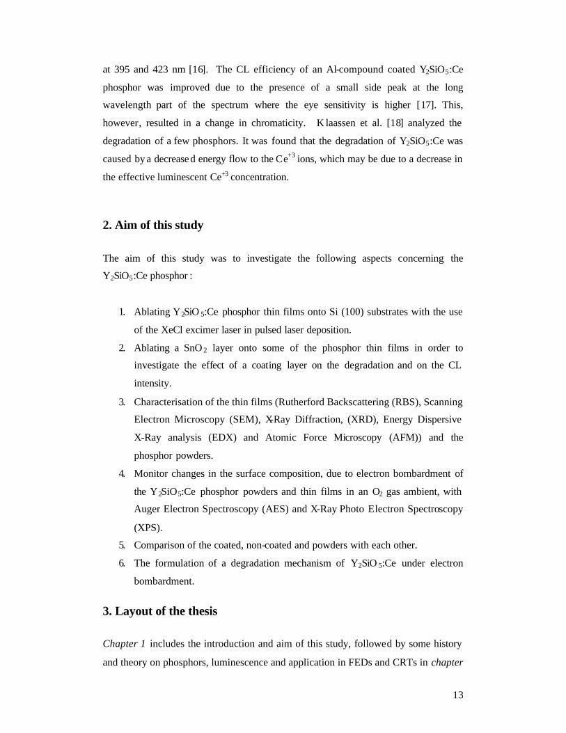
2.2 Field emission displays (FEDs)
FEDs are an alternative to CRTs, with the electron source an array of field emitter tips
as the cathode. Images are formed on the phosphor coated screen (anode) by the
impingement of electrons, emitted from the emitter tips, arranged in a grid. Each
phosphor pixel has its own set of field emitters [8, 9] (see figure 4).
A – Cathode C – Anode
E – Electron beams
B – Conductive coating
D – Phosphor coated screen F – Shadow mask
20
Figure 4: Schematic diagram of a FED [10].
The emitter tips are either made of metals like molybdenum, tungsten, platinum, or of
semiconductors like silicon or diamonds. The substrate supporting the tips is covered
by a dielectric film that provides isolation. A metal thin film deposited over this
dielectric layer serves as a gate electrode or a focusing electrode to improve the
resolution of the FED pixels.
The electrons tunnel from the array of tips and get accelerated towards phosphors
placed between a few micrometers to a few millimetres away from the tip. The
phosphors may be patterned to define the pixel, in which case three different
phosphors are deposited to achieve the primary colours of red, green and blue [11].
As mentioned before, FEDs need improvement in conditions for ideal operation such
as low voltages, high pressures and high current densities. Research on finding the
‘best’ phosphor for ideal operation in FEDs, led to the investigation of critical
properties such as luminescence, brightness, chromaticity, efficiency, conductivity,
particle size and maintenance. [11].
2.3 Emission of light
Light is a form of energy. To create light, another form of energy must be supplied.
There are two common ways for this to occur, incandescence and luminescence.
1/10’’
Phosphors
Electrons
Gate Microtips

21
2.3.1 Incandescence Incandescence is light from heat energy. If something is heated to a high enough
temperature it will begin to glow. When the tungsten filament of an ordinary
incandescent light bulb is heated it glows brightly. The sun and stars glow by
incandescence. Incandescent light is produced by lattice vibrations, called phonons,
which emit part of their energy in the form of electromagnetic radiation [12].
2.3.2 Luminescence Luminescence takes place at normal and low temperatures. Light emission is
produced by the relaxation of electrons from excited to ground states which produces
photons with energies equal to the energy difference between the two transition states.
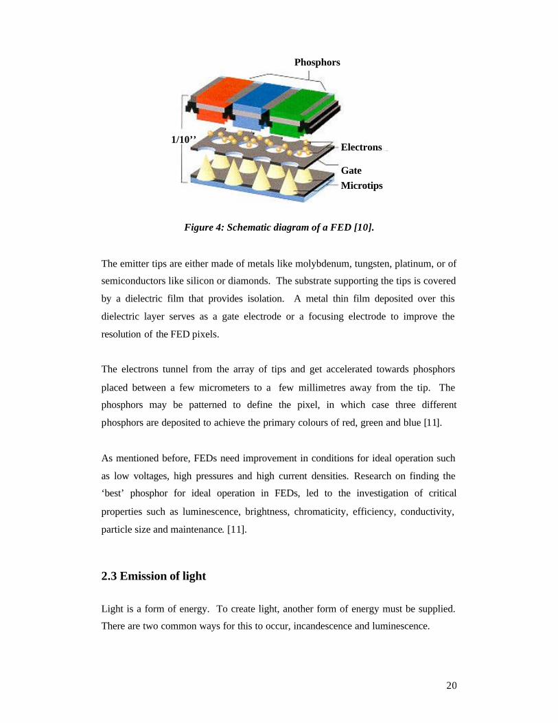
The most common techniques of excitation are i) photoluminescence, ii)
cathodoluminescence, iii) thermoluminescence and iv) electroluminescence.
i) Photoluminescence: This is luminescence by which electromagnetic radiation, i.e. photons, are used to
excite the material, usually done by ultraviolet light.
ii) Cathodoluminescence: This is the process by which a beam of electrons excites the material to luminesce.
Figure 5 shows a schematic diagram of luminescence process where photons are
emitted from excitation electron beam bombardment.
22
Figure 5: Schematic diagram of photons emitted by excitation occurring due to an
electron beam bombardment [13].
iii) Thermoluminescence Thermoluminescence is phosphorescence triggered by temperatures above a certain
point. This should not be confused with incandescence, which occurs at higher
temperatures; in thermoluminescence, heat is not the primary source of the energy,
only the trigger for the release of energy that originally came from another source. It
may be that all phosphorescent materia ls have a minimum temperature; but many
have a minimum triggering temperature below normal temperatures and are not
normally thought of as thermoluminescent materials [12].
iv) Electroluminescence This process occurs if a high electric field is applied across the luminescent material.
Electron-hole pairs get excited due to the applied field and as they recombine, they
emit photons [1, 12].
Luminescent materials are either electrically semiconducting (band gaps < 3 eV) or
insulating (band gaps > 3 eV). The difference in band gaps give rise to two
mechanisms of luminescence; band gap and characteristic luminescence.
Electron beam
Transmitted electrons
Specimen current
Secondary electrons
Characteristic X -rays Backscattered electrons
Cathodoluminescence
Auger electrons

23
2.4 Band gap luminescence
Band gap luminescence is light emission from semiconductors due to different crystal
structures. A crystal consists of a periodic arrangement of atoms, which is called a
crystal lattice. There are many different kinds of crystal lattices and are classified
according to their symmetries. In an isolated state, each atom has electrons that exist
in discrete electronic energy levels and the states of these bound electrons are
characterized by atomic wave functions. Their discrete energy levels, however, will
have finite spectral width in the condensed state because of the overlaps between
electronic wave functions belonging to different atoms. This is because electrons can
become itinerant between atoms, until finally they fall into delocalized electronic
states called electronic energy bands. The lower energy state, the valence band, gets
occupied by electrons originating from bound electrons of atoms.
The energy bands having higher energies are not occupied by electrons at 0 K and are
called conduction bands. Usually, in mate rials having crystal symmetries such as
zinc-blende structures, there is no electronic state between the top of the valence band
(the highest state of occupied bands) and the bottom of the conduction band (the
lowest state of unoccupied bands); this region is called the band gap. Unoccupied
states are called conduction bands, due to the fact that an electron in a conduction
band is almost freely mobile if it is excited from a valence band.
Electrons in valence bands cannot be mobile because of a fundamental property of
electrons, i.e. only two electrons (spin up and down) can occupy an electronic state. It
is therefore necessary for electrons in the valence band to have empty states in order
for them to move freely when an electric field is applied. After an electron is excited
to the conduction band, a hole that remains in the valence band behaves as if it were a
mobile particle with a positive charge. This particle is called a hole [1]. Figure 6
shows a schematic diagram of excitation to the conduction band and relaxation to the
valence band.

24
Figure 6: Schematic diagram of excitation to the conduction band and donor level
and relaxation to the valence band and acceptor level.
Excitation occurs due to energy transfer from the incident, high energy, particles to
electrons in the valence band. If the energy transferred is high enough the electrons
get excited to the higher energy levels. Relaxation (dotted lines) is the release of the
extra energy as a photon while it is de-excited back to the lower energy levels, thus
luminescence occurs
A material having the above mentioned energy bands is called a semiconductor and is
most commonly used for conduction purposes, other than for luminescence in
phosphors. Semiconductors fall on the conduction spectrum between an insulator and
a full scale conductor. Empty bands, which contain no electrons, are not expected to
contribute to the electrical conductivity of a material. Partially filled bands contain
electrons as well as available energy levels at slightly higher energies. These
unoccupied energy levels enable carriers to gain energy when moving in an applied
electric field. Electrons in a partially filled band therefore contribute to the electrical
conductivity of the material.
One of the main reasons that semiconductors are useful in electronics is that their
electronic properties can be greatly altered in a controllable way by adding small
amounts of impurities. These impurities are called dopants. Heavy doping of a
semiconductor can increase its conductivity by a factor greater than a billion.
Conduction band
Valence band
Donor Level
Acceptor Level
Band Gap
Incident

25
When semiconductors (the host material) are doped with impurities, the lattice of the
semiconductors is distorted and the energy level structures of the semiconductors are
also affected. For example, when in Si an As atom (Group V) is substituted for a Si
atom (Group IV), one electron in the outermost electronic orbit in the N shell of the
As atom is easily released and moves almost freely in the Si lattice, because the
number of electrons in the N shell of As (5) is one more than that in the M shell of Si
(4). Thus, impurities that supply electrons to be freed easily are called donors.
On the contrary, when a Ga atom (Group III) is substituted for a Si atom, one electron
is attracted from a Si atom, forming a hole that moves freely in the Si lattice. Thus,
impurities that supply free holes easily are called acceptors. In a donor, one excess
electron orbits around the positively charged nucleus, as in a hydrogen atom. This
electron moves around in a semiconductor crystal so that the Coulomb interaction
between the nucleus and the electron is weakened. The radius of the electron orbit
becomes large under these conditions and the electron is greatly affected by the
periodic potential of the crystal.
Therefore, the excess electron of the donor can be released from its nucleus by an
excitation of small energy. This means that the donor level is located very close to
the bottom of the conduc tion band, as shown in figure 6. Similarly the acceptor level
is located very close to the top of the valence band. Impurity levels with small
ionization energies are called shallow impurity levels; others can be located very deep
in the forbidden band. Luminescence takes place through these impurity levels with
wavelengths longer than the band gap wavelength [1].
If a semiconductor has equal numbers of electrons and holes, which means no
impurities or that the semiconductor is pure enough that the impurities in it, do not
appreciably affect its electrical behaviour, it is called an intrinsic semiconductor. The
carriers in this case are created by thermally or optically excited electrons from the
full valence band to the empty conduction band. The concentration of carriers in an
intrinsic semiconductor is strongly dependent on the temperature. At low
temperatures, the valence band is completely full, making the material an insulator.
Increasing the temperature leads to an increase in the number of carriers and a
corresponding increase in conductivity. A semiconductor that has been doped with

26
impurities to modify the number and type of free charge carriers present is called an
extrinsic semiconductor [14, 15].
2.5 Characteristic luminescence
Characteristic luminescence occurs by doping the host lattice with either transition
(3d) or rare-earth (4f) metal ions (impurities) that substitute for host lattice cations.
An electron gets excited to a higher energy level in the atom itself, see figure 7.
Rare earth ions from Ce3+ (atomic number of 58) to Yb3+ (70) have partially filled 4f
orbitals with energy levels characteristic to each ion and show a variety of
luminescent properties around the visible region. Many of these ions can be used as
luminescent ions in phosphors. There are 15 rare earth materials and the lanthanides
are those rare earths with the atomic numbers between 57 (La) and 71 (Lu). The 4f
electronic energy levels of lanthanide ions are characteristic of each ion.
Figure 7: Schematic diagram of how atoms emit light [16].
The levels are not affected much by the environment because 4f electrons are shielded
from external electric fields by the outer 5s2 and 5p6 electrons. This is in strong
contrast with transition metal ions, whose 3d electrons, located in an outer orbit, are
heavily affected by the environmental or crystal electric field [1]. Typical phosphors

27
used in CRTs and FEDs consist of a host matrix doped with activators such as the rare
earths (4f) and the transition metals (3d) [3].
2.6 Y2SiO5:Ce
Y2SiO5:Ce is a blue emitting, rare earth doped phosphor that is currently being
investigated for use in FEDs. Light emission is due to characteristic luminescence
where electron hole pairs are created in the atom itself, emitting photons as they
recombine. Ce3+ (Trivalent Cerium) has only one electron in the 4f shell, with an
electron configuration of [Xe].4f1.5d1.6s2. The 4f energy level splits into the 2F5/2 and
the 2Ff7/2 levels due to the electron having the ability to exhibit a + 1/2 or – 1/2 spin.
Light emission is due to the 5d ? 4f transition, resulting in the double shoulder peak
see figure 8 [5, 17].
Figure 8: (Y 1-xCex)2SiO5 emission spectra from Bosze et al [18].
The primary electrons get scattered throughout the host crystal, eventually
transferring energy to the Ce3+ ion (situated in the band gap of the host material)
resulting in excitation of the 4f1 electron. The luminescence photon energy depends
strongly on the structure of the host crystal through the crystal-field splitting of the 4f
state [1].
If an atom in a crystal is surrounded by ions, there exist s a “crystal field” due to the
interactions of the ions on the atom. Due to the symmetric effects, this crystal field
causes the energy levels of the atom to split. A splitting of energy levels (“crystal
field splitting”) occurs because the orientation of the “d” orbital wave function will
increase the electron energy when the orbital is located in a region of high electron

28
density. In crystals the dxy, dxz, dyz, dz2 and dx
2-y
2 energy orbitals, see figure 9, split
up, depending on their cation’s coordination [19].
Figure 9: Schematic diagram of the 5 d energy orbitals in an atom [20].
In atoms, all “d” orbitals have the same energy because their only difference is the
orientation of the orbitals. However, in a molecule, the outermost electrons may
interact with other electrons if they are orientated correctly.
The 5d orbitals of an atom have the same energy associated with them. However, if
an outside force is brought near the atom, the orientations of the different “d” orbitals
cause them to act differently from one another. The electrons from the other atoms
surrounding the specific atom, cause the “d” orbitals to split in regards to their energy.
The splitting of the orbitals is called crystal field splitting, as mentioned above.
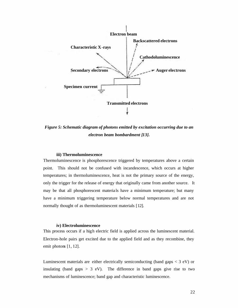
Figure 10 shows the energy levels of an atom.
dxy orbital dxz orbital dyz orbital
dx2-y
2 orbital dz2 orbital
29
Figure 10: Schematic diagram of the Orbital Energies of an atom [21].
The colours of many solids are due to the crystal field splitting of the “d” orbitals.
When a transition metal is surrounded by anions (as in a crystal), the “d” orbitals are
no longer all the same energy. The anions increase the energy of the orbitals closest
to it. The other orbitals must decrease in energy.
Figure 11 shows the yttrium orthosilicate (Y2SiO5) structure where four of the oxygen
atoms are bound in a silicon tetrahedron with each corner joining two yttrium
octahedrons and the fifth oxygen atoms, which are not involved with the silicon
tetrahedron, are shared between four yttrium octahedrons in a rod-like chain [ 22].
There are many types of silicates, whose properties depend on the number of oxygen
atoms that are charged instead of bonded and the cations that pair with the negative
charge [23].
Y2SiO5:Ce is highly stable physically and chemically with respect to time and
temperature as compared with other well-studied phosphor materials like ZnS and
CdS. It is studied for its polymorphous nature and interesting properties related to its
luminescence when doped with various rare earth ions [24].
Orbital Energies
Ene
rgy

30
Figure 11: Schematic crystal structure of Y2SiO5 [22].
SiO4 YO6

31
References
1. Shigeo Shionoya and William M. Yen, Phosphor Handbook, CRC Press
LLC, Boca Raton, (1999) p. 4, 21, 49, 61, 85, 178, 186.
2. After glow decay [Online]. Available from
http://www.duracorp.com/Articles/GlowAndBehold.htm [Accessed 9 March
2006].
3. A. M. Srivastava and C. R. Ronda, Phosphors, Electrochem. Soc. Inter,
(2003) 48.
4. T. A. Trottier, H. C. Swart, S. L. Jones, J. S. Sebastian and P. H. Holloway,
J. SID, 4/4 (1996) 351.
5. E. J. Bosze, G. A. Hirata, J. McKittrick and L. E. Shea, Mat. Res. Soc.
Symp, 508 (1998) 269.
6. Visible light spe ctrum [online]. Available from
http://www.bmb.leeds.ac.uk/pdt/science.htm [Accessed 10 January 2005].
7. J. Sebastian, S. Jones, T. Trottier, H. C. Swart and P. Holloway, J. SID, 3/4
(1995) 147.
8. The Cathode Ray Tube [online]. Available from
http://electronics.howstuffworks.com/tv3.htm [Accessed 10 January 2006].
9. P. H. Holloway, T. A. Trottier, B. Abrams, C. Kondoleon, S. L. Jones, J. S.
Sebastian, and W. J. Thomas, J. Vac. Sci. Technol. B , 17(2) (1999) 758.
10. Field Emission Displays [online]. Available from http://216.122.210.132/
tech/tech.htm [Accessed 10 January 2005].
11. P. H. Holloway, J. Sebastian, T. Trottier, H. C. Swart and R. O. Peteren,
Solid State Technol, (1995) 47.
12. Luminescence, [online]. Available from
http://www.uvminerals.org/luminese.htm [Accessed 10 January 2006].
13. Cathodoluminescence [online]. Available from http://www.cmeba.univ -
rennes1.fr/niveau2/PagePrincipeMEB.htm [Accessed 12 January 2006].
14. B. Van Zeghbroeck, Principles of Semiconductor devices, (2004), Chapter 2
[online]. Available from http://ece-
www.colorado.edu/~bart/book/book/content5.htm [Accessed 20 January
2006].

32
15. Extrinsic semiconductors, [online]. Available from
http://www.doe.carleton.ca/~tjs/475_pdf_02/snew14.pdf [Accessed 15
January 2006].
16. Characteristic Luminescence [online]. Available from
http://www.kushkush.me.uk/ [Accessed 15 January 2006].
17. H. C. Swart and K. T. Hillie, Surf. Interface Anal, 30 (2000) 383.
18. E. J. Bosze, G. A. Hirata and J. McKittrick, Proc. Mater. Res. Soc, 558
(1999) 15.
19. Crystal Field Splitting [online]. Available from
http://scienceworld.wolfram.com/ [Accessed 13 February 2006].
20. 5d Orbitals [online]. Available from
http://cwx.prenhall.com/bookbind/pubbooks/hillchem3/medialib/media_port
folio/07.html [Accessed 20 January 2006].
21. Orbital energy diagrams [online]. Available from
http://colossus.chem. umass.edu/genchem/Whelan/110_Fall_2004_Daily.htm
l [Accessed 20 January 2006].
22. Reactions for Yttrium Silicate High-k Dielectrics, James Joseph Chambers,
Ph. D thesis, 2000 p. 33, 41.
23. Crystal Field Splitting [online]. Available from
http://www.wwnorton.com/chemistry/overview/ch10.htm [Accessed 13
February 2006].
24. N. Karar and H. Chander, J. Phys. D : Appl. Phys, 38 (2005) 3580.
33
Chapter 3
Degradation
This chapter contains the theory on the ESSCR model on degradation of phosphors
and the theory on defects and the effect that it may have in the crystal structure. It
also contains theory on the phenomenon of total internal reflection and ends off with a
summary of the results from literature studies.
Light efficiency of the FED display technology strongly depends on the phosphor
material. These phosphor materials are usually wide band gap semiconductors that
have been doped with impurities to modify the energy gap for the appropriate light
frequency output. The distinction between an impurity and a dopant is as follows:
Impurities are elements or compounds that are present from raw materials or
processing. For example, silicon crystals grown in quartz crucibles contain oxygen as
an impurity. Dopants are elements or compounds that are deliberately added, in
known concentrations, at specific locations in the microstructure, with an intended
beneficial effect on properties or processing [1].
3.1 Literature review on phosphor degradation
FEDs operation is based on cathodoluminescence (CL), similar to CRTs but with
different architecture. The huge surface to volume ratio associated with the FEDs’
system presents a new set of problems that affect the overall FED picture operation.
3.1.1 High pressures
The residual gases in FED vacuum devices are critical to its performance and lifetime.
These gases are hydrogen, oxygen, water, methane carbon monoxide and carbon
dioxide, thus resulting in the high pressure conditions for operation of FEDs. Some of
the sources of these gasses in sealed FEDs are out gassing, vaporization, leaks and
evolution of gasses from bulk solutions [2].

34
These gasses need to be removed and the vacuum maintained with a vacuum pump as
in the case of CRTs where barium (Ba) is used on the glass tube as a getter pump.
However, to add vacuum pumps or getter mechanisms is not always convenient and
not always possible for the sealed vacuum in FEDs.
These gases thus not only contaminate the field emitter tips but also cause degradation
of the phosphor materials via the electron stimulated surface chemical reaction
(ESSCR) (see Chapter 1). Degradation of sulphide based phosphors, for example,
resulted in the generation of volatile species such as SO2 and H2S. These volatile
species get created due to the reaction between the phosphor and reactive gas species
such as H2O, COx, H2, etc., via the electron stimulated reactions (ESSCR) [3].
Previous studies showed that the CL degradation rate is linearly dependant on oxygen
pressures. High oxygen pressures will increase the degradation rate [2, 4, 5].
3.1.2 Low voltages
Due to the small cathode – anode spacing (< 0.2 – 2 mm), the FED typically operates
at a voltage below that of a CRT. FEDs require higher efficiency at lower voltages
(lower than 10 kV, in comparison with CRTs that require voltages between 20 and 30
kV). The lower voltages mean FEDs operate with low energy electrons which have a
shallower penetration depth for cathodoluminescence (CL).
The penetration range of primary electrons only depends upon the beam energy.
Therefore a decrease in the primary electron beam energy would lead to a decrease in
the penetration depth. The penetration depth of injected primary electrons can be
calculated by the following relationship:
R = bV n (1)
where R is the penetration distance limit, V is the voltage (kV) and b and n are
empirical values for the phosphor. This means that at low voltages, luminance comes
from the surface region of the phosphor material [ 6].

35
Increasing the beam energy would thus lead to an increase in the number of generated
electron-hole pairs. Phosphor light intensity typically decreases faster than linearly
with a decrease in the operating voltage [7].
3.1.3 Be am energies
To maintain brightness and constant power, the FEDs require higher current
densities. Luminescence quenching may occur at high current densities. Quenching
is defined as the reduction of phosphor efficiency with changes of operating
parameters or time [3]. Brightness/intensity is directly proportional to the beam
power, P = VI, where I is the electron beam current and V the potential difference
between the tip and the metal gate.
Maintaining the power level means increasing the current when reducing the voltage.
However, low energy (1 – 2 kV) electron beam irradiation has been found to increase
degradation of CL intensity of phosphors used in FEDs which is consistent with an
electron stimulated surface chemical reaction (ESSCR) model [2, 8, 9, 10].
The degradation rate depends on the energy of the electron beam, decreasing with
increasing beam energy. However increasing the beam energy may also result in an
increase in local temperature and may lead to saturation, which affect the degradation
rate and the phosphor performance. It is known that the phosphor efficiency
decreases with increasing temperature (thermal quenching) [3].
3.1.4 Saturation
Saturation occurs due to ground state depletion whereby most of the centres are
already in the excited state, leaving an insufficient number of available centres in the
ground state to accept energy from excited carriers [11], resulting in a decrease in CL
intensity.

36
3.1.5 Thermal quenching
Thermal quenching occurs at high temperatures when the thermal vibrations of the
atoms surrounding the luminescent centre transfer the energy away from the centre
resulting in a non-radiative recombination, and the subsequent depletion of the excess
energy as phonons in the lattice [6]
3.1.6 Killers
If an impurity reduces the intensity of the luminescence, it is known as a killer. Any
impurity or a lattice defect can serve as a non-radiative recombination centre if it is
capable of capturing a carrier of one type and subsequently capturing the opposite
type of carrier [6].
3.1.6.1 Defects
The effect of defect formation on the phosphor surface can influence the CL intensity
and thus lead to degradation. Defects can lead to a decrease in CL intensity for
example whereby a non–luminescent trap is formed during electron bombardment
(ESSCR) [10] or it can increase the CL intensity such as the intrinsic defects in SiO2
[13].
Point defects are localized disruptions in perfect atomic or ionic arrangements in a
crystal structure. The disruption affects a region involving several atoms or ions.
These imperfections may be introduced by movement of the atoms or ions when they
gain energy by heating, during processing of the material, by introduction of
impurities, or doping.
A point defect typically involves one atom or ion, or a pair of atoms or ions, and thus
is different from extended defects, such as dislocations, grain boundaries, etc. The
next three sections describe the, i) vacancy, ii) interstitial and iii) substitutional point
defects.

37
i) Vacancies A vacancy is produced when an atom or an ion is missing from its normal site in the
crystal structure. Vacancies are introduced into metals and alloys during
solidification, at high temperatures, or as a consequence of radiation damage.
Vacancies play an important role in determining the rate at which atoms or ions can
move around, or diffuse in a solid material, especially in pure metals.
ii) Interstitial defects An interstitial defec t is formed when an extra atom or ion is inserted into the crystal
structure at a normally unoccupied position. Interstitial atoms or ions, although much
smaller than the atoms or ions located at the lattice points, are still larger than the
interstitial sites that they occupy. Consequently, the surrounding crystal region is
compressed and distorted.
iii) Substitutional defects A substitutional defect is introduced when one atom or ion is replaced by a different
type of atom or ion. The substitutional atoms or ions occupy the normal lattice site.
These atoms or ions may either be larger than the normal atoms or ions in the crystal
structure, in which case the surrounding interatomic spacings are reduce d, or smaller
causing the surrounding atoms to ha ve larger interatomic spacings [1].
Another type of killer action, that does not necessarily require free carriers for its
quenching mechanism, is the removal of energy from the nearby luminescent centre
by resonance energy transfer [6]. Atoms and molecules adsorbed at the surface of the
phosphor particles and defects in the crystal can often become killers and may
produce a “dead voltage layer”.
3.1.7 Extra layer
Degradation is dependant on energy loss [14]. Itoh et. al. [15] showed the formation
of a sulphide on the surface of the ZnS:Zn phosphor under electron irradiation in a

38
H2O vapour ambient. This extra sulfate layer was the result of the dissociation of
H2O on the phosphor surface. The ESSCR as mentioned before, (Chapter 1) is a
degradation mechanism, postulated by Swart et. al. [5, 10] and Sebastian et. al. [9]
whereby a chemical change occurs on the surface of the phosphor, resulting in the
formation of an extra layer on the surface with a different chemical composition. The
chemical change on the surface is a result of electron beam irradiation in the presence
of an ambient gas pressure.
According to the ESSCR model, the electron beam used to irradiate the phosphor
sample, dissociates the water vapour and oxygen gas into atomic species which then
react with the phosphor surface, resulting in the chemical change and formation of
different chemical compounds [5, 7, 9].
These new compounds on the surface can be non – luminescent and thus reducing the
luminescence of the material, resulting in the “dead layer” on the phosphor surface.
Oosthuizen et al. [16] proved that a ZnO layer was formed on the surface after
electron bombardment with the release of SO2 gas.
If there is adventitious carbon present on the phosphor surface, the atomic species
would then also react with the carbon to form volatile compounds resulting in
depletion of carbon on the surface [10, 11].
The carbon on the surface leads to another extra layer which the incoming primary
electrons have to penetrate before they reach the phosphor bulk for CL excitation.
Thus the thicker the surface before entering the bulk, the greater the probability of
ene rgy loss through collisions and scattering, see Figure 1, resulting in a lower CL
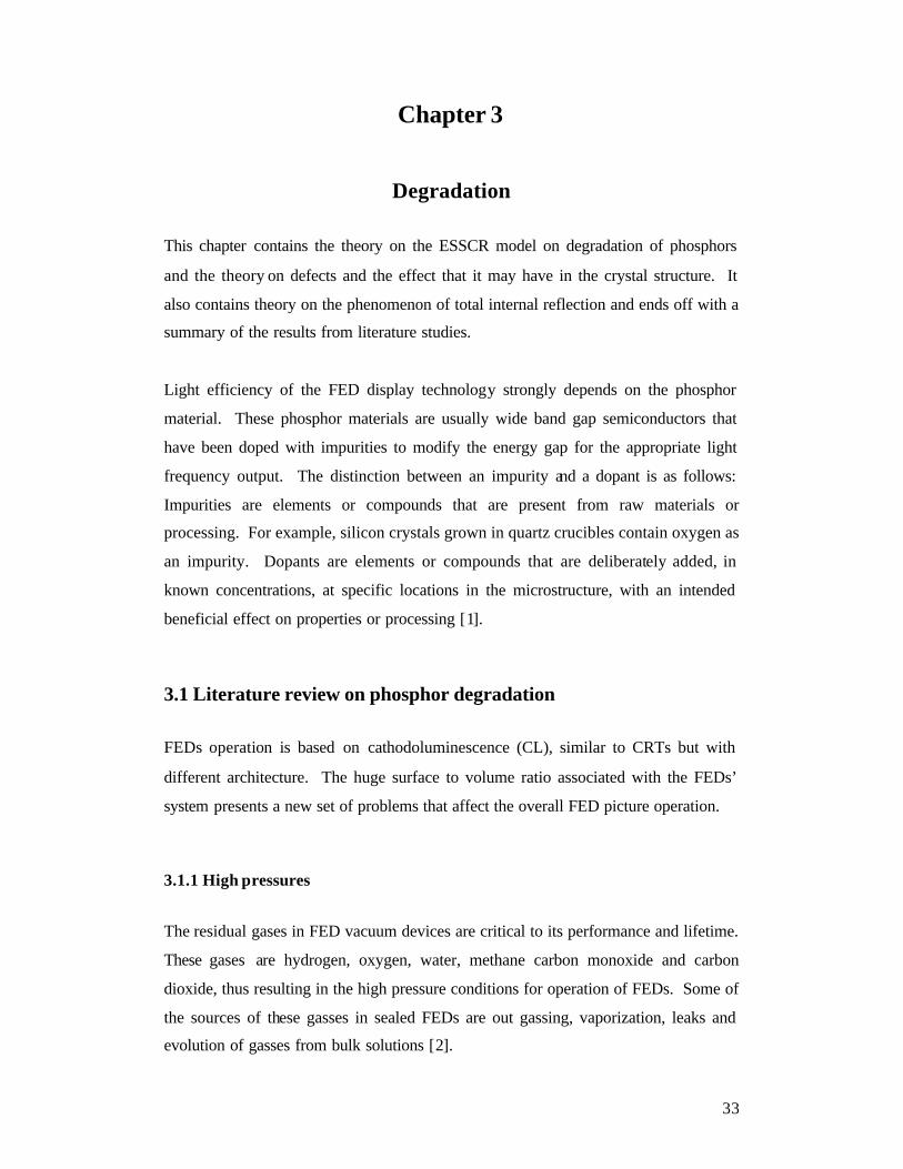
intensity [1, 8 - 11].
39
(a) (b)
Figure 1: Schematic diagram proposing an extra layer on the phosphor surface due
to ESSCR, a) before and b) after degradation .
3.1.8 Surface charging
When the primary electron beam is incident on a phosphor, secondary, back-scattered
and Auger electrons are emitted from the surface at a rate different from the primary
beam current, and this rate is dependant upon the beam energy and the phosphor
properties. Therefore, positive or negative charges may accumulate on and below the
surface to develop a space charge layer.
The accumulated charge alters the surface potential, which in turn alters the kinetic
energy of the primary electrons and also increases the probability that the electron –
hole pair will be swept apart before they can recombine radiatively. In some
situations like in insulators such as La2O2S:Eu, an internal electric field may form,
independent of whether there is zero, positive or negative charging effects relative to
ground. The internal electric field may increase with an increase of electron beam
current densities.
The fact that an internal field is induced during electron bombardment of phosphors
and that transport of charge carriers is affected by electric fields suggest a possible
mechanism for the CL quenching observed with time and increasing current density
[3].
Electron beam Electron beam
Phosphor bulk Phosphor bulk
Extra layer

40
3.2 Some results from literature
There are many different ways of phosphor sample preparation such as laser ablation
[8], sol-gel chemistry [17] and magnetron sputtering [18]. Pulsed laser deposition
(PLD) has advantages over other deposition techniques with an important feature of
maintaining the stoichiometry of the target material. Surface morphology and
thickness can be controlled by varying some of the growth parameters, such as the
ambient gas pressure and the number of pulses [19]. PLD was used for thin film
preparation in this research study.
Trottier et al. [4] reported that the degradation rate of ZnS phosphors was about 3
times faster than that of Y2O2S:Eu, which led to more research being done on oxide
based phosphors.
Research on Y2SiO5:Ce proved it to be a good candidate for ZnS:Ag blue emitting
phosphor [13, 17, 20, 21, 22].
Holloway et al. [ 7] reported results on advantages of using thin film phosphors above
phosphor powders. Powders have a much higher CL intensity but a significant
advantage of thin films would be lower out gassing [8]. Therefore this research study
includes an investigation of both thin films and phosphor powders.
Fitz-Gerald et al. [23] reported on coating the phosphor surface in order to prevent
degradation. The results showed a much lower degradation rate with a CL brightness
decreasing by only 12%. The coated layer should be transparent and not detrimental
to the CL efficiency. Some of the thin films in this study were therefore coated with
SnO2 in order to investigate the effect of the coated layer on the CL intensity.
Hillie et al. [8] showed that the degradation rate was more severe in an O2 ambient
gas than in CO2. He also showed that the degradation depends on the energy of the
electron beam, which decreases with an increase in beam energy. [8, 14].

41
3.3 Total internal reflection
Total internal reflection is a phenomenon that occurs during light emission from thin
films that leads to a decrease in the CL intensity, due to some of the light that gets
reflected internally.
If light travels through a surface that separates two mediums, the light gets refracted.
Unless an incident beam of light is perpendicular to the surface, the light’s direction
of travel gets changed by refraction at the surface. Figure 2 shows a light beam
travelling from a glass medium to air.
Figure 2: Schematic diagram illustrating the effect of total internal reflection for a
light beam travelling from a glass medium to air.
Ray a , is perpendicular to the surface so part of the light gets reflected at the interface
and the rest travels through it without a change in direction. As the angle of incidence
increases, as for ray b, part of the light gets reflected and the rest gets refracted. The
angle of refraction increases until it reaches 90° as for ray c. The incident angle is
then said to be the critical angle,?c . For angles of incidence larger than the critical
angle, like ray d, there is no refracted ray and all the light is reflected. This effect is
called total internal reflection.
The critical angle can be calculated by using Snell’s Law:
n2 sin 2? = n1 sin 1? (2)
d a b c
?c

42
where n2 and n1 are dimensionless constants, called the index of refraction that is
associated with a medium involved in the refraction. This index of refraction of a
medium is equal to c/v , where c is the speed of light in vacuum and v the speed in that
medium. For vacuum, n is defined to be 1, and for air, n is very close to 1.0. By
taking n2 as the air medium and 2? to be 90°, 1? can be calculated as the critical angle
[24].

43
References
1. D. R. Askeland and P. P. Phule, The Science and Engineering of Materials,
Thompson Brooks/Cole, United States of America, (2003) p. 130.
2. P. H. Holloway, J. Sebastian, T. Trottier, S. Jones, H. C. Swart and R. O.
Peterson, Mat. Res. Soc. Symp. Proc , 424 (1997) 425.
3. J. Bang, B. Abrams and P. H. Holloway, J of Appl. Phys, 94(11) (2003)
7091.
4. T. A. Trottier, H. C. Swart, S. L. Jones, J. S. Sebastian and P. H. Holloway,
J. SID, 4/4 (1996) 351.
5. H. C. Swart, L. Oosthuizen, P. H. Holloway and G. L. P. Berning, Surf.
Inter. Anal, 26 (1998) 337.
6. Shigeo Shionoya and William M. Yen, Phosphor Handbook, CRC Press
LLC, Boca Raton, (1999) p. 36, 566.
7. P. H. Holloway, T. A. Trottier, B. Abrams, C. Kondoleon, S. L. Jones, J. S.
Sebastian and W. J. Thomas, J. Vac. Sci. Technol. B, 17(2) (1999) 758.
8. K. T. Hillie and H. C. Swart, Appl. Surf. Sci, 183 (2001) 304.
9. J. Sebastian, S. Jones, T. Trottier, H. C. Swart and P. Holloway, J. SID, 3/4
(1995) 147.
10. H. C. Swart, J. S. Sebastian, T. A. Trottier, S. L. Jones and P. H. Holloway,
J. Vac. Sci. Technol. A, 14(3) (1996) 1697.
11. D. M. de Leeuw and G. W.’t Hooft, J. of Lumin, 28 (1983) 275.
12. H. C. Swart and K. T. Hillie, Surf. Interface Anal, 30 (2000) 383.
13. L. N. Skuja and W. Entzian, Phys . Stat. Sol. (a), 96 (1986)191.
14. H. C. Swart, K. T. Hillie and A. P. Greeff, Surf. Interf. Anal, 32 (2001) 110.
15. S. Itoh, T. Kimizuka and T. Tonegawa, J. of Electrochrm. Soc, 136(6)
(1989) 1819.
16. L. Oosthuizen, H.C. Swart, PE Viljoen, PH Holloway, G. L. P. Berning,
Appl. Surf. Sci, 120 (1997) 9.
17. P. J. Marsh, J. Silver, A. Vecht and A. Newport, J. Lumin, 97 (2002) 229.
18. K. T. Hillie, C. Curren and H. C. Swart, Appl. Surf. Sci, 177 (2001) 73.

44
19. Chen Li-Chyng, Particulates generated by pulsed laser ablation, in Pulsed
Laser Deposition of Thin Films (eds. Chrisey D. B, Hulber, G. K), John
Wiley & Sons, Inc , New York, (1994) p. 167.
20. R. Y. Lee, F. L. Zhang, J. Penczek, B. K. Wagner, P. N. Yocom and C. J.
Summers, J. Vac. Sci. Technol. B, 16(2) (1998) 855.
21. X. Ouyang, A. H. Kitai and R. Siegele, Thin Solid Films, 254 (1995) 268.
22. E. J. Bosze, G. A. Hirata, J. McKittrick and L. E. Shea, Mat. Res. Soc.
Symp, 508 (1998) 269.
23. J. M. Fitz-Gerald, T. A. Trottier, R. K. Singh and P. H. Holloway, Appl.
Phys. Lett, 72 (1998) 1838.
24. Halliday, Resnick and Walker, Fundamentals of Physics, John Wiley &
Sons, Inc, United States of America, (2001) p. 823.
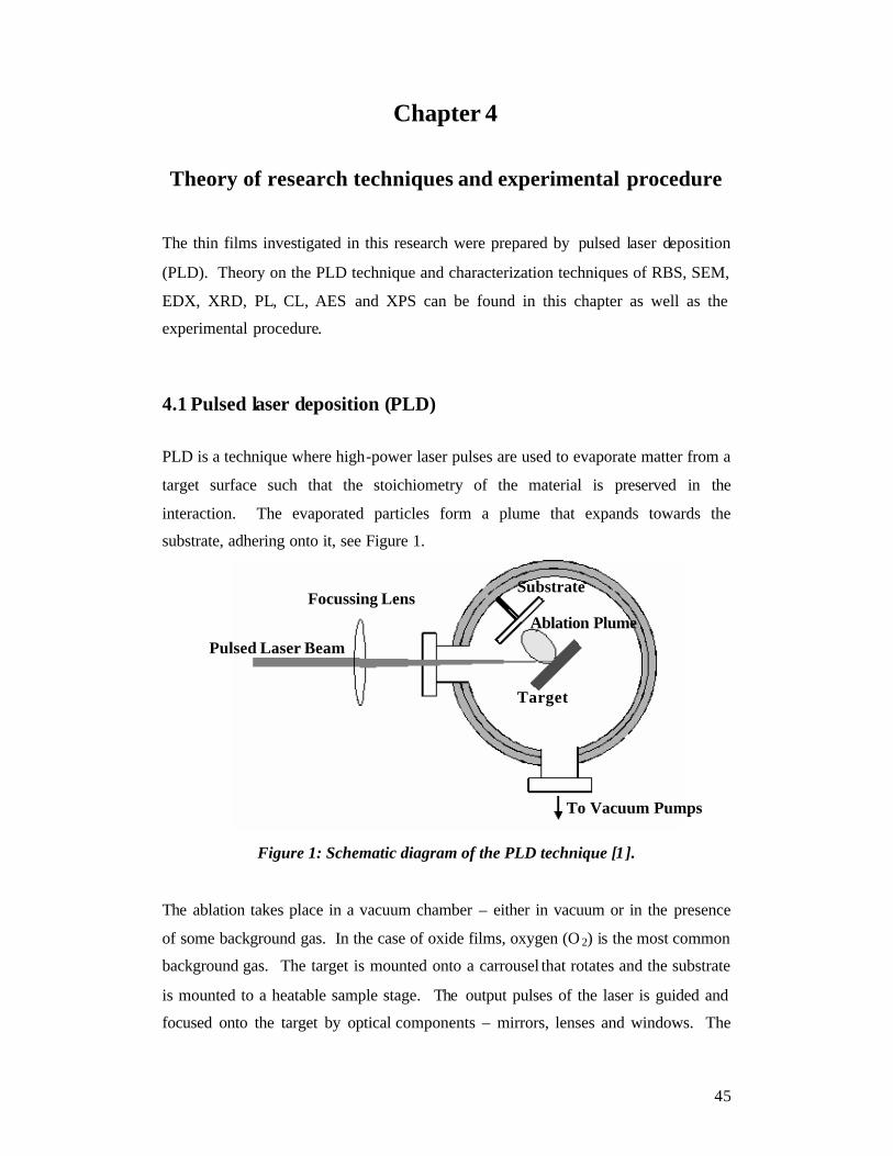
45
Chapter 4
Theory of research techniques and experimental procedure The thin films investigated in this research were prepared by pulsed laser deposition
(PLD). Theory on the PLD technique and characterization techniques of RBS, SEM,
EDX, XRD, PL, CL, AES and XPS can be found in this chapter as well as the
experimental procedure.
4.1 Pulsed laser deposition (PLD)
PLD is a technique where high-power laser pulses are used to evaporate matter from a
target surface such that the stoichiometry of the material is preserved in the
interaction. The evaporated particles form a plume that expands towards the
substrate, adhering onto it, see Figure 1.
Figure 1: Schematic diagram of the PLD technique [1].
The ablation takes place in a vacuum chamber – either in vacuum or in the presence
of some background gas. In the case of oxide films, oxygen (O 2) is the most common
background gas. The target is mounted onto a carrousel that rotates and the substrate
is mounted to a heatable sample stage. The output pulses of the laser is guided and
focused onto the target by optical components – mirrors, lenses and windows. The
Focussing Lens
Pulsed Laser Beam
Substrate
Ablation Plume
Target
To Vacuum Pumps

46
most important parameters to control are i) repetition rate of the laser, ii) the substrate
temperature, iii) the target to substrate distance, iv) the laser energy and v) the
pressure of the background gas [2].
4.1.1 Advantages of PLD
- It is conceptually simple: a laser beam vaporizes a target surface, producing a film
with the same composition as the target.
- It is versatile: many materials can be ablated in a variety of gases.
- It is cost effective: one laser can serve many vacuum systems.
- It is a fast technique: high quality samples can be grown in 10 or 15 min [3].
The generation of particles by PLD is of great significance in the deposition of thin
films. The particles can be classified into three categories. A specific type of particle
is distinguished by whether the original matter, when just ejected from the target, is in
the solid, liquid or vapour state. In general, the size of the particles formed from the
vapour state tends to be in the nanometre range, while the other two counterparts are
in the micron and submicron range.
The shape of the particles ejected formed from the liquid target tends to be spherical.
While the particles formed from solid targets tend to be irregular in shape. The shape
of the particles formed from vaporized species may be spherical or polyhedral.
Surface morphology and thickness can thus be controlled by varying some of the
growth parameters, such as the laser fluence, the laser wavelength, the ambient gas
pressure and the target-to-substrate distance [10, 5].
4.1.2 Laser fluence
For a chosen material and a fixed laser wavelength, the laser fluence (amount of
energy per pulse per unit area) has the most significant effect on the particle size and
density. The laser fluence can be varied by varying the laser power or the laser spot
size. At constant laser power, the particle number density is usually higher with
tighter focus [5].

47
4.1.3 Laser wavelength
The laser wavelength, ?, comes into play mainly in the effectiveness of the absorption
of the laser power by the target. The primary effect of the laser wavelength on
particle generation is most likely due to the difference in the absorption coefficient
when different laser wavelengths are used. Measurements that were done by Kautek
et al. [5] on a 1 µm thick YBCO film, indicated the absorbance decreases with
increasing wavelength. A decrease in absorbance result in a deeper penetration depth
that would lead to more and larger particles generated by the laser [5].
4.1.4 Ambient gas pressure
The effect of inert ambient gas pressure on the nature of particles is most likely
related to the increased collisions between the ejected species and the ambient gas as
the ambient gas pressure increases. When a laser deposition experiment is done in
vacuum, there are virtually no collisions between the ejected species before they reach
the substrate. When the ambient gas pressure increases, the vapour species can
undergo enough collisions that nucleation and growth of these vapour species to form
particles can occur before their arrival at the substrate.
Since the growth mechanism is by diffusion, the residence time for the particles in the
vapour controls the size of the particles. The longer the residence time, as is the case
with increased ambient gas pressure, the larger the particle size [5].
4.1.5 Target-to-substrate distance
When a PLD experiment is done in a poor vacuum, with an ambient gas, or at a
substantially large target-to-substrate distance in which coalescence of particles can
take place, markedly different particle appearance may occur, depending on the
position of the substrate. The specific effects of target-to-substrate distance and
ambient gas pressure are interrelated.

48
Dyer et. al. [5] have shown that E/P0 is the scaling parameter for plume range, where
E is the laser-pulse energy and P0 the background gas pressure. The length of the
plume is L a (E/ P0)1/3 ? with ? the ratio of specific heats of elements in the plume.
When the target-to-substrate distance is much smaller than L there is no marked
difference in particle size and density. As the target-to-substrate distance increases,
the particle sizes increase. If the substrate is located far beyond L, the adhesion to the
substrate of ejected matter is poor.
The particle size and density, thus strongly depend on the deposition parameters and
by proper choice of parameters, particle generation can be minimized. Figure 2
shows the PLD system at Stellenbosch University that was used for the thin film
ablation in this study.
Figure 1: PLD System used for thin film ablation.
4.2 Rutherford backscattering spectrometry (RBS)
Film thicknesses in this study, were determined with RBS. It is a technique were
energetic helium ions (4He+), typically having energies of several million electron
volts, are directed at the sample of interest. Most of the ions implant into the sample,
however some of these ions backscatter from the nuclei in the near surface (1 to 2
micron) of the sample, see figure 3.
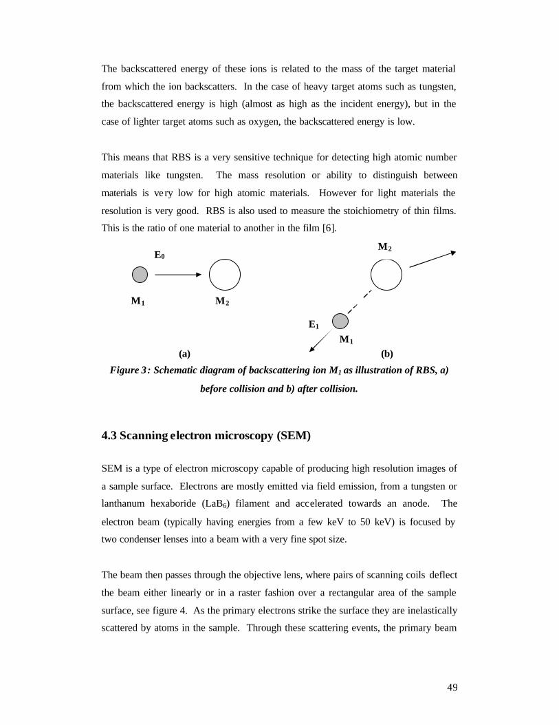
49
The backscattered energy of these ions is related to the mass of the target material
from which the ion backscatters. In the case of heavy target atoms such as tungsten,
the backscattered energy is high (almost as high as the incident energy), but in the
case of lighter target atoms such as oxygen, the backscattered energy is low.
This means that RBS is a very sensitive technique for detecting high atomic number
materials like tungsten. The mass resolution or ability to distinguish between
materials is very low for high atomic materials. However for light materials the
resolution is very good. RBS is also used to measure the stoichiometry of thin films.
This is the ratio of one material to another in the film [6].
(a) (b)
Figure 3: Schematic diagram of backscattering ion M1 as illustration of RBS, a)
before collision and b) after collision.
4.3 Scanning electron microscopy (SEM)
SEM is a type of electron microscopy capable of producing high resolution images of
a sample surface. Electrons are mostly emitted via field emission, from a tungsten or
lanthanum hexaboride (LaB6) filament and accelerated towards an anode. The
electron beam (typically having energies from a few keV to 50 keV) is focused by
two condenser lenses into a beam with a very fine spot size.
The beam then passes through the objective lens, where pairs of scanning coils deflect
the beam either linearly or in a raster fashion over a rectangular area of the sample
surface, see figure 4. As the primary electrons strike the surface they are inelastically
scattered by atoms in the sample. Through these scattering events, the primary beam
M1
M1
M2
M2 E0
E1

50
effectively spreads and fills a teardrop-shaped volume, known as the interaction
volume, extending about 1 to 5 µm below the surface.
Interactions in this region lead to the subsequent emission of secondary electrons
which are then detected, converted to a voltage and amplified to produce an image.
X-rays, which are also produced by the interaction of electrons with the sample, may
also be detected in a SEM equipped for Energy dispersive X-ray spectroscopy (EDX)
[7].
Figure 4: Schematic diagram of SEM [8].
There are two basic types of SEMs. The regular SEM, which requires a conductive
sample and an environmental SEM used to examine a non-conductive sample without
coating it with a conductive layer. Non-metallic samples, such as bugs, plants and
ceramics should be coated so they are electrically conductive for SEM imaging.
Figure 5 shows a photograph of the SEM system used in this research study.
Absorbed electrons
X-Ray Detector
Cathodo- luminescence
Screen
Secondary electron detector
Electromagnetic Lenses
Scan coils
Electron Gun
Scan Generator and magnification

51
Figure 5: SEM system used for measurements at the CSIR-NML Pretoria.
4.4 Energy dispersive spectrometry (EDS).
The surface chemical composition of the thin film grown in this study was determined
by EDS spectroscopy in conjunction with SEM. Chemical analysis of a specimen can
be obtained by measuring the energy and the intensity distribution of the X-ray signal
generated by a focused electron beam impinging the sample. The electron gun of a
scanning electron microscope is the source of the electron beam.
X-rays are the result from inelastic or energy-loss interactions between the incident
electrons and the specimen atoms. The incident electrons interact with core electrons
and by transferring sufficient energy to it, it can be removed from the target atom. A
characteristic X-ray is occasionally emitted when the ionized atom ‘relaxes’ to a
lower energy state by the transition of an outer-shell electron to the vacancy in the
core shell. The X-ray is called characteristic because its energy equals the energy
difference between the two levels involved in the transition and this difference is
characteristic of the material, see figure 6.

52
Figure 6: X-Rays emitted during EDS analysis [9].
The output of an EDS analysis is an EDS spectrum, see figure 7. The EDS spectrum
is just a plot of how frequently an X-ray is received for each energy level. The EDS
spectrum normally displays peaks corresponding to the energy levels for which the
most X-rays have been received. Each of these peaks is unique to an atom, and
therefore characteristic of a specific element. The higher a peak in a spectrum, the
more concentrated the element in the specimen will be [9].
Fig ure 7: Example of an EDS spectrum of a Y 2SiO5:Ce phosphor thin film.
EDS is used in hundreds of applications where knowledge of chemical information on
the micro- scale is important. Major users include industry, university research
institutes and government facilities. Typical applications are in materials research,
Electrons
X-Rays to Spectrometer
Zone of Fluorescent Excitation
Zone of Primary Electrons

53
quality control, failure analysis, and forensic science. Industries that commonly use
this technique include: semi-conductor and electronics, metals, ceramics, minerals,
manufacturing, engineering, nuclear, paper, petroleum, bio-science, and the motor
industry [9, 10].
4.5 Atomic force microscopy (AFM)
AFM stands for Atomic Force Microscopy or Atomic Force Microscope and is often
called the "Eye of Nanotechnology". AFM, also referred to as SPM or Scanning
Probe Microscopy, is a high-resolution imaging technique that can resolve features as
small as an atomic lattice in the real space. It allows researchers to observe and
manipulate molecular and atomic level features [11].
The atomic force microscope is one of about two dozen types of scanned-proximity
probe microscopes, used to study surface topography and morphology. All of these
microscopes work by measuring a local property - such as height, optical absorption,
or magnetism - with a probe or "tip" placed very close to the sample. The small
probe -sample separation (on the order of the instrument's resolution) makes it possible
to take measurements over a small area [12].
AFM works by bringing a cantilever tip in contact with the surface to be imaged, as
shown in figure 8. An ionic repulsive force from the surface applied to the tip bends
the cantilever upwards. The amount of bending, measured by a laser spot reflected on
to a split photo detector can be used to calculate the force. By keeping the force
constant while scanning the tip across the surface, the vertical movement of the tip
follows the surface profile and is recorded as the surface topography by the AFM.

54
Figure 8: Schematic diagram of the AFM operated in repulsive contact mode [11].
AFM (figure 8) thus operates by measuring the attractive or repulsive forces between
a tip and the sample. In its repulsive "contact" mode, the instrument lightly touches a
tip at the end of a cantilever to the sample. As a raster-scan drags the tip over the
sample, some sort of detection apparatus measures the vertical deflection of the
cantilever, which indicates the local sample height. Thus, in contact mode the AFM
measures hard-sphere repulsion forces between the tip and sample.
In no contact mode, the AFM derives topographic images from measurements of
attractive forces; the tip does not touch the sample. AFMs can achieve a resolution of
10 pm, and unlike electron microscopes, it can image samples in air and under liquids.
AFM incorporates a number of refinements that enable it to achieve atomic-scale
resolution: [12]
• Sensitive detection
• Flexible cantilevers
• Sharp tips
• High-resolution tip-sample positioning
• Force feedback
Surface Atoms
Tip
Force
Tip Atoms
Line Scan
Cantilever
Laser Beam
Photo detector

55
4.6 X-ray diffraction (XRD)
The crystal structure of the phosphor sample used in this research study was
determined by XRD. The planes were calculated using Bragg’s Law by determining
inter planar distances.
4.6.1 Crystal structure
To the naked eye, a solid appears as a continuous rigid body. Experiments have
proved, however, that all solids are composed of discrete basic units called atoms.
These atoms are arranged in a highly ordered manner relative to each other. Such a
group of ordered atoms is referred to as a crystal. There are several types of
crystalline structure, depending on the geometry of the atomic arrangement;
knowledge of these is important in solid -state physics because these structures usually
influence the physical properties of solids.
A solid is said to be a crystal if the atoms are arranged in such a way that their
positions are exactly periodic. In some solids the atoms appear to be randomly
arranged and this feature is called non-crystalline or amorphous solids, i.e. the
crystalline structure is absent.
In crystallography, only the geometrical properties of the crystal are of interest.
Replacing each atom by a geometrical point located at the equilibrium position of that
atom result in a pattern of points having the same geometrical properties as the
crystal. This geometrical pattern is the crystal lattice or simply the lattice. There are
two classes of lattices: the Bravais and the non-Bravais.
In a Bravais lattice, all lattice points are equivalent, and hence by necessity all atoms
in the crystal are of the same kind. On the other hand, in a non-Bravais lattice, some
of the lattice points are non-equivalent. A non-Bravais lattice is sometimes referred to
as a lattice with a basis [13]. Figure 9 shows a unit cell from a three dimensional
lattice with the basis vectors a,b and c and the angles between the vectors.

56
Figure 9: A unit cell from a three dimensional lattice illustrating the basis vectors
a, b and c and the angles between the vectors.
Table 1: The 7 crystal systems divided into 14 Bravais lattices [13].
System Bravais lattice Unit cell characteristics Triclinic Simple a ? b ? c a ? ß ? ? ? 90° Monoclinic Simple a ? b ? c Base-centred a = ß = 90° ? ? Orthorhombic Simple a ? b ? c Base-centred a = ß = ? = 90° Body-centred Face-centred Tetragonal Simple a = b ? c Body-centred a = ß = ? = 90° Cubic Simple a = b = c Body-centred a = ß = ? = 90° Face-centred Trigonal Simple a = b = c a = ß = ? ? 90° Hexagonal Simple a = b ? c a = ß = 90° ? = 120°
There are 14 Bravais Lattices which are divided into 7 crystal systems, see table 1. In
table 1, ‘simple’ (SC) lattice refers to a lattice that only has points at the corners, a
‘body-centred’ (BCC) lattice has one additional point at the centre of the cell and a
‘face-centred’ (FCC) lattice has 6 additional points, one on each face.
In connection with X-ray diffraction from a crystal, it is important to know the inter
planar distances between planes labe lled by the same Miller indices, say (hkl). The
distance is called dhkl. The orientation of a plane in a lattice is specified by giving its
a b
c
? ß a
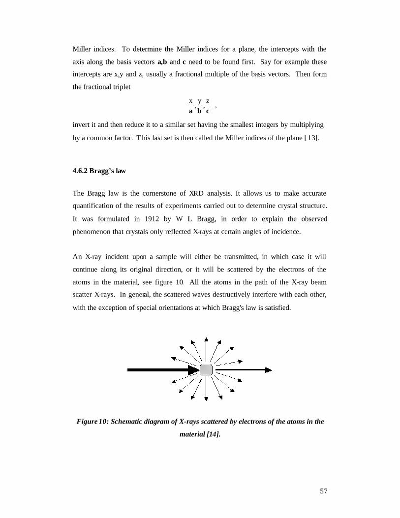
57
Miller indices. To determine the Miller indices for a plane, the intercepts with the
axis along the basis vectors a,b and c need to be found first. Say for example these
intercepts are x,y and z, usually a fractional multiple of the basis vectors. Then form
the fractional triplet
cbaz
,y
,x ,
invert it and then reduce it to a similar set having the smallest integers by multiplying
by a common factor. This last set is then called the Miller indices of the plane [ 13].
4.6.2 Bragg’s law
The Bragg law is the cornerstone of XRD analysis. It allows us to make accurate
quantification of the results of experiments carried out to determine crystal structure.
It was formulated in 1912 by W L Bragg, in order to explain the observed
phenomenon that crystals only reflected X-rays at certain angles of incidence.
An X-ray incident upon a sample will either be transmitted, in which case it will
continue along its original direction, or it will be scattered by the electrons of the
atoms in the material, see figure 10. All the atoms in the path of the X-ray beam
scatter X-rays. In general, the scattered waves destructively interfere with each other,
with the exception of special orientations at which Bragg's law is satisfied.
Figure 10: Schematic diagram of X-rays scattered by electrons of the atoms in the
material [14].

58
Consider a simple crystal such as that illustrated in figure 11, with lattice planes
separated by a distance dhkl. As illustrated above , the scattered X-rays from this
crystal will travel in random directions. A Bragg condition is such that the scattered
rays from two parallel planes interact with each other in such a way as to create
constructive interference. For this to happen the extra distance travelled by ray B,
figure 12, must be an exact multiple of the wavelength of the radiation. This means
that the peaks of each wave are aligned with each other.
Figure 11: Schematic diagram of XRD illustrating Bragg’s Law [14].
Figure 12: Schematic diagram as illustration to derive Bragg’s Law [14].
The geometry of the Bragg condition is remarkably simple, and leads to the powerful
result of the Bragg law:
The extra distance that ray B must travel is the distance X-Y-Z.
Thus X-Y-Z = n?
But X-Y = Y -Z = d sin ?
Hence, n ? = 2 d sin ?
dhkl
A B
2 ?
?
A
B
dhkl
? ?
X
Y
Z

59
In order to consider the general case of hkl planes, the equation can be rewritten as:
n? = 2 dhkl sin ? hkl,
since the dhkl incorporates higher orders of diffraction i.e. n greater than 1.
The angle between the transmitted and Bragg diffracted beams is always equal to 2?
as a consequence of the geometry of the Bragg condition. This angle is readily
obtainable in experimental situations and hence the results of X-ray diffraction are
frequently given in terms of 2? . However, it is very important to remember that the
angle used in the Bragg equation must always be that corresponding to the angle
between the incident radiation and the diffracting plane, i.e. ? .
The source of the X-rays incident on the sample, consists of an evacuated tube in
which electrons are emitted from a heated tungsten filament, and accelerated by an
electric potential (typically several tens of kilovolts) to impinge on a metal target.
The interaction between the electrons and the target leads to the emission of X-rays:
some having a wavelength characteristic of the target, and some having a continuous
distribution of wavelengths between about 0.05 nm and 0.5 nm (the so-called "white
radiation"). For most experiments, characteristic radiation is selected (using a filter or
Bragg reflection from a suitable crystal) because of its intensity and accurately known
wavelength [14].
4.7 Cathodoluminescence (CL)
Cathodoluminescence spectroscopy was used in this research to study the CL
efficiency of the Y 2SiO 5:Ce phosphor thin films and powders.
Cathodoluminescence is an optical and electrical phenomenon where a beam of
electrons generated by an electron gun (e.g. cathode ray tube) impacts on a phosphor
causing it to emit visible light. In the case of a semiconductor specimen, the CL
energy is equivalent to the energy gap between the conduction band and the valence
band, see Chapter 2, section 2.3 and 2.4.

60
Conventionally, the cathodoluminescence method has been used widely for research
of mineral specimens. Recently, it has receive d significant attent ion for developing
optical devices such as the commercialization of blue LEDs and laser diodes. It is
also used in various fields such as large capacity memory devices, devices for optical
communication network and materials for various kinds of displays [15].
4.8 Photoluminescence (PL)
Photoluminescence spectroscopy is a contactless, nondestructive method of probing
the electronic structure of materials and it was done on the Y2SiO5:Ce phosphor
powders in this study. Light is directed onto a sample, where it is absorbed and
imparts excess energy into the material. This process is called "photo-excitation."
One way this excess energy can be dissipated by the sample is through the emission
of light, or luminescence. In the case of photo-excitation, this luminescence is called
"photoluminescence". The intensity and spectral content of this photoluminescence is
a direct measure of various important material properties.
Specifically, photo-excitation causes electrons within the material to move into
excited states. When these electrons return to their equilibrium states, the excess
energy is released. The process may involve the emission of light (a radiative
process) or it may not (a nonradiative process). The energy of the emitted light, or
photoluminescence, is related to the difference in energy levels between the two
electron states involved in the transition, that is, between the excited state and the
ground state. The quantity of the emitted light is related to the relative contribution of
the radiative process.
One application of PL spectroscopy is band gap determination. The most common
radiative transition in semiconductors at or near room temperature is between states in
the conduction and valence bands, with the energy difference being known as the
band gap. Band gap determination is particularly useful when working with new
compound semiconductors [16].
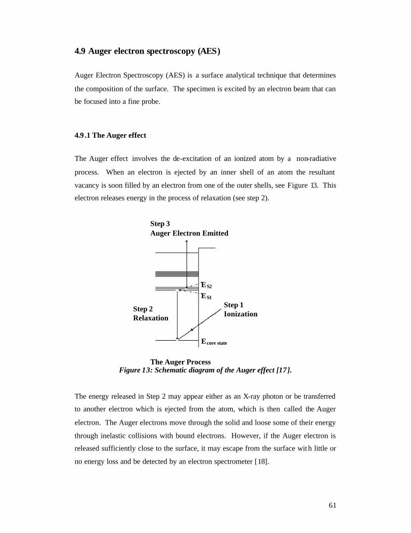
61
4.9 Auger electron spectroscopy (AES)
Auger Electron Spectroscopy (AES) is a surface analytical technique that determines
the composition of the surface. The specimen is excited by an electron beam that can
be focused into a fine probe.
4.9 .1 The Auger effect
The Auger effect involves the de-excitation of an ionized atom by a non-radiative
process. When an electron is ejected by an inner shell of an atom the resultant
vacancy is soon filled by an electron from one of the outer shells, see Figure 13. This
electron releases energy in the process of relaxation (see step 2).
Figure 13: Schematic diagram of the Auger effect [17].
The energy released in Step 2 may appear either as an X-ray photon or be transferred
to another electron which is ejected from the atom, which is then called the Auger
electron. The Auger electrons move through the solid and loose some of their energy
through inelastic collisions with bound electrons. However, if the Auger electron is
released sufficiently close to the surface, it may escape from the surface wit h little or
no energy loss and be detected by an electron spectrometer [18].
The Auger Process
Step 1 Ionization
Step 2 Relaxation
Step 3 Auger Electron Emitted
Ecore state
ES1 ES2

62
The primary, high energy, electrons (typically having a primary energy in the range 2
- 10 keV) have sufficient energy to ionize all levels of the lighter elements, and higher
core levels of the heavier elements. Some of the electrons emitted from the surface
have energies characteristic of the element from which they were emitted, and in
some cases, the bonding state of those atoms.
The characteristic Kinetic Energy (KE) of the Auger electron is:
KE = Ecore state – (ES1 + E S2) (1)
where S1 and S2 are the outer shell states. The KE of the Auger electron is
independent of the mechanism of initial core hole formation. The orbital energies are
determined by the element of the atom, thus the composition of a surface can be
determined. The emission of a characteristic Auger electron is more probable for
lighter elements than heavy elements (where electrons are more tightly bound to the
nucleus), therefore it is more sensitive to the lighter elements [19].
For Auger spectroscopy to be conducted the specimen chamber and spectrometer
must be maintained at Ultra High Vacuum (UHV) (typically at pressures of 10-9 and
10-10 Torr), as any gases present will both adsorb and scatter the very low energy
Auger electrons as well as forming a thin 'gas layer' on the surface of the specimen
degrading analytical performance [20].
4.9 .2 Instrumentation The basic components of an AES system are an electron gun (A), an electron
spectrometer, analyzer (B), an electron detector (D) to record secondary electron
images and an ion gun (C) for specimen cleaning and depth profiling, see Figure 14.
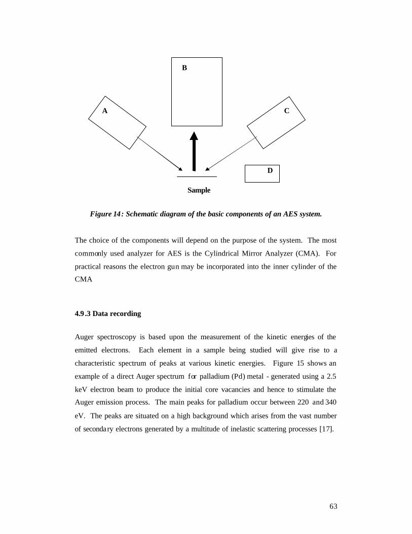
63
Figure 14: Schematic diagram of the basic components of an AES system.
The choice of the components will depend on the purpose of the system. The most
commonly used analyzer for AES is the Cylindrical Mirror Analyzer (CMA). For
practical reasons the electron gun may be incorporated into the inner cylinder of the
CMA
4.9 .3 Data recording
Auger spectroscopy is based upon the measurement of the kinetic energies of the
emitted electrons. Each element in a sample being studied will give rise to a
characteristic spectrum of peaks at various kinetic energies. Figure 15 shows an
example of a direct Auger spectrum for palladium (Pd) metal - generated using a 2.5
keV electron beam to produce the initial core vacancies and hence to stimulate the
Auger emission process. The main peaks for palladium occur between 220 and 340
eV. The peaks are situated on a high background which arises from the vast number
of secondary electrons generated by a multitude of inelastic scattering processes [17].
Sample
A
B
C
D
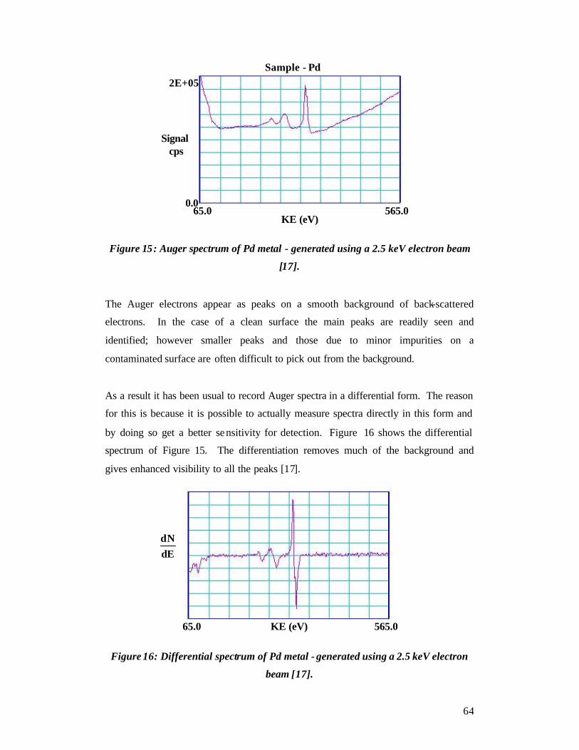
64
Figure 15: Auger spectrum of Pd metal - generated using a 2.5 keV electron beam
[17].
The Auger electrons appear as peaks on a smooth background of back-scattered
electrons. In the case of a clean surface the main peaks are readily seen and
identified; however smaller peaks and those due to minor impurities on a
contaminated surface are often difficult to pick out from the background.
As a result it has been usual to record Auger spectra in a differential form. The reason
for this is because it is possible to actually measure spectra directly in this form and
by doing so get a better sensitivity for detection. Figure 16 shows the differential
spectrum of Figure 15. The differentiation removes much of the background and
gives enhanced visibility to all the peaks [17].
Figure 16: Differential spectrum of Pd metal - generated using a 2.5 keV electron
beam [17].
Sample - Pd
KE (eV) 65.0 565.0
0.0
Signal cps
2E+05
dNdE
KE (eV) 65.0 565.0

65
4.9 .4 Chemical effects
The primary use of AES peaks is to identify the elements present on the surface;
particularly those involving valence electrons also carry information about the
chemical state of the surface. Usually XPS is the preferred technique for investigating
the chemistry of the surface as photoelectron peaks are sharper and chemical effects
are more easily interpreted than is the case for the corresponding Auger peaks [21].
Useful chemical information can be deduced from Auger spectra. The chemical
effect may appear as a simple peak shift, a change in peak shape or as both. A good
example of peak shift s can be found in the book of Walls [21]. Both the KLL and
LMM peaks showed shifts in position between pure silicon and the oxide or the
nitride. These chemical effects severely complicate quantitative measurements.
4.9 .5 Depth profiling
Depth profiling is one of the important applications of AES as it provides a
convenient way of analyzing the composition of thin surface layers. The data is
recorded as raw peak-to-peak heights plotted directly against sputtering time. The
provision of composition-depth profiles by AES has had an enormous impact on the
evaluation of thin films and surface coatings produced by a whole variety of methods
for use in optical coatings, materials protection and for semiconductor metallization
[21].
4.10 Residual gas mass analysis (RGA)
Residual Gas mass Analysis (RGA) was used in this research study to determine the
different kind of gas species present in the environment during AES and CL
spectroscopy. Residual gas analyzers operate by creating a beam of ions from
samples of the gas being analyzed.
The molecules of the gas being analyzed are turned into ions by an ionizer through
electron impact ionization, i.e., an electron beam is used to strike the gas atoms to
66
ionize them. This ionizing electron beam is generated by an emission filament and
extracted by means of an electric field.
The resulting mixture of ions is then separated into individual species through their
charge-to-mass ratios. To accomplish these, a typical RGA has three major parts,
namely, an ionizer, a mass analyzer, and an ion detector. The output of an RGA is a
spectrum that shows the relative intensities of the various species present in the gas.
This output is known as a mass scan or mass spectrum.
The ions from the gas are distinguished from each other in terms of their masses by
the mass analyzer of the RGA. There exist various techniques for mass separation,
but mass analyzers used in RGA's usually employ the radio frequency (RF)
quadrupole. The RF quadrupole has four cylindrical rods that are provided with
combinations of AC and DC voltages of varying frequency. Only ions that possess
the right mass-to-charge ratio can reach the ion collector for a given applied
frequency.
In the semiconductor industry, RGA is used in identifying gases, vapours, or residues
for the purpose of fixing leaks in vacuum systems and eliminating contaminants that
cause process problems or product failures [22].
4.11 X-ray photo electron spectroscopy (XPS)
XPS is a surface analytical technique where primary excitation is accomplished by
irradiating the specimen by a source of monochromatic X-rays. The X-rays cause
photo-ionisation of atoms in the specimen and the response of the specimen is
observed by measuring the energy spectrum of the emitted photo-electrons.
4.11.1 The photoelectric effect
Each atom present on the surface (except hydrogen) of the sample possesses core
electrons not directly involved in the bonding. The ‘binding energy’ (Eb) of each core
67
electron is characteristic of the individual atom to which it is bound. Information on
the binding energies of electrons within a sample allows qualitative elemental
analysis.
In the basic XPS experiment, the sample surface is irradiated by a source of low-
energy X-rays under ultra-high vacuum conditions. The incoming photons are
absorbed by atoms in a molecule or solid, leading to ionization and the emission of a
core (inner shell) electron. The photon having an energy of E = h? , which is the
Einstein relation, with
h - Plank's constant ( 6.62x10⁻³⁴ J.s )
? - frequency (Hz) of the radiation,
transfers its energy to the electron. If the energy is higher than Eb the electron may
escape from the surface as a photoelectron and the process is called photo-ionisation.
The photo-electrons have a KE which is related to the X-ray energy, h? and binding
energy Eb:
KE = h? - Eb (2)
If the photo-electrons have sufficient kinetic energy they are able to escape from the
surface by overcoming the specimen work function, and photo-emission is said to
occur. This entire process is referred to as the photo-electric effect [21, 23]. Figure
17 shows a schematic diagram of the photo-electric effect.

68
Figure 17: Schematic diagram illustrating the photoelectric effect [23].
By taking the specimen’s work function into consideration the KE of the photo-
electrons is then:
KE = h ? - Eb - Φ s (3)
were Φ s is the specimen’s work function [21].
4.11.2 Che mical shifts
The fixed binding energies of the core-levels of atoms are sufficiently affected by
their chemical environment to cause a detectable shift (ranging from 0.1 up to 10 eV
or more in magnitude) in the measured photo-electron energy; an effect termed the
“chemical shift” [21]. XPS is thus also termed as Electron Spectroscopy for Chemical
Analysis (ESCA) due to the chemical shift effect.
Initial State Vacuum Level
Core Level
h ?
Final State
Vacuum Level
h ?
KE
BE
69
4.11.3 Basic requirements
All XPS spectrometers must incorporate 1) a UHV environment, 2) a controlled
source of X-rays, 3) a specimen manipulation system, 4) an electron energy analyzer
and detection system and 5) a data recording, processing and output system.
1) UHV environment
A UHV environment is an essential requirement for almost every surface analysis
technique available today. X-ray, electron and ion sources, electron analyzers and
detectors will operate only under high vacuum or ultra-high vacuum conditions.
UHV conditions are achieved through the use of stainless steel and glass construction
materials, combined with suitable UHV pumping facilities.
2) X-ray source
One of the necessary characteristics of an X-ray source suitable for XPS is that the X-
ray energy should be sufficiently high to excite core-level electrons of all elements.
The two elements mostly used as X-ray sources for XPS are magnesium (Mg) and
aluminium (Al). Most commercial XPS instruments are fitted with twin X-ray
sources incorporating both Al and Mg anodes.
The advantage of having both AlKa and MgK a radiation available lies in the fact that
photo-ionisation produces not only photo-electrons, but also, via Auger decay of the
electron - hole formed, Auger electrons. The kinetic energy of the Auger electron is
independent of the X -ray energy used to create the hole, whereas the kinetic energy of
the photoelectron is related to the X-ray energy via the Einstein relation, see section
4.11. 1.
The binding energy of Auger peaks during XPS analysis appears to change by 233 eV
on going from AlKa to MgK a radiation (or visa versa) whereas the photoelectron
peaks do no shift in binding energy. This feature of XPS may be used not only to
differentiate between photo-electron and Auger peaks in the spectrum, but also to

70
resolve photo-electron and Auger pea ks which may otherwise overlap with each other
[21].
3) The specimen
In principle, all types of samples including gases and liquids, may be studied by XPS,
but limitations on instrument design usually restrict the range to low va pour pressure
(< 10-6 Torr), solid samples. Restrictions may also be imposed on sample size. Early
instruments were designed to hold only one sample at a time but modern
spectrometers are able to handle a number of powders, fibre or bulk solid samples
independently and simultaneously. Methods of sample mounting are numerous and
are often dictated by the nature of the sample itself.
4) The electron energy analyzer
The electron energy analyzer is the heart of every XPS spectrometer. Its function is to
disperse photo-electrons emitted from the specimen, according to their energies,
across a detector or detector array. The analyzer used is the spherical sector (or
concentric hemispherical) electrostatic analyzer (SSA).
5) Data recording, processing and o utput
Following energy dispersion in the SSA, the photo-electrons are made to enter an
electron multiplier detector or detector array. Here each incident photo-electron
causes a secondary electron cascade resulting in an output pulse of up to 108 electrons
with less than 0.1 µs duration. Since the detector output is in the form of discrete
pulses, XPS is ideally suited to conventional digital spectrum acquisition and
processing techniques [21].
4.11.4 Depth profiling It is also possible to use XPS to investigate the variation of composition with depth
into the sample in several ways, thereby producing a composition-depth profile of the
surface of interest [21].

71
4.12 Experimental procedure
4.12.1 Y2SiO 5:Ce thin films growth
Silicon (Si) (100) substrates were cleaned in acetone for 5 min, in an ultrasonic water
bath and then for 5 min in methanol. The substrates were blow n dry with nitrogen
(N2) gas. Commercially available Y2SiO 5:Ce standard phosphor powders were
pressed into a pellet and annealed at 600°C for about 16 hr.
The Lambda Physic EMG 203 MSC excimer XeCl laser with wavelength (?) = 308
nm was used to grow the thin films. The laser energy was 81.81 mJ, vacuum base
pressure was 3 x 10⁻⁵ Torr before the system was backfilled with oxygen ambie nt gas
to a pressure of 7.5 x 10⁻⁴ Torr, the substrate temperature was 400°C , repetition rate
was 10 Hz, target to substrate distance was 3.7 cm, 6600 laser pulses were used to
ablate the phosphor layer and 1200 pulses were used to ablate the SnO 2 layer on some
of the thin films.
4.12.2 Characterization of the Y2SiO5:Ce thin films
RBS was used to measure the thickness of the thin films by using a 3.100 MeV 4He+
beam. SEM images were taken with the Gemini LEO 1525 Model at the CSIR –
NML (Council for Scientific and Industrial Research – National Metrology
Laboratory), Pretoria and at the centre for Confocal and Electron Microscopy, UFS
with the Jeol 6400 Winsem model, to determine surface morphology of the thin films.
AFM, that was done with the Digital Instruments Multi Mode with Nano Scope IV
Controller and JV Scanner model, and EDS, done with the Oxford 1525 model,
analysis were used to monitor surface morphology and topography of the thin films.
The crystal structure of the thin films was determined with XRD, using a Siemens
Diffractrometer D5000 equipped with a Cu source.

72
4.12.3 Characterization of the Y2SiO5:Ce phosphor powders
SEM images were taken with the Gemini LEO 1525 Model at the CSIR – NML
(Council for Scientific and Industrial Research – National Metrology Laboratory),
Pretoria, to determine surface morphology of the commercially available Y2SiO5:Ce
phosphor powders, obtained from Phosphor Technology. The crystal structure of the
powders was determined with XRD, using a Siemens Diffractrometer D5000
equipped with a Cu source.
4.12.4 AES, CL spectroscopy and RGA for both the thin films and phosphor
powders
AES and CL spectroscopy, both excited by the same electron beam, using 2 keV
electrons with beam current densit ies between 26.3 mA.cm-2 and 52.63 mA.cm-2 were
used to monitor changes in the surface chemical composition and luminous efficiency.
The Auger and CL measurements were made in an ultrahigh vacuum (UHV) chamber
with a PHI Model 549 system, in oxygen pressures between 1×10⁻⁸ Torr and 1×10⁻⁶
Torr. CL data for the peak intensity at ? = 440 nm, were collected for 24 hrs with a
Ocean Optics S2000 spectrometer. RGA was performed to determine the volatile gas
species during electron bombardment, by using the Anavac-2 mass analyzer.
4.12.5 PL spectrometry for the phosphor powders
PL, excited by a HeCd laser, ? = 325 nm, power of 8.8 mW, was also pe rformed on
the phosphor powders at the Nelson Mandela Metropolitan University (NMMU).
4.12.6 XPS for both the thin films and the phosphor powders
XPS was done to determine the chemical composition of the phosphor surface before
and after 24 hr electron beam bombardment. XPS data were collected with a
Quantum 2000 system, using monochromatic Al Ka X-rays and Multipak, version 6,
computer software.

73
References
1. Pulsed Laser Deposition [online]. Available from
http://www.chm.bris.ac.uk/ [Accessed 5 March 2005].
2. Laser Ablation Technique, [online]. Available from
http://www.hut.fi/Units/AES/projects/prlaser/ablation.htm [Accessed 5
March 2005].
3. Pulsed Laser Deposition, [online]. Available from
http://www.esrf.fr/UsersAndScience/Experiments/CRG/BM25/inhouseresea
rch/supportlaboratory/PLD [Accessed 14 February].
4. K.T. Hillie and H.C. Swart, Appl. Surf. Sci, 183 (2001) 304.
5. Chen Li-Chyng, Particulates generated by pulsed laser ablation, in Pulsed
Laser Deposition of Thin Films (eds. Chrisey D. B, Hulber, G. K), John
Wiley & Sons, Inc , New York, (1994) p. 167.
6. Thin Film Analysis, Inc, San Jose, CA 95135, (408) [online]. Available
from http://www.tfainc.com [Accessed 25 November 2005].
7. Scanning electron microscopy – Wikipedia, the free encyclopedia, [online].
Available from http://en.wikipedia.org/wiki/Electron_microscope [Accessed
25 November 2006].
8. Scanning Electron Microscopy [online]. Available from
http://www.uccs.edu/ [Accessed 5 April 2005].
9. Energy Dispersive Spectroscopy [online]. Available from
http://ion.eas.asu.edu/descript_eds.htm [Accessed 17 February 2006].
10. J. I. Goldstein, D. E. Newbury, P . Echlin, D . C. Joy, C. Fiori and E. Lifshin,
Scanning Electron Microscopy and X-ray Microanalysis, Plenum Press,
Springer, ( 1981) p. 6.
11. Atomic Force Microscopy, [online]. Available from www.molec.com/
what_is_afm.html [Accessed 22 February 2006].
12. The tip-sample interaction in atomic force microscopy and its implications
for biological applications ", Ph.D. thesis by David Baselt, California
Institute of Technology.
13. M. Ali Omar, Elementary Solid State Physics: Principles and Applications,
Addison – Wesley Publishing Company, United States of America, (1975) p.
4, 6.

74
14. X-Ray Diffraction, [online]. Available from
http://www.doitpoms.ac.uk/tlplib/index.php [Accessed 10 December 2005].
15. Cathodoluminescence, [online]. Available from
http://www.jeol.com/jeolnews/jeol_news601/News%20home/35/index.html
[Accessed on 14 March 2006].
16. NREL Measurements and Characterization - Photoluminescence
Spectroscopy, [online]. Available from
http://www.nrel.gov/measurements/photo.html [Accessed 15 December
2005].
17. Auger, [online]. Available from http://www.phi.com/genf.asp_Q_ID_E_281
[Accessed 17 February 2006].
18. Auger Electron Spectroscopy, [online]. Available from
http://www.chem.qmul.ac.uk/surfaces/scc/scat5_2.htm [Accessed 15
December 2005].
19. The Auger Process, [online]. Available from
http://www.phi.com/genf.asp_Q_ID_E_281 [Accessed 16 December 2005].
20. Auger Electron Spectroscopy, [online]. Available from
http://en.wikipedia.org/wiki/Auger_electron_spectroscopy [Accessed 17
December 2005].
21. J. M. Walls, Methods of surface analysis, Cambridge University Press, Great
Brattain, (1989), p. 110, 111, 117, 132, 135, 140, 143, 152.
22. Residual Gas Analysis, [online]. Available from
http://www.semiconfareast.com/rga.htm [Accesses 18 December 2005].
23. Photoelectron Spectroscopy, [online]. Available from
http://www.chem.qmul.ac.uk/surfaces/scc/scat5_3.htm [Accessed 20
December 2005].
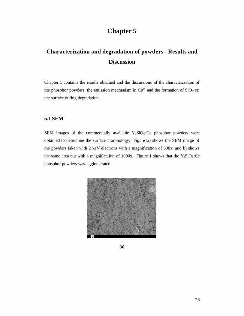
75
Chapter 5
Characterization and degradation of powders - Results and
Discussion
Chapter 5 contains the results obtained and the discussions of the characterization of
the phosphor powders, the emission mechanism in Ce3+ and the formation of SiO2 on
the surface during degradation.
5.1 SEM
SEM images of the commercially available Y2SiO5:Ce phosphor powders were
obtained to determine the surface morphology. Figure1a) shows the SEM image of
the powders taken with 2 keV electrons with a magnification of 600x, and b) shows
the same area but with a magnification of 1000x. Figure 1 shows that the Y2SiO5:Ce
phosphor powders was agglomerated.
(a)

76
(b)
Figure 1: a) SEM image of the powders taken with 2 keV electrons with a
magnification of 600x, and b) the same surface area with a magnification of 1000x.
5.2 XRD
XRD results (figure 2) showed the peaks of the monoclinic crystal structure of
Y2SiO5:Ce phosphor powders used in this research. As mentioned, it is very difficult
to study the crystal structure of Y2SiO5:Ce.
The crystal planes were calculated by using Bragg’s law. A crystal system is
described by three vectors. In the monoclinic system, the crystal is described by
vectors of unequal length, as in the orthorhombic system. Two of the vectors are
perpendicular, while the third makes an angle other than 90° with the plane formed by
the first two.

77
0
200
400
600
800
1000
Inte
nsit
y (A
rb. u
nits
)
0 10 20 30 40 50 60 702 theta
-4 0
20
1 3
-1 2
1
2 1
12
0 2
1 1
0
4 1
1
2 0
4
2 3
3
Figure 2: XRD results for the Y2SiO5:Ce phosphor powders.
5.3 Degradation
5.3.1 Electron beam size
The electron beam, used for AES and CL spectroscopy, was measured to be about 220
µm in diameter. The electron beam current was measured with an electrometer while
moving the electron beam horizontally from the inside of the hole of the Faraday cup
(beam current at maximum) to the outside, in the Auger vacuum chamber, a method
used by Oosthuizen et al. [1]. Figure 3 shows the electron beam current plotted
against moving distance. Figure 4 shows the differentiated spectrum of figure 3, with
the electron beam diameter measured at full width half maximum (FWHM). A
diameter of 220 µm results in an electron beam surface spot size area of 3.8 × 10⁻⁸ m2.
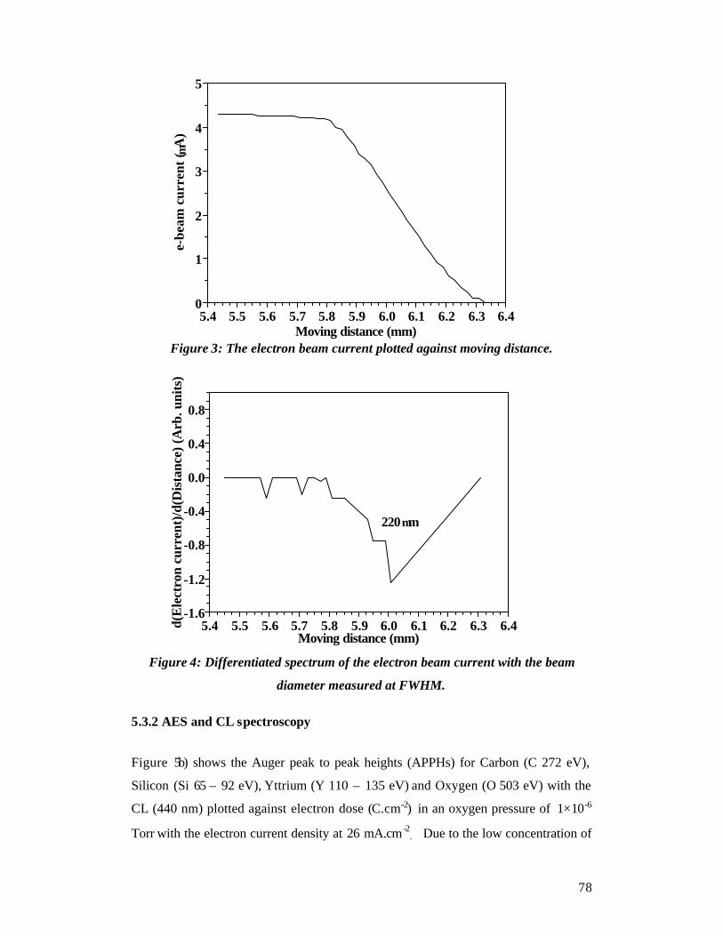
78
0
1
2
3
4
5
e-be
am c
urre
nt ( µ
A)
5.4 5.5 5.6 5.7 5.8 5.9 6.0 6.1 6.2 6.3 6.4Moving distance (mm)
-1.6
-1.2
-0.8
-0.4
0.0
0.4
0.8
d(E
lect
ron
curr
ent)
/d(D
ista
nce)
(Arb
. uni
ts)
5.4 5.5 5.6 5.7 5.8 5.9 6.0 6.1 6.2 6.3 6.4Moving distance (mm)
220µm
Figure 3: The electron beam current plotted against moving distance.
Figure 4: Differentiated spectrum of the electron beam current with the beam
diameter measured at FWHM.
5.3.2 AES and CL spectroscopy
Figure 5b) shows the Auger peak to peak heights (APPHs) for Carbon (C 272 eV),
Silicon (Si 65 – 92 eV), Yttrium (Y 110 – 135 eV) and Oxygen (O 503 eV) with the
CL (440 nm) plotted against electron dose (C.cm-2) in an oxygen pressure of 1×10⁻⁶
Torr with the electron current density at 26 mA.cm -2. Due to the low concentration of

79
Ce it was not detected by AES. As expected, the chemical bonding state of Y and Si
in Y2SiO5:Ce have a major effect on the energy position of the low energy peaks in
the AES spectra of the Y2SiO5:Ce phosphor powders , figure 5a). The electron current
density was calculated to be 26.3 mA.cm-2 by using an electron beam current of 10
µA. Time and beam current were converted to coulomb load (C) and the beam area
was used to convert it to electron dose (C.cm-2).
The presence of Si in its pure form should be manifested by a peak at 92 eV and Y
with peaks at 100, 110 and 127 eV [2]. Si in SiO2 was previously measured at 80 eV
[3]. In the present case the main peaks were measured at 83.5 eV and 124.5 eV for Si
and Y, respectively. Yttrium has a very low sensitivity factor for AES electrons. No
major changes in the APPHs were measured during the degradation process as shown
in Figure 5b). The CL intensity, however, decreased until about 300 C.cm-2 and then
slowly increased. The increase in the CL intensity against the wavelength for the
light emitted from the powders before and after 24 hr degradation is shown in Figure
6a). Figure 6b) shows the area under the curves plotted against time in hr. Lee and
Kim [4] measured the CL degradation of coated and uncoated Y2SiO5:Ce phosphors.
The measurements were done for coulomb doses of up to 150 C cm-2. A decrease of
about 12% of the original intensity was measured for the uncoated phosphor. The
degradation was however not measured for higher electron doses as in the present
case.
-0.4
0.0
0.4
0.8
1.2
1.6
2.0
dN(E
)/dE
0 100 200 300 400 500 600 700 800 900 1000Energy (eV)
before
after
O
YSi
83.5 108
124.5
(a)

80
Figure 5: a) AES spectra in the powders before and after degradation and b) the
APPHs and CL against Electron Dose (C.cm-2).
0
10
20
30
CL
Int
ensi
ty (A
rb. u
nits
)
300 400 500 600 700 800 900 1000Wavelength (nm)
1st spectrumafter 3 hrafter 24 hr
(a)
0.00
0.04
0.08
0.12
0.16
0.20
AP
PH
(A
rb. u
nits
)
0.00
0.04
0.08
0.12
0.16
0.20
Rel
ativ
e In
tens
ity
(Arb
. uni
ts)
0 400 800 1200 1600 2000 2400Electron Dose (C.cm -2)
CL Intensity
YC
CL
O
Si
(b)

81
Figure 6: (a) CL intensity against the wavelength for the light emitted from the
powders before and after 3 hr and 24 hr electron bombardment and (b) the area
under the curves in a) versus time in hr.
The first spectrum in figure 6a) shows the emission of the bright blue colour visibly
detectable with the human eye with two main peaks at the wavelengths of 440 and
500 nm. This spectrum is characteristic of the doublet character of blue light
emission from Ce3+, due to the 4f ground state splitting [5, 6, 7]. In Ce3+ the 5d and 6s
electrons shield the inner 4f electron. This results in the 5d ? 4f transition to be very
sensitive to the host lattice and crystal field [ 8]. The 4f level is affected by the crystal
field and it is different in host materials with different crystal structures. Different
crystal fields leads to different splitting effects of the 4f energy level. [9] see section
2.6.
It is postulated [5, 7] that in Y2SiO5:Ce the transition is more likely to be from the
lowest 5d level to the 2F5/2 level, emission at 440 nm (higher energy) see figure 7.
Bosze et al. [10], reported similar results. Due to the difficult crystal structure of
Y2SiO5:Ce the Ce3+ ion can be positioned at different sites in the host lattice, resulting
in the broad band emission at 440 and 500 nm.
3000
4000
5000
6000
Are
a un
der
curv
e (A
rb. u
nits
)
0 4 8 12 16 20 24Time (hr)
(b)
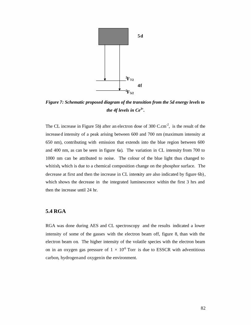
82
Figure 7: Schematic proposed diagram of the transition from the 5d energy levels to
the 4f levels in Ce3+.
The CL increase in Figure 5b) after an electron dose of 300 C.cm-2, is the result of the
increased intensity of a peak arising between 600 and 700 nm (maximum intensity at
650 nm), contributing with emission that extends into the blue region between 600
and 400 nm, as can be seen in figure 6a). The variation in CL intensity from 700 to
1000 nm can be attributed to noise. The colour of the blue light thus changed to
whitish, which is due to a chemical composition change on the phosphor surface. The
decrease at first and then the increase in CL intensity are also indicated by figure 6b) ,
which shows the decrease in the integrated luminescence within the first 3 hrs and
then the increase until 24 hr.
5.4 RGA
RGA was done during AES and CL spectroscopy and the results indicated a lower
intensity of some of the gasses with the electron beam off, figure 8, than with the
electron beam on. The higher intensity of the volatile species with the electron beam
on in an oxygen gas pressure of 1 × 10⁻⁶ Torr is due to ESSCR with adventitious
carbon, hydrogen and oxygen in the environment.
5d
2F7/2 4f
2F5/2

83
0
1
2
3
4
5
Rel
ativ
e In
tens
ity (A
rb. u
nits
)
0 10 20 30 40 50Atomic Mass Unit
Electron beam onElectron beam off
O2O2
CO2O OHCO
0.00
0.01
0.02
0.03
0.04
0.05
Inte
nsit
y (A
rb. u
nits
)
300 400 500 600 700Wavelength (nm)
Figure 8: RGA results for the electron beam on and off.
5.5 PL spectroscopy
Figure 9 shows the blue PL emission spectrum which is in agreement with results
reported thus far for PL spectroscopy of Y2SiO5:Ce [5, 7]. The emission of blue light
as shown in figure 6, between 400 and 500 nm, is a result of transitions from the 5d
energy level in Ce3+ to the 2F5/2 and 2F7/2 energy level.
Figure 9: Room temperature PL spectrum for the Y2SiO5:Ce phosphor powders.
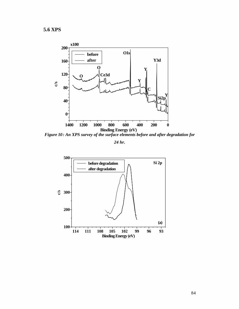
84
100
200
300
400
500
c/s
939699102105108111114Binding Energy (eV)
before degradationafter degradation
Si 2p
(a)
0
40
80
120
160
200
c/s
0200400600800100012001400Binding Energy (eV)
beforeafter
O
O
Ce3d
O1s
Y
Y
C
Y3d
Si2pY
x100
5.6 XPS
Figure 10: An XPS survey of the surface elements before and after degradation for
24 hr.
85
Figure 11: (a) Measured XPS results for the Si 2p peak before and after 24 hr
degradation, (b) fitted results for Si 2p in the Y 2SiO 5 and in the SiO2 chemical state.
Figure 10 shows the XPS survey spectrum of the Y2SiO 5:Ce before and after 24 h
degradation. Although the Ce could not be detected with AES the concentration was
still high enough to be detected with XPS (Note: The relative probabilities of
relaxation X-ray emission and electron emission changes with atomic number [11].) A
clear increase in the Ce peak intensity was measured after degradation. An extra
shoulder is detected at the high binding energy side of the Si 2p peak. The O1s peak is
much broader on the spectrum measured after degradation. It is therefore clear that a
chemical reaction occurred during the degradation process.
Figure 11a) shows the high resolution Si 2p XPS peak, before and after degradation.
Figure 11b) shows the fitted results from an XPS spectrum of the Si 2p peak after
degradation. The peak shape changed due to an extra peak that developed at higher
binding energies. The Si peak position for the yttrium silicate (Y2SiO5) chemical state
was measured at 101.3 eV before degradation. The extra Si peak measured at 103.3
eV was attributed to the silica (SiO2) [12] chemical state after degradation. The Si 2p
peak measured at 101.3 eV in figure 11 before degradation is consistent with a Si 2p
photoelectron peak position for a thin film containing bonds of Y-O-Si, measured at
101.0 eV by Chambers et al. [13, 14].
(b)
SiO2
Y2SiO 5
Binding Energy (eV) 101.3 103.3

86
This shows that the Si 2p peak in SiO2 shifted to higher binding energy than that for
Si in the Y2SiO 5:Ce bonding state , indicating the silicon in Y2SiO 5:Ce is in a lower
oxidation state than the silicon in SiO2. The O1s XPS peak of Y2SiO5:Ce was
measured at 530.4 eV before degradation (Figure 12a)). The peak broadened on both
the high and low binding energy side. Figure 12b) shows the fitted results from an
XPS spectrum of the O1s peak after degradation. The fitted peaks at 529, 530.4, 532.1
and 533.6 eV correlate well with CeO2 [15], the Y2SiO5:Ce O1s peak measured in this
study before degradation and the last two peaks with SiO2 [16, 17], respectively.
The Ce 3d peak before and after 24 hr degradation is shown in Figure 13a). The peak
fit after degradation is shown in Figure 13b). The peaks were at 881.7 and 885.4 eV
before degradation and 882.7 and 886.5 eV after degradation, which is in agreement
with Ce in the CeO2 oxidation stage [18] and CeH3 [19]. The Y 3d 157.6 and 159. 2
eV peak intensities before degradation (figure 14) decreased due to the coverage of
the Y2SiO5 with SiO2, CeO2 and CeH3 without a distinct shift in binding energy
position. It must be pointed out that there was a slight shift in the Y 3d peak to 157.1
eV which might be an indication of the formation of Y2O3 [20].
0
1000
2000
3000
4000
5000
c/s
520530540550Binding Energy (eV)
before degradationafter degradation
O1s
(a)

87
1100
1200
1300
1400
1500
1600
1700
1800
c/s
870880890900Binding Energy (eV)
before degradationafter degradation
Ce 3d
(a)
Figure 12: (a) Measured XPS results for the O 1s peak before and after 24 hr
degradation, (b) fitted results for O 1s after degradation in the SiO 2, Y2SiO5 and
CeO2 chemical state.
529 530.4
532.1 533.6
(b)
Binding Energy (eV)
SiO2
CeO2
Y2SiO 5

88
0
1000
2000
3000
4000
c/s
140150160170Binding Energy (eV)
before degradationafter degradation
Y 3d
Figure 13: (a) Measured XPS results for the Ce 3d peak before and after 24 hr
degradation, (b) fitted results for Ce 3d after degradation.
Figure 14: XPS results for the Y 3d peaks before and after 24 hr degradation.
The surface reaction on Y2SiO5:Ce is consistent with the well known ESSCR model
[6, 21]. The ESSCR mechanism explains the formation of SiO 2 plus CeO2 and CeH3,
whereby the electron beam dissociates the oxygen gas , as well as water vapour from
the background gases into atomic species, which then react with the surface atoms to
form a different chemical layer. In a situation where adventitious carbon is present on
the surface, the carbon would be depleted as volatile species, such as CO2.
882.7 886.5
(b)
CeO2
CeH3
Binding Energy (eV)

89
The increase in CL intensities indicates that the newly formed layer is luminescent
and thus contributing to the emission peak between 600 and 700 nm. SiO 2 has a band
gap and the electron beam irradiation can break the Si-O bonds and cause intrinsic
defects [15, 22]. Skuja et. al. [23, 24] reported two peaks for SiO 2 at 1.9 eV (650 nm)
and 2.7 eV (459 nm) with a theory that the two peaks are related to intrinsic defects
involving broken Si-O bonds. A definite contribution from the SiO2 1.9 eV defect
leads to the increase in the CL intensity between 600 and 700 nm, thus also resulting
in the change in colour. There could be a very low intensity contribution from the 2.7
eV defect to the peak emission between 400 and 500 nm, which results in the increase
in the intensity in that region. Violet/blue light emission (379.5 nm) was previously
observed at room temperature from thin CeO2 films deposited on Si (111) [25]. No
evidence of emission in the 600 to 700 nm range for CeO2 was found.
The formation of the luminescent SiO2 layer on the surface of the Y2SiO5:Ce
therefore lead to the degradation of the blue emitting Y2SiO5:Ce phosphor powders to
a whitish light emitting phosphor. Although the formation of SiO2 was measured,
(Figure 11), by XPS, it must be pointed out that reported results on the PL [7] and CL
[8] of Y2Si2O7:Ce indicated an emission peak in the deep red region at around 642
nm, which is much stronger in intensity than another peak at around 420 nm (deep
blue). Y2Si2O7 has a different crystal field than Y2SiO5 and doping it with Ce3+ leads
to a difference in the splitting effects of the 4f energy level. Possible reactions that
might have occurred during electron bombardment:
2Y2SiO5 ? 4Y + 2SiO 2 + 3O2
Si + O2 ? SiO 2
5.7 Y2Si2O7:Ce and SiO2:Ce
Since Y2Si2O7:Ce is polymorphous, it is very difficult to study its crystal structure [8].
The different crystal structures are a result of different contributing factors such as
sample preparation [5, 26] and annealing affects [7]. Each crystal structure would
thus lead to a different transition resulting in a double shoulder peak between 400 and
700 nm. XPS results on Y2Si2O7:Ce could not be found in the literature to give

90
complete clarification on the matter. The formation of small amounts of Y2Si2O7:Ce
on the surface is therefore not completely excluded. A shift of less than 2 eV in the 2p
Si peak (as measured for SiO2) is however expected.
Another possibility for the increase in the CL intensity between 400 and 500 nm
could be due to SiO 2:Ce. Ntwaeaborwa et. al. [ 27] reported on the photoluminescence
of SiO2:Ce, which resulted in a broad band emission spectrum between 400 and 500
nm (blue light) for 1 mol % concentration Ce. This broad band is due to the
transitions in Ce3+ and therefore could also possibly contribute to the increased CL
intens ity in figure 5c), but not to the increase in the peak intensity between 600 and
700 nm.
Conclusion
The degradation of the Y2SiO 5:Ce phosphor powders investigated with AES and CL
spectroscopy first resulted in a decrease in CL intensity measured at 450 nm and then
an increase after about 300 C.cm-2 due to the chemical change in the phosphor
surface. XPS and CL indicated that the change in peak shape is due to the formation
of a luminescent SiO2 layer on the surface which is formed according to the ESSCR
mechanism. The emission of light from the SiO 2 defect levels contributed to the CL
intensity in the 600 to 700 nm wavelength range . The colour changed from blue to
orange-reddish during the degradation process. CeO2 and CeH3 were also formed on
the phosphor surface during the degradation process.

91
References
1. H.C. Swart, L. Oosthuizen, P. H. Holloway and G. L. P. Berning, Surf. Inter.
Anal, 26 (1998) 337.
2. K. R. Brown and D. A. Bonnell, J. Am. Ceram. Soc, 82(9) (1999) 2423.
3. B. Carriere and J.P. Deville, Surface Sci., 80 (1979) 278.
4. R. Y. Lee and S. W. Kim, J. of Lumin., 93 (2001) 93.
5. Q. Y. Zhang, K. Pita, S. Buddhudu and C. H. Kam, J. Phys. D: Appl. Phys,
35 (2002) 3085.
6. J. Sebastian, S. Jones, T. Trottier, H. C. Swart and P. H. Holloway, J. SID,
3/4 (1995) 147.
7. N. Karar and H. Chander, J. Phys. D: Appl. Phys, 38 (2005) 3580.
8. X. Ouyang, A. H. Kitai and R. Siegele, Thin Solid Films, 254 (1995) 268.
9. H. C. Swart and K. T. Hillie, Surf. Interface Anal, 30 (2000) 383.
10. E. J. Bosze, G. A. Hirata and J. McKittrick, Mat. Proc. Symp. Mat. Res.
Soc. Proc, 558 (1999) 15.
11. J. T. Grant in Practical Surface Analysis, Second edition, Ed by D. Briggs
and M.P. Seah, John Wiley, New York, p61 (2003).
12. M. Laczka, W. Beier and L. Stoch, Glastechn. Berichte, 62 (1989) 320.
13. J. J. Chambers, B. W. Busch, W. H. Schulte, T. Gustafsson, E. Garfunkel, S.
Wang, D. M. Maher, T. M. Klein and G. N. Parsons, Appl. Surf. Sci, 181(1 -
2) (2001) 78.
14. J.J. Chambers and G.N. Parsons, J. Appl. Phys, 90(2) (2001) 918.
15. E.Paparazzo, Surface Sci. 234 (1990) L253.
16. D. Sprenger, H. Bach, W. Meisel and P. Gulich, J. Non-cryst. Solids, 126
(1990) 111.
17. T.A. Clarke and E.N. Rizkalla, Chem. Phys. Lett., 37 (1976) 523.
18. D.D. Sarma and C.N.R, J. Electron Spectrosc. Relat. Phenom. 20 (1980) 25.
19. L. Schlapbach, J. Osterwalder and H.C. Siegmann, J. Less-Common Metals,
88 (1982) 291.
20. Y. Uwamino, Y. Ishizuka, H. Yamatera, J. Electron Spectrosc. Relat.
Phenom, 34 (1984) 69.
21. P.H. Holloway, J. Sebastian, T. Trottier, S. Jones, H.C. Swart and R.O.
Peterson, Mat. R es. Soc. Symp. Proc, 424 (1997) 425.

92
22. X. Liu, J. C. H. Phang, D. S. H. Chan and W. K. Chim, J. Phys. D, Appl.
Phys, 32 (1999) 1563.
23. L.N. Skuja and W. Entzian, Phys . Stat. Sol. a, 96 (1986) 191.
24. L. N. Skuja, A. N. Streletsky and A. B. Pakovich, Solid State Comm, 50
(1984) 1069.
25. F. Gao, G. Li, J. Zhang, F. Qin, Z. Yao, Z. Liu, Z. Wang,. and L. Lin,Chin.
Phys. Lett., 18 (2001) 443.
26. P.J. Marsh, J. Silver, A. Vecht and A. Newport, J. Lumin, 97 (2002) 229.
27. O.M. Ntwaeaborwa, H.C. Swart, R.E. Kroon, P.H. Holloway and J.R. Botha ,
Surf. Interface Anal, 38 (2006) 458.

93
Chapter 6
Thin film characterization - Results and Discussion
Thin films of Y2SiO5:Ce coated and uncoated with SnO 2 were grown with PLD. RBS
was used to determine the thicknesses of both the Y2SiO5:Ce phosphor layer and the
SnO2 coated layer. Chapter 6 contains the results and discussion of the
characterization of the thin films.
6.1 RBS
RBS results indicated that the Y2SiO5:Ce thin films grown with 6600 were non-
uniform. The coated thin layer of SnO2 was 58 nm thick. SEM, AFM and EDX also
indicated that the Y2SiO5:Ce layer was non-uniform. The Y2SiO 5:Ce phosphor layer
consisted of spherical shaped particles not uniformly distributed on the surface.
6.2 SEM
(a) (b) Figure 1: SEM images of the uncoated a) and coated b) phosphor thin films with a
magnification of 1000x (10 kV electrons). Scale – 10 µm .

94
Figure 1, shows the SEM images of both the uncoated a) and coated b) thin film
surfaces. The surface displayed spherically shaped particles not uniformly distributed
with different sizes. Figure 2 shows a SEM image of a coated phosphor particle with
a diameter of about 12.3 µm.
Figure 2: Coated phosphor particle with a diameter of 12.3 µm, magnification of
22400x.
6.3 AFM
AFM results as shown in figure 3 and 4 indicated that the particle size distribution
varied between 10 nm to micron sized particles.

95
(a) (b)
(c) (d)
(e) (f)
Figure 3: AFM results indicating the topographic a), c) and e) images for 3
different locations on the uncoated thin film as well as the 3D images b), d) and f).
0 50 µm
50 µm
0
0 50 µm
50 µm
0
4 µm
0
50 µm
50 µm
0
Z
Y
X

96
0 50 µ m
0
50 µ m
(a) (b)
(c) (d)
(e) (f)
Figure 4: AFM results indicating the topographic a), c) and e) images for 3
different locations on the coated thin film as well as the 3D images b), d) and f).
The AFM images were obtained in contact mode. Contact mode is the most common
method of operation of the AFM. As the name suggests, the tip and sample remain in
close contact as the scanning proceeds. Figure 3 and 4 indicates that the surface is not
smooth, but covered with spherical particles. The height image data obtained by the
0 50 µm
50 µm
0
0 50 µm
50 µm
0

97
AFM is three-dimensional. The usual method for displaying the data is to use a colour
mapping for height, for example black for low features and white for high features
[1].
6.4 EDS analysis
Results from EDS also indicated nano- and micron meter size, tin oxide agglomerated
particles randomly distributed on the surface of the coated thin film (see figure 5b).
Areas marked with X and L in figure 5a) and T, Y, L, X in b) are the areas analyzed
by EDS. The electron beam used (10 kV energy electrons, resolution of 5 nm),
resulted in X-rays to be analysed that escaped from a depth of 1 to 2 µm [2].
(a)

98
(b)
Figure 5: SEM images (10 kV electrons ) of surface areas analyzed with EDS for
the uncoated a) magnification of 4270x, scale – 2 µ m and coated b) magnification
of 22500x,scale – 200 nm, thin films.
Figure 6 shows the result ing EDS spectra for the uncoated thin films and figure 7 for
the coated thin films.
Si
O C
(a)
0 5 10 keV
X
Rel
ativ
e In
tens
ity
Full scale 138 counts

99
Figure 6: EDS spectra for the uncoated thin film on the marked areas a) X and b)
L.
(b) 5 10 keV 0
C
O Si
Y L
Y
Rel
ativ
e In
tens
ity
Full scale 155 counts
T
Sn
Sn
Si
O
10 keV 0 5
(a)
Rel
ativ
e In
tens
ity
Full scale 107 counts
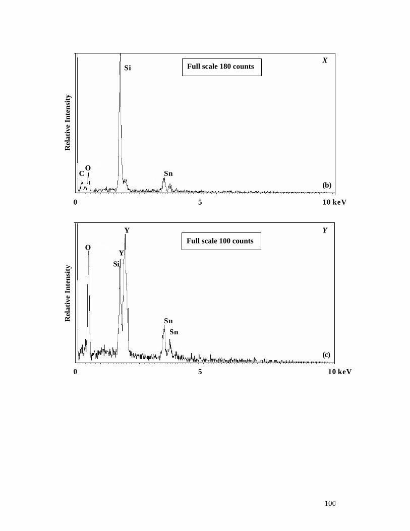
100
X
(b)
Sn
Si
O C
10 keV 5 0
Rel
ativ
e In
tens
ity
Full scale 180 counts
Y
Sn
Y
Sn
Si
O
(c)
0 10 keV 5
Y
Rel
ativ
e In
tens
ity
Full scale 100 counts

101
Figure 7: EDS spectrafor the coated thin film on the marked areas a) T, b) X, c) Y
and d) L.
EDS results are listed in Table 1.
Table 1: Listed EDS results for the uncoated and coated thin films.
Weight %
C O Si Y Sn (a) Uncoated
X 41 59 L 21 22 8 49
(b) Coated
T 31 2 67 X 10 14 41 35 Y 28 9 37 26 L 12 88
For the uncoated thin film, the area marked X (figure 6a)), correspond to a
composition of 59 % Si and 41 % adventitious C. L, figure 6b), was measured on the
spherical particle and the results indicated it to be the Y2SiO5:Ce phosphor particle.
The Ce concentration was too low to be measured. Figure 6b) and 7c) show an
overlapping of the Si and Y peaks at about 1.75 keV. Figure 6b) also shows a high
concentration of Y from the particle having a diameter of about 4 µm .
L
(d)
Si
O
10 keV 5 0
Rel
ativ
e In
tens
ity
Full scale 140 counts

102
0
10
20
30
40
50
60
Inte
nsity
(Arb
. uni
ts)
0 10 20 30 40 50 60 702 theta
Uncoated
0 1
30
2 0
-2 2
2
-5 1
4 4 0
0
x 10
Y2Si
O5
Y2Si
O5
Y2Si
O5
Si(a)
The area marked with T in figure 7a) is agglomerated SnO2 particles. The area
marked with X, figure 7b), is the thin film surface consisting of 41 % Si contribution
due to the substrate, 10 % adventitious C, 14 % O and 35 % Sn coated layer. Y,
figure 7c), was measured on the spherical shaped particle and the results showed Si, Y
and Sn, thus indicating the particles to be the Y2SiO5:Ce phosphor particles coated
with SnO2. The area marked with L, figure 7d) resulted in a high concentration of Si,
88 % and 12 % O, which is the Si substrate. This is an area on the surface were some
of the particles came loose due to handling.
6.5 XRD
XRD was done on both the coated and uncoated thin films to determine the crystal
structure. Figure 8a) shows the XRD results for the uncoated and b) for the coated
thin films.
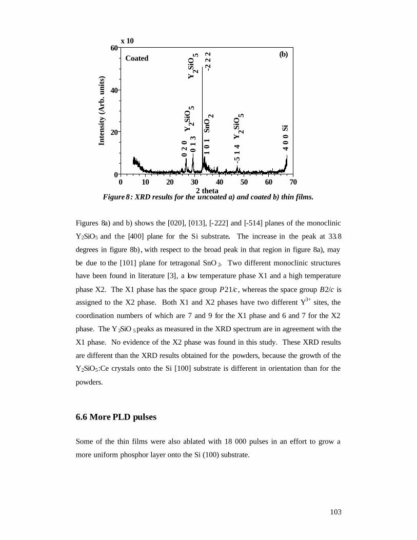
103
0
20
40
60
Inte
nsity
(Arb
. uni
ts)
0 10 20 30 40 50 60 702 theta
Coated
0 1
30
2 0
-2 2
21
0 1
-5 1
4 4 0
0
x 10
Y2Si
O5
Y2Si
O5
SnO
2
Y2Si
O5
Si
(b)
Figure 8: XRD results for the uncoated a) and coated b) thin films.
Figures 8a) and b) shows the [020], [013], [-222] and [-514] planes of the monoclinic
Y2SiO5 and the [400] plane for the Si substrate. The increase in the peak at 33.8
degrees in figure 8b) , with respect to the broad peak in that region in figure 8a), may
be due to the [101] plane for tetragonal SnO 2. Two different monoclinic structures
have been found in literature [3], a low temperature phase X1 and a high temperature
phase X2. The X1 phase has the space group P21/c , whereas the space group B2/c is
assigned to the X2 phase. Both X1 and X2 phases have two different Y3+ sites, the
coordination numbers of which are 7 and 9 for the X1 phase and 6 and 7 for the X2
phase. The Y 2SiO 5 peaks as measured in the XRD spectrum are in agreement with the
X1 phase. No evidence of the X2 phase was found in this study. These XRD results
are different than the XRD results obtained for the powders, because the growth of the
Y2SiO5:Ce crystals onto the Si [100] substrate is different in orientation than for the
powders.
6.6 More PLD pulses
Some of the thin films were also ablated with 18 000 pulses in an effort to grow a
more uniform phosphor layer onto the Si (100) substrate.

104
6.6.1 PLD
The same deposition parameters were used except for the laser energy which was
172.73 mJ and the number of pulses which was 18 000. The system was backfilled to
oxygen pressures of 7.5 ×10⁻⁴ Torr and 7.5 × 10⁻³ Torr.
6.6.2 EDS
Figure 9a) shows the SEM image of the areas that was analysed with EDS on the thin
film that was ablated in an increased oxygen pressure of 7.5 x 10⁻³ Torr and b) shows
the thin film ablated in 7.5 x 10⁻⁴ Torr with 18 000 pulses.
(a)

105
(b)
Figure 9: SEM images (20 keV electrons) of the areas analysed with EDS, for a)
the thin film ablated in an oxygen pressure of 7.5 × 10 -3 Torr and for b) the thin
film ablated in 7.5 × 10⁻⁴ Torr. Magnification - 1600x; scale - 10 µ m.
Figure 9a) shows more spherically shaped particles on the surface as well as an
agglomeration of particles (area T). Figure 9b) also just shows more particles on the
surface. EDS analysis of areas T and L in figure 9a), indicated the particles are
Y2SiO5:Ce while region X corresponded to the Si substrate as can be seen from figure
10.
Area L in figure 9b) also correspond to Si substrate, which means that the increased
number of pulses did not have the desired result of a more uniform phosphor layer on
the substrate surface.

106
Figure 10: EDS spectrum of the thin film surface (area X in figure 9a)), with the
Y2SiO5:Ce phosphor ablated onto the substrate using 18 000 pulses in an increased
oxygen pressure of 7.5 × 10⁻³ Torr.
Spherical particles of different sizes are typically found in laser ablation experiments
[3, 5]. Hirata et. al. [5] reported on rounded particles of different sizes that are formed
from local melting and ejected from the target onto the substrate on the smooth
surface of Y3Al5O12:Tb thin films grown by PLD.
Conclusion
Characterization (RBS, SEM, AFM, EDS, XRD) were successfully done on the
phosphor thin films. AFM and EDS showed that the Y2SiO5:Ce phosphor was ablated
onto the Si (100) substrate as spherical shaped particles. RBS, XRD and EDS showed
that the SnO 2 was successfully grown as a uniform coated layer onto some of the
phosphor thin films. PLD with more pulses in this case however did not have the
effect of a more uniform phosphor layer onto the surface. The system setup for PLD
was however changed, having the effect of increased laser energy.
Si
0 10 keV 5
100% X
Rel
ativ
e In
tens
ity
Full scale 187 counts
107
References
1. Atomic Force Microscopy, [online]. Available from www.molec.com/
what_is_afm.html [Accessed 22 February 2006].
2. EDS, [online]. Available from http://www.cascade.co.uk/xps.pdf [Accessed
24 March 2006].
3. J. Wang, S. Tian, G. Li, F. Liao and X. Jing, J. of the Electrochem. Soc, 148
(6) (2001) H61.
4. Chen Li-Chyng, Particulates generated by pulsed laser ablation, in Pulsed
Laser Deposition of Thin Films (eds. Chrisey D. B , Hulber, G. K), John Wiley
& Sons, Inc, New York, (1994) p. 167.
5. G. A. Hirata, O. A. Lopez, L. E. Shea, L. Y. Yi, T. Cheeks, J. McKittrick, J.
Siqueiros, M. Avalos-Borja, A. Esparza and C. Falcony, J. Vac. Sci. Technol.
A, 14(3) (1996) 1694.

108
Chapter 7
Thin film CL, AES and XPS - Results and Discussions
This chapter contains the results and discussions for the CL spectroscopy and AES
experiments were done in different O2 gas ambient and beam currents, as well as the
light emission process from the thin film surface.
7.1 CL spectroscopy and AES
CL spectroscopy and AES were done in vacuum and different oxygen pressures with
two different beam current densities to monitor chemical changes on the surface of
the thin films that were grown by PLD. The coated thin film was bombarded with a
beam current of 20 µA, on the same spot, by electrons, starting at UHV. The pressure
in the system was then increased (after 24 hrs), by leaking oxygen gas into the system
to a pressure of 1 × 10⁻⁸ Torr. After 16 hours the pressure was increased to 1 × 10⁻⁷
Torr. After 24 hrs the beam current was then decreased to 10 µA while the pressure
was kept constant. Finally the pressure was then increased to 1 × 10⁻⁶ Torr , after
another 24 hours. This was done to test the role of oxygen and also to deplete the
adventitious C on the surface. A new spot was also degraded starting with an oxygen
pressure of 1 × 10⁻⁶ Torr from the onset. The CL intensity data was collected at 440
nm. The uncoated thin film was then bombarded by electrons in 1 × 10⁻⁶ Torr oxygen
pressure for 24 hr. The results are presented and discussed in this chapter.
Uncoated thin film
7.1.1 AES and CL spectroscopy for the uncoated thin film - oxygen pressure - 1 ×
10-6 Torr - beam current 10 µA
AES and CL spectroscopy was done for the uncoated thin film in an oxygen pressure
of 1 × 10⁻⁶ Torr with the electron beam current at 10 µA. AES results for the
uncoated thin film showed that the carbon depleted from the surface while measuring
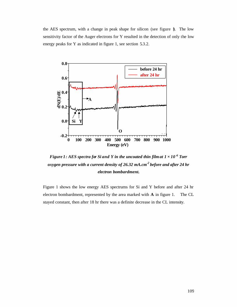
109
the AES spectrum, with a change in peak shape for silicon (see figure 1). The low
sensitivity factor of the Auger electrons for Y resulted in the detection of only the low
energy peaks for Y as indicated in figure 1, see section 5.3.2.
Figure 1: AES spectra for Si and Y in the uncoated thin film at 1 × 10 -6 Torr
oxygen pressure with a current density of 26.32 mA.cm-2 before and after 24 hr
electron bombardment.
Figure 1 shows the low energy AES spectrums for Si and Y before and after 24 hr
electron bombardment, represented by the area marked with A in figure 1. The CL
stayed constant, then after 18 hr there was a definite decrease in the CL intensity.
-0.2
0.0
0.2
0.4
0.6
0.8dN
(E)/d
E
0 100 200 300 400 500 600 700 800 900 1000Energy (eV)
before 24 hrafter 24 hr
O
Si Y
(a)
A
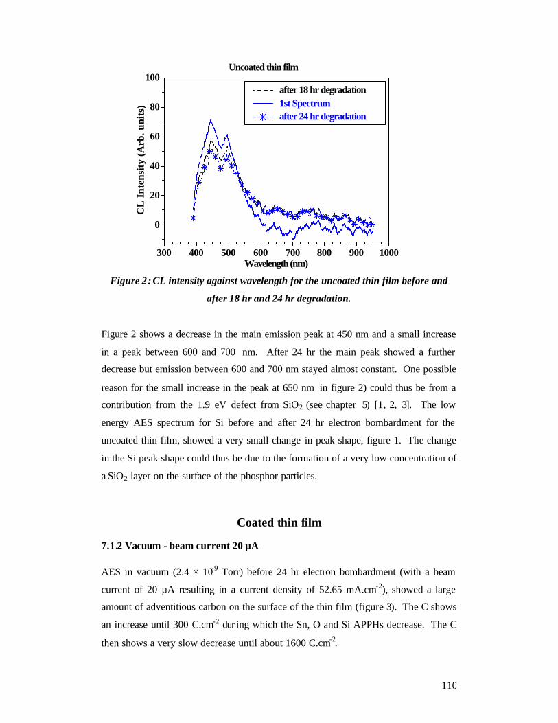
110
0
20
40
60
80
100
CL
Int
ensi
ty (
Arb
. uni
ts)
300 400 500 600 700 800 900 1000Wavelength (nm)
after 18 hr degradation1st Spectrumafter 24 hr degradation
Uncoated thin film
Figure 2: CL intensity against wavelength for the uncoated thin film before and
after 18 hr and 24 hr degradation.
Figure 2 shows a decrease in the main emission peak at 450 nm and a small increase
in a peak between 600 and 700 nm. After 24 hr the main peak showed a further
decrease but emission between 600 and 700 nm stayed almost constant. One possible
reason for the small increase in the peak at 650 nm in figure 2) could thus be from a
contribution from the 1.9 eV defect from SiO2 (see chapter 5) [1, 2, 3]. The low
energy AES spectrum for Si before and after 24 hr electron bombardment for the
uncoated thin film, showed a very small change in peak shape, figure 1. The change
in the Si peak shape could thus be due to the formation of a very low concentration of
a SiO2 layer on the surface of the phosphor particles.
Coated thin film
7.1.2 Vacuum - beam current 20 µA AES in vacuum (2.4 × 10⁻⁹ Torr) before 24 hr electron bombardment (with a beam
current of 20 µA resulting in a current density of 52.65 mA.cm-2), showed a large
amount of adventitious carbon on the surface of the thin film (figure 3). The C shows
an increase until 300 C.cm-2 dur ing which the Sn, O and Si APPHs decrease. The C
then shows a very slow decrease until about 1600 C.cm-2.

111
The Sn/C and O/C ratios show an almost linear decrease in the relative APPH at first,
which means that the APPH of C increased with respect to the Sn and O APPHs. The
carbon is thus creating an extra layer on the surface that increases the energy loss of
the primary electrons, see section 3.1.7. The CL intensity (measured at 450 nm)
decreased within the first 700 C.cm-2, then stayed almost constant due to the
protective C layer, see figure 3. The CL decrease is a result from the increased C on
the surface. The peak emission between 400 and 500 nm is the characteristic double
shoulder peak for CL emission of Y 2SiO5:Ce, [4, 5, 6] (see section 5.3.2).
0
1
2
3
4
5
AP
PH
(A
rb. u
nits
)
0
1
2
3
4
5
Rel
ativ
e In
tens
ity
(Arb
. uni
ts)
0 1000 2000 3000 4000 5000Electron Dose (C.cm -2)
CL
Si
Sn
O
C
Vacuum - 10-9
TorrBeam current - 20 µA
(a)
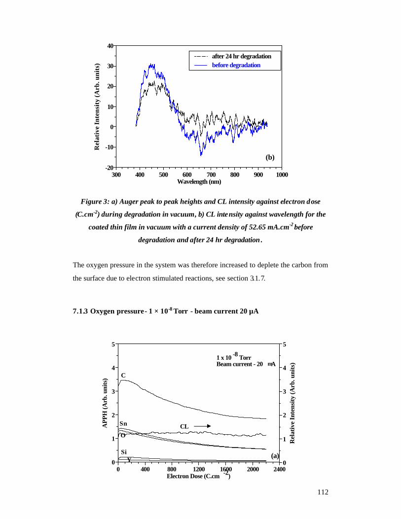
112
Figure 3: a) Auger peak to peak heights and CL intensity against electron dose
(C.cm-2) during degradation in vacuum, b) CL intensity against wavelength for the
coated thin film in vacuum with a current density of 52.65 mA.cm-2 before
degradation and after 24 hr degradation .
The oxygen pressure in the system was therefore increased to deplete the carbon from
the surface due to electron stimulated reactions, see section 3.1.7.
7.1.3 Oxygen pressure - 1 × 10⁻⁸ Torr - beam current 20 µA
-20
-10
0
10
20
30
40
Rel
ativ
e In
tens
ity
(Arb
. uni
ts)
300 400 500 600 700 800 900 1000Wavelength (nm)
after 24 hr degradationbefore degradation
(b)
0
1
2
3
4
5
APP
H (A
rb. u
nits
)
0
1
2
3
4
5
Rel
ativ
e In
tens
ity (A
rb. u
nits
)
0 400 800 1200 1600 2000 2400Electron Dose (C.cm -2)
O
Sn CL
C
SiY
1 x 10 -8 TorrBeam current - 20 µA
(a)

113
Figure 4: a) Auger peak to peak heights and CL intensity against electron dose
(C.cm-2) at 1 × 10⁻⁸ Torr oxygen pressure, b) CL intensity against wavelength for
the coated thin film in 1 × 10⁻⁸ Torr oxygen pressure with a current density of 52.65
mA.cm -2 before and after degradation for 16 hr.
The increase in the oxygen pressure showed little change in the CL intensity after
about 16 hr, figure 4. The carbon was still not depleted from the surface although it
showed a decrease; the concentration was still very high compared to the Sn and O
concentration on the surface. The Sn/C and O/C ratios again showed a decrease but
not as linear as for figure 3a). This is an indication that the C is depleting from the
surface and that the Sn and O APPHs are increasing. It seems that the C adsorption
from background gases and the removal of C due to ESSCR is traded against each
other at these experimental conditions. The expectation would thus be that a further
increase in the oxygen pressure would result in an increased CL intensity due to C
removal. The oxygen pressure was therefore further increased to 1 x 10⁻⁷ Torr.
7.1.4 Oxygen pressure - 1 × 10⁻⁷ Torr - beam current 20 µA
Figure 5a) shows the Auger peak to peak heights with the increasing CL intensity
against electron dose (C.cm-2), for 24 hrs as expected in 7.1.2.
-10
0
10
20
Rel
ativ
e In
tens
ity
(Arb
. uni
ts)
300 400 500 600 700 800 900Wavelength (nm)
after 16 hr degradationbefore degradation
(b)

114
-10
0
10
20
30
Rel
ativ
e In
tens
ity
(au)
300 400 500 600 700 800 900 1000Wavelength (nm)
before degradationafter 24 hr degradation
(b)
Figure 5: a) Auger peak to peak heights as a function of electron dose at 1 × 10 -7
Torr oxygen pressure and b) CL intensity against wavelength for the coated thin
film at 1 × 10⁻⁷ Torr oxygen pressure with a current density of 52.65 mA.cm -2 before
and after degradation for 24 hr.
The carbon gets depleted from the surface according to the well known ESSCR model
[5, 7] as volatile species such as CO2 but the concentration is still much higher than
the Sn and the O. The Sn/C and O/C APPHs ratios again showed an increase within
the first 1000 C.cm-2 which means that the Sn and O APPHs are increasing as the C is
0.0
0.4
0.8
1.2
1.6
2.0
APP
H (A
rb. u
nits
)
0.0
0.4
0.8
1.2
1.6
2.0
Rel
ativ
e In
tens
ity
(Arb
. uni
ts)
0 1000 2000 3000 4000 5000Electron Dose (C. cm -2)
C
O
Sn
CL
Si
1 x 10 -7 TorrBeam current - 20 µA
(a)

115
decreasing. Figure 5b) shows the increased CL against wavelength between 400 and
600 nm, after 24 hr. The increase in emission between 400 and 600 nm in figure 5b)
is thus due to the depletion of C and therefore an increased area of exposure of the
Y2SiO5:Ce phosphor particles to the electron beam. The beam current was then
decreased to 10 µA with the expectation that the CL would show a further increase as
a result of more depletion of the C on the surface.
7.1.5 Oxygen pressure - 1 × 10⁻⁷ Torr - beam current 10 µA
A lower beam current of 10 µA gives in a current density of 26.32 mA.cm-2 with a
lower temperature of contact with the electron beam on the thin film surface, which
leads to a longer mean stay time of the oxygen species on the surface for electron
stimulated reactions to occur and deplete the carbon from the surface [8, 9]. Figure 6
shows a definite decrease in the C APPHs and an increase in both the Sn and O
APPHs. This means that the lower beam current thus resulted in the longer mean stay
time of the reactive O species on the surface, which then reacted with the C to form
volatile species (see section 7.1.4). As the C layer is decreasing, more of the
phosphor particle’s surface is getting exposed to the electron beam for CL, thus the
increase in the CL intensity.

116
Figure 6: Auger peak to peak heights for the coated thin film at 1 × 10 -7 Torr
oxygen pressure with a current density of 26.32 mA.cm -2 as a function of electron
dose for 24 hrs of electron bombardment.
7.1.6 Oxygen pressure - 1 × 10⁻⁶ Torr - beam current 10 µA
Figure 6 shows that the C was still not completely depleted from the surface, thus the
O pressure was further increased to 1 x 10⁻⁶ Torr with a current density kept constant
at 26.32 mA.cm-2. Figure 7 shows the depletion of carbon as well as SnO2 on the
surface with an increase in the CL intensity during electron bombardment.
0.0
0.1
0.2
0.3
0.4
0.5
0.6
0.7
AP
PH
(Arb
. uni
ts)
0.0
0.1
0.2
0.3
0.4
0.5
0.6
0.7
Rel
ativ
e In
tens
ity
(Arb
. uni
ts)
0 400 800 1200 1600 2000 2400Electron Dose (C.cm -2)
CLC
O
Sn
1 x 10 -7 TorrBeam current - 10 µA

117
Figure 7: Auger peak to peak heights for the coated thin film at 1 × 10 -6 Torr
oxygen pressure with a current density of 26.32 mA.cm-2 as function of electron
dose for 24 hrs electron bombardment.
The APPH of C decreases within the first 400 C.cm-2 during which the APPHs of both
Sn and O increase and then show a decrease. The ratio of Sn/O is almost constant
initially w ith a slight decrease after 24 hr exposure, which means that the Sn
decreases relative to the O. The CL shows a definite increase as the C gets depleted.
After the depletion of the C the CL continues to increase while the SnO 2 was also
depleted from the surface due to ESSCR. The CL increased while the SnO 2 covering
layer on the surface was slowly removed during electron bombardment.
The electron beam was then focussed on a different surface area in order to
investigate if the CL would definitely reach a constant level if the C is depleted from
the surface, which would be an indication that the SnO 2 layer acts as a successful
coating layer.
0.0
0.4
0.8
1.2
1.6
2.0
AP
PH
(A
rb. u
nits
)
0.0
0.4
0.8
1.2
1.6
2.0
Rel
ativ
e In
tens
ity
(Arb
. uni
ts)
0 400 800 1200 1600 2000 2400Electron Dose (C.cm -2)
Sn
O
CL
C
1 x 10 -6 TorrBeam Current - 10 µA

118
0.0
0.1
0.2
0.3
0.4
0.5
0.6
dN(E
)/dE
0 100 200 300 400 500 600 700 800 900 1000Energy (eV)
C Sn O
Before electronbombardment
After 24 hr electron bombardment
7.1.7 Oxygen pressure - 1 × 10⁻⁶ Torr - beam current 10 µA - different area on
the coated thin film surface
Figure 8 shows the AES results before and after 24 hr electron bombardment on a
different area on the coated thin film in an oxygen pressure of 1 × 10⁻⁶ Torr with the
current density at 26.32 mA.cm-2.
Figure 8: AES results before and after 24 hr electron bombard ment on a different
area on the coated thin film at 1 × 10⁻⁶ Torr oxygen pressure with the current
density of 26.32 mA.cm -2.
As the C decreases the Sn and O APPHs increased and then almost stayed constant.
The C gets depleted from the surface within the first 300 C.cm-2 (about 3 hr), see
figure 9a), due to electron stimulated reactions (ESSCR) [7] in the oxygen
environment, resulting in the increase of the CL.

119
Figure 9: a) Auger peak to peak heights as function of electron dose at an oxygen
pressure of 1 × 10 -6 Torr and b) CL intensity against wavelength for a different
surface area on the coated thin film at 1 × 10⁻⁶ Torr oxygen pressure with a current
density of 26.32 mA.cm-2 before and after degradation for 24 hr.
As mentioned before, the adventitious C forms an extra layer on the surface of the
thin films that increases the energy loss of the primary electrons penetrating it on their
way to excite the electron-hole pairs in the phosphor bulk. A decrease in the C layer
increases the CL intensity, which then stayed almost constant. Figure 9b) shows the
increase in the main emission peak between 400 and 500 nm . This proves that the
0.0
0.1
0.2
0.3
0.4
0.5
0.6
0.7
AP
PH
(A
rb. u
nits
)
0.0
0.1
0.2
0.3
0.4
0.5
0.6
0.7
Rel
ativ
e In
tens
ity
(Arb
. uni
ts)
0 400 800 1200 1600 2000 2400Electron Dose (C.cm -2)
CL IntensitySn
O
C
CL
Si(a)
-10
0
10
20
30
CL
Int
ensi
ty (
Arb
. uni
ts)
300 400 500 600 700 800 900 1000Wavelength (nm)
before degradationafter 24 hr degradation
Coated thin film
(b)

120
1
2
3
4
5
6
7
8
Rel
ativ
e In
tens
ity
(Arb
. uni
ts)
0 400 800 1200 1600 2000 2400Electron Dose (C.cm -2)
Uncoated thin film
Coated thin film
SnO2 layer acts as a protective coating layer that resulted in a constant CL intensity
after 24 hr electron bombardment, but the layer unfortunately will also be removed
with continued electron bombardment as seen in figure 7. The constant CL intensity
means that no chemical changes occurred on the surface of the phosphor thin films
which could either result in an increased (extra luminescent layer, see chapter 5) or
decreased (extra non – luminescent layer) CL.
Light emission from both thin films in a 1 × 10⁻⁶ Torr oxygen environment, was blue
before and after 24 hrs electron bombardment. The CL intensity of the uncoated thin
film was about 60 % higher than for the coated thin film (see figure 10). The SnO2
layer at first prevented the phosphor surface to degrade as there was no change in the
chemical composition of the surface, proved by XPS results (not shown here). The
lower CL intensity of the coated thin film is thus due to the energy loss of primary
electrons penetrating the SnO 2 layer on the phosphor surface, as well as scattering
effects of the photons exiting the phosphor surface and the SnO 2 layer. A uniform
layer covering the surface of the spherical particles results in a small critical angle for
transmission and a large fraction of the light being totally internally reflected [5]. See
also section 7.1.1 for the decrease in the CL of the uncoated thin film.
Figure 10: CL intensity as function of electron dose (C.cm-2) for the coated and
uncoated thin films in 1 × 10 -6 Torr oxygen pressure with a beam current density of
26.32 mA.cm-2
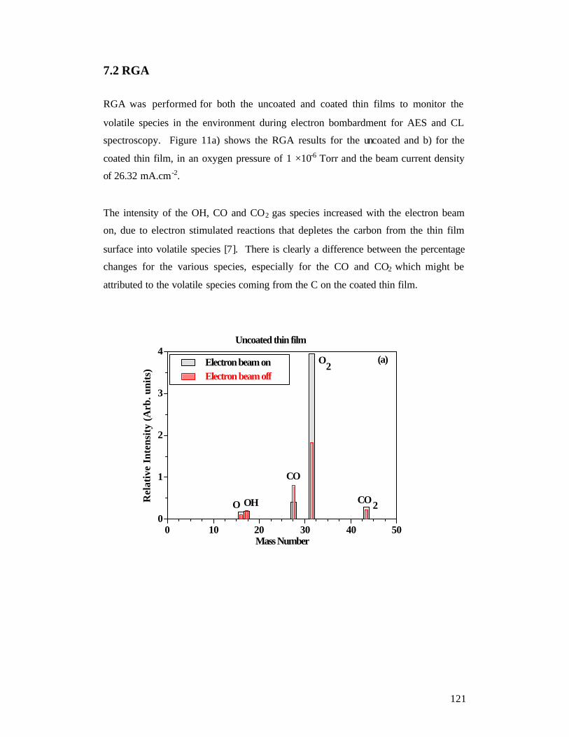
121
0
1
2
3
4
Rel
ativ
e In
tens
ity
(Arb
. uni
ts)
0 10 20 30 40 50Mass Number
Electron beam onElectron beam off
Uncoated thin film
CO2
O2
CO
OHO
(a)
7.2 RGA
RGA was performed for both the uncoated and coated thin films to monitor the
volatile species in the environment during electron bombardment for AES and CL
spectroscopy. Figure 11a) shows the RGA results for the uncoated and b) for the
coated thin film, in an oxygen pressure of 1 ×10⁻⁶ Torr and the beam current density
of 26.32 mA.cm-2.
The intensity of the OH, CO and CO2 gas species increased with the electron beam
on, due to electron stimulated reactions that depletes the carbon from the thin film
surface into volatile species [7]. There is clearly a difference between the percentage
changes for the various species, especially for the CO and CO2 which might be
attributed to the volatile species coming from the C on the coated thin film.

122
0
2
4
6
8
10
Rel
ativ
e In
tens
ity (A
rb. u
nits
)
0 10 20 30 40 50Mass Number
Electron beam onElectron beam off
Coated thin film
O2
CO2
CO
O OH
(b)
Figure 11: a) RGA for the coated and b) the uncoated thin film, with the electron
beam on and off.
7.3 Light emission
Chen [10] wrote a chapter on the generation of particles by pulsed laser deposition.
The nature of the particles, the energy, the size, the chemistry and microstructure all
depend upon the type of material used as the target and the effects of the deposition
parameters, eg. the ambient gas pressure. The effect of inert ambient gas pressure on
the nature of particles is most likely related to the increased collisions between the
ejected species and the ambient gas as the ambient gas pressure increases. When a
laser deposition experiment is done in vacuum, there are virtually no collisions
between the ejected species before they reach the substrate.
When the ambient gas pressure increases, the vapour species can undergo enough
collisions that nucleation and growth of these vapour species can occur to form
particles before their arrival at the substrate. Since the growth mechanism is by
diffusion, the residence time for the particles in the vapour controls the size of the
particles. The longer the residence time, as is the case with increased ambient gas
pressure, the larger the particle size.

123
hv
Electron beam
Light emission from the spherical shaped phosphor particles on the thin film surface
is affected much less by total internal reflection. Figure 12 shows a schematic
diagram of photons with energy hv exiting a spherical shaped particle compared to a
uniform layer.
Spherical particle.
Uniform layer
Figure 12: Schematic diagram of photons exciting a spherical particle compared to
the total internal reflection effects in a uniform layer.
The spherical surface of the particles results in more photons exiting the surface and
contributing to the high CL intensity of the thin films. Figure 13 illustrates the light
emission from such thin films.
Electron beam
hv

124
Figure 13: Schematic illustrating light emission from a phosphor thin film with
spherical particles on the surface, resulting from a 220 µm diameter electron
beam.
Electrons impinge on the thin film surface in an electron beam with a diameter of
220 µm , which results in photon excitation from an area on the surface containing a
number of spherical particles that vary in size from a few nano-metres to micron sized
particles. The photons are scattered from the particles in all directions, thus creating
the bright blue light emission visible with the human eye.
Conclusion
The depletion of the adventitious C on the surface of the SnO 2 coated phosphor thin
films occurred during 24 hr electron bombardment in an oxygen pressure of 1 x 10⁻⁶
Torr with an electron beam current of 10µA . An increased oxygen pressure resulted
in more reactive oxygen species which reacted with the C to create volatile species
such as CO2. The decrease in the beam current resulted in a lower temperature of
contact between the electron beam and the thin film surface which resulted in a longer
mean stay time of the oxygen species on the surface for depletion of the C via the
Thin Film
Y2SiO5:Ce Phosphor particles
Electron beam
hv

125
ESSCR model. The coated thin film resulted in a lower but constant CL intensity
than for the uncoated thin films. SnO 2 was therefore successfully ablated onto some
of the phosphor thin films as a coating layer which resulted in no degradation at first,
but the coating was also depleted after continued electron bombardment. The small
decrease in the CL intensity in the uncoated thin film could be due to a possible
formation of SiO 2. Light emission from the spherical shaped phosphor particles from
both the thin films showed the characteristic double shoulder peak for Y2SiO5:Ce
between 400 and 500 nm. The high CL intensity from the thin films is due to the
spherical shaped particles which have a larger critical angle for total internal
reflection.
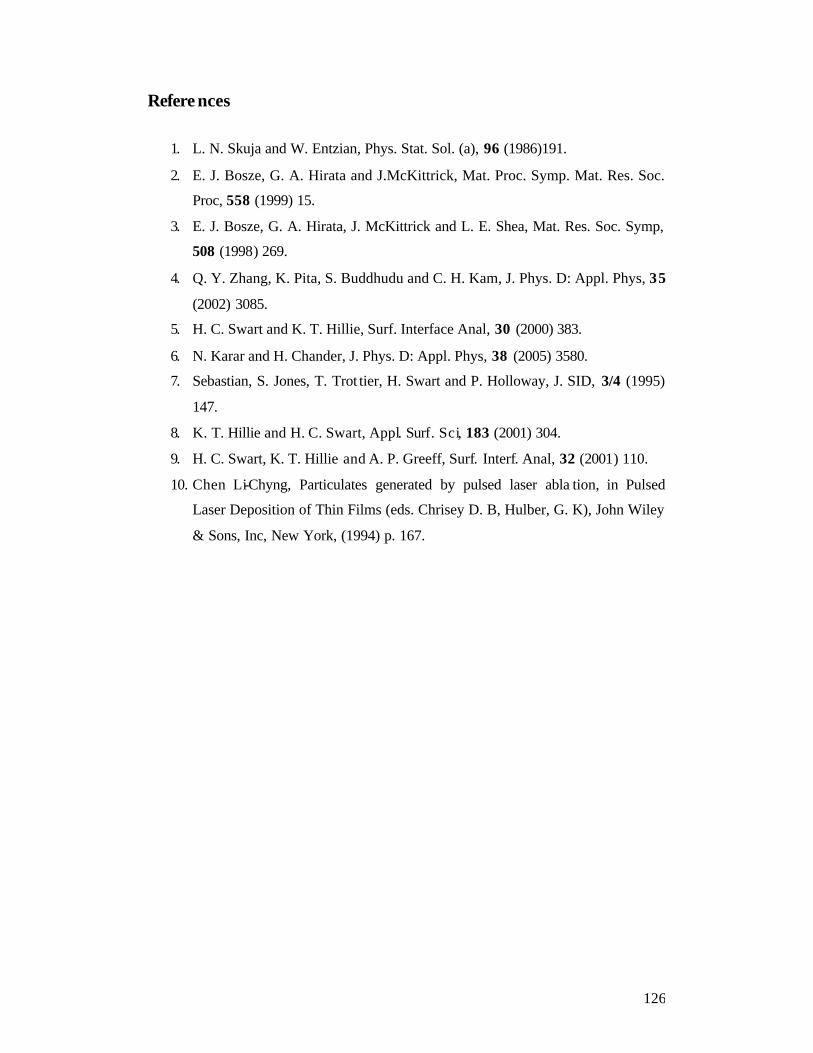
126
Refere nces
1. L. N. Skuja and W. Entzian, Phys. Stat. Sol. (a), 96 (1986)191.
2. E. J. Bosze, G. A. Hirata and J.McKittrick, Mat. Proc. Symp. Mat. Res. Soc.
Proc, 558 (1999) 15.
3. E. J. Bosze, G. A. Hirata, J. McKittrick and L. E. Shea, Mat. Res. Soc. Symp,
508 (1998) 269.
4. Q. Y. Zhang, K. Pita, S. Buddhudu and C. H. Kam, J. Phys. D: Appl. Phys, 35
(2002) 3085.
5. H. C. Swart and K. T. Hillie, Surf. Interface Anal, 30 (2000) 383.
6. N. Karar and H. Chander, J. Phys. D: Appl. Phys, 38 (2005) 3580.
7. Sebastian, S. Jones, T. Trot tier, H. Swart and P. Holloway, J. SID, 3/4 (1995)
147.
8. K. T. Hillie and H. C. Swart, Appl. Surf. Sci, 183 (2001) 304.
9. H. C. Swart, K. T. Hillie and A. P. Greeff, Surf. Interf. Anal, 32 (2001) 110.
10. Chen Li-Chyng, Particulates generated by pulsed laser abla tion, in Pulsed
Laser Deposition of Thin Films (eds. Chrisey D. B, Hulber, G. K), John Wiley
& Sons, Inc, New York, (1994) p. 167.
127
Chapter 8
Conclusion and future work
This chapter contains the overall conclusion of the results obtained for the Y2SiO5:Ce
phosphor powders and thin films as well as future work regarding this research study.
8.1 Powders
Y2SiO5:Ce is an organic phosphor that was investigated as an alternative for sulphide
based phosphors for application in FEDs. Surface morphology of the phosphor
powders was studied with SEM and it showed an agglomeration of the particles.
XRD that was done to determine the crystal structure showed the monoclinic crystal
structure of Y2SiO5:Ce. The degradation of the Y2SiO5:Ce phosphor powders was
found to take place by the electron beam stimulated surface reactions that were
manifested by the formation of a luminescent SiO2 layer on the phosphor surface,
proved by XPS. XPS and CL indicated that the change in the Si 2p peak shape is due
to the formation of the luminescent SiO2 on the surface. Light emission in Y2SiO5:Ce
is a result of characteristic luminescence with transition in Ce3+ from the 5d to the 4f
energy levels thus resulting in a double shoulder peak a t 440 and 500 nm.
Light emission in SiO 2 is due to the 1.9 eV (peak between 600 and 700 nm) and 2.7
eV (peak between 400 and 500 nm) intrinsic defects as a result of oxygen vacancies.
This resulted in a peak arising between 600 and 700 nm and an increase in the CL
intensity measured at 440 nm. The surface reactions correlated with the increased CL
intensity. CeO 2 and CeH3 were also formed on the phosphor surface during the
degradation process.
Degradation of this Y2SiO5:Ce phosphor powders in a high ambient gas pressure with
low excitation energy electrons would thus not be a very effective replacement for the
traditional blue ZnS phosphor powders, unless methods can be found to prevent it
from degrading to a whitish emitting phosphor powder.
128
8.2 Thin films
Application in FEDs would however be in thin film form, therefore Y2SiO5:Ce
phosphor thin films were grown in order to investigate whether the degradation would
proceed in the same way as for the powders.
The pulsed laser deposition technique that was used for grow ing the phosphor thin
films (using 6600 pulses) resulted in a non – uniform layer grown onto the Si (100)
substrate. AFM, SEM and EDS indicated that the non – uniform phosphor layer
consists of spherical shaped Y2SiO5:Ce particles randomly distributed on the surface.
These particles differ in size from a few nano-meters to micron size d particles. XRD
also showed the monoclinic crystal structure of Y2SiO5:Ce.
AES, CL spectroscopy and XPS results showed no severe chemical changes on the
thin film surface as for the powders. Adventitious C that was present on the thin film
surface before electron bombardment got depleted from the surface due to the ESSCR
model, in an O pressure of 1 x 10⁻⁶ Torr with an electron beam current density of
26.32 mA.cm-2. RGA indicated an increase in the CO and CO2 gas species during
electron bombardment. Some of the phosphor thin films were also coated with a
uniform SnO 2 layer. The thin films that were coated with SnO2 resulted in a lower
but more constant CL intensity than the uncoated thin films at first; however; the
SnO2 layer also gets depleted from the surface due to electron interactions.
Thin films were also grown using 18 000 pulses in a higher ambient oxygen pressure
of 7.5 x 10⁻³ Torr in order to create a more uniform layer on the surface. The SEM
and EDS results indicated that the phosphor layer was again non – uniform with the
spherical particles randomly distributed.
Light emission from the thin films is affected to a lesser extent by total internal
reflection compared with a uniform thin layer. The photons get scattered from the
particles in all directions, resulting in a relative high CL intensity.
The Y 2SiO 5:Ce phosphor thin films could thus be a good alternative for the traditional
blue ZnS phosphor in thin film form if the thin films could be grown onto the
129
substrate as a uniform layer. SnO 2 proved to be a sufficient coating layer that resulted
in a more constant CL intensity, which was , however, lower than the uncoated thin
film CL intensity. The very thin SnO 2 layer also started to degenerate from the thin
film surface due to the electron interactions.
8.3 Future work
1. In future , research needs to be done on how to prevent the Y2SiO5:Ce phosphor
powders from degradation for application in FEDs. A possible method could be to
investigate the effect of applying a transparent conductive surface layer to the
phosphor powders.
2. Research could also be done on growing a uniform Y2SiO 5:Ce thin film layer and
investigating the effect on the CL intensity and degradation for application in FEDs.
Pulsed reaction crossed beam laser deposition (PRCBLD) is an example of a different
PLD growth technique that could be investigated for growing a uniform layer. This
growth technique controls the oxygen inlet with a computerised valve, linked to the
laser beam frequency.
3. Applying a thicker SnO2 coating layer on the thin film surface could result in a
much lower CL intensity which would make this Y2SiO5:Ce thin film phosphor not
applicable in FED. It would however prevent it from degrading. Future work could
include investigating a different coating layer that would not degenerate from the
surface and finding a way of preventing the SnO 2 to deplete.
4. Further future work could also include investigating the effect of temperature and a
different ambient gas pressure (for example CO2) on the CL intensity of both the
powders and thin films, as it will contribute to the environmental effects for operation
in the FEDs.
5. Some other experimental aspects of this Y2SiO 5:Ce phosphor in future could also
involve characterization using glow discharge optical electron spectroscopy (GDOES)
and time of flight – secondary ion mass spectroscopy (TOF-SIMS)
130
Appendix A
Publications [1] E. Coetsee, H. C. Swart and J. J. Terblans , Degradation of Y2SiO 5:Ce phosphor powders, J. Lumin, accepted May 2006. [2] E. Coetsee, H. C. Swart, J. J. Terblans, O. M. Ntwaeaborwa, K. T. Hillie , W. A. Jordaan and U. Buttner, Characterization of Y2SiO 5:Ce thin films, Opt. Mat, accepted June 2006. [3] E. Coetsee, H. C. Swart and J. J. Terblans, Cathodoluminescence of Y2SiO5:Ce thin films. In preparation.
Conference [1] E. Coetsee, J. J. Terblans, O. M. Ntwaeaborwa, U. Buttner and H. C. Swart, Characterization of Pulsed Laser Ablated Cerium doped Yttrium Silicate (Y2SiO 5:Ce) thin films on Si (100), SAIP Pretoria (2005). [2] E. Coetsee, H. C. Swart, J. J. Terblans, O. M. Ntwaeaborwa, K. T. Hillie, W. A. Jordaan and U. Buttner , Cathodoluminescence of Y2SiO 5:Ce thin films , SAIP at UWC July 2006. [3] E. Coetsee, H. C. Swart and J. J. Terblans, Degradation of Y2SiO5:Ce phosphor powders, SAIP at UWC July 2006. [4] E. Coetsee, H. C. Swart, J. J. Terblans O. M. Ntwaeaborwa, K. T. Hillie and U. Buttner , Energy Dispersive Spectroscopy (EDS), Scanning Electron (SEM) and Atomic Force Microscopy (AFM) of Y2SiO5:Ce thin films. To be presented at SAIP MSSA at NMMU December 2006. [5] H. C. Swart, J. J Terblans, E Coetsee, O. M. Ntwaeaborwa, M. S. Dhlamini and P . H. Holloway, A short review on the ESSCR mechanism for phosphor degradation. To be presented at the AVS 53rd International Symposium & Exhibition, San Francisco, CA, USA, to be presented 12- 17 November 2006. [6] E Coetsee, JJ Te rblans and HC Swart, Cathodoluminescence Degradation of Y2SiO5:Ce Thin Films, AVS 53rd International Symposium & Exhibition, San Francisco, CA, USA, to be presented 12- 17 November 2006.