Chemical Vapor Deposition of Conformal, Functional, and Responsive Polymer Films
35
Chemical Vapor Deposition of Conformal, Functional, and Responsive Polymer Films By Mahriah E. Alf, Ayse Asatekin, Miles C. Barr, Salmaan H. Baxamusa, Hitesh Chelawat, Gozde Ozaydin-Ince, Christy D. Petruczok, Ramaswamy Sreenivasan, Wyatt E. Tenhaeff, Nathan J. Trujillo, Sreeram Vaddiraju, Jingjing Xu, and Karen K. Gleason* 1. Introduction 1.1. Motivation for Polymer Synthesis by Chemical Vapor Deposition The chemical vapor deposition (CVD) of polymers represents the translation of the well-known mechanisms for organic synthesis in the liquid phase to heterogeneous processes for functionalizing solid surfaces. CVD polymers are synthesized by delivering monomers to a surface through the vapor phase. Thus, polymerization and formation of a thin solid film occur in a single all-dry process. The CVD alternative becomes increasingly attractive as the prevalence of micro- and nanostructured surfaces and particles drives the desire for uniform coatings over surface topology. Such con- formal coverage is a characteristic that can differentiate CVD polymerization from solution methods that can suffer from non-wetting and surface-tension effects (Fig. 1a–c). This review focuses on CVD polymeriza- tion methods for surface-modification layers exhibiting strong structural retention of the organic functionalities originally present in the monomers. The retention of organic functional groups in the CVD polymer layers provides specific chemical sites for the surface attachment of moieties ranging from bioactive molecules to inorganic nanoparti- cles. Functional-group retention provides systematic control over surface properties such as wettability, lubricity, and adhesion. In addition, some functional groups impart the capability to create responsive surfaces. By extending the well-recognized advantages of inorganic CVD processes into the realm of organic materials, the mechanical properties of polymers can be exploited for achieving integration into flexible devices and low-cost production utilizing roll-to-roll processing. [1,2] The widespread utilization of CVD for inorganic materials in the semiconductor industry stems from the ability to purify precursors to a high degree in order to obtain high-purity deposits and to create high-quality interfaces using vacuum cluster tools. [3] Chemical purity of the thin films is of paramount importance for obtaining polymeric coatings with desirable characteristics, such as high electrical conductivity and fracture resistance in bioimplants. Indeed, the additives typically required to achieve uniform films by spin-casting and the impurities contained in the polymeric solutions, rather than the polymer itself, can be responsible for failures in biocompatibility testing and poor electrical characteristics of polymer films applied from REVIEW www.MaterialsViews.com www.advmat.de Chemical vapor deposition (CVD) polymerization utilizes the delivery of vapor-phase monomers to form chemically well-defined polymeric films directly on the surface of a substrate. CVD polymers are desirable as conformal surface modification layers exhibiting strong retention of organic functional groups, and, in some cases, are responsive to external stimuli. Traditional wet-chemical chain- and step-growth mechanisms guide the development of new heterogeneous CVD polymerization techniques. Commonality with inorganic CVD methods facilitates the fabrication of hybrid devices. CVD polymers bridge microfabrication technology with chemical, biological, and nanoparticle systems and assembly. Robust interfaces can be achieved through covalent grafting enabling high-resolution (60 nm) patterning, even on flexible substrates. Utilizing only low-energy input to drive selective chemistry, modest vacuum, and room-temperature substrates, CVD polymerization is compatible with thermally sensitive substrates, such as paper, textiles, and plastics. CVD methods are particularly valuable for insoluble and infusible films, including fluoropolymers, electrically conductive polymers, and controllably crosslinked networks and for the potential to reduce environmental, health, and safety impacts associated with solvents. Quantitative models aid the development of large-area and roll-to-roll CVD polymer reactors. Relevant background, fundamental principles, and selected applications are reviewed. [*] Prof. Karen K. Gleason, M. E. Alf, Dr. A. Asatekin, M. C. Barr, Dr. S. H. Baxamusa, H. Chelawat, Dr. G. Ozaydin-Ince, C. D. Petruczok, Dr. R. Sreenivasan, Dr. W. E. Tenhaeff, N. J. Trujillo, Dr. S. Vaddiraju, J. J. Xu Department of Chemical Engineering Massachusetts Institute of Technology Cambridge, MA 02138 (USA) E-mail: [email protected] DOI: 10.1002/adma.200902765 Adv. Mater. 2010, 22, 1993–2027 ß 2010 WILEY-VCH Verlag GmbH & Co. KGaA, Weinheim 1993
Transcript of Chemical Vapor Deposition of Conformal, Functional, and Responsive Polymer Films

R
www.MaterialsViews.comwww.advmat.de
EVIE
W
Chemical Vapor Deposition of Conformal, Functional,and Responsive Polymer Films
By Mahriah E. Alf, Ayse Asatekin, Miles C. Barr, Salmaan H. Baxamusa, Hitesh Chelawat,
Gozde Ozaydin-Ince, Christy D. Petruczok, Ramaswamy Sreenivasan, Wyatt E. Tenhaeff,
Nathan J. Trujillo, Sreeram Vaddiraju, Jingjing Xu, and Karen K. Gleason*
Chemical vapor deposition (CVD) polymerization utilizes the delivery of
vapor-phase monomers to form chemically well-defined polymeric films
directly on the surface of a substrate. CVD polymers are desirable as
conformal surface modification layers exhibiting strong retention of organic
functional groups, and, in some cases, are responsive to external stimuli.
Traditional wet-chemical chain- and step-growth mechanisms guide the
development of new heterogeneous CVD polymerization techniques.
Commonality with inorganic CVDmethods facilitates the fabrication of hybrid
devices. CVD polymers bridge microfabrication technology with chemical,
biological, and nanoparticle systems and assembly. Robust interfaces can be
achieved through covalent grafting enabling high-resolution (60 nm)
patterning, even on flexible substrates. Utilizing only low-energy input to drive
selective chemistry, modest vacuum, and room-temperature substrates, CVD
polymerization is compatible with thermally sensitive substrates, such as
paper, textiles, and plastics. CVD methods are particularly valuable for
insoluble and infusible films, including fluoropolymers, electrically conductive
polymers, and controllably crosslinked networks and for the potential to reduce
environmental, health, and safety impacts associated with solvents.
Quantitative models aid the development of large-area and roll-to-roll CVD
polymer reactors. Relevant background, fundamental principles, and selected
applications are reviewed.
1. Introduction
1.1. Motivation for Polymer Synthesis by Chemical
Vapor Deposition
The chemical vapor deposition (CVD) of polymers represents thetranslation of the well-known mechanisms for organic synthesis
[*] Prof. Karen K. Gleason, M. E. Alf, Dr. A. Asatekin, M. C. Barr,Dr. S. H. Baxamusa, H. Chelawat, Dr. G. Ozaydin-Ince,C. D. Petruczok, Dr. R. Sreenivasan, Dr. W. E. Tenhaeff, N. J. Trujillo,Dr. S. Vaddiraju, J. J. XuDepartment of Chemical EngineeringMassachusetts Institute of TechnologyCambridge, MA 02138 (USA)E-mail: [email protected]
DOI: 10.1002/adma.200902765
Adv. Mater. 2010, 22, 1993–2027 � 2010 WILEY-VCH Verlag GmbH & Co. KGaA, Weinhe
in the liquid phase to heterogeneousprocesses for functionalizing solid surfaces.CVD polymers are synthesized by deliveringmonomers to a surface through the vaporphase. Thus, polymerization and formationof a thin solid film occur in a single all-dryprocess. The CVD alternative becomesincreasingly attractive as the prevalence ofmicro- and nanostructured surfaces andparticles drives the desire for uniformcoatings over surface topology. Such con-formal coverage is a characteristic that candifferentiate CVD polymerization fromsolution methods that can suffer fromnon-wetting and surface-tension effects(Fig. 1a–c).
This review focuses on CVD polymeriza-tion methods for surface-modification layersexhibiting strong structural retention of theorganic functionalities originally present inthe monomers. The retention of organicfunctional groups in the CVD polymer layersprovides specific chemical sites for thesurface attachment ofmoieties ranging frombioactive molecules to inorganic nanoparti-cles. Functional-group retention providessystematic control over surface propertiessuch as wettability, lubricity, and adhesion.
In addition, some functional groups impart the capability tocreate responsive surfaces.
By extending the well-recognized advantages of inorganic CVDprocesses into the realm of organic materials, the mechanicalproperties of polymers can be exploited for achieving integrationinto flexible devices and low-cost production utilizing roll-to-rollprocessing.[1,2] The widespread utilization of CVD for inorganicmaterials in the semiconductor industry stems from the ability topurify precursors to a high degree in order to obtain high-puritydeposits and to create high-quality interfaces using vacuumcluster tools.[3] Chemical purity of the thin films is of paramountimportance for obtaining polymeric coatings with desirablecharacteristics, such as high electrical conductivity and fractureresistance in bioimplants. Indeed, the additives typically requiredto achieve uniform films by spin-casting and the impuritiescontained in the polymeric solutions, rather than the polymeritself, can be responsible for failures in biocompatibility testingand poor electrical characteristics of polymer films applied from
im 1993

REVIE
W
www.advmat.dewww.MaterialsViews.com
1994
solution.[4] Additionally, a large body of knowledge exists forsystematically tuning the properties of CVD inorganic films andfor producing uniform films over ever-larger-diameter wafers.Extending this knowledge to conformal, functional and responsivepolymeric surfaces is desirable for a diverse set of applicationsincluding biomedical implants, microelectrical and mechanicalsystems (MEMS) devices, and membrane separations.
Utilizing common vacuum deposition tools facilitates theintegration of organic and inorganic materials into novelmicrofabricated devices and hybrid structures. While inorganiclayers typically display fixed properties, organic materials canexhibit responsive behavior, such as swelling upon exposure to ananalyte or switching surface energy in response to a change intemperature, external field, or pH. Thus, devices incorporatingorganic materials can be designed to transduce chemical andbiological events into electrical and/or optical responses.
One niche for CVD polymer technology is the deposition ofinsoluble materials, such as fluoropolymers, electrically con-ductive polymers, and controllably crosslinked organic networks.Additionally, certain monomers can more readily be polymerizedthrough CVD methods. One example is a homopolymercontaining pendant functionalities that undergo side reactionsin solution.[5] Another example involves copolymers, where themonomers have no common solvent, such as a fluoromonomerpaired with a hydrophilic monomer.[6] Finally, because CVD‘‘builds’’ polymer films from the substrate up, in situ adhesionpromotion is possible, including creation of covalent graftingbetween the substrate and the deposited film.
All-dry processes are desirable for surface modification ofsubstrates that would degrade, swell, or dissolve upon exposure toliquids (Fig. 1d). All-dry methods are also desirable as ‘‘green’’manufacturing processes, avoiding the environmental and healthand safety concerns associated with solvents as well as theeconomic costs associated with solvent disposal.
1.2. Overview of CVD Chemistry and Processing
In pioneering work by Gorham,[7] [2.2]paracyclophane dimervapor was thermally cracked and the resultant monomer
Professor Karen K. Gleason is the Alexander and I. Michael KasseEngineering at MIT. The coauthors are members of her lab: MahrNathan J. Trujillo, and Jingjing Xu are currently doctoral candidates;Ph.Ds in 2009; and Drs. Ayse Asatekin, Gozde Ozaydin-Ince, Ramassociates. From left to right: RS, AA, GO-I, SV, NJT, SHB, HC, JX
� 2010 WILEY-VCH Verlag Gmb
subsequently self-initiated polymerization on a cool substrateto produce an electrically insulating material. The resultingpoly(p-xylylene) films and their various functionalized forms,commonly termed ‘‘parylenes’’, have since been widelycommercialized.
Many subsequently developed CVD polymer processes alsomake use of substrates held at or below ambient temperature.Indeed, the rates of many CVD polymer processes are limited bythe rate of adsorption of precursors onto the substrates. In thissituation, film growth rates increase as the substrate temperatureis lowered. Using low substrate temperatures is compatible withthe coating of thermally sensitive substrates, such as paper,textiles, and plastics. The use of low substrate temperatures alsodifferentiates most techniques for CVD polymers from their less‘‘gentle’’ inorganic CVD cousins. While using high temperaturesand/or high energy excitation successfully drives depositionthrough the fragmentation of inorganic precursors, suchaggressive conditions typically induce undesirable degradationof organic functionalities. Thus, selective chemical strategies aredesirable for achieving low-energy, low-temperature processes forCVD polymers.
Many methods developed for CVD polymerization draw uponthe vast knowledge of conventionial polymer growth, where themonomer units and their polymerization occur in the liquidphase.[8–10] After polymer synthesis, film formation requires asecond step such as spin-casting, dip-coating, or spray-and-bake,which may need to be followed by a third curing step. In contrast,the most common processes for CVD polymers convertmonomers to pure polymer films in a single step.
Knowledge of the chemical pathways and kinetics in theliquid-phase for a specific polymer is an excellent starting pointfor the design of the corresponding CVD process. Solutionpolymerization reactions are generally classified as either chain-or step-growth polymerization. In chain-growth polymerization,the polymer chain grows by the reaction of a monomer moleculewith a reactive group at the end of the active polymer chain. Thenature of this active site, whether it is a free radical, anionic orcationic, is a common basis of classification. Many monomers forchain polymerization contain vinyl groups, including acrylates,
r Professor of Chemical Engineering and Associate Dean ofiah E. Alf, Miles C. Barr, Hitesh Chelawat, Christy D. Petruczok,Drs. Salmaan H. Baxamusa and Wyatt E. Tenhaeff received theiraswamy Sreenivasan, and Sreeram Vaddiraju, are postdoctoral, MCB, MEA, WET, CDP, and KKG.
H & Co. KGaA, Weinheim Adv. Mater. 2010, 22, 1993–2027

REVIE
W
www.MaterialsViews.comwww.advmat.de
Figure 1. In some applications, CVD polymers (right column) offer advan-tages over solution processing (left column). a) Solvent surface tensionleads to poor step coverage in solution-coatedmicrotrenches whereas CVDleads conformal coverage of �300 thick polymer thin films along the top,bottom, and sidewalls of the trench. b) Particles agglomerate after solventevaporation in solution processing (left) but remain dispersed after CVDcoating (right). c) Fiber mats coated with electrically conducting polymerfilms by solution casting (left) showing non-wetting effects and aggregateformation while the oxidative CVD (oCVD) coating is conformal (right).d) Nylon fabric with dye leached out after solution coating (left) versus thedye retained in substrate after CVD polymer application (right). Repro-duced with permission from a) [1], b) [59] and [506], c) [64].
methacrylates, and styrenes. Anionic and cationic systems canalso lead to the ring-opening polymerization of cyclic monomersto form poly(dimethyl siloxane) (PDMS) and poly(oxymethylene).In step-growth polymerization, the polymer chain grows throughreactions that can occur between any two molecular species. Thisresults in a slow and steady growth in chain length withincreasing conversion. Step-growth polymerization leads to theformation of polymers ranging from poly(esters), poly(amides),
Adv. Mater. 2010, 22, 1993–2027 � 2010 WILEY-VCH Verlag G
and poly(imides) to electrically conductive materials such aspoly(thiophenes).[8,9]
1.2.1. Chain-Growth CVD Polymers
Similar to CVD of poly(p-xylylenes), plasma-enhanced CVD(PECVD),[11] initiated CVD (iCVD),[1] and photoinitiated(piCVD)[1] are one-step film-growth methods which draw onthe chemistry of free-radical chain-growth polymerization. InPECVD, plasma excitation of the vapor phase creates the radicalspecies.[11] However, the degree to which organic functionality ispreserved often improves by decreasing the plasma powerthrough strategies such as pulsing the plasma excitation[12–20] orperforming the deposition downstream of the active plasmaregion.[11,21,22] Alternatively, an initiating species can beintroduced through the gas phase along with the monomers.The initiator is selectively decomposed to free radicals throughgas-phase heating (iCVD) or by photons (piCVD).[1] By avoidingthe need for nonselective plasma excitation, high-rate depositionof true linear free-radical polymer chains can be achieved by iCVDand piCVD with essentially 100% functional retention.
While radicals are essential for the polymerization of vinylmonomers, if these species are not fully reacted during CVDgrowth, the resultant polymer film contains so-called dangling-bond defects. Once exposed to the air, these defects can furtherreact with oxygen and water, altering the film properties fromtheir as-deposited state.[23] Because of steric effects in the solidfilms, these aging reactions can occur over the course of severalweeks.[24–26] Electron spin resonance (ESR) studies revealed thatcompared to traditional PECVD, a desirable reduction indangling-bond defect concentration by one to two orders ofmagnitude down to �1018 spins cm�3 results from eitherreducing the excitation time used during pulsed PECVD[27] or byutilizing thermal excitation of the gas phase by hot filamentsrather than plasma excitation.[28]
Plasma environments create ionic species in the gas phase andthe importance of ionic mechanisms in polymer-like film growthhas been proposed.[26] In the absence of a plasma, the largeenergetic barrier to creating charged species in the gas phaseguarantees that heterogeneous processes will be the dominantpathways for reactions of ions. Explicit reports of ionic chainpolymerization in CVD are limited but include the cationicpolymerization of isobenzofuran.[29–31]
Examples of ring-opening CVD polymerizations are alsolimited. Insoluble poly(oxymethylene) films have been synthe-sized from the cyclic monomer trioxane using hot-filamentCVD.[32] Additionally, hot-filament CVD growth from the cycliccompound octamethylcyclotetrasiloxane, also known as D4, wasused to deposit films structurally similar to PDMS.[33] The D4
monomer also undergoes ring opening in the deposition oforganosilicon polymers by PECVD methods.[26,34]
Other CVD chain-growth polymerization methods entail twosteps: the preapplication of an initiator to the substrate, followedby exposure to monomer vapor. These strategies allow initiatorsof limited volatility to be employed. As compared to thecontinuous introduction of volatile initiators by iCVD andpiCVD, preapplication of initiator fixes the available supply forfilm growth. Methods for CVD polymerization involving pre-application of the initiator include vapor-phase assisted surfacepolymerization (VASP),[35–38] living free-radical polymerization
mbH & Co. KGaA, Weinheim 1995

REVIE
W
www.advmat.dewww.MaterialsViews.com
1996
methods such as nitroxide-mediated polymerization (surfaceinitiated vapor deposition polymerization (SI-VDP))[39] and atomtransfer radical polymerization (ATRP) (also categorized as a formof gas-phase assisted surface polymerization (GASP)),[40,41]
anionic[42] and cationic[43–45] ring-opening polymerization, catio-nic polymerization of acetylene derivatives,[46] photoinitiatedcationic polymerization of vinyl monomers,[47] and ring-openingmetathesis polymerization (ROMP) (sometimes termed solvent-less polymerization).[46,48,49]
1.2.2. Step-Growth CVD Polymers
Step-growth polymerizations have also been extensively trans-lated to vapor depositionmethods utilizing the introduction of themonomers into a vacuum chamber, either sequentially as inmolecular layer deposition (MLD)[50] or by simultaneous flowduring vapor deposition polymerization (VDP). Historically, theterm VDP is sometimes used as a generic label for other CVDpolymer processes. In this review, unless otherwise noted, theterm VDP will be used only for step-growth polymerization. Onesuch exception is SI-VDP, which has been retained to matchcurrent literature. Step-growth of electrically conductive polymershas been demonstrated through vapor phase polymerization(VPP) and oxidative CVD (oCVD).[1]
Figure 2. Cross-section microscopy images of conformal CVD polymerson micro- and nanostructures. Scanning electron micrographs (SEMs)a) of 300 nm deep trench conformally coated with poly(p-xylylene) andb) iCVD poly(tetrafluoroethylene) (PTFE) conformally coats an overhangMEMS test structure. c) Transmission electron micrograph (TEM) ofa 13 nm thick conformal MLD poly(aluminum ethylene glycol) on aninorganic nanoparticle. d) SEM cross-section of silica microparticle con-formally coated with a hydrogel by piCVD. Reproduced with permissionfrom a) [51], c) [56], d) [60]. c,d) Copyright 2008, American ChemicalSociety.
2. Characteristics of CVD Polymers
2.1. Conformal
Conformality describes the degree to which coating thickness ismaintained over topography in non-planar substrates, thusallowing all angles between intersecting curves to remainunchanged. Conformally coating 3D structures enables theaddition of novel surface functionalities to substrates of practicaluse in industrial, consumer, medical, pharmaceutical, andmicrofluidic applications. As feature sizes decrease and thedevice architectures become more complex, achieving goodconformality over high-aspect-ratio structures becomes increas-ingly challenging. A variety of CVDmethods enable the coating ofthin polymer films with good conformality (Fig. 2), an outcomewhich is difficult to achieve with solution polymerizationtechniques (Fig. 1a–c).
CVD of poly(p-xylylene) and its derivatives have long beenprized for enabling conformal coating of high-aspect-ratiostructures (Fig. 2a).[51] For example, poly(monochloro-p-xylylene)(‘‘parylene-C’’), is used to insulate wafer through-holes incomplementary metal-oxide semiconductor (CMOS) fabricationdue to its high quality as a dielectric material and nearperfect step coverage.[52] Functionalized and non-functionalizedpoly(p-xylylenes) have been successfully deposited in confinedmicrogeometries.[53] Poly(p-xylylene) films as thin as 3.5 nmsuccessfully prevented metal penetration into a porous methylsilsesquioxane matrix.[54]
Atomic layer deposition (ALD) processes for synthesizingconformal inorganic coatings on nanoscale devices, nanoporousmaterials, and nanoparticles have recently been reviewed.[55] ALDgrows alternating layers of atoms while the related methodof molecular layer deposition (MLD) utilizes alternation of
� 2010 WILEY-VCH Verlag Gmb
bifunctional molecular precursors. Each is based on sequential,self-limiting surface reactions. Thus, their growth rates areconstrained by the limited number of surface sites on thesubstrate and time required to alternate between precursors inthe deposition chamber. Uniform conformal coatings withthicknesses as low as 5 nm were achieved on large quantitiesof particles by MLD of hybrid organic-inorganic polymer films ofaluminum alkoxide (alucone) onto BaTiO3, silica, and titaniaparticles (Fig. 2c).[56,57] The sequential reactions of trimethyla-luminum and ethylene glycol provide precise chemical control ofthe alcone composition. Similar studies of MLD ‘‘zincone’’demonstrated the good conformality of these hybrid coatings withthicknesses of �20 nm on microtubes.[58]
The iCVD method conformally coats high-aspect-ratio struc-tures at high deposition rates, enabling conformal layers>100 nm in thickness (Fig. 1a, right) to be deposited using awide range of iCVD polymers. Microparticles (Fig. 1b, right) andnanotubes were conformally encapsulated with iCVD poly-(glycidyl methacrylate) (PGMA).[59] Retention of the functionalgroups from the monomer in the iCVD film enabled subsequent
H & Co. KGaA, Weinheim Adv. Mater. 2010, 22, 1993–2027

REVIE
W
www.MaterialsViews.comwww.advmat.de
binding of surface-active groups to the polymer. For example,fluorescent markers were bound to the glycidyl group of the iCVDPGMA film (Fig. 1b, right). The related method of piCVD,produced conformal hydrophilic poly(2-hydroxyethyl methacry-late) (PHEMA) coatings on microspheres (Fig. 2d).[60] Vaporintroduction of methylmethacrylate and divinylbenzene coupledwith preapplication of initiator to titania nanoparticles resulted insuccessful encapsulation varying from 2.5 to 40 nm in thickness,with potential applications for drug delivery, biocatalysis andphotonics.[61]
The degree to which conformality can be achieved by PECVDpolymerization is highly dependent on processing condi-tions.[15,62] The electric field of the plasma is an inherent sourceof directionality during film growth involving charged species,which leads to directional filling of features or differentialsputtering of surfaces. Moreover, the high sticking coefficients ofthe ionic species accelerated to the substrate surface also decreasethe step coverage. Therefore, using high deposition rates ofPECVD obtained at high RF power densities generally lead topoor conformality when coating high-aspect-ratio structures.[63]
However, by lowering the input power using pulsed PECVD,optimization of conformality through processing conditions ispossible.
Conformal deposition of conducting polymers is desired for avariety of electronic applications. The oCVD of poly(3,4-ethylenedioxythiophene) (PEDOT) allowed conformal depositionon delicate paper and nanofiber electrospun mats (Fig. 1c,right).[64] The conformality of oCVD PEDOT films dependsstrongly on the oxidant species employed, with CuCl2 providing amuch greater degree of conformality as compared to oCVD filmsgrown using FeCl3.
[65]
2.2. Functional
2.2.1. Surface Energy Control
Figure 3. a) X-ray photoelectron spectroscopy (XPS) reveals the distri-bution of C, CF, CF2, and CF3 bonding environments in PECVD (top) anddownstream PECVD fluoropolymer (middle) films as compared to the pureCF2 composition of a bulk PTFE standard. b) Solid-state 19F magic anglespinning nuclear magnetic resonance (NMR) confirms the linear bondingstructure of the CF2 units in iCVD PTFE. c) iCVD PTFE (filled circle) retains100% of the desirable CF2 functional groups, even at high deposition rates.In contrast, for pulsed PECVD fluoropolymer (open circles) there is atradeoff between growth rate and degree of functional group retention.Reproduced with permission from a) [74], b) [79], c) [80]. a) Copyright 1993American Chemical Society. b) Copyright 2000 Elsevier. c) Copyright 2007Elsevier.
Surface energy can be readily tuned by using numerous CVDpolymer methods. For low-surface energy films, CVD offluoropolymers is particularly advantageous for the synthesisof insoluble and conformal coatings on substrates havingtopographies spanning from the nanoscale to the macroscale.Only a thin CVD layer of an expensive fluoropolymer can impartdesired surface properties to a substrate that is inexpensive and/or has superior bulk properties. Often used in combination withsurface roughness to create hydrophobic and oleophobicsurfaces,[66,67] low-surface-energy CVD films have found applica-tion in MEMS devices,[68] antifouling/biofouling and stain-resistant textiles,[69] antiwetting, antisnow, and ice adherence.[70]
PECVD fluorocarbon films[17,26,71–75] often contain a variety ofbonding environments such as CF3, CF2, CF, and quaternarycarbon (Fig. 3a, top). Moving the substrate downstream of theplasma glow discharge slows deposition, but enhancesthe fraction of CF2 in the film (Fig. 3a, middle), resulting inchemical composition similar to poly(tetrafluoroethylene) (PTFE,(CF2)n,Teflon) (Fig. 3a, bottom). The precise stochiometry ofPTFE is achieved by hot-filament CVD[76–78] where the monomerhexafluoropropylene oxide (HFPO) is thermally decomposedto difluorocarbene (CF2:) (Fig. 3b).[79] Adding the initiator
Adv. Mater. 2010, 22, 1993–2027 � 2010 WILEY-VCH Verlag GmbH & Co. KGaA, Weinheim 1997

REVIE
W
www.advmat.dewww.MaterialsViews.com
1998
perfluorooctane sulfonyl fluoride greatly enhances depositionrate and represents the iCVD variation of the hot-filamentprocess.[78] The iCVD of PTFE displays both high depositionrates, 100% retention of the CF2 functional group, and conformalcoverage (Fig. 2b). By comparison, pulsed PECVD provides onlyincomplete retention of the CF2 functional group and increasedretention comes at the expense of slower deposition rate(Fig. 3c).[80]
Microscopy images of nanostructured CVD polymers areshown in Fig. 4. Limiting the nucleation process for iCVD fromHFPO results in nanostructured and porous PTFE coatings,where the anisotropic structures are likely to be associated withcrystallization of the linear (CF2)n chains (Fig. 4a).
[77] Nodular and‘‘stone rose’’ morphological features (Fig. 4b) occur in PECVDfluorocarbon films grown downstream of an HFPO plasma,[82]
whereas smooth films were obtained on substrates directlyadjacent to the plasma glow region. As a result of variation of theCF2 diradical concentration with position from the glow, the F/Cratio of downstream films reached 1.97 as compared to a value of1.5 for films grown on substrates directly exposed to glow region.The combination of the nanostructure and the high fluorinecontent in the downstream films resulted in superhydrophobicity(advancing contact angle of �1658 with water).
The conformality and low surface energy of iCVD PTFE werecombined to achieve surface modification of vertically alignedcarbon nanotube forests.[83] The structure of the forest waspreserved and a high degree of conformality resulted in coating ofthe entire surface of the individual nanotubes with aspect ratios of40:1 with ultrathin (�50 nm), insoluble, and hydrophobic iCVDPTFE. The resulting superhydrophobic surface displayed theso-called ‘‘lotus-leaf’’ effect, with advancing and receding contactangles with water of 1708 and 1608, respectively. Nearly spherical
Figure 4. Nanostructured as-grown CVD polymers a) Limiting nucleationand allowing for anistropic crystallite formation during iCVD PTFE growthfrom HFPO and results in a porous morphology. b) ‘‘Stone rose’’morphology of downstream PECVD PTFE-like coatings grown from HFPO.c) Nanosculptured poly(monochloro-p-xylylene) by oblique angle depo-sition. d) Basalt morphology of porous oCVD PEDOT using CuCl2 oxidant.Reproduced with permission from a) [77], b) [82], c) [454], d) [65].a) Copyright 2001 Elsevier. d) Copyright 2008 American Chemical Society.
� 2010 WILEY-VCH Verlag Gmb
droplets of water form on the iCVD PTFE coated nanotube forest.The texture of ordinary tissue paper modified with �40 nm ofiCVD PTFE results in a hydrophobic surface and clearlydemonstrates the compatibility of the iCVD technique withtemperature-sensitive substrates (Fig. 5a).[1]
Figure 5. Wetting behavior of textured substrates surface modified byconformal CVD polymers (a,b) and nanostructured CVD polymer films(c,d). a) Uncoated (left) and iCVD PTFE coated (right) tissue paper withdyed water. b) Pulsed PECVD fluoropolymer deposited on cotton fabricdisplays oleophobicity. c) Poly(p-xylylene) substituted with –COCF3 can beboth hydrophobic and adhesive when oblique angle deposition introducesinherent nanostructure. d) Colloidal lithographically patterned iCVDpoly(2-hydroxyethyl methacrylate) and the resulting low contact angle withwater (inset). Reproduced with permission from a) [1], b) [84], c) [88],d) [180]. b) Copyright 2000 American Chemical Society. c) Copyright 2007American Chemical Society. d) Copyright 2009 American Chemical Society.
H & Co. KGaA, Weinheim Adv. Mater. 2010, 22, 1993–2027

REVIE
W
www.MaterialsViews.comwww.advmat.de
As CF3 groups have lower surface energy than CF2 moieties,pulsed PECVD from perfluoroalkyl chains (1H,1H,2H-perfluoro-1-dodecene) provided films with critical surface tension values aslow as 1.5 mN m�1.[84] Limiting the PECVD excitation throughpulsing, correlated with improved retention of the pendantperfluoroalkyl chain and increased contact angles. Oleophobicitywas demonstrated on textiles (Fig. 5b).
Full functional retention of the perfluorinated pendant groupson acrylate and methacrylate monomers has been achievedthrough iCVD polymerization. Combined with conformaldeposition from these monomers on nanofiber mats, iCVDprovided systematic tuning of contact angle with morphology tomaximum advancing angles of 1758 with water (for more detailssee Section 4.3.2).[85–87]
Oblique angle deposition was demonstrated from -Br, -Cl, and-COCF3 substituted paracyclophane precursors.[88] Contact anglemeasurement with water on the resultant 50–200 nm diameternanocolumns revealed that the wetting behavior was intermedi-ate between the Wenzel and Cassie–Baxter states. The �COCF3substituted material displayed the highest contact angle at�1368,but water droplets did not fall off even when the surfaces weretilted or inverted (Fig. 5c), indicating good adhesion of the waterdroplets. This ‘‘rose petal’’ effect implies superhydrophobicityand high water adhesiveness simultaneously, and is in contrast tothe ‘‘lotus leaf’’ effect in which the surface is superhydrophobicand the droplets roll off the surface when it is tilted.
Discussion of CVD polymers for high-surface-energy wettablefilms (Fig. 5d) will be deferred to the later section on responsivebehavior (Section 2.3).
Table 1. Single-step methods for CVD functional polymers.
Method Example functional polymer Chemical
CVD functionalized poly(p-xylylenes)
Pulsed PECVD poly(pentafluorophenyl methacrylate)
iCVD functional poly(acrylates) and methacrylates
oCVD poly(pyrrole-co-thiophene-3-acetic acid)
VDP poly(p-phenylene terephthalamide)
Adv. Mater. 2010, 22, 1993–2027 � 2010 WILEY-VCH Verlag G
2.2.2. Groups for Subsequent Functionalization
Surface modification facilitates incorporation of multiple func-tional groups and provides the ability to tune and enhance surfaceproperties such as adhesiveness, hydrophobicity, antifouling,hardness, and roughness, as well as providing a platform forfurther chemical modification and synthesis on the surface.Common functional groups include carboxylic acids (�COOH),amines (�NH2), epoxy (�C2H3O), pentafluorophenyl ester(�OC6F5) and hydroxyl (�OH).[89] Carboxylic acids and aminesare omnipresent in amino acids and thus especially relevant forbiological applications. Examples of one-step CVD methods forthe growth of functional polymers are displayed in Table 1. MostCVD methods are compatible with a wide range of substratematerials (e.g., silicon, glass, metal, papers, textiles, plastics), incontrast to surface-specific methods like the formation ofself-assembled monolayers (SAMs) on gold.[90–92]
Amine-functionalized surfaces have been shown to provide aversatile platform for detection of biomolecules through facilereaction with carboxylic acid groups. The aminated surfaces canbe functionalized either by direct attachment of specific bindinggroups, such as carboxylic acids, aldehydes, and epoxy groups, orthrough the use of various chemical linkers. Common chemicallinkers include sulfosuccinimidyl-6-(biotinamido)hexanoate(sulfo-NHS-LC-biotin), which is used to bind streptavidin oravidin, and 1-ethyl-3-(3-dimethylaminopropyl) carbodiimide(EDC)/N-hydroxysulfosuccinimide (NHS), which is used to bindcarboxylic acids.[93] Examples of CVD polymerization of aminefunctional surfaces include poly(p-phenylene terephthalamide)
structure Application
Chemical functionalization groups including amine,
carboxylic acid, anhydride, and triflate. Optically
birefringent or isotropic films. Conformal chain-growth
polymers from paracyclophane monomers.
Binding of aminated ligands through nucleophilic
substition. Partial retention of other pendant-R groups
as for iCVD. Single-step deposition with possible
surface grafting of chain-growth polymers.
Chemical functionalization for surface energy control and
chemical binding of molecules and nanoparticles.
Conformal, high-rate, deposition of chain-growth polymers
with full functional retention.
Multifunctional electrically conducting films with carboxylic
acid functionalization groups. Step growth through oxidative
polymerization.
Step-growth polymer with good molecular control, often
relying on condensation addition reactions from pairs of
bifunctional monomers. Similar monomers are utilized in
the multi-step growth process MLD.
mbH & Co. KGaA, Weinheim 1999

REVIE
W
www.advmat.dewww.MaterialsViews.com
2000
thin films grown by MLD using terephthaloyl chloride andp-phenylenediamine as the bifunctional monomers[94] andthermally activated CVD from the monomer (3-aminopropyl)-triethoxysilane (APS).[95] The APTS is activated at �600 8C andthus is not compatible with temperature-sensitive substrates.
Variants of CVD poly(p-xylylene) films were grown from[2.2]paracyclophanes representing 13 different functionalities,including amino, hydroxyl, anhydride, triflate, or trifluoroacetylgroups.[96] These functional groups can serve as interfaces forprotein attachment or polymer brush patterning. Additionally,biomimetic surface modification was investigated using thealdehyde-functionalized CVD copolymer, poly[(4-formyl-p-xylylene)-co-(p-xylylene)].[97] A highly reactive alkyne-containingpolymer film, poly(4-ethynyl-p-xylylene-co-p-xylylene) was grownby CVD on a variety of substrates and modified by subsequent‘‘click chemistry’’,[98,99] which provides an opportunity todesign biofunctional surfaces for diagnostics, biosensors,and biomedical device coatings. By first synthesizing poly[(p-xylylene-4-methyl-2-bromoisobutyrate)-co-(p-xylylene)] by CVD,grafted hydrogel films could be subsequently prepared via atomtransfer radical polymerization (ATRP).[100]
Surfaces with a diverse class of functional groups, suchas amine,[101,102] carboxylic acid,[103] pentafluorophenyl,[104]
anhydride,[105] and epoxide,[106] which enable the immobilizationof biomolecules, can be synthesized utilizing PECVD.[23] Slidescoated with PECVD ethylenediamine (PPEDA) were used for thedevelopment of DNA arrays.[102]
The iCVD method, which is capable of synthesizing linearpolymeric chains at high deposition rates from commerciallyavailable monomers, has successfully been used to synthesizemany distinct homopolymers, random copolymers, and alter-nating copolymers using free-radical polymerization.[6,107,108]
Ultra-hydrophobic, hydrophilic, chemically resistant, hydrogel-,and peptide-functionalized polymer surfaces have all beenproduced via iCVD (Table 1). The maleic anhydride functionalgroup is attractive in biomaterial applications and has been usedin the functionalization of cellulose as well as varioussmall-molecule amines and alcohols.[108] An alkyne group canbe functionalized via an azide/alkyne ‘‘click’’ reaction to form atriazole.[109] Furan rings can be derivatized via the rapid andselective Diels–Alder reaction, which has been used to attachorganic molecules to semiconductor surfaces and immobilizevarious biomolecules on solid substrates.[5] Interestingly, theiCVD of poly(furfuryl methacrylate) to obtain the pendant furanrings avoids the side reaction leading to crosslinking duringconventional bulk polymerization.
The oxidative CVD (oCVD) copolymerization of pyrrole withthiophene-3-acetic acid (TAA) forms uniform electricallyconducting films with �COOH functionality,[64] which will bediscussed further in the next section.
2.2.3. Electrically Conductive
Since their discovery in 1970,[110] extensive research onconducting polymers has been motivated by a vast array ofpotential applications for flexible electronic devices includinglight-emitting diodes (LEDs), photovoltaics, transistors, biosen-sors, biomedical implants, memory devices, nanoswitches,optical modulators and valves, imaging materials, polymerelectronic interconnects, and nonlinear optical devices.[111]
� 2010 WILEY-VCH Verlag Gmb
Conducting polymers show negligible conductivity in the neutralstate. Conductivity results from the formation of charge carriersupon oxidation or reduction of their conjugated backbone.[112,113]
Difficulties with traditional methods of synthesis and filmformation for conducting polymers, many of which are insoluble,are the motivation for the development of CVDmethods. Indeed,conjugated polymers with rigid linear backbones typicallycrystallize readily; overcoming the resultant heat of crystallizationmakes them difficult to dissolve.[114] Electrochemical syntheticmethods produce films of poly(3,4-ethylenedioxythiophene)(PEDOT) with conductivities as high as 300 S cm�1[115] but thismethod is only compatible with conducting substrates.[116]
Wet-chemical oxidative polymerization from solutions containingoxidants like FeCl3 or iron(III) p-toluenesulfonate results inPEDOT filmswith similar conductivities. Films result either fromcasting the reaction mixture onto a surface and allowing thesolvent to evaporate or by immersing substrates directly into thereaction mixture.[117,118] These chemical routes are applicable to awider range of substrates but can suffer from lack ofreproducibility.[119] The incorporation of the soluble solid-statedopant poly(styrenesulfonate) (PSS) in an aqueous emulsion withPEDOT (PEDOT:PSS), enables spin-casting of composite filmsfrom commercially available formulations. However, the incor-poration of nonconducting PSS chains reduces conductivity.[120]
A variety of CVD methods have been devised for synthesis ofconducting polymer films. The CVD methods for conductingpolymers are often compatible with a wide range of substrates,including ones as fragile as paper.[121,122] For CVD PEDOT,3,4-ethylenedioxythiophene (EDOT) is the most commonly usedmonomer, but CVD growth from 2,5-dibromo-3,4-ethylenedioxy-thiophene has also been reported.[123]
PECVD has been used in conjunction with thiophene (and itsderivatives),[124–135] pyrrole,[121,133,136] and aniline[137–139] mono-mers. Both the chemical structure and properties of the PECVDfilms differ from the conducting polymers obtained by traditionalwet-synthetic methods and are dependent on the plasma-polymerization conditions. For thiophene and its derivatives,coatings obtained by PECVD have very low or even noconductivity, most likely due to the loss of aromatic structureof the thiophene ring being opened during the energetic andchemically nonselective plasma-polymerization process.[125,127,129]
After overnight dopingwith iodine, PECVD thiophene layers usingargon as an initiator displayed conductivities ranging from 10�6
to 10�4 S cm�1.[127] Retention of the ring structure in the filmswas enhanced by performing the growth downstream of theplasma discharge region. The in situ doping was accomplishedusing a mixture of argon, thiophene, and iodine.[140] Althoughfragmentation does occur, the thiophene ring was preserved tosome extent and a conductivity of 10�5 S cm�1 was obtainedwithout additional doping. PECVD at atmospheric pressuresresults in higher preservation of the conjugation of thiophene andits derivatives and has resulted in conductivities up to10�2 S cm�1.[132,141] Pulsed PECVD also increased the retentionof intact conjugated rings in the films grown from pyrrole andthiophene.[142] For thiophene, pulsed PECVD resulted intransparent films (with >80% transmission) with conductivitiesof �10�5 S cm�1.[125] The conductivity of PECVD films fromtetracyanoquinodimethane was observed to increase substan-tially, to 10�5 S cm�1 from 10�9 S cm�1, with the addition of
H & Co. KGaA, Weinheim Adv. Mater. 2010, 22, 1993–2027

REVIE
W
www.MaterialsViews.comwww.advmat.de
quinoline.[143] Variation in the chemical and physical character-istics of the PECVD films deposited from aniline was observedwith changes in discharge conditions.[138] The optimized filmswere smooth and free of solvent and oxidant, suggesting betterphysical properties than those obtained by wet-chemical methods.
Vapor-phase polymerization (VPP) directly translates thestep-growth mechanism established for the wet synthesis ofconducting polymers to a solventless environment. As early as1986, poly(pyrrole) films were VPP synthesized by supplyingvapors of both the oxidant (FeCl3) and the monomer (pyrrole)onto substrates maintained at a temperature of 0 8C.[144] Theconductivities of the obtained samples ranged from 10�2 to 1 Scm�1.
The VPP method to produce conducting polymers likepoly(pyrrole) and PEDOT has also been reported using FeCl3as oxidant.[145,146] Rather than being delivered through the vaporphase, the FeCl3, which is a low volatility solid under ambientconditions, was pre-applied to the substrate by a dip or amicrogravure roll coating method. The monomer was subse-quently delivered through the vapor phase. The maximumconductivity of PEDOT obtained by this method was 70 S cm�1.Further improvements in conductivity were achieved usingbase-inhibited (pyridine) VPP of EDOT with 1025 S cm�1
measured for a film thickness of 250 nm.[147] VPP using ironsulfonates as a preapplied oxidizing agent successfully resulted inthe deposition of poly(pyrrole),[148] PEDOT,[148] and opticallyactive poly(aniline).[149] In some cases, PEDOT prepared by VPPhas shown better performance than those prepared by wetmethods. For example, photovoltaic devices with VPP PEDOTshowed higher short-circuit current and better fill factor than onefabricated with spin-coated PEDOT:PSS[150] and an air electrodebased on a porous material coated by VPP PEDOTshowed higheroxygen reduction potential because of more stability andimproved ordering in this method.[151] The VPP PEDOT isdesirable as an electrodematerial because of its lowwork function(�4–4.5 eV) and high conductivity (102–103 S cm�1).[152,153]
VPP has been employed to direct the formation of poly(pyrrole)on selected areas of a substrate.[154] Chlorine treatment of apatterned metal film followed by exposure to pyrrole monomervapor was employed for obtaining sub-micrometer-wide con-ducting polymer films. Poly(pyrrole) film was only observed onthe areas containing the metal at the end of the experiment, asthese are the only areas having metal chloride available forpolymerizing the pyrrole monomer. A strategy of exposing FeCl3treated substrates,[128,150] porous templates[155] and cellulosefibers[156] to pyrrole vapor resulted in the successful formation ofpoly(pyrrole) films, nanotubes, and textiles, respectively.
Another strategy, oxidative CVD (oCVD), was developed for thesynthesis of a number of conducting polymers, includingPEDOT, poly(pyrrole), poly(thiophene-3-acetic acid) (PTAA) andcopolymers like poly(EDOT-co-TAA), and poly(pyrrole-co-TAA).[1,64,65,122,157–165] Analogous to the earliest report ofVPP,[144] both the oxidant and commercially available monomersare delivered directly to the substrate in the vacuum chamber in asingle step through the vapor phase.[157] High rate oCVD growthis enabled by utilizing a high flux of oxidant, typically created by aheated crucible internal to the vacuum chamber, and by utilizingmonomer partial pressures which are significant relative to thevapor pressure of the monomer. Smooth, high conductivity
Adv. Mater. 2010, 22, 1993–2027 � 2010 WILEY-VCH Verlag G
PEDOT films (up to 1000 S cm�1)[159] with thicknesses more than200 nm are formed in 30min.[158] The in situ vapor-phase deliveryof the oxidant distinguishes oCVD from the majority of VPPprocesses which pre-apply oxidant before placing the substrate inthe vacuum chamber. With oCVD, continuous film growth ispossible by simultaneously flowing the oxidant and the monomerto the substrate; however, oxidant can also be delivered in situ tothe substrate before the monomer to give self-limited growth ofthe polymer film, similar to the majority of VPP reports. oCVDPEDOT has been demonstrated to be compatible with glass,silicon, plastic and paper substrates.[122] Furthermore, indepen-dent control over the substrate temperature permits systematicvariation in film properties, including tuning the work functionand conductivity of the oCVD PEDOT films. The conductivity wasfound to increase with increasing substrate temperature. Thecorresponding activation energy of (28.2� 1.1) kcal mol�1 wasattributed to the formation of chains of increased conjugationlength during growth at higher substrate temperatures.[158] Thework function varied from 5.1 to 5.4 eV as the substratetemperature was raised from 15 to 100 8C.[160] This ability totune the work-function is important for optimizing deviceperformance, including the fabrication of efficient photovoltaiccells. Additionally, the morphology of oCVD films depends uponthe oxidizing agent. For instance, FeCl3 results in smooth filmswith root mean square roughness of around 4 nm whereas use ofthe weaker oxidant CuCl2 results in films with basalt-likenanoporous morphology(Fig. 4d).[65] The patternability oCVDpolymers will be discussed further in Section 4.1.4.
The oCVD process also enables introduction of functionalgroups in conducting polymers films using commerciallyavailable monomers, for instance through the copolymerizationof pyrrole with thiophene-3-acetic acid.[64] This copolymerizationscheme allowed for tuning both the amount of �COOHfunctionality and the conductivity of the resulting oCVD films.The presence of �COOH functional groups allowed for thesubsequent uniform assembly of metal nanoparticles throughcovalent bonding to the films for obtaining conductingpolymer-metal nanoparticle hybrids (see Section 4.1.4).
CVD has been achieved for the electroluminescent semi-conducting polymers poly(2,5-thienylene vinylene) (PTV)[166] andpoly(phenylene vinylene) (PPV).[167,168] As early as 1989, thepyrolysis of [2.2] (2,5)thiophenophane vapors were employed forthe formation of poly(2,5-thienylene ethylene) (PTE). Oxidation ofthis insoluble PTE film led to the formation of fully conjugatedPTV films.[166] The CVD of 1,9-dichloro [2.2]paracyclophaneresults in the synthesis of conjugated PPV films.[167] The presenceof chlorine in the precursor monomer allowed for its easydissociation. Similarly, pyrolysis followed by condensation ofmono- and di-substituted a,a0-dichloro-p-xylenes was alsoreported to lead to the formation of PPV films.[168,169] CVDcopolymers from a,a0-dichloro-p-xylenes and [2.2]paracyclophaneresulted in blue electroluminescent polymers.[170]
2.3. Responsive
2.3.1. Neutral Hydrogels
Hydrogels exhibit responsive behavior, swelling in the presenceof water. The desirable properties of these hydrophilic crosslinked
mbH & Co. KGaA, Weinheim 2001

REVIE
W
www.advmat.dewww.MaterialsViews.com
Figure 6. Responsive behavior of CVD polymers to a variety of externalstimuli. a) TEM cross-section revealing alternating layers of titania andiCVD poly(2-hydroxyethyl methacrylate) synthesized in a single vacuumchamber. b) In response to humidity, the swellable polymeric layers in a)produce a reversible green to red color change in the hybrid organic/inorganic Bragg mirror. c) The mechanical properties of PECVD(N-isopropylacrylamide) (PNIPAAm) displays a sharp change at the lowercritical solution temperature as revealed by AFM. d) Electrochromic oCVDfilms undergo color change upon the application of an external electricalbias. Reproduced with permission from a,b) [178], c) [209], d) [161]. a,b)Copyright 2008 American Chemical Society. c) Copyright 2001 AmericanChemical Society. d) Copyright 2007 Elsevier.
2002
organic networks include biocompatibility and low polymer-waterinterfacial tension. The rate of swelling of bulk hydrogels isgenerally a diffusion-limited process, therefore the fabrication ofthin films and nanostructures greatly improves swelling responsetimes with the possibility of creating nanodevices with ultrafastresponse times.[171] Dry processing offers one-step processing ofcrosslinked hydrogel thin films with excellent thickness control.The use of solvents such as N,N-dimethylformamide is avoided,and there is no potential for the undesirable retention of solventsin the CVD films.
The polymeric hydrogel poly(2-hydroxyethyl methacrylate)(PHEMA) is widely used for biomedical applications due to itsbiocompatibility and non-toxicity. Although linear PHEMAchains do not completely dissolve in water, crosslinking isusually introduced into the polymer film in order to control its gelproperties. PECVD methods are known to form crosslinksthrough the deposition process where the crosslink densitydepends on the power applied to the system. This crosslinking is aresult of the high-energy plasma interacting with the monomer,which causes a variety of side reactions and can also affectthe functionality of the monomer.[172–174] Low-power,[172]
pulsed,[174,175] and initiated[176] PECVD methods have beendemonstrated to successfully deposit thin films of PHEMA whilepreserving the functionality and biocompatibility of the film.Approximately 80% retention of the surface hydroxyl groups,resulting in a sessile drop contact angle of 17� 18, was obtainedusing pulsed PECVD at a deposition rate of 13.4 nm min�1.[174]
Due to the inherent crosslinking and some functional loss in thefilm, a maximum swelling ratio of approximately 12% wasachieved using an initiated PECVD technique, compared to 55%reported for conventional HEMA polymerization techniques.[176]
Additionally, adding a crosslinker, ethylene glycol diacrylate(EGDA), to HEMA during PECVD modified the degradationproperties of the resulting film.
Deposition of thin films of PHEMA is also possible usingiCVD[177–180] and piCVD.[60,181] Retention of 100% of the hydroxylfunctionality was achieved at deposition rates greater than 100 nmmin�1. The maximum swelling ratio was systematicallycontrolled in the range of 10–55% though the metered additionof the crosslinker EGDA to the iCVD process.[177] Receding watercontact angles as low as 178 were achieved. When swollen, themesh size of piCVD PHEMA (�2 to 7 nm) permits the passage ofsmall molecule analytes while excluding largermolecules, such asproteins.[60] Ultrathin (�100 nm) layers of piCVD PHEMAconformally coated microparticles (Fig. 2d) without inducingaggregation and reduced protein fouling on biosensors withoutmeasurably changing the sensor’s response time. Additionally,piCVD avoids exposing the sensors to potential degradation fromplasma excitation.
The iCVD hydrogels were integrated into flexible andresponsive Bragg reflectors,[178] multilayer photonic structuresdesigned to produce constructive interference of interfacialreflections via differences in refractive indices between thealternating layers. Responsive color changes occur when theperiodicity and/or refractive indices of the layers vary, e.g., byinducing a swelling response in a polymeric material. All-organicreflectors suffer from a relative lack of refractive index contrast,resulting in thick devices with tens or hundreds of layers and slowresponse times.[182,183] Hybrid reflectors offer a larger refractive
� 2010 WILEY-VCH Verlag Gmb
index contrast between inorganic and polymeric materials.[184]
The fabrication of iCVD PHEMA and hot-filament CVD titanialayers was carried out in the same vacuum chamber and used avariety of flexible substrates.[178] Exposure of the hydrophiliciCVD PHEMA layers to water elicits swelling, resulting in areversible color change between red and green (Fig. 6a,b). Theoverall thickness of the nine alternating layers was 300 nm.Response time was on the order of tenths of a second; the rapidcycling time results from the thinness of the device as well as thecomplete retention of chemical functionality in the PHEMA layer.
Functional thin films have been achieved by iCVD copolymer-ization of pentafluorophenyl methacrylate (PFM) with HEMA.The pendant group of PFM undergoes rapid nucleophilicsubstitution, allowing for further functionalization by moietiessuch as bioactive peptides.[179] Indeed, the phenotype of humanumbilical vein endothelial cells on hydrogel layers withimmobilizated peptide growth factors was superior to unfunc-tionalized hydrogel layers and identically functionalized surfaces
H & Co. KGaA, Weinheim Adv. Mater. 2010, 22, 1993–2027

REVIE
W
www.MaterialsViews.comwww.advmat.de
without hydrogel character. The homogeneous incorporation ofthe fluorinated PFM units throughout the hydrogel layer inhibitsoverall swelling. Varyingmonomer flowrates during the course ofpiCVD enabled growth of compositionally graded layers, with thePFM concentrated in the upper �20 nm of the film (see Section2.4.4. for more detail), where it is desired for subsequentfunctionalization reactions, while leaving the bulk film to displayproperties, including swellability, equivalent to pure PHEMA.[181]
Poly(vinylpyrrolidone) (PVP) is another neutral hydrogeldesired for its hydrophilicity and biocompatible nature. As withPHEMA, PVP has been deposited via PECVD meth-ods.[175,185–187] Using low duty cycle pulsed PECVD, good controlof chemistry was obtained as evidenced by the low contact angleof appoximately 108 for advancing and 18 for receding sessiledrops, indicating that the hydrophilic functionality of themonomer was retained in the film.[186] The PVP polymerizedvia iCVD also achieved linear chains which could be crosslinkedwith the addition of a crosslinker monomer such as EGDA.[188]
UV-induced vapor phase polymerization has been used to depositvery thin films having up to 5.5% graft yield for PVP, dependingon the grafting time, and up to 2.5% for the hydrogelpoly(acrylamide).[189–191]
2.3.2. pH-Responsive Layers
Ionic hydrogels exhibit volume changes corresponding tochanges in the pH of the solution in which they are immersed.The degree of swelling can be ten times greater than for neutralhydrogels. Among the classes of ionic hydrogels are polyacids,polybases, and biopolymers.[192]
Several CVD polymerization methods have been developed fordeposition of the polyacids such as poly(acrylic acid) (PAA) andpoly(methacrylic acid). The UV-induced grafting polymerizationof PAA begins with the preapplication of the Type II initiatorbenzophenone.[193–196] After immersion in benzophenone, thesubstrates are subjected to the flow of monomer vapors and UVradiation. The UV-induced grafting polymerization method forPAA successfully imparted surface hydrophilicity to ultrafiltra-tion membranes and influenced their permeability (see Section4.3.2. for more detail).[197] Surface-initiated VDP employs apreapplied nitroxide-mediated free-radical initiator and vapor-phase monomer delivery to grow PAA brushes.[39] The iCVD ofmethacrylic acid copolymerized with ethyl acrylate onto drugparticles functioned as an enteric coating.[198,199] In this case, thedissolution rate of the inner drug particles and the drug’s releaseinto the environment was controlled by changing the pH of thesurrounding solution.
Polymers with maleic anhydride units are not innately ionic,but when immersed in water, the ring structure is broken andbecomes carboxylated, which imparts ionic properties tothe polymers. UV polymerization of monomers delivered inthe vapor phase using benzophenone with maleic anhydride hasbeen attempted by several researchers,[189,191] but it has beenshown that the rate of depropagation is favored over propagationand thus homopolymerization was not successful. However,maleic anhydride readily copolymerizes in solution withelectron-donating monomers.[8] This chemistry was replicatedby iCVD of perfectly alternating copolymers of maleic anhydridewith styrene[108] and of the terpolymer poly(maleic anhydride-co-vinyl pyrrolidone-co-di(ethylene glycol) divinyl ether).[200]
Adv. Mater. 2010, 22, 1993–2027 � 2010 WILEY-VCH Verlag G
Large volume transitions (greater than 10�) have beenobserved for iCVD-polymerized crosslinked maleic anhydridehydrogels as the pH of the aqueous medium they are immersedin is varied.[201] The pH-responsive biopolymer poly(L-lysine) hasbeen synthesized via surface-initiated VDP.[202] The conforma-tional changes between a random coil, a-helix, and b-sheet can beobserved through pH changes in the surrounding solution.
2.3.3. Temperature-Responsive Layers
Temperature-responsive polymeric hydrogels exhibit either alower critical solution temperature (LCST) or upper criticalsolution temperature (UCST) when immersed in an aqueousmedium. Temperature-responsive polymers with LCSTs inbiologically relevant ranges (30–40 8C) are the most commonlystudied and include poly(N-isopropylacrylamide) (PNIPAAm),poly(vinyl methyl ether) (PVME), poly(N-vinyl caprolactam)(PNC), and hydroxypropyl cellulose (HPC).[171] A step changefrom hydrophilic to hydrophobic is induced by conformalchanges in the conformation of the polymeric structure as thetemperature is raised above the LCST transition point.
Of the temperature-responsive polymers, PNIPAAm is themost studied, with an LCSTof approximately 32 8C, and has beeninvestigated for a variety of applications including drug delivery,cell sheet engineering, separations, sensors, and MEMSdevices.[203] PECVD has been used to polymerize several differenttemperature-responsive films,[204,205] particularily ones from theN-isopropylacrylamide monomer[206–210] at deposition ratesranging from 2 to 56 nm min�1.[207] Step changes in contactangle[207] and the mechanical properties of the film (Fig. 6c), asseen by shear force modulation atomic force microscopy(AFM),[209] were observed at the LCST. Time-of-flight secondaryion mass spectrometry (ToF-SIMS) revealed that the compositionof the PECVD films was not identical to linear PNIPAAm as aresult of side reactions taking place due to the energetic plasmaprocess, mostly producing some crosslinking through theisopropyl groups.[208] For pulsed PECVD, the variation of contactangle with duty cycle demonstrates how the degree of functionalretention of the monomeric structure can be tuned and that lowerpower results in improved preservation of the monomerstructure.[210] Surface-initiated VDP was used to synthesizePNIPAAm polymer brushes attached to a substrate vianitroxide-mediated free-radical polymerization.[39]
2.3.4. Piezoelectric and Electrochromic Behavior
Piezoelectric polymers display an electrical response whensubjected to an applied mechanical stress and include poly-(vinylidene fluoride) (PVDF), poly(ureas), and nylons amongothers. The same dipolar structure which gives rise to piezo-electricity can also impart additional interesting properties,including pyroelectricity and ferroelectricity, which are electricalresponses of amaterial to temperature change andmagnetic field,respectively. Therefore, many polymers exhibit more than one ofthese properties. In the case of bulk synthetic polymers, theymust often also undergo drawing or poling to induce uniaxialorientation of the molecules and crystallites, although some workhas been done concerning synthesis of piezoelectric thins filmsvia VDP that required no poling.[211]
Strong ionic impurities can impede the observation ofpiezoelectric properties in poly(ureas).[212] Such defects are easier
mbH & Co. KGaA, Weinheim 2003

REVIE
W
www.advmat.dewww.MaterialsViews.com
2004
to avoid using CVD polymerization methods. The VDP of botharomatic[213–215] and aliphatic[216–220] poly(ureas) have beenreported. In the latter, the addition of oligthiophene segmentsimproved the magnitude and stability of the films’ pyroelectricproperties.[221]
PVDF is a common polymer for piezoelectric applications.PVDF can form three different basic crystal types with varyingpiezoelectric, pyroelectric, and ferroelectric properties; the crystaltype formed can be controlled via the substrate temperatureduring CVD.[222] The PVDF film can be formed by deliveringvinylidene fluoridemonomer and polymerizing on a substrate viaan initiation mechanism[223] or by heating the polymer andpolymerizing the decomposition products.[224–227] Several groupshave also investigated polymerization under an electricfield,[224,226] effectively poling the polymer during the depositionprocess instead of requiring a post-processing step.
Electrochromic devices fabricated using 100 nm thick oCVDPEDOT films on indium tin oxide (ITO)/glass displayed opticalswitching speeds of 13 and 8.5 s for light-to-dark and dark-to-lighttransitions, respectively (Fig. 6d).[161] The color contrast was 45%at 566 nm and was 85% stable over 150 redox cycles.
2.4. Control over Interfaces and Film Growth During
CVD Polymerization
2.4.1 Adhesion Promotion
Control over interfacial adhesion is particularly important whenintegrating the materials of choice into a device design. Althoughconformal vapor deposition processes can be used to impartwell-defined surface functionality to substrates with complexsurface geometries, themechanical and chemical stability (overall‘‘robustness’’) of this coating is dictated by the molecularinteraction between the coating and the substrate.[228] Thehydrophobic nature of many functional polymer coatings oftenmeans that there is inherently poor interfacial adhesion to polarsubstrates. Poor interfacial adhesion is a limiting step inpatterning dense sub-micrometer organic electronic featuresand can lead to cracks, delamination, and displacements.[162,229]
Indeed, many functional polymers either swell or dissolve incommon solvents such as tetrahydrofuran, toluene, and chloro-form, thus demonstrating poor chemical stability. They can berendered insoluble by introducing covalent interaction betweenthe polymer coatings and the substrates with a procedure knownas grafting. In order to remove grafted polymers from thesubstrate, covalent bonds must be broken. Thus, grafting alsoprovides some measure of abrasion resistance. Properlyengineering the substrate/coating interface allows an additionaldegree of freedom for designing robust devices and affordsthe ability to deposit functional CVD polymers for a specificapplication, regardless of the substrate.
Procedures for increasing the interfacial adhesion betweenfunctional CVD coatings and substrates are adopted from widelyused principles in solution-phase chemistry.[230] A commonapproach for grafting polymers deposited from the vapor phaserequires chemical activation of the substrates. Organic orinorganic substrates can be chemically activated prior topolymerization by creating reactive free-radical species on thesurface. Near-UV irradiation (>300 nm) coupled with the Type II
� 2010 WILEY-VCH Verlag Gmb
photoinitator benzophenone creates reactive sites directly onpoly(ethylene) and poly(styrene) substrates for graft polymeriza-tion of vapor-deposited poly(acrylic acid) (PAA).[196] TheUV-activated photoinitator forms an excited triplet state, whichcan abstract a hydrogen atom from the substrate to initiatepolymerization.[228] Similarly, using a wide-range UV irradiation(270–420 nm) and vapor-phase monomer precursors enabledcovalent coupling of poly(ethylene terephthalate) brushes on theactivated substrates.[231] The immobilized acrylamide was thenconverted into a primary amine by a Hoffmann reaction, whichwas useful for biocoupling reactions. This UVgrafting procedurewas also used for vapor-phase grafting of maleic anhydride ontopoly(ethylene terephthalate) substrates for protein couplingapplications.[232] Grafting CVD, using UV-initiated benzophe-none at 254 nm is a low temperature process for covalentlytethering antimicrobial dimethylamino methyl styrene polymersto nylon fabric.[233]
Organic substrates can be chemically activated using a plasmaglow discharge.[234,235] This activation generates free-radicalspecies on the substrate that can initiate polymerization whencontacted with gas-phase polymer precursors. This technique hasbeen used to initiate vapor-phase graft polymerization of HEMAon cotton fibers[236] and vinyl pyridine vapors on poly(imide)substrates.[237] Precise control over the plasma parameters isessential to prevent substrate etching from becoming thedominant process in the modification of the material surface.[234]
Extensive work on plasma-activated grafting has recently beenreviewed.[23] Additionally, examples of plasma grafting tomembrane subtrates will be discussed in Section 4.3.2.
Alternatively, inorganic substrates can be chemically activatedusing a piranha solution[238] or oxygen plasma pretreatment[239] tocreate a high density of surface hydroxyl groups. Thesesurface hydroxyl groups readily hydrolize silane couplingagents to covalently tether adhesion promoters[240] or surfaceinitiators for graft polymerization.[230] The adhesion promoterg -methacryloxypropyltrimethoxysilane (A-174) is commonlyapplied to substrates in order to couple with poly(p-xylylene)films.[241] The coupling agent (3-aminopropyl)-trimethoxysilanehas been used to immobilize an azo free-radical photoinitiator forphoto-induced vapor phase polymerization of vinyl monomers.[37]
Surface-initiated VDP covalently couples (3-aminopropyl)-triethoxysilane (APS) to hydroxylated substrates.[242] APS canbe used to initiate grafting polymerization for homo and blockco-polypeptides from N-carboxy anhydride peptide precursors.[243]
Similarly, the coupled silane initiator 1-(40-oxa-20-phenyl-120-trimethoxysilyldodecyloxy)-2,2,6,6-tetra-methylpiperidine (TEMPO)was thermally activated and used for polymerizing various graftedhomo and block copolymer brushes via nitroxide-mediatedfree-radical polymerization.[39]
Since the total quantity of initiating species is fixed when usingsurface-tethered initiators, this fundamentally limits the overallgrowth rates and thickness of the grafted films. Grafted silaneadhesion promoters can avoid these issues by immobilizingpassive chemical groups that become integrated into the growingpolymer backbone. Because these groups do not dictate thepolymer reactivity, initiators can be continuously suppliedthroughout the polymerization to encourage high growth ratesand covalent attachment of a thicker branched polymeric layer.Trichlorovinylsilane coupling agents impart dangling vinyl
H & Co. KGaA, Weinheim Adv. Mater. 2010, 22, 1993–2027
REVIE
W
www.MaterialsViews.comwww.advmat.de
groups onto silicon substrates. These groups are indistinguish-able from those belonging to vinyl monomers and have been usedto create grafted polymer layers from organic, fluorinated, andsilicon-containing precursors deposited by iCVD.[180] The vinylgroups on stainless steel stents treated with a triexthoxyvinylsi-lane adhesion promoter (A-174) immobilized vapor-depositedpoly(p-xylylene) for drug release applications.[244]
Tremendous adhesion enhancement has been demonstrated foroCVD PEDOT conducting polymer films deposited onto siliconsubstrates treated with trichlorophenylsilane.[162] The aromaticphenyl groups act as grafting sites when exposed to the Friedel-Crafts catalyst, which is used as the oxidizing agent. Thus, thistechnique also allows for linker-free grafting of oCVD conductingpolymers onto flexible substrates containing aromatic rings, whichis desirable for advanced organic microelectronics applications.Furthermore, these grafting techniques can prevent delaminationat the edges of high-resolution patterned features. The patterningsection in this review (Section 4.1.4.) containsmore detail regardingthe creation of durable polymer patterns using grafting.
2.4.2. Thickness Range
Polymeric CVD films range from less than ten nanometers totens of micrometers in thickness. Thickness is often linearwith deposition time if other parameters, such as substratetemperature and reactant flow rates, are held constant.Synthesis of ultrathin films has been well documented.Poly(N-carbobenzyloxy-L-lysine) films ranging from 4–120 nmwere achieved by varying reaction times for surface-initiatedVDP.[202] VDP poly(imide) films with thicknesses as low as1.5 nm have also been obtained.[245] Pinhole-free CVD poly-(p-xylylene) and poly(chloro-p-xylylene) films display birefringenceat thicknesses <100 nm.[246]10 nm thick hydrophobic iCVDpoly(1H,1H,2H,2H-perfluorodecyl acrylate) coatings form onthe internal surfaces of capillary pore membranes.[247] In thisstudy, doubling deposition time approximately doubled filmthickness. The thicknesses of these films are on the same order ofmagnitude as self-assembled monolayers (SAMs); however, theycan be relatively free of the surface defects and durabilityconcerns characteristic of SAMs[90–92] as demonstrated bydetailed durability testing of 8–54 nm films prepared usingphotoinitiated grafting CVD.[233] Robust films have also beenachieved for iCVD,[248] oCVD,[162] and pulsed PECVD[249] films;the mechanical durability and solvent resistance of many of thesematerials have been enhanced by surface grafting methods (seeSection 2.4.1.) or addition of crosslinking molecules.
Comparatively thick films may also be prepared using CVDmethods. In contrast to the ultrathin poly(imide) VDP filmsdescribed above, highly crosslinked 30mm poly(imide) VDPlayers have been formed, exhibiting high Young’s moduli andtensile strength, as well as being insoluble in sulfuric acid.[250]
Micrometer-thick, high-performance poly(benzoxazole) (PBO)coatings have also been vapor deposited.[251] Uniform, 3mm thickpoly(methyl methacrylate) (PMMA) films have been synthesizedusing iCVD; less than 2% deviation in thickness was noted acrossthe samples.[252]
2.4.3. Real-Time Control
A benefit of polymer CVD methods is the capability for real-timemeasurement of film properties, often with little or no
Adv. Mater. 2010, 22, 1993–2027 � 2010 WILEY-VCH Verlag G
modifications to existing reactors. A variety of methods havebeen employed to monitor film thickness and deposition rate insitu. Laser reflection interferometry measures the periodicintereference of light waves reflected from the growing filmsurface and the film/substrate interface. Comparison of theinterferometry results with data collected using an independentmethod yields a calibration that can be used to continuouslymonitor film growth. Utilization of optically transparent casingsfor iCVD reactors enables real-time determination of filmthickness, allowing the user to terminate the deposition oncethe desired result has been achieved.[5,188,252,253] Single andmultiple wavelength interferometry have also been used for insitu probing of the thermal properties of polymeric thinfilms.[254,255]
Film thickness and growth rates may also be monitored bysimultaneously depositing the material on the substrate and aquartz crystal microbalance (QCM). Mass adsorption on thequartz crystal results in a decrease in its oscillation frequency andallows measurement of smaller changes in thickness thaninterferometry. Elastic mass change can be calculated using theSauerbray relationship, and the film thickness and deposition rateare easily determined if the density of the deposited material isknown.[256] Real-time deposition rates have been obtained for avariety of PECVD[257–259] and ALD polymerized films.[260,261]
Modifying a commercial QCM design prevents ALD film growthon the back of the quartz crystal, allowing for calibrated mass dataand preventing electrical shorting.[262] QCM techniques have alsobeen employed to determine monomer surface concentrationsfor specific iCVD experimental conditions at sub- and multi-monolayer surface coverages[263] and for quantifying filmsorption properties post-deposition.[264,265]
2.4.4. Graded Composition
CVD techniques have long been established as methods ofsynthesizing functionally gradient inorganic materials, e.g.thermal shock resistant silicon carbide and carbon compo-sites.[266–268] The advent of polymer CVDmethods has yielded anarray of graded organic films ideal for use in bioengineeringapplications. Composition gradients along the surfaces ofvapor-deposited polymeric thin films can result from theutilization of unique reactor geometries. Gradients along thelength of a substrate have been obtained by feeding twomonomers countercurrently; conversion of these compositionalgradients into immobilization gradients has been demonstratedusing copolymers of paracyclophane derivatives functionalizedwith fluorescence-labeled ligands.[269] Deposition of gradedcopolymer films has also been achieved by changing monomerflow ratios and incrementally shielding the length of the substrateduring PECVD polymerization.[270,271] This approach has beenused to create functional gradients of heparin via adsorption ofthe biomolecule onto graded films of allyl amine in octadiene.[272]
The ability to vary properties down the length of a film also allowsfor combinatorial discovery. For example, multiple filamenttemperature zones were used to rapidly quantify the kinetics ofiCVD poly(diethylaminoethyl acrylate) and poly(dimethylaminomethyl styrene) thin film growth.[273]
Compositional gradients through the thickness of a film resultfrom varying the delivery rates of reactive precursors over thecourse of the deposition. Recently, planar graded hydrogel films
mbH & Co. KGaA, Weinheim 2005

REVIE
W
www.advmat.dewww.MaterialsViews.com
2006
of pentafluorophenyl methacrylate (PFM) and 2-hydroxyethylmethacrylate (HEMA) were formed by varyingmonomer feed gasflowrates during piCVD. Confinement of PFM moieties to thesurface region of the film yielded a material ideal for selectivepostfunctionalization with primary amines; this was achievedsimply by immersing the film in a ligand solution, without anadditional grafting step. Due to the thinness of the nanoconfinedPFM region (�20 nm), the bulk region of the copolymer retainedits hydrogel properties, including swellability.[181]
3. Unifying Themes
3.1. Mechanistic Aspects of CVD
3.1.1. Free-Radical Chain-Growth Mechanism
Free-radical polymerization has been extensively studied andtranslated to industrial application, due to its tolerance forrelatively low reactant purities, including the presence ofwater,[8–10] and the wide variety of monomers that can bepolymerized. It can be used to polymerize almost any chemicalwith a vinyl group.
Free radicals possess an unpaired electron, and are highlyreactive with short lifetimes. Free-radical polymerization is a typeof chain polymerization, and its mechanism can be divided intothree stages: initiation, propagation, and termination. Initiationinvolves the creation of a free-radical active site, which usuallytakes place in two steps. First, free radicals are formed from aninitiator, usually by exposure to heat or light, or by a redoxreaction. This radical then reacts with a monomer molecule toessentially create a one-mer ready to grow into a polymer chain. Inpropagation, the polymer chain grows by the rapid addition ofmonomers to this active center. Upon every addition of monomer,the active site is transferred to the newly created chain end.Finally, the chain terminates when two free-radical species meet,or due to chain transfer in which the active chain end reacts withand transfers the radical group to a non-radical molecule. Thismolecule can be a solvent, impurity, monomer, initiator, or asection of a polymer chain. The resultant radical may or may notstart a new chain, depending on its activity.[8–10] In CVD systems,chain transfer is much less pronounced due to the absence ofsolvent and other impurities.
Conventional free-radical polymerization is widely used toform various vinyl polymers, including poly(styrene), poly(methylmethacrylate) (PMMA), and low density poly(ethylene). It has alsobeen extensively used to form statistical copolymers. In free-radical copolymerization, the copolymer composition is generallydifferent than that of the comonomer feed, as differentmonomers have different tendencies to undergo copolymeriza-tion. For each comonomer system, this tendency is quantified bya set of reactivity ratios.
To achieve PECVD polymers that are similar in structure tothose created by free-radical polymerization, it is necessary tominimize side reactions such as dissociation, fragmentation, andcrosslinking resulting from sample heating and ionic bombard-ment.[21] This has been done by the use of monomers withpolymerizable double bonds, combined with three majormethods that decrease the energy flux delivered to the substrate
� 2010 WILEY-VCH Verlag Gmb
from the plasma source.[22,274] First, the use of ‘‘mild’’ plasmaconditions with a low Yasuda parameter, W/FM (W, plasmapower; F, flow rate; M, precursor molecular weight), leads tobetter control over film chemistry and improved functionalityretention.[11]
Second, use of a downstream plasma, where the substrate isplaced several centimeters outside the plasma zone, allows therelaxation of a portion of the reactive species before reaching thesubstrate. However, the formed films are often chemicallycomplex due to the dissociation and degradation of thereactants.[11,21,22]
Third, pulsed PECVD can be used, where the power ismodulated for durations of milliseconds or microseconds, andthe time period during which the power is on is only a fraction ofthe total time.[12–20] This decreases the total power delivered to thesubstrate, which also makes maintaining low substrate tempera-tures easier, particularly when using substrates of low thermalconductivity, such as textiles. Furthermore, pulsing results indifferent reaction schemes occurring during the times that theplasma is on (ton) and off (toff) (Fig. 7, top).
[275] During ton, thespecies in the plasma phase are comparable to those observed incontinuous plasma, and consist of different ions, radicals,metastables, electrons and products of substrate ablation. Duringtoff the ions, metastables, and electrons disappear rapidly, whilethe formed free radicals persist[27] and initiate the polymerizationof components that contain polymerizable groups such as doublebonds.[275,276] Thus, the ton in pulsed PECVD can be consideredan initiation step and toff as the propagation step.[21,27,275]
Polymers that are chemically similar to solution-polymerizedversions and incorporate several functionalities, such as hydro-xyl,[174,277] amine,[101] carboxylic acid,[101,103,275] anhydride,[278,279]
cyano,[280] perfluoroalkyl,[79,281] epoxide,[106] thiophene,[125]
furfuryl,[282] ferrocene,[283] and pyrrolidone[186] groups, as wellas copolymers,[101] have been successfully prepared by pulsedPECVD. These films have partial retention of the pendantfunctionality present in the monomer and are generallycrosslinked.[11,22]
Another approach to translating free-radical polymerization tovapor-phase systems, termed vapor-phase assisted surfacepolymerization (VASP), involves the deposition of a free-radicalinitiator onto a surface followed by exposure to monomervapor.[35–38] When the initiator dissociates thermally or by UVexposure, the growth of polymer chains starts from the surface,creating a polymer brush. The confinement of the free-radicalsites at the end of the chains also prevents termination throughsteric effects, which creates living chain ends that extend uponexposure to more monomer, and that can be used to form blockcopolymers.[35,37] The preapplication of initiator prior to placingthe substrate in the vacuum chamber for exposure to monomervapors was also used to perform living radical polymerizationsbased on ATRP by gas-phase assisted surface polymerization(GASP)[40,41] and nitroxide-mediated radical polymerization bysurface-initiated VDP.[39]
The method of initiated CVD (iCVD) provides a closetranslation of free-radical polymerization to heterogeneous,solventless chemistry (Fig. 8).[284] For iCVD, the monomer(s)and the initiator, both in the vapor phase, flow into a reactor heldat mild vacuum.[1] The first step in iCVD is the dissociation of theinitiator to create free radicals, which occurs in the vapor phase.
H & Co. KGaA, Weinheim Adv. Mater. 2010, 22, 1993–2027

REVIE
W
www.MaterialsViews.comwww.advmat.de
Figure 7. top) Pulsed PECVD, uses short excitation pulses to create areactive mixture, including reactive organic radicals that continue to reactto form a thin polymer film after the plasma pulse is turned off. Theretention of organic functionality in the film is aided by the lower overallinput resulting from pulsing. bottom) MLD involves the alternating intro-duction of bifunctional monomers, reacting to build the film molecularlayer by molecular layer. Reproduced with permission from Top) [21],Bottom) [329], Copyright 1997 Elsevier.
These radicals are transported to the surface where they initiatethe free-radical polymerization reaction with the adsorbedmonomers. The chain is terminated upon contact with anotherfree radical, whether it is another live chain end or a dissociatedinitiator molecule. As can be deduced from this description,iCVD closely mimics the reaction mechanisms that occur insolution during free-radical polymerization.[1,263,285] iCVDfollows the mechanism and kinetics of free-radical polymeriza-tion, but as a surface reaction that also includes adsorption/desorption equilibria. In fact, using the surface concentrations,which approach liquid-like concentrations, the propagation andchain termination rate constants determined for iCVD are verysimilar to those measured in solution-based systems.[285]
Additionally, iCVD copolymerization results in similarreactivity ratios as those observed in solution systemswhen the surface concentrations of the comonomers areconsidered.[1,85,108,198,286,287]
Most iCVD takes advantage of the thermal decomposition ofthe initiator, achieved upon contact with a resistively heatedfilament array in the vacuum chamber.[78,107,177,273,285,288]
Adv. Mater. 2010, 22, 1993–2027 � 2010 WILEY-VCH Verlag G
Thermal initiators for iCVD include perfluorooctane sulfonylfluoride,[78] triethylamine, [288] tert-butyl peroxide,[107] andtert-amyl peroxide.[285] The filaments are heated to a temperaturehigh enough for the decomposition of the initiator, but lowenough to preserve the integrity and functionality of themonomer.[263] The filament temperature can be as low as200–300 8C for the initiator tert-butyl peroxide (TBPO).
Initiation is also possible by UV irradiation, by usingthe continuous introduction of photoinitiator, such as2,20-azobis(2-methylpropane),[289] into a vacuum chamber with aUV-transparent window instead of filaments.[181,233,289,290]
Alternatively, a Type II photoinitiator that creates free-radicalsites on the substrate surface, such as benzophenone, canbe used to graft the polymer to the substrate.[233,290]
Successful free-radical polymerization and copolymeriza-tion by iCVD has been reported for a wide range of monomers,[1]
including acrylates,[6,86,180,198,233,273,285,287,291–294] meth-acrylates,[5,6,59,81,85,107,109,177,180,181,198,199,247,263,287–300] styre-nics,[108,233,273,286,301,302] 1-vinyl-2-pyrrolidone,[188] maleic anhy-dride,[108,286] and 1,3,5-trivinyltrimethylcyclotrisiloxane.[180,303–305]
In another variety of iCVD, the monomer is a CF2: diradicalrather than a vinyl group. In this system, CF2: groups aregenerated in situ by the thermolysis of hexafluoropropylene oxide(HFPO) at the filaments heated to 400–500 8C. Introducting thethermal initiator perfluorooctane sulfonyl fluoride (PFOSF) alongwith the HFPO represents the first reported demonstration ofiCVD,[78] and results in the high-rate deposition (up to 1mmmin�1) of poly(tetrafluoroethylene) (PTFE) films, chemicallyidentical to PTFE prepared by conventional bulk methods usingthe monomer tetrafluoroethylene (TFE).[77–79,306]
3.1.2. Condensation Step-Growth Polymerization
Vapor deposition polymerization (VDP) is a vapor-based poly-merization that typically entails condensation polymerization oftwo monomers carried out in an ultra high vacuum chamberwithout the use of a plasma, initiator, or oxidative species, thusdifferentiating it from PECVD, iCVD, and oCVD.[2] Themonomers are evaporated from crucibles typically locatedinside the vacuum chamber and the film deposits on a targetsubstrate which is cooled and located at an optimum distancefrom the heated crucibles.[307–310] The condensation polymeriza-tion results in alternating monomer units in the resultant films.Often the film is annealed/cured post deposition to improve filmproperties. Being a dry process, it offers the same advantages thatother vapor-based deposition processes have over solution andmelt processing and can be scaled up and integrated into amicrofabrication assembly line. VDP is conducive to tuning filmproperties such as thickness, conformation, crystallinity andsurface orientation.[2,61,222,309–317] Films with improved deviceperformance, dielectric properties, stiffness, density and hygro-scopic resistance have been deposited by VDP.[311,314,315] VDP hasbeen successfully used to deposit poly(amides), poly(aminoacids), poly(imides), poly(benzoaxoles) and poly(quinoxa-lines).[242,251,318,319] Placingmonomer crucibles inside the reactorchamber aids in delivering monomers with low volatility to thesubstrate but makes metering and controlling monomer flowrates difficult. A novel vapor delivery design of dianhydride anddiamine precursors allows film stoichiometry to be controlled tobetter than 1%.[320] Other disadvantages include poor growth
mbH & Co. KGaA, Weinheim 2007
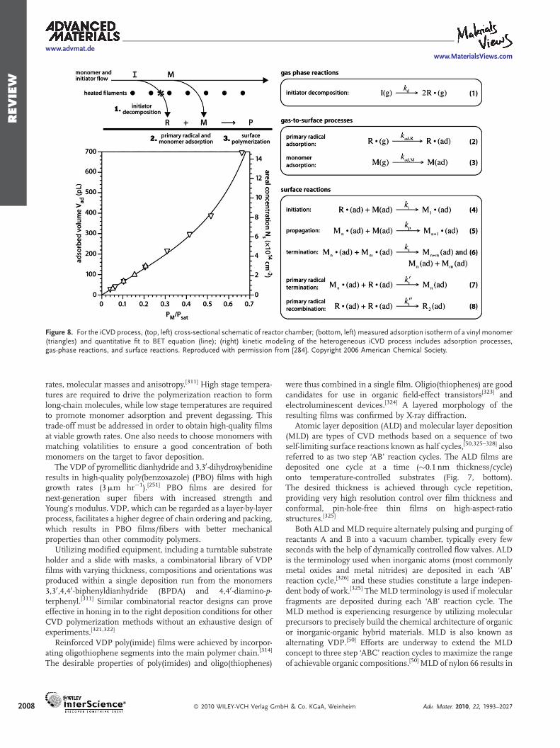
REVIE
W
www.advmat.dewww.MaterialsViews.com
Figure 8. For the iCVD process, (top, left) cross-sectional schematic of reactor chamber; (bottom, left) measured adsorption isotherm of a vinyl monomer(triangles) and quantitative fit to BET equation (line); (right) kinetic modeling of the heterogeneous iCVD process includes adsorption processes,gas-phase reactions, and surface reactions. Reproduced with permission from [284]. Copyright 2006 American Chemical Society.
2008
rates, molecular masses and anisotropy.[311] High stage tempera-tures are required to drive the polymerization reaction to formlong-chain molecules, while low stage temperatures are requiredto promote monomer adsorption and prevent degassing. Thistrade-off must be addressed in order to obtain high-quality filmsat viable growth rates. One also needs to choose monomers withmatching volatilities to ensure a good concentration of bothmonomers on the target to favor deposition.
The VDP of pyromellitic dianhydride and 3,30-dihydroxybenidineresults in high-quality poly(benzoxazole) (PBO) films with highgrowth rates (3mm hr�1).[251] PBO films are desired fornext-generation super fibers with increased strength andYoung’s modulus. VDP, which can be regarded as a layer-by-layerprocess, facilitates a higher degree of chain ordering and packing,which results in PBO films/fibers with better mechanicalproperties than other commodity polymers.
Utilizing modified equipment, including a turntable substrateholder and a slide with masks, a combinatorial library of VDPfilms with varying thickness, compositions and orientations wasproduced within a single deposition run from the monomers3,30,4,40-biphenyldianhydride (BPDA) and 4,40-diamino-p-terphenyl.[311] Similar combinatorial reactor designs can proveeffective in honing in to the right deposition conditions for otherCVD polymerization methods without an exhaustive design ofexperiments.[321,322]
Reinforced VDP poly(imide) films were achieved by incorpor-ating oligothiophene segments into the main polymer chain.[314]
The desirable properties of poly(imides) and oligo(thiophenes)
� 2010 WILEY-VCH Verlag Gmb
were thus combined in a single film. Oligio(thiophenes) are goodcandidates for use in organic field-effect transistors[323] andelectroluminescent devices.[324] A layered morphology of theresulting films was confirmed by X-ray diffraction.
Atomic layer deposition (ALD) and molecular layer deposition(MLD) are types of CVD methods based on a sequence of twoself-limiting surface reactions known as half cycles,[50,325–328] alsoreferred to as two step ‘AB’ reaction cycles. The ALD films aredeposited one cycle at a time (�0.1 nm thickness/cycle)onto temperature-controlled substrates (Fig. 7, bottom).The desired thickness is achieved through cycle repetition,providing very high resolution control over film thickness andconformal, pin-hole-free thin films on high-aspect-ratiostructures.[325]
Both ALD and MLD require alternately pulsing and purging ofreactants A and B into a vacuum chamber, typically every fewseconds with the help of dynamically controlled flow valves. ALDis the terminology used when inorganic atoms (most commonlymetal oxides and metal nitrides) are deposited in each ‘AB’reaction cycle,[326] and these studies constitute a large indepen-dent body of work.[325] The MLD terminology is used if molecularfragments are deposited during each ‘AB’ reaction cycle. TheMLD method is experiencing resurgence by utilizing molecularprecursors to precisely build the chemical architecture of organicor inorganic-organic hybrid materials. MLD is also known asalternating VDP.[50] Efforts are underway to extend the MLDconcept to three step ‘ABC’ reaction cycles to maximize the rangeof achievable organic compositions.[50] MLD of nylon 66 results in
H & Co. KGaA, Weinheim Adv. Mater. 2010, 22, 1993–2027

REVIE
W
www.MaterialsViews.comwww.advmat.de
high molecular orientation of the polymer chains perpendicularto the substrate.[329] Thicker films also displayed highermolecularweights. MLD growth from pyrometallic dianhydride (A) and2,4-diaminonitrobenzene (B) found that the optimum tempera-ture for monomolecular layer growth differed for the case of B’sgrowth on A when compared to A’s growth on B.[330] Thisobservation is attributed to a difference in vapor pressures of Aand B. Using 4,4’-diaminodiphenyl ether instead of2,4-diaminonitrobenzene allowed monomolecular layer growthto occur at the same temperature.
Homo-bifunctional molecules taking the form XRX andYR’Y are conducive to the ‘AB’ cycles of MLD, including thegrowth of nylon 66.[50] However, both functional groups canreact with chemical groups on the surface within each halfreaction, thus limiting propagation of polymer chaingrowth. Strategies to overcome this issue include 1) using ‘AB’cycles with hetero-bifunctional reactants such as H2N-R-OH, 2)employing ring-opening reactions in which a concealedfunctionality prevents a double reaction with the surface, 3)using reactants with protected groups, and 4) surfaceactivation where one functional group on a hetero-bifunctionalprecursor reacts with an active surface species. Additionalchemistry to transform the second functional group to a moreactive functional group is carried out and the reaction cycles canthen repeat.
3.2. CVD Fundamentals
3.2.1. Adsorption-, Reaction-, and Diffusion-limited Rate Regimes
Control over the CVD deposition rate, conformality, and filmproperties, requires understanding of the complex interplaybetween system chemistry, mass and energy transport, andreactor design.[331,332] The rate-limiting step for film depositiondepends on the specific processing conditions. ForiCVD[86,263,285] and for CVD poly(p-xylylene),[333–335] depositionrates typically increase as substrate temperature decreases
Figure 9. CVD process for poly(p-xylylene). (left) [2,2]paracyclophane, also knThis monomer adsorbs by either chemisorption or physisorption to a cooled suwith temperature, resulting in lower expermentally observed deposition rates tpermission from [334]. Copyright 2002 American Chemical Society.
Adv. Mater. 2010, 22, 1993–2027 � 2010 WILEY-VCH Verlag G
(Fig. 9). This apparent negative activation energy is the signaturethat surface adsorption of a reactive species is the rate-limitingstep. In the adsorption-limited regime, increased substratetemperature reduces adsorption onto the surface, leading tolower deposition rates, but often thickness uniformity isimproved.[336,337] While the adsorption-limited regime is com-monly observed for CVD polymers, in most inorganic CVDprocesses, increasing substrate temperature enhances depositionrate. The latter trend can correspond to a reaction-limited regime,where increasing substrate temperature accelerates the kineticsof the thermally- activated, rate-limiting surface reaction step.Alternatively, if the substrate temperature is increased suffi-ciently, the surface reaction kinetics are no longer rate-limitingand the rate of increase of deposition rate with increasingsubstrate temperature slows.[332] At these high substratetemperatures, the mass transport of reactants to (or reactionbyproducts from) the surface by diffusion through the boundarylayer above the substrate becomes the rate-limitingmechanism.[338]
For iCVD, where radicals form from the thermal decomposi-tion of initiator molecules, the filament temperature stronglyinfluences deposition rate. At low filament temperatures,deposition rate increases with filament temperature accordingto the Arrhenius relation.[78,107,273,339] The gas temperaturebetween the filaments and the surface can be modeled using alogarithmic temperature profile from which an apparentactivation energy can be derived.[340,341] The values obtainedare consistent with activation energy for the thermal decom-position of the initiator molecule, indicating that the radicalformation from the initiator is the rate-limiting step. At higherfilament temperatures, there is a weaker dependence betweendecomposition rate and filament temperature, suggesting thatmass transport of the radical species to the surface becomes therate-limiting mechanism.
3.2.2. Monomer Adsorption and Reactivity
Monomer adsorption to the substrate is often the rate-limitingstep for iCVD. This leads to a decrease in film deposition rates as
own as di-p-xylylene, is thermally cracked to monomeric units. (right, inset)bstrate and reacts to form poly(p-xylylene); monomer adsorption decreaseshat are in good agreement with model predictions (right). Reproduced with
mbH & Co. KGaA, Weinheim 2009
REVIE
W
www.advmat.dewww.MaterialsViews.com
2010
substrate temperature increases, as was also observed for CVDpoly(p-xylylenes) (Fig. 9). Values of the enthalpy of desorptionderived from Arrhenius behavior of iCVD film growth rates as afunction substrate temperature are 40.9 kJ mol�1 for ethylacrylate,[285] 49.7 kJ mol�1 for ethylene glycol diacrylate,[342] and60.7 kJ mol�1 for 1H,1H,2H,2H-perfluorodecyl acrylate.[86] Thesevalues fall in the range of 20 to 80 kJ mol�1 typical for thephysisorption of small molecules.[343] For the iCVD copolymer-ization of poly(trivinyltrimethylcyclotrisiloxane) (V3D3) andhexavinyldisiloxane (HVDS) the apparent activation energy wasmeasured to be �41 kJ mol�1.[248] Also falling in this range is theheat of desorption for the reactive monomer cracked from[2.2]paracyclophane, 75 kJ mol�1.[241]
Surface polymerization is favored over gas-phase chain growthby operating at low pressures, where there is a negligibleprobability of the three-body gas-phase collisions required tosatisfy the conservation of energy requirement for bimolecularreactions. Gas-phase propagation is also hindered by the limitedvolatility of the growing chain. For instance, the saturatedvapor pressure, PSAT, of the vinyl monomer butyl methacrylate at25 8C is 2.44 Torr (1 Torr¼ 133.32 Pa). While no data isavailable for the dimer, a similar molecule, dibutyl ester of2,2,4-trimethylpentanedioic acid, has a PSATof 0.0015 Torr at 25 8C.Assuming this molecule is a suitable analog for a butylmethacrylate dimer, the dimer would be predicted to be�1000x less volatile than the monomer.[1]
Measured adsorption data for different vinyl monomersdisplay similar trends when plotted against the dimensionlessquantity PM/PSAT, the ratio of the monomer’s partial pressure to itsvapor pressure, also termed the fractional saturation ratio (Fig. 8).Unlike the surface concentration of the adsorbed monomer, themonomer partial pressure, PM, represents a process variable thatcan be directly controlled during CVD reactor operation. Thus,the fractional saturation ratio is a key practical figure of merit forobtaining insight into the nature ofmonomer surface coverage onthe growth surface.
Additionally, while measuring an adsorption isotherm is timeconsuming, it is often simple to approximate the vapor pressureof the monomer, PSAT, as a function of temperature using readilyavailable data. Given only two data points, such as PSAT at ambienttemperature and the normal boiling point (PSAT¼ 1 atm), thepredicted value of PSAT at any substrate temperature can beestimated using the Claussius-Claperyon relationship or a relatedempirically based correlation method.
Knowledge of PM/PSAT is extremely powerful for rapidlydetermining the window of processing parameters capable ofiCVD film growth for a new monomer. Indeed, these guidelineshave led to the rapid expansion of the number of iCVD polymers(>50 different monomers). For a given set of pressure andsubstrate temperature conditions, some monomers are toovolatile and thus unable to achieve sufficient surface concentra-tion for efficient polymerization. Other monomers haveinsufficient volatility, becoming difficult to deliver into thechamber or condensing during operation. Similar considerationsare likely to be relevant for many of the other CVD polymerizationtechniques.
The Brunauer–Emmett–Teller (BET) isotherm provides anexcellent quantitative description of QCM data obtained for theadsorption of vinyl monomers (Fig. 8). From the BET analysis,
� 2010 WILEY-VCH Verlag Gmb
monolayer coverage for the vinyl monomers ethyl acrylate,[285]
butyl acrylate,[285] and 1H,1H,2H,2H-perfluorodecyl acrylate[86]
corresponds to areal concentrations of approximately 8.0� 1014,5.6� 1014, and 2.7� 1014 molecules cm�2, respectively. Thesevalues are roughly an order of magnitude lower than the arealdensity of silicon atoms, which is reasonable given the molecularsize of the vinyl monomers. Additionally, the observed trend isconsistant with differences in molecular size between themonomers.
For ethyl acrylate, monolayer coverage occurs at PM/PSAT¼ 0.42.Lower fractional saturation ratios correspond to submonolayercoverage. For PM/PSAT <0.3, the surface concentration is nearlylinear with monomer partial pressure (Henry’s law limit).[285]
Above the PM/PSAT value corresponding to monolayer coverage,multilayer adsorption is operative. By operating at partialpressures that are a reasonable fraction of the vapor pressure,adsorption serves to concentrate the monomers onto the surface.Under these conditions, the surface displays liquid-like con-centrations, whereas the gas-phase concentration in the CVDreactor is several orders of magnitude lower than for a liquid.Thus, the high density of monomer on the surface explains thehigh rates obtainable for some CVD polymer processes, as therelevant monomer concentration determining the heterogeneouskinetic rate is the high interfacial value, rather than the lowvapor-phase one. A value of unity for PM/PSAT corresponds tocondensation of a liquid phase. However, condensation at coldspots in the reactor and dynamic pressure transients resultingfrom valve operation, typically make operation at PM/PSAT >0.8quite challenging. One source of local cooling is theJoule–Thompson effect, associated with the expansion of feedstreams delivering reactants to the low pressure growth chamber.
Estimating monomer surface concentration based on thedimensionless fractional saturation ratio facilitates optimizingthe deposition rate for existing process. The growth rate and theaverage number molecular weight of the iCVD polymer bothincrease as PM/PSAT increases.[285] The conformality of iCVDdeposition decreases as PM/PSAT increases.[344] Nevertheless,deposition of conformal iCVD films is achievable at ratesapproaching �100 nm min�1.
Copolymerization requires the simultaneous control of surfaceconcentration for two monomer species. Experimentally, simul-taneous control is easiest to achieve when both monomers havesimilar values of PSAT. The surface concentrations of the twoadsorbed species can be quantitatively related to the compositionof the deposited film using kinetic analysis developed for solutionpolymerization. Indeed, the random copolymerization ofmethacrylic acid with ethyl acrylate,[198] of glycidyl methacrylatewith 2,2,3,3,4,4,5,5,6,6,7,7-dodecafluoroheptyl acrylate,[85] and ofmethyl a-chloroacrylate with methacrylic acid,[294] can each bedescribed quantitatively by the Fineman–Ross copolymerizationeqution. This analysis accounts for the relative probability ofreaction between two like monomers versus between unlikepairs. The reactivity ratios calculated for the three iCVDcopolymerization systems described above are in reasonableagreement with values determined from solution polymerization,again supporting the hypothesis of heterogeneous polymeriza-tion in a nearly liquid-like adsorbed surface layer.Copolymerization by iCVD incorporating a monomer havingtwo or more vinyl groups is an opportunity to deposit insoluble,
H & Co. KGaA, Weinheim Adv. Mater. 2010, 22, 1993–2027

REVIE
W
www.MaterialsViews.comwww.advmat.de
controllably crosslinked films in single-step and thereby increas-ing solvent resistance and enhancing mechanical properties.
When the probability for reaction between unlike monomersfar exceeds that for like pairs, a perfectly alternating copolymer(...ABABAB...) forms. Alternating polymerization was demon-strated for iCVD deposition of the electron-rich vinyl monomerstyrene with the electron-deficient monomer maleic anhydride.As the partial pressures of the two monomers were varied, thedeposited composition remained at 50 mol-% of each species.Spectroscopic characterization confirmed the structure of all theiCVD films as poly(styrene-alt-maleic anhydride).[108]
The propagation rate constant for a vinyl monomer, kP, derivedfrom solution measurements, often correlates with observed filmdeposition rates.[1] The acrylate monomers often have similarhigh values of kP and can provide iCVD growth rates exceeding400 nmmin�1. At a given value of PM/PSAT, a similar range of iCVDgrowth rates for acrylate precursors is observed. Methacrylatesoften have lower kP values and corresponding lower iCVD growthrates are observed. Both kP and iCVD growth rates are typicallyeven lower for styrenic monomers.
The quantitative analysis of the iCVD process along withdimensionless analysis of the transport phenomena facilitatesscale-up. Indeed, successful semi-continuous roll-to-roll iCVDgrowth has been demonstrated in a reactor having a 300mmwidth.[86]
3.2.3. Step Coverage and Sticking Coefficient
The degree of conformality over the micro- and nanoscalefeatures is determined by the details of the chemistry andtransport phenomena occuring during the CVD process.Conversely, the validity of a proposed CVD mechanism can betested using the observed conformality over a trench feature, suchas the ones shown in Fig. 1a.[15,344] Conformality can bequantified as step coverage: the ratio of the film thickness at aparticular location in the feature as compared to the filmthickness at the wafer surface. For process conditions resulting indiffusion-limited deposition, depletion of precursors inside thetrench leads to poor step coverage.[345] Additionally, the CVDreactions can produce concentration gradients of the precursorsinside the trenches, resulting in differences in local growth ratesfor non-zero order surface kinetics. Thus, good step coverage isfacilated by surface reactions that are zero-order with respect to aprecursor species.
Step coverage also depends on the reactive sticking coefficient(g), which is defined as the probability of a precursor speciesadsorbing/reacting each time it strikes the surface.[346] As g
increases, species increasingly stick to the surface on impact,leading to a faster deposition at the trench opening and poor stepcoverage. Conversely, low values of g lead to multiple collisionsbefore sticking, allowing for deposition deep inside high-aspect-ratio features. The observed value of g depends on thechemical structure of the precursor, the surface coverage of allspecies, and the substrate temperature.[347,348]
A kinetic model was developed for CVD poly(p-xylylene),where the adsorption of the monomer on the surface wastreated as the limiting step.[334] According to the model, themonomer would first physisorb onto the surface and wouldchemisorb only after overcoming an energy barrier (Fig. 9). Forthe chemisorbed monomer, g was 2.0� 10�5 at 60 8C and
Adv. Mater. 2010, 22, 1993–2027 � 2010 WILEY-VCH Verlag G
increased to 1.4� 10�3 at �60 8C. These low values of stickingcoefficients account for the excellent conformality observed forCVD poly(p-xylylene).
Under typical CVD polymerization conditions, the mean freepaths of the reacting species are much longer than thedimensions of microtrenches.[346,349] Therefore, collisionsbetween molecules and the trench walls occur more often thancollisions with other molecules. In this regime, a simple ballisticmodel was developed to estimate g for the radical species fromthe observed step coverage of iCVD from themonomer cyclohexylmethacrylate (CHMA).[344] With increasing surface concentrationof the monomer, g for the initiator radical increased from 0.011 at60 8C to 0.05 at 30 8C. This result suggests that an initiator radicalmust strike a vinyl bond in adsorbed monomer in order to react,an Eley–Rideal type mechanism. Changing the substratetemperature at constant monomer surface concentration didnot affect g for the radicals, indicating that the unreacted andvolatile radicals simply desorbed back to the vapor phase. Similarbehavior was also observed during iCVD from divinylprecursors.[342]
3.2.4. Reactor Design and Scale-up
The fundamental design of a CVD system requires threecomponents: 1) a precursor delivery system, 2) a reactionchamber, 3) and an effluent-handling system.[350–353] The reactionchamber is typically custom-designed for a specific substrategeometry and to include peripherals for process monitoring,[354]
such as in situ growth rate measurements by laser interfero-metry[285] or spectrometers to gain real-time knowledge of thegas-phase compositions.[354] The precursor delivery systems varydepending on whether the precursor is a solid, liquid, or gas.Solid precursors are typically sublimed or heated beyond theirmelting point to form a liquid. Depending on the precursor vaporpressure, liquid-phase precursors can be metered through needlevalves, mass flow controllers, flash evaporators, or by bubblingwith a carrier gas. The reaction-chamber design allows for controlover the process parameters that determine reaction kinetics,such as the temperature and the pressure. The materials ofconstruction determine the permissible range of operation andthe reactor geometry is designed for controlling the fluiddynamics and mass and energy transport properties of thereagents.[354]
CVD reactors typically operate at low pressures relative toambient. Mechanical rotary vane pumps in series with a rootsblower can reliably achieve pressures between 10�5–10�3 Torr.Ultrahigh vacuum levels between 10�10–10�12 Torr can bereached with a turbomolecular pump roughed by a rotary vanepump. A comprehensive overview of the vacuum systemsavailable for achieving the desired operating pressure isavailable.[355]
Effluent handling is specific to each application and isemployed to minimize equipment and health hazards. In orderto prolong the lifetime of vacuum equipment, traps are installedahead of the inlet to prevent corrosion of the working pumpsurfaces. Furthermore, toxic effluents from the pump can beneutralized by a scrubbing system prior to atmospheric release.For example, cryogenic condensation/distillation, pressure swingadsorption, and membrane separation have been used to mediateperfluorocarbon emissions from semiconductor processing.[356]
mbH & Co. KGaA, Weinheim 2011
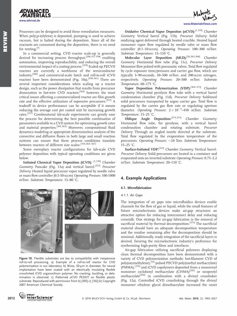
REVIE
W
www.advmat.dewww.MaterialsViews.com
2012
Processes can be designed to avoid these remediation measures.When poly(p-xylylene) is deposited, pumping is used to achievevacuum, but is halted during the deposition. Since all of thereactants are consumed during the deposition, there is no needfor venting.[7]
In a commercial setting, CVD reactor scale-up is generallydesired for increasing process throughput,[296,357,358] enablingautomation, improving reproducibility, and reducing the overallenvironmental impact of a coating process.[359] Scaled-up PECVDreactors are currently a workhorse of the semiconductorindustry,[360] and commercial-scale batch and roll-to-roll iCVDreactors have been demonstrated (Fig. 10a).[296,361] There areseveral important considerations when scaling up a reactordesign, such as the power dissipation that results from precursordissociation in hot-wire CVD reactors;[362] however, the mostcritical issues affecting a commercialized reactor are film growthrate and the effective utilization of expensive precursors.[357] Atradeoff in device performance can be acceptable if it meansreducing the average cost per coated unit by increasing growthrates.[357] Combinatorial lab-scale experiments can greatly easethe process for determining the best possible combination ofparameters available to a CVD system for optimizing growth ratesand material properties.[301,363] Moreover, computational fluiddynamics modeling or appropriate dimensionless analysis of theconvective and diffusive fluxes in both large and small reactionsystems can ensure that these process conditions translatebetween reactors of different size scales.[354,364–367]
Some exemplary reactor configurations for lab-scale CVDpolymer deposition with typical operating conditions are givenbelow:
Initiated Chemical Vapor Deposition (iCVD): [1,159] ChamberGeometry: Pancake (Fig. 11a) and vertical barrel.[252] PrecursorDelivery: Heated liquid precursor vapor regulated by needle valveor mass flow controller (0.5-50 sccm)Operating Pressure: 100-1000mTorr. Substrate Temperature: 15–80 8C.
Figure 10. Flexible substrates are key to compatibility with inexpensiveroll-to-roll processing. a) Example of a roll-to-roll reactor for CVDpolymerization in our laboratory. b) Wires, 50mm in diameter, for neuralimplantation have been coated with an electrically insulating flexiblecrosslinked iCVD organosilicon polymer. No cracking, buckling, or dela-mination is observed. c) Patterned oCVD PEDOT on flexible plasticsubstrate. Reproduced with permission from b) [305] c) [162] b) Copyright2007 American Chemical Society.
� 2010 WILEY-VCH Verlag Gmb
Oxidative Chemical Vapor Depositon (oCVD):[1,159] ChamberGeometry: Vertical barrel (Fig. 11b). Precursor Delivery: Solidoxidizing agent delivered through heated crucible. Heated liquidmonomer vapor flow regulated by needle valve or mass flowcontroller (0.1–10 sccm). Operating Pressure: 100–300 mTorr.Substrate Temperature: 15–110 8C.
Molecular Layer Deposition (MLD):[56,262,368] ChamberGeometry: Horizontal flow tube (Fig. 11c). Precursor Delivery:Monomer flow pulsed with pneumatic valves. Total flow regulatedby cycle exposure time/pressure and carrier gas flow, which aretypically 3–90 seconds, 20–500 mTorr, and 200 sccm nitrogen,respectively. Operating Pressure: 20–500 mTorr. SubstrateTemperature: 60–175 8C.
Vapor Deposition Polymerization (VDP):[369–372] ChamberGeometry: Horizontal pyrolysis flow tube with a vertical barrelcondensation chamber (Fig. 11d). Precursor Delivery: Sublimedsolid precursors transported by argon carrier gas. Total flow isregulated by the carrier gas flow rate or regulating aperturediameter. Operating Pressure: 2� 10�3–450 mTorr. SubstrateTemperature: 15–25 8C.
Oblique Angle Deposition:[373,374] Chamber Geometry:Horizontal flow tube, for pyrolysis, with a vertical barrelcondensation chamber and rotating substrate. PrecursorDelivery: Through an angled nozzle directed at the substrate.Total flow regulated by the evaporation temperature of theprecursors. Operating Pressure: �10 Torr. Substrate Temperature:15–25 8C.
Surface-Initiated VDP:[243] Chamber Geometry: Vertical barrel.Precursor Delivery: Solid precursors are heated in a container andevaporated onto an inverted substrateOperating Pressure: 0.75–2.2mTorr. Substrate Temperature: 20–110 8C.
4. Example Applications
4.1. Microfabrication
4.1.1. Air Gaps
The integration of air gaps into microfluidics devices enablechannels for the flow of gas or liquid, while the small features offuture microelectronic devices make air-gap structures anattractive option for reducing interconnect delay and reducingcrosstalk. One strategy for air-gap fabrication is the removal ofsacrificial material by thermal decomposition.[375] The sacrificialmaterial should have an adequate decomposition temperatureand the residue remaining after the decomposition should beminimal. Additionally, ready integration of the sacrificial layers isdesired, favoring the microelectronic industry’s preference forsynthesizing high-purity films and interfaces.
Air-gap fabrication utilizing sacrificial polymers displayingclean thermal decomposition have been demonstrated with avariety of CVD polymerization methods: hot-filament CVD ofpoly(oxymethylene),[32] pulsed PECVD poly(methyl methacrylate)(PMMA),[376] and iCVD copolymers deposited from a monovinylmonomer cyclohexyl methacrylate (CHMA)[295] or neopentylmethacrylate[292] in combination with a divinyl crosslinker(Fig. 12a). Controlled iCVD crosslinking through the divinylmonomer ethylene glycol dimethacrylate increased the onset
H & Co. KGaA, Weinheim Adv. Mater. 2010, 22, 1993–2027

REVIE
W
www.MaterialsViews.comwww.advmat.de
Figure 11. Examples of reactors for CVD polymerization. Common configurations for a) iCVD, b) oCVD, c)MLD, and d) VDP. Reproduced with permissionfrom a,b) [159], c) [262], d) [371]. a,b) Copyright 2009 Royal Society of Chemistry. c) Copyright 2002 AIP. d) Copyright 1999 Elsevier.
temperature for thermal decomposition, improved the solventresistance of the layer, and prevented its delamination from thesubstrate.[295] For iCVD crosslinking imparted by ethylene glycoldiacrylate, increased modulus, hardness and onset temperatureof decomposition resulted, with the trade-off of an increase inpercentage of residue after decomposition.[292] UV-assisteddecomposition of the sacrificial materials deposited by CVD tocreate air-gaps has been also reported.[377]
4.1.2. Micromechanical and Electrical Systems (MEMS)
Potential applications for MEMS are expanding to include rapiddiagnostics, drug delivery, 3-D artificial organs, and integratedsystems for personalized medicine.[200,378–380] Smaller dimen-sions, the ability to incorporate sensing, signaling, and actuationfunctions on the same substrate, and enhanced functionality are afew of the desired attributes.
Device bonding is always one of the most challenging aspectsof the fabrication process and restricts the choice of substratematerials.[381] For example, oxygen plasma bonding is widelyutilized, but is applicable only to Si-containing materials, such asPDMS and glass.[382,383] Furthermore, the aggressive oxidizingplasma will degrade cells or deactivate organic functional groupspresent on the surfaces. Adhesive bonding provides high bondingstrength, but non-conformal coatings can clog small chan-nels.[383] Thus, because conformal films can be applied to virtually
Adv. Mater. 2010, 22, 1993–2027 � 2010 WILEY-VCH Verlag G
any substrate by CVD, this solventless adhesive bonding strategyis very attractive for MEMS fabrication of miniaturized devices ina wide range of materials.
While reactive CVD coatings have been formed directly in theconfined channels of assembled microfluidics,[53] extending thisapproach to complex channel microgeometries is likely difficult.Alternately, several schemes have been successful for applyingfunctional and adhesive CVD polymers to unbonded devicecomponents.[298,384,385] Contacting the surfaces followed byannealing or UV curing completes the bonding while thefunctional groups inside the channel remain for subsequentbiological binding. The CVD bonding methods are applicable to abroad range of substrate materials, enabling greater choice in thematerials of construction for MEMS fabrication.
UV irradiation of surfaces coated with iCVD poly(glycidylmethacrylate) (PGMA) provided successful simultaneous micro-fluidic device sealing and channel functionalization.[384] Thesealed devices withstood modest pressures (22 psia).
Simultaneous bonding and functionalization was also achievedthrough the thermally activated (140 8C) reaction of the amineand aldehyde functional groups present in poly(4-formyl-p-xylylene-co-p-xylylene) and poly(4-aminomethyl-p-xylylene-co-p-xylylene) CVD polymer films.[385] This solventless adhesivebonding process is applicable to a wide range of materials,including PDMS, poly(tetrafluoroethylene) (PTFE), stainless
mbH & Co. KGaA, Weinheim 2013

REVIE
W
www.advmat.dewww.MaterialsViews.com
Figure 12. Integration of CVD polymers into microfabricated devices. a)Air gaps formed using an iCVD sacrificial polymer. b) Improved bonding ofmicrofluidics components and reduced channel dimensions result fromapplying an epoxide-functional iCVD polymer applied to the PDMS partand an amine-functional polymer to the poly(urethane) part. Adhesionresults from covalent bond formation that occurs when the two parts arebrought together and held a moderate temperature. c) Sensors withswitch-like responses in electrical resistance are based on the deflectionof iCVD-coated microcantilevers. The reaction of amine analytes with thereactive polymer coating is responsible for deflection and closure ofthe switch. d) Cantilevers coated with PECVD polymerized pentafluoros-tyrene undergo significant deflection as hydrazine absorbs in the film dueto the increased stress from the microstructured surface of the polymercoating. a) [295], b) [298], c) [200], d) [386]. a) Copyright 2006 TheElectrochemical Society. b) Copyright 2009 The Royal Society of Chemistry.c) Copyright 2009 IEEE.
2014
steel, glass, silicon and gold. Tensile stress data showed thebonding strength is >1.21 MPa for sealed devices. Custommonomer synthesis was required and the sealing mechanismresults in formation of reaction byproducts which must outgasfrom the seal.
Conformal coatings of iCVD PGMA served as a component ofthe high-strength nanoadhesives used in the fabrications ofmicro- and nanofluidic devices.[298] The iCVD PGMA wasdeposited conformally on a substrate containing channels. Toclose the channels, the PGMA surface was mated to a flat surfacecoated with PECVD poly(allylamine) (PAAm) and thermallybonding at 70 8C. Covalent tethers form between the comple-mentary surfaces without any gaseous byproducts, and therequired monomers are commercially available. Sealed deviceswith channel widths as small as 200 nm able to withstand >50psia were fabricated on silicon, glass, quartz, PDMS, poly(styr-ene), poly(ethylene terephthalate), poly(carbonate), and PTFE
� 2010 WILEY-VCH Verlag Gmb
(Fig. 12b). Successful functionalization of the epoxy and aminegroups remaining in the channel was achieved.
4.1.3. Devices: Cantilever Sensors
Over the course of the past decade, bimaterial microcantilevershave gained considerable attention as efficient and accuratechemical, biological, and thermal sensing devices.[386,387]
The microcantilever sensors consist of an inorganic cantileversubstrate coated with a responsive soft material; differences in thephysical, chemical, or mechanical properties of the materialsresult in the generation of differential stress and cantileverdeflection in the presence of a target stimulus. CVD polymeriza-tion methods facilitate the synthesis of thin, uniform, andresponsive coatings on the cantilevers. Crosslinked alternatingiCVD copolymers coated onto silicon nitride cantilevers swelledirreversibly upon exposure to amine-containing analytes(Fig. 12c).[200] The stress generation deflected the cantileverand produced an on/off switch exhibiting a six-orders-of-magnitude change in resistivity when the gold coatingon the underside of the cantilever contacted the underlyinginterdigitated electrodes. A peroxide sensor utilized the iCVDvapor-phase mechanism to induce optically detectable deflec-tion.[388] Peroxide-contaminated air is passed through filaments,and the resulting radicals adsorb onto a cantilever coated with amonolayer of surface-tethered reactive monomers. Chain poly-merization along the surface of the microcantilever causesdeflection. The granular surface morphology resulting fromPECVD polymerization processes enhances diffusion of targetanalytes into pentafluorostyrene, methacrylonitrile, and acryloni-trile films and their resulting swelling responses; rapid, reversiblechemical sensors as well as a humidity sensor with a detectionlimit in the range of 10 ppb have been demonstrated(Fig. 12d).[386] Observation of swelling-induced cantilever deflec-tion also serves as an effective method of testing the chemicalfunctionality of CVD polymers.[389,390] The differential stressrequired for deflection can occur in the presence of thermalstimuli if the organic and inorganic layers have vastly differentthermal expansion coefficients. Microcantilever temperaturesensors with a resolution of 0.2 mK were fabricated viaPECVD of poly(styrene).[391] Integration of a piezoelectric ZnOnanobelt into a PECVD benzonitrile-coated cantilever yields atemperature-sensitive device capable of acting as both a thermalsensor and a switch.[392]
4.1.4. Patterning
High-resolution functional polymer patterns have recentlygained exposure from their widespread applications in tissueengineering and biosensors,[393–396] anti-biofouling,[397,398]
microelectronics,[399–401] optics,[402,403] and MEMS.[404] Bothconventional[405–409] and nonconventional lithography[37,406,410]
can produce relief structures in functional CVD polymers(Fig. 13). These patterns can serve as a resist to enable patterningof an underlying layer or to subsequently immobilize specifictarget molecules or nanoparticles (Fig. 14).[411–413] Traditionalsubtractive processing of polymers is often incompatible withfunctional-group retention. The use of high-energy plasmaetching or corrosive solvents in pattern transfer from the resistto the organic CVD underlayer can destroy the delicate reactivemoieties in the CVD films.[414,415] These issues are exacerbated by
H & Co. KGaA, Weinheim Adv. Mater. 2010, 22, 1993–2027

REVIE
W
www.MaterialsViews.comwww.advmat.de
the lack of etch selectivity between organic CVD layers andorganic resists.[416] Additive processing can eliminate some ofthese difficulties (Fig. 13a); however, the pattern resolution andachievable film thicknesses can be limiting.[290]
Another approach is to chemically pattern a blanket film of thevapor-deposited polymer by selectively localizing target moleculesonto the reactive films using an elastomeric stamp,[6,417,418] hardmask,[419,420] or other spatially selective transfer process.[421,422] Acombination of topological and chemical patterning have beenextensively used for selectively immobilizing biomolecules ontovapor-deposited patterns from functionalized poly(p-xylylene)films (Figs. 13b and 14a).[98,100,423–429]
Figure 13. Micro- and nanopatterning of CVD polymer films. a) Additiveprocessing utilizing microcontact printing transition metals and salts thatinhibit polymer synthesis, resulting in selective growth of poly(p-xylylene).b) Patterns in functionalized CVD poly(p-xylylene) generated using shadowmasks. c) iCVD copolymer positive-tone e-beam resist at 60 nm resolution.d) Conventional lift-off photolithography is used to pattern oCVD PEDOTthat is grafted to Si; small features easily delaminate from the substrate forungrafted PEDOT (inset). e) Complex patterns in grafted oCVD PEDOTcreated using capillary force lithography. f) Preapplication of patterns ofinitiator molecules on the substrate prior to monomer introduction lead toperiodic morphology in poly(methyl methacrylate) (PMMA). Reproducedwith permission from a) [411], b) [423], c) [294], d,e) [162], f) [35]. a)Copyright 2000 American Chemical Society. c) Copyright 2006 AmericanChemical Society. f) Copyright 2003 American Chemical Society.
Adv. Mater. 2010, 22, 1993–2027 � 2010 WILEY-VCH Verlag G
Traditional lithographic processing offers the ability to createhigh-resolution patterns from CVD polymers and is the mostpromising method to accommodate in vivo measurementsusing systems-on-chip.[430] Hot-filament CVD (includingiCVD)[293,300,431] and physical vapor deposition (PVD)[432] havebeen used to deposit ‘‘dry’’ positive- and negative-tone e-beamresists (Fig. 13c),[294] including ones that are compatible withsupercritical CO2 development. These dry-applied resists over-come the shortcomings associated with patterning usingtraditional solution-deposited polymer photoresists.[431,432] Theconformal nature of CVD allows application of resist layers ontonon-planar substrates.[300,433] Furthermore, eliminating ‘‘wetprocessing’’ prevents pattern collapse of high-aspect-ratiofeatures during drying,[434] avoids solvent residues and impu-rities,[432,434] and reduces the negative environmental impactassociated with large volumes of solvent.[300]
High-resolution e-beam patterning for linewidths as small as60 nm was achieved on grafted oCVD and functional iCVDlayers.[109,162] Poly(propargyl methacrylate) (PPMA) is a click-active iCVD polymer that exhibits direct positive-tone sensitivityto e-beam irradiation. PPMA was directly patterned at 200 nmresolution without a resist (Fig. 14b).[109] Grafting provides thesefilms with the chemical and mechanical stability necessary forwithstanding subsequent click functionalization with selectivelyconjugated quantum dots.
Patternability is a key for integrating conducting polymers intoelectronic circuits and requires excellent adhesion of theconducting polymer to the substrate. The oCVD method enablesthe systematic ability to graft conducting polymers to substrates,preventing delamination during patterning (Fig. 13d,e).[162] Theoxidant, FeCl3, is a Friedel–Crafts catalyst that simultaneouslycreates radical cations on the monomer and on the substrate,provided the substrate contains aromatic groups. Indeed, oCVDPEDOT films covalently attach to poly(styrene), poly(ethyleneterephthalate), poly(carbonate), poly(ethylene naphthalate),poly(urethane), and poly(acrylonitrile butadiene styrene) sub-strates.[162] The adhesion provided by grafting enables theresolution of 60 nm features of oCVD PEDOT on flexiblepoly(ethylene terephthlate) substrates. Extending this concept,silane coupling agents containing aromatic groups enable thegrafting of PEDOT on silicon and glass, facilitating subsequentpatterning on these substrates.
Functional CVD polymer surfaces have been used to covalentlytether inorganic particles. Using oCVD, poly(pyrrole-co-thiophene-3-acetic acid) films were able to covalently attachsilver nanoparticles (Fig. 14c).[64] The resultant compositematerial had significantly enhanced conductivity as comparedto the polymer-only film. An interesting result observed was thatthe conductivity of the resulting hybrids depended on the type oflinker molecule employed for the assembly and use of aconjugated linker molecule (e.g. 4-aminothiophenol) resulted inan enhancement of the resulting hybrids.[64,163] Quantum dotswere also assembled onto the conducting oCVD copolymer films(Fig. 14d) to enable the fabrication of hybrid light-emittingdiodes.[164]
Materials patterning through nonconventional lithography canreduce the cost of patterning fine structures when compared totraditional nanofabrication techniques.[406] Capillary force litho-graphy[435] has been used for creating 110 nm line patterns from
mbH & Co. KGaA, Weinheim 2015

REVIE
W
www.advmat.dewww.MaterialsViews.com
Figure 14. CVD functional polymer films for subsequent attachments ofdye molecules (a,e), nanoparticles (b,c,d), and cells (f,g). a) Ethynyl-functionalized poly(p-xylylene) films are reactively patterned with azideligands through ‘‘click’’ chemistry. Fluorescence is localized to thepatterns as fluorescently labeled streptavidin binds to the ligands. Scalebar represents 50mm. b) AFM of iCVD poly(propargyl methacrylate)(PPMA) after patterning of 2mm wide lines and use of ‘‘click’’ chemistryfor the attachment quantum dots. Reactions between the carboxylic acidsof -COOH functionalized conductive polymers enables covalent tetheringof c) metal nanoparticles and d) quantum dots. The SEM (c) and AFM(d) images show that the nanoparticles remain after ultrasonication.The fluorescence observed in the inset in (d) indicates that negligibleagglomeration of the quantum dots. e) Fluorescent micrographs ofpatterns of two layers of orthogonally reactive iCVD polymers. The toplayer is patterned through capillary force lithography, and then bothlayers are functionalized with fluorescent moieties simultaneously in asingle reaction mixture. (Scale bar represents 30mm) f) Humanumbilical vein endothelial cells grown on amine functionalizedpoly(p-xylylene) CVD coatings g) Patterns in reactive poly(p-xylylene)-control the attachment of bovine aortic endothelial cells. Reproduced withpermission from a) [98], b) [109], c) [64], e) [297], f) [451], g) [427].e) Copyright 2008 American Chemical Society. g) Copyright 2002 AmericanChemical Society.
2016 � 2010 WILEY-VCH Verlag Gmb
bifunctional CVD polymers for one-pot, self-sorting, bio-functionalizable surfaces (Fig. 14e).[297] Colloidal lithographyhas been coupled with iCVD to generate high-resolution graftedpolymeric layers with lateral features as small as 25 nm (Fig. 5d).This represents a generic ‘‘bottom-up’’ process that is aninexpensive, simple, and environmentally friendly techniquefor creating robust, well-ordered arrays of functional patternedpolymeric nanostructures.[180] Transmission electron microscopy(TEM) grids have been used as templates for patterninghigh-fidelity micrometer-scale patterns of alternating hydropho-bic and hydrophilic materials deposited by pulsed PECVD[175]
and as a shadow mask for styrene graft polymerizationfrom maleic anhydride pulsed PECVD polymer films.[436]
Microcontact printing has been used to selectively depositphotoinitiators for additively patterned photoinitiated CVDpolymer films.[290]
4.2. Biomedical
There are multiple motivations for the surface modification ofbiomaterials,[437] such as the immobilization of biomolecules atthe surface, promotion of cell adhesion and growth, andinfluencing blood-material interactions, including thrombogeni-city. Additionally, improving the lubricity, surface electricalproperties (either insulating or conductive), wear resistance,and corrosion resistance of biomedical devices is often desired.The surface layer needs to be as thin as possible, without beingdegraded, eroded, or delaminated by the biological environment,and thus crosslinking and/or covalent tethering may berequired.[437] Well-adhered, conformal, ultrathin (<100 nm)CVD coatings of functional polymeric materials which can beapplied to virtually any substrate at room temperature are desiredfor tissue engineering applications.[438]
The reader is refered to a number of reviews on the extensiveresearch on organic PECVD layers for biomedical applica-tions.[26,274,437,439–446] Commercially available poly(p-xylylene)and poly(monochloro-p-xylylene) have found widespread com-mercial adaptation as biomedical coatings.[203,372,447,448] CVDfrom custom-substituted [2.2]paracyclophane monomers forproducing functionalized poly(p-xylylenes) has ushered inadditional potential applications in the biomedical field.[53,203,446]
Deposition of poly(2-chloro-p-xylyene) onto a metal stent followedby SO2 plasma treatment reduced the thrombogenicity of thesurface.[449] The immobilization of R-hirudin was also demon-strated on CVD films synthesized from substituted paracyclo-phane monomers.[450]
Spatially directed cell attachment was achieved throughmicrocontact printing of biotinyl-3,6,9-trioxaundecanediaminefollowed by self assembly of linker molecules of streptavidin byreactive CVD polymer coatings (Fig. 14f,g).[53,426,427,448,451] Next,human anti-a5-integrin was immobilized to biotin-patternedregions through the streptavidin linker molecules. Only areaspatterned with human anti-a5-integrin initiate attachment ofbovine aortic endothelial cells. This strategy was then used to coatthe luminal surface of a PDMS microfluidic device to create aversatile, spatially programmable platform compatible with a
H & Co. KGaA, Weinheim Adv. Mater. 2010, 22, 1993–2027

REVIE
W
www.MaterialsViews.comwww.advmat.de
variety of biomolecules. The bifunctional and reactive CVDcopolymers were synthesized from 4-trifluoroacetyl [2.2]para-cyclophane and 4-aminomethyl [2.2]paracyclophane in variousratios, resulting in ketone and aminomethyl functionalization,respectively.[424] Immobilization of Atto 655 ligands followed bybiotin-streptavidin ligands were subsequently carried out,demonstrating the ability of the bifunctional reactive coatingsto facilitate immobilization of substantially differentbiomolecules.
Area selective growth of poly(p-xylylene-4-methyl-2-bromoiso-butyrate-co-p-xylylene) was achieved by performing CVDthrough a microstencil.[100] This CVD coating served as aninitiator for the atom transfer radical polymerization (ATRP) ofoligio(ethylene glycol) methyl ether methacrylate (OEGMA).These spatially programmable hydrogel coatings resisted proteinadsorption and cell adhesion.
Both iCVD and piCVD have demonstrated promise forbiomedical applications.[1,2] The iCVD poly(1,3,5-trivinyltrimethylcyclotrisiloxane) of biopassive coatings on a50mm diameter gold wires is desired for biocompatibleinsulation on permanent neurally implanted devices.[304,305]
Indeed, the bulk resistivity of iCVD poly(1,3,5-trvinyl-trimethylcyclotrisiloxane) exceeds that of the poly(monochloro-p-xylylene) currently used in this application. This flexible andcrosslinked iCVD polymer (Fig. 10b) has exhibited stableinsulating properties under simulated bioimplanted conditionsfor over 2.5 years. The iCVD poly(pentafluorophenyl methacry-late-co-ethylene glycol diacrylate) is a surface-modifiable copoly-mer for ligand attachment through nucleophilic substitution, asdesired for immobilizing peptides for cell adhesion and growth.[6]
Mesh-like piCVD PHEMA films selectively permitted passage ofsmall molecule analytes to an optode sensor while excludinglarger molecules, such as proteins and lipophic drugs fromfouling the surface of the optode sensor.[60] The preparation ofultrathin (�100 nm) hydrogel films by piCVD under mildconditions was ideal for coating the optodes, as damage fromplasma or solvent exposure was avoided.
The columnar[452] or helical[453] sculpted nanowire assembliesformed through oblique angle deposition from functionalizedparacyclophanes films (Fig. 4c) can support fibroblast cellattachment,[454] and can be electrolessly templated withmetals[453] for surfaced enhanced Raman spectroscopy (SERS)of single cells.[455]
The thermoresponsive behavior of poly(N-isopropylacrylamide)(PNIPAAm) (discussed in Section 2.3.3.) alters its affinity towardsproteins and cells. Changing the temperature of pulsed PECVDPNIPAAm surfaces resulted in the fully reversible adsorptionof the proteins fibrinogen and albumin,[210] an improvementin behavior over PNIPAAm deposited using traditionalPECVD.[208,210]
4.3. Membranes
4.3.1 Motivation for CVD Polymer Surface Modification
of Membranes
Membranes are used in a wide range of commercial applicationsspanning from drinking water purification to gas separations,
Adv. Mater. 2010, 22, 1993–2027 � 2010 WILEY-VCH Verlag G
with a market that is expected to grow to over $10 billion by2010.[456] Membranes for aqueous filtrations are often classifiedaccording to the size of the species they reject. Microfiltration(MF) membranes retain particles 0.2mm in size and larger.Ultrafiltration (UF) membranes have pore sizes between2–200 nm and retain macromolecules and colloids.Nanofiltration (NF) membranes retain some small moleculesand doubly charged ions, whereas reverse osmosis (RO)membranes retain essentially all solutes in water, includingsalts. Pervaporation is another membrane technology in whichseparation occurs by the evaporation of feed componentsfollowed by the permeation of these vapors through a membrane.MFandUFmembranes aremicroporous. RO, NF, gas separation,and pervaporation membranes have a thin-film compositestructure, where a porous base is coated by a thin selectivelayer.[457–459] Microporous membranes are also often used assupports for catalysts and enzymes.[460,461]
Membranemodification through coatings has been extensivelyexplored to alter characteristics such as pore size, surfacechemistry, and functionality. Such coatings can be achieved byseveral approaches, including solution-based methods, surfacereactions, and vapor-based techniques. A crucial parameter inthese approaches is the conformality of the coating.
If the objective is to form a coating that covers all membranesurfaces including within its pores, a highly conformal coating isdesired. Such coatings are difficult to form using solutionmethods due to surface-tension limitations (Fig. 1).
Conversely, ultrathin, dense and defect-free blanket coatingsare desired on more mechanically robust base membranes withlarger pores in order to form composite membranes.[457–459] Thecoating acts as the selective layer while the base providesmechanical support. Under identical operating conditions,thinner coatings allow for greater flux through the membranes.Fig. 15 illustrates some of these CVD-based techniques formembrane modification.
The minimum thickness achievable by solution methods islimited by surface-tension effects and the coating equipment.Additionally, solution coatings on membranes are prone todefects due to air bubbles, surface-tension effects, and dust.[457]
Thus, potential advantages for employing CVD polymers as theselective layer of composite membranes include thinness andhigh purity.
4.3.2 Conformal CVD Polymers for Modification of Internal
Pore Surfaces
The presence of charged species and nonuniform electric fieldslimit the uniformity and degree of penetration of plasmas andplasma coatings on membranes.[462] In the case of an asymmetricmembrane with very fine surface pores (e.g. for UFmembranes),only the top surface of the membrane is functionalized if the sidewith the smaller pores is oriented towards the plasma.[463–466] Formembranes with larger pores, such as MF membranes, plasmacan often permeate through the membrane.
Numerous studies report changes in pore diameter or theformation of a crosslinked blanket layer created by exposingmembranes to plasmas containing small organic molecules orsilanes.[11,461,467,468] Pores can become narrower or widerdepending on the comparative rates of deposition and ablation.
mbH & Co. KGaA, Weinheim 2017

REVIE
W
www.advmat.dewww.MaterialsViews.com
Figure 15. CVD-based membrane modification methods. a) Plasma treat-ment to form free-radical initiation sites followed by vapor-phase grafting.b) Formation of a conformal coating. c) Formation of a blanket coating toserve as a selective layer.
2018
Membrane structure and orientation as well as plasma conditionsare very important in limiting the degree of ablation and porewidening, and in determining the degree of conformality of thecoating. To functionalize both the top surface and internalpores of an asymmetric membrane, the porous bottom side ofthe membrane should be oriented to face the plasma.[469,470]
Methods such as pulsed PECVD,[471] low-temperatureplasma,[469,470,472,473] and downstream sample placement[469–471]
are useful both in preventing ablation and for achieving morecontrol over the chemical structure of the resultant coating.
Plasma treatments can be used to create active sites onmembrane surfaces, from which polymer brushes can be grownby exposure to a monomer (Fig. 15a). Grafting is typicallyperformed by removing the membrane from the plasma reactorand immersing it into a monomer solution.[468,474,475] Graftingcan also be performed in the same reactor by evaporating themonomer into the chamber. Plasma-initiated grafting of acrylicacid onto a poly(sulfone) membranes from solution and vaporphases has been demonstrated via these methods.[471] Graftingfrom the solution phase took longer times and resulted in longpolymer chains that blocked pores. Grafting from the vapor phaseresulted in a dense brush of short polymer chains andimproved hydrophilicity. Polymer grafting yield was alsohigher, 25–260mg cm�2 compared with 0.3–12mg cm�2 forsolution-based grafting.[471] This work concluded that graftingfrom the vapor phase is the most reliable method for alteringmembrane surface chemistry. Plasma-initiated grafting from thevapor phase has also been used to graft acrylamide andacrylic acid onto poly(ether sulfone) membranes toreduce fouling[469,470] and to improve the hemocompatibility
� 2010 WILEY-VCH Verlag Gmb
of membranes for blood plasma separation by graftingutilizing the monomers 2-methoxyethyl acrylate[476]
and N,N-dimethylacrylamide.[477] If plasma-initiated grafting iscontinued for an extended time period, pore-filling occurs andmembranes are obtained with significantly tighter pores, asobserved for the grafting of acrylic acid[473] and styrene to convertUF membranes into NF membranes.[472,478,479]
For pores of modest aspect ratio (i.e., pore length:porediameter), such as those in MF membranes,[11] reasonablyconformal PECVD polymer coatings penetrate throughout themembrane thickness (Fig. 15b). This leads to modification ofsurface chemistry of the internal pore surface by thedeposited polymer and also narrows the pore diameter.PECVD amine-functionalized cellulose acetate membranesenabled the immobilization of enzymes.[480] Pulsed PECVDusing the monomers vinyl acetic acid and perfluorohexanenarrowed the pores of track-etched membranes and regulated gasflow through them.[481] In this case, conformality is not ascrucial, as the narrowest region of the pore determines theselectivity. PECVD from n-heptylamine achieved pore narrowingin porous alumina membrane, but these coatings werenon-conformal.[482]
The conformality of iCVD coatings from poly(1H,1H,2H,2H-perfluorodecyl acrylate) was demonstrated on membranes withhigh-aspect-ratio cylindrical pores (up to 125:1).[247,483] The thiniCVD layers, ranging from 10 to 150 nm in thickness, allowedindependent modification of the surface energy of thesemembranes. Conformal iCVD of poly(perfluoroalkyl ethylmethacrylate) onto nanofiber electrospun mats imparted super-hydrophobicity, with a contact angle of 1758 and a thresholdsliding angle less than 2.58 for a 20mg water droplet, and at least‘‘grade 8’’ oleophobicity.[299,484] Varying the iCVD coated mat’shierarchical surface roughness through systematically changingthe diameter of both beaded and bead-free fibers allowed theobserved contact angle behavior to be compared to theoreticalpredictions. Additionally, the conformality of iCVD fluoropoly-mers allowed successful modification of electrospun matscomposed of nanoporous fibers.[299,484] Similarly, oCVD wasused to deposit the conducting polymer PEDOT around thenanofibers in similar electrospunmats (Fig. 1c).[64] Indeed, all-dryconformal CVD processes are enabling technologies formembrane modification utilizing often insoluble polymers, suchas fluoropolymers and conducting polymers.
Highly conformal CVD films can be used to fabricatefree-standing structures.[485]
CVD polymeric nanotubes have been templated by exposinganodic aluminum oxide (AAO) membranes wetted with initiatorto vapor-phase monomer species, followed by etching to removethe AAO template (Fig. 16a).[155,485,486] The ability to tune thethickness of the walls of the nanotube were demonstrated usingconformal CVD poly(acrylonitrile).[155,485,486] In this work,heptane was used as a nonreactive vapor to enhance nanotubewall uniformity. Adding photoluminescent dyes followed by asecond PAN deposition step, created concentric PAN-dye-PANnanotube structures with tunable emission colors. Templatingusing AAOmembranes combined with CVD of the insoluble andinfusible polymer poly(2,5-thienylene vinylene) (PTV) successfulfabricated nanotubes with ultrathin walls (�5 nm thickness)(Fig. 16b).[487]
H & Co. KGaA, Weinheim Adv. Mater. 2010, 22, 1993–2027

REVIE
W
www.MaterialsViews.comwww.advmat.de
4.3.3 Non-Conformal CVD Polymers for Composite Membranes
Blanket coatings can also be used as a selective layer on top ofmembranes (Fig. 15c). Composite membranes prepared byPECVD of allylamine[464,465] and acrylic acid[463] onto porous UFmembranes have demonstrated salt retention, comparable to ROand NF membranes. Additionally, the ultrathin coatings from
Figure 16. a) Schematic process for templating of conformal CVD polymernanotubes using anodic aluminum oxide (AAO) membranes. TEMsdemonstrating a) tunable wall thickness for CVD poly(acrylonitrile) nano-tubes and b) the ultrathin (�5 nm) walls of insoluble, infusible CVDpoly(2,5-thienylene vinylene) AAO-templated nanotubes. Reproduced withpermission from a) [485], b) [487]. a) Copyright 2006 American ChemicalSociety.
Adv. Mater. 2010, 22, 1993–2027 � 2010 WILEY-VCH Verlag G
PECVD of allylamine impart hydrophilicity to the top surface of acomposite pervaporation membrane.[465] Similarly, PECVDpoly(thiophene) was grown on a porous membrane supportand demonstrated for use in pervaporation.[488]
Poly(imide) thin-film composite membranes are typicallymanufactured by interfacial polymerization and used extensivelyfor RO, NF, pervaporation and gas-separation applica-tions.[457,458,489] Under pervaporation testing, VDP poly(imide)layers, ranging between 0.2 and 2mm in thickness, fabricated on aporous base membrane displayed the same selectivities as acomposite membrane with a 20mm thick selective layer preparedby solution methods.[490–492] However, the flux through the VDPmembrane was much higher due to the thinness of thepermselective VDP polyimide layer.
In summary, CVD methods hold significant promise in thedevelopment of improved membrane systems for liquid- andgas-based separations. The potential for CVD polymers lies intheir ability to form ultrathin, pinhole-free coatings, eitherconformally or non-conformally, thus overcoming the limitationson thickness and defects associated with solution processes.Scale-up of these techniques to roll-to-roll processing systems[296]
will also be critical in the application of this technology forcommercial applications.
4.4. Micro- and Nanoparticles and Composites
Polymer composite systems are desired for creating superiormaterial properties.[493,494] Metal-polymer and semiconductor-polymer composites can have enhanced catalytic or optoelectronicproperties.[495] Polymer-clay and polymer-carbon nanotube (CNT)composites impart improved stability and mechanical strength tothe resulting material.[494]
The use of PECVD polymer films to form composites has beenextensively studied, especially with respect to polymer-metalcomposites.[26] Metal and semiconductor nanoparticles have alsobeen incorporated into CVD poly(p-xylylene).[495–500] The CVDpolymerization methods provide control over particle size andagglomeration, which are essential to the physical and chemicalproperties of the composite.[497] One popular method iscryopolymerization in which monomer vapors and sublimedmetal are introduced into the reactor and allowed to condense ona super-cooled substrate, followed by UV-induced solid-statepolymerization.[501] Incorporating Mn and Mg into CVDpoly(p-xylylene) formed optically adsorbing complexes, whileincorporating Ag did not.[495,498] A similar method, usingcyclophanes with an organogermanium bridge, was used toobtain poly(p-xylylene) films with incorporated Ge crystals afterthermal treatment to break the organogermanium bond.[496]
Curing of VDP poly(imide) films embedded with copperphthalocyanine (CuPc) resulted in small crystals of CuPc.[502]
These crystals demonstrated enhanced thermal stability incomparison to vapor-deposited pure CuPc.
Vapor-phase assisted surface polymerization (VASP) of PMMAon clay particles (Fig. 17a) improved the mechanical strength ofthe resulting composite films.[36] The vaporized monomer wasable to penetrate and exfoliate the silicate layers of the claysubstrate. This structure was preserved even after melt
mbH & Co. KGaA, Weinheim 2019

REVIE
W
www.advmat.dewww.MaterialsViews.com
Figure 17. Particle encapsulation and fabrication of composites utilizingCVD polymers. a) Schematic of vapor-phase assisted surface polymeri-zation (VASP) process in which montmorillonite platelets are infiltratedwithmethyl methacrylate vapors which polymerize in the interstitial spaces,leading to improved platelet exfoliation during melt processing of bulkPMMA. b) Agglomerates of CaO (top) have been conformally coated withpoly(b-propiolactone) (bottom) after preapplication of an initiator. c)Dispersed multi-wall carbon nanotubes (MWCNTs) have been coated withpoly(glycidyl methacrylate) (PGMA) by iCVD, showing that each individualtube is coated conformally. Reproduced with permission from a) [36],b) [42], c) [59]. a) Copyright 2009 American Chemical Society.
2020
processing, providing the homogeneous dispersion of silicateplatelets desired for clay-polymer composites.
Surface modification of micro- and nanoparticle composites isdesired for improving their compatibility with the polymericmatrix. Surface-initiated VDP using 2-methyl-2-oxazoline(MeOZO) has been applied to silica nanoparticles.[503] Therelated, gas-phase surface-assisted polymerization (GASP) tech-nique enabled the coating of CaO powder with biodegradableb-propiolactone (Fig. 17b).[42] Functional coatings on micro-spheres have also been demonstrated using both iCVD (Fig. 1b)and piCVD (Fig. 2d).[59,60,199,291] Conformal coatings wereobtained without agglomeration, a significant advantage overliquid-based methods which tend to bind together particles withdiameters below 100mm in diameter.[504] In order to improvecompatibility between the carbon nanotubes and polymeric
� 2010 WILEY-VCH Verlag Gmb
matrices, multiwall CNTs were coated with PMMA via pulsedPECVD, which were then dispersed in a PMMA matrix via meltprocessing methods.[505] Coatings of poly(glycidyl methacylate)(PGMA) were also conformally applied to multiwall CNTs viaiCVD (Fig. 17c).[59,199,291]
5. Conclusions
Delivering vapor-phase monomers which react to form chemi-cally well-defined thin polymeric films is a common thread whichunites the methods for CVD polymerization. Some of thesemethods represent heterogeneous versions of well-knownwet-chemical synthesis techniques, while others have no analogin the liquid phase. When all reactant species are continuouslydelivered through the vapor phase, the CVD polymerizationoccurs in a single step. Single-step methods for chain-growthpolymers include CVD from paracyclophanes, variants ofplasma-enhanced CVD (PECVD), initated CVD (iCVD), andphotoinitated CVD (piCVD). CVD methods for chain-growthpolymers employing the preapplication of a reactive species, suchas an initiator, include vapor-phase assisted surface polymeriza-tion (VASP), surface-initiated vapor deposition polymerization(SI-VDP) and gas-phase assisted surface polymerization (GASP).Examples of single-step CVD of step-growth polymers includevapor deposition polymerization (VDP) and oxidative CVD(oCVD), typically used for condensation polymers and conduct-ing polymers, respectively. The CVD synthesis of conductingpolymer layers using preapplied oxidant has been termed vaporphase polymerization (VPP). Molecular layer deposition (MLD)employs alternating flows of molecular precursors for self-limiting, layer-by-layer formation of step growth polymers.
The conformal, functional, and responsive nature of CVDpolymers makes them highly desirable in surface-modificationapplications. CVD polymers which conform to the geometry ofthe underlying substrate result in film thickness over non-planarsubstrates that are dramatically more uniform than afforded byconventional solution coating methods. By avoiding wetting andsurface-tension effects, conformal CVD films form on complexobjects with micro- and nanoscale features. CVD polymer filmswith 100% functional group incorporation can be grown at highrates. A wide variety of functional groups can be created using asingle reactor platform. Engineering functional group incorpora-tion is key to the design of CVD polymer films which areresponsive to changes in pH, temperature, chemical concentra-tions, and applied electric field. The response can be manifestedthrough changes in surface energy, film thickness, electricalresistance, and/or optical characteristics. CVD polymers whichare responsive to external stimuli have successfully beenintegrated into novel optoelectronic and sensing devices. A thinCVD layer can impart desired surface properties to a substratethat is inexpensive and/or has superior bulk properties.
The CVD of inorganic materials is favored by the semicon-ductor industry for the fabrication of high-purity films andhigh-quality interfaces. Aggressive CVD process conditionsutilized for inorganic CVD, such as high temperatures andinput powers, are generally not compatible with the retention offragile organic functional groups or the synthesis of linear,non-crosslinked polymer chains. Thus, efficient use of energy by
H & Co. KGaA, Weinheim Adv. Mater. 2010, 22, 1993–2027

REVIE
W
www.MaterialsViews.comwww.advmat.de
design of selective chemistry for organic CVD is required in orderto simultaneously retain functional groups while maintaininghigh film deposition rates. The control afforded by the CVDprocess enables both inorganic and organic film properties to besystematically tuned and uniform films to be deposited over largeareas and for adaptation to roll-to-roll processes. Film depositionrate, along with the availability, cost, and effective utilization ofprecursors, are essential factors influencing process commercia-lization. Utilizing a common reactor platform for both inorganicand organic materials simplifies the fabrication of hybrid devices.
CVD offers an alternative when commonly employed solutionmethods for applying polymers to surfaces cannot be imple-mented, thus extending the realm of applications for polymericthin films and surfaces. Insoluble and infusible films, such asfluoropolymers, electrically conductive polymers, and controlla-bly crosslinked networks, can be formed directly in a single step.Lack of stability in solvents or with respect to curing temperaturesmay also limit the use of solution-based coating methods.Additionally, all-dry solventless processing offers the potential forreduced environmental, health, and safety impact.
Many polymer CVD processes are adsorption limited, havingdeposition rates which increase as substrate temperature islowered. These processes are often operated using roomtemperature substrates. Combined with the low input energyenabled by the use of selective chemical pathways and the use ofmodest vacuum levels, surface modification by CVD polymerscan be utilized with virtually any substrate, including thermallysensitive materials, such as paper, textiles, and plastics.
Because CVD polymers are grown from the substrate up, theyoffer the opportunity to create chemical bonds between the filmand the underlying substrate and to grade film composition as afunction of thickness. Covalent grafts at the interface greatlyenhance the adhesion between the film and substrate. Robustattachment of the film to the substrate is essential for manypractical applications, particularly those on flexible substrates.Adhesion is also key for high-resolution patterning of CVDpolymers. Both the additive and subtractive patterning of CVDpolymers has been demonstrated. Resolution of 60 nm featureshas been achieved on flexible substrates. Graded layers allowindependent optimization of surface and bulk film properties.Real-time monitoring of growth permits direct control over thethickness grown. CVD polymerization processes are capable ofdepositing ultrathin (�5 nm) pinhole-free films as well as rapiddeposition of films several micrometers thick.
Quantitative understanding of the fundamentals of adsorption,kinetics, transport, and reactor design has enabled the rapiddiscovery of new CVD homo- and copolymers. Design andoptimization of adsorption-limited CVD polymer processes forspecific applications is greatly facilitated by knowledge of themonomer’s vapor pressure as a function of temperature. Thedimensionless fractional saturation ratio, the ratio of monomer’spartial pressure to its saturation pressure, provides insight intothe degree of monomer surface coverage, which can range fromsubmonolayer to multilayer. The scale-up of reactors fordeposition onto large area substrates and for roll-to-roll operationonto flexible substrates is also made possible by quantitativemodels.
Numerous current and future applications derive from thecombination of properties afforded by CVD polymers in
Adv. Mater. 2010, 22, 1993–2027 � 2010 WILEY-VCH Verlag G
combination with their process compatibility with microfabrica-tion technologies and with substrates of varied composition andshape. Thus, all-dry conformal CVD polymer processes,particularly for insoluble layers, are enabling technologies for awide range of applications including flexible optoelectronics,sensing, MEMS, medical devices, advanced textiles, membranes,and composites.
Acknowledgements
Preparation of this review was supported in part by the US Armythrough the Institute for Soldier Nanotechnologies, under ContractDAAD-19-02-D-0002 with the U.S. Army Research Office.
Received: August 12, 2009
Revised: September 9, 2009
Published online: December 4, 2009
[1] W. E. Tenhaeff, K. K. Gleason, Adv. Funct. Mater. 2008, 18, 979.
[2] R. Sreenivasan, K. K. Gleason, Chem. Vap. Deposition 2009, 15, 77.
[3] S. Wolf, R. N. Tauber, Silicon Processing for the VLSI Era, Vol. 1, Lattice
Press, Sunset Beach 2001.
[4] S. V. Bhat, Biomaterials, Narosa Publishing House, New Delhi 2002.
[5] G. H. Chen, M. Gupta, K. Chan, K. K. Gleason,Macromol. Rapid Commun.
2007, 28, 2205.
[6] W. S. O’Shaughnessy, N. Mari-Buye, S. Borros, K. K. Gleason, Macromol.
Rapid Commun. 2007, 28, 1877.
[7] W. F. Gorham, J. Polym. Sci, Part A: Polym. Chem. 1966, 4, 3027.
[8] G. G. Odian, Principles of Polymerization, Wiley-Interscience, Hoboken
2004.
[9] R. J. Young, P. Lovell, Introduction to Polymers, Chapman & Hall, London
1991.
[10] P. J. Flory, Principles of Polymer Chemistry, Cornell University Press, Ithaca
1953.
[11] H. Yasuda, Luminous Chemical Vapor Deposition and Interface Engineering,
Vol. 122, Marcel Dekker, New York 2005.
[12] H. G. P. Lewis, D. J. Edell, K. K. Gleason, Chem. Mater. 2000, 12, 3488.
[13] S. J. Limb, D. J. Edell, E. F. Gleason, K. K. Gleason, J. Appl. Polym. Sci. 1998,
67, 1489.
[14] E. J. Winder, K. K. Gleason, J. Appl. Polym. Sci. 2000, 78, 842.
[15] C. B. Labelle, K. K. Gleason, Chem. Vap. Deposition 2000, 6, 27.
[16] C. B. Labelle, S. M. Karecki, R. Reif, K. K. Gleason, J. Vac. Sci. Technol, A
1999, 17, 3419.
[17] C. B. Labelle, K. K. Gleason, J. Appl. Polym. Sci. 1999, 74, 2439.
[18] B. A. Cruden, K. K. Gleason, H. H. Sawin, J. Appl. Phys. 2002, 91, 9547.
[19] Q. G. Wu, K. K. Gleason, Plasmas Polym. 2003, 8, 31.
[20] Q. G. Wu, A. D. Ross, K. K. Gleason, Plasma Processes Polym. 2005, 2, 401.
[21] R. Forch, Z. H. Zhang, W. Knoll, Plasma Processes Polym. 2005, 2, 351.
[22] A. Choukourov, H. Biederman, D. Slavinska, L. Hanley, A. Grinevich,
H. Boldyryeva, A. Mackova, J. Phys. Chem. B 2005, 109, 23086.
[23] K. S. Siow, L. Britcher, S. Kumar, H. J. Griesser, Plasma Processes Polym.
2006, 3, 392.
[24] R. d’Agostino, Plasma Processes and Polymers, Wiley-VCH, Weinheim,
Germany 2005.
[25] R. d’Agostino, Advanced Plasma Technology, Wiley-VCH, Weinheim,
Germany 2008.
[26] R. d’Agostino, Plasma Deposition, Treatment, and Etching of Polymers,
Academic Press, San Diego 1990.
[27] C. B. Labelle, S. J. Limb, K. K. Gleason, J. Appl. Phys. 1997, 82, 1784.
mbH & Co. KGaA, Weinheim 2021

REVIE
W
www.advmat.dewww.MaterialsViews.com
2022
[28] S. J. Limb, C. B. Labelle, K. K. Gleason, D. J. Edell, E. F. Gleason, Appl. Phys.
Lett. 1996, 68, 2810.
[29] H. G. Choi, J. P. Amara, T. P. Martin, K. K. Gleason, T. M. Swager,
K. F. Jensen, Chem. Mater. 2006, 18, 6339.
[30] H. G. Choi, J. P. Amara, T. M. Swager, K. F. Jensen, Macromolecules 2006,
39, 4400.
[31] H. G. Choi, J. P. Amara, T. M. Swager, K. F. Jensen, Langmuir 2007, 23,
2483.
[32] L. S. Loo, K. K. Gleason, Electrochem. Solid-State Lett. 2001, 4, G81.
[33] M. C. Kwan, K. K. Gleason, Chem. Vap. Deposition 1997, 3, 299.
[34] A. M. Wrobel, M. R. Wertheimer, J. Dib, H. P. Schreiber, J. Macromol. Sci.
Chem. 1980, A14, 321.
[35] M. Yasutake, S. Hiki, Y. Andou, H. Nishida, T. Endo,Macromolecules 2003,
36, 5974.
[36] Y. Andou, J. M. Jeong, S. Hiki, H. Nishida, T. Endo,Macromolecules 2009,
42, 768.
[37] Y. Andou, H. Nishida, T. Endo, Chem. Commun. 2006, 5018.
[38] M. Yasutake, Y. Andou, S. Hiki, H. Nishida, T. Endo, Macromol. Chem.
Phys. 2004, 205, 492.
[39] J. Li, X. R. Chen, Y. C. Chang, Langmuir 2005, 21, 9562.
[40] Y. Andou, M. Yasutake, J. M. Jeong, M. Kaneko, H. Nishida, T. Endo, J.
Appl. Polym. Sci. 2007, 103, 1879.
[41] Y. Andou, M. Yasutake, J. M. Jeong, H. Nishida, T. Endo,Macromol. Chem.
Phys. 2005, 206, 1778.
[42] H. Nishida, M. Yamashita, Y. Andou, J. M. Jeong, T. Endo, Macromol.
Mater. Eng. 2005, 290, 848.
[43] Y. C. Chang, C. W. Frank, Org. Thin Films 1998, 695, 142.
[44] Y. C. Chang, C. W. Frank, Langmuir 1998, 14, 326.
[45] K. C. Popat, R. W. Johnson, T. A. Desai, J. Vac. Sci. Technol, A 2003, 21,
645.
[46] D. G. Fu, L. T. Weng, B. Y. Du, O. K. C. Tsui, B. Xu, Adv. Mater. 2002, 14,
339.
[47] A. Hult, S. A. Macdonald, C. G. Willson, Macromolecules 1985, 18, 1804.
[48] H. W. Gu, D. Fu, L. T. Weng, J. Xie, B. Xu, Adv. Funct. Mater. 2004, 14, 492.
[49] W. K. Lee, K. C. Caster, J. Kim, S. Zauscher, Small 2006, 2, 848.
[50] S. M. George, B. Yoon, A. A. Dameron, Acc. Chem. Res. 2009, 42, 498.
[51] B. P. Carrow, H. Bakhrit, P. I. Wang, Y. Q. Chen, J. L. Senkevich, Chem. Vap.
Deposition 2006, 12, 239.
[52] F. E. Rasmussen, J. Frech, M. Heschel, O. Hansen, in Boston Transdu-
cers’03: Digest of Technical Papers, Vols. 1 and 2, 2003, 1659.
[53] H. Y. Chen, Y. Elkasabi, J. Lahann, J. Am. Chem. Soc. 2006, 128, 374.
[54] C. Jezewski, C. J. Wiegand, D. X. Ye, A. Mallikarjunan, D. L. Liu, C. M. Jin,
W. A. Lanford, G. C. Wang, J. J. Senkevich, T. M. Lu, J. Electrochem. Soc.
2004, 151, F157.
[55] H. Kim, H. B. R. Lee, W. J. Maeng, Thin Solid Films 2009, 517, 2563.
[56] A. A. Dameron, D. Seghete, B. B. Burton, S. D. Davidson, A. S. Cavanagh,
J. A. Bertrand, S. M. George, Chem. Mater. 2008, 20, 3315.
[57] X. Liang, D. M. King, P. Li, S. M. George, A. W. Weimer, AIChE J. 2009, 55,
1030.
[58] Q. Peng, B. Gong, R. M. VanGundy, G. N. Parsons, Chem.Mater. 2009, 21,
820.
[59] K. K. S. Lau, K. K. Gleason, Adv. Mater. 2006, 18, 1972.
[60] S. H. Baxamusa, L. Montero, J. M. Dubach, H. A. Clark, S. Borros,
K. K. Gleason, Biomacromolecules 2008, 9, 2857.
[61] J. Jang, B. Lim, Angew. Chem, Int. Ed. 2003, 42, 5600.
[62] G. S. Senesi, E. D’Aloia, R. Gristina, P. Favia, R. d’Agostino, Surf. Sci. 2007,
601, 1019.
[63] D. Reuter, A. Bertz, A. Nowack, T. Gessner, Sens. Actuators, A 2008, 145,
316.
[64] S. Vaddiraju, K. Senecal, K. K. Gleason, Adv. Funct. Mater. 2008, 18, 1929.
[65] S. G. Im, D. Kusters, W. Choi, S. H. Baxamusa, M. de Sanden,
K. K. Gleason, ACS Nano 2008, 2, 1959.
[66] I. P. Parkin, R. G. Palgrave, J. Mater. Chem. 2005, 15, 1689.
[67] A. Nakajima, J. Ceram. Soc. Jpn. 2004, 112, 533.
� 2010 WILEY-VCH Verlag Gmb
[68] M. Doms, H. Feindt, W. J. Kuipers, D. Shewtanasoontorn, A. S. Matar,
S. Brinkhues, R. H. Welton, J. Mueller, J. Micromechanics Microengineering
2008, 18.
[69] E. J. Grajeck, W. H. Petersen, Text. Res. J. 1962, 32, 320.
[70] W. D. Bascom, R. L. Cottington, C. R. Singleterry, J. Adhes. 1969, 1, 246.
[71] P. B. Leezenberg, T. C. Reiley, G. W. Tyndall, J. Vac. Sci. Technol, A 1999, 17,
275.
[72] R. d’Agostino, F. Cramarossa, F. Illuzzi, J. Appl. Phys. 1987, 61, 2754.
[73] R. Chen, V. Gorelik, M. S. Silverstein, J. Appl. Polym. Sci. 1995, 56, 615.
[74] D. G. Castner, K. B. Lewis, D. A. Fischer, B. D. Ratner, J. L. Gland, Langmuir
1993, 9, 537.
[75] D. G. Castner, P. Favia, B. D. Ratner, Abstracts of Papers of the American
Chemical Society 1995, 209, 165.
[76] K. K. S. Lau, J. A. Caulfield, K. K. Gleason, Chem. Mater. 2000, 12, 3032.
[77] K. K. S. Lau, H. G. P. Lewis, S. J. Limb, M. C. Kwan, K. K. Gleason, Thin
Solid Films 2001, 395, 288.
[78] H. G. P. Lewis, J. A. Caulfield, K. K. Gleason, Langmuir 2001, 17, 7652.
[79] K. K. S. Lau, K. K. Gleason, J. Fluorine Chem. 2000, 104, 119.
[80] T. P. Martin, K. K. S. Lau, K. Chan, Y. Mao, M. Gupta, A. S. O’Shaughnessy,
K. K. Gleason, Surf. Coat. Technol. 2007, 201, 9400.
[81] K. K. S. Lau, Y. Mao, H. G. P. Lewis, S. K. Murthy, B. D. Olsen, L. S. Loo,
K. K. Gleason, Thin Solid Films 2006, 501, 211.
[82] F. Intranuovo, E. Sardella, P. Rossini, R. d’Agostino, P. Favia, Chem. Vap.
Deposition 2009, 15, 95.
[83] K. K. S. Lau, J. Bico, K. B. K. Teo, M. Chhowalla, G. A. J. Amaratunga,
W. I. Milne, G. H. McKinley, K. K. Gleason, Nano Lett. 2003, 3, 1701.
[84] S. R. Coulson, I. S. Woodward, J. P. S. Badyal, S. A. Brewer, C. Willis,
Langmuir 2000, 16, 6287.
[85] Y. Mao, K. K. Gleason, Macromolecules 2006, 39, 3895.
[86] M. Gupta, K. K. Gleason, Langmuir 2006, 22, 10047.
[87] M. L. Ma, M. Gupta, Z. Li, L. Zhai, K. K. Gleason, R. E. Cohen,
M. F. Rubner, G. C. Rutledge, Adv. Mater. 2007, 19, 255.
[88] S. Boduroglu, M. Cetinkaya, W. J. Dressick, A. Singh, M. C. Demirel,
Langmuir 2007, 23, 11391.
[89] G. D. Meakins, Functional Groups: Characteristics and Interconversions, Vol.
35, Oxford University Press, Oxford 1996.
[90] B. D. Gates, Q. B. Xu, J. C. Love, D. B. Wolfe, G. M. Whitesides, Annu. Rev.
Mater. Res. 2004, 34, 339.
[91] D. Losic, J. G. Shapter, J. J. Gooding, Langmuir 2001, 17, 3307.
[92] X. M. Zhao, J. L. Wilbur, G. M. Whitesides, Langmuir 1996, 12, 3257.
[93] G. T. Hermanson, Bioconjugate Techniques, Academic Press, San Diego
1996.
[94] N. M. Adarnczyk, A. A. Dameron, S. M. George, Langmuir 2008, 24, 2081.
[95] M. Arroyo-Hernandez, J. Perez-Rigueiro, J. M. Martinez-Duart,Mater. Sci.
Eng, C 2006, 26, 938.
[96] J. Lahann, R. Langer, Macromolecules 2002, 35, 4380.
[97] H. Nandivada, H. Y. Chen, J. Lahann, Macromol. Rapid Commun. 2005,
26, 1794.
[98] H. Nandivada, H. Y. Chen, L. Bondarenko, J. Lahann, Angew. Chem, Int.
Ed. 2006, 45, 3360.
[99] L. Nebhani, C. Barner-Kowollik, Adv. Mater. 2009, 21, 1.
[100] X. W. Jiang, H. Y. Chen, G. Galvan, M. Yoshida, J. Lahann, Adv. Funct.
Mater. 2008, 18, 27.
[101] C. G. Spanos, J. P. S. Badyal, A. J. Goodwin, P. J. Merlin, Polymer 2005, 46,
8908.
[102] D. Jung, S. Yeo, J. Kim, B. Kim, B. Jin, D. Y. Ryu, Surf. Coat. Technol. 2006,
200, 2886.
[103] S. J. Hutton, J. M. Crowther, J. P. S. Badyal, Chem. Mater. 2000, 12, 2282.
[104] L. Francesch, E. Garreta, M. Balcells, E. R. Edelman, S. Borros, Plasma
Processes Polym. 2005, 2, 605.
[105] S. Schiller, J. Hu, A. T. A. Jenkins, R. B. Timmons, F. S. Sanchez-Estrada,
W. Knoll, R. Forch, Chem. Mater. 2002, 14, 235.
[106] C. Tarducci, E. J. Kinmond, J. P. S. Badyal, S. A. Brewer, C. Willis, Chem.
Mater. 2000, 12, 1884.
H & Co. KGaA, Weinheim Adv. Mater. 2010, 22, 1993–2027

REVIE
W
www.MaterialsViews.comwww.advmat.de
[107] Y. Mao, K. K. Gleason, Langmuir 2004, 20, 2484.
[108] W. E. Tenhaeff, K. K. Gleason, Langmuir 2007, 23, 6624.
[109] S. G. Im, B. S. Kim, L. H. Lee, W. E. Tenhaeff, P. T. Hammond,
K. K. Gleason, Macromol. Rapid Commun. 2008, 29, 1648.
[110] A. J. Heeger, Angew. Chem, Int. Ed. 2001, 40, 2591.
[111] T. A. Skotheim, R. L. Elsenbaumer, J. R. Reynolds,Handbook of Conducting
Polymers, Marcel Dekker, Inc, New York 1998.
[112] J. L. Bredas, G. B. Street, Acc. Chem. Res. 1985, 18, 309.
[113] P. Chandrasekhar, Conducting Polymers, Fundamentals and Applications: A
Practical Approach, Springer, New York 1999.
[114] J. L. Bredas, R. J. Silbey, Conjugated Polymers: The Novel Science and
Technology of Highly Conducting and Nonlinear Optically Active Materials,
Kluwer Academic Publishers, Dordrecht 1991.
[115] H. Yamato, K. Kai, M. Ohwa, T. Asakura, T. Koshiba, W. Wernet, Synth.
Met. 1996, 83, 125.
[116] N. K. Guimard, N. Gomez, C. E. Schmidt, Prog. Polym. Sci. 2007, 32, 876.
[117] D. Hohnholz, A. G. MacDiarmid, D. M. Sarno, W. E. Jones, Chem.
Commun. 2001, 2444.
[118] F. Tran-Van, S. Garreau, G. Louarn, G. Froyer, C. Chevrot, J. Mater. Chem.
2001, 11, 1378.
[119] B. Winther-Jensen, D. W. Breiby, K. West, Synth. Met. 2005, 152, 1.
[120] F. Jonas, J. T. Morrison, Synth. Met. 1997, 85, 1397.
[121] H. T. Sahin, Central European J. Chem. 2007, 5, 824.
[122] J. P. Lock, S. G. Im, K. K. Gleason, Macromolecules 2006, 39, 5326.
[123] H. Meng, D. F. Perepichka, F. Wudl, Angew. Chem, Int. Ed. 2003, 42, 658.
[124] E. Vasallo, L. Laguardia, M. Catellani, A. Cremona, F. Dellera, F. Ghezzi,
Plasma Processes Polym. 2007, 4, S801.
[125] L. M. H. Groenewoud, G. H. M. Engbers, J. G. A. Terlingen,
H. Wormeester, J. Feijen, Langmuir 2000, 16, 6278.
[126] N. V. Bhat, D. S. Wavhal, J. Appl. Polym. Sci. 1998, 70, 203.
[127] R. K. Sadhir, K. F. Schoch, Thin Solid Films 1993, 223, 154.
[128] M. S. Silverstein, I. Visoly-Fisher, Polymer 2002, 43, 11.
[129] L. M. H. Groenewoud, G. H. M. Engbers, J. Feijen, Langmuir 2003, 19,
1368.
[130] K. Tanaka, K. Yoshizawa, T. Takeuchi, T. Yamabe, J. Yamauchi, Synth. Met.
1990, 38, 107.
[131] M. E. Ryan, A. M. Hynes, S. H. Wheale, J. P. S. Badyal, C. Hardacre,
R. M. Ormerod, Chem. Mater. 1996, 8, 916.
[132] R. Dams, D. Vangeneagden, D. Vanderzande, Chem. Vap. Deposition 2006,
12, 719.
[133] J. G. Wang, K. G. Neoh, E. T. Kang, Thin Solid Films 2004, 446, 205.
[134] B. Winther-Jensen, K. Norrman, P. Kingshott, K. West, Plasma Processes
Polym. 2005, 2, 319.
[135] T. W. Kim, J. H. Lee, J. W. Back, W. G. Jung, J. Y. Kim,Macromol. Res. 2009,
17, 31.
[136] J. L. Yague, N. Agulo, S. Borros, Plasma Processes Polym. 2008, 5, 433.
[137] P. A. Tamirisa, K. C. Liddell, P. D. Pedrow,M. A. Osman, J. Appl. Polym. Sci.
2004, 93, 1317.
[138] X. Y. Gong, L. M. Dai, A. W. H. Mau, H. J. Griesser, J. Polym. Sci, Part A:
Polym. Chem. 1998, 36, 633.
[139] U. S. Sajeev, C. J. Mathai, S. Saravanan, R. R. Ashokan, S. Venkatachalam,
M. R. Anantharaman, Bull. Mater. Sci. 2006, 29, 159.
[140] P. Giungato, M. C. Ferrara, F. Musio, R. d’Agostino, Plasma Polym. 1996,
1, 283.
[141] K. Tanaka, S. Okazaki, T. Inomata, M. Kogoma, Symp. Plasma Sci. Mater.
1995, 8, 33.
[142] L. Martin, J. Esteve, S. Borros, Thin Solid Films 2004, 451, 74.
[143] X. Xie, J. U. Thiele, R. Steiner, P. Oelhafen, Synth. Met. 1994, 63, 221.
[144] A. Mohammadi, M. A. Hasan, B. Liedberg, I. Lundstrom, W. R. Salaneck,
Synth. Met. 1986, 14, 189.
[145] J. Kim, D. Sohn, Y. Sung, E. R. Kim, Synth. Met. 2003, 132, 309.
[146] J. Kim, E. Kim, Y. Won, H. Lee, K. Suh, Synth. Met. 2003, 139, 485.
[147] B. Winther-Jensen, K. West, Macromolecules 2004, 37, 4538.
Adv. Mater. 2010, 22, 1993–2027 � 2010 WILEY-VCH Verlag G
[148] B. Winther-Jensen, J. Chen, K. West, G. Wallace,Macromolecules 2004, 37,
5930.
[149] J. Chen, B. Winther-Jensen, Y. Pornputtkul, K. West, L. Kane-Maquire,
G. G. Wallace, Electrochem. Solid-State Lett. 2006, 9, C9.
[150] S. Admassie, F. L. Zhang, A. G. Manoj, M. Svensson, M. R. Andersson,
O. Inganas, Sol. Energy Mater. Sol. Cells 2006, 90, 133.
[151] B. Winther-Jensen, O. Winther-Jensen, M. Forsyth, D. R. MacFarlane,
Science 2008, 321, 671.
[152] A. Gadisa, K. Tvingstedt, S. Admassie, L. Lindell, X. Crispin,
M. R. Andersson, W. R. Salaneck, O. Inganas, Synth. Met. 2006, 156,
1102.
[153] L. Lindell, A. Burquel, F. L. E. Jakobsson, V. Lemaur, M. Berggren,
R. Lazzaroni, J. Cornil, W. R. Salaneck, X. Crispin, Chem. Mater. 2006,
18, 4246.
[154] F. Cacialli, P. Bruschi, J. Appl. Phys. 1996, 80, 70.
[155] J. Jang, J. H. Oh, Chem. Commun. 2004, 882.
[156] L. Dall’Acqua, C. Tonin, A. Varesano, M. Canetti, W. Porzio, M. Catellani,
Synth. Met. 2006, 156, 379.
[157] S. G. Im, K. K. Gleason, Macromolecules 2007, 40, 6552.
[158] S. G. Im, E. A. Olivetti, K. K. Gleason, Surf. Coat. Technol. 2007, 201, 9406.
[159] S. H. Baxamusa, S. G. Im, K. K. Gleason, Phys. Chem. Chem. Phys. 2009,
11, 5227.
[160] S. G. Im, K. K. Gleason, E. A. Olivetti, Appl. Phys. Lett. 2007, 90.
[161] J. P. Lock, J. L. Lutkenhaus, N. S. Zacharia, S. G. Im, P. T. Hammond,
K. K. Gleason, Synth. Met. 2007, 157, 894.
[162] S. G. Im, P. J. Yoo, P. T. Hammond, K. K. Gleason, Adv. Mater. 2007, 19,
2863.
[163] S. Vaddiraju, K. K. Gleason, Manuscript in Preparation 2009.
[164] S. Vaddiraju, K. K. Gleason, Manuscript in Preparation 2009.
[165] S. Vaddiraju, H. Cebeci, B. L. Wardle, K. K. Gleason, Manuscript in
Preparation 2009.
[166] S. Iwatsuki, M. Kubo, H. Yamashita, Chem. Lett. 1989, 729.
[167] S. Iwatsuki, M. Kubo, T. Kumeuchi, Chem. Lett. 1991, 1071.
[168] E. G. J. Staring, D. Braun, G. Rikken, R. Demandt, Y. Kessener,
M. Bouwmans, D. Broer, Synth. Met. 1994, 67, 71.
[169] A. K. Li, N. Janarthanan, C. S. Hsu, Polym. Bull. 2000, 45, 129.
[170] K. M. Vaeth, K. F. Jensen, Macromolecules 2000, 33, 5336.
[171] I. Tokarev, S. Minko, Soft Matter 2009, 5, 511.
[172] G. P. Lopez, B. D. Ratner, R. J. Rapoza, T. A. Horbett,Macromolecules 1993,
26, 3247.
[173] M. Morra, C. Cassinelli, J. Biomed. Mater. Res. 1995, 29, 39.
[174] C. Tarducci, W. C. E. Schofield, J. P. S. Badyal, Chem. Mater. 2002, 14,
2541.
[175] G. S. Malkov, I. T. Martin, W. B. Schwisow, J. P. Chandler, B. T. Wickes,
L. J. Gamble, D. G. Castner, E. R. Fisher, Plasma Processes Polym. 2008, 5,
129.
[176] C. A. Pfluger, R. L. Carrier, B. Sun, K. S. Ziemer, D. D. Burkey, Macromol.
Rapid Commun. 2009, 30, 126.
[177] K. Chan, K. K. Gleason, Langmuir 2005, 21, 8930.
[178] M. Karaman, S. E. Kooi, K. K. Gleason, Chem. Mater. 2008, 20,
2262.
[179] N. Mari-Buye, S. O’Shaughnessy, C. Colominas, C. E. Semino,
K. K. Gleason, S. Borros, Adv. Funct. Mater. 2009, 19, 1276.
[180] N. J. Trujillo, S. H. Baxamusa, K. K. Gleason, Chem. Mater. 2009, 21, 742.
[181] L. Montero, S. H. Baxamusa, S. Borros, K. K. Gleason, Chem.Mater. 2009,
21, 399.
[182] P. K. H. Ho, D. S. Thomas, R. H. Friend, N. Tessler, Science 1999, 285, 233.
[183] K. D. Singer, T. Kazmierczak, J. Lott, H. Song, Y. H. Wu, J. Andrews,
E. Baer, A. Hiltner, C. Weder, Opt. Express 2008, 16, 10358.
[184] A. Convertino, A. Capobianchi, A. Valentini, E. N. M. Cirillo, Adv. Mater.
2003, 15, 1103.
[185] R. E. Marchant, S. D. Johnson, B. H. Schneider, M. P. Agger,
J. M. Anderson, J. Biomed. Mater. Res. 1990, 24, 1521.
mbH & Co. KGaA, Weinheim 2023

REVIE
W
www.advmat.dewww.MaterialsViews.com
2024
[186] L. C. M. Han, R. B. Timmons, J. Polym. Sci, Part A: Polym. Chem. 1998, 36,
3121.
[187] S. Bouaidat, B. Winther-Jensen, S. F. Christensen, J. Jonsmann, Sens.
Actuators, A 2004, 110, 390.
[188] K. Chan, L. E. Kostun, W. E. Tenhaeff, K. K. Gleason, Polymer 2006, 47,
6941.
[189] U. Edlund, M. Kallrot, A. C. Albertsson, J. Am. Chem. Soc. 2005, 127, 8865.
[190] A. Wirsen, H. Sun, A. C. Albertsson, Polymer 2005, 46, 4554.
[191] H. Sun, Z. W. Wu, Mater. Lett. 2009, 63, 729.
[192] E. S. Gil, S. A. Hudson, Prog. Polym. Sci. 2004, 29, 1173.
[193] Y. Ogiwara, M. Kanda, M. Takumi, H. Kubota, J. Polym. Sci, Part A: Polym.
Lett. 1981, 19, 457.
[194] Y. Ogiwara, K. Torikoshi, H. Kubota, J. Polym. Sci, Part A: Polym. Lett.
1982, 20, 17.
[195] Y. Ogiwara, H. Kubota, J. Polym. Sci, Part A: Polym. Lett. 1985, 23, 365.
[196] K. Allmer, A. Hult, B. Ranby, J. Polym. Sci, Part A: Polym. Chem. 1988, 26,
2099.
[197] M. Ulbricht, A. Oechel, C. Lehmann, G. Tomaschewski, H. G. Hicke, J.
Appl. Polym. Sci. 1995, 55, 1707.
[198] K. K. S. Lau, K. K. Gleason, Macromol. Biosci. 2007, 7, 429.
[199] K. K. S. Lau, K. K. Gleason, Surf. Coat. Technol. 2007, 201, 9189.
[200] W. J. Arora, W. E. Tenhaeff, K. K. Gleason, G. Barbastathis, J. Microelec-
tromechanical Syst. 2009, 18, 97.
[201] W. E. Tenhaeff, K. K. Gleason, Macromolecules, in press
[202] Y. L. Wang, Y. C. Chang, Macromolecules 2003, 36, 6511.
[203] M. Yoshida, R. Langer, A. Lendlein, J. Lahann, Polym. Rev. 2006, 46, 347.
[204] D. Bhattacharyya, K. Pillai, O. M. R. Chyan, L. P. Tang, R. B. Timmons,
Chem. Mater. 2007, 19, 2222.
[205] L. Q. Chu, X. N. Zou, W. Knoll, R. Forch, Surf. Coat. Technol. 2008, 202,
2047.
[206] P. A. Tamirisa, D. W. Hess, Macromolecules 2006, 39, 7092.
[207] P. A. Tamirisa, J. Koskinen, D. W. Hess, Thin Solid Films 2006, 515, 2618.
[208] X. H. Cheng, H. E. Canavan, M. J. Stein, J. R. Hull, S. J. Kweskin,
M. S. Wagner, G. A. Somorjai, D. G. Castner, B. D. Ratner, Langmuir
2005, 21, 7833.
[209] Y. V. Pan, R. A. Wesley, R. Luginbuhl, D. D. Denton, B. D. Ratner,
Biomacromolecules 2001, 2, 32.
[210] D. O. H. Teare, D. C. Barwick, W. C. E. Schofield, R. P. Garrod, A. Beeby,
J. P. S. Badyal, J. Phys. Chem. B 2005, 109, 22407.
[211] A. Kubono, M. Murai, S. Tasaka, Jpn. J. Appl. Phys. 2008, 47, 5553.
[212] S. Bauer, S. B. Lang, IEEE Trans. Dielectr. Electr. Insul. 1996, 3, 647.
[213] Y. Takahashi, S. Ukishima, M. Iijima, E. Fukada, J. Appl. Phys. 1991, 70,
6983.
[214] X. S. Wang, M. Iijima, Y. Takahashi, E. Fukada, Jpn. J. Appl. Phys. 1993, 32,
2768.
[215] X. S. Wang, Y. Takahashi, M. Iijima, E. Fukada, Jpn. J. Appl. Phys. 1995, 34,
1585.
[216] M. Tsukiji, H. Kowa, K. Muraki, N. Umeda, K. Morii, M. Honda, Y. Tajitsu,
Jpn. J. Appl. Phys. 2006, 45, 7531.
[217] T. Hattori, Y. Takahashi, M. Iijima, E. Fukada, J. Appl. Phys. 1996, 79,
1713.
[218] Y. Tajitsu, H. Ohigashi, A. Hirooka, A. Yamagishi, M. Date, T. Hattori,
E. Fukada, Jpn. J. Appl. Phys. 1996, 35, 5199.
[219] T. Hattori, M. Iijima, Y. Takahashi, E. Fukada, Y. Suzuki, M. Kakimoto,
Y. Imai, Jpn. J. Appl. Phys. 1994, 33, 4647.
[220] Y. Tajitsu, K. Ishida, S. Kanbara, H. Ohigashi, M. Date, E. Fukada, Jpn. J.
Appl. Phys. 1998, 37, 5375.
[221] H.Muguruma, M. Ishikawa, J. Nakada, S. Hotta, Y. Takahashi, Jpn. J. Appl.
Phys. 2004, 43, L859.
[222] A. Kubono, N. Okui, Prog. Polym. Sci. 1994, 19, 389.
[223] A. C. Rastogi, S. B. Desu, Chem. Vap. Deposition 2006, 12, 742.
[224] A. Kubono, T. Kitoh, K. Kajikawa, S. Umemoto, H. Takezoe, A. Fukuda,
N. Okui, Jpn. J. Appl. Phys. 1992, 31, L1195.
[225] J. Sakata, M. Mochizuki, Thin Solid Films 1990, 188, 123.
� 2010 WILEY-VCH Verlag Gmb
[226] A. Takeno, N. Okui, T. Kitoh, M. Muraoka, S. Umemoto, T. Sakai, Thin
Solid Films 1991, 202, 205.
[227] A. Takeno, N. Okui, T. Kitoh, M. Muraoka, S. Umemoto, T. Sakai, Thin
Solid Films 1991, 202, 213.
[228] J. P. Deng, L. F. Wang, L. Y. Liu, W. T. Yang, Prog. Polym. Sci. 2009, 34, 156.
[229] J. A. DeFranco, B. S. Schmidt, M. Lipson, G. G. Malliaras, Org. Electron.
2006, 7, 22.
[230] B. Zhao, W. J. Brittain, Prog. Polym. Sci. 2000, 25, 677.
[231] A. Wirsen, H. Sun, A. C. Albertsson, Biomacromolecules 2005, 6, 2697.
[232] A. Wirsen, H. Sun, L. Emilsson, A. C. Albertsson, Biomacromolecules 2005,
6, 2281.
[233] T. P. Martin, K. L. Sedransk, K. Chan, S. H. Baxamusa, K. K. Gleason,
Macromolecules 2007, 40, 4586.
[234] P. K. Chu, J. Y. Chen, L. P. Wang, N. Huang, Mater. Sci. Eng, R 2002, 36,
143.
[235] P. Heinz, F. Bretagnol, I. Mannelli, L. Sirghi, A. Valsesia, G. Ceccone,
D. Gilliland, K. Landfester, H. Rauscher, F. Rossi, Langmuir 2008, 24, 6166.
[236] V. Castelvetro, E. Fatarella, L. Corsi, S. Giaiacopi, G. Ciardelli, Plasma
Processes Polym. 2006, 3, 48.
[237] M. B. Chan-Park, S. S. Tan, Int. J. Adhes. Adhes. 2002, 22, 471.
[238] R. R. Rye, G. C. Nelson, M. T. Dugger, Langmuir 1997, 13, 2965.
[239] S. W. Choi, W. B. Choi, Y. H. Lee, B. K. Ju, M. Y. Sung, B. H. Kim, J.
Electrochem. Soc. 2002, 149, G8.
[240] J. Duchet, J. F. Gerard, J. P. Chapel, B. Chabert, J. Adhes. Sci. Technol. 2000,
14, 691.
[241] J. B. Fortin, T. Lu, Chemical Vapor Deposition Polymerization: The Growth
and Properties of Parylene Thin Films, Kluwer Academic Publishers, Boston
2004.
[242] N. H. Lee, C. W. Frank, Langmuir 2003, 19, 1295.
[243] Y. L. Wang, Y. C. Chang, Langmuir 2002, 18, 9859.
[244] P. Hanefeld, U. Westedt, R. Wombacher, T. Kissel, A. Schaper,
J. H. Wendorff, A. Greiner, Biomacromolecules 2006, 7, 2086.
[245] S. C. Hsu, W. T. Whang, S. C. Chen, J. Polym. Res. Taiwan 2003, 10, 7.
[246] J. J. Senkevich, J. Vac. Sci. Technol, A 2000, 18, 2586.
[247] M. Gupta, V. Kapur, N. M. Pinkerton, K. K. Gleason, Chem. Mater. 2008,
20, 1646.
[248] A. K. H. Achyuta, A. J. White, H. G. P. Lewis, S. K. Murthy,Macromolecules
2009, 42, 1970.
[249] A. T. A. Jenkins, J. Hu, Y. Z. Wang, S. Schiller, R. Foerch, W. Knoll,
Langmuir 2000, 16, 6381.
[250] F. Y. Tsai, E. L. Alfonso, D. R. Harding, S. H. Chen, J. Phys. D: Appl. Phys.
2001, 34, 3011.
[251] X. C. Chen, M. Anthamatten, D. R. Harding, Macromolecules 2006, 39,
7561.
[252] X. Chen, M. Anthamatten, Polymer 2008, 49, 1823.
[253] G. H. Chen, K. K. S. Lau, K. K. Gleason, Thin Solid Films 2009, 517, 3539.
[254] C. D. Diakoumakos, I. Raptis, Polymer 2003, 44, 251.
[255] N. Vourdas, G. Karadimos, D. Goustouridis, E. Gogolides,
A. G. Boudouvis, J. H. Tortai, K. Beltsios, I. Raptis, J. Appl. Polym. Sci.
2006, 102, 4764.
[256] K. A. Marx, Biomacromolecules 2003, 4, 1099.
[257] M. R. Alexander, T. M. Duc, J. Mater. Chem. 1998, 8, 937.
[258] S. Kurosawa, T. Hirokawa, K. Kashima, H. Aizawa, D. S. Han, Y. Yoshimi,
Y. Okada, K. Yase, J. Miyake, M. Yoshimoto, J. Hilborn, Thin Solid Films
2000, 374, 262.
[259] L. Otoole, A. J. Beck, A. P. Ameen, F. R. Jones, R. D. Short, J. Chem. Soc,
Faraday Trans. 1995, 91, 3907.
[260] J. Aarik, A. Aidla, A. Jaek, M. Leskela, L. Niinisto, Appl. Surf. Sci. 1994, 75,
33.
[261] E. B. Yousfi, J. Fouache, D. Lincot, Appl. Surf. Sci. 2000, 153, 223.
[262] J. W. Elam, M. D. Groner, S. M. George, Rev. Sci. Instrum. 2002, 73, 2981.
[263] K. Chan, K. K. Gleason, Macromolecules 2006, 39, 3890.
[264] S. Roualdes, J. Sanchez, J. Durand, J. Membr. Sci. 2002, 198, 299.
[265] V. Rouessac, P. Tuluc, J. Durand, J. Membr. Sci. 2004, 230, 49.
H & Co. KGaA, Weinheim Adv. Mater. 2010, 22, 1993–2027

REVIE
W
www.MaterialsViews.comwww.advmat.de
[266] Y. Kim, J. T. Choi, J. K. Choi, K. H. Auh, Mater. Lett. 1996, 26, 249.
[267] Y. Wang, M. Sasaki, T. Goto, T. Hirai, J. Mater. Sci. 1990, 25, 4607.
[268] Y. C. Wang, M. Sasaki, T. Hirai, J. Mater. Sci. 1991, 26, 5495.
[269] Y. Elkasabi, J. Lahann, Macromol. Rapid Commun. 2009, 30, 57.
[270] M. R. Alexander, J. D. Whittle, D. Barton, R. D. Short, J. Mater. Chem. 2004,
14, 408.
[271] J. D. Whittle, D. Barton, M. R. Alexander, R. D. Short, Chem. Commun.
2003, 1766.
[272] D. E. Robinson, A. Marson, R. D. Short, D. J. Buttle, A. J. Day, K. L. Parry,
M. Wiles, P. Highfield, A. Mistry, J. D. Whittle, Adv. Mater. 2008, 20, 1166.
[273] T. P. Martin, K. K. Gleason, Chem. Vap. Deposition 2006, 12, 685.
[274] H. Biederman, D. Slavinska, Surf. Coat. Technol. 2000, 125, 371.
[275] S. Fraser, R. D. Short, D. Barton, J. W. Bradley, J. Phys. Chem. B 2002, 106,
5596.
[276] H. Yasuda, Plasma Polymerization, Academic Press, Orlando 1985.
[277] C. L. Rinsch, X. L. Chen, V. Panchalingam, R. C. Eberhart, J. H. Wang,
R. B. Timmons, Langmuir 1996, 12, 2995.
[278] M. E. Ryan, A. M. Hynes, J. P. S. Badyal, Chem. Mater. 1996, 8, 37.
[279] C. Tarducci, W. C. E. Schofield, J. P. S. Badyal, S. A. Brewer, C. Willis,
Macromolecules 2002, 35, 8724.
[280] C. Tarducci, W. C. E. Schofield, J. P. S. Badyal, S. A. Brewer, C. Willis, Chem.
Mater. 2001, 13, 1800.
[281] S. R. Coulson, I. S. Woodward, J. P. S. Badyal, S. A. Brewer, C. Willis, Chem.
Mater. 2000, 12, 2031.
[282] C. Tarducci, J. P. S. Badyal, S. A. Brewer, C. Willis, Chem. Commun. 2005, 406.
[283] L. C. M. Han, K. Rajeshwar, R. B. Timmons, Langmuir 1997, 13, 5941.
[284] K. K. S. Lau, K. K. Gleason, Macromolecules 2006, 39, 3695.
[285] K. K. S. Lau, K. K. Gleason, Macromolecules 2006, 39, 3688.
[286] W. E. Tenhaeff, K. K. Gleason, Surf. Coat. Technol. 2007, 201, 9417.
[287] K. K. S. Lau, K. K. Gleason, Thin Solid Films 2008, 516, 678.
[288] K. Chan, K. K. Gleason, Chem. Vap. Deposition 2005, 11, 437.
[289] K. Chan, K. K. Gleason, Langmuir 2005, 21, 11773.
[290] W. S. O’Shaughnessy, S. Baxamusa, K. K. Gleason, Chem.Mater. 2007, 19,
5836.
[291] K. K. S. Lau, K. K. Gleason, Thin Solid Films 2008, 516, 674.
[292] L. H. Lee, K. K. Gleason, J. Electrochem. Soc. 2008, 155, G78.
[293] Y. Mao, N. M. Felix, P. T. Nguyen, C. K. Ober, K. K. Gleason, Chem. Vap.
Deposition 2006, 12, 259.
[294] Y. Mao, K. K. Gleason, Langmuir 2006, 22, 1795.
[295] K. Chan, K. K. Gleason, J. Electrochem. Soc. 2006, 153, C223.
[296] M. Gupta, K. K. Gleason, Thin Solid Films 2006, 515, 1579.
[297] S. G. Im, K. W. Bong, B. S. Kim, S. H. Baxamusa, P. T. Hammond,
P. S. Doyle, K. K. Gleason, J. Am. Chem. Soc. 2008, 130, 14424.
[298] S. G. Im, K. W. Bong, C. H. Lee, P. S. Doyle, K. K. Gleason, Lab Chip 2009,
9, 411.
[299] M. L. Ma, Y. Mao, M. Gupta, K. K. Gleason, G. C. Rutledge, Macromol-
ecules 2005, 38, 9742.
[300] Y. Mao, N. M. Felix, P. T. Nguyen, C. K. Ober, K. K. Gleason, J. Vac. Sci.
Technol, B 2004, 22, 2473.
[301] T. P. Martin, K. Chan, K. K. Gleason, Thin Solid Films 2008, 516, 681.
[302] T. P. Martin, S. E. Kooi, S. H. Chang, K. L. Sedransk, K. K. Gleason,
Biomaterials 2007, 28, 909.
[303] W. S. O’Shaughnessy, D. J. Edell, K. K. Gleason, Thin Solid Films 2008, 516,
684.
[304] W. S. O’Shaughnessy, M. L. Gao, K. K. Gleason, Langmuir 2006, 22, 7021.
[305] W. S. O’Shaughnessy, S. K. Murthy, D. J. Edell, K. K. Gleason, Biomacro-
molecules 2007, 8, 2564.
[306] K. K. S. Lau, S. K. Murthy, H. G. P. Lewis, J. A. Caulfield, K. K. Gleason, J.
Fluorine Chem. 2003, 122, 93.
[307] Y. Takahashi, M. Iijima, Y. Oishi, M. Kakimoto, Y. Imai, Macromolecules
1991, 24, 3543.
[308] A. Kubono, N. Yuasa, H. L. Shao, S. Umemoto, N. Okui, Thin Solid Films
1996, 289, 107.
[309] J. Sakata, M. Mochizuki, Thin Solid Films 1996, 277, 180.
Adv. Mater. 2010, 22, 1993–2027 � 2010 WILEY-VCH Verlag G
[310] S. F. Alvarado, W. Rieß, M. Jandke, P. Strohriegl,Org. Electron. 2001, 2, 75.
[311] M. Bate, C. Neuber, R. Giesa, H. W. Schmidt, Macromol. Rapid Commun.
2004, 25, 371.
[312] A. Kubono, H. Higuchi, S. Umemoto, N. Okui, Thin Solid Films 1993, 229,
133.
[313] A. Kubono, H. Higuchi, S. Umemoto, N. Okui, Thin Solid Films 1993, 232,
256.
[314] H. Muguruma, K. Matsumura, S. Hotta, Mater. Lett. 2003, 57, 2688.
[315] M. Tamada, H. Koshikawa, H. Omichi, Thin Solid Films 1997, 292,
164.
[316] M. Tamada, H. Omichi, N. Okui, Thin Solid Films 1995, 260, 168.
[317] M. Tamada, H. Omichi, N. Okui, Thin Solid Films 1995, 268, 18.
[318] M. Jandke, K. Kreger, P. Strohriegl, Synth. Met. 2000, 111, 221.
[319] Y. Takahashi, M. Iijima, K. Inagawa, A. Itoh, J. Vac. Sci. Technol, A 1987, 5,
2253.
[320] J. R. Salem, F. O. Sequeda, J. Duran, W. Y. Lee, R. M. Yang, J. Vac. Sci.
Technol, A 1986, 4, 369.
[321] R. Sreenivasan, R. A. Adomaitis, G. W. Rubloff, J. Vac. Sci. Technol, A 2006,
24, 2706.
[322] R. Sreenivasan, R. A. Adomaltis, G. W. Rubloff, J. Cryst. Growth 2008, 310,
270.
[323] H. E. Katz, Z. Bao, J. Phys. Chem. B 2000, 104, 671.
[324] F. Geiger, M. Stoldt, H. Schweizer, P. Bauerle, E. Umbach, Adv. Mater.
1993, 5, 922.
[325] R. L. Puurunen, J. Appl. Phys. 2005, 97.
[326] S. M. George, A. W. Ott, J. W. Klaus, J. Phys. Chem. 1996, 100, 13121.
[327] T. Suntola, Thin Solid Films 1992, 216, 84.
[328] H. S. Nalwa,Handbook of Thin FilmMaterials, Academic Press, San Diego
2002.
[329] H. I. Shao, S. Umemoto, T. Kikutani, N. Okui, Polymer 1997, 38, 459.
[330] T. Yoshimura, S. Tatsuura, W. Sotoyama, Appl. Phys. Lett. 1991, 59,
482.
[331] J. E. Crowell, J. Vac. Sci. Technol, A 2003, 21, S88.
[332] J. M. Jasinski, B. S. Meyerson, B. A. Scott, Annu. Rev. Phys. Chem. 1987, 38,
109.
[333] S. Rogojevic, J. A. Moore, W. N. Gill, J. Vac. Sci. Technol, A 1999, 17, 266.
[334] J. B. Fortin, T. M. Lu, Chem. Mater. 2002, 14, 1945.
[335] Y. P. Zhao, J. B. Fortin, G. Bonvallet, G. C. Wang, T. M. Lu, Phys. Rev. Lett.
2000, 85, 3229.
[336] A. Kubono, N. Yuasa, H. L. Shao, S. Umemoto, N. Okui, Appl. Surf. Sci.
2002, 193, 195.
[337] M. Shtein, H. F. Gossenberger, J. B. Benziger, S. R. Forrest, J. Appl. Phys.
2001, 89, 1470.
[338] K. E. Spear, Pure Appl. Chem. 1982, 54, 1297.
[339] S. K. Murthy, B. D. Olsen, K. K. Gleason, Langmuir 2002, 18, 6424.
[340] J. Mitrovic, B. Maletic, B. S. Baclic, Int. J. Eng. Sci. 2006, 44, 436.
[341] M. Olivas-Martinez, M. Perez-Tello, R. Cabanillas-Lopez, O. Contreras-Lopez,
G. Soto-Herrera, F. Castillon-Barraza,Modell. Simul. Mater. Sci. Eng. 2007, 15,
237.
[342] G. Ozaydin-Ince, K. K. Gleason, J. Vac. Sci. Technol, A 2009, 27, 1135.
[343] D. O. Hayword, B. M. W. Trapnell, in: Chemisorption, 2nd ed., Butter-
worths, London 1964, 198.
[344] S. H. Baxamusa, K. K. Gleason, Chem. Vap. Deposition 2008, 14, 313.
[345] B. Sell, A. Sanger, G. Schulze-Icking, K. Pomplun, W. Krautschneider, Thin
Solid Films 2003, 443, 97.
[346] D. G. Coronell, K. F. Jensen, J. Electrochem. Soc. 1994, 141, 2545.
[347] T. S. Cale, G. B. Raupp, J. Vac. Sci. Technol, A 1990, 8, 1242.
[348] J. J. Hsieh, J. Vac. Sci. Technol, A 1993, 11, 78.
[349] E. H. A. Granneman, Thin Solid Films 1993, 228, 1.
[350] D. W Hess,, K. F. Jensen, Eds, Microelectronics Processing: Chemical
Engineering Aspects, Vol. 221, American Chemical Society, Washington
DC 1989.
[351] J. B. Fortin, T. Lu, Chemical Vapor Deposition Polymerization: The Growth
and Properties of Parylene Thin Films, Springer, 2003.
mbH & Co. KGaA, Weinheim 2025

REVIE
W
www.advmat.dewww.MaterialsViews.com
2026
[352] R. Vedula, S. Kaza, S. B. Desu, Chemical Vapor Deposition, ASM Inter-
national, Materials Park 2000.
[353] H. Komiyama, Y. Shimogaki, Y. Egashira, Chem. Eng. Sci. 1999, 54, 1941.
[354] K. L. Choy, Prog. Mater. Sci. 2003, 48, 57.
[355] J. F. O’Hanlon, A User’s Guide to Vacuum Technology, John Wiley & Sons,
New York 1989.
[356] W. T. Tsai, H. P. Chen, W. Y. Hsien, Journal of Loss Prevention in the Process
Industries 2002, 15, 65.
[357] T. W. F. Russell, V. Dalal, R. Gay, S. Guha, Prog. Photovoltaics 1997, 5, 353.
[358] V. Hopfe, D. W. Sheel, Plasma Processes Polym. 2007, 4, 253.
[359] R. d’Agostino, P. Favia, C. Oehr, M. R. Wertheimer, Plasma Processes
Polym. 2005, 2, 7.
[360] K. E. Bean, Semiconductor Materials and Process Technology Handbook: For
Very Large Scale Integration (VLSI) and Ultra Large Scale Integration (ULSI),
Noyes Publications, Park Ridge 1988.
[361] H. G. P. Lewis, N. P. Bansal, A. J. White, E. S. Handy, Thin Solid Films 2009,
517, 3551.
[362] C. H. M. van der Werf, A. J. Hardeman, P. van Veenendaal, M. K. van Veen,
J. K. Rath, R. E. I. Schropp, Thin Solid Films 2003, 427, 41.
[363] C. Neuber, M. Bate, R. Giesa, H. W. Schmidt, J. Mater. Chem. 2006, 16,
3466.
[364] M. A. Prelas, G. Popovici, L. K. Bigelow, Handbook of Industrial Diamonds
and Diamond Films, Marcel Dekker, New York 1998.
[365] Y. K. Chae, Y. Egashira, Y. Shimogaki, K. Sugawara, H. Komiyama, J.
Electrochem. Soc. 1999, 146, 1780.
[366] K. F. Jensen, E. O. Einset, D. I. Fotiadis, Annu. Rev. Fluid Mech. 1991, 23,
197.
[367] C. R. Kleijn, Thin Solid Films 2000, 365, 294.
[368] Y. Du, S. M. George, J. Phys. Chem. C 2007, 111, 8509.
[369] M. Anthamatten, S. A. Letts, K. Day, R. C. Cook, A. P. Gies, T. P. Hamilton,
W. K. Nonidez, J. Polym. Sci, Part A: Polym. Chem. 2004, 42, 5999.
[370] J. J. Senkevich, B. W. Woods, J. J. McMahon, P. I. Wang, Chem. Vap.
Deposition 2007, 13, 55.
[371] B. Ratier, Y. S. Jeong, A. Moliton, P. Audebert, Opt. Mater. 1999, 12, 229.
[372] J. Lahann, Polym. Int. 2006, 55, 1361.
[373] S. Pursel, M. W. Horn, M. C. Demirel, A. Lakhtakia, Polymer 2005, 46,
9544.
[374] M. C. Demirel, S. Boduroglu, M. Cetinkaya, A. Lakhtakia, Langmuir 2007,
23, 5861.
[375] R. Daamen, P. H. L. Bancken, V. H. Nguyen, A. Humbert, G. Verheijden,
R. Hoofman, Microelectron. Eng. 2007, 84, 2177.
[376] T. B. Casserly, K. K. Gleason, Chem. Vap. Deposition 2006, 12, 59.
[377] M. Pantouvaki, A. Humbert, E. VanBesien, E. Camerotto, Y. Travaly,
O. Richard, M. Willegems, H. Volders, K. Kellens, R. Daamen,
R. Hoofman, G. Beyer, Microelectron. Eng. 2008, 85, 2071.
[378] K. F. Jensen, MRS Bull. 2006, 31, 101.
[379] D. B. Weibel, G. M. Whitesides, Curr. Opin. Chem. Biol. 2006, 10, 584.
[380] R. Bashir, Adv. Drug Delivery Rev. 2004, 56, 1565.
[381] H. K. Wu, B. Huang, R. N. Zare, Lab Chip 2005, 5, 1393.
[382] U. Gosele, Q. Y. Tong, Annu. Rev. Mater. Sci. 1998, 28, 215.
[383] F. Niklaus, G. Stemme, J. Q. Lu, R. J. Gutmann, J. Appl. Phys. 2006, 99.
[384] T. P. Martin, in: Chemical Engineering, Doctoral Thesis, Massachusetts
Institute of Technology, Cambridge 2007.
[385] H. Y. Chen, A. A. McClelland, Z. Chen, J. Lahann, Anal. Chem. 2008, 80,
4119.
[386] S. Singamaneni, M. E. McConney, M. C. LeMieux, H. Jiang, J. O. Enlow,
T. J. Bunning, R. R. Naik, V. V. Tsukruk, Adv. Mater. 2007, 19, 4248.
[387] S. Singamaneni, M. C. LeMieux, H. P. Lang, C. Gerber, Y. Lam,
S. Zauscher, P. G. Datskos, N. V. Lavrik, H. Jiang, R. R. Naik,
T. J. Bunning, V. V. Tsukruk, Adv. Mater. 2008, 20, 653.
[388] J. P. Lock, E. Geraghty, L. C. Kagumba, K. K. Mahmud, Thin Solid Films
2009, 517, 3584.
[389] S. Igarashi, A. N. Itakura, M. Toda, M. Kitajima, L. Chu, A. N. Chifene,
R. Forch, R. Berger, Sens. Actuators, B 2006, 117, 43.
� 2010 WILEY-VCH Verlag Gmb
[390] N. Queralto, G. G. Bumbu, L. Francesch, W. Knoll, S. Borros, R. Berger,
R. Forch, Plasma Processes Polym. 2007, 4, S790.
[391] M. C. LeMieux, M. E. McConney, Y. H. Lin, S. Singamaneni, H. Jiang,
T. J. Bunning, V. V. Tsukruk, Nano Lett. 2006, 6, 730.
[392] J. H. He, S. Singamaneni, C. H. Ho, Y. H. Lin, M. E. McConney,
V. V. Tsukruk, Nanotechnol. 2009, 20.
[393] G. C. Engelmayr, M. Y. Cheng, C. J. Bettinger, J. T. Borenstein, R. Langer,
L. E. Freed, Nat. Mater. 2008, 7, 1003.
[394] D. Morrison, K. Y. Suh, A. Khademhosseini, in: Principles of Bacterial
Detection: Biosensors, Recognition Receptors and Microsystems, Springer,
New York 2008, 855.
[395] N. D. Gallant, J. L. Charest, W. P. King, A. J. Garcia, ‘‘Micro-, nano-
patterned substrates to manipulate cell adhesion’’, presented at J.
Nanosci. Nanotechnol., 2007.
[396] K. K. Parker, D. E. Ingber, Philos. Trans. R. Soc. London, B 2007, 362, 1267.
[397] J. A. Finlay, S. Krishnan, M. E. Callow, J. A. Callow, R. Dong, N. Asgill,
K. Wong, E. J. Kramer, C. K. Ober, Langmuir 2008, 24, 503.
[398] J. Genzer, K. Efimenko, Biofouling 2006, 22, 339.
[399] E. Menard, M. A. Meitl, Y. G. Sun, J. U. Park, D. J. L. Shir, Y. S. Nam,
S. Jeon, J. A. Rogers, Chem. Rev. 2007, 107, 1117.
[400] T. W. Kelley, P. F. Baude, C. Gerlach, D. E. Ender, D. Muyres, M. A. Haase,
D. E. Vogel, S. D. Theiss, Chem. Mater. 2004, 16, 4413.
[401] S. R. Forrest, Nature 2004, 428, 911.
[402] T. Kan, K. Matsumoto, I. Shimoyama, ‘‘Nano-pattern replication using
parylene thin film for optical applications’’, presented at Proceedings of
the IEEE Twentieth Annual International Conference on Micro Electro
Mechanical Systems, Vols 1 and 2, 2007.
[403] Z. H. Nie, E. Kumacheva, Nat. Mater. 2008, 7, 277.
[404] A. C. R. Grayson, R. S. Shawgo, A. M. Johnson, N. T. Flynn, Y. W. Li,
M. J. Cima, R. Langer, Proceedings of the IEEE 2004, 92, 6.
[405] A. del Campo, E. Arzt, Chem. Rev. 2008, 108, 911.
[406] Y. Chen, A. Pepin, Electrophoresis 2001, 22, 187.
[407] M. D. K. Ingall, C. H. Honeyman, J. V. Mercure, P. A. Bianconi, R. R. Kunz,
J. Am. Chem. Soc. 1999, 121, 3607.
[408] J. C. Wu, Y. L. Wang, C. C. Chen, Y. C. Chang, Chem.Mater. 2008, 20, 6148.
[409] Y. L. Wang, Y. C. Chang, Adv. Mater. 2003, 15, 290.
[410] A. A. Tseng, A. Notargiacomo, J. Nanosci. Nanotechnol. 2005, 5, 683.
[411] K. M. Vaeth, R. J. Jackman, A. J. Black, G. M. Whitesides, K. F. Jensen,
Langmuir 2000, 16, 8495.
[412] N. K. Viswanathan, D. Y. Kim, S. P. Bian, J. Williams, W. Liu, L. Li,
L. Samuelson, J. Kumar, S. K. Tripathy, J. Mater. Chem. 1999, 9, 1941.
[413] A. N. Shipway, E. Katz, I. Willner, ChemPhysChem 2000, 1, 18.
[414] L. A. Pederson, J. Electrochem. Soc. 1982, 129, 205.
[415] M. A. Hartney, D. W. Hess, D. S. Soane, J. Vac. Sci. Technol, A 1989, 7, 1.
[416] G. N. Taylor, T. M. Wolf, Polym. Eng. Sci. 1980, 20, 1087.
[417] P. C. Hidber, W. Helbig, E. Kim, G. M. Whitesides, Langmuir 1996, 12,
1375.
[418] X. P. Jiang, H. P. Zheng, S. Gourdin, P. T. Hammond, Langmuir 2002, 18,
2607.
[419] E. J. Park, G. T. Carroll, N. J. Turro, J. T. Koberstein, Soft Matter 2009, 5, 36.
[420] J. Lahann, R. Langer, Macromol. Rapid Commun. 2001, 22, 968.
[421] S. Y. Yang, M. F. Rubner, J. Am. Chem. Soc. 2002, 124, 2100.
[422] D. S. Wilson, S. Nock, Curr. Opin. Chem. Biol. 2002, 6, 81.
[423] H. Y. Chen, J. Lahann, Adv. Mater. 2007, 19, 3801.
[424] Y. Elkasabi, H. Y. Chen, J. Lahann, Adv. Mater. 2006, 18, 1521.
[425] H. Y. Chen, J. H. Lai, X. W. Jiang, J. Lahann, Adv. Mater. 2008, 20, 3474.
[426] H. Y. Chen, J. Lahann, Anal. Chem. 2005, 77, 6909.
[427] J. Lahann, M. Balcells, T. Rodon, J. Lee, I. S. Choi, K. F. Jensen, R. Langer,
Langmuir 2002, 18, 3632.
[428] D. Wright, B. Rajalingam, J. M. Karp, S. Selvarasah, Y. B. Ling, J. Yeh,
R. Langer, M. R. Dokmeci, A. Khademhosseini, J. Biomed. Mater. Res, Part
A 2008, 85A, 530.
[429] K. Atsuta, H. Suzuki, S. Takeuchi, J. Micromechanics Microengineering
2007, 17, 496.
H & Co. KGaA, Weinheim Adv. Mater. 2010, 22, 1993–2027

REVIE
W
www.MaterialsViews.comwww.advmat.de
[430] Y. B. Yin, N. J. Nosworthy, B. Gong, D. Bax, A. Kondyurin, D. R. McKenzie,
M. M. M. Bilek, Plasma Processes Polym. 2009, 6, 68.
[431] H. G. P. Lewis, G. L. Weibel, C. K. Ober, K. K. Gleason, Chem. Vap.
Deposition 2001, 7, 195.
[432] F. Pfeiffer, N. M. Felix, C. Neuber, C. K. Ober, H. W. Schmidt, Adv. Funct.
Mater. 2007, 17, 2336.
[433] D. Parikh, B. Craver, H. N. Nounu, F. O. Fong, J. C. Wolfe, J. Microelec-
tromechanical Syst. 2008, 17, 735.
[434] G. L. Weibel, C. K. Ober, Microelectron. Eng. 2003, 65, 145.
[435] K. Y. Suh, H. H. Lee, Adv. Funct. Mater. 2002, 12, 405.
[436] D. O. H. Teare, W. C. E. Schofield, V. Roucoules, J. P. S. Badyal, Langmuir
2003, 19, 2398.
[437] B. D. Ratner, Biomaterials Science: An Introduction to Materials in Medicine,
Elsevier Academic Press, San Diego 2004.
[438] C. S. S. R. Kumar, Tissue, Cell, and Organ Engineering, Wiley-VCH,
Weinheim 2006.
[439] E. M. Liston, L. Martinu, M. R. Wertheimer, J. Adhes. Sci. Technol. 1993, 7,
1091.
[440] B. D. Ratner, D. G. Castner, Surface Modification of Polymeric Biomaterials,
Plenum Press, New York 1997.
[441] E. R. Leber, B. D. Ratner, Plasma Processes Polym. 2009, 6, 219.
[442] H. Biederman, Plasma Polymer Films, Imperial College Press, London
2004.
[443] W. C. E. Schofield, J. McGettrick, T. J. Bradley, J. P. S. Badyal, S. Przyborski,
J. Am. Chem. Soc. 2006, 128, 2280.
[444] C. Oehr, Nucl. Instrum. Methods Phys. Res, Sect. B 2003, 208, 40.
[445] L. Tang, Y. Wu, R. B. Timmons, J. Biomed. Mater. Res, Part A 1998, 42, 156.
[446] J.-H. Park, T. S. Sudarshan, Chemical Vapor Deposition, ASM International,
Materials Park 2001.
[447] J. Lahann, Chem. Eng. Commun. 2006, 193, 1457.
[448] J. Lahann, M. Balcells, H. Lu, T. Rodon, K. F. Jensen, R. Langer, Anal.
Chem. 2003, 75, 2117.
[449] J. Lahann, D. Klee, H. Thelen, H. Bienert, D. Vorwerk, H. Hocker, J. Mater.
Sci. : Mater. Med. 1999, 10, 443.
[450] J. Lahann, D. Klee, W. Pluester, H. Hoecker, Biomaterials 2001, 22, 817.
[451] Y. Elkasabi, M. Yoshida, H. Nandivada, H. Y. Chen, J. Lahann,Macromol.
Rapid Commun. 2008, 29, 855.
[452] M. Cetinkaya, N. Malvadkar, M. C. Demirel, J. Polym. Sci, Part B: Polym.
Phys. 2008, 46, 640.
[453] M. C. Demirel, M. Cetinkaya, A. Singh, W. J. Dressick, Adv. Mater. 2007,
19, 4495.
[454] M. C. Demirel, E. So, T. M. Ritty, S. H. Naidu, A. Lakhtakia, J. Biomed.
Mater. Res, Part B 2007, 81B, 219.
[455] P. Kao, N. A. Malvadkar, M. Cetinkaya, H. Wang, D. L. Allara,
M. C. Demirel, Adv. Mater. 2008, 20, 3562.
[456] Membr. Tech. 2007, 2007. 3.
[457] R. W. Baker, Membrane Technology and Applications, John Wiley & Sons,
Chichester 2004.
[458] S. P. Nunes, K. V. Peinemann, Membrane Technology in the Chemical
Industry, Wiley-VCH, Weinheim 2001.
[459] S. A. Stern, R. D. Noble,Membrane Separations Technology: Principles and
Applications, Vol. 2, Elsevier, Amsterdam 1995.
[460] S. S. Ozdemir, M. G. Buonomenna, E. Drioli, Appl. Catal, A 2006, 307, 167.
[461] M. Ulbricht, Polymer 2006, 47, 2217.
[462] E. B. Macak, W. D. Munz, J. M. Rodenburg, J. Appl. Phys. 2003, 94, 2829.
[463] T. D. Tran, S. Mori, M. Suzuki, Thin Solid Films 2007, 515, 4148.
[464] D. T. Tran, S. Mori, M. Suzuki, Thin Solid Films 2008, 516, 4384.
[465] D. T. Tran, S. Mori, D. Tsuboi, M. Suzuki, Plasma Processes Polym. 2009, 6,
110.
[466] H. Il Kim, S. S. Kim, J. Membr. Sci. 2006, 286, 193.
[467] M. Bryjak, G. Pozniak, I. Gancarz, W. Tylus, Desalination 2004, 163, 231.
[468] F. Poncin-Epaillard, G. Legeay, J. Biomater. Sci, Polym. Ed. 2003, 14, 1005.
[469] D. S. Wavhal, E. R. Fisher, J. Membr. Sci. 2002, 209, 255.
Adv. Mater. 2010, 22, 1993–2027 � 2010 WILEY-VCH Verlag G
[470] D. S. Wavhal, E. R. Fisher, Langmuir 2003, 19, 79.
[471] I. Gancarz, G. Pozniak, M. Bryjak, A. Frankiewicz, Acta Polym. 1999, 50,
317.
[472] Z. P. Zhao, J. D. Li, J. Chen, C. X. Chen, J. Membr. Sci. 2005, 251, 239.
[473] Z. P. Zhao, J. D. Li, D. X. Zhang, C. X. Chen, J. Membr. Sci. 2004, 232, 1.
[474] Y. M. Lee, I. K. Shim, J. Appl. Polym. Sci. 1996, 61, 1245.
[475] V. Michel, C. Marzin, G. Tarrago, J. Durand, J. Appl. Polym. Sci. 1998, 70,
359.
[476] M. Onishi, K. Shimura, Y. Seita, S. Yamashita, Radiat. Phys. Chem. 1995,
46, 219.
[477] M. Onishi, K. Shimura, Y. Seita, S. Yamashita, A. Takahashi, T. Masuoka,
Radiat. Phys. Chem. 1992, 39, 569.
[478] J. Chen, J. D. Li, Z. P. Zhao, D. Wang, C. X. Chen, Surf. Coat. Technol. 2007,
201, 6789.
[479] J. Chen, J. D. Li, C. X. Chen, Plasma Sci. Technol. 2009, 11, 42.
[480] H. Biederman, I. H. Boyaci, P. Bilkova, D. Slavinska, S. Mutlu, J. Zemek,
M. Trchova, J. Klimovic, M. Mutlu, J. Appl. Polym. Sci. 2001, 81, 1341.
[481] C. L. Chapman, D. Bhattacharyya, R. C. Eberhart, R. B. Timmons,
C. J. Chuong, J. Membr. Sci. 2008, 318, 137.
[482] D. Losic, M. A. Cole, B. Dollmann, K. Vasilev, H. J. Griesser, Nanotechnol.
2008, 19.
[483] M. Gupta, K. K. Gleason, Thin Solid Films 2009, 517, 3547.
[484] M. L. Ma, M. Gupta, Z. Li, L. Zhai, K. K. Gleason, R. E. Cohen,
M. F. Rubner, G. C. Rutledge, Adv. Mater. 2007, 19, 255.
[485] K. J. Lee, J. H. Oh, Y. Kim, J. Jang, Chem. Mater. 2006, 18, 5002.
[486] K. J. Lee, J. H. Oh, Y. Kim, J. Jang, Adv. Mater. 2006, 18, 2216.
[487] K. R. Lee, Y. J. Yu, S. H. Joo, C. Y. Lee, D. H. Choi, J. S. Joo, Y. S. Park,
J. I. Jin, Macromol. Rapid Commun. 2007, 28, 1057.
[488] N. V. Bhat, D. S. Wavhal, Sep. Sci. Technol. 2000, 35, 227.
[489] R. J. Petersen, J. Membr. Sci. 1993, 83, 81.
[490] H. Yanagishita, H. Nozoye, T. Nakane, Desalination 1993, 90, 55.
[491] H. Yanagishita, T. Nakane, H. Nozoye, H. Yoshitome, J. Appl. Polym. Sci.
1993, 49, 565.
[492] H. Yanagisita, D. Kitamoto, K. Haraya, T. Nakane, T. Tsuchiya, N. Koura, J.
Membr. Sci. 1997, 136, 121.
[493] K. Friedrich, S. Fakirov, Z. Zhang, Polymer Composites: From Nano- to
Macro-Scale, Springer, New York 2005.
[494] A. K. Kulshreshtha, C. Vasile,Handbook of Polymer Blends and Composites,
Vol. 1, Rapra Technology Limited, Shawbury 2002.
[495] L. Alexandrova, E. Sansores, E. Martinez, E. E. Rodriguez, G. Gerasimov,
Polymer 2001, 42, 273.
[496] H. Hopf, G. N. Gerasimov, S. N. Chvalun, V. I. Rozenberg, E. L. Popova,
E. V. Nikolaeva, E. I. Grigoriev, S. A. Zavjalov, L. I. Trakhtenberg, Chem.
Vap. Deposition 1997, 3, 197.
[497] D. Y. Godovsky, Device Applications of Polymer-Nanocomposites, Vol. 153,
Springer, New York 2000.
[498] L. Alexandrova, D. Likhatchev, S. Muhl, R. Salcedo, G. Gerasimov,
I. Kardash, J. Inorg. Organomet. Polym. Mater. 1998, 8, 157.
[499] H. W. Song, O. J. Ilegbusi, L. I. Trakhtenberg, Thin Solid Films 2005, 476,
190.
[500] S. A. Ozerin, E. V. Kireeva, E. I. Grigor’ev, G. N. Gerasimov, S. N. Chvalun,
Polym. Sci. Ser. A 2007, 49, 809.
[501] G. N. Gerasimov, V. A. Sochilin, S. N. Chvalun, L. V. Volkova, I. Y. Kardash,
Macromol. Chem. Phys. 1996, 197, 1387.
[502] Z. I. Green, X. Chen, A. G. Papastrat, L. Zou, M. Anthamatten, Chem. Vap.
Deposition 2009, 15, 106.
[503] J. Ueda, W. Gang, K. Shirai, T. Yamauchi, N. Tsubokawa, Polym. Bull.
2008, 60, 617.
[504] H. Kage, R. Abe, R. Hattanda, T. Zhou, H. Ogura, Y. Matsuno, Powder
Technol. 2003, 130, 203.
[505] R. E. Gorga, K. K. S. Lau, K. K. Gleason, R. E. Cohen, J. Appl. Polym. Sci.
2006, 102, 1413.
[506] Y. L. Wang, R. Pfeffer, R. Dave, R. Enick, AIChE J. 2005, 51, 440.
mbH & Co. KGaA, Weinheim 2027