Characterization of magnetostatic surface spin waves ... - arXiv
26
1 Characterization of magnetostatic surface spin waves in magnetic thin films: evaluation for microelectronic applications Jae Hyun Kwon, Sankha Subhra Mukherjee, Praveen Deorani, Masamitsu Hayashi, and Hyunsoo Yang J. Kwon · S. S. Mukherjee · P. Deorani · H. Yang Department of Electrical and Computer Engineering and NUSNNI-NanoCore, National University of Singapore, 117576, Singapore M. Hayashi National Institute for Materials Science, Tsukuba 305–0047, Japan The corresponding author: H. Yang, [email protected] S.S.M. and J.H.K. contributed equally to this work. Abstract The authors have investigated the possibility of utilizing spin waves for inter- and intra-chip communications, and as logic elements using both simulations and experimental techniques. Through simulations it has been shown that the decay lengths of magnetostatic spin waves are affected most by the damping parameter, and least by the exchange stiffness constant. The damping and dispersion properties of spin waves limit the attenuation length to several tens of microns. Thus, we have ruled out the possibility of inter-chip communications via spin waves. Experimental techniques for the extraction of the dispersion relationship have also been demonstrated, along with experimental demonstrations of spin wave interference for amplitude modulation. The effectiveness of spin wave modulation through interference, along with the capability of determining the spin wave dispersion relationships electrically during manufacturing and testing phase of chip production may pave the way for using spin waves in analog computing wherein the circuitry required for performing similar functionality becomes prohibitive.
-
Upload
khangminh22 -
Category
Documents
-
view
1 -
download
0
Transcript of Characterization of magnetostatic surface spin waves ... - arXiv
1
Characterizationofmagnetostaticsurfacespinwaves
inmagneticthinfilms:evaluationformicroelectronic
applications
Jae Hyun Kwon, Sankha Subhra Mukherjee, Praveen Deorani, Masamitsu
Hayashi, and Hyunsoo Yang
J. Kwon · S. S. Mukherjee · P. Deorani · H. Yang
Department of Electrical and Computer Engineering and NUSNNI-NanoCore, National University of Singapore, 117576, Singapore
M. Hayashi
National Institute for Materials Science, Tsukuba 305–0047, Japan
The corresponding author:
H. Yang, [email protected]
S.S.M. and J.H.K. contributed equally to this work.
Abstract The authors have investigated the possibility of utilizing spin waves for inter- and
intra-chip communications, and as logic elements using both simulations and experimental
techniques. Through simulations it has been shown that the decay lengths of magnetostatic spin
waves are affected most by the damping parameter, and least by the exchange stiffness constant.
The damping and dispersion properties of spin waves limit the attenuation length to several tens of
microns. Thus, we have ruled out the possibility of inter-chip communications via spin waves.
Experimental techniques for the extraction of the dispersion relationship have also been
demonstrated, along with experimental demonstrations of spin wave interference for amplitude
modulation. The effectiveness of spin wave modulation through interference, along with the
capability of determining the spin wave dispersion relationships electrically during manufacturing
and testing phase of chip production may pave the way for using spin waves in analog computing
wherein the circuitry required for performing similar functionality becomes prohibitive.
2
1. Introduction
Spin waves were first described by Bloch as collective, elementary excitations
of individual magnetic moments, interacting with each other in a ferromagnet
(FM). These excitations are precessional motion of spins, and propagate in the FM
through exchange or magnetostatic interactions. Spin waves have been identified
as promising candidates for information transfer [1, 2], quantum [3] and classical
[4] information processing, control of THz dynamics [5] and phase-matching of
nanotorque oscillators [6]. Ferromagnetic resonance and spin waves are used in
the study of spin pumping [7-12]. They have also been used for the determination
of damping using such techniques as spin torque induced ferromagneic resonance
(ST-FMR) [13] as well as for the explanation of the spin Seebeck effect [14, 15].
In this work, we have investigated the possibility of using spin waves for data
communication in microelectronic circuits, along with a study of its fesability in
logic, using simulations as well as exeprimental measurements. Using simulations
we have studied the effect of different material parameters on the spin wave
propagation length as a means of determining the possibility of interchip
communication using spin waves. For communications and logic, we have
demonstrated methods for finding the dispersion relationship of spin waves in thin
magnetic films via electrical measurements, so as to characterize the dispersion
relationships of spin waves for applications in the manufacturing and testing
stages. We have provided methods of determining wave vectors by applying a
bias field partially out-of-plane of the sample in pulse inductive microwave
magnetometry (PIMM) measurements [16]. Independent measurements of
frequency and group velocity have been performed for NiFe films, and compared
with theoretical calculations to verify the consistency of the adopted approach
with theory. Wave properties of spin wave such as interference [17-20], reflection
[21], or diffraction [22] have been reported in the previous studies. In our study,
spin wave interference experiments have been performed in time domain using
two pulses. We explore the possibility of using interference as a means of
modulating transmitted signals for logic as well as a tool for amplification in
communications.
3
2. Simulating the dynamics of spin waves
The characterization of the decay properties of spin waves, as they travel
through the magnetic material, allows for an accurate determination of the
damping of magnetization dynamics, an understanding of which is fundamental in
many practical applications, such as the study of bit reversal in hard disk drives,
the determination of the operational frequencies of spin torque oscillators [23], the
determination of the field-time characteristics of switching in field-driven
magnetic tunnel junctions (MTJ), and the determination of currents required for
switching spin-torque-transfer MTJs [24]. For determining the damping
characteristics, spin wave simulations have been performed using the OOMMF
simulator [25]. This has allowed us to characterize not only how different
materials behave, but also how changes in material parameters affect the
attenuation length. In all our simulations, exchange, demagnetization, Zeeman,
and magnetocrystalline energies are included in the simulations, while thermal
fluctuations are neglected.
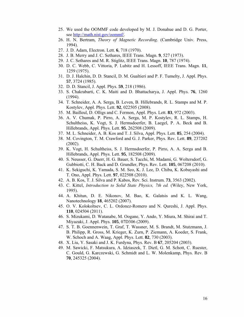
Snapshots of simulations performed on a 600 μm × 120 μm × 50 nm cuboidal
sample with a cell size 50 nm × 6 μm × 50 nm are shown in Fig. 1(a). The x-axis
lies along the length of the bar, and the z-axis points towards the reader in a right-
handed Cartesian coordinate system. The parameters used in the simulation are as
follows: Gilbert damping constant α = 0.01, a saturation magnetization Ms =
860×103 A/m, and an exchange stiffness A = 1.3×10⁻¹¹ J/m. A bias field (Hb) of
100 Oe is applied along the y direction, and thus the generated spin waves are
magnetostatic surface waves (MSSW). Spin waves are generated in the middle of
the strip at time t = 0 ns, and they progressively move away from the center with
time. The intensity plot in Fig. 1(a) shows the z-component of the magnetization
within the sample. In the simulations the Oersted field resulting from an antenna
has been replicated using the Karlqvist equations [26] given by
0, arctan / 2 / arctan / 2 /xH x z H W x z W x z , and
2 22 20, / 2 / / 22z
HH x z W x z W x z
where the time-dependent
part of the Karlqvist field H0 has a sinc-dependence to time,
0 0 0sinI I t t t t , with 40100 GHz, 2 10 A,I and
0 50 nst . The waveguide width W is 2 μm. H0 and I are related as WIH 20 .
4
Thus the amplitude of the magnetic field pulse is about 7 Oe in the x direction and
6.1 Oe in the z direction, as shown in Fig. 1(b).
Spin wave propagation loss is one of the critical factors required for modeling
of spin wave devices. These losses determine the distance which the spin waves
can travel before they become too small to be detected. There have been both
experimental and theoretical studies of propagation loss [27-32]. A
phenomenological loss theory determines the upper and lower limits of
propagation losses for different propagation modes of MSSW [32, 33]. However,
an accurate description of magnetization dynamics is very difficult as the
boundary conditions and initial conditions are difficult to access. In order to avoid
this problem, numerical methods such as finite-differential method (FDM) or
finite-element method become very helpful. In this regard, a study of spin wave
propagation losses based on numerical simulations is of direct importance.
In this study, micromagnetic simulations are used to study the attenuation
characteristics of MSSW. Simulations are done with cell a size 50 nm × 120 μm ×
50 nm on a 600 μm × 120 μm × 50 nm cuboidal sample. Spin waves are excited
from a waveguide located at the center of the sample. The waveguide has a width
of 2 μm and a thickness of 200 nm, and is separated from the sample by a 50 nm
thick insulator. A bias field (Hb) of 100 Oe is applied along the y direction. A sinc
pulse with a frequency of 100 GHz is used to generate a pulse field in the sample
with the spatial profile given by Karlqvist equations. The reason for using a sinc
pulse at 100 GHz is that in the frequency domain, this pulse has a uniform
distribution in 0-15 GHz. The amplitude of the magnetic field pulse is the same as
that in Fig. 1(b).
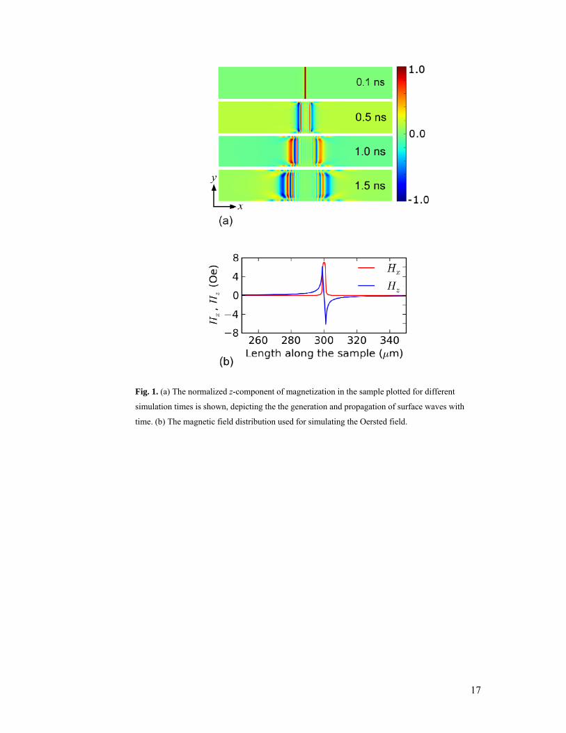
The spin wave amplitude, defined as the maximum variation in the z-
component of magnetization at different simulation times, is measured at different
locations in the sample and plotted against the distance from the source of the spin
waves. The data, between 7 and 77 μm from the source are fitted with an
exponentially decaying function to obtain the attenuation length of the spin waves
as shown in Fig. 2. The attenuation length (lAtt) is defined as the distance the wave
travels during which its amplitude decreases by 1/e. The parameters used for the
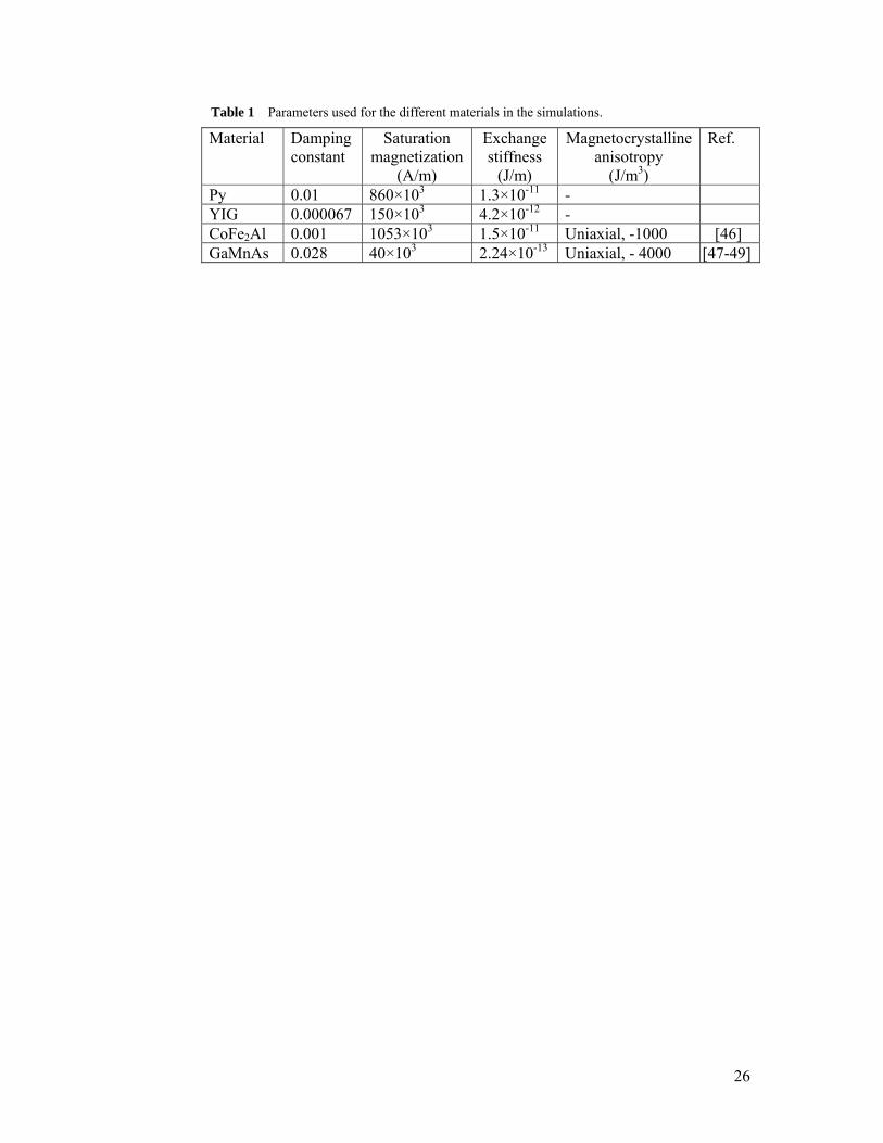
simulations of the different materials are shown in Table 1. For CoFe2Al and
GaMnAs, uniaxial anisotropy along the z direction has been included in the
simulations. The attenuation lengths are 11.54, 26.32, 18.95, and 3.42 μm for
5
permalloy (Py), yttrium-iron-garnet (YIG), CoFe2Al, and GaMnAs, respectively.
It is noteworthy that the spin waves in all these materials propagate through
similar distances. However, the amplitude of spin wave is found to be of similar
order in Py, YIG, and CoFe2Al, while in GaMnAs it is about four orders of
magnitude smaller. This result explains the difficulties associated with
observation of propagating spin waves in dilute magnetic semiconductors (DMS).
The challenge of measuring such small amplitude spin waves is a constraint that
needs to be considered when designing a spin wave device based on DMS. The
small amplitude of spin waves in GaMnAs is due to the small value of saturation
magnetization (Ms = 40×103 A/m) and a high value of damping constant (α =
0.028).
In these simulations, the cell size in the y direction is 120 μm, which is much
larger than the spin wave decay lengths. Since the waves travel only in the x
direction, and the sinc pulse has components in the x and z directions, we do not
expect any dynamics in the y direction and hence the cell size in the y direction
should not have any effect on magnetization dynamics. In order to confirm this,
simulations were performed with cell size 50 nm × 500 nm × 50 nm with
parameters for Py (α = 0.01, Ms = 860×103 A/m, and A = 1.3×10⁻¹¹ J/m), and
identical results to the larger cell size (50 nm × 120 μm × 50 nm) were obtained.
We further extend the simulations by varying different parameters such as the
damping constant (α), saturation magnetization (Ms), bias field (Hb), and exchange
stiffness (A) to see the effect of these parameters on spin wave attenuation length.
For each set of simulations only one parameter is changed and the other
parameters are kept the same as those of Py. Figure 3(a) illustrates the effect of
damping constant (α) on the attenuation length (lAtt). As α decreases, initially the
attenuation length increases logarithmically and then becomes nearly constant.
This behavior is explained by considering the two main factors responsible for
attenuation of spin wave amplitude: (1) energy loss by various damping
mechanisms represented by α, and (2) spreading of the wave packet as it travels
down the film due to a nonlinear dispersion relationship. For higher values of α,
the energy loss mechanisms are dominant, whereas for lower values of α,
dispersion becomes the dominant factor in determining the spin wave amplitude.
Figure 3(b) shows the dependence of lAtt on the saturation magnetization. In the
range Ms = 60×103 – 1800×103 A/m, lAtt increases nearly logarithmically with
6
increasing Ms and saturates at higher values of Ms. Figure 3(c) shows that lAtt
decreases as Hb increases when 20bH Oe. However, for 20bH Oe, lAtt
increases with increasing Hb. This is probably because spin waves are non-linear
for 20bH Oe. In Fig. 3(d) we show that lAtt does not change with the exchange
stiffness parameter. This is expected since, in our simulations, the waveguide is
very wide (2 μm), therefore, the waves are magnetostatic spin waves rather than
exchange-coupled waves.
It is remarkable that lAtt does not change very much, even when the parameters
(α, Ms, Hb and A) are varied over wide ranges. It means that choosing the right
material is not an efficient method for tuning the propagation length of spin
waves. However, as mentioned earlier, it is ultimately the amplitude of the spin
waves that is measured in real experiments, and in this regard the choice of
materials becomes very important. As described earlier, there are two reasons for
attenuation of spin waves damping and dispersion. The second factor can be
eliminated, if a sinusoidal field is used instead of a pulse field to excite spin
waves. In order to confirm this, simulations have been done with a sinusoidal field
at the resonance frequency of ferromagnets. All the other details of the
simulations remain same. The lAtt is found to be 31.92 μm and 1910.4 μm for Py
and YIG, respectively. These values are significantly larger for sinusoidal fields
than the sinc fields, and explain the observation of spin waves a few tens of μm
away from point of excitation in Py, and even hundreds of μm in YIG [2, 34, 35].
As can be seen from the simulations, the attenuation characteristics of YIG
allow for the transmission of spin waves over several millimeters with very little
loss, as shown previously [2, 34]. However, the fabrication of YIG films is not
compatible with concurrent complimentary metal oxide semiconductor (CMOS)
technology [36]. Thin-films such as Py which can be easily deposited are
preferable, however, the propagation length is much shorter than what is required
for chip-to-chip communications. Hence, it is practically impossible to use spin
waves for interchip communications, but intrachip communications and spin
wave-based logic may still be possible. For this reason, we have experimentally
evaluated all-electrical ferromagnetic thin-film magnonic systems to determine
their applicability for intrachip communication in the following section.
7
3. Wave properties of spin waves
Spin waves exhibit a number of different wave properties, the most
fundamental of which is the transfer of information from one point to another.
Electrical spin wave sources and detectors comprise of microwave antenna which
can generate high-frequency Oersted fields or those which can inductively detect
the same. For practical applications all-electrical systems are required for intra-
chip communications and logic. In this section, we have examined the wave
properties of spin waves in thin ferromagnetic films.
As is well known, dispersion characteristics of waves are fundamental to the
determination of the transmission characteristics of waves. Although the
determination of precessional frequency using purely electrical means is relatively
easy, the determination of k-vectors is rather challenging. In section 3.1, electrical
sources and detectors have been used for extracting the dispersion relationship in
spin waves. Furthermore, spin waves used for communications and logic in
electronic circuits would necessarily benefit from pulsed electrical measurements
because a vast majority of modern electrical circuits are digital circuits. Pulse
inductive microwave magnetometry (PIMM) is thus a very natural measurement
procedure for such intrachip communications. However, since the attenuation is
significant, a method for the modulation of spin waves in PIMM measurements is
very beneficial. In section 3.2, a method for achieving such modulation in PIMM
measurements has been demonstrated, which may be useful in combating such
problems with attenuation.
3. 1. Spin wave dispersion
The dispersion relationship of spin waves is strongly correlated to the applied
field, because the field changes the characteristics of the material through which
the spin waves travel. The spin waves are characterized by the precessional
frequency of the magnetization and the wavelength. In the current measurements,
we have used PIMM [37, 38] for studying the magnetization dynamics. In
particular, the wave-vectors of travelling spin wave packets resulting from
impulse excitations are studied, and their wave-vectors are extracted. Since PIMM
is a relatively fast and useful method of measuring magnetization dynamics, it
would be convenient to have a relatively easy method for extracting the wave-
vectors from these measurements electrically.
8
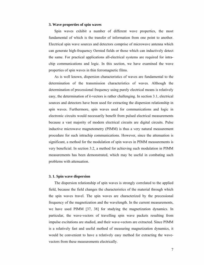
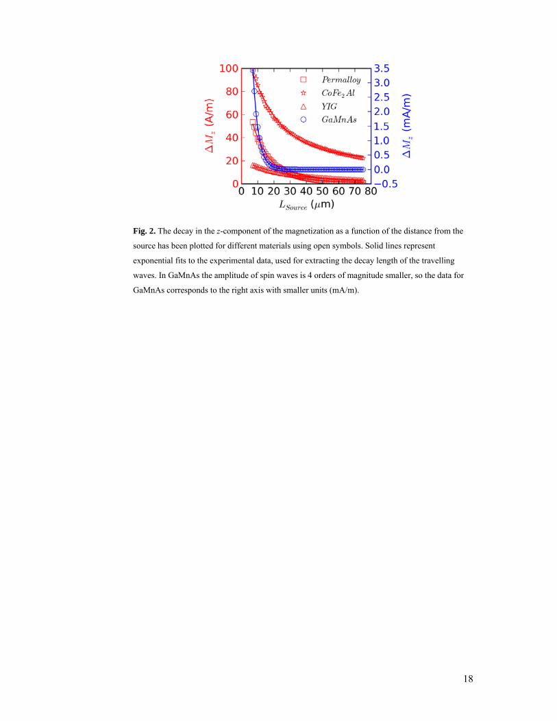
As shown in Fig. 4(a) and (b), two devices have been used for the extraction
of the wave vectors of travelling spin waves. For the device in Fig. 4(a) a 120 μm
× 200 μm Ni81Fe19 (30 nm) pattern is covered by a 30 nm thick SiO2 insulating
layer, and finally Cr (5 nm)/Au (100 nm) ground-signal-ground (GSG)
waveguides, with 8 μm signal lines are patterned on top. The device in Fig. 4(b)
comprises of a 220 μm × 340 μm Ni81Fe19 (20 nm) pattern, covered by a 30 nm
thick SiO2 layer, with asymmetric coplanar strips (ACPS) patterned on top with
10 μm signal lines. A 2 V, 100 ps pulse is applied and the Gaussian wave packet
detected at the detector waveguide, in the device shown in Fig. 4(a) is shown in
Fig. 4(c) with a 215 Oe bias field applied parallel to the film plane, along the
signal line. The angular frequency ω of the measured signal, and the applied bias
field (Hb) are related by the dispersion relation of MSSW:
2 2 2 2 20 1 / 4kd
b b S SH H M M e . Here, γ represents the
gyromagnetic ratio of an electron in free space, μ0 the permeability of free space,
Ms the saturation magnetization (μ0Ms ≈ 1 T for NiFe), d the sample thickness, k
the wave number (=2π/λ), and λ is the wavelength of the spin wave. However, it is
generally relatively difficult to extract the value of λ from electrical measurements
because these measurements are position-independent. When the magnetic field is
applied out of the plane of the sample, and is less than the field required to
saturate film, the in-plane component of the magnetic field is still used for
producing surface waves.
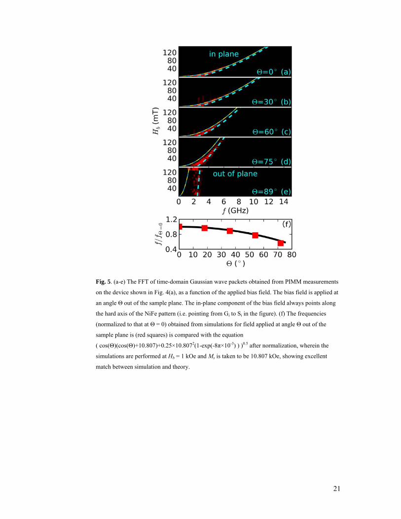
In Fig. 5, the frequency transform of the measured time-domain signals of the
sample shown in Fig. 4(a) are shown. For bias fields applied partially out-of-plane
and taking the FFT of these signals, the resultant frequency of the measured spin
waves is seen to shift steadily from a higher to a lower frequency with increasing
Θ, under similar magnetic bias conditions as shown in Fig. 5(a-e). The width of
the signal line has been commonly used for calculating the wave number k. As
previously shown by optical measurements, generated spin waves have
wavelengths between the width of the signal line and infinity (i.e. k = 0) [39, 40].
As can be seen, the frequency response falls within the dispersion regimes given
by the surface wave equation 2
8k
m
shown as thick dashed lines, and the
ferromagnetic resonance (FMR) mode 0k
shown as thin dashed lines. At

9
k = 0, the waves do not travel, and represent FMR spectra. For FMR, the resonant
frequency is zero at no applied bias. Note that in fitting equations Hb has been
replaced with the in-plane component of the field cosbH . Note that when the
applied magnetic field is in the low-bias field regime in which the measurements
have been performed, even though the field is out of the plane of the film, the
measured spin waves still faithfully reproduce the dispersion curves of surface
spin wave mode. A yellow line shows the fits to the magnetostatic backward
volume (MSBV) mode 2 2 20 1 /kd
b b SH H M e kd . As can be seen,
the calculated frequencies are lower than that required for explaining the observed
behavior. Furthermore, the equation for the magnetostatic forward volume
(MSFV) mode is only applicable, when the applied bias field is greater than the
saturation magnetization. Hence, for the range of fields which have been applied,
the MSFW mode is not generated.
In order to support this experimental data, simulations were performed with
Hb applied at an angle Θ out of the plane of the sample. The material parameters
used in the simulation are the same as used for permalloy earlier, and Hb is taken
to be 1 kOe. The geometry of sample used for these simulations is similar as that
used earlier for study of lAtt. In these simulations, we have studied the variation of
spin wave frequency as a function of Θ. The normalized frequency with respect to
that at Θ = 0 is shown as red squares in Fig. 5(f). It is then fitted with frequencies
calculated from the MSSW dispersion relation with k = 2π/(10 μm), in which 10
µm is the antenna width of the signal line. These calculated frequencies, after
normalizing with respect to the maximum, are shown as black line in the figure.
Using theoretical fits of the surface wave dispersion relationship to both measured
(Fig. 5(a-e)) and simulated data (Fig. 5(f)), one can conclude that the spin wave
mode propagating, when the field is applied partially out of the plane of the
sample, is essentially the surface wave.
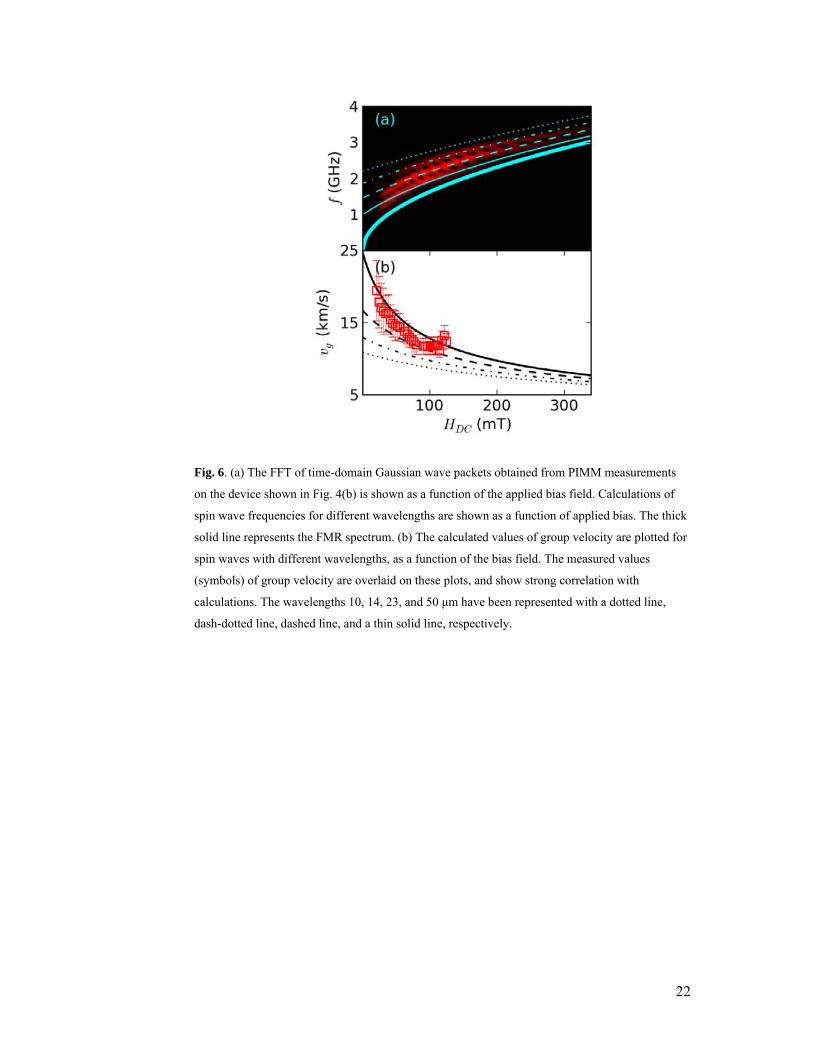
Using this information, a detailed mapping of the prevalent spin wave modes
may be extracted. For this purpose, the sample shown in Fig. 4(b) has been used,
wherein the applied magnetic field has been applied out of the sample plane.
Smaller waveguides are able to measure the signal levels to much greater
accuracy, and individual lines corresponding to different k vectors may be
extracted, as shown in Fig. 6(a). From the fitting dispersion curves corresponding
10
to the wavelengths 10, 14, 23, and 50 μm have been represented with a dotted
line, dash-dotted line, dashed line, and a thin solid line, respectively. The
measured frequency responses also have wavelengths between 10 μm and the
FMR spectrum (thick solid line) respectively.
As an additional check to ensure that the calculations are consistent, the
theoretical group velocity ( k ) for the different measured k vectors is
compared with measured values of group velocity, using two devices having
different excitation-detection distances of 20 μm (device D20) and 5 μm (devices
D5). The wave packets are fitted with the Gaussian function
2 20exp / 2A t t , with fitting parameters t0, σ, and A, for bias fields between
25 and 120 mT [41]. Only the temporal position (t0) of the center of the wave
packet has been obtained by fitting a Gaussian function to the wave packet. The
measured group velocity is defined as 20 5
0 020 μm 5 μm /D D
t t . Notice that
this is a direct measure of the speed of the Gaussian spin wave packets, and is
independent from the measurements of the frequency of the individual packets.
These are shown in Fig. 6(b) and show very good correspondence with predicted
theory. The theoretical group velocity for the different wave vectors shown by
cyan lines in Fig. 6(a) has been calculated by the formula
2 2 220
4kdS
g
Md dv e
dk
.
As can be seen from Fig. 6(a), at low values of the bias magnetic field, the
spin wave a wavelength of 50 μm is dominant. As the bias magnetic field
increases the spin waves with a wavelength of 50 μm slowly dwindle, and those
with a wavelength of 23 μm become more pronounced. As the field increases
further the signal to noise ratio slowly degrades and it becomes increasingly
difficult to fit Gaussian wave functions for the data. As can be seen in Fig. 6(b), at
low values of the applied bias magnetic field, the velocity corresponds to spin
waves having a wavelength of 50 μm. As the bias magnetic field increases,
however, the measured group velocity also shifts toward that resulting from spin
waves with a wavelength of 23 μm. Thus, one observes close agreement between
values of group velocity measured experimentally and theory, confirming again
that the observed spin waves are indeed surface waves. Note that two
measurements in Fig. 6(a) and 6(b) are two independent techniques, and both are
11
in good agreement with one another. Hence, one can conclude, that the method
described in this section is a practical and useful method of extracting the k-
vectors of spin waves in magnetic materials embedded in electronic circuitry.
3.2. Spin wave interference
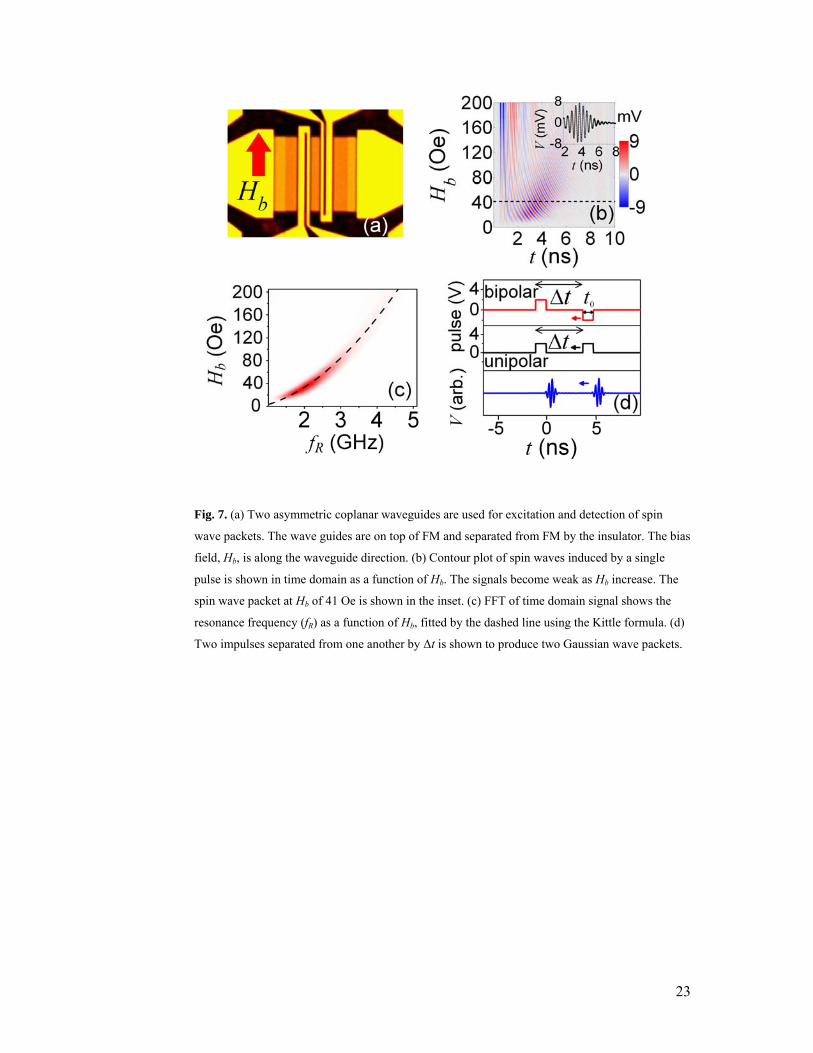
The microscope image of the sample used for the spin wave modulation
studies is shown in Fig. 7(a). A Py thin film was deposited and patterned on an
MgO substrate with dimensions of 410 × 220 μm2 and a thickness of 20 nm.
Asymmetric coplanar waveguides (CPW) are sputter deposited on the patterned
Py and is isolated from Py by 30 nm of SiO2. The signal line width of the CPW is
10 μm. The gap between the signal line and the ground conductor is 5 μm, and the
distance between two CPWs is 30 μm. PIMM is used to generate and detect spin
wave packets [16, 42]. A pulse generator is used to apply an impulse excitation at
the input CPW and the resultant Gaussian wave packet is detected via a low noise
amplifier by a 50 GHz sampling oscilloscope. Travelling spin wave packets are
detected in the MSSW mode, in which spin wave k-vector is perpendicular to the
direction of magnetization, M of the ferromagnetic thin film. The contour plot in
Fig. 7(b) shows color coded amplitudes of spin wave signals excited by a single
pulse at different bias fields. The dashed line in the inset of Fig. 7(b) indicates
spin wave packet at the fixed Hb of 41 Oe. The bias field dependent shift of the
resonance frequency, fR, obtained by taking a fast Fourier transform (FFT) of the
time-domain signals is shown in Fig. 7(c). The quadratic dependence of fR with
increasing Hb is shown in Fig. 7(c) by a dashed line [43].
Two spin waves excited by two pulses can interfere either constructively or
destructively, where one pulse is fixed and the other is shifted by a time delay (t)
indicated by the arrows in Fig. 7(d). The time delay between the two pulses is
changed from +5 ns to -5 ns in steps of 20 ps, while the bias field Hb is fixed at
123 Oe. Two different measurements were performed, and are termed bipolar and
unipolar experiments, respectively. In the bipolar experiment, the two impulses
have opposite polarity, whereas, in the unipolar experiment, both pulses have the
same polarity. Contour plots of the spin wave interference by the bipolar and
unipolar pulses with different time delays are shown in Figs. 8(a) and 8(c),
respectively. The blue dashed lines indicate constructive interferences at t =
±(2n+1)139 ps for the bipolar pulse, and ±(2n)139 ps for the unipolar pulse, where
n is an integer number. The red dashed lines indicate destructive interferences at
12
t = ±(2n)139 ps and ±(2n+1)139 ps for the bipolar and unipolar, respectively, as
shown in Figs. 8(b) and 8(d). When two spin waves constructively interfere, the
amplitude of interfered spin waves is the sum of the amplitudes of each spin wave
generated by the independent impulses. The amplitude of the non-interacting
wave packet for bipolar (unipolar) experiment is ~1.7 mV (~1.63 mV). When they
constructively interfere, the amplitude is ~3.4 mV (~3.3 mV) in case of bipolar
(unipolar) input pulses. Signals interfering destructively have a magnitude of
almost zero. Constructive and destructive interference caused by a linear
superposition of two spin waves [20] can be utilized for possible applications in
spin wave logic devices.
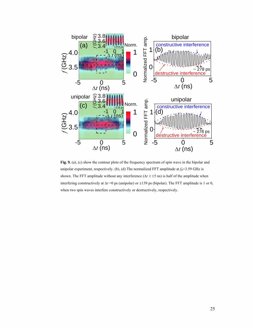
FFT is used to obtain further insight of the phenomenon in the frequency
domain. Color-coded frequency domain spectra are shown in Figs. 9(a) and 9(c),
as a function of t, for bipolar and unipolar pulses, respectively. As shown in Fig.
7(c), the resonance frequency, fR is ~3.59 GHz at a bias field Hb=123 Oe. The
dashed squares in the middle of Fig. 9(a) and 9(c) are expanded in the respective
insets. The normalized FFT amplitude in the frequency domain changes
periodically with a periodicity of ~278 ps. The horizontal dashed lines in Fig. 9(a)
and 9(c) are the t-dependent changes in FFT amplitude, extracted at fR=3.59
GHz and are plotted in Fig. 9(b) and 9(d), respectively. The spin wave packets
that interfere due to unipolar and bipolar pulses can be described in time domain
as 2 2
2 2
( )( ) cos(2 )exp( ) cos[2 ( )]exp( )
2 2
uni R R
t t tV t A f t A f t t
, and
2 2
2 2
( )( ) cos(2 )exp( ) cos[2 ( ) ]exp( )
2 2
bi R R
t t tV t A f t A f t t
,
respectively, where is the full width at half maximum of a single wave packet in
time domain. The interfered amplitude of both the unipolar and bipolar
experiments, Vuni (t) and Vbi (t), is the summation of the wave packet amplitudes
excited by the fixed pulse and the shifting pulse, which are the first and second
terms in the equations shown above, respectively. The wave packet excited by the
bipolar impulse is phase shifted by with respect to that excited by unipolar
pulses [19]. After applying FFT, as can be seen in the Fig. 9(b) and 9(d), the
intensity of the interference varies sinusoidally with t. The normalized FFT
amplitude changes periodically with a periodicity of 278 ps. Note that 278 ps is
equal to 1/fR (=1/3.59 GHz). Complete constructive or destructive interference
13
indicates 1 and 0, respectively, in the normalized FFT amplitude. In the unipolar
experiment, two wave packets interfere either constructively at t=0 or
destructively at t=139 ps. In the bipolar case, the destructive and constructive
interferences are observed at t=0 and t =139 ps, respectively. The amplitudes
for |t| > 5 ns, where the interference becomes negligible, are close to half the
value of the maximum FFT amplitude. Hence, we can use this method to
modulate the intensity of the spin waves through interference. This can be
effectively used for engineering spin wave intensity for communication and logic.
4. Conclusion
We have studied how different parameters affect the spin wave attenuation
length through micromagnetic simulations. We have shown that the attenuation is
most strongly affected by the damping constant above a certain value, below
which other means of attenuation such as that resulting from nonlinear dispersion
become more dominant. Since the attenuation length of spin waves are of the
order of several microns for most manufacture-friendly material systems, the
possibility of inter-chip communication using spin waves is ruled out. A few tens
of microns is generally sufficient for intra-chip communications. We have also
demonstrated a technique for determining the dispersion relationships by
electrical methods which would aid in the determination of the propagation
characteristics of spin waves in applications. Finally, we have also demonstrated
spin wave interference using electrical techniques.
Spin wave computation has been explored by two different techniques. First,
Khitun et al. [44] have attempted to implement logic using the spin wave bus.
However, they have used the phase of spin waves for implementing logic circuits,
which makes it difficult for use in logic circuits, because the phase is a continuous
variable and not a discrete binary one. The approach taken by Kolokoltsev et al.
[45] is much more practical, in which a PSK signal has been synthesized using
spin waves. The digital circuitry required for implementing PSK is significant,
and hence, such analog implementations may be more appropriate for spin wave
logic. Using the experimental implementations described above, it may thus be
possible to augment digital logic with efficient spin wave-based analog
computation.
14
Acknowledgements
This work is supported by the Singapore National Research Foundation under CRP Award No.
NRF-CRP 4-2008-06 and Grant-in-Aid for Scientific Research (No. 22760015) from MEXT,
Japan.
15
References
1. M. Murphy, S. Montangero, V. Giovannetti and T. Calarco, Phys. Rev. A 82, 022318 (2010).
2. Y. Kajiwara, K. Harii, S. Takahashi, J. Ohe, K. Uchida, M. Mizuguchi, H. Umezawa, H. Kawai, K. Ando, K. Takanashi, S. Maekawa and E. Saitoh, Nature 464, 262 (2010).
3. A. V. Gorshkov, J. Otterbach, E. Demler, M. Fleischhauer and M. D. Lukin, Phys. Rev. Lett. 105, 060502 (2010).
4. S. Bandyopadhyay and M. Cahay, Nanotechnology 20, 412001 (2009). 5. P. Buczek, A. Ernst and L. M. Sandratskii, Phys. Rev. Lett. 105, 097205
(2010). 6. S. Kaka, M. R. Pufall, W. H. Rippard, T. J. Silva, S. E. Russek and J. A.
Katine, Nature 437, 389 (2005). 7. K. Ando, S. Takahashi, J. Ieda, Y. Kajiwara, H. Nakayama, T. Yoshino, K.
Harii, Y. Fujikawa, M. Matsuo, S. Maekawa and E. Saitoh, J. Appl. Phys. 109, 103913 (2011).
8. M. Gradhand, D. V. Fedorov, P. Zahn and I. Mertig, Phys. Rev. B 81, 245109 (2010).
9. O. Mosendz, V. Vlaminck, J. E. Pearson, F. Y. Fradin, G. E. W. Bauer, S. D. Bader and A. Hoffmann, Phys. Rev. B 82, 214403 (2010).
10. H. Chudo, K. Ando, K. Saito, S. Okayasu, R. Haruki, Y. Sakuraba, H. Yasuoka, K. Takanashi and E. Saitoh, J. Appl. Phys. 109, 073915 (2011).
11. O. Mosendz, J. E. Pearson, F. Y. Fradin, G. E. W. Bauer, S. D. Bader and A. Hoffmann, Phys. Rev. Lett. 104, 046601 (2010).
12. S. S. Mukherjee, P. Deorani, J. H. Kwon and H. Yang, Phys. Rev. B 85, 094416 (2012).
13. L. Q. Liu, T. Moriyama, D. C. Ralph and R. A. Buhrman, Phys. Rev. Lett. 106, 036601 (2011).
14. J. Xiao, G. E. W. Bauer, K. Uchida, E. Saitoh and S. Maekawa, Phys. Rev. B 81, 214418 (2010).
15. H. Adachi, K. Uchida, E. Saitoh, J. Ohe, S. Takahashi and S. Maekawa, Appl. Phys. Lett. 97, 252506 (2010).
16. T. J. Silva, C. S. Lee, T. M. Crawford and C. T. Rogers, J. Appl. Phys. 85, 7849 (1999).
17. S. K. Choi, K. S. Lee and S. K. Kim, Appl. Phys. Lett. 89, 062501 (2006). 18. K. Perzlmaier, G. Woltersdorf and C. H. Back, Phys. Rev. B 77, 054425
(2008). 19. J. H. Kwon, S. S. Mukherjee, M. Jamali, M. Hayashi and H. Yang, Appl.
Phys. Lett. 99, 132505 (2011). 20. S. S. Mukherjee, J. H. Kwon, M. Jamali, M. Hayashi and H. Yang, Phys.
Rev. B 85, 224408 (2012). 21. T. Neumann, A. A. Serga, B. Hillebrands and M. P. Kostylev, Appl. Phys.
Lett. 94, 042503 (2009). 22. D. R. Birt, B. O'Gorman, M. Tsoi, X. Q. Li, V. E. Demidov and S. O.
Demokritov, Appl. Phys. Lett. 95, 122510 (2009). 23. A. Dussaux, B. Georges, J. Grollier, V. Cros, A. V. Khvalkovskiy, A.
Fukushima, M. Konoto, H. Kubota, K. Yakushiji, S. Yuasa, K. A. Zvezdin, K. Ando and A. Fert, Nat. Commun. 1, 8 (2010).
24. S. Garzon, L. F. Ye, R. A. Webb, T. M. Crawford, M. Covington and S. Kaka, Phys. Rev. B 78, 180401(R) (2008).
16
25. We used the OOMMF code developed by M. J. Donahue and D. G. Porter, see http://math.nist.gov/oommf/.
26. H. N. Bertram, Theory of Magnetic Recording. (Cambridge Univ. Press, 1994).
27. J. D. Adam, Electron. Lett. 6, 718 (1970). 28. J. B. Merry and J. C. Sethares, IEEE Trans. Magn. 9, 527 (1973). 29. J. C. Sethares and M. R. Stiglitz, IEEE Trans. Magn. 10, 787 (1974). 30. D. C. Webb, C. Vittoria, P. Lubitz and H. Lessoff, IEEE Trans. Magn. 11,
1259 (1975). 31. D. J. Halchin, D. D. Stancil, D. M. Gualtieri and P. F. Tumelty, J. Appl. Phys.
57, 3724 (1985). 32. D. D. Stancil, J. Appl. Phys. 59, 218 (1986). 33. S. Chakrabarti, C. K. Maiti and D. Bhattacharya, J. Appl. Phys. 76, 1260
(1994). 34. T. Schneider, A. A. Serga, B. Leven, B. Hillebrands, R. L. Stamps and M. P.
Kostylev, Appl. Phys. Lett. 92, 022505 (2008). 35. M. Bailleul, D. Olligs and C. Fermon, Appl. Phys. Lett. 83, 972 (2003). 36. A. V. Chumak, P. Pirro, A. A. Serga, M. P. Kostylev, R. L. Stamps, H.
Schultheiss, K. Vogt, S. J. Hermsdoerfer, B. Laegel, P. A. Beck and B. Hillebrands, Appl. Phys. Lett. 95, 262508 (2009).
37. M. L. Schneider, A. B. Kos and T. J. Silva, Appl. Phys. Lett. 85, 254 (2004). 38. M. Covington, T. M. Crawford and G. J. Parker, Phys. Rev. Lett. 89, 237202
(2002). 39. K. Vogt, H. Schultheiss, S. J. Hermsdoerfer, P. Pirro, A. A. Serga and B.
Hillebrands, Appl. Phys. Lett. 95, 182508 (2009). 40. S. Neusser, G. Duerr, H. G. Bauer, S. Tacchi, M. Madami, G. Woltersdorf, G.
Gubbiotti, C. H. Back and D. Grundler, Phys. Rev. Lett. 105, 067208 (2010). 41. K. Sekiguchi, K. Yamada, S. M. Seo, K. J. Lee, D. Chiba, K. Kobayashi and
T. Ono, Appl. Phys. Lett. 97, 022508 (2010). 42. A. B. Kos, T. J. Silva and P. Kabos, Rev. Sci. Instrum. 73, 3563 (2002). 43. C. Kittel, Introduction to Solid State Physics, 7th ed. (Wiley, New York,
1995). 44. A. Khitun, D. E. Nikonov, M. Bao, K. Galatsis and K. L. Wang,
Nanotechnology 18, 465202 (2007). 45. O. V. Kolokoltsev, C. L. Ordonez-Romero and N. Qureshi, J. Appl. Phys.
110, 024504 (2011). 46. S. Mizukami, D. Watanabe, M. Oogane, Y. Ando, Y. Miura, M. Shirai and T.
Miyazaki, J. Appl. Phys. 105, 07D306 (2009). 47. S. T. B. Goennenwein, T. Graf, T. Wassner, M. S. Brandt, M. Stutzmann, J.
B. Philipp, R. Gross, M. Krieger, K. Zurn, P. Ziemann, A. Koeder, S. Frank, W. Schoch and A. Waag, Appl. Phys. Lett. 82, 730 (2003).
48. X. Liu, Y. Sasaki and J. K. Furdyna, Phys. Rev. B 67, 205204 (2003). 49. M. Sawicki, F. Matsukura, A. Idziaszek, T. Dietl, G. M. Schott, C. Ruester,
C. Gould, G. Karczewski, G. Schmidt and L. W. Molenkamp, Phys. Rev. B 70, 245325 (2004).
17
Fig. 1. (a) The normalized z-component of magnetization in the sample plotted for different
simulation times is shown, depicting the the generation and propagation of surface waves with
time. (b) The magnetic field distribution used for simulating the Oersted field.
18
Fig. 2. The decay in the z-component of the magnetization as a function of the distance from the
source has been plotted for different materials using open symbols. Solid lines represent
exponential fits to the experimental data, used for extracting the decay length of the travelling
waves. In GaMnAs the amplitude of spin waves is 4 orders of magnitude smaller, so the data for
GaMnAs corresponds to the right axis with smaller units (mA/m).

19
Fig. 3. The attenuation length (lAtt) of spin wave packets is shown as a function of the damping
constant (α) in (a), the saturation magnetization (Ms) in (b), the bias magnetic field (Hb) in (c), and
the exchange stifness constant (A) in (d).
20
Fig. 4 The two devices used for determining the k-vectors are shown. (a) Input and output Cr/Au
GSG waveguides are deposited over a rectangular NiFe pattern. One of the grounds of the input
and output probes are connected. (b) Ta/Au ACPS strips are patterned over a rectangular NiFe
pattern. In both (a) and (b), subscripts ‘i’ and ‘o’ refer to input (excitation) and output (detection)
waveguides, respectively, and the waveguides are separated from the NiFe strip by an insulating
oxide layer. (c) The inductive spin wave signal obtained for an in-plane bias field of 215 Oe for the
device shown in (a).
21
Fig. 5. (a-e) The FFT of time-domain Gaussian wave packets obtained from PIMM measurements
on the device shown in Fig. 4(a), as a function of the applied bias field. The bias field is applied at
an angle Θ out of the sample plane. The in-plane component of the bias field always points along
the hard axis of the NiFe pattern (i.e. pointing from Gi to Si in the figure). (f) The frequencies
(normalized to that at Θ = 0) obtained from simulations for field applied at angle Θ out of the
sample plane is (red squares) is compared with the equation
( cos(Θ)(cos(Θ)+10.807)+0.25×10.8072(1-exp(-8π×10-3) ) )0.5 after normalization, wherein the
simulations are performed at Hb = 1 kOe and Ms is taken to be 10.807 kOe, showing excellent
match between simulation and theory.
22
Fig. 6. (a) The FFT of time-domain Gaussian wave packets obtained from PIMM measurements
on the device shown in Fig. 4(b) is shown as a function of the applied bias field. Calculations of
spin wave frequencies for different wavelengths are shown as a function of applied bias. The thick
solid line represents the FMR spectrum. (b) The calculated values of group velocity are plotted for
spin waves with different wavelengths, as a function of the bias field. The measured values
(symbols) of group velocity are overlaid on these plots, and show strong correlation with
calculations. The wavelengths 10, 14, 23, and 50 μm have been represented with a dotted line,
dash-dotted line, dashed line, and a thin solid line, respectively.
23
Fig. 7. (a) Two asymmetric coplanar waveguides are used for excitation and detection of spin
wave packets. The wave guides are on top of FM and separated from FM by the insulator. The bias
field, Hb, is along the waveguide direction. (b) Contour plot of spin waves induced by a single
pulse is shown in time domain as a function of Hb. The signals become weak as Hb increase. The
spin wave packet at Hb of 41 Oe is shown in the inset. (c) FFT of time domain signal shows the
resonance frequency (fR) as a function of Hb, fitted by the dashed line using the Kittle formula. (d)
Two impulses separated from one another by Δt is shown to produce two Gaussian wave packets.

24
8 10 12 14t (ns)
3 mV
unipolar
constructiveV (
mV
)
single wave packet
destructive
(c)
8 10 12 14t (ns)
3 mV
bipolar
destructive
single wave packet
V (
mV
)
constructive
(a)
(d)
(b)
Fig. 8. (a), (c) Contour plots of spin wave interference for the bipolar and unipolar measurement,
respectively, in time domain. Constructive (dashed blue line) and destructive (dashed red line)
interference of (a), (c) are shown in (b), (d) for the bipolar and unipolar cases, respectively, where
t is either 0 or +139 ps.
25
3.5
4.0
t (ns)
Norm.
0-5 5
unipolar
f (G
Hz)
0
13.43.63.8
10~278 psf (
GH
z)
t (ns)-1
3.5
4.0
t (ns)
Norm.
bipolar
f (G
Hz)
0-5 50
13.43.63.8
10~278 psf
(GH
z)
t (ns)-1
-5 0 5
0
1constructive interference
bipolar
Nor
mal
ized
FF
T a
mp.
t (ns)
destructive interference~ 278 ps
-5 0 5
0
1
~ 278 psdestructive interference
constructive interference
unipolar
Nor
mal
ized
FF
T a
mp.
t (ns)
(b)(a)
(c)(d)
Fig. 9. (a), (c) show the contour plots of the frequency spectrum of spin wave in the bipolar and
unipolar experiment, respectively. (b), (d) The normalized FFT amplitude at fR=3.59 GHz is
shown. The FFT amplitude without any interference (t 5 ns) is half of the amplitude when
interfering constructively at t =0 ps (unipolar) or 139 ps (bipolar). The FFT amplitude is 1 or 0,
when two spin waves interfere constructively or destructively, respectively.
26
Table 1 Parameters used for the different materials in the simulations.
Material Damping constant
Saturation magnetization
(A/m)
Exchange stiffness
(J/m)
Magnetocrystalline anisotropy
(J/m3)
Ref.
Py 0.01 860×103 1.3×10⁻¹¹ - YIG 0.000067 150×103 4.2×10⁻¹² - CoFe2Al 0.001 1053×103 1.5×10⁻¹¹ Uniaxial, -1000 [46] GaMnAs 0.028 40×103 2.24×10⁻¹³ Uniaxial, - 4000 [47-49]