
Chapter 10 - Digital Integrated Circuits
40
Chapter 10 Digital Integrated Circuits 10 .1 INTRODUCTION The integrated circuit (lC) and the digital logic families were introduced in Section 2.9. This chapter presents the electronic circuits in each Ie digital logic family and analyzes their elec - trical operation. A basic knowledge of electrical circuits is assumed. The Ie dig itall ogic families to be considered here are RTL DTL TTL E CL MOS CMOS Resistor -transistor logic Diod e-tran sistor logic Transistor-transistor logic Emitter-coupled logic Metal-oxide semiconductor Complementary metal-oxide semiconductor The first two, RTL and DTL. have only historical significance. since they are DO longer used in the de sign of digital systems. RTL was the first comme rcial family to have been used ex- tensively. It is included here because it represents a useful starting point for explaining the basic operation of digital gates. DTL circuits have been replaced by TIL In fact, TIl. is a modification of the DTL gate. The operation of the TI1.. gate will be easier 10 undersund after the DTL gate is analyzed.TI1.., ECl, and CMOS have a large numbc:rofSS Icircuits, as well as MSl, lSI, and VLSI components. The basic circuit in each Ie digital logic famil y is a NAND or NOR gate. This basic circuit is the primary building block from which all other, more compudigi!al(l'.'O'COlSucobtained. Each IC logic family has a data book that lists all the integrated cin::uits iDIbat family. The dif - ferences in the logic functions available from each family are DOt 10 mucbiD tbc: functions that 471
-
Upload
khangminh22 -
Category
Documents
-
view
0 -
download
0
Transcript of Chapter 10 - Digital Integrated Circuits

Chapter 10
Digital Integrated Circuits
10 .1 INTRODUCTION
The integrated circuit (lC) and the digital logic families were introduced in Section 2.9. Thischapter presents the electronic circuits in each Iedigital logic family and analyzes their elec trical operation. A basic knowledge of electrical circuits is assumed.
The Ie dig itallogic families to be considered here are
RTLDTLTTLECLMOSCMOS
Re sistor-transistor logicDiode-transistor logicTransistor-transistor logicEmitter-coupled logicMetal -oxide semiconductorComplementary metal-oxide semiconductor
The first two, RTL and DTL. have only historical significance. since they are DO longer usedin the de sign of digital sys tems . RTL was the first commercial family to have been used extensively. It is included here because it represents a useful starting point for explaining thebasic operation of digital gates. DTL circui ts have been replaced by TIL In fact, TIl. is amodification of the DTL gate. The operation of the TI1.. gate will be easier 10 undersund afterthe DTL gate is analyzed. TI1.. , ECl, and CMOS have a large numbc:rofSSI circuits, as wellas MSl, lSI, and VLSI components.
The basic circuit in each Iedigital logic famil y is a NAND or NOR gate. This basic circuit isthe primary building block from which all other, morecompudigi!al(l'.'O'COlSucobtained.Each IC logic family has a data book that lists all the integrated cin::uits iDIbat family. The differences in the logic functions available from each family are DOt 10 mucbiDtbc: functions that
471

472 Chapter 10 Digi ta l Integ rated Circuits
they achieve as in the specific electrical characteristics of the basic gate from which the circuitis constructed.
NAND and KOR gates are usually defined by the Boolean functions that they implementin terms of binary variables. In analyzing them as electronic circuits. it is neces'illry to investigate their input-output relationships in terms of two voltage levels: a IIigh level. designatedby H. and a law level, designated by L. As mentioned in Section 2.8. the assignment of binary1 to H results in a positive logic system and the assignment of binary 1 to L results in a negative logic system. The truth table, in terms of H and L, of a positive-logic r-;' t\..-...;" D gate is she .... nin Fig. 10.1. We notice that the output of the gate is high as long as one or more inputs are low.The output is low only when both inputs are high. The behavior of a positive-logic NA-SDgate in terms of high and low signals can be stated as follows:
If any input of a NAND gate is low. the output is high.
If all inputs of a NAND gate are high. the output is low.
The corresponding truth table for a positive-logic :-':OR gate is shown in Fig. 10.2. The outputof the NOR gate is low when one or more inputs are high. The output is high when both inputsare low. The behavior of a positive-logic NOR gate, in terms of high and low signals. can bestated as follows:
If any input of a NOR gate is high. the output is low.
If all inputs of a NOR gate are low, the outpu t is high.
These statements for NAND and NOR gates must be remembe red. because they will be u...edduring the analysis of the electronic gates in this chapter,
Inputs Output
., y z
I. L III. II 1/1/ L II1/ II L
FIGUR£ 10.1Positive-log ic NAND gate
Inputs Output
r j' z
I. L 1/I. 1/ L1/ L L1/ 1/ L
FIGUR£ 10.2Positive-log ic NOR gate

10 .2
Section 10.2 Specia l Characterist ics 473
A bipolur junrtion rrensts ror (B lT) can be either an npll or a pup junction transistor. in conrrast. the fi eld-effect transistor (FET) is said to be unipolar. The operation of a bipolar transistor dep end s on the now of two types of carriers: electrons and holes. The opera tion of aunipolar transistor depends on the flow of only one type of majority carrier, which may be electrons (in an n-channel transistor ) or holes (in a p-channel transistor ). The first four digita llogic families listed at the beginning of the chapter-c-Rf' L, DTl, TTL, and ECl - use bipolar transistors. The last two families- MOS and CMOS--employ a type of unipolar transistor ca lled a meral-oxide -serniconductor field-effe ct transistor. abbrevia ted MOSFET. or MOSfor short.
In this chapter. we first introduce the most common characteristics by which the digi tallogic families are co mpared. We then desc ribe the properties of the bipolar transistor and analyze the basic gates in the bipolar logic families. Finally. we explain the operation of the MOStransistor and introduce the basic gates of its two logic families.
SPECIAL CHARACTERISTICS
The charac teris tics of Ie digital logic famili es are usually compared by analyzing the circuitof the basic gate in each family. The most important parameters that are evaluated and compared are fan-out , power dissipation, propagation delay, and noise margin. We first explain theproperties of these parameters and then use them to compare the Ie logic families.
The fan-out of a gate specifies the number of standard loads that can be conne cted to the output of the gate without degrading its norma l operation . A standard load is usually defined asthe amount of current needed by an inpu t of anoth er gale in the same logic famil y. Sometime s the term loading is used instead of fan-out. The term is derived from the fact that theoutp ut of a gate can supply a limit ed amount of current. abo ve which it ceases to operateproperly and is said 10 be overloaded. The output of a gate is usually connected to the inputsof other gates. Each input requir es a certain amount of current from the gate output, so thaieach additional connection adds to the load of the gate. l oading rules are sometimes specified for a family of digi tal ci rcuits. These rules give the maximum amount of loadin g allowedfor each output of each circuit in the family. Exceed ing the specified maximum load maycause a malfunction because the circuit cannot supply the power demanded of it by its loads.The fan-out is the maximum number of inputs that ca n be co nnected to the output of a ga leand is expre ssed by a number.
The fan-out is calculated from the amount of current avai lable in the output of a gate andthe amount of current needed in each input of a gale. Consider the cooncdions sOOwn in Fig. 10.3.The outpu t of one gate is connected to one or more inputs ofotherpres.1be OUtpul of thegaleis in the high-voltage level in Fig. 1O.3(a ). It provides a current source IOH co all thegate inputs connected to it. Each gale input requires a current lIN for proper operation_Similarly, theoutput of the gate is in the low -voltage level in Fig. 1O.3(b). It provides a current sink IOL forall the gate inputs connected to it. Each gale input supplies a currenll,L_'The fan--oul: of me gale

474 Chapter 10 Digital Integrate d Circuits
10 •-
J,.-To other
inputs
(a) High -level output
I"
To otherinputs
(b) Low-level output
FIGURll0.JFan-cut computation
is calculated from the ratio IOH1IlH or IodIn , whichever is smaller. For example. the standardTIL gates have the following values for the currents:
IOH = 400 p.A
I lH = 40 p.A
IOL = 16 mA
In = I.6 mA
The two ratios give the same number in this case :
c4"OO,-,,,,,A:.: = 16 rnA = 1040 p.A 1.6 rnA
Therefore. the fan-out of standard TIL is 10. Thi s means thai the output of a TIL Bate can beconnected 10 no more than 10 inputs of other gates in the same logic family. Otherwise. the galemay not be able to drive or sink the amount of current needed from the inputs that are connected10 it.
Pow e r Dissipation
Every electronic circuit requires a cert ain amount of power to operate. The power dissipationis a parameter expressed in milliwatts (mW) and represents the amount of power needed by thegate. The number that represents this parameter does not include the power delive red from another gale; rather. it represents the power delivered 10 the gate from the power supply. An Ie
with four gates will require. from its power supply, four times the power dissipated in each gate.

Section 10.2 Specia l Characteristics 475
The amount of power that is dissipated in a gate is calculated from the supply voltage Veeand the current Icc that is drawn by the circuit. The power is the product Vee x l ee. The current drain from the power supply depends on the logic state of the gate. The current drawnfrom the power supply when the output of the gate is in the high-v oltage level is termed ICCH'
When the output is in the low-voltage level , the current is tccc The average current is
I ( )lCCH + ICCL
cc avg = 2
and is used to calculate the average power dissipation:
PD(avg) = lcd avg) x Vce
For example, a standard TTL NAND gate uses a supply voltage Vcc of 5 V and has currentdrain s ICCH = I rnA and ICCL = 3 rnA. The average current is (3 + l )/2 = 2 rnA. The average power dissipation is 5 x 2 = 10 mW. An Ie that has four NAN D gates dissipates atotal of 10 x 4 = 40 mW. In a typical digital system, there will be many ICs. and the powerrequired by each one must be considered. The total power diss ipation in the system is the sumtotal of the power diss ipated in all the ICs.
Propagation Delay
The propa gation delay of a gate is the average transi tion-delay time for the signal to propagatefrom input to output when the binary input signal changes in value. The signals through a gatetake a certain amount of time to propagate from the inputs to the outpu t. Th is interval of timeis defined as the propagation delay of the gate. Propagation delay is meas ured in nanoseconds(ns); I ns is equal to 10- 9 second.
The signals that travel from the inputs of a digita l circuit to its output s pass thro ugh a series of gates. The sum of the propagation delays through the gates is the tota l delay of the circuit. When speed of operation is important, each gate must have a short propagation delay andthe digital circuit must have a minimum number of gates between inputs and outputs.
The average propagation delay time of a gate is calculated from the inpu t and output waveforms, as shown in Fig . lOA. The signal-delay time between the input and the output when theoutput changes from the high to the low leve l is referred to as rnn- Similarly, when the output goes from the low to the high level , the dela y is tPLH ' It is customary to measure the timebetween the 50 percen t point on the input and output transitions. In general. the two delays arenot the same, and both will vary with loading co nditions. Tbe average propagaUoo-delay timeis calculated as the average of the two delays.
As an example. the delays for a standard TfL gate are t,.HL = 7 ns and t,.LH = II us.These quantitie s are give n in the TfL data book. and are measured with. load resiswx::e of400 ohms and a load capacitance of 15 pF.1be average propagatioD delay 01 theTIl. pte is( 11 + 7)/2 ~ 9 ns.
Under certain conditions. it is more imponam to know" the mnjnvmdelly timI: ata gate ratherthan the average value. The TILdata book lists the foUowiDg ",Allin _ prnpIgJ'ion delays for astandard NAND gate: tPHL = 15 ns andInn = 22 ns.. Wbcn spccdofq:cr isaitical. it isnecessary to take into account the maximum delay to ensure properopec 01the circuiL

476 Chapter 10 Digital Integrated Circuits
Input
Output
1//
'\I\.
"1\.'-- ____ I Time
1//
- If'LH ~
FIGURE 10.4Measurement of propaga t ion delay
The input signals in most digital circuits are applied simultaneously to more than one gate.All the gates that are connected to external inputs const itute the first logic leve l o f the circuit.Ga tes that recei ve at least one input from an output of a firs t-le....el gate are considered to bein the seco nd logic level. and similarly for the third and higher logic levels. Th e total propagation delay of the circuit is eq ual to the propagat io n dela y of a gate times the number oflogic levels in the circu it. Thus, a reduction in the number of logic levels results in a red uction in signal delay and faster circ uits. The reduction in the propagation delay in ci rcuits maybe more important than the reduction in the total number of gale s if speed of operation is amajor factor.
Noise Margin
Spurious electrical signals fro m indu strial and other sources ca n induce undesirable voltageson the con necting wires between logic circu its. These unwanted sig nals are re ferred to asnotse. There are two types of noise. DC noise is caused by a drift in the voltage levels of asignal. AC noise is a random pulse that may be created by other switching signals. Th us. noiseis a term used to denote an undesirable signal that is superimposed upo n the norm al operating signal. The noise ma rgin is the maximum noise voltage added to an input signal of a digital circuit that doe s nOI ca use an undesirab le change in the ci rcuit 's output. The ab ility ofci rcuits to operate reliably in an environment with noise is import ant in many applications.Noise margin is expressed in vo lts and represents the maximum noise signal that can be tolerated by the gate.
The noise margin is ca lculated from knowledge of the voltage signal availab le in the output o f {he ga te and {he voltage signal required in the input of the gate . Figure 10.5 illustratesthe signals used in computing the noise margin. Pan (a ) shows the range of out put voltages thatcan occ ur in a typica l gale. Any voltage in the gate output between Vee and VOH is considered10be the high-level state, and any voltage between 0 and VOL in the gate output is considered tobe the low-leve l slate. Voltage s betwee n VOL and VOH are indeterm inate and do nOI appear

Section 10.3 Bipolar -Transistor Characteristics 477
High-statenoise margin
(b) Inpu t voltage range
j
Low -stal l:noise margin
==="""0(a) Output voltage ra nge
FIGURE 10.5Signals for eva luat ing noise margin
under normal operating conditions. excep t d uring transition between the two levels . The co rresponding two volt age ran ges tha t are recog nized by the input of the gate are indica ted inFig . 1O.5(b). In order to compensate fo r any noise signal. the circuit must be designed so thatV/L is greater than VOL and V/H is less than VOH ' The no ise margin is the difference VOH - V'H
or V/L - VOL, wh ichever is smaller.As illustrated in Fig. 10.5, VOL is the maximum voltage that the output can be in the low-level
state. The circuit can tolerate any noise signal that is less than the no ise margin (ViI. - Vod because the input will recognize the signal as being in the low-level state . Any signal greater thanVOL plus the noise -margin figure will send the input voltage into the indetermi nate range. whichmay cause an error in the output of the gate. In a similar fashion , a negauve-volrage noise greaterthan VOH - VI H will send the input voltage into the indeterm inate range.
The parameters fo r the noise margin in a standard TT L NAN D gate are VOH = 2.4 V,VOL = 0.4 V, VI H = 2 V. and VI I. = 0.8 V. The high-stale noise marg in is 2.4 - 2 = 0.4 V,and the low-state noise margin is 0.8 - 0.4 = 0.4 V. In this case. beth values are the same.
10 . 3 B I PO LAR -T RA N SI ST O R C HAR A CT ERI STICS
This section reviews the bipolar transistor as app lied 10digital cin:uib.. "Ihc iofoIlcwioI. peesemedwill be used in the analysis of the basic circuit in the four bipolar logic: farnilieL As mentionedearlier, bipolar tran sistors may beof the npn or pnp type. MOft'O¥'er". (bey~ coosttul.Ud e itherwith germanium or silicon semiconductor material. Bipolar Ie baiiIii1us. bowe\rcr. are madewith silicon and are usually of the npn type. ....

478 Chapter 10 Digital Integrated Circuits
The bas ic data needed in the analysis of digital circuits may be obtained by inspection ofthe typical characteristic curves of a common-emitter npn silicon transistor, shown in Fig. 10.6.The circuit in (a) is a simple inverter with two resistors and a transistor. The curre nt markedIe flows through resistor Rc and the collector of the transistor. Curren! Is flows through resistorRB and the base of the transistor. The emitter is connected to ground. and its current1£ = Ie + te- The supply voltage is between Vee and ground. The input is between V; andground, and the output is between Vo and ground .
We have assumed positive directions for the currents as indicated. These are the directionsin which the currents normally flow in an npn transistor. Collector and base currents (Ie andIB' respectively) are positive when they flow into the transistor. Emitter current IE is positivewhen it flows out of the transistor. as indicated by the arrow in the emitter terminal. The symbol Ve£ stands for the voltage drop from collector to emitter and is always positive. Correspondingly. VB£ is the voltage drop across the base-to-emitter junction. This junction is forwardbiased when VB£ is positive and reverse biased when Vs£ is negative.
lc ~ Re
C v,1.-R. B
II,
I.(rnA)
0.6 0.7
(a) Common emitter inverter circuit
I ,(rnA )
_ _ ---0.6Vee "...R, ~ OO
I I.-~,--_- 0.41 1.-_~,-0.4
1I::====':s;:::~I~'~'~IO.2 rnAr: Vc£ (V )
(b) Transistor-base characteristic
fiGURE 10.6SlIleon npn t ransistor cha racteristics
(c) Transistor-collector characteristic

Sect ion 10.3 Bipolar-Transistor Characteristics 479
The base-emitter graphical characteris tic is shown in Fig. 1O.6(b). which is a plot of VBE versus lB' If the base-emitter vol tage is less than 0 .6 Y, the transisto r is said to be cut off and nobase current flows . Whe n the base-emitter junction is forward biased with a voltage greater than0 .6 V. the tran sistor condu cts and Ie starts rising very fas t wherea s VBEchanges very little . Thevoltage VBE across a conducting transistor seldom exceeds 0.8 V.
The graphical collector-emitter characteris tics . toge ther with the load line , are shown inFig. 1O.6(c). When VBE is less than 0.6 V, the transistor is cut off with IB = 0, and a negligi ble current flow s in the collector. The collector-to-emitter circuit then behaves like an open circuit. With lc =°the dro p across Re is 0 and Vo = vee-The output is then sa id to be pulledup. In the active reg ion , collec tor voltage VCE may be anywhere from abo ut 0.8 V up to Vec.Collector current Ie in this region can beca lculated to beapproximately equal to 18 hFE, wherehF£ is a transistor parameter called the de currelllgain. "The maximum collector curre nt dependsnot on IB' but rather on the external circuit connected to the collector. This is because VeE isalways positive and its lowest possible value is av. For example, in the inverter shown, the maximum tc is obtained by making VeE = 0, to ob tain lc = Vee!Re.
The parameter h FE varies widely over the operatin g range of the transistor. but still, it is usefu l to employ an average value for the purpose of analysis. In a typica l operat ing range. hFE
is about 50. but under certain conditions it could be as low as 20 . It must be realized that thebase current IB may be increased to any desirab le value, but the collector current Ie is limi tedby ex ternal circuit parameters . As a consequence. a situation can be reached in which hFEIBis greater than tc. lfthi s condition ex ists , then the tran sistor is said to be in the saturation region . Thu s, the condition for saturation is determined from the re lationship
IE
:2:: Ics
h"
where tcs is the maximum collec tor curre nt flowing during saturation. VeE is not exac tly ze roin the saturation region. but is normally about 0.2 V. In this condi tion. Vo = V8E = 0.2 V andthe output is said to bepulled down.
The basic data needed for ana lyzing bipolar-transistor digita l circuits are listed in Table 10.1.In the cutoff region, VEE is less than 0.6 V. VCE is conside red to be an open circuit, and bothcurrents are negligible. In the active region, VEE is about 0.7 V, VeE may vary over a widerange , and Ic can becalculated as a function of lB' In the saturation region. VBE hardl y changes,but Vee drops to 0.2 V. The base current mu st be large enough to satisfy the inequality listed.To simplify the analysis. we will ass ume that VBE = 0.7 V if the transistor is conducting.wheth er in the active or saturation region.
Tab le 10.1Typical npn Siffcon Tronsbtor Paronwten
Regi on
CutoffActiveSaturation
< 0.60.6-0 .70.7-0.8
Open circuit> 0.802
Current leI.tIonshlp
J. z 1c"" OIe = Ia,EI.
I. :i!:: laIA'E

480 Chapter 10 Digi tal Integrated Circui ts
Digita l circu its may be analyzed by means of the followin g prescribed procedure : For eachtra nsistor in the circuit. determine whether its VBE is less than 0.6 V. If so. then the trans istoris cut off and the collector-to-emitter circuit is considere d an ope n ci rcuit. If \ 'BE is greaterthan 0.6 V. the tran sistor may be in the acti ve or saturation region. Calculate the base curre nt.assuming that VBE = 0.7 V. Next. ca lculate the maximum possible value of collector currentIcs- assuming that VCE = 0.2 V. These calculations will be in terms of vol tages applied andresistor values. Then. if the base current is large enough that 18 ~ IcslhFE• we infer that thetran sistor is in the saturation region with VCE = 0.2 V. However. if the base current is smallerand the preceding relat ion ship is not satisfied. the tran sistor is in the active region and werecalculate co llector curre nt lc. using the equation tc = hFEI8.
To demon strate with an example. consider the inverter circ uit of Fig. 1O.6I'a) with the following parameters:
Re = I kO
RB = 22 kO
liFE = 50
Vee = 5 V ( voltage supply)
H = 5 V (high-level voltage )
L = 0.2 V (low-level voltage )
With input voltage Yj = L =0.2 V. we have VHE -c 0 .6 V and the transistor is CUI off. Thecollector-emitter circuit behav es like an open ci rcuit . so output voltage Vo =5 V = H .
With input vo ltage Yj = H = 5 V. we infer that VSf: > 0.6 V. Assuming that V8e = 0.7.we ca lculate the base curre nt:
V; - V8 E18 = =
RB
5 - 0.722 kO = 0.195 rnA
The maximum collector current. assuming that Vei: = 0.2 V. is
Vee - Veetcs = =
Re5 - 0.2
I to = 4.8 mA
0.195 =
We then check for saturation. using the condition
tcs 4.818 e h
FE= 50 = 0.096 mA
whereupon we find that the inequality is sati sfied. since 0.195 > 0.096. We conclude that thetransistor is saturated and output voltage Vo = VCE = 0.2 V = L. Thus. the ci rcuit behaves asan inverter.
The proced ure just described will be used extensively during the analysis of the ci rcuits inthe sec tions that follo w. We will perform a quathanve analysis-that is. an analysis that doesnot involve the specific numerical eq uations. A quantitative analysis and specific calculationswill be left as exercises in the "Problems" section at the end of the chapter.
There are occasions when no! only tran sistors. but also diodes. are used in digital circuits.An Ie diod e is usually co nstructed from a tra nsistor with its collecto r connect ed 10 [he base .as shown in Fig. 1O.7(a ). The graphic symbol employe d for a diode is show n in Fig. 1O.7(b ).Th e diode behaves essentially like the base-emit ter junct ion of a transistor. Its graphical

Section 10.4 RTl a nd OTl Circuit s 481
(a) Transistor adapted forU~ a~ a diode
10 + ~ 02
V.(b) Diode graphic symbol
'.(rnA)
0.6 0.7
(c) Diod e characte ristic
10.4
FIGURE 10.7smcc n diode symbol and charact erist ic
characteri st ic. shown in Fig. 10.7(c), is similar 10 the base-emiucr characteristic of a transistor. We ca n then co nclude that a diode is o ff and nonconducting whe n its forward vo ltageVo is less than 0.6 V. When the diode conducts. curre m lo flow s in the di rection show n inFig. 1O.7(b) and Vo stays at about 0.7 V. One must always pro vide an ext erna l resistor tolim it the current in a co nd uct ing diod e. since its voltage re ma ins fairly constant at a fract ionof a \ '011.
RTl AND DTl CIRCUITS
Rn Basic Gate
The basic circuit of the RTL digita l logic fam ily is the NO R gate shown in Fig. 10.8. Eachinput is assoc iated with one resistor and one transistor. The collectors of the tran sistors are tiedtogether at the output. The voltage levels for the circu it are 0 .2 V for the low leve l and from I10 3.6 V for the high level.
The analysis ofthc RFlcgate is simple and follows the procedure outlined in the previous sectio n. If any input of the RTL gate is high, the corresponding uan..,istor- is driven into saturationand the output goes low, regard less of the states of theother transistors, If al l inpulSare low at0.2 V, all transistors are cut off because VSE < D,6 V and the 0lllJU of the circuil goes high.approaching the value of the supply vo ltage Vee,This con firms lhec:ondilionsSUledin Fig. 10,2for the NO R gale. Note that the noise margin for low signal input is 0.6 - D.2 = D.4 V.
The fan-out o f the RTL gate is limited by a high OUtpul voltage. A5 die output is loadedwith inputs of other gates. more current is consumed by the load.. 1bi:sCWICIIl must flow throughthe &W-U resistor. A simple calculation (see Problem 10.2) shows _if"FE drops to 20. theoutput voltage drops to about I V when the fan-out is S.Any \IOItage below 1 V in theoutpul

482 Chapter 10 Digital Inte gra ted Circuits
Vcc - 3.6V
640 0
r--------+------,.~y . (A. B· C)'
450 0 4500
FIGURE 10.8Basic RTL NOR gate
may not drive the next transistor into saturation as requ ired. The power dissipation of the RTLgate is about 12 mw and the propagation delay averages 25 ns.
DTL Basic Gates
The basic circuit in the OTL digital logic family is the NAND gate shown in Fig. 10.9. Eachinput is associated with one diode. The diodes and the 5·kO resistor fonn an AXO gate. Thetransistor serves as a current amplifier while inverting the digital signal. The two voltage levels are 0.2 V for the low level and between 4 and 5 V for the high level.
The analysis of the DTL gate should conform to the conditions listed in Fig. 10.1 for theNAND gate. If any input of the gale is low at 0.2 V. the corresponding input diode conducts
Y - (A BC)'
nI
2k
S kO~
D I D2V Q IP
"'SkOB
A
C
FIGURE 10.9Basic OTL NAND gate

Section 10.4 RTL and OTL Circuits 483
current through Vee and the 5-kfl resistor into the input node . The voltage at point P is equal10 the input voltage of 0.2 V plus a diode drop of 0.7 V, for a total of 0.9 V. In order for the transiste r to start conducting, the voltage at point P must overcome (i.e., be at least as high as) aI· VBEdrop in QJ plus two diode drops across DI and D2, or 3 X 0.6 = 1.8 V. Since the voltage at P is maintained at 0.9 V by the input conducting diode. the transistor is cut off with nodrop across the 2-kO resistor. and the output voltage is high at 5 V.
If all input s of the gate are high , the transistor is driven into the saturation region . Thevoltage at P now is equal to VBE plus the two diode drops acro ss DI and D2, or0.7 X 3 = 2.1 V. Since all inputs are high at 5 V and since Vp = 2.1 V, the input diodes arereverse biased and off. The base current is equal to the difference of the current s flowing in theIWO 5·k n resistors and is sufficient to drive the transistor into saturation. (See Problem 10.3.)With the transistor saturated, the output drops to Va = 0.2 V, which is the low level for thegate .
The power dissipation of a DIL gate is about 12 mW and the propagation delay averages30 ns. The noise margin is about I V and a fan-out as high as 8 is possible . The fan-out of theDIL gale is limited by the maximum current that can flow in the collector of the saturatedtransistor. (See Problem 10.4.)
The fan-out of a DTL gate may be increased by replacing one of the diodes in the base circuit with a transistor, as shown in Fig. 10.10. Transistor Ql is mainta ined in the active regionwhen output transistor Q2 is saturated. As a consequence, the modified circuit can supply alarger amounl of base current to the output transistor, which can now draw a larger amount ofcollector current before it goes out of saturation . Part of the collector current comes from theconducting diodes in the loading gates when Q2 is saturated. Thus, an increase in the allow able saturated current in the collector allows more loads to be connected to the output, increasingthe fan-out capability of the gale .
Vee = 5 V
Y - (ASq '
n1.6 kl1
H
H O
""QI'-"
mt-..:~
"0
.!.
B
A
c
FIGURE 10.10Mod ifi ed OTL gate

484 Chapter 10 Dig ital Integra ted Circuits
1 0 . S TRANSISTOR-TRANSIST OR LO G IC
The original basic transistor- transistor logic (TIL) gute was a slight improvement over theDTL gate. As TIL technology progressed. improvements were added to the point where thislogic family became widely used in the design of digital systems. Today. ~10S and C~IOS
logic. which will be discussed in Sections 10.7 and 10.8. are the dominant technologies inVLSI circuits.
There are several subfamilies or series of the TTL technology. The names and characteristics of eight TIL series appear in Table 10.2. Commercial TIL ICs have a number deslgnation that starts with 74 and follows with a suffix that identifies the series. Examples are 740·t74S86. and 74ALS161. Fan-out . power dissipation. and propagation delay were defined inSection 10.2. The speed-power product is an important parameter used in comparing the various TIL series. The product of the propagation delay and power dissipation. the speed-powerproduct is measured in picojoules (pJ). A low value for this parameter is desirable. because itindicates that a given propagation delay can beachieved without excessive power dissipation.and vice versa.
The standard TIL gate was the first version in the TIL family. This basic gate v. as then designed with different resistor values to produce gates with lower power dissipation or withhigher speed. The propagation delay of a transistor circuit that goes into saturation dependsmostly on two factors: storage time and RC time constants. Reducing the storage time decreases the propagation delay. Reducing resistor values in the circuit reduces the RC time constants and decreases the propagation delay. Of course. the trade-off is higher power dissipation.because lower resistances draw more current from the power supply. The speed of the gate isinversely proportional to the propagation delay.
In the low-power TIL gate. the resistor values are higher than in the standard gate in orderto reduce the power dissipation. but the propagation delay is increased. In the high-speed TTLgate. resistor values are lowered to reduce the propagation delay. but the power dissipation isincreased. The Schottky TTL gate was the next improvement in the technology. The effect ofthe Schottky transistor is to remove the storage time delay by preventing the transistor from
Tabl e 10 .2TTLSeries and Their Characteristics
Fan- Power Dissipatio n Propagation Speed-PowerTTLSeries Name Prefix out (mW) Delay (n$) Product (pJ)
Standard U 10 I. 9 90Low power 74L ,. I 33 _~3
High speed U " ,. n 6 132
Schottky 745 ,. 19 3 57Low -power Schottky 7~LS ,. 2 9.' 19Advanced Schottky 7" AS 40 I. 1.5 "Advanced low-power
Schollky 7~ALS ,. 1 4 4
F~l U F ,. 4 3 "

Section 10.5 Transistor-Transistor l ogic 485
going into saturat ion. This series increases the speed of operation of the circuit without an excessive increase in power dissipa tion. The low-power Scho ttky TTL sacrifices some speed forreduced power dissipation . It is equal to the standard TTL in propagation delay, but has onlyone-fifth the power dissipat ion. Further innovations led to the deve lopment of the advance dSchottky series, which provides an improvement in propagation delay over the Schottky seriesand also lowers the power dissipation. The advanced low-power Schottky has the lowestspeed- power product and is the most efficient series. The fast TTL family is the best choicefor high-speed designs.
All TTL series are available in S81components and in more complex forms. such as MSIand LSI components. The differences in the TTL series are not in the digital logic that they perform, but rather in the internal construction of the basic NAND gale. In any case, TTL gatesin all the available series come in three different types of output configuration:
1. Open -collecto r output
2. Totem-pole output
3. Three-state output
These three types of outputs are considered next, in conju nction with the circuit description ofthe basic TTL gate.
Open-Collector Output Gate
The basic TIL gate shown in Fig. 10.11 is a modified circuit of the D'Tt.gate. The multiple emitters in transistor QI are connected to the inputs, Most of the time, these emitte rs behave likethe input diodes in the DTL gate, since they form a pn junction with their common base. Thebase-collector junction of QJ acts as another pI! junction diod e corresponding to D J in the
4 kH
FIGURE 10.11Open-coll ector TTL NAND gate
1.6 en
Q2
1til
r--~Y
QJ
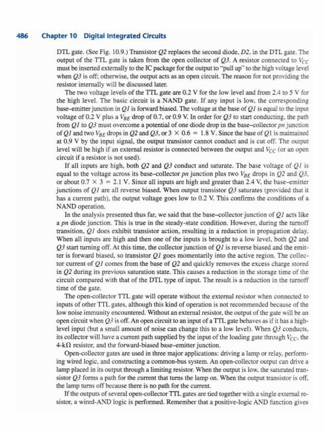
486 Chapter 10 Digital Integrated Circuits
DTL gate. (See Fig. 10.9.) Transistor Q2 repl aces the second diode. D2. in the DTL gale. Theoutput of the TTL gate is taken from the open coll ector of Q3. A resistor connected to l ecmust be inserted externally to the Ie package for the output to "pull up" to the high voltage levelwhen Q3 is off; otherwise. the O\Itput acts as an open circuit. Tbe reason for not provi ding theresistor internally will be discussed later.
The two voltage levels of the TTL gate are 0.2 V for the low le vel andfrom ~ ,~ to 5 v forthe high level. The basic circuit is a ~AND ga te, If any input is low. the corre spondingbase-emitter junction in QJ is forward biased. The voltage at the base of QJ is equal to the inputvoltage of 0.2 V plu~ a VHE drop of 0.7. or 0.9 V, In order for Q3 to start conducting. the pathfrom QJ to Q3 must overcome a potenti al of one diode drop in the base-collector pn junct ionof QJ and two VBEdrops in Q2 andQ3. or 3 x 0"6 = 1.8 V. Since the base of QI is maintainedat 0.9 V by the input signal. the output transistor ca nnot conduct and is cut off. The ou tputle vel will be high if an external resistor is connected between the output and vee(or an ope ncircu it if a resistor is not used).
If all inputs are high. both Q2 and Q3 co nduct and saturate. The base voltage of QJ isequal to the volt age across its base-collector pn j unction plus IWO VHE drops in Q2 and QJ.or about 0.7 x 3 = 2.1 V. Since all inputs are high and greate r than 2.4 V. the base-emitterjun ctions of Q1 are all reverse biased. When output transistor QJ saturat es (provided that ithas a current path). the output voltage goes low to 0.2 V. This co nfirms the conditions of aNAND operation .
In the analysis presented thus far. we said that the base-collector junction of QJ acts likea pn diode junction . This is true in the steady -state condition. However. duri ng the turnofftransition. Ql does exhibit transistor action. resulting in a reducti on in propagation delay .When all inputs are hig h and then one of the inputs Is brought to a low level. both Q2 andQ3 start turn ing off. At this time. the co llector j unction of QJ is reverse biased and the e mitter is forward biased. so transistor QJ goes momentarily into the act ive region. The collector current of Q J comes from the base of Q2 and qu ickly removes the excess charge sto redin Q2 during its previous saturation state. Th is causes a reduction in the storage time of thecircuit compared with that of the DTL type of input. The result is a reduction in the turno fftime of the gate.
The open-collector TTL gate will opera te without the external resistor when connected toinputs of other TTL gales. although this kind of operat ion is not recommended because of thelow noise immunity encou ntered. Without an external resistor. the output of the gate w ill be anopen circuit when QJ is off. An open circu it 10an input of a lTLgate behaves as ifit has a highlevel input (but a small amount of noise can change this to a low level)"wh en Q3 conducts,its co llecto r will have a current path supplied by the input of the loading gate through Vee. the4-k. 0 resistor. and the forward-biased base-emitter junction "
Open -collector gales are used in three major applications: driving a lamp or relay. performing wired logic. and constructing a common-bus system. An open-collector output can drive alamp placed in its output through a limiting resistor. When the output is low. the saturated tran sistor QJ forms a path for the current thai turns the lamp on. Whe n the output transistor is off.the lamp turns off because there is no path for the current.
If the outputs of several open-collector TTL gates are tied together with a single external resistor. a \l.ired-A~'D logic is performed Remember that a positi ve-logic A.\'D function gives

Section 10.S Transistor-Transistor Logic 487
;==[¥l~»--+-o y
(a) Physical connection
A-~+---,B --t~
c- - =='D-~'r---'(b) Wired-logic graphic symbol
y
FIGURE 10.12Wired-ANDof tw o cpen-ccuector (oc) gates, y ", (AS+ CD)'
a high level only if all variables are high: otherwise. the function is low. With the outputs ofopen-collector gate s connected together. the common output is high only when all output transistors are off (or high ). If an output trans isto r conduct s. it forces the output into the low state.
The wired log ic performed with open-co llector TIL gat es is depicted in Fig . 10.12. Thephysical wiring in (a) show s how the outputs must be connected to a common resistor. Thegraph ic symbol for such a connection is demonstrated in (b). The AND function formed by connecting the two outputs toge ther is called a wired -AND function. The AND gate is drawn withthe lines goin g through the center of the gate , to distinguish it from a conventional gate . Thewired·AND gate is not a physica l gate. but only a symbol to des ignate the function obtainedfrom the indic ated connection. The Boolean function obtained from the circuit of Fig. 10.12 isthe AND ope ration between the outputs of the two NAND gate s:
y ~ (AB )" (CD)' ~ (AB + CD)'
The second expression is preferred, since it shows an operation commonly referred to as anAND-OR-INVERT function. (See Section 3.8.)
Open -collector gates can be tied together to form a common bus. At any time, all gale outputstied to the bus. except one . must be maintained in their high state. The selected gate may be ineither the high or low state. depending on whether we want 10 trans mit a l or a 0 on the bus.Control circui ts must be used to select the particular gate thai drives the bus at any given time .
Figure 10.13 demonstrates the connection of four sources tied 10 a common bus line. Eachof the four inputs drive s an open-collec tor inverter, and the outputs of the inveners are tied together to form a single bus line. The figure shows that three of the inputs are 0, producing a I.or high level , on the bus. The founh input, 14 , can now transmit information through thecommon-bu s line into inverte r 5. Remem ber that an AND operation is peafuultd in thewired logic.If /4 = 1, the output of gate 4 is 0 and the wired-AND operation produces a O. If 4 = 0. theoutput of gate 4 is 1 and the wired-AND operation produces a 1. 1bus. if aU otbe.- outputs aremaintained at 1, the selected gale can transmi t its value Ihrougb the bus. TIle value uaesmirted is the complement of 14• but inverter 5 at the receiving end can easily invert thi s signalaga in to make Y = h.
488 Chap ter 10 Digital Integrated Circuits
v~
f ,o~·I
oI
Bus line s v
FIGURE 10 .13Open -collector gates forming a common bus line
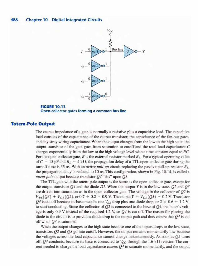
Totem-Pole Output
The output impedance of a gate is normally a resistive plus a capacitive load. The capacitiveload consists of the capacitance of the output transistor. the capacitance of the fan-out gates.and any stray wiring capacitance. When the output changes from the low to the high state. theoutput transistor of the gate goes from saturation to cutoff and the total load capacitance Ccharges exponentially from the low to the high voltage level with a time constant equal to RCFor the open-collector gate. R is the external resistor marked RL. For a typical operating valueof C = 15 pF and RL = 4 kU. the propagation delay of a TTL open-collector gate during theturnoff time is 35 ns. With an acti~'e pull -up circuit replacing the pas..ive pull-up resistor RL•the propagation delay is reduced to 10 ns. This configuration. shown in Fig. 10.14. is called atotem-po le output because transistor Q4 "s its" upon Q3.
The TIL gate with the totem-pole output is the same a" the open-collector gate. except forthe output transistor Q4 and the diode DJ . When the output Y is in the low state. Q2 and Q3are drive n into saturation as in the open-collector gate. The voltage in the collector of Q2 isVSE(Q3 ) + Va (Q2 ). or 0.7 + 0.2 = 0.9 V. The output Y = VcdQ3 ) = o. :! V. TransistorQ4 is cut off because its base must beone VB£ drop plus one diode drop. or 2 x 0.6 = 1.2 V.to start conducting. Since the collector of Q2 is connected to the base of Q4. the latter' s voltage is only 0.9 V instead of the required 1.2 V. so Q4 is cut off. The reason for placing thediode in the circuit is to provide a diode drop in the output path and thus ensure that Q4 is cutoff when Q3 is saturated.
When the output changes to the high state because one of the inputs drop.. to the low state,transistors Q2 and Q3 go into cutoff. However. the output remains momentarily low becausethe voltages across the load capacitance cannot change instantaneously. As soon as Q2 turnsoff. Q4 conducts. because its base is connected to veethrough the 1.6-1.: 0 resistor. The current needed to charge the load capacitance causes Q4 to saturate momentarily. and the output

Section 10.5 Transistor-Transistor l ogic 489
Vee = 5 V
4 en1.6 en Don
Q'
QlQ2
1 »n
D1
Q3
y
FIGURE 10.14TTLgate with totem-pole output
voltage rises with a time constant Re. But R in thi s case is equal to 130 n,plu s the saturationresistance of Q-I, plus the resistance of the d iode, for a total of approximately 150n. Thi svalue of R is much smaller than the passive pull-up resistance used in the open-collector circuit. As a conseq uence, the trans itio n from the low to high level is much fas ter.
As the capacitive load charges. the output voltage rises and the current in Q4 dec reases.bringing the tran sistor into the active region. Thu s, in contrast to the other transistors, Q4 is inthe active region when Q4 is in a steady -state condition. The fina l value of the output voltageis then 5 V, minu s a V8£ drop in Q4. minu s a diode drop in DJ to about 3.6 V. Transistor Q3 goesinto cutoff very fast, but durin g the initial transition time. bot h Q3 and Q4 are on and a peak current is drawn from the po wer supp ly. Thi s current sp ike generates noise in the power-supp ly distribut ion sys tem. Wh en the change of slate is frequent. the transient-current spikes increase thepower-supply current requirement and the average power dissipation o f the circuit increases.
The wired-logic connection is nOI allowed with tote m-pole ou tput circuits. When two totempoles are wired togethe r. with the outp ut of one ga le high and the output of the second gate low,the excessive amount of current drawn can produce enou gh heat 10damage the transistors in thecirc uit. (See Problem 10.7.) Some TTL gates are constructed 10 widasland theamounl ofcurrenlthat 110wsunder th is condition. In any case, lhe collector curren l in the low gale may be highenough to move the transistor into the active region and produce aD outpul voltagegrcaIa' Ihan0.8 V in the wired connection. This voltage is not a valWj binary signal forTl1. pIeS.
Schottky TTL Gate
As mentioned before , a reduction in storage time results in a redu::Iioa .in Pop8Iaf'ion delay.Thi s is because the tim e needed for a trans isto r to come OUI of saIUtlItioD delaysIhe switching

490 Chapter 10 Digital Integrated Circuits
of the transistor from the on condition to the off condition. Saturation can be eliminated by placing a Schottky diode between the base and collector of each saturated transistor in the circuit.The Schottky diode is formed by the junction of a metal and semiconductor, in contrast to a conventional diode, which is formed by the junction of p-type and n-type semicond uctor material.The voltage across a conducting Schottky diode is only 0.4 V. co mpared with 0.7 V in a conventional diode. The presence of a Schottky d iode between the base and collector prevents thetransistor from going into saturation.The resulting transistor is called a Schotrky transistor. Theuse of Schottky transistors in a TILdecreases the propagation delay without sacrificing powerdissipation.
The Schottky TTL gate is shown in Fig. 10.15. Note the speci al symbol used for theSchottky transistors and diodes. The diagram shows all transistors except Q-l to be of theSchottk y type. An exception is made for Q4, since it does not saturate. but stays in the activeregion . Note also that resistor values have been reduced in order to decrease the propagationdelay further.
In addition to using Schottky transistors and lower resistor values, the circuit of Fig. 10.15 includes other modifications not available in the standard gate of Fig. 10.14.Two new transistors.Q5 and Q6, have been added, and Schottky diodes are inserted between each input terminal andground. There is no diode in the totem-pole circuit. However. the new combination of Q5 and Q4still gives the two VBE drops necessary to prevent Q4 from conducting when the outpu t is low.This combination constitutes a double emitte r-follower called a Darlington pair. The Darlington
so o900 0
2.8kfl:
~Q5r-Q'
'"rQ1
3.5 enOJ f-o
-~
QJ
500 02500
~...L
FIGURE 10 .15Schottky TILgate

Section 10.5 Transistor-Transistor logic 49 1
pair provides a very high current gain and extremely low resistance, exactly what is needed duroing the low-to-high swing of the output, resulting in a decrease in propa gation delay.
Th e diodes in each input shown in the circuit help clamp any ringing that may occur in theinput lines. Under transient switch ing conditions, signal lines appear inductive ; this, along withstray capacitance, causes signal s to oscillate, or "ring." Whe n the output of a gate switchesfrom the high to the low state, the ringing waveform at the input may have excurs ions as grea tas 2-3 V below grou nd, depending on the line length . The diodes connected to ground helpclamp this ringing, since they conduc t as soon as the negative voltage exceeds 0.4 V. Whe n thenegative excursion is limited, the positive swing is also reduced. Clamp diodes have been sosuccessful in limiting line effects that all versions of TTL gates use them.
The emitter resistor Q2 in Fig. lO.14 has been replaced in Fig. lO.15 by a circuit consistingof transistor Q6 and two resis tors. Th e effect of thi s circ uit is to reduce the turnoff currentspikes discussed previously. The analys is of such a circuit, whose operation helps to reduce thepropagation time of the gate, is too involved to present in this brief discu ssion.
Three-State Gate
As mentioned ear lier, the outp uts of two Tl'L gates with totem-pole structures cann ot be connected together as in open-collector outputs. There is, however, a special type of totem-pole gatethat allows the wired connection of outputs for the purpose of forming a common-bus system.When a totem-pole output TTL gate has thi s property, it is called a three-stare gate.
A three -sta te gate exhi bits three outp ut states: (1) a low-leve l state when the lower tran sistor in the totem pole is on and the upper transistor is off, (2) a high -level state when the uppertransistor in the totem pole is on and the lower transistor is off, and (3) a third state when bothtransistors in the totem pole are off. The third state is an open-circ uit, or high-impedance, statethat allows a direct wire connec tion of many outputs to a common line. Three-state gates eliminate the need for open-collector gates in bus configurations.
Figure lO.16(a) shows the graphic symbol of a three-state buffer gate. When the controlinput C is high , the gate is enabled and behaves like a normal buffer, with the output equal tothe input binary value . When the control input is low, the output is an open circuit, which givesa high impedance (the third state) regardless of the value of input A. Some three-state gates produce a high -impedance state whe n the control input is high. Thi s is shown symbolically inFig. 1O.l6(b), where we have two small circle s, one for the inverter output and the other toindicate that the gate is enabled when C is low.
The circuit diagram of the three-state inverter is shown in Fig . IO.I 6(c ). Transistors 06.Q7, and Q8 associated with the control input form a circ uit similar 10 theopeo-collector gate .Transistors Q1- Q5. associated with the data input, form a tote m-pole TI1.. circuiL The twocircuits are connected together through diode D1. As in an opeo<oUc:c:cor- circuit. transistorQ8 turns off when the control inpu t at Cis in the low-level state.1biI prnaltS diode DI fromconducting. In addition. the emitter in Q1 connected to Q8 bas DOcft'dunion path. Under thiscondition, transistor Q8 has no effect on the operation of thegareandthe outpul ill Ydependsonly on the data input at A.
When the control input is high. transistor Q8 turns on and the CUItt:DI flowing from Veethrough diode D1 causes transistor Q8 to satura te. The voltage Illbc base 01 05 is nowequal

492 Chapter 10 Digital Integrated Circuits
Y =A if C "'highA ------{>----- Yh igh impedance~ if C - low
C(a) Three-stale buffer gate
Y "'A · if C = lo....A~ Y high impedance
if C = highC
(b) Thr ee-state inverter galt'
Contro linput C
Datainput
A
10,I,;
Q'I-..:
I Qf\ fQ]I,; f"Q.l
"'-
Df ...L-
Q6 f"Q 7
"08h."1.':
-J,.
,.
(e) Circuit diagram for the three-stale Inverter of (h )
FI(i,URE 10.16Three-state TTL gate

10.6
Section 10.6 Emitter-Coup led Logic 493
to the voltage acro ss the saturated tran sistor. Q8. plus one diode drop . or 0 .9 V. Th is voltageturns off Q5 and Q4. since it is less than two VBE drops. At the same time . the low input to oneof the emitter s of Ql forces trans istor Q3 (and Q2) to tum off. Th us. both Q3 and Q4 in thetotem po le are turned off. and the output of the circuit behav es like an open circu it with a veryhigh output impedance .
A three-state bus is created by wiring several three -state outputs togethe r. At any given time,only one control input is enabled while all other outpu ts are in the high-impedance state. Thesingle gate not in a high- impedance state can transmit binary information through the commonbus. Extreme care must be taken that all except one of the output s be in the third state; otherwise, we have the undesirable condition of having two active totem-pole output s connectedtogether.
An impo rtant feat ure of most thre e-state gate s is that the output enable delay is longer thanthe output disab le delay. If a control circuit enables one gate and disab les another at the sametime . the disabled gate ente rs the high-impedance state before the other gate is enabled. Th iseliminates the situation of both gates being active at the same time.
There is a very small leakag e current associated with the high-impedance conditio n in athree -state gate. Nevertheless. this current is so small that as many as 100 three-state outputscan be co nnected together to form a common-bus line .
EMITTER -COUPLED LOGIC
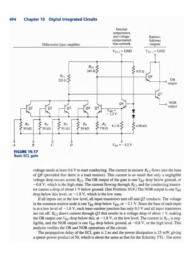
Emitter-coupled logic (ECL) is a nonsaturated digital logic fami ly. Since transistors do not seturate. it is possible to achieve propa gation delays as low as 1-2 ns. This logic family has thelowest propagation delay of any family and is used mostly in systems requiring very high speedoperation. Its noise immunity and power dissipation . however . are the worst of all the logic families available.
A typical basic circuit of the EeL family is shown in Fig. 10.17. The outputs provi de boththe OR and NOR functions. Each input is connected to the base of a transistor. The two voltage levels are abo ut - 0.8 V for the high state and abo ut - 1.8 V for the lo w state. The circuitconsists of a differential amplifier. a temperature- and voltage-compe nsated bias network. andan emitter-follower output. The em itter outputs require a pull-down resistor for current to flow.This is obtai ned fro m the input resistor Rp of another similar gate or from an ex ternal resistorconnected to a negative voltage supply.
The internal tempe rature- and voltage -compensated bias circuit supplies a reference volt age to the differential ampl ifier. Bias voltage Vss is set at - 1.3 V, which is me midpoint of mesignal's logic swing. The diodes in the voltage divider.fogetber with Q6. provide a circuit thatmaintain s a constant VBs value despite changes in temperature or supply voltage. Any one ofthe power supply inputs could be used as grou nd. However, the use of the Vccnode as groundand VEE at - 5.2 V results in the best noise immunity.
If any input in the ECL gate is high. the corresponding transistor is tumed OIl and Q5 isturned off . An input of - 0.8 V causes the tran sistor lOconduetand places -1.6 V OIl the emitters of all of the transistors. (The VB£ drop in EeL transistors is0.8 V.) Since VBB = - 1.3 V,the base voltage of Q5 is only 0.3 V more positive man itsemittet. Q5 is cut off because its VBE
494 Chapter 10 Digital Integrated Circuits
Differential input amplifier
Internaltemperatureand voltagecompensatedbias netwo rk
Emi tterfollo....erOUtputs
:-';ORoutput
ORoutpu t
Vee l - O:-iD
iVee: . GND
re+-
Rn245 0 970 n v.:
R" ~Q82200
IQ7
<161--1~l ~2 ~3 ~4 Q'j-1
,A V ,IIB = ,- 1.3V
r-r- r-t- r-t- r-r-R, R, R, R, R, 6.1n 4.98 kn
so en SOl O SO kH 50kO 779 n
A B c D VEE "" - S.2V
FIGURE 10.17Basic ECl gate
vol tage needs at least 0.6 V to stan conducting. The current in resistor Rc: flows into the baseof Q8 (provided that there is a load resistor). This current is so small that on ly a negligiblevoltage drop occurs across Rcz- The OR output of the gate is one VBE drop below ground. or- 0.8 V. which is the high stale. The current flowing through RCI and the conducting transistor causes a drop of abo ut 1 V below ground. (See Prob lem 10.9 .) The l'\OR output is one VBEdrop below this level. or - 1.8 V. which is the low stale.
If all inputs are at the low leve l, all input transistors tum off and Q5 conducts. The voltagein the common-emitte r node is one VBE drop below VBB, or - 2.1 V. Since the base of each inputis at a low level of - 1.8 V. each base-emitter junction has only 0 .3 V and all input transistorsare cut off. RCl dra ws current thro ugh Q5 that results in a vo ltage drop of about I V, makingthe OR output one VBE drop below this. at -1.8 V. or the low leve l. The current in RCl is negligible. and the NOR OUtpUI is o ne VBE drop below ground, at - 0.8 V. or the high level. Thisanalysis verifies the OR and NOR operatio ns of the circuit.
The propagation delay of the Ee L gale is 2 ns and the power dissipation is 25 mw, giv inga speed-power product of 50. which is about the same as that for the Schottky TIL. The noise

Section 10.7 Metal-Oxide Semiconductor 495
(A + B)' ... (C + D J'=
[(A + BltC + D)I'
+i4-- - - (A T B)(C + D )
A
B -L:...~-.
c- G*- -+_ ...JD
A-~ ,;",_ (A ..,. By NOR
B (A + B) OR
(a) Single gate (b) Wired combination of two gates
fiGURE 10.18Graphic symbol and wi red combinatio n of ECL gates
marg in is about 0.3 V and is not as good as that in the TTL gate. High fan-out is possible inthe ECl gate because of the high input impedance of the differential amplifier and the lowoutput impedan ce of the emitter-follower. Because of the extreme high speed of the signals.external wires act like transmission lines. Except for very sha lt wires of a few centimeters.ECl outputs must use coaxia l cables with a resistor termination to reduce line reflections.
The gra phic symbol for the ECl gate shown in Fig. 10 .18(a). 'TWo outputs are ava ilable: onefor the NOR function and the other for the OR function. The outputs of two or more ECL gate scan be connected togeth er to form wired logic. As shown in Fig. 1O.18(b), an external wiredconnection of two NO R outputs produces a wired-OR function. An internal wired connectionof two OR outputs is em ployed in some Eel ICs to produce a wired-AND (sometimes calleddot-AN D) logic. This property may be utili zed when ECL gales are used to form theOR- AND- INVE RT and the OR-AND functions.
10 .7 METAL -OXIDE SEMICONDUCTOR
The field-effect tra nsistor (FET) is a unipo lar transistor. since its operation depends on theflow of only one type of carrie r. Th ere are two types ofFETs: the junction field-effec t transistor (JPET) and the metal-oxide semiconductor (Ma S). Th e fanner is used in linear circuitsand the latter in digital circuits. MaS tran sistors can be fabricated in less area than bipolartransistors.
The basic structure of the MOS transistor is shown in Fig . 10.19. 1bep-channel MOS consists of a lightly doped substrate of a-type silicon material . Two regions are heavily doped bydiffusion with p- type impurities to fonn the source and drain. 1be region between the two~
type sections serves as the channel. Th e gale is a metal plate separated from thedwmeI by aninsulated dielectric of silicon dioxide . A negative voltage (with respect to tbe subsuaIe) 81 thegate terminal causes an induced electric field in the channe l thatattraetsp-eype carriers (ho&es)from the substrate . As the magnitude of the negative voltage on the pte iD:reases, the regionbelow the gale accumulates more positive carriers. the oonduaivity increases. and C\lI'ttnl cannow from source to drain. provided that a voltage difference is mainlaioed between these twoterminal s.

496 Chapter 10 Digital Integrated Circuits
{alp-channel
FIGURE 10.19Basic st ruct ure of MOS transistor
(b) u-channel
There are four ba-le types of ~fOS structures. The channel can be p or 11 type. dependingon whether the majo rity carriers are holes or elect rons. The mode of operation ca n be enhancement or depletion. dependin g on the state of the channel region at zero gate voltage . Ifthe channel is initially doped light ly with p-type impurity (in which case it is ca lled a diffusedchannels . a conducting channel exists at zero gate voltage and the device is said to operate inthe deplet ion mode. In this mode. current flows unless the channel is depleted by an appliedgate fte ld. lfthe region beneath the gale is lefl initia lly uncharged . a channel must be inducedby the gale field before current can flow. Thus. the channel current is enhanced by the gate voltage. and such a device is said to operate in the enhancement mode.
The source is the terminal through which the majo rity carriers enter the device. The drainis the termi nal through which the majo rity carriers leave Ihe device . In a n-channe l MOS. thesource terminal is connected to the substrate and a negative voltage is applied to the drainterminal. Whe n the ga le m ilage is above a thresho ld voltage Vr (abo ut - 2 V). no c urrentflow s in the channel and the drain -to-source path is like an open circu it. When the gate voltage is sufficiently negative below VT• a channel is formed andp-type carriers flow from source10 drain. p-Iype ca rriers are positive and correspond to a posit ive current flow from source 10
drain.In the u-channe! f\.I OS. the source terminal is co nnected to the substrate and a positive \ 011 ·
age is applied to the drain terminal. Whe n the gale voltage is below the thre..hold voltage Vr(about 2 V). no current flows in the channel. When the gate voltage is sufficiently positiveabove Vr to fonn the channel, a- type carriers flo ..... from source 10 drain. n-type carriers arenegat ive and correspond to a positive current flow from drain to source. The threshold voltagemay vary from I 104 V, depending on the particular process used.
The graphic symbols for the MOS transistors are shown in Fig. 10.20. The symbol for theenhancement type is the one with the broken-line connection between source and drain . In thissymbol. the substrate can be identified and is shown connected to the source. An alternative symbol omits the substrate. and instead an arro ..... is placed in the source termin al 10 show the direction ofpositivecu rrent flow (from source to drain in the p-channel MOS and from drain tosource in the II-channel MOS).
Because of the symmetrical construction of source and drain . the tl.l0S transistor can beoperated as a bilateral device. Although normally opera ted so that carriers flow from source todrain. there are circumstances when ir is convenient 10 allow carriers to flow from drain tosource. (See Proble m 10.12.)

Sec tion 10.7 Metal-Oxide Semicondu ctor 497
drain
.-J~alC --1 q sub!.tra te
W"=
D
G-<s
drain
.-J~a te --1 1--- sub!.lralc
'Isource
D
G-<s
(a) p -channe l
fiGURE 10.20Sym bols fo r MOS transistors
(b) e-channel
One advantage of the MOS device is that it ca n beused nOI only as a transistor, but as a resistor as well. A res istor is ob tained from the MOS by permanently biasing the gate terminalfor conduction. The ratio of the source-drain voltage to the channel current then determine s thevalue of the res istance . Different res istor values may heconstructed during manufacturing bytixing the channellength and width of the MOS device.
Three logic circuits using MOS devices are shown in Fig. 10.21. For an a-c hannel MOS,the supply voltage Vnn is positive (about 5 V). to allow positive curr ent flow from drain tosource. The IWO voltage levels are a function of the threshold voltage Vr .The low level is anywhere from zero to Vr • and the high level ranges from VT ttl Vnn. The n-chan nel gates usuallyemploy positive logic. Thep-channel ~10S circuit..U~ a negative voltage for Vnl). 10 allow pusitive current flow from source 10 drain. The IWO voltage levels are both negative abo ve andbelow the negative threshold voltage Vr . n-chan ne l gales usually e mploy negati ve logic.
r - -"-----r-- Y - (Ao + Bf
Y = (A B )'
\ ' OD
I
y - A '
[aj Inverter (b) SAND piC (c) NOR11*
FIGURE 10.21n-<hannel MOS logic circuits
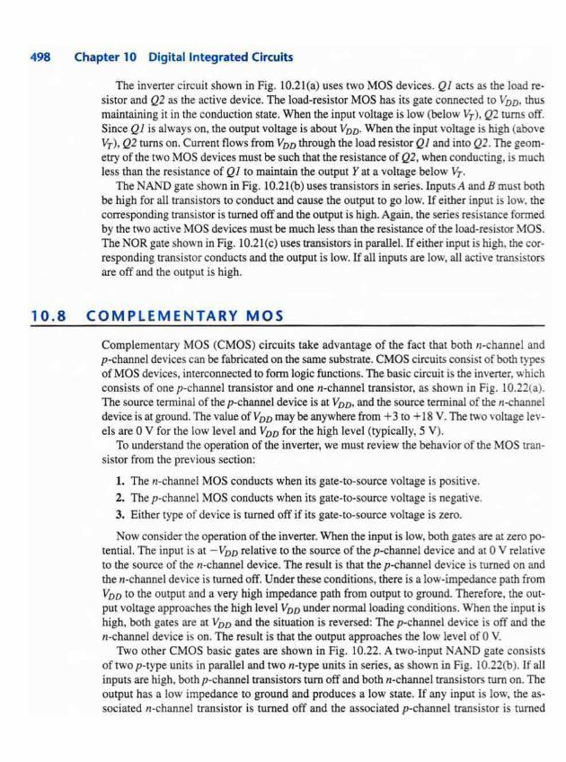
498 Chapter 10 Digital Integrated Circuits
The inverter circuit shown in Fig. 1O.21(a) uses two MOS devices. QJ acts as the load reosistor and Q2 as the active device. The load-resistor MOS has its gate connected to VDD• thusmaintaining it in the conduction stale. When the input voltage is low (below Vr ). Q2 turns off.Since QJ is always on. the output voltage is about VDD. When the input voltage is high (aboveVr ). Q2tums on. Current flows from VDD through the load resistor QJ and into Q 2. The geometry of the two MOS devices must be such that the resistance of Q2 . when conducting. is muchless than the resistance of QJ to maintain the outp ut Yat a voltage below Vr .
The NAl\' D gate shown in Fig. 10.21(b) uses transistors in series. Inputs A and B must bothbe high for all trans istors to conduct and cause the output to go low. If either input is low. thecorresponding transistor is turned off and the output is high. Again. the series resistance formedby the two active MOS devices must be much less than the resistance of the load-resistor ~10S.
The NOR gate shown in Fig. 1O.2Hc) uses transistors in parallel. If either input is high. the corresponding transistor conducts and the output is low. If all inputs are low, all active transist orsare off and the outp ut is high.
10 . 8 COM PLEM ENTARY MOS
Com plementary MOS (CMOS) circuit s take adva ntage of the fact thai both n-channe l andp -channel devices can befabricated on the same substrate. CMOS circuits cons ist of both typesof MOS devices . interconnected to form logic functions. The basic circuit is the inverter, whichconsis ts of one p-channel transistor and one n-channel transistor. as shown in Fig. 1O.22(a).The source terminal of the p-c hannel device is at VDD• and the source terminal of the a-channeldevice is at ground. The value of VDD may beanywhere from +3 to +18 V.Tbetwo voltage levels are av for the low level and VDD for the high level (typically. 5 V).
To understand the operati on of the inverter, we must review the behavior of the MOS tran-sistor from the previous section:
1. The a-channel MOS conducts when its gate-to-source voltage is positive.
2. The n-channel MOS conducts when its gale-to-source voltage is negative .
3. Either type of dev ice is turned off if its gate-to-source voltage is zero.
Now consider the operation of the inverter. When the input is low. both gates are at zero potential. The input Is at - VDD relative to the source of the p-channel device and at 0 V relativeto the source of the a-channel device. The result is that the p..channel device is turned on andthe a-channel device is turned off. Under these conditions. there is a low-impedance path fromVDD to the outpu t and a very high impedance path from output to ground. Therefore. the output voltage approaches the high level VDD under normal loading co nditions. When the input ishigh. both gates are at VDD and the situation is reversed: The p..channel device is off and thea-c hannel device i ~ on. The result is that the output approaches the low level of 0 V.
Two other CMOS basic gates are shown in Fig. 10.22. A two-i nput NAND gate consistsof two p- type units in parallel and two e-type units in series. as shown in Fig. 10.22(b ). If allinputs are high. both p-channel transistors tum off and both a-channel transistors tum on. Theoutput has a low impedance to ground and produces a low state. If any input is low. the associated a -channe l transistor is turned off and the assoc iated p-channel transistor is turned

Section 10.8 Com plementary MOS 499
v.,
1
P
A
A Y - A'
n
B
~
(I ) Inverter
rl ~ r F•.J
"~
,,-
I
(b) toOAND Ille
y .. (A B)"
A o--r----~
~-+---~---.---Q y .. (A + 8 )'
(e) S O R p ie
FJ(oURE 10.22CMOS logic c1n::uih

500 Cha pter 10 Digita l Integrated Circuits
on . The output is coupled to VOl) and goe s 10the high state. Multiple-input NAK D gates maybe formed by placing equal numbers of p-type and »-type transistors in para llel and serie s. respectively. in an arrangement similar to that shown in Fig. 1O.22(b J.
A two-input NOR gate consists of two »-type units in parallel and two p -type unit, in series. as shown in Fig. 1O.22(c) . When all input s are low. both n-c hannel units are on and botha-chan nel units are off. The outpu t is co upled to VD D and goes to the high srare. If any input ishigh. the associated p-c hanncl transistor is turned off and the associated n-ch annel transistorturns on . co nnecting the output to ground and causing a low-level output.
MOS transistors can be co nside red to be electronic switches that either con duct or areopen. As an example. the CMOS inverter can be visualized as consisting of two switches asshown in Fig. 1O.23(al . Applying a low voltage 10the input causes the upper switch (p) to dose.supplying a high voltage to the output. Applying a high voltage to the input ca uses the lowerswitch (n ) 10close. connecting the output to ground. Thu s. the output VOIle is the co mplementof the input Vi", Commercial applications often use other graphic symbols for ~10S transistors to emphasize the logica l behavior of the switches. The arrows showing the direction ofcurrent flow are omitted. Instead. the gate input of the p- chann eltrd.nsistor is draw n with aninversion bubble on the gate terminal to show that it is enabled wilh a low vokage. The inverter ci rcuit is redrawn with these symbols in Fig. 1O.23(b). A logic 0 in the input causes theupper transistor to conduc t. making the output logic I. A log ic I in the input enables the lowertransisto r. making the output logic O.
CMOS Characteristics
When a CMOS logic circuit is in a static state. its power dissipation is very low. This is becauseat least one transistor is always off in the path between the power supply and ground when thestate of the circuit is not changing. As a result. a typical CMOS gate has static power dissipation on the order of 0.0 1mw.However. when the circuit is changing state at the rate of I MHz.the power dissipation increases to abou t J rnw, and at In MHz it is about 5 mW.
V tJtJ .. 5 V
Iv"-[r- v~,
1{a}Switch model
FIGURE 10.2 3CMOS inverter
(b) logical model

, 0 . 9
Section 10.9 CMOS Transm ission Gate Circuits 501
C!\lOS logic is usually speci fied for a sing le power-supply operatio n ove r a voltage rangefrom 3 to 18 V with a typical vocvalue of 5 V. Operati ng CMOS at a larger power-supplyvoltage reduces the propa gatio n delay lime and improves the noise margin. but the powe r dissipat ion is increased . The propagat ion dela y time with VlJD = 5 V ranges from 5 to 20 ns.depending o n the type of CMOS used . Th e noise marg in is usually abo ut 40 percent of thepower supply volt age . Th e fan-out of CMOS gates is abo ut 30 when they are operated at afrequency of I MH z. The fan-ou t decreases with an increase in the freq uency of operatio nof the ga tes.
There are several series of the CMOS digital logic family. The 74C series are pin and function compatible with TTL devices havin g the same number. For e xample. C~IOS IC type740 )4 has six inverters with the same pin configuration as TIL type 7404. The high-speedC!\toS 74IJC series is an improvement over the 74C series. with a tenfo ld increase in switching speed. The 74HCT series is electrically compatible with TIL ICs.Thi ... means that circuitsin this series can he conne cted to inp uts and outputs of TTL le s without the need of additionalinterfaci ng circuits. Newer versions of CMOS are the high-speed series 74VHC and its TILcompatible version 74VHCT.
The CMOS fabrication process is simpler than that of TIl.. and pro vides a greater packingdensit y. Thu s. more circuits can beplaced on a given area of silicon at a reduced cost per function . This property. together with the low power dissipation of CMOS ci rcuits. good noise immunity. and reasonable propagation delay, makes CMO S the most popular standard as a digitallogic famil y.
CMOS TRANSMISSION GATE CIRCUITS
A special CMOS circuit that is not avai lable in the other digital logic families is the transmission
gale.Th e transmission gate is essentially an electronic switch that is controlled by an input logiclevel. It is used 10 simplify the construction of various digital components when fabricatedwith CMOS technology.
Figure 10.24(3) sho ws the basic ci rcuit of the transmission gate. Whereas a CMOS inverter consists of a p-c hanne l transistor connec ted in series with an n-channel transistor, atransmission gate is fonned by one a -channe l and one p-chan nel MOS transistor connectedin parallel.
The e-channel substrate is connected to ground and the p-channel substra te is connected to
VOl). When the N gate is at Vl)/J and the P gate is at ground. both trans istors condoct and thereis a closed path betwee n input X and output Y. When the N gate is at ground and me P gate isat VDl). both tra nsistors are off and there is an open circuit besweea X aDd Y. Figure IO.24(b)shows the block diagram of the transm ission gate . Note that the IenIJiaI oi lbep-cbaorrl gale
is marked with the negation symbol. Figure IO.24(c ) demonstnIIea thebebaYiorof theswitcbin terms of po..iti....e-togic assignment with ¥oo equivelent tc logic 1_~ c:qaivalClllllOlogic O.
Th e transmission gate is usually connected 10 an inverter, • sbowa .. .fi&.. 10.2.5. Thistype of arran gement is referred to as a bilateral switch: 'The coattoI input Cis ((JIW'IC'1I'(I direct ly 10 the n-chunnel gate and its inverse to the p-channel gale. Wheu C = I. the swi1dt is

S02 Chapter 10 Digital Integrated Circuits
y
p
(b)
TGx - ---jy
Tr
(.)
-'"...l..
x~
Closed switch
x~y."I-Ip- o
Open switch
x~L:>....-yN - OP - l
«)
FleUR! 10.2"Transmission gate (TG)
c ~
v
x - TG f--- y
FIGURE 10.25Bilate ral switch
closed. producing a path between X and Y. When C = O. the switch is open . disconnectingthe path between X and Y.
Various circuits can be constructed that use the transmission gale. To demonstrate its usefulness as a component in the CMOS family. we will show three examples.
The exclusive-OR gate can beconstructed with two transmission gates and rwc Inverters.as shown in Fig. 10.26. Input A co ntrols the paths in the trans mission gales and input B is
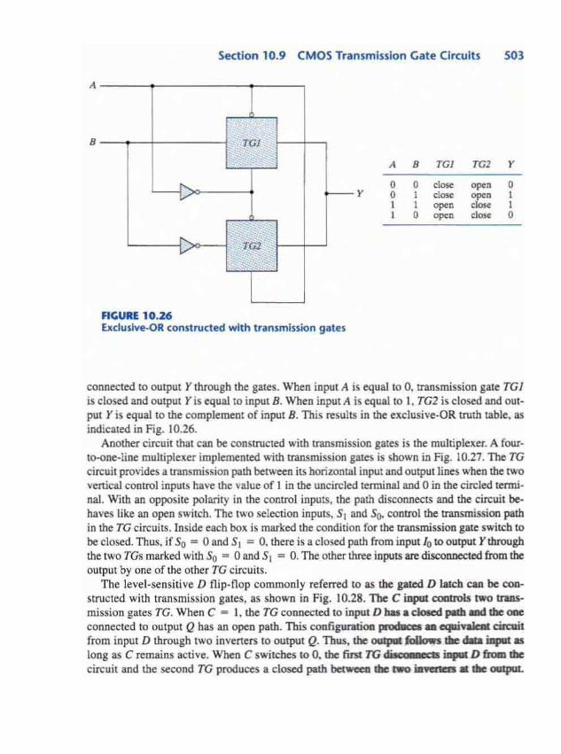
Section 10.9 CMOS Transmission Gate Circuits S03
A B TG1 TG2 Y
A
8
jTGJ ' i·
'. "i>t~~
v -•cc"!,\;'{i)).. ~"-S""·-'···
~ ~1,1i1~V~f~'"·~-::if!4.~'h,'i!.
FIGURE 10.26Exclusive-ORconst ructed with transmission gates
yooII
o close1 close1 "P"o open
"P" 0"P" Iclose 1close 0
connected to output Y through the gales. When input A is equal to O. trans mission gate TGIis closed and output Y is equal to input B. When input A is equal to I . TG2 is closed and ourput Y is equal to the com plement of input B. This resu lts in the exclusive-OR truth tab le. asindicated in Fig. 10.26.
Anothe r circui t that can be constructed with transmission gales is the multiplexer. A fourto-one-line multiplexer implemented with trans mission gates is shown in Fig. 10.27. The TGcircuit provides a transmission path between its horizontal input and output lines when the twovertical control inputs have the value of I in the uncircled term inal and 0 in the circled termi nal. With an opposite polari ty in the co ntrol inputs. the path disco nnects and the circuit behaves like an open switch. The two selection inputs. SI and So- control the transmissi on pathin the TG circuits. Inside each box is marked the condition for the transmission gate switch tobe closed. Thus. if So = 0 and SI =O. there is a closed path from input 10 to output Ythrou ghthe two TGs marked with So ". 0 and SI = O. The other three inputs art disconoected from theoutput by one of the other TG circuits.
The level-sen sitive D flip- flop co mmo nly referred to as the gated D latch can be coestruc ted with transmission ga tes. as shown in Fig. 10.28. The C input coouols lWO tn.nsmission gates TG. When C - I. the TO co nnected to input D has acJo.ed pMh 8Dd theoneco nnected to output Q has an open path . This co nfiguratioa prodDca .. eqaivalc8l ciraritfrom input D through two inverters to ou tput Q. Thus. the 0UIpal fcJrI)ows die data inpIt aslong as C remains active . When C switches to O. the fmt TG diN ' -dll iDpu& D from diecircuit and the seco nd TG produces a closed path benwcen dI£ two iIIft11cn • die output.

504 Chapter 10 Dig it al In teg ra t e d Circuits
s,
s,
I ,
I ,
vr-,v
..~ .«~TG~~,(~ -- 0),
,
&' ra'~J~,:?)
:,~~r~I' .
~
jfiflJ1jjI. TGr%(5,;" 0);;
fJlJi/fRiill:iJf;JISII, '.rog~7~~)0'
"·'t· ~', .' '~:%:""''--",'lt;!r:,/. _Ta e-,'Ilt,'(S "'1)";'IfJlf4i*
,.
FIGURE 10.27Multiplexer w ith t ransmiuion gates
Th us. the va lue that was present at input D at the lime that C went from I 100 is re tained atthe Qo utput.
A master- slave D llip-flop can be constructed with two circuits of the type shown in Fig. IO.!8.The first circ uit is the master and the second is the slave. Thus, a ma..rer- slave 0 flip-flop can beconstructed with four transmission gates and six inverters.

Sect ion 10.10 Switch-l evel Modeling with HOl 505
c - -r- -----.--- - - - - --,
TG f----.--+----1~-~-Q'
!;'f- - - - 4-- Q
10 ,10
FIGURE 10.28Gat ed D latch wit h transmission gates
SWITCH ·LEVEL MODELING WITH HDL
C~lOS is the dornlnant d igitallogjc family used with integrated circuits. By definition. C:-AOS~is a comp lementary connection of an NMOS and a PMOS transistor. ~OS transistors can beconsidered to be electronic switches that either conduct or are open. By specifying the connections among MOS switches. the des igner can describe a digital circuit constructed withCMOS. This type of description is called switch-level modeling in Veri log HDL.
The IWO types of MOS switches are specified in Verilog HOL with the keywords nmos andpmos. They are instantia ted by specifying the three terminals of the transistor. as shown inFig. 10.20:
nmos (drain. source , ga te);pmos (drain, source , gale);
Switches are considered 10 beprimitives. so the use of an instance name is op tiona l.The connections to a power source (VOD ) and 10 ground mU~1 be specified when MQS cir
cuits are designed. PO\I,er and ground are defined with the keywords suppl}"l and supplyu.Theyare specified. for example. with the following statements:
supply 1 PWR;supplyO GRO;
Sources of type supplyI are equivalent 10 VOD and have a value of logic I. Sources of type
supplyn are equivalent to ground connection and have a value of logic O.The descr iption of the CMOS inverter of Fig. 1O.22(a) is shown in HDLExample 10.1. The
input. the outp ut. and the IWO supply sources are dec lared first, Tbe module instantiates ap~tOS and an NMOS transisto r. The outpu t Y is common to both transistors at their drai n terminals. The input is also common to both transistors at their gate terminals. Tbe source: terminal of the PMOS transistor is connected to PWR and the source terminal of the NMOS transistoris connected to GRD.

S06 Chapter 10 Digita l Integrated Circuits
HDL Exam ple 10.1
1/ CMOS inverter of Fig. 10.22(a)module inverter (Y. A);Input A;output Y;supply1 PWR;supplyO GRD;pmos (Y, PWR, A);nmos (Y, GRD, A);
endmodule
1/(Drain, source, gale)1/(Drain, source. gate)
1/terminal between two nmos1/source connected to Vdd1/parallel connection1/ serial connection/I source connected to ground
The second module. set forth in HOL Example 10.2. describes the two-input C~(OS ~A;-';O
circuit of Fig. IO.22(b). There are two PMOS transistors connected in parallel, with their sourceterminals connected 10 PWR. There are also two NMOS transistors connected in series and witha common terminal WI . The drain of the first~OS is connected 10 the output. and the sourceof the second ;-..IMOS is connected to GRD.
HDL Exam ple 10.2
fI CMOS two-input NAND of Fig. 10.22(b)modu le NAND2 (Y, A, B);Input A, B;output Y;supp ly1 PWR;supplyO GRD;wire W1;pmos (Y, PWR, A);pmos (Y, PWR, B):nmos (Y, W1, A);nmos (W1, GRD, B);
endmod ule
Transmission Gate
The transmission gale is instantiated in Verilog HOL with the keyword cmos. II has an output .an input. and two control signals. as shown in Fig. 10.24. It is referred to as a cmos switch. Therelevant code is as follows:
cmos (output. input. ncontrot, pcontrol); /I general description
cmos (Y, X, N, P): 1/ transmission gate of Fig. 10.24(b)
Normall y. ncontrol and pcontrol are the comp lement of each other. The cmos switch does nOIneed power sources, since VDD and ground are co nnected to the substrates of the MOS transistors.Transmission gates are useful for building multiplexers and flip-flops with CMOS circuits.

Section 10,10 Switch-Level Modeling with HDL 507
HDL Example 10.3 describes a circuit with cmos switches. The exclusive-OR circuit ofFig. 10.26 has two transmission gates and two inverters. The two inverters are instantiatedwithin the module describing a CMOS inverter. The two cmos switches are instantiated without an instance name, since they are primitives in the language. A test module is included totest the circuit's operation. Applying all possible comb inations of the two inputs, the result ofthe simulator verifies the operation of the exclus ive-OR circuit. The output of the simulationis as follows:
HDL Exam ple 10.3
A =OA = OA = l
A =l
8 =0
8 = 1
8 = 0
B =l
Y = OY = lY =lY = 0
IICMOS XOR with CMOS switches , Fig. 10.26
module CMOS_XOR (A, B, Y);Input A, B;ou tput Y;wire A_b, B_b;II instantiate inverterinverte r vt (A_b, A);inverte r v2 (B_b, B);II instantiate cmos switchcmos (Y, B, A_b, A);cmos (Y, B_b, A, A_b );
e ndmoduleIf CMOS inverter Fig. 10-22(a )module inverter (Y, A);
Input A;output Y;supply1 PWR;supplyO GND ;pmos (Y, PWR, A);nmos (Y, GND , A);
e ndmo duleII Stimulus to test CMOS_XORmodule tesC CMOS_XOR;
reg A,S;wlre Y;IIlnstant iate CMOS_XORCMOS_XOR X1 (A, B, Y);II Apply truth tableInitial
beg in
lI(output, input, ncontrol, pcontrol)
II(Drain, source , gate)I/(Drain. source, ga te)

508 Chapter 10 Digital Integrat ed Circuits
A = l 'bO; B = l 'bO;#5 A = l'bO; B = l 'bl ;#5 A = 1'bl ; B = l 'bO;#5 A = t'b t : B = l 'bl ;
endf{ Display resultsInitial$monltor ( A =%b B= %b Y =%b~ , A, B, V);
endmodule
P RO BLEM S
Answers to problems marked w ith * appear at the end of the book.
10.1 * Following are the specifications for the Schottky TfL 74SOO quadruple lwo-inpur N'A:'\O gate' :
Paramet er
VeeICCH
tea.VOHVo,Vm
V"10 H
toehHI"t PLH
trn t:
Nam e
Supply voltageHigh-level supply current (four gates)Low-level supply current (four gates)High-level output voltage (min)Low-level output voltage (max)High-level input voltage (min)Low-level input voltage (max)
High-leve l output current (max)Low-level output current (max)High-level input current (max)
Low-level input current (max)Low-to-high delayHigh-to-low delay
Value
5 VlO rnA20 rnA2.7 V0.5 V2 V0.8 V
I rnA20 rnA0.05 rnA2 rnA
J ",,,
Calculate the fan-out, power dissipation. propagation delay, and noise margin of the Schottky
NAND gate.
10.24' (a) Determine the high-level OUlP UI voltage of the RTL gale (or a fan-out of 5.(b) Determine the minimum input voltage required to drive an RTL transistor to saturation
when hn = 20.(c) From the results in parts (a ) and (b), determi ne the noise margin oflhe Rr t. gmew hen the
input is high and the fan-out is 5.
10.]* Show that the output transistor of the on. gate of Fig. 10.9 goes into saueauon when all inPUI, are high. Assume that hn = 20.

10.4*
10.5*
10.6
10.7
10.8
10.9*
10.10*
10.1 1
10.12
Problems 509
Connect the output Yof the OTL gate shown in Fig. I0.9 to N inputs of other, similar gates. Assume that the output transistor is saturated and its base curre nt is 0.44 mAo Let h FE = 20.(a) Calculate the current in the 2-kn resistor.(b) Calculate the current coming from each input con nected to the gate.(c) Calcu late the total collec tor current in the output transistor as a function of N.(d) Find the value ofN that will keep the transistor in saturation.(e) What is the fan-out of the gate?
Let all inputs in the ope n-col lector TTL gate of Fig. I0.11 be in the high state of 3 V.(a) Determine the voltages in the base. collector. and emitter of all transis tors in the circuit.(b) Determin e the minimum hFE of Q2 which ensures that this transistor saturates.(c) Calculate the base current of Q3 .(d ) Assume that the minimum liFEof Q3 is 6. 18. What is the maxim um current that ca n be tol
erated in the collector to ensure saturation of Q3?(e) What is the minimum value of RL that ca n be tolerated to ensure saturation of Q3?
(a) Using the actual output transistors of t.... o ope n-collector TTL gates. show (by means of atruth table ) that . when connected together III an external resi stor and Vee, the wired connection produces an AKO function.
(b) Prove that two ope n-collector TTL inverters. when connected together. produce the NORfunction.
It was stated in Section 10.5 that totem-pole uutputs should not be tied together to fonn wired logic.To see why this is prohibitive. connect two such circuits together and let the output of one gate bein the high state and the output of the other gate be in the low state. Show that the load current(which is the sum of the base and collector currents of the saturated transistor Q-I in Fig. 10.14) isabout 32 mAoCompare this value with the recommended load current in the high state of 0.4 mA.
For the following conditions, list the transistors that are off and the transistors that are conducting in the three-state TTL gate of Fig. 1O.16(c} (for Ql and Q6. it is necessary to list theslates in the base-emitter and base--collector junctions separately):(a) when C is low and A is low.(b) when C is low and A is high.(c) when C is high.
Wh at is the stale of the output in each case?
(a) Calculate the emitter current te across R£ in the ECL gate of Fig. 10. 17 when atleas..t oneinput is high at -0.8 V.
(b) Calculate the same current when all inputs are low at - 1.8 v.(c ) Now assume that le = te. Calc ulate ibe voltage drop across the co llecto r resistor in eac h
case and show that it is about I V. as required.
Calculate the noise margin of the Eel gale.
Using the NOR outputs of two ECL gates. show that, whenCOlIlOCfed IOgelber 10 aD e1ICIDaIresister and a negative supply voltage, the wired connection prodDccs ..OR r-:tioL
The MOS transistor is bilateral (i.e.. curre nt may flow from alM'Ce 10draia or from. draillllOsource). On the basis of this property, derive a circu illb.al impIcmmIs Ibe Be:-*- r..aioa
Y = ( AS + CD + AED + CEB)'
using six MOS transistors.

510 Chapter 10 Digital Integrated ClrculU
10.13 (a) Show the circuit of a four-input NAA'U gate using CMOS transistors.(b) Repeal for a four-input NOR gate.
10.14 Construct an exclusive-NOR circuit wilh IWO inverters and two transmission gates.
10.15 Construct an eight-to-one-line multiplexer using transmission gates and inverters.
10.16 Draw the logic diagram of a master-s teve D flip-flop using transmission gates and tnveeers.
10.17 Write a test bench that will te st the NA.'lDcircu itof HDLExample 10.2. The simulation shouldverify the truth table of the gate.
RE FE REN C ES
1. ClLETIl. M. D. 1999. Modeling. Symhesis. and Rapid Protot)'ping with Verilog HDL Upper Sed-
dIe River. NJ: Prentice Hall.2 . CMOS Logic Data Book. 1994. Dallas: Texas Instruments.3. HODGES. D.A. 2003.Analysis and Design ofDigital Integrated Cirruits. New York: ~lcGra~ ·Hill .
4 . TOCCI. R. J.. and N. S. WIDMER. 2004. Digital Systems: Principles and Applications. 9th ed.Upper Saddle River. NJ: Prentice Hall.
S. The TTL Logic Data Book . 1988. Dallas: Texas Instruments.6 . WAKERLY. J. F. 2006. Digital Design: Princ iples and Practices. 4th ed . Upper Saddle River, S f:
Prentice Hall.7. WESTE. X. E.. and K. EsHRAGHlA.'l . 2005. Principles ofCMOS VLSI Design: A S)'slem Perspec
tive, 2d ed. Reading. MA: Addison-Wesley.