Bundles in Captivity: An Application of Superimposed Information
Upload
independentCategory
view
1download
0
Eur. Phys. J. B 31, 203–208 (2003)DOI: 10.1140/epjb/e2003-00024-8 THE EUROPEAN
PHYSICAL JOURNAL B
Carbon nanotube bundles and thin layers probed by micro-Ramanspectroscopy
L. Sangaletti1,a, S. Pagliara1, F. Parmigiani1, P. Galinetto2, R. Larciprete3, S. Lizzit3, and A. Goldoni3
1 Dipartimento di Matematica e Fisica and INFM, Universita Cattolica, Via dei Musei 41, 25121 Brescia, Italy2 Dipartimento di Fisica “A. Volta” and INFM, Universita di Pavia, Via Bassi 6, Pavia, Italy3 Sincrotrone Trieste, s.s. 14 Km 163,5 in Area Science Park, 34012 Trieste, Italy
Received 2 September 2002Published online 4 February 2003 – c© EDP Sciences, Societa Italiana di Fisica, Springer-Verlag 2003
Abstract. Raman spectra of single-wall carbon nanotubes (CNTs) either in the form of micrometer sizedbundles or thin layers prepared by dilution and sonication of powders have been compared. We have beenable to collect the Raman spectrum of nanotube bundles that are not in touch with the substrate, andtherefore not affected by interactions with the substrate surface. This spectrum resulted to be similar tothat of the precursor nanotube powders, whereas relevant changes in the Raman spectrum are detectedwhen the diluted powders form very thin layers on either metallic or insulating surfaces, as probed byconfocal microraman imaging on well defined areas of the CNTs layers. In the case of thin layers, theintensity of the Raman D band, detected between 1 320 and 1 340 cm−1 and ascribed to disorder effects,is strongly enhanced. This enhancement occurs independently on the kind of substrate.
PACS. 73.63.Fg Nanotubes – 63.50.+x Vibrational states in disordered systems – 78.30.-j Infrared andRaman spectra
Introduction
A wide range of potential applications for carbon nan-otubes (CNTs), assembled to fabricate electrical and me-chanical nanodevices, has raised much interest on thisnanostructured form of carbon. In the design of nanode-vices, possible changes in the properties of CNTs at theinterface between the CNT itself and other materials can-not be neglected. For example, for application of CNTsin electronic components, site-specific assemblies of nan-otubes onto patterned substrates are required. This canbe accomplished by surface modifications favoring the at-tachment of nanotubes to an electrode [1]. Indeed, a re-cent work shows that a deformation of adsorbed nanotubesdue to the interaction with the surface may occur [2]. Thisfinding has implications for electronic transport and tribo-logical properties of adsorbed CNTs. The interest in theseaspects of nanotube-substrate interaction is also large inview of the dramatic dependence of the electronic struc-ture on the substrate material already observed for singlelayers of C60 and C70 fullerides, i.e., the other nanostruc-tured form of carbon [3].
Raman spectroscopy is one of the most used toolsin the characterization of CNTs. Due to the high Ra-man cross section for the active vibrational modes andto the possibility to work at resonant excitation frequen-
a e-mail: [email protected]
cies, Raman spectroscopy was recently shown to be a non-destructive probe for the investigation of nanotubes [4].In principle, this probe is capable of determining the di-ameter and the electronic properties of single-wall CNTs.Moreover, when combined with a confocal microscope, theRaman probe can be integrated into a scanning confo-cal Raman imaging system which can provide a mappingof the Raman bands from a sample with a lateral res-olution of about 1 µm. Mews et al. have carried out aRaman imaging study of individual bundles of nanotubes,by combining confocal Raman spectroscopy and AFM mi-croscopy [5]. In this study it was possible to distinguishbetween the separate CNTs and to perform spatially re-solved Raman spectroscopy within a given bundle of CNTsdeposited onto a low-roughness Si3N4 membrane.
Many other experiments have been carried out withsamples prepared in different ways, including depositiononto substrates for surface-enhanced Raman scattering(SERS) investigations [6–10]. Several layers have beenprepared for SERS experiments on carbon CNTs. Corioet al. [6] have deposited silver or gold layers on glass toobtain clusters of metal particles. Colloidal silver clus-ters were used by Kneipp et al. [7,8]. Azoulay et al. havecarried out SERS experiments on single hot-spot site [9]whereas Duesberg et al. [10] were able to perform po-larized microraman spectroscopy on spatially separatedsingle-wall CNTs.

204 The European Physical Journal B
While all the previous studies have been carried out inthe presence of a specific substrate, the Raman study ofsingle-wall CNTs not interacting with the substrate hasbeen so far virtually neglected. Only in a recent experi-ment, the electronic properties of self-standing CNTs bun-dles with a diameter of about 150 nm were mapped byphotoemission spectro-microscopy [11].
The aim of the present study is to track changes in theRaman scattering of single-wall CNTs either in the formof micrometer sized bundles that are not in touch withany substrate (bridge-like CNTs), except for the bundleextremities, or thin layers deposited onto either metallicor insulating substrates. We have been able to collect theRaman spectrum of bridge-like bundles with a size downto one micrometer, prepared by dilution and sonicationof powders. This spectrum results to be similar to thatof the precursor powders, whereas relevant changes in theRaman spectrum are detected when the diluted powdersform very thin layers onto either metallic or insulating sur-faces. In the case of thin CNTs layers, the enhancementof the intensity of the band at about 1 330 cm−1 (usuallydenoted as D band in graphite) is related to defects inthe graphene sheets or size effects as observed by Maurinet al. [12]. Moreover, this enhancement occurs indepen-dently on the kind of substrate and, therefore, in this casecan not be ascribed to the chemical degradation inducedat SERS conditions, invoked by Lefrant et al. to explainthe dependence of the D band on the layer thickness [13].
Experiment
High quality purified single-wall CNT powder (byCARBOLEX [www.carbolex.com]), originally producedby laser vaporization of carbon with Ni/Co catalyst, wasfirst sonically dispersed in toluene, then sonically dis-persed in acetone and finally deposited, via evaporationof the solvent, on a clean copper grid or a copper platelet.
Microraman spectra from the nanotube powders werecollected by a Dilor Labram spectrograph. The excitationsource was a HeNe laser (632.8 nm; i.e. 1.96 eV) with apower of the order of 10 mW, focussed down to a diffrac-tion limited spot size of about 1 micrometer. This set upyielded an excitation power of about 1MW/cm2 on thesample. A Renishaw spectrograph was used to collect theRaman spectra with a photon energy of 2.41 eV (514 nm)obtained from an air-cooled Ar laser source. In both cases,a microscope was coupled confocally to the spectrograph.Rejection of the elastically scattered line was obtainedwith a holographic notch filter. The lateral resolution ofthe Labram probe during the microraman mapping wasabout 1 µm, resulting from the focussing of the laser beamwith a 100x (N.A. = 0.9) microscope objective.
Results and discussion
In the following, the Raman spectra of the precursor pow-ders are presented. From these powders, micrometer sized
Fig. 1. Microraman spectra of the single-wall CNT collectedunder different preparation conditions. (a) Precursor powders,λ = 632 nm. (b) Precursor powders, λ = 514 nm. (c) represen-tative Raman spectra collected from the bundle of Figure 2b.(d) Representative Raman spectrum collected from the CNTdeposited onto the copper mesh (thick layer). (e) Representa-tive Raman spectrum collected from the CNT deposited ontothe copper mesh (very thin layer, not visible under the micro-scope). (f) Representative Raman spectrum collected from theCNT deposited onto the copper plate (thick layer). (g) Repre-sentative Raman spectrum collected from the CNT depositedonto the copper mesh (thin layer).
bundles and thin layers were obtained after depositiononto a metallic (copper) mesh or a copper platelet.
Figure 1 shows the Raman spectra collected with632.8 nm (a) and 514.0 nm (b) laser sources in the1 200–2000 cm−1 range. In spectrum (a) several bands canbe clearly detected at about 1 312 (D), 1 580 (G), 1 736(A) and 1 920 (B) cm−1. The wavenumber of D and Gpeaks increases with the photon energy, as reported inTable 1. These features are typical of Raman bands aris-ing from single-wall CNTs [14]. Moreover the G-band atabout 1 580 cm−1 is much broader when collected with1.96 eV photon energy and displays a fine structure.
L. Sangaletti et al.: Carbon nanotube bundles and thin layers probed by micro-Raman spectroscopy 205
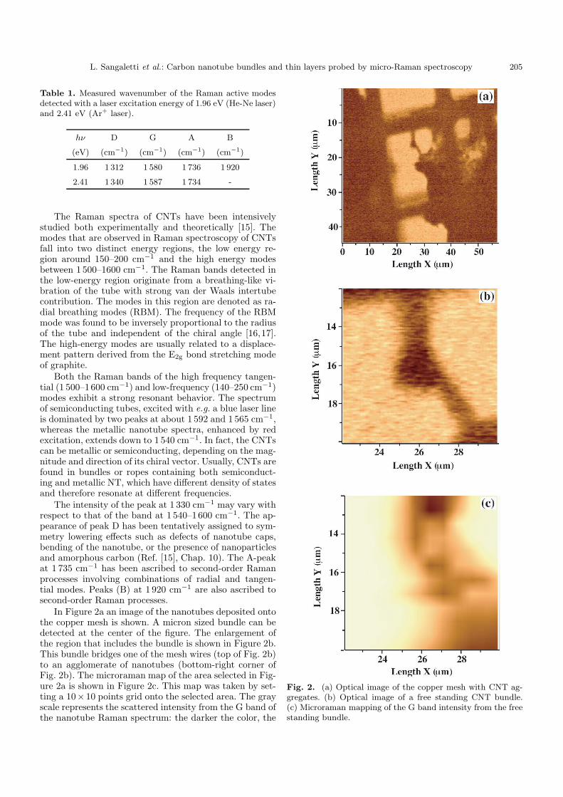
Table 1. Measured wavenumber of the Raman active modesdetected with a laser excitation energy of 1.96 eV (He-Ne laser)and 2.41 eV (Ar+ laser).
hν D G A B
(eV) (cm−1) (cm−1) (cm−1) (cm−1)
1.96 1 312 1 580 1 736 1 920
2.41 1 340 1 587 1 734 -
The Raman spectra of CNTs have been intensivelystudied both experimentally and theoretically [15]. Themodes that are observed in Raman spectroscopy of CNTsfall into two distinct energy regions, the low energy re-gion around 150–200 cm−1 and the high energy modesbetween 1 500–1600 cm−1. The Raman bands detected inthe low-energy region originate from a breathing-like vi-bration of the tube with strong van der Waals intertubecontribution. The modes in this region are denoted as ra-dial breathing modes (RBM). The frequency of the RBMmode was found to be inversely proportional to the radiusof the tube and independent of the chiral angle [16,17].The high-energy modes are usually related to a displace-ment pattern derived from the E2g bond stretching modeof graphite.
Both the Raman bands of the high frequency tangen-tial (1 500–1600 cm−1) and low-frequency (140–250 cm−1)modes exhibit a strong resonant behavior. The spectrumof semiconducting tubes, excited with e.g. a blue laser lineis dominated by two peaks at about 1 592 and 1 565 cm−1,whereas the metallic nanotube spectra, enhanced by redexcitation, extends down to 1 540 cm−1. In fact, the CNTscan be metallic or semiconducting, depending on the mag-nitude and direction of its chiral vector. Usually, CNTs arefound in bundles or ropes containing both semiconduct-ing and metallic NT, which have different density of statesand therefore resonate at different frequencies.
The intensity of the peak at 1 330 cm−1 may vary withrespect to that of the band at 1 540–1600 cm−1. The ap-pearance of peak D has been tentatively assigned to sym-metry lowering effects such as defects of nanotube caps,bending of the nanotube, or the presence of nanoparticlesand amorphous carbon (Ref. [15], Chap. 10). The A-peakat 1 735 cm−1 has been ascribed to second-order Ramanprocesses involving combinations of radial and tangen-tial modes. Peaks (B) at 1 920 cm−1 are also ascribed tosecond-order Raman processes.
In Figure 2a an image of the nanotubes deposited ontothe copper mesh is shown. A micron sized bundle can bedetected at the center of the figure. The enlargement ofthe region that includes the bundle is shown in Figure 2b.This bundle bridges one of the mesh wires (top of Fig. 2b)to an agglomerate of nanotubes (bottom-right corner ofFig. 2b). The microraman map of the area selected in Fig-ure 2a is shown in Figure 2c. This map was taken by set-ting a 10×10 points grid onto the selected area. The grayscale represents the scattered intensity from the G band ofthe nanotube Raman spectrum: the darker the color, the
Fig. 2. (a) Optical image of the copper mesh with CNT ag-gregates. (b) Optical image of a free standing CNT bundle.(c) Microraman mapping of the G band intensity from the freestanding bundle.

206 The European Physical Journal B
higher the scattered intensity. Taking into account the lat-eral resolution of the microraman probe, the dark regionwell matches the shape of the bundle evidenced in Fig-ure 2b. In Figure 1c two representative spectra from thenanotube bundle are shown. They differ by slight inten-sity variations of the D band, as well as of the shoulderat low energy of the G band. Spectra from other pointsof the bundle are quite similar, with intensity differenceswithin the variation presented in Figure 1c. Therefore,on the basis of these results we can conclude that theRaman spectrum of nanotubes from free standing aggre-gates bundles with a size down to about one micron issimilar to that of the precursor, not diluted, powders. Abetter imaging resolution on free standing CNTs was onlyachieved with a photoemission micro-spectroscopy probeat the ELETTRA synchrotron light source in Trieste [11].Instead, higher resolution imaging on CNT bundles wereobtained from samples deposited onto substrates [5]. How-ever, these experiments profited from the possibility tocollect tapping-mode AFM images of the area of interest,which are not feasible for free standing objects. Therefore,the possibility to collect images of thinner free-standingbundles (i.e. tens of nanometers instead of the micrometersized bundles studied in the present work) with confocalRaman imaging is still severely limited. Further develop-ments may come from the use of Raman probes coupledwith scanning near field optical microscopes.
The present results also enable us to discuss the role ofSERS effect on the Raman investigation of CNTs. Kneippet al. [7]. have shown a set of microraman spectra collectedfrom a large bundle (10 µm diameter) of CNTs depositedonto a surface prepared for SERS with colloidal Ag clus-ters. These authors were able to detect a Raman signalonly when the bundle was in touch with an Ag cluster.This is at odd with later results of Mews et al. [7], as wellas with the present data where it is recognized that SERSeffects are not required to have a well detectable emissionfrom CNTs either from an insulating substrate or fromfree-standing bundles.
In order to probe the effect of substrates on thin layersof nanotubes, microraman maps were collected also fromnanotube aggregates deposited onto the mesh copper wires(Fig. 3). In this case, a line scan along one of the wirescovered by nanotube aggregates was carried out. Figure 3ashows the optical image of two crossing wires. On the wirerunning from the top-left down to the bottom-right cor-ner the nanotube aggregate is clearly detectable. The dot-ted line shows the points from which the Raman spectrawere collected. The surface plot of Figure 3b shows theresult from the line scan. On the x-axis the wave numberis displayed, whereas spectra from the 50 probed pointsare stacked along the y-axis to yield the surface plot. Thebright vertical region corresponds to the intensity of the Gband. This intensity can vary considerably, but the overallfeatures of most of the points are quite similar to the rep-resentative spectrum shown in Figure 1d. Only few spectraresulted to be different from that displayed in Figure 1d.These spectra are collected from regions were no aggre-gates are expected from an inspection of the optical im-
age. However, when the microscope objective is pointed onthese regions (e.g. the bright topmost region of the scanin Fig. 3a), quite different spectra are collected, such asthat shown in Figure 1e. In this spectrum two bands areclearly detectable, which correspond to D and G bandsof Figure 1a. The G band presents a fine structure witha sequence of four peaks. Similar results were obtainedby Duesberg et al. [18] when single-wall CNT species de-posited onto colloidal silver were observed by Raman spec-troscopy. These authors reported several spectra with C-C stretching modes in the 1 510–1 595 cm−1 wavenumberrange, fitted by four Lorentzians. These well resolved fea-tures were detected from CNTs deposited onto SERS sub-strates. In particular, the four distinct bands were foundto occur only for the CNTs which displayed a single RBMat low wavenumbers. Moreover, in these spectra also anintense peak al 1 270 cm−1 (D band) was observed andtentatively ascribed to a selective surface enhancement ofthe Raman modes.
The present data do not allow us to draw a conclusionon this point. We have not systematically observed thisfeature and a more extensive study is required to clarifythis problem.
Figures 3c–d shows the results of the mapping ofRaman bands of CNTs deposited onto a copper substrateby dilution and sonication of powders. Figure 3c shows theoptical microscope image (collected with a 100X objec-tive) of the sampled area. In the darker area a higher con-centration of CNTs is present, which absorb the laser light,whereas in the brighter area, due to the low CNT cov-erage, the light of the microscope illuminator is reflectedfrom the copper substrate. In Figures 1f–g two representa-tive Raman spectra are shown. One of them (Fig. 1f) wastaken from the brighter area (more diluted CNT layer)whereas the other spectrum (Fig. 1g) was taken from thedarker area. The main difference between these spectra isthe intensity ratio between the disorder related D bandand the G bands. In spectrum of Figure 1f the D/G inten-sity ratio is enhanced with respect to the spectrum shownin Figure 1g. When this intensity ratio is mapped onto thesampled area, the image shown in Figure 3d is obtained.The darker areas represent higher values of the D/G ratio,which correspond to the bright region of Figure 3c, wherea thinner layer was is found. Therefore, there is a close cor-respondence between disorder effects, obtained for dilutedlayers, and the intensity of the D band in the Raman spec-tra. Quite a similar behavior was also observed in CNTslayers deposited onto insulating substrates (alumina orglass) [19]. Therefore the increase of the intensity of theD band can be related to disorder effects, and not to theinsulating or metallic nature of the substrate. This find-ing poses several questions on the origin of the disorder-related D band. In a recent work Lefrant et al. [13] haveclaimed that surface chemical effects lead to the appear-ance of disorder in thin nanotube films. In this view,because of the physico-chemical interactions with themetallic substrate prepared for SERS experiments,graphite-like particles such as highly oriented pyrolyticgraphite, carbon nanoparticles either close to amorphous

L. Sangaletti et al.: Carbon nanotube bundles and thin layers probed by micro-Raman spectroscopy 207
Fig. 3. (a) Optical image of one of the wires of the copper mesh with CNT aggregates. (b) Microraman mapping of the Gband intensity along the wire. (c) Optical image of CNT aggregates deposited onto a copper plate. (d) Microraman mapping ofthe D/G intensity ratio of the CNT aggregates deposited onto the copper plate.
carbon or precursor of the closed shell fullerenes areexpected. Our result points out that the degradation oc-curring at SERS conditions is not the only cause for theappearance of disorder and that for CNTs layers with re-duced thickness –prepared also on insulating substrates–a large amount of disorder is already present, which in-creases the intensity of the Raman D band. Moreover, thesimilar behavior observed for layers deposited onto metal-lic and insulating substrates is not surprising. Indeed, ametallic substrate does not necessarily produce SERS ef-fect unless it is properly prepared for the experiment, e.g.by etching the surface to yield a considerable roughness.
Our results also show that disorder can be inhomoge-neously distributed within the same layer and this distri-bution corresponds to an inhomogeneous distribution ofthe thickness. This makes microraman confocal imaging anecessary tool to discriminate the contribution from differ-ent microscopic regions to the overall spectrum collectedfrom a CNTs sample.
In conclusion, Raman spectra of single-wall carbonnanotubes either in the form of micrometer sized bundlesor thin layers prepared by dilution and sonication of pow-ders have been collected and compared. Our aim was toexplore possible changes in the Raman spectrum of CNTs,depending on the interaction with the substrate. We havebeen able to measure the Raman spectrum of nanotubebundles that are not in touch with the substrate, andtherefore not affected by interactions with the substratesurface. This spectrum results to be similar to that of thepowders. Also in the case of thick layers on metallic sub-strates, the Raman spectrum is very close to that observedfor the powders. Relevant changes in the Raman spectrumare detected only when the diluted powders form very thinlayers both on insulating or metallic surfaces. In the case ofthin layers, the Raman band at 1 320–1 340 cm−1, ascribedto confinement or disorder is strongly enhanced. This en-hancement occurs independently of the kind of substrateand therefore is not ascribed to physico-chemical interac-tions with the substrate.
208 The European Physical Journal B
Support from the Centro Grandi Strumenti at the Universityof Pavia is acknowledged for the experiments with the DILORconfocal microraman imaging probe. F. Giorgis is acknowl-edged for the assistance during the microraman experimentswith the RENISHAW probe. This work was partly financedby Sincrotrone Trieste under the project “Pristine and dopedfullerene and carbon nanotubes”.
References
1. M. Burghard, G. Duesberg, G. Philipp, J. Muster, S. Roth,Adv. Mat. 10, 584 (1998)
2. T. Hertel, R.E. Walkup, P. Avouris, Phys. Rev. B 58,13870 (1998)
3. C. Cepek, A. Goldoni, S. Modesti, Phys. Rev. B 53,7466 (1996), P. Rudolf, in Fullerenes and Fullerene Nanos-tructures, edited by J. Fink, M. Mehring, S. Roth,Vol. 263 (World Scientific, Singapore, 1996); A. Goldoni,C. Cepek, E. Magnano, A.D. Laine, S. Vandre, M.Sancrotti, Phys. Rev. B 58, 2228 (1998); A.J. Maxwell,P.A. Bruhwiler, D. Arvanitis, J. Hasselstrom, M.K.-J.Johansson, N. Martensson, Phys. Rev. B 57, 7312 (1998);B.W. Hoogenboom, R. Hesper, L. Tjeng, G.A. Sawatzky,Phys. Rev. B 57, 11939 (1998)
4. A.M. Rao, E. Richter, S. Bandow, B. Chase, P.C. Eklund,K.W. Williams, M. Menon, K.R. Subbaswamy, A. Thess,R.E. Smalley, G. Dresselhaus, M.S. Dresselhaus, Science275, 187 (1997)
5. A. Mews, F. Koberling, T. Basche, G. Phillipp, G.S.Duesberg, S. Roth, M. Burghard, Adv. Mat. 12, 1210(2000)
6. P. Corio, S.D.M. Brown, A. Marucci, M.A. Pimenta, K.Kneipp, G. Dresselhaus, M.S. Dresselhaus, Phys. Rev. B61, 13202 (2000)
7. K. Kneipp, H. Kneipp, P. Corio, S.D.M. Brown, K. Shafer,J. Motz, L.T. Perelman, E.B. Hanlon, A. Marucci, G.Dresselhaus, M.S. Dresselhaus, Phys. Rev. Lett. 84, 3470(2000)
8. K. Kneipp, L.T. Perelman, H. Kneipp, V. Backman, A.Jorio, G. Dresselhaus, M.S. Dresselhaus, Phys. Rev. B 63,193411 (2001)
9. J. Azoulay, A. Debarre, A. Richard, P. Tchenio, S.Bandow, S. Iijma, Chem. Phys. Lett. 331, 347 (2000)
10. G.S. Duesberg, I. Loa, M. Burhhard, K. Syassen, S. Roth,Phys. Rev. Lett. 85, 5436 (2000)
11. A. Goldoni, R. Larciprete, L. Gregoratti, B. Kaulich, M.Kiskinova, Y. Zhang, H. Dai, L. Sangaletti, F. Parmigiani,Applied Phys. Lett. 80, 2165 (2002)
12. G. Maurin, I. Stepanek, P. Bernier, J.-F. Colomer, J.B.Nagy, F. Henn, Carbon 39, 1273 (2001)
13. S. Lefrant, I. Baltog, M. Baibarac, J. Schreiber, O.Chauvet, Phys. Rev. B 65, 235401 (2002)
14. C. Thomsen, Phys. Rev. B 61, 4542 (2000)15. R. Saito, G. Dresselhaus, M.S. Dresselhaus, Physical
Properties of Carbon Nanotubes (Imperial College Press,London 1998), Chapts. 9 and 10
16. S. Bandow, S. Asaka, Y. Saito, A.M. Rao, L. Grigorian, E.Richter, P.C. Eklund. Phys. Rev. Lett. 80, 3779 (1998)
17. V.N. Popov, V.E. Van Doren, M. Balkanski, Phys. Rev. B59, 8355 (1999)
18. G.S. Duesberg, W.J. Blau, H.J. Byrne, J. Muster, M.Burghard, S. Roth, Chem. Phys. Lett. 310, 8 (1999)
19. L. Sangaletti, unpublished results
Copyright © 2022 FDOKUMEN