Numerical diffusive terms in weakly-compressible SPH schemes
Upload
khangminh22Category
view
0download
0
Capacitance Readout Circuits Based onWeakly-Coupled Resonators
by
Siamak Hafizi-Moori
B.Sc., University of Tehran, 1991M.Sc., Tehran Polytechnic, 1995
A THESIS SUBMITTED IN PARTIAL FULFILLMENT OFTHE REQUIREMENTS FOR THE DEGREE OF
DOCTOR OF PHILOSOPHY
in
The Faculty of Graduate and Postdoctoral Studies
(Electrical and Computer Engineering)
THE UNIVERSITY OF BRITISH COLUMBIA
(Vancouver)
April 2016
c© Siamak Hafizi-Moori 2016

Abstract
Capacitive sensors and their associated readout circuits are well known and have
been used in many measurement applications in different industries. Improving
the sensitivity, resolution and accuracy of measuring small capacitance changes
has always been one of the important research topics, especially in recent years
that sensors are becoming smaller in size with lower associated capacitance val-
ues. This thesis focuses proposes a new method for implementing capacitance
readout circuits with higher sensitivity. This is the first time, to our knowledge,
that this method has ever been applied directly in electrical domain for capacitance
measurement applications.
The proposed method, which is based on weakly-coupled-resonators (WCRs)
concept, can achieve considerably (orders of magnitudes) higher sensitivity while
simplifying the analog front end circuitry and reducing the cost. For compari-
son, capacitance-to-frequency conversion readout circuits were chosen, which are
one of the most reliable and best performing designs and also the closest to our
WCR method since both involve shift in natural modes due to capacitance changes.
Analysis and SPICE simulations followed by experiments proved the concept. The
experimental results have shown almost two orders of magnitude higher relative
sensitivity for our two-degree-of-freedom (2DOF) WCR-based system. In the next
step we proposed a novel (named hybrid) method to reduce the measurement er-
ii

Abstract
ror considerably (4 to 6 times lower). Hybrid method is robust and insensitive
to variations in excitation frequency, which is one of the main sources for errors.
We have also analyzed the use of active inductors in our coupled resonators. The
analyses and simulations proved the concept. This opens an avenue towards im-
plementation of WCR-based readout in integrated circuits; specifically applicable
for micro-electro-mechanical systems (MEMS) devices, and even integrating both
MEMS sensors and the readout circuit in the same integrated circuit (IC) package.
Another route on this research was to exploit the insensitivity and robustness of
three-degree-of freedom (3DOF) weakly-coupled resonators to resonant frequency
deviations. Analyses, followed by simulations, proved that applying 3DOF WCR
in sensing differential capacitance changes does not require frequency tracking, yet
has the same sensitivity achieved in 2DOF-based readout circuits.
iii
Preface
I, Siamak Hafizi-Moori, am the principal contributor of all chapters. Dr. Edmond
Cretu, supervisor of the research, has provided guidelines, technical support and
editing assistance on the manuscript.
In the early stages of the project, as a reference for one of the conventional
readout circuits, a capacitance-to-voltage readout circuit was designed and tested
by Ahmed Sharkia and I, which is being presented in Appendix A and helped in
completing the experimental results of the following paper:
E.H. Sarraf, A. Sharkia, S. Moori, M. Sharma and E. Cretu. “High Sensitivity
Accelerometer Operating on the Border of Stability with Digital Sliding Mode
Control”, IEEE Sensors 2013.
A version of chapter 4 has been published. S. Hafizi-Moori and E. Cretu,
“Weakly-coupled resonators in capacitive readout circuits,” Circuits and Systems
I: Regular Papers, IEEE Transactions on, vol. 62, no. 2, pp. 337–346, 2015.
A version of chapter 5 has been submitted to a journal and is under review.
iv

Table of Contents
Abstract . . . . . . . . . . . . . . . . . . . . . . . . . . . . . . . . . . . ii
Preface . . . . . . . . . . . . . . . . . . . . . . . . . . . . . . . . . . . . iv
Table of Contents . . . . . . . . . . . . . . . . . . . . . . . . . . . . . . v
List of Tables . . . . . . . . . . . . . . . . . . . . . . . . . . . . . . . . . ix
List of Figures . . . . . . . . . . . . . . . . . . . . . . . . . . . . . . . . xi
List of Acronyms . . . . . . . . . . . . . . . . . . . . . . . . . . . . . . xvi
Acknowledgments . . . . . . . . . . . . . . . . . . . . . . . . . . . . . . xviii
Dedication . . . . . . . . . . . . . . . . . . . . . . . . . . . . . . . . . . xix
1 Introduction . . . . . . . . . . . . . . . . . . . . . . . . . . . . . . . 1
1.1 History of Sensors . . . . . . . . . . . . . . . . . . . . . . . . . 1
1.2 Readout Circuits . . . . . . . . . . . . . . . . . . . . . . . . . . 4
1.3 Motivation . . . . . . . . . . . . . . . . . . . . . . . . . . . . . 5
1.4 Thesis Outlines . . . . . . . . . . . . . . . . . . . . . . . . . . . 8
v

Table of Contents
2 Capacitive Sensors and Their Associated Readout Circuits . . . . . 11
2.1 Introduction . . . . . . . . . . . . . . . . . . . . . . . . . . . . . 11
2.2 Capacitive Sensors . . . . . . . . . . . . . . . . . . . . . . . . . 12
2.3 Capacitance Readout Circuits . . . . . . . . . . . . . . . . . . . 17
2.3.1 Capacitance to Voltage Converter . . . . . . . . . . . . . 21
2.3.2 Capacitance to Duty Cycle Converter . . . . . . . . . . . 23
2.3.3 Capacitance to Phase Shift Converter . . . . . . . . . . . 26
2.3.4 Capacitance to Frequency Converter . . . . . . . . . . . 29
2.4 Comparison . . . . . . . . . . . . . . . . . . . . . . . . . . . . . 34
2.5 Justification . . . . . . . . . . . . . . . . . . . . . . . . . . . . 37
2.6 Summary . . . . . . . . . . . . . . . . . . . . . . . . . . . . . . 37
3 Weakly-Coupled-Resonators as Capacitance Readout Circuits . . . 39
3.1 Introduction . . . . . . . . . . . . . . . . . . . . . . . . . . . . . 39
3.2 Weakly Coupled Resonators . . . . . . . . . . . . . . . . . . . . 39
3.3 Reasons for Proposing WCRs as an Alternative for Readout Cir-
cuits . . . . . . . . . . . . . . . . . . . . . . . . . . . . . . . . . 44
3.4 Summary . . . . . . . . . . . . . . . . . . . . . . . . . . . . . . 46
4 WCR-Based Readout Circuit Analysis and Performance Estimation 47
4.1 Introduction . . . . . . . . . . . . . . . . . . . . . . . . . . . . . 47
4.2 Theory of Operation . . . . . . . . . . . . . . . . . . . . . . . . 48
4.2.1 Analytical Solution . . . . . . . . . . . . . . . . . . . . 55
4.3 Simulations . . . . . . . . . . . . . . . . . . . . . . . . . . . . . 65
4.4 Experimental Results . . . . . . . . . . . . . . . . . . . . . . . . 73
4.5 Summary . . . . . . . . . . . . . . . . . . . . . . . . . . . . . . 77
vi

Table of Contents
5 Error Reduction in WCR-Based Capacitance Readout Circuits . . 79
5.1 Introduction . . . . . . . . . . . . . . . . . . . . . . . . . . . . . 79
5.2 Theory of Operation . . . . . . . . . . . . . . . . . . . . . . . . 83
5.2.1 Measurement Sensitivity . . . . . . . . . . . . . . . . . . 85
5.2.2 Measurement Error . . . . . . . . . . . . . . . . . . . . 95
5.3 Simulations . . . . . . . . . . . . . . . . . . . . . . . . . . . . . 100
5.4 Experimental Results . . . . . . . . . . . . . . . . . . . . . . . . 102
5.5 Summary . . . . . . . . . . . . . . . . . . . . . . . . . . . . . . 107
6 3DOF WCRs in Capacitance Measurement . . . . . . . . . . . . . . 108
6.1 Introduction . . . . . . . . . . . . . . . . . . . . . . . . . . . . . 108
6.2 Analysis . . . . . . . . . . . . . . . . . . . . . . . . . . . . . . 109
6.2.1 Differential Perturbation Detailed Analysis . . . . . . . . 114
6.2.2 System Response to Common Mode Excitation . . . . . . 123
6.2.3 Differential Perturbation Analysis in Common Mode Ex-
citation . . . . . . . . . . . . . . . . . . . . . . . . . . . 125
6.3 Circuit Simulations . . . . . . . . . . . . . . . . . . . . . . . . . 132
6.3.1 Single-Sided Excitation, Differential Perturbation Case . 132
6.3.2 Differential Excitation, Differential Perturbation Case . . 137
6.3.3 Common-Mode Excitation, Differential Perturbation Case 138
6.4 Summary . . . . . . . . . . . . . . . . . . . . . . . . . . . . . . 142
7 Active Inductors in WCRs . . . . . . . . . . . . . . . . . . . . . . . 144
7.1 Introduction . . . . . . . . . . . . . . . . . . . . . . . . . . . . . 144
7.2 Real (Nonideal) Inductors . . . . . . . . . . . . . . . . . . . . . 144
7.3 Active Inductors . . . . . . . . . . . . . . . . . . . . . . . . . . 147
vii

Table of Contents
7.4 Summary . . . . . . . . . . . . . . . . . . . . . . . . . . . . . . 153
8 Conclusions and Further Discussions . . . . . . . . . . . . . . . . . 155
8.1 Research Contributions . . . . . . . . . . . . . . . . . . . . . . . 155
8.2 Prospects and Open Problems . . . . . . . . . . . . . . . . . . . 158
Bibliography . . . . . . . . . . . . . . . . . . . . . . . . . . . . . . . . . 160
Appendix . . . . . . . . . . . . . . . . . . . . . . . . . . . . . . . . . . . 171
Appendix A Circuit Simulations and Justification for Using CFC as the
Benchmark . . . . . . . . . . . . . . . . . . . . . . . . . . . . . . . 171
A.1 Introduction . . . . . . . . . . . . . . . . . . . . . . . . . . . . . 171
A.2 CVC Simulation and Implementation Results . . . . . . . . . . . 171
A.3 CDC Simulation Results . . . . . . . . . . . . . . . . . . . . . . 176
A.4 CPC Simulation Results . . . . . . . . . . . . . . . . . . . . . . 179
A.5 CFC Simulation Results . . . . . . . . . . . . . . . . . . . . . . 185
viii
List of Tables
2.1 Capacitance readout circuit methods, a brief comparison. . . . . . 36
3.1 Analogy between mass-spring-damper and RLC coupled oscillators. 46
4.1 Analytical values for 2DOF WCRs at out-of-phase resonance. . . 64
4.2 Comparison table between ∆
∣∣∣ i2i1
∣∣∣and ∆ ff methods of measurement. 67
4.3 Experimental results for both eigenvalue and eigenvector based
methods . . . . . . . . . . . . . . . . . . . . . . . . . . . . . . . 75
5.1 Experimental results for all three methods. . . . . . . . . . . . . . 106
6.1 Measured values at fixed excitation frequency (mode 2). . . . . . 136
6.2 Simulation results for differential excitation at first mode. . . . . . 137
6.3 Simulation results for differential excitation at third mode. . . . . 137
6.4 Simulation results; common mode excitation at 2nd mode. . . . . 138
7.1 Gyrator-based WCR simulation results (mode 1 excitation). . . . . 153
A.1 CDC circuit simulation data. . . . . . . . . . . . . . . . . . . . . 178
A.2 CPC simulation results, ratio of voltage magnitudes vs. perturbation.184
A.3 CPC simulation results, ratio of voltage magnitudes vs. perturbation.186
ix
List of Tables
A.4 CFC simulation results, output frequency vs. perturbation. . . . . 191
x

List of Figures
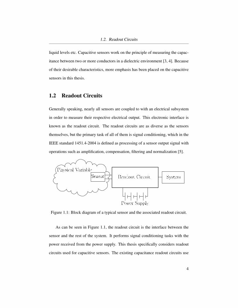
1.1 Typical sensor and associated readout circuit. . . . . . . . . . . . 4
1.2 Loci of the dimensionless eigenvalues of the two-pendulum system. 6
1.3 An RLC series weakly coupled resonator system. . . . . . . . . . 8
2.1 Simple capacitor construction and schematic symbol. . . . . . . . 12
2.2 Different arrangements for capacitive sensors. . . . . . . . . . . . 13
2.3 Applications of capacitive sensors. . . . . . . . . . . . . . . . . . 15
2.4 Image of an accelerometer obtained with PolytecMSA−500r . . 16
2.5 Image of accelerometer designed at Georgia Institute of Technology. 17
2.6 Examples of capacitance-to-voltage (CVC) readout circuits. . . . 19
2.7 Differential CVC based on charge integration. . . . . . . . . . . . 22
2.8 An improved CVC readout, based on low duty cycle periodic reset. 23
2.9 Schematic of a CDC with direct configuration. . . . . . . . . . . . 24
2.10 Schematic representation of a CDC with the relaxation oscillator . 25
2.11 Phase shift generated using capacitance in an RC circuit. . . . . . 27
2.12 Phase shift plot for differential RC circuit. . . . . . . . . . . . . . 27
2.13 CPC using zero-crossing detection. . . . . . . . . . . . . . . . . . 29
2.14 CPC using analog multiplier. . . . . . . . . . . . . . . . . . . . . 29
2.15 CFC based on simple Hartley oscillator. . . . . . . . . . . . . . . 30
xi

List of Figures
2.16 Switched-capacitor harmonic oscillator with AGC . . . . . . . . . 31
2.17 CFC based on CVC cascaded with VFC. . . . . . . . . . . . . . . 32
2.18 CFC based on integration and periodic reset. . . . . . . . . . . . . 34
3.1 Lumped-element model of a coupled 2DOF mechanical system . . 41
3.2 Loci of the dimensionless eigenvalues of the two coupled oscillators. 41
3.3 SEM image of a set of coupled gold-foil cantilevers. . . . . . . . . 42
4.1 Two weekly coupled mechanical resonators. . . . . . . . . . . . . 49
4.2 2DOF weekly-coupled series RLC resonators. . . . . . . . . . . . 50
4.3 Two weekly coupled resonators natural frequencies loci. . . . . . 52
4.4 Mode localization in two weekly-coupled-resonators. . . . . . . . 54
4.5 Effect of loss on sensitivity. Coefficient r in (4.25). . . . . . . . . 63
4.6 Relative shift in resonant frequency vs. eigenmode in 2DOF WCRs. 65
4.7 Circuit schematic of 2DOF WCRs for SPICE simulations. . . . . 66
4.8 AC analysis of 2DOF WCRs based on series RLC resonators. . . . 66
4.9 i1 plots, coupled RLC circuit AC analysis with sweeping C2. . . . 68
4.10 i2 plots, coupled RLC circuit AC analysis with sweeping C2 . . . . 68
4.11 Resonant frequency loci veering in 2DOF WCR. . . . . . . . . . 69
4.12 Sensitivity comparison between three different methods. . . . . . 70
4.13 LabVIEW-Multisim co-simulation for 2DOF WCRs. . . . . . . . 71
4.14 LabVIEW-Multisim co-simulation results. . . . . . . . . . . . . . 72
4.15 High-level-block-diagram of proposed capacitance readout. . . . . 73
4.16 Test setup for experimental measurements. . . . . . . . . . . . . . 74
4.17 Sensitivity comparison between simulations and experiments. . . . 76
4.18 Effect of parasitic parameters on frequency response. . . . . . . . 77
xii
List of Figures
5.1 Series RLC two weakly coupled resonators. . . . . . . . . . . . . 79
5.2 Relative shift in resonant frequency vs. eigenmode . . . . . . . . 80
5.3 Bode Plot for Series RLC Resonator . . . . . . . . . . . . . . . . 82
5.4 System high-level-block-diagram. . . . . . . . . . . . . . . . . . 83
5.5 Examples of conventional capacitance measurement methods. . . 84
5.6 Eigenvalue loci veering. . . . . . . . . . . . . . . . . . . . . . . . 85
5.7 Frequency response of the system for three values of perturbation
δ =−0.1%, 0%and 0.1%. . . . . . . . . . . . . . . . . . . . . . 93
5.8 Error comparison and improvement by hybrid method. . . . . . . 96
5.9 Error comparison and improvement by hybrid method. . . . . . . 98
5.10 Amplitudes of I1 and I2 at out-of-phase resonance. . . . . . . . . . 100
5.11 Analytical: linear approximation vs. exact for |I1|/|I2|. . . . . . . 101
5.12 Analytical vs. simulation for |I1|/|I2|. . . . . . . . . . . . . . . . 102
5.13 |I1|/|I2| plot around out-of-phase resonant frequencies. . . . . . . 103
5.14 High-level-block-diagram of proposed capacitance readout. . . . . 104
5.15 Magnitude of v1/v2 around out-of-phase resonance. . . . . . . . . 105
5.16 Measurement error comparison. . . . . . . . . . . . . . . . . . . 106
6.1 3DOF coupled spring-mass system with stiffness perturbation. . . 109
6.2 3DOF weekly coupled series RLC resonators. . . . . . . . . . . . 111
6.3 Frequency shift of all three modes in one-sided perturbation. . . . 112
6.4 Frequency shift of all three modes in differential perturbation. . . 113
6.5 3DOF WCR schematic with differential excitation. . . . . . . . . 114
6.6 3DOF WCR schematic with common mode excitation. . . . . . . 115
6.7 3DOF WCR schematic with differential excitation. . . . . . . . . 115
xiii

List of Figures
6.8 Frequency response; unperturbed 3DOF WCRs under differential
excitation. . . . . . . . . . . . . . . . . . . . . . . . . . . . . . . 119
6.9 3DOF WCR schematic with common mode excitation. . . . . . . 120
6.10 Frequency response; unperturbed 3DOF WCRs under common mode
excitation. . . . . . . . . . . . . . . . . . . . . . . . . . . . . . . 122
6.11 3DOF WCR, impact of loss on resonant frequencies. . . . . . . . 123
6.12 Phase plot of ε1 and ε2 at ω2 vs. Q factor. . . . . . . . . . . . . . 130
6.13 Magnitude plot of ε1 and ε2 at ω2 vs. Q factor. . . . . . . . . . . . 132
6.14 Three WCR veering from SPICE simulation. . . . . . . . . . . . 133
6.15 Three WCR, relative sensitivities, mode 1 excitation. . . . . . . . 134
6.16 Three WCR, relative sensitivities, mode 2 excitation. . . . . . . . 135
6.17 Three WCR, relative sensitivities, mode 3 excitation. . . . . . . . 135
6.18 3WCR, normalized current I2at 2nd mode. . . . . . . . . . . . . . 136
6.19 The effect of quality factor on f2- δ dependence. . . . . . . . . . 139
6.20 I2 magnitude for mode 2, common mode excitation, differential
perturbation. . . . . . . . . . . . . . . . . . . . . . . . . . . . . . 140
6.21 Effect of Q factor on the sensitivity. . . . . . . . . . . . . . . . . 141
6.22 Effect of Q factor on the magnitude of ε2 (simulation). . . . . . . 142
7.1 Equivalent circuits for a real inductor (from CoilCraft Inc.). . . . . 145
7.2 An example of an active inductor. . . . . . . . . . . . . . . . . . 147
7.3 Realization of a floating inductor using gyrators. . . . . . . . . . . 149
7.4 Realization of a floating inductor using gyrators ,rearranged. . . . 150
7.5 Circuit used in simulation of 2DOF WCR based on active inductors. 151
7.6 Gyrator-based 2DOF WCR simulation at balance. . . . . . . . . . 152
xiv

List of Figures
7.7 Gyrator-based 2DOF WCR simulation for different perturbations. 152
7.8 Relative sensitivity of gyrator-based 2DOF WCR. . . . . . . . . . 153
A.1 CVC readout using charge integration, capacitor driving circuit. . 172
A.2 CVC readout using charge integration, input stage differential am-
plifier, filtration and demodulation. . . . . . . . . . . . . . . . . . 173
A.3 CVC readout using charge integration, output buffer and LP filter. 173
A.4 CVC based on differential charge amplifier, capacitance changes
and output voltage plots. . . . . . . . . . . . . . . . . . . . . . . 174
A.5 CVC based on differential charge amplifier, intermediate nodes
simulation waveforms . . . . . . . . . . . . . . . . . . . . . . . . 175
A.6 Varicap SPICE model. . . . . . . . . . . . . . . . . . . . . . . . 176
A.7 Schematic representation of a CDC with the relaxation oscillator. . 177
A.8 Simulation graph for the CDC readout circuit. . . . . . . . . . . . 178
A.9 Simulation results for the CDC readout circuit. . . . . . . . . . . 179
A.10 CPC readout circuit using charge amplifier. . . . . . . . . . . . . 181
A.11 Improved CPC readout circuit. . . . . . . . . . . . . . . . . . . . 182
A.12 Simulation results for the readout circuit. . . . . . . . . . . . . . . 183
A.13 CPC parametric sweep simulation results. . . . . . . . . . . . . . 184
A.14 CFC readout circuit based on Hartley oscillator. . . . . . . . . . . 185
A.15 Simulation results for the readout circuit. . . . . . . . . . . . . . . 186
A.16 CFC readout circuit based on switched-capacitors. . . . . . . . . . 189
A.17 Simulation results for the readout circuit based on SC. . . . . . . . 190
A.18 Simulation results for the readout circuit based on SC . . . . . . . 191
xv

List of Acronyms
ADC Analog-to-digital converter
ASIC Application specific integrated circuits
CDC Capacitance-to-duty cycle converter
CFC Capacitance-to-frequency converter
CPC Capacitance-to-phase shift converter
CVC Capacitance-to-voltage converter
DOF Degree-of-freedom
ESR Equivalent series resistance
IC Integrated circuit
MEMS Micro-electro-mechanical systems
OPA Operational amplifier
PCB Printed circuit board
PLL Phase-locked loop
VARACTOR Variable-reactance diode
xvi

List of Acronyms
VARICAP Variable capacitor, variable-capacitance diode
VFC Voltage-to-frequency converter
WCR Weakly-coupled-resonator
xvii

Acknowledgments
I would like to express my gratitude to my research supervisor Dr. Edmond Cretu
for his supervision and his professional guidance. He is indeed much more than an
academic supervisor and I would always remember his support and advice. I am
also very thankful of Dr. Shahriar Mirabbasi and Dr. Robert Rohling who helped
me a lot, especially at the beginning and initiation of my research at UBC.
I would like to thank all my Ph.D. examination committee members for their
time and valuable comments and feedback.
xviii

Dedication
To my wife,
my mother and
memory of my father
xix

Chapter 1
Introduction
1.1 History of Sensors
Human life is becoming more and more dependent on the measurement of physical
phenomena. The advancement in science owes a great deal to our ability to measure
the environment around us; as Lord Kelvin aptly puts it: “To measure is to know”.
In the course of history, the methods for measurement have advanced alongside
the advancements in science and engineering, resulted in the use of “sensors”. A
sensor, in its crudest form, is a tool that yields a certain electrical output when
exposed to the a physical phenomenon. This broad definition includes everything
from the first electric thermostat patented by Warren S. Johnson in 1885, to the
most advanced pressure sensors used in high performance cars today.
Sensors have become the default tool for us to measure the properties of our
physical surroundings, and with the growth in the number of their applications,
they have reached a market share of $79.5 billion in 2013, and are expected to
reach nearly $154.4 billion by 2020 [1]. Of course this explosive growth is helped
by the advancements in electronics and IC manufacturing capabilities, which began
from the invention of the transistor in 1947 at Bell Laboratories, and the first im-
plementation of the monolithic IC at Fairchild Semiconductor in 1959. This trend
1

1.1. History of Sensors
has continued to the present day by the introduction of increasingly sophisticated
and specialized sensors.
The reasons for this fast growth in reliance on sensors could be summarized as
follows [2].
• Sensors have an electrical output, which is the most versatile form of signal
carrier that can be used for processing and storing sensor related information.
• Many different back-end circuitry options are available for use with the sen-
sors, resulting in the ability to manufacture the sensor and the signal condi-
tioning subsystem in the same package.
• Given that the output of the sensors can be amplified, there is the possibility
of using active sensors, which do not absorb energy from the process being
measured.
• Sensors can be designed to measure nonelectric quantities through the usage
of appropriate material and techniques (changes in the properties of nonelec-
tric material can be translated to electrical changes, which can be detected in
the electrical domain.
• The sensors output can be displayed, recorded and further processed, to pro-
vide more insight into the nature of the variations of the process being mea-
sured.
The need for measuring different types of physical quantities has led to the devel-
opment of many different sensor types, each of which has its own unique character-
istics. Sensors can be categorized based on their need for power (active or passive),
their output signals (analog or digital), or their mode of operation, e.g. deflection
2

1.1. History of Sensors
type or null type. However, in electronic engineering, it is preferred to categorize
sensors based on the measured electrical quantity (e.g. resistance, capacitance, and
inductance) [2].
Resistive sensors are widely used in measurement applications since one of the
simplest way of mapping the measurand onto electrical variations is through the
equivalent electrical resistance modulation. The outputs of the resistive sensors
are readily available for processing, hence these sensors have simple measurement
circuitry. Also, resistive sensors offer many options with regards to their size,
resistance value, back-end circuitry and AC/DC operation [3]. Resistive sensors
have a high sensitivity in general; however, their resolution is affected by thermal
noise, which means that various environment related factors will influence their
output [3].
Inductive sensors rely on the change of self or mutual inductance of a coil or
set of coils for measurement. These sensors can be used in applications where the
thickness of objects needs to be measured. The detection of change in inductive
sensors can be done only by using AC readout circuits. Because of the effect
of inductance on the neighboring circuitry, proper shielding is desirable for air
cored inductors [3]. This aspect, coupled with the direct relationship between the
physical dimensions of the coil and the quality factor (i.e. higher quality factor
coil needs a lower equivalent series resistance, and consequently require the larger
cross section of winding wire for the same number of turns) , means that these
sensors are usually bulkier than other passive sensor types.
Capacitive sensors are widely used for displacement measurement [3]. Because
of their precise performance, low cost construction, simple structure and versatility,
they are common solutions for measuring variables such as acceleration, humidity,
3
1.2. Readout Circuits
liquid levels etc. Capacitive sensors work on the principle of measuring the capac-
itance between two or more conductors in a dielectric environment [3, 4]. Because
of their desirable characteristics, more emphasis has been placed on the capacitive
sensors in this thesis.
1.2 Readout Circuits
Generally speaking, nearly all sensors are coupled to with an electrical subsystem
in order to measure their respective electrical output. This electronic interface is
known as the readout circuit. The readout circuits are as diverse as the sensors
themselves, but the primary task of all of them is signal conditioning, which in the
IEEE standard 1451.4-2004 is defined as processing of a sensor output signal with
operations such as amplification, compensation, filtering and normalization [5].
Figure 1.1: Block diagram of a typical sensor and the associated readout circuit.
As can be seen in Figure 1.1, the readout circuit is the interface between the
sensor and the rest of the system. It performs signal conditioning tasks with the
power received from the power supply. This thesis specifically considers readout
circuits used for capacitive sensors. The existing capacitance readout circuits use
4

1.3. Motivation
various methods, such as capacitance-to-voltage (CVC), capacitance-to-frequency
(CFC), capacitance-to-phase shift (CPC), capacitance-to-duty cycle (CDC) conver-
sions etc. All of the aforementioned methods utilize analog circuitry for filtering,
amplification and even switching.
There are many challenges for the existing capacitance readout circuit tech-
niques. Typically, factors such as intrinsic noise, switching noise (in circuits based
on switching elements), offset problems and temperature dependency of the cir-
cuit components result in a relatively high number of passive and active circuit
components. In addition, measuring small variations in capacitance (the measured
parameter), is often disturbed by the inherent presence of parasitic capacitances,
which could be even larger than the sensing capacitance. Capacitive MEMS sen-
sors have a typical capacitance in the range of 0.2pF to 1pF, parasitic capacitance
of about 2pF and typical resolution range of 1aF to 10aF. Achieving a high sensitiv-
ity/gain in measurement with a low signal to noise ratio has always been a serious
challenge.
In some applications the gain-bandwidth trade-off becomes another challenge;
the higher the rate of the sensor capacitance changes, the lower the overall gain of
the readout circuit. This tradeoff is not of a huge concern in this project since the
capacitance variation is considered to be quasi-static (that is, very slow relative to
the time constants of the readout circuits).
1.3 Motivation
In order to address some of the aforementioned challenges, especially the high sen-
sitivity and robustness, we searched for an alternate and innovative method with
5
1.3. Motivation
higher sensitivity and inherent simplicity. There has been a very elegant method
for measuring perturbations that has been used in mechanical domain for decades.
This method is based on weakly-coupled resonators (WCRs), and has a long his-
tory in mechanical and acoustic domain. WCRs exhibit an interesting feature re-
lated to the mode localization (energy localization), which is the energy repartition
between the two resonators due to perturbation. Mode localization was examined
in solid state physics applications by P. W. Anderson for the first time [6, 7] which
eventually led him win the Noble prize in physics in 1977.
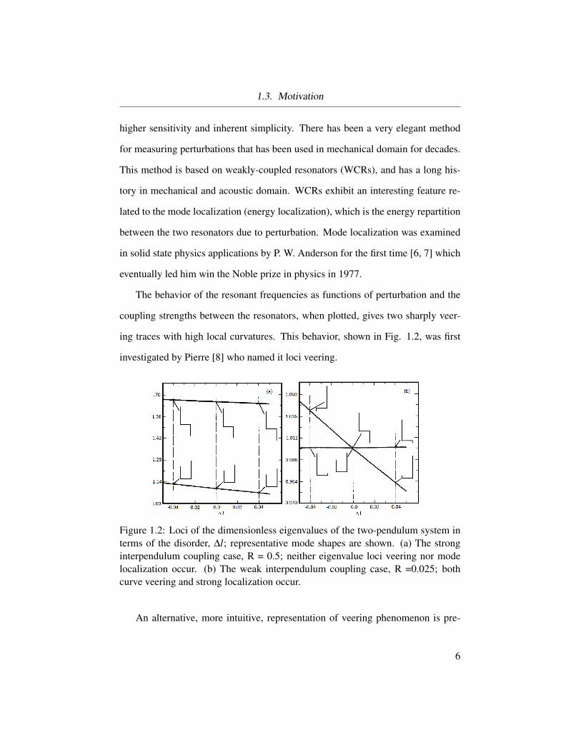
The behavior of the resonant frequencies as functions of perturbation and the
coupling strengths between the resonators, when plotted, gives two sharply veer-
ing traces with high local curvatures. This behavior, shown in Fig. 1.2, was first
investigated by Pierre [8] who named it loci veering.
Figure 1.2: Loci of the dimensionless eigenvalues of the two-pendulum system interms of the disorder, ∆l; representative mode shapes are shown. (a) The stronginterpendulum coupling case, R = 0.5; neither eigenvalue loci veering nor modelocalization occur. (b) The weak interpendulum coupling case, R =0.025; bothcurve veering and strong localization occur.
An alternative, more intuitive, representation of veering phenomenon is pre-
6

1.3. Motivation
sented in Fig 4.4. It is generally accepted that the eigenvalues of the WCRs system
represent the resonant frequencies of the system. As a result the term eigenvalue
loci veering phenomena has been used to describe a range of similar behaviors in
disordered structures in the mechanical and MEMS field [9, 10, 11, 12, 13, 14, 15].
This thesis offers an innovative method for capacitance measurement based
on weakly-coupled resonators (WCRs), which is proven to have more sensitivity
and circuit simplicity. It will be shown that WCR-based readout circuit can reach
several orders of magnitude higher sensitivity than other state-of-the art methods
(e.g. capacitance-to-frequency method). On the other hand, there is a challenge in
matching component values for both resonators. The higher the sensitivity of WCR
method, the more the negative impact of mismatch on the correct reading. Another
challenge with WCRs is the bandwidth of the perturbation since the theory assumes
implicitly a quasi-static perturbation. In this thesis we also study the effect of the
losses on the sensitivity of the system, which has not been offered in the previous
mechanical/MEMS researches.
The simplest WCR in the electrical domain consists of two series/parallel RLC
circuits coupled through a capacitor /inductor. This thesis proposes to use the
WCRs as an alternative for a capacitance readout circuit. Figure 2 shows the con-
figuration of the WCR fundamental circuit examined in this thesis. Using such an
arrangement for capacitance readout circuits results in lower number of compo-
nents required, contributing to the low cost, low power and high reliability of these
circuits. Moreover, as will be shown in the following chapters, the relative sensi-
tivity of a WCR arrangement is much higher than the existing comparable readout
circuit methodologies.
7
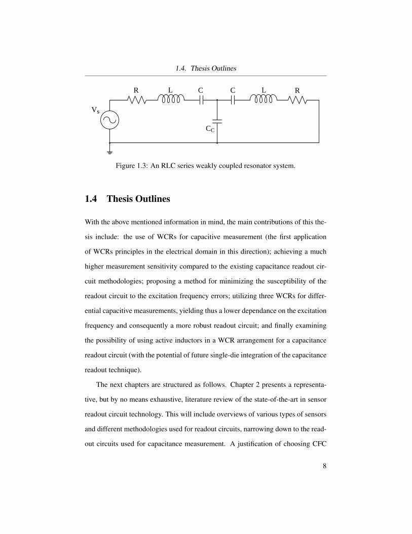
1.4. Thesis Outlines
RLC
CC
Vs
R L C
Figure 1.3: An RLC series weakly coupled resonator system.
1.4 Thesis Outlines
With the above mentioned information in mind, the main contributions of this the-
sis include: the use of WCRs for capacitive measurement (the first application
of WCRs principles in the electrical domain in this direction); achieving a much
higher measurement sensitivity compared to the existing capacitance readout cir-
cuit methodologies; proposing a method for minimizing the susceptibility of the
readout circuit to the excitation frequency errors; utilizing three WCRs for differ-
ential capacitive measurements, yielding thus a lower dependance on the excitation
frequency and consequently a more robust readout circuit; and finally examining
the possibility of using active inductors in a WCR arrangement for a capacitance
readout circuit (with the potential of future single-die integration of the capacitance
readout technique).
The next chapters are structured as follows. Chapter 2 presents a representa-
tive, but by no means exhaustive, literature review of the state-of-the-art in sensor
readout circuit technology. This will include overviews of various types of sensors
and different methodologies used for readout circuits, narrowing down to the read-
out circuits used for capacitance measurement. A justification of choosing CFC
8

1.4. Thesis Outlines
method as a reference for comparison with our proposed WCR-based method is
presented at the end of this chapter. The details of various state-of-the-art readout
circuits mentioned in this chapter, along with simulation results, are presented in
Appendix A.
Chapter 3 begins by giving a more detailed and historical introduction to WCRs,
and enumerating their various conventional uses. It then continues by formally
proposing the use of WCRs as the alternative method for capacitance readout cir-
cuits. The justification for such a proposal is given and finally the reader is pre-
sented with the research question.
Chapter 4 presents the theoretical analysis and simulation results examining
the use of the WCR methodology for the readout circuit. This is then followed by
the sensitivity analysis as well as the simulation and practical circuit implementa-
tion results. These results are then compared with the conventional CFC method,
showing the full extent of the sensitivity improvement.
Chapter 5 examines the capacitance measurement error problem for the WCR
methodology. It then proposes a method to minimize the measurement error, by
using a combination of the CFC and WCR methods, resulting in a more robust
readout circuit.
Chapter 6 proposes the use of three-degree-of-freedom WCRs in the readout
circuit to perform differential capacitive measurement in a robust manner. This
chapter also studies the effect of losses (quality factor) on the sensitivity. It shows
the trade-offs between quality factor (Q), dynamic range of measurable perturba-
tion and sensitivity. The analytical and simulation results are provided and com-
pared for such an arrangement.
Chapter 7 explores the use of an active inductor (in the form of an op-amp-
9

1.4. Thesis Outlines
based circuit) as alternatives for bulky passive inductors in implementing of WCR
methodology by theoretical analysis and simulation. This is helpful toward inte-
grating a complete WCR-based readout circuit on a chip. This chapter is followed
by final discussions, and outlining further avenues of research for the future in
chapter 8.
10

Chapter 2
Capacitive Sensors and Their
Associated Readout Circuits
2.1 Introduction
This chapter introduces capacitive sensors and their associated readout circuits.
The fundamentals of capacitive sensing are presented in §2.2, where various ca-
pacitive sensor configurations are depicted together with different ways of cate-
gorizing such. In addition , the benefits and limitations of capacitive sensors are
examined in detail.
Section 2.3 begins by defining what readout circuits are and different categories
they fall into. Subsequent subsections are then devoted to examining each of the
methods with more in-depth explanations for various configuration where neces-
sary. The related simulations are presented in Appendix A. This chapter continues
with a justification for choosing one of the capacitance readout circuit methodolo-
gies as a benchmark for comparison with our proposed WCR method. A summary
of this chapter is presented in the last section.
11

2.2. Capacitive Sensors
2.2 Capacitive Sensors
The past decades have seen a burgeoning attention to the use of capacitive sensors
for sensing and detecting physical quantities such as pressure, rotational angles,
linear displacement and acceleration [2]. As their name suggests, capacitive sen-
sors rely on a capacitance change in order to measure the desired quantity.
A capacitor in its simplest form consists of two conductive plates, separated by
a dielectric, as shown in Fig 2.1.
d
d
y
x
(a) (b)Figure 2.1: Simple capacitor, (a) construction, (b) schematic symbol and electricfield.
The distance between the plates, the plate overlapping area and the dielectric
substance are the critical parameters in any capacitor, determining the capacitance
value.
If we consider the parallel-plate capacitor model and neglect the fringe field
effects, the capacitance can be calculated using
C = ε0εrAd, (2.1)
12

2.2. Capacitive Sensors
where C is the capacitance, ε0 = 8.85 pF/m is the dielectric constant for vacuum,
εr is the relative dielectric constant, A = xy is the overlapping plate area, and d is
the distance between the plates.
Various arrangements for capacitors used in capacitive sensors are shown in
Fig 2.2.
(a) (b) (c)
(d)
z
d
d
C 1
C 2
(e)
C 1 C 2
d
z
z0
(f)
Figure 2.2: Different arrangements for capacitive sensors based on: (a,b) variationof area, (c) variation of gap between plates, (d) dielectric change, (e) differentialvariation in the gap, and ( f ) a differential variation in the area.
Using variable capacitors as sensors poses some difficulties. One of the first
problems with regards to such usage is the fringe effect present in parallel plate
capacitors. Although fringe effects are considered negligible in many instances,
this is only acceptable when the distance between the plates is far smaller than the
13

2.2. Capacitive Sensors
size of the plates.
Additionally there needs to be appropriate shielding for the capacitive sensor
plates and the wires connected to them, to reduce capacitive interference. However,
shielding wires to prevent capacitive interference introduces a new capacitance in
parallel with the sensor (parasitic capacitance). This in turn results in a loss of
sensitivity, as the change in the sensor capacitance only changes a part of the overall
capacitance. Also, relative movement between the wires and the dielectric could
introduce errors, caused by changes in the capacitor geometry.
Another important matter is the quality of the dielectric used in the capacitor.
There should be a constant and high electrical insulation between the plates. If
the insulation is poor, then there will be a leakage resistance in parallel with the
capacitor that affects the overall capacitance. This results in the impedance being
affected by a factor other than the capacitance, which renders the measurement
methods ineffective and prone to errors. Dielectrics with high conductivity (such
as water) could be affected by thermal interference generated because of the power
passing through their effective resistance and generating heat.
In general, the capacitive sensors are categorized into variable capacitors and
differential capacitors. In variable capacitive sensors one or more of the above
mentioned parameters change based on the measured phenomenon, where as in
differential capacitive sensors, the values of two capacitors simultaneously change
in opposite directions by the physical variable to be measured.
Despite the limitations mentioned above, capacitive sensors enjoy several ad-
vantages including: low power consumption, wide operating temperature range,
value dependency mainly on the geometry and less on the material properties, high
resolution and easy for fabrication.
14

2.2. Capacitive Sensors
As a result, capacitive sensors have a wide variety of applications, including
but not limited to the measurement of displacement, force, pressure, acceleration,
angular velocity. Moreover, the recent rapid growth in human/machine interface
has given rise to the application in touch screens in many personal communication
devices, such as mobile phones and tablets. Another area of interest is in medical
instrumentation, where accurate measurement of signals from the patients body is
of great importance. Fig. 2.3 shows some of these applications, e.g. measuring
inertia in aviation, tilt and inclination in dams, trains and off-shore platforms, and
seismic and vibration in highrises and race cars [16].
Figure 2.3: Applications of capacitive sensors (e.g. accelerometers and gyrosin navigation, aviation, race car data acquisition, oil and gas, seismic) and someMEMS based capacitive sensors fabrication [16].
15

2.2. Capacitive Sensors
This figure also shows some samples of capacitive sensors designed by Coli-
brys.
One area of recent advancement in capacitive sensing is designing sensors
based on micro-electro-mechanical systems (MEMS). Although MEMS are not
investigated in detail in this thesis, a capacitive interface is the common configura-
tion for them, due to better power efficiency and increased sensitivity [17]. Fig. 2.4
shows an image of a MEMS capacitive accelerometer designed by Dr. Elie Sarraf
at University of British Columbia (UBC) [18].
Figure 2.4: Image of IMOMBCEHS0903 accelerometer obtained withPolytecMSA−500r.
This capacitive sensor has two sets of differential capacitors, one gap varying
and one area varying. The typical value for the gap-varying capacitance in this
design is about 2 pF with a dynamic range of -10g to 10g, a noise floor of approx-
imately 4 µg/√
Hz, and a gain of 23.4 mV/g for the whole system including the
related readout circuit.
16

2.3. Capacitance Readout Circuits
Another example of such sensors is shown in Fig. 2.5. The plates that form the
differential capacitors are also shown on the image [19].
Figure 2.5: Image of accelerometer designed at Georgia Institute of Technology[19].
No matter where the capacitive sensors are used, or the amount of capacitance
change they create, there is a need for a mechanism to measure this change and
translate it into useable output. In literature this mechanism is known as a readout
circuit. The next section introduces the readout circuits and their various types in
more detail.
2.3 Capacitance Readout Circuits
As mentioned in the previous section, all sensors, including capacitive ones, rely
on a mechanism to measure a physical variable (measurand) and translate it to a
suitable signal to be used for further processing through filtering and amplification.
This mechanism, known as the readout circuit, is a broad topic by itself; as there are
as many readout circuits as there are sensors themselves. This section of the thesis
examines capacitance readout circuits in more detail categorizing them based on
their circuit configuration, time sampling and feedback.
17

2.3. Capacitance Readout Circuits
For either variable capacitance or differential capacitance types of sensors,
there are many types of readout circuits available. Some of the most common
are presented in Fig. 2.6[2]. Generally, a readout circuit designed for a differen-
tial capacitive sensor can also be used for a single variable capacitive sensor. The
most common way is to replace of the sensor capacitors with a fixed capacitor
(usually called reference capacitor). Differential readout circuits typically utilize
the difference between the two amplifier outputs in their circuit configuration. Fig.
2.6 presents examples of simple single-ended and differential readout circuits. Fig.
2.6(a) is a simple charge amplifier. Cx is the sensor capacitor and C f is the feedback
capacitor. R f provides the DC bias current for the operational amplifier (op-amp)
input stage. Assuming Cx is an area-varying capacitive sensor with parameter x as
the ratio of the change in the area:
Cx = ε0εrA0(1+ x)
d
and
Vo =−Cx
C fVs
which shows the output voltage is proportional to the capacitance changes. It
was assumed that R f is large enough to have a negligible effect in the output voltage
for the bandwidth of interest. In case a gap-varying capacitive sensor was used, it
would be helpful to swap Cx and C f to get a linear relationship between Vo and x,
the gap-variation measurand.
18

2.3. Capacitance Readout Circuits
Vs
Cx
Cf
Rf
Vo
Vs
Cx1
Cf
Rf
Vo
¡Vs
Cx2
Vs
Cx
Cf
Rf
Vo
R1
R2
Cx2
C4
R
Vo
Cx1
C3
R
R
R
Vs
R
Vo
R R
R
Vs
Z1
Z3
Z2
Z4
(a) (b) (c)
(d) (e)
Figure 2.6: Examples of capacitance-to-voltage converter (CVC) readout circuits.(a) single-ended charge amplifier for single variable capacitor (b) single-endedcharge amplifier for differential capacitive sensor. (c) bridge amplifier for sin-gle variable capacitive sensor. (d) differential amplifier for differential capacitivesensor. (e) instrumentation amplifier for differential capacitive sensor.
The readout circuit shown in Fig. 2.6(b) is very similar to the circuit of Fig.
2.6(a). It is rearranged to accommodate for a differential capacitive sensor. Figure
2.6(c) is a pseudo-bridge version of Fig. 2.6(a). The output of the circuit can be
written as [2]:
Vo =VsR1/R2−Z3/Z1
1+R1/R2,
where Z1and Z3 are the total impedances of Cx and C f || R f , respectively.
19

2.3. Capacitance Readout Circuits
The configurations of Fig. 2.6(d) and (e) are based on pseudo-bridges and
differential amplifiers. Figure 2.6(e) has an additional stage to convert the output
to single-ended, a stage known as instrumentation amplifier. The output voltage
for these differential configurations is:
Vo =Vs
(Z3
Z1− Z4
Z2
).
Differential readout circuits are less susceptible to common mode and power
supply noises; they typically have larger input signal range, and generally a bet-
ter resolution. Moreover, differential readout circuits have a larger common mode
rejection ratio (CMRR), which makes them more desirable. On the other hand,
compared to single-ended readout circuits, differential readout circuits consume
more current. This is because single-ended readout circuits normally use mini-
mum size and number of transistors. Also, due to the need for more components,
differential readout circuits require a larger silicon footprint in application specific
integrated circuits (ASIC) or on the printed circuit boards (in case of discrete circuit
implementation).
In terms of timing, there are two types of designs available for readout circuits,
continuous and discrete time. Intrinsically, the continuous time design has a higher
resolution since it does not suffer from sampling noise[20]. Discrete time readout
circuits are a better option when dealing with larger resistances, for instance in the
feedback loops. Switched-Capacitor circuits are one way of implementation based
on discrete time operation.
Examining the feedback structure of the sensor and corresponding readout cir-
cuits, two types of structures are present, open-loop and closed-loop. In the open-
20

2.3. Capacitance Readout Circuits
loop configuration the capacitance change from the sensor is amplified and turned
into a usable signal by the readout circuit and the resulting output is then trans-
ferred to subsequent data displays. The closed-loop configuration exploits a sec-
ondary input to the sensor which mimics the magnitude of the primary capacitance
changed caused by the measured phenomenon. This secondary input is essentially
a negative feedback set by the readout circuit designed to keep the actual value
of capacitance in equilibrium. The true capacitance change can be measured by
monitoring the negative feedback line.
As mentioned earlier, many different methods have been proposed and devel-
oped for capacitance readout circuits. Each of these methods rely on measuring
a parameter change with respect to the capacitance, e.g. voltage, phase shift, fre-
quency etc.
2.3.1 Capacitance to Voltage Converter
The first method examined in this thesis is the capacitance to voltage converter
(CVC), where the capacitance changes are translated into a change in voltage for
further processing [20, 21, 22, 23, 24, 25]. The CVC method on its own has many
different configuration, which are briefly mentioned below.
• CVC method using charge integration, which can be used for both single
and differential capacitance. In this configuration, the capacitance change is
converted to a corresponding electrical charge variation, that is afterwards
converted into a change in voltage using an op-amp. A schematic diagram
of this circuit can be seen in Fig. 2.7 below [21].
21

2.3. Capacitance Readout Circuits
C 0
f
R0
f Vo
Cx0 +¢Cx
Cf
Rf
Vc
C 0
x0¡¢C 0
x
VB
VC
VD
HINA
D
D0
CD
C 0
D
RD
R0
D
Carrier Sensor CurrentDetector
AMDemodulator
Inst:Amp:
AM ¡Modulator
VA
Figure 2.7: Differential CVC based on charge integration [21].
This method is less susceptible to parasitic capacitance, however it needs a
large value feedback resistor which could be difficult to implement on an IC [20].
The bandwidth of the capacitor in this configuration is from DC to 10 KHz and a
reported resolution of 24 aF is measured if a 12 pF capacitor is used [21].
• CVC method using low duty cycle periodic reset configuration is another
sub category of the CVC method which enjoys low noise, linear capacitance
to voltage transfer function, and low susceptibility to system offset. This
configuration has reached a 0.06% resolution for a 0.8 pF capacitor [20]. A
schematic diagram of this configuration is presented in Fig. 2.8.
22

2.3. Capacitance Readout Circuits
Cx1
Cf
S1
VoCx2
VDD
S2
S1
S 0
2S 0
1
Cp
Reset Sensing
S1, S0
1
S2, S0
2
Figure 2.8: An improved CVC readout, based on low duty cycle periodic reset[20].
• Other configurations designed to reduce offset and increase resolution, two
of which are chopper stabilized configuration, which is shown to reduce the
input offset effects [22] and a ratio-arm bridge which is a symmetrical and
sensitive circuit, but requires transformer coils [23].
2.3.2 Capacitance to Duty Cycle Converter
In the capacitance to duty cycle converter (CDC) method, the changes in capaci-
tance are translated into changes in the duty cycle of a pulse train. This method has
two main configurations that are listed below.
• CDC method using direct configuration is named as such because there is a
23
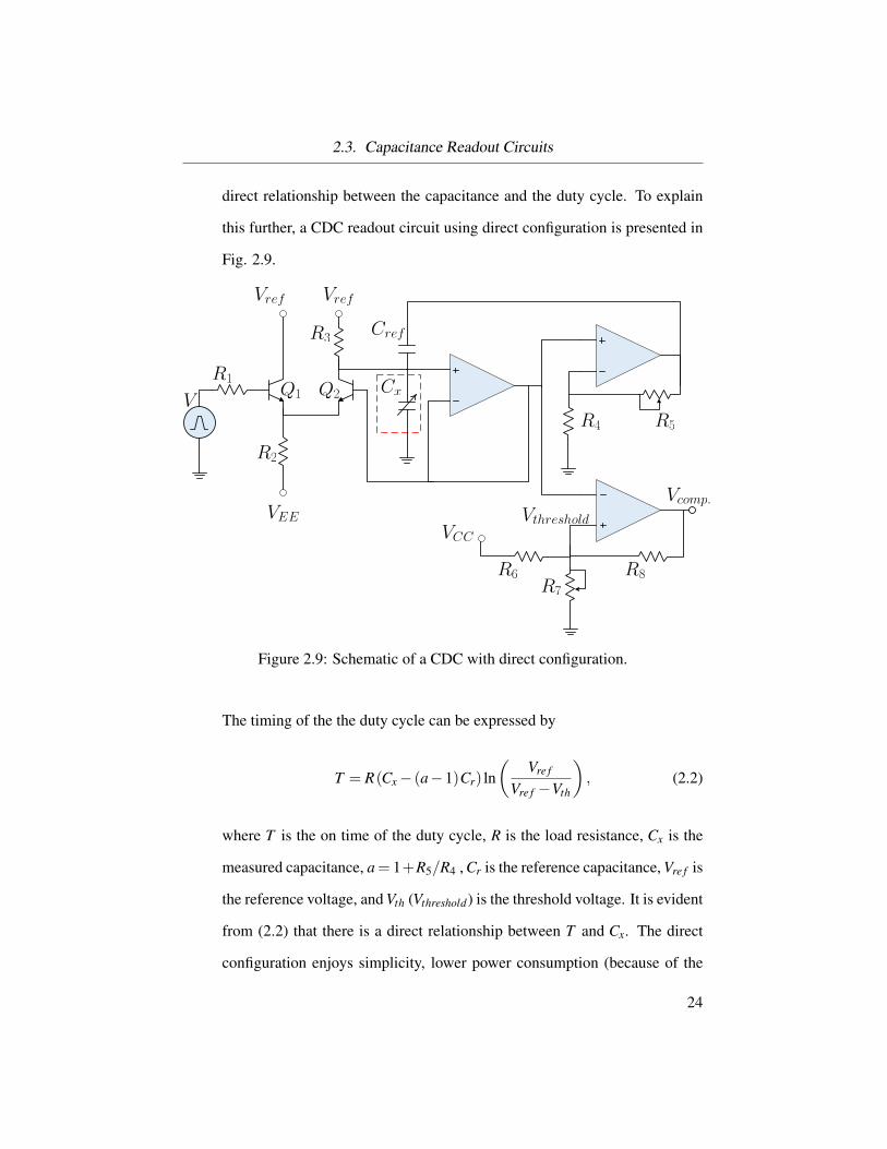
2.3. Capacitance Readout Circuits
direct relationship between the capacitance and the duty cycle. To explain
this further, a CDC readout circuit using direct configuration is presented in
Fig. 2.9.
Vref Vref
VEE
VCC
Cref
CxQ1 Q2
R2
R1
R3
R4 R5
R6
R7
R8
Vthreshold
Vcomp:
V
Figure 2.9: Schematic of a CDC with direct configuration.
The timing of the the duty cycle can be expressed by
T = R(Cx− (a−1)Cr) ln(
Vre f
Vre f −Vth
), (2.2)
where T is the on time of the duty cycle, R is the load resistance, Cx is the
measured capacitance, a= 1+R5/R4 , Cr is the reference capacitance, Vre f is
the reference voltage, and Vth (Vthreshold) is the threshold voltage. It is evident
from (2.2) that there is a direct relationship between T and Cx. The direct
configuration enjoys simplicity, lower power consumption (because of the
24

2.3. Capacitance Readout Circuits
smaller number of components), and easy linearization on the digital side.
If a modern low voltage/power CMOS implementation is used, then this
configuration achieved a bandwidth of 1 KHz with a 13 bit resolution. The
resolution and bandwidth were limited by the speed of the op-amp, which
has a 3 MHz maximum gain bandwidth and a 13 V/µs slew rate [26].
• CDC method using relaxation-oscillator configuration uses two capacitors
for sensing. These capacitors are multiplexed by diode switches to form an
op-amp based integrator. A schematic of this configuration is presented in
Fig. 2.10.
V0
B
A
C
C1
C2
V5
V3
Rt
R1
R2
D1D2
V2
R3
A1 A2
A3
A4
V4
Figure 2.10: Schematic representation of a CDC with the relaxation oscillator .
The interface presented in Fig. 2.10 detects the ratio of capacitances in the
form of the duty ratio.
D =TH
TH +TL=
C2
C1 +C2,
25

2.3. Capacitance Readout Circuits
where D is the duty cycle of the signal at V5 port.
This configuration allows for high speed measurements as reported in the lit-
erature. In one test case, a resolution of 60 aF was achieved using a 30 MHz
oscillation frequency with a reference capacitance of 3 pF [27].
2.3.3 Capacitance to Phase Shift Converter
Capacitance as a reactive component creates a phase shift between voltage and
current in a circuit. Assuming the rest of the circuit parameters and values are
constant, the phase shift, in reference to the input voltage, is a function of the
capacitance. As an example in a simple RC circuit shown in Fig. 2.11(a), the
phase is:
∠vo = φ =−arctan(1
ωRCx).
Typically in capacitance measurement, there is a reference capacitor, Cr, which is
the reference for the changes of the sensor capacitance Cx. One of the common
choices for Cr is the value of Cx at rest. An example of this configuration is shown
in Fig. 2.11(b). The phase of the differential voltage at the output, vo, is represented
by:
∠vo = φ = arctan(1
ωRCr)− arctan(
1ωRCx
)≈− ∆C/Cr
ωRCr +1
ωRCr
,
where ∆C =Cx−Cr. This approximation is true when Cx and Cr are close enough
i.e. φ < 6.
26

2.3. Capacitance Readout Circuits
Cx
R
Cr
Cx
R
R
A sin(!t) A sin(!t)
A sin(!t)
vo
vo = B sin(!t + Á)
Á = ¡ arctan( 1
!RCx
)
(a) (b)
\vo = Á ¼ ¡¢C
!RC2
r
+1
!R
Figure 2.11: Phase shift generated using capacitance in an RC circuit. (a) single-ended. (b) differential.
This phase difference for the circuit in 2.11(b) is plotted in Fig. 2.12 for the
values of Cr = 100nF, R = 10kΩ and five different values of Cx ∈ 80nF, 90nF,
100nF, 110nF, 120nF.
1 10 100 1k 10k 100k-6
-4
-2
0
2
4
6
Pha
se d
iffer
ence
(o )
Frequency (Hz)
Cx
80nF 90nF 100nF 110nF 120nF
Figure 2.12: Phase shift plot for differential RC circuit.
27

2.3. Capacitance Readout Circuits
The phase difference is almost linear at around -5 dB to -15 dB frequencies (10
Hz to 80 Hz); e.g. the phase shift is approximately 1 per 10 nF of capacitance
change (10% change in capacitance) at around 30 Hz. The common challenge in
capacitance measurement based on the phase shift is the nonlinearity introduced
by arctan function.
There are many different methods for measuring the phase of a signal, or the
phase difference between two signals [28], e.g. direct oscilloscope method, zero-
crossing, three-voltmeter, phase-locked-loops (PLLs), Fourier transform etc. An
example of high level schematic diagram for a capacitance-to-phase-shift converter
(CPC) based on zero-crossing detection is shown in Fig. 2.13. In this circuit, zero
crossings of the signals passing through the sensor and reference capacitors, which
represent the phase of the signal, are detected using comparators. The square wave
at the output of the comparators are used to set or reset the output of a R-S flip-flop.
so the duty cycle of the flip-flop output is proportional to the phase shift between
two signals. Another circuit based on modulation and demodulation is shown in
Fig. 2.14. In this method, the capacitance changes are modulated by the carrier
signal. A multiplier is made of two logarithmic amplifier and an analog summa-
tion, followed by an anti-log amplifier. The output of the anti-log amplifier has
two frequency components. The high frequency components is eliminated by the
low-pass filter (integrator) block. The low frequency component, which contains
the information regarding the phase difference, passes through the integrator. This
phase difference has a one-to-one relationship with the difference in the capaci-
tances (Cx−Cr).
28

2.3. Capacitance Readout Circuits
Non¡ invertingZero¡ crossingdetector
R
S
Integrator
BufferQVs
Vo
InvertingZero¡ crossingdetector
Cr
Cx
R
R
R1
R1
C
C
D1
D1
A
B
C
D
Q
Figure 2.13: CPC using zero-crossing detection.
LogAmplifier
Integrator
BufferVo
LogAmplifier
Cr
Cx
R
R
V0
sin(!t)
V0
cos(!t)
¡
+
Anti¡ LogAmplifierR
1
R1
R2
Figure 2.14: CPC using analog multiplier.
2.3.4 Capacitance to Frequency Converter
The last readout circuit design method introduced in this section converts the change
in capacitance to frequency, and it is known as capacitance to frequency converter
(CFC). The main distinguishing factor with regards to the CFC method is that it
generally does not need an analog-to-digital converter (ADC), since a simple zero
crossing counter can be used. Fig. 2.15 shows a schematic of a simple CFC read-
out circuit based on a Hartley oscillator. The oscillation frequency is a function of
the capacitance CL with the equation fosc = 1/(2π√
C2LT), where LT = L1 +L2 is
29

2.3. Capacitance Readout Circuits
the equivalent tank inductance [29].
VCC
R1 R2
R3 R4R5
R6L1 L2
C2
C1
C3
Q1
Figure 2.15: CFC based on simple Hartley oscillator.
Another example based on switched-capacitor oscillator is, illustrated in Fig.
2.16. This CFC design, presented in 1985 [30] , enjoys low complexity, as it does
not need an ADC. The design was based on implementation of a quadrature os-
cillator (two integrated loop circuit) using switched capacitors. The relationship
between the frequency of the oscillation and the capacitor to be measured is:
f0 =Cm
Cfc
2π,
where C is the integrating capacitor shown in Fig. 2.16, Cm , αC is the capacitor
to be measured, and fc is the clock frequency of the SC circuit.
30

2.3. Capacitance Readout Circuits
¡
+
¡
+
fc fc fc fc
Control
Pulse
Generator
Zero
Crossing
Detector
S/H§
Vref
k²C
®C ®C
C CV1
V2
1=f0
V+
¡
Figure 2.16: Switched-capacitor harmonic oscillator with AGC .
CFC has been applied in many readout circuits for different application re-
quirements and variety of implementation technologies. We are going to briefly
point to some of these applications, without going to the details, to show the broad
usage of CFC method in the literature.
A design based on the relaxation oscillator was presented for a capacitive dig-
ital hygrometer in 1995 [31] but no comparison with other contribution was pre-
sented. The design presented in [32] has the advantage of making the frequency
independent of the power supply in a wide dynamic range. The next contribution,
presented in 1991, is also based on switched capacitors. It has two main stages of
CVC (based on switched-capacitor) followed by a voltage-to-frequency converter
(VFC). It has low power, low cost, and linear capacitance to frequency transform
characteristics [33]. A simplified schematic of the circuit is shown in Fig. 2.17.
The CVC circuit based on SC is shown on the left. VR1 and VR2 are constant refer-
ence voltages. CR and CX are reference and measurand capacitors, respectively. VC
is the output of the CVC stage. The VFC circuit schematic is shown on the right
31

2.3. Capacitance Readout Circuits
side. The input is VC and the output is VO.
Figure 2.17: CFC based on CVC cascaded with VFC.
The relationship between VC and CX , for the CVC section, is given by:
VC =(CX −CR)
CF(VR2−VR1)+VR1 (2.3)
The relationship between the output frequency fo and VC is:
fo =(C1/C2)(VC−VR1)
VR2−VR1
fC2
(2.4)
where fC is the clock, Φ1 or Φ2 frequency.
The contribution presented in [34] improves the solutions presented in [31, 33,
30] by introducing a digital compensation system. This also uses a CVC followed
by a VFC . This solution boasts low complexity, eliminates the need for an ADC,
and increases linearity. The same authors use the same solutions with some minor
changes in [35] and [36].
A combination of CVC and CFC is used in a humidity and accelerometer sen-
sor presented in the literature [29]. The CFC part uses a Hartley oscillator with
a feedback loop. A comparative study presented in [37] improves the previous
32

2.3. Capacitance Readout Circuits
works [38, 33, 34] to propose a solution, which not only offers better performance
on frequency to code conversion, but has better electrical characteristics, wide in-
put spectrum range, and a wide high frequency dynamic range. The proposed
design is based on the relaxation oscillator. In another contribution presented in
[39], repetitive charge integration and charge conservation is used to combine both
the CVC and VFC into a single CFC that requires only one op-amp. This design
converts the difference between the capacitance values to an output frequency by
the repeated charge integration method.
The study presented in [40] improves on the methods presented in [36, 39, 41]
to get a more accurate and wider frequency range by saving and accumulating
the residual charges. A more recent study based on relaxation oscillator presents
an active bridge where the frequency is linearly related to capacitive imbalance
[42]. A recent paper on CFCs only presents simulation results, which indicate high
temperature (up to 175C), excellent stability over a wide temperature range and
good accuracy and resolution while not using a complex ADC [43]. The simple
principle of the circuit is based on integration, comparison and periodic reset. A
simplified schematic of this circuit is shown in Fig. 2.18. TG is a transmission gate
which discharges the sensing capacitor CS. The negative and positive inputs of
the operational amplifier (OPA) are biased through constant current I and constant
voltage VWE , respectively.
33

2.4. Comparison
Figure 2.18: CFC based on integration and periodic reset [43].
When Vint , which is the integral of current I offsetted by VWE , becomes greater
than threshold voltage Vth, a one-shot pulse gets generated which in turn discharges
the capacitor CS and resets the output at the same time. The frequency of the one-
shot output pulses are related to the capacitor value by:
f ≈ ICS(Vth−VWE)
(2.5)
The common point about the studies presented above are that they are mainly
geared towards IC design; however, this thesis is focused on more fundamental
circuit theory matters. As a result, the review of CFC designs presented above is
performed more for the purpose of completeness, not for a side by side comparison.
2.4 Comparison
Capacitive sensors, and specifically capacitive-based micro-electro-mechanical sys-
tems (MEMS), have more widespread use in comparison to their piezoelectric
and piezoresistive counterparts, due to larger temperature operating ranges, lower
34

2.4. Comparison
power consumptions and good resolution [17]. Both single ended and differential
capacitive sensing configurations are being commonly used. Nevertheless, design-
ing a reliable and accurate capacitance readout circuit is challenging, especially
for capacitive sensing of the displacement in MEMS structures that require small
structural size and hence very small capacitor values and their relative changes.
For instance, present inertial MEMS sensors require small bandwidths (50 - 100
Hz) with resolutions often reaching aF levels for nominal capacitance in the order
of 0.1 - 2 pF [44]. These small sensing capacitors in the presence of parasitic ca-
pacitance, which is in pF range, along with the interconnect resistance will limit
the measurement resolution and bandwidth of the readout circuit.
The more complex the readout circuit, the larger the risk of introducing para-
sitic elements, leading to a deterioration of the overall sensing performance. This is
valid for custom system-in-a-package capacitive sensing solutions, but even more
for discrete readout circuit alternatives. The need for complex solutions appears in
the context of required added features, e.g. self-calibration, temperature compen-
sation, self-testing and analog-to-digital conversion. Many different approaches
and methods have been introduced for high sensitivity capacitance readout circuits:
capacitance-to-voltage converters (CVC) [45, 41, 20, 21, 24, 25], capacitance-to-
frequency converters (CFC) [39], capacitance-to-duty-cycle converters [26, 46]
and capacitance-to-phase-shift converters (CPC) [47]. Each of these principles
can be implemented through multiple circuit techniques. For example, a CVC
can be implemented using charge integration, chopper stabilized, ratio-arm-bridge,
low duty cycle periodic reset, AM based relaxation oscillator, etc., which are pre-
sented in the above mentioned references. Comparisons between various capac-
itance readout methods are detailed in [48, 49]. Table 2.1 shows a comparison
35

2.4. Comparison
summary between the common methods named above.
Author / Manufacturer Method Performance Parameter(s)Ashrafi et al. [47] CPC Resolution: 0.7fF (32ppm)
Zubair and Tang [38] CPC Resolution: 4.7fF (50ppm), 1.5˚/fFWolffenbuttel [50] CPC Resolution: 0.4fF, 1.5˚/fFHaider et al. [51] CVC Resolution: 1fF, Sensitivity: 1mV/fF
Irvine Sensors [52] CVC Resolution: 4aF/√
HzLotters et al. [21] CVC Resolution: 24aF
Solidus [53] CFC Resolution: 20aF
Table 2.1: Capacitance readout circuit methods, a brief comparison.
The most commonly used capacitance readout circuits are CVCs based on
switched-capacitor charge amplifier and CFCs. The former is insensitive to par-
asitic capacitance at the input of integrating amplifier [54]. The main concern re-
lated to the SC method is the noise associated to the charge injection and clock feed
through that occurs in MOS switches. CFCs are among the highest performance
readout circuits, due to their higher sensitivity and circuit simplicity. Although
they are susceptible to parasitic capacitances and resistances, temperature drifts,
and other sources of variation in the nominal oscillation frequency, but then can be
made more robust by using a differential approach that compares the measured ca-
pacitance to a reference capacitance. The only major drawback of this differential
approach is the slower reaction since the circuit would have to switch between the
sensor and the reference, taking twice as long [54].
Since the focus of our project is not that much related to the most of the com-
monly used capacitance readout circuits methodologies, their simulation details
and analyses are left for Appendix A.
36

2.5. Justification
2.5 Justification
Now that all these readout circuit methods have been introduced, it is evident that
many methods for designing readout circuits exist, each of which being suitable
for specific applications and measurement ranges. It is however important to find
the method most suitable to compare against our proposed WCR method. Histor-
ically the measurement systems based on time or frequency are among the most
reliable methods of measuring systems. The output of these methods can be easily
connected to a digital processing systems. They inherently are closer to digital im-
plementations since they do not require analog-to-digital converters at their output.
This thesis applies the WCR-based principles to the capacitance measurement
problem. While CFC methods exploit a shift in the resonant frequency with the
capacitance change, WCR-based circuits are related to the resonant modes (the
resonant frequencies give the eigenvalues of the linear circuit), but focus rather on
the energy repartition between the existing eigenmodes, and the way this repar-
tition is influenced by a change in capacitance that induces a symmetry-breaking
phenomenon. Nevertheless, the nearest method to the proposed WCR is the CFC,
since both methods rely on exploiting resonance related characteristics. Based on
this knowledge, the CFC method is chosen as the benchmark to which WCR-based
readout circuits will be compared.
2.6 Summary
This chapter has presented an overview of capacitive sensors, and their various
types. Then readout circuits were introduced and various subcategories related to
readout circuits, namely CVC, CDC, CPC and CFC, were examined in some detail
37

2.6. Summary
using relevant literature. A summary and a brief comparison between these meth-
ods was presented. Appendix A goes through more detailed simulation of these
readout circuits. After examining all these methods in detail, the CFC was chosen
as the benchmark for comparison with the WCR, both exploiting circuit resonance
characteristics. The next chapter examines WCRs in general and considers their
usage as an alternative for conventional readout circuits.
38

Chapter 3
Weakly-Coupled-Resonators as
Capacitance Readout Circuits
3.1 Introduction
As mentioned in chapter 1, the physical principles which give WCRs their inter-
esting characteristics, namely mode localization and eigenvalue local veering, have
been analyzed and used in solid state physics, mechanics, acoustics, and for MEMS
devices. This chapter starts by introducing WCRs in more detail and reviewing the
existing literature concerning WCRs, which is mainly in the mechanical field. Then
the chapter studies suitability of WCRs as capacitance readout circuits. To deter-
mine its suitability, the WCR method is judged based on criteria such as sensitivity,
robustness and simplicity.
3.2 Weakly Coupled Resonators
Many different fields exhibit the interesting interplay between resonant frequen-
cies, coupling strength between coupled resonant systems, and perturbation. There
is a phenomenon called mode/energy localization which happens in nearly iden-
tical weakly-coupled resonators. Mode localization in its simplest form happens
39

3.2. Weakly Coupled Resonators
between two identical resonators that are weakly coupled and at least one of the
elements of the resonators gets perturbed. For simplicity, we consider two loss-
less spring-mass resonators in Fig. 3.1. At first assume there is no coupling be-
tween the resonators i.e. kc = 0. We also assume that the resonators are identical
i.e. m1 = m2 = m and ∆k = 0. In this case, both resonators have identical res-
onant/natural frequencies (eigenvalues or normal modes) of ω0 =√
k/m. These
resonators under the same initial and excitation conditions, have the same dis-
placements (eigenvectors or mode shapes). Now we assume that they are coupled
through a weak coupling of spring kc. Once they are coupled, then the system
becomes a second order system and the identical natural frequencies split in two
frequencies (eigenvalues). The gap between these two modes is identified by the
strength of the coupling. The stronger the coupling, the farther apart the normal
modes. If this coupled resonators system is excited, e.g. by an initial condition,
it starts oscillating and the energy will be exchanged between the two halves al-
ternatively and evenly. In other words, the energy gets delocalized in the system.
Now, if there is a perturbation introduced in the system, e.g. by changing the sec-
ond spring constant from k to k+∆k, then the localization phenomenon happens,
and one side will get more energy (magnitude of displacement) than the other side.
This is also called mode localization. The relative change of this mode localization
depends on the relative perturbation δ , ∆k/k. If the coupling is weak enough,
the two eigenvalues (natural modes) are close to each other. In this case, another
phenomenon, called normal mode veering, happens besides the mode localization.
Normal mode veering, which is also called eigenvalue loci veering, is shown
in Fig. 3.2 [12]. The vertical axis is the normalized eigenvalues and the horizon-
tal axis is the relative perturbation δ . The higher the perturbation, the more gap
40

3.2. Weakly Coupled Resonators
k2 = k +¢k
m1 = m m2 = m
k1 = k kCx1 x2
Figure 3.1: Lumped-element model of a coupled two-degree-of-freedom (2DOF)spring–mass system.
between the eigenvalues. The eigenvalues of the system are closest at δ = 0. The
loci is showing an abrupt change around δ = 0, which is called veering zone. If
the coupling is very week, these curve look like intercept lines, which is deceptive.
This is known as eigenvalue veering or normal mode veering.
Figure 3.2: Loci of the dimensionless eigenvalues of the two coupled oscillators interms of δ [12].
These phenomena of mode localization and veering are well known in the field
of mechanics, acoustics and MEMS. Mode localization have been used for detect-
ing and measuring very small perturbations that are nearly impossible, or much
more difficult, using other methods. As an example, ultrasensitive mass sensing
41

3.2. Weakly Coupled Resonators
was implemented by this method able to measure a 154pg mass, shown in Fig. 3.3
with almost two orders of magnitude better sensitivity than conventional relative
frequency shift methods [9].
Figure 3.3: Scanning electromicroscopy (SEM) image of the first set of coupledgold-foil cantilevers and SEM image of an attached microsphere (inset, circled)[9].
These aspects were firstly analyzed in the solid state field by Anderson in 1978
[6, 7], which was the fundamental for the energy localization in periodic disordered
structures, which also is called mode localization. The same phenomenon creates
another effect which was named curve veering by Pierre in 1988 [8]. More work
with plates was performed in [55], proving that the natural frequencies of plates
that belong to the same symmetry family exhibit the veering phenomenon when
the plates are subjected to geometrical changes. This led the authors to propose the
42

3.2. Weakly Coupled Resonators
conditions under which the eigenvalue loci veer do not cross. Another work pre-
sented in [56], improved on the conditions proposed in [57] and expanded them to
include general real-valued eigenvalues utilizing a perturbation method. The rela-
tionship between the eigenvalue loci veering and mode localization was described
in [58]. This work was then continued in [59], and the criteria governing the oc-
currence of veering as well as the relationship between the veering of eigenvalue
loci and eigenvector sensitivity was detailed. The dependency of the loci veering
on one or two parameters in a system has been investigated by [60].
Although the phenomenon of mode localization has been very well known and
used in disciplines such as acoustic and structural dynamics [61, 8, 58, 62] for a
long time, few publications have investigated the application of this phenomenon in
sensing and measurements of perturbations. There are several recent reports show-
ing the application of mode localization in detection and measurement of small
changes that can be considered as perturbation in the system. Chen and Kareem
[63] studied the curve veering of cable-stayed and suspension bridge frequency
loci. Spletzer et al. applied this concept as a method for ultrasensitive mass sens-
ing in coupled microcantilevers [9, 15]. Thiruvenkatanathan et al. reported the
use of mode localization concept in designing higher sensitivity MEMS sensors
[11, 12, 13]. The relative sensitivity of the mode localization method, which is
based on relative shift in eigenvectors of the system, is orders of magnitude higher
that the relative shift in the system resonant frequencies or eigenvalues [11]. This is
shown in Fig. 3.1 and equations (3.1) and (3.2). Equation (3.1) shows the influence
of the stiffness perturbation on relative change in eigenvectors.
43
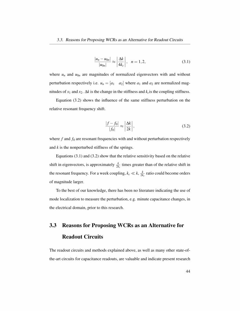
3.3. Reasons for Proposing WCRs as an Alternative for Readout Circuits
|un−u0n||u0n|
≈∣∣∣∣ ∆k4kc
∣∣∣∣ , n = 1,2, (3.1)
where un and u0n are magnitudes of normalized eigenvectors with and without
perturbation respectively i.e. un = [a1 a2] where a1 and a2 are normalized mag-
nitudes of x1 and x2. ∆k is the change in the stiffness and kcis the coupling stiffness.
Equation (3.2) shows the influence of the same stiffness perturbation on the
relative resonant frequency shift.
| f − f0|| f0|
≈∣∣∣∣∆k2k
∣∣∣∣ , (3.2)
where f and f0 are resonant frequencies with and without perturbation respectively
and k is the nonperturbed stiffness of the springs.
Equations (3.1) and (3.2) show that the relative sensitivity based on the relative
shift in eigenvectors, is approximately k2kc
times greater than of the relative shift in
the resonant frequency. For a week coupling, kc k, k2kc
ratio could become orders
of magnitude larger.
To the best of our knowledge, there has been no literature indicating the use of
mode localization to measure the perturbation, e.g. minute capacitance changes, in
the electrical domain, prior to this research.
3.3 Reasons for Proposing WCRs as an Alternative for
Readout Circuits
The readout circuits and methods explained above, as well as many other state-of-
the-art circuits for capacitance readouts, are valuable and indicate present research
44

3.3. Reasons for Proposing WCRs as an Alternative for Readout Circuits
in terms of technology and implementation. Looking at this problem from a dif-
ferent perspective opens a promising way for designing highly sensitive and low
cost capacitance readout circuits. As it has been proven in the mechanical/MEMS
domain, the mode localization is very sensitive to perturbation, and as capacitance
changes in the circuit can be considered a perturbation, this thesis aims to investi-
gate whether WCRs are a suitable alternative to existing capacitance readout cir-
cuits. By looking at the nature of this method and what has been achieved in the
mechanical field, it is very likely that using this method in electrical domain gives
us a very good sensitivity with considerably less sophisticated analog circuitry. In
terms of the physical implementation, as a digital signal processor is one of the
essential units in almost all readout systems, it is much simpler, though not neces-
sarily easier, to choose a method which is inherently closer or matches better with a
digital domain implementation. The proposed method reduces the amount of ana-
log circuitry and takes advantage of digital processors to measure the capacitance.
Sensitivity and the resolution of this method in electrical domain should be studied
and verified. To apply the mode localization technique to the electrical systems, we
can use the analogy between the coupled resonators in Fig. 3.1 and two coupled
LC circuits. The LC resonators could have either series or parallel configuration.
These parallel and series LC circuits are dual of each other. In more general form
in Fig. 3.1 there are dampers in parallel with each spring which have the same
roles as resistors in the electrical domain. This analogy between mechanical and
electrical domain is shown in Table 3.1. Note that to subscript index s , e.g. in Ls,
stands for “series” and index p stands for “parallel” dual circuit.
45

3.4. Summary
Mechanical Electrical (Series RLC) Electrical (Parallel RLC)Mass (M) Inductance (Ls) Inductance (Cp = Ls)
Damping (C) Resistance (Rs) Resistance (Rp = 1/Rs)Spring constant (1/K) Capacitance (Cs) Capacitance (Lp =Cs)
Displacement (x) Electric Charge (qs) Electric Charge (qp)Force (Fs) Voltage source (Vs) Current source (Is)
Table 3.1: Analogy between mass-spring-damper and RLC coupled oscillators.
3.4 Summary
This chapter first introduced the history and background of weakly coupled res-
onators, veering and mode localization in mechanical and acoustic field. The result
of an application of WCRs applied to MEMS inertial sensors was also presented.
The chapter was then concluded by briefly visiting the possibility of adopting WCR
method in electrical domain to measure small capacitance changes. The following
chapter examines the details of two-degree-of-freedom WCR circuit in capacitance
measurement.
46
Chapter 4
WCR-Based Readout Circuit
Analysis and Performance
Estimation
4.1 Introduction
This chapter presents an innovative and simple way of measuring small capaci-
tance changes. The proposed method can be a breakthrough in capacitance readout
circuits, commonly used for microsensors associated with physical quantities such
as pressure, rotational angles, linear displacement and acceleration [2].
In this chapter we propose a new method, based on weakly-coupled resonators
(WCR), which will be compared with the CFC method. It will be proven ana-
lytically, and shown by both simulations and experimental tests, that this method
has at least one order of magnitude, and ideally three orders of magnitude, better
relative sensitivity in comparison to the resonant frequency shift method.
The WCR-based readout circuit is based on the energy (or mode) localiza-
tion phenomenon. If two identical resonators are weakly coupled and excited by
a harmonic source, the oscillation energy is equally shared between them; mode
47

4.2. Theory of Operation
localization appears when one of them is perturbed relative to the other, leading to
an unbalance of the energy repartition among the two individual resonators. This
symmetry-breaking phenomenon is well known in acoustic resonators and other
mechanical systems [64, 8], as described in chapter 3. Recently, more attention
has been given to the use of WCRs in the mechanical aspect of resonating MEMS
mass sensors. It has been proven that weakly-coupled resonators can achieve al-
most three orders of magnitude higher sensitivity than conventional frequency shift
techniques for perturbation sensing [12, 11, 10, 13, 9]. We are hence transferring
this high sensitivity symmetry-breaking technique to the electrical domain, for the
first time (to our knowledge). We will use it for a simple capacitance readout solu-
tion. The measurement technique requires simple analog circuitry and is suitable
for integration with digital signal processing. The outcome of this chapter was pub-
lished as a journal paper in IEEE transactions on circuits and systems I (TCAS-I)
[65].
4.2 Theory of Operation
In principle, mode-localized or WCRs consist of two, or more, nearly identical cou-
pled resonators. As stated previously, the concept of WCRs has been used for the
detection of very fine changes (perturbations) in mechanical resonators. These type
of vibrating systems are analogous to quantum mechanical systems, e.g. the hy-
drogen molecule [9]. The eigenstates of two identical weakly-coupled resonators,
symmetric and antisymmetric, are very similar to "bonding orbitals" and "anti-
bonding orbitals", respectively. The frequency (eigenvalue) of the antisymmetric
mode is either higher or lower than that of the symmetric eigenmode, depending on
48

4.2. Theory of Operation
whether the coupling factor is positive or negative, respectively. Starting from an
identical set of two resonators, a symmetry-breaking perturbation can be defined as
a slight change in one of resonator’s parameters, e.g. the mass or spring constant in
mechanical systems, or capacitance or inductance value in electrical systems. The
perturbation will lead to both a further separation between the resonant frequencies
associated with the symmetric and antisymmetric modes, and to a redistribution of
the energies (amplitudes) associated with these modes, for a given external exci-
tation. The measurement of the ratio between their oscillation amplitudes (e.g.
displacement or charges amplitudes) is therefore directly correlated with the mag-
nitude of the perturbation. The energy is no longer divided evenly between two
resonators in such a case, and tends to localize more in one of them. An example
of 2DOF WCRs in the mechanical domain is shown in Fig. 4.1 illustrating two
spring-coupled mass-spring resonators.
k2 = k +¢k
m1 = m m2 = m
C1 = C CC C2 = C
k1 = k kCx1 x2
Figure 4.1: Two weekly coupled mechanical resonators.
The low stiffness spring connecting the two masses acts as the weak coupling
in this system. The coupling coefficient for this system, neglecting the damping
effect, is defined as kc/k. An analogous representation of this system, using series
RLC circuits, is shown in Fig. 4.2, assuming that the excitation is applied through
49

4.2. Theory of Operation
a voltage source, and the damping in the coupling is negligible. The coupling
coefficient becomes C/Cc in this case.
R1
= R L1
= L C1
= C L2
= L R2
= RC2
= C +¢C
CC
VS
i1 i2
+
+
+
+
¡
¡
¡
¡
q1
q2
Figure 4.2: 2DOF weekly-coupled series RLC resonators.
The coupled resonant system can be represented by the set of differential equa-
tions shown in 4.1. The most general case, damped and perturbed, is considered
here as it covers all other cases, e.g. undamped or unperturbed.
L1
d2q1dt2 +R1
dq1dt + 1
CC(q1−q2)+
1C1
q1 = vs
L2d2q2dt2 +R2
dq2dt + 1
CC(q2−q1)+
1C2
q2 = 0(4.1)
It is assumed that the circuit is excited with a harmonic sinusoidal voltage
source. Applying a perturbation to this circuit was defined as inducing very small
changes in the value of C2, from C to C+∆C. It was also assumed that the rate of
the perturbation change is slow enough (quasi-stationary signal), is that the tran-
sient parts of the responses, including the effect of initial conditions, do not play a
role. These assumptions were equivalent with the ones already used in the literature
related to the weakly-coupled mechanical resonators. Therefore the transient part
of the response was eliminated and the steady state part of the response was used
to detect the perturbation magnitude.With these assumptions, the initial conditions
and transient responses of the system are ignored. Hence (4.1) can be re-written in
50

4.2. Theory of Operation
Laplace domain as:
L
s2 + RL s+ 1
LC (1+ k) − kLC
− kLC s2 + R
L s+ 1LC (1+ k−δ )
Q1
Q2
=
Vs
0
(4.2)
δ , ∆C/C and k =C/CC are defined as the perturbation and coupling strength
of the system, respectively. Although in in circuits and systems it is more common
to use either node voltages or loop current as the circuit variables, here we use
charges on the capacitors in each resonators to follow the analogy given in Table
3.1.
The loci of the resonant frequencies of the system versus the relative changes
in capacitance C2 (perturbations) are shown in Fig. 4.3 [12]. The plotted results
are the outcome of SPICE simulations using National Instruments Multisim-12r
with the values of L1 = L2 = 10mH, C1 = 100nF, C2 = 100nF+∆C, with −4nF <
∆C < 4nF as perturbation, and three different coupling capacitance, CC, values of
5, 15 and 25µF. There are three pairs of curves shown, each corresponding to
different coupling strengths (different CC values). It will be shown that, since the
coupling coefficient is positive in this case, for a given perturbation value, the upper
branch of the locus is related to the out-of-phase mode (higher natural frequency),
while the lower branch corresponds to the in-phase resonant mode (lower natural
frequency). The middle zone of the graph (around zero perturbation) is called the
transition zone. The shown trend, where the loci of these eigenvalues in weakly-
coupled systems approach each other in the transition zone but do not intersect, is
called loci veering.
51

4.2. Theory of Operation
Figure 4.3: Two weekly coupled resonators natural frequencies loci.
As can be seen, the weaker the coupling is, the narrower the transition zone
and the higher the slopes in the curves around the transition zone are. This sudden
veering and narrowing of the transition zone results in a higher degree of energy
localization, or larger changes in the relative amplitudes of oscillation in the left
and right resonators.
This mode localization or shift in the eigenvector component values around the
transition zone is shown in Fig. 4.4. To show the eigenvectors abrupt changes in the
transition zone, the ratio between i2 and i1 (loop currents) is plotted in Fig. 4.4(a).
For positive perturbations, amplitude of i2 becomes considerably larger than i1 at
out-of-phase resonant excitation. Inversely, i1 gets quite larger than i2 at out-of-
52

4.2. Theory of Operation
phase mode excitation using the external voltage source. In other words, if the
system is excited at in-phase resonant frequency, the energy will be more localized
in the left loop of the circuit for positive perturbations and in the right loop for
negative perturbations. The opposite is true for in-phase excitation - energy will
be localized in the left loop for negative perturbations, or in the right loop for
positive perturbations. This is also shown using mode shape vector orientations
along with eigenvalue loci veering curve plot in Fig. 4.4(b). In this plot, normalized
eigenvalues are shown to be similar to the resonant frequencies loci in Fig. 4.3, as
expected.
The key aspect in achieving high sensitivity to perturbation is the drastic change
in the angle of the mode shape vector in the veering zone. In comparison, the
eigenvalue changes are not as significant.
In the series RLC-based WCRs shown in Fig. 4.2, we assume R1 = R2 = R,
L1 = L2 = L and C1 = C2 = C, which means both resonators are identical in the
absence of any perturbation. The coupling is done via CC ,with CC C being the
condition for a weak coupling.
53

4.2. Theory of Operation
(a)
(b)
Figure 4.4: Mode localization in two weekly-coupled-resonators.
54

4.2. Theory of Operation
A small change in any of these values can be defined as a perturbation, which
slightly pushes the system away from the energy equidistribution. We try to exploit
the high sensitivity in the orientation of the eigenvector around the symmetry-
breaking region, in order to use it as a measure of the applied perturbation (C2
variations). We will show that this technique provides a higher sensitivity than
existing state-of-the-art methods, e.g. monitoring the relative shift in the resonant
frequency. A detailed analytical solution to this second order differential equation,
using Laplace transform, is presented in the next section.
4.2.1 Analytical Solution
Equation 4.2, re-written below, representing the two weakly coupled RLC res-
onator systems, is solved through Laplace-transform techniques.
L
s2 + RL s+ 1
LC (1+ k) −1LC
−1LC s2 + R
L s+ 1LC (1+ k−δ )
Q1
Q2
=
Vs
0
(4.3)
The solutions Q1 and Q2 are therefore given by:
Q1 =1L
s2 + RL s+ 1
LC (1+ k−δ )(s2 + R
L s+ 1LC
(1+2k− δ
2
))(s2 + R
L s+ 1LC
(1− δ
2
))Vs (4.4)
Q2 =1L
1LCC(
s2 + RL s+ 1
LC
(1+2k− δ
2
))(s2 + R
L s+ 1LC
(1− δ
2
))Vs (4.5)
55

4.2. Theory of Operation
Using Partial Fraction Expansion (PFE), the equations can be simplified to
Q1 =1L
(k1
s2 + RL s+ 1
LC (1+2k− δ
2 )+
k2
s2 + RL s+ 1
LC (1− δ
2 )
)Vs (4.6)
Q2 =1L
(k3
s2 + RL s+ 1
LC (1+2k− δ
2 )+
k4
s2 + RL s+ 1
LC (1− δ
2 )
)Vs (4.7)
where
k1 =12
(1+
δ
2k
); k2 =
12
(1− δ
2k
)
k3 =−2k2
(LC)2 ; k4 =2k2
(LC)2
The response of this WCRs system to a Dirac Delta input is given by the inverse
Laplace transform of the above equations:
q1 =
12L
[1
ωd1
(1− δ
2k
)sin(ωd1t)+ 1
ωd2
(1+ δ
2k
)sin(ωd2t)
]e−R2L tu(t)
q2 =1
2L
[1
ωd1sin(ωd1t)− 1
ωd2sin(ωd2t)
]e−R2L tu(t)
(4.8)
where
ωd1 =1√LC
√1− δ
2,ωd2 =
1√LC
√1+2k− δ
2
56
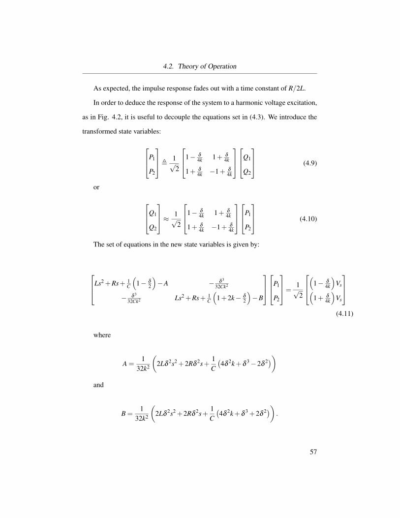
4.2. Theory of Operation
As expected, the impulse response fades out with a time constant of R/2L.
In order to deduce the response of the system to a harmonic voltage excitation,
as in Fig. 4.2, it is useful to decouple the equations set in (4.3). We introduce the
transformed state variables:
P1
P2
,1√2
1− δ
4k 1+ δ
4k
1+ δ
4k −1+ δ
4k
Q1
Q2
(4.9)
or
Q1
Q2
≈ 1√2
1− δ
4k 1+ δ
4k
1+ δ
4k −1+ δ
4k
P1
P2
(4.10)
The set of equations in the new state variables is given by:
Ls2 +Rs+ 1C
(1− δ
2
)−A − δ 3
32Ck2
− δ 3
32Ck2 Ls2 +Rs+ 1C
(1+2k− δ
2
)−B
P1
P2
=1√2
(
1− δ
4k
)Vs(
1+ δ
4k
)Vs
(4.11)
where
A =1
32k2
(2Lδ
2s2 +2Rδ2s+
1C
(4δ
2k+δ3−2δ
2))and
B =1
32k2
(2Lδ
2s2 +2Rδ2s+
1C
(4δ
2k+δ3 +2δ
2)) .
57

4.2. Theory of Operation
With the assumption of very small relative perturbations, even in comparison
with the coupling coefficient (i.e. δ k), we can eliminate the terms containing
higher order terms of δ/k. The resulting simplified and completely decoupled set
of equations is:
(
Ls2 +Rs+ 1C
(1− δ
2
))P1 =
1√2
(1− δ
4k
)Vs(
Ls2 +Rs+ 1C
(1+2k− δ
2
))P2 =
1√2
(1+ δ
4k
)Vs
(4.12)
Each of these equations can now be solved independently of one other, and
the inverse transformation to the physical state variables Q1, Q2 will give their
expression.
Assume vs(t) = Asin(ωt)u(t) or Vs(s) = ω/(s2 +ω2
)The equations then become:
P1(s) = ω√
2L
(1− δ
4k
)1
s2+ RL s+ 1
LC (1− δ
2 )1
s2+ω2
P2(s) = ω√2L
(1+ δ
4k
)1
s2+ RL s+ 1
LC (1+2k− δ
2 )1
s2+ω2
(4.13)
Using the inverse Laplace transform, the function x(t), in time domain, can be
retrieved:
x(t) = xt(t)+ xs(t) (4.14)
where xt(t) and xs(t) are transient and steady state parts of x(t) respectively.
Here, we focus on quasi-static perturbations, after the transient parts of the
responses have faded out. Therefore the transient part of the response can be elim-
inated and the steady state part is used to detect the perturbation magnitude.
58

4.2. Theory of Operation
The equations for P1 and P2 can be re-written as
P1(s) =ω√2L
(1− δ
4k
) k1s+ k2
s2 + RL s+ 1
LC
(1− δ
2
) +−k1s+ k3
s2 +ω2
(4.15)
where
ω2n1 =
1LC
(1− δ
2
)and 2ζ1ωn1 =
RL
k1 =2ζ1ωn1(
ω2n1−ω2
)2+(2ζ1ωn1ω)2
=RL(
1LC
(1− δ
2
)−ω2
)2+(R
L ω)2
k2 =(2ζ1ωn1)
2−ω2(ω2
n1−ω2)(
ω2n1−ω2
)2+(2ζ1ωn1ω)2
=
(RL
)2−ω2(
1LC
(1− δ
2
)−ω2
)(
1LC
(1− δ
2
)−ω2
)2+(R
L ω)2
k3 =ω2
n1−ω2(ω2
n1−ω2)2
+(2ζ1ωn1ω)2=
1LC
(1− δ
2
)−ω2(
1LC
(1− δ
2
)−ω2
)2+(R
L ω)2
P2(s) =ω√2L
(1+
δ
4k
) k′1s+ k′2s2 + R
L s+ 1LC
(1+2k− δ
2
) +−k′1s+ k′3s2 +ω2
(4.16)
where
59

4.2. Theory of Operation
ω2n2 =
1LC
(1+2k− δ
2
)and 2ζ2ωn2 =
RL
k′1 =2ζ2ωn1(
ω2n2−ω2
)2+(2ζ2ωn2ω)2
=RL(
1LC
(1+2k− δ
2
)−ω2
)2+(R
L ω)2
k′2 =(2ζ2ωn2)
2−ω2(ω2
n2−ω2)(
ω2n2−ω2
)2+(2ζ2ωn2ω)2
=
(RL
)2−ω2(
1LC
(1+2k− δ
2
)−ω2
)(
1LC
(1+2k− δ
2
)−ω2
)2+(R
L ω)2
k′3 =ω2
n2−ω2(ω2
n2−ω2)2
+(2ζ2ωn2ω)2=
1LC
(1+2k− δ
2
)−ω2(
1LC
(1+2k− δ
2
)−ω2
)2+(R
L ω)2
Assuming a quasi-static perturbation, P1 and P2 can be simplified and approxi-
mated by the steady-state, harmonic, part of the response:
P1(s) = ω√
2L
(1− δ
4k
)−k1s+k3s2+ω2
P2(s) = ω√2L
(1+ δ
4k
)−k′1s+k′3s2+ω2
(4.17)
or
p1(t) = ω√
2L
(1− δ
4k
)(k3ω
sin(ωt)− k1 cos(ωt))
p2(t) = ω√2L
(1+ δ
4k
)(k′3ω
sin(ωt)− k′1 cos(ωt)) (4.18)
Knowing p1 and p2, q1 and q2 can be solved.
60

4.2. Theory of Operation
q1(t) = 1√
2
[(1− δ
4k
)p1 +
(1+ δ
4k
)p2
]q2(t) = 1√
2
[(1+ δ
4k
)p1 +
(−1+ δ
4k
)p2
] (4.19)
By substituting p1 and p2 in the above equations
q1(t) =1
2L
[(1− δ
2k
)ω2
n1−ω2(ω2
n1−ω2)2
+(R
L ω)2 +
(1+
δ
2k
)ω2
n2−ω2(ω2
n2−ω2)2
+(R
L ω)2
]sin(ωt)
− ω
2LRL
[(1− δ
2k
)1(
ω2n1−ω2
)2+(R
L ω)2 +
(1+
δ
2k
)1(
ω2n2−ω2
)2+(R
L ω)2
]cos(ωt)
(4.20)
q1(t) =1
2L
[ω2
n1−ω2(ω2
n1−ω2)2
+(R
L ω)2 −
ω2n2−ω2(
ω2n2−ω2
)2+(R
L ω)2
]sin(ωt)
+ω
2LRL
[− 1(
ω2n1−ω2
)2+(R
L ω)2 +
1(ω2
n2−ω2)2
+(R
L ω)2
]cos(ωt).
(4.21)
The amplitudes of q1 and q2 have peaks at ωn1 and ωn2, which are natu-
ral/resonant angular frequencies of the system. The following approximation is
used in estimating q1, q2:
(1+
δ
2k
)/
(1− δ
2k
)≈ 1+
δ
kfor δ k.
The steady state solution for the ratio of the two capacitor charges will then be:
61

4.2. Theory of Operation
|q1||q2|
=
∣∣∣∣(1− δ
2k
)∣∣∣∣√√√√√√√√
4k2ω20 +
ω2n2
Q2
(1+(
1+ δ
k
)(1+ 4k2Q2
(1+2k− δ
2 )
))2
4k2ω20 +
ω2n2
Q2
(1+ 4k2Q2
(1+2k− δ
2 )
)2 (4.22)
with the following notations:
ω0 =1√LC
, Q =ω0L
R, ωn2 =
1√LC
√1+2k− δ
2(4.23)
and defining the square root term as:
r ,
√√√√√√√√4k2
L2C2 +R2
L3C
(1+2k− δ
2
)(1+(
1+ δ
k
)(1+ 4k2L
R2C(1+2k− δ
2 )
))2
4k2
L2C2 +R2
L3C
(1+2k− δ
2
)(4k2L
R2C(1+2k− δ
2 )
)2 . (4.24)
Using a rational function curve fit, with a least mean square (LMS) approxi-
mation, r is almost independent of δ which is graphed in Fig. 4.5. In this approx-
imation, with the values for L, C and k are 10 mH, 100 nF and 1/150 respectively,
r becomes:
r ∼=∣∣∣∣0.34171R+0.98−0.00252R+1
∣∣∣∣ (4.25)
Hence, the ratio between capacitor charges in (4.22) is well estimated, for re-
sistor values 0 < R < 100Ω, by:
62
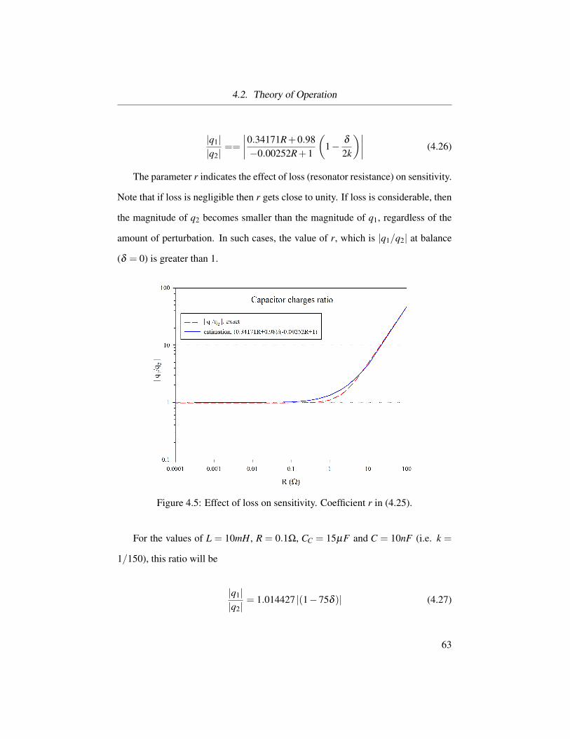
4.2. Theory of Operation
|q1||q2|
==
∣∣∣∣0.34171R+0.98−0.00252R+1
(1− δ
2k
)∣∣∣∣ (4.26)
The parameter r indicates the effect of loss (resonator resistance) on sensitivity.
Note that if loss is negligible then r gets close to unity. If loss is considerable, then
the magnitude of q2 becomes smaller than the magnitude of q1, regardless of the
amount of perturbation. In such cases, the value of r, which is |q1/q2| at balance
(δ = 0) is greater than 1.
Figure 4.5: Effect of loss on sensitivity. Coefficient r in (4.25).
For the values of L = 10mH, R = 0.1Ω, CC = 15µF and C = 10nF (i.e. k =
1/150), this ratio will be
|q1||q2|
= 1.014427 |(1−75δ )| (4.27)
63

4.2. Theory of Operation
This is completely in-line with the values from the exact equation, as shown in
Table 4.1 and Fig. 4.6. The following notations are used:
ωn1 =1√LC
√1− δ
2, ωn2 =
1√LC
√1+2k− δ
2
2ζiωni =RL, ωdi = ωni
√1−ζi
2 ; i = 1,2
where ωn1 and ωn2 , or their corresponding frequencies, fn1 and fn2, are the
resonant frequencies of the natural modes of the WCR system.
δ ωn2(Rad/Sec)∣∣∣q1
q2
∣∣∣− ∣∣∣q1q2
∣∣∣0
ωn2−ωn0ωn0
-1.33E-4 31623.83 -0.0098896 3.333E-05-1.07E-4 31623.62 -0.0079273 2.667E-05
-8E-5 31623.41 -0.0059573 1.999E-05-5.33E-05 31623.2 -0.0039795 1.333E-05-2.67E-05 31622.99 -0.0019937 6.667E-06
0 31622.78 0 02.667E-05 31622.57 0.0020017 -6.667E-065.333E-05 31622.35 0.0040114 -1.333E-05
8E-5 31622.14 0.0060293 -2.000E-051.07E-4 31621.93 0.0080552 -2.667E-051.33E-4 31621.72 0.0100894 -3.334E-05
Table 4.1: Analytical values for 2DOF WCRs at out-of-phase resonance.
In Table 4.1∣∣∣q1
q2
∣∣∣0is the value of
∣∣∣q1q2
∣∣∣ when there is no perturbation (δ = 0).
In Fig. 4.6, the relative shift in the resonant frequency of the out-of-phase mode
(Table 4.1) is plotted with a magnified scale of 100, in order to make it noticeable
in comparison to the relative shift of the ratio of capacitor charges. The sensitivity
based on relative capacitor charge measurement is approximately 300 times higher
64

4.3. Simulations
than the sensitivity based on the resonant frequency shift measurement. This data
was exported from circuit simulations using Multisim-12r.
-0.015 -0.010 -0.005 0.000 0.005 0.010 0.015
-0.010
-0.005
0.000
0.005
0.010
±(%)
¯
¯
¯
q1
q2
¯
¯
¯¡
¯
¯
¯
q1
q2
¯
¯
¯
0
!n2¡!n0
!n0
100£
Figure 4.6: Relative shift in resonant frequency vs. eigenmode in 2DOF WCRs.
4.3 Simulations
A series of simulations were performed with sinusoidal input as forced excitation.
Circuit simulations were conducted in National Instruments Multisim-12r for the
circuit shown in Fig. 4.7. The main reason for choosing Multisimr is the ca-
pability of co-simulation with LabVIEWr, which integrates very well with the
NI-PXI hardware platform used in our experiments. Perturbations of C2 values
were simulated by using a voltage-dependent capacitor (∆C in parallel with C2).
65

4.3. Simulations
When C+∆C = 100nF , the resonators are balanced.
R1
0:1Ð 100mH 100nH
L1 C1 C2 L2 R2
¢C
CC 15¹F
VS
0:1Vp
100nH 100mH 0:1Ð
i1 i2
Figure 4.7: Circuit schematic of 2DOF WCRs for SPICE simulations.
The results of the AC analysis, shown in Fig. 4.8, illustrate the natural frequen-
cies (modes) of the unperturbed circuit, at 5.033 kHz and 5.066 kHz, respectively.
Figure 4.8: AC analysis of 2DOF WCRs based on series RLC resonators.
From a practical perspective, the loop currents, i1 and i2, rather than charges
q1and q2, are taken as the eigenvectors components. The weak coupling is achieved
through CC, which was chosen to be approximately 15 times larger than C1 and C2.
If CC becomes too small, then the two resonators will become strongly coupled; if
66

4.3. Simulations
it is too large, then the amount of energy transferred to the second resonator is not
sufficient to be measured given the existing parasitics and noise sources.
In the next step of the simulation, the circuit was excited using a sine wave
input at one of the resonant frequencies. Perturbations were introduced to C2 us-
ing a voltage-controlled capacitor U1. The simulation results are aligned with the
theoretical analyses for both in-phase and out-of-phase modes, at 5.033 kHz and
5.066kHz respectively. A parametric sweep analysis on C2, from 95nF to 105nF,
shows the effect of perturbations on the natural frequencies and loop current values
(mode shapes). The results are shown in Table 4.2.
δ (%) fn2(Hz)∣∣∣∆u
u0
∣∣∣ ∣∣∣ i2i1
∣∣∣ ∣∣∣ i2i1
∣∣∣− ∣∣∣ i2i1
∣∣∣0
100∣∣∣ fn2− fn0
fn0
∣∣∣-5 5183.38 0.8470 3.2496 2.2752 2.3116-4 5156.96 0.8088 3.0782 2.1037 1.7901-3 5131.13 0.7481 2.8134 1.8389 1.2802-2 5106.31 0.6407 2.3969 1.4225 0.7903-1 5083.48 0.4224 1.7465 0.7721 0.33970 5066.27 0.0000 0.9744 0.0000 0.00001 5058.06 0.4238 0.5012 0.4732 0.16212 5054.65 0.6362 0.3079 0.6666 0.22943 5053.25 0.7383 0.2181 0.7564 0.25704 5052.45 0.7937 0.1685 0.8059 0.27285 5051.85 0.8285 0.1374 0.8370 0.2846
Table 4.2: Comparison table between ∆
∣∣∣ i2i1
∣∣∣and ∆ ff methods of measurement.
Note that for the theoretical eigenvectors, the charges on the capacitors C1 and
C2 were defined as vector components. Both analytical calculations and simula-
tions show that the value of relative change in loop current ratio is very close to
the relative shift in eigenvectors (∆u/u0) [9]. In these simulations a weak coupling
of C/CC = 1/150 and a maximum perturbation of δ = ∆C/C = 0.005 resulted in
67
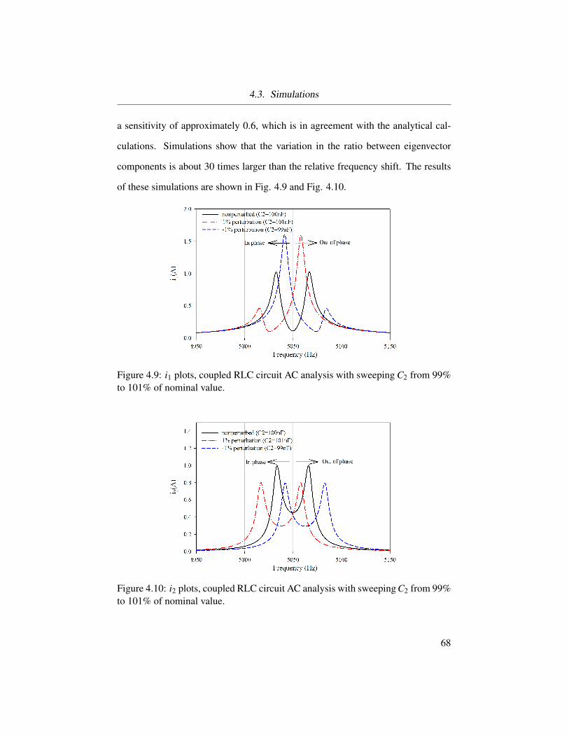
4.3. Simulations
a sensitivity of approximately 0.6, which is in agreement with the analytical cal-
culations. Simulations show that the variation in the ratio between eigenvector
components is about 30 times larger than the relative frequency shift. The results
of these simulations are shown in Fig. 4.9 and Fig. 4.10.
Figure 4.9: i1 plots, coupled RLC circuit AC analysis with sweeping C2 from 99%to 101% of nominal value.
Figure 4.10: i2 plots, coupled RLC circuit AC analysis with sweeping C2 from 99%to 101% of nominal value.
68
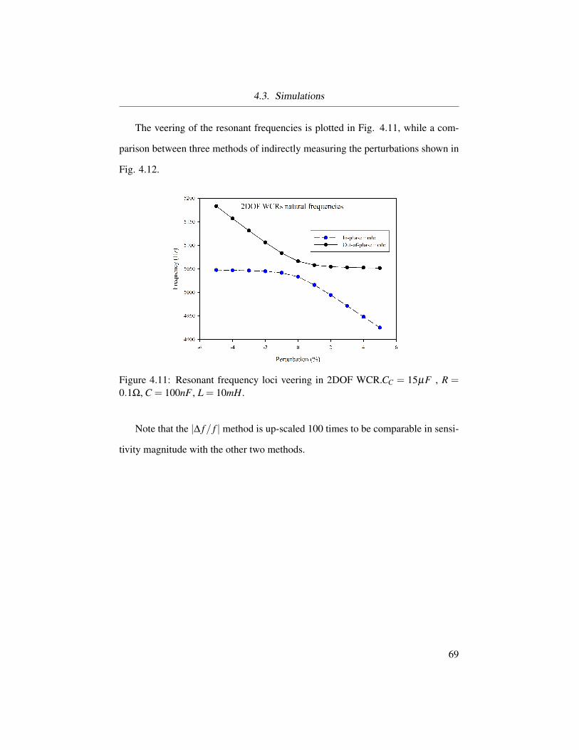
4.3. Simulations
The veering of the resonant frequencies is plotted in Fig. 4.11, while a com-
parison between three methods of indirectly measuring the perturbations shown in
Fig. 4.12.
Figure 4.11: Resonant frequency loci veering in 2DOF WCR.CC = 15µF , R =0.1Ω, C = 100nF , L = 10mH.
Note that the |∆ f/ f | method is up-scaled 100 times to be comparable in sensi-
tivity magnitude with the other two methods.
69

4.3. Simulations
-5.0 -2.5 0.0 2.5 5.0
-1.0
-0.5
0.0
0.5
1.0
1.5
2.0
2.5in-phase mode
The
res
pons
e of
thre
e m
etho
dsto
qua
si-s
tatic
per
turb
atio
ns
¢u1= ju10j¢ jI2=I1j¡ 100£¢f=f0
±(%)
(a)
-5.0 -2.5 0.0 2.5 5.0
-1.0
-0.5
0.0
0.5
1.0
1.5
2.0
2.5out-of-phase mode
±(%)
¢u2= ju20j¢ jI2=I1j100£¢f=f0
The
res
pons
e of
thre
e m
etho
dsto
qua
si-s
tatic
per
turb
atio
ns
(b)
Figure 4.12: Sensitivity comparison between three different methods; (a) compar-ison when exciting the in-phase (symmetric) mode (b) comparison when excitingthe antisymmetric mode.
70

4.3. Simulations
As it can be seen from the plots, for small perturbations the sensitivity of loop
currents ratio is almost equal to the sensitivity of the relative change in mode
shapes. The computation and hardware implementation of currents ratio estima-
tion is easier and requires less processing and memory resources; it is therefore the
adopted method. To further simplify the implementation, |i2/i1| ratio can be used
instead of ∆ |i2/i1|, eliminating unnecessary previous state storage in the computa-
tional algorithm.
Figure 4.13: LabVIEW-Multisim co-simulation for 2DOF WCRs.
The experiments, which will be described in the next section, were conducted
using National Instruments LabVIEWr software, together with a PXI data acqui-
sition system. The above simulations were repeated using a LabVIEW-Multisimr
71

4.3. Simulations
co-simulation framework (Fig. 4.13), to have a smoother transition from simula-
tion to hardware implementation. The results have confirmed the previous results
obtained using Multisim-only simulations.
-1.0 -0.5 0.0 0.5 1.0-0.6
-0.4
-0.2
0.0
0.2
0.4
0.6
±(%)
Com
parin
g re
lativ
e sh
ifts
in r
eson
ant
freq
uenc
y, e
igen
mod
e an
d cu
rren
t rat
io
100¢f=f0¢U= jU0j¢ jI2=I1j
Figure 4.14: Relative shifts for different methods; LabVIEW-Multisim co-simulation result.
The results are illustrated in Fig. 4.14, in a similar format as Fig. 4.12(b).
There is a small difference in the co-simulation results, specifically around -3%
perturbation. This comes from the fact that, for very high-Q (Q > 1000) circuits,
the accuracy of integration in time domain is strongly dependent on the time-step
settings in both LabVIEW and Multisim. Fine tuning this timing requires a vari-
able time step of in the order of ns, which makes the simulation very slow and
memory-intensive (several hours on a system with 8GB of RAM). The AC analy-
sis in Multisim simulations gives more reliable results without extensive simulation
72

4.4. Experimental Results
time.
4.4 Experimental Results
The components used for the hardware implementation were R1 =R2 = 0.1Ω, C1 =
C2 = 100nF, L1 = L2 = 10mH and CC = 15µF. C1 was regarded as a reference,
while C2 corresponded to the sensing capacitance. The perturbation of C2 was
generated by adding extra capacitors in parallel to the initial 100nF value. The
test-bench environment needed a voltage source with very low output impedance
for excitation, and an interface to measure the inductors or capacitors voltages.
Measurement of the analog values was done using a National Instrument PXIe-
1062Q system with a PXI-7854R analog interface module. A high level block
diagram of the proposed instrumentation system is shown in Fig. 4.15.
Figure 4.15: High-level-block-diagram of proposed capacitance readout.
73
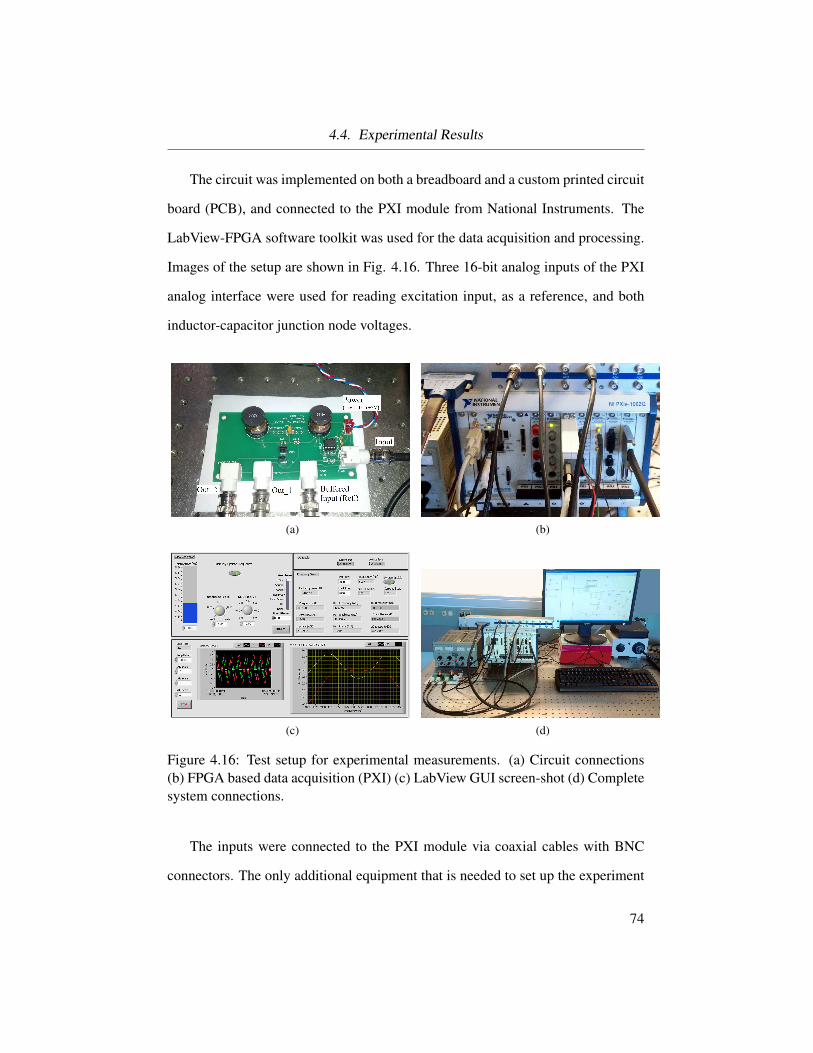
4.4. Experimental Results
The circuit was implemented on both a breadboard and a custom printed circuit
board (PCB), and connected to the PXI module from National Instruments. The
LabView-FPGA software toolkit was used for the data acquisition and processing.
Images of the setup are shown in Fig. 4.16. Three 16-bit analog inputs of the PXI
analog interface were used for reading excitation input, as a reference, and both
inductor-capacitor junction node voltages.
(a) (b)
(c) (d)
Figure 4.16: Test setup for experimental measurements. (a) Circuit connections(b) FPGA based data acquisition (PXI) (c) LabView GUI screen-shot (d) Completesystem connections.
The inputs were connected to the PXI module via coaxial cables with BNC
connectors. The only additional equipment that is needed to set up the experiment
74

4.4. Experimental Results
was an external power supply, or alternatively a pair of 9V batteries, to power up
the input op-amp buffer.
A single tone sine wave generator and a simple PLL algorithm were imple-
mented using LabView-FPGA to keep the excitation frequency tracking the out-
of-phase resonance frequency, when different perturbations were applied to C2.
The system was also capable of manually controlling the sine wave generator
by breaking the PLL loop, in order to test the designed PLL. In our experiments,
the capacitors voltage amplitudes were considered as components of the voltage
vector (i.e. v = [v1 v2]T ). v0 corresponds to v at balance (i.e. δ = 0) which
relates to the out-of-phase resonant frequency f0. Introducing a small perturbation
leads to a resonant frequency shift by ∆ f and a change in v by ∆v.
The values for ∆ f/ f0 and ∆v/v0 were taken as measures for the relative shift
in resonant frequency and the relative eigenvector shift methods, respectively. The
results of these methods are shown in Table IV for different perturbations, δ , of
C2; both the simulated and the measured sensitivities are plotted in Fig. 4.17.
δ (%) fn2 v1 v2
∣∣∣∆vv0
∣∣∣ 50∣∣∣∆ f
f0
∣∣∣0 5144 1.54059 1.30774 0 0
0.0295 5143.5 1.54481 1.30477 0.00502 0.004860.0586 5143 1.54792 1.30324 0.00823 0.009720.1119 5142.5 1.55792 1.30387 0.01425 0.014580.1948 5141 1.56675 1.30005 0.02300 0.029160.9787 5132 1.69866 1.29276 0.11538 0.11664
Table 4.3: Experimental results for both eigenvalue and eigenvector based methods
The experimentally obtained sensitivities were lower than in simulation due to
non-idealities of the circuit components, e.g. internal series resistance of the in-
ductors and electronic component tolerances. These led to reduced quality factors
75

4.4. Experimental Results
of the resonators and higher tolerance in their coupling strengths. Nevertheless, as
seen in Fig. 4.17 the capacitance-to-eigenvector shifting method proves to be at
least 50 times better than the capacitance-to-frequency shifting method.
Figure 4.17: Sensitivity comparison between simulations and experiments.
The experimental results using CC = 15µF did not show satisfactory results in
terms of distinguishing between the two resonant peaks (mainly due to the equiv-
alent series resistance ESRs). There are other parasitic parameters and sources for
nonlinearities, e.g. skin effect, core hysteresis etc. [66], which are not significant
in our case due to the low frequency and narrow band of operation.
In these lossy coupled resonators, there is a trade-off between the sensitivity
and detectability of the two resonant modes. To increase the gap between the reso-
76

4.5. Summary
nant frequencies, coupling should increase (i.e. CC should decrease) which in turn
decreases the sensitivity. In these experiments CC was changed to approximately
4µF . Fig. 4.18 shows the effect of this change on the frequency response.
(a) (b)
Figure 4.18: Effect of parasitic parameters on frequency response. (a) CC = 15µF(b) CC = 4µF.
4.5 Summary
The work presented in this chapter expands upon a principle validated already in
mechanical and acoustical engineering. The concepts of eigenvalues veering and
modes localization are fundamental in many physical problems; for instance the
mode localization aspect is reflected in the work of P. W. Anderson leading to the
Nobel prize in physics in 1977 (Anderson Localization) [6].
We have applied this technique, for the first time (to our knowledge), to a
capacitance-to-eigenvector shifting readout circuit and presented its superiority
over a capacitance-to- frequency shifting approach. The circuit is relatively sim-
ple and easy to couple with digital processing circuitry. The theoretical analysis
was complemented by both numerical simulations (SPICE and LabVIEWr) and
experimental measurements on a custom-made PCB level circuit.
77

4.5. Summary
Despite the presence of significant parasitic elements, e.g. ESR of inductors
and capacitors, the simple circuit was able to detect capacitive changes as low
as 30ppm and proved to be at least 50 times more sensitive than the equivalent
frequency-shifting method (Fig. 4.17). This opens up the new possibilities for
more advanced integrated solutions relying on mode localization for readout cir-
cuits of various electrical parameters. The next chapter focuses on the errors and
uncertainties associated with the excitation frequency, which are important in both
CFC and WCR-based methods.
78

Chapter 5
Error Reduction in WCR-Based
Capacitance Readout Circuits
5.1 Introduction
The superiority of the WCR over CFC method, in terms of the relative sensitivity,
has been proven and shown in the previous chapter. A WCR-based readout circuit
with a coupling factor of as low as k = 0.02 can show a sensitivity of at least two
orders of magnitude higher than the equivalent CFC configuration. An example
of such systems, based on coupled series RLC circuits, is shown in Fig. 5.1. The
capacitor CC provides the weak coupling between the two series resonance circuits,
with the coupling coefficient being defined as δ , ∆C/CC. The circuit will be
analyzed and discussed in more detail in the following sections.
Figure 5.1: Series RLC two weakly coupled resonators.
79
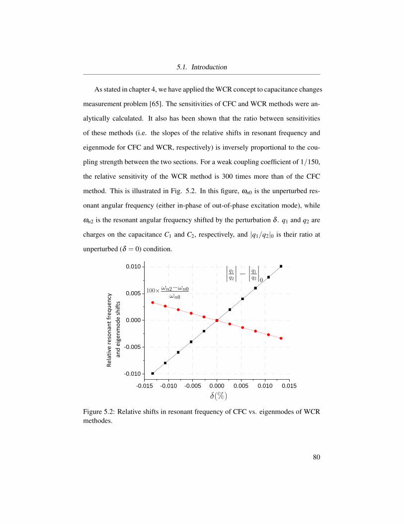
5.1. Introduction
As stated in chapter 4, we have applied the WCR concept to capacitance changes
measurement problem [65]. The sensitivities of CFC and WCR methods were an-
alytically calculated. It also has been shown that the ratio between sensitivities
of these methods (i.e. the slopes of the relative shifts in resonant frequency and
eigenmode for CFC and WCR, respectively) is inversely proportional to the cou-
pling strength between the two sections. For a weak coupling coefficient of 1/150,
the relative sensitivity of the WCR method is 300 times more than of the CFC
method. This is illustrated in Fig. 5.2. In this figure, ωn0 is the unperturbed res-
onant angular frequency (either in-phase of out-of-phase excitation mode), while
ωn2 is the resonant angular frequency shifted by the perturbation δ . q1 and q2 are
charges on the capacitance C1 and C2, respectively, and |q1/q2|0 is their ratio at
unperturbed (δ = 0) condition.
-0.015 -0.010 -0.005 0.000 0.005 0.010 0.015
-0.010
-0.005
0.000
0.005
0.010
±(%)
¯
¯
¯
q1
q2
¯
¯
¯¡
¯
¯
¯
q1
q2
¯
¯
¯
0
!n2¡!n0
!n0
100£
Figure 5.2: Relative shifts in resonant frequency of CFC vs. eigenmodes of WCRmethodes.
80
5.1. Introduction
The main difference between these two methods is that CFC is based on eigen-
values (natural frequencies) shifting of the system, while WCR scheme is based on
system eigenmodes shifting, which is 1/k times, k , CCC 1, more sensitive than
CFC method. The previous chapter mainly focused on relative sensitivity improve-
ment in capacitance change measurement but without analyzing its robustness to
excitation frequency errors. Therefore it is important to formally define expres-
sions for measurement errors for both CFC-based and WCR-based readout circuits,
to have a fair comparison between them. This chapter presents accurate and ana-
lytically deduced error expressions for CFC and WCR methods. Furthermore it
exploits these derivation for obtaining a new method with guaranteed lower mea-
surement errors. Typically, such systems based on resonance monitoring require a
feedback loop to keep the frequency of the excitation signal at resonance, e.g. by
using a PLL or some other locking mechanism [67]. There is a tradeoff between
sensitivity and phase noise. Higher sensitivity requires higher quality factors. On
the other hand, a high quality factor resonator has a sharp slope of the phase (φ )
vs. frequency ( f or ω) dependency around resonant frequency ( dφ/dω = 2Q/ω0,
), which in turn makes the system more sensitive and prone to error at the locking
frequency Fig. 5.3.
There are several possible implementations for CFC readout circuits. In our
case we have chosen the same double-resonator circuits for both methods, fre-
quency shift and eigenmodes shift. A high level block diagram of the system is
shown in Fig. 5.4. The linear combination of the CFC and WCR methods was
coined “Hybrid WCR” method. If the value of one of the circuit components
changes, the resonant frequency of the system changes accordingly. The feed-
back loop, including a phase detector and a loop filter, keeps the VCO tracking
81

5.1. Introduction
5026 5028 5030 5032 5034 5036 5038 5040−20
−10
0
10
20
Amplitude(dB)
Q = 500
Q = 100
Q = 20
5026 5028 5030 5032 5034 5036 5038 5040
−50
0
50
Phase
φ()
f (Hz)
Q = 500
Q = 100
Q = 20
Figure 5.3: Bode Plot for Series RLC Resonator
the resonant frequency. There are different methods for tracking and locking to
the resonant frequency of such RLC tanks, either based on amplitude, phase or
a combination of them. The phase information is used in this research for sim-
plicity and ease of implementation. It is also assumed that all the uncertainty
and errors in the circuitry, e.g. thermal and electronic noises, ADC quantization
noise, phase/frequency noise of the VCO etc, eventually show themselves in the
frequency/phase of the VCO output as a deviation from the exact resonant fre-
quency of the resonator. This erroneous frequency locking has a direct impact on
the perturbation estimation using CFC method. It also indirectly affects the WCR
method since all calculations are based on the assumption of the system being ex-
cited at resonance.
Our analysis shows that the errors in these two methods are of comparable
magnitude but of opposite sign. As a solution, we have linearly combined the
results of CFC and WCR methods to mitigate the estimation error.
The rest of this chapter is structured as follows: theory is presented in sec-
tion 5.2 followed by simulation results in section 5.3. Experimental results are
presented in section 5.4.
82

5.2. Theory of Operation
vs
vc
i1 i2fs = f0(1 + ®vc)V CO
i1 i2vs
AmplitudeDetection
LoopFilter
I1 I2Vs
WCRMethod
CFCMethod
fs
HybridWCR Method(this work)
Analog
Digital
PhaseDetector
Figure 5.4: System high-level-block-diagram.
5.2 Theory of Operation
Before discussing the details of the WCR system, it is useful to briefly discuss
the related frequency dependent methods. A simple RLC resonator vs. Colpitts
oscillator is shown in Fig. 5.5 as examples. Fig. 5.5a illustrates the capacitance
measurement based on the RLC resonator by simply associating the resonant fre-
quency and the capacitance C values, f0 =(2π√
LC)−1
. The formula indicates
a one-to-one correspondence between capacitance and resonant frequencies mea-
sured with the help of an excitation voltage Vs. An alternative method for a CFC
based capacitance measurement is to use an active oscillator, e.g. Colpitts oscilla-
tor shown in Fig. 5.5b. The op-amp gain and its positive feedback fulfills both gain
83
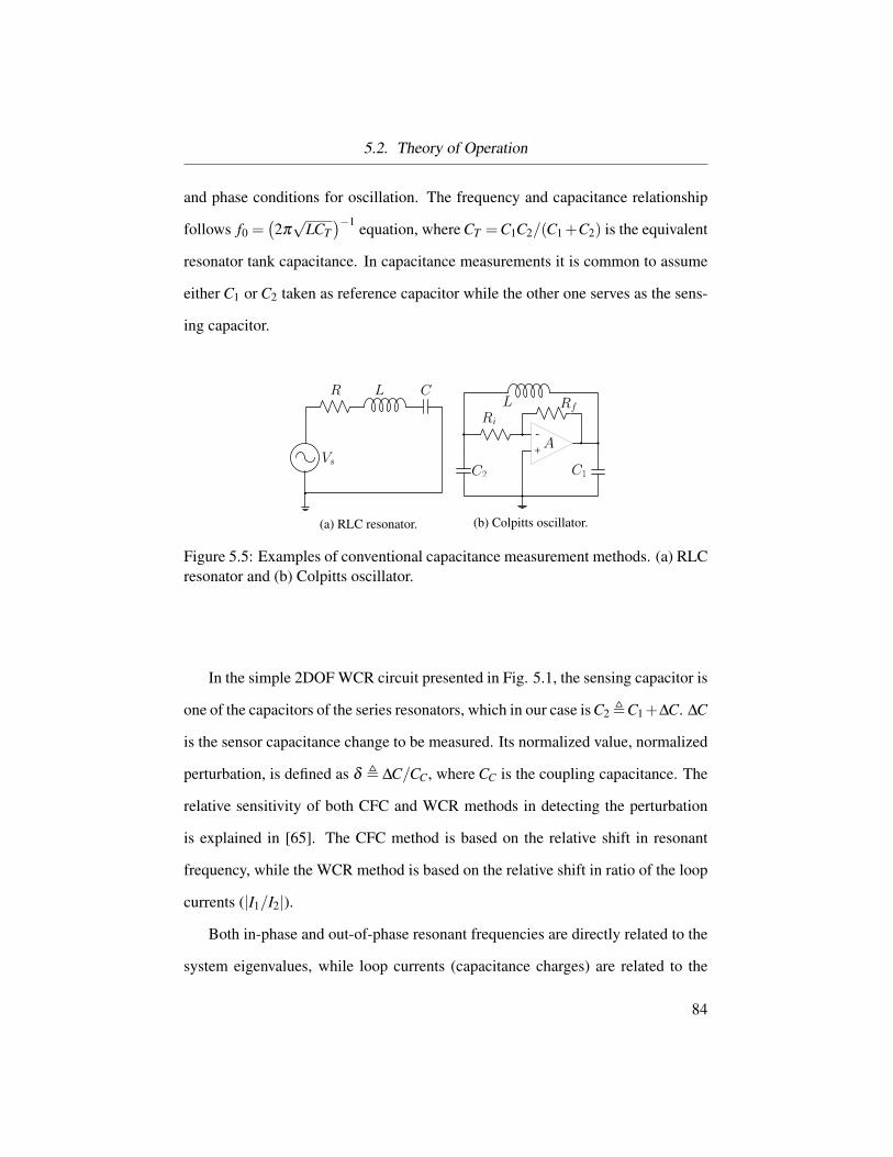
5.2. Theory of Operation
and phase conditions for oscillation. The frequency and capacitance relationship
follows f0 =(2π√
LCT)−1 equation, where CT =C1C2/(C1+C2) is the equivalent
resonator tank capacitance. In capacitance measurements it is common to assume
either C1 or C2 taken as reference capacitor while the other one serves as the sens-
ing capacitor.
Vs
R L C
(a) RLC resonator.
+
-
C1C2
Rf
Ri
L
A
(b) Colpitts oscillator.
Figure 5.5: Examples of conventional capacitance measurement methods. (a) RLCresonator and (b) Colpitts oscillator.
In the simple 2DOF WCR circuit presented in Fig. 5.1, the sensing capacitor is
one of the capacitors of the series resonators, which in our case is C2 ,C1+∆C. ∆C
is the sensor capacitance change to be measured. Its normalized value, normalized
perturbation, is defined as δ , ∆C/CC, where CC is the coupling capacitance. The
relative sensitivity of both CFC and WCR methods in detecting the perturbation
is explained in [65]. The CFC method is based on the relative shift in resonant
frequency, while the WCR method is based on the relative shift in ratio of the loop
currents (|I1/I2|).
Both in-phase and out-of-phase resonant frequencies are directly related to the
system eigenvalues, while loop currents (capacitance charges) are related to the
84

5.2. Theory of Operation
eigenvector components. Symmetry breaking phenomenon occurs around the point
of zero perturbation, where the orientation of the eigenvectors changes at a much
faster rate than the complimentary changes in the eigenvalues magnitudes. This is
shown in Fig. 5.6. The region around the zero perturbation is called the veering
zone.
Figure 5.6: Eigenvalue loci veering.
5.2.1 Measurement Sensitivity
Fig. 5.1 shows a simple weakly coupled resonators circuit based on series RLC
circuits. The first goal is to carry out closed loop equations for magnitudes of loop
currents, I1 and I2, and their ratio. This will be solved in two unperturbed and
perturbed cases.
First assume an unperturbed, ∆C = 0, case. The circuit is excited by a single
harmonic voltage signal. The phasor equation for the circuit can be interpreted by
85

5.2. Theory of Operation
equation (5.1).
z11 z12
z21 z22
I1
I2
=
Vm∠0
0
, (5.1)
where
z11 = z22 = R+ jωL+ 1jω
(1C + 1
CC
)and
z12 = z21 =− 1jωCC
.
This can be simplified further by:
1ωC
M
I1
I2
=
Vm∠0
0
, (5.2)
where
M =
m11 m12
m21 m22
,
m11 = m22 = RCω + jLCω2 + 1j (1+ k),
m12 = m21 = jk and k = CCC
.
Solving (5.2) for I1 and I2:
I1
I2
= M−1
Vm∠0
0
Cω, (5.3)
|I1|=VmCω
|det(M)|
√(RCω)2 +(LCω2−1− k)2, (5.4)
and
86

5.2. Theory of Operation
|I2|=1
|det(M)| (kCω)Vm, (5.5)
where
det(M) =(RCω + j(LCω
2−1− k))2
+ k2. (5.6)
Hence ratio of loop currents will become:
∣∣∣∣ I1
I2
∣∣∣∣= 1k
√(RCω)2 +(LCω2−1− k)2. (5.7)
Both |I1/I2| and |I1| have minimum values at:
ωz =
√1+ k√LC
(5.8)
which is in the middle of the two resonant frequencies of ω01 and ω02 with the
values of:
ω01 =1√LC
(5.9)
and
ω02 =
√1+2k√
LC(5.10)
The assumption is that the parameters δ , k and R are small enough so that all
second and higher order terms of these parameters could be neglected.
Equation (5.7) can be simplified by linearization around either of the resonant
frequencies, e.g. ω0 = 1/√
LC:
∣∣∣∣ I1
I2
∣∣∣∣= 2√
LCk
∣∣∣∣ω− 1√LC
∣∣∣∣+ 1k
√R2C
L+ k2 (5.11)
87

5.2. Theory of Operation
Now we consider more general case by assuming the presence of perturbation
∆C on capacitor C2 i.e. C2 =C+∆C. The equation (5.2) becomes:
1ωC
m11 m12
m21 m22 + j δ
1+δ
I1
I2
=
Vm∠0
0
(5.12)
where δ = ∆C/C. Solving (5.12) for I1 and I2 leads to:
I1
I2
= N−1
Vm∠0
0
Cω, (5.13)
where
N , (M+δM) =
m11 m12
m21 m22 + j δ
1+δ
. (5.14)
If perturbation is small enough, δ 1 i.e. (1+δ )−1 ≈ 1−δ , then
|I1|=
√(RCω)2 +(LCω2−1+δ − k)2
|det(N)| CωVm, (5.15)
and
|I2|=kCω
|det(N)|Vm, (5.16)
hence
∣∣∣∣ I1
I2
∣∣∣∣= 1k
√(RCω)2 +(LCω2−1+δ − k)2. (5.17)
88

5.2. Theory of Operation
Similar to the unperturbed case, both |I1/I2| and |I1| have minimum values at:
ωz =
√1+ k−δ√
LC, (5.18)
which is slightly shifted in comparison with the unperturbed case. Unlike the un-
perturbed case, this zero is not in the middle of the two resonant frequencies of:
ω01 =
√1−δ/2√
LC(5.19)
and
ω02 =
√1+2k−δ/2√
LC. (5.20)
The approximation (1+ k−δ/2)1/2≈ 12
[(1+2k−δ/2)1/2 +(1−δ/2)1/2
]is used,
where k 1 and δ 1.
Assuming circuit is symmetrical and all component values, except for C2, are
constant. The function |I1/I2| in (5.17), z(ω,δ ) , |I1/I2|, could be linearized in
the vicinity of δ = δ1 = 0 and ω = ω1 = ((1+2k)/LC)1/2 using Taylor series:
z(ω,δ ) ' z(ω1,δ1)
+∂
∂ωz(ω1,δ1)(ω−ω1)
+∂
∂δz(ω1,δ1)(δ −δ1) . (5.21)
The first order derivatives in (5.21) could be extracted from (5.17).
∂
∂ωz(ω1,δ1) =
1k
R2C2 +2kLCd
' 2k
√LC, (5.22)
89

5.2. Theory of Operation
∂
∂δz(ω1,δ1) =
1d' 1
k, (5.23)
where d ,(
R2CL (1+2k)+ k2
)1/2.
Approximations in equations (5.22) and (5.23) are done based on the R2C/L
k assumption which is true for this circuit.
Using values of δ1 = 0, ω1 = ((1+2k)/LC)1/2 = 31832.897, k' 1/150, RC'
10−9 and LC ' 10−9, (5.22) and (5.23) can be simplified further to:
z(ω1,δ1) =1k
√(RCω1)
2 +(LCω12−1+δ1− k)2
=1k
√R2C
L(1+2k)+ k2 (5.24)
' 1
∂
∂ωz(ω1,δ1)'
2k
√LC = 0.0095 (5.25)
∂
∂δz(ω1,δ1)'
1k= 150 (5.26)
Using these approximations, (5.21) can be re-written in simplified form of:
∣∣∣∣ I1
I2
∣∣∣∣= 1+2√
LCk
(ω−
√1+2k
LC
)+
1k
δ (5.27)
Using component values for the circuit related to this work:
90

5.2. Theory of Operation
∣∣∣∣ I1
I2
∣∣∣∣= 1+0.0095(ω−31832.897)+150δ (5.28)
or
∣∣∣∣ I1
I2
∣∣∣∣= 1+0.0597( f −5066.363)+0.0015∆C (5.29)
where f and ∆C are in Hz and pF respectively. Although the focus of this work
is around out-of-phase mode but with a similar approach around in-phase mode,
ω1 = (LC)−1/2 = 31622.777, the following linearization would be resulted.
∣∣∣∣ I1
I2
∣∣∣∣= 1− 2√
LCk
(ω− 1√
LC
)− 1
kδ , (5.30)
∣∣∣∣ I1
I2
∣∣∣∣= 1+0.0597(5032.921− f )−0.0015∆C. (5.31)
With approximation√
1+2k ≈ 1+ k and√
1+ k ≈ 1+ k/2, both in-phase and
out-of-phase equations for |I1/I2| can be combined to a single equation:
∣∣∣∣ I1
I2
∣∣∣∣= 2√
LCk
∣∣∣∣ω− 1√LC
(√1+ k− δ
2
)∣∣∣∣+ ε. (5.32)
Where ε is the error of linear approximation. This linearization should be very
precise around resonant frequencies and less precise around the corner where two
lines intersecting (ωz). To examine this lets calculate ε at these two frequencies
assuming there is no perturbation. At ω = ωz = ((1+ k−δ )/LC)1/2 :
91

5.2. Theory of Operation
ε =1k
√(RCωz)
2 +(LCωz2−1− k)2
=RC
k√
LC
√1+ k ' 0.047. (5.33)
This value matches with the minimum of the curve in Fig. 5.11. The next point
of interest is at out-of-phase resonant frequency, ω = ω1 = ((1+2k)/LC)1/2 :
ε =1k
√(RCω1)
2 +(LCω12−1− k)2−1
=RC
k√
LC
√1+2k+L(k)2/R2C−1 (5.34)
' 0.001139. (5.35)
As it can be seen, the error at resonant frequency is negligible. This error is the
equivalent of kε = 7.6×10⁻⁴% perturbation.
At this point we are going back to 5.17, which calculates the ratio of the loop
current magnitudes as:
∣∣∣∣ I1
I2
∣∣∣∣= 1k
√(RCω)2 +(LCω2−1+δ − k)2. (5.36)
The frequency responses of (5.15), (5.16) and (5.36) are shown in Fig. 5.7.
These parameters are shown for three different cases−one unperturbed and two
opposite perturbation values. For each perturbation value, the loop currents, as
well as any other physical parameters of the system, have two resonant frequen-
cies. For the unperturbed case, δ = 0, loop currents |I1| and |I2| are overlapping
92

5.2. Theory of Operation
at either in-phase or out-of-phase resonant frequencies. In positive perturbation
cases, e.g. ∆C = 100 pF or δ = 0.1% , the system has lower resonant frequen-
cies, with |I1| higher than |I2| for in-phase excitation and lower for out-of-phase
excitation. For negative perturbations, e.g. ∆C =−100 pF or δ =−0.1%, the sit-
uation is reversed. The frequency band of interest is either around the in-phase or
out-of-phase resonant frequencies.
5020 5030 5040 5050 5060 5070 50800
5
|I 1|a
nd|I 2
|(mA)
5020 5030 5040 5050 5060 5070 50800
1
2
|I 1|/
|I 2|
f (Hz)
5020 5030 5040 5050 5060 5070 50800
1
2
5020 5030 5040 5050 5060 5070 50800
1
2
|I1| / |I2| for +100 pF
|I1| / |I2| for no purturbation
|I1| / |I2| for -100 pF
∆C = -100 pF
No Perturbation (∆C = 0)∆C = +100 pF
Figure 5.7: Frequency response of the system for three values of perturbation δ =−0.1%, 0%and 0.1%.
As explained above and, in (5.32) and Fig. 5.7, |I1/I2| has a linear behavior in
either resonant frequencies neighborhood. This can be expressed by:
|I1/I2|= 2k
√LC∣∣∣ω− 1√
LC
(√1+ k− δ
2
)∣∣∣+1
k
(R2C
L (1+2k)+ k2)0.5
.(5.37)
In the case of exciting the circuit at the neighborhood of the out-of-phase reso-
nant frequencies, the (5.37) becomes:
93

5.2. Theory of Operation
∣∣∣∣ I1
I2
∣∣∣∣≈ 1+2k
√LC
(ω−
(1+2k
LC
)0.5)+
δ
2k. (5.38)
As an example for L = 10 mH, C = 100 nF and k = 1/150:
∣∣∣∣ I1
I2
∣∣∣∣= 1+0.0597( f −5066.363)+0.0015∆C, (5.39)
where f and ∆C are given in Hz and pF, respectively. Equation (5.38) is valid for
a wide range of excitation frequencies. It has the maximum error around the zero
of the system, which is not a useful excitation frequency. It is very precise in the
resonant frequency area, which is the focus of this work. For the high sensitivity
WCR method, which is based on the veering phenomenon, the following equation
can be used to backtrack the perturbation δ from the measurement of the loop
currents [65].
∆
∣∣∣∣ I1
I2
∣∣∣∣= δ
2k(5.40)
or
∣∣∣∣ I1
I2
∣∣∣∣= 1+δ/2k, (5.41)
where k ,C/CC 1 is the coupling factor of the circuit.
Similarly, for the CFC method, the following equation is applicable [11, 65]:
∣∣∣∣ ω
ω0−1∣∣∣∣= δ
4(1+2k)≈
δ
4, (5.42)
where ω0 =1√LC
or ω0 =1√LC
√1+2k for in-phase or out-of-phase cases, respec-
94

5.2. Theory of Operation
tively. For the out-of-phase case, (5.42) can be written as:
ω =
√1+2k−δ/2√
LC≈ ω0
(1− δ
4(1+2k)
). (5.43)
Equations (5.40) and (5.42) show that the WCR method has considerably ( 2k
times) higher sensitivity than CFC method. The lower the coupling factor, the
higher the sensitivity of WCR. For instance, for k = 0.02, the WCR method is
almost two orders of magnitude more sensitive than the CFC method.
While higher sensitivity is a desired performance metric, we are also interested
in improving the detection limit of the system. Two distinct type of noises limit
this factor. The thermal noise determined by the resistance in the circuit and the
mismatch between the excitation frequency and the actual resonant frequency. The
low resistance of the RLC circuit makes the thermal noise to be negligible with
respect to the latter source of uncertainty.
5.2.2 Measurement Error
As it is assumed in all the sensitivity calculations, to have a precise estimation of
the perturbation, the circuit has to be excited at the resonant frequency. All equa-
tions (5.37) to (5.43) are only valid at resonant frequencies, either the in-phase or
out-of-phase. For both WCR and CFC based capacitance measurements, it is very
crucial to keep the excitation precisely at resonant frequency and to dynamically
controlling it according to the changes in perturbation. Any mismatch between
the excitation and actual resonance frequencies leads to an erroneous perturbation
calculation.
The objective of this work is to introduce a method that is less sensitive to
95

5.2. Theory of Operation
excitation frequency errors. Interestingly, this simple circuit shows a very unique
characteristic that helps us achieving our goal. Considering an out-of-phase sce-
nario, if the excitation frequency is not exactly locked at resonant frequency, it will
introduce an error in estimating perturbation, δ , in either of these methods. The
errors associated with CFC and WCR methods have almost the same ampli-
tude, but opposite signs. This feature can be exploited to drastically reduce the
reading error by combining the results of both methods. Analytical proof of this
finding is presented below.
There is a one-to-one relationship between δ and ω or, δ and |I1/I2| in CFC
or WCR methods, respectively. Assume there is an error of ωerr , ω0−ω ( ferr ,
f0− f ) in excitation frequency. This causes both CFC and WCR method to estimate
the perturbation with errors. This is illustrated in 5.8.
jI1=I
2j
jI1=I
2j
±f
f (Hz)
±0 + "(±f)
±0
±0
±0+"(±
i)
f (Hz)
±i
f0+ferr
f0
Figure 5.8: Error comparison and improvement by hybrid method.
96

5.2. Theory of Operation
In WCR method, this error causes our system to compute a different |I1/I2|
according to (5.38). This deviation in |I1/I2| propagates to the final estimation of
the perturbation, given by (5.41). In summary:
δ = 2k
(∣∣∣∣ I1
I2
∣∣∣∣+2
√LCk
ωerr−1
)(5.44)
= 2k(∣∣∣∣ I1
I2
∣∣∣∣−1)+4√
LCωerr (5.45)
= 2k(∣∣∣∣ I1
I2
∣∣∣∣−1)+4√
2k+1ω0
ωerr (5.46)
where 2√
LCk ωerr is the propagated error to |I1/I2|. Looking at (5.46), the ulti-
mate error in estimating perturbation δ using WCR method will be defined as:
ε(δi), 4√
2k+1ω0
ωerr. (5.47)
Similarly,in the case of monitoring the resonant frequency shift, ωerr generates
a perturbation estimation error given by (5.43):
δ = 4(1+2k)(
1− ω +ωerr
ω0
)(5.48)
= 4(1+2k)(
1− ω
ω0
)−4
1+2kω0
ωerr. (5.49)
The final error in estimating perturbation using CFC method can be defined as:
ε(δ f ),−41+2k
ω0ωerr. (5.50)
97

5.2. Theory of Operation
The key point here is that the final errors in perturbation estimation in these
two methods, ε(δi) and ε(δ f ), have opposite signs. By combining equations (5.46)
and (5.49) to eliminate ωerr term, an unbiased actual perturbation estimation (δ )
is achievable.
δ =2√
1+2k1+√
1+2k
(2(
1− ω
ω0
)+ k(∣∣∣∣ I1
I2
∣∣∣∣−1))
. (5.51)
Figure 5.9 shows the effects of this hybrid method in correcting the error. The
horizontal axis is the excitation-resonance frequency mismatch ( ferr , ωerr/2π).
As an example, an arbitrary and fixed perturbation of about 0.025 is considered
as the reference point. The ideal perturbation curve would be a horizontal line at
0.025. The two lines crossing each other with opposite slopes are perturbation val-
ues estimated using CFC and WCR methods. The hybrid method result is plotted
and matches very closely with the ideal (no mismatch error) line.
−0.2 −0.1 0 0.1 0.20.01
0.015
0.02
0.025
0.03
0.035
0.04
δ
ferr (Hz)
δaδfδiδh
Figure 5.9: Error comparison and improvement by hybrid method.
98

5.2. Theory of Operation
To illustrate this with an example, assume ∆Ca is the actual capacitance change,
corresponding to actual perturbationδa. With ∆Ca = 25pF or δa = 2.5×10⁻⁴, the
resonant frequency will be:
fres =ω2
2π=
3.18309×10⁴
2π= 5066.05Hz. (5.52)
If the excitation frequency is off by +0.1 Hz ( f = 5066.15 Hz), then the esti-
mated perturbations will be:
δ f = 4√
1+2k(
1− ff 0
)= 1.669×10⁻⁴, (5.53)
and
δi = 2k(∣∣∣∣ I1
I2
∣∣∣∣−1)=
2150
(1.025−1) = 3.299×10⁻⁴, (5.54)
which correspond to ∆C f = 16.69pF (-33% error) and ∆Ci = 32.99pF (32% error)
respectively.
Using the hybrid method, the estimated ∆C, defined as ∆Ch, will become:
∆Ch = (1.0133/2.0133)1/2 (16.69+32.99) = 25.005pF ,
which has 0.02% error with respect to the actual value of 25pF.
99

5.3. Simulations
5.3 Simulations
Several SPICE simulations were performed to illustrate the circuit behavior and
support the analytical results. Fig. 5.10 shows a more detailed view of the peaks of
frequency responses of |I1| and |I2| in the region of out-of phase resonant frequen-
cies for different values of δ . The middle peak is related to the unperturbed case,
δ = 0, for which both loop currents have identical amplitudes at the resonant fre-
quency. This is marked with the vertical arrow on Fig. 5.10. Increasing δ reduces
the resonant frequency, increases the amplitude of I1 and slightly decreases the am-
plitude of I2 (thus increasing |I1|/ |I2|). Conversely, decreasing δ reduces both |I1|
and |I2|. Note that the changes in |I2| are not significant at resonant frequencies for
different values of δ . The dotted lines in Fig. 5.10 are used as a guide to show
the trend of the loop current amplitude peaks As it can be seen in Fig. 5.10, for
the ±90 pF range for ∆C (0.18% change in δ ) the relative changes of resonant fre-
quency and |I1|/ |I2| are 0.06% and 14%, respectively. The higher |I1|/ |I2| makes
the sensing easier for the analog front end.
5065 5065.5 5066 5066.5 5067 5067.5 50684.5
4.6
4.7
4.8
4.9
5
5.1
5.2
5.3
5.4
5.5
|I 1|a
nd|I 2
|(mA)
f (Hz)
|I1||I2|
-δ ↑δ ↑δ = 0
Figure 5.10: Amplitudes of I1 and I2 around out-of-phase resonant frequencies fordifferent perturbation values δ . From left to right ∆Cs are: -90, -60, -30, -10, 0, 10,30, 60 and 90 pF.
100

5.3. Simulations
Another set of simulations show the precision of the linearization in equation
(5.38). The circuit component values for this simulation were chosen to be R1 =
R2 = 0.1Ω, C1 = 100 nF, C2 = 100 nF + ∆C, L1 = L2 = 10 mH and CC = 15 µF.
The frequency response of |I1|/ |I2| is calculated for both the exact and linearized
solutions.
The simulation was performed using MATLAB and the results are plotted in
Fig. 5.11. As it can be seen, both exact and linear approximation curves match very
well in most of the frequency domain, especially close to the resonant frequencies.
The maximum error is in 5050 Hz neighborhood corresponding to the system zero
between the two resonant frequencies, which is not the region of excitation.
5030 5035 5040 5045 5050 5055 5060 5065 50700
0.2
0.4
0.6
0.8
1
1.2
1.4
|I 1|/
|I 2|
f (Hz)
exactlinear approx.
∆C=-100 pF
∆C=+100 pF
∆C=0
Figure 5.11: Analytical: linear approximation vs. exact for |I1|/|I2|.
To validate the analytical expressions, SPICE simulator was used to provide the
results shown in Fig. 5.12. The values used for this simulation are the same as the
ones employed for the analytical estimation. The exact solution, the linearization
and the SPICE numerical simulations all provide results validating the technique
101

5.4. Experimental Results
used.
5030 5035 5040 5045 5050 5055 5060 5065 50700
0.2
0.4
0.6
0.8
1
1.2
1.4
|I 1|/
|I 2|
f (Hz)
Analytical with ∆C = +100 pF
Simulation with ∆C = +100 pF
Analytical with ∆C = 0
Simulation with ∆C = 0
Analytical with ∆C = -100 pF
Simulation with ∆C = -100 pF
Figure 5.12: Analytical vs. simulation for |I1|/|I2|.
For different δ values, |I1|/ |I2| will have corresponding shift in value main-
taining their dependence on the excitation resonant frequency mismatch. This is
illustrated in Fig. 5.13.
5.4 Experimental Results
The components used for the hardware implementation were R1 = R2 = 0.1Ω,
C1 = C2 = 100nF, L1 = L2 = 10mH and CC = 4.7µF. C1 was considered as a
reference; C2 corresponded to the sensing capacitance. The perturbation of C2 was
generated by adding extra capacitors in parallel to the initial 100nF value. The test-
bench environment needed a voltage source with very low output impedance for
excitation, and an interface to measure the inductors or capacitors voltages. Mea-
surement of the analog values was done using a National Instrument PXIe-1062Q
102

5.4. Experimental Results
5065 5065.5 5066 5066.5 5067 5067.5 50680.75
0.8
0.85
0.9
0.95
1
1.05
1.1
1.15
1.2
1.25|I 1
|/|I 2
|
f (Hz)
δ = +0.09%
δ = +0.06%
δ = +0.03%
δ = +0.01%
δ = 0.00%
δ = −0.01%
δ = −0.03%
δ = −0.06%
δ = −0.09%
Figure 5.13: |I1|/|I2| around out-of-phase resonant frequencies for different pertur-bation values.
system with a PXI-7854R analog interface module. A high-level block diagram of
the proposed instrumentation system is shown in Fig. 5.14.
The circuit PCB was designed using Altium Designer 12 and connected to the
PXIe-1062Q module from National Instruments. The LabView-FPGA software
toolkit was used for the data acquisition and processing. Three 16-bit analog in-
puts of PXI analog interface were used for reading excitation input, as a reference,
and both inductor-capacitor junction node voltages. The inputs were connected
to the PXI module via coaxial cables and BNC connectors. The only additional
equipment that is needed to set up the experiment was an external power supply, or
alternatively a pair of 9V batteries, to power up the input op-amp buffer.
A single tone sine wave generator and a simple PLL algorithm were imple-
mented using LabView-FPGA to keep the excitation frequency tracking the out-
of-phase resonance frequency, when different perturbations were applied to C2.
103
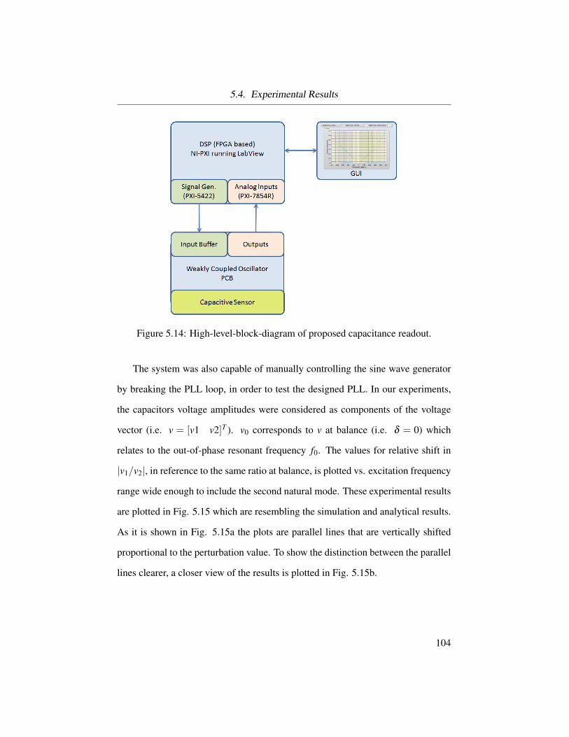
5.4. Experimental Results
Figure 5.14: High-level-block-diagram of proposed capacitance readout.
The system was also capable of manually controlling the sine wave generator
by breaking the PLL loop, in order to test the designed PLL. In our experiments,
the capacitors voltage amplitudes were considered as components of the voltage
vector (i.e. v = [v1 v2]T ). v0 corresponds to v at balance (i.e. δ = 0) which
relates to the out-of-phase resonant frequency f0. The values for relative shift in
|v1/v2|, in reference to the same ratio at balance, is plotted vs. excitation frequency
range wide enough to include the second natural mode. These experimental results
are plotted in Fig. 5.15 which are resembling the simulation and analytical results.
As it is shown in Fig. 5.15a the plots are parallel lines that are vertically shifted
proportional to the perturbation value. To show the distinction between the parallel
lines clearer, a closer view of the results is plotted in Fig. 5.15b.
104

5.4. Experimental Results
5100 5110 5120 5130 5140 5150
0.8
1.0
1.2
1.4
1.6
|V1
/ V2|
frequency (Hz)
δ = 0 % δ = 0.03 % δ = 0.06 % δ = 0.115 % δ = 2.15 %
δ increase
(a) Wider perturbation range.
5110 5120 5130 51400.87
0.90
0.93
0.96
0.99
1.02
1.05
1.08
1.11
1.14
1.17
|V1
/ V2|
frequency (Hz)
δ = 0 % δ = 0.03 % δ = 0.06 % δ = 0.115 %
δ increase
(b) Zoomed in, narrower perturbation range.
Figure 5.15: Magnitude of v1/v2 for excitation frequencies around out-of-phasemode for different perturbations.
Another experiment that shows the effectiveness of the proposed method in
system robustness due to frequency error is performed. In this experiment, a fixed
0.03% perturbation (∆C = 30pF) was applied on C2. Then the excitation frequency
was intentionally swept ±0.05% of the actual out-of-phase resonant frequency.
The results for perturbation estimation based on all three methods of frequency
shift (δ f ), eigenmode shift (δi), and hybrid method (δh) along with the actual per-
turbation (δa) which is a horizontal line at 0.03% are presented in table 5.1 and
plotted in Fig. 5.16. Note that all the values are expressed as percentages.
105
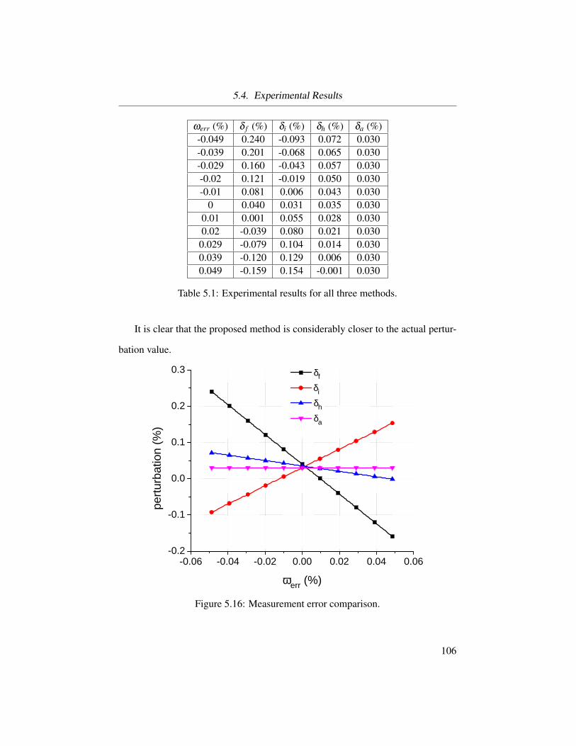
5.4. Experimental Results
ωerr (%) δ f (%) δi (%) δh (%) δa (%)-0.049 0.240 -0.093 0.072 0.030-0.039 0.201 -0.068 0.065 0.030-0.029 0.160 -0.043 0.057 0.030-0.02 0.121 -0.019 0.050 0.030-0.01 0.081 0.006 0.043 0.030
0 0.040 0.031 0.035 0.0300.01 0.001 0.055 0.028 0.0300.02 -0.039 0.080 0.021 0.0300.029 -0.079 0.104 0.014 0.0300.039 -0.120 0.129 0.006 0.0300.049 -0.159 0.154 -0.001 0.030
Table 5.1: Experimental results for all three methods.
It is clear that the proposed method is considerably closer to the actual pertur-
bation value.
-0.06 -0.04 -0.02 0.00 0.02 0.04 0.06-0.2
-0.1
0.0
0.1
0.2
0.3 δf
δi
δh
δa
pert
urba
tion
(%)
ωerr (%)
Figure 5.16: Measurement error comparison.
106
5.5. Summary
5.5 Summary
Based on the proposal for using WCRs in measuring minute capacitance changes
in this thesis, two sensitivity analyses have been performed - one using WCRs and
the other using CFC for comparison. The sensitivity analysis has focused on the
error in estimated δ due to the excitation-resonance mismatch. We have performed
both exact and linearized theoretical approach, complemented by SPICE numeri-
cal simulations and experiments. The two estimation methods based on CFC and
WCR have a dependence on the excitation-resonance mismatch of almost equal
magnitude but opposite sign. Combining the two measurement techniques to a hy-
brid method allows us to obtain a capacitive sensing method that is both highly
sensitive (due to the WCR method) and robust to excitation resonant mismatches.
The estimated error with the new combined method is at least one order of mag-
nitude smaller than either of the WCR or CFC schemes. In the next chapter we
try to examine the use of three-degree-of-freedom (3DOF) WCRs in capacitance
measurement aiming more simplification in excitation method.
107

Chapter 6
3DOF WCRs in Capacitance
Measurement
6.1 Introduction
In last two chapters we have seen the features and advantages of using 2DOF
WCRs in capacitance readout design. This chapter explores the possibility and
features of exploiting higher (three)-degree-of-freedom WCR for capacitance read-
outs. We have used mechano-electrical analogy to directly transfer the analysis per-
formed on 3WCRs to the electrical domain, in terms of eigenvalues and eigenvec-
tors sensitivities. We then run SPICE simulations to validate the theoretical insight.
The majority of the capacitive sensors in MEMS, especially for accelerometers and
gyroscopes, are based on sensing differential capacitors. The theoretical analysis
proves that differential perturbations in 3DOF WCRs do not require resonance fre-
quency tracking. We have shown this insensitivity to the excitation frequency in
SPICE simulation.
108

6.2. Analysis
6.2 Analysis
As we have seen, a 2DOF coupled resonator has two normal modes. Similarly, a
3DOF resonator, e.g. spring-mass, system shown in Fig. 6.1 with stiffness per-
turbation, has three normal modes [68, 69]. k is the stiffness of each of the three
main spring, kc is the stiffness of the two coupling springs, m is the mass and ∆ki
(i = 1,2, 3) is the perturbation of the spring of the ith resonator. Perturbation can
act either as small mass asymmetries or be reflected in ∆k differences that break
the symmetry of the system.
m m m
kc kc
k1 + ¢k1 k2 + ¢k2 k3 + ¢k3
Figure 6.1: 3DOF coupled spring-mass system with stiffness perturbation.
Since the system is initially symmetric, the analysis of a single perturbation
modifying the first or third mass will be the same. It has been shown that, if the
perturbation modifies the spring stiffness of the first of the third resonator, the
resonant frequencies ωi and mode shapes of the system φi are [69]:
109

6.2. Analysis
ω1 = ω0
(1+
δ
6
), φ1 =
[1 1− δ
3κ1− δ
κ
]T
,
ω2 = ω0
(√1+κ +
δ
4
), φ2 =
[1 − δ
κ−1− δ
2κ
]T
,
ω3 = ω0
(√1+3κ +
δ
12
), φ3 =
[1 −2− δ
6κ1+
δ
2κ
]T
, (6.1)
where ω0 =√
k/m is the natural frequency of each of the individual spring-
mass resonators, κ , kc/k , and δ = ∆k/k.
Another important case corresponds to a differential perturbation, where the
perturbations applied to the first and third spring have the same magnitude but
opposite signs +δ and −δ , respectively. The second (middle) resonator stays un-
perturbed. In this case we have:
ω1 = ω0, φ1 =
[1 1+
δ
3κ1+
δ
κ
]T
,
ω2 = ω0√
1+κ, φ2 =
[1
δ
2κ−1+
δ
2κ
]T
,
ω3 = ω0√
1+3κ, φ3 =
[1 −2+
δ
6κ1− δ
2κ
]T
. (6.2)
As the above equation shows, the resonant frequencies are independent of the
differential perturbation δ (for δ 1). This is due to the fact that the loci of
resonant frequencies of the system with a varying differential perturbation have
extrema points in the veering zone (in the vicinity of δ = 0) for all three modes.
This is very helpful in simplifying the excitation circuit design since there is no
110

6.2. Analysis
need for a sophisticated frequency tracking feedback loop to continuously adjust
the excitation frequency depending on the perturbation value. It is also shown that
in 3DOF WCR system, the sensitivity of the mode shapes in differential perturba-
tion mode is almost twice as the mode shape sensitivity in the case of one-sided
perturbation [68, 69]. This feature makes the 3DOF WCR system attractive to be
used as differential capacitance measurement system in the electrical domain.
A 3DOF WCR circuit based on series RLC is shown in Fig. 6.2.
R1 L1 C1 R2 L2 C2 R3 L3 C3
CC1 CC1
Vs
Figure 6.2: 3DOF weekly coupled series RLC resonators.
The equivalent of the equation sets (6.1) (one-sided perturbation) for this RLC
circuit is:
ω1 = ω0
(1− δ
6
), φ1 =
[1 1− δ
3k1− δ
k
]T
,
ω2 = ω0
(√1+ k− δ
4
), φ2 =
[1 − δ
k−1− δ
2k
]T
,
ω3 = ω0
(√1+3k− δ
12
), φ3 =
[1 −2− δ
6k1+
δ
2k
]T
, (6.3)
and for (6.2) (differential perturbation) this will be:
111

6.2. Analysis
ω1 = ω0, φ1 =
[1 1+
δ
3k1+
δ
k
]T
,
ω2 = ω0√
1+ k, φ2 =
[1
δ
2k−1+
δ
2k
]T
,
ω3 = ω0√
1+3k, φ3 =
[1 −2+
δ
6k1− δ
2k
]T
, (6.4)
where k ,C/CC, δ ,∆C/C, and ω0 = 1/√
LC. As it can be seen the sensitivity
of the resonant frequencies to perturbation δ , for all modes, is zero.
We are expecting a shift in resonant frequency corresponding to the perturba-
tion for single-ended perturbation and no shift in differential perturbation. SPICE
simulations, parameter sweep analysis, verifies this fact as shown in figures 6.3 and
6.4.
3DOF WCRs one-sided perturbationPrinting Time:Tuesday, December 15, 2015, 11:49:10 PM
C3 sweep
Frequency (Hz)
5.02k 5.09k5.03k 5.08k5.05k 5.06k
I1 M
ag
nitu
de
0
600m
100m
500m
200m
400m
300m
δ = − 0.1%
δ = + 0.1%
δ = + 0.05%
δ = 0
δ = − 0.05%
Figure 6.3: Frequency shift of all three modes in one-sided perturbation of a 3DOFWCRs system.
112

6.2. Analysis
3DOF WCRs differential perturbationPrinting Time:Tuesday, December 15, 2015, 11:50:50 PM
C3 sweep
Frequency (Hz)
5.02k 5.09k5.03k 5.08k5.05k 5.06k
I1 M
ag
nitu
de
0
600m
100m
500m
200m
400m
300m
δ = + 0.1%
δ = + 0.1%
δ = + 0.1%
δ = + 0.1%
δ = + 0.1%
Figure 6.4: Frequency shift of all three modes in differential perturbation of a3DOF WCRs system
For one-sided perturbation in Fig. 6.3, the frequency response of loop currents
shows the change in the resonant frequency, while Fig. 6.4 shows almost a fix res-
onant frequencies. This is one of the major advantages of differential perturbation
over one-sided perturbation in 3DOF WCRs.
The sensitivity of mode shapes, defined as the relative changes in the angle
of the mode shape in reference to δ . To define sensitivity, modal vectors will
be plotted in three-dimensional Cartesian space with standard basis and take their
projection on the plane defined by the first and the third axes (akin to X-Z plane in
XYZ coordinate system) [69]. The angle Θ j made by the projection of jth modal
vector with the first axis can be used to define sensitivity of the mode. This way,
the sensitivities for resonant frequencies and mode shapes are defined as:
113

6.2. Analysis
Nω j ,
∣∣∣∣ω j−ω j0
ω j0
∣∣∣∣ , NΘ j ,
∣∣∣∣Θ j−Θ j0
Θ j0
∣∣∣∣ (6.5)
where tanΘ j = a3 j and a3 j is the third element of φ j. Using the above defini-
tion, the sensitivity for mode shapes can be calculated.
NΘ1 =
∣∣∣∣ 4π δ
k
∣∣∣∣ , NΘ2 = NΘ3 =
∣∣∣∣ 2π δ
k
∣∣∣∣ . (6.6)
As we will see in the next section, we calculate the sensitivity simply by the
ratio of the magnitude of the change in mode shape vector over its magnitude prior
to perturbation.
6.2.1 Differential Perturbation Detailed Analysis
To make the analysis of 3DOF WCRs circuit shown in Fig. 6.2 simpler, we can use
superposition technique and split it to the circuits shown in Fig. 6.5 and Fig. 6.6.
R1 L1 C1 R2 L2 C2 R3 L3 C3
CC1 CC2
Vd
2¡
Vd
2
Figure 6.5: 3DOF WCR schematic with differential excitation.
114

6.2. Analysis
R1 L1 C1 R2 L2 C2 R3 L3 C3
CC1 CC2
Vc Vc
Figure 6.6: 3DOF WCR schematic with common mode excitation.
Assuming Vd =Vs and VC =Vs/2, then the superposition of the sources on the
left hand side of the circuits results in Vs, and they cancel each other out on the
right hand side. The circuit components are R1 = R2 = R3 = R, L1 = L2 = L3 = L,
CC1 = CC2 = CC, C1 = C+∆C, C3 = C−∆C, and C2 = C. The perturbation δ is
∆C/C and coupling value is k =C/CC.
In differential case we can simplify the circuit as shown in Fig. 6.7. We first
consider the unperturbed case i.e. δ = 0. Fig. 6.7(a) is the same as Fig. 6.5.
The resonator elements are identical and henceZ1 = Z2 = Z3 = Z where Z( jω) =
R+ j(Lω−1/(Cω)) or Z(s) = R+(Ls−1/(Cs)) in Laplace domain.
CC1 CC2
Vd
2
Z1 Z2 Z3 ¡
Vd
2
(a) Differential Excitation.
CC
Vd
2
Z Z=2
(b) Differential excitation, half-circuit.
Figure 6.7: 3DOF WCR schematic with differential excitation.
By splitting Z2 in two series Z/2 impedances and using the symmetry of the
115

6.2. Analysis
circuit, the circuit can be simplified to half-circuit shown in Fig. 6.7(b).
Vd
2=
(Z +
1sCC
Z2
1sCC
+ Z2
)I1 =
(Z +
Z2+ZCCs
)I1 (6.7)
= Z3+ZCCs2+ZCCs
I1. (6.8)
If we calculate the input admittance Yin ,I1
Vd/2 :
Yin(s) =I1
Vd/2=
1Z
2+ZCCs3+ZCCs
, (6.9)
or
Yin( jω) =1
Z( jω)
2+ jZ( jω)CCω
3+ jZ( jω)CCω. (6.10)
So, the resonant frequencies of the system are the zeros/minima of |Z( jω)| or
|3+ jZ( jω)CCω|. These frequencies are:
ω1 =1√LC
= ω0 (6.11)
ω3 =
√1+3k√
LC=√
1+3kω0. (6.12)
The magnitude of Yin( jω) is:
116
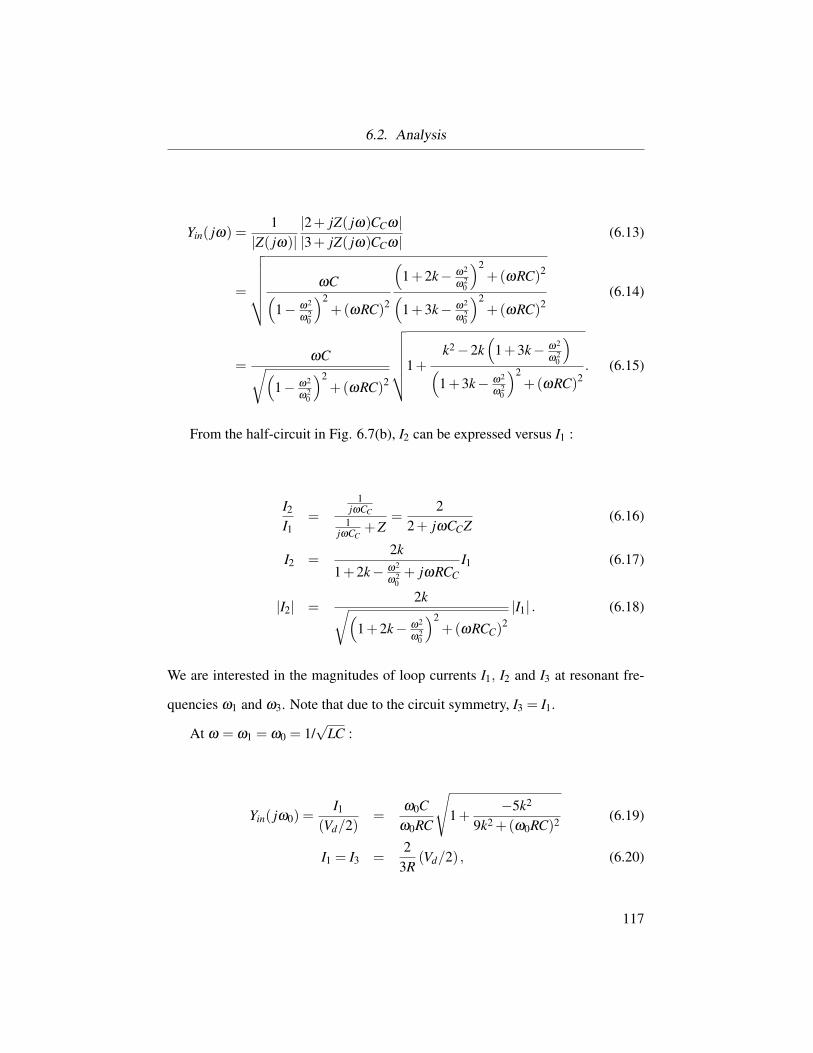
6.2. Analysis
Yin( jω) =1
|Z( jω)||2+ jZ( jω)CCω||3+ jZ( jω)CCω| (6.13)
=
√√√√√√ ωC(1− ω2
ω20
)2+(ωRC)2
(1+2k− ω2
ω20
)2+(ωRC)2(
1+3k− ω2
ω20
)2+(ωRC)2
(6.14)
=ωC√(
1− ω2
ω20
)2+(ωRC)2
√√√√√√1+k2−2k
(1+3k− ω2
ω20
)(
1+3k− ω2
ω20
)2+(ωRC)2
. (6.15)
From the half-circuit in Fig. 6.7(b), I2 can be expressed versus I1 :
I2
I1=
1jωCC
1jωCC
+Z=
22+ jωCCZ
(6.16)
I2 =2k
1+2k− ω2
ω20+ jωRCC
I1 (6.17)
|I2| =2k√(
1+2k− ω2
ω20
)2+(ωRCC)
2|I1| . (6.18)
We are interested in the magnitudes of loop currents I1, I2 and I3 at resonant fre-
quencies ω1 and ω3. Note that due to the circuit symmetry, I3 = I1.
At ω = ω1 = ω0 = 1/√
LC :
Yin( jω0) =I1
(Vd/2)=
ω0Cω0RC
√1+
−5k2
9k2 +(ω0RC)2 (6.19)
I1 = I3 =2
3R(Vd/2) , (6.20)
117

6.2. Analysis
The approximation of ω0RCC k is used here, which is valid by a good margin
(more than 4 orders of magnitude). I2 will be:
_
|I2| =2k√
(2k)2 +(ω0RCC)2|I1| (6.21)
≈ |I1|=2
3R(Vd/2) . (6.22)
At ω = ω3 =√
1+3k/√
LC we have:
Yin( jω0) =I1
(Vd/2)=
ω0√
1+3kC3k
√1+
k2
(ω0RC)2 (6.23)
I1 = I3 ≈ 13R
(Vd/2) , (6.24)
and I2 will become:
|I2|=2k√
(k)2 +(ω0√
1+3kRCC)2|I1|= 2 |I1|=
23R
(Vd/2) . (6.25)
In summary, the differential excitation mode, stimulates mode 1 and mode 3.
The resonant frequencies and magnitudes of the loop currents are:
ω1 = ω0, φ1 =
(Vd
2
)(2
3R
)[1 1 1]T ,
ω3 = ω0√
1+3k, φ3 =
(Vd
2
)(1
3R
)[1 −2 1]T , (6.26)
118

6.2. Analysis
SPICE simulation shown in Fig. 6.8 verify the above analysis.
Figure 6.8: Frequency response of unperturbed 3DOF WCRs circuit with differen-tial excitation.
For common mode excitation using Vc = Vs/2, the circuit can be simplified
as shown in Fig. 6.9. The only difference with the previous case is applying
a common mode voltage VC to both ends of the circuit. This symmetry of the
circuit results in no current passing through the middle resonator i.e. I2 = 0, which
simplifies the circuit to the half-circuit shown in Fig. 6.9(b).
119

6.2. Analysis
i = 1; 2; 3CC1 CC2
Vc
Z1 Z2 Z3
Zi = Ri + j(!Li ¡ 1=!Ci)
(a) Common mode excitation.
CC
VcZ
(b) common mode excitation,half-circuit.
Figure 6.9: 3DOF WCR schematic with common mode excitation.
Solving the circuit in 6.9(b) is simple.
Yin( jω) =I1
Vc=
1Z + 1
jωCC
=1
R+ j(
Lω− 1ω
(1C + 1
CC
))=
Cω
RCω + j(
ω
ω0− (1+ k)
) . (6.27)
The resonant frequency of the circuit with common mode excitation would be
ω2 =
√1+ k√LC
= ω0√
1+ k. (6.28)
The magnitude of loop current I1 can be calculated from:
120

6.2. Analysis
∣∣∣∣ I1
Vc
∣∣∣∣ =Cω√
(RCω)2 +(
ω2
ω20− (1+ k)
)2. (6.29)
At ω = ω2 the magnitude of I1 becomes:
|I1| =Cω√(RCω)2
|Vc| (6.30)
=1R|Vc| . (6.31)
I1 has the same magnitude as I3 but it has opposite phase. As we stated above,
I2 = 0. In summary:
ω1 = ω0, φ1 =Vc
R[1 0 −1]T . (6.32)
SPICE simulation shown in Fig. 6.10 verify the analysis the circuit in mode 2.
121

6.2. Analysis
Figure 6.10: Frequency response of unperturbed 3DOF WCRs circuit with com-mon mode excitation.
As it can be seen from the solutions to the differential and common mode
excitation cases above, the differential excitation stimulates mode 1 and 3, and
the common mode excitation only stimulates mode 2. This could be very helpful,
especially in cases of lossy circuits, where one of the challenges are detecting and
differentiating between the two modes due to the overlapping of the resonance
peaks. This is shown in Fig. 6.11 for a 3DOF WCR circuit with higher resistance
values, 2Ω (Q≈160), for each resonator. As it can be seen, mode 1 and mode 2
frequencies are merging into each other in a way that are not detectable using a
one-sided excitation. The peak frequency is also misleading, since mode 1 and 2
peaks are merged and created only one peak at a frequency between mode 1 and
mode 2 resonant frequencies.
122

6.2. Analysis
Figure 6.11: 3DOF WCR, impact of loss on resonant frequencies.
The common mode excitation, which only excites mode 2, avoids the above
mentioned difficulty. Hence we choose common mode excitation for the rest of the
analysis.
6.2.2 System Response to Common Mode Excitation
We have chosen excitation in mode 2, which can be achieved by common mode
circuit excitation as explained above.We also chose differential perturbation since
it is a common operating mode for most of the capacitive MEMS sensors. More-
over, the resonant frequency in this configuration is independent of perturbation
magnitude.
We start the analysis by introducing the quality factor of our 3DOF WCRs
circuit in mode 2. The peak of I1 magnitude can be calculated from (6.29), which
is rewritten below.
123
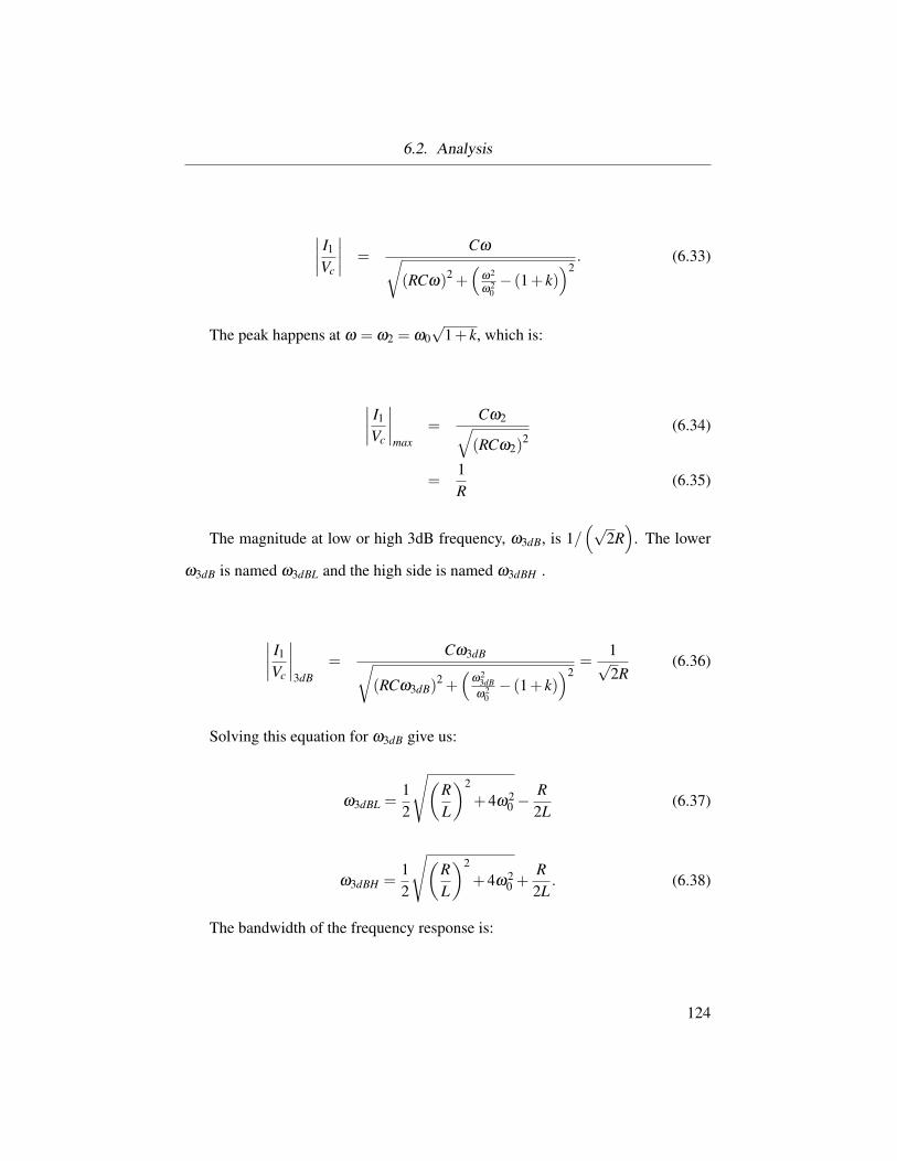
6.2. Analysis
∣∣∣∣ I1
Vc
∣∣∣∣ =Cω√
(RCω)2 +(
ω2
ω20− (1+ k)
)2. (6.33)
The peak happens at ω = ω2 = ω0√
1+ k, which is:
∣∣∣∣ I1
Vc
∣∣∣∣max
=Cω2√(RCω2)
2(6.34)
=1R
(6.35)
The magnitude at low or high 3dB frequency, ω3dB, is 1/(√
2R)
. The lower
ω3dB is named ω3dBL and the high side is named ω3dBH .
∣∣∣∣ I1
Vc
∣∣∣∣3dB
=Cω3dB√
(RCω3dB)2 +(
ω23dB
ω20− (1+ k)
)2=
1√2R
(6.36)
Solving this equation for ω3dB give us:
ω3dBL =12
√(RL
)2
+4ω20 −
R2L
(6.37)
ω3dBH =12
√(RL
)2
+4ω20 +
R2L
. (6.38)
The bandwidth of the frequency response is:
124

6.2. Analysis
B.W.= ω3dBH −ω3dBL =RL, (6.39)
and the quality factor is:
Q =ω2
B.W.=
ω0√
1+ kR/L
=1R
√LC
√1+ k. (6.40)
Rearranging it for R results in:
R =
√1+ kQ
√LC
=ω2LQ
. (6.41)
We will use this equation later in this chapter to interpret the loss effect on
sensitivity versus quality factor Q.
6.2.3 Differential Perturbation Analysis in Common Mode
Excitation
As we shown above, if our unperturbed 3DOF WCRs series RLC circuit is excited
in common mode configuration at mode 2 resonant frequency, it results in a zero
value for I2 loop current and an I1 loop current with value represented in (6.27). I3
will have the same magnitude as I1 does, with an opposite phase i.e. I3 = −I1. In
other word, we have an unperturbed system with the following state:
125

6.2. Analysis
I1 =Cω
RCω + j(
ω2
ω20− (1+ k)
)Vc (6.42)
I2 = 0 (6.43)
I3 = −I1. (6.44)
Applying a differential perturbation on C1 and C3 perturbs the system and conse-
quently the loop currents. The differential perturbations can be expressed as:
C1 = C+∆C =C (1+δ ) (6.45)
C2 = C−∆C =C (1−δ ) , (6.46)
where δ = ∆C/C.
In order to compute the new system response we will use perturbation anal-
ysis technique, assuming δ 1. In this analysis, we interpret all the perturbed
loop currents as proportionally related to the unperturbed current I1 i.e. I1 will be
changed to I′1, I2 changes to I
′2, and I3 becomes I
′3. This could be formulated as
shown below.
I′1 = I1(1+ ε1) (6.47)
I′2 = I1(ε2) (6.48)
I′3 = −I1(1+ ε3), (6.49)
where εi (i = 1,2,3) are small values representing the sensitivity of the changes
126

6.2. Analysis
in loop currents to perturbation. We solve the circuit in Fig. 6.6 for loop currents
under the perturbation condition. the main equations will be:
(Z + 1
jωCC− δ
jωC
)I′1− 1
jωCCI′2 =Vc(
2jωCC
+Z)
I′2− 1
jωCC
(I′1 + I
′3
)= 0(
Z + 1jωCC
+ δ
jωC
)I′3− 1
jωCCI′2 =−Vc,
(6.50)
where the following approximations are used.
1C±∆C
=1C(1∓δ ). (6.51)
At resonant frequency, ω2 = ω0√
1+ k, we will have:
Z +1
jω2CC= R, (6.52)
or
Z = R− 1jω2CC
. (6.53)
We assume δ and εi (i = 1,2,3) are small enough that we can eliminate any of their
second order or higher terms and their products. The loop currents with eliminating
term δε1 will become:
I1(1+ ε1)
(R− δ
jω2C
)− I1ε2 =Vc
I1ε2
(2
jω2CC− 1
jω2CC+R)− 1
jω2CC(I1(1+ ε1)− I1(1+ ε3)) = 0
−I1(1+ ε3)(
R+ δ
jω2C
)− I1ε2
1jω2CC
=−Vc
(6.54)
127

6.2. Analysis
which can be more simplified to:
Rε1 =
1jω2
(δ
C + ε2CC
)ε2R+ 1
jω2CC= 1
jω2CC(ε1− ε3)
Rε3 =− 1jω2
(δ
C + ε2CC
) (6.55)
Solving this equation for ε1, ε2 and ε3 , will result in:
ε1 =−ε3 =ε2
2(1+ jω2RCC) (6.56)
ε2 =1
1+ 12 (Rω2CC)
2 + j 12 Rω2CC
(−δ
k
). (6.57)
Applying (6.41) to the above equations with the approximation below
Rω2CC =
√1+ kQk
(6.58)
=1Q
√1k+
1k2 (6.59)
≈ 1Qk
(6.60)
results in:
ε2 =1
1+ 12Q2k2 + j 1
2Qk
(−δ
k
)(6.61)
ε1 =−ε3 =ε2
2
(1+ j
1Qk
)(6.62)
128

6.2. Analysis
For the ideal case, loss-less resonators, these values are:
ε1 = −ε3 =−δ
2k
ε2 = −δ
k
In this ideal case (Q→ ∞) the loop currents appear as spikes with infinite magni-
tudes (Dirac impulses in the frequency domain). In real cases, with very low losses
(very high Q), with the same assumptions for εi, the loop currents become:
I′1 =
Vc
R
(1− δ
2k
)(6.63)
I′2 =
Vc
R
(−δ
k
)(6.64)
I′3 =
Vc
R
(−1− δ
2k
)(6.65)
In other words the mode shape vector for high Q system is:
φ2 =Vc
R
[1− δ
2k− δ
k−(
1+δ
2k
)]T
. (6.66)
Now we consider more realistic case that Q is not desirably high. In this case we
compute the magnitudes of εi in (6.61) and (6.62) are affected by Q. The magni-
129
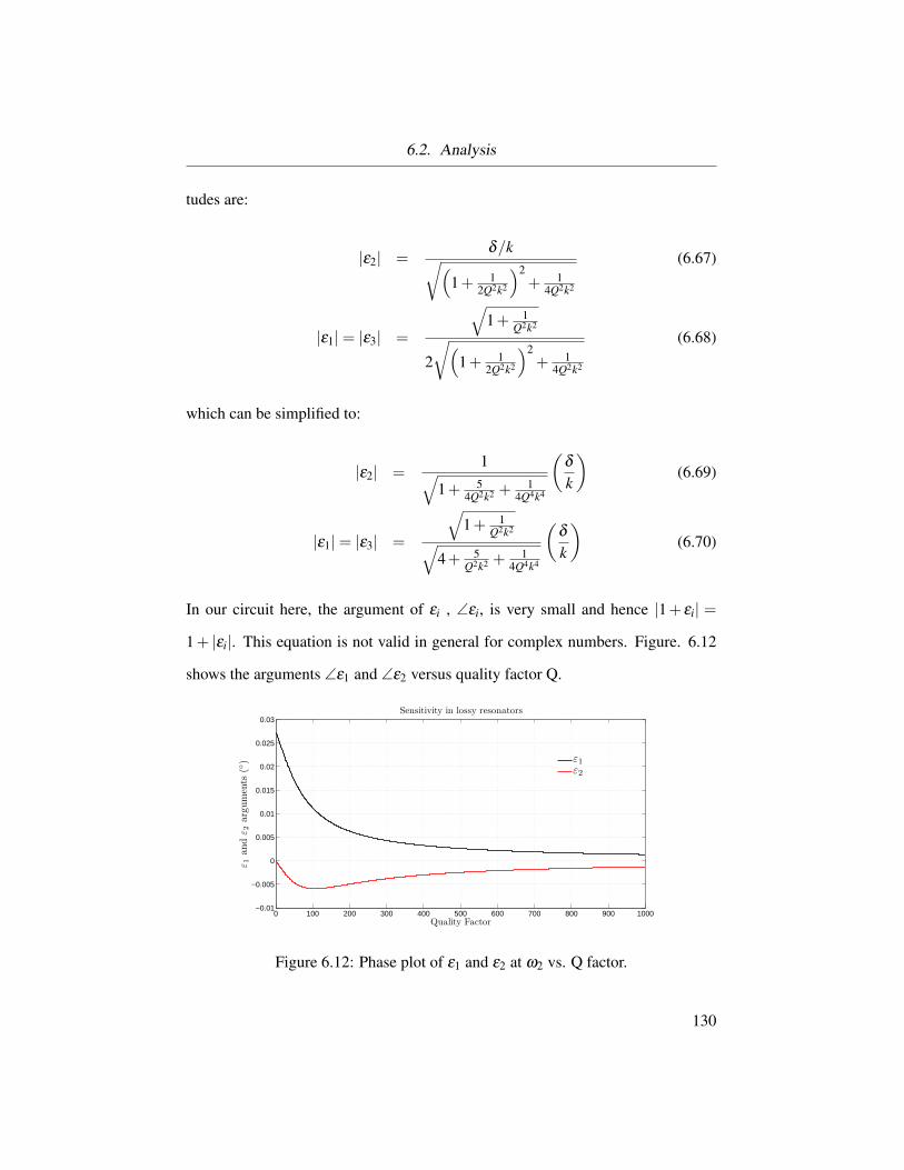
6.2. Analysis
tudes are:
|ε2| =δ/k√(
1+ 12Q2k2
)2+ 1
4Q2k2
(6.67)
|ε1|= |ε3| =
√1+ 1
Q2k2
2
√(1+ 1
2Q2k2
)2+ 1
4Q2k2
(6.68)
which can be simplified to:
|ε2| =1√
1+ 54Q2k2 +
14Q4k4
(δ
k
)(6.69)
|ε1|= |ε3| =
√1+ 1
Q2k2√4+ 5
Q2k2 +1
4Q4k4
(δ
k
)(6.70)
In our circuit here, the argument of εi , ∠εi, is very small and hence |1+ εi| =
1+ |εi|. This equation is not valid in general for complex numbers. Figure. 6.12
shows the arguments ∠ε1 and ∠ε2 versus quality factor Q.
0 100 200 300 400 500 600 700 800 900 1000−0.01
−0.005
0
0.005
0.01
0.015
0.02
0.025
0.03
Quality Factor
ε 1andε 2
arguments
()
Sensitivity in lossy resonators
ε1ε2
Figure 6.12: Phase plot of ε1 and ε2 at ω2 vs. Q factor.
130

6.2. Analysis
As it is graphed, the arguments are even less than 1 over the range shown for
Q.
In summary, when the circuit is excited in common mode, in the presence of
differential perturbation on C1 and C3 , the loop currents will change slightly to the
below values:
I1 =Vc
R(1+ |ε1|) (6.71)
I2 = −Vc
R|ε2| (6.72)
I3 = −Vc
R(1−|ε1|) (6.73)
where εis are
|ε2| = A(
δ
k
)(6.74)
|ε1|= |ε3| = B(
δ
k
)(6.75)
and coefficients A and B are functions of quality factor Q.
A =1√
1+ 54Q2k2 +
14Q4k4
(6.76)
B =
√1+ 1
Q2k2√4+ 5
Q2k2 +1
4Q4k4
(6.77)
The plot of A and B versus Q, Fig. 6.13, shows changes in A and B dependency to
Q. the higher the Q, the higher the sensitivity i.e. the effect of δ/k is translated to
131

6.3. Circuit Simulations
the loop current amplitudes with a higher coefficient.
0 100 200 300 400 500 600 700 800 900 10000
0.1
0.2
0.3
0.4
0.5
0.6
0.7
0.8
0.9
1
Quality Factor
Coeffi
cients
Aan
dB
Effect of loss on sensitivity
AB
Figure 6.13: Magnitude plot of ε1 and ε2 at ω2 vs. Q factor.
This plot suggest two approaches. If we have high enough quality factors, the
same input perturbation δ will reflect into an output perturbation ε2 magnitude
larger than ε1 and ε3 current perturbations. For lower quality factors, nevertheless,
ε2 has a higher sensitivity to variations in the quality factors. In such cases, moni-
toring I1 and I3 seems to be a better solution. If the operating conditions guarantee
a stable Q factor, ε2 magnitude is larger than ε1 and ε3, and monitoring I2 results
into a higher sensitivity.
6.3 Circuit Simulations
6.3.1 Single-Sided Excitation, Differential Perturbation Case
In the following simulations it is assumed that the resonators are identical; per-
turbation is differential and occurs on C1 and C3, while the circuit is excited from
132

6.3. Circuit Simulations
one end by the harmonic voltage source Vs (single-sided excitation with differential
perturbation) i.e.
C1 =C+∆C, C2 =C, C3 =C−∆C, CC1 =CC2 =Cc,
R1 = R2 = R3 = R, ,and L1 = L2 = L3 = L,
where k = CCC 1 and δ = ∆C
C 1 are conditions for weak coupling and small
perturbations respectively.
A SPICEr simulation of the circuit is done using Multisimr12 for Fig. 6.2
and the loci of the normal modes are plotted in Fig. 6.14. The values R = 100mΩ,
L = 10mH, C = 100nF, CC = 15µF are used in the simulation.
-0.050 -0.025 0.000 0.025 0.0504900
4950
5000
5050
5100
5150
5200
Nat
ural
freq
uenc
ies
(Hz)
δ
f1 f2 f3
Figure 6.14: Three WCR veering from SPICE simulation.
133

6.3. Circuit Simulations
Based on the data collected from the simulations, the following relative shift
functions are also calculated and then graphed vs. perturbation changes. the slope
of the graph represents the sensitivity.
Sω1 =ω1−ω10
ω10, Sω2 =
ω2−ω20
ω20, Sω3 =
ω3−ω30
ω30, (6.78)
Sφ1 =
∣∣∣∣φ1−φ10
φ10
∣∣∣∣ , Sφ2 =
∣∣∣∣φ2−φ20
φ20
∣∣∣∣ , Sφ3 =
∣∣∣∣φ3−φ30
φ30
∣∣∣∣ , (6.79)
where φ j0 and φi ( j = 1,2,3) are the vectors with normalized loop currents
magnitudes as the vector components for the ith normal mode without perturbation
and with perturbation, respectively, e.g. φ1 = [I1 I2 I3] for mode 1 where I1 and
I2 and I3 are normalized magnitudes of the loop currents at 1st normal mode. Sφ i
is the relative shift in φi due to the perturbation δ .
-0.0050 -0.0025 0.0000 0.0025 0.0050
-0.1
0.0
0.1
0.2
0.3
0.4
Rel
ativ
e se
nsiti
vity
δ
100x|∆f / f0|
|Φ - Φ0| / |Φ0|
Figure 6.15: Three WCR, relative sensitivities, mode 1 excitation.
134

6.3. Circuit Simulations
These two relative shift functions, Sωi and Sφ i are plotted in Fig. 6.15 to Fig.
6.16 for all three modes of the circuit with the component values stated above.
-0.0050 -0.0025 0.0000 0.0025 0.0050
0.0
0.1
0.2
0.3
0.4
0.5
Rel
ativ
e se
nsiti
vity
δ
100x|∆f / f0|
|Φ - Φ0| / |Φ0|
Figure 6.16: Three WCR, relative sensitivities, mode 2 excitation.
-0.0050 -0.0025 0.0000 0.0025 0.0050
0.00
0.05
0.10
0.15
0.20
0.25
Rel
ativ
e se
nsiti
vity
δ
100x|∆f / f0|
|Φ - Φ0| / |Φ0|
Figure 6.17: Three WCR, relative sensitivities, mode 3 excitation.
In these figures the Sωi curves are magnified by a factor of 100 to be better
comparable with Sφ i curves. This eigenmode sensitivities are similar, in magni-
135

6.3. Circuit Simulations
tudes, to 2DOF WCR configuration. The advantage is, nevertheless, the invariance
of the resonant frequencies on the differential perturbation magnitude, simplifying
the readout circuit.
We choose the 2nd normal mode as excitation frequency of our system and
keep it fixed regardless of the perturbation value (δ ). The circuit was simulated
and the values for Sφ2 were calculated and then plotted in Fig. 6.18.
δ (%) i1(mA) i2(mA) i3(mA) I1 I2 I3 |φ2−φ02|/|φ02|-0.05 531.041 42.5 493.95 0.73096 0.05850 0.67991 0.04379-0.025 516.56 29.18 497.83 0.719455 0.0406 0.69336 0.0197
0 498.98 23.8 498.93 0.70674 0.03371 0.70667 00.025 479.22 31.21 497.83 0.69281 0.04512 0.71971 0.022240.05 456.96 45.27 493.95 0.67756 0.06712 0.7324 0.05129
Table 6.1: Measured values at fixed excitation frequency (mode 2).
-0.050 -0.025 0.000 0.025 0.050
0.00
0.02
0.04
0.06 |φ2-φ02| / |φ02|
Rel
ativ
e sh
ift in
mod
e sh
ape
δ (%)
Figure 6.18: Three WCR, relative shift in normalized loop current vector under fixexcitation at 2nd mode.
136

6.3. Circuit Simulations
These simulation results show that, keeping the excitation frequency at unper-
turbed resonant frequency gives almost the same results (slope) as if the excitation
frequency tracks and locks to the exact resonant frequency
6.3.2 Differential Excitation, Differential Perturbation Case
A simulation based on a differential excitation and differential perturbations on
capacitors C1 and C3 is done. Two out of phase harmonic inputs excite the circuit
from both ends as shown in Fig. 6.5.
The results show that only mode 1 and mode 3 appear in this system. At mode
2 excitation all the loop currents are almost zero. The results are shown in Table
6.2 and 6.3.
δ (%) i1(mA) i2(mA) i3(mA) I1 I2 I3 |φ2−φ02|/|φ02|-0.1 563.07 655.12 757.71 0.4900 0.5701 0.6594 0.12005-0.05 615.58 663.53 714.7 0.5338 0.5753 0.6197 0.06081
0 666.8 666.48 666.79 0.5774 0.5771 0.5774 00.05 714.72 663.64 615.56 0.6197 0.5754 0.5337 0.060820.1 757.78 655.33 563.02 0.6594 0.5702 0.4899 0.12009
Table 6.2: Simulation results for differential excitation at first mode.
δ (%) i1(mA) i2(mA) i3(mA) I1 I2 I3 |φ2−φ02|/|φ02|-0.1 359.94 665.55 309.86 0.4402 0.8140 0.3790 0.0434-0.05 346.61 665.83 321.6 0.4244 0.8153 0.3938 0.0217
0 333.81 665.91 333.84 0.4089 0.8158 0.4090 00.05 321.6 665.78 346.61 0.3938 0.8153 0.4245 0.02160.1 309.86 665.55 359.94 0.3790 0.8140 0.4402 0.0433
Table 6.3: Simulation results for differential excitation at third mode.
The results show a relative sensitivity of almost 150 ( 1k ) and 50 ( 1
2k ) for mode
1 and mode 3, respectively.
137

6.3. Circuit Simulations
6.3.3 Common-Mode Excitation, Differential Perturbation Case
Another simulation based on common mode excitation and differential perturba-
tion on C1 and C3 is done, as shown in Fig. 6.6. In this case, system only responds
to excitation mode 2. Loop currents for mode 1 and mode 3 are almost zero. the
results are shown in Table 6.4.
δ (%) i1(mA) i2(mA) i3(mA) I1 I2 I3 |φ2−φ02|/|φ02|-0.1 1056.1 146.6 911.4 0.7529 0.1045 0.6498 0.1277-0.05 1032.9 74.5 958.7 0.7319 0.0528 0.6793 0.0646
0 1000.0 0.0 1000.0 0.7071 0 0.7071 00.05 958.8 74.6 1032.9 0.6794 0.0529 0.7319 0.06460.1 911.4 146.6 1056.1 0.6498 0.1045 0.7529 0.1277
Table 6.4: Simulation results; common mode excitation at 2nd mode.
These results show a relative sensitivity of about 127 for mode 2 with common
mode excitation. This complies with the sensitivity of the mode shape calculated
in (6.66). The analytical value for the relative sensitivity would be:
Sφ2 =
∣∣∣∣φ2−φ20
φ20
∣∣∣∣=√
ε21 + ε2
2 + ε23√
1+0+1=
√3
2δ
k≈ 129.9δ (6.80)
Repeating all these simulations for resonator series resistances of 1mΩ (Q =
ω2LR ≈300,000) and 100mΩ (Q≈3,000) shows that the sensitivity is robust to Q
variations as predicted by theoretical analysis. There is a trade off between the
quality factor Q, coupling strength k, and the desired dynamic range of measured
δ . The higher the quality factor and the weaker the coupling strength are, the lower
the measurable δ range will be. Fig. 6.19 illustrates the effect of different quality
factors on the dependence of the resonant frequency f2 (mode 2), on the differential
138

6.3. Circuit Simulations
perturbation magnitude.
5049.4 5049.6 5049.8 5050.0
0
20
40
60
i 1 (m
A)
frequency (Hz)
δ=−0.05% δ=−0.025% δ=0 δ=0.025% δ=0.05%
R = 1mΩ
(a) Q≈300,000 (R = 1 mΩ).
5046 5048 5050 5052 5054
0.1
0.2
0.3
0.4
0.5
0.6
i 1 (m
A)
frequency (Hz)
δ = −0.05% δ = −0.025% δ = 0 δ = 0.025% δ = 0.05%
R = 100 mΩ
(b) Q≈3,000 (R = 100 mΩ).
Figure 6.19: The effect of quality factor on f2- δ dependence.
139

6.3. Circuit Simulations
In the example above, with 1mΩ series resistance, the frequency response is
so sharp, that keeping the excitation frequency fixed for a perturbation range of
±0.05% does not work, Fig. 6.19a. The series resistances of the RLC resonators
are increased by a factor of 100 to 0.1Ω to get measurable values for currents over
the full range of δ , Fig. 6.19b. On the other hand, if the resistance is high ( Q is
low) the sensitivity will decrease. For high quality factors, as shown in Fig. 6.19a,
f2 will slightly vary with δ , possibly requiring a tracking feedback loop for the
proper common mode excitation if the dynamic range of δ is wide. This behavior
contrasts with the lower quality factor as shown in Fig. 6.19b, where f2 is practi-
cally insensitive to δ magnitude. Compared to the 2DOF WCR readout circuits, the
measurement setup is simplified not only because of a fixed excitation frequency
(no need of resonant frequency tracking), but also because the measurement of the
differential δ perturbation reduces to monitoring a single current (I2) amplitude.
Fig 6.20 shows I2 magnitude vs. δ .
Figure 6.20: I2 magnitude for mode 2, common mode excitation, differential per-turbation.
In this figure the vertical axis is normalized by dividing to Vc/R. The slope
140

6.3. Circuit Simulations
(sensitivity) compiles with the theory in (6.66). In this simulation Vc = 100 mV,
R = 100 mΩ, and coupling strength is k = 1/150.
Depending on the application, the amount of damping should be calculated
to fulfill both sensitivity and dynamic range trade-off. Moreover, as we have ob-
served in 2DOF WCRs, lower quality factors makes the detection of the resonant
frequencies difficult. This happens due to the fact that both amplitudes and the
resonant frequencies of the loop currents are affected by quality factors values. In
these cases, the coupling strength modifications might be helpful. The stronger
the coupling is, the farther the normal modes are pulled apart, hence the easier the
detection of their resonant frequencies becomes. This on the other hand, reduces
the relative sensitivity to the perturbation to be measured.
Another set of simulations shows the effect of Q on the sensitivity more clearly.
A parameter sweep on Q factor for differential perturbation with common mode
excitation (focused on mode 2) gave us the sensitivity results plotted in Fig. 6.21.
0.008
0.01
0.012
0.014
0.016
/ (V
s/R
)
Q>1000
Q=300
Q=150
0
0.002
0.004
0.006
0.008
-0.015 -0.01 -0.005 0 0.005 0.01 0.015
I 2/ (
δδδδ (%)
Q=60
Q=30
Figure 6.21: Effect of Q factor on the sensitivity (slope of normalized current I2);common mode excitation.
141

6.4. Summary
In this plot I2 is scaled in reference to the value of Vc/R.
As it can be seen, the lower Q the less sensitive the circuit is. The simulation
results plot of magnitude plot of ε2, shown as A, defined in (6.76), on vertical axis
in Fig. 6.22, is inline with analytical results estimated and plotted in Fig. 6.13.
0.8
1
1.2
0
0.2
0.4
0.6
1 10 100 1000 10000 100000 1000000
A
Quality factor (Q)
Figure 6.22: Effect of Q factor on the magnitude of ε2 (simulation).
6.4 Summary
In this chapter we explored the possibility and features of 3DOF WCRs in read-
out circuits. We showed that differential perturbation makes the overall circuitry
simpler, by eliminating the need for frequency tracking of the excitation voltage,
without sacrificing the relative sensitivity. We analytically showed that common
mode excitation at mode 2 resonant frequency simplifies the readout circuit, espe-
cially in the real scenarios with lossy elements. We have used perturbation theory
to obtain analytical estimates for eigenmode sensitivities to differential perturba-
tions. SPICE circuit simulations have validated the theoretical analysis. Practical
trade-offs between coupling strength, quality factor and desired perturbation range
142

6.4. Summary
to be measured have been discussed. In the following chapter, we discuss one of the
possible ways of improving circuit realization for WCRs based on active inductors.
143

Chapter 7
Active Inductors in WCRs
7.1 Introduction
This chapter examines the usage of active inductors (op-amp-based) for imple-
mentation of WCRs. The advantages and disadvantages of this method are also
examined.
The advantages are smaller size, with the possibility of die level integration of
WCR-based capacitance readout circuits.
The trend for the capacitive sensors is towards smaller physical dimensions,
and consequently lower capacitance values. In order to design coupled resonators
for smaller capacitance measurements and yet keep the resonant frequency low
enough to prevent ADC circuit complications, relatively large inductances are re-
quired. Although the circuit is simple, large value inductors are considerably bulky,
especially if a high quality factor is important (associated with a low DC series re-
sistance).
7.2 Real (Nonideal) Inductors
All real inductors have parasitic values causes their behavior deviates from their
ideal constitutive equations. There are different approaches to model a real induc-
144
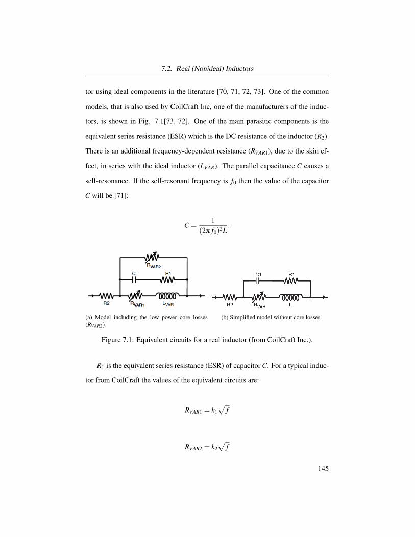
7.2. Real (Nonideal) Inductors
tor using ideal components in the literature [70, 71, 72, 73]. One of the common
models, that is also used by CoilCraft Inc, one of the manufacturers of the induc-
tors, is shown in Fig. 7.1[73, 72]. One of the main parasitic components is the
equivalent series resistance (ESR) which is the DC resistance of the inductor (R2).
There is an additional frequency-dependent resistance (RVAR1), due to the skin ef-
fect, in series with the ideal inductor (LVAR). The parallel capacitance C causes a
self-resonance. If the self-resonant frequency is f0 then the value of the capacitor
C will be [71]:
C =1
(2π f0)2L.
(a) Model including the low power core losses(RVAR2).
(b) Simplified model without core losses.
Figure 7.1: Equivalent circuits for a real inductor (from CoilCraft Inc.).
R1 is the equivalent series resistance (ESR) of capacitor C. For a typical induc-
tor from CoilCraft the values of the equivalent circuits are:
RVAR1 = k1√
f
RVAR2 = k2√
f
145

7.2. Real (Nonideal) Inductors
LVAR = k3− k4 log(k5 f )
where k1 to k5 are empirical coefficients measured by the manufacturer. As
an example for CoilCraft LPS4018-323 inductor with nominal value of L = k3 =
3.3uH these coefficients are:
k1 = 1.8x10⁻⁴, k2 = 0.792, k3 = 3.3, k4 = 0.083, k5 = 9.8x10⁻⁶.
In our WCR circuit implementation, we have tried many different inductors
and capacitors, to choose the ones with the least loss (or highest quality factors)
and closest mach. In almost all types of inductors there is a trade-off between in-
ductor loss, physical dimensions and inductance. In our case we wanted to push
the capacitance value of the resonator as low as possible, to be closer to the real
cases of capacitive sensors. On the other hand we had the bandwidth limitation of
the National Instruments data acquisition system; PXI-7854R analog interface of
PXIe-1062Q system has a sampling rate of 750kHz. For practical implementation
of the reconstruction filters, the sampling frequency should be more than theo-
ritical Nyquist frequency; practically 5 to 10 times the excitation (resonant) fre-
quency.To have enough samples in order to measure the peaks and zero-crossing
precise enough, sampling rate should be considerably lower, e.g. 5 to 10 times,
than the highest frequency of the signal. This limitation leads us to pick a reso-
nant frequencies below 10kHz. Unfortunately lower resonant frequencies require
inductors with larger inductance values, and if a low resistance (high quality fac-
tor) inductor is required the inductor will become bulky. To allow for a die level
integration of the WCR techniques, replacing physical coils with active inductors
is a promising solution. It even helps solving the circuit size issue, if we can use
146

7.3. Active Inductors
them in our WCR system as a replacement for the main inductors.
7.3 Active Inductors
Using active components in conjunction with passive RC circuits is a known so-
lution in electronics. The concept has been used in active filter circuits for a long
time [74, 75, 76, 77] . One of the use of these active components and RC circuits
is to implement so called active inductors [78]. Realization of active inductors can
be gyrator gyrators [79] or non-gyrator based .
In this section we would like to study the feasibility of using active inductors
in WCR-based readout circuit. We also try to keep the circuit as simple as possi-
ble as one of the main advantages of our method. A simple gyrator-based active
inductor implementation is shown in Fig. 7.2. The circuit is shown in Fig. 7.2(a)
its equivalent passive circuit is shown in Fig. Fig. 7.2(b).
¡
+
Rs
Rp
Cp
Vi
Cp
Rp Leq = RpRsCp
Rs
Vi
(a) (b)
Figure 7.2: An example of an active inductor, (a) schematic, (b) equivalent circuit.
The input impedance of the active circuit can be calculated easily assuming the
op-amp is ideal i.e. infinite input impedance and gain, and zero output impedance.
Since both input of the op-amp are at the same potential (and is equal to ICpRp):
147

7.3. Active Inductors
ICp
1sCp
= IRsRs. (7.1)
With a KVL from the input voltage Vi through Rs and considering the voltage
at the negative input of the op-amp is ICpRp:
Vi = IRsRs + ICpRp. (7.2)
By eliminating ICp from 7.1 and 7.2:
Vi = (1+ sRpCp)RsIRs , (7.3)
or
IRs =1
Rs (1+ sRpCp)Vi (7.4)
and
ICp =sCp
(1+ sRpCp)Vi. (7.5)
Knowing total input current is Ii = IRs + ICp , the input impedance Zincan be
written as:
Zin =Vi
Ii=
1+ sRpCp1Rs+ sCp
, (7.6)
Zin =Vi
Ii=
Rs + sRsRpCp
Rs + sRsCp. (7.7)
148

7.3. Active Inductors
or with a bit of rearrangement, it can be written as:
Zin =Vi
Ii=
(1
Rs + sRsRpCp+
1Rp +
1sCp
)−1
, (7.8)
which is direct representation of the equivalent circuit shown in Fig. 7.2(b)
with the equivalent inductor value of Leq = RsRpCp. As it can be seen, Rs appears
as a resistance in series with the inductor Leq and Rp and Cp, which are in series,
appear in parallel with Leq and Rs branch. This is very close to the real inductor
model discussed in the previous section.
One fundamental limitation in realization of an inductor using simple gyra-
tors (same as our case), is that the inductor has always a grounded terminal. In
our WCR circuit we need at least one of the inductors to be floating. There are
some solutions presented in the literature to make a floating inductor using two
interconnected gyrators. Usually the interconnection happens at the capacitance
connections. Fig. 7.3 shows such a floating active inductor circuit based on our
single-ended gyrator of Fig. 7.2.
¡
+
Rs
Rp
Cp
Vi1 Vi2
U2
R0
p
C 0
p
R0
s
U1Vo1 Vo2
Figure 7.3: Realization of a floating inductor using gyrators.
To simplify the analysis this circuit is rearranged as shown in Fig. 7.4. The
equations for the circuit are:
149

7.3. Active Inductors
Vi1−Vi2 = Rs (1+ sCpRp) IRs , ICp = sCpRsIRs
Vi2−Vi1 = R′s(1+ sC′pR′p
)I′Rs
, I′Cp= sC′pR′sI
′Rs
(7.9)
Assume R′s = Rs, C′p =Cp and C′s =Cs, then I′Rs=−IRs and I′Cp
= ICp , then:
IRs =1
Rs (1+ sCpRp)(Vi1−Vi2) , (7.10)
and
ICp =sCpRs
Rs (1+ sCpRp)(Vi1−Vi2) . (7.11)
¡
+
Rp
Cp
Vi1
Vi2
U1
U2
Vo1
Vo2
Rs
R0
p
C0
p
R0
s
Figure 7.4: Realization of a floating inductor using gyrators ,rearranged.
Eventually the differential input impedance of the circuit can be calculated as:
150
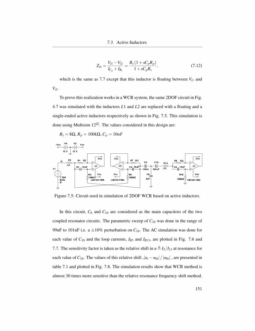
7.3. Active Inductors
Zin =Vi1−Vi2
ICp + IRs
=Rs (1+ sCpRp)
1+ sCpRs, (7.12)
which is the same as 7.7 except that this inductor is floating between Vi1 and
Vi2.
To prove this realization works in a WCR system, the same 2DOF circuit in Fig.
4.7 was simulated with the inductors L1 and L2 are replaced with a floating and a
single-ended active inductors respectively as shown in Fig. 7.5. This simulation is
done using Multisim 12r. The values considered in this design are:
Rs = 8Ω, Rp = 100kΩ, Cp = 10nF
U1
LMV2011MA
3
2
4
7
6
C1 10nF
R1 8Ω
R2
100kΩ
V1
1 Vpk
5kHz
0°
R3
.1Ω
V3
12 V
V4
12 V
Vcc
Vcc
Vcc Vcc
-Vcc
-Vcc
-Vcc -Vcc
U2
LMV2011MA
3
2
4
7
6
C5
10nF
R7 8Ω
R8
100kΩ
C6
100nF
U3
LMV2011MA
3
2
4
7
6
C4
10nF
R9 8Ω
R10
100kΩ
C8
2µF
C10
100nF
R13
.1Ω
Vi
Figure 7.5: Circuit used in simulation of 2DOF WCR based on active inductors.
In this circuit, C6 and C10 are considered as the main capacitors of the two
coupled resonator circuits. The parametric sweep of C10 was done in the range of
99nF to 101nF i.e. a ±10% perturbation on C10. The AC simulation was done for
each value of C10 and the loop currents, IR3 and IR13, are plotted in Fig. 7.6 and
7.7. The sensitivity factor is taken as the relative shift in u , I3/I13 at resonance for
each value of C10. The values of this relative shift ,|ui−u0i|/ |u0i| , are presented in
table 7.1 and plotted in Fig. 7.8. The simulation results show that WCR method is
almost 30 times more sensitive than the relative resonance frequency shift method.
151

7.3. Active Inductors
5000 5200 5400 5600 5800 6000 62000.00
0.01
0.02
0.03
0.04
0.05
0.06
0.07
0.08
0.09
Loop
cur
rent
s (m
A)
frequency (Hz)
IR3
IR13
Figure 7.6: Gyrator-based 2DOF WCR simulation at balance, loop currents fre-quency response.
5400 5600 58000.00
0.01
0.02
0.03
0.04
0.05
0.06
0.07
0.08
0.09
0.10
IR13
Loop
cur
rent
s (m
A)
frequency (Hz)
δ = -0.5%δ = -1%
δ = 0.5%δ = 1%
δ = 0
IR3
Figure 7.7: Gyrator-based 2DOF WCR simulation for different perturbations, loopcurrents frequency response.
152

7.4. Summary
C13 (nF) δ (%) i2(mA) i1(mA) i2(mA) |IR3/IR13| (u1−u01)/|u01|99 -1 5466.1 92.767 69.86 1.3279 0.07186
99.5 -0.5 5458.9 89.556 69.809 1.2829 0.03551100 0 5451.7 86.341 69.693 1.2389 0
100.5 0.5 5444.4 83.148 69.523 1.1960 -0.03463101 1 5437.2 79.997 69.303 1.1543 -0.06826
Table 7.1: Gyrator-based WCR simulation results (mode 1 excitation).
-1.0 -0.5 0.0 0.5 1.0-0.10
-0.05
0.00
0.05
0.10
(u-u0)/u0
10 x ∆f/f0
Rel
ativ
e se
nsiti
vity
δ (%)
Figure 7.8: Relative sensitivity of gyrator-based 2DOF WCR.
7.4 Summary
In this chapter we have introduced a typical model for real inductors, we have
explained the reason behind the need for large inductors for our WCRs, and we
have suggested one alternative based on active inductors. One of the main chal-
lenges related to the active inductors is the design of floating inductors. Our WCR
153

7.4. Summary
uses at least one floating inductor. This work offers a topology for realization
of floating inductors. A WCR circuit based on active inductors, one floating and
one grounded, is suggested and simulated. Simulation results are validating the
theory. The relative sensitivity comparison between frequency method and mode
shapes was presented and confirmed the higher sensitivity of the WCR method.
The following chapter summarizes the contributions, challenges and prospects of
this research.
154

Chapter 8
Conclusions and Further
Discussions
8.1 Research Contributions
The focus of this thesis was on applying innovative methods for capacitance read-
out circuits based on weakly-coupled-resonators, a technique applied in the elec-
trical domain for the first time. Other than the novelty of this method in electrical
domain, WCR-based capacitance readout circuits provide higher sensitivity (theo-
retically three orders of magnitude) over the method based on resonant frequency
shift method which is one of the state-of-the-art methods.
Capacitive sensors are one of the most popular sensors in various industries and
applications. Higher sensitivity capacitance readout circuits are of high interest in
recent years since MEMS capacitive sensors, with smaller capacitance changes,
have become common in the industry. This demand for high sensitivity and more
reliable readout circuits was the main motivations for the present work. The re-
search started with a literature survey of state-of-the art readout circuits in chapter
(2). Some of these circuits were simulated along the path of this project and pre-
sented in more detail in Appendix (A). One of the readout circuits, which is based
155
8.1. Research Contributions
on capacitance-to-voltage conversion was made with discrete component at PCB
level and used experimentally in another project conducted by Dr. Elie Sarraf [80].
The application of 2DOF WCRs has been proposed in chapter (3), accompanied
by a theoretical analysis and proof for its higher sensitivity, followed by validat-
ing simulations and experimental measurements presented in chapter (4). Tracking
and exciting the the resonance frequency accurately is essential to the success of
the 2DOF-WCR method. It is paramount that the resonant frequency is locked by
the excitation source with a high degree of precision. The accuracy of the reso-
nant frequency manifests itself in the sharpness of the resonant frequency peaks.
If circuit losses are present, the sharpness of the resonant frequency peaks is sig-
nificantly reduced, to the effect that no distinct peaks would be distinguishable if
losses are higher than a certain threshold. This of course adversely affects the reso-
nance detection in experiments. Moreover, the high sensitivity achievable in theory
(orders of magnitude better than the CFC method), will be significantly reduced as
shown in chapter 4.
Along the way, we have found an improved, hybrid method, combining fre-
quency shifting and energy localization measurements, as proposed in chapter 5.
This technique is more robust, higher insensitivity to the excitation frequency devi-
ations. In another step further, analytical and simulations studies of readout circuit
based on 3DOF-WCR have been presented in chapter 6. It has been proven that,
similar to the mechanical and MEMS domains, the 3DOF-WCR method can be
used to measure differential perturbations and has the advantages an invariant res-
onant frequency over a certain range of perturbations. This is helpful in simplifying
the circuit even more by eliminating the frequency tracking (e.g. PLL). This also
makes it inherently insensitive to errors in excitation frequency. Another unique
156

8.1. Research Contributions
behavior of 2DOF WCR circuits, under differential perturbation, is that only nat-
ural mode 2 or modes 1 & 3 gets stimulated if they excited by common mode or
differential source, respectively. This behavior becomes very helpful is real (lossy)
systems, where the low quality factor impacts the frequency response by pushing
the resonant peaks toward each other and overlapping them to a point that the cur-
rent peaks are not happening at any of the exact resonant frequencies. We have
proven that common mode excitation is insensitive to these impact of low quality
factor for differential perturbations.
One of the challenges of these WCRs, for relatively low resonant frequencies,
is the bulkiness of the inductors. We have presented the use of active inductors (e.g.
gyrator-based inductors) as an alternative way to reduce the circuit size and possi-
bly implementing the entire readout circuit in as a single integrated circuit. This
eliminates the need for physical inductors, as they are replaced by circuits based
on resistors, capacitors and op-amps which are much easier to be implemented in
integrated circuits. This was shown analytically in chapter 7 along with the related
simulations.
Another advantage of readout circuits based on WCRs is insensitivity to the
changes in the ambient conditions, e.g. temperature and relative humidity, due to
the circuit symmetry. They also require simpler analog circuit. On the other, fully
tuning and matching all resonators is a challenge which is needed to get a good
result from WCR based circuits. There is also a limitation on the bandwidth of the
perturbation relative to the resonant frequency since the perturbation assumed to
be quasi-static throughout this work. Another limitation of 2DOF WCRs, which is
eliminated in 3DOF WCR with differential perturbation, is the need for frequency
tracking system that adds to the system complexity.
157

8.2. Prospects and Open Problems
8.2 Prospects and Open Problems
Since the WCR-based readout circuits are being introduced in electrical domain
for the first time, there are several directions for expanding this research, some of
them being outlined below.
The circuit excitation can be done in different ways or with different wave-
forms. Several questions remain: are there more efficient ways of excitation?
Is differential excitation a good choice for differential capacitive sensors? Does
square wave excitation, binary level, have any advantage over sine wave excita-
tion? These questions are valid for both 2DOF and 3DOF WCR cases.
Another topic for research is to evaluate the effects of higher rate of capac-
itance changes on the circuit. There was a fundamental assumption throughout
this research, in accordance with the other researches related to mode localiza-
tion phenomena, namely the assumption of perturbations being quasi-static. This
assumption simplifies the analyses and simulations. Now that the basics of the
WCR-based readout circuit have been proven, there will be a good research topic
to study the bandwidth of the perturbation δ , or ∆C. This research and all the other
related literature considered quasi-static perturbation. There is an open question if
we go towards dynamic perturbation since it enters into nonlinear analysis due to
the fact that both capacitance and excitation signal are changing in time.
On the application of active inductors, there is still a lot of potential for new
research. Other types of active inductors could be designed, simulated and experi-
mentally tested.
There is a challenge about the inductor size and bulkiness, since the frequency
has to stay relatively low (limitation of an ordinary data acquisition system) while
158

8.2. Prospects and Open Problems
the sensor capacitance is low too. Finding solutions for this problem is another
topic for future work. One solution that we have thought about is to use an en-
velope detector before the data acquisition system. Knowing that in WCR-based
methods, the voltages and/or currents are more important than the instantaneous
signal, an envelope detection technique could be helpful to obtain the magnitudes.
The frequency of this envelope is equal to the rate of the capacitance changes,
which is much lower rate of change than the excitation (resonant) frequency. This
allows the use of smaller inductors.
Applying active inductors or methods like envelope detection explained above
or even combination of those could be another research topic. Considering new
technologies which allow MEMS device and CMOS circuitry on the same die is
very promising in pushing this idea even further to implement a single-chip WCR
based capacitive MEMS sensor and associated readout circuit.
There is also another potential to study a variation of WCR based capacitance
readout that keeps the system always at the balance (non-localized) by adding cali-
brated capacitors from a capacitor bank and adding them to the reference capacitor.
This should result in much larger dynamic range of perturbation.
The last point that we want to mention here is that all these WCR based meth-
ods and their variations can be used towards measuring small inductance too.
159

Bibliography
[1] BBCResearch. Global Markets and Technologies for Sensors. Market Re-
search IAS006F, BCC Research, July 2014.
[2] John G. Webster Ramon Pallas-Areny. Sensors and signal conditioning. John
Wiley & Sons Inc., second edition, 2000.
[3] DVS Murty. Transducers and Instrumentation. PHI Learning Pvt. Ltd., sec-
ond edition, 2010.
[4] L.K. Baxter and IEEE Industrial Electronics Society. Capacitive Sensors:
Design and Applications. IEEE Press series on electronics technology. IEEE
Press, 1997.
[5] IEEE. IEEE Standard for a Smart Transducer Interface for Sensors and Ac-
tuators - Mixed-Mode Communication Protocols and Transducer Electronic
Data Sheet (TEDS) Formats. IEEE Std 1451.4-2004, pages 1–430, 2004.
[6] P. W. Anderson. Local moments and localized states. Reviews of Modern
Physics, 50(2):191–201, 1978.
[7] P. W. Anderson. Absence of Diffusion In Certain Random Lattices. Physical
Review, 109(5):1492–1505, 1958.
160

Bibliography
[8] C. Pierre. Mode localization and eigenvalue loci veering phenomena in dis-
ordered structures. Journal of Sound and Vibration, 126(3):485–502, 1988.
[9] Matthew Spletzer, Arvind Raman, Alexander Q. Wu, Xianfan Xu, and
R. Reifenberger. Ultrasensitive mass sensing using mode localization in cou-
pled microcantilevers. Applied Physics Letters, 88(25):254102–254102–3,
2006.
[10] P. Thiruvenkatanathan, J. Yan, J. Woodhouse, A. Aziz, and A.A. Seshia. Ef-
fects of mechanical and electrical coupling on the parametric sensitivity of
mode localized sensors. In Ultrasonics Symposium (IUS), 2009 IEEE Inter-
national, pages 1183–1186, 2009.
[11] P. Thiruvenkatanathan, Jize Yan, J. Woodhouse, and A.A. Seshia. Enhancing
Parametric Sensitivity in Electrically Coupled MEMS Resonators. Journal of
Microelectromechanical Systems, 18(5):1077–1086, 2009.
[12] P. Thiruvenkatanathan, J. Yan, and A.A. Seshia. Ultrasensitive mode-
localized micromechanical electrometer. In Frequency Control Symposium
(FCS), 2010 IEEE International, pages 91–96, 2010.
[13] P. Thiruvenkatanathan, J. Woodhouse, Jize Yan, and A.A. Seshia. Manip-
ulating Vibration Energy Confinement in Electrically Coupled Microelec-
tromechanical Resonator Arrays. Journal of Microelectromechanical Sys-
tems, 20(1):157–164, 2011.
[14] M Manav, G Reynen, M Sharma, E Cretu, and A S Phani. Ultrasensitive reso-
nant MEMS transducers with tuneable coupling. Journal of Micromechanics
and Microengineering, 24(5):055005, 2014.
161

Bibliography
[15] Matthew Spletzer, Arvind Raman, Hartono Sumali, and John P. Sullivan.
Highly sensitive mass detection and identification using vibration localiza-
tion in coupled microcantilever arrays. Applied Physics Letters, 92(11):–,
2008.
[16] http://www.colibrys.com/. accessed: 2014-02-05.
[17] Min-hang Bao. Micro Mechanical Transducers: Pressure Sensors, Ac-
celerometers and Gyroscopes. Elsevier, 2000.
[18] Elie H. Sarraf. Design, modelling, self-testing and self-calibration of MEMS
accelerometers with adaptive and non-linear digital control. PhD thesis, Uni-
versity of British Columbia, Aug 2013.
[19] Babak Vakili Amini and Farrokh Ayazi. A 2.5-V 14-bit Σ-∆ CMOS SOI ca-
pacitive accelerometer. Solid-State Circuits, IEEE Journal of, 39(12):2467–
2476, 2004.
[20] Shao Lichun, Moorthi Palaniapan, and Tan Woei Wan. A continuous-time ca-
pacitance to voltage converter for microcapacitive pressure sensors. Journal
of Physics: Conference Series, 34:1014–1019, 2006.
[21] J.C. Lotters, W. Olthuis, P.H. Veltink, and P. Bergveld. A sensitive differential
capacitance to voltage converter for sensor applications. IEEE Transactions
on Instrumentation and Measurement, 48(1):89–96, 1999.
[22] Jiangfeng Wu, G.K. Fedder, and L.R. Carley. A low-noise low-offset
chopper-stabilized capacitive-readout amplifier for CMOS MEMS ac-
celerometers. In Solid-State Circuits Conference, 2002. Digest of Technical
162

Bibliography
Papers. ISSCC. 2002 IEEE International, volume 1, pages 428–478 vol.1,
2002.
[23] W.-C. Heerens. Application of capacitance techniques in sensor design. Jour-
nal of Physics E: Scientific Instruments, 19(11):–, 1986.
[24] K. Mochizuki, K. Watanabe, and T. Masuda. A high-accuracy high-speed
signal processing circuit of differential-capacitance transducers. Instrumen-
tation and Measurement, IEEE Transactions on, 47(5):1244–1247, Oct 1998.
[25] F.N. Toth and G.C.M. Meijer. A low-cost, smart capacitive position sensor.
Journal of Microelectromechanical Systems, 41(6):1041–1044, 1992.
[26] Z. Ignjatovic and M.F. Bocko. An interface circuit for measuring capaci-
tance changes based upon capacitance-to-duty cycle (CDC) converter. IEEE
Sensors Journal, 5(3):403–410, 2005.
[27] K. Mochizuki, K. Watanabe, T. Masuda, and M. Katsura. A relaxation-
oscillator-based interface for high-accuracy ratiometric signal processing of
differential-capacitance transducers. IEEE Transactions on Instrumentation
and Measurement, 47(1):11–15, 1998.
[28] Peter O’Shea. Phase Measurement. CRC Press, 1999.
[29] N.B. Yusof, N. Soin, and S.Z.M. Dawal. Capacitive interfacing for MEMS
humidity and accelerometer sensors. In Technical Postgraduates (TECH-
POS), 2009 International Conference for, pages 1–5, Dec 2009.
[30] F. Krummenacher. A High-Resolution Capacitance-to-Frequency Converter.
Solid-State Circuits, IEEE Journal of, 20(3):666–670, June 1985.
163

Bibliography
[31] H. Shibata, M. Ito, M. Asakura, and K. Watanabe. A digital hygrometer using
a capacitance-to-frequency converter. pages 100–, April 1995.
[32] S. Chatzandroulis and D. Tsoukalas. Capacitance to Frequency Converter
Suitable for Sensor Applications Using Telemetry. Analog Integrated Circuits
and Signal Processing, 27(1-2):31–38, 2001.
[33] Daheng Yin, Zunqiao Zhang, and Jianwen Li. A simple switched-capacitor-
based capacitance-to-frequency converter. Analog Integrated Circuits and
Signal Processing, 1(4):353–361, 1991.
[34] Cheng-Ta Chiang, Chi-Shen Wang, and Yu-Chung Huang. A CMOS Inte-
grated Capacitance-to-Frequency Converter with Digital Compensation Cir-
cuit Designed for Sensor Interface Applications. In Sensors, 2007 IEEE,
pages 954–957, Oct 2007.
[35] Cheng-Ta Chiang and Yu-Chung Huang. A Low-Cost CMOS Integrated
Sensor Transducer Implemented as a Capacitance-to-Frequency Converter
for Capacitive Measuring. In Instrumentation and Measurement Technology
Conference Proceedings, 2007. IMTC 2007. IEEE, pages 1–4, May 2007.
[36] Cheng-Ta Chiang, Chi-Shen Wang, and Yu-Chung Huang. A Mono-
lithic CMOS Autocompensated Sensor Transducer for Capacitive Measur-
ing Systems. Instrumentation and Measurement, IEEE Transactions on,
57(11):2472–2486, Nov 2008.
[37] R. Aragones, P. Alvarez, J. Oliver, and C. Ferrer. A capacitance-to-frequency
converters comparison for a frequency acquisition platform. In Sensors, 2010
IEEE, pages 1431–1436, Nov 2010.
164

Bibliography
[38] Muhammad Zubair Aslam and Tong Boon Tang. A High Resolution Capac-
itive Sensing System for the Measurement of Water Content in Crude Oil.
Sensors, 14(7):11351–11361, 2014.
[39] H. Lee, J.-K. Woo, and S. Kim. CMOS differential-capacitance-to-frequency
converter utilising repetitive charge integration and charge conservation.
Electronics Letters, 46(8):567–569, 2010.
[40] Dong-Yong Shin, Hyunjoong Lee, and Suhwan Kim. Improving the Accuracy
of Capacitance-to-Frequency Converter by Accumulating Residual Charges.
Instrumentation and Measurement, IEEE Transactions on, 60(12):3950–
3955, Dec 2011.
[41] W. Bracke, P. Merken, R. Puers, and C. Van Hoof. Ultra-Low-Power Interface
Chip for Autonomous Capacitive Sensor Systems. IEEE Transactions on
Circuits and Systems I: Regular Papers, 54(1):130–140, 2007.
[42] T. Islam, A. Gangopadhyay, and Z. Zaheeruddin. An oscillator based active
bridge circuit for converting capacitance change into frequency for capaci-
tive humidity sensor. In Communications, Devices and Intelligent Systems
(CODIS), 2012 International Conference on, pages 480–483, Dec 2012.
[43] Yucai Wang and V.P. Chodavarapu. Design of CMOS capacitance to fre-
quency converter for high-temperature MEMS sensors. In SENSORS, 2013
IEEE, pages 1–4, Nov 2013.
[44] Cenk Acar and Andrei Shkel. MEMS Vibratory Gyroscopes. Springer US,
Boston, MA, 2009.
165
Bibliography
[45] W.F. Lee and P.K. Chan. A Capacitive-Based Accelerometer IC Using
Injection-Nulling Switch Technique. IEEE Transactions on Circuits and Sys-
tems I: Regular Papers, 55(4):980–989, 2008.
[46] J.H.-L. Lu, M. Inerowicz, Sanghoon Joo, Jong-Kee Kwon, and Byunghoo
Jung. A Low-Power, Wide-Dynamic-Range Semi-Digital Universal Sen-
sor Readout Circuit Using Pulsewidth Modulation. Sensors Journal, IEEE,
11(5):1134–1144, May 2011.
[47] Ashkan Ashrafi and Hossein Golnabi. A high precision method for mea-
suring very small capacitance changes. Review of Scientific Instruments,
70(8):3483–3487, 1999.
[48] N. Yazdi, H. Kulah, and K. Najafi. Precision readout circuits for capacitive
microaccelerometers. In Proceedings of IEEE Sensors, 2004, pages 28–31
vol.1, 2004.
[49] R. Aragones, P. Alvarez, J. Oliver, and C. Ferrer. Comparison of readout
circuitry techniques for data acquisition in raw sensor systems. In IECON
2010 - 36th Annual Conference on IEEE Industrial Electronics Society, pages
1252–1257, Nov 2010.
[50] R.F. Wolffenbuttel and Paul P L Regtien. Capacitance-to-phase angle conver-
sion for the detection of extremely small capacities. IEEE Transactions on
Instrumentation and Measurement, IM-36(4):868–872, 1987.
[51] M.R. Haider, M.R. Mahfouz, S.K. Islam, S.A Eliza, W. Qu, and E. Pritchard.
A low-power capacitance measurement circuit with high resolution and high
166
Bibliography
degree of linearity. In 51st Midwest Symposium on Circuits and Systems,
2008. MWSCAS 2008, pages 261–264, 2008.
[52] Irvine Sensors. MS3110 Universal Capacitive ReadoutTM IC.
[53] Solidus. CF100, Capacitance to Frequency ASIC, 2014.
[54] Mohamed Gad-el Hak. The MEMS handbook. CRC press, 2001.
[55] PS Nair and S Durvasula. Vibration of generally orthotropic skew plates. The
Journal of the Acoustical Society of America, 55(5):998–1002, 1974.
[56] NC Perkins and CD Mote. Three-dimensional vibration of travelling elastic
cables. Journal of Sound and Vibration, 114(2):325–340, 1987.
[57] PS Nair and S Durvasula. Vibration of skew plates. Journal of Sound and
Vibration, 26(1):1–19, 1973.
[58] Christophe Pierre and Philip D Cha. Strong mode localization in nearly peri-
odic disordered structures. AIAA journal, 27(2):227–241, 1989.
[59] Pei-Tai Chen and JH Ginsberg. On the relationship between veering of eigen-
value loci and parameter sensitivity of eigenfunctions. Journal of Vibration
and Acoustics, 114(2):141–148, 1992.
[60] Xinzhong Chen and Ahsan Kareem. On the veering of eigenvalue loci and
the physics of coupled flutter of bridges. In Proc 5th Asia-Pacific Conference
on Wind Engineering, Kyoto, Japan, pages 461–4, 2001.
[61] CH Hodges. Confinement of vibration by structural irregularity. Journal of
sound and vibration, 82(3):411–424, 1982.
167

Bibliography
[62] CH Hodges and J Woodhouse. Vibration isolation from irregularity in a
nearly periodic structure: theory and measurements. The Journal of the
Acoustical Society of America, 74(3):894–905, 1983.
[63] Xinzhong Chen and Ahsan Kareem. Curve veering of eigenvalue loci
of bridges with aeroelastic effects. Journal of engineering mechanics,
129(2):146–159, 2003.
[64] D. E. Newland. Calculation of power flow between coupled oscillators. Jour-
nal of Sound and Vibration, 3(3):262–276, 1966.
[65] Siamak Hafizi-Moori and Edmond Cretu. Weakly-Coupled Resonators in
Capacitive Readout Circuits. Circuits and Systems I: Regular Papers, IEEE
Transactions on, 62(2):337–346, 2015.
[66] Martin O’Hara. Modelling Non-Ideal Inductors in SPICE. Technical report,
Newport Components, Milton Keynes, 1994.
[67] C. Gokcek. Tracking the resonance frequency of a series RLC circuit using
a phase locked loop. In Control Applications, 2003. CCA 2003. Proceedings
of 2003 IEEE Conference on, volume 1, pages 609–613 vol.1, June 2003.
[68] Gregory Peter Reynen. Leveraging eigenvalue veering for improved sensing
with microelectromechanical systems. Master’s thesis, University of British
Columbia, Jul 2012.
[69] Manav. Vibration mode localization in coupled microelectromechanical res-
onators. Master’s thesis, University of British Columbia, Oct 2014.
168

Bibliography
[70] Jayanthi Suryanarayanan. Design and Fabrication of Toroidal Inductors for
Mixed Signal Packaging. PhD thesis, North Carolina State University, 2002.
[71] Martin O’Hara. Modelling non-ideal inductors in SPICE. Newport Compo-
nents, Milton Keynes, 1994.
[72] Coilcraft. S-parameters and SPICE models. Technical report, Coilcraft.
[73] Coilcraft. Using Coilcraft’s Advanced Models in LTSpice. Technical report,
Coilcraft.
[74] Wai-Kai Chen. The circuits and filters handbook. CRC Press, 2002.
[75] Hercules G Dimopoulos. Analog electronic filters: theory, design and syn-
thesis. Springer Science & Business Media, 2011.
[76] Theodore Deliyannis, Yichuang Sun, and J Kel Fidler. Continuous-time ac-
tive filter design. Crc Press, 1998.
[77] Fei Yuan. CMOS active inductors and transformers: principle, implementa-
tion, and applications. Springer Science & Business Media, 2008.
[78] Fei Yuan. CMOS Active Inductors and Transformers: Principle, Implemen-
tation, and Applications. Springer Publishing Company, Incorporated, 1st
edition, 2010.
[79] Timothy Wade Bakken. Gyrator-based synthesis of active inductances and
their applications in radio -frequency integrated circuits. PhD thesis, Univer-
sity of Southern California, 2006.
169
Bibliography
[80] E.H. Sarraf, A. Sharkia, S. Moori, M. Sharma, and E. Cretu. High sensitivity
accelerometer operating on the border of stability with digital sliding mode
control. In SENSORS, 2013 IEEE, pages 1–4, Nov 2013.
[81] R.F. Wolffenbuttel, K.M. Mahmoud, and Paul P.L. Regtien. Compliant ca-
pacitive wrist sensor for use in industrial robots. Instrumentation and Mea-
surement, IEEE Transactions on, 39(6):991–997, Dec 1990.
170

Appendix A
Circuit Simulations and
Justification for Using CFC as the
Benchmark
A.1 Introduction
This chapter continues the discussion on the various methods for the readout cir-
cuits introduced in §2.3 with more detail. Detailed simulation (and one implemen-
tation) results for each of the readout circuits are presented.
A.2 CVC Simulation and Implementation Results
This section presents the circuit design and simulation results for the CVC readout
circuit. As is was mentioned before, there are various CVC readout circuits. The
one that we are simulating here is based on charge amplifier. This circuit was
implemented using discrete components and was used experimentally in a research
related to the closed loop readout circuits using sliding-mode control [80]. The
circuit schematic used for the simulation is shown in Fig. A.1 to A.3.
171

A.2. CVC Simulation and Implementation Results
N1 N2V_REF_1
VinCMN
CMN CMN
V_REF_2
GND GNDV_CTRL+1
V_CTRL-2
REF3
VCC1
VARICAP
V_CTRL+1
V_CTRL-2
REF3
VCC2
VARICAP
1E-12
C_REF_1Cap
GND
1E-12
C_REF_2Cap
GND
10K
R02Res2
V_BIASVSRC
GND
1nF
-10
C01
Cap
5NEG
5POS
OUT 1IN-2
IN+3
48 BUFFERA
OPAMP
1MEG
R01Res2
GND
COM1
NC2
GND3
V+4 VL 5IN 6V- 7NO 8S1
DG419L
5POS5NEG
GND 5POS 5POS
5NEGCLK
Figure A.1: CVC readout using charge integration, capacitor driving circuit.
172

A.2. CVC Simulation and Implementation Results
N1
N2
10pF
C02
Cap
10pF
C03
Cap
5POS
5POS
5NEG
10meg
R03
Res2
10meg
R04
Res2
V1P
V1N
OUT+4IN-
1
IN+8
63
OUT- 5Vocm2
U4
THS4131
GND
5NEG
V2P
V2N
5POS
GND100pF
C05
100pF
C06120pF
C07
120pF
C08
20pF
C09
20pF
C10
36K
R05
120K
R06
120K
R07
OUT1
IN-2
IN+3
48 U1A
OPAMP
OUT7
IN-6
IN+5
48
U1BOPAMP
500R11
500
R13
Res2
500R12
500
R14
GND
5NEG
5POS
o1OUT+ 4
IN-1
IN+8
63
OUT-5Vocm
2
U5
THS4131
5NEG
V3P
V3N
5POS
GND100pF
C11
120pF
C13
120pF
C14
20pF
C15
20pF
C16
24K
R08
220K
R09
220K
R10
16K
R15
GND
OUT1
IN-2
IN+3
48 U6A
TQWFMRAP 100pF
C17 COM1
NC2
GND3
V+4
VL5IN6V-7
NO 8S2
DG419L
o2
GND
5POS
5NEG
5POS
GND
CLK
100pF
C12
V2P
V2N
Figure A.2: CVC readout using charge integration, input stage differential ampli-fier, filtration and demodulation.
8.2K
R18
1nF
C19
3.9K
R17
1.5nF
C18
GND
1.8K
R20
1nF
C21
1.5K
R19
12nF
C20
GND
OUT
o2
5NEG5NEG
5POS5POS
5POS
5NEG
OUT 7IN-6
IN+5
48
BUFFERB
BQHKHMFW
1MEG
R16
GND
OUT 1IN-2
IN+3
48
U9A
EAVJCLHD
OUT7IN-6
IN+5
48
U9B
ARLUJRXR
1MEG
R21
GND
12
ANALOG
Header 2GND
Figure A.3: CVC readout using charge integration, output buffer and LP filter.
In Fig. A.1 there are two voltage-controlled capacitors used to simulate the
173

A.2. CVC Simulation and Implementation Results
behavior of a differential capacitive sensor. Two opposite phase voltage sources
are used to control these variable capacitors. The common node of the differential
capacitors, CMN node, is excited by a 1MHz square pulse train with a DC bias.
This DC bias is needed in case of using a sensor such as a MEMS capacitive ac-
celerometer to bias the circuit connected to proof-mass [80]. The signal injected
to common node passes through the differential capacitors and gets amplified by
an op-amp based differential amplifier followed by two stages of second-order
multiple-feedback (MFB) high-pass filters. The modulation with 1MHz carrier
makes the effect of 1/f noise negligible by pushing the information signal away
from 1/f noise frequency region before amplification. The amplified differential
output translates to single-ended using an op-amp and then is demodulated by the
same 1MHz clock. After demodulation the signal goes through two low-pass fil-
ters. The final output will be an amplified voltage proportional to the differential
capacitance changes. The input and output of the circuit are plotted in Fig. A.4 and
simulation results for the middle stages are shown in Fig A.5.
0.000u 100.0u 200.0u 300.0u 400.0u 500.0uTime (Sec)
Out
put (
V)
-1.000
-0.750
-0.500
-0.250
0.000
0.250
0.500
0.750
1.000
1.250
1.500
Del
ta_C
(pF
)
-200.0m
-150.0m
-100.0m
-50.00m
0.000m
50.00m
100.0m
150.0m
200.0m
250.0m
300.0m OutputDelta_C
Figure A.4: CVC based on differential charge amplifier, capacitance changes andoutput voltage plots.
174

A.2. CVC Simulation and Implementation Results
0.000u 50.00u 100.0u 150.0u 200.0u 250.0u 300.0u 350.0u 400.0u 450.0u 500.0uTime (Sec)
Diff
eren
tial C
apac
itanc
e V
olta
ge
-50.00m
-40.00m
-30.00m
-20.00m
-10.00m
0.000m
10.000m
20.00m
30.00m
40.00m
50.00m (n1-n2)
(a) Differential capacitor output voltage.
0.000u 50.00u 100.0u 150.0u 200.0u 250.0u 300.0u 350.0u 400.0u 450.0u 500.0uTime (Sec)
Diff
. Cha
rge
Am
p. O
utpu
t (V
)
-400.0m
-300.0m
-200.0m
-100.0m
0.000m
100.0m
200.0m
300.0m
400.0m v1p-v1n
(b) Output of differential amplifier.
0.000u 50.00u 100.0u 150.0u 200.0u 250.0u 300.0u 350.0u 400.0u 450.0u 500.0uTime (Sec)
Firs
t Filt
er D
iff. O
utpu
t
-750.0m
-500.0m
-250.0m
0.000m
250.0m
500.0m
750.0m v2p-v2n
(c) First high-pass filter differential output.
0.000u 50.00u 100.0u 150.0u 200.0u 250.0u 300.0u 350.0u 400.0u 450.0u 500.0uTime (Sec)
2nd
Filt
er D
iff. O
utpu
t
-4.000
-3.000
-2.000
-1.000
0.000
1.000
2.000
3.000
4.000 v3p-v3n
(d) Second high-pass filter differential output.
0.000u 50.00u 100.0u 150.0u 200.0u 250.0u 300.0u 350.0u 400.0u 450.0u 500.0uTime (Sec)
Sin
gle-
ende
d M
odul
ated
and
Filt
erre
d O
utpu
tSig
nal (
V)
-4.000
-3.000
-2.000
-1.000
0.000
1.000
2.000
3.000
4.000 o1
(e) Output of differential to single-ended circuit prior to de-modulation.
0.000u 50.00u 100.0u 150.0u 200.0u 250.0u 300.0u 350.0u 400.0u 450.0u 500.0uTime (Sec)
Dem
odul
ated
Sig
nal (
V)
-3.000
-2.000
-1.000
0.000
1.000
2.000
3.000
4.000
5.000 o2
(f) Demodulated signal prior to low-pass filtration.
Figure A.5: CVC based on differential charge amplifier, intermediate nodes simu-lation waveforms
175
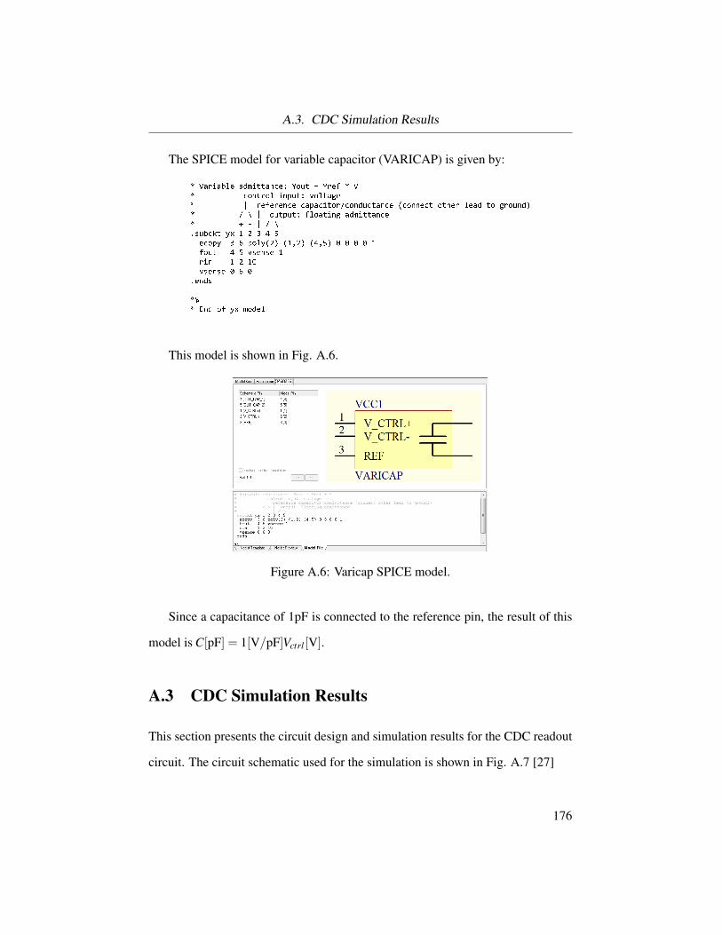
A.3. CDC Simulation Results
The SPICE model for variable capacitor (VARICAP) is given by:
!"#$ %
"&!
'(!"&
)*+,-./0
+.1+#-%#,2-%#/20%3333,
/0)),
,-,4
))313
)
5
6+
,
This model is shown in Fig. A.6.
Figure A.6: Varicap SPICE model.
Since a capacitance of 1pF is connected to the reference pin, the result of this
model is C[pF] = 1[V/pF]Vctrl[V].
A.3 CDC Simulation Results
This section presents the circuit design and simulation results for the CDC readout
circuit. The circuit schematic used for the simulation is shown in Fig. A.7 [27]
176

A.3. CDC Simulation Results
V0
B
A
C
C1
C2
V5
V3
Rt
R1
R2
D1 D2
V2
R3
A1 A2
A3
A4
V4
R4 R5
Figure A.7: Schematic representation of a CDC with the relaxation oscillator.
.
The differential capacitive sensor consist of is C1 = C0−∆C and C2 = C0 +
∆C. The duty cycle of output (V5) is linearly related to the differential capacitance
changes ∆C:
D =TH
TH +TL=
C2
C1 +C2=
12
(1+
∆CC0
),
where TL and TH are high and low time periods of output V5, respectively.
The SPICE simulation were done using the following parameters for the circuit,
and the results are shown in Fig XX.
R1 = R2 = R3 =1kΩ, Rt =125MΩ, R4 =5kΩ, R5 =20kΩ,
C0 =3pF, ∆C as a parameter varies between -0.45pF and 0.45pF.
177

A.3. CDC Simulation Results
∆C/C0 D-0.15 0.4258-0.1 0.4515
-0.05 0.47590 0.4993
0.05 0.52410.1 0.54730.15 0.5706
Table A.1: CDC circuit simulation data.
-0.2 -0.1 0.0 0.1 0.20.40
0.45
0.50
0.55
0.60
Dut
y C
ycle
C/C0
Figure A.8: Simulation graph for the CDC readout circuit.
178

A.4. CPC Simulation Results
CDC simulation
Time (s)0.0 3.0m500.0µ 2.5m1.0m 2.0m1.5m
Vol
tage
(V
)
-14
14
-9
9
-5
5
0
Figure A.9: Simulation results for the CDC readout circuit.
A.4 CPC Simulation Results
This section presents the circuit design and simulation results for the CPC readout
circuit. In CPC, the change in capacitance is translated into a change in the phase
shift of a sinusoid. Fig. A.10 presents the schematic of a CPC readout circuit [81].
It has two input voltages, Usin(ωt) as the main input and (U/a)sin(ωt +π − φ)
as compensating input. The main input goes through the sensor capacitance. The
value of the capacitance at rest (unperturbed) is C0 and the capacitance changes
(perturbation) subject to measure is ∆C. The compensating input goes through a
compensation capacitor CC. There are two conditions that are fundamental for this
circuit to appropriately function as shown in Fig. A.10. First, the ratio of the main
179

A.4. CPC Simulation Results
input voltage amplitude to the compensating input voltage amplitude should be
equal to the ratio of CCto C0, a ,CC/C0. Second, the condition ωRtCt 1 should
be met. The op-amp output voltage, Uo, was calculated to be:
U0 =−1Ct
√(∆C+
12
φ 2C0)2 +(φC0)2.Ucos(ωt−θ)
where
θ = arctan(
0.5φ 2C0 +∆CφC0
).
This method however is prone to non-linearity (in the form of tan−1), stray ca-
pacitance1 sensitivity and additional frequency dependent phase shift. An improve-
ment to this circuit was presented in [47] which mainly focused on linearization of
the phase shift using a buffer amplifier. on nonlinear phase shift using a charge
amplifier and differential capacitance. This improved configuration is presented in
Fig. A.11 and alleviates the issues mentioned above using two buffers creating an
almost frequency independent phase shift.
1Stray capacitance is a form parasitic capacitance which affects the phase shift.
180
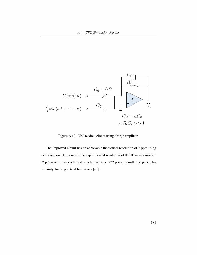
A.4. CPC Simulation Results
Ct
C0 +¢C
Uo
Rt
A
CC
CC = aC0
!RtCt >> 1
U
asin(!t + ¼ ¡ Á)
Usin(!t)
Figure A.10: CPC readout circuit using charge amplifier.
The improved circuit has an achievable theoretical resolution of 2 ppm using
ideal components, however the experimented resolution of 0.7 fF in measuring a
22 pF capacitor was achieved which translates to 32 parts per million (ppm). This
is mainly due to practical limitations [47].
181

A.4. CPC Simulation Results
C
T
R
T
ADC
ComparatorCos(!t)
ADC
Comparator
Sin(!t)
LPF
LPF
DS
DC
VS
VC
VO1
Cx
C0
From
Sinusoidal
Oscillator
R R
R R
R
1
C
1
V
B
= Bsin(!t + ¼ ¡ Ã)
V
A
= Asin(!t)
V
A
V
B
V
SS
V
CC
Figure A.11: Improved CPC readout circuit.
It is shown in this paper how to calculate the perturbation on Cx from measured
and digitized values related to voltages VS and VC (DS and DC).
Cx1
Cx0=
tan(ψ)
n.DC
DS−1,
where, Cx0 and Cx1 are the Cx values before and after perturbation, respectively.
n is a constant related to the ADC reference voltages, and ψ is one of the elements
for the phase (ωt +π−ψ) determined by values of R1 and C1 [47]. The perturba-
tion can be defined as δ ,Cx1/Cx0.
182
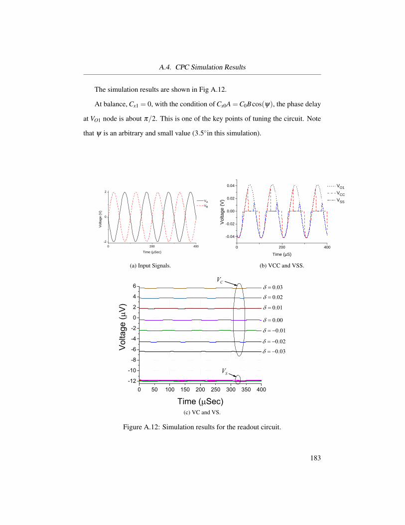
A.4. CPC Simulation Results
The simulation results are shown in Fig A.12.
At balance, Cx1 = 0, with the condition of Cx0A =C0Bcos(ψ), the phase delay
at VO1 node is about π/2. This is one of the key points of tuning the circuit. Note
that ψ is an arbitrary and small value (3.5in this simulation).
0 200 400
-2
0
2
Vol
tage
(V
)
Time (µSec)
VA
VB
(a) Input Signals.
0 200 400
-0.04
-0.02
0.00
0.02
0.04
Vol
tage
(V
)
Time (µS)
VO1
VCC
VSS
(b) VCC and VSS.
0 50 100 150 200 250 300 350 400-12
-10
-8
-6
-4
-2
0
2
4
6 0.03
0.02
0.01
0.00
0.01
0.02
SV
0.03Volta
ge (
V)
Time ( Sec)
CV
(c) VC and VS.
Figure A.12: Simulation results for the readout circuit.
183

A.4. CPC Simulation Results
The results of a SPICEr simulation with a sweep on parameter δ are presented
in the Table A.2
δ VC/VS
-0.03 0.508333333-0.02 0.341666667-0.01 0.175
0 0.0083333330.01 -0.1583333330.02 -0.3416666670.03 -0.5
Table A.2: CPC simulation results, ratio of voltage magnitudes vs. perturbation.
The slope of the line (gain of the whole system) is cot(ψ) which is approxi-
mately 16.68 and complies with the result of the simulation.
-0.03 -0.02 -0.01 0.00 0.01 0.02 0.03-0.6
-0.4
-0.2
0.0
0.2
0.4
0.6
C
S
VV
2
16.875 0.004760.999
y xR
Regression Line:
Figure A.13: CPC parametric sweep simulation results.
184

A.5. CFC Simulation Results
A.5 CFC Simulation Results
This section presents the simulation for two CFC based readout circuits. The first
circuit schematic used for the simulation is the one that previously shown in Fig.
2.15 which is repeated here in Fig. A.14 for ease of reading. The component values
used for the simulation are R1 = 56kΩ, R2 = 112.2kΩ, R3 = 2.5kΩ, R4 = 500Ω,
R5 = 500Ω, R6 = 1kΩ, C1 = C3 = 10µF, C2 = 100pF, L1 = 200µH, L2 = 50µH
and the transistor Q1 is a typical NPN signal transistor, e.g. 2N2222 [29].
VCC
R1 R2
R3 R4R5
R6L1 L2
C2
C1
C3
Q1
Figure A.14: CFC readout circuit based on Hartley oscillator.
In this oscillator based readout circuit, C2 is assumed to be the sensor capaci-
tance. The SPICE simulations are done with parameter sweep on C2 for the values
between 100pF to 700pF. The simulation results are shown in table A.3 and are
plotted in Fig A.15.
185

A.5. CFC Simulation Results
C3(pF) fo(kHz)100 905150 758200 664250 600300 553350 512400 482450 455500 433550 415600 398650 381700 369
Table A.3: CPC simulation results, ratio of voltage magnitudes vs. perturbation.
0 100 200 300 400 500 600 700 800300
400
500
600
700
800
900
1000
f o (k
Hz)
C3 (pF)
Figure A.15: Simulation results for the readout circuit.
The second CFC readout circuit that is chosen for simulation is based on
186
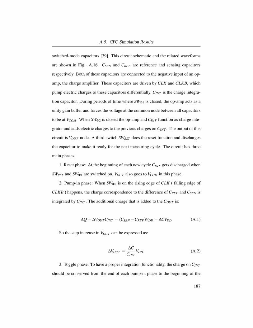
A.5. CFC Simulation Results
switched-mode capacitors [39]. This circuit schematic and the related waveforms
are shown in Fig. A.16. CSEN and CREF are reference and sensing capacitors
respectively. Both of these capacitors are connected to the negative input of an op-
amp, the charge amplifier. These capacitors are driven by CLK and CLKB, which
pump electric charges to these capacitors differentially. CINT is the charge integra-
tion capacitor. During periods of time where SWΦ1 is closed, the op-amp acts as a
unity gain buffer and forces the voltage at the common node between all capacitors
to be at VCOM. When SWΦ2 is closed the op-amp and CINT function as charge inte-
grator and adds electric charges to the previous charges on CINT . The output of this
circuit is VOUT node. A third switch SWRST does the reset function and discharges
the capacitor to make it ready for the next measuring cycle. The circuit has three
main phases:
1. Reset phase: At the beginning of each new cycle CINT gets discharged when
SWRST and SWΦ1 are switched on. VOUT also goes to VCOM in this phase.
2. Pump-in phase: When SWΦ2 is on the rising edge of CLK ( falling edge of
CLKB ) happens, the charge correspondence to the difference of CREF and CSEN is
integrated by CINT . The additional charge that is added to the COUT is:
∆Q = ∆VOUTCINT = (CSEN−CREF)VDD = ∆CVDD (A.1)
So the step increase in VOUT can be expressed as:
∆VOUT =∆C
CINTVDD. (A.2)
3. Toggle phase: To have a proper integration functionality, the charge on CINT
should be conserved from the end of each pump-in phase to the beginning of the
187

A.5. CFC Simulation Results
next pump-in phase. This happens by turning on SWΦ1 and falling edge of CLK
(rising edge of CLKB).
Pump-in and toggle phases alternating and depending on the value of CSEN in
reference to CREF the charge on CINT , or the voltage VOUT , increases or decreases.
This continues until VOUT reaches a predefined upper limit VREF = VH or lower
limit VREF =VL. The initial value for VOUT is VCOM after each reset phase. Assume
VOUT reaches VREF after n consecutive steps.
VREF −VCOM = n∆C
CINTVDD. (A.3)
On the other hand by definition of n:
n =fclk
fout. (A.4)
So the final equation that shows the relationship between fout and ∆C can be
written as:
∆C =CINTVREF −VCOM
VDD
fout
fclk(A.5)
188

A.5. CFC Simulation Results
¡
+
CSEN
CREF
¡
+
¡
+
VoutSW©1
SW©2
SWRST
VH
VL
FF
VDD
VDD
CLK
CLKB
CLKD
CSENCINT
Reset
Reset
CLK
CLKB
©1
©2
VCOM
Figure A.16: CFC readout circuit based on switched-capacitors.
The simulation plot for the values of CSEN = 10.5pF, CREF =10pF, CINT =10pF
, fclk =100kHz, VCOM = 0, VDD =3.3V and VREF =VDD/2 is shown in Fig. A.17.
189

A.5. CFC Simulation Results
0.0 0.2 0.40
2
4
0.0 0.2 0.40
2
4
0.0 0.2 0.40
1
2
0.0 0.2 0.4
0
2
4
0.0 0.2 0.40
2
4
φ 1φ 2
Vou
tR
eset
Clk
Time (mS)
Figure A.17: Simulation results for the readout circuit based on SC.
The results of the simulation with parameter sweep on CSEN for values between
9.5pF to 10.5pF are captured in table A.4 and plotted in Fig. A.18. Note that there
is an error associated with the ratio of VREF to ∆VOUT not being a whole number,
which is discussed in more details in literature [40].
190

A.5. CFC Simulation Results
δ = ∆CCREF
fout(kHz)0.05 7.1386677650.04 5.80150.03 4.35100.02 2.77630.01 1.2195-0.01 -1.2192-0.02 -2.8261-0.03 -4.3440-0.04 -5.5556-0.05 -7.1511
Table A.4: CFC simulation results, output frequency vs. perturbation.
-0.06 -0.04 -0.02 0.00 0.02 0.04 0.06-10
-5
0
5
10
freq
uenc
y (k
Hz)
δ (=∆C/CREF)
Figure A.18: Simulation results for the readout circuit based on SC
191
Copyright © 2022 FDOKUMEN