
BOOK OF ABSTRACTS - GitHub Pages
84
NPS 2022 INTERNATIONAL CONFERENCE ON RECENT TRENDS IN PHOTONICS Feb 27-March 1, 2022 Organised by: International School of Photonics Cochin,Kerala - 682022 Cochin Universtity of Science and Technology BOOK OF ABSTRACTS
-
Upload
khangminh22 -
Category
Documents
-
view
0 -
download
0
Transcript of BOOK OF ABSTRACTS - GitHub Pages
NPS 2022
INTERNATIONAL CONFERENCE ON RECENT TRENDS IN PHOTONICS
Feb 27-March 1, 2022
Organised by:International School of Photonics
Cochin,Kerala - 682022
Cochin Universtity of Science and Technology
BOOK OF ABSTRACTS
International Conference on Recent Trends in Photonics
NPS - 2022
27 February - 01 March 2022
International School of Photonics
Cochin University of Science and Technology
Cochin - 682022, Kerala, India
Book of Abstracts

Organizing Committee Members
Chairman: Prof. (Dr.) Pramod Gopinath
Convener: Dr. Mohamed Ameen P
Prof. (Dr.) A Mujeeb
Prof. (Dr.) M Kailasnath
Prof. (Dr.) Sheenu Thomas
Dr. Saji K J
Dr. Manu Vaishakh
Mr. Muhammad Rishad K P
Dr. Priya Rose T
Dr. Praveen C S
Anugop B Athira T Das
Raj Sha M M Jayaprasad K V
Cicily Rigi V J Karthika Sankar
Hajara P Lakshmi B
Soumya S Priya Mary N J
Dr. Bini P Pathrose Titu Thomas Praveen P
Dr. Kamal P. Mani Shilpa S Safna Saif
Dr. Md. Zaheer Ansari A K Sooraj Vishwam Maneesha M
Dr. Pradeep Chandran Jose Antony V J Adrine Antony Correya
Dr. Rehana P Ummer Mubeena Rafi Adarsh K J
Dr. Vineesh Kumar T V Syammohan V Mitty George
Dr. Shiju E Sathe Anil Mayur Reji Thankachan
Dr. Vijisha M V Divya Krishnan Arun Pappachan
Lakshmi R Jijo George
Vijoy K V Amrutha Thomas
Keerthana S H Lakshmi S
Pradeep Kumar V Anila Thomas
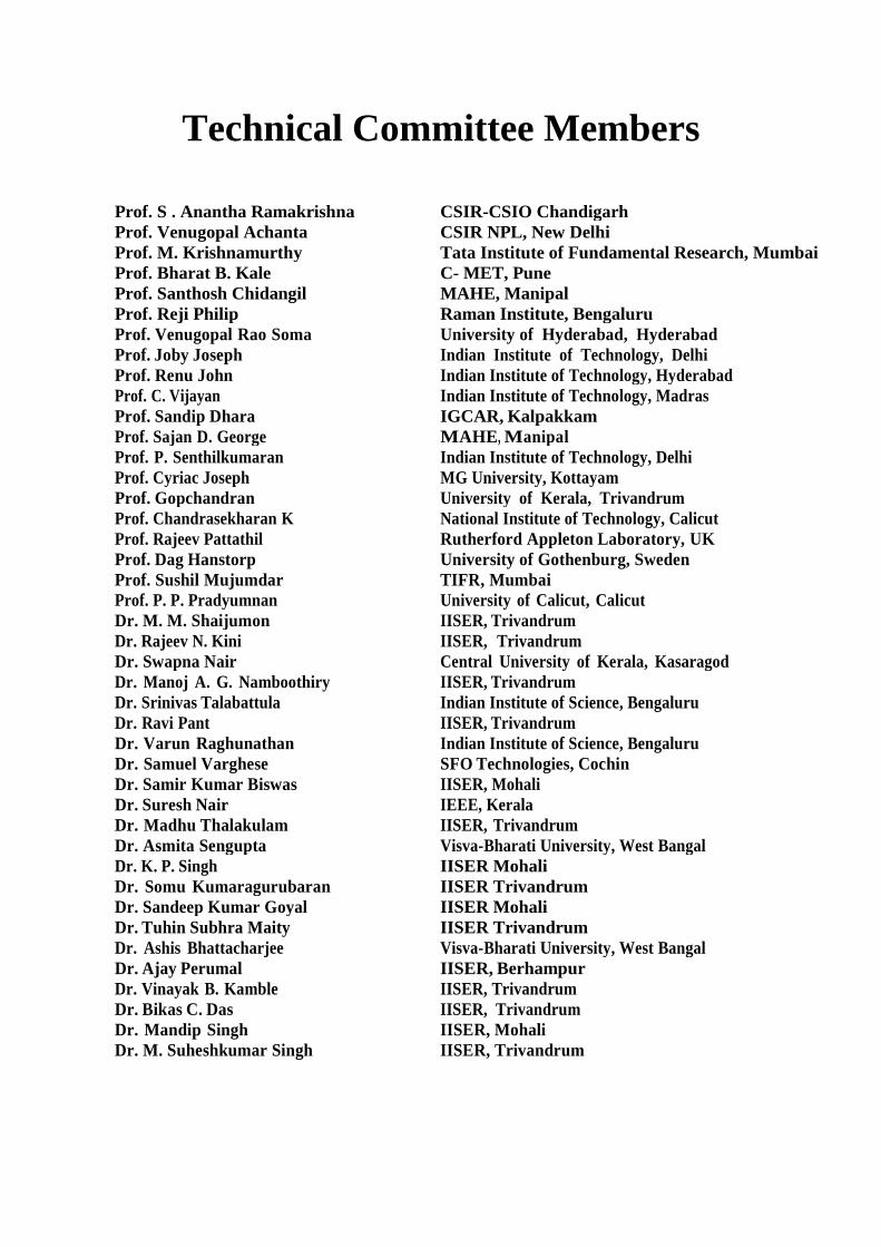
Technical Committee Members
Prof. S . Anantha Ramakrishna CSIR-CSIO Chandigarh
Prof. Venugopal Achanta CSIR NPL, New Delhi
Prof. M. Krishnamurthy Tata Institute of Fundamental Research, Mumbai
Prof. Bharat B. Kale C- MET, Pune
Prof. Santhosh Chidangil MAHE, Manipal
Prof. Reji Philip Raman Institute, Bengaluru
Prof. Venugopal Rao Soma University of Hyderabad, Hyderabad
Prof. Joby Joseph Indian Institute of Technology, Delhi
Prof. Renu John Indian Institute of Technology, Hyderabad
Prof. C. Vijayan Indian Institute of Technology, Madras
Prof. Sandip Dhara IGCAR, Kalpakkam
Prof. Sajan D. George MAHE, Manipal
Prof. P. Senthilkumaran Indian Institute of Technology, Delhi
Prof. Cyriac Joseph MG University, Kottayam
Prof. Gopchandran University of Kerala, Trivandrum
Prof. Chandrasekharan K National Institute of Technology, Calicut
Prof. Rajeev Pattathil Rutherford Appleton Laboratory, UK
Prof. Dag Hanstorp University of Gothenburg, Sweden
Prof. Sushil Mujumdar TIFR, Mumbai
Prof. P. P. Pradyumnan University of Calicut, Calicut
Dr. M. M. Shaijumon IISER, Trivandrum
Dr. Rajeev N. Kini IISER, Trivandrum
Dr. Swapna Nair Central University of Kerala, Kasaragod
Dr. Manoj A. G. Namboothiry IISER, Trivandrum
Dr. Srinivas Talabattula Indian Institute of Science, Bengaluru
Dr. Ravi Pant IISER, Trivandrum
Dr. Varun Raghunathan Indian Institute of Science, Bengaluru
Dr. Samuel Varghese SFO Technologies, Cochin
Dr. Samir Kumar Biswas IISER, Mohali
Dr. Suresh Nair IEEE, Kerala
Dr. Madhu Thalakulam IISER, Trivandrum
Dr. Asmita Sengupta Visva-Bharati University, West Bangal
Dr. K. P. Singh IISER Mohali
Dr. Somu Kumaragurubaran IISER Trivandrum
Dr. Sandeep Kumar Goyal IISER Mohali
Dr. Tuhin Subhra Maity IISER Trivandrum
Dr. Ashis Bhattacharjee Visva-Bharati University, West Bangal
Dr. Ajay Perumal IISER, Berhampur
Dr. Vinayak B. Kamble IISER, Trivandrum
Dr. Bikas C. Das IISER, Trivandrum
Dr. Mandip Singh IISER, Mohali
Dr. M. Suheshkumar Singh IISER, Trivandrum
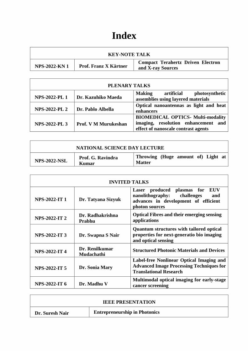
Index
PLENARY TALKS
NPS-2022-PL 1 Dr. Kazuhiko Maeda Making artificial photosynthetic
assemblies using layered materials
NPS-2022-PL 2 Dr. Pablo Albella Optical nanoantennas as light and heat
enhancers
NPS-2022-PL 3 Prof. V M Murukeshan
BIOMEDICAL OPTICS- Multi-modality
imaging, resolution enhancement and
effect of nanoscale contrast agents
INVITED TALKS
NPS-2022-IT 1 Dr. Tatyana Sizyuk
Laser produced plasmas for EUV nanolithography: challenges and advances in development of efficient
photon sources
NPS-2022-IT 2 Dr. Radhakrishna
Prabhu
Optical Fibres and their emerging sensing
applications
NPS-2022-IT 3 Dr. Swapna S Nair
Quantum structures with tailored optical
properties for next-generatio bio imaging
and optical sensing
NPS-2022-IT 4 Dr. Renilkumar Mudachathi
Structured Photonic Materials and Devices
NPS-2022-IT 5 Dr. Sonia Mary
Label-free Nonlinear Optical Imaging and
Advanced Image Processing Techniques for
Translational Research
NPS-2022-IT 6 Dr. Madhu V Multimodal optical imaging for early-stage
cancer screening
KEY-NOTE TALK
NPS-2022-KN 1 Prof. Franz X Kärtner Compact Terahertz Driven Electron and X-ray Sources
NATIONAL SCIENCE DAY LECTURE
NPS-2022-NSL Prof. G. Ravindra
Kumar
Throwing (Huge amount of) Light at
Matter
IEEE PRESENTATION
Dr. Suresh Nair Entrepreneurship in Photonics
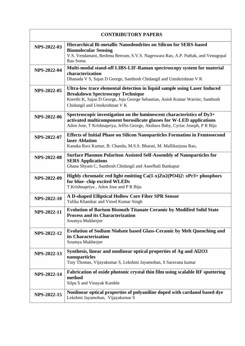
CONTRIBUTORY PAPERS
NPS-2022-03 Hierarchical Bi-metallic Nanodendrites on Silicon for SERS-based
Biomolecular Sensing V.S. Vendamani, Reshma Beeram, S.V.S. Nageswara Rao, A.P. Pathak, and Venugopal
Rao Soma
NPS-2022-04 Multi-modal stand-off LIBS-LIF-Raman spectroscopy system for material
characterization Dhanada V S, Sajan D George, Santhosh Chidangil and Unnikrishnan V K
NPS-2022-05 Ultra-low trace elemental detection in liquid sample using Laser Induced
Breakdown Spectroscopy Technique Keerthi K, Sajan D George, Joju George Sebastian, Anish Kumar Warrier, Santhosh
Chidangil and Unnikrishnan V K
NPS-2022-06 Spectroscopic investigation on the luminescent characteristics of Dy3+
activated multicomponent borosilicate glasses for W-LED applications Adon Jose, T Krishnapriya, Jeffin George, Akshara Baby, Cyriac Joseph, P R Biju
NPS-2022-07 Effects of Initial Phase on Silicon Nanoparticles Formation in Femtosecond
laser Ablation Kanaka Ravi Kumar, B. Chandu, M.S.S. Bharati, M. Mallikarjuna Rao,
NPS-2022-08 Surface Plasmon Polariton Assisted Self-Assembly of Nanoparticles for
SERS Applications Ghana Shyam C, Santhosh Chidangil and Aseefhali Bankapur
NPS-2022-09 Highly chromatic red light emitting Ca(1-x)Zn2(PO4)2: xPr3+ phosphors
for blue- chip excited WLEDs T.Krishnapriya , Adon Jose and P R Biju
NPS-2022-10 A D-shaped Elliptical Hollow Core Fiber SPR Sensor Tulika Khanikar and Vinod Kumar Singh
NPS-2022-11 Evolution of Barium Bismuth Titanate Ceramic by Modified Solid State
Process and its Characterization Soumya Mukherjee
NPS-2022-12 Evolution of Sodium Niobate based Glass-Ceramic by Melt Quenching and
its Characterization Soumya Mukherjee
NPS-2022-13 Synthesis, linear and nonlinear optical properties of Ag and Al2O3
nanoparticles Tiny Thomas, Vijayakumar S, Lekshmi Jayamohan, S Saravana kumar
NPS-2022-14 Fabrication of oxide photonic crystal thin film using scalable RF sputtering
method Silpa S and Vinayak Kamble
NPS-2022-15 Nonlinear optical properties of polyaniline doped with cardanol based dye Lekshmi Jayamohan, Vijayakumar S

NPS-2022-16 Design and analysis of micro-channelled Quasi D-shape optical Fiber
plasmonic Sensor Maya Chauhan, Sugandha Das, Vinod K. Singh
NPS-2022-17 Digital Laser Combustion Method: Synthesis of Silver Nanoparticles
(AgNps) Ganesh H Aralikatti, Basavaraj H. G and Dr. Madhukumar R
NPS-2022-19 Estimation of Random Duty Cycle in Periodically Poled Lithium Niobate
Through Second Harmonic Generation Madhu, Prashant Povel Dwivedi
NPS-2022-20 Quality Evaluation of Quasi-Phase Matching (QPM) by Diffraction-Noise Prashant Povel Dwivedi
NPS-2022-21 Nanoparticle Enhanced Femtosecond Laser Induced Breakdown
Spectroscopy of Aluminium Sheet coated with gold Nano-particle Embedded
nanofibers N. Linga Murthy, M.S.S. Bharathi, S. Venugopal Rao
NPS-2022-22 Enhanced Temperature Sensing Based on the Randomness in the
Multilayered 1D Photonic Crystals Lakshmi Thara R , P. Aruna Priya, Chittaranjan Nayak
NPS-2022-23 Generation of Parabolic pulse by nonlinear pulse reshaping inside a Silicon
on Insulator (SOI) Waveguide Hemant, Somen Adhikary, Mousumi Basu
NPS-2022-24 Ultrasensitive Detection of Thiram and Nile Blue using Au Nanostars
Decorated Laser-patterned Au Substrate Jagannath Rathod, Chandu Byram, Venugopal Rao Soma
NPS-2022-25 Generation of high-frequency pulse train by designing a buried SOI
waveguide
Somen Adhikary, Hemant, Mousumi Basu
NPS-2022-26 Si-based incident angle-sensitive reflective wavelength separator: a single-
step FIB lithography based nanopatterning application
Ramanathaswamy Pandian, Rajagopal R, Hrudya Radhakrishnan, G.Mangamma,
S. Dhara
NPS-2022-27 Structural, Cytotoxic and Anti Cancerous Studies on Er3+: Y2O3
Nanophosphors Sreejaya T S, Deepthi N Rajendran
NPS-2022-28 Study Of Conversion Efficiency For Second Harmonic Wave From
Fundamental Wave (Under Plane-Wave Approximation) Haziq Ali Peer Mohammed, Madhu, Prashant Povel Dwivedi
NPS-2022-29 Efficient optical limiting behavior of carbon encapsulated zinc sulfide core-
shell nanostructures Athulya K.S and Chandrasekharan K
NPS-2022-31 Copper-based Surface Plasmon Coupled Emission Steering for Biosensor
Applications Ajeesh P. Vijayan, A.Sreelakshmi Fasna Sharin and Pradeesh Kannan
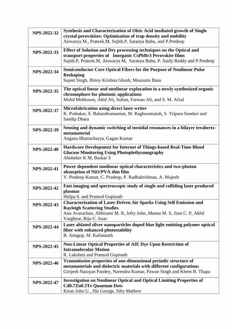
NPS-2022-32 Synthesis and Characterization of Oleic Acid mediated growth of Single
crystal perovskites: Optimisation of trap density and mobility Aiswarya M., Prateek.M, Sujith.P, Saranya Babu, and P.Predeep
NPS-2022-33 Effect of Solution and Dry processing techniques on the Optical and
transport properties of Inorganic CsPbBr3 Perovskite films Sujith.P, Prateek.M, Aiswarya M, Saranya Babu, P. Saidy Reddy and P.Predeep
NPS-2022-34 Semiconductor Core Optical Fibers for the Purpose of Nonlinear Pulse
Reshaping Sujeet Singh, Binoy Krishna Ghosh, Mousumi Basu
NPS-2022-35 The optical linear and nonlinear exploration in a newly synthesized organic
chromophore for photonic applications Mohd Mehkoom, Abid Ali, Sultan, Farman Ali, and S. M. Afzal
NPS-2022-37 Microfabrication using direct laser writer K. Prabakar, S. Balasubramanian, M. Raghuramaiah, S. Tripura Sundari and
Sandip Dhara
NPS-2022-39 Sensing and dynamic switching of toroidal resonances in a bilayer terahertz-
metamaterial Angana Bhattacharya, Gagan Kumar
NPS-2022-40 Hardware Development for Internet of Things-based Real-Time Blood
Glucose Monitoring Using Photoplethysmography Abubeker K M, Baskar S
NPS-2022-41 Power dependent nonlinear optical characteristics and two-photon
absorption of NiO/PVA thin film
V. Pradeep Kumar, C. Pradeep, P. Radhakrishnan, A. Mujeeb
NPS-2022-42 Fast imaging and spectroscopic study of single and colliding laser produced
plasmas Shilpa S. and Pramod Gopinath
NPS-2022-43 Characterization of Laser-Driven Air Sparks Using Self Emission and
Rayleigh Scattering Studies Anu Avarachan, Abhirami M. R, Jefry John, Meenu M. S, Jinsi C. P, Akhil
Varghese, Riju C. Issac
NPS-2022-44 Laser ablated silver nanoparticles doped blue light emitting polymer optical
fiber with enhanced photostability
B. Anugop, M. Kailasnath
NPS-2022-45 Non-Linear Optical Properties of AIE Dye Upon Restriction of
Intramolecular Motion R. Lakshmi and Pramod Gopinath
NPS-2022-46 Transmission properties of one-dimensional periodic structure of
metamaterials and dielectric materials with different configurations Girijesh Narayan Pandey, Narendra Kumar, Pawan Singh and Khem B. Thapa
NPS-2022-47 Investigation on Nonlinear Optical and Optical Limiting Properties of
Cd0.7Zn0.3Te Quantum Dots Kiran John U., Jilu George, Siby Mathew
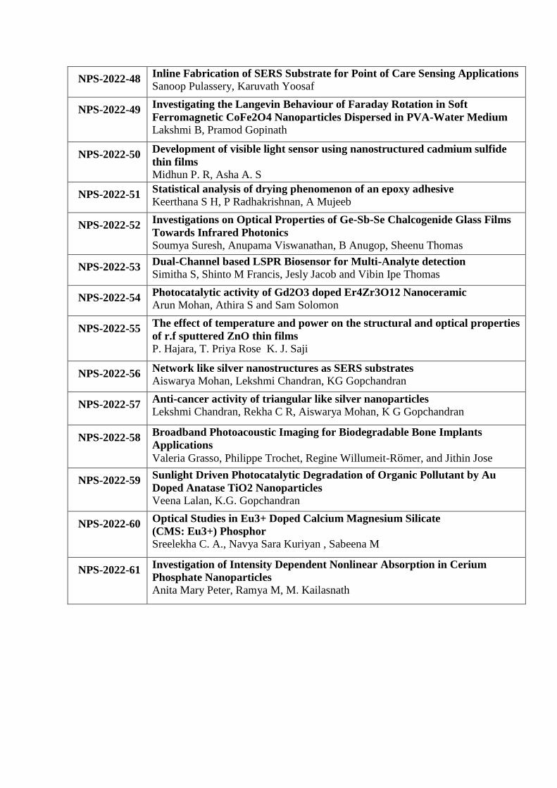
NPS-2022-48 Inline Fabrication of SERS Substrate for Point of Care Sensing Applications Sanoop Pulassery, Karuvath Yoosaf
NPS-2022-49 Investigating the Langevin Behaviour of Faraday Rotation in Soft
Ferromagnetic CoFe2O4 Nanoparticles Dispersed in PVA-Water Medium Lakshmi B, Pramod Gopinath
NPS-2022-50 Development of visible light sensor using nanostructured cadmium sulfide
thin films Midhun P. R, Asha A. S
NPS-2022-51 Statistical analysis of drying phenomenon of an epoxy adhesive Keerthana S H, P Radhakrishnan, A Mujeeb
NPS-2022-52 Investigations on Optical Properties of Ge-Sb-Se Chalcogenide Glass Films
Towards Infrared Photonics Soumya Suresh, Anupama Viswanathan, B Anugop, Sheenu Thomas
NPS-2022-53 Dual-Channel based LSPR Biosensor for Multi-Analyte detection Simitha S, Shinto M Francis, Jesly Jacob and Vibin Ipe Thomas
NPS-2022-54 Photocatalytic activity of Gd2O3 doped Er4Zr3O12 Nanoceramic Arun Mohan, Athira S and Sam Solomon
NPS-2022-55 The effect of temperature and power on the structural and optical properties
of r.f sputtered ZnO thin films
P. Hajara, T. Priya Rose K. J. Saji
NPS-2022-56 Network like silver nanostructures as SERS substrates
Aiswarya Mohan, Lekshmi Chandran, KG Gopchandran
NPS-2022-57 Anti-cancer activity of triangular like silver nanoparticles
Lekshmi Chandran, Rekha C R, Aiswarya Mohan, K G Gopchandran
NPS-2022-58 Broadband Photoacoustic Imaging for Biodegradable Bone Implants
Applications
Valeria Grasso, Philippe Trochet, Regine Willumeit-Romer, and Jithin Jose
NPS-2022-59 Sunlight Driven Photocatalytic Degradation of Organic Pollutant by Au
Doped Anatase TiO2 Nanoparticles
Veena Lalan, K.G. Gopchandran
NPS-2022-60 Optical Studies in Eu3+ Doped Calcium Magnesium Silicate
(CMS: Eu3+) Phosphor
Sreelekha C. A., Navya Sara Kuriyan , Sabeena M
NPS-2022-61 Investigation of Intensity Dependent Nonlinear Absorption in Cerium
Phosphate Nanoparticles
Anita Mary Peter, Ramya M, M. Kailasnath
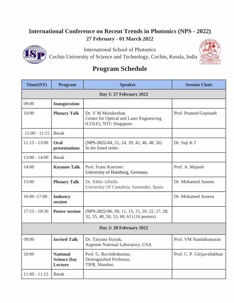
International Conference on Recent Trends in Photonics (NPS - 2022)
27 February - 01 March 2022
International School of Photonics
Cochin University of Science and Technology, Cochin, Kerala, India
Program Schedule
Time(IST) Program Speaker Session Chair
Day 1: 27 February 2022
09:00 Inauguration
10:00 Plenary Talk Dr. V M Murukeshan.
Center for Optical and Laser Engineering
(COLE), NTU Singapore.
Prof. Pramod Gopinath
11:00 - 11:15 Break
11.15 - 13:00 Oral
presentations
(NPS-2022-04, 21, 24, 39, 42, 46, 48, 56)
In the listed order.
Dr. Saji K J
13:00 - 14:00 Break
14:00 Keynote Talk Prof. Franz Kaertner.
University of Hamburg, Germany.
Prof. A. Mujeeb
15:00 Plenary Talk Dr. Pablo Albella
University Of Cantabria, Santander, Spain.
Dr. Mohamed Ameen
16:00 -17:00 Industry
session
Dr. Mohamed Ameen
17:15 - 18:30 Poster session (NPS-2022-06, 09, 11, 13, 15, 20, 22, 27, 28,
32, 35, 40, 50, 55, 60, 61) (16 posters)
Day 2: 28 February 2022
09:00 Invited Talk Dr. Tatyana Sizyuk,
Argonne National Laboratory, USA
Prof. VM Nandakumaran
10:00 National
Science Day
Lecture
Prof. G. Ravindrakumar,
Distinguished Professor,
TIFR, Mumbai.
Prof. C. P. Girijavallabhan
11:00 - 11:15 Break

11:15 Dr. Suresh Nair,
IEEE India Council Track Chair
Prof. M. Kailasnath
11:30 - 13:00 Oral
Presentations
(NPS-2022-03, 12, 17, 19, 25, 26, 44)
In the listed order.
Dr. SKS Nair
13:00 - 14:00 Break
14:00 Invited Talk Dr. Swapna Nair
Central University of Kerala, Kasaragod.
Dr. Saji K J
15:00 Invited Talk Dr. Madhu Veettikazhy
Technical University of Denmark,
Denmark
Muhammad Rishad
16:15 - 17:30 Poster
Presentations
(NPS-2022-05, 07, 08, 10, 16, 17, 23, 29, 31,
33, 34, 37, 43, 47, 51, 53, 57, 59) (18 posters)
Day 3: 01 March 2022
09:00 Invited Talk Dr. Sonia Mary,
The Jackson Laboratory, USA
Dr. Priya Rose
10:00 - 10:30 Break
10:30 Plenary Talk Dr. Kazuhiko Maeda,
Tokyo Institute of Technology, Japan
Dr. Praveen C S
11:30 - 13:00 Oral Presentations (NPS-2022-41, 45, 49, 52, 54, 58)
In the listed order.
Dr. Praveen C S
13:00 - 14:00 Break
14:00 Invited Talk Prof. Radhakrishna Prabhu,
Robert Gordon University, Aberdeen, UK.
Prof. M. Kailasnath
15:00 Invited Talk Dr. Renil Kumar
Chief Scientist,
Motion Imager, Twente, The Netherlands.
Industry Talk
Dr. Manu Vaishakh
16:00 ValedictoryMeeting
The codes mentioned in the schedule can be seen in the email received from Morressier.

KEY-NOTE TALK
2
NPS-2022-KN 1
Compact Terahertz Driven Electron and X-ray Sources
Franz X. Kärtner
Email: [email protected]
Ultrafast Optics and X-rays Group, Center for Free-Electron Laser Science, Deutsches
Elektronen Synchrotron (DESY), and Department of Physics and The Centre for Ultrafast
Imaging, Universität Hamburg, Germany
Email: [email protected]
The use of very high frequencies, in the THz region, specifically 100 - 500 GHz, enables
operation of accelerators at higher field strength with lower energetic driver pulses. This opens
up the possibility of compact low emittance electron sources and high-brightness fully coherent
X-ray sources. In this contribution, we summarize the progress made in the ERC Synergy Grant
AXSIS: Attosecond X-ray Science – Imaging and Spectroscopy in source technology. The high
acceleration fields and field gradients possible in terahertz devices enables novel electron
bunch manipulations, bunch diagnostic and promise ultimately fully coherent X-ray production
from compact sources. Latest experimental results in the implementation of electron and X-ray
sources based on this technology will be discussed.

PLENARY TALKS
4
NPS-2022-PL 1
Making artificial photosynthetic assemblies using layered
materials
Kazuhiko Maeda
School of Science, Tokyo Institute of Technology, Japan
Email: [email protected]
Metal oxide nanosheets derived from the layered counterparts have attracted attention in
various fields due to their unique structural properties. The anisotropic feature of nanosheets,
having a thickness of ~1 nm and lateral dimensions ranging from several hundred nanometers
to a few micrometer, is advantageous for heterogeneous photocatalysis, as the diffusion length
of photogenerated carriers to the surface is shortened, leading to higher activity.
It is also known that certain nanoparticulate metals or metal oxides on a semiconductor
photocatalyst work as cocatalysts to promote water reduction and/or oxidation. In
heterogeneous photocatalysis, the effect of cocatalyst size on the water-splitting performance
had not been examined at sizes smaller than 1 nm due to the lack of an effective preparation
method and a suitable photocatalyst. We have demonstrated that metal nanoclusters (such as
Pt) of <1 nm in size could be deposited on the interlayer nanospace of KCa2Nb3O10 using the
electrostatic attraction between a cationic metal complex and a negatively charged
Ca2Nb3O10– sheet, without the aid of any additional reagent. The material obtained exhibited
8 times greater photocatalytic activity for overall water splitting under band-gap irradiation than
the previously reported analog using a RuO2 promoter. This study highlighted the superior
functionality of <1 nm Pt nanoclusters for photocatalytic overall water splitting.
With further modification by a ruthenium(II) photosensitizer, this material also worked
as a H2 evolution photocatalyst in visible-light-driven Z-scheme water splitting, in combination
with a WO3-based O2 evolution photocatalyst and a triiodide/iodide redox couple. Pt-
intercalated HCa2Nb3O10 nanosheets further modified with amorphous AlOx clusters
demonstrated a remarkable photocatalytic activity with a dye-based turnover number and
frequency for H2 evolution of 4580 and 1960 h–1, respectively, which were by far the highest
among dye-sensitized nonsacrificial photocatalytic systems ever reported.
5
NPS-2022-PL 2
Optical nanoantennas as light and heat enhancers
Pablo Albella
Department of Applied Physics, University of Cantabria (Spain)
E-mail: [email protected]
Metallic or high-refractive index nanostructures that show resonances when excited with
light can act as optical nanoantennas, providing a versatile tool to control light beyond the
conventional diffraction limit. On the other hand, depending on their material optical
nanoantennas can be appropriate for different applications such as ultrasensitive (bio-) sensing,
surface enhanced spectroscopies or photothermal devices. In the case of metallic nanoantennas,
plasmonic excitations are possible but known to be present relatively large losses. This fact is
undesirable in applications like sensing or spectroscopy, and dielectric alternatives have been
successfully proposed to overcome this problem. However, optical losses in metals are
necessary when aiming at photothermal applications since they are the source of the thermal
generation. In this talk, I will describe and discuss the origins and recent advances in this
rapidly developing field of optical nanoantennas and its alternative based on dielectrics. I will
pay special attention to the main significant contributions we have made in applications such
as sensing, light guiding or those based on photothermal response
6
NPS-2022-PL 3
BIOMEDICAL OPTICS- Multi-modality imaging, resolution
enhancement and effect of nanoscale contrast agents
Murukeshan Vadakke Matham
Director, Center for Optical and Laser Engineering (COLE), NTU, Singapore
Email: [email protected]
High-resolution diagnostic biomedical optics is an interdisciplinary branch of science
and technology, which uses optics for improving the basic understanding of biological
processes to enhance the diagnostic efficiency thereby enabling efficient treatment of human
diseases. In most of the cases, conventional types of medical imaging may not be able to detect
subtle changes occurring in tissues easily. Each imaging modality has its own advantages and
limitations and one cannot fit one single modality for all diagnostic applications. Therefore,
the need for a multi or hybrid modality imaging arises. High-resolution imaging with optimal
working distance, imaging around opaque obstacles are also of prime importance in today’s
imaging world. However, the quest for multi-modality settings for the diagnostic imaging has
posed subduing effects of certain advantages of the respective individual modalities. From
these perspectives, a paradigm shift in medical diagnostics was introduced in the recent past by
way of enhancing different parameters of interest using nanoscale contrast agents. A brief
overview on the proposed schemes that can be explored based on the works carried out by the
author’s group for early diagnosis of cancerous growth in colon, and ocular imaging targeting
iridocorneal angle and imaging of cornea will be reviewed from this perspective. A high
resolution probe with selective spatiotemporal imaging that can find potential applications in
opto-genetics will also be discussed.

NATIONAL SCIENCE DAY LECTURE

8
NPS-2022-NSL
National Science Day Lecture
Throwing (Huge Amount of) Light at Matter
G. Ravindra Kumar
Tata Institute of Fundamental Research, Colaba, Mumbai 400 005
Email: [email protected]
Intense fluxes of light do very interesting things to matter and the resulting nonlinear
behavior of matter has been known for decades. The latest forays involve abnormally large
intensities of light (in W/sq.cm, the number reminds us of the Avagadro number from our
school chemistry!) and provoke matter to display very unusual behavior enabling us to study
stars right on a table top in the lab.
This talk will attempt to describe some science with abnormally large intensities of light,
citing experiments performed at TIFR – creation of gigantic magnetic pulses (100s of
megagauss), passage of relativistic electrons through dense, hot matter and its consequences in
terms of MeV ion production, ultrafast hard x-ray emission etc.. The emphasis will be on
conveying the broad scope of the field as well as some pointers to the future.
Gerard Mourou and Donna Strickland won half the Nobel prize in physics in 2018 for
the invention of chirped pulse amplification that facilitated ultrahigh power, femtosecond laser
pulses. The most powerful, ultrashort pulse laser that emits 10 petawatt, 25 femtosecond pulses,
was inaugurated in Nov 2020 at the ‘Extreme Light Infrastructure- Nuclear Physics’ in
Romania.
The 150 terawatt, femtosecond laser system at TIFR

INVITED TALKS
10
NPS-2022-IT 1
Laser produced plasmas for EUV nanolithography: challenges
and advances in development of efficient photon sources
Tatyana Sizyuk
Argonne National Laboratory, USA.
Email: [email protected]
Extreme ultraviolet (EUV) nanolithography is one of the current approaches for more powerful
microchips production by increasing the optical imaging resolution. Two decades of research
in this area showed that most feasible photon sources around 13.5 nm wavelength can be
developed in laser produced plasma (LPP) devices. Optimization of these devices depends on
the complex parameters involved including laser pulse characteristics, target material and pre-
conditioning, and ambient gas in the chamber to protect the optical collection mirrors. The
complexity is increased when dual-pulse laser systems are used to improve the efficiency of
EUV source and to reduce the damage to the multilayer mirror (MLM) system due to the
energetic ions from LPP. All these aspects and the progress in the improvement of EUV sources
will be presented based on the comprehensive modeling and benchmarking of LPPs from Tin
microdroplets in single and dual pulse systems. Modeling results from the 3D multi- physics
package will be presented illustrating the dependences of EUV photon emission and collection
as well as ion kinetic energies on the LPP temporal and spatial evolution.
11
NPS-2022-IT 2
Optical Fibres and their emerging sensing applications
Prof. Radhakrishna Prabhu
School of Engineering, Robert Gordon University, Aberdeen, AB10 7GJ, UK
Email: [email protected]
In the last two decades, fibre optic technology has revolutionized the telecommunications
industry, enabling high bandwidth, high-capacity, long-distance communications, and
networking at extremely low costs. Optical fibres have also played important roles in many other
applications including sensing. Fibre Optic Sensing is a powerful sensing approach with
widespread use in various applications. Over the past few years, there has been growing interest
in the development of glass or polymer-based fibre optic sensors. Optical fibres have
advantages like smaller size, immunity to electromagnetic interference, freedom from
corrosion, chemical inertness and large bandwidth which can accommodate the growing needs
of sensing and monitoring in challenging environments. Optical fibres allow real-time remote
monitoring of various environmental parameters such as pressure, temperature, strain, and they
are capable of carrying out distributed sensing. Further, many point-type sensors can be
embedded into fibres and can be monitored remotely, exploiting the large bandwidth associated
with fibres. This talk will explore recent developments of a variety of optical fibre- based sensing
devices for physical, chemical and biosensing applications, especially focussed on medical,
security, oil and gas applications. The small size of fibres allows miniaturization adequate for
most common medical applications and support integration of micro/nanosensors on the fibre
tip and has the capability to monitor multiparameters in real-time in-vivo, making a potential
candidate for the emerging robotic based surgeries. They have potential in security applications
also. Specialised optical fibres with composite materials or special coatings can detect
commonly encountered chemicals in oil and gas wells such as hydrocarbons, hydrogen, oxygen
and ammonia with unprecedented accuracy. Sensors based on special optical fibres such as
Photonic Crystal Fibres (PCF), Hollow Core Fibres (HCF) will be discussed. Emerging
complementary sensing approaches, both intrinsic and extrinsic, will also be discussed for
demonstrating multiparameter sensing.
12
NPS-2022-IT 3
Quantum structures with tailored optical properties for next
generation bio imaging and optical sensing
Dr. Swapna S Nair
Dept. of Physics, Central University of Kerala, Kasaragod, India 671314
Contributors: Neeli Chandran Manikanta B Rajendra P & Swapna S Nair
Author for correspondence: [email protected]
This era is of quantum structures (QS) and QS based optical devices including LASERs and
LEDs are largely conquering the device markets. Exploration of novel nanomaterials with
multifunctional properties essential for technological applications and fabrication of functional
devices based on them will assume major share in the semiconductor electronics market.
The tuneable optical properties of these quantum systems make them ideal candidates for
designing optical biosensors and bioimaging probes as well. However, their enormous
production cost is a great challenge for the popularisation of the technology, and therefore,
development of novel wet chemistry strategies for the fabrication of ultrafine nano systems
such as quantum dots, quantum cubes and quantum cages are the need of the hour.
Tuneable optical band gap is the most appealing property of semiconductor nanoparticles.
Especially when the nanoparticles are in the strong confinement regime, tailored band gap can
be induced and band engineered nano systems with core shell geometry can be exploited for
their vast technological applications in designing QD LEDs, QD LASERS and display devices
by incorporation of defect states that falls inside the band gap, which can create systems with
tailor made emissions. Size, surface functionalization, shape, the level of doping, and the
dielectric environments are the deciding parameters which needs thorough tuning and
monitoring. Results on the size, shape and surface modifications etc. on two different candidate
systems are investigated.
Apart from the bio imaging applications, Metal nanoparticles possess excellent application
potential in optical sensing devices due to their Surface plasmon resonance (SPR) and localised
surface plasmon resonance (LSPR) properties. Noble metal nanoparticles like gold and silver
are the regular choice for these. Plasmonic copper NPs are optimised by our group as an
economic alternative to noble metals like gold and silver.

13
Apart from the technological applications of nanomaterials in sensing and luminescent devices,
their application in cellular and live bio imaging is also commendable. Search for novel
materials and geometries with low toxicity and high luminescence are underway and non-
conventional materials like fluorescent carbon, metallic systems other than gold and silver,
core shell semiconductor systems, dye tagged nano systems etc. are being developed and
employed for bio sensing and imaging applications. ZnS, and Cu based bio imaging tags with
very low toxicity levels is synthesised and the results are presented. Future medical sensing
and imaging are looking forward for such multifunctional tailored structures.
14
NPS-2022-IT 4
Structured Photonic Materials and Devices
Renilkumar Mudachathi
Motion Imager, Twente, The Netherlands,
Metamaterials Laboratory, RIKEN, Japan.
E-mail: [email protected]
Renilkumar Mudachathi obtained a Ph.D. in Physics from Anna University, Chennai in the year
2013. His PhD work was carried out at Center for Nano Science and Engineering, Indian
Institute of Science, bangalore under the Indian Nanoelectronics Users Program. He had
worked as a postdoctoral fellow with Prof. Manoj Varma’s research group at CeNSE between
2012 and 2014. In 2014 he has been awarded with RIKEN’s prestigious Foreign Postdoctoral
Research (FPR) fellowship and joined RIKEN’s Metamaterials laboratory for doing research
in the fields of plasmonics and metamaterials. Currently he is with Motion Imager, Twente as
a chief scientist and visiting scientist at Metamaterials Laboratory, RIKEN, Japan. He has so
far published18 journal articles, filed 2 patents, bagged 3 awards.
Periodically arranged micro/nano structured light scatterers are responsible for the iridescent
colours found in nature such as butterfly wings, peacock feathers and opals. These periodic
arrangements of dielectric scatterers are known as Photonic Crystals (PCs) or Photonic Band
Gap (PBG) structures. PCs have been extensively explored for several photonics applications
owing to their wavelength selectivity arising from the PBG effect in which photon density of
states of certain frequency ranges are not permitted. PCs are the main components in integrated
silicon photonic devices used in wavelength selective applications such as filtering, routing,
switching and bypassing. As in the case of structured dielectrics, light interacts with
nanostructured metals through the excitation of localized surface plasmon resonance, which is
the collective oscillation of electron clouds on the metal surface. Plasmonic structures have
large electric response and have been explored for near field enhancement of electric fields in
several applications. They are also explored for structural colour printing applications, because
they are one step closer to the conventional pigment based colour printing, in which preferential
light absorption is used. Another class of structured materials are metamaterials which is a
combination of structured metals and dielectrics. Metamaterials have properties beyond
conventional materials such as negative or zero or large positive values of refractive index.
They are known for their tailored electric and magnetic responses to the incident
electromagnetic radiation. Metamaterials provide complete manipulation of light and can be
used for transformation optics applications where arbitrary bending of light is required.
In this seminar I will give an introduction to the light matter interactions in structured
dielectrics, structured metals and structured metal dielectric combinations with a focus on their
scientific and technological prospects.

15
NPS-2022-IT 5
Label-free Nonlinear Optical Imaging and Advanced Image
Processing Techniques for Translational Research
Sonia Erattupuzha1*, Philipp Henrich1
1The Jackson Laboratory (JAX), 600 Main Street, Bar Harbor, Maine, USA.
*Corresponding author: [email protected]
Microscopic examination of tissues in the clinical laboratory (clinical histopathology) is an
important step in many disease diagnoses. In biomedical research laboratories,
histopathological analysis of samples is used to standardize and confirm findings from a study.
The histopathological analysis is a time-consuming, and laborious process which involves,
tissue preparation, staining, and image analysis by an expert histologist and histopathologist.
The recent developments in technology and advances in microscopy open new possibilities to
advance this field which has stayed mostly unchanged for decades. Here I present different
approaches- two-photon excited autofluorescence lifetime imaging (2P-A-FLIM), second
harmonic generation (SHG) microscopy, image analysis techniques (Phasor plots, Python-
OpenCV tools for feature extraction), we explore at the Microscopy core at JAX and the SHG
imaging preliminary results from on-going research in collaboration with our Patient-Derived
Xenograft (PDX) core to advance this field of disease diagnosis. And finally, AI-assisted image
processing – deep learning using convolutional neural networks (CNN) will be discussed in
brief.
16
NPS-2022-IT 6
Multimodal optical imaging for early-stage cancer screening Dr. Madhu V
Technical University of Denmark, Denmark.
Email: [email protected]
Modern healthcare strives to provide early-stage cancer screening to mitigate the
rampant growth in cancer incidence and mortality worldwide. The histopathological evaluation
of resected tissue (biopsy) remains the gold standard for cancer diagnosis, which is inherently
invasive and time-consuming. On the contrary, optical biopsy could assist pathologists in
early cancer screening by exploiting the phenomena of light-tissue interactions with
excellent optical sectioning capabilities, potentially preventing the need for tissue resection.
The ongoing research in multimodal optical imaging emphasizes that combining different
noninvasive or minimally invasive imaging modalities is the key to retrieving morphological
and biochemical attributes of biological tissue for real-time grading and staging of cancer.
With the advent of lensless endoscopes, optical beam manipulations at the optical fiber
distal end are viable without any bulky distal optics. Multi-photon light-sheet fluorescence
microscopy (MP-LSFM) has emerged as an essential and powerful imaging tool for fast
volumetric data acquisition from biological tissues with subcellular spatial resolution as well
as reduced phototoxicity. The metabolic information a lensless MP- LSFM endoscope can
provide, especially in a fast, minimally invasive manner while not harming the specimen, will
be a great aid in determining the cancer stage in vivo and its subsequent clinical translation.
The complementary strengths of additional imaging technologies such as optical
coherence tomography (OCT) and Raman spectroscopy could improve sensitivity and
specificity and reduce unwanted excisional biopsies. This progressive miniaturization of
multimodal endoscopic components will open up novel alternatives in obtaining tissue
information in vivo while minimizing the patient discomfort to the possible extent.

CONTRIBUTORY
PAPERS
18
NPS-2022-03
Hierarchical Bi-metallic Nanodendrites on Silicon for SERS-
based Biomolecular Sensing
V.S. Vendamani,1 Reshma Beeram,1 S.V.S. Nageswara Rao,2,3 A.P. Pathak,3 and Venugopal
Rao Soma1,*
1Advanced Centre of Research in High Energy Materials (ACRHEM),
University of Hyderabad, Hyderabad, 500046, India.
2Centre for Advanced Studies in Electronics Science and Technology (CASEST),
University of Hyderabad, Hyderabad 500046, Telangana, India.
3School of Physics, University of Hyderabad, Hyderabad 500046, Telangana, India
*Corresponding author: [email protected], [email protected]
Surface-enhanced Raman spectroscopy (SERS) is one of the versatile, label-free analytical
techniques for rapid, on-field detection of biomolecules in a single shot. In the category of
safety concerns, food safety has probably been one of the profound aspects of human life that
have been researched vigorously. There have been a few reports that have investigated the
possibility of detection of antibiotics (i.e., ampicillin, penicillin, kanamycin), DNA bases (i.e.,
cytosine, adenine) assorted in the food beverages using low-cost SERS substrates based on
Silicon. Bio-compatible noble metal (Ag/Au) based SERS-active substrates are highly
desirable and potential candidates for the investigation of biological molecules. In the current
work, we report the fabrication of robust, cost-effective, and biocompatible hierarchical AuNPs
coated Ag nanodendrites (AgNDs) substrates on Si for the detection of the above-stated
molecules. Highly branched with trunks of AgNDs are prepared by a facile wet-electroless
etching process. Subsequently, the density dependence studies are explored by varying the
AuNPs deposition time via 30 min, 1 h, 2 h, and 3 h. Highly loaded AuNPs on AgNDs are
found to be responsible for superior detection of antibiotics and DNA bases. The detection has
been extended towards the detection of crystal violet and ammonium nitrate molecules also.
The detailed methodology and data analysis will be discussed during the presentation.
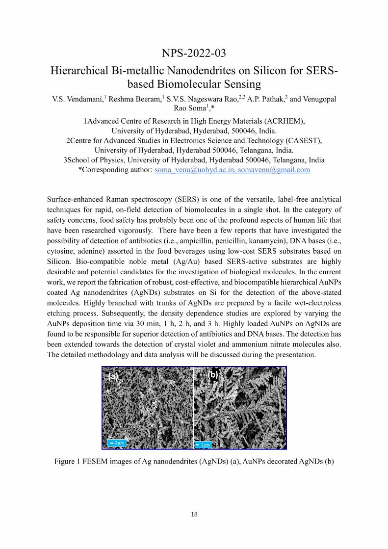
Figure 1 FESEM images of Ag nanodendrites (AgNDs) (a), AuNPs decorated AgNDs (b)
19
NPS-2022-04
Multi-modal stand-off LIBS-LIF-Raman spectroscopy system
for material characterization Dhanada V S*, Sajan D George, Santhosh Chidangil and Unnikrishnan V K*
Department of Atomic and Molecular Physics, Manipal Academy of Higher Education,
Manipal-576104, India
*Corresponding Authors: [email protected], [email protected]
The importance of remote detection of faraway targets with non-invasive or micro-destructive
spectroscopic techniques coupled with time-resolved detection has increased due to its
widespread applications and continued as a sensitive topic among different fields. However,
we focus on the most used remote laser-based novel detection techniques; Laser-induced
breakdown spectroscopy (LIBS), Raman spectroscopy, and Laser-induced fluorescence
spectroscopy (LIF), which are having the best potential to be selective, fast, sensitive, able to
identify many and different materials, and also extensible to new menaces. LIBS utilizes the
focusing of high energetic laser pulses to form a transient micro-plasma and fed to the detector
coupled spectrograph which disperses the incoming light into its wavelength components,
followed by further qualitative and quantitative analysis. Raman employs the inelastically
scattered radiation when a monochromatic beam of low energy incident upon the sample
surface. In LIF technique, upon laser excitation, an electronically excited state is produced by
the species of interest which then radiates subsequently. We have developed a compact multi-
modal stand-off spectroscopy system which comprises of a laser, beam expander, telescope and
a spectrograph with multi-analytical capability, which makes it fast, compact, reliable, and
cost-effective for field-based applications. The various experimental parameters such as gate
delay, gate width, laser energy, integration time were optimized using standard samples for
acquiring quality signals from a target sample kept at a remote distance. Thus, the new multi-
modal sensor fulfills the synergistic measurement scheme essential for a remote instrument that
can be utilized for various applications in the future. The optimized stand-off LIBS-LIF-Raman
system has been successfully employed for the analysis of different chemicals, minerals, and
liquid samples at various distances. We have also explored the feasibility of stand-off single
shot measurements using high throughput ICCD coupled CT spectrograph. The common
instrumentation for focusing and collection optics, laser source, and a detector enables the
hyphenation of LIBS, Raman, and LIF spectroscopy techniques in a single system and can be
used as a highly integrated multi-modal instrument for retrieving atomic and molecular
fingerprints.

20
NPS-2022-05
Ultra-low trace elemental detection in liquid sample using
Laser Induced Breakdown Spectroscopy Technique Keerthi K1, Sajan D George1, 2, Joju George Sebastian 3, Anish Kumar Warrier 3, 4, Santhosh
Chidangil1, 5 and Unnikrishnan V K1, 5* 1 Department of Atomic and Molecular Physics, Manipal Academy of Higher Education,
Manipal-576104, India 2 Centre for Applied Nanosciences, Manipal Academy of Higher Education, Manipal-576104,
India 3 Department of Civil Engineering, Manipal Institute of Technology, Manipal Academy of
Higher Education, Manipal-576104, India 4 Centre for Climate Studies, Manipal Academy of Higher Education, Manipal-576104, India
5 Centre of Excellence for Biophotonics, Manipal Academy of Higher Education, Manipal-
576104, India
*Corresponding author:[email protected]
Laser-Induced Breakdown Spectroscopy (LIBS) has aroused increasing interest in analytical
chemistry, biomedical and environmental fields due to its multi and trace elemental analysis
and real-time monitoring capability. However, LIBS studies on liquid samples often suffered
from the splashing and shorter plasma lifetime in a liquid environment that impede the
detection of the ultra-low concentration samples. The important challenge in the ongoing LIBS
application is to improve the limit of detection (LOD) from ppm to ultra-low concentration
(ppb, ppt) levels, particularly for liquid sample analysis. In the present work, we have compared
three different sampling approaches for trace elemental detection in aqueous samples: i) direct
bulk liquid ii) liquid jet iii) drop coating deposition of sample solution. Analysis of the results
elucidates that highly sensitive and reproducible LIBS spectra can be obtained using the drop
coating method. Undeniably, our drop coating deposition results established excellent
reproducibility with low limit of detection and it may be applicable for trace level elemental
detection in environmental liquid sample. The potential of the approach is demonstrated by
investigating the presence and bioaccumulation of trace elements in sediments from an East
Antarctic lake and water samples from River Swarna, southwest coast of India. The present
study demonstrates that the drop coating deposition technique is more advantageous in
investigating environmental applications with a sample volume as small as 10µl sample volume
in a single laser-pulse experiment.

21
NPS-2022-06
Spectroscopic investigation on the luminescent characteristics
of Dy3+ activated multicomponent borosilicate glasses for
W-LED applications Adon Jose1, 2, T Krishnapriya 1, Jeffin George2, Akshara Baby2, Cyriac Joseph1, P R Biju1
1 School of Pure & Applied Physics, Mahatma Gandhi University, Kottayam 686560, India 2 St.Stephen’s College, Uzhavoor, Kottayam 686634, India
E.mail : [email protected]
The spectroscopic exploration of Dy3+ activated multicomponent borosilicate glasses have
been performed via optical absorption, photoluminescence excitation and emission, CIE
chromaticity co-ordinates and correlated color temperature (CCT) values to investigate their
suitability in the advancement of solid state lighting and W-LEDs (white light-emitting diodes).
The oscillator strengths evaluated from the absorption spectrum were used to determine the
phenomenological Judd-Ofelt (JO) parameters through least square fitting procedure. The
photoluminescence emission spectra recorded for the Dy3+ activated multicomponent
borosilicate glasses under 348 nm excitation exhibit three emission bands which falls in the
yellow (4F9/2 →6H13/2), blue (4F9/2 →6H15/2) and red (4F9/2 →6H11/2) region. The
various radiative characteristics such as transition probability, branching ratio, emission cross-
section of the synthesised glass were evaluated by using JO intensity parameters. The
photoluminescence emission spectra were further characterized through the CIE chromaticity
diagram and the estimated color co-ordinates and CCT values recommend the prepared glasses
for various photonic applications.

22
NPS-2022-07
Effects of Initial Phase on Silicon Nanoparticles Formation in
Femtosecond laser Ablation Kanaka Ravi Kumar,1 B. Chandu,2 M.S.S. Bharati,2 M. Mallikarjuna Rao,4
S.V.S. Nageswara Rao,1,3,* S.Venugopal Rao,2 #
1 School of Physics
2Advanced Centre for Research in High Energy Materials (ACRHEM) 3 Centre for Advanced Studies in Electronics Sciences and Technology (CASEST), School of
Physics
4Department of Physics, SRM University, AP-Amaravati
University of Hyderabad, Hyderabad 50046, Telangana, India
Corresponding Author(s): [email protected], #[email protected]
We report here our results from the ultrafast laser ablation of monocrystalline Si (100),
polycrystalline Si, and Si (100) capped with SiO2 layer. The target material was ablated using
femtosecond laser pulses (~50 fs duration, 1 kHz repetition rate, 800 nm wavelength) with an
energy of ~100 µJ in acetone medium to fabricate Si Nanoparticles (NPs). The optical
properties of as-formed Si NPs were characterized by different spectroscopic techniques (UV-
Visible-NIR absorption spectra, Photoluminescence, and Raman) and these NPs were
characterized for their structural properties by TEM, HRTEM, and SAED analysis. It was
observed from the TEM data obtained that the average size of Si NPs produced by
monocrystalline Si (100) was found to be less than that of the NPs produced by polycrystalline
Si and the ablation of Si caped with SiO2 layer had resulted in the formation of bigger Si NPs
along with a low concentration of SiO2 NPs. Further, from HRTEM and SAED analysis, we
have observed polycrystalline Si NPs possessed (022), (012) planes from ablation of
monocrystalline Silicon; (011), (012), (110), (022) planes from ablation of polycrystalline Si;
and (101), (110), (201) (h, k, l) planes from the ablation of monocrystalline Si capped with
SiO2 layer. Therefore, we conclude that the initial bulk Si substrate type has majorly produced
only polycrystalline Si NPs possessing crystallite grains in different orientations (planes).
Complete details of the experiments and data analysis will be presented at the meeting.
23
NPS-2022-08
Surface Plasmon Polariton Assisted Self-Assembly of
Nanoparticles for SERS Applications Ghana Shyam C, Santhosh Chidangil and Aseefhali Bankapur*
Department of Atomic and Molecular Physics, Manipal Academy of Higher Education,
Manipal-576104
*Corresponding author: [email protected]
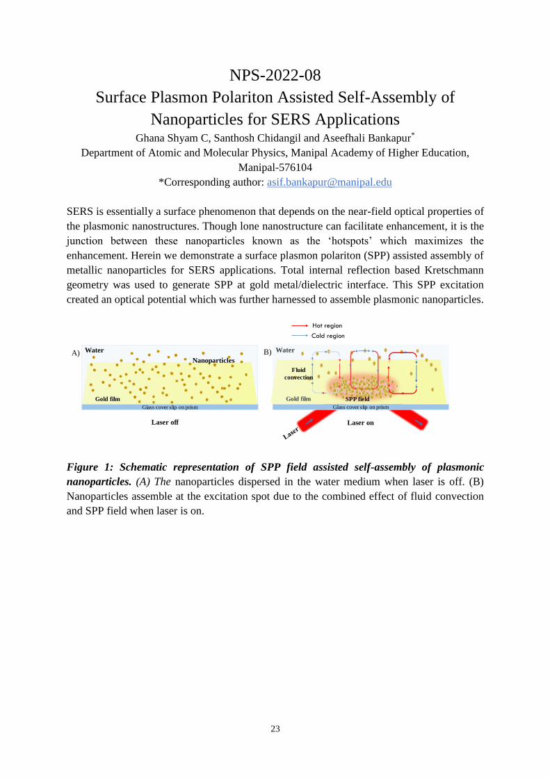
SERS is essentially a surface phenomenon that depends on the near-field optical properties of
the plasmonic nanostructures. Though lone nanostructure can facilitate enhancement, it is the
junction between these nanoparticles known as the ‘hotspots’ which maximizes the
enhancement. Herein we demonstrate a surface plasmon polariton (SPP) assisted assembly of
metallic nanoparticles for SERS applications. Total internal reflection based Kretschmann
geometry was used to generate SPP at gold metal/dielectric interface. This SPP excitation
created an optical potential which was further harnessed to assemble plasmonic nanoparticles.
Glass cover slip on prism
Water
Nanoparticles
Gold film
Laser off
Glass cover slip on prism
Water
Gold film
v
SPP field
Laser on
Fluid
convection
Hot region
Cold region
A) B)
Figure 1: Schematic representation of SPP field assisted self-assembly of plasmonic
nanoparticles. (A) The nanoparticles dispersed in the water medium when laser is off. (B)
Nanoparticles assemble at the excitation spot due to the combined effect of fluid convection
and SPP field when laser is on.
24
NPS-2022-09
Highly chromatic red light emitting Ca(1-x)Zn2(PO4)2:
xPr3+ phosphors for blue- chip excited WLEDs
T.Krishnapriya 1, Adon Jose1 and P R Biju1,* 1 School of Pure & Applied Physics, Mahatma Gandhi University, Kottayam, 686560,
Kerala, India
*Corresponding author: [email protected]
A concentration dependent spectroscopic analysis of highly chromatic red emitting Ca(1-
x)Zn2(PO4)2: xPr3+ (x= 0.02- 0.08) phosphors synthesized by solid state reaction method
have been performed. The obtained phosphors had a triclinic structure with P1 (2) space group.
The optical properties including reflectance, excitation, emission and the color coordinates
were investigated. The band gap of the phosphors was calculated from diffused reflectance
spectra data using the Kubelka- Munk function. The photoluminescence (PL) excitation spectra
showed the excitation peaks ranging from 430 to 490 nm. Under 444 nm blue photon excitation,
the phosphors emit red light due to 1D2→3H4 and 1D2→3H5 transitions of Pr3+.The optimal
concentration of Pr3+ was identified to be x= 0.04 after which concentration quenching occurs.
The colorimetric results suggest the phosphor to be of high color purity ∼ 100% and could be
an eventual choice as the red component in tricolor system used for solid state lighting.
NPS-2022-10
A D-shaped Elliptical Hollow Core Fiber SPR Sensor Tulika Khanikar1* and Vinod Kumar Singh1
1Optical Fiber Laboratory, Department of Physics, Indian Institute of Technology (Indian
School of Mines) Dhanbad, Jharkhand-826004, India.
*Corresponding author: [email protected]
A D-shaped elliptical hollow core fiber surface plasmon resonance (SPR) sensor is proposed
and analyzed here using gold and titanium oxide layer. The fiber geometry consists of a doped
elliptical core with a concentric central elliptical air hole. A finite element method-based
simulation software COMSOL Multiphysics is used for numerical analysis. Both gold and
TiO2 layers are optimized. The sensor responds over a wide range of refractive index (RI) from
1.33 to 1.40. The average sensitivity obtained for the designed sensor is 4142.85nm/RIU (RI
Unit) whereas that for a single mode fiber (SMF) is only 897.55nm/RIU. So, our designed
sensor gives more than 4 times enhanced sensitivity and proves to be a potential alternative of
SMF based low cost, compatible SPR sensors by covering the low sensitivity issue suffered by
SMF sensors.
NPS-2022-11
Evolution of Barium Bismuth Titanate Ceramic by Modified
Solid State Process and its Characterization Soumya Mukherjee1
1Department of Metallurgical Engineering, Kazi Nazrul University, Asanol-713340, West
Bengal, India
*Corresponding author: [email protected], [email protected]
Layered aurivillius bismuth-based prerovskite. Barium-bismuth titanate, BaBi4Ti4O15
(BBiT), was prepared from stoichiometric amounts of barium titanate and bismuth titanate by
modified solid state process. Sintering process was performed in atmospheric condition after
mixing in agate mortar-pestle. The thermal analysis of BaBi4Ti4O15 was studied by DSC-
TGA to identify phase transformation zone and consequent sintering at 1100 °C for 10 h and
15 hours heat treatment to be performed. Phase developed was identified from XRD pattern.
The bonding analysis and characteristics of BBiT ceramic powders were identified using FTIR
spectroscopy and Raman spectroscopy for its chemical formulations. The microstructure and
morphological development was analyzed from FESEM & HRTEM image. The granular size,
shape was observed from morphological features. The microstructure of BaBi4Ti4O15 exhibits
plate-like grains typical for the Bi-layered structural materials and spherical and polygonal
grains. The Ba2+ addition leads to changes in the microstructure development leading to
change in the average grain size. The optical property of BBiT was characterized by UV-VIS
spectroscopy. Band gap was estimated using Tauc relation and noted to be about 1.67, 1.62eV
(Direct & Indirect) while dielectric properties were estimated using LCR meter.
NPS-2022-12
Evolution of Sodium Niobate based Glass-Ceramic by Melt
Quenching and its Characterization Soumya Mukherjee1,
1Department of Metallurgical Engineering, Kazi Nazrul University, Asanol-713340, West
Bengal, India
*Corresponding author: [email protected], [email protected]
Glass-ceramic material based on sodium niobate in silica glass matrix doped with Eu3+was
synthesized by melt quenching process followed by controlled heat treatment. The activation
energy for crystallization of glass-ceramic was evaluated by Kissinger, Ozawa and Augis-
Bennet model. Activation energies were noted to be about 260.569kJ/mole, 279.37 kJ/mole
and 269.98 kJ/mole respectively. Ceramization of glass was carried at by double-stage heat-
treatment at 650°C for nucleation and crystal growth at varying temperatures of 700°C and
800°C for 5 h. Crystal phase developed through ceramization was identified by XRD analysis
followed by chemical bonding analysis through FTIR. Intensive chemical bonding analysis
was carried by Raman spectroscopy. Refractive Index was evaluated using a Prism Coupler
refractometer. Transmission spectra were evaluated using UV-VIS-NIR spectra while band gap
was evaluated using Tauc plot. For base glass band gap was noted to be 3.502eV while after
crystallization by ceramization heat-treatment band gap was reduced to 1.623eV respectively.
PL spectra of the glass-ceramic sample also studied to note emission behaviour after excitation
of samples at 395nm using Xenon lamp.
NPS-2022-13
Synthesis, linear and nonlinear optical properties of Ag and
Al2O3 nanoparticles
Tiny Thomas1, Vijayakumar S 2 *, Lekshmi Jayamohan 3, S Saravana kumar
1 Dept. of Physics, S.B College, Changanassery,686101, (Research centre-MG university)
India 2 PG and Research Dept.of Physics, N.S.S. College, Pandalam, 689501, India
3 Dept. of Physics, Christian College, Chenganoor, 689122, (Research Centre –University of
Kerala) India
Email: Corresponding author: [email protected]
This work reports a detailed study of the synthesis, characterization and third order nonlinear
optical properties of silver (Ag) and alumina (Al2O3) nanoparticles. The nano particles were
prepared by chemical precipitation method. X-ray diffraction studies confirm the purity, the
crystalline nature of the sample and also find out the crystallite size. The linear optical
properties and the structural morphology of the nano particles were confirmed by using the
UV-visible spectroscopy and SEM analysis. Open aperture Z-scan technique was used to study
the nonlinear absorption of the samples with a Q-switched CW Nd:YAG laser at 532 nm. Third
order nonlinear optical susceptibility(χ(3)) and nonlinear absorption coefficient(β) was
observed to be of the order of 10-4 esu and 10-6 cm/W respectively which reveals that the
samples are potential candidates for photonic applications.
NPS-2022-14
Fabrication of oxide photonic crystal thin film using scalable RF
sputtering method
Silpa S and Vinayak Kamble*
School of Physics, Indian institute of Science Education and Research Thiruvananthapuram, Vithura, Kerala
695551 India.
Photonic crystals (PCs) are optical analogues of electronic crystal lattice where light propagation is governed
by the spatial periodicity in the dielectric function. These not only exist in nature as a variety of colors in
biosystems, but they can be engineered using advanced synthesis tools and intricate symmetry designing.
Nevertheless, the ability to confine light and also forbid a certain range of frequencies, imparts PCs a
widespread utility in various applications such as optical communication, sensing, energy harvesting etc.1
Photonic band gaps(PBG) are the range of forbidden frequencies (energy band) formed in photonic crystals
due to periodicity of refractive indices. Thus, it is very important to design and fabricate structures of long
range periodic order. Mostly lithographic techniques are used to fabricate such PCs, however, those are of
limited scalability and throughput. In this work we demonstrate fabrication of Photonic crystal structure of
oxide opals thin films which could be used for various applications such as energy harvesting, sensing etc.
Copper Cobalt Oxide (CCO) is semiconductor with nearly 3 eV of band gap, however it shows a significant
absorption over the entire visible spectrum due to various defects. Here we use a self-assembled polystyrene
microsphere template followed by radio frequency magnetron sputtering technique to obtain a large area
photonic crystal with a sharp stop gap in the near IR region (peak at 1100 nm) due to periodicity of 500 nm.
CCO is a high spectral selective solar absorber material and its Opal PCs are developed for enhanced
photothermal conversion.
NPS-2022-15
Nonlinear optical properties of polyaniline doped with cardanol based
dye
Lekshmi Jayamohan1, Vijayakumar S2 *
1Dept. of Physics, Christian College, Chenganoor, 689122,(Research Centre –University of Kerala) India 2 PG and Research Dept.of Physics, N.S.S. College, Pandalam, 689501, India
Corresponding author: [email protected]
We report the third-order nonlinear optical properties of polyaniline doped with an azo dye synthesized using
cardanol. Cardanol, which is distilled from CSNL (Cashew Nut Shell Liquid), is a renewable resource since
it is a byproduct of the Cashew nut industry. The linear absorption spectrum of the sample was determined in
the wavelength range 100 – 800 nm. FTIR spectroscopic data of undoped and azo dye-doped polyaniline
samples were compared. The morphology and structure of the azo dye-doped polyaniline is studied using
SEM images and XRD. Nonlinear absorption studies were carried out using the single beam z scan technique.
A Q- switched Nd: Yag laser operating at 532 nm wavelength with a pulse width of 7 ns was used as the
source of light. The nonlinear absorption coefficient and nonlinear susceptibility were determined to be of the
order of 10-11 m/W and 10-13 esu respectively. These results indicate that the material is a good candidate
for optoelectronic applications.
NPS-2022-16
Design and analysis of micro-channelled Quasi D-shape
optical Fiber plasmonic Sensor
Maya Chauhan*, Sugandha Das, Vinod K. Singh
Optical Fiber Laboratory, Department of Physics
Indian Institute of Technology (ISM) Dhanbad, 826004, India.
*Corresponding author: [email protected]
This study reports on numerical investigation carried out over a newly designed open micro-
channel incorporated, side polished single mode fiber (SMF) based plasmonic sensor. Proposed
sensor operates on the principle of surface plasmon resonance (SPR) phenomenon to enhance
sensing performance. Commercially available COMSOL Multiphysics software tool is used to
design the sensor and finite element method is used for numerical investigation. From the detail
study, an average sensitivity of 1757 nm/RIU (refractive index unit) is obtained with nanoscale
gold strip for wide range of analyte RIs from 1.33 to 1.38. Result indicates that the designed
sensor can be effectively used in RI measurement in the various fields like chemical and
biological sensing.
NPS-2022-17
Digital Laser Combustion Method: Synthesis of Silver
Nanoparticles (AgNps)
Ganesh H Aralikatti1, Basavaraj H. G2 and Dr. Madhukumar R2,*
1B.Sc Final Year, Department of Physics, R.T.E.Society’s Arts Science and Commerce
Degree College, Ranebennur-581115, Karnataka, India 2Associate Professor, Department of Physics, R.T.E.Society’s Arts Science and Commerce
Degree College, Ranebennur-581115, Karnataka, India 2Assistant Professor, Department of Physics, R.T.E.Society’s Arts Science and Commerce
Degree College, Ranebennur-581115, Karnataka, India
*Corresponding author: [email protected]
Laser combustion is a green and simple method for synthesis of metal nanoparticles without
surfactant or chemical addition, and the properties of nanoparticles are unique. A variety of
preparation techniques have been reported for the synthesis of silver NPs; notable examples
include, laser ablation, gamma irradiation, electron irradiation, chemical reduction,
photochemical methods, microwave processing, and biological synthetic methods. In the
present work is relates to the design and development of digital combustion instrument for
synthesis of nanoparticles by laser combustion method. From this instrument we can able to
control the synthesis just by giving digital i/p, from this instrument we can prepare more sample
of linearly varying different physical variables with digital accuracy and it consume less time
and power, this instrument prepare a sample in such a way that it helps to further
characterization(XRD, SEM and UV-Vis).
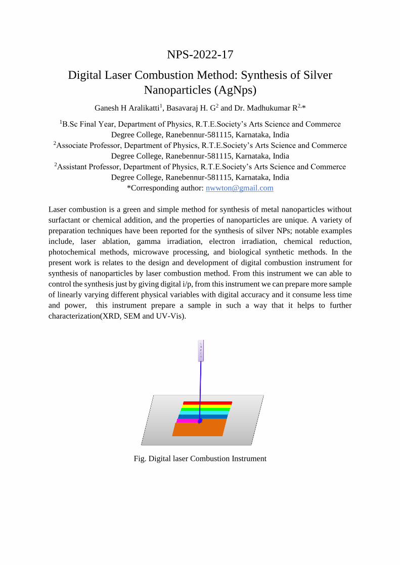
Fig. Digital laser Combustion Instrument
NPS-2022-19
Estimation of Random Duty Cycle in Periodically Poled
Lithium Niobate Through Second Harmonic Generation
Madhu, Prashant Povel Dwivedi*
Department of Electronics and Communication Engineering, Manipal University Jaipur,
Jaipur 303 007, Rajasthan India.
*Corresponding author: [email protected]
Periodic poling of lithium niobate (PPLN) is a technique for obtaining quasi-phase matching
(QPM) [1] of nonlinear interactions and Quasi-phase matching is a technique for phase
matching nonlinear optical interactions. PPLN involves processes which generate a periodic
reversal of the domain orientation in a lithium niobate, and sign of the nonlinear coefficient
also changes along the axis perpendicular to the optic axis of the crystal. There are numerous
of techniques which were developed for producing PPLN chips, but now a days electric-field
poling at room temperature is accepted as the most reliable one to date.
Fabrication of QPM devices from ferroelectrics crystals generates inevitable randomness in the
domain-wall locations in the QPM grating and we all know that errors (randomness) are
inherent in the fabrication process, which cannot be removed but can be minimized. One of the
possible causes of such errors is distribution of initial nucleation sites due to local strong
electric field effect and the deviations can lead to decreased efficiency or undesired function of
the devices such as parasitic harmonic generation which can cause green induced infrared
absorption (GRIIRA). Therefore, it is essential to keep RDE minimal.
In this paper, we analyse the influence of random duty error in PPLN devices which are formed
in the fabrication process (Electric Field Poling) and calculated the influence of the random
duty-cycle errors degenerate noise in second harmonic generation (SHG) consisting of PPLN
and we found that the normalized SHG Intensity-noise efficiency consists of two components.
The first component represents a flat PPLN noise ~ 1
2𝑁(1 − 𝑒−(𝜋𝜖𝑞)2
) that is independent of
the average duty ratio, but depends upon disorder and the number of periods in the sample. The
second part behaves as sinc2 (πNq) at SHG orders peaks, but reduced by the amount of
𝑒−(𝜋𝜖𝑞)2.
NPS-2022-20
Quality Evaluation of Quasi-Phase Matching (QPM) by
Diffraction-Noise
Prashant Povel Dwivedi*
Department of Electronics and Communication Engineering, Manipal University Jaipur,
Jaipur 303 007, Rajasthan India.
*Corresponding author: [email protected]
QPM is a method for achieving efficient energy transfer between interacting waves in nonlinear
process, which was first proposed by Armstrong et al. in 1962 . It is most efficient and practical
form of this technique is based on a spatial modulation of the nonlinear properties along the
interaction path in the material. Such a spatial modulation can be obtained in ferroelectric
crystals by periodically altering the crystal orientation so that the effective nonlinearity changes
according to the orientation and achieved great success with optical frequency conversion
devices such as second harmonic generation (SHG) and optical mediated oscillator. Fabrication
of QPM devices from ferroelectrics crystals generates inevitable randomness in the domain-
wall locations in the QPM grating. For a reasonably good QPM device, its standard deviation,
called the random duty-cycle error (RDE), gives quantitative estimation of the device quality.
If the RDE is large, then lead to decreased efficiency or undesired function of the devices such
as parasitic harmonic generation which can cause green-induced infrared absorption, etc.
Therefore, it is essential to keep RDE minimal. Various methods have been proposed to quality
evaluate of QPM devices. Among them microscopic imaging methods of chemically etched
crystal surface are more direct and accurate, but takes a long time, which is not desirable for
either device makers or users. Other methods based on nonlinear optical effect and indirect
method, among them, wavelength-tunable SHG is a representative one and gives a direct
estimation of the performance as other types of frequency conversion devices. The relationship
between the RDE and the efficiency of the SHG pedestal has been established in Ref, but same
experimental difficulties such as tunable narrow-line width sources, and the tuning range is
significantly limited by the tunable range of the pumping source. So, we propose a simple
method to assess the quality of the QPM device by analyzing the diffraction-noise pattern
(uniform and Gaussian beam) from the QPM device. In the uniform and Gaussian beam
diffraction-noise method, from 1st to 2nd order diffraction-noise patterns from the QPM were
analyzed to evaluate the RDE, the results were further verified by statistically analyzing the
microscopic image of the QPM grating. RDE with a Gaussian beam didn’t produce high-
frequency component between the diffraction orders so we can measure more accurate noise
away from the peaks compared with uniform beam.
NPS-2022-21
Nanoparticle Enhanced Femtosecond Laser Induced
Breakdown Spectroscopy of Aluminium Sheet coated with
gold Nano-particle Embedded nanofibers
N. Linga Murthy, M.S.S. Bharathi, S. Venugopal Rao*
Advanced Center of Research in High Energy Materials (ACRHEM), University of
Hyderabad, Hyderabad 500046, Telangana, India
Corresponding author e-mail: [email protected] OR [email protected]
Nanoparticle LIBS is useful in improving the sensitivity in detection of solids like metals,
precious gemstones and liquid samples. Femtosecond laser induced breakdown spectroscopy
(LIBS) signals can be enhanced in the presence of nanoparticles. We demonstrate two times
enhancement in the femtosecond LIBS spectra of aluminum sheet coated with the gold
nanoparticles embedded electro spin polyvinyl alcohol nanofibers. Gold nanoparticles were
fabricated using the femtosecond laser ablation the mean size of the nanoparticles fabricated
using laser ablation is 10 nm-15 nm. Enhancements were observed in the atomic and molecular
AlO emissions. The technique can further be optimized for better signal enhancement in the
molecular bands in of explosive traces.
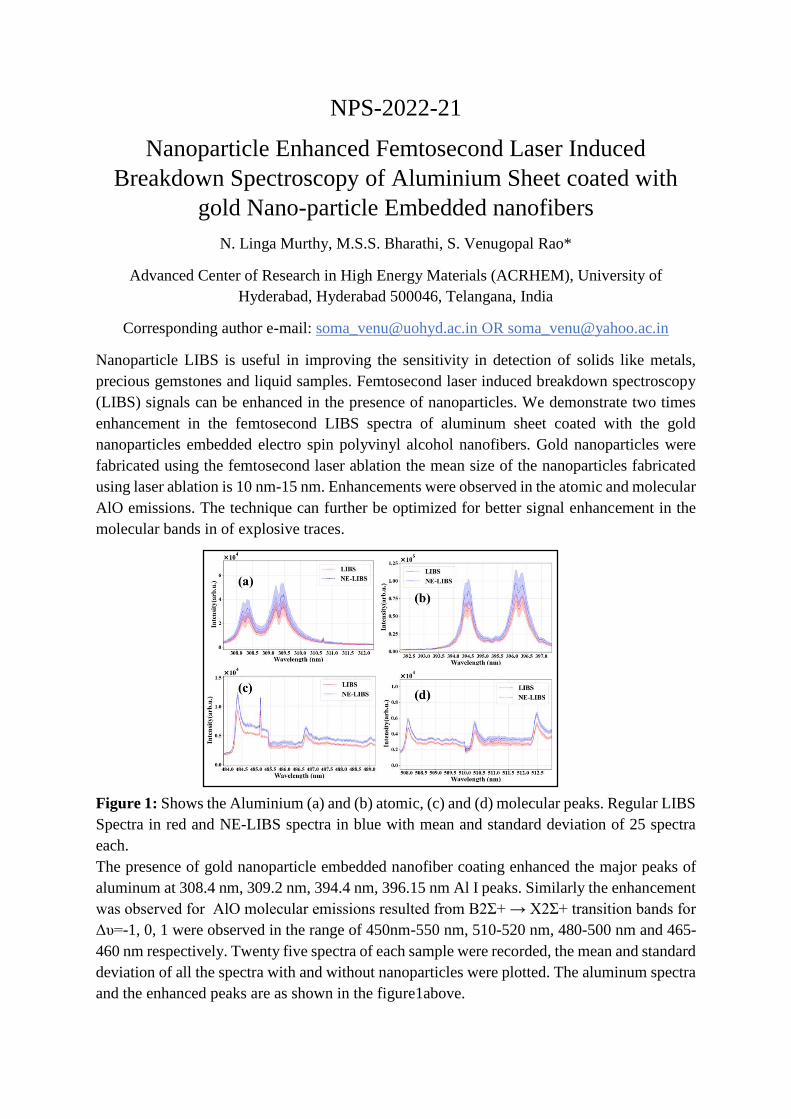
Figure 1: Shows the Aluminium (a) and (b) atomic, (c) and (d) molecular peaks. Regular LIBS
Spectra in red and NE-LIBS spectra in blue with mean and standard deviation of 25 spectra
each.
The presence of gold nanoparticle embedded nanofiber coating enhanced the major peaks of
aluminum at 308.4 nm, 309.2 nm, 394.4 nm, 396.15 nm Al I peaks. Similarly the enhancement
was observed for AlO molecular emissions resulted from B2Σ+ → X2Σ+ transition bands for
Δυ=-1, 0, 1 were observed in the range of 450nm-550 nm, 510-520 nm, 480-500 nm and 465-
460 nm respectively. Twenty five spectra of each sample were recorded, the mean and standard
deviation of all the spectra with and without nanoparticles were plotted. The aluminum spectra
and the enhanced peaks are as shown in the figure1above.
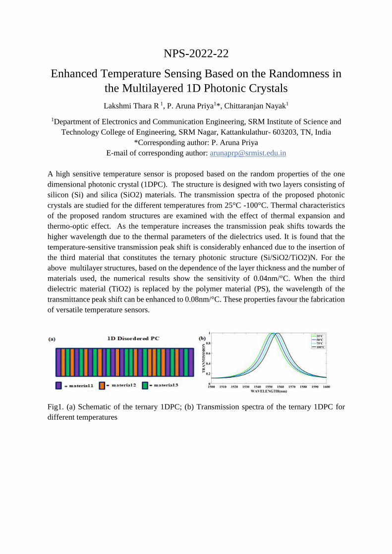
NPS-2022-22
Enhanced Temperature Sensing Based on the Randomness in
the Multilayered 1D Photonic Crystals
Lakshmi Thara R 1, P. Aruna Priya1*, Chittaranjan Nayak1
1Department of Electronics and Communication Engineering, SRM Institute of Science and
Technology College of Engineering, SRM Nagar, Kattankulathur- 603203, TN, India
*Corresponding author: P. Aruna Priya
E-mail of corresponding author: [email protected]
A high sensitive temperature sensor is proposed based on the random properties of the one
dimensional photonic crystal (1DPC). The structure is designed with two layers consisting of
silicon (Si) and silica (SiO2) materials. The transmission spectra of the proposed photonic
crystals are studied for the different temperatures from 25°C -100°C. Thermal characteristics
of the proposed random structures are examined with the effect of thermal expansion and
thermo-optic effect. As the temperature increases the transmission peak shifts towards the
higher wavelength due to the thermal parameters of the dielectrics used. It is found that the
temperature-sensitive transmission peak shift is considerably enhanced due to the insertion of
the third material that constitutes the ternary photonic structure (Si/SiO2/TiO2)N. For the
above multilayer structures, based on the dependence of the layer thickness and the number of
materials used, the numerical results show the sensitivity of 0.04nm/°C. When the third
dielectric material (TiO2) is replaced by the polymer material (PS), the wavelength of the
transmittance peak shift can be enhanced to 0.08nm/°C. These properties favour the fabrication
of versatile temperature sensors.
Fig1. (a) Schematic of the ternary 1DPC; (b) Transmission spectra of the ternary 1DPC for
different temperatures
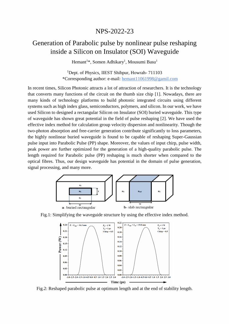
NPS-2022-23
Generation of Parabolic pulse by nonlinear pulse reshaping
inside a Silicon on Insulator (SOI) Waveguide
Hemant1*, Somen Adhikary1, Mousumi Basu1
1Dept. of Physics, IIEST Shibpur, Howrah- 711103
*Corresponding author: e-mail: [email protected]
In recent times, Silicon Photonic attracts a lot of attraction of researchers. It is the technology
that converts many functions of the circuit on the thumb size chip [1]. Nowadays, there are
many kinds of technology platforms to build photonic integrated circuits using different
systems such as high index glass, semiconductors, polymers, and silicon. In our work, we have
used Silicon to designed a rectangular Silicon on Insulator (SOI) buried waveguide. This type
of waveguide has shown great potential in the field of pulse reshaping [2]. We have used the
effective index method for calculation group velocity dispersion and nonlinearity. Though the
two-photon absorption and free-carrier generation contribute significantly to loss parameters,
the highly nonlinear buried waveguide is found to be capable of reshaping Super-Gaussian
pulse input into Parabolic Pulse (PP) shape. Moreover, the values of input chirp, pulse width,
peak power are further optimized for the generation of a high-quality parabolic pulse. The
length required for Parabolic pulse (PP) reshaping is much shorter when compared to the
optical fibres. Thus, our design waveguide has potential in the domain of pulse generation,
signal processing, and many more.
Fig.1: Simplifying the waveguide structure by using the effective index method.
Fig.2: Reshaped parabolic pulse at optimum length and at the end of stability length.
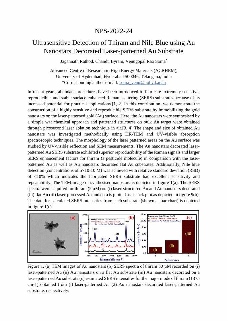
NPS-2022-24
Ultrasensitive Detection of Thiram and Nile Blue using Au
Nanostars Decorated Laser-patterned Au Substrate
Jagannath Rathod, Chandu Byram, Venugopal Rao Soma*
Advanced Centre of Research in High Energy Materials (ACRHEM),
University of Hyderabad, Hyderabad 500046, Telangana, India
*Corresponding author e-mail: [email protected]
In recent years, abundant procedures have been introduced to fabricate extremely sensitive,
reproducible, and stable surface-enhanced Raman scattering (SERS) substrates because of its
increased potential for practical applications.[1, 2] In this contribution, we demonstrate the
construction of a highly sensitive and reproducible SERS substrate by immobilizing the gold
nanostars on the laser-patterned gold (Au) surface. Here, the Au nanostars were synthesised by
a simple wet chemical approach and patterned structures on bulk Au target were obtained
through picosecond laser ablation technique in air.[3, 4] The shape and size of obtained Au
nanostars was investigated methodically using HR-TEM and UV-visible absorption
spectroscopic techniques. The morphology of the laser patterned areas on the Au surface was
studied by UV-visible reflection and SEM measurements. The Au nanostars decorated laser-
patterned Au SERS substrate exhibited superior reproducibility of the Raman signals and larger
SERS enhancement factors for thiram (a pesticide molecule) in comparison with the laser-
patterned Au as well as Au nanostars decorated flat Au substrates. Additionally, Nile blue
detection (concentrations of 5×10⁻¹⁰ M) was achieved with relative standard deviation (RSD)
of <10% which indicates the fabricated SERS substrate had excellent sensitivity and
repeatability. The TEM image of synthesised nanostars is depicted in figure 1(a). The SERS
spectra were acquired for thiram (5 µM) on (i) laser-structured Au and Au nanostars decorated
(iii) flat Au (iii) laser-processed Au and data is plotted as a stack plot as depicted in figure 9(b).
The data for calculated SERS intensities from each substrate (shown as bar chart) is depicted
in figure 1(c).
Figure 1. (a) TEM images of Au nanostars (b) SERS spectra of thiram 50 µM recorded on (i)
laser-patterned Au (ii) Au nanostars on a flat Au substrate (iii) Au nanostars decorated on a
laser-patterned Au substrate (c) estimated SERS intensities for the major mode of thiram (1375
cm-1) obtained from (i) laser-patterned Au (2) Au nanostars decorated laser-patterned Au
substrate, respectively.
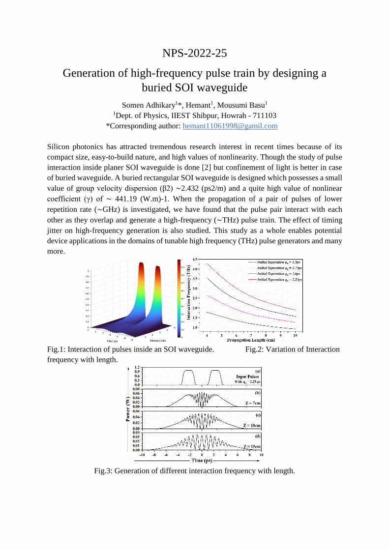
NPS-2022-25
Generation of high-frequency pulse train by designing a
buried SOI waveguide
Somen Adhikary1*, Hemant1, Mousumi Basu1
1Dept. of Physics, IIEST Shibpur, Howrah - 711103
*Corresponding author: [email protected]
Silicon photonics has attracted tremendous research interest in recent times because of its
compact size, easy-to-build nature, and high values of nonlinearity. Though the study of pulse
interaction inside planer SOI waveguide is done [2] but confinement of light is better in case
of buried waveguide. A buried rectangular SOI waveguide is designed which possesses a small
value of group velocity dispersion (β2) ∼2.432 (ps2/m) and a quite high value of nonlinear
coefficient (γ) of ∼ 441.19 (W.m)-1. When the propagation of a pair of pulses of lower
repetition rate (∼GHz) is investigated, we have found that the pulse pair interact with each
other as they overlap and generate a high-frequency (∼THz) pulse train. The effect of timing
jitter on high-frequency generation is also studied. This study as a whole enables potential
device applications in the domains of tunable high frequency (THz) pulse generators and many
more.
Fig.1: Interaction of pulses inside an SOI waveguide. Fig.2: Variation of Interaction
frequency with length.
Fig.3: Generation of different interaction frequency with length.

NPS-2022-26
Si-based incident angle-sensitive reflective wavelength
separator: a single-step FIB lithography based nanopatterning
application
Ramanathaswamy Pandian1*, Rajagopal R2, Hrudya Radhakrishnan1, G. Mangamma1, S.
Dhara1
1Surface and Nanoscience Division, Materials Science Group, Indira Gandhi Centre for
Atomic Research, A CI of HBNI, Kalpakkam - 603102, Tamil Nadu, India 2 Department of Nano Science and Technology, Central University of Jharkhand, Ranchi -
835 222, India
*Corresponding author: [email protected]
Inspired by nature, morpho-butterfly for example, the topic of research on engineering light at
nanoscale using subwavelength nanopatterns or nanostructures fabricated on surfaces of
various materials including dielectric, metallic and metalodielectric has been receiving
significant attention in recent years. The nanostructure-influenced visible colours arise from
resonant scattering of light from subwavelength structures and hence referred as structural
colors. Due to the enhanced color purity (via selective absorption of a narrow band of incident
light wavelengths) structural colors show great potential for several applications including
colour printing, optical security, energy-efficient displays, ultrahigh-resolution imaging,
ultrahigh-sensitivity biosensors and building-integrated photovoltaics. Manipulating light by
the organized array of nanopatterns/nanostructures is primarily dependent on the shape and
dimensions of the individual pattern/structure element. It is also influenced by the spatial
arrangement of the pattern/structure element. In this piece of work, we demonstrate generation
of vivid colours in reflection mode from the nanopatterns fabricated on a silicon substrate,
which is less expensive, has high-index and well applied in all the above-mentioned
applications. Nanopatterns were produced on Si by focused ion beam based nanolithography
technique in a single step. Basic element of the nanopatterns was a conical-shaped etch-pit,
with diameter ranging from 100 to 300 nm and depth from 50 to 150 nm on Si. Influence of
the spatial arrangement of the pattern elements on the reflected light and wavelength separation
was qualitatively and quantitatively analysed and discussed.
NPS-2022-27
Structural, Cytotoxic and Anti Cancerous Studies on
Er3+:Y2O3 Nanophosphors
Sreejaya T S1, Deepthi N Rajendran2* 1Department of Physics, Govt. College for Women, Thiruvananthapuram, University of
Kerala, Kerala, India 2Department of Physics, Govt. College for Women, Thiruvananthapuram, University of
Kerala, Kerala, India
* Corresponding author: [email protected]
Lanthanide doped upconverting nanomaterials are widely used in the field of biomedical
imaging because of its high luminescent efficiency and low cytotoxicity. The upconverting
nanomaterials are used for the imaging since These materials have excitation in Near Infra-Red
region1,2,3. Y2O3: xEr3+ (x= 1,2 and 3%) were prepared by sol citrate gel method and
calcinated at temperature 6000C for 2hrs.Structural studies of the synthesized samples were
carried out by XRD analysis. The pattern obtained shows cubic phase4 and the crystallite size
obtained for the samples were 6.1nm,6.4nm and 7.2nm respectively. Flakes like morphology
was obtained from SEM micrographs. EDS study confirmed the chemical composition. Optical
band gap energies obtained for samples x=1,2 and 3% are 5.50eV,5.46eV and 5.43eV
respectively. Cytotoxic and anticancerous studies done on samples proved that the prepared
samples have low toxicity which can be used for biomedical applications.
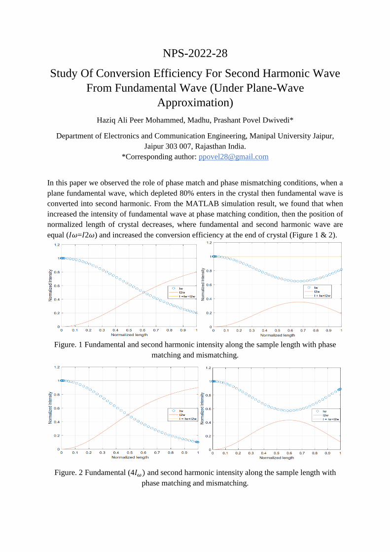
NPS-2022-28
Study Of Conversion Efficiency For Second Harmonic Wave
From Fundamental Wave (Under Plane-Wave
Approximation)
Haziq Ali Peer Mohammed, Madhu, Prashant Povel Dwivedi*
Department of Electronics and Communication Engineering, Manipal University Jaipur,
Jaipur 303 007, Rajasthan India.
*Corresponding author: [email protected]
In this paper we observed the role of phase match and phase mismatching conditions, when a
plane fundamental wave, which depleted 80% enters in the crystal then fundamental wave is
converted into second harmonic. From the MATLAB simulation result, we found that when
increased the intensity of fundamental wave at phase matching condition, then the position of
normalized length of crystal decreases, where fundamental and second harmonic wave are
equal (𝐼𝜔=𝐼2𝜔) and increased the conversion efficiency at the end of crystal (Figure 1 & 2).
Figure. 1 Fundamental and second harmonic intensity along the sample length with phase
matching and mismatching.
Figure. 2 Fundamental (4𝐼𝜔) and second harmonic intensity along the sample length with
phase matching and mismatching.
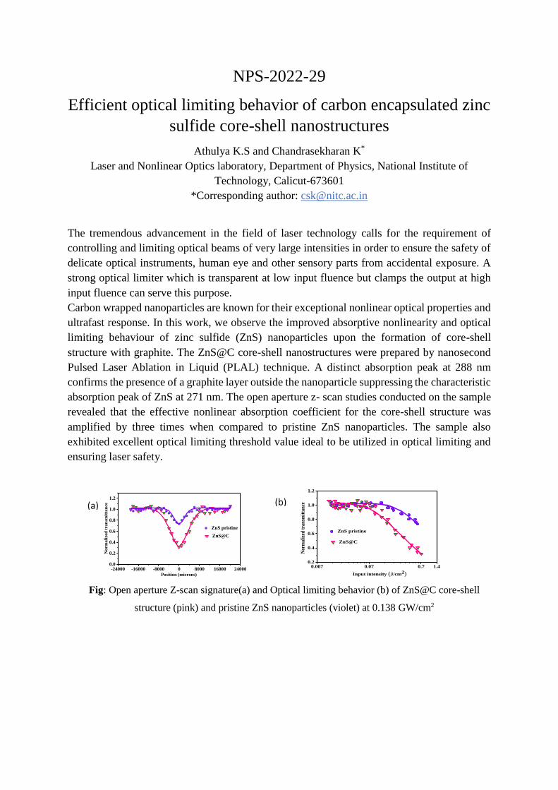
NPS-2022-29
Efficient optical limiting behavior of carbon encapsulated zinc
sulfide core-shell nanostructures
Athulya K.S and Chandrasekharan K*
Laser and Nonlinear Optics laboratory, Department of Physics, National Institute of
Technology, Calicut-673601
*Corresponding author: [email protected]
The tremendous advancement in the field of laser technology calls for the requirement of
controlling and limiting optical beams of very large intensities in order to ensure the safety of
delicate optical instruments, human eye and other sensory parts from accidental exposure. A
strong optical limiter which is transparent at low input fluence but clamps the output at high
input fluence can serve this purpose.
Carbon wrapped nanoparticles are known for their exceptional nonlinear optical properties and
ultrafast response. In this work, we observe the improved absorptive nonlinearity and optical
limiting behaviour of zinc sulfide (ZnS) nanoparticles upon the formation of core-shell
structure with graphite. The ZnS@C core-shell nanostructures were prepared by nanosecond
Pulsed Laser Ablation in Liquid (PLAL) technique. A distinct absorption peak at 288 nm
confirms the presence of a graphite layer outside the nanoparticle suppressing the characteristic
absorption peak of ZnS at 271 nm. The open aperture z- scan studies conducted on the sample
revealed that the effective nonlinear absorption coefficient for the core-shell structure was
amplified by three times when compared to pristine ZnS nanoparticles. The sample also
exhibited excellent optical limiting threshold value ideal to be utilized in optical limiting and
ensuring laser safety.
(a)
Fig: Open aperture Z-scan signature(a) and Optical limiting behavior (b) of ZnS@C core-shell
structure (pink) and pristine ZnS nanoparticles (violet) at 0.138 GW/cm2
(b)
0.0
0.2
0.4
0.6
0.8
1.0
1.2
-24000 -16000 -8000 0 8000 16000 24000
ZnS@C
Norm
ali
zed
tra
nsm
itta
nce
ZnS pristine
Position (microns)
0.07 0.70.007 1.40.2
0.4
0.6
0.8
1.0
1.2
Input intensity (J/cm2)
Nor
mal
ized
tra
nsm
itta
nce
ZnS pristine
ZnS@C

NPS-2022-31
Copper-based Surface Plasmon Coupled Emission Steering
for Biosensor Applications
Ajeesh P. Vijayan1, A.Sreelakshmi Fasna Sharin and Pradeesh Kannan*
1Department of Physics, Government Victoria College Palakkad, Kerala, India
(Affiliated to University of Calicut, India)
*Corresponding author: [email protected]
Surface plasmon resonance (SPR) is an established technique, used to study bio-chemical and
bio-molecular interactions, detection of lipid bilayer membranes, detection of molecules, etc.1
SPR coupled with fluorescence has been widely used in the field of research for fluorescence
imaging, molecular detection, etc. Surface plasmon coupled emission (SPCE) based on
Reverse-Kretchmann (RK) configuration utilises near field interaction of fluorescence with
metal thin films. This is a promising strategy for optical biosensors because of its great
directionality of emission, better surface selectivity, emission tuning as well as better plasmon
excitation.2-3 Substrates like silver (Ag) and gold (Au) thin films are widely used for SPR
applications due to its high plasmon oscillations within visible region4-5. Few works on SPR
sensors were based on copper (Cu) substrates. While several literatures report on SPCE based
on Ag and Au substrates, there are very few reports on SPCE based on copper substrates. In
the present work we have explored plasmon coupled emission studies on Cu substrates.
Samples for SPCE studies were fabricated by stacking metal-dielectric layers. Copper metal
(thickness ~ 55 nm) was first deposited on a cleaned glass substrate by sputtering technique.
Rhodamine B dye mixed with Polyvinyl Alcohol (PVA) in DI water was then coated on top of
Cu film by spin coating method. Thickness of dielectric layer was varied by varying PVA
concentration and by varying spin parameters. Fabricated films were then coupled to a
hemicylindrical prism arranged in RK configuration. The fluorescence molecules within PVA
were excited using 512 nm laser. Emission spectra were then recorded from prism side (RK
configuration) using an optical fibre coupled compact spectrometer. Angle dependant emission
spectra were recorded for all the fabricated samples. All the samples show emission
directionality confirming SPCE. As the thickness of PVA was increased, the emission direction
shifts to higher angle of detection showing a correlation of emission directionality with
dielectric layer thickness. Thus, by coupling SPR with emission, we could conveniently steer
the emission.

NPS-2022-32
Synthesis and Characterization of Oleic Acid mediated
growth of Single crystal perovskites: Optimisation of trap
density and mobility
Aiswarya M., Prateek.M, Sujith.P, Saranya Babu, and P.Predeep *
Laboratory for molecular photonics and electronics (LAMP), Department of Physics,
National Institute of Technology, Calicut,
*Corresponding author: [email protected]
In recent years, organic-inorganic hybrid perovskite single crystals advanced to the frontline
of various applications such as photodetectors, photovoltaic devices, light emitting devices,
sensors and memory devices owing to facile synthesis and its outstanding optoelectronic
properties. Addition of exotic ligand molecules in single crystal perovskites can refine the
morphology, trap density and mobility. Long chain amine ligands can improve interfacial
carrier transport, and defect passivation efficacy. This paper presents the synthesis and
characterization of ligand mediated growth of single crystal to improve the performance and
stability of methyl ammonium lead iodide single crystals. Oleic acid, an unsaturated
hydrocarbon chain with one double bond and a carboxylic acid group, added as the ligand, can
enhance the carrier mobility, reduce trap density and improve surface morphology.
NPS-2022-33
Effect of Solution and Dry processing techniques on the
Optical and transport properties of Inorganic CsPbBr3
Perovskite films
Sujith.P1,2, Prateek.M1, Aiswarya M1, Saranya Babu1, P. Saidy Reddy2 and P.Predeep1 *
Laboratory for molecular photonics and electronics (LAMP), Department of Physics,
National Institute of Technology, Calicut, 2Department of Applied Sciences, National Institute of Technology Goa, Farmagudi, Ponda ,
Goa - 403401
*Corresponding author: [email protected]
Caesium based inorganic, CsPbBr3 perovskite material possesses remarkable optoelectronic
properties, such as high light absorption coefficient, high carrier mobility, and long diffusion
length, and hence has promising applications in solar cells, photodetectors, and high-energy
radiation detectors, among others. Because of its simplicity, low cost, and high efficiency, spin-
coating deposition for CsPbBr3 perovskite layer for such diverse has been widely used.
However, the spin-coating technique has a technological constraints when it comes to
uniformly depositing large area films. Thermal evaporation, on the other hand, is inexpensive
and produces a uniform and repeatable thin film. In this study, the stability, energy band
alignment, surface morphologies, and light absorption of a CsPbBr3 perovskite layer produced
by spin coating and thermal evaporation are investigated and discussed.
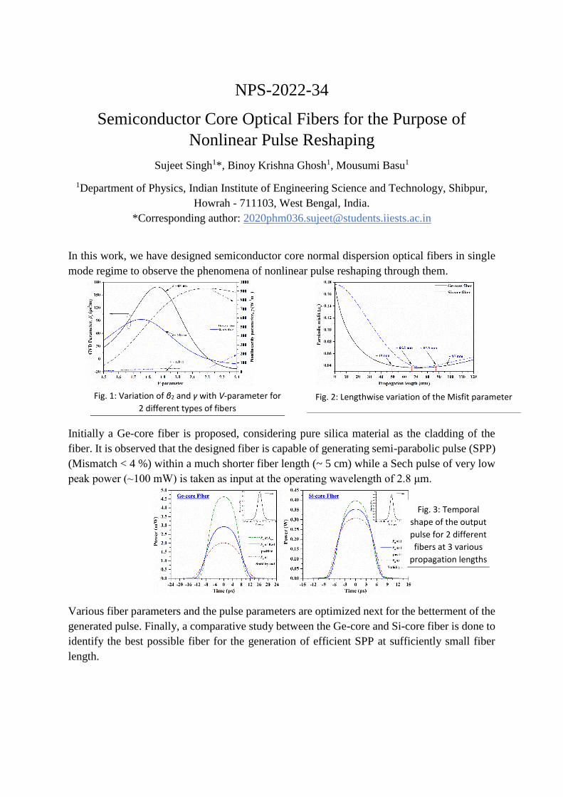
NPS-2022-34
Semiconductor Core Optical Fibers for the Purpose of
Nonlinear Pulse Reshaping
Sujeet Singh1*, Binoy Krishna Ghosh1, Mousumi Basu1
1Department of Physics, Indian Institute of Engineering Science and Technology, Shibpur,
Howrah - 711103, West Bengal, India.
*Corresponding author: [email protected]
In this work, we have designed semiconductor core normal dispersion optical fibers in single
mode regime to observe the phenomena of nonlinear pulse reshaping through them.
Initially a Ge-core fiber is proposed, considering pure silica material as the cladding of the
fiber. It is observed that the designed fiber is capable of generating semi-parabolic pulse (SPP)
(Mismatch < 4 %) within a much shorter fiber length (~ 5 cm) while a Sech pulse of very low
peak power (~100 mW) is taken as input at the operating wavelength of 2.8 μm.
Various fiber parameters and the pulse parameters are optimized next for the betterment of the
generated pulse. Finally, a comparative study between the Ge-core and Si-core fiber is done to
identify the best possible fiber for the generation of efficient SPP at sufficiently small fiber
length.
Fig. 1: Variation of β2 and γ with V-parameter for
2 different types of fibers Fig. 2: Lengthwise variation of the Misfit parameter
Fig. 3: Temporal
shape of the output
pulse for 2 different
fibers at 3 various
propagation lengths
NPS-2022-35
The optical linear and nonlinear exploration in a newly
synthesized organic chromophore for photonic applications
Mohd Mehkoom1*, Abid Ali2, Sultan1, Farman Ali2, and S. M. Afzal1
1Department of Physics, Aligarh Muslim University, Aligarh-202002, India.
2Department of Applied Chemistry, Faculty of Engineering and Technology, Aligarh Muslim
University, Aligarh-202002, India.
*Corresponding author: [email protected]
The present article demonstrates the optical linear and nonlinear studies of the chromophore
2,2'-(hexane-1,6-diylbis(9H-carbazole-9,3-diyl))bis(ethene-1,1,2-tricarbonitrile (HCzN).
Herein the carbazole as rich in electron mobility and attached with a strong electron-
withdrawing nitrile Group (EWG), shows the bear an enhanced dipole moment. We have
synthesized this molecule and the structure of this molecule has been confirmed via IR and
NMR spectroscopies. The linear optical study has been done with the help of UV-Vis
absorption and emission spectra in solution form (Acetone as solvent) at a concentration of 10-
3 M. The different linear optical characteristics as transmittance, absorption coefficient (α0),
refractive index (n0), optical conductivity (σ) and optical bandgap (Eg) have been calculated
at this concentration. The magnitude of these parameters is comparable with those of reported
compounds. The nonlinear optical study for this chromophore has been done using the Z-scan
technique in the solution form (Acetone as solvent). We have explored the third-order nonlinear
optical characteristics of HCzN at the different solution concentrations of 1, 2, 3, and 4 mM
employing both close and open aperture z-scan method using the Diode laser at 520 nm with a
maximum power of 120 mW. This chromophore evinces the self-defocusing and saturable
absorption nature for close and open aperture scans respectively. We have calculated third-
order nonlinear absorption coefficient (β), nonlinear refractive index (n2), nonlinear optical
susceptibility (χ(3)), and second-order hyperpolarizability (γ) for all concentrations and at 25
mW laser power. The values of n2, β, χ(3), and γ are found to be with the order of 10-6 cm2/W,
10-3 cm/W, 10-5 esu, and 10-27 esu respectively. The magnitude of n2, β, χ(3) increases almost
linearly with an increase in the solution concentration whereas the magnitude of γ decrease
almost linearly with concentration. The values of NLO parameters of HCzN are found to be
comparably large with those of related reported molecules. These large values of NLO
parameters support the good NLO behavior of HCzN. Hence this chromophore is a good
candidate for different photonic applications like optical communication, optical switching,
and optical data storage devices.
NPS-2022-37
Microfabrication using direct laser writer
K. Prabakar*, S. Balasubramanian, M. Raghuramaiah, S. Tripura Sundari and Sandip Dhara
Surface and Nanoscience Division, Materials Science Group,
Homi Bhabha National Institute, IGCAR, Kalpakkam – 603102.
*Corresponding author: [email protected]
Direct Laser Writing (DLW) is a mask-less lithographic technique which is emerging as an
interesting new technology for micro/nano fabrication. In this method, a laser beam (405 nm)
is used to transfer the pattern from a soft mask onto a photoresist coated substrate in serial
fashion. We have fabricated various microstructures such as microcantilevers, micro-bridges,
controlled micro-patterns and electrodes for 2D materials using DLW and wet chemical etching
methods. Various process parameters optimized such as stiction, laser dose, pre- and post-
baking temperature/time will be discussed [1]. Resonance frequency and curvature of
successfully released devices were carried out using nano vibration analyser and 3D optical
microscope. Ultrasensitive and ultrafast RH sensing using surface enhanced microcantilevers
is demonstrated [2]. Photo-induced deflection in Au/Si microcantilevers was also studied for
non-contact actuation and temperature sensing applications. It is shown that a maximum
temperature sensitivity of ∼ 62 mK/nm can be achieved by tuning the laser parameters and
microcantilever dimensions .
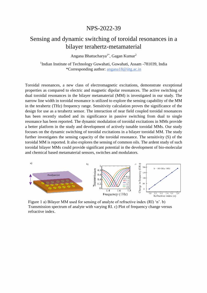
NPS-2022-39
Sensing and dynamic switching of toroidal resonances in a
bilayer terahertz-metamaterial
Angana Bhattacharya1*, Gagan Kumar2
1Indian Institute of Technology Guwahati, Guwahati, Assam -781039, India
*Corresponding author: [email protected]
Toroidal resonances, a new class of electromagnetic excitations, demonstrate exceptional
properties as compared to electric and magnetic dipolar resonances. The active switching of
dual toroidal resonances in the bilayer metamaterial (MM) is investigated in our study. The
narrow line width in toroidal resonance is utilized to explore the sensing capability of the MM
in the terahertz (THz) frequency range. Sensitivity calculation proves the significance of the
design for use as a terahertz sensor. The interaction of near field coupled toroidal resonances
has been recently studied and its significance in passive switching from dual to single
resonance has been reported. The dynamic modulation of toroidal excitations in MMs provide
a better platform in the study and development of actively tunable toroidal MMs. Our study
focuses on the dynamic switching of toroidal excitations in a bilayer toroidal MM. The study
further investigates the sensing capacity of the toroidal resonance. The sensitivity (S) of the
toroidal MM is reported. It also explores the sensing of common oils. The ardent study of such
toroidal bilayer MMs could provide significant potential in the development of bio-molecular
and chemical based metamaterial sensors, switches and modulators.
Figure 1 a) Bilayer MM used for sensing of analyte of refractive index (RI) ‘n’. b)
Transmission spectrum of analyte with varying RI. c) Plot of frequency change versus
refractive index.

NPS-2022-40
Hardware Development for Internet of Things-based Real-
Time Blood Glucose Monitoring Using
Photoplethysmography
Abubeker K M1, Baskar S2
Research Scholar1, Assistant Professor2
Dept. of ECE, Karpagam Academy of Higher Education, Coimbatore, India, 641 0211,2
*Corresponding Author 1: [email protected], [email protected]
Diabetes has been recently listed the tenth largest cause of mortality, accounting for 1.5
million fatalities, and it causes blindness, kidney failure, coronary artery disease, and even
diabetic agony. The global diabetes compact has established by the world health organization
(WHO) in 2021, bringing together governments, nongovernmental groups and academic and
research institutions to collaborate on a goal of lowering diabetes risk and ensuring cheap and
high-quality treatment and care for all people. Preexisting diabetes and hyperglycemia, when
discovered during pregnancy, may have major effects on both the mother's and the baby's
health; in particular, these disorders raise the chance of miscarriage and perinatal morbidity
and death. Worldwide, it is estimated that one in every seven pregnant women has
hyperglycemia, and many cases of gestational diabetes go undetected, with potentially fatal
consequences for both mother and child.
In recent years, bedside blood glucose monitors have become the predominant form of
patient assistance. Using non-invasive wearable devices and the Internet of Healthcare Things
(IoHT), blood glucose levels may now be monitored more accurately. ICU patients and
expectant mothers have a constant battle to keep their blood glucose (BG) levels in check,
which includes dealing with both hyper and hypoglycemia. Since internet-based healthcare
systems heavily rely on technology, ensuring adequate glucose control for pregnant women
and the ICU must be addressed cost-effectively. Using photoplethysmograph and machine
learning approaches, this research developed a hybrid non-invasive internet of things based BG
monitoring using near-infrared (NIR) spectroscopy. The developed IoT gadget is designed
with Max30102 and Mlx90614 for blood glucose absorption and body temperature
measurement respectively. The developed Hardware and support vector machine (SVM) model
is deployed in Raspberry Pi 4B computer with graphical processing unit (GPU) support. A non-
invasive glucose monitor that is more accurate than existing GM technology would be a big
step forward. This hybrid model offers 93.76% prediction accuracy and adaptability within the
range of clinical laboratory precision criteria.
NPS-2022-41
Power dependent nonlinear optical characteristics and
two-photon absorption of NiO/PVA thin film
V PRADEEP KUMAR 1*, C PRADEEP1, P RADHAKRISHNAN1, A MUJEEB1
1 international school of photonics
Cochin university of science and technology
*Corresponding author: [email protected]
The NiO/PVA thin film was prepared by drop-casting the NiO nanoparticles synthesized
by chemical precipitation method. The structural and optical properties of the film were studied
by the XRD and UV-VIS absorption. The surface roughness and particles distribution were
realized by atomic force microscopy and FESEM. The optical nonlinear property of the Nickel
oxide thin film was studied by the open aperture Z-scan method at 532 nm. The two-photon
absorption coefficient of the film was calculated with different optical intensities. The
nonlinear absorption coefficient has undergone a reduction with an increase in input intensity.
This is attributed to the saturation two photon absorption process. The process can be explored
for optical limiting applications.
NPS-2022-42
Fast imaging and spectroscopic study of single and colliding
laser produced plasmas
Shilpa S.1 and Pramod Gopinath 1,2*
1International School of Photonics, Cochin University of Science and
Technology, Kochi 682022, India
2Inter University Centre for Nanomaterials and Devices, Cochin University of Science and
Technology, Kochi 682022, India
*Corresponding author: [email protected].
The propagation dynamics of single and colliding laser-produced aluminium plasmas were
investigated using fast imaging and spectroscopic techniques. The collision of two laser-
produced seed plasmas resulted in the formation of a stagnation region in the collision front.
Time gated Intensified Charge-Coupled Device (ICCD) imaging was used to study the
temporal evolution of plasma. The forward expansion velocity of the stagnation region was
less than that of single plasma due to the additional complex collision process underlying the
stagnation region. Time-resolved spectroscopy was used to obtain information about the
distribution of neutral and ionic species in single plasmas and seed and stagnation region of
colliding laser-produced plasmas. Greater concentration of ionic species was found in the
stagnation region with a longer life time. Electron density and temperature were also calculated
from the emission spectra.
NPS-2022-43
Characterization of Laser-Driven Air Sparks Using Self
Emission and Rayleigh Scattering Studies
Anu Avarachan1*, Abhirami M. R1, Jefry John1, Meenu M. S1, Jinsi C. P1, Akhil Varghese1,
Riju C. Issac1*
1 Intense LAser Interaction (ILAI) Group
Department of Physics
Cochin University of Science and Technology (CUSAT), Kochi – 682022
*Corresponding author: [email protected]
Air plasma produced in a laboratory atmosphere by focusing the second harmonic radiation
from a Q switched Nd: YAG laser (532 nm,10 ns,10 Hz) is characterized using optical methods.
Self-emission from the plasma is studied at earlier times of its lifecycle, using emission
spectroscopy arrangement. The setup is used to analyze the optical emission lines and Rayleigh
scattered lines from the air plasma as a function of the vertical angle with the direction of
polarization. Measured line profiles of different ionic species were used to calculate the plasma
electron temperature and density at different angular positions. Line intensities of excited states
of singly ionized Nitrogen (N II) were used for electron temperature calculations. Stark
broadened profiles of singly ionized species and Hα lines have been utilized for electron density
measurements. The assumption of local thermodynamic equilibrium conditions is verified in
light of the measured plasma parameters.

NPS-2022-44
Laser ablated silver nanoparticles doped blue light
emitting polymer optical fiber with enhanced
photostability
B. Anugop*, M. Kailasnath
International School of Photonics, Cochin University of Science and Technology, Kerala-
682022
*Corresponding author: [email protected]
Here we present the fabrication of stable 1,4-Bis(2-methylstyryl) benzene (Bis-MSB)
doped polymer optical fiber containing silver nanoparticles. Spherical silver nanoparticles of
approximate size 15nm were fabricated using nanosecond laser ablation. The emission
characteristics of the polymer optical fiber were analysed using a Q-switched Nd:YAG laser
operating at 355 nm. The pump pulse energy (PPE) dependent emission spectra from the fiber
were analysed. The observed fluorescence emission was turned to amplified spontaneous
emission (ASE) at a PPE of 2.5mJ. The study shows that, at an optimum concentration of Ag
nanoparticles, the fiber offers better photostability. The proposed fiber may find potential
applications in the development of stable directional optical sources in the blue region.
Fig.1. (Left) HRTEM image of laser-ablated Ag nanoparticles in MMA (Right) Photograph of
amplified spontaneous emission under 355nm pulsed laser excitation
NPS-2022-45
Non-Linear Optical Properties of AIE Dye upon Restriction of
Intramolecular Motion
R. Lakshmi1 and Pramod Gopinath1,2* 1International School of Photonics and 2Inter University Centre for Nanomaterials and
Devices, Cochin University of Science and Technology, Cochin-682022, India.
*Corresponding author: [email protected]
Aggregation Induced Emission (AIE) is an interesting photophysical phenomenon by
which non-emissive molecules in solution become emissive in solid state. It overcomes the
demerits of Aggregation Caused Quenching (ACQ) effect shown by most fluorophores.
Restriction of Intramolecular Motion (RIM) or structural rigidification and thereby reducing
non-radiative decay is the basic principle behind AIE mechanism. In this study, purposeful
restriction of intramolecular motion in AIE dye named Tetraphenylethylene (TPE) is achieved
by changing binary solvent’s volume ratio (Acetonitryl:Water) and also by dispersing it in
PMMA matrix. Linear-optical studies were conducted using UV-VIS spectrophotometer. Non-
linear optical (NLO) absorption of TPE were investigated with open aperture Z-scan technique
using Nd:YAG laser pulses operating at 532nm by varing dye concentrations and PMMA
weight percentage. Reverse Saturable Absorption (RSA) is observed in TPE dopped PMMA
films while RSA in SA behavior is noted for TPE at varied water fractions suggesting a RIM
dependent NLO behaviour.
NPS-2022-46
Transmission properties of one-dimensional periodic structure
of metamaterials and dielectric materials with different
configurations
Girijesh Narayan Pandey1*, Narendra Kumar2, Pawan Singh3,4 and Khem B. Thapa4 1Department of Applied Physics, Amity Institute of Applied Sciences, Amity University,
Uttar Pradesh, Noida 201303, India 2Department of Physics, SLAS, Mody University of Science and Technology, Lakshmangarh
332311, Sikar, Rajasthan, India 3Department of Physics & Astrophysics, University of Delhi, New Delhi 110007, India
4Department of Physics, School of Physical and Decision Sciences, Babasaheb Bhimrao
Ambedkar University (A Central University), Lucknow226025, UP, India
*Corresponding author: [email protected]
In this work, we have investigated the tunable transmission properties of one- dimensional
(1D) periodic structure of metamaterials and dielectric materials in different configurations.
For the study of the optical properties of considered periodic structure, we have used transfer
matrix method (TMM) which is based on the solution of Maxwell’s equations and it connects
with the electric and magnetic fields at each interface of materials layers in periodic structures.
The different configurations of considered periodic structure shows tunable transmission
properties with type of configurations, number of layers, type of material and incident angle of
electromagnetic wave of particular wavelength. The proposed structure can be used in the large
variety of opto-electronic and photonic applications including optical filter, multichannel filter,
reflectors, switches and more optical devices.
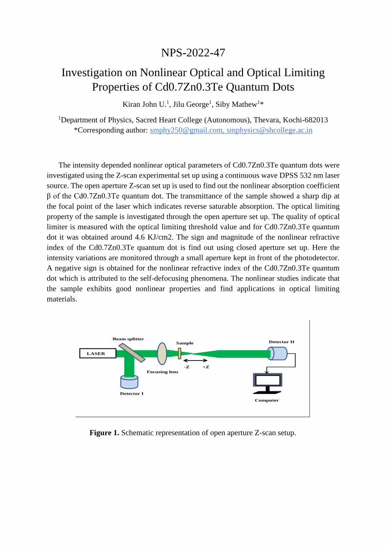
NPS-2022-47
Investigation on Nonlinear Optical and Optical Limiting
Properties of Cd0.7Zn0.3Te Quantum Dots
Kiran John U.1, Jilu George1, Siby Mathew1*
1Department of Physics, Sacred Heart College (Autonomous), Thevara, Kochi-682013
*Corresponding author: [email protected], [email protected]
The intensity depended nonlinear optical parameters of Cd0.7Zn0.3Te quantum dots were
investigated using the Z-scan experimental set up using a continuous wave DPSS 532 nm laser
source. The open aperture Z-scan set up is used to find out the nonlinear absorption coefficient
β of the Cd0.7Zn0.3Te quantum dot. The transmittance of the sample showed a sharp dip at
the focal point of the laser which indicates reverse saturable absorption. The optical limiting
property of the sample is investigated through the open aperture set up. The quality of optical
limiter is measured with the optical limiting threshold value and for Cd0.7Zn0.3Te quantum
dot it was obtained around 4.6 KJ/cm2. The sign and magnitude of the nonlinear refractive
index of the Cd0.7Zn0.3Te quantum dot is find out using closed aperture set up. Here the
intensity variations are monitored through a small aperture kept in front of the photodetector.
A negative sign is obtained for the nonlinear refractive index of the Cd0.7Zn0.3Te quantum
dot which is attributed to the self-defocusing phenomena. The nonlinear studies indicate that
the sample exhibits good nonlinear properties and find applications in optical limiting
materials.
Figure 1. Schematic representation of open aperture Z-scan setup.
LASER
Beam splitter
Detector I
Detector II
Focusing lens
Sample
-Z +Z
Computer
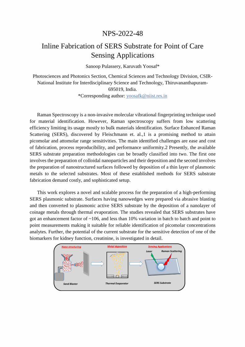
NPS-2022-48
Inline Fabrication of SERS Substrate for Point of Care
Sensing Applications
Sanoop Pulassery, Karuvath Yoosaf*
Photosciences and Photonics Section, Chemical Sciences and Technology Division, CSIR-
National Institute for Interdisciplinary Science and Technology, Thiruvananthapuram-
695019, India.
*Corresponding author: [email protected]
Raman Spectroscopy is a non-invasive molecular vibrational fingerprinting technique used
for material identification. However, Raman spectroscopy suffers from low scattering
efficiency limiting its usage mostly to bulk materials identification. Surface Enhanced Raman
Scattering (SERS), discovered by Fleischmann et. al.,1 is a promising method to attain
picomolar and attomolar range sensitivities. The main identified challenges are ease and cost
of fabrication, process reproducibility, and performance uniformity.2 Presently, the available
SERS substrate preparation methodologies can be broadly classified into two. The first one
involves the preparation of colloidal nanoparticles and their deposition and the second involves
the preparation of nanostructured surfaces followed by deposition of a thin layer of plasmonic
metals to the selected substrates. Most of these established methods for SERS substrate
fabrication demand costly, and sophisticated setup.
This work explores a novel and scalable process for the preparation of a high-performing
SERS plasmonic substrate. Surfaces having nanowedges were prepared via abrasive blasting
and then converted to plasmonic active SERS substrate by the deposition of a nanolayer of
coinage metals through thermal evaporation. The studies revealed that SERS substrates have
got an enhancement factor of ~106, and less than 10% variation in batch to batch and point to
point measurements making it suitable for reliable identification of picomolar concentrations
analytes. Further, the potential of the current substrate for the sensitive detection of one of the
biomarkers for kidney function, creatinine, is investigated in detail.
Nano structuring Metal deposition Sensing Applications
Sand Blaster Thermal Evaporator SERS Substrate
Raman ScatteringLaser
NPS-2022-49
Investigating the Langevin Behaviour of Faraday Rotation in
Soft Ferromagnetic CoFe2O4 Nanoparticles Dispersed in
PVA-Water Medium
Lakshmi B1, Pramod Gopinath1,2*
1International School of Photonics and 2Inter University Centre for Nanomaterials and
Devices,
Cochin University of Science and Technology, Cochin-682022, India.
*Corresponding author: [email protected]
Magneto-Optic Faraday Rotation (MOFR), defined as the phenomenon of rotation of the
polarisation plane of linearly polarised light passing through a magnetized medium, with the
magnetization parallel to the propagation direction of light, has many interesting applications,
from both, practical as well as fundamental theoretical point of view. MOFR studies in fluidic
media are generally performed by dispersing superparamagnetic (SPM) Nanoparticles (NP) in
suitable carrier liquids. The SPM size limit sets the ideal criterion to form stable magnetic
dispersions, thus limiting the MOFR studies only to SPM NP. Exploring the magnetization and
MOFR behaviour of NP with sizes above the SPM limit, could be an interesting domain, that
is however, generally excluded, due to the constraint in forming stable fluidic dispersions.
Here, we report the MOFR studies performed on CoFe2O4 NP that belong to a soft
ferromagnetic size range at room temperature. The constraint of forming stable dispersions of
the NP with sizes above the SPM critical diameter, is efficiently overcome by choosing a 2 Wt
% PVA-water solution as the dispersing medium. The dispersions thus formed are found to be
stable for a very long period, approximately, over a month, due to the efficient matrix-like
behaviour of PVA-layers that prevent the particles from agglomerating. The samples were
prepared at two different concentrations (CoF-1 and CoF-2) so as to investigate the
concentration dependence of MOFR. The FR values measured with applied magnetic fields
upto 3000 Oe were fitted with Langevin function and it was observed that MOFR exhibited a
saturation tendency similar to the magnetization of the sample. The sample at the lower
concentration, namely CoF-1, exhibited saturation at around 1800 Oe, whereas the sample with
the higher concentration, CoF-2 exhibited saturation at a higher magnetic field, at around 2200
Oe. The FR values were also found to be higher for the CoF-2 sample with the saturation value
of rotation being 0.10°. The study opens up possibilities for MOFR measurements on
dispersions of ferromagnetic NP, which may pave way for discovering newer exciting magnetic
phenomena in fluidic samples.
NPS-2022-50
Development of visible light sensor using nanostructured
cadmium sulfide thin films
Midhun P. R1,2, Asha A. S1,2,3*
1Nanomaterials for Emerging Solid-state Technology (NEST) research laboratory,
Department of Physics, Cochin University of Science and Technology, Kochi, Kerala,
682022 2Department of Physics, Cochin University of Science and Technology, Kochi, Kerala,
682022 3Centre of Excellence in Advanced Materials, Cochin University of Science and Technology,
Kochi, Kerala, 682022
*Corresponding author: [email protected]
A visible light photosensor based on metal chalcogenide-cadmium sulfide (CdS) thin film
is demonstrated. In this study, nanocrystalline CdS thin films were grown on precleaned
commercial glass substrates using chemical bath deposition (CB D) technique. The X-ray
diffraction confirms the formation of hexagonal CdS thin films with strong diffraction peaks
along (002) direction. The EDX results reveal the stoichiometric behavior of constituent
elements. The interconnected flakes structured morphology enhances the conduction
mechanism. Optical studies suggest a strong green emission band near 507 nm and have
bandgap energy near 2.25 eV. The electrical characterization of CdS thin films in visible light
displays a fast, reversible, and stable response. The high photosensitivity of 9564% and quick
photoresponse are attributed to the superior film quality. This opens up the possibility of using
CdS based photodetectors for commercial applications by cost-effective routes.
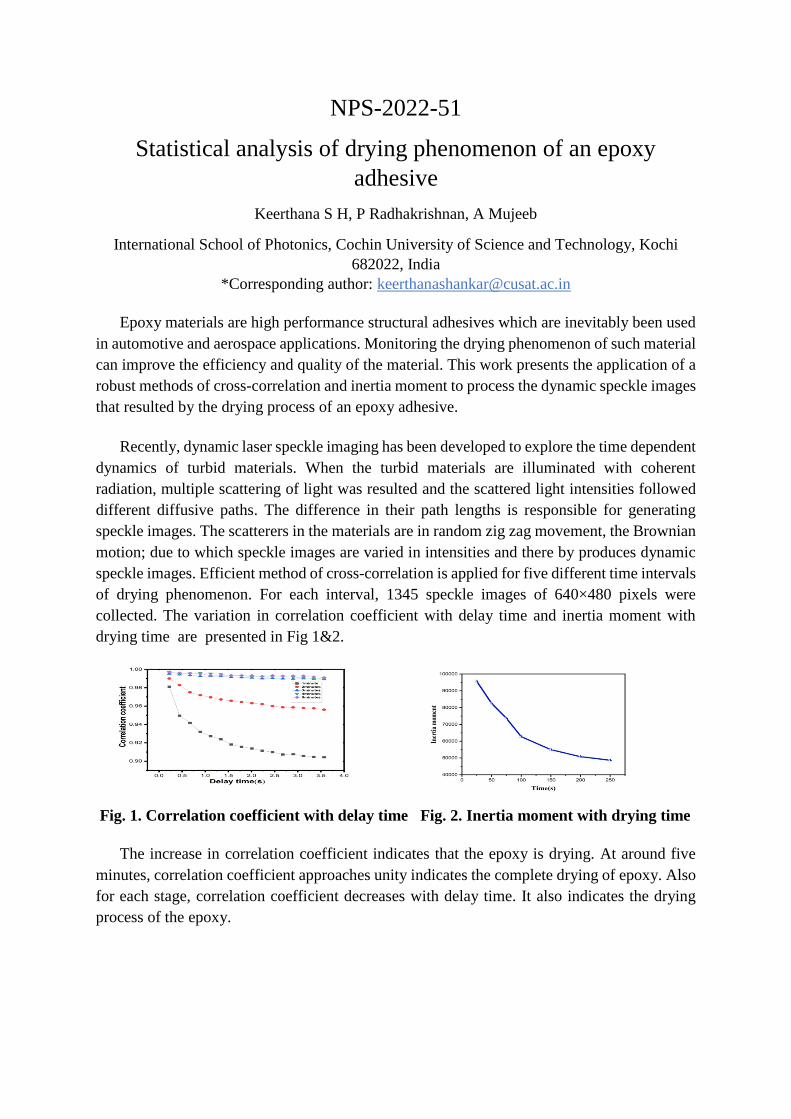
NPS-2022-51
Statistical analysis of drying phenomenon of an epoxy
adhesive
Keerthana S H, P Radhakrishnan, A Mujeeb
International School of Photonics, Cochin University of Science and Technology, Kochi
682022, India
*Corresponding author: [email protected]
Epoxy materials are high performance structural adhesives which are inevitably been used
in automotive and aerospace applications. Monitoring the drying phenomenon of such material
can improve the efficiency and quality of the material. This work presents the application of a
robust methods of cross-correlation and inertia moment to process the dynamic speckle images
that resulted by the drying process of an epoxy adhesive.
Recently, dynamic laser speckle imaging has been developed to explore the time dependent
dynamics of turbid materials. When the turbid materials are illuminated with coherent
radiation, multiple scattering of light was resulted and the scattered light intensities followed
different diffusive paths. The difference in their path lengths is responsible for generating
speckle images. The scatterers in the materials are in random zig zag movement, the Brownian
motion; due to which speckle images are varied in intensities and there by produces dynamic
speckle images. Efficient method of cross-correlation is applied for five different time intervals
of drying phenomenon. For each interval, 1345 speckle images of 640×480 pixels were
collected. The variation in correlation coefficient with delay time and inertia moment with
drying time are presented in Fig 1&2.
Fig. 1. Correlation coefficient with delay time Fig. 2. Inertia moment with drying time
The increase in correlation coefficient indicates that the epoxy is drying. At around five
minutes, correlation coefficient approaches unity indicates the complete drying of epoxy. Also
for each stage, correlation coefficient decreases with delay time. It also indicates the drying
process of the epoxy.
NPS-2022-52
Investigations on Optical Properties of Ge-Sb-Se
Chalcogenide Glass Films Towards Infrared Photonics
Soumya Suresh1*, Anupama Viswanathan2, B Anugop1, Sheenu Thomas1
1International School of Photonics, Cochin University of Science and Technology, Cochin-
22, India. 2Sree Narayana College Nattika, Triprayar-680566, India.
*Corresponding author: [email protected]
The present study focuses on the optical properties of thermally evaporated films of Ge-
Sb-Se chalcogenide glass system using UV-Vis-NIR Spectrophotometer. The optical
constants: refractive index and extinction coefficient, dispersion parameters: oscillator energy
and dispersion energy, and the thickness of the films were determined using open-source
software PRISA which uses the transmission spectrum to get more accurate results.

NPS-2022-53
Dual-Channel based LSPR Biosensor for Multi-Analyte
detection
Simitha S,1 Shinto M Francis,2 Jesly Jacob*2 and Vibin Ipe Thomas*1
1Department of Chemistry, CMS College, Kottayam-686001, Kerala, India. 2 Department of Physics, Assumption College, Changanacherry, Kottayam-686101, Kerala
*Corresponding authors: [email protected], [email protected]
A surface plasmon resonance (SPR) based sensor with multiple sensing cavities is proposed
for the qualitative and quantitative analysis of biochemical analytes, antigen-antibody
interaction, DNA/RNA binding, etc. Detection and analysis of different analytes by means of
the proposed dual-channel based plasmonic structure is numerically analysed using finite
element method via absorption cross-section profiles. The sensor structure consisted of two
segments of a square silver disc and ring with a channel/cavity in between acting as the sensing
region. 1The optical sensor monitors the change in resonance position corresponding to the
field localization near plasmonic channels accompanied by the change of refractive index of
the analyte embedded in the cavity. A maximum refractive index (RI) sensitivity of 1778.16
nm/RIU is obtained for concentration analysis of 0.07-0.12g/ml glucose-lactose solution via
their respective RI values. The dual absorption peak maxima obtained with multiple analytes
in each channel indicates the independent sensing behaviour of the structure that can potentially
quantify multiple analytes simultaneously.2 Further, when only a single analyte is loaded in
both cannels, merging of the two peaks into a single peak with equal charge distribution on
both cavities is observed which in turn finds the possible single or multiple analyte detection.
Moreover, the independent sensing behaviour can be effectively tuned with changing the
material or geometric parameter of any one of the segments. The proposed structure exhibits a
super ultra-broad RI sensing range of nearly 0.4 to 1.8 RIU with resonant peaks across near-IR
region. The reduction of size of the sensing channel to 10 nm further improves the performance.
Sensitivity, figure of merit (FOM), and Q-factor values of 4267.60 nmRIU-1, 82.23 RIU-1,
and 116.51 observed after optimization reveal the promising applicability of designed SPR
sensor in the areas of medical diagnostics, pharmaceuticals, chemical industries, and food
processing. Those simultaneous sensing channels proposed promises repeated confirmation
analysis, analyte comparison study, and multi-parameter detection together with the advantage
of simple and easy manufacturable structure profile.
NPS-2022-54
Photocatalytic activity of Gd2O3 doped Er4Zr3O12
Nanoceramic
Arun Mohan, Athira S and Sam Solomon*
Department of Optoelectronics, University of Kerala, Thiruvananthapuram 695581
*Author for correspondence: [email protected]
Water, the essential resource on which all life depends is alarmingly polluted. Dye from
industrial effluents is one of the main causes of water pollution. Simple and effective
approaches aiming at the rapid removal of dye from the environment are in demand. The aim
of this work is to investigate the effect of photocatalytic activity of Er4Zr3O12 system by Gd2O3
doping and a detailed investigation on photocatalytic activity mechanism of Gd2O3 doped
nanoparticles on pollutants using kinetic model. Nanoceramic materials can be synthesized by
different methods. Here we use cost effective, environment friendly combustion synthesis for
the synthesis of nanoparticles. Here we successfully synthesized Er4Zr3O12:Gd3+ nanoceramic
with enhanced photocatalytic activity by auto-ignited combustion and wet mixing method. The
purity and reusability of water after photocatalytic degradation is also checked. The structural
and morphological characterization of the sample was done by X-ray diffraction (XRD) and
Field Emission Scanning Electron Microscopy (FESEM) analysis, respectively. Photocatalytic
activity study reveals that the reaction occurring in the irradiation process is a first order type
chemical reaction. Reusability of water after photocatalytic dye degradation is evaluated using
the parameters like pH, total dissolved solids, conductivity and dissolved oxygen. Water quality
assessment test reveals that the water is reusable for industrial purposes.
NPS-2022-55
The effect of temperature and power on the structural and
optical properties of r.f sputtered ZnO thin films
P. Hajara1, T. Priya Rose1,2 K. J. Saji1,2,3*
1International School of Photonics, Cochin university of Science and Technology, Kochi-22,
India. 2Inter University Centre for Nano materials and Devices, Cochin University of Science and
Technology, Kochi-22, India.
3Centre of Excellence in Advanced Materials, Cochin university of Science and Technology,
Kochi-22, India.
*Corresponding author: [email protected]
ZnO thin films were deposited on glass substrate by r.f magnetron sputtering from a zinc oxide
target. The effect of r.f power and substrate temperature on the properties of ZnO thin films
was studied. The structural and optical properties were investigated by X-ray diffraction
(XRD), field emission scanning electron microscopy (FESEM), UV-Vis absorption spectra and
photoluminescence (PL). All the ZnO films were highly oriented in c-axis (002) and the film
deposited at 450℃ with a sputtering power of 50W exhibited the larger grain size. PL emission
was obtained at UV and green region for the excitation wavelengths of 280 nm and 390 nm
respectively. Dependence of temperature and power on absorption spectra is also discussed.
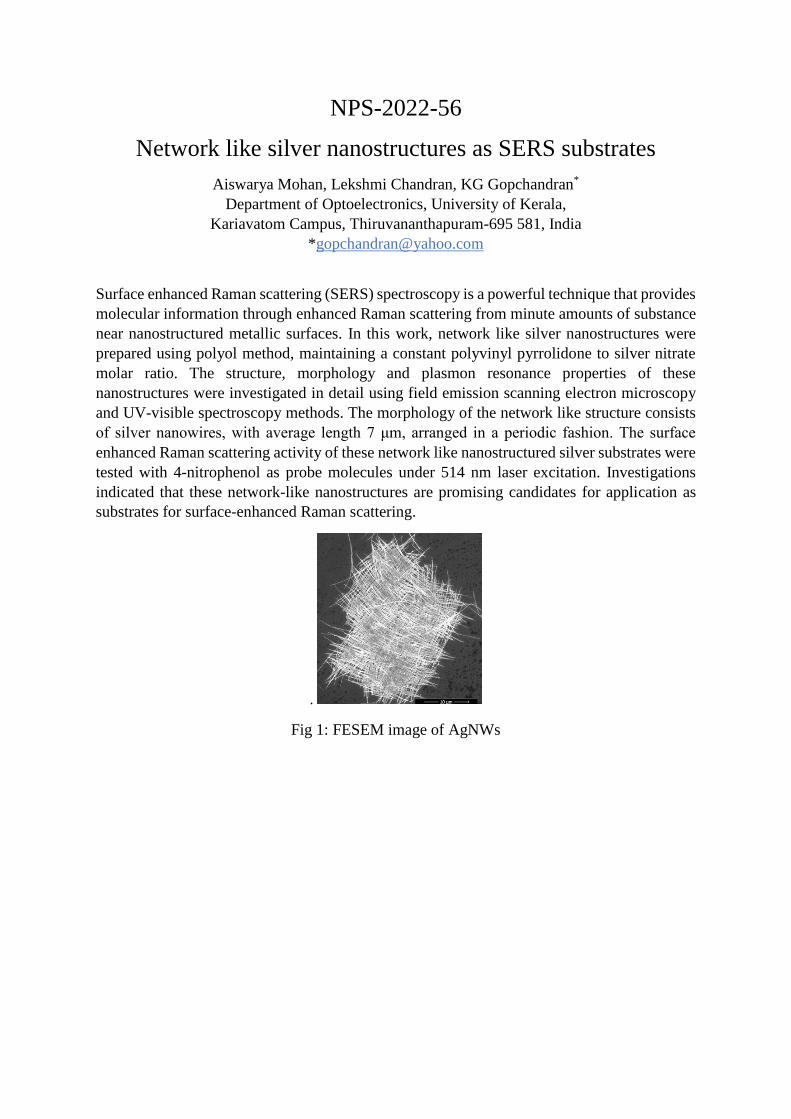
NPS-2022-56
Network like silver nanostructures as SERS substrates
Aiswarya Mohan, Lekshmi Chandran, KG Gopchandran*
Department of Optoelectronics, University of Kerala,
Kariavatom Campus, Thiruvananthapuram-695 581, India
Surface enhanced Raman scattering (SERS) spectroscopy is a powerful technique that provides
molecular information through enhanced Raman scattering from minute amounts of substance
near nanostructured metallic surfaces. In this work, network like silver nanostructures were
prepared using polyol method, maintaining a constant polyvinyl pyrrolidone to silver nitrate
molar ratio. The structure, morphology and plasmon resonance properties of these
nanostructures were investigated in detail using field emission scanning electron microscopy
and UV-visible spectroscopy methods. The morphology of the network like structure consists
of silver nanowires, with average length 7 μm, arranged in a periodic fashion. The surface
enhanced Raman scattering activity of these network like nanostructured silver substrates were
tested with 4-nitrophenol as probe molecules under 514 nm laser excitation. Investigations
indicated that these network-like nanostructures are promising candidates for application as
substrates for surface-enhanced Raman scattering.
.
Fig 1: FESEM image of AgNWs
NPS-2022-57
ANTI-CANCER ACTIVITY OF TRIANGULAR LIKE
SILVER NANOPARTICLES
Lekshmi Chandran1, Rekha C R2, Aiswarya Mohan3, K G Gopchandran4*
1234Department of Optoelectronics, University of Kerala, Kariavattom Campus,
Thiruvananthapuram 695581
Cancer is a multifactorial disease caused by environmental and genetic factors. Even though
anti-cancer drugs available, they are not capable to reach the target site in optimum level and
also causes many other health issues. Nanotechnology offers a wide variety of tools for
delivering therapeutic agents directly at target cells. The unique physical and chemical
properties of silver and gold nanoparticles make them suitable candidates for application in
anticancer treatments.
Herein, triangular silver nanoparticles (TSNPs) were synthesised by a two-step seed mediated
method. At first spherical silver seeds were obtained by the reduction of silver nitrate with
sodium borohydroxide and then these seeds acted as the nucleation sites for the formation of
triangular shaped nanoparticles. Surface resonance characteristics of these nanoparticles was
studied using UV Visible spectroscopy. Structural determination of the nanoparticles was done
using X-ray diffraction and its morphology was confirmed with high resolution transmission
electron microscopy (HRTEM) and field emission scanning tunnelling microscopy (FESEM).
In vitro cytotoxicity of the TSNPs were evaluated against human cancer cell lines, MCF-7
(Human Breast Adenocarcinoma). The results indicated that the TSNPs exhibit concentration
dependent anti-cancer activity in the tested cell lines.

NPS-2022-58
Broadband Photoacoustic Imaging for Biodegradable Bone
Implants Applications
Valeria Grasso1,2, Philippe Trochet1, Regine Willumeit-Romer3,2, and Jithin Jose1,* 1 FUJIFILM VisualSonics, Amsterdam, The Netherlands
2 Institute for Materials Science, Faculty of Engineering, CAU, Kiel, Germany 3 Institute of Materials Research, Helmholtz-Zentrum hereon GmbH, Geesthacht, Germany
*Corresponding author: [email protected]
Abstract: Magnesium-based biodegradable implants are a novel alternative to temporary
implants used to treat bone fractures [1]. Ultrasound and Photoacoustic (US-PA) imaging has
the potential to non-invasively monitor the tissue changes during the bone healing process,
while the implant is degrading. However, the US-PA imaging technologies typically work
either in the lower frequency or in the higher frequency due to the limitation of broadband
transducers and data acquisition (DAQ) systems. Here we used an innovative open architecture
system that enables the co-localization of ultra-high and low-frequency photoacoustic signals
within the frequency range of 71-1 MHz. The technology is optimized for imaging small to
large structures and provides unique opportunities for translational research in monitoring
tissue remodeling and implant osseointegration.
Introduction: Photoacoustic (PA) is an innovative imaging technology based on acoustic
waves generation induced by pulsed laser light. Sound waves are detected and reconstructed
just as conventional ultrasound signals to form imaging of the optical absorption. In PA
imaging, the limited acoustic frequency range has a significant impact on the resolution and
the depth of imaging. Here we are proposing an optimization of the broadband US-PA imaging
set up to monitor the tissue remodeling in the vicinity of a biodegradable implant.
Methods: We developed a tissue-mimicking phantom that includes an Mg implant. Multi-
spectral PA imaging (sPAI) has been acquired ranging from 680-970nm. The sPAI has been
acquired at multiple frequency bands using US transducers at a nominal center frequency of
6MHz, 15MHz, and 30MHz. A novel superpixel unmixing framework has been developed to
automatically extract the molecular tissue components from sPAI. Due to the broadband nature
of the acquisition, the approach can create multiscale and multi-contrast images of structures
ranging from small to large and facilitate respective spatial resolutions.
Results: In this study, the optimized US-PA multi-spectral and multi-frequency approach
offers the possibility of combining multiple photoacoustic information in customized phantoms
with unprecedented details.
Conclusion: In summary, the innovative ultra-high and low-frequency PA imaging technology
opens many opportunities to monitor tissue remodeling in presence of biodegradable implants
on a clinical level.

NPS-2022-59
Sunlight Driven Photocatalytic Degradation of Organic
Pollutant by Au Doped Anatase TiO2 Nanoparticles
Veena Lalan, K.G. Gopchandran*
Department of Optoelectronics, University of Kerala, Thiruvananthapuram, 695581
Email ID: [email protected]
Photocatalysis is considered a promising strategy for the removal of organic contaminants from
water bodies. Metal oxide-based photocatalysis is very effective for this application and in
which TiO2 is the benchmark one. Owing to the properties such as low toxicity, and chemical
and thermal stability, TiO2 can be used for the organic dye degradation from polluted water
[1,2]. In the present study, we have synthesized the pure anatase phase of TiO2 nanoparticles
by a simple route from the tetra isopropyl orthotitanate precursor and its surface is modified
with spherical Au nanoparticles. The Surface Plasmon Resonance of Au nanoparticle shifts the
photon response of pure TiO2 from 320 to 600 nm which is confirmed from the diffused
absorbance measurements. From the micro-Raman and XRD analysis, the anatase phase
formation of TiO2 is verified and the surface area analysis by BET method indicated that the
specific surface area of pure TiO2 increases from 72.50 to 96.80 m2/g after Au incorporation.
The surface state analysis of Au doped TiO2 nanoparticles was performed by using X-ray
photoelectron spectroscopy. FESEM and HRTEM analysis indicated that these nanoparticles
are spherical in shape. The photocatalytic degradation by the photocatalysts was carried out by
selecting Nile Blue Chloride dye as a model pollutant and the experiment was carried out under
direct sunlight. The photocatalytic degradation experiment shows that the Au incorporated
TiO2 nanoparticle almost completely degrade the NBC content from its aqueous solution within
27 min of sunlight exposure and the increase in activity of Au: TiO2 nanoparticles are mainly
arising from the enhanced visible light absorption and the increased surface area compared to
pure TiO2 nanoparticles.
NPS-2022-60
Optical Studies in Eu3+ Doped Calcium Magnesium Silicate
(CMS: Eu3+) Phosphor
Sreelekha C. A. 1, Navya Sara Kuriyan 2, Sabeena M 3*
Department of Physics, Cochin University of Science & Technology, Kerala- 682022
Phosphors play a vital role in modern technology because of their ability to convert incident
electromagnetic radiation to visible light, for white Light Emitting Diodes (wLEDs)
applications [1]. The present study focuses on the effect of pH, and surfactants on optimizing
the crystal structure and microstructure of Eu3+ doped calcium magnesium silicate phosphor
(CMS: Eu3+) and its influence on luminescence. Calcium magnesium silicate and Eu3+ doped
(1mol %) calcium magnesium silicate were synthesized separately via the sol-gel method and
annealed at 1200˚C. Samples were prepared at a pH of 2.2 using HNO3 as catalyst and pH of
9 and 11 using NH3 as catalyst with and without Cetyl Trimethyl Ammonium Bromide
(CTAB) as surfactant. The crystal structure variation with pH and surfactant were studied using
X-Ray Diffraction (XRD) analysis. XRD pattern of sample prepared at a pH 9 shows impurity
phases. However, presence of a combination of monoclinic structure with merwinite and
diopside phases and tetragonal structure with akermanite phase was confirmed in samples
prepared at pH 2.2 and pH 11. The addition of CTAB does not affect the crystal structure
formation in the synthesized samples. Hence acidic pH of 2.2 and alkaline pH of 11 supports
the formation of CMS: Eu3+ phosphor without any impurity phases due to the better metal ion-
oxygen bond polymerization. The microstructure evolutionwas studied using Field Emission
Scanning Electron Microscopy (FESEM). The morphology analysis confirmed the grain
formation at a pH of 2.2, while agglomerated morphology was obtained in samples prepared
at alkaline pH 9 and 11. A gradual reduction to the extend of agglomeration is noticed with
CTAB probably due to the reduction in the surface energy. The photoluminescence studies
using spectrofluorometer confirmed 5D0→ 7FJ (J= 0-4) transitions of Eu3+ with maximum
emission at 614nm irrespective of pH.

NPS-2022-61
Investigation of Intensity Dependent Nonlinear Absorption in
Cerium Phosphate Nanoparticles
Anita Mary Peter*, Ramya M, M. Kailasnath
International School of Photonics, CUSAT, Kochi-682022
Abstract: Cerium Phosphate (CePO4) is a material that has attracted attention because
of its unique properties, redox capabilities and awide variety of applications. Cerium Phosphate
nanoparticles with a nanowire structure were successfully synthesized by a hydrothermal
synthesis procedure using Cerium Nitrate Hexahydrate (Ce (NO3)3.6H2O) and Diammonium
Hydrogen Phosphate ((NH4)2HPO4) as the precursors without adding any surfactants. The
synthesized CePO4 nanowires were characterized using X-ray Powder Diffraction (XRD),
Transmission Electron Microscopy (TEM) analysis which showed pure monoclinic nanowire
structures. The optical properties were analysed by UV-visible absorption and
photoluminescence (PL) study. The Nonlinear Absorption was measured by the open aperture
Z-scan technique using Q switched Nd-YAG laser at 532nm. The Z-scan curve exhibited
reverse saturable absorption. In this study, the dependence of nonlinear absorption on the
intensity of incident light was investigated, the non-linear absorption coefficient was measured
and found the non-linear absorption increasing with the increasing intensity.
NATIONAL PHOTONICS SYMPOSIUM 2022
Organised by:International School of Photonics
Cochin Universtity of Science and Technology
Sponsored By
INTERNATIONAL CONFERENCE ON RECENT TRENDS IN PHOTONICS