
Book of Abstracts - Electrical & Computer Engineering
274
Book of Abstracts
-
Upload
khangminh22 -
Category
Documents
-
view
1 -
download
0
Transcript of Book of Abstracts - Electrical & Computer Engineering

Book of Abstracts

1

List of technical sessions
CommitteesTechnical Board
Symposium Chair: Jean-Philippe Parmantier, ONERA Symposium Co-Chair: Nadine Barriety, ONERA Symposium Secretary: Isabelle Junqua, ONERA
Technical Program Chair: Dave Giri, PRO-TECH Technical Program Co-Chair: William Radasky, METATECH Technical Program Advisor: Edl Schamiloglu, SUMMA
Exhibition Committee Chair: Hervé Grauby, GERAC Exhibition Committee Co-Chair: Frédéric Amoros, NEXIO
Technical Committee
TC1 HPEM: Souces, Antennas and Facilities (both wideband and narrowband) William Prather, Dave Giri
TC2 HPEM: Applications of Coupling to Structures and Cables Mats Bäcktröm, Lars Fichte
TC3 HPEM/UWB: Measurement Techniques Frank Sabath, Anthony Wraight
TC4 HPEM: IEMI Threats, Effects and Protection William Radasky, Richard Hoad
TC5 HPEM: System-level Protection and Testing Armin Kealin, Daniel Mansson
TC6 HPEM: Ligthning EM Effects Farhad Rachidi, Marcos Rubinstein
TC7 HPEM: Analytical and Numerical Models and Modeling Sergei Tkachenko, Jean-Philippe Parmantier
TC8 HPEM: Bioeffects and Medical Applications of EM Fields Joe Lovetri, Jayanti Venkataraman
TC9 UWB: Antenna Design, Radiation and Propagation Dave Giri, Everett Farr
TC10 UWB: Radar AspectsErik Mokole, Georges Baker
TC11 UWB: Target Detection, Discrimination and Imaging Dominique Sérafin
TC12 UXO: Landmine and IED Detection and Neutralization Christian Carel
TC13 POSTER: Philippe Besnier, Christian VollaireAdditional reviewers: Juergen Nitsch, Jean-Marc Dienot, Frank Gronwald,
Peter Zwamborn
Special Sessions
TC-SS1 HPEM: Safety of Installations Submitted to EM Threats Odd-Harry Arnesen
TC7-SS2 HPEM: Use of Computer Codes in HIRF Certification Process Jean-Patrick Moreau, Jean-Philippe Parmantier
TC6-SS3 HPEM: Lightning Indirect Effects on Aircrafts Houmam Moussa
TC4-SS4 HPEM: Susceptibility, effects, protection and test methods for electronics due to high power EM threats
William Radasky, Richard HoadTC3-SS5 HPEM/UWB: HPEM Detection
Frank Sabath
2

3

4

5

6
7

8

9

10

11
UW B RadarAspects

12

13

14

PlenarySession
15

High-Power Electromagnetics (HPEM) From the 1960s into the 21st Century
Dr. D. V. Giri Pro-Tech, 11-C Orchard Court, Alamo, CA 94507, USA & Dept. of ECE, Univ. of New Mexico, Albuquerque, NM 87130
E-mail: [email protected]: URL: www.dvgiri.com
Abstract— HPEM is a catch-all acronym that includes many electromagnetic waveforms such as natural lightning, nuclear electromagnetic pulse (NEMP), high-power microwaves (HPM), moderate band signals and hyperband transients [1]. With the exception of natural lightning which has existed from time immemorial, the scientific discipline of HPEM started in the 1960s, when serious attention was paid to NEMP. Dr. Carl Baum played a key role in the evolution of HPEM [2]. In this paper, we will review some major milestones of this evolution and also attempt to look ahead.
Keywords-HPEM, lightning, NEMP, HPM, short pulse, narrowband, moderate band, hyperband
I. INTRODUCTION
Prior to the world’s first atomic test in Alamogordo, NM, USA on July 16, 1945, Nobel laureate physicist Enrico Fermi tried to calculate the possible electromagnetic fields that would be produced from the nuclear explosion. This can be conidered as the birth of the study of HPEM.
II. MAJOR MILESTONES OF HPEM
Major Milestones of HPEM, especially in the last 5 decades can be summarized as follows.
1945 TRINITY - Fermi’s attempt to estimate NEMP 1951-1962 Additional nuclear tests and measurements
(crude compared to today’s standards) 1962 Partial Test Ban Treaty (PTBT) 1962–1990 Underground tests, development of EMP
simulators and sensors 1978 First NEM meeting, followed every even year Special Issue on NEMP in IEEE Transactions
on AP-S and EMC 1980-1989 Special Issues in IEEE Journals on Lightning,
HPM, EMP 201 (short course); HPEM technical sessions in various meetings, URSI Statement
1990 URSI Comm E, forms a HPEM working group 1993 IEC issues 61000-2-9 - Radiated HEMP Env. 1994 EUROEM Conference in France 1995 High-Power Short Pulse (IRA) technology
development 1996 Russian Scientists participate in AMEREM 1996 1999 URSI Statement on IEMI 2004 U.S. Congressional Committee publishes its first
Report on EMP [3]
2004 Special Issue on IEMI in IEEE Trans on EMC [4] 2008 EMP Commission report on threats to Critical
Infrastructures [5]
The first decade of the 21st century has seen real and anecdotal evidence of RF Terrorism and IEMI [6].
III. A LOOK AHEAD
Compact HPEM source/antenna systems are commercially available. Developments in pulse-power technologies driving conventional and newer RF devices will lead to improved and more powerful source/ antenna systems. An EMP attack is an example of RF terrorism by rogue countries and non-state actors, and the national infrastructure can be at risk. Infrastructure is a hyper system or a system of systems such as electric power, telecommunication, banking & finance, energy, transportation, food, water, emergency, space, and Government [5]. In addition, cyber threats from hostile governments, terrorist groups and disgruntled employees are on the increase as well. It is prudent for civilized societies to asses such threats and take pro-active and precautionary actions. As an example, if someone had foreseen a threat scenario wherein commercial airliners can be turned into missiles by hijackers, perhaps Nine-Eleven could have been avoided. In the case of Nine Eleven, the pro-active step would have been to install bullet-proof cockpit doors to deny entry to unauthorized persons.
References [1] D. V. Giri and F. M. Tesche, “Classification of Intentional
Electromagnetic Environments (IEME), IEEE Trans. EMC,Aug. 2004,
[2] C. E. Baum, “Reminiscences of High-Power Electromagnetics”, IEEE Trans. EMC, May 2007, pp 211-218.
[3] W.R. Graham (Chairman, EMP Commission) et al., “Report of the Commission to Assess the Threat to the United States from Electromagnetic Pulse (EMP) Attack,” Volume 1, Executive Report, 2004.
[4] “Special Issue on High-Power Electromagnetics (HPEM) and Intentional Electromagnetic Interference (IEMI),” IEEE Transactions on EMC, Vol. 46, No. 3, August 2004.
[5] W.R. Graham (Chairman, EMP Commission) et al., “Report of the Commission to Assess the Threat to the United States from Electromagnetic Pulse (EMP) Attack – Critical National Infrastructures”, April 2008.
[6] F. Sabath, “What can be learned from Documented Intentional Electromagnetic Interference (IEMI) Attacks”, presented at the International URSI XXX General Assembly, Istanbul, Turkey, 13-20 August 2011.
16

Threat of Electromagnetic Terrorism Leassons learned from documented IEMI Attacks
Frank Sabath Division 300: Balanced Nuclear Protection Measures and Nuclear Hardening, Electro-Magnetic Effects, Fire Protection
Bundeswehr Research Institute for Protective Technologies and NBC Protection (WIS) Munster, Germany
Abstract— The existing threat by criminal (intentional) use of electromagnetic tools is discussed. Reported Intentional Electromagnetic Interference (IEMI) attacks and similar incidents will be analyzed and discussed in regard to aspects like motivation and technical skills of the culprits, characteristics of the generated IEMI environment as well as effects on the target systems. Concluding common characteristics will lead to a discussion of the technological challenge of recognition and identification of an IEMI attack as well as backtracking of observed malfunction and destructions to an external IEMI environment.
Keywords- IEMI, HPEM, documented attacks, threat analysis
I. INTRODUCTION
This paper discusses to what extent the technological development in the last decades resulted in an ascent of the threat by criminal use of high power electromagnetic systems. It starts with an overview about Intentional Electromagnetic Interference (IEMI) attacks and similar incidents which were reported in freely accessible literature. The paper continues by analyzing these observed attacks and IEMI caused effects concerning motivation and technical skills of the culprits, characteristics of the generated IEMI environment and effects on the target systems. Finally, the section “lessons learned” will conclude common characteristics and discuss aspects of recognition and identification of an IEMI attack as well as backtracking of observed malfunction and destructions to an external IEMI environment.
II. DOCUMENTED CRIMINAL USAGE OF ELECTROMAGNETIC
TOOLS
Public literature [1,2,5] has reported eight criminal usages of electromagnetic tools:
1. In Japan, criminals used an EM disruptor to interfere with the computer of a gaming machine and falsely triggered a win.
2. In St. Petersburg, a criminal used an EM disruptor to disable a security system of a jeweler store.
3. In Kizlyar, Dagestan, Russia, Chechen rebel command disabled police radio communication using RF jammers during a raid.
4. In multiple European cities (e.g. Berlin) criminals used GSM-Jammers to disable the security system of limousines.
5. In Russia, Chechen rebels used an EM disruptor to defeat a security system and gain access to a controlled area.
6. In the Netherlands an individual disrupted a local bank IT network because he was refused loan.
7. In Moscow, the normal work of one automatic telephone exchange station has been stopped as a result of remote injection of a voltage in to a telephone line.
There have also been several documented incidents caused by EM devices that could be employed by criminals or terrorists [2, 5]. The IEMI cases presented above clearly point out that today the threat by (criminal) IEMI attacks on electronic systems already exists.
III. LESSONS LEARNED
The documented cases of criminal IEMI attack will be analyzed with regard to (1) motivation and needed skills of the offender, (2) risk aspects of the IEMI environment and (3) the caused effect on the target system (including consequences). The reported attack will be analyzed to deduce common characteristics that will enable an assessment of the current threat by IEMI terrorism and develop appropriate countermeasures.
REFERENCES
[1] V. Fortov, Yu. Parfenov, L. Siniy and L. Zdoukhov, “Russian Research of intentional electromagnetic disturbances over the past ten years”, Proceedings of the AMEREM 2006, Albuquerque (NM, USA), July 2006.
[2] R. Hoad and I. Sutherland, “The forensic utility on detecting disruptive electromagnetic interference”, Proceedings of the 6th European Conference on Information Warfare and Security (ECIW 2007), July 2007.
[3] D.V. Giri, “Documented Electromagnetic Effects (EME)”, Proceedings of the EUROEM 2008, Lausanne, Switzerland, July 2008.
[4] F. Sabath and H. Garbe, “Risk Potential of Radiated HPEM Environments”, Proceedings of the 2009 IEEE International Symposium on Electromagnetic Compatibility, Austin (TX), USA, August 2009, pp. 226-231
[5] Sabath, F.; , "What can be learned from documented Intentional Electromagnetic Interference (IEMI) attacks?," General Assembly and Scientific Symposium, 2011 XXXth URSI , vol., no., pp.1-4, 13-20 Aug. 2011
17

The Effects of Three High Power EM Threats on Electric Power Systems
W. A. RadaskyMetatech Corporation, Goleta, California, USA 93117
Abstract— This Plenary Paper reviews three high power EM threats that have the capability to create blackouts and damage to electric power system components, thereby lengthening their ability to recover. The threats include high-altitude electromagnetic pulse (HEMP), extreme geomagnetic storms, and intentional electromagnetic (IEMI) attacks from EM weapons. The effects caused by each threat will be identified.
Keywords-HPEM; HEMP; IEMI: Geomagnetic storms; EM weapons
I. INTRODUCTION
In recent years there has been considerable publicity relating to three high-power electromagnetic (HPEM) threats that are serious threats to the reliable delivery of electric power. These are: the high-altitude electromagnetic pulse (HEMP) from nuclear detonations in space, intentional electromagnetic interference (IEMI) produced by electromagnetic weapons and severe geomagnetic storms caused by charged particles ejected from the sun that intercept the Earth. This increased awareness is largely due to work performed by a U.S. Congressional Commission on EMP, the blackout caused by the March 1989 geomagnetic storm in Quebec Province, and due to the development of EM weapons and data showing their impacts on modern electronic systems. There is a clear understanding today regarding the nature of the effects on different aspects of the electric power delivery system, and also on the measures to protect the equipment that provides reliable power under normal operations.
This paper briefly reviews the three threats, discusses the main components of the power system that are at risk, and discusses the basic protection schemes that can be applied to reduce the risk of blackout and to enhance the recovery of the system if a blackout occurs.
II. COMPARISONS OF THE THREE EM THREATS
The three EM threats are well documented, and publications are now readily available to the public. The HEMP environment is best described in IEC 61000-2-9 [1], the narrowband and wideband environments that can produce IEMI are found in IEC 61000-2-13 [2], and the geomagnetic threat is well described in the Meta-R-319, which has been published on the Oak Ridge National Laboratory web site [3].
It is important to recognize that these three environments have some common elements in terms of their impacts on electronics in general and on power system equipment in particular.
The HEMP threat has three portions separated in time known as E1, E2, and E3. The E1 HEMP is the fastest portion of the pulse in time, with a rise time on the order of several nanoseconds, and with a pulse width of less than 30 ns. As the peak field may be as high as 50 kV/m over a large region, it produces a severe radiated and conducted environment for modern electronics. This includes the control electronics in high voltage substations and also the computer electronics in power system control centers. It may also create a problem for insulators on medium voltage power systems.
The third part of the HEMP threat, the E3 HEMP, begins at 1 second and lasts for hundreds of seconds. This peak field is as high as 40 V/m [2], and couples efficiently to long high voltage power lines. This creates a saturation condition in hundreds of connected transformers, simultaneously leading to voltage collapse and possible damage to a large number of expensive and difficult to replace transformers. While the transformers are in saturation, power harmonics are generated that may create problems in backup power systems, which are needed to operate electronics in control rooms.
The geomagnetic storm threat is also a wide area threat and creates electric fields up to 10s of V/km under extreme conditions. The time waveforms created by geomagnetic storms are very similar to E3 HEMP. While geomagnetic storms occur relatively often, not all storms are large enough to black out power systems or create to significant damage to transformers, although in the past 23 years regional blackouts have occurred and some transformers have been damaged.
The IEMI threat from EM weapons is not a wide area threat as those described above, but at distances on the order of 100 meters, fields as high as 50 kV/m may be produced. The short rise times of wideband pulses and the high frequencies of narrowband fields are usually more effective than E1 HEMP fields in producing damage to control electronics. This threat therefore affects power system components in a similar fashion, as does E1 HEMP.
The presented paper will describe these threats and their impacts in more detail.
REFERENCES
[1] IEC 61000-2-9, Ed. 1.0: “Electromagnetic compatibility (EMC) – Part 2: Environment – Section 9: Description of HEMP environment – Radiated disturbance,” February 1996.
[2] IEC 61000-2-13, Ed. 1.0: “Electromagnetic compatibility (EMC) – Part 2-13: High-power electromagnetic (HPEM) environments - Radiated and conducted,” March 2005.
[3] J. Kappenman, “Geomagnetic Storms and Their Impacts on the U.S. Power Grid,” Metatech Corporation, Meta-R-319, January 2010. http://www.ornl.gov/sci/ees/etsd/pes/ferc_emp_gic.shtml.
18

Relation Between Immunity Testing in Anechoic and Reverberation Chambers. Some Reflections
Mats Bäckström Saab Aeronautics
SE-58188 Linköping, Sweden [email protected]
Abstract— The relation between the maximum stress suffered by an equipment-under-test (EUT) in an immunity test in a anechoic chamber (AC) and in a reverberation chamber (RC), respectively, is discussed. The discussion focuses mainly on the significance of the directivity of the EUT.
Keywords-Immunity testing; Reverberation chamber; Anechoic chamber
I. INTRODUCTION
The problem of relating the outcome of a susceptibility test in a RC to free-space conditions was identified and addressed early [1]. In a RC the EUT is simultaneously irradiated by plane waves coming from many directions [2]. By use of a stirrer located inside the chamber the boundary conditions are changed thereby generating different field conditions. The concept of statistical isotropy, sometimes used for the RC, means that the ensemble average of the signal received by an antenna (or by a component inside the EUT) will be independent of the directional properties of the antenna.
The fact that the variations in directivity and polarization are averaged out in a RC indicates that an immunity test carried out in a RC might be less severe than a test carried out in an AC, at least if the AC test comprises the worst angle of incidence and polarization. Of course, the opposite may also be true, i.e. that the immunity test in an AC might be less severe than a test in a RC. This happens if the angles of incidence and/or the polarizations in the test correspond to a weak coupling to the EUT.
II. RELATION BETWEEN AC AND RC TEST ENVIRONMENTS
In a measurement of shielding effectiveness (SE) a natural choice may be to use the scalar power density, scS , to define the field level in the RC, since it is based on an ensemble average. Equating ACsc SS yields a value of SE measured in the RC that is equal to the average value, with respect to all aspect angles and polarizations, of the SE measured in the AC. It also follows that, cf. Eq. (13) in [3]:
MaxAC
RC DSE
SE2
min,
(1)
In (1) MaxD is the maximum directivity of the EUT.
In an immunity test the relation between the two environments becomes more complicated. One reason is that the immunity test parameter in a RC is given by the maximumfield strength. Another reason is that different definitions on the test field strength lead to different relations [3]. Both the total, MaxTE , , and a rectangular component, MaxRE , , of the electric field are used in different standards. For the power picked up by a critical component inside the EUT we get:
max,,
,, DPP
MaxRCrec
MAxACrex (2)
In (2) depends on the number of independent stirrer positions N . If ACMaxR EE , is used we get 32 . If
ACMaxT EE , is used we get 2 for small values of N and 1 for large values of N .
Eq. (2) points out the risk for undertesting in a RC, compared to a test in an AC. However, the maximum stress level in the AC is in practice never attained since that would require knowledge beforehand of the worst angle of incidence and polarization, or that a huge number of aspect angles and polarizations must be used in the test. In [4] it was shown that for typical test procedures in the two kind of chambers the expected level of undertesting, with respect to an ideal plane wave test in an AC maximising the response, were similar.
The discussion above relates to the power picked up by a critical component inside the EUT. Things may become more complicated if a malfunction of a system requires simultaneous malfunction of several critical components.
REFERENCES
[1] J. L. Bean and R. A. Hall, “Electromagnetic Susceptibility Measurements Using a Mode-stirred Chamber,” in Proc. of 1978 IEEE Int. Symp. on EMC, Atlanta, USA.
[2] D. A. Hill, “Plane Wave Integral Representation for Fields in Reverberation Chambers,” IEEE Trans. on EMC, Vol. 40, No. 3, August 1998, pp. 209-216.
[3] J. M. Ladbury, G. H. Koepke, “Reverberation Chamber Relationships: Corrections and Improvements or Three Wrongs Can (almost) Make a Right,” in Proc. of 1999 IEEE Int. Symp. on EMC, Seattle, USA.
[4] G. J. Freyer, M. Bäckström, “Impact of Equipment Response Characteristics on Anechoic and Reverberation Chamber Test Results”, in Proc. of EMC Europe 2002 Int. Symp. on EMC, Sorrento, Italy.
This work was financed by FMV, the Swedish Defence Materiel Administration
19

Carl Baum’s Lasting Legacy
William D. Prather Air Force Research Laboratory
Kirtland AFB NM USA [email protected]
Abstract—Dr. Carl Baum introduced numerous new and innovative concepts that made possible much of the HEMP technology we have today. He also turned these concepts into practical engineering solutions for what was then the emerging field of transient electromagnetics (EM). His knowledge spread across the world and created a lasting legacy of electromagnetic engineering that is still very much alive today. This paper will examine and discuss some of these concepts and hopefully give the reader a glimpse into the creative mind that led to so much of the wideband transient technology that we have today.
Keywords—high altitude electromagnetic pulse; EMP; HEMP; test; simulators; sensors; electromagnetic theory.
I. INTRODUCTION As the cold war gained momentum in the 1960s, Lt. Carl Baum was part of a cadre of young scientists and engineers faced with understanding and dealing with the nuclear weapon effects and, in his case, the electromagnetic pulse in all its forms, a phenomenon that was at once of high intensity, extremely wide bandwidth, fast risetime, and large dynamic range. At the time, such antenna and sensor technology simply didn’t exist, so Carl set about creating it [1-3]. Dr. Baum published his work in the IEEE journals and in the “Note Series,” for which he was the editor and a frequent contributor. In the 1960’s, Dr. Baum initiated a series of technical meetings called the FULMEN Meetings which in 1978 became the Nuclear Electromagnetics Meetings (NEM), both designed to bring together researchers so to share results in EMP and electromagnetics in general. After 1992, these were combined with the UWB/SP meetings begun by Prof. Leo Felsen at Brooklyn Polytechnic University. Later, in 1994, the conference was absorbed into what is now the AMEREM/EUROEM meeting on wideband electro-magnetics that are held in the U.S. and Europe. He presented numerous short courses on EMP and High Power EM, the first of which was held in Socorro NM in 1983. Since then, short courses have been offered in the US, Great Britain, Switzerland, Sweden, Israel, and India. In 1984, Dr. Baum established the SUMMA Foundation, a non-profit organization that has awarded scholarships, published books, and sponsored short courses and symposia on high-powered EM around the world.
II. SENSORS AND SIMULATORS The emerging field of transient electromagnetics required the development of new sensors capable of measuring the high intensity, ultra-wideband transients
from EMP. The eventual product was a complete line of wideband EM sensors, like the MGL-8 in Fig. 1.
Fig. 1. MGL-8 B-dot sensor for surface current measurements.
Dr. Baum designed the first successful EMP simulators including the radiating designs (RES I and VPD), parallel plate designs (ALECS, ARES, and Trestle), and the hybrids (TORUS and HPD). Many people had made horizontal dipoles before, but no-one had before conceived of a hybrid.
III. ULTRA-WIDEBAND TECHNOLOGY Dr. Baum was a pioneer in the field of ultra-wideband (UWB) technology starting in the early 1990, a subject which borrowed much from his precious experience with EMP. He improved upon existing designs and created new and unique antenna designs of his own for creating and transmitting UWB transient pulses.
IV. ELECTROMAGNETIC THEORY In the course of his career, Dr. Carl Baum introduced several new theoretical concepts that have left an indelible mark on the way we do system hardening and analysis. The concepts included advances in EM topology and symmetry as well as the well-known singularity expansion method (SEM), the eigenmode expansion method (EEM), and the Baum-Liu-Tesche (BLT) equation.
REFERENCES [1]. W.D. Prather, D.V. Giri, and R.L. Gardner, “Dr. Carl Baum:
One Remarkable Career,” Radio Science Bulletin (URSI),March 2005.
[2]. F. Sabbath, D.V. Giri, and W.D. Prather, “Remembering Carl E. Baum,” Proc. 30th URSI General Assembly, Istanbul, Turkey, August 2011.
[3]. D.V. Giri, F.M. Tesche, and W.D. Prather, “Dr. Carl Edward Baum’s Life and Legacy,” Proc. AP-S/URSI Conf., Spokane WA, July 2011.
20

HPEM-TC01 Sources, Antennas
and Facilities (both wideband and
narrowband)
21

Wide-band antennas for Reverberation Chamber Shielding Effectiveness Measurements
Hans Schipper1, Robert Vogt-Ardatjew2, Frank Leferink1,2
1Thales Nederland, Hengelo, The Netherlands [email protected]
2University of Twente Enschede, The Netherlands
Abstract— Shielding effectiveness measurements in reverberation chambers result in very repeatable results. The antennas in reverberation chambers do not need any gain, but the losses should be low. The dimensions should be small. The conical and discone antenna are very suitable. The antennas have been simulated, built and optimized, tested and used for measurements in a dual reverberation chamber.
Keywords- conical , discone antenna; reverberation chamber
I. INTRODUCTION
Reverberation chambers are being used for various types of measurements. We developed a Dual Vibrating Intrinsic Reverberation Chamber (Dual-VIRC), of size 1.5 x 1.2 x 1 m resulting in a first resonance frequency of 160 MHz [1]. Due to the effectiveness of the varying walls the VIRC can be used from approximately 200 MHz [2]. A conventional antenna, such as the logarithmic periodic dipole array, starting at 200 MHz is nearly the size of the VIRC. Actually, we do not need a standard antenna with gain in a reverberation chamber, but we need an antenna with perfect power matching and small size. The conical antenna is a suitable option [3][4][5] because perfect matching can be achieved over a very large frequency range. For the low frequencies the mechanical structure of a conical antenna is less stable and a discone (disk-conical) antenna is a better option.
II. DUAL-VIRC The Dual-VIRC is shown in Figure 1. The Dual VIRC has
a common wall for mounting the material under test. The field in the transmitting chamber as well as in the receiving is amplified. Even without additional amplifiers, so only using the internal generator of the network analyzer, the dynamic range is nearly 130 dB at 1 GHz decreasing to 80 dB at 18 GHz.
Fig. 1: The Dual VIRC with common wall.
Fig. 2: Dynamic range of the dual VIRC; The upper curve is after proper shielding of all seams of the setup
III. CONICAL ANTENNA
The conical antenna has been made from a solid brass tube, and an angle of nearly 45 degrees, creating an input impedance of 50 Ω. A picture and the S11 result is shown in Figure 3.
Fig. 3: Conical antenna 1-20GHz
IV. DISCONE ANTENNA
A picture of the discone antenna and the measured S11 data is shown in Figure 4.
Fig. 4: Discone antenna 0.25 – 1 GHz
The standing wave/S11 as shown in Figure 3 and 4 show a low reflection of energy, thus high energy injection into and out of the reverberation chambers
V. CONCLUSION
A discone and conical antenna for reverberation chamber measurements have been designed and used. These antennas show very wide-band low S11, so a perfect matching.
REFERENCES[1] J. Schipper, R. Serra, F.B.J. Leferink, Dual Vibrating Intrinsic Reverberation
Chambers for High-Dynamic Range Shielding Effectiveness Measurements, 14th International Symposium on Antenna Technology and Applied Electromagnetics and the American Electromagnetics Conference
[2] Frank Leferink, J.C. Boudenot, W.C. van Etten, Experimental Results Obtained in the Vibrating Intrinsic Reverberation Chamber, IEEE Symposium on EMC, Washington D.C., 2000, pp. 639-644
[3] C.H. Papas, R.W.P. King, Input impedance of wide-angle conical antennas fed by a coalxial line, Proc. IRE, vol.37, no.11, pp. 1269-1271, Nov. 1949
[4] C.H. Papas, R.W.P. King, Input impedance of wide-angle conical antennas fed by a coalxial line, Proc. IRE, vol. 39 no.1, pp. 49-51, Jan. 1951
[5] R.W.P. King, S. S. Sandler, Compact conical antennas for wide-band coverage, IEEE Transactions on Antennas and Propagation, Vol. 42, No. 3, 436–439, 1994.
[6] A.G. Kandoian, Three new antenna types and their application, Proc. IRE, vol. 34, pp. 70W-75W, Feb. 1946
-30
-20
-10
0
0 5 10 15 20
Frequency [GHz]
S11
[d
B]
-30
-20
-10
0
0.2 0.3 0.4 0.5 0.6 0.7 0.8 0.9 1
Frequency [GHz]
S11
[d
B]
22

Experimental setup for exposure of targets to ultrashort high-intensity pulsed electric fields and
simultaneous dosimetric measurements
S. Kohler, T. Vu, D. Arnaud-Cormos, P. Leveque XLIM Research Institute, UMR CNRS 6172
University of Limoges Limoges, France
P. Jarrige, L. Duvillaret IMEP-LAHC – University of Savoie
Kapteos– rue Lac de la Thuile 73376 Le Bourget du Lac Cedex, France
Abstract— In this paper, we describe and characterize an experimental setup that allows exposure of small targets to ultrashort high-intensity pulsed electric fields and dosimetric measurements. The generator produces pulses with adjustable amplitude (up to a few kV), duration (nano- and subnanosecond range) and shape (monopolar, bipolar). The exposure system is a transverse electromagnetic cell. Measurements of electric fields and temperature are conducted inside the exposed sample with a fiber-coupled electro-optic sensor. This allows us to show the ability of the system to deliver electric pulses with high-frequency content and to quantify the dose received by the target.
Keywords-exposure system; nsPEF measurement; pulse generator; ultra-wide bandwidth
I. INTRODUCTION Over the past decades, ultrashort high-intensity pulsed
electric fields (PEFs) have found many new applications, e.g. in biomedical research [1]. However very few systems have been reported for exposing biological loads to adjustable nano- and pico-second high-intensity PEFs. In addition, non invasive electric-field sensors with high-power handling capabilities are still missing. In this study, a setup is presented with a flexible nanopulse generator that allows exposing a cuvette or a transverse electromagnetic (TEM) cell. Dosimetric measurements are achieved using an ultra-wide bandwidth (> GHz) probe suited for measurements of high-intensity electric field (> 1 MV/m).
II. MATERIAL AND METHODS The experimental setup comprises a high-voltage pulse
generator based on optoelectronic switching [2], that is connected to a TEM cell [3]. A target, in this case a 3-mL water solution, is placed in the TEM cell using a plastic container. A tap-off is inserted between the generator and the TEM cell. This three-port device that allows measurement of the incident and reflected pulses to the TEM cell, is connected to a 12-GHz oscilloscope. A millimeter-sized fiber-coupled electro-optic probe [4] is inserted into the target for simultaneous measurements of electric field and temperature variations. The measurements are carried out by generating
monopolar or bipolar pulses of a few nanoseconds or less and of maximum amplitude of 120 kV/m.
III. RESULTS The electric field measurements show the capability of the
exposure system to deliver high-intensity broadband pulses. As shown in Fig. 1, a very small amount of the incident energy is reflected back by the system. Further results will be presented during the conference.
REFERENCES [1] K. H. Schoenbach, S. Katsuki, R. Stark, E. S. Buescher, S. J. Beebe,
“Bioelectrics—New Applications for Pulsed Power Technology,” IEEE Trans. Plasma Sci., vol. 30, no. 1, Feb. 2002.
[2] S. El Amari, M. Kenaan, C. Merla, B. Vergne, D. Arnaud-Cormos, P. Leveque, V. Couderc, “Kilovolt, nanosecond and picosecond electric pulse shaping by using optoelectronic switching, ” IEEE Photon. Technol. Lett., vol.22, no.21, pp. 1577-1579, Nov. 2010.
[3] C. Merla, N. Ticaud, D. Arnaud-Cormos, B. Veyret, and P. Leveque, “Real-Time RF Exposure Setup Based on a Multiple Electrode Array (MEA) for Electrophysiological Recording of Neuronal Networks,” IEEE Trans. Microw. Theory Tech., vol. 59, pp. 755-762, March 2011.
[4] P. Jarrige et al., “Electro-Optic probe adapted for bioelectromagnetic experimental investigations,” IEEE Trans. Instrum. Meas., in press.
0 5 10 15 20 25 30
0
1
2
Vol
tage
(kV
)
Time (ns)
→ ← 1.35 ns
Incident voltage
Reflected voltage
Figure 1. Incident and reflected pulses measured through the tap-off withthe generator polarized at 4 kV and the pulse width set to 1.35 ns.
23
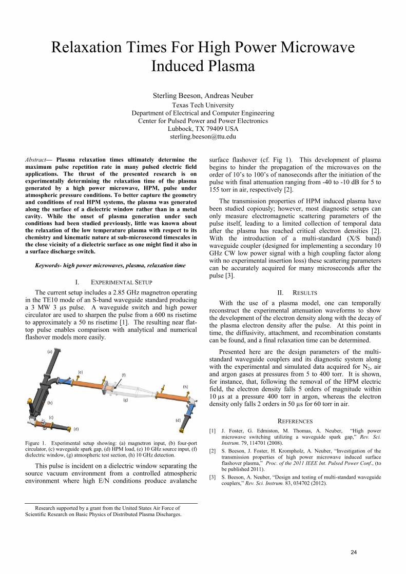
Relaxation Times For High Power Microwave Induced Plasma
Sterling Beeson, Andreas Neuber Texas Tech University
Department of Electrical and Computer Engineering Center for Pulsed Power and Power Electronics
Lubbock, TX 79409 USA [email protected]
Abstract Plasma relaxation times ultimately determine the maximum pulse repetition rate in many pulsed electric field applications. The thrust of the presented research is on experimentally determining the relaxation time of the plasma generated by a high power microwave, HPM, pulse under atmospheric pressure conditions. To better capture the geometry and conditions of real HPM systems, the plasma was generated along the surface of a dielectric window rather than in a metal cavity. While the onset of plasma generation under such conditions had been studied previously, little was known about the relaxation of the low temperature plasma with respect to its chemistry and kinematic nature at sub-microsecond timescales in the close vicinity of a dielectric surface as one might find it also in a surface discharge switch.
Keywords- high power microwaves, plasma, relaxation time
I. EXPERIMENTAL SETUP
The current setup includes a 2.85 GHz magnetron operating in the TE10 mode of an S-band waveguide standard producing a 3 MW 3 μs pulse. A waveguide switch and high power circulator are used to sharpen the pulse from a 600 ns risetime to approximately a 50 ns risetime [1]. The resulting near flat-top pulse enables comparison with analytical and numerical flashover models more easily.
Figure 1. Experimental setup showing: (a) magnetron input, (b) four-port circulator, (c) waveguide spark gap, (d) HPM load, (e) 10 GHz source input, (f) dielectric window, (g) atmospheric test section, (h) 10 GHz detection.
This pulse is incident on a dielectric window separating the source vacuum environment from a controlled atmospheric environment where high E/N conditions produce avalanche
surface flashover (cf. Fig 1). This development of plasma begins to hinder the propagation of the microwaves on the
pulse with final attenuation ranging from -40 to -10 dB for 5 to 155 torr in air, respectively [2].
The transmission properties of HPM induced plasma have been studied copiously; however, most diagnostic setups can only measure electromagnetic scattering parameters of the pulse itself, leading to a limited collection of temporal data after the plasma has reached critical electron densities [2]. With the introduction of a multi-standard (X/S band) waveguide coupler (designed for implementing a secondary 10 GHz CW low power signal with a high coupling factor along with no experimental insertion loss) these scattering parameters can be accurately acquired for many microseconds after the pulse [3].
II. RESULTS
With the use of a plasma model, one can temporally reconstruct the experimental attenuation waveforms to show the development of the electron density along with the decay of the plasma electron density after the pulse. At this point in time, the diffusivity, attachment, and recombination constants can be found, and a final relaxation time can be determined.
Presented here are the design parameters of the multi-standard waveguide couplers and its diagnostic system along with the experimental and simulated data acquired for N2, air and argon gases at pressures from 5 to 400 torr. It is shown, for instance, that, following the removal of the HPM electric field, the electron density falls 5 orders of magnitude within 10 μs at a pressure 400 torr in argon, whereas the electron density only falls 2 orders in 50 μs for 60 torr in air.
REFERENCES
[1] J. power microwave switching utilizing a waveguide spark g Rev. Sci. Instrum. 79, 114701 (2008).
[2] S. transmission properties of high power microwave induced surface
Proc. of the 2011 IEEE Int. Pulsed Power Conf., (to be published 2011).
[3] Design and testing of multi-standard waveguide Rev. Sci. Instrum. 83, 034702 (2012).
Research supported by a grant from the United States Air Force of Scientific Research on Basic Physics of Distributed Plasma Discharges.
24

Broadband Modeling of the Shielding Effectiveness of a Low Noise RF Facility
Christopher Kenyon, Christian Fazi, and Robert Atkinson US Army Research Laboratory
Adelphi, Maryland USA
Abstract We report the broadband RF shielding effectiveness of a (1) concrete, (2) concrete mesh reinforced and (3) solid steel facility. The frequency of interest is from 1 kHz to 1 GHz range. To accomplish this we model loops to be placed in a facility and compute the induced EMF or currents on various loops placed within the facility by using FEKO computational electromagnetics method of moments (MOM) software. The excitation source is an electromagnetic plane wave aimed at 45° with respect to the loops so that the loops will be struck with both horizontal and vertical polarizations. Figure 1 shows an example of the modeled loops with computed induced currents from a plane wave with amplitude of 1 V/m in free space at 1 MHz.the big loop probe point.
with the free space loops and no building structure. We add a lossy ground and a concrete base, then include concrete walls with and without steel reinforcement. Finally we add steel plates to the walls. The purpose of this study is to eventually compare modeled and
ielding as a function of different building materials. However for this paper we will be able to report only the initial modeling results.
Keywords-broadband RF; electromagnetic shielding; electromagnetic modeling; EMI
Figure 1. Four disconnected loops inside a building showing current or voltage measuring points to sense electromagnetic field penetration. The colors along the wires show the currents induced along the respective sections.
Figure 2. Computed current magnitude at big loop probe point from incident plane wave with amplitude 1 V/m.
25

Wideband Field Compensation
Motti Haridim, Boris LevinHIT-Holon Institute of Technology
Holon, [email protected]
Abstract - The compensation method permitting to reduce irradiation of the user’s body and to create a weak field area (a dark spot) in the antenna near region for operation in a wide frequency band is considered. For this purpose we propose and analyze different structures including structures of identical and similar radiators, radiators located at the equal distances from the compensation point, and structures using flat reflectors. The experimental results show that the irradiation power can be decreased by a factor of 5-10 in a wide bandwidth.
Keywords- field compensation; mobile antenna; mutual coupling; near fields; wide band
I. INTRODUCTIONThe compensation method was originally proposed for
protecting the human organism, primarily the user’s head, against irradiation from the cellular handset antenna without distorting the antenna pattern in the horizontal plane [1]. This method is based on mutual suppression of the near fields created by various radiating elements in a certain area.
The problem of field calculation in a space surrounding a radiator is complicated by the fact that this space is a heterogeneous medium. For example, the relative permittivity of the human body differs from that of the surrounding free space. This problem was considered in [2], using known electrostatic problem solutions. Since the antenna field in a near region has a quasi-stationary character, the analogy with the electrostatic problem permits to reduce the field calculation in a heterogeneous medium to field calculation in a homogeneous medium.
The calculation method of a system with two linear radiators is based on the folded dipoles theory and on the superposition principle [3, 4]. These allow analyzing thissystem as a superposition of two sub-systems: an even-mode sub-system (in-phase currents), and an odd-mode sub-system (anti-phased currents).
II. BAND COMPENSATION DIFFICULTIESThe requirement for field compensation in a wide
frequency band creates an additional difficulty. The fields of the main and the auxiliary radiators at the compensation point must be equal in magnitude and opposite in sign. The phase shift can be easily realized by using a transmitter of balanced output at the final stage. But the two antenna unitsmust have identical characteristics at an each frequency in a wide range. Besides, since the main and the auxiliary radiators are located at different distances from the compensation point, it is necessary to add a phase shifter in
one path. This phase shifter must exhibit a certain spectraldependence on the delay time.
Replacement of the phase shifter by a delay line gives the required phase provided the delay line is terminated by a matched load. But the radiator impedance is a complex value; it varies with a frequency and hence does not lenditself to high matching level. However, if the two antennas units have similar characteristics and their input impedances vary weakly with frequency, the use of the delay line permits expanding the operating frequency band.
III. RADIATORS’ PLACEMENT AT THE SAME DISTANCES
Let the main and the auxiliary radiators with similarcharacteristics be located at the same distances from the compensation point, and assume that the auxiliary radiator phase differs from the main radiator phase by 180 . If the amplitudes of the radiators’ signals are equal, the sum of the signals in the plane of the structure symmetry equals zero, and phase shift circuits are not necessary.
The disadvantage of the proposed circuit is the nullifying of the far field signal along the structure symmetry plane.But the lack of radiation along this plane is not alwayssubstantial as the angle, in which the radiation highly reduced, is very small. Besides, the ground and neighboring bodies help to fill the gap in the field pattern.
Utilization of two auxiliary radiators gives additional advantages. In this case the amplitude of one auxiliary radiator’s signal may be smaller than that of the main radiator, and the pattern has no gap. Compensation structures using flat metal reflectors (mirrors) instead of the auxiliary radiators have analogous performances.
The experimental results show that the irradiation powercan be decreased by a factor of 5-10 in a wide bandwidth.
REFERENCES[1] M. Bank and B. Levin, “The development of the cellular phone antenna
with a small radiation of human organism tissues,” IEEE Antennas Propagat. Magazine, vol. 49, No. 4, 2007, pp. 65-73.
[2] M. Haridim, M. Bank, B. Levin, T. Rechels, and Y. Levy, “Near region field of antennas in piecewise-homogeneous media,” in Proc. 2010 European Conference of Antennas and Propagation, Barcelona (Spain), 2010, pp. 1-5.
[3] B. Levin, Monopole and Dipole Antennas for Marine-Vehicle Radio Communications, Abris, Saint-Petersburg, 1998 (in Russian).
4] C.A. Balanis, Antenna Theory. Analysis and Design, John Wiley&Sons, New York, 1997.
26
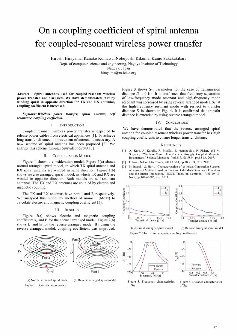
On a coupling coefficient of spiral antenna for coupled-resonant wireless power transfer
Hiroshi Hirayama, Kanako Komatsu, Nobuyoshi Kikuma, Kunio SakakakibaraDept. of computer science and engineering, Nagoya Institute of Technology
Nagoya, [email protected]
Abstract— Spiral antennas used for coupled-resonant wireless power transfer are discussed. We have demonstrated that by winding spiral in opposite direction for TX and RX antennas,coupling coefficient is increased.
Keywords-Wireless power transfer, spiral antenna, self resonance, coupling coefficient.
I. INTRODUCTION
Coupled resonant wireless power transfer is expected to release power cables from electrical appliances [1]. To achieve long transfer distance, improvement of antenna is necessary. A new scheme of spiral antenna has been proposed [2]. We analyze this scheme through equivalent circuit [3].
II. CONSIDERATION MODEL
Figure 1 shows a consideration model. Figure 1(a) shows normal arranged spiral model, in which TX spiral antenna and RX spiral antenna are winded in same direction. Figure 1(b) shows reverse arranged spiral model, in which TX and RX are winded in opposite direction. Both models are self-resonantantennas. The TX and RX antennas are coupled by electric and magnetic coupling.
The TX and RX antennas have port 1 and 2, respectively. We analyzed this model by method of moment (MoM) to calculate electric and magnetic coupling coefficient [3].
III. RESULTS
Figure 2(a) shows electric and magnetic coupling coefficient kc and kl for the normal arranged model. Figure 2(b) shows kc and kl for the reverse arranged model. By using the reverse arranged model, coupling coefficient was improved.
Figure 3 shows S21 parameters for the case of transmission distance D is 0.1m. It is confirmed that frequency separation of low-frequency mode resonant and high-frequency mode resonant was increased by using reverse arranged model. S21 at the high-frequency resonant mode with respect to transfer distance D is shown in Fig. 4. It is confirmed that transferdistance is extended by using reverse arranged model.
IV. CONCLUSIONS
We have demonstrated that the reverse arranged spiral antenna for coupled resonant wireless power transfer has high coupling coefficients to ensure longer transfer distance.
REFERENCES
[1] A. Kurs, A. Karalis, R. Moffatt, J. joannpoulos, P. Fisher, and M. Soljacic, “Wireless Power Transfer via Strongly Coupled Magnetic Resonances,” Science Magazine, Vol.317, No.5834, pp.83-86, 2007.
[2] I. Awai, Nikkei Electronics, 2011 11-14, pp.100-108, Nov. 2011.[3] N. Inagaki, S. Hori., “Characterization of Wireless Connection Systems
of Resonant Method Based on Even and Odd Mode Reactance Funcitons and the Image Impedance,” IEICE Trans. on Commun, Vol. J94-B, No.9, pp.1076-1085, Sep. 2011.
(a) Normal arranged spiral model (b) Reverse arranged spiral modelFigure 1. Consideration models
Figure 3. Frequency characteristics of S21
(a) Normal arranged spiral model (b) Reverse arranged spiral model
Figure 2. Electric and magnetic coupling coefficenent
Figure 4. Distance characteristics of S21
27

Compact Antennas for HPM Applications the EZ-Antenna Topology
Jackson Ng1, Richard W. Ziolkowski1,2, J. Scott Tyo1,2
1ECE Department, 2College of Optical Sciences University of Arizona
Tucson, AZ 85745 USA [email protected]
Michael C. Skipper and Michael D. Abdalla ASR Corporation
9817 Bursera Ave, NW Albuquerque, NM USA
Abstract— Here we report on the adaptation of the metamaterial-inspired EZ-Antenna concept for use with HPM mesoband sources. The EZ-Antenna is designed to be driven by a CW source, but in mesoband applications, the source is a resonant, quarter-wave transmission line oscillator. The principle challenge is to decouple the antenna from the source during the charge phase while preserving the radiation properties of the antenna. Here we are able to achieve ka = 0.44 at 510 MHz.
Electrically small antenna, mesoband sources, HPM antennas.
I. INTRODUCTION
Mesoband radiation is a denomination of intentional electromagnetic interference that occupies the domain between long-pulse, narrowband systems and extremely short pulse hyperband systems [1]. In the conventional parlance, mesoband systems have between 1% and 25% bandwidth. Here we are interested in sources wit fractional bandwidth on the order of 10%. There are two principal strategies for generating mesoband radiation. The first is to charge up the radiating structure and then allow it to discharge. In that case, the antenna serves as both the energy storage element and the pulse forming network [2]. However, when the antenna is desired to be electrically small, this strategy greatly limits the amount of available energy. A second strategy, and the one that we employ here, is to use a mesoband HPM source to drive an antenna. In this paper we couple an electrically small, magnetic EZ Antenna with a quarter-wave transmission line mesoband oscillator and demonstrate operation at high voltage.
II. ANTENNA DESIGN
The magnetic EZ antenna has a driven magnetic dipole that is passively coupled to an LC load. The load is composed of an extruded loop that has a capacitor at the top of the loop as shown in Fig. 1. The original EZ Antenna designs [3] were to be driven by a 50- source, and the driven element was shorted to the ground plane. However, for HPM applications, this is not feasible, since the quarter-wave transmission line oscillator shown in Fig. 2 requires the center conductor to be electrically isolated from the ground plane during the charge cycle.
This isolation was accommodated by adding a high-capacitance structure at the top of the driven loop. The capacitor was made by cutting a 1.6-mm-thick disk from a TDK UHV251A capacitor (100 pF, 50 kV), and the ceramic
has = 1501. The radiated fields measured at 1 m for a charge voltage of 10 kV are shown in Fig. 3.
Figure 1. HPM EZ Antenna over a ground plane with isolating capacitor.
Figure 2. Mesoband HPM quarter wave osillator used to drive the antenna.
Figure 3. Measured radiated fields in time and frequency.
REFERENCES
[1] D. V. Giri and F. M. Tesche, IEEE Trans. EMC 46, 322 - 328 (2004) [2] M. Armanious, Tyo, J.S.; Keller, S.D.; Skipper, M.C.; Abdalla, M.D.;
Altgilbers, L.L. “A small size resonant antenna for high power applications,” 2011 IEEE International Symposium on Antennas and Propagation pp. 1189 – 1192 (2011)
[3] R. W. Ziolkoski, C. –C. Lin, J. A. Nielsen, M. H. Tanielian, and C. L Holloway, IEEE Antennas Wireless Propag. Lett., vol. 8, pp. 989-993, 2009
28

DIEHL HPEM Technology and Applications
R.H. Stark, J. Urban, C. Bickes, D. Weixelbaum, E. Mutzbauer Diehl-BGT-Defence GmbH & Co.KG
Roethenbach a d Pegnitz, Germany [email protected]
Abstract— High power electromagnetic (HPEM) sources are systems generating ultra-short, high power electromagnetic pulses with powers ranging from several tens of Mega Watts up to several Giga Watts. Due to the high power and the high energy level emitted, HPEM sources are able to disrupt and even destroy electronic systems and components. DIEHL BGT Defence has developed non-lethal high power electromagnetic sources for various applications. The systems range from small size, autonomous and man-portable systems to larger high power devices and multi-antenna array systems. HPEM technology has been successfully tested to stop car and speedboat engines.
Keywords-component; High Power Eelectromagnetics; HPEM, High Power Microwave; HPM; Non-Lethal Weapon
I. INTRODUCTION
High power electromagnetic sources have been developed providing electromagnetic fields in the order of several hundreds of Mega Watts up to the Giga Watts level in order to disrupt functionality of electronic systems. The high power electromagnetic radiation targets the control and computer electronics of modern weapon systems and infra structures. The electronics of those systems is usually very complex. Due to the small feature size and low supply voltage of the electronics, currents and voltages induced in signal and power lines by HPEM pulses cause malfunction of electronic system.
II. HPEM SOURCE TECHNOLOGY
DIEHL BGT Defence has developed high power electromagnetic sources ranging from small size, autonomous and man-portable systems to larger high power devices and multi-antenna array systems. A basic scheme of a HPEM source is shown in figure 1.
Figure 1. Basic scheme of HPEM source
HPEM sources developed are usually battery driven. A Marx high voltage generator is employed to provide the required voltages in the order of several 100kV and a pulse forming unit is converting the Marx output voltage into a damped sinusoidal waveform emitted. HPEM pulses are targeting electronic systems only and do not have undesirable biological effects on personnel in the target area.
During recent years systems have been developed for high reliability, higher field amplitude, higher repetition rate and for various frequency ranges desired. However, high voltage and endurable spark gap technology developed, is still the key technology to drive such
pulsed power systems. A multi-antenna array source is shown in figure 2.
Figure 2. Multi-antenna array system
Besides the use of HPEM technology to defeat against electronic threats, also protection of own electronic equipment against HPEM is required. For electronic components and smaller electronic systems, protection against the powerful electromagnetic radiation may be realized on a component or on a sub-system level. However, for larger electronic systems or electronic based infrastructures like communication centres, control centres or power plants, provision of a protected “hotel room atmosphere” and therefore shielding of the room or building itself may be required.
III. APPLICATIONS
HPEM sources have been developed by DIEHL BGT Defence emitting high power electromagnetic radiation in a single pulse or a burst of pulses. The HPEM pulse is radiated over a short and limited period of time targeting the control and computer electronics of modern electronic systems and infra structures. However, source technology has to be tuned to the required frequency in order to be efficient. Sources developed are able to stop cars, to control admission to sensible or high value facilities and areas or to stop speed boats or jet-skis in maritime scenarios.
IV. CONCLUSION
High power electromagnetic radiation is a potential threat to modern electronic systems. The electromagnetic pulses induce currents and voltages in signal and power lines which are able to disrupt or even destroy electronic systems. HPEM technology can be used to defeat modern electronic based threats. HPEM technology is a non-lethal technology and targets the electronics system only. It offers new capabilities in order to deescalate situations and to react more flexible. HPEM technology has been successfully tested to stop car and speedboat engines.
Versorgungs Erzeugung von HPM Diode
Versorgungs Erzeugung von HPM Diode
Primary-Energy
HV Pulse Generator
DS Pulse Forming Antenna
29

Compact High Power Capacitor Charger
Willy DEBACHE TECHNIX
HV generators & chargers Créteil , France
Michael TEBOUL TECHNIX
HV generators & chargers Créteil , France
Abstract— We designed following compact High Power Capacitor Charger: 45 kVolts,40 kW peak power,25 kgs,25 liters volume. Double resonant technology,300V battery or external DC powersupply input. Optic fiber interface control. Oil tank is used as heat sink for reducing volume and weight. Work supported by French MOD (DGA) & CEA GRAMAT.
I. INTRODUCTION
The 45 kV compact High Power Capacitor Charger we designed can deliver a peak power of 40 kW during 10 seconds with a rest time of a few minutes.
The charger is easy transportable: 25 kgs weight for 25 liters volume and can be supplied either by one 300 V battery or an external DC power supply. It is fully controlled via an optic fiber interface at a distance of 50 meters with all logic/digital signal orders and status.
II. THE DESIGN
For realizing such a light and compact charger, each part was deeply considered with a particular emphasis on the transformer which represents the heart of the system. One of the major problems we met was the leakage inductance of the transformer. Following sketch represents the principle of the double resonant technology we use.
For getting a sufficient power transfer and a correct resonant frequency, the calculations show we needed a very low leakage inductance of the transformer: 2µH only.
The reduction of this inductance is in contradiction with the insulation rules between primary and secondary windings in High Voltage transformers.
It was a hard task for realizing a transformer with this very low leakage inductance.
Moreover, we had also to reduce the distance between the power components (IGBT) and the primary of the transformer which are in 2 different environments: IGBT is in the air and the transformer is in oil.
The oil tank, which is containing most of the parts, is also used as a heat sink for reducing volume and weight.
III. RESULTS
Tests were made on one 150 nF capacitor with a 320 V input power supply.
Following diagram represents in pink color the Voltage upon the capacitor and in green color the input Voltage. The capacitor is charged from 0 to 45 kV within 6 ms.
This work was supported by the French MOD (DGA) and the CEA,DAM,GRAMAT,F-46500 Gramat France
View of the charger
30

31

!"#$"%$ &"'*
""+88:;<=?!Q$*W
+ "#Y"+
!"# $ %& && ' &*+$/'& 0& $
Z+ Z\&^?%\Z^ _
" `W|+Z _ ~ "" " $"$ " $ $ + |8+ " "W"" " W" `W # " 8+ +\" " _ " # +$|= * "_`W"W|*#+8=# W"" #+
ZZ+ \Z?^&Z*\'^&% +
8W W" #W"W+Z";" "8==# `W < " W" #$ "?' +\" " W " % " + " '&_$" "W & &^<;% " ; " + | " " "8=# """" +8 " * "|= <+\" " " W + Z _ " " "
W W + \" " ;"W "_"+\" " " $ "_ `W+
| 8=# +
8Z 8==# +
ZZZ+ %^%?Z^\""" " " " " `+ ^# W ~+;+
&&%| +$++$+"$"_ $8
+$\W $8+8 +'+"$\ %\"W$| +$
'W $88+; +"#$+$*+'$^"W?
' " _ W * ` ++"?'$$8$+<<=+
32

A Novel Compact TEM-TE11 Mode Converter Integrated Antenna Using Disk-loaded Structure
Li Hanyu, Zhou HaijingInstitute of Applied Physics and Computational Mathematics
Beijing, [email protected]
Abstract— A novel compact TEM-TE11 mode converter based on disk-loaded backward wave structure is presented. By utilizing this backward wave characteristic, this type of mode converter would be more compact compared to the conventional ones.Examples of this type of mode converter and its integrated antenna are demonstrated.
Keywords- mode converter; antenna; disk-loaded waveguide
I. INTRODUCTION
The output modes of some microwave generator such as MILO (Magnetically Insulated transmission Line Oscillator), VCO (Virtual Cathode Oscillator) are coaxial TEM mode or circular TM01 mode. The aperture field distribution of these modes is circular symmetrical, thus the radiation field is boresight hollow. To obtain boresight gain, a mode converter is needed between the microwave source and antenna. There areseveral types of conventional mode converter, including transversal extraction type, curved waveguide type, plate-inserted type, and multi-sector lens type. However, these mode converters have some disadvantages in structure dimension orefficiency.
A novel TEM-TE11 mode converter based on disk-loaded backward wave structure is presented in this paper.
II. THEORY OF DISK-LOADED WAVE GUIDE MODE CONVERTER
This disk-loaded waveguide mode converter divides the coaxial waveguide into two half-circular parts, then applies disk-loaded and plate-inserted structure separately to each part. The disk-loaded structure makes the phase velocity reversed to its group velocity, while the plate-inserted structure accelerates the phase velocity. Choosing the proper parameters would make the phase difference of the electromagnetic wave travelling through the two parts to be π, and the field distribution is similar to TE11 mode. Because of the backward wave structure, this type of mode converter would be more compact compared to the conventional ones.
III. NUMERICAL EXAMPLES
An example of this type of mode converter is demonstrated. The converter works at 1.65GHz. The diameter of the
converter is 200mm, and the length is 98mm. Numeric simulation shows that the efficiency is 91%.
(a) (b)
Figure 1. (a) Diagram of disk-loaded waveguide mode converter. (b) S21
parameter
This type of mode converter could be mounted to the conical part of a horn antenna, composing a compact TEM-TE11 mode converter integrated antenna. An instance of this type of antenna is designed. The total length of this integrated antenna is 300mm, with aperture diameter of 340mm. The numerical simulation indicates that the antenna achieves a high boresight gain of 14.4dB.
(a) (b)
Figure 2. (a) Diagram of mode converter-radiation integrated antenna.(b)Farfield pattern
REFERENCES
[1] Yang S W, Li H F, “Numerical modeling of 8mm TM01-TE11 mode converter”, Infrared and Millimeter Waves, vol. 17 , pp. 1935-1943,1996.
[2] Eisenhart R L, “A novel wideband TM01-TE11 mode converter”, IEEE trans on Microwave Theory and Techniques, vol. 1, pp. 249-252, 1988.
[3] C.C. Cournley, C.E. Baum, “Coaxial Beam-rotating Antenna(COBRA)Concepts”, Sensor and Simulation Note 395, Apr. 1996.
[4] T. A. Milligan, “Modern Antenna Design”, McGraw-Hill, 1985.
33

High-power microwave frequency control in the course of nanosecond pulse
Oleg T. LOZA, Denis K. ULYANOV, Irina L. BOGDANKEVICH
Plasma physics dept. A.M.Prokhorov General physics institute RAS
Moscow, Russia [email protected]
Roman V. BARANOV, Svetlana E. ERNYLEVA Chair of experimental physics
Peoples’ Friendship University of Russia Moscow, Russia
Abstract— In experiments high-power microwave (HPM) pulses with the power 50 MW and the duration 60 ns were generated by two plasma relativistic microwave oscillators. Radiation frequency could be changed during a pulse in the bands 2 to 7 GHz and 5 to 20 GHz. HPM pulses with invariant frequency were obtained, pulses with continuously decreasing or increasing frequency, and also pulses with a few frequency jumps over 0.5 GHz. Frequency variation of 1.5 GHz throughout a pulse was demonstrated as well as spectrum modification from broad to narrow. Numerical modeling confirms experimental results.
Keywords - HPM; plasma; microwave; high-power; frequency; spectrum
Plasma relativistic microwave oscillator (PRMO) is a device capable to vary its emission spectrum in a very broad range. PRMO is a relativistic traveling wave tube with plasma as a slow-wave structure. Earlier we presented first repetitively-rated PRMO with the pulse power 108 W and the radiation frequency tunable electronically within two octaves from a pulse to a pulse according to any preset algorithm [1]. The spectrum width of a PRMO is also tunable from a single spectral line to 100% of the mean frequency [2].
In this work we demonstrate means of control over PRMO emission frequency within a single HPM pulse. Experiments [3] with X-band PRMO revealed a possibility of significant changes in frequency during 70 ns of microwave pulse. One of those results was repeated later and registered by a high bandwidth oscilloscope, it is shown in Fig.1. The time domain spectrum shows that during 60 ns emission frequency changes from 10.5 GHz to 12 GHz. The power level of 50 MW was measured using a microwave calorimeter overlapping the outlet horn of the PRMO.
Figure 1. Frequency rise in X-band, 50-MW pulse
Emission frequency depends on the density of plasma
prepared in PRMO using a special electron beam for gas ionization; the frequency rises with a rise of plasma density. In the course of HPM pulse either way is possible for the preformed plasma density changes. The density rise is due to further gas ionization in microwave fields ~ 100 kV/cm. Adjusting gas pressure from 5 10-5 to 3 10-3 Torr allows plasma to increase its density with a certain rate. The decrease of plasma density is determined by the effect found in [4], namely, the displacement of plasma electrons by electrostatic field of high-current relativistic electron beam. A balance between the two mechanisms of plasma density variation permits to raise emission frequency in the course of HPM pulse, to maintain it constant or even to decrease it a little as shown in Fig.2. The last mentioned result refers to the PRMO operating in the range from 2 GHz to 7 GHz.
Figure 2. Frequency reduction in G-band, 50-MW pulse
The above experiments were confirmed by numerical modeling carried out using 2.5-D version of the KARAT code (author V.Tarakanov) with PIC-method for electrons and ions.
REFERENCES
[1] O. T. Loza, et al. Rep-Rated Plasma Relativistic Microwave Oscillator with Tunable Radiation Frequency in Every Pulse // EUROEM 2008, 21-25 July 2008, Lausanne, Switzerland, p.26 // Plasma Phys. Reps., Vol. 34, No. 10, 2008, p. 855-859.
[2] O. T. Loza, et al. Control over the Radiation Spectra of Broadband Plasma Relativistic HPM Oscillators // EUROEM 2008, p.224 // Plasma Phys. Reps., 2009, Vol. 35, No. 3, pp. 183–190.
[3] O. T. Loza, D. K. Ul’yanov, and R. V. Baranov. Variation in the Radiation Frequency of a Plasma Relativistic Microwave Oscillator within Its Nanosecond Pulse // Technical Physics, 2011, Vol. 56, No. 3, pp. 413–417. http://www.springerlink.com/content/q0517t3qpn336l43/
[4] I. L. Bogdankevich, O. T. Loza, and D. A. Pavlov. // Bulletin of the Lebedev Physics Institute, 2010, Vol. 37, No. 2, pp. 40–48.
Supported by Russian Foundation for Basic Research, grant 10-08-00994, and RAS Program “Fundamental problems of high-current pulse electronics”.
34

Keywords - HPM; microwave; high-power; pulse shortening; plasma
35

Recent Advances in Relativistic Magnetrons
Edl Schamiloglu, Mikhail Fuks, Sarita Prasad, Christopher Leach, Cassandra Mendonca, and David GalbreathDepartment of Electrical and Computer Engineering, MSC01 1100
University of New MexicoAlbuquerque, NM 87131-0001, USA
Abstract— Recent work at the University of New Mexico has focused on various improvements to the performance of the relativistic magnetron. Most of the advances have been based on the A6 magnetron of Bekefi, although other magnetrons were studied. This paper summarizes these improvements.
Keywords-A6 magnetron; diffraction output; transparent cathode, strapping
I. INTRODUCTION
The A6 magnetron was introduced by Bekefi at MIT [1]. It is the most studied relativistic magnetron in the literature. Since 2005 the University of New Mexico has been proposing novel advances in this magnetron that achieves higher power, greater efficiency, and control over mode competition. This paper summarizes these advances.
II. SUMMARY OF ADVANCES
A. Introduction of the Transparent CathodeThe transparent cathode (TC) is an explosive emission
cathode where the first order microwave electric field penetrates the surface and goes to zero on axis [2,3]. It leads to magnetron operation whose efficiency is much greater than one driven by a solid cathode. A relativistic A6 magnetron with axial extraction was demonstrated to operate with nearly 70% efficiency in PIC simulations when using a TC [4]. The able to control mode competition by properly orienting the TCemitters and selecting an appropriate magnetic field magnitude was shown in detail in [3].
B. RF Mode SwitchingRF mode switching from one shot to the next was
demonstrated in PIC simulations [5,6]. This arose from studies of the dependence of A6 magnetron operation for a given cathode radius on the magnetic field. It turns out that there is a critical magnitude of the magnetic that delineates magnetron operation in either the -mode or 2 / 3 -mode. By operating this magnetron near this boundary and introducing a relatively weak (200 kW) input signal it is possible to switch the operating mode of a 1 GW-level magnetron.
C. StrappingGenerally, a multicavity magnetron can support many
resonant modes. Therefore, sufficient separation is necessary
between the desired mode and any other competing mode for efficient operation. Separation of modes was demonstrated in PIC simulations for the A6 magnetron by use of the strapping technique in which resonator segments having the same polarity are connected together by small conducting strips to suppress undesired modes [7].
D. Suppression of Leakage CurrentLeakage current is a parasitic current in relativistic
magnetrons. Novel endcap designs were recently studied in PIC simulations and experiments and one design nearly completely eliminated 1-2 kA-level leakage current [8].
E. A6 Magnetron with Permanent MagnetNeodymium permanent magnets were simulated using
both a magnetostatic solver and PIC code for an A6 magnetron with axial extraction. The aim was to replace the pulsed magnet system. Up to 0.58 T of uniform magnetic field in the electron interaction space was achieved in simulationsand higher fields are likely possible. This design appears to be very feasible for implementation.
REFERENCES
[1] A. Palevsky and G. Bekefi, “Microwave emission from pulsed, relativistic e-beam diodes. II. The multiresonator magnetron,” Phys. Fluids, vol. 22, pp. 986-996, 1979.
[2] M. Fuks and E. Schamiloglu, “Rapid start of oscillations in a magnetron with a “transparent” cathode,” Phys. Rev. Lett., vol. 95, 205101, 2005.
[3] H. Bosman, M. Fuks, S. Prasad, and E. Schamiloglu, “Improvement of the output characteristics of magnetrons using the transparent cathode,” IEEE Trans Plasma Sci., vol. 34, 620, 2006.
[4] M. Fuks and E. Schamiloglu, “70% efficient relativistic magnetron with axial extraction of radiation through a horn antenna,” IEEE Trans. Plasma Sci., vol. 38, 1302, 2010.
[5] M. Liu, C. Michel, S. Prasad, M. Fuks, E. Schamiloglu, and C.-L. Liu, “RF mode switching in a relativistic magnetron with diffraction output,” Appl. Phys. Lett., vol. 97, 251501-1-251501-3, 2010.
[6] M. Liu, C.-L. Liu, D. Galbreath, C. Michel, S. Prasad, M.I. Fuks, and E. Schamiloglu, “Frequency switching in a relativistic magnetron with diffraction output,” J. Appl. Phys., vol. 110, 033304-1-7, 2011.
[7] S. Prasad, D. Galbreath, M. Fuks, and E. Schamiloglu, “Influence of implementing straps on pulsed relativistic magnetron operation,” Proc. IVEC 2010 (Monterey, CA), pp. 379-380.
[8] C. Leach, S. Prasad, M. Fuks, and E. Schamiloglu, “Suppression of leakage current in a relativistic magnetron using a novel cathode endcap design,” submitted to IEEE Trans. Plasma Sci., 2011 (in review).
[9] C. Leach, S. Prasad, M. Fuks, and E. Schamiloglu, “Compact magnetron with permanent magnet,” submitted to Proc. IVEC 2012 (in review).
This work has been sponsored by grants from the Air Force Office of Scientific Research (John Luginsland, program manager) and the Office of Naval Research SAAET Program (Lee Mastroianni, program manager).
36

High Repetition Rate Picosecond FID Pulse Generators for UWB ApplicationsVladimir Efanov, Mikhail Efanov, Alexander Komashko, Sergey Zazoulin
FID GmbHBurbach, [email protected]
Abstract — A series of high voltage pulse generators and pulsepower modules with picosecond pulse duration and pulse repetition rate of megahertz range has been developed. Combination of megawatt peak power and megahertz PRF permit production of radiating systems with unique set of specifications. Pulse generator FPG 10-10PHF has maximum amplitude of 10 kV into 50 Ohm and can operate with pulse repetition rate of 10 MHz. Rise time of this pulser is 150-200 ps, pulse duration at half amplitude is 500 ps. With peak power of 2 MW average power in load is about 5 kW. The pulse generator can form bursts of pulses with any variation of PRF inside a burst. Maximum PRF of 500 MHz is reached in pulse generator FPG 1-500PHF with amplitude of 1 kV into 50 Ohm and burst duration of up to 10 microseconds.
Keywords-component; solid-state switches; gigawatt peak power; pulse generator; picosecond, high PRF
I. INTRODUCTION
The most important parameter for many UWB radiating systems is maximum pulse repetition rate that permits reaching high average values of radiated power and in certain limits adjust output spectrum.
FID GmbH has developed a series of high repetition rate pulse generators that permit operation into a wide variety of antennas and having high reliability, compact size and energy efficiency.
Modular pulse generator FPM10-100PNK has maximum amplitude 10 kV into 50 Ohm. Rise time is 80-100 ps, pulse width at half amplitude 200-300 ps, maximum PRF of 100 kHz with power consumption of about 200 W. Approximate size of module is 200x170x50mm, weight of 3 kg.
Pulser FPG 10-10PHF has an output amplitude of 10 kV into 50 Ohm with pulse repetition rate of 10 MHz. Output pulse has rise time of 150-200ps and duration of 500 ps FWHM. With peak power of 2 MW average power to load is 5 kW. Pulse generator permits creation of sequences of output pulses set by computer control with possibility to vary PRF in burst from zero to 10 MHz.
Maximum pulse repetition rate has pulse generator FPG 1-500PHF. In burst mode the achieved PRF is 500 MHz with burst duration of up to 10 microseconds and average repetition frequency of 1 MHz. Rise time of this type of pulsers is 150-200 ps, pulse duration at half amplitude is 300-500 ps. Pulsers
can form a computer controlled sequence of pulses with PRF inside such burst up to 500 MHz.
Operation of high power picosecond pulse generators in radiating systems requires high stability and EMI-proof power supplies and control systems. FID GmbH has developed a series of such power supplies with output power from tens ofwatts to tens of kilowatts. Digital control blocks permit operation of tens of pulsers with accuracy of 10-20 ps. Optical lines permit controls to be placed hundreds of meters away from radiating point and set the necessary operation mode via computer interface.
In most cases cooling of high repetition rate pulse generators and modules is done by forced air, however amplitudes higher than 10 kV usually require liquid cooling system.
37

A 12 KW wideband power amplifier
for strong field levels
Dr Cyril Lagarde PRANA R&D – www.prana-rd.com
Brive La Gaillarde, FRANCE [email protected]
Dr Ludovic Bacqué PRANA R&D – www.prana-rd.com
Brive La Gaillarde, FRANCE [email protected]
Abstract— Many EMC applications (automotive, military…) request more and more field level in order to realize immunity testing. Prana has developed and manufactured a new strong wideband power amplifier in the bandwidth 100 kHz - 225 MHz, named GN 12000.
Keywords: power amplifier, wideband, strong field, EMC, immunity
I. INTRODUCTION
Prana, French company, belongs to the worldwide leading manufacturers of RF Power Amplifiers for Broadband applications such as EMC testing, instrumentation and radio-communication. The Prana product lines are all solid state and cover a frequency range from 10 kHz to 6 GHz with power levels up to 12 kW: GN 12000.
This amplifier provides a CW typical power of 12 kW between 100 kHz and 225 MHz. The class A of the amplifier allows providing the output power at 1 dB of compression with a harmonic ratio less than -20 dBc.
Integrated in an EMC test system, the goal is to obtain an electric field level higher than 150 V/m in the frequencies (100 kHz – 225 MHz).
II. GN 12000 PRESENTATION AND MEASUREMENTS
Figure 1. Prana amplifier GN 12000
The GN 12000 design is modular and modern (figure 1). It is composed of 16 identical power modules, 4 intermediate combiners, 1 final combiner and 1 coupler. The GN 12000 was designed for minimal maintenance: easy accessibility of all sub systems and all the modules can be changed each other. This design allows a fast and efficient after sales service in the world. One power module provides a typical power of 1 kW. The power modules are composed of LDMOS transistors polarised in Class A in order to obtain both an important output power and a high linearity. The GN 12000 was tested in the Prana laboratory with a 50 ohms water cooled load. The output power has been measured at 1 dB (green curve – figure 2) of compression and 3 dB of compression (red curve - figure 2).
0
2000
4000
6000
8000
10000
12000
14000
16000
0 25 50 75 100 125 150 175 200 225
Ou
tpu
t po
wer
(Wat
t)
Frequency (MHz)
Linear Output Power (Compression max. = 1 dB) Saturated Output Power (Compression max. = 3 dB)
Figure 2. Output power at 1 dB and 3 dB of compression
This high power level is dedicated to EMC application for automotive. It was also tested in a famous automotive laboratory in German. The results will be presented in the final paper.
III. CONCLUSION
This amplifier GN 12000 was tested in different Automotive EMC test systems: combined to a stripline antenna and to a Log-periodical Antenna. These tests validate the GN 12000 capacity to generate strong field levels (> 150 V/m) and this reliability with high mismatched loads.
38

A New Set of Electrodes for Coaxial Quarter Wave Switched Oscillators
Felix Vega1,2,4, Farhad Rachidi1, Bertrand Daout2, Nestor Pena3, Francisco Roman4
1EMC Laboratory, Swiss Institute of Technology of Lausanne (EPFL), Lausanne, Switzerland 2Montena technology, Rossens, Switzerland
3Universidad de los Andes, Bogota, Colombia 4Universidad Nacional de Colombia, Bogota, Colombia
Abstract—In this paper, a new set of conformal electrodes for coaxial switched oscillators (SWO) is proposed. The proposed electrode geometry assures the maximization of the DC electric field distribution exclusively on the axis of symmetry of the SWO and a monotonically decreasing of the electric field amplitude with the distance.
Keywords-component; Switched oscillator, conformal electrodes.
I. INTRODUCTION A Switched Oscillator (SWO) is a mesoband radiating
system proposed by Baum in [1]. The coaxial SWO system consists of a DC-charged low-impedance transmission line that is discharged at one end by a spark gap formed by two electrodes. The other end is connected to a high impedance antenna. The reflections pattern occurring on the SWO produce a damped sinusoid-like signal with a central frequency of about f=vp/4L, where L is the length of the line and vp is the wave propagation velocity.
II. LOGARITHMIC-TANGENT ELECTRODESIn order to prevent distortion of the signal produced by the
SWO, all the points on the electromagnetic wave front originated at the discharge point should arrive to the antenna at the same time. On the other hand, the discharge should originate always at the same spot, if reproducibility is desired. The only way to guarantee this is producing the discharge exactly on the axis of symmetry of both the coaxial line (the main body of the SWO) and the radial transmission line (RTL) formed by the surface of the electrodes. To maximize the probability of producing the breakdown on the axis of symmetry, the magnitude of the electric field before the discharge should be maximum on the axis and should monotonically decrease in direction of the coaxial line.
We propose in this paper a new profile for the RTL of the SWO. The new profile is formed using a set of conformal curves generated using a specific 2-D transformation called Logarithmic-Tangent (Ln-Tan), proposed by Moon and Spencer in [2] (page 67). The Ln-Tan transformation is defined as
2 ln tanaZ W ia (1) where W=u+iv, and Z= x+iy
As usual, u and v are the flux and potential functions, respectively (0 u < /2, 0 v), (x,y) are the space coordinates (-a y a, - < x < ) and a >0 is a constant,
The space coordinates can be calculated using
2 21
2 2
sin ( ) sinh ( ) 2 sinh(2 )ln , tancos ( ) sinh ( ) sin(2 )
a u v a vx y au v u
(2)
These two equations represent two perpendicular sets of parametric curves in the Z plane. The first set (v-set) can be generated using u as parameter and v as a constant. The second set (u-set) uses v as parameter, while u is held constant. Figure 1 shows some examples of this family of curves.
-a
a
u= /4 v-set
y
x
u= /2u=0
u-set v=0
v=0
v= /8
v=
Figure 1 Logarithmic – Tangent curves. u-set curves (dashed lines), v-set curves (solid lines)
We propose to form the RTL taking a pair of curves belonging to the v-set and rotating them around the y axis. The curves parameters are v =v1 and v =v2 with 0<u< /2. If a constant difference of potential is applied between v1 and v2 the formed isopotential lines will be conformal to the v-set and the electric field stream lines will be conformal to the u-set [3]. As it can be seen from Figure 1, the distance between any pair of curves belonging to the v-set is minimum on the axis of symmetry (y axis) and increases as we move away from the axis of symmetry. This suggests that the maximum amplitude of the electric field occurs precisely on the axis of symmetry and decays as we move away from the y axis. The coaxial line section can be connected at the extremities of the curves, at the points where u=0, u= /2 (the horizontal axis y=0). Note that at this point, the stream lines are parallel to the x axis, coinciding with the direction of the stream lines inside the coaxial (which are radial).
III. REFERENCES[1] C. E. Baum, "Switched Oscillators," Circuit and Electromagnetic System Design Notes 45, 2000 [2] P. Moon and D. E. Spencer, Field Theory Handbook: Including Coordinate Systems, Differential Equations and Their Solutions 2ed.: Springer-Verlag, 1971 [3] F. Gardiol, Électromagnétisme, 2 ed. vol. 3. Lausanne, Switzerland: Éditions Georgi, 1979
This work was supported by the Swiss Agency for Development and Cooperation (SDC) and the Centre Coopération & Développement (CODEV) EPFL, Switzerland
39

Picosecond Pulse Generators Based on FID Technology with Gigawatt Peak Power
Vladimir Efanov, Mikhail EfanovFID GmbH
Burbach, [email protected]
Abstract — A new series of picosecond pulse generators and compact pulse power modules with output amplitude up to 500 kV and peak power up to 10GW has been developed. Rise time is about 100-150 ps, pulse duration at half amplitude is in range 200-500 ps. Dimensions of 200-300 kV pulse power module with impedance of 50 Ohm are about 220x170x70mm with weight of about 3 kg. Maximum pulse repetition frequency is 1 kHz. Jitter of output signal is about 20 ps, so that the modules can be used in multichannel radiation systems operating in synchronous mode.The pulsers can operate into any load ranging from short to open circuit. Power consumption of 1 GW pulser with pulse width of 200 ps FWHM running at 1 kHz is 300 W.
Keywords-component; solid-state switches; gigawatt peak power; pulse generator; picosecond
I. INTRODUCTION
Range and efficiency of UWB radiating systems are mostly dependent on peak power of pulse generators used in them. For a long time FID GmbH has offered a series of compact all solid state pulse generators with peak power from tens of kilowatts to hundreds of megawatts. Pulsers have pulse duration from 100 to 1000 picoseconds and pulse repetition frequency of up to several megahertz. High timing stability such pulse generators can be used in synchronous mode and their combined peak power can reach several gigawatts.
However for radiating systems with terawatt peak power level it is necessary to use pulsers with the peak power of up to 10 gigawatts. Voltage amplitude in this case should reach several hundreds of kilovolts. At the same time such pulsers should have timing stability or jitter better than a few tens of picoseconds with pulse duration of several hundreds of picoseconds.
To solve this question FID GmbH has developed new solid state switches capable to switch currents of several tens of kiloamperes for less than 100 ps and having high reliability and compact size.
On the base of new FID switches a new series of picosecond pulsers has been developed. These pulse generators are designed for operation into 50 Ohm loads with maximum amplitudes of 200 kV, 300 kV, 400 kV and 500 kV. Moreover the compact modular versions of these pulsers have also been developed.
Modular pulser FPG 200-1PM has approximate size of 220x170x70 mm and weights about 5 kg. Maximum voltage amplitude is 200 kV into 50 Ohm, maximum peak power is 1
GW. Rise time is about 150 ps with pulse duration at half amplitude of about 250 ps. Maximum pulse repetition rate is 1 kHz. The pulser module can operate into any load from short to open circuit. Input power of 1 module is about 500 W.
Another variant of pulse generator module is FPG 500-1PM. These pulsers have voltage amplitude of 500 kV into 50 Ohm with peak power of 5 GW. Dimensions of 500 kV module are 500x200x100 mm with total weight of 10 kg. Rise time is about 150 ps with pulse width of about 250 ps (FWHM). Maximum PRF is 1 kHz with maximum input power of about 2 kW.
Modules of FPG 200-1PM and FPG 500-1PM series can operate with any types of antennas. Compact size and low weight permit direct connection to antenna without transmitting cables and high timing stability permit synchronous operation of large number of modules.
In the nearest future FID GmbH is planning to perform tests of picosecond pulse generators with amplitude of 1-2 MV. A work on reaching 10 MV with rise time of 200 ps is in progress.
40
Numerical simulations of a new-type axial VIRCATOR with a reflector for enhanced efficiency
S. Champeaux, Ph. Gouard CEA, DAM, DIF
F-91297 Arpajon, France [email protected]
R. Cousin CST AG Bad Nauheimer Str. 19
64289 Darmstadt, Germany
J. Larour LPP, UMR 7648, CNRS, Ecole Polytechnique
91128 Palaiseau Cedex, France
Abstract A new type of axial vircator with reflector is numerically simulated with a PIC code for the first time. The power conversion efficiency of classical vircator is shown to be enhanced from 1% to 4.8%. Optimization of both reflector position and radius is expected to increase performances.
Keywords-component Microwave, virtual cathode oscillator (VIRCATOR), particle-in-cell (PIC), open drift tube.
Vircators are one of the most important class of high-power microwave generators [1]. Due to their conceptual simplicity, robustness and frequency tenability, Vircators are widely used. Nevertheless they exhibit low power conversion efficiency. To prevent this severe drawback, the classical axial Vircator is improved by introducing a reflector beyond the virtual cathode in the cylindrical waveguide [2]. The new-type Vircator, Fig. 1, is simulated with the PIC code CST - PS® [3].
Figure 1. Schematic structure of the vircator with reflector: (1) cathode, (2) anode, (3) virtual cathode, (4) reflector (5) cylindrical waveguide.
The electron beam is emitted from a 9 cm diameter cathode (K). Beyond the anode (A) the beam propagates into a 15.2 cm diameter cylindrical waveguide. The AK gap is equal to 2.3 cm. The applied diode voltage is about 500 kV with a 5 ns rise time, which gives an input diode power of 9 GW. This axial Vircator yields an average output power of 0.1 GW in the TM01 mode (Fig. 2a) at 3.06 GHz (Fig. 3a). An aluminized Mylar thin reflector of 5 cm diameter is placed in the waveguide at 6 cm from the anode, in such way that the virtual cathode is positioned between the anode and the reflector. As it is transparent to the electrons, the reflector allows increasing the microwave generated by the oscillating virtual cathode.
Such device delivers an average power of 0.43 GW in the same mode (Fig. 2b) at 3.01 GHz (Fig. 3b). Compared to conventional axial Vircators, this novel device can achieve higher microwave powers at the same frequency. Performances can be further increased by optimization of both position and radius of the reflector.
Figure 2. Output power in the TM01 mode for a classical axial VIRCATOR (a) and for an axial Vircator with reflector (b).
Figure 3. Emitted frequency spectrum in the TM01 mode for a classical axial Vircator (a) and for an axial Vircator with reflector (b).
[1] Ph. Gouard, O. Henry and F. Sellem, Numerical simulations of the vircator, Proc. of the EUROEM 94 International Symposium, pp. 237-241, 1994.
[2] J-L. Faure, and Ph. Gouard, Microwave generating device with oscillating virtual cathode, European Patent WO 2006/037918.
[3] CST AG, CST Particle Studio®, User Manuel 2011.
41

Turbulent Electron Beams -Sources of Broadband Noise-like Oscillations
Yu.A. Kalinin, A.V. Starodubov Saratov State University
Saratov, Russia [email protected]
Abstract — A new approach for the generation of broadband noise-like signals is proposed. It generalizes the system of vacuum microwave electronics in which there is an internal electronic feedback. The proposed approach is based on the formation the intense multispeed turbulent electron beams. In the turbulent electron beams there is a formation of dense bunches of space charge. The intensive spatial-temporal fluctuations of such dense bunches of space charge are the sources of broadband noise-like fluctuations. Various methods of formation of the turbulent electron beams have considered. The results of experimental studies of the structure of turbulent electron beams have shown. The results of experimental studies of laboratory models of broadband noise-like oscillations generators whose work is based on the physical effects in intensive turbulent electron beams have considered.
Keywords – vacuum microwave electronics, turbulent electron beams, broadband noise-like oscillation.
I. INTRODUCTION
At the present time a various communications and telecommunications systems widely use a super-high frequency (SHF) range of electromagnetic waves. It is interesting to consider the vacuum microwave sources of broadband radiation, which are essential elements of perspective radar systems, communications and telecommunications. In this work we attempt to consider from a unified point the vacuum generators with internal electronic feedback. A common feature of such systems of vacuum electronics is the existing of one or several bunches of space charge, which are formed by turbulent multispeed electron beams.
II. MAIN RESULTS
To form turbulent electron beams in which there will be a significant number of dense bunches of space charge need a large spread of electron velocities. In the electron gun region, the initial spread of electron velocities can be achieved by placing the accelerating electrode near by the cathode. The accelerating electrode can be a grid or a diaphragm, which, due to lens effects can provide a large spread of the electron transverse velocity (the angle of inclination of the trajectories of electrons). Naturally, the spread of the electrons over the transverse velocities leads to the spread of the electrons over longitudinal velocities. Further, in the drift space of the electron beam the presence of an inhomogeneous magnetic
field increases the spread of the electrons in the longitudinal velocities, which in turn affects the spread of the electrons over the transverse velocities. In the collector region spread of the electron velocity can be increased by a retarding electric field.
Thus, the following factors influence to the formation of dense bunches of space charge:
• The initial spread of electron velocities in the electron gun region;
• The spread of electron velocities in a magnetic field;
• the presence of reflected from the collector region "slow" electrons.
All of the above creates the conditions for the formation of dense bunches of space charge (current density in such clusters may be 300-500 times higher than the average). It should be noted that the internal electronic feedback is realized by means of electron emission from bunches of space charge, which leads to spatial and temporal oscillations of the clusters. Bunches of space charge and its spatial and temporal oscillations are a source of broadband noise-like oscillations [1].
In this work we also have reviewed the results of experimental studies of the structure of turbulent electron beams. An overview of some laboratorial circuits of compact generators of broadband noise-like microwave oscillations which are based on the formation and using the physical effects in intense turbulent electron beams have carried out. Effective ways to create a powerful broadband noise-generator which can be implemented on industry classical traveling wave tubes (TWT) by changing the magnetic periodic focusing systems and supplying the retarding potential on the of electrodynamics system have considered.
Thus this work is an attempt to illuminate the fundamental physical phenomenon of turbulence in high-intensity and dense electron beams observed in the vacuum electronics devices, from a new angle, by using it to generate broadband noise-like oscillations.
REFERENCES
[1] Ju.A. Kalinin, A.V. Starodubov, Physics of wave phenomena. 19, 1 (2011) 1-6
This work has been supported by RFBR projects (No 10-02-00256, 11-02-00047)
42

SF6 for High Voltage Pulse GeneratorsAn Ecological Analysis
Bertrand Daout, Felix VegaMontena technologyRossens, Switzerland
[email protected], [email protected]
Abstract
Keywords-component; SF6; pulse generators; global warming;recycling.
I. INTRODUCTION
SF6 (sulfur hexafluoride) is commonly used for theelectrical insulation of HV installations, for example in pulsegenerators. This gas insulates between 2 and 3 times better thanair or nitrogen at the same pressure thus allowing smallerdimensions and less stray inductance in the structure of thegenerators. Compared to oil, SF6 has a lower permittivity, islighter and makes adjustments easier. It is used for thesurrounding insulation of Marx generators and for the sparkgaps of peaking circuits of high speed pulse generators.However SF6 has undesirable properties: it is a potentgreenhouse gas and it produces toxic and corrosivedecomposition products when subjected to electricaldischarges. Some explanations and figures are given in order toevaluate the greenhouse potential of this HV pulse generatorand if recycling of the SF6 is required.
II. GREENHOUSE GAS EFFECT
About 60 % of the production of SF6 in the world is used inthe electricity industry, essentially for high voltage insulation.Most of the gas used in the industry is released in theatmosphere. The potent effect of SF6 is essentially due to itsvery good absorption of infrared radiation. Due to the growthof the global production of SF6 (8-9 % per year), theconcentration of this gas is also increasing (see Figure 1) [1].
Figure 1. Concentration of SF6 in the atmosphere, in parts in 1012 by volume
Due to the high density of the SF6 (5 times higher than air),the question arises as to how the greenhouse effect occurs? The
analysis of Figure 2 shows that the concentration of SF6 in theatmosphere remains quite high even at a high altitude [2]. Theimportant convection and vertical diffusion in the atmosphereexplain that this gas is relatively well mixed with air. Inaddition, SF6 has a very long lifetime.
Figure 2. Concentration of SF6 in the atmosphere as a function of thealtitude, in parts per 1012 by volume
The global warming potential (GWP) of SF6 is 22'600 timeshigher than CO2 [3]. A simple calculation gives an idea of theecological effect of the use of a 1 MV NEMP pulse generatorcomposed of a Marx generator and a peaking circuit using SF6.Considering that the peaking circuit spark gap uses 1.4 liters or8.8 g for each series of pulses, the equivalent production ofCO2 is 200 kg. This can be compared to driving a medium sizecar for 1'340 km.
III. RECYCLING
The recycling essentially consists of pumping the SF6 fromthe generator up to a pressure of 23 bars necessary to stock thegas in a liquid form. The used gas is then analyzed andreconditioned in specialized factories. If the gas is too pollutedby compound elements, the material is incinerated. If too muchair or nitrogen is mixed with SF6, the gas cannot be recycled. Inthis case the carbon balance sheet for the separation of the gasfrom the air and for the transportation is negative. Thus theonly solution is to release the gas in the atmosphere.
REFERENCES
[1] M. Rigby et al., “History of atmospheric SF6 from 1973 to 2008”,Atmos. Chem. Phys., 10, 10305–10320, 2010.
[2] A. B. Burgess, R. G. Grainger, and A. Dudhia, “Zonal mean atmosphericdistribution of sulphur hexafluoride” Geophysical Research Letters, Vol.33, 2006.
[3] J. Olivier and J. Bakker, “Good Practice Guidance and UncertaintyManagement in National Greenhouse Gas Inventories”, chap. 5, par. 3,IPCC, May 2001.
43

44

HPEM-TC02 Applications of
Coupling to Structures and
Cables
45

Propagation of Current Waves along a Transmission Line with Stochastic Geometry
Sergey Tkachenko, Jürgen Nitsch and Ralf Vick Institute for Fundamental Electrical Engineering and EMC
Otto – von – Guericke University Magdeburg Magdeburg, Germany
Abstract—On the basis of different analytical approaches we investigate the propagation of current waves along transmission lines with stochastic geometry.
Keywords: transmission lines, stochastic geometry, analytical approaches
I. INTRODUCTION
Investigation of the propagation of currents and voltages along different wiring structures constitutes one of the main groups of problems in electromagnetic compatibility. In praxis often electrical parameters of such transmission lines are known only statistically (e.g. in cars, aircraft, etc.). A usual approach to solve such problems includes the following three steps: numerical generating of the stochastic geometry of the line, numerical solution of corresponding TL- or full – wave equations for each configuration and averaging the statistical ensemble. On the other hand, the application of direct numerical methods to solve stochastic problems is very time consuming and only describes a specific case of distribution with fixed parameters.
II. RESULTS
In the present work we describe some preliminary results of our investigation of stochastic lines. We relay on analytical methods, which allows obtaining explicit equations for the probability distribution function (PDF) of interest as well as for its statistical moments.
We consider a lossless infinite single-wire line which central long region has stochastic geometry. To describe this geometry we use the representation of the dependence of the line transverse coordinate from the longitudinal coordinate as a Fourier series with stochastic coefficients [1]. Each of these coefficients has a Gaussian distribution with standard deviation exponentially decreasing for higher Fourier modes. For this model it is possible to obtain the correlation function in explicit form and to show by direct calculation that the transverse coordinate dependence of the wires from the average value is a Gaussian random process. The analysis of some other realistic models of stochastic TLs has shown that the correlation functions also can be approximated by a Gaussian process. Moreover, the TL parameters, as inductance
and capacitance, also can be described by a Gaussian process. In all cases the correlation function has a sharp peak form and for relative long wavelengths can be considered as a -function. It follows that the TL equation for an auxiliary function of the current can be reduced to a second order “Schrödinger” - like equation with stochastic “potential”[2]. Such equations have been studied very intensively in recent decades. One advanced technique to solve such equations is described, for example, in [3, 4]. After a cumbersome calculation one can obtain the equation (Fokker–Plank equation) for PDF of the reflection coefficient. Its solution allows obtaining the PDF as well as all statistical moments.
The interesting result of this theory is the following: if the region of stochastic non-uniformity is long enough, the line reflects the incident wave with probability one due to multiple re-reflections of the wave in internal sub-regions of the line. However, for some realizations the amplitude of current waves can essentially increase in some regions in comparison to the average value, but on the whole, the wave is reflected from the stochastic line. This physical phenomenon is known as a dynamical localization of scattered waves in the randomly layered media [4]. We have compared results with those of numerical simulations and obtained a good agreement.
In conclusion, we discuss the possibility of the generalization of obtained results for multiconductor lines and lines with (radiation) losses.
REFERENCES
[1] M.A Morgan, F.M Tesche, “Statistical Analysis of Critical Load Excitations Induced on a Random Cable System by an Incident Driving Field: Basic Concepts and Methodology”, Interaction Notes, Note 249, July 1975.
[2] J.B. Nitsch, S.V. Tkachenko „Propagation of Current Waves along Quasi-Periodical Thin-Wire Structures: Taking Radiation Losses into Account”, Rad. Sci. Bull., No 322, Sept. 2007, pp. 19-40.
[3] V. I. Klyatskin, Stochastic Equations and Waves in Random Media, Nauka, Moscow, (Rus.) 1980, 336 pp.
[4] V. I. Klyatskin, “Statistical topography and Lyapunov exponents in stochastic dynamical systems”, Phys. Usp., Vol. 51 (2008), No. 4, pp. 395-407.
This work was sponsored by the German Research Foundation (DFG), Contract Number: VI 207/3-1.
46

Keywords- Twisted Pair Cable (TPC); coupling; Transmission Line Theory (TLT); Equivalent Model
47

Management of EMC Segregation Rules Deviations
Richard Perraud, Jerome Robert EMC and Mathematics Group
EADS Innovation Works Suresnes, France
[email protected], [email protected]
Laurent Molinari, Claude Cuiller Aircraft Electrical Architecture
Airbus France Toulouse, France
[email protected], [email protected]
Abstract— On civil aircraft, physical integration requirements, especially for EMC purposes, have to be controlled before and during the design. Main drivers for EMC segregation rules are the type of signals (physical support, RF emissions, and susceptibility levels) and the distance between couple of routes (containing several signals) and to their respective protections. This paper demonstrates how the electromagnetic simulation at route level could help designers to decide whether or not a deviation to the installation rule is acceptable.
Keywords – EMC, DMU, Segregation between routes
I. INTRODUCTION
Different types of routes are installed on civil aircraft to distinguish power routes, signal routes, radio-communication routes, and audio routes. To avoid electromagnetic issues between signals belonging to two different routes, installation requirements are proposed in term of distance between those routes. During the design of route placement inside the aircraft, space allocation is limited for designers and some deviations to the installation requirements can occur. The presence of composite on new civil aircraft have added new installation requirements to manage short circuits current and their associated risk in term of damage to CFRP but also in term of voltage reference fluctuation. The space allocation is here lower than for metallic fuselage and a higher risk of deviations has been identified.
We present here a methodology based on electromagnetic computation to help designers to check the impact of deviations to segregation distance requirements, give them the possibility to decide if the deviations are acceptable and so minimize the time for deviation acceptance.
II. GENERAL METHODOLOGY
Designers are used to work within Catia Environment andthe checking of the installation rules is done inside the Digital Mock Up (DMU). The first step of our methodology is to understand what the main drivers of the coupling between routes are, and thus be able to select the needed 3D geometrical data and extract them to feed the electromagnetic model. Most of the time, bundles are routed near an internal structure specifically designed for electrical current return. This “grounding” network will concentrate all the spurious currents and will induce parasitics on signals referenced to the same ground (common ground coupling). The main drivers of the coupling are: the positions of the routes respect to their near
environment, typically distances to grounding network, distances between them, the nature of their protection (raceway, open sleeve …), coupling length… From this point, it has been decided that a 2D model will be convenient to represent the coupling and then avoid 3D time consuming computations. Local effects have been taken into account and the 2D global model has been validated considering real scale measurements in a complex environment.
Figure 1. Modelling redistribution effect for raceways
III. DECISION MAKING WITH EM RESULTS
Review of deviations will be gathered in a computation tool included in Catia Environment with the following flowchart :
Figure 2. Flowchart for segregation non compliance management
The presentation will present details of the methodology, obtained results and validation. The tool will be deployed within design teams in 2012.
Comparaison Mesure Mefisto sur Raceway Type2
0.00E+00
1.00E-04
2.00E-04
3.00E-04
4.00E-04
5.00E-04
6.00E-04
7.00E-04
8.00E-04
9.00E-04
1.00E-03
10 100 1000 10000 100000
Frequence(Hz)
Ohm
MESURE
MEFISTO
Selection & 3d measuring toolMeasure distances between routes and to the grounding
network
Harness Models building Route category (M,S, ...) Length Segregation distance between routes Distances to grounding network Type of protection (raceway, ...)
3d Model Filtering
Electromagnetic Analysis / Decision on compliance, ..
Victim cable
Culprit cable
48

Radiated Susceptibility of Automotive Electronics : Car Stopper Application
SALSA² project
Nicolas Picard, Serge Mazen, Bruno Beillard, Edson Martinod, Joel Andrieu
XLIM, UMR CNRS No. 6172 123,Av Albert Thomas
F-87060 Limoges, France [email protected]
Jean-Christophe Joly, Thomas Tournardre CEA, DAM
F-46500 Gramat, France
Regis Chantalat CISTEME
1, Av d'ESTER F-87069 Limoges, France
Abstract— This document describes the chosen methodology for design and use of a specific system designed to stop non-cooperative vehicles by electromagnetic illumination.
Car stopper; tracking; coupling, composant immunity, HPM;
I. INTRODUCTION
The objective of the SALSA² project is to combat the various threats in which motor vehicles are involved. The immobilization of these engines is caused by an electromagnetic wave illumination [1] produce by multibeam antenna. The engine stop is obtained at a distance, with smaller collateral effects than other current solutions. This project involves a study and understanding of the phenomena of electromagnetic compatibility in the automotive domain. The integration of the entire system on a demonstrator must be compatible with operational scenarios, discretion and ergonomics.
II. ROADSIDE SCENARIO
A. Description
Mainly SALSA² is designed for using from the roadside or a coastline, mounted on a carrier or not, even during a chase. The second use is for zone protection, at the entrance of a sensitive site such as harbor or at passage of a checkpoint. The system has to illuminate the target by HPM [1] (High Power Microwave) to stop or disrupt its functioning without disturbing other vehicles Fig 1.a.
a) b)Figure 1. Roadside scenario and multiple beams configuration
B. Vehicle tracking system
A laser system gives the position and the speed of a target and will send this information to the computer system. To keep the vehicle in the lobe during the illumination, two solutions have been studied to satisfy speed constraint. The first one uses
a beamforming antenna and microwave phase shifters Fig 1.b. The second one is built on switching circuits that creates different beams to follow the target.
III. COUPLING TO VEHICLE
A. Car body selectivity
The success of the mission depends on various parameters such as frequency penetration [2]. These materials (metallic or composite), apertures of car body etc, define the frequencies which give the best efficiency. CST (Computer Simulation Technology) simulation and measures will specify the suitable band Fig 2.a.
a) b) Figure 2. Car model on CST and number of cables length
B. Cables selectivity
Typically a car contains more than 2 km of cables to guarantee the communication (Control Area Network, serial …) and power supply Fig 2.b. The length of cables and their terminal impedances are then an important parameter witch optimize the coupling frequencies on strategic components.
IV. COMPOSANT IMMUNITY
The engine is stopped deluding the engine calculator. For this aim, it will be useful to look for strategic sensors and actuator mechanisms. The signals of those systems will be modified by microwave disruption and force the engine calculator to stop the motor. Thus a FAST (Function Analysis System Technique) diagram approach is used to solve this problem.
REFERENCES
[1] J.Elson, US Patent WO 2008/118532 A2, "Method and apparatus for remotely disabling vechicles", 2008.
[2] A.Rubinstein, F.Rachidi,J.P Parmantier, X.Ferrieres, S.Alestra, R.Perraud, A.R.Ruddle, B. Reusser, CEM 2002 symposium "Modélisation de la pénétration d'un cahmp électromagnétique à l'intérieur d'une automobile simulation et validation expérimentale".
This project is supported by the procurement agency of the French Ministry of Defense (DGA), by Police Nationale (STSI) and French Agence Nationale de la Recherche (ANR)
49

Influence of Internal Periodic Structures on the Emission Properties of Technical Enclosures
H.-J. Scheibe, M. Al-Hamid, S. Tkachenko, R. Vick, M. Magdowski
IGET Otto-von-Guericke-Universität
Magdeburg, Germany http://www.emv.ovgu.de/
Abstract— This paper addresses the problem of the change in the radiation behavior of individual modules with their implemen-tation in larger housings with a periodic internal architecture.
Keywords: periodic structures; radiation; anechoic chamber
I. INTRODUCTION
For the systems engineering of complex systems it is usual to guarantee the CE conformity of bought-in components by their manufacturers. These components are implemented into larger plant units for aspects of technical and visual design. Especially if some modules have larger parallel-guided me-tallic surfaces this can easily lead to periodic structures [1] within an enclosed housing unit. A typical example is the 19-inch rack system, but also in electrical enclosures and in equip-ments of the vehicle technology such structures are common. This paper aims to show, how it is possible to obtain informa-tion about the disturbances in a superior case with periodic resonant structures inside and to conclude to the radiation behavior in the environment in case that the behavior of local sources of perturbations is known in individual modules.
II. PROBLEM
The Starting point is, that broad-band disturbance in a periodic structure causes characteristic allowed and forbidden zones and these make it possible in the permitted areas to achieve increased currents, field strength and radiations [2]. This phenomenon has been already studied in [3] and led to the conclusion, that it will be recorded as substantial antenna gain in periodic structures depending on the frequency. It may join within the outer enclosures to a superposition of resonances from the surrounding case and the periodic structure. By this way, local field strength peaks can result in some frequency ranges. Similarly exceedances of the limit level of emission measurements at other frequencies in comparison to a single module are possible. However, this is also dependent on the shielding effectiveness of the surrounding housing. These stru-ctural resonances also cause an interference field with higher amplitudes near by other modules in the system.
III. SOLUTION
The solution approach is based on the fact to study the in-ternal resonance system at the point of an implemented module initially independent of its own behavior of disturbance. This is
done by measuring the input impedance at a characteristic point on the module using a network analyzer. The measure-ment allows to detect the characteristic resonances and possibly to change the system design. In an experimental example a wideband signal was fed to the module using a noise generator of type CNEIII. The measurement of the radiated emission of the system was carried out comparatively in the anechoic chamber, the GTEM-cell and in the reverberation chamber. The typical features of a periodic structure of allowed and for-bidden zones are visible in the emission spectrum and also in the course of the input impedance in Fig. 1. The input impe-dance refers in the allowed range for the number of periodic elements in the construction. The radiation pattern shows addi-tional properties of the surrounding housing, including its attenuation effectiveness. An analysis of the emission behavior of the noise generator compared to the emission behavior of a single module according to the substitution principle allows ad-vanced knowledge.
200 400 600 800 100010
20
30
40
50
60
70
80
10
100
1000
Anech. Chamber Reveb. Chamber
E-fie
ld s
treng
th m
ax. [
dB/u
V/m
]
Frequency [MHz]
Input ImpedanceIn
put I
mpe
danc
e [O
hm]
Figure 1. Comparison of Input Impedance and Radiation Behavior of a Periodic Structure in a 19-inch Rack
REFERENCES
[1] Nitsch, J.; Tkachenko, S.: Propagation of current waves along periodical thin-wire structures. EESC 05 (Torino, Italy September 12-16, 2005). - proceedings of joint. Torino : Politecnico, 2005, S. 31 - 34
[2] Scheibe, H.-J.; Nitsch, J.; Tkachenko, S.: Periodische Leitungsstruktu-ren, Ausbreitungseigenschaften von Stromwellen und Messung von Ver-gleichsgrößen in verschiedenen Umgebungen. Elektromagnetische Ver-träglichkeit . - Berlin: VDE Verl., S. 471-478, 2010
[3] Weil, G.: Étude d`un problème de diffraction des ondes électromagné-tiques de surface. Application a la théorie de l`antenne diélectrique. Thèses de doctorat, Université Paris 1955, page 24.
50

HPEM-TC02-SS1Safety of
Installationssubmitted to EM
threats
51

Protection of Critical Infrastructures against High Power Microwave Threats - HIPOW
An EU 7th framework project on protection of electronic systems against natural and manmade electromagnetic threats.
Odd Harry Arnesen and Anette Lauen BorgProtection department
Norwegian Defense Research Establishment (FFI)PO.box 25, N2027 Kjeller, Norway.
[email protected], [email protected]
Abstract
Keywords; EM threats; protection; critical infrastructure.
I. PROTECTION OF CRITICAL INFRASTRUCTURE
The efforts to protect civilian critical infrastructure against possibly harmful effects caused by various transient electromagnetic phenomena have not kept pace with the developments of relevant threats and consequences of system failure. There are several economical and practical reasons for this. Many critical infrastructure owners and operators regard EM threats as relatively obscure compared to other challenges they face. Research on EM susceptibility and hardening has largely been performed within the military sphere, and the results are, more often than not, classified. Private and public entities alike need justification for the resources they spend on protection, and in general seem to focus more on improving performance rather than resilience.
The scientific community does endeavor to provide justification for reasonable levels of protective measures by studying the physical phenomena, and demonstrating effects and consequences. This needs to be done in many ways, and on several levels.
.
II. OBJECTIVES OF THE HIPOW PROJECT
Our main goal is to improve the European critical infrastructures’ overall immunity against the threat from EM radiation like high power microwaves and electro-magnetic pulses by conducting a threat analysis and risk assessment of the occurrence of microwave radiation events and their most likely modalities. And investigate the influence of HPM pulseson civil objects, like buildings, energy units, transport, banks, communication systems, computer networks, computers and electronic units. We need to investigate to what extent the current protection is efficient and identify shortfalls, in order to provide recommendation tools, improved hardening,redundancy architectures etc. for protecting civil objects against EM radiation. Furthermore HIPOW will suggest a organizational regime for risk management and mitigation, and provide recommendations as input to standards organizations.[1]
Reliable detection of potentially harmful EM transients is also a priority, and the project will prepare for EM transientdetection and diagnostic systems, also by developing a pulse detector prototype.
Results will be disseminated through unclassified and classified channels, as need be. Our aim is to publish at workshops and meetings with authorized personnel, and disseminate unclassified main results in scientific papers,conferences and newspapers. Our end goal is to publish recommendations as handbooks or other reference material, directly available and applicable to our end users.
The HIPOW consortium consists of 14 partners from 10 european countries.
REFERENCES
[1] The HIPOW Project proposal. EU project grant nr. 284802.
52

On the Vulnerability Analysis Methods against IEMI
N. Mora, G. Lugrin, F. Rachidi, R. Cherkaoui Electromagnetic Compatibility Laboratory
Swiss Federal Institute of Technology - EPFLLausanne, [email protected]
M. Rubinstein Institute for Information and Communication Technologies
University of Applied Sciences - YverdonYverdon, Switzerland
Abstract— Vulnerability is estimated in terms of the effects that IEMI may induce to the services provided by the facility under study. We estimate the vulnerability by considering three variables: the likelihood, the risk, and the hardness. The different parameters that may be considered to estimate each of the variables are discussed.
Keywords- IEMI; vulnerability; critical infrastructure
I. INTRODUCTION
Many efforts have been dedicated to the estimation of threats against IEMI (Intentional Electromagnetic Interferences) in the past decades. The need for alternative methods to classify facilities when subjected to IEMI has been discussed in the literature. Some useful concepts were proposed in [1] to estimate the so-called ASC (accessibility, susceptibility, and consequence) cube for classifying facilities with respect to IEMI.
We propose in this work to evaluate the vulnerability in terms of the effects that a hostile environment may have on the services provided by the facility under study, rather than on the facility itself. To give a quantitative measure, we estimate the vulnerability by operating on three variables: the likelihood of the threat, the risk of the threat, and the hardness against the threat. The parameters that are considered in this work to estimate each of the quantitative variables are schematically presented in Fig. 1.
II. METHODOLOGY
A. AuditThe audit of the facility is the key starting point for the
analysis since the efficacy of the proposed methodology depends on how well the threats and the electromagnetictopology of the facility are specified.
B. Threat definitionAll the possible threats regardless of their likelihood will be
listed by using an all-hazard approach [2]. To obtain a list of threats that is as exhaustive as possible, it must be drawn up from a literature survey and through brainstorming from a team of experts. As new threats can be discovered or thought of at any time, the list can be set up to be a living document to be updated if required.
C. Likelihood of the threatWe propose to estimate the likelihood of the threat as a
weighted combination of three concepts that have already been defined in the literature: accessibility [1], transportability, and availability [3].
D. Risk of the threatThe risk measures the potential impact that any given threat
may have on people and goods to the temporary or permanent loss of the provided service. Depending on the severity of the risks, different weights can be assigned to each consequence.We consider in our tool to evaluate the risk to human life or health, to cause property damage, to generate economic loss, and to lose community trust.
E. Hardness against the threatThe hardness estimation considers the receptivity and the
redundancy of the facility under study [1]. The receptivity of the facility is measured in terms of norms and specified in terms of susceptibility levels. The redundancy of a facility measures the existence of backup systems that become operational in the presence of a failure.
VULNERABILITY
LikelihoodRisk
Hardness
AccesibilityTransportability
AvailabilityLife/health
Damage/failure
Loss of trust
Legal
Receptivity Redundancy
Figure 1. Proposed parameters for the vulnerability estimation
REFERENCES
[1] D. Mansson, R. Thottappillil, and M. Backstrom, "Methodology for Classifying Facilities With Respect to Intentional EMI," Electromagnetic Compatibility, IEEE Transactions on, vol. 51, pp. 46-52, 2009.
[2] H. Rodríguez, E. L. Quarantelli, R. R. Dynes, and W. L. Waugh, "Terrorism as Disaster Handbook of Disaster Research," ed: Springer New York, 2007, pp. 388-404.
[3] ITU, "High-power electromagnetic immunity guide for telecommunication systems," in K. 81 ed, 2009.
This project is funded by Swiss Electric Research.
53

Improvement of C4I Safety by Hardening
Chr. Adami1, A. J. M. van Bladel2, Chr. Braun1, P. Clemens1, M. Jöster1, M. Suhrke1, H.-J. Taenzer1
1Fraunhofer INT, P. O. Box 1491, 53864 Euskirchen, Germany 2RNLAF Logistic Establishment Woensdrecht , P.O. Box 77, 4630 AB Hoogerheide, The Netherlands
Email: [email protected]
Abstract— We report on high power microwave (HPM) vulnerability tests within a joint action of two NATO RTO Task Groups. The tests have been conducted on two generations of configurable military network communication systems. The systems based on state-of-the-art Commercial Off The Shelf (COTS) components have been adapted to the military environment with boxes, connectors, data cables and power supply hardened in various different ways. The investigation of susceptibility thresholds at Fraunhofer INT was done in its TEM waveguide which allows the generation of field strengths up to some kV/m, depending on measurement location. We find that only the exclusive use of good shielded SFTP cables in combination with state-of-the-art electrical equipment protection allows to avoid system failures due to HPM irradiation.
Keywords: C4I, hardening, HPM, high power microwave, network components
I. INTRODUCTION
The test facility consists of a waveguide built as an open pyramidal asymmetric three plate TEM transmission line which is located within a shielded hall. Susceptibility tests can be done with a pulse modulated generator in the frequency range from 150 to 3425 MHz for different pulse widths and repetition rates.
The tests were focused on the vulnerability of the network components of the two systems but not on connected PCs and other peripherals as monitors or keyboards. To this end, several subsystems were set up and network traffic was generated involving the relevant network components. In order to detect malfunctions due to microwave illumination data traffic was monitored with network diagnostics software. The setups also included different cabling ranging from tactical fibre optic via tactical SFTP (shielded) to UTP (unshielded) connections. Particularly the field coupling to TP (twisted pair) cables was tested in a special loop configuration.
II. MILITARY NETWORK COMMUNICATIONSYSTEM
The main components of the systems consist of different boxes (Hub, LAN, Access, Backbone) containing network components (switches, routers, media converters) and uninterruptible power supply units. At the new system in contrary to the 1st generation particular attention was focused on electrical equipment protection. The most important improvements concerning the boxes are EMI filters at the power input, conductive cases with gaskets and screened patch
cables inside. Furthermore EMC RJ45 connectors for harsh environment are used at the entry panel. At the older system also bad screened boxes and plastic shells were in use. The data transmission between the network boxes over long distances took place via fibre-optic and for shorter distances via shielded or unshielded TP cables.
III. SUSCEPTIBILITY TESTSThe susceptibility measurements for the two systems at our
test facility have been conducted in 2005 and 2009. To compare the results of the different laboratories taking part in the test campaign it was agreed for the new system to use a well-defined arrangement of boxes and cables and similar field parameters, if possible. The three principal test setups of the two systems were basically very similar except for the above mentioned differences. Obviously the use of boxes with plastic shells would be weak points regarding immunity. To examine the effects of field coupling into TP cables, in some cases one cable within the waveguide was formed to a rectangular loop. This should simulate the worst case cabling of a simple PC network with cables parallel to the electric field vector. To simulate the unintentional leave open of the box panel or dirt/corrosion at the gaskets in some experiments the hatch was leaved ajar.
IV. RESULTS AND CONCLUSIONS In summary it can be stated that the previously mentioned
EMC protection measures applied for the 2nd generation system considerably reduce the HPM vulnerability in comparison to the 1st generation. However, only the exclusive use of good shielded SFTP cables between the different network boxes in combination with state-of-the-art electrical equipment protection applied at the new system leads to a relatively interference-free data transmission between network components. The use of unshielded UTP cables induces severe effects like interference and disturbance in the low frequency range. In the case of not fully closed or conventionally shielded boxes and using fibre optic connections additionally interruptions in the medium and higher frequency range can occur due to field coupling to the media converter as a result of bad case shielding. So to reliably use these links necessary for longer distances it should be reasonable to use hardened media converters, if available. For application in the services only shielded cables between the distributed network casings should be used and all boxes with electronic devices must really be fully closed.
54

System level responces and mitigation. Recommendations from a decade of suscetibility testing experience
Odd Harry Arnesen and Anette Lauen BorgProtection department
Norwegian Defense Research Establishment (FFI)PO.box 25, N2027 Kjeller, Norway.
[email protected], [email protected]
Abstract
Keywords: System level effects; mitigation; diagnostics.
I. INTRODUCTION
FFI has performed susceptibility testing against electromagnetic (EM) threats since the 1960’s, for the purpose of understanding the inherent physics and developing efficient protective measures. During the last decade this has also covered man made threats, using a wide range of contemporary electronic devices as test objects. More often than not these test objects have been representative of components used in civil infrastructure, platforms and facilities. [1] [2] [3]
This paper is intended to present the findings from the above trials in a system level perspective, rather than as individual components.
II. THREAT, EFFECT AND CONSEQUENCE.Developments in the realm of EM threats and related topics
may be visualized along four axes:
Threat, including present and future EM weapons.
Susceptibilities, of components.
Vulnerabilities or consequences of effects.
Protective measures.
We present results on our research in these four axes, with emphasis on system level vulnerabilities and implications. This
is based on lessons learned and statistics from previousexperiments and scenario studies.
III. MITIGATION AND DIAGNOSTICS
The paper will illustrate how overall system hardening, or consequence reduction, may be applied with respect to the above four axes of developments.
We also attempt to use collected component susceptibility data for diagnostics or detection. I.E. we reverse engineer an irradiation scenario in order to reduce recovery time and correctly diagnose the cause of the disturbances. This has a forensic dimension as well; the desire to substantiate, or at least indicate, IEMI or HIRF incidents by analysis of observed effects.
REFERENCES
[1] Borg, A. L., Arnesen O.H. & Børve S. RF-DEW Related Research in Norway. NATO RTO SCI-177 Symposium on ‘High Power Microwaves, Threat to Infrastructure and Military Equipment’. Mannheim 2007.
[2] Arnesen, O.H. & al. High Power Microwave Effects on Civilian Wireless Equipment. EMC Europe Workshop, Rome 2005.
[3] Arnesen, O.H., Krogager, E., Bäckström M. & al. IEMI Against Modern Civilian Electronic Technologies. EMC Zurich Conference in Singapore 2006.
55

Susceptibility of Computer Network Components to High Power Microwaves
Žilvinas Kancleris, Paulius Ragulis, Rimantas Simniškis, Mindaugas Dagys Microwave laboratory, Center for Physical Science and Technology,
A. Goštauto 11, Vilnius LT-01108, Lithuania
Abstract— A susceptibility of a few types of network switches and media converters to high power microwave pulse radiation have been investigated. Investigations have been performed for fixed microwave frequencies at S (2.6 GHz), C (5.7 GHz) and X (9.3 GHz) bands. Different duration pulses in the rage of 0.3-7 s and repetition rate from single pulses up to 50 Hz have been used. Some dependence of susceptibility level on pulse duration and repetition rate for network switches was found whereas it is not a case for media converters. Two models of the failure of the device based on local heating and parasitic charging phenomenon have been considered.
Keywords-susceptibility; high power microwave pulse; network components;
I. INTRODUCTION
Nowadays the growing complexity of modern communication networks and their vulnerability to external disturbances are the challenges to the modern society. On the one hand, the miniaturisation of electronic circuitry used in modern electronic devices leads to the increase of their vulnerability to external radiation. On the other hand, the advance of modern technology in high power microwave (HPM) results in the development of compact HPM sources increasing the possibility of the intentional attack on civil or military communication network. Since the media converters and network switches are keystones of network, the investigation of their susceptibility to HPM radiation is the important part of assessment of entire communication network at severe electromagnetic environment.
In the present paper a susceptibility of a few types of network switches and media converters to HPM pulse radiation have been investigated.
II. EXPERIMANTAL SETUP
Susceptibility tests have been performed in semi-anechoic chamber for fixed microwave frequencies at S (2.6 GHz), C (5.7 GHz) and X (9.3 GHz) bands. Microwave pulses, duration of which was in the range of 0.3-7 s and repetition rate from single pulses up to 50 Hz, have been used. Horn antenna has been employed to illuminate the device under test. We were able smoothly change electric field strength from zero to a maximum available value. Pulse power transmitted to the horn antenna has been controlled with a resistive sensor (RS) [1].The RS connected to the other horn antenna has been used for direct measurement of the electric field strength that is applied to the device under test.
In the case of network switches we were looking for a threshold electric field Eth at which the failure of the switch occurred and it is unable to recover without the restart of the switch when the radiation is switched off. Experiments have been performed with the older style switch enabling up to 100 Mb/s data transfer rate and the new one up to 1 GB/s.
A few types of media converters have been tested for different HPM radiation levels starting from “weak effect” and finishing “physical damage”. Device under test has been connected between two computers. PING packet and FTPprotocol have been used as tools to determine the influence of HPM radiation on network communication performance.
III. RESULTS AND DISCUSSION
In the case of computer switches we found that the older style switch is less susceptible to the HPM in comparison with a new one. The threshold field for particular device strongly depends on frequency and polarization. The general trend is the increase of Eth with frequency, but 1 Gb/s switch is the most susceptible at C band (5.7 GHz). It can be explained by the better coupling of the switch with C band frequency due to the dimensional resonance of circuitry or printed circuit board elements. It was found that Eth depends on HPM pulse duration and repetition rate. Two models of the failure of the device based on local heating and parasitic charging phenomena have been considered. Unfortunately, the present experimental data could not confirm any of them. To prove one of the considered models the measurements with the shorter HPM pulses are desirable.
The susceptibility of industrial and a few commercial models of media converters were investigated. In the case of these devices the dependence of threshold field neither on pulse duration, nor on repetition rate has been observed.
It was found that some type of media converters can be damaged using sufficiently short pulse duration and low repetition rate HPM source. Performed investigation revealed that media converters put in metallic boxes demonstrate higher susceptibility to HPM radiation at some frequencies. It seems that metal enclosures with coupling holes and perforation can act as a cavity and microwave resonance occurring in them increases the susceptibility of the particular device.
REFERENCES
[1] M. Dagys, Ž. Kancleris, R. Simniškis, E. Schamiloglu, and F. J. Agee. “Resistive Sensor: Device for High-Power Microwave Pulse Measurement”, IEEE Anten. Propag. Mag., 43, (5), pp. 64-79, 2001.
56

High Power Microwave Effects on Data Network Components
Libor Palisek Locality Vyskov, EMC Test Site
VOP-026 Sternberk, s.p. Vyskov, Czech Republic
Abstract— The paper is focused on electromagnetic immunity of data network components. Data networks are considered as a possible vulnerable part of infrastructures hence susceptibility data regarding data network components can be very useful for vulnerability assessment and relevant protection countermeasures.
Used tested equipment (EUTs) as well as used testing facilities with relevant setups are introduced at the beginning of this paper. Power microwave generators, ultrawideband generator as well as signal generators with power RF amplifiers are used for these experimental measurements within the semianechoic chamber and reverberation chamber. Experimental data cover frequency band from 150 MHz up to 9 GHz.
The most sensitive parts of data networks are discussed as well as relevant immunity comparisons. Finally considerations regarding HPM parameters (frequency, pulse width) and their influence on electromagnetic effects are carried out.
Keywords - data; electromagnetic; EMC; HPM; IEMI; immunity; networks; susceptibility; testing; UWB
I. INTRODUCTION
HPM and UWB signals were used for experimental susceptibility measurements. As equipment under test were used typical parts of data networks i.e. data switches, rooters, media convertors and WiFi components.
Overall setup for HPM and UWB testing is shown in Fig. 1 and testing in reverberation chamber is shown in Fig. 2.
HPM generators 3 GHz, 6 GHz and 9 GHz were used to irradiate tested setups. Pulse power, pulse width and repetition rate of all used HPM generators are mentioned in Table 1.
One of the most important diagnostic tool during testing was the Colasoft ping software [1].
TABLE I. PARAMETERS OF HPM GENERATORS
Pulse power [kW]
Pulse width [µs]
Repetition rate [Hz]
3 GHz 500 2.5 400 6 GHz 500 1.75 400 9 GHz 200 0.5 2000
HPM or UWB
Generator
Triggering P2P
Shielded Semianechoic
Chamber
EUT
Oscilloscope TDS 7704
P2P Optical Converter
Optical Cable
Distance varied
Free Field D-Dot sensor
Figure 1. Test setups in semianechoic chamber for HPM and UWB testing
Figure 2. Test setups in reverberation chamber
REFERENCES
[1] Colasoft [online]. [cited 2011-01-10]. Available from: <http://www.colasoft.com/ping_tool/>
57

Abstract
Keywords-Power grid, Critical infrastructure
58

Progress in IEC SC77C Standards Addressing Systems and Infrastructure
Dr. Richard Hoad QinetiQ
Farnborough, UK [email protected]
Dr. William A. Radasky Metatech Corporation
Goleta, CA, USA [email protected]
Abstract — International Electrotechnical Commission (IEC) SC 77C has been developing High-Power Electromagnetic (HPEM) standards and publications since 1992. The documents deal with High-altitude Electromagnetic Pulse (HEMP) and Intentional Electromagnetic Interference (IEMI) phenomena. This paper briefly reviews some of the standards which are directly relevant to systems and infrastructure protection from IEMI or High Power Microwave (HPM) threats. The HIPOW consortium plans to make use of these documents in fulfilment of its objective to prepare a holistic regime for protection of European critical infrastructures against non nuclear high power microwaves (NNEMP/HPM).
Keywords; HPEM, HEMP, IEMI, HPM, Electromagnetic Compatibility.
I. INTRODUCTION
Since 1992 IEC SC 77C has been developing standards and publications dealing with the severe electromagnetic environments. Figure 1 shows 20 publications produced by IEC SC 77C and one publication under preparation.
Figure 1. Standards and Guidance produced by IEC SC 77C
Those in blue or light text of Figure 1 deal mainly with IEMI aspects. 61000-4-36 is a new project which has a planned publication date of November 2014. These standards and guidance documents are directly relevant to the protection of Critical National Infrastructure (CNI) assets to IEMI and HEMP threats. A small selection of arguably the most relevant of the published documents is summarised below.
II. DISCUSSION
A. 61000-1-5 HPEM effects on civil systems
This technical report [1] provides a general introduction to the subject of HPEM environments, effects on civilian systems and protection techniques.
B. 61000-2-13 HPEM environments – radiated and conducted
This standard [2] provides standardised definitions and a classification scheme for narrowband and wideband HPEM environments.
C. 61000-4-35 HPEM Simulator compendium
This technical report [3] provides information about existing system-level High-Power Electromagnetic (HPEM) simulators throughout the world.
D. 61000-5-9 System Level susceptibility assessment
This technical specification [4] provides information on methods and techniques available to assess the impact of IEMI on systems. In this context a system refers to a collection of subsystems, equipment and components brought together to perform a function. Specifically, a consistent methodology for the assessment of systems to the effects of IEMI is given.
III. SUMMARY
The emphasis in this paper is to introduce a few of the many publications produced by IEC SC 77C that will be of interest to the HIPOW consortium and to the high-power EMC community, more generally.
REFERENCES
[1] IEC/TR 61000-1-5, Electromagnetic compatibility (EMC) – Part 1-5: General – High-power electromagnetic (HPEM) effects on civil systems, 2004
[2] IEC/TR 61000-2-13, Electromagnetic compatibility (EMC) – Part 2-13: Environments – HPEM environments – radiated and conducted, 2004
[3] IEC/TR 61000-4-35, Electromagnetic compatibility (EMC) – Part 4-35: Testing and measurement techniques – High-power electromagnetic (HPEM) simulator compendium, 2009
[4] IEC/TS 61000-5-9, Electromagnetic compatibility (EMC) – Part 5-9: Installation and mitigation guidelines – System-level susceptibility assessments for HEMP and HPEM, 2009
59

60

HPEM-TC03 Measurement
Techniques
61

William D. Prather Air Force Research Laboratory
Kirtland AFB NM [email protected]
Lenny Ortiz and Jay Anderson Oklahoma City Air Logistics Center
Tinker AFB OK
Abstract—This paper reviews the advances made in low-level continuous wave (CW) measurement systems in recent years. There are now 3 Ellipticus antennas in the US, operating up to 1GHz in both vertical and horizontal polarizations. Shielding components such as door gaskets, window screens, and tubing penetrations can be measured using localized CW testers.
Keywords-continuous wave, CW, measurement systems, hardness surveillance, EMP
I. INTRODUCTION
Low-level CW testing has received a great deal of attention lately as a way of conducting evaluations of electromagnetic shielded systems. The development of the CW technology has also helped define how shielding specifications should be written in order that they can be measured unambiguously CW illumination testing has several advantages over full-threat pulse testing. The equipment is readily available and costs significantly less than that required for high-level pulse testing. Furthermore, the entire system can be easily transported to remote sites and quickly erected. The antennas are lightweight, inexpensive, and easy to fabricate. Peak input power to the antenna is usually on the order of 100W. Radiated output power is on the order of 4W. The major disadvantage of low-level CW testing is that it will not trigger the non-linear protective devices in the test object. Consequently, measurements on wires may not correctly reflect the EMP response. However, measurements of cable shield currents will be accurate. Common-mode core current measurements are usually accurate as well because most cable bundles have ground wires in them for EMI protection.
II. SHIELDING COMPONENT MEASUREMENTS. Shielding components can be represented by their transfer impedance as a function of frequency,
(1)
ZT( ) is in general complex having both a resistive as well as an inductive part. If a joint or gasket is seated perfectly, only a resistance will be measured. However, if part of the ___________________ This work was sponsored by AFRL, OC-ALC, and DTRA.
Jory Cafferky EG&G/URS, Inc. Albuquerque NM
Michael R. Rooney Defense Threat Reduction Agency
Ft. Belvoir, VA
gasket is not making good contact, there will be an inductive component as well.
A. Seams, Joints, and Gaskets. Seams and joints,including skin panel joints and the RF gaskets that are used on windows, doors, and hatches are characterized in terms of their surface transfer impedance.
B. Apertures. The transfer impedance of an aperture is represented in the same way, but with slightly different units Like a joint, this will have both a resistance and an inductance.
C. Shielded Cables. The braided shield on a cable along with the connector joints and backshells are also described by a resistance and inductance per unit length
III. SYSTEM-LEVEL CW ILLUMINATORS
A. Ellipticus. The Ellipticus antenna, so named because of its elliptical shape, was designed to emulate the field distribution and wave impedance of the ATHAMAS II (HPD) simulator [1-3]. The antenna is made of coaxial cable loaded with a combination of resistors and ferrites to give the same loading profile as the HPD to make the low frequency E/H = 377 . The Ellipticus system radiates up to 1GHz in both horizontal and vertical polarizations.
Fig. 1. Ellipticus CW Illuminator.
REFERENCES [1] W.D. Prather, R.J. Torres, and T.C. Tran, “Specifying and Measuring
Electromagnetic Shielding on Aircraft,” EUROEM 08, Lausanne, Switzerland, July 2008.
[2] C.D. Taylor, S. Langdon, and S.J. Gutierrez, “On the Wide-Band CW Illumination of Large Scale Systems: Part 1. The Ellipticus Illuminator,” IEEE Trans. On EMC, Vol. 37, No. 3, August 1995.
[3] W.D. Prather, D.P. McLemore, et al, “Comparison of the Low Level Ellipticus and High Level Pulse HPD Currents on the EMPTAC Aircraft,” Proc. IEEE Int’l Symp. on EMC, Dallas, August 1993.
Measuring Electromagnetic Shields with Swept CW
EUROEM 12 Abstract
62

Reciprocity Theorem: Practical Application in EMC Measurements
Felix Vega, Bertrand Daout Montena technology Rossens, Switzerland
[email protected], [email protected]
Pierre Bertholet Federal Department of Defence
Armasuisse Thun, Switzerland
Abstract—a preliminary study on the practical applications of the theorem of the reciprocity in EMC-EMI assessment is presented and discussed.
Keywords: reciprocity theorem; shielding effectiveness assesments.
I. INTRODUCTION
The assessment of the shielding effectiveness (SE) of a facility is usually performed by measuring the transfer function between an external illuminating field and the measured fields or current inside the facility under test, see for example [1].
In general an RF signal is injected into an antenna via an amplifier outside the facility, in order to produce the high power illuminating field. The resulting fields, currents or voltages are measured inside the tested facility using antennas, d-dot, b-dot or current probes. However, in some cases high amplitude illuminating fields could disperse in the vicinity, affecting surrounding equipment and infrastructures.
The idea of our approach consists on injecting high amplitude electromagnetic fields at the point of interest inside the tested facility and to measure the leaked fields in a given direction outside the facility, taking advantage of the fact that large RF-Fields are much more confined inside the facility under test.
II. RECIPROCITY IN EMC ASSESSMENTS
The principle of reciprocity could be used in order to avoid the unwanted illumination of surrounding infrastructures during SE assessments.
Reciprocity describes “the reversibility of an interaction, upon interchange of the source and target” [2]. A two ports network (Figure 1) is reciprocal if the transimpedances of its Z matrix are identical, Z12=Z21, see equation (1) for definitions.
Figure 1 Two-port network
A series of experiments permitting the evaluation of the feasibility of the use of the reciprocity theorem was set in
place. In particular, examples involving illumination tests of shielded enclosures and direct illumination of transmission lines were performed.
By using a VNA and a proper set of antennas and field sensors, the S-parameter matrix of a facility/device under tests was measured. The S-parameters were transformed to Z- parameters and the relationship between the direct and reciprocal transimpedances was estimated. It’s important to mention that a unidirectional fiber optic link was used in all the cases, in order to connect the receiving sensor/antenna to the VNA.
A criterion of evaluation, consisting on 6 dB range of agreement between the amplitudes and 20° of agreement in phase between Z12 and Z21was defined.
III. CONCLUSIONS In the case of the antenna tests, performed in open space,
the direct and reciprocal transimpedances fulfilled the defined criteria, in most of the evaluated frequency band. The frequencies where this wasn’t observed are generally correlated to low amplitude transimpedances. This suggests that at those precise frequencies the ambient noise affected the measurement.
When one of the antennas was placed inside a shielded enclosure, it was found that direct and reciprocal transimpedances still satisfied the amplitude criteria, however we found important differences between the phases.
In the case of the tests performed in cables, it was found that the criterion of reciprocity was satisfied in most of the studied frequency band. This means that the transimpedance function can be calculated illuminating the cable and measuring the induced current or voltages or by injecting current or voltages on the cable and measuring the fields radiated by the cable with an antenna.
REFERENCES
[1] U. S. D. o. Defense, "MIL-STD-188-125-1. high-altitude electromagnetic pulse (hemp) protection for ground-based c4i facilities performing critical, time-urgent missions, Part 1, Fixed Facilities," ed, 1994.
[2] R. L. Coren, "Reciprocity in EMI-EMC," in IEEE Electromagnetic Compatibility, Symposium, 1991, pp. 184-188.
This work was supported by Armasuisse , Switzerland
1 11 1 12 2
2 21 1 22 2 (1)V Z I Z IV Z I Z I
63

Keywords-component; Impulsive Noise; Inverter; motor; PLC
64

Keywords-component; De-embedding Technique; Power Line Communication; High Frequency;
65

Dual Frequency Microwave Power Generation
Rene KRIZAN Dept. of Radar Technology
University of Defence Brno, Czech Republic [email protected]
Libor DRAZAN Dept. of Radar Technology
University of Defence Brno, Czech Republic [email protected]
Abstract — The paper is aimed at the description of two channel power microwave pulse generator, which is possible to use for verification and setting of standards suitable for the measurement and mapping of high frequency high power electromagnetic field.
Keywords - microwawe generator, EMP, power pulse, HIRF, controlled generator
I. INTRODUCTION
Electro-magnetic pulse (EMP) is described by a very short pulse, in order of hundreds nanoseconds length with a very high level of electromagnetic field intensity. In other words, it is creation of a pulse with high energy in a very short time instant. Need of accurate mapping and measuring of high frequency high power electromagnetic field arose during EMP research. Therefore the microwave pulse generator with variable parameters for verification and setting of standards suitable for this measurement was needed to build.
II. MICROWAVE GENERATOR
Two bands S and X were chosen for the generator design. The generator of the band S, which is also widely used as microwave energy source in microwave ovens, is situated in these bands. The representative of the second band is generator of X band, which is used as a source for ship radar. This configuration was purposely chosen. The main reason is easy and cheap purchasing and also possibility of abuse of just easily available parts by terrorist groups. The impulse width and duty cycle in the range as shown in table I and II is possible to set in the both channels.
TABLE I. THE ELECTRICAL PROPERTIES OF THE CHANNEL S
Channel S
Frequency 2,45 GHz
Pulse width 100 µs až CW
Pulse duty factor 0,01 až 1
Peak power of pulses 1 kW
Waveguide R32
TABLE II. THE ELECTRICAL PROPERTIES OF THE CHANNEL X
Channel X
Frequency 9,4 GHz
Pulse width 0,5 µs až 2 µs
Pulse duty factor 0,001
Peak power of pulses 40 kW
Waveguide R100
Each channel is terminated by funnel antennas. The funnel antenna with directional coupler allowing power meter connection is also on the side of control reception, see Fig 1.
Figure 1. Scheme of power two-channel microwave pulse generator.
The generator is controlled via standard USB interface by computer, which can be placed out of the electromagnetic field range. The generator power is from the alternating 230 V.
III. EXPECTED RESULTS
The generator will be used for creation, verification and setting of standards suitable for measurement and mapping of high frequency high power electromagnetic field such as calorimeter. It is possible to use it as a source of high frequency high power electromagnetic field imitating disturbance in S and X band. It is also possible to carry out tests of resistance against EMP and tests of electromagnetic compatibility EMC with its help.
Channel X
Channel S
PC
Detector S
Detector X
66

Automated and Adaptive RF Effects Testing
Everett G. Farr, Leland Bowen, and W. Scott Bigelow Farr Fields, LC
Albuquerque, NM, USA
Robert L. Gardner Consultant
Alexandria, VA, USA
Abstract— Testing electronics for vulnerability to radio frequency (RF) radiation is time-consuming, due to the large number of source variables of interest. One typically searches for the minimum electric field that causes upset, as a function of center frequency, pulse width, pulse repetition frequency, number of pulses, and bandwidth. It is impossible to test all combinations of all the variables, so one must intelligently select the source parameters most likely to expose the greatest vulnerability. To select source parameters, we propose using standard techniques from minimization theory. Within a space of two or more variables, we search for the combination that upsets the system at the lowest power or field level. We investigated the vulnerability of media converters (MCs) to pulsed RF fields. We tested these devices by pinging a remote computer, and observing the field levels at which the pings failed to return.
Keywords-RF testing; vulnerability threshold; minimization algorithm; media converter
I. INTRODUCTION The vulnerability of electronics to radio frequency (RF)
fields has been well documented, for example in [1, 2]. This has led to a major effort to test electronics to find the minimum field or power at which an effect is observed. However, such testing is time-consuming, due to the large number of source variables of interest. One typically searches for the minimum electric field that causes upset, as a function of center frequency, pulse width, pulse repetition frequency, number of pulses, and bandwidth. It is impossible to test all combinations of all the variables, so one must intelligently select the source parameters most likely to expose the greatest vulnerability.
To select source parameters, we propose using standard techniques from minimization theory. Within a space of two or more variables, we search for the combination that upsets the system at the lowest power or field level. We begin by measuring the vulnerability levels on a coarse grid; and then fit a surface to the measured data. We then find the minimum of the surface, and measure the vulnerability at the minimum. With the new data, the process repeats iteratively until it converges.
Ideally, the entire process can be automated. The source variables can all be controlled electronically. In addition, one can determine automatically whether the test object has been upset, and send a reset command if necessary. This leads to a completely automated system that intelligently selects the test parameters, monitors the status of the device, and converges on a minimum upset threshold. During this first implementation,
some manual operations were required; however, these can be automated at a later date.
In this project, we investigated the vulnerability of media converters (MCs) to pulsed RF fields. MCs are network devices that convert signal on Cat 5 Ethernet cable to optical fiber, and are known to be vulnerable. We tested these devices by pinging a remote computer, and observing the field levels at which the pings failed to return. We searched a space of source variables, and converged on a minimum upset threshold. Most of the operations were carried out automatically.
II. CONCLUSION We have automated the testing of media converters for
vulnerability to RF effects. Our testing involved pinging a remote computer, and listening electronically for missing return signals. To do this, we used software written in LabVIEW and MATLAB.
The most important result is that we have successfully observed a minimum in the middle of a test space. This is the first nontrivial use of the minimization algorithm, so it is a significant milestone.
In future work, we will investigate vulnerabilities in higher dimensional spaces than the 2-D space considered here. In addition, we would test a variety of other devices, including cell phones, iPods, and/or network routers. The idea here would be to incorporate alternative upset modes and reset mechanisms into the programming. One could detect an upset by listening (electronically) for the music on a telephone or iPod to stop. One could also detect when a screen goes dark with a photodetector. One could reboot a system after upset by electronically toggling a power switch. One could use a servomotor to twist a knob on a source.
67

Numerical Study of Source Stirring Reverberation Chamber with Stationary Diffusers
Y.M. Shen, D. Shi, Y.G. Gao School of Electronic Engineering, Beijing University of
Posts and Telecommunications, BUPT Beijing, China
H.B. Tao, J. LI The State Radio_monitoring_center Testing Center
SRTCBeijing, China
Abstract—After measurement result validates the simulation model, field uniformity of Source Stirring Reverberation Chamber (SSRC) with stationary diffusers is investigated. And then comparisons of simulation results are carried out among SSRC, SSRC with diffusers and RC with rotating paddles.
Keywords-Reverberation Chamber; Source Stirring; diffuser
I. INTRODUCTION
Just like Reverberation Chamber (RC) with rotating paddles, Source Stirring RC (SSRC) is also a valid technique to generate a statistically uniform, isotropic and randomly polarized field, which is widely used in EMC testing and antenna measurements now [1]. Considering their mechanism differences and complement each other, RC combining source stirring and rotating paddles will be considered to have better performance especially in low frequency range. Therefore, as the first step, the field uniformity performance of SSRC with diffusers (stationary paddles) is investigated here.
II. NUMERICAL SIMULATION MODEL In order to accurately predict the field distribution in RC,
diffusers, door, seal gaps, antennas, material electrical parameters and some other factors are considered in the three-dimensional (3-D) RC simulation model which takes an EFIE-based frequency-domain MoM field solver as kernel [2]. Corresponding model for a smaller RC in which only a wideband excitation antenna is created, and the comparison between measurement and simulation of the antenna S-parameter (Fig. 1) validates the simulation method and model above. Therefore, model for another larger RC with dimensions of 3.7m 2.9m 2.2m is created subsequently, in which are three diffusers (stationary paddles) along three orthogonal directions, LDPA excitation antenna, etc.
III. RESULTS AND ANALYSIS Based on the model above, numerical simulation study has
been carried out, and the standard deviation from normalized mean value of the normalized maximum values has been selected to evaluate RC performance about field uniformity. Comparison among SSRC, SSRC with stationary diffusers and RC with rotating paddles (Fig. 2) indicates: 1. the performance of SSRC is worse than the other two; 2. the performance
improvement can be obtained by introducing stationary diffusers to SSRC; 3. the performance of SSRC with stationary diffusers is better than popular RC with rotating paddles in low frequency range.
Figure 1. Comparison between simulation and measurement of antenna S11in smaller
Figure 2. Comparison of standard deviation among RC with rotating paddles, SSRC with diffusers and SSRC alone
REFERENCES
[1] G. Cerri, V. M. Primiani, C. Monteverde, and P. Russo, “A Theoretical Feasibility Study of a Source Stirring Reverberation Chamber”, IEEE Transactions On Electromagnetic Compatibility, VOL.51, NO.1, pp3-11, February. 2009.
[2] C. Bruns, R. Vahldieck, A Closer Look at Reverberation Chamber – 3-D Simulation and Experimental Verification, IEEE Tran. On Electromagnetic Compatibility, VOL. 47, NO.3, pp612-626, Aug. 2005.
Supported by “the Fundamental Research Funds for the Central Universities”, BUPT 2009RC0309
Supported by National Natural Science Foundation of China, No. 60901049
68

Dielectric Characterization of building walls in the frequency range [300MHz-3GHz] after identification
of multiple paths H.Hamieh1, M. Sow1, E.Martinod1, N.Feix1, M.Jouvet1, M.Lalande1
1XLIM/OSA – IUT GEII – 7 rue Jules Vallès – 19100 Brive - France
Email :[email protected]
Abstract— In this work, we present a new technique for in-situ characterization of building walls via an UWB pulse measurement in the frequency range [300MHz, 3GHz]. The measurement system consists of a pulse generator, a transmitting antenna, a receiving antenna and an oscilloscope. This technique is based on the identification of multipath from the pulse response of the wall by CLEAN algorithm. The extraction of the dielectric parameters is then performed using the coefficient of the first transmission through the wall under test
CLEAN algorithm; dielectric properties; free space measurement; Ultra-Wide Band; transient measurement;
I. INTRODUCTION
The pulse UWB measurement technique in free space [1], has many advantages:
• A characterization in wide frequency band from a single radiated waveform.
• A time windowing that allows a measurement in-situ, outside of an anechoic chamber.
• A non-destructive measurement which does not require the preliminary preparation of a sample.
This measurement method leads to extract the transmission coefficient S21 (f) of the wall under test and, to deduce dielectric parameters, from innovative digital tools.
II. EXTRACTING TECHNIQUES OF DIELECTRIC PARAMETERS:
There are several techniques for extracting dielectric parameters using the transmission through the wall under test. A first technique uses the total transmission coefficient [2], which represents the various multi-paths through the material. Extraction of dielectric parameters (dielectric constant and loss factor) is achieved through an iterative technique. This method presents problems when the wall thickness is greater than the wavelength, and it leads to multiple solutions that are not physical. A second technique is based on the transmission coefficient of the first transmission [2] and overcomes the problems of multiple solutions. Finally, this technique requires the identification of multipath in transmission through the wall under test.
III. IDENTIFICATION OF THE MULTIPLE PATHS
Frequency algorithms have been developed based on the transmission coefficient S21 (f) such as Matrix Pencil and Music [3]. They showed that they are suitable for materials with constant permittivity or slightly variable depending on the frequency. To get around these problems, a new temporal algorithm is proposed in this paper for the identification of multiple paths through the walls that have highly variable dielectric permittivity versus the frequency. This algorithm is based on the CLEAN algorithm, proposed in 1974 by Hogbom in astronomy domain and adapted to a dielectric wall characterization. Figure 1 shows dielectric parameters of the natural rock deduces from our technique (measurement and CLEAN algorithm).
3
4
5
6
7
0,3 1,3 2,3Die
lect
ric c
onst
ant
Freq (GHz)
a) Dielectric constant
0
0,04
0,08
0,12
0,3 1,3 2,3
Loss
fact
or
Freq (GHz)b) Loss factor
Figure 1. The dielectric properties of the natural rock
IV. CONCLUSIONS AND PROSPECTS
A new algorithm for the identification of multipath was developed for precise dielectric characterization of building materials in frequency range [300MHz-3GHz]. The validation of the electromagnetic simulation and the measurement results obtained on natural rock wall will be detailed in the final document.
REFERENCES
[1] D.K. Ghodgaonkar, and V.V. Varadan, and V.K. Varadan. “A freespace method for measurement of dielectric constants and loss tangents at microwave frequencies,” IEEE Trans. On Instrum. and Measurement, vol. 38, no. 3, pp. 789–793, 1989.
[2] A. Muqaibel, “Characterization of Ultra Wideband Communication Channels,” Ph.D. dissertation, Faculty of The Bradley Department of Electrical and Computer Engineering Virginia Polytechnic Institute and State University, 2003.
[3] F. Sagnard, T. Quiniou, C. Vignat, G. Zein, “Identification for multipath phenomena from wide-band electromagnetic interactions with construction materials,” URSI International Symposium on Electromagnetic Theory, vol. 23-27 May 2004, pp. pp. 627–629, EMT 2004, Pisa (Italy).
69

Low-Frequency Shielding Measurements by Circular Loops
Jere D. DandoJD Engineering
Oakton, Virginia [email protected]
Joseph R. MilettaConsultant
Fairfax Station, Virginia [email protected]
Many shielding applications call for the use of flexible and shapeable shielding materials. There are many types in the market place that range from foils and meshes to various conductive materials. Other applications call for low weight shielding appliqués to plastic or composite panels. It is often difficult to compare the shielding effectiveness of such materials from manufacturer’s spec. sheets. This paper discusses the use of exciting and sensing loops to measure the shielding effectiveness.* A sample of the material, approximately 1 meter by 1 meter, is
placed between the two loops and the resulting attenuation is measured, as shown schematically in Figure 1. The relative effectiveness of each shielding approach can be evaluated with the use of a standard standardized test fixture. Solid, relatively thick materials challenge the dynamic range of the measurements. Other problems in the measurements can arise due to variations in the thickness of the shielding materials and appliqués. These and otherproblems encountered in the measurements will be addressed in the presentation.
The relationship between the shielding effectiveness as measured by the loop technique to plane wave
* This work is sponsored by the US Army Research Laboratory, Adelphi, MD .
shielding effectiveness will also be addressed. In general shielding effectiveness specifications are forplane wave shielding . Do the materials as measured by the loop technique meet those specs? The loop measurements allow for the calculation of material effective conductivity. With the effective conductivity the comparison with plane wave specifications can be made, as shown in Figure 2.
The various analytic bases for the calculation of SE and conductivity as well as the data reduction will be described. The results for various materials will be presented.
[1] J. R. Moser, "Low-Frequency Shielding of a Circular Loop Electromagnetic Field Source," IEEE Transactions on Electromagnetic Compatibility, EMC-9, pp. 6-18, March 1967.
[2] John Latess, Calvin D. Le, and Joe V. Jaucian, "Investigations on the Use of Near-Field Measurements to Determine the Effective Concuctivity of Advanced Composite Materials," US Army Research Laboratory, Adelphi, MD, July 1995.
0
20
40
60
80
100
120
1.0E+03 1.0E+04 1.0E+05 1.0E+06 1.0E+07 1.0E+08
Alumininum 120 x 120 188-125-2 SE Spec
70

Intentionally blank
71

The Near Field Scan : A performing measurement technique to identifiy EM emission sources
Sébastien Serpaud EMC Design support
NEXIO Toulouse, France
David Antonic EMC Expert Lead Engineer
Johnson Controls Cergy, France
Abstract – An investigation around a near field measurement approach is proposed in this paper. With the growing of electronic application complexity, investigation time following a no EMC compliance take an important part in product development and it is often result of cost overrun. This study highlights efficiency of near field measurement to quickly locate radiated sources of disturbance.
Keywords: near field measurement; wide band; radiated emission; investigation; design optimization
I. INTRODUCTION
Several standard qualification measurement methods are available to check EMC conformity of product. But in case of no compliance, EMC measurement results don’t give a lot of information to help EMC expert. To identify root cause of issues is often complexes and time-consuming. Since some year, a relevant measurement method is developed by Nexio to improve EMC characterization of electronics board. The near field measurement approach could be used to capture maps of near field radiated by an electronic board to investigate EMC performance.
II. INVESTIGATION ON GPS NAVIGATION SYSTEM
The study presented in this paper is carrying on a GPS navigation system for automotive application developed by Johnson Control. This product is build around a TFT screen controls by an electronics board including an FPGA drive at 33MHz. The Radiated Emission test has identified a no-compliance at 100MHz and 166MHz. To investigate this issue, an investigation based on near field measurement was performed.
Figure 1. Hx near field measurement (Max View) on Electronic Board
Figure 2. Hx near field measurement (Max view) on TFT Screen
The Figure 1 shows the near field measurement in wide band of frequency in bottom side of control board. Excepted in Area 1, near the flex connector, no significant emission level at 100MHz and 166MHz is detected. However the TFT screen is driven at 33MHz and all near field measurements show activity at 33MHz and its harmonics. The Figure 2 validates high emission of TFT screen at these frequencies.
III. CONCLUSION
Following a no-compliance, the result of global radiated measurement approach like standard test is not available to identify local source of disturbance. The EMC expert must investigation to execute several parametric measurements. This global approach could be taking a long time and to lock the test bench. The main root cause of disturbance is often not found and fix more expensive (common mode filter, shielding...). The near field measurement allows quickly identifying root cause of no compliance with high precision. The results of this investigation measurement method include a lot of information to reduce all sources of disturbance and optimize design of electronic board.
REFERENCES
[1] "Conception Assistée par Mesure Champ Proche", S. Serpaud, L. Arnal, B. Ravelo, D. Baudry ; Workshop 2emc 2010, Rouen, France
[2] "Near-field probes characterization and inter-laboratory comparisons of measurements" D. Baudry, P. Fernandez-Lopez, B. Ejarque, N. Bigou, L. Bouchelouk, M. Ramdani, S. Serpaud, , EMC Compo 2009, Toulouse, France.
[3] “Common Standard Proposal for Near-Field Data Exchange” Sébastien Serpaud, Bertrand Vrignon, Etienne Sicard; EMCCOMPO 2007; Turin
COG(vertical)
Flex
Area 1
Area 3
Area 5
Area 4
Area 2
Area 6
72

Infrared Imaging of Magnetic Field using Microstructured Ferromagnetic Films
J. Vernières, J.F. Bobo CEMES CNRS, Université de Toulouse
Toulouse, France [email protected]
F. Issac, F. Boust, D. Prost ONERA, The French Aerospace Lab
Toulouse, France [email protected]
Abstract— We have deposited ferromagnetic microstructured films using RF sputtering technique. These films consist in a pattern of sub-millimetric rectangles with the larger dimension parallel to the magnetic easy axis. Ferromagnetic resonance occurring at microwave frequencies is responsible for magnetic losses that create infrared emission. This heating can be recorded by an infrared camera to provide magnetic field pattern images. This setup allows imaging of the RF magnetic field on a large dimension scale.
Keywords- Magnetic field, Ferromagnetic resonance, Thermoemission, Infrared, EMIRTM
I. INTRODUCTION
The electromagnetic infrared (EMIR) method was developed and has been used at ONERA since the early 1990s in order to visualize and measure microwave electric fields. It consists in putting conductive films of large dimensions in the electromagnetic microwave excitation; the ohmic losses due to the induced currents create measurable heating, which is filmed by an infrared (IR) camera that gives both field pattern visualization and an estimation of the electric field amplitude. However, this method is sensitive only to the electric component of the microwave field. Getting an IR map of the microwave magnetic field over a large scale visualization and/or measurement of the magnetic field intensity is also of great interest. Thin films with large ferromagnetic losses are good candidates to achieve this goal; these losses will induce heating that can be measured by an IR camera. First results were obtained using a single layer of our microstructured magnetic alloy (NiFe) [1], [2]. In order to enhance the heating due to ferromagnetic losses, we prepared 4 multilayered samples, consisting in 1 to 4 layers (separated by Si3N4 insulator).
II. RESULTS
The energy absorbed by the sample subjected to microwave field is proportional to the µ".t product, where µ" is the imaginary part of the complex permeability and t the thickness of the ferromagnetic film [1]. At constant µ", increasing t would give stronger heating; we estimate that µ".t > 500 µm allows satisfying IR imaging. However, beyond some critical thickness of the order of 0.1 µm (due to skin effect and magnetic material limitations), the µ" value drops. Multilayered samples are therefore better suited for our
application. The Fig.1 presents µ" measurements obtained using a single coil broadband permeameter (see figure insert), in a 13 Oe (1000 A/m) static polarizing magnetic field. Near resonance frequency (1.2 GHz), we reach our µ".t criteria (red horizontal line = 500 µm). The Fig.2 gives the corresponding heating (in °C) versus static magnetic field, at 1.2 GHz. As expected, the heating increases with the number of layers, but not linearly. This last issue needs further studies which are in progress.
Figure 1. µ"(f) of the 4 samples ; insert: measurement setup
Figure 2. Heating of the 4 samples ; insert: thermal image of one sample
REFERENCES
[1] J. Vernières, J.F. Bobo, D. Prost, F. Issac, F. Boust, “Microwave Magnetic Field Imaging Using Thermo-Emissive Ferromagnetic Micro-Structured Films”, IEEE Trans. On Magnetics, vol. 47-9 , p.2184, 2011
[2] J. Vernières, J.F. Bobo, D. Prost, F. Issac, F. Boust, “Ferromagnetic microstructured thin films with high complex permeability for microwave applications”, Journal of Applied Physics 109, 07A323, 2011
73

!"#$%&'#(&#
)*+,&))'#-)!%!#+%
&)!.+/ 01/
2" .)'34435)$)!6.-
())11!#*#'#-75899#-
/:;
!! " #! $ %
& & '%*+!'&%
# //<=; ;/ &# 6= / = / < =< > =% ? = < /@ /# = =
&& )!'%%'&!1 1%1
' % )'%4
?-A@# & / =; ; ' =< =?λBA889@' < / ?" C
@DAE& / / =;<
-A %=
' % 6= #=<A9;F9# 6A99$#G 48 $ /# / < < < % DFE
&&& H& ')1+)'1
-F ' =" '! =<
?!*@%
6# < / 6 ' = <% !* ?-F@'< # ? -F@
&, !% !)+1&%
I = % = ' % ? / / /@ / <=
- !1
[1] 6$# <J=# ) */# #() ) #K <=<= #L /&'#F739F735?F99M@
[2] ;#<J=#)*/#;J# -00 )# K'< F #L / ((#A7AA9FA4?F9AA@
' <;;<*?- @
A9
9
A9
F9
49
79
89
F A#8 A 9#8 9
?;,N@
? @
M
9
M
A5
F7
4F
79
7M
A9 9 A9 F9 49 79 89
!*%
?;,N@
? @
74
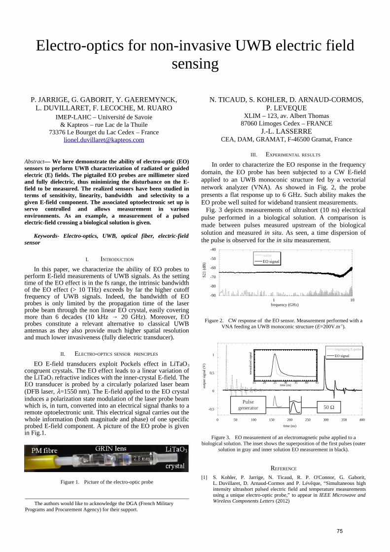
!"#
$ %&$$ ' $""(
$(" ) * +
, # ) - $ O-.//.0 $ - - $ "1 ) '
-234
! "% + #($ % !%" +
$&56$ ) 78/ 9 O4
:.;0; $4 "1 ) '!"
$ $++" % '<0=;; 4 '
!%"!
O > O? O 9@ 9 4 4-4 O 4 O O O 9>O O AB 7; (?C 1 9@ O OO - D-@ O 9>O 9 @ 4 9@ O 4 O 9 94 O-O O @ @ 4 O 0 A7; 3(? E 8; (?C 9 - O@ 4-O OO - 4-O > A-@ -C
$""+ +!+ !"$+
- 1 3 $/ - @ O O $/ >O O @ O - 9 9@ -@ ? 94 A%' λF7==; 4C O O @ - ? 4- O 9 94 >OO - O3 4 - O - O >O 4 A9O 4- OC 9 4 - O 9 '7
'- 7 - O 9
6 !$ +$+
O? O O D-@
4 O 9 O 9 -9G " 4 -- 9@
>3 @? A&!C O> ' 8 O 9 - 0 (? +-O 9@ 43 O
9 > - >9 4-4 ' / 4-4 -O A7; C
- 4 9 - 4 4 9> - 4- -4 O 9
- 4- 4 O - 9 O 4-4
P;
:;
.;
0;
=;
<;
7 7;D-@ A(?C
+87 AC
'- 8 " O -4 4 >O &! 4 -- AF8;;&47C
;=
;
;=
7
; =; 7;; 7=; 8;; 8=; /;; /=; <;;
4 -
-- A&C
4 AC
'- / 4-4 4 - 9 - O O> O - O - A-
- @ - 4-4 93C
'!"
[1] + #O ! - H" 9 $ %- % -"4 $*ID- J+4-- OO @ -O - 4- 4-4 - -D- 9Q A8;78C
O -O >- 3 3> O % A'O @ 4 -4 @C O -
7= 8; 8= /; /= <; <=
4?
4 AC
- =; Ω
75

Keywords-high power microwave pulse; microwave sensor; electric field measurement; microwave power measurement.
76

Resistive Sensor for High Power Microwave Pulse Measurement in Double Ridged Waveguide
Žilvinas Kancleris, Paulius Ragulis, Rimantas Simniškis, Mindaugas Dagys Microwave laboratory, Center for Physical Science and Technology,
A. Goštauto 11, Vilnius LT-01108, Lithuania
Abstract— A resistive sensor (RS) for the measurement of high power microwave (HPM) pulse in a double ridge waveguide has been developed. Finite-difference time-domain method was used for the calculation of electric field in the waveguide section with a sample made from n-type Si. This sample was considered as a prototype of a sensing element (SE) of the RS. Electrophysical parameters of the SE have been chosen to flatten out the frequency response of the RS. The RS was realised in the waveguide WRD250 covering frequency range 2.60-7.80 GHz. The frequency response of the RS connected to a horn antenna was also considered.
Keywords-resistive sensor; microwave pulse measurement; finite-difference time-domain method; double ridged waveguide;
I. INTRODUCTION
The performance of the RS is based on electron heating effect in semiconductors. The SE of the RS is usually inserted into a rectangular waveguide. Electric field of the microwave pulse heats electrons in the SE, its resistance increases and by measuring this resistance change, pulse power in the waveguide is determined. When measuring HPM pulses the RS has some advantages over traditional diode. It measures HPM pulses directly, produces a high output signal, is overload resistant and demonstrates perfect long term stability [1]. Main disadvantage of the RS is sufficiently narrow frequency range that is limited by a pass band of a rectangular waveguide, which is used as transmission line for SE mounting. In this paper we present a theoretical consideration of the RS in a double ridged waveguide and its practical implementation.
II. RS IN DOUBLE RIDGED WAVEGUIDE
Double ridged waveguide is traditional rectangular waveguide with two symmetrically situated metal bars or ridges. A cross sectional view of the double ridged waveguide is shown in Figure 1. Ridges significantly widens pass band of the waveguide. Waveguide WRD250 considered here covers frequency range 2.6-7.8 GHz that it roughly two times wider
than for the rectangular waveguide. Due to a smaller gap between metal walls the maximum power being transmitted through a double ridged waveguide decreases in comparison with rectangular one but roughly 120 kW pulse power can be transmitted through WRD250.
As it is seen from Figure 1, the SE is inserted between metal ridges and covers all, so called, gap region of the doubleridged waveguide. Finite-difference time-domain method was used to calculate electromagnetic field components in the waveguide section with the SE. Calculated electric field amplitude in the SE Ey was used to determine the sensitivity of the RS. General requirements for the SE can be formulated as follows: it should not cause considerable reflections in the waveguide, hence the value of a voltage standing wave ratio (VSWR) has been set at < 1.5; the DC resistance of the SE should not exceed 1 k providing measurement of microsecond duration microwave pulses; the frequency response of the RS in the waveguide’s frequency band should be as flat as possible. Therefore our task was to optimize electrophysical parameter of the SE taking into account all factors mentioned above.
III. RESULTS AND DISCUSIION
We started our investigation from different length dielectric samples. It was found that at some length l Fabry-Perot resonance is observed, at which reflection coefficient approaches zero, whereas Ey reaches its maximum value. Although near the resonance desirable dependence of Ey on frequency can be engineered providing flat frequency response of the RS, it will be problematic to arrange it for a whole frequency range. Therefore to compensate frequency response we employed shorter samples where the increase of Ey with frequency is observed. For experimental testing we chose two most promising SE with the following parameters: (a) specific resistance 10 ·cm, transverse dimensions w l 1 1 mm2,DC resistance R 400 , VSWR <1.4, relative variation of sensitivity in the frequency range = 10.4 %; (b) 50
·cm, w l 1 3 mm2, R 667 , VSWR <1.5, = 12.2 %. Experimental test of the RS is under way. The other layouts of the SE as well as the RS in a double ridge waveguide connected to the corresponding horn antenna were also investigated.
REFERENCES
[1] M. Dagys, Ž. Kancleris, R. Simniškis, E. Schamiloglu, and F. J. Agee. “Resistive Sensor: Device for High-Power Microwave Pulse Measurement”, IEEE Anten. Propag. Mag., 43, (5), pp. 64-79, 2001. Figure 1. Sectional view of the double ridged waveguide with the
semiconductor sample mounted between metal ridges. Dimension of the sample in z direction is l.
This research was funded by a grant MIP-092/2011 from the ResearchCouncil of Lithuania
77

78

HPEM-TC03-SS5HPEM detection
79

Requirements for HPEM Detection
Frank Sabath Division 300: Balanced Nuclear Protection Measures and Nuclear Hardening, Electro-Magnetic Effects, Fire Protection
Bundeswehr Research Institute for Protective Technologies and NBC Protection (WIS) Munster, Germany
Abstract— In this paper general requirements for HPEM detection systems, as part of a protection concept for critical systems, will be derived. The paper starts with a brief discussion of IEMI protection and the role of HPEM detection. It continues with an analysis of used and available IEMI environments.. Specific characteristics of those IEMI environment are discussed with regard to caused effects as well as detection and identification. The last section of the paper will deduce general requirements of HPEM detection systems from previous discussed characteristics of IEMI environments.
Keywords- IEMI, HPEM, threat analysis, IEMI environments, HPEM detection
I. INTRODUCTION
During the last decades several research programs around the world have investigated physical mechanism of electromagnetic interferences and caused effects on electronic equipment and systems. At the same time, the development of components for high-power electromagnetic (HPEM) sources has achieved notable progress. As a result, high-power systems difficult or impossible to build ten years ago are now being used for an increasingly wide variety of applications and are available on the free market. In addition the knowledge needed for their assembly as well as the operation can be gained from open literature and the internet.
A review of documented IEMI cases shows out that today the threat by (criminal) IEMI attacks on electronic systems already exists. Available IEMI sources are small and highly mobile, e.g. they are able to come close to the target systems. Those systems generate an EM environment that is capable to cause at least a malfunction or (temporary) set up of electronic components. The caused effects might be used to prepare the actual criminal activity.
The criticality of caused effects scales from No effects over Interference and Degradation to Loss of main function. Depending on the nature of the system under attack, implications of the observed effects might not be limited to the system. An interference or degradation of a critical (electronic) system could result in an economic loss or a catastrophic situation. Therefore, the consequence of an IEMI attack is of vital interest and it is very important to secure critical equipment, systems and infrastructure against these threats. Threat analysis showed that the capabilities to find and identify any source of electromagnetic threats is an essential part of a systematic protection concept..
In this paper general requirements for HPEM detection systems, as part of a protection concept for critical systems, will be derived. The paper starts with a brief discussion of IEMI protection and the role of HPEM detection. It continues with an analysis of used and available IEMI environments.. Specific characteristics of those IEMI environment are discussed with regard to caused effects as well as detection and identification. The last section of the paper will deduce general requirements of HPEM detection systems from previous discussed characteristics of IEMI environments.
II. HPEM DETECTION AS ELEMENT OF PROTECTION
CONCEPTS
IEMI attacks barely leave useful and provable traces. In addition, the complexity of systems often hinders error analysis and received error pattern point to internal causes. As a result an operator of a system which is subjected to IEMI environment is unlikely to have any sensation or perception of the (external) electromagnetic stress. Consequently, any IEMI counterattack measure depends on a monitoring of the (external) electromagnetic fields that enables an independent indication of high electromagnetic stress.
The role of an HPEM detector in a systematic IEMI protection concept varies depending on the specific level of protection. Generally, the HPEM detector provides information for one or more of the following tasks:
- Monitoring of EM environment
- Detection of an unusual HPEM environment (Detection)
- Initiation of protective measures (effect and damage limitation)
- Characteristics of the HPEM environment (Identification)
III. REQUIREMENTS FOR HPEM DETECTION SYSTEMS
From characteristics of reported and available IEMI environments general requirements of HPEM detection systems can be derived. At minimum a warning system must be able to detect the presence of a HPEM environment in a suitable form. Depending on the level of protection the HPEM detector must be able to collect and analyze specific characteristics of the IEMI environment in time and frequency domain. The unknown direction of arrival as well as the short duration and wide frequency range of most IEMI environment pose additional challenges for the HPEM detector.
80

Predetection for the Identification of Electromagnetic Attacks against Airports
A. Kreth, O. Doering, E. Genender, H. GarbeInstitute of Electrical Engineering and Measurement Technology
Leibniz University of HannoverHannover, Germany
Abstract— This work presents a sensor network, capable ofdetection and identification of electromagnetic (EM) attacks against airports. This network consists of a central operating unit (COU) and several intelligent sensors (IS). While a sophisticated algorithm is applied to the monitored EM field in the COU, the ISs run a simple predetection to trigger the overall process.
Intentional electromagnetic interference (IEMI); High-power electromagnetics (HPEM); detection; sensor network
I. INTRODUCTION
The importance of electronic equipment has increased significantly in the last years. However, with this trend there is also an intensifying danger of vulnerability of the IT-infrastructure of a modern airport. Previous works have shownthat electronic equipment can be disturbed by incident electromagnetic fields [1]. The resulting malfunction or failure of a device or system can result in financial loss or even personal damage.
II. NEED FOR DETECTION
The reason for the electromagnetic interference (EMI) may have different kind of origins. Electronic devices, placed close to the victim may interfere with it. Besides, IT systems are vulnerable in the presence of HPEM sources [2]. This poses a much more dangerous threat. Individuals with criminal intent might use electromagnetic energy to intentionally cause interferences with such systems. This vicious operation of HPEM sources is often referred to as intentional electromagnetic interference (IEMI).
This leads to an enhanced need for possibilities to detect electromagnetic attacks [3]. First approaches are mainly based on the observation of the electromagnetic stress and/or the rise time of the electromagnetic field [4,5]. However, at airports known approaches might be inappropriate, due to the normal electromagnetic environment (EME), containing high field strength values and short rise times. Therefore, a more sophisticated approach is presented, dealing with the distinction between the normal EME and an IEMI attack.
III. INTELLIGENT SENSOR NETWORK
The cooperation “Electromagnetic Protection of IT-Networks for Transportation-Infrastructures” (EMSIN) is a
joint venture in the civil security research field between Germany and Israel, coping with this subject. Using the example of an airport, a sensor network is to be realized, being capable of identifying electromagnetic attacks. The core of the network is the COU. In order to observe the electromagnetic field, several ISs are connected to the COU. The sensors buffer the monitored electromagnetic field in a continuous mode. To keep the costs for the overall system as low as possible, the processor capacity of the ISs is limited. Thus the ISs are not capable of running a sophisticated detection algorithm. Instead, a simple predetection algorithm is implemented in the ISs.Once an IS has a positive match of its predetection, this information is send to the COU. The latter triggers all ISs to send the buffered data and runs a sophisticated detection algorithm on the multiple data streams. As a result, the COU can ascertain what kind of IEMI signal has been found.
IV. PREDETECTION
The predetection in the ISs is based on the comparison of the measured filed strength values with a predefined maximum allowed value. These values can be based on different kind of sources. At first, it is possible to define these values based on ameasurement of the normal EME. To avoid a measurement, alternatively the field strength values given in norms for EMC testing can be used. However, these only go up to 1 GHz. Amore advanced source can therefore be the frequency allocation table, regulated by the government.
REFERENCES
[1] R. Hoad, N. J. Carter, D. Herke, and S. P. Watkins, “Trends in EM Susceptibility of IT Equipment,” IEEE Transactions on Electromagnetic Compatibility, vol. 46, no. 3, pp. 390-395, Aug. 2004.
[2] D. Nitsch, M. Camp, F. Sabath, J. L. ter Haseborg, and H. Garbe, “Susceptibility of Some Electronic Equipment to HPEM Threats,” IEEE Transactions on Electromagnetic Compatibility, vol. 46, no. 3, pp. 380-389, Aug. 2004.
[3] R. Hoad and A. Blyth, “Electromagnetic (EM) Susceptibility of information Systems - The Need for Em Detection,” Proceedings of the 5th European Conference on i-Warfare and Security, pp. 117-128, 2005.
[4] R. Hoad and I. Sutherland, “The Forensic Utility of Detecting Disruptive Electromagnetic Interference,” Proceedings of the 6th European Conference on Information warfare (ECIW) and security, 2007.
[5] C. Adami, C. Braun, P. Clemens, M. Suhrke, H. U. Schmidt, and A. Taenzer, “HPM Detection System for Mobile and Stationary Use,” Proceedings of the 10th Int. Symposium on Electromagnetic Compatibility (EMC Europe 2011), 2011.
This work is part of the civil security research “Electromagnetic Protection of IT-Networks for Transportation-Infrastructures” (EMSIN),supported by the „Bundesministerium für Bildung und Forschung“ (BMBF), the German Federal Ministry of Education and Research.
81

HPM Detector with Extended Detection Features
Chr. Adami, Chr. Braun, P. Clemens, M. Jöster, H.-U. Schmidt, M. Suhrke, H.-J. Taenzer Fraunhofer INT
P. O. Box 1491, 53864 Euskirchen, Germany [email protected]
Abstract— The growing threat by high power microwaves (HPM) also increases the importance of capabilities to detect high-strength electromagnetic fields. Fraunhofer INT has developed a demonstrator of an HPM detector with extended detection features for mobile and stationary use. A four-channel system with four antennas allows for additional direction finding.
Keywords- High power microwaves (HPM), detection
I. INTRODUCTION
The potential high power microwave threat to electronic devices and systems has reached a technological level whereby customary modern electronics can be disabled over small to medium distances. Recently, close range applications with suitcase-sized devices have proven very successful causing malfunctions of microprocessor or computer-controlled electronics, at least temporarily, at several ten up to some hundred metres. As there are no sufficient detection and warning systems as yet to verify this threat, it is very easy for attackers to test the effectiveness of HPM systems on-site without being discovered. Disturbances and failures of own equipment accordingly might not be associated with electromagnetic attacks. This makes it important to monitor critical devices and facilities and to have capabilities available to search for and identify sources of electromagnetic threats.
II. DETECTION FEATURES AND DETECTOR DEVELOPMENT
The aim of the work presented here was to design HPM detection systems and to build demonstrators that offer the possibility, beyond the simple warning devices presently available, to record and to display a number of pulse parameters. These include pulse amplitude, derived threat field strength, pulse width, and pulse repetition rate or the number of pulses for low repetition rate. It is thus possible to detect and distinguish a variety of signal types ranging from continuous wave to narrow band HPM pulses, to damped sinusoids, to ultra wideband signals. In a second stage a four-channel system was designed with four antennas for direction finding. In a later phase the intention is to determine also other characteristic features such as a coarse discrimination of frequency regions.
The suitability of different detection methods for HPM signals was evaluated from own investigations as well as from the literature. Beyond the mere announcement of a signal with threat field strength, the detection system is intended also for surveillance of a certain area or for search and identification of HPM sources. The necessary dynamics can be achieved by
means of logarithmic amplifier/detector modules with a measuring dynamics of 60 dB and bandwidths of up to 8 GHz.
The single-channel system consists of a polarization-independent broad-band antenna, which covers a defined sector at constant sensitivity, the logarithmic amplifier/detector module in an enclosure with high shielding effectiveness and with an appropriate input circuit for self-protection. This is supplemented with a signal processing system with a multi-channel oscilloscope and a computer with GPIB interface and with the necessary analysis and display software [1]. The four-channel system comprises four antennas, attenuators, limiters, and log-amplifier/detectors, and a four-input trigger recognition circuit (Fig. 1). The pulse analysis and direction finding is again done with a four-channel digital oscilloscope and a GPIB controller. The HPM robustness of the detectors has been tested in a TEM waveguide with field strengths of 1.5 kV/m and in a reverberation chamber for fields of 10 kV/m.
Figure 1. Demonstrator of four-channel system.
Both systems can be operated by mains or on-board power supply and with internal batteries, respectively, and thus can be flexibly set up in any location in both stationary and mobile settings without relying on external power supply. They complement the necessary shielding and protection measures and alternatively the hardening of systems against high power microwaves.
REFERENCES
[1] Chr. Adami, Chr. Braun, P. Clemens, H.-U. Schmidt, M. Suhrke, H.-J. Taenzer “HPM detection system for mobile and stationary use“, EMC Europe 2011, York, UK.
82

HPEM-TC04 IEMI Threats, Effects
and Protection of electronics
83

Breakdown Behavior of a Wireless Communication Network under UWB Impact
Melanie Rohe University of Applied Sciences and Arts
Hanover, Germany [email protected]
Michael Koch University of Applied Sciences and Arts
Hanover, Germany [email protected]
Abstract— Systems with high priority to safety and reliability such as monitoring systems on airports have to work properly. In this paper, the breakdown behavior of an UHF-Transmitter to unipolar fast rise time pulses (UWB) is determined. The immunity tests are accomplished as a function of the electromagnetic field direction to the device using an open TEM waveguide.
UWB; breakdown;network;suszeptibility;critical infrastructure
I. INTRODUCTION
Fast transmission of information and continuous access to databases as well as the management of air traffic are most important for effective and safe operations. Malfunctions or destruction of subsystems may cause a breakdown of the whole communication system thus leading to catastrophic accidents. Sources of Intentional Electromagnetic Interference can be manufactured relatively easy using commercially available components by civilian persons with relevant expertise and can be used as such for sabotage- or blackmail-purposes.
II. MEASUREMENT SETUP
A. UHF-Transmitter
The UHF-Transmitter consists of power supply with voltage converter, microcontroller and loop antenna with 433 MHz transmitter. The components are connected by data cables shown in figure 1.
Figure 1. UHF-Transmitter
The system differentiates between two modes: the standby- and activated mode. Compared to the activated mode the standby-mode is characterized by the operating microcontroller and the non-operating state of the UHF transmitter hence no electromagnetic wave is transmitted by the loop antenna. Light-emitting diodes show the current state of the system.
III. MEASUREMENTS AND RESULTS
The immunity of the UHF transmitter against electromagnetic threats was measured as a function of the field direction to the system. Figure 2 shows the breakdown thresholds for different lengths of the reset (RL) and data cable (DL) in case of vertical polarisation.
Conspicuous is the dependence of the breakdown behavior on the data cable lenght (DL). In case of vertical polarisation the breakdown threshold is less with increasing data cable length as shown in figure 3.
Figure 2. Thresholds vertical polarisation
IV. CONCLUSION
In this paper a wireless communication network was presented and its immunity against electromagnetic threats was determined. The breakdown behavior was investigated depending on the field direction and the length of the reset and data cable. The results are different breakdown thresholds in case of vertical polarisation and variable system states in horizontal position.
REFERENCES
[1] H. Thye, M. Koch, F. Sabath, "Aspects of Modelling a UWB Impulse Radiating Antenna", XXIX. General Assembly of URSI, Chicago, Illinois, USA, August 2008
RL DL
84

Intentionally blank
85

Effects of AC Mains Harmonics from Geomagnetic Storms on Uninterruptible Power Supplies
E.B. Savage, W.A. Radasky, and M.J. Madrid Metatech Corporation, Goleta, California, USA 93117
Abstract
Keywords-UPS; GIC; AC harmonics; AC reliability
I. HARMONIC ENVIRONMENT
Under normal circumstances, the electric power grid produces a sine wave at the designed operating frequency (50 or 60 Hz). One of the events that can modify a power system waveform is a geomagnetic storm, which produces half-cycle saturation in high voltage transformers, which then creates current and voltage harmonics. While it is possible that a severe geomagnetic storm could damage transformers and create wide-area blackouts, another concern is that the harmonics generated during a storm will flow into the medium and low voltage power networks, creating impacts on the operation of backup power systems at critical facilities. This paper deals with this aspect of the problem.
Fig. 1 illustrates a calculation (in the time domain) of the harmonic distortion that can be created by different levels of GIC in a transformer [1]. Fig 2 illustrates the accuracy of this modeling technique for an experiment performed on a three-phase 400 kV transformer that injected 67 A/phase [2].
500kV Transformer Current vs. GIC500kV Single Phase Bank - 0.8 Power Factor Load - GIC 0, 50, 100, 150 Amps/phase
-600
-400
-200
0
200
400
600
800
1000
1200
0.00 4.17 8.33 12.50 16.67 20.83 25.00 29.17 33.33 37.50 41.67
Time (msec)
Am
ps
Normal CurrentCurrent -GIC 150 Amps/phaseCurrent -GIC 100 Amps/phaseCurrent -GIC 50 Amps/phase
134% Total Distortion76% THD
219% Total Distortion96% THD
274% Total Distortion93% THD
Figure 1. Transformer total load current – under normal conditions and with 50, 100 and 150 A/phase of GIC injected
While not all of these harmonics will flow into the MV and LV power networks, significant levels of harmonics can be expected. It is important to recognize that the IEC has set compatibility levels for MV networks that indicate that to achieve normal operation, the 2nd harmonic should be less than 3% (for voltage). This harmonic compatibility level is much less than the 8% allowed for the 5th harmonic, which is a common harmonic, due to switched-mode power supplies in
customer equipment. The voltage compatibility level for the total harmonic distortion (THD) is 10% [3].
Compare Fingrid Harmonics - PowerCast Harmonics
0%
20%
40%
60%
80%
100%
120%
1 2 3 4 5 6
Harmonic Order%
Am
plitu
de
% Current - PowerCast
% Current - Fingrid
Figure 2. Comparison of observed and calculated AC harmonics for a 5-legged core-form transformer
II. HARMONIC UPS TESTS
Due to this concern we tested a typical UPS and PC setup, for various samples of UPSs, with controlled levels of harmonic distortion of the AC mains power supply using IEC immunity test equipment [4]. Potential issues included:
• Damage or upset of the UPS. • The degree of distortion that the UPS passed through
before it is triggered into its backup power mode. • The quality of the backup power waveform.
Some isolated damage and upset were found during testing. In many cases significant distortion passed through before the UPS switched over to the battery/inverter power mode. In fact, the power produced by the inverter itself can be highly distorted, such as simple three-level approximation to a sinewave for the UPSs tested. No damage or upset occurred to the PC that was powered through the UPS; it is believed that its switching power supply was very tolerant of the AC power quality. This may not be the case for other electronics.
REFERENCES
[1] J. Kappenman, “Geomagnetic Storms and their Impacts on the U.S. Power Grid,” Meta-R-319, Metatech Corporation, January 2010.
[2] M. Lahtien and J. Elovaara, “GIC occurrences and GIC test for a 400 kV system transformer,” IEEE Trans on Power Delivery, vol. 17, no. 2, April 2002, p. 555-561.
[3] IEC/TR 61000-2-5 Ed. 2: Electromagnetic compatibility - Part 2-5: Environment - Description and classification of electromagnetic environments, 2011.
[4] IEC 61000-4-13, Ed 1.1: Electromagnetic compatibility (EMC) - Part 4-13: Testing and measurement techniques - Harmonics and interharmonics including mains signalling at a.c. power port, low frequency immunity tests, 2009.
86
Real-Cases of Electromagnetic Immunity and Reliability in Embedded Electronics Architectures
Jean-Marc Dienot Labceem-Institute of Technology University P. Sabatier
Tarbes, France [email protected]
Emmanuel Batista Alstom Transports
Tarbes, France [email protected]
Abstract—this papers concerns works about electromagnetic immunity and reliability investigations on electronics devices, combined with different physical impacts as temperature.
Keywords-couplings; aggression; reliabilility; device; temperature;
I. INTRODUCTION
New complex electromagnetic environment have to be taken into account to prevent real critical electromagnetic compliances [1]. We try to estimate the realistic impact of external temperature on Electromagnetic Interferences (EMI) and compliances (EMC) for couplings in electronic structures [2]. Some cases of instantaneous failures (susceptibility, immunity) and long-time failures (reliability) of these configurations are presented, both by technical (characterization) and virtual (simulation) investigations.
II. THE METHODOLOGY OF VIRTUAL EXPERIMENT
The aim is to identify the electromagnetic contributions in a 3D complex physical architecture. The modeling approach is based on the optimized use of electromagnetic numerical tools, as Finite Elements Method (FEM) and Partial Electric Equivalent Circuit (PEEC). Wide-band Electrical equivalent models of a Hybrid Printed Circuit Board(PCB) can be used to investigate the thermal influences on EM characteristics. The temperature as an influent parameter is the new key for good simulation's results and EMC couplings prevention.
III. RESULTS AND DISCUSSIONS
Some parts of an embedded architecture studied to investigate the modeling way and the effects of temperature on electromagnetic noise, immunity behavior and reliability.
A. EM noise and reliabilty
The electromagnetic noise with chips on PCB is due to supply, input-output network, and device packaging pins, which acts as parasitic elementary antennas excited by fast signals transitions. Application on an active power PCB using IGBT (Insulated Gate Bipolar Transistor) has been driven (fig. 1). The results on electromagnetic radiation frequency confirm the trends: with high-temperature aggression, devices are emitting electromagnetic noise peak at lower frequency and levels.
B. EM immunity with temperature agression
Immunity is driven by aggressing integrated circuit and connexions with a combination of power-frequency levels. A
default is validated for when the criteria has been reached. The figures 2 and 3 show the difference of susceptibility/reliability on the parts of the devices, with the impact of T°
REFERENCES
[1] S. Weber, S. Guttowski, E. Hoene, W. John and H. Reichl, " EMI couplings from automotive traction systems", In Proc. IEEE EMC-S, , pp. 591-594 , May 2003.
[2] J.M. Dienot, "Experimental thermal impacts on EMC characteristics with new near-field measurements approach", In. Proc. of 3rd Intern. Conf. on Electromag. Near-field and Imaging Characterization, St Louis, pp. 302-307, June 2007.
Fig.1: Spectrum of radiated field over an IGBT module for different aggression temperature
Fig. 2: Simulation of radiated magnetic field(normal component) of a bus bar for different distances and aggression temperature.
-8 0
-6 0
-4 0
-2 0
0
0 2 0 0 4 0 0 6 0 0 8 0 0 1 0 0 0
F r e q u e n c y (M H z )
Am
plit
ud
e (d
BµV
)
A m p litu d e R e fe re n c e (n o th e rm a l- f re q u e n c y c o n s tr a in t )
T e m p . 2 2 °C
T e m p . 6 5 °C
Fig. 3: Comparison of electromagnetic aggression over a digital PCB at different temperature (22°C, 65°C)
n
87

Abstract
Keywords conducted disturbance; test setup; HEMP; protective devices
88
Pass / Fail Criteria for HPEM-Protection Devices
Armin W. Kaelin Meteolabor AG Hofstrasse 92
CH-8620 Wetzikon [email protected]
Markus Nyffeler Armasuisse DDPS
Science and Technology, WTK CH-3602 Thun
Abstract— This paper discusses pass/fail criteria for PCI-testing of HPEM-protection devices. It is shown that the residual voltage and residual energy are usually better criteria than a residual pulse current as suggested in some standards. Examples will be given during the presentation.
Keywords: HPEM-protection device, POE protection device, PCI-testing, pass/fail criteria, , residual voltage, residual energy
I. INTRODUCTION
Assessment of HPEM-protection on system-level is a very challenging task, especially for extended systems. Usually this requires dividing large systems into smaller subsystems, which allow easier assessment of the partial protections. The highest confidence in test results is obtained when the sub-systems are tested at threat level. The interfaces and the conducted disturbances between subsystems must be analyzed carefully. If all subsystems are well protected, it is reasonable to assume, that also the extended system will survive an HPEM-attack.
Equipment located in a shielded room usually experiences only relatively low levels of radiated HPEM-disturbances. However, dangerous levels of conducted HPEM-energy may propagate to the equipment, if conductors penetrating the shield are not equipped with adequate protection devices at the point of entry (POE). This implies that beside the shield quality the performance of the POE protection devices under threat-level-conditions is of great importance. PCI-testing (pulsed current injection) is a good test method for protection devices. For this purpose, clear pass/fail criteria for a variety of conducted HPEM-threats are required. While PCI threat-levels for conducted HEMP-tests are defined in various standards, e.g. [1], [2], [3], comprehensive pass/fail criteria are not available. In this paper, we discuss reliable and measurable pass/fail criteria for HPEM-protection devices.
II. REQUIREMENTS FOR PASS/FAIL CRITERIA
A. Reasons for Hardware Failures Most hardware damages caused by conducted HPEM-
threats are either due to an excessive voltage pulse or to excessive transient energy. Over-voltage failures are due to isolation breakdown in semiconductors or in wiring, in some cases damages occur due to a latch-up effect. Excessive transient energy usually results in thermal damages. Therefore protection devices must limit residual over-voltages and residual transient pulse energy to safe values for a variety of disturbance pulse shapes.
B. Pass/Fail Criteria for HPEM-Protection Devices MIL-STD-188-125 defines residual pulse current through a
defined resistive load, but only for E1 (early-time) HEMP. The only requirement for E2 (intermediate-time) HEMP is, that the protection device shall not be damaged.
This is obviously an insufficient pass/fail criterion, because it is not clear, if the equipment downstream of the protection device will survive under full threat conditions or not.
CE-marked equipment is declared to be compliant with EMC directives and has a minimum immunity against transient surges. Therefore the required protection level PL is given by
PL = TL – IL + SM
where TL is the threat-level expected, IL is the immunity level of the equipment and SM is a safety margin to be added.
The residual energy ER is given by
ER
UR t 2
RL
dt
where UR is the residual voltage and RL the load impedance.
The open circuit voltage represents the worst case, when no or only a small load is present. Since in many cases the load impedance is not a priori known, the open-circuit residual voltage is a better criterion than a residual current into a fixed impedance. For practical reasons a load around 1 M (voltage probe) seems appropriate for measuring purposes. Another important requirement is to check the proper coordination of protection stages to various HPEM-pulse shapes. More examples will be given during the presentation.
REFERENCES
[1] DSWA/ESE, “High-Altitude Electromagnetic Pulse (HEMP) Protection for Ground-Based C4I Facilities Performing Critical, Time-Urgent Missions”, MIL-STD-188-125-1, 17 July 1998
[2] IEC / SC77C, IEC 61000-2-10, Part 2-10: “Environment – Description of conducted HEMP environment”, 24 November 1998
[3] Bundesamt für Wehrtechnik und Beschaffung, “Nuclear Electromagnetic Pulse (NEMP) and Lightning Protection – Part77: Testing of Multi-application Protective Devices (MAPD) for Immunity to Lightning Interference”, VG 96903-77, September 2005
89

National Standard of Russian Federation for reproduction and transmission of unit sizes of pulse electric and magnetic intensities in
ultrawide band range
Sakharov K. Yu., Mikheev O. V., Turkin V. A. All-Russian Research Institute for Optophysical
Measurements, VNIIOFI,Moscow, Russia
e-mail: [email protected]
Abstract— The 178-2010 Standard for reproduction and transmission of the unit sizes of pulse electric and magnetic intensities in ultrawide band (UWB) range with the edge of picosecond units has been created in the Russian Federation(RF). The extended uncertainty of the reproduction of the field strengths is no more than 6.5 %.
Keywords: standard, pulse electric and magnetic intensities,edge duration, uncertainty of the unit reproduction
I. THE MAIN PART
The 178-2010 Standard [1, 2] is intended for keeping, reproduction and transmission of the unit sizes to the working standards in accordance with the hierarchy scheme (HS) RF GOST 8.540. The field of its metrological ensuring is the measurements of the parameters of ultrashort electromagnetic pulses (US EMP) with the rise time of tens and hundreds picoseconds created with the artificial and natural sources. The Standard and HS are applied in the problems of the digital information transmission and the safe personnel working, the hardware components and the objects under conditions of the impulse electromagnetic radiation influence.
The standard includes: field - forming system “cone over plane”; edge generator of voltage pulses TMG1010; transducer of field pulses IPPL-L; coupler of field pulses IPPL-M; coupler of voltage pulses; mobile shielded cab with digital stroboscopic signal analyzer Tektronix CSA 8000B (50GHz).
The block diagram of the standard is shown in Fig. 1, the exterior view is shown in Fig. 2.
Figure 1. The block diagram of the StandardThe formulas for the init reproduction in the standard (1):
,120
,sin
60 maxmaxmax
EHrZ
VE g (1)
where gV is the pulse amplitude at the TMG1010 generator output; Z is the wave resistance of the field-forming system “cone over plane” (50 Ohm).
Figure 2. The exterior view of the standard
The standard has the following metrological characteristics: the rise time of the reproduced electromagnetic pulses is no more than 20 ps; amplitude of the electric intensity pulses is no less than 100 V/m; amplitude of the magnetic intensity pulses is no less than 0,27 A/m; the extended uncertainty of the reproduction of the electromagnetic intensity is no more than 6,5 % [1,2].
The oscillograms of the reproduced pulses are presented in Fig. 3
Figure 3. The oscillograms of the reproduced pulses
REFERENCES
[1] K. Yu. Sakharov, O. V. Mikheev, V. A. Turkin, A. V. Sukhov, A. I. Aleshko, S. V. Tikhomirov, “The standard complex of the ultrashort electromagnetic pulses with the edge duration 20 ps,” Izmeritelnaya tekhnika, No. 7, pp. 57-59, 2010.
[2] K. Yu. Sakharov, O. V. Mikheev, V. A. Turkin, A. V. Sukhov, A. I. Aleshko, “Investigation of the reproduction uncertainty of the units of the pulse electric and magnetic intensities in the standard comples of ultrashort electromagnetic pulses with the edge duration 20 ps,” Izmeritelnaya tekhnika, No. 7, pp. 60-64, 2010.
90

Abstract
(Patents Pending)
References
91

Ground Conductivity Modeling forMagnetic Storm Calculations
J. L. Gilbert Metatech Corporation, Goleta, California, USA 93117
Abstract— This paper reports on a technique used to efficiently model the ground conductivity for use in the calculation of geomagnetically induced currents in power grids. From a layered model of the earth conductivity to a depth of typically 600 km, a fit of the discontinuity of the branch cut in the impedance function is determined. This can be used to replace the convolution with a series of first order differential equations, greatly reducing the time necessary to determine the electric field. This procedure is also applied to the enhancement of electric fields to incorporate stratified ground conductivities beneath ocean interfaces.
Keywords-GIC, Geomagnetic Storms, Space Weather
I. INTRODUCTION
In the calculation of the response of power grids to geomagnetic disturbances, it is necessary to model the effects of layered ground conductivity to depths of hundreds of kilometers to obtain the electric fields from magnetic fields.. The frequencies are sufficiently low that the impedance function need not consider the displacement current. In this presentation, it is shown that the planar impedance function in the frequency domain makes it possible to calculate the electric field in a more efficient manner than directly performing the convolution. We will also show the effect of a stratified ground conductivity on the enhancement of electric fields at oceanic boundaries.
II. MODELING OF PLANAR LAYERS The calculation of the surface impedance in the frequency
domain for a horizontally stratified ground is straightforward. In the lowest layer, only downward going diffusion solutions exist, so the impedance is
0jZ (1)
In higher layers, both upward and downward going fields exist, and this permits the sequential determination of the surface impedance of the higher layers. Fig 1 shows the surface impedance for three radically different ground profiles.
Using a weighted least-square fit in the frequency domain of the form
i i
ifit sj
aZ (2)
Figure 1. Variation of surface impedance for three different grounds.
allows the horizontal electric field to be obtained from the set of first order differential equations
iii
iii
EaEdt
dHEsdt
dE
(3)
III. MODELING OF OCEANIC INTERFACES In a previous reference [1], the enhancement of the horizontal electric field near oceanic interfaces was modeled for a constant slope homogeneous ground interface. It was shown that an analytic solution could be found in this case for a highly conducting ocean, and the “knife-edge” electric field behavior could be integrated with the skin depth acting as a cut-off distance for the integral. Changing the ground model to a horizontally stratified ground conductivity modifies this, making an analytic solution no longer possible, but the numerical solution of the underlying integral equation still provides insight into the behavior. The effect of the stratified ground is to change the cutoff distance resulting in a lower enhancement at low frequencies for the usual configuration with increasing ground conductivity at greater depths.
REFERENCES
[1] J. L. Gilbert, "Modeling the effect of the ocean-land interface induced electric fields during geomagnetic storms," Space Weather, vol. 3, S04A03, doi:10.1029/2004SW000120,2005.
92

Validation of Calculations of Power Systems Response to Geomagnetic Storms
J. L. Gilbert, W. A. Radasky, E. B. Savage Metatech Corporation, Goleta, California, USA 93117
Abstract— This presentation describes the validation of a methodology for the simulation of currents in large power networks. The methodology consists of two steps - the determination of the horizontal electric field from magnetic disturbances that may be taken from several sources, and the simulation of the flow of current on high voltage power grids. This presentation discusses the validation by comparison with measured data and the validation of the network solution by comparison with simple models.
Keywords-GIC, geomagnetic storms, space weather
I. INTRODUCTION
A methodology used to calculate the currents flowing in high voltage power grids [1-3] consists of two separate steps. The first is the calculation of the horizontal electric fields from geomagnetic disturbances either taken from measurements or synthesized worst-case conditions. The second step is the calculation of the current flow in the grid that results from these electric fields. Since the horizontal electric fields are generally not available separately, the use of measured data generally involves the validation of both steps together
II. COMPARISON WITH MEASURED DATA
Figs.1 and 2 show comparisons of calculated and measured ground currents at stations widely separated across CONUS during the storm of Feb 21-22 1994. Fig 1. shows the peak current and Fig. 2 shows the time history.
Comparison of Observed and Calculated Peak GICFeb 21-22, 1994 Storm Event
0
5
10
15
20
25
30
35
40
45
Bell Chester CPS Hope Ck Marysvl Monroe Moss Ld PLV Rockpt SPA
Location
Neu
tral
GIC
(Am
ps)
Observed Peak GIC
Calculated Peak GIC
Figure 1. Comparison of observed and calculated peak GIC.
Figure 2. Time history comparison at Forbes Substation, MN.
The comparisons were made using geomagnetic field disturbances taken from widely separated magnetometers that were then interpolated onto a regular grid with a one-degree spacing in latitude and longitude for use with a CONUS high voltage grid model.
III. COMPARISON WITH SIMPLE MODELS
In addition to comparison with measured data, it possible to make comparisons between the output of the large simulation and simple models of the current flow. One simple and illustrative case is the flow of current in the Oahu power grid during a simulated Sudden Storm Commencement. In this type of geomagnetic disturbance, the arrival of a CME compresses the geomagnetic field over the sunward face of the earth. We have made comparisons between the current flow models calculated and a simple model of the power grid where different stations are lumped together. This type of model provides a additional "sanity check" on the procedure.
REFERENCES
[1] J. G. Kappenman, W. A. Radasky, J. L. Gilbert and I. A. Erinmez, “Advanced Geomagnetic Storm Forecasting: A Risk Management Tool for Electric Power Operations," IEEE Plasma Society Special Issue on Space Plasmas, vol. 28, no. 6, pp. 2114-2121, December 2000.
[2] J. G. Kappenman, L. J. Zanetti and W. A. Radasky, "Space Weather from a User's Perspective: Geomagnetic Storm Forecasts and the Power Industry," EOS Transactions of the American Geophysical Union, vol. 78, no. 4, pp. 37-45, January 28, 1997.
[3] J. G. Kappenman, W. A. Radasky and J. L. Gilbert, "Electric Power Grid Vulnerability to Natural and Intentional Geomagnetic Disturbances," Proceedings of the 16th International Zurich Symposium on EMC, Zurich, Switzerland, February 2005, pp. 447-450.
93
An Overview on GIC-Induced Current Harmonics in a High Voltage Power Grid
Michael R. Rooney Survivability Assessments BranchDefense Threat Reduction Agency
Ft. Belvoir, Virginia USA
Walter J. ScottAnalytical and Advisory Services
TASC, Inc.Lorton, Virginia USA
Abstract
Keywords-GIC, power grid, EMP, harmonics, saturation, Quasi-DC, HV, E3, late-time EMP
I. INTRODUCTION
A threat to power grids consists of a quasi-DC current generated by either a solar storm or an exo-atmospheric nuclear detonation, as in [1]. For both cases, the induced current exhibits a slow risetime, long duration pulse with estimated amplitude for long lines of ~1–1000 Amperes. In this paper we will be discussing typical currents generated by a solar storm. The quasi-DC current causes half-cycle saturation of transformers which results in generation of harmonics (a secondary threat), especially even harmonics, and associated responses and effects (if any). Fig. 1 shows a photo of the DTRA Power Grid E3 testbed, where the quasi-DC drive occurred. Diagnostics included >120 channels of digitized voltage and current measurements, and video of loads and testbed for safety and completeness. A total of 144 tests were performed in the seven days of testing.
Figure.1. DTRA Power Grid E3 Testbed located at Department of Energy’s Idaho National Laboratory, USA
II. DISCUSSIONThe DTRA test site at the Department of Energy’s Idaho National
Laboratory (INL) was well suited to the investigation. The government owned grid offered an almost isolated 132 kV, long segment. The test loop was ~ 13 miles long. DTRA provided the source, diagnostics, and a simulated EM protected facility and its diagnostics which incorporated EM filters and typical loads including computers, heavy loads and switching power supplies similar to previous test phases. Grid operation was provided by INL personnel. Data acquisition and diagnostics on the high voltage and medium voltage transformers and loads were jointly operated and acquired.
III. RESULTS
Results presented will include sample measurements of grid voltage sag and harmonics at distant locations along the line, neutral currents showing the imbalance in the three phases, and distortion in total current from the overhead transmission line measurement into the pair of transformers.
IV. SUMMARY
This work demonstrated that a simulated power grid test can be conducted on a real HV grid segment with no detrimental perturbations on a 138kV transmission loop and no damage to a power grid or test infrastructure.
REFERENCES
[1] MIL-STD-188-125-1 High-Altitude Electromagnetic Pulse (HEMP) Protection for Ground-Based C4I Facilities Performing Critical, Time
Urgent Missions, Part 1, Fixed Facilities, 17 July 1998
94

Power Grid Protection against Geomagnetic Disturbances (GMD) and Electromagnetic Pulse
(EMP) Threats F.R. Faxvog, W. Jensen, G. Nording, N. Ruehl, G.
Fuchs, D. B. Jackson, B. Groh, T. L. Volkmann, and G.E. Anderson
Research and Engineering Department Emprimus LLC
Minneapolis, MN, 55416 USA [email protected]
A. P. Vitols Power Products Division
ABB Inc. Mount Pleasant, PA, 15666 USA
A.D. Rajapakse and N. Perera Dept. of Electrical and Computer Eng.
University of Manitoba Winnipeg, MB, Canada, R3T 6C1
G.H. Baker Professor Emeritus
James Madison University Harrisonburg, VA, 22801 USA
Abstract— Late time electromagnetic pulses (EMP-E3) and geomagnetic storm events have been shown to induce large quasi- DC currents in power transmission systems and power transformers. Such EMP-E3 or geomagnetic induced currents (GIC) give rise to half cycle saturation in the transformer core. This saturation generates excessive reactive power (VAR) losses and unwanted harmonics on the power grid which can lead to instabilities due to large reactive power flows and the potential loss of reactive resources. In some cases these DC currents can cause heating, damage, and even catastrophic failures in some transformers [1-5].
The objective of this effort was to design, simulate, construct and test a protective electrical system which could provide a cost effective and reliable solution for blocking the DC current in the neutral of “Y” configured power transformers. The blocking design uses electronic sensors to automatically remove a metallic grounding path to leave a capacitive blocking device in the transformer neutral connection [6]. The sensing electronics detects the quasi-DC current in the transformer neutral or the total harmonic distortion (THD) on the grid, resulting from either EMP (E3) or geomagnetic event, to activate the protective mode of operation. In practice it is anticipated that this protective system will operate in the capacitively grounded mode of operation less than 0.1% of the time, which limits the exposure to simultaneous GIC and ground fault currents.
A SOLIDGROUND TM protective system was designed, extensively simulated using PSCAD/EMTDC, constructed and tested. The system consists of a bank of HV capacitors, a HV power resistor, a neutral connection switch assembly, an MOV surge arrester, current transformer (CT), maintenance switches, sensing and control electronics, and a seismic rated structure to reliably secure the electrical components.
Detailed PSCAD/EMTDC simulations describing the SOLIDGROUND TM operation under EMP-E3 or GIC events
with and without various types of simultaneous ground faults will be presented. High voltage field testing results obtained using a prototype SOLIDGROUNDTM system will also be presented.
Keywords- Electromagnetic Protection; Geomagnetic Disturbance; SolarStorms; EMP; Transformers; Neutral Blocking; Grid Protection; Induce Currents;
ACKNOWLEDGMENT
The authors acknowledge the technical and partnering support of ABB North America, Power Products Division, Mount Pleasant, PA.
REFERENCES
[1] L. Bolduc, P. Langlois, D. Boteler, and R. Pirjola, "A study of geoelectromagnetic disturbances in Quebec. II. Detailed analysis of a large event," IEEE Trans. on Power Delivery, vol. 15, pp. 272-278, 2000.
[2] F.S. Prabhakara, L.N. Hannett, R.I Ringlee, J.Z. Ponder, "Geomagnetic effects modelling for the PJM interconnection system. II. Geomagnetically induced current study results" IEEE Trans. on Power Systems, vol.7, no.2, pp.565-571, May 1992.
[3] J.G. Kappenman, V.D. Albertson, N. Mohan, "Current Transformer and Relay Performance in the Presence of Geomagnetically Induced Currents," IEEE Trans. on Power Apparatus and Systems, vol-100, no.3, pp.1078-1088, March 1981.
[4] J.G. Kappenman, S.R. Norr, G.A. Sweezy, D.L. Carlson, V.D. Albertson, J.E. Harder, B.L. Damsky, "GIC mitigation: a neutral blocking/bypass device to prevent the flow of GIC in power systems," IEEE Trans. on Power Delivery, vol.6, no.3, pp.1271-1281, Jul 1991.
[5] L. Bolduc, M. Granger, G. Pare, J. Saintonge, L.Brophy, "Development of a DC current-blocking device for transformer neutrals," IEEE Trans. on Power Delivery, vol.20, no.1, pp. 163- 168, Jan. 2005.
[6] F.R. Faxvog, W. Jensen, G. Nordling, G. Fuchs, D.B. Jackson, T. L. Volkmann, J.N. Ruehl, B. Groh, “Continuous uninterruptable AC grounding system for power system protection”, US Patent Appl. No. 13/159,374, June 13, 2011.
95

Experimental Research for EMP Measurement in Environment of -ray
Radiation
MENG Cui1,2 Tan Zhao_jie1,2 Li Xin1,2 Xiang Zuo_xian1,2
1.Department of Engineering Physics, Tsinghua University ,Beijing 100084, China;
2.Key Laboratory of Particle & Radiation Imaging, Ministry of Education
sSiGy /)(101 7
Key words: EMP sensor ,CMOS -ray dose
rate
Introduction It is important to know the electromagnetic environment
in EMC research. Different type of sensor are designed to be used in measuring the EM environment and to research the waveform. A new EMP sensor using optical-fiber is developed in our lab.It’s diagram is shown in figure 1.
Antenna signalReceive circuit
Couple and laser
Optical power control circuit
Optical receiverFiber Optical
antenna
Figure 1. Diagram of sensor structure
But, -ray can penetrate the shielding box and radiate the integrated circuit directly when it is used to measure EMP that -ray radiated. Such problem is researched under
Qiangguang- I accelerator.
II Experimental principleDuring the experiment, 5 sensors are placed in the
different place around radiation scope of -ray .The sensors are placed in the metal shielding box and antennas areremoved. The sine wave is inputed to the input end of the sensor. The output of the sensor is observed via osilloscope.
Figure. 2. Experiment diagram Figure3. Time-domain waveform
of -ray
III Experimental conclusion The radiation experiment of -ray with different doses
shows that the dose rate interference threshold of
integrated circuit of sensors is about sSiGy /)(101 7 .
Figure 4. -ray noise Figure5. Output waveform under sSiGy /)(102.4 7
Figure6. Output waveform under sSiGy /)(102.8 7
Project 10927506 supported by Special Fund for Basic
Research on Scientific Instruments of NSFC96

An Energy Check on the Reasonableness of HEMP Field Calculations
E.B. Savage, J.L. Gilbert, and W.A. Radasky Metatech Corporation, Goleta, California, USA 93117
Abstract
Keywords-E1 HEMP;model validation
I. INTRODUCTION
Generally accessible specifications of E1 HEMP from high altitude nuclear bursts show a very high peak field level (i.e., 50 kV/m) over an extremely large area (for example, see [1]). However, it may seem inconceivable that a single burst could produce such large fields over continent-size regions. Because of unknowable information, such as where the burst will occur and the parameters of the nuclear device, worst case field levels are typically specified. However, because field saturation may limit the peak value of the waveform, the field levels do not fall off drastically when backing off from non-ideal conditions, and so planning for worst case fields is not unreasonable. In this paper we look at some parameter variations for E1 HEMP, and perform a simple energy conservation check on the reasonableness of E1 HEMP calculations.
II. E1 HEMP VARIATIONS
Reference 1 specifies an E1 HEMP field of 50 kV/m peak, with a pulse width of 23 nanoseconds. The field irradiates any region on the Earth that is in line-of-sight of the burst point. Fig. 1 indicates the exposed regions for several burst heights over the central US.
Figure 1. E1 HEMP exposed region for several burst heights
However, as noted in the reference, the field level varies with position on the Earth, and for the northern geomagnetic hemisphere, the peak is at a point to the south of ground zero (GZ, point directly below the burst). For example, Fig. 2 shows the variation for the peak field for a sample 75 km
altitude burst. (Note that the waveform also varies – getting wider for positions more towards the outer edge of the exposed region as indicated in [1].)
Figure 2. Sample spatial variation of the E1 HEMP peak, for a 75 km burst
Although higher burst heights expose more area, the HOB (height-of-burst) also affects the E1 HEMP generation process. Generally a HOB of about 75 km provides a reasonably high peak HEMP field, and the peak often decreases for higher HOBs.
III. SIMPLE ENERGY CHECK
Here we check the E1 energy for a sample 75 km HOB case. For a 50 kV/m peak field, a 17.3 ns effective pulse width, and 377 Ω wave impedance, the energy density at the max point is 0.115 J/m2. Over the exposed region the average peak is 0.1243 of the max peak, and the exposed region is 2.97×10¹²
m2. Thus, the total energy of the E1 HEMP exposing the Earth’s surface is 5.25×10⁹ J. Assuming a 30 kT burst, with 0.3% gamma efficiency, then the burst’s gamma output (which generates the E1) is 3.77×10¹¹ J [2]. Some of this goes off into outer space; for a 75 km HOB, 0.424 goes towards the Earth. The gamma energy that generates E1 is 1.60×10¹¹ J. Therefore with these simple calculations only 3.3% (5.25×10⁹/1.60×1011)of the gamma energy is converted into E1 HEMP. Thus, this energy check does not indicate a problem with the E1 calculation, even for this worst case of a 50 kV/m peak.
REFERENCES
[1] IEC 61000-2-9, Ed 1.0: “Electromagnetic compatibility (EMC) - Part 2: Environment – Section 9: Description of HEMP environment – Radiated disturbance. Bacis EMC publication”, February 1996.
[2] Glasstone, Samuel, and Philip J. Dolan, The Effects of Nuclear Weapons,U.S. Departments of Defense and Energy, 1977 (1st edition: 57, 2nd edition 1962).
97

98

HPEM-TC04-SS4Susceptibility, effects,
protection, and test methods for electronics
due to high power EM threats
99

The technique for evaluating the immunity of digital devices to the influence of ultrawideband
electromagnetic pulsesParfenov Yu.V., Titov B.A., Zdoukhov L.N.
Russian Academy of Sciences Joint Institute for High Temperatures, JIHT
Moscow, Russia [email protected]
Abstract— The procedure for evaluating the immunity of digital devices to the influence of repetitive ultrawideband electromagnetic pulses is proposed. This procedure makes it possible to choose the optimal characteristics of radiated pulses, and to predict the results of influence of pulses with arbitrary parameters, etc.
Key words- ultrawideband electromagnetic pulse, digital device, immunity.
I. THE CONTENT OF THE IMMUNITY EVALUATION PROCEDURE
The procedure for evaluating the immunity of digital devices to periodically repeating ultrawideband electromagnetic pulses (UWB EMP) includes the following stages [1]:
• Testing the device, using one or more UWB EMP sources (with varying pulse peaks and pulse repetition rates, and recording the aftereffects - for instance, the degree of data transmission rate decrease, the moment of the Denial of Service etc.);
• Calculating the probability (P) of incorrect transfers of data packets for each combination of pulse peak and pulserepetition rate of the influencing pulses (with the UWB EMP characteristics, the parameters of microstrip lines of the PCBs of the digital device under consideration and the characteristics of the information signal taken as the initial data for the calculation);
• Development of the relation between the parameter characterizing the aftereffects of electromagnetic influence to the digital device and the probability of incorrect transfer of data packets.
II. EXAMPLE OF EVALUATION OF THE IMMUNITY OF A PERSONAL COMPUTER (PC)
Two PCs were integrated in a local computer network. The first computer (PC1) was exposed to repetitive UWB EMP. The second computer (PC2) was placed in a shielded room and was therefore not exposed to electromagnetic pulses.
In order to determine the result of the influence of UWB EMP on the PC1, the measurement of the data transmission
rate via the local computer network was performed. It is established that data transmission rate decreases down to zero in the network as a result of PC1 exposure to UWB EMP, i.e. creating Denial of Service (DoS). The occurrence time of this event (TDoS) decreases as the influencing pulse repetition frequency increases.
During the test, the characteristics of pulses influencing PC1 were varied in a wide range.
In doing this, the probability (P) was calculated for each combination of pulse peak and pulse repetition rate of the influencing pulses. As a result of the tests and calculations, the initial data was obtained, which is required for the development of the relation between the parameter TDoS andthe probability P (See Fig. 1).
Figure 1. The occurrence time of DoS versus the probability of an incorrect transfer of data packet
Knowing this relation, the following tasks can be solved: determine a combination of amplitude/time and frequency behavior of a UWB EMP source that provides the most stringent test exposure of a PC; give estimates of influence on the PC of UWB EMP with arbitrary parameters etc.
REFERENCES
[1] Parfenov Yu.V, Titov B.A., and Zdoukhov L.N., “Technique of estimating probability of upsets in digital devices at influence of supershort electromagnetic impulses”, The Russian Academy of Sciences, MAGAZINE OF RADIOELECTRONICS, 5, May, 2011
100

30ns 100ns 1000ns
101

Determination of Cable Shielding in Reverberation Chamber to Meet HPM Requirements
Detection of Deficiencies and Design Flaws
T. Nilsson, M. Bäckström Saab Aeronautics
Saab AB Linköping, Sweden
e-mail: [email protected]
Abstract—This paper describes the test results and methodology which can be used to achieve a balanced overall shielding effectiveness (SE), focusing on cables. Reverberation Chamber (RC) measurements has been used to investigate the SE properties of the cable against High Power Microwaves (HPM). Different cable types i.e. different shield structures, number of shields, different connectors and cable length, have been investigated. In particular has the addition of an external braided shield been investigated. The lessons learned and the results are to be apart of a guideline for the protection and verification of hardness against HPM.
Keywords-High Power Microwaves (HPM); Cable Shielding
I. INTRODUCTION
As the development of HPM weapons advances, HPM requirements have recently entered standards, see [1]. This increases the shielding requirements on electronic equipments and the interconnecting cables. Some interconnecting cables may have SE requirements as high as 90 dB, which can be hard to meet. Standards for measuring SE of equipments and cables in RC are known, see [2]. However the test method needs to be tailored for our application and there are still cable parameters which needs further investigation. Cable SE measurements fill several purposes; it’s of great importance to detect deficiencies and design flaws in an early stage of the design process. SE data from cables are also needed in the power balance approach, to get a balanced shield for the whole system. Using the RC, the incident field becomes isotropic, which decreases the statistical uncertainty of the measurement compared to the plane wave case. The aim is to systematically gather data and experience of different cable designs and put it into a practical guideline for the defence industry.
II. TEST METHOD AND SETUP
The test setup consists of a RC with Network Analyzer (NWA) as the main instrument, both sending and receiving signals. A transmitting antenna is placed inside the RC and the inner conductor of the cable under test acts a receiving antenna, with one end connected to a 50 termination and the other end to the receiving port of the NWA. The forward transmission S21 is then measured by the NWA. A “naked” cable without shielding is used as reference cable, all the following
measurement of shielded cables are compared with the reference cable to determine the SE.
III. INVESTIGATED PARAMETERS AND RESULTS
A. Effects of Cable Length Based on the theory for an isotropic environment, the
received power in the load is not affected by the cable length, assumed that the mismatch factor, q as in (1), is independent of the length and the tested cable is a few wavelengths long.
B. Effects of Cable Connectors The choice of cable connector can affect the total SE of a
cable assembly. Identical cables with different connector types have been investigated and compared. The result show very large differences (tens of dB) in SE. Possible deficiencies and design flaws can be detected and corrected at an early stage.
C. Effects of Triple Cable Screen Adding an external braided shield on a double shielded
cable can add SE, if it’s done properly. It is of great importance to stretch and tighten the shield with the existing cable. Otherwise it’s likely that cavity effects will degrade the cable SE. Measurements have shown that SE for a triple shielded cable can decrease below the SE for a double shielded cable.
IV. FUTURE WORK
The effects of the impedance mismatch factor, q as in (1), should be further investigated for the reference cable to see if it can be replaced by a horn antenna.
2
111 Sq (1)
REFERENCES
[1] MIL-STD 464, Issue C, “Electromagnetic Envrironmental Effects Requirements For Systems”, pp. 79, December 2010.
[2] IEC 61726, Edition 2.0, ”Cable assemblies, cables, connectors and passive microwave components - Screening attenuation measurement by the reverberation chamber method”, November 1999.
This work was financed by FMV, the Swedish Defence Materiel Administration.
102

Electrostatic Discharge (ESD) Radiated Fields Exploring the Utility of ESD Radiated Fields as a Generic Radiated Transient Immunity Level
Barney Petit, Dr. Richard Hoad and Dr. Anthony Wraight Electromagnetic and Environmental Services
QinetiQ Farnborough, UK
[email protected], [email protected], [email protected]
Abstract — Radiated transient environments such as those produced by Intentional Electromagnetic Interference (IEMI) generators have been demonstrated to affect electronic systems. The immunity of electronics to transient electromagnetic interference is difficult to gauge because equipment is rarely tested to radiated transients and the parameter space for IEMI threats is very large. Electrostatic Discharge (ESD) testing is normally performed at some level as part of equipment electromagnetic compatibility (EMC) qualification, both for military and for commercial systems. The purpose of this paper is to summarise preliminary investigations into the transient radiated electric field immunity levels of equipment proven empirically from passing ESD immunity tests.
Keywords; Electrostatic Discharge, Electromagnetic Compatibility, Radiated Electric Field, Transient Immunity.
I. INTRODUCTION
It is important to understand the immunity of equipment and systems to transient radiated electric fields such as those from IEMI. Most of the immunity testing that is routinely done as part of equipment EMC qualification is at levels which are benign when compared with IEMI environments and radiated transient immunity threshold is rarely evaluated. However, most equipment will undergo some form of ESD testing during EMC qualification. Typically ESD is applied directly to the equipment during testing, either through contact or through air discharge. Generally it is the charging voltage that is used as the immunity level of the equipment. However, during testing, in particular the air discharge test, radiated electric fields are produced from the ESD [1], and [2]. This paper investigates these radiated fields to determine if equipment has proven immunity to radiated transient environments as a consequence of ESD testing. To this end; standards have been reviewed to understand the broad applicability of ESD and radiated fields from ESD have been measured to evaluate important parameters such as peak magnitude and frequency content.
II. INVESTIGATION
A. Standards Review
The first part of this paper summarises a review of the standards that are commonly used for ESD testing of commercial systems. This is primarily to confirm the test levels and methods used.
B. Measurement of ESD Radiated Electric Field
The second part of this paper summarises measurements made of the radiated electric field from typical ESD testing. This was performed on various different test objects to provide a statistically meaningful range of results.
III. INITIAL RESULTS
Some initial measurements have been taken of the ESD radiated electric field. These measurements were taken using a D-Dot probe 1 m away from a -15 kV charge level ESD test. Plots of the measurements are shown in Fig. 1 in the time domain. The results suggest that the radiated field frequency content is dependant on the size of the equipment under test (EUT) rather than the length of the ESD arc. More measurements have been performed and these will be discussed.
Figure 1. Radiated ESD Waveforms – Time Domain
REFERENCES
[1] S Caniggia, and F Maradei, ‘Numerical Prediction and Measurement of ESD Radiated Fields by Free-Space Field Sensors’, IEEE Transactions On Electromagnetic Compatibility, Vol. 49, No. 3, August 2007
[2] Honda, M.; ‘Measurement of ESD-gun radiated fields’, 29th Electrical Overstress/Electrostatic Discharge Symposium, 2007, Page(s): 5B.4-1 - 5B.4-5
This work was carried out as part of a UK MoD Research Programme
103

Transient Adaptor for GTEM-3750
Mr. Markus Nyffeler* armasuisse, Science and Technology, HPE – Laboratory
Feuerwerkerstrasse 39, CH-3602 Thun, Switzerland e-mail: [email protected]
Dr. D. V. Giri Pro-Tech, 11-C Orchard Court, Alamo, CA 94507 USA Dept. of ECE, University of New Mexico, Albuquerque,
NM 87130, USA: e-mail: [email protected]
Abstract— GTEM-3750 exits in the EMC laboratory of armasuisse and has been used in CW mode of operation. It is being upgraded for transient pulse operation with the goal of meeting MIL-STD- 461 F specifications. In this paper, we will describe the electromagnetic, mechanical and high-voltage design of a transient adaptor. An adaptation to a HN connector has also been designed and fabricated. By using the 50-Ohm HN connector at the input, it has been possible to test the bandwidth of the entire transient adaptor at low power levels, before we attempt the high-power transient measurements.
Keywords- GTEM, EMI testing, transient adaptor, ULTEM 2300, SF6 barriers
I. INTRODUCTION
We have investigated the possibility of adapting the existing GTEM-3750 for transient excitation, with the goal of being able to produce transient fields of > 100 kV/m with a risetime of 2.5 ns and a FWHM of 25 ns, in the test volume. This corresponds to the requirements in MIL-STD-461F.
It is noted that the GTEM-3750 is about 15.4m long and the largest cross section at the termination end is approximately 5.5m high x 8.3 m wide. We further note that the height of the septum in the region of the test volume is about 3m. A photograph of the existing CW adaptor is shown in Figure 1
Figure 1. Existing CW feed for GTEM -3750
II. PULSE ADAPTOR
On an average, transient source amplitude of 300 kV can produce about 100 kV/m electric field. Conservatively, we set a goal of 400 kV as the maximum source amplitude. Estimates
of relevant SF6 breakdown fields have been gathered from the literature. Those breakdown estimates have been combined with electric field simulations of various locations of the GTEM-3750 feed to estimate the SF6 pressure required to avoid electrical breakdown. The estimated pressure requirements have been used in designing a new GTEM-3750 feed that incorporates two new pressure barriers and revised outer conductors. All of the necessary hardware required for pulse excitation of the existing GTEM Cell have been fabricated and will be described in detail. The newly constructed pulse adaptor is shown in Figure 2.
Figure 2. Newly fabricated transient feed for GTEM -3750
At this time, the hardware is fully fabricated and some preliminary testing has been done at low-voltages. The initial experiments of TDR and S11(f) indicate that we have a minimum bandwidth of DC to 400 MHz with the transient adaptor. It is possible that the bandwidth is better than 400 MHz, since we had to introduce extraneous components (ex: adaptation to a HN connector) to facilitate the measurements. We are currently in the process of testing this new hardware with the following three different pulsers. a) Connect a HYPS pulser (2.8 kV, 100 ps rise / 3 ns FWHM),
estimate and measure transient fields in the test volume b) Connect a FID pulser (10 kV, 200 ps rise / 700 ps FWHM),
estimate and measure transient fields in the test volume c) Finally, connect a 300kV-400kV, 2.5ns rise / 25ns FWHM, In this paper, we will describe the design, fabrication and testing of this transient adaptor useful in MIL-STD-461F testing of electronic equipment.
[1] Electromagnetic compatibility (EMC) - Part 2: Environment - Section 9: Description of HEMP environment - Radiated disturbance. Basic EMC publication, 19 February 1996
[2] MIL-STD-461F, Department of Defense, Interface Standard, Requirements for the Control of Electromagnetic Interference Characteristics of Subsystems and Equipment, 10 December 2007
104
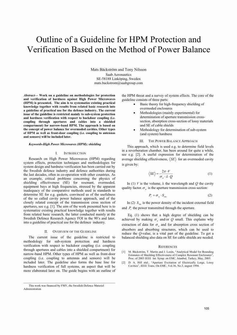
Outline of a Guideline for HPM Protection and Verification Based on the Method of Power Balance
Mats Bäckström and Tony Nilsson Saab Aeronautics
SE-58188 Linköping, Sweden [email protected]
Abstract— Work on a guideline on methodologies for protection and verification of hardness against High Power Microwaves (HPM) is presented. The aim is to systematize existing practical knowledge together with results from related basic research into a guideline of practical use for the defence industry. The current issue of the guideline is restricted mainly to sub-system protection and hardness verification with respect to backdoor coupling (i.e. coupling through apertures and cables into a shielded compartment) for narrow-band HPM. The approach is based on the concept of power balance for overmoded cavities. Other types of HPM as well as front-door coupling (i.e. coupling to antennas and sensors) will be included later.
Keywords-High Power Microwaves (HPM); shielding
I. INTRODUCTION
Research on High Power Microwaves (HPM) regarding system effects, protection techniques and methodologies for system design and hardness verification has been carried out by the Swedish defence industry and defence authorities during the last decades, often in co-operation with other countries. As an example, critical problems concerning the physics of shielding effectiveness (SE) for resonant, overmoded, equipment bays at high frequencies, stressed by the apparent inadequacy of the comparative methods used in standards to determine SE for e.g. gaskets, convinced us of the usefulness of the so called cavity power balance approach, and of the closely related concept of the transmission cross section of apertures, see e.g. [1]. The aim of the work presented here is to systematize existing practical knowledge together with results from related basic research, the latter conducted mainly at the Swedish Defence Research Agency FOI in the 90’s and later, into a guideline of practical use for the defence industry.
II. OVERVIEW OF THE GUIDELINE
The current issue of the guideline is restricted to methodology for sub-system protection and hardness verification with respect to backdoor coupling (i.e. coupling through apertures and cables into a shielded compartment) for narrow-band HPM. Other types of HPM as well as front-door coupling (i.e. coupling to antennas and sensors) will be included later. The guideline also forms the base line for hardness verification of full systems, an aspect that will be more elaborated later on. The guide begins with an outline of
the HPM threat and a survey of system effects. The core of the guideline consists of three parts:
Basic theory for high-frequency shielding of overmoded enclosures Methodologies (mainly experimental) for determination of aperture transmission cross-section, absorption cross-section of lossy materials and SE of cable shields Methodology for determination of sub-system (and system) hardness
III. THE POWER BALANCE APPROACH
This approach, which is used e.g. to determine field levels in a reverberation chamber, has been around for quite a while, see e.g. [2]. A useful expression for determination of the average shielding effectiveness, SE for an overmoded cavity is given by:
QVSE
a
2 (1)
In (1) V is the volume, the wavelength and Q the cavity quality factor. a is the aperture transmission cross section:
incat SP (2)
In (2) incS is the power density of the incident external field and tP the power transmitted through the aperture.
Eq. (1) shows that a high degree of shielding can be achieved by making a and/or Q small. This explains why extraction of data for a and for absorption cross section of absorbers and absorbing structures, which can be used to reduce the Q-value, is a vital part of the guideline. To get a balanced shielding also data on SE for cable shields are needed.
REFERENCES
[1] M. Bäckström, T. Martin and J. Lorén, “Analytical Model for Bounding Estimates of Shielding Effectiveness of Complex Resonant Enclosures”, Proc. of 2003 IEEE Int. Symp. on EMC, Istanbul, Turkey, May, 2003.
[2] D. A. Hill etal., “Aperture Excitation of Electrically Large, Lossy Cavities”, IEEE Trans. On EMC, Vol.36, No.3, august 1994.
This work was financed by FMV, the Swedish Defence Materiel Administration
105

Evaluations of Protection Methods Using TVS-array and Modal Filter
. R. Gazizov, ¡. ¢. Zabolotsky, A. O. Melkozerov, P. E. Orlov, I. G. Bevzenko, E. S. Dolganov Television and Control Department
TUSUR Tomsk, Russia
Abstract— Four protection methods are compared. Spice-simulation results for time domain response on UWB pulse are presented. Merits of combined usage of TVS-array with modal filter are shown.
Keywords- TVS-array; modal filter; protection; UWB pulse
I. INTRODUCTION
Several levels of protection are often necessary for proper protection of electronics against UWB conductive HPEM threats. A part of incident energy is treated at the first level, while the residual energy is decreased at the subsequent levels. Unfortunately, high-power protective devices are inertial, while the high-speed ones have low voltage or current. Both types being active components have short life cycle. At last, parasitic inductance of the leads inherent to any lumped component increasingly deteriorates component’s functioning when shortening the incident pulse.
Therefore, in order to overcome the drawbacks of the existing devices it is important to design an innovative protection for electronics. A new approach which is referred to as modal filtration has been proposed recently. It uses different delays of odd and even modes of three-conductor coupled lines in a nonhomogeneous dielectric filling [1–3]. However, analysis of the modal filter (MF) operation for various UWB pulse durations has not been performed yet. Moreover, options of the MF cascaded with commonly available protective devices should be considered for better total protection. At last, comparison of different protection methods may reveal their drawbacks and merits. The aim of this paper is to fill these gaps.
II. RESULTS
Spice-analysis of four protection methods has been performed using simple circuit comprising trapezoidal pulse (30, 150, 350 ps) generator (with e.m.f.=1 kV), protection and load. The results are summarized in Table I. As the first protection method the widely used transient voltage suppressor (TVS) array LC03-3.3 was simulated by means of the equivalent circuit (including 0.35 nH inductance of the leads) from manufacturer data sheet. As a result, instead of positive 3.3 V level the bipolar pulse with large magnitude decreasing with pulse widening has been obtained.
TABLE I. CALCULATED OUTPUT VOLTAGE AND ATTENUATION FOR THREE DURATIONS OF 1 KV E.M.F. PULSE FOR FOUR PROTECTION METHODS
Results (Uin=500 V, Rgen=Rload=100 Ohm) Protection method
T0,5, ps Uout,, V Uout /Uin
30 210 0.42
150 30 0.06 TVS-array
350 21 0.042
30 5 0.01
150 27 0.054 Modal filter
350 63 0.126
30 1.1 0.0022
150 1.2 0.0024 TVS-array+Modal filter
350 1.7 0.0034
30 1.09 0.0021
150 1.76 0.0035 Modal filter+TVS-array
350 1.9 0.0038
Then the MF with 2.5 ns difference of the modal delays [3] was considered. As a result, the 2.5 ns width pulse with small magnitude increasing with pulse widening was obtained. At last, two methods of cascaded TVS-array and modal filter was considered. As a result, the 10 ns width and 1 V magnitude pulse increasing up to the 20 ns width and 2 V magnitude with pulse widening was obtained.
Thus, the MF can compensate the drawbacks of the usual protective devices and improve protection against UWB pulse.
REFERENCES
[1] T. R. Gazizov, A. M. Zabolotsky. Experimental results on UWB pulse propagation in low-voltage power cables with different cross sections. IEEE Trans. on Electromagn. Compat., vol. 54, no. 1, February 2012, pp. 229–231.
[2] . R. Gazizov, ¡. ¢. Zabolotsky, I. E. Samotin. Modal decomposition of UWB pulse in power cable structures: simple experiment showing useful possible applications. Book of abstracts EUROEM 2008. 21–25 July 2008, Lausanne, Switzerland, p. 62.
[3] . R. Gazizov, I. E. Samotin, ¡. ¢. Zabolotsky, A. O. Melkozerov. Design of printed modal filters for computer network protection. Proc. of 30-th Int. conf. on lightning protection. Sept. 13–17, 2010. Cagliary, Italy, pp. 1246-1–1246-3.
This work was supported by the Ministry of Education and Science of the Russian Federation under government Contract 13.G25.31.0017 with the joint-stock company Academician M.F. Reshetnev “Information Satellite Systems”.
106

HPEM-TC05System-level
Protection and Testing
107

Evaluation of NEMP vulnerability on COTS electronic equipments
Laurent Labarbe – CEA/Gramat 46500 Gramat, France [email protected]
Abstract— This document deals with a new evaluation method of NEMP1 vulnerability on cots electronic equipments. This work was achieved for the French DGA (“Direction Générale de l’Armement – Unité de management NBC”). The method consists in comparing EMC tests severities to NEMP conducted stresses. The comparison is achieved on five characteristic criteria of the induced stresses, calculated with an analytic method. The processes lean on a software named “SUSIE” (in French : SUSceptibilité à l’IEMN). To date, only conducted stresses are analyzed. An evolution is planned to determine radiated stresses.
Keywords-component; NEMP vulnerability; EMC test; comparative method.
I. PRINCIPLE OF THE COMPARATIVEMETHOD
The comparative method can place an EMC testlevel in comparison with several performance tests which will be performed for NEMP evaluation. The analytical comparison method is based on the calculation of five criteria :
• peak : maximum of |i(t)|, (1)
• maximum slope : maximum of |di(t)/dt|, (2)
• maximum load transfert in the case of bipolar
wave : maximum of | t
dtti0
)( |, (3)
• maximum load transfert in the case of an
unipolar wave : t
dtti0
)( , (4)
• square root of the energy : t
dtti0
2)( (5)
The French « Guide d’Aide à la Conception dudurcissement IEMN » (GAC n°21311/DGA/ At/DR of December, 1st, 1989) propose protection classes referenced by an index from 0 to 6. For each protection class, is proposed a severity class for the
1 NEMP : Nuclear ElectroMagnetic Pulse
Florent Miquel – GERAC 46500 Gramat, France
susceptibility tests to apply on the equipments for a margin done. This severity is contained between SC02 and SC6, SC0 is the minimum level of the stress (and corresponds to the protection with the index 6).
II. SUSIE SOFTWARE
SUSIE software allows the comparison between the result of each criterion at each frequency and :
- on the one hand, SC NEMP attacks,
- on the other hand, EMC tests sustained by the equipments.
The EMC standards selected for this work concern 4 technical areas (military, aeronautical, civil and automobile).
We keep for each comparison the heaviest SC value lower or equal to the EMC test values. The result of the analysis performed on an equipment is integrated into a database.
The result for each criterion and each frequency allows to have a global result more precise making appear criteria and/or frequencies which final SC change for the worst. Obviously, some criteria are more relevant with particular frequency bands. For the calculation of the global equivalent SC level, each criterion has the same weight. For each frequency, the minimum value between all the criteria defines the SC level recalled.
III. CONCLUSION
The theoretical results calculated with SUSIE allow to identify trends in the level of resistance to EMP aggression of cots electronic equipments which have performed EMC tests. The SUSIE validation, thanks to experimental comparisons planned in 2012, aims to place this tool at the level of other numerical approved tools used for an NEMP evaluation for a system.
2 SC : severity of the equipment immunity tests of the conduced stresses
108

Electronic Disruptions by Radar Pulse : Car Stopper Application
Nicolas Picard, Serge Mazen, Bruno Beillard, Edson Martinod, Joel Andrieu
XLIM, UMR CNRS No. 6172 123,Av Albert Thomas
F-87060 Limoges, France [email protected]
Jean-Christophe Joly, Thomas Tournadre CEA, DAM
F-46500 Gramat, France
Regis Chantalat CISTEME
1, Av d'ESTER F-87069 Limoges, France
Abstract— This paper describes the ways to disrupt electronics circuits by a chosen radar signal in order to stop non-cooperative vehicles by electromagnetic illumination.
Car stopper; deluder concept, nonlinearity, HPM;
I. INTRODUCTION
The objective of SALSA² project is to combat various threats in which motor vehicles are involved.
Current solutions work with a very high power level of radiation and cause damage to electronics. This kind of attack will clear memories on chips or toggle states in logical circuits. It can be compared to a big flash which dazzles the eye. SALSA² issues are not aimed at destroying electronic components but to disrupt them by using a suitable microwave signal. Non linear components in automotive electronics have the ability to demodulate radar pulses.[1] The resulting LF (Low Frequency) parasitic signal is superposed on useful signals and forces engine to stop. Furthermore radiations will conformed to EMC health norms protecting passengers and users of the system.
For confidentiality reasons, some information will not be communicated.
II. DELUDER CONCEPT
A number of sensors give the state of motor (speed rotation, temperature, pressure…) and they involve non-linear entrance capable of demodulating. In a similar manner, entrances of engine computers have the same non-linear impedances. Cables of communication or power supply in the vehicle can be modeled by wires Fig. 1
Figure 1. Deluder concept
III. APPROACH BY SIMULATION
A way to describe the demodulation phenomena is to observe the behavior of a diode circuit under radar radiation. CST microwave is an environment which permits simulation of this basic structure Fig. 2.
Figure 2. Typical envelope detection circuit.
On port 1, a radar signal is applied as shown on Fig. 3. It results in a demodulated LF signal which can disrupt other electronic circuits [2].
Figure 3. Radar signal (red) and LF response (black)
IV. TDC APPLICATION
Top Dead Center sensor (TDC) gives the rotation speed of the motor and transmits it to the engine computer Fig. 4.a. This information is vital for the engine controller and it can't run without. Nonlinearities in the system that would be present in the sensor or engine computer can be assimilating as a diode behavior in the previous example.
a) b)
Figure 4. Useful signal (a) and disrupted signal (b) from TDC
The resulting signal deludes the computer Fig. 4.b obliging it to make a bad decision in motor control forcing the car stop.
REFERENCES
[1] J. Rodgers, T. Firestone, V. Granatstein, "Suceptibility of circuits and systems to HPM pulses", 2008.
[2] R.Mariz de Moraes, S. Mark Anlage "Effects of UHF Stimulus and Negative Feedback on Nonlinear Circuits", IEEE Transactions on cicuits and systems, april 2004.
This project is supported by the procurement agency of the French Ministry of Defense (DGA), by Police Nationale (STSI) and French Agence Nationale de la Recherche (ANR)
109

Modeling of a GSM-R receiving chain exposed to transient IEMIs
Souheir Mili, Virginie Deniau, David Sodoyer, Marc.HeddebautUniv. Lille Nord de France, F-59000 Lille, France
IFSTTAR, LEOST, F-59666 Villeneuve d’Ascq, France
Souheir.Mili, Virginie.Deniau, David.Sodoyer, [email protected]
Abstract—With the deployment of the European Rail Traffic Management System (ERTMS), most of the existing ground-based signaling equipment operated along railway tracks will gradually disappear. The signaling information and command/control signals will become exchanged over Global System for Mobile communications-Railways (GSM-R). Consequently, railway signaling resilience should be re-evaluated against Intentional ElectroMagnetic Interference (IEMI) threats.
In this paper we investigate GSM-R vulnerability to IEMI. These IEMIs consist in known interferers and their corresponding interference characteristics [1]. The paper starts by describing the GSM-R communication model. Then, the interference characteristics are analyzed and progressively modified in order to study the corresponding impact on the communication. Results are presented according to these interferer characteristics and associated communication bit error rate (BER).
Keywords- Transient (IEMI); GSM-R; vulnerability; BER.
I. INTRODUCTION
GSM-R is a European railway communication standard. Voice transmission and signaling information are continuously exchanged with train drivers, enabling high safe traffic density. GSM-R uses the 876-915 MHz band for the uplink and the 921-960 MHz band for the downlink. On board moving trains, the received GSM-R power generally varies between -20 dBm and -90 dBm [2]. Considering this dynamics, IEMI can alter more or less seriously the ground to train communication.
Therefore, the impact of different types of interference on the communication effectiveness is studied. The main objective is to detect if such intentional interference can cause a significant degradation of service for the railway network.
II. MODELING OF GSM-R COMMUNICATION CHAIN
A. Model and Transient IEMI
In order to simulate a railway transmission, a GSM-R communication is generated. A GSM-R burst (Fig. 2(a)) is modulated and transmitted through a Gaussian channel. A scenario of intentional EM disturbances is applied (Fig. 1).
The tested intentional disturbances are transient EM signals and various wave forms were generated and applied (ultra - wide band signal, damped sine wave, narrowband signals,
subsequent arcing…), to assigns error according to the characteristics (power, duration, time occurrence…) of the attack.
B. Results
For illustration, a Gaussian wide band attack signal (Fig. 2(b)) is used. By varying the bandwidth and intensity of the signal, we analyze the bit errors (Fig. 1(c)) on the railway communication.
Figure 1. Block diagram of the communication chain.
0 1 2 3 4 5 6
x 105
-1
0
1
data
In
Burst GSM-R
0 1 2 3 4 5 6
x 105
-20
0
20
IEM
I
Windowed Gaussien
0 1 2 3 4 5 6
x 105
-2
0
2
data
ERR
OR
Time ns
(b)
(a)
(c)
Figure 2. Perturbation Burst Data by windowed Gaussian.
In the final paper, we will detail the model of thecommunication chain. Several scenarios of attacks (waveforms, time occurrence, repetition rate, power…) will be presented in order to analyze their impact on the BER of the GSM-R communications.
REFERENCES
[1] D. Månsson, R. Thottappillil, and M. Bäckström, “Vulnerability of European Rail Traffic Management System to Radiated Intentional EMI”, IEEE Transactions on Electromagnetic Compatibility, Vol. 50, No. 1, pp. 101-109, Feb. 2008.
[2] T. Hammi, N. Ben Slimen, V. Deniau, J. Rioult and S. Dudoyer, Comparison between GSM-R coverage level and EM noise level in railway environment, ITST 2009, Lille, France.
110

Vulnerability analysis of propellers submitted to a radiated EM wave
E. Bachelier, F. Issac The French Aerospace Lab.
ONERA Toulouse, France
T. Soulignac HERAKLES
Le Haillan, France [email protected]
C. Nguyen HERAKLES
Vert le Petit, France [email protected]
Abstract— This document presents the scope of the work carried out in cooperation between HERAKLES and ONERA for qualifying EM vulnerability of Solid Rocket Motor vulnerability to EM radiated threats. Experimental studies as well as numerical simulations are conducted for final diagnosis.
Keywords- solid rockect motor; SRM; EM vulnerability
I. INTRODUCTION
Since the 1990’s, ONERA has been working with HERAKLES in order to evaluate solid rocket motors (SRM) vulnerability, when submitted to a radiated EM wave. Numerous studies have been conducted for material characterization, experimentations and tests for data acquisition, as well as numerical modelling.
Throughout these studies, a specific methodology has been set up for SRM analysis and for this type of threat. This approach is mainly based on the comprehension and the diagnosis of the different EM phenomenon that can occur on these objects.
II. EXPERIMENTAL WORK
In terms of tests and experiments, two directions of work are studied, and may be pointed out:
Material characterization: from an EM point of view, materials that are used in SRM have been characterized on a large wave band.
Tests on different physical parts of SRM: although numerical models become more and more accurate and efficient, some complex parts of SRM still need to be experimentally characterized. Measurements realised are then used to confirm hypothesis taken in simulations or to establish an equivalent model. They are also useful for a better EM phenomenon understanding on SRM vulnerability.
III. NUMERICAL WORK
Numerical simulations are based on three principal steps:
Step 1: analysis of the SRM definition and identification of an equivalent model that will correctly reproduce the object behaviour in an EM environment
Step 2: simulation with ALICE code, identification of the specific coupling frequencies and evaluation of the amount of energy transmitted to the propellant grain
Step 3: assessment of the induced temperature rise, in the propellant grain resulting from the EM energy
IV. CONCLUSION
Thus, the studies conducted in partnership between HERAKLES and ONERA have been very fruitful, and enable now to have accurate diagnosis tools and efficient numerical models suitable for SRM analysis when exposed to EM threat. Moreover, a large database has been constructed, and can be referred to. This methodology can now be applied on a wide range of pyrotechnic products.
EMIR infrared imaging of EM field leakages on a rocket
mockup junction zone
Numerical model of an ejection device mockup
Figure 1. Several examples of work carried out on SRM
111

An Overview – Role of Margins and Uncertainties in Electromagnetic Environment System
Immunity Assessments
Walter J. ScottAnalytical and Advisory Services
TASC, Inc.Lorton, Virginia USA
Michael R. Rooney Survivability Assessments BranchDefense Threat Reduction Agency
Ft, Belvoir, Virginia USA
Abstract—
Keywords-EMP; margin; uncertainties; coupling; stress; strength; immunity; variations; waveform norms
I. INTRODUCTION
Standards on system- and sub-system level electromagnetic (EM) environmental effects (E3) testing generally specify requirements for margins, as in [1]. These margins are needed to account for differences between a system’s responses when tested to a limited range of simulated E3 scenarios as compared to its response to the full range of possible threat scenarios.
This paper discusses the primary sources of uncertainty that need to be accounted for in system hardness margins to reduce the risk that a system will experience adverse effects such as mission-impacting upset or damage when exposed to an EM environment. Indeed, these uncertainties are the basis for EM hardness margins. Typicaluncertainty sources due to design and test variations include:
Environment – limitations in precisely knowing and replicating threat EM environment waveform(s)Coupling – system response variations due to field polarization, arrival angle, configuration, mode, system state, external cable layout, others
Threshold – component damage variation, upset dependent factorsSystem–to–system variations – cable layout, grounding and bonding, cavity resonances, installation variances (vs. blueprint), others
Some of the above uncertainties can be reduced through comprehensive testing and configuration control while other aspects of testing such as data collection and processing can result in additional uncertainties. The paper concludes with a discussion on ways to quantify and combine uncertainties into margins.
II. DISCUSSION
The primary sources of uncertainty in a test-based assessment of system-level immunity to an electromagnetic pulse event will be discussed in detail. These uncertainties are classified as Inherent Variations or Test Variations. Inherent Variations are random variables or processes that represent parameters that cannot be predicted or known a-priori while Test Variations are caused by inaccuracies in the measurement and approximations used in calculations.
The primary sources of stress uncertainties are due to the EM environment and the way it couples onto and into systems as induced charges, voltages and currents. Strength uncertainties are due to factors that determine the susceptibility and/or immunity of the electronic and electrical components in subsystems and equipment.
An important concept in applying hardness margins is the stress/strength interface. This is generally defined to be at equipment ports where conducted induced stresses can be measured and compared to previously established port strengths. The oral presentation will discuss different methods for combining uncertainties and incorporating them into hardness margins used to demonstrate a system’s survivability.
REFERENCES
[1] MIL-STD-464C Electromagnetic Environmental Effects RequirementsFor Systems, 1 December 2010
112

EMC, lightning, system, tests, aircraft, engine, closed loop
113
Low Loss Composite Magnetic Materials For High-Power Microwave Applications
Alexander FigotinDepartment of Mathematics
University of California at Irvine Irvine, CA 92697-3875, USA
Abstract— Use of low loss magnetic materials in high-power microwave devices can improve significantly their performance. We have demonstrated in [1] that the electromagnetic losses in the composite structure can be reduced by up to two orders of magnitude, compared to those of the uniform magnetic sample made of the same lossy magnetic material.
Keywords-high power microwaves, low loss magnetic material,absorption suppression, photonic crystals
I. INTRODUCTION
Use of low loss magnetic materials in high-power microwave devices can improve significantly their performance. We have demonstrated in [1] that the electromagnetic losses in the composite structure can be reduced by up to two orders of magnitude, compared to those of the uniform magnetic sample made of the same lossy magnetic material. Importantly, the dramatic absorption reduction is not a resonance effect and occurs over a broad frequency range covering a significant portion of the respective photonic frequency band. The optimal configuration of the composite may depend on the dominant physical mechanism of absorption, such as electric conductivity or domain wall friction.
II. SUMMARY OF RECENT WORK
The goal is to develop some fundamental qualitative and quantitative criteria determining the best configuration of the composite system for a given set of the constitutive components and the frequency range of interest. With that in mind we developed in [2] a general theory of composite structures involving high and low loss components. Guiding examples for our studies come from two-component dielectric media composed of a high-loss and lossless components. Any dielectric medium always absorbs a certain amount of electromagnetic energy. So the question stands: is it possible to design a composite material/system which would have a desired property comparable with a naturally occurring bulk substance but with significantly reduced losses. In a search of such a low-loss composite it is appropriate to assume that the lossy component, for instance magnetic, constitutes thesignificant fraction which carries the desired property. But
then it is far from clear whether a significant loss reduction is achievable at all. It is quite remarkable that the answer to the above question is affirmative, and we produced an example of a simple layered structure having magnetic properties comparable with a natural bulk material but with 100 times lesser losses in wide frequency range is constructed in [1].
A principal result of our theoretical studies in [2] is that a two-component system involving a high-loss component can be significantly low loss in a wide frequency range provided, to some surprise, that the lossy component is sufficiently lossy. An explanation for this phenomenon is that if the lossy part of the system has losses exceeding a critical value it goes into essentially an overdamping regime, that is a regime with no oscillatory motion.
REFERENCES
[1] A. Figotin and I. Vitebskiy, “Absorption Suppression in Photonic Crystals,” Phys. Rev. B, vol. 77, 104421 (2008).
[2] A. Figotin and A. Welters., “Dissipative Properties of Systems Composed of High-Loss and Lossless Components,” submitted.
114

HPEM-TC06 Lightning EM Effects
115

116

Experimental methodology for the evaluation of the lightning protection system on ground installations
Application to the SOYUZ and VEGA launching pads in Kourou
F. Issac, E. Bachelier, L. Guibert, W. Quenum
ONERA - DEMR Toulouse, France
V. Enjalbert DGA-TA
Toulouse, France [email protected]
L. Mohedano APAVE
Bordeaux, France [email protected]
Abstract—In 2011, two experimental studies were carried out on the the SOYUZ and VEGA launching pads in Kourou, French Guyana, in order to verify the installations, and give the elements needed for the certification of the sites. This paper presents the methodology of the tests and the expertise performed on the sites and which leaded to a good assessment of their lightning protection.
Keywords- lightning, experimental study, induced effetcs, interconnected buildings, grounding network
I. INTRODUCTION (HEADING 1)Recently, two new launching pads were realized in the
Guyana spatial center, in Kourou. The first one is dedicated to SOYOUZ launchers, and the first launch was in October 2011. The second one is for the future VEGA European launcher, and the first launch is planned in 2012. Among all the tests needed to qualify such sites, lightning protection is an important step. For both sites, ONERA has been involved in the definition of the lightning protection system (LPS) from the beginning of the projects. Some simulation studies had been made [1] to optimize the system and give some preliminary results of induced magnetic fields in the launcher area in case of lightning. It is quite difficult to evaluate the behavior of a large and complex site in case of lightning strike, and obviously the simulation has its limits, due to the complexity of the system, the impossibility to introduce all the elements of the system in the model, as well as of the lack of electromagnetic data. Thus, experimental tests are the only way to control the structure once the realization of the site is totally done and allow the verification of installed protection systems. Moreover, non linear behaviors can be observed, on the building structures for example.
II. EXPERIMENTAL METHODOLOGY
A lightning strike is very specific from an electrical point of view. Indeed, the equivalent circuit generator driving the current is not totally known. The intensity of the lightning current can be evaluated but not the way the current will be redistributed and close the electrical circuit. Consequently, when studying the behavior of a system, the important issue is to evaluate the current and voltage distributions in the installation that has to be protected. These distributions can be
seen as functions of an equivalent electrical circuit that is unknown.
The aim of the set of tests that has been performed on the SOYOUZ and VEGA sites during the experimental campaign was to stress the global system in some specific ways, in order to evaluate the sensitive parameters of the equivalent circuit of the system, and consequently to be able to analyze the current distribution in the system.
Due to the impossibility to use a real lightning strike as an injected source, we have used a high power generator, located far (some 100m away) from the masts of the LPS. The current,injected by the generator in the masts of the LPS, uses the local ground to "close" the circuit. To analyze the site as correctly as possible, it was necessary to inject the current with a generator reference (local ground) as independent as possible of the grounding network of the site.
Several kinds of measurements have been performed during the campaigns: induced currents in the masts, overvoltages between the masts and the ground, magnetic fields in several points in the launcher area, induced currents in the fluid pipes and on the power lines.
In order to be able to conclude on the symmetry of the current redistribution in case of real lightning strike, a global set of measurements has been recorded with four successivepositions of the generator. The interest of this approach is to have a global understanding of the behaviour of the systems, whatever the impacted mast is.
Finally, the analysis of the large set of results obtained, in addition to the previous analysis based on simulation results, leaded to a good evaluation of the efficient of the lightning protection system and, and to specific recommendations.
ACKNOWLEDGMENT
The results presented in this paper are based on data provided by CNES, France and VITROCISET, Italy. The authors would particularly like to thank Mr. Philippe CUROT Curot (CNES) and Mr. Leonardo Maria Triaca (Vitrociset).
REFERENCES
[1] E. Bachelier, F. Issac, S. Bertuol and JP. Parmantier, “Numerical EM simulations for the definition of the lightning protection systems of the future VEGA and SOYOUZ launching pads” , ESA Worshop on Aerospace EMC, Florence, Italy, march 2009.
117

Abstract
Keywords-component; Low-voltage control circuits; Induced voltages; GIS; lightning surges; switching surges
0 10 20 30-0.02
0
0.02
time [ s]
vo
lta
ge
[V
/A]
without metal sheath
with metal sheath grounded only at the relay
with metal sheath grounded at both ends of the cable
0 10 20 30 40 50
-0.02
-0.01
0
0.01
time [ s]
vo
lta
ge
[V
/A]
with surge-protecting devicewithout surge-protecting device
0 0.2 0.4 0.6 0.8 1
-0.5
0
0.5
time [ s]
vo
lta
ge
[V
/A]
without metal sheathwith metal sheath grounded only at the relay
with metal sheath grounded at both ends of the cable
0 0.2 0.4 0.6 0.8 1
-0.5
0
time [ s]
vo
lta
ge
[V
/A]
with surge-protecting device
without surge-protecting device
118

Lightning current measurement on a telecom tower
with remote monitoring in real-time
Ahmed ZEDDAM Sylvain PERSON
France Telecom Orange France
Salih SADOVIC Tarik SADOVIC Sadovic Consultant
France
Alain XEMARD Électricité de France
France
Abstract— This document presents a new monitoring system in the lightning measurement field. The total lightning current flowing through the telecom tower is measured as well as the transient currents inside the base station. Data is acquired in real-time at several locations and transmitted to a remote server.
Lightning; current measurement; data acquisition.
I. INTRODUCTION
This paper introduces a new monitoring system in real-time for measurement of the lightning current and its repartition on the earthing and bonding system of the impacted telecom tower. Its application on two locations is described, and some field measurements are presented.
II. MONITORING SYSTEM
The new monitoring system is based on an industrial computer. It records data from sensors with its acquisition unit and offers different alternatives to transfer data to a remote server in real-time. The acquisition unit can be selected according to the specificities of the application. For this project, a 4 channels card is used with an acquisition speed of 50 MSamples per second per channel and a 12 bits vertical resolution. The communication with the remote server is based on mobile (EDGE) and wireless networks (WiFi). The monitoring system transfers data to the remote server with mobile Internet with effective data rates of 56 kbits/s. Using an integrated GPS receiver, an accurate timing is performed regardless of the system location. Finally the low power consumption of the monitoring system (about 10 watts) permits its energization even by solar panels. Two solar panels of 130 watts each are permitting its continuous operation.
Figure 1. View of the current transformer used to measure the lightning current through the lightning rod
III. APPLICATION
The monitoring system is already installed on two telecom locations in Corsica, France.
The first site is a telecom base station at Sévi where two monitoring systems measure the current flowing through the telecom tower, as well as transient currents circulating inside the base station (grounding, mains power cable, mains power surge arrester). One system is installed outdoor and is energized by solar panels. It acquires data from the current transformer installed on the lightning rod of the telecom tower. The second system is installed indoor and is energized from the domestic low voltage network of the station.
The second site is a telecom base station at Miluccia. A current transformer is installed outdoor to measure the current circulating through the lightning rod of the telecom tower.
IV. RESULTS
Several measurement events due to lightning have been recorded and will be presented more deeply. The example below presents an event recorded at Miluccia, which occurred on the 2011/11/05 at 19:24:41.
Figure 2. Current shape through lightning rod
The new system which is effective on the two sites can be easily extended to other sites not specifically dedicated to telecommunications.
REFERENCES
[1] A. Xemard, S. Sadovic, T. Sadovic, M. Mesic and A. Guerrier, “Lightning current measurement on an overhead line equipped with line arresters” CIGRE 2010, Paris, France, August 2010.
119

Reduction of Electromagnetic Disturbances from nearby Lightning in Buried Telecommunication Cable
Sabrina Mezoued Bachir Nekhoul Department of Electrical Engineering LAMEL Laboratory, Jijel University
Jijel, Algeria [email protected]
Khalil El Khamlichi Drissi Kamal Kerroum Department of Electrical Engineering
LASMEA Laboratory, Blaise Pascal University Clermont Ferrand, France
Abstract— The aim of this paper is to present the effect of one or many bare earth conductors for the protection of buried telecommunication "Telecom" cable against indirect lightning strike. These conductors are placed in parallel with the shielded buried Telecom cable and they are connected to the cable shield at its first extremity. The theoretical study is based on the use of the Transmission Line "TL" theory. It allows the evaluation of the currents and voltages generated by the lightning wave, on the Telecom cable extremities. For this purpose, a linear equation system is obtained where the electromagnetic "EM" field excitation is represented with two equivalent current generators.
Keywords-Lightning; Induced Currents; Buried Telecom Cable; Protection; Transmission Line Coupling Equation
I. INTRODUCTION
The overvoltages induced on buried telecom cables by indirect lightning strokes actually represent one of the most delicate causes of disruption of the information network. In this context, we are interested in estimating the voltages and currents induced in the extremities of the buried telecom cable in order to optimize protection systems and to improve the quality of service. One of the methods used to protect this cable is the installation of one or more bare earth conductors connected to its shield at the first extremity.
In order to reduce the numerical heaviness of the problem and the computation time while taking into consideration the EM aggression distributed along the system (buried telecom cable-earth bare conductors), we propose [1] to replace it by two current sources deducted after some mathematical manipulations. The choice of this representation of the EM wave emitted by lightning facilitates the study.
II. FIELD-TO- BURIED TELECOM CABLE AND BARE EARTH
CONDUCTORS COUPLING MODEL
In frequency domain, the general transmission line coupling equations are given by [2]:
[ ] [ ][ ] [ ]),(),()( )(0
hxEdzzxBjxIZdxxUd ex
hey +−=+ ⎥⎦
⎤⎢⎣⎡∫ω (1)
[ ] [ ][ ] [ ] ⎥⎦⎤
⎢⎣⎡∫−=+h
ez dzzxEYxUYdxxId
0
),()( )( (2)
[Z], [Y] are the per-unit-length impedance and admittance matrices which depend on the installation mode of the line (aerial or buried). In our work, we are interested to a buried system (buried Telecom cable-bare earth conductors), Fig. 1.
In purpose to use a classical representation of the illuminated system by a quadruple, Fig.2 illustrates the equivalent diagram where the EM aggression is replaced by two current generators to each conductive layer terminations.
Telecom cable
Ee & Be
Bare earth conductors
x
d
Lightning
Figure 1. General configuration of our problem.
[ ])(lφ
In(0)
Ij(0)
Ii(0)
Is1n
Is1j
Is1i
Is2n
Is2j
x =0 l=x
Is2i
In(ℓ)
Ij(ℓ)
Ii(ℓ)
Figure 2. Equivalent model of the system excited by an external EM field.
III. NUMERICAL RESULTS
0 10 20 30 40 50 60 70 800
50
100
150
200
250
Time (μs)
Vco
re-V
shie
d (V
)
without bare conductor with one bare conductorwith two bare conductors
Figure 3. Potential difference between the cable core and shield at load end.
From simulation results, we can deduce an optimal protection of a Telecom cable against EM interferences. The simplified model presented in this work can contribute to a fast analysis.
REFERENCES
[1] S. Mezoued, S. Kaouche, B. Nekhoul, K. Kerroum, K. El Khamlichi Drissi, F. Paladiane “Illumination d’un réseau de lignes ou de câbles par une onde de foudre : Modélisation par des générateurs de courant ”, Annales de Télécommunications, Vol. 61, n° 5-6, pp. 721-747, 2006.
[2] C. D. Taylor, R. S. Satterwhite, W. Jr. Harrison, “The Response of Terminated Two-Wire Transmission Line Excited By a Nonuniform Electromagnetic field”, IEEE Trans. On Antennas and propagation, vol. AP-13, pp.987-989, 1965.
Core
Shield
120

Analysis of Indirect Lightning Stroke to a Towers Cascade
L. Boufenneche B. Nekhoul
LAMEL Laboratory. University of Jijel University of Jijel, BP 98 Ouled Aissa 18000 Jijel
Jijel, Algeria [email protected] and [email protected]
K. Kerroum K. El Khamlichi Drissi
LASMEA Laboratory. Blaise Pascal University Blaise Pascal University, 24 Avenue des Landais, 63177
Aubière, France [email protected]
Abstract— In this study we are interested in the indirect interaction between a lightning stroke and electrical cascade towers connected with ground wires and grounding systems at their bottoms. To do this, we are used a modeling approach based on the transmission lines that seems best suited for taking into account the different arms and treated the tower as a radial network of interconnected line conductors and numerical method calling FDTD. This approach will allow us to quantify by calculating the difference in potential between the ground wire and phase conductor, the design of surge arrester and the choice of adapted grounding systems.
Keywords-component; lightning; cascade tower; FDTD (Finite Difference Time Domain), transmission line theory (TL)
I. MODELING OF THE INTERACTION BETWEEN A LIGHTNING DISCHARGE AND A TOWER
To study the case of an electric cascade towers illuminated by a lightning wave, we propose to deduce and solve a matrix system [1]:
[ ][ ] [ ]BXA = (1) [ ]A : is the matrix of the network topology, [ ]X is the vector of unknown currents and voltages on all nodes, and [ ]B is the excitation vector.
The equivalent network of the cascade of the towers with the ground wire and grounding systems is modeled by the theory of lines. After discretization of the equations of lines [2] using the FDTD and the introduction of an approximation we derive a matrix form which reflects the relationship between currents and voltages at the input and output of each wire element constituting the equivalent network.
Solve the system (1), is equivalent to solving the set of differential equations describing the propagation across the network taking into account the relationship between current and voltage in each of its nodes.
II. APPLICATION Fig. 1 provides a basic single wire configuration showing a
cascade of towers subject to an indirect lightning stroke. In Fig. 2 we show the variation of the voltage induced by the lightning channel at a point of the ground wire. It is clear that for purposes of insulation coordination as well as the choice of the knowledge of lightning induced voltages at particular points of the ground wire is required.
km5.7
( )tzi ,'
v
'z
'dz
m50
Perfect ground
m8.62
x
y
z
Lightning channel
m2.32 Zc Zc
Ground wires
Zc
Zc
Vertical electrode
Tower
kAI 500 =
300 m
Figure 1. Geometry of the problem.
0 2 4 6 8 10-2000
0
2000
4000
6000
8000
10000
12000
Voltage (kV
)
Time (uS) Figure 2. Voltages at the middle point of the ground wire.
III. CONCLUSION In this work, we opted for the choice of an approach
developed from the theory of transmission lines, resolved by FDTD technique, which seems most appropriate to the wire nature of electrical tower. This simplified model can help the engineer in developing a strategy to protect the power network against the lightning discharge when several parameters are involved.
REFERENCES [1] S. Kaouche, S. Mezoued, B. Nekhoul, K. Kerroum and K. El Khamlichi
Drissi, “Induced disturbance in power network by lightning,”, EMC Europe, September 4-8, 2006, Barcelona, Spain, pp. 935-940.
[2] C. D, Taylor, R.S. Satterwhite, and C.W. Harrison, “The response of a terminated two-wire transmission line excited by a nonuniform electromagnetic field’’, IEEE Transaction on antenna paopagation, April 13, 1965.
121

Time and frequential modeling of lightning impact on a composite structure
Ali Jazzar, Edith Clavel, Gérard Meunier G2Elab, UMR5269
BP46, 38402 Saint Martin d’Hères cedex, France [email protected]
Enrico Vialardi CEDRAT
15, Chemin de Malacher, 38246 Meylan cedex, France [email protected]
Abstract— In the framework of the French PREFACE project, devoted to the study of Lightning Indirect Effects (LIE) on more electric and composite aircrafts, a special composite structures has been designed and manufactured. Measurements and simulations have been performed to study and evaluate, during a lightning impact, the mechanisms of coupling through this composite structure and the metallic wires routed inside. Different internal wiring configurations have been analyzed in the frequency and time domains: PEEC models have been established and compared to measurements. The final objective of such a methodology is to predict the current resulting from a lightning impact on an airplane made with more composite materials and help the design of the protecting devices for the internal electrical equipments.
Keywords-component: lightning, PEEC modeling, composite.
I. INTRODUCTION
For economical reasons, the contribution of composite materials is an important technical solution for the aircraft industry, even if it raises new questions of electromagnetic compatibility throughout the system and requires the use of appropriate simulation tools. The integral method PEEC (Partial Element Equivalent Circuit) is a relevant approach for the electromagnetic simulation of large systems with lots of empty space between the conductors [1]. In fact, thanks to its natural coupling with circuit simulation, it allows the prediction of the lightning current waveforms in different parts of the studied system.
II. STUDIED CASE
Figure 1. Studied configuration
A lightning impact is experimentally simulated and measured both in the frequency and time domain on the structure shown in Fig. 1. A standard lightning current is injected on the left side of the box; it flows through the case walls (made of composite fibers, =500 S/m) and the copper cable ( =4E7 S/m) which is connected to the structure and
finally it loops by means of the external wire. In this study the current flowing through the internal cable is measured.
III. MAIN RESULTS
The paper [2] has shown that the use of such a composite structure leads to a redistribution of the injected current very different from the metal structure case. This phenomenon is mainly observed for low frequencies, where almost 50% of the injected current reaches the internal cable (see Fig. 2).
As regards to the time-domain analysis, a standardized lightning waveform with reduced amplitude is injected; the simulations are carried out by the circuit simulator Portunus [3] where a PEEC equivalent macro-block is inserted to take into account the 3D geometry. The comparisons between measurements and simulation are very encouraging (Fig. 2 and Fig. 3) and the computation time very small, allowing parametric studies and optimization of the structure to design.
Figure 2. Cable current percentage in the frequency domain
Figure 3. Resulting current in simulation (InCa3D+Portunus), compared with time-domain measurements
REFERENCES
[1] InCa3D software, www.cedrat.com[2] A. Jazzar, E. Clavel, G. Meunier, B. Vincent, A. Goleanu, E. Vialardi,
“ Modeling and simulating the lightning phenomenon: aeronautic materials comparison in conducted and radiated modes” , ISIE 2011, 27-30 June 2011, Gdansk, Poland
[3] Portunus software, www.adapted-solutions.com
This paper is intended to be part of the SS3 special session on “Lightning Indirect Effects on Aircrafts”.
122

Lightning Surges on Overhead Wires in the Presence of Corona: FDTD Simulation of Inoue’s Experiment
Tran Huu Thang Yoshihiro Baba Naoto Nagaoka Akihiro Ametani Doshisha University
Kyotanabe, Kyoto 610-0321, Japan [email protected], ybaba/nnagaoka/[email protected]
Jun Takami Shigemitsu Okabe Vladimir A. Rakov Tokyo Electric Power Company, R&D Center University of Florida
Yokohama, Kanagawa 230-8510, Japan Gainesville, FL32611, USA takami.jun/[email protected] [email protected]
Abstract— In this paper, a simplified model of corona discharge for the finite-difference time-domain (FDTD) computations has been applied to analyzing lightning surges propagating along a 12.65 mm radius, 1.4 km long overhead wire and surges induced on a nearby parallel bundled conductor, which simulate the experiment of Inoue [1983]. The critical electric field on the surface of the wire for corona initiation is set to E0=2.9 MV/m. The critical background electric field for streamer propagation is set to Ecp=0.5 MV/m for positive voltage application and Ecn=1.5 MV/m for negative voltage application. The FDTD-computed waveforms of surge voltage at three different distances from the energized end of the wire agree reasonably well with the corresponding measured waveforms. Also, the FDTD-computed waveforms of surge voltage induced on the nearby conductor agree well with the corresponding measured waveforms.
Keywords— corona discharge; finite-difference time-domain method; lightning; surge propagation; overhead line
I. INTRODUCTION
In this paper, we apply a simplified model of corona discharge [1], which has been proposed recently for the finite-difference time-domain (FDTD) computations, to simulating of lightning surges propagating along a 1.4 km long overhead horizontal wire with corona discharge and surges induced on a nearby parallel bundled conductor.
II. MODELING
Figure 1 shows 3D and cross sectional views of an overhead horizontal single perfectly conducting wire of radius 12.65 mm and length 1.4 km located 22.2 m above ground of conductivity 10 mS/m and a bundled perfect conductor (four conductors in the bundle) of length 1.4 km located 14 m above the same ground and horizontally 2 m away from the single wire. The radius of each conductor of the bundle is 11.5 mm. The distance between conductors in the bundle is 0.4 m, and the four conductors in the bundle are electrically connected at the ends. One end of the single wire is energized by a lumped voltage source, and the other end is connected to the ground via a 490-Ω resistor. The bundled conductor is not grounded, nor is it energized. Corona discharge is assumed to occur only on the energized single wire. The radial progression of corona streamers from the energized wire is represented by the radial
expansion of a cylindrical conducting region (σcor =40 μS/m), as proposed in [1].
22.2 m
1.4 km
x
y
z
2 m
14 m
490 ΩPG
(a) (b) Figure 1. 3D and cross-sectional views of a horizontal single wire and a
four-conductor bundle.
III. RESULTS
Figures 2 (a) and (b) show FDTD-computed waveforms of voltage at three different distances from the energized end of the wire and those of voltage induced on the nearby conductor, respectively. The corresponding measured waveforms [2] are also shown in this figure. The applied voltage peak is +1580kV. The computed waveforms agree reasonably well with the corresponding measured waveforms.
0
500
1000
1500
2000
0 1 2 3
Time [μs]
Vol
tage
[kV
]
0
200
400
600
0 1 2 3
Vol
tage
[kV
]
Time [μs]
(a) (b) Figure 2. FDTD-computed and measured waveforms of surge voltage on the single wire and voltage induced on the nearby four-conductor bundle.
REFERENCES
[1] T. H. Thang, Y. Baba, N. Nagaoka, A. Ametani, J. Takami, S. Okabe, and V. A. Rakov, ”A simplified model of corona discharge on overhead wire for FDTD computations,” IEEE Trans. EMC (in press).
[2] A. Inoue, “Study on propagation characteristics of high-voltage traveling waves with corona discharge,” CRIEPI Report, no. 114, 1983.
y x
z
z=100cm
z=20cmz=10cmz=5.5cm
40 cm
2 m
z=5.0cm40 cm
8.2 m
Single wire
Four-conductor bundle
Applied (measured at d=0)
d=350m 700m 1050m
Computed
Measured by Inoue
Computed
Measured by Inoue
d=0m 350m 700m 1050m
123

Modeling the Response of Grounding Systems Subjected to Lightning Strike using TLM
Basma Harrat Bachir Nekhoul Department of Electrical Engineering LAMEL Laboratory, Jijel University
Jijel, Algeria [email protected]
Khalil El Khamlichi Drissi Kamal Kerroum Department of Electrical Engineering
LASMEA Laboratory, Blaise Pascal University Clermont Ferrand, France
Abstract— The aim of this paper is to present a simplified modeling of the response of grounding systems subjected to lightning strike. This modeling is based on transmission line model (TLM) and finite difference. Our approach is presented both in time and in frequency domains. For the validation of this approach we confront the applications results obtained using traditionally method based on antenna theory that consist on the resolution of Pocklington integro-differential equation by numerical moment method with those realized by our modeling.
Keywords-lightning; grounding grid; TLM; finite difference
I. INTRODUCTION
The Transient analysis of the grounding systems subjected to lightning strike is of great importance in lightning protection systems design. Grounding systems can be studied using different models available in literature [1-2]. However, note that the antenna formalism is the most used; it is based on the resolution of an integro-differential equation by the numerical moments method. This approach is rigorous in its version that is to calculate the Sommerfeld integrals for the consideration of the correction term introduced by the presence of finite conductivity of the soil. This version is so heavy and not suitable for engineers to analyze the behavior and design of the grounding systems. In our work, retaining a high accuracy of the simulation results, we propose to engineers a highly simplified and very accessible model based on the TLM.
II. MATHEMATICAL MODEL
For modeling the interaction (direct and indirect impact) problem of the lightning with a grounding grid, we propose a simple formulation in time and in frequency domains using the TLM and finite difference. Our approach is based on the resolution of two-dimensional partial differential equation in scalar potential deduced using Agrawal model [3].
( )y
E
x
E
t
uLC
t
uLGRCRGu
y
u
x
uey
ex
sss
ss
∂
∂+
∂
∂=
∂
∂−
∂
∂+−−
∂
∂+
∂
∂2
2
2
2
2
2
222 (1)
III. NUMERICAL RESULTS
In this application, we propose to simulate a grounding grid subjected to the lightning strike (Fig.1). We compare the results obtained by our approaches, in time domain and in frequency domain which is transposed in temporal by Fourier transform, to those realized by NEC4 software [4] using antenna theory.
soil A B
60 m
air
60 m
lightning strikeProfile 1
x
y
0
Figure 1. Direct impact of lightning strike on grounding grid
0 10 20 30 40 500
100
200
300
400
500
Time (μ s)C
urre
nt (
A)
A (NEC4)B (NEC4)A (temporal)B (temporal)A (frequential+IFFT)B (frequential+IFFT)
Figure 2. Transient currents in branches A and B of the grid
Cur
rent
(A
)
500
Time ( s) 0
μ 10 20 30 5040
0
x(m)
30
400
300
200
100
2010
-100
-20-30
a- Our computation
Cur
rent
(A
)
500
Time ( s) 0
μ 10 20 30 5040
0
x(m)
30
400
300
200
100
2010
-100
-20-30
b- NEC4
Figure 3. Temporal evaluation of current distribution along profile 1
By Comparison (Figs 2 and 3), we note a good agreement between our results and those obtained with NEC4 software. Consequently, it is possible to model, without numerical constraints, grounding devices excited by a lightning discharge even in the case of a very complex geometry (grounding grid). We can also say that the advantage of our model is the simplicity of practice implementation as well as the less calculation time.
REFERENCES
[1] L. D. Grcev, “Computer Analysis of Transient Voltages in Large Grounding Systems”, IEEE Transactions on Power Delivery, Vol.11, No 2, April 1996, pp. 815-823.
[2] B. Nekhoul, P. Labie, F. X. Zgainski, G. Meunier, F. Morillon, S. Bourg, “Calculating the Impedance of a Grounding System”, IEEE Transaction on Magnetics, Vol. 32. No 3, May 1996, pp. 1509-1512.
[3] A. K. Agrawal, H. J. Price, S. H. Gurbaxani, “Transient Response of Muulticonductor Transmission Lines Excited by a Non Uniform Electromagnetic Field”, IEEE Trans. On Electromagnetic Compatibility, EMC-22, pp.119-129, 1980.
[4] Gerald J. Burke, “Numerical Electromagnetic Code-NEC4”. January, 1992.
124
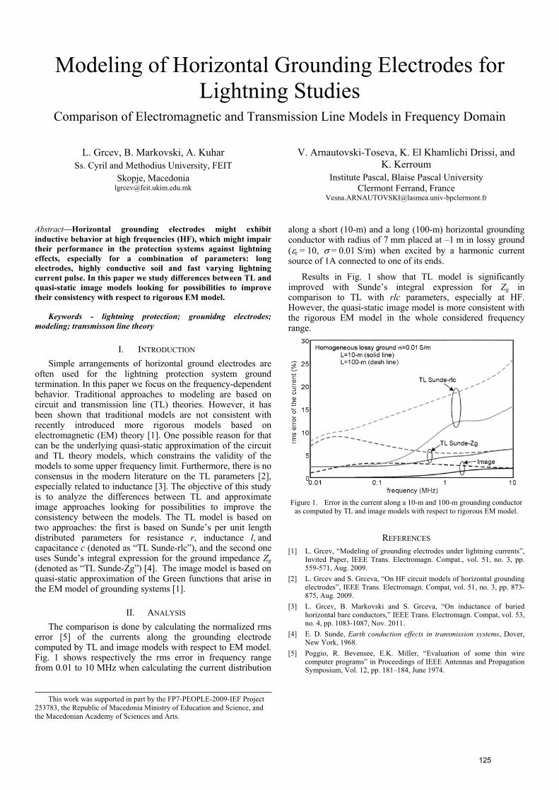
Modeling of Horizontal Grounding Electrodes for Lightning Studies
Comparison of Electromagnetic and Transmission Line Models in Frequency Domain
L. Grcev, B. Markovski, A. Kuhar Ss. Cyril and Methodius University, FEIT
Skopje, Macedonia [email protected]
V. Arnautovski-Toseva, K. El Khamlichi Drissi, and K. Kerroum
Institute Pascal, Blaise Pascal University Clermont Ferrand, France
Abstract—Horizontal grounding electrodes might exhibit inductive behavior at high frequencies (HF), which might impair their performance in the protection systems against lightning effects, especially for a combination of parameters: long electrodes, highly conductive soil and fast varying lightning current pulse. In this paper we study differences between TL and quasi-static image models looking for possibilities to improve their consistency with respect to rigorous EM model.
Keywords - lightning protection; grounidng electrodes; modeling; transmisson line theory
I. INTRODUCTION
Simple arrangements of horizontal ground electrodes are often used for the lightning protection system ground termination. In this paper we focus on the frequency-dependent behavior. Traditional approaches to modeling are based on circuit and transmission line (TL) theories. However, it has been shown that traditional models are not consistent with recently introduced more rigorous models based on electromagnetic (EM) theory [1]. One possible reason for that can be the underlying quasi-static approximation of the circuit and TL theory models, which constrains the validity of the models to some upper frequency limit. Furthermore, there is no consensus in the modern literature on the TL parameters [2], especially related to inductance [3]. The objective of this study is to analyze the differences between TL and approximate image approaches looking for possibilities to improve the consistency between the models. The TL model is based on two approaches: the first is based on Sunde’s per unit length distributed parameters for resistance r, inductance l, and capacitance c (denoted as “TL Sunde-rlc”), and the second one uses Sunde’s integral expression for the ground impedance Zg(denoted as “TL Sunde-Zg”) [4]. The image model is based on quasi-static approximation of the Green functions that arise in the EM model of grounding systems [1].
II. ANALYSIS
The comparison is done by calculating the normalized rms error [5] of the currents along the grounding electrode computed by TL and image models with respect to EM model. Fig. 1 shows respectively the rms error in frequency range from 0.01 to 10 MHz when calculating the current distribution
along a short (10-m) and a long (100-m) horizontal grounding conductor with radius of 7 mm placed at –1 m in lossy ground ( r = 10, = 0.01 S/m) when excited by a harmonic current source of 1A connected to one of its ends.
Results in Fig. 1 show that TL model is significantly improved with Sunde’s integral expression for Zg in comparison to TL with rlc parameters, especially at HF. However, the quasi-static image model is more consistent with the rigorous EM model in the whole considered frequency range.
Figure 1. Error in the current along a 10-m and 100-m grounding conductor as computed by TL and image models with respect to rigorous EM model.
REFERENCES
[1] L. Grcev, “Modeling of grounding electrodes under lightning currents”, Invited Paper, IEEE Trans. Electromagn. Compat., vol. 51, no. 3, pp. 559-571, Aug. 2009.
[2] L. Grcev and S. Grceva, “On HF circuit models of horizontal grounding electrodes”, IEEE Trans. Electromagn. Compat, vol. 51, no. 3, pp. 873-875, Aug. 2009.
[3] L. Grcev, B. Markovski and S. Grceva, “On inductance of buried horizontal bare conductors,” IEEE Trans. Electromagn. Compat, vol. 53, no. 4, pp. 1083-1087, Nov. 2011.
[4] E. D. Sunde, Earth conduction effects in transmission systems, Dover, New York, 1968.
[5] Poggio, R. Bevensee, E.K. Miller, “Evaluation of some thin wire computer programs” in Proceedings of IEEE Antennas and Propagation Symposium, Vol. 12, pp. 181–184, June 1974.
This work was supported in part by the FP7-PEOPLE-2009-IEF Project 253783, the Republic of Macedonia Ministry of Education and Science, and the Macedonian Academy of Sciences and Arts.
125

Keywords - plasma diagnostics, ultraviolet spectroscopy, streamer discharges, electrical breakdown
126

A Hierarchical System Approach to Electromagnetic Threats
Petri Järviö and Juhani Hämäläinen Finnish Defense Forces Technical Research Centre
Riihimäki, Finland
Abstract— We shall consider the threats caused by electromagnetic phenomena with a hierarchical structure. This is an overview of the threat and framework for the analysis. In particular, our goal is to categorize effects, corresponding models and damages with respect to hierarchy. This approach focuses on gaining understanding from detailed studies to complete analysis of electromagnetic threat. We show in an example how this framework can be used to describe effects of lightning.
Keywords- hierarchy; electromagnetic threat; lightning
I. INTRODUCTION
Electromagnetic field can break or interfere with electronic equipment directly or by various coupling mechanisms. It can also directly damage buildings, vehicles or humans. Shortly, it results in threats to electric and electronic components, equipment and systems of them. This leads us to consider relations among different levels of a system to estimate its vulnerability against the threats. We introduce a hierarchical framework for electromagnetic threats and models following the ideas of system engineering. The lowest level of the framework contains the studies of components and chips following with the equipment, system and a system of systems levels.
II. MODELS, PARAMETERS AND INFORMATION EXCHANGE
Electromagnetic threats are widely analyzed at different levels of the hierarchy with appropriate models and methods. Along the hierarchy, the parameters of the models follow a similar framework. To combine the models between different levels, information exchange is needed in both directions. The lower levels studies provide parameter information upwards and upper levels focuses on further analysis at lower levels.The complete threat analysis combines information from all levels to make a comprehensive outlook of the analyzed threat.
III. EXAMPLE OF LIGHTNING WITH FRAMEWORK
We consider an example of hierarchical overview for threat of lightning strike in a proposed manner. More details on the subject are available e.g. in [1]. For instance, the equipment should be shielded against direct coupling of a lightning electromagnetic pulse (LEMP) to avoid component level and equipment level damages. Surrounding buildings should be shielded against direct strike to avoid immediate mechanical damages of equipment and system. In the top level, lightning occurrence plays the key role of the analysis, see “Table 1”.
TABLE I. HIERARHIC CATEGORIZATION OF LIGHTNING
Hierarchical levels of EM
threats
Hierarchies of lightning
Example realization of the
phenomena
Example models and parameters Possible effects
System of systems Lightning
Probability of lightning,
environmental parameters
Loss of service
System Lightning strike Model of
strikes, energy of the strike
Malfunction of system
Equipment Current due to lightning
Shieldingmodeling,
current
Failures of equipment
Component Current peak to the components
Circuit models Threshold
voltage
Broken component
“Table 1” shows the differences of the effects and models in studying the threat of lightning. For instance, in the component level, analysis requires specific technical information, detailed models and measurements. This analysis set up the boundaries for the maximum field, peak current, coupling strength etc. that can be allowed inside the equipment without having any component failures or damages. Similarly, if the field strengths or other considered parameters are known, requirements for the components can used in equipment planning.
IV. SUMMARY
We have introduced a hierarchical framework to consider electromagnetic threats. This aspect divides the system and threats of the system into sub-studies, which can be combined to carry out the complete analysis. We applied the introduced technique to consider effects of lightning. However, it can be applied to related phenomena as well. The main point is to provide support for the understanding of how the threat analysis can be built up from detailed studies from the component level to the system level.
REFERENCES
[1] V. Cooray (Ed.), “The Lightning Flash,” IEE Power and Energy Series, London, vol. 34, pp. 482–484, 505-507, 2003.
127

Electric Field Characteristics of Negative Upward Lightning Initiated by the Peissenberg Tower
F. Heidler, M. Manhardt, K. Stimper University of the Federal Armed Forces Munich, EIT7, Werner-Heisenberg-Weg 35
Neubiberg, Germany
Abstract— We analyzed the slow-varying electric fields and the associated currents of the total of 35 negative upward lightning initiated by the Peissenberg tower, Germany. The slow-varying electric fields showed a fast rise characterized by the 10-to-90% risetime, with the arithmetic mean of 13.8 ms. After attaining the maximum, the electric field decayed slowly. The slow decay is characterized by the time on half value having the arithmetic mean of 441 ms. Transported charges to ground are on average 44.8 C and on maximum 165 C. The maximum value of the electric field was 39.9 kV/m on average with the highest value being 64.5 kV/m. Only weak correlations were found between the 10-to-90% risetime, the time on half value, the charge, and the maximum of the electric field.
Keywords-Lightning currents, electric field, direct strike, upward lightning, Peissenberg tower.
I. INTRODUCTION
The initial stage of the upward lightning is characterized by a leader moving up from the top of the structure. The leader produces a slowly-varying initial continuous current (ICC), which typically lasts some tens to some hundreds of milliseconds and has amplitude of some tens to some thousands of amperes (e.g. [1]). In the present study, we use the records of the currents and the corresponding electric fields of the total of 35 upward lightning, which were initiated by the 160-m high Peissenberg tower in Germany, to examine the characteristics of the slow-varying electric field for the time period of one second. All of them were from negative upward lightning.
II. ANALYSIS AND RESULTS
Fig. 1 shows an example for the time-correlated waveforms of the current and the associated slow-varying electric field. The lightning occurred on February 13, 1997. With the onset of the lightning current the electric field rises up rapidly. The 10-to-90% risetime ranged between the minimum value of 3.43 ms and the maximum value of 32.5 ms. The geometric mean (GM) and the arithmetic mean (AM) resulted in 12.3 ms and 13.8 ms, respectively. After attaining the maximum, the fields started immediately to decay. The time on half value, thv, varied between the minimum value of 188 ms and the maximum value of 817 ms. The geometric and arithmetic means are GM = 417 ms and AM = 441 ms, respectively. The charge totally transferred to ground varied between the
minimum value of 4.8 C and the maximum value of 165 C. The geometric mean resulted in 32.1 C and the arithmetic mean in 44.8 C. The Emax-values varied between the minimum value of 26.1 kV/m and the maximum value of 64.5 kV/m. The geometric and arithmetic mean are GM = 39.0 kV/m and AM = 39.9 kV/m. Higher values of the electric field are prevented by recovery effects (corona from ground, redistribution of charge in the thundercloud), which lower the electric field. These recovery effects are the reason why no or only insignificant correlation was found between the maximum electric field, Emax, the 10-to-90 % risetime of the electric field, t10-90, the charge, Q, and the time on half value, thv.
0.60.2 0.4 0.8 1Time, sC
urre
nt, A
0
-40
-120
-80
(a) Initial stage(IS)-current(21.6 C)
28
21
14
7
0 0.60.2 0.4 0.8 1Time, s
0
Emax
0,5 Emax
thv = 591 ms
Elec
tric
field
, kV/
m
(b) tonset = 62,1 ms
constant field level
Figure 1. (a) Current record as a function of time of a lightning which occurred on February 13, 1997, showing the initial stage (IS)- current. (b)
Slow-electric field record (189 m distance) of the same lightning.
REFERENCES
[1] V. A. Rakov, M.A. Uman, Lightning: Physics and Effects, Cambridge Univ. Press, New York, 2003.
128
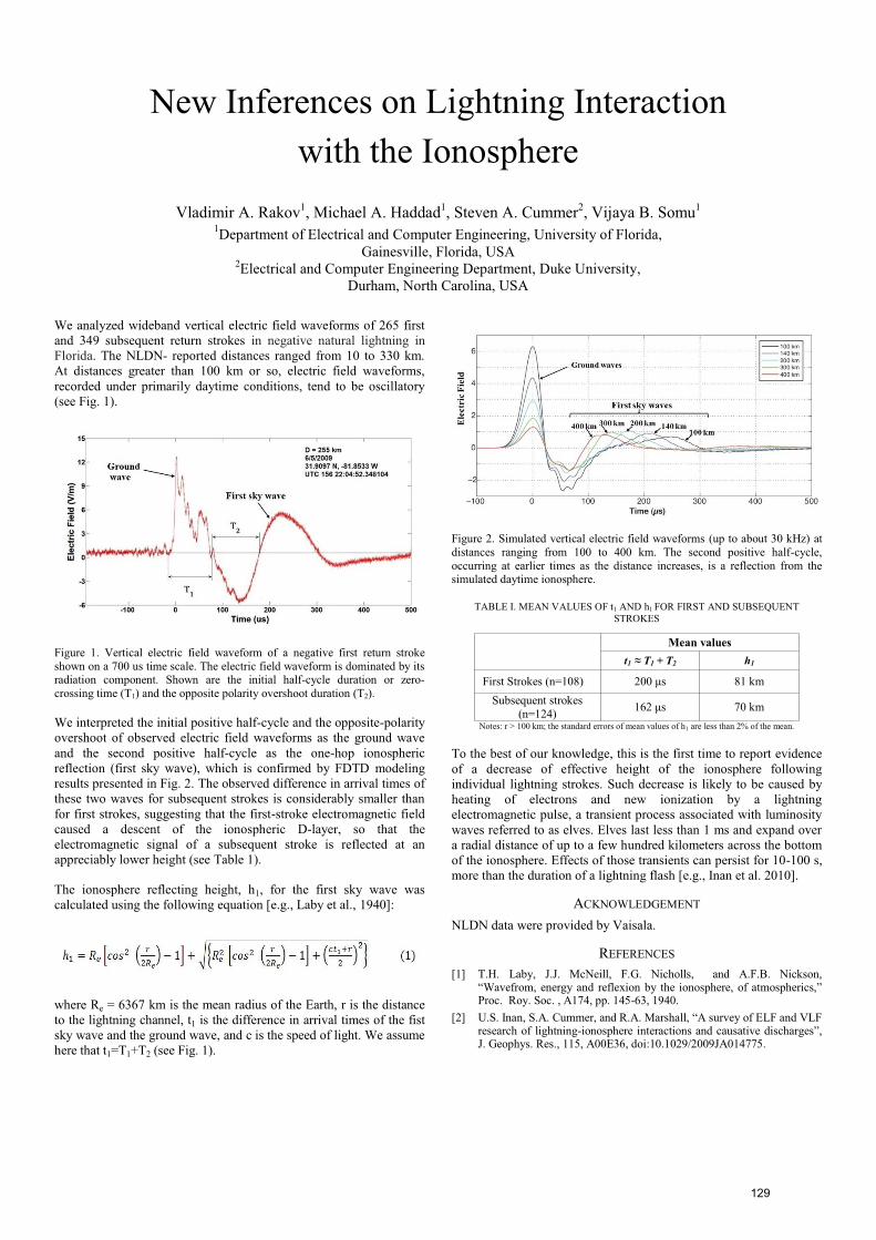
t1 1 + T2 h1
129

Computation of Distant Lightning Electric Fields: the Effect of Channel Geometry
A. Andreotti, C. Petrarca, L. Verolino University of Naples Federico II , DIEL
Naples, Italy [email protected], [email protected], [email protected]
V.A. Rakov University of Florida, DECE
Gainesville, Florida [email protected]
Abstract In this paper distant lightning electric fields generated by first and subsequent strokes will be numerically computed in order to reproduce the main characteristics of field waveforms measured at distances beyond 50 km. The effect of lightning channel geometry, together with the current attenuation along the channel and the return-stroke speed will be discussed.
Keywords- lightning; modeling
Lightning return stroke fields measured at distances of about 50 km and beyond show typical waveforms characterized by a polarity inversion with a zero crossing occurring in the tens of microseconds range [1].
According to Haddad and Rakov [2], the overwhelming majority of both first and subsequent stroke field waveforms at 50 to 350 km (96 and 88%, respectively) exhibit opposite polarity overshoots. Subsequent stroke signatures at 50 to 100 km are appreciably less likely (72% vs. 89%) to be bipolar than their first-stroke counterparts.
The main features of the distant fields waveshapes are summarized in Fig.1, as shown by Pavlick et al. [3]: they include a sharp initial peak Ep, a zero-crossing time T1, an opposite polarity overshoot (OPO) EOS, an OPO duration T2, with Eref being the reference (background) field.
Figure 1. Electric field waveform characteristics (from [3])
The features mentioned above are generally used as a benchmark in order to check the ability of return stroke models
to reproduce distant fields. In most of the previous model-validation studies, primarily zero-crossing time was used to characterize the distant fields waveforms.
Shoory et al. [4, 5], based on modeling, suggested that the zero-crossing time in far-field waveforms is influenced by three main mechanisms: the duration of the return-stroke current waveform, the current attenuation along the channel, and the return-stroke speed.
The aim of the present paper is to consider another influencing factor, namely the channel geometry, in order to reproduce the measured fields and try to explain the differences between the fields generated by first and subsequent strokes.
In particular, non-vertical lightning channels will be taken into account [6, 7] and two engineering models, the modified transmission line linear (MTLL) and the modified transmission line exponential (MTLE), will be employed in order to reproduce not only the zero-crossing times, but also the shape and magnitude of the entire field waveforms.
REFERENCES
[1] Y.T. Lin, M.A. Uman, J.A. Tiller, R.D. Brantley, W.H. Beasley, E.P. Krider and C.D. Weidman Characterization of Lightning return Stroke Electric and Magnetic Fields From Simultaneous Two-Station Measurements , J. Geophysical Research, 84, 6307-6314, 1979
[2] M.A. Haddad and V.A. Rakov, New Measurements of Distant Lightning Electric Fields in Florida , PIERS 2011, Marrakesh, Morocco, March 20-23 2011
[3] A. Pavlick, D.E. Crawford and V.A. Rakov, Characteristics of Distant Lightning Electric Fields , Proc. Of Intl. Conf. on probabilistic Methods Applied to Power Systems (PMAPS), Naples, Italy, September 22-26, 2002, pp. 703-707
[4] A. Shoory, F. Rachidi, M. Rubinstein, R. Moini and S.H.H. Sadeghi, Analytical Expression for Zero-Crossing Times in Lightning Return-
Stroke Engineering Models , IEEE Trans. on EMC, vol. 51, No 4, pp. 963-974, 2009
[5] A. Shoory, F. Rachidi, M. Rubinstein, R. Moini and S.H.H. Sadeghi Why do some lightning return stroke models not reproduce the far-field
zero crossing? , J. Geophysical Research, vol. 114, D16204, 2009 [6] G. Lupò, C. Petrarca, V. Tucci, and M. Vitelli, EM Fields Generated by
Lightning Channels with Arbitrary Location and Slope IEEE Trans. On EMC, vol. 42, no. 1, pp. 39 53, Feb. 2000
[7] A. Andreotti, C. Petrarca, V.A. Rakov, and L. Verolino, Calculation of Voltages Induced on Overhead Conductors by Nonvertical Lightning Channels , IEEE Trans. on EMC, in press, 2012
130

Close-Range Lightning Electromagnetic Fields in the Presence of a Stratified Ground
Abdenabi Mimouni Ibn Khaldoun University
Electrical engineering and Plasma Laboratory Tiaret, Algeria
Farhad Rachidi Swiss Federal Institute of Technology (EPFL)
Electromagnetic Compatibility Group Lausanne, Switzerland [email protected]
Abstract— We present an analysis of the electromagnetic fields originated by a lightning return stroke at very close distance range. The components of the electromagnetic fields are evaluated for observation points above and inside a horizontally stratified ground. The computations are obtained by solving Maxwell’s equations using the Finite Difference Time Domain (FDTD) technique, in which the return stroke channel is appropriately included using the so-called engineering models. The results obtained for a two-layer soil are compared with those related to a homogeneous soil. The effect of the soil stratification on both the above-ground fields and the fields penetrating into the ground are illustrated and discussed.
Keywords-Electromagnetic fields; FDTD; lightning; stratified ground.
I. INTRODUCTION
Lightning is a major source of electromagnetic radiation that interferes with modern electronic and communication systems and can damage a wide range of apparatus. A number of studies have addressed the issue of the evaluation of the electromagnetic fields radiated by lightning return strokes, using different theoretical approaches (see [1] for a review).
One of the first studies on the propagation of electromagnetic waves along a stratified medium is due to Wait, who showed that the concept of attenuation function and surface impedance can be used to represent the effect of a multi-layered soil [2]. Wait [3,4], and Hill and Wait [5] have derived the attenuation function for the vertical electric field propagating over a horizontally stratified ground. The theory was then used by Ming and Cooray [6], and Cooray and Cummins [7] to evaluate such effects on lightning return stroke electromagnetic fields. Recently, Shoory et al. [8-10] have examined the accuracy of the Wait formulations for horizontally stratified ground taking as reference full-wave simulations obtained using the FDTD technique.
II. AIM OF THE PAPER
In this paper, we present a comprehensive characterization of the electromagnetic fields in the immediate vicinity of a lightning channel, above and under the ground surface, for a two-layer configuration. The Maxwell’s equations for the electromagnetic fields are solved by applying the FDTD
technique, in which the return stroke channel is appropriately included using engineering models.
III. SIMULATION RESULTS
The results obtained for a two-layer ground configuration are compared with those related to a homogeneous soil. The effects of the soil stratification on both the above-ground and underground electromagnetic fields are illustrated. It is shown that the fields penetrating into the ground are, in general, markedly affected by the soil stratification.
REFERENCES
[1] V.A. Rakov, F. Rachidi, "Overview of Recent Progress in Lightning Research and Lightning Protection", IEEE Transactions on Electromagnetic Compatibility, Vol. 51, No. 3, August 2009, pp. 428-442.
[2] J. R. Wait, “Electromagnetic waves in stratified media,” Oxford, IEEE Press, 1996.
[3] J. R. Wait, “Radiation from a vertical electric dipole over a stratified ground,” I.R.E. Trans. Antennas and Propagation, Vol.1, pp. 9-11, 1953.
[4] J. R. Wait, “On the theory of transient electromagnetic sounding over a stratified earth,” Canadian Journal of Physics,Vol. 50, pp. 1055-1061, 1972.
[5] D. A. Hill and J. R. Wait, “HF radio wave transmission over sea ice and remote sensing possibilities,” Geoscience and remote sensing, IEEE Transactions on, Vol. 19, pp. 204-209, 1981.
[6] Y. Ming and V. Cooray, “Electromagnetic radiation fields generated by lightning return strokes over a stratified ground,” in 22nd InternationalConference on Lightning Protection (ICLP), Budapest, 1994, pp. R1c-05
[7] V. Cooray and K. L. Cummins, “Propagation effects caused by stratified ground of electromagnetic fields of return strokes,” in 20th International Lightning Detection Conference & 2nd International Lightning Meteorology Conference Tucson, Arizona, USA, 2008.
[8] A. Shoory, A. Mimouni, F. Rachidi, V. Cooray, R. Moini and S. H. H. Sadeghi, “Validity of simplified approaches for the evaluation of lightning electromagnetic fields above a horizontally stratified ground,” IEEE Trans. Electromagnetic Compatibility, 52 (3), pp.657-663, 2010.
[9] A. Shoory, A. Mimouni, F. Rachidi, V. Cooray and M. Rubinstein, “Lightning horizontal electric fields above a two-layer ground ,” in 30th
International Conference on Lightning Protection (ICLP), Cagliari, Italy, 2010, pp. 1285(01-05).
[10] A. Shoory, F. Rachidi, F. Delfino, R. Procopio, M. Rossi, "Lightning electromagnetic radiation over a stratified conducting ground: 2. Validity of simplified approaches ", Journal of Geophysical Research, Vol. 116, D11115, doi:10.1029/2010JD015078, 2011.
131

132

HPEM-TC06-SS3Lightning Indirect Effects on Aircrafts
133

Aircraft Sub-system Lightning Simulation using R, L Equivalent Circuit Approach
D. Prost, F. Issac ONERA, The French Aerospace Lab
Toulouse, France [email protected]
Abstract— Lightning indirect effect are generally computed on aircraft systems by full wave EM modelling such as FDTD. The equivalent circuit method is however well suited for those slow lightning waveforms since the quasi-static approximation is relevant in most cases. Comparison between the two methods is given in the case of a A320 landing gear submitted to the normalized "A" lightning waveform, and exhibits close results. Moreover, experimental measurements achieved on a real landing gear confirm the validity of the results.
Keywords - Lightning; FDTD; Equivalent Circuit.
I. INTRODUCTION
Lightning has always been a critical issue in the aircraft industry. The increasing use of composite materials, as well as the trend toward more electric systems, reinforces the constraints due to indirect lightning effects. To compute those constraints, i.e. the induced current on the different mechanical parts and cables, the FDTD (Finite Difference Time Domain) method is widely used [1] and gives satisfying results. Nevertheless, the computational cost of FDTD is far to be negligible even when using super-calculators; this makes parametric design studies difficult (because these imply several computation runs). Actually, slow lightning waveforms (such as "A" or "D" waves as defined in [2]) induce currents mainly showing a quasi-static behavior (bi-exponential, slow damped sinusoids). For these reasons, a quasi-static computation of an equivalent R, L, circuit resolution is an interesting alternative to full wave computation like FDTD. Here, both methods have been used and are compared, in the particular case of a A320 nose landing gear.
II. AIRCRAFT SUB-SYSTEM LIGHTNING COMPUTATION
A A320 nose landing gear has been meshed with relatively small cells (5 mm) to take into account geometric details and the presence of two harnesses. This leads to a huge FDTD model with 80-million nodes (Fig. 1) and a CPU time of almost 20-million seconds to obtain the 25 first µs of the lightning waveform. The lightning input current is applied on the wheel (see Fig. 1), while the return current is flowing on PEC wall beyond the ML (matched layers) surrounding the model.
An equivalent circuit (EC) of the landing gear has also been obtained, by replacing each mechanical part or harnesses segment by a straight conductor with resistance and self inductance values analytically calculated from material
conductivity and geometrical shape (using usual formulas). These conductors are modeled in 3D and the circuit respects the general shape and size of the gear; the mutual inductance of each couple of two conductors is thus obtained (Fig. 1, insert). This model contains only 56 conductors, and a CPU time of only 500 seconds allows computation of the whole "A" lightning waveform.
Figure 1. Landing gear FDTD model. Output currents (aircraft connections J1 to J5, harnesses A0 and B0). Insert : equivalent circuit
0
10000
20000
30000
40000
50000
60000
A0 B0 J1 J2 J3 J4 J5
Imax
(A
)
FDTD Equivalent Circuit Measurements
Figure 2. Maximum currents obtained with the FDTD and EC methods, and measurements
Fig.2 gives the maximum currents computed on the harnesses and on the different connections points to the aircraft (as indicated in Fig. 1), for a "A" waveform injection. Measurements for a reduced level A-shaped waveform (500A) have also been achieved and are given after normalization to the real A level (200 kA). This allows direct comparison between both computation methods and experimental results, which appears in good agreement. Such an agreement will also be showed in the presentation with some comparisons of time domain results.
REFERENCES
[1] M Apra, M. D'Amore, M. Sarto, V. Volpi, "Lightning Indirect Effects Certification of a Transport Aircraft by Numerical Simulation", IEEE Transactions on Electromagnetic Compatibility 50(3), pp.513, 2008.
[2] Aircraft Lightning Environment and Related Test Waveforms, ED-84, Eurocae, July 1997
This work was supported by the ASTECH, Aerospace Valley and Pégase Competitive Poles through the PREFACE project.
B0A0
J5J3
J2
J1Current injection
J4
134

Keywords : lightning, inductance, circuit-based method
t=6.3µs I lightning=200 kA
22
45
67
90
135

Indirect-Lightning Threat Level Computation on Aircraft Engines
T. Volpert, S. Bertuol, M. Ridel, J.P. Parmantier ONERA, The French Aerospace Lab
2 avenue Edouard Belin, 31055, Toulouse, France [email protected]
C. Lair, N. Cotereau SNECMA/YSSE
Villaroche, France [email protected]
Abstract— This paper synthesizes the work having been performed in order to simulate indirect-lightning threat level determination on two types of aircraft engine.
Keywords : Lightning; Indirect Effects; 3D Numerical Simulation; FDTD
I. INTRODUCTION
During the certification process of aircraft engines numerical simulations may now be used to understand and anticipate indirect-lightning threat levels on electronic devices: such an approach has been applied on the TP400 [1] and SaM146 engines using the well-known FDTD method,
II. DIGITAL MOCK-UP AND DOCUMENTATIONSANALYSIS
In order to obtain a numerical model relevant enough to simulate indirect-lightning coupling on an aircraft engine the bounding documentations has to be precisely analyzed. In addition relevant parts of the 3D geometry data from the digital mock-up have to be extracted. It is essential to not miss any part that may play a role in the current distributions. All the 3D main parts such as the engine itself, the pylon, the nacelle, the reverse must be included as well as some pipes, every bounding braids, and of course the cable harnesses and electronic devices and sensors.
III. FDTD MESH GENERATION
The mesh is produced with so-called STL files directly generated from the CAD models. All the 3D parts are then converted into 3D sets of FDTD cells, with a 1 cm step in our case. In order to better approach the average diameter of a harness section, the thin wire model is not used here: we use a continuous set of cells following the cable-harness route.
Once the 3D FDTD mesh, including all the geometrical data is complete, it is essential to verify that this model and the previous analysis perfectly matches in terms of existing electrical contacts. For this, a contact matrix between the different types of meshed cells is automatically generated and used to demonstrate the EM relevance of the model.
IV. ELECTRICAL MODEL
The full electrical model is built by collecting the material electrical characteristics of the 3D parts, including composite parts; this task may become a quest and may be tedious. On the
cable harnesses mesh, a surface model is used with an equivalent electrical conductivity to simulate the cable resistance. Then a set of thin wires are added to this model at the extremities in order to provide the 3D cable harness connection to the equipment or geometrical parts as well as for being able to observe directly the induced currents. Such thin wire models are also used for bounding braids and jumpers.
Figure 1. The Sam146 engine FDTD mesh.
V. SIMULATION AND POST-PROCESSING
In order to understand EM effects, the observation time must last at least 60 micro seconds for a “A” type of waveform (from Eurocae ED-84). Due to the spatial step of 1 cm, a parallel computer is used to reach the wanted final simulation time. Various simulation configurations are tested in order to understand correctly the physics of current distribution (different lightning injection and exit points, types of waveform, and some bounding modifications).
During the post processing phase, the current behaviour on all cables and termination braids are treated and analyzed. Current density on the 3D structure is displayed.
VI. CONCLUSION
The main steps of studies concerning the modelling of indirect-lightning threat level determination on the aircraft engine will be presented in the final paper. This simulation methodology has been successfully compared to laboratory lightning tests on the SaM146 engine and has proved to be helpful to assess the lightning response sensitivity when applying bonding modifications and thereby reducing the current levels on a selection of cable-harnesses.
REFERENCES
[1] J.P. Parmantier, S. Bertuol, T. Volpert, C. Lair, P. Dupre, F. Thérond, G. Gutierrez, J.I. Plaza Gomez, "Méthodologie de modélisation/simulation 3D des effets EM d'une injection foudre sur le moteur TP400", 15th International French EMC Conference, CEM 2010 Limoges – France.
136

Abstract
Keywords-component; Lightning; DO160 Section 22; ARP5415; aperture coupling; resistance coupling
137

A global circuit tool for modelling lightning indirect effects on aircraft
H. Moussa, M. Abdi Hispano-Suiza, Groupe SAFRAN
Rond Point René Ravaud, 77551 Moissy-Cramayel [email protected]
F. Issac, D. Prost ONERA, The French Aerospace Lab
F–31055, Toulouse, France
Abstract— The topic of this paper is EM Environment and EMI Effects, specifically the modelling of lightning indirect effects [1] of aircraft electrical systems on embedded and highly exposed equipments, such as nose landing gears (NLG) and nacelles, through a circuit approach. The novelty here is to provide a pre-sizing qualitative model allowing parametric approach in pre-design phases. The modelling tool intends to offer a user-friendly and time efficient way for taking into account the lightning constraints. Two cases are analysed: first, a NLG which is composed of tubular pieces that can be easily approximated by equivalent cylindrical straight conductors. Therefore, passive R, L, M elements of the structure can be extracted through analytical engineer formulas such as those implemented in the partial element equivalent circuit (PEEC)[2] method. Secondly, the same approach is applied on an electrical de-icing nacelle sub-system.
Lightning; equivalent circuit; circuit simulator
I. INTRODUCTION
The evolution of aeronautics, in the context of a “more composite” and “more electrical” aircraft, leads to many modifications in the electrical system design. The introduction of composite materials [3] in the aircraft structure, in order to save weight and to improve robustness to ageing, generates important environment changes. The composite fuselage can not entirely comply either with the grounding and bonding or with the lightning strike protection requirements. Thus, in order to ensure a proper functioning of the electrical system and to protect the electrical equipment or the high voltage direct current network, constraints at system and equipment levels have to be estimated in order to minimize the weight and innovative protection solutions.
The principle of our circuit approach is to automatically generate an equivalent passive circuit using a circuit simulator macro-component, SABER®, whose inputs and outputs can be defined by the user in order to be coupled with other functional circuit models (such as converter or harnesses) in the same circuit simulator. Therefore, the lightning current computation, on both the structure and the power harness shields, is done in time-domain by the circuit simulator. This allows predicting common mode voltage and current overload on the three phases of the converter.
II. EQUIVALENT CIRCUIT GENERATION
The idea is to calculate the R, L, equivalent circuit taking into account each conductor of the structure. The inductive coupling is directly linked to the geometry of the structure while the resistance is calculated from the material conductivity; formulas will be detailed in the presentation.
Another important aspect is the efficiency of the power harness shield, represented by its transfer impedance, Zt.
The first application presents the modelling of lightning current distribution on a A320 NLG. The first step is to simplify and discretize the landing gear structure using straight conductors in order to generate and compute the equivalent circuit components. This step requires the knowledge of the resistors values between the structure mechanical parts. These ones play a major role in the current magnitude limitation and distribution. These values have been measured by ONERA, in its EMC laboratory, and introduced in the model by changing the conductivity of the conductors being in contact. The result on the apparent conductivity is the same as if the contact resistance was added.
Figure 1. NLG Power converter lightning model
Preliminary results obtained in the A320 landing gear case are in very good agreement with measurements (less than 3dB, for the "A" standard lightning waveform described in the DO-160 [4]); the experimental setup and simulation results will be detailed in the presentation. The results obtained on a de-icing nacelle sub-system will also be presented.
REFERENCES
[1] S. Cristina, A. Orlandi, “Calculation of the induced effects due to a lightning stroke” IEE Proeeding B. On Electric Power Applications, vol. 139, no. 4, 1992, pp. 374–380.
[2] A.E. Ruehli, “Equivalent Circuits Models for three Dimensional Multiconductor Systems,” IEEE Transactions on Microwave theory and Techniques, Vol. MTT 22, N°3, March 1974.
[3] M. D'Amore, M. Sarto, “Time-domain analysis of lightning interaction to aeronautical structures composite materials,” IEEE 1997 International Symposium on Electromagnetic Compatibility, 1997, pp. 397-402.
[4] RTCA DO-160F, December 6, 2007.
138

Keywordt; (lightning, permittivity scaling, quasi-magnetostatic modeling, EMA3D, FDTD)
139
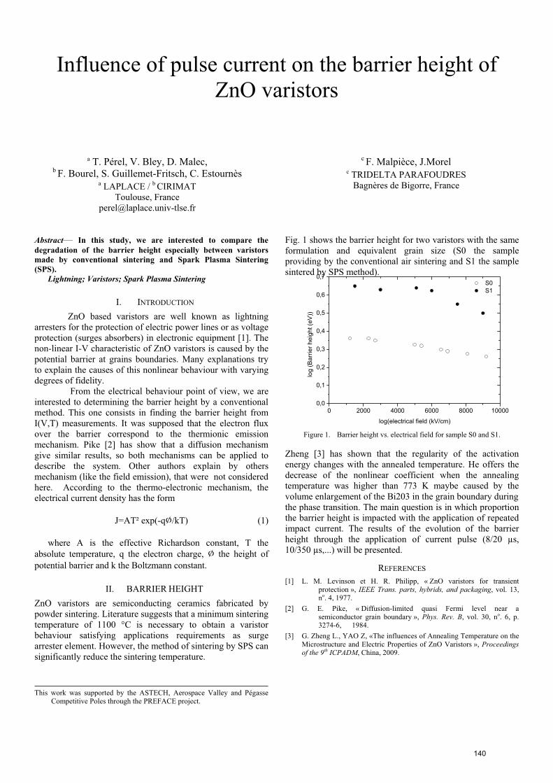
0 2000 4000 6000 8000 100000,0
0,1
0,2
0,3
0,4
0,5
0,6
0,7
log
(Bar
rier h
eigh
t (eV
))
log(electrical field (kV/cm)
S0 S1
Influence of pulse current on the barrier height of ZnO varistors
a T. Pérel, V. Bley, D. Malec, b F. Bourel, S. Guillemet-Fritsch, C. Estournès
a LAPLACE / b CIRIMATToulouse, France
c F. Malpièce, J.Morel c TRIDELTA PARAFOUDRES
Bagnères de Bigorre, France
Abstract— In this study, we are interested to compare the degradation of the barrier height especially between varistors made by conventional sintering and Spark Plasma Sintering (SPS).
Lightning; Varistors; Spark Plasma Sintering
I. INTRODUCTION
ZnO based varistors are well known as lightning arresters for the protection of electric power lines or as voltage protection (surges absorbers) in electronic equipment [1]. The non-linear I-V characteristic of ZnO varistors is caused by the potential barrier at grains boundaries. Many explanations try to explain the causes of this nonlinear behaviour with varying degrees of fidelity. From the electrical behaviour point of view, we are interested to determining the barrier height by a conventional method. This one consists in finding the barrier height from I(V,T) measurements. It was supposed that the electron flux over the barrier correspond to the thermionic emission mechanism. Pike [2] has show that a diffusion mechanism give similar results, so both mechanisms can be applied to describe the system. Other authors explain by others mechanism (like the field emission), that were not considered here. According to the thermo-electronic mechanism, the electrical current density has the form
J=AT² exp(-q /kT) (1)
where A is the effective Richardson constant, T the absolute temperature, q the electron charge, the height of potential barrier and k the Boltzmann constant.
II. BARRIER HEIGHT ZnO varistors are semiconducting ceramics fabricated by powder sintering. Literature suggests that a minimum sintering temperature of 1100 °C is necessary to obtain a varistor behaviour satisfying applications requirements as surge arrester element. However, the method of sintering by SPS can significantly reduce the sintering temperature.
Fig. 1 shows the barrier height for two varistors with the same formulation and equivalent grain size (S0 the sample providing by the conventional air sintering and S1 the sample sintered by SPS method).
Figure 1. Barrier height vs. electrical field for sample S0 and S1.
Zheng [3] has shown that the regularity of the activation energy changes with the annealed temperature. He offers the decrease of the nonlinear coefficient when the annealing temperature was higher than 773 K maybe caused by the volume enlargement of the Bi203 in the grain boundary during the phase transition. The main question is in which proportion the barrier height is impacted with the application of repeated impact current. The results of the evolution of the barrier height through the application of current pulse (8/20 μs, 10/350 μs,...) will be presented.
REFERENCES
[1] L. M. Levinson et H. R. Philipp, « ZnO varistors for transient protection », IEEE Trans. parts, hybrids, and packaging, vol. 13, no. 4, 1977.
[2] G. E. Pike, « Diffusion-limited quasi Fermi level near a semiconductor grain boundary », Phys. Rev. B, vol. 30, no. 6, p. 3274-6, 1984.
[3] G. Zheng L., YAO Z, «The influences of Annealing Temperature on the Microstructure and Electric Properties of ZnO Varistors », Proceedings of the 9th ICPADM, China, 2009.
This work was supported by the ASTECH, Aerospace Valley and PégasseCompetitive Poles through the PREFACE project.
140

HPEM-TC07 Analytical and
Numerical Models and Modelling
141

! #$\^|$^^$|\|\\
!"# $ &'* ++<+'
!
\ \!\
\ ^ \^ \ |
\\ \^
>
? \ \
" | !" !" ""! "
# $
%
! " % "
" "
" "
\\\ !\|!|
& ''*
' !57 |
\^ ¡ \ : # #$ : ¢
\ |!||¡£¤\\¡|¡¥
¦ ¥ § ¨ © £
¥¨ § § §§ §© ¨ ¨ ¨¦ ¨¥
¡
¦ © £ £ ¦ £ §
¥¨ ¥ ¦© ¦§ ¦ £ §
\ª !|\^|^\ª|
\^ \?'@ : ¢
|
|X Y$Y[ \ [ \ $ $$ $\$ $]^ \¥¬¥
X ]^ ^ ^£¨£¨¦
¯|X [ ]^^|££§
142

1D WCIP and FEM hybridization
C. Girard, N. Raveu, R. Perrussel, J. Li LAPLACE
CNRS, INPT, UPS, Université de Toulouse Toulouse, France
Stéphane Lanteri Equipe-projet NACHOS
INRIA Sophia Antipolis Méditerranée Sophia Antipolis, France
Abstract—The hybridization between two numerical methods, the 1D Wave Concept Iterative Procedure (WCIP) and the 2D Finite Element Method (FEM), is introduced. Preliminary numerical results are also presented.
Keywords-WCIP; FEM; inhomogeneous planar circuits.
I. INTRODUCTION
The Wave Concept Iterative Procedure (WCIP) is a numerical method dedicated to computations in planar homogeneous multi-layers circuits [1]. Currently, dealing with inhomogeneous dielectric substrate or via-holes is not possible with the WCIP alone. To overpass this difficulty, hybridization with the Transmission Line Matrix method has been achieved in [2] but it is restricted to regular rectangular mesh. Hybridization with the Finite Element Method (FEM) is a way to cope with this issue through unstructured triangular mesh.
II. METHOD
A. 1D WCIP method
The method relies on the behavior of incoming (B) and outgoing (A) waves upon an interface (Σ) which separates two domains 1 and 2 (Fig. 1). These waves are generated by an incident wave (Bom). The system to be solved is,
As = SBs;A = FMT(As),
B = ΓA + Bom;Bs = FMT−1(B),
⎧ ⎨ ⎩
(1)
where S is the scattering operator for boundary conditions on (Σ), Γ is the scattering operator for homogeneous media conditions, FMT is the Fast Modal Transform and FMT-1 is its inverse [1].
B. Hybridization principle
Instead of using the WCIP in the two domains, the FEM is implemented in the domain that contains the inhomogeneity (Domain 2 in Fig. 1). The wave Ay2 (the index 2 refers to domain 2) is the outgoing wave seen from the interface. Ay2 is a source term in the finite element formulation. The electric field Ey2 is calculated by FEM with (2).
∇ E y 2D 2
∫ .∇ wdS − k 02 E y 2
D 2
∫ wdS + jk 0 E y 2 wdl =∑∫
2 jk 0 Z 0 A y 2 wdl∑∫ ,
(2)
where w stands for a test function, k0 is the free space wavenumber and Z0 the free space impedance.
It enables calculating the incoming wave By2 which becomes an input variable for the WCIP with (3),
⎟⎟⎠
⎞⎜⎜⎝
⎛∂
∂ωμ
−=z
E
j
ZE
Z2
1B 2y
0
02y
0
2y (3)
Fig.1: Multi-layers circuit Fig.2: Scheme
The scheme is iterated until required convergence is reached according to Fig. 2.
III. CONCLUSION
Preliminary results over an interface separating two air volumes have been obtained: fields are compared to analytical cases and results are in good agreement with a relative error lower than 0.04%. Other structures have to be tested namely circuits with dielectric substrate change with vertical slope (cf. Fig. 1) or not, and via metallization connecting two metallic surfaces. Algorithm acceleration has also to be considered.
ACKNOWLEDGMENT
The first author is supported by a PhD grant from the Defence Procurement Agency (DGA).
REFERENCES
[1] S. Wane, D.Bajon, H. Baudrand and P.Gamand, “A new full-wave hybrid differential-integral approach for the investigation of multilayer structures including nonuniformly doped diffusions,” IEEE MTT., vol. 53, n°1, pp. 200-213, January 2005.
[2] A. Zugari, M. Khalladi, M.Iben Yaich, N.Raveu and H. Baudrand, “New approach: WCIP and FDTLM hybridization,” Mediterranean Microwave
Symposium (MMS), 2009
143
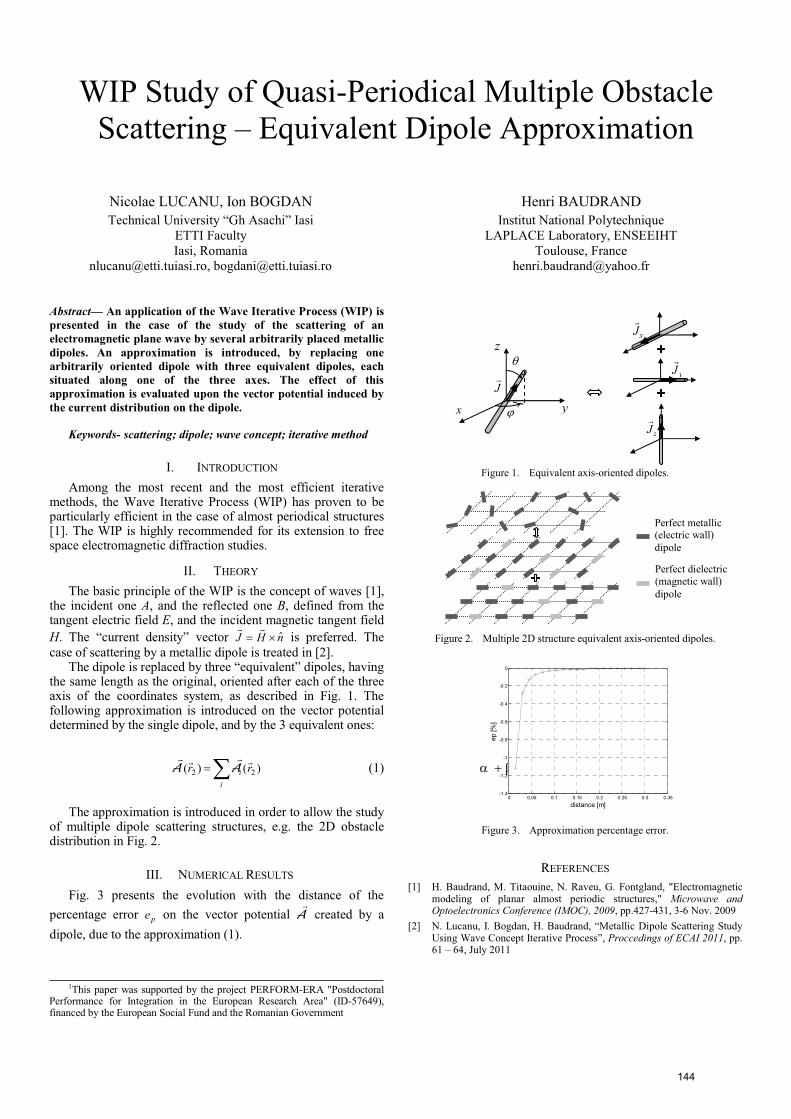
WIP Study of Quasi-Periodical Multiple Obstacle Scattering – Equivalent Dipole Approximation
Nicolae LUCANU, Ion BOGDAN Technical University “Gh Asachi” Iasi
ETTI Faculty Iasi, Romania
[email protected], [email protected]
Henri BAUDRAND Institut National Polytechnique
LAPLACE Laboratory, ENSEEIHT Toulouse, France
Abstract— An application of the Wave Iterative Process (WIP) is presented in the case of the study of the scattering of an electromagnetic plane wave by several arbitrarily placed metallic dipoles. An approximation is introduced, by replacing one arbitrarily oriented dipole with three equivalent dipoles, each situated along one of the three axes. The effect of this approximation is evaluated upon the vector potential induced by the current distribution on the dipole.
Keywords- scattering; dipole; wave concept; iterative method
I. INTRODUCTION Among the most recent and the most efficient iterative
methods, the Wave Iterative Process (WIP) has proven to be particularly efficient in the case of almost periodical structures [1]. The WIP is highly recommended for its extension to free space electromagnetic diffraction studies.
II. THEORY The basic principle of the WIP is the concept of waves [1],
the incident one A, and the reflected one B, defined from the tangent electric field E, and the incident magnetic tangent field H. The “current density” vector nHJ ˆ×=
rr is preferred. The
case of scattering by a metallic dipole is treated in [2]. The dipole is replaced by three “equivalent” dipoles, having
the same length as the original, oriented after each of the three axis of the coordinates system, as described in Fig. 1. The following approximation is introduced on the vector potential determined by the single dipole, and by the 3 equivalent ones:
∑=i
i rr )()( 22rrrr
AA (1) α + β = χ. (1) (1)
The approximation is introduced in order to allow the study of multiple dipole scattering structures, e.g. the 2D obstacle distribution in Fig. 2.
III. NUMERICAL RESULTS Fig. 3 presents the evolution with the distance of the
percentage error pe on the vector potential Ar
created by a dipole, due to the approximation (1).
Figure 1. Equivalent axis-oriented dipoles.
Figure 2. Multiple 2D structure equivalent axis-oriented dipoles.
0 0.05 0.1 0.15 0.2 0.25 0.3 0.35-1.4
-1.2
-1
-0.8
-0.6
-0.4
-0.2
0
distance [m]
ep [
%]
Figure 3. Approximation percentage error.
REFERENCES [1] H. Baudrand, M. Titaouine, N. Raveu, G. Fontgland, "Electromagnetic
modeling of planar almost periodic structures," Microwave and Optoelectronics Conference (IMOC), 2009, pp.427-431, 3-6 Nov. 2009
[2] N. Lucanu, I. Bogdan, H. Baudrand, “Metallic Dipole Scattering Study Using Wave Concept Iterative Process”, Proccedings of ECAI 2011, pp. 61 – 64, July 2011
1This paper was supported by the project PERFORM-ERA "Postdoctoral Performance for Integration in the European Research Area" (ID-57649),financed by the European Social Fund and the Romanian Government
Perfect metallic (electric wall) dipole Perfect dielectric (magnetic wall) dipole
zJr
xJr
yJrθ
ϕ
z
x yJr
144

New high order FDTD method to solve the Maxwell equations
T. Volpert, X. Ferrières ONERA, The French Aerospace Lab, F-31055,
Toulouse, France [email protected]
B. Pecqueux*, G Cohen** * CEA/DAM, ** INRIA
* Gramat, ** Le Chesnay, France
Abstract— This paper present a new high order FDTD method. The formulation is briefly given, then numerical results and method comparisons are presented on a test case.
Keywords-Time domain Maxwell equations, high order approximation schemes, Cartesian meshes, EMC.
I. INTRODUCTION
To avoid dissipative and dispersive errors, high order spatial approximations schemes as Discontinuous Galerkin method have been studied on unstructured meshes [1]. Here we present a variable order FDTD method which allows us to obtain accurate solutions, and has the advantage of the cartesian meshes to minimize the CPU-time and memory costs. This technique is very efficient for some configurations involving cavities or buildings, or for the evaluation of fields near structures in EMC problems.
II. FORMULATION Let be the computational domain, find E H(curl, )
and H H(div, ), satisfying the Maxwell equations. Let T be a cartesian mesh of . Any element K T is a rectangular parallelepiped of dimensions dx, dy, dz. On each cell K we approximate E and H as follow :
z (1)
yxG
zGLGL
zyxGL
yGGL
zyxGL
xGLG
EEEE
zyxGL
zGG
zyxG
yGLG
zyxG
xGGL
HHHH (2)
Where zyx are Gauss Lagrange polynomials, and
zyx are Gauss-Lobatto Lagrange polynomials.
Figure 1. Ex and Hz components at order 3
III. NUMERICAL RESULT
To show the interest of the method, we have computed the propagation of the principal mode (3,3,0) into a metallic cubic cavity with a side of 1 meter. We have done comparisons with the FDTD method and with the analytic solution given by
Ez = sin(3 x)sin(3 y)cos( t) for the Ez component.
We can notice int the figure 1, that the FDTD solution meshed at /23 presents at late time simulation important dispersive error. This can be fixed with mesh refinement, but it implies a high computational cost. Our method allow us to obtain a good precision due to high order approximation, and gives a low computational cost using larger cells.
Figure 2. comparisons of solutions
TABLE I. PERFORMANCES COMPARISONS
Method Time second Memory Mo Error % FDTD l/46 754 48 2.7FDTD l/23 52 7 23
ELFIC Order 3 69 24 2ELFIC Order 5 23 23 0.7
ELFIC Order 3 to 6 54 24 2
IV. CONCLUSION
We have presented a new technique to obtain a high order FDTD scheme with a variable spatial order of approximation. It may be coupled with Discontinuous Galerkin method. With additional physical models, like thin wires or thin slots models, it can be a powerful tool to solve EMC problems.
REFERENCES
[1] G. Cohen, X. Ferrieres, S. Pernet “A spatial high order discontinuous Galerkin Method to solve teh Maxwell’s equation in time domain.”, journal of computational physics 217 (2006) 340-363
145

FEMGD: An efficient discontinuous Galerkin approach on hybrid meshes for time domain
Maxwell’s equations
G. Cohen, corresponding and presenting authorProjet POEMS, INRIARocquencourt, [email protected]
X. FerrièresDept. DEMR, ONERA
Toulouse, [email protected]
B. PecqueuxCEG
Gramat, [email protected]
Abstract— In this paper, we present the features of FEMGD, a software for solving Maxwell’s equations in complex domains, based on discontinuous Galerkin methods (DGM) on a hexahedral mesh. The difficulty of constructing such meshes for complex domains lead us to seek for efficient palliatives. A first approach is the use tetrahedral meshes by splitting tetrahedra into four hexahedra. Although easy to construct, this approach provides highly distorted meshes, which substantially reduce the performance of the method. A second approach is to use hybrid meshes coupling hexahedra and tetrahedral and possibly pyramids. This new point of view dramatically increases the performance of the method and leads to an algorithm about five times faster than pure tetrahedral DGM.
Keywords-component; Maxwell’s equations; numerical methods; discontinuous Galerkin methods; hexahedral and hybridmeshes; local time-stepping.
I. INTRODUCTION
Solving Maxwell’s equation for complex geometries and physics (anisotropy, etc…) is a challenging problem. For a long time, FDTD, based on the Yee scheme was the reference numerical method for Maxwell’s. However, based on regular orthogonal grids, this method is has some difficulties for approximating complex domains. Moreover, its second-order accuracy requires the use of very fine grids for long time experiments. On the other hand, finite elements required the inversion of a n-diagonal mass matrix at each time-step. A first palliative to these drawbacks was the use of high-order DGM on tetrahedral meshes by Hesthaven et al. [1] which uses (large) block-diagonal mass matrices. FEMGD uses DGM based on spectral elements on hexahedra, which induce a substantial increase of the performance of the method.
II. PRESENTATTION OF THE METHOD USED IN FEMGDMixed spectral element methods are based on first-order
formulations and mass-lumping techniques using Gauss-like quadrature formulas on hexahedra. They were extended to time domain Maxwell’s equations by using discontinuous
Galerkin methods (DGM) on hexahedra. The use of a mass-lumping technique provides a 3x3 block-diagonal mass matrix which is easy to invert and the mixed formulation ensures a local definition of the curl matrix, which induces a dramatical gain of storage [2].
Unfortunately, it is very difficult to mesh any geometry by hexahedra and, in practice, very few hexahedral mesh generators can be found on the market. In a first step, FEMGD used split tetrahedral meshes. However, this solution leads to highly distorted meshes which require to have three more degrees of freedom to get the same accuracy as a regular mesh.
A palliative to this difficulty is the use of a hybrid mesh,composed of hexahedra, tetrahedra and possibly pyramids. This technique was integrated to FEMGD in a second step.
Tetrahedra are defined as in Hesthaven’s approach. Pyramids use high-order rational function basis as described in [3]. Moreover, local order definition and recursive local time-stepping methods adapted to our DG approach are included to speed-up the performance of our software.
Hybrid meshes enables to increase the minimum time-step and to reduce the number of degrees of freedom.
Local time-stepping allows the use of much larger time-steps on most of the elements, which considerably reduces the computing time.
Numerical experiments will show the efficiency of our approach.
REFERENCES
[1]
[2] G. Cohen, X. Ferrieres and S. Pernet, A Spatial High-Order Hexahedral Discontinuous Galerkin Method to Solve Maxwell Equations in Time Domain, J. of Comp. Phys., 217, pp 340–363,2006.
[3] M. Bergot, G. Cohen and M. Duruflé, Higher-Order Finite Elements for Hybrid Meshes using New Nodal Pyramidal Elements, J. of Sci. Comp, vol. 42(3) pp. 345-381, March 2010.
146

Iterative Physical Optics GPU Accelerated
J.-P. Adam IEEA, Courbevoie, France [email protected]
G. Kubické, R.Hémon DGA-MI, Bruz, France
Abstract— An Iterative Physical Optics solver has been ported to CUDA in order to use the computation power of a GPU. The obtained speedup is outstanding, even for mid-range graphic cards.
Keywords : Physical Optics ; IPO ; GPU acceleration
I. INTRODUCTION
Physical Optics (PO) is particularly well suited to compute the diffraction of electrically large objects. Iterative Physical Optics (IPO) is an improvement of PO that takes into account higher order interactions. Developed to simulate objects with many internal reflections, like cavities, IPO is now used for a wide range of application, as described in ref. [1] and ref. [2].
PO and IPO are usually classified as asymptotic methods. However, unlike other asymptotic techniques, like Geometrical Optics (GO), they avoid the implementation problems coming with the ray representation. For example, no ray caustics need to be considered or no complex ray tracing algorithm is used. Instead of rays, PO is based on the integration of surface currents directly deduced from the incident electromagnetic field. This also provides more accurate results. Unfortunately, these advantages require a much higher CPU usage.
II. GPU ACCELERATION
The aim of this paper is to show the hardware acceleration of IPO by using the processor embedded in the graphic cards, called GPU. These processors provide high computation power at lower cost than the classical CPU. In recent years, software packages like CUDA from NVIDIA (ref. [3]) made this computation power usable for non-graphic applications. This explains why more and more scientific applications are ported on GPU.
Only the most time consuming part of the IPO has been implemented on a graphic card : the integration loop over the currents to evaluate their radiation. Such a summation is now a common problem on a GPU and it was possible to benefit from the experience of other fields to use as efficiently as possible the GPU. The obtained performances are outstanding, even for the mid-range graphic card (i.e. Geforce), as shown in Fig. 2. Moreover, the high number of cores of the high-end card (i.e. Tesla) does not affect the parallelization efficiency.
III. APPLICATION EXAMPLES
The presented method was originally developed for Radar Cross Section (RCS) computations. For the example in Fig. 1, up to 6 IPO iterations are required, depending on the direction
of incidence. Metal cavities require even more iterations. This ability to handle large numbers of internal reflections is very interesting for Electromagnetic Compatibility (EMC) applications, like reverberation chambers for example.
Figure 1. IPO electric surface currents inside a dielectric cube illuminated by a plane wave coming from the –x direction (the illuminated face is not visible on the picture). The size of the cube is 12 cm and its dielectric constant is 2.7–
j0.01. The operating frequency is 30 GHz.
Description Cores Speed (GHz)Parallelization Time (s)Speedup
CPU Phenom 9650 4 2.3 OpenMP 41700 1 X
GPU Geforce GT440 96 1.62 CUDA 890 47 X
GPU Tesla M2050 448 1.15 CUDA 250 167 X
Figure 2. Speedup obtained with the GPU for the IPO simulation presented in figure 1. The time corresponds to the computation of a monostatic RCS
pattern of 91 directions. Each direction requires about 6 IPO iterations.
IV. CONCLUSION
In addition to its versatility and precision, the IPO algorithm has proven itself an efficient GPU executable, making it even more an adequate tool for real world electrically large structures simulation.
REFERENCES
[1] R.J. Burkholder, C. Tokgoz, C.J. Reddy, P.H. Pathak, “Iterative physical optics: its not just for cavities anymore”, Antennas and Propagation Society International Symposium, vol. 1A, pp. 18- 21, July 2005
[2] P. Pouliguen, R. Hémon, J.-F. Damiens, "Physical optics for large scale electromagnetic scattering problems", EuCAP 2010 Proceedings, April 2010
[3] http://www.nvidia.com/object/cuda_home_new.html
147
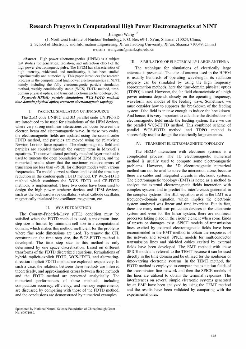
Research Progress in Computational High Power Electromagnetics at NINTJianguo Wang1,2
(1. Northwest Institute of Nuclear Technology, P. O. Box 69-1, Xi’an, Shaanxi 710024, China; 2. School of Electronic and Information Engineering, Xi’an Jiaotong University, Xi’an, Shaanxi 710049, China)
e-mail [email protected]
Abstract—High power electromagnetics (HPEM) is a subject that studies the generation, radiation, and interaction effect of the high power electromagnetic pulse. The HPEM has characteristics of high intensity, wideband, and nonlinearity, it has been studied experimentally and numerically. This paper introduces the research progress in the computational high power electromagnetics at NINT, mainly including the fully electromagnetic particle simulation method, weakly conditionally stable (WCS) FDTD method, time-domain physical optics, and transient electromagnetic topology, etc.
Keywords-HPEM; particle simulation; WCS-FDTD method; time-domain physical optics; transient electromagnetic topology
I. PARTICLE SIMULATION OF HPM SOURCE
The 2.5D code UNIPIC and 3D parallel code UNIPIC-3D are introduced to be used for simulations of the HPM devices, where very strong nonlinear interactions can occur between the electron beam and electromagnetic wave. In these two codes, the electromagnetic fields are updated using the second-order FDTD method, and particles are moved using the relativistic Newton-Lorentz force equation. The electromagnetic field and particles are coupled through the current term in Maxwell’s equations. The convolutional perfectly matched layer method is used to truncate the open boundaries of HPM devices, and the numerical results show that the maximum relative errors of truncation are less than -95 dB for different modes with various frequencies. To model curved surfaces and avoid the time step reduction in the contour-path FDTD method, CP WCS-FDTD method which combines the WCS FDTD and CP-FDTD methods, is implemented. These two codes have been used to design the high power terahertz devices and HPM devices, such as the backward wave oscillator, virtual cathode oscillator, magnetically insulated line oscillator, magnetron, etc.
II. WCS-FDTD METHOD
The Courant-Friedrich-Levy (CFL) condition must be satisfied when the FDTD method is used, a maximum time-step size is limited by minimum cell size in a computational domain, which makes this method inefficient for the problems where fine scale dimensions are used. To remove the CFL constraint on the time step size, the WCS-FDTD method is developed. The time step size in this method is only determined by one space discretization. Based on different transforms of the FDTD discretized equations, formulations of hybrid-implicit-explicit FDTD, WCS-FDTD, and alternating-direction implicit FDTD method are explored, respectively. In such a case, the relations between these methods are inferred theoretically, and approximation errors between these methods and the FDTD method are presented analytically. The numerical performances of these methods, including computation accuracy, efficiency, and memory requirements, are discussed by comparing with those of the FDTD method, and the conclusions are demonstrated by numerical examples.
III. SIMULATION OF ELECTRICALLY LARGE ANTENNA
The technique for simulations of electrically large antennas is presented. The size of antenna used in the HPEM is usually hundreds of operating wavelength, its radiation property can be simulated by using the high frequency approximation methods, here the time-domain physical optics (TDPO) is used. However, the far-field characteristic of a high power antenna depends closely on the operating frequency, waveform, and modes of the feeding wave. Sometimes, we must consider how to suppress the breakdown of the feeding system if the field is intense enough to induce the breakdown. And hence, it is very important to calculate the distributions of electromagnetic field inside the feeding system. Here we use the parallel WCS-FDTD method. This combined scheme of parallel WCS-FDTD method and TDPO method is successfully used to design the electrically large antennas.
IV. TRANSIENT ELECTROMAGNETIC TOPOLOGY
The HEMP interaction with electronic systems is a complicated process. The 3D electromagnetic numerical method is usually used to compute some electromagnetic problems. However, the 3D electromagnetic numerical method can not be used to solve the interaction alone, because there are cables and integrated circuits in electronic systems. The electromagnetic topology (EMT) is noted as a method to analyze the external electromagnetic fields interaction with complex systems and to predict the interferences generated in the complex systems. The BLT equation used in the EMT is a frequency-domain equation, which implies the electronic system analyzed was linear and time invariant. But in fact, there are many nonlinear protection devices in the electronic system and even for the linear system, there are nonlinear processes taking place in the circuit element when some kinds of upsets or damages exist. SPICE models of transmission lines excited by external electromagnetic fields have been recommended in the EMT method to obtain the responses of the network and several SPICE models for multiconductor transmission lines and shielded cables excited by external fields have been developed. The EMT method with these SPICE models is referred to the TEMT because it can be used directly in the time domain and be utilized for the nonlinear or time-varying electronic systems. In the TEMT method, the FDTD method is employed to compute the excitation fields of the transmission line network and then the SPICE models of the lines are utilized to obtain the terminal responses. The interferences on several simple electronic systems generated by an EMP have been analyzed by using the TEMT method and the results have been validated by comparing with the experimental ones.
Sponsored by National Natural Science Foundation of China through Grant No. 60971080.
148

Abstract
Keywords-component; Stochastic collocation; Morris; Sobol;Electromagnetic compatibility
(1)
149

Homogenisation of composite materials using global optimisation
Jana Jilková Dept. of Radar Technology
University of Defence Brno, Czech Republic [email protected]
Abstract— The aim of this paper is to introduce a method for creating a homogenous substitute material for composite materials using optimisation algorithms during an inversion task.
Keywords-component; composite material; homogeneous replacement; multiobjective and singleobjective optimization; inverse task;
I. INTRODUCTION
Composite materials are modern construction materials used, for example, in aircraft construction. However, numerical modelling of these materials is, due to its multi-layer structure and loss properties of each individual layer, very difficult to compute. This multi-layer structure and loss materials of the composite model are represented, in the numerical simulators, as a very fine grid, resulting in an extremely high density of cells and making the simulation time much longer and the calculation much more complex.
II. NUMERICAL MODELS AND MEASUREMENTS
A 3D simulation model was created in the CST Microwave Studio environment to discover the properties and behaviours of composite material in an electromagnetic field. This model consists of 2 layers of braided carbon fibres with a metal grid between them, and all inserted into a polymer epoxy matrix. The material’s behaviour was studied in the frequency range from 6.5 GHz to 40 GHz. Due to calculation complexity the composite material sample was spatially defined and inserted into a waveguide creating an equivalent to a numerical model. This way the calculated carrying parameters were experimentally verified by the measurements in the waveguide, an equivalent to a numerical model.
In the near future a 3D model simulation in non-defined space will be created utilising all periodical marginal conditions. This model will be used to study the non-linearity properties of composite materials in high-intensity fields. Then this non-linearity of composite materials calculated in this numerical model will be experimentally verified in an anechoic chamber using an electromagnetic impulse source.
III. INVERSE TASK
When numerically modelling tests for aircraft electromagnetic resistance to lightning, and for other high-intensity electromagnetic fields, the intension was to replace the composite material with a homogenous substitute material having equivalent behaviour to that of the composite material in an electromagnetic field. This homogenous substitute material is then represented by a much less detailed grid than the original composite, thus reducing computing time and hardware demands.
The main point of the analysed inversion task was to find a frequency flowchart for complex permittivity of this substitute material, where the transmission characteristics are the same as those of the composite material. To solve this inversion task, global optimizing algorithms in the MATLAB environment were used. When evaluating a criteria function of the optimizing algorithm, a 2D model of the substitute homogenous dielectric was produced using the Comsol Multiphysics program. Then, also using this program, the distribution of electromagnetic field was calculated for each actual value of complex permittivity calculated by MATLAB.
IV. EXPECTED RESULTS
Currently, it is possible to determine a frequency flowchart for complex permittivity of the substitute material where the electromagnetic waves hit perpendicularly. An error of the homogenous substitute calculated by optimisation in the whole range of 6.5-40 GHz is around 0.5% for all the optimisation methods. Both a single-criteria and a multi-criteria approach were used to find a homogenous substitute material. These two approaches were compared from the complexity, accuracy and time demand points of view. After a 3D model in non-defined space is created, the impact of waves hitting the composite materials non-perpendicularly can be measured. Then, after defining the parameters for non-lineal composite material, these properties will be taken into consideration for an optimising task definition when obtaining a homogenous substitute in inversion task.
150

RF Absorber Response to HPM-UWB Radar SignalsDrs. Ricky L. Moore and Robert Rice, Georgia Tech Research Institute
Signature Technology Laboratory Atlanta Georgia, 30332, USA
Abstract— This paper describes numerical studies that predict high power ultra wide band radar impact on absorber and EMI materials containing selected magnetic particulates. Such exposure may occur within the radar system or on a radiated target. Nano and micromagnetic simulations predict composite permeability time and frequency response of micro and nano scale composites. Calculations demonstrate non-linear material responses. Response magnitude is a function of pulse shape, frequency content, field strength, magnetic composition, anisotropy, magnetization, relaxation and particulate aspect ratio. Impact on reflection coefficients and absorption are shown.
Keywords- magnetic, nonlinear, ultrawideband, absorber, HPM
I. INTRODUCTION AND SUMMARY RESULTS
Advances in UWB-HPM sources and UWB apertures [1] necessitate design studies to determine HPM-UWB waveform impacts on absorbing materials that contain magnetic particulates since those may exhibit a non-linear response to the signal [2,3]. This paper reports predictions of nano-micro magnetic numerical simulations, combined with material composite models and anisotropic Cascade matrix models to predict reflection and transmission from absorbing anisotropic laminates. Predictions find that reflection may be altered from the low power expectation for selected UWB-HPM waveforms that approximate those from realized UWB radiators. Significant findings of simulations are: 1. nonlinearity is predicted for differentiated Gaussian pulses with center frequency near absorption peaks of low power magnetization spectra; 2. multi-domain particulates (multi-micron sizes) have less susceptibility than soft nm scale magnetic nano-particulates and 3. effectiveness of nano-particulate absorber materials may be impaired.
II. SIMULATIONS
Georgia Tech internal and external national institute of standards (NIST) micromagnetics codes were applied to calculate particulate time dependent magnetic moment, thus permeability as functions of shape, size, composition and UWB waveform and energy. Figure 1 shows a range of shapes.
Figure 1. Figure 1 Typical shape (micron and nanometer sizes used in simulation. Vectors indicate internal magnetic field and direction.
Micromagnetic simulation output was permeability as a function of waveform parameters and frequency. Permittivity was assumed to be constant. Bruggeman and Maxwell-Garnett Effective media models were used to calculate constitutive parameters of a theoretical composite of the particulates at various volume fractions, i.e.
1/22 2 2 2 21 2 1 2 1 2
1 1 12 1 2 1 2 1 1 2
2( 1) ( 1) ( 1) ( 1) ( 1) 2( 1 ) ;
B =B 1 ( ) ( ( )) .
Br
MGT
d B dp B dq B dp B dq B d pqd B B
p B B d B B B pd B B
where subscripts 1,2 indicate particulate and matrix in which the particulates are mixed; p, q are volume fractions of pigment and matrix; d is a function of particle shape and composite dimensionality. Cascade matrix calculations, for anisotropic materials, predicted metal and free spaced backed composite reflection and/or transmission for a given particulate, incident field, volume fraction, composite geometry and frequency. Figures 2 and 3 show reflection vs. volume fraction (0.10 – 0.50) and low power vs. HPM level fields respectively.
Figure 2. Predicted reflection at low power, PEC backed.
Figure 3. Predicted reflection at HPM power levels, PEC backed.
REFERENCES[1] W. D. Prather, et.al., IEEE Trans. EM Compat., V45, n3, Aug. 2004 [2] R.L.Moore,et.al., Radar 08 Proceedings ,2 26-30 May 2008 ,pp. 1 - 6 [3] G. Mohler, J. Appl. Phys. 93, 7456 (2003);
151

Analysis of the shielding properties of metalized nonwoven materials
A. N. Austin , J. F. Dawson , and A. C. Marvin
Department of Electronics, University of York, Heslington, York, [email protected] , [email protected] , [email protected]
Abstract—This paper considers the shielding effectiveness of metalized nonwoven materials in the 1–10 GHz range using numerical modelling and experimental techniques. A range of materials are considered with areal weights between 10 and 75 g/m², thicknesses between 50 and 400µm, and measured shielding effectiveness between 35 and 100dB. A simplified TLM model is presented and compared to experimental results.
Keywords: shielding; metallized nonwovens; high reflectivity; TLM modelling; aperture; pore; absorber box; carbon; fiber; electroplating; electrochemical; electric field; screening.
I. INTRODUCTION
There is a growing demand in the aerospace and automotive industry for lightweight composite structures that save weight, improve strength and meet enforced electromagnetic standards. The fast development of the electronics industry and deployment of wideband devices compounds this problem.
Metalized nonwoven materials are of interest because they provide optimized ways to control electromagnetic fields within a composite structure, for minimal weight and thickness gain. Adaptable reflection ( Γ ) and transmission ( τ ) coefficients mean that a range of electromagnetic applications such as frequency selective surfaces (FSS), low observability (LO) and radar absorbent materials (RAM) can be satisfied.
Figure 1. An SEM image cross section of an electroplated carbon fibre filament.
A metalized nonwoven material refers to an array of discontinuous metalized fibers that are formed into a sheet using a wet laid process. The fibers are metalized using an electrochemical process generating a 200nm coating (Figure 1).
Figure 2. An SEM image of a nonwoven material constructed of metalized carbon fibre elements.
As can be seen in Figure 2, these materials possess a complex structure with a distribution of pore shapes and sizes. The average pore size is approximately 20µm in diameter. The structure is electrically small for microwave frequencies. Measuring the shielding of samples is possible using various techniques [1,2] but predicting the performance of materials with such complex structure, and simulating them in numerical electromagnetic solvers is challenging.
We aim to present simplified structural models that allow the prediction of shielding performance of nonwoven materials along with measured data on a range of materials.
REFERENCES
[1] A. C. Marvin, L. Dawson, I. D. Flintoft & J. F. Dawson, “A Method for the Measurement of Shielding Effectiveness of Planar Samples Requiring No Sample Edge Preparation or Contact” IEEE Transactions on Electromagnetic Compatibility, 2009, 51, 255-262
[2] M. S. Sarto & A. Tamburrano, “Innovative Test Method for the Shieldi ng Effectiveness Measurement of Conductive Films in a Wide Frequency Range” IEEE Transactions on Electromagnetic Compatibility, 2006, 48, 331-341
Materials provided by Technical Fiber Products
3.6mm
7µm
152

Modeling and simulation of wire protections using a time domain FDTD code (Gorf3D)
Jean-Paul VANNEL1, Bernard PECQUEUX2, Christophe GUIFFAUT3, Jean-Pierre ADAM4, Cyril GIRAUDON5
1 : GERAC, 46500 GRAMAT, France. [email protected] : CEA, DAM, GRAMAT, F-46500 Gramat, France. [email protected]
3 : Xlim, 123 av. Albert Thomas 87060 Limoges, France. [email protected] : IEEA, 51/52 Fitzwilliam Square West, Dublin, Ireland. [email protected]
5 : Axessim, Parc d'Innovation, 67400 ILLKIRCH GRAFFENSTADEN, France. [email protected]
Abstract— A major change in the electromagnetic solver Gorf3D allows now to introduce protections or filtering circuits on wires in order to simulate their behavior in an electromagnetic environment. Two approaches are studied, one based on the technique of the state variables and the other one based on an hybridization with the circuit simulator called ngSpice.
Keywords-component: wire protections, filters, state variables, Runge-Kutta, ngspice, hybridization
I. INTRODUCTION
GORF3D is an electromagnetic code solving Maxwell's equations in the time domain by the method of finite differences using an explicit leapfrog scheme. This software is widely used for the calculation of electromagnetic environments on complex structures and has many functionalities.
Recently, a new functionality has been integrated to simulate wire protections of linear type such as RLC filters or nonlinear type such as diodes, varistors, transient suppressors or spark gaps.
The simulation of these protections is made with two distinct approaches: one using the technique of the state variables with a resolution based on the Runge-Kutta method, the other one using an hybridization of Gorf3D with the circuit simulator ngSpice.
The results of the simulations for various devices in various configurations are presented and compared to theoretical models or to experimental results.
II. MODELING
A. Approach by the technique of the state variables
This technique is based on the decomposition of circuits in branches that reduces the number of unknowns by calculating the currents through inductors and the voltages across capacitors. It requires however a preparation of the matrixes of calculation that is difficult to automate. The resolution is then performed using the Runge-Kutta methods RK4 and RK5 type according to whether the system is linear or not.
The final paper will present this approach in detail.
B. Approach by hybridization with ngSpice
ngSpice is a circuit simulator widely recognized and used throughout the world. A strong hybridization has been
performed with Gorf3D. Using ngSpice at each time iteration of Gorf3D, this hybridization allows to calculate the evolution of the circuits connected to the wires described as input data for Gorf3D.
This approach allows to take into account more flexible and complex circuits than the previous method. This will be detailed in the final paper.
III. IMPLEMENTATION IN GORF3D
The solving methods Runge-Kutta RK4 and RK5 have been coded and implemented in GORF3D.
The technique of the state variables requires the complete description of the circuits in the body of the program. Linear filters and nonlinear protections have thus been coded and implemented in Gorf3D.
Examples will be provided in the final version of this paper.
The hybridization with ngSpice is less intrusive in the code, but required the development of tools for the exchanges between the two solvers. These tools are based on the library of functions called MPI (Message Passing Interface). The final paper will present the main features.
IV. SIMULATION AND VALIDATION OF THE NEW
FUNCTIONALITY
Many examples of simulation will be presented and compared between them, or with theoretical calculations or experimental results.
REFERENCES
The final paper will appeal to many references which will be detailed.
153
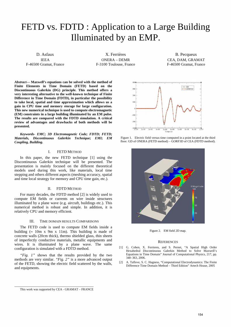
FETD vs. FDTD : Application to a Large Building Illuminated by an EMP.
D. Asfaux IEEA
F-46500 Gramat, France
X. Ferrières ONERA – DEMR
F-3100 Toulouse, France
B. Pecqueux CEA, DAM, GRAMAT F-46500 Gramat, France
Abstract— Maxwell’s equations can be solved with the method of Finite Elements in Time Domain (FETD) based on the Discontinuous Galerkin (DG) principle. This method offers a very interesting alternative to the well-known technique of Finite Difference in Time Domain (FDTD), in particular the possibility to take local, spatial and time approximation which allows us a gain in CPU time and memory storage for large configuration. This new numerical technique is used to compute electromagnetic (EM) constraints in a large building illuminated by an EM pulse. The results are compared with the FDTD simulation. A critical review of advantages and drawbacks of both methods will be presented.
Keywords- EMC; 3D Electromagnetic Code; FDTD; FETD; Materials, Discontinuous Galerkin Technique; EMI; EM Coupling, Building.
I. FETD METHOD
In this paper, the new FETD technique [1] using the Discontinuous Galerkin technique will be presented. The presentation is mainly focused on the different theoretical models used during this work, like materials, local time stepping and others different aspects (meshing accuracy, spatial and time local strategy for memory and CPU time gain, etc.).
II. FDTD METHOD
For many decades, the FDTD method [2] is widely used to compute EM fields or currents on wire inside structures illuminated by a plane wave (e.g. aircraft, buildings etc.). This numerical method is robust and simple. In addition, it is relatively CPU and memory efficient.
III. TIME DOMAIN RESULTS COMPARISONS
The FETD code is used to compute EM fields inside a building (≈ 10m x 9m x 11m). This building is made of concrete walls (20cm thick), thermo shielded glass, thin sheets of imperfectly conductive materials, metallic equipments and wires. It is illuminated by a plane wave. The same configuration is simulated with a FDTD method.
“Fig. 1” shows that the results provided by the two methods are very similar. “Fig. 2” is a more advanced output of the FETD, showing the electric field scattered by the walls, and equipments.
Figure 1. Electric field versus time computed in a point located at the third floor. GD of ONERA (FETD method) – GORF3D of CEA (FDTD method).
Figure 2. EM field 2D map.
REFERENCES
[1] G. Cohen, X. Ferrieres, and S. Pernet, “A Spatial High Order Hexahedral Discontinuous Galerkin Method to Solve Maxwell’s Equations in Time Domain” Journal of Computational Physics, 217, pp. 340–363, 2006.
[2] A. Taflove, S. C. Hagness, “Computational Electrodynamics: The Finite Difference Time Domain Method – Third Edition” Artech House, 2005
This work was supported by CEA - GRAMAT – FRANCE
154

A novel orthogonal mesh generation algorithm
based on polar angle judgment
Ying Li Min Zhou Yuhai Gao Jianshu Luo College of Science
National University of Defense Technology Changsha, Hunan 410073, China
E-mail: [email protected]
Abstract— In this paper, we present the orthogonal mesh generation algorithm based on polar angle judgment. This algorithm cuts the object of characteristic of electromagnetic scattering into a set of star polygons (polyhedrons) and judge the polar angle range of mesh central point of each star polygon (polyhedron). Thus based on the judgment of the mesh central point, the inner meshes are remained to generate the orthogonal meshes. This algorithm avoids the problem of singularity in the Kalay orthogonal mesh generation algorithm and outweighs Kalay's algorithm in computing complexity.
Keywords- polar angle; FDTD; orthogonal mesh generation algorithm; star polygon
I. INTRODUCTION
FDTD usually use Yee cell to discrete the object. Due to the geometrical characteristic of Yee cell, the minimum simulation scale of difference format of FDTD is a mesh, and thus it needs to use laddered approximation to simulate. Kalay orthogonal mesh generation algorithm [1] is the usual algorithm for laddered simulation, yet with the problem of singularity which will lead to deviation of laddered simulation for mis-judgment of mesh-point.
II. ORTHOGONAL MESH GENERATION ALGORITHM BASED
ON POLAR ANGLE JUDGMENT
A. Basic Theorems and Basic Idea
This paper prove three important theorems as follows. Theorem A: Any polygon can be cut into a set of convex
polygons. Theorem B: Any polygon can be cut into a set of star
polygons. Theorem C: Any polyhedron can be cut into a set of
convex polyhedrons or star polyhedrons. Basic idea of our algorithm: Cut the object into a set of
star polygons at first. Subdivide every star polygon into a set of meshes, respectively. If the mesh central point that is judged by our method is inside the mesh, choose the mesh as a part of laddered approximation of the object, namely, as a generation mesh. Otherwise, abandon the mesh.
B. The Computing Complexity of New Algorithm
For a star figure with N sides, use dichotomy to judge the range of polar angle of mesh central point. Therefore, the computing complexity of the judgment of the position of mesh central point is O(logN). Due to K meshes needs to be judged, the total computing complexity is O( ) O(log )K N× .
III. NUMERICAL SIMULATION
Suppose the coordinate of central point of pentagram is (1,1), the circumcircle of the pentagram is unit circle, and the size of mesh subdivision is 0.02 0.02× . The range of the
pyramid is[ ] [ ] [ ]0, 2 0, 2 0, 2× × , the size of mesh subdivision is
0.02 0.02 0.02× × .The results of mesh subdivision by using our algorithm are shown in Fig. 1.
Figure 1. The laddered Approximations of the pentagram and the pyramid
IV. CONCLUSION
For a star polygon with N sides, the computing time of judging the position of K points is O( ) O( )K N× in Kalay’s
algorithm and O( ) O(log )K N× in our algorithm. From the
comparison between the two algorithms, dealing with multi-mesh problems, we can obtain a conclusion that orthogonal mesh generation algorithm based on polar angle judgment is more advantageous on avoiding singularity and computing complexity.
REFERENCES
[1] Y.E.Kalay, “Determining the spatial containment of a point in general polyhedron,” Computer Graphics and Image Processing, vol. 19, pp. 303–334, 1982.
This work is supported by the National Natural Science Foundation of China. (61171018)
155

SAR Computation of the Human Body in a Metallic Cylindrical Cabin Using a Novel Dielectric
Conformal FDTD Method
Ling-Yu Kong, Jian Wang Key Lab of Ministry of Education for Design and EMC of
High-Speed Electronic Systems, Shanghai Jiao Tong University
Shanghai 200240, China
Wen-Yan Yin Center for Optical and EM Research
Zhejiang University, Hangzhou 310058, China E-mail: [email protected]
Abstract—Specific absorption rate (SAR) distribution over the human body model in one metallic cylindrical cabin is computed using an improved dielectric conformal finite-difference time-domain (FDTD) method. Such a cabin, having a window and a door, is illuminated by an intentional electromagnetic pulse (IEMP) with high power. Hybrid effects of the incident IEMP waveform and geometrical parameters of the cabin on the SAR distribution of the human body model are examined in detail.
Keywords-Conformal FDTD, IEMP, human body model, SAR
I. INTRODUCTION
It is known that conformal FDTD method can be used for handling various objects with arbitrary geometries, such as human body model, etc. In this paper, we want to develop an improved dielectric conformal FDTD method to compute the SAR calculation of a human body model in a large metallic cylindrical cabin with one window and one door, and it is illuminated by an intentional EMP (IEMP) with an arbitrary waveform.
II. OUTLINE OF NUBERICAL METHOD
We treat the FDTD cells on the curved object surface using magnetic grids instead of electric ones as adopted in the PEC conformal FDTD ones. The conformal mesh face is shown in Fig. 1(a), where S(1) is the area of Medium 1, 1, 1 and 0,
0 are the permittivities and the conductivities of Medium 1 and free space, respectively. Fig. 1(b) shows the face of modified mesh in Fig. 1(a), and the variable S denotes its area. Therefore, both effective permittivity x
eff and conductivity xeff
at (i+1/2, j, k) are obtained by the weighted area, i.e.(1) (1)
1 01/ 2, , 1/ 2, , 1/ 2, , /effx i j k S i j k S S i j k S (1)
(1) (1)1 01/ 2, , 1/ 2, , 1/ 2, , /eff
x i j k S i j k S S i j k S (2)
When the cells are in the conformal mesh, we compute xin the SAR formula as follows:
11/ 2, 1/ 2, 1/ 2 = ( 1/ 2, , ) ( 1/ 2, , ) ( 1/ 2, 1, ) ( 1/ 2, 1, )eff effx x x
x
i j k i j k B i j k i j k B i j kN
( 1/ 2, , 1) ( 1/ 2, , 1) ( 1/ 2, 1, 1) ( 1/ 2, 1, 1)eff effx xi j k B i j k i j k B i j k (3)
where Nx is the number of edges totally or partly in Medium 1 in the x-direction. When the edge is totally or partly in Medium 1, B= 1, and otherwise, it is zero. Similarly, y, z , Ex, Ey andEz of conformal meshes can be computed numerically.
Figure 1. (a) Conformal mesh with Medium 1 and free space, and (b) modified mesh with effective permittivity and conductivity.
III. APPLICATION FOR HUMAN BODY MODEL
We compute the SAR distribution of the human body model in a metallic cylinder cabin illuminated by an IEMP with the amplitude of 200 V/m. As shown in Fig. 2, the cabin has a window and a door. The model is filled with the human tissue liquid, characterized by relative permittivity r =45.3 conductivity =0.87 S/m [1], and mass density =1000 kg/m3.The IEMP illuminates from the –x-direction. Fig. 2(b) shows the 10g SAR distribution of the model at f=300MHz. It is observed that the right leg absorbs more EM energy than the other part of the body.
Figure 1. (a) Geometry of the cabin with one body model in it (b) Distributions of 10g SAR at f = 300 MHz over the body model.
REFERENCES
[1] CENELEC, EN 50383, Basic standard for the calculation and measurement of electromagnetic field strength and SAR related to human exposure from radio base stations and fixed terminal stations for wireless telecommunication systems(110MHz-40GHz), 2002.
156

Abstract
Keyword : ACA, antenna, cable, cavity, coupling
3e+008 4e+008 5e+008 6e+008 7e+008 8e+008 9e+008 1e+009
-100
-90
-80
-70
-60
-50
-40
-30
-20
-10
0
Freq. (Hz)
|S21
| (dB
)
Mesures
Capitole-EM
157

Fast computation of the main resonances occuring within an aircraft irradiated by HPEM field
S. LEMAN1-A.REINEIX2-M.MAHMOUDI1-Y.POIRE1-F.HOEPPE1–B.DEMOULIN3
1Nexio, 16 rue Troyon 92316 Sèvres – [email protected], 123 avenue Albert Thomas 87060 Limoges – [email protected]
3USTL – TELICE, Bâtiment P3 F-59655 Villeneuve d'Ascq - [email protected]
Abstract: In this paper is proposed a numerical tool to calculate very fastly the first resonance of an arbitrary shaped section structure as an aircraft irradiated by a High Power Electromagnetic field. From the geometrical parameters of the aircraft mock-up, the proposed tool is able to return the EM field mapping section and the first resonance of the structure in few seconds. The tool consists in a combination between analytical expressions due to the transmission line theory, and full wave computation using the FDFD method. This technique can be extended to the EM coupling calculation between a transmitter and a receiver installed inside the fuselage in reducing the problem with use of the Kron’s electrical circuit formulation. Comparisons between measurements and calculations have been performed and show a good correlation.
I. INTRODUCTION
Early in the design phase, investigations are needed especially concerning HPEM irradiation. During this phase, EMC engineers have to estimate electromagnetic constraints such as the first resonance of a structure very quickly. The hybrid numerical method proposed in this paper is based on the expressions of EM fields in a cavity expressed by the combination of a transverse component and a longitudinal component associated with progressive and retrograde wave in the z direction of increasing and decreasing.
−=
−=−
−
)).(,(),,(
)).(,(),,(zjzj
zjzj
eeyxHzyxH
eeyxEzyxEββ
ββ
(1)
In this way, the analysis of the cavity illustrated in figures 1 and 2 can be split into two parts: a modal analysis of a section of the cavity in the transverse Oxy plane with dimensions a=47cm and b=30cm, and propagation along the 0z axis of this section by an analogy with transmission lines. We choose the largest dimension d=150cm cavity length for the lines.
II. 2D FDFD METHOD
The 2D arbitrary shape cavity is modeled by a FDFDmethod. This numerical method needs some computation time and memory storage but for arbitrary geometry section, it will be the best adapted tool. FDFD method uses the discretization of the Helmholtz equations which E and H fields and wave number kci are the solutions. These solutions are separated into two types: TE and TM propagation modes. The total EM field distribution inside the cavity may be expressed as a linear sum of the individual basis TE and TM modes.
III. ESTIMATE OF THE FIRST RESONANCE
The first TE (p=1) and TM (p=0) resonances frequencies are obtained immediately by taking into account the third dimension d:
22__0 )()(
2 d
pk
vF TEciTE
ππ
+= 22__0 )()(
2 d
pk
vF TMciTM
ππ
+= (2)
We obtain respectively the TE and TM main resonances F0_TE=379MHz and F0_TM=649MHz attached to the following TE and TM field mapping presented in figure 1 with a computation time of 2s.
Figure 1. TE and TM Electric field mapping (Ey)
Figure 2. Aircraft Mockup (ASEAD Project)
Using Kron’s electrical circuit representation, the study can be extended to the EM coupling analysis between two antennas installed inside the mockup. Figure 3 depicted the comparison between measurements in red and calculation in blue of the coupling between two antennas in the cavity. Note that the two first resonance F0_TE and F0_TM are exciting by the two antennas. For this case, the computation time is 7 minutes.
Figure 3. S21 parameters between two antennas in aircraft mockup
REFERENCES
S. Leman, B.Démoulin, O.Maurice, M.Cauterman, P. Hoffman, "Use of the circuit approach to solve large EMC problems”, CRAS Physique10 (2009) pp.70-82, doi:10.1016/j.crhy.2009.01.006
158

Finite element method used to characterise surface modes in Electromagnetic Band Gap structures
Romain Garnier, André Barka ONERA, Department of Electromagnetic and Radar
Toulouse, France [email protected] , [email protected]
Olivier Pascal Laboratoire LAPLACE, université Paul Sabatier
Toulouse, [email protected]
Abstract—We present here an explanation and a characterization of surface modes which can be observed at the interfaces of two different media such as infinite dielectric rods and the air. To do this we will employ finite element method.
Key words: Surface modes, EBG structures, finite elment method
I. INTRODUCTION
Plane wave method and super-cell[1] are used to characterize modes which are located at the interface of two media which are an EBG and the air. We call it surface modes. As the domain of resolution is big in general these techniques can quickly becoming time and memory consuming . We propose a way to use Finite element method combine with eigenmode solver in order to extract surface modes. We will first treat the case of infinite dielectric rods to extend it to other EBG structures such as High Impedance Surfaces.
II. APPROACH AND PROCESS
A. About the modelisation
The electric field E can be expressed as a linear combination of zero order Nedelec function. By calling X the coordinates of E in the subspace generated by these basis functions, by applying Galerkine we will obtain the linear system: XMkAX 2
0 . Where A and M are finite element matrices modified by master-slave conditions[2] :
. Where and MS F
jF EeE
SFE FmE are the field located respectively on the Slave(Master) interface and is the phase shift between these two interfaces. As the matrices are sparse, we must find a way to optimise the time and memory optimisation. First we have to stock the matrices in the Compressed Sparse Row format[3] . Then by using a direct sparse solver PARDISO and the library ARPACK we can obtain a low memory and time cost by comparison with the plane wave method .
B. Extraction of the surface modes We are dealing with 3 dimensional periodic structure
defined by one basic cell with 2 direction of periodicity(OX,OY) The technique of super-cells[1] consist in
introducing a defect into a periodic structure which comport more than one basic cell (Fig.1) :
Figure 1. Super-cell with 2 basic cells and a surface defect
Then the analysis of the projected band diagram in the OY direction allow to recognize surface modes:
Figure 2. Projeted band diagram of the basic cell into the OY direction.
Figure 3. Re(Ez) , x=0 and y= 7 /8
The red line (Fig.2) represent the light cone. The yellow zone (Fig.2) correspond to the solutions which cannot be propagated into the air and into EBG structure. Surface mode are located into this area. In Fig.3 you can see the field Re(Ez) for given phase shifts ( x, y). In the final presentation we will show how to characterize surface modes in general by taking a complicated example to deal with: High Impedance Surfaces.
REFERENCES
[1] J. D. Joannopoulos, S. G. Johnson, J. N. Winn, R. D. Meade, Photonic cristal book molding the flow of light, pp. 87–92 (2007). [2] C. Mias, J. P. Webb, R. L. Ferrari, Finite element modelling of electromagnetic waves in doubly and triply periodic structures, IEE (1999).[3] R. E. Bank, C. C. Douglas, Sparse matrix multiplication package (2003).
159

A Novel Dispersive Numerical Approach for FastAnalysis of Asymmetric Coplanar Waveguide
A. Khodja, R. TouhamiFEI, U.S.T.H.B, Algiers, Algeria
M.C.E. YagoubEECS, Ottawa U., Ottawa, Canada
H. BaudrandENSEEIHT, Toulouse, France
Abstract
Keywords- dispersion; trial functions; quasi-symmetric model
I. INTRODUCTION
CPW are widely used in MMIC's [1]. Compared tosymmetric structures, asymmetric coplanar ones (Fig. 1) arevery attractive because of their easy matching and circuitdesign flexibility. To efficiently design them, an efficientquasi-symmetric CPW approach is proposed. It uses a modaltechnique in conjunction with an adequate choice of trialfunctions to determine the propagation characteristics.
o
o
o
Figure 1. Cross sectional view of general asymmetric CPW
II. METHODOLOGY
By properly selecting the trial functions for C and modes,an efficient quasi-symmetric approach was developed. It tookthe magnitudes of trial functions of the asymmetric caseexpressed on the second half of the considered asymmetricCPW in terms of that expressed on the first half [3].
This quasi-symmetric approach leads, via the Galerkin'stechnique, to a smaller-size dispersion matrix and thus, reducesthe CPU effort required to fully characterizing asymmetriccoplanar structures. A comparative study of the propagationcharacteristics demonstrated the efficiency of the proposedquasi-symmetric model.
III. NUMERICAL RESULTS
Let us represent the evolution of effective permittivity byusing sinusoidal trial functions taking into account the metallicedge effects (where the convergence was achieved withoutexceeding six trial functions per component). Figure 2 showsclearly that for identical widths of slots (d1=d2), theasymmetric CPW behaves as quasi-symmetric one. In
addition, for any C-mode width ratio (d2/d1), the asymmetricstructure has the same propagation properties as quasi-symmetric one, contrarily to the mode where the quasi-symmetric model is less valid [2], because the mode isaffected by the shielding or slots.
0.0 0.3 0.6 0.9 1.2 1.5 1.8 2.1 2.4 2.7 3.0
0.5
0.6
0.7
0.8
0.9
1.0
1.1
1.2
1.3
1.4
1.5
1.6
1.7
1.8
1.9
2.0
2.1
(w=0.2mm, d1=d2=0.1mm) (C1=0.5mm, d1=d2=0.1mm)(a=3.556mm, b2=0.125mm, f=33GHz, r=2.2)
0 1 2 3 4 5 6
0.4
0.5
0.6
0.7
0.8
0.9
1.0
1.1
1.2
1.3
1.4
1.5
1.6
1.7
1.8
1.9
2.0
26 28 30 32 34 36 38 40
0.80
0.85
0.90
0.95
1.00
1.05
1.10
(a=3.556mm, b2=0.125mm,C1=0.1mm, w=0.2mm, d1=0.1mm,
f=33GHz, r=2.2)
(a=3.556mm, b1=3.556mm,b2=0.127mm, b3=3.429mm,
d1=0.1mm, d2=0.3mm,w=0.2mm,C1=1.578mm, r=2.22)
Figure 2. Dispersion parameters versus physical and electrical parameters
REFERENCES
[1] T. Kitazawa and T. Itoh, "asymmetrical coplanar waveguide with finitemetallization thickness containing anisotropic media", IEEE Trans.Microwave Theory Tech., vol. 39, pp. 1427-1432, 1991.
[2] A. Biswas and V.K. Tripathi, "Analysis and design of asymmetric andmultiple coupled finline couplers and filters", IEEE MTT-S Symp., pp.403-406, 1990.
[3] A. Khodja, R. Touhami, M.C.E. Yagoub and H. Baudrand, "Full-wavemodal analysis of asymmetric coupled lines using the quasi-symmetricapproach", Mediterranean Microwave Symp., Hammamet, Tunisia, 2011.
160

Analysis of Open TEM-Waveguide StructuresEffects of Simplification by Using Wire Models
Ronald Rambousky Bundeswehr Research Institute for
Protective Technologies and NBC Protection Munster, Germany
Heyno Garbe Institut für Grundlagen der Elektrotechnik und Messtechnik
Leibniz-Universität Hannover Hannover, Germany
Abstract— This paper belongs to a research project to describe the field of open TEM-waveguides in terms of TEM-mode and higher order modes. Therefore this paper shows the calculation of the electromagnetic field in the test volume of an open TEM-waveguide to investigate the deviation from the pure TEM-mode propagation. In preparation to describe an open TEM-waveguide in Transmission Line Super-Theory, the resonance structure of the electromagnetic field is analyzed by MoM computer simulations for different levels of simplification going from planar conductors to a wire like structure.
I. INTRODUCTION
TEM-waveguides are widely used in EMC testing as a convenient alternative to OATS. Because of the generation of higher order TE- and TM-modes, closed TEM-waveguides are generally restricted in frequency range. Therefore in qualification testing of equipment in fast transient environments, as for example NEMP or UWB, open TEM-waveguide structures are used. While the higher order modes had been described analytically in the past [1], there is currently no satisfying (semi-)analytical description of the resonance effects in open TEM-waveguides.
II. OPEN TEM-WAVEGUIDE
A. Resonance effects in closed and open TEM-waveguides
The closed GTEM-cell (EMCO 5320) was transferred to an open one by cutting the sidewalls. Measurements and Method of Moments (MoM) simulations of the electromagnetic field in the test volume were done with a short-cut septum and without absorbers at the end of the cell for the closed and open version. It could be shown, that in the frequency range up to 1 GHz the resonance effects in the open system are lower by orders of magnitude compared to the closed system. But there are still characteristic deviations from a pure TEM-mode propagation.
B. Using wire models to represent the TEM-waveguide
One possible way to describe the electromagnetic field behavior in open TEM-waveguides is the use of the Transmission-Line Super Theory (TLST) [2], because it encompasses the full Maxwell’s equations and therefore takes into account all field modes and radiation losses. To use the
“Thin Wire Approximation” for practical reasons it is necessary to simplify the TEM-waveguide to a wire structure.
In MoM computer simulations the resulting H- and E-fields at representative positions in the test volume of the TEM-waveguide were investigated for different levels of simplification of the geometrical model (see Fig. 1).
Figure 1. Open TEM-waveguide (left), 9-wire-model (middle) and simulated (MoM) transversal H-field (right)
Fig. 2 shows the MoM simulation results of the transversal magnetic field component, Hx, of the different simplification levels of the open TEM-waveguide. It is clearly shown that the characteristic resonant behavior of the open TEM-waveguide can be produced using a simple 9-wire model. This also indicates that there are only minor cross currents on the septum plane and that the resonance structure of the open TEM-waveguide is mainly due to radiation losses caused by the missing conducting side walls.
Figure 2. Transversal magnetic field component for the different simplification levels of the open TEM-waveguide (MoM simulations)
REFERENCES
[1] M. Koch, “Analytische Feldberechnung in TEM-Zellen”, Dissertation, Universität Hannover, 1998
[2] J. Nitsch, F. Gronwald, and G. Wollenberg, „Radiating Nonuniform Transmission-Line Systems and the Partial Element Equivalent Circuit Method, J. Wiley & Sons Ltd., 2009
161

¶! ""#$¶% &¶'% ' (! ¶ )#*
¶') ! '+) !,$ ,$
@
'' '( # ( -'-# #' '( '-##!#!' ( ! .# ( % ' ' ( ! +$ ' ! ' / ) ! ! ' / 0+$ ( ! 12034 5 ' ' # ' + ''+' +'''(-1 4+' '' '##' '( '
% ' ' 6 ' (!1'(' #+ ( 4 ' + ' '#$ ' ' ( + #7 ' - ! ' ! # #' ' +''!# ! ( '$ '6 8 5 ' '
'5' #! + ' # - #' '/ 0+$( ! +''' ( ' ' ( ' $ - ' ( '+ '+ (9"6"': ' 6' +'(
'+65 #- ! !! ' 6 ' '0-# ''
' + - +' # ! ; ' / +'' ! '#' + 0 #' (! ' $ + +6 # ' 6 ( #
/ ' ( 6 !6 ' ' 6<6# !
'( #!'(' $ + !6 ( ( 2!0 '#7 '- !' # '
'+5 ! ' ('' $ !5 ! + -! (' 1 /( 4 % (''('' ' 203 / - $ ! 6 #! -#
4 #4 1' 4
/( "6"' (' =# =2>6 #-'( 1?@@;*3 ?" (6# 4
' "6"' + ! -# ' ''(203 6 % + ! '' -
'' ('+' + '- '"6"'#!
162

Keywords unintentional radiators; equivalent dipoles; 3D near-field scanning.
163

HF Coupling to an Electrically Small Antenna inside a Cylindrical Cavity
Sergey Tkachenko and Jürgen Nitsch Institute for Fundamental Electrical Engineering and EMC
Otto – von – Guericke University Magdeburg Magdeburg, Germany
Ronald Rambousky Bundeswehr Research Institute for Protective Technologies
and NBC Protection (WIS) Munster, Germany
Abstract— In this paper we outline our research of high – frequency electromagnetic field coupling to small antennae in cylindrical resonators. This problem has many practical applications in EMC, e.g., for electronic equipment in aircraft or other aerial vehicles.
Keywords: small antenna, cylindrical resonator, high-frequency coupling
I. INTRODUCTION
Investigation of the coupling of high-frequency electromagnetic fields caused by intentional electromagnetic excitations to linear structures becomes an actual topic. Usually the corresponding EMC experiments and engineering simulation models are applied to devices in free space. However, in reality, electronic equipment is placed in different kinds of resonator-like shells: cabinets of computers, aircraft fuselages, frames of cars, etc. These enclosures change the interaction of electromagnetic fields with scatterers remarkably due to re-reflections of electromagnetic fields inside the resonator.
It was shown in many experiments and simulations that the main mechanism of such interaction in free space is electromagnetic coupling to interconnectors of different scales. Often these interconnectors are electrically small (printed circuit boards, chips, etc.). Currents and voltages induced in such objects in free space can be evaluated by a method including two simple models: a model of a small linear antenna to describe the common mode and a model of a small loop to describe the differential mode.
In our papers [1-2] we proposed a method to analyze the coupling of an electrically small dipole (monopole) antenna in a resonator (Method of Small Antenna, MSA) by consequently using the scattering theory. This approach gives a possibility to analytically express the solution for the scattered current in small antenna inside the resonator from the free space solution and the regularized cavity Green’s function.
The developed MSA method gives also the possibility to obtain values of interest in the coupling problem: the transfer function “external field -> induced current”, the input impedance of the small antenna, the current transfer ratio for two small antennas, etc.
II. DESCRIPTION OF OBTAINED RESULTS
The method of small antenna could be also applied for the case of electromagnetic field coupling with small near dipole antenna in cylindrical resonator [3]. This geometry is important, for example, for EMC analysis of antennae and wiring in an aircraft. As in the general case, the length dependence of the antenna current coincides with the one in free space, however, with a factor which contains the scattering amplitude for the small antenna in free space (antennas polarisability) and the regularized Green’s function of the cylindrical resonator. To obtain the Green’s function in explicit form as a sum of a singular (free space-like) and a regular part we have used the Green’s function in Lorenz gauge instead of the dyad Green’s function of the cylindrical resonator in Coulomb gauge, which is often used in literature. Also a hybrid reflection (for the z-direction) – modal (for transversal direction) representation of the Green’s function was used. After the regularized Green’s function of the cylindrical resonator is found, all formulae of the MSA for the transfer function, input impedance, current transfer ratio, etc. can be obtained.
To check the developed theory we carried out numerical simulations. We considered a plane wave EM field coupling into a long cylinder (L~6d) which has a small circular aperture in the front surface and contains a small monopole antenna. The experimentally obtained frequency dependences for the transfer function were compared with theoretical results and results of numerical simulation and yielded a good agreement.
References[1] S. Tkachenko, F. Gronwald, H.-G. Kauthäuser, J. Nitsch, “High-
frequency electromagnetic coupling to small antennas in rectangular resonator”, Int. Conf. Electromagn. Adv. Appl. (ICEAA), 15-19 Sept. 2009, pp.74-78.
[2] S. Tkachenko, J. Nitsch, M. Al-Hamid, „Hochfrequente Feldeinkopplung in kleine Streuer innerhalb eines rechtwinkligen Resonators“, Int. Kong. EMV 2010, 09.-11. März 2010 Düsseldorf“, pp.121-128.
[3] S. Tkachenko, J. Nitsch, F.Sonnemann, H.-J.Sheibe, M.Magdowski, and R.Vick, “High Frequency Electromagnetic Field Coupling to Small Antennas in a Cylindrical Resonator”, Int. Conf. Electromagn. Adv. Appl., Sept. 12-16, 2011, Torino, Italy, pp. 1056-1057.
164

Receiving Antennas Analyzed with FDTD and the Theorem of Reciprocity
J.-P. Adam IEEA, Courbevoie, France [email protected]
J.-M. Lopez, B. Pecqueux, P. Viars CEA, Gramat, France
Abstract— By using the theorem of reciprocity, the equivalent circuit of a receiving antenna illuminated by plane waves is deduced from a single FDTD simulation. This circuit is used to analyze the antenna’s temporal response to an arbitrary incident plane wave, when connected to an arbitrary load.
Keywords : receiving antenna ; reciprocity ; FDTD
I. FDTD SIMULATION OF A TRANSMITTING ANTENNA
The presented work is based on the Gorf3D software (Ref. [2]). However it may be easily extended to any software able to simulate the radiation of an antenna. Gorf3D is a general purpose FDTD (Finite Differences in Time Domain) tool. Two of its features make it particularly well suited for antenna analysis : a voltage source to feed the radiating structure and a near field to far field transformation to compute the radiation of the antenna.
II. RECEIVING BEHAVIOUR DEDUCED BY RECIPROCITY
The reciprocity theorem is a powerful tool in electromagnetism. For example, it links the short circuit current of an antenna illuminated by a plane wave to the far field radiated by the same antenna when it is transmitting (Ref. [1]). The short circuit current is the first part of the Norton equivalent circuit of the receiving antenna (Fig. 1). The second part is the input impedance. This impedance is easily derived from the simulation of the radiating antenna.
Zin Isc
A
B
A
B
Figure 1. Receiving antenna Norton equivalent circuit. Zin is the antenna input impedance. Isc is its short circuit current and depends on the direction of
incidence of the plane wave
In addition, since FDTD is a time domain method, both parameters of the equivalent circuit can be computed over a large frequency spectrum. In other words, a single FDTD run simulating an antenna radiating in many directions provides all the information required to predict the behavior of the antenna
when illuminated by plane waves coming from those directions.
III. GRAPHICAL USER INTERFACE
In order to use the full flexibility of the receiving antenna equivalent circuit, a graphical user interface has been developed. First, it is a diagnostic tool visualizing the input impedance and the radiation characteristics of the antenna. Second, it allows the user to define the direction of incidence, the polarization and the waveform of the incoming plane wave. The user can also set the load of the antenna. Third, it applies the reciprocity theorem and presents the current flowing through the load in both frequency and time domains.
Fig. 2 is a snapshot of the user interface. Note that in this example, what is called “antenna” is in fact a more complex structure including the radiating element, a feeding cable, a building and a ground plane.
Figure 2. Example of results presented by the tool, including a 3D visualization showing the influence of the direction of incidence.
REFERENCES
[1] J.-P. Adam, J.-C. Joly, B. Pecqueux, D. Asfaux, “The reciprocity theorem applied to finding the best coupling incidence”, C. R. Physique 10, pp. 65–69, 2009.
[2] L. Morel, B. Pecqueux, R. Vézinet, ”Notice d’installation et d’utilisation de la version exportable du code GORF3D”, Note interne CEG I94-28, October 1994.
This work was funded by a CEA-Gramat contract
165

Intentionally blank
166

Fast-Transient Susceptibility of Printed Circuit Boards Including Non Linear Elements
François Torrès, Christophe Guiffaut and Alain Reineix OSA Department
XLIM Institute, UMR 6172 CNRS - University of Limoges Limoges, France
Abstract—This paper presents a time-domain approach to address the fast-transient susceptibility of printed circuit boards (PCBs) including non linear elements. The modeling of the boards is performed using a multiconductor transmission lines formalism, and the non linear loads are taken into account using a new SPICE-compatible generic diode model with special emphasis on non linear capacitance and recovery phenomena.
Keywords-Diodes; Fast Transients; PCB; SPICE; Susceptibility; Transmission Lines
I. INTRODUCTION
The analysis of susceptibility to fast transient pulses of electronic boards including non linear devices involves the simultaneous time-domain modeling of both the PCBs and the components [1]. Thus, this paper presents a time-domain methodology combining a transmission-line approach for the PCBs and a state-variable formulation for the non linear loads.
II. MODELING METHODOLOGY
Printed circuit boards are modeled using a multiconductor transmission lines (MTL) formalism in time-domain, which can handle conducted perturbations and incident fields as well. The board is decomposed into sets of coupled parallel transmission lines, of which the crosstalk parameters are extracted using a free-space Green’s function along with electric charges on conductors and polarization charges at dielectric interfaces [2]. Finally, the telegraphers’ equations are solved using the finite-difference time-domain (FDTD) method. Every possible configuration can be treated: buried traces, lossy lines and substrates, multilayer PCBs, etc…, and board layout can be extracted for design files, such as Gerber.
Non linear loads are taken into account using a newly-developed model for diode-like elements [3], which has proven to be generic enough to represent discrete protection elements and complex on-chip ESD protection devices as well. It improves the standard SPICE diode model by introducing a realistic junction capacitance formulation and a physical modeling of the forward and reverse recovery phenomena. This model is implemented using a state-variable formulation as in [1], and thus can be directly used with the MTL description of the boards. The state-variable equations are automatically built from the circuit description of each termination network, and thus linear and non linear loads can easily be taken into
account. The equations for the terminations are solved using a fifth-order Runge-Kutta algorithm with adaptative step-size.
III. RESULTS
Several test PCBs have been designed to validate the formalisms. The example presented here (Fig. 1) is composed of a 50 excitation line, fed with a high-voltage fast pulse (40V, 500ps rise time, 20ns duration). A victim trace runs close to the excitation line and is protected by a grounded guard trace. The victim line terminated at one end by the input of a logic integrated circuit (IC), of which ESD protection circuit has been characterized and modeled using our formalism [3].
Figure 1. Test PCB used for validation
-2
-1
0
1
2
3
4
0 5 10 15 20 25 30 35 40 45
Vol
tage
(V)
Time (ns)
MeasurementsSimulation
ESD Protection Effect
Figure 2. Measured and simulated voltages at point “A”
Fig. 2 compares the measured and simulated voltages at the IC’s input. The clamping effect of the ESD protection can be seen on the negative pulse, and the good agreement between curves validates the ability of this time-domain approach to model PCBs with complex trace terminations.
REFERENCES
[1] A. Orlandi and C.R. Paul, “FDTD Analysis of Lossy, Multiconductor Transmission Lines Terminated in Arbitrary Loads,” IEEE Trans. Electromag. Compat., vol. 38, pp. 388-399, Aug. 1996
[2] C. Wei, R. Harrington, J. Mautz, T. Sarkar, “Multiconductor Transmission Lines in Multilayered Dielectric Media,” IEEE Trans. Microw. Theory Tech., vol. 37, pp. 439-450, Apr. 1984
[3] B. Ben M’Hamed, F. Torrès, A. Reineix, P. Hoffmann, “Complete Time-Domain Diode Modeling: Application to Off-Chip and On-Chip Protection Devices,” IEEE Trans. Electromag. Compat., vol. 53, N° 2, pp 349-365, May 2011
167

Abstract
168

BCI Modeling at High Frequency: [10kHz-400MHz]
Determinist and Statistical Methods K.DIOMANDE, J.L BRAUT, A.GUENA
Thales Communications & Security A.REINEIX, E.PERRIN
Xlim Institute-CNRS - University of Limoges
Abstract— This paper describes a determinist approach to model the BCI configuration based on two complementary tools : CRIPTE and IMEA [2,3]. Some uncertainties due to the geometrical and electrical parameters require to elaborate a modeling based on the statistical approach. This method is useful to take into account the losses, in particular the radiated resistance. The main objective is to help the equipments qualification described in the DO160 standard [1].
Keywords :BCI, CRIPTE, IMEA, DO160
I. INTRODUCTION
The BCI tests modeling in bandwidth [10 KHz-400 MHz] operates on one hand the multi-wire modeling tool CRIPTE based on the BLT equations [2]. Another part deals with a systematic tool for the impedance matrices construction linked to the equipment interfaces. The Bundle resistive, dielectric and radiated losses are important for the high frequency modeling. This paper presents a methodology of analyzing and constructing a multidimensional impedance matrices interfaces for a specific aeronautical equipment. The second part is devoted to the determinist and statistical modeling of test BCI on a real equipment.
II. ANALYSIS AND CONSTRUCTION OF THE IMPEDANCE MATRICES FOR EQUIPEMENT UNDER TEST
The geometrical mapping of 60 pins’ equipment under test (EUT) interface allows us to identify 9 elementary functional impedance families (Power, Digital,…). These input impedances depend on the frequency, and are different not only into the same family but also between each family. IMEA tool [3] uses these elementary input impedances to build the impedance matrices linked to each equipment interface. These multidimensional impedance matrices depend on frequency and size of interfaces. Figure 1 gives an example of the input impedance matrix representation.
Number of acces
F1
Fm
Z11 0
Z11Z22
Z33 ZNN
. 0
0
...
. .
..
..
Z11
Z11
Z11
Z11
Z11
0
0
0
0
0
0
0
0
0
0
0
0
Z11
.
.
.
.
.
.
.
.
.
..
. .
.
.
.
.
.
.
.Frequency
Number of acces
F1
Fm
Z11 0
Z11Z22
Z33 ZNN
. 0
0
...
. .
..
..
Z11
Z11
Z11
Z11
Z11
0
0
0
0
0
0
0
0
0
0
0
0
Z11
.
.
.
.
.
.
.
.
.
..
. .
.
.
.
.
.
.
.Frequency
Figure 1: An example of input impedance matrix representation
For each frequency, we identify an elementary matrix linked to the number of pins on the equipment interface. The diagonal terms represent the common mode impedances and extra-diagonal terms differential impedances. The Impedance matrices are then use as load impedances in multi-wire modeling tool CRIPTE to compute the common mode current flowing on the bundle. Figure 2 shows the interaction between IMEA and CRITPE in a modeling scenario.
Zii(f)
Data base
CRIPTE
Output: Common mode current
IMEA
[Z]mc
(E.U.T)
[Z]mc
(L.B)
IMEA
Data base
Zii(f)Zii(f)
Data base
CRIPTE
Output: Common mode current
IMEA
[Z]mc
(E.U.T)
[Z]mc
(L.B)
IMEAZii(f)
Data base
CRIPTE
Output: Common mode current
IMEA
[Z]mc
(E.U.T)
[Z]mc
(L.B)
IMEA
Data base
Zii(f)
Figure 2: IMEA & CRIPTE in modeling scenario
III. HIGH FREQUENCY MODELING APPROACH
A. Determinist modeling approachThe determinist bundle modeling is based on a
Multiconductor Transmission Line in which losses have to be taken into account for the modeling accuracy. We recall losses expression [equation 1] .
Losses (%): ( 100*)1( 221
211 SS −− [equation 1]
B. Statistical modeling approachThe statistical modeling of injection test case takes into
account the variation of geometrical and electrical link parameters. These variations are due to the measurement uncertainties and the characterization of link parameters. We introduce two kinds of uncertainties. The first one type α is linked to the measurement. The second one (type β) is due to the link characterization. For each set of parameters (height, length, diameter) of the link, we compute corresponding common mode current at each frequency.
REFERENCES
[1]: Guide to certification of aircraft in high intensity radiated field (HIRF) environment, EUROCAE, 2001 [2]: J-P PARMENTIER, CRIPTE training and Electromagnetic coupling on cable networks presentation, Toulouse 2010, FRANCE[3]: A.GUENA, K.DIOMANDE, J-L BRAUT, J-P PARMANTIER, M.RIDEL, B.CHATELLIER, EMC Modeling of Avionic Equipment at Low Frequency, IEEE EMC York 2011
169

On Mathematical Definition of Chords between Networks
Olivier MAURICE1 – Alain REINEIX2
1GERAC 3 avenue Jean d’Alembert78 TRAPPES - France [email protected]
2Xlim Av. Albert ThomasLimoges – France [email protected]
Philippe DURAND3 – François DUBOIS3
3Conservatoire National des Arts et MétiersDepartment of engineering mathematics
Paris [email protected] [email protected]
Abstract— This paper deals with a tentative to define mathematically the “chords” used in the tensorial analysis of networks (TAN), usually employed by electricians to describe some magnetic interaction in transformers for example, and more generally in the TAN to describe any interaction between branches or meshes. While the formalism is well accepted by the users of the TAN method, it appears that it seems there is no mathematical definition for these objects. In order to insert the TAN in a general mathematical context including algebraic topology and graph theory, we try to propose a rigorous definition of these chords. Firstly we briefly recall the TAN method then the chords concept. Secondly we place the concept in the category context. In this theory, the chords appear to be the functors linking between various connex but separate networks. In conclusion we speak of futures works always in the idea to enforce the links between the TAN method and the algebraic topology.
Keywords-component; tensorial analysis of networks, topology, categories, functors, chords.
INTRODUCTION
The TAN method, elaborated by Sir Gabriel Kron in 1939, (perhaps the second father of topology applied to electromagnetism after Sir Gustav Kirchhoff - 1887) has demonstrated its capability to model complex electromagnetism situation like electrical machine [1] and recently, electromagnetic compatibility [2]. Banesh Hoffmann has already discussed of the Kron’s approach in his well-known “Kron’s Non-Riemannian Electrodynamics” [3]. In his symbolic representation for machines and in general for transformers, Kron uses symbolic lines to represent mutual inductances between coils [4]. Our purpose is to try to place this symbolic and pragmatic approach in a more fundamental definition reported in the discrete algebraic topology theory used e.g. in Rapetti et al [5].
TAN PRINCIPLES
A. StructuresThe TAN is based on the graph theory as graphic structure
and the tensorial algebra as algebraic structure. Confine electromagnetic energy exchanges can be represented by flux on graphs on a discrete topology usually noted Cn. Connex graphs involve nodes, branch (or edges) and meshes (or cycles) referring to C0 and C1 spaces in Cn. Electric interactions are projected on these connex graphs where each branch is a manifold with a straight link with the known physical properties of the electric field in space. Classical Kirchhoff’s laws can be retrieve through this discrete topology formalism.
B. Mutual inductancesAnother graph can be constructed for the magnetic
interactions, involving magnetic flux and magnetomotive forces. This description involves the C2.
C. Hamiltonian cross talkTo couple both electric and magnetic representations, we
can easily use the flux derivation. But formally, this operation needs to speak of a Hodge operator [5] as both graph doesn’t belongs to the same Cn spaces. To create the link, we give themselves a metric – the magnetic permeability - which will define as a consequence the electric permittivity and conductivity as metrics too. This mechanism and the Tonti’s diagrams of each situation describe the mecanisms involved.
D. Lagrangian descriptionIn order to reduce the hamiltonian two coupled equations in
a single one – a lagrangian description – we need to invent a special relation between the meshes: the mutual inductance or in other word, a “chord” added to link two connected components of the network. This chord can be seen as a functor if each network is considered as a category of “Top” kind, the chord making the link between a mesh of the first network to a mesh in the second network. This functor preserves the connection group between the branch and the mesh space.
CONCLUSION
The extension of the functor to any interaction between branches or meshes from two different networks is immediate, including the ones delaied coming from non confine interactions like the radiated far field. In this case, the discrete topology appears as a tangent plane to the continuous manifold of the Maxwell’s fields where a moment space is the vector space attached to the affine one of Cn[6].
REFERENCES
[1] N.V.Balasubramanian, J.W.Lynn, D.P.Sen Gupta, Differentieal forms on electromagnetic networks, édité par DANIEL DAVEY & Co, 1970.
[2] O.Maurice, A.Reineix, P.Hoffman, B.Pecqueux, P.Pouliguen, “A formalism to compute the electromagnetic compatibility of complex networks”, Advances in Applied Science Research. Volume 2, 2011
[3] B.Hoffmann, “Krons Non-Riemannian Electrodynamics”, review of modern physics, volume 21, number 3. July 1949.
[4] G.Kron, “Tensorial Analysis of Networks”, John Wiley & Sons, London, 1939.
[5] F. Rapetti, F. Dubois, A. Bossavit, SIAM J. Numer. Anal, vol. 41, p.1505-1537, 2003.
[6] B.Bossavit, Électromagnétisme, en vue de la modélisation, Springer, 1993.
170

Synthesis of the Guided Waves Modeling principles under the Tensorial Analysis of Network Formalism
Alain Reineix1 – Olivier Maurice2 - Patrick Hoffmann3– Bernard Pecqueux3 – Philippe Pouliguen4
1: Xlim, 123 av. Albert Thomas 87060 Limoges, France. [email protected]: GERAC, 3 av. Jean d’Alembert 78190 Trappes, France. [email protected]
3: CEA, DAM, GRAMAT, F-46500 Gramat, France. [email protected], [email protected]: DGA/MRIS, 7 rue des Mathurins, 92221 Bagneux cedex, France. [email protected]
Abstract— The theory of guided waves was well introduced and nearly completed by Collin [1], including classical lines to guides. After a short recall of the tensorial analysis of network (TAN) formalism, we present a first simple case using various approaches: wires modeling, telegraph modeling, Bergeron’s method, BLT equation, Paul’s approach. In a second step we consider obstacles in the wave propagation based on the Collin’s principle. Finally, we take a look on complex structures including coupled lines, complete cables., adding a stochastic dimension inthe analytical functions used for modeling the interactions.
Keywords-component; guided waves, lines, tensorial analysis of networks
I. INTRODUCTION
Through Diakoptic and tensor formalism, the TAN gives atechnique able to compute the response of complex systems, but not only, it gives the way to dispose of a theory to study them theoretically. We first show how to include various representations of guided waves in the Kron’s topologyformalism, in an uncompleted configuration space (we will define this notion) using or not a chord representation. In asecond step we explain how to take into account obstacles in the guided structures (walls, turns, windows, etc.). Finally we consider the cross talks between different guided structures and the way to compute the response of complex cables.
II. TAN FORMALISM
A brief recall of the tensorial analysis of network will be made in the final paper, firstly showing how the impedance (or fundamental) the tensor Z is sufficient to describe the entire problem to be solved. Next discussions will focus on the studyof the structure of this tensor.
III. SINGLE, HOMOGENEOUS GUIDED WAVE STRUCTURES
A. Lumped elements modellingHistorically, the first representation of a line (i.e. a TEM
guided wave structure – GWS) was an edge in an electronic schematic. Then appears the telegraph’s modeling through the works of Heaviside [2]. For this model, the TAN implementation is very simple: each cell becomes a mesh. The impedance of the meshes can easily be defined, and the common edge between two successive cells is the crosstalk impedance in the impedance tensor. This elementary structure
is implemented diagonally in a matrix that has the number of cells as dimension. This approach can either be used for guided structure. We will detail all these points in the final paper.
B. Two ports modellingFollowing Bergeron’s work, the only extremities of the
GWS are sufficient to model a two ports. In the TAN formalism, chords are used to implement the crosstalk between the GWS extremities and input/output impedances are edges in the discrete topology of the schematic representative of the problem. This principle can be used to model modal propagations in GWS at very high frequencies. We will detail the technique in the final paper.
IV. HETEROGENEOUS GUIDED WAVE
A. Successive two ports modellingUsing Collin’s principle, structures with obstacles or
inhomogeneous structures in dimensions can be modeledthrough combined GWS structures. In the Z tensor, functions appear to couple these various GWS in order to represent the whole system. Making the scalar product between the various modal basis attached to each sub-volume on the frontiers, the coupling at the interfaces level between the sub-volume are added in the Z tensor under this expression (will be detailed).
B. Complex structuresStarting from the same basics principles, it’s also possible
to add different interactions between different GWS includingin a complex structure as a complete cable. Shielded braids are taken into account through chords which have for functions the transfer impedance of the braid. The same approach is used for twisted pairs, etc. To consider the reality of the cable, stochastic parameters (distance between wires, …) are usedinstead of the constant ones. All detailed in the final paper.
REFERENCES
[1] R.E. Collin, “Field Theory of guided waves”. Mac Graw Hill Book Company, New York, Toronto, London, 1960.
[2] S.Leman, “Contributions à la resolution de problèmes de CEM par le formalism de Kron”. Lab.Telice, France, 2009.And many other references in the final paper…
171

Simulating Automotive Radar Sensors with a Multi-Scale Strategy
Jean-Claude Kedzia ESI Group
CEM Center of Excellence 94513 RUNGIS Cedex – FRANCE [email protected]
Abstract – When dealing with Advanced Driver Assistance Sys-tems (ADAS), a multi-scale strategy is usually required to handle the full 3D scenario in a realistic manner. Radar devices are small sized arrays located behind plastic bumpers with very thin (one hundred micrometers) metalized paint coatings. All those components are installed onboard automotive vehicles a few me-ters large while radiated fields at 24 GHz should be evaluated up to a few dozens of meters. When targeting realistic modeling, major contributors like the roadway, metallic rail guards and other nearby vehicles should also be taken into account. The solu-tion proposed by ESI Group has been developed with the aim of gathering most of those features. Typical applications are pre-sented to illustrate the electromagnetic design of a plastic bumper for optimized performances or the complete field distribution.
Keywords – Active Safety; ADAS; FDTD; Field Distribution
I. INTRODUCTION
The standard modeling process is performed in two main stages, aimed at characterizing the emitting device first (with all near-by components, the plastic bumper and various other relevant features) and at computing then the related field distri-bution taking into account the roadway, metallic rail guards and other vehicles. The field distribution is analytically com-puted starting from those Huygens sources outputted in the first stage. If extra refinement of the emitting device is required, a 3D/3D coupling formalism has been made available to connect a fine local gridding embedded in a larger but coarser one.
II. MODELING PROCESS
A. 3D/3D Coupling for Emitting Devices
Relying on the well known FDTD technique, the modeling process is starting with a 3D/3D coupling strategy based on a detailed model of the emitting/receiving radar array and ex-tended to the rear part of the vehicle featuring nearby metallic parts as well as the plastic bumper structure. Since metalized paintings may change the performances of the emitting device in a very significant manner, the “resistive sheets” formalism has been introduced to simulate those very thin paint coatings.
B. Field Distribution with other Vehicles
Radiated fields are computed analytically using the com-plete Green function or its simplified asymptotic expression at a finite distance. In the process, the roadway and metallic rail
guards if any are modeled as infinite and perfect mirrors. For a realistic 3D scenario, the Physical Optics formalism has been applied to integrate extra obstacles or vehicles located around. Because of the high operating frequency, the method has been combined with the Gauss quadrature technique allowing re-flecting vehicles to be coarsely meshed (element size in the cm range, i.e. a few wavelengths for this frequency range).
III. RESULTS
A typical application case is proposed in Fig. 1 illustrating the near field distribution obtained at 24 GHz with the same emitting device but considering three different bumper shapes. During this analysis, the parameters of the plastic bumper have been kept unchanged (thickness, permittivity, etc.). The 3D directivity with the bumper is also compared to the reference case (upper right hand side pictures). Additional results are illustrated in Ref. [1] with the electromagnetic field distribution within the complete 3D scene taking into account the roadway, metallic rail guards and other nearby vehicles. The Japanese automaker MAZDA has received the 2011 Euro NCAP Ad-vanced award for its Rear Vehicle Monitoring (RVM) system, helping the driver to avoid dangerous situations or even colli-sions with other vehicles during a lane change.
Figure 1. Electromagnetic design of a plastic bumper (Courtesy of MAZDA Motor Corporation)
REFERENCES
[1] T. Inada, Y. Hamada, M. Tsurunaga, Y. Hanada, F. Nishida, Y. Endo, and Y. Nakahata, “Development of Method for Visualizing Radio Propagation of Side to Rearward Sensing Radar”, Mazda Technical Report, N° 29, pp.93-98, 2011.
172
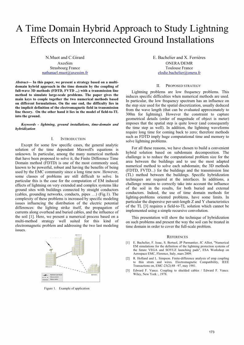
A Time Domain Hybrid Approach to Study Lightning Effects on Interconnected Ground Installations
N.Muot and C.Girard AxesSim
Strasbourg France [email protected]
E. Bachelier and X. Ferrières ONERA/DEMR Toulouse France
Abstract— In this paper, we present a strategy based on a multi-domain hybrid approach in the time domain by the coupling of full-wave 3D methods (FDTD, FVTD ...) with a transmission line method to simulate large-scale problems. The paper gives the main keys to couple together the two numerical methods based on different formulations. On the one end, the difficulty lies in the implicit definition of the electromagnetic field in transmission line theory. On the other hand it lies in the model of field-to-TL into the ground.
Keywords - lightning, ground installations, time-domain and hybridization
I. INTRODUCTION
Except for some few specific cases, the general analytic solution of the time dependant Maxwell's equations is unknown. In particular, among the many numerical methods that have been proposed to solve it, the Finite Difference Time Domain method (FDTD) is one of the most commonly used, known to be powerful, robust and having the benefits of being used by the EMC community since a long time now. However, some classes of problems are still difficult to solve. In particular this is the case for the computation of EM induced effects of lightning on very extended and complex systems like ground sites with buildings connected by straight conductors (cables, grounding networks, conducts, pipes …) (Fig.1). The complexity of these problems is increased by specific modeling issues influencing the distribution of the electric potential differences: the lighting strike itself, the propagation of currents along overhead and buried cables, and the influence of the soil [1]. Here, we present a numerical process based on a multi-method strategy well suited for this kind of electromagnetic problem and addressing the two last modeling issues.
Figure 1. Example of application
II. PROPOSED STRATEGY
Lightning problems are low frequency problems. This induces specific difficulties when numerical methods are used. In particular, the low frequency spectrum has an influence on the step size used for the spatial discretization, usually deduced from the wave length (that can be evaluated approximately to 300m for lightning). However the constraint to capture geometrical details (order of magnitude of object is meter) imposes that the spatial step is quite lower (and consequently the time step as well). In addition, the lightning waveforms require long time for coming back to zero; therefore methods such as FDTD imply huge computational time and memory to solve lightning problems.
For all these reasons, we have chosen to build a convenient hybrid solution based on subdomain decomposition. The challenge is to reduce the computational problem size for the area between the buildings and to use the most adapted numerical method to solve each subdomain; the 3D methods (FDTD, FVTD...) for the buildings and the transmission line (TL) method between the buildings. Specific hybridization techniques are required at the interfaces. In additions, a challenge remains to correctly take into account the influence of the soil in the results, for both buried and external conductors. Indeed, the use of time domain methods for lighting-problems oriented problems, have some limits. In particular the dispersive per-unit-length Z and Y characteristics of the TL [3] requires a field-to-TL solution which cannot be implemented using a simple recursive convolution.
This presentation will show the technique of hybridization on such problems and present the way the soil can be treated in time domain in order to cover the full-scale problem.
REFERENCES
[1] E. Bachelier, F. Issac, S. Bertuol, JP Parmantier, JC Alliot, "Numerical EM simulations for the definition of the lightning protection systems of the future VEGA and SOYUZ launching pads", ESA Workshop on Aerospace EMC, Florence, Italy, mars 2009.
[2] R. Holland and L. Simpson. Finite-difference analysis of emp coupling to thin struts and wires. Electromagnetic Compatibility, IEEE Transactions on, EMC-23(2):88 –97, may 1981.
[3] Edward F. Vance. Coupling to shielded cables / Edward F. Vance. Wiley, New York :, 1978.
173

Electromagnetic Environment of grounding systems Moussa Lefouili1, Kamal Kerroum2
1.LAMEL Laboratory, University of Jijel BP 98 Ouled Aissa 18000 Jijel, Algeria
K. El Khamlichi Drissi2, V. Arnautovski-Toshera2
2. Institut Pascal, Blaise Pascal University, 24 Avenue des Landais, 63177 Aubière, France
Abstract— This paper presents a transient analysis of electromagnetic environment of grounding systems. The response of grounding systems is calculated under fault conditions or when they are hit by lightning. The current distribution and potential along the structure are determined using transmission line theory. The electromagnetic fields in the surrounding soil are determined from the previously calculated current distribution using dipoles theory with analytical formulas. Our approach can be used to predict the electromagnetic environment of grounding systems. Keywords- Transient; Electromagnetic compatibility; Grounding systems;
I. INTRODUCTION
Since the early eighties modeling methods for grounding systems might be classified in only four groups: •Transmission line theory methods; •Electromagnetic field theory methods; •Circuit theory methods; •hybrid methods (that combine two first previous methods) In this work, we propose a new hybrid approach where three methods are combined. The transmission line theory is used for determining the current distribution along the grounding systems. The electromagnetic fields theory with analytical formulas is used for determining the E.M fields radiated by electrical dipole in infinite conductive medium. The total EM field is the sum of the contribution from each dipole. Modified images theory is used for taking into account the influence of a dissipative half-space instead Sommefeld integrals.
Figure 1. Cartography of Magnetic field radiated on the interface by buried grid (60mx60m)
This model can calculate directly in time domain the transient characteristic (potential, current, input impedance and electromagnetic fields) of large grounding systems (electrode or grid).
Figure 2.Cartography of Electric field radiated on the interface by buried electrode (15m)
This approach can be used to predict the electromagnetic environment of grounding systems because it can calculate the EM fields in any point of interest, it’s very easy to understand, reasonably accurate and time efficient.
REFERENCES
[1] Y. Liu, N. Theethay and R. Thottappillil “An engineering model for transient analysis of grounding systems under lightning strikes: non uniform transmission-line approach” IEEE, Trans. On Power Delivery, Vol.20 No.2, pp.722-730, April 2005.
[2] A.P. Meliopoulos and MG Mouharam. "Transient analysis of grounding systems", IEEE, Trans. Power apparatus and systems, Vol, PAS-102, No.2, pp. 389 399, 1983.
[3] L.D.Grcev “Computer analysis of transient voltages in large grounding systems”, IEEE Trans. on power delivery, Vol.11, No2, pp. 815-823, April 1996.
[4] F. Dawalibi “Electromagnetic fields generated by overhead and buried short conductors’ part1-Single-Conductor” IEEE Trans. on power delivery, Vol.PWRD-1, No 4, pp. 105-111, Oct. 1986.
[5] M. Lefouili , K. Kerroum and K. El Khamlichi Drissi “Hybrid approach for modeling transient EM fields generated by large earthing systems” Annals of telecommunication Springer , Vol.64 No.5/6 pp.349-357, May/June 2009
174

On the Transmission Line and Complex Image Modeling of TM Plane Wave Coupling to Horizontal Wire Conductor Above Homogeneous Lossy Ground
Vesna Arnautovski-Toseva Institute Pascal
Blaise Pascal University Clermont Ferrand, France
Khalil El Khamlichi Drissi Institute Pascal
Blaise Pascal University Clermont Ferrand, France
Kamal Kerroum Institute Pascal
Blaise Pascal University Clermont Ferrand, France
Abstract— The paper presents comparison of two approaches for analysis of frequency domain TM plane wave coupling to horizontal wire conductor above homogeneous lossy ground. The first approach uses transmission line theory and the second one uses complex image approximation within antenna theory model. The main objective of this study is to indicate the cases of applicability of both models in practical EMC studies. The results are verified by comparison with exact model.
Keywords- antenna theory; transmission line theory; complex image theory; electromagnetic field coupling; lossy ground
I. INTRODUCTION
The electromagnetic field coupling to overhead wires has been analyzed in many electromagnetic compatibility (EMC) studies. Different strategies for modeling have been developed, ranging from transmission line theory to exact approach based on electromagnetic theory [1-4]. In this paper the authors compare two approaches of modeling electric field coupling to overhead wires. The main objective is to determine the domain of their applicability in practical EMC studies. The first approach is based on transmission line (TL) theory, and the second one is based on complex image (CI) approximation within antenna theory. Within the TL model the induced currents are calculated by using three formulations for per unit length impedance based on: 1) Bridges expression for the external impedance [2]; 2) Sunde’s integral formulation for ground impedance [3]; and 3) Sunde’s approximate formulation for the ground impedance [3]. On the other hand, the CI model is based on the quasi-static complex image approximation [5] of the Green functions that arise in the antenna model based on the Mixed Potential Integral Equation and Method of Moments.
Fig. 1 shows the comparison between the TL and CI models with respect to exact full-wave model on the basis of rms error [6] of the current distribution. The studied case is a 200-m horizontal conductor located at height 1 m above homogeneous lossy ground ( r = 10; = 0.01 S/m) excited by TM plane wave of normal incidence in frequency range from 0.01 to 10 MHz. As may be observed all proposed approximate
approaches introduce some calculation error around the resonant frequencies. The accuracy of the approximate models is related to the ground parameters and the conductor’s height and dimension.
Figure 1. Comparison of the rms error of the current distribution with respect to frequency when using the proposed TL and CI models
REFERENCES
[1] F. Rachidi, S. Tkachenko, “Electromagnetic Field Interaction with Transmission Lines”, WIT Press, 2008.
[2] G. Bridges, “Transient Plane Wave Coupling to Transmission Lines Above a in Lossy Earth”, Antennas and Propagation Society International Symposium, 1988. AP-S. Digest, vol. 2, pp. 676 - 679.
[3] F. M. Teshe, M. Ianosz, T. Karlsson, EMC Analysis Methods and Computational Models, John Wiley and Sons, 1997.
[4] G.J. Burke, E.K.Miller, “Modeling antennas near to and penetrating a lossy interface,” IEEE Trans. Antennas Propag., Vol. AP-32, No. 10, pp. 1040–1049, 1984.
[5] P. Bannister, “Applications of complex image theory”, Radio Science, vol.21, no.4, pp.605-616, 1986.
[6] Poggio, R. Bevensee, E.K. Miller, “Evaluation of some thin wire computer programs” in Proceedings of IEEE Antennas and Propagation Symposium, Vol. 12, pp. 181–184, June 1974.
This work was supported in part by the FP7-PEOPLE-2009-IEF Project 253783
175

`|~|~||||
¸¹º¼½¼¸¾¿À¼½Á¼Â¸
üļŸÆÇÈǼ¿Ê˸̼ͺ¿¼Îº¿Ï¸ÐżÈѼ¸ÐËÏÈÀÊȸÒÀÄÀÈÀº½Ó¸ÔºÁǸÕÖ×Ø
Ù¼ÈËÀ½Úκ½¸ÒÔÓ¸ÛÜݸÀº¼½¼ÞοÀ¼½Á¼Â὿ÅÞ½¼ÄÏÞÑÀÅ
¸¸
%&'*789*Q\^_\`\ |`_~_\ _\`|\`\ _`|\`\ |`\`_\ `\ \ \ `\ `_\ _|`\ \ |~_`_\ |`\~__\ \ `|\ _|`\ _\ `~\ `\ |_\\ `\ `\ ~`_\ \ |_\ \ \ |\ |~\|\ \ _`\ `_\ `\ `|\ \|_\ ~\ ~\ \ _|\ |`_~_\ _\__\ \ ___`|\ ~_\ \ `\ \ `_\ \`~\\\\_`\_|\`_\`\`|\\
<=>?@7J'XYZ8@'[\ *78]'^_''_@]\ `_]=[\ j=`=78|Z=7'\ =~8*_@][\]'*8&`=\@7&_*[\9Z8@'\9@]*7@`\
¹Þ¸ ¸¹Ã¾ÆâÒÛÔ¾¹âø¸¾ËǸÇÂÂÇÊθºÂ¸ÎËǸο¼½ÈÑÀÈÈÀº½¸ÅÀ½Ç¸º½¸ÎËǸÈÀÚ½¼Å¸À½ÎÇÚ¿ÀÎϸÀȸ
¼¸ Ê¿ÀÎÀʼŸ ¼ÈãÇÊθ ºÂ¸ ËÀÚËåÈãÇÇÁ¸ ÁÀÚÀμŸ ÈÏÈÎÇѸ ãǿº¿Ñ¼½ÊÇÞ¸¹½Îǿʺ½½ÇÊÎÀº½È¸ ÍÇÎæÇǽ¸ ÇÅÇÊοº½Àʸ ÁÇÄÀÊÇȸ Ѽϸ ÍÇ˼ÄǸ ¼È¸Î¿¼½ÈÑÀÈÈÀº½¸ ÅÀ½Çȸ¼½Á¸º½Ç¸æºêÅÁ¸ ÅÀëǸ κ¸ ¿ÇÁêÊǸ ÈÀÚ½¼Å¸ źÈÈÇÈÓ¸¼½Á¸ ÁÀÈκ¿ÎÀº½ÈÓ¸ À½¸ º¿ÁÇ¿¸ κ¸ ǽÈê¿Ç¸ ÎËǸ ʺ¿¿ÇÊθ ºãÇ¿¼ÎÀº½¸ ºÂ¸ÇÅÇÊοº½ÀʸÊÀ¿ÊêÀÎÈÞ¸
¹½¸æ˼θºÅźæȸæǸÚÀÄǸ¼½¸Çì¼ÑãÅǸºÂ¸ÈÀÚ½¼Å¸ÁÀÈκ¿ÎÀº½¸ÁêǸκ¸ÑÀÈѼÎÊËÀ½Ú¸ ºÂ¸ ÎËǸ ÅÀ½Ç¸æÀÎ˸ ÎËǸ ÈÀÚ½¼Å¸ÍÇÀ½Ú¸ Èǽθ îïðÞ¸ÙǸ¼ÅȺ¸ã¿ÇÈǽθ¼¸ÈÏÈÎÇѸæËǿǸÊ˼ºÈ¸ºÊÊê¿È¸ÁêǸ κ¸ ÎËǸʺêãÅÀ½Ú¸ºÂ¸ÎËǸÅÀ½Ç¸Îº¸¼¸ÁÀºÁǸîØðÓ¸¼½Á¸È˺æ¸Ëºæ¸ÎËÀȸÊ˼ºÎÀʸÍÇ˼ÄÀº¿¸Ê¼½¸ÍǸʺ½Î¿ºÅÅÇÁÞ
¹¹Þ¸ ÌâÜܸâñ¸Ü¹óÃÝ̸¹Ã¾ôóƹ¾õ¸ÒÛô¸¾â¸÷¹Ü÷ݾÔù¹Ãó¸¾ËǸ ĺÅμÚǸ ĸ ¼½Á¸ Ê꿿ǽθ À¸ ¼Åº½Ú¸ ¼¸ Îæºåʺ½ÁêÊκ¿¸
ο¼½ÈÑÀÈÈÀº½¸ÅÀ½Ç¸¼¿Ç¸ÑºÁÇÅÇÁ¸ÍϸÎËǸ¾ÇÅÇÚ¿¼ãËÇ¿úȸÇûê¼ÎÀº½È¸
¸¸¸¸¸¸¸¸¸¸¸¸¸¸¸¸¸¸¸¸¸¸¸¸¸¸¸¸¸¸¸¸¸¸¸¸¸¸¸¸¸¸¸¸¸¸¸¸¸¸¸¸¸¸¸¸¸¸¸¸¸¸¸¸¸¸¸¸¸¸¸¸¸¸¸¸¸¸¸¸¸¸¸
æËǿǸ̸ÀȸÎËǸãÇ¿åê½ÀÎåÅǽÚÎ˸À½ÁêÊμ½ÊǸ¼½Á¸Ô¸ÀȸÎËǸãÇ¿åê½ÀθýÅǽÚÎ˸ ʼã¼ÊÀμ½ÊÇÞ¸ ¾º¸ ÎËÇÈǸ Çûê¼ÎÀº½È¸ æǸ ¼ÁÁ¸ ͺê½Á¼¿Ï¸Êº½ÁÀÎÀº½È¸
ÙËǽ¸ ÎËǸ ÈÀÚ½¼Å¸ Èǽθļ¿ÀÇȸ ¿¼ãÀÁÅϸ ¸ À½¸ ÎÀÑÇÓ¸ ʺÑ㼿ÇÁ¸ κ¸ ÎËǸÎÀÑǸ¿ÇûêÀ¿ÇÁ¸Âº¿¸ÎËǸÈÀÚ½¼Å¸Îº¸Î¿¼ÄÇŸ¼Åº½Ú¸ÎËǸÅÀ½ÇÓ¸ÎËǸ¿ÇÊÇÀÄÇÁ¸ÄºÅμÚǸ æ¼ÄǺ¿Ñ¸ ¼Î¸ ÎËǸ ź¼Á¸ ʼ½¸ ÍǸ Äǿϸ ÁÀÂÂǿǽθ ¿ºÑ¸ ÎËǸæ¼ÄǸ Î˼θ æ¼È¸ ÈǽÎÞ¸ ÛÈÀ½Ú¸ ¼¸ ÈÇʺ½Á¸ º¿ÁÇ¿¸ ÂÀ½ÀÎǸ ÁÀÂÂǿǽÊǸÈÊËÇÑǸ æǸ ʼÅÊêżÎǸ ÎËǸ ĺÅμÚǸ ¼Î¸ ÎËǸ ź¼Á¸ À½¸¼¸ ο¼½ÈÑÀÈÈÀº½¸ÅÀ½Ç¸ ʺ½½ÇÊÎÀ½Ú¸ Î溸 ÈÇÑÀʺ½ÁêÊκ¿ÈÞ¸ ¾ËǸ ĺÅμÚǸ ¼Î¸ ÎËǸ ź¼ÁÓ¸È˺潸À½¸ñÀÚÞïÓ¸Àȸ¼¸ÈÇÄÇ¿ÇÅϸÁÀÈκ¿ÎÇÁ¸Èû꼿Ǹæ¼ÄǸþ뽺潸¼È¸¿À½ÚÀ½ÚÿÞ¸¸
¸¸
ñÀÚê¿Ç¸ïÞ¸¸ ÆÀ½ÚÀ½Ú¸À½¸ÎËǸź¼Á¸ÄºÅμÚÇӸº¿¸¼¸ÑÀÈѼÎÊËÇÁ¸Î¿¼½ÈÑÀÈÈÀº½¸ÅÀ½Ç¸Êº½½ÇÊÎÀ½Ú¸Î溸ÈÇÑÀʺ½ÁêÊκ¿È¸
¸
¹¹¹Þ¸ ݸÃâÃ̹ÃôÝƸ¸ÒõÃÝ÷¹ÔÝ̸Üõܾô÷¸ÙǸ ʺ½ÈÀÁÇ¿¸ ½Çìθ ¼¸ ο¼½ÈÑÀÈÈÀº½¸ ÅÀ½Ç¸ ʺêãÅÇÁ¸ æÀÎ˸ ¼¸ ã½å
ê½ÊÎÀº½¸ ÁÀºÁǸ ¼Î¸ ÎËǸ ½Ç¼¿¸ ǽÁ¸ ¼½Á¸ æÀÎ˸ ¼¸ ÅÀ½Ç¼¿¸ ¿ÇÈÀÈκ¿¸ æÀÎ˸¿ÇÈÀÈμ½ÊǸÆÓ¸¼Î¸ÎËǸ¼¿¸Ç½ÁÞ¸ñº¿¸ÊǿμÀ½¸Ä¼ÅêÇȸºÂ¸ÎËǸ㼿¼ÑÇÎǿȸÌÓÔ¸ ¼½Á¸ Ƹ ÎËÀȸ ÈÏÈÎÇѸ ÇìËÀÍÀÎȸ Ê˼ºÎÀʸ ÍÇ˼ÄÀº¿¸ ¼È¸ È˺潸 À½¸îØðÞ¸ ¸ ¾ËǸ ÁϽ¼ÑÀÊȸ ºÂ¸ ÎËÀȸ ÈÏÈÎÇѸ ʼ½¸ ÍǸ ѺÁÇÅÇÁ¸ Íϸ ¼¸ º½ÇåÁÀÑǽÈÀº½¼Å¸ ½º½ÅÀ½Ç¼¿¸ ÀÑãÅÀÊÀθ кÀ½Ê¼¿Ç¸ Ѽ㸠îØðÓ¸ æËÀÊ˸ȼÑãÅÇȸÎËǸÁϽ¼ÑÀÊȸ¸¼Ê¿ºÈȸÎËǸÁÀºÁÇÞ¸
ݸãÇ¿ÀºÁÀʸê½ÈμÍÅǸº¿ÍÀθºÂ¸ÎËÀȸѼã¸ÀȸÂÀ¿ÈθÀÁǽÎÀÂÀÇÁÓ¸ÎËǸÅÀ½Ç¼¿À¼ÎÀº½¸¼ÍºêθÎËÀȸº¿ÍÀθÀȸêÈÇÁ¸Îº¸ÁÇÈÀÚ½¸ÈѼÅŸãÇ¿Îê¿Í¼ÎÀº½È¸À½¸ÎËǸ¿ÇÈÀÈμ½ÊǸ¼Î¸ÎËǸͺê½Á¼¿ÏÓ¸Î˼θڿ¼Áê¼ÅÅϸÈêãã¿ÇÈȸÎËǸÊ˼ºÎÀʸÀÎÇ¿¼ÎÀº½È¸¼È¸È˺潸À½¸ñÀÚÞØÞ¸ ¸
¸ ¸¸¸¸¸ ¸
ñÀÚê¿Ç¸ØÞ¸Ôº½Î¿ºÅÅÇÁ¸æ¼ÄǸÈ˺潸¼Î¸ÑêÅÎÀãÅÇȸºÂ¸ÎËǸ¿ºê½ÁåοÀã¸ÎÀÑǸ¾Þ¸
ÆôñôÆôÃÔôܸîïð¸ ÔżÏκ½¸ ÆÞ¸ мêÅÓ¸ ݽ¼ÅÏÈÀȸ ºÂ¸ ÷êÅÎÀʺ½ÁêÊκ¿¸ ¾¿¼½ÈÑÀÈÈÀº½¸ ÌÀ½ÇÈÓ¸
¹ôôô¸Ð¿ÇÈÈÓ¸ÙÀÅÇϸØÖÞ¸îØð¸ ÌÞ¸Ôº¿ÎÀÓ¸ÌÞ¸ÒǸ÷ǽ½¼Ó¸óÞ¸÷À¼½º¸¼½Á¸Ì޸ǿºÅÀ½ºÓ¸¸Ô˼ºÎÀʸÒϽ¼ÑÀÊȸ
À½¸¼½¸¹½ÂÀ½ÀÎÇåÒÀÑǽÈÀº½¼Å¸ôÅÇÊοºÑ¼Ú½ÇÎÀʸÜÏÈÎÇÑÓ¸¹ôôô¸¾¿¼½È¼ÊÎÀº½È¸º½¸ÔÀ¿ÊêÀÎȸ¼½Á¸ÜÏÈÎÇÑÈ幸ñê½Á¼ÑǽμŸ¾ËǺ¿Ï¸¼½Á¸ÝããÅÀʼÎÀº½ÈÓ¸ºÅÞ¸ïӸú޸ïïӸúÄÇÑÍÇ¿¸ï××Þ¸
¾ËǸ¼êÎ˺¿¸Ú¿¼ÎÇÂêÅÅϸ¼Ê뽺æÅÇÁÚÇȸÎËǸÈêã㺿θºÂ¸ÎËǸ¸âÂÂÀÊǸºÂ¸¸Ã¼Ä¼Å¸ÆÇÈǼ¿ÊËÞ¸
þïÿ¸¸¸¸¸¸¸¸¸¸¸¸¸¸¸¸¸¸ÎÄ
ìÀ¸¸¸¸Ó
ÎÀ
ìÄ
176

EM coupling to Transmission Lines with Symmetric Geometry inside Rectangular Resonators
Sergey Tkachenko, Jürgen Nitsch Institute for Fundamental Electrical Engineering and EMC
Otto – von – Guericke University Magdeburg Magdeburg, Germany
e-mail: [email protected]
Ronald Rambousky Bundeswehr Research Institute for Protective Technologies
and NBC Protection (WIS), Munster, Germany
Abstract— In this paper we outline an exact analytical solution for the current induced by an arbitrary exciting field in a loaded transmission line with symmetric geometry inside a rectangular resonator.
Keywords: transmission line, cavity resonator, analytical solutions
I. INTRODUCTION
Investigation of the coupling of high-frequency electromagnetic fields caused by intentional electromagnetic interferences to linear structures placed in cavity–like structures (racks, cases, housing, fuselage of aircraft, etc) becomes an actual topic. Existing numerical methods (Method of Moments, Transmission-Line Matrix method, etc.) allow considering specific cases only, but do not describe the general physical picture of the interaction. Thus, the analytical description of the interaction of high-frequency fields with wire structures in cavities has become a topic of interest.
To solve this problem several methods can be offered. The approximate methods are based, as is usual in theoretical physics, on the use of small parameters. One group of such methods, Method of Small Antenna (MSA), uses the smallness of the dimension of the wiring structure in comparison to the wavelength [1]. This method gives a possibility to analytically express the solution for the scattered current in a small antenna inside the resonator with the aid of the free space solution and regularized cavity Green’s function. Of course, for electrically large scatterers the MSA is not applicable. Another small parameter that can be used to solve the coupling problem for electrically long objects inside a resonator is the thickness of the wire compared to other geometrical parameters of the problem (wavelength, height of the wire above ground, etc.) [2]. The relevant mathematical technique is the method of analytical regularization which allows considering the coupling of EM fields with electrically long antennas and transmission lines inside the resonator, if the considered frequency is close to one of resonance frequencies and all the other modes of the resonator contribute to form the singular part of the cavity’s Green’s function. However, this method uses approximate representations of the singular and regular components of Green’s function and an approximate resolution operator (TL approximation). It is interesting to compare these results with results of an exact solution which is outlined in the next Section.
II. DESCRIPTION OF OBTAINED RESULTS
An analytical solution for the system “wire in a resonator” can be found for configurations with high symmetry with the aid of usual methods of theoretical physics [3]. The system consists of a rectangular resonator and an internal wire parallel to a resonator axis connecting opposite walls of the resonator. In the first step a short-circuit configuration was considered.
The electric field integral equation (using only thin-wire approximation) which describes the current in such wires induced by an arbitrary electrical field can be solved by a spatial Fourier series transformation. The geometry of the system allows a Fourier series ansatz with functions )/cos( hnz z for the induced current and also for the resonator Green’s function in the direction of the wire. Moreover, during the investigation of the exact equation for the induced current one can separate terms corresponding to the transmission line approximation from those corresponding to cavity modes and evaluate the effect of different resonances. The obtained solution is valid for arbitrary exciting fields which can be created by one or another way: by an external field penetrating through apertures, by a field of an internal radiating antenna or also by a field excited by lumped sources, located in the line or by all sources together. It is possible to show that the lumped loads (impedances) also can be considered as lumped sources with sizes which are defined by the product of the current values flowing through this load and the value of load. This fact gives the possibility to obtain a system of linear equations for these unknown currents (the order of the system coincide with the number of the loads), which finally yields the induced current in explicit form for both the lumped and/or distributed excitation.
REFERENCES
[1] S. Tkachenko, F. Gronwald, H.-G. Kauthäuser, J. Nitsch, “High-frequency electromagnetic coupling to small antennas in rectangular resonator”, Int. Conf. Electromagn. Adv. Appl. (ICEAA), 15-19 Sept. 2009, pp.74-78.
[2] S. Tkachenko, J. Nitsch, R. Vick, “HF coupling to a transmission line inside a rectangular cavity”, URSI Int. Symp. on Electromagn. Theor., Berlin, Germany, Aug. 16-19, pp. 5-8.
[3] S. Tkachenko, J. Nitsch and R. Rambousky, “Electromagnetic field coupling to transmission lines inside rectangular resonators”, Interaction Notes, Note 623, 30 June 2011.
177

Iterative Method for Multi-conductor Transmission Line Propagation Parameter
Jianshu Luo Min Zhou Ying Li Zhenzheng Ouyang Xufeng Zhang Yuhai Gao College of Science
National University of Defense Technology Changsha, Hunan 410073, China
E-mail: [email protected]
Abstract—Multi-conductor transmission line equation is based on the development of telegraph equation. With the number and complexity of the wire increases, the conductor's eigen impedance matrix and admittance matrix and the distribution of the source with the external excitation vector dimension becomes large, which costs the complex computation and expensive memory when solving voltage and current of multi-conductor cable transmission line. This paper is based on the general case of lossy conductor and lossy dielectric. For the eigen impedance matrix and admittance matrix of the product matrix, the iterative QR method for solving the eigenvalues and eigenvectors problems is employed. Compared with commonly used Gaussian elimination, our method significantly reduces the memory and computational time. Finally numerical examples are given.
Keywords-Multi-conductor transmission line; iterative QR method; eigenvalue
I. INTRODUCTION
The multi-conductor transmission line composed of a parallel with the N conductor and a reference conductor parallel is one of the basic circuit units of complex electronic systems. Many scholars studied on solving this multi-conductor transmission line voltage wave and current. With the increase in the number of conductors, the eigen impedance matrix and admittance matrix dimension in multi-conductor transmission line equation becomes large. To solve the multi-conductor transmission line equation, eigenvalues and eigenvectors of the admittance matrix and the characteristic impedance matrix need to be calculated.
II. THE ITERATIVE QR METHOD FOR SOLVING THE EIGEN
IMPEDANCE MATRIX AND ADMITTANCE MATRIX
A. Multi-conductor transmission line equation
Voltage and current propagation equations of the multi-conductor transmission line are
( ) ( ) ( ) ( ) ( )d, , ' ,
dsI z Y V z I z
zω ω ω ω′+ =
r r (1)
( ) ( ) ( ) ( ) ( )d, , ' ,
dsV z Z I z V z
zω ω ω ω′+ =
r r (2)
B. Iterative QR algorithm for matrix ( ) ( )Y Zω ω′ ′
Use firstly Alston Householder theorem, then use Francis iteration algorithm for solving the eigenvalues of matrix
( ) ( )Y Zω ω′ ′ . Finally apply Shifted QR algorithm to reduce computational time and speed up the convergence rate.
III. EXAMPLES AND ANALYSIS
The cables are composed by 9, 17, and 33 parallel conductors as shown in Fig. 1. The central conductor is the reference conductor, and the conductor radius is 0.3cm. The distance between the center point of the conductor and the reference conductor is 1cm. The diagonalized computational
time of matrix ( ) ( )Y Zω ω′ ′ for the three cable models is shown in Table 1.
Figure 1. Cables composed by 9,17 and 33 parallel conductors,respectively
TABLE I. THE DIAGONALIZED COMPUTATIONAL TIME OF
'( ) '( )Y Zω ω FOR THE THREE CABLE MODELS
Model The number of iterations for diagonalization
Computational time
Model I 30 0.0313s Model II 1800 0.5625s Model III 2000 4.1094s
IV. CONCLUSION
The multi-conductor transmission line equation is a kind of basic equation in the electromagnetic field. Based on the general case of lossy conductor and lossy dielectric, this paper presents the iterative QR method for solving the product matrix of the impedance matrix and admittance matrix, Compared with commonly used Gaussian elimination, our method significantly reduces the memory and computational time.
REFERENCES
[1] C.R.Paul, Analysis of Multiconductor Transmission Lines, New York: Wiley, 1994
[2] F. M. Tesche, M. V. Ianoz, and T. Karlsson, EMC Analysis Methods and Computational Models, New York: Wiley, 1997
This work is supported by the National Natural Science Foundation of China. (no.10871231)
178

1
High-frequency Electromagnetic Coupling to LongLoaded Multi-conductor Transmission Line
G. Lugrin1, N. Mora1, F. Rachidi1, S. Tkachenko2, M. Rubinstein3, R. Cherkaoui11 Electromagnetic Compatibility Laboratory, Swiss Federal Institute of Technology (EPFL), Lausanne, Switzerland
2 Department of Electrical Engineering and Information Technology, Otto-von-Guericke University, Magdeburg, Germany3 Institute for Information and Communication Technologies, University of Applied Sciences Yverdon, Yverdon, Switzerland
Email: [email protected]
Abstract— We present a theory for the problem of electromag-netic field coupling to a long multi-conductor line with arbitraryterminations. The theory is applicable for a high-frequency planewave electromagnetic field excitation, when the transmission lineapproximation is no longer valid. The method is particularlyefficient when considering the electromagnetic field coupling tovery long lines.
Keywords— enhanced transmission line model (ETL); high fre-quency electromagnetic field excitation; multi-conductor transmis-sion line (MTL).
I. INTRODUCTION
The electromagnetic field coupling to multi-conductor trans-
mission lines is generally evaluated making use of the trans-
mission line (TL) approximation which applies to uniform
transmission lines with electrically small cross-sectional di-
mensions, and where the dominant mode of propagation is
transverse electromagnetic (TEM). In the last decade or so,
significant efforts have been put into the elaboration of the
so-called “full-wave” TL theory, which incorporates high fre-
quency radiation effects, while keeping the relative simplicity
of TL equations. In particular, Tkachenko et al. [1] derived a
TL-like pair of equations for evaluating currents and potentials
induced by external electromagnetic fields on a single wire
above a perfect conducting ground. Based on perturbation
theory, an iterative procedure was proposed to solve the
derived coupling equations. Later in 2001, Tkachenko et al.
[2] extended their method to take into account the presence of
line terminations and discontinuities. In this paper, we present
the generalization of Tkachenko et al. theory to the case of a
multi-conductor line.
II. METHOD
Consider a set of infinite straight lines above a perfectly
conducting ground, excited by an external plane wave. The ex-
citing field will induce currents in the wires, which will in turn
radiate uniformly along the line (the so-called scattered field).
When the line uniformity is disturbed by a lumped impedance
or by line terminations, the current wave is more complex and
involves not only TEM (Transverse Electromagnetic) modes
but also leaky and radiation modes.
abcdefghijklmnopqrstuThis project is funded by Swiss Electric Research.
x
y
z
Z1i
Z2i
I II III
L∼ lbound ∼ lbound
H
Ei
k
Fig. 1. Geometry of the system.
Let us consider now the geometry sketched on Fig. 1 that
represents a multi-conductor line of length L. Each wire i is
loaded at each extremity by impedances Z1i and Z2i. It is
possible to break down this line into three different regions.
The first and the third zones are located near the extremities
of the line, i.e. z ≤ lbound (region I) and z ≥ L − lbound(region III). lbound corresponds to the distance where the
influence of the electromagnetic fields generated by the loads
may be neglected in comparison with the fields produced
by the currents along the wires. In these zones, a complete
solution is needed to represent the complexity of the current
wave. Region II corresponds to the part of the line that is
far enough from the boundaries so that only the TEM mode
exists, i.e. lbound z L − lbound. This part of the line
can be represented asymptotically by an infinite long line, for
which an analytical solution exists.
Since the size of the regions I and III does not depend on
the line length, the method is very useful in the case of very
long lines.
REFERENCES
[1] S. Tkatchenko, F. Rachidi, and M. Ianoz, “Electromagnetic field couplingto a line of finite length: theory and fast iterative solutions in frequencyand time domains,” Electromagnetic Compatibility, IEEE Transactionson, vol. 37, no. 4, pp. 509 –518, nov 1995.
[2] ——, “High-Frequency Electromagnetic Field Coupling to Long Termi-nated Lines,” IEEE Trans. on EMC, vol. 43, pp. 117–129, May 2001.
179

180

HPEM-TC07-SS2Use of Computer
Codes in HIRF certification process
181

HIRF SE: A Computational Electromagnetic Framework for Aircraft Design and Certification
M. Bozzetti Alenia Aermacchi, Strada Malanghero, 10072 Caselle Torinese (TO) – Italy
Abstract — The HIRF SE framework will be an EM analysis tool operating in HIRF radio frequency spectrum (10 KHz-40 GHz). It will simulate the air vehicle interaction with both far-field and near-field sources having any polarization and position in the presence or not of the ground. Also the HIRF SE framework will predict both the EM field distribution inside the airframe and the induced currents in the wiring system. The correct operating of the framework will be verified and validated by comparison with data from real testing on small and medium air vehicles and pre-existing data for large air vehicles. The validation at air vehicle level is the final step of the validation process.
Keywords-component; HIRF, civil, aircraft, rotorcraft, design, certification;
I. INTRODUCTION
HIRF Synthetic Environment (HIRF SE, [1]) main objectives can be summarized by the two followings items:
Fully validated and integrated solutions to model simulate and test air vehicles for EM aspects during the whole life cycle.Building (from past and ongoing works) of an integrated approach with an open and evolutionary architecture.
The former objective of the HIRF SE project is to address the drawbacks of the actual design, certification and modification approach with the assistance of EM computational techniques. The latter objective addresses the gathering of the whole currently available numerical simulation competence. The consequence is that many stand alone expert tools will cooperate in order to solve those problems.
The HIRF SE project (http://www.hirf-se.eu/hirf/) proposes to provide the aeronautic industry with an electromagnetic computational tool with an innovative and systematic solution based on a high level of software integration offering an open and evolutionary architecture: a computer framework. The HIRF Synthetic Environment project will also meet the objective to reduce the delivery timescales of future air vehicles and systems, decreasing the time required for physical testing, possible re-design and possible re-testing.
The correct operating of the framework will be verified and validated by comparison with data from real testing on small and medium air vehicles and pre-existing data
for large air vehicles. The validation at air vehicle level is the final step of the validation process.
Figure 1. Evector EV 55 morphed meshed model and electromagnetic model of Alenia’s Inverted V antenna
II. DIFFERENT SIMULATION APPROACHES
Simulation approaches have been classified with respect to a Low Frequency Band (LFB) scenario and a High Frequency Band (HFB) scenario.
The LFB scenario extends from 10 kHz to 3 GHz. It relies on the use of 3D full wave solvers for calculating both external and internal environments of air vehicles and the use of Multiconductor Transmission Line models for the calculating the response of cable bundles under test. The process for linking the two types of data is based on the field-to-transmission line approach but this process still requires extensive thin wire modeling in the 3D model in order to describe correctly the inner field environment. The HFB scenario extends from 3GHz to 40 GHz. It relies on asymptotic 3D solvers for calculating external fields at the level of points of entry of energy inside the air vehicle. The internal response is calculated with so called Power Balance tools making the assumption that the internal field environment can be considered as random.
In addition to those main computer modules, specific sub-modules have been developed in order to bring the EM physics required by HIRF modeling. Among them, material models have been extensively studied in order to be introduced as macro models in 3D computer solvers. The HIRF SE framework uses the AMELET format in order to standardize the flux of data of the various computer models involved in the LFB and HFB scenarios.
The research leading to these results has received funding from the European Community’s Seventh Framework Programme [FP7/2007-2013] under grant agreement no 205294.
182

A Simulation Framework applied to HIRF Certification Process
C. GIRAUDON, D. ROISSE, C. GIRARD AxesSim
Parc d’innovation, Rue Jean Sapidus, 67400 Illkirch-Graffenstaden - France [email protected]
Abstract — This paper presents the application of the generalized and extendable software framework “CuToo”, applied and improved in the HIRF-SE project. This framework implements specific capabilities required for applicability of numerical simulation in HIRF Certification Process. These capacities cover a full traceability of the simulation process and implementation of applicable scenarios.
Keywords-component; HIRF; Electromagnetic simulation, certification process
I. HIRF-SE SOFTWARE FRAMEWORK
The HIRF-SE project relies on a software framework, called, CuToo which is a generalized and extendable software framework dedicated to the scientific computing and scientific knowledge management. It offers the following major services:
• Scheduling and handling of batch and interactive simulations: o CAD edition and cleaning, mesh generation o Calculation of electromagnetic entities o Data exploration and treatment
• Business entity modeling: mesh, material, numerical data, simulation...
• Knowledge management: model instances are stored and have versions in a database
• Extendable by adding new models and new computation modules
• Remote visualization for 3D interactive tasks
CuToo is also a distributed, multi-user software platform with a large number of EM modeling features and offers rock-solid security and performance.
II. AMELET-HDF DATA FORMAT
Amelet-HDF [1] is the central format of description and storage of business entities in CuToo. Amelet-HDF is open and can be used be anyone wants to describe an electromagnetic computation use case. It defines the description of electromagnetic simulation domain objects like numerical data, mesh, material, transmission line network, simulation, output request, specific properties of computation codes... Amelet-HDF uses HDF5 [2] to store numerical objects in data files.
Communication between CuToo and the computation modules are assured by the sole Amelet-HDF description format. Consequently, it is very easy to interact with CuToo; importing and exporting entire simulation objects are open processes.
Figure 1. Screenshot of the CuToo framework GUI in the HIRF-SE project
III. HIRF CERTIFICATION PROCESS
Within the HIRF-SE project different computational algorithms are available in the CuToo platform to solve various problems in the HIRF frequency range. The set of plugged computional tools embeds Volume based calculation methods (FDTD, Hybrid techniques), Surface model/integral equation method (FMM, FEM…), Asymptotic techniques, Power balance techniques and Multi-conductor cables models (TL approach).
Some specific capabilities related to the certification process itself are implemented by the HIRF-SE platform:
• Global traceability and versioning of data and computation tools used in the simulation process;
• Consistency check of data used in input of simulations;
• Workflow Engine with specific scenarios (Model validation, BF, HF) dedicated to certification. This mechanism supports the choice of the appropriate algorithms. The choice of the algorithms provides a trade-off between Accuracy and Computation time.
REFERENCES
[1] http://http://code.google.com/p/amelet-hdf/
[2] http://www.hdfgroup.org/HDF5/
The research leading to these results has received funding from the European Community’s Seventh Framework Programme [FP7/2007-2013] under grant agreement no 205294.
183
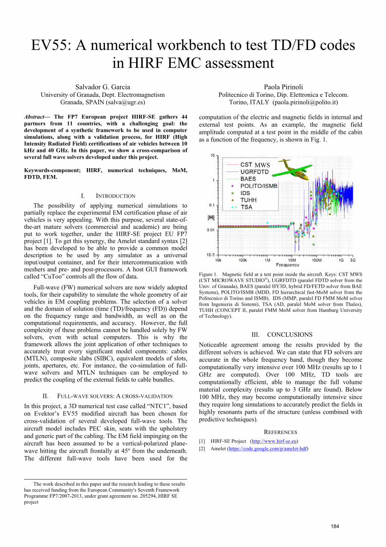
EV55: A numerical workbench to test TD/FD codes in HIRF EMC assessment
Salvador G. Garcia University of Granada, Dept. Electromagnetism
Granada, SPAIN ([email protected])
Paola Pirinoli Politecnico di Torino, Dip. Elettronica e Telecom.
Torino, ITALY ([email protected])
Abstract— The FP7 European project HIRF-SE gathers 44 partners from 11 countries, with a challenging goal: the development of a synthetic framework to be used in computer simulations, along with a validation process, for HIRF (High Intensity Radiated Field) certifications of air vehicles between 10 kHz and 40 GHz. In this paper, we show a cross-comparison of several full wave solvers developed under this project.
Keywords-component; HIRF, numerical techniques, MoM, FDTD, FEM.
I. INTRODUCTION
The possibility of applying numerical simulations to partially replace the experimental EM certification phase of air vehicles is very appealing. With this purpose, several state-of-the-art mature solvers (commercial and academic) are being put to work together, under the HIRF-SE project EU FP7 project [1]. To get this synergy, the Amelet standard syntax [2] has been developed to be able to provide a common model description to be used by any simulator as a universal input/output container, and for their intercommunication with meshers and pre- and post-processors. A host GUI framework called “CuToo” controls all the flow of data.
Full-wave (FW) numerical solvers are now widely adopted tools, for their capability to simulate the whole geometry of air vehicles in EM coupling problems. The selection of a solver and the domain of solution (time (TD)/frequency (FD)) depend on the frequency range and bandwidth, as well as on the computational requirements, and accuracy. However, the full complexity of these problems cannot be handled solely by FW solvers, even with actual computers. This is why the framework allows the joint application of other techniques to accurately treat every significant model components: cables (MTLN), composite slabs (SIBC), equivalent models of slots, joints, apertures, etc. For instance, the co-simulation of full-wave solvers and MTLN techniques can be employed to predict the coupling of the external fields to cable bundles.
II. FULL-WAVE SOLVERS: A CROSS-VALIDATION
In this project, a 3D numerical test case called “NTC1”, based on Evektor’s EV55 modified aircraft has been chosen for cross-validation of several developed full-wave tools. The aircraft model includes PEC skin, seats with the upholstery and generic part of the cabling. The EM field impinging on the aircraft has been assumed to be a vertical-polarized plane-wave hitting the aircraft frontally at 45º from the underneath. The different full-wave tools have been used for the
computation of the electric and magnetic fields in internal and external test points. As an example, the magnetic field amplitude computed at a test point in the middle of the cabin as a function of the frequency, is shown in Fig. 1.
Figure 1. Magnetic field at a test point inside the aircraft. Keys: CST MWS (CST MICROWAVE STUDIO®), UGRFDTD (paralel FDTD solver from the Univ. of Granada), BAES (paralel HY3D, hybrid FD/FETD solver from BAE Systems), POLITO/ISMB (MDD, FD hierarchical fast-MoM solver from the Politecnico di Torino and ISMB), IDS (MMP, paralel FD FMM MoM solver from Ingenieria di Sistemi), TSA (AD, paralel MoM solver from Thales), TUHH (CONCEPT II, paralel FMM MoM solver from Hamburg University of Technology).
III. CONCLUSIONS Noticeable agreement among the results provided by the different solvers is achieved. We can state that FD solvers are accurate in the whole frequency band, though they become computationally very intensive over 100 MHz (results up to 1 GHz are computed). Over 100 MHz, TD tools are computationally efficient, able to manage the full volume material complexity (results up to 3 GHz are found). Below 100 MHz, they may become computationally intensive since they require long simulations to accurately predict the fields in highly resonants parts of the structure (unless combined with predictive techniques).
REFERENCES
[1] HIRF-SE Project (http://www.hirf-se.eu)[2] Amelet (https://code.google.com/p/amelet-hdf)
The work described in this paper and the research leading to these results has received funding from the European Community's Seventh Framework Programme FP7/2007-2013, under grant agreement no. 205294, HIRF SE project
MWS
184

Parametric Evaluation of Absorption Losses and Comparison of Numerical Results to Boeing 707
Aircraft Experimental HIRF Results
J. Kitaygorsky, C. Amburgey, J.R. Elliott, R. Fisher, R.A. Perala Electro Magnetic Applications, Inc.
Denver, CO, [email protected]
Abstract— A broadband (100 MHz - 1.2 GHz) plane wave electric field source was used to evaluate the electric field penetration inside a simplified Boeing 707 aircraft model using a finite-difference time-domain (FDTD) method. Three different incidence angles, at two polarizations each, were implemented and compared. The role of absorption losses inside the simplifiedaircraft were investigated. It was found that, in this frequency range, none of the cavities inside the Boeing 707 model are trulyreverberant when frequency stirring is applied, and a purelystatistical electromagnetics approach cannot be used to predict or analyze the field penetration or shielding effectiveness (SE). Thus it was our goal to understand the nature of losses in such a quasi-statistical environment by adding various absorbing objects inside the simplified aircraft and evaluating the SE. We then compare our numerical results with experimental results obtained by D. Mark Johnson et al. [1] on a decommissioned Boeing 707 aircraft.
Keywords-HIRF; FDTD; aircraft losses; computational electromagnetics; shielding effectiveness, EMA3D
I. INTRODUCTION
The certification process for an aircraft is a lengthy and expensive process. The high-intensity radio frequency (HIRF) environment forms one segment of the certification requirements. A computational electromagnetics (CEM) model can provide a detailed view of the HIRF coupling processes and levels throughout the aircraft than is generally possible in testing due to time and cost constraints.
It is, however, not possible to know all the material losses inside an aircraft at high frequencies. Therefore, a technique needs to be developed where absorption losses can be reasonably approximated and compared with experimental measurements.
In this work, we investigate absorption losses numerically using EMA3D, a finite-difference time-domain (FDTD) based code. We start with a simplified model of an empty Boeing 707 aircraft and illuminate it with a broadband plane wave at three different incidence angles and both polarizations. Shielding effectiveness (SE) is then evaluated in three aircraft cavities, namely, the cabin, cockpit, and avionics bay. We then start adding lossy materials, which consist of randomly spaced cubes with very low conductivity, to investigate how SEchanges as a function of material conductivity and absorption
cross section in the frequency range from 100 MHz to 1.2 GHz.
We then compare our results with experimental data [1], and show how SE increases with increasing absorption cross section. SE curves inside the avionics bay are shown in Fig. 1 for broadside illumination with vertical polarization.
In addition to SE, the quality factor Q was extracted at different locations inside the aircraft and compared with experimental values. Predictably, it was found that Q decreases for a given frequency as the absorption cross section is increased.
Figure 1. SE comparison inside the avionics bay for the empty aircraft (blue), aircraft loaded with losses (green), and experimental data [1] (black).
II. SUMMARY AND CONCLUSIONS
We conclude that SE depends on the amount of losses present in the aircraft. In this aircraft, absorption losses tend to dominate over aperture and wall losses. Additionally, absorption losses can be numerically implemented to obtain SE levels similar to experiment, so long as correct parameterization is implemented.
ACKNOWLEDGMENT
We thank Dr. Robert T. Johnk (NTIA, Boulder, CO) and Chriss Hammerschmidt (NTIA, Boulder, CO) for their helpful discussions.
REFERENCES
[1] D. Mark Johnson et al., “Phase II Demonstration Test of the Electromagnetic Reverberation Characteristics of a Large Transport Aircraft,” Dahlgren Division Naval Surface Warfare Center, Sept. 1997.
185

Keywords: surface-impedance boundary condition; digital filter; finite-difference time-domain
186

EM coupling of an HIRF field onto a cable-harness Application of field-to-TL approach with a dedicated computer framework
S. Bertuol, M. Ridel, J-P. Parmantier ONERA, The French Aerospace Lab
2 avenue Edouard Belin, 31055, Toulouse - France [email protected]
L. Pisu, S. Messina Alenia Aermacchi
Strada Malanghero, 10072 Caselle Torinese (TO) – Italy [email protected]
A. Francavilla, F. Vipiana, ISMB, Istituto Superiore Mario Boella
Via Pier Carlo Boggio 61, Torino 10138, Italy [email protected], [email protected]
S.Arianos, G. Vecchi Politecnico di Torino
Corso Duca degli Abruzzi 24, Torino 10129, Italy [email protected], [email protected]
Abstract — This paper demonstrates a numerical application of the Field-to-TL approach carried out in a computer framework designed to facilitate and standardize the exchanges of data at the interfaces of various modeling computer tools. The interest of using a framework for making more robust the exchanges is showed. The comparison with measurements gives an idea of the degree of accuracy obtained with such an operating approach.
Keywords-component; HIRF-SE; Field-to-Transmisison-Line; Multiconductor-Transmission-Line Networks; Method of Moments; induced current; LLSC
I. INTRODUCTION
The HIRF-SE project implements various scenarios for linking several computer codes thanks to the AMELET standard of EM-model description. This standard provides a unique set of parameters for the various types of models required for the exchanges at the interfaces between the computer tools as well as common data formats. Particularly, the framework can be used to implement Agrawal’s field-to-TL scenarios [1] with any 3D full-wave type and multiconductor-transmission-line (MTL) solvers, provided that those solvers are capable to convert their input/output data with the AMELET format. The approach is based on the transformation of the incident electric field along the cable route into voltage generators distributed along MTL models of cable bundles. For a long time, Agrawal’s model has proved its efficiency in terms of implementation of this 3D/MTL approach [2], based on the fact that no MTL current generator is needed and that the incident field definition does not require any notion of verticality with the reference ground.
In the frame of the validations carried out in the HIRF-SE project, the methodology has been demonstrated on a generic test-case consisting in the illumination of a Piaggio cable-harness, made of several branches and involving a large variety of elementary shielded and unshielded cables. The harness has been installed over a table with a metallic ground plane. Several illuminations were considered in this validation. This paper focuses on the illumination provided by a V-inverted antenna available in Turin at Alenia Aermacchi’s Open Area
Test Site (OATS). Alenia Aermacchi carried out the associated measurements for comparisons (Fig. 1) according to the aeronautical standard regulations in force.
II. DIIFERENT STEPS OF THE SIMULATION
The presentation will show the different steps involving specific HIRF-SE tools for developing this modeling scenario:
- Meshing of the test configuration including the radiating antenna and the cable-harness central path (i.e. the route) the, with CIMNE’s GID software, - Calculation of the fields on the central path with MDD, fast multi-scale Method-of-Moments tool developed by the Politecnico di Torino and ISMB, - Modeling of the MTL network decomposed in tubes and junctions with ONERA’s CRIPTE tool - Assignment of the incident field files onto the tubes with the AxesSim’s CuToo computer framework - Calculation of the cable response with the CRIPTE tool - Comparison of simulated and measured results
Figure 1. Left: In the background, Alenia’s V-inverted antenna and, in the foreground, the table supporting the cable harness (picture © Alenia Aermacchi). Right: Mesh of the table with the cable-harness cental path for the 3D full-wave calculation
REFERENCES
[1] F.M. Tesche, M.V. Ianoz, T. Karlsson, “EMC Analysis Methods and Computational Models”, John Wiley & Sons, 1997, pp.247-266.
[2] L. Paletta, J-P. Parmantier, F. Issac, P. Dumas, J.-C. Alliot, “Susceptibility Analysis of Wiring in a Complex System Combining a 3-D Solver and a Transmission-Line Network Simulation”, IEEE Trans. on EMC, Vol. 44, No. 2, May 2002, pp. 309-317.
The research leading to these results has received funding from the European Community’s Seventh Framework Programme [FP7/2007-2013] under grant agreement no 205294.
187

Comparison between measured and computed BCI Tests - RF Currents on an Equipment Interface
A. Delogu, M. Stradella Selex Galileo
Strada Privata Aeroporto, 10077, S. Maurizio C.se – Italy [email protected]
M. Ridel, J.P. Parmantier, I. Junqua ONERA, The French Aerospace Lab
2 avenue Edouard Belin, 31055, Toulouse - France [email protected]
Abstract — A specific Instrumented Equipment has been designed to measure RF voltage and currents at equipment interface during EMC tests in laboratory, avionic rig and on aircraft. This paper presents its main features, the test procedure for Bulk Current Injection tests. Measured results are compared with data from simulation using the CRIPTE code from ONERA.
Keywords: Avionic Equipment, Instrumented Equipment, Bundle, EMC, Bulk Current Injection, BCI, HIRF-SE, CRIPTE
I. INTRODUCTION
The Instrumented Equipment (IE) is a mock-up of equipment which is mechanically representative of real equipment and is capable to measure Voltages/Currents at interface connectors and external field levels. It has been developed specifically to be able to measure RF voltages and Currents during EMC tests al laboratory, rig and aircraft levels. In the HIRF-SE project, the IE is used during HIRF certification process, to compare in a realistic case both computed and measured data, on aircraft and in laboratory.
II. INSTRUMENTED EQUIPMENT FEATURES AND SET-UP
The IE simulates size, mechanical interface and termination impedances of an Attitude and Heading Computer (AHC) equipment installed on Piaggio P180 aircraft. It includes the capability of measuring the RF current on a single cable shield, the total RF current on other cable bundle shields, common mode RF currents on 17 shielded and unshielded wires, 11 differential RF voltages on single or multiple balanced interface wires and 17 Common Mode voltages on balanced and unbalanced interface wires.
The IE has been developed to simulate typical equipment interface impedances. Actual common and differential mode impedances have been fully measured to be introduced in numerical simulations. Bulk Current Injection (BCI) tests on IE were carried out by injecting calibrated RF currents on the whole bundle at the IE connector extremity. The bundle is terminated on a Termination Box (TB) as shown in Fig. 1.
InstrumentedEquipment
TerminationBox
B
A
All shields connected together
Power Return
Single shielded cable
Ground PlaneShield bonding
(“pig tails”)
Current Injection Probe
Figure 1. Instrumented Equipment Set-up for BCI
Measurements were performed following the guidelines of [1]. Measured values at each connector pin were normalized to injected current to estimate coupling coefficients.
III. ANALYSIS TOOL
The analysis of the current distribution within the bundle wires has been performed using the CRIPTE computer code [2] from ONERA. The code allows modeling in details the whole topology of the wiring taking into account the bundle constitution, the interconnection and impedance matrices between different sections of the bundle and at the IE and TB. The code computes the total current on the cable-bundle and the currents and common mode voltages on instrumented ports.
IV. COMPARISON OF MEASURED AND COMPUTED RESULTS
The comparison of results was made on currents observed on all measured wires within the bundle. An example, relevant to a wire with high coupling coefficient, is shown in Fig. 2. The comparison between computed and measured values is reasonably good. In particular, the accuracy is better when both common mode and differential mode impedances are known in detail and included in the model (especially at low frequency). In addition, both measured and computed results show that the use of long wires for shield bonding (pig tails) destroys almost completely the shielding effectiveness for frequencies higher than about 10 MHz.
Figure 2. Comparison between measured and computed currents
REFERENCES
[1] EUROCAE ED-14E, section 20. “Environmental Conditions and Test Procedures for Airborne Equipment”.
[2] J.P. Parmantier, V. Gobin, F. Issac, I. Junqua, Y. Daudy, J. M. Lagarde: An Application of Electromagnetic Topology on the Test-Bed Aircraft, EMPTAC. Interaction Notes. Note 506. November 1993, http://www.ece.unm.edu/summa/notes/
The research leading to these results has received funding from the European Community’s Seventh Framework Programme [FP7/2007-2013] under grant agreement no 205294.
188

The Necessity of Including Complexity to Model Wire Harnesses in a HIRF Environment
C. Weber, G. Rigden, R.A. Perala, R. Fisher, J. Kitaygorsky, C. Amburgey Electro Magnetic Applications, Inc.
Denver, CO, [email protected]
Abstract — Canonical aircraft model simulations have been performed using a full wave finite-difference time-domain (FDTD) solver with an integrated multi-conductor wire harness algorithm (EMA3D with integrated MHARNESS) to demonstrate the importance of including cable complexities when predicting wire harness responses in a HIRF environment. Bundle currents for the wire harnesses were computed in the time domain and corresponding transfer function responses were determined in the frequency range of 1 - 400 MHz. This frequency range coincides with the bandwidth of the LLSC test required by ARP5583 Rev A (2010) Section 6.4.3. Two types of simulations were performed, one that uses a thin wire algorithmto represent wire harnesses and one that uses more realisticcomplex MHARNESS segments. Comparisons between the two simulation techniques are provided to demonstrate the necessity of capturing wire harness complexities in the numerical model such as all harness branching, position adjustment of conductors along the length of the harness and precise conductor resistancewith frequency dependant skin depth effects.
Keywords - FDTD; HIRF; wire harness; self consistent;EMA3D; MHARNESS
I. INTRODUCTION
In the canonical aircraft model, a straight thin wire harness is first examined as a baseline model. Two types of branching, micro and macro (Fig.1), are added to the straight wire. The same wire harness layouts are then simulated in EMA3D using complex MHARNESS segments. The MHARNESS segments can include all harness conductors, shields and inner wires, and every conductor interacts with the surrounding fields in a self consistent manner within. When branching with the thin wire technique, ohmic connections exist between all branched thin wires, whereas in the MHARNESS segments, individual harness conductors that branch off couple to the main harness by L and C matrices.
Figure 1. Canonical fuselage model with micro-branched (lef hand image) and macro-branched (right hand image) wire harness.
II. SIMULATION RESULTS AND CONCLUSIONS
Table 1 shows the peak magnitudes recorded for thedifferent wire harness configurations. The results suggest that thin wires alone cannot represent wire harnesses adequately in a HIRF environment model as they destroy significant resonances and overestimate peak magnitudes, Fig. 2.
TABLE I. PEAK CURRENT RESULTS SUMMARY
Simulation CaseTransfer Function
Peak Bundle Current mA/[V/m]
TW Straight Harness 500TW Macro-Branching 100TW Micro-Branching 290
TW Macro + Micro-Branching 100MH Straight Harness 500
MH Macro-Branching 30MH Micro-Branching 50
MH Macro + Micro-Branching 16MH Wire Position Adjustment 65MH Macro + Micro-Branching
with Skin Effects5
a. TW is for thin wire models and MH is for MHARNESS segment models.
106
107
108
10-7
10-6
10-5
10-4
10-3
10-2
10-1
100
Frequency [Hz]
Am
plitu
de A
/(V/m
)
Cable Transfer Function for Macro + Micro Branched Harness
Thin WireMHARNESS Segment
Figure 2. Comparison of EMA3D results for the macro+micro-branched wire harness modeled using thin wires and MHARNESS segments with skin
depth effects.
189
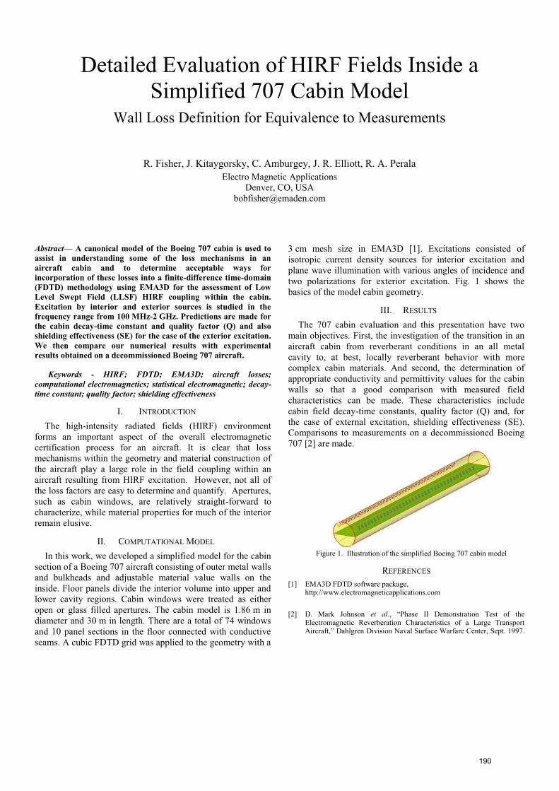
Abstract
Keywords - HIRF; FDTD; EMA3D; aircraft losses; computational electromagnetics; statistical electromagnetic; decay-time constant; quality factor; shielding effectiveness
190

Interior Aircraft HIRF Environment Above 400 MHZ Comparison of Computed Fields, Measured Fields and Ideal Reverberation Chamber Fields
James R. Elliott, C. Amburgey, R. Fisher, C. Weber, J. Kitaygorsky, T. McDonald, R. Perala, G. Rigden
Electro Magnetic Applications, Inc. Denver, CO USA
Robert Johnk, Chriss A. Hammerschmidt Institute for Telecommunications Sciences (NTIA/ITS)
Boulder, CO USA
Abstract— For HIRF environments above 400 MHZ, a common path to certification uses low level swept field measurements on a full aircraft to obtain the attenuated field levels inside the aircraft. Then, individual equipments or even systems are qualified to these attenuated levels using anechoic or reverberation chambers. Computational electromagnetics is increasingly becoming a valuable tool to support the certification process by allowing early evaluation of design options as well as permitting more detailed examination of the interior aircraft HIRF environment than is practical with measurement alone. In this paper, key aspects of computed electromagnetic fields are compared to those observed in an extensive program that made both interior quality factor measurements and exterior shielding effectiveness measurements on four different commercial aircraft [1-4]. Further, the ideally statistical fields obtained in reverberation chamber testing [5] are compared to the fields computed and measured in aircraft cavities.
Keywords- HIRF; computation; measurement; reverberation chamber, quality factor; shielding effectivenes;
I. INTERIOR HIRF EXCITATION
One way to characterize the response of an aircraft to HIRF is to use internal excitation, focusing on the statistical nature of the fields for a cavity as a whole or on the details of the fields as a function of position and polarization. This approach is sensitive to absorption and leakage out of apertures as reflected in decay times, quality factors and statistical measures such as cumulative probability functions. Whereas these quantities are global in a reverberation chamber, inside an aircraft they exhibit strong position dependences as illustrated in Fig.1. Further computed and measured results will be presented to delineate the interior response.
II. EXTERNAL HIRF EXCITATION
External excitation is more commonly used in HIRF LLSF measurements to obtain attenuation or shielding effectiveness for multiple angles of incidence and polarization. Explicit guidance for statistical characterization of shielding effectiveness is given in ARP 5583A, External excitation combines aperture coupling with absorption and leakage losses from the cavity. Fig. 2 shows measured field penetration variations for a B737 [2]. Other computed and measured penetrations will be compared.
Figure 1. Magnitude of computed interior field component vs. position
Figure 2. Penetration vs. angle of incidence, polarization and frequency [2]
REFERENCES
[1] “Phase II Demonstration Test of the Electromagnetic Reverberation Characteristics of a Large Transport Aircraft”, Dahlgren Division Naval Surface Warfare Center, NWSCDD/TR-97/84, September 1997
[2] “Electromagnetic Airframe Penetration Measurements for the FAA Passenger Jet 737-200”, NIST Technical Note 1549, March 2010
[3] “Electromagnetic Airframe Penetration Measurements for the FAA Bombardier Global 5000”, NIST Technical Note 1547, June 2008
[4] “Electromagnetic Airframe Penetration Measurements for a Beechcraft Premier IA," Natl. Inst. Stand. Technol. Tech. Note 1548 August 2008
[5] David A. Hill, “Electromagnetic Fields in Cavities, Deterministic and Statistical Theories”, IEEE Press, Piscataway, NJ 2009
191

Abstract
Keywords-component; HIRF-SE; Shielding Effectiveness;Power Balance; Method of Moments; LLSF; Reverberation Chamber; HIRF Certification;ED107 Standard;
192

Combining Asymptotic Methods and Power Balance Approaches to simulate HIRF HF scenarios
N. Douchin, N. Moreau, G. Moura OKTAL Synthetic Environment
Toulouse, France [email protected]
I. Junqua, J-P. Parmantier ONERA – The French Aerospace Lab, F-31055,
Toulouse, [email protected]
Abstract— This paper describes the cooperative work achieved in the frame of the HIRF SE European FP7 project to combine a 3D asymptotic software and a Power Balance software. The objective is to assess high frequency EM coupling constraints in a complex system. Each code is briefly described along with its function in the combination scheme. This method has been applied to several HIRF scenarios and validated in the HIRF SE project.
Keywords-HIRF; software computation; asymptotic methods; shouting and bouncing rays; Power Balance approach
I. INTRODUCTION
ONERA and the OKTAL-SE groups have been cooperating for more than 10 years in the development of numerical simulation tools with the ambition to calculate scattered electromagnetic fields at high frequency (the size of the objects is supposed to be large compared to the wavelength) in a complex modelled 3D scene including the environment. This cooperative work has first focused on radar applications [1] and extended to antenna radiation simulation. As illustrated hereafter, more recently both entities have initiated a cooperation on EMC issues in the HIRF SE project. This project aims at providing to the aeronautic industry a numerical modelling computer framework for HIRF aircraft/rotorcraft (A/C) certification purposes.
II. DESCRIPTION OF SE-RAY-EM SOFTWARE
The SE-RAY-EM software is based on a combination of Shooting and Bouncing Rays (SBR) technique, that has been optimized to calculate efficiently the intersections between rays from the transmitter towards the 3D database and back to a receiving point, and EM models for computing propagation, reflection and diffraction. These models are the formulations of Geometrical Optics (GO), Physical Optics (PO) and Equivalent Current Method (ECM). An operating strategy enables unified calculation for the near or far EM scattered fields from the scenes. The “forward scattering” approach based on the equivalence principle is also used to compute EM fields in the shadow region. Since it relies on asymptotic methods SE-RAY-EM is well suited for computing the EM interactions of an incident wave with a complex object at high frequencies typically in the 1 – 100 GHz range. In the HIRF SE project SE-RAY-EM is used for computing the EM field on the external surface of the A/C, at the points of entry up to 40 GHz.
III. THE POWER BALANCE METHOD
At high frequency, system cavities as in A/C are electrically oversized. Their geometry and constitution are not fully controlled. Therefore, EM environment in such a system can be characterized by a probabilistic model for which the relevant parameters are the mean power densities, the mean dissipated or the transmitted powers. These relevant parameters are evaluated by the Power Balance (PWB) method, developed by ONERA [2]. The resulting PWB computer code is based on a network representation of EM interactions in oversized cavities, taking into account energetic budgets, such as dissipative effects and transfer of energy between cavities
IV. COMBINING SE-RAY-EM AND PWB
Since the initial problem of EM HIRF HF coupling in complex oversized structure cannot be modelled as a whole, it is split into 2 elementary independent problems: - The “external EM problem”. It consists in solving with SE-RAY-EM the EM interaction between the incident EM interference with the external surface of the A/C. - The “internal EM problem” is solved by the PWB approach to obtain derive internal EM interference. The excitation terms are deduced from the incident EM environment at POE level, previously evaluated.
V. APPLICATION EXAMPLES
An example of application and validation in HIRF-SE of the methodology will be illustrated on a Piaggio P180 nose cone (Fig.1).
External Problem E-field mapping computed by SE-RAY-EM at 1GHz
Internal Problem PWB network modelling
Figure 1. Computed E field on the nose of an aircraft & PWB model.
REFERENCES
[1] H.J. Mametsa, S. Laybros,& Co, “FERMAT: A high frequency EM scattering code from complex scenes including objects and environment” Progress in Electromagnetic Research Symposium (PIERS 04), Pisa, Italy 28-31 March 2004.
[2] J-P. Parmantier, I. Junqua, “EM topology from theory to application”, In UWB, short-pulses Electromagnetics 7, Volume 7, pp 3-11, Oct 2006.
The research leading to these results has received funding from the European Community’s Seventh Framework Programme [FP7/2007-2013] under grant agreement no 205294.
193

EMC HIRF certification demonstration ofthe SETHI radar system
I. Junqua, F. Issac, L. Guibert, J. Besson ONERA – The French Aerospace Lab, F-31055,
Toulouse, [email protected]
S. Langlet, P. Dreuillet ONERA – The French Aerospace Lab, F-91761,
Palaiseau, France
TAbstract T— This paper addresses the work carried out to demonstrate the HIRF certification of ONERA’s onboard SAR system named SETHI For this, ONERA focused on evaluating the electromagnetic (EM) field possibly generated by the pod antennas inside the cockpit and inside the cabin at frequencies considered as the most critical in terms of EM coupling inside the aircraft. 3D calculations of the EM fields inside the cockpit and onto the cabin windows have been made using a computing code based on the resolution of the integral equation in frequency. EM fields inside the cabin are estimated thanks to a Power Balance approach which inputs are the external EM fields previously computed on the cabin windows, the shielding effectiveness of the cabin windows and the measured quality factor inside the cabin.
Keywords-EMC, DO-160, RTCA-ED-14, HIRF, Aircraft Certification, Standards
I. INTRODUCTION
Since 2004, in order to replace the former RAMSES Radar system for SAR imaging applications, ONERA has been working for the conception of the new SETHI radar system. SETHI is dedicated to civil teledetection activities based on SAR imaging in P, L and X bands. This radar is constituted of 2 pods installed on a Falcon-20 as in Fig. 1. In order to obtain flight authorizations and provide justification for EMC certification, ONERA has been asked to demonstrate that the radar could not induce any malfunction on the aircraft. ONERA’s approach consisted in demonstrating that the levels induced by the new system did not overcome those of the DO160 standard for which the onboard equipment was already certified. In this paper, among all scenarios of RF interference we are interested in possible interference, due to the antennas located in the pod systems, and induced in the most sensitive areas, the cockpit and the cabin.
Inside the POD-Video Camera-Positioning system-Antennas and microwaves systems -Inertial measurement unit-Accelerometer-Command and control systems
Inside the cabin-Waveform generator, Radar control commands-Microwave devices (Amplifiers, switches,…)-Acquisition and video storage-Guiding and positioning system (GPS, inertial measurement unit)
Figure 1. SETHI system on Falcon-20
The methodology of the EMC demonstration is based on an analysis of the worst case antenna position configurations, at 2 specific frequencies in the P band, 3D calculations in the cockpit and onto cabin windows and finally a power balance approach to evaluate EM fields in the cabin.
II. 3D NUMERICAL SIMULATIONS
3D calculations have been carried out thanks to ONERA’s ELSEM3D computer Method of Moment code in the frequency domain as illustrated in Fig. 2.
Absence de verrière
Hublotscourt-circuités
Antenne sur POD
No canopy
Short-circuitedwindows Antenna on POD
Absence de verrière
Hublotscourt-circuités
Antenne sur POD
No canopy
Short-circuitedwindows Antenna on POD
Calculation of EM fields in the Cockpit Calculation of EM fields on short-circuited windows
• 2 Frequencies in Band P 225MHz – 470MHz • 88 300 unknown • calculation with symetries • CPU time for 2 frequencies=11h
AntenneFréquenc
Emax=4.607e-4V/mEmin=7.69e-5V/m
Hmax=1.182e-6A/mHmin=1.4521e-7A/m
Polarisation 1
AntenneFréquenc
Emax=4.607e-4V/mEmin=7.69e-5V/m
Hmax=1.182e-6A/mHmin=1.4521e-7A/m
Polarisation 1
Antenna at the rear (20degres)Frequency=225MHz
EM fields in the Cockpit
Figure 2. 3D calculstion approach
III. EVALUATION OF EM FIELDS IN THE CABIN
Here, since the cabin can be considered as electrically large compared to the wavelength, it is possible to apply power Balance concepts to assess induced mean electric fields [1]. For this, E-fields are deduced from the previously 3D computed E-fields on short-circuited cabin windows, from analytical formulas of coupling cross section of the cabin windows and from an experimental evaluation of dissipative mechanisms in the cabin.
IV. CONCLUSION
In the oral presentation, we will give all details about the different steps of the whole methodology which combines 3D simulation, PWB concepts and experimentation.
REFERENCES
[1] J-P. Parmantier, I. Junqua, “EM topology from theory to application”, In Ultra-Wideband, short-pulses Electromagnetics 7, Volume 7, pp 3-11, October 2006.
194
Abstract
.
Keywords: Numerical simulation, HIRF, acceptance criteriria, design of experiment, IELF
195

Keywords EMC, HIRF, Computational electromagnetics
196

Simulations and Measurements of E Fields and EM-Excited Wiring Responses On Small Aircraft
1, Guido A. Rasek, Steffen E. Loos 2, Heinz D. B , Arne Sch der3
1 EMC & CEM Group, Evektor, spol. s r. o., Kunovice, Czech Republic, [email protected], [email protected] 2 EMC & EMP Tech. Group, , Moggast, Germany, [email protected], [email protected] 3 In -Harburg, Germany, [email protected],[email protected]
Abstract Fullwave 3D simulations of internal electromagnetic environment and its responses in the airborne wirings were carried out using a digital mockup of a real small aircraft. Numerical results are compared to experimental results of aHIRF certification test carried out in a semi-anechoic chamber.
Keywords - digital mockup, electromagnetic simulations, stressed wiring response, small aircraft, experimental test, HIRF
I. INTRODUCTION
Safety-critical functions executed by a modern avionics and use of modern materials on airframe skin are sometimes conflicting trends in the nowadays aerospace industry. Internal EM environment of aircraft is a stressing factor for airborne systems acting through the wiring and must be carefully examined in the processes of aircraft designs before a materialization of the first prototypes. A recent precipitate development in computational electromagnetics (CEM) and nowadays powerful computers make the virtual testing of such internal EM environment and its responses in wiring on digital mockups possible. If no present solver can be used as universal tool meeting all requirements for such EM simulations, an advanced EM computational toolbox is necessary for effective exploitations of laborious deterministic models created by meshing of standard CAD geometries. This toolbox is created in continuance of the HIRF-SE collaborative research project (7-th Framework Programme of EC) [1], where a common platform of the EM model data structure (AMELET-HDF) is established [2] to unify a data format for various EM solvers(full-wave TD/FD, asymptotic and stochastic for EM fields calculations and MTLN for wiring responses calculations) integrated within the HIRF-SE framework. Authors of this paper are involved in building of computational models, execution of appropriate simulations on them and experimental verifications of the above mentioned validations.
II. BUILDING OF COMPUTATIONAL MODELS
A virtual prototype of small reciprocating single-engine four-seater VUT100 Cobra was used for the creation of a digital mockup applicable for the simulations. Due to geometrical complexity and material diversity of the aircraft, the virtual prototype preparation from its standard quality CAD data was a tedious and time-consuming task [3].
III. SIMULATIONS
The HIRF-SE framework has integrated 3D full-wave solvers working in frequency as well as in time domains. Representatives of them (CONCEPT II of TUHH and MWS ofCST respectively) were chosen for calculations of stressing EM field on the wiring. The wiring responses were consequentially calculated by the Multiconductor Transmission Line Network solver (CRIPTE) [4] that is also integrated within the framework.
IV. EXPERIMENTAL TEST
The first flying prototype of VUT100 Cobra was tested in the semi-anechoic chamber of EMCC in Unterleinleiter, Germany. Classical low-level tests according to EUROCAE ED-107 were carried out when exciting the aircraft by direct current injection (DCI) and by consequential illuminations using antennas (LLSC).
Figure 1. VUT100 Cobra in EMCC semi-anechoic chamber illuminated by a log-periodic antenna, frequency range from 20 MHz to 200 MHz
REFERENCES
[1] http://www.hirf-se.eu/hirf/ [2] http://code.google.com/p/amelet-hdf/[3]
in Small Aircraft and Experimental Test Comparisons. Proceedings of EUCAP 2012 Conference, unpublished
[4] Parmantier, J.P. at al: Modelling of HIRF coupling on Complex Cable Architectures, Proceedings of ICEAA 2011 Int. Conference, p.219-222
The research leading to these results has received funding from the European Community's Seventh Framework Programme [FP7/2007-2013] under grant agreement no 205294.
197

Keywords: HIRF, FDTD, MTLN
198

Keywords: HIRF, FDTD, MTLN, LLDD
199

On the possible use of numerical simulation during HIRF certification process
J-P. Moreau Dassault-Aviation, 78 Quai Marcel Dassault Cedex 300 92552 St Cloud Cedex -FRANCE [email protected]
M. Bozzetti Alenia Aermacchi, Strada Malanghero,
10072 Caselle Torinese (TO) – Italy [email protected]
J -C. Lamy,, European Aviation Safety Agency
Postfach 10 12 53 D-50452 Cologne Germany
Abstract— This document details the proposal to use numerical simulation in the HIRF certification process of an Aircraft. It recalls the basic concept of the HIRF certification as defined in regulatory documents such as AC 20.158 and ARP 5583/ED 107, and explains the role that can be played by numerical simulation into the route to compliance to the rule. The benefits of this approach are discussed in terms of better confidence in the certification process, reduction of measurements, and substantiation of similarity arguments. In particular it explains how the test ground data can be converted into a free field environment. It is acknowledged also that measurement campaigns will still remain necessary to some extent, for calibration purposes.
Keywords-component; Aircraft certification, HIRF, HIRF SE,AC 20-158 ED107/ARP5583A
I. INTRODUCTION
The route to compliance to the High Intensity Radiated Field Aircraft regulations (AC20-158) requires the determination of the internal electromagnetic environment of critical systems for being able to verify that this environment remains below the equipment qualification. The increasing number of system critical functions inside the new generation aircraft will induce bigger and longer EM environment measurement campaigns unless new approaches are developed. The numerical simulation aiming to assess the EM environment of critical systems inside an aircraft impinged in a electromagnetic field can help to maintaining the measurement campaigns inside reasonable cost and timeframe. Furthermore numerical simulation can improve the accuracy of the measurements by better accounting for the differences between free field illumination and ground test illumination, by getting data for various field configurations and for inaccessible locations, thereby insuring better coverage of system environment. The purpose of this paper is to show how these numerical simulations can be inserted inside a certification process
II. EM SIMULATION DURING HIRF CERTIFICATION PHASE
The common practice, as indicated by Advisory Circular AC-20-158 and applicable recommendation ED107/A-July 2010, is to determine the internal Electromagnetic field environment during ground tests over a frequency range from 10kHz to
18GHz using low power generators. The actual aircraft environment is then scaled to the High values of the HIRF requirement.
It is important to point out that the HIRF requirement concerns free field plane wave illumination and that the evaluation of the aircraft environment is typically achieved by measurements on the ground where free field conditions are not easily reproduced. Moreover, the limited number of measurements (between 100 and 1000) may become insufficient to cover the environment of the increasing number of level A complex systems. Therefore, the advantages of using a fully validated tool like HIRF SE become obvious: the numerical simulation provided by HIRF SE can be used to compute the environment around the equipment in free field conditions as well as in the test setup environment; HIRF SE can provide a much larger set of data than the one provided by measurements and offer the amount of samples/data suitable for modern complex systems.
At the moment two different applications are proposed (Figure 1): a short term application and a long term application The short term application will only use HIRF SE for tuning the test setup and compute corrections factors to apply to ground measurements to convert the data into free field environment data. These corrections factors will not only be based upon surface current but also on internal computed currents. The long term application will use direct computation of free field data that will be eventually calibrated by comparison between ground measurements and ground simulation.
Figure 1. HIRF SE roadmap for certification
The research leading to these results has received funding from the European Community’s Seventh Framework Programme [FP7/2007-2013] under grant agreement no 205294.
200

Numerical Simulations for HIRF Certification Benefits and Challenges
R.A. Perala PhD, J.R.Elliott PhD, T. McDonald PhDElectro Magnetic Applications, Inc.
Denver, CO USA [email protected]
Abstract
Keywords-component; HIRF, numerical simulation, aircraft certification
I. INTRODUCTION
The HIRF certification process of a commercial aircraft is described in the relevant regulations and advisorydocumentation. This process is complex and expensive, withsignificant cost, schedule and technical risks for the applicant. This is particularly true for Level A Control Systems, for which the applicable qualification DO-160 test levels must be determined by full aircraft LLSC and LLSF testing. (Note: full aircraft high level testing is also an acceptable approach.)Numerical simulation of the HIRF response of an aircraft can significantly benefit the HIRF certification process. These benefits include optimization of the HIRF and other E3 environment protection designs, development of a model that can be used for other E3 considerations (e.g., lightning), determining the HIRF LLSC and LLSF environments to flow down to vendors, reducing risk that the aircraft and its systems will pass final HIRF qualification testing, and planning LLSF and LLSC tests and interpretation of their results. Finally, amodel that has been validated on an aircraft can then be confidently used to evaluate future version of this aircraft.
II. SIMULATION AND EXPERIMENTAL ACCURACY
Confidence in numerical simulation accuracy is usually obtained by comparisons of numerical and experimental results. It is necessary that both the certification authorities and the applicant understand that uncertainties exist in both numerical and experimental results.
Maxwell’s Equations solvers are not themselves significant sources of errors. In a numerical solution, the aircraft geometry is replaced by a mesh whose dimension places an upper bound on computational bandwidth and geometrical resolution. In addition, uncertainties can arise from the CAD import and model building processes, in which defeaturing and approximations to geometry are implemented. A larger issue arises from wire harness simulation. Wire harnesses are usually the last aircraft feature to appear in the CAD description, and HIRF simulations will need to be done long before the harnesses are well defined. Even if they are defined,
some wire harness parameters are not controlled, such the location of a particular conductor within a bundle, or even the precise location of a bundle with respect to its surrounding geometry. Finally, simulation accuracy depends upon accurate knowledge of material parameters, especially frequency dependent losses of dielectric materials, which are often unknown.
HIRF measurements have significant uncertainties. For example, NIST has indicated that their LLSF measurements of field penetration into aircraft cavities for a 95% confidence level have uncertainties of 8-10 dB [1]. For LLSC measurements, N. Carter has published LLSC measurementsfor 21 identical aircraft of the same type, and has found variabilities on the order of 16 dB [2]. Finally, all measurements are made with the aircraft over a lossy ground plane and with non-plane wave sources, which creates results different from that of an aircraft in flight.
III. THE NEED FOR SIMULATION MODEL COMPLEXITY
We need to include as much geometry, wire harness configuration and material complexity into the simulation model as is possible. This includes cable branching, cable frequency dependent skin depth losses, variability of conductor lengths within the same bundle, and location of individual conductors within a bundle. Internal structures of complex shape must be included, because they diminish cavity modes associated with geometrically regular structures.
IV. RESULTS PROCESSING
Post-processing of HIRF measurements includes bandwidth averaging and enveloping. The required frequency spacing of measured results is also not explicitly defined beyond 100 points/decade minimum. Numerical results need to be post-processed in a similar manner for comparison purposes.Specifics of post-processing and frequency spacing significantly affect wave-shapes and peak values of the results.
REFERENCES
[1] NIST & NTIA, “Electromagnetic Airframe Penetration Measurements for the FAA Passenger Jet 737-200”, NIST Technical Note 1549, March 2010
[2] Nigel Carter, Spread of EM Coupling Characteristics between Aircraft,presented to SAE AE4R HIRF Committee, 1986
201

Use of computational modeling for Lightning Indirect Effects / HIRF protection of aircraft & Use in certification processes
Franck FLOURENS and Frédéric THEROND EYDV - Installation Environment & Standard parts
Airbus Operations SAS Site de Saint Martin du Touch
316 route de Bayonne 31060 Toulouse Cedex 9 FRANCE
Abstract— This paper gives the outlook of the use of computational modeling for Lightning Indirect Effects (LIE) and HIRF protection of Airbus’ aircraft.
Keywords- Lightning Indirect Effects, HIRF, aircraft, certification, computational modeling
For LIE and HIRF protection, Airbus makes ample use of computational modeling at several stages of aircraft development, in particular Finite Differences Time Domain. The scope for modeling ranges from case studies at early stages of development to verification tasks for certification.
On hybrid composite aircraft, Lightning Direct and Indirect Effects are major design drivers for structure and systems. At the beginning of aircraft development, several protection options have to be assessed and compared to orient the design and allow decision making. Prediction tools are then of utmost interest to perform LIE trade-off studies and to determine the relative impact of main factors: cables shielding performances, installation rules, and electrical properties of structural parts (equivalent surface impedance). For LIE, the modeling approach is a “reasonable worst-case” with observables depending on the interfaces with the equipment suppliers, i.e. induced voltage and current on equipment pins and wiring. Within this framework, and at these early stages, there is no detailed definition of the aircraft but only main principles. The objective is to establish compromises between the specifications for equipment, the performance objectives of shielding means, and the structural protection (metallic wire-mesh) on composite panels. The interest is then principally on the most exposed zones of the aircraft (long wires to wing, vertical and horizontal tail planes, fuselage), and on the determination of the current flowing on the overshielded harnesses. Only the main cables routes are taken into account and incorporated in the numerical model. For such an implementation, the difficulty lies more in the proper selection
of input parameters (surface impedance for composite parts) than in the numerical model in its own right.
Afterwards, computational modeling is directly used for certification purposes to determine the ground-to-flight extrapolation functions for the Low-Level Direct Drive (LLDD) technique implemented to establish protection margins for both LIE and HIRF. The induction is then measured on a real aircraft, on ground, and the results have to be extrapolated to the in-flight situation. The final quantities of interest are the induced voltages and currents on the cables in flight, which are obtained further to the following stages:
Measurement on ground of the induced voltages and currents in the frequency domain. These measurements are scaled to the injected current on the structure for the relevant entry/exit points configuration. Multiplication of the measured voltages and currents by the ground-to-flight extrapolation function. The ground-to-flight extrapolation function is a weighting/correcting factor to apply to the on-ground measurements to get the in-flight results. The extrapolation function is based on the comparison of surface current densities on ground and in-flight; it gives the figure of merit of the ground test set-up. For LIE, multiplication by the lightning waveforms spectrums (WFA and H) and calculation of the time-domain induced levels via inverse-Fourier transform.
The pre-requisite for this process is that the on-ground test set-up is demonstrated capable of “stimulating” correctly the aircraft for the various entry&exit points configurations. This task is performed using computational modeling results of surface current densities.
.
202

The use of modelling in ED107A Guide for certification of aircraft in HIRF environment
M. PONÇONEurocopter France –
Route de l’aéroport - 13725 [email protected]
Abstract — This paper presents possible use of analytical methods in general and 3D modelling in particular as recommended by ED107A/ARP5583A, “Guide for certification of aircraft in High IntensityRadiated Field environment”.
Keywords-component; ED107/ARP5583; ElectroMagneticmodelling; HIRF; LLDD, LLSC
I. INTRODUCTION
The ED107/ARP5583A “Guide for certification of aircraft in HIRF environment” document provides key guidance in all domains leading to HIRF certification of an aircraft. It hasbeen updated in 2010 in accordance with new Federal Aviation Administration HIRF certifications rules and certification guidance released in September 2007. This new issue of the user guide is a total rework of the document which in particular takes into account the most recent knowledge acquired by industry since the first release of the document in January 2003. This knowledge includes the increasing use of modelling of EM coupling for design and certification purposes. Eurocopter has been using 3D modelling to support the EC 175 HIRF certification process. Example of this work will be provided to illustrate this presentation.
II. QUICK OVERVIEW OF ED107A ED107/ARP5583 has been established to recall or clarify many various aspect of the HIRF protection of Aircraft that should be made familiar to design as well as certification engineers. It starts with a synthesis of the origin of the HIRF environment, goes on with the specific aspect of the HIRF safety analysis and provides recommendation for the design of protections. Then the main part of the document focuses on the various routes to compliance and associated test methods. It ends with continued airworthiness considerations, addressing aircraft modification and ageing problematic.
III. INTRODUCTION OF EM MODELLING IN ED 107AThe first introduction to 3D computation is made in chapter 4 dealing with design considerations. Section 4.4 is indeed dedicated to analytical methods, how to choose and use them.Next (section 6.1) is related to the certification process. First possibility is to use analytical methods in determining the actual internal HIRF environment seen by the level A systems installed in the Aircraft. At this step, the key word is certainly validation, which basically means that test data will be made available to convince that the model used is adequate.
Section 6.3 presents High Level tests on aircraft. At low frequencies, a current injection on the aircraft structure is used to reproduce the envelope of the skin currents that would be flowing on the aircraft structure when exposed to various incident fields. 3D modelling is then part of the test methodology. Details are provided in 6.3.4, based on skin current distribution computed in the test set-up and in flight (see 6.4.1 skin current analysis). Similar considerations apply for Low Level Direct Drive coupling measurement test as described in 6.4.2 3D modelling can also be used in support of conventional radiated test, as mentioned in 6.3.7 to justify the reduced choice of antenna position for high level tests, or as mentioned in 6.4.3.1 to account for ground proximity effect when performing Low Level Swept Coupling test.It will be a very challenging aspect of the HIRF protection continued airworthiness, addressed in chapter 9, to anticipate, for new technologies in particular, the ageing profile of the aircraft and its impact on the HIRF protection. If an accurate model of the aircraft has been developed for the design and validated for certification phase, it will be a major support of modification certification, but it will be alsopossible to run parametric studies to assess the critical point of interest in the maintenance and the assurance plan. Even with the development of computer resources, such parametric studies may require to develop new calculation techniques in order to keep having reasonable duration of such studies.
IV. CONCLUSION
In conclusion it will turn out to be a very natural evolution that the quest for more safety at reasonable cost will result in a combined use of modelling and test, both considered at the same level of importance in the demonstration process. Indeed the ultimate confidence will be reached with very comprehensive test methodologies and cross correlation of the two approaches. In other words, measurements performed in the frame of certification will not remain the unique, and necessarily approximate, assessment of the aircraft coupling property but will turn out to confirm the prediction and therefore demonstrate that the assessment is totally under control. This was one of the key ideas of the 5 years MOVEA research program launched by DGA in 2003 which concluded in 2008 that this process and the associated tools can be considered operational. No doubt that the on-going HIRF-SE research program will reach the same conclusion and further consolidate the recommendation for well-balanced calculation and test approach for HIRF certification.
203

204

HPEM-TC08Bio effects and
MedicalApplications of EM
Fields
205

Acute effects of radiofrequency exposure to mobile phone upon human cutaneous microvascular tone
Radiofrequency exposure upon skin vasomotricity Nathalie Loos1,2, Valérie Brenet-Dufour2, Rania Ghosn3, Sophie Liabeuf2, Brahim Selmaoui3, Véronique Bach1,
György Thuróczy3, René de Seze3
1EA 4285 UMI-INERIS Laboratoire PERITOX
e-mail: Nathalie.loos-picardie.fr 2Centre de Recherche Clinique
Amiens, France 3INERIS
Verneuil-en-Halatte, France
Abstract—The study investigated in adults specific effects of radiofrequency field to mobile phone upon skin vasomotricity by laser Doppler flowmetry. The results showed larger BFc values under RF exposure than those under sham exposure, at equal value of skin temperature between the both exposures. These specific effects upon BFc due to the RF exposure were associated with higher neurogenic activity controlling the skin vascular tone, in comparison with sham exposure.
Key words: skin microflow, vascular tone, radiofrequency field, nervous sympathetic activity
I. INTRODUCTION The existence of specific effects of radiofrequency (RF)
exposure upon skin microflow (BFc) has been never shown. We hypothesized that the BFc variations due to RF exposure would be probably larger from those only due to the heating effects of electronic components of mobile phone. We also do not know whether the ability of cutaneous micro-vessels to vasodilate, may be affected under RF exposure. Moreover, the local sympathetic neuronal activity controlling the microvascular tone of the skin has never been studied.
II. MATERIALS AND METHODS The variations of BFc and skin temperature (Tc)
were performed simultaneously and at the same site, by using laser Doppler thermostatic flowmeter (LDF). One LDF probe was applied on the cheek near the ear lobe in ipsilateral (exposed), a second probe in contralateral (non-exposed) side of the head. Spectral analysis of skin LDF signal using the fast Fourier transform (FFT) algorithm was also performed. The frequency sub-interval [0.02-0.06 Hz] was specifically selected, since it reflects the nervous autonomic activity of smooth muscles of micro-vessels. The exposure system was a GSM 900 MHz mobile phone (max SAR=0.49 W/kg for 10g of tissue). The sham exposure was done by connecting an external 50-ohm RF resistive load to the remote antenna connector of the phone.
Twenty one healthy adults were studied (mean age: 25 ± 0.9 yrs). Two random sessions by using 2 mobile phones were performed in double-blind way: 20 minutes under real RF or sham exposure. Data of BFc (expressed as perfusion unit PU) and Tc were analyzed within 1 minute of recording before (T0: at 5th min.) and during mobile phone exposure (at 1st, 5th, 10th, 15th and 20th min.). BFc variations were expressed in percent of baseline (i.e., T0). For determining the vasodilatory reserve of cutaneous micro-vessels, a standard provocative heating test was performed post-exposure by heating locally the cutaneous temperature up to 44°C. Statistic comparisons between exposed- and non exposed- cheek, and between RF- and sham- exposure, were performed by using paired Student’s t tests following one-way ANOVA analysis.
III. RESULTS AND INTERPRETATION Under RF exposure, the BFc from exposed side of the
head was significantly increased compared to the non-exposed side by +38.5% of baseline (vs -3.6 %, t= 4.81, P<0.001) to +175 % (vs -4.2, t=5.50, P<0.001) from the 1st to the 20th
minute of exposure, respectively. Tc of exposed side was also increased compared to the non-exposed side by +1.0 ± 0.1 °C (t=6.57, P<0.001) to +2.7 ± 0.2°C (t=17.88, P<0.001) from the 1st to the 20th minute, respectively. These increases were of same amplitude than those under sham exposure, whereas BFc variations were 4 times larger under RF exposure (at the 20th
minute) than those under sham exposure (P<0.001). This suggests thus the existence of specific electromagnetic effects determined by delta difference of BFc between “real” and “sham” exposures on exposed side. Moreover the heating test the vasodilatory reserve of skin micro-vessels under RF exposure was significantly larger than that under sham exposure (t=2.98, P<0.01). It was accompanied with higher local sympathetic neurogenic activity according to the results of FFT analysis on LDF recordings (t=5.56, P<0.0001).
IV. ACKNOWLEDGMENTS We want to thank Pr Jean-Pierre Libert for his advices.
Financing « Post-Grenelle » by the french Ministery of Ecology in the frame of “Pôle Applicatif en Toxicologie et Eco-toxicologie porté par l'INERIS”.
206

Intentionally blank
207

Keywords- blood glucose, resonant frequency, phantom
208

Abstract
Keywords- inverse scattering; biomedical microwave imaging;contrast source inversion; finite-element method.
209

Influence of High Power Microwave Pulses to Properties of Seeds
Mindaugas Dagys, Rimantas Simniškis, Paulius Ragulis, Žilvinas Kancleris
Microwave laboratory, Center for Physical Science and Technology, A. Goštauto 11, Vilnius LT-01108, Lithuania
Irena Gauril ikien , J rat Ramanauskien , Audrius Radzevi ius, Sandra Sakalauskien
Lithuanian Research Centre for Agriculture and ForestryInstituto al. 1, K dainiai distr. LT-58344 Lithuania
Abstract— The impact of microwave radiation on properties of seeds of vegetables and crops was investigated. The experimental setup for seeds radiation in free space and rectangular waveguides was designed. Radiation of objects has been performed for fixed microwave frequencies at S (2.6 GHz), C (5.7 GHz) and X (9.3 GHz) bands. Duration of pulses in the rage of 4-6 s and repetition rate 25 Hz have been used. The analysis of properties of vegetation, growth of radiated seeds and parasitic contamination was performed.
Keywords-seeds ;high power microwave pulse.
I. INTRODUCTION
Nowadays has been a dramatic increase in the production and use of microwave technologies all over world. Thousands of scientists investigate microwave radiation effects on the biological objects. Most of them are devoted to the investigation of thermal influence on biological objects using microwave ovens. On the other hand, it is very important to investigate influence of high power microwave (HPM) pulses on the biological objects trying to distinguish between heating and direct influence of strong electric field to them. We prepared experimental set up for radiation of different seeds using HPM pulses In the present contribution the investigation and analysis of properties of vegetation, growth of radiated seeds and parasitic contamination was done. The impact of microwave radiation on seeds properties from different year of storage was investigated. It was carried out the research of influence of microwave radiation on seeds contaminated by the most harmful pathogenetic micromycetes.
II. EXPERIMENTAL SET UP
The experimental setup for microwave radiation, monitoring and diagnostics on the basis of original resistive sensor (RS) [1] was developed and built. HPM pulse radiation experiments have been performed in a semi-anechoic chamber for fixed microwave frequencies at S (2.6 GHz), C (5,7 GHz) and X (9,3 GHz) bands. Microwave pulses up to 100 kW peak powers, duration of which was in the range of 4-6 s and repetition rate 25 Hz have been used. Horn antenna has been employed to illuminate the object under test. Pulse power transmitted to the horn antenna has been controlled with the resistive sensor. The RS connected to the other horn antenna has been used for direct measurement of the electric field
strength that is applied to the object under test. The set of holders for seeds radiation in free space and rectangular waveguides was developed and fabricated. The several sorts of vegetables and crop seeds have been illuminated by high level non-heating microwave electric field. Seeds of radish, tomato, carrots, spring wheat, spring barley, oat and pea have been tested in pulsed microwave electric field strength up to few hundreds kV/m. Illumination time was from 5 up to 10 minutes.
II. RESULTS AND DISCUSSION
The study results show that HPM radiation increases radish seeds germination energy for about 6%. Affected by HPM radiation tomato seeds increases their germination by 8.7 %. Microwaves exposure significantly increases the germination and germination energy of carrot seeds. We observed some increase of germination of 11-year-old carrot seeds subjected by microwave radiation but the germination percentage was very low. Study of different microwave frequencies and the different effects of radiation time have shown that the highest impact on seed germination was revealed at 9.3 GHz frequency and 5 minutes exposure. But the increase of exposure up to 10 min at 2.6 GHz substantially reduced carrots seed germination.
We found any influence on germination of wheat seeds illuminated by HPM. But the reduction of germination of spring wheat and spring barley seeds treated for 5 min. at 2.6 GHz and oat seeds at 9.3 GHz was observed. However the germination of pea seeds treated at 9.3 GHz was significantly higher than that of untreated. In the field conditions, in many cases 9.3 GHz microwave treatment significantly improved spring wheat, barley and oats seed germination.. The effect of HPM on seeds infestation with seeds borne pathogenic fungi varied between the cultivars and treatments. Seed infestation varied under the impact of microwave treatment; the reduction of some genus of fungi was followed by an increase of another genus. Conversely, in microwave treatments in many cases we noticed an increase in root and crown roots of cereals.
REFERENCES
[1] M. Dagys, Ž. Kancleris, R. Simniškis, E. Schamiloglu, and F. J. Agee. “Resistive Sensor: Device for High-Power Microwave Pulse Measurement”, IEEE Anten. Propag. Mag., 43, (5), pp. 64-79, 2001.
This research was funded by a grant MIP-040/2011 from the Research Council of Lithuania
210

UWB-TC09Antenna Design,
Radiation and Propagation
211

Propagation of Short Pulses through an Ionosphere Modelled by a Cold Plasma
Dr. D. V. Giri* Pro-Tech, 11-C Orchard Court, Alamo, CA 94507, USA Dept. of ECE, University of New Mexico, Albuquerque,
NM 87130 USA, E-mail: [email protected]
Prof. Steven L. Dvorak Dept. of ECE, The University of Arizona
Tucson, AZ 85721 USA E-mail: [email protected]
Abstract— In this paper based on [1], we have studied the propagation of a short, impulse-like transient waveform propagating through the ionosphere. The short pulse incident on the ionosphere is the radiated pulse from the prototype impulse radiating antenna (IRA) [2]. The ionosphere is modeled by a cold plasma with known attributes of plasma and collision frequencies. The focus here is how the IRA pulse propagates and hence known properties of simplified plasma are used. It is not our intent to analyze the ionosphere, but get an idea of how the IRA pulse goes through it. The impulse propagates as an impulse followed by a long tail. Closed form expressions for the propagated waveform are also compared with numerical results obtained by a convolution process.
Keywords- short pulse, ionosphere, propagation, cold plasma, plasma frequency, collision frequency, dispersion
I. INTRODUCTION
Short pulse technologies are finding many applications in transient radar, target identification, wideband jammers, etc. The pulse durations are typically 100’s of ps and the bandwidths range from 10’s of MHz to several GHz. All such applications will involve short pulse propagation through, or interaction with, many media such as the earth’s surface, water, and the earth’s atmosphere. In this paper, we focus on the interaction of approximate impulses with the earth’s atmosphere. When the ionosphere is modeled by cold plasma with a fixed plasma frequency, the resulting dispersion of the pulse is similar to the propagation in a waveguide filled with a homogeneous medium [3].
II. PROPAGATION CHARACTERISTICS
The geometry of the problem and the incident short pulse are shown in Figure 1. The trans-ionospheric pulse is shown in Figure 2. The incident pulse created by the prototype IRA has no DC component and has spectral content ranging from 40 MHz to 4 GHz. The impulse response of cold plasma model is known in closed form [3] and is convolved with the incident spectrum. The resultant pulse, after propagation through the ionosphere is given by equation (1). All the parameters in equation (1) are known [1]. Analytical and numerically computed trans-ionospheric waveforms are in good agreement.
Figure 2. Trans-ionospheric propagation for the case of Ne = 1.12 x10¹² electrons/m3 or fp = 9.54 MHz.
References [1] D. V. Giri and S. L. Dvorak, “Propagation od Impulse-Like Waveforms
through the Inonosphere Modelled by a Cold Plasma, Theoretical Note 366, 2 February 1996.
[2] D. V. Giri, . M. Lehr, W. D. Prather, C. E. Baum, and R. J. Torres, “Intermediate and Far Fields of a Reflector Antenna Energized by a Hydrogen Spark-Gap Switched Pulser”, IEEE Trans. Plasma Science, Oct. 2000.
[3] S. L. Dvorak and D. G. Dudley, “Propagation of Ultrawideband Electromagnetic Pulses Through Dispersive media, “ IEEE Trans. on Electromagnetic Compatibility, vol 37, no 2, 2 May 1995, pp 192-200.
Figure 1. Geometry of the Problem (left) and the incident short pulse (right)
(1)
212

Antenna radiation in the presence of an infinite interface
Yannick Béniguel IEEA
Courbevoie, france [email protected]
Abstract—Two calculations techniques allowing to determine the current distribution on antennas placed at the vicinity of one or several interfaces between different media will be presented. In both cases the Green function is modified to avoid the meshing of the interfaces.
Keywords: complex images, HF antennas, surface wave
I. INTRODUCTION
This paper addresses the problem of antennas placed at the vicinity of one or several interfaces between different media. This kind of structure is very common. It includes the case of HF antennas above the air ground interface but also the case of multilayer microstrip antennas. Use of the integral equation technique for the resolution consists in introducing a magnetic and electric current distribution on all interfaces. However this technique fails to consider infinite interface and may become costly in case of large structures. One alternative procedure consisting in a Green’s function modification is presented in this paper.
II. METHOD OF SOLUTION
In order to meet the boundary conditions at the interface, the integral equations shall be modified. Additional terms are introduced both for the vector and scalar potential. The solution is not unique, as stated by Michalski, who has introduced three possible different formulations. Among these three, according to Michalski notations, formulation C is the most convenient and will be presented. The new equation, named Mixed Potential Integral Equation (MPIE) includes the additional terms related to the Green function modification.
The MPIE equation is composed of integral terms which involve for all of them the so called Sommerfeld integrals written in a slightly different way in this formulation. These integrals are known to be poorly convergent making the problem subject to inaccuracy and CPU time consuming. Two techniques can be employed to calculate them: the classical phase stationary technique and the complex images technique. In the first case the steepest descent contour shall be found. It
is a different one for all the integral terms. As an alternative, the complex image technique consists in splitting the integrals into three different terms for the contour, the poles and the quasi static contribution. All these terms are regular and rapidly convergent making this technique very appropriate.
Figure 1: the elementary field contributions to the total scattered field obtained by the complex image theory
Figure 1 shows the field decomposition as obtained by the complex image technique : surface wave and sky wave contribution can in particular be identified.
III. CONCLUSION
The MPIE formulation and a comparison of integral terms evaluation by the two techniques here above indicated will be presented. These two techniques being very different, this brings a strong confidence in the obtained results. We will finally present how the technique can be extended for multilayer materials as is often the case in microstrip antennas.
REFERENCES
[1] K. Michalski, J. Mosig “Multilayered Media Green’s functions in Integral Equation Formulations” IEEE Trans on Antennas and Propagation, Vol 45, N° 3, March 1997
[2] M. Aksun, G. Dural, “Clarification of Issues on the Closed Form Green’s function in stratified media” IEEE Trans on Antennas and Propagation, Vol 53, N° 11, November 2005
-1.5
-1
-0.5
0
0.5
1
-2 -1.5 -1 -0.5 0 0.5
Gzzepsr = 5 ; sigma = 0.005 ; f = 11.3 MHz
complex imagesSurface waveQuasi statiqueTotal
Log
( )
Log(k ro)
213

Compact, High-Power, Self-Resonant Antenna Based on Rapid Discharge of Conical Spiral Antennas
Miena Armanious and J. Scott Tyo College of Optical Sciences
University of Arizona Tucson, AZ 85745 USA
Michael C. Skipper and Michael D. Abdalla ASR Corporation
9817 Bursera Ave, NW Albuquerque, NM USA
Abstract— One strategy that can be used for mesoband sources is to charge up an antenna and then discharge it through a fast-closing switch. So long as the switch closure is fast compared with the period of the fundamental resonance, the antenna will ring. This allows the stored energy to radiate away from the structure. When the desired frequency is low, this strategy is limited because of the need for the resonant structure to be comparable to the wavelength in size. In this paper we present a strategy that adapts a conically-wound spiral to serve as both the energy storage and the pulse forming line. The symmetry of the spiral is broken at the feed, and the arms are capacitively coupled to force the currents to flow along the full length of the would spiral. The result is an antenna that resonates at 38 MHz with an overall size of a = 60 cm, resulting in ka = 0.47, satisfying the conventional definition of electrically small antennas.
Electrically small antenna, mesoband sources, transient antennas.
I. INTRODUCTION
Mesoband sources are designed to have bandwidth on the order of 10%. One simple strategy for making a mesoband source is to charge up an antenna then discharge it through a fast closing switch. This allows the antenna to resonate in its fundamental frequency, thus converting the DC stored charge into microwave energy as depicted in Figure 1.
Figure 1. Self-resonant antenna concept for Mesoband HPM sources
When the desired radiation frequency is low, this strategy is limited by the large size required of the resonant antenna. The traditional way to achieve resonance is to have the antenna be a half wavelength. For frequencies below 50 MHz, this
corresponds to antenna sizes of 3 m and larger, which are too large to practically be applied in many scenarios.
II. ANTENNA DESIGN
Best and others faced a similar challenge when designing electrically small antennas [1,2]. Best specifically considered the case of a volume-filling spiral antenna that efficiently occupied the available volume (and associated surface area) with current-carryin wire. We have leveraged this concept while considering the details that are required for a HPM source. Figure 2 shows the evolution of the design of the biconical antenna to the asymmetric conical spiral antenna that we discuss in this paper.
Figure 2. Starting with a standard bicone, we can move to a conical spiral. Then, by breaking the symmetry at the feed, we can almost double the electrical length of the antenna while preserving the HPM properties.
Resonant properties are at right.
As expected, as the resonant frequency is lowered while maintaining the physical size results in a narrower bandwidth. This corresponds to the Chu-limit performance on the Q of electrically small antennas.
REFERENCES
[1] S. R. Best, “A discussion on power factor, quality factor and efficiency of small antennas,” IEEE Trans. Antennas Propagat. December 2001.
[2] J. R. McLean, “A re-examination of the fundamental limits on the radiation q of electrically small antennas,” IEEE Trans. Antnenas Propagat. May 1996.
214

Limits on Ultra-Wideband Field Inference From a Lightning Return Stroke
Robert L. Gardner, ConsultantAlexandria, VA, USA
Abstract—This paper considers the potential effects of two phenomena on fields emitted by a lightning return stroke and how those effects can skew the implied currents. These two effects are the preferential attenuation of high frequency currents as they propagate up the channel and the preferential attenuation of high frequency fields by lossy ground.
Keywords-lightning; ultra wideband; lightning currents
I. INTRODUCTION
Lightning return-stroke currents are often derived from the fields emitted by the return stroke. The derived bandwidth of the currents can be limited by the technique used to invert the current-field relationship. Two phenomena that can mask the full bandwidth are 1) the effects of lossy ground on the distant fields and 2) the changes in the current waveform as the current propagates up the channel.
To show the effects of lossy ground, we will compare the current derived from a simple transmission-line model with a simple lossy ground dipole model. Only simple dipoles will be used to illustrate the ideas to allow use of analytic models. Illustrations of both horizontal and vertical polarizations will be presented. Earlier calculations [1] have shown that, in some interesting cases, effects of the lossy ground can mask very short rise time fields.
To show the effects of variation of current along the return-stroke channel, we will use a simple analytic model [2]. Although more complex models have been published, even the simple show the same result: that the current rate of rise decreases as the current leading edge propagates up the channel. These channel models only use a nonlinear resistivity and ignore changes in time and position of the other transmission-line elements. Specific examples will be shown.
II. LOSSY GROUND
A. Fields from a Vertical DipoleHigh frequency fields from a vertical electric dipole are
preferentially attenuated when they propagate over lossy
material. Eq. 1 shows an estimate for that attenuation using a formula originally derived by Sommerfeld using the Sommerfeld Numerical Distance p, where k is the wave number and N is the ground impedance.
(1)
B. Horizontal Electric DipoleLightning consists of both horizontal and vertical dipole
components. Horizontal electric dipoles propagate differently from the vertical ones [3]. Effects of both will be shown in the presentation
III. EFFECTS OF NONLINEAR TRANSMISSION LINE
After the return-stroke discharge begins, it behaves very much as a transmission line. As currents propagate along that transmission line, the leading edge (high-frequency components) are preferentially attenuated, causing most to the high-frequency emission from near the initiation point on the channel [2]. Since the propagation attenuation from the previous section also depends on height, we will discuss how the two effects reinforce and canel.
REFERENCES
[1] R. L. Gardner, “Effects Of Complex Models In Deriving Lightning Return-Stroke Currents From Fields”, PIERS, Hangzhou, China, 2008.
[2] R. L. Gardner, “Effects of Channel Resistance on the Current Propagation Along a Cylindrical Model of the Lightning Return Stroke”, ICEAA, Turin, 2007.
[3] R. L. Gardner, “Effect of Propagation Path on Lightning Induced Transient Fields”, Radio Science, 16, March-April 1981.
215

Transmission-Line Super Theory as Antenna Theory for Linear Structures
Ronald Rambousky Bundeswehr Research Institute for Protective Technologies
and NBC Protection (WIS) Munster, Germany
Jürgen Nitsch and Sergey Tkachenko Otto – von – Guericke University Magdeburg
Magdeburg, Germany [email protected]
Abstract— This contribution exhibits the equivalence between transmission-line super theory (TLST) and antenna theory, as applied to thin-wire structures. While in antenna theory focus is put on the direct solution of appropriate field integral equations, in the derivation of TLST the relevant field integral equations are first transformed into equivalent generalized Telegrapher equations and eventually solved by methods which are tailored to classical transmission-line theory. This is illustrated by three examples that exemplify the use of TLST in EMC analysis for the investigation of radiating transmission line systems.
Keywords: Transmission-line theory, antenna theory, electromagnetic compatibility.
I. INTRODUCTION
Electromagnetic phenomena along transmission lines play a major role in EMC analysis. Traditionally, these phenomena have often been modelled within the framework of classical transmission-line theory. It is well known that classical transmission-line theory determines a quasi-static approximation of the full dynamics of the electromagnetic field which, in particular, neglects radiation effects. This limitation is not always satisfying since EMC analysis of transmission line structures increasingly often involves high frequencies which do generate radiation effects that need to be taken into account. In order to include radiation effects in a consistent way, a generalized transmission line theory has been developed [1–5] and extended or analyzed [6–10] over the last years. It is the aim of the presentation to give a straightforward, short, and pedagogical derivation of this theory and to further point out that the TLST, as it is presented here, comprises the same physical features as antenna theory, if applied to thin-wire structures. The latter statement follows since both, TLST and antenna theory, are based on the solution of equivalent field integral equations.
II. RESULTS
First the continuity equation and the mixed potential field integral equation are adapted to the geometry of a general transmission-line system followed by a concise derivation of the TLST equations for the current and scalar potential along the line (in the Lorenz gauge). The corresponding coordinate-dependent parameter matrix contains also diagonal terms. In contrast to classical transmission-line approximation these parameters depend on frequency and are related to the radiation of the system. They contain all information about the
electromagnetic properties of the system and its environment. These parameters satisfy a complex functional equation, containing the Green’s function of the system and product integrals [11], which, however, can be solved by iterations [10].
Finally, the capabilities of these equations are demonstrated by three radiating transmission-line (antenna) configurations which can not be analyzed by classical TLT. Comparison of results obtained by the TLST with those of direct numerical MoM calculations (NEC and/or CONCEPT) demonstrates excellent agreement.
REFERENCES
[1] H. Haase and J. Nitsch, “Full-wave transmission line theory for the analysis of three dimensional wire-like structures”, in Proc. of EMC Zurich 01, Zurich, Switzerland, Feb. 2001, 235–240.
[2] H. Haase, J. Nitsch, and T. Steinmetz, “Transmission-Line super theory: a new approach to an effective calculation of electromagnetic interactions”, URSI Radio Science Bulletin (Review of Radio Science), vol. 307, (Dec. 2003), 33–60.
[3] H. Haase, T. Steinmetz, and J. Nitsch, “New propagation models for electromagnetic waves along uniform and nonuniform cables”, IEEE Trans. on Electromagn. Compat., vol. 46, (Aug. 2004), 345–352.
[4] H. Haase, “Full-wave field interactions of nonuniform transmission lines”, PhD thesis, appeared in Res Electricae Magdeburgenses, Magdeburger Forum zur Elektrotechnik, Nitsch, J. and Styczynski, Z.A. (eds.), vol. 9, (Otto-von-Guericke-Universitat Magdeburg, 2005).
[5] J. Nitsch, F. Gronwald, and G. Wollenberg, “Radiating Nonuniform Transmission-Line Systems and the Partial Element Equivalent Circuit Method”, (John Wiley & Sons, Chichester, 2009).
[6] J. Nitsch and S. Tkachenko, “Telegrapher equations for arbitrary frequencies and modes-radiation of an infinite, lossless transmission line”, Radio Science, vol. 39, (2004), RS2026, doi: 10.1029/2002RS002817.
[7] J. Nitsch and S. Tkachenko, “Complex-valued transmission-line parameters and their relation to the radiation resistance”, IEEE Trans. Electromagn. Compat., vol. 46, (Aug. 2004), 477–487.
[8] J. Nitsch and S. Tkachenko, “Global and modal parameters in the generalized transmission line theory and their physical meaning”, URSI Radio Science Bulletin, vol. 312, (March 2005), 21–31.
[9] J. Nitsch and S. Tkachenko, “Newest developments in transmission-Line theory and applications”, in Ultra-Wideband-Short-Puls-Electromagnetics 7, (Springer, New York, 2007), p. 21–32.
[10] J. Nitsch and S. Tkachenko, “High-frequency multiconductor transmission-line theory”, Foundations of Physics, (2010), 40: 1231-1252 .
[11] F.R. Gantmacher, The theory of matrices, vol. 2, (Chelsea Publishing, New York, 1984).
216

JEMS-FDTD: A Massively Parallel Electromagnetic Field Simulation Program Oriented to Thousands of
Processors with Multi-Core
Li Hanyu, Zhou HaijingInstitute of Applied Physics and Computational Mathematics
Beijing, China [email protected]
Abstract—JEMS-FDTD (J ElectroMagnetic Solver-Finite Difference Time Domain) is a universal massively parallel electromagnetic field simulation program developed since 2008, which is capable of simulating transient electromagnetic problems such as the propagation, radiation, coupling of microwaves, using the FDTD-related methods. JEMS-FDTD is designed and structured oriented to thousands of processors with multi-core on HPC (High Performance Computer). In this paper, the design and architecture of JEMS-FDTD is discussed. A performance test of JEMS-FDTD is demonstrated. As an electric-large-scale example, the computation and analyzing of a computer case with complex structure illuminated by pulsed electromagnetic wave is introduced.
Keywords-computational electromagnetism; FDTD; parallel computation; parallel performance
I. INTRODUCTION
The development of electromagnetism study and microwave engineering has being demanding larger scale and more accurate computation of electromagnetic problems continuously. We have been developing a universal massively parallel electromagnetic field simulation program named JEMS-FDTD since 2008, which is capable of simulating transient electromagnetic problems such as the propagation, radiation, coupling of microwaves, using the FDTD-related methods.
II. ARCHITECTURE OF JEMS-FDTDJEMS-FDTD is constructed based on a software
infrastructure named JASMIN (J parallel Adaptive Structured Mesh applications INfrastructure), which provides C++ classes for large-scale parallel applications for scientific computationson MPPs. By encapsulating high performance data structure, integrating developed numerical algorithms, masking parallelization and adaptive meshing technology, JASMIN would accelerate the development of large-scale parallel adaptive programs which can employ the modern HPC effectively, and reduce the development cost of both time and finance apparently.
Figure 1. Architecture of JEMS-FDTD
III. PERFORMANCE TEST
A detailed performance test of JEMS-FDTD with a brief analysis is demonstrated including single-node and multi-node MPI/OPENMP hybrid parallel performance. The test shows JEMS-FDTD is capable of performing parallel computation on up to tens of thousands processor cores efficiently.
IV. NUMERICAL EXAMPLE
As a large-scale Numerical example, the scatter fields of a computer case with complex structure illuminated by pulsed plane wave are simulated. 30000 CPU-Cores are used in thesimulation.
Figure 2. Electric Fields Distribution
REFERENCES
[1] A. Taflove and S. Hagness, “Computational Electromagnetics: the Finite-Difference Time Domain Method (2nd edition.)”, Artech House, Boston, 2000.
[2] V. Varadarajan and R. Mittra, “Finite-Difference Time-Domain (FDTD)Analysis Using Distributed Computing”, IEEE Microwave and Guided Wave Letters, Vol.4, No.5, May 1994, pp.144-145
217

Abstract
Keywords-UWB; GPR; TWIR;Characteristic modes; RWG
0.5 1 1.5 2 2.5 3
x 109
-16
-14
-12
-10
-8
-6
-4
-2
0
2
Frequency, Hz
Eig
en V
alue
s
218

UWB Antennas for CW Terahertz Imaging Geometry choice criteria
Ibrahim Türer*, Annick F. Dégardin, Alain J. Kreisler Paris Electrical Engineering Laboratory (LGEP)
UPMC Univ Paris 06; SUPELEC; CNRS; Univ Paris Sud 11 91190 GIF SUR YVETTE (France)
* Present address : Otokar A.S., 54580 Sakarya (Turkey) [email protected]
Abstract— There is a strong need for wideband and sensitive receivers in the terahertz (THz) region. The case of CW imaging with superconducting hot electron bolometers as sensors is targeted, when the coupling to the incident THz radiation is accomplished by means of multi-octave antennas. Various antenna geometries are studied, namely bow-tie (straight or quarter-pie), sinuous, log-periodic and Sierpinsky fractal. By selecting the antenna shape as angular, self-complementary and self-similar, characteristics such as input impedance, radiation pattern and polarization behavior are considered. Both simulations and measurements on large scale microwave models are used to compare the various geometries.
Keywords: self-complementary antenna, multi-octave antenna
I. INTRODUCTION
Basically, the antenna function is here to couple the THz radiation emanating from some scene and propagating in free space, to a sensing device with dimensions much smaller than the wavelength (namely a highly sensitive hot electron bolometer – HEB). Considering integrated antennas and their characteristics, electrical dimension invariance is a help in defining UWB (i.e. multi-octave) CW concepts. Among these, self-complementarity and self-similarity are chiefly considered.
II. SELECTION CRITERIA
A. Leading Principles Self-complementarity depicts antenna geometry invariance
when dielectric regions are replaced by metals and vice versa. Then, Babinet’s equivalence principle states that the input impedances Z1 and Z2 of self complementary antennas obey Z1Z2 = 2/4 ( is the vacuum impedance). Finally, self-similarity defines the invariance when some geometrical shape is repeated at scales that are multiples to each other.
B. Selected Micro-antennas The above-mentioned principles were for instance applied
to consider various medium infrared micro-antennas [1]. For our application, we selected bow-tie (straight or quarter-pie – Fig. 1a: self-complementary with angular concept), sinuous – Fig. 1b and log-periodic – Fig. 1c (self-complementary) and Sierpinsky fractal – Fig. 1d (self-similar).
III. MAIN RESULTS
THz simulations were performed with the temporal finite element CST Microwave Studio® software. Antenna measurements were conveniently performed on large-scale models (size factor 300-500 by wavelength in a vacuum), manufactured on Duroid® 6010LM substrate (Fig. 1a & 1b).
Comparison in terms of input impedance shows that bow-tie and sinuous are the more stable ones, whereas the Sierpinsky fractal exhibits large instabilities. Radiation patterns have also been extensively compared. To summarize, bow-tie and Sierpinsky fractal are the less directive, whereas sinuous and log-periodic exhibit bore sight gains of 6 dB and 4 dB, respectively. Taking into account polarization characteristics and fabrication issues, log-periodic seems the best compromise for the targeted application [2].
REFERENCES
[1] F. J. Gonzalez and G. D. Boreman, “Comparison of dipole, bow-tie, spiral and log-periodic IR antennas,” Infrared Physics and Technology, vol. 46, pp. 418-428, 2005.
[2] I. Türer, X. Gaztelu, N. Ribière-Tharaud, A. F. Dégardin and A. J. Kreisler, “Modeling broadband antennas for hot electron bolometers at terahertz frequencies,” in F. Sabath et al. (Eds.), Ultra wide-band, short-pulse electromagnetics 9, Springer, pp. 179-188, 2010.
(a) (b)
(c) (d)
Figure 1. Multi-octave antenna geometries: (a) quarter-pie bow-tie; (b) sinuous; (c) log-periodic; (d) Sierpinsky fractal sieve. Both antennas on top are large scale microwave models.
Research supported in part by a Marie Curie EST Training Fellowship of the European Community’s Sixth Framework Programme under contract number MEST-CT-2005-020692
219

UWB Antennas for CW Terahertz Imaging Crosstalk issues
Alain J. Kreisler, Ibrahim Türer*, Xabier Gaztelu**, Annick F. Dégardin Paris Electrical Engineering Laboratory (LGEP)
UPMC Univ Paris 06; SUPELEC; CNRS; Univ Paris Sud 11 91190 GIF SUR YVETTE (France)
* Present address: Otokar A.S., 54580 Sakarya (Turkey) ** Present address: Proquinorte S.A., 48314 G. Arteaga (Spain)
Abstract— There is a strong need for wideband and sensitive receivers in the terahertz (THz) region. When considering imaging issues, crosstalk between neighbor pixels is of key importance. The case of CW imaging with superconducting hot electron bolometers as sensors is considered, when the coupling to the incident THz radiation is accomplished by means of multi-octave log-periodic antennas. The minimum distance between two antennas is considered in terms of resolution, diffraction criteria and electromagnetic coupling.
Keywords: THz imaging array; log-periodic antenna; crosstalk
I. INTRODUCTION
This study follows previous work on multi-octave THz antennas matched with ultrasensitive hot electron bolometer (HEB) superconducting sensors [1]. In view of THz imaging application, we are dealing with arrays of pixels each comprising an HEB and a self-complementary log-periodic planar antenna of 0.9 - 7 THz bandwidth. More specifically, electromagnetic crosstalk between antennas is considered as a function of antenna 1st neighbor distance and frequency.
II. DIMENSIONAL CRITERIA
Provided neighboring antennas are separated by a distance dAB larger than the Airy distance 1.22 f /d ( is the wavelength, d is the diameter of the focusing lens of focal length f), a rough evaluation of the crosstalk can be obtained from Friis formula:
CAB = GA(90°) + GB(90°) L(dB AB, sub) , (1)
where GA (resp. GB) is antenna A (resp. antenna B) gain at 90° elevation angle (i.e. parallel to the substrate plane) and L the inter-antenna loss expressed in terms of antenna separation distance and wavelength in the substrate material.
B
The use of (1) is obviously restricted to far field condition, i.e. dAB should be larger than the Rayleigh distance R = 2D 2/ ,where D is the antenna diameter (provided that dAB >> D, ).
III. SUMMARY OF RESULTS
Crosstalk was computed from antenna gain in (1) deduced from simulations with CST Microwave Studio® software. To
allow measurements, large-scale models were built, the THz bandwidth of the log-periodic antenna being down shifted to microwaves with a scaling factor 400 by wavelength in a vacuum, keeping the same substrate dielectric constant of 10 (Fig. 1). An example of measurement is shown in Fig. 2, which is in line with simulations. Other cases will be discussed.
REFERENCES
[1] I. Türer, X. Gaztelu, N. Ribière-Tharaud, A. F. Dégardin and A. J. Kreisler, “Modeling broadband antennas for hot electron bolometers at terahertz frequencies,” in F. Sabath et al. (Eds.), Ultra wide-band, short-pulse electromagnetics 9, Springer, 2010, p. 179-188.
Figure 1. Microwave models of THz log-periodic antennas on Eccostock® HiK substrate for crosstalk measurements (substrate size: 30 30 10 cm3).
-80
-60
-40
-20
0
0 4 8 12 16
0 1 2 3 4 5 6 7
Cro
ssta
lk C
AB (d
B)
Down scaled frequency (GHz)
Targeted frequency (THz)
Antenna bandwidth
Figure 2. Measured crosstalk between two antennas A and B with spacing dAB = 3.5 D, as a function of frequency
(bottom abscissa: microwave model; top abscissa: THz equivalent).
Research supported in part by a Marie Curie EST Training Fellowship of the European Community’s Sixth Framework Programme under contract number MEST-CT-2005-020692
220

A Standard for Characterizing Antenna Performance in the Time Domain
Everett G. Farr Farr Fields, LC
Albuquerque, NM, USA [email protected]
Abstract— We derive here a simple function describing antenna performance in the time domain. This function describes antenna performance in both transmission and reception, and in both the time and frequency domains. The resulting equations are as simple as possible. From this function one can simply derive such conventional frequency domain quantities as gain, realized gain, and antenna factor. It is hoped that this function will be adopted as an IEEE standard for time domain antenna performance.
Keywords-antenna impulse response; gain; realized gain; antenna factor; reciprocity.
I. INTRODUCTION There are already standards for characterizing antenna
performance in the frequency domain, but no such standard exists in the time domain. This becomes a challenge if, for example, one wishes to buy or sell an antenna with a specified performance in the time domain. In the frequency domain, one normally uses antenna gain, but this offers little information about the antenna's time domain performance.
II. GOALS OF THE FUNCTION In order to characterize an antenna in the time domain, a
function should have five characteristics..
• It should fully describe antenna performance with equations that are as simple as possible.
• It should describe antenna performance in both transmission and reception.
• It should describe antenna performance in both the frequency and time domains.
• It should be simply related to frequency domain standards, such as gain, realized gain, and antenna factor.
• It should be simply related to quantities that are measurable in the laboratory, typically with an oscilloscope.
In this spirit, we propose the function hN(t), which satisfies all five criteria. This function was first derived in [5] for antennas with TEM feeds, but we extend the concept here to all antennas.
III. THE PROPOSED FUNCTION We have found that the antenna equations exhibit a striking
simplicity and symmetry if they are expressed not in terms of electric fields and voltages, but in terms of the square-root of power or power density. Thus, instead of voltages, we use voltages divided by the square root of the load or source impedance; and instead of electric fields, we use electric fields divided by the square root of the intrinsic impedance of free space. In this format, we have the following equations for transmission and reception on boresight, with dominant polarization.
crtt
tEth
tV
dttVdth
rctE
incN
rec
srcN
rad
/377
)()(
50)(
50/)(
)(2
1377
)(
−=′Ω
=Ω
Ω
′=
Ω
o
oπ
. (1)
where Vrec(t) is the received voltage into a 50-Ω load or oscilloscope, and Vsrc(t') is the source voltage in retarded time as measured into a 50-Ω load or oscilloscope. Furthermore, Einc(t) is the incident electric field, Erad(t) is the radiated electric field, r is the distance away from the antenna, c is the speed of light in free space, and “ o ” is the convolution operator. Note also that hN(t) has units of meters per second in the time domain, and meters in the frequency domain.
All five criteria cited in the previous section are met with hN(t). The above equations are as simple as possible. The function hN(t) describes antenna performance in both transmission and reception, and in both the frequency and time domains. The function hN(t) is simply expressed in terms of voltages that are measured with an oscilloscope. And finally, as we will see later, hN(t) is simply related to gain, realized gain, and antenna factor.
221

Design, Assembly and Laboratory Test of a UWB-High Power Planar Array Element
Drs. E. Kuster, R. L. Moore and S. Blalock; Georgia Tech Research Institute Signature Technology Laboratory
Atlanta Georgia 30332, USA
Abstract— This paper describes design, assembly and laboratory measurements of an UWB fragmented array element for a UWB-high power radars and/or communications. The elements are composed of multilayer fragmented metallic surfaces and ground planes. This paper presents fragmented aperture designs, assembled elements and test results of extremely well matched (VSWR < 0.1 dB) apertures with bandwidths of 2.5:1. Extremely small mismatch assures that energy is radiated from the aperture rather than dissipated in the RF feed. Designs are assembled atscaled microwave frequencies for ease of assembly and prototype test. The paper reports laboratory proof of concept tests with full scale field tests anticipated for mid to late 2012.
Keywords-fragemented aperture, UWB, VSWR
I. INTRODUCTION AND RESEARCH PRODUCTS
The antenna design concept uses a symmetric fragmented aperture driven layer in front of a ground plane [1]. The driven dipole like element is fed be coaxial line from an electromagnetic source that is placed behind a ground plane. The transmit signal is brought to the driven layer through a feed tower composed of four coax cables bundled inside a PEC cylinder. In order to improve impedance match with the 50 ohm coax cables, multiple parasitic layers are layered onto ceramic foam substrates (polymer foam in lab measurements)and placed in front of the driven layer. The parasitic fragmented layers allow the power reflected back down the feed tower to be adjusted and nearly vanish, thus even intense electromagnetic signals can be efficiently radiated.
Microwave (> 1 GHz) and RF (< 1 GHz) aperture designs were investigated in this research phase. All designs apply fragmented constructs like that of Figure 1. Aperture element geometries for a 2 – 8 GHz microwave design and A VHF – UHF design was also achieved for the 200-600 MHz band.
A full FDTD analysis was used for the final optimization of a design. Computations were performed with actual C-sheet fragmented surfaces and compared to computations with “ideal C-sheets”. In general it was found that matching required that C-sheet patterns be perturbed by adding or subtracting, conducting patches or changing patch interconnectivity. Asingle element simulator of a microwave design was assembled and tested in late December 2011. The microwave design is 3cm thick with miss match < -0.5 dB from 2.5 – 6 GHz.
Figure 1 also shows a photo of an S-C band assembled design. This configuration was assembled in November 2011 and laboratory
Under vacuum
Antenna layers
Antenna towers
Figure 1 Colored patches indicated locations of metallic patches in fragmented design. Photo shows assembled prototype antenna with feed towers and multiple antenna layers
VSWR measurements on the prototype were performed in December 2011. Data, Figure 2, indicated unexpected reactive and resistive components in the feed structure. The problemswere visually identified as electrically poor bonding at the feed. Comparison of design and measurement were still nominal. Based on the physical evaluation and data, production of two final active apertures were begun. These will be attached to the antenna structure in late January 2012 and retested. Data will be reported during the conference. Field trials are still planned for summer 2012 at western ranges.
Figure 2 Measured VSWR of prototype and numerical design
REFERENCES
[1] Maloney J., KeslerM.,Harms P., Smith G., States Patent 6323809, 2001.
222

Abstract
Keywords-dielectric resonator antenna; high power RF; high dielectric constant composite; nanotechnology
223

?'#
!"#$"%$ &"'*
""+88:8;<?!Q$*W
+ "#Y"+
"$\" ¬ "Z !\"
+=|;| "$*W
+ "Y+
< 0 > && ?@# & <$ / < 0 B<&& H B$ J N % & &<$%%$
! "#$%
Z+ Z\&^?%\Z^ _ ++
_ _ _ ~Z # " $ $ + "" #$ $ \ " $ + |+ #_ W"" +\"$ _ # _ $ "#+ Z < " |= +
ZZ+ \Z*&?\
~ ~&#
|#_+
| " " # _ + 8 " " " " +%" " " " $ " +
~ ~
8 "+
~ ~
;Z +\" " ;+ " W ""W ?+" + W" " " +:+\" `_ + " + \" _ < " +8; 8=%+
ZZZ+ %^%?Z^# ""
+ Z < $ |= _ # "W" +\" _W " $_" $? $+
&&%| +$++$+"$"_ $8
+$\W $8+
224

High Power Microwaves; Wideband & Ultra-wideband sources; Marx generator; Pulse forming line; Helical antenna; Kraus monofilar axial mode
225

Excitation of Surfacewaves over a Lossy Half-Space
Bas MichielsenOnera, DEMR
Toulouse, [email protected]
Abstract— This paper presents a spectral analysis leading toa modal expansion of the field radiated by a current distributionin a configuration with a lossy half-space. The discrete part ofthe spectrum gives rise to an expansion in surface waves andbecause this part is orthogonal to the remaining part of thespectrum, we obtain explicit and relatively easily computablemodal amplitudes. The part of the current distribution’s radiationresistance, corresponding to the energy carried by the surfacewaves, is identified as the optimisation target for communicationusing these surface waves.
Keywords—Surface waves; Lossy Half-Space; Radiation; Propa-gation;
I. INTRODUCTION
The study of electromagnetic wave propagation over a lossy
half-space has a long history starting with the solution of the
dipole radiation problem by Sommerfeld [1] and Weyl [2] and
the debate apparently continues in recent years [3]. Particular
attention has always been attracted by the so-called Zenneck
surface waves because it was supposed to be the type of waves
which make radio communication beyond the horizon possible.
Apparently, however, no general excitation theory is available
for computing the amplitudes of these surface waves.
II. MODAL EXPANSION THEORY
We consider a configuration with a conducting half-space
as depicted in Fig. 1, where Ω− is a cylindre containing
the support of a general current distribution J. From the
Maxwell equations for a field, E,H, corresponding to a
time-harmonic current distribution, J, we can derive the in-
tegral relation
∫∂Ω−
(E− ∧ H − E ∧ H−) = −∫
Ω−(E− ∧ ∗J) (1)
z
rRϑ
Ω− Ω+
εr > 1
σ > 0
εr = 1
σ = 0J
Figure 1. General current distribution in a lossy half-space configuration
where the field E−,H− is any field satisfying the homoge-
nous Maxwell equations inside Ω−. Using azimuthal symmetry
and the Hodge decomposition on the planes parallel to the
interface, to express the complete field in Ω+ in terms of the
axial field components, the expansion problem reduces to a
spectral problem for the one-dimensional Helmholtz equation,
[∂ 2z + εk2
0]ψλ = λψλ λ ∈ C
where ε = εr− jσ/ωε0 and ψλ is a (generalised) eigenfunction
in S′(R) representing either Ez or Hz. The spectrum is deter-
mined by the continuity properties to be required on ψλ : when
ψλ represents Ez, one has to require continuity of εψ and ∂zψ ,
when ψλ represents Hz one has to require continuity of ψ and
∂zψ . There is only a 1-point discrete spectrum in the Ez case,
λZ ∈ C (the “Zenneck pole”). The axial components of the
radially outward propagating +-mode fields and the regular −-
mode fields, corresponding to the (generalised) eigenfunctions,
are then given by
E±n,λ ;z,H
±n,λ ;z(r,ϑ ,z) = exp(± jnϑ)B±
n (√
λ r)ψλ (z)
where B+n = H(2)
n and B−n = Jn. Substitution of the modal
expansion for the radiated field E,H into the above intergral
relation and choosing the subsequent regular modes for the
E−,H− field in that relation, gives, due to the orthogonality
properties of the ψλ , a diagonal system of equations for the
modal expansion coefficients, An,λ , which is easily solved.
III. RADIATION RESISTANCE OF J
We define the radiation resistance of a current distribution
J as R = (∫
EJ ∧∗J)/|I|2 where EJ is the electric field corre-
sponding to the distribution J and I a normalisation current.
If the surface waves of the discrete part of the spectrum are
normalised to have unit power at a radius D, we can define
RD = ∑ |An;λZ /I|2
as the part of the radiation resistance describing the rate of
energy loss to the lower halfspace beyond the distance D by
means of the surface waves. As this is at the same time the
maximum available power in the surface waves at distance D,
it can be used as the optimisation target for communication
using surface waves.
REFERENCES
[1] A. Sommerfeld “Über die Ausbreitung der Wellen in der drahtlosenTelegraphie,” Ann. Physik, 28, pp. 665–737, 1909.
[2] H. Weyl, “Ausbreitung elektromagnetischer Wellen über einem ebenenLeiter,” Ann. Physik vol. 60, pp. 481–500, 1919
[3] R.E. Collin, “Hertzian Dipole Radiating over a Lossy Earth or Sea,” IEEEAnt. Propag. Magazine, vol. 46, No. 2, pp. 64–79, 2004
226

\""%_^ ?'%"
*® \
#¯?_ W\"W#¯$
Y++#+
'°" \
#?_ W\"W#¯$
°"+ Y+#+
/&0 QS% & &<> &$ U <& B!# < & & * & && &<> &$ S & * & & &&& * & &$ B& > &$
#$% #&' (&') * (')! +(),! (/&)1
Z+ Z\&^?%\Z^' " " _
?'" " ~++"" W _ ° ~W ; 8 W "+\" "" W+ \" |+ \" _ " _ | " "W _ +\" "~~$&$"$| " ?' ++ _ ~"_± ²" " " ~~$&³"$ | " "" ?' _ W " " ~" $++$ + Z " " W " + \" 8 "" +
ZZ+ \&Z\Z^^\'Z?&^^?\ZZ&%\Z^&´
\" ?\
_ 8~ _~||+
! !
! !" # !
!
!
"#"$
#
"
$%$
%%
8|µ
µ<< 8
88~ &'
*'** ~|
'|~¶8~""__ " ~ # " " ~8~ ~|~¶ $ " W"_ ¶ +\" " +\"_ " ~ + \" "`W + W " "_ " _~8~ ·;&8_$¶ ·88_$_ " _$ ¸¸¹¹|
! !
! !
++++
,
-
////
0
2
*&3&
*&3&
3
4
5
5
'
'&
%
&
&
%
&
&
&
&
!!*
!#!#*
+-+
%!"%!#"
|8
8
88
||
|
||
8
|
8
|
$$$
$$
~8
\" " ` " ~ $ ¶ _ " + W "`W ~ +W~8 W" +
%. /& + \`_ ~8 W+Z
" " " _ " + \" " ~8 " +\" Z\ _ " |~º|$""""_|+
ZZZ+ %^%?Z^
\"_ _ W?' $ $ +Z_ _W~"_W W _W W "W ?'" +
&&%| +*®$'+ $ »\\ ¬
%_^ ²$±?'$" :²$$8|+
8 + * _ $ + W$ ±& `W W _ ²$ Z \+ _W$_+|<$+;$|:::$+|=8||+
227
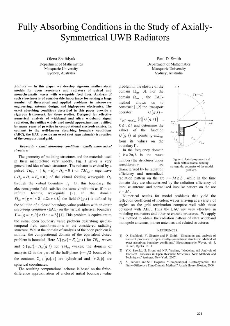
Keywords - exact absorbing conditions; axially symmetrical structures
228

Keywords method of analytical regularization; cavity resonators
229

Highly Directive Multi-Band Circular Patch Antenna Partially filled with ENG-metamaterial
Md.Saimoom Ferdous(1), Md.Ababil Hossain(1), Shah Mahmud Hasan Chowdhury(1), Mahdy Rahman Chowdhury Mahdy(2) and Md.Abdul Matin(1)
[email protected] and [email protected] (1)Bangladesh University of Engineering & Technology
(2)Presidency University of Bangladesh
Abstract—Based on the idea of additional modified mode(s) [1], metamaterial loaded triple band rectangular patch antennas have been reported in [2]. But the idea of additional modified mode(s) to achieve multi-band performance in circular patch antenna probably has not been reported so far. Recently we have reported the idea of ‘additional modified mode(s)’ in circular shaped patch antennas to achieve multi-band performance [3]. Based on the idea reported in [3], in this paper, a triple band circular patch antenna loaded with ENG-metamaterial has been reported. The proposed antenna not only provides good resonance, but also ensures satisfactory radiation performances (i.e. directivity, radiation efficiency & gain) for all the three bands. Achieving triple band performance was made possible by modifying TM (using metamaterial) along with TM210 mode modification with symmetrical slots. We expect that our proposed antenna will be effective in multiband high directive applications specially in satellite communication.
Keywords-triple band; ENG-metamaterial; circular patch.
I. INTRODUCTION
Increased popularity of satellite communication has aroused researchers’ interest in designing highly directive and multi band antennas. In this paper, we have successfully depicted how ENG-metamaterial and symmetrical slotting can be used in designing triple band circular microstrip patch antenna. In section (2), antenna design specifications are shown. Lastly in section (3), we have shown the resonance and radiation patterns that we have simulated in CST MICROWAVE STUDIO.
II. ANTENNA DESIGN PARAMETERS
In Fig. 1, geometry of our proposed antenna with corresponding parameters are shown along with material property specifications. With the aid of dispersive equation (1), ENG metamaterial’s permittivity and filling ratio have been calculated using a MATLAB based parameter optimization algorithm, [3].
2
| | (| | )
(| | ) (| | ) =
… …(1)
III. RESONANCE AND RADIATION PATTERNS
Satisfactory resonance and radiation patterns are observed in all three frequencies: conventional TM110 mode(f1= 3.6508 GHz ),unconventional modified TM mode(f2= 4.2686 GHz) and conventional modified TM210mode(f3=5.2169 GHz) as shown in Fig. 2.
Fig. 1 Geometry of a circular microstrip patch antenna partially loaded with metamaterial (ENG) (a) substrate and ground plane with parameters: a=(.56)(20 mm)=11.2 mm, a=20 mm, h=4.3 mm, tg=2 mm, Dg=40 mm, 2=1.33, 1=-1.9(at 4.2686 GHz ), μ2=1, μ1=1 (b) metallic patch with parameters: ar=19.3 mm, at , fp=15 mm.
Fig. 2 Clockwise from top left, (a) S11-parameter; (b),(c) and (d) 3-D radiation pattern for the antenna in Fig. 1 at f1 f2and f3 frequencies.
REFERENCES
[1] Mahdy Rahman Chowdhury Mahdy, Md. Rashedul Alam Zuboraj, Abdullah Al Noman Ovi, and Md. Abdul Matin, “An Idea of Additional Modified Modes in Rectangular Patch Antennas Loaded With Metamaterial” IEEE Antennas and Wireless Propagation Letters, vol. 10,2011.
[2] M. R. C. Mahdy, M. R. A. Zuboraj, A. A. N. Ovi and M. A. Matin “Novel Design of Triple Band Rectangular Patch Antenna Loaded with Metamaterial” Progress In Electromagnetics Research Letters, Vol. 21, 99-107, 2011.
[3] Md.Saimoom Ferdous, Md.Ababil Hossain, Shah Mahmud Hasan Chowdhury, Mahdy Rahman Chowdhury Mahdy and Md. Abdul Matin,“Reduced and Conventional sized Multi-Band Circular Patch Antennas Loaded with Metamaterials” submitted in IET journal (Under Review)
(a) (b)
(b) (a)
(d) (c)
230

UWB-TC10 adar spects
231
Pulse Transmission into a Lorentz Half-Space
Natalie A. CartwrightDepartment of Mathematics
State University of New York at New PaltzNew Paltz, NY USA
Abstract— The propagation of a one-dimensional electromagnetic plane-wave pulse that is obliquely incident on a Lorentz half-space is studied analytically using saddle point methods. An asymptotic approximation to the transmitted field is given, valid for large propagation distances. The asymptotic forms are shown to be continuous in time and comparable to numerical computations of the transmitted field. Arrival times and angles of refraction are given for prominent transient pulse features and the steady-state signal.
Dispersive pulse propagation; pulse transmission; dielectric material; saddle point method
I. INTRODUCTION
Shortly after Sommerfeld [1] and Brillouin [2] published their seminal work on the propagation of a step-modulated sinusoid through an unbounded, Lorentz-type dielectric, Colby[3] investigated how such a “signal front” may change at a plane boundary. Colby restricted his analysis to regions removed from the absorption band of the material and thus, his results are valid only for very small time. Since then, others[4-5] have addressed the same problem, but none have given a complete and continuous approximation to the transmitted field of a plane-wave pulse obliquely incident on a Lorentz half-space. We accomplish this here by analyzing the integral representation of the field using uniform saddle point methods while retaining the full (and causal) dielectric permittivity of the Lorentz material.
II. FORMULATION AND RESULTS
When a step-modulated sinusoidal plane-wave is obliquely incident on a planar boundary between air and a Lorentz dielectric (with the xz-plane the plane of incidence), the transmitted field is given exactly by the integral
ψ = −1
2πi
ω −ωc
g(ω;α) expdωc
φ (ω,θ;α)⎡⎣⎢
⎤⎦⎥dω
ia−∞
ia+∞
∫ , (1)
whereωc is the carrier frequency of the input pulse,α is the angle of incidence, d = x sinα + z cosα is the distance from the interface to the observation point,
φ(ω,θ;α) = iω z
dcosα N2(ω;α) − θ − x
dsinα
⎛⎝⎜
⎞⎠⎟
⎡
⎣⎢
⎤
⎦⎥ (2)
is the phase function, and g(ω;α) is the amplitude function
whose exact form depends upon if the incident pulse is TE or TM, as well as the component being considered. Here,
θ = ctd
where c denotes the speed of light in vacuum, and
N2(ω;α) is the index of refraction of the Lorentz material in which the square of the plasma frequency has been divided by cosα .
The phase function has two sets of saddle points; the contribution to the integral (1) from one set gives the high frequency response of the material whereas the contribution from the other set gives the low frequency response. The steady-state contribution is given by the residue term. The asymptotic approximation to the transmitted field is then the sum of these three contributions, valid as d → ∞. These approximations require numerical calculations as to the locations of the saddle points of the phase function, but otherwise are given in closed form in terms of special functions. The asymptotic solution is uniform in time and is comparable with numerical computations of the transmitted field.
The arrival time and angle of refraction for the high- and low-frequency components is then given in terms of the saddle points. It is seen that the high-frequency contribution arrives at the speed of light in vacuum and refracts away from the normal of the plane of incidence with increasing θ , whereas the low-frequency contribution has a peak amplitude point that arrives at the space-time point
θ0 =z cosαd
N 2 (0;α) +x sinαd
(3)
and refracts toward the normal with increasing θ .
REFERENCES
[1] A. Sommerfeld, “Uber die fortpflanzung des lichtes in dispergierenden medien,” Ann. Phys., vol. 44, pp. 177–202, 1914.
[2] L. Brillouin, “Uber die fortpflanzung des lichtes in dispergierenden medien,” Ann. Phys., vol. 44, pp. 203–240, 1914.
[3] W. Colby, “Signal Propagation in Dispersive Media,” Phys. Rev., vol. 5, pp. 253–265, 1915.
[4] E. Gitterman and M. Gitterman, “Transient processes for incidence of a light signal on a vacuum-medium interface,” Phys. Rev. A, vol. 13, pp. 763–776, 1976.
[5] E. L. Mokole and S. N. Samaddar, “Transmission and reflection of normally incident, pulsed electromagnetic plane waves upon a Lorentz half-space,” J. Opt. Soc. Am. B, vol. 16, pp. 812–831, 1999.
232

Toward Integrated μNetwork Analyzer Single chip M-Sequence based sensor with integrated ultra-wideband wave separation
M.Kmec, M.Helbig, R.Herrmann, J.Sachs, K.Schilling Dept. of Electrical Engineering and Information Technology
Ilmenau University of Technology Ilmenau, Germany
P.RauschenbachMeodat GmbH
Ilmenau, Germany
Abstract— The article deals with a fully monolithically integrated single chip M-Sequence based UWB MiMo compatible sensor head with a built-in ultra-wideband wave separation option in the receiver chains. The discussed single chip sensor module is a further development of the mother SiGe System-on-Chip (SoC) presented in [1]. The introduced on-chip wideband wave separation is realized using an optimized resistive directional coupler combined with customized differential LNA. The wave separation works almost down to DC and its upper frequency limit is determined by the performance of the implemented technology (i.e. transistors, bridge resistors, process grid itself, etc.), selected LNA topology as well as by customized wirings of coupler components, and finally by IC packaging itself. However, the upper limit is designed to be compatible with the analog input bandwidth of the receiver sampling circuit, which is about 18 GHz (see also [1]). In spite of its relatively high complexity, the realized single chip IC features a compact size of only 2x1mm2
and moderate power consumption - below 1 W at -3 V supply.
Keywords— integrated UWB sensor, M-Sequance, integrated directional coupler, System-On-Chip (SoC)
I. INTRODUCTION
For decades, miniaturization has been a key to faster performance of electronics. Therefore, ultra-high-speed monolithic integrated circuits (ICs) seem to be obligatory components for novel Ultra-Wideband (UWB) sensors, e.g. for M-Sequence approach with digital signal correlation [2]. The approach is considered to be an interesting alternative to the classical pulse or stepped frequency continuous wave (SFCW) based UWB systems. However, it can be expected, that the acceptance of this new sensor technology by the user will largely depend on implementation flexibility of sensor electronics for different sensing tasks, as well as on device costs, reliability, robustness, power efficiency, etc. It is obvious, that one possible way to reach all these expectations lies in fully monolithically integrated sensor solutions [1]. The paper concentrates on the latest M-Sequence based single chip evolution with integrated ultra-wideband directional couplers to enhance the system implementation scope.
II. REALISED IC ARCHITECTURE
The implemented IC architecture which is depicted in Figure 1 follows the topology with one transmitter and two receivers as presented in [1]. The on chip integrated ultra-
wideband wave separation is based on optimized resistive Wheatstone bridge combined with a customized differential LNA structure.
μNA
buf. measurem
entport
calibrationcontrolon/offenable
initialstate
shiftregister
binarydivider
anal
og d
ata
AD
Ccl
ock
cont
rol
systemclock
singlechip
device
LNA
coupler unit
IC RF I/O connections
calibrationunit
Rx1Widebandd sampli gate
LNARx2wideband sampling gate
Figure 1. Implemented single chip architecture and simplified intended μNetwork Analyser (μNA) realisation.
The example of the realized transceiver SiGe die is depicted in the Figure 2. In the final article, details of its particular blocks with deeper design and layout aspects will be given. Measured system performance of the realized analyzer laboratory prototype as well as particularity of added measurement fidelity gained by the ability to mount the unit very close to the measurement points will be also discussed.
directionalcoupler + Rx1
directionalcoupler + Rx2
synchronisationand
stimulusgeneration units
Figure 2. Single chip die microphotograph (2 x 1 mm2).
REFERENCES
[1] M. Kmec, M. Helbig, R. Herrmann, P. Rauschenbach, J. Sachs, K. Schilling, “M-Sequence Based Single Chip UWB-Radar Sensor,” ANTEM/AMEREM 2010 Conference, July 5 – 9, 2010, Ottawa, ON, Canada.
[2] J. Sachs, P. Peyerl, M. Rossberg, “A new UWB-principle for sensor-array application, “ Instrumentation and Measurement Technology Conference, 1999. IMTC/99. Proceedings of the 16th IEEE , vol.3, no., pp.1390-1395 vol.3, 1999
233

Intentionally blank
234

UWB-TC11Target Detection,
Discrimination and Imaging
235

Keywords-Through wall imaging; backprojection; trilateration
236

Keywords-component; Electromagnetic Induction, target detection and discrimination, Magnetic polarizability.
HMHZ
ZH H
M
M
VUM
M
Z
237

!"
#$%&'()*$+,
!"# !"
- #* #-. """
. / + 0 "
0 + 12 . . . 3 ++4 .+ 5".. . ".612 +++ 172 8&9: 3 12. . ;<
++=> 8': > "8?: "3 + . >++5".+
" "..""..3
$#$5 #-
.12 ". + .7 " 3 1 2 .+ > ..+.; <3
; <7 .3 "71+0.0323 . 7 "0+ ".0.
#7 . 3 . 0. . 0 .+3+ ".+ +
7-
8&: $@. !@&%%%
89: AB;$"03 ". <. &CD'D0D?%&%C'
8': BE$ ; 0. " < #A.&D'9)0'99&%%)
8?: $@BF;7+ +< *. -"E -E 9))' * $#$$&%0)&0&0)((C7
"+$7#
238

UXO-TC12Landmine and IED
Detection and Neutralization
239

On the Computation of Fields in the Presence of Ferromagnetic Objects
I.R. Ciric, Fellow of IEEEDepartment of Electrical and Computer Engineering
The University of ManitobaWinnipeg, MB, [email protected]
Abstract—The ideal ferromagnetic model is used to formulate the magnetic field problem outside ferromagnetic bodies in terms of a single-valued scalar potential. Boundary integral equations are constructed for the solution of the associated Dirichlet problem for the scalar potential. This makes the field analysis more efficient than that based on existing formulations by reducing drastically the amount of necessary computation. The results presented have relevance to the identification of hidden magnetic material objects and to the development of much improved computational methods for nonlinear magnetic fields.
Keywords-field modeling for magnetic bodies; scalar potential integral equations; detection
I. INTRODUCTION
In numerous practical applications, for example in the detection of the position and shape of the underground objects or in various iterative procedures applied to nonlinear field analysis, the computation of the quasistationary magnetic field in the presence of a system of ferromagnetic bodies is required to be performed many times. The computational effort can be substantially reduced by introducing a scalar potential Φ [1] and by implementing adequately formulated surface integral equations.
II. FORMULATION
At a first approximation, the ferromagnetic bodies can be considered to be ideal ferromagnetics (permeability → ∞ )and, thus, the magnetic field lines outside the bodies are normal to their surfaces. As a consequence, these surfaces are equipotential and the exterior field problem becomes a Dirichlet problem for the Laplace equation satisfied by the scalar potential. The constant values of the potential on the body surfaces Sk, k =1, 2, . . ., remain unknown (“floating” potentials), Φk ≡Ck on Sk, and the formulation of the field problem is completed by specifying that the magnetic flux through the closed surface of each body Sk is equal to zero, i.e.,
∂Φ∂n
dS =Sk∫ 0, k =1, 2, . . . (1)
with ∂ ∂n denoting the normal derivative.
A surface integral equation formulation for Φ outside the bodies is derived from the classical Green function representation of the potential [2] at an arbitrary point inside the outer region,
Φ(r ) =Φ0(r )− 1
4π1
R
∂Φ(r ')
∂n '−Φ(r ')
R ⋅ n '
R3
⎡⎣⎢
⎤⎦⎥
S∫ dS ' (2)
where Φ0 is the scalar potential of the given external field, S ≡ S1U S2 U. . ., R = r - r ',R= R , r and r ' are the position vectors of the observation and integration points, respectively, and the normal unit vector n ' is outwardly oriented with respect to each body. Bringing the observation point on the surfaces of the bodies yields the system of integral equations
1
R
∂Φ(r ')
∂n 'dS ' + α(r )Ck =
S∫ 4πΦ0(r ),
r ∈ Sk, k =1, 2, . . .
(3)
where α is the solid angle under which a small neighbourhood of the outer region is seen from the observation point. The equations in (3) together with those in (1) constitute a system whose solution gives the functions ∂Φ ∂n on the surfaces Skand the constants Ck .
Concrete computation examples, including those for the canonical geometries of spheres and ellipsoids, will be presented at the Conference.
REFERENCES
[1] I.R. Ciric, “New models for current distributions and scalar potential formulations of magnetic field problems”, J. Appl. Phys., vol. 61, pp. 2709-2717, 1987.
[2] J.G. Van Bladel, Electromagnetic Fields, 2nd ed. Hoboken, New Jersey:IEEE Press-Wiley, 2007, pp. 97-98.
240

A Study on the ElectromagneticSusceptibility of Improvised Explosive Devices
John J. Pantoja A.*, Néstor M. Peña*, Francisco Roman#, Félix Vega+, Farhad Rachidi+
*University of Los Andes, Electronics and Systems of Telecommunications Group (GEST), Bogotá, Colombia jj.pantoja28, [email protected]
#National University of Colombia, Bogotá, Colombia [email protected]
+Swiss Federal Institute of Technlogy EPFL, Lausanne, Switzerland felix.vega, [email protected]
Abstract— In this paper, a study on the coupling between an external electromagnetic field and an improvised explosive device (IED) is presented. The randomness of the wiring geometry of these devices is considered by means of a Monte-Carlo approach. As a result, the frequency of optimal coupling considering a monochromatic excitation and an IED in free space is determined.
Keywords- improvised explosive devices, electro-explosive device, intentional electromagnetic interference, IEMI
I. INTRODUCTION
The remote detonation of improvised explosive devices (IEDs) by using radiated energy has been a subject of interest in the last years. Although studies on the effects of intentional electromagnetic interferences (IEMI) on IEDs are recent [1, 2], works on the radiated susceptibility of this kind of circuits have been carried out earlier since the detonator in these devices is commonly used in the industry. The activation mechanism of IEDs is based on feeding an electro-explosive device (EED) with an electrical current to increase the temperature of its bridge-wire until a critical temperature. The feeding current is usually produced when a switch is closed and, as a consequence, the EED is connected to a battery. The remote activation could be achieved if an IEMI induces a current with sufficient energy in the EED feed wires.
II. COUPLING MODEL
The coupling between an incident plane wave and the bridge-wire of an EED can be decomposed in two transfer functions, corresponding respectively to the external interaction and the penetration. The external interaction function provides the relation between the incident electric field and the input current in the EED, and the penetration function relates this current with the dissipated power in the bridge-wire.
Although both transfer functions can be considered as randomly variable in IEDs, the penetration function was treated as deterministic in this study. In fact, it depends on the EED structure, whose electromagnetic response can be considered as typical [3]. On the contrary, the external interaction was considered as arbitrary to include in the analysis the variability of the wiring characteristic in IEDs.
With these considerations, the connection wires with arbitrary shapes can be modeled as a receiving antenna and the EED as its load with a deterministic impedance value. The induced power in the bridge wire can be calculated as a function of the gain and impedance of the wires.
III. RESULTS
An IED in free space that is impinged by an incident CW plane wave was considered. The IED was assumed to be composed only by the EED and the connection wires of the firing circuit. The wires were let to have random geometries; they can have different total length and pattern. Arbitrary patterns were obtained dividing the wire in four sections with equal length but with random inclination angles. Random uniformly distributed wire lengths between 5 cm and 25 cm were considered. The gain and the input impedance of a sample of 500 arbitrary wire structures were calculated numerically with Time Domain Integral Equation (TDIE) technique. The EED impedance was calculated by using the SABC model [3].
An optimal frequency of coupling can be defined when the induced power is the maximum possible for most of the observations. The mean value and the confidence interval of a standard deviation of the induced power in the EED as a function of the frequency are presented in Fig. 1. The results clearly indicate an optimal frequency in the range of 600 MHz, at which the mean value of the power increases considerably as compared with the rest of the frequencies.
Figure 1. Mean value and 68.3% confidence interval of the induced power in the bridge-wire of an EED with connection wires with arbitrary geometries.
Einc=1V/m, radius=0.7mm, length=[5:25]cm
REFERENCES
[1] J. Galuga and J. R. Bray, "Induced currents on electric detonators for improvised explosive device pre-detonation," in Electromagnetic Compatibility (EMC), 2011 IEEE International Symposium on, 2011, pp. 758-762.
[2] N. R. Devarapalli, et al., "A Fan-Beam Radiator Using Waveguide's Narrow Wall for Horizontal Polarization and High Power," Electromagnetic Compatibility, IEEE Transactions on, vol. 53, pp. 380-389, 2011.
[3] M. R. Lambrecht, et al., "Electromagnetic Modeling of Hot-Wire Detonators," Microwave Theory and Techniques, IEEE Transactions on, vol. 57, pp. 1707-1713, 2009.
0.5 1 1.5 2 2.5 3-70
-60
-50
-40
-30
-20
FREQUENCY (GHz)
BR
IDG
E-W
IRE
PO
WE
R (d
Bm
)
MeanMean
This work was financially supported by the EPFL SDC (Swiss Agency for Development and Cooperation) Fund
241

Keywords-component; Electromagnetic Induction, landmines, UXO, Magnetic polarizability, nonlinear inverse problems.
HMHZ
ZH H
M
DZM
D
0 2 4 6 810
15
20
25
RMS
erro
r in
Tens
or (%
)
Iteration number
0 2 4 6 80.01
0.015
0.02
0.025
Posit
ion
estim
ate
(cm
)Tensor
Position
242

Object
Receiver coils Transmitter coil
Ground
Experimental Designs Method for UXO Detection and Classification Based on EMI Sensor
Y. MATRICHE(1), A. ZAOUI(2), M. ABDELLAH(2)
(1)URD-T, Belfort El-Harrach, Algeria (2)École Militaire Polytechnique, BP17 B.E.Bahri, Algiers,
Algeria. [email protected]
M. FELIACHI PRES-L’UNAM, IREENA, Bd de l'Université, BP 406,
44602 St-Nazaire cedex, France
Abstract— In this paper, we propose to apply the experimental designs method for the detection and classification of UXOs by electromagnetic induction sensor. We evaluate the measure of the signature associated with the limit values of the physical parameters and geometrical dimensions of the common UXOs. Thereafter, we apply the experimental designs method to find a model of the electromagnetic induction sensor response. This model leads to a fast inversion tool for detection.
Keywords- EMI; UXO; experimental designs; Matrix of experience and results, Finite Elements Method
I. INTRODUCTION
Characterization of Unexploded Ordnance (UXO) remains a crucial problem for a long time. However, several physical techniques such as Electromagnetic Induction (EMI), Ground Penetrating Radar (GPR) and magnetometry are used. In the same time, processing methods are developed to reduce false alarms rate due to the heterogeneity of the sol and the presence of metallic debris.
The EMI technique is very efficient for detecting metallic buried items [1]. In this paper, we introduce the method of experimental designs to provide a model of the response of the EMI system. However, experiments will be made to the limit values of the conductivity (σ) and the dimension of object. From this definition, we construct an approximate model of the induced voltage response of the EMI coil sensor. This model will be used to estimate the nature of the buried object.
II. PRESENTATION OF THE EMI SYTEM
Figure 1 shows the system used for detection. It consists of a transmitter coil, two receiver coils in differential mode, power supply and a data acquisition system.
Figure 1. System used for EMI detection of buried objects.
The response of the EMI sensor is determined using 2D axisymmetric finite element computation. For simplification reason we consider only one dimension of the test buried objet (radius) and one physical parameter (the electric conductivity).
III. APPLICATION OF THE EXPERIMENTAL DESIGNS METHOD
For the implementation of the experimental designs method, and since that the EMI system only detects metallic objects such as mines, we will restrict the values of the object conductivity between 1.32[MS/m] (for the Stainless-Steel 304) and 62.1 [MS/m] (for Silver) and the radius between 5cm and 20cm. These data can be represented in the following study area (Figure 2), where ∆Vi ; i=0..4 represent the sensor response for the limits input values.
Figure 2. Representation of the study area. ∆V=[ 4.13 1.42 1.53 10.63 9.42 ] Volts.
The predicted EMI-sensor response *VΔ can be obtained using Maclaurin/Taylor’s expansion [2] at level Nk. N is the number of factor’s levels (in our case the levels are -1 and 1) and k is the number of factors (in our case r and σ): σσσ raaraarV 12210
* ),( +++=Δ (1)
Where a0=1,1742, a1=0,9243, a2=1,59x10⁻⁷, a12=-1,45x10⁻⁷.
The proposed model gives a relationship between the expected parameters and the measurements, which can constitute a basis for the identification of the object.
IV. CONCLUSION
The exploitation of the experimental designs method leads to a simple model of the EMI-sensor response. Such a model makes faster the detection and classification of UXOs. To increase the accuracy of detection, the method can be extended to the identification of other geometrical or physical parameters defining the object.
REFERENCES
[1] M. W. Asten, A. C. Duncan, “Fast approximate EM induction modelling of metallic and UXO targets using a permeable prism,” Journal of Applied Geophysics 61: 235–242, 2007.
[2] J. Goupy, L. Creighton, Introduction aux Plans d’expériences, 3eme
édition DUNOD, 2006.
-1 0 1 1.32 31.71 62.1
20 1
12.5 0
5 -1
σ (MS/m)
∆V4 ∆V3
∆V1 ∆V2
r (cm)
∆V0
ΔV
243

244

HPEM-TC13Poster
245

Keywords-emp; d-dot sensor; antenna factor; calibration;
246
Compact 0.5 MV capacitive voltage probe used as developmental tests for a wideband source
R. Pecquois, L. Pecastaing, M. Rivaletto, A. de Ferron SIAME, Equipe Génie Electrique,
Université de Pau Hélioparc Pau-Pyrénées, 2 avenue Angot
64000 Pau, France [email protected]
B.M. Novac, I.R. Smith School of Electronic, Electrical and Systems Engineering
Loughborough University Loughborough, Leicestershire LE11 3TU, UK
R.J. Adler North Star High Voltage, 12604 New Reflection Dr. Marana
AZ 85658, USA
Abstract— This paper describes a simple and compact 0.5 MV high-voltage capacitive probe developed in common by Université de Pau (France) and Loughborough University (UK). Design details are provided, together with a simple and straightforward methodology developed to assess the characteristics of high-voltage probes. Finally, a practical example of high-voltage measurement performed with this probe during the development phase of a HPM generator is provided.
Keywords: high voltage capacitive probe
I. INTRODUCTION
Modern pulsed power applications of high power microwave (HPM) technology require simple, compact and if possible inexpensive high-voltage probes for the reliable measurement of impulse voltages with amplitudes of about 0.5 MV inside relatively small oil-filled containers. The paper introduces a simple design of a compact 0.5 MV probe termed Half-Megavolt, proved to be extremely useful during the developmental phase of a HPM generator.
II. HIGH-VOLTAGE PROBE DESIGN
A. High-voltage arm
The high-voltage arm comprises a collection of N metallic (aluminium) discs, parallel-mounted and kept in place by a plastic bar (Figure 1). Because the high-voltage arm has cylindrical symmetry, an electrostatic analysis of the probe immersed in transformer oil of permittivity of 2.25 was made using Ansys Maxwell 2D software. The resulting capacitance matrix is used in the PSpice analysis (Figure 2).
B. Low-voltage arm
The low-voltage arm of the Half-Megavolt probe comprises 20, 200 V, 1 nF low-inductance capacitors type NP0. These miniature capacitors are one of the most stable ceramic capacitors commercially available, and they also have no measurable variation of capacitance with frequency up to at least 10 MHz and no hysteresis effect.
The number of parallel-mounted capacitors has been used as a means of adjusting the probe attenuation factor as close as possible to 10,000. The results indicate that the probe have a ±3 dB bandwidth up to about 55 MHz (Figure 2).
16.5cm
Figure 1. Half Megavolt probe
0.1 1 10 100140−
120−
100−
80−
60−
40−
20−
0
ExperimentalSimulation
frequency (MHz)
ampl
itud
e (d
B)
Figure 2. Frequency response for the Half Megavolt probe
III. DEVELOPMENTAL TESTS FOR A HPM SOURCE
A compact high-power UWB system developed at Pau University uses an innovative and very compact resonant transformer to drive a dipole antenna. The complete pulsed power source, termed MOUNA, comprises a set of batteries, a DC/DC (300V/10kV) converter to charge four capacitors, four synchronised spark gap switches, a resonant transformer generating 600 kV/300 ns pulses and an antenna.
The total volume of the pulsed power source is less than 20 litres and the complete system is housed inside a metallic container, filled with transformer oil and degassed using vacuum technology. A very compact high-voltage probe was necessary to measure the very high voltage pulses inside oil during the developmental programme in a volume limited to only 1.5 litre.
Finally, for an input voltage of only 9.5 kV, the maximum output voltage measured by the Half-Megavolt probe reaches 555 kV, with a rise-time of only 265 ns.
This work was initiated and financially supported by the French Ministry for Defense (Direction Générale de l’Armement – contract N° 07.34.027)
247

Keywords-SE test; shielded enclosure; underground facility;
248

Infrared Imaging of Electric Field : Amplitude, Phase and Polarization measurement
F. Lemaître, F. Issac, D. Prost ONERA, The French Aerospace Lab
Toulouse, France [email protected]
Abstract— Electric field visualization using thermoemissive film and infrared camera is presented. Beyond this EMIRTM
(ElectroMagnetic InfraRed) method well established in the case where source field is controlled, we present interferometric techniques that allow measuring any field, and getting both phase and amplitude for each polarization.
Keywords – Electric field, thermoemission, Infrared, EMIRTM.
I. INTRODUCTION
The electromagnetic infrared (EMIRTM) method was developed and has been used at ONERA [1] in order to visualize and/or measure microwave electric fields. It consists in putting conductive films of eventually large dimension (up to more than one square meter) in the electromagnetic field. Induced currents in the films create ohmic losses and consequently a heating that can be filmed using an infrared camera. This method provides thermal frames that can be linked to the square of the electric field amplitude (absorbed electric power); it gives qualitative information (for example the electric field profile near an antenna). To get more quantitative information, an interferometric setup is presented consisting in adding to the unknown field a known one with a very small frequency difference and various polarizations. Then the amplitude level as well as the field phase (and therefore wave direction) can be obtained sequentially for co/cross polarizations.
II. MEASUREMENTS SETUP
The EMIRTM film is located in the incident field Ei (to be measured) zone. A local field EL is also generated. This latest has the frequency of Ei plus a small Δf (the local field can be derived from the incident field by a I/Q modulator driven by Δf followed by amplification). The incident power on the film is in these conditions:
P(t) = K.[Ei² + EL² + 2 Ei.EL.cos(φ + 2π.Δf.t)] (1)
The constant K is the film characteristic. The phase difference φ between Ei and EL depends on the location on the film. By Fourier transform we get a continuous component and an alternative one which contains useful information: it gives the phase φ and the amplitude Ei, assuming EL is known. We tested this setup on our electromagnetic experimental bench CAREM (for EM characterization) with two Gaussian beams interfering on a EMIRTM film as illustrated by the Fig. 1
Measured Field Ei
Local Field
EL
IR Camera
Film
Figure 1. Measurement setup with two antennas and the thermoemissive film
The local field antenna can be turned from vertical to horizontal configuration. This allows getting the direction of the measured field (corresponding to maximal interferences). When this direction is obtained, demodulation of the thermal frames (or Fourier transform on each pixel of the IR image) provides the field amplitude. One of the advantages of this modulation is to eliminate thermal noise (convection), or low frequency perturbations (due to wind for example). Signal processing software has been developed to provide real time images of the incident field after demodulation or Fourier analysis. The Fig. 2.a thus shows the thermal frame for a 4 GHz Gaussian beam field (temperature scale) and the corresponding amplitude field frame. On the Fig. 2.b the phase is plotted (using the same software), before and after a 10° tilt of the measured field source, which illustrates the phase measurement capacity of the method. This non intrusive phase and amplitude near field measurement could theoretically give, by Fourier analysis, far field information.
a)
b)
Figure 2. a): IR frame (left), and amplitude image (right); b): Field phase before and after a 10° tilt of the source
REFERENCES
[1] P.Levesque, L. Leylekian, French Patent n° 9816079 (1998)
249
Abstract
Keywords-component; wavefront synthesis, test facilities, time reversal, TREC, electromagnetic pulses.
250

Effects of chronic exposure to radiofrequency electromagnetics fields on energy balance in juvenile
rats Amandine Pelletier1, René de Seze2, Stéphane Delanaud1, Gyorgy Thuroczy2, Véronique Bach1, Jean-Pierre Libert1, Nathalie Loos1
1 Laboratory Péritox – Ineris (EA 4285-UMI01) Faculty of Medicine, University of Picardy Jules Verne
Amiens, France
2 Laboratory Péritox – Ineris (EA 4285-UMI01) Experimental Toxicology Unit, INERIS
Verneuil-en-Halatte, France
Abstract—This study investigated the effects of a chronic exposure to radiofrequency electromagnetic fields designed to simulate a current chronic exposure from antennae base station on the energy balance in juvenile rats. The results showed a decrease in body cooling and an increase in energy saving. Most effects due to the exposure were dependent on the ambient temperature.
Radiofrequency electromagnetic fields; sleep; feeding behavior; thermoregulation; young rat
I. INTRODUCTION
The effects of radiofrequency electromagnetic fields (RF-EMF) on the control of body energy balance were never studied while energy is necessary to vital functions, body homeothermia and body growth, particularly in developing organisms. This study investigated the effects of chronic RF-EMF exposure, similar to mobile phone base stations (900 MHz, 1 V.m-1), on feeding behavior, sleep and thermoregulatory processes which are involved in the control of energy balance. All these functions were investigated at 2 ambient temperatures (Ta= 24 and 31°C) which are in the range of the rat’s thermoneutral zone, within which the animal’s cutaneous heat losses are controlled by peripheral vasomotor tone alone.
II. METHODS
13 juvenile male Wistar rats were continuously exposed to continuous RF-EMF (900 MHz, 1 V.m-1) during 5 weeks and compared with 11 non exposed rats (control group). The 2 groups of animals were placed into 2 chambers climatic with strictly controlled environmental conditions. The rats were implanted with EEG and EMG electrodes to score wakefulness (W), slow wave sleep (SWS) and paradoxical sleep (PS). The rats were implanted with 2 thermoprobes: a subcutaneous tail thermoprobe was inserted into the proximal part of the tail to reflect the overall thermal status of the tail surface. An additional thermoprobe was placed under the skull but over the dura mater of the brain. At the beginning of the 6th week, food intake, body temperatures and polysomnographic data were recorded at Ta of 24ºC and 31ºC between 12 am and 06 pm. To
explore the vasomotor tone, a vasodilatative drug (prazosin) was injected at a dose of 1 mg.kg-1 at 12 am and the tail temperature was recorded at Ta of 24ºC and 31ºC between 12 am and 06 pm. The average value of the subcutaneous tail temperature (Ttail, index of peripheral vasomotricity) and of the cortical temperature (Tcor, index of central temperature) were calculated. The total durations of W, SWS and PS and the durations and frequencies of episodes were calculated. The food intake was calculated individually as an index of energy requirements. Between and intra group comparisons were made using ANOVA.
III. RESULTS
There was no difference in the total duration of wakefulness, SWS and PS between the 2 groups of animals. The frequency of PS episodes was specifically increased by RF-EMF exposure independently of Ta (+42.1 and 31.6% at 24 and 31°C respectively, p<0.001). RF-EMF exposure modified differently several sleep parameters according to Ta. At Ta of 31°C, RF-EMF exposure was associated with a lower frequency of W and SWS episodes, compared with the control group (W: -50.0%, p<0.001; SWS: -14.8%, p<0.01), whereas only the duration of W episodes was lower at 24°C (-27.8%, p<0.001). Exposure to RF-EMF did not have a significant effect on Tcor. At 31°C, RF-EMF exposed group had significant lower mean value of Ttail than control group (-1.21°C, p<0.001) ascribing a peripheral vasoconstriction which was confirmed by using prazosin. RF-EMF exposure also increased food intake at 31°C (+1.3g, p<0.001).
IV. CONCLUSION
Most effects of RF-EMF exposure observed are temperature-dependent. RF-EMF exposure appears to modify the functioning of thermal effectors eliciting a peripheral vasoconstriction which decreases body cooling while energy intake increases. This point out that RF-EMF exposure can trigger energy saving processes without strong disturbances of sleep structure.
This study was funded by a “Post-Grenelle” from the French Ministery of Ecology.
251

Abstract
Homogenization; Dielectric; Periodic Structures;Electromagnetic scattering; Rough Surfaces;
252
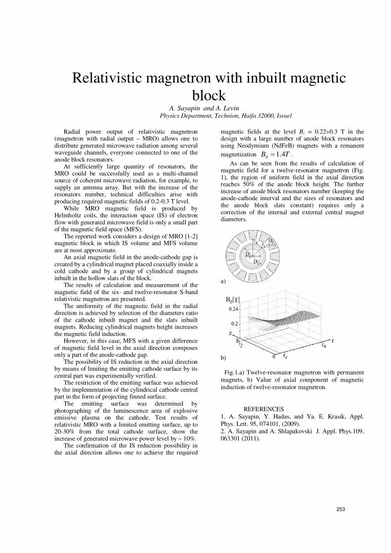
Relativistic magnetron with inbuilt magnetic block
A. Sayapin and A. Levin Physics Department, Technion, Haifa 32000, Israel
Radial power output of relativistic magnetron (magnetron with radial output – MRO) allows one to distribute generated microwave radiation among several waveguide channels, everyone connected to one of the anode block resonators.
At sufficiently large quantity of resonators, the MRO could be successfully used as a multi-channel source of coherent microwave radiation, for example, to supply an antenna array. But with the increase of the resonators number, technical difficulties arise with producing required magnetic fields of 0.2-0.3 T level.
While MRO magnetic field is produced by Helmholtz coils, the interaction space (IS) of electron flow with generated microwave field is only a small part of the magnetic field space (MFS).
The reported work considers a design of MRO [1-2] magnetic block in which IS volume and MFS volume are at most approximate.
An axial magnetic field in the anode-cathode gap is created by a cylindrical magnet placed coaxially inside a cold cathode and by a group of cylindrical magnets inbuilt in the hollow slats of the block.
The results of calculation and measurement of the magnetic field of the six- and twelve-resonator S-band relativistic magnetron are presented.
The uniformity of the magnetic field in the radial direction is achieved by selection of the diameters ratio of the cathode inbuilt magnet and the slats inbuilt magnets. Reducing cylindrical magnets height increases the magnetic field induction.
However, in this case, MFS with a given difference of magnetic field level in the axial direction composes only a part of the anode-cathode gap.
The possibility of IS reduction in the axial direction by means of limiting the emitting cathode surface by its central part was experimentally verified.
The restriction of the emitting surface was achieved by the implementation of the cylindrical cathode central part in the form of projecting finned surface.
The emitting surface was determined by photographing of the luminescence area of explosive emissive plasma on the cathode. Test results of relativistic MRO with a limited emitting surface, up to 20-30% from the total cathode surface, show the increase of generated microwave power level by ~ 10%.
The confirmation of the IS reduction possibility in the axial direction allows one to achieve the required
magnetic fields at the level Bz = 0.22÷0.3 T in the design with a large number of anode block resonators using Neodymium (NdFeB) magnets with a remanent magnetization TB 4.10 = .
As can be seen from the results of calculation of magnetic field for a twelve-resonator magnetron (Fig. 1), the region of uniform field in the axial direction reaches 50% of the anode block height. The further increase of anode block resonators number (keeping the anode-cathode interval and the sizes of resonators and the anode block slats constant) requires only a correction of the internal and external central magnet diameters.
a)
b)
Fig.1.a) Twelve-resonator magnetron with permanent magnets, b) Value of axial component of magnetic induction of twelve-resonator magnetron.
REFERENCES 1. A. Sayapin, Y. Hadas, and Ya. E. Krasik, Appl. Phys. Lett. 95, 074101, (2009). 2. A. Sayapin and A. Shlapakovski J. Appl. Phys.109, 063301 (2011).
253

Optimization of TEM Antenna Design forHigh Voltage HPEM Signal
S. M. Han, J. J. Bang, C. S. Huh Department of Electrical Engineering
INHA UniversityIncheon, Korea [email protected]
J. S. ChoiAgency Defense for Development
Daejeon, Korea [email protected]
Abstract— Normally High Power Electromagnetic wave signal generators use high voltage signal so they need high voltage level insulated radiating antenna. So optimization of input port height, dielectric material insertion can be important insulating method. But they also change the original antenna specification and characteristics. So optimization of TEM antenna design parameter is very important. In this paper the study on TEM antenna characteristic change due to high voltage insulation is presented.
Keywords-component;HPEM, TEM, High Voltage, insulation
I. INTRODUCTION
A wide band antenna is normally used to radiate HPEM (high power electromagnetic) signal into free space from high voltage impulse generator [1]. Normally TEM antenna can be used for the purpose but the high voltage impulse signal occur electrical breakdown on the antenna. So the design of electrical insulation is essential. But the electrical insulation can change the original specification and characteristics of the antenna(especially gain, directivity, input impedance, signal distortion), it can be significant problem for using antenna.
Normal insulation design parameters of TEM antenna are input port height and dielectric material insertion. If the input port height is longer, the input impedance is changed. It means that the reflection of input signal is increased and radiating energy is decreased. So study on the change of the characteristics of the antenna due to insulation design is important.
In this paper, for the purpose, change of the antenna characteristics due to electrical insulation is presented. The study was performed by 3 dimension full wave electromagnetic wave simulation software and various antenna specificationswere examined.
II. SIMULATION SETUP
The analyzing electromagnetic wave simulation software was based on FIM (Finite Integrate Method) algorithm. And the high power electromagnetic wave signal generating wideband antenna was TEM horn antenna. The antenna was designed for subnano seconds of impulse rise time (above 1 GHz of frequency), the length of antenna was 800 mm.
The variables were the kinds of dielectric insulating materials (Air, epoxy, glass, mica, oil, rubber, SF6, silicon, Teflon, wood) and the input port height. The results were gain, directivity, input impedance, signal distortion.
III. CONCLUSION AND RESULTS
The gain change is depicted in Figure 1 and it shows that gain differences were small, but wood gave negative gain level. It means that wood distorts the antenna’s gain and it can be a good antenna’s insulation materials. And rubber splits the main beam of gain pattern. Directivity also showed similar trend with gain.
Input impedances varied largely. If the input impedance of air is standard, SF6 gas can be good choice of insulation material. But the other liquid (oil) and solids gave large differences. It means that liquid or solid dielectric materials reflect the input signal and energy more than gas. So the input height and width should be redesigned.
Air Epoxy Mica Oil Rubber SF6 Siicon Teflon Wood
-10
-5
0
5
10
15
Max
imum
Gai
n (d
B)
Materials
Maximum Gain
Figure 1. Gain changes due to dielectric materials
REFERENCES
[1] Constantine. A. balanis, “Antenna Theory analysis and design 3rd
edition”, John-Wiely Sons. Inc., 2005
The Author(s) gratefully acknowledge the financial support given by the Agency for Defense Development.
254

Timing in Magnetic Switches and Magnetic Pulse Compression
Jeremy Oliver, William Bailey, Michael Pochet, Andrew TerzuoliAir Force Institute of Technology
Dayton, Ohio, USA
Abstract— The magnetic switch is a saturable core inductor that can be used in a Melville line for magnetic pulse compression in pulse power systems. These switches have instabilities which lead to unique timing delays in the devices. This paper presents an effective approach to model the characteristic timing delays associated with switch designs.
Keywords-magnetic switch; magnetic pulse compression; Melville line; saturable inductor
I. INTRODUCTION
The Melville line, also known as a magnetic pulse compressor (MPC), uses saturable core inductors and capacitors to compress the width of a pulse. This substantially increases the peak power of the initially applied pulse. A two stage MPC is illustrated in Fig. 1. Saturable core inductors, often referred to as magnetic switches, are favorable in pulsed power systems due to their high power capacity, simple design with no moving parts, and ability to generate short pulses.
Figure 1. Two stage MPC circuit.
Figure 2. B-H hysteresis behavior of the saturable inductor.
The saturable inductor exhibits a hysteresis curve behavior as seen in Fig. 2. As the voltage across C1 increases the magnetic field of the inductor core goes from its initial state at point 1 through points 2, 3, and 4. If the circuit is properly designed, at the peak voltage of C1 the path will move from 4-5. This will cause the inductor to saturate which leads to C1 discharging into C2 at a faster rate than what C1 was charged. The magnetic field should then proceed to point 6 then back to point 1 for the next pulse. One particular problem with these MPC circuits is timing variances in the pulse rate of the system. These can be caused by several things from poorly regulated power supplies to the saturable inductor not resetting to the initial state after each pulse. If the curve does not reset to the initial state at point 1 after each pulse then there will be instabilities in the timing of the system. This work models the unique characteristics and signatures of the timing variations of magnetic switches and pulse compressors.
II. SIMULATING SATURABLE INDUCTORS
Following the research by Chua and Stromsmoe [1], the hysteresis curve of the saturable inductor was created by using a nonlinear inductor and a nonlinear resistor in parallel as a substitute for L1 and L2 in the circuit shown in Fig. 1. The measured data provided in [1] for the supermalloy core was used in MATLAB to construct the curves for the nonlinear inductors and nonlinear resistors. Once the circuit was built in MATLAB, simulations were run to determine the effectiveness of the pulse compression as well as the timing delays. The delays were measured over multiple pulses from the peak of the initial pulse at C1 to the peak of the pulse across the load as a time in microseconds. A signature resembling a decaying exponential was then able to be recorded from the simulations. This shape was caused by the hysteresis curve not resetting to the initial state at point 1 on the B-H plane after the first pulse is applied and it achieving a steady state at some smaller B-Hcurve after several pulses.
REFERENCES
[1] L. Chua and K. Stromsmoe, “Lumped-Circuit Models for Nonlinear Inductors Exhibiting Hysteresis Loops,” IEEE Transactions on Circuit Theory, vol. CT-17, No. 4, pp. 564–574, November 1970.
255

Pulse generator for achieving powerful adjustable nanosecond pulsed electric fields (nsPEFs)
S. Kohler, S. El Amari, V. Couderc, D. Arnaud-Cormos, P. Leveque XLIM Research Institute, UMR CNRS 6172
University of Limoges Limoges, France
Abstract— In this paper, we describe a flexible nanosecond pulse generator for delivering high-intensity pulsed electric fields into 50–ohm loads. The pulse shaping is based on the photoconductive frozen-wave generator concept using coaxial technology. Monopolar and bipolar pulses of 2 to 100-ns duration are obtained with a maximum amplitude of 13 kV. Control of the output voltage and frequency content of the pulses is possible by adjusting the optical energy impinging on the photoconductive switches.
Keywords- frozen-wave generator; nanosecond; photoconductive switch; pulse generation; pulsed electric fields
I. INTRODUCTION In the field of biotechnology, nanosecond pulsed electric
fields (nsPEFs) of several MV/m have been shown to alter the structure and functions of biological cells. The effects are dependent upon the pulse parameters such as shape, duration and amplitude [1]. For investigating dose-effect relationships, pulse generators with easily adjustable pulse parameters are best suited [2]. In previous reports, we described flexible microstrip-based high-voltage nanosecond pulse generators of 10 and 50-Ohm impedance [3,4]. In this paper, a new 50-Ohm coaxial-based high-voltage (HV) nanosecond pulse generator is described and characterized.
II. DESIGN OF THE GENERATOR As depicted in Fig. 1, the generator based on the frozen
wave generator concept, comprises two coaxial structures with 2 and 3 ports, respectively. A photoconductive semiconductor switch (PCSS) is embedded in each structure. Connection between the structures is made by a coaxial cable through THT connectors. The 3-port structure is also connected to the HV power supply that charges the pulse forming line and a 12-GHz oscilloscope for acquisition of the output voltage. The 2-port structure is grounded at the second port. An aperture in the structure allows the switches to be optically triggered by a high-energy mode-locked Nd:YAG laser operating at 1064 nm. The optical 35-ps pulses are generated at a frequency rate of 20 Hz. The DC polarization is set to 16 kV.
III. PERFORMANCE AND CONCLUSION By changing the length of the line connecting the two
coaxial structures, the pulse duration was varied from 2 to 100 ns. When setting the optical energy to 8 mJ per pulse, rectangular monopolar pulses of 6.9 kV and 12-ns duration were measured. The rise and fall times were 1.1 ns and 1.3 ns, respectively. Balanced and unbalanced bipolar pulses with various amplitudes were obtained by adjusting the optical energy received by each PCSS. A maximum peak-to-peak amplitude of 13 kV was recorded. Higher amplitudes are expected as the bias voltage is increased (up to 20 kV). Thus we propose a robust HV nanosecond pulse generator with improved voltage limit and adjustable pulse parameters in terms of shape, amplitude and duration.
REFERENCES [1] P.T. Vernier, Y. Sun, L. Marcu, C.M. Craft, M.A. Gundersen,
“Nanosecond pulsed electric fields perturb membrane phospholipids in T lymphoblasts,” FEBS Lett., vol. 572, pp.103-108, 2004.
[2] J. F. Kolb, S. Scarlett, J. Cannone, J. Zhuang, C. Osgood, and K. H. Schoenbach, “Nanosecond pulse generator with variable pulse duration for the study of pulse induced biological effects,” Proceedings of the 2008 Power Modulator Conference, Las Vegas, NV, pp. 61-64, 2008.
[3] S. El Amari et al., “Kilovolt, nanosecond and picosecond electric pulse shaping by using optoelectronic switching, ” IEEE Photon. Technol. Lett., vol.22, no.21, pp. 1577-1579, November 2010.
[4] C. Merla et al., “A 10 Ω high-voltage nanosecond pulse generator,” IEEE Trans. Microw. Theory Tech., vol. 58, no. 12, pp. 4079–4085, December 2010.
GND
HV supply
Data acquisitionsystem
Figure 1. Schematic of the pulse forming line. The 2-port and 3-port coaxial structures are connected by a coaxial cable via THT connectors. The switches
(white oval) are optically triggered.
256

Effects of CW interferences on a 5 GHz
Monolithic VCO, and on its associated PLL A. Blain, J. Raoult, A. Doridant, S. Jarrix
Institut d’Electronique du Sud (IES) Université Montpellier 2
Montpellier, [email protected]
Abstract— This paper is a contribution to the electromagnetic susceptibility studies conducted on active circuits. First, we study the effects of a high frequency continuous wave injection on one of the major items of an integrated phase locked loop: the voltage controlled oscillator. We describe here the three major phenomena observed on its operating mode. We then show some of the results obtained when injecting the interference signal on the complete PLL system.
Keywords- electromagnetic susceptibility; voltage controlled oscillator; phase locked loop; injection; injection locking; quasi-lock; injection pulling
I. INTRODUCTION
The rise of mobile telecommunication systems, and other wireless devices, saturates our environment with electromagnetic waves. These mobile devices use low power supply, making them more sensitive to all those interference signals, because of the safety margins decrease. This is one of the reasons why Electro-Magnetic Compatibility (EMC) is a major issue in current electronics.
In this paper, we describe the effects of CW (Continuous Wave) interferences on a 5 GHz monolithic voltage controlled oscillator (VCO), implemented in a 0.35 µm BiCMOS SiGe process. We will first describe the different operating modes experimentally observed when injecting an Electromagnetic Interference (EMI) in a conducted mode, on a large frequency range. We will give a theoretical expression for the most critical frequencies for injection locking. Then we will present some results obtained when injecting the interference signal on the complete PLL system. The study of analog and digital items of the PLL will be made separately.
II. DEVICE UNDER TEST
Due to their relatively low phase noise and ease of implementation the well-known cross-coupled pair VCO topology plays a key role in radio-frequency circuit design. This type of VCO studied here is moreover part of a complete integrated PLL system, which will be studied at the end of this paper.
III. VCO BEHAVIOUR UNDER EMI
A. The three major phenomena
Three major operating modes can be observed when a VCO is submitted to an aggression [1]. In the first mode numerous
intermodulation products emerge, polluting the output spectrum. The second mode corresponds to the injection locking mode. In this case, one can observe an injection frequency range, the lock range, for which the VCO is totally controlled by the aggression signal. The last mode corresponds to an intermediate state when the injected signal frequency is just in the vicinity of the lock range. The VCO is then pulled or “quasi-locked” and the oscillation frequency shifts from its natural value, with numerous tones on each side.
B. Critical frequencies determination
Experimental observations have shown that these phenomena do not occur solely when the injection frequency is in the vicinity of the oscillation frequency of the VCO [2]. Each time the injection frequency crosses an intermodulation tone, there is a risk of locking. Thus, we can give an analytic expression (1) of every interference frequency leading to a high disturbance on the output spectrum of the VCO.
(1)
IV. COMPLETE PLL BEHAVIOUR UNDER EMI
The interference signal is injected on the complete PLL. We thus have seen that when injecting the agression on the supply tracks of the analogic part, we observe intermodulation phenomena, but the PLL disables the locking phenomenon. When injecting the interference signal on the digital parts, important deviations of the oscillation frequency occur.
V. CONCLUSION
Different effects are observed on a 5 GHz monolithic VCO, and on its associated PLL, when subject to a CW sinusoidal interference. These disturbance phenomena are not all disabled by the system loop, and therefore will impact strongly reception devices. Simulations are currently studied to predict and reduce these phenomena at the design stage.
REFERENCES
[1] B. Razavi, “A study of Injection Locking and Pulling in Oscillators”, IEEE Journal of solid-state circuits, vol. 39, n°9, September 2004.
[2] A.S. Daryoush, T. Berceli, R. Saedi, P.R. Herczfeld, A. Rosen, “Theory of subharmonic synchronization of nonlinear oscillators”, IEEE MTT-S Digest, vol 2, pp 735-738, 1989.
257

Abstract
Keywords: wire bonding; electromagnetic forces, mechanical stress
df1 df2df
258

FDTD Analysis of Shielding in High-Tc Microstrip Resonators on Anisotropic Substrates
Mohamed Lamine Tounsi Faculty of Elec. and Inform. USTHB
P.O. 32, El-Alia, Bab Ezzouar, 16111. Algiers, Algeria
Othmane Madani, Messaoud Bensebti Laboratoire des radiocommunications
mobiles, University Saad-Dahlab P.O. 270, Blida, Algeria
Mustapha C.E. Yagoub EECS, University of Ottawa
800 King Edward, Ottawa, Ontario, K1N 6N5, Canada
Abstract— In this paper, we present a hybrid-mode analysis of shielded high temperature Tc superconducting (HTS) microstrip resonators using the finite difference time domain method. The temperature dependence on resonant frequency and bandwidth are investigated assuming an anisotropic dielectric substrate. Variations of resonant frequency with high Tc superconducting thickness are also presented.
Keywords – shielding, microstrip resonator, superconductor, anisotropy, UWB, FDTD method.
I. INTRODUCTION Because of their low-loss characteristics, high temperature
Tc superconducting (HTS) passive microwave devices have shown significant preeminence over related devices fabricated with normal conductors. Especially, superconducting filters are thought to be one of the most effective applications for HTS circuits [1]. To the best of our knowledge, no work has been carried out on the study of the resonance characteristics of HTS resonators and filters on anisotropic substrates using a time domain method. Shielding effect is an important task for electromagnetic compatibility (EMC) design, the presence of conducting top and side walls can significantly change the resonance characteristics. In this paper, a finite difference time domain (FDTD) analysis of shielded HTS microstrip resonator on anisotropic substrate yields good agreement with published data [2]. The resonator is of arbitrary thickness and can operate within the UWB band by adjusting its dimensions.
II. THEORY To simulate HTS resonators, Maxwell's equations were
solved by FDTD method [3]. The two-fluid model was used to describe the superconductor with a complex conductivity. An arbitrary thickness was introduced [4] without meshing the superconductor including anisotropic media. Perfect electric conductor (PEC) boundary conditions were applied to account for shields while absorbing boundary conditions are used to minimize reflections.
III. NUMERICAL RESULTS The resonant frequency as function of temperature for both
isotropic and anisotropic sapphire substrates is presented in figure 1(a), showing good agreement with [2]. Figure 1(b) shows that the effect of temperature on the bandwidth of the YBCO superconducting resonator is significant near the critical temperature Tc. The thickness effect of the HTS film is
also investigated in Figure 2(a), showing more effect for small values of t. Finally, in Figure 2(b), the shielding effect shows a decrease in resonant frequencies when b (height of top cover) increases. This decrease is more important for small values of b (b=2h and b=3h). When b exceeds ‘10h’ no variation in the resonant frequencies was observed.
40 50 60 70 80 908.9
9.0
9.1
9.2
9.3
9.4
9.5
Res
onan
t Fre
quen
cy (G
Hz)
Temperature (K)
Our results (εxx=εzz=9.4, εyy=11.6)
[2] Modelled (anisotropic sapphire) [2] Measured Our results (isotropic case ε
r=9.4)
40 50 60 70 80 90
0.00.51.01.52.02.53.03.54.0
Ban
dwid
th (%
)
Temperature (K) (a) (b)
Figure 1. Resonant frequency and bandwith versus temperature (W=0.5mm, G=0.352mm, L=5.78mm, h= 5mm, a=5.1 mm, b=10 h , Tc=88K,
λL(0) =0.16 μm, σn= 3.106 S/um, t=0.2 μm)
0 100 200 300 4008.00
8.25
8.50
8.75
9.00
9.25
9.50
Reso
nant
Fre
quen
cy (G
Hz)
Thickness t (nm) 4 0 5 0 6 0 7 0 8 0 9 0
8 ,89 ,09 ,29 ,49 ,69 ,8
1 0 ,01 0 ,2
b = 4 hb = 3 h
b = 2 hR
eson
ant f
requ
ency
(GH
z)
T e m p e ra tu re (K )
b = 5 hb = 1 0 h
(a) (b)
Figure 2. Resonant frequency versus the thickness of the HTS film (T=50K) and top cover effect
REFERENCES [1] Y. Okazaki, K. Suzuki, and Y. Enomoto, “Superconducting Microstrip
Resonator Investigated by FDTD Electromagnetic Field Simulator”, IEEE Trans. Appl. Superconduct., vol. 9, no. 2, June 1999.
[2] O. G. Vendik and I. B. Vendik, “Empirical Model of the Microwave Properties of High-Temperature Superconductors”, IEEE Trans. Microwave Theory Tech., vol. 46, pp. 469-478, May 1998.
[3] K. S. Yee, “Numerical solution of initial boundary value problems involving maxwell’s equations in isotropic media”, IEEE Trans. Antennas Propagat., vol. 14, pp. 302–307, May 1966.
[4] S. Protat, C. Delabie, O. Picon, and M. Villegas, “Improved FDTD Tool for the Analysis of Arbitrarily Thick HTC Superconducting Planar Lines”, Electronics Letters, vol. 36, pp. 17-19 no. 1, 2000.
a
H t b h
L G
259
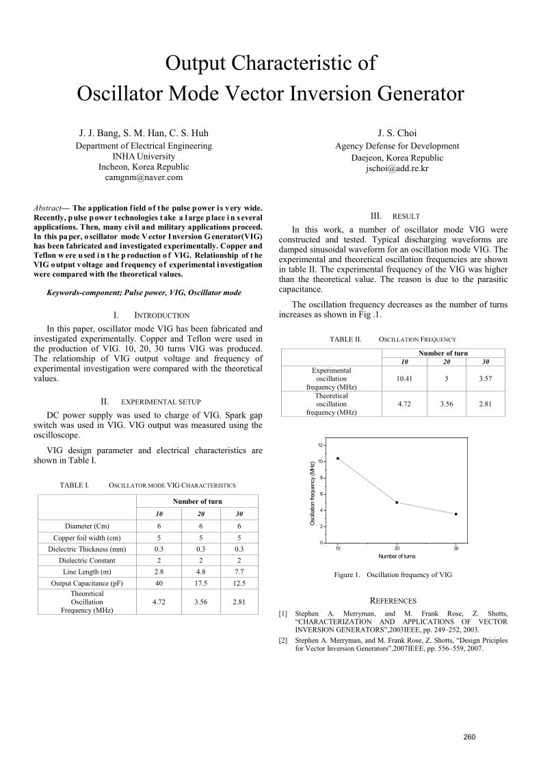
Output Characteristic of Oscillator Mode Vector Inversion Generator
J. J. Bang, S. M. Han, C. S. Huh Department of Electrical Engineering
INHA UniversityIncheon, Korea Republic
J. S. ChoiAgency Defense for Development
Daejeon, Korea [email protected]
Abstract
Keywords-component; Pulse power, VIG, Oscillator mode
I. INTRODUCTION
In this paper, oscillator mode VIG has been fabricated and investigated experimentally. Copper and Teflon were used in the production of VIG. 10, 20, 30 turns VIG was produced. The relationship of VIG output voltage and frequency of experimental investigation were compared with the theoretical values.
II. EXPERIMENTAL SETUP
DC power supply was used to charge of VIG. Spark gap switch was used in VIG. VIG output was measured using the oscilloscope.
VIG design parameter and electrical characteristics are shown in Table I.
TABLE I. OSCILLATOR MODE VIG CHARACTERISTICS
10 20 30
Diameter (Cm) 6 6 6 Copper foil width (cm) 5 5 5
Dielectric Thickness (mm) 0.3 0.3 0.3Dielectric Constant 2 2 2
Line Length (m) 2.8 4.8 7.7Output Capacitance (pF) 40 17.5 12.5
TheoreticalOscillation
Frequency (MHz)4.72 3.56 2.81
III. RESULT
In this work, a number of oscillator mode VIG were constructed and tested. Typical discharging waveforms are damped sinusoidal waveform for an oscillation mode VIG. The experimental and theoretical oscillation frequencies are shown in table II. The experimental frequency of the VIG was higher than the theoretical value. The reason is due to the parasitic capacitance.
The oscillation frequency decreases as the number of turns increases as shown in Fig .1.
TABLE II. OSCILLATION FREQUENCY
10 20 30Experimental
oscillationfrequency (MHz)
10.41 5 3.57
Theoreticaloscillation
frequency (MHz)4.72 3.56 2.81
10 20 30
0
2
4
6
8
10
12
Osc
illatio
n fre
quency
(M
Hz)
Number of turns
Figure 1. Oscillation frequency of VIG
REFERENCES
[1] Stephen A. Merryman, and M. Frank Rose, Z. Shotts,“CHARACTERIZATION AND APPLICATIONS OF VECTOR INVERSION GENERATORS”,2003IEEE, pp. 249–252, 2003.
[2] Stephen A. Merryman, and M. Frank Rose, Z. Shotts, “Design Priciples for Vector Inversion Generators”,2007IEEE, pp. 556–559, 2007.
260

INDEX
261

262

263

264

265
266

267

268

269

270

271

272

273