
Bit Patterned Media at 1 Tdot/in$^{2}$ and Beyond
6
IEEE TRANSACTIONS ON MAGNETICS, VOL. 49, NO. 2, FEBRUARY 2013 773 Bit Patterned Media at 1 Tdot/in and Beyond Thomas R. Albrecht, Daniel Bedau, Elizabeth Dobisz, He Gao, Michael Grobis, Olav Hellwig, Dan Kercher, Jeffrey Lille, Ernesto Marinero, Kanaiyalal Patel, Ricardo Ruiz, Manfred E. Schabes, Lei Wan, Dieter Weller, and Tsai-Wei Wu HGST, a Western Digital Company, San Jose Research Center, San Jose, California 95135 USA Bit patterned media (BPM) provide an alternative to conventional granular thin film recording media, circumventing the challenges of managing grain size and its associated noise and thermal stability issues in granular media. A viable fabrication strategy involves creation of a master pattern by rotary-stage e-beam lithography and directed self-assembly of block copolymers, followed by pattern replication via UV-cure nanoimprint lithography and pattern transfer to a magnetic thin film by ion beam etching. These steps have been demonstrated for 150 Gdot/cm (1 Tdot/in ) hcp patterns, achieving a dot placement tolerance of 1.2 nm and a defect rate of . Media samples fabricated in this manner from continuous CoCrPt alloy films have achieved a switching field distribution of 4% of . A 2T medium SNR of nearly 14 dB and a write bit error rate of 2 10 have been shown using a static tester with a conventional product read/write head. Modeling and experiment suggest that higher recording density can be achieved using BPM with a bit aspect ratio (BAR) . A master pattern generation generation strategy for BAR with rectangular islands is shown using intersecting lines generated by directed self-assembly of lamellar block copolymers in combination with spacer-defined line doubling. Index Terms—Bit error rate, media SNR, nanoimprint, patterned media, self-assembly. I. INTRODUCTION C ONTINUED PROGRESS in areal density for con- ventional perpendicular magnetic recording (PMR) on granular media has become increasingly difficult. Although adoption of energy assisted magnetic recording (EAMR) is widely viewed as a promising solution for thermal stability problems, challenges in scaling grain size and managing media noise may limit the rate of progress for EAMR with granular media. Bit patterned media [1]–[4] provide an alternative to granular media, offering a path to thermally stable recording at high density and low media noise by replacing the segregated random grains of PMR media with lithographically defined single domain islands. Recording experiments at 150 Gdot/cm (1 Tdot/in ) demonstrate the attributes of BPM and provide insight into its extendibility. II. BPM FABRICATION A viable process for high volume manufacturing of BPM is well established [3], [4]. A master pattern is created on a master template and replicated via a two-generation UV-cure full-disk nanoimprinting process to create replica working templates and imprinted disks [5], [6]. Pattern transfer from nanoimprint resist to magnetic islands is accomplished by etching islands from a full film of CoCrPt alloy using a carbon hard mask and ion beam etching (IBE) or ion implantation. Fabrication of master templates for BPM has triggered in- novative nontraditional lithographic processes to deliver excep- tionally small feature sizes on a schedule ahead of that contem- plated by the international technology roadmap for semiconduc- tors (ITRS). Because of the unique circular geometry of hard Manuscript received August 10, 2012; revised September 12, 2012; accepted October 22, 2012. Date of current version January 22, 2013. Corresponding author: T. R. Albrecht (e-mail: [email protected]). Digital Object Identifier 10.1109/TMAG.2012.2227303 disk drives and the high resolution needed, the most likely sce- nario for pattern formation will include e-beam directed self-as- sembly of block copolymers in which a rotary e-beam tool is used to fabricate sparse chemical contrast patterns to guide the assembly of denser block copolymer patterns via feature density multiplication [7]–[9]. Graphoepitaxy (guiding via topographic features) [10], [11] is another approach which has been pursued as an alternative to chemical contrast guiding for establishing long-range order in block copolymer films. Self-assembling block copolymer materials can readily form uniform periodic patterns in the range from to 50 nm full pitch. When it comes to lithographic applications, block copolymer thin films most readily form patterns with a limited set of geometries, namely, round dots in a hexagonal close pack (hcp) lattice (or possibly in a square lattice) or parallel stripes in line/space patterns [12], [13]. Until recently, most demon- strations of BPM fabrication had been based on round dots in hcp patterns formed by either cylindrical or spherical block copolymer domains [14], [15]. Fig. 1(a) shows a pattern formed by cylindrical PS-b-PMMA domains at Gdot/cm ( Tdot/in ), with 27 nm full pitch. This pattern can be transferred into a pillar-tone Si master template [Fig. 1(b)], then replicated onto a quartz working template [Fig. 1(c)] and imprinted onto a disk [Fig. 1(d)] to be finally transferred into magnetic islands [Fig. 1(e)]. While hcp patterns maximize the areal density of features for a given lithographic resolution, modeling and experimental data (see Section IV) suggest that a bit aspect ratio (BAR) , where BAR is defined as the ratio of the cross-track pitch to the down-track pitch, is superior for recording system integra- tion. Rectangular bit cells with arbitrary BAR can be obtained through a double imprint process via the intersection of orthog- onal line patterns imprinted from two independent submaster templates—one containing radial stripes and a second one with circumferential stripes [16] as shown in Fig. 2(a). The submaster templates used in this process are fabricated by e-beam directed self-assembly of lamellar phase block copolymers [Fig. 2(b) and (c)]. 0018-9464/$31.00 © 2013 IEEE
Transcript of Bit Patterned Media at 1 Tdot/in$^{2}$ and Beyond

IEEE TRANSACTIONS ON MAGNETICS, VOL. 49, NO. 2, FEBRUARY 2013 773
Bit Patterned Media at 1 Tdot/in and BeyondThomas R. Albrecht, Daniel Bedau, Elizabeth Dobisz, He Gao, Michael Grobis, Olav Hellwig, Dan Kercher,Jeffrey Lille, Ernesto Marinero, Kanaiyalal Patel, Ricardo Ruiz, Manfred E. Schabes, Lei Wan, Dieter Weller, and
Tsai-Wei Wu
HGST, a Western Digital Company, San Jose Research Center, San Jose, California 95135 USA
Bit patterned media (BPM) provide an alternative to conventional granular thin film recording media, circumventing the challengesof managing grain size and its associated noise and thermal stability issues in granular media. A viable fabrication strategy involvescreation of a master pattern by rotary-stage e-beam lithography and directed self-assembly of block copolymers, followed by patternreplication via UV-cure nanoimprint lithography and pattern transfer to a magnetic thin film by ion beam etching. These steps have beendemonstrated for 150 Gdot/cm (1 Tdot/in ) hcp patterns, achieving a dot placement tolerance of 1.2 nm and a defect rate of .Media samples fabricated in this manner from continuous CoCrPt alloy films have achieved a switching field distribution of 4% of. A 2T medium SNR of nearly 14 dB and a write bit error rate of 2 10 have been shown using a static tester with a conventional
product read/write head. Modeling and experiment suggest that higher recording density can be achieved using BPM with a bit aspectratio (BAR) . A master pattern generation generation strategy for BAR with rectangular islands is shown using intersecting linesgenerated by directed self-assembly of lamellar block copolymers in combination with spacer-defined line doubling.
Index Terms—Bit error rate, media SNR, nanoimprint, patterned media, self-assembly.
I. INTRODUCTION
C ONTINUED PROGRESS in areal density for con-ventional perpendicular magnetic recording (PMR) on
granular media has become increasingly difficult. Althoughadoption of energy assisted magnetic recording (EAMR) iswidely viewed as a promising solution for thermal stabilityproblems, challenges in scaling grain size and managing medianoise may limit the rate of progress for EAMR with granularmedia. Bit patterned media [1]–[4] provide an alternative togranular media, offering a path to thermally stable recording athigh density and low media noise by replacing the segregatedrandom grains of PMR media with lithographically definedsingle domain islands. Recording experiments at 150 Gdot/cm(1 Tdot/in ) demonstrate the attributes of BPM and provideinsight into its extendibility.
II. BPM FABRICATION
A viable process for high volume manufacturing of BPM iswell established [3], [4]. A master pattern is created on a mastertemplate and replicated via a two-generation UV-cure full-disknanoimprinting process to create replica working templates andimprinted disks [5], [6]. Pattern transfer from nanoimprint resistto magnetic islands is accomplished by etching islands from afull film of CoCrPt alloy using a carbon hard mask and ion beametching (IBE) or ion implantation.Fabrication of master templates for BPM has triggered in-
novative nontraditional lithographic processes to deliver excep-tionally small feature sizes on a schedule ahead of that contem-plated by the international technology roadmap for semiconduc-tors (ITRS). Because of the unique circular geometry of hard
Manuscript received August 10, 2012; revised September 12, 2012; acceptedOctober 22, 2012. Date of current version January 22, 2013. Correspondingauthor: T. R. Albrecht (e-mail: [email protected]).Digital Object Identifier 10.1109/TMAG.2012.2227303
disk drives and the high resolution needed, the most likely sce-nario for pattern formation will include e-beam directed self-as-sembly of block copolymers in which a rotary e-beam tool isused to fabricate sparse chemical contrast patterns to guide theassembly of denser block copolymer patterns via feature densitymultiplication [7]–[9]. Graphoepitaxy (guiding via topographicfeatures) [10], [11] is another approach which has been pursuedas an alternative to chemical contrast guiding for establishinglong-range order in block copolymer films.Self-assembling block copolymer materials can readily form
uniform periodic patterns in the range from to 50 nmfull pitch. When it comes to lithographic applications, blockcopolymer thin films most readily form patterns with a limitedset of geometries, namely, round dots in a hexagonal close pack(hcp) lattice (or possibly in a square lattice) or parallel stripesin line/space patterns [12], [13]. Until recently, most demon-strations of BPM fabrication had been based on round dots inhcp patterns formed by either cylindrical or spherical blockcopolymer domains [14], [15]. Fig. 1(a) shows a pattern formedby cylindrical PS-b-PMMA domains at Gdot/cm (Tdot/in ), with 27 nm full pitch. This pattern can be transferredinto a pillar-tone Si master template [Fig. 1(b)], then replicatedonto a quartz working template [Fig. 1(c)] and imprinted ontoa disk [Fig. 1(d)] to be finally transferred into magnetic islands[Fig. 1(e)].While hcp patterns maximize the areal density of features
for a given lithographic resolution, modeling and experimentaldata (see Section IV) suggest that a bit aspect ratio (BAR) ,where BAR is defined as the ratio of the cross-track pitch tothe down-track pitch, is superior for recording system integra-tion. Rectangular bit cells with arbitrary BAR can be obtainedthrough a double imprint process via the intersection of orthog-onal line patterns imprinted from two independent submastertemplates—one containing radial stripes and a second one withcircumferential stripes [16] as shown in Fig. 2(a). The submastertemplates used in this process are fabricated by e-beam directedself-assembly of lamellar phase block copolymers [Fig. 2(b) and(c)].
0018-9464/$31.00 © 2013 IEEE

774 IEEE TRANSACTIONS ON MAGNETICS, VOL. 49, NO. 2, FEBRUARY 2013
Fig. 1. SEM micrographs at various stages of BPM fabrication: (a) developedblock copolymer pattern on Si master template, (b) Si master template, (c) quartzreplica working template, (d) imprinted resist on disk, and (e) finished magneticislands (inset: X-section TEM). An island placement tolerance of nmis achieved at all steps.
The process of creating high BAR island features via the in-tersection of two separate line patterns as shown in Fig. 2 allowsfor the straightforward creation of skewed patterns (by usinginclined instead of perpendicular lines for the “radial” lines).In addition, this process easily accommodates localized partialtrack offsets and inclined chevron patterns, both of which areattractive options for servo patterns needed for track-followingservo in a disk drive [17], [18]. For hcp BPM, self-assembly incomplex patterned groove structures provides an alternative ap-proach for servo patterns [11], [19].While block copolymer pattern formation has been docu-
mented to extend up to 1.5 Tdot/cm (10 Tdot/in ) [20], blockcopolymer lithography, in which block copolymer patternsare used as lithographic masks for pattern transfer, is onlymature enough for near future industrial applications whenutilizing PS-b-PMMA block copolymers which can only reachdimensions down to nm full pitch. Smaller dimensionsrequire developing of robust lithographic processes with morestrongly segregating block copolymer materials. Alternatively,a conventional sidewall spacer double patterning process [21]can be used in combination with the striped patterns formed bylamellar PS-b-PMMA block copolymers to reach well below 25nm full pitch [22]. Fig. 2(c) shows an example of 20.5 nm fullpitch lines after line doubling from block copolymer patterns.
Fig. 2. (a) Schematic representation of a double imprint process to producerectangular features. Two “sub-master” templates, one with circumferentialstripes and a second one with radial lines are imprinted onto a separate “master”template. The intersection of the two sets results in rectangular features. (b)Circumferential block copolymer lines with a 27 nm full pitch. (c) Sidewallspacer line doubling from block copolymer lines with a 41 nm full pitch (topof image) to 20.5 nm pitch lines after line doubling (bottom). (d) High bitaspect ratio rectangular features imprinted in resist by the master template.This particular sample has 27 41 nm pitch (line doubling step for the radiallines not included for this sample).
At densities Gdot/cm (1 Tdot/in ), “reverse tone”nanoimprinting has advantages in yield and image quality.For normal tone imprinting, a hole-tone template is used tocreate resist pillars corresponding to BPM islands. Such pillarsare subject to pattern collapse and pattern transfer is sensitiveto resist residual layer thickness (RLT). These problems aremitigated by reverse-tone imprinting, which uses a pillar-tonetemplate to produce holes in resist, which in turn are convertedto isolated spots of high selectivity etch mask material by adeposition and etchback process. Our process differs from apreviously described reverse tone nanoimprinting processes[23], [24] in that vacuum deposition and etchback of a metalfill material is used instead of a second nanoimprint processusing Si-containing UV-curable resist. The vacuum depositionand etchback approach is thought to be more easily scalable tolow cost high volume production.
III. MAGNETIC FILMS FOR BPM
For the 150 Gdot/cm (1 Tdot/in ) static tester demonstrationin Section IV we used dual layer CoCrPt alloy hard/soft mediastructures with a total thickness of 6 nm for the magnetic layers.These dual layer structures are similar in behavior to previously

ALBRECHT et al.: BIT PATTERNED MEDIA AT 1 TDOT/IN AND BEYOND 775
Fig. 3. Partial Kerr loops (major and minor) of CoCrPt alloy BPM at 1Tdot/in .
reported hard/soft CoPd multilayer media [4], [25], [26]. Useof thin magnetic layers keeps the etch time to a minimum, re-quires less hard mask thickness, andmaximizes the island fillingfactor, since sidewall slope for ion beam etching is limited toaround 80 degrees. The average coercivity of the islandson the recording demonstration disks was in the range of 6.9–7.2kOe. Good recording performance was achieved on disks withan intrinsic switching field distribution (iSFD) as high as 720Oe for the island array. The iSFD/ ratio of 10.4% is near theupper bound of what is required theoretically for a successful150 Gdot/cm (1 Tdot/in ) demo. The fact that we achieveda good error rate with such a large iSFD/ ratio confirmsthat other margins limiting bit addressability are well controlledwithin our BPM recording system.Recent progress in CoCrPt alloy magnetic thin film deposi-
tion (yielding crystallographic out-of-plane c-axis alignmentdistributions of only 2.4 degrees) and additional improve-ments in patterning techniques have enabled fabrication of thin(6–8 nm) single layer BPM island arrays at 150 Gdot/cm (1Tdot/in ) areal density with iSFD as low as 230 Oe with anof around 5.7 kOe, thus yielding iSFD/ values of only 4% asdemonstrated in Fig. 3. Measurements of iSFD were performedas described in [27], [28]. The perpendicular anisotropyof these magnetic islands was determined to be around 14 kOe,thus yielding iSFD/ values close to 1.6%. Furthermore suchhigh anisotropy thin film islands provide excellent thermal sta-bility in the range of or higher, suggestinggood extendibility for recording at even higher densities thanreported in Section IV.
IV. RECORDING PERFORMANCE
A. Method
The readback and recording performance of the 150Gdot/cm (1 Tdot/in ) BPM was evaluated using a statictester [29]–[33] with a commercially available perpendicularmagnetic recording head. During testing, the recording headslider body was in contact with the disk. However, due to
slider topography, the read and write elements were abovethe surface of the disk with a small separation of nm. Therecording head used in the experiments is identical to thosefound in commercially available 650 Gb/in hard disk drives.The measured write width on perpendicular media was 70 nmwhile the magnetic read width was 45 nm.We examined two types of recording disks: one with a hexag-
onal 27 nm (island pitch) 24 nm (track pitch) lattice createdusing the full fabrication process based on nanoimprint lithog-raphy, as described in Section II and shown in Fig. 1, and onewith a staggered 26 26 nm square lattice created using di-rect-write e-beam lithography with HSQ resist [34], which wewill denote as NIL and EB disks, respectively. Both disks usedCoCrPt alloy magnetic media, but with slightly different com-positions. The NIL disk had higher moment and higher iSFD(710 Oe) than the EB disk, for which the iSFD was 570 Oe. Thedifference in iSFD is attributed to the different media composi-tions. In the recording regions the defect rate of the NIL disk waswell below 10 while the EB disk had a defect rate .
B. Readback SNR
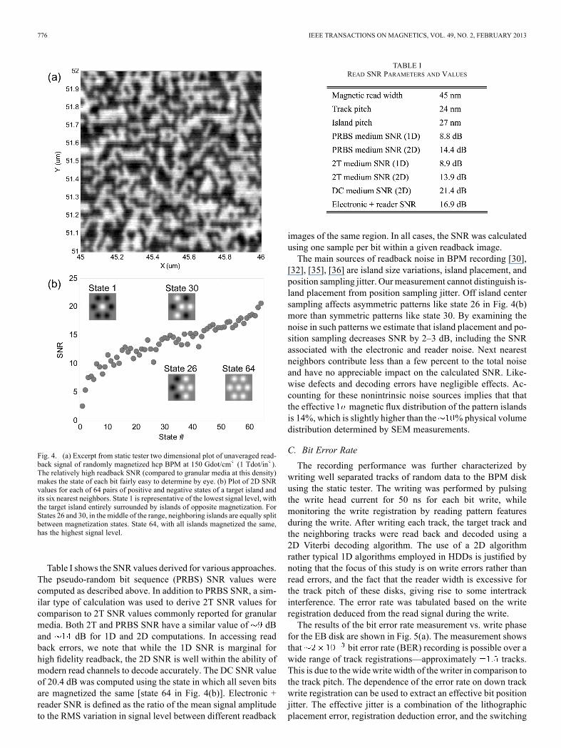
Fig. 4 shows a two dimensional (2D) readback image of partof an ensemble of about 100 000 islands on the NIL disk writtento random states with an unsynchronized write head in the statictester. The randomly written data was read back 30 times toallow separation of media noise and electronic/reader noisecomponents by statistical analysis. The state of each islandwas decoded using a 2D Viterbi decoding algorithm. For eachisland in the full image, the state of the target island and its sixnearest neighbors fall into one of possible patterns.Some representative patterns are shown in Fig. 4(b). Sinceeach pattern has equal probability of occurring throughoutthe image, there are roughly 10 occurrences of each patternamong the 10 islands read. For each of the possible patterns,the RMS deviation in signal amplitude at the center of the targetisland comprises the noise, while the mean amplitude serves asthe target signal level for SNR computation. Variations in thesignal (averaged over multiple reads) at different locations ofthe same pattern on the medium are used to compute mediumnoise; variations at the same location between different read-back images are used to compute electronic and reader noise.Since the read head used in these experiments is significantly
wider than optimal for the narrow track pitch of the recordingmedium, both 1D and 2D calculation methods were used forSNR. In the 1D case, variations in signal level due to inter-track interference (ITI) from the four islands of the pattern in theneighboring tracks are treated as noise. The signal stems fromcenter bit, where the sampling occurs, but also contains con-tributions from the two neighboring down track bits. The threedown track bits can be viewed as constituting a symbol. In the2D case, the symbol contains the additional four adjacent trackbits and ITI from those bits is part of the signal. Considering theadjacent track bits in this way provides an SNR value more rela-vant for decoding schemes that use intertrack interference (ITI)cancellation or 2D decoding. This approach also simulates tosome extent how a narrower readback head with minimal ITIwould behave and is better suited for calculating a true mediumSNR, free of read head contributions to noise.
776 IEEE TRANSACTIONS ON MAGNETICS, VOL. 49, NO. 2, FEBRUARY 2013
Fig. 4. (a) Excerpt from static tester two dimensional plot of unaveraged read-back signal of randomly magnetized hcp BPM at 150 Gdot/cm (1 Tdot/in ).The relatively high readback SNR (compared to granular media at this density)makes the state of each bit fairly easy to determine by eye. (b) Plot of 2D SNRvalues for each of 64 pairs of positive and negative states of a target island andits six nearest neighbors. State 1 is representative of the lowest signal level, withthe target island entirely surrounded by islands of opposite magnetization. ForStates 26 and 30, in the middle of the range, neighboring islands are equally splitbetween magnetization states. State 64, with all islands magnetized the same,has the highest signal level.
Table I shows the SNR values derived for various approaches.The pseudo-random bit sequence (PRBS) SNR values werecomputed as described above. In addition to PRBS SNR, a sim-ilar type of calculation was used to derive 2T SNR values forcomparison to 2T SNR values commonly reported for granularmedia. Both 2T and PRBS SNR have a similar value of dBand dB for 1D and 2D computations. In accessing readback errors, we note that while the 1D SNR is marginal forhigh fidelity readback, the 2D SNR is well within the ability ofmodern read channels to decode accurately. The DC SNR valueof 20.4 dB was computed using the state in which all seven bitsare magnetized the same [state 64 in Fig. 4(b)]. Electronic +reader SNR is defined as the ratio of the mean signal amplitudeto the RMS variation in signal level between different readback
TABLE IREAD SNR PARAMETERS AND VALUES
images of the same region. In all cases, the SNR was calculatedusing one sample per bit within a given readback image.The main sources of readback noise in BPM recording [30],
[32], [35], [36] are island size variations, island placement, andposition sampling jitter. Our measurement cannot distinguish is-land placement from position sampling jitter. Off island centersampling affects asymmetric patterns like state 26 in Fig. 4(b)more than symmetric patterns like state 30. By examining thenoise in such patterns we estimate that island placement and po-sition sampling decreases SNR by 2–3 dB, including the SNRassociated with the electronic and reader noise. Next nearestneighbors contribute less than a few percent to the total noiseand have no appreciable impact on the calculated SNR. Like-wise defects and decoding errors have negligible effects. Ac-counting for these nonintrinsic noise sources implies that thatthe effective magnetic flux distribution of the pattern islandsis 14%, which is slightly higher than the % physical volumedistribution determined by SEM measurements.
C. Bit Error Rate
The recording performance was further characterized bywriting well separated tracks of random data to the BPM diskusing the static tester. The writing was performed by pulsingthe write head current for 50 ns for each bit write, whilemonitoring the write registration by reading pattern featuresduring the write. After writing each track, the target track andthe neighboring tracks were read back and decoded using a2D Viterbi decoding algorithm. The use of a 2D algorithmrather typical 1D algorithms employed in HDDs is justified bynoting that the focus of this study is on write errors rather thanread errors, and the fact that the reader width is excessive forthe track pitch of these disks, giving rise to some intertrackinterference. The error rate was tabulated based on the writeregistration deduced from the read signal during the write.The results of the bit error rate measurement vs. write phase
for the EB disk are shown in Fig. 5(a). The measurement showsthat bit error rate (BER) recording is possible over awide range of track registrations—approximately tracks.This is due to the wide write width of the writer in comparison tothe track pitch. The dependence of the error rate on down trackwrite registration can be used to extract an effective bit positionjitter. The effective jitter is a combination of the lithographicplacement error, registration deduction error, and the switching

ALBRECHT et al.: BIT PATTERNED MEDIA AT 1 TDOT/IN AND BEYOND 777
Fig. 5. bit error rate versus write head registration to BPM islands. (a)On-track error rate. (b) Overall write rate. (c) Combined on-track and adjacenttrack actual error rate. (d) Extrapolated combined error rate with media defectsremoved.
field distribution normalized by the write field gradient [35],[36]. Given the 570 Oe iSFD and Oe/nm down track gra-dient, the later is expected to be the dominant component. Whenwriting with the head centered on the track, the effective bit po-sition jitter is measured to be 2.2 nm.Fig. 5(b) shows the write probability dependence on write
registration for the EB disk. The mean write width of therecording head is 90 nm, taken at the 25% write probabilitypoint. Note that since we are writing random data, there is atmost a 50% chance that a bit will be flipped during writing.The BPM write width is wider than the nm write widthon conventional media. The differences in write width are con-sistent with differences in and angle dependent switchingcharacteristics of the EB BPM and PMR media.Due to write width mismatch we evaluate the recording in
terms of shingled magnetic recording system. Fig. 5(c) showsthe combined on track error rate and adjacent track write ratevs. write registration. The combined BER has two local minimacorresponding to the two possible shingling directions. Thelowest observed combined BER is . The BER is con-sistent with the known defect rate in the sample of .To estimate the possible recording performance in the absenceof the defects we fit the on track and cross track write char-acteristics using the Gaussian error model in [31], [35], [36].Fig. 5(d) shows the resulting fit with the defect contributionremoved. In the absence of defects the media exhibits a sub10 BER write margin of nm in the down track directionand nm in the cross track direction. A similar BER wasobtained on a NIL disk with a similar , but 25% higher iSFDdue to composition differences. The BER on the NIL disk waslimited by the iSFD rather than defects.
Fig. 6. Areal density as a function of bit aspect-ratio.
D. Higher BAR
The observed asymmetry in the down-track and cross-trackmargins suggests that the areal density may be extended by in-creasing the bit aspect-ratio (BAR) to values larger than one [4],[36]. In general, the down-track bit density and the cross-trackbit density pose different challenges to the system design. Forexample, current servo techniques demand a track pitch that isconsiderably larger than the smallest down-track bit-pitch. Sim-ilarly, today’s PMR heads are optimized to have sharper gradi-ents in the down-track direction as compared to the cross-trackdirection. Furthermore, tails of the write field may extend far inthe cross-track direction requiring additional cross-track mar-gins. A detailed discussion of the system-level consequences ofthese asymmetries is given in [37].Applying a Monte-Carlo model of the write-BER [37] to the
experimental conditions of static tester experiments, Fig. 6 plotsthe defect-free areal density (i.e., in absence of patterning de-fects) as a function of BAR. In these calculations, down-trackand cross-track synchronization-jitter values are 1.0 nm ,and the magnetic spacing is 6 nm. The cross-track servo ca-pability of the static tester is assumed to be 0.5 nm . TheiSFD is 424 Oe, and the residual unshielded demagnetizationcontribution to the SFD is taken to be 75 Oe. The areal den-sity in Fig. 6 shows a significant positive slope near ,giving a gain of more than 25% when increasing the BAR from1.0 to 1.5. Fig. 6 also indicates that areal densities in excessof 300 Gdot/cm (2 Tdot/in ) are in principle possible on thestatic tester by increasing the BAR of the media to , all otherparameters unchanged. The gains observed in Fig. 6 are an ex-pression of the fact that the down-track and cross-track profilesof the effective write field strongly affect the optimum BAR andhence the entire bit-patterned media fabrication process. Opti-mizing write heads for BPM may compound the gains from thebit-patterned media technology and thus significantly extend theachievable areal densities of magnetic recording.

778 IEEE TRANSACTIONS ON MAGNETICS, VOL. 49, NO. 2, FEBRUARY 2013
REFERENCES
[1] S. Y. Chou, P. R. Krauss, and L. S. Kong, “Nanolithographically de-fined magnetic structures and quantum magnetic disk,” J. Appl. Phys.,vol. 79, pp. 6101–6106, 1996.
[2] R. M. H. New, R. F. W. Pease, and R. L. White, “Lithographicallypatterned single-domain cobalt islands for high-density magneticrecording,” J. Magn. Magn. Mater., vol. 155, pp. 140–145, 1996.
[3] B. D. Terris and T. Thomson, “Nanofabricated and self-assembledmagnetic structures as data storage media,” J. Phys. D, vol. 38, pp.R199–222, 2005.
[4] T. R. Albrecht, O. Hellwig, R. Ruiz, M. E. Schabes, B. D. Terris, and X.Z. Wu, “Bit-patterned magnetic recording: Nanoscale magnetic islandsfor data storage,” in Nanoscale Magnetic Materials and Applications,J. P. Liu, E. Fullerton, O. Gutfleisch, and D. J. Sellmyer, Eds. NewYork: Springer, 2009, pp. 237–274.
[5] G. M. Schmid, M. Miller, C. Brooks, N. Khusnatdinov, D. LaBrake, D.J. Resnick, S. V. Sreenivasan, G. Gauzner, K. Lee, D. Kuo, D. Weller,and X. Yang, “Step and flash imprint lithography for manufacturingpatterned media,” J. Vac. Sci. Technol. B, vol. 27, pp. 573–580, 2009.
[6] X. M. Yang, Y. Xu, K. Lee, S. Xiao, D. Kuo, and D.Weller, “Advancedlithography for bit patterned media,” IEEE. Trans. Magn., vol. 45, no.2, pt. 2, pp. 833–838, Feb. 2009.
[7] R. Ruiz, H. Kang, F. A. Detcheverry, E. Dobisz, D. S. Kercher, T. R.Albrecht, J. J. de Pablo, and P. F. Nealey, “Density multiplication andimproved lithography by directed block copolymer assembly,” Science,vol. 321, no. 5891, pp. 936–939, 2008.
[8] X. M. Yang, L. Wan, S. G. Xiao, Y. Xu, and D. K. Weller, “Directedblock copolymer assembly versus electron beam lithography for bit-patterned media with areal density of 1 terabit/inch and beyond,” ACSNano, vol. 3, pp. 1844–1858, 2009.
[9] R. Ruiz, E. Dobisz, and T. R. Albrecht, “Rectangular patterns usingblock copolymer directed assembly for high bit aspect ratio patternedmedia,” ACS Nano, vol. 5, no. 1, pp. 79–84, 2011.
[10] C. A. Ross and J. Y. Cheng, “Patterned magnetic media made byself-assembled block-copolymer lithography,” MRS Bull., vol. 33, pp.838–845, 2008.
[11] R. Yamamoto, A. Yuzawa, T. Shimada, Y. Ootera, Y. Kamata, N. Ki-hara, and A. Kikitsu, “Nanoimprint mold for 2.5 Tbit/in. directedself-assembly bit patterned media with phase servo pattern,” Jpn. J.Appl. Phys., vol. 51, p. 046503, 2012.
[12] C. T. Black, R. Ruiz, G. Breyta, J. Y. Cheng, M. Colburn, K. W.Guarini, H.-C. Kim, and Y. Zhang, “Polymer self assembly in semi-conductor microelectronics,” IBM J. Res. Devel., vol. 51, no. 5, pp.605–633, 2007.
[13] R. A. Segalman, “Patterning with block copolymer thin films,”Mater.Sci. Eng. R-Reports, vol. 48, no. 6, pp. 191–226, 2005.
[14] O. Hellwig, J. K. Bosworth, E. Dobisz, D. Kercher, T. Hauet, G.Zeltzer, J. D. Risner-Jamtgaard, D. Yaney, and R. Ruiz, “Bit patternedmedia based on block copolymer directed assembly with narrowmagnetic switching field distribution,” Appl. Phys. Lett., vol. 96, no.5, p. 052511, 2010.
[15] H. Wang, M. T. Rahman, H. B. Zhao, Y. Isowaki, Y. Kamata, A. Kik-itsu, and J. P. Wang, “Fabrication of FePt type exchange coupled com-posite bit patterned media by block copolymer lithography,” J. Appl.Phys., vol. 109, p. 07B754, 2011.
[16] L. Wan, R. Ruiz, H. Gao, K. C. Patel, J. Lille, G. Zeltzer, E. Dobisz, A.Bogdanov, P. F. Nealey, and T. R. Albrecht, “Fabrication of templateswith rectangular bits on circular tracks by combining block copolymerdirected self-assembly and nanoimprint lithography,” J. Micro/Nano-lith. MEMS MOEMS, vol. 11, p. 031405, 2012.
[17] G. Liu, P. F. Nealey, R. Ruiz, E. Dobisz, K. C. Patel, and T. R. Al-brecht, “Fabrication of chevron patterns for patterned media with blockcopolymer directed assembly,” J. Vac. Sci. Tech. B, vol. 29, p. 06F204,2011.
[18] J. Lille, R. Ruiz, L. Wan, H. Gao, A. Dhanda, G. Zeltzer, T.Arnoldussen, K. Patel, Y. Tang, and T. R. Albrecht, “Integration ofservo and high bit aspect ratio data patterns on nanoimprint tem-plates for patterned media,” IEEE Trans. Magn., vol. 48, no. 11, pp.2757–2760, Nov. 2012.
[19] Y. Kamata, A. Kikitsu, N. Kihara, S. Morita, K. Kimura, and H. Izumi,“Fabrication of ridge-and-groove servo pattern consisting of self-as-sembled dots for 2.5 Tb/in bit patterned media,” IEEE Trans. Magn.,vol. 47, no. 1, pp. 51–54, Jan. 2011.
[20] S. Park, D. H. Lee, J. Xu, B. Kim, S. W. Hong, U. Jeong, T. Xu,and T. P. Russell, “Macroscopic 10-terabit-per-square-inch arrays fromblock copolymers with lateral order,” Science, vol. 323, no. 5917, pp.1030–1033, 2009.
[21] C. Bencher, “SADP: The best option for nm NAND flash,”Nanochip Technol. J., vol. 2, pp. 8–13, 2007.
[22] K. C. Patel, R. Ruiz, J. Lille, L. Wan, E. Dobisz, H. Gao, N. Robertson,and T. R. Albrecht, “Line frequency doubling of directed self assemblypatterns for single-digit bit pattern media lithography,” in Proc. SPIEAlternative Lithographic Technol., W.M. Tong and D. J. Resnick, Eds.,2012, vol. 8323, pp. 8323OU–1.
[23] M.Miller, G. Doyle, N. Stacey, F. Xu, S. V. Sreenivasan, M.Watts, andD. L. LaBrake, “Fabrication of nanometer sized features on non-flatsubstrates using a nano-imprint lithography process,” in Proc. SPIE,2005, vol. 5751, p. 994.
[24] X. M. Yang, Y. Xu, C. Seiler, L. Wan, and S. Xiao, “Toward 1 Tdot/innanoimprint lithography for magnetic bit-patterned media: Opportuni-ties and challenges,” J. Vac. Sci. Technol. B, vol. 26, pp. 2604–2610,2008.
[25] T. Hauet, E. Dobisz, S. Florez, J. Park, B. Lengsfield, B. D. Terris,and O. Hellwig, “Role of reversal incoherency in reducing switchingfield and switching field distribution of exchange coupled compositebit patterned media,” Appl. Phys. Lett., vol. 95, p. 262504, 2009.
[26] O. Hellwig, T. Hauet, T. Thomson, E. Dobisz, J. D. Risner-Jamtgaard,D. Yaney, B. D. Terris, and E. E. Fullerton, “Coercivity tuning in Co/Pdmultilayer based bit patterned media,” Appl. Phys. Lett., vol. 95, p.232505, 2009.
[27] A. Berger, Y. Xu, B. Lengsfield, Y. Ikeda, and E. E. Fullerton,“ method for the determination of intrinsic switchingfield distributions in perpendicular media,” IEEE Trans. Magn., vol.41, no. 10, pp. 3178–3180, Oct. 2005.
[28] O. Hellwig, A. Berger, T. Thomson, E. Dobisz, Z. Z. Bandic, H. Yang,D. S. Kercher, and E. E. Fullerton, “Separating dipolar broadeningfrom the intrinsic switching field distribution in perpendicular pat-terned media,” Appl. Phys. Lett., vol. 90, p. 162516, 2007.
[29] A. Moser, D. Weller, M. E. Best, and M. F. Doerner, “Dynamic co-ercivity measurements in thin film recording media using a contactwrite/read tester,” J. Appl. Phys., vol. 85, pp. 5018–5020, 1999.
[30] M. Albrecht, C. T. Rettner, A. Moser, M. E. Best, and B. D. Terris,“Recording performance of high-density patterned perpendicular mag-netic media,” Appl. Phys. Lett., vol. 81, pp. 2875–2877, 2002.
[31] M. Grobis, E. Dobisz, O. Hellwig, M. E. Schabes, G. Zeltzer, T. Hauet,and T. R. Albrecht, “Measurements of the write error rate in bit pat-terned magnetic recording at 100–320 Gb/in ,” Appl. Phys. Lett., vol.96, p. 052509, 2010.
[32] M. Asbahi, J. Moritz, B. Dieny, C. Gourgon, C. Perret, and R. J. M.van de Veerdonk, “Recording performances in perpendicular magneticpatterned media,” J. Phys. D, vol. 43, p. 385003, 2010.
[33] S. H. Leong, M. J. B. Lim, B. Santoso, C. L. Ong, Z.-M. Yuan, Y. J.Chen, T. L. Huang, and S. B. Hu, “Patterned media and energy assistedrecording study by drag tester,” IEEE Trans. Magn., vol. 47, no. 7, pp.1981–1987, Jul. 2011.
[34] E. A. Dobisz, D. Kercher, M. Grobis, O. Hellwig, E. E. Marinero, D.Weller, and T. R. Albrecht, “Fabrication of CoCrPt alloy bit patternedmedia at 1 Td/in and recording performance measurement with con-ventional read/write head,” J. Vac. Sci. Techn. B, vol. 30, no. 06FH01,2012, .
[35] H. J. Richter, A. Y. Dobin, R. T. Lynch, D. Weller, R. M. Brockie, O.Heinonen, K. Z. Gao, J. Xue, R. J. M. v. d. Veerdonk, P. Asselin, andM. F. Erden, “Recording potential of bit-patterned media,” Appl. Phys.Lett., vol. 88, p. 222512, 2006.
[36] M. E. Schabes, “Micromagnetic simulations for terabit/in head/mediasystems,” J. Magn. Magn. Mater., vol. 320, pp. 2880–2884, 2008.
[37] M. E. Schabes, T. R. Albrecht, and M. Grobis, System Level Perspec-tive of Bit-Patterned Magnetic Recording TMRC’12, paper F-4, Aug.2012.