Beam test results for single- and double-sided silicon detector prototypes of the CMS central...
45
Available on CMS information server CMS NOTE 1997/006 CMS Note The Compact Muon Solenoid Experiment Mailing address: CMS CERN, CH-1211 GENEVA 23, Switzerland Beam Test Results for Single- and Double-Sided Silicon Detector Prototypes of the CMS Central Detector O. Adriani 5 , E. Babucci 8 , N. Bacchetta 7 , G. Bagliesi 9 , P. Bartalini 8 , A. Basti 9 , G. M. Bilei 8 , D. Boemi 4 , L. Borrello 4 , F. Bosi 9 , R. Castaldi 9 , G. Castellini 6 , E. Catacchini 5 , U. Cazzola 9 , B. Checcucci 8 , C. Civinini 5 , D. Creanza 3 , R. D’Alessandro 5 , M. de Palma 3 , R. Dell’Orso 9 , R. Della Marina 2 , L. Fiore 3 , E. Focardi 5 , A. Gabbanini 6 , A. Giassi 9 , A. Giraldo 7 , L. Gorn 11 M. Loreti 7 , G. Maggi 3 , G. Mantovani 8 , M. Meschini 5 , A. Messineo 9 , S. My 3 , G. Parrini 5 , M. Pieri 5 , F. Raffaelli 9 , G. Raso 3 , A. Santocchia 8 , E. Scarlini 5 , G. Selvaggi 3 , L. Servoli 8 , L. Silvestris 3 , A. Skassyrskaia 9a , F. Szoncso 1 , P. Tempesta 3 , M. Tesi 6 , G. Tonelli 9 10 , C. Vannini 9 , P. G. Verdini 9 , R. Wheadon 9 , Abstract We report the results of two beam tests performed in July and September 1995 at CERN using silicon microstrip detectors of various types: single sided, double sided with small angle stereo strips, double sided with orthogonal strips, double sided with pads. For the read-out electronics use was made of Preshape32, Premux128 and VA1 chips. The signal to noise ratio and the resolution of the detectors was studied for different incident angles of the incoming particles and for different values of the detector bias voltage. The goal of these tests was to check and improve the performances of the prototypes for the CMS Central Detector. to be submitted to Nucl. Instr. Meth. 1 CERN Geneva, Switzerland 2 ETH Zurich, Switzerland 3 I.N.F.N. and University of Bari, Italy 4 I.N.F.N. and University of Catania, Italy 5 I.N.F.N. and University of Florence, Italy 6 I.N.F.N. and Istituto Ricerca Onde Elettromagnetiche of Florence, Italy 7 I.N.F.N. and University of Padova, Italy 8 I.N.F.N. and University of Perugia, Italy 9 I.N.F.N. and University of Pisa, Italy 10 University of Sassari, Italy 11 Iowa State University, USA a On leave of absence from BINP, Moskow, Russia
Transcript of Beam test results for single- and double-sided silicon detector prototypes of the CMS central...

Available on CMS information server CMS NOTE 1997/006
CMS NoteThe Compact Muon Solenoid Experiment
Mailing address: CMS CERN, CH-1211 GENEVA 23, Switzerland
Beam Test Results for Single- and Double-SidedSilicon Detector Prototypes of the CMS Central
Detector
O. Adriani5), E. Babucci8), N. Bacchetta7), G. Bagliesi9), P. Bartalini8), A. Basti9), G. M. Bilei8), D. Boemi4),L. Borrello4), F. Bosi9), R. Castaldi9), G. Castellini6), E. Catacchini5), U. Cazzola9), B. Checcucci8),
C. Civinini5), D. Creanza3), R. D’Alessandro5), M. de Palma3), R. Dell’Orso9), R. Della Marina2), L. Fiore3),E. Focardi5), A. Gabbanini6), A. Giassi9), A. Giraldo7), L. Gorn11) M. Loreti7), G. Maggi3), G. Mantovani8),M. Meschini5), A. Messineo9), S. My3), G. Parrini5), M. Pieri5), F. Raffaelli9), G. Raso3), A. Santocchia8),E. Scarlini5), G. Selvaggi3), L. Servoli8), L. Silvestris3), A. Skassyrskaia9;a), F. Szoncso1), P. Tempesta3),
M. Tesi6), G. Tonelli9;10), C. Vannini9), P. G. Verdini9), R. Wheadon9),
Abstract
We report the results of two beam tests performed in July and September 1995 at CERN using siliconmicrostrip detectors of various types: single sided, double sided with small angle stereo strips, doublesided with orthogonal strips, double sided with pads. For the read-out electronics use was made ofPreshape32, Premux128 and VA1 chips. The signal to noise ratio and the resolution of the detectorswas studied for different incident angles of the incoming particles and for different values of thedetector bias voltage. The goal of these tests was to check and improve the performances of theprototypes for the CMS Central Detector.
to be submitted toNucl. Instr. Meth.
1) CERN Geneva, Switzerland2) ETH Zurich, Switzerland3) I.N.F.N. and University of Bari, Italy4) I.N.F.N. and University of Catania, Italy5) I.N.F.N. and University of Florence, Italy6) I.N.F.N. and Istituto Ricerca Onde Elettromagnetiche of Florence, Italy7) I.N.F.N. and University of Padova, Italy8) I.N.F.N. and University of Perugia, Italy9) I.N.F.N. and University of Pisa, Italy
10) University of Sassari, Italy11) Iowa State University, USA
a) On leave of absence from BINP, Moskow, Russia

Contents
1 Introduction 2
2 Detectors 2
3 Read-out Electronics 3
3.1 The PreShape32 chip . . . . . . . . . . . . . . . . . . . . . . . . . . . . . . . . . . . . . . . . . 3
3.2 The PreMux128 chip . . .. . . . . . . . . . . . . . . . . . . . . . . . . . . . . . . . . . . . . . 4
4 Detector Modules 4
5 Experimental Set-up 5
5.1 July ’95 beam test . . . . . . . . . . . . . . . . . . . . . . . . . . . . . . . . . . . . . . . . . . . 5
5.2 September ’95 beam test . . . . . . . . . . . . . . . . . . . . . . . . . . . . . . . . . . . . . . . 5
6 Data Acquisition System 5
6.1 July setup . . . . . . . . . . . . . . . . . . . . . . . . . . . . . . . . . . . . . . . . . . . . . . . 5
6.2 September setup . . . . . . . . . . . . . . . . . . . . . . . . . . . . . . . . . . . . . . . . . . . . 6
7 Offline Analysis 6
7.1 Data processing . . . . . . . . . . . . . . . . . . . . . . . . . . . . . . . . . . . . . . . . . . . . 6
7.1.1 Cluster finding . . . . . . . . . . . . . . . . . . . . . . . . . . . . . . . . . . . . . . . . 6
7.1.2 Tracking . . . . . . . . . . . . . . . . . . . . . . . . . . . . . . . . . . . . . . . . . . . 7
7.2 Monte Carlo . . . . . . . . . . . . . . . . . . . . . . . . . . . . . . . . . . . . . . . . . . . . . . 7
8 Results 8
8.1 Single-sided detectors and p-side performance in general . . . . . . . . . . . . . . . . . . . . . . 8
8.1.1 Charge response and signal-to-noise ratio . . .. . . . . . . . . . . . . . . . . . . . . . . 8
8.1.2 Bias voltage scan . . . . . . . . . . . . . . . . . . . . . . . . . . . . . . . . . . . . . . . 9
8.1.3 Angular scan . . .. . . . . . . . . . . . . . . . . . . . . . . . . . . . . . . . . . . . . . 9
8.1.4 Response function and space resolution. . . . . . . . . . . . . . . . . . . . . . . . . . . 9
8.2 Double-sided stereo detectors and n-side performance in general . . . . . .. . . . . . . . . . . . 10
8.2.1 Charge response and signal-to-noise ratio . . .. . . . . . . . . . . . . . . . . . . . . . . 10
8.2.2 Resolution . . . . . . . . . . . . . . . . . . . . . . . . . . . . . . . . . . . . . . . . . . 11
8.3 R&D devices . . . . . . . . . . . . . . . . . . . . . . . . . . . . . . . . . . . . . . . . . . . . . 11
8.3.1 The WEDGE detector . . . . . . . . . . . . . . . . . . . . . . . . . . . . . . . . . . . . 11
8.3.2 The DSODM and the BABY detectors . . . . . . . . . . . . . . . . . . . . . . . . . . . . 12
8.3.3 The PAD detector . . . . . . . . . . . . . . . . . . . . . . . . . . . . . . . . . . . . . . . 12
8.3.4 Charge response in presence of weakly coupled floating strips . . .. . . . . . . . . . . . 13
9 Summary and Conclusions 14
1

1 IntroductionThe proposed CMS Silicon Tracker consists of four layers of silicon detectors instrumenting the intermediate partof the tracking cavity, between the inner pixel detector and the outer MSGC layers [1]. High precision microstripsilicon detectors will provide accurate measurements in the bending plane. In the barrel region, rectangular detec-tors with p-strips oriented along the beam direction are expected to provide point resolution better than 15µmin ther-φ plane for perpendicular incidence; a coarse measurement (σ '1mm) of the z coordinate provided by double-sided detectors with stereo strips on the n-side is also foreseen for pattern recognition and to resolve differentinteraction vertices at full luminosity. Similarly, in the forward region wedge-shaped detectors will provide pre-cision measurements of the azimuthal coordinate and a coarse measurement of the radial coordinate. Four basictypes of silicon detectors are therefore included in the CMS baseline tracker layout: single- and double-sideddevices, in two different geometries (barrel-rectangular and forward-wedge).
The purpose of the beam test activity described herein was to check carefully the performances of non-irradiatedsingle- and double-sided devices in terms of signal-to-noise ratio and space resolution under different conditionsof bias voltage and for tracks at various incident angles.
Fast amplifiers (PreShape32 and PreMux128) based on the same preamplifier-shaper design that will be part of thefinal chip foreseen for LHC were used to study the performance of the system. Also, for a better understanding ofthe detector response a few detectors were read-out with conventional slow electronics (VA1).
The aim was to show that the performances attainable with non-irradiated devices coupled to the first prototypes ofthe final electronics are compatible with the design parameters contained in the CMS Technical Proposal. In addi-tion, several interesting new devices were tested within an R&D effort aimed at an optimisation of the performanceof the tracker in its entirety.
2 DetectorsSeveral different types of detectors were tested on the beam. All detectors were built from standard n-type highresistivity silicon wafers, 300µm thick. All single- and double-sided microstrip detectors tested have identicalstructures on the p-side. Each strip is AC coupled to external amplifiers by means of integrated capacitors builton the wafer itself by deposition of thin dielectric layers. Bias is provided to the strips via polysilicon resistorsconnected to the guard-ring structure. A similar arrangement is used on the ohmic side of the double-sided deviceswith the addition of an isolation p-stop box surrounding each electrode. In the devices featuring what we will callin the following “Double-Metal technology” (DM) the ohmic electrodes are connected, through a small contact,with a set of metal electrodes deposited on top of a thick insulator layer. The detectors tested were produced in twodifferent technologies [2, 3, 4] by the CSEM and SINTEF foundries. A detailed description of the technologicalaspects of the detectors can be found in ref. [5].
The characteristics of the detectors used are summarised in table 1, where the values following thep or n symbolsindicate quantities pertinent to the junction or ohmic side respectively; SS stands for Single-Sided, DS for Double-Sided and DM for Double-Metal.N is the number of strips on the junction or ohmic side,L their length,W theirwidth, Pph the pitch,RB the bias resistor value range, andDph indicates the overall size of the detector. Notethat for some double-metal detectors the pitch of the readout strips may not coincide with the pitchPph of thecharge-collection strips once the detectors are assembled to form a module, due to the possible presence of floatingstrips.
CSEM single-sided detectors have a large implant and metal pad on the ohmic side to provide uniform biasing,surrounded by a guard ring structure. The DS Orthogonal DM detector has 384 strips patterned on the ohmicside in the Metal-2 layer on a decoupling dielectric consisting of 4µmthick Silicon dioxide. These readout stripsare orthogonal to the detector strips and connected to them by vias; the BABY detector is another double-sided,orthogonal, double-metal design, and it has a Metal-2 pattern on the ohmic side consisting of 186 strips orthogonalto then+ implants. The so-called stereo detectors are double-sided detectors where the strips on the ohmic side aretilted with an angle of 100 mrad with respect to those on the junction side. Fig. 1 shows the layout of the ohmic sidestrips for the SINTEF Double-Sided Stereo Double-Metal detectors. These detectors have an additional Metal-2pattern of 25.7mm long strips on the ohmic side that run orthogonal to the junction side strips; each of themis connected to two detector strips at the edges of the rectangular active area, by vertical vias passing through adecoupling dielectric consisting of a 4µm thick polyimide layer. This arrangement was used to avoid dead zonesin the two triangular areas at the opposite edge of the module. The PAD detector has the ohmic side patternedinto 4 columns of 32 pads, each 6.42 mm2. For the WEDGE detector (fig. 2) the strips of the p-side follow the
2

Table 1: Detector Characteristics
Detector Maker N L W Pph RB Dph
(mm) ( µm ) ( µm ) (MΩ) (mm2)
SS Small Size CSEM p 384 62.2 14 50 0.7-1.4 21x64SS Full Size CSEM p 1024 62.2 14 50 0.7-1.4 64x64DS Stereo CSEM p 384 62.2 14 50 0.7-1.4 21x64
n 256 62.2 28 100 0.7-1.4DS Orthog DM CSEM p 384 62.2 14 50 0.7-1.4 21x64
n 621 19.2 28 100 0.7-1.4BABY CSEM p 384 8.2 14 50 1.0 21x10
n 186 19.2 14 50 0.7DS Stereo DM SINTEF p 512 62.5 14 50 0.3-1.0 30x65
n 256 65. 28 100 0.3-1.0PAD SINTEF p 512 62.5 14 50 0.3-1.0 30x65
n 32 6.4 2000 0.3-1.0WEDGE CSEM p 128 62 14-26 38-50 18 8.6x64
n 495 4.8-6.3 60 125 25
trapezoidal geometry with a fanning structure that makes the pitch change from 38 to 50µm . The n-side stripshave a pitch of 125µmand are orthogonal to the central strip of the p-side.
In the CSEM process a typical yield for coupling capacitors was found to be1% shorted capacitors on the junctionside and3.5% on the ohmic side; the typical leakage current density for these devices were below 50 nAcm2 at100 V. The SINTEF devices gave a yield of1% broken capacitors on the junction side,2% for the ohmic sideand typical leakage current density at 100 V of 350 nAcm2.
3 Read-out ElectronicsFor the two test periods in which the data for this study were taken, two different readout chips, and consequentlytwo different readout systems, were tested. Both chips were developed by the RD20 Collaboration [4, 6, 7, 8]and are based on the same preamplifier-shaper design used in the APV-series chips [9], meant for LHC trackerapplications. Initially only the PreShape32 chip [10] was available and was therefore used. Later, when themultiplexed PreMux128 chip [11] became available it replaced the PreShape32.
In order to decouple from the tests possible effects of the relatively new RD-20 chips, a small number of detectorswere also tested with LEP-type electronics, namely the VA1 chips. These are characterized by a peaking time ofabout 1 to 2µs and a very low Equivalent Noise Charge figure of 140e + 12e/pF (of course with LHC-typedetectors the noise from the relatively low value of the bias resistors and eventually from the high dark currentsafter irradiation would dominate). The VA1 chips were also used for the B1, B2 and B3 detectors in the beamtelescope [12].
3.1 The PreShape32 chip
The PreShape32 contains 32 channels of integrated preamplifier/shaper circuits optimised for MSGC detectorsignals, even though they are quite usable with silicon detectors as well. Each channel consists of a charge pream-plifier followed by a shaping amplifier which can be adjusted, via externally provided bias currents and voltages,to provide a simple CR-RC type pulse with a nominal peaking time of 45 ns. The 32 inputs at a 100µmpitchare DC-coupled to the preamplifiers, since the design was intended to be used with silicon detectors incorporatingcapacitive coupling on the detector wafer. The output of each shaper is followed by a single-ended buffer, whichdrives the signal off chip. For nominal bias currents, linearity is reasonable over the range25 fC, or6 timesthe charge deposited by a minimum ionising particle in 300µmof Silicon. In order to match the 220Ω impedanceof the PreShape32 outputs to the 50Ω cables, and also to better drive the 30 m long cables going to the countingroom, special single-ended buffer amplifiers [13] were developed by IPN Lyon.
3

3.2 The PreMux128 chip
Readout of a large number of strips of detectors connected to PreShape32 chips, requiring a separate ADC channelfor each strip, proved to be a major problem. However, the PreMux128 expansion of the PreShape32 solved thisproblem by adding multiplexing of the analogue outputs. A PreMux128 chip contains 128 channels of chargepreamplifiers and shaper-amplifiers analogous to the PreShape32 design, plus 128 channels of double correlatedsampling circuitry and an analogue multiplexer. This made the use of Flash-ADC boards possible, with a singleFADC channel reading out an entire detector module, and with some additional circuitry to handle the delicateaspects of token-passing and output buffering, even multiple modules could be read with a single FADC channel,at the expense of course of a longer digitization time per event.
The PreMux128 multiplexer allows two possible modes of operation in order to subtract baseline fluctuationsdirectly on-chip: a “double-correlated sampling” mode in which for each channel the output is the differencebetween the value sampled at trigger time and a “pre-trigger” sample, and a single-sampling mode, better suitedfor asynchronous operation, in which the baseline value to be subtracted comes from an additional preamplifier andshaper, isolated from the inputs. The use of the double-correlated sampling mode having the added disadvantageof an increased noise (by a factor
p2), all data were collected by operating the PreMux chips in the alternative
single-sampling mode.
4 Detector ModulesDetectors and electronics units have been assembled together in different detector modules as indicated in table 2,whereL indicates the total strip length in the module andP the read-out pitch. When two detectors were usedto built a module, the procedure consisted in glueing them together under a coordinate measuring machine with arelative alignment between the two detectors better than 3µmin the directions parallel and orthogonal to the stripsand a planarity better than 20µm.
Table 2: Modules
Module Name Detectors L P Floating Electronics(mm) ( µm ) Strip
SS 1 SS Small Size p 62.2 50 VA1SSFS 2 SS Full Size p 124.4 50 Premux128DSS 1 SS Small Size and p 124.4 50 Preshape32
1 DS Stereo n 62.2 100 Preshape32DSODM 1 DS Orthog DM p 62.2 50 Premux128
n 19.2 100 Premux128BABY 1 BABY p 8.2 100 Yes VA1
n 19.8 50 VA1DSSDM100 2 DS Stereo DM p 125. 50 Premux128
n 138. 100 Premux128DSSDM200 2 DS Stereo DM p 125. 50 Premux128
n 138. 200 Yes Premux128PAD 2 PAD n Premux128WEDGE 1 WEDGE p 62 38-50 Premux128
n 4.8-6.3 125 or 250 Mixed Premux128
The strips coupled to the small fraction of broken capacitors were not connected to the read-out electronics.
The depletion voltage was always applied through the ohmic side; in case of double-sided modules the ohmic sideelectronics was therefore operated around a virtual ground corresponding to the bias voltage.
4

5 Experimental Set-up5.1 July ’95 beam test
The set-up of the beam test performed in July ’95 in the H2 beam line of the CERN SPS North Area is shown infig. 3.
A description of the beam test area and of the trigger system used to select a 300 GeV/c muon beam can be foundin [14]. The magnetic field was off throughout the tests described in this paper.
Several detectors of known performances, grouped asB1, B2 andH1, were used as reference telescopes to preciselyreconstruct the trajectories of incoming particles.
B1 andB2 each consisted of two identical double-sided silicon microstrip detectors, with orthogonal strips, of area1:921:92cm2 and thickness 300µm [12]. Each of them had 384 read-out strips with 50µmpitch on each side,and a floating strip between two read-out strips on the junction side. The spatial resolution was 3µmon the junctionside and 6µmon the ohmic side. Read-out was performed using VA1 chips and VME SIROCCO-1 modules.
H1 was made of eight single-sided silicon detectors, with 512 strips 5.82 cm long and a thickness of 500µm[15].The read-out pitch was 50µmand one floating strip for each read-out strip was present. The planes were arrangedalong the beam line in such a way that the detectors alternately measured the vertical or the horizontal coordinateof the incoming particles. Their spatial resolution was 6µm . Read-out was performed using MX-2 chips anddedicated digitizing and clustering VME boards.
Between these telescopes one optical bench of 1 m length supported several modules equipped with MSGC, MGC,Silicon and GaAs detectors, mounted on frames that allowed for rotation around an horizontal axis perpendicularto the beam. Here we will discuss results relative to the following silicon detectors: a Double Sided Stereo (DSS),a Single Sided (SS) and a Double Sided Orthogonal Double Metal (BABY).
The results exposed hereafter are based on a sample of about 400K triggers taken during this beam test.
For some detectors angular and bias voltage scan were performed. In those cases a minimum of 8K events perpoint was recorded at incident angles ranging from 5o to 20o and at different bias voltage settings.
5.2 September ’95 beam test
In September ’95, the test was performed on the X7 beam line at the CERN SPS West Area, using a pion beam withenergies of 20 and 50 GeV/c2. For this test one more telescope,B3, was added: it consisted of two double-sideddetectors having the same characteristics as those ofB1 andB2, except the bigger active area (5.265.26 cm2 with1024 read-out strips on each side).
The detectors under test were arranged along the beam line on two optical benches between the telescopes, asshown in fig. 4.
Here we will report results for the following detectors: a Double-Sided Pad (PAD), a Single-Sided Full Size (SSF),two Double-Sided Stereo (DSSDM100 and DSSDM200), a Double-Sided Orthogonal Double-Metal (DSODM) anda Double-Sided Wedge (WEDGE).
In september, for all detectors the read-out was performed using PreMux128 chips.
A total of about 500K triggers were taken including angle and bias voltage scans.
6 Data Acquisition System6.1 July setup
During the July ’95 beam test the data acquisition was based on the RD5 framework [16]. All modules equippedwith PreShape32 electronics were read out using LeCroy 2280 CAMAC Charge ADC boards. These deviceswere operated in a “wide gate” mode, integrating the CR-RC shaped pulses from the PreShape32 chips (whichhave a nominal risetime of 45 ns) over a period of approximately 500 ns. This was necessary because the ADCcharacteristics did not allow for operation with a sufficiently short integration gate to sample the CR-RC pulsepeak only. Moreover, the board inputs being unipolar and having an impedence of 50Ω required the use of a largenumber of high speed, high density buffer hybrids to drive the long BNC cables from the detectors to the countingroom. Altogether, this resulted in increased noise and sometimes in high frequency oscillations with an overalldegradation of the detector performances with respect to the a priori expectations.
5

The CAMAC crates housing the LeCroy ADCs were also equipped with a LeCroy Scanning Processor, which didsome zero-suppression before the data was transferred to a VME-based MC68020 CPU which handled the eventprotocol and the further data transfer to the RD5 Event Builder.
Those detectors that were equipped with VA1 chips, as well as the B1 and B2 telescopes, having a serialized outputcould be read out using a LEPSI-designed VME Flash ADC/Transient Digitizer, the SIROCCO-1 [17] capable ofsampling up to 4096 “buckets” at a conversion rate of up to 5 MHz, with 10-bit accuracy and a programmablebaseline adjustment for optimal use of the 300 mV input range.
The FADC boards were controlled and read out by MC68020 cards, and the data transferred over VSB/VME DualPort Memories (DPM) to the Event Builder crate for logging and monitoring.
The digitization and cluster finding for theH1 telescope was done by ROXI, dedicated VME Flash ADC cardswith DSP56001 processors on board. Cluster information was then transferred to a dedicated processor card witha MC68040 CPU over a number of TAXI links. Once more, data were transferred to the RD5 Event Builder viaa Dual Port Memory. For a detailed description of the digitizer/clustering boards and of the event builder see ref.[15].
6.2 September setup
For the X7 test in September ’95 a completely new system was assembled from scratch in a big effort to provideDAQ capabilities completely independent from the RD5 system. No CAMAC digitizers were used, and all de-tectors, which were by then equipped with PreMux128 electronics, were read out by either SIROCCO-1 or thefunctionally analogous CAEN V551 FADC boards.
The WEDGE and DSODM read out system [18] used different ADCs and an extensive decoupling schemes al-lowing a fully floating connection to the detectors. The analog signal from the PreMux128 was converted by flashADC boards placed next to the detectors. The data coming from the ADC were immediately moved in FIFOmemories, then serially transferred to a VME crate and written into a DPM which interfaced the system to themain DAQ. The WEDGE and DSODM VME crate consisted basically of two Motorola CPU boards, one havinga full Unix operating system which handled disks and networking, while the other was dedicated to the runningof binaries compiled and downloaded by the control CPU. The sequences needed to drive the PreMux128, theADC strobe and the control logic for the FIFO’s, and the serial communication have been implemented using theAltera family of programmable devices. This part of DAQ could be separately controlled and monitored using aHP workstation, with the added possibility of an almost real time data analysis.
The multi-crate system used MC68040 processors running the OS-9 operating system for the front-end crates,where the digitizers and the sequencers controlling the electronics and the ADCs are located, and a VME-basedSparc 5/64 processor in the Event Builder crate. A simple handshake protocol handling dual “ping-pong” buffers,implemented using DPM boards, dealt with the data transfer from the front-end crates to the Event Builder. Datafrom the detectors were digitized and buffered in the MC68040 “private” memory throughout the SPS spill. Anend-of-spill interrupt to the processors triggered the data transfer to the DPMs, finally signaling the availabilityof the data to the Event Builder CPU. This in turn handled the logging of Zebra banks to tape and some onlinemonitoring of the detector performance.
7 Offline Analysis7.1 Data processing
7.1.1 Cluster finding
The signalS(i) on thei-th strip at each event is extracted from the value read from the analog-to-digital converter,ADC(i), by subtracting the strip pedestalPED(i) and the common mode fluctuation for the event,CM:
S(i) = ADC(i)PED(i)CM
The common mode represents the joint shift of the baseline in a group of strips situated in the same readout unit,possibly caused by low frequency pickup. TheCM is defined for each event and is computed for sets of contiguousstrips situated on the same physical chip using an iterative trimmed mean algorithm.
The pedestal of each strip is defined as the average of theADCcounts of that channel, evaluated and updated every100 events, taking care not to include those events in which the strip may have been hit by a particle. On the samesample of 100 events, the strip noise is also calculated as the statistical fluctuation of the signalS(i).
6

Strips are identified as bad (noisy, disconnected or shorted) when the value of their noise goes outside an acceptancerange; as soon as they are flagged they are excluded from further analysis. The first 50 events are used only tocalculate the starting values for the pedestal and noise of each channel.
To cross-check the results of this method we have developed a different algorithm that uses an iterative procedureto find the pedestals, the noise and the bad strip list. The pedestal value is still defined as the average of theADC(i)
counts but the events over which it is computed are now all the events of the run in which thei-th strip has not beenhit by a particle (classC(i)). This class is selected for each iteration checking if theS(i) differs from zero by at leastthree times the value of the noise for the particular channel. The noise (N(i)) is defined as the root mean square ofS(i) in the classC(i), except for the first iteration where it is set to zero. Is it clear that at the end of the first iterationPED(i) andN(i) have only approximative values since at that stage all the events in the run are used inC(i). Afterfew iterations the procedure converges and a list of bad strips is obtained for all the channels whoseN(i) is outsidea certain range. Both methods give comparable results.
Using the previous definitions for the signal and the noise of each strip we then look for clusters of adjacent stripsin order to identify the passage of a particle.
The offline search algorithm looks for contiguous strips having a signal satisfyingS(i)=N(i) > T0, with T0 = 3or more depending on the specific detector examined. Once at least one such strip is found, all adjacent stripswith S( j)=N( j) > T1 are added to the cluster, with a minimum value ofT1 = 2. When no more adjacent stripsabove threshold are found, the cluster chargeScluster is computed as the sum of the pulse heights over the acceptedstrips. The cluster noise is then defined asNcluster=
p∑cluster[N(i)]2=Lcluster, whereLcluster is the number of strips
accepted for that cluster. If the conditionScluster=Ncluster> T2 is satisfied, the cluster is retained. Typical valuesfor T2 for the various detectors range from 5 to 10. The performance of the detectors was found to be reasonablystable for 10% variations of the threshold values.
The position is then calculated from the accepted clusters as the pulse height-weighted mean of all strips.
7.1.2 Tracking
To determine the spatial resolution of the detectors under test use was made of the tracking information providedby the beam telescopes. For this purpose, all the system must be properly aligned first.
The alignment procedure computes, for each detector, the three translational offsets inx, y andz and the rotationangleφ in the plane orthogonal to the nominal beam direction (z); the other possible rotations were found to givenegligible effects.
For each event the straight lineL joining the hits in the first and in the last telescope detector is found. The othertelescope planes and the test detectors are aligned looking at the distribution of the residuals between the crossingpoint of L with each detector plane and the locally reconstructed hit position. The values of the rotation angleφand of thez offset are found minimising the width of the residual distribution for each module, while thex andyoffsets are given by the average of the distribution itself.
Completely consistent results were obtained using a different alignment procedure: the points measured by alldetectors are used to reconstruct two straight lines (least square fit), one for thex and one for they projection.These tracks are then extrapolated to determine the impact point on the detector planes. The offsets and therotation parameters are then determined by a global minimisation of the width of the residual distribution.
From the Monte Carlo simulation the extrapolation error on the impact point due to multiple scattering and to finitetelescope resolution was found to range from 5µmto 9µmboth in thex andy projection depending on the positionalong the set-up. The resolution of each detector can then be obtained by subtracting in quadrature the extrapolatedimpact point error from the width of the distribution of the residuals. Possible deterioration effects on the measuredresolution due to remaining uncertainties in the alignment parameters are presently neglected.
7.2 Monte Carlo
For the Monte Carlo simulation of the test setup, the relevant routines describing the functioning of silicon detectorswere extracted from the general CMSIM simulation [19] and included in a simplified GEANT skeleton. A completegeometrical description of the experimental setup and of the detectors under study was done.
The strip signal is generated as follows:
The entry point (A), the exit point (B), and the energy deposition in the silicon (Eion) by the incident particle
7

are given directly by the GEANT package during the tracking simulation.
Inside the silicon wafer, the track segment AB is subdivided inNsegsubsegments (currently 40) and a fractionof the deposited energyEion=Nseg is assigned to each. For each subsegment a packet of hole-electron pairsis created, the diffusion time and the related diffusion width are calculated and the deviation of the driftdirection due to the eventual magnetic field is taken into account.
For each drifted hole (electron) packet the fraction of charge collected by every strip falling in the 3σ rangeof the diffusion cloud is calculated. When floating strips are present, the resulting charge distribution ismodified correspondingly.
The noise on the read-out strips is generated [20]. This is made of two components: the parallel noise whichoriginates from the detector components and the series noise which is generated inside the amplifier. Thelatter also generates some noise charge on the neighbouring strips by capacitive coupling.
The parameters describing the charge division mechanism and the parallel and series noise generation were tunedto reproduce the measured cluster width, noise level and signal/noise ratio. An example of the agreement obtainedis shown in fig. 5 where real data distributions from a SSFS module are superimposed to the distributions obtainedby the MC simulation of a module having the same caracteristics.
Analysing MC events with the same program used to measure the resolution of real data, good agreement wasfound as is shown in fig. 6 for the two detectors SSFS and DSSDM200. The first row (figs. 6a and b) shows thedetector intrinsic resolution for the two detectors, defined as the difference between the coordinate as reconstructedfrom the simulated charge collected by the strips and the MC “true” particle crossing point. To estimate thetracking interpolation error, due to multiple scattering and finite beam telescope resolution, figs. 6c and 6d showthe difference between the interpolated track impact point as reconstructed by the simulated beam telescope hits,and the “true” crossing point. Lastly, in figs. 6e and 6f the histograms show the distribution of the residuals (i.e.the difference between the interpolated track point and the reconstructed coordinate) for simulated events, whilethe superimposed points refer to real beam test data.
8 Results8.1 Single-sided detectors and p-side performance in general
8.1.1 Charge response and signal-to-noise ratio
In CMS baseline design the high resolution track information is provided by the strips on the junction side. Forthis reason, the behaviour of single-sided detectors and of the p-side of double-sided devices was studied in detail.The detector response is characterized by the set of plots shown in fig. 7. All plots refer to the typical response ofthe junction side in overdepleted detectors for tracks at perpendicular incidence.
The cluster shape gives us information on how the charge is shared between the strips in the same cluster. Fig. 7ashows how the “seed” strip in multi-strip clusters collects on average more than 65% of the total charge of thecluster. Any asymmetry in the distribution of this plot may indicate problems in the charge sharing that could beattributed to non-optimized performance of detectors or electronics.
The cluster multiplicity distribution, plotted in fig. 7b, shows that 75% of the clusters are single-strip clusters whilethe two-strip clusters are about 22% of the total. We expect charge division, and therefore two-strip clusters, onlyfor tracks hitting the central region between the two strips, with the charge spread on both due to diffusion anddelta rays, while for tracks in the proximity of a strip the charge is collected by that strip only.
The charge-sharing mechanism can be studied from the plot of fig. 7c which shows the correlation between thecharge collected by the “left” and the “right” strips, where left and right is defined relatively to the reconstructedhit position. As expected, in part of the events the signal is collected by either the right or the left strip, and only ina fraction of the events the charge is shared.
The signal-to-noise ratio has been measured for different configurations of detectors. Of particular interest arethe results for the SSFS module, which can be considered a good approximation of the final single-sided detectormodule of CMS. The distribution of the signal, i.e. the total charge associated with a cluster, for this module isshown in fig. 7d with a Landau fit superimposed to the data.
The cluster noise, as defined in Section 7.1.1, and the signal-to-noise ratio, are shown in figs. 7e and 7f. A summaryof the S/N performance of the p-side for different detector configurations is shown in table 3. The figures listed
8

are computed as the ratio of the most probable signal value from the Landau fit to the average noise as fitted with aGaussian. The S/N value of 26.1 for the SSFS module is in good agreement with the expected noise performanceof the electronics and the charge released in 300µmthick detectors.
8.1.2 Bias voltage scan
On all devices we performed a voltage scan to study the effect of different bias voltages on the signal-to-noiseratio. The voltage range scanned was from 10 to 60 Volts for the SS detector, from 30 to 100 Volts for DSODMand WEDGE and from 60 to 200 Volts for SSFS. Except for very low bias voltages, the noise should stay basicallyconstant while the signal should increase up to its maximum value atVdepwhen the depleted region extends to theentire thickness of the wafer. This standard behaviour was observed in all detectors. Furthermore, we measured aslight improvement of the signal-to-noise ratio even after full depletion as indication of a better charge collectionefficiency due to the higher electric field inside the silicon. As one may expect, the effect is more evident when fastshaping time electronics is used. Fig. 8a refers to a module read-out with relatively slow VA1 electronics, whilefigs. 8b and 8c show the results for PreMux128 equipped detectors.
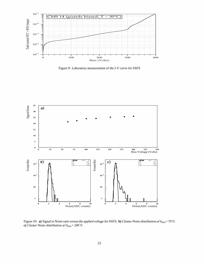
The data taken with the SSFS module biased at voltages up to 200 Volts are of particular interest since high voltageoperation is foreseen in CMS to survive the effect of irradiation. As can be seen in fig. 9 the SSFS module itselfwas able to stand voltages up to 300 Volts before reaching the breakdown point; nevertheless for safety reasons wedecided to limit this first test to a maximum of 200 Volts.
Fig. 10a shows the effect of bias on the S/N ratio for this module. Although the average noise figure remains almostconstant with increasing bias, we monitored the behaviour of individual channels to look for hot strips which couldaffect the local efficiency. In figs. 10b and 10c we compare the individual channel noise distribution atVdepand at200 Volts. Only a small fraction of channels (1%) appears to be affected by the high voltage operation and exhibitsan increased noise, but the values reached are however still quite manageable by the clustering algorithm.
8.1.3 Angular scan
All data presented so far were taken exposing the detectors to the beam at normal incidence (α=0). The effect ofinclined tracks on the response of the p-side has been studied in detail by rotating the detector modules around thehorizontal axis perpendicular to the beam direction. The mechanics allowed for rotation angles up to 25o.
The detectors were mounted with the p-side strips parallel to the rotation axis, therefore the amount of chargereleased in the silicon and the cluster width are expected to increase for geometrical reasons. Consequently thesignal-to-noise ratio is expected to improve with the angle.
All detectors behave as expected: there is a clear widening of the p-side clusters, an increase in the total collectedcharge compatible with the expected 1/cosα dependence, no visible effect on noise and consequently an increaseof the signal-to-noise ratio. Examples of the behaviour of the various parameters are shown in fig. 11 for the p-sideof DSODM.
8.1.4 Response function and space resolution
To reconstruct the particle impact point from the cluster information, the center of gravity of the cluster, weightedwith the charge collected on each strip, is usually evaluated. This way of reconstructing the position assumes alinear sharing of the charge released on each strip, an assumption which is far from reality in our case.
To study the deviations from the linear approximation and possibly give a correction to the reconstructed positionwe have studied the response function defined asη = QL=(QL+QR), whereQL andQR refer to the charge collectedon the left and right strip respectively. In fig. 12a a typicalη distribution for the p-side of a detector is shownsuperimposed to the equivalent MC distribution. The reconstructed position, modulo the strip pitch, is anothervariable which shows the non-uniformity of the reconstruction across the region between two neighbouring strips,in fig. 12d this variable is plotted as a function of the value ofη for real data.
From figs. 12b, 12c, 12e and 12f, where entries are subdivided into two multiplicity classes, it is evident that in thecentral region, populated by multi-strip clusters, the charge is linearly shared among the strips and hence the linearinterpolation is correct, while in the proximity of the strips single-strip clusters dominate and a digital responseshould be assumed.
The detectors were placed within a high precision telescope system to study the position resolution. For alignmentstudies and for position resolution measurements, only events with one cluster per view in each telescope detector
9

were used. A typical distribution of the residual, i.e. the difference between the locally reconstructed position andthe interpolated impact point of the beam telescope track, is plotted in fig. 13a for a standard p-side 50µmpitchdevice. The residuals are computed using the centre of gravity technique previously described. By subtracting inquadrature the tracking error from the width of the residual distribution we obtain the resolution values listed intable 4. In all cases the resolution is better than 15µm, the goal value foreseen for the CMS detector module. TheSSFS module gives, after subtracting 9µmin quadrature for the error of the track interpolation, a point resolutionof 11µm. The dependence of the resolution from the signal-to-noise ratio is weak: even with a most probable S/Nof 8.2, as in the case of the p-side of DSS, we can achieve a space resolution of about 14µm . These values ofresolution can be further improved by using the non linearη-technique which makes use of the response functiondistribution to interpolate properly the measured coordinate. This exercise was performed for the n-side of theBABY detector yielding an improvement in the detector resolution from 6.2µmto 4.7µm.
By using the telescope information we performed a careful study of the resolution versus interstrip position(fig. 13d); the digital response of the region close to the read-out strips is clearly separated from the interme-diate region dominated by charge sharing. The same behaviour is also visible in fig. 13b and 13c, where theresiduals of the single- and multi-strip clusters are plotted separately. Fig. 13e shows the resolution along the stripto check for uniformity of response over the detector length.
Data taken with tilted detectors were used to study the resolution for inclined tracks. Fig. 14a shows the resolutionand fig. 14d the average number of strips per cluster versus the tilt angle for the DSS module. The resolution at firstimproves because of the increased two-strip cluster contribution, and subsequently deteriorates due to fluctuationsin the charge released on the side strips as the clusters become wider.
8.2 Double-sided stereo detectors and n-side performance in general
8.2.1 Charge response and signal-to-noise ratio
The response of the n-side has been analysed in terms of cluster shape and cluster multiplicity using the approachpreviously described for the p-side. The same distributions of fig. 7 are shown in fig. 15 for the n-side of theDSSDM200 device. The average cluster multiplicity is larger, due to the presence of the floating strips, a furthereffect of which is the clustering of events in which the signal is equally shared between the left and the right stripsin the scatterplot of fig. 15c.
The performance in terms of signal-to-noise ratio for the n-side of different detector modules is summarized intable 3. It should be noticed that in general, for detectors with comparable strip length on both sides, the S/N valuesfor the ohmic side are lower than the corresponding values for the junction side. The difference is mainly due tothe fact that all detector modules were biased through the ohmic side and several paths of possible interferencebetween the read-out lines and the power supply circuitry were present in the motherboard coupled to the detectormodules. To check this point we inverted the high voltage circuit in one detector module to bias the silicon throughthe p-side and a symmetric worsening of the noise on the junction side was observed.
Particular attention was put in the evaluation of the performance of the DSSDM modules, very similar, as far as themain features are concerned, to the baseline CMS double-sided barrel modules. We were particularly interestedin verifying the effects of the double-metal technology on the stereo devices and to compare the performance ofidentical devices read-out at a 100µm pitch with no floating strip and at a pitch of 200µm with floating strips(DSSDM100 and DSSDM200 modules).
The effect of the double-metal technology was evaluated: the second metal layer introduces an additional couplingcapacitance which increases the total capacitance at the input of the amplifier and may also produce some chargeloss. To study this problem we subdivided the strips on the ohmic sides in two samples: “DM” strips, joined acrossthe detector through the second metal layer, and “non-DM” strips, with no contact to the second metal layer. Forthe two categories we compared the performance in terms of cluster charge, noise and signal-to-noise ratio. Theresults for the DSSDM100 module are shown in fig. 16. We observe in fact a worsening of the S/N ratio at the10% level between the two categories which can be attributed to the effect of the additional capacitance. A similarbehaviour is observed also in the DSSDM200 module. We consider this slight deterioration compatible with therequired performance and fully compensated by the advantage of recovering the dead areas at the edges of thestandard stereo devices, about 25% of the detector area for a stereo angle of 100 mrad.
The bias voltage scan gives no signal on the ohmic side until full depletion is reached and the isolation mechanismamong the n-strips becomes effective; a slight improvement of the signal-to-noise ratio aboveVdep is still visible(fig. 17), but the effect of a higher electric field is less important for electrons whose mobility is already highenough to cope with the 45ns peaking time of the read-out chips. The effects of the angular scan in terms of
10

collected charge are similar to those previously described for the junction side.
The charge sharing mechanism on the ohmic side was studied for all devices with a particular attention to theeffects of large read-out pitches. The effect of the floating strip can be easily seen from fig. 18 where the ResponseFunctions and their correlation with the interstrip position are compared for the two detectors DSSDM100 andDSSDM200.
The charge response dependence on the interstrip position could become critical for readout pitches close to thesilicon thickness. If the coupling to the read-out electrodes becomes comparable to the coupling with the back sideof the device, a significant fraction of the signal is lost and this can result in a reduction of the efficiency in thefloating strip region. A similar behaviour is produced when the signal is lost due to parasitic couplings as is thecase when floating strips are used in very short devices (see section 8.3.4).
The plots of fig. 19 show the charge signal collected by the left and right strips versus the reconstructed interstripposition for the DSSDM200 module. The sum of the two distributions shows a charge loss at the level of 30% inthe middle of the interstrip region. The corresponding efficiency plot shows that the effect of the charge loss on thereconstruction efficiency is very modest and only affects the very central region with a deterioration from 98.0%to 95.6%.
8.2.2 Resolution
In the CMS baseline tracker, the stereo strips are used to measure the so-called “secondary” coordinate, perpen-dicular to the high-precision one measured by the p-side strips, through the association between hits on the twoviews. In the case of the Barrel, the secondary coordinate coincides with thezcoordinate (along the beam axis); inthe Forward the secondary coordinate will measure the radial position.
The correlation plots between the intercept of the tracks, measured by the beam telescope, and the hit positionas reconstructed by the stereo strips are shown in fig. 20 for the two modules DSSDM100 and DSSDM200. Inplots 20a and 20c the y-coordinate reconstructed from the n-side hits is the intrinsic high-resolution coordinateorthogonal to the stereo strips projected on the y-axis, while in plots 20b and plots 20d an association was foundwith the corresponding p-side hits and the secondary coordinate, in this case the x-coordinate, was reconstructed.The effect of the double-metal connection of the edge strips is clearly visible in plots 20a and 20c: if not taken intoaccount, it will introduce an offset in the intrinsic coordinate equal to the detector width. This does not howevercause ambiguities in the reconstruction of space points once the n-side hit is associated with a p-side hit, becausethe geometry of the module is such that the reconstructed point is univocally determined as is shown in fig 20b and20d.
The resolution in the intrinsic coordinate for both modules has been evaluated from the distribution of residualscomputed using the centre of gravity technique already described for the p-side (figs. 21a and c ). The width of thetwo distributions is comparable: 34 vs 36µmas expected as a consequence of the presence of the floating strips.The plots of fig. 22 show the typical behaviour of the resolution across the interstrip region and its uniformity alongthe strip length in the two cases.
The resolution in the secondary coordinate is shown for DSSDM100 and DSSDM200 in figs. 21b and d: the widthof the two distributions is respectively 327µmand 357µm . From these values, obtained with a stereo angle of100 mrad, we can extrapolate a resolution for the baseline CMS Double-Sided Stereo Module (200µmread-outpitch, floating strip and a stereo angle of 60 mrad) of about 600µm, well within the expected requirements.
Data taken with tilted detectors were used to study the resolution versus the angle of incident tracks. Fig. 23 showsthe effect of the tilt angle on the resolution and on the average cluster size for the DSS module. The behaviour ofthe n-side with the angle is very similar to what was already described for the strips on the junction side.
8.3 R&D devices
8.3.1 The WEDGE detector
The wedge detectors of the forward Silicon Tracker are identical to the rectangular devices of the barrel from thetechnological point of view, but the non-conventional geometry requires some optimization work: for example, thetrapezoidal shape implies that the effective p-side strip pitch in the final modules will vary along the strips from 38to 76µmand this feature may in principle affect the uniformity of the detector response.
We performed a preliminary study of different design options in a small wedge device whose strips on the p-sidewere subdivided in three groups: one based on a constant strip width of 14µm , the second based on a constant
11

width over pitch ratio of 0.37 and the last featuring a variable strip width from 14 to 26µmmantaining a constantinterstrip gap of 24µmalong the detector.
In principle the three options imply small differences in the interstrip and coupling capacitance but we checkedanyhow to see if this introduces systematic effects in the detector behaviour. For this purpose we tested one ofthese devices carring the three different geometries at a bias voltage of 100 V and in good conditions of signal-to-noise ratio. Fig. 24a shows the overall charge response with a superimposed Landau fit; the correspondingsignal-to-noise distribution peaks at 26.5.
The operating conditions were clean enough to allow a careful study of the effects of the three different designs.We subdivided the tracks hitting the device according to the different regions and for each we plotted the clustercharge, the multiplicity distribution, the response function and the residual distribution. We found no significantdifferences for all these variables except for a slight worsening of the noise in the constant-gap region (fig. 24b).
The average performance in terms of position resolution for the p-side is shown in fig. 24c and is well within theexpectations for the CMS forward detectors: sigma of 7µm(after subtracting the impact point extrapolation errorof 5 µm ) against a required 15µm resolution. Studying the resolution as a function of the coordinate along thep-side strips we observe a 10% improvement when moving from the larger to the smaller pitch region.
The WEDGE detector was a double-sided device with 60µmwide strips on the back side, orthogonal to the centralp-side strip, at a pitch of 125µm. A kapton fan-out circuit was used to connect the n-side strips to the electronics:128 strips were read-out at 125µmpitch and 128 were read-out every 250µm leaving one floating strip betweentwo electrodes. The residual distribution for the 125µm read-out zone is shown in fig. 24d. It appears as auniform distribution with a FWHM of 80µm , corresponding to a sigma of about 23µm . The same plot for the250µmread-out pitch region with floating strip gives a similar resolution.
The strip length on the n-side of the WEDGE device was very short (ranging from 4.8 to 6.3mm): this impliesa weak interstrip coupling which heavily affects the charge response when a floating strip is left between tworead-out electrodes. This problem is treated in detail in Section 8.3.4.
8.3.2 The DSODM and the BABY detectors
The possibility of using the double-metal technology to obtain high-resolution information also in the reconstruc-tion of the second coordinate has been evaluated looking at the performance of DSODM and BABY detectors. Inthese two devices the n-side strips are orthogonal to the p-side strips and the signals are brought to the read-outelectronics through a connection on a second metal layer separated from metal-1 by a 4µmthick oxide.
This technique avoids the use of external kapton fan-out circuits but introduces additional parasitic capacitancewhich may affect the performance of the device. We tested this technique in two different detectors: the DSODMwhere strips on the n-side run at a 100µmpitch for a length of 19.2mmwhile the metal-2 lines are about 61mmlong on a 50µmpitch; the BABY device where strips of the same length on the n-side (19.2mm) are drawn at a50µmpitch and the metal-2 lines are 8mmlong on a 100µmpitch.
Fig. 25a shows the charge response of the n-side of the DSODM device; there is a good correlation between thecharge collected on the two sides (fig. 25c).
The n-side cluster shape (shown in fig. 25b) has the typical behaviour expected for standard devices. The residualdistribution for 100µmpitch is shown in fig. 25d. The width of this distribution is 58µmFWHM (correspondingto a sigma of about 25µm). The p-side resolution of this detector is 11µm.
The performance that could be achieved with this technique has been investigated looking at the data of the BABYdevice where a read-out pitch of 50µm is used for the n-side too. The detector response appears to be withinexpectations in terms of charge, signal-to-noise distribution, andη function (fig. 26). The residual distributionafter correcting for non-linearity in theη function is shown in fig. 26d: the sigma of the residual distribution is6.9µmand by subtracting the track extrapolation error we obtain a detector resolution of 4.7µm.
The p-side of the BABY detector, where we used the floating strip technique, was affected by the same problemalready mentioned for the n-side of the WEDGE: very short strips, weakly coupled to the read-out electrodes,producing distortions in the charge response. A detailed description of the problem is given in Section 8.3.4.
8.3.3 The PAD detector
An alternative approach to the use of stereo strips for the second coordinate has been tested with devices having then-side subdivided into pads [21]. The n-side is organized in rows of 32 pads, 6.4mmwide and 2mmhigh, whose
12

signals are routed to the read-out electronics sitting on the edge of the detector with a separate kapton circuit,glued on top of the device. We expect that this detector, without increasing the number of channels, could providea position resolution similar to the stereo detectors with the pattern recognition problem simplified by the use oftrue space points.
The most probable signal-to-noise measured for this device was 7.7; a preliminary investigation of the reasons forthis low value points out the combined effects of non-negligible capacitance contributions from the kapton circuitand of large common mode fluctuations due to imperfect filtering of the read-out circuitry.
From the residual distribution shown in fig. 27a we measure a position resolution of about 600µm in the perpen-dicular coordinate for this device. The tracking potential of the device can be appreciated from fig. 27b, whichshows the correlation between the hits reconstructed by the pad device and the track position as predicted by thebeam telescope.
8.3.4 Charge response in presence of weakly coupled floating strips
The use of floating strips, although convenient in terms of reduction of the number of read-out channels, mayintroduce distortions in the detector response. The mechanism of charge sharing between the floating strips andthe read-out electrodes may be critical when the coupling is too weak. The charge collected on the floating stripsinduces signals on all surrounding electrodes in accordance to the coupling capacitances; when the coupling withthe read-out electrodes is comparable with the coupling to passive elements, a significant fraction of the charge islost and the uniformity in the detector response is affected. This is the case, for instance, when the strips are veryshort. Some parasitic capacitance to the guard-ring and to the back of the detector is always present; usually, fora strip length of several centimeters, these couplings are much lower than the coupling to the read-out electrodes,which increases linearly with the strip length (at the rate of 1-1.4pF=cm). When very short strips are used, thecoupling to the read-out electrodes may be lower than 1pF and every parasitic coupling of the same order ofmagnitude will cause substantial charge loss. A similar case may appear when the interstrip gap is too wide: forread-out pitches above 200µmthe coupling to the back becomes important and a large fraction of the charge is lostwhen tracks hit the region of the floating strip. This problem was observed in the data of the WEDGE detector onthe n-side and of the BABY detector on the p-side.
Figs. 28a and 28b show the anomalies seen in the n-side cluster signal and in the correlation plot for the WEDGE.These plots show a clear double-peaked distribution that can be explained looking at the cluster multiplicity. Thecharge response of the n-side for single-strip clusters (fig. 28c) shows a good Landau distribution; if we plot thecharge collected by multi-strip clusters we obtain another good Landau distribution (fig. 28d) but the peak value inthis case is much lower (40 % lower) than the previous one.
Since the charge sharing mechanism is strongly dependent on the hit position we explain this result with a chargeloss for tracks hitting the intermediate region between the read-out electrodes and therefore seen by the floatingstrip.
The very short n-strips (4.8 to 6.3mm) and the large read-out pitch (250µm) imply a weak coupling of the floatingelectrodes to the read-out strips. It should be noticed that this result has no impact on the position resolution of thedetector but will affect the efficiency and uniformity of response of the device.
A similar behaviour was noticed for the p-side of the BABY detector giving us further evidence that the mechanismis independent of the read-out side. Fig. 29a shows the distribution of the charge collected on the p-side and againthe double-peaked distribution can be resolved by plotting separately the charge collected in single- (fig. 29b) andmulti-strip clusters (fig. 29c). In this case too, the coupling of the floating electrodes to the read-out strips is veryweak, due to the very short strip length (8.2mm), and comparable with the parasitic coupling to the guard ringelements.
The charge loss in the central region has been studied with the BABY by plotting theη distribution (fig. 29d) whichshows a very low central peak in correspondence of the floating electrode, and by studying the most probable signalon the left and right strip versus the interstrip position. The plots in fig. 30 compare the distributions of this variablefor the p-side and for the n-side. From the distribution we can estimate a signal loss up to 60% in the middle of theinterstrip gap on the p-side.
The effect of this charge loss on the efficiency of the device has been carefully investigated. The overall efficiencyof the p-side, excluding a few dead or disconnected strips, is about 97% while the corresponding value for then-side exceeds 99.6%. The inefficiency on the p-side is uniformly spread over the detector, being mostly due toclusters with signal below threshold caused by the previously decribed mechanism.
13

For a better understanding of the problem the device was also tested in laboratory using a laser diode. Infrared lightpulses having a wavelength of 940nmand collimated to within 20µmwere shot across the interstrip region andthe corresponding signals were digitized. Fig. 31 shows the result of the scan transverse to the p-side strips. Theaverage cluster signal is plotted as a function of the laser spot position. A substantial reduction of the cluster chargeappears exactly at the position of the floating strip, thus confirming the result obtained with charged particles.
9 Summary and ConclusionsThe results obtained so far can be considered promising in terms of detector performance.
The measured resolution of all tested detectors is well within the requirements set for the CMS Silicon Tracker.
The value of 26:1 for the signal to noise ratio measured on the SSFS module appears quite satisfactory. As a matterof fact, the final single-sided modules will differ from the module tested mainly in the use of more sophisticatedread-out electronics. With respect to the performance of the PreMux128, the final front-end chip is expected tohave an ENC worse by a factor 1.4, mostly due to the modified filtering of signals provided by the deconvolutioncircuit, while the contribution of the analog pipeline and of the optical link are expected to be negligible. One mustalso take into account the effect of irradiation on detectors and read-out electronics. Nevertheless, even consideringhigher leakage currents, increases of the interstrip capacitance, and some charge loss on the p-side due to the lowerfield after inversion, we still have a large margin before reaching an average signal to noise ratio of 10:1, which isconsidered our lower limit for safe operation after 10 years of high-luminosity operation at the LHC.
We have demonstrated that high voltage operation, which will be needed to keep full efficiency after irradiation,is feasible with single sided detectors without a significant noise increase. Our study is currently limited to 200 Vand single sided detectors, but preliminary measurements suggest that the range can be extended safely at least upto 300 V. A thorough study is foreseen in forthcoming beam tests for single- and double-sided devices before andafter irradiation.
We have proved that the double metal technology can be used to solve of the problem of dead regions at the edgesof double sided stereo devices. The performances of stereo devices featuring 100µmand 200µmread-out pitch withand without floating strip, have been carefully investigated. Although the overall efficiency does seem satisfactory,the charge loss affecting the floating strip region requires an optimization of the detector design. Further study isneeded to improve the signal to noise ratio of the n-side with particular care to the filtering of the detector biaslines.
We have obtained very promising preliminary results on the performance of wedge detectors similar to those thatwill be used in the forward disks.
Lastly, several R&D devices have been investigated including PAD detectors and high resolution double-sideddevices.
Acknowledgements
We wish to thank all people whose support has been essential for this work, in particular the technical staff ofthe INFN laboratories, the colleagues of other CMS institutions who provided crucial elements of the read-outelectronics, and all people involved in the setting up and running of the two beam tests at CERN.
References[1] The Compact Muon Solenoid,“Technical Proposal”, CERN/LHCC 94-38 LHCC/P1, Dec 15, 1994
[2] P. Weiss et al.,“Wafer-Scale Technology for Double-Sided Silicon Microstrip Particle Detectors”, The 7th
International Conference on Solid-State Sensors and Actuators
[3] G. Tonelli et al., Nucl. Instrum. and Meth. A377 (1996) 422
[4] A. Holmes-Siedle et al., NIM A339 (1994) 511
[5] E. Catacchini et al.“Wedge silicon detectors for the inner tracking system of CMS”, presented at the 6thTopical Seminar on “Experimental Apparatus for Particle Physics and Astrophysics” in S.Miniato 1996, tobe published in Nucl. Phys. B Proceedings Supplement
[6] RD20 Collaboration,“RD20 Status Report 1995”, CERN-LHCC/96-2
14

[7] RD20 Collaboration,“RD20 Status report”, CERN/DRDC 94-39
[8] J. Matheson et al.,“ Radiation Damage Studies of Field Plate and p-stop n-side Silicon Microstrip Detec-tors” , accepted for publication by NIM
[9] M. French, L. Jones, P. Murray, P. Seller, M. Raymond, G. Hall,“APV5-RH: a 128 Channel RadiationHard Pipeline Chip for LHC Tracker Applications”, Proceedings of 1st Workshop on Electronics for LHCExperiments, CERN/LHCC/95-56.
[10] M. Raymond and L. Jones,“RD20 PreShape32 User Manual”
[11] L. L. Jones,“PreMux128 User Manual”
[12] L. Celano et al.,“A High Resolution Beam Telescope Built with Double Sided silicon Strip Detectors”,accepted for publication by NIM
[13] IPN Lyon, S. Electronique,“BUFFER pour detecteurs SILICIUM”and“BASE carte HT”.
[14] RD5 Collaboration,“Status Report of the RD5 Experiment”, CERN/DRDC 93-49
[15] C. Albajar et al., NIM A364 (1995) 473
[16] RD5 Collaboration,“RD5 ’93 Trigger System”, RD5 TN/93-14, Nov 2 1993
[17] W. Dulinksi et al.,“VME Flash ADC multi-purpose module”, Draft, VFLAM-CRN/Lepsi 1992.
[18] O. Adriani et al.,“A data acquisition system for silicon microstrip detectors”, Dipartimento di Fisica e INFNFirenze Preprint DFF 237/11/95.
[19] “CMSIM User Manual”
[20] “Simulation of VDET”, ALEPH Internal Note 92-052, 1992
[21] R. Wheadon et al.,”Double-sided silicon detectors using n-side pad readout for the CMS silicon innertracker”, 1995 IEEE Nuclear Science Symposium and Medical Imaging Conference Record Oct 21-28 1995,San Francisco, Guest Editor Patricia A. Moonier, Volume 1
15

Module side SS SSFS DSS DSODM BABY DSSDM100 DSSDM200 PAD WEDGE
Signal/Noise p 27. 26.1 8.2 23.2 15.9 14.9 13.4 - 26.5
Signal/Noise n - - 9.5 17. 21. 8.4 11. 7.7 38.4
Table 3: Most probable value of the signal to noise ratio for all tested detectors at nominal conditions. Figuresmarked with an asterisk were obtained averaging the results from separate distributions for single- and multi-stripclusters.
Module side SS SSFS DSS DSODM BABY DSSDM100 DSSDM200 PAD WEDGE
Resolution p 12. 11. 14. 11. 16. 12. 12. - 7.
Resolution n - - 275. 17. 6. 325.a) 357.a) 600. 23.32.b) 35.b)
Table 4: Spatial resolution inµm for all tested detectors. Superscript a) refers to the resolution in the secondarycoordinate (orthogonal to the one measured by the p-side), while b) refers to the resolution in the intrinsic n-sidecoordinate.
16

30 mm
65 m
m
AAAAAAAAAAAAAAAAAAAAAAAAAAAAAA
AAAAAAAAAAAAAAAAAAAA
AAAAAAAAAAAAAAAAAAAA
Double metal connection
129 straightstrips63 strips joined in 1st detector
63 strips joined in 2nd detector
Daisy ChainBonds
1stdetector
2nddetector
Stereo angle 0.1 radstrip pitch 100 mµ
Double metal connection
Strip Number1 63 126 255
Figure 1:Schematic description of two DSSDM detectors assembled in a module.
...128 strips
38 mpitch
µ
50 mpitch
µ
Junction Side
Ohmic Side
...49
5st
rip
s
µ 128 strips read-out at 125 m+128 strips read-out at 250 mµ
6.3 mm
62 m
m
4.8 mm
Figure 2:Wedge detector schematic description.
17

Figure 3:July 95 set-up
Figure 4:September 95 set-up
18

10-4
10-3
10-2
10-1
1
-10 -5 0 5 10
Strip number
Fra
ctio
n o
f sig
na
l
0
200
400
600
800
1000
0 1 2 3 4
Cluster noise (ADC counts)E
ntr
ies
0
100
200
300
400
500
600
700
0 50 100 150
Signal (ADC counts)
En
trie
s
0
100
200
300
400
500
600
700
800
0 20 40 60 80 100
Signal/Noise
En
trie
s
Figure 5:Comparison between MC (full line) and real data (dots):a) Cluster shape;b) Cluster Noise;c) ClusterSignal; d) Signal to Noise ratio.
19

0
200
400
600
-0.01 -0.005 0 0.005 0.01
RMS .1067E-02
Residual (cm)
En
trie
s
0
100
200
300
400
-0.02 -0.01 0 0.01 0.02
RMS .3459E-02
Residual (cm)
En
trie
s
0
100
200
300
400
-0.01 -0.005 0 0.005 0.01
53.95 / 12Constant 369.2Mean -.1507E-04Sigma .9249E-03
Residual (cm)
En
trie
s
0
200
400
600
-0.02 -0.01 0 0.01 0.02
38.21 / 5Constant 730.3Mean -.3809E-04Sigma .9180E-03
Residual (cm)
En
trie
s
0
100
200
-0.01 -0.005 0 0.005 0.01
66.38 / 18Constant 245.5Mean -.3066E-04Sigma .1384E-02
Residual (cm)
En
trie
s
0
50
100
150
200
-0.02 -0.01 0 0.01 0.02
64.78 / 34Constant 200.8Mean -.7392E-04Sigma .3284E-02
Residual (cm)
En
trie
s
Figure 6:Plots on the first column refer to SSFS while those on the second column refer to DSSDM200: a) andb) Simulated detector intrinsic resolution;c) andd) Error on track extrapolation point as evaluated by the MC;e) and f) Comparison between MC (histogram and fit) and real data (dots) distributions of residuals for the twodetectors.
20

10-3
10-2
10-1
1
-10 -5 0 5 10
MeanRMS
-.4639E-02 .7329
Strip number
Fra
ctio
n o
f sig
na
l
0
0.2
0.4
0.6
0.8
0 2 4 6 8
MeanRMS
1.339 .5591
Cluster multiplicity
Fra
ctio
n o
f e
ve
nts
0
200
400
600
0 200 400 600 800 1000
Left strip charge
Rig
ht str
ip c
ha
rge
0
500
1000
1500
2000
0 50 100 150 200
1039. / 54P1 9682.P2 52.29P3 5.922
Signal(ADC counts)
En
trie
s/B
in
0
1000
2000
3000
4000
0 1 2 3 4 5
668.7 / 38Constant 3678.Mean 2.015Sigma .1255
Cluster Noise (ADC counts)
En
trie
s/B
in
0
500
1000
1500
0 20 40 60 80 100
Signal/Noise
En
trie
s/B
in
Figure 7:Data for a p-side 50µmpitch detector at normal incident angle:a) Cluster shape;b) Number of stripsper cluster;c) Charge collected on left and right strips;d) Cluster Signal;e) Cluster Noise; f) Signal to Noiseratio.
21

Bias Voltage (Volts)
Sig
na
l / N
ois
e
Bias Voltage (Volts)
Sig
na
l / N
ois
e
Bias Voltage (Volts)
Sig
na
l / N
ois
e
0
10
20
30
0 20 40 60 80 100
0
10
20
30
0 20 40 60 80 100
0
10
20
30
0 20 40 60 80 100
Figure 8:Signal to Noise ratio versus the applied voltage for:a) SS, b) WEDGE p-side,c) DSODM p-side.
22
10-7
10-6
10-5
10-4
10-3
Total
curren
t W17
+ W18
(Amps)
4003002001000Bias (Volts)
CMS 14 (guards biased, T ~ 30°C)
Figure 9:Laboratory measurement of the I-V curve for SSFS
0
5
10
15
20
25
30
35
0 25 50 75 100 125 150 175 200 225 250
Bias Voltage (Volts)
Sign
al/N
oise
1
10
10 2
10 3
0 2 4 6 8 10
87.28 / 11P1 1232.P2 2.159P3 .1340
Noise(ADC counts)
Even
ts/B
in
1
10
10 2
10 3
0 2 4 6 8 10
143.7 / 21P1 1291.P2 2.019P3 .1314
Noise(ADC counts)
Even
ts/B
in
Figure 10:a)Signal to Noise ratio versus the applied voltage for SSFS;b) Cluster Noise distribution atVbias= 70 V;c) Cluster Noise distribution atVbias= 200 V.
23

Tilt Angle (Deg.)
No
rm. M
ultip
licity
Tilt Angle (Deg.)N
orm
. S
ign
al
Tilt Angle (Deg.)
No
rm. N
ois
e
Tilt Angle (Deg.)
No
rm. S
ign
al / N
ois
e
0
0.2
0.4
0.6
0.8
1
1.2
1.4
0 10 200
0.2
0.4
0.6
0.8
1
1.2
0 10 20
0
0.2
0.4
0.6
0.8
1
0 10 200
0.2
0.4
0.6
0.8
1
1.2
0 10 20
Figure 11:Scan in the tilt angle for the p-side of a DSODM detector; all points are normalized to the orthogonalincidence values:a) Number of strips in cluster,b) Cluster Signal,c) Cluster Noise,d) Signal to Noise ratio.
24

Response Function
En
trie
s/B
in
Response Function
Inte
rstr
ip p
ositio
n(µm
)
0
50
100
150
200
250
0 0.25 0.5 0.75 1
0
100
200
0 0.25 0.5 0.75 1
0
20
40
60
80
0 0.25 0.5 0.75 1
-10
0
10
20
30
40
50
60
0 0.25 0.5 0.75 1
0
20
40
60
0 0.25 0.5 0.75 1
0
20
40
60
0 0.25 0.5 0.75 1
Figure 12: a) Response Function for DSS p-side with MC simulation superimposed;b) and c) same as a) forsingle- and multi-strip clusters respectively;d) Interstrip position versus Response Function for real events;e)andf) same asd) for single- and multi-strip clusters respectively.
25

Constant 73.52Mean -.5808E-03Sigma .1421E-02
Residual(cm)
En
trie
s/B
in Constant 33.69Mean -.6498E-03Sigma .1423E-02
Residual(cm)
Constant 22.58Mean -.4821E-03Sigma .1292E-02
Residual(cm)
Interstrip position(µm)
Re
so
lutio
n(µm
)
Position along the strip(cm)
Re
so
lutio
n(µm
)
0
10
20
30
40
50
60
70
80
-0.02 -0.01 0 0.01 0.02
0
10
20
30
-0.02 -0.01 0 0.01 0.02
0
10
20
-0.02 -0.01 0 0.01 0.02
0
2
4
6
8
10
12
14
16
18
20
0 20 400
2
4
6
8
10
12
14
16
18
20
-0.5 0 0.5
Figure 13: a) Residuals for a p-side 50µmpitch detector (SSFS);b) andc) same as a) referring to single- andmulti-strip clusters respectively;d) Resolution versus the interstrip position;e) Resolution versus the positionalong the strip.
26

Tilt angle (deg)
Re
so
lutio
n (µ
m)
Tilt angle (deg)
Clu
ste
r m
ultip
licity
0
2
4
6
8
10
12
14
16
18
20
-2.5 0 2.5 5 7.5 10 12.5 15 17.5 20 22.5
0
0.5
1
1.5
2
2.5
3
-2.5 0 2.5 5 7.5 10 12.5 15 17.5 20 22.5
Figure 14:Scan in the tilt angle for the p-side of the DSS detector:a) Resolution;b) Number of strips per cluster.
27

MeanRMS
.9692E-02 .6871
Strip number
Fra
ctio
n o
f sig
na
l
MeanRMS
1.564 .6198
Cluster multiplicity
Fra
ctio
n o
f e
ve
nts
Left strip charge
Rig
ht str
ip c
ha
rge
2032. / 54P1 .1196E+05P2 91.68P3 17.58
Signal(ADC counts)
En
trie
s/B
in
808.7 / 37Constant 3405.Mean 9.438Sigma .7301
Cluster Noise (ADC counts)
En
trie
s/B
in
Signal/Noise
En
trie
s/B
in
10-4
10-3
10-2
10-1
1
-20 -10 0 100
0.2
0.4
0.6
0 2 4 6 8
0
50
100
150
200
250
0 100 200 300 4000
500
1000
1500
2000
0 200 400 600
0
1000
2000
3000
0 5 10 15 200
500
1000
1500
2000
0 20 40 60
Figure 15:Data for the n-side of DSSDM200: a) Cluster shape;b) Number of strips per cluster;c) Charge collectedon left and right strips;d) Cluster Signal;e)Cluster Noise;f) Signal to Noise ratio.
28

Strip Number
Sig
na
l(A
DC
co
un
ts)
Strip NumberN
ois
e(A
DC
co
un
ts)
Strip Number
Sig
na
l/N
ois
e
0
10
20
30
40
50
60
70
80
90
100
0 100 2000
2
4
6
8
10
12
0 100 200
0
2
4
6
8
10
12
0 100 200
Figure 16:Data for the n-side of (DSSDM100). Average values are evaluated in bins of 32 strips. DM strips gofrom 1 to 128 while non-DM strips go from 129 to 256:a) Most probable value of the Cluster Signal;b) AverageCluster Noise;c) Average Signal to Noise ratio.
29

Bias Voltage (Volts)
Sig
na
l / N
ois
e
0
2
4
6
8
10
12
14
16
18
20
0 20 40 60 80 100
Figure 17:Signal to Noise ratio for the n-side of DSODM as a function of Bias Voltage.
30

Response Function
En
trie
s/B
in
Response Function
En
trie
s/B
in
Response Function
Inte
rstr
ip p
ositio
n(µm
)
Response Function
Inte
rstr
ip p
ositio
n(µm
)
0
25
50
75
100
125
150
175
200
0 0.25 0.5 0.75 10
200
400
600
800
1000
0 0.25 0.5 0.75 1
-20
0
20
40
60
80
100
120
0 0.25 0.5 0.75 1
0
50
100
150
200
0 0.25 0.5 0.75 1
Figure 18: a) Response Function for the n-side of DSSDM100; b) same as a) for the n-side of DSSDM200;c) Interstrip position versus the Response Function for the n-side of DSSDM100; d) same as c) for the n-side ofDSSDM200.
31

Interstrip distance (cm)
Interstrip distance (cm)
Interstrip distance (cm)
0
50
100
150
0 0.002 0.004 0.006 0.008 0.01 0.012 0.014 0.016 0.018 0.02
0
50
100
150
0 0.002 0.004 0.006 0.008 0.01 0.012 0.014 0.016 0.018 0.02
0
0.25
0.5
0.75
1
1.25
0 0.002 0.004 0.006 0.008 0.01 0.012 0.014 0.016 0.018 0.02
Figure 19:Data from the n-side of DSSDM200: a) Charge collected on the left and right strips (ADC counts);b) Total Signal; c) Efficiency. All variables are plotted versus the reconstructed position modulo the strip pitch.
32

Track y-coord(cm)
y-c
oo
rd(c
m)
Track x-coord(cm)x-c
oo
rd(c
m)
Track y-coord(cm)
y-c
oo
rd(c
m)
Track x-coord(cm)
x-c
oo
rd(c
m)
-0.5
0
0.5
1
1.5
2
-1 -0.5 0 0.5 1-1
-0.8
-0.6
-0.4
-0.2
0
0.2
0.4
0.6
0.8
1
-1 -0.5 0 0.5 1
-0.5
0
0.5
1
1.5
2
-1 -0.5 0 0.5 1-1
-0.8
-0.6
-0.4
-0.2
0
0.2
0.4
0.6
0.8
1
-1 -0.5 0 0.5 1
Figure 20:Correlation between the interpolated track position and the point locally reconstructed by the stereostrips: a) and b) refer to DSSDM100, c) and d) refer to DSSDM200. The y coord is the coordinate almostorthogonal to the stereo strips; thexcoord is the ’secondary’ coordinate.
33

Constant 188.7Mean .3718E-03Sigma .3417E-02
Residual(cm)
En
trie
s/B
in Constant 237.6Mean -.1883E-02Sigma .3277E-01
Residual(cm)E
ntr
ies/B
in
Constant 164.6Mean .2454E-04Sigma .3601E-02
Residual(cm)
En
trie
s/B
in Constant 189.4Mean .7244E-03Sigma .3573E-01
Residual(cm)
En
trie
s/B
in
0
25
50
75
100
125
150
175
200
225
-0.02 -0.01 0 0.01 0.020
50
100
150
200
250
-0.2 0 0.2
0
25
50
75
100
125
150
175
200
-0.02 -0.01 0 0.01 0.020
25
50
75
100
125
150
175
200
225
-0.2 0 0.2
Figure 21: a) Residuals in the intrinsic coordinate for the n-side of DSSDM100; b) Residuals in the secondarycoordinate for the n-side of DSSDM100; c) same as a) for DSSDM200; d) same as b) for DSSDM200.
34

Interstrip position(µm)
Re
so
lutio
n(µm
)
Position along the strip(cm)R
eso
lutio
n(µm
)
Interstrip position(µm)
Re
so
lutio
n(µm
)
Position along the strip(cm)
Re
so
lutio
n(µm
)
0
5
10
15
20
25
30
35
40
45
50
0 20 40 60 80 1000
5
10
15
20
25
30
35
40
45
50
-0.5 0 0.5
0
5
10
15
20
25
30
35
40
45
50
0 50 100 150 2000
5
10
15
20
25
30
35
40
45
50
-0.5 0 0.5
Figure 22: Resolutions in the intrinsic coordinate:a) Resolution versus the interstrip position for the n-side ofDSSDM100; b) Resolution versus the position along the strip for DSSDM100; c) same as a) for DSSDM200; d) sameas b) for DSSDM200.
35

Tilt angle (deg)
Re
so
lutio
n (µ
m)
Tilt angle (deg)
Clu
ste
r m
ultip
licity
0
50
100
150
200
250
300
350
400
0 5 10 15 20 25
0
0.25
0.5
0.75
1
1.25
1.5
1.75
2
2.25
2.5
0 5 10 15 20 25
Figure 23:Scan in the tilt angle for the n-side of DSS:a) Resolution;b) Number of strips per cluster.
36

P1 291.9P2 160.9P3 22.19
Signal (ADC Counts)
En
trie
s / B
in
Strip No.N
ois
e (
AD
C C
ou
nts
)
Constant 432.5Mean .2734Sigma 8.550
Residuals (µm)
En
trie
s/B
in
Residuals (µm)
En
trie
s/B
in
0
10
20
30
40
50
60
70
80
90
0 200 400 600 8003
3.54
4.55
5.56
6.57
7.58
0 50 100
050
100150200250300350400450
-100 -50 0 50 1000
100
200
300
400
500
-200 -100 0 100 200
Figure 24:Data for WEDGE:a) p-side Cluster Signal;b) p-side strip Noise for the three different regions (seetext);c) p-side Residual distribution;d) n-side Residual distribution.
37

P1 727.6P2 162.7P3 24.13
Signal (ADC Counts)
En
trie
s / B
in
Strip NumberF
ractio
n o
f S
ign
al
n-side Signal
p-s
ide
Sig
na
l
Residuals (µm)
En
trie
s / B
in
0
25
50
75
100
125
150
175
200
225
0 200 400 600 800
10-3
10-2
10-1
1
-4 -2 0 2 4
0
100
200
300
400
500
600
0 200 400 6000
50
100
150
200
250
300
350
-100 -50 0 50 100
Figure 25: Data for DSODM:a) n-side Cluster Signal;b) n-side Cluster shape;c) p-side and n-side signalscorrelation;c) n-side Residual distribution.
38

153.3 / 46P1 1392.P2 20.60P3 2.186
Signal (ADC counts)
Ent
ries/
Bin
Signal/Noise
Ent
ries/
Bin
Response Function
Ent
ries/
Bin 118.6 / 55
Constant 150.8Mean -0.5582E-04Sigma 0.6877E-03
Residual (cm)
Ent
ries/
Bin
0
50
100
150
200
250
0 50 100 1500
20
40
60
80
100
120
140
0 20 40 60 80
0
10
20
30
40
50
60
70
80
0 0.2 0.4 0.6 0.8 10
20
40
60
80
100
120
140
160
180
-0.01 -0.005 0 0.005 0.01
Figure 26:Distributions for the n-side of BABY:a) Cluster Signal;b) Signal to Noise ratio;c) Response Function;d) Distribution of Residuals.
39

MeanRMS
-.7390E-02 .5877E-01
Residual(cm)
Ent
ries/
Bin
x-coord (cm)
Tra
ck x
-coo
rd (
cm)
0
50
100
150
200
250
-0.5 -0.25 0 0.25 0.5-1
-0.75
-0.5
-0.25
0
0.25
0.5
0.75
1
-1 -0.5 0 0.5 1
Figure 27:PAD: a) Residual distribution;b) Correlation with tracks reconstructed by the telescope.
40

Signal (ADC counts)
En
trie
s / B
in
n-side Signal
p-s
ide
Sig
na
l
P1 554.9P2 195.9P3 20.10
Signal (ADC Counts)
Eve
nts
/Bin P1 755.9
P2 123.4P3 16.66
Signal (ADC Counts)
Eve
nts
/Bin
0
50
100
150
200
250
300
0 200 400 6000
100
200
300
400
500
600
0 200 400 600
0
20
40
60
80
100
120
140
160
0 200 400 6000
255075
100125150175200225
0 200 400 600
Figure 28:Distributions for the WEDGE n-sidea) Cluster Signal;b) Cluster Signal correlation;c) Cluster Signalfor single-strip clusters;d) Cluster Signal for multi-strip clusters.
41

Signal (ADC counts)
Ent
ries/
Bin
Signal
Ent
ries/
Bin
Signal
Ent
ries/
Bin
Response Function
Ent
ries/
Bin
0
25
50
75
100
125
150
175
200
0 50 100 1500
20
40
60
80
100
120
0 50 100 150
0
20
40
60
80
100
120
140
160
180
0 50 100 1500
20
40
60
80
100
120
0 0.2 0.4 0.6 0.8 1
Figure 29:Distributions for the BABY p-side:a) Cluster Signal;b) Cluster Signal for single-strip clusters;c) Clus-ter Signal for multi-strip clusters;d) Response Function.
42

Interstrip distance (cm)
Interstrip distance (cm)
0
5
10
15
20
25
0 0.001 0.002 0.003 0.004 0.005 0.006 0.007 0.008 0.009 0.01
0
2.5
5
7.5
10
12.5
15
17.5
20
0 0.05 0.1 0.15 0.2 0.25 0.3 0.35 0.4 0.45 0.5x 10
-2
Figure 30:Data from BABY. Charge collected on the left and right strips (ADC counts)a) p-side ;b) n-side ; Allvariables are plotted versus the reconstructed position modulo the strip pitch.
43

100
125
150
175
200
225
250
275
300
-75 -50 -25 0 25 50 75 100
Figure 31:Cluster signal in the laser transverse scan;
44