Multiplexing Firmware Prototypes
29
Multiplexing Firmware Prototypes for the Global Trigger System of the ATLAS Phase-II Upgrade #1121 - N32 IEEE NSS-MIC 2020.11.05 Filiberto Bonini On behalf of the ATLAS TDAQ Collaboration
-
Upload
khangminh22 -
Category
Documents
-
view
0 -
download
0
Transcript of Multiplexing Firmware Prototypes

Multiplexing Firmware Prototypesfor the Global Trigger System of the ATLAS Phase-II Upgrade
#1121 - N32IEEE NSS-MIC 2020.11.05
Filiberto BoniniOn behalf of the ATLAS TDAQ Collaboration

Outline
● Global Multiplexer: Context & Specifications
○ Phase-II Upgrades > Global Trigger (cf. IEEE-NSS T-DAQ-FE N-21)
● Global Multiplexer: Prototype Designs
● Prototype: Latency Performances
● Conclusions & Outlook
2

Global Trigger:Multiplexing nodes
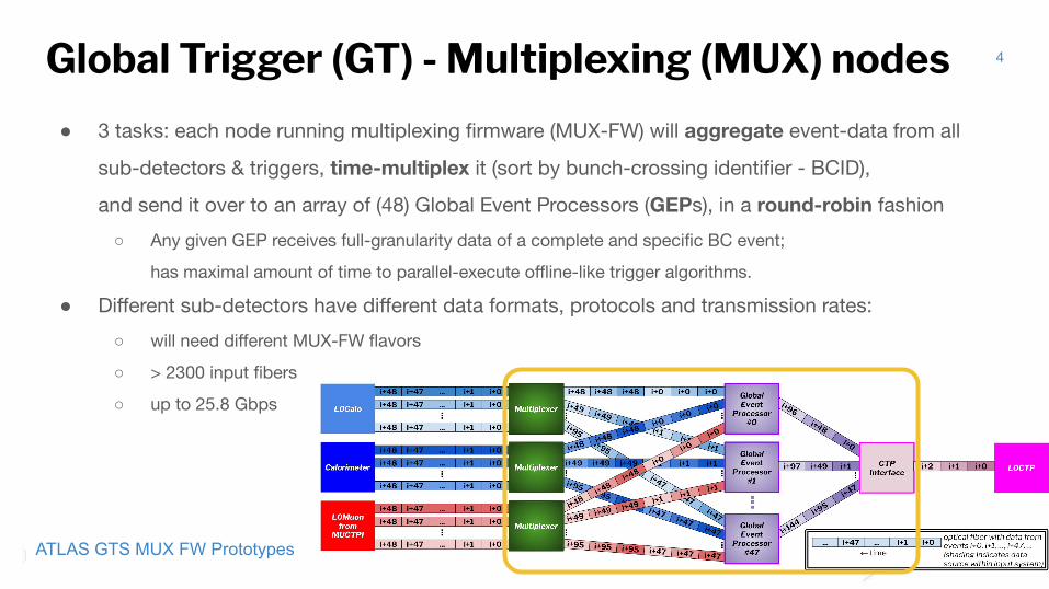
IEEE-NSS 2020-11-05ATLAS GTS MUX FW Prototypes
Global Trigger (GT) - Multiplexing (MUX) nodes● 3 tasks: each node running multiplexing firmware (MUX-FW) will aggregate event-data from all
sub-detectors & triggers, time-multiplex it (sort by bunch-crossing identifier - BCID),
and send it over to an array of (48) Global Event Processors (GEPs), in a round-robin fashion
○ Any given GEP receives full-granularity data of a complete and specific BC event;
has maximal amount of time to parallel-execute offline-like trigger algorithms.
● Different sub-detectors have different data formats, protocols and transmission rates:
○ will need different MUX-FW flavors
○ > 2300 input fibers
○ up to 25.8 Gbps
4
IEEE-NSS 2020-11-05ATLAS GTS MUX FW Prototypes
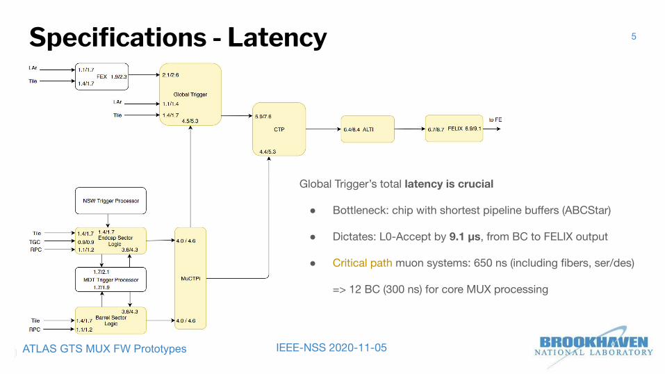
Specifications - Latency
Global Trigger’s total latency is crucial
● Bottleneck: chip with shortest pipeline buffers (ABCStar)
● Dictates: L0-Accept by 9.1 μs, from BC to FELIX output
● Critical path muon systems: 650 ns (including fibers, ser/des)
=> 12 BC (300 ns) for core MUX processing
5

Global MultiplexerPrototype Designs
IEEE-NSS 2020-11-05ATLAS GTS MUX FW Prototypes
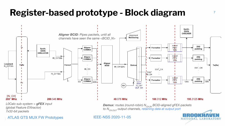
Register-based prototype - Block diagram 7
Demux: routes (round-robin) NCH,IN BCID-aligned gFEX-packets to NCH,OUT output channels, retaining data at output port
Aligner BCID: Pipes packets, until all channels have seen the same <BCID_N>
L0Calo sub-system > gFEX input(global Feature EXtractor)7x32-bit packets

IEEE-NSS 2020-11-05ATLAS GTS MUX FW Prototypes
● Achievements
○ Up to 72*72-ch. synthesized & simulated
■ Max FF usage < 60% (XCVU9P)
○ Up to 12*12-ch bitwise verified on HW
○ Short (MUX-core) latency: < 8 BCs
● Exponential dependency: complexity of
registers optimization at synthesis
○ due to the buffering output port of Demux,
a register matrix scaling as ( NCH,IN * NCH,OUT )
array <OUT_CH> of array <IN_CH> of gFEX_packets <7*32b>
Register-based - Optimization complexity 8

IEEE-NSS 2020-11-05ATLAS GTS MUX FW Prototypes
BRAM FIFO-based prototype - Block diagram 9
BCID Alignment per-channel:input pkts are pushed once <BCID_N> is received
to GEParray
4*64b=256b
fromgFEX
IEEE-NSS 2020-11-05ATLAS GTS MUX FW Prototypes
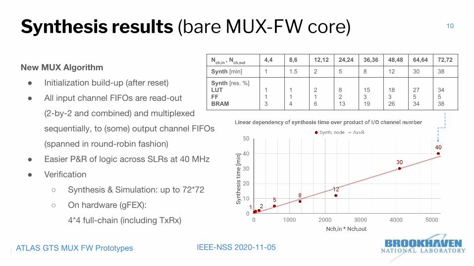
Synthesis results (bare MUX-FW core) 10
Nch,in , Nch,out 4,4 8,6 12,12 24,24 36,36 48,48 64,64 72,72
Synth [min] 1 1.5 2 5 8 12 30 38
Synth [res. %]LUTFFBRAM
113
114
216
8213
15319
18326
27534
34538
New MUX Algorithm
● Initialization build-up (after reset)
● All input channel FIFOs are read-out
(2-by-2 and combined) and multiplexed
sequentially, to (some) output channel FIFOs
(spanned in round-robin fashion)
● Easier P&R of logic across SLRs at 40 MHz
● Verification
○ Synthesis & Simulation: up to 72*72
○ On hardware (gFEX):
4*4 full-chain (including TxRx)

MUX-FW 4-ch prototypeLatency Performance

IEEE-NSS 2020-11-05ATLAS GTS MUX FW Prototypes
Latency measurements - Setup 12
gFEX Production Board
pFPGA-A XCVU9P
Rx GTY11.2G8b/10b
MUX-FW Tx GTY25.8G
64b/66b
pFPGA-B / Zynq+
miniPOD
miniPOD
OscilloscopeTektronix DPO77002SX
Optical probe 33 GHz
DPO7OE1
SMAprobe
● Nominal MUX-FW latency
time elapsed between the arrival of Nth BC data on
the slowest MGT input channel, and the beginning of
MGT transmission (to GEPs) of the same Nth BC data
● Tripartition of the full-chain
latency measurement on pFPGA-A:
a. Rx 11.2G : from first 8b/10b optical character
received, to 32b key-word seen at GTY interface
b. MUX-FW processing (internal): from GTY Rx
interface, to Aurora AXIS Tx interface
c. Tx 25.8G : from Aurora AXIS Tx interface,
to first 64b/66b optical character transmitted
Data Emu/ Data
Checker
Tx GTY11.2G8b/10b
Rx GTY25.8G
64b/66bHP IO
a b c

IEEE-NSS 2020-11-05ATLAS GTS MUX FW Prototypes
Latency measurements - Rx 11.2G 8b/10b1. After alignment, a unique K-char is sent once
○ K28.1 0x3C → 00-11111-001 [11-00000-110]
2. HP-IO FPGA pin asserted upon K28.1 detection
3. Trigger-A arms trigger-B
○ HIGH: width > 400ps
○ rising-edge of test-point
4. Trigger data: search for 5x HIGH (must be K28.1)
○ Found, once, @ -103.2 ns before trigger-B
5. Align to first serial bit, subtract external delays
○ eg. loopback fibers, test-point coaxial cable, ...
○ => 34.07 ns / 24.951 ns = 1.37 BC
■ within range from Xilinx latency tables0 0 1 1 1 1 1 0 0 1
2*200ps=400ps
13
10 UI = 891 ps

IEEE-NSS 2020-11-05ATLAS GTS MUX FW Prototypes
Latency measurements - Internal MUX-FWNominal latency: 218 ns = 8.76 BC
for 1-lane Aurora core (unpractical)
● 4-lane Aurora core bundles 4 output ch.s sharing
1 AXI-Stream bus (tvalid): fastest output-ch. has to
wait for (t)valid BC data on the slowest one:
8.76+(4-1) = 8.76+3 =~ 11.8 BC○ It makes practical sense to bundle
1 GTY quad in FW implementation
○ Current Best Estimate (CBE) = 12 BC
for MUX-FW processing
● Trade-off latency / FPGA resources:
instantiating one 1-lane, independent AXIS
Aurora core per output channel
14

IEEE-NSS 2020-11-05ATLAS GTS MUX FW Prototypes
CLOCK domains MUX-FW components LATENCY [BC]
Clk Freq.[MHz] Module Detail Data
widthExpected(min-max)
Measured
gFEX INMGTREF 280 MGT Rx
WrapperGTY
11.2G
32b*Nch,in
1.2-1.5 (a)1.4
7*TTC 280
Data EMU - N/A N/A
Fanout Data source 0
(b)11.8
ALIGN Comma 0.3-1
TTC 40
ALIGN BCID 256b*Nch,in
0(BCID skew not accounted
against MUX-FW)IN-FIFO(FWFT) in=out 2-3
MUX RR+buildup
[non-const]
(1-2)+3=4-5(3: AXIS 4-lane tvalid)
AXIS-IC
input 512b*Nch,out
(~5 + ~2 + 2 + 3)/10.1 = 1-2(CDC+WM+Swtc+FIFO)
OUT2GEPTXUSRCLK 403
output
64b*Nch,out
MGT TxWrapper
Aurora64b/66b
0.4-0.8(reg.count + ILA) (c)
1.8GTY25.8G 0.9-1.2
TOTAL MUX-FW w/ ser/des (a+b+c) 9.8-14.5 15
15
GTY+ Latency tablesXilinx AR#69011 [UI](TxRx FIFOs enabled)
(c) w/oAurora PE delaysTx 25.8G 64b/66b
(a)Rx 11.2G8b/10b
PMA (de)serializer 29 62.5To serializer 128 (Tx FIFO) -PMA / PCS boundary 64 0 (Rx buff.)Buffer: Phase FIFO (Tx), Elastic buffer (Rx) 160-224 (60-100)
+10*6COMMA Alignment - 80-129Sync. gearbox 64b/66b/ 8b/10b decoder 128→254 40
Tx/Rx Fabric interface 64 40TOTAL (min-max)
[UI][ns]
[BC]
573-76322.23-29.60
0.89-1.19
342.5-431.530.52-38.45
1.22-1.54
Latency measurements - Totals & Comparison
● ATLAS Phase-II Upgrade Technical Design Review CBE (Current Best Estimates):
○ Ser/des (standard) = 2 BC○ MUX-FW = 12 BC○ Total = 2+12+2 = 16 BC > 15

Conclusions & Outlook● The Global Trigger is a new firmware-focused project designed to meet new trigger requirements
○ for the High-Luminosity runs (Run-4) of the Large Hadron Collider (HL-LHC)
● Two MUX-FW prototypes are designed, implemented and validated on hardware
○ 4 (full-chain), 12, 72 channels
○ gFEX processor inputs & gFEX production board for actual HW validation
○ Choice based on implementability
● Latency has been accurately measured
○ Meeting Maximum Possible Value (MPV) and also CBE requirements from Phase-II Upgrades TDR
○ Margin to optimize it, if needed, trading-off FPGA resources
● Development framework defined for the next steps
○ Completion of multi-quad (12,48-channel) versions
○ Expansion to support the other GT inputs: LASP (LAr Signal Processor), FEXs (Feature EXtractors), etc.
16

Thank you

References
● Technical Design Report for the Phase-II Upgrade of the ATLAS TDAQ System
https://cds.cern.ch/record/2285584/files/ATLAS-TDR-029.pdf
● Xilinx UltraScale+ GTY Latency Tables
https://www.xilinx.com/support/answers/69011.html
18

Backup Slides

IEEE-NSS 2020-11-05ATLAS GTS MUX FW Prototypes
Global Trigger - Overview● The ATLAS Experiment Phase-II (HL-LHC) Upgrades
○ installation Large Hadron Collider (LHC) Long Shutdown 3 ~ 2025-27
● Concentrates data for a full bunch-crossing (BC) event onto a single processor
○ ~ 60 Tb/s into Global Trigger (GT): exploiting parallelization, data aggregation, time multiplexing
● Primarily a firmware (FW) project
○ different functions are
implemented in firmware,
rather than hardware;
○ Common hardware: Global
Common Module (GCM)
will host 3 FW layers
20

IEEE-NSS 2020-11-05ATLAS GTS MUX FW Prototypes
Global Trigger - GCM● Global Common Module
1 board, 3 layers:
○ MUX: data aggregation
& time multiplexing of
events from all sub-detectors
○ GEP: Global Event Processing
& trigger algorithms (base-config: 48)
○ CTPi: Central Trigger
Processor interface: final decision
● Cf. talk by S. Tang: “The Prototype Hardware Design of Global Common Module for Global Trigger System of the ATLAS Phase II Upgrade”
21
IEEE-NSS 2020-11-05ATLAS GTS MUX FW Prototypes
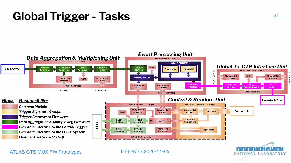
Global Trigger - Tasks 22

IEEE-NSS 2020-11-05ATLAS GTS MUX FW Prototypes
Specifications - MUX-FW Inputs
Global Feature EXtractor (gFEX) flavor
● Protocol: 8b/10b encoding
● Line-rate: 11.2 Gbps
● Quad-scalable (4→24 fibers)
● 1 BC package = 7*32b words
23
IEEE-NSS 2020-11-05ATLAS GTS MUX FW Prototypes
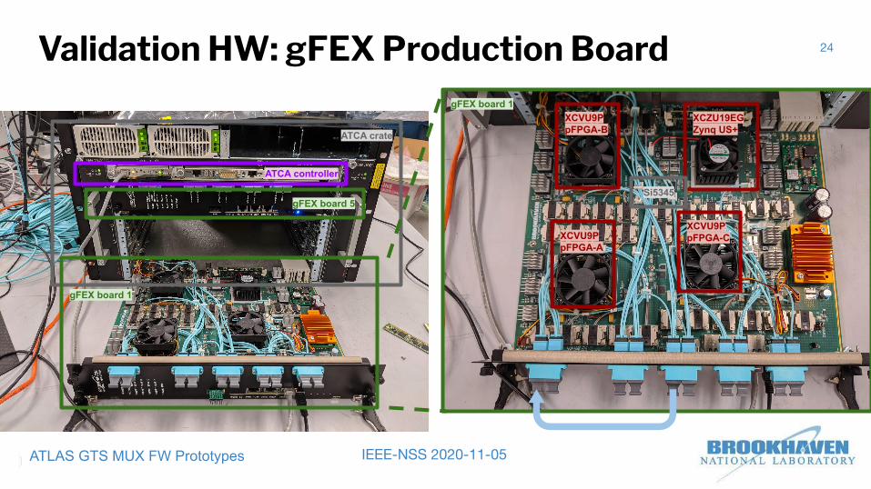
gFEX board 1
Validation HW: gFEX Production Board 24
ATCA crate
XCVU9PpFPGA-A
XCVU9PpFPGA-C
XCVU9PpFPGA-B
XCZU19EGZynq US+
ATCA controller
gFEX board 5
gFEX board 1
Si5345
IEEE-NSS 2020-11-05ATLAS GTS MUX FW Prototypes
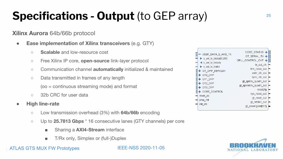
Specifications - Output (to GEP array)Xilinx Aurora 64b/66b protocol
● Ease implementation of Xilinx transceivers (e.g. GTY)
○ Scalable and low-resource cost
○ Free Xilinx IP core, open-source link-layer protocol
○ Communication channel automatically initialized & maintained
○ Data transmitted in frames of any length
(oo = continuous streaming mode) and format
○ 32b CRC for user data
● High line-rate
○ Low transmission overhead (3%) with 64b/66b encoding
○ Up to 25.7813 Gbps * 16 consecutive lanes (GTY channels) per core
■ Sharing a AXI4-Stream interface
■ T/Rx only, Simplex or (full-)Duplex
25

More on Aurora core 26

IEEE-NSS 2020-11-05ATLAS GTS MUX FW PrototypesFull-chain 4-ch Prototype Floorplan
P&R ~ 8 min (with pBlocks)
gFEX prod. board pFPGA-A (XCVU9P)
27

IEEE-NSS 2020-11-05ATLAS GTS MUX FW Prototypes
PCB tracksMiniPODs
GTY Integration: gFEXprod. brd. clock diagram
Si5345
OUT2 = 280M→ BUF2
OUT4 = 280M→ BUF1
OUT1 = 390M→ BUF5
OUT3 = 390M→ BUF4
MGTREFCLK0b100+ 20,22,24,25(c1),27,29,31,33
b200+ 20,22,25,27,29,31,33
b226 qX1Y7 chX1Y28-31MGTREFCLK0 b(226-1) @ AE11,10
Data EmulatorTx 11G 8b/10b
pFPGA-B
MGTREFCLK0b129-134, 226-234
b133 qX0Y6 chX0Y24-27MGTREFCLK0 b133 @ H32,33
Data CheckerRx 25G Aurora
ZYNQ+
MGTREFCLK0b100+ 20,22,24,25(c1),27,29,31,33b200+ 20,22,25,27,29,31,33
b222 qX1Y3 chX1Y{14,15,12,13}MGTREFCLK0 b222 @ AJ11,10
Rx 11G 8b/10b
pFPGA-A
MGTREFCLK1b126,128,225,227
b125 qX0Y6 chX0Y24-27MGTREFCLK1 b(125+1) @ AB34,35
Tx 25G Aurora
pFPGA-A
XO40M
J(H)22LVDS
AT18,17LVDS
IBUFDSAV14, LVDS
MMCM40M, 280M
H20,21LVDS
Z_PA_BUS_CLK2_P/N
ZSI5345_TTC_40M_P/N
MMCM
28

IEEE-NSS 2020-11-05ATLAS GTS MUX FW Prototypes
GTY TxRx Integration & Full-chain Verification 29
gFEX prod. board
pFPGA-B
DataEMU
GTY Tx11.2G
MiniPODs
pFPGA-A
MUXFW
AuroraTx 25G
Zynq
DataCHECK
AuroraRx 25G
PS
GTY Rx11.2G
Si5345
● Per-channel, bit-wise validation
● Functional verification plan
○ Payload data incrementing: intra- and inter- packets
○ BCID packets sorting across output channels
○ Input-channel markers scanning inputs
○ Output-channel markers mapped and fixed
I2C
390.625 MHz280.553 MHz