
Elsherif, Mohamed Asaad (2016) Mapping multiplexing technique ...
252
Elsherif, Mohamed Asaad (2016) Mapping multiplexing technique (MMT): A novel intensity modulated transmission format for high-speed optical communication systems. PhD thesis, The University of Nottingham. Access from the University of Nottingham repository: http://eprints.nottingham.ac.uk/33413/1/thesis_final%20version%20_Mohamed_Asaad.pdf Copyright and reuse: The Nottingham ePrints service makes this work by researchers of the University of Nottingham available open access under the following conditions. This article is made available under the University of Nottingham End User licence and may be reused according to the conditions of the licence. For more details see: http://eprints.nottingham.ac.uk/end_user_agreement.pdf For more information, please contact [email protected]
-
Upload
khangminh22 -
Category
Documents
-
view
0 -
download
0
Transcript of Elsherif, Mohamed Asaad (2016) Mapping multiplexing technique ...

Elsherif, Mohamed Asaad (2016) Mapping multiplexing technique (MMT): A novel intensity modulated transmission format for high-speed optical communication systems. PhD thesis, The University of Nottingham.
Access from the University of Nottingham repository: http://eprints.nottingham.ac.uk/33413/1/thesis_final%20version%20_Mohamed_Asaad.pdf
Copyright and reuse:
The Nottingham ePrints service makes this work by researchers of the University of Nottingham available open access under the following conditions.
This article is made available under the University of Nottingham End User licence and may be reused according to the conditions of the licence. For more details see: http://eprints.nottingham.ac.uk/end_user_agreement.pdf
For more information, please contact [email protected]

Mapping Multiplexing Technique (MMT):
A Novel Intensity Modulated Transmission Format
For High-Speed Optical Communication Systems
MOHAMED ASAAD ELSHERIF, MSc
Thesis submitted to The University of Nottingham,
Department of Electrical and Electronic Engineering,
Faculty of Engineering, for the degree of
Doctor of Philosophy, May 2016

I
Abstract
There is a huge rapid growth in the deployment of data centers, mainly driven from the
increasing demand of internet services as video streaming, e-commerce, Internet Of
Things (IOT), social media, and cloud computing. This led data centers to experience an
expeditious increase in the amount of network traffic that they have to sustain due to
requirement of scaling with the processing speed of Complementary metal–oxide–
semiconductor (CMOS) technology. On the other side, as more and more data centers
and processing cores are on demand, as the power consumption is becoming a
challenging issue. Unless novel power efficient methodologies are innovated, the
information technology industry will be more liable to a future power crunch. As such,
low complex novel transmission formats featuring both power efficiency and low cost are
considered the major characteristics enabling large-scale, high performance data
transmission environment for short-haul optical interconnects and metropolitan range
data networks.
In this thesis, a novel high-speed Intensity-Modulated Direct-Detection (IM/DD)
transmission format named “Mapping Multiplexing Technique (MMT)” for high-speed
optical fiber networks, is proposed and presented. Conceptually, MMT design challenges
the high power consumption issue that exists in high-speed short and medium range
networks. The proposed novel scheme provides low complex means for increasing the
power efficiency of optical transceivers at an impactful tradeoff between power
efficiency, spectral efficiency, and cost. The novel scheme has been registered as a patent
(Malaysia PI2012700631) that can be employed for applications related but not limited
to, short-haul optical interconnects in data centers and Metropolitan Area networks
(MAN).
A comprehensive mathematical model for N-channel MMT modulation format has
been developed. In addition, a signal space model for the N-channel MMT has been
presented to serve as a platform for comparison with other transmission formats under
optical channel constraints. Especially, comparison with M-PAM, as meanwhile are of
practical interest to expand the capacity for optical interconnects deployment which has

II
been recently standardized for Ethernet IEEE 802.3bs 100Gb/s and in today ongoing
investigation activities by IEEE 802.3 400Gb/s Ethernet Task Force.
Performance metrics have been considered by the derivation of the average electrical
and optical power for N-channel MMT symbols in comparison with Pulse Amplitude
Modulation (M-PAM) format with respect to the information capacity. Asymptotic power
efficiency evaluation in multi-dimensional signal space has been considered. For
information capacity of 2, 3 and 4 bits/symbol, 2-channel, 3-channel and 4-channel MMT
modulation formats can reduce the power penalty by 1.76 dB, 2.2 dB and 4 dB compared
with 4-PAM, 8-PAM and 16-PAM, respectively. This enhancement is equivalent to 53%,
60% and 71% energy per bit reduction to the transmission of 2, 3 and 4 bits per symbol
employing 2-, 3- and 4-channel MMT compared with 4-, 8- and 16-PAM format,
respectively.
Beside the power efficiency advantage, N-channel MMT data capacity multiplexing
feature enhances the eligibility for scaling the baud rate with the limitations that exists in
electronic and optical components operating at a fraction of the aggregated data rate.
Therefore, 2-channel MMT has the feature to scale its baud rate to 1/2 of its aggregated
bitrate compared with OOK. While, 3-channel MMT has a baud rate equivalent to 1/3 of
its aggregated bitrate compared with OOK. Also, 4-channel MMT is capable of
decreasing the electronic requirement of its components to a baud rate equivalent to 1/4
of the aggregated bit rate compared with OOK.
One of the major dependable parameters that affect the immunity of a modulation
format to fiber non-linearities, is the system baud rate. The propagation of pulses in fiber
with bitrates in the order > 10G, is not only limited by the linear fiber impairments,
however, it has strong proportionality with fiber intra-channel non-linearities (Self Phase
Modulation (SPM), Intra-channel Cross-Phase Modulation (IXPM) and Intra-channel
Four-Wave Mixing (IFWM)). Hence, in addition to the potential application of MMT in
short-haul networks, the thesis validates the practicality of implementing N-channel
MMT system accompanied by dispersion compensation methodologies to extend the
reach of error free transmission (BER ≤ 10-12
) for Metro-networks. In chapter 5, N-
Channel MMT has been validated by real environment simulation results to outperform
the performance of M-PAM in tolerating fiber non-linearities.

III
By the employment of pre-post compensation to tolerate both residual chromatic
dispersion and non-linearity, performance above the error free transmission limit at
40Gb/s bit rate have been attained for 2-, 3- and 4-channel MMT over spans lengths of up
to 1200Km, 320 Km and 320 Km, respectively. While, at an aggregated bit rate of 100
Gb/s, error free transmission can be achieved for 2-, 3- and 4-channel MMT over spans
lengths of up to 480 Km, 80 Km and 160 Km, respectively.
At the same spectral efficiency, 4-channel MMT has realized a single channel
maximum error free transmission over span lengths up to 320 Km and 160 Km at 40Gb/s
and 100Gb/s, respectively, in contrast with 4-PAM attaining 240 Km and 80 Km at
40Gb/s and 100Gb/s, respectively.
Keywords:-
Optical Interconnects, Intensity-Modulated Direct-Detection Systems (IM/DD), Mapping
Multiplexing Technique (MMT), Metropolitan Area Networks (MAN) and Fiber Non-
Linearities.

IV
Acknowledgments
First of all, I would like to thank my supervisor Prof. Amin Malek Mohammadi for his
insights, guidance and support over the years. I have benefitted from the numerous
opportunities, advices and experiences he provided me. It was a great pleasure working
under his supervision. I would like also to thank my co-supervisor Dr. Wee Gin Lim for
his fruitful discussions during the PhD. In addition, I would like to thank my internal
examiner Dr. Gnanam Gnanagurunathan for her time and willingness to examine my
work. I also want to thank my colleague and friend Nguyen Dong-Nhat for the productive
collaboration and useful discussions we had together.
Both, the Ministry of Science, Technology and Innovation (MOSTI) Malaysia and The
University of Nottingham, financially funded this research work. Thanks to them.
I would like to express my deepest gratitude and special thanks to both, Dr. Ashraf
Abdelraouf & Dr. Lamia Khashan for their continuous all-time support, encouragement
and valuable advice since the start of my bachelor degree studies and up until this
moment. This work would not have been realized without their motivation.
I would also like to take the opportunity to thank all my professors, colleagues and
friends in the Department of Electronics and Communication Engineering, Misr
International University.
My warmest and sincere thanks go to my parents Mr. & Mrs. Asaad Elsherif and my
sisters, for their continuous never ending love, support and patience. I thank my father
and mother for raising me with good values and without whom I would not be the person
that I am today.
Finally, I am dedicating this work to my beloved wife and life-partner Dina Kouta,
without her love, support and patience; I do not even imagine how it would have been
done. Also, I owe a thank you to my father and mother in law Mr. & Mrs Alsaid Kouta
for their encouragement and support.

V
Contents
Abstract ............................................................................................................................................ I
Acknowledgments ........................................................................................................................ IV
Contents ......................................................................................................................................... V
Abbreviations ............................................................................................................................... IX
List of Figure ................................................................................................................................ XI
List of Tables .............................................................................................................................. XV
1. Chapter 1: Introduction ..................................................................................................... 1
1.1 Overview .............................................................................................................................. 1
1.1.1 Fiber optic solutions for Metro and Short Range Networks ............................. 1
1.1.2 Ethernet ............................................................................................................... 3
1.2 Problem statement and Research Motivation ....................................................................... 5
1.2.1 Data Center Power Consumption ........................................................................ 5
1.2.2 Data Center Optical Interconnection ................................................................... 6
1.2.3 Intensity Modulated Multilevel Transmission Formats ...................................... 8
1.3 Thesis Aims and Objectives ............................................................................................... 10
1.4 Scope of Work .................................................................................................................... 11
1.5 Contribution of this research work ...................................................................................... 12
1.6 Thesis Organization ............................................................................................................. 17
2. Chapter 2: Literature Review ........................................................................................... 19
2.1 Introduction .......................................................................................................................... 19
2.2 Intensity-Modulated Direct-Detection (IM/DD) system ...................................................... 20
2.2.1 Channel characteristics ...................................................................................... 21
2.3 Signal Space Analysis .......................................................................................................... 23
2.4 Memoryless modulation or Non-coherent modulation ........................................................ 27
2.4.1 ON-OFF Keying (OOK) ................................................................................... 27
2.4.2 Pulse-Position Modulation (PPM) ..................................................................... 28
2.4.3 Pulse Amplitude Modulation (PAM) ................................................................ 30
2.5 Optical Modulation .............................................................................................................. 34
2.5.1 Mach-Zehnder Modulator (MZM) .................................................................... 35
2.6 Pre-Amplified Optical Receiver .......................................................................................... 39

VI
2.7 Linear fiber Impairments ..................................................................................................... 41
2.7.1 Fiber Attenuation ............................................................................................... 42
2.7.2 Dispersion .......................................................................................................... 44
2.8 Non-Linear Fiber impairments ............................................................................................ 46
2.8.1 Self-Phase Modulation ...................................................................................... 46
2.8.2 Intra-channel Cross-Phase Modulation (IXPM) and Intra-channel
Four-Wave Mixing (IFWM) Non-linearities .................................................. 48
2.8.3 Stimulated Brillouin Scattering (SBS) .............................................................. 51
2.9 Concluding Remarks……………………………………...……………………………….52
3. Chapter 3 - MMT System Model and Performance Metrics ......................................... 53
3.1 The Methodology behind MMT Structural Design ............................................................ 53
3.2 Channel Characteristics ...................................................................................................... 57
3.2 Signal Space Model ............................................................................................................. 58
3.2.1 N-channel MMT Signal Model ......................................................................... 59
3.2.2 Geometric Representation of N-channel MMT ................................................. 62
3.3 MMT Transceiver Model .................................................................................................... 64
3.3.1 Basic Properties and Waveform Synthesis ........................................................ 66
3.3.2 N-channel MMT Transmitter Model ................................................................. 68
3.3.3 Receiver Model ................................................................................................. 72
3.3.3.1 Threshold Detection Receiver………………………….………73
3.3.3.2 Optimal Detection Receiver……………………………....……78
3.4 Performance Evaluation Criterion ....................................................................................... 82
3.4.1 Analytical Evaluation Model ............................................................................. 82
3.4.2 Numerical Evaluation Model ............................................................................ 83
4. Analytical Performance Evaluation ................................................................................. 91
4.1 Power Performance Metrics ................................................................................................. 91
4.1.1 Electrical Domain .............................................................................................. 91
4.1.2 Optical Domain ................................................................................................. 93
4.2 Performance Analysis Utilizing Direct Modulation ............................................................ 94
4.2.1 Bit Error Rate Analytical Model ....................................................................... 94
4.2.2 Bit Error Rate Results ........................................................................................ 97
4.2.3 Noise Model Analysis ................................................................................... 102

VII
4.3 Asymptotic Power Efficiency Analysis and Results .......................................................... 113
4.3.1 Power Penalty at Fixed Baud Rate .................................................................. 113
4.3.2 Power Penalty at Fixed Bit Rate ...................................................................... 115
4.3.3 Power penalty with respect to OOK at Fixed information capacity ................ 117
4.4 Concluding Remarks .......................................................................................................... 119
5. Chapter 5: Numerical Performance Analysis ................................................................ 121
5.1 Introduction ........................................................................................................................ 121
5.2 N-Channel MMT for Metro Networks............................................................................... 122
5.2.1 2-Channel MMT with 2 bits/symbol .............................................................. 122
5.2.2 3-channel MMT with 3 bits/symbol.............................................................. 129
5.2.3 4-channel MMT with 4 bits/symbol.............................................................. 134
5.2.4 Receiver Sensitivity Comparison between MMT and M-PAM .................... 138
5.3 N-channel MMT evaluation in the presence of Fiber linear and non-linear
impairments ...................................................................................................................... 139
5.3.1 Chromatic Dispersion Tolerance ..................................................................... 140
5.3.1.1 Comparison between N-channel MMT and M-PAM….....141
5.3.2 System Tolerance to fiber Non-linearity ........................................................ .147
5.3.2.1 Introduction……………………………………………..………….…..147
5.3.2.2 Self Phase Modulation………………………………..….………….…147
5.3.2.3 Post Compensation System Setup…………………..…………….…...148
5.3.2.4 Post Compensation System Results……………………………..….…152
5.3.2.5 Pre-Post Compensation System Setup………………..….……………158
5.3.2.6 Performance comparison bet. Post & Pre-post Results………………..160
5.3.2.7 IFWM and IXPM Investigation…………………………………….…..174
5.3.2.8 MMT Maximum Reach for Metro Networks……….……………..…..184
5.3.2.9 Stimulated Brillouin Scattering (SBS) Non-linear Effect……………...192
5.4 Concluding Remarks ........................................................................................................ ..193

VIII
6. Chapter 6: MMT Practical Consideration ..................................................................... 196
6.1 MMT Cost Consideration .................................................................................................. 196
6.2 MMT Transmitter based upon CMOS circuits .................................................................. 198
6.3 MMT Receiver based upon CMOS circuits ....................................................................... 200
6.4 DSP Technologies enabling MMT .................................................................................... 201
6.5 System Requirements and Commercial components Enabling MMT ............................... 202
7. Chapter 7: Conclusion and Future Directions .............................................................. 206
7.1 Conclusion ........................................................................................................................ 206
7.2 Future Directions .............................................................................................................. 212
Appendix A ................................................................................................................................. 214
Bibliography ............................................................................................................................... 216
List of Publications, Awards and Grants ................................................................................. 232

IX
List of Abbreviations
100GBase-ER4
40Gbase-LR4
40Gbase-SR4
ADC
100G Ethernet – Extended Range-4-channels
40G Ethernet – Long Range-4-channels
40G Ethernet – Short Range-4-channels
Analog to Digital Converter
ASIC Application Specific Integrated Circuits
ANSI American National Standards Institute
ASE Amplified Spontaneous Emission
AS Aggregate Switch
AWGN Additive White Gaussian Noise
BER Bit Error Rate
CGR Cumulative Growth Rate
CS Core Switch
CMOS Complementary metal–oxide–semiconductor
CD Chromatic Dispersion
CENELEC European Committee for Electro-technical
Standardization
CW Continuous Wave
DAC Digital to Analog Converter
DML Directly Modulated Laser
DCF Dispersion Compensation Fiber
DSF Dispersion Shifted Fiber
DC Direct Current
EML Externally Modulated Laser
EM External Modulator
EDFA Erbium Doped Fiber Amplifier
FEC Forward Error Correction
FPGA Field Programmable Gate Arrays
GVD Group Velocity Dispersion
HBTs Heterojunction Bipolar Transistors
HSSG High Speed Study Group
IM Intensity Modulated
IP Internet Protocol
ITU International Telecommunication Union
ISI Inter-symbol-interference
IXPM Intra-channel Cross-Phase Modulation
IFWM Intra-channel Four-Wave Mixing
IEEE Institute of Electrical and Electronics Engineers

X
IM/DD Intensity-Modulated/Direct-Detection
InP Indium Phosphide
InGaAs Indium Gallium Arsenide
LED Light Emitting Diode
LD Laser Diode
MCML MOS Current Mode Logic
MZM Mach-Zehnder Modulator
MQW-MZM Multiple-Quantum-Well Mach-Zehnder Modulator
MMT Mapping Multiplexing Technique
MMF Multi-Mode Fiber
MAN Metropolitan Area Networks
ML Maximum Likehood
MAP Maximum A Posteriori
MLSD Maximum Likehood Sequence Detection
NLS Non-linear Schrodinger
NRZ-OOK Non Return to Zero ON-OFF Keying
NZDF Nonzero Dispersion Fiber
NF Noise Figure
OTN Optical Transport Networks
OOK On-Off Keying
OSI Open System Interconnection
PRBS Pseudo Random Bit Sequence
PDF Probability Density Function
PPM Pulse Position modulation
PAM Pulse Amplitude Modulation
PHY Physical Layers
PIN PIN photodiode
PWM Pulse Width Modulator
RDF Reverse Dispersion Fiber
RIN Relative Intensity Noise
RZ-OOK Return to Zero On-Off Keying
RMS Root-Mean-Square
SBS Stimulated Brillouin Scattering
SPM Self-Phase Modulation
SMF Single Mode Fiber
SONET Synchronous Optical Networking
SDH Synchronous Digital Hierarchy
SNR Signal To Noise Ratio
SiP Silicon Photonics
TOR Top of Rack switch
TDM Time Division Multiplexed
TIA Trans-Impedance Amplifier
VLC Visible Light Communication
VCSEL vertical-cavity surface-emitting laser
WAN Wide Area Network
WDM Wavelength Division Multiplexing

XI
List of Figure
Figure1.1 Global IP data traffic growth percentage for metropolitan and longhaul networks[1]. ................ 2
Figure1.2 Global IP data traffic growth for metropolitan and long-haul networks between
2013-2018[1]. ........................................................................................................................... 2
Figure1.3 IEEE Standards for Ethernet with respect to link distance, trans-mission speed and
fiber type. ................................................................................................................................. 4
Figure1.4 Data center optical medium range links with cloud applications in a metropolitan
area architecture. ...................................................................................................................... 7
Figure1.5 Typical 3-Tier data center optical interconnection with multiple Ethernet switches. .................... 8
Figure1.6 Research progress for employment of M-PAM with respect to variable link distances
and bit rates highlighted in table 1.1. ..................................................................................... 32
Figure1.7 N-channel MMT transmission format position in digital commu-nications. The MMT
design and performance evaluation aspects discussed in the thesis are highlighted
in orange colour. .................................................................................................................... 16
Figure2.1 shows a general communication system. .................................................................................. 21
Figure2.2 shows a general communication system. .................................................................................. 24
Figure2.3 Symbol structure waveform of (a) NRZ-OOK and (b)RZ-OOK .............................................. 28
Figure2.4 Symbol structure waveform of 4-PPM...................................................................................... 29
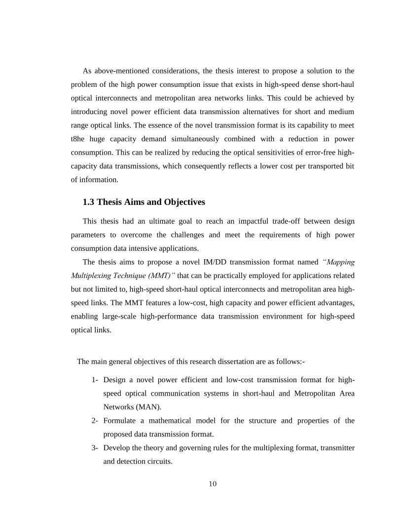
Figure2.5 M-PAM basis function .............................................................................................................. 31
Figure2.6 M-PAM signal constellation for 4-PAM, 8-PAM and 16- PAM. ............................................. 31
Figure2.7 Illustration of the operation methodology of direct (a) and (b) external modulation. ............... 34
Figure2.8 Mach-Zehnder Modulator structure. ......................................................................................... 36
Figure2.9 Mach-Zehnder Modulator power transmission function ........................................................... 37
Figure2.10 Pre-amplified system model. .................................................................................................... 39
Figure2.11 Attenuation of old (dotted line) and new (solid line) silica fibers. The shaded regions
indicate the three telecommunication wavelength windows ................................................ 43
Figure2.12 Chromatic dispersion effects (a) Pulse broadening (b) Inter-symbol interference. ................... 45
Figure2.13 Impact of fiber non-linearity with respect to channel bit rate, fiber local dispersion
and spectral efficiency[109], [119] ....................................................................................... 49
Figure2.14 IXPM effect on signal: a) Time shift occurrence in waveform. b) Tim-ing jitter
occurrence in eye diagram. ................................................................................................... 49
Figure 2.15 IFWM effect on signal: a) Ghost pulse occurrence in waveform. ........................................... 50
Figure3.1 N-channel MMT free space channel model for IM/DD systems………………….58
Figure3.2 N-channel MMT format generated orthonormal basis functions. ............................................. 59
Figure3.3 4-Channel MMT generated symbols in terms of the basis functions. ...................................... 61
Figure3.4 Signal space constellation geometry 2, 3, and 4-channel MMT for IM/DD ............................ 63
Figure3.5 Signal space constellation 4-, 8- and 16-PAM for IM/DD. ...................................................... 63
Figure3.6 MMT generic transceiver model, (a) Transmitter and (b) Receiver. ........................................ 64
Figure3.7 MMT symbol format. ............................................................................................................... 67
Figure3.8 N-channel waveform structure for (a)2-Channel MMT , (b)3-Channel MMT and (c) 4-
channel MMT. ...................................................................................................................... 67
Figure3.9 MMT transmitter proposed model. .......................................................................................... 68

XII
Figure3.10 De-mapping multistage decision methodology for (a) 2-Channel MMT, (b) 3-Channel
MMT, and (c) 4-Channel MMT. .......................................................................................... 74
Figure3.11 MMT De-Mapping receiver structure. .................................................................................... 75
Figure3.12 2-, 3- and 4-Channel MMT eye diagrams ................................................................................ 77
Figure3.13 N-channel MMT optimal matched filter receiver. ................................................................... 81
Figure3.14 4-Channel MMT conditional Gaussian PDF. ........................................................................... 85
Figure3.15 4-channel MMT Eye diagram with Probability Density Functions (PDF)............................... 89
Figure4.1 MMT system model for direct modulation light-wave system……………. ….. 94
Figure4.2 Optical sensitivity versus BER for 2-channel MMT and 4-PAM at 10 Gb/s, 40Gb/s
and 100Gb/s.......................................................................................................................... 97
Figure4.3 Optical sensitivity versus BER for 3-channel MMT and 4-PAM at 10 Gb/s, 40Gb/s
and 100Gb/s.......................................................................................................................... 98
Figure4.4 Optical sensitivity versus BER for 4-channel MMT and 4-PAM at 10 Gb/s, 40Gb/s
and 100Gb/s.......................................................................................................................... 99
Figure4.5 Theoretical optical receiver sensitivities of N-channel MMT , M-PAM and OOK
transmission formats........................................................................................................... 101
Figure4.6 Total noise variance in [A2] versus the received optical power at various spectral
width. .................................................................................................................................. 101
Figure4.7 Thermal noise variance versus spectral width at different noise figure values. ....................... 103
Figure4.8 The BER curves at various effects of RIN noise, (a) for 2-channel MMT, (b) for 3-
channel MMT, and (c) for 4-channel MMT. ...................................................................... 106
Figure4.9 The BER curves at various effects of RIN noise, (a) for 4-PAM, (b) for 8-PAM and
(c) for 16-PAM. .................................................................................................................. 109
Figure4.10 N-channel MMT power penalty as a function of relative intensity noise at various
spectral width. .................................................................................................................... 111
Figure4.11 Power penalty of M-PAM as a function of relative intensity noise at various spectral. ........ 112
Figure4.12 M-PAM power penalty with respect to number of amplitude levels at fixed baud rate. ......... 114
Figure4.13 N-channel MMT power penalty with respect to the maximum number of amplitude
levels of its two slots at fixed baud rate. ............................................................................ 114
Figure4.14 M-PAM power penalty with respect to number of amplitude levels at fixed bit rate. ............ 116
Figure4.15 N-channel MMT power penalty with respect to the maximum number of amplitude
levels of its two slots at fixed bit rate. ................................................................................ 116
Figure4.16 The average optical power penalty for M-PAM and N-channel MMT with respect to
the information capacity relative to OOK at a fixed bandwidth. ........................................ 117
Figure4.17 The average optical power penalty for M-PAM and N-channel MMT with respect to
the information capacity relative to OOK at a fixed bitrate. .............................................. 118
Figure5.1 2-Channel MMT system setup at aggregated bit rate 40Gb/s, (a) Eye diagram at BER=
,(b) RF Spectrum and (c) Optical Spectrum. .................................................................... 123
Figure5.2 2-channel MMT receiver sensitivity versus BER employing analytical MZM model at
bit rates 40Gb/s and 100Gb/s. ............................................................................................ 125
Figure5.3 2-Channel MMT system setup employing single drive MQW-MZM MZM modulator
at aggregated bitrate 100Gb/s, (a)Eye diagram at BER= ,(b)RF Spectrum, and
(c)Optical Spectrum. .......................................................................................................... 126
Figure5.4 2-channel MMT system pre-amplifier gain optimization. ...................................................... 127
Figure5.5 2-channel MMT receiver sensitivity versus BER employing analytical MZM model
and MQW-MZM at 40Gb/s and 100Gb/s........................................................................... 128
Figure5.6 2-channel MMT Eye diagram at BER =910
,:- (a) At 40Gb/s using single drive
MQW-MZM model, and (b) At 100Gb/s using single drive MQW-MZM model. ........... 129
Figure5.7 3-Chanel MMT system setup at aggregated bit rate 40Gb/s, (a) Eye diagram at BER=
,(b) RF Spectrum and (c) Optical Spectrum. .................................................................... 130
Figure5.8 3-channel MMT receiver sensitivity versus BER employing analytical MZM model and
single drive MQW-MZM at 40Gb/s and 100Gb/s. ............................................................ 132

XIII
Figure5.9 3-channel MMT Eye diagram at BER =910
(a) at 40Gb/s using analytical MZM
model, (b) at 100Gb/s using analytical MZM model, (c) At 40Gb/s using single
drive MQW-MZM, and (d) At 100Gb/s using single drive MQW-MZM model .............. 133
Figure5.10 4-Chanel MMT system setup at aggregated bit rate 40Gb/s, (a) Eye diagram at BER=
910 ,(b) RF Spectrum, and (c) Optical Spectrum .......................................................... 134
Figure5.11 4-channel MMT receiver sensitivity versus BER employing analytical MZM model
and single drive MQW-MZM at 40Gb/s and 100Gb/s. ..................................................... 136
Figure5.12 4-channel MMT Eye diagram at BER =910 , (a) at 40Gb/s using analytical MZM
model, (b) at 100Gb/s using analytical MZM model, (c) At 40Gb/s using single
drive MQW-MZM model, and (d) ) At 100Gb/s using single drive MQW-MZM
model .................................................................................................................................. 137
Figure5.13 Receiver sensitivities comparison between 2, 3, and 4 bits/symbol transmission, using
M-PAM and MMT systems at an aggregated bitrate of 40 Gb/s . ...................................... 138
Figure5.14. Dispersion tolerances in a back to back configuration for (a) 2-channel MMT, (b)3-
channel MMT and (c)4-channel MMT. .............................................................................. 143
Figure5.15 Optical spectrum of N-channel MMT formats at 40Gb/s. ..................................................... 144
Figure5.16 Dispersion tolerances in a back to back configuration for (a) 4-PAM, (b) 8-PAM and
(c) 16-PAM. ....................................................................................................................... 146
Figure5.17 Transmission setup in post compensation configuration used for the investigations of
maximum fiber reach and optimized power settings. ......................................................... 149
Figure5.18 Dispersion map of post compensation configuration. ............................................................ 151
Figure5.19 Contour plot at variable input powerSMFinP ,
and DCFinP ,
for 2-channel MMT at
40Gb/s over 720 Km in a post compensation configuration .............................................. 153
Figure5.20 Contour plot at variable input powerSMFinP ,
and DCFinP ,
for 3-channel MMT at
40Gb/s over 240 Km in a post compensation configuration. ............................................. 154
Figure5.21 Contour plot at variable input power SMFinP ,
and DCFinP ,
for 4-channel MMT at
40Gb/s over 240 Km in a post compensation configuration. ............................................. 155
Figure5.22 Contour plot at variable input powerSMFinP ,
andDCFinP ,
for 4-channel MMT at
100Gb/s over 80 Km in a post compensation configuration. ............................................. 156
Figure5.23 Contour plot at variable input powerSMFinP ,
andDCFinP ,
for 4-PAM at 40Gb/s
over 160 Km in a post compensation configuration. .......................................................... 157
Figure5.24 Transmission setup in pre-post compensation configuration used for the
investigations of maximum fiber reach and optimized power settings at fixed
DCFinP ,. ............................................................................................................................ 159
Figure5.25 Dispersion map of pre-post compensation configuration. ...................................................... 159
Figure5.26 BER as a function of the launch power for 2-channel MMT over multiple span
distances in both post and pre-post compensation configurations at (a)40 Gb/s and
(b) 100Gb/s. ........................................................................................................................ 163
Figure5.27 BER as a function of the launch power for 3-channel MMT over multiple span
distances in both post and pre-post compensation configurations at (a)40 Gb/s and
(b) 100Gb/s. ........................................................................................................................ 166
Figure5.28 BER as a function of the launch power for 4-channel MMT over multiple span
distances in both post and pre-post compensation configurations at (a)40 Gb/s and
(b) 100Gb/s. ........................................................................................................................ 169
Figure5.29 BER as a function of the launch power for 4-PAM over multiple span distances in
both post and pre-post compensation configurations at (a)40 Gb/s and (b) 100Gb/s. ........ 172
Figure5.30 Eye diagrams comparison at 40Gb/s between 2-channel MMT in a configuration
without enabling the SPM effect and with SPM enabled at various input SMF
power at fixed (a) dBmP SMFin 0, , (b) dBmP SMFin 3, and (c)
dBmP SMFin 6, . ........................................................................................................... 176

XIV
Figure5.31 Eye diagrams comparison at 100Gb/s between 2-channel MMT in a configuration
without enabling the SPM effect and with SPM enabled at various input SMF
power at fixed (a) dBmP SMFin 0, , (b) dBmP SMFin 3, and (c)
dBmP SMFin 6, . ........................................................................................................... 177
Figure5.32 Eye diagrams comparison at 40Gb/s between 3-channel MMT in a configuration
without enabling the SPM effect and with SPM enabled at various input SMF
power at fixed (a) dBmP SMFin 0, , (b) dBmP SMFin 3, and (c)
dBmP SMFin 6, . ........................................................................................................... 178
Figure5.33 Eye diagrams comparison at 100Gb/s between 3-channel MMT in a configuration
without enabling the SPM effect and with SPM enabled at various input SMF
power at fixed ..................................................................................................................... 179
Figure5.34 Eye diagrams comparison at 40Gb/s between 4-channel MMT in a configuration
without enabling the SPM effect and with SPM enabled at various input SMF
power at fixed ..................................................................................................................... 180
Figure5.35 Eye diagrams comparison at 100Gb/s between 4-channel MMT in a configuration
without enabling the SPM effect and with SPM enabled at various input SMF
power at fixed (a) dBmP SMFin 0, , (b) dBmP SMFin 3, and (c)
dBmP SMFin 6, . ........................................................................................................... 181
Figure5.36 Eye diagrams comparison at 40Gb/s between 4-PAM in a configuration without
enabling the SPM effect and with SPM enabled at various input SMF power at
fixed,(a) dBmP SMFin 0, , (b) dBmP SMFin 3, and (c) dBmP SMFin 6, . ......... 182
Figure 5.37 Eye diagrams comparison at 100Gb/s between 4-PAM in a configuration without
enabling the SPM effect and with SPM enabled at various input SMF power at
fixed, (a) dBmP SMFin 0, , (b) dBmP SMFin 3, and (c) dBmP SMFin 6, . ........ 183
Figure5.38 Q-factor performance of N-channel MMT and 4-PAM as a function of the
transmission distance at 40Gb/s aggregated bit rate. .......................................................... 185
Figure5.39 OSNR requirement of N-channel MMT and 4-PAM at variable transmission distances
at 40Gb/s aggregated bit rate. ............................................................................................. 185
Figure5.40 Q-factor performance of N-channel MMT and 4-PAM as a function of the
transmission distance at 100Gb/s aggregated bit rate. ........................................................ 186
Figure5.41 OSNR requirement of N-channel MMT and 4-PAM at variable transmission distances
at 100Gb/s aggregated bit rate. ........................................................................................... 186
Figure5.42 Eye diagram of 2-channel MMT transmission format with variable transmission
distances at aggregated bit rates of (i)40Gb/s and (i)100 Gb/s ........................................... 188
Figure5.43 Eye diagram of 3-channel MMT transmission format with variable transmission
distances at aggregated bit rates of (i)40Gb/s and (i)100 Gb/s ........................................... 189
Figure5.44 Eye diagram of 4-channel MMT transmission format with variable transmission
distances at aggregated bit rates of (i)40Gb/s and (i)100 Gb/s ........................................... 190
Figure5.45 Eye diagram of 4-PAM transmission format with variable transmission distances at
aggregated bit rates of (i)40Gb/s and (ii)100 Gb/s ............................................................. 191
Figure6.1 4-channel MMT generic transmitter block diagram based upon CMOS circuits. .................... 199
Figure6.2 MMT Transmitter circuit blocks (a) MCML encoder, D-flip-flop and Thermometer
Code DAC generator, (b) MCML and Thermometer Code truth tables, and (c)
CMOS Delay Circuit. ......................................................................................................... 199
Figure6.3 4-channel MMT generic receiver block diagram based upon CMOS circuits. ...................... 200
FigureA1.1 Dual-Drive Mach-Zehnder Modulator Configuration ............................................................ 214
FigureA1.2 The MQW DD-MZ waveguide characteristics in terms of absorption ( a ) and phase
difference ( ) dependence of the material with varying the applied voltage .............. 215

XV
List of Tables
Table1.1 Recent experimental research progress employing M-PAM modulation format for short
and medium range optical links. .............................................................................................. 33
Table2.1 Wavelength range of optical communications bands ................................................................. 43
Table3.1 4-Channel MMT SYMBOL MAPPER………..……………………………………….....71
Table3.2 4-Channel MMT SYMBOL De-Mapper. ................................................................................... 76
Table4.1 Overall comparison between N-channel MMT and M-PAM ................................................... 120
Table5.1 3-channel MMT system setup optical modulators specifications ............................................. 132
Table5.2 4-channel MMT system setup optical modulators specifications. ............................................ 136
Table5.3 FIBER DESIGN PARAMETERS ............................................................................................ 150
Table5.4 Performance comparison with respect to system tolerance to linear and non-linear
impairments for maximum system reaches at error free transmission of BER in a pre-
post compensation setup. ....................................................................................................... 194
Table5.5 Comparison between N-channel MMT and different systems at 40 Gb/s bit rate ..................... 195
Table6.1 show a comparison between 4-channel MMT, 4-PAM and NRZ-OOK with respect to system
requirements………………………………………….. …………...………..203
Table6.2 state of art commercial electrical and optical components. ...................................................... 204

XVI

1
1. Chapter 1: Introduction
1.1 Overview
1.1.1 Fiber optic solutions for Metro and Short Range Networks
Recently, optical transmission systems have received much interest as one of the
major and dominant solutions for metropolitan and short-range area networks. This was
stimulated by the growing desire for bandwidth and speed, enabled by the high-speed
optical transmission systems. In 2014, Cisco Forecast and Methodology study has
estimated that metro traffic demand for metropolitan area networks will be twice as fast
as long-haul networks and will account for 62% of the global IP traffic demand in 2018
as shown in figure 1.1[1]. At 2015, the same research group released its study estimating
an increased share for metro networks and reported that it will account to 66% in 2019
[2]. This is due to the incremental role of content delivery networks, which are
transmitted through metro networks and bypassed by long-haul networks. Figure 1.2
shows the exponential increase in the data traffic per month for metropolitan networks
compared to long-haul networks where the estimated growth factor will be doubled by
2018. Studies have predicted 560% increase in metropolitan area network traffic demand
between (2012-2017)[3]. As such, this rapidly increasing demand is driving researchers
to look into possible capacity expansion solutions for high speed metropolitan and optical
access networks.

2
Figure 1.1 Global IP data traffic growth percentage for metropolitan and long-haul networks[1].
Figure 1.2 Global IP data traffic growth for metropolitan and long-haul networks between 2013-
2018[1].

3
1.1.2 Ethernet
There are three main standards for short and medium range optical links; Ethernet,
Fiber Channel and Infiniband. Ethernet is considered the major and the widest spread of
them, which standardize links over copper and fiber optic links.
The IEEE standards include many forms that support variable distances and
throughput speeds. To date, figure 1.3 shows clearly all supported IEEE standardization
with respect to link bitrates, transmission distances and fiber type, enabling high speed
data connectivity for short and medium range links. In 1995, 100 Mbit/s speed has been
standardized in IEEE802.3u and known at that time as “Fast Ethernet” and referred to it
as (100Base-SX)[4]. In 2001, Gigabit Ethernet has been released through IEEE 802.3z
standardization, which was referred to it as (1000Base-LX “Long Range” and
1000Base-SX “Short Range”). In 2002, IEEE 802.ae standard has been issued to
announce the emerge of 10Gigabit Ethernet and was referred to it as (10Gbase-SX and
10Gbase-LR [5]. In 2009, a collaborative work has started between International
Telecommunication Union's Telecommunication Standardization (ITU-T) and IEEE
802.3 working group to provide a standardization for 40Gb/s and 100Gb/s Ethernet for
next-generation Optical Transport Networks(OTN) [6]. The working groups objective
was to support 40Gb/s and 100Gb/s bitrates for distance at least 10Km and 40 Km using
SMF[6]. In 2010, the IEEE 802.3 have released the standardization and referred to it as
(40Gbase-SR4, 100Gbase-SR4, 40Gbase-LR4 and 100Gbase-LR4), which was
considered at that time the first Ethernet penetration for metropolitan area network and
Wide Area Network (WAN) that was dominated by Synchronous Optical Networking
(SONET) and Synchronous Digital Hierarchy (SDH) protocols [7]–[9]. The existing
100GBase-ER4 (ER4-Extended Range- 4-channels) and 40GBase-ER4 have been
standardized to support the 40 km metro application such as Datacenter to Datacenter
links, Metro Ethernet,…etc[10]. As such, the demand is rising for extending the
transmission reach of optical metro links utilizing low cost optical link solutions.

4
Short link distances are necessitated by cost effective cabling solutions being a
significant trade-off parameter. For short-range application < 1Km, Multi-Mode Fiber
(MMF) is employed for IM/DD systems. This is due to its lower cost and relatively good
performance for this kind of applications performance requirement. However, multi-
mode fibers are limited by the low bandwidth distance product, which leads to a
limitation in both system throughput and link distance. In 2014, 400Gigabit Ethernet
Task force has started the investigation for SMF and MMF links through its
standardization IEEE P802.3bs. However, it deduced that MMF is not able support intra
data centers connectivity at bit rate of 400Gb/s. Hence, started its investigation for
400Gb/s over 500m SMF[11], [12].
Hence, Single Mode fiber (SMF) is considered a perfect optimum alternative for
longer transmission distances links aided by its superiority in supporting higher
capacities. One of the significant high consumers for these sort of links; are data centers
point-to-point optical interconnects.
Figure 1.3 IEEE Standards for Ethernet with respect to link distance, transmission speed and fiber
type.

5
1.2 Problem statement and Research Motivation
1.2.1 Data Center Power Consumption
On the other side, as more and more data centers and processing cores are on demand,
as the power consumption is becoming a challenging issue. Greenpeace’s Maker IT
Green report [13], estimates that the global demand for electricity from data centers was
around 330bn kWh in 2007. This demand is projected to triple by 2020 (more than
1000bn kWh). The typical electrical consumption of this class of data centers are in the
order of tens of megawatt, equivalent to supply a small size city with electricity and the
total electricity consumed by data centers are equivalent to the fifth country whole
consumption of electricity [14]–[18]. In 2013, power demand for data centers alone grew
40GWatt[19]. Although, the United States is the largest consumer of data center power
globally, followed by Japan, UK, Germany and France, however, there are fast emerging
markets for data centers in countries such as China, Singapore ,Malaysia, Egypt, etc..
This is aided by the virtualization and cloud computation widespread in which recent
studies predicted that in 2019, 86% of the workload will be handled and stored in cloud
data centers, while just 14% will be processed in conventional localized data centers[20].
SMART 2020 is a report that quantifies the role and efforts of the Information
Communication Technology (ICT) industry sector in overcoming the environmental
negative impacts of carbon excess usage[21]. In addition, SMART2020 evaluates the
energy saving efforts through the utilization of green technology in reducing the harmful
emissions from the ICT sector. From the environmental perspective, SMART2020 annual
report has accounted data centers responsible for 14% of the total gas emissions from the
information technology sector in 2007 [21]. SMART 2020 encourages an upgrade and
optimization in ICT sector infrastructure utilizing energy efficient methodologies. It
reported that a huge energy saving can be achieved by employing smart motor systems,
smart logistics, smart buildings and smart grids.

6
Innovative methodologies to lower the power consumption of data centers in every
aspect (i.e, cooling infrastructure, devices heat dissipation, data transmission efficiency,
etc..), which is mostly classified to be green technologies, are under active research
interest [15], [18], [22]–[27]. Recent act from worldwide organizations is taking place to
produce annual reports monitoring the progress of big data centers hosts in terms of their
efforts in turning their data centers facilities to employ Green power technologies [19].
1.2.2 Data Center Optical Interconnection
The rapid growth in network traffic demand has motivated the continual development
in 100G, 400G technologies in the context of next generation Multi-Giga Ethernet for
short-haul and metropolitan data networks[1]. One of the significant IP consumers in
metropolitan area network are data centers in which the data centers traffic demand will
reach 10.4 Zettabyte per year by 2019 with a CGR of 25% [20]. Figure 1.4 shows the
data center medium range links with cloud applications in metropolitan area architecture.
In order to a give an insightful close analysis to these data, it is worth noting that in
2014, 75.4% of the data traffic remained inside the data center , while 17.8% was from
data center to user and 6.8% from data center to data center[20]. This level of network
traffic inside the data centers with thousands of servers and rigorous requirement for low
latency, scalable and high throughput solutions, has turned the attention to the
employment of power efficient optical interconnects to replace the electrical ones[28].

7
Figure 1.4 Data center optical medium range links with cloud applications in a metropolitan area
architecture.
Nowadays, data center traffic relies on electronic switching employing point to point
high speed optical interconnects[29]. The data centers with thousands of servers are
linked in layers by multiple Ethernet switches. Figure 1.5 shows a 3-tier data center
architecture interconnected by multiple varied speed Ethernet optical interconnections.
First, the Top of Rack switch (TOR) installed and hosting a number of server blades
through 1G/10G line rate links. Second layer, interconnecting a number of TOR switches
to an Aggregate Switch (AS) with higher multiplexing throughput reaching 10/40G. The
AS’s are further interconnected to the Core Switch (CS) employing 100G/400G Ethernet.

8
Figure 1.5 Typical 3-Tier data center optical interconnection with multiple Ethernet switches.
As such, aggregated bitrates of 10Gb/s, 40Gb/s, 100Gb/s and 400Gb/s Ethernet
speeds are attracting research communities for cost effective optical solutions for next
generation data center optical interconnections.
1.2.3 Intensity Modulated Multilevel Transmission Formats
The highest channel transmission rate supported by IEEE 802.3 electrical interfaces is
25Gbit/s, that is due to the existence of many electronic signal-processing challenges and
link losses [12]. One way to increase the bit rate, the employment of one or a plural of
different data transmission methodologies as increasing the number of levels, channels,
modulation order and baud rate. Wavelength Division Multiplexing (WDM) is one of the
classical approaches for expanding the capacity, however, it imposes higher system cost
and an increased power consumption, which is due to the number of optical components
employed. Optical components have been reported being the dominant cost element in

9
optical links [30], [31]. Higher order Intensity-Modulated/Direct-Detection (IM/DD)
systems with single wavelength have attracted much interest recently due to its low
complexity and cost compared with multiple wavelength multiplexing[32], [33]. This is
driven by the huge progress in silicon photonics with its advancement in the integration
of photonic components with the CMOS manufacturing process[34]–[40]. The IEEE
High Speed Study Group (HSSG) is in the process of an extensive investigation for the
feasibility of different economic low complex alternatives for next generation 100G and
400G optical Ethernet networks [41].
M-PAM is considered a perfect candidate for systems featuring an optimum trade-
off balance between high performance, low cost and complexity for short-haul and metro
area applications[42]–[50]. Recently, IEEE 802.3bm Task Force (TF) has investigated the
technical performance, feasibility and different design aspects for 4-PAM, 8-PAM and
16-PAM multilevel formats on Single Mode Fiber (SMF) to be standardized to the
existing 100 GBASE-LR4 [51]. The reports demonstrated the deployment practicality of
4-PAM, and 8-PAM in the context of being an upper boundary limit for the modulation
order due to the exponential increase in impairment penalties with the increment in the
number of levels[30]. In 2014, IEEE 802.3bj standard has approved 4-PAM as a
modulation format for 100Gb/s backplane PHY of 100GBASE-KR4[52].
M-PAM has M number of levels for the transmission of )(log2 M bits of
information. Hence, M-PAM is considered a bandwidth limited signaling format, since
the spectral requirement is in the order of )(log/1 2 M of On-Off Keying (OOK), while its
power penalty is )1( M of OOK at fixed bandwidth. On the other hand, Pulse Position
modulation (M-PPM) divides the symbol duration sT in to M number of sub intervals
with duration MTs / for the transmission of )(log2 M bits of information with a two
constant distinct levels. Hence, M-PPM is considered a power limited signaling format
with a power efficiency advantage, while its spectral requirement is )(log/ 2 MM . The M-
PAM and M-PPM performances have been investigated for intensity modulated direct
detection systems (IM/DD) in [50], [53], [54].
10
As above-mentioned considerations, the thesis interest to propose a solution to the
problem of the high power consumption issue that exists in high-speed dense short-haul
optical interconnects and metropolitan area networks links. This could be achieved by
introducing novel power efficient data transmission alternatives for short and medium
range optical links. The essence of the novel transmission format is its capability to meet
t8he huge capacity demand simultaneously combined with a reduction in power
consumption. This can be realized by reducing the optical sensitivities of error-free high-
capacity data transmissions, which consequently reflects a lower cost per transported bit
of information.
1.3 Thesis Aims and Objectives
This thesis had an ultimate goal to reach an impactful trade-off between design
parameters to overcome the challenges and meet the requirements of high power
consumption data intensive applications.
The thesis aims to propose a novel IM/DD transmission format named “Mapping
Multiplexing Technique (MMT)” that can be practically employed for applications related
but not limited to, high-speed short-haul optical interconnects and metropolitan area high-
speed links. The MMT features a low-cost, high capacity and power efficient advantages,
enabling large-scale high-performance data transmission environment for high-speed
optical links.
The main general objectives of this research dissertation are as follows:-
1- Design a novel power efficient and low-cost transmission format for high-
speed optical communication systems in short-haul and Metropolitan Area
Networks (MAN).
2- Formulate a mathematical model for the structure and properties of the
proposed data transmission format.
3- Develop the theory and governing rules for the multiplexing format, transmitter
and detection circuits.

11
4- Evaluation for the performance of the proposed technique in comparison to
relevant existing schemes.
5- Comparison between the proposed format and other relevant transmission
formats with respect to their power efficiency.
6- To develop a Bit Error Rate (BER) model for the proposed transmission
format.
1.4 Scope of Work
As far as the Open System Interconnection (OSI) 7-layer reference model is concerned,
the research work proposed through MMT signaling format concerned with its utilization
in the physical layer.
This research work incorporated a pragmatic methodology to achieve the desired
objectives focusing on three main goals:-
a) Design and development of the theory and rules behind the MMT transceiver
under optical channel constraints for non-coherent optical communication
systems.
b) Analytical evaluation for N-channel MMT performance by comparing it with
existing modulation formats. The incorporated transmission formats is selected
based upon their relevance to the proposed transmission technique.
c) Numerical performance investigation of N-channel MMT tolerance to fiber linear
and non-linear impairments for future deployment in desired short and medium
range applications.
Exhaustive procedures, design aspects and performance evaluation metrics have been
executed through the thesis focusing on the three aforementioned main goals to achieve
the desired thesis objectives.

12
1.5 Contribution of this research work
MMT design aspects and performance evaluation metrics considered in this thesis have
comprised the following:-
1- Development of signal space model for the first time for N-channel MMT system.
a) Definition of the basis functions for the signal structure of N-channel MMT (in
section 3.2).
b) Derivation for the MMT symbols with respect to the defined basis functions.
c) Construction for the constellation diagram of N-channel MMT format in a
multi-dimensional signal space geometry under optical channel constraints.
2- Transceiver system design included the following :-
a) Transmitter design with an adequate governing data multiplexing and mapping
algorithms. This included the following:-
i. Definition for the basic properties and waveform synthesis of MMT
symbol structure based on the system information capacity (in
bits/symbol), which is equivalent to the number of users (or channels)
(in section 3.3).
ii. Mathematical formulation for the MMT dual-slot and multilevel
waveform generator.
b) Proposal for two receiver detection designs utilizing:-
i. Optimal detection receiver, which is based upon Maximum Likehood
(ML) criterion (in section 3.3.3).
ii. Threshold detection, which is based upon low complex multiple stage
detection algorithm(in section 3.3.3).
3- Performance metrics to assess MMT and compare it with other similar modulation
formats. This comprised the following:-
a) Derivation of closed form expressions for calculating the average electrical and
optical power for N-channel MMT symbols, based upon MMT signal space
constellation. These expressions are governed by the system information
capacity or in other words number of channels (in section 4.1).

13
b) Derivation of an explicit expression for the theoretical BER calculation of N-
channel MMT format with respect to the received optical power in the presence
of Additive White Gaussian Noise (AWGN) model (in section 4.2).
c) Optical power penalty comparison between N-channel MMT and M-PAM
modulation formats, relative to OOK with respect to fixed information capacity
of 2-, 3- and 4-bits/symbol. The model has encountered the three most relevant
noise sources in IM/DD system: shot noise, thermal noise and relative intensity
noise at aggregated bit rates of 10Gb/s, 40 Gb/s and 100 Gb/s (in section 4.2.2).
d) Development of a bit error rate estimation model for MMT threshold detection
receiver based upon MMT Gaussian Probability Density Function (PDF) (in
section 3.4.2).
e) Establishment for asymptotic power efficiency assessment comparison between
N-channel MMT and M-PAM relative to OOK, to verify our BER results
presented in (iii) (in section 4.3).
f) Derivation of expressions to calculate the theoretical power penalty of N-
channel MMT at both, fixed baud rate and fixed aggregated bitrate.
g) Quantitative numerical analysis for N-channel MMT and M-PAM receiver
sensitivities in the presence of pre-amplified receiver model utilizing an
integrated simulation module between OptiSystem® and MATLAB
® (in section
5.2).
h) Quantitative comparison between N-channel MMT and M-PAM transmission
formats with respect to their tolerance against chromatic dispersion (in section
5.3.1).
i) Performance investigation for the impact of linear and nonlinear impairments in
the presence of pre-amplified receiver Amplified Spontaneous Emission (ASE)
noise, Group Velocity Dispersion (GVD), Self-Phase Modulation (SPM)
utilizing post compensation and pre-post compensation methodologies(in
section 5.3.2).
j) Exploration for the optimal dispersion compensation methodology (Post
compensation and Pre-post compensation) to compensate for the residual
dispersion in fiber spans for metro network data transmissions(in section 5.3.2).

14
k) Numerical analysis for the immunity of N-channel MMT and M-PAM signal
characteristics in tolerating the impact of non-linear fiber impairments. The
immunity is translated to a maximum transmission reach tolerating non-linear
impairments such as i.e SPM, Intra-channel Four-Wave Mixing (IFWM) and
Intra-channel Cross-Phase Modulation (IXPM) (in section 5.3.2).
l) Investigation for the maximum achievable error free transmission at 40Gb/s and
100Gb/s systems in the presence of fiber linear and nonlinear impairments (in
section 5.3.2.8).
m) Investigation for the impact of non-linear inelastic scattering i.e Stimulated
Brillouin Scattering (SBS) (in section 5.3.2.9).
n) Exploration on the practical applicability and availability of state of art circuit
design methodologies that enable future implementation of MMT transceiver (in
chapter6).
o) Energy Efficiency comparison between MMT and M-PAM presented through
the paper “Energy Efficient Transmission Scheme Alternative to M-PAM for
Short Range Data Communication”.
p) Performance enhancement of 4-channel MMT through optical signal processing
presented through paper “Performance Enhancement of Mapping Multiplexing
Technique (MMT) Utilizing Dual-Drive Mach-Zehnder Modulator for
Metropolitan Area Networks”.
Figure 1.7 Shows N-channel MMT novel transmission format positioned with respect to
digital modulation formats. In addition, the figure summarizes the MMT design aspects
and performance evaluation metrics discussed in the thesis.

15

16
Figure 1.6 N-channel MMT transmission format position in digital communications. The MMT
design and performance evaluation aspects discussed in the thesis are highlighted in orange
colour.

17
1.6 Thesis Organization
The structure of the thesis is as follows:-
Chapter 2 “Literature Review”: The chapter presents and provides a basic general
overview for the fundamentals of modulation formats, fiber impairments, and optical
components discussed through the thesis. The basic concepts of IM/DD systems,
detection and channel characteristics, are presented. In addition, the chapter describes the
main fiber propagation impairments limiting the IM/DD system for short and metro
optical communication links.
Chapter 3 “MMT System Model and Performance Metrics”: The chapter discusses
the methodology behind MMT format structure based upon Shannon channel capacity
theory. Afterwards, presents the characteristics and constraints of the IM/DD channel
with an overview of N-channel MMT transceiver models. Then, benchmark classical
methodology for modulation formats analytical evaluation utilizing signal space analysis
for N-channel MMT have been adopted. Moreover, the theory and governing rules
behind the data multiplexing and modulation of N-channel MMT system is developed. In
this context, the basic properties and waveform synthesis for 2-, 3-, and 4-channel MMT
data structures are defined. Furthermore, a proposal for two-receiver detection designs for
MMT symbols. The first is an optimal detection based receiver, while, the second is
threshold detection based receiver. Then, an illustration for a unique low complex MMT
symbol detection and recovery algorithm based upon threshold detection receiver.
Chapter 4 “Analytical Performance Evaluation”: In this chapter, analytical
performance metrics have been employed to evaluate the performance of N-channel
MMT. This included a mathematical derivation for the average electrical and optical
power for MMT symbols, based upon signal space constellation. Moreover, mathematical
formulation for a closed form expression for theoretical Bit Error Rate (BER) calculation
of N-channel MMT. Then, an optical receiver sensitivity comparison between N-channel

18
MMT and M-PAM at error free transmission is presented. Afterwards, a validation for
the results has been executed by performing an asymptotic power efficiency evaluation
between N-channel MMT and M-PAM, relative to On-Off Keying format. The
comparison between N-channel MMT has been investigated with respect to fixed
information capacity, fixed baud rate and fixed bitrate. In addition, explicit expressions to
calculate the power penalty at both fixed bitrate and baud rate for N-channel MMT are
developed.
Chapter 5 “Numerical Performance Analysis”: The chapter presents a numerical
investigation on the appropriateness of N-channel MMT for deployment in metropolitan
area networks. The investigation comprised a study on the interaction between signal
format characteristics and their interplay with fiber linear and nonlinear impairments. An
optimization for system settings have been carried to acquire a maximum transmission
reach in the presence of fiber intra-channel non-linearities, scattering non-linearity effect
and dispersion inherent impairments. The investigation of N-channel MMT and M-PAM
immunity to fiber intra-channel non-linearity i.e Self Phase Modulation (SPM), Intra-
channel Cross Phase Modulation (IXPM) and Intra-channel Four Wave Mixing (IFWM),
is discussed. In addition, an exploration for the impact of Stimulated Brillouin Scattering
(SBS) non-linearity on MMT system. Moreover, an exploration for the maximum
achievable error free transmission of N-channel MMT and M-PAM at system aggregated
bitrates of 40Gb/s and 100Gb/s systems is discussed.
Chapter 6 “MMT Practical Consideration”: This chapter addresses the practical
applicability, feasibility and availability of state of the art CMOS circuits technology
enabling future MMT transceiver implementation. In addition, a comparison between the
system requirement for 4-channel MMT, 4-PAM and OOK has been presented.
Chapter 7 “Conclusion and Future Directions”: This chapter summarizes the
important findings and contributions of the thesis with an outlook on future research
directions.

19
2. Chapter 2: Literature Review
2.1 Introduction
In chapter 2, a basic general overview for the fundamentals of modulation formats, fiber
impairments, and optical components that has been discussed through the thesis, is
presented. The basic concepts of IM/DD systems, detection and channel characteristics,
are presented. In addition, the chapter describes the main fiber propagation impairments
limiting the IM/DD system for short and metro optical communication links.
In this thesis, a discussion on the linear and nonlinear limiting factors to MMT
consideration for single channel wavelength over single mode fiber. Thus, for linear
impairments, the topics chosen to be discussed are: Attenuation and Chromatic
Dispersion (CD).
Attenuation is one of the significant impairment in each and every optical communication
system, since it determines how far an optical signal can reach and can be detected by a
receiver at an acceptable received optical power with a given system performance
requirement. In addition, chromatic dispersion is a fundamental limitation in modern
optical communication systems, due to the inherent dispersion nature of light wave
pulses. Furthermore, CD influences the behavior and propagation of signals over fiber at
a low power input transmission region and the interplay with the nonlinear fiber
impairment at the high power region. This imposes a limitation on the maximum
transmission reach of the system as discussed in chapter 5.
Intermodal dispersion is not discussed in this thesis since it is premeditated a major
limitation and dominant factor over multimode fiber (considered for future work as
discussed in chapter 7) and do not impose major influence on single mode fiber[55] .

20
For non-linear impairments, the topics chosen to be discussed related to single
channel wavelength is related to intra-channel non-linearities, such that, Self-Phase
Modulation (SPM), Intra-channel Four Wave Mixing (IFWM) and Intra-channel Cross
Phase Modulation (IXPM). These topics have been selected due to its harmony with
MMT proposal and validation of the practicality to be deployed in metro networks
accompanied by dispersion compensation scheme (discussed in chapter 5).
Since MMT is considered in this thesis for the transmission of a single optical
wavelength channel, hence, inter-channel non-linearities such as four-wave mixing and
cross phase modulation is not examined, which will be considered for future works(as
discussed in section 7.2).
Moreover, the other class of non-linear fiber impairments that is relevant for
investigation; is the non-elastic scattering effects. Non-elastic scattering effects depend
on the interaction between the optical pulses and the silica molecules of the optical fiber.
The selected scattering effect that is relevant to single channel carrier transmission is
Stimulated Brillouin Scattering (SBS). Stimulated Raman scattering is not discussed, as it
has an influence with the transmission of multiple wavelength multiplexed systems[56].
2.2 Intensity-Modulated Direct-Detection (IM/DD) system
Intensity-Modulated Direct-Detection (IM/DD) system is a non-coherent method of
transmission, where the information is conveyed in the optical intensity of the signal (or
power) [57]–[60]. The non-variation in the phase is one of the main differences between
non-coherent and coherent signaling formats. The high throughput and low cost features
of IM/DD have driven it to be employed for a wide range of applications such as optical
interconnects in data centers , short range communication links, Metropolitan Area
Networks (MAN), Visible Light Communication (VLC) and infrared communication
[61]–[66]. Also, the main advantage of employing IM/DD in a variety of applications is
due to the availability of commercial optical low cost on the shelf [67]–[69].

21
2.2.1 Channel characteristics
Figure 2.1 shows a generic IM/DD system model. The intensity modulated signal is
transmitted by modulating the power of the optical carrier )(tP . Thus, the opto-electronic
component is responsible for the conversion of signal from the baseband frequency to the
passband optical frequency generating an optical power signal )(tP based upon the
electrical signal )(tx , so that
)()( txctP (2.1)
where c is the electro-optic conversion factor in Watt/Ampere. The electro-optical
component can be a Laser Diode (LD), Light Emitting Diode (LED) or an External
Modulator (EM)[67].
Figure 2.1 shows a general communication system.

22
In IM/DD, the optical channel can be modelled as an Additive White Gaussian Noise
(AWGN) channel, which serves as a good model for all types of noise present [53], [57],
[60], [70]. Hence, the received electrical signal can be expressed as
)()(.)( twtxRtz r (2.2)
where rR is the photodiode responsivity in unit Ampere/Watt and )(tw accounts for the
Additive White Gaussian Noise.
Due to the physical structure of IM/DD channel, there are two main fundamental
constraints on all transmitted modulation formats. Due to the power nature of the
transmitted signal, thus, the transmitted signal should maintain a non-negativity
constraint at all time instants, such that,
t
min 0)( tP (2.3)
This constraint is taken in to consideration for design and analysis of IM/DD
modulation formats[71]. Hence, system designers impose Direct Current (DC) bias for
bipolar modulated formats in order to satisfy the non-negativity conditions.
From the safety perspective and since signal propagate in free space, thus, safety
regulations must ensure that the emitted radiated power follows international bodies
regulations for eye and skin safety precautions[53], [57], [72], [73]. A variety of
international standards organizations, such as, the International Electro-technical
Commission (IEC) (IEC60825-1), American National Standards Institute (ANSI) (ANSI
Z136.1), European Committee for Electro-technical Standardization (CENELEC) have
specified guidelines on the emitted power of IM/DD components[74]–[76].
Hence, in contrast to conventional channels, the second constraint is a limitation on
the emitted peak and average signal power, so the maximum optical signal power signal
should be less than or equal to the maximal power the eye can tolerate eyeP , such that,

23
T
T
eyeT
PtPT
Lim )(2
1 (2.4)
where T is linked to the signal time domain duration.
International bodies imposed safety precautions on both the average and peak power
to guarantee eye and skin safety. For optical components sources emitting power at
frequency greater than 55KHz, the average optical power is dominant over the peak
power[77], [78]. Hence, a minimization for the average optical power of modulation
formats is a desirable approach for IM/DD systems.
A numerous work have been carried to develop novel signaling formats and
processing techniques in order to minimize the signal average power. Examples of these
formats and techniques are constellation shaping, non-equiprobable signaling, multi-
dimensional signaling, multilevel coding …etc [60], [79]–[85].
2.3 Signal Space Analysis
Apart from the time and frequency component of signals transmission formats, signal
space analysis provide a convenient platform for representation and comparison between
modulation formats[86]. This platform is based upon vector-domain analysis, which leads
to a geometric representation of modulation formats. Thus, the ability to interpret the
transmission formats behavior under different channel models.
Figure 2.2 shows a generic communication system. The system is composed of a
number of input data bits k that form a vector symbol component kx by the aid of a
symbol vector mapping. The symbol kx is composed of R -dimensions in a vector space
S , where a condition KR is satisfied.

24
Figure 2.2 shows a general communication system.
Then, a waveform modulator is present which converts the symbol kx to a time
domain unique waveform )(txk from a signaling set )}(),...,(),({)( 1-10 txtxtxtx Kk ,
where K is the total number of signaling waveforms to be transmitted through the
channel and )(tw accounts for the AWGN with zero mean and double sided power
spectral density 2
0N.
Vector space S is considered as an Euclidean space spanned by a number of finite
orthogonal R -dimensions. Let us define a number of orthonormal basis functions 𝜙𝑗(𝑡)
where 𝑗 = 1,2, … , 𝑅, which exhibit a unit length. These orthonormal basis function are
characterized by being orthonormal, thus, can be expressed as
⟨𝜙𝑙(𝑡), 𝜙𝑚(𝑡)⟩ = ∫ 𝜙𝑙(𝑡), 𝜙𝑚∗ (𝑡)
∞
−∞𝑑𝑡 = {
1 𝑙 = 𝑚0 𝑙 ≠ 𝑚
(2.5)
𝜙𝑙(𝑡), 𝜙𝑚(𝑡) represent the orthonormal basis functions.
The signal )(txk can be formed of the weighted linear combination of the basis
function, such that,
∑=
=
R
1kjR,kk )t(x)t(x (2.6)
The waveform )t(xk can be represented at the receiver by )t(z , such that,
)t(w)t(x)t(z k += (2.7)
where )(tw accounts for the AWGN in which the Probability Density Function (PDF)
can be expressed as

25
22 2/
22
1)( ww
w
ewPDF
(2.8)
where 2
w is equivalent to the noise variance. Assuming zero mean, the power spectral
density in Watt/Hertz for all frequency spectrum is equivalent to
2
)( odef N
fW , f (2.9)
where2
0Nis equivalent to the noise double sided power spectral density.
AWGN is a relevant channel model and extensively employed to model the IM/DD
system environment[53], [57], [60], [70], [78], [87].
Hence, the noise variance can be expressed as
2
)(.)().().(
)().(
0
2
2
N
ddtwttwE
dtttwEwE
(2.10)
where .E represents the expectation of the variable.
Without loss of generality, the vector representation of the continuous-time model of
AWGN can be expressed by its corresponding discrete model as
wxz k (2.11)
The waveform demodulator extracts the transmitted vector from the received vector
z by the aid of waveform demodulator which can be implemented utilizing a bank of
matched filters or correlators , such that
𝑧𝑗 = ∫ 𝑧(𝑡)𝜙𝑗(𝑡)∞
−∞𝑑𝑡 (2.12)

26
The noise 𝑤 can be expressed in the same form, i.e,
𝑤𝑗 = ∫ 𝑤(𝑡)𝜙𝑗(𝑡)∞
−∞𝑑𝑡 (2.13)
where 𝑗 = 1,2, . . , 𝑅. The matched filter receiver has an impulse response )t(h j ,i.e,
)()( tth jj (2.14)
By sampling the output of the matched filters, Signal To Noise Ratio (SNR) is
maximized and statistics can provide an estimate for the most likely transmitted symbol.
The probability conditional distribution of z can be expressed as
2
2
2
22
1
k
k
Xz
sentXz ef (2.15)
where is the variance.
Assuming an equiprobable signaling format, this methodology for symbol detection is
based upon optimal detection, which is concerned with the detection employing
maximum a posteriori (MAP) or Maximum likehood (ML) optimal detections.
Hence, utilizing the signal space methodology aided by the fact that the noise is
AWGN, it can be deduced that this detector outputs the signal vector kx̂ that is
calculated being the nearest Euclidean distance to the received signal vector z . Finally,
by symbol de-mapping, it is converted to the most likely transmitted input bits k̂ .

27
2.4 Memoryless modulation or Non-coherent modulation
The thesis focuses in the area of memoryless multilevel transmission formats. Non-
coherent modulation scheme is the least complex. Multilevel signaling allows for lower
symbol rates at a fixed data rate, which is favorable in the presence of dispersive signal
distortions, as well as for implementing digital electronic signal processing[88],[47].
In this section, an overview on ON-OFF Keying (OOK), Pulse Position Modulation
(PPM) and Pulse Amplitude Modulation (PAM) modulation formats is presented.
Although, this thesis focuses on multilevel modulation formats, some properties of OOK
are reviewed since OOK is a relevant reference of comparison between MMT and other
modulation formats as PAM as discussed in [53], [60].
2.4.1 ON-OFF Keying (OOK)
ON-OFF Keying (OOK) is the most widely employed modulation format in optical
communication systems[89]. The terms OOK or 2-Pulse Amplitude Modulation are often
employed synonymously for 2-PAM. Although, this thesis focuses on multilevel
modulation formats, some properties of OOK are reviewed since OOK have been used as
a reference of comparison between MMT and PAM as [53], [60]. Non Return to Zero
(NRZ-OOK) refers to the fact that for binary high bit, the pulse signal does not return to
zero during any instant of the symbol interval, while Return to Zero (RZ-OOK) return to
zero at half of the symbol interval[90]. Figure 2.3 shows the symbol structure waveform
of NRZ-OOK and RZ-OOK. RZ-OOK signal exhibit better receiver sensitivity compared
to NRZ which has been employed for optically pre-amplified system with direct detection
in [58] [59].

28
Figure 2.3 Symbol structure waveform of (a) NRZ-OOK and (b)RZ-OOK
RZ-OOK pulse has half the duty cycle (RZ-50%) compared to NRZ , thus, it exhibit
an advantage having a higher peak signal at the receiver at the same optical power.
However, RZ-OOK exhibit more spectral width compared with NRZ. The higher RZ
signal bandwidth need to be taken in design consideration of Wavelength Division
Multiplexing (WDM) transmission systems, where the frequency spacing between
adjacent channels must be adjusted to the signal bandwidth in order to avoid inter-
channel interference. Furthermore, the narrower spectral width of NRZ enables the
denser packing of channels and therefore an increased capacity [91].
2.4.2 Pulse-Position Modulation (PPM)
Pulse-position modulation (PPM), is a method of encoding information over intensity
modulated direct-detection channel [92], [93]. At the transmitter, the encoder maps
blocks of m bits into a PPM symbol by dividing the symbol interval to m
ppmM 2 time
slots. Figure 2.4 shows the symbol structure waveform of 4-PPM. The PPM is orthogonal
where the pulses are time disjoint. The PPM receiver detects the PPM symbols by the aid
of clock recovery and determines which of the ppmM slots contains the laser pulse, and

29
performs the inverse mapping operation to recover the bit stream. The receiver bandwidth
requirement is greater than the actual data rate affecting the detection operation.
For large m, the bandwidth requirement is exponentially increasing; which result in
limiting the information throughput of the system due to electronics limitation on the
sampling rate[94]. The optical power requirement can be expressed relative to OOK as
[95]
ookppm
mppm PM
P)(log
1
2
2
2
(2.16)
And the bandwidth requirement can be expressed as
ookppm
m
ppm BM
B2log
2 (2.17)
Figure 2.4 Symbol structure waveform of 4-PPM.

30
2.4.3 Pulse Amplitude Modulation (PAM)
Pulse Amplitude Modulation (PAM) is a classical modulation scheme which has gained a
lot of research interest to be deployed in short and medium range IM/DD systems[30],
[96]. In PAM, the transmitted signal )(tx is mapped to a discrete digital amplitude
waveform levels mA which can occupy a value from a set of amplitudes values M .
Electrical PAM have elemA , signal amplitudes in which
dMmA elem )12(, where Mm ,...,2,1 (2.18)
where d is the minimum Euclidean distance between every pair of M-PAM symbols.
Due to the non-negativity constraint, the intensity modulated M-PAM is defined by
inmA , signal amplitudes i.e
dmA inm , where Mm ,...,2,1 (2.19)
Also, the M-PAM can be expressed with respect to the signal space analysis in terms of
the basis function, i.e
)()( tAtx PAMm (2.20)
And the basis function for PAM shown in figure 2.5 can be expressed as
symsym
PAMT
trect
Tt
1)( (2.21)
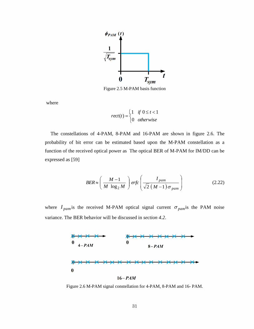
31
Figure 2.5 M-PAM basis function
where
otherwise
tiftrect
0
101)(
The constellations of 4-PAM, 8-PAM and 16-PAM are shown in figure 2.6. The
probability of bit error can be estimated based upon the M-PAM constellation as a
function of the received optical power as The optical BER of M-PAM for IM/DD can be
expressed as [59]
pam
pam
M
Ierfc
MM
MBER
12log
1
2
(2.22)
where pamI is the received M-PAM optical signal current pam is the PAM noise
variance. The BER behavior will be discussed in section 4.2.
Figure 2.6 M-PAM signal constellation for 4-PAM, 8-PAM and 16- PAM.

32
Meanwhile, M-PAM is receiving much research interest in expanding the capacity of
short and medium range optical links. Figure 1.6 and table 1.1 show some of the recent
progress in the employment of M-PAM at varied distances and bitrates for optical short-
haul and metro applications. It is clear that SMF is receiving increased interest due to its
direct impact on a longer fiber reach and/or increased system capacity.
Figure 2.7 Research progress for employment of M-PAM with respect to variable link distances
and bit rates highlighted in table 1.1.

33
Table 2.1 Recent experimental research progress employing M-PAM modulation format for short
and medium range optical links.
Label Year Wavelength Modulation
Format Bit Rate Distance
Fiber
Type Reference
1
2012 1550nm 4-PAM 100Gb/s 100m SMF [97]
2
2013 850 nm 4-PAM 50 Gb/s 50m MMF [98]
3
2013 850nm 4-PAM 60 Gb/s 2m MMF [98]
4
2013 850nm 8-PAM 35.2 Gb/s 100m MMF [99]
5
2014 1060nm 4-PAM 50 Gb/s 100m MMF [100]
6
2014 1060nm 4-PAM 50 Gb/s 200m MMF [100]
7
2014 1550nm 4-PAM 100 Gb/s 30KM SMF [101]
8
2014 1310nm 4-PAM 107 Gb/s 10Km SMF [102]
9
2015 1550 nm 4-PAM 56 Gb/s 25Km SMF [103]
10
2015 1550nm 4-PAM 24 Gb/s 120Km SMF [40]
11
2015 850nm 4-PAM 50 Gb/s 200m MMF [104]
12
2015 1310nm 4-PAM 224 Gb/s 10Km SMF [43]
13
2015 1310nm 4-PAM 112 Gb/s 20km SMF [43]
14
2015 1550nm 4-PAM 21.4 Gb/s 10Km SMF [105]
15
2015 850nm 8-PAM 56 Gb/s 50m MMF [50]
16
2015 850nm 4-PAM 70 Gb/s 50m MMF [50]
17
2015 1550nm 4-PAM 100 Gb/s 1Km SMF [106]

34
2.5 Optical Modulation
(a) Direct Modulation
(b) External Modulation
Figure 2.8 Illustration of the operation methodology of direct (a) and (b) external modulation.
In IM/DD, the electrical data signal is intensity modulated on an optical carrier
utilizing direct or external modulation. At high data rate, one significant and critical
component in IM/DD system is the optical modulator.
Figure 2.8 shows an illustration of the operation methodology of direct and external
modulation. Direct Modulation is a low complex way of optical modulation in which
light is emitted according to an electrical data signal from a directly modulated laser only
when a binary high signal is transmitted. In particular, the 100-Gb Ethernet is a standard
both for very short-reach (less than 100 m) based on vertical-cavity surface-emitting laser

35
(VCSEL) sources in case of multi-mode fiber (MMF) propagation and for reach up to 10
km in case of single-mode fiber (SMF) propagation [1].
The bandwidth demand required in data-intensive environment as data centers is
pushing the scientific community toward solutions guaranteeing Ethernet bitrates
reaching 400G Ethernet [2], utilizing VCSEL lasers.
Another way is to modulate the light from a continuous wave laser by an external
modulator as shown in figure 2.8(b). In IM/DD transmission systems with system
aggregated bitrate larger than 10Gbaud/sec, external modulation turn to be a viable
solution due to the impact of the laser source chirp on optical signal which can be highly
reduced. The extinction ratio (ER) describes the modulation efficiency for both directly
or externally optical modulated signal and is defined by the ratio of 1P & 0P as
0
1log10P
PER (dB) (2.23)
2.5.1 Mach-Zehnder Modulator (MZM)
The MZM operational basics is originated on the principle of the electro-optic effect. The
electro-optic effect is described by the difference in the applied electrical field resulting
in the refractive index variation at both of the modular dual arms[107]. This variation in
the refractive index imposes a change in the material propagation constant which leads
to the presence of two phases at both arms of the modulator.

36
Figure 2.9 Mach-Zehnder Modulator structure.
As shown in figure 2.9, the MZM is composed of an input pair of waveguide arms (1
and 2) in a Y-branch architecture, in which light launched through one end, )(tEin , is
split to a two equal waveguide arms 1E and 2E , which can be expressed as
21
2
)( Ee
tEE tjin
(2.24)
In case of non-applied electric field at the arms of the modulator, the signals arrive in
phase and interfere constructively at the output of the modulator.
On the other hand, if an electric field is applied across the arms, thus, the output
optical field takes the form
2
21
2cos
2
1
2
121
jtj
in
jjo
eE
eEeEE
(2.25)
where 1 and 2 are the phase at the MZM modulator waveguides, 12
is the phase difference which is a measure of the constructive or destructive interference.
The optical signal power of the MZM can be expressed as
cos12
ino
PP (2.26)

37
The MZM power transfer function can be shown in figure 2.10 in which the phase
difference determine the operating point or bias point of the MZM. MZM operate by
biasing the electrodes controlling the phase shift at a value equivalent to the quadrature
point where the applied input voltage to the arms iV is the voltage required to acquire a
phase difference equivalent to 2
. On the other hand, biasing iV at the zero point
is can generate different modulation formats[108].
The relation between iV and can be represented by
V
Vi (2.27)
where iV is the applied voltage to the arms of the modulator and V is the required
voltage to achieve a phase difference equivalent to .
An internal chirp is a result of the amplitude modulation in the MZM which is due to
the phase difference. This internal chirp can be expressed as
Figure 2.10 Mach-Zehnder Modulator power transmission function

38
dt
dP
Pdt
d o
o2
(2.28)
where is the frequency chirp parameter for the modulator which controls the
modulator frequency chirping. This relation controls the chirp effect on the MZM transfer
function. In case is positive, thus a positive frequency chirp exists which causes a
high frequency component at the leading edge or in other words, pulse said to be blue
shifted. The relation can be elaborated more i.e,
V
V
nn
nni
2cot
2cot.
21
21
(2.29)
Where represent the chirp factor which affect the internal symmetry of the modulator
transfer function where 1n and 2n is the index change per input voltage across the
MZM modulator arms.

39
2.6 Pre-Amplified Optical Receiver
Figure 2.11 Pre-amplified system model.
Figure 2.11 shows the pre-amplified based receiver that is employed in MMT
investigation for metro networks presented in chapter 5. It is composed of an optical link
with an Erbium Doped Fiber Amplifier (EDFA) pre-amplifier accompanied by an optical
band pass filter, a semiconductor photodetector and an electrical low pass filter. The
optical filter with a bandwidth oB reduces ASE-noise impact on the optical signal.
The received power oP by the photodiode generates a photocurrent equivalent to
or PRI . (2.30)
where rR is the responsibility of the photodiode, which can be expressed as
h
eRr (2.31)
where is the quantum efficiency, e is the electron charge and h is the photon energy.
Typical values for the responsivity of photodiodes are equivalent to 0.4-0.8 A/W[109],
[110].
The fiber is modelled using a low pass equivalent representation of a linear bandpass
system in which the fiber dispersion is accounted through the quadratic (nonlinear) phase
response of the fibers transfer function, given by[111]
)2
exp(22 L
c
fDLjH dBfib
(2.32)

40
where c is the free-space speed of light, is the wavelength of operation, L is the trans
mission distance, D is the dispersion parameter in ( ps/km .nm ) . After the photodiode, a
low pass filter exist with bandwidth eB to filter the noise out of the detected electrical
signal spectral width.
In the link design, there exit a different number of amplifiers with booster, inline and
pre-amplifiers configurations. This results in the addition of amplified spontaneous
emission (ASE) noise components to the noise received by the photodetector. The added
noise components can be classified in to: signal-ASE beat noise 2
ASEs , ASE-ASE beat
noise 2
ASEASE , ASE-shot noise 2
shASE and signal-shot noise 2
shs .
According to [111] ,the ASE-ASE beat noise 2
ASEASE component can be expressed
as
eon
eoASErASEASE
BBeFG
BBPR
2
222 4
(2.33)
Where G is the amplifier gain, nF is the amplifier noise figure , ASEP is the optical
noise power density , eB is the low pass filter electrical bandwidth, oB is the optical
filter bandwidth . While, the ASE-shot beat noise 2
shotASE is represented by
eon
eoASErshotASE
BBeFG
BBePR
2
2
2
4
(2.34)
The signal-ASE noise 2
ASEs can be expressed as
eoASErASEs BPPGR22 4 (2.35)
while, the signal-shot noise 2
Shots
eASErshots BPGR22 (2.36)
Another source of noise is thermal noise 2T , which can be expressed as

41
L
enBT
R
BFTk42 (2.35)
where T is the temperature (in Kelvin), LR is the load resistance, Bk is the Boltzmann
constant. The electrical filer transfer function can be expressed in terms of the noise
bandwidth eB as
dffHB ee2
(2.37)
where fHe is the transfer function of the electrical signal. The role of the electrical
filter is the equalization of the detected signal and reduction of noise imposed on the
received waveform.
The ASE-ASE beat noise 2
ASEASE spectrum can be calculated as the auto-
correlation of the ASE optical spectrum. Taking the transfer function frequency response
into account, the noise bandwidth of the ASE–ASE beat noise2
ASEASE is calculated as
dffHfHfH ooeASEASE2222
(2.38)
where fHo is the transfer function of the optical signal. The photodiode dark current of
the detector is very small compared to the photocurrent and therefore is ignored.
2.7 Linear fiber Impairments
The linear fiber characteristics can be classified in to three main parameters: fiber
attenuation and Chromatic Dispersion (CD) or Group Velocity Dispersion (GVD). These
parameters influence the behavior and propagation of signals in fiber at a low power
input transmission region and the interplay with the nonlinear fiber impairment at the
high power region, which impose a limitation on the maximum transmission reach of the
system as discussed in section.

42
2.7.1 Fiber Attenuation
The propagation of a light signal in optical fiber is influenced by total internal reflections
in the fiber core medium surrounded by the cladding. These reflections are caused by the
fiber design in which refractive indices of the core and cladding are varied acquiring total
internal reflections. Fiber attenuation is the main limiting factor for signal transmission
across large distance reach. The relation between attenuation and transmission distance
can be expressed in terms of the signal power after propagating inside the fiber with
length z as
zin etPtzP , (2.39)
where representing attenuation factor in Neper/meter, tPin is the input optical
intensity or power. It can be determined by measuring the input and output power
through the relation
tzP
tP
z
in
,ln
1 (2.40)
There is another relation which better describe dB as an attenuation coefficient in terms
of dB/KM as
tzP
tP
zdB
,
,0log10
1 (2.41)
The relation between both parameters and dB can be expressed from eq.2.40
and eq.2.41 as
343.4
dB (2.42)
The parameter is dependent on the operating optical signal wavelength . A
typical model for the attenuation with respect to the operating wavelength can be shown
in figure 2.12. The dotted line shows the attenuation of old fibers that were made before
the 1980s. In addition to strong water absorption peaks, the attenuation is generally
higher than new fibers due to material impurity and waveguide scattering. The impurities

43
impose an increased absorption in a certain wavelength regions. The vibrational
resonances of OH-ions occur near 2.73μm with higher harmonics at 1.39μm and 0.95 μm
as shown in figure 2.12. Three wavelength windows have been utilized for optical
communications in 850 nm, 1310 nm, and 1550 nm where fiber attenuation exhibits
minimum losses. Table2.1 show the wavelength range of optical communications bands.
Figure 2.7 Attenuation of old (dotted line) and new (solid line) silica fibers. The shaded regions
indicate the three telecommunication wavelength windows
[112].
Table 2.2Wavelength range of optical communications bands
Band Wavelength (nm)
O Band 1260 nm - 1360 nm
E Band 1360 nm - 1460 nm
S Band 1460 nm - 1530 nm
C Band 1530 nm - 1565 nm
L Band 1565 nm - 1625 nm
U Band 1625 nm - 1675 nm

44
2.7.2 Dispersion
Dispersion is responsible for the propagation of different signal components travelling in
fiber at different velocities resulting on pulse delay when arrived at the photodiode. There
are two main dispersion types, First, intermodal dispersion which is the major limitation
in multimode fiber due to the pulse propagation with different velocities at different fiber
modes which result in inter-symbol interference.
The second is intramodal dispersion, which occurs within a mode of fiber
transmission and has two contributions, waveguide dispersion and material or chromatic
dispersion. As for waveguide dispersion, it is due to the propagation of a portion of light
in the fiber cladding which have a relatively lower refractive index compared to the core.
The waveguide dispersion can be mitigated by proper system design consideration.
Dispersion Shifted Fiber (DSF) or Nonzero Dispersion Fiber (NZDF) can be employed to
counteract the partial effects of chromatic dispersion.
The second fundamental contribution is chromatic dispersion, which takes place
significantly in single mode fiber. Since the thesis proposes MMT to be deployed across
single mode fiber, thus, chromatic dispersion is elaborated in details.
2.7.2.1 Chromatic Dispersion
One of the significant characteristics of optical fiber communication is the pulse
broadening during travelling at various spectral components in SMF. The modulated field
may be described as an infinite sum of different frequency components (i.e. a Fourier
transform). For such a field, the effect of a dispersive medium will result in different
frequency components traveling at different velocities. This can be reasoned to the
frequency dependence nature of the fiber medium refractive mode index, which causes
different spectral components to propagate at different group velocities. Thus, chromatic
dispersion is known also as Group Velocity Dispersion (GVD). Hence, CD results in the
broadening of the propagating signal and the existence of interference between adjacent
pulses known as Inter-symbol-interference (ISI). Figure 2.13 shows the implication of the
chromatic dispersion. The group velocity 𝑣𝑔 can be expressed as
𝑣𝑔 = (𝑑𝛽𝑝
𝑑𝑓)
−1
(2.43)

45
=𝑐
𝑛𝑔
where 𝛽𝑝 is the propagation constant and 𝛽𝑝 =𝑛 𝑓
𝑐 ,𝑛𝑔 is the group index parameter. if
we want to express the different arrival times of the spectral components of the signal
through fiber. we can develop the time delay equation to be
∆𝑇 =𝑑𝑇
𝑑𝑓 𝑓
= 𝐿 ∆𝑓 (𝑑2𝛽𝑝
𝑑𝜔2) (2.44)
= 𝐿 ∆𝑓 𝛽𝑝2
Figure 2.8 Chromatic dispersion effects (a) Pulse broadening (b) Inter-symbol interference.

46
with ∆𝑓 representing the spectral bandwidth of the pulse and 𝛽𝑝2 defined as group
velocity parameter and 𝑓 =2𝜋𝑐
𝜆. Also, the time delay can be expressed as
∆𝑇 = 𝐷 𝐿 ∆𝜆 (2.45)
where 𝐷 is the dispersion parameter in (ps/nm.km) and can be expressed as
𝐷 =𝑑
𝑑𝜆(
1
𝑣𝑔) = −
2𝜋𝑐
𝜆2 𝛽𝑝2 (2.46)
The total fiber dispersion for a conventional single mode fiber (SMF) in the 1.55μm
region varies between 16 to 19 ps/nm·km[55], [113].
2.8 Non-Linear Fiber impairments
The intra-channel non-linearity is one of the main fiber non linearities that affects fiber
transmission between the signals on itself at a single wavelength. The propagation of
pulses with bitrates in the order > 10G in fiber is not only limited by the linear fiber
impairments, however, it has strong proportionality with fiber intra-channel non-linearity.
Thus, it is significant to investigate the non-linear interplay between adjacent pulses in
the presence of dispersion which cause pulse broadening at high aggregated channel
bitrates. Fundamentally, there are three types of intra-channel non linearities: SPM, Intra-
IXPM and IFWM [69].
2.8.1 Self-Phase Modulation
For fiber non-linearity being investigated, an inclusion of fiber Kerr effect in the fiber
channel model is necessary[114]. Kerr occurs due to the dependence of the refractive
index on the launched fiber optical intensity. For single channels, this leads the optical
field amplitude to have a self-induced phase modulation by the signal self-power, in
which this phenomenon is called Self Phase Modulation (SPM)[115], [116].

47
As the need for high power pulses for maximum reach and error free fiber optic link
systems, their performances are eventually limited by SPM effect [117]. Since, the
dominant non-linear effect in transmission systems is self-phase modulation (SPM).
SPM appears due to the dependence of the refractive index on the signal intensity,
which leads to an induced phase change for the pulse propagating in the fiber [3]. The
different parts of the pulse undergo different phase shifts, which give rise to chirping of
the pulses. Pulse chirping in turn enhances the pulse broadening effect caused by CD.
This chirping effect is proportional to the transmitted power, which in turn SPM effects
to be more pronounced in the systems employing high transmitted powers. At the high
power levels, SMF has a large anomalous dispersion due to the GVD of 16.75 ps/nm/km.
Therefore, necessities emerge to compensate the envelope time domain pulse broadening,
which leads to a chirp at the end of the propagation distance.
Methods that utilize the employment of SPM effect in the compensation for the second
and almost the third order dispersion parameters have been previously proved effective
by using Dispersion Compensation Fiber (DCF) in pre and post compensation scenarios
[6-8].
Dispersion and SPM effects can be mathematically modeled in our transmission links
referring to Non-linear Schrodinger (NLS) equation. Simulation was performed for
MMT in both dispersion post-compensated and combination of pre- and post-
compensated transmission links. The optimum value of dispersion pre-compensation is
reported in order to enhance the performance of MMT system in terms of SPM tolerance
as discussed in section 5.3.
2.8.1.1 SPM Mathematical Modal
The mathematical model which best describes the propagation of the pulses in SMF,
were taken to account for the effect of SPM and GVD in the NLS as [56]
2
2 2
( , ) ( , )( , ) ( ) ( , ) ( , )
2 2
A z j A zA z z j A z A z
z
(2.47)
where z is the longitudinal propagation distance, ( , )U z is the normalized amplitude for
a Gaussian pulse and the amplitude for a complex electric field pulse envelope is equal to

48
( , ) exp( / 2) ( , )oA z P z U z (2.48)
where ( / ) /g ot z T denotes the retarded time framework for the GVD ( g ), oT is the
pulse width, represent the attenuation coefficient, 2 and represent the GVD
parameter and the fiber nonlinearity parameter, respectively. The non-linear factor is
described by the dominant parameter, which is the dispersion length ( DL ):
2
2/D oL T (2.49)
And the non-linear length ( NLL ) as
1/NL oL P (2.50)
Where the non-linearity parameter is dependent on the operating wavelength, the non-
linear index of refraction 2n and the effective core area effA by
effeff
o
A
n
Ac
nw
22 2
(2.51)
Both the GVD and SPM phenomenon will be considered in our system as L>>LNL and
L>>LD where L is the fiber length.
2.8.2 Intra-channel Cross-Phase Modulation (IXPM) and Intra-channel
Four-Wave Mixing (IFWM) Non-linearities
At high system baud rates, the impact of the intra channel non-linearity becomes
dominant. This can be shown in figure 2.14 highlighting the impact of non-linearity with
respect to channel bitrate, fiber local dispersion and format spectral efficiency[108],
[118]. For high capacity time division systems reaching higher than 10 G baud per
channel, the dominant nonlinear effects are due to IXPM and IFWM[88]. IXPM and
IFWM are considered an interactions among neighboring bits (pulses) that are a result of
fiber intra-channel nonlinearities. Considering three propagating signals 1P , 2P and 3P ,
the interplay effect between them can be expressed by [119]

49
Figure 2. 9 Impact of fiber non-linearity with respect to channel bitrate, fiber local dispersion and
spectral efficiency[108], [118]
IFW MIXPMSPM
PPPPPPPt
P
z
Pj *
32112
32
22
121
221 222
2
(2.52)
where the first component represents the SPM effect, the second component represents
the IXPM effect with its interplay with consecutive neighboring signals and the third
term represents the IFWM and its interplay between neighboring signals.
(a) (b)
Figure 2.10 IXPM effect on signal: a) Time shift occurrence in waveform. b) Timing jitter
occurrence in eye diagram.
.

50
IXPM impose phase modulation between consecutive neighboring signals[56]. Figure
2.15 shows the impact of IXPM on signal waveform and eye diagram. A frequency chirp
occur as a result of the time dependency of the signal phase modulation which is
translated to a timing jitter[87]. Although the signal energy remains constant, the IXPM
lead to fluctuations in the symbol period and the symbol amplitude which causes an
amplitude-jitter and closure of the eye diagram as shown in figure2.14 [120]. IXPM
impact can be reduced or controlled by proper design of dispersion management map
[121]. Some forms PPM have been investigated capable of suppressing IXPM and IFWM
by adding guard interval to transmitted pulse sequence[122].
At high bit rate, the signal suffer a frequency shift which is translated to a time delay,
thereby resulting in the formation of ghost pulses or shadow pulses. If there is a vacant
slot as RZ-OOK format, a small pulse fluctuation appears (ghost pulse). However, if the
signal structure occupy 100% duty cycle, thus, the time delay will lead neighboring slots
to beat together creating variations in main pulse amplitude or an amplitude jitter. Figure
2.16 shows the impact of IFWM on signal waveform and eye diagram. A lot of research
have been carried on mitigating the effect of IFWM by destructive interference utilizing
bitwise phase changes coding techniques and other techniques for Time Division
Multiplexed (TDM) systems[123]–[126].
(a) (b)
Figure 2.11 IFWM effect on signal: a) Ghost pulse occurrence in waveform.
b) Amplitude jitter occurrence in eye diagram.

51
2.8.3 Stimulated Brillouin Scattering (SBS)
In contrast to the Kerr-non linearity effects, there is another non linearity which is based
on inelastic scattering process where a photon of the propagating signal interacts with the
fiber medium and during this process a new photon with less energy is launched. At high
power levels, the nonlinear phenomena Stimulated Brillouin Scattering (SBS) associated
lead to the presence of optical amplification in the backward direction. The SBS can
cause signal attenuation if the launched power is higher than a certain threshold[110].
SBS have been studied theoretically and numerically over different fiber modes[127]–
[129]. The effect of SBS optical threshold power SBSP can be calculated as [55]
effB
eSBS
Lg
AbP
21 (2.52)
where eA is the effective area of fiber, Bg is the Brillouin gain coefficient which equal to
11105 m/W and b take value between 1 and 2 depending on the relative polarizations
of the pump and Stokes waves and effL is the effective fiber length and can be expressed
as
dB
L
eff
dBeL
1
(2.53)
One way of mitigating the effect of SBS is to modulate the laser pump current at a
frequency region in the upper KHz regime[130].

52
2.9 Concluding Remarks
This chapter presented an overview for the fundamentals of modulation formats,
optical components, fiber linear and non-linear impairment. In addition, the chapter
described the constraints and channel characteristics that exist in intensity modulated
direct detection channels.
Modulation Formats which are relevant for comparison with MMT has been
discussed. Also, the modulation formats that are employed and relevant for comparison with
the proposed technique, is presented and discussed. The chapter concluded by a description
for the main fiber propagation impairments limiting the IM/DD system for short and
metro optical communication links. The chapter discussed the linear fiber impairments
such as attenuation and chromatic dispersion. In addition, non linear impairments such as
self phase modulation and intra-channel non linearities have been discussed. Also, the
nonlinear phenomena Stimulated Brillouin Scattering (SBS) which lead to the presence
of optical amplification in the backward direction has been explained.
The topics have been chosen based upon their relevance to the intensity modulated
directed detection systems, discussed and presented in the thesis.

53
3. Chapter 3 - MMT System Model and
Performance Metrics
3.1 The Methodology behind MMT Structural Design
The pioneer Claude Shannon put the foundation for digital communication through his
classical paper [131], which has paved the way for the huge advances in communication
and information theory. The paper puts a limitation on the maximal rate for reliable
transmission over a noisy channel (equivalent to low bit error probability). It stated that
the transmission of data under a noisy channel can be achieved with a specified signal
power at an arbitrarily low bit error probability as long as the coding rate is not exceeding
a certain factor, which is the channel capacity (in bits/sec). Shannon has formulated his
theory in an equation which has been expressed as [131]
).
1(log)1(log 22BN
PB
N
SBC
o
(3.1)
where C is the channel capacity in (bits/sec), B is the bandwidth of the channel in (Hz),
S or P is the average received signal power in (Watts), N is the total received signal
noise power in (Watts) and equivalent to BNN o , oN is the one-sided power spectral
density and NS / represents the Signal To Noise Ratio (SNR). The method or approach
to achieve this channel capacity have been left by Shannon as an open question for
researchers all over the world and through many years, to develop the practical
methodologies and design procedures to achieve this capacity boundary or Shannon
limit[132], [133].
To answer this question, system designers have considered the three pivotal trade-
off design resources that govern any data transmission format proposed by Shannon
capacity formula. The three-tradeoff key factors are power, bandwidth and complexity.

54
The formula in other words states that, the ultimate goal of the design of any transmission
format is to reach an impactful trade-off between design parameters to overcome the
challenges and meet the requirements of a particular desired application.
According to Shannon equation, the capacity (in b/s) is directly proportional to the
SNR. Aided by the fact, that SNR and Bit Error Rate (BER) have an inverse exponential
relationship in which as the BER decrease (enhance) as the SNR requirement increase.
Thus, one solution to increase the capacity was to employ higher order modulation
formats offering an expansion in system information capacity (in bits/symbol). Higher
order modulation formats features scaling system baud rate at a fraction of the aggregated
bit rate.
Recently, M-PAM has been proposed as a higher order modulation format for short-
haul and metro networks [30], [41], [134]. M-PAM is a multiple-level bandwidth-limited
transmission format offering a high spectral efficiency on the cost of high power
penalty[86]. As such, 8-PAM with 3 bits/symbol and 16-PAM with 4 bits/symbol have
imposed large SNR requirement to achieve an acceptable BER at a fixed baud rate. This
high SNR requirement is reasoned to the higher number of levels penalties that are
associated with increasing the number of levels. A solution has been proposed to 8-PAM
format, is to apply error correction techniques, as block coding and Forward Error
Correction (FEC) codes to enhance the SNR, but again this implicates a rise in the system
complexity [41], [48], [50].
According to our problem statement, the thesis aims to design a power efficient and
high capacity transmission format for reducing the power consumption of data intensive
applications (as discussed in chapter 1). Thus, as our research motivation combined with
avoiding the high power penalty imposed on higher order M-PAM modulation format,
MMT design has taken in to account other trade-off parameters to increase the capacity
without significant power penalty cost. The other signal dimension considered was
dividing the symbol duration into two slots (as discussed in section 3.3.1).
Although, dividing the MMT slots induce an increased bandwidth penalty. However,
increasing the bandwidth, has two major effects on the capacity. First, it raises the

55
available link degrees of freedom since as BN
PNS
o./ , thus at fixed SNR, the
dependency is clear on limiting the power P . In other words, at fixed power P and by
increasing the bandwidth B , the SNR requirement is decreased. The second effect is
comprised on the SNR requirement per dimension, which will be spread among the
dimensions or degree of freedoms with the bandwidth increase.
Although, increasing the bandwidth had a positive impact on increasing the capacity
and reducing the SNR requirement, however, we cannot neglect the fact that increasing
the bandwidth above a certain value, will entangle a weaker impact on the capacity. This
can be verified by Shannon capacity equation assuming high bandwidth, the equation can
be approximated by [135]
eN
Pe
BN
PB
BN
PBC
oo
o
22
2
loglog)..
(
).
1(log
(3.2)
As such, it is clear that in this case, the capacity is directly proportional to the average
received power and increasing the bandwidth further has a very limited effectiveness. At
this point, the channel capacity is power limited in which the capacity does not increase
further with increasing the bandwidth; however, it increases with increasing the power.
As such argument, MMT structure has been designed utilizing two slots only, in
which increasing the number of MMT slots more than two will impose more bandwidth
penalty with non-significant trade-off advantage for desired application.
As above-mentioned consideration, MMT structural design has considered reaching an
impactful intermediate compromise between power and bandwidth. Hence, MMT has
been designed as a joint multiplexing and modulation format, which can be viewed as a
hybrid combination between M-PPM and M-PAM modulation formats. The joint design
in MMT causes more degree of freedom in optimizing the performance, which can be
viewed as a power efficient alternative and bandwidth efficient alternative compared to
M-PAM and M-PPM, respectively.

56
3.2 Channel Characteristics
Due to the huge demand for both low-complex and low-cost modulation formats
featuring low power consumption for metropolitan and short range optical fiber
systems[25], [53], [60], [136], [137], hence, N-channel MMT is presented as a power
efficient alternative transmission format for non-coherent applications. Although, N-
channel MMT is a modulation format that is applicable for wired and wireless
communication links, however, it is the interest of this thesis to present N-channel MMT
for Intensity-Modulated Direct-Detection (IM/DD) links. The reason behind choosing the
IM/DD channel was driven by the trade-off advantage between cost and power efficiency
fulfilling the thesis objectives, compared with coherent systems.
In IM/DD, the information is conveyed in the form of optical power intensity signal
)(tP , where the input is an electrical signal )(tX K . The direct detection is a linear
process where the photodiode is responsible for the opto-electrical conversion.
IM/DD channel characteristics have two fundamental constraints on all implemented
transmission formats. Since information is conveyed by modulating the instantaneous
optical power signal )(tP , thus, no negative amplitudes can be used [53], [73], [78],
[138]. Hence, N-channel MMT has been designed to fulfill the non-negativity constraint
at all time instants, i.e
t
min 0)( tP (3.3)
Since N-channel MMT is designed to cope with IM/DD for both fiber and wireless
optical links (where the signal propagate in free space), thus, eye safety is an important
metric. Eye safety is one of the most vital restrictions for IM/DD systems operating in the
infrared, ultraviolet, visible communication frequency band. Safety regulations must
ensure that the emitted radiated power follows international bodies regulations for eye
and skin safety precautions[53], [57], [72], [73].

57
Hence, in contrast to conventional channels, the second constraint is a limitation on
the emitted peak and average signal power, so the maximum optical signal power should
be less than or equal the maximal power the eye can tolerate eyeP as
sym
symsym
T
T
eyeT
PtPLim )( (3.4)
The maximum allowable power the eye can tolerate is dependent upon the intensity
modulated system application. In addition, it is strongly dependent on the wavelength of
operation. At 1550nm wavelength, the maximum allowable power for safe operation is
less than 10 mW. While, at 1310nm, the maximum allowable power is less than 8.8 mW
[138].
In this thesis, N-channel MMT design is focused mainly for optical fiber links while
the discussion on wireless optical links will be considered for future works (as discussed
in section 7.2).
Figure 3.1 shows a generic free space model for N-channel MMT IM/DD system. The
optical intensity modulator is responsible for generating an optical power signal, so that
)()( tXctP k (3.5)
where c is the electro-optic conversion factor in Watt/Ampere. Note that the optical
power is proportional to )(tX k and not to )(2 tX k due to the fact that in a system based on
IM/DD, the SNR is proportional to the square of the received optical power (due to
square law detector) [53], [60]. In IM/DD optical communication with non-optical
amplification, the optical channel can be modelled as an Additive White Gaussian Noise
(AWGN) channel which serve as a good model for all types of noise present [53], [57],
[60], [70]. Hence, the received electrical signal can be expressed as
)()(..)( twtXcRtz kr (3.6)
where rR is the photodiode responsivity and )(tw accounts for the AWGN with zero
mean and double sided power spectral density2
0N, which is equivalent to the thermal
noise at the system receiver environment.

58
Figure 3.1 N-channel MMT free space channel model for IM/DD systems.
3.2 Signal Space Model
Signal space model is a benchmark assessment methodology for investigating modulation
formats in general and especially for IM/DD systems. Signal space have been first
proposed by Kotelnikov [139] two years earlier before it was proposed by Shannon in
1949 [140], then afterwards it has been developed widely by Wozencraft and
Jacobs[141]. The signal space analysis approach has been employed widely to provide an
in-depth evaluation of various modulations and coding techniques [82], [142]–[144]. The
concept of portraying different modulation formats as constellation points in Euclidean
space lead to more consistent and efficient approach for mandatory design tradeoff
analysis and discussions. Moreover, the advantage of signal space comprised in the
ability of conveying signal sets and noise as vector space components in a geometric
representation where probabilities of these components can be derived [86], [90], [145].

59
3.2.1 N-channel MMT Signal Model
Since MMT signals are dependent upon two orthogonal time slots, the signal calculations
can be interpreted from the vector space component by the construction of orthogonal
basis functions. Signals can be represented by defining a set of orthonormal basis
function )(tj for Rj ,...,2,1 where R is equivalent to the number of signal dimensions
or slots ( S ) as in [58], [82], [86] , which satisfy KR . Therefore, each of the signals
can be expressed as
)()(1
, txtX j
S
j
jkk
(3.7)
where 1,...,0 Kk and Rkkkk xxxx ,2,1, ,...,, is the vector component representation
of )(txk with respect to the defined basis functions. The basis function per slot is
represented by
Figure 3.2 N-channel MMT format generated orthonormal basis functions.
2
.
2)1()
2
1(
2)(
symsym
symS
TSt
TSfor
Strect
Tt
(3.8)
where
otherwise
tiftrect
0
101)(

60
Figure 3.2 Shows the N-channel MMT developed basis function following the IM/DD
channel constraint. It is clear that each of the time slots is non-overlapping in the time
domain. The N-channel MMT symbols can be expressed as a linear combination of its
basis functions. Thus, the MMT symbol can be translated to the weighted sum of two
orthogonal basis functions corresponding to two consecutive one-dimensional signal
constellations. The signal )(, tx Sk is defined with respect to the basis function as
)(2
)( ,, tT
Atx Ssym
SmSk (3.9)
Each of the N-channel MMT symbol is defined by multiplying an amplitude SmA , by the
corresponding basis function. While the entire MMT signal can be represented based on
the basis functions as
S
S
Ssym
Smk tT
AtX1
, )(2
)( )(2
)(2
22,11, tT
AtT
Asym
msym
m (3.10)
and each )(, tx Sk is defined to guarantee the non-negativity constraint as
tmin 0)(, tx Sk (3.11)
Figure 3.3 shows the sixteen different signals for 4-Channel MMT with respect to the
defined MMT basis function in eq(3.10).

61
Figure 3.3 4-Channel MMT generated symbols in terms of the basis functions.

62
3.2.2 Geometric Representation of N-channel MMT
The N-channel MMT signal can be viewed as a vector space component in a geometric
representation[86], [146]. By employing vector representation, the Euclidean distance
between any pair of signal vectors can be expressed as 2
ji xxd . This can be
translated to compute the Euclidean distance between the two MMT signals slots as
])()[(2
22,2,
21,1,
2
2,1,
jijisym
kkMMT
xxxxT
xxd
(3.12)
where SMji ,...,2,1,0, and each MMT signal is represented in vectors in terms of each
constellation dimension as ),( 2,1, kkk xxX which is equivalent to it waveform
representation )(tX k .
For IM/DD systems, the constellation diagram for N-channel MMT symbol structure is
shown in figure 3.4, compared to its counterpart of M-PAM in figure 3.5.

63
Figure 3.4 Signal space constellation geometry 2, 3, and 4-channel MMT for IM/DD systems.
Figure 3.5 Signal space constellation 4-, 8- and 16-PAM for IM/DD systems.

64
3.3 MMT Transceiver Model
(a) Transmitter
(b) Receiver
Figure 3.6 MMT generic transceiver model, (a) Transmitter and (b) Receiver.
Figure 3.6 shows a general model for both MMT transmitter 3.6(a) and receiver
3.6(b). The input data from different channels are multiplexed and divided into a set of
data clusters. Then, MMT mapper exploits a multiple layer mapping algorithm to encode
the subset partitioned multiplexed channels data under mapping rules. The main function
of the MMT mapper unit is to transform the received data array from different channels
(users) into a sequence of symbols according to a predefined algorithm, which is based
upon a defined mapping rules. Afterwards, the data are modulated considering a hybrid
combination between Pulse Amplitude Modulation (PAM) and Pulse Position
Modulation (PPM). The symbol duration is divided in to two slots and each slot is
composed of multiple amplitude levels dependent upon the number of channels or
information capacity (in bits/symbol).

65
The N-channel MMT is classified under memoryless multilevel modulation scheme
with multi-dimensional constellation diagram. N-channel MMT is based upon two
consecutive one-dimensional constellation, designed for IM/DD systems. In IM/DD,
Electro-Optical conversion is present by the responsibility of Directly Modulated Laser
(DML) or an external optical modulator, which produce an intensity (power) signal
proportional to the input electrical replica.
In MMT receiver design, two symbol detection methodologies have been considered
to provide the detection techniques for the MMT symbols. First, detection based upon an
optimal receiver with a bank of matched filter, where an abstract analytical performance
evaluation for N-channel MMT technique can be performed. This analytical model can
be considered later for comparison with other modulation formats. The optimal receiver
involves a decoding process based upon Maximum Likehood Sequence Detection
(MLSD) for the received message, searching among the set of N-channel MMT
constellation points for the nearest Euclidean distance to the received message. The
MLSD enable attaining the lowest probability of error. Thus, it can be employed as a
performance measure to evaluate and compare MMT performance with other modulation
formats.
The second method is a threshold detection receiver, which is based upon a dual
threshold detection among the two symbol slots, in addition to a clock data recovery for
synchronization with the transmitter. Before the threshold detection, an electrical filter is
present in order to reshape signals and remove noise. Then, MMT de-mapper is present
where a multiple stage decoding process takes place according to preset de-mapping rules
defined later in section 3.3.3.1. In the end, the data is de-multiplexed back to the
channels or users.

66
3.3.1 Basic Properties and Waveform Synthesis
The number of MMT symbol waveform alphabet ( K ) is equivalent to the number of
different possible input channels combinations NK 2 . The MMT method to convey
information is not only based on dividing the symbol duration in to two sub interval slots,
but also dependent on a varied number of levels per slot. The number of levels per slot (
SM ) is related to the code length S per cluster SY for the multiplexed channels by
SSM
2 (3.13)
i.e }2,.....,2,2{ 21 SSM
. The MMT signaling symbol set K is equivalent to the
product of the number of levels for the two slots
21 . MMK (13.14)
where 1M , 2M denote number of levels for slot 1 and slot 2 , respectively.
Moreover, the number of multiplexed bits N is related to the code length S per cluster
by
S
i
i
S
i
iMN11
2 )()(log (3.15)
Figure 3.7 depicts the generic MMT symbol format that employs a varied number of
slot amplitude levels ( SmA , ) (dependent on the cluster code length S ), and two slots (
S ), for “ N ” number of users. The time duration of each slot interval ( slotT ) is given by
2
symslot
TT , where symT , is the MMT symbol duration (1/ bitrate).

67
Figure 3.7 MMT symbol format.
N-Channel MMT has been designed for multiplexing and modulation of multiple
different data channels (or users) bit streams. Two, three and four bits/symbol
information capacities have been represented by 2-, 3- and 4-channel MMT, respectively.
The N-channel waveform structure for 2-, 3- and 4-channel MMT are shown in figure
3.8.
(a) (b)
(c)
Figure 3.8 N-channel waveform structure for (a)2-Channel MMT , (b)3-Channel MMT and (c) 4-
channel MMT.

68
3.3.2 N-channel MMT Transmitter Model
Figure 3.9 MMT transmitter proposed model.
MMT transmitter model is depicted in figure 3.9. The MMT mapper on the
transmission side is built with an input array of parallel channels ],...,,[ 11 Nnn yyyN
where 1,..,2,1,0 Nn , with an array size of 1N . Each channel (user) data is
represented by ny , where }1,0{ny .
The mapper maps the parallel input channels data to MMT different unique symbols. The
serially converted input data array is split in to two clusters (subsets) SY , where each
cluster address is denoted by a subscript index S where }2,1{ S . The code length (
S ) per cluster SY in principle is dependent upon the number of input channels and is
equal to
For odd number of channels For even number of channels
bitsN
bitsN
2
1
2
121
bitsN
2, 21
(3.16)
A mapper and waveform modulator unit performs bijective-mapping operation to map
the input multiplexed cluster SY to a distinct MMT symbol. The basic idea behind
MMT mapper is to exploit a multiple layer mapping algorithm to encode an input
multiplexed data channels to a subset partitioned data cluster following MMT mapping
rules. MMT mapper and waveform generator is composed of a subdivided dual slot
amplitude modulator. The MMT symbol is composed of a waveform that belongs to a set
of signal waveform alphabet )}()....,(),({ 110 tXtXtXX KK where K is the size of the

69
MMT signaling set. The message sent during a symbol interval is chosen as one of the
waveform alphabets KX , which are sent independently of each other. The N-channel
MMT signal are equiporbable with an equal probability of K/1 . Note that the waveform
symbol pattern is divided in to two slots 2,1 S in which amplitude modulated
waveform per slot represented by )(1, txk and )(2, txk where subscript k , S denote the
alphabet index and the slot index, respectively.
At an instant t, the MMT mapper maps the input data cluster SY to an amplitude-
modulated waveform following the mapping table 3.1, which can be expressed as
SmSmSk AtAx ,,, {),( M Map )( SY ]},..,,[| 110 NS yyyY (3.17)
where ),( ,, tAx SmSk denotes the amplitude modulated waveform corresponding to slot
S and SY is the data cluster mapped to an amplitude level SmA , . The mapper
modulator unit generates two consecutive slot waveforms )](),([ 12,1, ikikK txtxX .
For more illustration of the MMT technique, the MMT data encoding system is based
on two layer mapping for a two-consecutive one-dimensional system where each layer
represent single dimension. The first layer comprises mapping the data subset 1Y to the
first slot for synthetization to the first constellation dimension by modulation and
denoting it ,1 , 1( )k m slotx A where , 1m slotA represent the amplitude modulation for the first slot
,i.e
Mslot1 )()( 1,1,1 slotmk AxY (3.18)
In the same manner, the second layer encompass mapping the data subset 2Y to the
second slot for synthetization to the second MMT constellation dimension and denoting it
,2 , 2( )k m slotx A where , 2m slotA denote the amplitude modulation for the second slot, i.e

70
M slot2 )()( 2,2,2 slotmk AxY (3.19)
The symbol alphabet is transmitted upon the mapping of both data clusters each to its
correspondent slot to form an MMT symbol generated by the waveform modulator, i.e
M MMT )(,)(),( 2,2,1,1,21 slotmkslotmk AxAxYY (3.20)
Table 3.1 shows a 4-channel MMT two layer symbol mapping operation. In time
domain, the MMT mapper waveform unit is capable of generating the MMT symbols
following a formulated expression, i.e
),( ,, tAx SmSk
otherwise
TSt
TSfor
StWA
symsymTSm sym
0
2
.
2)1()
2
)1((,
(3.21)
where each k represents an MMT symbol from a total of )(1 tX K symbols, symTW is the
waveform corresponding to MMT symbol duration symT and S is the slot index
where }2,1{ S .
The waveform dependent variables are amplitude and time; the amplitude is based upon
the mapping rule in (3.17) and table 3.1, while the time interval depends upon the slot
number ( 1S or 2S ) which corresponds to the slot index

71
Table 3.1 4-Channel MMT SYMBOL MAPPER.
First Mapping Layer Second Mapping Layer
Mslot1 )( 1Y )( 1,1, mk Ax Mslot2 )( 2Y )( 2,2, mk Ax
Ms=1 (00) )( 1,01, Axk
Ms=1(01) )( 1,11, Axk
Ms=1(11) )( 1,21, Axk
Ms=1(10) )( 1,31, Axk
Ms=2(00) )( 2,02, Axk
Ms=2(01) )( 2,12, Axk
Ms=2(10) )( 2,22, Axk
Ms=2(11) )( 2,32, Axk
M MMT ),( 21 YY Kmkmk XAxAx )](),([ 2,2,1,1,
M (00,00) 02,02,01,01,0 )](),([ XAxAx
M (00,01) 12,12,11,01,1 )](),([ XAxAx
M (00,10) 22,22,21,01,2 )](),([ XAxAx
M (00,11) 32,32,31,01,3 )](),([ XAxAx
M (01,00) 42,02,41,11,4 )](),([ XAxAx
M (01,01) 52,12,51,11,5 )](),([ XAxAx
M (01,10) 62,22,61,11,6 )](),([ XAxAx
M (01,11) 72,32,71,11,7 )](),([ XAxAx
M (10,00) 82,02,81,21,8 )](),([ XAxAx
M (10,01) 92,12,91,21,9 )](),([ XAxAx
M (10,10) 102,22,101,21,10 )](),([ XAxAx
M (10,11) 112,32,111,21,11 )](),([ XAxAx
M (11,00) 122,02,121,31,12 )](),([ XAxAx
M (11,01) 132,12,131,31,13 )](),([ XAxAx
M (11,10) 142,22,141,31,14 )](),([ XAxAx
M (11,11) 152,32,151,31,15 )](),([ XAxAx

72
3.3.2.1 N-channel MMT Symbol Rate
One of the main advantages that features MMT compared with other modulation
formats, is the system symbol rate reduction. N-channel MMT data capacity multiplexing
feature enhances the eligibility for scaling the baud rate with the limitations that exists in
electronic and optical components operating at a fraction of the aggregated data
rate.Therefore, N-channel MMT has the capability of reducing the baud rate to
)(log/1 212 MM of the the aggregated bit rate.
As such, 2-channel MMT features a baud rate equivalent to 1/2 of its aggregated
bitrate compared with OOK. While, 3-channel MMT has a baud rate equivalent to 1/3 of
its aggregated bitrate compared with OOK. Also, 4-channel MMT is capable of
decreasing the electronic requirement of its components to a baud rate equivalent to 1/4
of the aggregated bit rate compared with OOK.
3.3.3 Receiver Model
The receiver is one of the crucial components in the transceiver design due to their
responsibility in recovering the transmitted data. The receiver function is to decide upon a
certain observation the transmitter sent message. This decision is determined based upon
a pre-set a particular criteria.
As mentioned earlier, two receiver detection designs have been proposed for N-Channel
MMT, which can be classified as follows :-
1. Threshold detection receiver for the numerical model.
2. Optimal detection receiver for the analytical Model.

73
3.3.3.1 Threshold Detection Receiver
The N-channel MMT threshold detection methodology employs a reduced complexity
algorithm, which is based upon dividing detection process to two stages in
correspondence with the two consecutive one-dimensional constellation nature of MMT.
Conventionally, the processing de-mapping unit should searches for the transmitted
message among all possible combinations of the lattice constellation points that is equal
to N
2 symbols. However, in MMT design, the detection process is divided in to two
stages; in which the first stage is searching for the transmitted first cluster message over
the lattice of the first dimension that are equivalent to SM
K
of the total MMT symbols.
Afterwards, the second stage in turn searches for the second cluster message over the
second dimensional constellation lattice points that are equivalent to SM
K
of the total
MMT symbols. This method can reduce the number of the search processing hardware
device to a number proportional to a total number of processing searches equivalent to
21 ststtot III (3.22)
,the number of processing searches for each stage SstI , is equivalent to
SSst
M
KI
, (3.24)
where K is the number of MMT symbols and SM is the number of levels per slot. The
reduction in number of constellation search lattice points is equivalent to ( totIK ). The
multistage decision and de-mapping operation is shown with respect to constellation
points in figure 3.10 (a-c) for 2-channel, 3-channel and 4-channel MMT, respectively.

74
(a)2-channel MMT
(b) 3-channel MMT
(c) 4-Channel MMT
Figure 3.10 De-mapping multistage decision methodology for (a) 2-Channel MMT, (b) 3-
Channel MMT, and (c) 4-Channel MMT.

75
Figure 3.11 MMT De-Mapping receiver structure.
The MMT receiver model is shown in figure 3.11. MMT threshold detection receiver
employs a low complexity decision circuit and data recovery algorithm. At the receiver
side, the received signal is fed into sampling and decision circuit. The samples are taken
at two sampling points SSP (one sampling point per slot S ). The outputs of the
sampling circuit are fed into a decision and de-mapping unit. In this unit, the sampled
values are compared against a number of threshold values.
},...,,{ ,1,1,, SMSiSiSi S
(3.25)
where SM corresponds to the number of levels for a slot S .
Sampling circuit outputs are driven to a decision and regeneration unit for the data
recovery that is according to preset defined de-mapping rules shown in table 3.2. The de-
mapping operation is based upon two layers multistage detection operation as shown in
figure 3.8 to map the received slot waveforms )(ˆ),(ˆ 2,2,1,1, mkmk AxAx to a distinct
constellation point .The two stages de-mapping operation can be expressed as
]ˆ,ˆ[ 21 YY M De-Map ))(ˆ),(ˆ( 2,2,1,1, mkmk AxAx (3.26)

76
Table 3.2 4-Channel MMT SYMBOL De-Mapper.
4-Ch. MMT De-Mapping Detection Rules Symbol
Decision
ˆKX
1st Cluster Rule
Slot 1
Ch1 - Ch2
1st
Stage
Decision
2nd
Cluster Rule
Slot 2
Ch3 - Ch4
2nd
Stage
Decision
if
1,11 SP
)(ˆ 1,01,0 Ax if
2,11 SP )(ˆ 2,02,0 Ax
02,02,01,01,0ˆ)](ˆ),(ˆ[ XAxAx
)(ˆ 1,01,1 Ax if
2,112,2 SP )(ˆ 2,12,1 Ax
12,12,11,01,1ˆ)](ˆ),(ˆ[ XAxAx
)(ˆ 1,01,2 Ax if
2,212,3 SP )(ˆ 2,22,2 Ax
22,22,21,01,2ˆ)](ˆ),(ˆ[ XAxAx
)(ˆ 1,01,3 Ax if
2,31 SP )(ˆ 2,32,3 Ax
32,32,31,01,3ˆ)](ˆ),(ˆ[ XAxAx
if
1,111,2 SP
)(ˆ 1,11,4 Ax if
2,11 SP )(ˆ 2,02,4 Ax
42,02,41,11,4ˆ)](ˆ),(ˆ[ XAxAx
)(ˆ 1,11,5 Ax if
2,112,2 SP )(ˆ 2,12,5 Ax
52,12,51,11,5ˆ)](ˆ),(ˆ[ XAxAx
)(ˆ 1,11,6 Ax if
2,212,3 SP )(ˆ 2,22,6 Ax
62,22,61,11,6ˆ)](ˆ),(ˆ[ XAxAx
)(ˆ 1,11,7 Ax if
2,31 SP )(ˆ 2,32,7 Ax
72,32,71,11,7ˆ)](ˆ),(ˆ[ XAxAx
if
1,211,3 SP
)(ˆ 1,21,8 Ax if
2,11 SP )(ˆ 2,02,8 Ax
82,02,81,21,8ˆ)](ˆ),(ˆ[ XAxAx
)(ˆ 1,21,9 Ax if
2,112,2 SP )(ˆ 2,12,9 Ax
92,12,91,21,9ˆ)](ˆ),(ˆ[ XAxAx
)(ˆ 1,21,10 Ax if
2,212,3 SP )(ˆ 2,22,10 Ax
102,22,101,21,10ˆ)](ˆ),(ˆ[ XAxAx
)(ˆ 1,21,11 Ax if
2,31 SP )(ˆ 2,32,11 Ax
112,32,111,21,11ˆ)](ˆ),(ˆ[ XAxAx
if
1,31 SP
)(ˆ 1,31,12 Ax if
2,11 SP )(ˆ 2,02,12 Ax
122,02,121,31,12ˆ)](ˆ),(ˆ[ XAxAx
)(ˆ 1,31,13 Ax if
2,112,2 SP )(ˆ 2,12,13 Ax
132,12,131,31,13ˆ)](ˆ),(ˆ[ XAxAx
)(ˆ 1,31,14 Ax if
2,212,3 SP )(ˆ 2,22,14 Ax
142,22,141,31,14ˆ)](ˆ),(ˆ[ XAxAx
)(ˆ 1,31,15 Ax if
2,31 SP )(ˆ 2,32,15 Ax
152,32,151,31,15ˆ)](ˆ),(ˆ[ XAxAx

77
Based on the regeneration rules, the decision circuit detects the received samples and
estimates the corresponding transmitted amplitude waveform per slot )(ˆ ,, SmSk Ax .
Consequently, the decision is fed to the data recovery unit to extract the sent data clusters
based on the defined algorithm.
Figure 3.12 shows the calculated eye diagram structure for 2, 3, and 4-channel MMT
system composed of multiple fragmented eye diagrams with different threshold levels.
Figure 3.12 2-, 3- and 4-Channel MMT eye diagrams

78
3.3.3.2 Optimal Detection Receiver
Signal space analysis discussed in section 3.2 aimed to analyze N-channel MMT with
respect to an abstraction level by representing it in N-dimensional signal constellation.
This kind of representation necessitates unambiguous evaluation criteria to be a platform
for comparison with other modulation formats. Hence, an optimal receiver detection
receiver has been assumed for the detection of the MMT symbols where a precise
computation of the bit error probability of a set of pairwise signals can be realized.
Optimal receiver has been extensively employed for the optimal detection of modulation
formats[53], [86], [90], [138], [147]–[149]. Since, a signal space analysis is employed,
thus, it is more convenient to express the MMT system in terms of its vector component
assuming additive Gaussian channel as
wXz k (3.27)
where w is the vector noise component, kX is the transmitted MMT signal vector and z
is the received signal vector. At the receiver, the received message kX̂ can be estimated
upon the detection of z . The receiver detection process is based upon Maximum like-
hood sequence detection (MLSD) following[86], [126], [145], [150]–[155].
Assuming equiprobable MMT signals, the optimal receiver involves a detection
process for the received message, searching among the set of N-channel MMT
constellation points for the nearest Euclidean distance to the received message. This
maximization of the correct decision of the sent MMT symbol can be expressed as
)|(maxargˆ
0
sentisXzPPX kXKk
k k
(3.28)
where kXP is the priori probability of the transmission of MMT symbols and is
equivalent to 21
1
MM
PkX .

79
The signal space point nearest to the received message is output as an estimate to the
received N-channel symbol. Assuming Gaussian random variables, the received vector z
is dependent upon the conditional probability density function, which can be expressed as
)2
(
2
2
2
2
1
k
k
Xz
sentXz ef
(3.29)
where 2 is the variance equivalent to
2
oN. Hence, by substitution from (4.27) in (4.26).
Assuming a MLSD, kX̂ can be derived as [86]
)2
(
20
2
2
2
1maxargˆ
k
k
Xz
XKk
k ePX
(3.30)
Since 22
1
is a constant, thus, neglecting it will not affect the result, where
2
2
210 2
1lnmaxargˆ
k
Kkk
Xz
MMX
(3.31)
By substitution with 2
2 oN and multiplying the equation with
2
oN,
2
1ln
2maxargˆ
2
210
ko
Kkk
Xz
MM
NX (3.32)
Since the natural logarithm ln (.) is a monotonically increasing function and by
neglecting the constants, hence, the optimal kX̂ is equivalent to
KkkX
0
maxargˆ ][2
kXz (3.33)

80
Eq. (3.33) which looks in to maximizing the negative correct decision of the received
MMT symbol is equivalent to minimizing it square root positive counterpart to be
kKk
k XzX 0
minargˆ (3.34)
Assuming an equiprobable MMT signals, eq.(3.26)-(3.33) show that the MMT
optimum receiver have maximized the correct decision of MMT symbol (which is
equivalent to minimizing the bit error probability). The detection process involves
searching among the set of N-channel MMT constellation points for the one with
minimum Euclidean distance to the received message. The optimal receiver includes a
continuous time matched filter where its impulse response is the same as the transmitted
MMT symbols pulse shape[86], [89], [156].
The matched filter maximizes the SNR of the MMT signal at the detection instant.
Since the MMT signals are represented in terms of their basis functions, thus, the impulse
response of the employed matched filter can be expressed as
2
.
2)1()
2
1(
2)()(
symsym
symmSS
TSt
TSfor
Strect
TtTth
(3.34)
where mT is a filter design specification aspect and sampling occurs in an instant mTt of
the output of the matched filter. Figure 3.13 shows the MMT optimal receiver structure. It
consists of two continuous time matched filter with an equivalent impulse response to the
two MMT basis functions. The output of the matched filter is sampled at time instance
equivalent to MMT defined dual slot duration. The output of the matched filter is denoted
by the convolution of the received message and the filter impulse response to be

81
dttTtz
thtzty
mS
Sm
)()(
)()()(
(3.35)
Then, a correlator is present where a multiplying operation for the output of the filter
with each signal )(, tx Sk coefficient and integrate the result to find all the inner products
of the received message )(tz . Afterwards, a constant term is added which is equivalent to
each signal coefficient mC . Then, a selector is present where the largest value is chosen
as a decision to be the most probable estimated transmitted message )(ˆ , tx Sk per slot.
Finally, a de-mapping unit exists in the final stage to determine the final overall message
and then maps data to the corresponding channels. A lot of practical MLSD have been
implemented using state of the art CMOS technology[157], [158]. Also, MLSD have
been employed extensively to mitigate fiber impairments [151], [154], [159].
)()( 11 tTth m
)()( 22 tTth m
mTt
Largest Selector
21,
symm
TA
21,1
symm
TA
21),1( 1
symM
TA
22,
symm
TA
22,1
symm
TA
22),1( 2
symM
TA
Largest Selector
MMT
De-mapper
)(tz
mC
1mC
11MC
mC
1mC
11MC
1,ˆ kx
2,ˆ kxmTt
Figure 3.13 N-channel MMT optimal matched filter receiver.

82
3.4 Performance Evaluation Criterion
The proper choice of the performance assessment methodology is a crucial part in
evaluating the effectivity of MMT novel transmission format. These parameters consider
the interaction between signal characteristics and noise components existing in optical
fiber communication systems.
Thus, for MMT evaluation the thesis has considered as highlighted in chapter 1, two
major approaches: analytical evaluation model and numerical investigation model.
3.4.1 Analytical Evaluation Model
Since, MMT is proposed as a novel power efficient transmission format for high speed
short range optical networks. Hence, it is the interest of the thesis to provide an efficient
benchmark assessment method for evaluating the power efficiency of MMT compared
with other similar multilevel modulation formats i.e M-PAM. The analytical evaluation is
based upon the signal space analysis presented in (section 3.2) and the optimal detection
receiver presented in (section 3.3.3.2).
Although, the MMT analytical evaluation criterion has been discussed in details in
chapter 4, however, it can be summarized in the main following assessment approaches:-
Bit Error Rate (BER) model to calculate the N-channel MMT BER with respect to
the received optical power and comparing it with M-PAM; in order to assess the
receiver optical sensitivity for both formats.
Asymptotic power efficiency evaluation based upon signal space analysis in order
to assess the power penalties of MMT and M-PAM transmission formats relative
to OOK, at fixed bit rate and fixed baud rate. This evaluation criterion is an
elegant validation methodology for MMT derived BER model.
Investigation for the N-channel MMT performance characteristics at different
noise levels in the presence of the dominant sources of noise for short-haul optical
transmission applications.

83
Comparison between N-channel MMT and M-PAM with respect to power
penalty, spectral efficiency and receiver sensitivity at an aggregated bit rates of
10G, 40G and 100Gb/s.
3.4.2 Numerical Evaluation Model
MMT is designed for deployment not only for short-haul optical links, but also as a
potential practical format for metropolitan area networks for application related, but not
limited to, data center to data center metro links, Metro-Ethernet, enterprise/campus
Ethernet links etc.. Hence, it is the interest of the thesis to expand the analysis by
investigation of the performance of MMT in the presence of pre-amplified receiver noise
model.
This investigation comprises a consideration of numerous number of characteristics
for both, the electrical and optical system components (i.e, modulators, filters, amplifiers,
fibers, receivers, etc..) combined with fiber medium linear and non-linear impairments.
The interaction of these components characteristics with each other and with medium
impairments affect the overall system performance. Hence, an optimization for system
design parameters is crucial for setting a design environment with certain specific
boundaries in order to fulfill the system objectives.
As such mentioned reasons, numerical simulation analysis has been carried out for
the design and testing of MMT system employing a hybrid co-simulation environment
between MATLAB® (version 12.1) and OptiSystem
® (version 12) [114], [160]. In this
simulation analysis, we have been able to build, define and optimize our own MMT
custom design, and measurement techniques using a numerical semi-analytical model.

84
3.4.2.1 Thesis Simulation Software
The significance of the employment for computer aided software has been recommended
by top researchers and industry professionals in the optical communication field [89],
[114]. OptiSystem®
is a worldwide verified simulation software enabling the design,
customization, testing of modulation formats over optical links[161]. The software has
been validated through numerous comparisons between analytical, experimental and
simulation works[160]. It comprises a wide variety of active and passive photonic and
electrical components. Furthermore, the software leverages an interface for an integrated
module between OptiSystem®
and MATLAB®
programming language. This feature has
enabled us to evaluate the MMT format according to our developed unique BER model
adequate with MMT structure via MATLAB®
.
3.4.2.2 BER based upon threshold detection receiver
The BER computation is considered the key figure of merit evaluation metric in receiver
systems[114], [162], [163]. The BER is dependent mainly upon the data transmission
structure and the receiver detection methodology. In this section, a customized BER
model based upon MMT Threshold detection receiver is developed.
Conventionally, Gaussian and chi-squared distributions are assumed to estimate the
signaling formats Probability Density Functions (PDF). The Gaussian distribution has
been extensively employed in BER estimation of multilevel data transmission formats
utilizing threshold detection receiver[59], [60], [87], [138], [164], [165]. The MMT
symbol BER can be estimated based upon the approximation of the probability density
function (PDF) following the Gaussian distribution.

85
Figure 3.14 4-Channel MMT conditional Gaussian PDF.
Since the MMT symbol is composed of multiple levels, thus the bit error probability
for a multilevel format is based upon the PDF of the upper and lower levels. This can be
expressed as
1
0
1,11,1,11,1,11, ))(|().())(|().(SM
m
mmmmmm sentAlevelIPApsentAlevelIPApBER
(3.36)
where 2/1)( 1, mAp is the priori probability of transmitting level 1,mA ,
))(|( 1,1,1 sentAlevelIP mm is the probability of wrong decision of the received
random variable 1,1 mI while 1,mA level have been sent.
Figure 3.14 shows the 4-channel MMT conditional Gaussian PDF. In the
development of the BER formula, it is assumed that the receiver is comparing the
sampled current or voltage to a reference threshold value for each eye. For 4-channel
MMT, the BER can be computed for eye 1 as
))(|())(|(2
11,0,1,1,0,1
sentAlevelIPsentAlevelIPSBER SSS (3.37)

86
which is equivalent to the PDF as
])()([2
1,1
,1
0
,1
1 0011,1
S
s
s I
IIS dxxfdxxfBER (3.38)
where )(xf I is the pdf of continuous random variable with Gaussian distribution and
equivalent to
2
2
2
)(
2
1)( I
Ix
I
I exf
(3.39)
, for the second eye equivalent BER can be expressed in a similar manner as
))(|())(|(2
1,1,2,2,1,2 sentAlevelIPsentAlevelIPBER SSSSS (3.40)
which is equivalent to the PDF as
])()([2
1,2
,1
1
,1
,1
2 1122,2
S
s
s
S
I
I
I
IS dxxfdxxfBER (3.41)
And for the third eye equivalent BER as
))(|())(|(2
11,21,31,31,2,3 sentAlevelIPsentAlevelIPsBER (3.42)
which is equivalent to the corresponding third level PDF as
])()([2
1,3
,2
1
,3
2 1122,3
s
Ss I
IIS dxxfdxxfBER (3.43)

87
In the development of the BER formula, it is assumed that the receiver is comparing
the sampled current or voltage to a reference threshold value for each eye. It is essential
to define the optimal threshold for each eye. This can be deduced by assuming a
Gaussian distribution and substituting in the relation
Sm
SmSm
Sm
SmSm II
,1
,1,1
,
,,1
(3.44)
where }1,.....,2,1,0{ SMm . Therefore, the threshold value can be expressed as
SmSm
SmSmSmSmSm
II
,1,
,,1,1,,1
(3.45)
The threshold levels have been optimized by signal processing for equal spacing between
amplitude levels.
The overall BER per slot can be expressed as
)]()()([4
1
,3,2
,2,3
,2,1
,1,2
,1,0
,0,1
SS
SS
SS
SS
SS
SSS
IIQ
IIQ
IIQBER
(3.46)
where Q-factor can be defined as
y
x dxeyQ2
2
1)(
(3.47)
The MMT overall symbol BER can be expressed in terms of the average of the two slot
BER as
S
i
ichannelN BERS
BER1
1 (3.48)
where S denotes the number of slots.

88
3.4.2.3 BER based on Eye Diagram Q-factor
Q-factor evaluation is considered as a fast and accurate method of choice for evaluation
of system BER performance[110], [166]–[170]. The Q-factor has been standardized in
accordance with ITU-TG.976 and OFSTP-9 TIA/EIA-526-9[171]–[174]. The BER can
be calculated based upon the eye diagram Q-factor by analyzing the mean and the
noise standard deviation as shown in figure 3.15. The accumulated noise can be
analyzed analytically with the eye opening in the waveform by
SASA
SASA
eye
mm
mmQ
,,
,,
1
1
(3.49)
where SAm , is the mean value of level mA for slot S in the eye diagram and SAm ,
is the noise standard deviation at the sampling time SSP for level mA and slot S , as
shown in figure 3.15. In Q-factor measurement, the threshold and sampling point are
chosen on the basis maximizing the Q-factor. The Gaussian approximation for the
received signal after the photodetector, is considered the most widely employed
technique since it attain an accurate approximated results compared with experimental
ones[175], [176].
Using this technique for eye diagram evaluation, a BER relation with Q-factor can be
employed[117]. The BER can be expressed as
)2
(2
1 eyeeye
QerfcBER (3.50)
where erfc is the complementary error function, defined as
x
t dtexerfc22
)(
(3.51)

89
Figure 3.15 4-channel MMT Eye diagram with Probability Density Functions (PDF).
3.4.2.4 Receiver Sensitivity
Receiver sensitivity is considered a widely standardized approach for BER quantification
and system performance assessment for numerical and experimental works[55], [177],
[178]. The receiver sensitivity is calculated at an acceptable BER value in a back-to-back
system configuration. The sensitivity is based upon measuring the minimum required
received optical power to the receiver in order to acquire a certain BER performance. The
receiver sensitivity is dependent upon many of transmission system characteristics and
component settings ( i.e amplifier gain, extinction ratio, modulator type, filter
bandwidth…etc.). Accordingly, the optimization of component characteristics and system
settings is required. As for metro networks, a BER value =910 is considered a
standardized acceptable BER for reliable data system transmission, while for short haul
optical networks, a BER value =1210 is considered[110].

90
3.4 Concluding Remarks
The methodology behind the development of N-channel MMT format structure has been
presented and discussed. Accordingly, the MMT structural design has considered
dividing its symbol duration into two slots with a variable number of levels per slot
which is dependent upon the input channel count. As such, N-channel MMT has
considered the impactful trade-off between system parameters to satisfy the requirement
and offer a solution to the thesis problem statement in realizing a high capacity
transmission format accompanied by a reduced power budget.
A benchmark classical procedure for defining novel modulation formats with respect to a
signal space model has been performed. The N-channel MMT signal space analysis has
included a definition for its orthonormal basis function. Then, a derivation for the N-
channel MMT symbols with respect to its basis function has been derived. Afterwards, a
construction diagram for N-channel signal space constellation was shown.
In addition to the signal space analysis, a development of the rules and theory governing
the transmission and reception of N-channel MMT signaling format, have been
addressed. Two receiver detection methodologies have been proposed for the detection
and recovery of MMT transmission format. The first is based upon threshold detection,
while the second is based upon optimal detection.
Finally, the criteria for the performance evaluation of N-channel MMT has been
presented. Two performance approaches are employed to investigate and analyze the
performance of N-channel MMT; the first is analytical evaluation, while, the second is
numerical evaluation.

91
4. Analytical Performance Evaluation
4.1 Power Performance Metrics
In order to assess the performance of MMT power efficiency, the average electrical
power and optical power expressions are developed. These metrics will be the framework
for assessing N-channel MMT compared with other IM/DD transmission formats. The
average electrical and optical power, are derived based upon the basis functions and the
constellation geometry in the electrical and optical domain following [58], [82], [179].
4.1.1 Electrical Domain
The first evaluation metric is the average electrical power which is defined as
dttXT
P
T
T
kT
elect
)(
2
1lim
2 (4.1)
which, can be simplified to
s
eavgelect
T
EP
, (4.2)
where sT is the total signal duration, eavgE , is the average electrical energy per signal
constellation in the electrical domain and equivalent to
K
k
keavg XK
E1
2,
1 (4.3)

92
For MMT, the energy in signal )(, tX Sk can be expressed by
)(2
)
22,
21,
2,
2,
2
mmsym
SkSkke
AAT
xxXE
(4.4)
,the average electrical energy for Skx , per slot S can be expressed by
)12)(1(24
4
1
0
,2
,
SSsym
M
i
Si
S
symeavg
MMT
AM
TE
S
S
(4.5)
where SM , ( }2,.....,2,2{ 21 SSM
) represents the number of levels per slot. While,
the total average electrical energy per MMT symbol will be
)]12)(1()12)(1[(12
)(2
2211
1
0
1
0
2,2
1,2
21,
1 2
MMMMT
AAMM
TE
sym
M
i
M
j
jisym
eavg
(4.6)
for an equivalent number of levels per slot where ( MMM 21 ), eavgE , is
)12)(1(
6, MM
TE
symeavg (4.7)

93
4.1.2 Optical Domain
The second evaluation metric is the average optical power, which is defined as
dttxT
vP
T
T
kT
oavg
)(
2lim, (4.8)
where v is the electro-optic conversion factor in watts/Ampere, and oavgP , can be
simplified to
s
oavgoavg
T
EP
,, (4.9)
where oavgE , is the average optical energy per signal constellation in the optical domain
and 1v has been assumed where the average optical energy per signal can be simplified
to
K
k
ko xK
E1
1 (4.10)
In a similar manner as the energy electrical domain, the average optical energy per slot
S for Skx , can be expressed by
1
0
,,22
S
S
M
i
Si
S
sym
oavg AM
TE (4.11)
while the total average optical energy per MMT symbol will be
)]1()1[(22
)(2
21
1
0
1
0
2,1,
21
,
1 2
MMT
AAMM
TE
sym
M
i
M
j
ji
sym
oavg
(4.12)
This parameter includes the D.C bias which satisfies the non-negativity constraint
highlighted earlier and discussed in [53], [58], [73], [82].

94
4.2 Performance Analysis Utilizing Direct Modulation
4.2.1 Bit Error Rate Analytical Model
(a) MMT transceiver
(b) PAM transceiver
Figure 4.1 system model for direct modulation light-wave system. (a) MMT transceiver, (b) PAM
transceiver.
IM/DD systems for short-haul high speed optical transceivers can employ both
Directly Modulated Laser (DML) and Externally Modulated Laser (EML). However, the
state of the art for short range links prefer DML, due to its cost effectiveness and low
power consumption, besides being applicable for integration in CMOS chips with limited
non linearity[12], [42], [50], [59], [97], [180], [181].
Hence, the thesis considers the direct modulation noise model for our MMT and M-PAM
BER comparison. Figure 4.1 shows the lightwave system model considered for MMT in
figure 4.1(a) and M-PAM in figure 4.1(b) direct modulation noise model.

95
The development of an explicit BER expression for the N-channel MMT transmission
formats in terms of the receiver optical power is essential [50], [59], [86], [90], [96]. The
generic SER can be expressed as
1
0
M
xxym PPSER (4.13)
where mP is the priori probability of the transmission of symbols, xyP is the probability
of receiving a symbol y given that symbol x is transmitted and can be expressed as
1
0
,
22
1 M
j i
ijth
xy
IIerfcP
(4.14)
where M denotes number of levels iI is the current associated with the optical electric
field transmission on the PIN photodiode at symbol i ; jthI , is the threshold current and
i is the root mean square of the noise variance current for a symbol i .
The BER formula is dependent upon the type of mapping the binary bit cluster to the
symbols, where Gray mapping has an expected slightly improved performance compared
with natural mapping[182]–[184]. This is because of less number of bit transitions per
symbol. The mapping type is influenced by the average hamming distance, which
corresponds to a BER expression variation. Assuming the thermal noise as the dominant
noise source, the BER for N-channel MMT can be expressed as:
1
1
1
111
).(log 212
2
1
1
212 MM
Ierfc
M
M
M
M
MM
dBER
avgHMMT
(4.15)
where Hd is the average hamming distance, is the Root-Mean-Square (RMS) of the

96
current noise and avgI is the average photodiode current and dependent upon the received
optical power optP by optravg PRI where rR is the photodiode responsivity[155]. The
average hamming distance for N-channel MMT can be estimated for N-channel MMT as
1
)(log2
21
212
MM
MMdH (4.16)
where for gray mapping, the average hamming distance Hd is equal to 1 .
Assuming directly modulated optical link, there are three fundamental noise
components, shot noise S , thermal noise T and relative intensity noise I . The total
current variance noise 2TT can be expressed as
ITSTT 2 (4.17)
fNI
R
fFTkfIq RINavg
L
nBavgTT
22 4
2 (4.18)
where S is the shot noise, T is the thermal noise and I is the relative intensity noise,
q is the electron charge, f is the receiver spectral width, Bk is Boltzmann constant, T
is the temperature (in Kelvin), LR is the load resistance, nF is the electrical amplifier
noise figure and RINN is the relative intensity noise. For simplicity, the dark current has
been neglected as its effect is much less than the detected photodiode current. Also, a set
of values has been assumed where noise figure dBFn 5 , Temperature KT 298 , Load
resistance 50LR , Relative Intensity Noise HzdBNRIN /155 and photodiode
responsivity WARr /8.0 .

97
4.2 .2 Bit Error Rate Results
In this section, the thesis present a fully analytical comparison between MMT and M-
PAM for single wavelength transmission at aggregated bit rates of 10Gb/s, 40Gb/s and
100Gb/s. The investigation have been developed at these bit rates, since, there are a
current ongoing groups working to standardize 40Gb/s and 100Gb/s Ethernet considering
multilevel modulation format (M-PAM) for short range optical networks.
4.2.2.1 BER Comparison between 2-channel MMT and M-PAM at bit rates of
10Gb/s, 40Gb/s and 100Gb/s
Figure 4.2 Optical sensitivity versus BER for 2-channel MMT and 4-PAM at 10Gb/s, 40Gb/s and
100Gb/s.
At information capacity of 2 bits/ symbol, figure 4.2 shows the optical sensitivity of 2-
channel MMT and 4-PAM at fixed aggregated bit rate of 10Gb/s, 40Gb/s and 100Gb/s.
At bit rate 10 Gb/s and BER=1210 , 2-channel MMT has an optical sensitivity = –14
dBm and 4-PAM exhibit a sensitivity= –12.2 dBm. While, at bit rate 40 Gb/s and BER=
1210 , 2-channel MMT and 4-PAM exhibit an optical sensitivity= –10.9 dBm and –9.1

98
dBm, respectively. Additionally, at the same BER=1210 and bit rate 100Gb/s, 2-channel
MMT and 4-PAM exhibit an optical sensitivity= –8.9 dBm and –7.1 dBm, respectively.
The optical gain of 2-channel over 4-PAM is equivalent to 1.8 dB. This superiority of 2-
channel MMT over 4-PAM can be justified by the power penalty that is induced due to
the signal constellation of both formats and the inherent number of levels difference
between 2-channel MMT and 4-PAM (as verified in section 4.3).
Figure 4.3 Optical sensitivity versus BER for 3-channel MMT and 4-PAM at 10Gb/s, 40Gb/s and
100Gb/s.
At information capacity= 3bits/Symbol, figure 4.3 shows the optical receiver
sensitivity of 3-channel MMT and 8-PAM at fixed aggregated bit rate of 10Gb/s , 40Gb/s
and 100Gb/s. At bit rate 10Gb/s and BER=1210 , 3-channel MMT has an optical
sensitivity dBm5.11 and 8-PAM exhibit a sensitivity dBm3.9 . While, at bit rate
40Gb/s and BER=1210 , 3-channel MMT and 8-PAM exhibit an optical sensitivity= –8.5
dBm and –6.3 dBm, respectively. Moreover, at BER=1210 and bit rate 100Gb/s, 3-
channel MMT and 8-PAM exhibit an optical sensitivity= –6.4 dBm and –4.2 dBm,

99
respectively. The optical penalty of 8-PAM over 3-channel is equivalent to approximately
2.2 dB. This is justified by the constellation size difference between 3-channel MMT with
four amplitude levels spread among two slots and 8-PAM with eight amplitude levels
exhibiting one slot.
Figure 4.4 Optical sensitivity versus BER for 4-channel MMT and 4-PAM at 10Gb/s, 40Gb/s and
100Gb/s.
At information capacity= 4 bits/symbol, figure 4.4 denote the optical receiver
sensitivity of 4-channel MMT and 16-PAM at fixed aggregated bit rate of 10 Gb/s ,
40Gb/s and 100Gb/s. At bit rate 10Gb/s and BER=1210 , 4-channel MMT has an optical
sensitivity = –10.7 dBm and 16-PAM exhibit a sensitivity= –6.7 dBm. While, at bit rate
40Gb/s and BER=1210 , 4-channel MMT and 16-PAM exhibit an optical sensitivity= –
8.3 dBm and –4.3 dBm, respectively. Additionally, at the same BER=1210 and bit rate
100 Gb/s, 4-channel MMT and 16-PAM exhibit an optical sensitivity= –5.5 dBm and –1.5
dBm, respectively. In the case of 4 bits/symbol, 4-channel outperforms 16-PAM by
around 4 dB, which is mainly due to the double slot design advantage of MMT that leads
to the reduction in the number of levels from sixteen in PAM to four in MMT.

100
4.2.2.2 Overall Comparison between N-channel MMT and M-PAM Relative to
OOK
At asymptotically high SNR, the performance difference between various modulation
formats approach constant values. Hence, a classical approach to assess novel
transmission formats is to evaluate and compare between the performances of modulation
formats with respect to On-Off Keying as a benchmark modulation format. On-Off
keying have been employed as a platform for comparison with other modulation formats
in [53], [60], [185]. By the development of an explicit BER expression for N-channel
MMT derived in (4.15), a comparison between MMT and M-PAM with respect to
common relative factor, represented by OOK format is a considered a significant
persuasive evaluation metric [86].
At fixed Bitrate of 40 Gb/s, figure 4.5 shows the received optical power versus
theoretical BER assessment for both N-channel MMT and M-PAM with respect to OOK.
The M-PAM modulation formats have been analyzed following the M-PAM BER
expression in [13]. The receivers spectral widths were set as OOKf =40 GHz
MMTchf .2 =40 GHz, MMTchf .3 =26.6 GHz , MMTchf .4 =20 GHz, PAMf 4 =20 GHz ,
PAMf 8 =13.3 GHz, PAMf 16 =10 GHz for OOK, 2-channel MMT, 3-channel MMT,
4-channel MMT, 4-PAM, 8-PAM, 16-PAM, respectively.
At BER of 1210 , the received optical powers sensitivities are –10.9 dBm, –9.1 dBm,
–8.5 dBm, –6.3 dBm , –8.3 dBm and –4.3 dBm for 2-channel MMT, 4-PAM, 3-channel
MMT, 8-PAM, 4-channel MMT and 16-PAM, respectively.
Therefore the optical power penalty relative to OOK are, 1.55 dB, 3.3 dB, 3.85 dB, 6.05
dB, 4.85 dB and 8.85 dB for 2-channel MMT, 4-PAM, 3-channel MMT, 8-PAM, 4-
channel MMT and 16-PAM, respectively. These results are verified by our asymptotic
power efficiency results discussed in section 4.3.

101
Figure 4.5 Theoretical optical receiver sensitivities of N-channel MMT, M-PAM and OOK
transmission formats..
Figure 4.6 Total noise variance in [A2] versus the received optical power at various spectral
width.
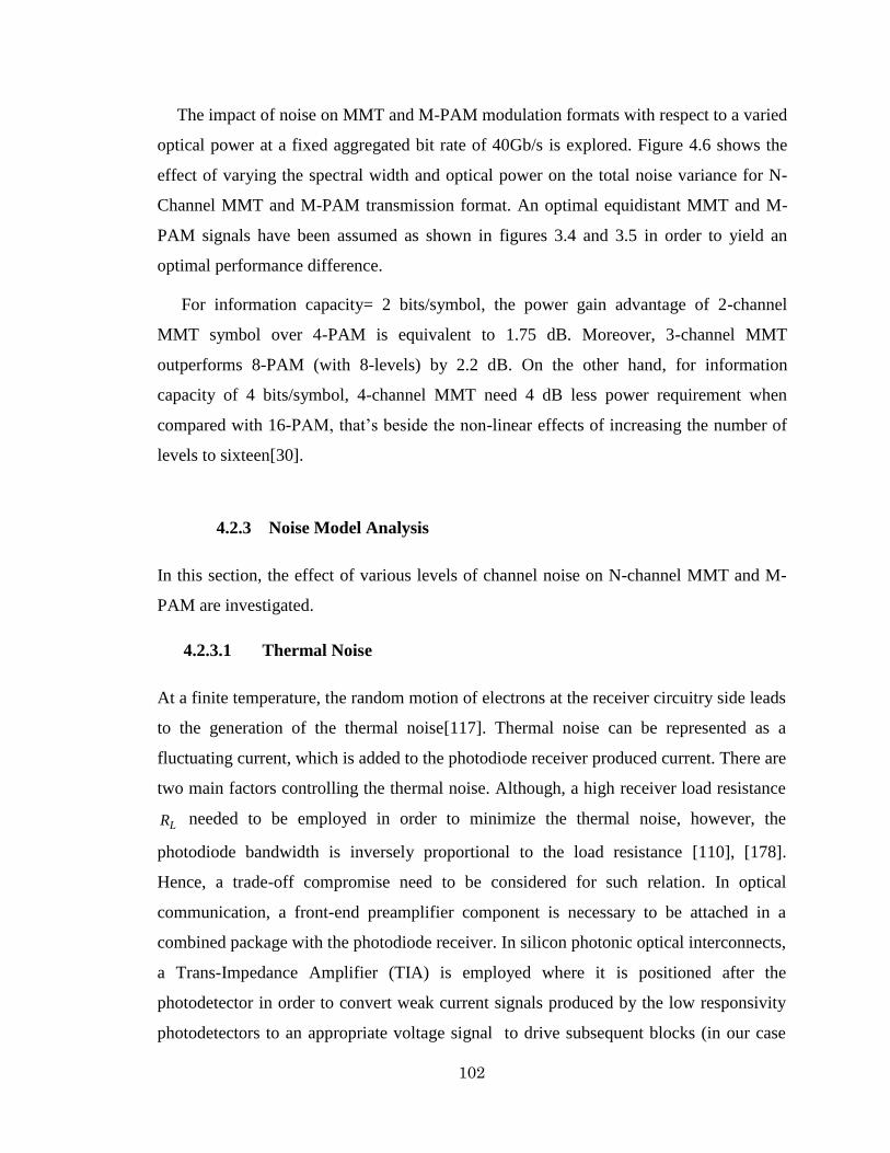
102
The impact of noise on MMT and M-PAM modulation formats with respect to a varied
optical power at a fixed aggregated bit rate of 40Gb/s is explored. Figure 4.6 shows the
effect of varying the spectral width and optical power on the total noise variance for N-
Channel MMT and M-PAM transmission format. An optimal equidistant MMT and M-
PAM signals have been assumed as shown in figures 3.4 and 3.5 in order to yield an
optimal performance difference.
For information capacity= 2 bits/symbol, the power gain advantage of 2-channel
MMT symbol over 4-PAM is equivalent to 1.75 dB. Moreover, 3-channel MMT
outperforms 8-PAM (with 8-levels) by 2.2 dB. On the other hand, for information
capacity of 4 bits/symbol, 4-channel MMT need 4 dB less power requirement when
compared with 16-PAM, that’s beside the non-linear effects of increasing the number of
levels to sixteen[30].
4.2.3 Noise Model Analysis
In this section, the effect of various levels of channel noise on N-channel MMT and M-
PAM are investigated.
4.2.3.1 Thermal Noise
At a finite temperature, the random motion of electrons at the receiver circuitry side leads
to the generation of the thermal noise[117]. Thermal noise can be represented as a
fluctuating current, which is added to the photodiode receiver produced current. There are
two main factors controlling the thermal noise. Although, a high receiver load resistance
LR needed to be employed in order to minimize the thermal noise, however, the
photodiode bandwidth is inversely proportional to the load resistance [110], [178].
Hence, a trade-off compromise need to be considered for such relation. In optical
communication, a front-end preamplifier component is necessary to be attached in a
combined package with the photodiode receiver. In silicon photonic optical interconnects,
a Trans-Impedance Amplifier (TIA) is employed where it is positioned after the
photodetector in order to convert weak current signals produced by the low responsivity
photodetectors to an appropriate voltage signal to drive subsequent blocks (in our case

103
the decision circuit)[186], [187]. Hence, the amplifier noise contribution is presented as
the Noise Figure (NF) which influences the SNR and consequently the thermal noise.
Thermal noise can be modeled as IId stationary Gaussian random process[110], [188].
Figure 4.7 shows the influence of various noise figure values on thermal noise
variance at different receiver bandwidth range. At fixed GHzf 10 and NF=3 dB, 4dB,
5dB and 6dB the thermal noise variance is equal to 25.6 Ap , 22.8 Ap , 24.10 Ap and
21.13 Ap , respectively. Front end amplifier design specification can limit the impact of
thermal noise at the input and output of the amplifier[117], [188], [189]. Moreover, it is
clear that the noise variance is proportional to the frequency range. At low cutoff
frequency range GHzf 10 , the impact of increasing the frequency on the thermal
noise is large. However, on receiver bandwidth GHzf 10 , the increase in thermal
noise is much less than at low frequency range. Nowadays commercial receiver VCSEL
components are available on market with cut of frequencies reaching 37GHz[50].
Figure 4.7 Thermal noise variance versus spectral width at different noise figure values.

104
4.2.3.2 Shot Noise
Shot noise is a natural process that occurs due to the random fluctuation distribution of
electrons generated during the quantum photo-detection process[55], [89].
since for direct detection PIN receivers, shot noise is not the prevailing noise
component, but the thermal noise. However, since shot noise scales linearly with the
signal power, thus, optical sensitivity enhancement can play a role to keep low levels of
shot noise [110].
It can be deduced from (4.18) that the amount of shot noise introduced to any
modulation format is dependent linearly on both the spectral component and the received
optical power to acquire a certain BER value. For the model discussed, the shot noise is
not the dominant source of noise.
4.2.3.3 Effects of Relative Intensity Noise (RIN)
Relative intensity noise can be one of the major elements that degrade the system
SNR[114], [190]. Although the RIN noise is associated with the transmitter source,
however, the intensity fluctuations of the laser are transformed to the receiver in the form
of electrical noise. Thus, thermal noise at the photodiode may not be the dominant noise
source. High levels of random intensity fluctuation in the output of a laser may cause a
higher RIN noise effect[55], [191], [192]. Relative intensity noise has a Gaussian
response distribution with a noise variance dependent upon the laser optical power.
Hence, increasing the emitted optical power to an extent may not lead to better BER
system performance since the noise power at the receiver is increased likewise. Fiber
optical communication designers take in to account the RIN element and be certain that
its effect is limited to a pre-defined extent. Most link budget analysis carried out by IEEE
standards industry groups, set a maximum penalty for the RIN noise factor[193].
Thus, investigation of BER floors at different optical power affected by various RIN
noise values is essential.
Figure 4.8(a-c) depicts the effect of a series number of RIN noise levels range from -
120 dB/Hz to -150 dB/Hz on 2-channel, 3-channel and 4-channel MMT BER at an

105
aggregate bit rate 40 Gb/s. The results show a non-linear relationship between the BER
and the optical power that is dependent upon the component RIN noise. At low RIN noise
level -150 dB/Hz, a low BER can be observed with the increase in the optical power.
However, at high RIN noise component = -120 dB/Hz accompanied by an increase in the
optical power, the curve results in an error floor where BER cannot exceed that level.
Furthermore, it is clear that the number of MMT channels increase is inversely
proportional to BER floor that can be attained. This is due to the number of levels
increment, which leads to more impact of intersymbol interference, which leads to more
BER floor.
(a) 2-Channel MMT

106
(b) 3-channel MMT
(c) 4-Channel MMT
Figure 4.8 The BER curves at various effects of RIN noise, (a) for 2-channel MMT, (b) for 3-
channel MMT, and (c) for 4-channel MMT.

107
Figure 4.9(a-c) depicts the effect of the RIN noise levels on 4-PAM, 8-PAM and 16-
PAM BER at the same aggregate bit rate 40 Gb/s. Comparing the results of N-channel
MMT and M-PAM, the dependency of the number of amplitude levels on the BER floor
is clear. For information capacity of 2 bits/symbol and -120dB/Hz , 2-channel MMT and
4-PAM show an approximately equivalent BER floor at 4105 , while at relatively
lower RIN noise level 2-channel MMT shows more robustness to noise compared to M-
PAM whereas at -127.5 dB/Hz, the BER floor for 2-channel MMT and 4-PAM are
17101 and 15105 , respectively.
At information capacity= 3 bits/symbol and127.5 dB/Hz, 8-PAM are more influenced
by RIN noise compared with 3-channel MMT, where the BER floors are 7105 and
5101 for 3-channel MMT and 8-PAM, respectively.
At information capacity= 4 bits/symbol and 127.5 dB/Hz, as shown in figure 4.8(c), 4-
channel MMT has a BER floor 5105 where the 16-PAM has a BER floor of 2101
. It is worth to note that even at relatively lower RIN noise components, N-Channel MMT
shows more tolerance to RIN noise and acquires better BER floor in contrast to M-PAM
transmission format at the same aggregate bit rate.

108
(a) 4-PAM
(b) 8-PAM

109
(c) 16-PAM
Figure 4.9 The BER curves at various effects of RIN noise, (a) for 4-PAM, (b) for 8-PAM and (c)
for 16-PAM.
4.2.3.4 RIN Power penalty
Most link budget design analysis that are performed during setting of IEEE standards
specify the maximum allowable penalty as a result of each noise component[41], [194]–
[196]. The power penalty can be assessed based upon computation of the required optical
power needed to attain a specific BER. For error free transmission BER of 12101 is
required. Hence, for clearer picture of the effects of RIN on M-PAM and N-channel
MMT, power penalty as a function of RIN noise is explored.
At BER12101 and assuming a maximum allowable power penalty of 0.5 dB due
to RIN, figure 4.10 (a-c) shows the N-channel MMT power penalty as a function of the
RIN at various spectral width.
At spectral widths of 10 GHz, 20GHz, 30GHz and 50GHz which correspond to
different bit rates, 2-channel MMT, shows a maximum acceptable RIN spectral density
to be HzdB /133 , HzdB /132 , HzdB /130 and HzdB /127 , respectively.

110
At spectral widths of 10 GHz, 20GHz, 30GHz and 50GHz, 3-channel MMT, shows a
maximum acceptable RIN spectral density to be HzdB /140 , HzdB /138 ,
HzdB /136 and HzdB /133 , respectively. While, at spectral width of 10 GHz,
20GHz, 30GHz and 50GHz, 3-channel MMT, shows a maximum acceptable RIN spectral
density to be HzdB /143 , HzdB /141 , HzdB /139 and HzdB /5.136 ,
respectively.
(a) 2-channel MMT
(b) 3-channel MMT

111
(c) 4-Channel MMT
Figure 4.10 N-channel MMT power penalty as a function of relative intensity noise at various
spectral width.
At spectral widths of 10 GHz, 20GHz, 30GHz and 50GHz which correspond to
different bit rates, 4-PAM, shows a maximum acceptable RIN spectral density to be
HzdB /137 , HzdB /134 , HzdB /136 and HzdB /130 , respectively. At
spectral widths of 10 GHz, 20GHz, 30GHz and 50GHz, 8-PAM, shows a maximum
acceptable RIN spectral density to be HzdB /145 , HzdB /5.142 , HzdB /140
and HzdB /5.137 , respectively.
While, at spectral widths of 10 GHz, 20 GHz, 30 GHz and 50 GHz, 16-PAM, shows a
maximum acceptable RIN spectral density to be HzdB /150 , HzdB /147 ,
HzdB /146 and HzdB /143 , respectively.
To conclude, the maximum RIN for N-channel MMT and M-PAM have been specified.
The calculation were based upon an allowable power penalty equivelant to 0.5 dB
(according to IEEE standard) for varied spectral widths.

112
(a) 4-PAM
(b) 8-PAM
(b) 16-PAM
Figure 4.11 Power penalty of M-PAM as a function of relative intensity noise at various spectral.

113
4.3 Asymptotic Power Efficiency Analysis and Results
At asymptotically high SNR, the performance difference in dB between the different
modulation formats approaches constant values .One classical approach to assess novel
transmission formats, is to evaluate and compare between schemes with respect to OOK
as a benchmark for power efficiency[53], [58], [60] .
4.3.1 Power Penalty at Fixed Baud Rate
For Intensity Modulated (IM) non-coherent transmission formats, the basic element
for power penalty is directly related to the number of amplitude levels. Assuming
stationary noise only with AWGN spectral density, at fixed baud rate, the M-PAM power
penalty is equivalent to [165]
)1(10, MLogP PAMp [dB] (4.19)
A theoretical power penalty expression with respect to OOK has been derived for N-
channel MMT modulation. At fixed baud rate, the N-Channel MMT optical power
penalty with respect to OOK can be represented by
2
)1()1(10
10
21
,
,,
MMLog
P
PLogP
OOK
MMT
oavg
oavgMMTp
[dB] (4.20)
WhereOOKoavgP , ,
MMToavgP , are the average optical powers for OOK and MMT signaling,
respectively. The MMT has been derived based upon signal constellation by substitution
from (4.12) in (4.9).
Figure 4.12 shows the power penalty of M-PAM modulation format with respect to
the number of levels at fixed baud rate. Relative to On Off Shift Keying (OOK), 4-PAM,
8-PAM, 16-PAM and 32-PAM depicts an inherent power penalties due to their number of
levels augmentation, equivalent to dB77.4 , dB45.8 , dB76.11 and dB91.14 ,
respectively.

114
Figure 4.13 shows the power penalty of N-Channel MMT with respect to the
maximum number of levels over its two slots at fixed baud rate. Relative to OOK, 2-
Channel 3-Channel, 4-Channel, 5-Channel and 6-Channel MMT has power penalties
equivalent to dB5.1 , dB51.4 , dB27.6 , dB5.8 and dB91.14 , respectively.
Figure 4.12 M-PAM power penalty with respect to number of amplitude levels at fixed baud rate.
Figure 4.13 N-channel MMT power penalty with respect to the maximum number of amplitude
levels of its two slots at fixed baud rate.

115
4.3.2 Power Penalty at Fixed Bit Rate
Assuming stationary noise only with AWGN spectral density, at fixed bit rate, the M-
PAM power penalty is equivalent to
M
MLogP PAMpb
2,
log
)1(10 [dB] (4.21)
On the other side, at fixed bitrate an expression to calculate the theoretical inherent
power penalty for N-channel MMT modulation format has been derived. At fixed bitrate,
the N-Channel MMT optical power penalty with respect to OOK can be represented by
2
)1()1(
).(log
2log10 21
212,
MM
MMP MMTpb [dB] (4.22)
by taking into consideration the relative proportionality of the noise power to the noise
voltage.
Figure 4.14 shows the power penalty of M-PAM modulation format with respect to
the number of levels at fixed bitrate. Relative to on-off-shift-keying format, 4-PAM, 8-
PAM, 16-PAM and 32-PAM have an inherent power penalties due to its number of levels
augmentation which are equivalent to dB26.3 , dB06.6 , dB75.8 and dB42.11 ,
respectively.
Figure 4.15 shows the power penalty of N-Channel MMT with respect to the
maximum number of levels over its two slots at fixed bitrate. Relative to OOK, 2-
Channel MMT, 3-Channel MMT, 4-Channel MMT, 5-Channel MMT and 6-Channel
MMT exhibit power penalties equivalent to dB5.1 , dB6.3 , dB77.4 , dB47.4 and
dB7.5 , respectively.

116
Figure 4.14 M-PAM power penalty with respect to number of amplitude levels at fixed bit rate.
Figure 4.15 N-channel MMT power penalty with respect to the maximum number of amplitude
levels of its two slots at fixed bit rate.

117
4.3.3 Power penalty with respect to OOK at Fixed information capacity
Since N-channel MMT is designed for a practical interest to expand the capacity of
optical communication networks, thus, investigating the performance of N-Channel and
M-PAM with respect to information capacity is essential. To calculate the differences in
power efficiency with respect to the information capacity, the asymptotic power penalty
relative to OOK, is provided.
At fixed bandwidth, figure 4.16 shows the asymptotic power penalty of N-Channel
MMT and M-PAM modulation format relative to OOK to achieve an equivalent BER
performance at asymptotically high SNR. For information capacity of 2 bits/symbol, 2-
channel MMT has a power gain of 3.27 dB over 4-PAM compared to OOK at a fixed
baud rate. For information capacity=3 bits/symbol, 8-PAM need 3.94 dB more required
optical power compared to 3-channel MMT, both with respect to OOK. For information
capacity=4 bits/symbol, 16-PAM has an optical power penalty of 5.5 dB worse than 4-
channel MMT at the same BER performance.
Figure 4.16 The average optical power penalty for M-PAM and N-channel MMT with respect to
the information capacity relative to OOK at a fixed bandwidth.

118
In order to have a meaningful assessment, in figure 4.17 the N-Channel MMT is
compared with M-PAM at a constant bit rate constraint with respect to the information
capacity. At fixed bit rate, Fig. 5(b) depicts the asymptotic power penalty of N-Channel
MMT and M-PAM modulation format proportional to OOK as in eq. (33) to achieve a
proportional BER performance at asymptotically high SNR. For information capacity= 2
bits/symbol, 2-channel MMT has an incremental gain of 1.76 dB over 4-PAM relative to
OOK at fixed aggregated data rate. For information capacity= 3 bits/symbol, 3-channel
MMT require 2.2 dB reduced optical power against 8-PAM at a BER figure610 . For
information capacity= 4 bits/symbol, 4-channel MMT has an optical power gain of 4 dB
more than 16-PAM, relative to OOK.
Figure 4.17 The average optical power penalty for M-PAM and N-channel MMT with respect to
the information capacity relative to OOK at a fixed bitrate.

119
4.4 Concluding Remarks
It is worth noting that the asymptotic optical power efficiency of the calculated data
formats has an agreement and verify our theoretical results obtained in fig.4.2 – fig. 4.5 at
BER 1210 since the results are compared in both cases relative to OOK. Also, the M-
PAM penalties matches the verified experimentally results discussed in [59].
Electrical bandwidth is one of the important trade-off metrics for modulation formats.
The spectral width of N-channel MMT modulation format relative to OOK can be
expressed as
OOK
OOKMMT
SWMM
NchannelsMMTofnumber
SWSslotsofnumberSW
).(log
2
)(
)(
212
[Hz] (4.23)
where OOKSW is the spectral width of OOK for IM/DD system.
Table 4.1 summarizes the performance of MMT and PAM formats in terms of
spectral efficiency, number of levels and receiver sensitivity for transmission of 2, 3 and
4 bits/symbol. Although the transmission of 4 bits/symbol using 16-PAM system has a
spectral efficiency advantage over 4-channel MMT system, but it suffers from a
significant power penalty due to the division of its eye diagram to 15 narrow eyes which
has not proven practical for implementation [4]. As illustrated in Table 4.1, 4-channel
MMT with the spectral efficiency of Hzsb //2 can be considered as an effective and
desirable practical compromise between power efficiency advantage and an appropriate
spectral efficiency for 4 bits/symbol transmission systems.

120
These results published in [197] verify our proposed signal design advantage on the
power efficiency of N-channel MMT system compared to M-PAM, which justify our
consideration for N-Channel MMT transmission format as a potential practical candidate
for deployment in high capacity power limited systems.
Table 4.1 Overall comparison between N-channel MMT and M-PAM at 40Gb/s.
Setup
at 40 Gb/s
Information
Capacity
in bits/symbol
Spectral
Efficiency
(b/s/Hz)
Spectral Width
(Hz)
at a given Bit
Rate “R”
Number of
levels
Receiver
Sensitivity
BER=10-9
(dBm)
2-channel
MMT 2 1 R 2 –11.6
3-channel
MMT 3 1.5 2 R / 3 3 –9.3
4-channel
MMT 4 2 R / 2 4 –8.3
4-PAM
Format 2 2 R / 2 4 –9.85
8-PAM
Format 3 3 R / 3 8 –7.1
16-PAM
Format 4 4 R / 4 16 –4.3

121
5. Chapter 5: Numerical Performance
Analysis
5.1 Introduction
Nowadays, the variety of services and internet application in data centers, enterprises,
organizations and campuses have led to more capacity demand in metropolitan area
networks[12]. N-channel MMT is designed not only for optical interconnects, but also a
potential applicable and feasible solution for medium range high-speed optical links.
Beside the conventional analytical performance evaluation parameters of modulation
formats that is dependent upon signal characteristics such as Euclidean distance in signal
space, signal shape, power efficiency, spectral efficiency…etc. It is the substantial to
investigate N-channel MMT system reach in an optically amplified transport
configuration for Metropolitan Area Networks (MAN).
Optical links are classified based upon the reach and capacity[110]. Access networks
exhibit a maximum reach of 50 Km and dominated by Ethernet and optical transport
networks technology (OTN). Metro networks are designed for metropolitan areas with a
typical ring topology and a reach of less than 300 km with an Erbium Doped Fiber
Amplifier (EDFA) amplifier placed every 80Km. Regional networks are responsible for
inter-city links with a maximum reach of 600 Km. In the end, long-haul links, which is
considered the core of the internet network with transmission reach that extend between
600 km to 10,000 km.

122
5.2 N-Channel MMT for Metro Networks
In this section, an expansion for the performance investigation analysis for MMT in the
presence of pre-amplifier receiver has been adopted. In metropolitan area networks,
EDFA amplifiers are employed in a booster and pre-amplifier configurations. The
dominant noise source in these optically amplified links is due to the Amplified
Spontaneous Emission Noise (ASE) [110].
In this section, an investigation for the back-to-back receiver sensitivity of 2-ch, 3-ch
and 4-ch MMT at an aggregated bit rate of 40Gb/s and 100Gb/s utilizing single
wavelength carrier is manifested. The sensitivity is based upon measuring the minimum
required received optical power to the receiver in order to acquire a certain BER
performance. For metro networks, a BER value =910 is considered a good BER
platform for reliable data transmission system.
The forthcoming evaluation for the receiver sensitivity includes two types of Mach-
Zehnder Modulators (MZM); the first is based upon the MZM analytical model and the
second is single drive Multiple-Quantum-Well Mach-Zehnder Modulator (MQW-MZM),
which is based upon pre-defined measurement model defined in Appendix A. The
receiver employed in these analyses, is the MMT threshold detection receiver discussed
in section 3.3.3. The BER for MMT is estimated according to the BER and Q-factor
models demonstrated in section 3.4.2.
5.2.1 2-Channel MMT with 2 bits/symbol
Performance evaluation for the receiver sensitivity of 2-channel MMT with 2 bits/symbol
at 40 and 100Gb/s system aggregate bit rate in the presence of dominant ASE noise
source, is presented.

123
5.2.1.1 System setup Utilizing MZM Analytical Model
Figure 5.1 2-Channel MMT system setup at aggregated bit rate 40Gb/s, (a) Eye diagram
at BER=910 ,(b) RF Spectrum and (c) Optical Spectrum.
Figure 5.1 shows the system setup of 2-channel MMT employing an MZM analytical
model at aggregated system bit rate of 40 Gb/s with baud rate 20 G baud/sec. In the
electrical domain, the MMT transmitter multiplexes the data from 2 data channels (or
users) using MMT mapping algorithm (as discussed in section 3.3). The two channels of
data are modeled using a Pseudo Random Bit Sequence (PRBS) generator of the order
1210 following [198]. A PRBS generator (AGILENT-Keysight-N4974A) is
commercially available with data rate 40Gb/s and maximum pattern sequence reaching
1231 [199].
Afterwards, the electrical MMT signal is converted to an optical MMT signal by the aid
of Mach-Zhender Modulator (MZM). The MZM is composed of two 3 dB couplers
connected by dual waveguides with an equivalent length, which acts as an intensity

124
modulator based upon the inferometric principle. The MZM analytical behavior can be
expressed by an optical signal outE as [161], [200]
)(.))(cos().( tjinout ettEE (5.1)
where )(tEin is the electrical field input to the modulator, )(t is the phase difference
between the two arms of the MZM and can be defined as
))2
1)(.(
2
1(
2)( tXERt
(5.2)
where ER is the extinction ratio and )(tX is the input electrical modulated signal. A
Variable optical attenuator (VOA) exists to vary the optical power in order to measure the
receiver sensitivity at an acceptable BER value. The eye diagram of 2-channel MMT
system with 2×20 Gbit/s is shown in figure 5.1(a). In figure 4.19 (b), RF spectrum
analyzer is employed enabling a calculation for the Power Spectral Density (PSD) of
MMT signal relative to the frequency in the electrical domain. The RF bandwidth of 2-
channel MMT is shown equivalent to GHzfRF 40 with a spectral efficiency of 1
b/s/Hz and an optical spectrum resolution filtered bandwidth of 1 GHz[112].
Furthermore, figure 5.1 (c) depicts the optical spectrum of 2-channel MMT employing
optical spectrum analyzer, which enables a calculation for the Power Spectral Density
(PSD) of MMT signal relative to the frequency in the optical domain. The optical spectral
width is equivalent to GHzfo 80 (twice the RF spectral bandwidth) acquiring a
spectral efficiency of 0.5 b/s/Hz at an optical spectrum resolution filtered bandwidth of
0.01nm. An optical spectrum analyzer (OSA) (AGILENT-71452B) is commercially
available with resolution bandwidth accuracy 0.5 nm [201].

125
5.2.1.2 2-channel MMT Receiver Sensitivity utilizing MZM Analytical Model
Figure 5.2 depicts and compares the receiver sensitivities of 2-channel MMT system at
40Gbs/ and 100Gb/s. The system settings has been optimized to maintain the minimum
sensitivity at BER =910 . For 2-channel MMT at 40Gb/s, the optical sensitivity is
equivalent to = dBm7.30 , while at 100 Gb/s, the sensitivity corresponds to dBm7.26 .
The power penalty for increasing the throughput from GG 10040 is 4 dB for an
equivalent BER performance.
Figure 5.2 2-channel MMT receiver sensitivity versus BER employing analytical MZM model at
bit rates 40Gb/s and 100Gb/s.
4 dB

126
5.2.1.3 System setup using Single Drive Multiple-Quantum-Well Mach-Zehnder
(MQW-MZM)
Figure 5.3 2-Channel MMT system setup employing single drive MQW-MZM modulator at
aggregated bitrate 100Gb/s, (a)Eye diagram at BER=910 ,(b)RF Spectrum, and (c)Optical
Spectrum.
Figure 5.3 depicts 2-channel MMT system setup utilizing MQW-MZM at aggregated
system bit rate of 100 Gb/s with baud rate 50 Gbaud/sec. The booster EDFA amplifier
has a gain= 10dB with 5 dB noise figure, while the pre-amplifier has a gain of 20 dB with
a 5 dB noise figure. An EDFA (Optilab-EDFA) optical component is commercially
available with maximum gain=25dB and noise figure=4.5dB[202]. The photodiode
responsivity is equal to 0.8 A/W. A commercially available pin photodiode
(THORLABS-D400FC InGaAs PIN) with responsivity reaching 0.95A/W[203]. A
second order low pass Gaussian filter has been adopted with a cutoff frequency
baudratef 05.1 , which corresponds to GHz5.52 .

127
5.2.1.4 Pre-Amplifier Gain Optimization
Figure 5.4 2-channel MMT system pre-amplifier gain optimization.
A pre-amplifier is a crucial component that is placed at the optical link receiving end to
enhance the receiver sensitivity. Since, 2-channel MMT system evaluation is dependent
upon the calculated eye diagram, which is split into two slots eye diagram. Hence, it is
desirable to optimize the pre-amplifier gain in order to obtain the maximum allowable Q-
factor for both slots.
Figure 5.4 shows the Q-factor of eye 1 (slot 1) and eye 2 (slot2) relative to the
launched pre-amplifier gain. With a pre-amplifier gain G=20 dB, the 2-channel MMT
acquire an acceptable Q-factor values 5.9 and 6.1 for eye 1 and eye 2, respectively. These
Q-factors are equivalent to an acceptable metro link BER 910 . Figure 5.4 depicts the
eye diagram observing non major degradation between the two slots Q-factors, except for
penalty equivalent to 0.1 dB on eye 2 relative to eye 1. We conjecture that this penalty is
due to to the inter-symbol interference between the two slots.

128
5.2.1.5 2-channel MMT Receiver Sensitivity comparison
Figure 5.5 2-channel MMT receiver sensitivity versus BER employing analytical MZM model
and MQW-MZM at 40Gb/s and 100Gb/s.
Figure 5.5 depicts a comparison between the employment of single drive MQW-MZM
and analytical MZM model on 2-channel MMT system with respect to the receiver
sensitivity at bit rates 40Gbs/ and 100Gb/s. For single drive MQW-MZM model at BER =
910 , the receiver sensitivity is equivalent to = dBm1.30 for 40Gb/s system, while it is
equivalent to dBm1.26 for 100Gb/s. The corresponding eye diagrams with each slot
Q-factor are shown in figure 5.6. The results agree well with the 2-channel MMT
utilizing MZM analytical model discussed in figure 5.2 with a 4dB penalty of increasing
the bit rate from 40G to 100G. Furthermore, a power penalty of 0.6 dB is observed with
the utilization of single drive MQW-MZM compared with the MZM analytical model.
4 dB

129
Figure 5.6 2-channel MMT Eye diagram at BER =910 :- (a) At 40Gb/s using single drive MQW-
MZM model, and (b) At 100Gb/s using single drive MQW-MZM model.
5.2.2 3-channel MMT with 3 bits/symbol
In this section, performance assessment on realizing the transmission of 3bits/symbol
employing 3-channel MMT at 40Gb/s and 100Gb/s system aggregate bit rates, in the
presence of pre-amplified receiver model.
5.2.2.1 System setup using Analytical MZM
In the same manner as 2-channel MMT , figure 5.7 shows the system setup of 3-
channel MMT utilizing MZM analytical model at an aggregated bit rate 40Gb/s
equivalent to 13.3 G baud/sec. In the electrical domain, the MMT transmitter multiplexes
the data from 3 data channels using MMT mapping algorithm. The three channels of data
are presented by an input pseudo random bit sequence (PRBS) of 1210 . The booster
amplifier has a gain G=10dB with noise figure NF=5dB, whereas the pre-amplifier has a
gain G=20dB with noise figure NF=5dB. Eye diagram for the 3-channel MMT electrical
signal at the sampling and decision device is shown in figure 5.7(a). The received optical
signal corrupted mainly by ASE noise is filtered by a 2nd order low pass Gaussian filter.
The electrical low pass filter cutoff frequencies are optimized to acquire
baudratef 05.1 which corresponds to GHz14 .

130
Figure 5.7 3-Channel MMT system setup at aggregated bit rate 40Gb/s, (a) Eye diagram at BER=
910 ,(b) RF Spectrum and (c) Optical Spectrum.
As shown in figure 5.7(b), by the inspection of the RF optical spectrum
GHzfRF 7.26 with a spectral efficiency of 1.5 b/s/Hz. Moreover, the optical spectral
width exhibit GHzfo 4.53 as figure 5.7 (c) depicts. This spectral width is equivalent to
a spectral efficiency of 0.75 b/s/Hz. By the inspection of the optical spectrum, 3-channel
MMT spectrum is shaped as continuous samples in the frequency domain, and a high
power discrete tone at the carrier center frequency corresponding to a 1550 nm
wavelength. Other weaker residual tones exist at multiples of the bit rate. 3-channel
MMT frequency spectrum exhibits a strong spectral content at line rate. This feature is
beneficial in simplifying the clock recovery.

131
5.2.2.2 Receiver sensitivity Utilizing Analytical MZM and single drive
MQW-MZM
In the same manner as section 5.2.1, figure 5.8 depicts a receiver sensitivity
comparison between single drive MQW-MZM and the analytical MZM model for 3-
channel MMT system at 40Gbs/ and 100Gb/s. Table 5.1 shows the optimized modulator
device parameters for both setup configurations. For single drive MQW-MZM, the
receiver sensitivity at BER =910 is equivalent to = dBm26 with OSNR=24.9 at
40Gb/s system. While, for 100Gb/s, it is equivalent to dBm1.22 with OSNR=27.6dB at
100Gb/s. On the other hand, using analytical MZM model, the receiver sensitivity at BER
=910 is equivalent to = dBm9.23 with OSNR=28.1 at 40Gb/s system. While, for
100Gb/s, it is equivalent to dBm20 with OSNR=31.5dB. The power penalty due to the
increase in the aggregated bit rate from 40G to 100G is equivalent to 3.9 dB.
Furthermore, it can be deduced that there is a penalty of 2.1 dB due to the use of single
drive MQW-MZM compared with the analytical MZM model.

132
Figure 5.8 3-channel MMT receiver sensitivity versus BER employing analytical MZM
model and single drive MQW-MZM at 40Gb/s and 100Gb/s.
Table 5. 1 3-channel MMT system setup optical modulators specifications
MZM
Parameters
Analytical MZM
Model
At 40Gb/s
Single drive
MQW-MZM
Model At 40Gb/s
Analytical MZM
Model
At 100Gb/s
Single drive
MQW-MZM
Model At
100Gb/s
Bias
Voltages
Not
Applicable
Vb1= -1.8V
Vb2= -1.1V
Not
Applicable
Vb1= -1.8V
Vb2= -1.1V
Extinction Ratio =18 dB Not
Applicable 16 dB
Not
Applicable
Modulation
Voltage
Not
Applicable 1.5 V
Not
Applicable 1.5 V
3.9 dB 3.9 dB
2.1 dB

133
Figure 5.9 shows the eye diagram for the receiver sensitivity results presented earlier
at BER= 910 . The calculated eye diagram for 3-channel MMT is composed of multiple
levels with a fragmentation of main eyes to four smaller eyes with four different Q-
factors. Hence, an equal spacing between levels is essential. For analytical MZM with
sensitivity -23.9 dBm at 40Gb/s, The Q-factor (Q_eye1_s1, Q_eye1_s2, Q_eye2_s2,
Q_eye3_s2) is equivalent to 10.35, 11.8, 7 and 5.7, respectively. However, as shown in
figure 5.9, for single drive MQW-MZM at 40Gb/s, the Q-factor (Q_eye1_s1, Q_eye1_s2,
Q_eye2_s2, Q_eye3_s2) is equivalent to 7.5, 8.1, 5.7 and 9, respectively. It is clear that
due to the optical optimization of the bias voltages in single drive MQW-MZM, the
levels are more distributed equally, as a result the noise is more evenly distributed on
each level. In a similar manner, 100Gb/s system exhibited better performance.
Figure 5.9 3-channel MMT Eye diagram at BER =910
(a) at 40Gb/s using analytical MZM
model, (b) at 100Gb/s using analytical MZM model, (c) At 40Gb/s using single drive MQW-
MZM, and (d) At 100Gb/s using single drive MQW-MZM model

134
5.2.3 4-channel MMT with 4 bits/symbol
In this section, performance assessment on realizing the transmission of 3bits/symbol
employing 4-channel MMT at 40Gb/s and 100Gb/s system aggregate bit rate, in the
presence of pre-amplified receiver.
5.2.3.1 System setup using Analytical MZM
In the same manner as section 5.2.2.3, figure 5.10 shows the system setup of 4-channel
MMT using MZM analytical model at an aggregated bit rate 40Gb/s equivalent to 10G
baud/sec. In the electrical domain, the MMT transmitter multiplexes the data from 4 data
channels using MMT mapping algorithm. The four channels of data are modelled by an
input pseudo random bit sequence (PRBS) of 1210 . The booster amplifier has a gain
G=10dB with noise figure NF=5dB, whereas the pre-amplifier has a gain G=20dB with
noise figure NF=5dB. Eye diagram for the 4-channel MMT electrical signal at the
sampling and decision device are given in figure 5.10(a). The received optical signal
corrupted mainly by ASE noise is filtered by a 2nd order low pass Gaussian filter.
Figure 5.10 4-Channel MMT system setup at aggregated bit rate 40Gb/s, (a) Eye diagram at
BER=910 ,(b) RF Spectrum, and (c) Optical Spectrum

135
The electrical low pass filter cut-off frequencies are optimized to be
baudratef 2.1 which corresponds to GHz12 . As shown in figure 5.10(b), by the
inspection of the RF optical spectrum GHzfRF 20 with a spectral efficiency of 2 b/s/Hz.
Moreover, the optical spectral width exhibit spectral bandwidth equivalent to
GHzfo 40 acquiring a spectral efficiency of 1 b/s/Hz as shown in figure 5.10(c) with a
resolution filtered bandwidth 0.01nm.
5.2.3.2 Receiver sensitivity using Analytical MZM and single drive MQW-MZM
In the same manner as section 5.4.2.2, figure 5.11 depicts a comparison between the
employment of single drive MQW-MZM and the analytical MZM model on 4-channel
MMT system with respect to the receiver sensitivity at 40Gbs/ and 100Gb/s. Table 5.2
shows the modulator device parameters for both setup configurations, using analytical
MZM model and single drive MQW-MZM. For single drive MQW-MZM, the receiver
sensitivity at BER =910 is equivalent to = dBm8.22 for 40Gb/s system, while it is
equivalent to dBm8.18 at 100Gb/s. On the other hand, using analytical MZM model,
the receiver sensitivity at BER =910 is equivalent to dBm6.23 with OSNR=28.1 for
40Gb/s system, whereas it is equivalent to dBm6.19 at 100Gb/s. The power penalty due
to increasing the aggregated bit rate from 40G to 100G is equivalent to 4 dB.

136
Figure 5.11 4-channel MMT receiver sensitivity versus BER employing analytical MZM model
and single drive MQW-MZM at 40Gb/s and 100Gb/s.
Table 5. 2 4-channel MMT system setup optical modulators specifications.
MZM parameters Analytical MZM
Model
At 40Gb/s
Single drive
MQW-MZM
Model
At 40Gb/s
Analytical MZM
Model
At 100Gb/s
Single drive
MQW-MZM
Model
At 100Gb/s
Bias
Voltages
Not
Applicable
Vb1= -2.8V
Vb2= -1.8V
Not
Applicable
Vb1= -2.8V
Vb2= -1.8V
Extinction Ratio 29 dB Not
Applicable 29 dB
Not
Applicable
Modulation
Voltage
Not
Applicable 1.5 V
Not
Applicable 1.5 V
0.8 4 dB

137
Furthermore, it can be deduced that there is a penalty of dB8.0 due to the use of
single drive MQW-MZM compared with the analytical MZM model. Figure 5.12 depicts
the calculated eye diagram for 4-channel MMT in which it is composed of multiple levels
with a fragmentation of main eyes to four smaller eyes with eight different Q-factors. For
analytical MZM with sensitivity -23.6 dBm at 40Gb/s, The Q-factor (Q_eye1_s1,
Q_eye2_s1, Q_eye3_s1, Q_eye1_s2, Q_eye2_s2, Q_eye3_s2) is equivalent to 10.8, 6,
5.9, 11.1, 6.4 and 5.8, respectively. However, as shown in figure 5.12, for single drive
MQW-MZM at 40Gb/s, the Q-factor (Q_eye1_s1, Q_eye2_s1, Q_eye3_s1, Q_eye1_s2,
Q_eye2_s2, Q_eye3_s2) is equivalent to 10.9, 5.6, 7.6, 10.5, 5.9 and 7.9, respectively.
Figure 5.12 4-channel MMT Eye diagram at BER =910 , (a) at 40Gb/s using analytical MZM
model, (b) at 100Gb/s using analytical MZM model, (c) At 40Gb/s using single drive MQW-
MZM model, and (d) ) At 100Gb/s using single drive MQW-MZM model

138
5.2.4 Receiver Sensitivity Comparison between MMT and M-PAM
In the presence of EDFA amplifiers, the information capacity effect in terms of number
of bits/symbol (2, 3, and 4) on receiver sensitivity of MMT and PAM systems at an
aggregate bit rate of 40 Gb/s are shown in figure 5.13. In comparison with M-PAM
system, the transmission of 2, 3 and 4 bits/symbol using MMT system can improve the
receiver sensitivity by 7.4 dB, 11.3 dB, and 17.5 dB, respectively. This power penalty in
M-PAM is due to the higher number of levels in comparison to the MMT system, with
the fragmentation consequences of main eyes to the smaller eyes as shown in the eye
diagram in figure 5.13. It is worth noting that the difference in power penalty with respect
to the theoretical results is due to the employment of an EDFA booster and preamplifier
where the signal dependence on spontaneous beat noise dominates, which leads to an
additional power penalty to reach 8 dB. Furthermore, the penalty increase is reasoned to
the non-equal spacing that lead to increase the penalty, especially in higher order PAM
formats utilizing 8 and 16 levels [108], [204], [205].
Figure 5.13 Receiver sensitivities comparison between 2, 3, and 4 bits/symbol transmission, using
M-PAM and MMT systems at an aggregated bitrate of 40 Gb/s .

139
5.3 N-channel MMT evaluation in the presence of Fiber linear and
non-linear impairments
Optical amplifiers existence introduces a certain level of ASE noise, which is
dependent upon the gain[110], [206], [207]. The need for amplifier gain depends on the
transmission distance in which long fiber transmission links necessitate an increase in the
amplifier gain, which is translated to an more impact from the ASE noise. Also, due to
the attenuation characteristics in the fiber, the longer the fiber reach presuppose more
input power requirement. However, we cannot neglect the fact that increasing the input
power will stimulate the non-linear effects, thus leading to distortion of the propagating
signal. Furthermore, other practical deployment considerations that include the
optimization of components settings and the interplay between the signal characteristics
and fiber impairments must be taken into account.
Hence, a study and quantification for the impact of fiber non-linear impairments in
which the interaction between Group Velocity Dispersion (GVD), Self-Phase Modulation
(SPM) and intra-channel non-linearities, is crucial. Accordingly, there is a necessity in
choosing an adequate dispersion compensation scheme to compensate for the
accumulated residual dispersion in fiber transmission spans. Furthermore, the N-channel
MMT maximum system reach will be discussed for metro networks.
As such, in this section the exploration of N-channel MMT transmission format
behavior against fiber linear and non-linear impairments are essential to satisfy the thesis
objective (in section 1.3, objective number 4 ).

140
5.3.1 Chromatic Dispersion Tolerance
The main system linear limitation for high rate optical systems on SMF is mainly due
to chromatic dispersion. Chromatic dispersion can be the dominant reason for signal ISI
and it occurs due to the dependence relation between the operating wavelength and the
optical fiber index of refraction[208]–[210]. This leads to a pulse broadening in the time
domain envelope because of the change in the propagation speed of different spectral
component of the pulse. This broadening results in the signal distortions at the end of the
fiber with length L. The relation between the maximum dispersion length DL and the
spectral width f is given by[110]
fRD
cLD
2 (5.3)
where ‘ c ’ is the speed of light in vacuum, ‘ R ’ is the bit rate, ‘ D ’ is the dispersion
parameter, and ‘ ’ is the signal wavelength. It is clear that the pulse spectral width is
inversely proportional to both the dispersion parameter and the transmission length which
correspond to the pulse width. Hence, the signal with narrower spectral width exhibit
better chromatic dispersion tolerance than other higher spectral width schemes. Also, it
can be deduced the inverse proportionality relation between the link length and the bit
rate .For systems with higher order modulation formats, the bit rate in eq. (5.3) turn to be
the system baud rate. Accordingly, the less the baud rate will procure longer signal
propagation reach.

141
5.3.1.1Comparison between N-channel MMT and M-PAM
As discussed in section 5.3.1, beside dispersion dependent variables that control the
amount of dispersion tolerance; also, optimization of component characteristics and
system configuration settings has an influence. Accordingly, dispersion tolerance may
vary due to the interaction of different components with each other.
The chromatic dispersion tolerance of 2-, 3-, and 4-channel MMT have been
investigated in a back-to-back configuration allowing an abstract quantification for MMT
system tolerance to chromatic dispersion. An analytical Mach-zehnder modulator model
has been employed in order to investigate the maximum optimized chromatic dispersion
tolerance for the schemes under study.
Figure 5.14 depicts the chromatic dispersion tolerance of 2-channel MMT, 3-channel
MMT and 4-channel MMT at 40 Gb/s and 100 Gb/s. At BER= 910 , 2-channel, 3-
channel and 4-channel MMT exhibit a dispersion tolerance of nmps /158 ,
nmps /246 and nmps /460 at 40 Gb/s, respectively. While, at 100Gb/s, 2-channel,
3-channel and 4-channel MMT shows a dispersion tolerance of nmps /28 , nmps /40
and nmps /76 , respectively.

142
(a) 2-channel MMT
(b) 3-channel MMT
±158
±40
±246
±28

143
(c) 4-channel MMT
Figure 5.14. Dispersion tolerances in a back to back configuration for (a) 2-channel MMT, (b)3-
channel MMT and (c)4-channel MMT.
Figure 5.15 shows a comparison for the optical spectral width between 2-ch, 3-ch and
4-ch MMT systems at the same aggregate bit rate of 40 Gb/s. The optical spectral width
is equivalent to 80 GHz, 53.4 GHz and 40 GHz for 2-ch MMT, 3-ch-MMT and 4-ch
MMT, respectively. As (5.3) the narrower the optical spectrum, the more tolerance is the
modulation format to chromatic dispersion. Hence, it can be expected that 4-MMT
exhibit a superior chromatic dispersion tolerance when compared with 2-channel MMT
and 3-channel MMT. Moreover, for 100Gb/s, N-channel MMT observe less tolerance
since the signal pulse width is much less than its counterpart which lead to more ISI
effect. Furthermore, higher information capacity MMT channels leads to a reduction in
the symbol rate, which reflects more tolerance to chromatic dispersion.
±460
±76

144
Figure 5.15 Optical spectrum of N-channel MMT formats at 40Gb/s.
Figure 5.16 depicts the chromatic dispersion tolerance of 4-PAM, 8-PAM and 16-
PAM at 40Gb/s and 100Gb/s. System settings have been optimized to acquire the
maximum performance which is equivalent to a minimum BER. At an acceptable BER=
910 , 4-PAM exhibits a dispersion tolerance of nmps /224 and nmps /36 , for
40Gb/s and 100Gb/s, respectively. While, at 40Gb/s, 8-PAM shows a dispersion
tolerance equivalent to nmps /40 . However, 8-PAM observes a BER floor of 6106 x
at 0 ps/nm dispersion for 100Gb/s system aggregated bit rate. In addition, 16-PAM also
shows a BER floor of 3106 x and 2105 x at 0 ps/nm dispersion for 40Gb/s and
100Gb/s, respectively. The chromatic dispersion tolerance degradation for 8-PAM and
16-PAM is due to the exhibition of multiple amplitude of levels, which imposes an
inherent penalty as discussed in section 4.3. Thus, leads to a difficulty in acquiring an
equidistant spacing between levels as shown in the eye diagrams shown in figure 5.16(b)
and figure 5.16(c) at a dispersion tolerance of ±5 ps/nm.
The 4-PAM results can be validated by comparing it to the analytical investigation
utilizing optimal electrical and optical receiver bandwidth settings combined with equal
level spacing utilizing more complex signal PDF approximation models as Karhunen-

145
Leove expansion and saddle point approximation, in which 4-PAM have acquired
400ps/nm[204]. The superior tolerance for 4-PAM is due to the optimality assumptions
for electrical and optical receiver settings combined with the equal spacing between M-
PAM levels.
(a) 4-PAM
±224
±36

146
(b) 8-PAM
(c) 16-PAM
Figure 5.16 Dispersion tolerances in a back to back configuration for (a) 4-PAM, (b) 8-PAM and
(c) 16-PAM.
±40

147
5.3.2 System Tolerance to fiber Non-linearity
5.3.2.1 Introduction
For fiber non-linearity investigation, an inclusion for the fiber Kerr effect in the fiber
channel model is necessary. Kerr occurs due to the dependence of the refractive index on
the launched fiber optical intensity[110]. For single channels, this leads the optical field
amplitude to have a self-induced phase modulation by the signal self-power, in which this
phenomenon is called Self Phase Modulation (SPM).
As the need for high power pulses for maximum reach and error free fiber optic link
systems, their performances are eventually limited by SPM effect . Since, the dominant
non-linear effect in transmission systems is self-phase modulation (SPM). Thus, in this
section, the effect of self-phase modulation is investigated over N-channel MMT optical
fiber links.
5.3.2.2 Self Phase Modulation
SPM appears due to the dependence of the refractive index on the signal intensity,
which leads to an induced phase change for the pulse propagating in the fiber [122],
[211]–[213]. The different parts of the pulse undergo different phase shifts, which give
rise to chirping of the pulses. Pulse chirping in turn enhances the pulse broadening effect
caused by CD. This chirping effect is proportional to the transmitted power, which turns
SPM effects to be more pronounced in systems employing high transmitted powers [214].
At the high power levels, Standard Single Mode Fiber (SSMF) has a large anomalous
dispersion due to the Group Velocity Dispersion (GVD) of ~ 16.75 ps/nm/km. Therefore,
necessities emerge to compensate the envelope time domain pulse broadening, which
leads to a chirp after propagation.
Methods which exploit the use of SPM effect in the compensation for the second and
almost the third order dispersion parameters have been previously proved effective by
using Dispersion Compensation Fiber (DCF) in pre and post compensation scenarios [6-
8].

148
In this section, the dispersion balance and SPM effects in our transmission link
referring to non-linear Schrodinger (NLS) equation is modelled. Simulation is performed
in both dispersion post-compensated and combination of pre- and post-compensated
transmission links. The optimum value of dispersion pre-compensation is reported in
order to enhance the performance of MMT system in terms of SPM tolerance.
For SMF with operating wavelength nm1550 , kmps /20 22 and D
nmkmps ./75.16 . At 40Gb/s with symbol duration psTsym 100 (baudrate=10G). The
MMT signal can be considered as a Gaussian pulse with an incident pulse field in the
form [56]
)2
exp(),0(2
2
o
oT
tPtE
(5.4)
where oT is the pulse width. The relation between the pulse width and the full width at
half maximum ( FW HMT ) can be expressed as
665.1
FW HMo
TT (5.6)
Hence, by employing a default value for the Gaussian pulse for FW HMT corresponds to
0.5 of the pulse width. Hence, 4-ch MMT pulse width at 40Gb/s (10Gbaud) corresponds
to a dispersion length KmLD 45 , while for 100Gb/s(25Gbaud) 4-ch MMT system,
corresponds to a dispersion length KmLD 2.7 . As such values, a dispersion
compensation technique need to be employed in MMT to compensate for the residual
dispersion in medium range metro networks.
5.3.2.3 Post Compensation System Setup
In this study, a simulation system involving two software, MATLAB®
and OptiSystem®
were employed to model the N-channel MMT system performance in both electrical and
optical domains. System BER performance has been evaluated using the BER model
described in section 3.4.2.

149
System setup is shown in figure 5.17 for N-channel MMT where N corresponds to 2-,
3-, 4-channel MMT multiplexed and modulated using mapping algorithm discussed
earlier. System have been modelled for 40G/s and 100Gb/s, each channel is represented
by a PRBS= 1210 . The MMT symbol is used to modulate a Continuous Wave (CW)
laser, operating at 1550nm wavelength by the aid of Mach-zehnder modulator. The
modulator is biased by varying the bias voltages applied to the MZM arms. An optimized
extinction ratio hs been set in the modulator to operate at the linear region with a high
peak to average power ratio.
Figure 5.17 Transmission setup in post compensation configuration used for the investigations of
maximum fiber reach and optimized power settings.

150
The link is composed of sN number of spans of SMF transmission fiber each 80Km
correspond to a loss of 16dB and a 13.4Km DCF fiber module with loss 6.7dB. A
commercially available DCF and SMF modules with the designated specification[113],
[215]. The noise figure in all of the amplifiers, including the optical pre-amp have a
typical noise figure =6 dB. In line amplifiers have been employed to compensate for the
link length attenuation and components coupling loss factors. It is worth noting that due
to the existence of EDFA amplifiers, thus, ASE noise have been considered with other
non-linear noise factors. Table 5.3 defines the SMF and DCF parameters specifications.
TABLE 5. 3 FIBER DESIGN PARAMETERS
SINGLE MODE FIBER (SMF) SPECIFICATION
Symbol Parameter Value
D Dispersion nmkmps ./75.16
S Dispersion
Slope kmnmps ./075.0 2
Attenuation
Coefficient KmdB /2.0
effA Effective Area 280um
2 GVD parameter kmps /20 2
2n Non Linear
Index of
Refraction Wm /1026 221
L SMF Length 80 Km
DISPERSION COMPENSATED FIBER (DCF) SPECIFICATION
D Dispersion nmkmps ./100
effA Effective Area 212um
Attenuation
Coefficient KmdB /5.0

151
The length ratio has been designed to compensate for the normal and anomalous
dispersion regimes where the overall second-order dispersion is calculated to be zero.
Since, SMF operating in the wavelength region nm1550 , thus, an anomalous
dispersion equivalent to nmkmpsD ./75.16 is observed. Hence, adjustment in the DCF
link length is employed in order for both fibers to compensate each other. The DCF
exhibit dispersion equivalent to nmkmpsD ./100 . Figure 5.18 shows the system
dispersion map employing post compensation on a span-by-span basis with an
accumulated dispersion equivalent to 1340 ps/nm.
For 2-channel MMT, MZM extinction ratio have been optimized to 22dB, with a
Bessel 1st order optical bandpass filter with cutoff frequency of= Bitrate1.2 and 2
nd
order electrical low pass Gaussian filter with cutoff frequency= Baudrate2.1 . For 3-
channel MMT, MZM extinction ratio has been optimized to 20 dB with a Bessel 2nd
order
optical band pass filter= Baudrate3 and 2nd
order electrical low pass Gaussian filter
with cutoff frequency= Baudrate2.1 . For 4-channel MMT, MZM extinction ratio have
been optimized to 22dB , with a Bessel 1st order optical bandpass filter= Baudrate1.2
and 2nd
order electrical low pass Gaussian filter with cutoff frequency= Baudrate2.1 .
Figure 5.18 Dispersion map of post compensation configuration.

152
5.3.2.4 Post compensation Results
In order to quantify the system non-linear tolerance, the link launched optical power
is increased continuously up till the non-linearity consequences are significant. This is
apparent by noticing a degradation in the performance due to Kerr non-linear effect. A
contour plot is a meaningful graphical representation for the relationship between three
variable in two dimensions[216], [217]. In order to define the system best performance
regions, a contour plot investigating the maximum Q-factor at an optimized fiber power
region. The system Q-factor is calculated with the variation of both the input launched
power to the SMF span ( SMFinP , ) and the input propagated power in to the DCF (
DCFinP , ). The horizontal and vertical axis correspond to variation in the launched power
to the SMF ( SMFinP , ) and DCF ( SMFinP , ), respectively. In order to secure a reliable
communication link, the transmission distance has been investigated over a maximum
number of fiber spans in which the system attains a Q-factor 6 which corresponds to a
system BER 910 [218].

153
Figure 5.19 shows the contour plot for 2-channel MMT at 40Gb/s over a transmission
distance of 11x80Km equivalent to 880KM. 2-channel MMT exhibit a wide input power
region in to the SMF for a Q-value of 6 where the input SMF power range from ~ −
5 dBm to ~5 dBm. Also, contour plot shows two maximum Q-factor power regions. The
first at dBmP SMFin 3, and dBmP DCFin 6, . The maximum input SMF power have
achieved a dBmP SMFin 1, with dBmP DCFin 7, . Since the DCF fiber is designed to
work in the normal dispersion region where the DCF is manufactured with an effective
core area 261020 m , while on the other hand the typical SMF effective area is in
the range between 261050 m to 261080 m [110]. Hence, the impact of Kerr non-
linearity effect on DCF will be larger than its counterpart in SMF, which is reflected on
larger non-linear tolerance due to increasing the power on SMF SMFinP , compared with
DCFinP , .
Figure 5.19 Contour plot at variable input powerSMFinP ,
and DCFinP ,
for 2-channel MMT at
40Gb/s over 720 Km in a post compensation configuration

154
Figure 5.20 shows the contour plot for 3-channel MMT at 40Gb/s over a transmission
distance of 3x80KM. At metro link equivalent to 240Km SMF transmission distance, 3-
channel MMT system exhibits a wide power region for a Q-value of 6 where the input
SMF power range from dBm3 to dBm5.5 . The system shows one tiny maximum Q-
factor region at Q-factor=7, where SMFinP , is between dBm1 and dBm2 with
dBmP DCFin 8, .
The reduced transmission distance compared to 2-channel MMT is mainly due to the
nonlinear characteristics effects on signal format that governs its SPM nonlinear impact.
This is aided by the fact of increasing the interplay between SPM and GVD in fiber with
the already existing ASE noise. Also, the multilevel power penalty and the division of the
main eye diagram into 4 small eye diagrams have induced different noise standard of
deviation on each level eye.
Figure 5.20 Contour plot at variable input power SMFinP , and DCFinP , for 3-channel MMT at
40Gb/s over 240 Km in a post compensation configuration.

155
Figure 5.21 shows the contour plot for 4-channel MMT at 40Gb/s over a transmission
distance of 3x80Km. At metro link equivalent to 240Km SMF transmission distance, 4-
channel MMT system exhibits a relatively less wide power region compared with 2-ch
and 3-ch MMT for a Q-value of 6 where the input SMF power range from dBm1 to
dBm4 . The system shows one tiny maximum Q-factor region at Q-factor=6.4 where
SMFinP , is between dBm1 and dBm2 with dBmP DCFin 7, .
Figure 5.21 Contour plot at variable input power
SMFinP ,and
DCFinP , for 4-channel MMT at
40Gb/s over 240 Km in a post compensation configuration.

156
Figure 5.22 shows the contour plot for 4-channel MMT at 100Gb/s over a
transmission distance of 80Km. As shown, 4-channel MMT system exhibits a wide
operating power region for both input power to SMF and DCF where for a Q-value of 7,
the input SMF power range from dBm0 to dBm5.4 and the input DCF power range
from dBm10 to dBm5.1 . While, at Q-factor=6, the SMFinP , range between
dBm2 and dBm5.6 . However, this large dynamic range region of operation is on
a tradeoff cost of limited transmission distance of 80Km. The higher the bit rate the
smaller the pulse width which are more susceptible to inter symbol interference. 4-
channel MMT system exhibits a relatively less wide power region compared with 2-ch
and 3-ch MMT for a Q-value of 6 where the input SMF power range from dBm1 to
dBm4 . The system shows one tiny maximum Q-factor region at Q-factor=6.4 where
SMFinP , is between dBm1 and dBm2 with dBmP DCFin 7, .
Figure 5.22 Contour plot at variable input power SMFinP , and DCFinP , for 4-channel MMT at
100Gb/s over 80 Km in a post compensation configuration.

157
Figure 5.23 shows the contour plot for 4-PAM contour plot at 40Gb/s over a
transmission distance of 2x80Km. At metro link equivalent to 240Km SMF transmission
distance, 4-PAM system exhibits a less maximum transmission compared with 4-ch
MMT at the same spectral efficiency for a Q-value of 6 with power region ranging from
an input SMF power between dBm1 to dBm4 . The contour plot shows a
maximum Q-factor region at Q-factor=6.5 where SMFinP , is between dBm0 and dBm3
with DCFinP , ranging between dBm6.7 to dBm5 .
Figure 5.23 Contour plot at variable input power SMFinP , and DCFinP , for 4-PAM at 40Gb/s
over 160 Km in a post compensation configuration.

158
5.3.2.5 Pre-Post Compensation System Setup
In this section, an investigation for the employment of pre-post dispersion compensation
is presented. The employment of pre-post compensation scheme aims to enhance the
transmission characteristics of modulation formats under study. Instead of compensating
for all accumulated dispersion in a 100% post setup, pre-post configuration involves
applying pre- and post-compensation modules before and after the SMF transmission on
a span by span basis.
System setup of pre-post compensation have been shown in figure 5.24 with the same
settings as figure 5.17 except with an optimized pre-post compensation settings of 2.4Km
dispersion pre compensation DCF module and 11 Km dispersion post compensation DCF
module. The pre- and post-dispersion distances have been selected based upon an
optimization process for the lowest BER. The effect of SPM is neglected in the DCF as
the input power into the DCF is fixed to -7dBm. Figure 5.25 shows the system pre-post
dispersion map. The dispersion pre-compensation module accounts for -240 ps/nm, while
the dispersion post compensation module for 1100 ps/nm, in which both are equivalent to
the total dispersion of 1340 ps/nm.

159
Figure 5.24 Transmission setup in pre-post compensation configuration used for the
investigations of maximum fiber reach and optimized power settings at fixedDCFinP ,
.
Figure 5.25 Dispersion map of pre-post compensation configuration.

160
5.3.2.6 Performance comparison between Post and Pre-post Compensation
Results
In this section, performance evaluation comparison has been carried between N-
channel MMT and 4-PAM, in the presence of a post and pre-post dispersion
compensation techniques. The investigation has been carried by examining the maximum
performance input power to the SMF that enables a better characterization for the
transmission behavior, thus, enable increased system tolerance to nonlinear impairments.
The tolerance can be translated to a longer fiber in the presence of non-linear
impairments added to it linear impairments.
Although, the system performance has been investigated over multiple Ns spans at an
acceptable reliable transmission equivalent to BER 910 . However, the transmission
reach exhibit longer distance by considering the addition of a Forward Error Correction
(FEC) module in which the FEC BER limit is 310 [219].

161
5.3.2.6.1 2-Channel MMT at 40Gb/s and 100Gb/s
For 2-channel MMT, figure 5.26 shows the BER dependence on launched power at
variable transmission distances in a post compensation and pre-post compensation design
configuration at 40Gb/s and 100Gb/s. The SPM in the DCF can be neglected since the
launched power has been optimized, fixing it to -7 dBm.
At 40 Gb/s, 2-channel MMT system has been investigated over 880Km, 960 Km,
1040Km, 1200Km, 1280Km and 1360Km transmission distances in a post compensation
configuration. Figure 5.26(a) shows 2-channel MMT exhibiting a maximum transmission
distance equivalent to 960 Km (12x80Km) with an input SMF power SMFinP ,
=0 dBm at
acceptable BER data transmission.
On the other hand, by having a pre-post compensation configuration, with
transmission distances of 1040Km, 1200 Km, 1360Km, 1520Km, 1680Km and 1840Km,
the maximum performance has been shifted to be +1 dBm with an increased reach of
1200Km (15x80Km) at an acceptable BER data transmission.
At 100 Gb/s, 2-channel MMT system has been investigated over 480Km, 560 Km,
640Km, 720Km and 800Km transmission distances in a post compensation configuration.
Figure 5.26(b) shows 2-channel MMT exhibits a maximum transmission distance
equivalent to 480 Km (6x80Km) with an input SMF power SMFinP ,
=1 dBm at error free
transmission (BER 910 ). At 100 Gb/s, pre-post compensation does not observe an
enhancement in performance except for shifting the maximum input power to +2dBm
(this result is discussed in section 5.3.2.7.1).

162
(a)2-channel MMT at 40Gb/s Post-compensation and Pre-Post Compensation

163
(b) 2-ch MMT at 100Gb/s Post-compensation and Pre-Post Compensation
Figure 5.26 BER as a function of the launch power for 2-channel MMT over multiple span
distances in both post and pre-post compensation configurations at (a)40 Gb/s and (b) 100Gb/s.

164
5.3.2.6.2 3-Channel MMT at 40Gb/s and 100Gb/s
For 3-channel MMT, figure 5.27 shows the BER dependence on launched power at
variable transmission distances in a post compensation and pre-post compensation design
configuration at 40Gb/s and 100Gb/s. The SPM in the DCF can be neglected since the
launched power has been optimized, fixing it to -6.8 dBm.
At 40 Gb/s, 3-channel MMT system has been investigated over 240KM, 320KM, and
400KM transmission distances in a post compensation configuration. Figure 5.27(a)
shows 3-channel MMT exhibiting a maximum transmission distance equivalent to 240
Km (3x80Km) with an input SMF power SMFinP ,
=0 dBm at acceptable reliable
transmission of (BER 910 ). On the other hand, by having a pre-post compensation
configuration, with transmission distances of 240Km, 320Km, 400Km, and 480Km, the
maximum performance has been shifted to be +1 dBm with an increased reach of 320Km
(4x80Km) at an acceptable reliable transmission of (BER 910 ).
At 100 Gb/s, 3-channel MMT system has been investigated over 160Km, 240Km and
320Km transmission distances in a post compensation configuration. Figure 5.27(b)
shows 2-channel MMT exhibiting a maximum transmission distance equivalent to 160
Km (2x80Km) with an input SMF power SMFinP ,
=2 dBm at acceptable reliable
transmission of (BER 910 ). At 100 Gb/s, pre-post compensation does not exhibit an
enhancement in performance except for shifting the maximum input power to +3dBm.

165
(a)3-channel MMT at 40Gb/s Post-compensation and Pre-Post Compensation

166
(b)3-ch MMT at 100Gb/s Post-compensation and Pre-Post Compensation
Figure 5.27 BER as a function of the launched power for 3-channel MMT over multiple span
distances in both post and pre-post compensation configurations at (a)40 Gb/s and (b) 100Gb/s.

167
5.3.2.6.3 4-Channel MMT at 40Gb/s and 100Gb/s
For 4-channel MMT, figure 5.28 shows the BER dependence on launched power at
variable transmission distances in a post compensation and pre-post compensation design
configuration at 40Gb/s and 100Gb/s. The SPM in the DCF can be neglected since the
launched power has been optimized, fixing it to -7 dBm.
At 40 Gb/s, 4-channel MMT system has been investigated over 160Km, 240Km, 320
Km, 400Km and 480Km transmission distances in a post compensation configuration.
Figure 5.28(a) shows 4-channel MMT exhibiting a maximum transmission distance
equivalent to 240 Km (3x80Km) with an input SMF power SMFinP ,
=1 dBm at at
acceptable reliable transmission (BER 910 ). On the other hand, by having a pre-post
compensation configuration, with transmission distances of 240Km, 320Km, 400 Km,
480Km, 560Km and 640Km, the maximum performance has been shifted 3dB to be +4
dBm with an increased reach of error free transmission to 320Km (4x80Km).
At 100 Gb/s, 4-channel MMT system has been investigated over 80Km, 160 Km,
240Km, 320Km and 400Km transmission distances in a post compensation configuration.
Figure 5.28(b) shows 4-channel MMT exhibiting a maximum transmission distance
equivalent to 80 Km (1x80Km) with an input SMF power SMFinP ,
=2 dBm at acceptable
reliable transmission of(BER 910 ). While, pre-post compensation at 100Gb/s with
transmission distances of 160 Km, 240Km 320Km and 400Km show a relatively better
performance with a maximum performance shifted 2dB to be SMFinP ,
=+4dBm with an
increased reach equivalent to 160Km (2x80Km).

168
(a)4-channel MMT at 40Gb/s Post-compensation and Pre-Post Compensation

169
(b) 4-ch MMT at 100Gb/s Post-compensation and Pre-Post Compensation
Figure 5.28 BER as a function of the launched power for 4-channel MMT over multiple span
distances in both post and pre-post compensation configurations at (a)40 Gb/s and (b) 100Gb/s.

170
5.3.2.6.4 4-PAM at 40Gb/s and 100Gb/s
For 4-PAM, figure 5.29 shows the BER dependence on launched power at variable
transmission distances in a post compensation and pre-post compensation design
configuration at 40Gb/s and 100Gb/s. The SPM in the DCF can be neglected since the
launched power has been optimized, fixing it to -7 dBm.
At 40 Gb/s, 4-PAM system has been investigated over 80Km, 160Km, 240Km, 320
Km, 400Km and 480Km transmission distances in a post compensation configuration.
Figure 5.29(a) shows 4-channel MMT exhibiting a maximum transmission distance
equivalent to 160 Km (2x80Km) with an input SMF power SMFinP ,
=1 dBm at acceptable
reliable transmission of (BER 910 ). On the other hand, by having a pre-post
compensation configuration, with transmission distances of 240Km, 320Km, 400 Km,
480Km and 560Km, the maximum performance has been shifted 3dB to be +4 dBm with
an increased reach equivalent to 240Km (3x80Km).
At 100 Gb/s, 4-PAM system has been investigated over 80Km, 160 Km, 240Km, and
320Km transmission distances in a post compensation configuration. Figure 5.29(b)
shows 4-PAM exhibiting a maximum transmission distance equivalent to 80 Km
(1x80Km) with an input SMF power SMFinP ,
=4 dBm at acceptable reliable transmission
of (BER 910 ). At 100 Gb/s, pre-post compensation does not exhibit an enhancement
in performance.

171
(a) 4-PAM at 40Gb/s Post-compensation and Pre-Post Compensation

172
(b)4-PAM at 100Gb/s Post-compensation and Pre-Post Compensation
Figure 5.29 BER as a function of the launched power for 4-PAM over multiple span distances in
both post and pre-post compensation configurations at (a)40 Gb/s and (b) 100Gb/s.

173
5.3.2.6.5 Discussion on Results
From the results of N-channel MMT and 4-PAM modulation format non-linear
tolerance to SPM in addition to ASE and GVD. The curves are symmetrical around the
optimal maximum performance input power over various distances in which the system
nonlinear tolerance is defined. With the increase in the input power to the SMF, the non-
linear effects of SPM accumulate and degradation in the system BER is observed.
For 40Gb/s systems, N-channel MMT and 4-PAM pre-post compensation setup have
exhibited better tolerance when compared with 100% fully post compensation in which
the performance of the maximum input power is increased and shifted to higher levels.
This is reflected in increasing the error free fiber reach. The result was expected and the
reason is due to the existence of a combination between chromatic dispersion and SPM,
in anomalous dispersion regime where 02 , SPM induced chirp produce new
frequency component, which is red shifted in the leading edge and blue shifted in the
tailing pulse edges. Since red frequency components have a higher velocity than the blue
components. Thus, the effect of GVD and SPM accumulate, leading to fasten the rate of
pulse broadening when compared with the effect of GVD pulse broadening only; which
is the case when full post compensation is employed. However, in normal dispersion
region where 02 , the GVD chirp is negative while the SPM induced chirp is
positive. This leads to pulse compression and thus leading to less pulse broadening;
which is the case when the pre-compensation DCF module has been employed.

174
For 100Gb/s aggregated bit rate systems, although the systems are operating in a baud
rates of 20G, 33.3G, 25G and 50G baud/sec for 2-channel MMT, 3-channel MMT, 4-
channel MMT and 4-PAM, respectively, however, this high speed rates impose more
dominance of intra-channel non-linearity factors. This lead the pulse to be influenced by
nonlinear pulse inter-symbol-interference, timing jitter and amplitude jitter[89], [220],
[221].
The impact of intra-channel non-linearity is strongly dependent on the system
bitrate[55]. Accordingly, pre-post compensation of 100Gb/s systems has not depicted a
performance enhancement, except for a relatively better BER result for 4-channel MMT
as shown in figure 5.28(b). Intra-channel non-linearities are divided in to Intra-channel
Cross Phase Modulation (IXPM) and Intra-channel Four Wave Mixing (IFWM), which
interplay with SPM degrading the system performance.
5.3.2.7 IFWM and IXPM Investigation
In order to elaborate more on the IFWM and IXPM phenomenon, figures 5.30-5.38
show eye diagram comparison at different increasing input power values between two
configurations, first in which GVD and ASE noise exist but with disabled SPM effect.
The second is a system with SPM enabled coupled with all other linear impairments
(GVD and ASE). It is clear from the eye diagram that with increasing the input power
from 0 dBm to 6 dBm, the eye diagram performance degrades suffering from a clear
timing jitter between the dual N-channel slots. The input power to the DCF has been
chosen according to the defined contour plot power regions in figure 5.22 and figure
5.23. This is due to the impact of IXPM combined with SPM. Also, it is evident that at
the same power regions, eye diagrams showed a degradation in performance for systems
in which SPM is enabled, this degradation is noticeable with amplitude ghost
fluctuations, which can be reasoned to the impact of IFWM effect.

175
IFWM and IXPM have direct proportionality with increasing the system baud rate.
This is due to the reduction in pulse width, which induces a rise in waveform amplitude
jitter. Moreover, multiple level formats suffer from amplitude fluctuations in all levels,
which cause more eye closure, thus, reducing the Q-factor. This can be verified by
observing the eye diagrams at 40Gb/s and 100Gb/s. Although, at 40Gb/s the implication
discussed for the IFWM and IXPM exists, however, it is not dominant as its counterpart
at aggregated bit rate of 100Gb/s.
It is worth noting that by comparison between 4-channel MMT and 4-PAM at both the
same spectral efficiency and aggregated bit rate, 4-channel MMT shows a better non-
linear tolerance. This can be justified by 4-channel MMT baud rate advantage, where 4-
channel MMT operate at half the baud rate compared with 4-PAM. At 40Gb/s and 100
Gb/s aggregated system bit rates, 4-channel MMT exhibit 10Gbaud/sec and 25Gbaud/sec,
while 4-PAM operate with 20Gbaud/sec and 50Gbaud/sec, respectively.
Since the nonlinear Kerr effect, which occurs due to increasing the input power, is
polarization dependent. Hence, a solution is proposed to suppress Kerr non-linearity
effect and thus, reducing the impact of IXPM and IFWM. The method is based upon the
transmission of adjacent bits in alternate polarizations [222]. This technique has been
reported enhancing the eye diagram by reducing the amplitude fluctuations and timing
jitter.

176
Figure 5.30 Eye diagrams comparison at 40Gb/s between 2-channel MMT in a configuration
without enabling the SPM effect and with SPM enabled at various input SMF power at fixed (a)
dBmP SMFin 0, , (b) dBmP SMFin 3, and (c) dBmP SMFin 6, .

177
Figure 5.31 Eye diagrams comparison at 100Gb/s between 2-channel MMT in a configuration
without enabling the SPM effect and with SPM enabled at various input SMF power at fixed (a)
dBmP SMFin 0, , (b) dBmP SMFin 3, and (c) dBmP SMFin 6, .

178
Figure 5.32 Eye diagrams comparison at 40Gb/s between 3-channel MMT in a configuration
without enabling the SPM effect and with SPM enabled at various input SMF power at fixed (a)
dBmP SMFin 0, , (b) dBmP SMFin 3, and (c) dBmP SMFin 6, .

179
Figure 5.33 Eye diagrams comparison at 100Gb/s between 3-channel MMT in a configuration
without enabling the SPM effect and with SPM enabled at various input SMF power at fixed(a)
dBmP SMFin 0, , (b) dBmP SMFin 3, and (c) dBmP SMFin 6, .
6 dBm

180
Figure 5.34 Eye diagrams comparison at 40Gb/s between 4-channel MMT in a configuration
without enabling the SPM effect and with SPM enabled at various input SMF power at fixed (a)
dBmP SMFin 0, , (b) dBmP SMFin 3, and (c) dBmP SMFin 6, .

181
Figure 5.35 Eye diagrams comparison at 100Gb/s between 4-channel MMT in a configuration
without enabling the SPM effect and with SPM enabled at various input SMF power at fixed (a)
dBmP SMFin 0, , (b) dBmP SMFin 3, and (c) dBmP SMFin 6, .

182
Figure 5.36 Eye diagrams comparison at 40Gb/s between 4-PAM in a configuration without
enabling the SPM effect and with SPM enabled at various input SMF power at fixed,(a)
dBmP SMFin 0, , (b) dBmP SMFin 3, and (c) dBmP SMFin 6, .

183
Figure 5.37 Eye diagrams comparison at 100Gb/s between 4-PAM in a configuration without
enabling the SPM effect and with SPM enabled at various input SMF power at fixed, (a)
dBmP SMFin 0, , (b) dBmP SMFin 3, and (c) dBmP SMFin 6, .
6 dBm
6 dBm

184
5.3.2.8 MMT Maximum Reach for Metro Networks
In this section, the maximum system reach is identifyed and compared between 2-, 3-
, 4-channel MMT and 4-PAM at 40Gb/s and 100Gb/s for metro-networks. The
maximum transmission system reach can be defined as the link SMF transmission length
in which the system obtain an acceptable reliable transmission at a Q-factor 5.9
equivalent to BER 910 . By applying forward error correction (FEC) codes and
dispersion electronic equalization, a coding gain can be attained by reducing the signal to
noise ratio required to attain a BER 910 requirement and thus, increasing the
maximum reach distance.
Figure 5.38 and figure 5.40 compare the relative performance of 2-, 3-, 4-channel
MMT and 4-PAM with respect to the maximum reliable data transmission at 40Gb/s and
100Gb/s, respectively. In order to highlight the optical signal to Noise Ratio effect in
obtaining a maximum transmission, figure 5.39 and figure 5.41 shows the corresponding
OSNR requirement for variable number of spans transmission distances at 40Gb/s and
100Gb/s, respectively. The design setup is following the pre-post design, configuration
due to its optimal performance, which is translated into maximization for the
transmission reach, as discussed earlier.

185
Figure5.38 Q-factor performance of N-channel MMT and 4-PAM as a function of the
transmission distance at 40Gb/s aggregated bit rate.
Figure 5.39 OSNR requirement of N-channel MMT and 4-PAM at variable transmission
distances at 40Gb/s aggregated bit rate.

186
Figure 5.40 Q-factor performance of N-channel MMT and 4-PAM as a function of the
transmission distance at 100Gb/s aggregated bit rate.
Figure 5.41 OSNR requirement of N-channel MMT and 4-PAM at variable transmission
distances at 100Gb/s aggregated bit rate.

187
The results show that at 40 Gb/s system with baud rate = 20Gbaud/sec , 2-channel
MMT with an input launched power of 2 dBm exhibits a maximum transmission distance
of 1200Km, while at 100Gb/s with baud rate = 50Gbaud/sec, the maximum transmission
distance have been reduced to 480Km. This is can be justified by looking in to the OSNR
penalty difference between 2-channel MMT operating at 40Gb/s and 100Gb/s.
At 40Gb/s and 100Gb/s, figure 5.42 depicts the eye diagram of 2-channel MMT at
various transmission distances. The symbol rate increase has induced more noise, which
is translated into inter-symbol interference observed in the eye diagram for 2-channel
MMT at both baud rates with variable increasing fiber distances. The in band noise and
non-linearity effects are shown to scale with system baud rate. In addition, it is clear that
at 40Gb/s the OSNR equivalent distance requirement is less for 2-channel MMT
compared with increased number of levels formats. This can be justified by 2-channel
MMT format structure exhibiting two levels, which is reflected in the eye opening of 2-
channel MMT compared with 3-, 4-channel MMT and 4-PAM with four amplitude
levels.

188
(i)2-channel MMT at 40Gb/s
(ii)2-channel MMT at 100Gb/s
Figure 5.42 Eye diagram of 2-channel MMT transmission format with variable transmission
distances at aggregated bit rates of (i)40Gb/s and (i)100 Gb/s

189
At an aggregated bit rate of 40Gb/s (baud rate = 13.3 Gbaud/sec), 3-channel MMT
with a launched input power to the SMF = 1 dBm demonstrates a maximum reach of 320
Km, in which the transmission distance is reduced to 80Km for 100Gb/s aggregated bit
rate with baud rate = 33.3 Gbaud/sec. The 3-channel MMT eye diagram degradation in
performance for various transmission distances at both 40Gb/s and 100Gb/s are shown in
figure 5.43. This can be justified as mentioned earlier by the nonlinear impairment
penalties caused by the combination between SPM and intra channel non-linearities
(IXPM and IFWM).
(i)3-channel MMT at 40Gb/s
(ii)3-channel MMT at 100Gb/s
Figure 5.43 Eye diagram of 3-channel MMT transmission format with variable transmission
distances at aggregated bit rates of (i)40Gb/s and (i)100 Gb/s

190
For 4-channel MMT with an aggregated bit rate of 40Gb/s ( baud rate = 10
Gbaud/sec), a maximum fiber reach of 320Km at an input launched power of 1 dBm is
shown. While, at 100Gb/s (baud rate = 25 Gbaud/sec), a reduced fiber transmission
reach of 240 Km is manifested at input launched power of 3 dBm. The eye diagram for 4-
channel MMT generated at variable distance fiber reach for 40Gb/s and 100Gb/s
aggregated bitrates is shown in figure 5.44.
(i) 4-channel MMT at 40Gb/s
(ii) 4-channel MMT at 100Gb/s
Figure 5.44 Eye diagram of 4-channel MMT transmission format with variable transmission
distances at aggregated bit rates of (i)40Gb/s and (i)100 Gb/s

191
For 4-PAM with an aggregated bit rate of 40Gb/s (baud rate = 20 Gbaud/sec), a
maximum fiber reach of 240 Km at an input launched power of 4 dBm is observed.
While, at 100Gb/s and baud rate = 50 Gbaud/sec, a reduced fiber transmission reach of
80 Km is show at the same input launched power equivalent to 4 dBm. The eye diagram
for 4-PAM generated at variable distance fiber reach for 40Gb/s and 100Gb/s aggregated
bit rates are depicted in figure 5.45.
(i)4-PAM at 40Gb/s
(ii) 4-PAM at 100Gb/s
Figure 5.45 Eye diagram of 4-PAM transmission format with variable transmission distances at
aggregated bit rates of (i)40Gb/s and (ii)100 Gb/s

192
5.3.2.9 Stimulated Brillouin Scattering (SBS) Non-linear Effect
Although, Stimulated Brillouin Scattering (SBS) impose a non-linear impact on optical
communication links, which is due to the interaction of light with acoustic modes in an
optically transparent medium. However, optical system designers may overcome the
effect of SBS by considering factors that help to overcome SBS reflections.
Accordingly, MMT design configuration employs a continuous wave laser with a
wide spectral width (spectral linewidth laserf =100MHz) taking advantage of the narrow
gain bandwidth of the SBS (SBS gain bandwidth SBSf =20 MHZ). In this case, most of
the laser power will fall outside the SBS bandwidth spectrum region and the power
threshold of SBS can be expressed by [55]
SBS
laser
effB
eSBS
f
f
Lg
AbP 1
21 (5.7)
where laserf is the spectral line width, eA is the effective area of fiber, Bg is the Brillouin
gain coefficient which equal to 11105 m/W, KmLeff 20 for dB
L
1 and b take
value between 1 and 2 depending on the relative polarizations of the pump and Stokes
waves.
For MMT system setup parameters, MHzflaser 100 , 280umAe , 1b , the SBS
threshold power is equivalent to dBmPSBS 11 . Since the input power to SMF for MMT
system is less than the SBS threshold in the dispersion compensation configuration.
Consequently, the SBS nonlinear effect will not influence neither MMT or M-PAM
configurations discussed.

193
5.4 Concluding Remarks
In this chapter, a numerical investigation on the suitability of N-channel MMT for
deployment in metropolitan area networks in the presence of pre-amplified receiver has
been presented. The investigation comprised a study on the interaction between signal
format characteristics and their interplay with fiber linear and non-linear impairments
with an exploration for the optimized maximum power regions. An optimization for
system settings have been carried to acquire a maximum transmission reach in the
presence of fiber intra-channel non-linearities and dispersion inherent impairments.
Table 5.4 summarizes the performance difference between N-channel MMT and M-
PAM formats.
Beside refractive index related non-linearities, it was meaningful to highlight the
impact of scattering related fiber non-linearities. After calculating the SBS threshold, it
was demonstrated that N-channel MMT power regions of operation is below the SBS
threshold. Thus, N-channel MMT will not be influenced by SBS reflection penalties.
Table 5.5 shows an overall comparison between the performance of N-channel MMT
and other different modulation formats at aggregate bitrate of 40 Gb/s.
From these analysis, it is evident that at the same spectral efficiency and aggregated
bit rate, N-channel MMT observe more nonlinear immunity to fiber non-linearity which
is translated to a longer fiber reach when compared with 4-PAM. This is due to the 4-
channel design main feature in scaling the baud rate at fraction equivalent to ¼ of the
aggregated bit rate. It is verified that 8-PAM and 16-PAM are non-feasible for
deployment in metro links due to their inherent high power penalty.

194
Table 5.4 Performance comparison with respect to system tolerance to linear and non-linear
impairments for maximum system reaches at acceptable reliable transmission of BER = 10-9
in a
pre-post compensation setup.
Maximum
System Reach
(Km)
Maximum
Input Power
(dBm)
Chromatic
Dispersion
Tolerance
(ps/nm) Information
Capacity
(bits/symbol)
Spectral
Efficiency
(b/s/Hz)
At
40
Gb/s
At
100 Gb/s
At 40
Gb/s
At
100
Gb/s
At 40
Gb/s
At
100
Gb/s
2-channel
MMT 1200 480 2 1 ±158 ±28
2
bits/symbol 0.5
3-channel
MMT 320 80 1 1 ±246 ±40
3
bits/symbol 0.75
4-channel
MMT 320 240 1 3 ±460 ±76
4
bits/symbol 1
4-PAM 240 80 4 4 ±224 ±36 2
bits/symbol 1
8-PAM N/A N/A N/A N/A ±40 N/A 3
bits/symbol 1.5
16-PAM N/A N/A N/A N/A N/A N/A 4
bits/symbol 2

195
Table 5.5 Comparison between N-channel MMT and different systems at 40 Gb/s bitrate
Inform.
Capacity
(bits/
symbol)
CD
(ps/nm)
Rx
Sens.
(dBm)
Optical
Spectral
Effic.
(b/s/Hz)
Tx
Complexity
Baud
Rate
(Gbaud/
s)
Ref.
NRZ-
OOK
1
bits/symbol
±108
ps/nm
-29.5
dBm
0.5
b/s/Hz
Laser + MZM
+Photodiode 40 [118]
Duo-
binary
1
bits/symbol
±340
ps/nm
-31
dBm
1
b/s/Hz
Laser
+ MZM
+Electrical
pre-coder
+Driver for
modulator
+Photodiode
40 [223],
[224]
2-channel
MMT
2
bits/symbol
±158
ps/nm
-30.7
dBm
0.5
b/s/Hz
Laser
+ MZM
+Photodiode
20 -
3-channel
MMT
3
bits/symbol
±246
ps/nm
-26
dBm
0.75
b/s/Hz
Laser
+ MZM
+Photodiode
13.33 -
4-channel
MMT
4
bits/symbol
±460
ps/nm
-22.8
dBm
1
b/s/Hz
Laser
+ MZM
+Photodiode
10 -
4-PAM 2
bits/symbol
±224
ps/nm
-23.3
dBm
1
b/s/Hz
Laser
+ MZM
+Photodiode
20 -
8-PAM 3
bits/symbol
±40
ps/nm
-14.3
dBm
1.5
b/s/Hz
Laser
+ MZM
+Photodiode
13.33 -
16-PAM 4
bits/symbol N/A
-5.3
dBm
2
b/s/Hz
Laser
+ MZM
+Photodiode
10 -

196
6. Chapter 6: MMT Practical Consideration
Since, N-channel MMT has been proposed as a low cost modulation format, thus, it is
meaningful to highlight the practical implementation consideration, applicability and
feasibility of our MMT transceiver design.
The aim of this section is to highlight and emphasize on the practical applicability and
availability of CMOS circuits adequate for future MMT transceiver implementation
utilizing state of the art CMOS circuits technology. Moreover, the commercial
components (with their part numbers) are demonstrated to verify the practicality of the
MMT format presented.
6.1 MMT Cost Consideration
The four available paths to increase the capacity in optical communication systems
were comprised in increasing either one or a combination of the following: the frequency,
the number of fibers, the number of wavelength per fiber and/or the number of
bits/symbol. By taking in to consideration the cost constraint in high-speed short and
metro range optical networks, industry and academic researchers have explored the
optimum trade-off that could acquire a low cost high capacity solution.
Optical components have been reported being the dominant cost element[30], [31].
Thus, in order to lower the cost of optical transceiver, reducing the number of optical
components is essential. Accordingly, IEEE standardization groups have reported that the
system cost is the lowest if (Ideally) the link comprised a single laser component and a
receiver[31].
As such, standardization bodies have leveraged the employment of higher order
modulation formats to transfer the complexity and cost from optics to electronics. This
approach was driven by the huge advances and maturity of electronic signal processing
techniques[225].

197
Silicon Photonics (SiP) technology is providing unprecedented level of optoelectronic
components integration featuring a reduction in area, cost and power consumption[32],
[34], [226]–[228]. Nowadays, SiP is able to integrate CMOS circuits, communication
systems, signal processors, filters, dense memory elements, oscillators and photonic
components (such as laser, modulators and photo detectors), all integrated on a single
module[229]–[232]. This revolution enabled CMOS SiP to be considered as the most cost
effective, mass production, richly function solution for high speed optical transceivers
[229], [233]–[235].
Luxtera company has released a high speed optoelectronic transceiver based upon
CMOS photonics achieving a cost value equivalent to less than 1$ per
Gigabit/second[236]. In addition, the energy consumption of all these integrated
components and systems, are in its lowest order compared with conventional stand-alone
devices. This is due to the integration advantage in canceling the parasitic and low
impedance components interfaces which impose power losses in conventional
systems[227], [229], [233], [237]–[240].
As such and since the CMOS technology is mature enough to provide both low cost
and low power consumption for multilevel signaling, hence, the practical consideration to
implement MMT using CMOS circuits are presented.

198
6.2 MMT Transmitter based upon CMOS circuits
For the MMT transmitter, the MMT symbol is composed of a dual slot and multiple
amplitude level. This is based upon the MMT amplitude waveform modulator which is
governed by the mapping table 3.1 and eq.(3.17).
By employing CMOS technology, Figure 6.1 shows the proposed block diagram of 4-
channel MMT, which can be further customized for 2- and 3-channel MMT. First, in
order to generate an amplitude-modulated waveform, the first cluster for the first slot is
encoded by using MOS Current Mode Logic (MCML). The MCML encoder converts the
input channels data in to a thermometer code as discussed in [241]. The MCML output is
then applied to D-flip-flop for synchronization purpose. Then, the thermometer coded
current steering digital to analog converter (DAC) is present to generate the four level
amplitude modulated waveform. Figure 6.2(a) shows the MCML logic gate design.
Figure 6.2(b) shows the truth tables of MCML circuit and thermometer code DAC as
discussed in [241].
The thermometer coded DAC circuit is composed of P-MOS or N-MOS CMOS
switches operating in the linear region in order to guarantee high-speed switching feature
needed for MMT system. Due to the dual slot design nature of MMT symbol, hence, a
delay circuit equivalent to half of the symbol period is required for the second slot
waveform. This delay can be implemented by employing an RC delay circuit as discussed
in [242]. Another alternative CMOS circuit design for generation of MMT signal can be
implemented by utilizing already reported Pulse Width Modulator (PWM) circuit which
features a duty cycle controller to govern the amplitude modulated slot, as discussed in
[242], [243]. Furthermore, other signal processing circuits (such-as pre-emphasis
techniques, feed-back equalizers,…) can be added to reduce the inter-symbol
interference (ISI) as discussed and reported in [244]–[246].

199
Figure 6.1 4-channel MMT generic transmitter block diagram based upon CMOS circuits.
Figure 6.2 MMT Transmitter circuit blocks (a) MCML encoder, D-flip-flop and Thermometer
Code DAC generator, (b) MCML and Thermometer Code truth tables, and (c) CMOS Delay
Circuit.

200
6.3 MMT Receiver based upon CMOS circuits
The CMOS circuit consideration for MMT receiver threshold detection based (discussed
on chapter 3, section 3.3.3.1), is demonstrated. A receiver that is based upon multilevel
threshold detection of four level signal has been reported in [165], [247], [248]. Figure
6.3 shows the general proposed circuit design for MMT receiver. The threshold detection
for a four level detected signal can be implemented by utilizing three comparators, which
compare the detected signal against three voltage thresholds. The MMT employs two
sampling instants for its dual slot MMT symbol structure. This can be realized by the
employment of a recent multilevel dual sampling D-flip flop circuit that has been
reported in [249]. The dual sampling flip-flop circuit outputs is driven to a decision and
regeneration unit for the data recovery, according to pre-set defined de-mapping rules
shown in table 3.2. Moreover, another alternative CMOS detection circuit can be
considered for MMT receiver implementation utilizing InP/InGaAs Heterojunction
Bipolar Transistors (HBTs) technology, has been reported in [248].
Figure 6.3 4-channel MMT generic receiver block diagram based upon CMOS circuits.

201
6.4 DSP Technologies enabling MMT
Digital Signal Processor (DSP) offers a high level of performance in integrating multiple
signal processing circuits in one chip. This is enabled by the DSP richly-functions cost-
effective signal processing solutions (i.e signal generation, encoding, decoding, error
correction, noise cancellation, signal equalization, ..etc.)[235]. These features enable
direct compensation for fiber impairments[225]. Moreover, it enables the implementation
of customized advanced novel modulation formats that is able to satisfy the requirement
and limitations for a particular targeted application.
As such mentioned features, this section aims to highlight on the practical
applicability and availability of DSP technology for future implementation of MMT
based DSP module.
Field Programmable Gate Arrays (FPGA) is promising high functionality signal
processing chips, which features a customization capability according to a self-defined
software algorithms[250], [251]. The software-defined characteristics of FPGA make it
adequate to generate the MMT waveform based upon MMT waveform generator and
mapping table defined earlier (in section 3.3.2). A multilevel real-time software for the
generation of multilevel data transmission symbols has been realized operating with
28Gbaud by utilizing Xilinx Virtex5 FPGAs with the aid of MICRAM high speed DAC
[252]. On a similar manner, the MMT symbols can be generated by utilizing FPGA
device driven by MICRAM DAC as discussed in [252]. The system can multiplex the
data from 4-channel MMT, which enable realizing MMT 112Gb/s system. Recently,
DAC and ADC with a manufactured interface to FPGA chips have been released by
MICRAM with sampling rate 30GS/s and 2 times interleaver ADC with sampling rate
60GS/s[253].

202
Although, FPGA provide adequate platform for a rapid prototyping of systems,
however, the main drawbacks are classified in to, the high power consumption and high
net system cost. Another mature technology that can be utilized for MMT
implementation enabling low cost and low power consumption is Application Specific
Integrated Circuits (ASIC) technology [254], [255]. Due to the custom design of
Integrated Circuits (IC), thus, it provides the ultimate optimization for both the area and
power.
6.5 System Requirements and Commercial components Enabling
MMT
Table 6.1 compares between the system requirements to implement 4-channel MMT, 4-
PAM and NRZ-OOK systems at 10Gb/s, 40Gb/s and 100Gb/s bitrates. Although, these
requirements are based upon optimal industry standards and manufacturers application,
however, these values may vary due to other dependent elements. For example , filters
with fast roll off rate induces a narrower bandwidth requirement[256], [257]. Although,
ideal oversampling ratio equivalent to 2 is optimal to guarantee non aliasing effect.
However, practical systems employ a minimum oversampling ratio equivalent to
5/4[258]. It is clear that 4-channel MMT offer a relaxation in the optical system
requirement compared with 4-PAM and NRZ-OOK. This advantage can be translated to
a reduction overall system cost.

203
Table 6.1 show a comparison between 4-channel MMT, 4-PAM and NRZ-OOK with respect to
system requirements.
System Requirement
Bit Rate Baud Rate DAC/ADC
Sampling
Filter
BW
TIA+
photodiode
4-channel
MMT
4x25=
100Gb/s
25
Gbaud/sec
Optimal=100GS/s
Or Practical=
62.5GS/s
18.75
GHz
18.75
GHz
4x10=
40Gb/s
10
Gbaud/sec
Optimal=40GS/s
Or Practical=
25GS/s
7.5
GHz
7.5
GHz
4x2.5=
10Gb/s
2.5
Gbaud/sec
Optimal=100GS/s
Or Practical=
6.25GS/s
1.875
GHz
1.875
GHz
4-PAM
2x50=
100Gb/s
50
Gbaud/sec
Optimal=100GS/s
Or Practical=
62.5GS/s
37.5
GHz
37.5
GHz
2x20=
40Gb/s
10
Gbaud/sec
Optimal=40GS/s
Or Practical=
25GS/s
15
GHz
15
GHz
2x 5=
10Gb/s
5
Gbaud/sec
Optimal=100GS/s
Or Practical=
6.25GS/s
3.75
GHz
3.75
GHz
NRZ-OOK
1x100=
100Gb/s
100
Gbaud/sec
Optimal=200GS/s
Or Practical=
125GS/s
75
GHz
75
GHz
1x40=
40Gb/s
40
Gbaud/sec
Optimal=80GS/s
Or Practical=
50GS/s
30
GHz
30
GHz
1x 10=
10Gb/s
10
Gbaud/sec
Optimal=10GS/s
Or Practical=
12.5GS/s
7.5
GHz
7.5
GHz
For the above-mentioned requirement, it is meaningful to list state of the art commercial
components that are adequate to enable the implementation of 4-channel MMT system.
Table 6.2 list some of the commercial products fulfilling the requirements for the MMT
system at 10Gb/s, 40Gb/s and 100Gb/s required optical components in MMT system.

204
Table 6.2 state of art commercial electrical and optical components.
Components Commercial Products
Reference Company Performance Specs
DAC/ADC
+
DSP
(Integrated)
Fujitsu®
40nm-CMOS Technology
(Part No.LEIA-DAC)
(PartNo.LUKE-ES-ADC)
Sampling Rate=
65 GSa/s
8-bit resolution
[259],[260]
MICRAM®
Vega-Technology
(Part No. AWG6020)
Sampling Rate=
72 GSa/s DAC [261]
Fujitsu®
CHAIS-
65nm CMOS Technology
Sampling Rate=
56GSa/s ADC
6-bit resolution
[262]
Ciena®
65nm-CMOS Technology
Sampling Rate=
56GSa/s DAC
6-bit resolution
[263]
Photodetector
Finisar®
1550nm/1330nm
(Part No.XPDV412xR)
Cut-off frequency=
100GHz [264]
Finisar®
1550nm/1330nm
(Part No.XPDV2320R)
Cut-off frequency=
50GHz [265]
Finisar®
1550nm/1330nm
(Part No.XPDV3120R)
Cut-off frequency=
70GHz [266]
Finisar®
1550nm
(Part No.XPDV3120R)
Cut-off frequency=
35GHz [267]
Trans-impedance
Amplifier
INPHI®
Wide Band
(Part No.IN2844TA)
Bandwidth=25GHz
Trans-impedance Gain=
3KOhm at DC
[268]
SIRENZA®
MICRODEVICES
InP HBT Technology
Bandwidth=60GHz
Trans-impedance Gain=
3.6KOhm at DC
[269]
Photodetector+
Trans-impedance
Amplifier
INPHI®
InP-HBT Technology
Bandwidth=38GHz
Trans-impedance Gain=
1KOhm at DC
[270]
Laser
Finisar®
(Directly-Modulated
DFB laser chip)
CML Technology
1550nm
(Part No.DM200-3/4)
Baud rate=10Gbaud
Output Power=
0-3 dBm
[271]
Finisar® Baud rate=10Gbaud [272]

205
Laser (CW Tunable Laser)
CML Technology
1550nm
(Part No. S7500)
Output Power=
9-13 dBm
Optical External
Modulators
EOSpace®
Li NbO3
Intensity Modulator
1550nm
Bandwidth=
30GHz [273]
Thorlabs®
20 GHz Analog Modulator
1550nm
(Part No. LN58S-FC)
Bandwidth=
20GHz [274]
Erbium Fiber Doped
Amplifier
(EDFA)
“For Metro links”
Finisar®
1550nm
(Product: EDFA-PA-M)
Max Gain=
25 dB
Noise Figure=
4.5 dB
[202]
Standard
single-mode fibers
(SMF)
Corning®
Product: SMF-28
Following ITU-T
Recommendation
G.652A–D
[113]
Dispersion
Compensation Fiber
(DCF)
“For Metro links”
Corning®
Product: Pure-form
DCM-SMF
Dispersion for 80KM
span=
-1314 ±26 ps/nm
[215]
PRBS Generator
“For Test”
Agilent®
40 Gb/s
Based upon ASIC technology
Product:
Keysight N4974A
With maximum pattern
length
1231
[199]
OSA
Optical spectrum
Analyzer
“For Measurement”
Agilent®
Product:
71452B
High resolution
0.5nm [201]
EDFA
Optilab®
C-band
1528nm-1563nm
Pre-Amp EDFA
Maximum gain
= 25 dB
Noise Figure=
4.5 dB
[202]

206
7. Chapter 7: Conclusion and Future
Directions
7.1 Conclusion
In this thesis, N-channel MMT has been proposed and investigated as a novel low-
cost, power-efficient and high-capacity data transmission solution for short-haul and
medium range optical links. The novel design has been motivated by the increase in
power consumption that exists in high-speed and dense data centers interconnects and
metropolitan area network. In this context, IM/DD system has been selected for N-
channel MMT transmission since it exhibit the least cost and power consumption in
contrast to coherent optical systems. The N-channel MMT has been compared with M-
PAM, as both feature a capacity expansion advantage with the eligibility for scaling the
baud rate with the limitations that exists in electronic and optical components operating at
a fraction of the aggregated data rate.
In chapter 3, the thesis has started with a discussion on the methodology behind
MMT format structure based upon Shannon channel capacity theory. Accordingly, the
MMT structural design has considered the impactful trade-off between system parameters
to satisfy the requirement and offer a solution to the thesis problem statement in realizing
a high capacity transmission format accompanied by a reduced power budget. As such,
N-channel MMT has been designed as joint multiplexing and modulation format utilizing
two slots only and multiple levels dependent upon system information capacity (in
bits/symbol) or channel count.
Afterwards, a benchmark classical methodology for modulation formats analytical
evaluation utilizing signal space analysis has been performed for N-channel MMT. The
signal space analysis has included the following:-
a) Orthonormal basis functions have been defined for N-channel MMT format in
which a representation of MMT symbols with respect to the basis function is
derived.

207
b) N-channel MMT has been conveyed in a multi-dimensional signal constellation
following the optical channel non-negativity constraint.
Beside the signal space analysis, a development for the theory and governing rules behind
the data multiplexing and modulation of N-channel MMT system was essential. The
basic properties and waveform synthesis for 2-, 3-, and 4-channel MMT were defined.
The thesis has proposed two receiver detection designs: Optimal detection receiver and
threshold detection receiver. The optimal detection receiver was proposed based on the
maximum likehood criterion, where an optimal assessment for MMT can be achieved.
This model has been employed in chapter 4 analytical evaluation. The threshold detection
receiver exhibits a low complex BER model based upon the MMT dual slot and
multilevel MMT structure. This model has been adopted in chapter 5 numerical
evaluation.
In chapter 4, analytical performance metrics have been employed to evaluate the
performance of N-channel MMT. The signal space analysis has provided an appropriate
level of abstraction in assessing the power efficiency of N-channel MMT compared with
M-PAM. The evaluation metrics results and analysis can be summarized in the
following:-
a) Since, the BER is a key figure of merit in transceiver systems assessments; hence,
an explicit BER expression for computing the BER of 2-, 3-, and 4-channel MMT
with respect to the received optical power has been derived.
b) For system information capacity of 2, 3 and 4 bits/symbol, 2-channel, 3-channel
and 4-channel MMT formats have manifested a reduction in power penalty
equivalent to dB76.1 , dB2.2 and dB4 compared with 4-PAM, 8-PAM and 16-
PAM, respectively relative to OOK format at fixed aggregated system bit rate.
c) For system information capacity of 2, 3 and 4 bits/symbol, 2-channel, 3-channel
and 4-channel MMT formats have manifested a reduction in power penalty
equivalent to 3.27 dB, 3.94 dB and 5.5 dB compared with 4-PAM, 8-PAM and
16-PAM, respectively relative to OOK format at fixed system baud rate.
d) At bit rates of 10Gb/s, 40Gb/s and 100Gb/s, the optical receiver sensitivity results
have been calculated for N-channel MMT and M-PAM in the presence of directly

208
modulated fiber link noise model for short-haul optical links. The results confirm
the optical sensitivity advantage of N-channel MMT compared with M-PAM.
e) A closed form expression to calculate the average electrical and optical power for
N-channel MMT symbols has been derived. With respect to the same information
capacity(in bits/symbol), the calculated results show that the energy per symbol
and per bit is less than their counterparts in 4-, 8- and 16-PAM, respectively.
f) Asymptotic power efficiency evaluation between N-channel MMT and M-PAM
has been demonstrated at both fixed bit rate and baud rate. The evaluation
validated the derived BER model and manifested an agreement between analytical
BER results and power efficiency asymptotic results relative to OOK.
g) The impact of the shot, thermal and relative intensity noise on N-channel MMT
and M-PAM signal characteristics have been examined. Although, the results
show that both formats exhibit different, but stable performance between each
other against varied noise levels. However, the overall performance cannot be
judged except by taking in consideration other dependent variables and system
requirements such as bitrate, baud rate, bandwidth, availability of commercial
optical components.
h) The electrical spectral efficiency has been calculated for M-PAM and N-channel
MMT. At fixed information capacity, M-PAM exhibits less spectral width
compared with N-channel MMT. Although, the transmission of 3 and 4
bits/symbol using 8-PAM and 16-PAM system has a spectral efficiency advantage
over 3-channel and 4-channel MMT, respectively. However, 8-PAM and 16-PAM
incur a significant power penalty disadvantage that act as a barrier between their
realizations in practical systems. Un-coded 8-PAM and 16-PAM have been
reported not practical for implementation in [11], [28], [30], [275], [276].
Although, for 8-PAM, a solution has been proposed to enhance the SNR by the
addition of error correction techniques, as block coding or forward error
correction codes (FEC). However, this caused an increase in one of the system
trade-off parameters which is complexity[41], [48], [50].

209
i) The results show that 4-channel MMT against N-channel MMT formats and 4-
PAM against M-PAM modulation formats exhibit superior performance and
optimum compromise with respect to power penalties and trade-off parameters.
j) Although, 4-PAM exhibit less power penalty compared with 4-channel MMT at
the same spectral efficiency. However, 4-PAM is operating at double the baud
rate of 4-channel MMT, which implicate a rise in the fiber non-linearities impact
that has strong direct proportional with the system baud rate of operation (as
discussed in chapter 5) [108], [110]. In addition, 4-channel MMT operating at half
the baud rate of 4-PAM offers a relaxation in the requirement of optical
components characteristics. This constraint possessed the major challenge for the
standardization of 100G and 400G Ethernet by IEEE Ethernet task forces [11],
[30].
In chapter 5, a numerical investigation for the adequacy of N-channel MMT
deployment in metropolitan area networks is presented. The investigation comprised a
study on the interaction between signal format characteristics and their interplay with
fiber linear and non-linear impairments. An optimization for system settings has been
carried to acquire a maximum transmission reach in the presence of fiber intra-channel
non-linearities and dispersion inherent impairments. The evaluation metrics results and
analysis can be summarized in the following:-
a) At 40Gb/s and 100Gb/s, the receiver sensitivity for N-channel MMT has been
examined in the presence of pre-amplified receiver. The results emphasize on the
power penalty advantage of 2-, 3- and 4-channel MMT compared with 4-, 8- and
16-PAM. At 40Gb/s system bit rate, in comparison with M-PAM system, the
transmission of 2, 3 and 4 bits/symbol employing N-channel MMT have
manifested receiver sensitivity improvement equivalent to 7.4 dB, 11.3 dB, and
17.5 dB, respectively.
b) Quantitative comparison between N-channel MMT and M-PAM transmission
formats in a back-to-back system configuration with respect to their tolerance
against chromatic dispersion has been demonstrated. The tolerance results
revealed that 4-channel MMT is outperform other N-channel MMT and M-PAM

210
formats with tolerances reaching ±460 and ±76 at 40Gb/s and 100Gb/s,
respectively. At BER = 910 , the results have marked a degradation in chromatic
dispersion tolerance for 8-PAM at 40Gb/s with tolerance ±40. In addition, 8-PAM
at 100Gb/s and 16-PAM at both 40 and 100Gb/s showed a severe degradation in
performance showing a BER floor = 6106 x , 3106 x and 2105 x , respectively.
c) Numerical exploration for the optimal dispersion compensation methodology
(Post compensation and Pre-post compensation) to compensate for the residual
dispersion in fiber spans for metro network data transmissions. The results
revealed pre-post compensation display a longer transmission reach and more
tolerance against fiber non-linearities
d) In this non-linearity investigation, the thesis has focused on the intra-channel non-
linearities and their interaction with fiber linear impairment in the presence of pre-
amplified receiver noise. Performance evaluation for N-channel MMT and M-
PAM has been explored utilizing dispersion post compensation and dispersion
pre-post compensation scenario in order to quantify the system tolerance to fiber
non-linearities i.e Self Phase Modulation (SPM), Intra-channel Cross-Phase
Modulation (IXPM) and Intra-channel Four-Wave Mixing (IFWM). The
investigation has been adopted over different numbers of fiber spans for metro
links applications. The results show that pre-post compensation configuration
exhibit longer fiber reach, which can be translated to more tolerance to fiber non-
linearities compared with post compensation.
e) By the employment of pre-post compensation to tolerate both residual chromatic
dispersion and non-linearities, performance above acceptable reliable data
transmission limit at 40Gb/s bit rate has been attained for 2-, 3- and 4-channel
MMT over spans lengths of up to 1200Km, 320 Km and 320 Km, respectively.
While, at an aggregated bit rate of 100 Gb/s, acceptable BER=10-9
data
transmission can be achieved for 2-, 3- and 4-channel MMT over spans lengths of
up to 480 Km, 80 Km and 160 Km, respectively.
f) The results clarified that at a high bitrate, the main dominant system limitation
was due to the strong impact of IXPM and IFWM non-linearities. Hence, it is

211
desirable to embrace higher order modulation formats operating at a baud rate
with a smaller fraction of the aggregated bit rates. As such, 4-channel MMT with
information capacity equivalent to four bits/ symbol featuring a capability for
scaling the system baud rate to ¼ of the aggregated bitrate, has shown superior
performance. At information capacities of three and four-bits/ symbol, un-coded
8-PAM and 16-PAM has been verified non-feasible or applicable for deployment
in metro links due to their inherent unambiguous high power budget.
g) By comparing 4-channel MMT and 4-PAM exhibiting an equivalence spectral
efficiency at 40Gb/s and 100Gb/s, 4-channel MMT system has demonstrated
better system immunity to fiber non linearities. This conjectured to 4-channel
MMT baud rate advantage, where 4-channel MMT operate at half the baud rate
compared with 4-PAM. Hence, the impact of intra-channel non-linearities on 4-
PAM operating at 20Gbaud/sec and 50Gbaud/sec, is more than its counterpart 4-
channel MMT exhibiting 10Gbaud/sec and 25Gbaud/sec systems.
h) Beside refractive index related non-linearities, it was meaningful to highlight the
impact of scattering related fiber non-linearities. After calculating the SBS
threshold, it was demonstrated that N-channel MMT power regions of operation is
below the SBS threshold. Thus, N-channel MMT will not be manipulated by SBS
reflection penalties.
In chapter 6, the thesis concluded by highlighting the practical applicability, feasibility
and availability of state of the art CMOS circuits technology enabling future MMT
transceiver implementation. In addition, a comparison between the system requirement
for 4-channel MMT, 4-PAM and NRZ-OOK has been presented. The results have
verified the potential advantage of 4-channel MMT offering a cost effective solution
compared with 4-PAM and NRZ-OOK.
To conclude, with respect to system trade-off compromise between spectral efficiency,
information capacity, power efficiency and immunity to fiber non-linearities, the thesis
argues that 4-channel MMT exhibit supremacy against other higher order multilevel
formats discussed in the thesis.

212
7.2 Future Directions
N-channel MMT being a novel power-efficient transmission format paves the way for its
utilization in plenty of data transmission applications that are beyond the thesis
objectives. MMT may be extended in future works into the following directions:-
From both performance and implementation perspectives, CMOS Silicon
Photonics is providing unprecedented levels of optoelectronic component
integration with richly functional digital signal processing modules, featuring a
reduction in area, cost and power consumption. In our discussion, the practical
applicability and availability of CMOS circuits adequate for future MMT
transceiver implementation utilizing state of the art CMOS technology has been
highlighted. Other digital signal processing modules that are applicable for
integration with MMT and feature enhancement in MMT signal characteristics
can be classified into:-
Forward error correction (FEC) module has a good potential for
employment with MMT. This is based upon the availability of a DSP chip
with numerous functional capabilities beyond the MMT transmission
format requirement. This will offer an enhancement in the overall MMT
signal characteristics that is translated to a higher signal to noise ratio
gain. This acquired robustness can be exploited to increase the fiber reach
and/or tolerating imposed signal impairments.
Electronic Dispersion Compensation (EDC) is a powerful module that is
able to overcome uncompensated chromatic dispersion effects. EDC
exhibits a much lower cost compared with conventional DCF modules
taking advantage of the cost effectiveness and richly functions of CMOS
digital signal processors. Maximum-Likelihood Sequence Detection
(MLSD) proposed for MMT optimal detection has been employed for
EDC. In fact, MLSE does not compensate for chromatic dispersion, but
take account for the dispersion effects during signal detection. MLSD has

213
been extensively reported as a detection technique for EDC modules
[151], [159], [225].
Although, in this thesis, N-channel MMT performance investigation has
considered its deployment over SMF, however, MMT has a good potential to be
transmitted over multi-mode fiber for short-high capacity optical links. This is due
to the numerous commercial products and standardizations that are utilizing 4-
PAM format over MMF[12], [100], [106], [277], [278]. As such, characterization
for N-channel MMT tolerance to intermodal dispersion is an important figure of
merit to evaluate the MMT performance for such short link applications over
MMF.
Although, performance investigations for MMT have been carried exhibiting a
single wavelength channel due to cost constraints, however, with data hungry
applications and internet services, the necessity is expected to grow for expanding
the capacity in the order of 1T, 10T and beyond. As such, more investigations for
N-channel MMT need to consider increasing the signal dimensionality. This can
be achieved by the employment of a combination between Polarization Division-
Multiplexing (PDM) and Dense Wavelength Division-Multiplexing (DWDM)
with channel spacing in the order of 50GHz and 100GHz acquiring an overall
system bit rate that can reach 3.2 T b/s, 6.4 T b/s and 12.8 Tb/s.
The thesis has proposed a novel modulation format for applications related, but
not limited to short-haul optical interconnects and metro networks. Since, N-
channel MMT is an intensity-modulated format that follows the optical channel
constraints, i.e. non-negativity constraint and average optical power constrained
due to eye and skin safety consideration. Hence, N-channel MMT has a promising
potential after further investigations in applying it for wireless optical applications
such as visible indoor light communication and free space optical
communications.

214
Appendix A
Figure A1.1 Dual-Drive Mach-Zehnder Modulator Configuration
As shown in figure A1.1, the Mach-Zehnder structure follow the two waveguide arms
model discussed in section 2.5.1 .
In addition to many parameters, including the choice of the electro-optic wave
guide material, the orientation of the crystal with respect to the external electric field, as
well as to the polarization of the incoming light wave, the splitting ratios of the Y-branch
divider and the differential length between the arms of the modulator. For modeling the
output optical electrical field for the DD-MZ, The output of the modulator electric field
can be represented by equation [211]:
oa
aino
jLVjV
LVjV
SRSR
EVVE
22
11
21
2exp
2exp
1),(
2121 ,exp, VVjVVI (6)

215
SR is the splitting ratio where 12 / PPSR , 2/a represents the attenuation constant;
is the phase of the output signal and o is equal 0 or radian for conventional
modulator and phase-shift modulator, respectively . For 2,1i
)()( )(mod)( tvVVtV iibiasi (7)
Where )(ibiasV is the DC bias voltage, for specifying the quadrature point of the
modulator; )(mod iV peak amplitude of the modulating voltage; )(tv is the peak
amplitude of one and an average value of zero for the modulating voltage. The electrical
input signal is normalized between 0.5 and -0.5. The model utilizes a single drive
modulation, i.e., )(mod iV is 0 in one of the arms. The model behavior resembles the
measured experimental absorption and phase of optical signal on the applied voltage for
each arm of a modulator.
Figure A1.2 The MQW DD-MZ waveguide characteristics in terms of absorption ( a ) and phase
difference ( ) dependence of the material with varying the applied voltage[211].

216
Bibliography
[1] CISCO, “Cisco Visual Networking Index: Forecast and Methodology(2013–2018),” 2015.
[2] CISCO, “Cisco Visual Networking Index: Forecast and Methodology, 2014-2019,” 2015.
[3] Bell-Labs, “Metro Network Traffic Growth: an Architecture Impact Study: Strategic White Paper,”
2013.
[4] IEEE-802.3u-standard, “IEEE802.3u Standard,” 1995.
[5] G. Held, Carrier Ethernet: Providing the Need for Speed. CRC Press, 2008.
[6] “IEEE P802.3ba,” IEEE P802.3ba 40Gb/s and 100Gb/s Ethernet Task Force, 2009. [Online].
Available: http://www.ieee802.org/3/ba/PAR/P802.3ba_Objectives_0709.pdf.
[7] R. Rabinovich, “40Gb / s & 100Gb / s Ethernet Long-Reach Host Board Channel Design,” no.
November, pp. 152–158, 2013.
[8] The IEEE Standards Association, “802.3ba-2010 standard,” 802.3ba-2010 - The IEEE Standards
Association, 2010. .
[9] “100G Ethernet Technology and Applications,” ZTE Communications, 2009.
[10] IEEE, “IEEE 802.3bm Standard,” 2015. [Online]. Available:
https://standards.ieee.org/findstds/standard/802.3bm-2015.html.
[11] IEEE-400GBE-Taskforce, “400 Gb/s Ethernet Study Group,” 400 Gb/s Ethernet Study Group,
2014. [Online]. Available: http://www.ieee802.org/3/400GSG/public/index.html.
[12] J. Wei, Q. Cheng, R. V Penty, I. H. White, and D. G. Cunningham, “400 Gigabit Ethernet using
advanced modulation formats: Performance, complexity, and power dissipation,” Commun. Mag.
IEEE, vol. 53, no. 2, pp. 182–189, 2015.
[13] Greenpeace International, “Make It Green - Cloud Computing and its Contribution to Climate
Change,” Forbes, p. 12, 2010.
[14] GreanPeace, “How clean is your cloud?,” GreenPeace Report, 2012. [Online]. Available:
http://www.greenpeace.org/international/Global/international/publications/climate/2012/iCoal/How
CleanisYourCloud.pdf.
[15] M. Erol-Kantarci and H. T. Mouftah, “Energy-Efficient Information and Communication
Infrastructures in the Smart Grid: A Survey on Interactions and Open Issues,” IEEE Commun. Surv.
Tutorials, vol. 17, no. 1, pp. 179–197, 2015.
[16] L. M. Hilty and B. Aebischer, “The Energy Demand of Data Centers,” in ICT Innovations for
Sustainability, 2015, pp. 113–124.
[17] P. Wiatr, J. Chen, P. Monti, and L. Wosinka, “Energy Efficiency Versus Reliability Performance in
Optical Backbone Networks,” J. OPT. COMMUN. NETW., vol. 7, no. 3, pp. A482–A491, 2015.
[18] C. Gough, I. Steiner, and W. Saunders, “Why Data Center Efficiency Matters,” in Energy Efficient
Servers, 2015.
[19] Greenpeace International, “How Companies are Creating the Green Internet,” 2015.

217
[20] CISCO, “Cisco Global Cloud Index: Forecast and Methodology, 2014–2019,” 2015.
[21] SMART2020, “Enabling the low carbon economy in the information age. A report by The Climate
Group on behalf of the Global eSustainability Initiative (GeSI),” 2008.
[22] T. Gao, M. David, J. Geer, R. Schmidt, and B. Sammakia, “Experimental and numerical dynamic
investigation of an energy efficient liquid cooled chiller-less data center test facility,” Energy
Build., vol. 91, pp. 83–96, 2015.
[23] C. Fiandrino, D. Kliazovich, P. Bouvry, and A. Zomaya, “Performance and Energy Efficiency
Metrics for Communication Systems of Cloud Computing Data Centers,” IEEE Trans. Cloud
Comput., vol. PP, no. 99, pp. 1–1, 2015.
[24] L. Wang, F. Zhang, J. A. Aroca, A. V. Vasilakos, K. Zheng, C. Hou, D. Li, and Z. Liu,
“GreenDCN: A general framework for achieving energy efficiency in data center networks,” IEEE
J. Sel. Areas Commun., vol. 32, no. 1, pp. 4–15, 2014.
[25] C. Kachris and I. Tomkos, “A Survey on Optical Interconnects for Data Centers - IEEE
Communications Surveys & Tutorials.pdf,” vol. 14, no. 4, pp. 1021–1036, 2012.
[26] J. Arjona, A. Chatzipapas, A. F. Anta, and V. Mancuso, “A Measurement-based Analysis of the
Energy Consumption of Data Center Servers,” in 5th international conference on future energy
systems, 2014, pp. 63–74.
[27] A. V. Krishnamoorthy, H. Schwetman, X. Zheng, and R. Ho, “Energy-Efficient Photonics in Future
High-Connectivity Computing Systems,” J. Light. Technol., vol. 33, no. 4, pp. 889–900, 2015.
[28] C. Cole, “Beyond 100G Client Optics,” IEEE Commun. Mag., no. February, pp. 58–66, 2012.
[29] C. Kachris and I. Tomkos, “A survey on optical interconnects for data centers,” IEEE Commun.
Surv. Tutorials, vol. 14, no. 4, pp. 1021–1036, 2012.
[30] C. Cole, I. Lyubomirsky, and F. Corp, “Higher-Order Modulation for Client Optics,” no. March,
pp. 50–57, 2013.
[31] V. Bhatt, B. Dama, and G. Nicholl, “Update on Advanced Modulation for a Low Cost 100G Single
Mode Fiber PMD,” no. July, pp. 1–20, 2012.
[32] D. V Plant, “Silicon Photonic Enabled 400G/1T Short Reach Optical Interconnects for Data Center
Applications,” in 2015 IEEE Optical Interconnects Conference, 2015, pp. 126 – 127.
[33] F. Karinou, R. Borkowski, D. Zibar, I. Roudas, K. G. Vlachos, and I. Tafur Monroy, “Advanced
Modulation Techniques for High-Performance Computing Optical Interconnects,” IEEE J. Sel.
Top. Quantum Electron., vol. 19, no. 2, p. 3700614, 2013.
[34] Z. Zhou, Z. Tu, T. Li, and X. Wang, “Silicon Photonics for Advanced Optical Interconnections,” J.
Light. Technol., vol. 33, no. 4, pp. 928–933, 2015.
[35] and J. V. C. Absil, P. Verheyen, P. De Heyn, M. Pantouvaki, G. Lepage, J. De Coster, “Silicon
photonics integrated circuits: a manufacturing platform for high density, low power optical I/O’s,”
Opt. Express, vol. 23, pp. 9369–9378, 2015.
[36] J. Sangirov, I. A. Ukaegbu, T.-W. Lee, M. H. Cho, and H.-H. Park, “10 Gbps transimpedance
amplifier-receiver for optical interconnects,” J. Opt. Soc. Korea, vol. 17, no. 1, pp. 44–49, 2013.
[37] W. Way, T. Chan, and A. Lebedev, “Technical Feasibility Study of 56Gb/s and 112Gb/s PAM-4
Transmission,” no. May, 2014.

218
[38] M. Traverso, M. Mazzini, M. Webster, C. Muzio, S. Anderson, P.-C. Sun, D. Siadat, D. Conti, A.
Cervasio, S. Pfnuer, J. Stayt, C. Togami, T. Daugherty, and K. Yanushefski, “25GBaud PAM-4
Error Free Transmission over both Single Mode Fiber and Multimode Fiber in a QSFP form factor
based on Silicon Photonics,” Opt. Fiber Commun. Conf. Post Deadline Pap., p. Th5B.3, 2015.
[39] K. Zhong, X. Zhou, T. Gui, L. Tao, Y. Gao, W. Chen, J. Man, L. Zeng, A. P. T. Lau, and C. Lu,
“Experimental study of PAM-4, CAP-16, and DMT for 100 Gb/s Short Reach Optical
Transmission Systems,” Opt. Express, vol. 23, no. 2, p. 1176, 2015.
[40] T. Inoue and S. Namiki, “Dispersion Pre-Compensation for PAM Transmission System Using 1-
sample / symbol DAC and IQ Modulator,” pp. 7–9, 2015.
[41] “Fiber Optic Task Force and Next Generation Optical Ethernet Study Group,” IEEE 802.3bm 40
Gb/s and 100 Gb/s. [Online]. Available: http://www.ieee802.org/3/bm/index.html.
[42] a. Boletti, P. Boffi, P. Martelli, M. Ferrario, and M. Martinelli, “Performance analysis of
communication links based on VCSEL and silicon photonics technology for high-capacity data-
intensive scenario,” Opt. Express, vol. 23, no. 2, p. 1806, 2015.
[43] M. Morsy-Osman, M. Chagnon, M. Poulin, S. Lessard, and D. V. Plant, “224-Gb/s 10-km
Transmission of PDM PAM-4 at 1.3 #x03BC;m Using a Single Intensity-Modulated Laser and a
Direct-Detection MIMO DSP-Based Receiver,” J. Light. Technol., vol. 33, no. 7, pp. 1417–1424,
2015.
[44] R. Dubé-demers, C. S. Park, S. Larochelle, and W. Shi, “60 Gb / s PAM-4 Operation with a Silicon
Microring Modulator,” vol. 59, pp. 153–154, 2015.
[45] W. T. Beyene, Y. Hahm, D. Secker, D. Mullen, and N. Mayandi, “Measurement and
Characterization of Backplanes for Serial Links Operating at 56 Gbps,” pp. 512–517, 2015.
[46] J. Zhou, S. Member, C. Yu, S. Member, H. Kim, and S. Member, “Transmission Performance of
OOK and 4-PAM Signals Using Directly Modulated 1 . 5- μ m VCSEL for Optical Access
Network,” J. Light. Technol., vol. 33, no. 15, pp. 3243–3249, 2015.
[47] B. Teipen, N. Eiselt, A. Dochhan, H. Griesser, M. Eiselt, J. Elbers, A. Optical, and N. Se,
“Investigation of PAM-4 for Extending Reach in Data Center Interconnect Applications,” pp. 3–6,
2015.
[48] F. Karinou, C. Prodaniuc, N. Stojanovic, M. Ortsiefer, A. Daly, R. Hohenleitner, B. Kogel, and C.
Neumeyr, “Experimental performance evaluation of equalization techniques for 56 Gb/s PAM-4
VCSEL-based optical interconnects,” 2015 Eur. Conf. Opt. Commun., no. 2, pp. 1–3, 2015.
[49] D. Sadot, G. Dorman, A. Gorshtein, E. Sonkin, and O. Vidal, “Single channel 112Gbit/sec PAM4
at 56Gbaud with digital signal processing for data centers applications,” Opt. Express, vol. 23, no.
2, pp. 991–997, 2015.
[50] K. Szczerba, P. Westbergh, M. Karlsson, P. A. Andrekson, and A. Larsson, “70 Gbps 4-PAM and
56 Gbps 8-PAM Using an 850 nm VCSEL,” J. Light. Technol., vol. 33, no. 7, pp. 1395–1401,
2015.
[51] IEEE Std 802.3-2012 Section Six, “IEEE Std 802.3-2012 Section Six,” 2012.
[52] IEEE-802.3bj-standard, “IEEE 802.3bj-2014,” 2014.
[53] J. R. Barry, Wireless Infrared Communications. M A Kluwer, 1994.
[54] S. B. Inphi, “PAM Modulation for 400G SMF 400GE Reach Objectives,” no. May, 2014.

219
[55] R. Ramasawami, K. Sivarajan, and G. Sasaki, Optical networks: a practical prespective, Third.
Morgan Kaufman, 2010.
[56] G. P. Agrawal, “Nonlinear Fiber Optics,” pp. 195–211, 2000.
[57] S. Arnon, J. R. Barry, G. K. Karagiannidis, R. Schober, and M. Uysal, Advanced wireless optical
communication systems. 2006.
[58] J. Karout, E. Agrell, K. Szczerba, and M. Karlsson, “Optimizing constellations for single-subcarrier
intensity-modulated optical systems,” IEEE Trans. Inf. Theory, vol. 58, no. 7, pp. 4645–4659,
2012.
[59] K. Szczerba, P. Westbergh, J. Karout, J. S. Gustavsson, Å. Haglund, M. Karlsson, P. a. Andrekson,
E. Agrell, and A. Larsson, “4-PAM for High-Speed Short-Range Optical Communications,” J. Opt.
Commun. Netw., vol. 4, no. 11, p. 885, 2012.
[60] J. M. Kahn and J. R. Barry, “Wireless Infrared Communications,” vol. 9219, no. 97, 1997.
[61] P. Pathak, X. Feng, P. Hu, and P. Mohapatra, “Visible Light Communication, Networking and
Sensing: A Survey, Potential and Challenges,” IEEE Commun. Surv. Tutorials, no. c, pp. 1–1,
2015.
[62] H. C. Ji, H. Kim, and Y. C. Chung, “Full-duplex radio-over-fiber system using phase-modulated
downlink and intensity-modulated uplink,” IEEE Photonics Technol. Lett., vol. 21, no. 1, pp. 9–11,
2009.
[63] W. Yan, T. Tanaka, B. Liu, M. Nishihara, L. Li, T. Takahara, Z. Tao, J. C. Rasmussen, and T.
Drenski, “100 Gb/s Optical IM-DD Transmission with 10G-Class Devices Enabled by 65
GSamples/s CMOS DAC Core,” Opt. Fiber Commun. Conf. Fiber Opt. Eng. Conf. 2013, p.
OM3H.1, 2013.
[64] W. Yan, L. Li, B. Liu, H. Chen, Z. Tao, T. Tanaka, T. Takahara, J. C. Rasmussen, and T. Drenski,
“80 km IM-DD transmission for 100 Gb/s per lane enabled by DMT and nonlinearity
management,” Conf. Opt. Fiber Commun. Tech. Dig. Ser., pp. 4–6, 2014.
[65] X. Z. X. Zhu and J. M. Kahn, “Free-space optical communication through atmospheric turbulence
channels,” IEEE Trans. Commun., vol. 50, no. 8, pp. 1293–1300, 2002.
[66] J. M. Kahn, K. Ho, and S. Member, “Spectral Efficiency Limits and Modulation / Detection
Techniques for DWDM Systems,” vol. 10, no. 2, pp. 259–272, 2004.
[67] M. S. Islim, D. Tsonev, and H. Haas, “Spectrally Enhanced PAM-DMT for IM/DD Optical
Wireless Communications,” Int. Symp. Pers. Indoor Mob. Radio Commun., pp. 877–882, 2015.
[68] M. Presi, R. Corsini, M. Artiglia, F. Bottoni, G. Cossu, and E. Ciaramella, “Low-Cost 6 . 25 GHz
UDWDM-PON based on Direct Intensity-Modulated Transmitters,” pp. 6–8, 2015.
[69] R. P. Giddings, Y. Hong, X. Q. Jin, J. L. Wei, X. Zheng, and J. M. Tang, “First Experimental
Demonstration of Low-Cost VCSEL- Intensity Modulated End-to-End Real-Time Optical OFDM
Signal Transmission at 11 . 25Gb / s over 25km SSMFs,” Assembly, pp. 25–27, 2011.
[70] J. Armstrong, B. J. C. Schmidt, D. Kalra, H. a. Suraweera, and A. J. Lowery, “Performance of
asymmetrically clipped optical OFDM in AWGN for an intensity modulated direct detection
system,” GLOBECOM - IEEE Glob. Telecommun. Conf., pp. 6–10, 2006.
[71] K. Szczerba, J. Karout, E. Agrell, P. Westbergh, P. Andrekson, and A. Larsson, “Chalmers
Publication Library Copyright Notice Demonstration of 8-level subcarrier modulation sensitivity
improvement in an IM / DD system,” vol. 9, pp. 8–11.

220
[72] R. Ramirez-Iniguez, S. M. Idrus, and Z. Sun, Optical Wireless communications : IR for wireless
connectivity. CRC Press, 2008.
[73] X. Li, J. Vucic, V. Jungnickel, and J. Armstrong, “On the Capacity of Intensity-Modulated Direct-
Detection Systems and the Information Rate of ACO-OFDM for Indoor Optical Wireless
Applications,” IEEE Trans. Commun., vol. 60, no. 3, pp. 799–809, 2012.
[74] ANSI, “Laser Standards and Classifications,” American National Standard for Safe Use of Lasers,
2007. [Online]. Available: https://www.lia.org/PDF/Z136_1_s.pdf.
[75] Internationatal-Electrotechnical-Commission-(IEC), “Safety of laser products- Part12: Safety of
Free space opticalk communication systems used for tranmssion of information,” Safety of laser
products, 2004. .
[76] F. Träger, “Springer Handbook of Lasers and Optics,” Springer Handb. Lasers Opt., vol. 72, p.
1332, 2007.
[77] IEC, “Safety of laser products - Part1: Equipment classification and requirements,” Int. Stand., vol.
05, pp. 1–13, 2014.
[78] S. Arnon, J. R. Barry, G. K. Karagiannidis, R. Schober, and M. Uysal, Advanced Optical Wireless
Communication Systems. 2006.
[79] G. D. Forney and L. F. Wei, “Multidimensional Constellations-Part I: Introduction. Figures of
Merit, and Generalized Cross Constellations,” IEEE J. Sel. Areas Commun., vol. 7, no. 6, pp. 877–
892, 1989.
[80] L.-F. Wei, “Trellis-coded modulation with multidimensional constellations,” IEEE Trans. Inf.
Theory, vol. 33, no. 4, pp. 483–501, 1987.
[81] W. Mao and J. Kahn, “Lattice codes for amplified direct-detection optical systems,” IEEE Trans.
Commun., vol. 56, no. 7, pp. 1137–1145, 2008.
[82] S. Hranilovic and F. R. Kschischang, “Capacity bounds for power- and band-limited optical
intensity channels corrupted by Gaussian noise,” IEEE Trans. Inf. Theory, vol. 50, no. 5, pp. 784–
795, 2004.
[83] D. S. Shiu and J. M. Kahn, “Shaping and nonequiprobable signaling for intensity-modulated
signals,” IEEE Trans. Inf. Theory, vol. 45, no. 7, pp. 2661–2668, 1999.
[84] A. R. Calderbank and L. H. Ozarow, “Nonequiprobable Signaling on the Gaussian Channel,” IEEE
Trans. Inf. Theory, vol. 36, no. 4, pp. 726–740, 1990.
[85] R. Laroia, N. Farvardin, and S. A. Tretter, “On Optimal Shaping of Multidimensional
Constellations,” IEEE Trans. Inf. Theory, vol. 40, no. 4, pp. 1044–1056, 1994.
[86] M. S. Proakis, John G., Digital Communications. McGraw-Hill, 2008.
[87] K.-P. Ho, Phase-Modulated Optical Communication Systems. Springer Verlag, 2005.
[88] R.-J. Essiambre, G. Kramer, P. J. Winzer, G. J. Foschini, and B. Goebel, “Capacity Limits of
Optical Fiber Networks,” J. Light. Technol., vol. 28, no. 4, pp. 662–701, 2010.
[89] L. Nguyen Binh, Advanced digital optical communications. CRC Press, 2015.
[90] J. B. Anderson, Digital Transmission Engineering. New Jersey: IEEE Press, 2005.
[91] P. J. Winzer and R. J. Essiambre, “Advanced modulation formats for high-capacity optical

221
transport networks,” Journal of Lightwave Technology, vol. 24, no. 12. pp. 4711–4728, 2006.
[92] S. Dolinar, D. Divsalar, J. Hamkins, and F. Pollara, “Capacity of PPM on Gaussian and Webb
channels,” 2000 IEEE Int. Symp. Inf. Theory (Cat. No.00CH37060), no. 1, pp. 1–31, 2000.
[93] H. P. H. Park and J. R. Barry, “Modulation analysis for wireless infrared communications,” Proc.
IEEE Int. Conf. Commun. ICC ’95, vol. 2, pp. 1182–1186, 1995.
[94] Z. Ghassemlooy, W. Popoola, and S. Rajbhandari, Optical wireless communications: system and
channel modelling with Matlab®. 2012.
[95] J. R. Barry, DIGITAL Communication, Third Edit. Springer, 2004.
[96] K. Szczerba, P. Westbergh, J. Gustavsson, A. Haglund, J. Karout, M. Karlsson, P. Andrekson, E.
Agrell, and A. Larsson, “30 Gbps 4-PAM transmission over 200m of MMF using an 850 nm
VCSEL,” 2011 37th Eur. Conf. Exhib. Opt. Commun., vol. 19, no. 26, pp. 1–3, 2011.
[97] R. Rodes, J. Estaran, B. Li, M. Mueller, J. B. Jensen, T. Gründl, M. Ortsiefer, C. Neumeyr, J.
Rosskopf, K. J. Larsen, M.-C. Amann, and I. T. Monroy, “100 Gb/s single VCSEL data
transmission link,” Opt. Fiber Commun. Natl. Fiber Opt. Eng. Conf., p. PDP5D.10, 2012.
[98] K. Szczerba, P. Westbergh, M. Karlsson, P. A. Andrekson, and A. Larsson, “60 Gbits error-free 4-
PAM operation with 850 nm VCSEL,” Electron. Lett., vol. 49, no. 15, pp. 953–955, 2013.
[99] K. Szczerba, M. Karlsson, P. Andrekson, A. Larsson, and E. Agrell, “35.2 Gbps 8-
PAMTransmission Over 100 m of MMF Using an 850 nm VCSEL,” 39th Eur. Conf. Exhib. Opt.
Commun., no. 2, p. Th.1.F.1, 2013.
[100] S. K. Pavan, J. Lavrencik, R. Shubochkin, Y. Sun, J. Kim, D. Vaidya, R. L. Jr, T. Kise, and S. E.
Ralph, “50Gbit / s PAM-4 MMF Transmission Using 1060nm VCSELs with Reach beyond 200m,”
Opt. Fiber Commun. Conf., no. 1, pp. 4–6, 2014.
[101] H. Zhang, S. Fu, J. Man, W. Chen, X. Song, and L. Zeng, “30km Downstream Transmission Using
4×25Gb/s 4-PAM Modulation with Commercial 10Gbps TOSA and ROSA for 100Gb/s-PON,”
Opt. Fiber Commun. Conf., p. M2I.3, 2014.
[102] M. Poulin, C. Latrasse, J.-F. Gagne, Y. Painchaud, M. Cyr, C. Paquet, M. Morsy-Osman, M.
Chagnon, S. Lessard, and D. V Plant, “107 Gb/s PAM-4 transmission over 10 km using a SiP series
push-pull modulator at 1310 nm,” in Optical Communication (ECOC), 2014 European Conference
on, 2014, pp. 1–3.
[103] C. Prodaniuc, N. Stojanovic, F. Karinou, G. Goeger, and Z. Qiang, “56 Gb / s , PAM-4
Transmission Over 25 km , Using IQ Modulator and Unequally Spaced Levels,” no. Cd, pp. 6–7,
2015.
[104] J. M. Castro, R. Pimpinella, B. Kose, Y. Huang, B. Lane, K. Szczerba, P. Westbergh, T. Lengyel, J.
Gustavsson, A. Larsson, and P. A. Andrekson, “50 Gb/s 4-PAM over 200 m of High Bandwidth
MMF using a 850 nm VCSEL,” Opt. Fiber Commun. Conf., vol. 6, p. W1D.1, 2015.
[105] J. Zhou, C. Yu, H. Kim, P. Krrqnlp, and N. Df, “1.5-µm, 21.4-Gbps 4-PAM VCSEL Link for
Optical Access Applications,” vol. 1, pp. 53–55, 2015.
[106] D. Patel, A. Samani, V. Veerasubramanian, S. Ghosh, and D. V Plant, “Silicon Photonic
Segmented Modulator-Based Electro-Optic DAC for 100 Gb / s PAM-4 Generation,” vol. 27, no.
23, pp. 2433–2436, 2015.
[107] J. C. Cartledge, “Comparison of Effective -Parameters for Semiconductor Mach – Zehnder Optical
Modulators,” vol. 16, no. 3, pp. 372–379, 1998.

222
[108] P. J. Winzer and R.-J. Essiambre, “Advanced optical modulation formats,” Opt. Fiber Telecommun.
V B Syst. Networks, 2008.
[109] D. Feng, S. Liao, P. Dong, N. N. Feng, H. Liang, D. Zheng, C. C. Kung, J. Fong, R. Shafiiha, J.
Cunningham, A. V. Krishnamoorthy, and M. Asghari, “High-speed Ge photodetector
monolithically integrated with large cross-section silicon-on-insulator waveguide,” Appl. Phys.
Lett., vol. 95, no. 26, 2009.
[110] G. P. Agrawal, Lightwave Technology: Telecommunication Systems. John Wiley & Sons, Inc.,
2005.
[111] J. L. Rebola and A. V. T. Cartaxo, “Gaussian approach for performance evaluation of optically
preamplified receivers with arbitrary optical and electrical filters,” IEE Proc. - Optoelectron., no.
June, pp. 135–142, 2001.
[112] R. Hui and M. O’Sullivan, Fiber Optic Measurement Techniques. 2009.
[113] Corning, “Corning SMF -28 Ultra optical fiber.” [Online]. Available:
https://www.corning.com/media/worldwide/coc/documents/Fiber/SMF-28 Ultra.pdf.
[114] G. P. Agrawal, Fiber-Optic Communications Systems, Third Edition., vol. 6. 2002.
[115] E. Ip, A. P. T. Lau, D. J. F. Barros, and J. M. Kahn, “Coherent detection in optical fiber systems.,”
Opt. Express, vol. 16, no. 2, pp. 753–791, 2008.
[116] T. Xu, G. Jacobsen, S. Popov, J. Li, E. Vanin, K. Wang, A. T. Friberg, and Y. Zhang, “Chromatic
dispersion compensation in coherent transmission system using digital filters.,” Opt. Express, vol.
18, no. 15, pp. 16243–16257, 2010.
[117] G. P. Agrawal, Fiber-Optic Communication Systems. John Wiley & Sons, Inc., 2002.
[118] P. J. Winzer and R.-J. Essiambre, “Advanced Optical Modulation Formats,” Proc. IEEE, vol. 94,
no. 5, pp. 952–985, 2006.
[119] S. Kumar, “Intrachannel Four-Wave Mixing in Dispersion Managed RZ Systems,” vol. 1135, no.
August, pp. 800–802, 2001.
[120] B. Essiambre, R.-J., Raybon, G., and Mikkelsen, “Pseudo-linear transmission of highspeed TDM
signals: 40 and 160 Gb/s,” in Optical Fiber Telecommunications IV:, T. Kaminow, I. P. and Li, Ed.
Academic press, 2002.
[121] I. Djordjevic, W. Ryan, and B. Vasic, Coding for Optical Channels, no. 1. 2010.
[122] J. Takala, “Roles of pulse position modulation on intrachannel nonlinearities affected high-bit-rate
optic fiber channel,” 2004 IEEE Int. Conf. Commun. (IEEE Cat. No.04CH37577), vol. 3, no. 1, pp.
1745–1749 Vol.3, 2004.
[123] R.-J. Essiambre, B. Mikkelsen, and G. Raybon, “Intra-channel cross-phase modulation and four-
wave mixing in high-speed TDM systems,” Electron. Lett., vol. 35, no. 18, pp. 1576–1578, 1999.
[124] M. Forzati, J. M??rtensson, A. Berntson, A. Djupsj??backa, and P. Johannisson, “Reduction of
intrachannel four-wave mixing using the alternate-phase RZ modulation format,” IEEE Photonics
Technol. Lett., vol. 14, no. 9, pp. 1285–1287, 2002.
[125] S. Randel, B. Konrad, A. Hodlic, and K. Petermann, “Influence of Bitwise Phase Changes on the
Performance of 160 Gbitls Transmission Systems,” in European Conference of Optical
Communication (ECOC), 2002, vol. 1, no. c, pp. 1–2.

223
[126] M. Khairuzzaman, C. Zhang, K. Igarashi, K. Katoh, and K. Kikuchi, “Fiber-nonlinearity
equalization by maximum-likelihood-sequence estimation (MLSE) in digital coherent receivers,”
2009 14th Optoelectron. Commun. Conf. OECC 2009, pp. 2–3, 2009.
[127] P. Zhou, X. Wang, and Z. Jiang, “Theoretical Study of the Threshold of Stimulated Brillouin
Scattering in Multimode Fibers,” Light. Technol. IEEE J., vol. 33, no. 21, pp. 4464–4470, 2015.
[128] T. Schneider, a. Wiatrek, and R. Henker, “Dispersion compensation by SBS based slow-light in an
optical fiber,” 2009 Conf. Opt. Fiber Commun. - incudes post deadline Pap., no. 1, pp. 7–9, 2009.
[129] H. a Al-Asadi, M. H. Al-Mansoori, M. Ajiya, S. Hitam, M. I. Saripan, and M. a Mahdi, “Effects of
pump recycling technique on stimulated Brillouin scattering threshold: a theoretical model.,” Opt.
Express, vol. 18, no. 21, pp. 22339–47, 2010.
[130] N. Reinold, Essentials of modern optical fiber communication. Springer, 2010.
[131] C. E. Shannon, “A mathematical theory of communication,” Bell Syst. Tech. J., vol. 27, no. July
1928, pp. 379–423, 1948.
[132] a. D. Ellis, J. Z. J. Zhao, and D. Cotter, “Approaching the Non-Linear Shannon Limit,” J. Light.
Technol., vol. 28, no. 4, pp. 423–433, 2010.
[133] A. Ellis, “Modulation Formats Which Approach the Shannon Limit,” Opt. Fiber Commun. Conf.
Natl. Fiber Opt. Eng. Conf., p. OMM4, 2009.
[134] J. D. Ambrosia, “400GbE Task Force Opening Report IEEE P802 . 3bs 400GbE Task Force,” pp.
1–7.
[135] D. Tse, “Fundamentals of Wireless Communications 12,” p. 646, 2004.
[136] M. a. Taubenblatt, “Optical Interconnects for High-Performance Computing,” J. Light. Technol.,
vol. 30, no. 4, pp. 448–457, 2012.
[137] J. C. Cartledge and A. S. Karar, “100 Gb/s Intensity Modulation and Direct Detection,” Light.
Technol. J., vol. 32, no. 16, pp. 2809–2814, 2014.
[138] Steve Hranilovic, Wireless Optical Communication Systems. 2005.
[139] V. A. Kotelnikov, “The theory of optimum noise immunity,” Ph.D. dissertation, 1947.
[140] Shannon, “Communication in the Presence of Noise,” 1949.
[141] J. M. Wozencraft and I.M. Jacobs, “Principles of Communication Engineering.” John Wiley &
Sons, Inc., Newyork, 1965.
[142] Xue-Bin Liang and Xiang-Gen Xia, “Unitary signal constellations for differential space-time
modulation with two transmit antennas: parametric codes, optimal designs, and bounds,” IEEE
Trans. Inf. Theory, vol. 49, no. 8, pp. 2291–2322, 2002.
[143] J.-K. K. and I. L. Jihoon Kim, Wonjun Lee, “On the symbol error rates for signal space diversity
schemes over a rician fading channel,” IEEE Trans. Commun., vol. 57, no. 8, pp. 2204–2209, 2009.
[144] S. H. and F. R. Kschischang, “Optical intensity-modulated direct detection channels: Signal space
and lattice codes,” IEEE Trans. Inf. Theory, vol. 49, no. 6, pp. 1385–1399, 2003.
[145] S. and E. B. Benedetto, Principles of Digital Transmission With Wireless Applications. New York,
NY: KLUWER ACADEMIC PUBLISHERS, 2002.

224
[146] A. V Oppenheim and R. W. Schafer, “Communication Systems,” 1987.
[147] B. Sklar, Digital Communications: Fundamentals and Applications, 2nd Editio. .
[148] M. Tavan, E. Agrell, J. Karout, and S. Member, “Bandlimited Intensity Modulation,” IEEE Glob.
Commun. Conf., pp. 1–28, 2011.
[149] A. Goldsmith, Wireless communications. Wiley, 2005.
[150] J. Proakis and M. Salehi, Communication systems engineering, 2nd Editio. 1994.
[151] O. E. Agazzi, M. R. Hueda, H. S. Carrer, and D. E. Crivelli, “Maximum-likelihood sequence
estimation in dispersive optical channels,” J. Light. Technol., vol. 23, no. 2, pp. 749–763, 2005.
[152] O. E. Agazzi, D. E. Crivelli, and H. S. Carrer, “Maximum likelihood sequence estimation in the
presence of chromatic and polarization mode dispersion in intensity modulation/direct detection
optical channels,” 2004 IEEE Int. Conf. Commun. (IEEE Cat. No.04CH37577), vol. 5, no. c, pp.
2787–2793, 2004.
[153] M. O. Damen, H. El Gamal, and G. Caire, “On maximum-likelihood detection and the search for
the closest lattice point,” IEEE Trans. Inf. Theory, vol. 49, no. 10, pp. 2389–2402, 2003.
[154] D. Marsella, M. Secondini, and E. Forestieri, “Maximum Likelihood Sequence Detection for
Mitigating Nonlinear Effects,” Light. Technol. J., vol. 32, no. 5, pp. 908–916, 2014.
[155] Agrawal, Fiber-Optic Communications Systems, Third Edition., vol. 6. 2002.
[156] E. A. Lee and D. G. Messerschmitt, Digital Communication. KLUWER ACADEMIC
PUBLISHERS, 1994.
[157] A. . Fallis, “A COMPARISON OF CMOS AND BiCMOS ADD-COMPARE-SELECT CIRCUITS
FOR MAXIMUM LIKELIHOOD SEQUENCE DETECTORS,” J. Chem. Inf. Model., vol. 53, no.
9, pp. 1689–1699, 2013.
[158] G. Bosco and P. Poggiolini, “Long-distance effectiveness of MLSE IMDD receivers,” IEEE
Photonics Technol. Lett., vol. 18, no. 9, pp. 1037–1039, 2006.
[159] T. Foggi, E. Forestieri, G. Colavolpe, and G. Prati, “Maximum-likelihood sequence detection with
closed-form metrics in OOK optical systems impaired by GVD and PMD,” J. Light. Technol., vol.
24, no. 8, pp. 3073–3087, 2006.
[160] O. Software, “OptiSystem Publication References - 2014,” OptiSystem Publication References -
2014, 2015. .
[161] O. Software, “OptiSystem Version 12,” Manual-OptiSystem Version 12. [Online]. Available:
http://optiwave.com.
[162] J. Salehi and M. Proakis, Communication Systems Engineering. 2002.
[163] W. Freude, R. Schmogrow, B. Nebendahl, M. Winter, A. Josten, D. Hillerkuss, S. Koenig, J.
Meyer, M. Dreschmann, M. Huebner, C. Koos, J. Becker, and J. Leuthold, “Quality metrics for
optical signals Eye diagram, Q-factor, OSNR, EVM and BER,” Transparent Opt. Networks
(ICTON), 2012 14th Int. Conf., vol. 1, pp. 1–4, 2012.
[164] S. Ibrahim and S. Bhandare, “Narrowband 2x10 Gbit/s Quaternary Intensity Modulation Based on
Duobinary Modulation in Two Polarizations with Unequal Amplitudes,” Opt. Fiber Commun., no.
August, pp. 10–12, 2006.

225
[165] S. Walklin, J. Conradi, and S. Member, “Multilevel Signaling for Increasing the Reach of 10 Gb / s
Lightwave Systems,” Light. Technol. IEEE J., vol. 17, no. 11, pp. 2235–2248, 1999.
[166] Anritsu CORPORATION, “Q Factor/Eye Analysis Software,” 2000.
[167] B. Nebendahl, R. Schmogrow, T. Dennis, A. Josten, D. Hillerkuss, S. Koenig, J. Meyer, M.
Dreschmann, M. Winter, M. Huebener, W. Freude, C. Koos, and J. Leuthold, “Quality Metrics in
Optical Modulation Analysis: EVM and its relation to Q-factor, OSNR, and BER,” in Asia
Communications and Photonics Conference, 2012, p. AF3G.2.
[168] Maxim Integrated, “Optical Modulation Amplitude ( OMA ) and Extinction Ratio,” pp. 1–5, 2008.
[169] D. Van Den Borne, Robust Optical Transmission Systems: Modulation and Equalization. 2008.
[170] E. FORESTIERI, OPTICAL COMMUNICATION THEORY AND TECHNIQUES. Springer US,
2005.
[171] OFSTP-4A, “Optical Eye Pattern Measurement Procedure,” 1997.
[172] GR-253-CORE, “Synchronous Optical Network (SONET) Transport Systems: Common Generic
Criteria,” 1999.
[173] ITU-T-Recommendation-G.957, “Optical Interfaces for Equipments and Systems Relating to the
Synchronous Digital Hierarchy,” 2006.
[174] IEC-61280-2-2:, “Fibre Optic Communication Subsystem Test Procedures - Part 2–2: Digital
Systems - Optical Eye Pattern, Waveform, and Extinction Ratio Measurement,” 2008.
[175] G. Breed, “Using the Eye Diagram,” High Freq. Electron., no. November, pp. 50–53, 2005.
[176] J. L. Rebola and A. V. T. Cartaxo, “Q-factor estimation and impact of spontaneous-spontaneous
beat noise on the performance of optically preamplified systems with arbitrary optical filtering,” J.
Light. Technol., vol. 21, no. 1, pp. 87–95, 2003.
[177] S. Alexander, Optical Communication Receiver Design. London, UK: SPIE Press, 1997.
[178] K. Kikuchi and S. Tsukamoto, “Evaluation of Sensitivity of the Digital Coherent Receiver,” J.
Light. Technol., vol. 26, no. 13, pp. 1817–1822, 2008.
[179] E. Agrell and M. Karlsson, “Power-efficient modulation formats in coherent transmission systems,”
J. Light. Technol., vol. 27, no. 22, pp. 5115–5126, 2009.
[180] P. D. Townsend, P. Ossieur, and N. Quadir, “A 56Gb/s PAM-4 VCSEL driver circuit,” IET Irish
Signals Syst. Conf. (ISSC 2012), no. JUNE 2012, pp. 59–59, 2012.
[181] P. Moser, “oxide-confined VCSELs for optical interconnects in data centers and supercomputers,”
no. April 2015.
[182] F. Gray, “Pulse code communication.” US Patent, 1953.
[183] E. Agrell, J. Lassing, E. G. Strom, and T. Ottosson, “On the Optimality of the Binary Reflected
Gray Code,” IEEE Trans. Inf. Theory, vol. 50, no. 12, pp. 3170–3182, 2004.
[184] Z. Zalevsky, P. García-Martínez, and J. García, “Superresolution using gray level coding.,” Opt.
Express, vol. 14, no. 12, pp. 5178–5182, 2006.
[185] S. Hranilovic, “Spectrally Efficient Signalling for Wireless Optical,” 2003.
[186] L. N. Binh, Digital Processing Optical Transmission and Coherent Receiving Techniques. CRC

226
Press, 2014.
[187] S. M. Park, J. Lee, and H. J. Yoo, “1-Gb/s 80-dBΩ fully differential CMOS transimpedance
amplifier in multichip on oxide technology for optical interconnects,” IEEE J. Solid-State Circuits,
vol. 39, no. 6, pp. 971–974, 2004.
[188] C. DeCusatis, HANDBOOK OF FIBER OPTIC DATA COMMUNICATION, Second edi. Academic
press, 2002.
[189] G. Boreman, Basic Electro-optics for Electrical Engineers. SPIE Press, 1998.
[190] M. I. Products, “Impact of Transmitter RIN on Optical Link Performance,” pp. 1–7, 2008.
[191] J. Palais, Fiber Optic Communications. Prentice Hall, 2005.
[192] C. Science, Fundamentals of Optical Communications. Prentice Hall, 2005.
[193] L. A. N. Man, S. Committee, and I. Computer, IEEE Standard for Ethernet Amendment 2 :
Physical Layer Specifications and Management Parameters for 100 Gb / s Operation Over
Backplanes and Copper Cables, vol. 2014. 2014.
[194] E. Säckinger, Broadband Circuits for Optical Fiber Communication. 2005.
[195] C. M. DeCusatis and C. J. Sher DeCusatis, Fiber Optic Essentials. 2006.
[196] G. Nicholl and C. F. Cisco, “Update on technical feasibility for PAM modulation,” no. March,
2012.
[197] M. A. Elsherif and A. Malekmohammadi, “Power Efficiency Evaluation of Mapping Multiplexing
Technique and Pulse Amplitude Modulation for Noncoherent Systems,” IEEE Photonics J., vol. 7,
no. 4, pp. 1–12, 2015.
[198] W. H. Press, S. a Teukolsky, W. T. Vetterling, and B. P. Flannery, Numerical recipes in C (2nd
ed.): the art of scientific computing, vol. 29, no. 4. 1992.
[199] AGILENT, “Keysight N4974A PRBS Generator 40 Gb / s,” PRBS Keysight. [Online]. Available:
http://literature.cdn.keysight.com/litweb/pdf/N4974-91021.pdf?id=2217665.
[200] C.-F. Lin , Optical Components for Communications: Principles and Applications. Congress
library, 2004.
[201] AGILENT, “Agilent 71452B Optical Spectrum Analyzer,” Optical Spectrum Analyzer. [Online].
Available: http://cp.literature.agilent.com/litweb/pdf/5963-7148E.pdf.
[202] Optilab, “25 dB Gain Pre-Amp EDFA Module, C-band (EDFA-PA-M),” EDFA. [Online].
Available:
http://www.optilab.com/products/category/module_edfa/25_d_gain_pre_amp_edfa_module_c_ban
d/.
[203] THORLABS, “D400FC InGaAs Fiber Optic Photo Detector,” Photodetcttors. [Online]. Available:
https://www.thorlabs.de/thorcat/2100/D400FC-SpecSheet.pdf.
[204] J. Zhao, L. Huo, and C. Chan, “Analytical investigation of optimization, performance bound, and
chromatic dispersion tolerance of 4-amplitude-shifted-keying format,” 2006 Opt. Fiber Commun.
Conf. Natl. Fiber Opt. Eng. Conf., p. 3 pp., 2006.
[205] M. Seimetz, High-Order Modulation for Optical Fiber Transmission. Berlin: Springer Germany,
2009.

227
[206] N. a. Olsson, “Lightwave systems with optical amplifiers,” J. Light. Technol., vol. 7, no. 7, pp.
1071–1082, Jul. 1989.
[207] V. Ter-Mikirtychev, Fundamentals of fiber lasers and fiber amplifiers, vol. 181. Springer Series in
Optical Sciences, 2014.
[208] Y. Chen, X. Zhou, X. Chen, J. Su, and C. Li, “A Cost-effective and Low-overhead Chromatic
Dispersion Compensation Scheme in TDM PON Systems,” 2012 Second Int. Conf.
Instrumentation, Meas. Comput. Commun. Control, pp. 1069–1072, Dec. 2012.
[209] B. Konrad, K. Petermann, S. Member, J. Berger, R. Ludwig, C. M. Weinert, H. G. Weber, and B.
Schmauss, “Impact of Fiber Chromatic Dispersion in High-Speed TDM Transmission Systems,”
vol. 20, no. 12, pp. 2129–2135, 2002.
[210] J. M. Senior, Optical Fiber Communications: Principles and Practice. Pearson Education, 2009.
[211] J. C. Cartledge and S. Member, “Combining Self-Phase Modulation and Optimum Modulation
Conditions to Improve the Performance of 10-Gb / s Transmission Systems Using MQW Mach –
Zehnder Modulators,” J. Light. Technol., vol. 18, no. 5, pp. 647–655, 2000.
[212] A. K. Somani, J. R. J. Endowed, and C. Engineering, SURVIVABILITY AND TRAFFIC
GROOMING IN WDM OPTICAL NETWORKS. Cambridge University Press.
[213] M. D. Perry, T. Ditmire, and B. C. Stuart, “Self-phase modulation in chirped-pulse amplification.,”
Opt. Lett., vol. 19, no. 24, pp. 2149–51, 1994.
[214] G. P. Agrawal, “Self-phase modulation in optical fiber communications: good or bad?,” in 2007
Quantum Electronics and Laser Science Conference, 2007, pp. 1–2.
[215] Corning, “Corning Pure-form SMF DCM Modules.” [Online]. Available:
http://www.lightwavestore.com/product_datasheet/FSC-DCM-018C_pdf1.pdf.
[216] R. Lipsman and J. Rosenberg, A Guide to MATLAB, vol. 16. 2001.
[217] W. L. Martinez, A. R. Martinez, and H. Crc, “Computational Statistics Handbook with Matlab,”
New York, vol. 65, no. 1, p. 616, 2002.
[218] A. Sahara, H. Kubota, and M. Nakazawa, “Q-factor contour mapping for evaluation of optical
transmission systems: Soliton against NRZ against RZ pulse at zero group velocity dispersion,”
Electron. Lett., vol. 32, no. 10, pp. 915–916, 1996.
[219] G. Tzimpragos, C. Kachris, I. Djordjevic, M. Cvijetic, D. Soudris, and I. Tomkos, “A Survey on
FEC Codes for 100G and Beyond Optical Networks,” IEEE Commun. Surv. Tutorials, no. c, pp. 1–
1, 2014.
[220] N. Kikuchi and S. Sasaki, “Improvement of tolerance to fibre non-linearity of incoherent multilevel
signalling for WDM transmission with 10-Gbit/s OOK channels,” 2009 35th Eur. Conf. Opt.
Commun., pp. 4–5, 2009.
[221] G. Agrawal, “Nonlinear Fiber Optics,” Nonlinear Sci. Daw. 21st Century, pp. 195–211, 2000.
[222] M. f. Ferreira, Nonlinear Effects in Optical Fibers. New Jersey: John Wiley & Sons, Inc., 2011.
[223] X. Wei, X. Liu, S. Chandrasekhar, A. H. Gnauck, G. Raybon, J. Leuthold, and P. J. Winzer, “40
Gb/s Duobinary and Modified Duobinary Transmitter Based on an Optical Delay Interferometer,”
28th Eur. Conf. Opt. Commun., vol. 4, pp. 1–2, 2002.
[224] E. Pincemin, C. Gosset, N. Boudrioua, A. Tan, D. Grot, and T. Guillossou, “Experimental

228
performance comparison of Duobinary and PSBT modulation formats for long-haul 40 Gb/s
transmission on G 0.652 fibre,” Opt. Express, vol. 20, no. 27, pp. 28171–28190, Dec. 2012.
[225] M. Franceschini, G. Bongiorni, G. Ferrari, R. Raheli, F. Meli, and A. Castoldi, “Fundamental limits
of electronic signal processing in direct-detection optical communications,” J. Light. Technol., vol.
25, no. 7, pp. 1742–1753, 2007.
[226] E. Kakoulli, V. Soteriou, C. Koutsides, and K. Kalli, “Design of high-performance, power-efficient
optical NoCs using Silica-embedded silicon nanophotonics,” 2015 33rd IEEE Int. Conf. Comput.
Des., pp. 1–8, 2015.
[227] Y. a. Vlasov, “Silicon CMOS-integrated nano-photonics for computer and data communications
beyond 100G,” IEEE Commun. Mag., vol. 50, no. 2, pp. 67–72, 2012.
[228] R. R. Panepucci, C. a Finardi, L. T. Zanvettor, D. S. Spozito, A. C. Gozzi, C. T. I. Centro, D.
Tecnologia, I. Renato, R. Dom, and P. I. S.- Km, “Silicon Photonic Integrated Circuits,” pp. 6–8,
2013.
[229] L. Tsybeskov, D. J. Lockwood, and M. Ichikawa, “Silicon Photonics: CMOS Going Optical
[Scanning the Issue],” Proc. IEEE, vol. 97, no. 7, pp. 1161–1165, 2009.
[230] A. Biberman and K. Bergman, “Optical interconnection networks for high-performance computing
systems,” Reports Prog. Phys., vol. 75, p. 046402, 2012.
[231] K. Ohashi, K. Nishi, T. Shimizu, M. Nakada, J. Fujikata, J. Ushida, S. Toru, K. Nose, M. Mizuno,
H. Yukawa, M. Kinoshita, N. Suzuki, A. Gomyo, T. Ishi, D. Okamoto, K. Furue, T. Ueno, T.
Tsuchizawa, T. Watanabe, K. Yamada, S. I. Itabashi, and J. Akedo, “On-chip optical interconnect,”
Proc. IEEE, vol. 97, no. 7, pp. 1186–1196, 2009.
[232] A. Malacarne, F. Gambini, S. Faralli, J. Klamkin, and L. Potì, “High-Speed Silicon Electro-Optic
Microring Modulator for Optical Interconnects,” IEEE Photonics Technol. Lett., vol. 26, no. 10, pp.
1042–1044, 2014.
[233] D. Guckenberger, S. Abdalla, C. Bradbury, J. Clymore, P. De Dobbelaere, D. Foltz, S. Gloeckner,
M. Harrison, S. Jackson, D. Kucharski, Y. Liang, C. Lo, M. Mack, G. Masini, A. Mekis, A.
Narasimha, M. Peterson, T. Pinguet, J. Redman, S. Sahni, B. Welch, K. Yokoyama, and S. Yu,
“Advantages of CMOS photonics for future transceiver applications,” 36th Eur. Conf. Exhib. Opt.
Commun., pp. 1–6, 2010.
[234] P. De Dobbelaere, S. Abdalla, S. Gloeckner, M. Mack, G. Masini, A. Mekis, T. Pinguet, S. Sahni,
A. Narasimha, D. Guckenberger, and M. Harrison, “Si Photonics Based High-Speed optical
Transceivers,” Eur. Conf. Exhib. Opt. Commun., no. 1, p. We.1.E.5, 2012.
[235] P. J. Winzer, “Modulation and Multiplexing in optical communication systems,” IEEE LEOS Res.
Highligh, 2009.
[236] A. Narasimha, S. Abdalla, C. Bradbury, A. Clark, J. Clymore, J. Coyne, A. Dahl, S. Gloeckner, A.
Gruenberg, D. Guckenberger, S. Gutierrez, M. Harrison, D. Kucharski, K. Leap, R. LeBlanc, Y.
Liang, M. Mack, D. Martinez, G. Masini, A. Mekis, R. Menigoz, C. Ogden, M. Peterson, T.
Pinguet, J. Redman, J. Rodriguez, S. Sahni, M. Sharp, T. J. Sleboda, D. Song, Y. Wang, B. Welch,
J. Witzens, W. Xu, K. Yokoyama, and P. De Dobbelaere, “An Ultra Low Power CMOS Photonics
Technology Platform for H/S Optoelectronic Transceivers at Less than $1 per Gbps,” Opt. Fiber
Commun. Conf., p. OMV4, 2010.
[237] N.-N. Feng and X. Sun, “Parallel Optical Interconnects Submodule Using Silicon Optical Bench,”
J. Light. Technol., vol. 33, no. 4, pp. 811–813, 2015.
[238] O. Liboiron-ladouceur, “Design Approaches for Energy-Efficient Optical Interconnects in

229
Computing Platforms,” p. 5369, 2010.
[239] J. Chen, “High Capacity and Energy Efficient Optical Interconnects at Top of the Rack in
Datacentres,” p. 2014, 2016.
[240] J. Chen, S. Member, Y. Gong, M. Fiorani, and S. Aleksic, “Optical Interconnects at Top of the
Rack for Energy - Efficient Datacentres,” no. August, pp. 140–148, 2014.
[241] S. Jung and J. Gao, “CMOS Multi-level signal transmitter for optical communicatio,” in The 47th
IEEE International Midwest Symposium on Circuits and Systems, 2004, pp. 185–188.
[242] J.-R. (J. H. R. . Schrader, E. A. M. Klumperink, J. L. Visschers, and B. Nauta, “Pulse-Width
Modulation Pre-Emphasis Applied in a Wireline Transmitter, Achieving 33 dB Loss Compensation
at 5-Gb/s in 0.13-μm CMOS,” IEEE J. Solid-State Circuits, vol. 41, no. 4, pp. 990–999, 2006.
[243] H. Cheng and A. C. Carusone, “A 32/16 Gb/s 4/2-PAM transmitter with PWM pre-emphasis and
1.2 Vpp per side output swing in 0.13-??m CMOS,” Proc. Cust. Integr. Circuits Conf., no. Cicc,
pp. 635–638, 2008.
[244] D. J. Foley and M. P. Flynn, “A low-power 8-PAM serial transceiver in 0.5- mu;m digital CMOS,”
IEEE J. Solid-State Circuits, vol. 37, no. 3, pp. 310–316, 2002.
[245] B. Song, K. Kim, J. Lee, and J. Burm, “A 0.18-?? m CMOS 10-Gb/s dual-mode 10-PAM serial link
transceiver,” IEEE Trans. Circuits Syst. I Regul. Pap., vol. 60, no. 2, pp. 457–468, 2013.
[246] C. K. K. Yang, M. a. Horowitz, and H. Lee Thomas, “A 0.3-um CMOS 8-Gb/s 4-PAM serial link
transceiver,” IEEE J. Solid-State Circuits, vol. 35, no. 5, pp. 757–764, 2000.
[247] S. K. Ibrahim and S. Bhandare, “Performance of 20 Gb / s Quaternary Intensity Modulation Based
on Binary or Duobinary Modulation in Two Quadratures With Unequal Amplitudes,” no. August,
pp. 596–602, 2006.
[248] P. Desrousseaux, P. André, M. Meghelli, A. Konczykowska, and J. Godin, “Multilevel Decoder-
Decision Circuit for High Bitrate ETDM Transmission,” in European Solid-State Circuits
Conference (ESSCIRC 1997), 1997, pp. 368–371.
[249] G. Byun and M. Navidi, “A Low-Power 4-PAM transceiver using a Dual-Sampling Technique for
Heterogeneous Latency Sensitive Network-on-Chip,” IEEE Trans. Circuits Syst. II Express Briefs,
vol. PP, no. 99, pp. 1–1, 2015.
[250] S. Qasim, S. Abbasi, and A. Bandar, “Advanced FPGA Architectures for Efficient Implementation
of Computation Intensive Algorithms: A State-of-the-Art Review,” MASAUM J. Comput., vol. 1,
no. 2, pp. 300–303, 2009.
[251] H. G. Yang, “Overview: Emerging technologies on Giga-scale FPGA implementation,” ISCAS
2010 - 2010 IEEE Int. Symp. Circuits Syst. Nano-Bio Circuit Fabr. Syst., pp. 1428–1431, 2010.
[252] R. Schmogrow, D. Hillerkuss, M. Dreschmann, M. Huebner, M. Winter, J. Meyer, B. Nebendahl,
C. Koos, J. Becker, W. Freude, and J. Leuthold, “Real-time software-defined multiformat
transmitter generating 64QAM at 28 GBd,” IEEE Photonics Technol. Lett., vol. 22, no. 21, pp.
1601–1603, 2010.
[253] MICRAM, “60GS/s ADC and 30GS/s DAC MICRAM,” 2015. .
[254] U. Meyer-Baese, Digital signal processing with field programmable gate arrays, 2nd Editio.
Springer, 2013.
[255] C. Laperle, M. O. Sullivan, and K. Roberts, “Advances in High-Speed ADCs , DACs , and DSP for

230
Optical Transceivers,” pp. 1–30, 2013.
[256] W. Paper, “NRZ Bandwidth ( -3db HF Cutoff vs SNR ) How Much Bandwidth is Enough ?,” pp.
1–11, 2003.
[257] P. J. Winzer, M. Pfennigbauer, M. M. Strasser, and W. R. Leeb, “Optimum filter bandwidths for
optically preamplified NRZ receivers,” J. Light. Technol., vol. 19, no. 9, pp. 1263–1273, 2001.
[258] J. Perin, M. Sharif, and J. Kahn, “Modulation Schemes for Single-Laser 100 Gbit/s Links:
Multicarrier,” J. Light. Technol., pp. 1–1, 2015.
[259] Fujitsu-LEIA, “Digital to Analog Converter (DAC) 55 – 65 GSa/s 8-bit.” [Online]. Available:
http://www.fujitsu.com/uk/Images/c60.pdf.
[260] Fujitsu-LUKE-ES, “Analog to Digital Converter (ADC) 65 GSa/s 8 bit,” Optical Components.
[Online]. Available: http://www.fujitsu.com/uk/Images/c63.pdf.
[261] Micram-Instruments-AWG6020, “AWG6020 - 72 GS/s VEGA DAC,” DAC. .
[262] Fujitsu, “The Fujitsu 56GSa/s Analog-to-Digital Converter Enables 100GbE Transport,” Fujitsu
Technology Backgrounder. [Online]. Available:
http://www.funkschau.de/fileadmin/media/whitepaper/files/56gsa-tech-backgrounder.pdf.
[263] Y. M. Greshishchev, D. Pollex, S. C. Wang, M. Besson, P. Flemeke, S. Szilagyi, J. Aguirre, C.
Falt, N. Ben-Hamida, R. Gibbins, and P. Schvan, “A 56GS/s 6b DAC in 65nm CMOS with 256x6b
memory,” Dig. Tech. Pap. - IEEE Int. Solid-State Circuits Conf., pp. 194–195, 2011.
[264] FINISAR-XPDV412xR, “100 GHz Single High-speed Photodetector,” Optical Components. .
[265] Finisar-XPDV2320R, “50 GHz 1310/1550nm Single High-speed Photodetector,” Optical
Components. [Online]. Available: https://www.finisar.com/optical-components/xpdv2320r.
[266] FINISAR-XPDV3120R, “70 GHz DWDM Single High-speed Photodetector,” High-Speed
Detectors and Receivers. [Online]. Available: https://www.finisar.com/optical-
components/xpdv3120r.
[267] FINISAR-MPDV1120RA, “35 GHz Single High-speed Photodetector,” Optical Components.
[Online]. Available: https://www.finisar.com/optical-components/mpdv1120ra.
[268] INPHI-IN2844TA, “IN2844TA - 28 Gbps Quad Transimpedance Amplifier/ Limiting Amplifier,”
Optical Components. [Online]. Available: https://www.inphi.com/products/in2844ta.php.
[269] K. W. Kobayashi and S. Microdevices, “State-of-the-Art 60 GHz, 3.6 K-Ohm Transimpedance
Amplifier for 40 Gb/s and Beyond,” in Radio Frequency Integrated Circuits (RFIC) Symposium,
2003, pp. 3–6.
[270] T. P. E. Broekaert and M. W. Pospieszalski, “High gain (1 kOhm) high transimpedance bandwidth
(38 GHz) transimpedance amplifier in InP-HBT technology,” no. 805, pp. 38–40, 2002.
[271] Finisar, “10Gb/s 200km Telecom CMLTM 13pin-GPO Butterfly Transmitter,” DM200-01-3/4.
[Online]. Available: https://www.finisar.com/sites/default/files/downloads/dm200-01-3-
4_10gbs_200km_telecom_cml_13pin-gpo_butterfly_transmitter_datasheet_reva.pdf.
[272] Finisar, “CW Tunable Laser – Butterfly Package-S7500,” CW Tunable Laser. [Online]. Available:
https://www.finisar.com/sites/default/files/downloads/finisar_s7500_cw_tunable_laser_butterfly_p
ackage_product_specification.pdf.
[273] Eospace, “Low-loss and wideband intensity modulators for OC-768 applications,” External

231
Modulators. [Online]. Available: http://www.eospace.com/40G_modulator.htm.
[274] THORLABS, “20 GHz Analog Modulator,” Modulators. [Online]. Available:
https://www.thorlabs.de/newgrouppage9.cfm?objectgroup_id=3945.
[275] A. Ghiasi and B. Welch, “Investigation of 100GbE Based on PAM-4 and PAM-8,” IEEE 802.3bm
Task Force, 2012.
[276] J. Anderson and S. Anderson, “PAM MPI – Overview & Recommendations,” IEEE 802.3bm Task
Force, no. May, 2012.
[277] J. Anderson and M. Traverso, “Optical transceivers for 100 gigabit ethernet and its transport,”
IEEE Commun. Mag., vol. 48, no. 3, pp. 35–40, 2010.
[278] J. M. Castro, R. Pimpinella, B. Kose, Y. Huang, B. Lane, K. Szczerba, P. Westbergh, T. Lengyel, J.
S. Gustavsson, A. Larsson, and P. A. Andrekson, “48.7-Gb/s 4-PAM Transmission Over 200 m of
High Bandwidth MMF Using an 850-nm VCSEL,” IEEE Photonics Technol. Lett., vol. 27, no. 17,
pp. 1799–1801, 2015.

232
List of Publications, Awards and Grants
Patent
A novel multilevel modulation scheme for high speed intensity modulated
direct detection systems, “Mapping Multiplexing Technique”, (MY
PI2012700631).
Accepted & presented in Tech-Connect World Innovation Conference and
Exhibition, June 2015, Washington D.C, USA.
Peer Reviewed Publications
Journal Publications:-
[Paper-1] Mohamed A. Elsherif , and A. Malekmohammadi, " Power Efficiency
Evaluation of Mapping Multiplexing Technique (MMT) and Pulse
Amplitude Modulation (M-PAM) for Non-Coherent Systems," IEEE
Photonics Journal , vol. 7(4), August 2015.
[Paper-2]Mohamed A. Elsherif, and A. Malekmohammadi, "Performance
Enhancement of Mapping Multiplexing Technique (MMT) Utilizing Dual-
Drive Mach-Zehnder Modulator for Metropolitan Area Networks," IET
Optoelectronics ,vol. 8, no. 6, Dec. 2014.
[Paper-3] A. MalekMuhammadi, Mohamed A. Elsherif, “A Novel Multilevel Coding
Technique for High Speed Optical Fiber Communication Systems,” Optik -
International Journal for Light and Electron Optics, 2013.

233
International Conferences Publications:-
[Paper 4] Mohamed A. Elsherif , and A. Malekmohammadi, " Energy Efficient
Transmission Scheme Alternative to M-PAM for Short Range Data
Communication," Tech Connect World Innovation Conference , Taylor &
Francis , Washington DC USA, June 2015.
[Paper 5] Mohamed A. Elsherif , and A. Malekmohammadi, " An Alternative to M-
PAM Transmission System Featuring Improved Receiver Sensitivity for
Optical Interconnects," in Proc. IEEE Optical Interconnects (OI), pp. 66-67,
San Diego-USA, April 2015.
[Paper 6] Mohamed A. Elsherif ,A. MalekMuhammadi, “Performance Improvement
of Mapping Multiplexing Technique (MMT) Using Dual-Drive Mach-
Zehnder Modulator at 40 Gb/s” in The IEEE 23rd Wireless and Optical
Communication Conference (WOCC 2014), pp. 66-67, New-Jersey USA,
May 2014.
[Paper 7] Mohamed A. Elsherif and A. MalekMohammadi, “Utilization of Dual-Drive
Mach-Zehnder Modulator in Performance Improvement of Mapping
Multiplexing Technique (MMT)" In: The International Optical Society of
America (OSA) Network of Students (IONS-14) Conference, Torun Poland ,
2013.
[Paper 8] Mohamed A. Elsherif and A. MalekMohammadi, “The Impact of Self-Phase
Modulation on Dispersion Compensated Mapping Multiplexing Technique
(MMT) In: International Conference on Mobile, Wireless and Optical
Communication, ICMWOC 2013, Paris, France, 2013.

234
Funding Organizations
This work has been funded by both, The Ministry of Science, Technology and
Innovation (MOSTI) and The University of Nottingham.
Conference Meetings
Topical Meeting on Photonics, Organized by IEEE Malaysia Chapter and IEEE
Photonics Society, Aug. 2015.
Scholarship Grant & Awards
USA Best Poster Award Prize
The International Optical Society of America (OSA) Network
of Students (IONS-14) Conference.
Malaysia Best Project Award
The International Engineering and Technology Exhibition
(IETE 2015).
Malaysia PhD scholarship
Funded by the Ministry of Science, Technology and
Innovation (MOSTI), Malaysia.
Malaysia Research Assistant scholarship
Tuition fees waiver funded by The University of
Nottingham.
Certificates
1. Certified Fiber Optics Technical (CFOT) , The Fiber optics Association of
America (FOA), 2013.
2. Certificate of Competency in Fiber optics, The Fiber Optic Association of
Malaysia (FOAM), 2013.