Thermal design and experimental validation for optical transmitters
Upload
khangminh22Category
view
7download
0
Basics of DAC-based Wireline Transmitters
Friedel Gerfers
Technische Universität Berlin
www.msc.tu-berlin.de
Friedel Gerfers Basics of DAC-based Wireline Transmitters 1
Self Introduction
Friedel Gerfers Basics of DAC-based Wireline Transmitters 2
1997 / 2003 Dipl.-Ing. & Dr.-Ing. in Microelectronics, University Duisburg-Essen &Albert-Ludwigs Universität Freiburg
2003 – 2006 Senior Design Engineer, Philips Semiconductors, Munich
2006 – 2007 Senior Researcher, Research Fellowship, Intel, Santa Clara, USA
2007 – 2012 Technical Director, Aquantia, Milpitas, USA
2012 – 2013 Technical Director, Alvand Technologies, Santa Clara, USA
2013 – 2014 Director, IDT, San Jose, USA
2014 Design Manager, Apple Inc., Cupertino, USA
2012 – 2014 Member Advisory Board, Berkeley Design Automation, USA
Since 2014 Member Advisory Board, Mentor Siemens, Fremont, USA
Since 2020 Member of the Board of Trustees, Leibniz Institute IHP, Germany
Since 2015 Full Professor, Head of Chair Mixed Signal Circuit Design, TU BerlinSince 2019 Einstein Professor, Einstein Foundation, TU Berlin
Since 2009 Founder NiederRhein Technologies, Mountain View, USA
Since 2018 Founder IC4X GmbH, Berlin, Germany

Basics of DAC-based Wireline Transmitters
This tutorial presents a practical overview of current-mode (CM) and voltage-mode (VM) DAC drivers, focusing on the fundamentals, accuracy challenges anddesign solutions.First, the tutorial explains transmitter specifications for swing, jitter, equalizationand linearity, introduces DAC performance metrics and discusses their overallimpact on wireline systems.Next, the current-mode and voltage-mode DAC architectures are introducedwhile highlighting the Pros / Cons of each. High-speed design challenges,bandwidth and non-linearity trade-offs are reviewed. PVT & mismatch effects,swing enhancements and calibration techniques are introduced.The tutorial concludes with several DAC design examples utilizing deepsubmicron CMOS technologies reaching up to 56Gbaud/s.
Friedel Gerfers Basics of DAC-based Wireline Transmitters 3

Relevant Past ISSCC Tutorials
ISSCC 2015: High-Speed Current-Steering DACs, Jan Mulder Performance Metrics, DAC Design & Optimizations, Layout Effects
ISSCC 2017: Signal Integrity Analysis for GB/s Links Tony Chan Carusone Channel & Crosstalk Modeling, Statistical Eye Analysis
ISSCC 2018: ADC-Based Serial Links: Design and Analysis Sam Palermo Performance Metrics, ADC based Links, ADC Design and Optimization
Friedel Gerfers Basics of DAC-based Wireline Transmitters 4
All ISSCC tutorials are available for free to SSCS members at:https://resourcecenter.sscs.ieee.org

Tutorial Overview High-speed transceiver overview
Key TX metrics and design objectives Transmitter termination
High-speed design solutions Current-mode DAC drivers
Segmentation Voltage-mode DAC drivers
Signal swing enhancements High-speed data serialization
Data multiplexing
Friedel Gerfers Basics of DAC-based Wireline Transmitters 5

Consumer High-Speed Serial Links
Basics of DAC-based Wireline Transmitters 6
HDMI
Examples are e. g. HDMI™ and Thunderbolt™ infrastructure Both are point-to-point links
Courtesy: Internet

Industry High-Speed Serial Links
Backplane and chip-to-chip (e.g. processor, memory, …) Data center networks (e.g. Ethernet, fiber optical networks, … )
Basics of DAC-based Wireline Transmitters 7
Courtesy: Internet

Trend of Ever-Increasing Data Rate
PAM4 based transceivers drive the data rate beyond 100GBit/s 7nm CMOS technology enables power-efficiency <10pJ/conv. Details of the wireline transceiver survey: [1], [2]Friedel Gerfers Basics of DAC-based Wireline Transmitters 8
•28nm: NRZ•28nm: PAM4

Basic Wireline Link - SerDes
Transmitter (TX): Converts the digital (time-discrete) data into a (time-continuous) analog electrical signal D-to-A conversion
Channel: Transmission media for the analog signal Receiver (RX): Digitizes the analog signal back to bits (quantize
in voltage and time) A-to-D conversion Serialize (TX) – Deserialize (RX) “SerDes”
Friedel Gerfers Basics of DAC-based Wireline Transmitters 9
TX RXZL
MUX Eq. Driver
RT
PLL
DEM
UX
RT
PLL
Eq.
CDR
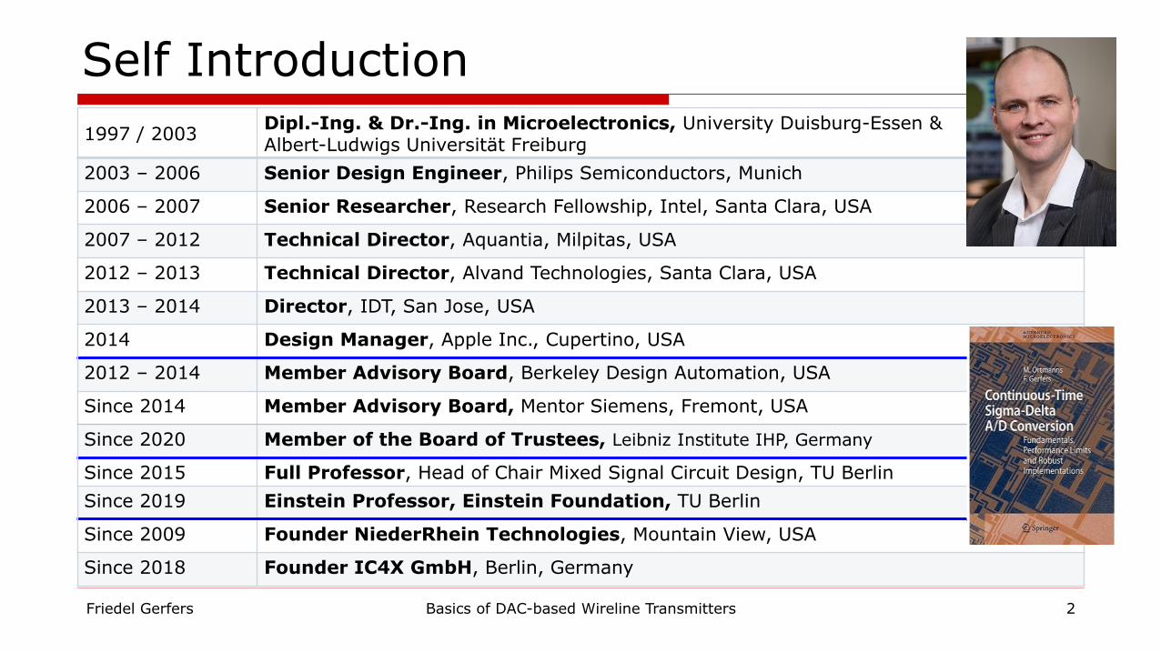
NRZ and PAM4 Eye Diagram
Eye diagram construction by overlaying waveform segments Non-return-to-zero (NRZ) 1bit/symbol, PAM4 2 bits/symbolFriedel Gerfers Basics of DAC-based Wireline Transmitters 10
NRZ eye diagram
PAM4 eye diagram
Vout,TX
12/31/30
Vout,TX
Full Scale (FS)
NRZ eye diagram
1Tbit =1UI(UI ≡ unit interval)
1Tbit =1UI
1 11 00 10 0
D1 D0
1
0

NRZ Eye Diagram Analysis
Eye height= (Vtop – 3𝝈top) – (Vbot + 3𝝈bot) Eye width = (tcross2 – 3𝝈cross2) – (tcross1 + 3𝝈 cross1)Friedel Gerfers Basics of DAC-based Wireline Transmitters 11
Vtop
Vbot
Horizontal eye opening / width
Eye
ampl
itude
Vert
ical
eye
open
ing
/ he
ight
tcross1 tcross2
𝝈cross2𝝈cross1
(µtop)
(µbot)
Probability distribution of noise
𝝈bot
𝝈top

Bit Error Rate (BER)
If the received bit is different from the transmitted bit error
BER No. of bit errorsNo. of transmitted bits
BER characterization: BER-tester or loop back
Mathematical model with a normalized threshold of VDTH=0.5 This area is the probability that 0 is decoded as 1 This area is the probability that 1 is decoded as 0
Friedel Gerfers Basics of DAC-based Wireline Transmitters 12
tj,pp
VDTH
tS

Bit Error Rate (BER) II
Noise is assumed to be normal distributed [3] Mean free 𝜇 0 and variance 𝜎
“BER” means the probability that noise becomes larger than the threshold VDTH
Probability of an error p(bit error) BER
For low BER: maximize signal amplitude, minimize noise & jitter
Friedel Gerfers Basics of DAC-based Wireline Transmitters 13
0 0.5x/1V
𝑝 𝑥 0.5 12𝜋𝜎 𝑒 . 𝑑𝑥.𝑝 𝑥 0.5 1 −Φ 0.5 − 0𝜎 Φ − 0.5𝜎10.5
x/1V
𝑝 𝑥 0.5 12𝜋𝜎 𝑒 . 𝑑𝑥.𝑝 𝑥 0.5 Φ 0.5 − 1𝜎 Φ − 0.5𝜎
𝑝 bit error 𝑝 TX 0 · 𝑝 𝑥 0.5 𝑝 TX 1 · 𝑝 𝑥 0.5𝑝 bit error 0.5 · Φ − . 0.5 · Φ − . 𝑝 bit error Φ − .
VDTH
VDTH
Φ 𝑥 − 𝜇𝜎 ≡ 𝐶𝐷𝐹

Bit period
Verticaleye margin
BER
0.5
10-12
VDTHVbot("0")
Vtop("1")
Bit period
Horizontaleye margin
BER
0.5
10-12
tS
0 Tbit Bit period
Verticaleye margin
BER
0.5
10-12
VDTHVbot("0")
Vtop("1")
Bit period
Horizontaleye margin
BER
0.5
10-12
tS
0 Tbit
Bit Error Rate (BER) III
Vertical and horizontal BER BER depends on decision threshold VDTH and sample instant tS
(1) Faster link speed shorter bit period (Tbit) higher BER (2) Higher TX eye amplitude improved SNR lower BERFriedel Gerfers Basics of DAC-based Wireline Transmitters
Bet
ter
(2) (1)
14
Eye amplitude

PAM4 Eye Linearity
PAM4 eye linearity critical for low BER Eye compression:
Minimum signal level 𝑆 swing between adjacent symbol levels Resulting relative level mismatch (𝑅𝐿𝑀)
Eye linearity: Compares maximum to minimum eye voltage levelFriedel Gerfers Basics of DAC-based Wireline Transmitters 15
𝑆 min 𝑉 − 𝑉 ,𝑉 − 𝑉 ,𝑉 − 𝑉Eye linearity max 𝑉 − 𝑉 ,𝑉 − 𝑉 ,𝑉 − 𝑉min 𝑉 − 𝑉 ,𝑉 − 𝑉 ,𝑉 − 𝑉𝑅𝐿𝑀 3 ⋅ 𝑆𝑉 − 𝑉
V3
V2
V1
V0

Basic Wireline Link - TX
TX serializes parallel data TX drives channel with large (enough) voltage swing TX amplitude critical for link SNR and BER TX linearity critical for PAM4-based link SNR and BER
Friedel Gerfers Basics of DAC-based Wireline Transmitters 16
TX RXZL
MUX Eq. Driver
RT
PLL
DEM
UX
RT
PLL
Eq.
CDRVout,TX

Single-Ended Serial Link
Transmit signal needs a return path Gnd signals (TX & RX) are not exactly same voltage SNR, BER Finite transmitter supply impedance switching noise (SSO)
Demands large amount of local decoupling capacitance at TX and RX (Vref) Pro: Single-ended links exhibit compact footprint, 1 pin, 1 wire, … Con: Sensitive to power supply noise, xtalk (even with local Vref)Friedel Gerfers Basics of DAC-based Wireline Transmitters 17
TX RXZL
MUX Eq. Driver
DEM
UX
Vout,TX Cin
Vref
Vin,RX + vnoise,gndRT

Differential Serial Link
Pro: Voltage/current difference transmitted better noise immunity Pro: Signal is self-referenced, can achieve twice the signal swing,
rejects common-mode noise, return current is ideally only DC Con: Differential links have twice the complexity, # of pins, wires,… Friedel Gerfers Basics of DAC-based Wireline Transmitters 18
TX RX
ZLM
UX
Eq. Driver
PLL
DEM
UX
PLL
Eq.
CDR
RT RT

Channel – Physical Media
Friedel Gerfers Basics of DAC-based Wireline Transmitters 19
L
TX RXZL
MUX Eq. Driver
RT
PLL
DEM
UX
RT
PLL
Eq.
CDR
Typically, copper interconnect E. g. shielded twisted pair (STP), PCB trace, vias, connectors, …
Channel length L varies (L ≥ 𝜆clk, Tbit) Channel cause frequency-dependent loss insertion loss (IL)
Crosstalk (NEXT, FEXT,..) Discontinuities due to connectors & IO interfaces
Allowed IL

|Ins
ertio
n lo
ss|
(dB)
Insertion Loss – Attenuation & ISI
Friedel Gerfers Basics of DAC-based Wireline Transmitters 20
TX RXZL
MUX Eq. Driver
RT
PLL
DEM
UX
RT
PLL
Eq.
CDR
Channel has a low-pass behavior Skin effect 𝐻 𝑓 ∝ and dielectric losses 𝐻 𝑓 ∝
Attenuates transmit signal (IL) Introduces Intersymbol Interference (ISI) Both affect link SNR and BER
Frequency (GHz)
Allowed IL
Example IL
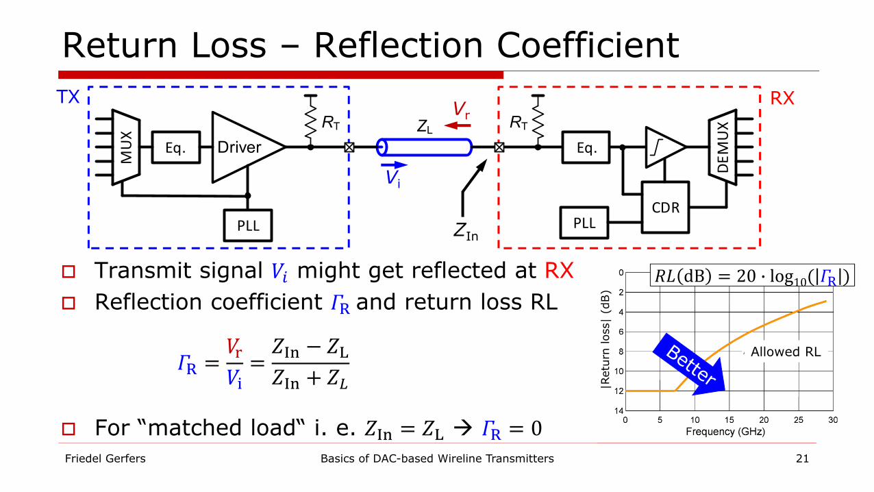
Return Loss – Reflection Coefficient
Friedel Gerfers Basics of DAC-based Wireline Transmitters 21
𝛤 𝑉𝑉 𝑍 − 𝑍𝑍 𝑍
Vi
Vr
ZIn
TX RXZL
MUX Eq. Driver
RT
PLL
DEM
UX
RT
PLL
Eq.
CDR
Transmit signal 𝑉 might get reflected at RX Reflection coefficient 𝛤 and return loss RL
For “matched load“ i. e. 𝑍 𝑍 𝛤 0 |Ret
urn
loss
| (d
B)
Allowed RL
𝑅𝐿 dB 20 · log10 𝛤

Tutorial Overview High-speed transceiver overview
Key TX metrics and design objectives Transmitter termination
High-speed design solutions Current-mode DAC drivers
Segmentation Voltage-mode DAC drivers
Signal swing enhancements High-speed data serialization
Data multiplexing
Friedel Gerfers Basics of DAC-based Wireline Transmitters 22

Transmitter Termination
Off-chip vs. on-chip termination Series vs parallel termination AC vs DC coupled termination Termination calibration Finite TX output bandwidth TX with shunt peaking TX with bridged T-coil
Friedel Gerfers Basics of DAC-based Wireline Transmitters 23

Termination
Friedel Gerfers Basics of DAC-based Wireline Transmitters 24
TX RXZL
MUX Eq. Driver
RT
PLL
DEM
UX
RT
PLL
Eq.
CDR
Termination RT is typ. part of the transmitter / DAC driver design Mismatch RT ≠ZL introduces amplitude variations, RL, … Termination RT is commonly an on-chip passive component RT often built from a digitally tunable resistor to match ZL

RX
RXTX
Off-Chip vs On-Chip Termination
Friedel Gerfers Basics of DAC-based Wireline Transmitters 25
TXZL
MUX Eq. Driver
DEM
UX
RT
Eq. Lp
ZL
MUX Eq. Driver
DEM
UX
Eq. Lp
RT
Off-chip: package parasitics act as unterminated stub reflections On-chip: package inductance Lp part of transmission line

Series vs Parallel Termination
Friedel Gerfers Basics of DAC-based Wireline Transmitters 26
Low impedance voltage-mode drivers employ series termination High impedance current-mode drivers employ parallel termination
Series Termination Parallel Termination
Double Termination (TX & RX)
ZLRT
VTX
ZLRT
VTX RT
ZL
ITX
ZL
RTRTITX
RT

Series vs Parallel Termination
Friedel Gerfers Basics of DAC-based Wireline Transmitters 27
Double termination yields best signal quality Improved signal integrity forms a trade-off with signal amplitude
Series Termination Parallel Termination
Double Termination (TX & RX)
ZLRT
VTX
ZLRT
VTX RT
ZL
ITX
ZL
RTRTITX
RT

AC vs DC Coupled Termination
DC coupling allows for uncoded data (non-DC-balanced)
RX common-mode set by transmitter current level
AC coupling enables flexible RX common-mode level
Channel has low frequency high pass corner data must be coded / scrambled
Friedel Gerfers Basics of DAC-based Wireline Transmitters
ZL
RT=ZLZL
2RT
ITX
D D
RT=ZL
VCM,RX
VCM,RX
VCM,RX = ITXRT/2
ZL
RT=ZLZL
2RT
ITX
D D
RT=ZL
RCM
RCM
CAC
CAC
VTT
VTT
VCM,RX = VTT

On-Chip Termination Calibration
Friedel Gerfers Basics of DAC-based Wireline Transmitters 29
TXZL
MUX Eq. Driver
RT
PLL
DEM
UX
RT
PLL
Eq.
CDR
Trimmable poly resistor RT digital code D<2:0> alters actual RT
Goal ZL = RT with RT = 1/(1/R + D2 /R2 + D1 /R1 + D0 /R0 ) Note: Switch impedance Rsw usually not negligible Note: Temperature dependency How to obtain the optimum D<2:0>?
D0
R0
D1
R1
D2
R2R
RT
Di ∈ {0,1}Rsw = 0Ω

On-Chip Termination Calibration II
Friedel Gerfers Basics of DAC-based Wireline Transmitters 30
Calibration loop uses an accurate Rext to match to the replica RT*
Tuning range & resolution (LSB) considers process variations & RL Up ±20% process variations 3 bit lead to ~5% LSB step
I
Rext
VDD,ext
D0
R0
D1
R1
D2
R2R
I
VDD,int
MUX
Clock
On-chip Calibration
Cal Code <D2,D1,D0>
Replica Terminator RT*
UpDown Count

Termination, ESD, IO Pads
Friedel Gerfers Basics of DAC-based Wireline Transmitters 31
TXM
UX Eq. DriverRT
PLL
Cp,TX+CpadCESD
Driver output impedance is frequency dependent output pole 𝑓 Contributors:
TX output and routing capacitance Cp,TX
IO pad capacitance Cpad
ESD capacitance CESD, package, bondwire, …
Ctot = Cp,TX + Cpad + CESD𝑓 𝑝 2𝜋𝑅 𝐶

TX Output Bandwidth Limitation
Friedel Gerfers Basics of DAC-based Wireline Transmitters 32
TXM
UX Eq. RT
PLL
Ctot
Tb
Io
0Io RT Ctot
Tb
Io
0
Driver
TX output signal 𝑉 , and final settling error 𝑒 at t=Tb=(Rb)-1
Tb denotes TX bit period and Rb denotes TX data rate Low-frequency pole TX high and low levels experience ISI
Tb
ITX
0ITX RT Ctot
Tb
0
Vout,TX
t
𝑉 , 𝑡 𝐼 𝑅 1 − exp − 𝑡𝜏 𝑒 𝐼 𝑅 − 𝑉 , 𝑇𝐼 𝑅 exp −𝑇𝜏 exp − 2𝜋𝑓𝑅
𝜏 𝑅 𝐶
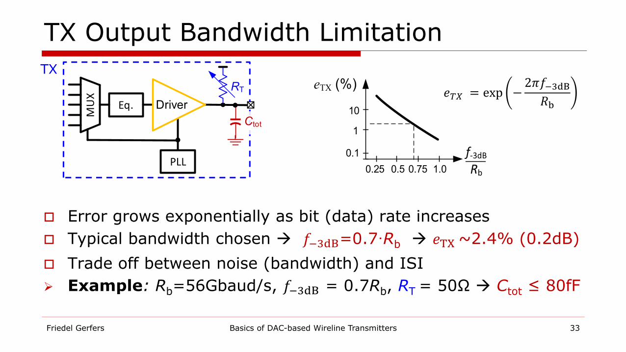
Error grows exponentially as bit (data) rate increases Typical bandwidth chosen 𝑓 =0.7·Rb 𝑒 ~2.4% (0.2dB) Trade off between noise (bandwidth) and ISI Example: Rb=56Gbaud/s, 𝑓 = 0.7Rb, RT = 50Ω Ctot ≤ 80fF
TX Output Bandwidth Limitation
Friedel Gerfers Basics of DAC-based Wireline Transmitters 33
TXM
UX Eq. RT
PLL
Ctot
Driver𝑒 exp − 2𝜋𝑓𝑅eTX (%)
0.1
1
10
0.25 0.5 0.75 1.0f-3dB Rb

Connect inductor LT in series with termination resistor RT
Additional zero z1 = –RT /LT and pole p2 = –(1/(RTCtot)+RT /LT) Idea: More current used for longer time to charge load capacitance Resonance is avoided if damping factor ζ = LT/(RT
2Ctot)<1 (p1 < z1)
TX with Shunt Peaking
Friedel Gerfers Basics of DAC-based Wireline Transmitters
TXM
UX Eq. DriverZT
PLL
CtotITX
RTCtot
LT
𝑍 𝑠 𝑅 1 𝑠1 𝑠𝑅 𝐶 𝑠2𝐿 𝐶Re(s)
Im(s)
p1
p2 z1
35

TX with Shunt Peaking II
Friedel Gerfers Basics of DAC-based Wireline Transmitters
TXM
UX Eq. DriverZT
PLL
Ctot
Shunt series-peaking increases small-signal bandwidth Maximum bandwidth extension of 1.84 for LT/(RT
2Ctot)=√2/2=0.707 Note: 1.5dB peaking
Maximum flat extension of 1.72 for LT/(RT2Ctot)=1/(1+√2)=1/2.828
f-3dB,wo = 39GHzf-3dB,flat = 67GHz
f-3dB,max = 72GHz
36

100 101 102 103
Frequency (GHz)
-10
-5
0
|H| (
dB)
RT=50 , Ctot=80fF
wo shunt peaking, wo T-coilw shunt peaking, max. flatw bridged T-coil
TX with Bridged T-Coil
Friedel Gerfers Basics of DAC-based Wireline Transmitters
TX
ITX
RT
Ctot
L2
L1
Cb
CL
M
T-coil configuration for high output impedance drivers Effective output impedance is RT
Maximum bandwidth extension of 2.83 for ζ=√2/2 Assumes L1=L2, 4Cb(1+k)=(1-k)CL with k=M/√(L1L2)
f-3dB,wo = 39GHzf-3dB,flat = 67GHz
f-3dB,Tcoil = 110GHz
[B. Razavi, JSSC Magazine, 2015]
37

TX with Bridged T-Coil II
Friedel Gerfers Basics of DAC-based Wireline Transmitters
TX
L1=L2=L leads to simple spiral inductor Trace (metal) spacing defines mutual coupling Outer dimensions and Nr. of turns define the inductance L Be aware of self-resonance
A
B
CITX
RT
Ctot
L2
L1
Cb
CL
M
[J. Paramesh, TCAS I, 2007]
38

TX with Bridged T-Coil III
Friedel Gerfers Basics of DAC-based Wireline Transmitters
TX
Input impedance of 2nd-order T-coil is constant T-coil input/output can be combined with series peaking LS
Enables cancellation of large TX parasitic capacitance CTX
ITX
RT
CTX
L2
L1
Cb
CL
MLS
Series peaking
ITX
RT
Ctot
L2
L1
Cb
CL
M
[B. Razavi, JSSC Magazine, 2015]
39

Tutorial Overview High-speed transceiver overview
Key TX metrics and design objectives Transmitter termination
High-speed design solutions Current-mode DAC driver
Segmentation Voltage-mode DAC driver
Signal swing enhancements High-speed data serialization
Data multiplexing
Friedel Gerfers Basics of DAC-based Wireline Transmitters 39

Current-Mode DAC Driver
High-impedance current-mode driver Current-mode logic (CML) driver N-Bit current-mode DAC DAC segmentation Non-linear effects and gradient errors
Friedel Gerfers Basics of DAC-based Wireline Transmitters 40

Current-Mode TX (DAC) Driver
Signal integrity demands Zout ≈ RT = ZL = 50Ω output impedance Output impedance of driver ≫ RT
Current-mode drivers use (Norton-equivalent) parallel termination Easier to tune output impedance RT
Review first single-ended design
Friedel Gerfers Basics of DAC-based Wireline Transmitters 41
TX RXZL
MUX Eq. Driver
RT
PLL
DEM
UX
RT
PLL
Eq.
CDRZOut

High-Impedance Current-Mode Driver
Friedel Gerfers Basics of DAC-based Wireline Transmitters 42
M1Vin
ZL
RT
VTT
VRXVTXrOut,TX = rDS
t
Vin
VRX
Vin,H
Vin,L = 0V
τd
VTXVTTVTT – ITX ZL
τd
ITX ZL = RT
rDS ≫ RT
Keep current source (CS) M1 in saturation region! VTT – ITXZL = VTT – ITXRT = VRX > VDSsat,M1
Make sure rDS ≫ RT across desired bandwidth cascoded CS Keep driver current constant
Use feedback to set ITX (Vin,H) IR drop can shift the bias point: Use current reference

Current-Mode Logic (CML) Driver
Differential RX signal swing is ±IRT/2 with double termination High output common-mode keeps current source saturated Power consumption is Pdiss=VDD×IFriedel Gerfers Basics of DAC-based Wireline Transmitters 43
ZL
ZL
Vin,RX
D
D
VBias I
I/2
I/2
RT=ZLRT=ZL
VDD
RT=ZLRT=ZL
VDD
I
I/2
Vin,RX,0 = - (I/2) × RTVin,RX,1 = + (I/2) × RTVin,RX,ppd = I × RT
I = Vin,RX,ppd / RT
Vout,TX

Current-Mode Logic (CML) Driver II
Differential termination with 2RT
RX signal swing is still ±IRT/2 with double termination Power consumption is Pdiss=VDD×IFriedel Gerfers Basics of DAC-based Wireline Transmitters 44
ZL
ZL
Vin,RX
D
D
VBias I
¾ I
¼ I
RT=ZLRT=ZL
VDD
2RT=2ZL
I
Vin,RX,0 = - (I/4) × 2RTVin,RX,1 = + (I/4) × 2RTVin,RX,ppd = I × RT
I = Vin,RX,ppd / RT
Vout,TX

2-Bit Current-Mode DAC
Binary DAC (I is LSB current) current sources scale by 2x Two bits (D<1> & D<0> ∈ {0,1}) 4 levels with 2IRT spacing Note: Constant current of 3I independent of D<1:0>Friedel Gerfers Basics of DAC-based Wireline Transmitters 45
ZL
ZL
D<0>
D<0>
VBias ID<1>
D<1>
VBias 2I
RT=ZLRT=ZL
VDD
MSB LSB
2RTVout,TX Vin,RX
-½(3I)RT
-½(1I)RT
+½(1I)RT
00 01 10 11
D<1:0>
+½(3I)RT
Vin
,RX
[V]
DAC transfer func.
[B. Razavi, JSSC Magazine, 2018]

N-Bit Current-Mode DAC Model
n=2N-1 LSB unit current cells x is DAC input code with x ∈ {0,….,n}Friedel Gerfers Basics of DAC-based Wireline Transmitters 46
RT=ZLRT=ZL
VDD
Vout,TX
(n-x)·I x·I
2RT
Vout,TX (N=2, x=3)= ½ · 3 · I · RT
Vout,TX (N=2, x=0)= ½ · (–3) · I · RT
Vout,TX (x) = ½ · (2x–n) · I · RT

4-Bit Binary Weighted Current-Mode DAC
Data change from (9)10 (6)10 Dnew=Dpre – 8 – 1 + 4 + 2 Switching of many binary current cells can cause glitchesFriedel Gerfers Basics of DAC-based Wireline Transmitters 47
RT=ZLRT=ZL
VDD
Vout,TX 2RTVin,RX
8I 2I4I I
( 1 0 0 1 )2 = (9)10 = Dpre<3:0>
( 0 1 1 0 )2 = (6)10 = Dnew<3:0>
t
Vout,TX
TbTb
possible glitch
[C.-H. Lin, JSSC, 1998][J. Mulder, ISSCC Tutorial, 2015]

4-Bit Thermometer Decoded DAC
Unary DAC 15 equal current source with current value I Data change from (9)10 (6)10 Dnew=Dpre – 3 Binary-to-thermometer decoder requiredFriedel Gerfers Basics of DAC-based Wireline Transmitters 48
RT=ZLRT=ZL
VDD
Vout,TX 2RTVin,RX
I I I
t
Vout,TX
TbTb
avoids glitch
(0 …………………… 0 1 1 1 1 1 1 1 1 1)2 = (9)10 = Dpre<3:0>

4-Bit Segmented DAC
To balance DAC complexity segmentation MSBs are thermometer encoded, LSBs are binary encodedFriedel Gerfers Basics of DAC-based Wireline Transmitters 49
RT=ZLRT=ZL
VDD
Vout,TX 2RTVin,RX
4I 2I4I I4I
Thermometer Binary
(0 1 1 0 1)2 = (9)10
[C.-H. Lin, JSSC, 1998]

Current Source Matching
Current sources designed for matching
Good matching requires: Low Aβ and AVth (CMOS technology parameter) Large transistor area (W·L) parasitic Cpar
Low gm (high overdrive Vgt) voltage headroom
Friedel Gerfers Basics of DAC-based Wireline Transmitters 50
RT=ZLRT=ZL
VDD
Vout,TX
I+ΔI
𝜎 Δ𝐼𝐼 = 𝜎 Δ𝛽𝛽 + 𝑔𝐼 𝜎 Δ𝑉
𝑔𝐼 = 2𝑉𝜎 Δ𝑉 = (𝐴 )2 𝑊 ⋅ 𝐿𝜎 Δ𝛽𝛽 = (𝐴 )2 𝑊 ⋅ 𝐿
[M. J.M. Pelgrom, JSSC, 1989] [K. R. Lakshmikumar, JSSC, 1989]
(1)
(2) (3)

Output Impedance Variation
Current sources have finite conductance gds Current I is switched Conductance gds is switched as well
Effective output impedance RT,eff is a functionof DAC input code
Introduces DAC non-linearity
Friedel Gerfers Basics of DAC-based Wireline Transmitters 51
I gdsI gdsI gdsI gds
RTRT
VDD
Vout,TX
I gds

N-Bit Rout DAC Model
n=2N-1 LSB unit current cells x is DAC input code with x ∈ {0,….,n} GT = 1 / RT and rDAC = 1/ (n · gds)Friedel Gerfers Basics of DAC-based Wireline Transmitters 52
RTRT
VDD
Vout,TX
(n-x)·I x·I
x·gds (n-x)·gdsGT,P = GT + x · gds
GT,N = GT + (n-x) · gdsGT,N
𝐻𝐷 ≈ 𝑅4𝑟GT,P
[C.-H. Lin, JSSC, 2009]

N-Bit Cascoded DAC
Friedel Gerfers Basics of DAC-based Wireline Transmitters 53
RTRT
VDD
Vout,TX
Mcas
MCS
Msw Msw
Mcas2 Mcas2
rds
(gmrds)rds
(gmrds)2rds
Trade-offs for good linearity: Decrease RT power consumption, signal
swing (usually fixed by line impedance) Increase rDAC
Decrease I signal swing Increase Vgt voltage headroom Use cascodes voltage headroom
𝐻𝐷 ≈ 𝑅4𝑟
(gmrds)3rds

Output Impedance Distortion
Friedel Gerfers Basics of DAC-based Wireline Transmitters 54
Example: N=8bit DAC, RT=25Ω rds,cell = 63.75kΩ (255·250Ω) rDAC=1/gDAC= rds,cell/n=250Ω |HD3|= 64dB
𝐻𝐷 ≈ 𝑅4𝑟 ≈ 𝑅 · 𝑛4 · 𝑟 ,𝑛 = 2 − 1 = 2 −1 = 2550 50 100 150 200 250
DAC input code x
22
22.5
23
23.5
24
24.5
25 R
T,p,
RT,
n
47.6
47.65
47.7
47.75
RT,
eff
RT,p RT,n RT,eff

N-Bit Cascoded DAC II
Friedel Gerfers Basics of DAC-based Wireline Transmitters 55
Capacitance at source node S Switched impedance Code-dependent Cout
Dynamic non-linearity
Non-linear Cgs of Mcas2 devices
Small current IBias linearizes Cgs Few % of switched current Significant linearity improvement Small power increase only
S
RTRT
VDD
Vout,TX
Mcas
MCS
Msw Msw
Mcas2 Mcas2CgsCgs
IBiasIBias
[C.-H. Lin, JSSC, 2009]
RTRT
VDD
Vout,TX
Mcas
MCS
Msw Msw
Mcas2 Mcas2

DAC Cell Switches Msw
Switches operate in: Saturation region Triode region
Re-timing of data required Latch Switch driver
Friedel Gerfers Basics of DAC-based Wireline Transmitters 56
Mswp Mswn Mswp Mswn Mswp Mswn Mswp Mswn Q
Q
DQ
Q
DQ
Q
D
latch
Q
Q
D di
clk

Switches Signals
Distortion due to glitches at node S Coupling to bias node Glitch mismatch between DAC cells
Optimize crossing point of switch signal Non-overlap: Current source turns off shortly Overlap: Current division between switches Optimum: Small glitch
Switch signal swing Low-swing (CML) driver: Smaller glitch CMOS-swing driver: Shorter glitch
Friedel Gerfers Basics of DAC-based Wireline Transmitters 57
Mswp Mswn
SMCS

Clock & Output Summing Tree Structure
Equal delay to/from DAC unit cells Tree structures recommended for: supply & bias routing Separate analog and digital supply rails (data-dependent currents)Friedel Gerfers Basics of DAC-based Wireline Transmitters 58
QQD
clk
QQD
clk
QQD
clk
QQD
clk
QQD
clk
QQD
clk
QQD
clk
QQD
clk
Vclk
Ioutp Ioutn

Tutorial Overview High-speed transceiver overview
Key TX metrics and design objectives Transmitter termination
High-speed design solutions Current-mode DAC drivers
Segmentation Voltage-mode DAC drivers
Signal swing enhancements High-speed data serialization
Data multiplexing
Friedel Gerfers Basics of DAC-based Wireline Transmitters 59

Voltage-Mode DAC Drivers
Basic voltage-mode transmitter Low-swing and high-swing voltage-mode driver N-Bit voltage-mode DAC Static current compensation Impedance calibration Signal swing enhancement
Friedel Gerfers Basics of DAC-based Wireline Transmitters 60

Voltage-Mode TX
Signal integrity demands ZOut+RT=ZL output impedance Voltage-mode drivers use (Thévenin-equivalent) series termination
Potential ½ to ¼ the current for given output swing Review first single-ended design Friedel Gerfers Basics of DAC-based Wireline Transmitters 61
TX RXZL
MUX Eq. Driver
RT
PLL
DEM
UX
RT
PLL
Eq.
CDRZOut

Low-Impedance Voltage-Mode Driver
Inverter switches VO between VS / gnd Driver on-resistance ZOut contributes to termination Duplicating drivers for differential signaling
Pseudo-differential architecture
Friedel Gerfers Basics of DAC-based Wireline Transmitters 62
ZL = ZOut + RT
t
VOVS
0V
VRXVS
τd τd
VS/2VTXVS
D Vin,H = VSVin,L = 0VD
ZL
RT τd
DZL
τd
VS
RT
VRX
VRX
ZOut
VTX
VTX
VO
VO
t0+τdt0 t0+2τd
VSZOut/(2ZL)

Differential Voltage-Mode Driver
Differential RX signal swing is ±VS/2Friedel Gerfers Basics of DAC-based Wireline Transmitters 63
ZL
ZL
Vin,RX
RT=ZL
RT=ZL RT=ZL
Vin,RX,0 = - VS / 2Vin,RX,1 = + VS / 2Vin,RX,ppd = VS I = VS / (2RT)RT=ZL
VSD D
VS D D
ZL
ZL
Vin,RX
RT=ZL
2RT
Vin,RX,0 = - VS / 2Vin,RX,1 = + VS / 2Vin,RX,ppd = VS I = VS / (4RT)RT=ZL
VSD D
VS D D

Simple Low-Swing Voltage-Mode Driver
All-NMOS TX driver transistor width (WN) designed to RNMOS=RT
Note: Effective VGS different for top and bottom NMOS Pre-driver power supply used to control TX impedanceFriedel Gerfers Basics of DAC-based Wireline Transmitters 64
[K.-L. J. Wong, JSSC, 2004][J. Poulton, JSSC, 2007]
WNbot
WNtop
VS
VTX,N
DVTX,P
D
ZL
ZL
VTX,P (D=0)= ¼·VSVTX,P (D=1)= ¾·VS
VTX,N (D=0)= ¾·VSVTX,N (D=1)= ¼·VS
Vin,RX,ppd=VS
WNbot
WNtop
VTX,N
DVTX,P
D
ZL
ZL
VS
WNbot
WNtop
VTX,N
VTX,P
ZL
ZL
VS
D
VZcont
D
VS < 4/3(VDD-VTH-VDSsat)

High-Swing Voltage-Mode Driver
CMOS TX driver source impedance defined by Zd,i+RT=ZL
To meet termination resistance of 50Ω large transistor width Trade-off: Pre-driver strength, jitter, timing vs. power consumptionFriedel Gerfers Basics of DAC-based Wireline Transmitters 65
VS > VTH+VDSsat
D
VS
RTVTX,PVO,P
D
VS
RT
VTX,N
VO,N
ZL
ZL
Zd,N
Zd,P
[M. Kossel, JSSC, 2008][C. Menolfi, ISSCC, 2018]
D
VS
RTVTX,PVO,P
D
VS
RT
VTX,N
VO,N
ZL
ZL
Zd,N
Zd,P

2-Bit Voltage-Mode DAC
Binary DAC RU scales by 2x
LSB resistance is 2RU
Example: D<1:0>=11
Rtot = RU || 2 RU = RT = 50Ω
RU = 75Ω
Friedel Gerfers Basics of DAC-based Wireline Transmitters 66
Zd
D<1>
Zd
VS
VTX,N
RU
RU
Zd
D<0>
Zd
VS
2RU
2RU
Zd
D<1>
Zd
VS
VTX,P
RU
RU
Zd
D<0>
Zd
VS
2RU
2RU
2RT
Zd=0Ω

N-Bit Voltage-Mode DAC Model
n = 2N-1 LSB unit resistors
x is DAC input code with x ∈ {0,….,n}
RU = n·RT = n·ZL
Example: N = 4 n = 15
RU = 750Ω
Friedel Gerfers Basics of DAC-based Wireline Transmitters 67
VS
RUx
RU n – x
2RT
VS
RUn – x
RUx
Vout,TX
RU / 0 ∞

High-Swing Voltage-Mode DAC Driver
N-Bit voltage-mode DAC driver n=2N-1 parallel unit cells RU is defined by DAC resolution RU=n·50Ω Note: Data-dependent current consumption max. at mid-codeFriedel Gerfers Basics of DAC-based Wireline Transmitters 68
D<n:0>
VS
VTX,PRU
RT
D<n:0>
VS
VTX,N
RU
RU
ZL
ZL
Cp
Cp
Cp
D<n:0>
VS
VTX,P
RU
D<n:0>
VS
VTX,N
ZL
ZL
Cp
Cp
RU
VO,N
VO,P

4-Bit Voltage-Mode IVDD
Friedel Gerfers Basics of DAC-based Wireline Transmitters 69
VS
RU15
RU 0
2RT
VS
RU0
RU15
Vout,TX
VS
RU8
RU 7
2RT
VS
RU7
RU8
Vout,TX
Example: n = 2N-1=15, RU = 750Ω and VS =1V VM DAC has ~2x (data dependent) supply current variation
x
IVDD
5mA
10mA
0 7 8 153 12
𝐼 (𝑥 = 0) = 𝑉2𝑅15 + 2𝑅𝐼 (𝑥 = 0) = 𝑉4𝑅 = 5mA𝐼 (𝑥 = 8) = 𝑉 (15𝑅 + 112𝑅 )𝑅 (2𝑅 + 15𝑅 )𝐼 (𝑥 = 8) = 9.978𝑚𝐴

x
IVDD
5mA
10mA
0 7 8 153 12
Efficient VM Static Current Compensation
Friedel Gerfers Basics of DAC-based Wireline Transmitters 70
Reduce static current variations IVDD Employ shunting devices between diff. outputs Per code x, new set of Ra, Rb, Rc selected to maintain Rdiff and RCM
Trade-off: Hardware complexity vs. power consumption
VS
Ra
Rb
2RT
VS
Rb
Ra Vout,TX
Rc/2Cac
Rc/2
x
IVDD
5mA
10mA
0 7 8 153 12
[W. Dettloff, ISSCC, 2010][R. Sredojevic, JSSC, 2011]
VS
Ra
Rb
2RT
VS
Rb
Ra Vout,TX 2RT
Di
VS
VTX,NRa
*
RT
Di
VS
VTX,P
Rb*
Ra*
ZL
ZL
Xi

Fast Switching
Make transistors become significant part of impedance RT
Smaller ratio rR=RU/Zd increase Zd decrease W smaller Cp
Trade-off: Switch non-linearity vs. timing performance Friedel Gerfers Basics of DAC-based Wireline Transmitters 71
D<n:0>
VS
VTX,PRU
RT
D<n:0>
VS
VTX,N
RU
RU
ZL
ZL
Zd
Zd
Zd
[H. Ghafarian, SSC Letters, 2020]𝑉 = 𝑉4 11 + 𝑟 𝑉 = 3𝑉4 11 + 𝑟𝑉 𝑟 = 4 = 50 … 150𝑚𝑉𝑉 𝑟 = 2 = 83 … 250𝑚𝑉
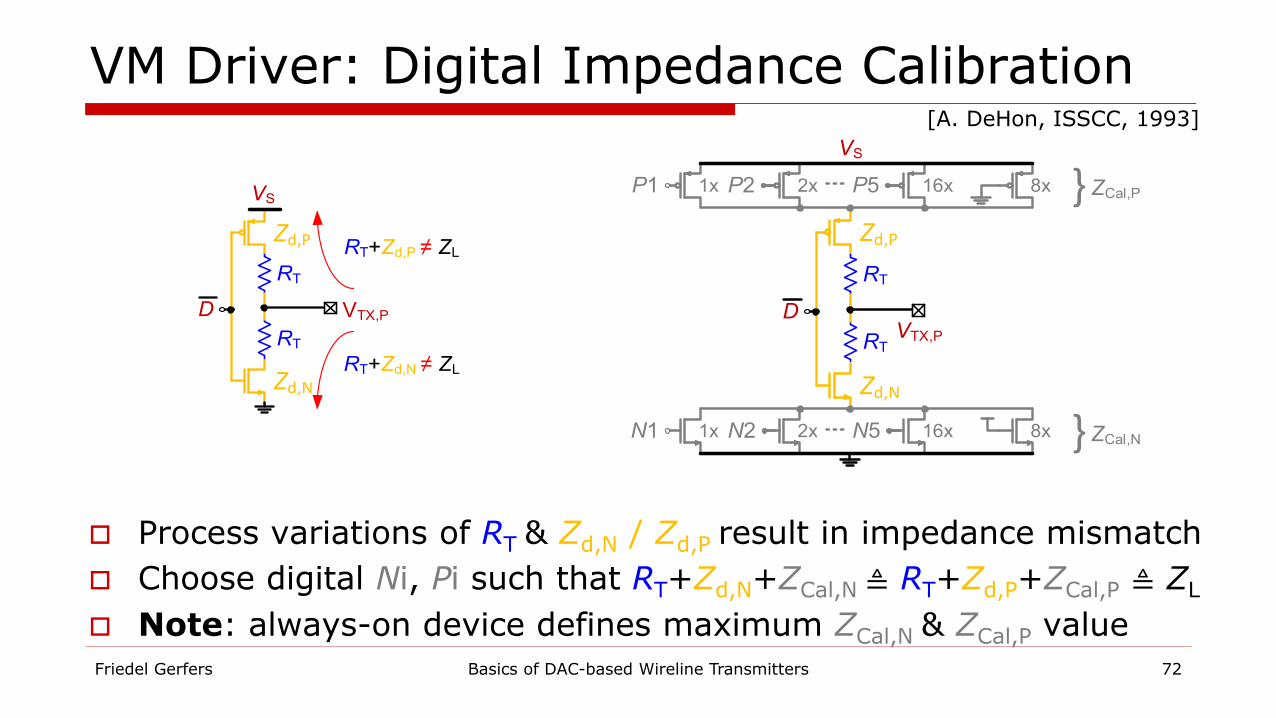
VM Driver: Digital Impedance Calibration
Process variations of RT & Zd,N / Zd,P result in impedance mismatch Choose digital Ni, Pi such that RT+Zd,N+ZCal,N ≜ RT+Zd,P+ZCal,P ≜ ZL
Note: always-on device defines maximum ZCal,N & ZCal,P valueFriedel Gerfers Basics of DAC-based Wireline Transmitters 72
Zd,N
D
Zd,P
VS
VTX,P
RT
RT
RT+Zd,P ≠ ZL
RT+Zd,N ≠ ZL Zd,N
D
Zd,P
VTX,P
RT
RT
VS
1xP1 2xP2 16xP5 8x
1xN1 2xN2 16xN5 8x } ZCal,N
} ZCal,P
[A. DeHon, ISSCC, 1993]

Signal-Swing Enhanced VM Transmitter
VM driver + CML stage Enhanced output swing from VS to (VS +2ISRT) Slightly affects the TX return loss & needs calibration Friedel Gerfers Basics of DAC-based Wireline Transmitters 73
D
VS
RT VTX,PVO,P
D
VS
RT
VTX,N
VO,N
ZL
ZL
VDDH
DD
IS
[A. Joy, ISSCC, 2011]
NRZ PAM4
VTX,P
VTX,N
ZL
ZL
LSB3RT
MSB3/2RT
LSB3RT
MSB3/2RT
2IS/3MSB MSB
IS/3LSB LSB
2IS/3MSB MSB
IS/3LSBLSB
[M. Bassi, ISSCC, 2016]

Current-Mode vs. Voltage-Mode Comparison
Driver / Termination Signal Current Normalized CurrentCurrent-Mode / Single-Ended Vin,RX,pp/ZL 1xCurrent-Mode / Differential Vin,RX,pp/ZL 1x
Voltage-Mode / Single-Ended Vin,RX,pp/(2ZL) 0.5xVoltage-Mode / Differential Vin,RX,pp/(4ZL) 0.25x
Friedel Gerfers Basics of DAC-based Wireline Transmitters 74
Pro: Ideal voltage-mode driver with differential RX termination potential of 4x reduction in power consumption
Actual driver power consumption depends on: Output impedance control, pre-driver power consumption, equalization
implementation Con: Voltage-mode driver has limited power supply rejection

Tutorial Overview High-speed transceiver overview
Key TX metrics and design objectives Transmitter termination
High-speed design solutions Current-mode DAC drivers
Segmentation Voltage-mode DAC drivers
Signal swing enhancements High-speed data serialization
Data multiplexing
Friedel Gerfers Basics of DAC-based Wireline Transmitters 75

High-Speed Data Serialization
Full-rate TX architecture Half-rate TX architecture Clock duty-cycle mismatch Quarter-rate TX architecture Output-multiplexed TX architecture
Friedel Gerfers Basics of DAC-based Wireline Transmitters 76

dout
d02
d13
clk
RT
DriverFF
1/2clk/2
1
0
FF
LFF
1/2clk/4
d0 d1 d2 d3 d0 d1 d2 d3 d0 d1
d2
d3
d0
d1
d2
d3
d0
d1
d2
d3
d0
d1
clk
clk/2
d02
d13
clk/4
dout d2
Final flip-flop (FF) uses a full-rate clock clk of Tclk = Tbit
Critical path defines maximum data rate FF clk-Q delay tFF,CQ + mux delay tMUX + FF setup time tFF,set < 1 UI
Full-rate TX architecture with cascade of 2:1 mux stages
Full-Rate TX Architecture
Friedel Gerfers Basics of DAC-based Wireline Transmitters 77
TX
dout
d02
d13
clk
RT
DriverFF
1/2clk/2
1
0
FF
LFF
1
0
FF
LFF
1
0
FF
LFF
1/2clk/4
d0
d2
d1
d3
1 UI critical path
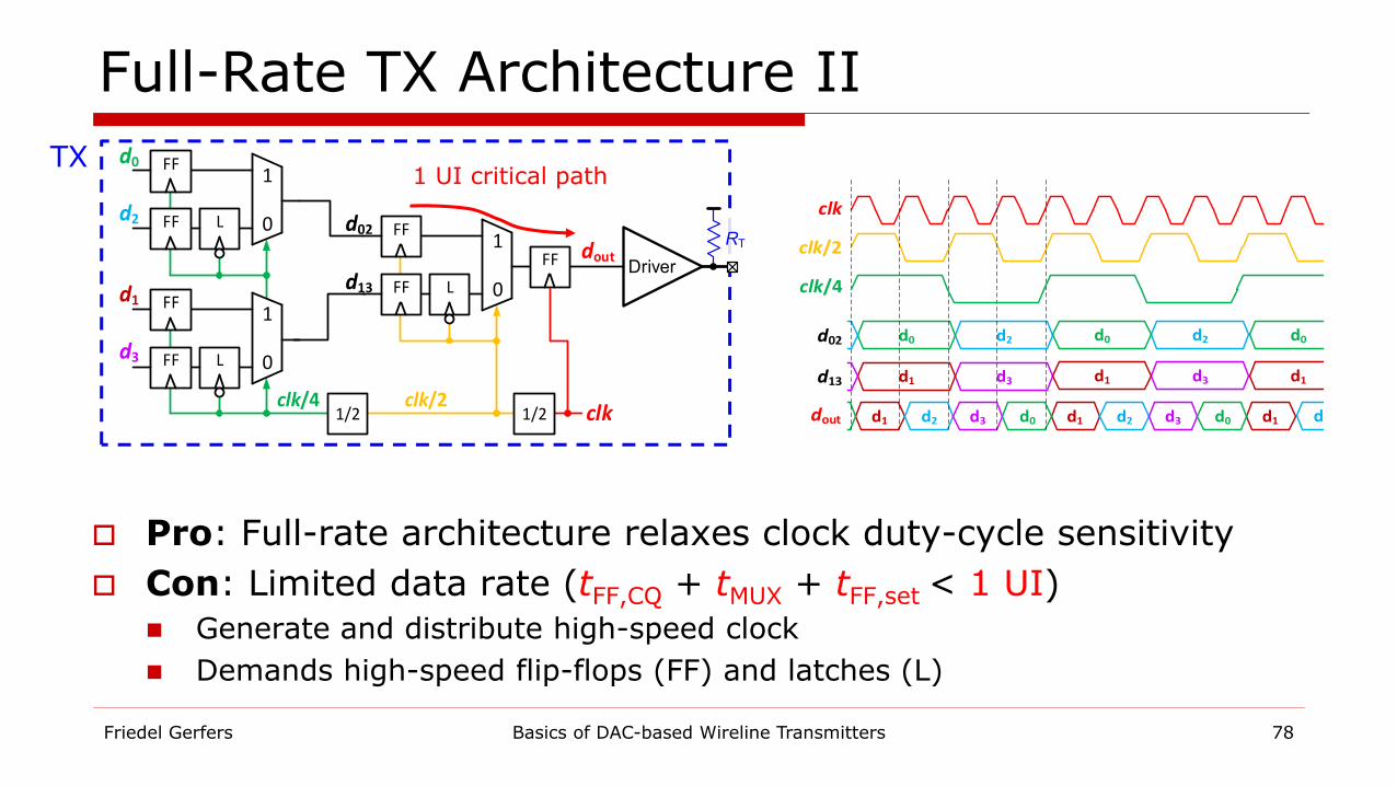
Pro: Full-rate architecture relaxes clock duty-cycle sensitivity Con: Limited data rate (tFF,CQ + tMUX + tFF,set < 1 UI)
Generate and distribute high-speed clock Demands high-speed flip-flops (FF) and latches (L)
Full-Rate TX Architecture II
Friedel Gerfers Basics of DAC-based Wireline Transmitters 78
TX
dout
d02
d13
clk
RT
DriverFF
1/2clk/2
1
0
FF
LFF
1
0
FF
LFF
1
0
FF
LFF
1/2clk/4
d0
d2
d1
d3
1 UI critical path
d0 d1 d2 d3 d0 d1 d2 d3 d0 d1
d2
d3
d0
d1
d2
d3
d0
d1
d2
d3
d0
d1
clk
clk/2
d02
d13
clk/4
dout d2

Half-rate TX architecture uses both clock phases of clk/2 Half-rate architecture relies on accurate (50%) clk/2 duty-cycle Final MUX control swapped to prevent glitches
Half-Rate TX Architecture
Friedel Gerfers Basics of DAC-based Wireline Transmitters 79
TX
dout
d02
d13
RT
Driver
clk/2
FF
LFF
1
0
FF
LFF
1
0
FF
LFF
1/2clk/4
d0
d2
d1
d3
1
0
1 UI critical path
d0 d1 d2 d3 d0 d1 d2 d3 d0 d1
d2
d3
d0
d1
d2
d3
d0
d1
d2
d3
d0
d1
clk/2
d02
d13
clk/4
dout d2
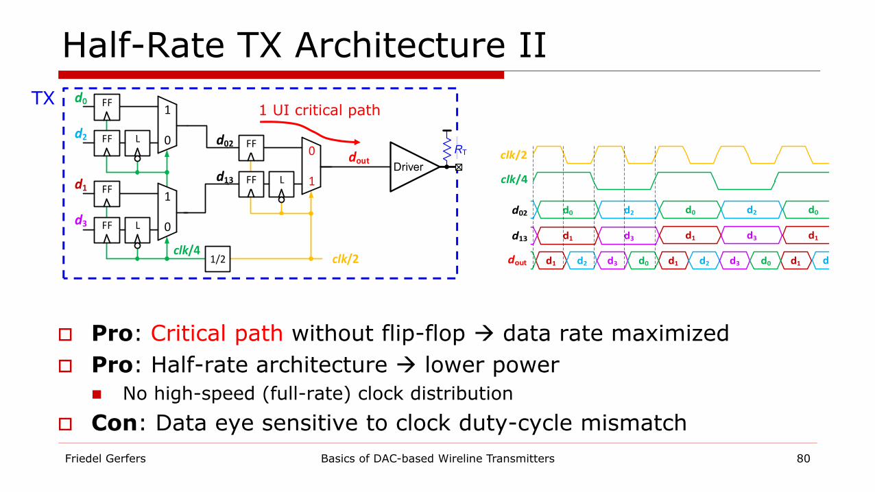
Pro: Critical path without flip-flop data rate maximized Pro: Half-rate architecture lower power
No high-speed (full-rate) clock distribution Con: Data eye sensitive to clock duty-cycle mismatch
Half-Rate TX Architecture II
Friedel Gerfers Basics of DAC-based Wireline Transmitters 80
TX1 UI critical path
dout
d02
d13
RT
Driver
clk/2
FF
LFF
1
0
FF
LFF
1
0
FF
LFF
1/2clk/4
d0
d2
d1
d3
1
0
d0 d1 d2 d3 d0 d1 d2 d3 d0 d1
d2
d3
d0
d1
d2
d3
d0
d1
d2
d3
d0
d1
clk/2
d02
d13
clk/4
dout d2
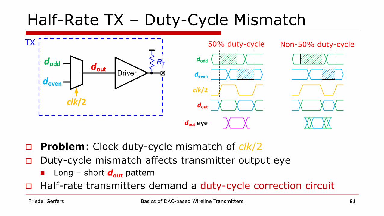
Problem: Clock duty-cycle mismatch of clk/2 Duty-cycle mismatch affects transmitter output eye
Long – short dout pattern Half-rate transmitters demand a duty-cycle correction circuit
Half-Rate TX – Duty-Cycle Mismatch
Friedel Gerfers Basics of DAC-based Wireline Transmitters 81
clk/2
dodd
deven
dout
dout eye
TX 50% duty-cycle Non-50% duty-cycle
doutRT
Driverdodd
deven
clk/2

CMOS 2:1 MUX able to propagate minimum pulse Half-rate clk/2 distribution still limited by clock distribution
Quarter-rate architecture enables 56Gbaud/s in 22nm FDX
Quarter-Rate TX
Friedel Gerfers Basics of DAC-based Wireline Transmitters 82
TX
RT
Driver
dodd
deven
clk/2clk/2
TX
RT
Driver
clk90
clk180
clk270
clk0
4:1MUX
d0d1d2d3

2:1 current-mode MUX function at TX output pads Makes sense if output time constant 𝝉 is smaller than on-chip
𝝉 =25Ω·COut
Very sensitive to clock phase spacing
Current-Mode Output-Multiplexed TX
Friedel Gerfers Basics of DAC-based Wireline Transmitters 83
TXRTRT
VDD
Vout,TX
Msw Msw
Mclk Mclk clk/2
devendeven
clk/2
Msw Msw
Mclk Mclk clk/2
dodddodd
clk/2
[C.-K. K. Yang, 1998][C. Menolfi, ISSCC, 2011]

Relevant TX Papers to See This Year
Suggested TX papers based on ISSCC 2021 Advance Program
8.1: „A 224Gb/s DAC-based PAM-4 Transmitter with 8-Tap FFE in 10nm CMOS“
8.2: „An Output Optimized 200Gb/s PAM-4 100Gb/s NRZ Transmitter with 5-Tap FFE in 28nm CMOS“
8.3: „An 8b DAC-based SST TX using metal gate resistors with 1.4pJ/b efficiency at 112Gb/s PAM4 and 8-taps FFE in 7nm CMOS“
8.4: „A 116Gb/s DSP based Wireline Transceiver in 7nm CMOS achieving 6pJ/bit at 45dB Loss in PAM4/Duo-PAM4 and 52dB in PAM2“
11.2: „A 26.5625Gbps to 106.25Gbps XSR SerDes with 1.55pJ/bit efficiency in 7nm CMOS “
Friedel Gerfers Basics of DAC-based Wireline Transmitters 84

References I[1] TU Berlin Wireline Transceiver Survey: https://www.msc.tu-berlin.de/menue/research/wireline_survey/[2] Oregon State Wireline Transceiver Survey: https://web.engr.oregonstate.edu/~anandt/linksurvey/[3] MIT, Digital Communication Systems: http://web.mit.edu/6.02/www/s2011/handouts/L07_slides.pdf
T-Coil J. Paramesh, D. Allstot, “Analysis of the Bridged T-Coil Circuit Using the Extra-Element Theorem“,
IEEE Tran. Circuits and Systems II, 2007 B. Razavi, “The bridged T-Coil”, IEEE Solid-State Circuits Magazine, 2015
MOS Matching, Tuning M. J.M. Pelgrom, et al., “Matching properties of MOS transistors”, JSSC, 1989 K. R. Lakshmikumar, et al., “Characterization and modeling of mismatch in MOS transistors for
precision analog design”, JSSC, 1989 A. DeHon, et al. “Automatic Impedance Control“, ISSCC, 1993 E. Wittenhagen, et al., “Advanced Mixed Signal Concepts Exploiting the Strong Body-Bias Effect in
CMOS”, TCAS I, 2020
Friedel Gerfers Basics of DAC-based Wireline Transmitters 85

References IICurrent-Steering DAC B. Razavi, “The Current-Steering DAC [A Circuit for All Seasons]”, JSSC Magazine, 2018 J. Mulder, “High-Speed Current-Steering DACs”, ISSCC Tutorial, 2015 C.-H. Lin, et al., “A 12b 2.9GS/s DAC with IM3 <-60dBc Beyond 1GHz in 65nm CMOS”, JSSC, 2009 K. O. Andersson, et al., “A Method of Segmenting Digital-to-Analog Converters”, Symp. MSD, 2003 C.-H. Lin, et al., “A 10-b 500MSample/s CMOS DAC in 0.6mm2”, JSSC, 1998 Chih-Kong Ken Yang, “Design of high-speed serial Links in CMOS”, PhD Stanford, 1998 T. Toifl, et al., "A 0.3pJ/Bit 112GB/S PAM4 1+0.5D TX-DFE Precoder and 8-Tap FFE in 14nm CMOS”,
Symp. VLSI Circuits, pp. 53-54, Jun. 2018 J. Kim et al., “A 112-Gb/s PAM-4 56 Gb/s NRZ reconfigurable transmitter with thee-tap FFE in 10-
nm FinFET”, JSSC, 2019. Z. Toprak-Deniz et al. "A 128Gb/s 1.3pJ/b PAM-4 Transmitter with Reconfigurable 3-Tap FFE in 14nm
CMOS," ISSCC, 2019 E. Groen et al., “A 10-to-112Gb/s DSP-DAC-based transmitter with 1.2Vppd output swing in 7nm FinFET,”
ISSCC, pp. 120-122, Feb. 2020
Friedel Gerfers Basics of DAC-based Wireline Transmitters 86

References IIIVoltage-Mode DACs W.D. Dettloff, et al., “A 32mW 7.4Gb/s Protocol-Agile Source-Series Terminated Transmitter in 45nm CMOS
SOI”, ISSCC, 2010 R. Sredojevic, “Fully Digital Transmit Equalizer With Dynamic Impedance Modulation”, JSSC, 2011 K.-L. J. Wong et al., “A 27-mW 3.6Gb/s I/O Transceiver”, JSSC, 2004 J. Poulton, et al.,”A 14-mW 6.25-Gb/s Transceiver in 90-nm CMOS”, JSSC, 2007 M. Kossel, et al., “A T-Coil-Enhanced 8.5Gb/s High-Swing SST Transmitter in 65nm Bulk CMOS With <-16dB
Return Loss Over 10GHz Bandwidth”, JSSC, 2008 M. Bassi, et al., “A 45Gb/s PAM-4 Transmitter Delivering 1.3Vppd Output Swing with 1V Supply in 28nm
CMOS FDSOI“, ISSCC 2016 H. Ghafarian, et al., “Analysis and Compensation Technique Canceling Non-Linear Switch and Package
Impedance Effects of a 3.2GS/s TX-DAC“, MWCAS, 2017 A. K. Joy, et al., “Analog-DFE-Based 16Gb/s SerDes in 40nm CMOS That Operates Across 34dB Loss
Channels at Nyquist with a Baud Rate CDR and 1.2Vpp Voltage-Mode Driver”, ISSCC, 2011 C. Menolfi et al., "A 112Gb/S 2.6pJ/b 8-Tap FFE PAM-4 SST TX in 14nm CMOS," ISSCC, 2018 K. Tan et al., “A 112-Gb/s PAM4 transmitter in 16nm FinFET”, Symp. VLSI Circuits, 2018 P-J Peng, at al., “A 112Gb/s PAM-4 voltage-mode transmitter with 4-tap two-step FFE and automatic phase
alignment techniques in 40nm CMOS,” ISSCC, pp.124-125, Feb. 2019 H. Ghafarian, et al., “A 9-bit, 45mW, 0.05mm2 Source-Series-Terminated DAC Driver with Echo Canceller in
22nm CMOS for In-Vehicle Communication”, SSC Letters, 2021
Friedel Gerfers Basics of DAC-based Wireline Transmitters 87
Copyright © 2022 FDOKUMEN


![[PSS 2A-1F5 A] Temperature Transmitters Model RTT15 with ...](https://static.fdokumen.com/doc/165x107/63234f56117b4414ec0c43f4/pss-2a-1f5-a-temperature-transmitters-model-rtt15-with-.jpg)