Distributed Beamforming of Two Autonomous Transmitters
83
Distributed Beamforming of Two Autonomous Transmitters A Major Qualifying Project Report Submitted to the Faculty of the Worcester Polytechnic Institute in partial fulfillment of the requirements for the Degree of Bachelor of Science By: _________________________ Michael T. Guay ________________________ Gregary B. Prince ________________________ Jonathan M. Rivers April 27, 2006 Approved: _______________________ Professor D. Richard Brown III, Project Advisor
-
Upload
khangminh22 -
Category
Documents
-
view
0 -
download
0
Transcript of Distributed Beamforming of Two Autonomous Transmitters

Distributed Beamforming of Two Autonomous Transmitters
A Major Qualifying Project Report
Submitted to the Faculty
of the
Worcester Polytechnic Institute
in partial fulfillment of the requirements for the
Degree of Bachelor of Science
By:
_________________________ Michael T. Guay
________________________
Gregary B. Prince
________________________ Jonathan M. Rivers
April 27, 2006
Approved:
_______________________
Professor D. Richard Brown III, Project Advisor

i
Abstract The distributed beamformer is a scheme which provides spatial diversity to combat the
undesired effects of the wireless channel. The distributed beamformer requires strict
carrier frequency and phase synchronization in order to maximize SNR at a destination
for fixed transmit powers. This project investigated the synchronization of two such
transmitters in a wired single path channel with off-the-shelf integrated circuits.
Additionally, a stable hardware platform for an acoustic (wireless) implementation of
such a distributed beamformer was provided.

ii
Executive Summary
The advent of wireless communication has required the development of various
schemes to combat the effects of fading in order to achieve reliable communications.
Sendonaris, Erkip, and Aazhang [2] state that independent of other diversity schemes
being employed, having multiple antennas on a communication device is beneficial due
to the additive spatial diversity the auxiliary antennas provide. However, having multiple
antennas on a single aperture is infeasible if not impractical on most modern day mobile
devices; therefore the concept of cooperative diversity[2], a form of spatial diversity in
which single-antenna transmitters in a multi-user communication system cooperate to
achieve the benefits of having multiple antennas [2]. Since the introduction of
cooperative diversity [2], researchers have focused on the development of cooperative
protocols. There have been several protocols which implement cooperative diversity and
they are divided into two classes: those that do not require carrier frequency and phase
synchronization (orthogonal subchannel protocols) and those that do (single subchannel
protocols), e.g. distributed beamforming.
A carrier synchronization scheme for the single subchannel protocol that permits
high rates of source and/or destination mobility was proposed in [0], where each source
node receives a transmitted beacon from the destination node by employing a frequency
synthesis phase locked loop (FS-PLL) tuned to the beacon frequency to generate a
secondary beacon signal that is phase locked to the master signal but at a different
determined frequency. A secondary group of FS-PLL’s receives this secondary beacon
and produces a carrier signal that is then used to modulate baseband waveforms. The
modulated waveform then propagates and coherent combining is achieved at the
destination.
Creating a collection of nodes and having them synchronize via the method
described in [0] would provide a means of verifying the simulation results with a proof of
concept demonstration. A wired system was constructed with two nodes and a series of
tunable delays in order to verify that the idea described in [0] functions correctly in easily
controllable single path channels before proceeding to implement a more complicated
wireless verification.

iii
After the system with wired channels was demonstrated, the next step was to
incorporate wireless channels. In order to develop a deeper understanding of the practical
aspects of cooperative communications and the ideas in [0], Acoustic Cooperative
Communications Experimental Network Testbed (ACCENT) was started. The motivation
for using an acoustic network stems from the fact that common RF communication
wavelengths can be replicated in the audible domain by scaling all frequencies in the RF
system, implying that the results obtained using the ACCENT system can easily be
translated into the RF domain. Moreover, by using an acoustic channel to transmit
wireless data, bit rates are inherently lower, thus allowing for real-time network operation
with simple, low-cost hardware.
Since the ACCENT nodes transmit through an acoustic channel, the transducers
and audio signal chain had to be carefully designed, constructed, and tested. This
involved design of a hardware platform and frequency and directivity response testing to
insure a relatively flat frequency response in the node circuitry. Also, one of the main
components of the node circuitry is the digital signal processor board, which was
designed and tested by verifying functionality.

iv
Table of Contents Table of Tables ............................................................................................................. vii 1 Introduction .................................................................................................................. 1 2 Background .................................................................................................................. 3
2.1 Cooperative Diversity ............................................................................................... 3 2.2 Distributed Beamforming ......................................................................................... 5
2.2.1 Principles of Transmit Beamforming................................................................. 5 2.2.2 Specific Challenges of Distributed Beamforming.............................................. 8
2.3 Two –Source Distributed Beamforming System ...................................................... 9 2.4 Phase Locked Loops ............................................................................................... 10
2.4.1 Principles of Operation.................................................................................... 11 3. Wired Two-Source Carrier Synchronization System ..................................... 13
3.1 Source Node Design ............................................................................................... 13 3.1.1 Phase Locked Loop .......................................................................................... 14 3.1.2 Frequency Synthesis Considerations ............................................................... 17 3.1.3 Loop Filter ....................................................................................................... 18 3.1.4 Channel Implementation .................................................................................. 20 3.1.5 Summing Node Implementation ....................................................................... 21
3.2 Wired Synchronization System Results.................................................................. 23 4.1 ACCENT Node Embedded Controller ................................................................... 27
4.1.1 Design Methodology ........................................................................................ 27 4.1.2 dsPIC-AIC23 Board Design ............................................................................ 30 4.1.3 Verification of dsPIC –AIC23 Interface .......................................................... 32
4.2 Microphone Circuitry.............................................................................................. 35 4.2.1 Current Design................................................................................................. 35 4.2.2 Prior Test Results and Issues ........................................................................... 36 4.2.3 Low-Resonance Booth Background Measurements and Results ..................... 37 4.2.4 Microphone Circuitry Design Modifications................................................... 38 4.2.5 Microphone Circuitry Frequency Response Test Methodology and Results... 42 4.2.6 Microphone Circuitry Directivity Test Methodology and Results ................... 50
5 Recommendations ................................................................................................... 53 5.1 Microphone circuitry .......................................................................................... 53 5.2 Microcontroller-Codec system............................................................................ 53 5.3Other Issues ......................................................................................................... 55
6 Conclusion ................................................................................................................. 56 7 APPENDIX I: ACCENT Node Embedded Controller PCB Notes.................. 57 8 APPENDIX II: Accent Node DSP Board Hardware .......................................... 63 9 APPENDIX III: dsPIC Application Code ............................................................. 64 9 APPENDIX IV: Microphone Directivity Code .................................................... 73 10 Bibliography ............................................................................................................ 75

v
Table of Figures Figure 1: Transmit beamformer block diagram. ................................................................. 6 Figure 2: Two source carrier synchronization system. ..................................................... 10 Figure 3: Elements of a phase locked loop. ...................................................................... 10 Figure 4: Source node block diagram. .............................................................................. 14 Figure 5: Block diagram of the Sa7025 from Phillips Semiconductors. .......................... 15 Figure 6: Schematic of the CD74HC7046 phase locked loop from Texas Instruments <SCHS218> ...................................................................................................................... 16 Figure 7: JK flip flop frequency synthesizer schematic.................................................... 18 Figure 8: Illustration of frequency synthesis. ................................................................... 18 Figure 9: Loop filter for wired synchronization system using MC14007UB MOSFET. . 19 Figure 10 : 555 Timer delay circuit with duty cycle control. ........................................... 21 Figure 11: Two sample delays invoked by the 555 timer. ................................................ 21 Figure 12: Summing node function. ................................................................................. 22 Figure 13: Summing circuitry........................................................................................... 22 Figure 14: Demonstration of 555 timer delay.................................................................. 23 Figure 15: Demonstration of multiply by 2 frequency synthesizer. ................................. 24 Figure 16: Phase jitter of PLL........................................................................................... 24 Figure 17: Inverted sum of the destination waves. ........................................................... 25 Figure 18: ACCENT concept [9]. ..................................................................................... 26 Figure 19: ACCENT node. ............................................................................................... 27 Figure 20: dsPIC/codec communication interface............................................................ 28 Figure 21 : SPI timing diagram......................................................................................... 29 Figure 22: I2S timing diagram.......................................................................................... 29 Figure 23: dsPIC & codec schematic................................................................................ 31 Figure 24: PCB layout for PIC codec board. .................................................................... 32 Figure 25: Serial clock, serial bit stream, and latch signal. .............................................. 33 Figure 26: ADC DAC DCI verification............................................................................ 33 Figure 27: Digital filtering part 1...................................................................................... 34 Figure 28: Digital filtering part 2...................................................................................... 34 Figure 29: Digital filtering part 3...................................................................................... 35 Figure 30: ACCENT microphone circuit [9]. ................................................................... 35 Figure 31: ACCENT NODE comparative microphone frequency response [9]. ............. 37 Figure 32: Frequency response of sound booth background noise................................... 38 Figure 33: Highpass filter schematic ................................................................................ 39 Figure 34: Highpass filter response. ................................................................................. 40 Figure 35: Post differential receiver high pass filter......................................................... 40 Figure 36: Frequency response of ACCENT microphone on-axis. .................................. 41 Figure 37: Frequency response of ACCENT node microphone normal........................... 42 Figure 38: Measurement microphone and powered speaker. ........................................... 43 Figure 39: Measurement microphone with ACCENT node in place................................ 43 Figure 40: ACCENT Node microphone, normal. ............................................................. 43 Figure 41: ACCENT mode microphone, on-axis. ............................................................ 43 Figure 42: Sound booth and acoustical test setup............................................................. 44 Figure 43: Microphone testing flowchart. ........................................................................ 45 Figure 44: ACCENT microphone comparative frequency response. ............................... 46

vi
Figure 45: Spectrogram of signal sent from HP ZD8060. ................................................ 47 Figure 46: Spectrogram of reference microphone. ........................................................... 48 Figure 47: Spectrogram of ACCENT node microphone normal. ..................................... 49 Figure 48: Spectrogram of ACCENT MIC on-axis.......................................................... 50 Figure 49: Directivity test setup........................................................................................ 51 Figure 50: Directivity response of ACCENT node normal. ............................................. 52 Figure 51: Voltage level translator. .................................................................................. 54 Figure 52: PIC instruction picture 1.................................................................................. 57 Figure 53: PIC instruction picture 2.................................................................................. 58 Figure 54: PIC instruction picture 3.................................................................................. 59 Figure 55: PIC instruction picture 4.................................................................................. 60 Figure 56: PIC instruction picture 5.................................................................................. 61 Figure 57: PIC instruction picture 6.................................................................................. 62

vii
Table of Tables
Table 1: Component values for CD74HC4046AE. .......................................................... 17 Table 2 : Loop filter component values. ........................................................................... 20 Table 3: Component values for high pass filter. ............................................................... 39
1 Introduction
The advent of wireless communication has required the development of various
schemes to combat the effects of fading in order to achieve reliable communications.
These schemes have been termed diversity schemes, and are attractive due to the fading
characteristics of the wireless channel. The main forms of diversity are associated under
three categories: spatial, temporal, and frequency. Sendonaris, Erkip, and Aazhang [2]
state that, independent of other diversity schemes being employed; having multiple
antennas on a communication device is attractive due to the additive spatial diversity the
auxiliary antennas provide. However, having multiple antennas on a single aperture is
infeasible if not impractical on most modern day mobile devices; therefore the concept of
cooperative diversity [2], a form of spatial diversity in which single-antenna transmitters
in a multi-user communication system cooperate to achieve the benefits of having
multiple antennas communication systems, was developed by [2].
There have been several protocols which implement cooperative diversity [2] and
they are divided into two classes: those that do not require carrier frequency and phase
synchronization (orthogonal subchannel protocols) and those that do (single subchannel
protocols) e.g. distributed beamforming. The approaches that use carrier synchronization
have the potential for achieving an increase in power efficiency and achievable rate
relative to the protocols which operate in an orthogonal subchannel. A disadvantage is
that the transmitters require strict carrier frequency and phase synchronization in order
for coherent combing at the intended destination to occur, hence, the development and
implementation of carrier synchronization schemes for coherently combined cooperative
transmission is of particular importance to cooperative diversity protocols.
This carrier synchronization problem was considered in the context of distributed
beamforming in [6] where coherent combining is achieved through a master
synchronization beacon and precise placement of both the source and destination nodes is
performed in order to equalize all round-trip propagation times.
Pottie [7] proposed that a beacon can be used to measure round-trip phase delays
between each transmitting node and the destination. A common time scale must be

2
tracked by all nodes in the network and this is achieved through the “master” receive
antenna clock. The destination can then estimate these phase delays and transmit them to
the appropriate nodes for local phase pre-compensation to ensure source synchronization.
While there are several theoretical papers in the literature, there is no discussion
of a physical realization of the distributed beamformer. In this project a physical
realization of the carrier synchronization system described in [0]. This was accomplished
in two phases, first, to ensure the basic operation of the system, a wired two source one
destination carrier synchronization with easily controllable single-path channel delays.
Secondly, to provide a platform for testing in more complicated channel environments,
the hardware for an acoustic test bed consisting of a microcontroller board, filter board,
and power supply board was developed
The future of this project will revolve around testing the provided hardware
platform in the acoustic channel. With this platform, a researcher will have an easily
programmable and self powered ACCENT node that can be customized for an array of
purposes. The prospect of expandability was the objective in so far as hardware is
concerned.

3
2 Background
Before pursuing a course of action for the project, the team was required to
understand the needs and technical requirements for the implementation and modification
of a carrier frequency and phase synchronization system. Having an initial understanding
of the concept of cooperative diversity, the different types of protocols, and the practical
problem of physically implementing a synchronization system was essential to a
successful project. Firstly, we discuss the theory of cooperative diversity and then
proceed with the theories of beamformers and phase locked loops to provide the reader
with an understanding of the tools used to realize the distributed beamformer outlined in
[0].
2.1 Cooperative Diversity
Due to the nature of the noisy wireless channel many diversity schemes have been
developed to combat the effects of fading i.e. severe variations in signal attenuation. It
has been found by Sendonaris, Erkip, and Aazhang [2] that spatial diversity is
particularly attractive in that it may be used in conjunction with other forms of diversity
for a relatively small amount of additional overhead. In other words, having multiple
antennas on a communication device is attractive due to the additive spatial diversity the
auxiliary antennas provide. However, having multiple antennas on a single aperture to
create a beamformer is impractical if not infeasible on practically all mobile devices;
therefore the concept of cooperative diversity, a form of spatial diversity in which single-
antenna transmitters cooperate to achieve the benefits of having multiple antennas, was
developed by [2]. This concept implies that single transducer devices may create a
beamformer by cooperatively making use of the antennas of other transmitters in the
system. The results of [2] show that cooperation amongst nodes leads to an increase in
each user’s capacity and a decrease in susceptibility of user rates to channel fading
despite the fact that the channel between user nodes is noisy.
The concept of cooperative diversity functions as follows. The active users in a
cooperative network are defined as users whom each have unique data to transmit on the

4
network and are not strictly defined as just an information relay. The demonstration
Sendonaris [2] provides is based upon the Code Division Multiple Access (CDMA)
transmission network for cellular communication. In simplest terms a network consists
of two active users and a base station (BS).
In Sendonaris’ CDMA demonstration in [2], there are three transmission periods.
The first period is the transmission of data from one user to the base station. The second
period is used to send information to the base station and the other cooperative user. This
information is interpreted by the cooperative user, and transmitted in period three as a
cooperative signal. Sendonaris admits that there is some redundancy in the third
transmission period, as some previously transmitted information is resent (the result
being two new bits of information being sent per three periods). However, he indicates
that this is justifiable given the performance increase, arguing that it is better to send one
high signal-to-noise ratio (SNR) bit than ten lower SNR bits. Since a bit is only useful if
it is received, the focus should instead be upon sending bits that have a higher probability
of reception.
There are two main conclusions drawn in [2] that advocate the use of cooperative
networks. First, higher throughput and data transmission rates are allowable through
cooperative networks. A positive side effect of this conclusion is that battery life on
mobile phones will be extended due to the more lenient power requirements present in a
cooperative environment. Also, a tradeoff between coverage area and data rates could be
made. If a particular provider decided that they wanted an expansive coverage area, they
could simply use lower data rates or vice versa.
The second, and possibly the more compelling conclusion is that the use of
cooperative networks leads to reduced sensitivity to channel effects. Sendonaris
postulates that even if the cooperative strategy did not lead to increased data rates that the
increased robustness as a result of using cooperation is a worthy cause. Hence
investigation into protocols performing the cooperative diversity scheme is desirable to
achieve the advantages of additive spatial diversity.

5
2.2 Distributed Beamforming
The fact that multiple antennas cannot be practically placed on a single device
precludes the use of spatial diversity in many scenarios. However, with the use of
transmit beamforming, communication devices may achieve higher throughput and data
transmission by exploiting the additive spatial diversity created by the beamformer.
Cooperative Diversity as discussed in section 2.1 Cooperative Diversity is a means of
exploiting such diversity gains. In Sendonaris’ cooperative model, the third transmission
interval assumes that the transmission of both sources arrive in phase at the destination
[1]. This assumption is a distributed beamformer. To better understand distributed
beamforming, the basics of conventional transmit beamformers are discussed followed by
a discussion of the challenges of distributed beamforming
2.2.1 Principles of Transmit Beamforming
The basic principle of transmit beamforming is to maximize the received Signal to
Noise Ratio (SNR) at the intended destination. It is a general signal processing technique
used to control the directionality of the transmission of a signal on a transducer array. A
transmit beamformer itself is a spatial filter that operates on the output of an array of
sensors in order to enhance the amplitude of a coherent wavefront relative to background
noise and directional interference. A block diagram of a general transmit beamforming
scheme is depicted in Figure 1.

6
Figure 1: Transmit beamformer block diagram.
The objective of beamforming is to sum multiple elements in an array to achieve a more
focused response in a desired direction determined by the Minimum Response Angle
(MRA) [8]. That way when a sound from a given transmitted beam is heard, it is known
from which direction it came. Beamforming and beam scanning are generally
accomplished by phasing the feed to each element of an array so that signals received or
transmitted from all elements will be in phase in a particular direction [8]. This is the
direction of the beam’s maximum orientation, which is typically Gaussian in nature.
Beamforming and beam scanning techniques are typically used with linear, circular, or
planar arrays but some approaches are applicable to any array geometry [8].
The purpose of this report, however, is to provide a general concept of the
practical purpose of beamforming, not its implementation details. Herein cooperative
diversity and energy efficiency are motivating factors for exploiting the benefits of
beamforming. In the context of this project the transducers being used are to replicate
antennas on mobile devices using a variation of the delay-sum beamformer.
∑. . .
...
TX 1
Destination
RX
h1
Channel
TX 2
TX n
h2
hn
X1
X2
Xn
ξ1
ξ2
ξn
y

7
2.2.1.1 Energy Gains of Transmit Beamforming The question of how is directional transmission achieved is of particular importance. In
beamforming, each user’s signal is multiplied with complex weights that adjust the
magnitude and phase of the signal to and from each antenna. This causes the output from
the array of antennas to form a transmit beam in the desired direction and minimizes the
output in other directions. This directionality provides a strong energy gain observed at
the destination.
Referring to Figure 1, the receiver obtains the data
wxhy T vvvv+= )(* ξ
where *hv
is the complex conjugate of the channel response matrix, xv is the user data
vector, Tξv
is the transpose of beamformer weight vector, and wv is the AWGN matrix.
For example, assume the transmitter knows the channel perfectly. This knowledge would
enable the transmitters to send
hhxx T v
vvv =ξ
to maximize the received SNR by coherent reception of all signals at the receiver. The
problem is that more often than not the transmitters do not have full knowledge of the
channel through which they are sending information. Hence the ability to achieve
synchronization of signals in an unknown channel state is desired and this is achieved via
a synchronization method used to create a high gain steerable antenna with significantly
higher SNR.
2.2.1.2 Diversity Gains of Transmit Beamforming Diversity provides redundancy enabled by the spatial interleaving of signals and
causes fewer fluctuations in the observed SNR. Beamformers provide N-fold diversity

8
Gain as opposed to omnidirectional antennas. This diversity gain increases system
capacity, coverage, quality, and data rate via Spatial Division Multiple Access (SDMA).
Redundancy across multiple paths ensures quality.
2.2.2 Specific Challenges of Distributed Beamforming
The notion of a distributed beamformer has been researched in recent years and
has been given particular attention as of late. It can be shown that distributed
beamforming can increase energy efficiency of communications in sensor networks
similar to that of a conventional beamformer. Distributed beamforming is the
coordination of transmissions from neighboring transmitting antennas in order to form an
antenna array that directs the beam to a desired location. Distributed beamforming is akin
to transmit beamforming with the exception that each antenna has its own local oscillator.
Hence distributed beamformer protocols, require strict transmitter synchronization in
order for coherent reception of beamformer data at the intended destination. As long as
this synchronization is ensured, the ad-hoc transmitters may form a distributed
beamformer and in consequence achieve the added benefits of multiple antenna spatial
diversity (cooperative diversity)
In the literature two methods have been identified to achieve carrier frequency
and phase synchronization. Madhow [6] showed that coherent combining can be achieved
through a master synchronization beacon with precise placement constraints placed on
both the source and destination nodes in order to equalize all round-trip propagation
times. Pottie [7] proposed that a beacon can be used to measure round-trip phase delays
between each transmitting node and the destination. A common time scale must be
tracked by all nodes in the network and this is achieved through the “master” receive
antenna clock. The destination can then estimate these phase delays and transmit them to
the appropriate nodes for local phase pre-compensation to ensure coherent reception at
the destination. Both of these models achieve coherent reception; however, the amount of
mobility permitted by the nodes and destination are strictly limited in [6] and is restricted

9
by the amount of time required to estimate, quantize, deliver, and implement the phase
pre-compensation estimates in [7]. Hence, mobility is a major challenge of the
distributed beamformer.
2.3 Two –Source Distributed Beamforming System
Due to limited performance of the distributed beamformer in mobile networks,
further investigation into synchronization schemes was conducted. Brown [0] developed
a method for achieving the same goal as [6] and [7], coherent combination of distributed
synchronized sources with the ability for nodes to be mobile. Herein, the two source
distributed beamformer shall refer to the work in [0]. Brown’s work improves upon the
prior schemes, but the distributed beamformer’s performance still degrades in the
presence of the multipath channel.
The two source distributed beamformer system depicted below in Figure 2 is the
means by which this project demonstrated the ability to construct a beamformer. This
beamformer (synchronization) system permits high rates of source and/or destination
mobility, thus being tremendously practical for mobile device beamformer applications.
Its operation is as follows:
• Each source node receives a transmitted beacon from the destination node
by employing a frequency synthesis phase locked loop (FS-PLL 11 & FS-
PLL 21) tuned to the master beacon frequency.
• FS-PLL’s 11 & 21 generate a secondary beacon signal that is phase
locked to the master signal but at a different determined frequency (in this
project the determined frequency is two times that of the incoming
frequency).
• The secondary group of FS-PLL’s (12 & 22) receives this secondary
beacon and produces a carrier signal then used to modulate baseband
waveforms and then proceeds to the destination for coherent cooperative
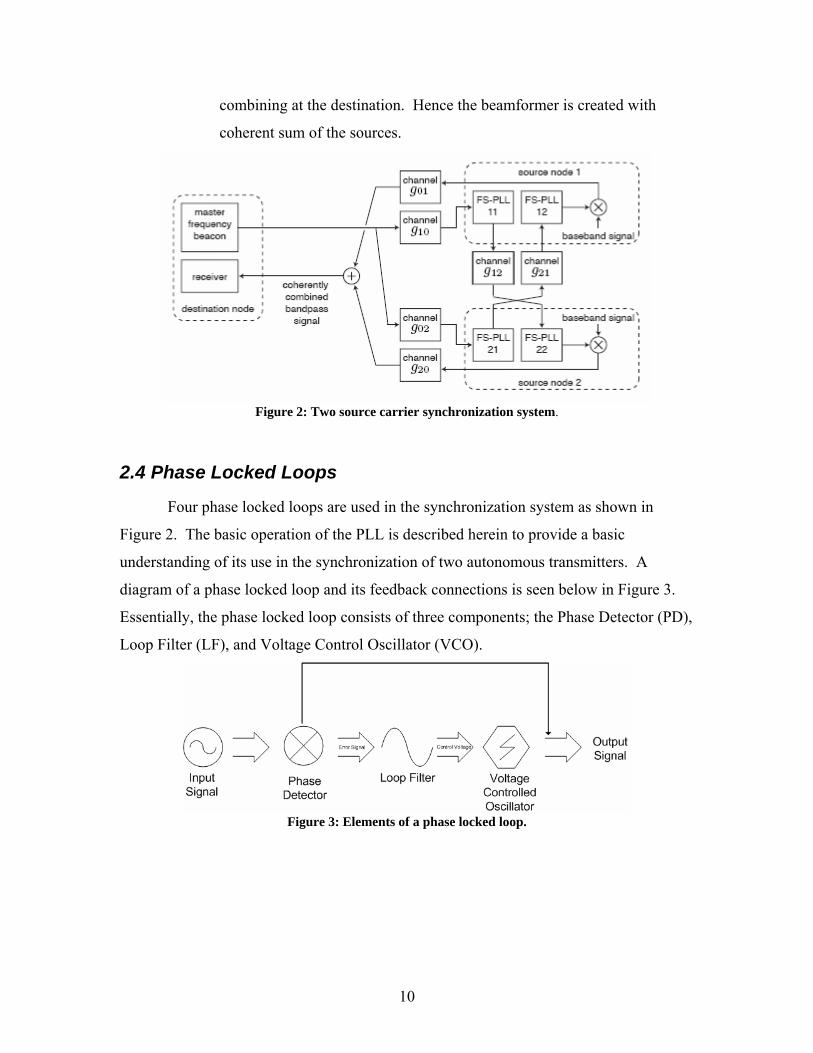
10
combining at the destination. Hence the beamformer is created with
coherent sum of the sources.
Figure 2: Two source carrier synchronization system.
2.4 Phase Locked Loops
Four phase locked loops are used in the synchronization system as shown in
Figure 2. The basic operation of the PLL is described herein to provide a basic
understanding of its use in the synchronization of two autonomous transmitters. A
diagram of a phase locked loop and its feedback connections is seen below in Figure 3.
Essentially, the phase locked loop consists of three components; the Phase Detector (PD),
Loop Filter (LF), and Voltage Control Oscillator (VCO).
Figure 3: Elements of a phase locked loop.

11
2.4.1 Principles of Operation
The PD essentially generates a voltage signal, which represents the phase
differential between two signal inputs. The Phase Frequency Detector (PFD) is a specific
type of PD comprised of two flip-flops which detect phase as well as frequency
deviations. The use of the PFD prevents the synchronizing (locking) to the harmonics of
the reference signal. One such ambiguity is addressed in [0], in which Brown compares
the operation of the traditional modulo-2 addition (XOR) gate with that of the PFD. The
XOR gate approach may lock on to phases on the order of 2πn as opposed to the PFD
locking on to phases π2n . Hence, output source phase ambiguity is eliminated by
choosing to use the PFD as opposed to other such Phase Detectors which do not lock at
phase multiples of π2 .
Given an input of the form )sin()( 1111 ϑω +Ψ= ttu and a secondary input Walsh
function (Square Wave) of the form )()( 2222 ϑω +Ψ= trecttu , which may be expressed as
a Fourier series ])12cos[()12(
14)( 220
22 ϑωπ
+++
Ψ= ∑∞
=
tkk
tuk
, one may see that the
higher order harmonics of the )(2 tu hold no information to the phase deviations between
reference signals [5].
This result gives rise to the importance of the loop filter. As described above the
harmonics of 2ω are inconsequential to performance of the phase locked loop. Hence a
low pass filter is required as the general purpose loop filter for the phase locked loop to
provide only linear term frequencies of the inputs. There are many pros and cons to the
particular choice of the loop filter; whether it is an active or passive filter, higher order,
etc. Loop filters are outlined in [5].
The third element of the PLL is the VCO, which is an electronic oscillator
specifically designed to be controlled in oscillation frequency by a reference input control
voltage. The frequency of oscillation is varied with an applied DC voltage obeying the
following relation refuK002 += ωω , where 0K is the VCO gain. Typically the frequency
of a voltage-controlled crystal oscillator can only be varied by a few tens of parts per
million (ppm). The high Q-factor of the crystals allows only a small "pulling" range of

12
frequencies to be produced. Brown [0] discusses the center frequency inaccuracy and its
effects on output phase ambiguity.

13
3. Wired Two-Source Carrier Synchronization System
An investigation of the performance of the two node carrier synchronization
shown in Figure 2 was performed using off-the-shelf PLL’s and flip-flops to create the
FS-PLL’s of each node and 555 timers to replicate the channel delays. . The scheme
implemented modeled that of a single path channel and provided the entire team with an
understanding of the concept of carrier frequency and phase synchronization, via a means
of confirming the ideas discussed in [0] under controlled channel conditions.
3.1 Source Node Design
Each board has the following functional elements in each as seen in Figure 4. The
PLL and JK flip flops are the core of each source node and together they form the
frequency synthesis phase locked loops of each source node as seen in Figure 4 below.
The channel delays have been implemented via 555 timers with the design constraint that
sum of three channel delays on each board equal each other, as proposed in Brown [0].
Herein the details of three components are discussed in detail.
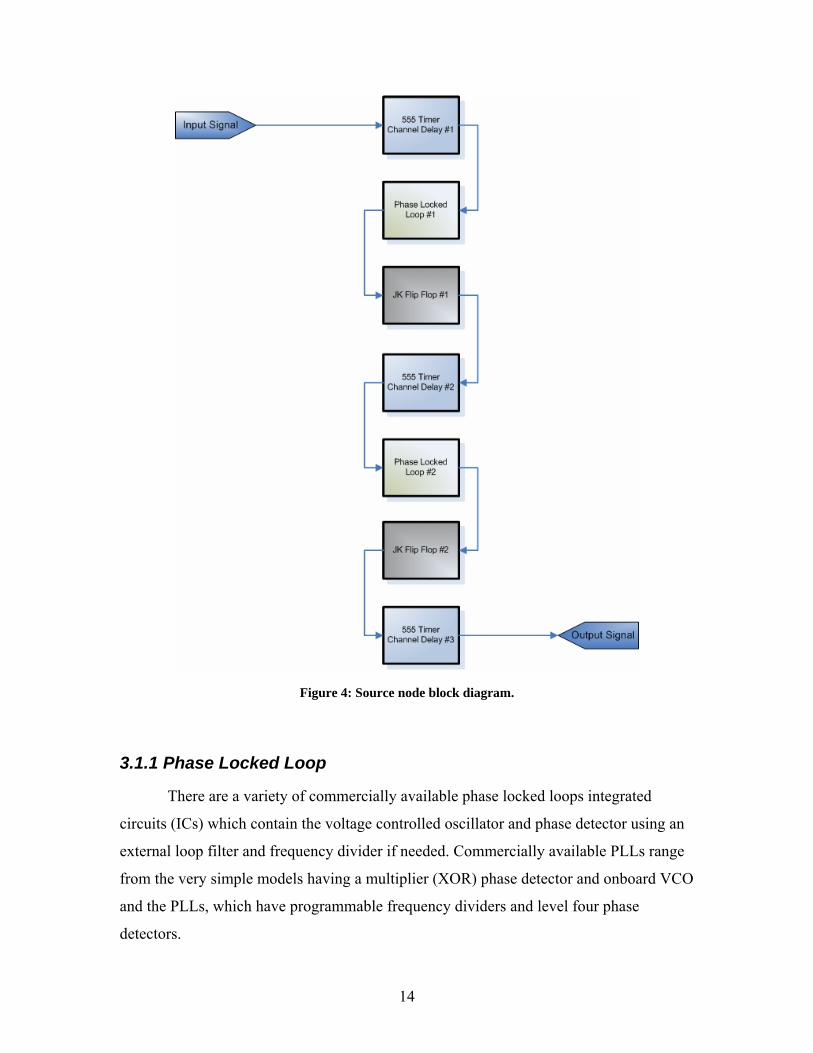
14
Figure 4: Source node block diagram.
3.1.1 Phase Locked Loop
There are a variety of commercially available phase locked loops integrated
circuits (ICs) which contain the voltage controlled oscillator and phase detector using an
external loop filter and frequency divider if needed. Commercially available PLLs range
from the very simple models having a multiplier (XOR) phase detector and onboard VCO
and the PLLs, which have programmable frequency dividers and level four phase
detectors.

15
There are also integrated circuits available, which contain blocks such as the
phase detector and programmable frequency divider. This system would employ an
external VCO and loop filter. An example of this is the SA7025 by Phillips
Semiconductors. This IC features fractional N division with operation up to 1.04 GHz.
This chip's dividers and counters are programmed through a 3 wire serial interface. A
block diagram is shown below in Figure 5.
Figure 5: Block diagram of the Sa7025 from Phillips Semiconductors.
This IC contains two D-type flipflop phase frequency detectors with charge pump
outputs, also known as the common phase frequency detector. The IC features a normal
output charge pump, a speed-up charge pump, and an integral output charge pump.
Typical applications of this IC are found in spread-spectrum receivers and cellular radio.
The TLC2932 and the CD 74HC7046A by Texas Instruments are also IC’s
designed for phase locked loop systems. They are composed of a VCO and an edge-
triggered-type phase frequency detector (PFD). The oscillation frequency range of the

16
VCO’s are set by an external bias resistor. The VCO of the TLC2932 has a 1/2 frequency
divider at the output stage. The high-speed PFD’s with internal charge pump detects the
phase difference between the reference frequencies and signal frequency input from the
external divider.
The Phase Locked Loop (PLL) chip CD74HC7046A was chosen to meet two
specific requirements. One design choice was the usage of the phase frequency detector
(type 4) as the phase detector due to the analysis on false locking outlined in [0]. An
internal voltage controlled oscillator facilitated the design effort by not having external
complex circuitry to the PLL, and the team opted to find an off the shelf PLL with this
added feature to simplify the design. The loop filter of the PLL was constructed external
to the chip to control convergence of the locked state. A schematic of the
CD74HC7046A can be seen below in Figure 7.
Figure 6: Schematic of the CD74HC7046 phase locked loop from Texas Instruments <SCHS218>
Below is a table of passive component values for the indicated response for each
external element for the CD74HC4046AE. The R1 and C1 components together dictate
the frequency range of the voltage controlled oscillator. With the values indicated, a

17
frequency range of 14 kHz at a supply voltage of 4.5 V is introduced. The design did not
call for the use of a frequency offset or demodulation, hence R2 and R5 were not
required. Lastly, the lowpass filter design for this application was more involved than a
simple RC lowpass as suggested by the manufacturer (see section 3.1.3 for discussion).
Description Component Value VCO frequency range R1 5.61 kΩ VCO frequency range C1 0.1 µF
Extra VCO frequency offset R2 Not Needed Demodulator Output R5 Not Needed
Lowpass Filter R3 Modified Filter1 Lowpass Filter C2 Modified Filter2
Table 1: Component values for CD74HC4046AE.
3.1.2 Frequency Synthesis Considerations
The PLL chosen was not able to synthesize frequency as it was packaged;
therefore a simple JK flip flop was used to implement the frequency divider due to the
square wave nature of the selected PLL IC. This design choice was simple in that FS-
PLL’s cost more than a PLL and a flip flop combined and its implementation was straight
forward. The JK flip flop implements a frequency divider in a direct and uncomplicated
manner. Consider the JK Flip Flop circuit in Figure 7. Figure 8, illustrates that given a
reference clock signal, the gray square wave, and the given configuration in Figure 8; a
clock signal at half the clock input frequency will appear at the output Q1. The basic
operation is as follows: if inputs J and K are tied to VCC, then flip flop transitions on a
rising edge and hence the frequency is halved.
1 See section 3.1.3 for Loop Filter Discussion 2 See section 3.1.3 for Loop Filter Discussion

18
Figure 7: JK flip flop frequency synthesizer schematic.
Figure 8: Illustration of frequency synthesis.
3.1.3 Loop Filter
The loop filter of the wired system is akin to that of the [0]. The only difference
is that the particular PLL chip chosen to perform synchronization in this system produces
a voltage from the charge pump of the phase detector and a slightly modified loop filter
was designed in order to compensate for a voltage signal as opposed to a current signal.
The loop filter may be seen below in Figure 9.

19
Figure 9: Loop filter for wired synchronization system using the MC14007UB MOSFET.
The transfer function of the loop filter is simply the ratio of impedances
1Z and 2Z .
11 RZ = (2)
12
212
)(
CCZ
CZC
ZZRZRZ
Z++
+= (3)
Analysis in the Laplace Domain implies that the impedance of each capacitor is of the
form 1)( −= iCi sCZ , which implies that
)(
1)()(
])([)()(
21212
21
11
2
12
11
2 CCsRCCsRsC
sCsCRsCRsC
ZsHZ
Z
Z
Z
+++
=++
+== −−
−−
(4)
Taking the ratio of the two individual transfer functions yields the overall loop
filter transfer function.
121121
22
1
2
)(1
)()()(
RCCsRRCCsRsC
sGsH
ZZ
sFZ
Z
+++
=== (5)
According to the design criteria, PLL phase jitter may be minimized so long as the
bandwidth tω obeys the following constraint:

20
⎥⎦
⎤⎢⎣
⎡ +<<<<
Zt
Z RCCCC
RC 21
21
2
1 ω
where the upper bound is the non DC pole location and the lower bound is the transfer
function’s zero location. This constraint ensures adequate phase margin i.e. ensures loop
stability.
The loop bandwidth for consideration was 50 Hz and adhering to the design
criteria it was determined that the following values would yield an appropriate phase
margin and loop bandwidth. In particular these values yield a phase margin
of 253450592.1 << .
2C Fµ1.0
1C pF10
ZR ΩM1
1R Ωk1
Table 2 : Loop filter component values.
3.1.4 Channel Implementation
Once the node hardware was created, the channels needed to be modeled. For the
demonstration of a single path wired system, the channels were simply time delays. An
investigation of the popular 555 timer was performed due to its flexibility. The 555 timer
delay was composed of two timers in series, the first controlled the delay of the square
wave and the second controlled the duty cycle based on particular choices of external
resistors and capacitors. The 555 timer solution worked well with PLL and the square
waves produced and served as a solution to modeling the single path wired channel.
The circuit in Figure 10 below illustrates generating a single positive pulse which
is delayed relative to the trigger input time. The circuit employs two stages so that both
the pulse width and delay can be controlled. When triggered, the output of the first stage
will move up and remain near the supply voltage until the delay time has elapsed. The
second 555 stage will not respond to the rising voltage since it requires a negative, falling
voltage at pin 2, and so the second stage output remains low and the relay remains de-

21
energized. At the end of the delay time, the output of the first stage returns to a low level,
and the falling voltage causes the second stage to begin its output cycle.
Figure 10 : 555 Timer delay circuit with duty cycle control.
Figure 11: Two sample delays invoked by the 555 timer.
The resistor and capacitor values for the delay circuit can be chosen with the
constraint that each delay RC constant CRR BA )( 11 +=τ , where C is the capacitance seen
at both AC1 and BC1 , must account for the frequency of the incoming signal. For example,
a 2.5 kHz signal requiring a 0.1 ms delay will have a different RC value than a 5 kHz
signal requiring the same 0.1 ms delay.
3.1.5 Summing Node Implementation
Referring back to Figure 2, one may see that the synchronization system requires
two nodes, 6 channels and one summing node to perform coherent combination of the

22
sources. Figure 4 illustrates how 3 channels and one node (comprised of two FS-PLL’s)
generate an output signal. This output signal generated by each node is sent to the
summing node. If the synchronization scheme works the output of the summing node
will be the same waveform with the sum of the node output amplitudes. Figure 12
provides an illustration the role the summing node plays in the overall synchronization
system.
Figure 12: Summing node function.
To implement a circuit which is capable of taking the waveforms processed by
each node and taking their sum, a simple summer circuit was investigated. For the two
source carrier synchronization system, we only have two incoming waveforms hence the
circuit depicted in Figure 13, provides the appropriate summing properties. The output is
described by )( 21 VVVout +−= . The negation has no impact to the performance of
coherent combination of sources.
Figure 13: Summing circuitry.

23
3.2 Wired Synchronization System Results
The wired synchronization system was the focal point of the first phase of this
project and confirmation of the results obtained in [0] were desired. With the wired
system designed and implemented on breadboards, testing began. While testing the
performance of the wired system, four main functionalities were scrutinized throughout.
1. Verification of single-path delays
2. Verification of PLL operation
3. Verification of frequency synthesis
4. Verification of summing node
5. Verification of overall coherent combining operation
6. Jitter and other performance metrics
Referring back to Figure 11, it may be noted that the width of the time delay pulse is
directly proportional to the physical waveform delay. Figure 14 illustrates the effect of
this delay by showing the input signal in blue in conjunction with its delayed version in
purple.
Figure 14: Demonstration of 555 timer delay
The JK flip flop’s functionality as a frequency divider was confirmed as
illustrated in Figure 15. The input signal was applied to the JK Flip Flop clock (green
signal) and a signal at double the frequency was produced (blue signal).
24
Figure 15: Demonstration of multiply by 2 frequency synthesizer.
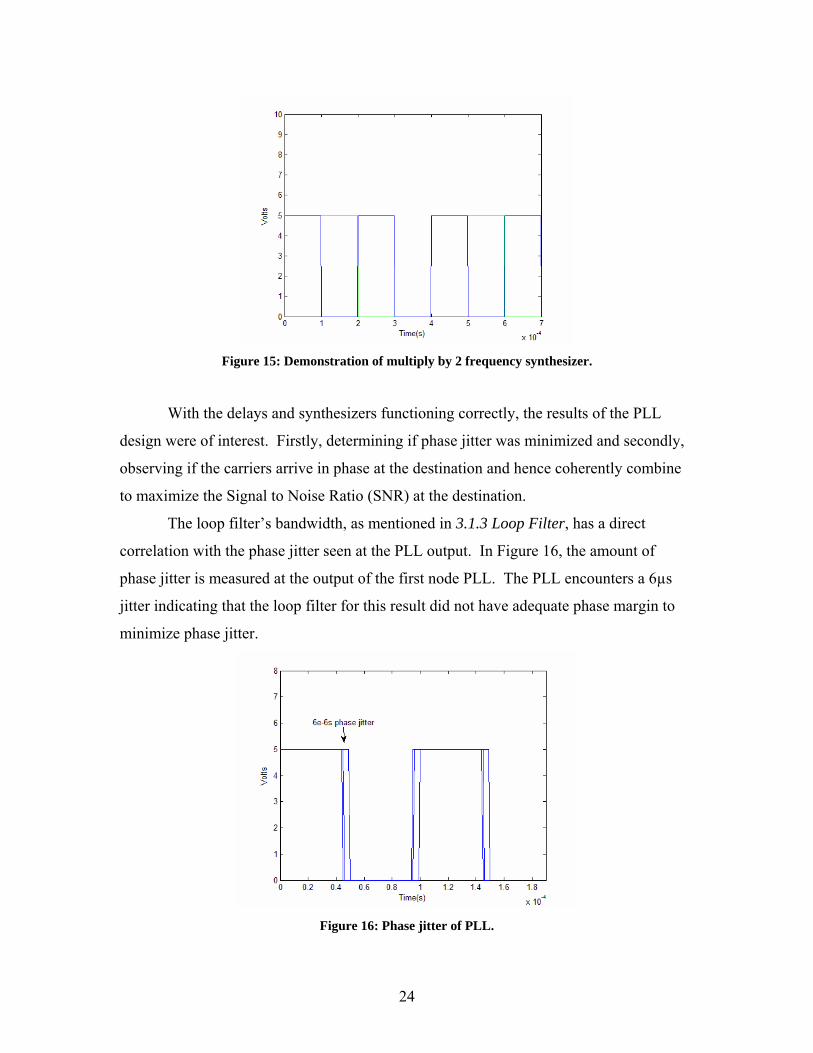
With the delays and synthesizers functioning correctly, the results of the PLL
design were of interest. Firstly, determining if phase jitter was minimized and secondly,
observing if the carriers arrive in phase at the destination and hence coherently combine
to maximize the Signal to Noise Ratio (SNR) at the destination.
The loop filter’s bandwidth, as mentioned in 3.1.3 Loop Filter, has a direct
correlation with the phase jitter seen at the PLL output. In Figure 16, the amount of
phase jitter is measured at the output of the first node PLL. The PLL encounters a 6µs
jitter indicating that the loop filter for this result did not have adequate phase margin to
minimize phase jitter.
Figure 16: Phase jitter of PLL.

25
The consequence of the phase jitter observed through each PLL stage leads to a
situation seen in Figure 16. These two signals are the outputs of PLL processing in both
source nodes. Notice, however, that the signals are not in phase due to the accumulation
of phase jitter through each PLL stage.
The combination of signals seen at the destination can be observed in Figure 17,
below. Notice that due to the collective phase jitter acquired, the combination of the
sources is not entirely coherent (e.g. a square wave at the sum of the amplitudes of the
inputs).
Figure 17: Inverted sum of the destination waves.
In order to achieve ideal coherent combination of source signals, fine tuned calibration
amongst all delays, loop filter bandwidths, and duty cycles. This precludes the use of
potentiometers to finely tune these quantities. The non-ideal characteristics observed in
Figure 17 is largely due to the 555 timers which have different delays on adjacent nodes.
This is because of resistor and capacitor tolerances. We have verified this by
disconnecting the delays from the circuit and summing the output signals from the PLLs.
This showed us the near ideal results as expected in [0].

26
4 ACCENT Node Development
The Acoustic Cooperative Communications Experimental Network Testbed
(ACCENT) is a system that will be used to understand cooperative communications in
real world applications [9]. This test bed will include one network for configuration,
diagnostics, and data collection and another network of nodes which transmit
cooperatively. These nodes will wirelessly transmit their data across the acoustic channel.
Figure 18: ACCENT concept [9].
The acoustic channel was chosen because it provides a great educational benefit
in addition to the fact that transmission over the acoustic channel can be accomplished
with low-cost hardware. Since the acoustic channel is used, the transmissions are audible
which allows for easier debugging and a better understanding of the cooperative
transmission protocol. After the cooperative transmission protocols are maturely
developed, the results using the ACCENT network can be easily translated to the RF
domain by scaling all frequencies in the RF system by the ratio 810329.340
×, implying that the
results obtained using the ACCENT system can easily be translated into the RF domain.
Moreover, by using an acoustic channel to transmit wireless data, bit rates are inherently
lower, thus allowing for real-time network operation with simple, low-cost hardware.

27
Figure 19: ACCENT node.
In Figure 19, above, an ACCENT node is shown. Mounted on the top of the node
is the microphone board with microphone and signal gain stages. The speaker is housed
right below the microphone board with an acoustic reflector right above to redirect the
acoustic energy such that the node radiates omni-directionally on the horizontal plane..
Inside the speaker housing, the power supply board is mounted along with a signal
processing board containing the Microchip dsPIC30F4013. In the future, a filter board
will also be included under the node to enable the ACCENT node to perform full-duplex
communication.
4.1 ACCENT Node Embedded Controller
4.1.1 Design Methodology
The dsPIC30F4013 microcontroller is the core of the ACCENT node’s computing
power. This microcontroller features multiple programmable I/O ports, 10-bit A/D
converter, and an instruction set specifically tailored for digital signal processing (DSP)
tasks. In comparison to other DSP chips on the market, the dsPIC is relatively low cost.

28
While other higher end competitors boast floating point processors and additional
features, the dsPIC blends the right amount of versatility, interoperability, performance,
and cost. Given the ACCENT node’s low power requirement, the dsPIC’s low power
consumption and ability to run at low voltages make it an ideal candidate for a battery
supplied power system.
In conjunction with the dsPIC’s processing ability, the TLV320AIC23 audio
codec was used to convert between analog and digital signals. The codec has 2 channels,
independent volume controls, and the ability to bypass the ADC and DAC. This codec is
very high performance with a 90 dB SNR ADC, 100dB SNR DAC, and a maximum
sampling rate of 96 kHz with a resolution of up to 32 bits. It is also must be noted that the
codec has a high resolution due to the fact that received signals may be highly attenuated
by the transmit channel.
The AIC23 audio codec features the DCI / SPI control interface that is directly
compatible with the dsPIC present in the ACCENT node. This will facilitate
communication between two of the most important components in the system. The
hardware is programmable in-circuit, which will allow future teams to flash the dsPIC
with newer firmware and add more features without the need of de-soldering the chip. A
counterpart to this function is the in-circuit debugging through Microchip’s MPLAB
developer suite. Developers will be able to troubleshoot programming issues by stepping
through each processor instruction in real time.
Figure 20: dsPIC/codec communication interface.
In Figure 20 above, the connections are shown between the dsPIC and the AIC23
codec. The codec will outsource all of the A/D conversions to the dsPIC and simply

29
process the results as well as perform any signal conditioning that is required (i.e. digital
filtering)
Figure 21 : SPI timing diagram3.
The Serial Peripheral Interface (SPI), is a three-wire control interface which
generates the bit string sequences needed to control the AIC23 codec. This
communication protocol is synchronous in that it sends both clock (see timing diagram
above) and data signals. The AIC23 has a serial input pin which receives the information
generated by the SPI output pin on the dsPIC. The controls are latched in by a framing
signal generated on the rising edge of the serial clock after the 16th bit has been
transmitted in the control signal (one word wide). Once this control word is sent, the next
set of bits are buffered and transmitted. The instructions generated by the dsPIC control
all aspects of codec operation, including but not limited to the adjustable volume, mute
controls, sampling rate, and analog bypass.
Figure 22: I2S timing diagram4.
The Digital Converter Interface (DCI) is operating in I2S (see timing diagram above) for
our application with the ACCENT node. This setting is optimal for the transmission of
3 Taken from the TLV320AIC23 Datasheet. 4 Taken from the TLV320AIC23 Datasheet.

30
digital audio information. Since stereo audio consists of both a left and right channel, the
synchronous framing signal generated has both a high and low state which correspond to
the left and right channels. Information is transferred by the most significant bit (MSB)
first. This action occurs one clock cycle following the framing signal transitioning state.
For each clock cycle, there are two data words being sent. The processor receives data
from the codec as the codec receives data from the processor simultaneously. This
bidirectional functionality is a vital parallelization feature that improves the speed of the
system. The I2S mode must be set in software in order for it to function. The DCI control
register must have the proper values appended to it in order to be I2S compliant.
4.1.2 dsPIC-AIC23 Board Design
The dsPIC and codec schematic is shown below in Figure 23. In order to verify
operation of the dsPIC-codec interface in this design, digital signal filtering was
demonstrated. The codec sampled at 48 kHz with a resolution of 16 bits. A sinusoid is
inserted to the left channel input and the digital stream of samples is captured by the
dsPIC and passed through a digital averaging filter.
The sampled digital signal is then passed back to the DAC in the codec where it
exits through the output and into the speaker amplifier. This simple test allows
verification that the codec, dsPIC, and speaker amplifier are operating correctly. As the
input sinusoid frequency is varied, the amplitude of the sinusoid changes because of the
filter and can be heard as it exits the speaker.

31
Figure 23: dsPIC & codec schematic.
The printed circuit board layout for the DSP board design may be seen below in Figure 24.

32
Figure 24: PCB layout for PIC codec board.
4.1.3 Verification of dsPIC –AIC23 Interface
It was required that the data paths between the dsPIC microcontroller and the
AIC23 audio codec be verified functionally. In order to test these data paths, the SPI
controls were tested first. This was done by looping the SPI signals and checking the
timing. The results of the verification are described and depicted within this section.

33
Figure 25: Serial clock, serial bit stream, and latch signal.
In Figure 25, above the three signals are shown. The purple trace on channel
three is the serial clock. The yellow trace on channel one is the serial bit stream which
contains the address of the register to be programmed as the first nine bits and the last
seven bits as the data being programmed into the registers. The last signal, the blue trace
on the second channel, is the latch signal. Once the 16 bit value is sent, the value is
latched into the TLV320AIC23. Once the SPI signals were verified the codec settings
could be programmed.
Figure 26: ADC DAC DCI verification.
Next, it was necessary to test the DCI interface. Two of the more important
signals are shown in Figure 26 above. The dsPIC was set so correct settings to use the

34
ADC and DAC were sent to the codec and then the DCI signals were then verified. The
yellow trace on channel one shows the framing signal. When the signal is high, the
signal is output the left channel of the codec and when the signal is low the signal is
output of the right channel of the codec. The purple trace on channel 3 shows the 2s
complement data from the ADC of the codec.
Figure 27: Digital filtering part 1.
In order to verify the dsPIC codec interface was fully operational, a simple digital
averaging filter was coded and the output was observed. Above in Figure 27 at 9 kHz the
signals are approximately the same.
Figure 28: Digital filtering part 2.

35
As the frequency increases to about 11 kHz the signal is highly attenuated as shown in
Figure 28 above.
Figure 29: Digital filtering part 3.
As the filter reaches 12 kHz, the output is about zero. This shows the digital signal
processing portion of the board is fully operational.
4.2 Microphone Circuitry
4.2.1 Current Design
Figure 30: ACCENT microphone circuit [9].
The basic layout for the microphone circuit remains unchanged since the original
board was fabricated (see Figure 30 above). The balanced line driver (DRV134) is still

36
responsible for turning the single-ended, amplified microphone signal into a balanced
pair of signals. The advantage to this is reduced susceptibility to undesirable noise
effects.
To further combat noise, our group has fabricated new 4-wire cables that will be
used to transfer power and audio signals between the microphone board and line receiver
board. These cables consist of braided wiring. The cables are also twisted into a helix to
further reduce noise. Not only is this a cleaner solution to the previous implementation,
but it is also more soundly designed given the sensitive nature of acoustic measurements.
The board itself was mounted on a piece of medium density fiberboard (MDF) for
the purposes of audio testing. The ACCENT node enclosure was not included for this
latest series of tests. The MDF is mounted to the board’s standoffs in order to reduce the
effects of vibration from either the metal stand that the board sits on or from loose
connections. Additionally, the latest regimen of tests will be conducted inside a sound
booth to reduce acoustic reflections and ambient noise effects. All measurements were
taken from outside the booth, with only the connections necessary to power the board,
monitor, and shotgun microphone running into the boot itself.
4.2.2 Prior Test Results and Issues
With the majority of the work on the microphone board already completed by the
original ACCENT group in the summer of 2005[9], further testing and characterization of
this design revolves around improving the connections and building a more permanent
platform for which to perform development and testing (mainly attempting to replicate,
and if necessary, correct the 20dB roll-off experienced by the summer team.) The work
completed in the summer of 2005 on the accent node included the initial design of a
microphone board. The initial tests that were run on this board determined there is a -20
dB per decade roll-off in the frequency response when the incoming signal is
perpendicular to the microphone orientation.

37
The initial tests performed on this microphone driver board indicated a -20 dB per decade
roll off in the frequency response when the incoming signal is normal to the microphone.
The initial test results conducted are shown in Figure 31 [9].
Figure 31: ACCENT NODE comparative microphone frequency response [9].
The blue plot line in the graph above shows that the frequency response is not perfectly
flat but decreases by about -20 dB per decade. The purple plot shows the frequency
response of the reference microphone and the light blue plot is the frequency response of
the accent node microphone and the reference combined. It can be seen in the red plot
that when the accent microphone is on-axis with the oncoming sound wave, the -20 dB
roll-off does not exist. There is only notching due to frequency cancellations.
4.2.3 Low-Resonance Booth Background Measurements and Results
As indicated by the recorded data above, the -20 dB/dec for the normal orientation
was confirmed and a simple RC highpass active filter solution was implemented to
mitigate the undesired response. However, ambient noise was a consideration in our
filter design and a sound booth frequency response was collected in order to yield
accurate filter design specifications. As indicated by Figure 32 below, most of the noise
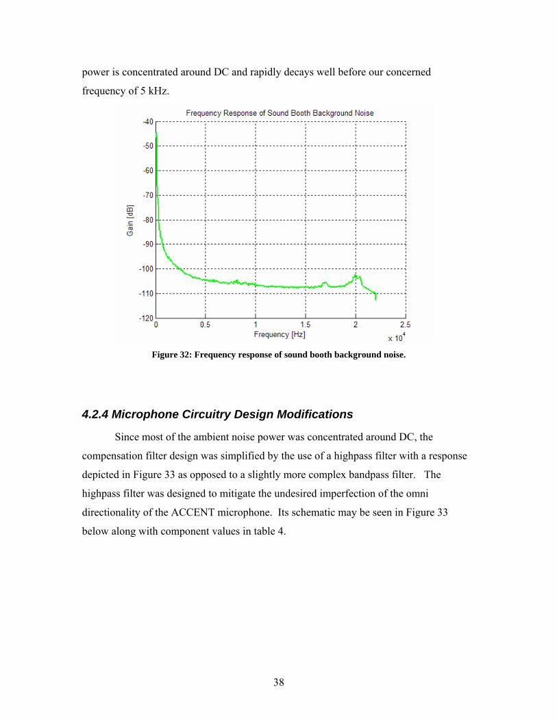
38
power is concentrated around DC and rapidly decays well before our concerned
frequency of 5 kHz.
Figure 32: Frequency response of sound booth background noise.
4.2.4 Microphone Circuitry Design Modifications
Since most of the ambient noise power was concentrated around DC, the
compensation filter design was simplified by the use of a highpass filter with a response
depicted in Figure 33 as opposed to a slightly more complex bandpass filter. The
highpass filter was designed to mitigate the undesired imperfection of the omni
directionality of the ACCENT microphone. Its schematic may be seen in Figure 33
below along with component values in table 4.

39
Figure 33: Highpass filter schematic
C 0.2µF
R1 3.1623 kΩ
R2 1 kΩ
Table 3: Component values for high pass filter.
The response of the filter was designed to have a +20 dB/dec slope from DC to
5 kHz and a flat response with a gain of +10 dB for all frequencies beyond the 3dB 5 kHz
bandwidth. The theoretical design response may be seen below in Figure 34. The
reasoning for designing the filter in this manner was to cancel out the influence of an
unwanted pole with careful zero placement in the band of interest.

40
Figure 34: Highpass filter response.
The filter was placed at the output of the differential line receiver to yield a +20
dB/dec in order to compensate for the inherent -20 dB/dec rolloff observed in the
ACCENT microphone.
Figure 35: Post differential receiver high pass filter.
The filter block was chosen to perform after the differential receiver, which may

41
be seen above in Figure 35; however, the filter is invariant to where it is placed in the
processing flow of the acoustic signals with the exception of the point where the signal is
split into a differential pair. This implies that the filtering may be performed wherever
deemed appropriate by the engineers who finalize the ACCENT system design.
The filter response adhered to the design specification quite well. The active filter
provided the signal with enough gain in the DC to 5 kHz band to place a zero at the
proper location in order to cancel the unwanted pole. The results are depicted below in
Figures 38 and 39. The effect of the designed filter was to have the waveform ride on the
rms value of the pre-filtering response.
.
Figure 36: Frequency response of ACCENT microphone on-axis.
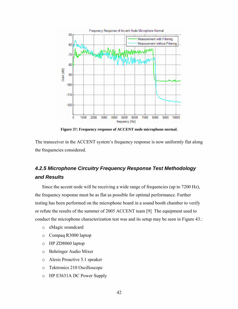
42
Figure 37: Frequency response of ACCENT node microphone normal.
The transceiver in the ACCENT system’s frequency response is now uniformly flat along
the frequencies considered.
4.2.5 Microphone Circuitry Frequency Response Test Methodology
and Results
Since the accent node will be receiving a wide range of frequencies (up to 7200 Hz),
the frequency response must be as flat as possible for optimal performance. Further
testing has been performed on the microphone board in a sound booth chamber to verify
or refute the results of the summer of 2005 ACCENT team [9] The equipment used to
conduct the microphone characterization test was and its setup may be seen in Figure 43.:
o eMagic soundcard
o Compaq R3000 laptop
o HP ZD8060 laptop
o Behringer Audio Mixer
o Alesis Proactive 5.1 speaker
o Tektronics 210 Oscilloscope
o HP E3631A DC Power Supply

43
o Audio Technica AT835b Microphone
o M-Audio Firewire 410 external soundcard
To compare results with the summer ACCENT team, the setup was tested and its
frequency response was measured for the same 4 different test setups the summer team
performed. Figures 40 through 43 below depict these various test setups.
Figure 38: Measurement microphone and powered speaker.
Figure 39: Measurement microphone with ACCENT node in place.
Figure 40: ACCENT Node microphone, normal.
Figure 41: ACCENT mode microphone, on-axis.
To begin our test, it was necessary to make sure all the circuitry was connected
correctly and functioning. A silent recording inside the booth was taken using a Marantz
portable digital recorder and the ACCENT microphone board. These results were
important to understand the properties of the ambient noise power in the sound booth.

44
Below a snapshot of the actual sound booth with the testing setup may be seen.
Figure 42: Sound booth and acoustical test setup.
The next portion of the test involved generating and recording frequency sweeps, which
ranged up to 8 kHz. This was replicated for each of the given configurations above as to
mirror the tests performed in [9]. The Hewlett Packard ZD8060 laptop was connected to
the external M-Audio Firewire 410 soundcard and was used to generate a frequency
sweep from 1-8000 Hz, which were approximately 40 seconds in duration. The frequency
sweep was played through the Alesis Proactive 5.1 speaker in the sound recording booth.
While generating and playing these tones, the Compaq R3000 laptop was connected to
the E-Magic soundcard, which was connected to the Behringer mixer, in order to record
and process the received acoustical data. The mixer is attached to the board which
receives the signal from the microphone board.

45
Figure 43: Microphone testing flowchart.
A recording of the frequency sweep was completed with the reference
microphone sitting over the Accent node microphone board, on axis to the microphone
board alone, and normal to the microphone board. The frequency sweep was recorded in
Goldwave and saved as a wave file. A FFT was preformed on this information in
MATLAB to determine the frequency response.
The results in [9] indicated an undesired -20 dB/dec rolloff in the ACCENT
node microphone frequency response. Our tests were conducted and confirmed the
results obtained by [9]. A frequency sweep from 1 Hz – 8 kHz was sent directly to the
Audio-M external soundcard, which played the audio data through the Alesis Single
Woofer Single Tweeter Speaker. This data was then recorded by two different devices,
the reference microphone, as well as the ACCENT microphone in an on-axis and normal
orientation. The results in Figure 44 below illustrate a strong correlation with the
summer team’s results in Figure 31.

46
Figure 44: ACCENT microphone comparative frequency response.
A more detailed spectral analysis was performed for the duration of each .wav file
recorded. The use of spectrograms was used to extrapolate the presence of harmonics
and intensity of desired signals for duration of each recording. The magnitudes of the
signals are measured in dB. A color map indicating the intensities as a function of time
and frequency is located on the right hand side of each of the following four graphs.

47
Figure 45: Spectrogram of signal sent from HP ZD8060.
As indicated in the spectrogram in Figure 45, the signal sent directly from the
HPZD8060 during the 45 second time window is fully concentrated at approximately 50
dB along the frequencies sent (DC to 8 kHz) with a small (-25 dB) variation in intensity
of that which was transmitted. Notice that the ambient signal strength in frequencies not
intended to be transmitted is approximately -150 dB relative to the transmitted signal
strength of 50 dB. The following spectrograms are for various microphone
measurements of the received acoustical signals. The first spectrogram considered is that
of the reference microphone shown in Figure 46 below.

48
Figure 46: Spectrogram of reference microphone.
Compared to the HPZD8060 spectrogram, the ambient signal strength is much
stronger (approximately 50 dB stronger). However, a more interesting observation is the
presence of harmonics in the signal seen by the reference microphone. These harmonics
are depicted by the faint “red” lines above the intense 50 dB line. These harmonics affect
the overall frequency sweep power spectral density. Their faintness in intensity indicates
that although presence is observed, their affect is not damaging to the response.
49
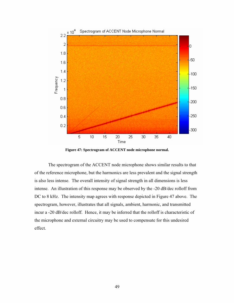
Figure 47: Spectrogram of ACCENT node microphone normal.
The spectrogram of the ACCENT node microphone shows similar results to that
of the reference microphone, but the harmonics are less prevalent and the signal strength
is also less intense. The overall intensity of signal strength in all dimensions is less
intense. An illustration of this response may be observed by the -20 dB/dec rolloff from
DC to 8 kHz. The intensity map agrees with response depicted in Figure 47 above. The
spectrogram, however, illustrates that all signals, ambient, harmonic, and transmitted
incur a -20 dB/dec rolloff. Hence, it may be inferred that the rolloff is characteristic of
the microphone and external circuitry may be used to compensate for this undesired
effect.

50
Figure 48: Spectrogram of ACCENT MIC on-axis.
The results are for the on-axis orientation of the ACCENT node are similar to
normal orientation with the exception of intensity observed. The on-axis orientation has
a 15 dB more intense response overall. The more interesting observation is the presence
of multiple harmonics around the 6 -7 second window of time.
4.2.5 Microphone Circuitry Directivity Test Methodology and Results
After the filter was designed to obtain a relatively flat frequency response, we
performed tests to understand directionality response of the ACCENT node. The same
equipment was used as in the frequency response testing but with the addition of a
turntable to rotate the node at 33 rpm.
Again, using the sound booth, we positioned the ACCENT node in the same
location as the frequency response testing (approximately 50 cm apart), thus satisfying

51
far-field conditions. The setup is shown in Figure 49 below.
Figure 49: Directivity test setup.
The node is positioned in the center of the turntable and rotates at a speed of 33
rpm. Single tones were generated at 1200, 2400, 3600, 4800, 6000, and 7200 Hz and the
waveform seen at the ACCENT node was recorded by the Compaq R3000. The recorded
signals were then imported into MATLAB and the envelope of the time domain signal
was analyzed. This was completed by rectifying the signal, then passing it through a low
pass filter to isolate the received signal’s envelope.
It is known that the node rotates at a speed of 33 rpm; therefore one revolution
takes 1.81 seconds. With this information, we can plot the envelope over the course of a
360 degree rotation of the node. With this data one may infer the gains and attenuations
incurred by the node while spinning in its 360 degree rotation.
The directivity of the ACCENT node was investigated and the results are shown
below in Figure 50. The test was performed for 6 pure tones in increments of 1.2 kHz
ranging the bandwidth seen by the ACCENT node. The response for the 1.2 kHz tone
has a relatively flat directivity response around -20 dB. The one general trend the data
seems to have is its decrease in gain attenuation during the majority of the rotation as the

52
tonal frequency is increased.
Figure 50: Directivity response of ACCENT node normal.

53
5 Recommendations In order to have a solid hardware platform for the ACCENT node, there is still
work that needs to be performed in the future. It is essential to have the hardware
working efficiently so the ACCENT node network operates correctly. We have provided
recommendations to insure an easy to work with ACCENT node.
5.1 Microphone circuitry
The first item is the microphone board. In future versions of the microphone
board the standoffs must be attached to the ground plane of the microphone board. This
will give a solid ground throughout the circuit.
Also, the microphone circuit clips the 5 volt rail very easily with a loud enough
acoustic signal. Therefore, it is recommended on future versions of the microphone board
that there is an LED circuit that allows the accent node user to quickly check if the signal
is clipping. The last improvement is placing the analog filter, which corrects the
frequency response, onto the board (preferably after the gain stages).
5.2 Microcontroller-Codec system
In order to build a solid accent node DSP board, it is necessary to correct the
mistakes outlined in the PCB board appendix. The signal coming from the line receiver is
a maximum of 5 volts. This signal must be scaled down to 3.3 volts in order for the signal
not to clip entering the codec. A resistive divider can be used here.

54
Figure 51: Voltage level translator.
Above, the Maxim 3393E is shown. This chip can provide a more reliable
solution to the resistive divider used for the SPI control signals for the codec. In the next
version of the DSP board, it is recommended the resistive divider be replaced with this
integrated circuit. This solution will make the circuit less susceptible to tolerances and it
is easier to install.
In the reset circuitry on the PCB board, when the capacitor is included in this
circuit, there is a problem with the MCLR pin receiving a large amount of current and
therefore destroying the dsPIC. Microchip makes two potential IC CMOS voltage
supervisors; the MCP131 and TC1270. These devices are designed to hold the
microcontroller in reset until the supply voltage reaches a predetermined operating level,
which is will work well with our DC/DC converter power supply. The TC1270 also
allows for a switch to be attached in order to externally reset the dsPIC. They also protect
against brownout conditions that occur as a result of the supply voltage dropping below a
tolerable level. It is highly recommended one of these voltage supervisory ICs are used.
Another future recommendation for the DSP board would be to use a reference crystal in
order to operate the dsPIC. Currently, the node uses the FRC oscillator of the dsPIC.
Using a crystal would provide a more accurate operating frequency, which is better for
use in SPI and DCI timing.

55
5.3Other Issues
Lastly, the power supply does not currently run the DSP board. Further testing
will need to be done to rectify this problem. A possible start to solving this problem
would be bread boarding the 5 volt supply and trying to operate the DSP board
afterwards. It is unknown whether or not the power supply board or the reset circuitry
before the dsPIC is at fault.
Once these problems are fixed, the ACCENT nodes will be ready for assembly
and coding of the phase locked loops which are part of the cooperative communication
protocol.

56
6 Conclusion
The purpose for this project was to develop a proof of concept for the distributed
beamformer scheme as well as continue hardware development and testing for a
prototype ACCENT node to be used in future research involving the wireless distributed
beamformer.
A wired system for a distributed beamformer was developed and the concept of
synchronizing two transmitters via the method described in [0] was demonstrated using
off the shelf PLL integrated circuits and 555 timers. In order to develop a deeper
understanding of distributed beamformers, a prototype ACCENT node was constructed.
Testing of hardware was completed and documented. In addition to current progress
future recommendations for work in this area were also discussed.
At the close of this phase of the project there are some very positive and
promising results that should serve as a platform for follow-on work. It is now known
that the synchronization method in [0] functions appropriately in a wired system. The
microcontroller board was designed, fabricated, and tested. Future groups will be able to
program the dsPIC through the port on board. A filter board to remove the 20 dB roll-off
from the microphone was built and tested. All of the mechanical hardware and cabling
for the node has been acquired. Extensive testing was performed to deduce both the
frequency and directivity responses of the microphone circuitry. The use of a sound booth
helped minimize the number of acoustic reflections and allowed for a higher level of
accuracy in test results. Once additional nodes are fabricated and the cooperative
software is developed, a wireless test of [0]’s synchronization method will be possible.

57
7 APPENDIX I: ACCENT Node Embedded Controller PCB Notes
The first surface mount chip to be installed is the Max1658. There is a mistake in
the connections on this chip which makes the regulator act irregularly. Pins 4, 5 and 6, 7
must be separated by cutting the trace with a knife.
Figure 52: PIC instruction picture 1.
The next chip to be installed is the TLV320AIC23 codec. On the resistive divider
off of pin 23, there is a shorted resistor shown below in Figure 57.This trace can be cut
easily with a knife.

58
Figure 53: PIC instruction picture 2.
Also, pins 19 and 20 are shorted due to manufacturing error. These must be carefully
separated by a sharp blade. These pins are the analog inputs to the codec, so it does not
matter if they are not separated because only the left analog output is used anyways. This
defect can be seen in the picture below.
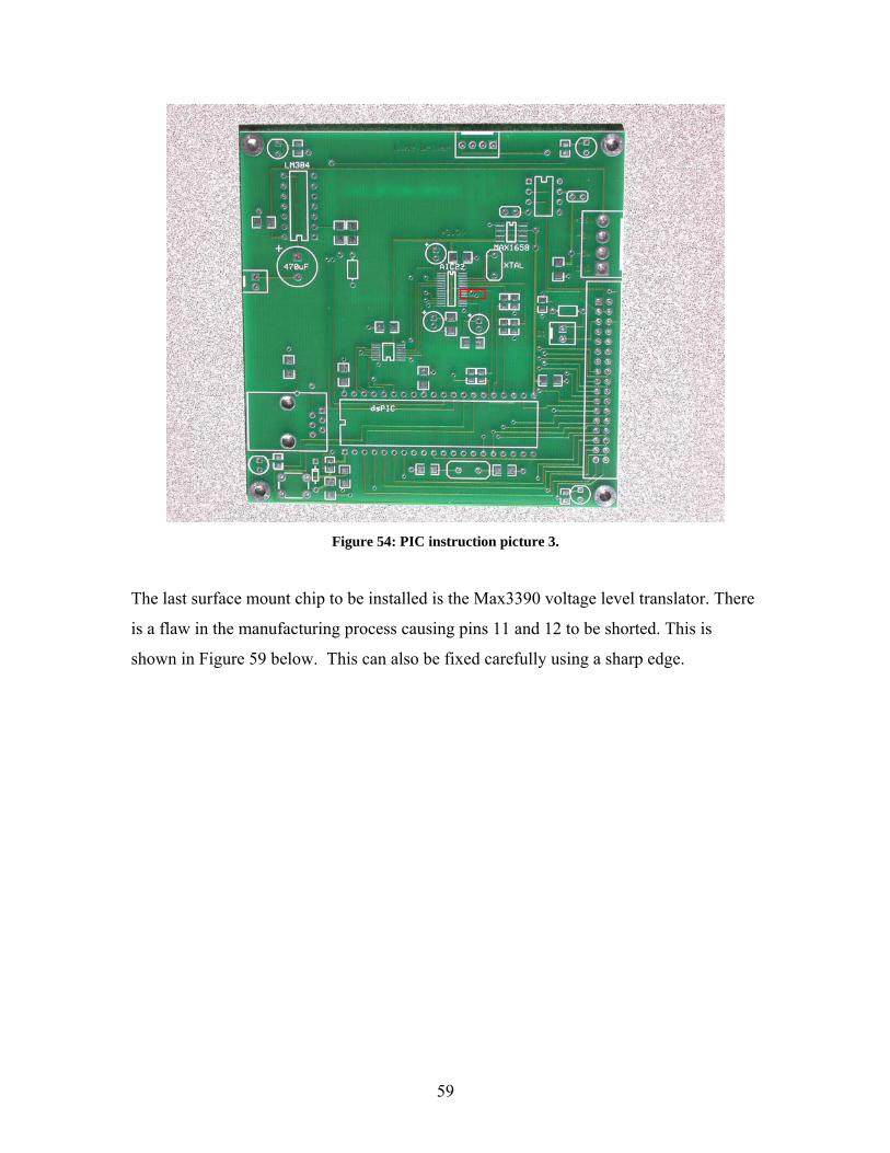
59
Figure 54: PIC instruction picture 3.
The last surface mount chip to be installed is the Max3390 voltage level translator. There
is a flaw in the manufacturing process causing pins 11 and 12 to be shorted. This is
shown in Figure 59 below. This can also be fixed carefully using a sharp edge.

60
Figure 55: PIC instruction picture 4.
The dsPIC socket was soldered on after all the surface mount chips were in place. Pins 8
and 9 of the dsPIC cross the power rail. Therefore the power rail was cut before it runs
into pins 8 and 9. A thin wire then connects the power rail back together.

61
Figure 56: PIC instruction picture 5.
As shown in the Figure 60 above, a 600 ohm resistor is connected to pin 1 in order to
limit current from flowing into the MCLR pin when the dsPIC is being programmed.

62
Figure 57: PIC instruction picture 6.
In Figure 61above, the MCLR pin of the dsPIC is connected to Vdd through a 5kohm
resistor. The resistor pad is shorted and the capacitor to ground should not be connected.
The button is connected to the MCLR pin by a small resistor which is connected to
ground.

63
8 APPENDIX II: Accent Node DSP Board Hardware Integrated Circuits
• Microchip dsPic4013 40 Pin Dip package
• Texas Instruments TLV320AIC23 codec TSSOP 28 pin
• Maxim Max1658 SO 8pin
• National Semiconductor LM384 Dip 14 pin
• INA134 Audio Differential Line Receiver Dip 8pin Capacitor Description Quantity
• 470uF electrolytic capacitor 1 • Surface Mount (SMT)- 1206 (8) .1uF 8 • SMT - 0805 220pf 1 • Cap - 0.1uf axial ceramic, decoupling (DigiKey 1210PHCT-ND) 2 • Cap - Radial electrolytic - Lead spacing 0.079 inch (2mm) 10uF 3 • Cap - Lead spacing 0.1 inch (2.5mm) .1uF 2
Resistors Description Quantity
• SMT - 0805 600ohm 4 • SMT - 0805 15kohm 3 • SMT - 0805 8.2kohm 3 • SMT - 1206 15kohm 1 • SMT - 1206 1kohm 1
Other Components
• LED - T 1 4 • Switch - 6mm Push button (Omron B3F-1022, Digikey SW403-ND) • Ribbon Connector hdr, 34 pin (3M 2534-6002UB,DigiKeyMHB34K) • RJ11-6 Connector (Amp 520250-3, DigiKey A9043-ND) • Molex Connector, .1 inch KK, up, 2 pin (DigiKey WM4200) • Molex Connector, .156 in KK, up, 4 pin (DigiKey WM4622) • Molex Connector, .1 inch KK, up, 4 pin (DigiKey WM4202)

64
9 APPENDIX III: dsPIC Application Code -Written in C /*---------------Preprocessor-------------------------------*/ #include <p30F4013.h> #include <spi.h> #include <dci.h> #include "aic23_ctrl_add.h" #include "tri_wav_table.h" #define _ISR __attribute__((interrupt(__save__(AIC23_CONTROL)))) #define FCY 7500000 //DCI TESTING MASTER MODE #define FS 48000 #define FCSCK 64*FS //was64 #define ON 0b0 // active low #define OFF 0b1 #define _CS PORTDbits.RD8 #define LED0 PORTFbits.RF0 #define LED1 PORTFbits.RF1 #define LED2 PORTFbits.RF4 #define LED3 PORTFbits.RF5 /*---------------Variable Declarations----------------------*/ /* AIC23 control address (7-bit) and instruction (9-bit) */ /* combined in a 16bit data type (unsigned int) */ union aic23control struct unsigned INST:9; // example: AIC23_CONTROL.CTRL.INST=0b010101010; unsigned ADDR:7; //example: AIC23_CONTROL.CTRL.ADDR=0b0101010; CTRL; unsigned int WORD; // example: AIC23_CONTROL.WORD=0xABCD; AIC23_CONTROL; unsigned int hold_time = 1; unsigned char count = 0; unsigned char sample = 0; /*----------------Define buffers and unions for codec------*/ int left_in[10]=0; // codec data is 2's complement 70 int right_in[10]=0; unsigned int spread=0; int temp = 0; int temp1 = 0; // variable to use for testing DCI int temp2 = 0; int temp3 = 0; int temp4 = 0; int j = 0; // interrupt counter

65
int k=0; int n=0; int sendtri=0; int goback=1; short y_low=0; short sample_left[4]; int sqr = 16000; int done=1; /*---------------Function Prototypes----------------------*/ unsigned int ReadSPI1(); void CloseSPI1(); void Write_SPI(unsigned int); void DCIInit (void); void PlayDitty(void); void __attribute__((__interrupt__)) _T1Interrupt(void); void __attribute__((__interrupt__)) _T2Interrupt(void); void __attribute__((__interrupt__)) _DCIInterrupt(void); void __attribute__((__interrupt__)) _SPI1Interrupt(void); /*---------------Main Function----------------------------*/ //_FOSC(CSW_FSCM_OFF & EC); _FOSC(CSW_FSCM_OFF & FRC_PLL4); //_FOSC(CSW_FSCM_OFF & FRC); // macro to select FRC internal osc w/ 4x PLL (32MHz) _FWDT(WDT_OFF); /* Turn off the Watch-Dog Timer. */ 71 _FBORPOR(MCLR_EN & PWRT_OFF); /* Enable MCLR reset pin and turn off the power-up timers. */ _FGS(CODE_PROT_OFF); /* Disable Code Protection */ int main() /* set desired I/O pins as outputs */ ADPCFG = 0xFFFC; // disable analog inputs except for AN0-AN1 TRISA = 0x0000; // set all I/O pins as outputs TRISB = 0x0000; // (SPI and DCI pins will be under module control) TRISC = 0x0000; TRISD = 0x0000; TRISF = 0x0000; /* disable unused peripherals */ PMD1 = 0b1111011011110111; // DCI, SPI, & T1 enabled PMD2 = 0xFFFF; // all others disabled /* configure interrupts and priorities */ IEC0 = 0x0000; // disable all interrupts IEC1 = 0x0000; IEC2 = 0x0000; IEC0bits.SPI1IE = 0b1; // enable SPI interrupts IPC0 = 0x0000; // disable all interrupts by setting IPC1 = 0x0000; // priority to 0 IPC2 = 0x0000; IPC3 = 0x0000; IPC4 = 0x0000; IPC5 = 0x0000; IPC6 = 0x0000; IPC10 = 0x0000;

66
IPC0bits.T1IP = 0b100; // T1 int priority 4of7 0b100 IPC10bits.DCIIP = 0b101; // DCI int priority 5of7 0b101 IPC2bits.SPI1IP = 0b110; // SPI int priority 6of7 0b110 72 IFS0bits.T1IF = 0b0; // clear T1 interrupt flag /* configure SPI module */ SPI1CON =FRAME_ENABLE_ON & //FRAME_ENABLE_OFF & // Frame SPI support Disable FRAME_SYNC_OUTPUT & // Frame sync pulse Output (doesn't matter) ENABLE_SDO_PIN & // SDO pin is used by module SPI_MODE16_ON & // Communication is word wide SPI_SMP_OFF & // Input data sampled at middle of data output time SPI_CKE_ON & //was ON // Transmit happens on transition from //active clock state to idle clock state SLAVE_ENABLE_ON & // WAS OFF Slave Select not used by module - controlled by I/O port CLK_POL_ACTIVE_HIGH & // Idle state for clock is low, active is high MASTER_ENABLE_ON & // Master Mode SEC_PRESCAL_6_1 & // Secondary Prescale 6:1 => SPI clk = 1/24*32MHz PRI_PRESCAL_4_1; / // Primary Prescale 4:1 => = 1 MHz SPI1STAT = SPI_ENABLE & // Enable module SPI_RX_OVFLOW_CLR & SPI_IDLE_STOP; // Discontinue module operation in idle mode SPI1STATbits.SPIROV = 0b0; // No overflow has occured IFS0bits.SPI1IF = 0b0; EnableIntSPI1; CS=0; /* configure timer 1 - appx 0.5Hz blink*/ TMR1 = 0x0000; T1CON = 0b1000000000110000; // 1:256 prescale PR1 = 4000; // period register 73 /* write instructions to AIC23 */ AIC23_CONTROL.CTRL.ADDR = POWER_DOWN; // Power on AIC23_CONTROL.CTRL.INST = 0b000000010; // DAC & ADC on //AIC23_CONTROL.CTRL.INST = 0b000000011; //AIC23_CONTROL.CTRL.INST = 0b000001110; // DAC OFF & ADC off line outputs off Write_SPI(AIC23_CONTROL.WORD); AIC23_CONTROL.CTRL.ADDR = L_LINEIN_VOL; AIC23_CONTROL.CTRL.INST = 0b000010111; // L line-in: un-muted, 0dB //AIC23_CONTROL.CTRL.INST = 0b010000000; // L line-in: muted, -34.5dB //AIC23_CONTROL.CTRL.INST = 0b000011111;// unmuted +12db Write_SPI(AIC23_CONTROL.WORD); AIC23_CONTROL.CTRL.ADDR = R_LINEIN_VOL; AIC23_CONTROL.CTRL.INST = 0b000010111;// unmated //AIC23_CONTROL.CTRL.INST = 0b010000000; // R line-in: muted, -34.5dB //AIC23_CONTROL.CTRL.INST = 0b000011111;// unmuted +12db

67
Write_SPI(AIC23_CONTROL.WORD); AIC23_CONTROL.CTRL.ADDR = L_HP_VOL; AIC23_CONTROL.CTRL.INST = 0b000000000; // L headphone: muted Write_SPI(AIC23_CONTROL.WORD); // AIC23_CONTROL.CTRL.ADDR = R_HP_VOL; // AIC23_CONTROL.CTRL.INST = 0b000000000; // R headphone: muted // Write_SPI(AIC23_CONTROL.WORD); AIC23_CONTROL.CTRL.ADDR = DIGITAL_FORMAT;//Master mode AIC23_CONTROL.CTRL.INST = 0b001000010; // DAC L/R swap disabled //AIC23_CONTROL.CTRL.INST = 0b000000010; //slave mode //AIC23_CONTROL.CTRL.INST = 0b001001110; // DAC L/R swap disabled 32 bit //AIC23_CONTROL.CTRL.INST = 0b001000010; // DAC L/R swap enabled Write_SPI(AIC23_CONTROL.WORD); // 16bit input length; I2S format AIC23_CONTROL.CTRL.ADDR = SAMPLE_RATE; // CLKin and CLKout 1/2x division AIC23_CONTROL.CTRL.INST = 0b000000010; // fs = 48kHz 384fs oversampling rate //AIC23_CONTROL.CTRL.INST = 0b011000010; // clocks divide by 2 //AIC23_CONTROL.CTRL.INST = 0b001000010; //clock out not divide by 2 //AIC23_CONTROL.CTRL.INST = 0b000000010; //clock out and in not divide by 2 //AIC23_CONTROL.CTRL.INST = 0b000000110; Write_SPI(AIC23_CONTROL.WORD); AIC23_CONTROL.CTRL.ADDR = DIGITAL_ACT; AIC23_CONTROL.CTRL.INST = 0b000000001; // Activate digital interface Write_SPI(AIC23_CONTROL.WORD); AIC23_CONTROL.CTRL.ADDR = DIGITAL_PATH; // DAC soft-mute disabled AIC23_CONTROL.CTRL.INST = 0b000000100; // ADC HPF disabled //AIC23_CONTROL.CTRL.INST = 0b000000101; // ADC HPF enabled Write_SPI(AIC23_CONTROL.WORD); // 48Khz De-emphasis AIC23_CONTROL.CTRL.ADDR = ANALOG_PATH; //AIC23_CONTROL.CTRL.INST = 0b000001010; // Analog bypass enabled, sidetone disabled, DAC disabled //AIC23_CONTROL.CTRL.INST = 0b000010010; AIC23_CONTROL.CTRL.INST = 0b000000110; // Analog bypass disabled, sidetone disabled, DAC enabled //AIC23_CONTROL.CTRL.INST = 0b000000110; // Analog bypass disabled, sidetone disabled, DAC off Write_SPI(AIC23_CONTROL.WORD); // MIC muted AIC23_CONTROL.CTRL.ADDR = R_HP_VOL; AIC23_CONTROL.CTRL.INST = 0b000000000; // R headphone: muted Write_SPI(AIC23_CONTROL.WORD); int hold_time2 = 15; while(hold_time2!=0) hold_time2=hold_time2-1; CloseSPI1(); DCIInit(); PlayDitty(); IEC0bits.T1IE = 0b1; while(1)

68
/*---------------Interrupt Service Routines---------------*/ void _ISR _T1Interrupt(void) LED0 = !LED0; LED2 = !LED2; IFS0bits.T1IF = 0b0; // clear T1 interrupt flag void _ISR _SPI1Interrupt(void) _CS = 0b1; hold_time = 3; while(hold_time!=0) hold_time=hold_time-1; _CS = 0b0; IFS0bits.SPI1IF = 0b0; // clear SPI interrupt flag SPI1STATbits.SPIROV = 0b0; // clear overflow bit void __attribute__((__interrupt__)) _DCIInterrupt(void) if(DCISTATbits.RFUL==0b1) temp5 = RXBUF0; temp6 = RXBUF1; temp4 = RXBUF2; temp8 = RXBUF3; sample_left[n++] = temp1; if (n==4) n=0; y_low = sample_left[0]+sample_left[1]+sample_left[2]+sample_left[3]; if (done==1) if(DCISTATbits.TMPTY==0b1) TXBUF0 =temp1; // tx buff transmits on low frame TXBUF1 =0x0000; TXBUF2 =temp1; //temp; TXBUF3 =0x0000; /* if (done==0) if(DCISTATbits.TMPTY==0b1)

69
TXBUF0 =temp5; // tx buff transmits on low frame TXBUF1 =0x0000; TXBUF2 =temp4; //temp; TXBUF3 =0x0000; */ sendtri=1; _DCIIF = 0; /*Clear the DCI Interrupt Flag */ /*---------------Function Declarations--------------------*/ unsigned int ReadSPI1() /* Check for Receive buffer full status bit of status register*/ if (SPI1STATbits.SPIRBF) SPI1STATbits.SPIROV = 0; if (SPI1CONbits.MODE16) return (SPI1BUF); /* return word read */ else return (SPI1BUF & 0xff); /* return byte read */ return -1; /* RBF bit is not set return error*/ void Write_SPI(unsigned int data_out) while(SPI1STATbits.SPITBF==0b1); // wait until transmit buffer is ready SPI1BUF = data_out; /******************************************************************** * Function Name : CloseSPI1 * * Description : This routine disables the SPI module and its * * interrupt bits. * * Parameters : None * * Return Value : None * ********************************************************************/ void CloseSPI1() IEC0bits.SPI1IE = 0; /* Disable the Interrupt bit in the Interrupt Enable Control Register */ SPI1STATbits.SPIEN = 0; /* Disable the module. All pins controlled by PORT Functions */ IFS0bits.SPI1IF = 0; /* Disable the Interrupt flag bit in the 79 Interrupt Flag Control Register */
70
void DCIInit (void) /* DCI Control Register DCICON1 Initialization */ DCICON1bits.CSCKD = 1; /*Serial Bit Clock (CSCK pin) is input */ DCICON1bits.CSCKE = 1; /*Data changes on falling edge */ /*& sampled on rising edge of CSCK */ DCICON1bits.COFSD = 1; /*Frame Sync Signal is output */ DCICON1bits.UNFM = 0; /*If Tx Buffers are not reloaded after */ /*transmission is complete, then 0's are*/ /*transmitted */ DCICON1bits.CSDOM = 0; /*CSDO pin is held low during inactive */ /*time-slots */ DCICON1bits.DJST = 0; /*Data is transmitted one bit clock */ /*after Frame Sync pulse */ 80 DCICON1bits.COFSM = 1; /*Frame Sync Signal set up for I2S mode */ DCICON1bits.DLOOP = 0; /* DCI Control Register DCICON2 Initialization */ /* In this section we will set up the frame length for the operation shown in Figure 1. */ DCICON2bits.BLEN = 3; /*Enable all 4 transmit & receive buffer*/ /*for use */ DCICON2bits.COFSG = 1; /*Set up Frame Sync Generator for 2 */ /*words per frame */ DCICON2bits.WS = 15; /*Set up Word Size to 16 bits */ /* Transmit Slot Control Register Initialization */ TSCONbits.TSE0 = 1; /*Transmit on Time Slot 0 */ TSCONbits.TSE1 = 1; /*Transmit on Time Slot 1 */ /*2 timeslots are enabled to send 32- */ /*bit data per channel (left or right) */ /* Receiver Slot Control Register Initialization */ RSCONbits.RSE0 = 1; /*Receive on Time Slot 0 */ RSCONbits.RSE1 = 1; /*Receive on Time Slot 1 */ /*2 timeslots are enabled to send 32- */ /*bit data per channel (left or right) */ _DCIIE = 1; /*Clear the DCI Interrupt Flag */ _DCIIF = 0; /*Enable DCI ISR processing */ DCICON1bits.DCIEN = 1; /*Enable the DCI module */

71
void PlayDitty(void) LED1=ON; LED2=OFF; LED0=OFF; LED3=OFF; while(k<200) if(j==49) k++; j=0; if(sendtri==1) temp1=10000*triangle[j]; sendtri=0; j++; LED1=OFF; LED3=OFF; LED2=ON; LED0=OFF; ////next ditty k=0; j=0; while(k<200) if(j==49) 82 k++; j=0; if(sendtri==1) temp1=5000*triangle[j]; sendtri=0; j++; ////next ditty LED2=OFF; LED3=ON; LED0=OFF; LED1=OFF; k=0; j=0; while(k<200) if(j==49) k++; j=0; if(sendtri==1) temp1=1000*triangle[j]; sendtri=0; j++;
72
LED1=OFF; LED2=OFF; LED3=OFF; LED0=ON; ////next ditty k=0; j=0; while(k<200) 83 if(j==49) k++; j=0; if(sendtri==1) temp1=10000*triangle[j]; sendtri=0; j++; LED0=OFF; LED1=OFF; LED2=OFF; LED3=OFF; done=0;

73
9 APPENDIX IV: Microphone Directivity Code -written in MATLAB clc clear all [yOrig,fsOrig] = wavread('1200Hz33rpm.wav'); % import wave file [y1,fs1] = wavread('2400Hz33rpm.wav'); % import wave file [y2,fs2] = wavread('3600Hz33rpm.wav'); % import wave file [y3,fs3] = wavread('4800Hz33rpm.wav'); % import wave file [y4,fs4] = wavread('6000Hz33rpm.wav'); % import wave file [y5,fs5] = wavread('7200Hz33rpm.wav'); % import wave file rectOrig = abs(yOrig); % rectify wave rectOrig = rectOrig(1:270000); % eliminate zeros rectdOrig = resample(rectOrig,1,10); % resample at fsOrig/10 [nOrig,wnOrig]=buttord(0.05,0.1,0.1,40); % design filter [bOrig,aOrig]=butter(nOrig,wnOrig); % obtain filter coefficients zOrig = filtfilt(bOrig,aOrig,rectdOrig); % filter forwards and backwards for no phase dist. %%%%%%%%%%%%%%%%%%%%%%%%%%%%%%%%%%%%%%%%%%% rect1 = abs(y1); % rectify wave rect1 = rect1(1:270000); rectd1 = resample(rect1,1,10); % resample at fsOrig/10 [n1,wn1]=buttord(0.05,0.1,0.1,40); [b1,a1]=butter(n1,wn1); z1 = filtfilt(b1,a1,rectd1); %%%%%%%%%%%%%%%%%%%%%%%%%%%%%%%%%%%%%%%%%%% rect2 = abs(y2); % rectify wave rect2 = rect2(1:270000); rectd2 = resample(rect2,1,10); % resample at fsOrig/10 [n2,wn2]=buttord(0.05,0.1,0.1,40); [b2,a2]=butter(n2,wn2); z2 = filtfilt(b2,a2,rectd2); %%%%%%%%%%%%%%%%%%%%%%%%%%%%%%%%%%%%%%%%%%% rect3 = abs(y3); % rectify wave rect3 = rect3(1:270000); rectd3 = resample(rect3,1,10); % resample at fsOrig/10 [n3,wn3]=buttord(0.05,0.1,0.1,40); [b3,a3]=butter(n3,wn3); z3 = filtfilt(b3,a3,rectd3); %%%%%%%%%%%%%%%%%%%%%%%%%%%%%%%%%%%%%%%%%%% rect4 = abs(y4); % rectify wave rect4 = rect4(1:270000); rectd4 = resample(rect4,1,10); % resample at fsOrig/10 [n4,wn4]=buttord(0.05,0.1,0.1,40); [b4,a4]=butter(n4,wn4); z4 = filtfilt(b4,a4,rectd4); %%%%%%%%%%%%%%%%%%%%%%%%%%%%%%%%%%%%%%%%%%%
74
rect5 = abs(y5); % rectify wave rect5 = rect5(1:270000); rectd5 = resample(rect5,1,10); % resample at fsOrig/10 [n5,wn5]=buttord(0.05,0.1,0.1,40); [b5,a5]=butter(n5,wn5); z5 = filtfilt(b5,a5,rectd5); %%%%%%%%%%%%%%%%%%%%%%%%%%%%%%%%%%%%%%%%%%% hold on plot(180.*(0:1/(fsOrig/10):(length(zOrig)-1)/(fsOrig/10)),20.*log10(zOrig),'c'); plot(180.*(0:1/(fs1/10):(length(z1)-1)/(fs1/10)),20.*log10(z1),'r'); plot(180.*(0:1/(fs2/10):(length(z2)-1)/(fs2/10)),20.*log10(z2),'g'); plot(180.*(0:1/(fs3/10):(length(z3)-1)/(fs3/10)),20.*log10(z3),'b'); plot(180.*(0:1/(fs4/10):(length(z4)-1)/(fs4/10)),20.*log10(z4),'k'); plot(180.*(0:1/(fs5/10):(length(z5)-1)/(fs5/10)),20.*log10(z5),'m');

75
10 Bibliography [0] D.R.Brown III, G.B.Prince, and J.A.McNeill, “A method for carrier frequency and phase synchronization of two autonomous cooperative transmitters,” in Proc. 2005 IEEE Signal Processing Advances in Wireless Communications, New York, NY, June 5-8 2005. [1] A. Sendonaris, E. Erkip, and B. Aazhang, “Increasing uplink capacity via user cooperation diversity,” in Proc. 1998 IEEE International Symp. on Information Theory, Cambridge, MA, August 16-21 1998, p. 156. [2] A. Sendonaris, E. Erkip, and B. Aazhang, “User cooperation diversity — part I: System description,” IEEE Transactions on Communications, vol. 51, no. 11, pp. 1927–1938, November 2003. [3] Kai Dietze, Carl Dietrich, and Warren Stutzman, Vector Multipath Propagation Simulator (VMPS), Draft report, Virginia Tech Antenna Group, April 7, 1999. [4] A. Sendonaris, E. Erkip, and B. Aazhang, “User cooperation diversity — part II: Implementation aspects and performance analysis,” IEEE Transactions on Communications, vol. 51, no. 11, pp. 1939–1948, November 2003. [5] R.E. Best, Phase-Locked Loops : Design, Simulation, and Applications, McGraw-Hill, New York, 2003. [6] G. Barriac, R. Mudumbai, and U. Madhow, “Distributed beamforming for information transfer in sensor networks,” in Information Processing in Sensor Networks (IPSN), Third International Workshop, Berkeley, CA, April 26-27 2004. [7] Y.S. Tu and G.J. Pottie, “Coherent cooperative transmission from multiple adjacent antennas to a distant stationary antenna through AWGN channels,” in Proceedings of the IEEE Vehicular Technology Conference (VTC), Spring 2002, vol. 1, pp. 130–134. [8] W. L. Stutzman and G. A. Thiele, Antenna Theory and Design, John Wiley & Sons, New York, 1981. [9] S.Brown, ACCENT Report, August 2005