Development of ion-implanted optical waveguides in optical materials: A review
Upload
khangminh22Category
view
1download
0
A111D3 QSb3SS
NATL INST OF STANDARDS & TECH RI.C.
A1 11 03056385_ Conference o/Basic optical prope
100 U57 N0.574, 1980 C.1 NBS-PUB-C 19
V„U Of*
NBS SPECIAL PUBLICATION 574
U.S. DEPARTMENT OF COMMERCE/ National Bureau of Standards
Basic Optical Properties of Materials
Summaries of Papers

NATIONAL BUREAU OF STANDARDS
The National Bureau of Standards' was established by an act of Congress on March 3, 1901.
The Bureau's overall goal is to strengthen and advance the Nation's science and technology
and facilitate their effective application for public benefit. To this end, the Bureau conducts
research and provides: (1) a basis for the Nation's physical measurement system, (2) scientific
and technological services for industry and government, (3) a technical basis for equity in
trade, and (4) technical services to promote public safety. The Bureau's technical work is per-
formed by the National Measurement Laboratory, the National Engineering Laboratory, and
the Institute for Computer Sciences and Technology.
THE NATIONAL MEASUREMENT LABORATORY provides the national system ot
physical and chemical and materials measurement; coordinates the system with measurement
systems of other nations and furnishes essential services leading to accurate and uniform
physical and chemical measurement throughout the Nation's scientific community, industry,
and commerce; conducts materials research leading to improved methods of measurement,
standards, and data on the properties of materials needed by industry, commerce, educational
institutions, and Government; provides advisory and research services to other Government
agencies; develops, produces, and distributes Standard Reference Materials; and provides
calibration services. The Laboratory consists of the following centers:
Absolute Physical Quantities 2 — Radiation Research — Thermodynamics and
Molecular Science — Analytical Chemistry — Materials Science.
THE NATIONAL ENGINEERING LABORATORY provides technology and technical ser-
vices to the public and private sectors to address national needs and to solve national
problems; conducts research in engineering and applied science in support of these efforts;
builds and maintains competence in the necessary disciplines required to carry out this
research and technical service; develops engineering data and measurement capabilities;
provides engineering measurement traceability services; develops test methods and proposes
engineering standards and code changes; develops and proposes new engineering practices;
and develops and improves mechanisms to transfer results of its research to the ultimate user.
The Laboratory consists of the following centers:
Applied Mathematics — Electronics and Electrical Engineering 2 — Mechanical
Engineering and Process Technology 2 — Building Technology — Fire Research —Consumer Product Technology — Field Methods.
THE INSTITUTE FOR COMPUTER SCIENCES AND TECHNOLOGY conducts
research and provides scientific and technical services to aid Federal agencies in the selection,
acquisition, application, and use of computer technology to improve effectiveness and
economy in Government operations in accordance with Public Law 89-306 (40 U.S.C. 759),
relevant Executive Orders, and other directives; carries out this mission by managing the
Federal Information Processing Standards Program, developing Federal ADP standards
guidelines, and managing Federal participation in ADP voluntary standardization activities;
provides scientific and technological advisory services and assistance to Federal agencies; and
provides the technical foundation for computer-related policies of the Federal Government.
The Institute consists of the following centers:
Programming Science and Technology — Computer Systems Engineering.
'Headquarters and Laboratories at Gaithersburg, M D, unless otherwise noted;
mailing address Washington, DC 20234.;Some divisions within the center are located at Boulder, CO 80303.

Basic Optical Properties of Materials
Summaries of Papers
NATIONAL BUREAUOF STANDARDS
LIBRARY
APR 2 1 1980
nt> t- 0-CC- -Ct4<
Presented at the Topical Conferenceon Basic Optical Properties of Materials
Held at the National Bureau of Standards
Gaithersburg, Maryland, May 5-7, 1980
&C/60. as?
J9Po
Edited by:
Albert Feldman
Center for Materials Science
National Measurement Laboratory
National Bureau of Standards
Washington, D.C. 20234
In cooperation with:
The Optical Society of America
1816 Jefferson Place, NWWashington, DC 20036
U.S. DEPARTMENT OF COMMERCE, Philip M. Klutznick, Secretary
Luther H. Hodges, Jr., Deputy Secretary
Jordan J. Baruch, Assistant Secretary for Productivity, Technology, and Innovation
3. NATIONAL BUREAU OF STANDARDS, Ernest Ambler, Director
Issued May 1980

Library of Congress Catalog Card Number: 80-600038
National Bureau of Standards Special Publication 574
Nat. Bur. Stand. (U.S.), Spec. Publ. 574, 252 pages (May 1980)
CODEN: XNBSAV
U.S. GOVERNMENT PRINTING OFFICE
WASHINGTON: 1980
For sale by the Superintendent of Documents, U.S. Government Printing Office, Washington, D.C. 20402
Price $6.50
(Add 25 percent for other than U.S. mailing).

Foreword
This Special Publication contains summaries of papers to be pre-
sented at the Topical Conference on Basic Optical Properties of Materi-als to be held at the National Bureau of Standards in Gai thersburg
,
Maryland on May 5-7, 1980. The conference is sponsored by the NationalBureau of Standards in cooperation with the Optical Society of America.This publication contains summaries of 62 papers which include 14
invited papers. The principal topical areas are:
Nonl inear Optical PropertiesUltraviolet PropertiesInfrared PropertiesGraded Index MaterialsInhomogeneous MaterialsProperties of Thin FilmsOptical FibersPlanar Optical WaveguidesExternal Influences: Piezo-optics , Thermo-opti cs
,
Magneto-optics
The purpose of the conference is to discuss the state of the artin the measurement of the optical properties of optical materials. Theemphasis is primarily on materials properties rather than on optical
devices. The primary focus of the conference is on the measurement and
theory of basic optical properties of materials in bulk, thin film, andfiber form.
The manuscripts for the conference have been prepared by the
authors in camera-ready form, and any questions pertaining to theircontent should be addressed to those authors.
Albert FeldmanChai rperson
Acknowl edgements
We wish to thank the following individuals for their invaluableassistance in preparing for the conference and this summary:Jeanmarie Bartlett, Marilyn Dodge, Barbara Hyde, Jo Ann Lorden, andKathy Stang. Special thanks are due to Kimberly Morgan for organizingthe mailings for the conference, and for editing and assembling the
completed Summary of Papers. Thanks are due to the Word ProcessingCenter of the National Measurement Laboratory for retyping several ofthe manuscripts.
i i i
Program and Editorial Committee
Albert Feldman - ChairpersonNational Bureau of Standards
Edward Pal i k - Co-ChairmanNaval Research Laboratory
Michael I. Bell
National Bureau of Standards
Arthur H. GuentherAir Force Weapons Laboratory
Ivan P. Kami nowBell Telephone Laboratories
Bernard BendowRome Air Development Center
Harold E. BennettMichel son LaboratoryNaval Weapons Center
Robert V. MohrCatholic University
Alfred J. ThelenOptical Coating Laboratory
Disclaimer
Certain commercial equipment, instruments, or materials may be
identified in this publication in order to adequately specify theexperimental procedure. In no case does such identification implyrecommendation or endorsement by the National Bureau of Standards,nor does it imply that the material or equipment identified is
necessarily the best available for the purpose.
iv

CONTENTSPage
Foreword iii
Keynote Address— Important Areas of Optical MaterialsResearch 1
*H. V. Winsor
NONLINEAR OPTICAL PROPERTIES
Properties of Low-Index Laser Materials 3
*M. J. Weber
Nonlinear Optical Susceptibilities of Semiconductorsand Optical Bi stability 9
H. M. Gibbs, S. L. McCall, T. N. C. Venkatesan,A. Passner, A. C. Gossard, and W. Wiegmann
Band Structure Calculations of the Two-Photon AbsorptionCoefficients of InP and CdTe 13
A. Vaidyanathan, A. H. Guenther, and S. S. Mitra
ULTRAVIOLET PROPERTIES
Measurement and Interpretation of Ultraviolet Propertiesof Solids 16
*D. W. Lynch
The Optical Properties of Kapton: Measurement andApplications 20
L. R. Painter, E. T. Arakawa, M. W. Williamsand J. C. Ashley
Optical Properties of TiC x ( 0 . 64<x<0 . 90 ) From 0.1 To 30eV ... 24
D. W. Lynch, C. G. Olson, D. J. Peterman, and
J. H. Weaver
Superconvergence Relations and the Analysis of Optical Data . . 28*D. Y. Smith
INFRARED PROPERTIES
Measurement of the Far Infrared Optical Constants ofDisordered Solids 32
*U. Strom and P. C. Taylor
*Invited Speaker
v
Infrared Impurity Absorption Spectra of Premium - Q Quartz. . . 36
H. G. Lipson
Far Infrared Study of the Reflection Spectra of SnS 40
D. G. Mead and H. R. Chandrasekhar
Infrared Absorption in Highly Transparent Cubic Zirconia. ... 44B. Bendow, H. G. Lipson, R. C. Marshall, and D. Billard
The Temperature Dependence of the Optical Absorption of
Metals 48
M. Bass, D. Gallant, and S. D. Allen
GENERAL OPTICAL PROPERTIES
The Statistical Description of Optical Inhomogenieties 51
E. L. Church
Photoconductivity at 77K In Undoped Tellurium 55
N. G. Shyamprasad, C. H. Champness, and I. Shi
h
Extrinsic States in Cinnabar (a-HgS) Grown by Chemical VaporTransport 59
C. T. Simpson, W. Imaino, and W. M. Becker
Differential Reflectometry - An Optical Technique for
Investigating Band Structure Changes Associated withAlloying, Dealloying, Corrosion and Ordering 63
R. J. Nastasi-Andrews, J. B. Andrews, C. W. Shanley,
J. Finnegan, and R. E. Hummel
Free Carrier Absorption in Semiconductors in QuantizingMagnetic Fields 67
H. N. Spector
NONLINEAR OPTICAL PROPERTIES
Multiphoton Absorption in Direct Gap Solids 71
*S. S. Mitra
Measurements of Two Photon Absorption 77
A. F. Stewart and M. Bass
Three-Photon Absorption in Nd:YAG . 81
R. W. Boyd and M. A. Kramer
vi

POSTER PAPERS
Refractive Index and Thermo-Optic Coefficients of CD*A 85
L. G. DeShazer and K. E. Wilson
On the Use of a Calorimeter to Investigate Loss Mechanismsin Optical Fibers 87
F. T. Stone
Computerized Refractive Index Measurement for Fiber OpticGlasses 91
D. L. Wood and J. W. Fleming
Stress Optic Coefficient of Optical Fibers 92
N. Lagakos
Chromatic Measurements of Gradient Index Materials By
Multiple Wavelength Interferometry 96
D. P. Ryan
Optical Coupling Coefficients for Pulsed C02
Laser Radiationon Bare and Painted Aluminum Surfaces 100
S. C. Seitel, J. 0. Porteus, and W. N. Faith
Thermomodulation Spectra of High-Energy Interband Transitionsin Cu, Pd, Ag, Pt, and Au 104
C. G. Olson, D. W. Lynch, and R. Rosei
El lipsometric Observations on Thermally Grown Oxide Films
on Titanium 108
A. H. Musa and W. E. J. Neal
Optical Properties of A-15 Thin Films and Single Crystals . . .114R. C. McKee, D. W. Lynch, C. G. Olson, J. W. Osmun,and J. H. Weaver
IR Absorption Bands in Multilayer Thin Films of Some II/VI,
V/VI Materials 118
J. S. Seeley, R. Hunneman, and A. Whatley
Multiwavelength Laser Rate Calorimetry on Various InfraredWindow Materials 122
G. S. Coble, D. V. Dempsey, J. A. Detrio, N. C. Fernelius,J. A. Fox, P. R. Greason, G. T. Johnson, and D. B. O'Quinn
Optical Constants of Boron Carbide in the Infrared 126
J. L. Lauer and H. Adari
vi i
Critical Point Analysis of Multiphonon InfraredAbsorption in Zinc Selenide 131
C. A. Klein and R. N.Donadio
Multiphoton Absorption in Infrared Glasses Based on
Zirconium and Hafnium Fluorides 135
H. G. Lipson, B. Bendow, and M. G. Drexhage
GRADED INDEX AND INHOMOGENEOUS MATERIALS
Optical Characterization of Bulk Graded Index Materials .... 139*D. T. Moore
Measurement of Axial, Gaussian Index Distribution 143
G. W. Johnson
Graded-Index AR Surfaces for Improved Laser-DamageResistance 147
W. H. Lowdermilk and D. Milam
Reflectance Properties of Pressed TetrafluoroethylenePowder 149
J. J. Hsia and V. R. Weidner
Measurements of Large Optical Absorption Coefficients By
Diffuse Reflectance 152
R. K. Waring
El 1 ipsometric Measurements of the Optical Properties ofCompacted Powders 156
F. C. Zumsteg
PROPERTIES OF THIN FILMS I
Material Properties By Spectroscopic Ellipsometry 160
*D. E. Aspnes
Dielectric Function of Superlattice Materials 164
P. J. Price
Determination of Thin Film Optical Dispersion FromSpectrophotometer Data 167
A. L. Bloom and D. Fischer
vi i i
Page
OPTICAL FIBERS
Optical Properties of Doped-Sil ica Waveguide Glasses in the
0.8-1.8 ym Region 171
*R. Olshansky
The Use of a Scattering Cube to Characterize the SpectralLoss of Optical Fibers 178
D. L. Phi len and F. T. Stone
Transition Element Absorption in Moleculary-Doped OpticalFiber Glasses 182
A. Barkatt, D. C. Tran, and J. H. Simmons
Measured Pockels Coefficients and Predicted Static PressureSensitivity for Interferometric Fiber Optic Hydrophones .... 185
R. Hughes, N. Lagakos, H. Dardy, and J. Bucaro
PROPERTIES OF THIN FILMS II
Absorption and Scattering Phenomena in Thin-Fi lm-andBulk-Materials 188
*M. S. Sparks
The Measurement of Interface and Bulk Absorption in ThinFilms and Bare Substrates 194
*P. A. Temple
Infrared Optical Properties of Silicon Monoxide Films:
Application to Radiative Cooling 201
A. Hjortsberg and C. G. Granqvist
EXTERNAL INFLUENCES
The Photoelastic Effect in Optical Materials 204*A. Feldman and R. M. Waxier
The Relation of Elastooptic and Electrostricti ve Tensors. . . . 209
D. F. Nelson
Photoelastic Properties of Magnesium Fluoride 213S. Chung and H. R. Carleton
A Microscopic Approach To Predict Refractive Indices andElectro- or Strain-Optic Coefficients 217
M. D. Ewbank, P. R. Newman, and W. A. Harrison
ix

Page
Dispersion of Thermo-optic Coefficients of Nd LaserMaterials 221
K. E. Wilson and L. G. DeShazer
Temperature Dependence of the Optical Properties of SomeMetals at Visible and Infrared Wavelengths 223
D. L. Decker and V. A. Hodgkin
PLANAR OPTICAL WAVEGUIDES
Optical Properties of Ti Diffused LiNbO^ Waveguides 225*W. K. Burns
J
Optical Properties of Thin Films By Guided Waves andSurface Pol ari tons 226
*J. D. Swalen
Properties of Low Loss Diffused Optical Waveguides in Glass . . 230T. Findakly and E. Garmire
Thickness Measurement of Very Thin-Films By ObservingAnomalous Light Absorption 234
H. Kitajima, K. Hieda, and Y. Suematsu
Interferometric Wavelength Measurement of Infrared SurfaceWaves 238
Z. Schlesinger and A. J. Sievers
Author Index 240
x

IMPORTANT AREAS OF OPTICAL MATERIALS RESEARCH
Harry V. WinsorMaj., USAF
Defense Advanced Research Projects AgencyArlington, VA 22209
This paper discusses the many areas of optical properties measurementimprovement needed to develop the optical properties needed by advancedapplications in energy, defense, communication, resources, surveil-lance, lasers, industrial processing, and optical system design andfabrication
.
There are two central points to the talk:
Optical systems are very special purpose, so eachapplication may require information that is notapparent from the outset.
The interaction of light with matter is verycomplex, leading to literally millions of measur-able properties for each material.
In support of these two central points, several examples of criticaloptical properties will be discussed including, perhaps, topics fromthe following areas:
Solar energy systems propertiesThermal control coatings performanceHigh power laser windows and mirrors parametricsOptical detector characterizationFiber optics measurementNon-linear conversion materials properties
Light emitting diodes and solid state lasers
Laser host materials behaviorLaser materials efficiencySaturable absorber characterizationPhotochemical reaction vessels designSpace environmental degradationRadiation damage to optical materialsTemperature dependent optical properties
Acousto-optic coefficientElectro-optic constants
Magneto-optic effects measurementStress-optic effectsOptical activity and its measurementChemical spectroscopy
1

Luminescence and fluorescencePolarizers and polarization dependent phenomena
The examples (and others not discussed in detail) reveal an extraordi-narily large optical measurements task which co-exists with a corre-spondingly large effort to optimize the relevant optical properties of
optical materials. The talk will end with consideration of how theselarge problems can be systematically addressed by the optical researchcommunity.
2

PROPERTIES OF LOW-INDEX LASER MATERIALS
M. J. WeberLawrence Livermore Laboratory
University of CaliforniaLivermore, California 94550
The use of large, high-power lasers for inertial confinement fusionexperiments has prompted the search for improved optical material sJThese include glasses and crystals for both passive components (lenses,windows, substrates) and active components (amplifiers, Faraday rota-tors). Neodymium-doped glass lasers, which operate at * lym, have beenthe most widely used fusion lasers. Of major concern for these lasersare (1) the nonlinear optical properties, including intensity-dependentchanges in the refractive index, multiphoton absorption, and damageprocesses, and (2) the spectroscopic properties of the active laser ion
which affect energy storage and extraction and the overall lasingefficiency. To reduce self-focusing and beam breakup, materials forthe amplifying medium and transmitting optics must have a small non-linear refractive index r\2- This is characteristic of low-refractive-index materials. In the past few years, the optical properties andpreparation of many low-index materials have been investigated. Fromthis search, fluoride crystals and glasses have emerged as superioroptical materials for short-pulse high-power lasers. Of these,fluorophosphate2 5 3 ancj fl uoroberyllate^'^ glasses have received parti-cular attention.
The large variety of inorganic glass forming systems^ provides manyopportunities to tailor materials for specific applications. Opticalproperties are generally most affected by the glass network former,however within a given glass type, further variations are possible by
the selection of the network modifier cations. The optical propertiesof Nd3+ in hundreds of oxide, fluoride, and oxyfluoride glasses havebeen investigated to determine the range of variations possible by
altering the host glass composition. Examples of the ranges of opticaland spectroscopic properties observed for some common oxide and
fluoride glasses are summarized in Table I. These represent valuesobserved to date at the Lawrence Livermore Laboratory, but are notnecessarily the extreme values possible. Depending upon the mode ofoperation and the environment of the laser, other physical and chemicalproperties may also be important. All of these properties are depen-dent, in varying degrees, on the chemical composition of the host.
Measurements of n£ for a large class of oxide and fluoride crystals and
glasses have been made using 100-ps, 1.06-ym laser pulses and time-resolved interferometry
.
~l Values of for various glasses are sum-marized in Table I. These results established that low-index,
3

TABLE I. Observed variations of Nd laser glass properties.4 4
Spectroscopic properties are for the F~ /9-> transition.
NL Index Cross Section Linewidth LifetimeGlass n
?(10~13 esu) a(pm2
) AX ff (nm) xR (ys)
Si 1 icate > 1
.
2 1 .0-3,,6 34-43 170--950
Phosphate > 1
.
0 1 .8-= 4,,7 23-•34 320--560
Tellurite > 10 3 .0--5. 1 26--31 140-•240
Fluorophosphate > 0. 5 2 .2-4, 3 27--34 350-•600
Fluoroberyl late > 0. 3 1 .7-4.,0 19--28 550-•1000
low-dispersion materials have small n2 values. These are materialshaving low atomic number anions and cations and small optical polariz-abilities. Boling, Glass, and OwyoungS have discussed variousempirical relationships that can be used to predict the nonlinear indexbased upon simple measurements of the linear index and dispersion.These relationships provide valuable guidance for screening materials.
For short pulse durations and large beam diameters, the principal
refractive index nonlinearity arises from the optical Kerr effect. For
longer pulses (> Ins), electrostrictive effects may become important.
These contributions have been found to be smaller for low-index mater-ials. 9
Most n2 measurements in solids have been made at wavelengths far
removed from the fundamental absorption edge. At shorter wavelengths,r\2 will increase due to resonant and nonresonant contributions to the
wavelength dispersion of noJG This consideration is germane for
fusion lasers such as KrF (248 nm) or the use of higher harmonics of
Nd lasers (532, 355, 266 nm). At present, however, there is no data
on the magnitude and functional dependence of the wavelength dependence
of n2-
Low-index materials are generally wide band gap materials.11
Therefore
materials selected to reduce self-focusing will probably also have
small linear and nonlinear absorption. At ultraviolet wavelengths,
most materials are subject to two-photon absorption (TPA). TPA coef-
ficients at short wavelengths are known for only a few optical
materials J 2 Measurements of TPA spectra of a variety of materials areneeded to select laser materials with minimum losses at short wave-
lengths.
4

iABLE II. Comparison of Ndifluoroberyllate laser glasses.
Composition(mol. %)
98 BeF2
+ 2 NdF^58 BeF
2+ 32 KF
+ 6 CdF2+ 2NdF
3
47 BeF2
+ 27 KF +
14 CaF2
+ 10 A1F3
+ 2NdF3
4 F 4 T
SpectroscopicProperties
:
x (nm)P
1046 1048 1047
a(pm2 ) 2.0 3.8 3.2
AXeff
(nm) 27.7 20.1 23.2
xR(ys) 920 600 610
Re 1 ati ve bma 1 1
-
Signal GainCoefficient. ^
g (m_1
) 7.8 17 (estimate) 14.8
Laser-induced damage thresholds of materials have also been found tovary with refractive index. Bettis, Guenther, and House^ havemeasured damage thresholds for surfaces and thin films of many mater-ials at 10.6 ym. They find a systematic increase in damage fluencewith decreasing refractive index. Low-index fluoride materials havethe highest damage thresholds. This behavior continued to hold atshorter wavelengths.^
Whereas low-index materials are clearly superior based on their non-linear optical properties and laser-induced damage thresholds, for theamplifying medium, the effects of compositional changes on the spectro-scopic properties must also be considered. From Table I we see thatthe Nd^+ stimulated emission cross section a can be varied by more thana factor of 5. There are corresponding large changes in the radiativelifetime tr. For xenon flashlamp pumping, the population inversionobtainable in various glasses in a standard rest setup are comparable,but the small-signal gain coefficient varies because of the differenta values. Therefore glasses having large cross sections, such as
phosphates, have large gain coefficients. By varying the composition,
5

f 1 uoroberyl late glasses having either small or large cross sections andgain coefficients are possible. Several examples are given in
Table II and in Ref. 4. The spectroscopic variations achieved forNd3+ should also be obtained for other rare-earth laser ions.
The absorption and emission spectra and gain profile of rare earths in
glass are inhomogeneously broadened because of site-to-site differencesin the local environment of the laser ion. This structural disorder is
not evident in amplifiers operating under small-signal conditions, butunder large-signal or saturated gain conditions, spectral hole burningmay occur. 16 in addition, the energy extracted from an inhomogeneoussystem is always less than that obtainable from a homogeneous systemhaving the same initial small -signal gain.
To minimize these effects, one seeks materials in which the ratio ofthe homogeneous to inhomogeneous linewidths is as large as possible.The effective fluorescence linewidth in Table I is a measure of a
combination of the extent of the crystalline Stark splitting of the
initial and final J manifolds and the inhomogeneous broadening. Of theglasses studied to date, fl uoroberyl late glasses have the narrowesteffective linewidths. Our knowledge of the effects of glass composi-tion on the homogeneous linewidth, on the other hand, is still verylimited. Laser-induced fluoroscence line narrowing techniques are usedto measure tne homogeneity of the spectroscopic properties in glass.
"
The homogeneous linewidths of oxide and fluoride glasses measured thusfar do not differ greatly. 18 Therefore fl uoroberyl late glasses shouldhave good saturation properties. Additional studies of the homogeneouslinewidths for a wider range of glasses are underway. 19
Of the various low-index materials, fl uoroberyl late glasses have the
smallest refractive index nonli nearly and a large range of transparency.Inclusion-free materials have high damage thresholds. 20 Fl uoroberyl
-
late glasses have now been prepared by the Corning Glass Works^l in
sizes up to 20-cm diameter by 5-cm thick. The toxicity of berylliumnecessitates special handling requirements for the melting and finish-ing of these glasses. The hygroscopicity of BeF2 is well known, butby the addition of suitable modifier cations, the chemical durabilitycan be greatly improved. Although the water solubility is still
greater than for most commercial optical glasses, it is less than for
many alkali halide optical crystals. 22
Acknowl edgements
Many colleagues at LLL have contributed to the results summarized in
this paper. It is a pleasure to thank S. Brawer, C. Cline, D. Kingman,
G. Linford, J. Lynch, D. Milam, R. Saroyan, W. L. Smith, and
S. Stokowski for their contributions.
This work was performed under the auspices of the U.S. Dept. of Energy
Office of Basic Energy Sciences and the Lawrence Livermore Laboratoryunder Contract No. W-7405-Eng-48.
6

References
X M. J. Weber, "Optical Materials for Neodymium Fusion Lasers," in
Critical Materials Problems in Energy Production, ed. C. Stein(Academic Press, New York, 1976), p. 261.
20. Deutschbein, M. Faulstich, W. Jahn, G. Krolla, and N. Neuroth,
"Glass with a Large Laser Effect: Nd-Phosphate and Nd-Fl uorophos-phate," Appl. Optics 17_, 2228 (1978).
3 J. T. Wenzel, D. H. Blackburn, W. K. Haller, S. E. Stokowski, andM. J. Weber, "Development of Fl uorophosphate Optical Glasses,"SPIE Vol. 204, Physical Properties of Optical Materials (in press).
hC. F. Cline and M. J. Weber, "Beryllium Fluoride Optical Glasses:
Preparation and Properties," Wiss. Ztschr. Friedrich-Schiller-Univ.Jena, Math. -Nat. R. , 28_, Jg. H. 2/3, 351 (1979); also available asLawrence Livermore Laboratory Rpt. UCRL-81168.
5K. H. Sun, "Fluoride Glasses," Glass Technology 20, 36 (1979).
5H. Rawson, Inorganic Glass-Forming Systems (Academic Press, London and
New York, 1967).
7M. J. Weber, D. Milam, and W. L. Smith, "Nonlinear Refractive Index of
Glasses and Crystals," Opt. Engin. V7, 463 (1978).
8N. L. Boling, A. J. Glass, and A. Owyoung, "Empirical Relationships
Predicting Nonlinear Refractive Index Changes in Optical Solids,"IEEE J. Quantum Electron. QE-14 , 601 (1978).
9D. Heiman, R. W. Hellwarth, and D. S. Hamilton, "Raman Scattering and
Nonlinear Refractive Index Measurements of Optical Glasses," j. Non-Cryst. Solids 34, 63 (1979).
m R. W. Hellwarth, "Third-Order Optical Susceptibilities of Liquids andSolids," in Progress in Quantum Electronics, Vol. 5 (Pergamon Press,
London, 1977).
nS. H. Wemple, "Optical Oscillator Strengths and Excitation Energies in
Solids, Liquids, and Molecules," J. Chem. Phys. 67, 2151 (1977).
^W. L. Smith, "Laser-Induced Breakdown in Optical Materials," Opt.
Engin. ]]_, 489 (1978).
B J. R. Bettis, A. H. Guenther, and R. A. House II, "Refractive-IndexDependence of Pul sed-Laser- Induced Damage," Optics Lett. 4_, 256
(1979).
7

1I+B. E. Newman and D. H. Gill, "Ultraviolet Damage Resistance of Laser
Coatings," NBS Spec. Publ . 541, Laser Induced Damage in OpticalMaterials: 1978, p. 190.
15J. Linford, R. A. Saroyan, J. B. Trenholme, and M. J. Weber,"Measurements and Modeling of Gain Coefficients for NeodymiumLaser Glasses," IEEE J. Quantum Electron. QE-15 , 510-523 (1979).
i6 See, for example, V. I. Niki tin, M. S. Soskin, and A. I. Khizhnyak,"Influence of uncorrelated inhomogeneous broadening of the 1.06 y
band of the Nd^+ ions on laser properties of neodymium glasses,"Sov. J. Quantum Electron. 8, 788 (1978).
17 S. A. Brawer and M. J. Weber, "Observation of Fluorescence LineNarrowing, Hole Burning, and Ion-Ion Energy Transfer in NeodymiumLaser Glass," Appl. Phys. Lett. 35, 31-33 (1979).
3+18 J. Hegarty and W. M. Yen, "Optical Homogeneous Lindewidths of Pr in
BeF2
and Ge02
Glasses," Phys. Rev. Lett. 43 1126 (1979).
19 J. M. Pellegrino, J. Hegarty, W. M. Yen, and M. J. Weber, "CompositionDependence of Nd3+ Homogeneous Linewidth in Glasses," Bull. Amer.Phys. Soc. (March, 1980) and to be published.
20 W. H. Dumbaugh and D. W. Morgan (private communication).
21 S. E. Stokowski, D. Milam, and M. J. Weber, "Laser Induced Damage in
Fluoride Glasses: A Status Report," in NBS Spec. Publ. 541, LaserInduced Damage in Optical Materials: 197
8
3 p. 99.
22 C. F. Cline, D. D. Kingman, and M. J. Weber, "Durability of BerylliumFluoride Glasses in Water: Comparison with other Glasses and
Crystals, J. Non-Cryst. Solids 33, 417 (1979).
8

NONLINEAR OPTICAL SUSCEPTIBILITIES OF SEMICONDUCTORSAND OPTICAL TESTABILITY
H.M. Gibbs, S.L. McCall, T.N.C. Venkatesan,A. Passner, A.C. Gossard, and W. Wiegmann
Bell LaboratoriesMurray Hill, New Jersey 07974
The transmission of 500 ns pulses through GaAs-AlGaAsheterostructures has been studied as a function of lightintensity and wavelength; see Fig. I
1. The intrinsic exciton
absorption can be modeled by the sum of a small unsaturablebackground and a dominant term which saturates as a Blochresonance; see Fig. 2. Corrections for the Gaussian trans-verse spatial profile and finite optical thickness lead to150 W/cm 2 for the uniform-plane -wave saturation intensityfor an optically thin GaAs exciton transition. The nearlyBloch-like saturation curve does not imply that the freeexciton transition is a simple saturable two-level system,but does suggest that it saturates as a homogeneouslybroadened line.
A signal beam transmitted by a Fabry-Perot cavity can bemodulated by a control beam which changes the refractiveindex of the intracavity medium. High finesse at the signalwavelength and strong absorption at the control wavelengthsresult in efficient optical gating and modulation. Suchmodulation has been observed using GaAs with detector-limited switch-on times of 1 ns and switch-off times of 2-20ns and a physical length of only 5 ym; see Fig. 3. 2 In asucceeding paragraph, the refractive index extracted fromthese data is compared with that calculated from the non-linear absorption measurements above.
Using these free exciton optical nonl inearities in GaAs,optical bistability has been observed in a semiconductor forthe first time 1
'3
; see Figs. 4 and 5. The bistability isprimarily dispersive with the nonlinear refractive indexarising from light- induced changes in exciton absorption.Using light of frequency just below the exciton peak,bistability was observed from 5 to 120°K with 40-ns turn-offand subnanosecond turn-on times with 1 mW/um 2 holdingintensity.
For many optical bistability applications, the larger thenonlinearity the better. If one calculates the change inrefractive index An^lO" 2 for the intensity changes Al-100kW/cm 2 used in the GaAs optical modulation . and bistabilityexperiments, one calculates An/AI«10" lt cm 2 /kW. This, of
9
course, is not 112 • Those experiments were performed atintensities far above the I s =0.6 kW/cm 2 from Fig. 2. Pre-sumably, this was necessary because the sample was ten timesthicker and because the laser wavelength was 20 to 40 A awayfrom the exciton peak to reduce the unsaturable backgroundabsorption
.
One may represent the contribution of the exciton resonanceto the refractive index as
nEX
(A) =(aEXA/47T) AA/6A
(1)
the wavelength A exceeds the wavelength of peak excitonabsorption by AA, and 6A is the width (HWHM) of the excitonresonance with peak absorption a£xL.
The nonlinear index n£ can be calculated as dngx/dl for 1 = 0:
Aa-p Y ( AA/ 6 A)
n2
=" TT ' W
4ttI s (1+(AA/6A)2
)2
This has extreme values for AA = ±6A:|
|
(max) =Aagv-/16TrI s ;
the value is 0.4 cm 2 /kW for GaAs with aEx = 4/ym and I s =
150 kW/cm 2 from Ref. 1. Values of aEX as high as 6/ym havebeen seen. 1 There is considerable hope that thinner GaAsetalons can be constructed with sharper exciton features andless background absorption permitting bistable operationmuch closer to the exciton resonance and with much lowerinput intensities.
A subsequent observation of optical bistability in a semi-conductor was reported recently by Miller, Smith, and John-ston using an uncoated 560-ym long etalon of InSb at 5°K. 4
They find ni is 10" 2 to 10" 1 cm 2 /kW.
A large n2 is desirable if one wants to reduce the holdingintensity, but the time response of n2 is crucial for fastdevices. In GaAs, the saturation which turns on the bistab-ility can be subpicosecond 5
, but the recovery once the lightis removed seems to be governed by the carrier lifetimewhich can be nanoseconds unless shortened by impurities ordefects. 2 Switching times for the InSb bistability have notbeen reported.
1 H. M. Gibbs, A. C. Gossard, S. L. McCall, A. Passner,W. Wiegmann, and T.N.C. Venkatesan, Solid State Commun.30, 271 (1979).
10

H.M. Gibbs, T.N.C. Venkatesan, S.L. McCall, A. Passner,A.C. Gossard, and W. Wiegmann, Appl . Phys. Lett. 34
,
511 (1979)
.
H.M. Gibbs, S.L. McCall, T.N.C. Venkatesan, A.C. Gossard,A. Passner, and W. Wiegmann, CLEA:IEEE J. Quantum.Electron. QE-15 , 108D (1979) and Appl. Phys. Lett. 3_5,
451 (1979) .
D.A.B. Miller, S.D. Smith, and A. Johnston, Appl. Phys.Lett. 3_5, 658 (1979). D.A.B. Miller and S.D. Smith,Opt. Commun. 31, 101 (1979).C.V. Shank, R.L. Fork, R.F. Leheny, J. Shah, Phys. Rev.Lett. 42 , 112 (1979) .
Imax ( x 0 7 ), no sample
10°K
840 830 820
WAVELENGTH (nm)
810
Fig. 1 Nonlinear transmission of 500 ns pulses through anantireflection-coated AIq 24^ a 0 76^s ~^ a^s 24^ a
0 76^s
heteros tructure with layer thicknesses in ym o£ 2.38-0.42-3.33, respectively. Imax
-43 kW/cm 2.
L = O 26 +1 + 1/06
0 01 0 1 1 10
INTENSITY (kW/cm 2)
100
Fig. 2 Saturation of the free exciton resonance in GaAswith 500 ns pulses of wavelength equal to the wavelength ofpeak exciton absorption. The solid curve is a least squaresfit of aL=A[l+B/ (1+I/Is) ] , which yielded A=0 . 257±0 . 033
,
B=6.65±0.99, and I s = 0 . 605±0 . 064 kW/cm 2.
11

FP PEAK
Fig. 3 Control of a 10-mW cw dye laser beam I s (A s =821.3nm)by 2.5-W 200-ps modelocked Ar pulses I c (A c=514.5 nm) . Thedevice consists of a molecular-beam, epitaxially- grown sand-wich of 4.1 ym of GaAs between 0.21 ym thick A1 A .»Ga n roAs
U . 4 L U.jowindows with reflectivities of 0.9 and 0.25 at A s and A c ,
respectively
.
Fig. 4 Excitonic optical bistability in GaAs at 15°K and819.9 nm laser wavelength. Bistability as seen in (a) x-ydisplay and (b) time display. The 45° line in (a) showsetalon transmission at the next etalon peak (^830 nm)
.
Fig. 5 Approximate GaAs absorptionaL(a)
,roundtrip phase shift cj)(b),
and Fabry-Perot transmission underconditions of optical bistability(c) and Fig. 4. The solid curvesare for zero input intensity wherethe exciton absorption is fullyeffective. The dashed curves arefor intensities which are highenough to saturate the excitonfeature, but low enough to leavethe band-to-band contributions toa and $ unaffected. The peakabsorption ag^L at the excitonresonance was 10 in our sample.
WAVE LENGTH
12

BAND STRUCTURE CALCULATIONS OF THE TWO-PHOTON ABSORPTIONCOEFFICIENTS OF InP AND CdTe
A. Vaidyanathan and A. H. GuentherAir Force Weapons Laboratory
Kirtland AFB , NM 87117
and
S. S. MitraDepartment of Electrical Engineering
University of Rhode Island
Kingston, R. I. 02881
In the last two decades there have been numerous theoretical and
experimental studies of two-photon absorption coefficients in crystal-line solids. In spite of these extensive investigations, a generallyaccepted quantitative description of two-photon absorption has notbeen achieved even for the case of the simplest semiconductors, as is
evidenced by the unacceptably large disparity between theoreticalestimates and available experimental measurements. These differencesstem in part from the simplifying models employed to describe theelectronic band structures and oscillator strengths. In an attempt to
improve this situation we have calculated the two-photon absorptioncoefficients of crystalline InP and CdTe by first computing theirelectronic band structures by means of the empirical pseudopotentialmethod (EPM), followed by a numerical evaluation of the two-photontransition probability employing second-order perturbation theory.
We start with the following expression for the transition pro-
bability rate of an electron in a solid, with direct energy gap
Eg, from an initial valence band state f/l<> to a final conduction
band |bk> by the simultaneous absorption of two photons whosefrequency is such that 2 Aw > E > "hco
,H H 2 / \
Ji*. V vn ncs(E
vc(£)-2tJ
(2tt 3 \/mj + Vvc J
n
Evn
(k) "^
13

In eq. (1) Eyi
(i = c,n) is the energy separation between bands v and
i at wave vector £, the summation n is over all intermediate states, and
the t integral extends over the entire first Brillouin zone. The H-.'soccurring in eq. (1) are the Hamiltonian matrix elements given by 1J
2TTTi e
m 2 w
» 2
(2)
where N is the photon number density and the P . .
1
s are appropriate
momentum matrix elements.
It is obvious from eqs.O) and (2) that to evaluate the two-photontransition probability, knowledge of the electronic energies and wave
functions throughout the first Brillouin zone is needed. We obtainthese by carrying out EPM calculations of the energy bands, using avail-
able pseudopotential form factors. In order to numerically integrateeq. (1) we convert the delta function in energy to a delta function in
wave vector by use of the following relation:
"vc(£)-2n»j = ^2 (3)
where represents all values of k for which Evc
(k) = Zfjoo
momentum matrix elements are obtained from the relation:
The
->2 _
i ,£ >2
p.
.
1J<j h (4)
are the Bloch functions of the states i and j
at wave vector k. We then calculate the two-photon transition pro-babilities of InP and CdTe by including the transitions originating from
the three highest valence bands (which are degenerate at k = 0 in the
absence of spin-orbit splitting), and ending in the lowest conductionband. The intermediate states in the highest 4 valence bands andlowest 31 conduction bands were included in the summation in equation(1), resulting in a convergency better than 0.01%. Finally, the two-photon absorption coefficient (3) is obtained from the two-photon tran-sition probability rate by use of the following expression.
14

I
where I is the intensity of the radiation.
The resulting values of 3 for InP and CdTe are reported in Table I,
together with available experimental data and the results of earlier
theoretical calculations.
Table I. Two-Photon Absorption Coefficients of CdTe and InPin units of (cm/MW)
Crystal Wavelength THEORETICAL EXPERI-
(ym
) Keldysh9
Braunstein5
Basovc
Lee andd
Present MENTALFan
InP 1.064 0.026 0.008 0.0003 0.096 0.722 0.18-
0.26d
CdTe 1.064 0.023 0.007 0.0005 — - 0.201 0.02-
0.3e
a. L. V. Keldysh, Sov. Phys. JETP 20, 1307 (1965).b. R. Braunstein and N. Ockman, Phys. Rev. 134 , A499 (1964); see also
S. S. Mitra, L. M. Narducci , R. A. Shatas, Y. F. Tsay, and A.
Vaidyanathan, Appl . Opt. 1_4, 3038 (1975).
c. N. G. Basov, A. Z. Grasyuk, I. G. Zubarev, V. A. Katulin, and 0. N.
Krokhin, Sov. Phys. JETP 23, 366 (1966). Also, A. Vaidyanathan,T. W. Walker, A. H . Guenther, S. S. Mitra, and L. M. Narducci,Phys. Rev. B (in press)
.
d. C. C. Lee and H. Y Fan, Phys. Rev. B 9_, 3502 (1974).
e. J. M. Ralston and R. K. Chang, Opto-electronics T, 182 (1969);J. H. Bechtel and W. L. Smith, Phys. Rev. B13, 3515 (1976);S. J. Bepko, Phys. Rev. Bl_2, 669 (1 975); and M. Bass, E. W. VanStryland, and A. F. Stewart, Appl. Phys. Lett. 34, 142 (1979).
Acknowledgement
This research was supported in part by an Air Force SystemsCommand-National Research Council Postdoctoral Resident Research
Associateship (A.V.).
15
MEASUREMENT AND INTERPRETATION OFULTRAVIOLET OPTICAL PROPERTIES OF SOLIDS
David W. LynchAmes Laboratory-USDOE and Department of Physics
Iowa State University, Ames, Iowa 50011
This paper reviews methods of measuring the optical properties of solidsin the energy range above 6eV and some of the experimental problems en-countered. General interpretations are discussed with some examples.References prior to 1978 may be found in references 1 and 2.
Above 6eV, measurement techniques become somewhat limited compared withthose used in the visible region because of the limited number of trans-parent materials. Special problems arise in making polarizers whichare highly efficient over a large wavelength range, and transparentmaterials, other than unsupported thin films, are not available for useabove lleV as substrates for thin films. The advent of synchrotronradiation has ameliorated problems associated with sources above 6eV.
It usually provides a known state of polarization as well. The problemsassociated with the samples themselves often become more severe above6eV. Thin film samples may incorporate oxygen during their preparation,and the 2p electrons of oxygen absorb strongly from 6eV to very highenergies, 75eV or more. Both thin film and bulk samples may have sur-face oxides as well, and the correction for such an overlayer is far
less reliable when it is an absorbing oxide instead of a transparentone. Finally, surface roughness often has a more deleterious effect onreflectance data at shorter wavelengths. The ideal measurement has notyet been made, one in which the sample surface was shown to be clean,e.g., by Auger spectroscopy, unstrained, e.g., by LEED, and flat, e.g.,by measuring scattered light, during the measurement of the opticalproperties
.
Measurements of optical properties fall into three general classes,1. Ellipsometry . Such methods appear to have been used only once
in the vacuum ultraviolet. [3] Although synchrotron radiation is
polarized, the need to analyze refelected radiation with a polarizerof low efficiency and limited spectral range makes ellipsometric methodsunattractive
.
2. Photometric reflectance. One either measures the reflectance at
one angle over a wide energy range and Kramers-Kronig analyzes the
reflectance (by far the most popular method) or fits it to a series of
oscillators, or one measures the reflectance at several angles of in-cidence and uses the Fresnel equations to obtain the optical constants.One then must know the state of polarization of the incident radiationor treat it as a third unknown. In at least one case it has not beenvery constant during the course of the measurements . [4 ] In addition
16

to the effects of surface roughness and oxides mentioned above, addi-tional errors can arise for insulators from luminescence. A detectorwhich scans continuously over angle can detect luminescence and sur-face scattering. It can be eliminated in some cases by suitable choiceof detectors, and in some cases by gating the detectors and using the
pulsed nature of synchrotron radiation. At energies above about 30eVthe reflectance of most materials falls to very low levels. To maintainaccuracy the measurements must be made at large angles of incidence,necessitating larger samples.
3. Photometric transmission. Above 30eV the reflectance is usuallyso low that corrections for multiple reflections are negligible.Transmission measurements on samples of different thicknesses then giveabsorption coefficients which can be KK analyzed to get the refractiveindex.
There are other methods. Characteristic electron energy losses can beanalyzed to get optical constants and this method is an excellent onefor anisotropic materials, especially highly anisotropic layeredmaterials [51 for which most of the above-mentioned methods give poorresults for E c. The total yield of photoelectrons gives a spectrumgenerally proportional to the absorption coefficient spectrum, but inarbitrary units, above an energy of about 20eV. Finally, modulationspectroscopic methods can be used to at least 200eV to measure thedependence of optical properties on applied uniaxial stress, and elec-tric and magnetic fields, and on temperature.
The accuracy of the resultant optical constants is difficult to deter-mine, being so strongly dependent on the degree to which the actualsample approaches the ideal. Kramers-Kronig integrals and resultantsum rules and "super" sum rules can be very useful in determining con-sistency, but only when data believed to be reliable extend over a verywide energy range. Such consistency tests work rather well for Al, butnot for Au, and they have been carried out for very few other materials.
Above 6 to lOeV the reflectance of most solids falls with increasingphoton energy, and the anisotropy of the optical constants diminishes,then disappears. If there are core levels deep enough so that they donot exhibit band effects, deeper than about lOeV, the reflectance andabsorption will increase at the threshold for the core level. The corelevels are usually spin-orbit split so the measured spectra must beseparated into two components before interpretation. The core levelshave definite angular momenta and are localized on one atomic site.The selection rules for the excitation at their simplest make thespectrum resemble one component of the angular-momentum-and site-decom-position of the density of empty states. The strong localization alsocauses the oscillator strength to be spread over a very wide energyrange. The localization of the transitions makes such core level stu-dies promising for the stody of alloys, but the lack of satisfactoryinterpretation in the cases in which it has been employed makes futureutility doubtful.
17

The core edges do however, offer some novel features. For both semi-conductors and insulators, core excitons can form and the binding energymay be quite high because of the extreme localization of the exciton.In the case of semiconductors the binding energies are higher than canbe understood at present [6] . Also for semiconductors the core excitonscan be used to study the conduction band by itself, something not poss-ible with conventional uv spectroscopy which uses the highly dispersedvalence band for initial states. In metals many-body effects causeadditional structure at the soft x-ray core edges in simple metals,while Coulomb-induced coupling of quasi-discrete and continuum transi-tions causes unusual line shapes for core edges of metals with incom-plete d-shells. All these phenomena may be studied by modulationspectroscopy. [7,8]
Many soft x-ray core transitions exhibit extended x-ray absorption finestructure (EXAFS) similar to that seen above deep core x-ray edges, butthe structure is usually overlapped by other nearby soft x-ray coreedges
.
If there are no core levels in the 5-30eV range the reflectance maystill rise at some threshold. This is the case with most transitionmetals and with noble metals. Here there are bands lying 5-15eV abovethe Fermi level, bands which are not free-electron like. These bandsare relatively flat and transitions to them cause an increase in theabsorption. They begin at an energy which depends, to first order,
primarily on the crystal structure. As far as is known, such flat
bands do not form in a number of transition metal compounds, e.g., TiC,
A-15-structured superconductors, and NaxW03, ^ut tne reason is notalways the greater spacing between the transition metal ions.
The falloff in reflectance often signifies a plasma edge as in the caseof a free-electron gas. One can plot the loss function for the
excitation of volume longitudinal excitations, Im(-l/g), which is thezero wave-vector limit of a more general function best measured by the
inelastic scattering of fast electrons. We have found that most tran-sition metals have two distinct peaks in both the volume and the surface
loss functions. The larger is always near the free electron plasmonenergy, counting the d and the s-p electrons. The other is alwayslower in energy, lying in the absorption minimum just below the thres-hold energy for the excitation of electrons into the high-density bands
mentioned above. This peak represents some sort of screened plasmon,
the collective motion of a group of electrons whose mutual Coulombinteraction is screened by other electrons. For transition metals one
cannot identify the groups of electrons from only data. They may bejust the d- electrons, just the s,p- electrons or neither. In layered
semiconductors a similar phenomenon occurs, but the groups of electronsthere are better defined, being bonding and non-bonding valence elec-tron-. The occurrence of two volume plasmons is easily seen from a
macroscopic dielectric model, but a microscopic interpretation is still
lacking. The optical data are of considerable aid in understanding the
18

electron energy loss data, for in reactive materials the energy lossmeasurements are usually made with reflected electrons
. [9] The volumeand surface losses cannot be separated easily, and their spectralfeatures are known to overlap severely.
This work was supported by the U.S. Department of Energy, contract No.
W-7405-Eng-82, Division of Materials Science budget code AK-01-02-02-2
References
1. D. W. Lynch, J. de Physique 39, C4-125 (1978).
2. D. W. Lynch in C. Kunz, ed. , Topics in Current Physics, Vol. 10,
"Synchrotron Radiation, Techniques and Applications" (Springer-Verlag, Berlin, 1979), Chapter 7.
3. M. Schlederman and M. Skibowski, Appl . Opt. 10, 321 (1971).
4. D.Beaglehole, M. De Crecenzi, M. L. Theye, and G. Vuye, Phys.Rev. B19, 6303 (1979).
5. C. H . Chen and J
.
Silcox, Phys. Rev. B20, 3605 (1979).
6. A. Quattropani, F. Bassani, G . Mar^aritondo , and G. Tinivella,11 Nuovo Cim. 51B, 335 (1979).
7. C. G. Olson and D. W. Lynch, Solid State Comm. 31, 601 (1979).
8. C. G. Olson and D. W. Lynch, to appear in Solid State Comm.
9. w. K. Schubert and E. L. Wolf, Phys. Rev. B20, 1855 (1979).
19
THE OPTICAL PROPERTIES OF KAPTON: MEASUREMENT AND APPLICATIONS*
L. R. Painter, 1" E. T. Arakawa, M. W. Williams, and J. C. AshleyHealth and Safety Research Division
Oak Ridge National LaboratoryOak Ridge, Tennessee 37830
Kapton Type H polyimide film 1 is used extensively in situations
demanding good electrical insulation, radiation resistance, and/or
chemical resistance, particularly at high operating temperatures. At
room temperature the physical properties of Kapton are similar to those
of Mylar polyester film 1, but Kapton is less affected by temperature
changes and is also =50 times more resistant to radiation damage than
Mylar. In fact, Kapton has been found to retain its useful properties
over the wide temperature range from -269°C to +400°C. In view of its
extensive use, measurements of the optical properties of Kapton and
calculations of the transport parameters for ionizing radiations,
particularly low energy electrons, in Kapton are of interest.
We have found over the past decade that the most satisfactory way to
obtain the absorption spectrum of an organic material over an extended
wavelength region that includes essentially all of the oscillator
strength of the valence electrons is by transmission measurements.
Unfortunately methods developed for obtaining samples of organic
materials suitable for transmission measurements at wavelengths below
*Research sponsored jointly by the Deputy for Electronic Tech-nology, Air Force Systems Command, under Interagency Agreement DOENo. 40-226-70 and the Office of Health and Environmental Research,U.S. Department of Energy, under contract W-7405-eng-26 with the UnionCarbide Corporation.
+Also Department of Physics and Astronomy, University of Tennessee,Knoxville, Tennessee 37916.
Manufactured by E. I. du Pont de Nemours and Company.
20
the UV absorption edge (1-4), in which uniform thin films of an organic
material have been obtained by vacuum evaporation or from a solution of
the material in a suitable solvent, cannot easily be applied to Kapton.
Kapton is available 1 as Type H film with nominal thicknesses from
7.6*10~ 6 m to 1.27xl0 _ltm. Such films are too thick for transmission
measurements in the vacuum UV region. The optical properties of Kapton
were thus obtained for wavelengths in the range of 16.3 nm to 2500 nm
from reflectance measurements on Kapton films stretched over a sample
holder. At each wavelength the measured reflectance as a function of
the angle of incidence was least-squares fit to Fresnel's equations to
yield the real and imaginary parts of the complex refractive index,
n = n + ik, and of the complex dielectric function, e = e:
+ ie 2 . At
photon wavelengths where the extinction coefficient k is zero, normal
incidence reflectance and transmittance were measured and a direct
calculation made of the refractive index n. Transmission measurements
on the thinnest Kapton films in the wavelength region of the ultraviolet
absorption edge were also used to calculate k values in the region of
the edge. Measurements were made with a spectrophotometer (Cary Model
14) in the 2500 nm to 300 nm range, a Seya-Namioka monochromator
(McPherson Model 235) in the 620 nm to 82.7 nm range and with a grazing-
incidence monochromator (McPherson Model 247) in the 95.4 nm to 16.3 nm
range. Below 165 nm, measurements were made using line sources (hydro-
gen discharge and a condensed air spark) while above 165 nm continuum
sources were employed. The estimated uncertainties on the values
obtained for n and k were everywhere < ±6%.
As a test of the general validity of the data obtained, the measured k
values for Kapton, which has a monomeric unit of -\C 22^i o^z^^t, were
combined with estimated values of k at shorter wavelengths to form a
spectrum extending over the oscillator strength of both valence and core
electrons. The values of k due to valence electrons were extrapolated
to lower wavelengths and estimations (4) made of superimposed structure
in k due to the C, N, and 0 K-shell electrons. A Kramers-Kronig
analysis of this k-spectrum (3,4) yields n-values in the experimental
21

region which agree with the measured values within the estimated
uncertainties associated with the measurements. As a further overall
check on the values of k over the entire wavelength range, the "k sum-
rule" (3,4) was performed on these data and yields a total number of
electrons consistent with the known number of valence plus core elec-
trons per monomeric unit of 188. Thus the optical constants over the
whole wavelength range, arrived at by a combination of measurements and
estimations, are internally self-consistent. These data were then used,
as previously demonstrated for polystyrene (5,6) and polyethylene (4),
to calculate values of the mean excitation energy of Kapton, electron
mean free paths in Kapton, and the stopping power of Kapton for
electrons.
Values of the mean free paths in Kapton for electrons of energies from
=1.6xl0-17 J to x 1.6xl0 -15 J were calculated from the variation with
photon wavelength of the energy loss function, Im[-l/e], obtained from
the measurements of e. The values agreed with those predicted by a
recently proposed (7) simple expression for calculating electron mean
free paths, A, in solid organic insulators, i.e.,
A np_ = f(E),M
where n is the number of valence electrons per monomeric unit, p the
density of the material, M the molecular weight of the monomeric unit,
and E the energy of the incident electron. This expression was based on
a theoretical formula for mean free path with input parameters derived
from the experimental optical properties of six organic insulators --
the only data then available which extended over a sufficiently wide
wavelength range. The agreement of the values of A obtained by calcu-
lations based on the optical properties, e, of Kapton and from the
simple expression for A given in Ref. 7 assuming a density of 1.42xl0 3
kg/m 3 for Kapton 2, increases our confidence both in the measured values
2 Electrical Insulation Products Division Du Pont Film Department,Bulletin H-1D.
22

of the optical properties of Kapton which were difficult to obtain
accurately and in the simple expression for electron mean free paths in
solid organic insulators which was based on only six materials.
REFERENCES
1. T, Inagaki, R. N. Hamm, E. T. Arakawa, and L. R. Painter, Optical
and dielectric properties of DNA in the extreme ultraviolet.J. Chem. Phys. 61_, 4246-4250 (1974).
2. T. Inagaki, R. N. Hamm, E. T. Arakawa, and R. D. Birkhoff, Opticalproperties of bovine plasma albumin between 2 and 82 eV.
Bio-polymers 1_4, 839-847 (1975).
3. T. Inagaki, E. T. Arakawa, R. N. Hamm, and M. W. Williams, Opticalproperties of polystyrene from the near-infrared to the x-rayregion and convergence of optical sum rules. Phys. Rev. B 15 ,
3243-3253 (1977).
4. L. R. Painter, E. T. Arakawa, M. W. Williams, and J. C. Ashley,Optical properties of polyethylene: measurement and applications.Accepted for publication by Radiation Research.
5. J. C. Ashley, Mean excitation energy of polystyrene. Phys. Rev. B19, 5429-5430 (1979).
6. J. C. Ashley, C. J. Tung, and R. H. Ritchie, Inelastic interactionsof electrons with polystyrene: calculations of mean free paths,stopping powers, and csda ranges. IEEE Trans. Nuol. Sei. NS-25 ,
1566-1570 (1978).
7. J. C. Ashley and M. W. Williams, Electron mean free paths in
solid organic insulators. Accepted for publication by RadiationResearch.
23

OPTICAL PROPERTIES OF TiC (0 . 64<x<0 . 90) FROM 0.1 TO 30eVx
D. W. Lynch, C. G. Olson and D. J. PetermanAmes Laboratory-USDOE and Department of Physics
Iowa State University, Ames, Iowa 50011and
J. H. WeaverSynchrotron Radiation Center, University of Wisconsin-Madison,
Stoughton, Wisconsin 53589
The absorptance of four bulk samples of TiC were measured in the 0.1-4.6eV energy range and the reflectances measured between 4 and 30eV.For x=0.64 the sample was polycrystalline, previously fused, whilesingle crystals were used for x=0.833, 0. 90, and 0.97. All samples wereelectropolished before measurements. The samples for x=0.64 and 0.90were large enough so that absolute data could be obtained for KramersKronig analysis. The reflectances and absorptances of the other twosamples are in arbitrary units.
Our data are in poor agreement with earlier data on sintered samples [1]
and with infrared and visible data on single crystals, [2] but in gen-eral agreement with vuv data on single crystals. [2] Figure 1 shows the
reflectances of our samples while the optical conductivity obtained by
KK analysis for two samples is shown in Fig. 2. From these figuresone can see that there is a one-for-one correspondence of the structuresin the reflectance and the conductivity so the trends with stoichiometrycan be followed meaningfully in the reflectance spectra. The partialsum rule on shows that about 4.3 electrons per molecule contributeto optical absorption between 0.4 and 30eV for x=0.90 vs 4.1 for x=0.64.Interband absorption occurs at very low energies, down to O.leV, so
meaningful Drude parameters cannot be extracted.
Discussions of bonding in TiC and related compounds have a long history.We attempted to explain our data on the basis of two recent band calcu-lations [3,4] and had more success with the latter of the two, whichwas self-consistent. The lowest curve in Fig. 2 shows the calculatedjoint density of states for TiC (x=l) calculated from parameterizationof the bands of Ref . 4, which are shown in Fig. 3. The agreement is
surprisingly good. The strong absorption in the 1-10. 7eV region arisesfrom transitions between bands based on Ti 3d and C 2p levels. Theirexhaustion occurs at the minimum in the conductivity at 10.7eV. The
rise at higher energy is due to transitions from the C 2s band, the
lowest band in Fig. 3. The calculated structures appear too sharp, no
lifetime broadening having been included. A detailed assignment to
particular regions of reciprocal space is premature.
24

Most of the stoichiometry dependence occurs above 5eV. Above 10.7eVthe transitions primarily originate on the C 2s levels and their con-ductivity should then fall as x decreases. This occurs, but the finalstates, which involve hydridized Ti 3d and C 2p levels should changeas well. (Also the Fermi level should move, but there is no evidencein our data for the validity of the simple rigid band model.) Thelow energy peak at 1.3eV does not change as x changes. It appears to
be a transition between parallel bands cut by the Fermi level, e.g.,along A in Fig. 3.
Figure 4 shows the electron energy loss functions for volume and sur-face longitudinal excitations. (No electron energy loss spectrahave been reported for TiC.) The high energy peak in the volume lossfunction is near the free electron plasmon energy, calculated with the2s and 2p electrons of C as well as three electrons per Ti. The lowerenergy "plasmon" occurs at the minimum in the conductivity. The sur-face loss function peaks are at lower energies than those in thevolume loss function, but are not related by a factor of 1/v^as fora free electron gas. The low energy peaks in the volume and surfaceloss functions overlap and would not be resolved in electron energyloss spectra measured in reflection.
This work was supported in part by the U.S. Department of Energy,contract No. W-7405-Eng-82 , Division of Materials Sciences, budget codeAK-01-02-02-2 and in part by the National Science Foundation undercontract DMR 7821080.
The single crystals of TiCx were kindly supplied by Wendell S. Williamsof the University of Illinois. The polycrystalline sample was producedby F. A. Schmidt of the Ames Laboratory. The storage ring is operatedby the Synchrotron Radiation Center, University of Wisconsin-Madison,under contract DMR 7721888 from the National Science Foundation. Wethank K. H. Schwarz and A. C. Switendick for supplying us with a tableof energy eigenvalues.
References
1. J. F. Alward, C. Y. Fong, M. El-Batanouny , and F. Woo ten, Phys. Rev.
B 12, 1105 (1975); Solid State Comm. 17, 1063 (1975).
2. R. G. Lye and E. M. Logothetis, Phys. Rev. 147 , 622 (1966).
3. V. Ern and A. C. Switendick, Phys. Rev. 137 , A1927 (1965).
4. A. Neckel, P. Rastle, R. Eibler, P. Weinberger, and K. Schwarz,
J. Phys. C. 9, 579 (1976).
25
Figure 1.
Reflectance spectraof TiC for severalstoichiometrics
.
Reflectance scalesfor x=0.83 and 0.97have been adjust-ed and are essenti-ally arbitrary.
15
ENERGY (eV)
15
ENERGY feV)
Fig. 2. Optical conductivity of TiC . Solid: x=0.90, dashed, x=0.64,
Obtained from the date of Fig. 1 by Kramers-Kronig analysis.
The lowest curve is the conductivity for x=l calculated with-
out dipole matrix elements from the bands of Ref. 4 (Fig. 3).
26

Ti C
in'X)
o
VOLUME
SURFACE
/
10 15
ENERGY (eV)
20 25 30
Figure 4. Electron energy loss functions, Im(-l/g) (volume) andIm(-l/(g+l)) (surface) for TiC . Solids, x=0.90;dashed, x=0.64. x
27

SUPERCONVERGENCE RELATIONS AND THE ANALYSIS OF OPTICAL DATA"'
D. Y. Smith§
Physikalisches Institut der Universitat Stuttgart
7 Stuttgart 80, Germanyand
Argonne National LaboratoryArgonne, Illinois 60439, U. S. A.
andE. Shiles
Virginia Commonwealth UniversityRichmond, Virginia 23284, U,S,A,
Recent studies have shown that the optical constants satisfy a largenumber of sum rules in addition to the well-known f sum rules. Theseprovide tests of agreement with both theoretical constraints and inde-pendently measured quantities. They are particularly valuable in com-bining optical measurements obtained by different techniques to formcomposites of data covering a wide spectral range. In conjunction withan iterative self-consistent Kramers-Kronig procedure, optical sum ruleshave been used to analyze the optical properties of Al , Si and GaAs.This approach has made it possible to select the most probable valuesfrom the available optical measurements and has pinpointed a number ofsystematic experimental errors.
1 . Sum Rules for the Optical Constants . It has been known for many yearsthat the imaginary part of the complex dielectric function,e(oo) = £i (oo) +i£2 (w) , the imaginary part of the complex refractive index,
N(oo) = n(oo)+iK(co) , and the energy-loss function, Im£(co)-1
,satisfy f sum
rules. For example
oo-J]- 2
f 00£2 (Gi)) dGO = tt<jO , ( 1 )0 ^ p
2 1 12where go^ is the plasma frequency, U)p=(4n>Ve /m) , with-/!' the electron
density.
By applying methods originally developed for dispersion analysis ofscattering data m high-energy physics, it has recently been shown '
that similar superconvergence relations or sum rules hold for the realparts of the optical functions. Some simple examples are
-OO -
/ {n(Go) - 1 } dGO = 0 (2)0
andOO - , 9
/ {e.(go) - 1} dGO = -2tt a(0), (3)0 1
28

where cr(0) is the d.c. conductivity. There are, infact, an infinite
number of such relations 3 involving higher powers and products of £1
,
£2, n and k. Generalizations'* of all these rules exist for circularly-and elliptically-polarized light, and a number of finite-energy f sumrules 5 hold under special circumstances.
Mathematically the rules are a consequence of the analyticity of the
optical functions and their asymptotic behavior at high frequencies.Physically they are a consequence of causality and the equations of
motion 3. For example, in classical linear response theory Eqs. 2 and
3 are just a restatement of the law of inertia while Eq. 1 is equiva-lent to Newton's equation of motion.
In addition to these superconvergence relations for the optical func-tions, the mean energy loss of a fast charged particle penetratingthrough matter, i.e. the stopping power, is related to the dielectricfunction through a sum rule 6
. This provides a useful test of the
dielectric function particularly at higher energies.
2. Self-Consistent Kramers-Kronig Analysis . The Kramers-Kronig rela-tions are widely used in the analysis of optical data. However, theyrequire the knowledge of one optical function over the entire spectralrange. Experimentally this requirement is never fulfilled, rather,optical measurements consist of a mixture of reflection, absorption,refractive index, and ellipsometric measurements in different, gene-rally non-overlapping spectral regions.
Commonly the Kramers-Kronig relations are applied to a single opticalquantity by using plausable extrapolations into the ranges for whichmeasurements of this property are not available. However, superior re-sults can be obtained by treating the mixture of all optical measure-ments by an iterative, self-consistent solution to the Kramers-Kronigrelations. In practice this involves choosing one optical property, pre-ferably available over a wide range of energies, as a starting function.To augment the measured values, provisional estimates of the functionoutside the range of measurements must be made from other data. Theprovisional solution is then improved iteratively using all availabledata until satisfactory convergence is achieved. Application of theconstraints given by the various optical sum rules provides a system-atic procedure for selecting the most probable values from theavailable optical measurements during the iterative process.
3. Application: The Bulk Optical Properties of Al, 0.04 to 10,000 eV .
The self-consistent Kramers-Kronig procedure has been applied toelemental Al and Si, and to GaAs. The most detailed results 7 have beenobtained for aluminium and these will be outlined here. Reflectancemeasurements on samples of aluminum prepared in ultrahigh vacuum areavailable from the far infrared to the near ultraviolet and formed thebasis for the initial trial function. These data are probably the bestavailable at present and are free from surface contamination and
29
surface-plasmon effects. At wavelengths shorter than the plasma edgethe normal reflectance was calculated from a combination of measuredabsorption data and refractive index estimates from a preliminarycalculation of Sasaki and Inokuti 8 based on model fits to reflectanceand transmission measurements. On iteration it was found that the regionnear the plasma edge (15eV) was the most uncertain because of difficul-ties associated with both reflectance and transmission measurements in
this transition region. Electron energy-loss measurements were there-fore used as a guide by requiring that the dielectric function repro-duce the energy-loss function.
The optical functions were tested at various stages in the iterativecalculation with the optical sum rules. The d.c. conductivity sum ruleprovided a useful control on the conduction-electron portion of spec-trum since it is insensitive to band-to-band transitions. Agreement ofa(0) with direct measurement was always well within experimentalerror. From the beginning application of the f sum rule disclosed a
significant systematic error: the electron density corresponding to theexperimental spectrum was over 14 electrons/atom (e/a) rather than theknown value of 13 e/a.
The spectral region responsible for this inconsistency could belocated because the valence, K-shell and L-shell absorptions are wellseparated and finite-energy f sum rules 5 could be applied. It was foundthat the absorption measurements for several hundred volts above the
L-edge (72eV) were systematically some 14 % too high. All reliable mea-surements in this region have been made in transmission on thin filmsamples. However, these samples have a high surface oxide-layer to
bulk ratio and appear to be subject to spurious effects. A combinationof ad hoc reduction of the extinction coefficient in this region andnew data from Frascati yielded agreement with both the partial f sumrules and the total f sum as well as the average excitation energy for
charged particle energy loss.
In addition to providing a more reliable composite of the opticalconstants, this analysis has disclosed two interesting physical pro-cesses: (a) the "shielding" of valence-electron processes by the
polarizable core electrons and (b) the exchange of oscillator strengthbetween core and valence electrons.
The first of these appears as a difference between the partial f sums
for £2,K and the energy-loss function for the conduction electronspectrum. Each quantity measures a somewhat different physical processand the "effective" number of electrons contributing to each processdiffers because of the polarizable ion cores. Denoting the dielectricconstant of the fictitious medium made up of the ion cores alone by e^,
the effective number of conduction electrons calculated from the sum
rules for £2>k and the energy-loss function are in the ratio 5:
30

I I ,"J/2 "2 /n
eff'£2 eff'x eff'e b bI
• * 7In the case of aluminum £, is found to have a value of 1.03s.
b
The second effect, the exchange of oscillator strength, appears as a
departure of the oscillator strength for a given shell of electronsfrom the occupation number (i.e. from the assumption of unit oscillatorstrength per electron) . This is well known in atomic physics but doesnot appear to have been as generally demonstrated for solids hereto-fore. It is easily understood in the one-electron approximation as a
result of the Pauli-principle prohibition of transitions to occupiedstates. Thus, electrons in the K-shell cannot make transitions to
occupied states at higher energies and lose oscillator strength.Similarly, valence electrons cannot make downward transitions (whichhave negative oscillator strength) and hence have oscillator strengthsgreater than one. In the case of Al the three valence electrons contri-
bute an oscillator strength of 3 . 1 i , the eight L-shell electrons havea strength of 8.27, while the two K-shell electrons have a strengthof only 1 . 6 1 . The oscillator strength lost by one shell is gained bythe others so that the total remains 13.
FOOTNOTES AND REFERENCES
Work supported by the Deutsche Forschungsgemeinschaf t and the U.S.
Department of Energy.
§ Permanent address: Solid State Science Division, Argonne NationalLaboratory, Argonne, Illinois 60439, U.S.A.
1. M. Altarelli, D.L. Dexter, H.M. Nussenzweig, and D.Y. Smith,
Phys. Rev. B6, 4502 (1972).
2. W. M. Saslow, Phys. Lett. 33A, 157 (1970); A. Villani and A. H.
Zimerman, Phys. Rev. B _8 , 3914 (1973) and Phys. Lett. 44A, 295
(1973); K. Furuya, A. H. Zimerman and A. Villani, Phys. Rev. B L3>
1357 (1975); and F. W. King, J. Math. Phys. _T7, 1509 (1976).
3. M. Altarelli and D.Y. Smith, Phys. Rev. B _9, 1290 (1974).
4. D.Y. Smith, Phys. Rev. B J_3, 5303 (1976).
5. D.Y. Smith and E. Shiles, Phys. Rev. B L7> 4689 (1978).
6. U. Fano, Phys. Rev. K)3, 1202 (1956).
7. E. Shiles, T. Sasaki, M. Inokuti, and D.Y. Smith (submitted for
publication)
.
8. T. Sasaki and M. Inokuti, Conference Digest of the Third Internat.Conference on Vacuum Ultraviolet Radiation Physics, Y. Nakai, editor(The Physical Society of Japan, Tokyo 1971) page 2aC2-2.
31
MEASUREMENT OF THE FAR INFRARED OPTICALCONSTANTS OF DISORDERED SOLIDS
U. Strom and P. C. TaylorNaval Research LaboratoryWashington, D. C. 20375
The study of optical properties in the region from 0.1 to 100 cmrequires diverse experimental techniques depending on the specificmaterial and frequency of interest. Traditionally, Fourier transformspectroscopy (FTS) has been the primary spectroscopic tool in the farinfrared (FIR). This technique is fast and reliable, but suffers fromwea| radiation sources at the long wavelength end of the spectrum (< 10
cm ). Furthermore, FTS is poorly suited to the measurement of thebroad spectral features expected for disordered materials.
We briefly outline here recent developments in the far infraredspectroscopic study of disordered solids over a large range of discretefrequencies. The sources of radiation are optically pumped moleculargas lasers (5-150 cm ) and Klystrons (< 5 cm ). The primary opticalconstants obtained are the imaginary (s") and real (£') parts of thedielectric constant and their dependences on temperature and frequency.These in turn are related to the index of
_jefraction n and tl^e con-
ductivity a by a = U)£", n = V^' and na(cm ) = 120 7ta(Q cm ).
The simplest experiment which can be performed is direct opticaltransmission. For a free-standing thin parallel-faced slab of materialof thickness d and complex refractive index N = n-ik the transmissionat normal incidence (for^ k = 0) is found to vary with a period of
(2nd) in wavenumbers. The transmission will be reduced for k > 0
(where Of = 2iok/c). In Fig. 1 we show the measured far-infrared trans-
mission of a freestanding 10.4 pm thick film of amorphous Ge. The
solid line represents the expected transmission for an absorption-freefilm with n = 4.25. The difference between the ^o curves yields an
absorption coefficient Of which peaks near 105 cm . This absorption is
forbidden by selection rules in crystalline Ge but occurs in a-Ge
because of the lack of long-range periodicity.
In Fig. 2 the absorption curve for Ge is extended below 50 cm
by microwave cavity measurements. Measurements of such small values of
absorptions are made possible by the sensitivity increase over direct^
transmission by a factor which is comparable to cavity Q values (~ 10
to 10 ). Generally, a perturbative technique is used, in which small
changes in cavity Q and resonance frequency f can be directly related to
e" and &',respectively. As seen in Fig. 2, the absorption falls off
nearly quadratically with decreasing frequency (of « u) ) . This quadratic
dependence of the FIR absorption coefficient is characteristic of many
disordered solids, such as Se in Fig. 2, other chalcogenide and oxide
glasses, as well as polymers. * It is attributed to the disorder-
32

100 io-
80 100 120 140
WAVENUMBER (CM~')
Fig. 1. Transmission at 300K ofa 10.4 [jm thick film of amorphousGe evaporated at 2$/sec. Dashedcurve through measurement. Solidcurve represents absorption free(k=0) transmission with n=4.25.
_ 10
o
9C
to4
—1 1 T
/A
-
Ge-/ /-Se /-At
_i 1
—
0.1 1.0 10 100
wave number (cm"1
)
Fig. 2. Absorption ofbulk (As, Se) and evap-orated film (Ge) elemen-tal amorphous semicon-ductors at 300K.
induced optical coupling to Debye-l^ke lattice excitations which have a
density of states proportional to U) . For a one-phonon process thisabsorption is predicted to be temperature independent, as is indeedobserved above 10 cm
In a few amorphous and disordered solids the frequency dependenceof a in the FIR is faster than quadratic; i.e., a a u) with n > 2.
Examples are amorphous As in Fig. 2 and the ionic conductor Na {3-Alumina
in Fig. 3. In the case of As the 3-fold coordination of the As-atomintroduces structural rigidity^which inhibits optical coupling tolong-wavelength lattice modes. Such reduced optical activity wouldalso be expected for amorphous Ge (a-Ge) which is four-fold coor-dinated. However, the a-Ge structure is over-constrained to such anextent that sizeable voids, which are free of Ge, form within theevaporated film. There is evidence, from changes in the FIR absorptionwith evaporation conditions , that the FIR absorption is dominated bythe presence of charged defects on the interior surfaces of the voids.Thus, the "intrinsic" absorption in "void-free" a-Ge is possibly lowerthan even that of As.
We contrast these results with Na 0-Alumina, a crystalline _
material which exhibits certain properties of a disordered solid. NaP-Alumina consists of spinel-like blocks of kS,^0^ which are separatedby highly disordered planes occupied by Na and 0 ions. At T > 300K theNa cations diffuse rapidly within a conducting plane, resulting inan ionic conductivity which is typical of liquids. With cooling the
33

WAVENUMBER (cm-' )
I0"3 IO"2 10"' I 10 I0 2
FREQUENCY ( Hz)
Fig. 3. Conductivity a (wherena=120na) of Na p-Alumina withelectric field parallel to con-ducting planes.
ocr
B_!LjJ
Q u/
sa:
2
CRYSTAL(Si02)
"SUPER"\IONIC CONDUCTOR
•. (Na^QALUMINA)
GLASS*. .•
(Si02) \ "
—I 1 1—
0.5 I 2 5 10 20
TEMPERATURE (K)
Fig. 4. Change in dielectricconstant versus temperatureat 10 GHz (0.33 cm ) forcrystalline and glassy SiO^and the ionic conductorNa (3-Alumina. ~Verticalfull scale 10 .
cation layers remain disordered and exhibit dielectric, thermal andresonancg properties similar to those of glasses. The low T dielectricresponse is shown in Fig. 4, which illustrates the "glass-like" behav-ior of the ionic conductor. The local vibrational motion leads to
a strong FIR absorption peak near 65 cm , as seen in Fig. 3. Thismotion is essentially decoupled from the considerably higher frequencyvibrational modes of the AiLO^ structure. In addition, the coupling to
long wavelength acoustic modes is also inhibited as evidenced by therapid fall-off of the absorption at long wavelengths (measured at 4K to
remove^the effect of^a temperature dependent vibrational peak near12 cm ), i.e. a ~ w with n < 4.
The above examples are illustrative of the potential for carefulmeasurements of the optical constants at discrete frequencies in thefar infrared region. For disordered solids such measurements areparticularly sensitive to the degree and nature of the disorder.Although the sensitivities of the_measurements below 5 cm are high(A£'/£' ~ 1 part in 10 at 0.3 cm ) because of high Q cavities, themeasurement accuracy above 5 cm is much less precise. However A ^carefully designed confocal resonators for the region above 5 cm canprovide considerably improved sensitivity. Such improvements, coupledwith the great number of far infrared lines available from opticallypumped FIR lasers, promise an increasing wealth of optical informationin a relatively unexplored spectral region.
34

References
1. O.S. Heavens, Optical Properties of Thin Films (Dover, NewYork, 1935), p. 20.
2. P.C. Taylor, U. Strom, J.R. Hendrickson and S.K. Bahl, Phys.
Rev. B 13, 1711 (1976).3. U. Strom and P.C. Taylor, Phys. Rev. B 16, 5512 (1977).4. C.R. Pidgeon, CD. Holah, F. Al-Bakdar, P.C. Taylor and
U. Strom, Proc. 3rd International Conf. on Submillimeter Waves,Univ. of Surrey, England (1978).
5. U. Strom, P.C. Taylor, S.G. Bishop, T.L. Reinecke andK.L. Ngai, Phys. Rev. B 13, 3329 (1976).
6. U. Strom, M. von Schickfus and S. Hunklinger, Phys. Rev.
Lett. 41, 910 (1978).
35
INFRARED IMPURITY ABSORPTIONSPECTRA OF PREMIUM-0 QUARTZ
Herbert G. LipsonRome Air Development Center
Deputy for Electronic TechnologyHanscom AFB , MA 01731
Applications such as precision quartz oscillators and surface acousticwave devices place stringent requirements on the purity and consistencyof high grade synthetic quartz. The frequency stability of satellite-borne oscillators, particularly when operated in a ionizing radiationenvironment, may be affected through changes in impurity-related de-fects present in the quartz. In practice, it has been found thatsweeping, or electrodiffusion , where an electric field is appliedparallel to the z-axis while the material is heated to temperatures be-tween 400 and 550C, markedly reduces frequency changes induced by
ionizing radiation.
Characteristic impurity bands found in the low temperature infraredspectra provide more information for early evaluation of oscillatorquartz than the usual quality control methods which rely on room temp-erature absorbance measurements at one specific wavenumber. In this
paper the impurity bands found in state-of-the-art Premium-Q and
optical grade quartz are classified and changes in these bands intro-duced by sweeping and ionizing radiation, as well as their polarizationdependence are discussed.
A comparison of absorption spectra of unswept and swept quartz measuredat 300, 85 and 15K is shown in Figure 1 .
_-|
At 300°K, only one impurity band at 3585cm can be resolved above the
broad peaks characteristic of ^he Si-0 lattice mode overtone absorp-
tion at 3200, 3300 and 3400cm~ . Since the frequency value 3500cm" 1
widely used for quartz characterization at room temperature is on the
side of the 3400cm-
'' Si-0 vibration and does not coincide with any
specific band, this method is not sensitive enough to evaluate Premium-Q
material. The impurity bands, which are well-resolved at 15K, can be
distinguished above the Si-0 background at 85K . Four principal bands
designated_.S1
, S , S and S4
with peak positions at 3349, 3396, 3438,
and 3581cm , respectively, at 85K are found in nearly all synthetic
quartz. While the band positions do not shift appreciably between 85
and15K, and vary only slightly (+ 1cm_1
) from sample to sample, wide
variations have been observed in the intensities of these bands
measured for different bars of the same autoclave run or even for
adjacent regions of a bar. Thus the s-bands are sensitive indicators
36

SARP PREMIUM-Q QUARTZD14-45
1. Absorption spectra taken at 300, 85 and 15K with E J_ Y for
unswept and swept Premium-Q quartz from Sawyer Research Products
autoclave run D14-45.
Note the labeled impurity bands appearing at low temperatureS-| - S4 , characteristic for synthetic quartz and e-| and e2
produced by electrodiffusion (sweeping).
37
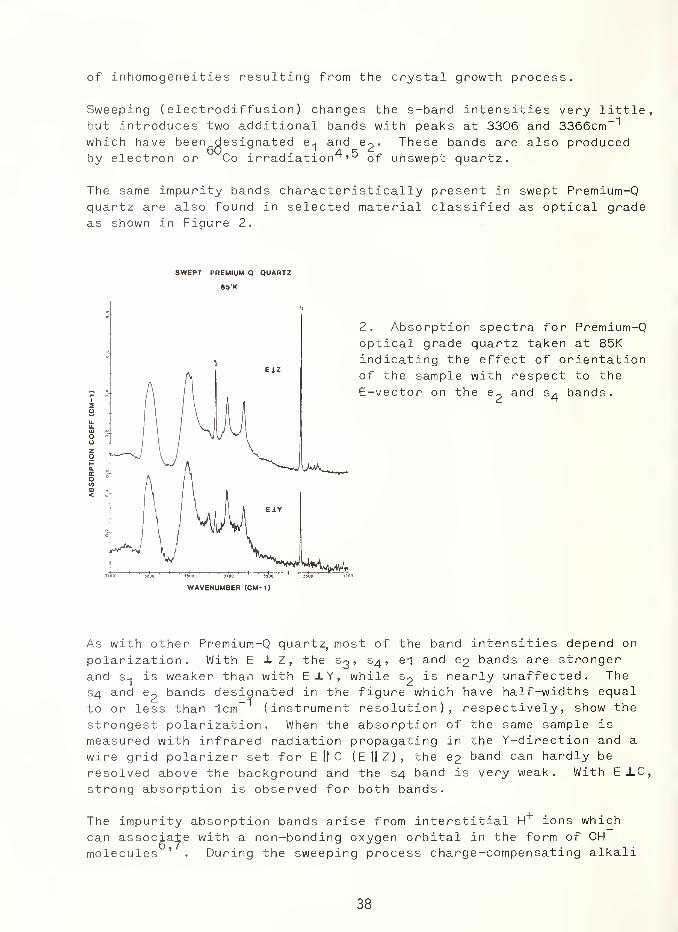
of inhomogeneities resulting from the crystal growth process.
Sweeping ( electrodiffusion ) changes the s-band intensities very little,but introduces two additional bands with peaks at 3306 and 3366cm
- ''
which have been^cjesignated e^ and . These bands are also producedby electron or Co irradiation^'^ of unswept quartz.
The same impurity bands characteristically present in swept Premium-Qquartz are also found in selected material classified as optical gradeas shown in Figure 2.
SWEPT PREMIUM Q QUARTZ
85-
K
2. Absorption spectra for Premium-Qoptical grade quartz taken at 85Kindicating the effect of orientationof the sample with respect to the
E-vector on the and s^ bands.
WAVENUMBER (CM- 1
)
As with other Premium-Q quartz, most of the band intensities depend on
polarization. With E X Z , the So, s4 , ei and e2 bands are stronger
and S-j is weaker than with ElY, while S2 is nearly unaffected. The
S4 and bands designated in the figure which have half-widths equal
to or less than 1cm-
(instrument resolution), respectively, show the
strongest polarization. When the absorption of the same sample is
measured with infrared radiation propagating in the Y-direction and a
wire grid polarizer set for E It C (E||Z), the ep band can hardly be
resolved above the background and the S4 band is very weak. With EXC,strong absorption is observed for both bands.
The impurity absorption bands arise from interstitial HT ions which
can assoc^a^e with a non-bonding oxygen orbital in the form of OH
molecules '. During the sweeping process charge-compensating alkali
38
ions such as Na on Li , pnesent on purposely intnoduced into the melt,
are moved away fnom substitutional aluminum impurities by the electnicfield and are replaced by hydrogen present in the ambient gas. A
similar movement of the alkali ions can also be produced by ionizingradiation at sufficiently high temperatures^'^.
Widely different e2 band intensities resulting for samples swept com-mercially by the same process^ has led to the conclusion that the
strength of this band is principally determined by the initial substi-tutional aluminum concentration in the quartz. The results of an in-
vestigation in progress on samples with identical initial infraredspectra and more uniform aluminum concentration to determine whetherchanges in e-band strength are sufficiently sensitive to monitor the
sweeping process will be presented. Also the use of e-band intensityas a possible indicator of the extent of radiation hardening of
oscillator quartz will be discussed.
References
1. D.B. Fraser, Physical Acoustics , Vol 5, W.P. Mason, Editor, Aca-
demic Press, New York, pp. 59-110; J.C. King, U.S. Patent 3,932,777
(1976)
2. B. Sawyer, IEEE Trans. Sonics and Ultrasonics SU-19 , 41 (1972).
3. H.G. Lipson , F. Euler, and A. Armington, Proc . 32nd Annual
Symposium on Frequency Control, 11(1978).
4. R.N. Brown and A. Kahan , J. Phys . Chem. Solids, 36, 467(1975).
5. H.G. Lipson, F. Euler and P. A. Ligor, to be published in Proc.
33rd Annual Symposium on Frequency Control (1979).
6. A. Kats, Phillips Research Reports, 17, 133(1962).
7. D .M .. Dodd and D.B. Fraser, J. Phys. Chem. Solids, 26, 673(1965).
8. J. J. .Martin, L.E. Halliburton, M. Markes, N. Koumuakalis, W.A.
Sibley, R.N. Brown and A. Armington, to be published in Proc. 33rd
Annual Symposium on Frequency Control ( 1979)
.
The author would like to thank Mr. F. Euler fo(
r helpful discussions.
39

FAR INFRARED STUDY OF THE REFLECTION SPECTRA OF SnS
D. G. Mead*Nicolet Instrument Corporation, Madison, WI 53711
H. R. Chandrasekhar+
Dept. of Physics, University of Missouri -Columbia, Columbia, MO 65211
Tin sulphide SnS is a IV-VI semiconductor possessing an orthorhombicstructure with eight atoms per unit cell forming double-layer planesnormal to the c(longest) axis.l Thus, SnS cleaves very easily in a
plane perpendicular to the c-axis, suggesting a weak inter-layer bond-ing. Unpglarized infrared transmission and power reflectivity spectraof SnS, ' polarized infrared and Raman^ have been reported and latticedynamical calculations 5 investigated.
The reported polarized infrared power reflection spectra^ were analysedby means of a Kramers-Kronig (KK) relation and the infrared activetransverse-optic (TO), associated longitudinal phonon frequencies andthe dielectric constants determined for all three principal directions.A similar analysis was also carried out for isomorphs SnSe^, GeS^ andGeSe^. For GeS^ the widely used formula of the damped classical oscil-lator (see eq. 1, ref. 6) was fitted to the reflectivity data to yieldthe position, strength and damping constant of each oscillator. No
such analysis was reported for SnS and SnSe^ or GeSe 5. It is evident
from the oscillator fits to GeS^ that only poor agreement between thecalculated and experimentally observed spectra were obtained. The fitpresented for the electric vector Ej |c_ was found to be substantiallyworse than for E_||a_and Ej |b directions .
6
As part of an investigation to accurately determine the far infraredoptical constants of GeS and its isomorphs. we have re-examined the
polarized power reflection spectra of SnS.
In view of the failure of the classical oscillator fit to GeS, we have
attempted to fit the reflectivity data of SnS with the aid of a fourparameter dispersive model based on the factorized form of the complexdielectric function. 9 ,10
N Q2 . • - a)2 - iy, „ -co
£ (u))= £,
(aJ )+ie"(a))=e 00 n —^ (1)
j = l Q 2 - ej2
- l'y w
Toj Toj
Here ^Toj> fil_oj> YToj > Y|_ch are tne frequencies and dampings of the TOand LO modes of the jth oscillator. Eq. 1 has been shown to have se-veral advantages ,8,9 including the fact that the model equation allowsthe damping constants yjio anc' YjLO ^° nave se Para te identities so that
40
fits may be made to reflection features having wide bands, as found in
SnS. A non-linear least-squares minimization algorithm to fit the ex-
perimental data was used.H Table 1 lists the resulting fit parameters.
The value of the static dielectric constant is given by:
N w 2
Loj.
3=1w
Toj
and are shown in Table 1, including the corresponding mode frequenciesand dielectric constants obtained from a KK analysis. ^ Table I indi-
cates that the mode frequencies and dielectric parameters are in overall
good agreement with those obtained from the KK analysis. However, for
the Ej |c_ polarization there is a discrepancy outside the range of experimental error. The LO fit frequency situated at 215.9 cm - l lies well
outside the estimated frequency obtained from the KK results. Fig. 1
shows the oscillator fit (solid line) to the observed data for E_[ |c_ ob-
tained with the relevant parameters of Table 1 inserted in eq. 1. Dis-crepancies outside the range of experimental error are particularly no-
ticeable in certain regions surrounding the two prominent reststrahlbands. Hence, model eq. 1 cannot adequately describe the power reflec-tion for this particular orientation and so allow the dielectric func-tion to be obtained.
It was decided to obtain directly the experimental 300K complex reflec-tion (amplitude and phase) coefficient for the same orientation using a
dispersive Fourier Michelson interferometer, 1^ to enable the complexdielectric function to be experimentally obtained without the need forany theoretical models or devices. Sample preparation and polishingtechniques have been given elsewhere^ except that the b face used (sur-
face area -0.16 cm2) was polished flat to less than 0.3ym to avoid dis-tortions of the phase coefficient 0 occurring. The amplitude coeffi-cient (the square root of the power reflection coefficient) revealedessentially the same features as in Fig. 1 and is not given here. Themeasured phase reflection coefficient is shown over the 80-400 cm
- l re-gion in Fig. 2. The phase rises slowly, then descends very quickly at-280 cirri where the amplitude coefficient fal 1 s to a small value (-0.1).The resulting complex (real e
1
and imaginary e" part) dielectric func-tion using standard formulae are shown in Fig. 3. The TO and L0 fre-quencies were derived from peaks in the associated energy loss functionsand are given in Table 1. The results support the KK calculated modefrequencies. ^ The imaginary part e" spectrum reveals an asymmetric lineshape particularly on the high frequency side of TO3. Model eq. 1 im-
plies a constant damping factor while an asymmetric line shape suggestsa more sophisticated model is necessary which includes a frequency de-pendent damping function.
Finally, with typical carrier concentrations ofp-10^/cc. expected forSnS compounds, it has been speculated that coupled pi asmon-phonons modesare present. 13 Hughes et al 13 have suggested that SnS exhibits a plasmaedge at about 280 cm-l, since the reflectivity data do not conform to
41

pure phonon behaviour. (Our attempt to account for the reflection spec-trum by imposing a secondary oscillator positioned at -280 cm~l in eq. 1
resulted in much poorer agreement with the experimental data). However,eq. 1 allows for a system of coupled plasmon-phonon modes by setting oneof the 9,jQ frequencies to zero. This procedure has been recently usedto explain the reflectivity data of GaAs,l 4 >15 CdTe 15 and Ti02i_ x
*
Modified eq. 1 included the plasma frequency ftp, the plasmon damping ynand the damping Yo at zero frequency. The parameters of the coupled LO
modes are given in Table 1, and resulted in an overdamped plasmon pres-ent at 164 cm-1. Identical TO modes were found to those obtained fromeq. 1. Agreement between the fit and experimental data was excellentup to -220 cm-1, but the phonon-plasmon model could not account for the
high frequency side of the spectrum, and shows the disadvantage of modelfitting for obtaining the optical properties.
References
1. OKAZAKI , A., J. Phys. Soc. Japan 13_, 1151 (1958).2. NIKOLIC, P. M. et al., Proceed. XII Int. Conf. on Phys. of Semicon-
ductors, Stuttgart, 1974, Ed. PILKUHN, M. H., p. 331 (unpublished).3. HAAS, C. & CORBEY, M. M. G., J. Phys. Chem. Solids 20, 197 (1961).4. CHANDRASEKHAR, H. R. , HUMPHREYS, R. G., ZWICK, U. & CARDONA, M.
,
Phys. Rev. B15, 2177 (1977).5. FREY, A., Thesis, University of Stuttgart (1977), unpublished.6. WILEY, J. D., BUCKEL, W. J. & SCHMIDT, R. L. , Phys. Rev. B13, 2489
(1976).7. CHANDRASEKHAR, H. R. & ZWICK, U., Solid State Commun. 18, 1509
(1976).8. The original experimental data from ref. 4 was used for this inves-
tigation.9. BERREMAN, D. W. & UNTERWALD, F. C, Phys. Rev. 174, 791 (1968).
10. GERVAIS, F. & PIRI0U, B., J. Phys. C7, 2374 (19747.11. BROWN, K.L. & DENNIS, J. E., Numerische Mathematik 18, 289 (1972).12. MEAD, D. G. & GENZEL, L., Infrared Phys. 18, 555 (1978).13. HUGHES, 0. H. et al . , Phonon Scattering in Solids, p. 312, Plenum
Press (1976).14. KUKHARSKI I , A. A., Solid State Commun. 13, 1761 (1973).15. PERK0WITZ, S. & THORLAND, R. H., Solid State Commun. 16, 1093
(1975).16. BAUMARD, J. F. & GERVAIS F., Phys. Rev. B15, 2316 (1977).
*Work performed in part at Max Planck Institute fur Festkorperforschung,Stuttgart, West Germany.
+A. P. Sloan Fellow
Acknowl edgement
We are grateful to Prof. L. Genzel for use of the facilities at M.P.I.
42

Fig. 1
200
FREQUENCY (cm-1)
200 300
FREQUENCY (cm-1
)
E a
TO
Table 1
LO YTO YLO
1. 99-0 105.9
(99) (10T)
8.2
2. 177. 8 213.3 9-6 6.1 29.0 11.2
(178) (215)
3. 220.2 276. 15 1* 7.8 29.2
(222) (277)
(32+1+) (1U+2)
E| |b 1. 1U5.1 265.3 7.8 30.5 UU.5 13.3(1U5) (265) (U8+5) (16+2)
Fig. 2
200 300 400
FREQUENCY (cm-')
1. 67.5 68.0 3.2 U.U
(69) (71)
2. 189.I* 215.9 6.2 19.0 29.6 12.7
(188) (193) (32+U) (16+2)*189.0 *193.0
3. 216.8 288.2 15.7 23.3E| |c_ (220) (289)
*219.0 *288
COUPLED LO MODES219.3 8.3286.1 8.1
PURE PLASMON PARAMETERS
% = 16U Yp
= 828 yq
= 832
Fig. 3
43

INFRARED ABSORPTION IN HIGHLY TRANSPARENTCUBIC ZIRCONIA
Bernard Bendow, Herbert G. Lipson and Robert C. MarshallSolid State Sciences Division, Rome Air Development Center
Hanscom AFB, MA 01731 USA
Didier BillardCentre de Recherche sur la Physique des Hautes Temperatures
CNRS, 45045 Orleans Cedex, FRANCE
Cubic zirconia possesses an unusual combination of properties whichmake it attractive as an optical material for a variety of applica-tions tit is very hard, has a very high melting temperature, resistschemical attack and is an excellent insulator. It is readily dopedwith various rare-earth and transition-metal ions to provide a widerange of potential laser-host materials. The purpose of the presentwork is to investigate the absorption characteristics of yttria-stabilized cubic zirconia in the highly transparent regime from approx-imately 1500 to 2300 cm~l, at temperatures ranging from 85 to 1000°K.The present measurements constitute the first detailed analysis ofabsorption in the highly transparent (three to four phonon) regime ofzirconia
.
The crystals utilized for this study were produced at RADC employing a
relatively new process called "skull melting", in which the melt is
contained within a solid "skull" of identical composition-'-. This pro-cedure minimizes difficulties with reaction and contamination encoun-tered in conventional crucible-type growth. Heating is accomplished bycoupling RF energy to zirconium metal placed into the charge. Crystalsare finally obtained by preferential freezing of the melt when the cru-cible is slowly lowered through the coil. The yttria-stabilized crys-tals obtained in this way possess hardness ~ 1370 Knoop, density
5.9 gm/cm^, thermal conductivity ~ .018 W/cm/°C and visible refrac-tive index ~ 2.15-2.18. The yttria concentration varied from aroundtwelve to twenty-five weight percent. The detailed frequency (co) andtemperature (T) measurements described below were performed on samplescontaining fifteen weight-percent yttria, with thickness ranging fromapproximately .2 to 1.3 cm.
The absorption coefficient ( a ) was deduced from transmission spectraobtained utilizing a Digilab FTS-14 Fourier spectrophotometer operatedin the double-beam mode using a dry nitrogen gas atmosphere. For thelow temperature measurements, the sample was clamped against an indiumring in contact with the coolant reservoir of a dewar positioned closeto the focal point of the spectrophotometer sample compartment. Ele-vated temperature measurements were made in a small furnace placed in
the same position. Temperatures were measured with a Cu-constantan
44

thermocouple in contact with the polished face of the sample. Absorp-tion values were determined in the usual fashion2 from measured valuesof transmittance and reflectivity.
Typical results for the absorption coefficient as a function of w and
T are indicated in Figs. 1 and 2. The spectra in Fig. 1 display a nearexponential decrease with increasing frequency, behavior characteristicof intrinsic multiphonon absorption 3
. Only weak structure (shoulders
in the 1900-2100 cm~l region) is evident, consistent with the multiphononspectra of other ionic materials 3
. Raman and Reststrahlen spectra4 indi-cate fundamental optical vibrations spanning the 350-700 cm-1 regime,which suggests that the shoulders arise from three to four phonon combi-nation processes involving these strong vibrations. To gain more in-sight regarding the average number of phonons involved, and to corrob-orate that the absorption is due to intrinsic multiphonon processes, it
is useful to analyze the T-dependence of a over a range of frequencies(see Fig. 2). In regimes where the absorption is nearly exponential,a may be represented by the approximate formula^
a(x,y) = aoe~^[N(y)+l]
X/[N(xy)+l]
x = w/oo , y = -ha) A„To 1 o B
where N is the Bose-Einstein function, and co0 is an appropriate averageoptical frequency. The solid lines in Fig. 2 indicate a fit to themeasured data obtained with w = 480 cm-1 ,^A = 7.4xl0-3 ,
otQ=2.2 x 10 5.
The agreement between theory and experiment is quite good, with expecteddepartures due to deviations from exponential frequency dependence. Thevalue utilized for ojq is consistent with IR data for the fundamentalregime, which reveal a broad peak in the range 400-550 cm~l. We con-clude, then, that the present data span a range of approximately 3 to4^ phonons (on the average) , with the shoulder occurring in the 4-4 1/3phonon regime. We have also performed preliminary measurements athigher temperatures 600-1000°K, which indicate similar trends to thosedisplayed in Fig. 2. Detailed analysis of measurements in this tempera-ture range are currently in progress.
In order to assess the effect of yttria concentrations on the absorptionin the highly transparent regime, we have measured the room temperaturespectrum for a series of samples with different yttria concentrationsvarying from twelve to twenty-five weight-percent. The data displayrelatively small shifts (typically 10-30 cm""l) of the absorption edgein the 1600 to 2000 cm~l range. It therefore appears that the dominantcontribution to the absorption in this regime stems from zirconia, withonly a minor contribution from the yttria.
The authors thank P.D. Gianino for assistance with the numericalcomputations
.
45
1. See, for example, D. Michel et al, Jour. Crystal Growth 43 , 546
(1978) and references therein.
2. See, for example, H. Lipson et al, Phys. Rev. B 13, 2614 (1976).
3. B. Bendow, in "Solid State Physics", H. Ehrenreich et al, eds(Academic, NY, 1978), Vol. 33.
4. C. Perry et al, in Proc. of Sixth Intrnl Conf. on RamanSpectroscopy, Vol 2.
5. B. Bendow, Appl. Phys. Lett. 23, 133 (1973).
46

1
0
\\w
v\\
Fig. 1. L°g|Q °^ the absorption
coefficient oC measured in cm \ vs
frequency U) for cubic zirconia at
various temperatures indicated
\\ \ 585 in the figure.
- CUBIC ZIRCONIA
i i i
\\ 490\ 30080
i
1.4 1.6 1.8 2.0 2.2 2.400 (103 cm~1
)
Fig. 2. Absorption coefficient Ql
vs temperature T for cubic zirconia.
The discrete points are measured
values and the solid curves theoreti-
cal predictions.

THE TEMPERATURE DEPENDENCE OF THE OPTICAL ABSORPTION OF METALS*
Michael Bass, David Gallant and Susan D. AllenCenter for Laser Studies
University of Southern CaliforniaUniversity Park, Los Angeles, California 90007
The temperature dependence of the optical absorption of metals must bedetermined in order to throughly understand the optical properties ofmetals and the interaction between intense laser light and metallicsurfaces (1,2). In this paper results are presented for three metals(Mo, Al and 1018 steel), at two wavelengths (10.6 and 1.06 ym) , andover the temperature range from room temperature to 600 C. Theseexperimental parameters were selected because: 1, laser metal workingmost often employs either 10.6 and 1.06 ym lasers for these and similarmaterials, and 2, these combinations of metals and wavelengths mightaid in testing the applicability of the Drude-Lorentz model for theoptical properties of metals (1) . The model predicts nearly equalroom temperature absorptions at 10.6 and 1.06 ym while the experi-mental results show that at 1.06 ym the absorption is ^10X largerthan it is at 10.6 ym. A linear fit can be used to approximate theDrude-Lorentz prediction for the increase of absorption with temper-ature based on measurements of the dc conductivity. This behavior isexperimentally observed for Fe and Mo at both wavelengths and Al at10.6 ym. However at 1.06 ym the absorption of Al decreases with in-creasing temperature.
Laser calorimetry was used to measure the absorption as a function oftemperature (3) . The samples were polished conventionally with thefinal finish obtained using Linde A polishing compound. Polishedsamples were placed in a thermally isolated mount in an evacuablequartz chamber with an NaCl window. This window permitted both 10.6and 1.06 ym laser energy to irradiate the sample. The chamber wasevacuated to pressures of <2 x 10
- ^ T using an oil free pumping systemconsisting of LN2 sorption pump and an ion pump. With this system,the sample could be heated to 600 C in a radiant heating oven with nosignificant surface contamination or decomposition.
Thermocouples (0.8 mm diameter chrome 1-alumel) were attached to thesample to measure its absolute temperature when irradiated relative toa reference sample. The heating and cooling curves obtained with thedifferential thermocouple pair were analyzed by the "three slope"method (3) to obtain the fractional power absorbed at each temperature.Figure 1 shows the results of such an experiment for Mo at 10.6 ym.
The experimental and theoretical results are summarized in Table I.
48

The Drude-Lorentz calculations were performed using the formlism ofRef. 1 and the dc conductivity versus temperature data found in Refs.
4 and 5. On the basis of the Drude-Lorentz model the room temperatureabsorption at 1.06 ym of these metals should be approximately equaland the absorption should increase linearly with increasing tempera-ture .
The experimental results show that the absorption at 1.06 ym is, in
general, £10X that at 10.6 ym. In part, these differences may beattributed to the role of interband transitions in these metals near1 ym. In any case, it is evident that the Drude-Lorentz formalism is
not applicable to these materials at 1.06 ym. For Fe and Mo, thepredicted linear increase in absorption with temperature is observedat both wavelengths. For Al , however-, the 1.06 ym absorption de-creases as the temperature is increased. This type of deviation in
the sign of da/dT from the Drude-Lorentz result was observed byDecker in measurements of the temperature dependence of the reflect-tivity of vacuum deposited Ag films at 1 and 4 ym(6) . At 10 ym,
the Ag films behaved as the calculations predicted. However, bothDecker (6) and Wieting(7) found Al films have positive da/dT for
wavelengths from 1-20 ym. Further studies will be conducted usinglaser calorimetry and more ideally finished samples in order to re-solve the disagreement between the properties of bulk surfaces andfilms of Al . In addition measurements of a and da/dT for Ag will becarried out.
0.06r-
100 200 300 400 500 600 700TEMPERATURE (°C)
Fig. 1. The 10.6 ym absorption of Mo versus temperature. The X's aredata points obtained during heating and the 0's are points obtained asthe sample cooled down to room temperature. The straight line is a
least squares fit of the data.
49

TABLE I
Metal
1018 Steel at:
10.6 ym1.06 ym
Molybdenum at:
10.6 ym1 . 06 ym
Aluminum at
:
10.6 ym1.06 ym
Drude-Lorentz Model
da/dT (%)anm (%)RT
3.44.6
1.31.4
1.01.0
9.2
3.8x 10x 10
-3-2
3.6 x 105.5 x 10
= 3
= 3
3.1 x 105.2 x 10
-3= 3
Experimental Results
aRT (%) da/dT (%) ( C)
2.3
22.6
2.019.7
.1.4
20.0
5.5 x 101.1 x 10
-3
-3
4.5 x 101.4 x 10
-3-2
1.9 x 10-9.2 x 10
-3
-3
Temperature Dependent Absorption of 1018 Steel, Mo and Al
The Drude-Lorentz Model gives results that have been approximated byat least squares fit straight line. For each metal, the experimentaldata has been fit with a straight line, as shown in Fig. 1 for Mo.
REFERENCES
1. T.J„ Wieting and J.T. Schriempf, "Free Electron Theory and LaserInteractions with Metals", Report of NRL Progress, June 1972,Naval Research Laboratory, Washington, D.C.
2. M. Sparks and E. Loh, Jr., J. of Optical Soc. Am. 69, 847 (1979)
M. Sparks and E. Loh, Jr., J. of Optical Soc. Am. 69, 859 (1979).
3. M. Hass, J.W. Davidson, P.H. Klein and L.L. Boyer, J. Appl . Phys.45 , 3959 (1974)
.
4. "Handbook of Thermo-Physical Properties of Solid Materials" Vol. I,
A. Goldsmith, T. Waterman and H. Hirschorn, eds. (McMillan Co.,
New York, NY, 1961)
.
5. P.R. Pallister, J. of the Iron and Steel Institute (1957).
6. D.L. Decker and J.M. Bennett, SPIE Proceedings 140 , 32 (1978),and D.L. Decker "High Energy Laser Mirrors and Windows", Semi—Annual Report No. 4, Sept. 1973 - Mar. 1974, D-ARPA Order No. 2175
pp. 66-83.
7. T.J. Wieting, Bull. Am. Phys. Soc. 19, #1, 92 (1974)
T.J. Wieting, Bull. Am. Phys. Soc. 19, #3, 339 (1974).
^Research supported by Office of Naval Research through SelectedResearch Opportunities Program, Contract No. N000 14-79-C-0896.
50

THE STATISTICAL DESCRIPTION OF OPTICAL INHOMOGENIETIES
E. L. ChurchUS ARRADCQM
Dover NJ 07801
Index horaogeniety is an iaportant attribute of optical materials, whichis usually tested by interferometry ; that is, by measuring the wave-front distortion, £>tp
pinduced into a plane wave traversing a slab of
material. Results are described in terms of an average index fluctua-tion per unit thickness,
= S^/kT (i)
mapped over the interferometer field Here T is the slab thick-ness and k = 2T("/A«
A representative value is $n = 10"^, which, for T = 2.5 cm, correspondsto a wavefront distortion of A/25 at HeNe wavelengths. Distortions ofthis magnitude decrement the Strehl intensity factor by ~ 6%. Effectsof this magnitude are important for high-performance optics, especiallyin multi-element systems.
In principle, it is possible to reconstruct the distribution of the in-
homogenieties in a volume of material by multiscan interferometry , sim-ilar to CAT scanning ^2^. Both the single- and multi-scan methods leadto a deterministic output which provides the basis for judgement of the
quality of the sample under test.
This paper explores the description of the optical inhomogenieties in
statistical terms, which may provide a more general basis for qualitycontrol and specification. Interest is also prompted by the increasingavailability of "digital" interferometers capable of performing on-lineanalysis, and recent advances in the analogous area of surface-finishspecification [3^ .
The optical properties of an element involving random fluctuations gen-
erally depend on the second-order statistics of those fluctuations.
Here the natural second-order statistic is the index covariance func-tion, which describes the spatial distribution of the index fluctua-tions within the sample.^To define this quantity, write the index of
refraction at any point 71 within the three-dimensional sample volume
as the sum of an average "n" and a local fluctuation Sn:
mix) = 7a +- sm(7o • (2)
For the present discussion we take the medium to be statistically iso-
tropic, homogeneous, and stationary. The index covariance function is
then the scalar quantity: _^
Cna(t) = <S/tiU+t)-SffW/0> (3)
51

where denotes the ensemble average and t is the lag parameter.
The gross features of Cn are characterized by "height" and "width" par-ameters, <J"n and tn ; the rms magnitude of the index fluctuations andtheir correlation length, respectively. Specifically, (T~n
^ - Cn (0)
and tn is the first root of Cn (tn ) = Cn(0)/e.
The phase of the transmitted wavefront, If , can also be written as thesum of two terms; the first corresponding to the average medium and thesecond to the fluctuations arising from the index fluctuations. Therelevant statistic is the phase covariance function:
C,p(t) -S4>(t)> > (4)
where s is the position vector in the two-dimensional interferometerfield and t is again a lag parameter. This covariance function may becalculated directly from the measured wavefront distortion, although in
practice it is only possible to measure over a limited range of t.
The phase covariance is related to the index covariance via the waveequation applied to a particular model. In the usual geometrical-optics limit, the result for a slab geometry is easily seen to be:
The problem is now this: Given a measurement of C ^ (t), which obvious-
ly depends on the slab thickness T, how do we deduce Cn? The point of
determining Cn is that it is an intrinsic property of the medium, andonce obtained, can be plugged back into Eq. (5) or its equivalent foranother geometry to determine the optical properties of an element made
of the same, or statistically equivalent, material.
Equation (5) is an integral equation for the unknown function Cn , whichcan be solved in closed form. Here, however, we indicate the physicsinvolved by examining two natural limiting cases: the thin- and thick-
sample limits.
In the thin limit, T«tn , where the slab thickness is much less thanthe index correlation length, Eq. (5) reduces to
CyLt) = (kT fc^(t) ' (6)
That is, the index and phase covariances are proportional. At the zero-lag point, t = 0, this leads to a simple relationship between the rms
phase and index fluctuations:
cr^ = kT<rm > (7)
which is a precise version of Eq. (1).
In other words, in the thin-sample limit, the rms phase fluctuationsscale as the first power of the sample thickness.
52

In the opposite, or thick-sample limit, T»tn , where the slab thickness
is greater than the index correlation length, Eq. (5) reduces to
C(f (t)=2feIT^^^Cm (X) • <s)
This states that the phase covariance is the Abel transform or half in-
tegral of the index covariance. The inverse is the ha If-derivative re-
lationship:00 dLx dL
(9)
In general, there is little resemblance between the analytic expres-sions for Cn and C^in this limit.
For example, the exponential index covariance:
Cm (t) =G^* EXP(-t/tm ) •> (10)
corresponds to the thick-sample phase covariance
(t) = £k*TG^t„ [w.K,<U>] > (ID
where u = t/tn and is a modified Bessel function £4].
When Eq. (5) and its inverse are evaluated at zero lag, they relate the
rms fluctuations in one domain to the covariance function in the other.
In the thin-sample limit the measured phase variance is proportional to
Cn(0). In the thick-sample limit it is proportional to the area of Cn :
(T^ = (o) = Z^Ct ^dX Cm CX) • (12)
Note though, that the area of any simple form of Cn is proportional to
the product <Tn2tn» so tnat
,
ay = # kcrm vUT • (13)
Here ff is a number of the order of unity, the precise value of whichdepends on the form of Cn . Examples are easily generated.
In other words, in the thick-sample limit the rms phase fluctuations are
expected to scale as the square root of the sample thickness.
What happens when the sample is neither thin nor thick? That is, whenthe thickness parameter Z = T/tn falls between the limits of 0 and 00considered above. This region can be explored using the general solu-
tion of Eq. (5), a Gaussian form for Cn (for which Eq. (5) can be
evaluated in closed form) , or by perturbation expansions.
Here we examine the Z dependence of Eq. (5) at the particular point
t = 0, where it becomes an expression for the measured phase variance:
53

o>z = C ¥ (°) -£k
lT^d.x (i-x/T)Cm (x) • oi,)
The transition of this expression between the thin- and thick-samplelimits has been explored using different forms for Cn : a Gaussian, anexponential, and a Lorentzian. The ratio of the phase variance for ar-bitrary thickness to that for infinite thickness is found to increaserapidly as Z*- for Z = 0 to 1, but to approach unity only slowly, as Z"*-,
Values of Z = 6 - 20 are required to reach a ratio of 0.9.
Another important relationship is that between t^and tn . In the thin-sample limit tq>/tn = 1 for any form of Cn , as shown by Eq. (6). Inthe thick-sample limit, however, the relationship depends on the formof Cn , as shown by Eqs. (8) and (9). For the three cases consideredabove, direct evaluation gives ty/tn = 1.0, 1.7 and 1.9, respectively.
Taken together, these results suggest that T^ t q> /2 and T > 20t^ are
required to ensure the practical applicability of the thin- and thick-sample results, Eqs. (6)-(7) and Eqs. (8)-(13), respectively.
SUMMARY
This paper discusses the relationship between interferometric measure-ments of an inhomogeneous optical medium and the statistics of its in-dex fluctuations. It is hoped that these results will focus intereston experimental studies of this method of materials characterization.
Subjects not covered in this Summary are the validity of the underlyingphysical and statistical assumptions, the practicality of obtainingsufficient and sufficiently accurate data for analysis, and bandwidth-limit effects such as those which appear in the related analysis ofrandom surface-height fluctuations L^l.
ACKNOWLEDGEMENTS
I thank Dr. H. E. Bennett at the Naval Weapons Center for drawing atten-
tion to the importance of index inhomogenieties on system performance,Dr. J. A. Cochran at Washington State University for his inversion of
Eq. (5), and Dr. J. M. Zavada at ARRADCOM for helpful discussions.
REFERENCES
1. F. W. Rosberry, App. Opt. £ 961 (1966); F. E. Roberts andP. Langenbeck, ibid. 8 23lT (1969).
2. R. D. Matulka and D. J. Collins, J. Appl. Phys. 42 1109 (1971);
D. W. Sweeney and C. M. Vest, App. Opt. 12 2649 (1973).
3. E. L. Church, H. A. Jenkinson and J. M. Zavada, Opt. Engineering18 125 (1979); E. L. Church, J. Opt. Soc. Am. 69 1404A (1979).
4. Tables of Integral Transforms , Vol. 2 (McGraw Hill Book Company,1954). A. Erdelyi Ed.
54

PHOTOCONDUCTIVITY AT 77K IN UNDOPED TELLURIUM
N.G. Shyamprasad, C.H. Champness and I. ShinElectrical Engineering Dept. , McGill University,3480 University Street, Montreal, Canada H3A 2A7.
1. Introduction Apart from the potential of tellurium as an infrareddetector material [1] between 3 and 4 ym wavelength, there is a need forbetter characterization of photoconductivity in this substance. This is
especially so in crystals with a minimum of imperfections, since tell-urium is known to be very sensitive to lattice damage. Arising from the
high quality crystals grown in our laboratory [2] by the Czochralskimethod, the present work was carried out. It consisted of a study of
the wavelength and thickness dependence of the photoconductivity in
monocrystalline undoped tellurium samples at 77K. Some preliminaryresults on polycrystalline thin film samples are also reported.
2
.
Samples The bulk samples were cut using a solvent saw [3] fromsingle crystal ingots, pulled in the c-direction from melts of highpurity undoped tellurium. The dimensions of the samples are given in
Table I and the orientations are illustrated in Fig. 1. Transport meas-urements showed such samples to be intrinsic at room temperature but ex-trinsically p-type at 77K. Three thin film polycrystalline samples werealso prepared by evaporating tellurium on Pyrex slides on which gold endand side electrodes had been previously sputtered.
3. Method of Photoconductivity Measurements The samples were mounted in
a dewar with an IRTRAN 2 window. Monochromatic polarized light at wave-lengths between 1 and 4.5 microns and chopped at 13 hertz from a PerkinElmer model 13 spectrophotometer was focused on to the sample, main-tained at 77K. The voltage change across the sample was measured usinga lock-in amplifier. The intensity level at each wavelength was deter-mined from the vacuum thermopile detector within the monochromator
.
4. Experimental Results Plots of photoconductive sensitivity againstwavelength (A) are shown in Figs. 2 and 3 for a set of samples cut withthe longest dimension (i.e. the direction of bias current) parallel tothe c-axis, see inset. The ordinate is Aahv/(a J), representing therelative conductivity change per incident photon. Here, Aa is the photo-induced change of conductivity, a is the dark conductivity, J is theincident energy flux at a frequency v and h is Planck's constant.
The difference between having the E-vector of the incident polarizedradiation parallel or perpendicular to the c-axis is contrasted in Fig.
4 for two samples with the same thickness. It is evident that on theshort wavelength side of the maxima the photoconductivity falls offfaster with decreasing X for Ej.c than E//c. This was observed previous-ly by Grosse and Winzer [4]. Similar results were obtained on samples
55
Bulk Samples used in Photoconductivity HeaeureaentB
Saaple no.Dimensions (mm) Orientation
Length Width Thick. Bias curr.to c- a x 1 s
Plane oflllua.
CZ-77-1 Ik 9 1 .8 parallel ( i olo
)
CZ-77-1/B 8 2.0 0.25 perpend. ( i oTo
)
CZ-77-1/C 8 1.9 perpend. (0001
)
CZ-76-10/A 8 2.1 parallel (1010)
CZ-76-10/B 7 2.5 U.BO perpend. ( i oTo
)
CZ-76-10/C 8 2.0 perpend. (0001
)
CZ-76-20/A2 9 1 .8 parallel (1010)
CZ-76-20/B2 8.5 1.9 1 .20 perpend. ( l oTo
)
CZ-76-20/C2 9 1.7 perpend. (0001
)
CZ-76-20/A1 9 2.0 parallel (ioTo)
CZ-76-20/B1 10 1 .8 2 .20 perpend. ( l olo
)
CZ-76-20/C1 10 1.7 pe r pend
.
(0001
)
A
-nxis
B
n-nxis
Fig.l Orientation of samples chem-ically cut from Te crystals.
WAVELENGTH ( u )
Fig. 2 Photoconductive photonsensitivity, La/ (a J ) , forE-vector parallel ?oPc-axis of4 bulk Te samples cut withorientation shown in the inset.
rO CI-77-l/fl* CI-76-10/SC7-76-20/B2
0 CZ-76-20/BI
WAVELENGTH ( m 1
Fig. 3 Photoconductive photonsensitivity, Aa/( a
0JDh
)' forE-vector perpendicular to c-axisof 4 bulk Te samples cut withorientation shown in the inset.
56
cut in the other orientations shown in Fig. 1 but, within the reproduc-ibility of the data, no dependence of photoconductivity on currentorientation was observed.
The effect of sample thickness (d) is brought out more clearly in Fig. 5,
which shows photoconductive sensitivity Aa/ (a J) at X = 2ym plottedagainst d. For the bulk samples (Ej_c) , the photoconductivity increaseswith decreasing thickness, at least down to 0.25 mm. On the other hand,results for the thin film polycrystalline samples indicate a slightdecrease with decreasing thickness.
5 . Theory The relative change of conductivity under a photon fluxJ = J/hv can be shown, with certain assumptions, to be given by:
y + y J xAg _ n p ph
°o
=yPPod 1"K
2L2
i - exp(-Kd) + KL(KL-a) exp(-Kd)- (KL+a)
1 + coth(d/2L)(1)
where a = sL/D, s is the surface recombination velocity, L the dif-fusion length, D the diffusivity, x the lifetime, K the absorption co-efficient, yn the electron mobility, the hole mobility and pQ theextrinsic equilibrium hole concentration.
y + y J
(i) Thick Sample If d»l/K&L, eq. (1) gives: =— 2- -ES., (2)
a y p do p o
so that the photoconductivity varies inversely as sample thickness.
Aa y + y
(ii) Thin Sample If d «1/K & L, eq. (1) gives: =— ^- KJ x , (3)
if s = a=0, so that photoconductivity is thickness independent,/ever, if s > 0 , consideration of i
increases weakly with increase of d.
However, if s > 0 , consideration of equation (1) shows that Aa/aQ
6. Discussion and Conclusions The variation of photoconductivity withsample thickness, shown in Fig. 5, is qualitatively in accordance withthe theory presented above. The decrease with increasing d for the bulksamples evidently corresponds to the "thick" regime, while the slightincrease for the evaporated film samples corresponds to the "thin"regime. The maximum response appears to lie at a thickness between 10
and 100 ym. Analysis of the spectral variations, such as those shownin Fig. 4, indicates s-values between 1000 and 5000 cm/sec. These cal-culations were done using eq. (1) and taking x to be lOOy sec. Asmaller value of s for the (1010) surfaces compared with that for (0001)
surfaces, as reported by Grosse and Winzer [4], was not observed in thepresent work. Absorption coefficients were calculated from the resultsusing eq. (1) with an assumed L-value of 3.6x10"^ cm. These results, asshown in Fig. 6, extend to lower wavelength than those of Blakemore andNomura [5] . The larger K-values for Ej.c than E//c are consistent withdirect photoelectron transitions across the gap for the former orient-ation. It is apparent from the present work that photoconductivity doesoffer a convenient method of determining absorption coefficient in a
57

A-region where the large values make transmission measurements difficult.[1] D.F. Edwards and M. Mercado, Infrared Phys. , 1, 17, 1961.[2] I. Shih and C.H. Champness, J. Cryst. Growth, 44, 492, 1978.[3] M.El-Azab, C. McLaughlin , C.H. Champness , J. Cryst . Growth , 28,1, 1975.[4] P. Grosse and K. Winzer, Phys. Stat. Solidi, 13_, 269, 1966.[5] J.S. Blakemore and K.C. Nomura, Phys. Rev. 127 , 1024, 1962.
1.2 HHC2-76-20/A2r
£ 10'
- -1 1
\ \\ \\ \\i
1
W \\\\ wW \\\ \V w
v\ V
-
1
c
I 1 1 >URVCLtNCTH C m I UAVELENGTH ( M 1
Fig. 4 Photoconductive photon sensi- Fig. 6 Absorption coefficient calc.
tivity, Aa/(aQJ ) , for two samples from photoconductive data.
of same thickness 1.2 mm, with the Curves 1,2: sample CZ-76-20/A2;orientations E//c and Ej.c. curves 3,4: sample CZ-76-20/B2
;
curves 5,6: data of reference [53.
2h
THIN FILM POLTCRTSTBL
10"*
THICKNESS (cr
10«
Fig. 5 Photoconductive sensitivity, Aa/(a J) at X=2ym plotted againstsample thickness, d. The solid line for the bulk samples (Exc)
corresponds to a 1/d variation.
58

EXTRINSIC STATES IN CINNABAR (df-HgS) GROWNBY CHEMICAL VAPOR TRANSPORT
C. T. Simpson, W. Imaino, and W. M. BeckerDepartment of Physics, Purdue University
West Lafayette, Indiana 47907
INTRODUCTION
Cinnabar, the trigonal form of mercury sulfide, is a wide band-gap semi-conductor whose crystal structure belongs to the space group P3i21 (D^)
[l]. Some of the interesting properties exhibited by cinnabar are a
pronounced band-edge dichroism [2], a large birefringence [3], remark-able optical activity [4], and one of the strongest acousto-optic effectsobserved [5], Because of the potential applications of cinnabar, it is
important to establish the nature of extrinsic states due to native de-fects or chemical impurities introduced during the growth process. Afurther stimulus for this study is the recent observation of new Ramanmodes in cinnabar grown by chemical vapor transport (CVT) [6] ; thesemodes exhibit striking resonant enhancement for exciting photon energiesnear the electronic transitions discussed in this paper. We have usedphotoluminescence (PL), optical absorption and excitation spectroscopyto study CVT-grown cinnabar. An understanding of the observed spectrapresents new opportunities for the characterization of this material.
EXPERIMENTAL
Both dendritic and tabular habit (TH) crystals occur in a single growthrun. As we reported previously [7], narrow spectral features were ob-served only in the TH crystals; we confine our discussion to these sam-ples. The volume of TH samples ranged up to ~5 mm^ with a typical sam-ple having dimensions 0.3 X 1 X 2 mm. The largest crystal face wasbounded by the_basal plane
,_c{ 0001} . Other prominent forms present were
rflOll], -r{011l], and m{ 1010} . Impurity analysis revealed that iodine,the transport agent, was the major impurity 10^ cm~3) [7]. The pho-toluminescence and excitation spectra were measured on a Raman scatter-ing spectrometer system employing various cw laser excitation sources, a
double monochromator , a cooled photomultiplier detector and photoncounting electronics.
Figure 1 shows a typical PL spectrum for a TH sample when ftu^, the ex-citing laser energy, is in the range, E(X^) ^ hoi-^ < E . Three peaks,labeled X]_
,X2 and B2 , are observed; at 22 K the peak energies are
E(Xi) = 1.872 eV, E(X2) = 1.854 eV and E(B 2 ) = 1.78 eV, with half-widthsof 3.7, 6.6 and 113 meV, respectively. In the temperature range,20 ^ T ^ 80 K, the half-widths of X]_ and X 2 increase linearly with
59

temperature at rates of 0.25 meV/K and 0.46 meV/K, respectively. At lowtemperatures, T < 10 K, the half-widths appear to be temperature inde-pendent and are typically a few meV at super fluid helium temperatures.The peak intensity of the B2 band decreases by over two orders of magni-tude from 20 to 60 K. The and X2 peak intensities vary only by a
factor of 3 for this same temperature range.
Figure 2 exhibits the excitation spectrum of the B2 luminescence. ForftcjjT < E(X^) the excitation is weak. A dramatic peak in the excitationoccurs for ftu)^ — E(X^). The excitation decreases but persists for
ftuj^ > E(X^). Because the B2 excitation remains strong for ftuJL wellabove E(X-^) , we conclude that a continuum of states is involved in theexcitation process. The excitation spectrum of the X2 luminescence is
very similar to that of the B2 luminescence. We conclude from thissimilarity that the same excitation process is involved in the excita-tion of both X2 and B2.
DISCUSSION
The results exhibited in Figs. 1 and 2, together with the observation of
a sharp, asymmetric absorption at E(X^),suggest that the X^ transition
involves a discrete state and a continuum. Resistance and Seebeck co-
efficient measurements indicate that the TH CVT-grown cinnabar samplesare n-type with gp , the Fermi energy, lyings 0.5 eV below the conduc-tion band edge. To account for the Xi PL and absorption, we postulate a
donor state at ~ 1.873 eV, which we label 2 in Fig. 3. Excitationspectra lead us to propose that the X^
,X2 and B2 PL features result
from the excitation of a valence band electron into level 2. The recom-bination of photoexcited electrons in level 2 with free holes yields theX^ luminescence. No absorption or PL excitation can be detected for
photon energies near E(X2). For this reason, we conclude that in the THCVT-grown samples studied, eF lies above a state at «=- 1.855 eV, which welabel 3 in Fig. 3. The recombination of electrons already occupyinglevel 3 with free holes generated by the photoexcitation of electronsinto level 2 yields the X2 luminescence. The mechanism we propose for
the broad B2 band is a donor-acceptor pair transition broadened bystrong coupling to lattice vibrations. As indicated in Fig. 3, the
zero phonon transitions are between level 2 and level 5, or level 3 andlevel 5, or both. We cannot distinguish between these two processes be-cause of the lack of structure in the B2 emission. Levels 1 and 4 shownin Fig. 3 are used to explain PL features not shown in Fig. 1; thesefeatures are discussed elsewhere [7,8],
The dramatic decrease in the peak intensity of the B2 band with increas-
int temperature can be discussed in terms of a configuration-coordinatemodel. Further details of this model will be presented elsewhere [8],The thermal broadening of the X-^ and X2 PL can be interpreted in termsof a lifetime effect. Due to the electron-phonon interaction the ex-
cited state lifetime is reduced, yielding a broadened lineshape [9,10j.
60

In order to account for the peak in the optical absorption and the exci-tation spectra at ftU) ~ E(X, ) , we performed a simple model calculation of
band-to-impurity absorption in cinnabar [11]. The details of this cal-culation will also be presented elsewhere [8], however the result whichis of importance here is that the peak is a consequence of the matrixelement between the initial and final electronic state wave functions
.
ACKNOWLEDGMENTS
This work was supported by the NSF-MRL Program No. DMR 77-23798 and the
National Science Foundation Grant No. DMR 77-27248.
REFERENCES
r m 4[1] K. L. Aurivillius, Acta Chem. Scand. 4, 1413 (1950). P3
1 21 (D3) is
the space group for the right-handed form; the enantiomorphicleft-handed form belongs to P3
221 (D^)
.
[2] R. Zallen, in II-VI Semiconducting Compounds , edited by D. G.
Thomas (Benjamin, New York, 1967), p. 877.
[3] W. L. Bond, G. D. Boyd, and H. L. Carter, Jr., J. Appl. Phys. 38,
4090 (1967).
[4] B. Ayrault, F. Lefin, H. Langlois, Y. Toudic , and J. F. Palmier,Opt. Commun. _5, 239 (1972).
[5] J. Sapriel, Appl. Phys. Lett. 19, 533 (1971).
[6] W. Imaino, C. T. Simpson, W. M. Becker, and A. K. Ramdas, Phys.
Rev. B. (to be published).
[7] C. T. Simpson, W. I. Imaino, W. M. Becker, and S. P. Faile, SolidState Commun. 28, 39 (1978).
[8] C. T. Simpson, W. Imaino, and W. M. Becker (to be published).
[9] K. Colbow, Can. J. Phys. 41, 1801 (1963).
[10] R. Barrie and K. Nishikawa, Can. J. Phys. 41, 1823 (1963).
[11] We follow the approach of D. M. Eagles, J. Phys. Chem. Solids 16 ,
76 (1960) and W. P. Dumke, Phys. Rev. 132* !998 (1963).
61

1.90 1.85 1.80
ENERGY (eV)
1.75 1.70
1.86 1.921.88 1.90
-fiwL(eV)
Figure 2
Excitation spectrum (ES) of
the B2 photoluminescence peakin the vicinity of E(X^) theX
-Lemission energy.
Figure 1
Photoluminescence spectrum ofCVT-grown cinnabar excited by1.959 eV (6328 A) radiation.
, E(eV)n ///A
2.275--
2.270--
.873--
.855-
0.250-
0.050
0
©
©CB
VB
Figure 3
An energy level scheme for tabularhabit CVT-grown cinnabar. Stateslabeled 1-5 lie within the forbid-den gap. The band continua are re-
presented by cross-hatching.
62

DIFFERENTIAL REFLECTOMETRY - AN OPTICAL TECHNIQUE FORINVESTIGATING BAND STRUCTURE CHANGES ASSOCIATED WITH
ALLOYING, DEALLOYING, CORROSION AND ORDERING
R. J. Nastasi-Andrewst , J. B. Andrews t, C. W. Shanley*,J. Finnegant and R. E. Hummel
Department of Materials Science and EngineeringUniversity of Florida, Gainesville, FL 32611 U.S.A.
The differential reflectometer measures the normalized differencein the spectral reflectivity between two specimens mounted side by side.
The instrument is capable of determining within a hundredth of anelectron volt the energy for interband transitions of electrons.
Light coming from a monochromator is alternately scanned by a
vibrating mirror across the two samples (Figure 1) . The signal from
X-Y
recorder
Figure 1. Schematic diagram of the differential ref lectometer
.
a photomultiplyer tube which picks up the reflected light from the
specimens is electronically processed to obtain the normalized_difference in reflectivity (AR/R) . An x-y recorder plots AR/Rautomatically as a function of wavelength. A scan between 200 and800 nm requires between one and three minutes.
For studying changes in the band structure due to alloying, thetwo specimens which are scanned by the light beam have a small differencein composition (compositional modulation). Applying a line shapeanalysis to the resulting differential ref lectogram, three different
63
8000 6000 £ 4000 2000
2 ' 3 4 ' 6
E, eV
Figure 2. Differential reflectogram of a Cu/Cu - 0.1% Al samplepair.
transitions can be identified (Figure 2): a) A threshold energy forinterband transitions around 2.2 eV (peak A) which involves the upperd-bands and the Fermi energy. This transition energy does not changefor solute concentrations up to approximately 1 at. %, confirming thetheory by Friedel concerning screening of solute charges at low soluteconcentrations. Experimental evidence is given which suggests thatboth the d-bands and the Fermi energy are raised by alloying,b) Lower d-band to Fermi energy transitions around 5 eV (peak D)
behave in many respects similar to the upper d-band to Fermi energytransitions, except that the lower d-bands appear to be raised muchless due to alloying. c) A conduction-band to conduction-bandtransition around 4 eV (peaks B and C) was observed to decrease in
energy with alloying.
In corrosion experiments, one-half of a specimen is protected byan insulating lacquer, while the other half is allowed to form a thinfilm corrosion product . The use of a transparent lacquer permitsmonitoring the film in situ. Owing to the differential nature of
the technique, the effect of the metal substrate is essentiallysubtracted out, so that the resulting differential reflectogram is
related to the absorption spectrum of the corrosion product. Uniquespectra for cuprous oxide, Cu20 (Figure 3) and cupric oxide, CuO
(Figure 4), were obtained and their identities verified either by using
conventional optical techniques or by using calculated electronic bandstructures. The intensity of the structure in the differentialreflectogram is related to the thickness of the corrosion film.
64

5k
Figure 4. Differential reflectogram of CuO on copper substrate.
Differential ref lectometry studies were performed on short-rangeordering in a Cu-17 at.% Al alloy. The differential reflectogram of
a short-range ordered, versus a disordered specimen, shows a pronouncedpeak at 2.64 eV which is attributed to new structure in the orderedstate. The new structure can be explained using the folding bandconcept, which yields additional interband transitions. Short-rangeordering decreases the energy of peak "C" in the differentialref lectograms by 0.04 eV. This shift is equivalent to an increase insolute concentration amounting to one-half of a percent.
Dealloying studies of copper - 5 at. % Zn alloys (red brass)showed that, contrary to literature reports, these alloys dezincifysimilarly as yellow brass.
65

Present address:^Present address
:
^Present address:
University of Alabama in BirminghamMotorola, Inc., Plantation, FloridaBell Labs, Murry Hill, NJ
Bibliography
R. E. Hummel, D. B. Dove and J. A. Holbrook, Phys. Rev. Letters, 25
(1970), 290.
J. A. Holbrook and R. E. Hummel, Rev. of Scientific Instruments, 44 ,
(1973), 463.
R. E. Hummel and J. B. Andrews, Phys. Rev., B8, (1973), 2449.
R. J. Nastasi-Andrews and R. E. Hummel, Phys. Rev. B, 16, (1977), 4314
C. W. Shanley, R. E. Hummel and E. D. Verink, Jr., Corrosion Science,in press.
J. Finnegan and R. E. Hummel, Corrosion Science, submitted forpublication
.
J. B. Andrews, R. J. Nastasi-Andrews and R. E. Hummel, Phys. Rev.,submitted for publication.
66

FREE CARRIER ABSORPTION IN SEMICONDUCTORS IN QUANTIZINGMAGNETIC FIELDS
Harold N. Spector*Department of Physics
Illinois Institute of TechnologyChicago, Illinois 60616
Free carrier absorption in semiconductors is of interest both becauseit is the dominant mechanism for the absorption of electromagneticradiation of frequencies lower than those which give rise to interbandtransitions (i.e.,-fift<E ) and because the dependence of the free
Qcarrier absorption coefficient on photon frequency and temperaturedepends critically on the dominant scattering mechanism for the freecarriers in a particular semiconductor. We have extended the theoryof free carrier absorption in nondegenerate semiconductors to takeinto account the presence of quantizing magnetic fields for the casewhere acoustic phonon scattering is the dominant mechanism for thescattering of the free carrier. 1 Previous work only considered thecase where the electromagnetic radiation was polarized parallel to thed.c. magnetic field and neglected the possibility of stimulated emis-sion of photons in the semiconductor. The latter assumption is correctif the energy of the photon is much greater than the thermal energy ofthe free carriers, i.e. lift » k^T, but is not true in the reverse case.Here the theory is extended to take into account the stimulated emis-sion of photons and to treat the situation where the radiation caneither be polarized parallel (longitudinal case) or perpendicular(transverse case) to the d.c. magnetic field. For the transverse case,photons can be absorbed in intraband transitions between adjacentLandau levels even in the absence of collisions of the free carrierswith phonons or impurities in the semiconductors when the cyclotronresonance condition is satisfied, i.e., ft = u> . For the longitudinalcase, and also for the transverse case when we are on the low fieldside of the cyclotron resonance frequency, absorption of the radiationcan only occur via phonon or impurity assisted transitions betweenthe various Laundau levels.
In a quantum theory, the free carrier absorption coefficient is cal-
culated by relating it to the transition probability for an electronto make an intraband transition from a given initial state by absorb-ing or emitting a photon while simultaneously emitting or absorbingthe phonon which is involved in the scattering process. This transi-tion probability W.
a,eis given by the Born, second order golden rule
approximation,1
W.a
'e
= j£ Z|< f|M|i >|26(E
f- E. ±-fift) (1)
67
where <f|M|i> is the transition matrix element for the electron-photon-phonon interaction and we have neglected the energy of the acousticphonons in the argument of the energy conserving delta function. Thislatter approximation is valid at all except the very lowest tempera-tures since the electrons only interact with the very long wave lengthacoustic phonons in nondegenerate semiconductors. Here E. and E
fare
the initial and final energies of the carrier and -HQ is the energy ofthe photon which is emitted (+sign) or absorbed (-sign). In terms ofthe transition probabilities for the absorption or emission of thephoton, the free carrier absorption coefficient is given by
hK =
f-2 (W.
a- W.
e) f . (2)
where e is the dielectric constant of the material, f. is the freecarrier distribution and the sum goes over all the initial states ofthe free carriers. The above expressions have to be evaluated usingthe energy eigenvalues and eigenfunctions of the free carriers. Forelectrons in a parabolic energy band, these eigenvalues and eigen-functions are
EM = (n^)fkc
+ (3)
|k,n> = axLy)
_!5exp[i(ly + k
zz)]
<J>
n(x-A
2ky), (4)
respectively. Here ty^ are the harmonic oscillator wave functions, ky
and kz
are the components of the free carriers wave vector in the y and
z directions, m* is the free carriers effective mass, and k = (-fic/eB)^.
Using the Landau gauge for the vector potential, we can use the eigen-values and the eigenfunctions for the free carrier in quantizing mag-netic fields to evaluate the matrix element for the electron-photon-phonon interaction. Once this matrix element is obtained, it can beused in equations (1) and (2) to evaluate the free carrier absorptioncoefficient K. It is particularly simple to express the magnetic fielddependence of the free carrier absorption by expressing our results in
terms of the dimensionless ratio of the free carrier absorption co-
efficient in the presence of the magnetic field to that in the absenceof the magnetic field. The reason for presenting our results in termsof this dimensionless ratio is that all fundamental constants and ma-terial parameters, except those that come into the cyclotron resonancefrequency od , cancel and therefore, this dimensionless ratio yields a
universal relation for the magnetic field dependence of the free car-rier absorption which only depends on the photon frequency Q, the ab-
solute temperature T, and the cyclotron frequency w = eB/m*c. Forthe longitudinal case, this dimensionless ratio is
68

Kn (B) 3w
K(oT~=
1 +nu)
Qexp
exp Ki^V L" ~J/
(5)
HQ12K
BT
while for the transverse case, this dimensionless ratio is
Kj_(B)
KToT_316
xuj HI
L v cw -Qc
nu».
coth
si nhl2K
BT
>
(6)
Qexp
V2KB7 0
^2K
BT
1+-Q
In equations (5) and (6), K (x) is the modified Bessel function oforder n and argument x. The results for the longitudinal polarizationreduce to those previously obtained when the photon energy is muchgreater than the thermal energy of the free carriers. In this case,the contribution of stimulated photon emission to the free carrier ab-sorption coefficient can be neglected as all initial states from whichstimulated emission of photons could occur have negligible population.The absorption coefficient for this case is an oscillatory function ofthe magnetic field which increases in magnitude as the magnetic fieldincreases. 1 The results for the transverse case are similar in thatthe absorption coefficient is an oscillatory function of the magneticfield on the low field side of the cyclotron resonance frequency. How-
ever, instead of reaching a peak value at certain values of the ratioof the cyclotron frequency to the photon frequency as in the longi-tudinal case, the absorption coefficient diverges logarithmically atthese values of the ratio. The reason for this logarithmic divergencein the transverse case is the same as for the logarithmic divergenceof the transverse magnetoresi stance in nondegenerate semiconductors 2
,
namely that the collision time for the electron-phonon interactiondiverges for carriers traveling with low velocities along the magneticfield for this configuration and the Born approximation can no longerbe used to calculate the absorption coefficient. In fact, one would
69
expect that the correct approach would be to follow a procedure similarto that used by Arora and Peterson3 to extend the theory of the mag-netoresi stance of nondegenerate semi-conductors beyond the simple Bornapproximation. Such an approach has proved to be successful in calcu-lating the cyclotron resonance linewidth in nondegenerate semiconduc-tors. 4
*Research supported by a grant from the NSF Material Research Lab-
oratory Program, Grant No. DMR 76-24466.
REFERENCES
1. E. R. Generazio and H. N. Spector, Phys. Rev. B (in press).
2. E. N. Adams and T. D. Holstein, J. Phys. Chem. Solids 10, 254
(1959).3. V. K. Arora and R. L. Peterson, Phys. Rev. B 12, 2285 (1975).4. V. K. Arora and H. N. Spector, Phys. Stat. Sol idi (b) 94, 701
(1979).
70
MULTIPHOTON ABSORPTION IN
DIRECT GAP SOLIDS
S.S. MitraDepartment of Electrical Engineering
University of Rhode IslandKingston, R.I. 02881
Introduction
Because of the availability of high power laser sources, non-linearabsorption processes in gases and solids have been the subject of exten-sive investigations in recent years. This interest has been stimulatedin part by the role of non-linear absorption in laser-induced damage ofoptical components, as well as by its many fundamental applicationssuch as determination of non-linear susceptibility, band perturbationunder strong illumination (dynamic Franz-Keldysh effect), parity andselection rule assignments, band structure analysis in semiconductors,etc. In this review, we shall limit our discussion to multiphotonabsorption processes in non-metallic solids.
Phenomenological Description
The multiphoton absorption can be described in a phenomenological mannerby the generalized Beer-Lambert's law:
= -I a In
(1)dx n
n [?n— 3(length)
-/
(power) n f , I the light flux (Wm ) and x the propagation direction.If for a given field strength and frequency the nth order processdominates, the attenuation rate of the light flux is
- £ a In
(2)dt /e
noo
where c is the speed of light in vacuum and the high frequencydielectric constant of the material
._^The relation between I and the
peak electric f^eld amplitude Eq
(Vm ), as well as the photon numberdensity N ^ (m ) is given by
E (e )
'2
I =u0 / 2Z = -S -ficoN , ( 3 )
o ve ph
71

where ZQ is the vacuum impedance. Accordingly, the rate of photonabsorption per unit volume is expressed as
dN , aph _n jn
dt >hoj- n
dNi
e
dt (4)
where Ne is the density of conduction electrons created by the n-photonabsorption process. In terms of the transition rate W(= dNe ) f a i s
given by dt
2nfia) (21 )
nW (E
2n)
an/2 c2noo o
(5)
Theory
The general theory of multiphoton absorption in atoms was outlined byM. Goppert-Mayer A There are essentially two approaches to calculatea for solids, viz., the second2,3 ancj higher-order time dependent per-turbation theories, and the "dressed-state" model of Keldysh.4
By assuming that the transitions take place between Stark-shifted energybands, and that the wave functions are described by Houston functions,Keldysh obtained the following expression for W
W = (
9\) (
3/2, 2 Ae E
o
16 m* oo2
Evc g
i
<x+l>
x (|) (2<x+l> - 2 x)'
2 P 2e E
x exp 2<x+l> (1 =; )
4m* oj Evc g
(6)
where x r^- and the effective band gap
e 2 E 2
E = E + ^^ ^ 4m* govc
(7)
72
subject to the condition
2 P 2e c
o
4m* oj
2E
vc g
« 1 (8)
The photon multiplicity is given by
n = <x+l>
where < > denotes the integer part of the argument, m*^ the reduced
mass of the valence (v) and the conduction band (c) electrons. TheDawson integral (p (z) is defined by
(?)
U) = exp (-z2
) / ey dy
o
The transition rate for a two-photon process from the second orderperturbation theory2/3 i s given by
(10)
w d31 1
H Hvn nc
E (k) -/Cuevn v
6{ E (k) - 2Ku) }vc
(ID
where h\.'s are the interaction matrix elements. The k integral extends
over the entire first Brillouin zone, the index n extends over allpossible intermediate states, and the delta function expresses theenergy conservation required. Braunstein and Ockman^ assumed only oneintermediate state situated above the conduction band, and all threebands were parabolic and isotropic. Depending on the symmetries ofthe bands, three types of two-photon transitions were possible:allowed-allowed, allowed-forbidden and forbidden-forbidden. Basov etal. assumed that the intermediate states were in the valence and theconduction bands themselves. They also used isotropic and parabolicenergy bands.
Recent Work
Mitra, Vaidyanathan and co-workers have recently critically examined thethree models. They have used both the parabolic and a non-parabolic^energy bands, given, respectively by
vc at) + *2
k2
2m^vc
(12)
73

and E (£) = E (1 + « -| )vc g m * Evc g
2.2 ^
(13)
Keldysh's model uses only the non-parabolic band structure (13). Wehave shown that the Keldysh formula is closely related to Braunstein'sfor allowed-allowed transitions, while Basov's proposed formula moreclosely corresponds to Braunstein's for allowed-forbidden transitions.A number of improvements and corrections to both Braunstein and Basovformulas will be indicated. The two-photon absorption coefficients forseveral direct-gap seminconductors and alkali halides are calculatedfrom these formulas and compared with the available experimental data.The formulas of Keldysh and Braunstein for describing allowed-allowedtransitions, where one considers excitonic intermediate states andnonparabolic energy bands, are found to give results in fair agreementwith published experimental results. Basov's and Braunstein's absorp-tion coefficients for allowed-forbidden transitions are smaller thanavailable experimental data by orders of magnitude.
Vaidyanathan, Guenther, and Mitra^ have recently proposed a newmodel that combines the elements of second order perturbation theory andelectronic energy band structure calculations. This procedure is found
||
j
to represent a significant improvement over currently available theo-retical models reviewed above. Results for CdTe, GaAs, InP and ZnSe are
;
in good agreement with available experimental data.
)!8,
Keldysh model is capable of predicting the n-photon absorption coef-ficient for any value of n. For example, Fig. 1 shows such a calcula-tion for PbTe for up to 4-photon transitions. In the passing, it maybe remarked that we have previously shown^ that the one-photon absorp-tion edge in direct-gap crystals predicted by the Keldysh formula agreeswith the results of conventional perturbation theory to within a factorof order unity. This is in contrast to the frequently stated opinionthat the Keldysh formula is incorrect or invalid when the photon multi-plicity is small.
9Kovarskii and Perlin have treated the three-photon absorption in
direct gap solids by an improved but similar model to that of Keldysh.Bassani and Hassanl^ have presented a perturbation calculation for the
third order coefficient. Judell, Mitra, and Vaidyanathanll have usedthe third-order time dependent perturbation theory to determine the
three-photon absorption coefficient for several direct-gap semicon-ductors using both parabolic and non-parabolic band structures.Intermediate levels needed in these calculations are the higher energybands obtained from band structure calculations. The dispersion of a-j
closely follows that of Keldysh's result in shape but not in magnitudeas shown in Fig. 2. Our result for CdS agrees closely with theexperimental valued.
74
Acknowledgment
The author is very grateful to Dr. A. Vaidyanathan for many helpfuldiscussions
.
References
1. M. Gioppert-Mayer, Ann. Phys. (Leipzig) 9_, 273 (1931).
2. R. Braunstein, Phys. Rev. 125 , 475 (1962); R. Braunstein and N.
Ockman, Phys. Rev. 134, A499 (1964).
3. N.G. Basov, A.Z. Grasyuk, I.G. Zubarev, V.A. Katulin and O.N.Krokhin, Sov. Phys. JETP 23, 366 (1966).
4. L.V. Keldysh, Sov. Phys. JETP 20, 1307 (1965).
5. S.S. Mitra, L.M. Narducci, R.A. Shatas, Y.F. Tsay and A. Vaidyanathan,Appl. Opt. 14, 3038 (1975); A. Vaidyanathan, T. Walker, A.H. Guenther,S.S. Mitra, and L.M. Narducci, Phys. Rev. B (in press).
6. E.O. Kane, J. Phys. Chem. Solids 1, 249 (1957).
7. A. Vaidyanathan, A.H. Guenther and S.S. Mitra, to be published.
8. L.M. Narducci, S.S. Mitra, R.A. Shatas, P. A. Pfeiffer and A.
Vaidyanathan, Phys. Rev. B14, 250 (1976); A. Vaidyanathan, T. w.
Walker, A.H. Guenther, S.S. Mitra and L.M. Narducci, Phys. Rev. B2Q,
3526 (1979).
9. V.A. Kovarskii and E. Yu Perlin, Phys. Status Solidi 45, 47 (1971).
10. F. Bassani and A.R. Hassan, Nuovo Cimento B7 313 (1972).
11. N. Jodell, S.S. Mitra and A. Vaidyanathan, to be published.
12. A. Penzkofer and W. Falkenstein, Opt. Commun. 16, 247 (1976); I.M.
Catalano and A. Cingolani, J. Appl. Plys. 50, 5638 (1979).
75


MEASUREMENTS OF TWO PHOTON ABSORPTION*
Alan F. Stewart and Michael BassCenter for Laser Studies
University of Southern CaliforniaLos Angeles, CA 90007
Since the first observation of a two photon absorption (TPA) process byKaiser and Garrett in 1961(1), there have been many conflicting experi-mental results and theoretical predictions (2,3). An absolute mea-surement of the TPA coefficient, 3 , for any given material has provento be experimentally difficult and reported values differ by an orderof magnitude or more. New measurements of TPA are reported here for
several zincblende and wurtzite materials employing the technique of
nonlinear laser calorimetry (4) . Internal reflections in our sampleswere eliminated by appropriate antireflection coatings and an accuratedetermination of the TPA coefficient was possible. The results are in
agreement with previous state-of-the-art measurements using the trans-mission technique (5)
.
The propagation of light in a medium which exhibits both linear and
TPA is described by
dl(x,y,z,t ) = _ (ct+ BI(x Z/t) ) i (x , y , z ,t) (1)dz
2where I(x,y,z,t) is the light intensity in MW/cm , z is the directionof propagation, a is the linear absorption coefficient in cm
--'- and 3 is
the TPA coefficient in cm/MW. Internal reflection at the exit surfacecreates a counterpropagating field which may interfere with the incidentradiation inside the crystal. In a semiconductor with a large refrac-tive index the reflectivity may reach 30% per surface. Thus construc-tive interference between incident and reflected beams can increase theintensity inside the crystal by a factor of 2.4. An unmeasurable en-hancement of this magnitude would distort the results of any experimentdesigned to measure an intensity squared dependent process such as TPA.How much enhancement occurs in the crystal will depend on the reflec-tivity, surface figure and the angle between incident and reflectedbeams
.
In order to account for internal reflections we consider only thatoccurring at the exit surface of the sample. The following equationsfor the incident and reflected intensities were obtained from the con-tributing terms of the nonlinear polarization assuming perfect spatialoverlap and constructive interference:
* This work was supported by National Science FoundationGrant No. ENG-7820470
77

dldz
-a I - 31 (I + 21 )R (2)
5dz
"RaI
R+ BI
R(IR
+ 2I) (3)
where I is the incident intensity and Ir is the reflected intensity.In reference (4) the coefficient of the cross terms was set equal tounity because it was felt that the lack of parallelism and the imper-fect surface quality of the sample faces resulted in imperfect con-structive interference of the two beams. Intuitively, one would expectthe coupling between the two beams to be greatest near the exit surface.The coupling should decrease to zero as the two beams physically sep-arate and lose their phase coherence nearer the entrance surface. Thesurface parellelism required in order to observe interference effectsin transmission from a low reflectivity etalon is typically less thanone arc minute for 1 ym light (5) . However, field enhancement in a 1mmthick slab of material would occur over most of the thickness with a
required parallelism of slightly less than one degree. Thus, fieldenhancement must be present in a typical TPA experiment but the magni-tude of the effect has not been determined until now.
The experimental procedure used in this study follows that outlined in
reference (4). A passively Q-switched NdrYAG laser which operates in
the TEMqq mode at low repetition rate (4Hz) was the source for thiswork. The beam intensity reaching the sample was adjusted using a twopolarizer attenuator. The total absorption of the sample was measuredas a function of the incident intensity using standard procedures forlaser calorimetry (6) . The Gaussian intensity distribution reachingthe sample was measured by scanning the beam with a narrow slit in
front of a pyroelectric detector. The temporal profile was measuredwith a fast photodiode (risetime of 0.1 nsec) and was completely smoothand nearly Gaussian when observed on a R7912 Transient Digitizer. Anytemporal structure in the laser pulse represented intensity fluctuationswhich precluded accurate measurement of 3 and hence that condition wascarefully avoided.
The crystals used in this study were selected from three lattice fam-
ilies: sphalerite or zincblende structure, wurtzite structure andsimple cubic. The orientation of these crystals was chosen to precludesecond harmonic generation which if followed by linear absorption wouldalso appear as an intensity squared dependent process. For zincblendematerials the incident light propagated along the (110) direction andwas polarized in the (001) direction. For wurtzite materials the in-cident light propagated along the optic axis. The linear absorption wasmeasured using conventional calorimetric techniques and a CW Nd:YAGlaser. All crystals were high resistivity (>10° fi-cm) except for theCd Sq 25 Se0.75 which was accidentally uncompensated and showed a re-sistivity of <1q3 fl-cm.
73

The role of internal reflections was determined by applying multilayerantireflection coatings to one surface each of samples of CdTe, CdSeand GaAs. In this way, the total absorption as a function of inten-sity could be measured with no internal reflection or exactly oneinternal reflection simply by turning the sample around. The TPA co-efficient, 3, was obtained from data taken with the antireflectioncoating on the exit surface using Eq. (1) . Once the value of 3 wasknown the data obtained with the antireflection coating on the en-trance surface was analyzed using Eqs. (2) and (3) with the coef-ficient of the cross terms as the fitting parameter. As a final check,
uncoated but otherwise identical samples of these materials were mea-sured and again the best fit coefficient for the cross terms in Eqs.
(2) and (3) was determined. In order to use Eqs. (1) , (2) and (3) toanalyze the experimental results numerical integrations were carriedout over the temporal and spatial profiles of the incident pulses.
The results of these experiments appear in Table I. In all cases a
cross term coefficient in Eqs. (2) and (3) of unity resulted in thebest fit to the data. Also we have observed no spot size dependencein our measurements indicating that diffusion of free carriers is notimportant on a nanosecond time scale for beams with 1/e radiigreater than 100 urn.
Table I
Measured Absorption and TPA Coefficients
GaAs CdTe CdSe
a(cm_1
) 1.50 +0.15 0.049 + Q.005 0.026 +0.003
B(cm/MW) 0.030 +0.009 0.041 +0.012 0.043 +0>013
CdS 0 ^ c Se n CdS n e Se„ _ KRS-V0.25 0.75 0.5 0.5
a (cm"1
) 0.028 +0.003 0.254 +0.03 0.0047 +0,0005
B(cm/MW) 0.075 +0.023 0.031 +0.009 0.0016 +0.0005
A good example of the sensitivity of this technique is demonstratedin our measurement of KRS-V. Since nonlinear calorimetry compares
the magnitudes of linear and TPA processes the minimum detectable
TPA coefficient is limited by the maximum intensity that does not
damage the sample and linear absorption coefficient. In KRS-V,
which has a linear absorption of only 4.7 x 10⁻³ cm-1 , a 400% in-
crease in the total absorption was detected with only 20 MW/cm2 of
incident intensity. This same intensity would result in only a one
percent change in transmission. Nonlinear laser calorimetry shows
its greatest promise in measuring TPA in highly transparent materials.
The experimental errors indicated in Table I were primarily caused by
uncertainty in the absolute determination of the incident intensity
of each pulse. The uncertainty comes from calibrations of both the
79

pyroelectric detector and the average power meter used. Additionalcontributions arise from laser intensity fluctuations and uncer-tainties in the measurements of the laser spot size and temporalprofile. As with any calorimetry experiment there is some additionaluncertainties resulting from analysis of the heating and coolingcurves
.
In conclusion, we have measured the TPA coefficient in six materialsand have obtained results in good agreement with those obtained in
a very different type of experiment. This suggests that the experi-mental results are asymptotically approaching the true value of $•
It is clearly impractical to apply antireflection coating to all mat-erials to be tested for nonlinear absorption. In this research it
has been demonstrated that a cross term coefficient of unity in Eqs.
(2) and (3) allows proper analysis of data obtained from uncoatedsamples. It should be noted that if the true coupling coefficient hadsome other value between 0 and 2, assuming a value of unity leads to
an estimated uncertainty in 3 which is at most 20%.
REFERENCES
1) W. Kaiser and O.G.B. Garrett, Phys. Rev. Lett. 7_, 229 (1961)
2) C.C. Lee and H.Y. Fan, Phys. Rev. B 9_, 3502 (1974)
3) J.H. Bechtel and W.L. Smith, Phys. Rev. B 13_, 3515 (1976)
4) Michael Bass, Eric W. Van Stryland, and A.F. Stewart, Appl. Phys.
Lett. 34, 142 (1979)
5) Raoul Weil and Dalia Neshmit, Appl. Opt. 16, 2847 (1977)
6) A. Hordvik, Appl. Opt. 16, 2827 (1977).
80
THREE-PHOTON ABSORPTION IN Nd : YAG
Robert W. Boyd and Mark A. KramerInstitute of Optics
University of RochesterRochester, New York 14627
The narrow spectral linewidths characteristic of transi-tions of rare-earth ions (Fig. 1) make rare-earth-dopedcrystals interesting systems in which to study resonantand near-resonant optical nonlinearities . While populationinversion and consequent laser action is a common exampleof a nonlinear effect involving the rare earths, othertypes of optical nonlinearity also exist. The generationof sum and difference frequencies of applied laser fieldsthrough a second-order "%u ^ nonlinearity is such an example.For a laser frequency close to a resonance frequency ofthe rare-earth ion, these nonlinearities are by theoreticalarguments expected to become very large.
Another type of optical nonlinearity involving the rareearths, and the subject of this article, is three-photonabsorption in Nd:YAG. In the schematic setup of Fig. 2,
a 6 nsec pulse of 30 kW peak power at 5933 £ is focussedto an 18 um spot size in a 5-mm-long sample of 1 wt percentNd : YAG . Blue fluorescence light is found to be emittedfrom the focal volume, and it is of sufficient intensityto be easily observed by eye. A spectrum of the fluores-cence is shown in Fig. 3. No fluorescence is observed atwavelengths shorter than that of the intense doublet at4000 In addition, a number of longer wavelength linesappear throughout the visible. The fluorescence spectrumfor wavelengths greater than the excitation wavelengthclosely mimics the normal, low intensity, one-photon-induced fuorescence spectra, such as those shown in Fig. 4,
which were also taken with the apparatus of Fig. 2 but withthe laser defocussed.
The intensity of the 4000 A* fluorescence is found to varyas the third power of the laser intensity over a range of30 in laser intensity. The process giving rise to thisfluorescence is thus interpreted as three-photon absorptionfollowed by a partly radiative and partly nonradiativede-excitation, and is illustrated in Fig. 5. Following
81

excitation to level 2 by three-photon absorption, the atomdecays nonradiatively to level 3, radiatively to level 4,
and nonradiatively back to level 1. In principle, levels2 and 3 or levels 1 and 4 could be coincident, but theobserved fluorescence spectrum suggests that the dominantdecay route is as illustrated in Fig. 5.
Nd:YAG is known to essentially opaque for wavelengthsshorter than 2400 S. Three-photon absorption thus permitsthe probing of levels such as level 2 which are more than42,000 cm above the ground state and are thus inaccessi-ble by conventional spectroscopic techniques.
The intensity of the 4000 8 fluorescence is plotted as a
function of laser wavelength in Fig. 6a; below it the prod-uct of the laser power (shown in 6b) and the crystal trans-mission is plotted in 6c. It should be noted that eachpeak in 6a matches a dip in 6c, thus indicating that anenhancement of the three-photon-absorption process occurswhenever the laser is tuned to a one-photon resonance.Similarly, theory predicts an enhanced three-photon absorp-tion rate if the energy of two photons is equal to theenergy of a two-photon-allowed transition. Since three-photon absorption necessitates the existence of level 2 ofFig. 5 at an energy equal to that of three incident photonsit can be concluded from the data of Fig. 6 that a broadenergy level or several overlapping levels exist some51,000 cm
-"'" above the ground state of Nd:YAG.
In conclusion, a method is presented for studying the ener-gy-level structure of Nd:YAG and similar rare-earth-dopedcrystals in an energy region where one-photon techniquesare not possible. This three-photon-absorption process is
presently being studied over a much broader range of laserwavelengths, and the results of this investigation will bereported in the future.
This work was partially supported by NSF grants SER77-06914and ENG79-08038.
Reference1 W. F. Krupke, IEEE J. Quantum Electron., QE-7 , 153, 1971
82
3000 4000 5000 6000
\(A)
1^ 1^ 1^ I
I
7000 8000 9000
Figure 1. Absorption spectrum of Nd : YAG at 300 K.
SAMPLE
I
LASER p
STRIPCHART (~2 [pmtI
M0N0CHR0MAT0R
Fig. 2. Experimental setup,
4000
Fig. 3
5000 6000 7000
X(A)
8000 9000
Emission spectrum for three-photonexcitation at 5933 8.
83
Fig. 6. a) Intensity of4000$ fluorescence, b) Laserpower vs. wavelength. c)Power transmitted by 5mmsample.
84

REFRACTIVE INDEX AND THERMO-OPTICCOEFFICIENTS OF CD*A
L. G. DeShazer and K. E. WilsonHughes Research Laboratories
3011 Malibu Canyon RoadMalibu, CA 90625
The refractive indices of CD*A were measured at 29 wavelengths by themethod of minimum deviation. The crystal was cut into a prism withthe optic axis parallel to the prism apex edge enabling both theordinary and extraordinary refractive indices to be measured withoutaltering the position of the prism in its mount. The index measure-ments were made in a dry environment to prevent deterioration of theCD*A polished surfaces by moisture. The level of deuteration of themeasured crystal was about 90%.
A two- resonance Sellmeier formula was fit by the method of leastsquares to the measured index values. The formula used was
n2 = 1 + AA 2/(A 2 -B) + CX7(A 2 -D).
The determined Sellmeier constants are listed in Table 1 for both theordinary and extraordinary indices. For example, the indices at
1.0642um are Ne = 1.5366 and n Q = 1.5531.
Table 1. Sellmeier Constants for CD*AA' B(ym') C D(um z
)
Ordinary 1 .402934 0.0132 0.14654 24.0117
Extraordinary 1 .34951 0.012227 0.062868 25.0
The thermo-optic coefficients ctn ( = n_1
dn/dT) of CD*A were measured as
a function of wavelength from 325 to 632.8 nm using a double inter-ferometric technique involving both Twyman-Green and Fizeau configura-tions. The thermal coefficient of linear expansion of CD*Aperpendicular to the optical axis was also measured by this techniqueand was determined to be 8. 7+0.2xlO" 6 /°C At 632. 8nm, dn/dT =
25.78xlO' 6 /°C for ordinary polarization and -20.19xlO" 6 /°C for extra-ordinary polarization. Using this data, Type I phasematch solutionswere calculated for CD*A as a function of temperature. Figure 1 showsthe phasematch plots for three frequency mixing in CD*A at roomtemperature which can be used to design sum frequency generators(SFG)
,
difference frequency generators, and optical parametric oscillators.For example, in SFG the wavelength on the abscissa represents the sumfrequency and the wavelengths on the ordinate axis represents the input
frequencies
.
85

ON THE USE OF A CALORIMETER TO INVESTIGATELOSS MECHANISMS IN OPTICAL FIBERS
F. T. StoneBell Laboratories
Norcross, Georgia 30071
Loss mechanisms in optical fibers are classed as intrinsic,
i.e., caused by the inherent limits of the materials andstructure, and extrinsic, i.e., added on during processing.To attain low loss in fibers, the fundamental limits mustbe understood; then any additional contributions to fiberloss must be identified and reduced to negligible levels.In our lab we have used a calorimeter to aid in meetingthese objectives. Calorimetry has the capability to:(1) directly measure absorption and total loss, (2) measurethe loss of short (~lm) samples to determine uniformity overthe fiber length, (3) measure extremely low fiber losses(-0.01 dB/km) , (4) measure mode-dependent loss for multimodefibers (to determine the variation of loss over the coreregion) or measure the loss accurately in small-core-diameterfibers by exciting only a single mode even when these fiberssupport more than one mode (thus avoiding mode-cut off com-plications) , and (5) measure the loss of the same segment ofthe fiber coated (or even completely packaged) and bare toquantify coating (or packaging) loss. We present hereexamples illustrating a variety of uses of calorimetry infiber loss measurements.
MODE DEPENDENT LOSS
Since short lengths of fiber can be measured, the modedistribution set up at the input face of the fiber isessentially the distribution in the fiber length beingmeasured. (Extremely lossy cladding, leaky, and marginalbound modes are eliminated immediately after launch with amode stripper.)
Different mode groups are excited in the graded-index multi-mode fibers studied by scanning a focused laser beam acrossthe fiber core. Lowest order modes are excited with thebeam focused at the center of the core, highest order modeswith beam focused on the core-cladding boundary. Figure 1
presents the mode-dependent loss of two fibers: for fiber399, which exhibits a large amount of higher-order modeattenuation, other measurements indicate core-claddingboundary problems; fiber 4 34, on the other hand, is a
87

TOTAL LOSS
(dB/km)
14
12FIBER 399
/
FIBER 434
Ge-B-S,0 2 CORE FIBERS
X = 647nmCORE DIA. = 55H m
Fig. 1. Mode-dependent losscharacteristicsof two fibers
0 5 10 IS 20BEAM POSITION (r |
reasonably good fiber of the same type inserted for com-parison. These plots illustrate how mode-dependent lossdata aids in localizing the region of excess fiber loss.
UNIFORMITY OF THE LOSS OF VARIOUS SEGMENTS OF A LONG FIBER
_i i
25 27.5
The title of this section presents one aspect of a fundamen-tal problem in fiber manufacture - how uniform are the fiberparameters with position down the fiber. This question isalso pertinent in evaluating a technique such as calorimetrythat provides information on limited regions of the fiber.We have examined the loss-uniformity of many fibers usingan optical time-domain reflectometer , a scattering cube, anda calorimeter. Figure 2 is a presentation of absorption
ABSORPTION
LOSS
(dB/km)
3 0
2 0
1 0
° MEAN OF 5 MEASUREMENTS TAKEN AT
Z = 0, 1000, 1500, 2000 AND 2300m
I TOTAL RANGE OF RESULTS
FIBER LL
Fig. 2. Absorp-tion loss mea-sured on segmentstaken from dif-ferent regionsof a 2300m longfiber.
647 n m
0 5 10 15 20 25 27.5
BEAM POSITION <pm)
88

data of fiber segments taken from various places along a2 . 3-km fiber. As can be seen, the absorption appears uni-form throughout the fiber; hence, measurements on any onesegment are typical of the whole fiber.
Using calorimetry, the loss versus length of a fiber canalso be measured for situations where loss differences arecaused by changes in the mode distributions in the fiber,not by changes in the fiber itself. By doing this, one can,for example, study the effectiveness of different excita-tion conditions in launching an approximation to the steady-state mode distribution.
EFFECT OF COATING
Figure 3 demonstrates the way a coating can increase the
IS
TOTAL LOSS
(dB/km)
5 - « HARD POLYMER COATING
° UNCOATED FIBER
Fig. 3. Coatedvs . uncoatedfiber lossillustrating themeasurement ofpackaging loss
0 I 1 1 I I J
0 5 10 15 20 25
BEAM POSITION| H m)
higher-order mode loss, probably by causing microbending.Such results can be used to compare different packagingmaterials, for instance, in an environmental study, and tosettle questions such as whether or not a given coating isresponsible for excess loss measured in a fiber by othertechniques
.
SPECTRAL LOSS
Figure 4 is the absorption loss of an experimental single-mode fiber that was examined to determine the cause of theexcess loss. The results show absorption far greater thanthat of a good fiber (see 64 7-nm data point in Figure 4)
.
By using various lines of a Krypton laser, the absorptioncan be obtained at a number of wavelengths in the visibleand near IR, giving a good outline of the spectral charac-teristics of the absorber. In this case the outline matchesthat of nickel in sodium borosilicate glass as reported byBeales et al.l This has not been directly verified, however.Another aspect of the usefulness of calorimetry is illus-
39
ABSORPTIONLOSS
(dB/km)
SINGLE MODE FIBER
LOW LOSS SINGLE MODE FIBER
ABSORPTION AT 647 ]nm—
600
X („m|
TOTAL LOSS
SORPTION
J*' LOSS
752 Snm
-J
Fig. 4. Spectralabsorption lossof a single modefiber with largeextrinsicabsorption
trated by this example, namely the capability to measureseparately the fiber absorption and the total fiber loss
FUNDAMENTAL LOSS MEASUREMENTS
Since only short lengths of fibers are needed for calori-metry, the lack of mode mixing enables the power distri-bution to be determined rather exactly, for example, bymeasuring the near-field radiation pattern. Thus, powerdistributions can be excited that probe only the regionsof the fiber that one wishes to study. If one wished toexamine the loss of the glass itself, one could avoidlaunching energy in the vicinity of the core-claddingboundary, thereby avoiding complications caused by theunknown nature of this boundary. Furthermore, the losshistory of the glass could be examined as a function ofvarious environmental conditions - heat, humidity, radia-tion, etc. - and this glass effect could be separated outfrom any effects due to packaging changes.
Because calorimetry can detect very low losses, these var-ious measurements mentioned can be made with great sensi-tivity and repeatability (~0.01 dB/km for ~1 watt throughthe fiber) . By optimizing the calorimeter structure andthe measurement electronics, appreciably lower losses couldbe measured. For these reasons calorimetry is a usefulmeasurement technique to examine the intrinsic and extrin-sic loss characteristics of optical fibers.
K. J. Beales, C. R. Day, W. J. Duncan, J. E. Midwinter, andG. R. Newns, Proc. IEE 123, 591 (1976).
90

COMPUTERIZED REFRACTIVE INDEXMEASUREMENT FOR FIBER OPTIC GLASSES
D. L. Wood and J. W. FlemingBell Laboratories
Murray Hill, New Jersey 07974
In screening glass compositions for possible waveguideapplications it is necessary to evaluate the refractiveindex and its first and second derivatives with respectto wavelength. We have constructed an apparatus to performthis task with a minimum of operator time required but withaccuracy in the fifth decimal place of the index routinelyachieved.
The apparatus is built around a 20-bit digital angle sensorwhich measures the deviation of monochromatic radiationthrough a prism of the composition to be investigated. A
minicomputer controls the experiment, records the data andcalculates the index values from the measured angles. Wechose an optical system involving an off -ax is paraboliccollimating mirror and a reflecting rear face on the prismso that measurements at other than room temperature canalso be conveniently made, and a broad wavelength range canbe covered.
Index values for germanium silicate glasses of various com-positions have been measured, and these results togetherwith temperature coefficients near room temperature will be
reported
.
91

STRESS OPTIC COEFFICIENT OF OPTICAL FIBERS
N. LagakosThe Catholic University of America
(Present Address: Naval Research LaboratoryCode 8133, Washington, D.C. 20375)
Introduction : The introduction of a mechanical clad under compressionas a possible solution to the static fatigue problem of opticalfibers-^ has necessitated the develovpment of a polariscope for measur-ing the stress optic coefficient and the stress profile of opticalfibers. Such a polariscope has been developed. This polariscopecould be used for evaluating the acoustic response of the opticalfiber acoustic sensors^.
Experimental set-up : The stress optic coefficient of fibers, f, was de-termined by the experimental set-up shown schematically in Fig. 1, whichis based on the Friedel's method of compensation^ . The light from anArgon ion laser after becoming partly incoherent by passing through a
scrambler (a rotating semitransparent plastic disc) was incident perpen-dicularly on the fiber. The observed part of the fiber was immersed ina refractive index matching liquid and it was placed between a polarizerand an analyzer with their vibration axes perpendicular to each otherand at 45° with the fiber axis. A quarter-wave plate was placed beforethe analyzer to ensure linear light polarization. A 20x microscope ob-jective and a projection lens focused the fiber cross section on the
plane of a 0.7mm diameter pinhole in front of a photomultiplier . By
slight translation of the projection lens the transmitted light fromdifferent parts of the fiber could be detected. The fiber was heldhorizontally with one end fixed and the other clamped by a mount whichcould freely slide horizontally in a slot. A weight suspended at the
end of a string, which was attached to the moveable mount around a
pulley, was applied along the fiber axis introducing some stress a z .
This stress would rotate the light polarization (retardation) by anangle 9 , which is given by the rotation angle of the analyzer axisfor minimum transmitted light. It can be shown that 0
z= Nf/L,
where N( = 9/180) is the relative retardation and L is the
light path length in the fiber. It can be shown that f can be ob-tained from the slope, S, of the plot of weight, W, vs resultant light
retardation 9 as follows:
The retardation profile of the clad was obtained by translating the
projection lens in small steps. This would translate the fiber image
f=180LS (1)
92

on the pinhole plane allowing different parts to be detected. Theretardation was then obtained directly from the rotation angle of the
analyzer for minimum transmitted light power. From the retardationprofile and the stress optic coefficient the stress profile was ob-
tained and the average clad compression was calculated.
Experimental Results ; The stress optic coefficient, f, was first de-termined for a suprasil fiber without clad. (In this case the lightpath was a diameter). The results of this experiment are shown infig. 2, where the applied weight is plotted against the resultant re-tardation. From the best linear fit of these data the slope S wasdetermined, and from eq (1), f was found to be 3.19 ±4% brewsters,in agreement with the literature^. In addition, f was also determinedfor a phasil fiber^ (a 96% silica type glass made by sintering a purified leached porous glass), without clad. The value was found to be3. 16 ±4%, which is almost identical to that for suprasil. Finally, f
was determined in the clad of four different fibers with phasil cladand silica core doped with CS2O for the first three fibers andCs20-K.20-B£20 3 for the fourth (table I, column I). For these fourfibers as well as for four more fibers with core dopant Cs20-K.20~Bi20the stress profile was determined from the clad retardation and thestress optic coefficient and the average clad stress was calculated(table I, column III). (For the last four fibers f was taken to beequal to the one found for the fourth fiber). These results werecompared with the stress determined on the fiber preforms (table I,
column II) using an optical polarizing microscope equipped with a
tilting compensator. (The values for f found for the fibers wereused). It seems that the stress found in the preforms is slightlybut consistently higher than the fiber clad compression. Finally,the compression strengthening of these fibers was obtained directlyfrom tensile tests^ using an Instron testing machine (table I, columnIV) and it was found to be in good agreement with the results of theabove described technique.
References
1. D.A. Krohn and A.R. Cooper, J. Amer. Ceram. Soc. 5_2 (12) 661-64
(1969).2. FOSS Workshop at NRL, Washington, D.C., December 12-14, 1979.
3. A.J. Durelli and W.F. Riley, Introduction to Photomechanics,Prentice Hall, Englewood Cliffs, N.J. (1965).
4. M.J. Saunders, Rev. Sci. Instrum. 47, 496 (1976).5. P.B. Macedo, et. al., U.S.A. patent 3, 938,974, Feb. 17 (1976).6. O.H. El-Bayoumi, R.K. Mohr, N. Lagakos, and P.B. Macedo,
"Residual Stress Measurements of Optical Fibers with Surface
Compression," to be submitted for publication to the J. of the
Am. Ceram. Soc.
93
TABLE I
StreesOptic Preform Fiber FiberCoefficient Stress Average Strength
Stress resultsbrewsters kpsi kpsi kpsi3.16 ± 7% 19 i 15% 24 ± 7%
2.80 ± 5/o 14 - 5 /o 10 ± 12% 11 ±4%2.69 ± 7% 12 10 ± 12% 10 ±5%2.78 ± 7% 26 21 ± 12% 22 ± 5%
33 33 ± 10% 32 ±6%34 31 ± 8% 36 ± 5%31 26 ± 9% 24 ± 5%
25 20 ± 13% 22 ± 4%
LASERmirror
mirror.
i wavek Plate
fiber
polarizer scramblermm o Qanalyzer M.O 1—I
—
1
/
projectionlens
phototubemirror
recorder
Fig. 1 Experimental set-up for measuring stress optic coefficientand stress profile in fibers.
94
0 1 I I I i_0 10 20 30 40
RETARDATION »• degree
Fig. 2 Applied weight vs. resulted retardation for a suprasilfiber (circles). The straight line is the best linearfit to these data.
95

CHROMATIC MEASUREMENTS OF GRADIENT INDEX MATERIALS BY
MULTIPLE WAVELENGTH INTERFEROMETRY
Danette P. RyanGradient Index LaboratoryThe Institute of OpticsUniversity of Rochester
Rochester, New York 14627
Gradient index materials have been studied at the University ofRochester. The samples studied are several centimeters in apertureand are applicable to high performance lens systems. The design ofcomponents using these materials requires accurate measurement of theindex of refraction profile and the dispersion.
Models"*" predict the existence of achromatized gradient index materials
.
These materials would make possible the manufacture of color correctedfibers and single element lenses (Wood lenses) . Accurate dispersionmeasurements are required to verify the existence of these materials.
Multiple wavelength a.c. interferometry has been used to obtain theindex of refraction profile and the chromatic properties with a singlemeasurement. Two simultaneous wavelengths are used for any singlemeasurement.
The theory has been developed for a Mach-Zehnder interferometer. Thestandard two beam interference equation can be written out for each ofthe two wavelengths incident upon the interferometer. The final ir-radiance is given by
I(x # y # Xlf X2
) = I1X
+ I21
+ I12
+ I22
+ 271^ cos 6X
+ 2J\2T2~2 C°S 62
(1)
where I-jj/ an<^ ^± are dePendent upon x, y and and 1^2' ^22 an<̂
6 2 are dependent upon x, y and X^.
Using a standard trigonometric identity, one obtains
I(x,y,A1,A
2) = iu + I
21+ i + I
22+ 2(v^i^ -v^i^Jcos 6
2
+ 4,/
I11
I21
cos 1/2 (6 - 62
) cos 1/2 (6±
+ 62
) (2)
The term of interest is the term containing the product of the two
cosines. The cosine whose argument contains the sum of the phases at
the two wavelengths is at a relatively high frequency. The cosine
96

whose argument contains the difference of the phases at the two wave-lengths is at a relatively low frequency and is the envelope function.It contains the dispersion of the gradient as a function of the spatialcoordinates
.
In order to automate the data acquisition process, one mirror of theinterferometer is modulated. The phase is then a function of bothspace and time. For two wavelength a.c. inter ferometry , the phase is
written as a function of spatial coordinates and time for each of thetwo wavelengths
6(x,y,A1,t) = 6
1+ 6(X
1,t)
6(x,y,X2,t) = &
2+ 6U
2,t) (3)
Assuming S U^t) = 6(A2,t) = 6 (t) , I = and I
21= I , equation 1
becomes
r
Kx,y,X1,X
2,t) = 21.^ + 2I
21+ 2vI
l;LI21
jcos 6 (t)j
cos 61
+ cos 62
- sin 5 (t)jsin 6^ + sin 5
2 j |(4)
Using standard trigonometric identities this becomes
I(x,y,A1,A
2,t) = 2I
±1+ 2I
21+ 4,1^1^ cos 1/2 (&
1-
cos[l/2(6 + 6 ) + 6(t)J (5)
Only one term of this equation has time dependence. The amplitude ofthis a.c. signal is given by
4 ^ I11
I21
COS 1/2 (61
" 62
} (6)
The amplitude of the a.c. signal contains the information of importancefor the dispersion measurements . It corresponds to the envelope func-tion of equation 2 which gives the dispersion of the gradient as a
function of the spatial coordinates.
Figure 1 is a schematic of the a.c. Mach-Zehnder interferometer usedfor the measurements. Two colinear laser lines enter the interferom-eter. The sample is conjugate to detectors 1 and 2. The light is
filtered at detectors 2 and 3. The signal at detector 2 is a measureof the index profile at one wavelength. Detector 3 is used as a
phase reference at that same wavelength. The signals from detectors2 and 3 are processed in hard-wired electronics and analyzed by a
minicomputer to yield the index of refraction profile. Detector 1
detects the sum of the irradiance patterns due to the separate wave-lengths. The signal is processed electronically to yield the ampli-tude of the a.c. signal given by equation 6. This signal is then
97

analyzed by the minicomputer to yield the dispersion of the gradientas a function of position.
Figures 2 and 3 show the experimental results for a gradient indexsample. Figure 2 is the index of refraction profile obtained fromdetectors 2 and 3. Figure 3 compares an experimental plot of theamplitude of the a.c. signal to a theoretical plot of that samequantity. The experimental plot is modulated due to an intensity mis-match between the two laser lines. This modulation is predicted byequation 2. The envelope of the experimental curve is found to be ingood agreement with the theoretical curve. These results are consis-tent with the results obtained by Moore and Ryan using a conventionala.c. interferometer .
^
The multiple wavelength a.c. interferometer has an advantage over theconventional a.c. interferometer. It yields the index profiles fortwo wavelengths in a single measurement. In addition, a directmeasure of the dispersion can be obtained.
References
:
1. Stephen D. Fantone, Design, Engineering and Manufacturing Aspectsof Gradient Index Optical Components, Ph.D. Thesis, University ofRochester, 1979.
2. Duncan T. Moore and Danette P. Ryan, Measurement of the OpticalProperties of Gradient Index Materials, J. Opt. Soc. Am. 68 ,
No. 9, pp 1157-1166.
Figure 1
98

Q -0.16 1 I I II I
I II
I I I
0.00 0.10 020 0.30 0.40 050
DISTANCE INTO SAMPLE IN cmFigure 2
VISIBILITY
DISTANCE INTO SAMPLE IN mmFigure 3
99
OPTICAL COUPLING COEFFICIENTS FOR PULSED C02
LASERRADIATION ON BARE AND PAINTED ALUMINUM SURFACES
S. C. Seitel, J. 0. Porteus, and W. N. FaithMichelson Laboratory, Physics Division
Naval Weapons Center, China Lake, California 93555
Introduction
The response of a material sample to laser radiation is specified bythe coupling coefficient, defined as the fractional energy absorbed in
a given time interval. The coupling of 10.6 urn radiation to planaraluminum samples has been studied extensively; reference 1 contains a
recent bibliography. In all cases, the coupling coefficient was deter-mined by observing the temperature rise or rise rate of an appropriatelyinstrumented sample. In this paper, a fundamentally different methodof measurement, based on thermal expansion of the laser-heated sample,is reported. Coupling coefficients for bare and painted aluminum arepresented for pulsed laser fluences up to 145 J/cm2
.
Theory
The total energy absorbed is given by the volume integral of the temper-ature rise AT in the material; it does not depend upon the details of
the temperature distribution. In a sample of length L and constantcross-sectional area A, the absorbed energy E(t) depends only on the
irradiation time t:
L(t)E(t) = pCA / AT(z,t)dz . (1)
o
Here z represents position along the length of the sample. Equation
(1) presumes that the sample area A, specific heat C, and mass density
p are constant, and that thermal losses to radiation and convection arenegligible. After irradiation, the sample length satisfies Eq. (2):
L(t) = LQ+
F(t^A
L(° + r /
LAT(z,t)dz , (2)
o
where LD is the unstretched length. The remaining terms representsample elongation due to tensile load F(t) and to thermal expansion.
Young's modulus Y and the thermal expansion coefficient r are presumedconstant. Before irradiation (t = 0), elongation is determined only by
the applied tensile load F(0), since AT = 0. The net length changeAL(t) is taken up by the load cell, which has elastic compliance Yl =
-AL(t)/AF(t) . Thus, the instantaneous tensile relaxation AF(t) =
F(t)-F(0) must satisfy
100

O
The second term in brackets is negligibly small if the experimentalparameters F, L, and yl are chosen carefully. Equations (3) and (1)
together yield the desired expression for total optical energy absorbedas a function of the observed peak tensile relaxation:
E(t) = - i pCA(yL+ Y
s)AF(t) . (4)
Here ys= 1(0) /YA is the elastic compliance of the sample. The coupling
coefficient is the slope of the curve obtained when E(t) is plottedagainst the total energy incident on the sample. In the experimentsreported here, values for C, p, and r were taken from tables of physi-cal data, while A, Yl> and Ys were measured directly.
Experiment
Samples 1.0 mm wide by 50 mm long were cut from the .030 mm thick 2024-T3 aluminum [2], using a pair of slitting saws on a common mandrel in a
milling machine. Earlier attempts to shear samples to size induceddistortion and caused paint delamination. Sample thickness was reducedto 0.15 mm (including paint, if any) in a single pass with the edge of
a milling cutter. This increased the energy per unit (sample) volumedeposited in a single pulse and, hence, system sensitivity by a factorof two. The samples were cleaned carefully with acetone to removemachining residues.
The sample was clamped between the jaws of a tensioning device, shownschematically in Fig. 1; a static tensile load, approximately 50% of
the elastic limit, was applied by increasing the jaw separation. The
elastic limit was established for each sample from a measurement of
elongation vs. applied load; it is the maximum load which caused no
permanent deformation. For virgin samples, the elastic limit wasapproximately 4.4 N (8 pounds). Pulsed 10.6 urn laser radiation of 100
nsec duration was focused on the sample center with a ZnSe lens. Thespatial profile at the target, inferred from pinhole scans, was verynearly Gaussian, but elongated (with a Ge prism) to overfill the narrowsample dimension. The 1/e 2 full widths in the elongated direction, andnormal to it, were 1.399 and 0.393 mm, respectively. Approximatelyhalf of the total energy was intercepted by the sample.
The total optical energy delivered to the sample was determined bydeflecting a known fraction of the incident radiation onto a calibratedreference detector with a beamsplitter. That portion of the incident
laser pulse which was absorbed was converted into heat, causing thesample to expand thermally. The expansion was taken up internally by afast load cell which, together with bridge circuit and chart recorder,sensed and displayed the resultant tensile relaxation. System response
101

to a typical thermal pulse was limited by the recorder to 20 msec.Sensitivity was 8.8 x 10
-Lf N (2 x 10 -lt pounds). Recovery to ambienttemperature and tension was governed by the rate at which absorbedlaser energy was removed. The dominant mechanism was heat conductionto the massive sample supports, with a characteristic time of approxi-mately 1 sec. This is long compared to the time required to diffuseheat across the sample (1 msec); thus the linear integrations in Eqs.
(1) and (2) are justified.
Results
Figure 2 shows the energy absorbed by an unpainted sample as a functionof intercepted incident energy. The slope, which is the coupling coef-ficient, increases dramatically at the flash threshold (~ 17 mJ) , from0.03 to 0.25, in agreement with published values obtained by directtemperature measurements [1,3,4]. Coupling above threshold is domi-nated by the laser-produced plasma, which absorbs more strongly thanthe reflective bare metal. Unpainted samples show little evidence of
damage above threshold in spite of the large amount of energy absorbed.Plasma expansion evidently enlarges the area over which energy is
transferred to the aluminum, so that the effective fluence is reduced.At very high incident fluences, the slope decreases; this is consistentwith more rapid plasma expansion or detachment, with reduced transferto the sample [1,5]. No permanent laser-induced deformation wasobserved, even in samples stretched to the elastic limit. The maximumfluence (145 J/cm2
), which was sufficient to produce an intense flashand crater the sample surface, is well above that required to producethe slip phenomena reported previously [6]. It is concluded that
laser-induced slip has no significant adverse effect on mechanicalstrength under load. Shock effects from individual pulses produce nomeasurable reduction in strength under these conditions.
Also shown are similar results for a painted sample. The peak absorp-tion coefficient occurs at very low incident energies and was measuredas 1.15. This remarkable result is, in fact, consistent with an overall
energy measurement accuracy of 20%. No significant change in slopeoccurs at the flash threshold, since absorption already is near total.
The roll-off above threshold is attributed to plasma shielding as
above, except that the painted surface produces a rapidly expandingplasma at lower energies. This is consistent with the observation that
the painted samples are damaged severely above threshold.
References
[1] J. A. McKay et al. , J. Appl. Phys. 50, 3231 (1979).
[2] Sample materials were supplied by G. F. Thomas of Vought Corpora-
tion.
[3] S. Marcus, J. E. Lowder, and D. L. Mooney, J. Appl. Phys. 47, 2966
(1976).
102

[4] W. E. Maher and R. B. Hall, J. Appl. Phys. 4_9, 2254 (1978).[5] J. 0. Porteus et al. , NBS Spec. Publ. 509, 204 (1977).[6] J. 0. Porteus, M. J. Soileau, and C. W. Fountain, NBS Spec. Publ.
462, 165 (1976).
LOAD CELL
Figure 1. Experimental apparatus.
t i i i i i i r
o
INCIDENT ENERGY (mJ)
Figure 2. Absorbed versus incident energy.
103

THERMOMODULATION SPECTRA OF HIGH-ENERGY INTERBANDTRANSITIONS IN Cu, Pd, Ag, Pt, AND Au
C. G. Olson and D. W. LynchAmes Laboratory-USDOE and Department of Physics
Iowa State University, Ames, Iowa 50011and
R. RoseiAmes Laboratory-USDOE and Department of Physics
andIstituto di Fisica del ' Universita , Rome, Italy*
Many f.c.c. metals exhibit a rise in the reflectance at about 18eV,leading to a broad peak. Thermomodulation spectra in this region re-veal a richly-structured spectra. We have made thermotransmissionmeasurements [1] on unsupported thin films of Cu, Pd, Ag, and Au, andthermoreflectance measurements on Pt in the 15-30eV spectral region.The temperature-modulated transmittance spectrum can be shown to besimply -dAu, the sample thickness multiplied by the negative of thetemperature-induced change in the absorption coefficient. No datatreatment is necessary. For Pt the thermoreflectance spectra wereKramers-Kronig analyzed to get Ay. The data obtained for these metalsis given in Fig. 1. The spectra do not change appreciably when the
ambient temperature is changed.
There are no core electron excitations in this spectral region. Thestructures in Ay arise from excitations of the 3d, 4d, or 5d electrons.Band structures for many of these metals have been calculated byChristensen, [2,3,4] all with the same method and potential, so com-parisons between metals are meaningful. Figure 2 shows his bandstructure for Au. The region of structure beginning around 18eVcorresponds to excitations from the top of the 5d band complex to the
relatively flat bands centered around r, about lleV above the Fermienergy. These flat bands are based on 5f wave functions at T withmixing of p components away from r. The shifts in the structures fromone metal to another correlates with the shift in the d-bands as canbe seen in Fig. 1. The phase space associated with T is very small andcritical points at r should not contribute strongly to either theabsorption spectrum or the modulated absorption spectrum. Howeverone can see, even in Fig. 2, many places where possible initial bandsand final bands are parallel, especially along E and A, and thesemay produce critical points very close to those at r, critical pointsat nearly the same energies and with more associated phase space.
Present address.
104

We fit Christensen' s bands for Au to a parametrization scheme andsought interband critical points along E and A, finding over 40 suchpoints, all rather close to the zone center. Of these, we eliminateda few by selection rules, then looked for those which involved thesame band pairs as the interband critical points at V, assuming thatthey all would be modulated by the same mechanism, since nearly thesame states were being considered. The critical point transitionsmay be modulated by a thermal-expansion-induced shift of the energy,a thermally-induced broadening, or both. Each type of critical pointhas a characteristic line shape for each mechanism. [5] We synthesizedthe expected spectrum for each of the T interband critical points andfor the nearby E and A critical points involving the same bands.Figure 3 is an example. It is clear that the T critical points contri-bute little, but the E and A points dominate. The line shapes aresuch that either a red shift or a broadening with increasing temperatureor both is consistent with the data for all of the major structuresseen.
The spectra for the metals other than Au, e.g., Ag, show less finestructure in the corresponding region. This appears to be the resultof more overlapping of the structures. A mapping of all the V cri-tical points expected from the band calculations onto the measuredspectra, the letters u-z in Fig. 1, shows this to be the case. Criticalpoint transitions at L, shown as letters a-r contribute some structureand a background, while critical point transitions at X contribute aswell, but not just in the region of prominent structure. Note thatthe calculated critical points have not been shifted before plotting.
Pt has a different spectral feature at about 15eV, a positive peakfollowed by a negative peak. This is the characteristic shape of a
transition from the Fermi level to a relatively flat band [6] and it
agrees in energy with the energy of the flat band at T above Ep. Asimilar transition is not present in Pd, although it might be expected,because the density of d states at Ep is lower.
The sharpness of the structures in the thermoreflection spectrum forAu, about O.leV, implies that these excited states, over 15eV aboveEp have relatively long lifetimes, long compared with those for elec-trons in free electron-like bands just below them in energy . [7 ,8, 9]
This long lifetime probably is the result of selection rules for elec-tron-electron scattering.
This work was supported by the U.S. Department of Energy, contract No.
W-7405-Eng-82 , Division of Materials Sciences budget code Ak-01-02-02-2
.
It was carried out at the Synchrotron Radiation Center of the PhysicalSciences laboratory of the University of Wisconsin. The storage ringwas operated under NSF contract DMR-77-21888 . We wish to thank N. E.
Christensen for tables of energy eigenvalues for Au at several latticespacings, and for partial joint densities of states for Au and Ag. We
105

also acknowledge assistance from B. N. Harmon and D. J. Peterman inthe use of the interpolation program and a program to produce plotsof interband energies vs. wave vector.
References
1. R. Rosei, M. Meuti, C. Coluzza, and C. Quaresima, Opt. Letters !L,
217 (1977).
2. N. E. Christensen, Phys. Rev. B 13, 2698 (1976).
3. N. E. Christensen, Phys. Stat. Solidi (b) 54, 551 (1972).
4. N. E. Christensen, Phys. Rev. B 14, 3446 (1976).
5. E. Matatagui, A. G. Thompson, and M. Cardona, Phys. Rev. 176 ,
950 (1968).
6. R. Rosei and D. W. Lynch, Phys. Rev. B 5_, 3883 (1972).
7. J. A. Knapp, F. J. Himpsel and D. E. Eastman, Phys. Rev. B 19 ,
4952 (1979).
8. P. Thiry, D. Chaudesris, J. Lecante, C. Guillet, R. Pinchaux,and Y. Petroff, Phys. Rev. Lett. 43, 82 (1979).
9. P.S. Wehner, R. S. Williams, S. D. Kevan, D. Denley, and D. A.
Shirley, Phys. Rev. B 19, 6164 (1979).
106
ATT
ATT
ATT
ATT
Au II
be 4*1
111 II
vA/X_„ 1.
^ In\ II
J \ I III / \
\ P N P v.
p1 r \
A Ag
/ \ be
1 \ TTT
mi iiiA—1 / \
1
1 1
Pd
I
'
if "'\ /
1 It \ / \
Cu
i
ell/ \
\1
'v \
« » j,
Figure 1. Thermo transmission spectra(AT/T = -dAy) for Au, Ag, Pd and Cu, and-Ay for Pt. The ambient temperatures are52K for Au and about 200K for the othermetals. AT/T is in arbitrary units andthe magnitudes of two spectra cannot becompared
.
10 15 20 25 30
ENERGY (eV)
1 u I I n' 1
/ I// \
7 \
/ ^i
//
1
/'Jjf\
\ yd \
v,v' \ w,w' U
Vv
1 1 1 1 1 1
19.5 20.0 20.5 2IO 215 22X5
ENERGY (eV)
Figure 2. Energy bands of Au obtainedby a Fourier series fit to the eigen-values of Ref. 2.
Figure 3. Line shapes for -Ae2(n-Ay)spectra for an M (V) and Mg(w) criticalpoint at T and the associated criticalpoints along Z and A (v' and w')
upper: Modulation by a red shift of
the critical point energy. Lower:Modulation by thermal broadening.
107

ELLIPSOMETRIC OBSERVATIONS ON THERMALLY GROWN OXIDEFILMS ON TITANIUM
Alia H. Musa and W. E. J. Neal
Physics DepartmentUniversity of Aston in Birmingham
Birmingham, B4 7ET, U.K.
Apart from the use of oxide films of titanium as transparent anti-reflection coatings (Fan and Bachner 1
,Yoshida2
), recently there hasbeen increased interest in their possible application in the photo-reduction of water to produce hydrogen. The work reported here onoptical properties of oxide films on titanium forms part of an ongoing investigation into properties of materials for solarapplications. The equipment used for the optical studies was the twoangle ellipsometer described by Neal 3 but in this investigation onlyone angle of incidence (63.8°) was employed. The wavelength rangewas in the visible region from 397.1 nm to 576.6 nm. Details of theel 1 ipsometric technique have been adequately described elsewhere; see
for example Neal 4.
The basic equation of ellipsometry is:
R /R = tan i|/ exp(iA). (1)
In general, film growth on a surface changes the values of both t|> andA. The magnitudes of the changes depend on film thickness, theoptical constants of the substrate and film material and theradiation wavelength. For the growth of thin films on a pure cleansubstrate (up to 10 nm thick) the changes 6i|< and 6A can be assumed to
be proportional to thickness for a given substrate and film. Forthick films this approximation is not valid and exact equationsproposed by Drude must be used. The exact equations have been usedfor all calculations in this work. Winterbottom5 drew attention to
the fact that a polar diagram plot of tan ijj against A, for filmgrowth on a surface, produced a closed loop for nonabsorbing films
but the curve for an absorbing layer was not closed. In this workplots of tan 4< against A for different thermally grown oxide layerson titanium have been compared with computer generated values usingassumed optical constants n and k for the oxide and measuredconstants for the titanium substrates which were mechanicallypolished in air.
The titanium substrates were examined optically prior to the growof oxide films and were characterised by the instrument anglesettings *)< and A as previously mentioned. The values were measured
108

for light radiation of five wavelengths in the range 397.1 nm to
576.6 nm. Because of the wavelength spread the Beattie-Conn methodwas employed as opposed to the use of the compensator method. Thevalues obtained are given in Table 1 together with the correspondingoptical constants n and k for the clean substrate. Figure 1 showsplots of computed values of tjj and A as a function of n for values of
k ranging from 3.22 to 3.28. Experimentally determined values of t|>
and A at a given wavelength for the surface of a clean titaniumsubstrate are shown as horizontal lines. The points of intersectiongiving the same value of n and k are the values taken to characterisethe substrate prior to oxide growth.
Table 1. Optical constants of titanium substrate.
(nm)4>
degreesA
degreesn2
k2
576.6 32.48 139.29 2.52 3.36
546.1 32.62 137.76 2.36 3.28
499.7 33.65 134.29 2.01 3.26
454.1 32.60 131.08 1.94 2.96
397.1 32.46 127.34 1.76 2.78
Figure 2 shows an example of a plot of tan i|i against A at a wave-length of 546.1 nm for the growth of an oxide film on bulk titaniumin air at 750 K as measured at stages during the growth. Computedvalues of and A are also shown for films of different thickness on
a substrate with optical constants determined experimentally as
indicated above. In the example shown the computed values weregenerated by using optical constants n = 2.40, k = 0.24 for thetitanium oxide on a titanium substrate having n = 2.36, k = 3.28(from fig. 1). The values of n and k were determined as indicatedabove and the optical constants obtained at the various wavelengthsare given in Table 2, together with substrate reflectances.
The reflectance of the (Ti0 2- Ti) system was calculated from the
expression as given by Heavens 6 for an absorbing surface covered by
an absorbing layer. Figures 3A and 3B show reflectance against wave-length for differing thickness of oxide on titanium and reflectanceagainst oxide thickness for the two extreme wavelengths.
The optical constants obtained by other workers for titanium filmsand bulk titanium can be compared with the present values given in
109

Table 2. The optical constant of titanium free film,titanium oxide and the calculated reflectances.
\ ( nm 1A ^ Mill J
Optical Constant ofmetal free film (Ti)
Optical Constant ofFilm (Ti0
2 )
n2 h n
lkl
Substrate
0 / D . D 2.52 3.36 2.45 0.23
546.1 2.36 3.28 2.40 0.25 57.1
499.7 2.01 3.26 2.39 0.25 59.2
454.1 1.94 2.96 2.38 0.24 55.9
397.1 1.76 2.78 2.38 0.23 54.1
Table 1. In the region of 580 nm the present values lie betweenthose of Smith 7 for films deposited in UHV and those of Winterbottom8
for mechanically polished material. At a wavelength of 540-550 nmpublished values of n lie between 1.78 for mechanically polishedsurfaces in air to 3.09 for bulk material polished in UHV. 5 ' 8 11 Thehighest value of n for films deposited in UHV is 3.03. It can be
assumed in general that the cleaner the surface the higher will beboth the n and k values. Published values for k over the samewavelength region vary from 3.73 for films prepared in UHV to 2.46for mechanically polished bulk. The optical constants of n = 2.36and k = 3.28 at a wavelength of 546.1 nm are lower than the bestvalues reported for UHV prepared films and much higher than bulksamples polished in air indicating a good quality substrate for oxidegrowth.
Hass and Bradford 12 in 1957 assuming that k = 0 for the oxideobtained a value of n = 2.7 at a wavelength of 546 nm on evaporatedtitanium film. Menard 13 gives values of n = 2.4 and k = 0.17 in thewavelength range 588.9 nm to 589.5 nm for Ti0 2 thermally grown in
oxygen at 755 °K. The corresponding values for air grown Ti0 2 are n
= 2.40 and k = 0.25, obtained in the present work shows only a small
variation in n from 2.45 to 2.38 over the wavelength range 576.6 nm
to 397.1 nm and a variation in k from 0.23 to 0.25. The present workclearly shows slight absorption of Ti0 2 in the visible region and is
in close agreement with the work of Menard 13 at 589 nm.
Plots of oxide thickness (t) against log time (T) for a given tem-
perature showed linear relationships relating to the expression
110

t = A + B log T (2)
suggested by Vermilyea (14) for oxide growth on tantalum where A and
B are constants at a given temperature.
REFERENCES
1. J. C. C. Fan and F. J. Bachner, Applied Optics 15, 1012 (1976).2. S. Yoshida, Thin Solid Films, 56, 321 (1979).3. W. E. J. Neal, Surface Technology 6, 81 (1977).4. W. E. J. Neal, Applications of Surface Science 2, 445 (1979).5. A. B. Wi nterbottom, Optical Studies of Metal Surfaces, Bruns
Bokhandel,Trondheim, (1955).
6. 0. Heavens, Optical Properties of Thin Solid Films (Dover, NewYork), (1955).
7. T. Smith, Surface Science 38, 292 (1973).8. A. B. Winterbottom, Trans. Farad. Soc.
, 42, 487 (1946).9. A. B. Winterbottom, J. Opt. Soc. Am. 38, 38 (1948).
10. A. B. Winterbottom, J. Iron & Steel Ind. (London) 165, 9 (1950).11. A. B. Winterbottom, Ellipsometry in the Measurement of Thin
Films.
12. G. Hass and A. P. Bradford, J. Opt. Soc. Am. 47, 125 (1957).13. C. R. Menard, J. Opt. Soc. Am., 52, 427 (1962).14. D. A. Vermilyea, Acta Metal! . 6, 166 (1958).
FIG. 1 ANGLES $ AND A VERSUS n FOR DIFFERING VALUES OF k.
Ill
90m.n #
(Clean surface)
FIG. 2 TAN $ VS. A FOR (Ti02-Ti) SYSTEM
x - Experimental, • - computed, <j>= 63.6°,
x = 546.1 nm
546 1 Irani 576Mml
CNnmP ol TIO,
20lnml o(TiO,
30(nmloCnO,
FIG. 3A REFLECTANCE AGAINST WAVELENGTHS FOR DIFFERING THICKNESSES OFTITANIUM OXIDE ON TITANIUM
112

r-im Thickness inmi
FIG. 3B REFLECTANCE CURVES FOR (TiOg-Ti) SYSTEM
138 -
Tinw m (min t
FIG. 4 A AGAINST TIME DURING OXIDATION OF BULK TITANIUM IN AIR ATVARIOUS TEMPERATURES FOR X = 546.1 (nm)
113

OPTICAL PROPERTIES OF A-15 THIN FILMS AND SINGLE CRYSTALS
R. C. McKee, D. W. Lynch, C. G. Olson, and J. W. OsmunAmes Laboratory-USDOE and Department of Physics
Iowa State University, Ames, Iowa 50011and
J. H. WeaverSynchrotron Radiation Center, University of Wisconsin
3Z25 Schneider Drive, Stoughton, Wisconsin 53589
Much interest has been paid to A-15 compounds in recent years but not a
great deal of work has been done on their optical properties. Therehave been some reflection studies in the optical range [1] on V^Si,
V"3Ge, V3Pt and Ti3 Sb and in the infra-red on V-Ga alloys [2] and Nb-Sn
alloys. [3] Ellipsometry measurements [4] have been made on several A-15 compounds in the near i.r. in an attempt to extract effective Drudeparameters . [5, 6] There is a question if these parameters are meaning-ful since calculations [7] on ten A-15 compounds having Nb and V as
the A element show possible interband transitions in the optical range.
This problem seems to be solved for V^Si [8] by doing far i.r. trans-mission studies which are below any interband transitions.
Our work has two parts. Most of the work has been on optical absorp-tance studies. These have been made on sputtered thin films of M^Ge,Nb3Al, Nb3lr, and V^Ga; polycrystalline bulk samples of V3Ga, V3Ge,
V^Si, and single crystal Cr3Si. The measurements were made in theenergy range of 0.2 eV to 4.0 eV using a calorimetric technique operat-ing at 4.2K. Reflectance measurements on NboGe, Nb3lr and Nb3Al in the
range 4.0 eV to 30.0 eV were done using synchrotron radiation at the
University of Wisconsin. The second part of our work is to modulatethermally the sputtered films and measure the change in reflectance in
the range 0.4 eV to 3.5 eV. The optical absorptance data is Kramers-Kronig analyzed and compared to existing band structures. [7,8]
The films were sputtered onto heated (850°C) sapphire substrates (5.0
mm x 12.5 mm x 0.05 mm) using the getter sputtering technique. [10]
Transition temperatures and superconducting onset widths for M^Ge,Nb3Al and V
3Ga were respectively; (18. 4K, 1.1K), (16. 7K, 0.9K), and
(14. 6K, 0.1K). These samples have a surface roughness the same size
as that of the substrates which are hundreds to several thousands of
Angstroms. This appears in S.E.M. pictures and in non-specular reflec-tion from synchrotron radiation data above 6.0 eV. This roughness will
cause trouble in the visible also.
The calorimetric data was K-K analyzed using a Drude extrapolation forenergies less than 0.2 eV with parameters chosen to match the slope anc
magnitude of the data. The vanadium compounds and the single crystal
114
Cr^Si use vanadium absorption data [11,12] for the energy range 4.0 to
300.0 eV and an E~x (x between 3.5 and 4.0) function used as a highenergy extrapolation.
The optical absorptance data are shown in Fig. 1. The single crystalCr
3Si has the sharpest structure with a peak in the absorptance at 0.85
eV. Spectra from sputtered films of V3 Ga show a small peak at 0\85 eV
and structure at 0.3 eV, while data from a polycrystalline bulk sampleyielded a shoulder at 0.85 eV but not the low energy structure, other-wise being the same. Bulk samples of V^Si and V3Ge produced spectrawhich are in agreement with some of the literature [1,4] with the mainstructure being a shoulder at 0.75 eV. This is shifted from the peakin the Cr3 Si and V3Ga spectra.
The absorptance data obtained from the sputtered films of the niobiumcompounds show structure which is smeared when compared to the vanadiumand chromium compounds. Spectra from Nb^Ge shows broad structures at
1.0 eV and about 1.6 eV. Data from Nb^Ir appears as a shoulder at 0.45eV and a peak at 1.3 eV, while Nb 3Al spectra yields small shoulders at0. 45 eV, o.75 eV and 2.0 eV.
Figure 2 graphs the conductivity obtained from the K-K analysis. Theconductivity shows a peak for V
3Ge and V3 Si at 1.0 eV which shifts for
V3Ga to 1.1 eV and to 1.45 eV for Cr3Si. Nb 3Ge has structure at 1.3 eV.
A peak at 0.55 eV and one at 0.95 eV constitute most of the structurefor Nb3Al.
Figure 3 shows a band structure calculation [7] for V3Ga showing thecomplication of bands caused by the transition metal. The broad 1.1 eVstructure in the conductivity of V
3Ga has possible origins at M and
along parallel bands in the S, T and A directions.
Spectra obtained from thermomodulation studies of these films show sig-nals one part in 10^ to 10^, smaller than that of Cr which are one partin 10 . This is expected since these films have low resistance ratiosbetween one and three.
This work was supported by the U.S. Department of Energy contract No.
W-7405-eng-82, Division of Materials Sciences budget code AK-01-02-02-2.Most of the work was carried out at Ames Laboratory-USDOE and the
Department of Physics at Iowa State University. The remainder of the
work was done at the Synchrotron Radiation Center of the Physical Sci-ences Laboratory of the University of Wisconsin. The storage ring wasoperated under NSF contract DMR-77-21888
.
References
1. J. A. Benda, T. H. Geballe and J. H. Wernick, Phys . Letters, 46A ,
389 (1974).
115

2. A. I. Golovashkin, I. S. Levchenko , T. A. Leskova, V. M. Sokolov,and N. S. Vorob'yeva, Fiz . metal, metalloved 36, 1187 (1973).
3. A. I. Golovashkin, E. D. Donner, I. S. Levchenko, and G. P.
Motulevich, Soviet Physics JEPT 32, 1064 (1971)
.
4. B. Y. Yao Ph.D. thesis (Princeton, 1978) (unpublished).
5. I. Tutto, L. M. Kahn, and J. Ruvalds, Phys. Rev. B 20, 952 (1979)
.6. M. H. Cohen, Phil. Mag. 3, 762 (1958).
7. B. M. Klein, L. L. Boyer and D. A. Papaconstantopoulos,Phys. Rev
B 18, 6411 (1978)
.
8. S. W. McKnight, S. Perkowitz, D. B. Tanner, and L. R. Testardi,Phys. Rev. B 19, 5689 (1979).
9. W. E. Pickett, K. M. Ho and M. L. Cohen, Phys. Rev. B 1_9, 1734(1979)
.
10. H. C. Theuer and J. J. Hauser, Transactions of the MetallurgicalSoc. of A.I.M.E. 233, 588 (1965).
11. B. Sonntag and R. Haensel, Solid State Comm. 7_, 597 (1967).
12. D. W. Lynch, J. H. Weaver and C. G. Olson, Phys. Rev. B 10, 501
(1974)
.
116

Figure 1. Optical absorptance of Nb3 Ge, Nb3Al, Nb3lr, V3Ga sputteredfilms; single crystal Cr3Si; and VoGe and V3Si bulk samples.
Figure 2. Conductivity of A-15 compounds obtained from K-K analysisNote the main feature, the peak shift at 1.0 eV in goingfrom V
3Ge and VoSi to 1.1 eV in ^Ga and to 1.45 eV in
single crystal C^Si.
r UffL4
ri i.ocuSji.y.ySSjUs
Z 02S~0.yC,04,5-0.7
A o.-7,/.©,i.y
Figure 3. Band structure calculation [7] of V-^Ga and listing of ener-
gies (eV) of allowed direct interband transitions at
symmetry points.
117

IE ABSORPTION BANDS IN MULTILAYER THIN FILMS OF SOMEII/VI, V/VI MATERIALS
J.S. Seeley, R.Hunneman, A.WhatleyDepartment of Cybernetics
University of EeadingReading, England
In an empirical investigation of materials for use in FIR interferenceand/or absorption filters we have given attention to the thin layerforms of familiar bulk materials. These comprise ZnS, ZnSe, CdSeand CdTe (II/VI) and As~S^, As_Se^ (V/VI). A. prerequisite of the
materials is that they be available in pure and stoichiometricevaporable form*
%and that their dissociation (if any) during
evaporation be recoverable during deposition in the manner describedby Ritter and Hoffman*^. The deposition surface comprises polished,non-oriented polycrystalline substrates the temperature of which is
precisely controlled by a thermal contact technique; at about 100°C
for single layers, at about 180°C with bled-in O2 for "hard" multi-layers on silicon substrates, at 20°C for "soft" multilayers on
KRS-5 or 6 substrates.
Many of the materials have been investigated in the configuration ofthe optical multilayer , for the dual purpose of demonstratinginterference possibilities and minimising the specific thickness ofeach contributory layer of the material: the significance of this
latter being that thick, single, layers become excessively rough and,
.
are known to yield inadequate delineation of the reststrahlung band^
06
Wavenumber (cm"')
Fig. 1 CdSe/PbTe multilayer on Si substratecontaining about 3 M-
equivalent of CdSe
The possibility that a sharp and fully absorbed reststrahlung bandcould be obtained from one constituent in a multilayer initially came
to our attention in CdSe/PbTe-based interference filters transmitting
118

to kO |i. The CdSe band at 185 cm" is shown in Fig.1, where the onsetof PbTe absorption beyond 100 cm-1 can also be clearly seen: the CdSeband appearing classical in shape. The cut off in ZnS (Fig. 2), andin ZnSe (Fig. 3) and CdTe also appear classical; their occurrencebeing found at longer wavelengths than was formerly supposed and beingsufficiently abrupt to provide definitive filtering action when asuitable continuum of absorption is provided for the longer wavelengths.
Microns 11
Fig. 2 Double-beam ratio spectrum of thick layerof ZnS on Si substrate
The cut on in ZnS (Fig. k) occurs at kO u and was suspected in a studyfrom an earlier period(5). We are at present using it to strengthenfilter action at ^+0 \i where it is complementary to thin quartz alsocutting on there.
In comparison with these classical profiles thin-layer As_Se_, (Fig.2 t>
5(a) and (b)) shows a pronounced rectangularity having transmissionless than 0.01% in its band but still retaining good transparencyadjacent to the band indefinitely in both directions. As^Se^ reverts
to a classical profile and in neither this or the sulphide glass doesthe thin layer absorption relate to the known bulk spectrum.
These studies continue and we are presently engaged in examining thethin layer reststrahlung at k deg K for use in cooled filters wherevarious continuum of absorption are required in the region 20-100 |i.
119

MICRONS25
MICRONS U35 50
80
60
,UUIoz
40
20
WAVENUMBER cm'1
Fig. 3 Cut off of ZnSe inZnSe/KRS-6 multilayer onthin KRS-6 substrate:about 8 |i total thicknessZnSe
400
Fig. k
300 200-i
WAVENUMBER cm
Cut on of PbTe/ZnSmultilayer on Si
substrate containingin excess of 8 ji ZnS
120

WAVENUMBER cm" 1
WAVENUMBER cm"1
Fig. 5(a) As^S^rvjl^ |i thick in (b) Intermediate thicknesses
As2S3/KRS-6 multilayer on
of As2§3
KRS-6 substrate
eferences
1. ZnS, ZnSe, CdTe procured from Eastman Kodak.
2. CdSe, As_S , As_Se procured from BDH Chemicals Ltd.d. 5 d 3
3- Hitter E, Hoffman R. J. Vac Sci Technol 3^+ (1967) 803.
*f. Evans C.S., Hunneman R.,Seeley J.S. J. Phys _D: Appl Phys £
(1976) 309.
5- Smith S.D., Seeley J.S. Final Rep, May 1968, USAF Contract AF61(052) -833.
121

MULT I WAVELENGTH LASER RATE CALORIMETRY ON VARIOUSINFRARED WINDOW MATERIALS
G. S. Coble, D. V. Dempsey, J. A. Detrio, N. C. Fernelius, J. A. Fox,
P. R. Greason, G. T. Johnston, D. B. O'QuinnUniversity of Dayton Research Institute
Dayton, Ohio 45469
Over a period of several years we have measured the optical absorption
coefficient, 3, using the slope method of laser rate calorimetry^ on
a variety of materials for the Air Force Materials Laboratory. The
lasers used to obtain these results include a modified Nd:YAG laser at
1.319 ym, an HF laser at 2.7 ym, a DF laser at 3.8 ym, a CO laser at
5.3 ym and a CO,, laser at 9.27 ym and 10.6 ym. The purpose of this
work was to provide 6 values at various wavelengths on a sample in which
the sample received similar mountings in a calorimetry box, received
similar data analysis, and which did not undergo the rigors of shipping
to another location for measurement.
The NaC£ samples were single crystals grown by Harshaw Chemical Company.
Some samples were grown by the Stockbarger technique while others were
Kyropoulos grown. Raytheon fabricated the six-inch CaF^ ingot by
remelting CaF2 P ieces - ^rom tnis 38 mm diameter discs were cut. The
RAP-grown (Reactive Atmosphere Processed) Rb-doped KQ samples were
made by Hughes. Note the large absorption value in this material at
2.7 ym. The LiF samples were grown by Harshaw. One sample was forged
by Honeywell. The Aj^ 1^* sapphire, samples were made by Crystal
Systems, Inc. Fused silica, S i0 2 » samples were obtained from a variety
of vendors. The Suprasil samples were obtained from Heraus-Amersi
1
122

and BK-7 from Zygo Corporation. The samples were prepared by
Optovac. Gadolinium gallium garnet, Gd^Ga^O-^ (GGG) is a material
developed as a substrate for magnetic bubble memories. We obtained
samples from Lambda/Airtron and Allied Chemical. Since GGG is not
normally regarded as an infrared material we include a Perkin-Elmer
180 transmission curve in Figure 1. The ZnSe samples were from CVD
(chemical vapor deposition) plates grown by Raytheon for the Air Force
Materials Laboratory Manufacturing Technology program MT-11 . The
silicon sample was cut from an ul trahigh-purity boule grown by Texas
Instruments. The 6 slope results are listed in Table 1 in the order of
increasing value at 1.3 ym.
Acknowledgment
We wish to acknowledge the support of the Air Force Materials Labora-
tory, Wright-Patterson Air Force Base, Ohio for this work.
References
1. M. Hass, J. W. Davisson, P. H. Klein and L. L. Boyer, J. Appl . Phys.
45, 3959 (1974).
123

fCO COo LO CM
4 • 1 i 1 1 • • 1 • 1o CM
£
1X1 o CM• en 1 i 1 1 t 1 1 CO 1
• • •o o CM
f ono lo co CM CO i?r—i VO CM i 1 1 LO 1 1 LO at
1 LT)
E a o o o o o cou
oi—
1
•I-
euCl eo
CO CTl o wo CO CO CO coto • CO CM Cl CM 1 CTi LO CO to t—
1
CQ ro • • • • • • • • •
E( o o o O CO CO I—
1
«—
•
CM c—
1
E3. o CM CO o LO CO O LO CO• co —
«
r—
t
f—
1
(1 cn t—I CO• • • • •
a o r—
*
«a- f—
c
o t—
1
«—l CO CM*
E3.ro co as co CO LO CO CO CO CO CTt CO CO CO
• CO CO lo LO CO O CO <-< <-> LO CM CO CO• • • • • • • • •o o © o O O «-" CM CO CO CO •—
•
1—
«
f—
1
•—
<
<_> roc O
10 •T— c ro4-> CD o uX i_ - •— *-«. o o CM i. .r-
T- 1/1 co i r>- •—< «c - 4J E0) JZ E > O S- CJ
O. CO o cm r-. o ")•>—_£:cr> erf Cl -i-> OJ 4-1 <o < oc C_> ro */) 1/1 -, --r- en Cl CD —
to >> 3 i/i to c O a>rO 1/) to U_ lOT rrj-f CO c 1/1
c s- cm i- c CO -O c c o co DC 3 Cl-* Cl L_ 1 E '
—
rvi oa> erf ro CM <D i/> ro O ro 3 LJ 3 O CM » (O <
—
CMij e: C- OJ u. .e. CO* co to co c_j ca U. CO _1< Q -C 1/1
113 ro to ro < -= •<— i/> erf \r> !_ to > +J roZL S- <~> >> c: en _i i- <Z >% CO CO CO <-) >, CO X
_fO rO ro s. ro a>d: a: <_) en I—
124

125

OPTICAL CONSTANTS OFBORON CARBIDE IN THE INFRARED
James L. Lauer and Hedy AdariRensselaer Polytechnic Institute
Troy, New York 12181
I. INTRODUCTION
Boron carbide has been suggested as a material suitable for obscurationagainst thermal imaging. It has an absorption band peaking at about9.5 ym, which is fairly wide and therefore potentially able to block asubstantial portion of the 8 - 14 ym atmospheric window. Since the CO2laser emits at 9.6 and/or at 10.6 ym, a material absorbing strongly at
these wavelengths is more effective than an aerosol spray with onlygeneral absorption and scattering.
The optical constants n and k determine the behavior as an obscurant.They depend on many variables in addition to chemical composition,however, and are difficult to determine. Particle size and shape areamong them. Perhaps the most direct way of measurement is unsymmetrica
1
Michelson interferometry (UMI) in which the phases of reflection spectraare directly and independently recorded. This procedure has been verysuccessful with liquids and appears to be applicable to fine powders or
compacted powders, provided both theory and procedures are properlymodified
.
While UMI would still be our preferred method, the availability of com-
pacted material of flatness and surface finish better than 1.0 ym madespecular reflection a promising initial step for background information.
This procedure has many well-known drawbacks, especially since boroncarbide is hexagonal or rhombohedral and the bulk density was less than
the crystal density, but it nevertheless gives some information on the
location, relative strength, and width of the infrared bands and helps
pinpoint problems to be overcome by UMI later. This paper describes
the reflection method used and preliminary results .
II. MATERIAL
Compacted Norbide (boron carbide plates) was obtained from the NortonCompany. Pieces of 10 x 10 x 5 mm size were cut with a diamond saw and
diamond-polished. A representative piece was coated with a thin layer
of gold and examined under the scanning electron microscope (SEM) . A
particle size of average diameter of 2.0 ym was noted. Surface examin-
ation by X-rays in the SEM apparatus revealed the presence of iron,
presumably as iron oxide on the surface. An estimate of the surface
126

area potentially covered is 1 - 5%, which is considerably above the 0.9%by weight of Fe for the bulk material. Therefore it could be a factorinfluencing the optical constants.
III. APPARATUS
The instrument used for the reflectance measurements was a Model £21Perkin Elmer double-beam grating spectrophotometer with a Harrickreflectance adapter (VRA and VARA) containing a mirror system automat-ically equating angles of incidence and reflection. Different attenu-ating screens could be put into the reference beam to balance the in-strument for a gold reference surface. A wire grid polarizer of finemesh size (0.4 ym) could be inserted in front of the sample slit.
IV. PROCEDURE
Measurements were made at several angles of incidence £or both unpolar-ized^, and p-polarized radiation in the 700 - 1200 cm wavenumbersrange. The standard gold surface and the boron carbide surface wereexamined under identical conditions . Careful attention was given tohaving the surfaces clean.
V. DATA PROCESSING
2The processing procedure adapted was that of Simon
}although^the form
of the Fresnel equations used by Rusch, Koehler, and Lagowski provedto be more readily programmable. For every 10 degrees of incidence,plots, of which Figure 1 is an example, were drawn to supplement those
of Simon for 20 and 70 only. Furthermore the computer program andplotting routine can generate plots at any angle. It was found to bebest to compare R
}R , and R at one angle only and find the best com-
bination of n and^k to satisfy at least two R' s simultaneously. Thisis the method of Heilmann.^ The advantage is that no change need bemade in the area irradiated; it proved to be difficult to maintain a
constant area,especially at large angles of incidence. The experi-
mental arrangement was optimized at 60 incidence ^ although other angleswere also used.
VI. RESULTS
Figure 2 shows n and k for the 700 -120(J
cm ^ region. There are twoabsorption bands
;a minor one at 810 cm and major one at about
1050 cm . Figure 3 shows typical reflectance spectra from whichFigure 2 was derived.
127

VII. DISCUSSION
The limitations of the reflectance method are quite clear as the compar-ison given by Huffman^ has shown. An "absorption" spectrum of a KBrdisc containing suspended particles of a very limited size range appearsto be more direct. This author is, however, well aware of many difficulties of the pressed KBr technique in quantitative infrared spectroscopyand some of them would seem to be applicable here as well. As our SEM/
X-ray measurements have shown, contaminants prefer to accumulate oninterfaces. The interface area of suspended particles is extremelylarge. Infrared-invisible contaminants may affect the scattering char-acteristics of other materials.
We tried to correct for the differences between bulk and particle densi-ties by assuming a proportion of "black" holes on the reflecting sur-faces. However, it turned out to be impossible to get consistentresults. Judging from the SEM photos, it would seem that the holes were"filled in" in the polishing operation.
ACKNOWLEDGEMENT
This work was supported in part by Naval Air Systems Command underContract No. N00164-79-M-2522
.
REFERENCES
1. Harrick, N. J., "Internal Reflection Spectroscopy". Second Edition1979. Harrick Scientific Corporation, Ossining, N.Y. 10562.
2. Simon, I., J_. Opt . Soc . Am. , 41, 336 (1951).
3. Rusch, P. F. , Koehler, W. H. , and Lagowski, J. J., Spectrochim . Acta
25A, 1537 (1969).
4. Heilmann, G. , Z. Naturforsch. 18, 1103 (1962).
5. Huffman, D. R. , Adv. in Physics , 26, 129 (1977).
128
1
Figure 1: Complex refractive index versus absorption atone angle of incidence.
1
f\ » ( » t 1 —t » 1/.0
766 P6Q 90O (OOO 1(00 (200
Figure 2: Complex refractive index spectrum.
129

100 &o fooot~ r
//oo /Joo
Figure 3: Reflectance spectra
130

CRITICAL POINT ANALYSIS OF MULTIPHONON
INFRARED ABSORPTION IN ZINC SELENIDE
Claude A. Klein and Robert N. DonadioResearch Division, Raytheon Company
Waltham, Massachusetts 02154
Multiphonon lattice-absorption processes in cubic ZnSe have been thesubject of a number of investigations, beginning in 1961. Infraredreflectance and transmittance measurements by Aven et al . [1] first
led Mitra [2] to attempt an interpretation in terms of characteristicphonon energies and , subsequently , to carry out a partial critical pointanalysis [3]. Inelastic neutron- scattering [4] and second-order Ramanscattering [5] data having since become available, it should now befeasible to interpret multiphonon infrared absorption in ZnSe on a muchsounder basis. Furthermore, the development of chemically vapor-deposited (CVD) ZnSe has stimulated a great deal of interest in obtain-ing absorption spectra covering a range of multiphonon regimes [6,7,8],primarily for the purpose of characterizing the nature of light-absorp-tion processes of relevance in a C0 2~laser environment. In this con-text, Bendow et al . [9] succeeded in demonstrating that, even in thethree- and four-phonon regions, ZnSe exhibits structure, which appearsto be consistent with the results of calculations that emphasize theeffect of phonon density of states. For this reason, it will be the pur-pose of the present paper to take advantage of the availability of CVD-ZnSe specimens of widely differing thickness in order to examine theroom-temperature infrared spectrum over the entire wavelength range ofinterest and, in particular, to identify significant features of the ab-sorption and assign them to phonon summations at critical points of theBrillouin zone.
Figure 1 shows the far-infrared transmission profile of a thin specimenof CVD ZnSe (t = 0.0225 cm), which illustrates the type of structurethat this material can exhibit in the two-phonon absorption regime[LO(D< v < 2 LO(D]. Twelve features have been identified andassigned to critical-point phonon combinations as indicated in column 2
of Table I. In this connection, we note that, of the three sets of room-temperature zone-edge mode frequencies presently available [4,5,10],only those of Irwin and LaCombe were found to be compatible with bothinfrared lattice absorption and Raman spectral characteristics. Furthercomments are in order:(a) At frequencies above the one-phonon cutoff [LO(T) = 250 cm~l]
,
electric-dipole allowed two-phonon summations occurring at stations Xand L all have been assigned to specific features of the spectrum, withthe exception of the TO(L) + LA(L) combination.(b) On assuming that three-phonon processes can be ruled out , it
appears necessary to assign two of the features to events occurring at
station W; feature 5 then must be attributed to an acoustic phonon
131

overtone, which violates the usual dipole selection rule but confirmsthat, for ZnSe as for ZnS [11], electric quadripole moments indeed playa significant role in the multiphonon absorption mechanism,(c) Most of our assignments also apply to Irwin and LaCombe's second-order Raman features and properly describe their polarization character-istics [12].
Since the highest-frequency zone-boundary phonons [LO(X,L)] are at
approximately 224 cm~l, it follows that the absorption edge shown inFig. 2, and which refers to an 0.264-cm thick specimen of CVD ZnSe,must be attributed to three-phonon processes operating up to a cutoffat 3 x LO ^ 670 cm~l. There are many such processes that are infra-red active thus giving rise to considerable complexity if one attemptsto elucidate the details of the spectrum in this frequency range; also,
structural features are seen to be much less prominent than earlier.
For this reason, it should be more meaningful to describe the grossfeatures of the absorption in terms of combinations of four character-istic phonons , or in other words , on the basis of assigning a singlephonon energy to each of the main branches of the dispersion. In this
regard, it is interesting that the density-of-states distribution gen-erated by means of neutron diffraction [13] has four major peaks, whichare indicative of weighted average populations at the Brillouin-zoneboundary and, hence, might provide a set of suitable characteristic
phonons: LO = 222, TO = 204, LA = 131, and TA = 65 cm" 1. In this
approximation, and following Bendow [9], we may assume that for high-multiplicity (n > 3) phonon events selection rules are of little conse-quence. In this manner, we arrive at assignments as specified in
Table I, which points to some impressive correlations in terms ofshoulder positions (see Fig. 2) and reemphasizes the importance ofoptical phonon overtones in shaping the absorption profile of zinc-
blende type semiconductors [11].
Work in progress involving 1-in. thick specimens has allowed us to iden-tify four-phonon summations in the infrared transmission, at frequenciesup to 750 cm~l. In this connection, we note that both Fourier trans-mission spectroscopy [14] and thermal emittance work [15] performedat Hanscom AFB disclose that structure persists in the absorption spec-trum of CVD ZnSe, over the entire four-phonon region. Figure 3
illustrates the situation as recorded by Lipson [14] together with rele-
vant assignments as obtained from our previous set of characteristic
phonon energies. Evidently, this procedure confirms the contentionthat structure in the absorption spectrum of CVD ZnSe, at wavelengthsabove 11 ym, can be attributed to the phonon dynamics and reflects
the main features of the phonon density-of-states distribution.
REFERENCES
1. M. Aven, D. Marple, and B. Segall, J. Appl. Phys. 32, 2261 (1961).
2. S. S. Mitra, Phys. Rev. 132, 986 (1963).
3. S. S. Mitra, J. Phys. Soc7~7apan 21, supplement, 61 (1966).
4. B. Hennion, F. Moussa, G. Pepy, and K. Kunc, Phys. Letters 36A ,
376 (1971).
132

5. J. Irwin and J. LaCombe, Can. J. Phys. 50, 2576 (1972).6. T. F. Deutsch, J. Phys. Chem. Solids 34, 2091 (1973).7. J. M. Rowe and J. A. Harrington, in Optical Properties of Highly
Tranparent Solids (Plenum Press, New York, 1975), p. 109.
8. P. Miles, in Proc. Fifth Conf. Infrared Laser Window Materials(AFML, Wright -Patterson AFB, 1976), p. 8.
9. B. Bendow, H. Lipson, and S. Yukon, Phys. Rev. B16 , 2684 (1977).10. B. A. Weinstein, High Pressure Sc. and Tech. 1, 141 (1979).11. C. A. Klein and R. N. Donadio, J. Appl. Phys., to be published.12. W. G. Nilsen, Phys. Rev. 182, 838 (1969).13. R. Beserman, M. Zigone, W. Drexel, and C. Marti, Solid State
Comm. 18, 419 (1976).14. H. G. Lipson, Appl. Opt. 16, 2902 (1977).15. L. Skolnik, A. Kahan, R. Brown, H. Lipson, A. Golubovic, and
J. Engel, in Proc. Fifth Conf. Infrared Laser Window Materials(AFML, Wright -Patterson AFB, 1976), p. 806.
Table I. Two- and Three-Phonon Summation Bands in Cubic ZnSe
Feature^a ^ Assignment Position (cm
1)
(b) Ac)Comment
J A ( Y ) -t-T A f Y \ 2Q2
2 TD { Y 1 4-T A ( Y \ £10 P
3 L0(L)+TA(L) 282
4 L0(X)+TA(X) 293 R
5 2A1(W) 300 Dipole forbidden
6 o1(vn+A
2(v>) 329 Also 0
2(W)+A
2(W)
7 2LA(L) 362 R
8 2LA (X
)
380 Dipole forbidden; R
9 T0(X)+LA(X) 401 Also LO(L)+LA(L);R
10 2TO(X) 412 2T0(L);L0(X)+LA(X);R
11 LO(X)+TO(X) 430 Also LO(L)+TO(L) ;R
12 2L0(L) 448 R
13 TO+2LA 466 R
14 2T0+TA 473
15 LO+2LA 484
16 LO+TO+TA 491
17 2L0+TA 509
18 2T0+LA 539
19 LO+TO+LA 557
20 2L0+LA 575
21 3TO 612
22 LO+2TO 630
23 2LO+TO 648
24 3LO 666
(a) See Fig. 1 and Fig. 2.
(b) Based on critical-point mode frequencies as listed in Ref. 5 andcharacteristic zone-edge phonons derived from a density-of-statesdistribution reported in Ref. 13.
(c) R means Raman active as observed in Ref. 5.
133

WAVELENGTH (,/j.m)
20 25 30 40 50
500 400 300 200WAVENUMBER (cm"1
)
Fig. 1. Optical transmittance ofchemically vapor-deposited ZnSe in
the two-phonon absorption regime.
WAVELENGTH (^m)
14 16 !8 20 25 301
I 'l1
I
1
I
1
'l
1
I
1 V 'I'"
!'1
"!
CVD ZnSet= 0.264cm
800 600 400WAVENUMBER (cm"1
)
Fig. 2. Optical transmittance ofchemically vapor-deposited ZnSe in
the three-phonon absorption regime
Fig. 3. Room-temperature absorption spectrum of chemically vapor-deposited ZnSe in the three- and four-phonon absorption regimes.
Assignments are based on a set of characteristic phonons specified
in text. 134
MULTIPHONON ABSORPTION IN INFRARED GLASSESBASED ON ZIRCONIUM AND HAFNIUM FLUORIDES
Herbert G. Lipson, Bernard Bendow and Martin G. DrexhageSolid State Sciences Division, Rome Air Development Center
Hanscom AFB, MA 01731
There has been considerable interest in recent years in highly trans-parent mid-IR glasses for applications such as IR-domes , laser windowsand guided-wave optics (1). The preparation of one such class of
glasses based on zirconium (2-5) and hafnium (6) fluorides has beenreported recently. These glasses possess high densities (^4.5-6 gm/
cm3), fairly low refractive indices 0^1.53) and low glass transitiontemperatures C^600-620°K) , and are highly resistant to attack by wateror acids. Most importantly, they offer the potential for high trans-parency (absorption coefficient a < 0.1cm ) throughout the visible,out to IR wavelengths in the vicinity of 6ym and beyond. In the
present work we conduct experimental investigations of the vibrationaledge absorption of these glasses and compare the results with theoreti-cal predictions. In particular, we perform detailed frequency (
(0) and
temperature (T) dependence studies of a for one zirconium fluoridebased glass, and interpret the results in terms of intrinsic multiphon-on absorption. The analysis also yields parameters which can be util-ized to predict a in ranges which are not usually accessible to experi-ment .
The glasses utilized for the present study were synthesized usingreagent grade Zr02 ,
Hf02 , BaO, Th02,La203 and NH4F' HF as starting
materials. The preparation techniques were similar to those reportedpreviously- (2-6). The required amounts of the oxides were thoroughlymixed with twice the stoichiometric amount of NH^F-HF needed to fluori-nate them and placed in a vitreous carbon crucible loosely covered withplatinum foil. Batches of ^25g were fired under argon atmosphere,first at ^40000 for 1.5h to achieve fluorination and then briefly at°J800°C to melt the glass and to assure the removal of any excess NH4F
-
HF. Melts were cast into room temperature b^ass molds and then anneal-ed at ^J300o C, yielding clear vitreous discs %2.5cm in diameter by2-4mm thick.
The glass compositions, selected from the center of the glass formationregions reported in references 2-5, are as follows (mol %) : Glass ZBT,
57.5 ZrF4, 33.75 BaF2 , 8.75 ThF4 ; Glass HBT, 57.5 HfF4, 33.75 BaF2 ,
8.75 ThF4; Glass HZBT, 28.75 Hf F^ , 28.75 ZrF4 , 33.75 BaF2 , 8.75 ThF4
,
Glass HBL, 57.5 Hf F4 , 33.75 BaF2 , 8.75 LaF3
.
135
The absorption coefficient was deduced from transmission measurementsconducted utilizing a Digilab FTS-14 Fourier spectrophotometer. Asmall furnace was added for measurements above room temperature.Readers interested in details of the measurement technique are dir-ected to Ref. 7.
Room temperature absorption spectra for glasses with the four compo-sitions indicated above are displayed in Fig. 1. The results are ingood agreement with spectra obtained previously for a > 0.1cm- -1-
utilizing a Perkin-Elmer 221 spectrophotometer (6). The values ob-tained here for a below ^O.lcm"! are sensitive to corrections forbackground noise, and to the values used for the reflectivity foreach oo and T. A measure of confidence in the data for this range is
provided by the very good agreement between theory and experiment ob-tained in a detailed analysis of ZBT glass data, as described below.
ZBT and HBL display an overall exponential-like decrease in a (seeFig. 1) characteristic of intrinsic multiphonon absorption over thefrequency range under consideration (8) ; HZBT departs somewhat fromsuch behavior, while HBT departs markedly. The absence of structurein the ZBT spectrum, combined with the similarity in bonding betweenZr and Hf
, strongly suggests that the observed structure in the otherspectra are due to extrinsic processes. This is likely the result of
utilizing 0.97 purity Hf02, as compared to 0.999 purity Zr02> Hf-based samples with improved purity are currently in preparation. Wenote that a smooth, structureless spectrum is indeed a familiar char-acteristic of intrinsic multiphonon absorption in most ionic materials(8). The shift in the exponential-like portion of the curves may, as
shown previously (6) , be attributed to differences in reduced massbetween Hf and Zr in the present glasses.
Since its spectrum appeared closest to intrinsic, ZBT was chosen for
more detailed investigations over a range of elevated temperatures.Experimentally determined values of a are displayed in Fig. 2, alongwith a theoretical fit based on Ref. 9. The latter theory fits theabsorption in the exponential-like regime with just three parametersvia the approximate formula
where N is the Bose-Einstein function and oo0 an appropriate averagephonon frequency. The overall good agreement between theory and
experiment suggests that the observed absorption is due to intrinsicmultiphonon processes. Departures between theory and experiment maybe due to deviations in the data from the purely exponential depend-ence assumed in the theory. The value utilized for oo0 is consistentwith Raman (various peaks between 350-600cm~l) and reststrahl reflec-
tance (peaking near 500 cm~l) (10). Thus the shoulder in the dataspanning the 1300-1700 cm~l may well be due to three-phonon conbina-tion bands involving these vibrations. One also notes a weakening
a
136
FIGURE 1
Measured absorption coeffic-ient vs. frequency for fourfluroide glasses.
HBL^*"\ \WHZBT
\ \
(J(cm-l)-^
1000 1400 1800
_l I I I I l_
FIGURE 2
Absorption coefficient versustemperature at selected frequ-encies for ZBT glass; circlesare experimental points andthe curves a theoretical fit
(see text) with Wq = 500 cm~l,
A = 0.00908, a0 = 452091 cm"l.
(jj (em-1)
I
lO
_J200_^ —
•
•
1300 - •
• •
-J400__*-
•
i50O_«"*
• J620—*•
XTOO.
0.1
300_l_
T(°K)-400 500
I
137

of the spectral structure at elevated temperatures, as expected fromthe increase in phonon linewidth as a function of temperature.
The authors thank M. Clark for assistance with the computations, andC.T. Moynihan and M. Saleh of Catholic Univ. for useful discussions.
References
1. See, e.g., "Optical Properties of Highly Transparent Solids,"S.S. Mitra and B. Bendow, eds. (Plenum, N.Y. , 1975).
2. M. Matecki, M. Poulain, M. Poulain and J. Lucas, Mat. Res. Bull.
13, 1039 (1978).
3. A. Lecoq and M. Poulain, J. Non-Cryst. Solids 34, 101 (1979).
4. M. Poulain and J. Lucas, Verres Refract. 32_, 505 (1978).
5. M. Poulain, M. Chanthansinh and J. Lucas, Mat. Res. Bull. 12 ,
151 (1977).
6. M.G. Drexhage, C.T. Moynihan and M. Saleh, Mat. Res. Bull., in press.
7. See, e.g., B. Bendow et al, Phys. Rev. B, 20 1747 (1979).
8. B. Bendow, in "Solid State Physics", H. Ehrenreich et. al. , eds.
(Academic, N.Y. , 1978) Vol. 33.
9. B. Bendow, Appl. Phys. Lett. 23, 133 (1973).
10. Unpublished data, courtesy of S.S. Mitra, Univ. of R.I.
138
OPTICAL CHARACTERIZATION OF BULK GRADED INDEX MATERIALS
Duncan T. MooreGradient Index LaboratoryThe Institute of OpticsUniversity of Rochester
Rochester, New York 14627
The implementation of the large gradient index materials into opticalsystems relies on the development in four areas. These are the designand analysis algorithms for including gradient index optics in lenssystems, the fabrication and modeling of glass materials with theseindex variations, the measurement of the optical properties, and the
fabrication of the materials into finished lens elements. This paperis restricted to the discussion of the measurements of gradient indexmaterials; in particular, the materials whose geometries are largerthan 1 mm. In the systems which are being developed and produced atthis time, the gradients may be as large as 10 mm. In the next fewyears the size will increase to multiple centimeter geometries.
In the telecommunications business, the important parameter is thebandwidth that can be transmitted through a fiber. In the opticalsystems design, it is more important to know the quality of an image.Thus the types of testing equipment that one uses for telecommunica-tions applications are not applicable to that for bulk materials.Typically, the most important parameters for bulk gradient index ma-terials are: 1) the index of refraction profile of the material,2) the derivative of the index of refraction profile (the slope)
,
3) the variation of the index of refraction with wavelength, 4) theindex of the variation of index of refraction profile with tempera-ture, 5) the variation of thermal expansion coefficient with tempera-ture, 6) the transmittance of the material, and 7) the three-dimen-sional variation of the gradient.
The geometries of the gradients are not as simple as they are in tele-communications. There are currently four types of gradients that arebeing investigated: 1) axial gradient in which the index of refrac-tion varies in the direction of the optical axis, 2) the cylindricalor radial gradient which varies perpendicular to the optical axis,
3) the spherical gradient which has symmetry about a point, and 4)
the conical gradient which has surfaces of a constant index which areellipses, parabolae, etc. Each of these geometries creates unusualproblems for the measurements , particularly in systems which havespherical or conical symmetries.
The effect of each of these gradients on the aberrations of a lenssystem are now well understood. The axial, spherical and conical
139

gradients have the same effect on aberrations as an aspheric surfacedoes. This implies that any aspheric surface can be replaced withone of these types of gradients and have equal performance by properchoice of the gradient profile and its depth. The radial gradient,on the other hand, is much more important from a design standpoint,although it is much more difficult to manufacture in large geometries.The principle advantage of radial gradients is in their ability to
correct field aberrations (particularly the field curvature) andchromatic aberrations. Unlike homogeneous elements, where the focallength of the lens depends upon the index of refraction^ a slab of
radial gradient material (called a Wood lens) has a focal length whichdepends only on the gradient. Therefore, if a gradient profile can bemanufactured which is independent of wavelength, then this single ele-
ment lens can be achromatized. Based on models predicted by Fantone^glasses have been manufactured which exhibit no chromatic variationof the gradient. Of course, there is a variation in the base index,
but the profile itself is unchanged as a function of wavelength. This
results in a chromatically corrected single element lens.
A number of techniques have been proposed for measuring the index ofrefraction profile in bulk materials. These techniques include prismmethods, moire techniques, Schlieren, interferometry , auto-collimationand holography. In some of these techniques, the index profile is notmeasured, but rather the derivative of the index of refraction profile,and thus they are not usable for characterization of the gradient indexprofiles because the profile is needed. Furthermore, we are restrictedto techniques which provide accuracies of the index profile of the
order 10~5 in change in index. The most likely prospect is that ofinterferometry . However, interferometry has the necessary drawbackthat the readout is a series of contours, each of which represents a
change in index determined by the thickness and the optical path dif-
ference in material. In typical examples, the number of fringes willreach several hundred, and thus the measurement of a photographicplate becomes very tedious. Furthermore, in standard interferometry,there are ambiguities of hills and valleys, that is, you cannot tell
from a simple interferogram whether the phase, i.e. the optical pathand the index, is increasing or decreasing. To eliminate these pro-blems a technique was developed called AC interferometry (also calledphase-locked inter ferometry , homodyne inter ferometry , and heterodyneinterferometry) which will allow for the automatic measurement ofphase into a computer or onto a x-y recorder. This technique was notoriginally designed for measurement of index profiles, but was con-
sidered a general technique for reading of phase maps of complicatedobjects
.
For the last eight years the group at the University of Rochester has
used this AC interferometry technique for regular measurement of index
of refraction samples. The technique involves the modulation in time
of one path of a Mach-Zehnder interferometer. By introducing this
140
time variation in phase in one arm relative to the other, the outputof a detector varies in time depending upon the initial location ofthe detector in the field. The actual phase of the optical wave canbe determined.
The current problems of measurement of bulk gradient index materialsinclude the variation of the gradient with wavelength. While it can
be argued that the measurement of the phase at one wavelength can then
be subtracted from the data at a second, this becomes a tedious opera-tion and is subject to a series of registration and magnificationerrors. Therefore, a two wavelength interferometry technique has
been developed and is described in a subsequent paper.
The most important type of gradient at todays writing is the axialgradient. This gradient can replace an asphere in a lens system andis readily manufactured by a number of different techniques. It is ourfeeling that these gradients will be implemented in gradient indexsystems in the next three years. We therefore need to be able to
measure the index of refraction in the lens blanks. In such a lensblank the index profile is in the direction of light propagation.Therefore, a standard interferometer will not make such a measurement.To be able to measure non-destructively the index profile in eachblank it is necessary to develop a new type of instrumentation. Thisinstrument is based on AC interferometry techniques. As a sample is
rotated in a beam, the phase varies in a well-known way as a functionof rotation. If the general shape of the gradient is known, thenthe index of refraction profile can uniquely be determined. Such aninstrument has been developed and tested.
The next series of problems to be solved are those of the index of re-fraction measurements in the infrared and the measurement of thermalproperties of gradient index materials. In the infrared, the problemsbecome one of using the same phase modulation techniques where the
modulation has to be much larger than in the visible. Linearity of
the system becomes more important. The measurement of thermal pro-perties is a very difficult one. It is necessary to measure not onlythe change in index of refraction profile as a function of temperature,but also to measure a thermal expansion coefficient as a function ofposition. The latter is important in actual manufacturing of gradientindex materials at elevated temperature. A system using a Fabry-Perotinterferometer with multiple internal interferometers will be dis-cussed for such a measurement.
The implementation of gradient index components into conventional op-tical systems relies heavily on the measurement technique. While it
is now possible to design with such materials and many materials havenow been made, the measurement technique ultimately will determine thecost and use of bulk gradient index materials.
141

1 . S . D . Fantone , Design, Engineering and Manufacturing Aspects ofGradient Index Components , Ph.D. Thesis, University of Rochester,1979.
142

MEASUREMENT OF AXIAL / GAUSSIAN INDEX DISTRIBUTION
Glen W. JohnsonThe Institute of OpticsUniversity of Rochester
Rochester, New York 11*627
Two examples are presented that illustrate themeasurement capabilities of a modified Mach-Zehnderinterferometer (see Fig. 1), its support electronics andcomputer programs. Presently, two types of measurementsare possible. First, two-dimensional scans of the samplemay be made. In this case, two galvanometer driven mirrorsare positioned such that successive points of the objectplane (at the sample) are imaged onto the detector. Second,with the galvanometers fixed at preset positions, thesample may be rotated to selected angles, either manuallyor under program control.
Figure 2 illustrates the orientation of the samplein the sample arm of the interferometer. When two-dimen-sional maps are made, the rotation angle w is (very nearly)zero and the surface of the sample is imaged onto thedetector plane. When measurements of optical path lengthversus angle are made, a point (along the axis of rotation,for this study) is selected using the galvanometers.
Data derived from measurements of the latter typeare analyzed (with a specially written ray trace program(1)) by simulating the optical system in the neighborhoodof the sample as follows. From a point on the exit plane,a ray traveling towards the sample originates. Uponpassing through the sample, the ray terminates on theoffset plane. At this plane, the ray's optical path lengthis compared with the experimentally derived optical pathlength. The position of this offset plane is adjustedautomatically during the analysis.
The index profile of a class of gradient indexmaterials is described accurately by a Gaussian distri-bution (2) as in the equation
n(z) = n(0) + An exp(-a(z-d) )
where n(0) is the base index, An is the maximum indexchange, a is the shape factor of the distribution and dis a displacement representing the location (along thez axis) of the peak of the Gaussian. These four Gaussiancoefficients are also construction parameters whose valuesmay be adjusted automatically by the ray tracing programduring the analysis of experimental data.
143
As in the various forms of tomography / In order tocompute information about the index as a function ofposition within a sample region, a series of measurementsare made of a beam that probes the sample at differentangles. To show how this can be done with a system forwhich a model of the refractive index distribution isassumed, measurements made using the wavefront trackingcapabilities of the modified Mach-Zehnder interferometerare analyzed.
For rays traced through a homogeneous glass plate(1 cm. thick) over a range of incident angles a plot ofthe optical path length versus angle of incidence showsa characteristic parabolic shape. When a typical axialGaussian index distribution is introduced into the glassplate, the shape of the curve (optical path length versusangle) is slightly different. if measurements of sucha system are to be made over incident angles of plus andminus 60 degrees, optical path length variations of theorder of two millimeters (approximately 4000 fringes) mustbe tracked. In addition, to resolve the small differencesbetween the homogeneous and i nhomogeneous cases,measurements of optical path length differences that areof the order 0.1 micrometer must be made.
When a gradient sample or a homogeneous plate ofglass is mounted on the stepping motor driven rotarystage and measured under program control, a plot of theoptical path length versus incident angle is generated.Once the experimental data and the optical system havebeen described to the ray tracing program, the construc-tion parameters that are free to vary must be described.For the measurements of the homogeneous plate, the thick-ness and the index are known fairly accurately. Thesevalues are held fixed, initially, while the two quantities(position of the offset plane and the offset angle) areallowed to vary. After good estimates for these quantitiesare generated by the program, all four construction param-eters (offset angle, position of offset plane, glass platethickness and index) are allowed to vary.
For the homogeneous sample, the optimization proceedsquite rapidly towards a solution. The thickness of thehomogeneous sample, as measured by a micrometer, is 1.001+..001 cm. and the thickness, computed from measurementsmade with the interferometer, is 1.0012 cm. The index ofrefraction, computed from measurements using a Pulfrichref Tactometer, is 1 . 5206 +.. 0002 and the index computedfrom the i n terferomet r i ca 1 1 y measured data is 1.5205.
144
For the analysis of the measurements of the gradientsample, a subset of data points was selected initially.After the initial fit to the data was performed, theresiduals were plotted. From that plot, gross errors in
properly assigning the fringe count were obvious. To reducethe time required to compute better estimates for theconstruction parameters, a representative set of 10 datapoints was selected for fitting. The residuals associatedwith these initial points are plotted in Figure 3. Afteroptimizing using this subset of data, the residuals wereplotted again. Finally, optimization was performed onthe entire dataset. Most of the optical path differences(between computed and measured values) lie within aboutone fifth of a wavelength. Given the conditions of theexperiment, the magnitude of these residuals is attributedprimarily to errors made in the phase measurements. Usinga micrometer and a standard, an estimate of the thicknesswas 1. 0028 +.. 0005 cm. After final optimization, the computedthickness (1.0026 cm.) is found to lie within this range.With the exception of d, good estimates for the valuesof these Gaussian parameters are known. The table belowreviews the measured Gaussian coefficients.
Measured Gaussian coefficients (Sample: BL44)
Coef f i c i entn(0)Anad (*)
wavelength ofmeasurement
(*)
Moore/Ryan1.505
. 02948.140 cm
-.0303 cm
5145 ymDue to unresolvable differencesprocedures, the values for thiscan not be compared.
present work1.5044.02876
8.149 cm" 2
.00005 cm(-.015 cmapprox. removedin preparation).5309 ym
in experimentalcoef f i ci ent
Procedures for reconstructing index profile infor-mation from measurements of optical path length have beengiven. These procedures have been applied in the recon-struction of an axial, Gaussian index profile.
References1. G. W. Johnson, Measurement of Strongly Refracting
Th ree-D imens i ona 1 Index Distributions .
Ph.D. Thesis, University of Rochester, 1979
2. D. T. Moore and D. P. Ryan, "Measurement of theOptical Properties of Gradient Index Materials,"J. Opt. Soc. Am., pp. 1157-1166 68 (1978)
145

UJ
146

GRADED- INDEX AR SURFACES FOR IMPROVEDLASER-DAMAGE RESISTANCE
W. H. Lowdermilk and D. MilamLawrence Livermore Laboratory
University of CaliforniaLivermore, CA 94550
Thin-film AR (anti ref 1 ecti on) coatings have traditionally been the mosteasily damaged elements in laser amplifier chains. Their damage thres-holds limit the output fluence of high power lasers for pulsewidths in
the 1-10-ns range. The 1-ns threshold for commercial thin-film ARcoatings of 4-6 J/cm2 has resisted numerous experimental attempts to
improve it. These attempts included variations of substrate materialsand surface finish, coating design, materials, and deposition processes.In exploring alternate techniques for AR surfaces we found that graded-refractive- index AR surfaces, which can be developed on certain types ofglass by acid etching, have median damage thresholds two and one-halftimes greater than the electron beam evaporated, thin-film Si0 2 /Ti0 2 ARcoatings now used extensively in large Nd: glass laser systems.
M. J. Mi not 1 introduced the formation of a graded- index surface basedon separation of certain glass compositions into silica-rich and silica-poor phases. Acid etching the more soluble, silica-poor phase forms a
microporous high-silica-content surface layer. The pores have typicaldimensions of 100 A , so scattering of visible and longer-wavelengthlight is negligible. Reflectivity of the surface can be 0.1-0.2%(comparable to thin-film coatings) over a very broad bandwidth (<l/2%for 0.35-2.5-um light) and range of incidence angles. Such opticalbehavior is characteristic of a graded refractive index as opposed to a
homogeneous low- index layer.
Damage threshold measurements were made with 1.06-um, 1-ns, linearilypolarized pulses, focused to a 2-mm spot diameter on the sample. Beforeand after irradiation, each site was examined and photographed using a
Nomarski microscope at lOOx magnification. Sites were irradiated, onceeach, at increasing fluence levels until physical change occurred. Atthreshold, 1-10 spots, ~10 urn in diameter, of apparently melted materialwere formed with random distribution over the irradiated surface.
The laser-damage thresholds of more than 60 graded-index samples havebeen measured. The median threshold of 12 J/cm2 is 2.5-times greaterthan the median threshold of state-of-the-art Si0 2 /Ti0 2 thin-film ARcoatings. Some samples were further irradiated at fluences of20-50 J/cm2
. Even then, the extent of damage was not severe; in fact,it was difficult for the unaided eye to detect. Such behavior is
distinctly different from thin-film coatings, where irradiation atfluences only 10-20% above threshold causes catastrophic damage.
147
We believe the high damage thresholds of graded- index AR surfaces aredue to the absence of the highly contaminated substrate/film interfaceregion where AR coatings normally damage, and/or the removal of surfaceimpurities by the acid etch.
In conclusion, research samples of graded- index AR surfaces haveexhibited a median, 1-ns damage threshold of 12 J/cm2
, compared to a
median threshold of 5 J/cm2 for commercial thin-film AR coatings, andsome samples withstood fluence of 20-50 J/cm2 without catastrophicdamage. The transmission and scatter throughout the visible and near-IRspectral regions were found to be acceptable for laser-transmittingoptical components.
REFERENCES
1. M. J. Minot, J. Opt. Soc. Am. 66, 515 (1976).
148
REFLECTANCE PROPERTIES OF PRESSED TETRAFLUOROETHYLENE POWDER
Jack J. Hsia and Victor R. WeidnerNational Bureau of Standards
Washington, D. C. 20234
Good white diffusers are useful in diffuse reflectance spectrophotometryboth as diffuse reflectance standards and as coatings for increasing the
reflectance efficiency of integrating spheres used in measuring diffusereflectance. Historically, the most commonly used materials have beenmagnesium oxide and barium sulfate powders or paints. Much has been
written on the optical properties of these materials, and the advantagesand disadvantages of their use in spectrophotometry applications havebeen experienced by nearly anyone faced with the problems of reflectancespectrophotometry.
This paper will describe some of the properties of tetrafl uoroethyl ene 1
powder that make it attractive as a substitute or replacement for thecommonly used magnesium oxide or barium sulfate coatings.
Basically, tetrafl uoroethyl ene powder exhibits the highest diffusereflectivity of any known material in the wavelength range 200 nm to
2500 nm, its reflectance being above 96% in this wavelength range andgreater than 99% over the wavelength range 400 nm to 1800 nm. It is
manufactured in such high purity that samples prepared from differentlots over a 5 year period are found to have the same reflectance to
within ±0.2%. Its reflectance properties are not affected by changes in
humidity. Exposure to intense ultraviolet radiation causes little orno change in its reflectivity in the visible and infrared and only slightdegradation of the ultraviolet reflectance 2
. The mechanical propertiesof pressed tetrafl uoroethyl ene powder are excellent from the standpointof using it as an integrating sphere coating.
The absolute 6°-hemispherical spectral reflectance of tetrafl uoroethyl enepowder for sample densities of approximately 0.8 g cm" 3 has been deter-mined by means of the NBS Reference Spectrophotometer 3 for diffusereflectance and the reflectance accessories used in conjunction withthis instrumentation. These reflectance accessories include integratingspheres for measuring 6°-hemispherical reflectance, directional -hemi
-
spherical reflectance, and a specular refl ectometer which can be usedto measure bidirectional reflectance in the plane of the incident beam.
The term "6°-hemispherical " refers to a geometry in which the incidentsample beam is 6° from the normal to the sample plane and the hemisphe-rical reflectance of that beam is measured. This is a commonly usedgeometry in many commercial spectrophotometers equipped with integratingspheres for measuring diffuse reflectance. The geometry allows the
149

specular component of the reflected sample beam to be included in thehemispherical reflectance measurement, a condition which would not bepossible with the sample beam normal to the sample plane.
Measurements of the absolute reflectance of tetrafl uoroethylene powderwere made by means of the reference spectrophotometer, using the auxil-iary sphere or Van den Akker method4
. Briefly, the technique utilizesa measuring integrating sphere equipped with a suitable detector and a
second sphere (auxiliary sphere) which is attached as a sample to thesample port of the measuring sphere. The auxiliary sphere is linedwith a coating of the material to be measured (in this case, tetra-fl uoroethyl ene powder). The auxiliary sphere, and several flat samplesof the same material used to line the auxiliary sphere, are measured.These flat samples are prepared in the same manner and with the samethickness and surface finish as the auxiliary sphere coating. Calcula-tions from these measurements will yield the absolute reflectance ofthe sphere coating for the bi hemispherical geometry represented by thisdouble sphere geometry. The 6°-hemispherical reflectance will be
slightly lower than the bihemispherical value. In order to make thisadjustment to the 6°-hemispherical geometry, the directional -hemispheri-cal distribution of the tetrafl uoroethyl ene powder reflectance must be
determined by means of a special integrating sphere which will bedescribed.
Measurements of the hemispherical reflectance of tetrafl uoroethyl enepowder as a function of angle of incidence (directional -hemispherical
)
are made with an integrating sphere in which the sample is suspendedin the center of the sphere 3
. A stepping-motor-dri ven turntable loca-ted on top of the sphere can control the angle of incidence of the
sample beam by rotating the suspension rod on which the sample is
mounted. The detector is located at the bottom of the sphere where it
is baffled so as to prevent direct viewing of the sample or sphere port.
Di rectional -hemispherical reflectance measurements are made at anglesof incidence in 5° increments between 5° and 75°. All measurementsare then normalized to the value at 6° incidence, thus showing the
relative diffuse reflectance of the sample at the selected angles ofincidence.
In addition to the 6°-hemispherical reflectance and the directional
-
hemispherical reflectance, measurements were also made of the directional
directional or bidirectional reflectance of tetrafl uoroethyl ene powderfor the plane of the incident sample beam. The tetrafl uoroethyl ene
powder samples were prepared with both smooth and rough finishes for
this measurement. Angles of incidence of -10°, -30°, -50°, and -70°
were selected and the reflected signal was measured at viewing angles
of -80° to +80° in increments of 10°. The limiting aperture of the
detector system for these measurements subtended an angle of 3.6° at
the sample. The measurements were made at 300 nm, 600 nm, and 1500 nm.
Among the other optical properties of tetrafl uoroethyl ene powder thathave been investigated at NBS are its reflectance as a function of
150

thickness, and its fluorescence properties. It was found that the maxi-mum reflectance of tetrafluoroethylene powder was obtained for densities
of approximately 0.8 g cm-3
and thicknesses of 6 mm or more, for the
wavelength range of these investigations. The reflectance of tetra-fluoroethylene powder as a function of density is reported in reference2.
Although there is no direct evidence that tetrafluoroethylene powderitself fluoresces, there is an indication that there is some weakfluorescence associated with contaminants, possibly introduced into the
powder from the plastic bag in which the material is shipped. It is
known that tetrafluoroethylene powder can be contaminated by tobaccosmoke and that this introduces a weak fluorescence effect. The observedexcitation wavelengths are in the wavelength range 270 nm to 290 nm
with very weak emission in the wavelength range 300 nm to 330 nm. Formost spectrophotometry application where the sample is illuminatedwith essentially monochromatic sources the fluorescence does not intro-
duce a problem. No fluorescence has yet been observed for the visibleor infrared spectral range.
A detailed description of the diffuse reflectance properties of tetra-
fluoroethylene powder and the techniques used in their determination is
being prepared for publication. An Information Sheet describing tech-niques for using tetrafluoroethylene powder and tabulated results ofthe absolute reflectance measurements of the powder is available from
the authors. The absolute 6°-hemispherical reflectance is given at
10-nm intervals over the spectral range 200 nm to 2500 nm. Data is
also given for the measurements of directional-hemispherical reflectanceand bidirectional reflectance.
REFERENCES:
1. Tetrafluoroethylene resin is manufactured by Allied Chemical Co.,
under the trade name Halon. This product is mentioned by tradename for purposes of identification, but in no way implies recom-mendation or endorsement by the National Bureau of Standards.
2. Grum, F. and Saltzman, M.; P-75-77 New White Standard of Reflec-tance, Compte Rendu 18 e Session, Londres 1975, CIE PublicationNo. 36, 91 (1976).
3. Venable, William H. Jr., Hsia, Jack J., and Weidner, Victor R.,
Development of an NBS reference spectrophotometer for diffusereflectance and transmi ttance , Nat. Bur. Stand. (U.S.), Tech.
Note 594-11, 47 pages (October 1976).
4. Venable, William H. Jr., Hsia, Jack J., and Weidner, Victor R.
,
Establishing a scale of directional -hemispherical reflectancefactor I: The Van den Akker Method, J. Res. Nat. Bur. Stand.
82, 29, (July-August 1977).
151

MEASUREMENTS OF LARGE OPTICAL ABSORPTION COEFFICIENTS BY DIFFUSEREFLECTANCE
R. K. WaringCentral Research and Development Department
E. I. du Pont de Nemours & Co.
Experimental StationWilmington, Delaware 19898
INTRODUCTION
The dilution method of diffuse reflectance"'" is, in principle, suited to
the measurement of large absorption coefficients (ou > 10^ cm-
-'-) . Asmall concentration, on the order of 0.01, of the unknown is mixed witha white diluent powder of very low absorption coefficient, but of knownscattering function, S. Then, the Kubelka-Munk theory yields,
(1-Roo>
2
K(1)
2R S'00
where R^ is the diffuse reflectance of a thick layer of powder, and Kis the Kubelka-Munk absorption coefficient of the mixture. Then, makingthe assumption that the small amount of absorber has negligible effecton S, but dominates the absorption,
1 Ka =
tt— . (2)p 2 v
PHere Vp is the fraction of the powder volume (including air space)
oecUpied by the unknown. The factor 1/2 implies that the optical pathlength between two points in the diffusing medium is twice the lineardistance between them. This has been justified on theoretical grounds^for the relatively high reflectance (R > 0.26) of the diluted samplesused in this work. The technique has been applied to measure the ab-sorption coefficient of airborne particulates^ . The diluent used in
this work was Eastman #6091 BaSO^ White Reflectance Standard^. Thescattering power, for this material has been published5.
EXPERIMENTAL DETAILS
It is implicit in the Kubelka-Munk theory that the absorber is molecu-lar ly dispersed. For particles of diameter d, the condition d <0t
- 1
should be approximated for K to be linear in a. For d > > a, K willbecome insensitive to changes in 0t. In this work, stable water sus-
pensions of powders were centrifuged to remove particles with a Stokesradius, r s > 10~5 cm. The fines were then heteroagglomerated with the
BaSO, under conditions that prevented homoagglomeration of absorbing
152

particles with each other. The mixture was then dried and pressed intolow density pellets at 2.4x10^ Pascals (350 pounds/in. 2) . Reflectanceof loose BaSC>4 powder is not reduced at this pressure^. To improvestrength, a few drops of a 1% water solution of polyvinyl alcohol werediffused into the pellet and dried. This also did not measurablyaffect reflectance or scattering power. Diffuse reflectance wasmeasured on a Cary 14 fitted with a #1411 diffuse reflectance attach-ment. Eastman BaSC>4 White reflectance Standard was used as a reference.
To correct for finite absorption in the diluent, intrinsic or possiblyintroduced during sample preparation, the following formula was used:
a =-S_{F[R - -VP)F[R (3)
p 2v 00 abs v, 00 absp d
where R^Cmix/abs) is the absolute reflectance of the pigment/diluentmixture, R^Cdil/abs) is the absolute reflectance of the diluent alone,and vj is the fraction of the volume occupied by the diluent in thesample of diluent alone. Equation (3) reduces to equation (2), if
absorption by the diluent is negligible. Further, if we imagine the
colored pigment to be replaced by white diluent, (3) reduces to theintrinsic absorption coefficient of the diluent.
In a measurement R (dil/st) is determined according to the relationCO °
Rjdil/abs) = Roo(dil/st)-R
oo(st/abs) (4)
where R (dil/st) is the reflectance of the diluent alone measuredCO
relative to the standard, and Roo(st/abs) is the published absolute
reflectance of the standard. ^ R^tmix/abs) is then measured accordingto the relation:
R^Onix/abs) = R^Onix/dil) -R^dil/abs) (5)
where R^Onix/dil) is the reflectance of the pigmented mixture measuredrelative to the diluent.
For minimum dependence of a p on errors in measured reflectance, thecolored pigment loading in the mixture should be sufficient to insurethat 0.2 < R < 0.6 in the spectral region of interest^.
RESULTS
As an example of spectra obtained with this technique, Fig. 1 shows theabsorption coefficients of PbCrO^ and BaCrO^ . The shoulder in the
visible, which accounts for the exceptionally strong, pure yellow colorof PbCrO^ is not seen in BaCr04. The additional transition has beenattributed^ to Pb2+(6s)-Cr6+(3d) charge transfer. SzabolO has suggesteda similar interpretation of a qualitative diffuse reflectance spectrum.A detailed band theory calculation^ indicates that the transition
153

occurs between a filled hybrid 0 ^~ (2p)+Pb2+(6s) state and an emptyCr6+ (3d) state.
12Zumsteg has measured the absorption coefficient of PbCrO^ by ellipso-metry. While the spectrum is qualitatively similar, the absolute valuesare substantially higher. It is of interest to consider possiblesources of error in the diffuse reflectance measurement. Unexpecteddifficulties were encountered in measurement of Vp, where
v = c Pp /p (6)P P d p
Here Cp is the mass concentration of colored pigment in the mixture, P
is the volume packing fraction, and p^ and p are the intrinsicdensities of the diluent and pigment, respectively. While, in princi-ple, Cp could be determined from the mass of a dried aliquot of thestable suspension of fines, the measurement is complicated because the
relative concentration of dissolved contaminants such as surfactantsis enhanced in the classification step. Therefore, in this work, X-rayfluorescence was used with known mixtures of unclassified pigment anddiluent as standards. Using this technique, we should obtain a value of
c correct to within ±10%.P
Other sources of error reside in assumptions implicit in the Kubelka-Munk theory. While a > 10^ cm
-! for a strongly colored solid, particle
diameters less than 10" 5 cm are not readily obtainable by grinding.
Colorant concentrated in a particle will be less effective in absorbinglight than an equal amount molecular ly dispersed^. No adequate parti-cle size correction for light diffusing systems is known to thisauthor. In any event, the difference between ellipsometric and diffusereflectance values persists for a < d~l.
An experimental plot of the remission function (1) v_s. Cp(cp < 0.02)
for constant particle size distribution displays slight downward conca-vity. This indicates a failure in the assumptions of the Kubelka-Munktheory or of the dilution method. If the curves for different parts of
the spectrum, and thus different absorption are normalized to superposethem at one concentration, they are nearly identical, indicating that
the non-linearity is a function of concentration, not of ot in the rangestested. Accordingly, the non-linearity does not appear to be a particlesize effect. Further, it cannot account for an error larger than 2%
in our results.
None of the identified sources of error seems adequate to
account for the differences (^X2) between diffuse reflectance and ellip-sometric determinations. A remaining possibility is that the causecan be found in the abrupt change in refractive index at the surface of
the strongly absorbing solid particles.
The collaboration of J. A. Perry in developing the data analysis is
gratefully acknowledged.
154
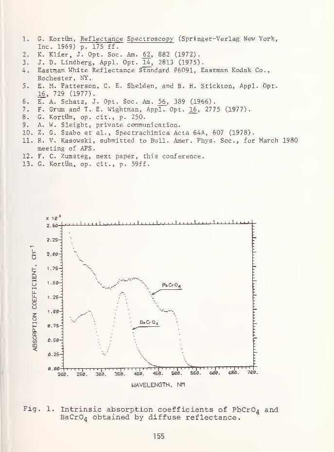
1. G. Kortiim, Reflectance Spectroscopy (Springer-Verlag New York,
Inc. 1969) p. 175 f f
.
2. K. Klier, J. Opt. Soc. Am. 62, 882 (1972).
3. J. D. Lindberg, Appl. Opt. 14, 2813 (1975).4. Eastman White Reflectance Standard #6091, Eastman Kodak Co.,
Rochester, NY.
5. E. M. Patterson, C. E. Shelden, and B. H. Stlckton, Appl. Opt.
16, 729 (1977).
6. E. A. Schatz, J. Opt. Soc. Am. 56_, 389 (1966).7. F. Grum and T. E. Wightman, Appl. Opt. 16, 2775 (1977).8. G. Korttlm, op. ext., p. 250.
9. A. W. Sleight, private communication.10. Z. G. Szabo et al., Spectrachimica Acta 64A, 607 (1978).11. R. V. Kasowski, submitted to Bull. Amer . Phys. Soc, for March 1980
meeting of APS.
12. F. C. Zumsteg, next paper, this conference.13. G. Kortlim, op. cit., p. 59ff.
u
z111I—
I
uI—
I
u.IdOUzo
Cl
O</>
CD<
X 10
2.50-
2.25-
2.Z0-
1
\.SZ-
1 .25^
1 .00-
0.75-
0.50
0.25H
0.00-
200.
I i i i . I i i i I ii
i i I i ' I ' ' I ' ' ' I ' ' ' ' I ' ' ' ' I ' '
PbCrO^
BeCr04
mTTTTTTPI
i i i i
I
i i i i
fi i i i
|i i iT
|i i i i
i
"i i i i
li i
250 . 300 . 350. 400. 450 . 500 . 550 . 600 . 650 . 700.
WAVELENGTH. NM
Fig. 1. intrinsic absorption coefficients of PbCrC>4 andBaCrO^ obtained by diffuse reflectance.
155

ELLIPSOMETRIC MEASUREMENTS OF THE OPTICAL PROPERTIES OFCOMPACTED POWDERS
F. C. ZumstegCentral Research and Development Department
Experimental StationE, I. du Pont de Nemours & Company
Wilmington, Delaware 19898
Transmission and normal incidence reflection spectroscopyare the most common methods for determining optical con-stants. Both have serious drawbacks when used for manyhighly absorbing ( i > 104 cm~l) materials. Both techniquesrequire moderate size single crystals that may not bereadily available. Transmission measurements requiresamples so thin that only micaceous materials can seriouslybe considered for measurement. In addition, these measure-ments do not provide refractive index information. Normalincidence reflection measurements require spectral dataover an extremely broad range so that an accurate Kramers-Kronig transformation can be made.
Spectroscopic ellipsometry provides a partial solution tothese problems. When single crystals are available, theoptical constants of even anisotropic crystals can bedetermined at any given wavelength without the need foradditional spectral information!. In addition, we havefound that ellipsometry can be used to obtain semiquantita-tive values of the optical constants of powders which havebeen compressed into specularly reflecting pellets.
Pellets with densities near 100% were produced by compress-ing a powdered sample between the faces of a small Bridge-man anvil at pressures ranging from 100-600 atmospheres.The powder was contained by a 30 mil-thick washer ofTeflon® fluorocarbon resin. The tungsten carbide faces ofthe anvil were highly polished, so that in most cases theresulting pellets needed no additional treatment beforemeasurements were made.
Ellipsometric measurements were made using a Rudolph Model200E ellipsometer setup in a standard polarizer-compensator-sample-analyzer configuration. The light source was aPerkin-Elmer 112 monocnrometer illuminated with a quartz-halogen lamp. A Babinet-Soliel compensator was used so that1/4 A retardation could be used at all wavelengths.
156

Figs. 1 and 2 show the absorption coefficient, a , and therefractive index of BiV04 as a function of wavelength.Absorption data is shown for ellipsometric measurements ona single crystal and a compressed powder, as well asR. K. Waring' s data obtained by diffuse reflectance . 2 onecan see that there is excellent agreement between theellipsometric data while the diffuse reflectance values ofa are appreciably smaller. Although the ratio is not alwaysthe same, the ellipsometric value is always larger than thatdetermined by diffuse reflectance. This difference mav re-sult from particle size effects in the diffuse reflectancemethod where, for large values of a, light does not inter-act with the entire volume of the crystallites.
To a certain extent, the agreement between single crystaland compressed powder is fortuitous. Inasmuch as BiV04 isanisotropic, one would not necessarily expect agreementbetween data obtained from a single crystal and a powderof randomly oriented crystallites. Fig. 2, in fact, showsa substantial difference between the single crystal re-fractive index data and that of the compressed powder.
Ellipsometry is particularly useful for measuring theoptical properties of thin surface layers. As a result,surface layers, whether they be of a second phase, adsorbedliquid layers, or irregularities, can cause appreciableerrors. Most of the materials we have examined have beenstable oxides, so our primary concern has been with adsorb-ed water and surface roughening. In both cases, errorscaused by either appear to be less than a = 3 x 10^ cm~l.
One should note that ellipsometry is limited to measure-ment of relatively large absorption coefficients,a > 1()4 cm~l. For values of a less than this, sensitivityis greatly reduced and surface effects play an increasinglyimportant role. An example of this can be seen in Fig. 1
where there appears to be a residual absorption of 3 x 104cm~l for A > 550 nm in the ellipsometric data. From othermeasurements, however, we know that B1VO4 has an absorptioncoefficient of <.l cm~l in this wavelength region. Similardiscrepancies have been seen in our measurements on othermaterials
.
Although there are some limitations to the techniquedescribed here, it provides a method by which optical prop-erties can be obtained when only very small crystallites orpowders are available. One can determine the shape andlocation of absorption peaks with a moderate degree of pre-cision and determine the refractive index and the magnitudeof the absorption to a lesser degree.
157

1. M. Elshazly-Zaghloul , A. M. A. Azzam, and N. M. Bushara,Surface Science 56_, 281 (1976).
2. R. K. Waring, preceeding paper, this conference.
v-V0)
oUco.J
aLa
<
X 10
4.0-p-1
3.5-
3.0-
2.5-
2.0-
1.5-
1 .0-
0.5-
0.0-
I j I i i i i L J I I I I J 1—1 I I I L_l I 1—1 I I I I I I I L.
-AX #
X XxX x
/*
\\\
\
wX\X
B1VO4
single crystal
^ co mp ressed powder
x diffuse reflecleoce
300.~i—i—r~1—r-r
350.
i—|—i—I—I—I—I—
r
400. 450. 500. 550. 6C0. 650. 700
Uio velength (nm)
Fig. 1. Absorption coefficient vs. wavelength of BiV04
158
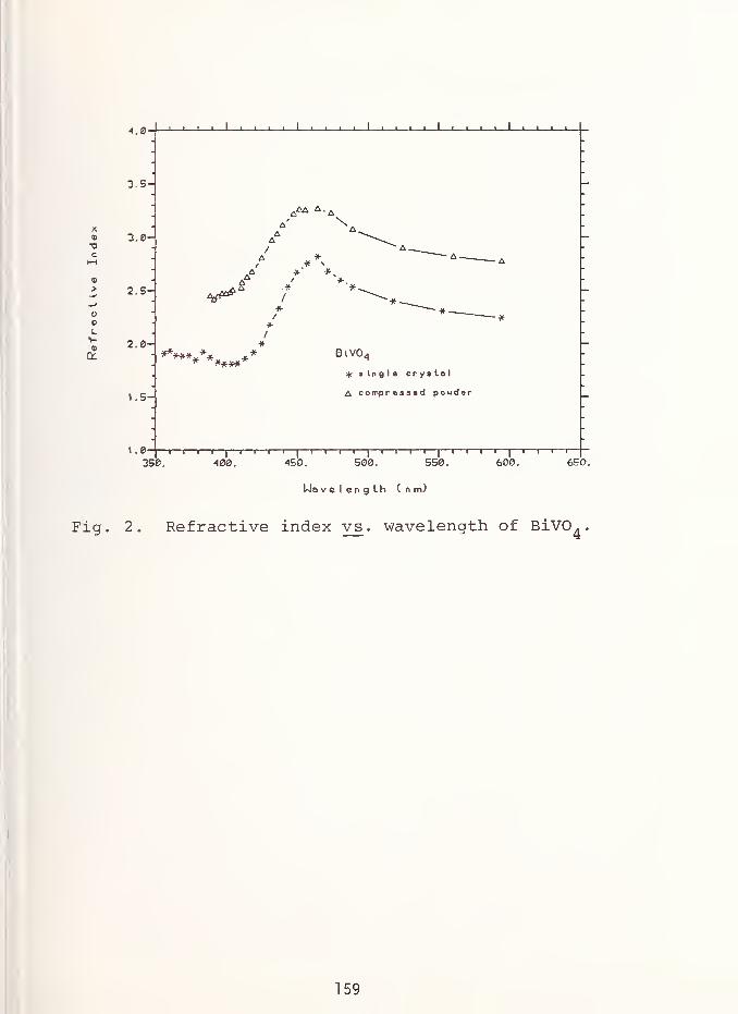
o
c
cLV»
4.0-
3.5-
3.0-
2.5-
2.0-
1.5-
1.0
J I I I I I I I I 1 I I I I I I I I I I L_
*' *.
********** * ** *****
*.
BiV04
* single crystal
A compressed powder
T—i—i—i—|—i—i—i—i—|—i—i—i—i—|—i—i—i—I—|—I—I—I—i—|—i—I—i—r-
350. 400. 450. 500. 550. 6C0. 6B0.
Uo velength (nm)
Fig. 2. Refractive index vs. wavelength of BiVO
159

MATERIAL PROPERTIES BY SPECTROSCOPIC ELLIPSOMETRY
D. E. AspnesBell Laboratories
Murray Hill, N. J. 07974
An ellipsometer is an optical device that measures the change in
polarization state which occurs when light is reflected at non-normalincidence from a surface."'- The polarization state is a complexquantity having both amplitude and phase, and is independent of theaverage light intensity. As a result, ellipsometry offers several sig-nificant advantages with respect to reflectance or transmittancetechniques for determining the basic optical properties of materials.
First, two parameters are determined in a single measurement instead ofone. These two parameters can be used to calculate both real andimaginary parts of the dielectric function of a uniform sample at a
single wavelength; extended wavelength measurements and Kramers-Kroniganalyses are not needed. Laminar or otherwise nonuniform sampleswhich are too complicated to investigate in single-wavelength measure-ments can be analyzed more definitively for structure and compositionbecause two spectra are available for interpretation instead of one.
Alternatively, the values of parameters in models describing suchsamples can be determined more precisely. This is particularlyimportant if material properties are to be deduced from their measuredvisible-near uv optical response.
Second, accurate ellipsometric measurements can be made on surfacesthat are too rough for reflectance spectroscopy . ^ Ideally, samplesshould be prepared with undamaged, atomically clean, and specularsurfaces. It is relatively easy to obtain clean, undamaged surfaces bycleaving, ion bombardment and annealing, or chemical processing tech-niques. But quite often these surfaces are macroscopically rough,causing light scattering which leaves them unsuitable for reflectancespectroscopy although quite adequate for ellipsometric spectroscopy.
Third, the fast measurement and analysis capabilities of automaticellipsometers allow cleaning procedures to be monitored and surfaceconditions to be assessed essentially in real time. This is almosttrivial to do with spectroscopic instruments that can be tuned to thewavelength corresponding to the peak in the spectrum of a sample.At this wavelength, surface sensitivity is maximized because lightpenetration is least, and surface overlayers (including microscopicroughness) almost invariably act to reduce the apparent value of £2by reducing the impedance mismatch between substrate and ambient.
*
This leads to a "highest is best" rule that can be applied withvirtually no modeling assumptions or a prior knowledge of sample
160

properties, but which nevertheless insures that the subsequent data are
taken with the sample in its cleanest possible state. Using these
techniques the dielectric functions of materials as diverse as Nb^ and
GaAs^ were recently revised by as much as 20% and 30%, respectively,
in the visible-near uv spectral range relative to values previouslydetermined by reflectance measurements and Kramers-Kronig analysis.
Because instrumentation and the determination of the intrinsicdielectric properties of materials in their pure bulk form are nowbasically solved problems, attention is turning to the determination of
properties of heterogeneous samples from their visible-near uv opticalresponse. Spectroscopic ellipsometric techniques can go much furtherthan simply measuring thicknesses and refractive indices of films, as
a recent analysis of the interface between Si and its thermally grownoxide has shown. ' For example, we recall that the dielectric functionis defined as a polarization per unit volume. Thus it is clear thatellipsometry can also be used to estimate the density of bulkmaterials.^ Noting that a microscopically rough surface layer can beconsidered as density-deficient bulk material, it is not surprisingthat ellipsometric measurements can yield information about microscopicroughness that is virtually impossible to attain any other way.
9
Likewise, the sensitivity of the dielectric response to long-rangeorder makes it an ideal probe for detecting the presence, or deter-mining the fraction, of crystallinity in otherwise amorphousmaterials
.
^
The determination of the properties of a heterogeneous sample from its
optical response is a three-step process. ^ First, accurate dielectricfunction data must be acquired for the pure bulk forms of its consti-tuents as well as accurate ellipsometric data for the sample itself.Second, the physical microstructure must be mathematically representedin some way, for example by n-phase models^ for laminar structures orby effective medium theories for heterogeneous materials. Third, themodel parameters must be determined from the data. By analogy tocircuit analysis, the sample can be viewed as a black box but with theusual frequency-independent parameters of resistance, capacitance, andinductance replaced by thicknesses, compositions, and void fractions.
The modeling of heterogeneous materials requires some comment. It is
generally assumed that the characteristic length of inhomogeneities is
much less than the wavelength of light, but that this length is
sufficiently large so the inhomogeneities themselves possess their owndielectric identity. This avoids the local-field problem even whilerecognizing that everything is heterogeneous on an atomic scale. Themacroscopic (observable) dielectric function is now obtained by solvingthe microscopic problem exactly for the microscopic electric fielde~(r) and polarization density p(r) , then spatially averaging the micro-scopic quantities to calculate the observed macroscopic equivalents<E> and <P> from which <e><t> = <t> + 4Tr<Pr>. 11 It is clear thatinternal boundaries and the distribution of the resultant screening
161

charge will play an important part in determining <e>. Either the
boundaries are known in detail or suitable approximations to them must
be made. The latter approach is usually taken because internal
structure is not generally known, or else requires far too manyparameters to describe, except in idealized models. We simply use
the self-consistent Bruggeman effective medium model, which differs
from the more common Lorentz-Lorenz and Maxwell Garnett models only in
the choice of dielectric background. 9 The advantage of so doing is
that the number of parameters are minimized; the disadvantage is that
the parameters that remain are effective averages whose values maydiffer somewhat from those corresponding to the actual compositions.
The parameters themselves can be determined by linear regressionanalysis^ (LRA) . LRA yields not only the best-fit values and the
residual mean-square deviations on a systematic basis, but it also
provides correlations and confidence limits. The latter are importantif meaning is attributed to the best-fit values, for it establisheswhich parameters are being determined by the data and which are not.
Because correlations are included, the confidence limits also preventabuses such as using too many parameters. While adding another parameteralways reduces the mean square deviation, it can also cause cata-strophic increases in confidence limits if it is not being determinedindependently by the data.
14The above approach has been applied in detail to Au. Representativedielectric function spectra are shown in Fig. 1. Data include thosetaken on bulk materials (Winsemius, Pells and Shiga) unannealed thinfilms deposited in moderate pressure (Johnson and Christy, "thiswork"), and annealed thin films deposited in ultrahigh vacuum (Theye)
.
The spectra at energies above the interband transition threshold at
2.5eV differ almost entirely because the samples contain differentvoid fractions, as shown in Fig. 2. Here, using the locally preparedfilm data as a basis, void fractions were calculated in a one-parameter Bruggeman effective medium approximation using linearregression analysis. The model describes the major differencessatisfactorily in the interband transition region not only in termsof absolute values but also with regard to spectral variations.Below 2.5eV the E2 spectra are dominated by the Drude tail, whichprovides a measure of the importance of bulk and surface scattering.The former can be related to grain size, and the latter to microscopicroughness
.
REFERENCES
1. R. M. A. Azzam and N. M. Bashara, Ellipsometry and Polarized Light(North-Holland, Amsterdam, 1977).
2. M. D. Williams and D. E. Aspnes, Phys. Rev. Letters 41, 1667 (1978).
3. D. E. Aspnes, in Proceedings of the Conference on Non-TraditionalMethods to the Study of Solid-Electrolyte Interfaces, ed. by T.
Furtak and D. W. Lynch (North-Holland, Amsterdam, 1980) (in press).
162
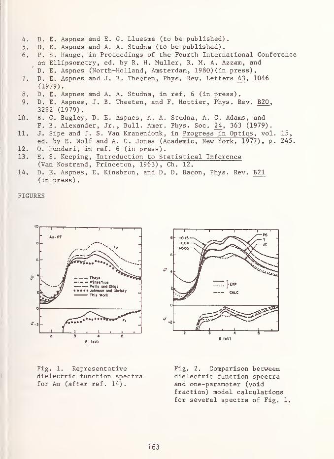
4. D. E. Aspnes and E. G. Lluesma (to be published).
5. D. E. Aspnes and A. A. Studna (to be published).
6. P. S. Hauge, in Proceedings of the Fourth International Conferenceon Ellipsometry , ed. by R. H. Muller, R. M. A. Azzam, andD. E. Aspnes (North-Holland, Amsterdam, 1980) (in press).
7. D. E. Aspnes and J. B. Theeten, Phys . Rev. Letters 4_3, 1046
(1979).
8. D. E. Aspnes and A. A. Studna, in ref. 6 (in press).9. D . E . Aspnes, J. B. Theeten, and F. Hottier, Phys. Rev. B20
,
3292 (1979).10. B. G. Bagley, D. E. Aspnes, A. A. Studna, A. C. Adams, and
F. B. Alexander, Jr., Bull. Amer. Phys. Soc. 24_, 363 (1979).11. J. Sipe and J. S. Van Kranendonk, in Progress in Optics , vol. 15,
ed. by E. Wolf and A. C. Jones (Academic, New York, 1977), p. 245.
12. 0. Hunderi, in ref. 6 (in press).13. E. S. Keeping, Introduction to Statistical Inference
(Van Nostrand, Princeton, 1963), Ch. 12.
14. D. E. Aspnes, E. Kinsbron, and D. D. Bacon, Phys. Rev. B21(in press)
.
FIGURES
Fig. 1. Representativedielectric function spectrafor Au (after ref. 14).
Fig. 2. Comparison betweendielectric function spectraand one-parameter (voidfraction) model calculationsfor several spectra of Fig. 1.
163

DIELECTRIC FUNCTION OF SUPERLATTICE MATERIALS
P.J. Price
IBM T.J. Watson Research Center
Yorktown Heights, New York 10598
In a "superlattice" formed from alternating layers of GaAs and (Ga.Al)As alloy, the
conduction band edge of the alloy is higher than that of the GaAs by a few tenths of an
eV. Consequently an individual GaAs layer acts as a "potential well" for electron motion
in the growth (say, X) direction, with quantized energy levels En . These levels are the
minima for the electron energy including motion in the YZ plane:
En + (h2/2m*)(kj + \fy (1)
in the parabolic range. 1 A similar situation for holes applies with those levels that can be
formed in the shallower valence-band wells. The lowest level in (1) is
E, - (h2/2m*)(i7/aj)
2(2)
where to sufficient approximation aj may be equated to the layer thickness a.2 (For
example, aj = 0.7 x 10⁻⁶ cm gives Ej = 0.1 eV.) The interconnection of wavefunc-
tions through the alloy "barriers" between neighboring GaAs layers is believed to result in
the individual well states (with the same kyand kz) combining into Bloch-like itinerant
states; but if the barrier thickness, b, is fairly large then this phenomenon may be disre-
garded here. At the same time, with wavelengths at optical and infrared frequencies large
compared to the layer spacing c = a + b, the response to an electromagnetic field
should be given by the dielectric function e(w) for a uniform electric field.
The contribution to e that is dealt with here comes from the dipole matrix elements
between electron and hole Bloch states, in GaAs, at energies near the band edges, and
compares with the corresponding contribution to e(<o) in homogeneous GaAs. The latter
may be calculated on the assumption of constant momentum matrix elements [that is,
constant dipole matrix element times energy difference, <c | x |v> Ecv (k)] between all
164
the pairs of Bloch states with the same wavevector. The result is
ecv ( u ) = e G G(h«/Eg) (3)
where
G(u) - (4/u2)(2 - (1 + u)
1/2 - (1 - u)1/2
), (4)
so that G(0) = 1 and G(l) = 2.34 . This formula can be fitted to the measured values
of Marple, 3 by assuming that the background e — ccv is a linear function of u over the
range of the data, and taking e0 = 1.0 . (The value of e 0 that one obtains theoretically,
using experimental values of mass and energy and momentum matrix element,4 agrees well
with this empirical value.)
A similar analysis for the GaAs "potential wells" of the superlattice case gives
««>(«,) = e<» H(WE<») (5)
where
H(u) = -L/n(-l_) (6)
uz v l-uz/
The superscript "l" signifies that this contribution is from the two-dimensional continuum
associated with the lowest level, Ej in eq. (1). From the theory one has approximately
(neglecting the difference between Eg
and Eg1*, as well as spin-orbit splitting in the
valence band)
c e^/e0 * 2h/(mcvEg)
1/2(7)
where m^ is the appropriate joint-density-of-states mass. With the latter approximately
0.1 times the free electron mass, the right hand side of (7) equals 1.3 x 10 -7 cm.
Accordingly, we expect e^1* ~ 10" 1
for the usual values of layer spacing c = a + b.
The infini ty in (6) should be not very pronounced in practice, even when the superlattice
band width is not appreciable; for example, at 1 — u = 10~ 3, H is only 6.2 . There is a
possibility, however, of observation of the peak by the electroreflectance method. 5 In an
electric field <?, the quantization energy Ej changes by —Yia^8 , where orj is the polariza-
165

bility, and similarly Eg . It can be shown that (disregarding the difference between
and a)
a, = 7 x 10" 3(e
2me/h
2) a
4
= (0.92 x 105 cm" 1
) a4
(8)
the second line of (8) being for GaAs. For a = 10~ 6 cm and & = 10 5 V/cm, this gives
Yi <xj S2 = 3.2 milli eV. In this idealized model, such a shift would give a maximum 5e
of about 0.5. For the next level, a2 is calculated to be only about 8% of O], however. It
is not clear, at the time of writing, whether electron and hole in this system can bind into
an exciton.
1. For example, R. Dingle, W. Wiegmann and C.H. Henry, Phys. Rev. Lett. 33, 827
(1974); R. Tsu, A. Koma and L. Esaki, J. Appl. Phys. 46, 842 (1975).
2. The correction, from the finiteness of the barrier height and from the atomic-scale
"mismatch" of wavefunctions in the two layer materials, is a few lattice constants
at most. (The mismatch effect is important, however, in the strength of the interac-
tion between GaAs layers which is associated with the superlattice band.)
3. D.T.F. Marple, J. Appl. Phys. 35, 1241 (1964).
4. C. Hermann and C. Weisbuch, Phys. Rev. B J_5, 823 (1976).
5. M. Cardona, K.L. Shaklee and F.H. Pollak, Phys. Rev. 154, 696 (1967).
166
DETERMINATION OF THIN FILM OPTICAL DISPERSIONFROM SPECTROPHOTOMETER DATA
Arnold L. Bloom and Dennis FischerCoherent, Incorporated
3210 Porter DrivePalo Alto, California 94304
This paper describes work being done on a project in which an attemptis made to determine the dispersive characterstics of optical thinfilms using relatively common laboratory instruments, such as a
transmission spectrophotometer. It is well known that the real part ofthe refractive index can be measured very accurately by ellipsometryand the imaginary part can be measured by calorimetry, but thesetechniques are time-consuming and the instruments are not alwaysavailable in the laboratory. The output of a spectrophotometer, on theother hand, provides data rapidly over wide wavelength ranges andshould be particularly convenient for the purpose if the output datacan be analyzed properly.
In our laboratory the experimental procedure is as follows. Thematerial whose dispersion curve is to be measured is coated on a
substrate whose refractive index is well known and which is highlytransparent over the wavelength range in question (for example, fusedsilica in the visible and near UV) . The coating is monitored at a
highly transparent wavelength for the material and the layer is maderelatively thick, for example 5 to 9 (an odd number) quarter waves atthe monitoring wavelength. The transmittance of the entire sample is
then measured over the entire wavelength range of the spectrophotometer,along with zero and full-scale calibrations of the strip chart recorder.Because the layer is many wavelengths thick, the chart will show rapidoscillations between maximum and minimum transmittance as a function ofwavelength, with the average transmittance decreasing rapidly to zeroat the short-wavelength end of the chart. It is clearly desirable tomake the layer as thick as possible, in order to get rapid oscillations,but not so thick that the short-wave transmittance decreases below 20
or 30 percent of full scale.
In initial experiments the values of refractive index, n, andabsorption, k, at various wavelengths were estimated by handcalculations based on the oscillation frequency, maximum and minimumvalues after correction for the back-surface reflection of the sample.The values obtained from this relatively crude technique turned out tobe surprisingly good in predicting the behavior of multilayer stacksusing the material. However, it appeared desirable to improve themethod by using a computer program to reduce the data. The remainderof this paper describes the computer data reduction and the results
167

obtained in this way.
To start with, we assume that the optical thickness at the monitoringwavelength is known approximately, and that there is a wavelengthregion around the monitoring wavelength in which the index isrelatively constant and in which there is negligible absorption. Wehave available several computer algorithms that can adjust the thicknessand index of thin films to make a least-squares fit to a giventransmittance or reflectance curve. These algorithms are used normallyfor optimization of multilayer designs, but here they are usedessentially as curve- fitting devices. The spectrophotometer output inthe monitoring range, corrected for back-surface reflection, is enteredinto the program and the algorithm solves for accurate values of n andof the physical thickness to fit the data. Experience has shown thatgood fits to the data can be obtained consistently in this way and webelieve the values of thickness and index that are obtained are reliable.It is necessary to include, in the input data, enough values oftransmittance so that the sine wave variation of transmittance is
clearly delineated over part of a period including a minimum value(hence the odd number of quarter-waves) . Transmittances near the curvemaximum are essentially those of the bare substrate and convey noinformation to the program. In addition, the curve-fitting process canbe expedited considerably by a proper choice of variables in thealgorithm. The algorithm requires both the function (transmittance in
this case) and first partial derivatives with respect to the variables.In initial experiments we used, as variables, the index and the physicalthickness. It was found that the optimization program did not work wellwith this choice of variables and the reason is not hard to find: Overa limited range of wavelengths a small change in thickness has nearlythe same effect on the transmittance curve as a small change in index.
A much better choice of variables is index and phase (or optical)thickness. In this case the variables are nearly orthogonal, onevarying only the amplitude and the other varying only the period of thesine wave, and the optimization process proceeds efficiently.
With the thickness determined accurately, the next step is to use the
curve-fitting algorithm to determine n and k at other wavelengths. Our
present efforts are aimed at making transmittance curve fits bydetermining single values of n and k for use in restricted wavelengthranges, or pairs of values with linear interpolation in between for
longer wavelength ranges. Attempts to fit constants of Lorentzian or
complex Sellmeier equations were unsuccessful because of difficultiesinvolved in making optimization algorithms work with complex variables.
Interpolation using polynomials of order higher than linear is
esthetically pleasing but not suitable for cases where k may varybetween small and large values. The reason is that such interpolations
may result in k changing sign unexpectedly over some wavelength ranges
(i.e., giving gain), which is extremely undesirable in thin film design
work. Experience with the curve-fitting has shown that the linear
interpolation is quite satisfactory in wavelength regions in which n and
168
k do not vary too rapidly over the region. Where there is. rapidvariation of k with wavelength, as near the absorption edge of the
material, linear interpolation can be used only over very narrowwavelength ranges.
The problems that arise in using this method are as follows. First,the strip chart data must be nearly noiseless and the data transcriptionto numeric values must be done carefully (it is not necessary to makebaseline and back-surface corrections by hand as this can be done in theprogram) . Secondly, when n and k values at each end of a wavelengthrange have been computed, it would be nice to have the values of n and k
agree with those calculated in an abutting wavelength range, howeverthis will not always be the case. An additional problem that has arisenis that the transmittance is not particularly sensitive to n in regionswhere k is large, and small deviations in the initial conditionspresented to the curve-fitting program may result in widely differentfinal values for n, although the values for k will always be consistent.
EXAMPLE
A layer of Ti02 was coated on a fused silica substrate. The operatorwas instructed to lay on 5 quarter waves at a monitoring wavelength of633 ran. The thickness was computed from data between 590 and 650 nm.
The results are as follows:Physical thickness = 327.5 nmRefractive index = 2.3793Quarter wave thickness = 3117 nm
(Note this differs slightly from the assumed quarter wave thickness of
3165 nm. ) The fit to the data curve was better than 1% over the entirerange and better than 0.5% over most of it.
Table I shows the calculated values of n and k over several wavelengthranges
:
TABLE I.
Range, nm. wavelength n k
600 - 800 600 2.3781 0.
800 2.3371 -0.0069
500-600 500 2.4490 -0.0057
600 2.3905 -0.00072
400-500 400 2.6430 -0.0040
500 2.4539 -0.0018
360-400 360 2.8328 -0.0197
400 2.5648 -0.0060
169

CONCLUSIONS
The results given above show that the method has promise but there arealso problems, particularly the need to get highly accuratespectrophotometer data. The anomalous wandering of the k values in thevicinity of zero is undoubtedly due to the fact that the calculatedvalue will be very sensitive to the value of the transmittance maximum,and in this case could have been affected by very small errors in thebaseline correction. The differences in index for the same value ofwavelength calculated in different wavelength ranges is an effect of thelinear interpolation and could be reduced by using shorter wavelengthranges.
Despite the relatively crude appearance of the results, this outputshould be quite satisfactory for most thin films design work. Above allit points out the fact that hand calculations, based only on maximum andminimum values of transmittance, are not nearly as reliable as one mightbe led to expect naively on the basis of equations that can be solvedfrom these data.
170
OPTICAL PROPERTIES OF DOPED-SILICA WAVEGUIDEGLASSES IN THE 0.8-1.8 um REGION
Robert OlshanskyCorning Glass WorksCorning, NY 14830
In optical quality glasses prepared by conventional melting techniques,the principal source of attenuation is absorption from transition metalimpurities. To attain the very low loss required for telecommunicationsthe transition element contamination must be kept below a few parts perbillion.
The vapor phase oxidation technique 1 provides a simple and practicalmethod for achieving these purity levels. High purity raw materialssuch as SiCli+j GeCl^ , BBr3 and POCI3 are readily available and can beoxidized and deposited under controlled conditions to form glasspreforms from which optical fibers can be drawn.
Once the absorbtive losses of transition metals are eliminated, thesedoped-Si02 glasses exhibit a broad transmission window encompassing therange from 0.8-1.8 urn of interest for optical communications. In theregion from 0.8 to 1.2 urn, Rayleigh scattering losses from intrinsicdensity and concentration fluctuations of the glass matrix are the
dominant loss sources. These scattering losses decrease as the fourthinverse power of wavelength. In the region between 1.2-1.8 urn lossesare dominated by 0-H absorption bands, Rayleigh scattering and, in thecase of B2O3 doped waveguides, the tail of the B-0 infrared vibrationalabsorbtion bands.
1. Rayleigh Scattering
The Rayleigh scattering of optical waveguides and of bulk samplesappears to vary somewhat according to the details of sample preparationsIt is convenient to characterize the Rayleigh scattering by the form
YRS= a/X\ (1)
The lowest value reported for bulk Si02 is 0.63 dB/km-um4.
3 As shownin Fig. 1 the scattering values observed in optical waveguides varywith composition. 3-7
As there appears to be considerable variability among the varioustechniques used for determining dopant concentration, it is useful tocompare data from different laboratories by using A, the relative
171

difference in refractive index between the core and fused Si02
A ° (I" ' no)• (2)
Fig. 1 shows that as the A increases (or equivalently the Ge02concentration) the scattering level also increases. This presumably is
the result of the increase in concentration fluctuations as dopant is
added
.
Many of the earliest waveguides were made with a low level of B2O3added to reduce the sintering temperature of the glass and tofacilitate the deposition process. The scattering data of Yoshidaet al 6 clearly shows that substitution of a low level of P2O5 for theB2O3 reduces the Rayleigh scattering by 40-50%. At 0.85 urn this is a
significant difference, amounting to 1 dB/km.
Horiguchi and Osanai have reported 4 the lowest scattering value for anywaveguide. Their waveguide doped with 2 m/o P2O5 had a Rayleighscattering coefficient of 0.60 dB/km-um
1*.
Because of the large viscosity difference between glassed doped withhigher P2O5 levels (>10 m/o) and fused Si02> fabrication of graded-index multimode waveguides is very difficult in the P205~Si02 binarysystem. Little work has been reported in this compositional system.
Blankenship et al 7 have reported a A=1.0%, P 205-Ge02-Si02 waveguide in
which the P2O5 level is high enough to contribute about 50% of the index
difference. The scattering coeffient of 1.0 dB/km-um 1
* is the lowest
reported for a graded-index multimode waveguide.
2 . Infrared Absorption Edge
All oxide glasses have very strong cation-oxygen vibrational bands
in 4-25 um region. Multiphonon excitation of these states 8 produces an
absorptive tail of the form
YJR = CIR exp (-E/E0 ) (3)
where E is the photon energy and C-j-r and EQ are empirically determinedconstants. Izawa et al 9 have measured this absorption in the 1.8 to
20 um region using both bulk and fiber samples of Si02 and B203~dopedSi0 2 . The Si02 edge is well represented by the constants
E0 = .0235 eV
'IR= 1.19 x 10 13 dB/km •
This edge falls off rapidly with increasing energy. At 1.6 um the
intrinsic absorption of fused-Si02 is 0.06 dB/km.
172
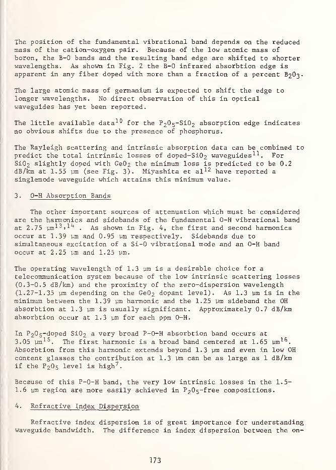
The position of the fundamental vibrational band depends on the reducedmass of the cation-oxygen pair. Because of the low atomic mass of
boron, the B-0 bands and the resulting band edge are shifted to shorterwavelengths. As shown in Fig. 2 the B-0 infrared absorbtion edge is
apparent in any fiber doped with more than a fraction of a percent B2O3.
The large atomic mass of germanium is expected to shift the edge tolonger wavelengths. No direct observation of this in opticalwaveguides has yet been reported.
The little available data 10 for the P 20 5-Si02 absorption edge indicatesno obvious shifts due to the presence of phosphorus.
The Rayleigh scattering and intrinsic absorption data can be combined to
predict the total intrinsic losses of doped-Si02 waveguides 1. For
SiC>2 slightly doped with GeC>2 the minimum loss is predicted to be 0.2dB/km at 1.55 ym (see Fig. 3). Miyashita et al 12 have reported a
singlemode waveguide which attains this minimum value.
3 . 0-H Absorption Bands
The other important sources of attenuation which must be consideredare the harmonics and sidebands of the fundamental 0-H vibrational bandat 2.75 um 13
>11+
. As shown in Fig. 4, the first and second harmonicsoccur at 1.39 ym and 0.95 ym respectively. Sidebands due to
simultaneous excitation of a Si-0 vibrational mode and an 0-H bandoccur at 2.25 ym and 1.25 ym.
The operating wavelength of 1.3 ym is a desirable choice for a
telecommunication system because of the low intrinsic scattering losses(0.3-0.5 dB/km) and the proximity of the zero-dispersion wavelength(1.27-1.35 ym depending on the Ge02 dopant level). As 1.3 ym is in theminimum between the 1.39 ym harmonic and the 1.25 ym sideband the OHabsorbtion at 1.3 ym is usually significant. Approximately 0.7 dB/kmabsorbtion occur at 1.3 ym for each ppm 0-H.
In P205~doped Si02 a very broad P-O-H absorbtion band occurs at
3.05 ym 15. The first harmonic is a broad band centered at 1.65 ym 16
.
Absorbtion from this harmonic extends beyond 1.3 ym and even in low OHcontent glasses the contribution at 1.3 ym can be as large as 1 dB/kmif the P2O5 level is high 7
.
Because of this P-O-H band, the very low intrinsic losses in the 1.5-
1.6 ym region are more easily achieved in P 205-free compositions.
4. Refractive Index Dispersion
Refractive index dispersion is of great importance for understandingwaveguide bandwidth. The difference in index dispersion between the on-
173
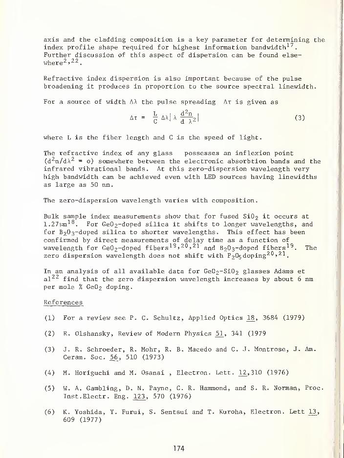
axis and the cladding composition is a key parameter for determining theindex profile shape required for highest information bandwidth 17
.
Further discussion of this aspect of dispersion can be found else-where 2
>22
.
Refractive index dispersion is also important because of the pulsebroadening it produces in proportion to the source spectral linewidth.
For a source of width AX the pulse spreading At is given as
L , , i, d 2n
i xAT =
cAA|A IT2
'
(3)
where L is the fiber length and C is the speed of light.
The refractive index of any glass possesses an inflexion point(d 2n/dX 2 = o) somewhere between the electronic absorbtion bands and theinfrared vibrational bands. At this zero-dispersion wavelength veryhigh bandwidth can be achieved even with LED sources having linewidthsas large as 50 nm.
The zero-dispersion wavelength varies with composition.
Bulk sample index measurements show that for fused Si02 it occurs at
1.27um 18. For Ge02-doped silica it shifts to longer wavelengths, and
for B20 3~doped silica to shorter wavelengths. This effect has beenconfirmed by direct measurements of delay time as a function of
wavelength for Ge02~doped fibers 19'20
'21 and B203~doped fibers 19
. Thezero dispersion wavelength does not shift with P2O5 doping 20
»21
.
In an analysis of all available data for GeQo-SiC^ glasses Adams et
al22 find that the zero dispersion wavelength increases by about 6 nmper mole % Ge02 doping.
References
(1) For a review see P. C. Schultz, Applied Optics 18, 3684 (1979)
(2) R. Olshansky, Review of Modern Physics 51, 341 (1979
(3) J. R. Schroeder, R. Mohr, R. B. Macedo and C. J. Montrose, J. Am.
Ceram. Soc. 5_6, 510 (1973)
(4) M. Horiguchi and M. Osanai , Electron. Lett. 12,310 (1976)
(5) W. A. Gambling, D. N. Payne, C. R. Hammond, and S. R. Norman, Proc.
Inst.Electr. Eng. 123, 570 (1976)
(6) K. Yoshida, Y. Furui, S. Sentsui and T. Kuroha, Electron. Lett 13,
609 (1977)
174
(7) M. G. Blankenship, D. B. Keck, P. S. Levin, W. F. Love,R. Olshansky, A. Sarkar, P. C. Schultz, K. D. Sheth andR. W. Siegfried, Post-deadline Paper Topical Meeting on OpticalFiber Communications, March 6-8, 1979, Washington, D.C.
(8) For a review see T. C. McGill in Optical Properties of HighlyTransparent Solids ed. by S. Mitra and B. Bendow, Plenum Press(1975)
(9) T. Izawa, N. Shibata, A. Takeda, Appl. Phys . Lett. 31, 33 (1977).
(10) S. Kobayashi, W. Shibata, S. Shibata and T. Izawa, Rev. Elect.Comm. Lab. 26, 453 (1978).
(11) M. Osanai, T. Shioda, T. Moriyama, S. Araki, M. Horiguichi, T.
Izawa, M. Takata, Electron Letts 12, 549 (1976)
(12) T. Miyashita, T. Miya and M. Nakahara, Post-deadline paper TopicalConference on Optical Fiber Communication, March 6-8, 1979,Washington, D.C.
(13) D. B. Keck, R. D. Maurer and P. C. Schultz, Phys. Letts 22_, 307
(1973)
(14) P. Kaiser, A. R. Tynes, H. W. Astle, A. D. Pearson, W. G. French,R. E. Jaeger and A. M. Cherin, J. Opt. Soc. Am. 63_, 1141 (1973)
(15) Y. Mita, S. Matsushita, T. Yanase and H. Nomura, Electron. Tett.
13 , 55 (1977)
(16) T. Edahiro, M. Horiguchi, K. Chida and Y. Ohmori, Electron. Lett.
15, 275 (1979)
(17) R. Olshansky and D. B. Keck, Appl. Opt. 15, 483 (1976)
(18) I. H. Malitson, J. Opt. Soc. Am. 55 , 1205 (1965)
(19) L. G. Cohen and C. Lin, Appl. Opt. 16, 3137 (1977)
(20) D. N. Payne and A. H. Hartog, Electron. Lett. 13, 627 (1977)
(21) C. Lin, L. G. Cohen and V. A. Foertmayer, Electron. Lett. JL4, 170
(1978)
(22) M. J. Adams, D. N. Payne, F. M. E. Sladen and A. H. Hartog,
Electron Lett. 14, 703 (1978)
175

RAYLEIGH SCATTERING VS A20
1.5
10
0.5
OY0SHIDA ET AL (1977)
A GAMBLING ET AL (1976)
• SCHROEDER ETAL (1973)HORIGUCHI ET AL (1976)
BBLANKENSHIP ET AL(1979)
P2 05 -Ge0 2 -Si02
P2 05 -Si02
,Si02 (BULK)
CT-P205 -Si02
_i i i i i_i i_
0 0.5 10
A (%) RELATIVE TO SiO,
Fig. 1 Rayleigh scatteringloss versus relative indexdifference is shown fordifferent optical waveguidecompositions.
CORE CLADl)Ge02-B 20 3-Si02 B20 3 -Si02
Fig. 2 Spectral attenuationfor three low-loss waveguidesreported by Osanai, et. al.
WAVELENGTH ( M m)
176
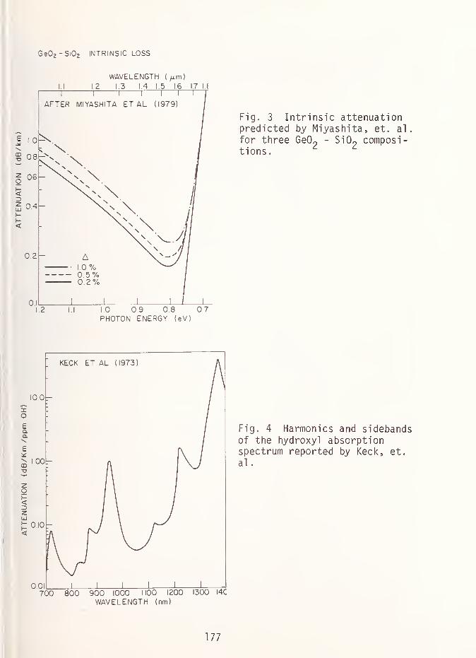
Ge02 -Si02 INTRINSIC LOSS
WAVELENGTH ( ^m)1.2 1.3 1.4 1.5 1.6 17 I f
Fig. 3 Intrinsic attenuationpredicted by Miyashita, et. al
.
for three GeCL - SiCL composi-tions.
1 L
I 2 1.0 0 9 0 8 0.7
PHOTON ENERGY (eV)
10.0-
xo
E
\CD
<3
010-
Fig. 4 Harmonics and sidebandsof the hydroxyl absorptionspectrum reported by Keck, et.
al
.
001700 800 900 1000 1100 1200 1300 I4C
WAVELENGTH (nm)
177
THE USE OF A SCATTERING CUBE TOCHARACTERIZE THE SPECTRAL LOSS OF OPTICAL FIBERS
Dan L. Phil en and Frank T. StoneBell Laboratories
Norcross, Georgia 30071
In many instances, it is useful to separate the scattering loss of anoptical fiber into a wavelength dependent component, Rayleigh Scattering= a/A^, and a wavelength independent component, b, caused by scatteringmechanisms with dimensions large compared with the signal excitingwavelength. These scattering components provide important data charact-erizing the fiber material system and manufacturing process. When theyare obtained by curve fitting total loss data versus frequency, errorsare introduced because of band-edge and other forms of absorption.These errors can be eliminated by measuring only the scattering losswith a scattering cube. Using this technique with a laser source andrelatively short fiber samples, it is also possible to: (1) excitedifferent mode groups in multimode fibers, thereby determining thescattering intensity from different regions within the fiber core, and
(2) obtain accurate data on single mode fibers that can be difficult to
get from two-point loss measurements. For example, by careful scrutinyof the near field pattern of short (several meter) lengths of fiberand appropriate adjustment of launch conditions, a single mode can be
excited even at wavelengths where the fiber supports several modes.This avoids effects due to mode cut-off, and yields useful data on the
basic glass properties. Two-point loss measurements do not isolate thescattering component, and require fibers so long that mode-mixing is
difficult to avoid.
The essential component to this measurement is the scattered lightdetector. Since the scattered light exits in all directions, this
detector must surround the fiber completely to collect all thescattered radiation. Two types of detectors have been used to do
this: an integrating sphere!, and a scattering cube^, which was used
in this work. This scattering cube is constructed of 1 -cm-squaresilicon solar cells with a 0.25mm hole drilled through the center oftwo opposite faces to allow the fiber to pass through the cube. One
side of the cube is removable to facilitate the insertion of thefiber and allow the cube to be filled with index-matching fluid. The
sensitivity and impedance of all the cells are matched as closely as
possible. Final matching is accomplished by trimming potentiometersthat equalize the outputs of the individual cells.
The linearity of the scattering cube at 633nm was determined by
launching a He-Ne laser beam into a fiber pigtail and inserting the
other end of the pigtail into the scattering cell. The input power
178
was varied over eight orders of magnitude using a set of calibratedneutral density filters and the cell was found to be linear over six
orders of magnitude. During the experiments, the detector was alwaysoperated well within the linear region.
Since the scattering cube is composed of silicon solar cells, its
sensitivity is wavelength dependent. This spectral dependence wasobtained by using a He-Ne laser and a Krypton laser as sources and a
Scientech calorimeter to measure the absolute optical power. The
sensitivity at 633nm was measured to be 100.5 yv per yw. The relativesensitivity is given in the following figure.
1.6 r
0.2 -
! I 1 I L
560 620 660 720 760 820
WAVELENGTH IN nm
The experimental set-up is illustrated in the following figure.
MICROSCOPE
OBJECTIVE
SCATTERING
CELL
-o FIBER-r\J^—
B
CHOPPER
S-SHAPED
MODE STRIPPER
CLADDING MODE STRIPPER
LOCK-IN AMPLIFIER
Samples of fiber a few meters in length were selected for test,
stripped of their coating, cleaned to remove adhering dust particles,and threaded through the scattering cell. Bends in the fiber
immediately before or after the cell were avoided. Scattering fromcladding, leaky, or marginal bound modes was suppressed to a high
179

degree by using an S-shaped mode stripper before the scattering cube.To insure that no cladding modes had built up in the straight sectionof fiber between the S-shaped mode stripper and the scattering cell,an additional cladding mode stripper consisting of black papersaturated with index oil was placed 1mm in front of the scatteringcube. The remaining power guided by the fiber into the scatteringcube was now largely confined to the bound modes of the fiber. Thescattering cube was filled with index oil to prevent any scatteredlight from being trapped in the cladding, and the end of the fiberwas terminated in index matching fluid to prevent light reflectedfrom the fiber end from being scattered back into the scattering cube.
The input laser light was chopped mechanically and the output of thesilicon detectors was measured on a lock-in amplifier. The total
light incident on the fiber was measured on a Scientech calorimeter.The scattering loss in dB/km for a particular wavelength is given by:
where V = signal from the lock- in in microvolts.D = normalized spectral response of the scattering cube. (Fig. 1)
C = sensitivity of scattering cell = 100.5 yv/uw/cm at 633nm.
P = total incident power in microwatts.
By using several lines of the Krypton laser, the spectral dependenceof the fiber scattering loss could be obtained at well -spaced
wavelengths in the region from A = 0.568 urn to X = 0.799 urn.
Since we model the scattering loss by an as= a/A^ + b relationship,
a linear least squares fit to the loss data on a 1/A 4 scale gives
the "a" coefficient as the slope and the "b" coefficient as the
intercept. The following figure is a plot of the average scattering
loss versus wavelength for a germanium-borosil icate-core, silica-
clad multimode fiber that was measured many times to determine the
experimental repeatability.
a,
|dB/km|
14 -
12
10
2 —
\/\4
( Mr»-«)
180
The fiber was excited using a 5x microscope objective to focus theKrypton laser beam to a spot positioned at the center of the corewhere maximum compositional fluctuations should occur. The repeatabil-ity was of the order of + 1-2%, even when measurments occured severalweeks apart and were taken on different 1 -cm-long regions of thefiber. The correlation coefficient for the a/A^ + b curve-fit was0.9995. The "a" coefficient obtained this way was approximately 0.2pnrdB/km lower than the value obtained by curve-fitting to total lossdata, as might be expected from the effect of band-edge absorption.
We have examined a number of other multimode and single mode fibers.The next figure gives an interesting example of a single mode fiber(borosilicate core, borosilicate inner cladding, silica outer cladding)that had high total loss. 12 _
(dB/km)
c c c c c
1/X4
(^n.-4
!
The plot of the scattering loss, however, is what is expected from a
good fiber, indicating the source of the added loss is absorption.
This was confirmed calorimetrical ly.
In summary, the direct measurment of the scattering component of the
spectral loss of an optical fiber is a useful diagnostic technique.
It can be used to eliminate the errors in the a and b coefficients due
to absorption, and to determine whether scattering is the cause of
excess fiber loss.
REFERENCES1. D. B. Keck, P. C. Schultz, and F. Zimar, Appl . Phys. Lett.
n, 215 (1972).
2. A. R. Tynes, Appl. Opt. 9_, 2706 (1970).
181

TRANSITION ELEMENT ABSORPTION INMOLECULARLY-DOPED OPTICAL FIBER GLASSES
Aaron Barkatt, Dahn C. Tran* and Joseph H. Simmons
Vitreous State LaboratoryThe Catholic University of America
Washington, DC 20064
The presence of transition elements in fiber optic waveguideglasses, even at trace levels, causes high absorption losses(in some cases, higher than ldB/km for each ppb of impurity)in the wavelength range of most interest in the developmentof long-range communication systems (600-1300nm) . Control-ling the resulting absorption losses is hard because of thedifficulties encountered in identifying and determining thelevels of the important absorbing impurities. Chemicalanalysis is complicated because of the trace concentrationsinvolved, while the absorption spectra in the region ofinterest often consist of broad bands and often reflect thepresence of a transition element in several oxidation orcoordination states. The relative amounts of differentstates are determined by the conditions of preparation.
It is therefore desirable to develop methods of character-izing the various species which are likely to contribute toabsorption losses in the near-IR region by searching forintense, sharp, characteristic features in other spectralregions such as the visible and the UV. The moleculardoping method is particularly suitable for such studies be-cause it can be used to produce large, uniformly doped sam-ples at relatively low temperatures (<_ 850° C) , whereindividual oxidation states can be isolated by means of con-trolling the atmosphere under which the doped porous preformis sintered.
Glasses prepared by this method, with a base composition ofapproximately 92mol% Si02 / 4.5mol% B 2 0 3 , 3.5mol% CS2O, 0.03mol% Na 2 0 and 0.0 3mol% K2O, were doped with several transi-tion elements at a level of 0.0 5wt% (only in the case of Rua concentration of 0.008wt% was used). Samples doped witheach of these elements were consolidated in each of threeatmospheres: oxygen (oxidizing), helium (intermediate) and5% hydrogen in nitrogen (reducing) . The samples had a dia-meter of about 0.6cm and were 0.1-5cm long, polished at bothends. The spectra of each of the doped glass prepared underthese conditions were analyzed in order to identify the im-portant absorbing species in each case. The findings aresummarized in the following Table.
182

Spectra of Transition Elements inMolecularly Doped High-Silica Glasses
ApproximateSpectral Principal Absorbance,
Transition Features Chemical 1060nm,Element Atmosphere nm Species dBkm ! ppb 1
Fe 0 2 ,He 375,412,437,470
Fe (III) 0 . 008
H 2 820 ,950 Fe (II) 3. 0
Cu 0 2 ,He 785,1050,1080 Cu(II) 0. 90
H 2 cud) < 0. 01
Co o 2 778,1552 Co (III) 0. 80
He / H 2 547,600,648
,
1329 .2556 .1750Co(II) tet 0. 21
MiIN _1_ \j 2 f lie 512 56 8 6401158,1500
Ni ( TT )u±; tet1 1
H 2 430,1125 Ni(II)oct
0. 05
Cr o 2 435,600,750,1000
Cr (VI) 0. 13
He 435,587,723,XUUU (lo JU
Cr (IV) 1. 4
H 2 354,499,700,1075,1850
Cr (III) 1. 2
Mn o 2 363,520 fin (III) 0. 27
H 2 325,358,370,422 ,435,470 ,
515,650
Mn (II) < 0. 006
Rh o 2 312,470 Rh(III) 0. 03
H 2 Rh (III) 0. 08
Ru He 480,815 Ru(VI) 0. 19
Ag 0 2 ,He Ag(I) < 0. 005
H 2 229,300,399 < 0 . 01
Zr 0 2 /He ,H2
Zr (IV) < 0. 005
183

The results show that the molecular doping method is verysuitable for the isolation of individual oxidation or co-ordination states and obtaining characteristic "finger-prints" consisting of a series of well-defined spectroscopicfeatures in the near-IR, visible or near-UV regions. Inparticular, detailed band structures are evident in thecases of Fe(III), Co (II), Ni(II) / Mn(II) and the variousforms of Cr. Such "signatures" can serve as convenient,sensitive methods of identifying transition metal specieswhich cause absorption losses in fiber optic glasses.Moreover, identification of the oxidation state makesit possible to try to reduce losses by changing the redoxconditions of the environment during the preparation ofthe glasses. Of the species identified, Fe(II) and Cu(II)are of major concern because of their ubiquity and theirhigh specific absorption in the near-IR. Fe(II) can beeliminated by oxidation, Cu(II) by reduction. Cr is aproblem under all conditions. Oxidized Cr absorbs to asmaller extent than Cr doped under He or H2/N2 around1060nm (by one order of magnitude) , but bands in this re-gion are still observed, probably due to the difficulty inoxidizing all traces of the lower oxidation states (Cr(III)and Cr (IV) ) to Cr (VI)
.
The results also show that because of the presence of arelatively large concentration of the highly basic oxideCS2O and the low temperature of preparation these glassesprovide a unique opportunity, especially when producedunder an oxygen environment, of isolating and characteri-zing the spectra of species accessible only at unusuallyhigh basicities, such as the high oxidation states Co (III),Cr(VI) and Mn(VII) and the low coordination state Ni(II) tetin a high-silica matrix.
*Present address: Battelle Laboratories, Columbus, Ohio
184
MEASURED POCKELS COEFFICIENTS AND PREDICTEDSTATIC PRESSURE SENSITIVITY FOR INTERFEROMETRIC FIBER OPTIC HYDROPHONES
R. Hughes, N. Lagakos , H. Dardy and J. BucaroNaval Research Laboratory
Code 5133Washington, D.C. 20375
Introduction ; Optical phase modulations induced in glass fibers havebeen investigated-'-, especially since potential use of fibers for detect-ing sound was established 2. in sound detection, efforts were concen-trated on describing theoretically and experimentally pressure inducedeffects in step index, single mode fused silica cored fibers positionedin interferometers More recently, consideration is being given to
fibers with numerical apertures larger than that found in fused silicacored fibers because microbend loses are reduced
Variations in optical phase induced by an externally applied soundfield have been examined by several groups 2~5
# The primary causes of
phase variation for an applied static pressure have been attributed tocertain effects: axial strain alters the physical length of the fiberwaveguide and axial and radial strains alter the refractive index of
the fiber waveguide. For purposes of calculating pressure (sound)sensitivities of fiber optic hydrophones, experimental values for me-chanical elasticity and Pockels coefficients are needed 5,
Predicted static pressure sensitivity of particular fiber optic hydro-phones depend directly on the values of Pockels coefficients for thespecific fiber used. Measurements were made on two glass specimens to
determine values of their respective Pockels coefficients. Using thesedetermined values, predictions of pressure sensitivities for the twotypes of fibers are presented.
Experimental Technique : Cylindrical fiber preforms including one with afused silica core and the other with a Ge02 doped silica core werepolished on the ends normal to the symmetry axis of the preforms.The two preforms were approximately equal in diameter (7mm diameter).Both preforms were of the "w" index profile. The smaller numerical aper-ture (NA=0.1) preform was composed of a fused silica core with lessthan 0.1% Ge0 2 impurity; a clad of 5% B2O3 + 95% Si02 ; and a substrateof the same material as the core. The other preform (NA=0.15) includeda 3% Ge02+97% Si02 core; 15% B203+ 85% Si02 clad; and a fused silicasubstrate.
Brillouin scattering techniques ° were used in determining Pockelscoefficient values. The preforms were immersed in parafin oil and
185

positioned in the focused beam of an Argon ion laser (A=0.5145um)
.
Light scattered at 90 degrees with respect to the incident light wasanalyzed with a Fabry-Perot interferometer at room temperature.
Experimental Results : Calculated values of the Pockels coefficients,P44 and ?i2 of the studied preforms are given in Table I. The methodof calculation involves analysis of the observed Brill ouin Spectra.
As given in Table I, the P44 value of the NA=0.15 preform is approxi-mately 2 % less than P44 for the NA=0.1 preform. The P^2 coefficientfor the NA=0.15 preform is smaller than Pj^ f°r tne NA=0.1 preform by
approximately 13%. The Pockels coefficients determined for the NA=0.1preform are in close agreement with reported values ^ of Pockelscoefficients for fused silica.
Calculated Fractional Phase Change: An analytical model for predictingthe static pressure sensitivity for a two layered fiber has been derivedpreviously 5. The model assumes the fiber composite to be a rightcircular cylinder having a length which is much greater than its diam-eter. Additionally, each material in the composite is assumed to be
isotropic, homogeneous and of uniform diameter. Further, the appliedhydrostatic pressure is symmetric. For these considerations it wasshown that for an interferometric fiber optic hydrophone the fractionalphase change, A(|)/(J>, for a change in pressure, Ap, could be expressed as:
A<t>/<J> = (ez-n2/2(e
r(P44+P 12
)+e2P12 ))
Ap (1)
where $ = rikl
The quantities in Eq. 1 include the axial strain, e z , radial strain, er ,
wave number of the light, k, length of the fiber, 1, and refractive in-
dex, n. The static pressure sensitivity for a given fiber is definedas A(J)/Ap.
Calculated fractional phase changes for an applied static pressure of
1 dyne/cm^ for the two specimens studied are given in Table II. Diame-ters of materials for the various layers in the fibers used in the
calculations are: 1) NA=0.1: substrate 80um, clad 30um and core 4.5um;
2) NA=0.15: subtrate 80um, clad 30um and core 2.2um. The fractionalphase change of the NA=0.15 fiber is approximately 1.3 times largerthan that calculated for the NA=0.1 fiber. This difference is due not
only to values of the Pockels coefficients but also to the elasticproperties of the glasses in the fibers. The signs of the fractionalphase change are negative for both specimens considered. This indicatesthat the optical path length of the test arm is reduced compared to
that of the reference fiber.
Conclusions
:
Values of the Pockels. coefficients Pn and P12 f°r single
mode preforms were determined. The numerical apertures of the fibers
drawn from the preforms were 0.1 and 0.15. Calculated values of the
fractional phase change per unit of applied pressure show the fiber
186

with numerical aperture .15 has the larger sensitivity of the two spec-imens studied. Judiciously selected materials for the glass layers insingle mode fibers could be combined to enhance pressure sensitivity in
interferometric fiber optic hydrophones.
References
1. FOSS Workshop (NRL Washington, D.C.) Dec. 12-14, 1979
2. J. A. Bucaro, H.D. Dardy and E.F. Carome, JASA 62, 1302 (1977);J.H. Cole, R.L. Johnson and P.G. Buta, JASA 62^ 1136 (1977)
3. P. Shajenko, J. P. Flatley and M.B. Moffett, JASA 64, 1286 (1978)4. G.B. Hocker, Appl. Opt. JJ5, 1445 (1979)5. R. Hughes and J. Jarzynski, Appl. Opt. Jj?, 98 (1980)6. H.Z. Cummings, in Proceedings of the Second International Conference
in Light Scattering In Solids, ed. M. Balkanski (Flammarion Sciences,Paris, 1971) p.
3
7. J. Schroeder, PhD Thesis, Catholic University of America (unpublished)
TABLE I
NumericalAperture
0.1
CoreMaterial
Fused Silica(less than 0.1 % Ge02 )
Pock el '
s
Coefficientsp 44 Pl2
-0.0718±6% 0.270±2%
0.15 3 % Ge0 2 + 97 % Si0 2 -.0736 ± 6% 0.236 ± 2%
TABLE II
NumericalAperture
0.1
0.15
Fractional PhaseChange , A
(J) / <$>
-2.79 x 10* 13
-3.73 x 10⁻¹³
187
ABSORPTION AND SCATTERING IN THIN-FILM AND BULK MATERIALS
Marshall S. SparksPacific-Sierra Research Corporation
1456 Cloverfield Blvd.
Santa Monica, California 90404
The past ten years have seen great improvements in the materials usedas reflectors and windows for high-power lasers. Polarizers, grat-ings, switches, modulators, and partially transmitting reflectors havealso benefited, although indirectly, from the search for better opticalmaterials. This review discusses optical attenuation, absorptance, andscattering, considering transparent materials, reflectors, thin films(coatings), and fibers, in the infrared, ultraviolet, and visible re-gions.
Bulk attenuation, represented by the extinction coefficient 3 , is theexponential decay constant in the Beer law I = I 0 exp (-6 z),
ewhere I 0
is the irradiance at z = 0 and I the irradiance at z. It is the sumof absorption and scattering (8 = 8 + 8 ). Absorption is of primeimportance here because it produces heat, which can limit an opticalmaterial's application.
In a transparent material there is also optical attenuation at the sur-
face due to surface absorptance and surface scattering. Total ab-sorptance is determined by bulk absorption 8 = 8, surface absorptanceAg
, and sample thickness £.
The lowest measurable absorptance obtained by using transmissionmethods is 0.01. Absorption is now measured directly by calorimetry,emissivity, and photoacoustics ; attenuation less than 0.01 is measuredby modulation spectroscopy and attenuated-total-internal reflection.The absorption coefficient can be measured from 10 5 or 106 cm'^-atabsorption peaks--to as low as 0.5 dB/km for optical fiber materialsor ^10~5 cm -1 for window materials.*
The required absorptance and absorption coefficient varies with theapplication, but values much less than 10"4 would be useful in high-
power studies, spectrometry, and fiber optics. Optical material 8's
have been reduced from 10"2 cm-1 to near the current measurable limitof ~10" 5 to 10"6 cm-1
. Measured values far below 10~4 are still sus-
pect, however, and maintaining such low values has not been proved fea-
sible. Temple [1], Hass [2], Harrington and coworkers [3], and Deutsch
[4] have measured bulk and surface absorptance separately.
*1 dB/km = 2.3 x 10~6 cm"1.
188

Intrinsic attenuation mechanisms include absorption-mul tiphonon,multiphoton, direct one-phonon (across the bandgap), or by thermal-equilibrium concentration of vacancies; and scattering— Brillouin, or
by random molecular structure in glassy or amorphous material. Extrin-sic attenuation comprises absorption by molecular ions (on surfaces or
within materials), electron absorption by impurity ions, and absorp-tion by microscopic inclusion.
Intrinsic limits establish the maximum obtainable absorption. Knowingthat, neither of the following material-improvement plans could pos-sibly decrease absorptance: reducing the 10.6-um absorption coeffi-cient of potassium chloride below its current minimum (~10~4 cm -1 )
—
because it is already at the intrinsic limit; or obtaining 1 percentabsorptance in a metal at 250 nm— because it is unlikely that a metalwith a lower intrinsic absorptance than aluminum (20 percent at 250 nm
[5]) will be found.
For frequency iu greater than several times the fundamental reststrah-len frequency to
f , p decreases nearly exponentially as tu increases. Foralkali halides at room temperature, the coefficient varies smoothly withfrequency. The exponential frequency dependence of p was first observedby Rupprecht [6], who suggested it resulted from mul tiphonon absorp-tion. Horrigan and Deutsch [7] studied the effect in detail; Sparks[8] rediscovered its theoretical multiphonon source.
The temperature dependence of (3 is considerably weaker than the T
predicted [9,10]. Sparks and Sham [11] obtained good agreement betweentheory and experiment by including the temperature dependence of theother parameters in the calculation of the absorptance dependence.Multiphonon absorption is now considered to explain the exponentialfrequency dependence of the absorption coefficient.
The highly transparent region of optical materials is bounded by vi-
brational (phonon) absorption at low frequencies and electron absorp-tion at high frequencies. Electron promotion from a valence band tothe conduction band, which often produces an exciton, is primarilyresponsible for the high-frequency absorption edge. In this region(the Urbach), (3 increases steeply and exponentially with frequency.Extrapolating the two boundary exponents would yield an intersectionat a value of p typically below 10~5 ° cm" 1
. At frequencies where theintrinsic £ is less than, say, 10"2 to 10"6 cm -1
, extrinsic mechanismsdetermine the absorption coefficient.
Extrinsic absorption mechanisms include point imperfections (e.g., im-
purities such as molecules in anion sites); extended imperfections(e.g., voids, inclusions, dislocations); electrical carrier absorption(e.g., interband transitions of holes or electrons); and surface ef-fects (e.g., contamination).
189
Extrinsic_absorption_due to molecular ions [12] is exemplified by N0 2 ,
HC03 ,S0| , and CrO| , which substitute for the halide ions in
al kal i-hal ide crystals, vibrating relatively freely of the host/ionenvironment. Matrix-isolation spectroscopy reveals that a typical im-
purity absorbed in the infrared region has a large cross section atresonance of a -10~17 cm2 . Thus, p = 10-4 cm- 1 is obtained from animpurity concentration N = p/a = 10 13 cm-3 (a few parts per billion).
Impurity ions or molecules on a sample surface give rise to absorp-tances of 0.1 percent per surface [13]. Such large effects follow froman order-of-magni tude argument. For a surface layer 0.5 nm thick hav-ing p = 10 s cm-1 at resonance, the absorptance is p£ 5 x 10~3
, or0.5 percent absorption per surface. Ions that absorb as a result ofelectron transitions have absorption bands spanning wide frequenciesin the visible and ultraviolet regions, with large cross sections a =
p/N of a — 10~17 cm2 . Only a few parts per billion of strongly ab-sorbing ions can thus yield p ^ 10""4 cm- 1 (the infrared absorptionlines are generally more strongly peaked than the visible and ultra-violet) .
Isolated-region absorption is the best understood type of absorption(surface or bulk) for transparent materials. The phenomenon has beenstudied experimentally by Boling and Dube [14], theoretically by Hopperand Uhlmann [15] and also by Sparks and Duthler [16], who found thatvolume fractions of strongly absorbing inclusions as low as 10"8 yield
P = 10~4 cm -1. The frequency and temperature dependence of the absorp-
tion depends strongly on the type of inclusion (strong or weak absorb-er, metal or dielectric, large or small).
A local increase in absorption can cause fracture, vaporization, melt-ing, or other material failure. Damage almost always occurs in small
regions in the laser beam, rather than being uniform across the beam.
Such damage is known to occur from polishing compounds embedded in thesurface of materials. Other possible sources include polishing-compound inclusions, thermally isolated flakes on metallic surfaces,clusters of microscopic inclusions, scratches, Bloembergen field en-
hancement, surface contamination, or airborne particles that burn near
the surface.
Obtaining low optical attenuation in thin films and optical fibersentails difficulties. The extinction coefficient of both is limited to
an optical value much greater than for corresponding bulk materials.When material is deposited as a thin film, its absorption coefficientis almost always three to six orders of magnitude greater than thatof the same material in bulk [17]. The reason is not clear, but themost likely cause is contamination—which could occur at the inter-
faces, in the pores or bulk of the film, or on the surface of the coat-ing. It could occur during deposition— e.g., from residual gas; after
deposition— e.g., by surface absorption or by absorption into the
190
pores; or before deposition— e.g., from substrate or material contami-nation.
Water is the most important of many contaminates in the 2-to-5 pm wave-length region. Donovan [18] has verified that water accounted for mostof a 10-order-of-magnitude increase in the absorptance of thin filmsof sodium fluoride. At 10.6 pm, only two molecular layers of water (a
packing density of 99.95 percent) will give an absorptance of 10~ 4.
Even if films are deposited water-free, water is absorbed by the filmpores shortly after removal from the deposition chamber.
Sparks [17] has suggested that a working ultrapurification depositionprocess would greatly improve all types of optical coatings over all
wavelength regions. Though it is unlikely that all sources of extraabsorptance could be eliminated, ultrapurification deposition processeshave had some success.
Protective coatings are required to prevent degradation by water, othercontaminants, and hostile environments. Glassy arsenic-trisulf idefilms thicker than the maximum diameter of scratches on the surface ofthe material to be protected have been found to protect sodium chloridefrom water vapor [19] (the edges would have to be protected for longexposures)
.
Plasma-polymerized polymers have successfully protected alkali halidesfrom water vapor, despite the fact that the thin, unsupported, pin-hole-free films of polymers transmit much more water vapor than would de-stroy the halides. Flannery and Sparks [20] explain that plasma de-posited by the polymer formed a protective coating on the surface ofthe sodium chloride.
An otherwise adequate coating may nevertheless have excesssive absorp-tance. That of most polymers exceeds 10
-4, even for extremely thin
coatings. However, Braunstein [21] measured 6 = 4 to 7 cm-1 at 10.6 pmfor polyethane films that were plasma-deposited by Shen [22], andthe lowest measured 10.6 pm absorptance of thin-film arsenic trisulfideis 0.8 cm -1 . Thus, 0.5 pm films of those materials would have absorp-tances of 2 x 10~4 to 4 x 10~4 and 4 x 10
-5,respectively.
Scattering as a function of surface roughness of metallic reflectorshas been studied extensively [23]. In crystalline fibers, it is oneof the most likely sources of attenuation, the lowest measured valuebeing 100 dB/km. A lower bound in transparent materials is establishedby Brillouin scattering. In glassy materials, total scattering is
typically 20 times the Brillouin value. It is theoretically possibleto approach the Brillouin limit in crystals. However, any of four orfive extrinsic mechanisms could cause excessive scattering.
191

Of the nonlinear and parametric absorption processes, we now appear tohave a viable theory of electron-avalanche breakdown [24]. Multiphotonabsorption is clear in principle, but multiphoton rates still cannot becalculated accurately for most solids because the energy bands are notwell understood. By assuming they are spherically symmetrical and thatthe oscillator strengths have reasonable values, surprisingly goodagreement (within a factor of 2) between experimental and theoreticaltwo-photon cross sections can be obtained [25]. Estimates of higherorders are scant and become more unreliable as the order increases.
REFERENCES
1. P. Temple, this volume.2. M. Hass et al
., "Infrared Absorption in Low-Loss KC1 Single Crys-
tals Near 10.6 urn," J. Appl. Phys. 45, September 1974.3. J. A. Harrington, D. L. Bobbs, and M. Braunstein, Ninth Annual
Damage Symposium on Optical Materials for High-Power Lasers,Boulder, Colorado, 4 October 1977 (NBS Spec. Publ. 509).
4. T. Deutsch, "Lattice Absorption in Zinc Sulphide," Proc. of Inter-nat. Conf. on the Physics of Semiconductors, held at Exeter, July1962; published by the Institute of Physics and the PhysicalSociety, 1962.
5. M. Sparks, "High-Power Ultraviolet Materials and Components," in-
vited paper, Tenth Annual Damage Symposium on Optical Materialsfor High-Power Lasers, Boulder, Colorado, 12-14 September 1978.
6. G. Rupprecht, Phys. Rev. Lett. 12, 508 (1964).7. F. A. Horrigan and T. F. Deutsch, "Research in Optical Materials
and Structures for High-Power Lasers," Raytheon Research Division,Final Technical Report, Contract DAAH01-70-C-1251, 1971.
8. M. Sparks, National Materials Advisory Board Ad Hoc CommitteeMeeting, March 1, 1971; "Theoretical Studies of High-Power Infra-red Window Materials," Xonics, Inc. Quarterly Technical ProgressReport No. 1, Contract DAHC15-72-0129, March 1972.
9. J. A. Harrington and M. Hass, Phys. Rev. Lett. 31, 710 (1973).
10. A. J. Barker, J. Phys. C 5, 2276 (1972).11. M. Sparks and L. J. Sham, "Theory of Multiphoton Absorption in In-
sulating Crystals," Phys. Rev. B 8, 3037 (1973).12. C. J. Duthler, "Extrinsic Absorption in 10.6 pm Laser Window Ma-
terials Due to Molecular-Ion Impurities," J. Appl. Phys. 45,
2668 (1974).13. T. F. Deutsch and R. I. Rudko, "Research in Optical Materials and
Structures for High-Power Lasers", Raytheon Research Division,Final Technical Report, Contract DAAH01-72-0194, January 1973.
14. N. L. Boling and G. Dube, Appl. Phys. Lett.
15. R. W. Hopper and D. R. Uhlmann, J. Appl. Phys. 41, 4023 (1970).
16. M. Sparks and C. J. Duthler, "Theory of Infrared Absorption andMaterial Failure in Crystals Containing Inclusions," J. Appl. Phys.
44, 3038 (1973).
192

17. M. Sparks, "Materials for High-Power Window and Mirror Coatings andMultilayer-Dielectric Reflectors," Eighth NBS-ASTM-ONR-ERDA-DARPASymposium on Laser Induced Damage in Optical Materials, Boulder,Colorado, 13-15 July 1976 (NBS Spec. Publ. 462).
18. T. Donovan, this volume.19. P. A. Young, Thin Solid Films 6, 423 (1970).20. M. Flannery and M. Sparks, in [17].
21. M. Braunstein, private communication to M. Shen, 1978.
22. M. Shen, Eighth NBS-ASTM-ONR-ERDA-DARPA Symposium on Laser InducedDamage in Optical Materials, Boulder, Colorado, 13-15 July 1976(NBS Spec. Publ. 462).
23. H. E. Bennett, "Validity of the Drude Theory for Ag, Au, and Al
in the Infrared," Optical Properties and Electronic Structure ofMetals and Alloys , edited by F. Abeles, Amsterdam, 1966.
24. M. Sparks et al. ,
"Theory of Electron-Avalanche Breakdown in
Solids," 1979 Symposium on Optical Materials for High- PowerLasers, Boulder, Colorado, 30-31 October 1979 (NBS Spec. Publ.).
25. M. Sparks, "Nonlinear Absorption in Optical Materials," in Physicsof Transmissive Optical Materials , edited by Marvin Hass, to bepublished by Springer Verlag.
193
THE MEASUREMENT OF INTERFACE AND BULK ABSORPTIONIN THIN FILMS AND BARE SUBSTRATES
P. A. TempleMichelson Laboratory, Physics Division
Naval Weapons Center, China Lake, California 93555
Introduction
In recent years, with the availability of large cw infrared lasers,there has been much interest in the problem of optical absorption inhighly transparent materials. Early effort was aimed at determiningand then lowering the bulk absorption in available optical materials.However, as purer materials were developed, it became clear that absorp-tion at the two surfaces, which was introduced by the required polishingand grinding, frequently dominated the bulk absorption of the optic.Additionally, many of the optical components of a low absorption systemrequire thin-film coatings. These coatings serve as environmentallyprotective coatings, as antireflection or partially reflecting coatings,or, finally, as highly reflecting coatings for either enhanced metalmirrors or dielectric mirrors. In many cases the absorption introducedby the coating is larger than the optic's bulk absorption. The loweringof this surface and thin-film absorption remains a challenge to theoptics industry.
This paper is concerned primarily with the measurement of the absorptionwhich takes place at bare surfaces or, for coated optics, the absorptionwhich takes place within the various coating layers and the interfacesbetween those layers. Ideally, for bare surfaces, one would like to
measure the absorption at the surface for all wavelengths of interest,and in a manner which separates the surface contribution from the bulkcontribution. For coated optics, we wish to measure the bulk absorptioncoefficient, a-j_, of the film of a stack and the interfacial specificabsorptance, a^j , between the 1^ and 3^ layers, again for all wave-lengths of interest. By determining these quantities, we hope to
proceed in an orderly fashion to construct an understanding of the
causes and cures for the high absorptance of bare surfaces and thin-film coatings.
Absorptance Measurement Techniques
The bulk of coated windows and mirrors designed for use at one of the
laser wavelengths in the 1- to 10-ym range which we have looked at over
the last two years at the Naval Weapons Center (NWC) have exhibitedabsorptances , that is (total absorbed power) / (incident power), offrom 2 x 10~ 3 to 2 x 10
_I+. An exception to this has been very carefully
194

polished and cleaned fused silica, which exhibits, at 1.06 urn, anabsorptance of ~ 2 x 10⁻⁵ . This includes contributions from bothsurfaces and one-quarter inch of bulk material. The measurement ofsuch low absorptance requires substantial effort.
Several techniques have been developed to measure absorptances as lowas those listed above. Two excellent review articles, one by Skolnik[1] published four years ago, and a later one by Hordvik [2] publishedtwo years ago, discuss the state of the art in absorptance measurementas of that time. Since that time some of these techniques have beenrefined or supplemented. Harrington et al. [3] reported on a wave-length modulation scheme which, when calibrated with laser calorimetricdata, yielded spectral absorptance data in the 10-5 range. A particu-larly simple technique, that of photoacoustic spectroscopy (PAS) [4-6],has also been used in conjunction with laser calorimetry. The strengthof the PAS signal is proportional to the absorptance of the sample butis not directly calibrated. This problem can be overcome by measuringidentical samples calorimetrically [7] or by electrical calibration[8]. If this calibration is performed, PAS offers the potential of
very rapid evaluation of similar samples. In addition, the PAS responseis sufficiently great that a high intensity lamp and monochromator maybe used as a source, allowing spectral absorptance measurements to bemade. PAS also has the potential of separating surface and bulk contri-butions [7-10], although this feature has not been extensively exploitedas yet. Recently, Farrow [11] described a Fourier-transform PAS tech-nique which improves the signal-to-noise ratio of the PAS signal andalso allows rapid data collection. A fundamentally different absorptionmeasurement technique has been reported by Seitel et al. [12] whereinthe absorptance of a metal surface is determined by noting the elonga-tion of a long, thin sample due to heating by laser irradiation. Unlikethe other techniques, this method uses pulsed laser radiation and is atechnique for learning absorptive properties of a surface under dynamicconditions
.
In spite of the advantages of the various systems discussed above,there are probably more laser calorimeters in operation at this timethan all other instruments combined. In laser calorimetry, the absorp-tance of a sample is determined by measuring the temperature rise of
the sample caused by a timed laser radiation of known power [1], Thereasons for the popularity of laser calorimetry are its mechanicalsimplicity, reasonable sample turn-around time, and adaptability to
various sample sizes. Laser calorimetry is potentially capable of
yielding absolute absorptance values and can be electrically calibrated.
Finally, not to be discounted is the fact that laser calorimetry is
essentially a prototype setup where one measures the actual temperaturerise of a sample under actual laser irradiation of the exact samewavelength which will be used in the full size system. It is just thistemperature rise which worries the system designer and which hasprompted so much activity in the area of absorptance measurement.
195
Surface Versus Bulk Absorption
Two calorimetric techniques have been employed to differentiate surfaceabsorption from bulk absorption in uncoated samples. In the first [13]
,
the absorptance of rods of various lengths are compared, with theshorter rods showing lower absorptance due to the decreased path length.When a plot of the absorptance data versus sample length is made, theslope of the data is the bulk absorption coefficient, and the extrapo-lated zero-thickness absorptance is the contribution made by the twosurfaces. The problem with this straightforward technique lies in thedifficulty of obtaining uniform and repeatable surface absorptance fromthe various samples.
The second technique, which also uses a long, rod-shaped sample [14]
,
uses the fact that heat generated at the rod's ends must travel halfthe length of the rod to reach a centrally located temperature sensorwhile heat generated in the center of the rod by bulk absorption willreach the sensor almost immediately. By analyzing this "prompt" signal,one can determine the bulk absorption coefficient of the rod, while the
delayed signal indicates the magnitude of the surface absorption presentThis latter technique has also been used to measure the absorption of
surfaces coated with thin films to determine the change of absorptancecaused by the film [15].
The most common way of measuring coating absorptance is to measure the
absorptance of the bare substrate, and then measure its absorptanceagain after coating. By comparing the two measurements, one can deter-mine the absorptance of the thin-film coating. It is recognized,however, that the increased absorption of the filmed substrate is duenot only to absorption in the bulk of the film, but also to absorptionin the newly introduced film-substrate interface and the film-airinterface. It is not possible to distinguish among these three sources
of absorption by any of the measurements discussed above. The remainderof this paper will be concerned with the technique we have been using
at NWC to determine these three quantities.
Standing Waves and Optical Absorption
The absorptance of a filmed or unfilmed sample of thickness L undernormal incidence radiation is given by the general expression
L
A = / p(x)a(x)dx , (1)
o
where a(x) is the absorption coefficient at x, and p(x) = n(x)|E2 (x)|/
n0 |E^| is the time averaged relative energy density at position x.
|Eq| is the time average of the square of the incident electric field
external to the sample, and n(x) is the index of refraction of the
material at position x.
196
In the absence of reflections caused by index discontinuities, p(x) is
constant, and each portion of a sample contributes to the absorptancein direct proportion to the absorption coefficient at that location.In the usual case, however, there are index discontinuities which causea portion of the incident light beam to be reflected. This reflectedbeam combines coherently with the incident beam, resulting in a spa-tially modulated relative energy density, p(x). It is this varyingp(x) which weights regions of the sample to contribute proportionatelymore or less to the total absorption of the sample. By proper construetion of a sample, it is possible to accentuate the contribution of oneportion of a sample over another portion and thus enhance that portion'contribution to the absorptance.
At NWC we have been using wedge-shaped single-layer films on uniformsubstrates to produce samples whose absorptance can be measured atseveral film thicknesses [16,17]. A portion of the coated surface is
left bare to allow the uncoated substrate absorptance to be measured.The adiabatic calorimeter [18] used to make these measurements allowsabsorptance measurements to be made at any point along a selecteddiameter. Each film thickness selected on the wedge produces a uniquerelative energy density at the film-substrate interface, within the
film, and at the film-air interface.
We characterize the absorptance at the air-film interface by a specificabsorptance a r = a rh r , where the air-film interface is a sheet of
af af af
thickness A _ with absorption coefficient a Similarly, the film-af af
substrate interface is characterized by a, = A,, a- . We assume thatJ fs fs fs
the bulk absorption coefficient of the film, a^, is constant throughout
the remaining thickness of the film. Under these conditions, the
filmed-substrate absorptance [using Eq. (1)] becomes
A = Pafaaf
+ PfVf + P fsafs
+ (Tl/T
o)A
o(2)
where p^ is the spatially averaged relative power density within the
film, T-, is the first surface transmittance with the film in place, T'1 o
is the unfilmed-substrate first-surface transmittance, and A is theo
unfilmed-substrate absorptance. The physical thickness of the film is
p^, as well as p - and p.. (the relative power densities at thef f af fs
air-film and film-substrate interfaces) , are calculable from boundaryvalue considerations. The first three terms in Eq. (2) are the contri-butions to the absorptance made by the film bulk and its two interfaces
and the last term is the substrate contribution.
197

The four quantities p^, pf
, p , and T are dependent on the film
thickness. By choosing appropriate film thicknesses, a set of independ-ent equations can be generated from Eq. (2). Then, in principle, fourmeasurements of absorptance are required to determine the four quanti-ties a _ , ar , a r , and A . The four measurements we generally make on
af fs t o b j
a wedge sample are at the bare substrate (which determines Aq) and atfilm thicknesses of 1/4A, 1/2A, and 3/4A optical thickness. Furthermeasurements at A, 5/4A, ... are redundant and serve to improve thequality of the data.
Figure 1 shows previously published data [17] from a As2Se3 film onCaF2 measured on the bare substrate and at 1/4A, 1/2A, 3/4A, and A
optical thicknesses at 2.72 and 2.87 urn. The slopes of the two solidlines determine af. These data, when analyzed using Eq. (2), indicatethat most of the observed absorption can be attributed to water at thefilm-substrate interface, and very little to the film itself or to theair-film interface. We have found, in fact, that quite frequently a
substantial portion of the observed absorption takes place at the firstfilm-substrate interface. The existence of hydrogen at this interfacehas been verified by a completely independent, nuclear resonance tech-nique [19]. If one assumes that the presence of hydrogen indicates thepresence of water, there is very good agreement between the calorimetricdata and the nuclear data.
14
12
10
-5
2 -
V 2.87 jum
O 2.72 Aim
0.4 cm-1
= -0.4 x 10"
= 4.2 x 10"
a S o.O cm-1
= -0.4
= 2.3
X 10"
X 10"
4"
0.25 0.50
THICKNESS, mi
0.75 1.0
Figure 1. The absorptance of an As2Se3 film on CaF2 measured at
0, 1/4, 1/2, 3/4, and 1A optical thicknesses at two laser wave-lengths. A film of 1/2A optical thickness is ~0.5-ym thick.
198

As of this time we have looked only at single-layer films at the HF/DFlaser wavelengths (2.7 to 2.9 ym and 3.8 to 4.0 ym) . We have usedsingle-line wavelengths in the 2.7 to 2.9 ym band to verify the presenceof water. Ideally, one would like to extend this technique to the caseof two films to measure the absorption present at the film-film inter-face. In addition, there is evidence that the single-layer film proper-ties are not always representative of that materials behavior in a
complicated stack. In particular, hygroscopic materials such as ThF^show the presence of substantial amounts of water when measured in
single-layer form, while these same films do not contain nearly as muchwater when sealed by an overlayer of such materials as ZnS. It is
hoped that through techniques such as the wedged-film method we canlearn enough about the absorptive properties of thin films and theirinterfaces to make use of the method developed by Bennett and Burge
[20,21] for calculating the expected absorptance of both highly reflec-tive and antireflective multilayer stacks from the explicit knowledgeof the individual interface and bulk properties of all films in thestack. We would like to point out, as a concluding remark, that whilewe have used calorimetry to make these measurements, Eqs. (1) and (2)
apply in general. Another technique, such as PAS, might be used as anabsorptance measurement technique just as well as, and possibly evenbetter than, laser calorimetry.
Conclusion
In this paper we have discussed some of the more recent advances in
the measurement of absorption in optical materials. We have put par-ticular emphasis on the problem of measuring the separate contributionsof the film interfaces and the film bulk to the overall absorption of a
coated sample. The measurement technique developed at NWC, a schemewhich uses a wedged-film sample for calorimetric measurement, has shown
that, at least in many cases, there is substantial absorption at the
first film-substrate interface. We conclude the paper by indicating
that this wedged-film technique may be adaptable to two-layer filmstacks.
References
[1] L. Skolnik, in Optical Properties of Highly Transparent Solids,
S. S. Mitra and B. Bendow, Eds. (Plenum, New York, 1975), p. 405.
[2] A. Hordvik, Appl. Opt. 16, 2827 (1977).
[3] J. H. Harrington, B. L. Bobbs, M. Braunstein, R. K. Kim, R. Stearns,
and R. Braunstein, Appl. Opt. 17, 1541 (1978).
[4] L. K. Kreuzer, J. Appl. Phys. 42, 2934 (1971).
[5] A. Rosencwaig, Opt. Commun. 7_, 305 (1973).
[6] E. L. Kerr, Appl. Opt. 12, 2520 (1973).
[7] A. Hordvik and L. Skolnik, Appl. Opt. 16, 2919 (1977).[8] J. M. McDavid, K. L. Lee, S. S. Yee, and M. A. Afromowitz, J.
Appl. Phys. 49, 6112 (1978).
199

[9] A. Hordvik, J. Opt. Soc. Am. J56, 1105 (1976).
[10] H. S. Bennett and R. A. Forman, in Digest of Topical Meeting onOptical Phenomena in Infrared Materials (Optical Society ofAmerica, Washington, DC, 1976).
[11] M. M. Farrow, R. K. Burnham, and E. M. Eyring, Appl. Phys. Lett.
33, 735 (1978).
[12] S. C. Seitel, J. 0. Porteus, and W. N. Faith, "Optical CouplingCoefficients for Pulsed CO2 Laser Radiation on Bare and PaintedAluminum Surfaces," this conference.
[13] T. F. Deutsch, J. Electron. Mater. 4, 663 (1975).[14] M. Hass, James W. Davisson, Herbert B. Rosenstock, and Julius
Babiskin, Appl. Opt. 14, 1128 (1975).[15] J. A. Harrington, M. Braunstein, and J. E. Rudisill, Appl. Opt.
16, 2893 (1977).[16] P. A. Temple, D. L. Decker, T. M. Donovan, and J. W. Bethke,
NBS Spec. Publ. 541, 37 (1978).
[17] P. A. Temple, Appl. Phys. Lett. 34, 677 (1979).
[18] D. L. Decker and P. A. Temple, NBS Spec. Publ. 509, 281 (1977).[19] T. M. Donovan, P. A. Temple, Shiu-Chin Wu, and T. A. Tombrello,
"The Relative Importance of Interface and Volume Absorption byWater in Evaporated Films," 11th Annual Symposium on OpticalMaterials for High Power Lasers, Boulder, Colo., 1979 (to bepublished)
.
[20] H. E. Bennett and D. K. Burge, NBS Spec. Publ. 541, 266 (1978).
[21] H. E. Bennett and D. K. Burge, "Simple Expressions for Predictingthe Effect of Volume and Interface Absorption and of Scattering in
High Reflectance or Antireflectance Multilayer Coatings," to bepublished in J. Opt. Soc. Am. (March 1980).
Added Note : The author is grateful to Dr. A. Feldman for bringing to
his attention the recent work of Tam and Patel [22] and its potentialusefulness in the measurement of absorption in optical materials. In
this technique, called optoacoustic (OA) spectroscopy, a pulsed laserimpinges on a sample to which is attached a piezoelectric transducer.The transient acoustic signal is detected by a gated signal processor.When properly gated, this technique has the important advantage over
the normal PAS scheme of rejecting the detector's spurious response to
scattered light. Such scatter now limits the sensitivity of PAS to
absorptances of ~ 1 x 10-t+
.
[22] C. A. Tam and C.K.N. Patel, Appl. Phys. Lett. 35_, 843 (1979).
200

INFRARED OPTICAL PROPERTIES OF SILICON MONOXIDEFILMS: APPLICATION TO RADIATIVE COOLING
A. Hjortsberg and C.G. GranqvistPhysics Department, Chalmers University of
Technology, S-412 96 Gothenburg, Sweden
Radiative cooling during clear weather occurs since the atmosphere can
be sufficiently transparent for wavelengths 8 < X < 13 ym that radiative
losses in this range are not balanced by reradiation from the sky. Ablackbody may reach a temperature which lies 10 to 15°C below that of
the ambient because of this effect, while temperature differences as
large as 40°C are possible with a selective infrared radiator, whosespectral emittance matches the atmospheric transmittance . Previouslysuggested selectively emitting surfaces have used plastic films bondedto aluminium ]j-~3] . Below we report on a more efficient approach, whosebasis is a determination of the infrared optical properties of siliconmonoxide from a novel technique. These data lead us to predict that SiO
films on a metallic substrate can give the spectral profile demandedfor efficient radiative cooling. This result is verified by measurements.
The optical constant n and k of SiO films were determined from trans-mittance and reflectance recordings with double beam spectrophotometryin the range 2.5 to 40 ym. Initially, only results from SiO films vacuumevaporated onto infrared transparent KRS-5 (thallium bromide-iodide)plates were used. It was found that only k could be accurately deter-mined, whereas experimental uncertainties affected n to an unacceptableextent. This result is indeed expected, since curves for constant re-
flectance and transmittance drawn in the n-k plane show branch pointsin the pertinent intervals for n and k [4] . However, accurate values of
n could be obtained by using the additional information from reflectancespectra of SiO films on Al-coated smooth glass plates. Transmittancemeasurements on films on transparent substrates combined with reflec-tance measurements on films on highly reflecting substrates in fact makea powerful new technique for determination of infrared optical proper-ties of absorbing films [5] .
The solid curves in Figure 1 show our results for £i = n 2-k 2 and
£2 = Ink. A strong absorptance peak at X ^ 10 ym is noteworthy. ForX < 14 ym, these data agree rather well with an earlier evaluation [6]
.
The internal consistency in the results for £i and £2 was tested byusing the Kramers-Kronig relation to calculate £1 from the experimen-tally determined values of £2 (properly extended towards small wave-numbers; cf. the dotted line at the bottom of Figure 1). The circles in
the upper part of Figure 1 show good correspondence with the experimen-tally determined result for Ex.
201

Wavelength [ym]
Fig. 1. Real and -imaginary parts of the dieleetrio permeability ofSiO. Solid curves represent this work3 while dashed curves representdata from Ref. 6. Circles denote results obtained via Kramers-Kroniganalysis
.
The infrared optical properties of SiO will now be used in a discussionof surfaces for radiative cooling. The upper part of Figure 2 depictszenithal spectral emittance as obtained from an accurate model of a
typical midlatitude summer atmosphere by use of published spectralradiance data [7] . Low emittance is noted for the interval 8 < X £ 13 ym.
Cooling to low temperatures is possible for a surface which radiatespredominantly in this "window" range. The ideal spectral reflectance is
indicated by the dotted lines in the lower part of Figure 2. Reflectancedata which approximate the ideal behaviour could be obtained by computa-tions based on the dielectric permeability of SiO. The dashed curve in
the lower part of Figure 2 pertains to a film thickness of 0.9 ym. The
202

Fig. 2. Upper part shows zenithal atmospheric emittance as derived fromRef. 7. Lower part shows reflectance for SiO on Al as measured and as
computed from the dielectric permeability given in Fig. 1.
strong minimum at A ^ 10 \m results from the dominant absorption bandin SiO combining with destructive interference. Hence the reflectancedata are strongly dependent on film thickness. The solid curve in the
lower part of Figure 2 represents a measurement on a SiO film, with an
estimated thickness of 1.0 pm, deposited onto Al . Good agreement be-tween theory and experiments in noted. Detailed reports on our work willbe given elsewhere [8,9]
.
REFERENCES
1. F. Trombe, Rev. Gen. Thermique 6, 1285 (1967).2. S. Catalanotti, V. Cuomo, G. Piro, D. Ruggi, V. Silvestrini, and
G. Troise, Solar Energy 17, 83 (1975).3. Ph. Grenier, Rev. Phys . Appl. 14, 87 (1979).4. P.-0. Nilsson, Appl. Opt 7, 435 (1968).5. A. Hjortsberg, to be published.6. G. Hass and CD. Salzberg, J. Opt. Soc. Am. 44, 181 (1954).
7. P. Berdahl and M. Martin, Proc. 2nd Nat. Passive Solar Conf. 3
Philadelphia, 1978; Vol. 2, p. 684; Proc. 3rd Nat. Passive SolarConf. j San Jose, 1979; to be published.
8. C.G. Granqvist and A. Hjortsberg, Appl. Phys. Lett., in the press.9. A. Hjortsberg and C.G. Granqvist, to be published.
203

THE PHOTOELASTIC EFFECT IN OPTICAL MATERIALS*
Albert Feldman and Roy M. WaxierNational Bureau of StandardsWashington, D. C. 20234
The photoelastic constants are components of a fourth rank tensor that
relates the change of the dielectric impermeability tensor Ak" 1 and,
hence, refractive index n to an applied elastic deformation. Pockels
[1] first formulated the relationship of A<_1
to the stress tensor
a and the strain tensor n. Using group theory, Bhagavantum [2] cor-rected some errors that existed in the earlier formulation. In recentyears, Nelson and Lax [3] discovered that body rotations make an addi-tional contribution to the photoelastic effect in naturally birefringentmaterials and this effect has been shown to be significant in theacousto-optic interaction of light with shear waves. In this paper, wewill not be concerned with the latter effect.
The earliest theories of the photoelastic effect were based on molecularor atomic polarizabilities. The most comprehensive theory appears to bedue to Mueller [4] who considered the following stress dependent factorsfor cubic and amorphous materials: change of density; change of thelocal field correction (or the Lorentz-Lorenz field); change in thecrystal field (or Coulomb field); and change in the intrinsic polariz-ability of the atoms. Mueller appears to be the first to recognize theimportance of the last factor. His formulation considered only theelectronic polarizabilities of the ions, but did not include the effectof stress on lattice polarization, which has been treated only in recentyears.
A large body of experimental work has dealt with the effect of hydro-static stress P on refractive index. These results can be interpretedon the basis of the density dependence of the Lorentz-Lorenz equation
pjjlU[ {n 2 . 1)(n 2 + 2 )/6n](l - \
Q) (1)
where p = the density and \Q
= the strain polarizability parameterintroduced by Mueller. Values of x 0 have been published for a widerange of materials and they have yielded qualitative information aboutthe amount of heteropolar binding and ionic overlap in crystals [5].
*This work supported in part by the Air Force Office of Scientific Re-search, Air Force Systems Command, USAF, under Grant Nos. AFOSR-ISSA-79-0001 and -80-00002. The U. S. Government is authorized to reproduce anddistribute reprints for governmental purposes not withstanding anycopyright notation hereon.
204

However, they have not been derived on the basis of fundamental calcu-lations. Recent results have shown that x 0
z 0 for molecular solids[6]. A formulation based on the Drude equation has been shown to beequivalent to the Lorentz-Lorenz formulation described above [7].
Several years ago, some materials were found to exhibit a nonlinearpiezo-effect, that is, the change of n was not a linear function of a.
The explanation of the effect was dependent on the material. In ionicmaterials, it was shown that the nonlinear dependence of n on hydrostat-ic pressure [8] was due to the nonlinear deformation. When the non-linear elastic constants were used to calculate the strain, it wasfound that n was a linear function of strain.
Intrinsic semiconductor materials were shown to exhibit a nonlinearpiezo-optic effect at wavelengths near the absorption edge [9,10]; thecoefficients for piezo-birefringence, qn - q12 and q^, exhibited a
large dispersion in this region as well. This nonlinear piezo-opticeffect was attributed to the complicated stress-dependence of thevalence-band splittings and interband oscillator strength.
Significant nonlinear piezo-optic effects were observed in highly dopedn-type Ge [9,11]. Schmidt-Tiedemann [12] was the first to observepiezo-birefringence due to the transfer of free carriers in the highly-anisotropic conduction bands of Ge. Other workers [9,11] used thiseffect to calculate the shear deformation potential E 2 of Ge. Workingat 1.4°K, Feldman [9] found a dramatic nonlinearity in the piezo-birefringence in which the incremental stress-induced birefringencereversed sign. This occurred when the stress was sufficient to transferall free electrons to a single conduction band minimum.
In the Mueller theory of photoelastici ty, dispersion effects had notbeen treated. In order to account for dispersion, modern formulationstreat a material as consisting of oscillators due both to interbandband transitions and to the creation of lattice optical phonons.
Cardonna and coworkers have calculated the dispersion of the piezo-birefringence of al kali-hal ide and semiconductor crystals based on bandstructure models with certain phenomenological parameters fitted to
experimental data [13,14]. Wemple and DiDomenico [15] have fitted a
wide range of piezo-optic data to a phenomenological oscillator model
for electronic transitions.
Van Vechten [16] developed a model for the pressure dependence of the
optical dielectric constant of a wide range of materials based on the
Penn model for the optical dielectric constant,
£oo= 1 + (g 0̂
2 /Eg
2 )(l " B + j B2 ) (2)
where B = Eg/4Ep, Ep = Fermi energy, g 0 = oscillator strength, and Eg =
average energy gap consisting of a homopolar part E^ and a heteropolarpart C related by
205

p 2 - p 2 + r2(3)
Based on the band structure calculations of others, Van Vechten con-cluded that Eh was a function only of the interatomic spacing r, andthen postulated that there is a power law dependence of Eh on r; thus,
Eh « r~ s with s = 2.48. Biegelson demonstrated a shortcoming of themodel by showing that the s parameter calculated from his strain-opticmeasurements on Si was at variance with the predicted value [17].
Until recently, almost no piezo-optic data in the infrared have beenavailable for ionic materials. A theory for piezo-optic dispersion dueto infrared lattice modes has been developed by Humphreys and Maradudin[18] (HM) and extended by Bendow, Gianino, Tsay, and Mitra [19] to a
wide range of zinc-blende and al kal i-hal ide crystals. Subsequently,several experiments were conducted that suggested inadequacies in themodel [20,21]. However, the experimental data were obtained at fewwavelengths and were prone to large experimental errors, and, hence didnot provide a stringent test of the model. We have measured the piezo-birefringence coefficients of CaF2 , SrF2 , and BaF 2 over the wavelengthrange 0.45 to 10.6 ym and have been able to fit the data to the basicphenomenological equation
+3G
l /3r>i' 3 G2/3 n-j (2G
o/v
T0 )(v/v T0 )2 8A
i/3ri
i111 - (v/vTn )2 [1 . (v/vTn )2?
where i = index indicating uniaxial strain either along the [100] or
[111] crystal axis, k-j = photoe2astic constant derived from the piezo-birefringence coefficient q., = high frequency photoelastic con-stant, ni = magnitude of strain, G0
= zero-strain oscillator strength,Gj = oscillator strength for polarization along strain direction,G2 = oscillator strength for polarizaton perpendicular to straindirection, v = optical frequency, v™ = transverse optic-mode fre-
quency, a 4 = strain-induced optic-moae frequency splitting. This
equation is equivalent to the phenomenological expression of HM. In
Figure 1, we show experimental photoelastic constants of BaF2 plotted
as a function of wavelength, and a curve denoting a least squares fit
of equation (4) to the experimental data. Analogous results have been
obtained for CaF2 and SrF 2 . The fit indicates that the strain-inducedoscillator strength anisotropy is negligible suggesting that the Szigeti
effective charge remains a scalar. In addition, the shear deformation
potentials have been calculated. To our knowledge, this has been the
first determination of the splitting of the transverse optic phonon
mode due to uniaxial stress (or strain). The complete interpretation
of these latest results will depend on the development of a microscopicmodel for the strain dependence of the dielectric function in fluoritestructure materials. Clearly, a large amount of experimental workremains in the measurement of dispersion of the piezo-optic coeffi-
cients of ionic materials in the infrared.
206
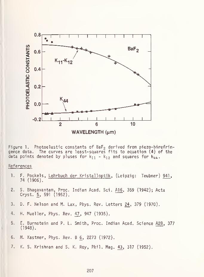
WAVELENGTH (jim)
Figure 1. Photoelastic constants of BaF 2 derived from piezo-birefrin-gence data. The curves are least-squares fits to equation (4) of thedata points denoted by pluses for kn - k12 and squares for kt^.
References
1. F. Pockels, Lehrbuch der Kristalloptik , (Leipzig: Teubner) 941,74 (1906).
2. S. Bhagavantam, Proc. Indian Acad. Sci. A16, 359 (1942); ActaCryst. 5, 591 (1952).
3. D. F. Nelson and M. Lax, Phys. Rev. Letters 24, 379 (1970).
4. H. Mueller, Phys. Rev. 47, 947 (1935).
5. E. Burnstein and P. L. Smith, Proc. Indian Acad. Science A28, 377(1948).
6. M. Kastner, Phys. Rev. B 6, 2273 (1972).
7. K. S. Krishnan and S. K. Roy, Phil. Mag. 43, 317 (1952).
207

8. K. Vedam and E. D. D. Schmidt, J. Mat. Sci. 1_, 310 (1966).
9. Albert Feldman, Phys. Rev. 150, 748 (1966).
10. K. Vedam and E. D. D. Schmidt, Phys. Rev. 150, 766 (1966).
11. S. Riskaer, Phys. Rev. 152, 845 (1966).
12. K. J. Schmidt-Tiedemann, Phys. Rev. Lett 7, 372 (1961).
13. A. Gavini and M. Cardonna, Phys. Rev. 177, 1351 (1969).
14. P. Y. Yu, M. Cardonna, and F. H. Pollak, Phys. Rev. B3, 340 (1971).
15. S. H. Wemple and M. DiDomenico, Jr., Phys. Rev. Bl_, 193 (1970).
16. J. A. Van Vechten, Phys. Rev. 182, 891 (1969).
17. David K. Biegelsen, Phys. Rev. Letters 32, 1196 (1974).
18. L. B. Humphreys and A. A. Maradudin, Phys. Rev. B6, 3868 (1972).
19. B. Bendow, P. D. Gianino, Y. F. Tsay, and S. S. Mitra, Appl . Optics
13, 2382 (1974).
20. J. P. Szczesniak, D. Cuddeback, and J. C. Corelli, J. Appl. Phys.
47, 5356 (1976).
21. A. Feldman, D. Horowitz, and R. M. Waxier, Appl. Optics 16, 2925
(1977).
208

THE RELATION OF ELASTOOPTIC ANDELECTROSTRICTIVE TENSORS
D. F. Nelson
Bell Laboratories
Murray Hill New Jersey 07974
BACKGROUNDElectrostriction is the deformation that is produced in a body by the application of an elec-
tric field and is proportional to the square of that field. Traditionally the applied electric field is
a very low frequency or constant field and is applied by electrodes attached to the body. It is
apparent that electrostriction must be characterized by a fourth rank tensor, two indices cou-
pling to the two electric fields and two indices coupling to the relevant measure of deformation,
the strain.
The elastooptic effect (also called the photoelastic or piezooptic effect) is the interaction
of an elastic deformation with an input light wave to produce an altered output light wave.
Since the light waves are determined by their electric fields, the elastooptic effect can also be
characterized by a fourth rank tensor with two indices coupling to the two electric fields and two
indices coupling to the relevant measure of elastic deformation. From the discovery of the
elastooptic effect by Brewster in 1816 through the extensive work of Pockels in the 1890's until
1970 it was believed that the appropriate measure of elastic deformation for the elastooptic
effect was the strain. It was thus quite natural to expect that the electrostriction and elastooptic
tensors were closely related, the electrostrictive tensor being simply the low frequency limit of
the elastooptic tensor. Proofs of this equality, in fact, were given many times1-4
based simply
on reversing the order of partial differentiation of a thermodynamic potential.
In 1970 it was shown 5that the elastooptic effect had been misrepresented throughout its
long history and that the proper measure of elastic deformation relevant to the elastooptic effect
is the displacement gradient which is a sum of strain and rotation. Measurements on strongly
birefringent crystals such as rutile6 and calcite
7 showed that the contribution of rotation to the
elastooptic effect can be comparable to that of strain. If the proofs1-4
cited above are correct,
then the electrostrictive tensor must also couple to rotation as well as to strain; that is, the
application of an electric field to electrodes on a body would cause the body to rotate. That,
however, would clearly violate angular momentum conservation. Thus, something must be
wrong with the phenomenological proof.1-4
Since the mathematics of the proof is too simple to
be wrong, it must be that the proof inadequately addresses the physics of the processes
involved.
In order to avoid any confusion before proceding further let us point out that a converse
elastooptic effect in which two light waves are mixed to produce a deformation (such as an
acoustic wave) has sometimes been called electrostriction, in particular by Caddes, Quate, and
Wilkinson 8 who first observed this effect. We do not use the term electrostriction in this sense
here but rather in the traditional sense defined above. Clearly the converse elastooptic effect is
properly characterized by the same elastooptic tensor that characterizes the normal elastooptic
effect.
209
Recently a new relationship between the low frequency limit of the elastooptic tensor and
the electrostriction tensor was obtained by comparing the results from the application of the
same basic theory of long wavelength interactions in dielectric crystals9,10
to the elastooptic
effect5 and to electrostriction.
11 The difference between the two tensors was attributed to the
differing coordinates, spatial and material, that are appropriate in expressing the tensors for the
two interactions, the elastooptic effect and electrostriction. Since the length of those two
derivations may obscure this interpretation, it is worthwhile to distill from them the essential
physics into a compact derivation of the new relationship. It is the purpose of this paper to do
that.
The choice of coordinates to which to refer the two tensors is determined by the methodsof measurement. In the elastooptic effect the electric fields of the input and output light waves
are known relative to the spatial (laboratory) coordinates since the light source and detector are
fixed in the laboratory. It is thus natural also to express the deformation with respect to the
same coordinates.
In the study of electrostriction as in the study of other phenomena in the low frequency
(quasielectrostatic) region electric fields and deformations are known relative to the material
coordinates anchored in the crystal. This results because electric fields are typically applied to
and detected by electrodes evaporated onto the surfaces of the crystal and deformations are
applied and detected by transducers bonded to the crystal surfaces. This means that the electric
and deformation fields are known only relative to the crystal surfaces and not relative to the
laboratory because the crystal surfaces are moving and deforming relative to the laboratory as a
result of the applied influences.
DERIVATION
The deformed position of a matter point is given by the spatial position vector x and the
designation of a matter point is given by the material position vector X. The latter can be
regarded as the name of the matter point that remains with the matter point during deforma-
tion. The relation between these two positions is the deformation transformation x = x(X,t).
It is convenient to take the material coordinate vector as the undeformed position of the matter
point and to represent the deviation of the matter point from this position arising from defor-
mation by the displacement vector u. Thus
x = X+u. (1)
Both the spatial and material positions are measured with respect to a rectangular coordinate
system. The deformation gradients bx/dXjand dXjdx, can be expressed in terms of the dis-
placement gradient, for instance,
aX/dxj = 8ji- du/ax, (2)
The displacement gradient is a sum of strain u< kii ) and rotation U[k
aui/dxj = u k)i= u (k)i)
+ U[kii], (3)
where
U(k,i) = (dui/dxi + c)u/dx k)/2 (3a)
and
u tk,i]= (duk/axj — Qu/9x k)/2. (3b)
The Jacobian of the deformation transformation is
J = det (dx/dX) = 1 + Uij + • • • (4)
210

Finally we note that a theory is said to be cast in the spatial description (or frame) if x, t are
regarded as the independent variables and in the material description (or frame) if X, t are
regarded as the independent variables.
In the spatial description the polarization P relevant to the elastooptic effect is given by5
Pi = eoXijEj + 2e, EjU k>1,(5)
where xy is the linear electric susceptibility, Ej is the spatial frame electric field, e 0 is the per-
mittivity of free space, and the elastooptic susceptibility Xij(ki) is related to the Pockels elastoop-
tic tensor p^, by
2Xij(ki) = ~~ K imKjnp mnkl- (6)
being the dielectric tensor. The factor of two before Xij(ki) in Eqs. (5) and (6) results
because xy(ki) applies to one Fourier frequency component (Stokes or anti-Stokes) and a low
frequency limit is taken here in which these two components coalesce. The Pockels term is
symmetric upon interchange of k and 1 and so couples only to the strain part of u k >t. The last
two terms5are antisymmetric upon interchange of k and 1 and so couple only to the rotation
part of u k j.
We now wish to transform Eq. (5) to the material frame. A study12
of the Maxwell equa-
tions in the material frame shows that the material frame polarization P and the material frame
electric field £are related to the corresponding spatial frame quantities by
Pm = JPiSXjdxi , ^ = EndXjdx,. (7)
If Eqs. (5) and (7) are now combined with the use of Eqs. (2) and (4), we obtain
•Pm = e 0Xmn-En + eO^Xmnfkl)-
Xm(kSl)n—
Xn(kS|)m+XmnSkl)£ n<)UkA)Xl. (8)
A material frame study of nonlinearities in the quasielectrostatic region11
yields
* m *0X + €ol mn ( ki)£ ndu k/9X|, (9)
where lmn (ki) is the electrostrictive susceptibility. Since to first order duj/dx, = duJdX h com-
parison of the last two equations gives
Imn(kl) = 2Xmn(kl)—
Xm(k8|)n—
Xnd^Dm + Xmn8 kl (10)
for the final result.
An alternate form of the last equation can be obtained if the expression12
for the low fre-
quency material frame electric displacement,
Z) k= e
(>I(C- 1
) klJE 1+ P k , (11)
where (C-1
)^ = (9X/9x k) (9X/Qx k), is expanded to yield
Dm - €oKmn£n + eoUnGcD-EnWdX! . (12)
The expansion gives the electrostriction tensor Imn(k0 in terms of the electrostrictive susceptibil-
ity by
Imn(kl) = lmn(kl)— 2S m ( kS 1)n + 8 mn8 k ,
(13)
and so allows an alternate form for Eq. (10) to be
Imn(kl)=
2Xmn(kl)— Kmd^Dn ~~ K n(l£\)m + K mn8 kl • (14)
211

We regard both the electrostrictive susceptibility and the electrostriction tensor as equally
important. The former, like the linear electric susceptibility, vanishes for a vacuum and so
characterizes the medium. The latter, like the dielectric tensor, is nonzero for a vacuum and is
the tensor entering the differential equations. It also enters the stress expression as the
coefficient of the square of the material frame electric field.
DISCUSSION
Let us note several things about Eq. (10) [similar remarks could be made about Eq. (14)].
First, we see that the essential difference between the electrostrictive susceptibility and the elas-
tooptic susceptibility arises because the former is a material frame tensor and the latter is a spa-
tial frame tensor. As pointed out in the Introduction this difference arises from the differing
methods of measurement. Second, the electrostrictive susceptibility couples only to strain, as
expected from an angular momentum conservation argument, even though the elastooptic ten-
sor can couple also to rotation. Note that the antisymmetric part of the elastooptic tensor that
couples to rotation does not enter Eq. (10). Third, the terms by which the electrostrictive sus-
ceptibility and the elastooptic susceptibility differ are terms describing Maxwell stresses arising
from the presence of a polarizable medium. These terms are comparable in magnitude to the
elastooptic susceptibility in many materials.
REFERENCES
1. H. Osterberg and J. W. Cookson, Phys. Rev. 51, 1096 (1937).
2. J. F. Nye, Physical Properties of Crystals (Clarendon, Oxford, 1957), pp. 255-256.
3. W. P. Mason, Crystal Physics ofInteraction Processes (Academic, New York, 1966), p. 166.
4. K. Iamsakun, W. Elder, C. D. W. Wilkinson, and R. M. DeLaRue, J. Phys. D 8, 266
(1975).
5. D. F. Nelson and M. Lax, Phys. Rev. Lett. 24, 379 (1970); Phys. Rev. B 3, 2778 (1971).
6. D. F. Nelson and P. D. Lazay, Phys. Rev. Lett. 25, 1187, 1638 (1970).
7. D. F. Nelson, P. D. Lazay, and M. Lax, Phys. Rev. B 6, 3109 (1972).
8. D. E. Caddes, C. F. Quate, and C. D. W. Wilkinson, in Modern Optics J. Fox, Ed.
(Polytechnic Press, Brooklyn, NY, 1967), p. 219.
9. M. Lax and D. F. Nelson, Phys. Rev. B 4, 3694 (1971); 13, 1759 (1976).
10. D. F. Nelson, Electric, Optic, and Acoustic Interactions in Dielectrics (Wiley, New York,
1979).
11. D. F. Nelson, J. Acoust. Soc. Am. 63, 1738 (1978).
12. M. Lax and D. F. Nelson, Phys. Rev. B 13, 1777 (1976).
212
PHOTOELASTIC PROPERTIES OF MAGNESIUM FLUORIDE
Sunwhee ChungEMR Photoelectric
P.O. Box 44Princeton, New Jersey 08540
Herbert R. Carleton*Department of Materials Science
State University of New York at Stony BrookStony Brook, New York 11794
Magnesium fluoride (MgF2) has the rutile crystal structure with a tetra-gonal space lattice (P4/mnm) 1
. The crystal is uniaxial positive withnU)=1.378 and n£=1.390 for sodium D light 2
. A single crystal of MgF 2grown by the Materials Research Corporation was used in this study. Thecrystal was approximately 1 cm^ with polished faces in the (001) , (110)
,
and (110) crystal planes as verified by the back-reflection Laue method.
After preparation, the sample was bonded with salol to a fused silicablock on which an x-cut 20 MHz quartz transducer was bonded with epoxycement. A similar fused silica block was prepared with a y-cut 20 MHzquartz transducer for shear wave measurements. Upon the completion ofmeasurements with this configuration, the crystal was cut at an angle45±0.5° to [110] and [110] in order to obtain (100) and (010) faces.Further measurements were conducted with this configuration, which werefollowed by another cutting at an angle 45±0.5° to [100] and [001].
This orientation was verified by obtaining an angular separation of11.6±0.5° between [101] and the direction perpendicular to the newly-cutface as determined by the back-reflection Laue method.
The experimental arrangement for ultrasonic laser-diffraction used for
all measurements is similar to that previously reported 3. The intensity
of light pulses diffracted from the MgF2crystal and the fused silica
reference was measured on an oscilloscope after detection with a photo-multiplier tube.
It can be shown 4 that the photoelastic constant p responsible for opti-cal diffraction by an ultrasonic wave is related to experimentallyavailable parameters by the relation:
<ps >
2- <iR >
1/2^> 3£>V> 2 u>^27 r s
where the subscripts r and s stand for reference and sample respective-ly, IR is the measured intensity ratio, p is the density, V is the
* Research supported in part by NSF Grant GK28383.
213
sound velocity, and n is the refractive index. The photoelastic con-stants of the sample were calculated from the known piezooptic constantsof fused silica which were measured by Primak and Post
5. These piezo-
optic constants at several wavelengths were converted to the photoelas-tic constants using the elastic moduli reported by Primak and Post, andtabulated in Table I.
Table I. Photoelastic constants of fused silica.
Wavelength (nm) 436.0 546. 0 579.0 589.0 644.0
P12
0.121 0.121 0.121 0.121 0.1220. 272 0. 270 0.270 0.270 0. 270
The ratio of sound velocities was obtained from a knowledge of the Braggangle 0 B which is one half the angle between incident and diffractedbeams. The sound velocities Vs are then calculated from 2V
sSin8
B=Af
where A is the laser wavelength in air and f is the frequency of thesound wave.
Six of the seven independent photoelastic constants of MgF2 have beendetermined and listed in Table II. The piezooptic constants q^j werederived using elastic constants obtained in this experiment. Since p
3could not be measured accurately with a longitudinal wave along [001]
because of low diffracted light intensity, p j3was determined using
quasi-longitudinal and quasi-shear waves along a direction 45° from[100] and [001] in the (010) plane. These results were also used to
assign the relative signs of pij( p 3, and p . Diffraction involving
p is "abnormal" 6, i.e. scattering
3
between light beams with differentphase velocities requires very large "phonon" frequencies to conservek-vector. Since this experiment was conducted in the Raman-Nath regime,
p could not be measured.
Table II. Photoelastic and piezooptic constants of MgF 2 at 632. 8nm.
Photoelastic Experimental Piezooptic Calculated ValueConstant Result* Constant (10
1
3
cm 2/dyn)
p +0.041±0.002 q -0.467
p1 1
+0.119±0.002 q11
+1.053
p12
+0.07810.002 q +0.197
p13
-0.099±0.003 q13
-0.545
p31
+0.01410.001 q31
+0.409^3 3 3 3
p — qp44
-0.047510.0015 qkk
-0.498^66 6 6
*Signs are assigned with respect to p which is assumed positive.
The change of the refractive indices of rutile under hydrostatic pres-
sure dn/dP was reported by Davis and Vedam 7. For the sake of comparison
dn/dP of MgF2 was calculated using the following relations (2) and com-
pared with those of rutile in Table III where we find that dn^dP is
positive while dn£/dP is negative.
214

dn ci£ n£ 3 11(0— = — (2q31
+ q 33), — = —(q^ + + q^) (2)
Using known relations for the photoelastic constants, p(dn/dp) of MgF2was calculated using Equations (3) and (4) and is listed in Table IIIalong with the corresponding strain polarizabilities
.
dn,,. n,
dn, n,
0) 0) I 1
= —=-{-(P, +P ) (S +S +S ) + -p (2S +S )} (3)2 S 11 12 11 12 13 S 13 13 33
p
dn£ n 3 2P= { (S +S +S ) +
dp 2 S 11 12 l 3J
p 33 ,„(2S +S
S 13 3 3)} (4)
Here, Sj_j is the elastic compliance, and 3=23!1+2S
1
2
+4Sx
3
+S3
3
Table III Change of refractive indices for MgF 2 and rutile.
Crystal Refractive Index A(nm)dn/dP _.(Mbar)~ ^P
A 0
MgF 2 n(jJ=l. 377 632.8 0.102 0.104 0.754
n£=1.389 -0. 0915 -0. 0927 1.21
Ti02* n
0J=2.587 58 9.3 0.11 0. 25 0.92
ne=2. 902 -0.49 -0. 95 1.21
*Davis and Vedam .
It is interesting to note that the ordinary and extra-ordinary refrac-
tive indices of MgF2
and rutile change in opposite directions underhydrostatic pressure.
A total differentiation of the Lorentz-Lorenz equation predicts a densi-7 8 9ty dependence of the refractive index, » >
dn>dp"
(n2- 1) (n
2+ 2)
6n(1 " AJ, (5)
where A = -(p/a) (da/dp) is the strain polarizability
.
Detailed studies 10 have shown that the polarizability of a cation in-
creases under compression while that of an anion decreases. This is
related to a decrease in ionicity of valence-pairs under compression.It can be expected that shifts away from ionicity, and hence to directedbonds, will produce anisotropic changes in refractive index where crys-
tal symmetry permits. The contribution of different ions to changes in
refractive index can be considered by introducing an ionic strain polar-izability A^,
Ai = -(p/a± ) (daj/dp) , (6)
so that the molecular strain polarizability is given, for binary sys-
tems, by
215

a+ a_A„ = — A, + A
, (7)a++a_ + a++a_
~' '
where the subscripts + and - represent the cation and anion, respective-ly. A Q is a phenomenological constant which attempts to explain thosechanges in refractive index which cannot be explained by volume changesalone. It must be interpreted as a tensor in the case of MgF2 . Sincethe two terms appearing in (7) are of opposite sign, the observed valuesof A D are consistent with a larger value of A+ for polarization in thebasal plane (nw ) than for polarization along the c axis (n£ ) . This is
plausible if one takes a close look at the irregular octahedron made bysix anions of MgF
2 . Along the directions [110] and [110] , all ions arein close contact with one cation for every two anions. However, alongthe [001] direction, the anions are not in contact, leaving some spacefor cations in the direction perpendicular to the c axis.
One can go a step further from this argument and say that dn/dP is neg-ative for more covalent crystals because the former part of Equation (7)
is very small or non-existent compared to the latter part which is posi-tive, thus making A Q
greater than 1. This will in turn make p(dn/dp)negative. The experimental results for MgO, C (diamond), Si, and Gesupport this argument. The values of A
oare 1.1 for diamond 7 and 1.2 -
1.4 for MgO 7'11
. Accordingly, p(dn/dp) and dn/dP for diamond and MgO1 2
are negative. Gibbs and Hill reported the change of the static elec-
tronic dielectric constant due to pressure for diamond as (l/Ej (0)
)
(0)/3P) T=(-1.07±0.09)xlO~7cm2
/Kg. Cardona et al12 reported (1/n) (dn/dP)
=(-3±2)xlO_7cm 2/Kg for Si and (1/n) (dn/dP) = (-7±2) xlO~ 7cm 2 /Kg for Ge.
Davis and Vedam 7 related the larger values of AQ
to the more covalent-
type bonding and the smaller values to the more ionic-type bonding from
the experimental results. This is in agreement with the conclusionderived in this report using the concept of the ionic strain polariza-bility.
References
1. R.W.G. Wyckoff, Crystal Structure Vol. 1, John Wiley New York (1963).
2. Handbook of Chemistry and Physics, 56th edition, CRC Press.
3. W.T. Maloney and H.R. Carleton, IEEE Trans, on Sonics and Ultrasonics
SU-14 , 135 (1967).
4. R.W. Dixon and M.G. Cohen, Appl. Phys. Lett. 8_, 205 (1966).
5. W. Primak and D. Post, J., Appl. Phys. 30, 779 (1959).
6. R.W. Dixon, IEEE J. Quantum Electronics QE-3 , 85 (1967).
7. T.A. Davis and K. Vedam, J. Opt. Soc. Am. 58, 1446 (1968).
8. H.R. Carleton in "Amorphous Materials", John Wiley New York (1972).
9. H. Mueller, Phys. Rev. 47_, 947 (1935).
10. S. Chung, "Photoelastic Dispersion of Alkali Halides and Alkaline
Earth Fluorides", Ph.D. Thesis (1976) State University of New York.
11. T.S. Narasimhamurty, Acta Cryst. 17_, 788 (1964).
12. J. A. Van Vechten, Phys. Rev. 182, 891 (1969).
216
A MICROSCOPIC APPROACH TO PREDICT REFRACTIVE INDICESAND ELECTRO- OR STRAIN-OPTIC COEFFICIENTS
M.D. Ewbank, P.R. NewmanRockwell International Science Center
1049 Camino Dos RiosThousand Oaks, California 91360
and
W.A. HarrisonDepartment of Applied Physics
Stanford UniversityStanford, California 94305
Introduction - Research and development of solid state optical deviceshas recently been increasing. Specific examples are tunable spectralfilters, modulators and beam steerers (both acousto-optic (AO) and
electro-optic (EO)). However, some devices exhibit unacceptable per-
formance characteristics. This limitation is usually not device designbut rather the relevant materials properties of the few selective com-
pounds being utilized. One solution to this problem obviously is tofind crystals which demonstrate superior materials properties. However,the experimental investigation (including growth, fabrication, and char-acterization) of random compounds which satisfy the necessary criteriais prohibitively expensive.
A more efficient approach entails theoretically estimating the virtuesof candidate materials. Several authors 1" 3 have addressed the issue ofidentifying promising compounds for both AO and EO applications. Otherauthors** 5 have attempted to establish empirical "guidelines," which arebased upon bulk macroscopic properties, for selecting new crystals. Ourmethod, by contrast, is a "first principles" scheme that commences at
the atomic level of the solid. The ultimate goal is to develop a com-pletely general (based solely on elemental composition, atomic configu-ration, and crystal symmetry) theoretical predictive methodology forcomparing materials properties of different compounds, to "prescreen"candidate materials, and subsequently to assist in the selection ofoptimal materials to be grown and characterized experimentally.
Approach - Initially, we have identified three relevant material param-eters: 1) the refractive indices, 2) the electro-optic coefficients, and
3) the photoelastic constants. This selection is based, in part, on two"figures-of-merit" for EO 5 and AO 6 devices which are F = n?r.?/e. and
M« = n?n?P.?/pv 3, respectively, where n^ is the optical i ndexJ of J refrac-
tion, rA H the electro-optic coefficient, e,- is the dielectric con-stant at the frequency of the external electric field, P
7- • is the photo-
elastic component, p is the mass density and v is the acoustic velocity.
217
Briefly, the procedure for determining the refractive indices and theelectro-optic or strain-optic tensors is as follows: 1) calculate theelectronic susceptibility tensor and hence the refractive indices(n. = A + 4™-..-), using a "first principles" method discussed below,for the "unperturbed" crystal, 2) apply an external perturbation (an
electric field for EO or a strain field for AO) and calculate theeffects of this perturbation on the atomic configuration and/or chemicalbonds, 3) recalculate the susceptibility for the "perturbed" crystal.The resulting change in the susceptibility tensor due to the externalelectric or strain field can be related to the electro-optic or strain-optic coefficients, respectively. 7
The interaction between the electric field associated with light propa-gating in a material and its constituent electrons is manifest in thedynamic electronic susceptibility. Specifically, we are concerned withthe spectral region above the lattice response modes (Reststrahl) andbelow the interband or interatomic transitions. A novel approach forthe calculation of the principle (diagonal ized) components of the elec-tronic susceptibility has been put forth by Harrison 8 in terms of a
modified LCAO theory as:
X11
= (4e2/v) I I [V
a3]2
(J e\)2/U
3- g 3
(1)a 3
where s is a summation over occupied states in the unit cell, I is a
summation over coupled unoccupied states, e is the electronic charge,v is the volume per unit cell, V a o represents the interatomic matrixelement (overlap) between occupied state a and unoccupied state 3, a is
the vector distance between bonding atoms, E. is the unit vector alongthe i-th principal crystal axis, ea is the energy of the occupied statea, and eg is the energy of the unoccupied state 3. The factors v and a
depend only on the crystal geometry. The interatomic matrix elements,V a3 , can be quantitatively evaluated by using the Slater-Koster LCAOenergy integral formulas 9 along with a parameterization by Harrison 10
for the two-center integrals. The energies, e a and e«, can be deter-mined from band structure calculations which depend on elemental compo-sition, crystal structure, and the same set of interatomic matrixelements, V a3.
Results - The above formalism has been applied to the change in the
refractive indices due to variations in atomic positions, of the sul-
fosalt, Tl3AsSe3 (TAS). As one example, the variation of atomic posi-
tions caused by' a longitudinal acoustic wave (uniaxial strain) leads tocalculation of photoelastic constants. Another calculation involves theeffects of thermal expansion on the refractive indices. 11
The crystal structure of TAS at room temperature was determined by Hong,
et al. 2 The perturbed structure is generated by incorporating a strain
which is assumed to be anisotropic and microscopically inhomogeneous,with the As-Se, Se-Se and Tl-Tl interatomic distances remaining constantand the Se-Tl distances accommodating all of the strain. A detailedstudy of the atomic configuration makes this assumption plausible.
218

Following the procedure outlined above, the unperturbed refractiveindices of TAS can be calculated. The ordinary index, n
0, is dominated
by the As(pz)-Se(p
z ) ir-bond since these two states constitute the bottommost conduction band and top most valence band, respectively, which re-
sults in a small energy difference (eg
- e ).13 However, since the
As-Se bonds essentially lie in the a_ - b_ pfane, they do not contributeto the extraordinary index, ne . Consequently, the main contribution to
ng
is from the Se-Tl p state interactions.
The change in the refractive indices, due to thermal contraction or
strain (e.g. uniaxial contraction), can be understood by examiningEq. (1). Both n
Qand n
ewill experience the volume dependence; as con-
traction occurs, both refractive indices tend to increase. For nQ , this
volume effect is the only contribution because nQ
is dominated by theAs-Se interaction whose interatomic distance remains constant despitecontraction elsewhere in the lattice. Therefore, n0 increases withcontraction. In contrast, n
ehas several competing factors. Most are
specified directly by the change in Se-Tl bond length. A significantcontribution results from the change in the energy difference,(e - e ), for the Se-Tl p state. As the interactomic distances con-
tract,athe wave function overlaps increase and the energy levels split
apart. This variation in energy difference can be approximated by con-
sidering only two coupled states . Then the shift in (eg
- e ) can be
expressed as ^(e, - e? )
2 + 4V,£. In the case of TAS, and are
the ionization energies of Se and Tl p states and ls tne interatomicmatrix element between the Se and Tl p states.
The seemingly anomalous experimental temperature dependences of therefractive indices for TAS are explained in the context of the abovemodel, since the factor (e - e ) dominates over the volume for n
fi
. A
comparison between theory and experiment is shown in Figs. 1 and 2.
Fig. 1 Comparison of the predictedtemperature dependence of theordinary refractive index of
TKAsSeo with experiment.
Fig. 2 Comparison of the predictedtemperature dependence of theextraordinary refractive indexof TloAsSeq with experiment.
219
The strain-optic coefficients (P-jii^) are defined in terms of the changein the dielectric impermeability tensor (B^,-) with respect to elasticstrain (^-j):
7
AB. . = I P. .. , e. tUkj Ukl kl
optic axis,
<5)c where 6
To examine the effect of a uniaxial strain in TAS
the lattice parameter, c, is modified as follows:is a small number. Then, since TAS has the pointAB, = = for ordinary polarized light and ^ordinary light, where we have used the standard contracted
0! nd ices nota-
along thec' = (1 +
group 3m,AB-, = 6 for extra-
tion. 7 The strain-optic coefficients are then defined in terms of therefractive indices as:
13 K2
>s " (%2
>u/« and
33(n;
2)s
- (n;2
)u
/«
where subscripts "s" and "u" refer to "strained" and "unstrained,"
respectively.
Conclusion - We have outlined a predictive methodology for calculatingrefractive indices and electro- or strain-optic coefficients. To testits fundamental basis, this theory was successfully employed in predict-ing the photoelastic constants and the temperature dependences of therefractive indices of Tl3AsSe3.
References
1. N. Uchida and N. Niizeki, Proc. of the IEEE 61_, 1073 (1973).2. R.W. Dixon, J. Appl. Phys. 38, 5149 (1967).3. I. P. Kaminow and E.H. Turner, Proc. of the IEEE _54 , 1374 (1966).4. D.A. Pinnow, IEEE QE-6 , 223 (1970).5. I. P. Kaminow and E.H. Turner, in CRC Handbook of Lasers , p. 447
(1974).6. I.C. Chang, IEEE SU-23 , 2 (1976).7. J.F. Nye, Physical Properties of Crystals , (Oxford Univ. Press,
Oxford, 1976), p. 244.
8. W.A. Harrison, Electronic Structure and the Properties of Solids ,
(Freeman, San Francisco, 1980).9. J.C. Slater and G.F. Koster, Phys. Rev. 94, 1498 (1954).
10. S. Froyen and W.A. Harrison, Phys. Rev. B20 , 2420 (1979).11. M.D. Ewbank, P.R. Newman, N.L. Mot a, S.M. Lee, W.L. Wolfe,
A.G. DeBell, and W.A. Harrison, to be published.12. H. Y-P Hong, J.C. Mikkelsen and G.W. Roland, Mat. Res. Bull. _9» 365
(1974).13. M.D. Ewbank, E.A. Kraut, S.P. Kowalczyk, W.A. Harrison, to be
publ ished.
220

DISPERSION OF THERMO-OPTIC COEFFICIENTSOF Nd LASER MATERIALS
K. E. Wilson and L. G. DeShazerHughes Research Laboratories
3011 Malibu Canyon RoadMalibu, CA 90625
We developed a double interferometer capable of measuring simultaneous-ly both the coefficient of linear expansion a£ and the thermo-opticcoefficient an and also capable of measuring differences in dB/dT in
anisotropic materials to better than 2%. The experimental techniqueconsisted of having the sample in one arm of a Twyman-Green inter-ferometer which formed the first interferometer and the second inter-ferometer, a Fizeau type, was formed by the reflected beams from thefront and back faces of the sample. The measured phase shifts in theFizeau interferometer are caused by optical path length changes in thesample, while the phase shifts in the Twyman-Green are caused by pathlength changes between the two arms of the interferometer. The linearexpansion and thermo-optic coefficients are therefore determined fromthe simultaneous solution of the equations for the phase shifts in thetwo interferometers.
The thermo-optic coefficients an and the thermal expanion coefficienta^ were determined for seven laser materials: YAG, YALO, BeL, ruby(Cr:Al203), quartz, ED2 and Nd Kodak glasses using the double inter-ferometer technique. For YAG and ED2 glass, the wavelength variationof the thermo-optic coefficient was fitted to a single resonancetheoretical model from which the relative variation of the electronicresonance frequency with temperature wg 1 dwg/dt was determined to be
-1.73xl0 5/°C (undoped YAG), -1 . 77xl0_5
/°C (Nd:YAG) and -1 . 39xl0_5
/°Cfor ED2 glass. As a comparison, these values were determined for NaCl
and quartz and are -2.03xl0~ 5 /°C and -0.97xl0" 5 /°C respectively.Fig. 1 shows the wavelength dependence of the electronic resonancecontribution to the thermo-optic coefficient.
In the course of our experiments, we discovered a new technique for
precisely measuring the temperature dependence of the birefringence of
anisotropic materials. We call this technique "fringe beating" whichis the superposition of the interference fringes for the two orthogon-
al polarizations in the sample and is very sensitive for measuringsmall values of dB/dT, capable of measuring values of dB/dT on the
order of 10_7
/°C. Figure 2 illustrates the beating for both Twyman-
Green and Fizeau interferometer fringes with increasing sample
temperature using ruby.
221

WAVELENGTH, (J
' 0 06 0 38 0.32 0.29 9i96-4
L I I I II I
02 4 6 8 10 12
FREQUENCY SQUARED, »T2
-2 -2Figure 1. Plots of (1-n )/A vs. X where A is the electronicresonance part of the thermo-optic coefficients.
TEMPERATURE °C
Figure 2. Beating of interferometer fringes for ruby (60° cut) forincreasing T where top trace is Fizeau fringes and bottom, Tywman-Green
.
222
TEMPERATURE DEPENDENCE OF THE OPTICAL PROPERTIES OF SOMEMETALS AT VISIBLE AND INFRARED WAVELENGTHS
D. L. Decker and V. A. HodgkinMichelson/Lauritsen Laboratories
Naval Weapons Center, China Lake, California 93555
This paper briefly describes experimental techniques and apparatusdeveloped at the Naval Weapons Center for measuring temperature-dependent changes in the near-normal incidence reflectance (R) of asample to a precision of a few parts in 10 5 [1], Reflectance resultsobtained from this instrument are presented for Al, Cu, Ag, and Mofilms and bulk material over the 0.6 to 10.0 um wavelength range attemperatures from 80 to 450°K. The sample and reference surfaces wereprotected in ultrahigh vacuum for these measurements. These data(dR/dT) are analyzed by a differential Kramers-Kronig technique toyield the temperature dependence of the real and imaginary parts of theindex of refraction and dielectric constants [2],
The infrared optical properties of a "good" metal are described classi-cally by the simple Drude model [3]. The temperature dependence of theoptical constants computed from this model primarily arises from thetemperature dependence of the dc conductivity (a) [4]. For the metalsconsidered in this paper, at temperatures near room temperature and at
wavelengths in the infrared, nearly wavelength and temperature independent values of dR/dT are computed from measured values of a(T). In thefar infrared, the measured and computed values of dR/dT are in reason-able agreement and are on the order of -1 x 10
-5/°C. In detail, there
are discrepancies which are both time and temperature dependent.Reflectance data taken with ascending and descending temperatures showhysteresis with very noticeable time dependence. Especially at elevatetemperatures, permanent changes in reflectance do occur due to "anneal-ing." Much of the time-dependent variation is very similar to thatpreviously seen in heat capacity, thermal conductivity, and electricalresistivity and is broadly described under the title of "premeltingeffects" [5].
At shorter wavelengths in the visible and ultraviolet, these metalshave an additional dispersion mechanism associated with electron inter-band transitions. This dispersion acts in addition to that provided byintraband electron transitions, which is accounted for by the Drudemodel. For example, in Al, a very pronounced dip occurs in reflectancewith a minimum at about 0.83 um, which has been identified with inter-band transitions near specific critical points in the Brillouin zone ofthis face centered cubic metal [6]. In this region, both the magnitudeand sign of dR/dT fluctuate wildly, and at a given wavelength, dR/dT is
223

strongly temperature sensitive. This is especially true near 0.81 urn
where dR/dT « 0. The detailed temperature dependence of the reflectancenear the region of the interband transition is also strongly dependentupon the condition and method of preparation of the sample. Data arepresented for both evaporated film and single-crystal samples. Anotherclass of non-Drude effects has been discovered for Ag in the nearinfrared, which also causes a sign reversal in dR/dT. This effectoccurs in a region where the reflectance is known to be very sensitiveto surface roughness and may be associated with a surface plasmon-likeexcitation which is coupled to the incident light by very small slope,spatially uncorrelated surface roughness.
The data presented in this paper is of immediate engineering value in
computing the performance of optical systems whose components neces-sarily operate at temperatures other than room temperature. It is also
hoped that it will stimulate theoretical interest in examining some of
the subtle and poorly understood dispersion effects such as those seen
in the near infrared in silver.
References
[1] D. L. Decker, "Measurement of the Optical Constants of Thin Filmsof Silver and Other Metals at Temperatures Near Room Temperature,"
in High Energy Laser Mirrors and Windows, ARPA Semi-Annual Report
#2, ARPA Order 2175 (Mar 1973), pp. 34-49.
[2] D. L. Decker, J. Opt. Soc. Am. 61, 679 (1971).
[3] H. E. Bennett and J. M. Bennett, "Validity of the Drude Theory for
Silver, Gold, and Aluminum in the Infrared," Optieal Properties andElectronic Structure of Metals and Alloys, ed. by F. Abeles (North
Holland Publishing Co., Amsterdam, 1966), pp. 175-188.
[4] G. A. Boloshin, Opt. Spectrosc. 18, 423 (1965).
[5] G. Borelius, "The Changes in Energy Content, Volume and ResistivityWith Temperature in the Simple Solids and Liquids," in Solid State
Physics, Vol. 15, ed. by F. Seitz and D. Turnbull (Academic Press,
New York, 1963), pp. 1-51.
[6] H. Ehrenreich, A. R. Philipp, and B. Segall, Phys. Rev. 132, 1918
(1963).
224
OPTICAL PROPERTIES OF Ti DIFFUSEDLiNbO„ WAVEGUIDES
W. K. BurnsNaval Research Laboratory
Washington, DC 20375
We will discuss measurements of the optical properties of LiNbO^ which
are pertinent to optical waveguiding applications. LiNbO^, which is
both electro-optic and piezoelectric, has many potential uses in inte-
grated optic applications, including communications, signal processing,and spectrum analysis. Typically, optical waveguides are formed in
LiNbO by the diffusion of thin films of Ti at high temperatures,^resulting in an increased index of refraction in a surface layer. Thewaveguide is then characterized by the diffusion length and the surfaceindex change. Since LiNbO^ is uniaxial, the diffusion coefficients areanisotropic and the index change depends on optical polarization. Thesituation is complicated by the outdiffusion of Li which occurs simul-taneously with the indiffusion of Ti, and causes a non-stoichiometricsurface layer with a corresponding increase in the extraordinary indexof refraction. Using a suitable dispersion theory to describe thegraded-index waveguide, it is possible to obtain the index changes anddiffusion coefficients from optical measurements of the effective
9indices (phase velocity) of the propagating modes. By using a seriesof waveguides which vary in a known manner, a fairly complete descrip-tion of the diffusion process can be obtained. Alternatively, usinganalyzing techniques such as secondary-ion mass spectrometry (SIMS)
,
the Ti and Li concentration profiles can be observed directly. Inchannel waveguide devices, the extent of lateral diffusion from thechannel is sometimes of interest. This effect has been successfullymeasured by the electron microprobe.
In integrated optical spectrum analyzer applications utilizing Ti dif-fused LiNbO_ waveguides, it is desirable to induce absorption in vari-ous parts of the waveguide and substrate. This would improve the signalto noise ratio by reducing optical noise at the detector array. We willdiscuss the creation of optically absorbing layers which result fromthe implantation of H into bulk and Ti diffused LiNb0
3.
References
1) R. V. Schmidt and I. P. Kaminow, Appl. Phys. Lett. 25_, 458 (1974)
.
2) W. K. Burns, P. H. Klein, E. J. West and L. E. Plew, J. Appl. Phys.50, 6175 (1979).
225

OPTICAL PROPERTIES OF THIN FILMSBY GUIDED WAVES AND SURFACE POLARITONS
J. D. SwalenIBM Research Laboratory
San Jose, California 95193
Guided optical waves, also called integrated optics, are optical waveswhich propagate in a thin layer, usually a few micrometers thickp-These parallel plate waveguides, as in the microwave case, havepropagation characteristics which follow directly from a solution of
Maxwell's equations matching the boundary conditions at eachinterface. The optical fields are highly localized within the filmand the polarization of the light can be either s or p. Coupling is
usually accomplished by high index half prisms^ as illustrated in
Fig. 1 or gratings. The mode characteristics, the number of nodes inthe optical field across the guide, their angle of propagation andtheir attenuation, can be analyzed to give detailed information aboutthe film thickness and its refractive index, real and imaginary parts,or its related dielectric function.^
Surface polaritons are surface waves which propagate along aninterfaced Like guided waves they are also highly localized but in
this case decaying exponentially away from the surface. They existonly for p polarized light and require that the sum of the real partsof the two dielectric functions at the interface be less than zero.
This can be accomplished either with a metal at energies below thebulk plasmon energy or with a strong absorber where the real part of
the dielectric constant becomes sufficiently negative. For the caseof a metal the surface wave is called a plasmon surface polariton andthe polarization change at the interface of metal and dielectric comesfrom the oscillations of the pseudo-free electrons in the metal. Forthe case of a strong absorber the surface wave is called an excitonsurface polariton when the absorption is from excitons and a phononsurface polariton when the absorption is from phonons . The dispersioncurve is shown in the top of Fig. 2.
6,7 8Coupling is again accomplished with high index prisms or gratingsbut since the propagation is for only a very short distance, a fewmicrometers in the visible region of the optical spectrum, the
reflected instead of the propagated light is observed, see Fig. 1. In
Fig. 2 a typical reflectivity curve is shown, 9C being the criticalangle for prism-air interface. Measurement of this reflectivityminimum gives a measure of dielectric function (and the thickness in
226
the Kretschmann scheme shown in the lower left of Fig. 1) of the metalor strongly absorbing layer. Overlay ers of transparent or absorbingfilms shift the angle at which the reflectivity minimum occurs. This
shift is a function of both the thickness and the refractive index(the real part) of the overlayer but from this measurement only one
can be determined. Absorption has the added features of broadeningand changing the depth of the reflectivity minimum. Detailed analysisof this exciton - plasmon surface polariton interaction has explained n
this anomalous dispersion behavior which is orientationally dependent.in 111?Absorption, fluorescence , Raman scattering, > lifetime, spatial
and orientational dependency, and scattering from surface roughness^
are some of the many observables which can be analyzed to
characterized a film and the species within it. Recently thick liquidcrystal cells next to metal electrodes have also been studied bysurface polaritons as a function of applied electric field to
determine the anchoring and reorientational characteristics.^
1. See for example D. Marcuse, Theory of Dielectric OpticalWaveguides, (Academic, New York, 1974).
2. P. K.Tien, R. Ulrich, and R. J. Martin, Appl. Phys. Letters 14, 291
(1969)
.
3. M. K. Dakss, L. Kuhn, P. F. Heidrich and B. A. Scott, Appl. Phys.
Letters 16, 523 (1970).4. J. D. Swalen, J. Phys. Chem. 83, 1438 (1979).5. E. Burstein, 'Introductory remarks on polaritons', Polaritons,
Proceedings of the First Taormina Research Conference on theStructure of Matter, Edited by E. Burstein and F. de Martini,(Pergamon, New York, 1974)
.
6. A. Otto, Z. Physik 216, 398 (1968).7. E. Kretschmann and H. Raether, Z. Naturforsch. 23a, 2135 (1968).
8. A. Girlando, M. R. Philpott, D. Heitmann, M. R. Philpott, J. D.
Swalen and R. Santo J. Chem. Phys. (in press).9. I. Pockrand, J. D. Swalen, J. G. Gordon II, and M. R. Philpott, J.
Chem. Phys. 70, 3401 (1979).10. W. H. Webber and C. F. Eagen, Optics Letters 4, 236Z(1979).11. G. Burns, F. Dacol , J. C. Marinace, B. A. Scott and E. Burstein,
Appl. Phys. Letters 22, 356 (1973).12. J. F. Rabolt, R. Santo, and J. D. Swalen, J. Appl. Spectrosc. (in
press)
.
13. I. Pockrand, Optics Commun. 13, 311 (1975).
14. J. D. Swalen and G. J. Sprokel, 'Liquid crystal - surfaceinteractions by surface plasmons
' ,Symposium on the Physics and
Chemistry of Liquid Crystal Devices, IBM Symposium Series(Plenium Press, New York, 1979).
227
Laser
Beam Aj r
Waveguide Configuration
Substrate
Kretschmann Configuration Otto Configuration
Fig. 1. The schematics for coupling light into guided waves and
surface waves. In the top figure for waveguide coupling the film
thickness is exaggerated and the angle <j> is changed to couple to
different modes. The middle figure is an enlargement showing the
optical rays. The lower figures illustrate the two methods for
coupling to surface waves. In the Kretschmann configuration the
metal film must be thin enough for the evanescent wave to
penetrate to the bottom side.
223

£ 0.6>
<d 0.4oc
0.2
IE i
40 44 48 52
Internal Angle 0
Fig. 2a The dispersion curve (u vs. k) for plasmon surface
polaritons (SP) and its intersection with a laser frequency U£
and propagation vector ko. The frequency wp
is the bulk plasmon,
eA is the dielectric function of the dielectric half space, and
Tip is the refractive index of the coupling prism. 2b A typical
reflectivity curve.
229

PROPERTIES OF LOW LOSS DIFFUSED OPTICAL WAVEGUIDES IN GLASS
T. Findakly, E. GarmireCenter for Laser Studies
University of Southern CaliforniaUniversity Park, Los Angeles, California 90007
Graded index waveguides in glass are typically fabricated by ion ex-change from a silver nitrate melt. Residual losses observed in suchwaveguides are from 0.5 to 2 dB/cm and are generally attributed to
either scattering from surface irregularities or loss due to silvergrains. In order to reduce the loss, and to investigate mechanisms forloss in glass waveguides, we have investigated other techniques of fab-rication. In particular, we have employed a dry process, diffusingmetallic silver into the glass substrates. In addition, we have in-
vestigated the effect of an electric field applied during diffusion.We have observed losses so low as to be unmeasurable (0.1 dB/cm), andhave made both single mode waveguides and highly multimode waveguideswith large numerical aperatures. We report measurements of mode-dependent losses in these waveguides at several wavelengths and also ofabsorption, measured calorimetrically . In addition, we report experi-ments on burying the waveguide below the surface.
Silver films several hundred angstroms thick were evaporated on soda-lime silicate glass slides and diffusion was carried out at 500 C in
oxygen, for periods from 5 minutes to 7 hours forming waveguides at6328A
5
of depths from 6 urn to 85 urn.
The waveguide losses of the thicker waveguides were lower than could bemeasured by monitoring the decrease in scattered light as a functiondistance along the waveguide, using the photomultiplier . This very lowloss was due to a combination of relatively thick waveguides and a lowconcentration of silver, which reduced both absorption and scatteringfrom any possible aggregates. The losses increased somewhat as thewaveguides were made thinner, however. Figure 1 shows the loss as a
function of the diffusion time, and would indicate that surface scat-
tering is the dominant loss mechanism in this case (assuming an in-
finite diffusion source) . Although they have very low loss, thesewaveguides have the advantage of having a very low index (An^O. 002)
.
It is interesting to note that the ions may diffuse very far (85 um)
,
but with a very low solubility. This is in contrast to the high con-
centration of silver ions achieved with ion exchange.
In order to increase the index of the waveguides, we applied an electricfield during diffusion. Diffusion was carried out at 300°C in air with
an applied electric field of from 0 to 100 V/mm for periods rangingfrom a few minutes to one hour. The ionic current ranged from micro-
230

amperes to a few milliamperes and was monitored throughout. The re-fractive index profile for the multimode guides could be determinedfrom the WKB method and is shown in Fig. 2. It can be seen thatlarge refractive index increases can be obtained. The large indexprofiles obtained are very different from the erfc (x) profiles usuallyobserved in ion exchange. These flatter distributions do not concen-trate the light so close to the surface and should have a smaller losscontribution due to surface scattering than do those fabricated byion exchange.
These studies show that by applying an electric field it is possibleto drive as many silver ions into the glass as with ion exchange.We observed index changes as large as 0.03. A monitoring of the ioniccurrent showed a decrease in exchange current as a function of time,which we attributed to a buildup of sodium on the gold cathode. Inorder to continue the diffusion for a long time and make deep wave-guides, we have found it necessary to use NaNO^ as the cathode.
These waveguides typically show more loss than those fabricated with-out an electric field. This appears to be due to the much largersilver content of the guides. The losses in these guides are^1 dB/cm and are comparable to those quoted in the literature for
ion exchanged guides. The mode dependent loss was measured for a
highly multimode waveguide and is shown in Fig. 3. The decrease in
loss with increasing mode number differs from the independence ob-served in ion exchanged guides. The reasons for this difference willbe discussed.
We have found that it is possible to reduce the loss below that shownin Fig. 2 by annealing after electro-diffusion. Reductions to lessthan 0.5 dB/cm for all modes was typical. Further reduction of theloss is possible by burying the waveguide below the surface. Wefabricated an electro-thermally diffused waveguide, removed excesssilver oxide, applied new electrodes and reintroduced the sample intothe furnace. The loss was decreased by 70% and the fact that theguide was buried below the surface was confirmed by the substantialreduction in prism coupling efficiency.
In this paper we shall present detailed results on the losses for
single mode guides and highly multimode guides. In addition,calorimetric absorption measurements and total loss measurements atother wavelengths are presently underway and will be presented at theconference
.
231

12 3
Diffusion Time (hrs)
Fig. 1. Measured losses in waveguides fabricatedby diffusion of evaporated silver at 500 Cas a function of diffusion time.
0. 02
°Ua b
N ^a b \ c s
1
\ \d n.
n
Fig. 2.
10 15 20
x (ym)
25 30 35
Refractive index profiles for waveguidesdiffused in the presence of an electricfield. (a) and (b) were at 60 V/mm withtwo metal electrodes for 15 and 60 min.respectively (c) and (d) were at 12 V/mmwith a cathode of NaNO^ for 1 and 2 hrsrespectively.
232

2.0
1.0
0 5 10 15
Mode Number
Fig. 3. Mode-dependent loss for a highly
multi-mode waveguide
233

THICKNESS MEASUREMENT OF VERY THIN-FILMSBY OBSERVING ANOMALOUS LIGHT ABSORPTION
t t 1tH. Kitajima, K. Hieda and Y. Suematsu
t Kyushu Institute of TechnologyTobataku Kitakyushu, 804 Japan
it Tokyo Institute of TechnologyOokayama Meguroku Tokyo, 152 Japan
1. IntroductionRapid and accurate measurement of film thickness is important in manyapplications 1 ' 2
. The prism coupler called m-line method 3, which is one
of the most convenient methods, can not be used when a film is too thinor the refractive index of a film is too small to support a guided mode.
We report here a powerful technique for measuring very thin-film thick-ness. The method is based on observing anomalous light absorptions in
a metal-clad thin-film into which surface waves are excited through a
prism4. A metal-clad thin-film, a transparent film coated on metal,
can support the guided mode, number m=-l of a TM wave, even the film is
extremely thin 5 ' 6. Metal-clad films possess a quasi discrete spectrum
of leaky modes 7 and a continuous spectrum of radiation modes. In con-trast to the radiation modes which are observed by ellipsometry method 8
,
the leaky modes are obseved using a prism coupler. Therefore, the ano-malous absorption characteristics strongly depend on the film thicknessand the incident angle.
2. TheoryIn the layered structure shown in Fig.l, the four media are denoted bysubscripts j=l,2,3,4, respectively. Their refractive indices are n .
Incident|:E
wave : H"Reflected
wave
Prism
Metal Substrate
Fig.l. Prism-film couplingstructure.
0
n . = / e . / e„J J 0
( J=l,2,3 )
(1)
kQ
= a) / y 0eQ
= 2tt / A0
exp [ibit ]
wavelength in vacuum space
time convention
Let us assume that we are dealing with a plane wave which is impinging
obliquely at the prism-gap boundary. The magnetic fields in each region
are written as follows.
234

H. = expt-ifrc] (A .exp [-iy .s]+B .exp [iy .z] ) , j=l,2,3,4
where = 1 (incidence) , 8^=0
6 = fe n^ -sin6 .
Y . = k nn .cos6 .
3 0 3 3Real{y .} > 0
3Imag{y • } < 0
3
(2)
(3)
(4)
The reflection coefficient, at the prism-gap boundary is obtained
exp[-£<j> 12 ] + B2/A2B, =
1 1 + exp[-£<t> 12 ]*B
2/A2
where (5)
B2
-exp[i(j> 32 ] + R31t
exp[i(<l>3tt-2<|>^,) ]
"A^ " 1 - R 34 expK(<|)3 2+<j)3 ir 2<jy)]•exp[-2a^]
y ./ z . - y, / e,
^12 = ^32 =» ^34 ^ !
exp[i<f>., ] = -exp [£<{>, .]
2<jy = 2y3<i^
,
2a = i2y 0d = 2|yJd9 2 g
1 21g
The norraalized film thickness (guided modes)
dj. <}> 32 + 4>31(
+ 2m-rr
4Trn3cos8
3
( ^=-1,0,1,2,..- )
The no-reflection (B-^0) conditions are given as
Ap tan(
A<(y 2* Ap tan( -j-
d1
1
1
X A 4tt n„cos6,
»
12 ) , A(d^/XQ)
=
'0 r-2
Ap = 1 - R
2sincf> 32log <
-
> >
/Ap z + Acjy^
4iTn3cose
3
where
34
A(f>/=
*32 + *34 + 2W7T " 2(|)
/
12'
(6)
(7)
(8)
(9)
(10)
(11)
(12)
(13)
(14)
(15)
235

Fig. 2. Film and gap thicknesses asfunctions of incident angles for theno-reflection. d^/\ Qt dg/Xq versus 8^° .
The broken line is corrected filmthichness for the no reflection. Thethree dots (1,2,3) are experimental data.
Fig. 3. Light absorption character- Fig. 4. Vector trajectories ofistics as a function of incident reflection coefficient showingangle. | B |
2 versus 8^°. The plots resonant absorption. versusare experimentally measured values. 8. °. ( ® : guided mode point)
236

3. Experimental Results and DiscussionFirst, we determined the refractive index of sputtered silica films ongold films which support several guided modes.
Refractive index of sputtered SiC^: 1.47+0.002 at 6328A
Next, we measured thickness of very thin silica films on gold, which is
sputtered on glass substrates. Relation between the incident anglesand the thickness are shown in Fig. 2. According to Fig. 3, the measuredabsorption characteristic fits in well with the calculated curve usingthe index of bulk gold. However, thickness differences between the bulkand evaporated gold are within 3^ for all samples. We did not deal witha serious matter here; the complex refractive index of the gold shouldhave been measured.
From the vector trajectories shown in Fig. 4, one can understand that
when a trajectory crosses the origin, the reflection coefficient becomeszero. However, even when the reflection does not become zero completely,the incident angles at which the reflection becomes minimum are not so
different from the angles which satisfy the guided mode. Therefore,rapid and accurate thickness measurement is possible.
Table 1. Measured samples.
SampleDeterminedThickness
Measured Thickness [£]
Evaporated* Bulkt1 161±5 162.06 159.272 71±5 72.39 69.793 32+5 33.98 31.47
* 0.15-£3.2 , t 0.35-£3.16 at A0 =6328a"
4. ConclusionThis work has demonstrated the feasibility of using anomalous light
absorptions in metal-clad thin-film systems, as a thickness measurementmethod for very thin films. Complex refractive index of metal may alsobe measured in this way. Unlike ellipsometry , this technique need notto measure either the reflection ratio or the phase difference.
References1. N. M. Bashara and D. W. Peterson, J. Opt. Soc. Am., 56, pp. 1320-1331,
1966.2. P. K. Tien, Rev. Mod. Phys., 42, 2, pp. 361-420, 1977.3. P. K. Tien, R. Ulrich and R. J. Martin, Appl. Phys. Lett., 10, 14,
pp. 291-294, 1969.4. V. Shah and T. Tamir, Opt. Commun., 23, 10, pp. 113-118, 1977.
5. A. Otto, Zeit Phys., 216, pp. 398-410, 1968.
6. A. Otto and W. Sohler, Opt. Commun., 3, pp. 254-258, 1971.
.7. K. Furuya and Y. Suematsu, Trans. IECE Jpn., 57-c, 11, pp. 411-418,
1974.8. R. J. Archer, J. Opt. Soc. Am., 52, pp. 970-977, 1962.
237
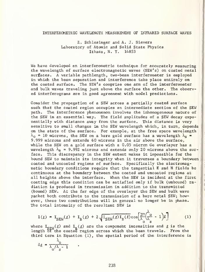
INTERFEROMETRIC WAVELENGTH MEASUREMENT OF INFRARED SURFACE WAVES
Z. Schlesinger and A. J. SieversLaboratory of Atomic and Solid State Physics
Ithaca, N. Y. 14853
We have developed an interferometric technique for accurately measuringthe wavelength of surface electromagnetic waves (SEW's) on coated metalsurfaces. A variable pathlength, two-beam interferometer is employedin which the beam separation and interference take place entirely onthe coated surface. The SEW's comprise one arm of the interferometerand bulk waves traveling just above the surface the other. The observ-ed interferograms are in good agreement with model predictions.
Consider the propagation of a SEW across a partially coated surfacesuch that the coated region occupies an intermediate section of the SEWpath. The interference phenomenon involves the inhomogeneous nature ofthe SEW in an essential way. The field amplitudes of a SEW decay expo-nentially with distance away from the surface. This distance is verysensitive to small changes in the SEW wavelength which, in turn, dependson the state of the surface. For example, at the free space wavelengthXQ = 10 microns, the SEW on a bare gold surface has a wavelength Xs =
9.999 microns and extends 60 microns in the air above the surface,while the SEW on a gold surface with a 0.05 micron Ge over layer has a
wavelength Xs = 9.992 microns and extends only 20 microns above the sur-face. This discrepancy in the SEW extent makes it impossible for thebound SEW to maintain its integrity when it traverses a boundary betweencoated and uncoated regions of surface. Specifically the electromag-netic boundary conditions require that the tangential E and H fields becontinuous at the boundary between the coated and uncoated regions atall heights above the interface. When the SEW is incident at the firstcoating edge this condition can be satisfied only if bulk (unbound) ra-diation is produced in transmission in addition to the transmitted(bound) SEW. At the far edge of the over layer the SEW and bulk wavepacket both contribute to the transmission of a bare metal SEW; how-ever, these two contributions will in general no longer be in phase.
The total intensity of the resultant SEW is
i<i> - iSEW(i) + v*) + NW^V^trV - i>] (i)
' o s
where ^ogW (^) an<* are the component intensities and I is the
length or the coatect region across which the beam travels. From the
third term in Equation (1), the spatial period of the interference is
XA*
=X /X°- 1 •
o s
238

Because ^Q/^s - 1 is small, large interference periods will be prod-
uced by relatively short wavelength radiation (e.g. — 3 mm at X —10H).
'
To test these conclusions, evaporated Ag and Au films were deposited onKC1 couplers. (1) Over part of these rectangularly shaped films thin Geover layers of a triangular shape were then deposited. Both the metaland Ge film evaporations were carried out at a pressure of 4 x 10~6
torr. The SEW was launched from a laser beam at one edge of the
metal film by means of the edge coupling technique. The length, l,of the over layer region probed by the beam was continuously varied bytranslating the film assembly in the plane of the surface but perpen-dicular to the beam direction. The transmission was measured as a
function of & for fixed over layer thicknesses, d, and CO2 laser wave-length, X0 .
Ge over layers ranging in thickness from O.Lu ^ d ^ 0.7|J were studied inthis manner in the range 9.2|_i ^ Xq ^ 10. 8\J-. In each case the observedtransmission characteristics and interference period were in agreementwith model predictions.
In conclusion the SEW interferometer provides a unique method for study-ing thin films on metal surfaces. Not only is the attenuation of theSEW obtained but also, of equal spectroscopic significance, the wave-length of the SEW is measured, an undetermined quantity in ordinarytransmission measurements.
ACKNOWLEDGMENTS
The authors acknowledge valuable conversation with R. Warner and Y.
Chabal.
Work supported by AFOSR under Grant #AFOSR-76-3684. Additional supportwas received from the National Science Foundation under Grant No.DMR-76-81083 A02 and technical report #4210, to the Cornell MaterialsScience Center.
REFERENCE
1. Y. Chabal and A. J. Sievers, Appl. Phys. Lett. 32, 90 (1978).
239
AUTHOR INDEX
Page
Adari, H. ..... . . 126
Allen, S. D 48
Andrews, J. B. . . . 63
Arakawa, E. T. . . . . 20
Ashley, J. C 20
160
Barkatt, A 182
Bass, M 48,77Becker, W. M 59
44,135Bi 1 lard, D 44
Bloom, A. L 167Boyd, R. W. 81
, 185
Burns, W. K 225
213Champness, C. H. 55
Chandrasekhar, H. R. 40213
Church, E. L 51
Coble, G. S 122
Dardy, H 185223
Dempsey, D. V. . . . . 122
DeShazer, L. G. . . . 85,221
Detrio, J. A 122
Donadio, R. N. . . . . 131
135
Ewbank, M. D 217
Faith, W. N 100204
Fernelius, N. C. . 122
23063
167
Fleming, J. W. . . . . 91
Fox, J. A. . . . . . 122
Gallant, D 48
230
Gibbs, H. M 9
Gossard, A. C. . . . 9
Granqvist, C G. . 201
122
13
217
Hieda, K 234. 201
PageHodgkin, V. A. . . ... 223Hsia, J. J . . .149Hughes, R ... 185Hummel, R. E. . . . ... 63
Hunneman, R. . . . ... 118Imaino, W ... 59
Johnson, G. W. ... 143Johnston, G. T. . . ... 122Kitajima, H. . . . ... 234Klein, C. A. . . . ... 131
Kramer, M. A. . . . ... 81
92,185Lauer, J. L. . . . ... 126
Lipson, H. G. . . . 36,44,135Lowdermilk, W. H. . ... 147Lynch, D. W. . . . 16,24,104
114Marshall, R. C. . . ... 44McCall, S. L. . . . ... 9
McKee, R. C. . . . ... 114
Mead, D. G ... 40
Milam, D . ... 147
Mitra, S. S. . . . 13,71Moore, D. T. . . . ... 139
Musa, A. H ... 108Nastasi-Andrews, R. J. .63Neal, W. E. J. . . ... 108
Nelson, D. F. . . . ... 209
Newman, P. R. . . . ... 217
Olshansky, R. . . . ... 171
Olson, C. G. . . . 24,104,114O'Quinn, D. B. . . ... 122
Osmun, J. W. . . . ... 114
Painter, L. R. ... 20
Passner, A ... 9
Peterman, D. J. . . ... 24
Philen, D. L. . . . ... 178
Porteus, J. 0. ... 100
Price, P. J. . . . ... 164
... 104
Ryan, D. P ... 96
... 238
... 118
... 100
... 63
Shih, I ... 55
Shyamprasad, N. G. ... 55
240

Page
Sievers, A. J 238Simmons, J. H 182
Simpson, C. T 59
Smith, D. Y 28
Sparks, M. S 188
Spector, H. N 67
Stewart, A. F 77
Stone, F. T 87,117Strom, U 32
Suematsu, Y 234Swalen, J. D 226Taylor, P. C 32
Temple, P. A 194
Tran, D. C 182Vaidyanathan, A 13
Venkatesan, T. N. C. . . 9
Waring, R. K 152
Waxier, R. M 204Weaver, J. H 24,114Weber, M. J 3
Weidner, V. R 149Whatley, A 118
Wiegmann, W 9
Williams, M. W 20
Wilson, K. E 85,221Winsor, H. V 1
Wood, D. L 91
Zumsteg, F. C 156
241
fr VS. GOVERNMENT PRINTING OFFICE : 1980 0-31 1-046 (54)

NBS-114A IREV. 8-78)
1. PUBLICATION OR REPORT NO. HIPIl^MP^*M 3« &c(m$iw No,'
SP 574
U.S. DEPT. OF COMM.
BIBLIOGRAPHIC DATASHEET
4. TITLE AND SUBTITLE
Basic Optical Properties of Materials, Summaries of Papers(Topical Conference on Basic Optical Properties of Materials)
5. Publication Date
May 1980
7. AUTHOR(S)
Albert Feldman, Chairperson, Editorial Committee
8. Performing Organ. Report No.
9. PERFORMING ORGANIZATION NAME AND ADDRESS
NATIONAL BUREAU OF STANDARDSDEPARTMENT OF COMMERCEWASHINGTON, DC 20234
Unit No.
11. Contract/Grant No.
12. SPONSORING ORGANIZATION NAME AND COMPLETE ADDRESS (Street, city, state, ZIP)
National Bureau of Standards Optical Society of AmericaDepartment of Commerce 1816 Jefferson Place NWWashington, DC 20234 Washington, DC 20036
13. Type of Report & Period Covered
15. SUPPLEMENTARY NOTES
| |Document describes a computer program; SF-185, FIPS Software Summary, is attached.
16. ABSTRACT (A 200-word or teas tactual summary of moat significant information. If document includes a significant bibliography or
literature aurvey, mention it here.)
This Special Publ
Topical Conference onBureau of Standards in
sponsored by the Natioof America. This publ
invited papers. The p
Ultraviolet PropertiesMaterials; PropertiesExternal Influences -
ication contains summaries of papers to be presented at the
Basic Optical Properties of Materials to be held at the NationaMay 5-7, 1980. The conference is
cooperation with the Optical Societyof 62 papers which include 14
Nonl inear Optical Properties;Infrared Properties; Graded Index Materials; Inhomogeneous
of Thin Films; Optical Fibers, Planar Optical Waveguides;
Piezo-optics, Thermo-optics, Magneto-optics.
Gaithersburg, Maryland on
nal Bureau of Standards in
ication contains summariesrincipal topical areas are:
The purpose of the conference is to discuss the state of the art in the measure-
ment of the optical properties of optical materials. The emphasis is primarily on
materials properties rather than on optical devices. The primary focus of the con-
ference is on the measurement and theory of basic optical properties of materials in
bulk, thin film and fiber form.
17. KEY WORDS (six to twelve entries; alphabetical order; capitalize only the first letter of the first key word unless a proper name;
separated by semicolons)
Fiber optics; graded index materials; infrared; magneto-optics; nonlinear optics;piezo-optics; planar waveguides; thermo-optics; thin films; and ultraviolet.
J21. NO. OFPRINTED PAG 11
18. AVAILABILITY Unlimited
| |For Official Distribution. Do Not Release to NTIS
|"X] Order From Sup. of Doc, U.S. Government Printing Office, Washington, DC20402
| |Order From National Technical Information Service (NTIS), Springfield,
VA. 22161
19. SECURITY CLASS(THIS REPORT)
UNCLASSIFIED
20. SECURITY CLASS(THIS PAGE)
UNCLASSIFIED
252
22. Price
$6.50
USCOMM-DCJ

NBS TECHNICAL PUBLICATIONS
PERIODICALS
JOURNAL OF RESEARCH—The Journal of Research of the
aWational Bureau of Standards reports NBS research and develop-
ment in those disciplines of the physical and engineering sciences in
ivhich the Bureau is active. These include physics, chemistry,
jngineering, mathematics, and computer sciences. Papers cover a
broad range of subjects, with major emphasis on measurement
*hethodology and the basic technology underlying standardization.
|a1so included from time to time are survey articles on topics
ulosely related to the Bureau's technical and scientific programs.
Ks a special service to subscribers each issue contains complete
illations to all recent Bureau publications in both NBS and non-
WBS media. Issued six times a year. Annual subscription: domestic
17; foreign $21.25. Single copy, $3 domestic; $3.75 foreign.
J<JOTE: The Journal was formerly published in two sections: Sec-
tion A "Physics and Chemistry" and Section B "Mathematical
iences."
IMENSIONS/NBS—This monthly magazine is published to in-
rm scientists, engineers, business and industry leaders, teachers,
itudents, and consumers of the latest advances in science and
technology, with primary emphasis on work at NBS. The magazine
highlights and reviews such issues as energy research, fire protec-
|ion, building technology, metric conversion, pollution abatement,
lealth and safety, and consumer product performance. In addi-
jion, it reports the results of Bureau programs in measurementjtandards and techniques, properties of matter and materials,
!ngineering standards and services, instrumentation, andlUtomatic data processing. Annual subscription: domestic $11;
preign $13.75.
NONPERIODICALS
ponographs—Major contributions to the technical literature onarious subjects related to the Bureau's scientific and technical ac-
uities.
handbooks—Recommended codes of engineering and industrial
iractice (including safety codes) developed in cooperation with in-
brested industries, professional organizations, and regulatory
todies.
•pecial Publications— Include proceedings of conferences spon-
sored by NBS, NBS annual reports, and other special publications
rppropriate to this grouping such as wall charts, pocket cards, and
jlibliographies.
.pplied Mathematics Series—Mathematical tables, manuals, andmudies of special interest to physicists, engineers, chemists,
biologists, mathematicians, computer programmers, and others
hngaged in scientific and technical work.
I National Standard Reference Data Series—Provides quantitative
S lata on the physical and chemical properties of materials, com-
Kfiled from the world's literature and critically evaluated.
((Developed under a worldwide program coordinated by NBS under
ij.ie authority of the National Standard Data Act (Public Law
jJO-396).
NOTE: The principal publication outlet for the foregoing data is
the Journal of Physical and Chemical Reference Data (JPCRD)published quarterly for NBS by the American Chemical Society
(ACS) and the American Institute of Physics (AIP). Subscriptions,
reprints, and supplements available from ACS, 1 155 Sixteenth St.,
NW, Washington, DC 20056.
Building Science Series— Disseminates technical information
developed at the Bureau on building materials, components,
systems, and whole structures. The series presents research results,
test methods, and performance criteria related to the structural and
environmental functions and the durability and safety charac-
teristics of building elements and systems.
Technical Notes—Studies or reports which are complete in them-
selves but restrictive in their treatment of a subject. Analogous to
monographs but not so comprehensive in scope or definitive in
treatment of the subject area. Often serve as a vehicle for final
reports of work performed at NBS under the sponsorship of other
government agencies.
Voluntary Product Standards—Developed under procedures
published by the Department of Commerce in Part 10, Title 15, of
the Code of Federal Regulations. The standards establish
nationally recognized requirements for products, and provide all
concerned interests with a basis for common understanding of the
characteristics of the products. NBS administers this program as a
supplement to the activities of the private sector standardizing
organizations.
Consumer Information Series— Practical information, based on
NBS research and experience, covering areas of interest to the con-
sumer. Easily understandable language and illustrations provide
useful background knowledge for shopping in today's tech-
nological marketplace.
Order the above NBS publications from: Superintendent of Docu-
ments, Government Printing Office, Washington, DC 20402.
Order the following NBS publications—FIPS and NBSlR's—fromthe National Technical Information Services, Springfield, VA 2216!
.
Federal Information Processing Standards Publications (FIPSPUB)— Publications in this series collectively constitute the
Federal Information Processing Standards Register. The Register
serves as the official source of information in the Federal Govern-
ment regarding standards issued by NBS pursuant to the Federal
Property and Administrative Services Act of 1949 as amended.
Public Law 89-306 (79 Stat. 1127), and as implemented by Ex-
ecutive Order 11717 (38 FR 12315, dated May 11, 1973) and Part 6
of Title 15 CFR (Code of Federal Regulations).
NBS Interagency Reports (NBSIR)—A special series of interim or
final reports on work performed by NBS for outside sponsors
(both government and non-government) In general, initial dis-
tribution is handled by the sponsor; public distribution is by the
National Technical Information Services, Springfield, VA 22161,
in paper copy or microfiche form.
BIBLIOGRAPHIC SUBSCRIPTION SERVICES
5]
he following current-awareness and literature-survey bibliographies
re issued periodically by the Bureau:
ryogenic Data Center Current Awareness Service. A literature sur-
'jey issued biweekly. Annual subscription: domestic $25; foreign'"30.
liquefied Natural Gas. A literature survey issued quarterly. Annual
I ubscription: $20.
Superconducting Devices and Materials. A literature survey issued
quarterly. Annual subscription: $30. Please send subscription or-
ders and remittances for the preceding bibliographic services to the
National Bureau of Standards, Cryogenic Data Center (736)
Boulder, CO 80303.

U S DEPARTMENT OF COMMERCESSion"a. B«r.-u of StandardsWashington. DC. 2UdJt
OFFICIAL BUSINESS
Penalty for Private Use. $300
POSTAGE AND FEES PAID
U.S. DEPARTMENT OF COMMERCECOM-215 US-MAIL
|
SPECIAL FOURTH-CLASS RATE
BOOK
Copyright © 2022 FDOKUMEN