Automatic Gain Control: Techniques and Architectures for RF ...
149
-
Upload
khangminh22 -
Category
Documents
-
view
0 -
download
0
Transcript of Automatic Gain Control: Techniques and Architectures for RF ...


Analog Circuits and Signal Processing
Series EditorsMohammed IsmailMohamad Sawan
For further volumes:http://www.springer.com/series/7381


Juan Pablo Alegre Pérez • Santiago Celma PueyoBelén Calvo López
Automatic Gain Control
Techniques and Architectures for RF Receivers
1 3

ISBN 978-1-4614-0166-7 e-ISBN 978-1-4614-0167-4DOI 10.1007/978-1-4614-0167-4Springer New York Dordrecht Heidelberg London
Library of Congress Control Number: 2011933911
© Springer Science+Business Media, LLC 2011All rights reserved. This work may not be translated or copied in whole or in part without the written permission of the publisher (Springer Science+Business Media, LLC, 233 Spring Street, New York, NY 10013, USA), except for brief excerpts in connection with reviews or scholarly analysis. Use in connec-tion with any form of information storage and retrieval, electronic adaptation, computer software, or by similar or dissimilar methodology now known or hereafter developed is forbidden.The use in this publication of trade names, trademarks, service marks, and similar terms, even if they are not identified as such, is not to be taken as an expression of opinion as to whether or not they are subject to proprietary rights.
Printed on acid-free paper
Springer is part of Springer Science+Business Media (www.springer.com)
Juan Pablo Alegre PérezLSI CorporationMadrid [email protected]
Santiago Celma PueyoUniversity of ZaragozaZaragoza [email protected]
Belén Calvo LópezUniversity of ZaragozaZaragoza [email protected]

v
Preface
Receivers have been a basic block in telecommunication systems since the inven-tion of the radio in the late 19th century, acquiring an essential role in what has been called the third Communication Revolution where information is transferred via controlled waves and electronic signals. Their main function is to recover the information from the transmitted wave and convert it to electronic signals that can be understood by the succeeding electronic processing signal systems. Since the Internet revolution, new receivers appeared to connect computers one to another or to the World Wide Web, such as wireless systems, have been gaining more and more popularity over the last few years. Thus, great investments in time, effort and money from both academia and industry have been made in the development of these re-ceivers in order to achieve fully integrated solutions in form of ASICs meeting the demand for ever increasing high performance with low cost, low voltage supply, low power consumption and reduced surface area.
The design of one of these receivers include different blocks such as filters, low noise amplifiers, gain controlled amplifiers, mixers and analog to digital converters. This book is precisely focused on the analysis and design of automatic gain control, AGC, circuits with wireless receivers as the main target application. In this context, the general function of the AGC circuitry is to automatically adjust the output sig-nal of a variable gain amplifier to an optimal rated level, for different input signal strengths. This function is essential to guarantee that the system dynamic range is neither saturated with large signals nor makes the system fall below a tolerable noise level.
Specifically, some wireless applications, such as WLAN or Bluetooth, must be able to handle packets-based data transmission and orthogonal frequency division multiplexing which introduce stringent settling-time constraints. Thus, fast AGCs are primordial in those systems. It is under these conditions that feedforward AGCs present their greatest advantages as an alternative to conventional feedback AGCs. Thus, all through this book we offer a detailed study about feedforward AGCs de-sign—both at basic AGC cells and system level—, their main characteristics and performances.

vivi
The starting point is a complete review and theoretical analysis of both feed-forward and feedback configurations and their behavioural modelling, issues ad-dressed in Chap. 2.
Next, basic components in gain control function, i.e., variable/programmable gain amplifiers, peak detectors and control voltage generation circuits are exam-ined. These basic blocks must be carefully chosen as they will limit the full AGC performance, so their specifications have to guarantee those required by the corre-sponding application. Thus, the main challenges and solutions encountered during the design of such high performance cells are summarized in Chap. 3 and different high performance integrated proposals that will be next employed in specific AGCs are described and characterized considering low voltage low power constraints. To achieve low power consumption and ease any future scale to shorter transistor chan-nel length technologies, low voltage power supplies have been employed: this re-quires greater effort in the design, but guarantees the validity of the achieved results in current submicron process technologies.
To close, the work is focused on the complete characterization of few different gain control loops required to implement a complete AGC system making use of some previously studied cells. Three complete AGC proposals are fully designed and evaluated in Chap. 4: a general purpose digital feedforward CMOS AGC op-erating at 100 MHz, a fully analogue feedforward AGC for an 802.11a WLAN re-ceiver in SiGe BiCMOS technology and a combined feedforward/feedback CMOS AGC for operating frequencies up to 250 MHz. These novel AGC contributions, more than competitive with those already presented in the literature, prove that feedforward AGCs are a fine alternative in wireless receiver applications, evidenc-ing that this class of circuits will take an important role in upcoming applications where the stringent time constraints preclude the use of conventional closed-loop AGCs.
Preface

vii
Contents
1 Introduction ............................................................................................... 11.1 AGC Design Strategies ...................................................................... 31.2 AGC Architectures for RF Receivers ................................................. 61.3 Outline of the Work ............................................................................ 8References ................................................................................................... 10
2 AGC Fundamentals .................................................................................. 132.1 AGC Loop Fundamentals ................................................................... 14
2.1.1 AGC with Feedback Loop ...................................................... 142.1.2 AGC with Feedforward Loop ................................................. 20
2.2 Matlab Simulations ............................................................................ 212.2.1 AGC with Feedback Loop ...................................................... 212.2.2 AGC with Feedforward Loop ................................................. 25
2.3 Conclusions ........................................................................................ 26References ................................................................................................... 27
3 Basic AGC Cells ........................................................................................ 293.1 Variable Gain Amplifiers .................................................................... 29
3.1.1 Degeneration Based VGA Structures. Proposed VGA1 ......... 323.1.2 Multiplier-Based VGA Structures. Proposed VGA2
and VGA3 ............................................................................... 353.1.3 Complete VGA Architecture Design Considerations ............. 513.1.4 Conclusions ............................................................................ 52
3.2 Peak Detectors .................................................................................... 543.2.1 Basic Peak Detector Topologies ............................................. 553.2.2 Open-Loop Envelope Detectors. Proposed PD1
and PD2 .................................................................................. 573.2.3 Closed-Loop Envelope Detectors. Proposed PD3
and PD4 .................................................................................. 663.2.4 S/H Based Envelope Detector. Proposed PD5 ....................... 703.2.5 Conclusions ............................................................................ 76

viiiviii
3.3 Control Voltage Generation Circuit .................................................. 783.3.1 Digital Control ...................................................................... 783.3.2 Analog Control ..................................................................... 793.3.3 Conclusions .......................................................................... 82
References ................................................................................................. 82
4 AGC Systems ........................................................................................... 874.1 CMOS Feedforward Digital AGC Circuit ........................................ 87
4.1.1 System Architecture .............................................................. 884.1.2 Performances ........................................................................ 91
4.2 SiGe BiCMOS Analog AGC Circuit ................................................ 934.2.1 System Architecture .............................................................. 944.2.2 Performances ........................................................................ 98
4.3 CMOS Mixed Feedback/Feedforward AGC Circuit ........................ 1014.3.1 System Architecture .............................................................. 1024.3.2 Performances ........................................................................ 109
4.4 Conclusions ...................................................................................... 112References ................................................................................................. 114
5 Conclusions .............................................................................................. 1175.1 General Conclusions ........................................................................ 1175.2 Further Research Directions ............................................................. 119
Appendix A: Layout and Experimental Techniques .................................. 121
Appendix B: Acronym List ........................................................................... 127
Appendix C: Parameter Glossary ................................................................ 129
Appendix D: Process Parameters ................................................................. 131
Index ............................................................................................................... 133
Contents

ix
List of Tables
Table 2.1 Summary of main AGC loop control characteristics.................... 14Table 3.1 Summary of VGA1 performances ................................................ 35Table 3.2 VGA2 transistors sizes ................................................................. 41Table 3.3 Simulation and measurement data of the VGA2 .......................... 44Table 3.4 VGA3 transistor sizes ................................................................... 48Table 3.5 Comparison of several VGAs ....................................................... 53Table 3.6 PD1 devices sizes ......................................................................... 59Table 3.7 Comparison of principal characteristics for simulation
and measurements of the open-loop peak detector ...................... 61Table 3.8 Comparison summary between PD1 and PD2 for 10 MHz ......... 65Table 3.9 PD5 transistor sizes ...................................................................... 75Table 3.10 Comparison of proposed envelope detectors................................ 77Table 4.1 Comparison of literature and proposed AGCs ............................. 113Table D.1 Technology: AMS 0.35 μm CMOS P-Substrate,
N-Well, 4-Metal, 2-Poly .............................................................. 131Table D.2 Technology: IHP 0.25 μm SiGe:C BiCMOS with
High-Voltage Devices, 5-metal .................................................... 132


xi
List of Figures
Fig. 1.1 Estimated wireless subscribers from 1985 to 2009 ........................... 2Fig. 1.2 WLAN and Bluetooth receiver block diagram ................................. 2Fig. 1.3 Feedback ( left) and feedforward ( rigth) AGC architectures ............. 4Fig. 1.4 IF strip example ................................................................................. 6Fig. 1.5 OFDM preamble symbols transient response ................................... 7Fig. 1.6 Feedback closed-loop AGC block diagram ....................................... 7Fig. 1.7 Feedback open-loop AGC block diagram ......................................... 8Fig. 2.1 Simplified block diagrams of feedback
(a) and feedforward (b) AGCs .......................................................... 14Fig. 2.2 Common block diagram of feedback AGC ....................................... 15Fig. 2.3 Model of generalized feedback AGC ................................................ 16Fig. 2.4 Equivalent AGC loop diagram .......................................................... 19Fig. 2.5 Common block diagram of feedforward AGC .................................. 21Fig. 2.6 AGC1: Simulink model ..................................................................... 22Fig. 2.7 Convergence response of AGC1 for different stepwise changes ...... 22Fig. 2.8 AGC2: Simulink model ..................................................................... 23Fig. 2.9 Convergence response of AGC2 for different stepwise changes ...... 23Fig. 2.10 AGC3: Simulink model ..................................................................... 24Fig. 2.11 Settling-time versus reference voltage for different
input signal steps ............................................................................... 24Fig. 2.12 AGC4: Simulink model ..................................................................... 25Fig. 2.13 Convergence response of AGC4 for different stepwise changes ...... 26Fig. 2.14 AGC5: Simulink model ..................................................................... 26Fig. 2.15 Convergence response of AGC5 for a stepwise change .................... 27Fig. 3.1 a Programmable resistor and fixed gain amplifier
based PGA and b high gain amplifier with resistor network feedback based PGA ........................................................... 31
Fig. 3.2 Differential pair transconductor with degenerative resistor .............. 32Fig. 3.3 Schematic view of the PGA proposed in [10] ................................... 34Fig. 3.4 PGA frequency response ................................................................... 36Fig. 3.5 THD levels at 10 MHz for all gain settings
versus output voltage Vout .................................................................. 36

xiixii
Fig. 3.6 a Conceptual multiplier scheme. b Gilbert cell................................. 38Fig. 3.7 Multiplier cell proposed in [14] ........................................................ 39Fig. 3.8 Complete scheme of the proposed VGA ........................................... 40Fig. 3.9 VGA2 chip photograph (a) and measurement setup (b) ................... 42Fig. 3.10 VGA gain frequency response: simulated (dashed)
and measured ( solid) ......................................................................... 43Fig. 3.11 IM3 levels versus peak-to-peak differential input voltage
(Vp-p) at 50 MHz for different gain settings ...................................... 43Fig. 3.12 VGA IM3 versus frequencies at 0.4 and 0.8 Vp-p output ................... 43Fig. 3.13 Measured HD3 for different gain settings at 100 kHz ...................... 44Fig. 3.14 Classical CMOS pseudo-differential transconductor ........................ 45Fig. 3.15 CMOS pseudo-differential transconductor: a Core
of the proposed topology and b Output DC current for different Vd = VG − VCM values ..................................................... 46
Fig. 3.16 Proposed CMOS pseudo-differential VGA with 3-bit rough gain adjustment, CMFF (a) and selfbias common-mode feedback loop (b) .............................................................................. 47
Fig. 3.17 VGA cell photograph ........................................................................ 49Fig. 3.18 Simulated ( dashed) and measured ( solid) VGA frequency
response for different gain settings ................................................... 50Fig. 3.19 PGA plus buffer simulated ( black) and experimental ( grey)
IM3 for outputs signals of 0.4 and 0.8 Vp-p at 100 MHz ................... 50Fig. 3.20 Typical multiple cell VGA AGC structure ........................................ 51Fig. 3.21 Rough/fine gain based VGA structure .............................................. 52Fig. 3.22 Ideal charge/discharge behaviour in a peak detector
with load capacitor, C, and resistor, R 54Fig. 3.23 Diode-RC peak detector topology ..................................................... 55Fig. 3.24 Op-amp plus diode based peak detector topology ............................ 56Fig. 3.25 Op-amp plus source follower based peak detector topology ............ 56Fig. 3.26 Open-loop peak detector topology .................................................... 57Fig. 3.27 Schematic diagram of the full-wave precision rectifier block .......... 58Fig. 3.28 Schematic diagram of the mirrored cascode OTA............................. 58Fig. 3.29 Schematic diagram of the peak detector block.................................. 59Fig. 3.30 Chip photograph of the peak detector PD1 ....................................... 60Fig. 3.31 Measured and ideal linearity performance ........................................ 60Fig. 3.32 Measured tracking ( solidgreyline) of the open-loop
envelope detectors for a 500 kHz square signal ( solidblackline) and simulation results ( dashedgreyline) for a 71 MHz sinusoidal signal with a stepwise change ( dashedblackline) ............................................................................ 60
Fig. 3.33 Fast-settling open-loop envelope detector block diagram................. 62Fig. 3.34 Schematic of the peak hold block ..................................................... 62Fig. 3.35 Envelope detector operation. Peak holder both output
signals ( greyandblack) and input signal (--) ( up). Below VC1 control signal ..................................................................................... 63
List of Figures

xiiixiii
Fig. 3.36 Schematic diagram of the control path .............................................. 63Fig. 3.37 Ripple of the conventional (--) and the proposed (―)
envelope detectors for an input voltage of 300 mV at 10 MHz and a total capacitance of 3.2 pF ....................................................... 64
Fig. 3.38 Tracking of (--) ideal, (-.) conventional and (―) proposed envelope detectors for a step signal at 10 MHz and ripple of 1% ..... 65
Fig. 3.39 DC (o) and 10 MHz (-) transfer characteristic for the conventional and the proposed envelope detector ................. 65
Fig. 3.40 OTA plus current mirror closed-loop topology ................................. 66Fig. 3.41 Schematic of a high-Gm OTA/current mirror based peak detector .... 67Fig. 3.42 Peak detector input-output performance ........................................... 68Fig. 3.43 Peak detector convergence performance for an input sinusoidal
100 MHz stepwise signal .................................................................. 68Fig. 3.44 Schematic of the fast-settling OTA/current mirror PD ..................... 69Fig. 3.45 Chip photograph ................................................................................ 70Fig. 3.46 Measured and ideal input-output performance.................................. 70Fig. 3.47 Simulated ( up) and measured ( down) convergence
performance with a 20 MHz input sinusoidal signal modulated by a 400 kHz square signal ............................................................... 71
Fig. 3.48 S/H based detector conceptual scheme ............................................. 72Fig. 3.49 Schematic of the control block .......................................................... 72Fig. 3.50 Schematic diagram of the peak holder .............................................. 73Fig. 3.51 Schematic diagram of the telescopic OTA ........................................ 73Fig. 3.52 Tracking of ideal (–), conventional (-.) and proposed (–)
envelope detectors for a step signal at 10 MHz and ripple of 1% ..... 75Fig. 3.53 Envelope detection of a frequency modulated input signal .............. 76Fig. 3.54 10 MHz input output performance for different
envelope detectors ............................................................................. 76Fig. 3.55 Comparator bank cell employed in [57] ............................................ 79Fig. 3.56 Piece-wise linear approximation based logarithmic amplifier .......... 81Fig. 3.57 Circuit to implement inverse of exponential function ....................... 81Fig. 3.58 Simple divider ................................................................................... 82Fig. 4.1 IF 71 MHz strip ................................................................................. 88Fig. 4.2 Programmable gain amplifier cell ..................................................... 89Fig. 4.3 Comparator bank cell ........................................................................ 90Fig. 4.4 AGC1 chip photograph ..................................................................... 91Fig. 4.5 Measured PGA frequency response: solidline, K = 1; dashed
line, K = 1.5 ....................................................................................... 92Fig. 4.6 Simulated THD levels at 71 MHz for the main gain settings
versus output voltage Vout .................................................................. 92Fig. 4.7 Measured input-output linearity of the peak detector ....................... 93Fig. 4.8 Measured peak detector convergence response for a 21
dB abrupt stepwise change ................................................................ 93Fig. 4.9 Simulated worst case AGC output .................................................... 94
List of Figures

xivxiv
Fig. 4.10 Complete AGC architecture ............................................................ 95Fig. 4.11 Schematic of the peak detector ........................................................ 98Fig. 4.12 Die photo of the full AGC ............................................................... 99Fig. 4.13 Measurement test-bench PCB ......................................................... 99Fig. 4.14 Frequency response of the full VGA for several VC
with fixed amplifiers VGA1 and VGA2 switched off ( black) and for VC = 120 mV with VGA1 “on” ( grey). Results are the mean value of 100 measurements........................................ 100
Fig. 4.15 Input-output linearity for the peak detector..................................... 100Fig. 4.16 Control voltage ( VC,diff ) versus peak detector output Vpd ................ 100Fig. 4.17 Measured peak detector settling-time with a 20 MHz
sinusoidal wave modulated with a 400 kHz square signal .............. 101Fig. 4.18 Simulated AGC output signal, Vout, with an OFDM input
signal for highest gain adjustment (18 dB) from lowest input level ........................................................................................ 101
Fig. 4.19 AGC3 system schematic ( down) and VGA3 ( up) ........................... 104Fig. 4.20 Block schematic of feedforward loop ............................................. 105Fig. 4.21 Inverter based comparator schematic .............................................. 106Fig. 4.22 Peak detector schematic .................................................................. 107Fig. 4.23 Peak detector comparator ................................................................ 107Fig. 4.24 Equation (4.7) for arbitrary constants and fitting curve
obtained by Matlab Curve Fitting Toolbox ..................................... 108Fig. 4.25 Chip photograph .............................................................................. 109Fig. 4.26 Measurement test circuitry .............................................................. 109Fig. 4.27 Gain vs. input amplitude for an input signal at 100 MHz ............... 110Fig. 4.28 AGC convergence with a square modulation at 300 KHz
and a carrier at 250 MHz for simulation ( up) and 20 MHz for measurements ( down) are offered ............................................. 111
Fig. A.1 Measurement scheme ...................................................................... 123Fig. A.2 CMOS test-buffer schematic ........................................................... 124Fig. A.3 Test buffer chip photograph ............................................................. 124Fig. A.4 PCBs for each chip .......................................................................... 125
List of Figures

1
Receivers have been a basic block in telecommunication systems since the inven-tion of the radio in the late nineteenth century, acquiring an essential role in what has been called the third Communication Revolution where information is trans-ferred via controlled waves and electronic signals. Their main function is to recover the information from the transmitted wave and convert it to electronic signals that can be understood by the succeeding electronic processing signal systems.
Following the Internet revolution which started in 1980s, new systems appeared designed either to connect computers one to another or to the World Wide Web. Among those new communication systems, wireless systems, such as wireless local area network (WLAN) and Bluetooth, have been gaining more and more popularity over the last few years. Figure 1.1 shows estimated wireless subscribers between 2006 and 2009. Thus, great investments in time, effort and money from both aca-demia and industry have been made in the development of these receivers in order to achieve fully integrated systems meeting the demand for ever increasing high performance with low cost, low power consumption and reduced surface area.
The design of one of these receivers is usually carried out by several specialists, as it is made up of different blocks such as filters, low noise amplifiers (LNA), gain controlled amplifiers, mixers and analog to digital converters (ADC), see Fig. 1.2. This book is precisely focused on the analysis and design of automatic gain control (AGC) circuits. Although the designed AGCs could serve other applications, the main target applications are wireless receivers. Therefore, the proposed AGCs must be able to handle a packets-based data transmission, orthogonal frequency division multiplexing (OFDM) and stringent settling-time constraints [1].
For the last two decades the expansion of ASICs (Application Specific Inte-grated Circuits) among many electronic applications has been spectacular. Wireless receivers are not an exception to this tendency. The main advantages of integrating mixed digital/analog functions into the same chip are the full system area reduction, improved operating speed, parasitic and contacts failure reduction, higher versatil-ity of the design and reduced cost, etc.
In the design of digital circuits, which make up over 90% of the whole electronic system, CMOS technology is very superior to the other technologies such as bipolar due to its lower power consumption, high performance, higher integration density
J. P. Alegre Pérez et al., AutomaticGainControl,Analog Circuits and Signal Processing, DOI 10.1007/978-1-4614-0167-4_1, © Springer Science+Business Media, LLC 2011
Chapter 1Introduction
aero
打字機
aero
打字機
aero
打字機
aero
底線
取得了至關重要的作用
aero
底線
出現
aero
打字機
aero
打字機
aero
打字機
aero
打字機
aero
打字機
aero
底線
其中
aero
底線
估計
aero
底線
學術界和工業界
aero
底線
集成
aero
底線
消耗
aero
無設定由aero
aero
底線
專門
aero
底線
就是
aero
底線
因此
aero
底線
提出
aero
底線
handle
aero
底線
封包
aero
底線
正交
aero
底線
嚴謹的
aero
底線
幾十年
aero
底線
在過去的二十年擴張 decades幾十年
aero
底線
特定用途集成電路
aero
底線
其中
aero
底線
壯觀
aero
底線
無線接收機這個傾向也不會例外。 exception 例外 tendency 傾向
aero
底線
寄生
aero
底線
接點
aero
底線
失敗
aero
底線
多功能性
aero
底線
優越

2
and unbeatable cost. Consequently, as mixed digital/analog ASICs became more popular, the interest for designing the analog part in the same digital CMOS process has increased exponentially. Thus, bipolar technology, which offers better perfor-mance for analog circuits than CMOS, has been progressively given up in exchange for the implementation of mixed ASICs.
In the search to further reduce the power consumption, achieve higher integra-tion density and increase signal processing speed in digital circuits, the tendency in CMOS has been to reduce the transistors’ channel length and consequently, the power supply. This tendency, however, has put up the price of the CMOS process while other options have become more reasonable. One of these options is SiGe
Fig. 1.1 Estimated wireless subscribers from 1985 to 2009
Fig. 1.2 WLAN and Bluetooth receiver block diagram
VGAVoutChannel
Filter
Mixer
VCO
ADCLNARFFilter
Antenna
1 Introduction
aero
底線
無與倫比
aero
底線
因此
aero
底線
成指數
aero
底線
逐步 漸次
aero
底線
趨勢
aero
底線
因此
aero
底線
工藝
aero
底線
合理

3
BiCMOS technology. This process offers a combination of bipolar and CMOS technologies, so that digital circuitry can still be designed in CMOS, but without losing the best option of bipolar transistors for analog design. Furthermore, SiGe technology offers very high transconductance with much lower power consumption than CMOS counterparts, so this technology is mainly employed in applications in the frequency range of 5–100 GHz, representing a performance-cost trade-off in Very High Frequency (VHF) applications.
In this book both CMOS and BiCMOS technology processes have been em-ployed for different applications, so that the study of both technologies is incorpo-rated to the book and results obtained in each case can be compared.
To achieve low power consumption and ease any future scale to shorter transistor channel length technologies, low voltage power supplies have been employed in al-most all the proposed designs. This requires greater effort in the design, but guaran-tees the validity of the achieved results in current submicron process technologies.
High frequency signals can easily be transmitted inside a circuit going from one via to another close by or through power and substrate lines. This effect is called crosstalk and it is unavoidable, so a way to cancel it must be found. Bal-anced signals allow us to reject common-mode noise very efficiently, so it can be used to remove noise caused by crosstalk. Furthermore, balanced circuits obtain better linearity results as even non-linear harmonics are cancelled and also per-mit doubling the noise-signal ratio of the differential signal with regard to non-balanced circuits. On the other hand, balanced circuits require greater area and power consumption, but this increase can be reduced as differential structures can be less complex than single ones. Additionally, balanced circuits need special structures to fix the common-mode voltage and special care is a must in layout to keep good symmetry between balanced signal paths. Anyhow, all these drawbacks are acceptable if we are to obtain the advantages inherent to balanced signals and, as a consequence, balanced signals have been employed in most circuits presented here.
1.1 AGC Design Strategies
Automatic gain control (AGC) is an essential function in many modern applications where incoming signals with a high dynamic range must be processed, such as disk drive read channels, medical and multimedia systems, wire and wireless commu-nications, sensor interfaces and charge coupled devices (CCD) imagers, to name a few. In disk drives, the AGC circuit is required to stabilize the voltage supplied to the detector and filter section in the read channel [2]. In modern hearing aids, AGCs are employed to fit information variations in the world of sound in the dynamic range of the person with hearing impairment; this way, the loss of certain parts of information or the excess of the pain limit is avoided and an improvement of the speech intelligibility is achieved [3, 4]. AGC circuit is also a critical block in many communications applications such as portable [5] or optical systems [6–8], WLAN
1.1 AGC Design Strategies
aero
底線
此外
aero
底線
跨導 轉導
aero
底線
同行
aero
底線
代表 意味著
aero
底線
因此,這兩種技術的研究被納入書中,並在每種情況下獲得的結果可以進行比較。 in each case 在每一種情況下 compared 比較
aero
底線
緩解
aero
底線
保證
aero
底線
有效性
aero
底線
策略
aero
底線
必要
aero
底線
其中
aero
底線
輸入
aero
底線
例如
aero
底線
醫療
aero
底線
電荷耦合
aero
底線
僅舉幾例
aero
底線
助聽器
aero
底線
用來
aero
底線
適應
aero
底線
過量
aero
底線
改善
aero
底線
語音清晰度 intelligibility 清晰度 可理解

4
or Bluetooth receivers [1, 9], etc., where the received signal strength depends on the distance between the transmitter and the receiver.
The general function of the AGC circuitry is to automatically adjust the output signal of a variable or programmable gain amplifier (VGA or PGA) to an optimal rated level, for different input signal strengths. This is needed to assure that the input dynamic range for the subsequent analog to digital converter (ADC) is nei-ther saturated with large signals nor makes the system fall below a tolerable noise level. Furthermore, in all these applications where analog signals must be processed before converting them to digital, the number of bits required by the analog-to-digital converter depends on its input dynamic range. A converter dynamic range, in decibels, is six times the number of bits, so a 10-bit converter has 60 dB of range. If the carrier average-signal-strength swing is 50–80 dB, which is common in many applications, you lose most or all of the headroom you need to distinguish the infor-mation embedded within that carrier [10]. Since the ADC is one of the most power hungry blocks of the analog receiver, its reduction in complexity, derived from op-erating with a delimited dynamic range set by the AGC, leads to a reduction in the total power consumption of the system. This is a critical characteristic, for example, in modern portable systems [11].
The AGC function can mainly be realized in two different ways according to the signal which senses the amplitude and adjusts the gain correspondingly. If the input VGA signal is employed, the AGC loop moves forward in the receiver signal direction, so this loop is called “feedforward loop”. On the other hand, if the output VGA signal is sensed, the AGC loop moves backwards in the signal direction. This loop is called “feedback loop”. Both structures are drawn in Fig. 1.3. Between both loop structures, the feedback one is the most popular when designing AGCs since it provides higher linearity and requires narrower dynamic range (DR) in the detector. However, as will be demonstrated in next chapter, feedforward loops present some very interesting characteristics, such as wide bandwidth loop and consequently, faster settling-time which can overshadow the drawbacks: high linearity loop and wide DR peak detector are required. Thus, this book is mainly focused on the study of this kind of structure.
Apart from the classification depending on the direction of the AGC loop, AGCs can be classified in a further two groups depending on whether the control loop is digital or analog. The digital option is much simpler and commonly employs the Digital Signal Processor (DSP) to control the PGA in a feedback loop [12]. How-
Fig. 1.3 Feedback ( left) and feedforward ( rigth) AGC architectures
VGAVIN VOUT
VGAVIN VOUT
FB-AGC FF-AGC
1 Introduction
aero
底線
額定
aero
底線
保證 確保
aero
底線
隨後的
aero
底線
既不
aero
底線
既不
aero
底線
降至低於
aero
底線
可容忍
aero
底線
此外
aero
底線
實現
aero
底線
根據
aero
底線
相應地
aero
底線
其他方面
aero
高亮
aero
高亮
aero
打字機
反饋迴路(常用)
aero
打字機
aero
打字機
aero
打字機
aero
打字機
aero
打字機
aero
打字機
前饋迴路
aero
打字機
aero
打字機
aero
打字機
aero
底線
結構
aero
高亮
aero
底線
aero
高亮
aero
底線
需要較窄的動態範圍(DR)的檢測器。
aero
底線
aero
底線
aero
打字機
aero
打字機
aero
打字機
aero
打字機
aero
打字機
aero
底線
因此,
aero
底線
有趣
aero
高亮
aero
高亮
aero
高亮
aero
底線
掩蓋缺點

5
ever, this solution does not allow a fast-settling response and spends DSP resources which could be employed for other issues. These problems are both solved by using a digital solution in feedforward loop: the simplicity inherent to the digital solution is kept without the previously mentioned drawbacks. Nevertheless, certain applica-tions such as audio do not admit discrete gain steps or require small gain error so a high number of bits would be required to adjust the gain through the PGA. The analog AGC is usually more complex and specific, but in such cases this solution is preferred. Finally, a combination of both can be the best option as advantages are put together in one sole circuit. All these options are analyzed in depth further on, in Chap. 4.
Focusing on wireless receivers, the receiver architecture itself greatly affects the AGC specifications. The IF filter, analog-to-digital converter (ADC) and AGC block order in the receiver chain would require different solutions for the AGC. Therefore, if the AGC loop is after the ADC, the only logical solution is to design a digital AGC circuit which would be inside the DSP. The drawbacks are that using DSP processing capacity increases system power consumption and that feedback architecture is only possible, so this solution has the speed limitations typical of this kind of loop. If the AGC is at the beginning of the IF block, the received signal could be quite noisy and the AGC design would have to be able to distinguish be-tween wanted signal and noise; in contrast, the design of the filter would be greatly simplified as its dynamic range requirement would be very low. Finally, if the AGC is between the filter and the ADC, the filter requires special care in the design as it must be able to filter the signal and handle the full input dynamic range. However, the AGC receives a completely filtered signal without the inconvenience of spuri-ous signals.
Therefore, each solution offers advantages and drawbacks. The design of a cir-cuit can be greatly simplified just by increasing the complexity of the one close to it. When trying to improve their block over other previous designs in the literature, designers usually forget the circuit background: the best solution is the one which improves the whole receiver performance. Furthermore, circuit performance usu-ally improves from very simple to moderate ones with a moderate increase in power and area consumption. However, achieving very high performance usually requires extremely high power and area consumption. Therefore, in this book has been considered a structure which obtains a good trade-off among different blocks’ performance and one which is usually employed in receivers [1, 13]. This solu-tion is a mixture where the AGC is split into at least two cascaded parts, with the filter inserted between them. The first half of the AGC, i.e. the blocks preceding the filter, introduces a rough gain adjustment that does not require great precision so high noise rates are easily withstood. This rough gain adjustment is enough to reduce the filter input dynamic range by many decibels so its design is not so complex. Finally, AGC fine gain block is introduced after the filter. This way both the AGC and the filter gain advantages, none of which is either too complex or power/area hungry. An example figure of the considered receiver chain is shown in Fig. 1.4.
1.1 AGC Design Strategies

6
1.2 AGC Architectures for RF Receivers
The applications that will be considered in this book are focused on RF receiver IF blocks. Typically these blocks are in the HF (3–30 MHz) and VHF range (30–300 MHz). Therefore, in order to fulfil the whole work frequency range, a differ-ent AGC solution is offered for three different frequency ranges: lowest frequency range goes from 300 kHz to 20 MHz; middle frequency range is around 100 MHz and high frequency AGC can work with input signals up to 250 MHz.
Another characteristic specifically present in wireless receivers is the wide dy-namic range required due to the possibility of receiving signals from points close or far from the emitter. This wide dynamic must be achieved while keeping ± 1 dB accuracy.
Finally, some wireless receivers, such as WLAN and Bluetooth receivers, have stringent settling-time requirements. In WLAN receivers one of the accepted stan-dards is the so called “IEEE 802.11a standard” [14]. This standard uses orthogo-nal frequency division multiplexing (OFDM) to allow high data rates in multipath WLAN environments. As it is known, in the IEEE 802.11a WLAN protocol, re-ceived data consists of a preamble, header and data segments. The receiver esti-mates the characteristics for each channel during the reception of the preamble, which consists of ten symbols of 0.8 µs microseconds as those in Fig. 1.5.
In the literature it is possible to find feedback AGC examples designed for wire-less applications, such as that proposed in [15]. This is a conventional feedback AGC designed in a 0.25 µm BiCMOS technology which includes on-chip peak-detect and hold gain control circuitry with short attack-time, developed for IF trans-ceiver applications in burst-transmission-based wireless access systems. To obtain the short attack-time as well as the analog gain control voltage, an on-chip gain control processes the amplifier differential output signals through a peak detection/comparison block (PCO) and a multistage gain control circuit (GCC) as shown in Fig. 1.6. This AGC obtains a 400 MHz bandwidth with gain range from 0 to 45 dB, a fast attack-time of 0.3 µs and a total power consumption between 60 and 104 mW.
This is a very high frequency AGC with a very fast attack-time. However, its fast attack-time does not guarantee a fast release-time, so global settling-time can
Fig. 1.4 IF strip example
VGA
Vref
VoutVin ChannelFilter
IF Strip
Mixer
VCO Switched Gain Control
Preamp
Fine GainControl
FromLNA
ToADC
1 Introduction
user
底線
因此
user
底線
履行
user
底線
整個
user
底線
特別是
user
高亮
user
底線
精度
user
高亮
user
底線
公認
user
底線
環境
user
底線
由於這是眾所周知
user
底線
頭段和數據段。 segments 段
user
底線
估計
user
底線
在文獻中
user
底線
如提出了
user
底線
傳統
user
高亮
user
矩形
user
底線
開發
user
底線
以及
user
底線
比較
user
底線
多級
user
底線
釋放時間
user
底線
保證
user
底線
全局

7
be slow. Besides, in feedback closed-loop AGCs, to keep the circuit stable and to properly determine the gain control signal, the loop response must be much slower than the input signal. This means that the loop needs many input signal cycles to generate a valid gain control signal. Therefore, in cases as OFDM modulation with only few symbols available to adjust the receiver AGC gain, the associated stringent time constraints preclude the use of AGC schemes using a closed-loop feedback technique to settle the desired output signal amplitude.
As an alternative to obtain faster convergence, a so-called open-loop AGC algo-rithm has recently been proposed [1]. The architecture proposed in this case makes use of a pseudo-RMS block to estimate OFDM signal amplitude. Then, this ampli-tude is compared with a reference and converted to the required form by a computa-tion block. Finally, the inverse gain block generates the control signal that is applied
Fig. 1.5 OFDM preamble symbols transient response
0 0.2 0.4 0.6 0.8 1 1.2 1.4 1.6
x 10–6
–1
–0.8
–0.6
–0.4
–0.2
0
0.2
0.4
0.6
0.8
1
t (s)
Am
plitu
de (V
)
Fig. 1.6 Feedback closed-loop AGC block diagram
VIN VOUT
VREFGCC PCO
VGA
1.2 AGC Architectures for RF Receivers
user
底線
除了
user
底線
適當地 正確地
user
高亮
user
底線
因此
user
底線
在案件
user
底線
可用的
user
底線
嚴格的
user
底線
約束條件 約束
user
底線
排除使用
user
底線
計劃
user
底線
解決
user
底線
所需 想要的
user
打字機
OFDM系統不用閉迴路反饋系統
user
打字機
user
打字機
user
打字機
user
打字機
user
打字機
user
底線
替代
user
底線
收斂
user
底線
所謂的
user
底線
最近
user
底線
提出 建議
user
底線
虛擬 假
user
底線
估計
user
底線
計算
user
底線
應用的

8
to the VGA. Complete block diagram is shown in Fig. 1.7. These operations are realized in a feedback loop. Nevertheless, to avoid inherent limitations of conven-tional closed-loops the signals generated by pseudo-RMS block and computation block are sampled and held, so this loop is always kept as an open loop.
Thus, this feedback open-loop AGC, implemented in 0.18 µm CMOS, ac-complished the strict time requirements of a 802.11a WLAN receiver, achieving 18 MHz bandwidth, gain range between − 8 and 32 dB, a maximum settling-time below 4.2 µs and total power consumption of 10.44 mW. However, a quicker solu-tion would be to employ feedforward AGC architecture.
In this context is where the work of this book is placed. The main objective is to offer a reliable alternative to conventional feedback AGC solutions, based on the feedforward approach that has not been developed as much as its counterpart. Al-though each application requires different specifications, the AGCs proposed in this book mean to achieve the usual specifications required for WLAN receivers. Thus, settling-time must be around 1 µs; non-linearities below 1%; considered frequency range, as said before, from 3 to 300 MHz and gain error less than 1 dB. Finally, as is compulsory in all ASICs, the complete specifications mentioned must be obtained with both area and power consumption kept to an absolute minimum.
1.3 Outline of the Work
The main objective of this book is to develop AGC solutions in the environment of wireless receivers, aiming to present novelties which mean an improvement to cur-rent states-of-art. Two common process technologies, CMOS and SiGe BiCMOS,
Fig. 1.7 Feedback open-loop AGC block diagram
VIN VOUT
VO1
VGA
VCP
VREF
VC1VC1 VC2
VC
Inverse Gain
block
RMS
S&H
Computation block
VC2 = VC1 VREF / VO1
1 Introduction
user
底線
儘管如此 雖然如此
user
底線
固有
user
底線
實現
user
底線
完成 來實現
user
底線
在這種情況下
user
底線
可靠
user
底線
替代
user
底線
盡可能多的
user
底線
對應的
user
底線
規範
user
高亮
user
底線
義務 強制性的
user
底線
完善
user
底線
提到
user
底線
工作大綱

9
are employed in this endeavour and thus, a wider application and solution range is covered. Though the detailed specifications of an AGC depend on each application, the following numeric values are chosen as general objectives: the frequency range variation can be between 30 and 250 MHz; fast settling-time is pursued, generally below 1 µs; maximum total non-linearities below 1% are accepted; and gain error must be under 1 dB. These are only approximate values; for a particular application few of them can be improved without jeopardizing the rest. Moreover, the main objective is to obtain a good trade-off between all these specifications, area and power consumption.
In addition, this study is mainly focused on wireless receivers with stringent constraints in settling-time and wide dynamic range, such as WLAN and Bluetooth receivers. It is under these specifications that feedforward AGCs present their great-est advantages. Thus, through this book we offer a detailed study about feedforward AGCs design, their main characteristics and performances as an alternative to con-ventional feedback AGCs.
The starting point is a theoretical analysis of both feedforward and feedback con-figurations and their behavioural modelling. Next, basic components in gain control function are characterized and modelled, this time by an electric simulator. These basic blocks must be carefully chosen as they will limit the full AGC performance, so their specifications have to guarantee those required by the corresponding appli-cation. Finally, the work is focused on the complete characterization of few differ-ent gain control loops required to implement a complete AGC system making use of some previously studied cells. Thus, three complete AGC systems are presented at the end as a result of the complete study carried up along this book.
This book is set out in five different chapters; the first one includes this introduc-tion and the last one presents conclusions of the whole work. In all the chapters a section is reserved at the end for conclusions drawn for that chapter and bibliogra-phy employed.
This first chapter sets out to situate, in the corresponding context, the work de-veloped in this book. In addition, the aims to be achieved are presented and the book organization is offered.
The second chapter contains a theoretical analysis of gain control loops: feed-back and feedforward. First, feedback AGC loop models are developed starting from the most basic to the most generic configuration. Then, the transfer function is obtained for this later AGC model and possible AGC solutions are analyzed look-ing towards the optimization of the time-constant. The ideal solution is that which keeps time-constant as a function of invariable parameters. In the case of feedfor-ward loop the same process is followed. Once the main solutions are identified, Matlab numerical computing environment is employed to implement behavioural models of each AGC. These models are then simulated to verify results predicted by developed equations. Thus, in this chapter, main AGC solutions are identified and taken into account for the AGC structure proposals made in this book.
In Chap. 3 the study of main AGC circuit blocks is completed. The variable gain amplifier, the peak detector and the control voltage generation block are separately analyzed, each one in a different section. In the first section, a classification of dif-ferent VGAs is given depending on the different ways to change gain: passive and
1.3 Outline of the Work

10
active VGA. At the same time, the VGA cells that will be employed in complete AGCs are characterized, their design is explained and simulation and experimental results are offered. Moreover, as wide gain range VGAs require very specific struc-tures, one of the most popular solutions is chosen and its properties are explained.
The next section deals with the analysis of different peak detectors. In this case, an evolution of peak detectors structures is offered from the most basic cell to the more complex ones that can be found in the literature. Furthermore, some of these circuits are improved by several proposals so the fast-settling objective is covered while keeping other performances at the same level. As well as for VGAs, several peak detector proposals are characterized as they will be employed in the develop-ment of AGC systems.
Finally, a general view of the possible control voltage generation circuits is of-fered in Chap. 3. This block is actually a group of blocks which will be different depending on the AGC structure and the VGA gain control function. In general, digital or analog, feedback or feedforward, each one requires different solutions. Thus, generalized solutions are only considered at this point, while more specific solutions are presented later for each AGC proposal.
Chapter 4 offers a summary of the analysis made and the blocks presented throughout the book, all included in three complete AGC proposals. These AGC circuits are completely characterized, each design is explained step by step, simula-tion results are offered and finally experimental verifications are given.
To conclude, Chap. 5 draws up the general conclusions of the book and the most important contributions are summarized. Moreover, the aspects that have not been analyzed in depth are identified and future work lines are drawn.
At the end of this work, are several appendixes. The first one shows some gen-eral layout techniques considered which are critical to achieve valid prototypes. Furthermore, also described are the experimental considerations used. Both are completely necessary in order to validate the designs developed throughout this book as any error committed at these stages could undermine the work done pre-viously. Finally, further appendixes give an acronym list, parameter glossary and process parameters.
References
1. O. Jeon, R.M. Fox, B.A. Myers; “Analog AGC Circuitry for a CMOS WLAN Receiver”; Sol-id-State Circuits, IEEE Journal of; Vol. 41, Issue 10, pp. 2291–2300, Oct. 2006.
2. R. Harjani.; “A low-power CMOS VGA for 50 Mb/s disk drive read channels”; Circuits and Systems II: Analog and Digital Signal Processing, IEEE Transactions on; Vol. 42, Issue 6, pp. 370–376, Jun. 1995.
3. W.A. Serdijn, A.C. Van Der Woerd, J. Davidse, A.H.M. van Roermund; “A low-voltage low-power fully-integratable automatic gain control for hearing instruments”; Solid-State Circuits, IEEE Journal of; Vol. 29, Issue 8, pp. 943–946, Aug. 1994.
4. J. Silva-Martinez, Salcedo-Suner; “A CMOS automatic gain control for hearing aid devices”; Circuits and Systems, 1998. ISCAS ’98. Proceedings of the 1998 IEEE International Sympo-sium on; Vol. 1, pp. 297–300, 31 May-3 Jun. 1998.
1 Introduction

11
5. G.S. Sahota, C.J. Persico; “High dynamic range variable-gain amplifier for CDMA wire-less applications”; Solid-State Circuits Conference, 1997. Digest of Technical Papers. 43rd ISSCC. 1997 IEEE International; pp. 374–375, 488, 6–8 Feb. 1997.
6. M. Nakamura, N. Ishihara, Y. Akazawa, H. Kimura; “An instantaneous response CMOS opti-cal receiver IC with wide dynamic range and extremely high sensitivity using feed-forward auto-bias adjustment”; Solid-State Circuits, IEEE Journal of; Vol. 30, Issue 9, pp. 991–997, Sep. 1995.
7. A. Tanabe, M. Soda, Y. Nakahara, T. Tamura, K. Yoshida, A. Furukawa; “A single-chip 2.4-Gb/s CMOS optical receiver IC with low substrate cross-talk preamplifier”; Solid-State Cir-cuits, IEEE Journal of; Vol. 33, Issue 12, pp. 2148–2153, Dec. 1998.
8. W. I-Hsin, L. Shen-Iuan; “A 0.18-μm CMOS 1.25-Gbps Automatic-Gain-Control Ampli-fier”; Circuits and Systems II: Express Briefs, IEEE Transactions on; Vol. 55, Issue 2, pp. 136–140, Feb. 2008.
9. W. Hioe, K. Maio, T. Oshima, Y. Shibahara, T. Doi, K. Ozaki, S. Arayashiki; “0.18-/spl mu/m CMOS Bluetooth analog receiver with -88-dBm sensitivity”; Solid-State Circuits, IEEE Journal of; Vol. 39, Issue: 2, pp. 374–377, Feb. 2004.
10. B. Schweber; “AGC disciplines RF and fiber signals so they "ain’t misbehavin"”; EDN, Vol. 43, Issue 3, 1998.
11. B. Calvo, S. Celma, M.T. Sanz; “Low-voltage low-power 100 MHz programmable gain am-plifier in 0.35 μm CMOS”; Analog Integrated Circuits and Signal Processing; Vol. 48, Issue 3, Sep. 2006.
12. H. Elwan, T.B. Tarim, M. Ismail; “Digitally programmable dB-linear CMOS AGC for mixed-signal applications”; IEEE Circuits and Devices Magazine; Vol. 14, Issue 4, pp. 8–11. Jul. 1998.
13. C.P. Wu, H.W. Tsao: “A 110-MHz 84-dB CMOS programmable gain amplifier with integrat-ed RSSI function”; Solid-State Circuits, IEEE Journal of; Vol. 40, Issue 6, pp. 1249–1258. Jun. 2005.
14. “Wireless Lan Medium Access Control (MAC) and Physical Layer (PHY) Specifications: High-Speed Physical Layer in the 5-GHz Band”; IEEE Std. 802.11a; Part11, Sep. 1999.
15. T. Drenski, L. Desclos, M. Madihian, H. Yoshida H. Suzuki, T. Yamazaki; “A BiCMOS 300ns Attack-Time AGC Amplifier with Peak-Detect and Hold Feature for High-speed Wire-less ATM Systems”; Solid-State Circuits Conference, Digest of Technical Papers. ISSCC. IEEE International; pp. 166–167, Feb. 1999.
References


13
From a practical point of view, the most general description of an AGC system is presented in Fig. 2.1. The input signal VIN is amplified by a variable gain amplifier (VGA), whose gain is controlled by a signal VC. In order to adjust the gain of the VGA to its optimal output level VOUT, the AGC generally, first detects the strength level of the signal using the peak detector; it then compares this level with a refer-ence voltage VREF and finally, it filters and generates the required control voltage. This function can be performed by detecting the signal at the output of the VGA, so the architecture is called “feedback” AGC (Fig. 2.1a), or at the input, in which case it is identified as “feedforward” AGC (Fig. 2.1b) [1].
Both structures present different inherent characteristics which means choosing one or the other depending on the target application.
Feedback AGCs The advantages of using feedback AGC are: first, the dynamic range required at the detector input is reduced in the same way as the AGC gain range; and second, the circuit linearity is high due to the feedback loops’ inherent characteristic. On the other hand, this architecture also has the following disadvan-tages. The high level of feedback required to reach high compression ratios makes feedback processors more likely to exhibit instabilities if high compression ratios are managed. Instability is also likely in feedback expanders where high expansion ratios are desired. Finally, the feedback loop will always have a maximum boundary bandwidth in order to maintain stability. This maximum bandwidth entails a mini-mum settling-time [2]. In many applications this is not a significant issue, since sev-eral signal periods are processed before the gain is changed. However, in other cases the standard imposes a maximum settling-time that precludes the use of conven-tional feedback configurations [3, 4]. Moreover, in order to keep the settling-time constant, the feedback configuration requires the use of specific control voltage generation functions.
Feedforward AGCs High compression and high expansion ratios are possible with this configuration [5]. Moreover, the feedforward AGC offers a time constant that mainly depends on the peak detector response, so this loop is ideally not affected by the minimum settling-time restriction. In contrast, the disadvantages of a feed-forward AGC are that the level detector is exposed to the entire dynamic range of
J. P. Alegre Pérez et al., AutomaticGainControl,Analog Circuits and Signal Processing, DOI 10.1007/978-1-4614-0167-4_2, © Springer Science+Business Media, LLC 2011
Chapter 2AGC Fundamentals
aero
底線
呈現在圖
aero
底線
在這種情況
aero
底線
固有
aero
高亮
在同樣的AGC的動態範圍下,檢測器的輸入所需要的動態範圍縮小
aero
無設定由aero
aero
打字機
aero
打字機
aero
打字機
aero
高亮
電路的線性高由於反饋環路固有特性。
aero
無設定由aero
aero
高亮
aero
底線
一個重要的問題,
aero
底線
因為幾個信號週期前增益已經改變了
aero
底線
規定了
aero
底線
穩定時間
aero
底線
避免 排除
aero
底線
此外
aero
高亮
aero
底線
與此相反
aero
底線
裸露 暴露
aero
底線
整個

14
the input signal and that the loop requires higher linearity, since the feedback loop inherent linearity improvement is now absent. Table 2.1 summarizes the main char-acteristics of these two configurations.
To provide a deep insight into the theory and design of AGC circuits, this chapter will be focused on the study of the control theory involved behind the primary idea of an AGC system, for both the feedback and feedforward configurations. After that, a few practical AGC circuits will be simulated and the obtained performances analyzed.
2.1 AGC Loop Fundamentals
2.1.1 AGC with Feedback Loop
Typically, the AGC circuit has to adjust the amplitude of the incoming signal before the ADC continues with the recovery of data from the input signal. This adjustment usually occurs during a predetermined preamble where known data are transmitted and whose duration should be minimized to attain an efficient use of the channel bandwidth. One of the key issues in feedback control loops is that if the control voltage generation function is not correctly chosen, the acquisition time will be a function of the input amplitude and the preamble will be shorter than the slow-est possible AGC circuit acquisition time [6, 7]. Consequently, to optimize system
Fig. 2.1 Simplified block diagrams of feedback (a) and feedforward (b) AGCs
Advantages DisadvantagesFeedback
LoopLower input dynamic
range required by peak detector
Inherently higher linearity
Instabilities with high compression or expansion
Higher settling-time
Feedforward Loop
No instability problems
Ideally, zero settling-time
AGC input dynamic range required by peak detector
High linearity required in loop
Table 2.1 Summary of main AGC loop control characteristics
2 AGC Fundamentals
aero
文字注釋
本質上較高的線性度
aero
底線
不存在
aero
底線
改善
aero
底線
總結
aero
底線
深入了解
aero
底線
提供
aero
底線
涉及 參與
aero
底線
基本思想
aero
底線
在那之後
aero
底線
通常情況下 典型的
aero
底線
此調整過程中,通常會發生預定的前同步碼 occurs 發生 preamble 前言
aero
底線
持續時間 為期
aero
底線
正確地
aero
底線
取樣時間
aero
高亮
前同步碼,簡單來說,就是一個請求同步的信號。當兩個進程之間需要進行通信時,接收信號的一方不可能知道發送信號的一方是什麼時候發送信號的,而這個時候,雙方的數據也不可能是同步的。那麼當接收方一旦接收到了前同步碼,接收方就要知道開始和接收到的數據進行同步並採集,這樣就能準確接收到發送方發送的數據。 於是,前同步碼的作用就是提醒接收方開始同步接收數據以及給時間接收方同步數據
aero
底線
因此
aero
注意
什麼是前同步碼(preamble)? 前同步碼,簡單來說,就是一個請求同步的信號。當兩個進程之間需要進行通信時,接收信號的一方不可能知道發送信號的一方是什麼時候發送信號的,而這個時候,雙方的數據也不可能是同步的。那麼當接收方一旦接收到了前同步碼,接收方就要知道開始和接收到的數據進行同步並採集,這樣就能準確接收到發送方發送的數據。 於是,前同步碼的作用就是提醒接收方開始同步接收數據以及給時間接收方同步數據
aero
箭頭

15
performance, the AGC loop settling time should be well defined and signal inde-pendent.
A typical feedback AGC scheme is shown in Fig. 2.2. It consists of a variable gain amplifier, a peak detector and a loop filter. The loop filter is required to gener-ate the DC level required to manage the VGA and in feedback AGCs, it is especially important to settle loop bandwidth and keep it stable. In this scheme, VIN is the input signal to be adjusted; VOUT is the output signal which must have a constant ampli-tude associated to VREF; VP is the amplitude level detected by the peak detector; VREF is the reference which fixes the required output amplitude; and VC is the control signal which varies the gain of the VGA by means of a function G( VC) in order to obtain the desired output.
Although the AGC loop is typically a nonlinear system, the employment of a logarithmic converter, shown in the scheme in dashed lines, together with the cor-rect function G( VC), will result in a linear system in decibels (dB) [8]. As will be shown in the following analysis, this result is the most common condition required to obtain the essential property of a constant acquisition time [9]. The loop works by increasing or reducing VC until VP is made equal to the reference voltage VREF which determines the output amplitude.
Consider now input VIN and output VOUT signals given by the general expres-sions:
(2.1)
where Ai corresponds to the amplitude term and f is a function which introduces the frequency dependence.
Since the AGC loop responds only to the amplitude level of the signals, let us continue this analysis considering onlyAIN( t) and AOUT( t). From Fig. 2.2 the rela-tionship between the input and output amplitude is given by:
(2.2)
To facilitate analysis, the AGC of Fig. 2.2 is reshaped to the logarithmic domain, so in the following, the equivalent representation of the AGC shown in Fig. 2.3 will be used. This AGC model employs logarithmic blocks to express the main input
VIN (t) = AIN (t)f (wt)
VOUT (t) = AOUT (t)f (wt),
AOUT = G(VC)AIN .
Fig. 2.2 Common block diagram of feedback AGC
2.1 AGC Loop Fundamentals
aero
高亮
aero
高亮
aero
底線
在這個方案中
aero
底線
所需
aero
底線
采取
aero
底線
虛線
aero
底線
連同
aero
底線
如 正如
aero
底線
最常見的條件
aero
底線
基本特性
aero
底線
決定
aero
打字機
aero
打字機
aero
打字機
aero
打字機
aero
打字機
aero
打字機
aero
打字機
aero
打字機
aero
打字機
aero
打字機
aero
打字機
aero
打字機
aero
打字機
aero
打字機
aero
底線
對應
aero
底線
項次
aero
底線
引入了 采用 介紹
aero
底線
依賴
aero
底線
便於
aero
底線
重新塑造
aero
底線
採用

16
signals in dBs. Thus, x, y and z are now the input, output and reference signals respectively. The peak detector block has been removed from the AGC in Fig. 2.3, since it has been considered that the peak detector extracts the amplitude of VOUT linearly and much faster than the loop basic operation, so it has no effect on the loop dynamics. The loop filter H( s) is represented as a low pass filter with the transfer function equal to GM2/sC. Again, as shown in the figure, only amplitude levels are taken into account.
Thus, (2.2) can be rewritten as:
(2.3)
where kc1 is a constant with the same dimensions as AIN and AOUT.On the other hand, according to Fig. 2.3, the output of the AGC can be ex-
pressed as:
(2.4)
and the control voltage is given by this expression:
(2.5)
Taking the derivative with respect to the time of (2.4) and introducing the result in (2.5), the following equation is obtained:
(2.6)
AOUT = kc1 exp
log [G(VC)] + log
[AIN
kc1
],
y(t) = x(t) + log [G(VC )]
VC(t) =t∫
0
GM2
C
kc1e
z−kc2 log[ey(τ )
]dτ.
dy
dt=
dx
dt+
1
G(VC)
dG
dVC
GM2
C
kc1e
z − kc2 log [ey(t)]
,
Fig. 2.3 Model of generalized feedback AGC
2 AGC Fundamentals
aero
橢圓
aero
橢圓
aero
橢圓
aero
底線
分別
user
高亮
user
底線
提取
user
高亮
user
打字機
user
打字機
user
打字機
數學方程式裡面沒有PD的原因
user
打字機
user
打字機
user
打字機
user
打字機
user
打字機
user
打字機
user
打字機
user
打字機
user
打字機
user
打字機
user
矩形
user
矩形
user
矩形
user
橢圓
user
打字機
user
打字機
user
打字機
user
打字機
user
打字機
user
打字機
user
打字機
user
打字機
user
打字機
user
打字機
user
打字機
user
打字機
=y
user
打字機
user
高亮
user
高亮
user
底線
關於
user
底線
衍生
user
底線
引入
user
打字機
user
打字機
user
橢圓
user
箭頭
user
箭頭
對2.4做微分
user
打字機
user
打字機
微分(2.4)
user
打字機
user
打字機
user
矩形
user
橢圓
user
箭頭
user
橢圓
user
箭頭
user
打字機
=s(Vc)
user
打字機
user
打字機
user
打字機

17
which represents a nonlinear system response of the output y to the input x, depend-ing on the function G( VC). Let us rewrite (2.6) in the following way:
(2.7)
where
(2.8)
Equation (2.7) describes a first-order linear system having a high pass response with a time constant given by:
(2.9)
We are now going to look at different system responses depending on the choice of G( VC) function. Many different functions could be employed though only main cases will be analyzed in this work.
Linear function Let us begin with the simplest case taking G( VC) as a linear func-tion: G( VC) = aVC, where a is a constant. With this selection, the time constant in (2.9) yields to:
(2.10)
As shown in (2.10), the time constant, τ, depends on the control voltage, VC. As a result, τ depends on the input signal strength, since VC will vary inversely propor-tional to the input level. In many receivers, input dynamic range can be up to 80 dB [10, 11]. This means the time constant for small signals would be ten thousand times longer than the minimum τ. As a result, given that the ADC must wait until all the previous blocks characteristics are fixed, the time performance of the full receiver would be degraded.
Exponential function The solution to the above problem is to employ a func-tion G( VC) so that the associated time constant is kept steady throughout the full dynamic range: the most popular solution is to fix GM2 and C in Fig. 2.3 and to make constant by choosing the correct function G( VC). Thus, we need only to solve the differential equation below:
(2.11)
which has the unique solution given by:
(2.12)
dy
dt+ s(VC)kc1y(t) =
dx
dt+ s(VC)VREF ,
s(VC) =1
G(VC)
dG
dVC
GM2
C.
τ =1
s(VC)kc2=
[1
G(VC)
dG
dVC
GM2
Ckc2
]−1
.
τ =[
1
VC
GM2
Ckc2
]−1
.
1
G(VC)
dG
dVC
= kG1,
G(VC) = kG2ekG1VC ,
2.1 AGC Loop Fundamentals
user
打字機
user
打字機
user
打字機
user
打字機
重寫(2.6)
user
打字機
user
打字機
user
打字機
user
打字機
user
打字機
user
打字機
user
打字機
user
打字機
user
打字機
user
打字機
user
打字機
user
箭頭
user
橢圓
user
橢圓
user
箭頭
user
打字機
user
打字機
user
打字機
user
橢圓
user
橢圓
user
箭頭
user
箭頭
user
橢圓
user
底線
採用
user
打字機
先令G(Vc)=aVc
user
打字機
user
打字機
user
打字機
user
打字機
user
打字機
user
打字機
user
打字機
user
底線
取決於
user
底線
其結果是
user
底線
成反比
user
底線
按比例
user
底線
前面的
user
底線
降低
user
底線
指數函數
user
底線
穩定
user
橢圓
user
箭頭
user
底線
獨特
user
打字機
?
user
打字機
user
矩形

18
so the time constant depends only on certain internal circuit characteristics:
(2.13)
The function in (2.12) is the most popular solution employed to implement AGCs. This has lead many designers to try to implement the VGA with an exponential con-trol voltage [10–13]. This is not difficult if BiCMOS technology is used [14], but the logarithmic block (in dotted lines) is quite complicated to implement in CMOS technologies, and consequently, in some CMOS systems this block is omitted [15]. In these cases, it is also possible to meet the constant settling-time objective con-sidering small signal approximations. Using (2.8) and considering s( VC) = kx, (2.6) without the log function is rewritten as:
(2.14)
Assuming that the output amplitude of the AGC loop is operating near its fully converged state AOUT ≈ VREF, or equivalently, ( y − z) << 1, the exponential function in (2.14) can be expanded in Taylor series as shown below:
(2.15)
Since kc1ez = VREF, the following expression is obtained from (2.14):
(2.16)
where the first-order linear system described by (2.16) again has a high pass re-sponse with the following time constant:
(2.17)
Bearing in mind once again the assumptions required to develop (2.11) and (2.12) (i.e. GM2, C = constant and G( VC) exponential), the time constant is given by:
(2.18)
Notice that in this case the settling time is a function of the input variable VREF, indicating that the system is fundamentally nonlinear. On the contrary, (2.13) is in-dependent of any bias condition, since in this case the circuit is perfectly modelled as a linear system in the logarithmic domain.
τexp−log =C
GM2kG1kc2= constant.
dy
dt=
dx
dt+ kx[VREF − kc1ey(t)].
ey(t) ≈ ez[1 + y(t) − z + . . . ].
dy
dt+ kxVREF y(t) =
dx
dt+ kxVREF log
(VREF
kc1
),
τ =1
VREF kx
=[
1
G(VC)
dG
dVC
GM2
CVREF
]−1
.
τexp =C
GM2kG1VREF.
2 AGC Fundamentals
aero
文字注釋
牢記
aero
文字注釋
制定
aero
文字注釋
注意,在這種情況下,穩定時間是一個輸入變量VREF函數
aero
文字注釋
與此相反
aero
文字注釋
公式2.3在任何偏置條件下是獨立自主的
aero
文字注釋
因為在在對數域這種情況下的電路理想模型為線性系統
user
底線
所以時間常數只取決於某些內部電路特性
user
矩形
user
打字機
?
user
打字機
user
打字機
user
底線
實現
user
底線
這已經導致許多設計師嘗試實現VGA透過指數控制電壓
user
高亮
user
底線
並因此
user
底線
刪除
user
底線
在這些情況下,它也未能滿足恆定的穩定時間的目標
user
底線
近似值
user
橢圓
user
橢圓
user
箭頭
user
底線
等價
user
底線
收斂狀態
user
底線
泰勒級數
user
底線
可展開成
user
矩形
user
打字機
?
user
打字機
user
打字機
user
打字機
user
打字機
user
打字機

19
Although the most popular, solution (2.11) is not the only way to achieve a con-stant settling-time. As shown in (2.9), the function of the time constant depends on more parameters which can be employed to fix it to a constant value. In fact, a more general solution would be to consider a variable GM2, while C is kept constant due to the difficulty in varying its value in a continuous way. In this more general case, the settling-time will be constant if
(2.19)
Many solutions exist which satisfy (2.19), however in this chapter only the sim-plest one will be commented on briefly. This solution, already proposed in [9], is to consider again a linear variation Gwith the control voltage VC, but in this case GM2 varies in the same way as G. Therefore, dG/dVC is constant due to its linear depen-dence and GM2( VC)/G( VC) is constant because both functions are changed together in the same way. Thus, a constant settling-time is achieved without employing any complex function.
A second key issue in feedback AGCs is the stability of the loop. As in any other feedback loop, designer must be careful when choosing parameters to guarantee the loop is stable for all conditions. Consider the equivalent feedback AGC loop diagram in logarithmic domain shown in Fig. 2.4.
Its transfer function can be given as in standard feedback theory by
(2.20)
where A(s) is VGA transfer function and F(s) is AGC loop transfer function.For the study of stability, the well-known rules of feedback theory apply [16].
Many AGC stability analysis only consider the loop filter poles [17, 18]. However, in any practical AGC design, at least two other secondary poles should be consid-ered: one main pole associated to the VGA and another one to the peak detector. Here, as we are only interested in minimum stability conditions and their effects on loop performance, just a first order filter, VGA and peak detector are considered to
GM2
G(VC)
dG
dVC
= kxC = constant.
H (s) =A(s)
1 + A(s)F (s).
Fig. 2.4 Equivalent AGC loop diagram
A(s)VIN(dB) VOUT(dB)
F(s)
2.1 AGC Loop Fundamentals
user
打字機
user
打字機

20
simplify the analysis, but any higher number of poles would only introduce more limitations to loop stability conditions.
The choice of VGA main pole must be done considering input signal bandwidth and noise constraints. The pole must be high enough, so that the amplifier can man-age the full input signal bandwidth. On the other hand, this pole cannot be chosen infinitely high as this is very power expensive and it would increase the noise intro-duced in the system. Thus, the usual choice is to match the VGA pole at the input signal highest frequency.
One of the simplest ways to detect signal strength is to first rectify and next filter it. To correctly detect signal strength, detector output ripple must be low. This is possible if the signal strength is detected by averaging many signal cycles. How-ever, this also means that the detector pole is much lower than the main signal fre-quency or, in other words, much lower than the VGA pole.
Finally, AGC loop filter introduces a third pole. As said before, a first order filter is considered to simplify this analysis. The main function of this filter is to reduce the ripple generated by the detector to generate a cleaner control voltage. Thus, to accomplish this function and to avoid the stability problems generated by having two poles very close in a feedback loop, this pole is chosen still smaller than the peak detector pole, which at the same time was smaller than the VGA pole:
(2.21)
Consequently, the feedback AGC loop bandwidth is much smaller than VGA’s one, so loop response is much slower than input signal. That is a limitation in fast-set-tling applications, as mentioned in Chap. 1.
2.1.2 AGC with Feedforward Loop
Feedforward loop does not have the stability problems which can arise in feedback loop, as the circuit is open loop [1]. This loop responds in a predefined way to the input signals and so, its settling-time depends only on the time required by the level detector to follow the input signal, which is usually much lower than the feedback loop filter time constant. In consequence, feedforward loop has much faster con-vergence and does not present the time-constant variation problems explained in Sec. 2.1.1.
A typical feedforward AGC scheme is shown in Fig. 2.5, which consists of a variable gain amplifier, a peak detector and a control voltage generation circuit. The nodes in this scheme have equivalent meaning to those of feedback AGC: VIN is the input signal that must be adjusted; VOUT is the output signal which must have a constant amplitude associated to VREF; VP is the amplitude level detected by the peak detector; VREF is the reference which fixes the required output amplitude; and VC is the control signal generated as a function of VP and VREF to vary the gain of the VGA by means of function G( VC) to obtain the wanted output.
pF << pPD << pVGA.
2 AGC Fundamentals
user
打字機
user
打字機

21
The key problem associated with feedforward AGCs is that the peak detector needs to be linear in the full VGA input dynamic range. This drawback can lead to a very power hungry detector or in some cases, makes its implementation impossible. In order to reduce the required dynamic range, multi-stage VGAs can be employed, so that the total input dynamic range is shared out between them and the detector sees only a small part of the full range.
2.2 Matlab Simulations
In order to verify the convergence response for the different AGC loops, behav-ioural simulations were carried out in Matlab using Simulink, a tool for modelling, simulating and analyzing multi-domain dynamic systems [19]. Five loop cases are analyzed: four feedback and one feedforward, one for each solution given in a pre-vious section. Feedback models are based on Fig. 2.3 where different G( VC) are em-ployed. The feedforward model is based on a VGA and loop linear in dB response; although any other function where the loop response is interrelated with the VGA gain function would ideally have the same result.
2.2.1 AGC with Feedback Loop
Simulink models based on the AGC loop in Fig. 2.3 are implemented for the feed-back case. Differences are then introduced in the model depending on the function G( VC). All the cases will undergo the same test conditions so that a direct compari-son can be made. To facilitate simulations, only amplitude signals are considered. The reference signal, Vref, is arbitrarily chosen equal to 0.1 V, but any other value would not affect the model dynamics. As a result, three different stepwise signals are introduced which start at t = 0 s with an amplitude of 0.2 V; at t = 5 µs these signals change abruptly to 100, 20 or 2 mV, values which correspond to 6, 20 and 40 dB steps, respectively, and keep constant at these values until t = 10 µs. The reference signal is set at 100 mV and the loop filter is chosen to have a DC gain equal to 20 dB.
Fig. 2.5 Common block dia-gram of feedforward AGC
VGAG(VC)
VIN VOUT
VC
VREF
VPPeakDetector
VC = F(VP,VREF)Generator
2.2 Matlab Simulations

22
2.2.1.1 Case 1: Linear AGC
The first analyzed case is the linear AGC, whose convergence is described by:
(2.22)
The equivalent Simulink model can be seen in Fig. 2.6, where G( VC) = VC.According to (2.22), the settling-time of this AGC should increase as long as the
input signal decreases. Thus, as expected, the output transient response shown in Fig. 2.7 validates the expected result for the linear AGC.
2.2.1.2 Case 2: Exponential AGC
The second case employs an exponential function G( VC) to obtain a constant set-tling-time as shown in
τ =[
1
VC
GM2
Ckc2
]−1
.
Fig. 2.6 AGC1: Simulink model
Fig. 2.7 Convergence response of AGC1 for differ-ent stepwise changes
0 1 2 3 4 5 6 7 8 9 100
0.02
0.04
0.06
0.08
0.1
0.12
0.14
0.16
0.180.2
t (us)
Am
plitu
de (V
)
6 dB20 dB40 dB
2 AGC Fundamentals
user
打字機
user
打字機
user
打字機

23
(2.23)
which has the unique solution:
(2.24)
so
(2.25)
The employed Simulink model is the one in Fig. 2.8.The same simulation conditions have been employed as in the previous model.
Results are expressed in Fig. 2.9. The settling-time is constant and independent of any external parameter, this behaviour makes this AGC model one of the most popular options among AGC designers.
1
G(VC)
dG
dVC
= kG1,
G(VC) = kG2ekG1VC ,
τexp − log =C
GM2kG1kc2= constant.
Fig. 2.8 AGC2: Simulink model
2Vc
1Out
0.1
Vref
Step
ln
eu
ln
ln
1s
Integrator
–K–
Gm/C+
++
Fig. 2.9 Convergence response of AGC2 for differ-ent stepwise changes
0 1 2 3 4 5 6 7 8 9 100
0.05
0.1
0.15
0.2
t (us)
Am
plitu
de (V
)
6 dB20 dB40 dB
2.2 Matlab Simulations
user
打字機

24
2.2.1.3 Case 3: Exponential AGC without log-converter
The model in Fig. 2.8, still employs a logarithmic block in the AGC loop. This block is very complicated to be implemented in CMOS technology. However, it can be avoided. The Simulink model in Fig. 2.10 verifies this response, which was previ-ously analyzed in (2.18):
(2.26)
Considering small variations of the output signal versus the reference signal, this AGC settling-time could be considered constant. Figure 2.11 illustrates the varia-tion of the time constant (defined as the time required to converge to ± 10% of the
τexp =C
GM2kG1VREF
.
Fig. 2.10 AGC3: Simulink model
2Vc
1Out
Step Producteuln
Integrator Gm/C
1In1
++
–K1s ¯+
Fig. 2.11 Settling-time versus reference voltage for different input signal steps
0 1 . 0.2 0.3 0.4 0.5 0.6 0.7 0.8 0.9 10
0.5
1
1.5
2
2.5
3
3.5
4
4.5
51%10%25%50%
Settl
ing-
Tim
e (9
0%) (
us)
Vref (V)
2 AGC Fundamentals

25
reference voltage) versus the reference voltage. The simulated response verifies that expected in (2.18). The same simulation has been carried out for input signals with changes around VREF of 1, 10, 25 and 50%. Again, as expected, an almost constant settling-time is obtained where the response is degraded when the variation percent-age increases.
2.2.1.4 Case 4: Linear VGA with linear loop filter
The last feedback AGC model means to verify the response expected from:
(2.27)
A linear G( VC) response is employed together with a linear GM2( VC) filter response so that (2.27) is achieved. The corresponding Simulink model can be seen in Fig. 2.12.
This model ideally offers a constant settling-time and the response is confirmed in Fig. 2.13.
2.2.2 AGC with Feedforward Loop
Finally, in order to compare all previous feedback AGC models with a feedforward AGC, the model in Fig. 2.14 was simulated.
GM2
G(VC)
dG
dVC
= kxC = constant.
Fig. 2.12 AGC4: Simulink model
1Out
0.1
Vref
VGAStep
ln
ln
Integrator Gm/C Gm
¯+–K1s
2.2 Matlab Simulations

26
2.2.2.1 Case 5: Feedforward AGC
As shown in Fig. 2.4 and 2.14, no filter is needed in this AGC as stability will not suffer the lack of this block. Since the peak detector response is supposed to be immediate and given that ideally there is no other block to limit the frequency response of the loop, the ideal settling-time of this AGC is constant and immediate as shown in Fig. 2.15.
2.3 Conclusions
In this chapter, the two main AGC configurations have been introduced: feedback and feedforward loops. An analysis has been made which, though not exhaustive, it highlights each of the main topology properties. Furthermore, Simulink-Matlab toolbox has been employed to verify these results by behavioural simulation.
Fig. 2.13 Convergence response of AGC4 for differ-ent stepwise changes
0 2 4 6 8 100
0.02
0.04
0.06
0.08
0.1
0.12
0.14
0.16
0.18
0.2
t (us)
Am
plitu
de (V
)
6 dB20 dB40 dB
Fig. 2.14 AGC5: Simulink model
1Out
0.1Vref
Step
ln
eu
ln
ln
+
++
2 AGC Fundamentals

27
Each architecture offers different advantages and drawbacks, which must be taken into account when choosing one for a target application.
Conventional feedback AGC facilitates peak detector design and intrinsically offers higher linearity. On the other hand, high compression or expansion ratios make feedback processors more likely to exhibit instabilities; their correct design only allows the use of certain given control functions in order to obtain a constant settling-time circuit and furthermore, these circuits submit a trade-off between time constant and stability which precludes the possibility of designing AGCs with a very fast convergence.
Alternatively, feedforward AGC requires a highly linear peak detector; since it responds in a predefined way to the input signals. However, stability is not a con-cern in these AGCs. In consequence, settling-time can be made ideally zero and much faster convergence is achieved.
Due to the stringent time constraints in modern communication receivers, and due to the lack of available literature, this book will focus attention on the explora-tion of feedforward AGCs: new devices, circuits and techniques must be studied, developed and implemented to answer the demands of wireless technology, which is becoming ever faster, smaller and more complex. This study will be made mainly in standard CMOS technology, but also in SiGe BiCMOS technology which offers great advantages in performance with a cost difference that is rapidly increasing thanks to current submicron CMOS technologies.
References
1. “The Mathematics of Log-Based Dynamic Processors”; THAT Corporation; Application Note 101A.
2. D. Green; “Global stability analysis of automatic gain control circuits”; Circuits and Systems, IEEE Transactions on; Vol. 30, Issue 2, pp. 78–83, Feb. 1983.
Fig. 2.15 Convergence response of AGC5 for a stepwise change
0 2 4 6 8 100
0.050.1
0.150.2
t (us)
Inpu
t Am
plitu
de (V
)
0 2 4 6 8 100
0.05
0.1
0.15
0.2
t (us)
Out
put A
mpl
itude
(V)
References

28
3. O. Jeon, R.M. Fox, B.A. Myers; “Analog AGC Circuitry for a CMOS WLAN Receiver”; Sol-id-State Circuits, IEEE Journal of; Vol. 41, Issue 10, pp. 2291–2300, Oct. 2006.
4. W. Hioe, K. Maio, T. Oshima, Y. Shibahara, T. Doi, K. Ozaki, S. Arayashiki; “0.18-/spl mu/m CMOS Bluetooth analog receiver with -88-dBm sensitivity”; Solid-State Circuits, IEEE Jour-nal of; Vol. 39, Issue: 2, pp. 374–377, Feb. 2004.
5. J. Israelsohn; “Gain control”; EDN; pp. 38–46, Aug. 8, 2002.6. J. Ohlson; “Exact Dynamics of Automatic Gain Control”; Communications, IEEE Transac-
tions on; Vol. 22, Issue 1, pp. 72–75, Jan. 1974.7. E.J. Tacconi, C.F. Christiansen; “A wide range and high speed automatic gain control”; Particle
Accelerator Conference, 1993, Proceedings of the 1993; Vol.3, pp. 2139–2141, 17-20 May 1993.
8. J. Smith; “Modern Communication Circuits”; McGraw-Hill, 1986. 9. J.M. Khoury; “On the design of constant settling time AGC circuits”; Circuits and Systems
II: Analog and Digital Signal Processing, IEEE Transactions on; Vol. 45, Issue 3, pp. 283– 294, Mar. 1998.
10. J.K. Kwon, K.D. Kim, W.C. Song, G.H. Cho; “Wideband high dynamic range CMOS vari-able gain amplifier for low voltage and low power wireless applications”; Electronics Letters; Vol. 39, Issue 10, pp. 759–760, May 2003.
11. Quoc-Hoang Duong, Le-Quan, and Sang-Gug Lee; “An All CMOS 84dB-Linear Low-Power Variable Gain Amplifier”; Digest of Technical Papers Symposium on VLSI Circuits; pp. 114 –117, 2005.
12. W. Liu, S.-I. Liu, S.-K. Wei; “CMOS exponential-control variable gain amplifiers”; Circuits, Devices and Systems, IEE Proceedings; Vol. 151, Issue 2, pp. 83–86, Apr. 2004.
13. S.-C. Tsou, C.-F. Li, P.-C. Huang; “A Low-Power CMOS Linear-in-Decibel Variable Gain Amplifier With Programmable Bandwidth and Stable Group Delay”; Circuits and Systems II: Express Briefs, IEEE Transactions on; Vol. 53, Issue 12, pp. 1436–1440, Dec. 2006.
14. B. Gilbert; “Limiting-Logarithmic Amplifiers”; Electronics Laboratories Advanced Engi-neering Course on RF IC Design for Wireless Communication Systems; Lausanne, Switzer-land, Jul. 1995.
15. Hung Yan Cheung, King Sau Cheung, J. Lau; “A low power monolithic AGC with automatic DC offset cancellation for direct conversion hybrid CDMA transceiver used in telemetering”; Circuits and Systems, 2001. ISCAS 2001. The 2001 IEEE International Symposium on; Vol. 4, pp. 390–393, 6-9 May 2001.
16. S. Skogestad and I. Postlethwaite; “Multivariable Feedback Control”; New York: Wiley, 1996.
17. D. N. Green; “Global stability analysis of automatic gain control circuits”; Circuits and Sys-tems, IEEE Transactions on; Vol. 30, Issue 2, pp. 78–83, Feb. 1983.
18. D. V. Mercy; “A review of automatic gain control theory”; Electron Radio Engineers; Vol. 51, Issue 12, pp. 579–590, Dec. 1981.
19. MATLAB and Simulink for Technical Computing, www.mathworks.com.
2 AGC Fundamentals

29
Automatic gain control circuit configurations require three key components that are employed in all or most architectures: a variable gain amplifier, a peak signal detec-tor and a gain control voltage generation circuit.
The AGC core cell is the variable gain amplifier. This cell determines the main properties of the complete AGC, such as the frequency response, gain range and dis-tortion, and this is the reason for its importance. The other two basic blocks are part of the AGC loop. The peak detector is responsible for detecting the signal strength before adjusting the gain. The most important characteristics of peak detectors are linearity, input dynamic range and settling-time. Finally, the gain control voltage generation circuit is a block which is made up of several cells and whose particular structure depends on the chosen loop function. One of the most popular topologies consists of a filter, an adder and an exponential converter.
In this chapter, an introduction to each of these basic cells will be made and some examples will be advanced from the solutions that will be proposed in Chap. 4 meeting the specifications of wireless transceivers AGCs. Therefore, vari-able gain amplifiers are studied in the first section. Next, in the second section peak detectors are analyzed and finally, in the third section, several different gain control voltage generation circuits are introduced. As each cell is so different from the others, instead of introducing a closing section in the chapter with general conclusions, the analysis of each cell will end with the corresponding conclusions in each section.
3.1 Variable Gain Amplifiers
The Variable Gain Amplifier (VGA) is the core cell of the AGC system. It is a signal-conditioning amplifier with settable gain: the VGA adjusts -amplifying or attenuating- the incoming signal to the desired optimal level according to a gain function, G( VC), which depends on a control signal VC provided by the AGC loop. The importance that this cell is to the AGC is shown in several publications where both concepts, AGC and VGA, are employed equivalently.
J. P. Alegre Pérez et al., AutomaticGainControl,Analog Circuits and Signal Processing, DOI 10.1007/978-1-4614-0167-4_3, © Springer Science+Business Media, LLC 2011
Chapter 3Basic AGC Cells

30
The VGA directly affects the main AGC specifications, such as bandwidth, noise and harmonic distortion. Ideally, to obtain the best overall performance, the VGA should neither limit the frequency operation nor the linearity of the system. As a consequence, in the design of the AGC, meeting the VGA requirements is usually the most challenging task.
Although in this chapter all the amplifiers are called generically “Variable Gain Amplifier”, depending on the continuous or discrete nature of the gain control, the amplifier is often given different names. Thus, when the gain is varied continuously, the amplifier takes the generic name “VGA”. In contrast, if the gain is varied digi-tally the amplifier is called “Programmable Gain Amplifier” or “PGA”. In this sec-ond case, the amplifier gain is typically controlled by a digital word either derived directly from the DSP (Digital Signal Processor) or, in order to liberate the DSP from this task, it can be provided by analog/mixed circuitry out of the DSP. Pro-grammable Gain Amplifiers save the need for auxiliary digital-to-analog converters and, due to the inherent robustness of digital circuits, are much easier to implement. However, some applications do not tolerate discrete steps in the gain; in these cases, the continuously variable gain amplifier is the only alternative.
VGA Core Cells Many techniques to vary the gain of an amplifier have been pro-posed since the beginning of Electronics. However, most of them are based on a few basic architectures. An initial classification can be made based on the amplified signal type: current mode or voltage mode, where each of them offers different characteristics [1]. In this book, all proposed VGAs are voltage based.
According to the VGA gain function, G( VC), it is also possible to classify ampli-fiers. Many options exist as shown in Chap. 2. However, two functions constitute the most popular: the linear gain and the exponential gain amplifiers. The linear gain VGA behaves like a simple multiplier so that VOut = kVCVin. One of its main ad-vantages is the great amount of bibliography available on multipliers, which makes it very easy to find the adequate VGA for each application. On the other hand, the need for an exponential control voltage response in most popular feedback AGCs has lead to the exponential variable gain amplifiers [2, 3] that offer an exponential response with the control voltage as:
(3.1)
where k1,2 are constants, VC is the control voltage and Vin and Vout are the input and output signals respectively. The advantage of these VGAs would be simply to re-duce the number of blocks in the loop by introducing the function of the exponential converter in the VGA. Although the advantage of this option is clear in feedback AGCs, in feedforward it limits the choice of the VGA scheme and in some cases it could be more interesting to keep both blocks separated in order to obtain the advantages of another VGA scheme which can not offer an exponential response. Thus, all the VGAs proposed in this section will be linear.
If the way to vary the gain is considered, VGAs can be split into two main groups: PassiveVGA and ActiveVGA. In the first group, VGAs based on passive elements
VOut = k1Vinek2VC ,
3 Basic AGC Cells

31
to achieve gain variation will be introduced; in the second group, gain variation is achieved by changing the transconductance of the amplifier. The main gain varia-tion techniques will then be introduced according to this classification.
PassiveVGAs One of the simplest techniques to build a VGA is to use a pro-grammable resistor attenuator followed by a fixed gain amplifier [4] (Fig. 3.1a). The advantage of this technique is that the amplifier may be optimized for high gain and low noise figure. In addition, the gain variation range can be adapted as much as required simply by adding more stages to the programmable resistor. The drawbacks are that input impedance varies together with gain and furthermore, high output current is required from the previous stage to drive this VGA input impedance.
High gain amplifier with resistor network feedback is another simple VGA tech-nique [5, 6] (Fig. 3.1b). In the same way as in the previous technique, the voltage gain is varied by changing the resistor ratios. Thus, assuming the loop gain is large and the resistor network is linear, high linearity can be achieved. The drawbacks of this technique are firstly, that the feedback loop constrains the capacity of this archi-tecture to achieve high frequency performance; and secondly, that when changing the gain, the variation of the feedback factor results in variations of the input/output impedance, bandwidth, stability and the total harmonic distortion. Consequently, the operational amplifier usually employed in this architecture requires higher pow-er consumption to cover the worst case scenario over the entire gain range, so that with this technique power consumption is not optimized.
To overcome the impedance problem intrinsic to this previous technique, a MOS programmable structure based on the current division technique can be used to im-plement the resistor network [7]. However, current division technique presents the same power consumption problem as the high gain amplifier with resistor network feedback technique.
Therefore, typical application fields for passive VGAs are those which require high linearity at low frequency and with moderate/high power consumption.
ActiveVGAs For high frequency applications, open loop amplifiers are commonly used that employ variable transconductance to achieve gain variation or active
Fig. 3.1 a Programmable resistor and fixed gain amplifier based PGA and b high gain amplifier with resistor network feedback based PGA
vin voutAmp OAvin vout
a b
¯
+
¯
¯+
+
3.1 Variable Gain Amplifiers

32
VGAs. This transconductance variation is usually achieved by changing the bias current, or by means of an adjustable source degeneration resistor.
3.1.1 Degeneration Based VGA Structures. Proposed VGA1
The differential pair with variable degenerative resistor, shown in Fig. 3.2 [8], is a very popular standard topology for a differential variable-gain amplifier since it offers a good trade-off between linearity, gain range and power consumption. The differential input signal is copied over the series impedance of the two nonlinear transconductances and the linear degeneration resistor resulting in a differential sig-nal current given by:
(3.2)
As (3.2) shows, the relationship between the output current and the input voltage will be linear as long as 1/gm << Rdegen. In this case, the gain of the VGA will be given by the ratio of load and degeneration resistors.
The amplifier gain can then be selected either by using a variable degeneration or load resistor. In order to realize an amplifier with constant bandwidth independent of the programmable gain, the dominant pole at the VGA output node,
(3.3)
determined by load resistor RL and load capacitanceCL, must be kept constant. A variable degeneration resistor is therefore mostly preferred as programmable im-pedance in the VGA while maintaining a constant load resistor.
i =vin+ − vin−
Rdegen + 2gm
.
fd =1
2πRLCL
,
Fig. 3.2 Differential pair transconductor with degen-erative resistor
3 Basic AGC Cells

33
This structure presents several advantages over other VGA cells. Firstly, this VGA can be designed to produce both gain and attenuation by choosing the correct load and degeneration resistors. Secondly, as far as 1/gm << R condition is fulfilled, its linearity is higher than that obtained by other active VGA structures. However, practical values for the transconductance of the differential pair are limited to the mA/V range with moderate consumption for modern CMOS processes. As a result, degeneration resistor values > 10 kΩ are required if good linearity and gain ac-curacy are required. At the same time, load resistors must be increased to achieve enough gain range, but then the frequency response of the circuit is limited. Hence, a trade-off exists for this structure between consumption, frequency response, lin-earity, gain range and accuracy.
A possible solution to this trade-off is the use of gm-boosting techniques. Although different solutions have been published in the literature [6, 8, 9], they can be classi-fied into only two groups depending whether they are based on positive or negative feedback techniques. The latter solution is the most commonly used. It boots gm by a factor which depends on the feedback amplifier gain, but has its drawbacks due to the intrinsic complexity of designing a stable loop, increased power consumption and the dynamic range restriction related to the use of a high gain amplifier.
Alternatively, the positive feedback based approach also offers an increase in gm through parameter compensation techniques. As this effect can be achieved with lower gain they do not have the above mentioned drawbacks for the negative coun-terparts. In contrast, stability conditions must be considered carefully.
3.1.1.1 Proposed VGA1: Degenerated OTA with gm-Boosting
The first studied VGA scheme is shown in Fig. 3.3a. It is based on a very simple negative feedback gm-boosted differential pair with output resistive loads [10]. The gain is varied by a switchable array of source degenerating hybrid polysilicon-MOS (Fig. 3.3b).
Focusing on the transconductor core, transistors M1-M2 form a two-pole neg-ative-feedback loop that boosts the equivalent transconductance of the input pair transistors M1 up to approximately [11]:
(3.4)
where gmi and roi are respectively the transconductance and the output conductance of transistor Mi. Now, for a source-degenerated pair exploiting this approach, the differential transconductance can be expressed as
(3.5)
where R denotes one-half of the degeneration resistance andα denotes the M1 gate-to-source DC voltage gain, which is somewhat less than unity due to the body
gm ≈ gm1ro1gm2,
Gm =α
R,
3.1 Variable Gain Amplifiers

34
effect of the input pair transistors—NMOS in a P-substrate single well CMOS technology:
(3.6)
Next, the linearized differential signal current, copied out by loading each M2 gate terminal with a matched NMOS device, is converted to voltage through load resis-tors RL. Thereby, the differential gain of the full VGA is given by
(3.7)
For high-frequency applications, noise specifications limit the value of the load and degeneration resistors to the kΩ range. Further, high resistivity polysilicon (HRP) loads RL will be implemented to avoid degrading the linearity performance.
α ≈gm1
gm1 + gmb1.
Gain = Gm · RL = αRL
R.
Fig. 3.3 Schematic view of the PGA proposed in [10]
3 Basic AGC Cells

35
A variable degeneration resistor can be created using a resistor bank or ladder with CMOS switches to obtain selectable taps. In our case, in order to preserve good linearity, moderate area consumption and, at the same time, facilitate digital gain control, we settled for an approach which merges, in equal parts, HRP resistors and MOS transistors biased in the triode region. These act simultaneously as resistors and switches. The minimum gain setting is imposed by a fixed high resistivity poly-silicon (HRP) resistor R0. The gain is then digitally increased by adding in parallel a new linear resistor in series with two MSi NMOS switches biased in the triode region, whose on-resistance is one half of the total conversion impedance. Fine gain tuning can be performed if necessary by applying slight gate voltage varia-tions for the switching transistors in order to improve accuracy. In particular, for this design the programmable degeneration impedance consists of a 3-bit array of hybrid NMOS-HRP resistors in parallel, which are weighted to obtain a logarithmic gain distribution ranging from 0 to 18 dB in 6 dB steps through a thermometer code control. Higher accuracy would be easily obtained just by increasing the bit number of the comparator bank. An additional current source, IQ, is introduced to guarantee a suitable common-mode output voltage, equal to that of the input.
This PGA cell has been designed in the AMS 0.35 μm CMOS technology. Tran-sistor sizes (W/L in μm) are M1 = 10/0.5 and M2 = 4/0.5; bias current IB = 40 μA and RL = 10 kΩ. The circuit consumes less than 0.5 mW from a single voltage of 1.8 V with a common-mode voltage of 1.3 V. Its main performances are summa-rized in Table 3.1. The bandwidth is kept constant around 100 MHz assuming ca-pacitive loads of 150 fF at the two outputs, see Fig. 3.4.
The total harmonic distortion (THD) behaviour for a signal frequency of 10 MHz is depicted in Fig. 3.5 considering constant differential output levels. Figures are be-low − 70 dB over all the gain setting range with a differential output signal level of 0.2 Vp-p, value that increases to − 60 dB for 0.4 Vp-p.
This circuit has been selected as it offers a good trade off between power con-sumption, maximum operating frequency and linearity.
3.1.2 Multiplier-Based VGA Structures. Proposed VGA2 and VGA3
Among the VGAs whose gain is changed by varying the bias current are multiplier-based cells. This is a very versatile architecture which is employed not only as a
Design parameter ValueTechnology 0.35 µm CMOSSupply voltage 1.8 VFrequency response 100 MHzGain range 0–18 dB in 6 dB stepsTHD@ 10 MHz, 0.2 Vp-p out < − 70 dBIn-band noise @ 0 dB 51 nV/√HzPower consumption 0.42 mW
Table 3.1 Summary of VGA1 performances
3.1 Variable Gain Amplifiers

36
computational building block but also as a programming element in systems such as filters, neural networks, and communication systems where they are used to imple-ment mixers and modulators [4]. In this book we are only interested in its possible application as a VGA. Since the function of a multiplier is simply to multiply two signals, we will in our case multiply the input signal by the control signal generated by the AGC loop. Thus, a linear VGA is obtained by employing any multiplier cell, which, combined with an exponential converter, gives us the possibility to use it as a linear-in-dB VGA. This demonstrates that the multiplier cell is also a valid option a priori.
Fig. 3.5 THD levels at 10 MHz for all gain settings versus output voltage Vout
6 dB
12 dB
18 dB
0 dB
0.0¯80
¯70
¯60
¯50
0.2 0.4 0.6 0.8
differential output (Vpp)
THD
, 10
MH
z (d
B)
Fig. 3.4 PGA frequency response
C=‘111’
C=‘011’
C=‘001’
C=‘000’
106¯18
¯12
¯6
0
6
12
18
24
107
Frequency (Hz)108 109
Gain(dB)
3 Basic AGC Cells

37
To understand the basic idea of the multiplier implementation, consider two signals, v1( t) and v2( t), applied to a nonlinear device. The output of this device can be characterized by a high-order polynomial function, which is composed of terms like v1
2( t), v22( t),v1
3( t), v23( t), v1
2( t)*v2( t) and many others besides the desired v1( t)*v2( t). It is then required to cancel the undesired components. This is accom-plished by a cancellation circuit configuration.
Typically, a multiplier-based VGA is realized using variable transconductance components, which are programmed by the bias current. Ideally, the output current of a transconductance amplifier is simply given by
(3.8)
where
(3.9a)
For a CMOS transconductor, Gm1 becomes
(3.9b)
where K1 is the transconductance factor.Then, a small signal i2 from a second transconductor is added to the bias current
Ibias1. If we introduce the new expression in (3.9b), and since i2 << Ibias1, applying the Taylor series approximation, the transconductance can be rewritten as
(3.9c)
At the same time, as well as in (3.8), i2( t) = Gm2v2( t). Thus, the output current yields
(3.10a)
(3.10b)
or
(3.10c)
where k1 =√
2K1K2Ibias2Ibias1
and k2 =√
2K1Ibias1
Ibias1.
io = Gm1v1,
Gm1 = Gm1(Ibias1).
Gm1 =√
2K1Ibias1,
Gm1 ≈2K1(Ibias1 + i2)
√2K1Ibias1
.
io(t) = Gm1v1 =
√2K1
Ibias1(Ibias1 + Gm2v2(t)) v1(t),
io(t) =
√2K1
Ibias1Gm2v2(t)v1(t) +
√2K1
Ibias1Ibias1v1(t)
=
√
2K1K2Ibias2
Ibias1v2(t)v1(t) +
√2K1
Ibias1Ibias1v1(t)
io(t) = k1v2(t)v1(t) + k2v1(t),
3.1 Variable Gain Amplifiers

38
Thus, io( t) represents the multiplication of two signals v1( t) and v2( t) plus an un-wanted component k2v1( t). This component can be eliminated by using a third trans-conductor equal to the first one Gm1 so that the whole transconductor group forms a conceptual multiplier cell. Furthermore, better cancellation is achieved when the second transconductor becomes a fully differential transconductor, and v1( t) and v2( t) are fully differential inputs. Thus, the following result is obtained:
(3.11)
The complete conceptual multiplier can be illustrated as in Fig. 3.6a. It is the basic operation principle of a Gilbert cell [12, 13], shown in Fig. 3.6b.
Although this cell is one of the most popular multipliers, the MOS version has several setbacks which limit its application as a variable gain amplifier. After the analysis given between (3.8) and (3.11), the most obvious problem is the approxi-mation required to obtain a linear response as in (3.9c). Furthermore, once second order effects are introduced, the linearity offered by the Gilbert cell shows poor performance. On the other hand, the MOS transistor length reduction that has been given during recent years and the popularity obtained by low power portable de-vices make it necessary to use low voltage configurations. However, the classical Gilbert cell requires at least 4 transistors in cascade, making it an unsuitable struc-ture for low voltage implementation. Moreover, the only way to improve the inher-ently poor linearity of this cell is by increasing the bias current and consequently, increasing the power consumption. As a result, a highly linear multiplier structure, adequate for low voltage is required in order to employ a multiplier as a variable gain amplifier in present-day applications.
3.1.2.1 Proposed VGA2: Multiplier-Based VGA
The proposed VGA is an improved adaptation of the multiplier cell proposed by Liu and Hwang [14] shown in Fig. 3.7, which offers the best performance accord-
io(t) = 2k1v2(t)v1(t).
Fig. 3.6 a Conceptual multiplier scheme. b Gilbert cell
v1
ioGm2
Gm1
Gm1
Ibias2
i2Ibias1
i2
v2
v1
Iout+
IL
GND
Iout¯
Vx+
Vy¯Vy+
Vx+ Vx¯
a b+
¯
+
¯
+
¯
3 Basic AGC Cells

39
ing to the comparison criteria established by Han and Sánchez-Sinencio in [15], including parameters such as linearity, minimum power supply and noise perfor-mance.
Focussing on the core of this circuit in Fig. 3.7, the control voltage and the input signal are introduced through transistors M1 and M2, respectively. Transistors M2 works in the saturation region while transistors M1 operate in the triode region. Consequently, drain currents of both transistors are given approximately by:
(3.12)
where Ki = 1/2µCoxWi/Li is the transconductance parameter and VTHi is the threshold voltage for both types of transistors i = 1, 2. Assuming VTH1 = VTH2 = VTH and using these equations to obtain the expression for I1, a routine circuit analysis yields:
(3.13)
where
(3.14)and,
(3.15)
ID = 2K1[(VGS1 − VTH1)VDS1 − V 2
DS1/2]
ID = K2(VGS2 − VTH2)2,
I1 = K2(Vin − V1 − VT H )2,
V1 =Vin + VC − 2VT H
√(VC − VT H )2 + 2(VC − VT H )(Vin − VT H ) − (Vin − VT H )2
2
Vin± = VCM ,in ± vin/2
VC± = VCM ,C ± vC ,
Fig. 3.7 Multiplier cell proposed in [14]
3.1 Variable Gain Amplifiers

40
where vin is the differential input voltage and vC is the control voltage. If vin, vC << VTH, (3.13) can be approximated by
(3.16)
Following a straightforward analysis with the remaining currents, the differential output current is approximately given by:
(3.17)
whereK2 is the transconductance constant of transistor M2. As a result, by K2, we can control the bias current through transistors M1 and M2 (3.12) and the maximum gain (3.17), so that both increase in parallel.
Next, we built a VGA based on this core [16] converting the output current into voltage by load resistors RL (see Fig. 3.8 in solid lines). Since all the bias current of the core (0.5 mA) is transmitted to the outputs, the maximum RL maintaining M4 in saturation operation is 2.5 kΩ for B = 1. Thus, the results obtained are: a gain band-width product, GBW, of 570 MHz for a maximum gain of 3 dB ( vC = 400 mV); an output RMS noise of 240 µV and an IM3 of −46 dB for a differential output signal of 0.4 Vp-p at 50 MHz.
In order to improve linearity and achieve higher gain than the original cir-cuit, a feedback loop is introduced into the circuit as shown in Fig. 3.8 in dashed lines. The negative feedback path, which consists of transistors M5-8, controls the common-mode current through load resistors. When this current increases, output
I1 = K2
(Vin − VC
2
)2 −
√2(Vin − VC )VTH
2
×[
1 −VC
VTH+
VinVC
2V 2TH
+V 2
C − V 2in
4V 2TH
]
+V 2
TH
2
[1 −
VC
VTH+
VinVC
2V 2TH
+V 2
C − V 2in
4V 2TH
]2
.
I0 = (I1 + I2) − (I3 + I4) ≈ 4K2vCvin,
Fig. 3.8 Complete scheme of the proposed VGA
M3
A+
M1 M1 M1M1
M2
M4
M2M2 M2
M3M4
A¯
RL RL
I1 I2I3 I4
VDD
GND
¯out
CL CL
+out
B:1
CC /2
M5
M7M8 M8M7
Vin¯Vin¯Vin+ Vin+
CC /2
VC+ VC+VC¯VC¯
Iref
1:B
3 Basic AGC Cells

41
common-mode voltage, VCM,out, increases, then the drain current in transistor M5 increases and is transmitted through transistor M8 which draws the current surplus to the total current throughout M3, so the output current is reduced. Therefore, VCM,out is now controlled and fixed to 0.9 V by current source Iref . In consequence, with this technique output common mode current is controlled and thus, higher load resistances are possible ( RL = 5 kΩ), higher gain can be achieved through the current mirror (B = 3, gain 18 dB, GBW = 1.6 GHz) and lower power consump-tion is required. Furthermore, it moderates the variations of the common-mode current sensed by transistors M5 due to gain variation. In this way, linearity is also improved, offering distortion levels (IM3) below −68 dB for a 0.4 Vp-p 50 MHz differential output signal. The feedback loop includes a capacitor, CC, to guarantee circuit stability.
The VGA was simulated using Spectre AMS 0.35 μm CMOS level 49 device parameters. Transistor sizes are shown in Table 3.2.
The chip was built in the same AMS technology, see picture in Fig. 3.9a and measured with a PCB as shown in Fig. 3.9b. In simulation, the load capacitors, CL, are 50 fF (simulating the input capacitance of the next stage) while the load resis-tors, RL, are 5 kΩ. The feedback loop capacitor, CC, is 2 pF. The circuit consumes 2.7 mW with a supply voltage of 1.8 V. Both, input common-mode and control volt-age levels are 0.9 and 1.4 V, respectively. These values have been chosen so that the control voltage input range can be maximized up to ± 400 mV, while the maximum differential input signal can swing up to 400 mVp-p. Measurements were taken using a buffer after the VGA to reduce external parasitic capacitance influence and CC was chosen external to save chip area. Post-layout simulations provide a maximum gain range of 36 dB (from −18 to 18 dB) for an almost constant bandwidth of 200 MHz, while measurements verify a similar performance offering a 190 MHz bandwidth and a minimum gain range from 0 to 18 dB. It was not possible to measure attenua-tion range due to device intrinsic noise. The gain can be continuously adjusted with a linearity error below 1 dB in both cases. Good correspondence between simula-tion and measurement can be seen in Fig. 3.10.
The third-order intermodulation distortion (IM3) is simulated with two equal input signals, V1 and V2, at 50 and 51 MHz respectively. IM3 curves are shown in Fig. 3.11 over the whole input range voltage for different gain settings. Fig-ure 3.12 shows the simulated IM3 of the VGA at different frequencies when the output is 0.4 and 0.8 Vp-p. Measurements were taken at a low frequency because
W/L (μm/μm)M1 10/0.35M2 30/0.35M3 10/0.5M4 30/0.5M5 2.5/0.4M7 1/0.5M8 40/0.5
Table 3.2 VGA2 transis-tors sizes
3.1 Variable Gain Amplifiers

42
employed buffer attenuates the signal too much making it impossible to measure distortion properly. Results are shown in Fig. 3.13. As can be seen, agreement is quite good compared with simulation except for input signals above 0.4 Vp-p. The sensitivity of the circuit to large input signals was known from the reference [14], however, lower sensitivity was expected from simulations. The VGA still offers very good performance for lower input signals and in spite of this limita-tion it continues to be a viable choice for consideration. Furthermore, future work could be to find a solution to this problem by dynamic biasing. The input-referred noise spectral density under maximum gain setting and 200 MHz bandwidth is 12 nV/√Hz only.
Fig. 3.9 VGA2 chip photograph (a) and measurement setup (b)
3 Basic AGC Cells

43
Fig. 3.11 IM3 levels versus peak-to-peak differential input voltage (Vp-p) at 50 MHz for different gain settings
0.02 0.04 0.06 0.08 0.1 0.12 0.14 0.16 0.18 0.2¯90
¯85
¯80
¯75
¯70
¯65
¯60
¯55
¯50
¯45
Input signal (Vp-p)
IM3@
50M
Hz
(dB
)
¯18 dB0 dB6 dB12 dB18 dB
IM3 for an outputvoltage of 0.4 Vp-p.
Fig. 3.12 VGA IM3 versus frequencies at 0.4 and 0.8 Vp-p output
20 40 60 80 100¯75
¯70
¯65
¯60
¯55
¯50
¯45
Frequency (MHz)
Vou
t IM
3 (d
B)
0 dB18 dB
Vo = 0.4 Vp-p
Vo = 0.8 Vp-p
¯5
0
5
10
15
20
25
Frequency (Hz)
Gai
n (d
B)
Vc = 120mV
Vc = 240mV
Vc = 440mV
Vc = 840/880mV
105 106 107 108
Fig. 3.10 VGA gain frequency response: simulated (dashed) and measured ( solid)
3.1 Variable Gain Amplifiers

44
The main performances of the proposed design are shown in Table 3.3. The proposed VGA offers considerably low power consumption, great bandwidth and gain range, while distortion levels and noise performance obtain acceptable values. Furthermore, it offers a continuous gain variation and so features the possibility of a fine, smooth automatic gain control. Thus, a continuously variable linear gain amplifier is obtained, without the glitches introduced by the digital control required by programmable gain amplifiers and with a good trade-off between bandwidth, gain range, power consumption, linearity and noise performance. And in spite of being a linear gain amplifier, it is possible to obtain a linear-in-dB gain amplifier using an exponential converter, like the one proposed in [17], increasing the power consumption by only 0.2 mW.
3.1.2.2 Proposed VGA3: Linearly Tuneable VGA with CMFF
In the literature, there are also VGAs which were not originally designed as mul-tipliers, but make use of the same principle of varying the gain through the trans-
Fig. 3.13 Measured HD3 for different gain settings at 100 kHz
0.1 0.2 0.3 0.4 0.5 0.6 0.7 0.8 0.9¯85¯80¯75¯70¯65¯60¯55¯50¯45¯40
Vout (Vp-p)
Vou
t HD
3 (d
B)
0 dB6 dB12 dB18 dB
Table 3.3 Simulation and measurement data of the VGA2Design Simulated MeasuredCMOS process (µm) 0.35 0.35Supply voltage (V) 1.8 1.8Power (mW) 2.7 2.7Intrinsic bandwidth (MHz) 200 190Gain range (dB) −18−18 <0−18Gain error (dB) <1 dB 1 dBMode setting Continuous ContinuousDistortion (IM3) 10 MHz 50 MHz
< − 70(0.4 Vp-p) < − 60(0.4 Vp-p)a
< − 68(0.4 Vp-p) ―Input referred noise (nV/
√Hz) 12 ―
a HD3 at 100 kHz
3 Basic AGC Cells

45
conductance. We will now take a look at one of these VGAs [18] which also offers a good trade-off between operating frequency, gain range, and power consump-tion, and which the author has therefore found suitable for application in one of the AGCs presented in Chap. 4.
The proposed CMOS VGA is based on a Gm cell which is a new version of the ground referred differential pair using transistors in the saturation region with bal-anced input signals shown in Fig. 3.14.
This simple transconductor meets the currently demanded low voltage require-ment. High transconductance values can also be obtained, thus being an appealing choice for high frequency operation. However, the only way to tune the transcon-ductance necessary for compensation of fabrication tolerances and to achieve pro-grammability of VGA characteristic parameters is through the input common mode bias voltage VCM , see (3.18).
(3.18)
This modifies the biasing point of the pair transistors and directly affects the trans-conductor linearity performance, since the third harmonic distortion is inversely proportional to the pair transistors gate overdrive voltage Vod = VCM − VTH [19]. In addition, this issue is critical for low voltage applications where the signal swing, inherently constrained to a small headroom voltage, would be further limited due to common-mode voltage variations. On the other hand, for a VGA section consisting of cascaded Gm cells, the transconductance tuning through the input common mode voltage makes direct coupling impossible.
To overcome the aforementioned disadvantages derived from changing VCM for tuning purposes, the pseudo-differential stage shown in Fig. 3.15a is proposed. Each transistor M1-M2 has been split into common-source transistors M1A-M1B and M2A-M2B. Fully balanced input signals are applied to M1A and M2A respectively, which act as improved voltage followers thanks to the negative feedback introduced through M3: M1(2)A-M3 that form a two-pole shunt negative-feedback loop. This reduces the equivalent M1(2)A source resistance down to 50 Ω, a value approximate-ly given by 1/gm1Aro1Agm3, where parameters have their usual meaning [20]. These voltage followers: first, set the MA-MB common source quiescent voltage VS and second, accurately translate input signals to the source of MB transistors, leading, as shown in Fig. 3.15a, to source voltages VS + (1/2)Vin, VS − (1/2)Vin.
Both M1B and M2B transistor gates are controlled through a bias voltage VG. Therefore, the DC current through M1B (M2B) will replicate the current through M1A (M2A), with a gain which depends on the transistor MA-MB size ratio and on the
IO = I+out − I−
out = 2K(VCM − VTH )Vin.
Fig. 3.14 Classical CMOS pseudo-differential transconductor
3.1 Variable Gain Amplifiers

46
value of the DC voltage VG with respect to VCM. For instance, given that M1A and M1B are equally sized, for VG = VCM, the current I1 through M1B will be equal to the current through M1A, which remains constant to the value IB set by the bias current. For VG > VCM, I1 will be higher than IB and the contrary for the complementary case. Figure 3.15b shows, for MA = MB = 12/0.5 µm/µm and IB = 50 µA, the I1 ( I2) output current DC transfer characteristic versus Vd = VG − VCM. Transistor M3 takes in M1B (M2B) current changes.
Straightforward analysis of this stage shows that the output differential current is given by
(3.19)Io = I2 − I1 = 2K(VGS − VT H )Vin,
Fig. 3.15 CMOS pseudo-differential transconductor: a Core of the proposed topology and b Out-put DC current for different Vd = VG − VCM values
3 Basic AGC Cells

47
where VTH and VGS are, respectively, the threshold voltage and the gate-to-source voltage of MB transistors and K = (1/2)μCOX( W/L)B.
According to the expression in (3.19), this simple scheme makes it possible to preserve the input common mode voltage VCM constant, keeping it separate from the transconductance adjustment DC control voltage VG while, as will be shown next, linearity is independent of VG for a moderate transconductance tuning range.
Another important issue is that, since a pseudo-differential structure has the same transconductance for both differential and common mode signals, the use of this solution requires a careful control of the common mode behaviour of the circuit.
The common-mode control task can be performed efficiently by adopting a common-mode feedforward (CMFF) technique taking advantage of its own cell structure. As shown in Fig. 3.16a in dashed lines, CMFF cancellation is inherently achieved using the same differential transconductance by making copies of the in-dividual currents and drawing the common-mode current at the output. Note that, at the same time, this structure sets the adequate output adaptive DC current over the whole VG tuning range. This latter feature is particularly useful as it avoids using ex-tra circuitry, so the resulting topology is very simple and compact. In addition, this
Fig. 3.16 Proposed CMOS pseudo-differential VGA with 3-bit rough gain adjustment, CMFF (a) and selfbias common-mode feedback loop (b)
3.1 Variable Gain Amplifiers

48
feedforward approach—in contrast with the alternative based on the use of a sepa-rate transconductance for the common-mode detection—adds no more load to the driving stage as it keeps the input capacitance constant. Finally, although CMFF im-proves the rejection to the common-mode components at the output, it is incapable of properly fixing the DC common-mode output voltage. However, the control of the common-mode output voltage is easily had by employing floating resistors and fixing the common-mode voltage with a simple selfbias feedback loop which first, senses the output nodes, adds and filters both outputs and then, compares the result with a reference to fix the voltage at the floating node (see Fig. 3.16b). Since control is regulated outside the signal path, frequency response is not affected. One of the advantages of this selfbias loop is that it avoids the use of other calibration circuitry.
For the proposed VGA in Fig. 3.16,
(3.20)
and thus the transfer characteristic is
(3.21)
where parameters have the same meaning as in (3.19).The circuit of Fig. 3.16 has been designed in 0.35 µm CMOS technology by
Austria Microsystems (AMS). Transistor sizes are shown in Table 3.4.The bias current IB has been implemented through high-swing cascode current
mirrors to maximize signal swing while improving mirroring. Its value is fixed at IB = 50 μA. Passive component values are: C1 = 2.4 pF, R2 = 26 kΩ, R1 = 10 kΩ and RL1,2 = 2 kΩ. The photograph is shown in Fig. 3.17. The corresponding layout for this structure has been carefully realized taking into account matching between transistors and symmetry between sections in order to minimize second order dis-tortion components due to mismatches [21].
In order to demonstrate the low-voltage operation, the proposed transconductor with common-mode feedforward is biased with a single supply voltage of 1.8 V. The common mode voltage VCM has been set to 1.3 V. Since the value for the bias current IB has been fixed to 50 µA, for VG = VCM = 1.3 V, the current I1 ( I2) through output transistors will ideally be also equal to 50 µA. So as to keep moderate power
Io1 = −Io2 = I2 − I1 = 2K(VGS − VT H )Vin
Iod = Io1 − Io2 = 4K(VGS − VT H )Vin = GmVin,
W/L (μm/μm)M1 12/0.5M2 12/0.5M3 8/0.5M4 20/0.5M5A 6/0.4M5B 3/0.4M6 20/0.5M7 2/0.5M8 40/0.5
Table 3.4 VGA3 transistor sizes
3 Basic AGC Cells

49
consumption, the maximum value for the output current I1 ( I2) that will be consid-ered is 100 µA.
Therefore, for the nominal value VG = VCM = 1.3 V the current through output transistors isI1 = I2 ≈ 50 µA and the experimental power dissipation is 0.65 mW. For VG = 1.25, 1.35 and 1.4 V the currents through output transistors are approxi-mately 25, 75 and 100 µA respectively, and the power consumption varies between 0.55 and 1.1 mW. In order to increase the gain range, transistors M1,2B—both in the output and the feedforward path- are composed of a switchable array of transistors so that the effective (W/L)B size is changed and, according to (3.19), gain variation is obtained. In particular, a 3-bit array has been used, achieving a gain range from 0 to 12 dB in 6 dB steps. Simulations offered a bandwidth between 570 and 700 MHz for different gain settings. A measured intrinsic bandwidth almost constant above 500 MHz over the whole tuning range is obtained. Both, simulation and measured results are shown in Fig. 3.18.
The measured and simulated IM3 of the output differential voltage for VG = 1.3 V is depicted in Fig. 3.19, for a signal frequency of 100 MHz and considering constant output voltage levels. It is important to note that in our experimental set-up the noise floor was at values around − 50 dB due to the high operating frequency and genera-tor noise, so it was not possible to make accurate measurements for output signals below 0.4 Vp-p. Furthermore, IM3 was also affected by a test buffer. Consequently, simulations are also given for the combination of the IM3 due to VGA and buffer blocks together: for Vout = 0.4 Vp-p, an IM3 below − 40 dB is obtained for all gain settings at 100 MHz.
Fig. 3.17 VGA cell photograph
VGA3
Test Calibration
Buffer Buffer
70 µm
200 µm
70 µ
m
60 µ
m
3.1 Variable Gain Amplifiers

50
As shown, the worst case results for IM3 correspond quite closely to those ex-pected by simulations, although IM3 for 6 and 12 dB was underestimated by simu-lations. Even if it was not possible to measure VGA IM3 without a buffer, it is pos-sible to obtain a first estimation: simulations offer an IM3 for an output of 0.4 Vp-p at 100 MHz below − 49.2 dB for all gain settings.
The common-mode rejection ratio at low frequencies is 37, 35 and 32 dB for VG = 1.25, 1.3 and 1.4 V respectively. At 100 MHz the CMRR figures are 19, 22 and 24 dB for VG = 1.25, 1.3 and 1.4 V. These values are comparable to those reported for other CMOS pseudo-differential pairs using transistors in the saturation region [22].
A limitation of this topology is the restriction in the input voltage swing, imposed by maintaining transistors MA, M3 in saturation. The input VCM has been set to 1.3 V so as to obtain a maximum voltage swing of 0.6 Vp-p on each input, or equivalently,
Fig. 3.19 PGA plus buffer simulated ( black) and experi-mental ( grey) IM3 for outputs signals of 0.4 and 0.8 Vp-p at 100 MHz
0.2 0.4 0.6 0.8 1¯50
¯45
¯40
¯35
¯30
¯25
Vout (Vp-p)
Vou
t IM
3 @
100M
Hz
(dB
)
0 dB 6 dB12 dB
Fig. 3.18 Simulated ( dashed) and measured ( solid) VGA frequency response for differ-ent gain settings
105 106 107 108 109¯6¯4¯2
0
2
4
6
8
10
12
Frequency (Hz)
Cel
l Gai
n (d
B)
Vc = 1.31, bit = 001
Vc = 1.31, bit = 010
Vc = 1.31, bit = 100
3 Basic AGC Cells

51
a maximum differential 1.2 Vp-p input swing. This value is high enough for current wireless communication applications.
3.1.3 Complete VGA Architecture Design Considerations
Another important aspect to be considered is the structure of the full VGA when wide gain variation range is mandatory. Typical one cell VGAs offer a maximum gain between 12 and 40 dB depending on the bandwidth of the application, so at higher frequencies lower gain is achievable. In certain applications such as Code Division Multiple Access (CDMA) for example, 80 dB gain range and above 60 dB maximum gain VGAs are required.
In these cases, it may not be possible to achieve all the specifications using a single high gain VGA. An additional problem of high gain VGAs is the DC-offset at the output. An amplifier with a maximum 60 dB gain would amplify 1 mV offset in the input to 1 V at the output and would reduce the total headroom in that point. Thus, it is mandatory to use a DC-offset cancellation circuit in such VGAs. This circuit usually consists of a low-pass filter forming a slow feedback loop from the output node to the input, so that any offset at the output will be corrected in the input [23].
Therefore, several VGA cells are employed in series. The number of cells used will be a trade-off between circuit simplicity and power consumption: employing many cells will ease the design of each one but in general the total power con-sumption will be higher than when using fewer cells. This trade-off is more critical when all the cells employ a different control voltage, since, to the increase of the power consumption, an increment in the AGC loop complexity must be added, see Fig. 3.20. Thus, when planning to use several VGAs in series a good trade-off is usually achieved by splitting the full VGA into no more than three. However, there
Fig. 3.20 Typical multiple cell VGA AGC structure
PeakDetector
Vref
VGA VGA VGA
Control voltageGenerator
vin vout
3.1 Variable Gain Amplifiers

52
is another option, as explained in [24] and shown in Fig. 3.21. Instead of using multiple VGAs controlled by the same AGC loop, one single VGA only is em-ployed to introduce the fine gain and several fixed gain amplifiers set up the rough gain variation. The rough gain control can be managed by simple digital circuitry and does not greatly increase the total power consumption. Furthermore, fixed gain amplifiers can be switched off when their gain is not required, reducing the pow-er consumption when high strength signals are received. Hence, a low gain range (12–20 dB) VGA would be enough for this application. This structure also presents some advantages for the AGC loop, since, by reducing the gain range, the effective input dynamic range in the loop is also reduced and the linearity requirements for the blocks in the fine gain control loop, such as the peak detector, are relaxed.
3.1.4 Conclusions
For the purpose of this work, the study of the feedforward approach for automatic gain control circuits is necessary to have a clear knowledge and to obtain a steady gain response with the control voltage, since we can not expect the inherent auto-correction of the feedback loop case. Hence, the linear response of the multiplier based VGAs fulfils this requisite quite accurately. Another alternative is the use of programmable gain amplifiers whose response can easily be predicted too. For the latter case, the cell proposed in [10] has offered a very good trade-off.
To close the study of VGAs, a summary of the characteristics of the three con-sidered structures is offered in Table 3.5. They are also compared with some of the typical VGAs that can be found in the literature. The first conclusion of the com-parison is that the proposed examples offer all low power operation while keeping a wide bandwidth. Furthermore, distortion and noise levels are competitive and different gain ranges are obtainable to suit different possible applications. On the whole, a good trade-off between the main characteristics is obtained for given ex-amples. Thus, these cells are suitable for the applications studied in this book and consequently, will be used to implement different AGC topologies as will be ex-plained in Chap. 4.
Fig. 3.21 Rough/fine gain based VGA structure
3 Basic AGC Cells

53
Tabl
e 3.
5 C
ompa
rison
of s
ever
al V
GA
sD
esig
nH
su [2
5]Ts
ou [2
6]Ph
ilips
[27]
VG
A 1
VG
A 2
VG
A 3
CM
OS
proc
ess (
µm)
0.35
0.18
0.25
0.35
0.35
0.35
Supp
ly v
olta
ge (V
)3.
31.
82.
51.
81.
81.
8Po
wer
(mW
)21
2.43
6.75
0.42
2.7
< 1.
1In
trins
ic b
andw
idth
(MH
z)12
50.
5 ∼ 30
100
100
200
500
Gai
n ra
nge
(dB
)0 ∼
19−
10 ∼
205.
6 ∼ 17
0 ∼ 18
− 18
∼ 18
0 ∼ 12
Mod
e se
tting
Dis
cret
eD
iscr
ete
Dis
cret
eD
iscr
ete
Con
tinuo
usD
iscr
ete +
cont
inuo
usD
isto
rtion
(IM
3)
10 M
Hz
50
MH
z−
74 (2
Vp-
p)–a
− 67
(1.4
Vp-
p)−
60 (0
.4 V
p-p)
b−
70 (0
.4 V
p-p)
− 43
(0.
Vp-
p)b
− 55
(2 V
p-p)
–a–
–−
68 (0
.4 V
p-p)
Inpu
t ref
erre
d no
ise
(nV
/√
Hz)
8.6
11.2
< 84
< 51
1213
.4
a OIP
3 is
giv
en: 2
9.2
dBm
b At 1
00 M
Hz
3.1 Variable Gain Amplifiers
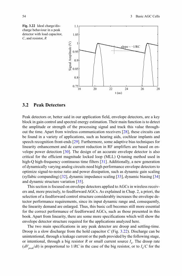
54
3.2 Peak Detectors
Peak detectors or, better said in our application field, envelope detectors, are a key block in gain control and spectral energy estimation. Their main function is to detect the amplitude or strength of the processing signal and track this value through-out the time. Apart from wireless communication receivers [28], these circuits can be found in a variety of applications, such as hearing aids, cochlear implants and speech recognition front-ends [29]. Furthermore, some adaptive bias techniques for linearity enhancement and dc current reduction in RF amplifiers are based on en-velope power detection [30]. The design of an accurate envelope detector is also critical for the efficient magnitude locked loop (MLL) Q-tuning method used in high-Q high-frequency continuous time filters [31]. Additionally, a new generation of dynamically varying analog circuits need high performance envelope detectors to optimize signal-to-noise ratio and power dissipation, such as dynamic gain scaling (syllabic companding) [32], dynamic impedance scaling [33], dynamic biasing [34] and dynamic structure variation [35].
This section is focused on envelope detectors applied to AGCs in wireless receiv-ers and, more precisely, to feedforward AGCs. As explained in Chap. 2, a priori, the selection of a feedforward control structure considerably increases the envelope de-tector performance requirements, since its input dynamic range and, consequently, the linearity demand are enlarged. Thus, this basic cell becomes still more essential for the correct performance of feedforward AGCs, such as those presented in this book. Apart from linearity, there are some more specifications which will show the envelope detector structure required for the applications analyzed here.
The two main specifications in any peak detector are droop and settling-time. Droop is a slow discharge from the hold capacitor C (Fig. 3.22). Discharge can be unintentional, through a leakage current or the path provided by the following stage, or intentional, through a big resistor R or small current source Ib. The droop rate ( dVpeak/dt) is proportional to 1/RC in the case of the big resistor, or to Ib/C for the
Fig. 3.22 Ideal charge/dis-charge behaviour in a peak detector with load capacitor, C, and resistor, R
18 20 22 24 26 280.75
0.8
0.85
0.9
0.95
1
1.05
1.1
t (us)
Sign
al A
mpl
itude
(V)
slope ~ ¯1/RC
3 Basic AGC Cells

55
small current source, since across the capacitor, I = C*( dVpeak/dt). This behaviour generates ripple at the output, so the output peak voltage deviates from the true peak value. As a consequence, droop should be reduced to increase accuracy. Settling-time is split into attack and release time. Attack-time, defined as the time required by the circuit to respond to a positive stepwise change in the input signal envelope, is dependent on the slew rate which is an indicator of the speed of the circuit. Higher slew rate offers a higher speed charging the hold capacitor. Speed is required in order to obtain a peak detector which can accurately track an increment in the input signal amplitude. The mentioned speed fixes circuit attack-time which is one of the parameters usually given to characterize peak detector speed. High speed means low attack-time. In contrast, release-time, defined as the time required to respond to a negative stepwise change in the input signal envelope, depends on the capaci-tor discharge current and the capacitor size itself. This parameter defines the peak detector capacity to track a decline in the input signal amplitude.
One of the main problems with envelope detectors is that droop and release-time are correlated. Both are controlled by the capacitance plus the current source or the load resistor. Release-time is reduced choosing smaller capacitor (or bigger discharge current) while droop is reduced with a bigger capacitor (or smaller dis-charge current) that will discharge slowly. Therefore, there is a trade-off between fast decay-time and low droop rate in peak detector design [36].
There are more specifications, such as the sensitivity of the circuit output signal to input signal impairments [37]. This error is reduced simply by integrating several cycles before generating the output. Finally, the peak detector, as well as most IC´s, can retain minimum performance specifications considering PVT variations.
The aim of delving into feedforward gain control configurations to achieve fast and accurate AGCs, requires high performance fast settling-time envelope detec-tors with high linearity. Next, different peak detector topologies will be analyzed, starting from the simplest and increasing complexity until previously introduced minimum requirements are achieved, following on to reach several peak detector topologies which are more appropriate for the studied applications.
3.2.1 Basic Peak Detector Topologies
The conventional diode-RC circuit, shown in Fig. 3.23, is the simplest structure that can work as a peak detector. In this circuit, when the input signal is above the output signal plus the diode threshold voltageVtd, the diode is equivalent to a resistor and the capacitor is charged by the current which flows from the input. On the other
Fig. 3.23 Diode-RC peak detector topology
Vin
CL
Vpeak
3.2 Peak Detectors

56
hand, when the input signal is smaller, the diode is in cut off operation region and the capacitor load is slowly discharged through the resistance. In spite of, or due to its simplicity, this circuit is not practical in present-day low voltage applications, as the diode does not allow detecting input signals with a peak voltage below Vtd. In addition, the diode threshold voltage depends on the temperature and process varia-tion, so this structure is very inaccurate.
To improve the accuracy, an op-amp can be employed in feedback configura-tion so that the diode output is connected to the op-amp negative input, as shown in Fig. 3.24 [38, 39, 40]. This op-amp and diode based peak detector reduces the threshold voltage to Vtd/A0, where A0 is the op-amp DC gain. Hence, this circuit can closely track Vin while its value is above the capacitor voltage, Vpeak. Alternatively, when the input signal is below Vpeak, the op-amp output goes to negative saturation, the diode goes to the cut-off region and the capacitor voltage is slowly discharged in the same way as previously explained. In order to minimize uncontrolled capaci-tor charge/discharge currents, a second op-amp is employed as a buffer to isolate Vpeak from the next stage. Furthermore, these unwanted currents can be completely cancelled just by employing MOSFET input devices in both op-amps. The main drawback of this circuit is that op-amp and diode based envelope detectors have a problem due to high distortion during the zero crossing of the input signal. This is because the op-amps have to recover during non-conduction/conduction transi-tion with a small finite signal dV/dt (slew rate). The envelope detector is therefore limited to a frequency performance well below the gain bandwidth product of the amplifier.
A similar topology is obtained simply by employing a source follower to perform the diode function [41, 42, 43], as shown in Fig. 3.25. Its performance is similar to that explained for the op-amp plus diode topology: while Vin exceeds Vpeak, M1 is on,
Fig. 3.24 Op-amp plus diode based peak detector topology
OA2
+OA1Vin
CL
VoutVpeak¯+
¯
Fig. 3.25 Op-amp plus source follower based peak detector topology +
¯
OA
Vin
CL
Vpeak
M1
3 Basic AGC Cells

57
which charges the capacitor C. While Vin goes below Vpeak, M1 is off and the capaci-tor holds the output peak voltage. A very small current source Ib can be included to discharge the capacitor for better tracking. However, as well as in the previous topology, this scheme also requires high slew rate and its frequency performance is limited.
3.2.2 Open-Loop Envelope Detectors. Proposed PD1 and PD2
As an alternative to closed loop schemes, a solution is to use an open-loop configu-ration [37] to achieve higher operating frequencies. This kind of circuit makes use of an OTA for voltage to current conversion followed by a precision rectifier and a current mode peak detector or a capacitor so that integration is made, see Fig. 3.26. Due to the fact that the OTA is performing the voltage to current conversion in open loop and current mode rectifiers can operate at frequencies as high as 100 MHz [44], this circuit is capable of working at higher frequencies than diode based peak detectors.
Next, we are going to evaluate several envelope detectors, all of which are suit-able for wireless LAN applications.
3.2.2.1 Proposed PD1: Conventional Open-Loop Envelope Detectors
The objective is to obtain a high performance envelope detector with a 71 MHz performance frequency and input amplitudes above 300 mV.
The precision rectifier used for this circuit is based on the configuration proposed in [44] which is shown in Fig. 3.27. This cell has been chosen due to its linearity for frequencies up to 100 MHz and input current signals above 150 µA. The bias voltage VB1 is used to bias M1 and M2 transistors to have drain currents of 2.5 µA; This bias voltage has the function of a threshold current and the rectifier does not rectify input current signals below this value. In order to overcome this limitation, an offset current is generated by the OTA with a value slightly higher than the bias current, so the signal is always above the threshold current.
As high input frequencies, direct coupling and good control of the output offset current are required, the design of the OTA is started with the fully differential ver-sion of the folded cascode OTA, see Fig. 3.28. The bias voltage VC1 controls the offset current required for the next stage and indirectly, the common-mode voltage
Fig. 3.26 Open-loop peak detector topology
OTA RECTIFIER PEAKDETECTOR
Vin¯
Vin+ RL
Vpeak+
+ ¯
¯
3.2 Peak Detectors

58
at the output of the OTA. Due to the direct coupling between the OTA and the recti-fier, the offset current biases the diode-like transistor at the input of the rectifier, while the rectifier’s input resistance fixes the common-mode voltage at the output of the OTA. This makes the common-mode feedback circuit unnecessary.
Finally, Fig. 3.29 shows the cell of the peak detector which is suitable for opera-tion up to frequencies of 100 MHz. It consists of a slow source follower composed of M3, IL, CL and the feedback transistor M1a [29, 45]. The transistor M1b outputs a copy of the current in M1a, while transistors M2a,b are introduced to obtain a higher output resistance and thus, to minimize the offset current at the output. The source follower can follow descending signals in the input voltage rapidly because of the exponential dependence of the current of M3 on its gate voltage. However, the small current IL is slow in charging capacitor CL; as a result, during ascending signals in
Fig. 3.28 Schematic diagram of the mirrored cascode OTA
VDD
VSS
Vin¯Vin+
VBP
VC1 VC1
VBN
Iout+ Iout¯
+
¯
M4 M4
M2
M1 M1
M5
M3 M3
M2 M5
RDIN2
IN1
IP+
¯
VDD
Iin+ Iin¯
M1 M1
M4
M2 M2
M3
Iout
VB1
VB3
VB2
Ibias
Fig. 3.27 Schematic diagram of the full-wave precision rectifier block
3 Basic AGC Cells

59
the input, the output signal is slow to respond as discharge slope is proportional to CL/IL. In consequence, the ripple and time constant, τ, are controlled by IL and CL.
This circuit was first simulated and next fabricated in AMS 0.35 μm CMOS technology. All the blocks are powered with a single power supply of 3.3 V. Transis-tors sizes are shown in Table 3.6. Bias current, Ibias, in rectifier and in peak detector are 100 and 20 μA, respectively. IL is 1 μA, while IN1, IN2 and IP are 300, 200 and 500 μA, respectively. Finally, RD is 2.8 kΩ and CL is 1 pF. Chip photograph is shown in Fig. 3.30. Measurements were realized employing a PCB and a 500 MHz band-width oscilloscope (for further information see Appendix A). The first parameter measured was the linearity of the circuit shown in Fig. 3.31 for input sinusoidal signals at 71 MHz. The simulated result was up to 33 dB range for ±1 dB linearity, while the measurement offered quite a close value with 29 dB range.
Next, the other two principal parameters were measured: ripple and settling-time. In this case a square signal was employed at 500 kHz with a predefined offset so that the input signal was equivalent to a 20 dB stepwise signal. Results are shown in Fig. 3.32. Simulated release-time was around 0.15 μs, but 0.6 μs was measured. The same happens with attack-time where the measured time has a similar value to the release-time. There is an easy explanation for these discordances. As mentioned, the attack-time of the presented peak detector should be incredibly fast due to the exponential behaviour of the current in transistor M3. On the other hand, release-
Fig. 3.29 Schematic diagram of the peak detector block
M1a
M2a
M1b
M2b
M3
VDD
VSS
VBP
CLIL
Ibias Ibias
Iin Iout
W/L (μm/μm)Rectifier OTA PD
M1 2/0.4 100/0.4 20/0.8M2 2/0.4 90/2 5/0.4M3 30/2 150/2 20/0.4M4 5/0.4 40/0.4 –M5 – 60/2 –
Table 3.6 PD1 devices sizes
3.2 Peak Detectors

60
Fig. 3.31 Measured and ideal linearity performance
0 200 400 600 800 10000
100
200
300
400
500
600
700
800
900
Input signal (Vp-p)
Out
put s
igna
l (V
)
y = 0.763*x + 80.6
IdealMeasured
Fig. 3.32 Measured tracking ( solidgreyline) of the open-loop envelope detectors for a 500 kHz square signal ( solidblackline) and simulation results ( dashedgreyline) for a 71 MHz sinusoidal signal with a stepwise change ( dashedblackline)
0 0.2 0.4 0.6 0.8 1 1.2 1.4 1.6 1.8 2
x 10¯6
¯0.5¯0.4¯0.3¯0.2¯0.1
0
0.1
0.2
0.3
0.4
0.5
t (s)
Det
ecto
r Sig
nals
(V)
Fig. 3.30 Chip photograph of the peak detector PD1
µ
µ
3 Basic AGC Cells

61
time is slow as it depends on the relation between CL and IL. Furthermore, as simu-lated parasitic capacitances (~ 7 pF) between the chip and the PCB did not degrade the circuit performance considerably, simple buffers were kept. However, the only explanation to obtain similar settling-times in both cases is that larger parasitic ca-pacitances than expected have degraded the performance at the output.
Droop was also measured with the oscilloscope and the measured peak-to-peak ripple went up to 15 mV. A discordance appeared again as simulations had predicted a ripple of 2.5 mV. Noise, low oscilloscope accuracy for small signals and PVT variations are possible responses to this issue. However, the lack of accuracy in set-tling-time measurements prevents it from being solved by making use of the known relation between both performances. Finally, a summary of circuit characteristics is given in Table 3.7 for simulation and measurement.
A structure based on the high performance envelope detector topology presented here but scaled for a 10 MHz performance frequency application was also imple-mented in order to compare it with other peak detectors that will be introduced next.
This scheme suffers from the same limitation as all the topologies introduced in Figs. 3.23, 3.24 and 3.25: the trade off between droop and settling-time that makes necessary the use of filters at the output to minimize the ripple of the envelope at the cost of higher area and power consumption. Next, a novel envelope detector, pro-posed in [46, 47], is developed. Then, this circuit is modified so that it overcomes the traditional trade-off present in these circuits, thus improving both the droop and the settling-time of the circuit.
3.2.2.2 Proposed PD2: Fast-Settling Open-Loop Envelope Detector
Figure 3.33 shows the conceptual scheme of the newly proposed envelope detector. As can be seen, the circuit makes use of two peak detectors working in parallel. However, it is then shown that it is unnecessary to duplicate all the circuit; in fact, no more than a part of the peak hold circuit is duplicated, as will be shown later.
In order to obtain the modified circuit, peak holders are employed instead of the peak detector to achieve a smaller ripple. The switches at the peak holders and the output are managed by a square signal provided by two control circuits. The control path changes the phase of the input signal by 90º before generating the digital signal by a few inverters. Thus, the peak holder is in hold mode just when the signal has reached its maximum value. This allows us to employ smaller load capacitance
Design Simulation MeasurementsSupply voltage (V) 3.3 3.3Power (mW) 6.1 6.1Performance frequency (MHz) 71 71Settling time (−20 dB step) (µs) 0.15 0.6Ripple ( Vin = 440 mVp–p) (mVp–p) 2.5 15Linearity range (±10%) (dB) ∼33 ∼ 29
Table 3.7 Comparison of principal characteristics for simulation and measure-ments of the open-loop peak detector
3.2 Peak Detectors

62
without spoiling the DC level obtained during the hold mode. To obtain the enve-lope of the signal, two peak holders work in parallel, one of them always providing a signal in hold mode at the output.
The OTA and the rectifier are the same ones used for the basic topology. The following introduces the control path and the peak hold circuit shown in Fig. 3.33:
Figure 3.34 shows the proposed peak hold block. Note that the advantage of using current mirrors in Fig. 3.29 makes it unnecessary to duplicate all the cir-cuit to obtain two peak holders. Both circuits work with the same discharge path during different periods: when the first peak holder is in hold mode the second is discharging and vice versa, Fig. 3.35 clarifies this. In red and black is shown the performance of each half peak holder. The envelope of the signal is obtained by switching between both halves and transmitting to the output only the hold signal. VC1 and VC2 are the signals provided by the control path and manage the switches of the peak holds.
Fig. 3.33 Fast-settling open-loop envelope detector block diagram
Vin¯
Vin+
CONTROL ¯
CONTROL +
PEAKHOLDER
Vout
RL
RL
RECTIFIEROTA
CO
+
+ ¯
¯
Fig. 3.34 Schematic of the peak hold block
3 Basic AGC Cells

63
The power consumption is increased by 50% at this stage. However, we must remember that over 90% of the power consumption of the complete circuit is due to the OTA and in consequence, this increase is insignificant. Furthermore, two capacitances are employed instead of one, but the total capacitance is much smaller than the original. On the other hand, this configuration has a great advantage: the release time constant is given by CL and IL, while the ripple depends on CL and the equivalent resistance of the switches when working in subthreshold. This resistance is very high and offers the possibility of using much smaller capacitances, besides obtaining smaller ripple.
The control path consists of a passive RC-differentiator followed by a few in-verters as shown Fig. 3.36. The major problem of this stage is that after deriving the input signal to obtain a phase delay of 90º it is necessary to amplify the signal by the inverters to obtain a signal capable of managing the switches. In consequence, noise is also amplified and dynamic range is reduced. To minimize this effect, instead of a
Fig. 3.35 Envelope detector operation. Peak holder both output signals ( greyandblack) and input signal (--) ( up). Below VC1 control signal
0.2 0.3 0.4 0.5 0.6 0.7 0.8 0.9 1¯0.2
¯0.1
0
0.1
0.2
t (us)
Am
plitu
de (V
)
0.2 0.3 0.4 0.5 0.6 0.7 0.8 0.9 1¯2
¯1
0
1
2
t (us)
Clo
ck (V
)
Fig. 3.36 Schematic diagram of the control path
RC
CCVin Vout
VDD
VSS
3.2 Peak Detectors

64
fourth inverter, two control paths are employed and a capacitance, CO, is connected at the output (see Fig. 3.33) working as a first-order low-pass filter, thus providing a signal-to-noise ratio (SNR) not less than 60 dB. The need for a capacitance at the output could be considered a setback; nevertheless the total silicon area in this circuit is much smaller than that needed in the conventional counterpart of PD1 for 10 MHz and tracking is still much faster, as we will see.
To verify the circuit performance, SPECTRE is used to simulate the proposed circuit using the AMS 0.35 µm technology. The proposed envelope detector has been designed with the following component values: Transistors W/L relations are M1 = 20/0.8, M2 = 5/0.4, M3 = 20/0.4, Ibias = 20 µA, CL = 0.6 pF, CC = 0.1 pF and CO = 1.6 pF; while IL = 1 µA, RC = 10 kΩ and RL = 2 kΩ. The obtained rip-ple is around 0.3% when Vin = 300 mV for a total capacitance CT = 3.2 pF. On the other hand, if we use an equivalent capacitance area at the conventional circuit, i.e. CL = 3.2 pF, the minimum ripple to be reached is around 3%, as depicted in Fig. 3.37, and if we use the same IL to obtain a similar release-time, then ripple is ten times that percentage. In order to compare the release time constant, the ripple is fixed at around 1%; In this case, the conventional circuit needs a huge load capaci-tance of 10 pF while the proposed circuit maintains previous values. A stepwise sig-nal at 10 MHz is employed in both circuits, which descends abruptly from a peak of 300 to 30 mV; results are shown in Fig. 3.38. As can be seen, the proposed circuit is much faster tracking the signal than the conventional one and in addition, it is pos-sible to configure the desired release time constant by IL without changing the ripple of the envelope. The release-time constants, τ, defined as the time required by the signal to respond to 99% of a 20 dB stepwise change, are in this case τ = 27.5 µs for the conventional circuit and = 0.4 µs for the proposed circuit. Figure 3.39 shows DC and 10 MHz transfer characteristic.
As seen, both envelope detectors are linear for amplitudes up to 300 mV. The proposed envelope detector obtains lower amplitude at high frequency since there is a gap between the input signal and the control path signal and the hold mode starts
Fig. 3.37 Ripple of the conventional (--) and the proposed (―) envelope detectors for an input voltage of 300 mV at 10 MHz and a total capacitance of 3.2 pF
4 4.5 5 5.5 6
x 10¯6
0.286
0.288
0.29
0.292
0.294
0.296
0.298
0.3
0.302
0.304
t (s)
Det
ecto
r Vou
t (V
)
PD1 10MHz
PD2
3 Basic AGC Cells

65
just after the signal has reached its maximum. However, this gap can be minimized with careful phase matching of both signals.
Table 3.8 summarizes the main characteristics of both envelope detectors. The proposed envelope detector has 17% higher power consumption. However, in re-turn, it obtains much better performance in keeping and tracking at the same time. This leads to simplifying the circuits required after the detector, and obtaining a faster circuit. Moreover, the capacitance area needed to obtain the same ripple is for this configuration a third of that needed by the conventional circuit.
Fig. 3.38 Tracking of (--) ideal, (-.) conventional and (―) proposed envelope detectors for a step signal at 10 MHz and ripple of 1%
0 0.5 1 1.5 2 2.5 3 3.5
x 10¯5
0
0.05
0.1
0.15
0.2
0.25
0.3
0.35
t (s)
Det
ecto
r Sig
nals
(Vpk
)
PD1 for 10MHz
PD2
Conventional circuit
Proposed circuit
Ripple (CT = 3.2 pF) (%) 3 0.3 (99%) (ripple 1%) (µs) 27.5 0.4Power consumption (mW) 2.13 2.49
Table 3.8 Comparison summary between PD1 and PD2 for 10 MHz
0 0.1 0.2 0.3 0.4 0.50
0.05
0.1
0.15
0.2
0.25
0.3
0.35
0.4
Vou
t RM
S (V
rms)
Vin (Vpk)
PD2 (10MHz)PD2 (DC)PD1 (DC)PD1 (10MHz)
Fig. 3.39 DC (o) and 10 MHz (-) transfer charac-teristic for the conventional and the proposed envelope detector
3.2 Peak Detectors

66
3.2.3 Closed-Loop Envelope Detectors. Proposed PD3 and PD4
Although open-loop configuration is a proven solution for achieving higher perfor-mance operation frequency, closed-loop topologies can still offer similar frequen-cies with the advantages that the higher linearity closed-loop configurations offer inherently. The op-amp/diode topology of Fig. 3.24 can be replaced by a transcon-ductor plus a current mirror (M1 and M2) structure [48, 49], as shown in Fig. 3.40. When Vpeak < Vin and the capacitor is being charged, the behaviour of this circuit is ideally described by:
(3.22)
or
(3.23)
where it is shown that the tracking behaviour of the peak detector can be improved just by increasing Gm/CL, instead of the slew-rate in the op-amp/diode topology. The advantage in this case is that higher values can be obtained for transconductance simply by using Gm-boosted transconductors. On the other hand, when Vpeak>Vin, since the current mirror is unidirectional it can not discharge the load capacitor and CL is slowly discharged byIL following these expressions:
(3.24)
where, since IL is a constant current, the capacitor discharge is linear with IL/CL:
(3.25)
IL + Gm(Vpeak − Vin) = −CL
dVpeak
dt
dVpeak
dt+
Gm
CL
Vpeak =Gm
CL
Vin −IL
CL
,
dVpeak (t) =dQ (t)
CL
=IL
CL
dt ,
Vpeak(t) = Vpeak(0) −IL
CL
t.
Fig. 3.40 OTA plus current mirror closed-loop topology
+
¯OTA
Vin
CL
Vpeak
M1 M2
3 Basic AGC Cells

67
As a result, peak detector settling time increases with the detected input signal am-plitude and it must be calculated for the worst case, i.e. the maximum possible amplitude.
3.2.3.1 Proposed PD3: High-Gm Transconductor/Current Mirror Based PD
The peak detector structure is a differential positive scheme where one detector is employed for each balanced signal, adding both signals at a single output. The schematic is shown in Fig. 3.41, specifying transistor sizes, component values and biasing conditions.
Rather than using a simple transconductor as in [48, 49], we employ a high performance Gm-cell based on the same core cell as the PGA proposed in [34]. In this way, with a very compact design, the peak detector exhibits higher linearity at higher frequencies with lower power consumption [50].
The aforementioned positive envelope detector has been designed in AMS 0.35 µm CMOS technology and simulated using SPECTRE with a BSIM3v3.2 level 53 transistor model. The circuit linearity and frequency response were tested introducing differential signals from 40 to 400 mVp-p at 100 MHz. The input-output performance with sinusoidal input for the implemented envelope detector is given in Fig. 3.42. It is found that deviations from ideal behaviour are below ± 0.5 dB for all the input range. Next, the convergence of the circuit is tested introducing a 21 dB stepwise signal. To measure the attack-time, the input signal is increased by 21 dB, and the detector converges in less than 40 ns. On the other hand, to measure the release-time the input signal is reduced. The result for the latter is shown in Fig. 3.43. The worst case settling-time is no more than 0.25 µs.
This circuit presents, due to the employed Gm-boosted transconductor cell, a highly linear envelope detector. Furthermore, as a result of employing this trans-conductor cell, it is also suitable for Very High Frequency (VHF) applications. Fi-nally, release-time is, as expected, the same achieved by any conventional envelope detector.
Fig. 3.41 Schematic of a high-Gm OTA/current mirror based peak detector
Vin¯Vin+
CL CLIL
Vout
1.8 V
M1
M2M2 M3
M4 M5 M5 M4
M1
M2 M2M3
M1M1
IB IB80uA
5/0.5
3/0.35 3/0.35
5/0.4
5/0.4
0.5uA1.5pF
IB IB IB IB
3.2 Peak Detectors

68
In the same way as made for PD1, it is possible to design a fast-settling enve-lope detector based on the topology of PD3. This time, the new version, which is presented next, is part of the AGC proposed in [51], targeting specifically an IEEE 802.11a 5-GHz WLAN receiver application. It is implemented in SiGe technology in order to raise the range of study of this work. This technology offers advantages such as higher transconductance and consequently, higher linearity and speed, but also has some disadvantages such as the leakage current due to gate current.
3.2.3.2 Proposed PD4: Fast-Settling OTA/Current Mirror PD
As well as the topology PD3 presented, the basic PD4 cell is a differential positive peak detector where, instead of a diode, a unidirectional current mirror is employed
Fig. 3.43 Peak detector convergence performance for an input sinusoidal 100 MHz stepwise signal
0.2 0.3 0.4 0.5 0.6 0.7 0.8 0.9 1
–0.2
–0.1
0
0.1
0.2
0.3
t (us)
Inpu
t & O
utPD
(V)
Fig. 3.42 Peak detector input-output performance
0.05 0.1 0.15 0.2 0.25 0.3 0.35 0.40.01
0.02
0.03
0.04
0.05
0.06
0.07
0.08
0.09
Vin,p-p (V)
Vou
t (V
)
IdealSimulated
3 Basic AGC Cells

69
together with a transconductor to implement the rectifier. A significant difference is the use of source followers as buffers in order to avoid bipolar transistor base cur-rent discharging the load capacitors. Furthermore, the circuit is split into two parts. Half cell is employed to detect the positive peak of each balanced signal, V1±, and the hold value of both peaks is transmitted to the output sequentially, see Fig. 3.44. The detector makes use of switches, S1-4, so a track and hold behaviour is obtained. This characteristic allows us to employ smaller load capacitance without spoiling the DC level obtained during the hold mode. The switches are managed by a digital control signal generated by a few D flip-flops and logic gates from a single 5 MHz clock provided by the receiver.
The performance of each side of the circuit can be split into three different states, depending on the position of the switches and two symbols, where a symbol is de-fined as a period of time fixed by the control signal (0.4 μs in this case). Thus, it is composed of several input signal cycles. The states are: the tracking state, which requires one full symbol, and the hold and discharge states, which together take another symbol. During the first symbol in the left side detector, switches S1,3 are “off” and the left side load capacitor is charged with the positive input signal; this is called tracking state. At the beginning of the second symbol, hold state starts and S3 is closed so that the peak detected during previous period is transmitted to the output. In the last state named discharge, S1 is closed and S3 is opened, so that the rest of the second symbol is employed to discharge the load capacitor, CL, through current IL. This performance is successively repeated during the following symbols. The right side of the detector works equivalently, but employing the even symbols for tracking state and odd symbols for hold and discharge. Thus, this technique employs half circuit to detect the peak during odd symbols and the second one for even symbols. The advantage of considering symbols is that this way, this topology is also suitable for more complex modulated signals such as orthogonal frequency division multiplexing (OFDM).
The envelope detector was designed, like the AGC, in a low-cost 0.25 μm 75 GHz SiGe BiCMOS process. It employs a single supply voltage of 2.5 V and has a total current consumption of 220 μA.. The photograph of the integrated detec-tor is shown in Fig. 3.45. The linearity performance is depicted in Fig. 3.46 for a
Fig. 3.44 Schematic of the fast-settling OTA/current mirror PD
3.2 Peak Detectors

70
20 MHz sinusoidal input signal. It can be seen that a 20 dB range with nonlinearities below ± 0.5 dB is offered at least. The settling-time of the envelope detector was measured with a 20 MHz input sinusoidal signal modulated by a 400 kHz square signal. The result is shown in Fig. 3.47. Due to the awful modulation, release-time only can be measured, but the step response of the discharge is clear and the fast discharge is shown clearly setting in 1 μs.
3.2.4 S/H Based Envelope Detector. Proposed PD5
Many different envelope detector topologies have already been analyzed. However, they are all based on some kind of rectification and integration. In fact, track and hold based topologies are no more than a mix between sample and hold circuits and peak detectors. Therefore, it will be shown next how theoretically a basic sample and hold (S/H) circuit, where switches are controlled properly, can also be em-ployed to track the envelope of a signal.
Fig. 3.46 Measured and ideal input-output performance
0 50 100 150 200 250 300 350 400 450-300
¯250
¯200
¯150
¯100
¯50
0
Vin+ (mVp-p)
Peak
Det
ecto
r Out
put (
mV
)
y = 0.495*x - 250
Measuredlinear
Fig. 3.45 Chip photograph
70 µm
440 µm
C1
PMOS Transistors
BuffersCurrent Bias
Bio. Diff. pair
3 Basic AGC Cells

71
3.2.4.1 Proposed PD5: S/H Based Envelope Detector
The conceptual scheme of the topology presented next is shown in Fig. 3.48 [52]. In fact, this topology is almost the same as that offered in Fig. 3.33 for PD2. As well
Fig. 3.47 Simulated ( up) and measured ( down) convergence performance with a 20 MHz input sinusoidal signal modulated by a 400 kHz square signal
3.2 Peak Detectors

72
as in the mentioned detector, to obtain the envelope of the signal, two peak hold circuits work in parallel, one of them always providing a signal in hold mode at the output. The switches at the peak holder and the output are managed by a square signal provided by a control circuit. The control path changes the phase of the input signal by 90º before generating the digital signal by a few inverters (see Fig. 3.49). Thus, the peak holder is in hold mode just when the signal has reached its maxi-mum value. This allows us to employ smaller load capacitance without spoiling the DC level obtained during the hold mode. The change in the phase can be made in several ways. In this case, amplitude-shift keying (ASK) or amplitude modulation (AM) applications are targeted, so for a constant frequency input signal, a simple RC differentiator can be used. The control circuit is to be adapted to the application or signal modulation required in the circuit. For example, in the case of applications where frequency modulation must be adopted, a simple RC differentiator would not be accurate enough and an RC-CR circuit could be used for input and control signals since it offers ideally both outputs with a 90º phase shift over the whole frequency range.
The main change comes in the employed peak holder block. Its schematic is shown in Fig. 3.50. The OTA, a telescopic OTA with cascode compensation, is that shown in Fig. 3.51. One of the reasons for using this basic sample and hold scheme is that it was specially designed to overcome certain drawbacks due to non-ideal effects associated with the use of switches in sample and hold circuits, which limit its dynamic range. These effects are capacitive feedthrough and, mainly, charge injection.
Fig. 3.48 S/H based detector conceptual scheme
Fig. 3.49 Schematic of the control block
RC
CCVin
S+
VDD
VSS
S¯
3 Basic AGC Cells

73
To understand charge injection, consider a MOS switch followed by a load ca-pacitor. When the MOS switch is on, there is a charge under the gate oxide result-ing from the inverted channel. When the switch is turned off, part of this charge is injected into the load capacitor which results in a change of voltage across it [53]. This change in voltage is nonlinear with respect to the input signal and consequently
Fig. 3.50 Schematic diagram of the peak holder
VG2
VG2
VG1
VG1
R2
R1
R2
S+
S+
CL
CL
OTAS
¯
S¯
Vout+
Vout¯
Vin+
Vin¯
¯
+
+
¯
Fig. 3.51 Schematic diagram of the telescopic OTA
VDD
Vb3
Vb2
Vb1
Vb0
VSS
V0+
+Vin/2 ¯Vin/2
Co Co Vo¯
M12 M8M7
M5
M10
MC1 MC2 MC3
M1 4
MC4
M11
M13
M6
M3 M4
M1
M9
M2
3.2 Peak Detectors

74
makes the envelope detector nonlinear with respect to the input signal. The change in load voltage is given by:
(3.26)
where the threshold voltage, VTH, is a nonlinear function of Vin:
(3.27)
The advantage of this circuit is that both sides of the switch are at virtual ground and the change in voltage is no longer dependent on the threshold voltage of the switch itself. Therefore, the charge injection will be independent of the input signal and will result as a simple offset at the output [53]. When sampling, V– is closed and V+ is opened, and the equivalent circuit is a low-pass filter with buffered input and an approximated transfer function given by.
(3.28)
Once the hold mode starts, the output will stay constant at a value equal to the in-put signal. In our case, R2C1 is chosen small to obtain a fast-settling circuit. Thus, capacitor area is saved and ripple is kept low since discharge is controlled by the equivalent resistance of the switches when turned-off.
A MOS transistor is employed in parallel with resistances R1 and R2. As a result, it is possible to control the total gain of the circuit with small variations of their gate voltages. This is very useful if we need to compensate for the gain factor that appears when envelope is detected in this circuit. In our particular design, gain was fixed so the relation between input signal amplitude and output signal root-mean-square was equal to one.
Mismatching between both peak holders introduces a time varying DC offset in the output. However, since cross-coupling outputs are employed, this offset is the same in both outputs so it is cancelled when the differential output is considered. On the other hand, if we introduce a dc offset in the input, the balanced output does not cancel it and the performance of the detector is degraded. However, this circuit shall be considered part of a complete automatic gain control circuit where a DC offset cancellation circuit is employed, so this problem can be overlooked [49].
To verify the circuit performance, SPECTRE is used to simulate the proposed circuit using the AMS 0.35 μm technology. The proposed envelope detector has been designed with the following component values: C1 = 0.3 pF and CC = 0.1 pF; while RC = 10 kΩ and R1,2 = 6 kΩ. Transistor sizes are shown in Table 3.9. Further-more, each OTA requires two compensation capacitors of CO = 0.5 pF considering load capacitors of 1.6 pF. These loads together with switch transistors are employed as a simple first order low pass loop filter. Thus, the ripple is around 0.3% when
Vload = −C ′
oxWL(VDD − Vin − VT H )
2Cload
,
VT H = VT H0 + γ
(√∣∣2Vfp
∣∣ + Vin −√∣∣2Vfp
∣∣)
.
vout
vin
= −R2
R1
1
(sR2C1 + 1).
3 Basic AGC Cells

75
Vin = 300 mV for a total capacitance CTotal = 3.3 pF. In order to check the release time constant, a 10 MHz sinusoidal signal is employed, where the amplitude descends abruptly from a peak of 300 to 30 mV. The result is shown in Fig. 3.52 and com-pared with the topology of PD1 for 10 MHz modified to obtain the same ripple with the same input signal.
As can be seen, the proposed circuit is much faster at tracking the signal than PD1, in the same way as with PD2 in Fig. 3.38. The release time constants, τ, de-fined as the time required by the signal to respond to 99% of a stepwise change, is τ = 0.4 µs. The operation of the envelope detector can be understood in the same way as explained previously for PD2 and shown in Fig. 3.35.
Figure 3.53 shows the circuit performance for a frequency modulated signal. Since the phase shift between the input and the control signal varies between 90 and 85º, the peak detection varies slightly for different frequencies, increasing ripple. However, as mentioned, this problem could be solved by employing an RC-CR circuit which would maintain a constant phase shift of 90º for the whole frequency range. Furthermore, we have to consider that typical frequency modulated signals variations are into a small frequency range around the IF frequency, so the differ-ences in the phase shift will usually be negligible.
Fig. 3.52 Tracking of ideal (--), conventional (-.) and proposed () envelope detectors for a step signal at 10 MHz and ripple of 1%
0 0.5 1 1.5 2 2.5 3 3.5
x 10¯5
0
0.05
0.1
0.15
0.2
0.25
0.3
0.35
t (s)
Vin
(Vpk
)
Ideal
PD1 for 10MHz
PD5
W/L (μm/μm)M1,2 4/0.4M3,4 18/0.4M5,6 4/0.4M7,8 10/1.2M9 11.6/0.4M10,11 90/0.4M12,13 30/1.2M14 30/0.4MC1,2 1.9/0.4MC3,4 5/0.4
Table 3.9 PD5 transistor sizes
3.2 Peak Detectors

76
Although the performance obtained in keeping and tracking is similar to that ob-tained by the fast-settling envelope detector PD2, in this case the linearity is 20 dB higher. Figure 3.54 shows the 10 MHz transfer characteristic for the envelope detec-tors PD1, PD2 and PD5. In fact, linearity could be further improved, bettering gain and frequency behaviour in the control circuit, since the nonlinearity at low voltage seems to be due to the fact that the input voltage is employed to manage switches.
In return for the increase in circuit complexity and consumption, this envelope detector offers high performance characteristics: much smaller release time con-stant, smaller ripple independent of the discharge resistor, higher linearity and con-sequently, higher dynamic range.
3.2.5 Conclusions
To end this section, Table 3.10 summarizes the principal characteristics of evaluated envelope detectors. They all have high performance characteristics and are suitable
Fig. 3.54 10 MHz input out-put performance for different envelope detectors
Fig. 3.53 Envelope detection of a frequency modulated input signal
0 2 4 6 8 10¯0.2
¯0.15¯0.1
¯0.05
0
0.05
0.1
0.15
0.2
t (us)
Am
plitu
de (V
)
3 Basic AGC Cells

77
Tabl
e 3.
10 C
ompa
rison
of p
ropo
sed
enve
lope
det
ecto
rsD
esig
nPD
1PD
1 (b
)PD
2PD
3PD
4PD
5Te
chno
logy
CM
OS
0.35
µm
CM
OS
0.35
µm
CM
OS
0.35
µm
CM
OS
0.35
µm
SiG
e B
iCM
OS
CM
OS
0.35
µm
Supp
ly v
olta
ge (V
)3.
33.
33.
31.
82.
53.
3Po
wer
(mW
)6.
12.
132.
490.
864
0.55
2.98
+ 1
.37a
Perf
orm
ance
freq
. (M
Hz)
711 ∼
101 ∼
1010
00.
3 ∼ 20
1 ∼ 10
Fast
-set
tling
tech
niqu
eN
oN
oYe
sN
oYe
sYe
sC
apac
itanc
e (p
F)1
103.
33
3.5
3.3
Settl
ing
time
(− 20
dB
step
) (µs
)0.
627
.50.
40.
251
0.4
Rip
ple
(Vin
= 4
40 m
Vpp
)15
mV
pp0.
3%0.
3%–
–0.
3%Li
near
ity ra
nge
(± 1
dB) (
dB)
∼ 29
3022
> 21
> 20
42a P
ower
con
sum
ptio
n du
e to
out
put b
uffe
r
3.2 Peak Detectors

78
for wireless LAN applications as will be shown in Chap. 4 for some of them. A wide range of performance frequencies has been considered, from 0.3 to 100 MHz. High linearity detectors have also been obtained, always above 20 dB, which is appropri-ate for feedforward AGC configuration. Moreover, new fast-settling configurations have been presented, which achieve very low release time and ripple at the same time, so a theoretical trade-off of these circuits has been overcome. Finally, the validity of one of the proposed topologies in a SiGe BiCMOS technology has been verified, so the range of applications has been extended to this technology market.
3.3 Control Voltage Generation Circuit
The control voltage generator must take the output signal from the peak detector and after comparing it with a reference signal, generate the control signal VC re-quired to adjust the gain in the VGA. The way it was explained in Sect. 2.1, multiple choices exist to generate this control signal. Furthermore, feedforward and feedback AGCs require different solutions, the feedback loop being more restrictive in the VC generation function required, while in the feedforward loop, accuracy is mandatory.
Therefore, the main objective of this circuit is to generate a signal function of a reference voltage VREF and the input (or output) amplitude, depending on which loop topology is employed), such as
(3.29)
so
(3.30)
where fand g functions correspond to the VC generator block and VGA block re-spectively. As indicated in (3.29) and (3.30), functions f and g are correlated and thus, a different solution, f, will be required for each different VGA function g, so AOUT is constant.
In this section, first, two main groups will be differentiated, namely digital and analog VC generators corresponding each one to one of the VGA main topologies: (i) programmable gain amplifiers and (ii) continuously variable gain amplifiers. In both digital and analog subsections, different solutions will be offered.
3.3.1 Digital Control
Digital control approach groups mainly two options. First topology is that where the AGC loop is fully implemented inside the DSP [54]. This option requires a dif-ferent type of work completely oriented to digital designers, so it will not be gone into here as we understand it is beyond the aims of this book. The second option,
VC = f (AIN/OUT , VREF ),
AOUT = g(AIN , VC) = g(AIN , f (AIN/OUT , VREF )) ≈ constant,
3 Basic AGC Cells

79
however, takes the output of the peak detector and, making use of a simple digital block, generates the digital word required to manage the PGA [55]. Thus, the latter option inside mixed-signal design is considered in this book.
Many different digital solutions are available to control more or less efficiently the PGA gain. However, usually PGAs of 10–20 dB gain range per stage are enough in wireless applications and 2–3 dB gain steps are also acceptable. Therefore, the most common solution is a simple comparator bank ADC [56, 57], as shown in Fig. 3.55.
3.3.2 Analog Control
Analog control is much more complicated to implement than digital. However, some applications require smooth gain variation and thus, analog solutions can pro-vide the key. The main solutions are those analytically presented in Sect. 2.1. Since, for each VGA case employed a different analog control is required and it is not pos-sible to offer an implementation of all the possibilities in this work. However, sev-eral solutions will be considered which could fit the VGAs presented in Sect. 3.1. Then, the generalization will be analytically explained in Sect. 2.1.
VGA1 is fully programmable and in spite of it being possible to obtain a con-tinuous gain variation using active resistors, the gain dependency would again be linear in the best case, so it offers nothing new. VGA2 is the one which offers more control options, already presented in Sect. 3.1, due to its linear dependency of gain with the control voltage. Finally, VGA3, which proposes a mixed, analog/digital, gain adjustment, presents a complex gain variation response to its control voltage, which could be considered linear at first order. Thus, VGA2 is the best candidate of
Fig. 3.55 Comparator bank cell employed in [57]
a0
Vpeak
a1
a2
Vref +VCM
VCM
Comp
Comp
Comp
¯
+
¯
+
¯
+
3.3 Control Voltage Generation Circuit

80
all to make a study of different linear VC generation circuits for both feedforward and feedback. Other options exist in the literature, the most common being the linear in dB VGA. However, VGA2 can also be employed as a linear-in-dB VGA just by introducing an exponential block to generate VC and considering the input to this block the real control voltage. Finally, VGAs with general gain functions can also be considered [58, 59], but these cases require the generation of the opposite function, which usually involves another feedback loop inside the AGC loop. In feedback AGCs the use of another internal loop can greatly complicate the stability of the system or force making a considerable reduction in the bandwidth of the feed-back loop in order to make it much slower than the internal loop. This goes against the aims of this book of studying AGCs with a fast convergence. Alternatively, in feedforward AGCs the introduction of a new feedback loop in the AGC loop does not cause more stability complications than those inherent to the loop itself. How-ever, it does go against obtaining a fast convergence. Thus, the use of these general gain function VGAs has also been ruled out. The control voltage required by VGA2 to accomplish (3.30), is simply:
(3.31)
where k is a constant, Vref is the desired output voltage and Vpd is the signal provided by the peak detector.
The most common analog control voltage generation circuit is based on the ex-ponential solution used to obtain a time-constant independent of bias signals in feedback loop AGCs. In these loops, it is the option of employing the exponential converter at the end of the loop alone or with a logarithmic converter just after the peak detector. The generation of both converters is feasible in BiCMOS technology due to the exponential behaviour of the bipolar transistors. However, in CMOS technology this task is much harder, since transistors present a quadratic current response (characteristics of both technologies are exposed in Appendix D). Several solutions exist in the literature for the CMOS exp-converter [60–64] or exponential VGAs [65, 66] employing pseudo-exponential functions that make the task easier. On the other hand, there are no simple solutions for the log-converter. Thus, for the latter case the need is to make use of a piece-wise linear approximation to the logarithm function, see Fig. 3.56. As explained in [67], this method consists of us-ing many small linear functions combined together to approximate the logarithmic function. Another option is to try implementing it by using previously mentioned exponential solutions in a feedback loop as shown in Fig. 3.57. The logarithm func-tion in the latter case is approximated when amplifier gain, A0, is much bigger than one only. From Fig. 3.57 we have: z = A0( x − y), y = ez. As mentioned if A0 >> 1, x ≈ y, x ≈ ez, and consequently z ≈ log( x).
Both cases cause complications in the AGC loop so in feedback loop the ap-proach is usually preferable where a log-converter is avoided.
Unfortunately, feedforward loop has no possibility of avoiding the use of the log-converter without accepting the loss of accuracy, since the relation between
vC = k
(Vref
Vpd
).
3 Basic AGC Cells

81
the control voltage function and the VGA gain function must be exact. Thus, it is mandatory to generate a circuit with a logarithmic response, employing one of the solutions proposed in Figs 3.56 and 3.57. The latter solution would be preferable for small input dynamic range AGCs, while piece-wise linear approximation is a better option for a higher dynamic range.
Apart from the exponential VC generator, feedforward AGC´s accept another straightforward solution. To achieve output amplitude as shown in (3.31), when using a linear multiplier, the logical solution would be to use a divider. Even if the implementation of an accurate divider in both CMOS and BiCMOS technologies can be as laborious as implementing an exponential circuit, when small dynamic range is required, simple dividers based on MOS transistors operating in triode re-gion, as shown in Fig. 3.58, can be an acceptable solution. In this case, M2 operates in triode region so
(3.32)
where K and VTH are M2 transistor transconductance constant and threshold voltage, respectively. Thus, a division relation is obtained between the two inputs, I0 and VX .
Dividers based on this simple technique can be found in several works in the lit-erature and they have been employed in the implementation of pseudo-exponential circuits [64] for example. Higher accuracy and dynamic range can be obtained em-
Vout ≈I0
K(VX − VT H ),
Fig. 3.56 Piece-wise linear approximation based logarithmic amplifier
Vpd
Log(Vpd)
Lim(Vout)
Fig. 3.57 Circuit to imple-ment inverse of exponential function
Exp
Vpd
AmpLog(Vpd)
x
yz
¯
+
3.3 Control Voltage Generation Circuit

82
ploying more complex circuits; however, the study of this possible solution is left for future work.
3.3.3 Conclusions
In conclusion, each VGA can require a different solution, although, for example in feedback AGCs, the same exponential type solution is preferred among designers in the end, while in feedforward AGCs, PGAs and digital control are usually em-ployed. The next chapter introduces some proposals of control voltage generators explained in this section in general terms as part of the full AGCs proposed in the book.
References
1. C. Toumazou, F. J. Lidgey, and D. G. Haigh, Eds.; “Analogue IC Design: The Current-Mode Approach”; London: Peregrinus, 1990.
2. Quoc-Hoang Duong, Quan Le, Chang-Wan Kim, and Sang-Gug Lee; “A 95-dB Linear Low-Power Variable Gain Amplifier”; Circuits and Systems II: Express Briefs, IEEE Transactions on; Vol. 53, Issue 8, Aug. 2006.
3. W. Liu, S.-I. Liu and S.-K. Wei; “CMOS exponential-control variable gain amplifiers”; Cir-cuits Devices Syst., IEE Proc.; Vol. 151, Issue 2, Apr. 2004.
4. S. Tadjpour, F. Behbahani, A.A. Abidi; “A CMOS variable gain amplifier for a wideband wire-less receiver”; VLSI Circuits, Digest of Technical Papers. 1998 Symposium on; pp. 86–89, Jun. 1998.
5. C. C. Hsu and J. T. Wu; “A Highly Linear 125-MHz CMOS Switched-Resistor Programmable-Gain Amplifier”; Solid-State Circuits, IEEE Journal of; Vol. 38, Issue 10, Oct. 2003.
6. J. Guido, V. Leung, J. Kenney, J. Trackim, A. Agrillo, E. Zimany, and R. Shariatdoust; “Analog front end IC for category I and II ADSL”; VLSI Circuits, 2000. Digest of Technical Papers. 2000 Symposium on; pp. 178–181, 2000.
Fig. 3.58 Simple divider
3 Basic AGC Cells
83
7. Huy-Hieu Nguyen, Hoai-Nam Nguyen, Jeong-Seon Lee, and Sang-Gug Lee; “A Binary-Weighted Switching and Reconfiguration-Based Programmable Gain Amplifier”; Circuits and Systems II: Express Briefs, IEEE Transactions on; Vol. 56, Issue 9, Sep. 2009
8. J.J.F. Rijns; “CMOS low-distortion high-frequency variable-gain amplifier”; Solid-State Cir-cuits, IEEE Journal of; Vol. 31, pp. 1029–1034, Jul. 1996.
9. M.A.I. Mostafa, S.H.K. Embabi, M. Elmala; “Variable Gain Amplifier for Dual Mode WCD-MA/GSM Receivers”; Solid-State Circuits Conference, 2001. ESSCIRC 2001. Proceedings of the 27th European; pp. 53–56, Sept. 2001.
10. B. Calvo, S. Celma, M.T. Sanz; “Low-Voltage Low-Power 100MHz Programmable Gain Amplifier in 0.35μm CMOS”; Analog Processing; May 2006.
11. J. Ramírez-Angulo, R. G. Carvajal, A. Torralba, J.A. Galan, A.P. Vega-Leal and J. Thombs; “The flipped voltage follower: a useful cell for low- voltage low-power circuit design”; Cir-cuits and Systems, 2002. IEEE International Symposium on; Vol. 3, pp. 615–618, 2002.
12. J.N. Babanezhad, G.C. Temes; “A 20-V four-quadrant CMOS analog multiplier”; Solid-State Circuits, IEEE Journal of; Vol. 20, Issue 6, pp. 1158–1168, Dec. 1985.
13. D.C. Soo, R.G. Meyer; “A four-quadrant NMOS analog multiplier”; Solid-State Circuits, IEEE Journal of; Vol. 17, Issue 6, pp. 1174–1178, Dec. 1982.
14. S.I. Liu and Y.S. Hwang; “CMOS Four-Quadrant Multiplier Using Bias Feedback Tech-niques”; Solid-State Circuits, IEEE Journal of; Vol. 29, Issue 6, Jun. 1994.
15. G. Han and E. Sánchez-Sinencio; “CMOS Transconductance Multipliers: A Tutorial”; Cir-cuits and Systems II: Express Briefs, IEEE Transactions on; Vol. 45, Issue 12, Dec. 1998.
16. J.P. Alegre, S. Celma, B. Calvo and A. Otin; “Low-Voltage Low-Power 200MHz Variable Gain Amplier in CMOS 0.35µm”; European Conference on Circuit Theory and Design (ECCTD); Sevilla, Spain, Aug. 2007.
17. Q.H. Duong, V. Krizhanovskii, H.C. Choi, S.J. Yun, M.S. Yang and S.G. Lee; “Low-voltage, High dB-Linear, Exponential V-V Converter”; Electronic Letters; Vol. 40, Issue 17, 2004.
18. B. Calvo, S. Celma, M.T. Sanz, J.P. Alegre and F. Aznar; “Low-Voltage Linearly Tunable CMOS Transconductor with Common-Mode Feedforward”; Circuits and Systems I: Regular Papers, IEEE Transactions on; Vol. 55, Issue 3, pp. 715–721, Apr. 2008.
19. E. Sánchez-Sinencio and J. Silva-Martínez; “CMOS Transconductance Amplifiers and Ac-tive Filters: A Tutorial”; IEE Proceedings Circuits, Devices & Systems; Vol. 147, Issue 1, pp. 3–12, 2000.
20. R.G. Carvajal, J. Ramírez-Angulo, A.J. Lopez-Martin, A. Torralba, J.A.G. Galan, A. Car-losena and F.M. Chavero; “The Flipped Voltage Follower: a Useful Cell for Low-voltage Low-power Circuit Design”; Circuits and Systems I: Regular Papers, IEEE Transactions on; Vol. 52, Issue 7, pp. 1276–1291, 2005.
21. V. Saari, S. Lindfors; “Analysis of Common-Mode Induced Even-Order Distortion in a Pseu-do-Differential gm-C Filter”; Circuits and Systems, 2007. ISCAS 2007. IEEE International Symposium on; pp. 3546–3549, May 2007.
22. A. Baschirotto, F. Rezzi and R. Castello; “Low-voltage Balanced Transconductor with High Input Common-mode Rejection”; Electronics Letters; Vol. 30, Issue 20, pp. 1669–1670, Sep. 1994.
23. H.Y. Cheung, K.S. Cheung and J. Lau; “A low power monolithic AGC with automatic DC offset cancellation for direct conversion hybrid CDMA transceiver used in telemetering”; Circuits and Systems, Proceedings of the 2001 International Symposium on, ISCAS’01; Vol. 4, pp. 390–393, May 2001.
24. Chun-Pang Wu and Hen-Wai Tsao; “A 110-MHz 84-dB CMOS Programmable Gain Ampli-fier With Integrated RSSI Function”; Solid-State Circuits, IEEE Journal of; Vol. 40, Issue 6, pp. 1249–1258, 2005.
25. C.C. Hsu and J.T. Wu; “A Highly Linear 125-MHz CMOS Switched-Resistor Programma-ble-Gain Amplifier”; Solid-State Circuits, IEEE Journal of; Vol. 38, Issue 10, Oct. 2003.
26. S.C. Tsou, C.F. Li, P.C. Huang; “A Low-Power CMOS Linear-in-Decibel Variable Gain Am-plifier with Programmable Bandwidth and Stable Group Delay”; Circuits and Systems II: Express Briefs, IEEE Transactions on; Vol. 53, Dec. 2006.
References

84
27. K. Philips and E.C. Dijkmans; “A Variable Gain IF Amplifier with -67dBc IM3 Distortion at 1.4 Vpp Output in 0.25μm CMOS”; 2001 Symp. VLSI Circuits Dig. Tech. Papers; pp. 81– 82, 2001.
28. Chunbing Guo, Chi-Wa Lo, Yu-Wing Choi, I. Hsu, T. Kan, D. Leung, A. Chan, H.C. Luong; “A fully integrated 900-MHz CMOS wireless receiver with on-chip RF and IF filters and 79-dB image rejection”; Solid-State Circuits, IEEE Journal of; Vol. 37, Issue 8, pp. 1084–1089, Aug. 2002.
29. Serhii M. Zhak, Michael W. Baker and Rahul Sarpeshkar; “A Low-Power Wide Dynamic Range Envelope Detector”; Solid-State Circuits, IEEE Journal of; Vol. 38, Issue 10, pp. 1750–1753, Oct. 2003.
30. V.W. Leung, P.S Junxiong Deng Gudem, L.E. Larson; “Analysis of envelope signal injec-tion for improvement of RF amplifier intermodulation distortion”; Solid-State Circuits, IEEE Journal of; Vol. 40, Issue 9, pp. 1888–1894, Sept. 2005.
31. J.M. Stevenson, E. Sanchez-Sinencio; “An accurate quality factor tuning scheme for IF and high-Q continuous-time filters”; Solid-State Circuits, IEEE Journal of; Vol. 33, Issue 12, pp. 1970–1978, Dec. 1998.
32. Y.P. Tsividis, V. Gopinathan and L. Toth; “Compandig in signal processing”; Electronic Let-ters; Vol. 26, pp. 1331–1332, Aug. 1990.
33. F. Behbahani, A. Karimi-Sanjaani, Wee-Guan Tan, A. Roithmeier, J.C. Leete, K. Hoshino, A.A. Abidi; “Adaptive analog IF signal processor for a wide-band CMOS wireless receiver”; Solid-State Circuits, IEEE Journal of; Vol. 36, Issue 8, pp. 1205–1217, Aug. 2001.
34. N. Krishnapura, Y.P. Tsividis; “Noise and power reduction in filters through the use of adjust-able biasing”; Solid-State Circuits, IEEE Journal of; Vol. 36, Issue 12, pp. 1912–1920, Dec. 2001.
35. Y. Tsividis, N. Krishnapura, Y. Palascas and L. Toth; “Internally Varying Analog Circuits Minimize Power Dissipation”; Circuits and Devices Magazine, IEEE; Vol. 19, Issue 1, pp. 63–72, Jan. 2003.
36. Seok-Bae Park, James E. Wilson, and Mohammed Ismail, “Peak Detectors for Multistandard Wireless Receivers”, Circuits & Devices Magazine, IEEE, Vol. 22, Issue 6, pp. 6–9, Nov.-Dec. 2006.
37. Michel S. J. Steyaert, Wim Dehaene, Jan Craninckx, M´airt´ın Walsh and Peter Real; “A CMOS Rectifier-Integrator for Amplitude Detection in Hard Disk Servo Loops”; Solid-State Circuits, IEEE Journal of; Vol. 30, Issue 7, pp. 743–751, Jul. 1995.
38. A.J. Peyton and V. Walsh; “Analog Electronics with Op Amps: A Source Book of Practical Circuits”; Cambridge, U.K.: Cambridge Univ. Press, 1993.
39. R.G. Meyer and W.D. Mack; “Monolithic AGC loop for a 160 Mb/s transimpedance ampli-fier”; Solid-State Circuits, IEEE Journal of; Vol. 31, Issue 9, pp. 1331–1335, Sept. 1996.
40. H.-C. Chow and I.-H. Wang; “High performance automatic gain control circuit using a S/H peak detector for ASK receiver”; Electronics, Circuits and Systems, 2002. 9th International Conference on; Vol. 2, pp. 429–432, Sept. 2002.
41. J. Silva-Martinez, J. Salcedo-Suner; “A CMOS automatic gain control for hearing aid de-vices”; Circuits and Systems, 1998. ISCAS ’98. Proceedings of the 1998 IEEE International Symposium on; Vol. 1, pp, 297–300, Jun. 1998.
42. E.A. Crain and M.H. Perrott; “A 3.125 Gb/s limit amplifier in CMOS with 42 dB gain and 1 μs offset compensation”; Solid-State Circuits, IEEE Journal of; Vol. 41, Issue 2, pp. 443– 451, Feb. 2006.
43. R.J. Baker, H.W. Li, and D.E. Boyce; “CMOS: Circuit Design, Layout, and Simulation”; New York: Wiley, 1998.
44. Surachet Khucharoensin and Varakorn Kasemsuwan; “A High Performance CMOS Current-Mode Precision Full-Wave Rectifier”; Circuits and Systems, 2003. ISCAS ’03. Proceedings of the 2003 International Symposium on; Vol. 1, pp. 41–44, May 2003.
45. Rahul Sarpeshkar, Richard F. Lyon and Carver Mead; “A Low-Power Wide-Dynamic-Range Analog VLSI Cochlea”; Analog Integrated Circuits and Signal Processing; Vol. 16, Issue 3, pp. 245–274, Aug. 1998.
3 Basic AGC Cells

85
46. J.P. Alegre, S. Celma, M.T. Sanz, and J.M. García del Pozo; “Low-ripple fast-settling enve-lope detector”; Electronics Letters; Vol. 42, Issue 18, pp. 1011–1012, Aug. 2006.
47. J.P. Alegre, S. Celma, B. Calvo and J.M. García del Pozo; “Design of a Novel Envelope De-tector for Fast-Settling Circuits”; Instrumentation and Measurements, IEEE Transactions on; Vol. 57, no 1, pp. 4–9, Jan. 2008.
48. S.A. Sanielevici, K.R. Cioffi, B. Ahrari, P.S. Stephenson, D.L. Skoglund, and M. Zargari; “A 900 MHz transceiver chipset for two-way paging applications”; Solid-State Circuits, IEEE Journal of; Vol. 33, Issue 12, pp. 2160–2168, Dec. 1998.
49. H.-Y. Cheung, K.S. Cheung, and J. Lau; “A low power monolithic AGC with automatic DC offset cancellation for direct conversion hybrid CDMA transceiver used in telemetering”; Circuits and Systems, 2001. ISCAS ’01. Proceedings of the 2001 International Symposium on; Vol. 4, pp. 390–393, May 2001.
50. J.P. Alegre, B. Calvo and S. Celma; “A Low-Voltage High-Performance CMOS Feedforward AGC Circuit for Wideband Wireless Receivers”; ETRI Journal; Vol. 30, no 5, pp. 729–734, Oct. 2008.
51. J.P. Alegre, N. Fiebig, S. Celma, S. Halder and B. Calvo; “SiGe Analog AGC Circuit for an 802.11a WLAN Direct Conversion Receiver”; Circuits and Systems II: Express Briefs, IEEE Transactions on; Vol. 56, Issue 2, pp. 93–96, 2009.
52. J.P. Alegre, S. Celma, J.M. García del Pozo and N. Medrano; “Fast-Response Low-Ripple Envelope Follower”; Integration, the VLSI Journal; Vol. 42, Issue 2, pp. 169–174, May 2008.
53. R.J. Baker; “CMOS circuit Design, Layout and Simulation”; IEEE Press Series on Micro-electronic Systems, 2005.
54. H. Elwan, T.B. Tarim, M. Ismail; “Digitally programmable dB-linear CMOS AGC for mixed-signal applications”; IEEE Circuits and Devices Magazine; Vol. 14, Issue 4, pp. 8–11. Jul. 1998.
55. Willy Hioe, Kenji Maio, Takashi Oshima, Yoshiyuki Shibahara, Takeshi Doi, Kiyoharu Ozaki, and Satoshi Arayashiki; “0.18-_m CMOS Bluetooth Analog Receiver With 88-dBm Sensitivity”; Solid-State Circuits, IEEE Journal of; Vol. 39, Issue 2, pp. 374–377, Feb. 2004.
56. Takashi Oshima, Kenji Maio, Willy Him, Yoshiy& Shibahara, Takeshi Doi; “Automatic tun-ing of RC filters and fast automatic gain control for CMOS low-IF transceiver”; Custom Integrated Circuits Conference, 2003. Proceedings of the IEEE 2003; pp. 5–8, Sept. 2003.
57. J.P. Alegre, B. Calvo, S. Celma; “A fast compact CMOS feedforward automatic gain control circuit”; Circuits and Systems, 2008. ISCAS 2008. IEEE International Symposium on; pp. 1504–1507, May 2008.
58. J.M. Khoury; “On the design of constant settling time AGC circuits”; Circuits and Systems II: Analog and Digital Signal Processing, IEEE Transactions on; Vol. 45, Issue 3, pp. 283– 294, Mar. 1998.
59. O. Jeon, R.M. Fox, B.A. Myers; “Analog AGC Circuitry for a CMOS WLAN Receiver”; Solid-State Circuits, IEEE Journal of; Vol. 41, Issue 10, pp. 2291–2300, Oct. 2006.
60. Weihsing Liu, Shen-Iuan Liu and Shui-Ken Wei; “CMOS Differential-Mode Exponential Voltage-To-Current Converter”; Analog Integrated Circuits and Signal Processing; Vol. 45, Issue 2, pp. 163–168, Nov. 2005.
61. Weihsing Liu and Shen-Iuan Liu; “CMOS exponential function generator”; Electronics Let-ters; Vol. 39, Issue: 1, pp. 1–2, Jan. 2003.
62. A. Motamed, C. Hwang and M. Ismail; “CMOS exponential current-to-voltage converter”; Electronics Letters; Vol. 33, Issue: 12, pp. 998–1000, Jun. 1997.
63. Cheng-Chieh Chang and Shen-Iuan Liu; “Current-mode pseudo-exponential circuit with tun-able input range”; Electronics Letters; Vol. 36, Issue: 16, pp. 1335–1336, Aug. 2000.
64. Q.-H. Duong, V. Krizhanovskii, H.-C. Choi, S.-J. Yun, M.-S. Yang and S.-G. Lee; “Low-voltage, high dB-linear, exponential V-V converter”; Electronics Letters; Vol. 40, Issue: 17, pp. 1032–1034, Aug. 2004.
65. W. Liu, S.-I. Liu and S.-K. Wei; “CMOS exponential-control variable gain amplifiers”; Cir-cuits, Devices and Systems, IEE Proceedings; Vol. 151, Issue: 2, pp. 83–86, Apr. 2004.
References

86
66. Q.-H. Duong, T.-J. Park, E.-J. Kim, and Sang-Gug Lee; “An All CMOS 743MHz Variable Gain Amplifier for UWB Systems”; Circuits and Systems, 2006. ISCAS 2006. Proceedings. 2006 IEEE International Symposium on; 2006.
67. B. Gilbert; “Limiting-Logarithmic Amplifiers”; Electronics Laboratories Advanced Engi-neering Course on RF IC Design for Wireless Communication Systems; Lausanne, Switzer-land, Jul. 1995.
3 Basic AGC Cells

87
Chapter 4 presents the final AGC circuits achieved as a result of the study and the blocks implementation carried in previous chapters. In total three novel AGC cir-cuits are proposed.
First is a CMOS feedforward digital AGC loop, AGC1. It is targeted for WLAN applications and its main strong points are its compactness and simplicity, together with its fast convergence time.
The second AGC, AGC2, looks into the advantages of SiGe BiCMOS technol-ogy and offers solutions to an existing standard. Thus, a full AGC architecture is implemented to be integrated as a block of an IEEE 802.11a WLAN receiver. In this case a specific application is pursued, the main objective being to fulfil the standard requirements with a robust proposal offering minimum area and power consumption.
The last AGC, AGC3, is designed to complete this chapter with a circuit capable of working at very high frequencies. The interesting field of the mixed loop AGC is also analyzed and novel unconventional level detection methods are proposed.
Finally, at the end of the chapter conclusions are drawn and an interesting com-parison is offered between the proposed AGC circuits and some other architectures already proposed in the literature.
4.1 CMOS Feedforward Digital AGC Circuit
In applications such as WLAN or Bluetooth receivers, timing constraints preclude the use of closed-loop AGC schemes. Meanwhile, novel feedforward and open loop gain control techniques have proven to be adequate to shorten the settling time and reduce the acquisition time of AGCs [1–3]. Therefore, an automatic gain control circuit based on a feedforward approach to achieve very fast convergence will be presented in this section. It consists of a digitally programmable gain amplifier, a peak detector and a 4-bit flash ADC using thermometer code, offering low-voltage (1.8 V) low-power operation (1.6 mW), low-distortion (< −70 dB IM3) and an in-herent rapid convergence of the amplifier gain (attack-time < 40 ns and settling-time
J. P. Alegre Pérez et al., AutomaticGainControl,Analog Circuits and Signal Processing, DOI 10.1007/978-1-4614-0167-4_4, © Springer Science+Business Media, LLC 2011
Chapter 4AGC Systems

88
< 250 ns). First, the proposed AGC architecture and the circuit design of the key function blocks will be described. After that, main measured and simulated perfor-mances are summarized.
4.1.1 System Architecture
The automatic gain control described in this section is the last stage of the complete IF AGC shown in Fig. 4.1. The full background AGC would consist of two coarse fixed-gain preamplifiers, controlled by simple pass-switches, with a digitally pro-grammable gain amplifier (PGA) at the end which allows final fine gain adjust-ment [4]. With this common gain distribution architecture, the total input range variation at the last stage can not exceed the gain of one of the previous amplifiers: establishing Vout = 0.4 Vp-p as a typical output voltage and by using preamplifiers of 21 dB as depicted in Fig. 4.1, the expected input dynamic range extends from − 25 to − 4 dBm (21 dBm). This range is small enough to relax the design specifications of the peak detector.
To reach the desired constant output amplitude a peak detector (PD) extracts the signal amplitude at the input of the PGA, as shown in Fig. 4.1. This signal amplitude is then introduced in a simple comparator array –like a flash ADC– that directly generates the digital word to control the PGA gain. The circuit description and implementation of these main blocks which constitute the proposed AGC, that is, the digitally programmable gain amplifier, the peak detector and a 4-bit com-parator bank, are described in the following.
Programmable Gain Amplifier The complete PGA scheme, specifying transistor sizes and biasing conditions, is shown in Fig. 4.2. It is based on the VGA1 scheme analyzed in Sect. 3.1, so for detailed information refer to this Section.
The core circuitry consists of a very simple negative feedback gm-boosted dif-ferential pair with output resistive loads and a switchable array of source degenerat-ing hybrid polysilicon-MOS resistors. In this design an additional gain program-mability degree of freedom is provided at the output current mirrors implemented
Fig. 4.1 IF 71 MHz strip
PGA
Vref
VoutVin
This workChannel
Filter
IF 71MHz
Mixer
VCO
D
0 to 21 dB
PeakDetectorSwitched Gain Control
Preamp
0/21/42 dB
RMS
ComparatorBank
4 AGC Systems

89
through M2-M3 by adding one identical output stage in parallel, with the M3 cascode transistors acting as the switching elements [5]. Thus, the PGA total differential gain is equal to:
(4.1)
where K is the current mirror gain
(4.2)
R denotes one-half the degeneration resistance and α = gm1/(gm1+gmb1) the M1 gate-to-source DC voltage gain.
The cell, designed in a 0.35 µm CMOS process, is supplied with a single voltage of 1.8 V and the bias current value has been fixed to 40 µA. Biasing currents have been implemented through cascode configurations. HRP load resistors RL = 8.3 kΩ are selected, which results in an expected intrinsic constant bandwidth in the 100 MHz range assuming output capacitive loads of 150 fF modelling the input capacitance of a succeeding cell based on this same topology.
The programmable degeneration impedance consists of a 3-bit array [a2 a1 a0] of hybrid HRP-NMOS resistors in parallel, binary weighted to obtain a logarithmic gain distribution ranging from 0 to 18 dB in 6 dB steps through a thermometer code control. A fourth bit a3 allows the output current mirror gain K to be set either at
Gain = KαRL
R,
K =(W/L)3
(W/L)2,
Fig. 4.2 Programmable gain amplifier cell
4.1 CMOS Feedforward Digital AGC Circuit

90
1 or 1.5. This enables scaling each 6 dB step, so that the scheme covers an overall 021 dB gain programmability range, in 3 dB steps, by a 4-bit discrete coarse tuning. Fine gain tuning can be performed if necessary through slight gate voltage varia-tions for the switching transistors in order to improve accuracy.
To generate a suitable common-mode output voltage, equal to that of the input ( VCM = 1.3 V), an additional current source, controlled through the complementary of a3, is introduced. In this way, when the output current mirror gain K = 1, the cur-rent source switches on, while when K = 1.5 it switches off, enabling the output DC current and common mode voltage to be kept constant.
Peak Detector The peak detector structure is the same differential positive scheme presented in Sect. 3.2 as PD3, where a unidirectional current mirror is employed together with a transconductor to implement the rectifier circuit [6]. A high per-formance Gm-cell is employed. In this way, with a very compact design, the peak detector exhibits higher linearity at higher frequencies with lower power consump-tion. One detector is employed for each balanced signal, adding both signals at a single output.
Gain Computation Block The output of the envelope detector is carried to a com-parator bank (simple differential pairs) where it is compared to a reference level Vref, as shown in Fig. 4.3. In order to take into account any change in the input common-mode level VCM, and since the peak detector is not balanced, the refer-ence level is generated with respect to VCM. The first 3 bits [a2 a1 a0] that control the degeneration resistance providing the logarithmic gain distribution ranging from 0 to 18 dB in 6 dB steps are obtained simply by comparing the detected amplitude to the reference voltages Vref0, Vref1, Vref2 derived from a resistor ladder.
The 4th bit a3, that allows the 3 dB step gain resolution through the control of the output current mirror, is generated by using a single comparator which contrasts the detected amplitude to a reference voltage Vref3 obtained by using simple logic (see Fig. 4.3).
Fig. 4.3 Comparator bank cell
4 AGC Systems

91
(4.3)
That is, Vref3 equals one of the reference voltages Va, Vb, Vc or Vd depending on the value of the first three bits. For example, should Vpeak be between Vref0 and Vref1, the corresponding digital word would be [0 0 1] and following (4.5), the comparison reference voltage Vref3 to generate a3 would be equal to Va. Two different resistor banks are employed to avoid undesired feedback which would spoil the perfor-mance of the circuit.
4.1.2 Performances
The aforementioned proposed AGC has been simulated using SPECTRE with a BSIM3v3.2 level 53 transistor model and designed in AMS 0.35 µm CMOS tech-nology. The chip photograph is shown in Fig. 4.4. The overall circuit comprising the digitally programmable gain amplifier, the peak detector and the 4-bit comparator bank consumes 1.6 mW from a single 1.8 V supply voltage: 0.504 mW the PGA, 0.86 mW the peak detector and 0.23 mW the gain control block. Through a 4-bit thermometer code control, the gain can be varied linearly in dB from 0 to 21 dB in 3 dB steps. The frequency response of the main gain settings is shown in Fig. 4.5; the − 3 dB bandwidth, as expected, is kept constant around 100 MHz over the whole gain range.
The total harmonic distortion (THD) for sinusoidal input signals at 71 MHz is shown in Fig. 4.6 considering constant differential output levels. Figures are below
Vref 3 =
Va, if a0 = 1Vb, if AND(a1, a0) = 1Vc, if AND(a2, a1, a0) = 1Vd , if AND(a2, a1, a0) = 1.
Fig. 4.4 AGC1 chip photograph
4.1 CMOS Feedforward Digital AGC Circuit

92
− 68 dB over all the gain setting range with a differential output signal level of 0.2 Vp-p, a value that increases to − 58 dB for 0.4 Vp-p.
Measured input-output performance with sinusoidal inputs for the implemented envelope detector is given in Fig. 4.7. It is found that deviations from ideal behav-iour are below ± 0.5 dB for all the input range. Therefore, although the accuracy for the AGC employed in this work is 3 dB with 4 bits, if necessary it can be increased up to 1 dB by raising the bit resolution.
The convergence of the AGC is tested in the worst case condition: introducing a 21 dB stepwise signal, which is the maximum change that the AGC can observe due to the switching of one of the fixed gain amplifiers just before the PGA. To measure the attack-time, the input signal is increased by 21 dB, and the AGC converges in less than 40 ns. At the same time, to measure the settling-time the input signal is reduced. The results for the latter are shown in Fig. 4.8. Simulated convergence time is around 0.25 µs, while readings show a result of around 0.3 µs. Thus, after measurements, the circuit still keeps a fast convergence response.
Fig. 4.6 Simulated THD levels at 71 MHz for the main gain settings versus output voltage Vout
106 107 108 109
Frequency (Hz)
–18
–12
–6
0
6
12
18
24
Gain(dB)
‘111’
‘011’
‘001’
‘000’
Fig. 4.5 Measured PGA fre-quency response: solidline, K = 1; dashedline, K = 1.5
4 AGC Systems

93
Total convergence is also checked by simulations for the full AGC in Fig. 4.9. The AGC adjusts signals to the desired output level (0.4 Vp-p) in no more than 0.25 µs: since the AGC has a feedforward loop, the settling time required by the AGC is equal to that required by the envelope detector. The same can be expected for measurement results, where total convergence should be also around 0.3 µs.
4.2 SiGe BiCMOS Analog AGC Circuit
In wireless local-area network (WLAN) receivers one of the accepted standards is the so called “IEEE 802.11a standard”. This standard uses orthogonal frequency di-vision multiplexing (OFDM) to allow high data rates in multipath WLAN environ-ments. As it is known, in the IEEE 802.11a WLAN protocol, received data consists of a preamble, header and data segments. The receiver estimates the characteristics
Fig. 4.7 Measured input-output linearity of the peak detector
Fig. 4.8 Measured peak detector convergence response for a 21 dB abrupt stepwise change
4.2 SiGe BiCMOS Analog AGC Circuit

94
for each channel during the reception of the preamble. Once fixed, these charac-teristics must remain constant for the whole packet reception, which lasts up to 1 ms. The preamble consists of 10 short training symbols of 0.8 μs each and 2 long training symbols of 4 μs each, which are composed of a predefined data stream [7].
These stringent time constraints preclude the use of conventional AGC schemes using a closed-loop feedback technique to settle the desired output signal amplitude [8]. As an alternative, a so-called open-loop AGC algorithm has recently been pro-posed [1], obtaining convergence in less than 5.6 µs. However, a quicker solution would be to employ a feedforward AGC architecture. In this section, the feasibil-ity of this latter solution is validated through the implementation of a feedforward analog AGC circuit embedded in an IEEE 802.11a 5-GHz WLAN receiver that has a fast convergence (3.2 µs), while offering a good trade-off between the main char-acteristics: a gain range from 15 to 69 dB with an accuracy of ± 1 dB, a 9.7 dB noise figure and a total power consumption of 13.75 mW. An analog solution is adopted to reduce power consumption, allowing the DSP to sleep most of the time.
The overall WLAN receiver is implemented through a direct conversion topol-ogy as its simplicity and benefits outweigh drawbacks such as DC-offset sensitivity [9]. To obtain a fully integrated system, a low-cost 0.25 μm 75 GHz SiGe BiCMOS process is used for the whole receiver and consequently for the AGC shown here. Next, the complete AGC system is presented. After that, the design and implemen-tation of the different cells are explained. Finally, results and a summary of main characteristics are given.
4.2.1 System Architecture
Figure 4.10 shows the proposed feedforward baseband AGC block. The re-quired AGC design specifications in the WLAN receiver are: output voltage of
Fig. 4.9 Simulated worst case AGC output
0.2 0.3 0.4 0.5 0.6 0.7 0.8 0.9 1
¯0.2
¯0.1
0
0.1
0.2
0.3
t (us)
Vout
(V)
4 AGC Systems

95
Fig.
4.1
0 C
ompl
ete A
GC
arc
hite
ctur
e
≠
4.2 SiGe BiCMOS Analog AGC Circuit

96
500 mVp-p,diff, noise figure below 10 dB, − 3 dB gain bandwidth from 100 kHz to 20 MHz, settling-time below 8 μs and a 54 dB overall gain with ± 1 dB accuracy, ranging from 15 to 69 dB. The main setback of relying on a feedforward technique is that the peak detectors used to set the gain require higher input dynamic range. As a trade-off between power consumption and complexity, the total amplifier gain is split into three 18 dB stages, thus limiting to 18 dB the maximum input dynamic range for each peak detector.
The AGC operates in three phases: two 0/18 dB switched coarse gain-setting phases, followed by a final 0 to 18 dB fine gain-setting phase. A fast settling chan-nel filter is embedded between the second and third VGA stages [1, 10]. The first coarse-gain stage VGA1 switches from 0 to 18 dB when the input signal Vin drops below − 32 dBm, during the first short training symbol time (t = 0–0.8 μs). Simi-larly, the second coarse- gain stage VGA2 sets its gain to 0 or 18 dB during the second short training symbol (t = 0.8–1.6 μs) and it is switched on when Vin is be-low − 50 dBm. Finally, the last stage VGA3 provides fine-gain variation from 0 to 18 dB and its settling time is determined by the peak detector PD3 response, which requires two short training symbols to converge. As shown in the scheme, a further stage A with a 15 dB fixed gain is required to fit the targeted specifications, but this does not take part in the gain settling process. Therefore, the AGC shows an overall 15–69 dB gain range and settles to ±1 dB in 3.2 μs.
The DC offset cancellation circuit consists of a Gm-C filter with two external capacitors of 500 nF.
The different blocks shown in Fig. 4.10 which constitute the proposed AGC will be discussed next. All circuits were designed with fully differential circuitry.
4.2.1.1 Coarse Gain
The coarse gain block, provides a 15/33/51 dB controllable gain through VGA1–2 and a 15 dB fixed gain amplifier A. The input stage VGA1 is implemented by a simple BJT differential pair with load resistors to keep a low noise figure. The following stages, A and VGA2, are both implemented by resistively-loaded BJT differential pairs with emitter degeneration resistances to increase the linear range for large input signals.
Each VGA is managed by a 1-bit control circuit that completely switches on/off the corresponding amplifier depending on the input voltage level. The control circuit consists of a peak detector PD1(2), followed by a simple op-amp comparator and a D flip-flop, which stores the bit once the decision is taken. The structure of the peak de-tectors PD1,2 is based on the same principle as for PD3, which will be explained later on, but with relaxed requirements as precision for the coarse setting is not so critical.
4.2.1.2 Fine Gain
The final AGC stage VGA3 must provide a 0–18 dB fine gain tuning by means of a continuous control voltage VC. The cells included in this block are VGA3, peak detector and VC generation circuit.
4 AGC Systems

97
VGA3 Architecture The detailed VGA3 schematic is shown in Fig. 4.10. It is an improved BiCMOS version of the VGA2 in Sect. 3.1: a pseudo-differential BJT pair topology with common-mode feedforward cancellation to achieve high CMRR [6] and a negative feedback loop to increase linearity and reduce power consump-tion. Fully differential input signals Vin± = VCM,in ± vin/2 are applied to bipolar tran-sistors operating in the active region, while control voltages VC± = VCM,C ± VC drive the gate of emitter-degeneration NMOS transistors operating in the triode region. The negative feedback path, shown in dashed lines, allows keeping constant the common-mode current transmitted through the output mirrors, while the current surplus over the whole gain range is driven through a feedback-controlled transis-tor. In consequence, since not all the common-mode current is transmitted, power consumption reduction is achieved. Furthermore, using this technique, DC-voltage variations in nodes A± are moderated and therefore linearity is improved.
After a non trivial routine circuit analysis [11], the output differential current can be approximated by
(4.4)
where B is the gain in the current mirror, fixed to 2, and K0 is a constant which de-pends on the transistors’ intrinsic parameters. The output current in (4.6) is converted to voltage through floating output resistive loads RL = 5 kΩ implemented with a high resistivity poly-silicon layer. Therefore, the differential control voltage VC needed to obtain the desired output amplitude vO = Vref independently of vin can be expressed as:
(4.5)
where k is a constant and Vpd is the signal provided by the peak detector.This cell consumes a total current of 0.5 mA and can offer a continuous linear
gain from − 3 to 21 dB with an accuracy of ±1 dB. Since only 18 dB gain variation is required, this ±3 dB gain excess can be employed to fix possible process variations.
Peak Detector The design of the peak detector is important because, as the AGC makes use of a feedforward loop, the total settling time of VGA3 is principally due to the settling time of the peak detector. The peak detector shown here is based on that introduced in Sect. 3.2 as PD4. Consequently, a summary only is given here but for further details, the full explanation can be found in Chap. 3.
The basic cell is the same differential positive peak detector employed in PD3 and PD4. One cell is employed to detect the positive peak of each balanced signal, V1±, and the mean value of both peaks is transmitted to the output, see Fig. 4.11. The detector makes use of switches, S1-4 to obtain a track and hold behaviour so that small load capacitances can be employed. The switches are managed by a digital control signal generated by a few D flip-flops and logic gates from a single 5 MHz clock.
The switches split the performance of the circuit into three different periods: “tracking”, “hold” and “discharge”, which all together require two symbols. During “tracking” all switches S1-4 are “off” and the load capacitor is charged with the first
IO = IO+ − IO− = B(I1 + I2) − B(I3 + I4) ≈ 4BK0VCvin,
VC = k
(Vref
Vpd
),
4.2 SiGe BiCMOS Analog AGC Circuit

98
symbol. At the beginning of the second symbol, “hold” period starts and S3,4 are closed so that the peak detected during the first symbol is transmitted to the output. Finally, S1,2 are closed and S3,4 are opened, so that the rest of the second symbol is employed to discharge the load capacitor, CL, through current IL. This performance is successively repeated during the following symbols.
In order to double the peak detector speed, a second peak detector like the one in Fig. 4.11 works in parallel, starting the “tracking” during the second symbol, and “holding” and “discharging” during the third symbol. Thus, there is one circuit to detect the peak of odd symbols and the second one for even symbols, similar to that proposed in [12].
Control Voltage Generation Circuit Once the strength of the input signal is mea-sured, the circuitry to generate the required VC control voltage can be implemented either by a divider or by using the log-domain approach. Since we are employing BiCMOS technology and, log-amplifiers can easily be implemented making use of the direct translinearity of BJT, the latter choice is preferred in this case. Fur-thermore, since the loop operation frequency is low and a moderate dynamic range is required, it is possible to employ simple translinear cells to implement log and exp-amplifiers [13]. Separately, the performance of these cells is very dependent on process, voltage and temperature (PVT) variations. However, when they are employed in series as shown in Fig. 4.10, the expression in (4.7) is achieved with PVT cancelled to the first order of approximation.
Following the exp-amplifier, a conventional buffer stage is employed to generate the required VC± = VCM,C ± VC control voltages. This buffer is also used to connect the circuit with an external capacitor which stores the control voltage, VC, after the preamble signal.
4.2.2 Performances
Like the receiver, the complete AGC has been designed, in a low-cost 0.25 μm 75 GHz SiGe BiCMOS process. It employs a single supply voltage of 2.5 V and has
Fig. 4.11 Schematic of the peak detector
CL CLIL
Vph
S1
S3 S4
S2
VDD
V1+ V1–
4 AGC Systems

99
a total current consumption of 5.5 mA for all the grey shadowed blocks in Fig. 4.10. The photograph of the integrated AGC is shown in Fig. 4.12. Employed PCB for the measurement test-bench is shown in Fig. 4.13. The frequency response is given in Fig. 4.14 for several VGA3 gain settings, but with VGA1 and VGA2 disconnected. The low frequency response is controlled by DC-offset cancellation circuit. The bandwidth is constant for all the gain settings.
The peak detector performance is given in Fig. 4.15, while the control voltage versus detected amplitude is shown in Fig. 4.16.
Peak detector settling-time was measured with a 20 MHz sinusoidal wave modu-lated with a 400 kHz square signal. As shown in Fig. 4.17, convergence is achieved in three clock cycles, consistent with the required three short symbols to settle the AGC.
The convergence of the post-filter AGC for an OFDM signal was simulated us-ing SPECTRE due to the lack of instrumentation to generate this kind of modula-tion. The result for the worst case, high gain adjustment from low input level, is
Fig. 4.12 Die photo of the full AGC
Fig. 4.13 Measurement test-bench PCB
4.2 SiGe BiCMOS Analog AGC Circuit

100
Fig. 4.15 Input-output lin-earity for the peak detector
0 50 100 150 2000
20
40
60
80
100
120
140
Vin (mV)
Vpd
(mV
)
y = 0.68*x - 1.6
Measured data Fitting
Fig. 4.16 Control voltage ( VC,diff ) versus peak detector output Vpd
Fig. 4.14 Frequency response of the full VGA for several VC with fixed amplifiers VGA1 and VGA2 switched off ( black) and for VC = 120 mV with VGA1 “on” ( grey). Results are the mean value of 100 measurements
4 AGC Systems

101
shown in Fig. 4.18. Initializing VGA3 gain in 0 dB, the fine gain circuit makes use of symbols t1 and t2, so the gain is already adjusted to ± 1 dB in t3. Since the coarse gain stage requires 1.6 μs to set the gain, the total settling time is 3.2 μs. This time is well below the standard preamble time, 8 μs, so the rest of the preamble time is available to the digital signal processor (DSP).
4.3 CMOS Mixed Feedback/Feedforward AGC Circuit
In Sect. 4.1, a feedforward digital AGC loop for 71 MHz applications has been proposed. In Sect. 4.2, a feedforward analog AGC loop for OFDM modulation at frequencies up to 20 MHz was analyzed. To finish this chapter, we propose a very high frequency (VHF) AGC, an AGC which is suitable for IF frequencies up to 250 MHz.
Fig. 4.17 Measured peak detector settling-time with a 20 MHz sinusoidal wave modulated with a 400 kHz square signal
0 0.5 1 1.5 2 2.5 3 3.5 4 4.5 5 5.5 6 6.5 7 7.5 8
x 10¯6
–0.2–0.18–0.16–0.14–0.12
–0.1–0.08–0.06–0.04–0.02
00.020.040.060.080.1
t (s)
Sign
als (
V)
0 0.8 1.6 2.4 3.2
1
1.1
1.2
1.3
1.4
1.5
1.6
t (us)
Vout
(V)
t4t3t2t1Initial gain
0 dB
Fig. 4.18 Simulated AGC output signal, Vout, with an OFDM input signal for high-est gain adjustment (18 dB) from lowest input level
4.3 CMOS Mixed Feedback/Feedforward AGC Circuit

102
As for the gain control approach, if high compression ratios are used, feedback AGCs can exhibit instabilities. Alternatively, the use of a feedforward loop can re-lax the compression ratio of the feedback loop [14]. In addition, the use of a digital control loop makes the output signal compression easy for high compression ratios. However, in feedback topologies, sudden steep rise in gain can reduce the stability margin. A solution is to increase the feedback loop time constant, slowing down the AGC response. Instead, digital control can be used in the feedforward loop drasti-cally reducing the target time constant. Therefore, a combined feedforward/feed-back AGC loop is chosen to take advantage of both control characteristics: high compression ratio and fast settling-time for the feedforward loop and accuracy for the feedback loop. This AGC is therefore suitable for applications such as terrestrial microwave equipment where 250 MHz IF frequency is common or television re-ceivers where IF is between 30 and 900 MHz.
Such mixed architecture however has already been proposed in the literature [15, 16], where a circuit with advantages of both loops is obtained. So the novelty of the circuit is not in the architecture, but in a couple of blocks employed in both loops. Feedforward loop includes an almost completely digital structure where the level detection is made not by a conventional peak detector, but by comparators, whereas feedback loop also employs an unconventional peak detector with an interesting response function.
The system architecture and its different blocks are then described in more detail and simulation and experimental results are offered to finish off.
4.3.1 System Architecture
As mentioned above, high frequency AGC is a necessary requirement. Consequent-ly, to achieve this, the foremost characteristic of this circuit lies in simplicity. Apart from system architecture validation, this section also introduces a few novel blocks which will deal with the conventional AGC block functionality from a different angle, focused on circuit simplicity.
The proposed combined feedforward/feedback AGC system is shown in Fig. 4.20. The VGA is suitable for low voltage and allows for digital and analog gain control. The gain adjustment is dealt with in two phases: first, a digital feed-forward control loop, which tolerates very fast convergence of the amplifier gain, sets the output level as close as possible to the desired output amplitude. A feedback loop is then used to make the fine gain adjustment. Note that for this loop the input signal level varies within a reduced range, equal to the feedforward loop gain step. Therefore, its design can be greatly simplified.
The feedforward loop is based on a novel configuration where a peak detector is not required, but keeps the same functionality as that obtained for AGC1. The feedback loop does not use a conventional peak detector, but a simple compara-tor followed by a charge pump and an integrator. The control voltage generation in this loop is finally accomplished through a simple Gm-C filter. The loop should
4 AGC Systems

103
be completed with an exponential converter in order to maintain a constant (or almost constant) convergence time; however, this block has not been introduced here. Therefore, feedback loop convergence time will vary according to input sig-nal level. For the feedback loop the input signal level will vary only within a range equal to the minimum feedforward loop gain step. In this case, this is equal to 6 dB. Future work is intended to introduce the exponential block and to check the differ-ence obtained in the convergence time for both cases.
To follow, different blocks will now be described. First, a summary of the perfor-mance characteristics will be offered of the employed VGA, which was presented in Chap. 3. Then feedforward loop will be analyzed and a novel digital level detection concept will be presented. Finally, feedback loop is described along with another novel level detection concept.
Variable Gain Amplifier The VGA within the AGC is the one introduced as VGA3 in Sect. 3.1. Only a brief summary of the circuit will be offered here but further details can be found in Chap. 3.
The VGA is based on a new version of the ground referred differential pair, so low-voltage operation over the high frequency range can be achieved. A CMFF cancellation structure has been implemented to this Gm cell. The VGA cell is shown in the upper part of Fig. 4.19.
The Gm cell consists of an improved voltage follower formed by transistors M1A and M3 that increases the structure equivalent Gm to gm1Aro1Agm3, where the param-eters have their usual meaning [17]. According to previous analysis, the output dif-ferential current of the VGA is given by
(4.6)
where VTH and VGS are, respectively, the threshold voltage and the gate-to-source voltage of MB transistors and K = (1/2)COX( W/L)B.
In order to demonstrate the low-voltage operation, the proposed VGA with com-mon-mode feedforward is biased with a single supply voltage of 1.8 V. The common mode voltage VCM has been set to 1.3 V and the value for the bias current IB fixed at 50 µA. This means that for VG = VCM = 1.3 V, the current I1 ( I2) through the output transistors will ideally be also equal to 50 µA and the VGA power dissipation is 0.65 mW. For VG = 1.25, 1.35 and 1.4 V the currents through the output transistors are approximately 25, 75 and 100 µA respectively, and the power consumption var-ies between 0.55 and 1.1 mW. In order to maintain moderate power consumption, the maximum value for the output current I1 ( I2) that will be considered is 100 µA.
Feedforward Loop The feedforward loop is based on the concept already pre-sented for AGC1: first, input signal level detection is realized; then, this value is compared by simple comparators with reference values; and finally, the digital word required to adjust the gain in the PGA is generated.
Though already really simple, the loop from AGC1 can be simplified still fur-ther. Instead of employing a peak detector followed by comparators, high speed comparators only are used. Supposing a sinusoidal input signal, when the amplitude
Io1 = −Io2 = I2 − I1 = 2K(VGS − VTH)Vin,
4.3 CMOS Mixed Feedback/Feedforward AGC Circuit

104 4 AGC Systems
Fig.
4.1
9 A
GC
3 sy
stem
sche
mat
ic ( down)
and
VG
A3
( up)
M4
M4
M4
M3
M4
M6 M
5AM
5BM
5B
M6
M2B
M2A
M2B
M1B
M3
3-bi
t3-
bit
3-bi
t
VG
A
D
3-bi
t
M1A
M1B
I o1
V o2
V o1
V o1
V o2
I o2
I o1
R L1,
2
C1
R 1 R 2
I O2
I B
I BI B
I 1
I 1 I 2I 2
V G
V CM
V G
V G
V C
V in
V out
V ref
V CC
V CC
V DD
V CC
v in
I 2 I 1+
1 2V C
M
V CM
v in
–1 2
M7
M8
Com
psD
igita
lB
lock
Loop
Filte
rC
omp
&D
etec
tor
– +
VG
A3

105
is above the reference value a pulse is generated at the comparator output. If this input level is kept constant, as the sinusoidal signal is periodic, the output pulse will become a periodic square signal. So, it is possible to use this square signal as a clock which makes a digital block changing its state from “low” to “high”. This state is also continuously reset with an internal clock, which could, for example, be provided by the DSP. This is not a special requirement as the digital circuitry usu-ally provides a clock signal to the analog block for normal performance. Thus, if the input amplitude drops below the reference value the clock will not be generated and as soon as the digital block is reset, the gain control bit will return to the start value. As one might deduce, the feedforward loop speed is fixed by the internal clock used to reset the digital block. The block schematic of this loop is shown in Fig. 4.20.
As what we require is a high frequency application, the comparator must be able to generate a pulse with a frequency equal to the input signal frequency. In this case, 250 MHz range is the target frequency. This means a very high slew rate is required. Two options were considered, the latch comparator [18] and inverter based com-parator [19], both of which provide a high slew rate and fast response. The inverter based comparator however, is the simplest circuit and its power consumption in static is almost nil. Thus, it is preferred to the latch comparator, which requires more transistors and has higher power consumption. The main disadvantage of the inverter based comparator is that it is highly sensitive to process variations and so requires calibration at the start up. In this work calibration has been made external-ly, though it could easily be done internally and controlled by the DSP, which is also a common practice in industrial electronics. The method chosen to calibrate each comparator is to introduce different small fixed currents into the inverter NMOS in order to change the crossover point to the desired value. Then, compared to the input signal common-mode voltage, this crossover point will be equivalent to the reference voltage generated by the string resistor ladder from AGC1. After that, the signal is regenerated by a few more inverters until a square signal is obtained at the
Fig. 4.20 Block schematic of feedforward loop
Vin± 3-bitDigitalWord
Comp
Comp
Comp
Iref1
Iref2
Iref3
1
1
1
D
clk
Q
R
D
clk
Q
R
D
clk
Q
R
D
clk
Q
D
clk
Q
D
clk
Q
Clk
Vb1
Vb2
Vb3
4.3 CMOS Mixed Feedback/Feedforward AGC Circuit
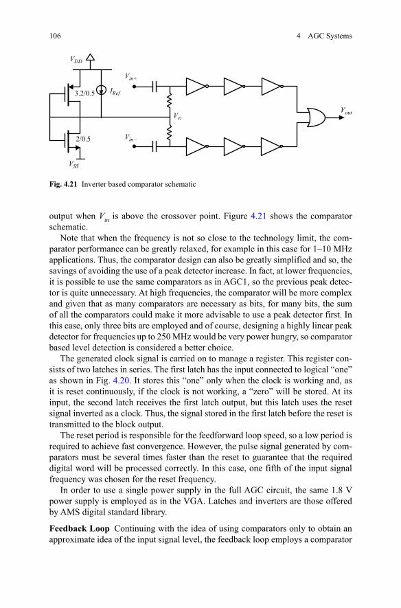
106
output when Vin is above the crossover point. Figure 4.21 shows the comparator schematic.
Note that when the frequency is not so close to the technology limit, the com-parator performance can be greatly relaxed, for example in this case for 1–10 MHz applications. Thus, the comparator design can also be greatly simplified and so, the savings of avoiding the use of a peak detector increase. In fact, at lower frequencies, it is possible to use the same comparators as in AGC1, so the previous peak detec-tor is quite unnecessary. At high frequencies, the comparator will be more complex and given that as many comparators are necessary as bits, for many bits, the sum of all the comparators could make it more advisable to use a peak detector first. In this case, only three bits are employed and of course, designing a highly linear peak detector for frequencies up to 250 MHz would be very power hungry, so comparator based level detection is considered a better choice.
The generated clock signal is carried on to manage a register. This register con-sists of two latches in series. The first latch has the input connected to logical “one” as shown in Fig. 4.20. It stores this “one” only when the clock is working and, as it is reset continuously, if the clock is not working, a “zero” will be stored. At its input, the second latch receives the first latch output, but this latch uses the reset signal inverted as a clock. Thus, the signal stored in the first latch before the reset is transmitted to the block output.
The reset period is responsible for the feedforward loop speed, so a low period is required to achieve fast convergence. However, the pulse signal generated by com-parators must be several times faster than the reset to guarantee that the required digital word will be processed correctly. In this case, one fifth of the input signal frequency was chosen for the reset frequency.
In order to use a single power supply in the full AGC circuit, the same 1.8 V power supply is employed as in the VGA. Latches and inverters are those offered by AMS digital standard library.
Feedback Loop Continuing with the idea of using comparators only to obtain an approximate idea of the input signal level, the feedback loop employs a comparator
Fig. 4.21 Inverter based comparator schematic
IRef
VDD
Vin+
VSS
Vout
2/0.5
3.2/0.5
Vri
Vin¯
4 AGC Systems

107
based detector instead of conventional peak detectors such as those presented in Sect. 3.2 (see Figs. 4.22 and 4.23).
In this case, the input signal is compared with a reference signal which marks the minimum expected output. This means that any input amplitude below this reference value will result in a VGA maximum gain configuration from the feed-back control. Should the input amplitude rise above the reference value, a pulse will be generated at the comparator output as happened in the feedforward loop. However, this case is analog and a continuous output is required for different input amplitudes. To obtain the analog response it must be noted that the generated pulses have a different width depending on how much bigger the amplitude is than the reference value. If a charge pump is connected in series with the comparator, this variable width pulse generates current pulses proportional to the square root of the input voltage. Loading the charge pump with a 1 pF capacitor, the current pulses charge the capacitor up to a value proportional to the current introduced. The rela-tion between the charge pump output and the input amplitude is not linear. In fact
Fig. 4.22 Peak detector schematic
1pF
VDD
Vin
VSS
Vout
2/0.35
2/0.35
Comp+
¯Vref
Fig. 4.23 Peak detector comparator
4.3 CMOS Mixed Feedback/Feedforward AGC Circuit

108
the relation is quite an unusual and interesting function. Straightforward analysis yields:
(4.7)
where Io is the charge pump current, T is the input signal period, A is the input signal amplitude and VRef is the reference voltage. This equation is only valid for A > VRef , since it must be remembered that for A ≤ VRef the comparator output is zero. If we plot (4.7) for arbitrary constants using Matlab and analyze it with Curve Fitting Toolbox, it is found that another very useful function approximately fits in our ap-plication dynamic range. As Fig. 4.24 shows, for VRef = 0.1 V and input amplitude, A, between 0.1 and 0.2 V, (4.7) is quite close to a logarithmic function. Thus, a peak detector with an approximate logarithmic function is obtained as long as input dy-namic range is kept low enough.
After the detector, the signal is simply filtered and shifted so that the required VGA control voltage is obtained. Filtration is by means of a simple RC filter which mainly reduces the ripple generated by the charge pump. The RC filter is imple-mented as a MOS/switch-capacitor configuration where the MOS operates in triode and its equivalent resistance is reduced by a switch in parallel, which is connected for a small time period each time the digital feedforward loop changes the digital word. Providing the time period is not too long, AGC settling-time is reduced by this technique, whereas a simple differential pair makes the function of the level shifter.
As mentioned, once logarithmic conversion has been achieved by the peak de-tector, if an exponential converter was introduced into the loop, the dynamic re-sponse given by (2.13) would be obtained. In its place, the dynamic response given by (2.10) for linear control voltage is expected.
Once again, power supply is 1.8 V, the same as for the VGA. To follow, simu-lation and measurement results for certain separated blocks and the full AGC are offered.
Vout = IoT
(1
2−
1
πarcsin
(VRef
A
)),
Fig. 4.24 Equation (4.7) for arbitrary constants and fitting curve obtained by Matlab Curve Fitting Toolbox
100 120 140 160 180 2000
100
200
300
400
500
600
A (mV)
y
y = 1001 - 637.3*arcsin(Vref/A)y = 204.8*log(A - 94.76) - 285.8
Vref = 100 mV
4 AGC Systems

109
4.3.2 Performances
The AGC circuit was designed in 0.35 µm CMOS technology by Austria Microsys-tems (AMS). The chip photograph is shown in Fig. 4.25. The corresponding layout for this structure has been carefully realized taking into account matching between transistors and symmetry between sections in order to minimize second order dis-tortion components due to mismatches. Figure 4.26 shows the chip and the PCB used during measurement tests. Further information on the instrumentation and test probes employed is offered in Appendix A.
First, VGA frequency response was measured. Simulation results obtained an al-most constant bandwidth around 700 MHz. Measurements however obtained a con-stant bandwidth of only 500 MHz though this bandwidth is more than enough for the target application, which was expected to be around 250 MHz. Bandwidth and
Fig. 4.25 Chip photograph
Fig. 4.26 Measurement test circuitry
4.3 CMOS Mixed Feedback/Feedforward AGC Circuit

110
gain configuration measurement results are the same as those obtained by VGA3 and can be consulted in Fig. 3.18. Next, measurement results are offered for input signals though only at 100 MHz, as, due to instrumentation limitations, it was not possible to make measurements at higher frequencies. Target and achievable fre-quencies are not so far apart, consequently, the obtained results can give a close view of expected results for 250 MHz signals.
Distortion levels at high frequencies are expected to be high. Simulation results predicted an IM3 for a Vout = 0.4 Vp-p at 100 MHz below − 42 dB. Measured IM3 is below − 40 dB for all gain settings. Both results, simulated and measured, were ob-tained for the combination of the VGA and the buffer together and can be checked, as well as bandwidth results, in Chap. 3 (see Fig. 3.19).
As shown, worst case results for IM3 correspond quite closely to those expected by simulations, although 6 and 12 dB IM3 was underestimated by simulations. A first estimation for the VGA without buffer IM3 is given by simulations which offer an IM3 for an output of 0.4 Vp-p at 100 MHz below − 49.2 dB for all gain settings.
To check AGC loop linearity response, the output amplitude was measured for different inputs at 100 MHz and thus, a graph with the gain vs. input amplitude was obtained. Figure 4.27 shows this graph where it can be compared with the ideal response and with ± 1 dB error curves. As shown, the obtained gain is below ±1 dB from the ideal response for a range above the input dynamic range of 12 dB (from 100 to 400 mVp-p).
Finally, convergence was checked. Simulation results predicted a convergence time for a stepwise signal at 250 MHz below 50 ns. Again, instrumentation limita-tions prevented the use of such a high frequency modulation; instead, measure-ments were made with a square modulation of 300 KHz and a carrier frequency of 20 MHz. As shown in Fig. 4.28, the AGC response to this input signal is quite fast. Therefore, although it is not possible to verify whether predicted simulations are
Fig. 4.27 Gain vs. input amplitude for an input signal at 100 MHz
100 150 200 250 300 350 400 450 500Vin (mVp-p)
–2
0
2
4
6
8
10
12
14
Gain(dB)
Measured responseIdeal response
4 AGC Systems

111
good, measurement results at least offer a maximum response time below 0.8 µs which is the maximum time required to vary VC between its maximum and mini-mum value with a 20 MHz signal.
Fig. 4.28 AGC convergence with a square modulation at 300 KHz and a carrier at 250 MHz for simulation ( up) and 20 MHz for measurements ( down) are offered
0 0.5 1 1.5 2 2.5 3 3.5 41.1
1.2
1.3
1.4
1.5
t (s)
Vc
(V)
0 0.5 1 1.5 2 2.5 3 3.5 4¯0.3¯0.2¯0.1
0
0.1
0.2
0.3
t (s)
AG
C O
utpu
t (V
)
0.5 1 1.5 2 2.5 3 3.5x 10¯7
x 10¯7
x 10¯6
x 10¯6
¯0.3¯0.2¯0.1
0
0.10.2
0.3
AG
C In
put (
V)
0 0.5 1 1.5 2 2.5 3 3.5 4 4.5 5¯0.05
¯0.025
0
0.025
0.05
t (s)
AG
C In
put (
V)
0 0.5 1 1.5 2 2.5 3 3.5 4 4.5 5¯0.03¯0.02¯0.01
0
0.01
0.02
0.03
t (s)
AG
C O
utpu
t (V
)
1 30.25
0.3
0.35
0.4
0.45
Vc
(V)
4.3 CMOS Mixed Feedback/Feedforward AGC Circuit

112
4.4 Conclusions
Section 4.1 presented a 1.8 V0.35 µm CMOS automatic gain control circuit based on a digital feedforward approach which converges to the desired level within 0.3 µs. The proposed architecture is very simple, compact and can be implemented with basic cells, obtaining at the same time high performance characteristics. There-fore, this AGC would prove very useful in applications such as WLAN or Blue-tooth receivers where the use of traditional closed loop feedback amplifiers forms a boundary due to the stringent settling time constraints.
The second proposition presented is a full analogue SiGe BiCMOS AGC cir-cuitry embedded in an IEEE 802.11a WLAN direct conversion receiver. Based on an analog feedforward gain control technique, the circuit adjusts the gain rapidly and with high accuracy, maintaining at the same time a good trade-off between sim-plicity and power consumption. Therefore, this analog feedforward approach which provides very fast convergence and high enough linearity performance, classifies this architecture for WLAN receiver implementation.
The third and final proposed AGC is a double loop AGC for application frequen-cies up to 250 MHz. The fast feedforward loop is combined with a more linear feedback loop, so it is possible to offer a fast enough AGC without gain steps that not all applications can accept. Furthermore, a novel digital level detection method is proposed for the feedforward loop and another pseudo-logarithmic peak detector has been obtained for the feedback loop. Summarizing, 0.35 µm CMOS technology has been taken to its upper frequency limitation to offer a sufficiently linear AGC implemented with some simple but novel blocks.
Next, a table (Table 4.1) is offered with main characteristics of three analyzed AGCs and some more AGC proposals from the literature:
For WLAN applications, the AGC proposed by Dr. Jeon ET. Al in [1] is one of the most complete AGCs to be found in the literature. Therefore, it is a key refer-ence in this book where WLAN receivers are the target application. AGC1 and AGC2 proposals aim to improve the performances obtained in this case. AGC2 is targeted specifically for the same IEEE standard as Jeon’s work. However, the cir-cuit proposed here obtains a faster convergence-time thanks to its feedforward loop, while other performances are similar to those obtained in [1]. The strong points of AGC1 are its simplicity and very fast response. This AGC also offers considerably lower power consumption than other options; although, it would rise a little if gain range and precision were increased. [20] is another example from the literature of an AGC implemented in BiCMOS with high bandwidth and fast response. How-ever, it has the usual drawback in BiCMOS technologies. A higher power supply voltage is used and consequently, consumption is much higher than in other AGCs. AGC2. In spite of using BiCMOS technology, it also makes use of low voltage blocks, so it can work with the right power supply for CMOS transistors.
Finally, AGC3, the proposal for high frequency applications, achieves the 243 MHz standard with moderate power consumption, while other performances are below standard for these frequencies.
4 AGC Systems

113
Tabl
e 4.
1 C
ompa
rison
of l
itera
ture
and
pro
pose
d A
GC
sD
esig
n[2
0][1
]A
GC
1A
GC
2A
GC
3
Tech
pro
cess
0.
25 μ
m0.
18 μ
m0.
35 μ
m0.
25 μ
m0.
35 μ
mB
iCM
OS
CM
OS
CM
OS
SiG
E B
iCM
OS
CM
OS
Supp
ly v
olta
ge (V
)3–
5.2
1.6–
21.
82.
51.
8Po
wer
(mW
)60
–104
10.4
41.
6213
.75
2.2
Intri
nsic
ban
dwid
th (M
Hz)
400
1810
00.
068–
2025
0A
GC
Gai
n ra
nge
(dB
)0 ∼
45−8
∼ 32
0 ∼ 21
15 ∼
690 ∼
12G
ain
setti
ngC
ontin
uous
Con
tinuo
us (±
ldB
)D
iscr
ete
(3 d
B)
Con
tinuo
us (±
ldB
)D
iscr
.+C
ont.
(±ld
B)
AG
C se
ttlin
g-tim
e (μ
s)0.
3a4.
20.
253.
2<
0.8
AG
C o
utpu
t vol
tage
(V)
0.11
0.5
0.4
0.5
0.4
Dis
torti
on: I
M3
(dB
)—
< −
37@
lMH
zb<
− 60
@71
MH
z<
− 41
dB
@20
MH
z<
− 42
dB
a Atta
ck-ti
me
b TH
D
4.4 Conclusions

114
The AGC circuits proposed in this book are therefore highly competitive with those already presented in the literature.
References
1. O. Jeon, R.M. Fox and B.A. Myers; “Analog AGC Circuitry for a CMOS WLAN Receiver”; Solid-State Circuits, IEEE Journal of; Vol. 41, Issue 10, pp. 2291–2300, Oct. 2006.
2. T. Oshima, K. Maio, W. Hioe, Y. Shibahara and T. Doi; “Automatic Tuning of RC Filters and Fast Automatic Gain Control for CMOS Low-IF Transceiver”; Custom Integrated Circuits Conference, 2003. Proceedings of the IEEE 2003; pp. 5–8, Sept. 2003.
3. C.-W. Lin, Y.-Z. Liu and K. Y. J. Hsu; “A Low-Distortion and Fast-Settling Automatic Gain Control in CMOS Technology”; Circuits and Systems, 2004. ISCAS ’04. Proceedings of the 2004 International Symposium on; Vol. 1, pp. 541–544, May 2004.
4. Chun-Pang Wu and Hen-Wai Tsao; “A 110-MHz 84-dB CMOS Programmable Gain Ampli-fier With Integrated RSSI Function”; Solid-State Circuits, IEEE Journal of; Vol. 40, Issue 6, pp. 1249–1258, Jun. 2005.
5. B. Calvo, S. Celma and M.T. Sanz; “Low-Voltage Low-Power CMOS IF Programmable Gain Amplifier”; Circuits and Systems, 2006. MWSCAS ’06. 49th IEEE International Midwest Symposium on; Vol. 2, pp. 276–280, Aug. 2006.
6. S.-B. Park, J.E. Wilson, and M. Ismail; “Peak Detectors for Multistandard Wireless Receiv-ers”; Circuits and Devices Magazine, IEEE; Vol. 22, Issue 6, pp. 6–9, Nov.-Dec. 2006.
7. “Wireless Lan Medium Access Control (MAC) and Physical Layer (PHY) Specifications: High-Speed Physical Layer in the 5-GHz Band”; IEEE Std. 802.11a, Part11, Sep. 1999.
8. J.M. Khoury, “On the design of constant settling time AGC circuits”; Circuits and Systems II: Analog and Digital Signal Processing, IEEE Transactions on; Vol. 45, Issue 3, pp. 283–294, Mar. 1998.
9. M. Zargari, D.K. Su, C.P. Yue, S. Rabii, D.Weber, B.J. Kaczynski, S.S. Mehta, K. Singh, S. Mendis, and B.A. Wooley; “A 5-GHz CMOS transceiver for IEEE 802.11a wireless LAN system”; Solid-State Circuits, IEEE Journal of; Vol. 37, Issue 12, pp. 1688–1694, Dec. 2002.
10. A. Otin, S. Celma and C. Aldea; “A 40-200MHz Programmable 4th-Order Gm-C Filter with Auto-Tuning System”; Solid State Circuits Conference, 2007. ESSCIRC 2007. 33rd Euro-pean; pp. 214–217, Sep. 2007.
11. S.I. Liu and Y.S. Hwang; “CMOS Four-Quadrant Multiplier Using Bias Feedback Tech-niques”; Solid-State Circuits, IEEE Journal of; Vol. 29, Issue 6, Jun. 1994.
12. J.P. Alegre, S. Celma, B. Calvo and J.M. García del Pozo; “Design of a Novel Envelope De-tector for Fast-Settling Circuits”; Instrumentation and Measurement, IEEE Transactions on; Vol. 57, Issue 1, pp. 4–9, Jan. 2008.
13. B. Gilbert; “Limiting-Logarithmic Amplifiers”; Electronics Laboratories Advanced Engi-neering Course on RF IC Design for Wireless Communication Systems, Lausanne, Switzer-land, Jul. 1995.
14. J. Israelsohn; “Gain control”; EDN; pp. 38–46, Aug. 2002.15. M. Fujii, N. Kawaguchi, M. Nakamura, T. Ohsawa; “Feedforward and feedback AGC for fast
fading channels”; Electronics Letters; Vol. 31, Issue 13, pp. 1029–1030, Jun. 1995.16. Wang Wenzhao, Chen Yaqin, Zhou Qi; “Implementation of mixed feedback/feedforward
analog and digital AGC”; Microwave and Millimeter Wave Technology, 2004. ICMMT 4th International Conference on, Proceedings; pp. 377–381, Aug. 2004.
17. R.G. Carvajal, J. Ramírez-Angulo, A.J. Lopez-Martin, A. Torralba, J.A.G. Galan, A. Car-losena and F.M. Chavero; “The Flipped Voltage Follower: a Useful Cell for Low-voltage Low-power Circuit Design”; Circuits and Systems I: Regular Papers, IEEE Transactions on; Vol. 52, no. 7, pp. 1276–1291, 2005.
4 AGC Systems

115
18. C.J.B. Fayomi, G.W. Roberts, M. Sawan; “Low power/low voltage high speed CMOS dif-ferential track and latch comparator with rail-to-rail input”; Circuits and Systems, 2000. Pro-ceedings. ISCAS 2000; Vol. 5, pp. 653–656, May 2000.
19. J. Segura, J.L. Rossello, J. Morra, H. Sigg; “A variable threshold voltage inverter for CMOS programmable logic circuits”; Solid-State Circuits, IEEE Journal of; Vol. 33, Issue: 8, pp. 1262–1265, Aug. 1998.
20. T. Drenski, L. Desclos, M. Madihian, H. Yoshida H. Suzuki, T. Yamazaki; “A BiCMOS 300ns Attack-Time AGC Amplifier with Peak-Detect and Hold Feature for High-speed Wire-less ATM Systems”; Solid-State Circuits Conference, Digest of Technical Papers. ISSCC. IEEE International; pp. 166–167, Feb. 1999.
References


117
Throughout this book, the most relevant results and main conclusions have been summarized in the concluding discussion of each chapter. In this final chapter, the most significant contributions will be reported in order to give a general overview of the work.
First, the fulfilment of the main objectives presented in Sect. 1.2 will be verified, leading on to the corresponding conclusions.
Further research directions will then be pointed out. Among these are the ques-tions not considered in this book and the extra development of those already com-pleted. These proposed investigations could well be used in future works as an extension to complement the work presented here.
5.1 General Conclusions
Chapter 1 has been employed to introduce the framework for this book: techniques used, technology processes, active blocks, target applications, challenges and main objectives have been laid out.
The second chapter offers a theoretical analysis of feedback and feedforward AGCs transfer functions and several possible solutions have been identified. Fur-thermore, behavioural models realized in Matlab made it possible to verify the ex-pected performance of these solutions.
The third chapter consists of three sections, one for each of the main blocks required in an AGC: VGA, peak detector and control voltage generation circuit. Section 3.1 characterizes several VGAs, some of which were classic literature pro-posals. We were however particularly concerned about those developed inside the design group. These were all designed in a 0.35 µm CMOS process with a single 1.8 V power supply, so that the 1.8 V–0.18 µm CMOS technology migration could easily be realized. Moreover, a multiplier based VGA was proposed (VGA2): a low-voltage constant-bandwidth VGA based on a high performance multiplier cell in a 0.35 µm CMOS technology. This consumes a mere 1.5 mA from a single 1.8 V power supply voltage. Measured results showed competitive performances, such as
J. P. Alegre Pérez et al., AutomaticGainControl,Analog Circuits and Signal Processing, DOI 10.1007/978-1-4614-0167-4_5, © Springer Science+Business Media, LLC 2011
Chapter 5Conclusions

118
190 MHz gain bandwidth, while a continuous and wide gain range of 36 dB was offered. Thus, a set of high performance VGAs with very predictable responses has been put together to be suitable for feedforward AGCs.
Section 3.2 offered the evolution of peak detector cells ranging from the most basic to more complex ones. In this case, several peak detector proposals were made, all of them in 0.35 µm CMOS technology. The first, PD1 is an open loop peak detector composed of a voltage to current converter, a rectifier and a cur-rent mode peak detector, which is able to operate at high frequencies. It employs a 3.3 V single supply voltage and consumes 6.1 mW when designed for a 71 MHz bandwidth or 2.13 mW for 10 MHz bandwidth. In order to obtain a 0.3% ripple, the latter one, requires 10 pF total capacitance and worst case settling-time can be up to 27.5 µs due to the inherent trade-off between keeping and tracking. To overcome these results a new concept of envelope detector was proposed (PD2) based on a sample and hold performance controlled by the input signal. This proposal obtained similar performances to those obtained by its counterpart, but this time it only re-quired 3.3 pF and presented a worst case of 0.4 µs settling-time. Thus, it offers the possibility of reducing the capacitance needed for the same performance, thereby achieving a great saving of circuit area and completely overcoming the inherent trade off between keeping and tracking exhibited by conventional peak detectors. Another proposal, PD3, was a differential positive peak detector where, instead of a diode, a unidirectional current mirror is employed together with a high performance transconductor. This transconductor allowed for high operation frequencies with quite low power consumption (0.9 mW) for a moderate linearity range (21 dB). Based on the same concept, but making use of a similar fast-settling technique as with PD2 and in SiGe BiCMOS technology, PD4 obtained very good performance tracking signals with low power consumption (0.55 mW). As speed was limited by an external 5 MHz clock, its settling-time was lower than that of others, though still quite fast. Finally, a peak detector based on a conventional Sample & Hold structure has been presented (PD5) proving how this kind of circuit is able to de-tect the amplitude of certain types of signals. The advantages of such circuits are those obtained in this case: fast settling-time, low capacitance area… Furthermore, this circuit was specifically designed to cancel charge injection, so a wide dynamic range would be obtained (42 dB).
In Chap. 4 all the AGC loops analysis carried out in Chap. 2 and different block proposals developed in Chap. 3 were considered and three different AGC proposals were offered. The first AGC proposal (AGC1) was based on a digital feedforward approach and offered very fast settling time. The projected architecture was very simple, implemented in 0.35 µm CMOS process with basic cells, such as VGA1, PD3 and some simple comparators. Its characteristics obtained a good trade-off of 100 MHz bandwidth, 20 dB gain range with only 1.62 mW power consumption. Furthermore, it took full advantage of feedforward structure and fast peak detector, so its settling-time was only 0.25 µs.
The second proposition presented, AGC2, was implemented in a low-cost SiGe BiCMOS technology process. It is a fully analogue feedforward AGC circuit em-bedded in an IEEE 802.11a WLAN direct conversion receiver. This receiver had
5 Conclusions

119
stringent settling-time constraints, so this AGC fast tracking capability (requiring only 4 out of 10 OFDM preamble symbols to settle the worst case signal variation) was perfect for this application, improving the results obtained by other circuits in the literature. This time the AGC adjusted the gain continuously with only ± 1 dB measured accuracy and a range which extends from 15 to 69 dB. Thus, all speci-fications fixed by the receiver were satisfied and the analog feedforward approach proved itself capable of providing very fast convergence with ample linearity per-formance.
Finally, a double loop feedforward/feedback AGC (AGC3) was proposed for ap-plication frequencies of up to 250 MHz. The fast feedforward loop was combined with a more linear feedback loop to be able to offer a fast AGC with continuously variable gain. Furthermore, a novel digital level detection method was proposed for the feedforward loop and another pseudo-logarithmic peak detector was ob-tained for the feedback loop. In summary, a low-cost 0.35 µm CMOS technology was taken to its upper frequency limitation and fed with a lower supply (1.8 V) to present a linear AGC which consumes 2.2 mW implemented with some simple but novel blocks.
For WLAN applications, the CMOS AGC proposed by Jeon etal. (see Table 4.1 in Chap. 4) is one of the most complete AGCs to be found in the literature. Thus, it is a key reference in this book where WLAN receivers are the target application. AGC1 and AGC2 proposals aim to improve the performances obtained in this case. The strong points of AGC1 are its simplicity and very fast response. This AGC also presents considerably lower power consumption than other options; although, it would raise a little if gain range and precision were increased. AGC2 is targeted specifically for the same IEEE standard as Jeon’s work. However, the circuits pro-posed here obtained a faster convergence-time thanks to their feedforward loop, while other performances are within the requirements of the application. There is another BiCMOS example taken from the literature with high bandwidth and fast response (also shown in Table 4.1, Chap. 4). However, it has the usual drawback in BiCMOS technologies. It uses a higher power supply voltage and consequently, its power consumption is much higher than in other AGCs. In spite of employing BiC-MOS technology, AGC2 also makes use of low voltage blocks, so it can work with the power supply corresponding to CMOS transistors. Thus, by means of these two AGCs, this book shows that mentioned AGCs are competitive with those already presented in the literature and consequently, the feedforward loop is a fine alterna-tive in WLAN receivers.
5.2 Further Research Directions
The fast-settling peak detectors introduced in Sect. 3.2 offer a new research line which is very advantageous in many applications such as adaptive bias techniques for linearity enhancement, dc current reduction in RF amplifiers or MLL Q-tun-ing method used in high-Q high-frequency continuous time filters, beyond AGC
5.2 Further Research Directions

120
circuits. These detectors still have one or two issues to be solved such as those brought about by switches: charge injection and capacitive feedthrough. Many tech-niques in the literature deal with these problems, but their study was sidestepped to avoid deviating from our objectives in this book.
AGC3, the proposal for high frequency applications, introduced a new field of study that should be developed still further: the feedforward/feedback dual loop. The possibility of reducing feedback loop compression ratios by feedforward loop and thus, relaxing loop stability conditions can lead to faster AGC circuits. This has been introduced through AGC3, but could require much greater work and has been set aside for future investigation lines.
Finally, another issue to be investigated is the use of the pseudo-logarithmic peak detector presented in Sect. 4.3. This simple method for obtaining a logarithmic response in CMOS technologies could be combined with other simple exponential converters to design a fast analog feedforward loop in a CMOS process.
Thus, the future work to be realized is clear and will be useful to complete the study carried out in this book as well as to explore new research directions.
5 Conclusions

121
A.1 General Layout Considerations
The layout of an analog IC directly influences its performance. Therefore, if we are to keep the characteristics of the designed circuits up to certain specifications despite negative effects such as crosstalk, parasitics, mismatches, noise, etc, a care-ful layout is mandatory. Although the layout considerations to be taken into account to minimize these effects are quite well-known and commonly used by analog de-signers [1–4], a reminder of them here in this work will not go amiss. A summary follows of the relevant key points to be considered in the design of the main com-ponents.
A.1.1 Layout Components
Transistors Transistor layout was carried out using common design rules in order to achieve adequate matching. Therefore, in cases where matching between com-ponents was critical, interdigitized or common centroid structures were employed. Likewise, dummy transistors were introduced in the stack borders to guarantee obtaining similar performance for each finger. These dummies were connected to the adequate power supply, to keep them in the cutoff region. Guard rings were also included to reduce substrate noise influence in transistor signals.
Capacitors These are basic elements in the implementation of any integrated cir-cuit. In this book, the main use of capacitors has been in peak detectors and in stabil-ity compensation of feedback loops. All the capacitors in 0.35 µm CMOS process were implemented by double poly structures. The main reason for choosing this type was its superior linearity and area relation. Metal-metal capacitors offer supe-rior linearity performance, but their specific capacitance is low and requires greater area. Alternatively, MOS based capacitors can present high specific capacitance, but their linearity performance is lower.
J. P. Alegre Pérez et al., AutomaticGainControl,Analog Circuits and Signal Processing, DOI 10.1007/978-1-4614-0167-4, © Springer Science+Business Media, LLC 2011
Appendix A: Layout and Experimental Techniques

122
With regard to circuits in 0.25 µm SiGe BiCMOS, Metal-Insulator-Metal, MIM, capacitors were employed as this technology allows only this kind of capacitor.
In the circuits offered throughout this work, no critical capacitor matching re-quirement was found and their values were moderate, so parasitic capacitors were a second order issue. Thus, their layouts have not followed any special requirement.
Resistors 1. MOS based resistors: To implement the layout of MOS based transistors, the
criteria explained in transistor layout has been followed: basically, transistors were interdigitized and dummy transistors were introduced in the borders of the stacks. A guard ring connected to VSS was also used in each case.
2. Polysilicon resistors: If best linearity is required, MOS based resistors are not adequate. Therefore, in high frequency amplifiers for example, load resistors were implemented in this technology. When matching was necessary, these resis-tors were interdigitized with dummy structures on both sides, inside an N-well and a guard ring to guarantee isolation.
Pads In CMOS circuits two types of pads were employed. One included a simple diode based protection system to avoid break voltages in MOS gates due to Elec-troStatic Discharge. (ESD). This is a simple system, but adequate enough for our requirements. In all the other inputs/outputs simple custom pads were used to avoid degradation in frequency response.
In SiGe BiCMOS circuits, there were also two pad types: one for high frequency response and the other for DC signals. Furthermore, the same simple protection system was introduced where required as in CMOS circuits.
A.1.2 Full Systems Layouts
In the different circuit layouts, apart from using different component matching tech-niques, we have tried to keep the natural circuit symmetry. Furthermore, differences in the paths of balanced signals were carefully avoided as it is absolutely necessary to obtain the benefits inherent to these signals.
To avoid coupling between inputs and outputs, bondpads were distributed sepa-rately. As previously mentioned, balanced signal paths were drawn symmetrically and the same was done with bondpads.
A.2 Experimental Considerations
To verify simulation results several circuits were measured. This section introduces the techniques that were used to realize the measurements and the solutions applied to the typical small problems that crop up during the process. First of all, here is a layout of the equipment used.
Appendix A: Layout and Experimental Techniques

123
A.2.1 Measurement Equipment
Apart from the typical measuring equipment found in any laboratory, the following devices were employed:
• Network analyzer: Rohde&Schwartz ZVL6 (9 kHz–6 GHz)• Digital oscilloscope: Tektronix TDS544A (500 MHz)• Signal synthesizer/generator: HP3325B (20 MHz)• Signal generator: Rohde&Schwartz SMY-01 (1.04 GHz)• RF signal generator: Rohde&Schwartz SM300 (9 kHz–3 GHz)• Spectrum analyzer: Rohde&Schwartz FS300 (9 kHz–3 GHz)
A.2.2 Measurement of Integrated Circuits
The first thing to take into account in the measurement of an IC is the design of PCB board required to support the chip and connect it to the measurement devices and auxiliary circuitry. The most important requirement of a PCB board in this work was to avoid as much as possible parasitic capacitances along the signal path from the generator to the chip input pads and from the output pads to the measurement devices. To do so, SMA connectors were employed, PCB paths were kept as short as possible to minimize parasitics and high frequency transformers (WBC8-1LB and WB3-1TSLB) were used.
A way to facilitate tests is to introduce calibration test circuitry in the chip de-sign or Device Under Test (DUT). This calibration circuitry is composed, for ex-ample, of a second path between inputs and outputs with the test-buffer employed to cancel pad parasitic capacitances in the middle, so that it is possible to calibrate the frequency analyzer and measure DUT frequency response. This measurement schematic is shown in Fig. A.1.
The input signal is carried from the generator to the PCB in single mode. Then, it is converted to balanced currents by the transformers and again into voltage by in-put resistors, Rin. These resistors are chosen so that the generator sees an equivalent load resistor of 50 Ω to optimize energy transmission. The output buffer is loaded
Fig. A.1 Measurement scheme
VoutVin
DUT
Test
Test
CHIP
A.2 Experimental Considerations

124
with Rout resistors, which again give an equivalent resistance equal to the measure-ment device input resistor: 50 Ω.
The test-buffer scheme is shown in Fig. A.2. It is a two stage transconductor, which consequently, avoids inverse transmissions. The first stage is a simple source follower composed of P-transistors M1. The second stage is a simple differential pair biased by 2 mA current and loaded by external resistors. These resistors can not be very big, as together with parasitic capacitors, they would greatly reduce buffer bandwidth. Thus, 100 Ω resistors were employed, so, at the same time an equivalent output resistor of 50 Ω was obtained. In BiCMOS designs, buffers based on simple transconductors with a feedback loop were employed. As the bipolar differential pair was used instead of the MOS one, greater transconductance was obtained, so these buffers offered very good performance in spite of the feedback loop.
Figure A.3 shows a CMOS test buffer chip photograph, while Fig A.4 shows example pictures of both the PCBs used to measure chips and of the laboratory test table.
To automate some of the measurements, GPIB connectors were inserted between the measurement devices and the computer. Using Matlab, it was possible to create the adequate files to automatically measure and collect the data.
Fig. A.2 CMOS test-buffer schematic
Vout–
Iout–
IB2
IB1 IB1
VDD VDD
Vout+
Iout+
GND
Fig. A.3 Test buffer chip photograph
Test buffer
Appendix A: Layout and Experimental Techniques

125
References
1. Y. Tsividis; “Mixed Analog Digital VLSI Devices and Technology”; McGraw-Hill, New York, 1996
2. R.J. Baker, H.W. Li, D.E. Boyce; “CMOS Circuit Design, Layout and Simulation”; IEEE Press Series on Microelectronic Systems, 1998.
3. A. Hastings; “The Art of Analog Layout”; Prentice Hall Inc., New Jersey, 20014. F. Maloberti; “Analog Design for CMOS VLSI Systems”; Kluwer Academic Publishers, 2001.
Fig. A.4 PCBs for each chip
References


127
Appendix B: Acronym List
Acronym Significance
ADC AnalogtoDigitalConverterAGC AutomaticGainControlAM AmplitudeModulationAMS AustriaMicroSystemsASIC ApplicationSpecificIntegratedCircuitsASK Amplitude-ShiftKeyingBiCMOS Bipolar-CMOSBJT BipolarJunctionTransistorBSIM BerkeleyShort-channelIGFETModelBW BandwidthCCD ChargeCoupledDeviceCDMA CodeDivisionMultipleAccessCMFF Common-ModeFeedforward(C)MOS (Complementary)MetalOxideSemiconductorCMRR Common-ModeRejectionRatioDR DynamicRangeDSP DigitalSignalProcessorGBW GainBandwidthproductGPIB GeneralPurposeInterfaceBusHF HighFrequencyHRP HighResistivityPolysiliconIC IntegratedCircuitIEEE InstituteofElectricalandElectronicsEngineersIF IntermediateFrequencyIM3 ThirdorderIntermodulationdistortionLAN LocalAreaNetworkLNA LowNoiseAmplifierMLL MagnitudeLockedLoopMOSFET MetalOxideSemiconductorFieldEffectTransistorN/PMOS N-channel/P-channelMOS
J. P. Alegre Pérez et al., AutomaticGainControl,Analog Circuits and Signal Processing, DOI 10.1007/978-1-4614-0167-4, © Springer Science+Business Media, LLC 2011

128
Op-Amp OperationalAmplifierOFDM OrthogonalFrequencyDivisionMultiplexingOTA OperationalTransconductanceAmplifierPCB PrintedCircuitBoardPD PeakDetectorPGA ProgrammableGainAmplifierPH PeakHolderPVT variations Process-Voltage-TemperaturevariationsRMS RootMeanSquareS/H SampleandHoldSiGe BiCMOS SiliconGermaniumBiCMOSSNR Signal-to-NoiseRatioSR Slew-RateTHD TotalHarmonicDistortionVGA VariableGainAmplifierVHF VeryHighFrequencyVLSI VeryLargeScaleIntegrationWLAN WirelessLAN
Appendix B: Acronym List

129
Appendix C: Parameter Glossary
Parameter Significance
k Boltzmann constant (1.38 × 10⁻²³ J/K)T Absolute temperature (in Kelvin degrees)εox Dielectric permittivity of SiO2 (3.4531 × 10⁻¹¹ F/m)ID Total drain current of a MOS transistorμn/μp Surface mobility for electrons and holes respectivelyμo Effective mobility at low electrical fieldstOX Gate-oxide thickness of a MOS transistorθ Mobility-reduction coefficient of a MOS transistorγ Body-effect coefficient of a MOS transistorλ Channel-length modulation factor of a MOS transistorNSUB Effective substrate dopingCJ Junction capacitance per unit area (source/drain-bulk)CJW Sidewall junction capacitance (source/drain-bulk)CPOX Poly1-poly2 specific capacitance per unit areaρSH Sheet resistance of a high resistivity poly moduleW Channel width of a MOS transistorL Channel length of a MOS transistordW Difference between W and the effective channel width WeffdL Difference between L and the effective channel length Leffα MOS transistor gate-to-source DC voltage gainK MOS transistor gain factor: K = ½ µCoxW/Lgm MOS transistor transconductance defined as δID/δVGSgmb MOS transistor bulk-transconductance defined as δID/δVBSro MOS transistor output conductanceVTH Threshold voltageVTHO Zero-VBS value of thresholdVfp Fermi potentialVDSAT Drain-source saturation voltage of a MOS transistor
J. P. Alegre Pérez et al., AutomaticGainControl,Analog Circuits and Signal Processing, DOI 10.1007/978-1-4614-0167-4, © Springer Science+Business Media, LLC 2011

130
VGS,VDS ,VBS Gate-source, drain-source and bulk-source MOS transistor voltages
COX MOS gate-oxide capacitance per unit areaVDD Supply voltageVCM Common-mode voltageIB,Ibias Bias currentRL,CL Load resistance and load capacitanceCT Circuit total capacitanceGm Differential transconductance of a systemτ Time constant
Appendix C: Parameter Glossary

131
This appendix summarizes the most important parameters associated to both tech-nologies, CMOS and SiGe BiCMOS, considered in this work. Table D.1 reports the parameters related to the 0.35 μm, P-substrate, N-well, 4-metal, 2-poly, Aus-tria Microsystems (AMS); whereas Table D.2 reports those related to SGB25V, the 0.25 µm CMOS core, SiGe:C BiCMOS with High-Voltage Devices, 5-metal, IHP-microelectronics.
Appendix D: Process Parameters
Table D.1 Technology: AMS 0.35 μm CMOS P-Substrate, N-Well, 4-Metal, 2-PolyParameter N-Transistor P-Transistor UnitsμCOX 170 58 μA/V2
VTHo (10/035) 0.5 − 0.65 VtOX 7.58 7.75 nmμO 370 126 cm2/(Vs)θ 0.264 0.258 1/VdL 0.06 0.04 μmdW 0.05 0.05 μmγ 0.58 0.40 V1/2
λ 0.044 0.178 1/VNSUB 2.12 × 10¹⁷ 1.01 × 1017 cm–3
COX 4.54 × 10–3 4.54 × 10⁻³ F/m2
CJ 0.94 × 10⁻³ 1.36 × 10⁻³ F/m2
CJW 0.25 × 10⁻⁹ 0.32 × 10⁻⁹ F/mCPOX 0.86 × 10⁻³ 0.86 × 10⁻³ F/m2
ρSH 1200 1200 Ω/SqCPoly 1.1 fF/µm2
J. P. Alegre Pérez et al., AutomaticGainControl,Analog Circuits and Signal Processing, DOI 10.1007/978-1-4614-0167-4, © Springer Science+Business Media, LLC 2011

132
CMOS SectionParameter N-Transistor P-Transistor UnitsVTH 0.6 − 0.56 VIDSAT 540 − 230 μA/μmIoff 3 − 3 pA/μm
Bipolar SectionParameter Standard UnitsAE 0.42 × 0.84 µm2
Peak fmax 90 GHzPeak fT 45 GHzBVCE0 4.0 VBVCB0 > 15 VVA > 80 Vß 190
PassivesMIM Capacitor 1 fF/µm2
N+ Poly Resistor 210 Ω/sqP+ Poly Resistor 280 Ω/sqHigh Poly Resistor 1600 Ω/sq
Table D.2 Technology: IHP 0.25 μm SiGe:C BiCMOS with High-Voltage Devices, 5-metal
Appendix D: Process Parameters

133
Aactive VGA, 33AGC, 1, 3–10, 13–16, 18–27, 87, 88, 91–99,
101–103, 106, 108–114AGC model, 15, 23AGC stability, 19analog AGC, 5analog control, 79, 80attack-time, 55, 59, 67
Bbalanced signals, 3Bluetooth, 1, 2, 4, 6, 9, 87, 112
Ccharge pump, 102, 107, 108closed-loop AGC, 87CMFF, 44, 47, 48, 103CMOS, 1–3, 8common-mode control, 47Comparator bank, 35, 79, 88, 90, 91compression ratio, 13, 102control voltage, 13, 14, 16–20, 96–99, 102,
108Control voltage, 98, 100conventional AGC, 94, 102
Ddegenerative resistor, 32Digital AGC, 5, 87, 101digital control, 44, 69, 82direct conversion, 94, 112divider, 81, 82droop, 54, 55, 61
Eenvelope detector, 54–57, 61, 62, 64, 65,
67–71, 74–76, 132exp-amplifier, 98
Exponential AGC, 23exponential converter, 29, 30, 36, 44, 80
Ffeedback AGC, 6, 8, 9, 13, 15, 16, 19, 20, 25,
27feedback loop, 31, 33, 40, 41, 45, 47, 48, 51,
52, 78, 80feedforward AGC, 8, 9, 13, 20, 21, 25, 27, 94Feedforward AGC, 101, 103, 105, 107, 109,
111feedforward loop, 78, 80folded cascode OTA, 57
Ggm-boost, 33, 88
Hhigh speed comparator, 103
IIEEE 802.11a, 6, 87, 93, 94, 112IF strip, 6Inverter based comparator, 105, 106
Llatch comparator, 105leakage current, 54, 68linear AGC, 22log-amplifier, 98logarithmic amplifier, 81
Mmultiplier, 30, 36–38, 52, 81
OOFDM, 1, 6, 7, 93, 99, 101open-loop AGC, 94
Index
J. P. Alegre Pérez et al., AutomaticGainControl,Analog Circuits and Signal Processing, DOI 10.1007/978-1-4614-0167-4, © Springer Science+Business Media, LLC 2011

134
Ppeak detector, 87, 88, 90, 91, 93, 96–103,
106–108Peak detector, 68, 90, 107peak holder, 61, 62, 72, 73PGA, 30, 31, 34–36, 50, 67, 79, 88, 89, 91,
92, 103preamplifier, 88pseudo-logarithmic peak detector, 112
RReceivers, 1rectifier, 57–59, 62, 69release-time, 55, 59, 61, 64, 67, 70resistor bank, 35ripple, 55, 59, 61, 63–65, 74–76, 78
Ssettling-time, 29, 54, 55, 59, 61, 67, 70, 87, 92,
96, 99, 101, 102, 108, 113SiGe BiCMOS, 3, 8Simulink, 21–26
Ttelescopic OTA, 72, 73time constant, 13, 17–20, 24, 59, 63, 64, 75,
76, 102
VVGA, 29–38, 40–45, 47–52, 78–82, 96, 100,
102, 103, 106–110
Wwireless system, 1WLAN, 1–3, 6, 8, 9, 87, 93, 94, 112
Index