Atomic scale annealing effects on InxGa1-xNyAs1-y studied by TEM three-beam imaging
12
PHYSICAL REVIEW B 84, 045316 (2011) Atomic scale annealing effects on In x Ga 1−x N y As 1− y studied by TEM three-beam imaging Knut M¨ uller, * Marco Schowalter, and Andreas Rosenauer Universit¨ at Bremen, Otto-Hahn-Allee 1, D-28359 Bremen, Germany Dongzhi Hu, Daniel M. Schaadt, and Michael Hetterich Institut f ¨ ur Angewandte Physik and DFG Center for Functional Nanostructures (CFN), Karlsruhe Institute of Technology (KIT), Wolfgang-Gaede Str. 1, D-76131 Karlsruhe, Germany Philippe Gilet CEA LETI Minatec Campus, 17 Avenue des Martyrs, F-38054 Grenoble Cedex 9, France Oleg Rubel Thunder Bay Regional Research Institute, 290 Munro Street, Thunder Bay, Canada Lakehead University, 955 Oliver Road, Thunder Bay, Ontario, P7A 7T1 Canada and Materials Science Center and Faculty of Physics, Philipps Universit¨ at Marburg, Hans-Meerwein-Straße, D-35032 Marburg, Germany Rafael Fritz and Kerstin Volz Materials Science Center and Faculty of Physics, Philipps Universit¨ at Marburg, Hans-Meerwein-Straße, D-35032 Marburg, Germany (Received 17 December 2010; revised manuscript received 18 May 2011; published 18 July 2011) A transmission electron microscopy (TEM) method for simultaneous measurement of indium and nitrogen content in InGaNAs at atomic scale is introduced, tested, and applied to investigate thermal annealing effects on structural properties. Our technique is based on the extraction of strain and chemical sensitive contrast from a single three-beam TEM lattice fringe image by subsequent decomposition into 220 and 020 two-beam fringe images, being free of nonlinear imaging artifacts. From comparison with simulated strain and 020 fringe amplitude, concentration maps and profiles are derived. For this purpose, the Bloch-wave approach is used with structure factors adapted for chemical bonding, static atomic displacements, as well as diffuse losses due to static and thermal disorder. Application to In 0.28 Ga 0.72 N 0.025 As 0.975 before and after annealing at 670 ◦ C yields dissolution of In-rich islands and N-rich clusters and formation of a quantum well with nearly constant thickness and homogeneous elemental distributions, resulting in symmetric profiles along growth direction. To verify that these structural transitions are indeed correlated with typically observed changes of optical properties during thermal annealing, photoluminescence spectra are presented, revealing an increase in intensity by a factor of 20 and a strong blue shift of 60 meV. DOI: 10.1103/PhysRevB.84.045316 PACS number(s): 81.40.Tv, 68.35.Dv, 68.35.bg I. INTRODUCTION Investigation of dilute nitride semiconductor nanostruc- tures, such as In x Ga 1−x N y As 1−y , has raised interest within several physical disciplines, namely semiconductor epitaxy, optics, and solid-state theory. After the first successful epitaxy of In x Ga 1−x N y As 1−y on GaAs by Kondow et al., 1 it was quickly noticed that as-grown samples indeed exhibit room- temperature photoluminescence (PL) near 1.3 μm, which is principally suitable for signal transmission in optical fibers. However, PL peaks of as-grown samples are relatively weak and broad, 1–3 so postgrowth thermal annealing has since been used to drastically improve PL peak intensity and width. Unfortunately, this happens at the expense of spectral perfor- mance because PL emission shifts several tens of nanometers to smaller wavelengths, depending on annealing temperature and stabilizing atmosphere. 3–7 In order to explain this blue shift in the PL signal, researchers additionally focused on structural characteristics of InGaNAs before and after annealing. Subsequent measure- ments have then frequently been interpreted by accompanying studies of the coordination of nitrogen 4,8–12 and of long-range ordering of indium and nitrogen. 5,13 However, it is interesting to compare the progress in epitaxy, optics, and theoretical modeling with that in the field of transmission electron microscopy (TEM), where no versatile method exists that deals with unambigous atomic-scale mapping of both indium and nitrogen content. The method developed by Grillo et al. 14 is based on a supplementary superposition of an off-zone dark field and a zone axis high-resolution TEM micrograph, making imaging of the same specimen area with atomic accuracy difficult. In a previous study that was focused on theoretical models for In x Ga 1−x N y As 1−y scattering factors, M¨ uller et al. 15 used a single lattice fringe image formed by beams 000 and 020 to determine both local strain and chemically sensitive contrast simultaneously. Unfortunately, the 020 fringes vanish for certain concentrations, making strain evaluation for such specimens impossible. Concerning electron-energy loss spec- troscopy, both the broad shape of the indium edge and the low nitrogen content complicate reliable elemental mapping. Similarly, the nitrogen signal in energy-dispersive x-ray spec- troscopy is too low for scanning TEM mapping at the atomic scale. In this article, we first present a three-beam method for atomic-scale measurement of both x and y , being suitable for 045316-1 1098-0121/2011/84(4)/045316(12) ©2011 American Physical Society
-
Upload
fraunhofer-de -
Category
Documents
-
view
1 -
download
0
Transcript of Atomic scale annealing effects on InxGa1-xNyAs1-y studied by TEM three-beam imaging

PHYSICAL REVIEW B 84, 045316 (2011)
Atomic scale annealing effects on InxGa1−xN yAs1− y studied by TEM three-beam imaging
Knut Muller,* Marco Schowalter, and Andreas RosenauerUniversitat Bremen, Otto-Hahn-Allee 1, D-28359 Bremen, Germany
Dongzhi Hu, Daniel M. Schaadt, and Michael HetterichInstitut fur Angewandte Physik and DFG Center for Functional Nanostructures (CFN), Karlsruhe Institute of Technology (KIT),
Wolfgang-Gaede Str. 1, D-76131 Karlsruhe, Germany
Philippe GiletCEA LETI Minatec Campus, 17 Avenue des Martyrs, F-38054 Grenoble Cedex 9, France
Oleg RubelThunder Bay Regional Research Institute, 290 Munro Street, Thunder Bay, Canada
Lakehead University, 955 Oliver Road, Thunder Bay, Ontario, P7A 7T1 Canada andMaterials Science Center and Faculty of Physics, Philipps Universitat Marburg, Hans-Meerwein-Straße, D-35032 Marburg, Germany
Rafael Fritz and Kerstin VolzMaterials Science Center and Faculty of Physics, Philipps Universitat Marburg, Hans-Meerwein-Straße, D-35032 Marburg, Germany
(Received 17 December 2010; revised manuscript received 18 May 2011; published 18 July 2011)
A transmission electron microscopy (TEM) method for simultaneous measurement of indium and nitrogencontent in InGaNAs at atomic scale is introduced, tested, and applied to investigate thermal annealing effectson structural properties. Our technique is based on the extraction of strain and chemical sensitive contrastfrom a single three-beam TEM lattice fringe image by subsequent decomposition into 220 and 020 two-beamfringe images, being free of nonlinear imaging artifacts. From comparison with simulated strain and 020 fringeamplitude, concentration maps and profiles are derived. For this purpose, the Bloch-wave approach is used withstructure factors adapted for chemical bonding, static atomic displacements, as well as diffuse losses due tostatic and thermal disorder. Application to In0.28Ga0.72N0.025As0.975 before and after annealing at 670 ◦C yieldsdissolution of In-rich islands and N-rich clusters and formation of a quantum well with nearly constant thicknessand homogeneous elemental distributions, resulting in symmetric profiles along growth direction. To verify thatthese structural transitions are indeed correlated with typically observed changes of optical properties duringthermal annealing, photoluminescence spectra are presented, revealing an increase in intensity by a factor of 20and a strong blue shift of 60 meV.
DOI: 10.1103/PhysRevB.84.045316 PACS number(s): 81.40.Tv, 68.35.Dv, 68.35.bg
I. INTRODUCTION
Investigation of dilute nitride semiconductor nanostruc-tures, such as InxGa1−xNyAs1−y , has raised interest withinseveral physical disciplines, namely semiconductor epitaxy,optics, and solid-state theory. After the first successful epitaxyof InxGa1−xNyAs1−y on GaAs by Kondow et al.,1 it wasquickly noticed that as-grown samples indeed exhibit room-temperature photoluminescence (PL) near 1.3 μm, which isprincipally suitable for signal transmission in optical fibers.However, PL peaks of as-grown samples are relatively weakand broad,1–3 so postgrowth thermal annealing has since beenused to drastically improve PL peak intensity and width.Unfortunately, this happens at the expense of spectral perfor-mance because PL emission shifts several tens of nanometersto smaller wavelengths, depending on annealing temperatureand stabilizing atmosphere.3–7
In order to explain this blue shift in the PL signal,researchers additionally focused on structural characteristicsof InGaNAs before and after annealing. Subsequent measure-ments have then frequently been interpreted by accompanyingstudies of the coordination of nitrogen4,8–12 and of long-rangeordering of indium and nitrogen.5,13 However, it is interesting
to compare the progress in epitaxy, optics, and theoreticalmodeling with that in the field of transmission electronmicroscopy (TEM), where no versatile method exists that dealswith unambigous atomic-scale mapping of both indium andnitrogen content. The method developed by Grillo et al.14 isbased on a supplementary superposition of an off-zone darkfield and a zone axis high-resolution TEM micrograph, makingimaging of the same specimen area with atomic accuracydifficult. In a previous study that was focused on theoreticalmodels for InxGa1−xNyAs1−y scattering factors, Muller et al.15
used a single lattice fringe image formed by beams 000 and020 to determine both local strain and chemically sensitivecontrast simultaneously. Unfortunately, the 020 fringes vanishfor certain concentrations, making strain evaluation for suchspecimens impossible. Concerning electron-energy loss spec-troscopy, both the broad shape of the indium edge and thelow nitrogen content complicate reliable elemental mapping.Similarly, the nitrogen signal in energy-dispersive x-ray spec-troscopy is too low for scanning TEM mapping at the atomicscale.
In this article, we first present a three-beam method foratomic-scale measurement of both x and y, being suitable for
045316-11098-0121/2011/84(4)/045316(12) ©2011 American Physical Society

KNUT MULLER et al. PHYSICAL REVIEW B 84, 045316 (2011)
structural characterization of quaternary zinc-blende alloysin view of the aspects mentioned at the beginning. Bothcompositions are extracted from a single TEM lattice fringeimage based on the interference of 000, 220, and 020. Sincethe 220 reflection is very intense for all compositions, the 220lattice fringes are used to measure strain throughout the wholeTEM image. Additionally, the chemically sensitive signal isextracted from the 020 lattice fringes. Thus, our technique pro-vides strain and chemically sensitive contrast simultaneouslyfor each lattice point, even if the 020 structure factor is zero.Regarding three-beam imaging, a special objective aperturehas been fabricated to eliminate nonlinear contributions tothe respective diffractogram reflections. After summary ofexperimental items in Sec. II, a detailed description of themethod will be given in Sec. III.
As most quantitative methods, our technique requirescomparison with simulated reference intensities. Thus, aprerequisite for the Bloch-wave simulations used here is anadequate model for InGaNAs scattering factors under theinfluence of static atomic displacements (SAD) and bonding.In principal, this was reported in a previous study,15 whereSAD were derived using valence force field (VFF) methods16
and joined with an atomistic approach for chemical bondingin terms of modified atomic scattering amplitudes (MASA).17
However, SAD include diffuse scattered electrons adding tothe thermal background in a diffraction pattern or, equivalently,lacking in Bragg scattered beams. Besides optimized imagingconditions and the reference data itself, a theoretical study ofappropriate absorptive form factors will be given in Sec. IV Avia comparison of Bloch-wave pendellosung plots with a fullmultislice result.
Second, we apply our three-beam method to investigatethermal annealing effects on structural properties of anIn0.28Ga0.72N0.025As0.975 layer in Sec. V. Photoluminescencespectra before and after thermal annealing show a blue shiftof 65 nm, which is interpreted by means of the three-beamresults. As to the TEM results, we give errors stemmingfrom inaccurately known specimen thickness and verify thereliability of our method by application to a well-characterizedIn0.08Ga0.92N0.03As0.97 solar cell structure. Finally, methodicaland physical results will be discussed in Sec. VI, before mainconclusions will be summarized in Sec. VII.
II. EXPERIMENTAL DETAILS
A 7-nm-thick quantum well with nominal compositionIn0.28Ga0.72N0.025As0.975, being a typical setup for InGaNAslaser structures, was grown by molecular beam epitaxy (MBE)and is referred to as sample I in the following. Part of thissample was treated by thermal annealing at 670◦ C for 15 minin a N2 atmosphere. When dealing with comparison of theannealed and as-grown part, we refer to the former as sample Iaand to the latter as sample Ib.
A 15-nm-thick lattice-matched quantum well with nominalcomposition In0.08Ga0.92N0.03As0.97, being a typical setupfor InGaNAs solar cell structures, was grown by metalorganic vapor phase epitaxy (MOVPE). We refer to this assample II whose composition has been studied before15 andwhich therefore helps to verify the three-beam approach forcomposition mapping presented here.
Cross-sectional TEM specimens have been prepared con-ventionally in zone axis [001] by first mechanical grindingand second argon ion polishing using a Gatan precision ionpolishing system operating at angles of ±3◦–5◦ and an energyof 3.5 keV. An FEI Titan 80/300 TEM facility equipped witha corrector for the spherical aberration of the objective lens,operated at 300 kV, was used for all TEM measurements. Allimages have been recorded on a 2K × 2K charge-coupleddevice camera. An L-shaped objective aperture consisting oftwo 12.5 × 25 μm rectangles oriented by 90◦ was etched intoa 7-μm-thick platinum foil using an FEI Nova 200 NanoLabfocused ion beam facility.
The room-temperature near-infrared PL spectra of samplesIa and Ib have been dispersed using a 46-cm monochromatorequipped with a 600 lines/mm grating and detected by athermoelectrically cooled InGaAs detector using a lock-intechnique. A laser diode emitting at a wavelength of 670 nmwith a power of about 200 mW was used for excitation.
III. DESCRIPTION OF THE METHOD
In high-resolution TEM, inclusion of more than twodiffracted beams in the imaging process principally involvesnonlinear contributions to phases and amplitudes of diffrac-togram reflections. It is thus necessary to constrain the numberof diffracted beams as far as possible with respect to quantitiesthat are to be extracted from the image. In order to measurestrain from 220 and chemically sensitive contrast from 020lattice fringes, an objective aperture is preferable that transmitsthe beams �g1 = (000), �g2 = (020), and �g3 = (220). In theframe of nonlinear imaging theory, the image intensity atposition �r reads
I (�r) = A21 + A2
2 + A23
+ 2A1A2T12 cos(2π �g2�r − φ12 − ϕ12)
+ 2A1A3T13 cos(2π �g3�r − φ13 − ϕ13)
+ 2A2A3T23 cos[2π (�g2 − �g3)�r + φ23 + ϕ23]. (1)
In Eq. (1), An exp(iϕn) is the amplitude of diffracted beam n,ϕnm = ϕn − ϕm is the phase difference between beams n,m,and Tnm exp(iφnm) is the corresponding transmission crosscoefficient. The first two cosine terms in Eq. (1) express con-ventional two-beam images, i.e., interference of one diffractedwith the primary beam. The last summand, however, originatesfrom nonlinear imaging and causes additional diffractogramreflections at ±(200). Thus, 020 and 220 fringes are notaffected by nonlinear imaging, so the three-beam image canbe decomposed into conventional two beam fringe images byFourier filtering.
Figure 1(a) depicts an experimental noise-filteredthree-beam image containing an interface betweenInxGa1−xNyAs1−y and GaAs in the center. The superpositionof 020 and 220 fringes is clearly visible in both image anddiffractogram bottom left. However, the latter depicts alsoweak ±(200) reflections, although only beams (000), (020),and (220) were selected by our L-shaped objective aperture.The advantage to include the (220) beam becomes obviousin Figs. 1(b)–1(d): At certain concentrations (x,y), the 020structure factor becomes zero and changes sign, resulting innearly vanishing 020 fringes and a phase shift of half a period
045316-2

ATOMIC SCALE ANNEALING EFFECTS ON InxGa1−xNyAs1−y . . . PHYSICAL REVIEW B 84, 045316 (2011)
FIG. 1. Decomposition of an experimental three-beam image (a)acquired near zone axis [001] with a Laue circle center at (4.2 0 0).Via Fourier filtering, 220 and 020 fringe images (b) and (c) areobtained by keeping the primary beam and a circular area aroundthe respective reflection in the diffractogram shown as an inset in(a). The lower half of the image corresponds to pure GaAs, evolvingto an In0.28Ga0.72N0.025As0.975 quantum well in the upper half. Thechemically sensitive 020 fringe amplitude obtained by keeping onlyfrequencies close to the 020 reflection in the diffractogram and inverseFourier transformation is shown in part (d). Contrast has been adjustedfor better visibility.
as depicted in Figs. 1(c) and 1(d). In contrast, the amplitude ofthe 220 fringes in Fig. 1(b) is nearly constant throughout theinterface, allowing for strain measurement in the whole region.
The term strain requires some attention since it refersto the distortion of a bulk InGaNAs cell in terms of therelaxed cell dimensions. In practice, we apply elasticity theoryto calculate the lattice parameter in growth direction as afunction of composition and normalize the result to the latticeparameter of the GaAs substrate. As growth is along [010]here, the 020 fringe distance can be used to access this relativelattice parameter, which is denoted by ε[010] in the following.However, 45◦ rotation of the 220 fringes with respect to growthdirection [010] induces a conversion factor
ε[010] = ε[110]√2 − ε2
[110]
(2)
in order to calculate ε[010] in growth direction from themeasured quantity ε[110]. Equation (2) requires precise mea-surement of the local fringe distances, because small errorsfor ε[110] translate to considerably larger errors for ε[010]. Forexample, a fluctuation of �ε[110] = 0.01 yields �ε[010] = 0.02.In practice, we apply a Wiener noise filter to the 220 fringeimage and detect preliminary maxima positions by searchingfor pixels with highest intensity on each fringe. After that,local cosines are fitted at each maximum, yielding positionswith subpixel accuracy. Then, ε[010] is obtained by applicationof Eq. (2) to local distances along [110] between adjacentmaxima, normalized to the mean distance in a GaAs referenceregion. Note that a cosine is the exact representation of theimage intensity according to Eq. (1).
Concerning evaluation of 020 fringe amplitude, we proceedas follows15,18: In the diffractogram, we isolate the 020
FIG. 2. Two quarters of a GaN0.06As0.94 diffraction pattern in anexact [001] zone axis orientation for 300-kV electrons, simulated19
with the multislice approach in the frozen lattice approximation. Inquarter (a), the diffuse background stems from SAD only, whereasboth SAD and thermal displacements according to 300 K fromSchowalter et al.20 are applied for part (b).
reflection and obtain the local 020 fringe amplitude. Regions ofknown composition, usually GaAs buffer layers, are used for atwo-dimensional polynomial surface fit, yielding the expectedsignal for pure GaAs throughout the whole image, to whichthe 020 fringe amplitude is normalized. This normalized 020amplitude aN , defined by
aN (�r,�c,t,x,y) = A1(�r,�c,t,x,y)A2(�r,�c,t,x,y)
A1(�r,�c,t,0,0)A2(�r,�c,t,0,0), (3)
in general depends not only on compositions x and y at position�r (chemical sensitivity) but also on specimen thickness t andspecimen orientation �c, measured in terms of the position ofthe Laue circle center. Since the specimen thickness is usuallyinaccurately known, Sec. IV B deals with the derivation oforientations �c being robust against this error.
Finally, each point �r in the image can be assigned a concen-tration pair (x,y) by comparison of ε[010] and aN (�r,�c,t,x,y)with their simulated counterparts. Whereas concentration-dependent strain reference data can be calculated usingVegard’s rule in combination with elasticity theory, care mustbe taken for the simulation of aN because the method relies onsignificant presence of both the 020 and the 220 beam that canonly be achieved by small specimen tilts. This in turn causesstrong dynamical effects on the beam amplitudes and phasesin Eq. (1), which will be analyzed in the following.
IV. SIMULATION OF REFERENCE INTENSITIES
A. Treatment of disorder in the Bloch-wave approach
The oversimplified model of an ideal crystal, on which theBloch theorem and the expansion of the crystal potential inFourier series rely, has experienced numerous modificationsin the past regarding simulation of correct Bragg beamamplitudes even in the presence of disorder: Thermal disordernot only leads to Debye-Waller damping of atomic scatteringamplitudes but also causes an imaginary (absorptive) part(e.g., Ref. 21), for which absorptive form factors have beenpublished in, e.g., Refs. 22 and 23 Static atomic displacementshave been shown to significantly alter the nonabsorptive partof the crystal potential.15,24,25 Besides this direct influenceon structure factors, Fig. 2(a) illustrates that SAD lead to anincrease of the diffuse background in a diffraction pattern and
045316-3

KNUT MULLER et al. PHYSICAL REVIEW B 84, 045316 (2011)
FIG. 3. Pendellosung plots of diffracted beam amplitudes for astrain relaxed In0.25Ga0.75N0.05As0.95 cell using multislice (MS) andBloch-wave (BW) methods for 300-kV electrons incident exactlyalong [001] zone axis. The MS graphs were obtained from 10thermal displacement configurations and by mapping the amplitudein the pixels that correspond to the respective Bragg beam. Atomicscattering amplitudes were taken from Weickenmeier and Kohl22 inall three cases. The BW simulations contain absorptive form factorsdue to thermal (dashed curve), as well as both thermal and static(circles) disorders, respectively.
must thus be included in the absorptive part of the crystalpotential, too. In contrast to thermal diffuse scattering (TDS),which was additionally accounted for in Fig. 2(b), theseelectrons remain in the vicinity of Bragg peaks. Here, thesimulation was performed with the STEMSIM19 software usingthe multislice method and the frozen lattice approximationapplied to GaN0.06As0.94. Static atomic displacements werederived with VFF.16,24
In Fig. 3, we present a study of thickness dependencies forselected Bragg beam amplitudes in a 100-nm-thick 10 × 10In0.25Ga0.75N0.05As0.95 supercell. Electron beam incidence wasexactly along [001] zone axis and SAD have been obtainedby VFF. The solid curves correspond to the frozen latticemultislice result, averaged over 10 thermal displacementconfigurations, and are regarded as the most reliable onesbecause they contain both the dynamics of diffuse and Braggscattered electrons.26 The dashed curves originate from Bloch-wave simulations with conventional absorptive form factorsaccording to the Debye paramters used in the multislicesimulation, too. Comparison with the solid curves reveals
FIG. 4. Histograms of SAD in the x direction for individualatomic species in a strain relaxed 100-nm-thick 10 × 10In0.25Ga0.75N0.05As0.95 supercell (bars) with respective Gaussian least-squares fits (solid lines). Mean displacements are derived from thestandard deviations in the x, y, and z directions and serve for thecalculation of absorptive form factors analogous to those for meanthermal displacements from Ref. 22.
differences that become most significant for the 200 reflection,where absorption is clearly underestimated.
Physically, atom size effects introduced by a foreign atomon the gallium or arsenic sublattice, can be regarded as apoint defect. The application of Huang scattering theory27
then yields expressions that are formally equivalent with thetreatment of TDS if SAD show a Gaussian distribution.28,29
Therefore, a comfortable way to include Huang scatteringlosses in the absorptive potential would be to calculate absorp-tive form factors for each atomic species as conventionallydefined for TDS losses22 based on the width of the distributionof SAD for this species, provided that SAD satisfy a Gaussiandistribution.
For a strain relaxed In0.25Ga0.75N0.05As0.95 cell consistingof approximately 141 000 atoms, Fig. 4 shows histogramsof the displacements in the x direction for each of thefour constituents and corresponding least-squares Gaussianfits. The latter is in nearly perfect agreement with SAD ofnitrogen and arsenic, respectively. For indium and gallium,the Gaussian slightly underestimates large displacementsoriginating from strong local strains in the immediate vicinityof nitrogen atoms. However, the principal similarity betweenfit and histogram motivates the calculation of absorptiveform factors from Weickenmeier and Kohl22 according tostandard deviation of the respective SAD distribution. Totaldiffuse losses are then incorporated in the potentials forthe Bloch-wave simulations as an effective absorptive formfactor for each atom, being the sum of TDS and SADcontributions.
Thickness dependencies derived this way are depicted ascircles in Fig. 3 and exhibit an improved accordance with themultislice result. Nevertheless, the agreement is not perfect,which can be explained by the fact that Huang scatteringoccurs at definite positions in the crystal where SAD arelarge. This is translated to a continuous, mean absorption inthe Bloch-wave approach, so we expect mainly the dampingenvelopes to be well represented, as can be verified best forthe 200 beam. Moreover, histograms in Fig. 4 are not exactlyGaussian.
045316-4

ATOMIC SCALE ANNEALING EFFECTS ON InxGa1−xNyAs1−y . . . PHYSICAL REVIEW B 84, 045316 (2011)
FIG. 5. (Color online) On the thickness dependence of aN (�c =(h k 0),t,x = 0.08,y = 0.03) as a function of specimen tilt. Thestandard deviation σt (h,k) derived from thickness characteristics ofaN (t) was normalized to aN (1 nm) and is depicted color-coded,showing that tilts with h > 3 significantly minimize dependence onthickness.
B. Specimen tilt
In contrast to systematic-row-like imaging conditions usedfor dark-field or two-beam interference patterns,14,15,18 inclu-sion of the 220 reflection pushes incidence further toward zoneaxis [001]. As this leads to an excitation of more diffractedbeams and hence more complex dynamics among them,the amplitude aN in Eq. (3) may exhibit stronger thicknessdependence than in the systematic row case. In order to studythis dependence with respect to specimen tilt, we exemplarilycalculated aN (t) for a VFF-relaxed In0.08Ga0.92N0.03As0.97
structure for a series of Laue circle centers �c in a thicknessrange t ∈ [0 . . . 100 nm]. In practice, the beam is usuallyfocused slightly to concentrate illumination on the specimenarea of interest. This was accounted for by averaging aN
over several incidences according to a beam convergence of1.5 mrad, which was measured from the reflection disk size ina diffraction pattern. To present results in a compact manner,the standard deviation σt (�c) of the thickness dependence aN (t)was calculated for each orientation �c = (h k 0). In order tostudy the relevance of σt (�c) in view of the magnitude of aN
itself, it was divided by the respective normalized amplitudeat a thickness of 1 nm, which, in principle, represents aN
in a kinematic approximation. The function σt (�c)/aN (1 nm)is mapped in reciprocal space in dependence on h and k inFig. 5.
As expected, orientations close to the zone axis in theleft quarter of Fig. 5 exhibit comparably strong thicknessdependence with σt (�c)/aN (1 nm) ∈ [0.1 . . . 0.25]. This meansthat the uncertainty of aN due to unknown specimen thicknessis up to 25% of the signal itself. Toward h ≈ 3, the ratioσt (�c)/aN (1 nm) rapidly drops below 0.05, which is due tothe fact that the ±(4 0 0) reflections become very weak dueto an increasing distance to the Ewald sphere. For h > 3,σt (�c)/aN (1 nm) first passes a minimum around h ≈ 5 andthen slightly increases again toward h = 10. Furthermore,the thickness dependence is rather independent of tilt k for
FIG. 6. Reference values for ε[010] (dashed white isolines) andnormalized 020 fringe amplitude aN as a function of indiumconcentration x and nitrogen concentration y for a Laue circle center�c = (4.2 0 0) and for a thickness of 30 nm. Bonding and SAD areaccounted for as proposed by Muller et al.,15 except for the additionalabsorptive form factor due to SAD diffuse losses dealt with inSec. IV A.
h > 3, so the error due to a slight misorientation in experimentis low. In order to achieve significant 220 fringes and apassably small thickness dependence of aN (t), a Laue circlecenter �c = (4.2 0 0) was set in all three-beam experiments andsimulations of reference amplitudes according to Eq. (3). Here,the uncertainty of aN due to unknown specimen thickness isonly around 2% of aN itself.
In general, it is, of course, not only necessary to additionallystudy σt (�c) as a function of composition but also to translatethe error due to inaccurately known specimen thickness toabsolute errors for the concentrations x and y. For reasons ofbrevity, we alternatively address this issue in Sec. V whereexperimental profiles are presented by giving compositionranges for the indium- and nitrogen content resulting fromdifferent assumptions for the specimen thickness.
C. Example reference data
Figure 6 depicts aN obtained from Bloch-wave simulationsfor a thickness of 30 nm exemplarily as a gray-scale map,together with reference values for the lattice parameter ingrowth direction, normalized to that of GaAs, as dashedisolines. Note that, except for the tilt setting and the fact thatabsorption due to Huang scattering was taken into accounthere, the reference data in Fig. 6 appear completely analogousto a former work,15 to which the reader is referred to for detailson bonding, VFF relaxation, and strain reference data. Anotherimportant difference is the magnitude of the normalizedamplitude here, being nearly twice as large in the maximum,compared to using a Laue circle center of �c = (20 1.5 0).15
Finally, each point in a three-beam image as depicted inFig. 1 can be assigned an amplitude-strain pair that correspondsto, at most, two indium-nitrogen composition pairs separatedby the dark valley in Fig. 6 as indicated by the solid white line.
045316-5

KNUT MULLER et al. PHYSICAL REVIEW B 84, 045316 (2011)
FIG. 7. The 020 dark-field overview images of samples Ia(annealed, top) and Ib (as-grown, bottom) that qualitatively showthe effect of thermal annealing on layer morphology that roughlyfollows the null of the 020 structure factor. Both images were takenoff-zone with a Laue circle center at (20 1 0).
Nevertheless, this ambiguity is not critical since both solutions(denoted by sol. 1 and sol. 2 in Fig. 6) can be well separatedin experiment, as Fig. 1(d) shows.
V. RESULTS
A. Annealing of InGaNAs: Structural properties
To get an impression of annealing effects on structuralchanges of an InGaNAs layer, Fig. 7 contains 020 TEM dark-field images of samples Ia (annealed, top) and Ib (as-grown,bottom). To enhance visibility of the InGaNAs layer, a sys-tematic row condition with 020 in Bragg excitation was usedhere. Before annealing, we observe clear evidence for islandformation on a wetting layer. After annealing, homogenizationof layer thickness is found. A more quantitative result for thelocal indium and nitrogen distributions will now be derivedusing our three-beam method. In the following, optimizedimaging conditions derived in Sec. IV B with a Laue circlecenter at (4.2 0 0) were used.
Before turning toward the elemental distributions, weexemplify the evaluation of normalized fringe distance ε[010]
and contrast using sample Ia. Parts of the local distance andamplitude maps, having been derived from a TEM three-beamimage as explained in Sec. III, are depicted in Fig. 8. Eachpixel on the left corresponds to one local result for ε[010],clearly exhibiting GaAs buffer layers with ε[010] ≈ 1.0 and astrained InGaNAs layer with a thickness of about 10 nm withε[010] ≈ 1.025 in the maximum. The right-hand side of Fig. 8shows the normalized amplitude aN for the same specimenregion. Here, two different regimes appear according to indiumcontents below and above the intensity valley in Fig. 6. Notethat precise data for ε[010] are available also where aN nearlyvanishes.
Comparison with reference data as described in Sec. IV Cfor thicknesses between 10 and 80 nm and subdivision ofthe TEM image in high- and low-indium sections yieldslocal distributions of indium and nitrogen that are shown inFigs. 9(a) and 9(b) exemplarily for a thickness of 30 nm. To
FIG. 8. (Color online) Experimental maps for the local fringedistance (normalized to GaAs) ε[010] (left) and chemically sensitivefringe amplitude aN (right) for sample Ia. Both maps have beenextracted from the same three-beam TEM image by evaluation oflocal 220 fringe distances and Eq. (2) and 020 fringe amplitude. TheLaue circle center was set at (4.2 0 0).
allow for composition fluctuations around zero in the GaAsbuffer layers due to statistical errors in measurements of localfringe distances and normalized amplitudes, we extrapolatedour reference data down to concentrations of −0.05. Both mapsin Fig. 9 reveal a more or less homogeneous layer thicknessand stoichiometry in a lateral direction with x ∈ [0 . . . 0.28]and y ∈ [0 . . . 0.03], respectively. However, a slight indiumenrichment of 0.03 appears at the left and right edges ofFig. 9(a).
The lateral homogeneity motivates an analysis of character-istic features on the basis of concentration profiles presentedin Fig. 9(c), which originate from lateral averages overthe full widths in Figs. 9(a) (dashed line) and 9(b) (solidline), respectively. For indium, a symmetric, Gaussian-shapedprofile is observed with a maximum of x = 0.27. In contrast,the nitrogen profile is shifted by about 2 nm in the growthdirection, leading to slight enrichment up to y = 0.03 in theupper half of the quantum well.
Furthermore, Fig. 9(c) contains two types of error displayedin the form of error bars and a gray corridor, respectively.The former corresponds to the standard deviation derivedfrom lateral averages in the two-dimensional elemental maps[Figs. 9(a) and 9(b)]. For better visibility, this error is drawnonly every 2 nm. The latter error results from elemental mapsfor which different specimen thicknesses were assumed. Inthis respect, the gray area indicates the concentration rangederived from profiles corresponding to specimen thicknessesbetween 10 and 80 nm in steps of 5 nm and is thus a directmeasure of the error induced by inaccurately known specimenthickness. Whereas the statistical error (black bars) takesnearly constant values of ±0.01 and is widely independent onx,y and the atomic species, the imprecision due to unknownspecimen thickness mostly affects the indium measurementand significantly depends on the magnitude of x, resulting in amaximum absolute error of ±0.01 in the quantum well center.
As to structural changes during annealing it is instructiveto compare sample Ia with its as-grown counterpart Ibwhose composition maps are depicted in Figs. 10(a) and
045316-6
ATOMIC SCALE ANNEALING EFFECTS ON InxGa1−xNyAs1−y . . . PHYSICAL REVIEW B 84, 045316 (2011)
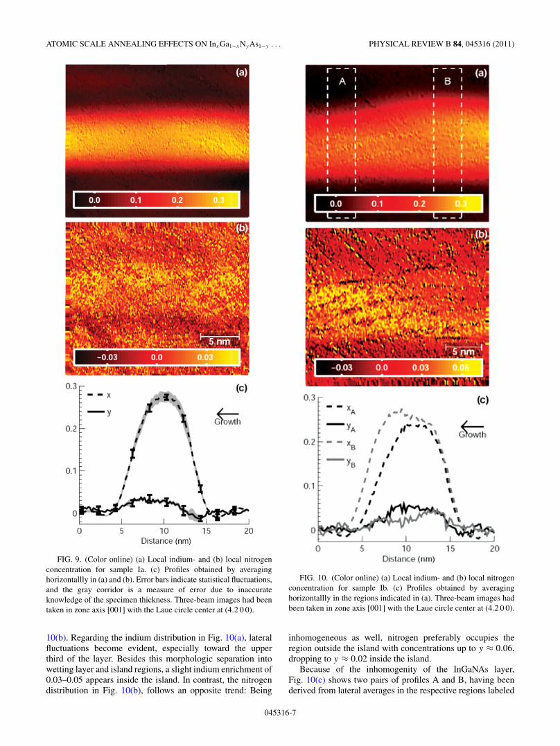
FIG. 9. (Color online) (a) Local indium- and (b) local nitrogenconcentration for sample Ia. (c) Profiles obtained by averaginghorizontallly in (a) and (b). Error bars indicate statistical fluctuations,and the gray corridor is a measure of error due to inaccurateknowledge of the specimen thickness. Three-beam images had beentaken in zone axis [001] with the Laue circle center at (4.2 0 0).
10(b). Regarding the indium distribution in Fig. 10(a), lateralfluctuations become evident, especially toward the upperthird of the layer. Besides this morphologic separation intowetting layer and island regions, a slight indium enrichment of0.03–0.05 appears inside the island. In contrast, the nitrogendistribution in Fig. 10(b), follows an opposite trend: Being
FIG. 10. (Color online) (a) Local indium- and (b) local nitrogenconcentration for sample Ib. (c) Profiles obtained by averaginghorizontallly in the regions indicated in (a). Three-beam images hadbeen taken in zone axis [001] with the Laue circle center at (4.2 0 0).
inhomogeneous as well, nitrogen preferably occupies theregion outside the island with concentrations up to y ≈ 0.06,dropping to y ≈ 0.02 inside the island.
Because of the inhomogenity of the InGaNAs layer,Fig. 10(c) shows two pairs of profiles A and B, having beenderived from lateral averages in the respective regions labeled
045316-7

KNUT MULLER et al. PHYSICAL REVIEW B 84, 045316 (2011)
FIG. 11. Photoluminescence spectra for the laser structures in-vestigated by TEM. After 15 min of thermal annealing under N2
stabilization, the PL peak intensity increases by a factor of 20 butshifts about 65 nm toward higher energies. Spectra were recorded atroom temperature.
in Fig. 9(a). Here, error bars have been omitted to point outprofile shape. However, thickness errors are comparable tothose in Fig. 9(c), whereas statistical fluctuations are slightlylarger due to the narrow areas for averaging. As expected,indium profiles xA,B exhibit fluctuations of about 2.5 nm forthe layer thickness and differ in maximum indium amountsby about 0.04. Compared to the symmetric indium profile forsample Ia, mainly the profile for xA here is asymmetric: Aftergradual increase, the indium content saturates to a maximumin the upper half of the layer and then decreases rapidly.
The nitrogen profiles yA,B in Fig. 10(c) differ significantlyin shape and reveal different nitrogen contents as mentionedabove. However, yA shows up a maximum amount of about0.05 and is not only symmetric with respect to the center ofthe wetting layer but also in phase with profile xA. Concerningthe gray curve yB , slight nitrogen enrichment up to yB = 0.05at incipient layer formation is observed which decays to about0.02 during further growth and increasing indium content asexpressed by profile xB .
B. Annealing of InGaNAs: Optical properties
As one expects from the TEM results, optical performanceof samples Ia and Ib changes drastically by annealing asbecomes obvious in the PL spectra shown in Fig. 11. Scaling ofboth curves to comparable peak intensities requires a factor of20 for as-grown sample Ib, demonstrating strong improvementin light output efficiency by thermal annealing. Unfortunately,this happens at the expense of spectral performance as a strongblue shift of about 65 nm or, equivalantly, 60 meV occurs.
C. Application to a solar cell structure
As a third evaluation, we present results for a lattice-matched InGaNAs layer in sample II, being a typical setupfor solar cell applications. These results are of particularinterest from the methodological point of view, becauseconsistency with compositional analysis of this sample usingdifferent TEM methods15 or x-ray diffraction and band-gapmeasurements3 for a sample grown under same conditionsmay be checked.
Except for the fact that compositions uniquely range inthe low-indium regime according to Fig. 6, evaluation iscompletely analogous here and results in composition mapsdepicted in Figs. 12(a) and 12(b). Both indium and nitrogenreveal laterally homogeneous distributions of x ≈ 0.085 andy ≈ 0.03, respectively. As in Sec. V A, composition evaluationwas performed for thicknesses between 10 and 80 nm, ofwhich the 30 nm result is shown. A compact presentationof mean concentration characteristics and errors is shown inform of profiles in Fig. 12 (c) that have been obtained fromhorizontal averages over the full maps [Figs. 12(a) and 12(b)].Lateral compositional fluctuations, measured in terms of thestandard deviation represented by the black bars, stay below±0.01 and are independent of the magnitude of x and y.In contrast, the gray corridor, in which all results betweenthicknesses of 10 and 80 nm fall, widens to diameters of�x ≈ 0.012 with increasing composition. However, a meanindium composition x = 0.088 ± 0.01 and a mean nitrogencontent y = 0.03 ± 0.01 can be assigned to sample II fromFig. 12(c). Finally, the nitrogen profile exhibits marginalenrichment of this element at the layer interfaces, which
FIG. 12. (Color online) Concentration evaluation yielding (a) local indium and (b) local nitrogen distribution for sample II exemplarilyfor a thickness of 30 nm. (c) Respective profiles obtained by averaging horizontallly in (a) and (b). Error bars are drawn each 2 nm only andindicate statistical fluctuations, and the gray corridor is a measure of error due to inaccurate knowledge of the specimen thickness. Three-beamimages had been taken in zone axis [001] with the Laue circle center at (4.2 0 0).
045316-8
ATOMIC SCALE ANNEALING EFFECTS ON InxGa1−xNyAs1−y . . . PHYSICAL REVIEW B 84, 045316 (2011)
nevertheless ranges inside the error bars. Whether this is indeeda physical effect or an artifact of, e.g., the measurement of localfringe distances, will be discussed in Sec. VI.
VI. DISCUSSION
A. Disorder in the Bloch-wave limit
By definition of additional absorptive form factors inSec. IV A, we intended to close the gap between the correctsimulation of Pendellosung plots under the influence of Huangscattering losses caused by SAD. Although not perfect, ourapproach agrees much better with a full multislice calcula-tion than using absorptive form factors for thermal diffusescattering alone. This is a marginal effect when only a fewstrong beams are excited, as is the case for the systematicrow condition.15 However, the method presented here relieson images taken near zone axis [001] where many beams areinvolved and the beam of interest, 020, is of low intensity.For example, neglect of Huang scattering decreases maximumconcentrations in Fig. 9(c) by about 0.02 for indium and 0.01for nitrogen.
A legitimate question is why the Bloch-wave approachis frequently used even in the presence of static besidesthermal disorder, whereas multislice methods in combinationwith today’s computer capacity can do without any symmetryrequirements. Until now, this is true as long as chemicalbonding is negligible, because the MASA approach yieldsbonding effects only for perfect crystals, or, equivalently,discrete spatial frequencies. Efficient full density functionaltheory calculations of the electron density in realistic crystalsupercells are still too computationally demanding. Therefore,adapting the real part of the ideal crystal potential to bondingand SAD, and the imaginary part to losses arising fromthermal and static disorder, means an efficient way to simulatediffraction patterns if only Bragg spots are of interest.
B. Composition mapping
The three-beam method presented here is, in principle, aconsequent combination of strain state analysis and compo-sition evaluation by lattice fringe analysis (CELFA)18 andrequires low experimental effort provided that an aperture isavailable that suppresses nonlinear imaging artifacts on the220 and 020 diffractogram reflections. In contrast to off-axistechniques,14,15,18,30 the error of inaccurately known specimenthickness becomes significant, so indication of concentration-dependent corridors that contain solutions for physicallyplausible thicknesses should be part of final concentrationprofiles. Nevertheless, one should keep in mind that, eventhough the corridor in Fig. 9(c) corresponds to a thicknessinterval of 70 nm, errors for nitrogen are negligible and thosefor indium do not exceed ±0.01. However, comparison ofFigs. 9 and 10 clearly shows that qualitative observations as tothe correlation of indium and nitrogen distributions or shapeof the layer are not influenced by this error.
In methodological respect, introduction of a new approachshould meet two criteria: First, compared to previouslyreported techniques, application to the same samples mustreproduce former reliable results. Second, it should extendapplicability of existing TEM methods.14,15,31 Concerning the
first argument, it was verified in Sec. V C that mean indium andnitrogen contents agree well with independently found results:For sample II, two-beam imaging under systematic row con-ditions yielded15 x = 0.08 ± 0.01, y = 0.03 ± 0.005 for themean concentrations. Additionally, band-gap measurementsand x-ray diffraction applied to a sample grown under the sameconditions confirmed this composition.3 As to different TEMcomposition quantification techniques, three main argumentsare worth mentioning: First, our approach is standardless in thesense that no ternary quantum well is needed as a reference, asis the case in the studies of Litvinov et al.31 We can drop theassumption that indium incorporation during growth does notdepend on that of nitrogen. Second, the present method is nolonger limited to concentrations far from the phase jump, or,equivalently, to the significant presence of 020 fringes. Thisextends single-image compositional analysis to the importantfield of InGaNAs laser structures. Third, it becomes obviousfrom Sec. V A that an analysis of composition fluctuationsrelies on knowledge of both strain and chemical contrast foreach lattice point that can hardly be assured by superpositionof a systematic row dark field and a zone-axis high-resolutionTEM image.14,30 Of course, this procedure is less critical forInGaNAs layers having homogeneous composition laterally.However, a three-beam approach has been proposed alreadyto solve this problem.14,15
C. Annealing effects
Investigation of compositional fluctuations by TEM mustcritically be analyzed with respect to specimen thickness,because measured quantities are a superposition of sampleproperties in the zone-axis direction. Nevertheless, it is obviousthat the island observed in Fig. 10 is indeed the image ofa single island. If the specimen was much thicker than themean distance between islands, being 20–30 nm accordingto Fig. 7, a blurred layer with homogeneous thickness wouldbe observed. If so, the observation of an InGaNAs layer withhomogeneous thickness after annealing in Fig. 9 could be dueto this effect. However, the 020 fringe intensity would notvanish at the upper interface because at some specimen depthan area with pure GaAs would exist that violates the continuitycondition for the transition between the two possible solutionsaccording to Fig. 6. For thick regions of the as-grown sampleIb this effect was indeed observed.
In short, it is observed here that annealing changes long-range order of both indium and nitrogen. This results in ahomogenization of the nitrogen distribution and symmetricindium concentration profiles. In particular, thermal annealingcauses a dissolution of islands, which leads to a nearly ho-mogeneously thick InGaNAs layer. This observation suggeststhat the increase of PL intensity by a factor of 20 andthe spectral shift of about 60 meV to higher energies isdue to a long-range homogenization of stoichiometry in ourcase. From the experimental point of view, the presence ofnitrogen fluctuations in as-grown InGaNAs is controversiallydiscussed in the literature. For example, Albrecht et al.11 foundindium fluctuations of ±0.05 on length scales of 20 nm buthomogeneous nitrogen content. In contrast, Herrera et al.32
additionally report on nitrogen modulations, resulting inuncoupled indium-rich and nitrogen-rich regions. Common to
045316-9
KNUT MULLER et al. PHYSICAL REVIEW B 84, 045316 (2011)
these analyses is the underlying dark-field imaging techniqueusing, e.g., the 220 reflection. In this respect, simultaneousevaluation of both strain- and chemical-sensitive contrastat identical specimen positions is a requirement to clarifythis issue. Thus, our results tend to confirm findings ofHerrera et al.,32 who interprete composition modulations anddecoupling of nitrogen and indium profiles in the frameworkof spinodal decomposition. However, it is important to notethat characteristics of the InGaNAs layer are highly dependenton growth conditions that differ among research groups.
Our PL spectra exhibit characteristic annealing behavior,since a blue shift of about 60 meV has also been found by Klaret al.4 for the same annealing temperature. However, Klaret al. found no evidence for compositional fluctuations, evenin the as-grown sample. Consequently, this group interpretsannealing effects in terms of preferential coordination ofnearest neighbors, that is, an affinity to form In-N bondsinstead of Ga-N bonds, as has frequently been reportedin conjunction with thermal annealing.4,8,12,30,33,34 In thiswork, direct observation of the dissolution of compositionalmodulations during thermal annealing implies that the changein PL is due to homogenization of stoichiometry. Since Klaret al. used MOVPE, whereas sample I in this work was grownby MBE, one tends to assign different annealing mechanismsto both epitaxial techniques. In fact, there is no contradictionbetween both explanations, because annealing might also havecaused preferential nearest-neighbor configurations here. Inthis respect, Figs. 10 and 9 imply that a dissolution of nitrogen-and indium-rich regions in favor of a more homogeneous layerought to be accompanied by an increase of the frequency ofIn-N bonds.
In the strict sense, structure factors for random alloys,which determine all simulations in this work, should bemodified to take into account preferential bond configurations.So far, we consider the effect on composition maps to besmall with respect to experimental errors and point outthat observations of long-range structural changes remainunchanged. Furthermore, both high-resolution and dark-fieldTEM provide only indirect access to study preferential nearest-neighbor configurations. Instead, it is advisable to makecombined use of TEM and, e.g., extended x-ray-absorptionfine-structure investigations, which are not available for thesamples investigated here but left as a future task.
Additionally, literature offers various findings for the im-pact of annealing on the nitrogen profile. Grillo et al.14 deducestrong nitrogen enrichment at the well edges, confirmed bylater studies of Albrecht et al.30 with the same method, whereadditional out-diffusion is found and assigned to the blue shiftof PL peaks. In contrast, Volz et al. observed no annealingeffect on nitrogen profiles in InGaNAs.10 One common resultof these groups and the present report is that annealing leadsto lateral homogenization of nitrogen content, although theprofiles themselves differ a lot. According to Fig. 9(c), atendency of nitrogen to diffuse out of the well in the growthdirection may be derived from the fact that both profiles are notcentered around the same position, but this must be considereda minor effect, which is not responsible for the change in PL.Concerning the indium concentration profile, the Gaussianshape observed here after annealing, in principle, agrees withthat of previous reports.30
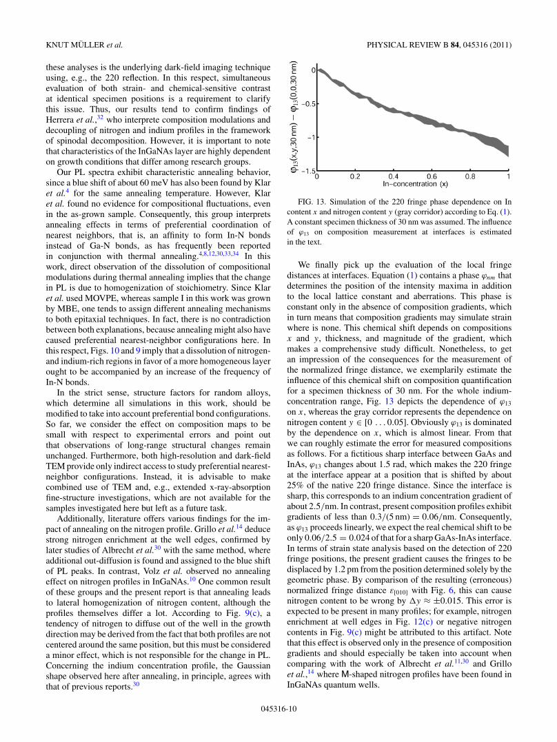
FIG. 13. Simulation of the 220 fringe phase dependence on Incontent x and nitrogen content y (gray corridor) according to Eq. (1).A constant specimen thickness of 30 nm was assumed. The influenceof ϕ13 on composition measurement at interfaces is estimatedin the text.
We finally pick up the evaluation of the local fringedistances at interfaces. Equation (1) contains a phase ϕnm thatdetermines the position of the intensity maxima in additionto the local lattice constant and aberrations. This phase isconstant only in the absence of composition gradients, whichin turn means that composition gradients may simulate strainwhere is none. This chemical shift depends on compositionsx and y, thickness, and magnitude of the gradient, whichmakes a comprehensive study difficult. Nonetheless, to getan impression of the consequences for the measurement ofthe normalized fringe distance, we exemplarily estimate theinfluence of this chemical shift on composition quantificationfor a specimen thickness of 30 nm. For the whole indium-concentration range, Fig. 13 depicts the dependence of ϕ13
on x, whereas the gray corridor represents the dependence onnitrogen content y ∈ [0 . . . 0.05]. Obviously ϕ13 is dominatedby the dependence on x, which is almost linear. From thatwe can roughly estimate the error for measured compositionsas follows. For a fictitious sharp interface between GaAs andInAs, ϕ13 changes about 1.5 rad, which makes the 220 fringeat the interface appear at a position that is shifted by about25% of the native 220 fringe distance. Since the interface issharp, this corresponds to an indium concentration gradient ofabout 2.5/nm. In contrast, present composition profiles exhibitgradients of less than 0.3/(5 nm) = 0.06/nm. Consequently,as ϕ13 proceeds linearly, we expect the real chemical shift to beonly 0.06/2.5 = 0.024 of that for a sharp GaAs-InAs interface.In terms of strain state analysis based on the detection of 220fringe positions, the present gradient causes the fringes to bedisplaced by 1.2 pm from the position determined solely by thegeometric phase. By comparison of the resulting (erroneous)normalized fringe distance ε[010] with Fig. 6, this can causenitrogen content to be wrong by �y ≈ ±0.015. This error isexpected to be present in many profiles; for example, nitrogenenrichment at well edges in Fig. 12(c) or negative nitrogencontents in Fig. 9(c) might be attributed to this artifact. Notethat this effect is observed only in the presence of compositiongradients and should especially be taken into account whencomparing with the work of Albrecht et al.11,30 and Grilloet al.,14 where M-shaped nitrogen profiles have been found inInGaNAs quantum wells.
045316-10

ATOMIC SCALE ANNEALING EFFECTS ON InxGa1−xNyAs1−y . . . PHYSICAL REVIEW B 84, 045316 (2011)
VII. SUMMARY AND CONCLUSIONS
A method for the measurement of strain and contrastin quaternary InGaNAs was introduced, which allows forsimultaneous quantification of indium and nitrogen content.The technique exploits one high-resolution TEM micrographformed by three beams that are not coupled with respect tononlinear imaging. Bloch-wave simulations of reference beamamplitudes included the finding of optimized imaging condi-tions and account for absorption ascribed to Huang scatteringat SAD, as well as chemical bonding and the influence of SAD(found by VFF relaxation) on structure factors. Application ofthe three-beam method to an In0.28Ga0.72N0.025As0.975 quantumlayer before and after thermal annealing has shown thatannealing caused a dissolution of indium- and nitrogen-richregions in favor of a homogeneous layer with Gaussian-shaped indium profile. In addition, recorded room-temperaturephotoluminescence exhibits a blue shift of about 60 meV andan increase by a factor of 20 after annealing, for which theobserved structural changes were made responsible.
In this contribution, method and application take equal partso the latter was restricted to one as-grown and one annealedstructure. From the significant redistribution of impurity atomsof all species on length scales of 10 nm we concludethat interpretation of PL spectra solely in the context ofnearest-neighbor configurations can be insufficient. However,
detailed understanding of structural transitions as a functionof annealing conditions such as temperature or pressure andcorrelation to optical properties and growth conditions is leftas a future task.
As our method falls in the category of conventionalhigh-resolution TEM without the explicit need for advancedequipment such as imaging correctors, it is easy to apply,provided that a proper objective aperture for three-beamimaging is available. In principle, the same holds for thesimulation of reference data since Bloch-wave simulations arecapable for desktop computers. This holds even if bondingand SAD are to be included since MASA and VFF provideefficient but accurate approximations, respectively. In thatrespect absorptive form factors for SAD scattering derivedhere are not only of academical interest but may also affectconcentration profiles more or less strongly, depending on theamount of nitrogen and imaging conditions.
ACKNOWLEDGMENTS
This work was supported by the Deutsche Forschungs-gemeinschaft (DFG) under contract nos. RO 2057/4,SCHO 1196/3, VO805/4, and VO805/5. K.M. also thanksthe Physics International Postgraduate Programme (PIP) atBremen University.
*[email protected]. Kondow, T. Kitatani, M. C. Larson, K. Nakahara, K. Uomi, andH. Inoue, J. Cryst. Growth 188, 255 (1998).
2M. Hetterich, M. D. Dawson, A. Y. Egorov, D. Bernklau, andH. Riechert, Appl. Phys. Lett. 76, 1030 (2000).
3K. Volz, W. Stolz, J. Teubert, P. J. Klar, W. Heimbrodt, F. Dimroth,C. Baur, and A. W. Bett, in Dilute III/V Nitride Semiconductors andMaterial Systems (Springer, Berlin, 2008), pp. 369–404.
4P. J. Klar, H. Gruning, J. Koch, S. Schafer, K. Volz, W. Stolz,W. Heimbrodt, A. M. Kamal Saadi, A. Lindsay, and E. P. O’Reilly,Phys. Rev. B 64, 121203 (2001).
5H. Djie, D.-N. Wang, B. Ooi, J. Hwang, X.-M. Fang, Y. Wu,J. Fastenau, and W. Liu, Thin Solid Films 515, 4344 (2007).
6J.-Y. Duboz, J. A. Gupta, Z. R. Wasilewski, J. Ramsey, R. L.Williams, G. C. Aers, B. J. Riel, and G. I. Sproule, Phys. Rev.B 66, 085313 (2002).
7A. Pomarico, M. Lomascolo, R. Cingolani, A. Y. Egorov, andH. Riechert, Semicond. Sci. Technol. 17, 145 (2002).
8O. Rubel, K. Volz, T. Torunski, S. D. Baranovskii, F. Grosse, andW. Stolz, Appl. Phys. Lett. 85, 5908 (2004).
9K. Kim and A. Zunger, Phys. Rev. Lett. 86, 2609 (2001).10K. Volz, T. Torunski, O. Rubel, W. Stolz, P. Kruse, D. Gerthsen,
M. Schowalter, and A. Rosenauer, J. Appl. Phys. 102, 083504(2007).
11M. Albrecht, V. Grillo, T. Remmele, H. P. Strunk, A. Y. Egorov,G. Dumitras, H. Riechert, A. Kaschner, R. Heitz, and A. Hoffmann,Appl. Phys. Lett. 81, 2719 (2002).
12K. Volz, T. Torunski, O. Rubel, and W. Stolz, J. Appl. Phys. 104,053504 (2008).
13C. S. Peng, E. M. Pavelescu, T. Jouhti, J. Konttinen, and M. Pessa,Solid-State Electron. 47, 431 (2003).
14V. Grillo, M. Albrecht, T. Remmele, H. P. Strunk, A.Yu. Egorov, and H. Riechert, J. Appl. Phys. 90, 3792(2001).
15K. Muller, M. Schowalter, A. Rosenauer, O. Rubel, and K. Volz,Phys. Rev. B 81, 075315 (2010).
16P. N. Keating, Phys. Rev. 145, 637 (1966).17A. Rosenauer, M. Schowalter, F. Glas, and D. Lamoen, Phys. Rev.
B 72, 085326 (2005).18A. Rosenauer, U. Fischer, D. Gerthsen, and A. Forster,
Ultramicroscopy 72, 121 (1998).19A. Rosenauer and M. Schowalter, in Springer Proceedings in
Physics, edited by A. G. Cullis and P. A. Midgley, (Springer, Berlin,2007), Vol. 120, pp. 169–172.
20M. Schowalter, A. Rosenauer, J. T. Titantah, and D. Lamoen, ActaCrystallogr. Sect. A 65, 5 (2009).
21A. Rosenauer, M. Schowalter, J. T. Titantah, and D. Lamoen,Ultramicroscopy 108, 1504 (2008).
22A. Weickenmeier and H. Kohl, Acta Crystallogr. Sect. A 47, 590(1991).
23D. M. Bird and Q. A. King, Acta Crystallogr. Sect. A 46, 202 (1990).24O. Rubel, I. Nemeth, W. Stolz, and K. Volz, Phys. Rev. B 78, 075207
(2008).25F. Glas, Philos. Mag. 84, 2055 (2004).26D. Van Dyck, Ultramicroscopy 109, 677 (2009).27K. Huang, Proc. R. Soc. London A 190, 102 (1947).28C. R. Hall, P. B. Hirsch, and G. R. Booker, Philos. Mag. 14, 979
(1966).
045316-11

KNUT MULLER et al. PHYSICAL REVIEW B 84, 045316 (2011)
29Z. L. Wang, Elastic and Inelastic Scattering in Electron Diffractionand Imaging (Plenum Press, New York, 1995).
30M. Albrecht, H. Abu-Farsakh, T. Remmele, I. Hausler, L. Geelhaar,H. Riechert, and J. Neugebauer, Phys. Rev. Lett. 99, 206103 (2007).
31D. Litvinov, D. Gerthsen, A. Rosenauer, M. Hetterich, A. Grau,P. Gilet, and L. Grenouillet, Appl. Phys. Lett. 85, 3743 (2004).
32M. Herrera, D. Gonzalez, M. Hopkinson, M. Gutierrez, P. Navaretti,H. Y. Liu, and R. Garcia, J. Appl. Phys. 97, 073705 (2005).
33O. Rubel, B. Kunert, S. D. Baranovskii, F. Grosse, K. Volz, andW. Stolz, Phys. Rev. B 74, 195206 (2006).
34A. Jenichen, C. Engler, G. Leibiger, and V. Gottschalch, Surf. Sci.574, 144 (2005).
045316-12