Appendix A: Physics Primer for Electronic Devices
66
Appendix A: Physics Primer for Electronic Devices A.1 Quantum Mechanics A.1.1 Particles and Wavefunctions: Elementary Wave Mechanics We normally think of particles in a classical or Newtonian mechanics sense; that is, they occupy a specific point in space with well-defined position given by spatial coordinates and their velocity or momentum at any given instant is also precisely specified. In many cases, this picture is clearly satisfactory and very accurate. However, it is found that particularly when describing microscopic systems such as atoms and electrons it is more accurate to represent each particle by a wavefunction Ψ which describes its distribution or amplitude as a function of space 1 and time coordinates. For example, the plane wave is a harmonic function that is infinite in extent and periodic in both space and time Ψ x; t ð Þ¼ e i kxωt ð Þ (A.1) 2 where k ¼ 2π λ and ω ¼ 2πv are the wave vector (or wave number) and angular frequency, respectively. 3 In quantum mechanics the basic equation of motion that governs the wavefunction is the Schro¨dinger equation: h 2 2m ∂ 2 ∂x 2 Ψ x; t ð Þþ Vx ðÞΨ x; t ð Þ¼ i h ∂ ∂t Ψ x; t ð Þ (A.2) 1 Most of the discussion will only involve one spatial dimension (e.g., x) for simplicity, but all the results can be generalized to three dimensions in a straightforward manner. 2 Recall e iθ ¼ cos θ + i sin θ. 3 λ and ν are the wavelength and frequency, respectively. C. Papadopoulos, Solid-State Electronic Devices: An Introduction, Undergraduate Lecture Notes in Physics, DOI 10.1007/978-1-4614-8836-1, © Springer Science+Business Media New York 2014 209
-
Upload
khangminh22 -
Category
Documents
-
view
4 -
download
0
Transcript of Appendix A: Physics Primer for Electronic Devices

Appendix A: Physics Primer
for Electronic Devices
A.1 Quantum Mechanics
A.1.1 Particles and Wavefunctions: Elementary WaveMechanics
Wenormally think of particles in a classical or Newtonianmechanics sense; that is, they
occupy a specific point in space with well-defined position given by spatial coordinates
and their velocity ormomentum at any given instant is also precisely specified. Inmany
cases, this picture is clearly satisfactory and very accurate. However, it is found that
particularlywhen describingmicroscopic systems such as atoms and electrons it ismore
accurate to represent each particle by awavefunctionΨ which describes its distributionor amplitude as a function of space1 and time coordinates. For example, the plane wave
is a harmonic function that is infinite in extent and periodic in both space and time
Ψ x; tð Þ ¼ ei kx�ωtð Þ (A.1)2
where k ¼ 2πλ and ω ¼ 2πv
are the wave vector (or wave number) and angular frequency, respectively.3
In quantummechanics the basic equation of motion that governs the wavefunction
is the Schrodinger equation:
� �h2
2m
∂2
∂x2Ψ x; tð Þ þ V xð ÞΨ x; tð Þ ¼ i�h
∂∂t
Ψ x; tð Þ (A.2)
1Most of the discussion will only involve one spatial dimension (e.g., x) for simplicity, but all the
results can be generalized to three dimensions in a straightforward manner.2 Recall eiθ ¼ cos θ + i sin θ.3 λ and ν are the wavelength and frequency, respectively.
C. Papadopoulos, Solid-State Electronic Devices: An Introduction,Undergraduate Lecture Notes in Physics, DOI 10.1007/978-1-4614-8836-1,
© Springer Science+Business Media New York 2014
209

where �h ¼ h2π
h is Planck’s constant, V(x) is the potential energy of the particle, m is its mass, and
i2 ¼ �1.
The Schrodinger equation is a separable partial differential equation and its
solutions can be shown to take the form
Ψ x; tð Þ ¼ ψ xð Þexp � iEt
�h
� �(A.3a)
where ψ(x) solves the energy eigenvalue equation4:
� �h2
2m
d2
dx2þ V xð Þ
� �ψ xð Þ ¼ Eψ xð Þ (A.3b)
for a particle with energy E.The Schrodinger equation is also linear, so further wavefunction solutions can be
constructed from linear superpositions of the basic solutions:
Ψ x; tð Þ ¼Xn
anψn xð Þexp � iEnt
�h
� �(A.4)
Equation (A.4) gives the most general solution where n is an integer labeling thedifferent solutions and scalar coefficients an. It can be seen that once the energy
eigenvalue equation has been solved the complete solution for the wavefunction
can be directly obtained, which makes the energy eigenvalues and eigenfunctions
particularly important.
A series of examples will help to illustrate the above concepts.
Example A.1: Free Particle For a particle that is completely free and not subject to
any potentials V(x) ¼ 0 and we therefore obtain the following equations:
� �h2
2m
∂2
∂x2Ψ x; tð Þ ¼ i�h
∂∂t
Ψ x; tð Þ, � �h2
2m
d2ψ xð Þdx2
¼ Eψ xð Þ
Solutions to these equations are the plane waves that we saw earlier in Eq. (A.1):
Ψ x; tð Þ ¼ ei kx�ωtð Þ
4ψ(x) is known as the energy eigenfunction.
210 Appendix A: Physics Primer for Electronic Devices

where some important relations now arise as a result, namely,5
E ¼ �h2k2
2m
p ¼ �hk ¼ h
λ
where the latter expression is known as the de Broglie relation. In addition, it can beseen that
E ¼ �hω ¼ hν
(attributed to Planck and Einstein, respectively).
Example A.2: Bound Particle; Infinite Quantum Well In this case, the particle is
completely confined to a small region of space. The bound particle can be modeled
using an infinite square well potential shown in Fig. A.1a, often referred to as a
“particle in a box” problem. Inside the well the potential energy is zero whereas at the
boundaries it rapidly increases to infinity and the particle cannot escape or exist
outside the well. Mathematically, for a well of length L, this corresponds to
V xð Þ ¼ 0, 0 < x < L; V xð Þ ¼ 1, otherwise
n=1
n=2
n=3
Infinite square well
2aE1
E2
E3
ψ1
ψ2
ψ3
Ground state
1st excited state
2nd excited state
L
n=1
n=2
n=3
Infinite square well
2aE1
E2
E3
y1
y2
y3
Ground state
1st excited state
2nd excited state
L
V(x)
0 L
a
b∞ ∞
Fig. A.1 Infinite square well problem. (a) Potential well. (b) Energy eigenfunctions for three
lowest energy states
5 Note that the relation E ¼ �h2k2/2m does not apply to photons (i.e., massless particles). In general,
we are also assuming that particles with mass are not traveling at very high velocities; in other
words this is a nonrelativistic treatment of quantum mechanics and sufficient for most purposes
when dealing with solid-state electronic devices. Also note that this equation is analogous to the
classical expression for kinetic energy E ¼ p2/2m, where p is the momentum.
Appendix A: Physics Primer for Electronic Devices 211

In order to solve the energy eigenvalue problem for this potential, we can note that
inside the well the particle is not subjected to any potential and thus the solution
should be the same as the free particle case we found earlier, i.e., a plane wave or in
other words a combination of cosine and sine waves. However, in the case of the
infinite quantum well we must also take heed of the boundary conditions at the edges
of the well. Since the particle cannot exist outside the well we can write
ψ 0ð Þ ¼ ψ Lð Þ ¼ 0
This means that the cosine function is not suitable (since it does not equal zero at
the origin) and we can therefore write the energy eigenfunction as
ψ xð Þ ¼ sin kx
Now, applying the boundary condition at x¼ L to this function yields the followingrelation:
sin kL ¼ 0 ) kL ¼ nπ ) k ¼ nπ
L
where n is a nonzero positive integer. Therefore by confining the particle to a “box”its energy levels become quantized:
En ¼ �h2k2
2m¼ �h2π2n2
2mL2
This is an important result. It shows that the energy levels are inversely propor-
tionally to the width of the well squared; i.e., more confinement (smaller well) leads to
higher energy levels. In addition, the energy levels become increasingly spaced out as
n increases due to the factor of n2. It also tells us the lowest energy a particle can havewhen confined to a region of space and that this must be a finite value, known as
the ground state energy. Classically, we would expect a particle to eventually settle to
the bottom of the well with zero energy. The quantum mechanical description of
nature precludes this from happening and although the infinite square well is a
simplified or “toy” model it serves to illustrate many concepts that occur in real
systems and is often a good enough approximation to use for first-order calculations.
In particular, the finite ground state energy is one of the reasons that matter is stable:
without the wave behavior of particles, the electron and proton in a hydrogen atom,
for example, would simply collapse into each other.
The energy eigenfunctions are explicitly (apart from a multiplicative constant,
A to be determined),
ψn xð Þ ¼ Asinnπx
L, n ¼ 1, 2, 3, . . .
and are plotted in Fig. A.1b, for the first 3 levels.
212 Appendix A: Physics Primer for Electronic Devices

A.1.2 Interpretation of the Wave Function
The wavefunction itself is not something that can be directly measured. The
standard interpretation of the wavefunction is based on the following:
Ψ x; tð Þj j2dx ¼ probability of finding the particle
between x and xþ dx at time t
� �(A.5a)
The magnitude of the wavefunction squared can be thought of as representing
the “intensity” of the wave and represents the probability that a particle exists at a
certain point in space. For particles which are conserved, in other words particles
that cannot be destroyed, we require that the net probability for finding the particle
somewhere in space must add up to 1, orð1�1
Ψ x; tð Þj j2dx ¼ 1 (A.5b)
known as the normalization condition for the wavefunction. For example, the
wavefunctions of the particle in an infinite quantum well must obey
1 ¼ðL0
Ψ n x; tð Þj j2dx ¼ðL0
ψn xð Þj j2dx
¼ðL0
A2 sin 2 nπx
Ldx ) A ¼
ffiffiffi2
L
s (A.6a)
Thus the complete wavefunction for the infinite square well problem is given by
Ψ n x; tð Þ ¼ffiffiffi2
L
rsin
nπx
Lexp
�iEnt
�h
� �(A.6b)
Note that there is one important exception to the normalization condition: Plane
waves cannot be normalized in the manner above because they have infinite extent.
However, they are still very useful for calculations in which we are only interested
in relative probabilities, as we will see later on.
A.1.3 Operators and Physical Quantities
In quantum mechanics all physically observable quantities are represented by
operators. For example, we have already seen the energy operator in the energy
eigenvalue equation:
� �h2
2m
d2
dx2þ V xð Þ
� �ψ xð Þ ¼ Eψ xð Þ , Hψ xð Þ ¼ Eψ xð Þ (A.7)
Appendix A: Physics Primer for Electronic Devices 213
The operator in brackets6 representing energy is known as the Hamiltonian, H.If the wavefunction Ψ of a particle corresponds to an eigenfunction of the operator
representing an observable being measured, then that observable has a definite value.
For example, the energy of a particle in the first excited state of the infinite quantum
well has a precise value given by E1.
A.1.4 Expectation Values
The expectation or average value of a quantity associated with a particle can be found
from its wavefunction. For example, the average position of a particle is given by
x tð Þh i ¼ðx Ψ x; tð Þj j2dx ¼
ðΨ � x; tð Þ x Ψ x; tð Þdx (A.8)
which is essentially a weighted sum of the quantity of interest with the wavefunction
probability distribution. Using this equation we can calculate the average position for
a particle in the lowest energy level of the infinite quantum well as
x tð Þh i ¼ 2
L
ðL0
xsin 2 πx
Ldx ¼ L
2(A.9)7
Note that in this case the average position is constant in time—this is a general
property of energy eigenfunctions and they are referred to as stationary states. Allexpectation values of stationary states are constant in time.
In general the expectation value of some physical observable, Q, is given by
Qh i ¼ðΨ � x; tð Þ Q Ψ x; tð Þdx (A.10)
A.1.5 Uncertainty Relations
A measure of the uncertainty or dispersion8 of an observable associated with a
particle is given by the root-mean-square (RMS) deviation:
ΔA � A2� �� Ah i2
1=2
(A.11)
for an operator A.
6 This can be thought of as the sum of kinetic plus potential energy just as in classical systems.7 Note that the expectation value of position for any energy eigenstate in the infinite quantum well
will always be L/2 due to the mirror image symmetry about the center of the potential well.8 In this case dispersion refers to the spread of an observable about some average value.
214 Appendix A: Physics Primer for Electronic Devices

There are two very important uncertainty relations in quantum mechanics that
arise from Eq. (A.11) and the properties of solutions to the Schrodinger equation:
The first relates the uncertainty between position and momentum, known as the
Heisenberg uncertainty principle:
ΔxΔp � 1
2�h (A.12a)
This oft-quoted relation tells us that we can never know the exact position and
momentum of a particle at the same time.9
A different type of uncertainty that arises when dealing with quantum systems
(such as lasers) is the energy–time uncertainty relation:
ΔE δt � 1
2�h (A.12b)
Here, the “uncertainty” in time is not the same type as in the observables we
looked at before, which arose from their probability distributions. (Time is a parame-
ter in conventional treatments of quantum mechanics and does not have any inherent
uncertainty.) Rather, δt is the time interval required for an appreciable change to
occur in the properties of the system under study.
Example A.3: Energy–Time UncertaintyFixed stationary state We know that for an energy eigenstate ΔE ¼ 0 and thus the
energy–time uncertainty relation yields δt ¼ 1(i). In other words, the system does
not change, as expected for a state fixed in time.
Excited stateConsider now the more interesting case of a particle that has been excited to some
higher energy level and then decays. For a concrete example, suppose as shown in
Fig. A.2 that a particle is in the second (n ¼ 2) energy level of a quantum well and
νh
E1
E2
h = E2 − E1ν
Fig. A.2 Excited state.
Particle in upper energy
level relaxes to ground state
with emission of a photon
9 This should seem, along with many other results of quantum mechanics, somewhat counterintui-
tive. It may help to note that the scale set by Planck’s constant is very small, which at least partly
explains why everyday macroscopic objects do not normally display explicit wavelike behavior.(i)Or vice-versa; δt ¼ 1 ) ΔE ¼ 0.
Appendix A: Physics Primer for Electronic Devices 215
spontaneously decays to the lowest (ground) state by the emission of a photon. If the
typical lifetime for this decay to occur is given by τ then the energy–time uncertainty
imposes the condition
ΔE2 � �h
2τ
After the particle reaches its ground state, no further decay can occur and we are
back to a fixed stationary state which does not change in time, as in the previous
case. In practice, the spread in energies determined by the energy–time uncertainty
relation imposes a fundamental limit on how sharp the output spectrum of light-
emitting devices can be.
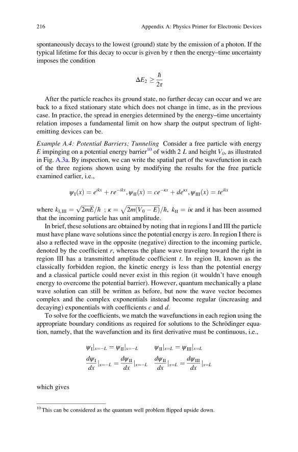
Example A.4: Potential Barriers; Tunneling Consider a free particle with energy
E impinging on a potential energy barrier10 of width 2 L and height V0, as illustrated
in Fig. A.3a. By inspection, we can write the spatial part of the wavefunction in each
of the three regions shown using by modifying the results for the free particle
examined earlier, i.e.,
ψ I xð Þ ¼ eikx þ re�ikx,ψ II xð Þ ¼ ce�κx þ deκx,ψ III xð Þ ¼ teikx
where kI, III ¼ffiffiffiffiffiffiffiffiffi2mE
p=�h ; κ ¼ ffiffiffiffiffiffiffiffiffiffiffiffiffiffiffiffiffiffiffiffiffiffiffiffi
2m V0 � Eð Þp=�h, kII ¼ iκ and it has been assumed
that the incoming particle has unit amplitude.
In brief, these solutions are obtained by noting that in regions I and III the particle
must have plane wave solutions since the potential energy is zero. In region I there is
also a reflected wave in the opposite (negative) direction to the incoming particle,
denoted by the coefficient r, whereas the plane wave traveling toward the right in
region III has a transmitted amplitude coefficient t. In region II, known as the
classically forbidden region, the kinetic energy is less than the potential energy
and a classical particle could never exist in this region (it wouldn’t have enough
energy to overcome the potential barrier). However, quantum mechanically a plane
wave solution can still be written as before, but now the wave vector becomes
complex and the complex exponentials instead become regular (increasing and
decaying) exponentials with coefficients c and d.To solve for the coefficients, we match the wavefunctions in each region using the
appropriate boundary conditions as required for solutions to the Schrodinger equa-
tion, namely, that the wavefunction and its first derivative must be continuous, i.e.,
ψ I x¼�L ¼ ψ II x¼�Ljj ψ II x¼L ¼ ψ III x¼Ljjdψ I
dxx¼�Lj ¼ dψ II
dxx¼�Lj dψ II
dxx¼Lj ¼ dψ III
dxx¼Lj
which gives
10 This can be considered as the quantum well problem flipped upside down.
216 Appendix A: Physics Primer for Electronic Devices

V(x)
0 L-L
V0
x
I II III
ψE
Classicallyforbiddenregion
particle wavefunctionpast the barrier
particle energy
incoming particlewavefunction
Yincidentyexit
E
Tip
Az ~ 1 nm
Sample
I(x, y)
b
c
a
Fig. A.3 Potential barrier problem. (a) Square potential barrier with incident plane wave shown.
(b) Resulting wavefunction at a given instant in time for a particle tunneling through the barrier.
(c) Scanning tunneling microscope schematic and surface scan showing atomic resolution. Quan-
tum corrals created by manipulating atoms on a surface to confine the electrons of a metal are also
shown (IBM Corp.)

x ¼ �L;e�ikL þ reikL ¼ ceκL þ de�κL
ike�ikL � ikreikL ¼ �κceκL þ κde�κL
x ¼ L;ce�κL þ deκL ¼ teikL
�κce�κL þ κdeκL ¼ ikteikL
These 4 equations can be solved for the 4 unknown coefficients. For example,
the amplitude of the transmitted wave is
t ¼ �4ikκe�2κLe�2ikL
κ � ikð Þ2 � κ þ ikð Þ2e�4κL
If κL is fairly large (in other words if the barrier is tall and wide) the probability
of transmission,
T ¼ ��t��2can be approximated as
T / exp �4κLð Þ
Thus the particle has a finite probability of transmission through the barrier
that depends sensitively on the height and width of the barrier. In particular,
if the barrier becomes thin the transmission can be quite significant. This
inherently quantum mechanical phenomenon is known as tunneling. The spatial
part of the wavefunction for a particle tunneling through the barrier is sketched
in Fig. A.3b.
A direct application of quantum mechanical tunneling is the scanning tunneling
microscope (STM),11 which employs the very sensitive dependence of tunneling with
distance to form images with atomic resolution by scanning a sharp tip across a
surface (Fig. A.3c). STM measures the tunneling current between a very sharp
metallic tip (e.g., PtIr) and the surface being studied. The tip is scanned across the
surface using a piezoelectric scanner(s) and its height is also controlled in a similar
manner. Typically an order of magnitude change in current is observed for a 0.1 nm
change in tip height and this results in the very high vertical resolution of STM
(<1 pm). STM can also be used to manipulate individual atoms as illustrated by the
well-known “quantum corrals” created by researchers at IBM.
11 Invented by Binning and Rohrer at IBM in 1981.
218 Appendix A: Physics Primer for Electronic Devices

A.1.6 Atoms and the Periodic Table
Hydrogen Atom
The simplest atomic system, hydrogen, consists of one electron and one proton. The
motion of the negatively charged electron about the positively charged fixed
nucleus (Fig. A.4a) can be solved using the Schrodinger equation in 3D for the
central (Coulombic) potential:
V rð Þ ¼ �q2
4πε0r(A.13)
+
– q, m0
r
x z y
rq
rV2
)( −∝
l = 0 1 2 3
a
c
b
Fig. A.4 Hydrogen atom. (a) Negatively charged electron coupled to a fixed proton. (b) Energy
levels versus n and l quantum numbers and Coulombic potential energy superimposed on energy
levels. (c) Illustration of s- and p-orbital wavefunctions (different colors on p-orbitals correspondto positive and negative values of the wavefunction)
Appendix A: Physics Primer for Electronic Devices 219

where r is the distance from the origin (nucleus). The energy eigenfunctions and
eigenvalues in spherical coordinates are given by
ψnlm r; θ;ϕð Þ ¼ Rnl rð ÞYml θ;ϕð Þ (A.14a)
n ¼ 1, 2, 3, . . .l ¼ n� 1, n� 2, n� 3, . . . , 0
mj j ¼ l, l� 1, . . . , 0
En ¼ � m0q4
4πε0ð Þ22�h2n2 (A.14b)
where Rnl(r) are known as the radial wavefunctions and Yml (θ,ϕ) are the spherical
harmonics. Figure A.4b shows sketches of the energy levels versus quantum number
n and position r. Although the wavefunction is now defined by three12 indices, the
energy levels only depend on n. The 1/r dependence of the potential well for the
hydrogen atom leads to the energy levels becoming more closely spaced as
n increases (c.f. infinite square well example). Another occurrence that is very typical
of systems in 2 and 3 dimensions is that several eigenfunctions have the same value of
energy, known as energy degeneracy. The value of the ground state energy level
E1 (�13.6 eV) is known as the ionization energy of hydrogen and represents the
energy required to completely remove the electron from the hydrogen atom.
The explicit solution for the wavefunction of the ground state of the hydrogen
atom is
ψ100 ¼1ffiffiffiπ
p 1
a0
� �3=2e�r=a0 (A.15a)
where a0 is known as the Bohr radius
a0 ¼ 4πε0�h2
m0q2¼ 0:529A
∘(A.15b)
which corresponds to the most probable radius for the electron.13 The Bohr radius is
an important physical parameter that sets the typical length scale of atomic systems.
Two types of hydrogen eigenfunctions or orbitals that are relevant to electronic
devices are illustrated in Fig. A.4c: s-orbitals such as ψ100 are spherically symmetric
while p-orbitals (e.g., ψ210) possess a directionality or polarization with a dumbbell-
like shape.
12 This corresponds to the three spatial dimensions of the hydrogen atomic system.13 Found from the maximum value of the ground state probability distribution integrated over a
spherical shell.
220 Appendix A: Physics Primer for Electronic Devices

Periodic Table
Two additional concepts are required before we can explain the main features of
atomic elements beyond simple hydrogen:
1. Spin
Electrons possess an intrinsic angular momentum known as spin, which leads to a
magnetic moment.14 Electron spin can take one of two values (usually referred to as
spin up and spin down):
s ¼ � �h
2(A.16)
Thus for every energy eigenfunction which represents an electron there also
exist two possible spin states. Therefore in addition to the wavefunction we must
also specify the spin value in order to uniquely define the electron state.
Spins were experimentally identified in 1922 via the Stern–Gerlach experiment,
a simplified representation of which is shown schematically in Fig. A.5.
2. Pauli exclusion principle
An important physical property of particles with half-integer spin (like electrons) is
encapsulated by the following principle:
No more than one electron can be in any given state (wavefunction and spinstate) at the same time.
N
S
Fig. A.5 Stern–Gerlach
experiment and spin. If a
beam of electrons is directed
towards the nonuniform
magnetic field it splits into
two parts; half are deflected
upwards and half downwards
due to the two possible
values of spin (Note: the
Lorentz force due to the
charge on the electrons is
ignored in this diagram)
14Qualitatively, one can think of the electron wave possessing a circular polarization and thus a
localized “current loop” leading to an intrinsic magnetic field. Clockwise and counterclockwise
rotation can be related to the two possible values of spin.
Appendix A: Physics Primer for Electronic Devices 221

A proof of this statement is beyond the scope of this text.15 This principle plays a
crucial role in determining the arrangement and allowed states of electrons in
atoms, molecules, and solids. For example, it tells us that each energy level in the
infinite square well problem discussed earlier can have at most two electrons (spin
up and down). It also explains the strong repulsive interaction force when two
pieces of matter are pushed against each other.
Using the results for the hydrogen atom and these two concepts we can now
approximate quite well the basic electronic structure for most of the elements in the
periodic table of interest for electronic devices.16
For example, Si (element 14) has the configuration 1s22s22p63s23p2. Here the
first digit corresponds to the energy level index, n, while the superscripts denote thenumber of electrons in each state, where
l ¼ 0, 1, 2, 3, . . .s, p, d, f , . . .
Note that the above configuration is for isolated Si atoms.When atoms are brought
together to form solids and molecules the outer or valence electrons almost always
reconfigure themselves to achieve the most energetically favorable or stable configu-
ration as will be discussed in the following section. A periodic table is given in
Appendix B as reference.
A.2 Semiconductor Physics
A.2.1 Crystal Structure
When atoms are brought together they can form crystalline solids or crystals. The
atoms in a crystal are arranged in a periodic array which can be described in terms of
a lattice. Most materials used for electronic devices are usually based on the cubiclattices shown in Fig. A.6a. Some standard definitions are used to define planes and
directions in a crystal. Most of these are straightforward extensions of ideas from
Cartesian geometry. Figure A.6b illustrates the use of Miller indices to define the
planes in crystal. In brief, the plane denoted by the triplet (h,k,l) is found by taking
the inverse of the point that it cuts on each axis and reducing (if necessary) to the
smallest set of three integers. If a plane cuts on the negative side of the origin,
15 Note that the Pauli exclusion principle only applies to Fermions (e.g., electrons, and most
particles with mass). Bosons (e.g., light or photons, which have integer values of spin), on the other
hand, can have more than one particle in a given state simultaneously.16 For heavier elements (~60 and above) the simple hydrogen atom-based shell-filling model
begins to break down as electron–electron interactions and other phenomena such as relativistic
effects become more important.
222 Appendix A: Physics Primer for Electronic Devices

the corresponding index is negative, indicated by placing a minus sign or bar above
the index. Directions within a crystal are found in the usual way and denoted by the
lattice vector [h,k,l], where the coordinates are multiples of the unit axis vectors.
Two very important crystal structures for electronics are diamond and zincblende.The diamond structure (Fig. A.7a) consists of two face-centered cubic (fcc) lattices
offset from each other by [¼, ¼, ¼]. Silicon and germanium (in addition to carbon, or
diamond itself) crystallize in the diamond structure. The zincblende structure is
identical to diamond except that the two fcc lattices now contain different atoms.
Compound materials such as gallium arsenide and indium phosphide in addition to
ternary and quaternary materials (AlGaAs, InGaAs, etc.) and alloys such as SiGe
correspond to zincblende crystals.
Bonding Orbitals
In both the diamond and zincblende structures each atom has 4 nearest neighbors,
which lead to tetrahedral bonding (Fig. A.7b). The atomic bonding exhibited by
crystals of Si and Ge is referred to as covalent bonding, due to the overlap of
valence electron wavefunctions from neighboring atoms. This sharing of electrons
results in bonds that are very strong and highly directional.
In order to describe how the covalent bond forms one usually employs the
concept of hybridization as discussed in the following example.
Fig. A.6 (a) Cubic lattice crystal structures (a denotes the length of the sides in the cubic unit
cell). (b) Miller indices for some important crystal planes (after W. H. Miller, 1839)
Appendix A: Physics Primer for Electronic Devices 223

a
a
a/2
a
aa
b
Fig. A.7 (a) Diamond and zincblende crystal structure composed of two interpenetrating fcc
lattices. Two planes or faces of the fcc cubic unit cells are indicated in the top view shown (blue
face in foreground). (b) Four nearest neighbors highlighted in the diamond cubic unit cell. (c)
Illustration of sp3 hybridization concept leading to tetrahedral bonding. (After R. H. Petrucci, F. G.Herring, J. D. Madura, C. Bissonnette, General Chemistry: Principles and Modern Applications,10th Edition, Prentice-Hall, 2010.) (d) Electron microscopy cross-section image of a MOSFET
device showing different levels of crystalline order (After S. Monfray et al., Solid-State Electron.
48, 887 (2004))
224 Appendix A: Physics Primer for Electronic Devices

Example A.5: sp3 Hybridization in Silicon We saw earlier that the electronic
configuration of a silicon atom in its ground state is given by
1s22s22p63s23p2
However, when Si atoms combine to form tetrahedral bonds in the diamond
configuration the atoms are first promoted to the electronic configuration:
1s22s22p63s3p3
We now have one valence s-electron and three valence p-electrons that can be
combined to form four tetrahedral bonds. Hybridizing these 3s and 3p valence
Polycrystalline
Amorphous
Crystalline
z
z z z z
z z z
y
y y y y
y y y
x
x x x x
x xx
Px Py Pzs
Combine to generatefour sp3 orbitals
Which are representedas the set
c
d
Fig. A.7 (continued)
Appendix A: Physics Primer for Electronic Devices 225

orbitals is energetically favorable because it increases the wavefunction overlap
between atoms, thus creating a more stable bonding structure as illustrated in
Fig. A.7c. Note that because of the Pauli exclusion principle the two electrons
participating in each bond have opposite or antiparallel spins.The tetrahedral bonding in zincblende structures such as GaAs possesses both a
covalent and ionic character (due to charge transfer between the two different atoms).
Although the discussion on crystal structure has assumed a perfect periodic collec-
tion of atoms, real systems invariably contain defects and impurities that cause
deviations from the ideal crystal structure. Figure A.7d illustrates the varying amounts
of disorder in a solid that can occur in practice by examining the cross section of a
siliconMOSFET structure from gate to channel (see Chap. 4). An amorphousmaterial
has the least amount of long-range order and the atoms can be considered randomized
except over very small distances. A polycrystalline material generally contains
domains or regions with crystalline order that can vary in size from submicron
to many microns. As the domains in a poly-crystal become larger we eventually
reach the perfect crystal. Note that even the most perfect crystals will in practice
have finite extent and thus the surface of a crystal will always be a source of defects.
A.2.2 Electrons in Crystals; Metals, Insulators,and Semiconductors
There is a very large variation in the electrical conductivity of materials. For example,
the resistance of a good metal at room temperature can be up to ~1024 times less than
that of an insulator. If one considers that most solids contain approximately 1023
atoms/cm3, getting charged particles such as electrons to efficiently move through a
material would seem nearly impossible. This difficulty can be reconciled using what
is known as the energy band theory of solids.Two methods are commonly used to describe how electrons behave in crystals:
One approach considers how the energy levels of isolated atoms change when
they are brought together to form a crystal (Fig. A.8a). The discrete atomic energy
levels will begin to split as their wavefunctions begin to overlap (due to the Pauli
exclusion principle). At some point the atoms will reach their stable configuration
with the original discrete levels now spread out to form an essentially continuous
distribution of energies over a certain range.
The other approach examines the quantum mechanical properties of electrons
in a crystal by attempting to solve the Schrodinger equation directly for particles
traveling in the periodic potential of a crystal lattice. This can be thought of as
an extension of the single potential barrier problem examined earlier to an
infinite number of regularly space barriers. Figure A.8b shows the resultant
energy vs. wave vector dispersion relation for such a system in the case of a
model one-dimensional lattice. The result is very similar to the parabolic disper-
sion relation for a free particle given in Sect. A.1 except that at particular values
of wave vector the parabola is no longer continuous but forms gaps in energy.
226 Appendix A: Physics Primer for Electronic Devices
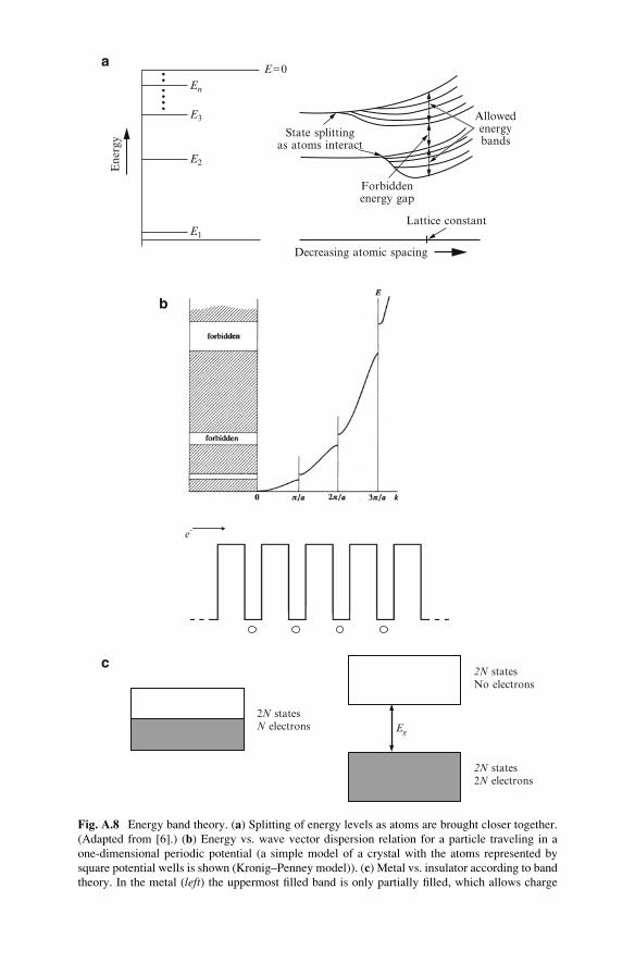
e-
Eg
2N statesN electrons
2N statesNo electrons
2N states2N electrons
c
b
aE=0
En
E3
E2
E1
State splittingas atoms interact
Forbiddenenergy gap
Allowedenergybands
Lattice constant
Decreasing atomic spacing
Ene
rgy
Fig. A.8 Energy band theory. (a) Splitting of energy levels as atoms are brought closer together.
(Adapted from [6].) (b) Energy vs. wave vector dispersion relation for a particle traveling in a
one-dimensional periodic potential (a simple model of a crystal with the atoms represented by
square potential wells is shown (Kronig–Penney model)). (c) Metal vs. insulator according to band
theory. In the metal (left) the uppermost filled band is only partially filled, which allows charge

A similar phenomenon arises whenever a wavelike disturbance is incident on a
periodic potential, i.e., Bragg reflection. At certain wavelengths there will be
strong constructive interference of the multiple wavefronts being reflected by a
periodic system. The Bragg condition states that strong reflection will occur
when
nλ ¼ 2asin θ (A.17)
where n is a positive integer and a corresponds to the lattice spacing for a wave
incident at an angle θ. For a one-dimensional lattice the incident angle is 90� and theBragg condition corresponds to nλ ¼ 2a or, in terms of wave vector, k ¼ nπ/a. Atthese special values of wave number electrons are strongly reflected and cannot
propagate through the crystal. Away from these values, however, electrons in a
crystal can behave very much like free particles.
In practice, a combination of approaches and significant computational effort are
usually needed to explain the electronic properties of real materials. However,
regardless of the particular details, the formation of allowed and forbidden electron
energy bands in crystalline solids is predicted, which provide an avenue for electronsto travel through the crystal.17
Band theory allows a straightforward explanation of the difference between a
metal and an insulator18: Each band has 2N available electron states where N is the
number of unit cells making up the crystal (the factor of 2 accounts for spin). How
the bands are filled with electrons determines whether a material is a metal or an
insulator. Referring to Fig. A.8c, if the uppermost populated energy band is only
partially filled (say, half-filled) then there are plenty of higher energy states
available for electrons to gain kinetic energy so that they can contribute to current
flow and thus the crystal is able to conduct electricity. If, on the other hand, the
uppermost band is completely filled then there is no easy and continuous way for
charge carriers to gain energy because there is a forbidden energy band gap Eg
before the next band of states becomes accessible. The crystal is therefore
insulating and cannot conduct electrical current.19
Fig. A.8 (continued) carriers to gain energy and contribute to current flow. In the insulator
(right) the band is completely filled and separated from the next available states by the band gap
energy, which means there is no continuous way to increase the energy of charge carriers and thus
no current can flow
⁄�
17 There are some important exceptions where the band theory of solids is not valid, such as
materials that have very strong electron–electron interactions. However, the vast majority of
crystalline solids are very accurately described using band theory.18 These arguments were first put forth by Alan Wilson in 1930.19 Note that at some point an insulator subjected to very large external forces will conduct
electricity via various breakdown mechanisms.
228 Appendix A: Physics Primer for Electronic Devices
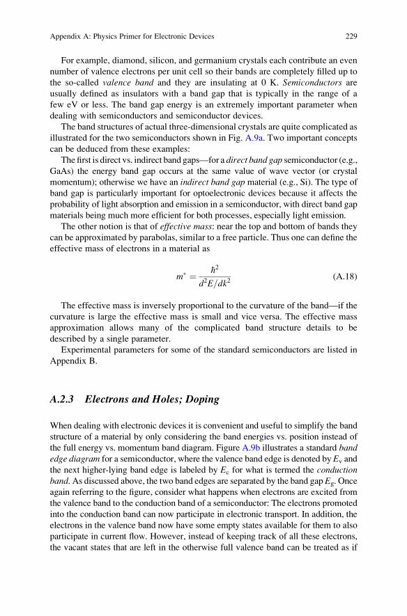
For example, diamond, silicon, and germanium crystals each contribute an even
number of valence electrons per unit cell so their bands are completely filled up to
the so-called valence band and they are insulating at 0 K. Semiconductors are
usually defined as insulators with a band gap that is typically in the range of a
few eV or less. The band gap energy is an extremely important parameter when
dealing with semiconductors and semiconductor devices.
The band structures of actual three-dimensional crystals are quite complicated as
illustrated for the two semiconductors shown in Fig. A.9a. Two important concepts
can be deduced from these examples:
The first is direct vs. indirect band gaps—for a direct band gap semiconductor (e.g.,
GaAs) the energy band gap occurs at the same value of wave vector (or crystal
momentum); otherwise we have an indirect band gap material (e.g., Si). The type of
band gap is particularly important for optoelectronic devices because it affects the
probability of light absorption and emission in a semiconductor, with direct band gap
materials being much more efficient for both processes, especially light emission.
The other notion is that of effective mass: near the top and bottom of bands they
can be approximated by parabolas, similar to a free particle. Thus one can define the
effective mass of electrons in a material as
m� ¼ �h2
d2E=dk2(A.18)
The effective mass is inversely proportional to the curvature of the band—if the
curvature is large the effective mass is small and vice versa. The effective mass
approximation allows many of the complicated band structure details to be
described by a single parameter.
Experimental parameters for some of the standard semiconductors are listed in
Appendix B.
A.2.3 Electrons and Holes; Doping
When dealing with electronic devices it is convenient and useful to simplify the band
structure of a material by only considering the band energies vs. position instead of
the full energy vs. momentum band diagram. Figure A.9b illustrates a standard bandedge diagram for a semiconductor, where the valence band edge is denoted by Ev and
the next higher-lying band edge is labeled by Ec for what is termed the conductionband. As discussed above, the two band edges are separated by the band gap Eg. Once
again referring to the figure, consider what happens when electrons are excited from
the valence band to the conduction band of a semiconductor: The electrons promoted
into the conduction band can now participate in electronic transport. In addition, the
electrons in the valence band now have some empty states available for them to also
participate in current flow. However, instead of keeping track of all these electrons,
the vacant states that are left in the otherwise full valence band can be treated as if
Appendix A: Physics Primer for Electronic Devices 229

Ec
Ev
Eg
c
b
a
Ec
Ev
Ec
Ev
Fig. A.9 (a) Band structures for Si and GaAs along high-symmetry directions. All the bands are
usually plotted about the origin as shown without loss of generality (cf. Fig. A.8b). (After
M. L. Cohen, J. R. Chelikowsky, Electronic Structure and Optical Properties of Semiconductors,2nd Edition, Spring-Verlag, 1988.) (b) Energy band edge diagram for a semiconductor.
Electron–hole pairs are created when carriers are excited from the valence band to the conduction
band. (c) Illustration of direct (left) vs. indirect (right) band gap semiconductor

they were particles called holes.20 A hole acts like a particle with positive charge q.Both electrons and holes contribute to electric current.
Notice that the electron effective mass is negative at the top of the valence band.
This is equivalent to a hole with positive effective mass and positive charge. Thus
we use the notation
mp ¼ �mn (A.19a)
for the hole effective mass at the top of the valence band and
mn (A.19b)
for the electron effective mass at the bottom of the conduction band. As a result we
can write
E ¼ Ec þ �h2 k � k0ð Þ22mn
;E ¼ Ev ��h2 k � k
00
� 22mp
(A.20)
for the electron energies in the conduction band and valence band, respec-
tively. Note that if k0 ¼ k00 the band gap is direct; otherwise it is indirect (see
Fig. A.9c).
Donors and Acceptors
In an intrinsic material the number of electrons in the conduction band is equal to
the number of holes in the valence band. At a given temperature, such electron–holepairs are excited across the band gap in a semiconductor by thermal energy. In
terms of carrier concentration per unit volume this is expressed as
n ¼ p ¼ ni (A.21)
where n and p are the electron and hole concentrations, respectively, and ni is calledthe intrinsic carrier concentration.
On the other hand, in an extrinsic material one type of carrier has a greater
concentration (majority carriers) than the other (minority carriers). This is achieved
by substitutional doping of the crystal with impurity atoms that either donateelectrons to the conduction band or accept electrons from the valence band. When
electrons are the dominant carrier type in a semiconductor it is called n-type.
20 A very often used analogy considers the electrons as a “sea” and the holes as “bubbles” in this
sea. Even though the bubbles do not contain any water they can still be treated as particles as long
as one remembers that it is actually the water that moves in the opposite direction. The same
principle applies to the electrons in the valence band, which move oppositely to the holes. Holes
can also be said to “float” to the top of the valence band in order to reach their lowest energy.
Appendix A: Physics Primer for Electronic Devices 231

Similarly, when holes are the dominant carriers the material is called p-type. Typicaldonor atoms for semiconductors are from column V of the periodic table, e.g., P, As,
Sb. Acceptors commonly used are from column III such as B, Al, Ga, and In.
Hydrogenic Model for Impurity Binding Energy
Recall for the hydrogen atom the ionization energy was given by
E ¼ � m0q4
4πε0ð Þ22�h2
which turned out to be –13.6 eV. In other words the energy required to remove an
electron from a hydrogen atom, or the binding energy, is 13.6 eV.
A donor impurity atom in a semiconductor can be approximated as a hydrogen
atom by considering the outer electron as being loosely bound (Fig. A.10a). We can
now use the same results as for the hydrogen atom by substituting the effective
mass and the dielectric constant of the semiconductor (or relative permittivity, εr) inorder to approximate the binding energy of a donor impurity atom:
E ¼ mnq4
4πε0εrð Þ22�h2 ¼13:6
ε2r
mn
m0
eV (A.22)
Ec
Ev
Eg
Ed
Ea
Donor
b
aFig. A.10 Impurity dopant
atom binding energies. (a)
Donor impurity hydrogenic
model. (b) Band edge
diagram showing impurity
energy levels and carrier
distribution at low
temperature
232 Appendix A: Physics Primer for Electronic Devices

The same thing can be done for acceptor impurities by simply replacing the
electron effective mass with the hole effective mass.
Measured values of the donor binding energies in most semiconductors are
typically between 10 and 50 meV and similarly for acceptors. This means that the
donor and acceptor impurity levels are quite close to either the conduction or
valence band edges (Fig. A.10b), which is important if doping is to be effective
around room temperature.21
A.2.4 Carrier Concentration in Thermal Equilibrium22
A fundamental result from statistical mechanics is the Fermi–Dirac distribution,which states the probability that an electron will occupy a state with energy Eat temperature T as
f Eð Þ ¼ 1
1þ e E�EFð Þ=kBT (A.23)
where kB is Boltzmann’s constant and EF is the Fermi level. It is useful to think of
the Fermi level, also known as the chemical potential, as representing the surface
level of the “sea” of electrons in a material.23 A plot of the Fermi–Dirac distribution
is shown in Fig. A.11a. Note that f(E) is always equal to ½ when the energy E is
equal to EF. In addition, the hole probability distribution is given by 1 – f(E), since ahole is the absence of an electron.
Combining the Fermi–Dirac distribution with the band edge diagram of a
semiconductor results in Fig. A.11b. It can be seen that the Fermi level of a
semiconductor moves closer to the conduction band edge for an n-type material
(more electrons) whereas it is lowered toward the valence band edge for p-type
doping (less electrons). For an intrinsic semiconductor with equal numbers or
electrons and holes, the Fermi level lies very close to the middle of the band gap
(see discussion below).
Before continuing, we mention some standard definitions involving the Fermi
level: The vacuum energy level (E0) is a convenient reference in band edge
diagrams, which corresponds to the energy of an electron that has been just freed
21 In other words, the dopants will be easily activated by thermal energy.22 A system is considered to be in a state of thermal equilibrium if its temperature is equal to that of
the surrounding environment (or thermal energy “reservoir”) and its properties will not change as
long as the temperature remains constant. This implies that the system is not subjected to any
external forces or sources of energy that can perturb it from being in equilibrium with its
environment (also known as thermodynamic equilibrium).23 A higher Fermi level means more carriers in the electron sea and a lower Fermi level means less.
Most of the important electronic effects in materials occur in and around the Fermi level
(somewhat similar to the disturbances that occur on the surface of a body of water).
Appendix A: Physics Primer for Electronic Devices 233

from a material. The difference between the Fermi level and E0 is known as
the work function, qΦ, of the material (similar to the binding energy of an atom).
Since the work function will vary with doping level in a semiconductor, we also
define the difference between the conduction band edge, Ec, and the vacuum level
as the electron affinity, qX, which is constant for a given semiconductor.
Fig. A.11 (a) Fermi–Dirac Distribution at different temperatures. Dotted curve is for a temperature
of 0 K and the curves gradually spread out as temperature is increased. Note that this distribution is
for a system in thermal equilibrium. (b) Fermi–Dirac distribution superimposed on semiconductor
band edge diagram (After B. Streetman, S. Banerjee, Solid State Electronic Devices, 6th Edition,
Prentice-Hall, 2005)
234 Appendix A: Physics Primer for Electronic Devices
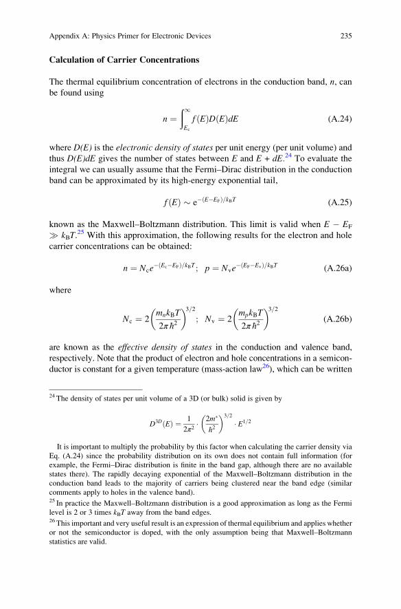
Calculation of Carrier Concentrations
The thermal equilibrium concentration of electrons in the conduction band, n, canbe found using
n ¼ð1Ec
f Eð ÞD Eð ÞdE (A.24)
where D(E) is the electronic density of states per unit energy (per unit volume) and
thus D(E)dE gives the number of states between E and E + dE.24 To evaluate the
integral we can usually assume that the Fermi–Dirac distribution in the conduction
band can be approximated by its high-energy exponential tail,
f Eð Þ � e� E�EFð Þ=kBT (A.25)
known as the Maxwell–Boltzmann distribution. This limit is valid when E � EF
kBT.25 With this approximation, the following results for the electron and hole
carrier concentrations can be obtained:
n ¼ Nce� Ec�EFð Þ=kBT ; p ¼ Nve
� EF�Evð Þ=kBT (A.26a)
where
Nc ¼ 2mnkBT
2π �h2
� �3=2
; Nv ¼ 2mpkBT
2π �h2
� �3=2
(A.26b)
are known as the effective density of states in the conduction and valence band,
respectively. Note that the product of electron and hole concentrations in a semicon-
ductor is constant for a given temperature (mass-action law26), which can be written
24 The density of states per unit volume of a 3D (or bulk) solid is given by
D3D Eð Þ ¼ 1
2π2 2m�
�h2
� �3=2
E1=2
It is important to multiply the probability by this factor when calculating the carrier density via
Eq. (A.24) since the probability distribution on its own does not contain full information (for
example, the Fermi–Dirac distribution is finite in the band gap, although there are no available
states there). The rapidly decaying exponential of the Maxwell–Boltzmann distribution in the
conduction band leads to the majority of carriers being clustered near the band edge (similar
comments apply to holes in the valence band).25 In practice the Maxwell–Boltzmann distribution is a good approximation as long as the Fermi
level is 2 or 3 times kBT away from the band edges.26 This important and very useful result is an expression of thermal equilibrium and applies whether
or not the semiconductor is doped, with the only assumption being that Maxwell–Boltzmann
statistics are valid.
Appendix A: Physics Primer for Electronic Devices 235

np ¼ ni2 (A.27)
where
ni ¼ffiffiffiffiffiffiffiffiffiffiffiNcNv
pe�Eg=2kBT (A.28)
is the intrinsic carrier concentration. This shows mathematically that the intrinsic
carrier concentration increases with increasing temperature and decreases withincreasing band gap, as expected for the thermal excitation of electron–hole pairs.
Finally, we can also express the equilibrium electron and hole concentrations in
terms of the intrinsic concentration and Fermi level as
n ¼ nieEF�Eið Þ=kBT
p ¼ nieEi�EFð Þ=kBT (A.29)
where Ei is the intrinsic Fermi level. This form of the equations is useful in practice
because ni is usually well known from experiment for most semiconductors.
The position of Ei can be found by equating Eqs. (A.26a) to give
Ei ¼ Ec þ Ev
2þ 3
4kBT ln
mp
mn
� �(A.30)
This shows that the intrinsic Fermi level lies very close to the center of the band
gap, with only a slight offset due to the difference in electron and hole effective mass.
Space-Charge Neutrality
If we start with an electrically neutral semiconductor in thermal equilibrium it must
remain neutral regardless of the number of holes, electrons, or ionized impurities
present. This condition is known as (global) space-charge neutrality and can be
expressed as
nþ N�a ¼ pþ Nþ
d or n ¼ pþ Nþd � N�
a
� (A.31)
whereN�a andNþ
d represent the concentration of ionized dopant atoms.Equation (A.31)
and the mass-action law [Eq. (A.27)] are the two requirements that must be maintained
at equilibrium. Assuming all the dopant atoms are ionized27 and substituting
p ¼ n2i =n
into Eq. (A.31), we obtain
27We will normally assume in this text that all dopants are ionized and therefore not explicitly
include the superscripts in the symbols for dopant concentration.
236 Appendix A: Physics Primer for Electronic Devices

n� n2in¼ Nd � Na ) n ¼ Nd � Na
2þ Nd � Na
2
� �2
þ n2i
" #1=2
(A.32a)
for the electron concentration in a semiconductor (keeping only the positive root),
and the analogous expression for holes is given by
p ¼ Na � Nd
2þ Na � Nd
2
� �2
þ n2i
" #1=2
(A.32b)
Example A.6: Carrier Concentration Calculation Find the electron and hole
concentrations and location of EF for silicon at 300 K doped with 3 � 1016 cm�3
arsenic atoms and 2.9 � 1016 cm�3 boron atoms.
Using Eq. (A.32a) we can see that since Nd � Na >> ni (see Appendix B)
that ) n � Nd � Na ¼ 1015cm�3 and therefore p ¼ n2i
n ¼ 2:25� 105cm�3 . The
position of the Fermi level can now be found using Eq. (A.29) for the electron
concentration:
n ¼ nieEF�Eið Þ=kBT ;
) EF � Ei ¼ kBT ln nni
¼ 0:289 eV
A.2.5 Equilibrium Fermi Level and Band Edge Diagrams
Recall that in thermal equilibrium there can be no external forces or excitations
acting on the material or device under consideration. In other words, there is a
detailed balance between the various physical processes occurring in the system.
From the perspective of electronic devices this implies the following statement
holds
In thermal equilibrium there is no net current flow and thus the Fermi levelmust be constant throughout the material or device.
As a function of distance x, this condition requires
dEF
dx¼ 0 (A.33)
in thermal equilibrium. As illustrated in Fig. A.12, regardless of the particular
material or device details the Fermi level must be constant in order to satisfy the
condition of zero net current flow and this is represented by a horizontal straight line
in the thermal equilibrium band edge diagram.
Appendix A: Physics Primer for Electronic Devices 237

A.2.6 Electronic Transport
At a given temperature, electrons and holes in a semiconductor possess average
thermal energy given approximately by28
1
2m�v2th ¼
3
2kBT (A.34)
where vth is the thermal velocity. This causes random motion of the charge carriers
resulting in collisions or scattering with the lattice impurities and between carriers
etc. In thermal equilibrium we have seen that this type of random motion does not
produce any net current flow.
Drift Current
On the other hand, when an external electric field is applied to the semiconductor
the carriers acquire a drift velocity: Figure A.13a shows the combined effects of the
+
+
EF
EF
Ec
EF
Ev
Fig. A.12 Thermal
equilibrium Fermi level.
The water analogy shows
that the level of liquid will
always be constant in
equilibrium regardless of
the amount of water in the
vessels before they are
combined. Water will flow
from high level to low level
in order to establish thermal
equilibrium as shown in the
two examples. The same
ideas apply to the electrons
in a thermal equilibrium
band edge diagram of a
material or device
regardless of the doping
levels or type of
material, etc.
28 This result comes from the Equipartition theorem of classical statistical mechanics, which states
that for a system in thermal equilibrium particles have an average kinetic energy of 1/2 kBT per
spatial degree of freedom.
238 Appendix A: Physics Primer for Electronic Devices

applied electric field and random scattering processes on carrier motion that leads to
drift transport in a semiconductor. Figure A.13b is a sketch of the corresponding
carrier velocity vs. time in a constant applied field showing the initial increase in
velocity as carriers are accelerated by the field and subsequent loss of energy due
to the various scattering processes. The time interval between scattering events
is given by the mean free time, τ. The mean free time gives the characteristic
timescale over which the carriers are accelerated.
If a constant electric field, Ex, is applied in the x-direction the drift velocity
acquired by electrons is given by
v ¼ � qExτ
mn(A.35)29
The electron mobility is defined as
t
Ec
EF
Ei
Ev
dx
dE
qE i
x
1=
b
aFig. A.13 (a) Illustration
of carrier drift in an applied
electric field (top—real
space, bottom—band edge
diagram). The electric field
is found from the gradient
of the potential, which can
be defined in terms of either
of the parallel band edges or
the Fermi level. A
convenient definition is in
terms of the intrinsic Fermi
level as indicated on the
diagram (the electrons drift
towards the field). (b)
Velocity versus time for a
carrier undergoing drift
transport leading to an
average drift velocity
29 This result can be obtained by integrating Newton’s second law to find the velocity for a force of
qEx and using the mean free time in the resulting expression. Such approaches, which combine
aspects of classical and quantum mechanics, are usually referred to as “semi-classical” treatments.
Appendix A: Physics Primer for Electronic Devices 239

μn ¼qτ
mn(A.36)
and describes how easily an electron can move in response to an applied electric
field. Analogous arguments apply for holes (in general, the drift velocity can be
found using��v j¼μEx ). Remembering that holes and electrons move in opposite
directions in an electric field and thus both contribute positively to the drift current,
the general expression for electrical current density, J ¼ qnv,30 can be now be used
to write
Jx ¼ Jn þ Jp ¼ nqμn þ pqμp�
Ex (A.37)
as the total drift current density due to both electrons and holes in a semiconductor.
Equation (A.37) has the form of Ohm’s law
Jx ¼ σEx (A.38)
with the conductivity, σ, given by the term in brackets,31,32 We can relate this
expression to the resistance, R, by considering a bar of material with cross-sectional
area A and length L. In this case the current density and electric field are given by
J ¼ I
Aand E ¼ V
L(A.39)
respectively, where I is the current and V is the voltage. Substituting into Eq. (A.38)
and rearranging terms gives
V ¼ L
σA
� �I ¼ ρL
A
� �I ¼ IR (A.40)
which gives Ohm’s law in the familiar form relating voltage and current and shows
the dependence of resistance on material geometry (the resistivity ρ ¼ 1/σ has also
been introduced).
30 Here n simply denotes a generic carrier concentration and v the carrier velocity that lead to a
certain flux density of particles per unit area.31 The analysis leading to Eq. (A.37) is generally referred to as the Drude model. This model works
well for semiconductors but must be modified for metals to take into account that carriers near the
middle of a band have energies on the order of EF and thus the full quantum Fermi–Dirac statistics
must be used. The modified approach is known as Drude–Sommerfeld theory.32 In general the conductivity will be given by a tensor; however, a one-dimensional treatment
usually suffices for first-order device analysis.
240 Appendix A: Physics Primer for Electronic Devices

Scattering
The two main types of scattering that influence the mobility of charge carriers in
a semiconductor crystal are lattice (phonon) scattering and impurity (defect)
scattering.
Lattice scattering increases with temperature as the vibrations of the lattice
become greater. This type of scattering causes the mobility to scale as a power
law with temperature, T�n, with n typically ~1.5–3.
Impurity or defect scattering, on the other hand, decreases as temperature
increases. This is due to the increased thermal velocity of carriers, which makes
them less susceptible to interaction with impurities/defects. The opposing
tendencies for the two types of scattering lead to semiconductor carrier mobility
that often resembles an inverted arch shape versus temperature.
Scattering data for silicon is given in Appendix B.
Drift Velocity Saturation
The expressions for drift velocity given above predict that the carrier velocity
will continue to increase indefinitely as the electric field is increased. In reality,
these expressions are only valid for relatively low fields. At very high electric fields
the drift velocity becomes comparable to the thermal velocity. Charge carriers
are referred to as hot carriers when their kinetic energy is greater than the
thermal energy of the rest of the crystal. The drift velocity of such carriers
approaches a saturation value at high fields and thus the mobility decreases from
its low-field value. This is caused by increased scattering at high fields which
limits further increase in the drift velocity. In silicon the saturation velocity
for both electrons and holes is approximately 107 cm/s or about 0.1 % of the
speed of light. Carrier velocity vs. electric field data for silicon are given in
Appendix B.
Diffusion Current
In addition to the drift of carriers in an electric field another basic mechanism which
can contribute to the electrical current in a material is diffusion. Diffusion occurs
when there is a carrier concentration gradient. This causes charge carriers to flow
from a region of high concentration to low concentration resulting in a net current.
This is similar to diffusive phenomena that occur in chemical systems such as gases
and liquids, in addition to the thermal diffusion of heat.
At a finite temperature, the thermal motion of carriers leads to a net flux of
current that will depend on the difference in concentration between adjacent
regions (i.e., the concentration gradient) as the schematic of Fig. A.14a illustrates.
Appendix A: Physics Primer for Electronic Devices 241

Fick’s law, which governs the diffusive flux of carriers, allows the electron
diffusion current density to be expressed as
Jn ¼ qDndn
dx(A.41)
where the diffusion coefficient (or constant) Dn can be found using
Dn ¼ kBT
qμn (A.42)
which is known as the Einstein relation.Analogous results apply for the diffusion of holes due to a concentration
gradient.
n
x-l 0 l
A A
+ –
p-type n-type
hot cold hot cold
a
b
Fig. A.14 Diffusion transport of carriers. (a) Schematic displaying a varying electron concentra-
tion as a function of position. Carriers within a mean free path λ on either side of the plane at the
origin will cross the plane due to random thermal motion at a finite temperature. If the concentra-
tion of carriers is not constant this thermal motion will lead to net carrier flow from an area of high
concentration to low concentration (towards the left in the diagram). (b) Hot probe measurement.
In this case, a difference in the thermal velocities of the two regions near the hot and cold probe
pins has the same effect as a concentration gradient (in other words there is a velocity gradient
instead) and leads to diffusion of carriers from the hot probe to cold
242 Appendix A: Physics Primer for Electronic Devices

A hot-probe measurement is a convenient technique that relies on diffusion
currents to determine the conductivity type of a semiconductor sample. The
hot-probe setup consists of two probes, one of which is heated, and an ammeter
(Fig. A.14b). No voltage is applied but a current flows when the probes touch the
semiconductor whose direction depends on whether the material is n-type or p-type.
We can now write the total electron and hole current densities including both
drift and diffusion:
Jn ¼ qμnnEx þ qDndn
dx
Jp ¼ qμppEx � qDpdp
dx
(A.43)33
Note that because diffusion depends on the gradient of carrier concentration
minority carriers can still make a significant contribution to the overall current
density even if their total concentration is low.
The drift–diffusion transport equations (A.43) are the typical starting point for
standard semiconductor electronic device analysis. (Along with the basic equations
of electrostatics and the continuity equations).
The Hall Effect
The total force on a charged particle moving in electric and magnetic fields is given
by the Lorentz force:
F! ¼ q E
! þ v! � B
!h i(A.44)
The Hall effect34 is a direct consequence of this equation and has become a very
useful and important experimental technique for the study of semiconductors.
Consider a sample placed in a magnetic field while current is passed through it as
shown in Fig. A.15a: Due to the Lorentz force an induced transverse electric field
EH, known as the Hall field, is set up, which produces a Hall voltage VH that can be
measured with external contacts as shown. The force created by the Hall field
opposes the Lorentz force, which in steady state leads to a balance that can be
expressed mathematically as
qEH ¼ qv B (A.45a)
33Note that the negative sign for the hole current density expression arises from the fact that both
electrons and holes diffuse in the same direction (from high to low concentration) but have
opposite charges.34 First observed by Hall for metals in 1879.
Appendix A: Physics Primer for Electronic Devices 243

) EH ¼ JxB
qpfor holes; EH ¼ � JxB
qnfor electrons (A.45b)
These equations can be rewritten as
EH ¼ RHJxB (A.45c)
where RH is the Hall coefficient, which can be used to determine the majority carrier
type (based on its sign), concentration, and mobility of a semiconductor.35
Fig. A.15 Hall effect. (a) Experimental setup showing movement of electrons/holes under
the influence of an applied magnetic field in the z-direction due to the Lorentz force interaction.
(After [6]) (b) Hall effect linear motion sensor example and integrated circuit device structure
schematic (After S. M. Sze, K. K. Ng, Physics of Semiconductor Devices, 3rd Edition, Wiley
Interscience, 2007)
35 Our derivation has implicitly assumed that only one type of carrier is important in the semicon-
ductor, in other words the doping level is such that the minority carriers do not need to be
considered. (If this is not the case and both electrons and holes are present in comparable quantities
the Hall coefficient expressions become fairly complex.) In addition, note that a numerical factor
of order unity usually multiplies RH to obtain quantitative agreement with experiment.
244 Appendix A: Physics Primer for Electronic Devices

Compact sensors based on the Hall effect are used in a wide variety of products
and applications. In addition to magnetometer applications, Hall sensors are also
very often used as position sensors (Fig. A.15b).
A.2.7 Continuity Equations
The dynamics or time-dependent behavior of free charge carriers in semiconductors
is governed by the basic principle of conservation of charge and this leads to a
continuity equation that must be obeyed for electrons and holes.
Consider a one-dimensional slice of a semiconductor, dx, as shown in Fig. A.16a:The rate of change of electron concentration in this thin slice will depend only on
the net current flowing into it and any generation or recombination (the opposite
process) of carriers inside it. Mathematically, the continuity equations for both
electrons and holes are given by
∂n∂t
¼ 1
q
∂Jn∂x
þ Gn � Rnð Þ;∂p∂t
¼ � 1
q
∂Jp∂x
þ Gp � Rp
� (A.46)
where G and R represent the generation and recombination rates (per unit volume)
for either or electrons or holes. The expressions we have for electron and hole
Ec
Ev
G R
x x+dx
Jn (x) Jn (x+dx)
Ec
Ev
Et
sn
sp
b
aFig. A.16 (a) Conservation
of charge in a thin slice of
semiconductor used to
derive continuity equations.
The diagram shows the rate
of change of electrons can
only be due to current flow
into a region or generation/
recombination processes
inside of it. (b)
Generation–recombination
via localized trap levels
usually described by
Shockley–Hall–Read theory
Appendix A: Physics Primer for Electronic Devices 245

current densities [Eq. (A.43)] can be substituted into the continuity equations to
obtain partial differential equations which can in principle be solved to obtain the
temporal and spatial dependence of the carrier concentrations in a semiconductor.
Generation and Recombination
We have seen that excess carriers can be created or generated in a semiconductor by
exciting carriers from the valence band to the conduction band. Similarly, excess
carriers can recombine by the reverse process. In thermal equilibrium, generation
and recombination are in perfect balance. Deviations from thermal equilibrium will
lead to either net generation or recombination of carriers in a semiconductor.
For indirect semiconductors such as Ge and Si recombination/generation usually
occurs via localized states within the band gap caused by impurities and/or defects
(Shockley–Hall–Read (SHR) recombination36) as illustrated in Fig. A.16b. These
states act as “stepping stones” for carriers and are referred to as traps or recombi-nation centers. On the other hand, for direct band gap semiconductors recombina-
tion from the conduction band to valence band without an intermediate state is
more probable. The rate of recombination is proportional to the density of carriers,
the density of empty available states, and the probability that a carrier passing near
an available state will be captured by it.
The net recombination rate, R–G, of carriers in a semiconductor is characterized
by the excess carrier lifetime, τ, whose value can vary widely depending on the
factors listed above and also the physics of the specific recombination mechanism(s)
taking place.
We can define the excess electron and hole concentrations in a semiconductor as
n0 � n� n0
p0 � p� p0
(A.47)
where n0 and p0 denote the thermal equilibrium carrier concentrations.
If the condition of low-level injection is valid (i.e., the majority carrier concen-
tration is unaffected and remains near its thermal equilibrium value), the net
recombination rate is simply proportional to the excess minority carrier concentra-
tion divided by the minority carrier lifetime.
The continuity equations now become
∂n0
∂t¼ 1
q
∂Jn∂x
� n0
τn
∂p0
∂t¼ � 1
q
∂Jp∂x
� p0
τp
(A.48)
for the minority carriers in p- and n-type semiconductors, respectively.
36 R.N. Hall, Phys. Rev. 87, 387 (1952); W. Shockley, W. T. Read, Jr., Phys. Rev. 87, 835 (1952).
246 Appendix A: Physics Primer for Electronic Devices

If low-level injection is not valid the situation becomes somewhat more compli-
cated. For SHR theory the net recombination rate is
U ¼ σnσpvthNt pn� n2i�
σn nþ niexpEt�Ei
kBT
h iþ σp pþ niexp
Ei�Et
kBT
h i (A.49a)
where Nt is the density of recombination traps and Et their energy, and σn and σp arethe cross sections associated with electron and hole recombination, respectively.U is
peaked around Et ¼ Ei, and thus traps near the middle of the band gap tend to make
the largest contribution. If only these traps are considered Eq. (A.49a) reduces to
U ¼ σnσpvthNt pn� n2i�
σn nþ nið Þ þ σp pþ nið Þ (A.49b)
Lastly, a further assumption that is often used to allow approximate calculations
is that σn ¼ σp ¼ σ, and thus U simplifies to
U ¼ σvthNt pn� n2i�
nþ pþ 2ni(A.49c)
A.3 Outline of Semiconductor Planar Processing
(Optional)
The technology behind virtually all solid-state electronic devices and integrated
circuits currently produced is based on planar processing37 of single-crystal
(usually silicon) semiconductor wafers in a sequence of steps, layer by layer, to
achieve the desired final structure. The technology of semiconductor electronics is
not required for understanding the main concepts in the text and therefore this
section is optional reading. However, the ideas and techniques presented will
certainly be very helpful for providing underlying insight and putting the various
device structures discussed in this book into context. Practically, of course, how
electronic devices and integrated circuits are made is very important.
A.3.1 Basic Steps in Processing a Wafer
1. Crystal growth and wafer formation
2. Patterning
3. Dopant deposition
37Many of the initial planar device processing concepts were disclosed by Hoerni in 1959.
Appendix A: Physics Primer for Electronic Devices 247

4. Dielectric formation
5. Etching
6. Metal deposition
7. Formation of interconnect layers
8. Packaging and testing
Note that steps 2–7 are largely applied in a parallel fashion across the entire
surface of the wafer—it thus costs roughly the same (in time and resources) to
manufacture a chip containing billions of components as it does to produce a single
discrete device. A brief description of each step follows.
High-purity single-crystal semiconductors are required for precisely controlling
electronic device properties, which is necessary for producing reliable large-scale
integrated circuits. To obtain a silicon wafer (Fig. A.17a), the starting material is
silica or SiO2 (found in sand). This is reduced in a high-temperature arc furnace
containing carbon, resulting in about 90 % pure silicon material. This powdered
form of silicon is then reacted with hydrogen chloride to form trichlorosilane liquid.
The liquid is then purified via distillation and subsequently reduced with hydrogen
to form high-purity (>99.999999 %) polycrystalline silicon. To go from polysilicon
to defect-free single crystals the so-called Czochralski crystal growth method is
standard. Here, a small seed crystal is dipped into a Si melt and slowly withdrawn
to grow a progressively larger crystal referred to as in ingot. By incorporating a
controlled amount of dopant atoms into the melt doped single crystals can also be
grown using the Czochralski method.38 To create wafers, the single-crystal ingots
are typically sliced using a diamond saw followed by polishing and chemical
etching to prepare the surface for IC processing.39 The standard wafer diameter
for electronics today is 12 in. (300 mm) with 18 in. (450 mm) soon to be
implemented.
Photolithography (Fig. A.17b) is the standard approach used to create the
individual patterns on the surface of a wafer that result in the high density of
devices inside an integrated circuit. By exposing and developing a photosensitive
polymer, known as photoresist, very high-resolution features can be printed on
38 Silicon grown using the Czochralski method contains significant amounts of oxygen
(~1018 cm�3) arising from the crucible used to hold the molten Si. The oxygen is usually
electrically inactive but can be used to trap unwanted impurities (gettering). For some applications
(e.g., some high-power devices) the whole wafer thickness is required and the oxygen atoms can
be problematic. This requires a different approach that does not employ a fixed pool of molten
material but rather uses a heating element that moves along a polycrystalline rod of material in
order to induce crystallization, known as the Float-zone technique.39 An additional step that involves growing a thin (~micron) layer of crystalline material on top of
the underlying single crystal substrate, known as epitaxy, is also often performed. This can involve
the same type of semiconductor (homoepitaxy, e.g., Si on Si) or different semiconductors
(heteroepitaxy, e.g., compound semiconductors or Ge on Si). Vapor phase epitaxy or chemical
vapor deposition (CVD) is the most commonly used approach to form the epitaxial or “epi” layers
on a silicon wafer. High-quality epi layers allow more precise control of the semiconductor
properties and can lead to improved performance of the active devices in an IC.
248 Appendix A: Physics Primer for Electronic Devices

the surface of a wafer using a predefined mask containing the desired pattern.
This type of patterning step is used several times for the various levels of an
integrated circuit. The resolution of optical lithography is limited by diffraction,
i.e., by the wavelength of radiation used (analogous to an optical microscope).
Reducing the wavelength is therefore one way to define finer features and today
193-nm photolithography (deep UV) is standard in industry. Other innovations such
as phase-shift masks (defining sharper features by modifying the mask to produce
destructive interference of light waves for adjacent patterns), immersion lithogra-phy (reducing wavelength by increasing the refractive index), and multiple pattern-ing (superimposing more than one lithography step per level to create a higher
Fig. A.17 Planar processing steps. (Intel Corp.) (a) Crystal growth and wafer formation.
(b) Photolithography. (c) Device structures are created via a series of patterning, thin film
deposition, and etching steps to create active devices layers, contacts, isolation, etc. (d) Metallic
interconnect network formation. Cross section of a finished chip with nine metal layers is shown
(transistors are small structures at the bottom). (e) IC packaging
Appendix A: Physics Primer for Electronic Devices 249

density of patterns) have allowed state-of-the-art photolithography to reach
sub-20-nm feature sizes. Photolithography based on 13.5 nm radiation (Extreme
UV) incorporating reflective optics is also being developed and could be used for
electronics manufacturing within 5–10 years.
After pattern transfer to the photoresist layer, dopant atoms can be selectively
deposited on the exposed Si regions to define the doping levels (and junctions)
needed for devices in an IC. The two main methods of depositing dopants are gas-phase deposition (or diffusion, for larger/deeper doped regions) and ion implanta-tion (accelerated dopant ion species allowing thinner layers with more precise
control). Following dopant deposition the remaining photoresist is removed and
the resulting high-density patterned regions form the basis of the devices
(e.g., transistors) that will make up the IC.
Fig. A.17 (continued)
250 Appendix A: Physics Primer for Electronic Devices

The next several steps (4, 5, and 6) are combined with photolithography to create
the necessary insulating layers (e.g., gate dielectrics (high-κ), device isolation
(Si oxidation), etc.), structures (e.g., channels, gates, source–drain), and metallic
contacts, respectively, to each device on the wafer surface (see Fig. A.17c for an
example process flow). Note that planarization steps are performed at various
stages of the fabrication process in order to properly prepare and ensure a uniform
surface for the next level of processing.
Steps 2–6 are generally known as front-end processing of an integrated circuit
wafer. Step 7 is the last important IC fabrication step that involves connecting all
the individual transistors into the desired circuit functionality and system architec-
ture using metallic wires, which are formed using combinations of patterning/
deposition/etching steps. Since ICs have now become very dense with many
elements the interconnect superstructure above a wafer can be very complex and
usually contains ~10 or more levels on the most advanced chips (Fig. A.17d).
Once all the interconnect layers and intervening insulators have been fabricated,
the packaging and test process flow begins. This involves electrically testing each
“die” or chip pattern on the wafer, followed by wafer40 slicing (along the single-
crystal planes) and packaging of each individual chip into the final “plug-in” chip
Fig. A.17 (continued)
40 Although standard IC wafers are usually several hundred microns thick, only the top few
microns are used to create the devices for an integrated circuit, with the remainder of the wafer
acting mainly as a mechanical support.
Appendix A: Physics Primer for Electronic Devices 251
module (including mechanical protection and thermal dissipation layers) for
consumer use (Fig. A.17e). A final sequence of higher level testing is performed
prior to product shipment to the end user.
References
1. Ohanian, H.C.: Principles of Quantum Mechanics. Prentice-Hall (1989)2. Sakurai, J.J: Modern Quantum Mechanics, Revised Edition, Addison-Wesley
(1993)
3. Smith, R.A: Semiconductors, 2nd Edn. Cambridge University Press (1978)
4. Kittel, C.: Introduction to Solid State Physics, 8th Edn. Wiley, New Jersey
(2005)
5. Kittel, C., Kroemer, H.: Thermal Physics, 2nd Edn. Freeman (1980)
6. Muller, R.S., Kamins, T.I.: Device Electronics for Integrated Circuits, 3rd Edn.
Wiley, New York (2003)
7. Ng, K.K: Complete Guide to Semiconductor Devices, 2nd Edn. Wiley
Interscience, New York (2002)
Problems
1. Electron wavelength. Find the wavelength of free electrons at room temperature.
2. Semiconductor conductivity. (1) A silicon sample contains Nd ¼ 1016cm�3 and
Na ¼ 1016cm�3. Calculate the conductivity of the sample. (2) Two semiconduc-
tor crystal samples are being examined at room temperature: Sample A has a
large concentration of electrons in the conduction band, n ni, while sample B
has n ¼ p ¼ ni. Which sample has the highest electron mobility? (3) An n-type
Si sample has a resistivity of 0.5 Ω-cm. Is the doping level uniquely defined?
3. Carrier concentration and drift current. Find the thermal equilibrium carrier
concentrations for a silicon sample doped with 3 � 1017cm�3 phosphorus atoms
and 3 � 1017cm�3 arsenic atoms. Sketch the thermal equilibrium band edge
diagram and find the position of the Fermi level. What is the maximum drift
current density that can flow through this sample?
252 Appendix A: Physics Primer for Electronic Devices

Appendix B: Useful Data
B.1 General Comments
When solving problems in this textbook you should assume room temperature and
that the semiconductor is silicon, unless otherwise stated.
It is important, as always, to use consistent units when solving problems. Electron
volts41 and centimeters are most often used in the electronic devices field; however
SI, cgs, or other systems are also perfectly valid and sometimes preferable.
B.2 Fundamental Constants and Definitions
Planck’s constant h ¼ 6:63� 10�34J� s; �h ¼ h2π ¼ 1:055� 10�34J� s
Speed of light c ¼ 3 � 108 m/s
Electron/proton charge magnitude q ¼ 1.6 � 10�19C
Free electron rest mass m0 ¼ 9.11 � 10�31kg
Proton rest mass Mp ¼ 1.67 � 10�27kg
Avogadro’s number NA ¼ 6.02 � 1023/mol
Atomic mass unit amu ¼ 1.66 � 10�27kg
Boltzmann constant kB ¼ 1.38 � 10�23J/K
Permittivity of free space ε0 ¼ 8.85 � 10�12F/m
1 eV ¼ 1:6� 10�19 J; kBT 300 Kð Þ � 0:026 eV; 1 A� ¼ 10�10m ¼ 0:1 nm
Photon energy: E (eV) ¼ 1.24/λ (μm)
41 Recall that 1 eV is the amount of energy gained by an electron that is accelerated through a
potential difference of 1 V (or 1 J/C). Therefore, the term qV that often appears in electronic device
work gives an energy in eV if the bias is in volts.
C. Papadopoulos, Solid-State Electronic Devices: An Introduction,Undergraduate Lecture Notes in Physics, DOI 10.1007/978-1-4614-8836-1,
© Springer Science+Business Media New York 2014
253
B.3 Periodic Table
B.4 Semiconductors and Other Relevant Electronic
Materials
Important parameters42
42 All parameters at 300 K.
254 Appendix B: Useful Data

Crystal
Eg(eV)a
n i(cm
�3)
Effective
massb
(inunitsofm0)
Intrinsic
mobility
(cm
2/V
s)
Effectivedensity
ofstates
(cm
�3)
Relative
permittivity
ε r
Electron
affinity
qΧ(eV)
Lattice
constantc
a(nm)
Diamond
i
5.5
–mn¼
0.52
mn¼
0.40
mp¼
0.75
mp¼
0.46
μ n¼
2100
μ p¼
2000
Nc¼
9�
1018
Nv¼
1.6
�1019
5.7
–0.3567
Si
i
1.12
1.02�
1010#
mn¼
1.08
mn¼
0.26
mp¼
0.81
mp¼
0.386
μ n¼
1450
μ p¼
450
Nc¼
2.8
�1019
Nv¼
1.0
�1019
11.7
4.05
0.5431
Ge
i
0.67
2.33�
1013
mn¼
0.55
mn¼
0.12
mp¼
0.3
mp¼
0.21
μ n¼
3900
μ p¼
1900
Nc¼
1.0
�1019
Nv¼
6.0
�1018
16.0
4.0
0.5658
GaA
sd
1.42
2.1
�106
mn¼
0.067
mp¼
0.47
mp¼
0.34
μ n¼
8500
μ p¼
400
Nc¼
4.7
�1017
Nv¼
7.0
�1018
13.1
4.07
0.5653
GaP
i
2.24
–mn¼
0.79
mn¼
0.35
mp¼
0.83
mp¼
0.50
μ n¼
250
μ p¼
150
Nc¼
1.9
�1019
Nv¼
1.2
�1019
11.1
3.8
0.5450
GaN
d 3.4
–mn¼
0.2
mp¼
1.5
mp¼
0.8
μ n¼
900
μ p¼
200
Nc¼
2.2
�1018
Nv¼
4.6
�1019
9.7
4.1
0.3190
0.5189
InP
d
1.34
1.3
�107
mn¼
0.073
mp¼
0.6
μ n¼
4600
μ p¼
150
Nc¼
5.2
�1017
Nv¼
1.1
�1019
12.4
4.35
0.5869
InSb
d
0.17
2�
1016
mn¼
0.012
mp¼
0.43
μ n¼
77000
μ p¼
850
Nc¼
4.2
�1016
Nv¼
7.3
�1018
17.9
4.6
0.6479
(continued)
Appendix B: Useful Data 255

Crystal
Eg(eV)a
ni(cm
�3)
Effective
massb
(inunitsofm0)
Intrinsic
mobility
(cm
2/V
s)
Effectivedensity
ofstates
(cm
�3)
Relative
permittivity
ε r
Electron
affinity
qΧ(eV)
Lattice
constantc
a(nm)
InAs
d
0.36
1�
1015
mn¼
0.023
mp¼
0.41
μ n¼
33000
μ p¼
450
Nc¼
8.3
�1016
Nv¼
6.4
�1018
14.6
4.9
0.6058
Graphene
08�
1010
(cm
�2)
–~105
–2.2
4.6
0.246
CNT
d
0~2
0~107
(cm
�1)
–~105
––
~4.5
–
SiO
28–9
––
––
3.9
0.95
–
HfO
25.8
––
––
20–25
2.1
0.508
ad—
directbandgap;i—
indirectbandgap.
bWheretwovalues
arelisted
forthesameparam
eter,thefirstvalueshould
beusedfordensity
ofstates
calculationsandthesecondforconductivity
calculations.
cTwolatticeconstants(a,c)
correspondto
materialsthat
crystallize
inthehexagonal
wurtzite
structure.
#Avalueof~1.5
�1010cm
�3isoften
usedinsteadforcalculations/problemsinvolvingSi.
256 Appendix B: Useful Data

Metal work functions
Metal Work function qΦM (eV)
Al 4.1
Au 5.1
Ag 4.75
Cu 4.7
Pt 5.3
Ti 4.3
Ta 4.25
W 4.5
Ni 5.05
Fe 4.7
Co 5.0
Band gap energy vs. lattice constant [4]
Appendix B: Useful Data 257

B.5 Silicon Properties
Intrinsic carrier concentration vs. temperature [4]
258 Appendix B: Useful Data

Electron concentration vs. temperature (After R. A. Smith, Semiconductors, 2ndEdition, Cambridge University Press, 1978.)
Fermi level vs. temperature (After [5])
Appendix B: Useful Data 259

Note that the band gap decreases with temperature in the above diagram. This is
a typical trend in most semiconductors as the average lattice spacing increases with
temperature [4]:
Carrier mobility vs. total impurity concentration (300 K) [4]
260 Appendix B: Useful Data

Carrier mobility (low-field) in Si as a function of temperature (After C. Jacobini,
C. Canali, G. Ottaviani, A. A. Quaranta, Solid-State Electron. 20, 77 (1977).)
Appendix B: Useful Data 261

Resistivity vs. dopant concentration (only one type of dopant is present for each
curve, i.e., the data are for uncompensated material) (After [4])
262 Appendix B: Useful Data

MOS inversion layer carrier mobilities for silicon (100) surface vs. transverseelectric field [4]
Minority carrier lifetimes versus doping level for n- and p-type silicon (After
J. Dziewior, W. Schmid, Appl. Phys. Lett. 31, 346 (1977).)
Appendix B: Useful Data 263

Carrier drift velocity vs. applied electric field [4]
264 Appendix B: Useful Data

References
1. Kittel, C.: Introduction to Solid State Physics, 7th Edn. Wiley, New Jersey (1996)
2. Martienssen W., Warlimont, H. (eds.): Springer Handbook of Condensed Matter and Materials
Data. Springer, Berlin (2005)
3. Muller, R.S., Kamins, T. I.: Device Electronics for Integrated Circuits, 3rd Edn. Wiley,
New York (2003)
4. Sze, S.M., Ng, K.K.: Physics of Semiconductor Devices, 3rd Edn. Wiley Interscience,
New Jersey (2007)
5. Grove, A.S.: Physics and Technology of Semiconductor Devices. Wiley (1967)
Appendix B: Useful Data 265

List of Symbols
a Lattice constant
A�
Angstrom
a0 Bohr radius
B Magnetic field
BVCB0 Collector-base breakdown voltage with emitter open-circuited
BVCE0 Collector-emitter breakdown voltage with base open-circuited
C Small-signal capacitance per unit area
c Speed of light
Cd Diffusion capacitance per unit area
Cj Junction capacitance per unit area
Cmin Minimum MOS capacitance
Cox Oxide capacitance per unit area
Cs MOS depletion capacitance
D(E) Electronic density of states
Dn Electron diffusion coefficient
Dp Hole diffusion coefficient
E0 Vacuum energy level
Ec Conduction band edge energy
Ecn Conduction band edge energy in n-type semiconductor
Ecp Conduction band edge energy in p-type semiconductor
EF Fermi level
Eg Band gap energy
EH Hall field
Ei Intrinsic Fermi level
Emax Maximum electric field
En Energy eigenvalues
Eox Oxide electric field
Es0 Electric field at oxide-silicon interface
Et Recombination trap energy level
Ev Valence band edge energy
Ex Electric field in the x-direction
f(E) Fermi-Dirac distribution
(continued)
C. Papadopoulos, Solid-State Electronic Devices: An Introduction,Undergraduate Lecture Notes in Physics, DOI 10.1007/978-1-4614-8836-1,
© Springer Science+Business Media New York 2014
267

(continued)
FF Fill factor
fT Cut-off frequency
G Small-signal conductance; carrier generation rate
g0 Output transistor conductance
gd Output drain conductance
gm Transconductance
gmsat Saturation transconductance
GN Gummel number
H Energy operator (Hamiltonian)
h Planck’s constant
�h h2π
I Current
I00 Effective reverse saturation current
I0 Reverse saturation current
IB Base current
IC Collector current
ICB0 Collector current with emitter open-circuited
ICE0 Collector current with base open-circuited
ID Drain current
ID0 Subthreshold drain saturation current
Idark Diode current in the absence of light
IDsat MOSFET saturation current
IE Emitter current
IF Forward current flowing through a diode
IF0 Ebers-Moll forward current parameter
IGR0 Reverse saturation current due to space-charge generation-recombination
IL Diode photocurrent
IR Reverse current flowing through a diode
IR0 Ebers-Moll reverse current parameter
IrB Base recombination current
Isc Diode short-circuit current
J Current density
J0 Reverse saturation current density
JG Space-charge generation current density
Jideal Ideal diode current density
Jl Leakage current density
Jn Electron current density
Jp Hole current density
JR Space-charge recombination current density
Jx Current density in the x-direction
k Wave vector; spring constant
kB Boltzmann constant
L Channel length
LD Debye length
Ln Electron diffusion length
Lp Hole diffusion length
M Multiplication factor for avalanching
(continued)
268 List of Symbols

(continued)
m Mass
m* Effective mass
m0 Free electron mass
mn Electron effective mass
mp Hole effective mass
n Electron carrier concentration
n0 Excess electron concentration
n0p Excess electron concentration in p-type semiconductor
n0 Thermal equilibrium electron concentration
Na Acceptor impurity concentration
Nc Effective density of states in the conduction band
Nd Donor impurity concentration
NI Implanted dopant ions per unit area
ni Intrinsic carrier concentration
nn Electron concentration in n-type semiconductor
nn0 Thermal equilibrium electron concentration in n-type semiconductor
np Electron concentration in p-type semiconductor
np0 Thermal equilibrium electron concentration in p-type semiconductor
ns Electron density in semiconductor near an interface
Nt Recombination trap density
Nv Effective density of states in the valence band
p Hole carrier concentration
P Power
p0 Excess hole concentration
p0n Excess hole concentration in n-type semiconductor
p0 Thermal equilibrium hole concentration
Pin Input power
Pm Maximum output power
pn Hole concentration in n-type semiconductor
pn0 Thermal equilibrium hole concentration in n-type semiconductor
pp Hole concentration in p-type semiconductor
pp0 Thermal equilibrium hole concentration in p-type semiconductor
ps Hole density in semiconductor near an interface
q Electron/proton charge magnitude
QB Majority carrier charge density per unit area in the base of a bipolar transistor
Qd Depletion space-charge density per unit area
Qdmax Maximum depletion space-charge density per unit area
Qf Fixed oxide interface charge density per unit area
Qfg Floating-gate charge per unit area
Qn Excess minority electron charge per unit area; MOS inversion layer charge per unit area
Qp Excess minority hole charge per unit area; MOS inversion layer charge per unit area
Qs Space charge per unit area
R Resistance; carrier recombination rate
RH Hall coefficient
Rs Series resistance
T Temperature; tunneling probability
tr Diode recovery time
(continued)
List of Symbols 269

(continued)
ts Diode storage time
Ttr Channel transit time
U Net recombination rate
V Voltage
V(x) Potential energy
v Drift velocity
VA Early voltage
Va Applied voltage
VB Substrate bias
VBC Base-collector voltage of a bipolar transistor
VBE Base-emitter voltage of a bipolar transistor
Vbi pn junction built-in potential
VBR Breakdown voltage
VC Channel bias
VCEsat Voltage drop from collector to emitter in saturation
VD Drain voltage
VDsat MOSFET saturation voltage
VFB Flat-band voltage
VG Gate voltage
VH Hall voltage
Vn Voltage at edge of depletion region in n-type semiconductor
Voc Diode open-circuit voltage
Vox Voltage drop across the oxide of a MOS structure
Vp Voltage at edge of depletion region in p-type semiconductor
VS Source voltage
vsat Saturation velocity
VT MOS threshold voltage
Vt Thermal voltage
vth Thermal velocity
W Channel width
WB Distance from metallurgical junction to contact on n-side of pn junction
WE Distance from metallurgical junction to contact on p-side of pn junction
xB Neutral width of base region; n-region of a pn junction
xd Width of depletion region
xdmax Maximum width of the depletion region
xE Neutral width of emitter region; p-region of a pn junction
xn Extent of depletion region in n-type semiconductor
xox Oxide thickness
xp Extent of depletion region in p-type semiconductor
α Bulk-charge factor
αF Forward-active dc alpha
αT Base transport factor
β Bipolar current gain
βF Forward-active current gain
βR Reverse-active current gain
γ Emitter injection efficiency
δ Fraction of charge removed during diode storage time
(continued)
270 List of Symbols

(continued)
ε0 Vacuum permittivity
εox Oxide permittivity
εr Relative permittivity or dielectric constant
εs Semiconductor permittivity
η Diode ideality factor; solar cell power conversion efficiency
λ Carrier mean free path; wavelength
μn Electron mobility
μp Hole mobility
ν Frequency
ρ Electrical resistivity
ρ(x) Distributed charge density
σ Electrical conductivity
σn Electron recombination cross-section
σp Hole recombination cross-section
τ Mean free time; excess carrier lifetime
τB Base transit time
τC Collector transit time
τEC Bipolar transistor delay time
τn Excess electron lifetime
τp Excess hole lifetime
τRC RC time constant
τt Transit time
Φ Work function (voltage)
ϕ(x) Potential inside silicon substrate of a MOS structure
ϕ0 Fermi level pinning (voltage)
ϕB Schottky barrier height (voltage)
ϕbi Metal-semiconductor junction built-in potential
ΦM Metal work function (voltage)
ΦMS Metal-semiconductor work function difference, ΦM � ΦS
ϕn Potential in bulk n-type substrate of a MOS structure
ϕp Potential in bulk p-type substrate of a MOS structure
ΦS Semiconductor work function (voltage)
ϕs Potential at oxide-silicon interface
Χ Electron affinity (voltage)
ψ(x) Spatial part of the wavefunction
Ψ (x,t) Wavefunction
ω Angular frequency
ω0 Resonance frequency
List of Symbols 271

General Bibliography
1. Grove, A.S.: Physics and Technology of Semiconductor Devices. Wiley (1967)—A classic in
the field.
2. International Technology Roadmap for Semiconductors, ITRS, (2011–2012)—An immense
practical resource for the present and future of the semiconductor industry that is released
every two years with brief updates in the intervening years.
3. Kittel, C.: Introduction to Solid State Physics, 7th Edn. Wiley, New Jersey (1996)—A standard
reference for solid state physics. Now in its 8th edition, earlier versions are also worth a look.
4. Muller, R.S., Kamins, T.I.: Device Electronics for Integrated Circuits, 3rd Edn. Wiley, New
York (2003)—Containing practical and fundamental concepts, this textbook emphasizes both
an intuitive and comprehensive understanding of the subject.
5. Ohanian, H.C.: Principles of Quantum Mechanics. Prentice-Hall (1989)—A good introduction
to fundamental quantum mechanical concepts and their mathematical formalism.
6. Pierret, R.F., Neudeck, G.W.: Modular Series on Solid State Devices Volumes I-IV. Prentice-
Hall (1990)—A standard set of introductory level volumes on semiconductor properties and
devices.
7. Purcell, E.M.: Electricity and Magnetism, 2nd Edn. McGraw-Hill (1985)—An excellent
introduction to classical electromagnetic theory. Chapters 1–4 are particularly relevant to
electronic devices. (An updated edition has also recently been published.)
8. Shur, M.S.: Introduction to Electronic Devices. Wiley (1995)—Contains many useful insights
by an author who has a clear mastery of the material.
9. Streetman, B., Banerjee, S.: Solid State Electronic Devices, 6th Edn. Prentice-Hall (2005)—A
standard beginner- to intermediate-level devices text.
10. Sze, S.M., Ng, K.K.: Physics of Semiconductor Devices, 3rd Edn. Wiley Interscience,
New Jersey (2007)—A comprehensive reference text.
C. Papadopoulos, Solid-State Electronic Devices: An Introduction,Undergraduate Lecture Notes in Physics, DOI 10.1007/978-1-4614-8836-1,
© Springer Science+Business Media New York 2014
273

Index
A
Acceptor, 60, 122, 125, 127, 146
Atomic switch, 189–191
B
Band edge diagram, 12, 13, 17, 31, 51, 52, 55,
66, 67, 79, 85, 122–126, 130, 138,
144, 145, 147, 148, 184
Band gap, energy, 19, 30, 32, 34, 61, 66, 67, 72,
83, 119
Band structure, 32, 119, 144, 169
Band theory, 226–228
Beyond CMOS, 174, 183–194
Bioarray, 201–203
Biochips, 201–208
Bipolar transistor
active-bias, 85, 86, 88, 90–97, 100–106,
109, 111, 112, 119
base transport factor, 91, 93, 94
breakdown, 104–106, 115
cut-off, 96, 97, 101, 113
cut-off frequency, 114
early effect, 104–105, 110–112, 115, 144
Ebers-Moll model, 99–103, 109
emitter injection efficiency, 92–94,
116–119
gain, beta, 94
Gummel number, 88, 89, 93
I-V characteristics, 97–98, 105
modes of operation, 94–97
non-ideal behavior, 108, 110
npn, 84, 85, 89, 91, 92, 94–96, 98, 100–103,105, 106, 113–116, 118
optimizing performance, 114–119
pnp, 84, 99, 100, 115saturation, 96–97, 101, 102, 113, 115
small-signal parameters, 110–114
switching speed, 97
thermal equilibrium, 85, 87
transconductance, 111, 112, 118
transistor effect, 83–89, 108
Bonding orbitals, 223–226
C
Carbon nanotube, 177, 178
CCD. See Charge-coupled device (CCD)
Charge-coupled device (CCD), 135–137
CMOS. See Complementary MOS (CMOS)
Complementary MOS (CMOS), 156–160,
174, 176, 178, 183–194, 197,
206, 207
Conduction band, 12, 13, 17, 32, 57, 106, 115,
124, 125, 127
Continuity equations, 21, 22, 39, 47, 78
Crystal structure, 192
D
de Broglie relation, 211
Depletion approximation, 14, 37, 51, 129, 130
Diffusion, 20, 22–27, 33, 37–42, 48, 56, 63,
72–75, 88, 91–94, 96, 97, 112, 148
3D integration, 180–182
DNA sequencing, 203, 205
Donor, 51, 148
Doping, impurity, 116
DRAM. See Dynamic random access memory
(DRAM)
Drift, 56, 63, 139, 140, 147, 165, 175
Drug delivery, 199, 200
Dynamic random access memory (DRAM),
153–156, 169, 179, 180, 191
C. Papadopoulos, Solid-State Electronic Devices: An Introduction,Undergraduate Lecture Notes in Physics, DOI 10.1007/978-1-4614-8836-1,
© Springer Science+Business Media New York 2014
275
E
Effective mass, 59, 169
Einstein relation, 242
Electron concentration, 58, 86, 96
Electronics, history, 1–3, 5, 12, 81, 185
Electronic transport, 2, 56, 94, 119, 147
F
Fermi-Dirac distribution, 19, 25
Fermi level, 12–14, 17, 19, 20, 51, 57, 60,
122, 125, 127, 128
Floating-gate memory (FLASH), 156, 157,
179–184
G
Graphene, 177, 178
H
Hall effect, 201
Heterojunction, 66–67, 70, 116, 119
Heterojunction bipolar transistor, 116, 119
Hole concentration, 23, 24, 58, 92
Hot probe measurement, 242, 243
Hydrogen atom, 212, 219–222, 232
I
IC. See Integrated circuit (IC)
Inkjet printing, 198–199
Insulator, 5, 32, 122, 187, 188, 191
Integrated circuit (IC), 1, 6–7, 48–50, 57, 64,
68, 70, 83, 87, 95, 109, 118, 119,
121, 144, 151–171, 173, 178, 180,
183, 193–195, 205, 208
Intrinsic carrier concentration, 34, 35, 68, 116
Ion-sensitive FET (ISFET), 205–207
ISFET. See Ion-sensitive FET (ISFET)
Isotype junction, 65–66, 70
L
Lab-on-a-chip (LOC), 203–208
LOC. See Lab-on-a-chip (LOC)
M
Mass action law, 36
MEMS. See Microelectromechanical systems
(MEMS)
Metal, 2, 11, 51, 54–65, 67, 118, 122–125, 169,
175, 189, 195, 197, 217
Metal-oxide-silicon (MOS)
capacitance, 122–137, 140, 153–155, 163
flat-band voltage, 124, 125, 133, 134
regions of operation, 122, 129, 137
thermal equilibrium, 122–124
threshold voltage, 131–133, 145, 163, 164
Metal-oxide-silicon field effect transistor
(MOSFET)
alternate channel materials, 175–179
comparison to bipolar transistor, 151–152
cut-off frequency, 151
high-κ dielectric, 170, 175, 179
IC applications, 152–160
long-channel theory, 139–143, 149, 165
extensions, 143–147, 205
multi-gate, 174, 176, 179
pinch-off, 141–144
saturation, 142–144, 147, 149–152,
165, 166
scaling, 151–171, 174–182
short-channel effects, 163–166
silicon-on-insulator (SOI), 167–169, 174
small-signal parameters, 149–151
strain, 168–169, 175
subthreshold conduction, 147–148, 183
switching speed, 151, 161, 178
transconductance, 149, 152, 178
Metal-semiconductor junction
built-in potential, 53–55, 59, 65
fabrication, 50
I-V characteristic, 54–58
non-ideal behavior, 61, 66
ohmic contact, 57–59, 66
Schottky barrier, 51, 54, 60–64, 67
Schottky diode, 56, 57, 62, 63, 65
small-signal parameters, capacitance,
62–65
surface states, 60–62
thermal equilibrium, 49, 51–55, 59, 61, 65
Microelectromechanical systems (MEMS),
194–201, 203
Microfluidics, 195, 198–200, 204
Micromirror array, 196–198
Microwave detection, 69–70
Mobility, 27, 63, 114, 140, 161, 165, 166, 168,
176, 177
Moore’s law, 160, 161, 171, 180, 184, 185,
207, 208
More than Moore, 160, 161, 195
MOS. See Metal-oxide-silicon (MOS)
MOSFET. See Metal-oxide-silicon field effect
transistor (MOSFET)
MOTT FET, 187, 188
276 Index

N
Nanoelectronics, 173–194
Nanomagnetic logic, 187, 188, 193
Nanotube, 177, 178
Nanowire, 177, 178
Negative gate capacitance FET, 187, 188
O
Ohm’s law, 2
P
Pauli exclusion principle, 221–223, 226
Periodic table, 5
Phase change memory, 191–193
Photovoltaics, 70–77
Planar processing, 63, 173, 194
pn junction
avalanche breakdown, 30–33
built-in potential, 12–21, 28, 35, 41
depletion approximation, 14, 37
fabrication, 48–50
high-level injection, 36, 37, 109
ideal diode equation, 26, 27, 33, 35, 36,
71, 108
I-V characteristic, 19–29, 71, 75
law of the junction, 37
long-base diode, 23–27, 34, 39, 44–47
low-level injection, 20, 21, 36
non-ideal behavior, 36–38, 44, 110
short-base diode, 25–29, 39, 43, 44, 47, 86, 87
small-signal parameters, capacitance, 38–43
space-charge region, 12–16, 19, 20, 22, 23,
28–37, 41, 44, 45
step junction, 14, 23, 28, 37, 41
thermal equilibrium, 12–21, 25, 28, 36
transient behavior (switching), 43–49
Zener breakdown, 30, 32
Point-contact diode, 11, 70
Point-contact transistor, 83
Punchthrough, 29, 104, 106, 158, 160, 166, 167
Q
Quantum mechanics, 6, 8, 183
Quantum well, 211–216
R
Radio, 4, 5, 69, 70, 81
Recombination/generation, 33–35, 56, 62,
125, 136
Relay, 4
Resistive RAM, 191, 192
S
Scanning tunneling microscope, 217, 218
Schrodinger equation, 209, 210, 215, 216,
219, 226
Semiconductor, 3–8, 11–13, 17, 18, 25, 34, 36,
51–63, 65–70, 75, 77, 81, 83, 84,
105, 107, 110, 115, 117, 121–127,
132, 145, 169, 175–178, 180, 185,
198, 201, 206
Sensors, 1, 68, 164, 195, 199–201, 203–206,
208
Silicon, 6, 12, 18, 19, 27, 30, 32, 34, 47–49, 51,
52, 64, 69, 70, 77, 90, 94, 105, 114,
116, 119, 121–135, 137, 145,
167–168, 173, 176, 187, 194, 195,
198, 203, 205, 208
Solar cell
efficiency, 76, 77
fill factor, 76, 77
I-V characteristic, 72, 76
open-circuit voltage, 77
short-circuit current, 77
structure, 71, 72
Solid-state electronic device,
Solid-state lighting, 68, 70
Space charge neutrality, 16, 36, 131
Spin, 186–189, 193
Spin FET, 186
Spin-wave logic, 188, 189
T
Telegraph, 3–6, 69, 83
Telephone, 4, 83
Thermal equilibrium, 12–21, 25, 28, 36, 50–55,
58, 61, 65, 85, 87, 122–125, 138,
143, 156
Transistor, history, 81
Tunnel FETs, 183–184
Tunneling, 31–33, 56–59, 62, 63, 156, 157,
165, 170, 179, 183, 185
U
Uncertainty relations, 214–219
V
Vacuum tube, 5, 6, 11, 69, 70, 81, 82, 173
Valence band, 32, 57, 115, 125, 127
Velocity saturation, 113, 151, 165, 166
W
Wave function, 209–214, 218–221, 223, 226
Index 277