
ANTENNAS AND PROPAGATION - Dyuthi - CUSAT
422
-
Upload
khangminh22 -
Category
Documents
-
view
0 -
download
0
Transcript of ANTENNAS AND PROPAGATION - Dyuthi - CUSAT

PROCEEDINGS OF EIGHTH NATIONAL SYMPOSIUM ON
ANTENNAS AND PROPAGATION DEPARTMENT OF ELECTRONICS COCHIN UNIVERSITY OF SCIENCE & TECHNOLOGY Cochin 682 022, INDIA. 9-11 DECEMBER 2002.
Editors Prof. K.G. Nair Prof. K.G. Balakrishnan Prof. P.R.S. Pillai Prof. K. Vasudevan Prof. K.T. Mathew Prof. P. Mohanan Dr. C.K. Aanandan Co-sponsored by University Grants Commission All India Council for Technical Education Department of Science & Technology (Govt. of India) Council of Scientific and Industrial Research IEEE Student Branch, Cochin. December 2002.
2
Proceedings of APSYM 2002 DECEMBER 9-11, 2002.
Organised by Department of Electronics Cochin University of Science & Technology Phone: 91 484 576418 Fax: 91 484 575800 URL: www.doe.cusat.edu Editors
Prof. K.G. Nair Prof. K.G. Balakrishnan Prof. P.R.S. Pillai Prof. K. Vasudevan Prof. K.T. Mathew Prof. P. Mohanan Dr. C.K. Aanandan
Co-sponsored by University Grants Commission All India Council for Technical Education Department of Science & Technology (Govt. of India) Council of Scientific and Industrial Research IEEE Student Branch, Cochin.
Copyright ©2002, CREMA, Department of Electronics, Cochin University of Science & Technology. All rights reserved. No part of this publication may be reproduced, stored in a retrieval system or transmitted in any form or by any means, electronic, mechanical, photocopying and recording or otherwise without the prior permission of the publisher. This book has been published from the Camera ready Copy/softcopy provided by the Contributors Published by CREMA, Department of Electronics, Cochin University of Science & Technology Cochin 682 022, India and printed by Maptho Printers, South Kalamassery, India.
3
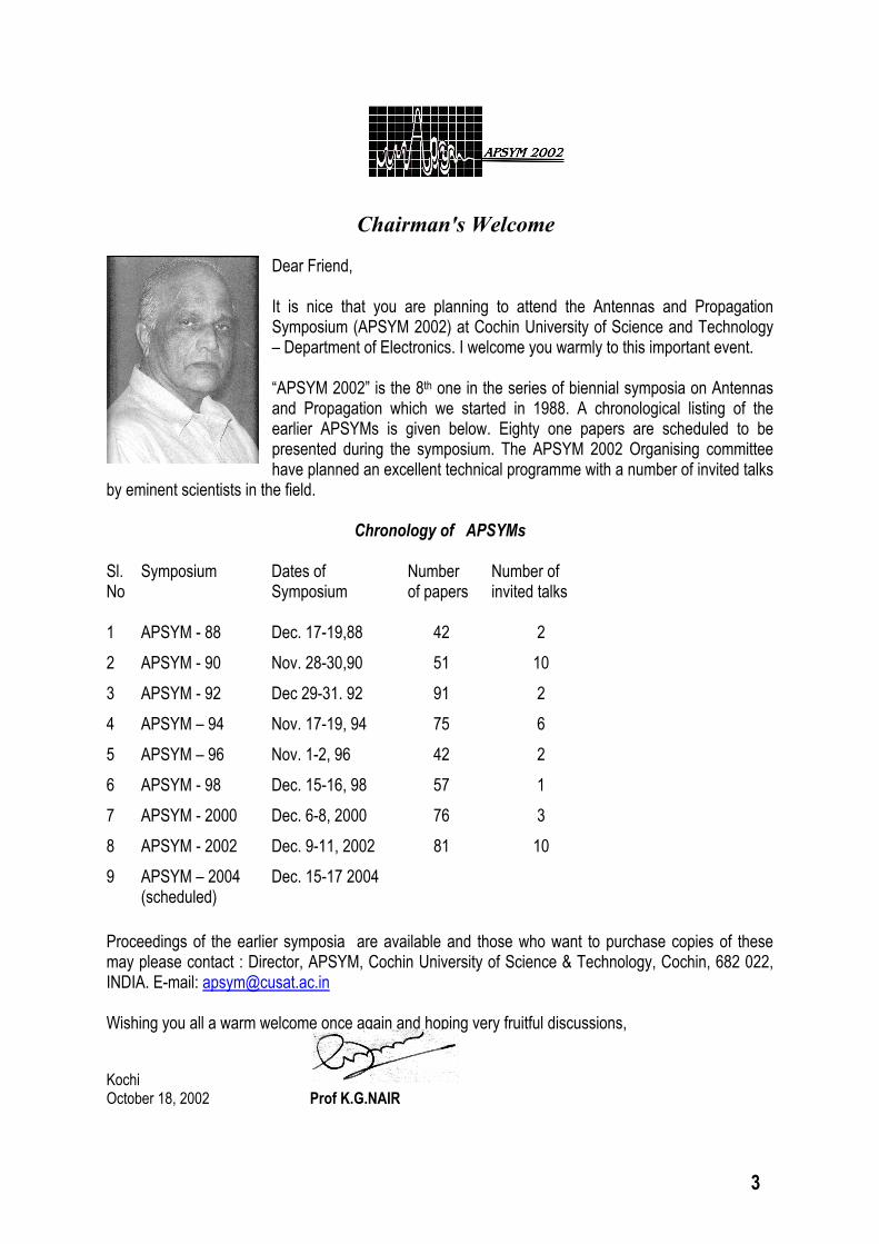
Chairman's Welcome
Dear Friend, It is nice that you are planning to attend the Antennas and Propagation Symposium (APSYM 2002) at Cochin University of Science and Technology – Department of Electronics. I welcome you warmly to this important event. “APSYM 2002” is the 8th one in the series of biennial symposia on Antennas and Propagation which we started in 1988. A chronological listing of the earlier APSYMs is given below. Eighty one papers are scheduled to be presented during the symposium. The APSYM 2002 Organising committee have planned an excellent technical programme with a number of invited talks
by eminent scientists in the field.
Chronology of APSYMs
Sl. No
Symposium Dates of Symposium
Number of papers
Number of invited talks
1 APSYM - 88 Dec. 17-19,88 42 2 2 APSYM - 90 Nov. 28-30,90 51 10 3 APSYM - 92 Dec 29-31. 92 91 2 4 APSYM – 94 Nov. 17-19, 94 75 6 5 APSYM – 96 Nov. 1-2, 96 42 2 6 APSYM - 98 Dec. 15-16, 98 57 1 7 APSYM - 2000 Dec. 6-8, 2000 76 3 8 APSYM - 2002 Dec. 9-11, 2002 81 10 9 APSYM – 2004
(scheduled) Dec. 15-17 2004
Proceedings of the earlier symposia are available and those who want to purchase copies of these may please contact : Director, APSYM, Cochin University of Science & Technology, Cochin, 682 022, INDIA. E-mail: [email protected] Wishing you all a warm welcome once again and hoping very fruitful discussions, Kochi October 18, 2002 Prof K.G.NAIR

4
5
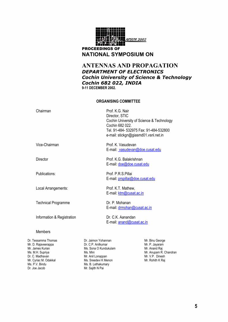
PROCEEDINGS OF NATIONAL SYMPOSIUM ON
ANTENNAS AND PROPAGATION DEPARTMENT OF ELECTRONICS Cochin University of Science & Technology Cochin 682 022, INDIA 9-11 DECEMBER 2002.
ORGANISING COMMITTEE
Chairman Prof. K.G. Nair Director, STIC Cochin University of Science & Technology Cochin 682 022. Tel. 91-484- 532975 Fax: 91-484-532800 e-mail: [email protected] Vice-Chairman Prof. K. Vasudevan E-mail: [email protected] Director Prof. K.G. Balakrishnan E-mail: [email protected] Publications: Prof. P.R.S.Pillai E-mail: [email protected] Local Arrangements: Prof. K.T. Mathew, E-mail: [email protected] Technical Programme Dr. P. Mohanan E-mail: [email protected] Information & Registration Dr. C.K. Aanandan E-mail: [email protected] Members
Dr. Tessamma Thomas Mr. D. Rajaveerappa Mr. James Kurian Ms. M.H. Supriya Dr. C. Madhavan Mr. Cyriac M. Odakkal Ms. P.V. Bindu Dr. Joe Jacob
Dr. Jaimon Yohannan Dr. C.P. Anilkumar Ms. Sona O Kundukulam Ms. Mini Mr. Anil Lonappan Ms. Sreedevi K Menon Ms. B. Lethakumary Mr. Sajith N Pai
Mr. Binu George Mr. P. Jayaram Mr. Anand Raj Mr. Anupam R. Chandran Mr. V.P. Dinesh Mr. Rohith K Raj

6
7
PROCEEDINGS OF
NATIONAL SYMPOSIUM ON
ANTENNAS AND PROPAGATION DEPARTMENT OF ELECTRONICS Cochin University of Science & Technology Cochin 682 022, INDIA 9-11 DECEMBER 2002
Board of Referees
Prof. G.P. Srivastava Prof. M.C. Chandramouly Prof. Bharathi Bhat Dr. Ram Pal Prof. S.K. Choudhary Prof. A.D. Sharma Dr. S. Pal Prof. B.R. Viswakarma Prof. Ramesh Garg Dr. A.K. Patel Prof. K.K. Dey Prof. K.G.Nair Dr. S. Christopher Prof. C.S. Sridhar Prof. Girish Kumar Prof. K. Vasudevan Prof. S. N. Sinha Dr. K.T. Mathew Prof. V.M. Pandharipande Dr. P. Mohanan Dr.V.K. Lakshmee Sha Dr. C.K. Aanandan

8

9
MILESTONES IN THE HISTORY OF ELECTROMAGNETICS
1747 Benjamin Franklin Types of Electricity 1773 Henri Cavendish Inverse square law 1785 Coulomb Law of electric force 1813 Gauss Divergence theorem 1820 Ampere Ampere's experiment 1826 Ohm Ohm’s law 1831 Michael Faraday Faraday's law 1837 Morse Telegraphy 1855 Sir William Thomson Transmission lines theory 1865 James Clerk Maxwell Electromagnetic field equations 1873 James Clerk Maxwell Unified theory of Electricity and Magnetism 1876 Graham Bell & Gray Telephone 1887 Heinrich Hertz Spark plug experiment 1888 Heinrich Hertz Half-wave dipole antenna 1890 Ernst Lecher Lecher wire 1893 Thomson Waveguide theory 1897 Jagadish Chandra Bose Horn antenna and Millimeter wave Source 1901 Marconi First wireless signal across Atlantic 1906 Fessenden Radio broadcasting Dunwoody Crystal detectors 1912 Eccles lonospheric propagation 1915 Carson Single side-band transmission 1918 Watson Ground wave propagation 1919 Heinrich Barkhausen & Kurz Triode electron tube at 1.5 GHz 1920 Yagi and Uda Yagi-Uda antenna 1921 HuII Smooth bore Magnetron 1923 HH Beverage Beverage antenna 1925 Van Boetzelean Short wave Radio Appleton Ionospheric layer 1929 Clavier Microwave Communication 1930 Hansen Resonant cavity Barrow L Waveguides Karl G Jansky Bruce Curtain antenna 1931 Andre G Clavier Microwave Radio transmission across English Channel Introduced the term "Microwave". 1932 Claud Cleton Microwave spectroscopy 1933 Armstrong Frequency modulation 1935 Oscar Heil Velocity modulation Watson watt RADAR 1936 G. H. Brown Turnstile antenna

10
1937 Russel & Varian Bros Klystron A, H. Boot , J T. Randall M. L. Oliphant Magnetron Pollard Radar aiming anti-aircraft guns 1938 J. D. Kraus Corner reflector 1939 P. H. Smith Smith impedance chart 1940 Bowen, Dummer et al P P I Scope Rosenthan Skiratron 1944 Kompfner T W T 1946 J. D. Kraus Helical antenna Percy Spencer Microwave oven 1948 Van der Ziel Non-linear capacitors 1950 C. L. Dolph Dolph-Tchebyscheff array 1953 Deschamps Microstrip antenna 1954 Towns Maser 1956 Bloembergen Three level Maser 1957 V. H. Rumsey Frequency independent antenna Weiss Parametric amplifier 1958 John D Dyson Spiral antenna Read Read diode Leo Esaki Tunnel diode Satellite launching Space Communication 1960 D. Wigst Isbell Log periodic antenna Maiman Ruby Laser L. Lewin Strip line radiator 1963 J. B. Gunn Gunn diode 1964 A F. Kay Scalar feed 1964 Arno Penzias & Big Bang theory R. Wilson Proved by microwave antenna expts. 1965 B. C, Delosch & R. C. Jonston IMPATT diode 1996 Clorfeine & Delohh TRAPATT diode 1970 Byron Microstrip array 1975 Bekati Relativistic cavity Magnetron 1986 Didenko et. al. Advance relativistic Magnetron 1988 S. K. Khamas High Tc Super conducting dipole 1992 Victor Trip, Johnson wang Paste-on Antenna 1993 Te-Kao Wu et.al Multiple Diachronic Surface Cassegrain Reflector 1996 John W Mc Carkle Microstrip DC to GHz Field Stacking Balun 2000 Zhores I Alferov Fast opto and microelectronic
Herbert Kroemer Semiconductor heterostructures.
11
CONTENTS
Session Title Page
I MICROSTRIP ANTENNAS I 25
II ANTENNAS I 63
III MICROWAVE PROPAGATION 99
IV MICROWAVE DEVICES 153
V MICROSTRIP ANTENNAS II 219
VI MICROWAVE MATERIALS 249
VII MICROSTRIP ANTENNAS III 281
VIII ANTENNAS II 309
IX ANTENNAS III 331
X MICROWAVE & OPTICAL TECHNOLOGY 355
INVITED TALKS 383
AUTHOR INDEX 426

12
23
INVITED TALKS
1.
Time-Domain CFIE for the Analysis of Transient Scattering from Arbitrarily Shaped 3-D Conducting Objects Tapan Kumar Sarkar1 and Baek Ho Jung2 1 Department of Electrical Engineering and Computer Science Syracuse University, Syracuse, NY 13244 e-mail: [email protected] 2 Department of Information and Communication Engineering Hoseo University, Asan 336-795, South Korea e-mail: [email protected]
385
2.
Advancement in Vacuum Microwave Devices for Strategic and Communication Sectors S.N. Joshi Central Electronics Engineering Research Institute Pilani. Email [email protected]
389
3.
EM Field Display with Modulated Scattered Technique Fred Gardiol Laboratory of Electromagnetism & Acoustics Swiss Federal Institute of Technology Chemin Des Graminees 11, CH 1009 Pully, Switzerland Email [email protected]
396
4 Growth of Microwaves G.P .Srivastava Department of Electronic Science, University of Delhi South Campus, New Delhi -110 021
402
5 On Em Well-Logging Sensors and Data Interpretation Jaideva C. Goswami Schlumberger Technology Corporation 110 Schlumberger Drive, Sugar Land, Texas 77478, U.S.A. [email protected]
404
6.
Effect Of Microwaves and R. F. Palsma on The Sensitivity And Response of Tin Oxide Gas Sensors S. K. Srivastava Department of Electronics Engineering Institute of Technology, Banaras Hindu University Varanasi – 221 005.
405
7.
An Overview of Dielectric Horn Antennas and an Attempt to Investigate Broad Band Dielectric Structures R. K. Jha, S. P. Singh And Rajeev Gupta* Department of Electronics Engineering Institute of Technology, Banaras Hindu University, Varanasi – 221 005.
412
8 Diversity Schemes for Mobile Communications Parveen F. Wahid, Senior Member, IEEE School of Electrical Engineering and Computer Science University of Central Florida Orlando, FL 32816-2450 Email: [email protected]
418
9.
A Chronology Of Developments Of Wireless Communication And Electronics Till 1920 Magdalena Salazar-Palma*, Tapan K. Sarkar**, Dipak Sengupta*** *Departamento de Señales, Sistemas y Radiocomunicaciones, Escuela Técnica, Universidad Politécnica de Madrid, Ciudad Universitaria s/n, 28040 Madrid Spain [email protected]**Department of Electrical Engineering and Computer Science, Syracuse University ***Department of Electrical Engineering, University of Michigan, Ann Arbor, Michigan 48109-2122, USA Email: [email protected]
424
Proceedings of APSYM, Dec. 9-11, 2002, Dept. of Electronics, CUSAT, Cochin, INDIA
24
25
RESEARCH SESSION I Monday, December 9, 2002 (1.30 p.m. to 3.30 p.m)
MICROSTRIP ANTENNAS I Hall : 1
CHAIRS: PROF.PANDHARIPANDE PROF.GIRISHKUMAR
1.1 Calculation of parameters of Microstrip Antenna using Artificial Neural Networks Dhruba C .Ponda, Syam.S. Pattnaik, Swapna Devi, Bonomali Khuntia & Dipti K.Neog Lecturer, Computer Science & Engg., NERIST, Nirjuli - 791 109, Itanagar, Arunachal Pradesh. [email protected]
27
1.2 Active Annular Ring Microstrip Antenna Binod K. Kanaujia & B.R .Vishvakarma Professor, Dept. of Electronics Engg. Institute of Technology, Banaras Hindu University, Varanasi-221 005. [email protected]
32
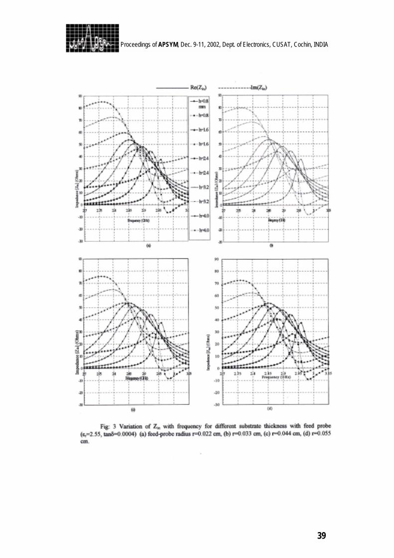
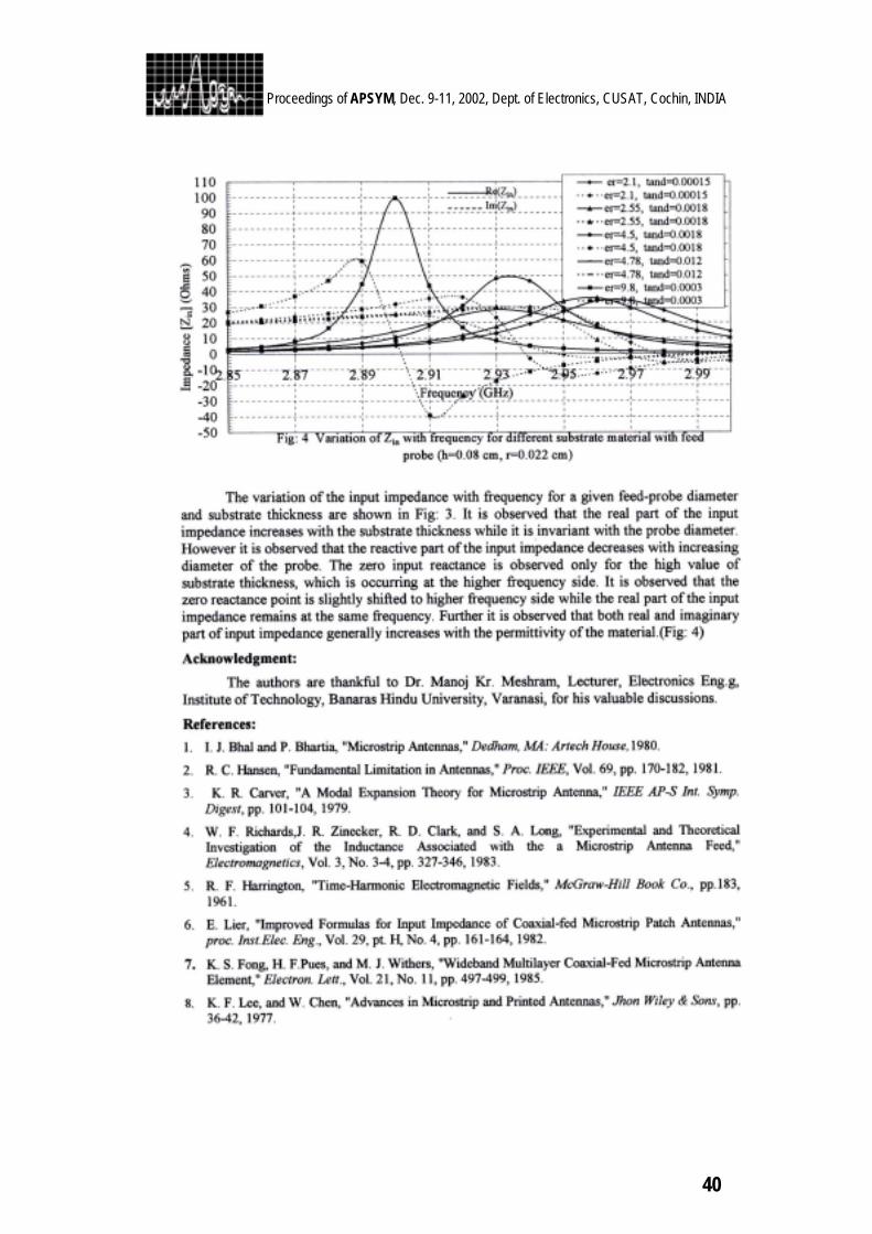
1.3 Effect of coaxial feed on the performance of Microstrip patch Antenna Pradyot Kala, Reena Pant, R .U. Khan & B.R. Vishvakarma Dept. of Electronics Engg. Institute of Technology, Banaras Hindu University, Varanasi-221 005. [email protected]
37
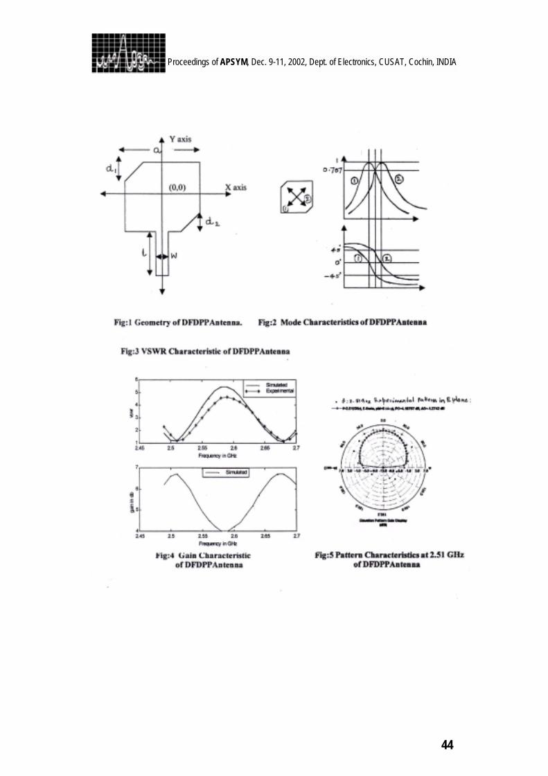
1.4 Single Layered Dual Frequency Microstrip Antenna with Orthogonal Polarization V. Sarala, V.M. Pandharipande* E.C.E. Dept., Sree Nidhi Institute of Science & Technology, Yamnampet, Hyderabad – 501 301. *E.C.E.Dept., University College of Engg., Oasmania Ut.Hyderabad-500 007. [email protected]
41
1.5 CAD Formulas for the Triangular Microstrip Patch Antennas Debatosh Guha and Jawad Y.Siddique Institute of Radio Physics and Electronics, University of Calcutta, 92, Acharya Prafulla Chandra Road, Calcutta-700 009. [email protected]
45
1.6 Experimental Investigation On Equilateral Triangular Microstrip Antenna Rajesh K. Vishwakarma, Babu R. Vishwakarma Electronics Engg, Dept., Institute of Technology, Banaras Hindu University, Varanasi-221 005. [email protected]
50
1.7 A Neural Network Approach For Resonant Frequency Of Annular-Ring Microstrip Antenna Amalendu Patnaik, Rabindra K.Mishra Dept. of Electronics & Commn. Engg., National Institute of Science and Technology, Berhampur-761 008, , [email protected]
54
1.8 FDTD Analysis of L-Strip Fed Microstrip Antenna B. Lethakumary, Sreedevi K. Menon, C.K. Aanandan, K. Vasudevan, P. Mohanan CREMA, Dept. of Electronics, CUSAT, Cochin-682 022, [email protected]
58
Proceedings of APSYM, Dec. 9-11, 2002, Dept. of Electronics, CUSAT, Cochin, INDIA
27
Proceedings of APSYM, Dec. 9-11, 2002, Dept. of Electronics, CUSAT, Cochin, INDIA
CALCULATION OF PARAMETERS OF MICROSTRIP ANTENNA USING ARTIFICIAL NEURAL NETWORKS
Dhruba C. Panda , Syam S. Pattnaik, Senior Member IEEE, Fellow
IETE, Swapna Devi and Bonomali Khuntia and Dipak K. Neog NERIST, Nirjuli-791 109, India
Email - [email protected] or [email protected]
In this paper, a feed forward back propagation neural network is used to calculate the parameters of microstrip antenna. Also a tunnel based Artificial Neural Network(ANN) is used to calculate the resonant frequency of thick substrate rectangular microstrip antenna. The results shows that the tunnel based ANN is faster in terms of time and is more accurate compared to the feed forward back propagation ANN. IE3D software package is used to find simulation results of these antennas. The results are in good agreement with the experimental findings.
INTRODUCTION
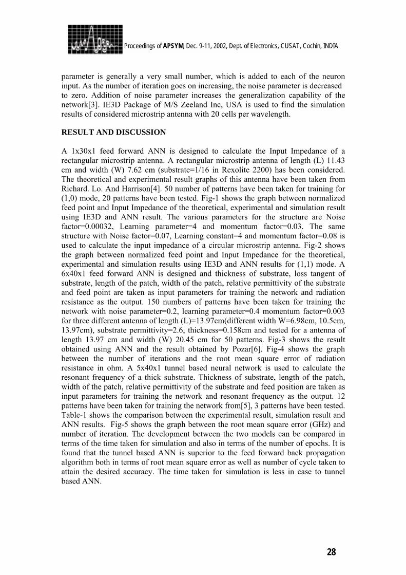
Research on microstrip antenna in 21st century aims at developing reduced size, integrated, wide band, multifunctional antennas for various platforms. Wide band and miniaturization are the major characteristics of present day wireless hand-held devices. Design of antennas for these are getting complex due to strategic incorporation of users realistic conditions. This has forced the researchers to develop accurate low cost and less complex simulation techniques to design microstrip antennas. In this paper, feed forward algorithm[1] is used for the calculation of radiation resistance, input impedance and resonant frequency of microstrip antenna. When the training data bank is large the feed forward algorithm takes much time to overcome the virtual valley. Addition of tunneling phenomenon[2] to the feed forward algorithm enhances the capability of feed forward back propagation algorithm many folds. The tunneling is implemented by solving the differential equation given by, dw/dt=ρ(w-w*)1/3
Where, ‘ρ’ and ‘w*’ represent the strength of learning and last local minima for ‘w’ respectively. The differential equation is solved for some time till it attains the next minima. To start with the training cycle, some perturbation is added to the weights. Then the sum of square errors for all the training patterns is calculated. If it is greater than the last minima than it is tunneled according to above equation. If the error is less than the last local minima than the weights are updated according to the relation, ∆w(t)=-η∇∇∇∇ E(t)+α ∆w(t-1) where, ‘η’ is called learning factor and ‘α’ is called momentum factor. ‘t’ and ‘(t-1)’ indicate current and the most recent training steps respectively. In addition to above parameters, another parameter called the noise parameter is also used. The noise
28
Proceedings of APSYM, Dec. 9-11, 2002, Dept. of Electronics, CUSAT, Cochin, INDIA
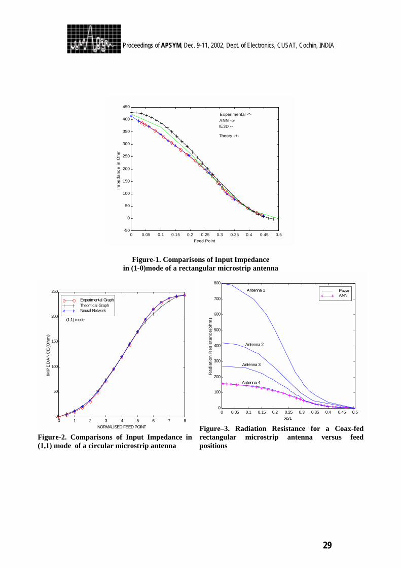
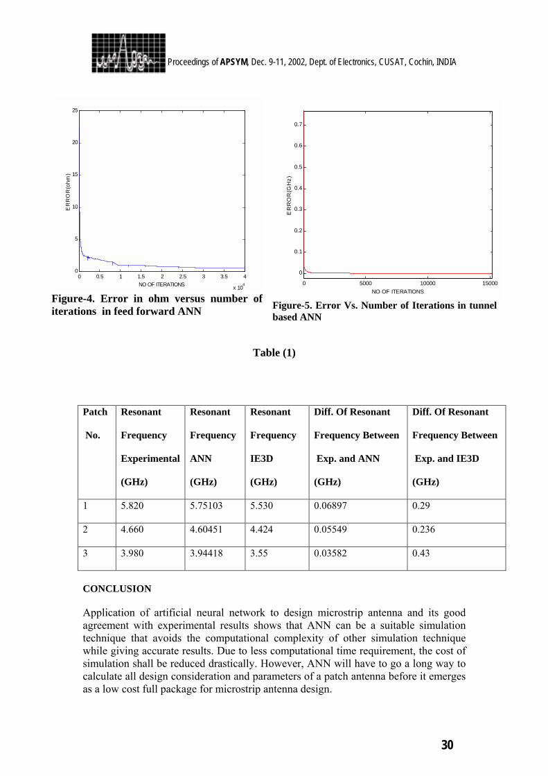
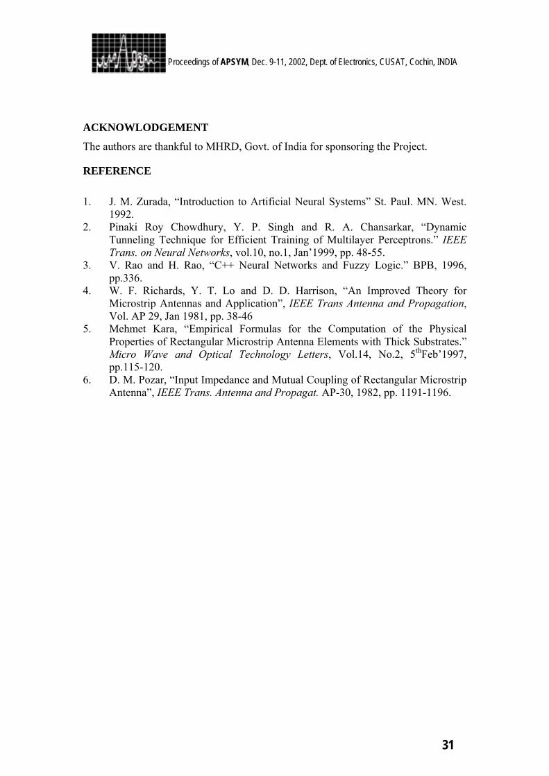
parameter is generally a very small number, which is added to each of the neuron input. As the number of iteration goes on increasing, the noise parameter is decreased to zero. Addition of noise parameter increases the generalization capability of the network[3]. IE3D Package of M/S Zeeland Inc, USA is used to find the simulation results of considered microstrip antenna with 20 cells per wavelength. RESULT AND DISCUSSION A 1x30x1 feed forward ANN is designed to calculate the Input Impedance of a rectangular microstrip antenna. A rectangular microstrip antenna of length (L) 11.43 cm and width (W) 7.62 cm (substrate=1/16 in Rexolite 2200) has been considered. The theoretical and experimental result graphs of this antenna have been taken from Richard. Lo. And Harrison[4]. 50 number of patterns have been taken for training for (1,0) mode, 20 patterns have been tested. Fig-1 shows the graph between normalized feed point and Input Impedance of the theoretical, experimental and simulation result using IE3D and ANN result. The various parameters for the structure are Noise factor=0.00032, Learning parameter=4 and momentum factor=0.03. The same structure with Noise factor=0.07, Learning constant=4 and momentum factor=0.08 is used to calculate the input impedance of a circular microstrip antenna. Fig-2 shows the graph between normalized feed point and Input Impedance for the theoretical, experimental and simulation results using IE3D and ANN results for (1,1) mode. A 6x40x1 feed forward ANN is designed and thickness of substrate, loss tangent of substrate, length of the patch, width of the patch, relative permittivity of the substrate and feed point are taken as input parameters for training the network and radiation resistance as the output. 150 numbers of patterns have been taken for training the network with noise parameter=0.2, learning parameter=0.4 momentum factor=0.003 for three different antenna of length (L)=13.97cm(different width W=6.98cm, 10.5cm, 13.97cm), substrate permittivity=2.6, thickness=0.158cm and tested for a antenna of length 13.97 cm and width (W) 20.45 cm for 50 patterns. Fig-3 shows the result obtained using ANN and the result obtained by Pozar[6]. Fig-4 shows the graph between the number of iterations and the root mean square error of radiation resistance in ohm. A 5x40x1 tunnel based neural network is used to calculate the resonant frequency of a thick substrate. Thickness of substrate, length of the patch, width of the patch, relative permittivity of the substrate and feed position are taken as input parameters for training the network and resonant frequency as the output. 12 patterns have been taken for training the network from[5], 3 patterns have been tested. Table-1 shows the comparison between the experimental result, simulation result and ANN results. Fig-5 shows the graph between the root mean square error (GHz) and number of iteration. The development between the two models can be compared in terms of the time taken for simulation and also in terms of the number of epochs. It is found that the tunnel based ANN is superior to the feed forward back propagation algorithm both in terms of root mean square error as well as number of cycle taken to attain the desired accuracy. The time taken for simulation is less in case to tunnel based ANN.
29
Proceedings of APSYM, Dec. 9-11, 2002, Dept. of Electronics, CUSAT, Cochin, INDIA
0 0.05 0.1 0.15 0.2 0.25 0.3 0.35 0.4 0.45 0.5-50
0
50
100
150
200
250
300
350
400
450
Feed Point
Impe
danc
e in
Ohm
Experimental -*- ANN -o-IE3D --
Theory -+-
Figure-1. Comparisons of Input Impedance in (1-0)mode of a rectangular microstrip antenna
0 1 2 3 4 5 6 7 80
50
100
150
200
250
NORMALISED FEED POINT
IMP
ED
AN
CE
(Ohm
)
(1,1) mode
Experimental GraphTheoritical Graph Neural Network
Figure-2. Comparisons of Input Impedance in (1,1) mode of a circular microstrip antenna
0 0.05 0.1 0.15 0.2 0.25 0.3 0.35 0.4 0.45 0.50
100
200
300
400
500
600
700
800
Xo/L
Rad
iatio
n R
esis
tanc
e(oh
m)
Antenna 4
Antenna 3
Antenna 2
Antenna 1 PozarANN
Figure–3. Radiation Resistance for a Coax-fed rectangular microstrip antenna versus feed positions
30
Proceedings of APSYM, Dec. 9-11, 2002, Dept. of Electronics, CUSAT, Cochin, INDIA
0 0.5 1 1.5 2 2.5 3 3.5 4
x 104
0
5
10
15
20
25
NO OF ITERATIONS
ER
RO
R(o
hm)
Figure-4. Error in ohm versus number of iterations in feed forward ANN
0 5000 10000 15000
0
0.1
0.2
0.3
0.4
0.5
0.6
0.7
NO OF ITERATIONSE
RR
OR
(GH
z)
Figure-5. Error Vs. Number of Iterations in tunnel based ANN
Table (1)
CONCLUSION Application of artificial neural network to design microstrip antenna and its good agreement with experimental results shows that ANN can be a suitable simulation technique that avoids the computational complexity of other simulation technique while giving accurate results. Due to less computational time requirement, the cost of simulation shall be reduced drastically. However, ANN will have to go a long way to calculate all design consideration and parameters of a patch antenna before it emerges as a low cost full package for microstrip antenna design.
Patch
No.
Resonant
Frequency
Experimental
(GHz)
Resonant
Frequency
ANN
(GHz)
Resonant
Frequency
IE3D
(GHz)
Diff. Of Resonant
Frequency Between
Exp. and ANN
(GHz)
Diff. Of Resonant
Frequency Between
Exp. and IE3D
(GHz)
1 5.820 5.75103 5.530 0.06897 0.29
2 4.660 4.60451 4.424 0.05549 0.236
3 3.980 3.94418 3.55 0.03582 0.43
31
Proceedings of APSYM, Dec. 9-11, 2002, Dept. of Electronics, CUSAT, Cochin, INDIA
ACKNOWLODGEMENT
The authors are thankful to MHRD, Govt. of India for sponsoring the Project. REFERENCE 1. J. M. Zurada, “Introduction to Artificial Neural Systems” St. Paul. MN. West.
1992. 2. Pinaki Roy Chowdhury, Y. P. Singh and R. A. Chansarkar, “Dynamic
Tunneling Technique for Efficient Training of Multilayer Perceptrons.” IEEE Trans. on Neural Networks, vol.10, no.1, Jan’1999, pp. 48-55.
3. V. Rao and H. Rao, “C++ Neural Networks and Fuzzy Logic.” BPB, 1996, pp.336.
4. W. F. Richards, Y. T. Lo and D. D. Harrison, “An Improved Theory for Microstrip Antennas and Application”, IEEE Trans Antenna and Propagation, Vol. AP 29, Jan 1981, pp. 38-46
5. Mehmet Kara, “Empirical Formulas for the Computation of the Physical Properties of Rectangular Microstrip Antenna Elements with Thick Substrates.” Micro Wave and Optical Technology Letters, Vol.14, No.2, 5thFeb’1997, pp.115-120.
6. D. M. Pozar, “Input Impedance and Mutual Coupling of Rectangular Microstrip Antenna”, IEEE Trans. Antenna and Propagat. AP-30, 1982, pp. 1191-1196.
32
Proceedings of APSYM, Dec. 9-11, 2002, Dept. of Electronics, CUSAT, Cochin, INDIA
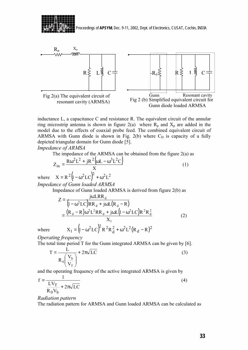
ACTIVE ANNULAR RING MICROSTRIP ANTENNA
Binod K. Kanaujia and B. R. Vishvakarma
Department of Electronics Engineering, Institute of Technology, Banaras Hindu University,
Varanasi -221 005, India. E-mail: [email protected]
In the present paper various parameters such as input impedance, VSWR, bandwidth, radiation pattern, beam width etc. of a Gunn integrated annular ring microstrip antenna are evaluated as a function of bias voltage and threshold voltage. The Gunn loaded patch provides wider tunability, better matching, and enhanced radiated power as compared to the patch alone. Bandwidth of the Gunn loaded patch improves to 11.07 % over the 7.9 % bandwidth of the patch whereas radiated is enhanced by 3.7 dB as compared to patch alone.
INTRODUCTION
There are several interesting features like small size and larger bandwidth associated with the annular ring patch as compared to other conventional patches that attracted the attention of several investigators [1]-[4]. In the present endeavor, the analysis of Gunn loaded annular ring antenna is presented. THEORETICAL CONSIDERATIONS
The Gunn integrated annular ring microstrip antenna is shown in fig. 1. The equivalent circuit for the ARMSA can be expressed as parallel combination of an
Fig. 1(a) Top view of the Gunn integrated annular ring microstrip antenna (b) Side view of the Gunn integrated annular ring microstrip antenna
DC reverse bias
h
Gunn diode Ground plane (b)
ARMSA Dielectric substrate (εr)
Gunn diode
a b
D.C. bias line (a)
33
Proceedings of APSYM, Dec. 9-11, 2002, Dept. of Electronics, CUSAT, Cochin, INDIA
inductance L, a capacitance C and resistance R. The equivalent circuit of the annular ring microstrip antenna is shown in figure 2(a) where Rp and Xp are added in the model due to the effects of coaxial probe feed. The combined equivalent circuit of ARMSA with Gunn diode is shown in Fig. 2(b) where CD is capacity of a fully depicted triangular domain for Gunn diode [5]. Impedance of ARMSA The impedance of the ARMSA can be obtained from the figure 2(a) as
( )X
CLLjRLRZ23222
inω−ω+ω= (1)
where ( ) 22222 LLC1RX ω+ω−= Impedance of Gunn loaded ARMSA Impedance of Gunn loaded ARMSA is derived from figure 2(b) as
( ) ( )RRLjRRLC1LRRj
Zdd
2d
−ω+ω−ω
=
( ) ( )
1
2d
22d
22d
XRRLC1LjRRLRR ω−ω+ω−
= (2)
where ( ) ( )2d222
d222
1 RRLRRLC1X −ω+ω−= Operating frequency The total time period T for the Gunn integrated ARMSA can be given by [6].
LC2
VV
R
LT
T
b0
π+
= (3)
and the operating frequency of the active integrated ARMSA is given by
LC2VR
LV1f
b0
T π+= (4)
Radiation pattern The radiation pattern for ARMSA and Gunn loaded ARMSA can be calculated as
Fig 2 (b) Simplified equivalent circuit for Gunn diode loaded ARMSA
C LR -Rd
Gunn Resonant cavity
CL R
Rp Xp
Fig 2(a) The equivalent circuit of resonant cavity (ARMSA)
34
Proceedings of APSYM, Dec. 9-11, 2002, Dept. of Electronics, CUSAT, Cochin, INDIA
θ−θφ
π=
−θ
)bk(J)ak(J)sinbk(J)sinak(Jncos
re
kEhk2j
E1
'n
1'n
0'n0
'n
rjk
1
00n 0
(5a)
θ−
θθ
φθπ
−=
−φ
)bk(J)ak(J
b)sinbk(J
a)sinak(J
sinnsincos
re
knhE2j
E1
'n
1'n0n0n
rjk
1
0n 0
(5b)
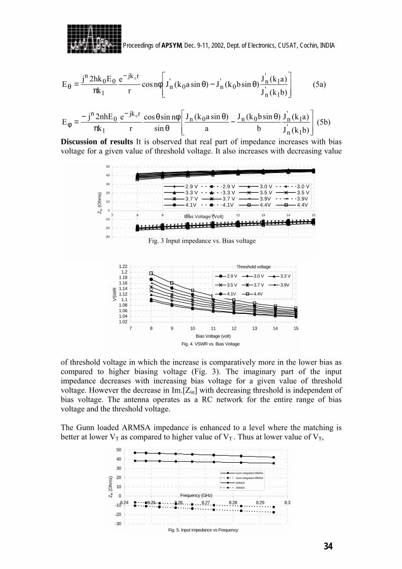
Discussion of results It is observed that real part of impedance increases with bias voltage for a given value of threshold voltage. It also increases with decreasing value
of threshold voltage in which the increase is comparatively more in the lower bias as compared to higher biasing voltage (Fig. 3). The imaginary part of the input impedance decreases with increasing bias voltage for a given value of threshold voltage. However the decrease in Im.[Zin] with decreasing threshold is independent of bias voltage. The antenna operates as a RC network for the entire range of bias voltage and the threshold voltage. The Gunn loaded ARMSA impedance is enhanced to a level where the matching is better at lower VT as compared to higher value of VT . Thus at lower value of VT,
-30
-20
-10
0
10
20
30
40
50
7 8 9 10 11 12 13 14 15Bias Voltage (Volt)
Z in (
Ohm
s)
2.9 V 2.9 V 3.0 V 3.0 V3.3 V 3.3 V 3.5 V 3.5 V3.7 V 3.7 V 3.9V 3.9V4.1V 4.1V 4.4V 4.4V
Fig. 4. VSWR vs. Bias Voltage
1.021.041.061.081.1
1.121.141.161.181.2
1.22
7 8 9 10 11 12 13 14 15
Bias Voltage (volt)
VS
WR
2.9 V 3.0 V 3.3 V
3.5 V 3.7 V 3.9V
4.1V 4.4V
Threshold voltage
Fig. 3 Input impedance vs. Bias voltage
Fig. 5. Input impedance vs Frequency -30
-20
-10
0
10
20
30
40
50
8.24 8.25 8.26 8.27 8.28 8.29 8.3Frequency (GHz)Z i
n (O
hms)
Gunn integrated ARMSA
Gunn integrated ARMSA
ARMSA
ARMSA
35
Proceedings of APSYM, Dec. 9-11, 2002, Dept. of Electronics, CUSAT, Cochin, INDIA
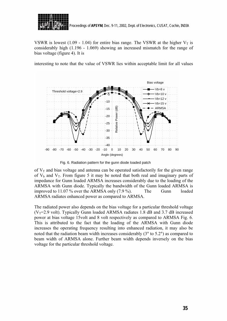
VSWR is lowest (1.09 - 1.04) for entire bias range. The VSWR at the higher VT is considerably high (1.196 - 1.069) showing an increased mismatch for the range of bias voltage (figure 4). It is interesting to note that the value of VSWR lies within acceptable limit for all values
of VT and bias voltage and antenna can be operated satisfactorily for the given range of Vb and VT. From figure 5 it may be noted that both real and imaginary parts of impedance for Gunn loaded ARMSA increases considerably due to the loading of the ARMSA with Gunn diode. Typically the bandwidth of the Gunn loaded ARMSA is improved to 11.07 % over the ARMSA only (7.9 %). The Gunn loaded ARMSA radiates enhanced power as compared to ARMSA. The radiated power also depends on the bias voltage for a particular threshold voltage (VT=2.9 volt). Typically Gunn loaded ARMSA radiates 1.8 dB and 3.7 dB increased power at bias voltage 15volt and 8 volt respectively as compared to ARMSA Fig. 6. This is attributed to the fact that the loading of the ARMSA with Gunn diode increases the operating frequency resulting into enhanced radiation, it may also be noted that the radiation beam width increases considerably (3° to 5.2°) as compared to beam width of ARMSA alone. Further beam width depends inversely on the bias voltage for the particular threshold voltage.
Fig. 6. Radiation pattern for the gunn diode loaded patch
-40
-35
-30
-25
-20
-15
-10
-5
0
-90 -80 -70 -60 -50 -40 -30 -20 -10 0 10 20 30 40 50 60 70 80 90
Angle (degrees)
Rel
ativ
e P
ower
(dB
)
Vb=8 vVb=10 vVb=12 vVb=15 vARMSA
Threshold voltage=2.9
Bias voltage

36
Proceedings of APSYM, Dec. 9-11, 2002, Dept. of Electronics, CUSAT, Cochin, INDIA
REFERENCES
1. S. Ali, W. C. Chew, and J. A. Kong, " Vector Hankel transform analysis of annular ring microstrip antenna, " IEEE Trans. Antennas Propagat., vol. AP-30, no. 4, pp. 637-644, July 1982.
2. W. C. Chew, " A broad band annular ring microstrip antenna, " IEEE Trans. Antennas Propagat., vol. AP-30, no. 5, pp. 918-922, Sept. 1982.
3. A. K. Bhattacharyya and R. Garg, " Analysis of annular ring microstrip antenna using cavity model, "Arch. Elek, Ubert, vol. 39, no. 3, pp. 185 -189, 1985.
4. H. J. Thomas, D. L. Fudge and G. Morris, " Gunn source integrated with microstrip patch, " Microwaves and RF., pp. 87-91, Feb. 1985.
5. G. S. Hobson " The Gunn effect " Clarendon Press, Oxford, UK. 1974. 6. S. K. Sharma and B. R. Vishvakarma , " Gunn integrated microstrip antenna,"
Indian J. of Radio and Space Physics, vol. 26, pp. 40-44, Feb. 1997.
37
Proceedings of APSYM, Dec. 9-11, 2002, Dept. of Electronics, CUSAT, Cochin, INDIA
38
Proceedings of APSYM, Dec. 9-11, 2002, Dept. of Electronics, CUSAT, Cochin, INDIA
39
Proceedings of APSYM, Dec. 9-11, 2002, Dept. of Electronics, CUSAT, Cochin, INDIA
40
Proceedings of APSYM, Dec. 9-11, 2002, Dept. of Electronics, CUSAT, Cochin, INDIA
41
Proceedings of APSYM, Dec. 9-11, 2002, Dept. of Electronics, CUSAT, Cochin, INDIA
42
Proceedings of APSYM, Dec. 9-11, 2002, Dept. of Electronics, CUSAT, Cochin, INDIA
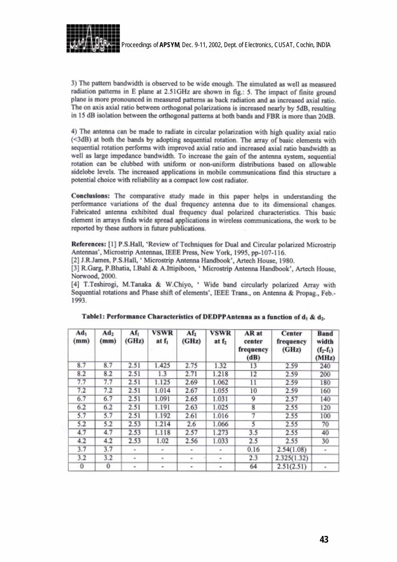
43
Proceedings of APSYM, Dec. 9-11, 2002, Dept. of Electronics, CUSAT, Cochin, INDIA
44
Proceedings of APSYM, Dec. 9-11, 2002, Dept. of Electronics, CUSAT, Cochin, INDIA
45
Proceedings of APSYM, Dec. 9-11, 2002, Dept. of Electronics, CUSAT, Cochin, INDIA
CAD FORMULAS FOR THE TRIANGULAR MICROSTRIP PATCH ANTENNAS
Debatosh Guha & Jawad Y.Siddique
Institute of Radio Physics and Electronics, University of Calcutta 92 Acharya Prafulla Chandra Road, Calcutta 700 009, India
E-mail: [email protected]; [email protected]
Triangular microstrip patch is the least investigated candidate among the series of various geometrical shapes. Various CAD formulas developed so far are reviewed and a new improved formulation is proposed in this paper. The present model is compared with all previous results reported in open literature.
INTRODUCTION
Triangle is one of the common geometrical shapes as such, has been investigated since the early days of its development of microstrip patches. The first studies of triangular microstrip patch (TMP) dates back to 1977 [1]. Almost simultaneously, Helszajn and James [2] reported another theoretical and experimental investigation on equilateral TMP as disk resonator, filter and circulator. They used the cavity resonator model, though subsequently other analyses techniques were applied. It is apparent that most of the analyses and resulting CAD formulas are based on cavity resonator model for the TM n,m,l modes. The basic formula developed in [2] to determine the resonant frequency of TMP, been improved from time to time by different researchers[2]-[15] as reviewed in Table 1. In this paper, a new cavity model formula is proposed to predict accurate resonant frequency of an equilateral TMP antenna printed on any substrate having any dielectric constant. THE CAD MODEL AND RESULTS
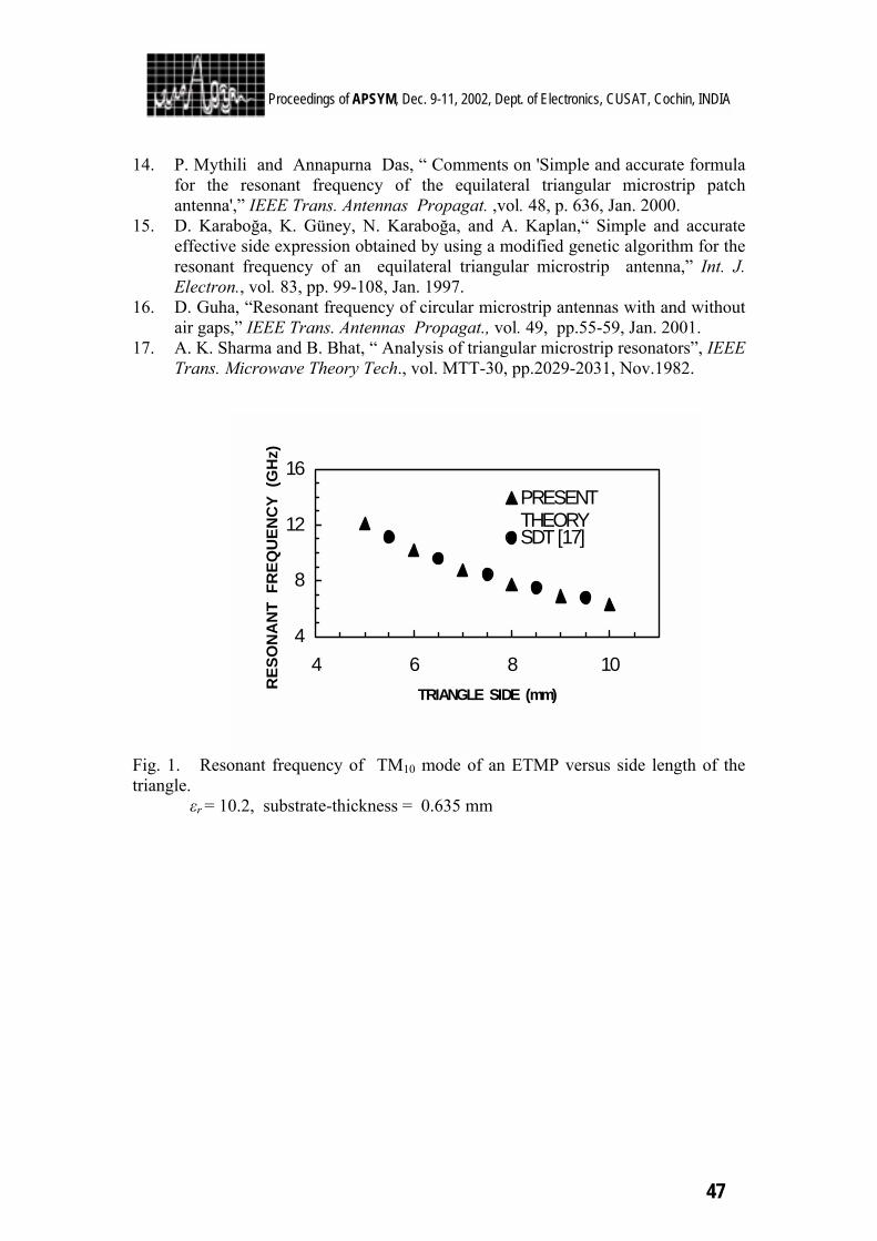
The resonant frequency of an equilateral TMP (ETMP) antenna having side length r printed on a substrate with εre is given by [2] ( ) 2122
,, 32 mnmn
rcf
reffefflmn ++=
ε (1)
In the proposed model, εreff can be determined from an earlier work of the authors [16] and reff is determined as )1(
32 qaeffr += π . (2)
The parameter q can be readily computed from [2, eq.(9)-(14)] with an equivalence relation a=(3/2π)r. A circular patch (with radius a) equivalent to an ETMP has been defined to workout the new CAD model. The basis of the equivalence is the equal circumference of both the geometries. Computed results are compared with some previously reported theories and measured data in Fig. 1 and Table II, respectively. Excellent agreement of the present model with the numerical techniques and measured data is apparent from the comparison.
46
Proceedings of APSYM, Dec. 9-11, 2002, Dept. of Electronics, CUSAT, Cochin, INDIA
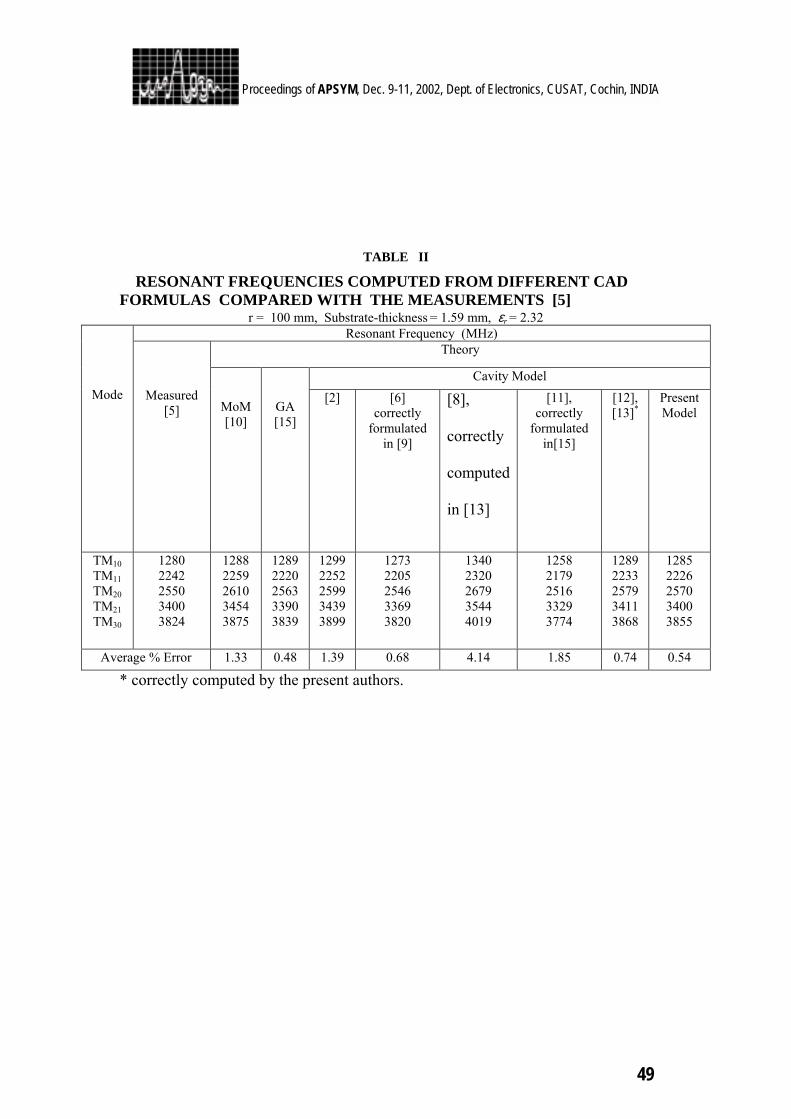
CONCLUSION
Various CAD formulas proposed so far to calculate the resonant frequency of an ETMP antenna is reviewed and a new formula is proposed. The computed results are compared with all previous ones and a set of measured data. The closest agreement of the present formula is apparent from the comparison and their respective average % error. REFERENCES 1. T. Miyoshi, S. Yamaguchi, and S. Goto, “Ferrite planar circuits in microwave
integrated circuits,” IEEE Trans. Microwave Theory Tech., vol. MTT-25, pp.593-600,July 1977.
2. J. Helszajn and D. S. James, “ Planar triangular resonators with magnetic walls,” IEEE Trans. Microwave Theory Tech., vol. MTT-26, pp.95-100,Feb. 1978.
3. Y. T. Lo, D. Solomon, and W. F. Richards, “ Theory and experiment on microstrip antennas,” IEEE Trans. Antennas Propagat., vol. AP-27, pp.137-145, 1979.
4. C. S. Gurel, E. Yazgan, “ New computation of the resonant frequency of a tunable equilateral triangular microstrip patch,” IEEE Trans. Microwave Theory Tech.,vol. 48, pp. 334-338, March. 2000.
5. J. S. Dahele and K. F. Lee, “ On the resonant frequencies of the triangular patch antenna,” IEEE Trans. Antennas Propagat., vol. AP-35, pp.100-101, Jan. 1987.
6. R. Garg and S. A. Long, “An improved formula for the resonant frequency of the triangular microstrip patch antenna,” IEEE Trans. Antennas Propagat., vol.AP-36, p.570, Apr. 1988.
7. K. F. Lee, K. M. Luk, and J. S. Dahele, “ Characteristics of the Equilateral triangular patch antenna,” IEEE Trans. Antennas Propagat. ,vol. AP-36, pp. 1510-1518, Nov. 1988.
8. X. Gang, “On the resonant frequencies of microstrip antennas,” IEEE Trans. Antennas Propagat., vol.37, pp.245-247, Feb. 1989.
9. R. Singh, A. De, and R. S. Yadava, “Comments on An improved formula for the resonant frequency of the triangular microstrip patch antenna,” IEEE Trans. Antennas Propagat., vol.39, pp.1443-1444, Sept. 1991.
10. W. Chen, K. F. Lee, and J. Dahele, “ Theoretical and experimental studies of the resonant frequencies of equilateral triangular microstrip antenna,” IEEE Trans. Antennas Propagat., vol.40, pp.1253-1256, Oct. 1992.
11. N. Kumprasert and K.W. Kiranon, “Simple and accurate formula for the resonant frequency of the equilateral triangular microstrip patch antenna,” IEEE Trans. Antennas Propagat., vol.42, pp.1178-1179, Aug. 1994.
12. K. Güney, “Resonant frequency of a triangular microstrip antenna,” Microwave Opt. Technol. Lett., vol. 6, pp. 555-557, July 1993.
13. K. Güney, “Comments on 'On the resonant frequencies of microstrip antennas',” IEEE Trans. Antennas Propagat. ,vol. 42, pp. 1363-1365, Sept. 1994.
47
Proceedings of APSYM, Dec. 9-11, 2002, Dept. of Electronics, CUSAT, Cochin, INDIA
14. P. Mythili and Annapurna Das, “ Comments on 'Simple and accurate formula for the resonant frequency of the equilateral triangular microstrip patch antenna',” IEEE Trans. Antennas Propagat. ,vol. 48, p. 636, Jan. 2000.
15. D. Karaboğa, K. Güney, N. Karaboğa, and A. Kaplan,“ Simple and accurate effective side expression obtained by using a modified genetic algorithm for the resonant frequency of an equilateral triangular microstrip antenna,” Int. J. Electron., vol. 83, pp. 99-108, Jan. 1997.
16. D. Guha, “Resonant frequency of circular microstrip antennas with and without air gaps,” IEEE Trans. Antennas Propagat., vol. 49, pp.55-59, Jan. 2001.
17. A. K. Sharma and B. Bhat, “ Analysis of triangular microstrip resonators”, IEEE Trans. Microwave Theory Tech., vol. MTT-30, pp.2029-2031, Nov.1982.
Fig. 1. Resonant frequency of TM10 mode of an ETMP versus side length of the triangle. εr = 10.2, substrate-thickness = 0.635 mm
4
8
12
16
4 6 8 10TRIANGLE SIDE (mm)R
ESO
NA
NT
FR
EQU
ENC
Y (G
Hz)
PRESENTTHEORYSDT [17]

48
Proceedings of APSYM, Dec. 9-11, 2002, Dept. of Electronics, CUSAT, Cochin, INDIA
TABLE I
CAD Formulas Proposed to improve eq.(1)
Proposed by
Correction Factors and the basis of Formulations* εεε =+= reffreff hrr ,
(i) Helszajn (1978) rreff
eq
eqreff h
rrhrr εε
ππε
=
++= ,7726.12
ln2121
Semi-empirical relation
(ii) Garg et.al (1988) corrected Singh et.al.(1991)
req = (S/π)1/2 , where S = Area of the Equilateral Triangle, *Applied by Wolff and Knoppik
( ) ( ) ( ) ( ) ( ) ( )[ ]
23,36
,2/ln/ln
2121
rHhA
HAAHAHHAHHAxrrreff
==
+++−+
−++= εεε
(III) XU GANG(1989) ( ) ( )
( )
−
++
−+=
−
−−
2
21
2
121
802.9182.6
436.16853.12199.21
rh
rh
rh
rh
rh
rr
r
rr
eff
ε
εε
reff as in # I * Integration Averaging Procedure (iv) Chen,Lee and Dahele (1992) ( )
21
65.1268.077.141.12
ln21
++++
+= r
eqr
eq
eqreff r
hh
rrhrr εε
πε εreff * Curve fitting formula based on MoM
(v) Guney (1994)
reff = r +(h0.6 r 0.38) /√εr,, εreff as in # iii * Semi-empirical relation
(vi) Kumprasert et.al. (1994) Corrected by Mythili et.al (2000)
req as in # ii * Disk capacitance obtained by Chew and Kong
(vii) Gurel (2000)
reff as in # v, εreff = εr, dyn * Modeled by Wolff and Knoppik
49
Proceedings of APSYM, Dec. 9-11, 2002, Dept. of Electronics, CUSAT, Cochin, INDIA
TABLE II
RESONANT FREQUENCIES COMPUTED FROM DIFFERENT CAD FORMULAS COMPARED WITH THE MEASUREMENTS [5]
r = 100 mm, Substrate-thickness = 1.59 mm, εr = 2.32 Resonant Frequency (MHz)
Theory
Cavity Model
Mode
Measured [5]
MoM [10]
GA [15]
[2]
[6] correctly
formulated in [9]
[8],
correctly
computed
in [13]
[11], correctly
formulated in[15]
[12], [13]*
Present Model
TM10 TM11 TM20 TM21 TM30
1280 2242 2550 3400 3824
1288 2259 2610 3454 3875
1289 2220 2563 3390 3839
1299 2252 2599 3439 3899
1273 2205 2546 3369 3820
1340 2320 2679 3544 4019
1258 2179 2516 3329 3774
1289 2233 2579 3411 3868
1285 2226 2570 3400 3855
Average % Error 1.33 0.48 1.39 0.68 4.14 1.85 0.74 0.54
* correctly computed by the present authors.
50
Proceedings of APSYM, Dec. 9-11, 2002, Dept. of Electronics, CUSAT, Cochin, INDIA
EXPERIMENTAL INVESTIGATION ON
EQUILATERAL TRIANGULAR MICROSTRIP ANTENNA
Rajesh K. Vishwakarma and B. R. Vishvakarma Electronics Engineering Department
Institute of Technology, Banaras Hindu University Varanasi -221 005
E-mail: [email protected]
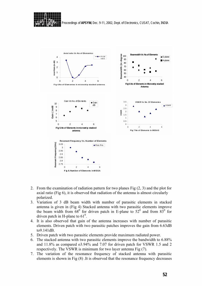
Experimental investigations were conduct on the equilateral triangular microstrip antenna to examine the radiation characteristic with several parasitic element stacked over the driven patch. It has been found that the radiated power axial ratio beam width VSWR gain etc. depend heavily on number of parasitic element
INTRODUCTION
One of the most attractive features of equilateral triangular microstrip antenna (ETMSA) [1] is that the area necessary for the patch radiator becomes about half as large as that of a nearly square MSA. Accordingly, an equilateral triangular MSA can be installed in a narrow space than a nearly square MSA can. In addition if the are used as elements of an array antenna, element spacing can be made shorter than that of an array [4] antenna using a nearly square MSA, and the resultant array antenna can have many elements in a limited area namely it can have only high degree of freedom for pattern synthesis problems but also there is the possibility of wide beam scanning for phased array antenna application. However, in these applications much more investigation on mutual coupling is necessary of course .Two kinds of CP wave [5] can be radiated at two different frequencies from the equilateral -triangular MSA. This dual CP response may be useful in operating MSA as a CP antenna in dual frequency modes e.g. transmitting and receiving modes. ETMSA DESIGN
The designs of the microstrip antenna consist of determination of patch dimensions and location of the feed point determination of patch dimensions. Let 'a' is the side length of the equilateral triangular strip antenna and the used substrate material is Bakelite. Where parameters are, relative dielectric constant rε = 4.8, substrate thickness = 0.15cms, thickness of the copper foil t = 0.0018cms, loss tangent tan δ=0.034,design frequency = 3 GHz. The resonance frequency corresponding to various modes is
22
rr
mnr nmnm
ε3a2C
ε2πCK
f ++== (1)
51
Proceedings of APSYM, Dec. 9-11, 2002, Dept. of Electronics, CUSAT, Cochin, INDIA
where 22
mn nmnm3a4πK ++=
for dominant mode
a = side length,rr3f
2caε
= h of ETMSA
Substituting the values in eq (1) we have
LOCATION OF FEED POINT
The geometry for the calculation model and the co-ordinate system employed here are illustrated in figure (1). An equilateral-triangular-patch of area S is etched on the metallic constant rε .Usually the Patch is fed either by a microstrip feed line or by a coaxial probe. To get good CP wave from an MSA with a single feed [3] , the patch must be Generally fed at an optimum feed location (x0,y0) . EXPERIMENTAL MEASUREMENT
The conventional set-up was used for measuring the E and H plane pattern of the antenna. During the experiment the output of the source was fairly constant. The source of the microwave power was quite stable and the frequency variations were negligibly small. Isolator was used to avoid the reflection from the antenna. The receiver system was kept in the for zone 2d2/λ. Using the setup the radiation patterns of the antenna were measured. The data of measured radiation pattern using different number of parasitic elements are shown in Figs 2.and 3. The data for various parameters like, axial ratio beam width, gain, and VSWR, resonant frequency are shown in Fig 4,5,6,7,and 8 DISCUSSION OF THE RESULTS
1. From the examination of radiation pattern (Fig2, 3) it is observed that radiated power of the triangular patch stacked antenna increases with increasing the parasitic elements. Typically two parasitic elements in stacked antenna improve the radiated power approximately by 17 dB in E-plane and by 20 dB in H-plane. However, the increase in parasitic element beyond two decreases the radiated power. This is also corroborated from the VSWR data Fig (7.) of stacked antenna with two parasitic elements in which VSWR in minimum. For parasitic elements beyond two, enhances the VSWR resulting into high reflection losses.
3.04cm4.8x3x3x10
2x3x10ε3f
2ca9
10
rr
===
rr 3a
2cfε
=
Fig 1 . Co-ordinate system for equilateral-triangular microstrip antenna
Z
t
R
ε
θ
φ b
b a
X
Y S εr
(x0,y0)
52
Proceedings of APSYM, Dec. 9-11, 2002, Dept. of Electronics, CUSAT, Cochin, INDIA
Resonant Frequ ency Vs. N umber of Elements
2.752.8
2.852.9
2.953
3.05
0 2 4 6
F ig 8. Numb er o f Elemen ts in M SSA
Res
onan
t Fre
quen
cy (G
Hz)
R es .Fre.
Gain Vs No. of Elements
56789
10
0 2 4 6Fig 5.No of Elements in microstrip stacked
antenna
Gai
n ( i
ndB
GaindB
VSW R Vs No. Of Elemente s
0
0 .5
1
1 .5
2
2 .5
3
3 .5
0 2 4 6
Fig 7 No of Elements in MSSAS
VS
WR
VSWR
Ax ia l ra ti o Vs No of Ele mente s
0
1
2
3
4
0 2 4 6Fi g 4.No of E lem entes in mi cros tri p sta cke d a nte nna
Axi
al-R
atio
(in
dB)
A xialrat io
Beamwidth Vs No.of Elements
405060708090
100
0 2 4 6Fig 5.No of Elements in Microstrip stacked
Antenna
Bea
mw
idth
(in
degr
ee E-planeH-plane
2. From the examination of radiation pattern for two planes Fig (2, 3) and the plot for
axial ratio (Fig 6), it is observed that radiation of the antenna is almost circularly polarized.
3. Variation of 3 dB beam width with number of parasitic elements in stacked antenna is given in (Fig 4) Stacked antenna with two parasitic elements improve the beam width from 680 for driven patch in E-plane to 520 and from 830 for driven patch in H-plane to 610.
4. It is also observed that gain of the antenna increases with number of parasitic elements. Driven patch with two parasitic patches improves the gain from 6.63dB to9.141dB.
5. Driven patch with two parasitic elements provide maximum radiated power. 6. The stacked antenna with two parasitic elements improve the bandwidth to 6.88%
and 11.8% as compared o3.94% and 7.07 for driven patch for VSWR 1.5 and 2 respectively. The VSWR is minimum for two layer antenna Fig (7).
7. The variation of the resonance frequency of stacked antenna with parasitic elements is shown in Fig (8) .It is observed that the resonance frequency decreases
53
Proceedings of APSYM, Dec. 9-11, 2002, Dept. of Electronics, CUSAT, Cochin, INDIA
with increasing the number of elements in MSSA. This is in accordance with the fact that the parasitic elements when stacked with driven patch, offers an additional fringing capacitance parallel to the capacitance offered by driven resonator. This increases the overall equivalent capacitance of the stacked antenna, which is bound to lower the resonance frequency as observed experimentally.
REFERENCES:
1. Bahl.I.J.andBhartia.P,"Microstripantennas",(ArtechHouse.Dedham,Massachusetts,U.S.A) pp.139-179
2. Nirum Kumprasirt and Wiwat Kiranou, "Simple and accurate formula for the resonant frequency of the equilateral triangular microstrip patch antenna" IEEE Trans on A&P Vol.42, No.8, August.1994
3. Suzuki Y.and Chiba, T " Improved theory for a single fed circularly polarized microstrip antenna" Trans. Electron & Commun. Engg. Jpn.Part B, 1985.E 68,(2) pp.76-82
4. Weinschel, H.D."A cylindrical array of circularly polarized microstrip antenna. "In International Symposium Digest of the Antennas Propagation Society, 1975,pp.177-180
5. Y.Suzuki, N.Miyano and T.Chiba"Circularly polarized radiation from singly fed equilateral microstrip antenna. "IEE Proceeding, Vol.134, pt H, No.2April 1987
54
Proceedings of APSYM, Dec. 9-11, 2002, Dept. of Electronics, CUSAT, Cochin, INDIA
A NEURAL NETWORK APPROACH FOR RESONANT FREQUENCY OF ANNULAR-RING MICROSTRIP
ANTENNA
Amalendu Patnaik, Rabindra K. Mishra∗∗∗∗ Dept. of Electronics & Communication Engineering
National Institute of Science & Technology, Berhampur –761 008, India Email - [email protected]
∗ Dept. of Electronics, Berhampur University, Berhampur – 760 007, India Email - [email protected]
Artificial neural network technique is applied to determine the resonant frequency of annular-ring microstrip antenna. It drastically reduces the mathematical complexity involved in the resonant frequency determination using Galerkin’s method. Neural network results are compared with the available results.
INTRODUCTION
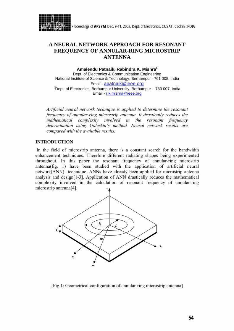
In the field of microstrip antenna, there is a constant search for the bandwidth enhancement techniques. Therefore different radiating shapes being experimented throughout. In this paper the resonant frequency of annular-ring microstrip antenna(fig. 1) have been studied with the application of artificial neural network(ANN) technique. ANNs have already been applied for microstrip antenna analysis and design[1-3]. Application of ANN drastically reduces the mathematical complexity involved in the calculation of resonant frequency of annular-ring microstrip antenna[4].
[Fig.1: Geometrical configuration of annular-ring microstrip antenna]
x
z
ρ
ab
φy
d
55
Proceedings of APSYM, Dec. 9-11, 2002, Dept. of Electronics, CUSAT, Cochin, INDIA
PROBLEM FORMULATION
Following the Vector Hankel transform and subsequent application of Galerkin’s method reduces the vector integral equations to a system of M+P linear algebraic equations as[4] :
PMAbAa
MjAbAa
kp
P
ppkm
M
mm
jp
P
ppjm
M
mm
,...,2,10
,...,2,10
11
11
==+
==+
∑∑
∑∑
==
==
φφφϕ
ϕφϕϕ
(1) Eqn. (1) has a nontrivial solution under the condition that det Aij = f(ω) = 0. In general the roots of this equation are complex numbers indicating that the structure has complex resonant frequencies. At this point, we have used the ANN technique for the determination of the resonant frequency. Standard numerical techniques are used to determine the elements of the determinant. APPLICATION OF NEURAL NETWORK TECHNIQUE
Data Generation: At first a simple procedure[5] is used to determine the trial complex resonant frequency ft = frt + jfit of the annular-ring microstrip antenna. Ten arbitrary complex frequencies, around and including ft are then chosen for the network outputs and corresponding determinant values were selected as the neural network inputs. Here we fixed (b/a) at 2.0 and varied (d/a) between 0.005 and 0.3. Network Structure: A three layer feed forward neural network structure was selected. The input layer contains three neurons (two neurons for the real and imaginary parts of the det Aij (i.e., Dr and Di) and the rest neuron is for the (d/a) value). The output layer consists of two neurons for fr and fi i.e., the real and imaginary parts of the resonant frequency. The number of neurons in the hidden layer was determined in trial-and-error basis. Network Training: Here we have used the well known back propagation training algorithm[6]. Accordingly, the network output for the µth input pattern is
= ∑ ∑j r
rjriji wvO µµ ξφψ (2)
where µµξ rD=1 and µµξ iD=2 are the real and imaginary parts of det Aij , wjr and vij are the weighted connections from rth input neuron to jth hidden neuron and from jth hidden neuron to ith output neuron respectively. xx =)(ψ and )tanh()( xx =φ are the activation functions. After proper training, the network adjusts itself with the updated set of weight values. Different network parameters taken during training are given in Table-I. After proper training, the network output, corresponding to the inputs
0== ir DD gives the desired resonant frequency of the structure.
56
Proceedings of APSYM, Dec. 9-11, 2002, Dept. of Electronics, CUSAT, Cochin, INDIA
a) Table - I
2) Parameter 3) Value 4) No. of Input Neurons 3
No. of Output Neurons 2 Neurons in the hidden layer 8 Learning Rate (η) 0.53 Training tolerance 2.5 × 10⁻³
d/a0.02 0.04 0.06 0.08 0.10 0.12 0.14 0.16 0.18 0.20
Im[k
1a]
-0.020
-0.018
-0.016
-0.014
-0.012
-0.010
-0.008
-0.006
-0.004
-0.002
0.000
Galerkin's MethodPresent Method
Shift in fi of TM12 mode
d/a0.001 0.01 0.1 1
Re[
k 1a]
-0.020
-0.018
-0.016
-0.014
-0.012
-0.010
-0.008
-0.006
-0.004
-0.002
0.000
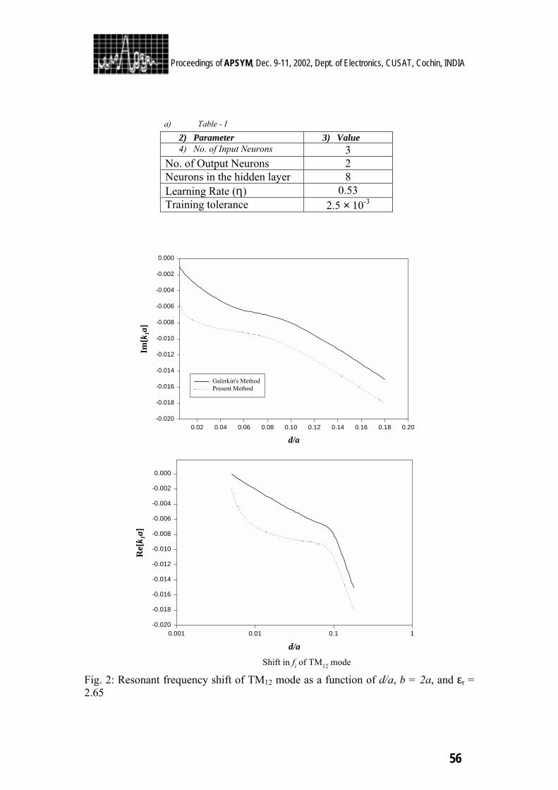
Fig. 2: Resonant frequency shift of TM12 mode as a function of d/a, b = 2a, and εr = 2.65
57
Proceedings of APSYM, Dec. 9-11, 2002, Dept. of Electronics, CUSAT, Cochin, INDIA
RESULTS
The trained network was then used to calculate the resonant frequency of an annular-ring microstrip antenna with b = 2.0 a and εr = 2.65. In order to compare the results with the available published results, we have calculated the resonant frequency shift of the TM12 mode. Fig. 2 compares the result of the present method with the Hankel transform technique followed by Galerkin’s method[4]. CONCLUSION
Application of ANN method drastically reduces the computation time. It takes time only during training. After proper training, the network can be used for CAD purpose in place of the computational intensive methods. REFERENCES
1. R. K. Mishra, A. Patnaik; “Neurospectral computation for complex resonant frequency of microstrip resonators,” IEEE Microwave and Guided Wave Letters, vol. 9, no. 9, pp. 351-353, Sept. 1999.
2. R. K. Mishra, A. Patnaik; “Neurospectral computation for input impedance of rectangular microstrip antenna,” Electronics Letters, vol. 35, no. 20, pp. 1691-1693, Sept. 1999.
3. R. K. Mishra, A. Patnaik; “Neural network based CAD model for the design of square-patch antennas,” IEEE Trans. on Antennas and Propagation, vol. 46, no. 12, pp. 1890-1891, 1998.
4. Sami M. Ali, Weng C. Chew, and J. A. Kong, “Vector Hankel transform analysis of annular-ring microstrip antenna,” IEEE Trans. on Antennas and Propagation, vol. 30, no. 4, pp. 637-642, July 1982.
5. I. J. Bhal, P. Bhartia, Microstrip Antennas, Norwood, MA: Artech House, 1980. 6. S. Haykin, Neural Networks: A Comprehensive Foundation, New York: IEEE
Computer Society Press/IEEE Press, 1994.
58
Proceedings of APSYM, Dec. 9-11, 2002, Dept. of Electronics, CUSAT, Cochin, INDIA
FDTD ANALYSIS OF L-STRIP FED MICROSTRIP ANTENNA
B. Lethakumary, Sreedevi K Menon, C.K. Aanandan, K.Vasudevan and P. Mohanan
CREMA,Department of Electronics, Cochin University of Science and Technology Cochin- 682 022, India.
A broad band L strip fed Microstrip antenna design is presented. The impedance and
radiation characteristics of this antenna are analyzed by the finite difference time domain (FDTD) method.
INTRODUCTION The FDTD method has become a popular tool for analyzing the performance of antennas and microstrip devices with arbitrary three-dimensional structures [1]. With transient excitation, it provides impedance and scattering parameters over a wide range of frequencies. Compared to other discrete methods, FDTD method is extremely efficient and may be derived directly form Maxwell’s equations. When time domain electromagnetic field equations are solved using finite difference techniques, the domain in which the field has to be computed is unbounded. In order to limit the domain in which the field is computed, mesh of limited size is used and absorbing boundary conditions is applied [2] on the outer surface. FDTD method is formulated by discretising Maxwell’s curl equation over a finite volume and approximating derivatives with central difference approximations. Conducting surfaces are treated by setting tangential electric field component to zero. For the electric field components on the dielectric –air interface the average of the two permittivities, (ε0+ε1 ) /2, is used [3]. The maximum time step that may be used is limited by stability restriction of the finite difference equations. ∆t≤ (1/c (1/∆x2
+1/∆y2 +1/∆z2)-1/2), where c is the velocity of the light. A Gaussian pulse is desirable as the excitation because its frequency spectrum being Gaussian and provide frequency domain information from dc to the desired cutoff frequency by adjusting the width of the pulse .To increase the computational efficiency an external source resistance of 50 Ω is used [4]. In this paper, the scattering parameters and electric field distribution of a rectangular patch antenna exited using an L-shaped microstrip fed is calculated using FDTD. Calculated results are presented and compared with experimental observations [5]. NUMERICAL RESULTS The geometry and FDTD analysis structure of the L-strip fed rectangular microstrip patch antenna are shown in figure1 (a) and 1(b) respectively. Rectangular patch antenna of dimension L=40mm and W=20mm is etched on a substrate of thickness 1.6mm and permittivity 4.28. The patch is electromagnetically fed using L-shaped
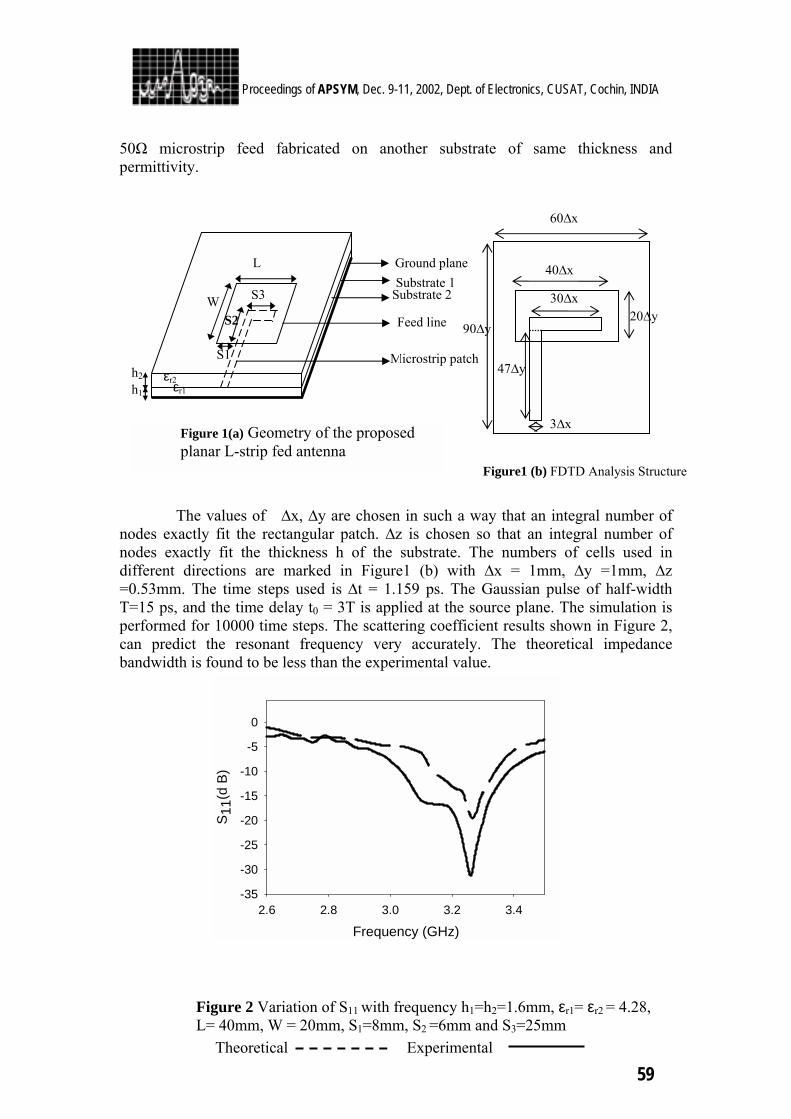
59
Proceedings of APSYM, Dec. 9-11, 2002, Dept. of Electronics, CUSAT, Cochin, INDIA
50Ω microstrip feed fabricated on another substrate of same thickness and permittivity. The values of ∆x, ∆y are chosen in such a way that an integral number of nodes exactly fit the rectangular patch. ∆z is chosen so that an integral number of nodes exactly fit the thickness h of the substrate. The numbers of cells used in different directions are marked in Figure1 (b) with ∆x = 1mm, ∆y =1mm, ∆z =0.53mm. The time steps used is ∆t = 1.159 ps. The Gaussian pulse of half-width T=15 ps, and the time delay t0 = 3T is applied at the source plane. The simulation is performed for 10000 time steps. The scattering coefficient results shown in Figure 2, can predict the resonant frequency very accurately. The theoretical impedance bandwidth is found to be less than the experimental value.
Frequency (GHz)2.6 2.8 3.0 3.2 3.4
S11
(d B
)
-35
-30
-25
-20
-15
-10
-5
0
Figure 2 Variation of S11 with frequency h1=h2=1.6mm, εr1= εr2 = 4.28, L= 40mm, W = 20mm, S1=8mm, S2 =6mm and S3=25mm
Theoretical Experimental
Microstrip patchh2 h1
Ground plane
Substrate 2
Feed line
S1
S2
L
W Substrate 1
εr2 εr1
Figure 1(a) Geometry of the proposed planar L-strip fed antenna
60∆x
Figure1 (b) FDTD Analysis Structure
90∆y
40∆x
20∆y 30∆x
47∆y
3∆x
S3
60
Proceedings of APSYM, Dec. 9-11, 2002, Dept. of Electronics, CUSAT, Cochin, INDIA
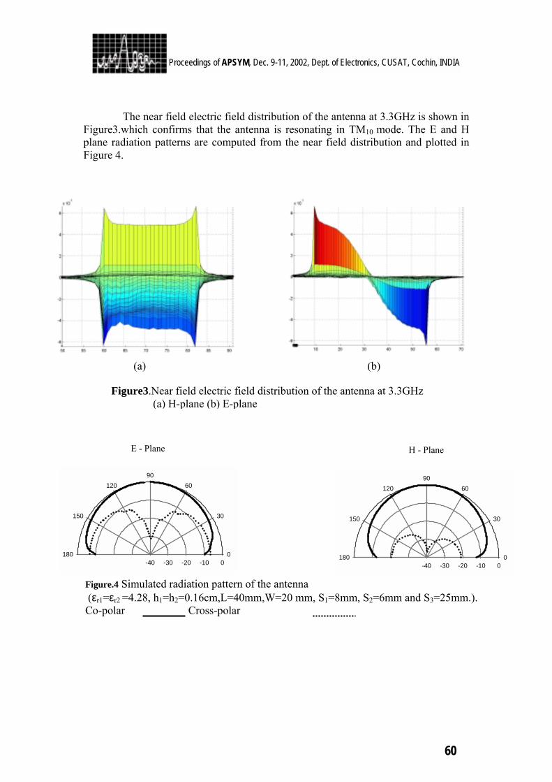
The near field electric field distribution of the antenna at 3.3GHz is shown in Figure3.which confirms that the antenna is resonating in TM10 mode. The E and H plane radiation patterns are computed from the near field distribution and plotted in Figure 4.
-40 -30 -20 -10 00
30
6090
120
150
180
-40 -30 -20 -10 00
30
6090
120
150
180
E - Plane H - Plane
Figure.4 Simulated radiation pattern of the antenna (εr1=εr2 =4.28, h1=h2=0.16cm,L=40mm,W=20 mm, S1=8mm, S2=6mm and S3=25mm.). Co-polar Cross-polar
Figure3.Near field electric field distribution of the antenna at 3.3GHz (a) H-plane (b) E-plane
(a) (b)
61
Proceedings of APSYM, Dec. 9-11, 2002, Dept. of Electronics, CUSAT, Cochin, INDIA
CONCLUSIONS In this paper the characteristics of the wide band L-strip fed microstrip antenna are investigated using FDTD method. The results have been verified by comparison with measured data. As this antenna has wide bandwidth, compact structure, it may find applications in wideband communication systems. REFERENCES
1. Kane S. Yee, “Numerical Solution of Initial Boundary Value Problems
Involving Maxwell’s Equations in Isotropic media”, IEEE Trans. on Antennas and Propagation, Vol.AP-14, pp.302-307, May1966.
2. G.Mur, “Absorbing Boundary conditions for the Finite Difference
Approximations of the Time Domain Electromagnetic Field Equations”, IEE Trans.Electromagn.Compat., Vol.EMC-223, pp.377-382, Nov.1981.
3. M Sheen .S.Ali.M.D Abouzahara.and J.A.Kong. “Application of the Three-
Dimensional Finite- Difference Time Domain method to the Analysis of Planar Microstrip Circuits”, IEEE Trans.Microwave Theory and Tech., Vol.38, pp.849-857, July1990.
4. R.J Lubbers, H.S Langdon, “ A simple Feed Model that Reduces Time Steps
Needed for FDTD Antenna and Microstrip Calculations”, IEEE Trans. On Antenna and Propagation, Vol.44, No.7, pp-1000-1005, July1996.
5. S.Mridula, S.K Menon, B.Lethakumary, B.Paul, C.K Anandan, and
P.Mohanan., “ Planar L-Strip Fed broad band Microstrip Antenna”, Microwave Opt Technol Lett,Vol.34,pp.115-117,July 2002
62
Proceedings of APSYM, Dec. 9-11, 2002, Dept. of Electronics, CUSAT, Cochin, INDIA
63
Proceedings of APSYM, Dec. 9-11, 2002, Dept. of Electronics, CUSAT, Cochin, INDIA
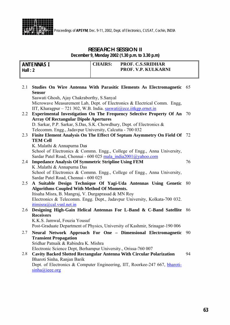
RESEARCH SESSION II December 9, Monday 2002 (1.30 p.m. to 3.30 p.m)
ANTENNAS I Hall : 2
CHAIRS: PROF. C.S.SRIDHAR PROF. V.P. KULKARNI
2.1 Studies On Wire Antenna With Parasitic Elements As Electromagnetic Sensor Saswati Ghosh, Ajay Chakraborthy, S.Sanyal Microwave Measurement Lab, Dept. of Electronics & Electrical Comm. Engg, IIT, Kharagpur – 721 302, W.B. India. [email protected]
65
2.2 Experimental Investigation On The Frequency Selective Property Of An Array Of Rectangular Dipole Apertures D. Sarkar, P.P. Sarkar, S.Das, S.K. Chowdhury, Dept. of Electronics & Telecomm. Engg., Jadavpur University, Calcutta - 700 032
70
2.3 Finite Element Analysis On The Effect Of Septum Asymmetry On Field Of TEM Cell K. Malathi & Annapurna Das School of Electronics & Commn. Engg., College of Engg., Anna University, Sardar Patel Road, Chennai - 600 025 [email protected]
72
2.4 Impedance Analysis Of Symmetric Stripline Using FEM K .Malathi & Annapurna Das School of Electronics & Commn. Engg., College of Engg., Anna University, Sardar Patel Road, Chennai - 600 025
76
2.5 A Suitable Design Technique Of Yagi-Uda Antennas Using Genetic Algorithms Coupled With Method Of Moments. Itisaha Misra, B. Mangraj, V. Durgaprasad & MN Roy Electronics & Telecomm. Engg. Dept., Jadavpur University, Kolkata-700 032. [email protected]
80
2.6 Designing High-Gain Helical Antennas For L-Band & C-Band Satellite Receivers K.K.S. Jamwal, Fouzia Yousuf Post-Graduate Department of Physics, University of Kashmir, Srinagar-190 006
86
2.7 Neural Network Approach For One – Dimensional Electromagnetic Transient Propagation Sridhar Patnaik & Rabindra K. Mishra Electronic Science Dept, Berhampur University., Orissa-760 007
90
2.8 Cavity Backed Slotted Rectangular Antenna With Circular Polarization Bharoti Sinha, Ranjan Barik Dept. of Electronics & Computer Engineering, IIT, Roorkee-247 667, [email protected]
94
64
Proceedings of APSYM, Dec. 9-11, 2002, Dept. of Electronics, CUSAT, Cochin, INDIA
65
Proceedings of APSYM, Dec. 9-11, 2002, Dept. of Electronics, CUSAT, Cochin, INDIA
STUDIES ON WIRE ANTENNA WITH PARASITIC ELEMENTS
AS ELECTROMAGNETIC SENSOR
Saswati Ghosh, Ajay Chakrabarty, Subrata Sanyal
Department of Electronics & Electrical Communication Engineering, Indian Institute of Technology, Kharagpur-721302, West Bengal E-mail: [email protected], [email protected]
In this paper, studies are performed on the behaviour of wire antenna in receiving mode in presence of other conducting wire or parasitic element with axis in varied angle of inclination with the exciter axis. A simple and useful method of moment-based theoretical technique is described to evaluate the current distribution on the antenna surface and hence the antenna factor of a receiving antenna when used as an EMI (Electromagnetic Interference) sensor in presence of parasitic elements.
INTRODUCTION
The presence of other conducting wires or parasitic elements, will alter the current distribution, the field radiated, and in turn the input impedance in transmitting mode and output impedance in receiving mode of the wire antenna. The authors had already reported the investigations performed on the theoretical evaluation of antenna factor of simple wire antenna [1]. In this paper, investigations are performed on the evaluation of antenna factor of wire antenna when used for EMI (Electromagnetic Interference) measurements with other non-parallel parasitic wire element. The Method of Moment based numerical technique is applied for the evaluation of current distribution on the wire antenna and hence the antenna factor of the wire antenna. THEORETICAL ANALYSIS
A wire antenna with one parasitic element is shown in Figure 1(a) - Figure 1(b). A z-directed electric field of 1volt/meter is incident on the surface of the conducting wires. This incident field induces linear current density on the surface of the conducting wires which reradiate and produce the scattered electric field Es. Assuming the wire as perfectly conducting with same radius a (a<<λ), the total tangential electric field is considered as zero on the surface of the wire element and also interior to the wire. The surface of the vertical element is defined as S1 and that of the parasitic element as S2. The total tangential field component on S1 and S2 are written as follows
0211111
=++= S,SS,SS tanSEtanSEiSEtanE (1a)
0221222
=++= S,SS,SS tanSEtanSEiSEtanE (1b)
The terms of equation 1(a) and 1(b) are defined as below
1StanE , 2StanE - Total tangential electric field on S1 and S2 respectively.
iSE,i
SE21
- Incident electric field on S1 and S2 respectively.
66
Proceedings of APSYM, Dec. 9-11, 2002, Dept. of Electronics, CUSAT, Cochin, INDIA
Z L2 S2 θ h EtanS2
Ei Gap L EtanS1 Gap Incident wave L1 y d
2a x S1 Figure 2. Dipole segmentation
and its equivalent current. 2a
Figure1(a). Plane wave incidence on wire antenna with parasitic element.
Z L1 S1
θ Ei Incident wave EtanS1 h EtanS2 d Gap y L2
x S2 Figure 4. Equivalent circuit diagram.
2a
Figure1(b). Plane wave incidence on wire antenna with parasitic element.
11 S,StanSE , 21 S,StanSE -Tangential component of scattered electric field on S1 due to current
distribution on S1 and S2 respectively.
12 S,StanSE , 22 S,StanSE -Tangential component of scattered electric field on S2 due to source
on S1 and S2 respectively.
Voc
V
67
Proceedings of APSYM, Dec. 9-11, 2002, Dept. of Electronics, CUSAT, Cochin, INDIA
The field equation 1(a) is simplified as follows izEi
SE =1
θθ sinS
yEcosSzEtanSE
zSEtanSE
S,SS,SS,S
S,SS,S
212121
1111
−=
= (2)
To evaluate the scattered field due to the parasitic element, it is found convenient to define a rotated rectangular coordinate system with the origin at the center of the parasitic element and the z-axis coinciding with the axis of the element.
For 1(b) the field component are simplified as follows θcosi
zEiSE =
1
2222
121212
S,SS,S
S,SS,SS,S
zSEtanE
sinySEcoszSEtanE
=
+= θθ (3)
where the field components are defined as follows SzE
S,S 11, S
zES,S 12
- z component of scattered electric field on S1 and S2 respectively due to
current distribution on S1.
21 S,SSzE , S
zES,S 22
- z component of scattered electric field on S1 and S2 respectively due to
current distribution on S2.
21 S,SSyE ,
12 S,SSyE - y component of scattered electric field on S1 due to current distribution
on S2 and scattered electric field on S2 due to current distribution on S1
respectively. For the evaluation of the electric field components, the magnetic vector potential A is
introduced which is related to the magnetic and electric field as follows
AH
×∇=µ1 , H
jE
×∇=ωε1 (4)
where ( )∫∫ ′−
′′′=S
sdR
jkRez,y,xsJA
πµ
4 (5)
For perfectly conducting wires, equation (5) is simplified as follows [2]
zd)z,z(G)z(I)a(A/L
/Lzz ′′′== ∫
−
2
2
µρ (6)
For very thin wire (a<<λ), ( ) ( )R
eRGz,zGjkR
π4
−==′ and 222
24 )zz()(sina)a(R ′−+
′== φρ .
Putting the values of AZ in (4), the components of scattered electric field are evaluated as follows
( )( ) zdRkjkRzzyyR
jkRe)z(/L
/LzI
kjS
yE ′
−+′−′−
−′
−−= ∫
22335
2
24π
η (7)
68
Proceedings of APSYM, Dec. 9-11, 2002, Dept. of Electronics, CUSAT, Cochin, INDIA
( ) ( ) zdkaRaRjkRR
jkRe)z(/L
/LzI
kjS
zE ′
+
−+
−′
−−= ∫
22322154
2
24 ππ
η (8)
Equations (7) and (8) are solved by approximating the integrals as the sum of integrals over N small segments (Fig. 2) where the main arm is divided into N1 number and the load arm into N2 number of subsections. The current density is considered as constant over each segment.
Equation 1(a) and 1(b) are combined to a matrix equation as follows [Vt]=[Z][I] (9)
ANTENNA FACTOR
The ratio of incident electric field on the surface of the sensor to the received voltage at the antenna terminal when terminated by 50 ohm load is known as antenna factor [3].
)V(voltageceivedRe)E(fieldelectricIncidentFactorAntenna i= (10)
where received voltage V is evaluated as follows (Figure.3)
ocoutL
L VZZ
ZV+
= (11)
Generally ZL i.e. impedance of the detector (e.g. spectrum analyser) is considered as 50 ohm. Here effectiveioc l.EV
= (12) leffective is the vector effective length of the antenna. The effective length is the length of a thin straight conductor oriented perpendicular to the given direction and parallel to the antenna polarisation, having a uniform current equal to that at the antenna terminals. By approximating the integral as the summation over N1 subsections, effective length is simplified as follows
scI
N
nn.nI
effectivel∑==
1
1∆
(13)
The output impedance of the antenna is written as follows
scIocV
outZ = (14)
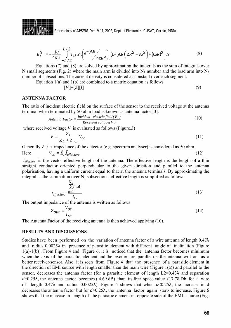
The Antenna Factor of the receiving antenna is then achieved applying (10). RESULTS AND DISCUSSIONS
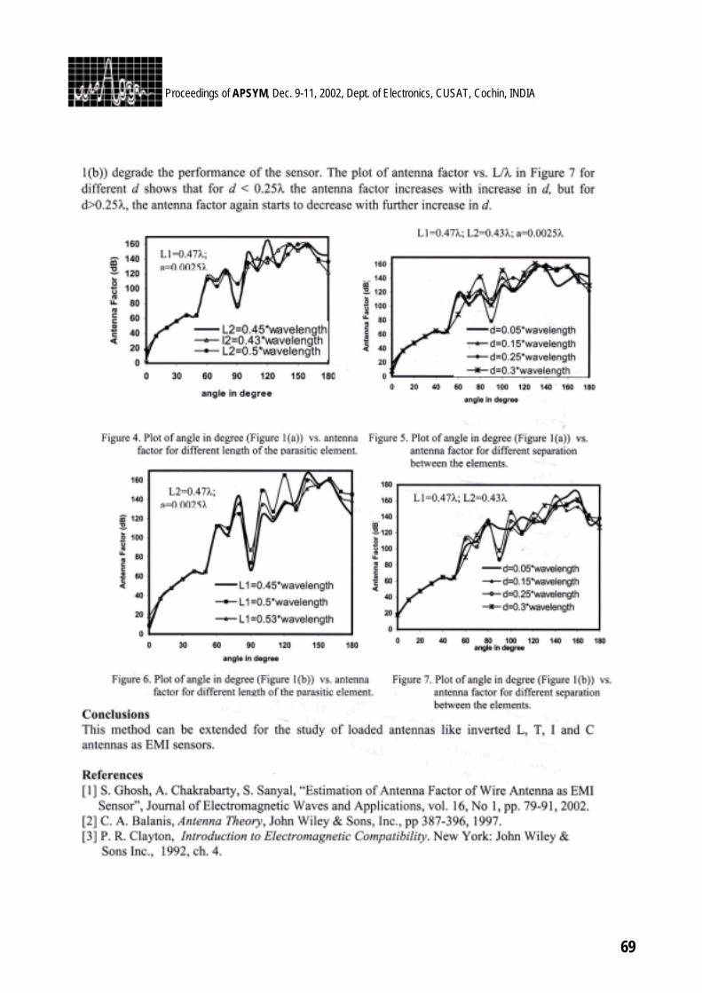
Studies have been performed on the variation of antenna factor of a wire antenna of length 0.47λ and radius 0.0025λ in presence of parasitic element with different angle of inclination (Figure 1(a)-1(b)). From Figure 4 and Figure 6, it is noticed that the antenna factor becomes minimum when the axis of the parasitic element and the exciter are parallel i.e. the antenna will act as a better receiver/sensor. Also it is seen from Figure 4 that the presence of a parasitic element in the direction of EMI source with length smaller than the main wire (Figure 1(a)) and parallel to the sensor, decreases the antenna factor (for a parasitic element of length L2=0.43λ and separation d=0.25λ, the antenna factor becomes ( 4.69 dB) than its free space value (17.78 Db for a wire of length 0.47λ and radius 0.0025λ). Figure 5 shows that when d<0.25λ, the increase in d decreases the antenna factor but for d>0.25λ, the antenna factor again starts to increase. Figure 6 shows that the increase in length of the parasitic element in opposite side of the EMI source (Fig.
69
Proceedings of APSYM, Dec. 9-11, 2002, Dept. of Electronics, CUSAT, Cochin, INDIA
70
Proceedings of APSYM, Dec. 9-11, 2002, Dept. of Electronics, CUSAT, Cochin, INDIA
EXPERIMENTAL INVESTIGATION ON THE FREQUENCY SELECTIVE PROPERTY OF AN ARRAY OF RECTANGULAR
DIPOLE APERTURES.
D. Sarkar*, P.P. Sarkar*, S. Das++ and S.K. Chowdhury+ *USIC, University of Kalyani, Kalyani
++Dept. of E. & T.C.E., B.E.College (D.U.), Howrah +Dept. of E. & T.C.E., Jadavpur University, Calcutta
Frequency Selective property of a regular periodic array of rectangular dipole apertures has been investigated experimentally. Measured data show a 40 dB separation between transmission and reflection bands of the FSS in the normalized transmitted electric field versus frequency plot.
INTRODUCTION
Frequency Selective Surfaces (F.S.S.), which find widespread applications as filters for microwaves and optical signals have been the subject of extensive studies in recent years. These surfaces comprise periodically arranged metallic patch elements or aperture elements within a metallic screen and exhibit total reflection (patches) or transmission (aperture) in the neighborhood of the element resonance. A numerical analysis of finite frequency selective surfaces with rectangular patches of various aspect ratios was done using the method of moment[1]. This paper deals with the experimental investigation on an FSS consisting of a regular periodic array of rectangular dipole apertures fabricated on one side of the metal plated dielectric slab. DESIGN OF THE FSS
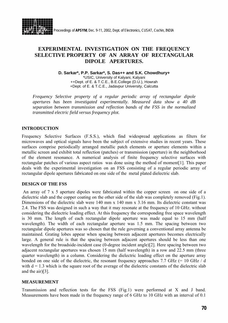
An array of 7 x 5 aperture dipoles were fabricated within the copper screen on one side of a dielectric slab and the copper coating on the other side of the slab was completely removed (Fig.1). Dimensions of the dielectric slab were 140 mm x 140 mm x 3.16 mm. Its dielectric constant was 2.4. The FSS was designed in such a way that it may resonate at the frequency of 10 GHz. without considering the dielectric loading effect. At this frequency the corresponding free space wavelength is 30 mm. The length of each rectangular dipole aperture was made equal to 15 mm (half wavelength). The width of each rectangular aperture was 1.5 mm. The spacing between two rectangular dipole apertures was so chosen that the rule governing a conventional array antenna be maintained. Grating lobes appear when spacing between adjacent apertures becomes electrically large. A general rule is that the spacing between adjacent apertures should be less than one wavelength for the broadside-incident case (0-degree incident angle)[2]. Here spacing between two adjacent rectangular apertures was chosen 15 mm (half wavelength) in a row and 22.5 mm (three quarter wavelength) in a column. Considering the dielectric loading effect on the aperture array bonded on one side of the dielectric, the resonant frequency approaches 7.7 GHz (= 10 GHz / d with d = 1.3 which is the square root of the average of the dielectric constants of the dielectric slab and the air)[3]. MEASUREMENT
Transmission and reflection tests for the FSS (Fig.1) were performed at X and J band. Measurements have been made in the frequency range of 6 GHz to 10 GHz with an interval of 0.1
71
Proceedings of APSYM, Dec. 9-11, 2002, Dept. of Electronics, CUSAT, Cochin, INDIA
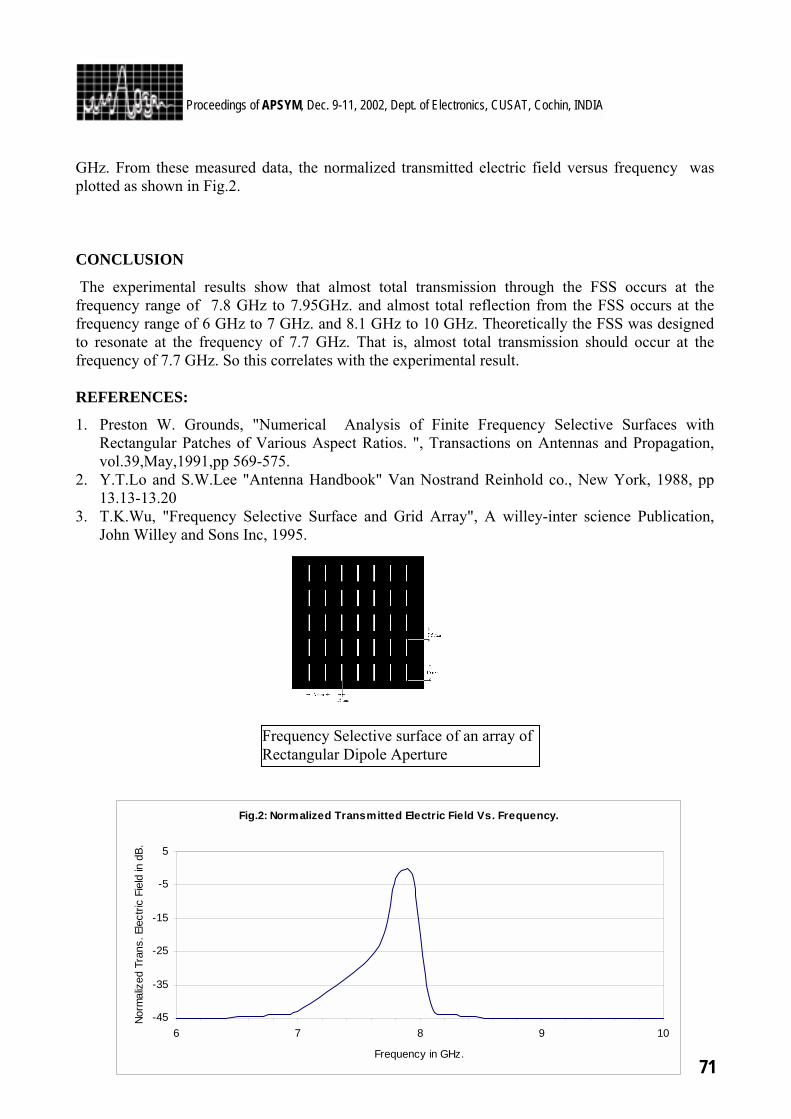
GHz. From these measured data, the normalized transmitted electric field versus frequency was plotted as shown in Fig.2. CONCLUSION
The experimental results show that almost total transmission through the FSS occurs at the frequency range of 7.8 GHz to 7.95GHz. and almost total reflection from the FSS occurs at the frequency range of 6 GHz to 7 GHz. and 8.1 GHz to 10 GHz. Theoretically the FSS was designed to resonate at the frequency of 7.7 GHz. That is, almost total transmission should occur at the frequency of 7.7 GHz. So this correlates with the experimental result. REFERENCES:
1. Preston W. Grounds, "Numerical Analysis of Finite Frequency Selective Surfaces with Rectangular Patches of Various Aspect Ratios. ", Transactions on Antennas and Propagation, vol.39,May,1991,pp 569-575.
2. Y.T.Lo and S.W.Lee "Antenna Handbook" Van Nostrand Reinhold co., New York, 1988, pp 13.13-13.20
3. T.K.Wu, "Frequency Selective Surface and Grid Array", A willey-inter science Publication, John Willey and Sons Inc, 1995.
Frequency Selective surface of an array of Rectangular Dipole Aperture
Fig.2: Normalized Transmitted Electric Field Vs. Frequency.
-45
-35
-25
-15
-5
5
6 7 8 9 10
Frequency in GHz.
Norm
aliz
ed T
rans
. Ele
ctric
Fie
ld in
dB.
72
Proceedings of APSYM, Dec. 9-11, 2002, Dept. of Electronics, CUSAT, Cochin, INDIA
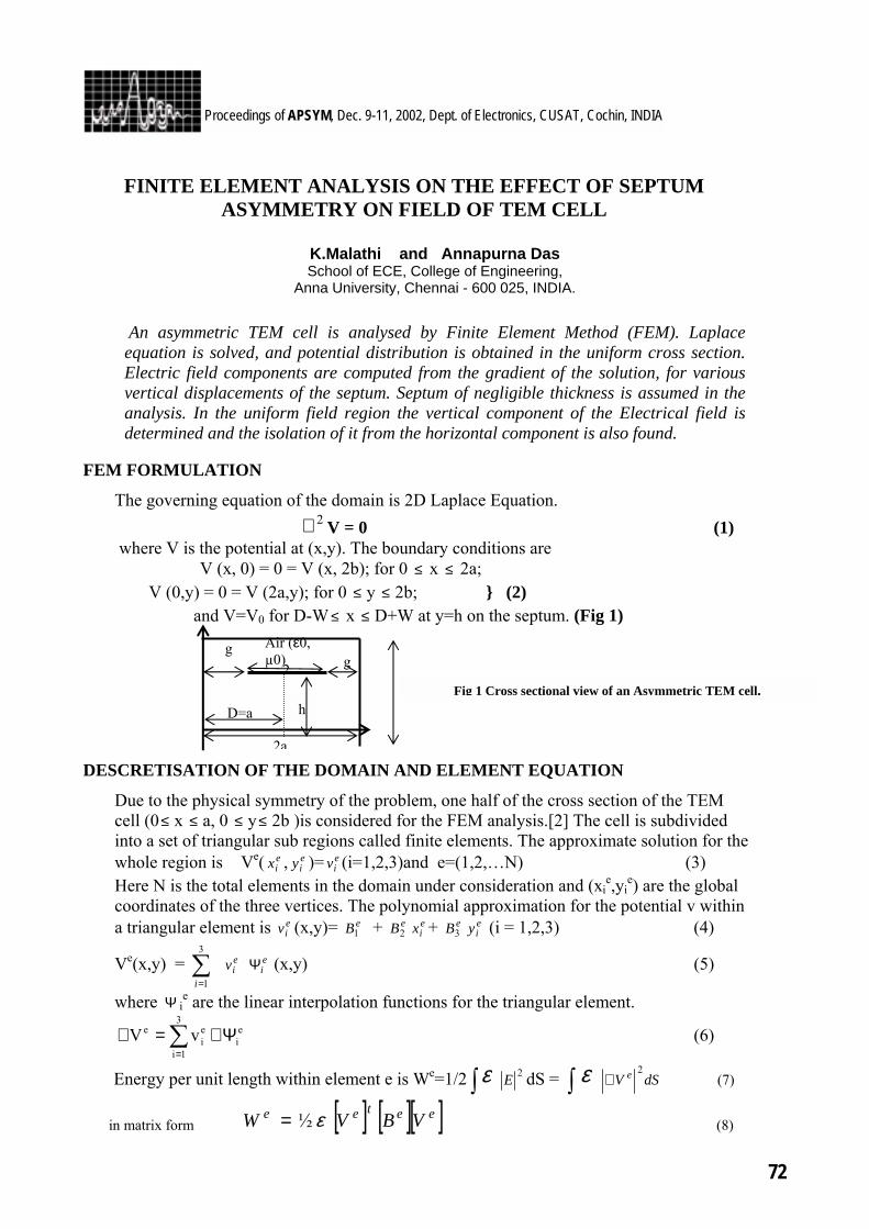
FINITE ELEMENT ANALYSIS ON THE EFFECT OF SEPTUM ASYMMETRY ON FIELD OF TEM CELL
K.Malathi and Annapurna Das School of ECE, College of Engineering,
Anna University, Chennai - 600 025, INDIA.
An asymmetric TEM cell is analysed by Finite Element Method (FEM). Laplace equation is solved, and potential distribution is obtained in the uniform cross section. Electric field components are computed from the gradient of the solution, for various vertical displacements of the septum. Septum of negligible thickness is assumed in the analysis. In the uniform field region the vertical component of the Electrical field is determined and the isolation of it from the horizontal component is also found.
FEM FORMULATION
The governing equation of the domain is 2D Laplace Equation. 2∇ V = 0 (1) where V is the potential at (x,y). The boundary conditions are V (x, 0) = 0 = V (x, 2b); for 0 ≤ x ≤ 2a;
V (0,y) = 0 = V (2a,y); for 0 ≤ y ≤ 2b; (2) and V=V0 for D-W ≤ x ≤ D+W at y=h on the septum. (Fig 1)
DESCRETISATION OF THE DOMAIN AND ELEMENT EQUATION
Due to the physical symmetry of the problem, one half of the cross section of the TEM cell (0≤ x ≤ a, 0 ≤ y≤ 2b )is considered for the FEM analysis.[2] The cell is subdivided into a set of triangular sub regions called finite elements. The approximate solution for the whole region is Ve( e
ix , eiy )= e
iv (i=1,2,3)and e=(1,2,…N) (3) Here N is the total elements in the domain under consideration and (xi
e,yie) are the global
coordinates of the three vertices. The polynomial approximation for the potential v within a triangular element is e
iv (x,y)= eB1 + eB2eix + eB3
eiy (i = 1,2,3) (4)
Ve(x,y) = ∑=
3
1i
eiv e
iΨ (x,y) (5)
where Ψ ie are the linear interpolation functions for the triangular element.
∑=
Ψ∇=∇3
1i
ei
ei
e vV (6)
Energy per unit length within element e is We=1/2∫ ε 2E dS = ∫ ε dSV e 2∇ (7)
in matrix form [ ] [ ][ ]eetee VBVW ε½= (8)
2
h
g g Air (ε0,
µ0)
D=a
2a
Fig 1 Cross sectional view of an Asymmetric TEM cell.
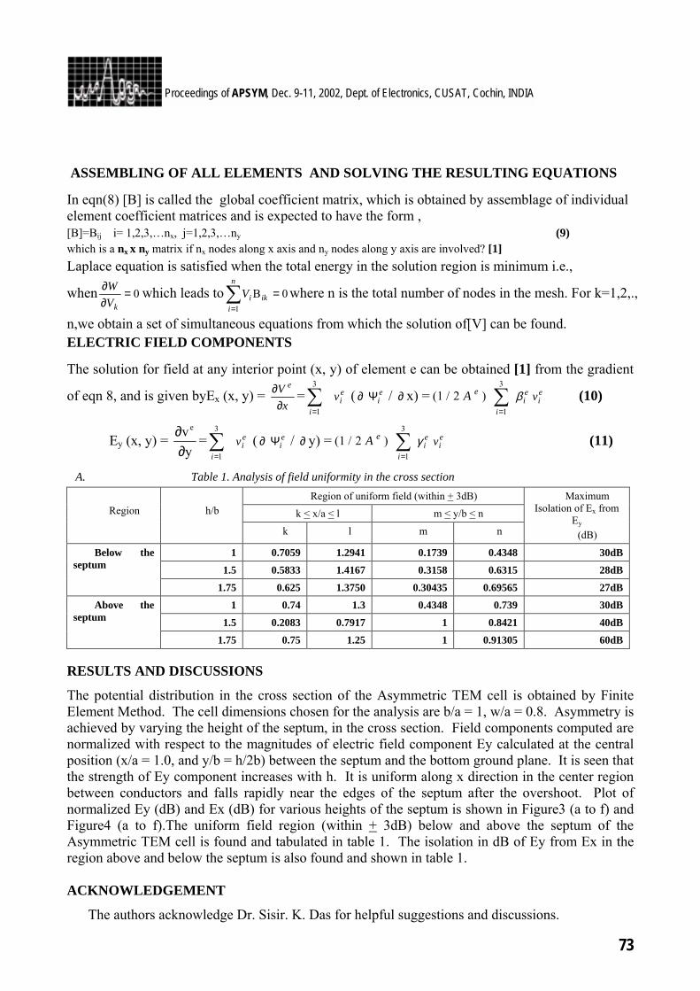
73
Proceedings of APSYM, Dec. 9-11, 2002, Dept. of Electronics, CUSAT, Cochin, INDIA
ASSEMBLING OF ALL ELEMENTS AND SOLVING THE RESULTING EQUATIONS
In eqn(8) [B] is called the global coefficient matrix, which is obtained by assemblage of individual element coefficient matrices and is expected to have the form , [B]=Bij i= 1,2,3,…nx, j=1,2,3,…ny (9) which is a nx x ny matrix if nx nodes along x axis and ny nodes along y axis are involved? [1] Laplace equation is satisfied when the total energy in the solution region is minimum i.e.,
when 0=∂∂
kVW which leads to 0B
1
=∑=
n
iikiV where n is the total number of nodes in the mesh. For k=1,2,.,
n,we obtain a set of simultaneous equations from which the solution of[V] can be found. ELECTRIC FIELD COMPONENTS
The solution for field at any interior point (x, y) of element e can be obtained [1] from the gradient
of eqn 8, and is given byEx (x, y) = x
V e
∂∂ =∑
=
3
1i
eiv ( ∂ e
iΨ / ∂ x) = )2/1( eA ei
i
β∑=
3
1
eiv (10)
Ey (x, y) = yve
∂∂ =∑
=
3
1i
eiv ( ∂ e
iΨ / ∂ y) = )2/1( eA ei
i
γ∑=
3
1
eiv (11)
A. Table 1. Analysis of field uniformity in the cross section Region of uniform field (within + 3dB)
k < x/a < l m < y/b < n
Region
h/b
k l m n
Maximum Isolation of Ex from
Ey (dB)
1 0.7059 1.2941 0.1739 0.4348 30dB 1.5 0.5833 1.4167 0.3158 0.6315 28dB
Below the septum
1.75 0.625 1.3750 0.30435 0.69565 27dB 1 0.74 1.3 0.4348 0.739 30dB
1.5 0.2083 0.7917 1 0.8421 40dB Above the
septum
1.75 0.75 1.25 1 0.91305 60dB RESULTS AND DISCUSSIONS
The potential distribution in the cross section of the Asymmetric TEM cell is obtained by Finite Element Method. The cell dimensions chosen for the analysis are b/a = 1, w/a = 0.8. Asymmetry is achieved by varying the height of the septum, in the cross section. Field components computed are normalized with respect to the magnitudes of electric field component Ey calculated at the central position (x/a = 1.0, and y/b = h/2b) between the septum and the bottom ground plane. It is seen that the strength of Ey component increases with h. It is uniform along x direction in the center region between conductors and falls rapidly near the edges of the septum after the overshoot. Plot of normalized Ey (dB) and Ex (dB) for various heights of the septum is shown in Figure3 (a to f) and Figure4 (a to f).The uniform field region (within + 3dB) below and above the septum of the Asymmetric TEM cell is found and tabulated in table 1. The isolation in dB of Ey from Ex in the region above and below the septum is also found and shown in table 1. ACKNOWLEDGEMENT
The authors acknowledge Dr. Sisir. K. Das for helpful suggestions and discussions.
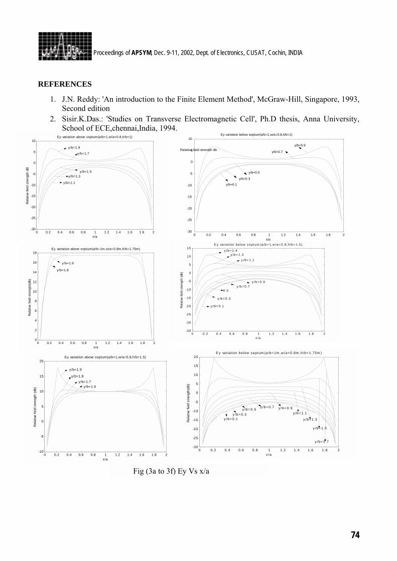
74
Proceedings of APSYM, Dec. 9-11, 2002, Dept. of Electronics, CUSAT, Cochin, INDIA
REFERENCES
1. J.N. Reddy: 'An introduction to the Finite Element Method', McGraw-Hill, Singapore, 1993, Second edition
2. Sisir.K.Das.: 'Studies on Transverse Electromagnetic Cell', Ph.D thesis, Anna University, School of ECE,chennai,India, 1994.
0 0.2 0.4 0.6 0.8 1 1.2 1.4 1.6 1.8 2-30
-25
-20
-15
-10
-5
0
5
10Ey variation below septum(a/b=1,w/a=0.8,h/b=1)
x/a
Relative field strength db
y/b=0.1
y/b=0.3
y/b=0.5
y/b=0.7 y/b=0.9
0 0.2 0.4 0.6 0.8 1 1.2 1.4 1.6 1.8 2-30
-25
-20
-15
-10
-5
0
5
10Ey variation above septum(a/b=1,w/a=0.8,h/b=1)
x/a
Rel
ative
fiel
d st
reng
th d
B
y/b=1.1
y/b=1.3 y/b=1.5
y/b=1.7
y/b=1.9
0 0.2 0.4 0.6 0.8 1 1.2 1.4 1.6 1.8 2-10
-5
0
5
10
15
20Ey variation above septum(a/b=1,w/a=0.8,h/b=1.5)
Rel
ative
fiel
d st
reng
th (d
b)
x/a
y/b=1.9
y/b=1.8 y/b=1.7
y/b=1.6
0 0.2 0.4 0.6 0.8 1 1.2 1.4 1.6 1.8 20
2
4
6
8
10
12
14
16
18Ey variation above septum(a/b=1m,w/a=0.8m,h/b=1.75m)
x/a
Rel
ative
fiel
d st
reng
th(d
b)
y/b=1.8
y/b=1.9
0 0 .2 0.4 0.6 0.8 1 1.2 1.4 1 .6 1 .8 2-35
-30
-25
-20
-15
-10
-5
0
5
10
15E y va ria t ion be low s ep tum (a/b= 1,w /a= 0 .8 ,h /b= 1.5 )
x /a
Rel
ative
fiel
d st
reng
th (d
b)
y /b= 0.1
y /b= 0.3
0 .5 y /b= 0.7
y /b= 0.9
y /b= 1.1
y /b= 1.3 y /b= 1.4
0 0.2 0.4 0.6 0.8 1 1.2 1.4 1.6 1.8 2-30
-25
-20
-15
-10
-5
0
5
10
15
20E y variat ion below s eptum (a/b= 1m ,w/a= 0.8m ,h/b= 1.75m )
x /a
Rel
ative
fiel
d st
reng
th(d
b)
y /b= 0.1 y /b= 0.3
y /b= 0.5 y /b= 0.7 y /b= 0.9
y /b= 1.1
y /b= 1.3
y /b= 1.5
y /b= 1.7
Fig (3a to 3f) Ey Vs x/a
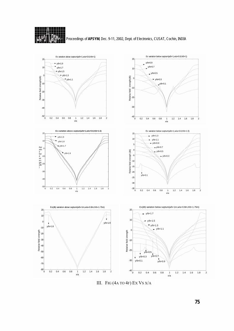
75
Proceedings of APSYM, Dec. 9-11, 2002, Dept. of Electronics, CUSAT, Cochin, INDIA
0 0.2 0.4 0.6 0.8 1 1.2 1.4 1.6 1.8 2-50
-40
-30
-20
-10
0
10
20Ex variation above septum(a/b=1,w/a=0.8,h/b=1)
x/a
Rel
ative
fiel
d st
reng
th(d
b)
y/b=1.9
y/b=1.7
y/b=1.5
y/b=1.3
y/b=1.1
0 0.2 0.4 0.6 0.8 1 1.2 1.4 1.6 1.8 2-50
-40 -30
-20
-10
0 10
20 Ex variation above septum(a/b=1,w/a=0.8,h/b=1.5)
x/a
Relative field strength(db)
y/b=1.9 y/b=1.8
y/b=1.7 y/b=1.6
0 0.2 0.4 0.6 0.8 1 1.2 1.4 1.6 1.8 2-80
-70
-60
-50
-40
-30
-20
-10
0
10
20Ex(db) variation above septum(a/b=1m,w/a=0.8m,h/b=1.75m)
x/a
Rel
ative
fiel
d st
reng
th
y/b=1.8 y/b=1.9
0 0.2 0.4 0.6 0.8 1 1.2 1.4 1.6 1.8 2-40
-30
-20
-10
0
10
20Ex variation below septum(a/b=1,w/a=0.8,h/b=1)
x/a
Rel
ative
fiel
d s
treng
th(d
b)
y/b=0.9
y/b=0.7
y/b=0.5
y/b=0.3
y/b=0.1
0 0.2 0.4 0.6 0.8 1 1.2 1.4 1.6 1.8 2-35
-30
-25
-20
-15
-10
-5
0
5
10
15Ex variation below septum(a/b=1,w/a=0.8,h/b=1.5)
x/a
Rel
ative
fiel
d st
reng
th (d
b)
y/b=0.1
y/b=0.3
y/b=0.5
y/b=0.7
y/b=0.9 y/b=1.1
y/b=1.3
0 0.2 0.4 0.6 0.8 1 1.2 1.4 1.6 1.8 2-40
-30
-20
-10
0
10
20Ex(db) variation below septum(a/b=1m,w/a=0.8m,h/b=1.75m)
x/a
Rel
ative
fiel
d st
reng
th
y/b=0.1
y/b=0.3
y/b=1.7
y/b=0.5
y/b=0.7
y/b=0.9
y/b=1.1 y/b=1.3
y/b=1.5
III. FIG (4A TO 4F) EX VS X/A
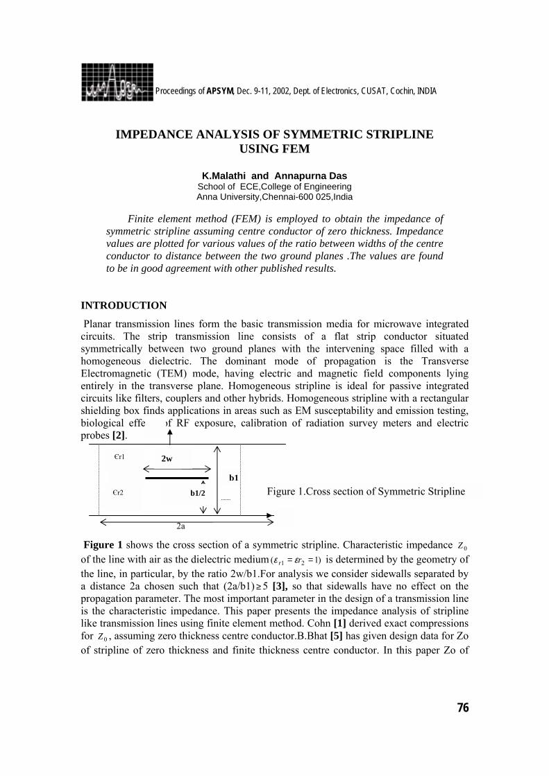
76
Proceedings of APSYM, Dec. 9-11, 2002, Dept. of Electronics, CUSAT, Cochin, INDIA
IMPEDANCE ANALYSIS OF SYMMETRIC STRIPLINE USING FEM
K.Malathi and Annapurna Das
School of ECE,College of Engineering Anna University,Chennai-600 025,India
Finite element method (FEM) is employed to obtain the impedance of symmetric stripline assuming centre conductor of zero thickness. Impedance values are plotted for various values of the ratio between widths of the centre conductor to distance between the two ground planes .The values are found to be in good agreement with other published results.
INTRODUCTION
Planar transmission lines form the basic transmission media for microwave integrated circuits. The strip transmission line consists of a flat strip conductor situated symmetrically between two ground planes with the intervening space filled with a homogeneous dielectric. The dominant mode of propagation is the Transverse Electromagnetic (TEM) mode, having electric and magnetic field components lying entirely in the transverse plane. Homogeneous stripline is ideal for passive integrated circuits like filters, couplers and other hybrids. Homogeneous stripline with a rectangular shielding box finds applications in areas such as EM susceptability and emission testing, biological effects of RF exposure, calibration of radiation survey meters and electric probes [2]. Figure 1 shows the cross section of a symmetric stripline. Characteristic impedance 0Z of the line with air as the dielectric medium )1( 21 == rr εε is determined by the geometry of the line, in particular, by the ratio 2w/b1.For analysis we consider sidewalls separated by a distance 2a chosen such that (2a/b1) ≥ 5 [3], so that sidewalls have no effect on the propagation parameter. The most important parameter in the design of a transmission line is the characteristic impedance. This paper presents the impedance analysis of stripline like transmission lines using finite element method. Cohn [1] derived exact compressions for 0Z , assuming zero thickness centre conductor.B.Bhat [5] has given design data for Zo of stripline of zero thickness and finite thickness centre conductor. In this paper Zo of
A
Figure 1.Cross section of Symmetric Stripline
b1
2w
b1/2
B
Єr1
Єr2
2a
77
Proceedings of APSYM, Dec. 9-11, 2002, Dept. of Electronics, CUSAT, Cochin, INDIA
symmetric stripline is obtained using FEM and the results are compared with those of others[5] and found to be in good agreement. FEM ANLYSIS:
Assuming that the line is of infinite length, the governing equation of the domain is 2D Laplace Equation: 2∇ V = 0 (1) where V is the potential at (x,y). The boundary conditions are V (x, 0) = 0 = V (x, 2b); for 0 ≤ x ≤ 2a; V (0,y) = 0 = V (2a,y); for 0 ≤ y ≤ 2b; (2) and V=V0 at y=b1/2 on the centre conductor. In electrostatic field analysis the functional to be minimized is the electrostatic energy inside a bounded volume isW dvyVxV
V
])/()/([)2/1( 22 ∂∂+∂∂= ∫ε (3)
In the FEM, we minimize the energy functional in (3) because the variation of energy in the system is insignificant with respect to small changes in dV within the bounded region S. Hence, we can determine the potential distribution inside the region under consideration by setting the differential change in energy equal to zero[4]. DOMAIN DISCRETISATION
In finite element analysis, the region under study is divided into a finite number of triangular meshes known as finite elements. Owing to mathematical and physical symmetry of the problem only one quarter of the domain is considered for the analysis. If there is m number of nodes at which the potentials are unknowns then 0]/[ =∂∂= dVVWdW T (4) The elements of dV cannot be zero; therefore, the elements of VW ∂∂ / must be zero to minimize the energy functional. Thus, VW ∂∂ / =0 (5) The electric energy inside this element is )(2)(2)()( ])/()/[(*2/1
)(
ee
s
ee dsyVxVWe
∂∂+∂∂= ∫ε (6)
where V )(e is the potential distribution inside an element e,and s )(e is the element area. Consequently, we can determine the total energy for the entire region from
)()()2/1( ee
Te dsffW ∑ ∫= ε (7)
where
∂∂∂∂=yVxVf e
e
e //
)(
)( (8)
ELEMENT EQUATION
The approximate solution for the potential distribution inside element e is assumed to be )(
3)(
3)(
2)(
2)(
1)(
1)( ),(),(),(),( eeeeeee VyxLVyxLVyxLyxV ++= (9)
78
Proceedings of APSYM, Dec. 9-11, 2002, Dept. of Electronics, CUSAT, Cochin, INDIA
in terms of the shape functions ),(),,(),,( )(3
)(2
)(1 yxLyxLyxL eee and node potentials
)(3
)(2
)(1 ,, eee VVV . The shape functions for a two dimensional geometry are defined as
3,2,1/),( )()()( == iAAyxL eei
ei (10)
Where )(eA is the area of element e,and )(eiA is the area of a section in element e. )(eA
and )(eiA can be calculated from
22
11)(
111
*2/1
++
++=
ii
ii
iie
yxyxyx
A and 3,2,1111
*2/1
22
11)( ==
++
++ iyxyx
yxA
ii
iie
i (11)
We can evaluate asyVandxV ee ∂∂∂∂ // )()(
332211
)(
332211)(
*]/),([*]/),([*]/),([/
*]/),([*]/),([*]/),([/
VyyxLVyyxLVyyxLyV
andVxyxLVxyxLVxyxLxV
e
e
∂∂+∂∂+∂∂=∂∂
∂∂+∂∂+∂∂=∂∂ (12)
and reconstruct ef as )()( ee
e VTf = (13) where
∂∂∂∂∂∂∂∂∂∂∂∂=yyxLyyxLyyxLxyxLxyxLxyxLT eee
eeee
/),(/),(/),(/),(/),(/),(
)(3
)(2
)(1
)(3
)(2
)(1)( (14)
and
=)(
3
)(2
)(1
)(
e
e
e
e
VVV
V (15)
therefore )()()()()(
)(
*2/1 eeeTe
s
Te dsVTTVWe∫= ε (16)
The partial derivatives of W with respect to the node potentials are
)()()(
1
)(
)(
/ eeen
e s
Te dsVTTdVdWe
∑ ∫=
= ε (17)
Solution of the element equation we arrive at 0)()()(
1
)(
)(
=∑ ∫=
eeen
e s
Te dsVTTe
(18)
from which we can determine the node potentials. Equation (18) is solved iteratively to determine the node potentials. THE CHARACTERISTIC IMPEDANCE Z0
The Characteristic impedance is expressed in terms of Capacitance as
uoC
Zo1== (19) where uo= 3*108 m/s, the speed of light in free space. Thus to
find Zo and uo C-capacitance per unit length of the structure is to be found. If Vd is the potential difference between the septum and the outer conductors,
dVQC 4
= (20)
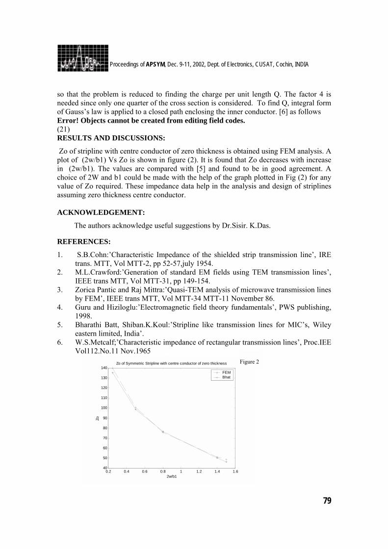
79
Proceedings of APSYM, Dec. 9-11, 2002, Dept. of Electronics, CUSAT, Cochin, INDIA
so that the problem is reduced to finding the charge per unit length Q. The factor 4 is needed since only one quarter of the cross section is considered. To find Q, integral form of Gauss’s law is applied to a closed path enclosing the inner conductor. [6] as follows Error! Objects cannot be created from editing field codes. (21) RESULTS AND DISCUSSIONS:
Zo of stripline with centre conductor of zero thickness is obtained using FEM analysis. A plot of (2w/b1) Vs Zo is shown in figure (2). It is found that Zo decreases with increase in (2w/b1). The values are compared with [5] and found to be in good agreement. A choice of 2W and b1 could be made with the help of the graph plotted in Fig (2) for any value of Zo required. These impedance data help in the analysis and design of striplines assuming zero thickness centre conductor. ACKNOWLEDGEMENT:
The authors acknowledge useful suggestions by Dr.Sisir. K.Das. REFERENCES:
1. S.B.Cohn:’Characteristic Impedance of the shielded strip transmission line’, IRE trans. MTT, Vol MTT-2, pp 52-57,july 1954.
2. M.L.Crawford:’Generation of standard EM fields using TEM transmission lines’, IEEE trans MTT, Vol MTT-31, pp 149-154.
3. Zorica Pantic and Raj Mittra:’Quasi-TEM analysis of microwave transmission lines by FEM’, IEEE trans MTT, Vol MTT-34 MTT-11 November 86.
4. Guru and Hiziloglu:’Electromagnetic field theory fundamentals’, PWS publishing, 1998.
5. Bharathi Batt, Shiban.K.Koul:’Stripline like transmission lines for MIC’s, Wiley eastern limited, India’.
6. W.S.Metcalf;’Characteristic impedance of rectangular transmission lines’, Proc.IEE Vol112.No.11 Nov.1965
Figure.3
0.2 0.4 0.6 0.8 1 1.2 1.4 1.640
50
60
70
80
90
100
110
120
130
140Zo of Symmetric Stripline with centre conductor of zero thickness
2w/b1
Zo
FEM Bhat
Figure 2
80
Proceedings of APSYM, Dec. 9-11, 2002, Dept. of Electronics, CUSAT, Cochin, INDIA
A SUITABLE DESIGN TECHNIQUE OF YAGI-UDA ANTENNAS USING GENETIC ALGORITHMS COUPLED
WITH METHOD OF MOMENTS
Iti Saha Misra, B. Mangaraj, V. Durgaprasad & M.N.Roy Department of Electronics & Tele-Communication Engineering
Jadavpur University, Kolkata-700032, India Email: [email protected]
A method of moments code is generated using MATLAB to analyze and to evaluate the Yagi-Uda antenna characteristics such as impedance, radiation patterns and the directivity. To optimize the elements lengths and spacing of the Yagi antenna, Genetic Algorithms (GAs) is used and results for six elements Yagi array have been compared with the existing published works. By judiciously choosing the initial parameters for GA application, considerable improvement of gain has been obtained over the compared published works. Moreover radiation patterns have been given to see the effects of element lengths and spacing.
INTRODUCTION
A considerable amount of interest has been given on optimizing the Yagi-Uda antenna since it was introduced in 1920s [1]. Because of the parasitic elements of this antenna, accurate modeling using closed form expressions is difficult. In the early stages of Yagi-Uda antenna, many extensive laboratory experiments were performed to optimize lengths and spacing for maximum gain [2]. Experimental methods are expensive and do not give physical insight. With the advent of computers, numerical methods are being used for the solution [3-4]. The initial choices of the parameters are very much important and affect the end results [4]. Again when the antenna is optimized both for gain and impedance, the problem becomes harder than it is optimized for gain only. That is why Yagi-Uda antenna becomes the proper candidate for applying GA. The main purpose of antenna design is to set some specific performance characteristics such as gain, impedance, beam width etc. For large number of parameter variation, optimized design becomes the hardest job to solve in analytical methods. For such cases GA approach of conducting global search for a solution that satisfied some specified performance becomes more popular. The application of GA to antenna design problem is not new. There are so many such problems [5-8] solved by GA. In this paper, we have presented a step by step design approach of Yagi-Uda antenna using GA coupled with method of moments and optimized the elements lengths and spacing for maximum gain, and for gain and impedance together.
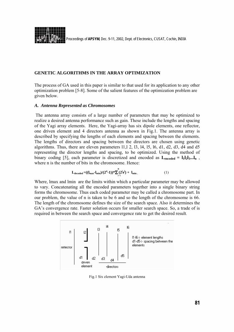
81
Proceedings of APSYM, Dec. 9-11, 2002, Dept. of Electronics, CUSAT, Cochin, INDIA
GENETIC ALGORITHMS IN THE ARRAY OPTIMIZATION The process of GA used in this paper is similar to that used for its application to any other optimization problem [5-8]. Some of the salient features of the optimization problem are given below. A. Antenna Represented as Chromosomes The antenna array consists of a large number of parameters that may be optimized to realize a desired antenna performance such as gain. These include the lengths and spacing of the Yagi array elements. Here, the Yagi-array has six dipole elements, one reflector, one driven element and 4 directors antenna as shown in Fig.1. The antenna array is described by specifying the lengths of each elements and spacing between the elements. The lengths of directors and spacing between the directors are chosen using genetic algorithms. Thus, there are eleven parameters l1,l 2, l3, l4, l5, l6, d1, d2, d3, d4 and d5 representing the director lengths and spacing, to be optimized. Using the method of binary coding [5], each parameter is discretized and encoded as Lencoded = l1l2l3...ln , where n is the number of bits in the chromosome. Hence: n Ldecoded =((lmax-lmin)/(2n-1))*∑∑∑∑ (2iei) + lmin . (1) i=1 Where, lmax and lmin are the limits within which a particular parameter may be allowed to vary. Concatenating all the encoded parameters together into a single binary string forms the chromosome. Thus each coded parameter may be called a chromosome part. In our problem, the value of n is taken to be 6 and so the length of the chromosome is 66. The length of the chromosome defines the size of the search space. Also it determines the GA’s convergence rate. Faster solution occurs for smaller search space. So, a trade of is required in between the search space and convergence rate to get the desired result.
Fig.1 Six element Yagi-Uda antenna
82
Proceedings of APSYM, Dec. 9-11, 2002, Dept. of Electronics, CUSAT, Cochin, INDIA
B. Genetic operations
Crossovers and Mutations: Information transfer occurs from one generation to the next through crossovers and mutations. In this context, the selection of individuals for crossover is done using tournament selection [6] and the probability of crossover (pcrossover) is chosen to be 0.7. In cross over, information between two chromosomes is exchanged by cutting the chromosomes at a randomly chosen location and swapping the ends of the chromosome to create two new chromosomes. In the process of mutation the probability of mutation (pmutation) is taken to be 0.002. In order to maintain more diverse population, mutation operation is required. In propagation from one generation to the next the best set of chromosomes out of the parent and offspring population is taken to avoid loss of a very fit parent in the subsequent population. Moreover, carrying out the search a number of times separately instead of computing a large number of generations continuously prevent the searching process to get stuck to some local extremum. The iterative process may be terminated by a test of convergence or after a pre-defined number of iterations. Here an initial population size of twenty members carried through twenty generations, the process is repeated ten times yielded desired results.
C. The Fitness Function
In the evaluation of the fitness of a chromosome, the gain or directivity and antenna input impedance, corresponding to the antenna physical structure (length, spacing etc) by a particular chromosome, is first computed. If the gain is found to exceed desired value, then the fitness of the chromosome is set at 1 (very fit chromosome). The fitness function is evaluated as : F(x) = aD(x) (2) Where, F is the fitness of a chromosome, D(x) is the desired directivity for an antenna design parameter x. For optimizing both the impedance (Z) and directivity together fitness function is defined as, F(x) = aD(x) +b|Re(Z(x)-50|+c|Im(Z(x)-5| (3) Here, a, b and c are the weighting constants to define the fit objective function. Generally a is high compared to b and c. High value of weighting constant means putting more emphasis to that particular term than the other in the objective function. The process of optimization is necessarily a maximization of the fitness function. DESIGN EXAMPLE
To simulate the antennas method of moments code has been written using MATLAB. GA is coupled with this code to optimize the parameters over a specified range of spacing and lengths. The random nature of GA, results in different solution for every run. If the fitness function of one antenna is fixed for gain and other for impedance of 50 ohm, different runs will give different solution. By inspecting the results it is observed that some GA results gives very good gain without satisfying impedance criteria and other will have smaller gain but better impedance value. So it is required to run the program several times and choose the antenna that is best fits for any application. The most interesting part is that, inspecting some results for good gain and impedance and radiation patterns, probable application area may find.
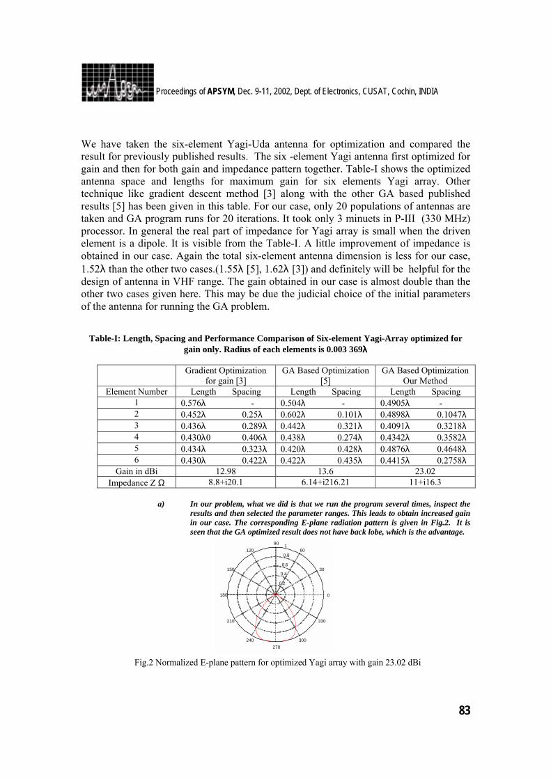
83
Proceedings of APSYM, Dec. 9-11, 2002, Dept. of Electronics, CUSAT, Cochin, INDIA
We have taken the six-element Yagi-Uda antenna for optimization and compared the result for previously published results. The six -element Yagi antenna first optimized for gain and then for both gain and impedance pattern together. Table-I shows the optimized antenna space and lengths for maximum gain for six elements Yagi array. Other technique like gradient descent method [3] along with the other GA based published results [5] has been given in this table. For our case, only 20 populations of antennas are taken and GA program runs for 20 iterations. It took only 3 minuets in P-III (330 MHz) processor. In general the real part of impedance for Yagi array is small when the driven element is a dipole. It is visible from the Table-I. A little improvement of impedance is obtained in our case. Again the total six-element antenna dimension is less for our case, 1.52λ than the other two cases.(1.55λ [5], 1.62λ [3]) and definitely will be helpful for the design of antenna in VHF range. The gain obtained in our case is almost double than the other two cases given here. This may be due the judicial choice of the initial parameters of the antenna for running the GA problem.
Table-I: Length, Spacing and Performance Comparison of Six-element Yagi-Array optimized for gain only. Radius of each elements is 0.003 369λλλλ
Gradient Optimization
for gain [3] GA Based Optimization
[5] GA Based Optimization
Our Method Element Number Length Spacing Length Spacing Length Spacing
1 0.576λ - 0.504λ - 0.4905λ - 2 0.452λ 0.25λ 0.602λ 0.101λ 0.4898λ 0.1047λ 3 0.436λ 0.289λ 0.442λ 0.321λ 0.4091λ 0.3218λ 4 0.430λ0 0.406λ 0.438λ 0.274λ 0.4342λ 0.3582λ 5 0.434λ 0.323λ 0.420λ 0.428λ 0.4876λ 0.4648λ 6 0.430λ 0.422λ 0.422λ 0.435λ 0.4415λ 0.2758λ
Gain in dBi 12.98 13.6 23.02 Impedance Z Ω 8.8+i20.1 6.14+i216.21 11+i16.3
a) In our problem, what we did is that we run the program several times, inspect the results and then selected the parameter ranges. This leads to obtain increased gain in our case. The corresponding E-plane radiation pattern is given in Fig.2. It is seen that the GA optimized result does not have back lobe, which is the advantage.
Fig.2 Normalized E-plane pattern for optimized Yagi array with gain 23.02 dBi
0.2
0.4
0.6
0.8
1
30
210
60
240
90
270
120
300
150
330
180 0
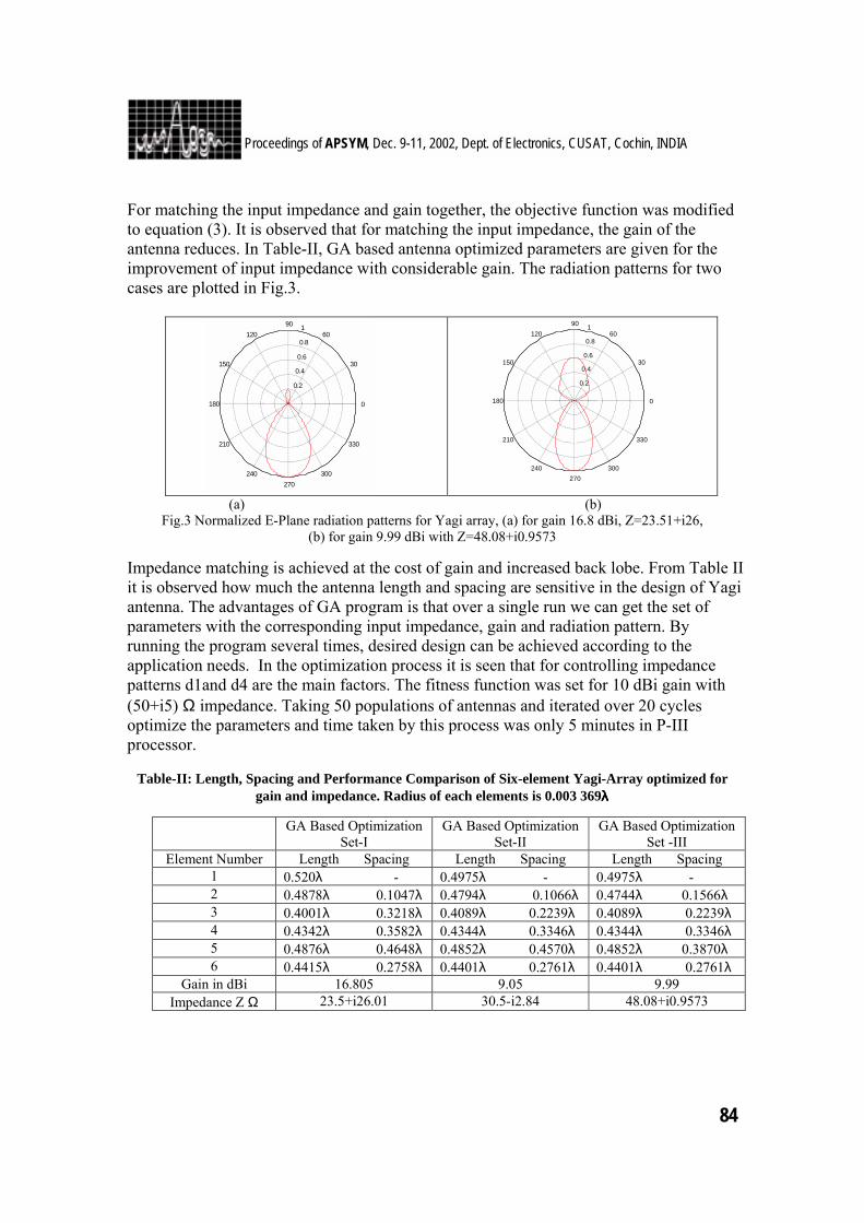
84
Proceedings of APSYM, Dec. 9-11, 2002, Dept. of Electronics, CUSAT, Cochin, INDIA
For matching the input impedance and gain together, the objective function was modified to equation (3). It is observed that for matching the input impedance, the gain of the antenna reduces. In Table-II, GA based antenna optimized parameters are given for the improvement of input impedance with considerable gain. The radiation patterns for two cases are plotted in Fig.3.
0.2
0.4
0.6
0.8
1
30
210
60
240
90
270
120
300
150
330
180 0
0.2
0.4
0.6
0.8
1
30
210
60
240
90
270
120
300
150
330
180 0
(a) (b)
Fig.3 Normalized E-Plane radiation patterns for Yagi array, (a) for gain 16.8 dBi, Z=23.51+i26, (b) for gain 9.99 dBi with Z=48.08+i0.9573
Impedance matching is achieved at the cost of gain and increased back lobe. From Table II it is observed how much the antenna length and spacing are sensitive in the design of Yagi antenna. The advantages of GA program is that over a single run we can get the set of parameters with the corresponding input impedance, gain and radiation pattern. By running the program several times, desired design can be achieved according to the application needs. In the optimization process it is seen that for controlling impedance patterns d1and d4 are the main factors. The fitness function was set for 10 dBi gain with (50+i5) Ω impedance. Taking 50 populations of antennas and iterated over 20 cycles optimize the parameters and time taken by this process was only 5 minutes in P-III processor.
Table-II: Length, Spacing and Performance Comparison of Six-element Yagi-Array optimized for gain and impedance. Radius of each elements is 0.003 369λλλλ
GA Based Optimization
Set-I GA Based Optimization
Set-II GA Based Optimization
Set -III Element Number Length Spacing Length Spacing Length Spacing
1 0.520λ - 0.4975λ - 0.4975λ - 2 0.4878λ 0.1047λ 0.4794λ 0.1066λ 0.4744λ 0.1566λ 3 0.4001λ 0.3218λ 0.4089λ 0.2239λ 0.4089λ 0.2239λ 4 0.4342λ 0.3582λ 0.4344λ 0.3346λ 0.4344λ 0.3346λ 5 0.4876λ 0.4648λ 0.4852λ 0.4570λ 0.4852λ 0.3870λ 6 0.4415λ 0.2758λ 0.4401λ 0.2761λ 0.4401λ 0.2761λ
Gain in dBi 16.805 9.05 9.99 Impedance Z Ω 23.5+i26.01 30.5-i2.84 48.08+i0.9573
85
Proceedings of APSYM, Dec. 9-11, 2002, Dept. of Electronics, CUSAT, Cochin, INDIA
CONCLUSION
In this paper the method of Genetic Algorithm is used for the design of Yagi antenna. The advantage of this system is that large number of parameters is handled together over the search place. The local optimum methods are difficult to handle and do not perform well. By trial and error, proper parameter ranges are selected to meet the design performance. The use of Genetic Algorithm in this age of fast computers ensures the global nature of the search process and an optimal solution may be obtained, for arbitrary gain, impedance and radiation patterns.
REFERENCES
1. H Yagi, “Beam transmission of ultra-short waves,” Proc. IRE, vol.16, p.715, June 1928.
2. H. W. Ehrenspeck and H. Poehler, “ A new method for obtaining maximum gain from Yagi antennas,” IRE Trans. Antennas Propagat., vol. AP-7, pp 379-386, Oct. 1959.
3. D. K. Cheng, “ Gain optimization for Yagi-Uda arrays,” IEEE Antennas Propagat. Mag., vol. 33, pp 42-45, June 1991.
4. C.A. Chen and D. K. Chen, “Optimum element lengths for Yagi-Uda arrays,” IEEE Trans. Antennas Propagat., vol. AP-23, pp 8-15, Jan, 1995.
5. E. A. Jones, W.T.Joines, “Design of Yagi-Uda antennas using Genetic Algorithms,” IEEE Trans. Antennas Propagat., vol. 45, pp 1386-1392, Sep. 1997.
6. I.S. Misra, A. Roychowdhury, K.K. Makkik and M.N.Roy, “Design and optimization of a Non planar multidipole array using genetic algorithms for mobile communications,” Microwave and Optical Tech. Letters, vol. 32, pp 301-304, Feb. 2002.
7. R.L. Haupt, “Thinned arrays using genetic algorithms,’’ IEEE Trans. Antennas Propagat., vol. 42, no. 7, pp. 993 - 999, July 1994.
8. J.M. Johnson and Y. Rahmat-Samii, “Genetic Algorithms in Engineering Electromagnetics,’’ IEEE Antennas and Propagation Magazine, vol. 39, no. 4, pp. 7 - 20, Aug 1997.
86
Proceedings of APSYM, Dec. 9-11, 2002, Dept. of Electronics, CUSAT, Cochin, INDIA
DESIGNING HIGH-GAIN HELICAL ANTENNAS FOR L- AND C-BAND SATELLITE RECEIVERS
K.K.S. Jamwal & Fouzia Yousuf Post-Graduate Department of Physics
University of Kashmir, Srinagar-190 006 (J&K)
The gain-radiation characteristics of helix (or helical) antennas is highly dependent upon the design parameters viz., diameter, length, turn spacing and the number of turns. L and C-Band axial-mode gain optimized helical antennas realizing 14-18 dB with VSWR below 1.5 have been analysed and designed. For satellite communication receivers, the theory developed for X-Band microwave frequencies 3,6 can be applied in realizing high-gain and small HPBW helix antennas which show satisfactory experimental results.
INTRODUCTION
The helix or helical antenna first described by Kraus2 is of simple structure and possesses remarkable gain and radiation characteristics for wideband applications in the 500MHz-11 GHz frequency range1-5. Axial mode helix antennas find extensive applications in defence, satellite communication and telemetry owing to its circular polarization (RH and LH modes), moderately high gain (between 12-18 dB), low VSWR (≤ 1.5) and fairly wide -3dB beam-width ( ~ 20-30o) 5. Whereas most of the applications of the helix antennas have been in the UHF frequencies, the structure can be utilized successfully up to X-band frequencies due to appropriately short wavelengths up to 30 mm 3,6. Beyond X-band frequencies, extremely small wavelengths do not permit the physical designing of the antenna structure. Recently, the advent of satellite communications in the L-Band (high quality stereo channels in the 1.12 – 1.75GHz) and C-Band (satellite broadcast video channels in the 4.9 – 7.0 GHz) has given a fresh impetus to exploit the advantages of the helical antenna structure at the receiving end 6. This paper discusses the important characteristics and the design expression that must be optimized in the L and C-bands respectively to obtain high directive gain and relatively sharp half-power beam width for satellite communication applications.
DESIGN ANALYSIS
The electric field array factor for a helical antenna expressed by the relation 2-3 Ê= sin(π /2N) sin Nπ(Sλ – LT /β) / sin π(Sλ – LT /β) …….. (1) is used in the design of the high directive gain antenna, where N, LT, Sλ and β refers to the number of turns of the helix, length per turn, spacing per turn and the relative phase velocity of the slow-traveling wave antenna structure respectively (see inset Fig – 1). In Eq.1, the length per turn LT = (Cλ2 + Sλ2 )½ is a function of the circumference of each turn of the helix antenna Cλ and the spacing Sλ, which influences the gain-radiation characteristics in addition to N.
87
Proceedings of APSYM, Dec. 9-11, 2002, Dept. of Electronics, CUSAT, Cochin, INDIA
Introducing a function U = π (Sλ – LT /β), Eq.1 reduces to Ê =sin (π /2N) sin NU / sin U. This expression can be optimized by taking the second-order differential of Ê with respect to LT and letting it as the function F(U) assumes the relation after simplification as F(U) = 1/ sin3U sin NU (2 cos2U + (1- N2) sin2U) – cos NU (2N cosU. sinU)
=1 / ¼(3 sin U- sin 3U) sin NU(1+ cos 2U) + ½(1-N2) (1 –cos 2U)
– cos NU(2N cosU. sin U) ….. (2) and should be minimized for optimization. The function d2Ê/dLT
2 attains the minimum value by letting F(U)=0 for particular values of design parameter U as expressed in terms of Sλ , LT and magnitude of the phase velocity β. In all the antenna design examples, the phase velocity β=0.76 is utilised for analysis as this magnitude results in good directive gain for slow-wave structures like the helix antenna in which the e.m.signal travels on the conductor skin. L AND C-BAND HELIX ANTENNA DESIGN CHARACTERISTICS
Equation 2 is analysed for high directive gain characteristics by studying the dependence of F(U) as a function of design parameters U. Fig.-1 shows the plot of F(U) versus U for the L-band frequencies between 1.1 to 1.7 GHz respectively. The design parameters LT, Sλ and Cλ are measured in terms of wavelengths λ(corresponding to the operating frequency). In all the three curves Fig-1 a, b and c respectively, the number of turns is maintained constant with N=11. The length per turn LT is varied from 0.76λ to 0.86λ corresponding to λ of the operating microwave signal. Fig-1a shows that U attains minimum values at U=15.1 and 16.8 respectively. For the other two curves Fig-1b and 1c respectively F(U) decreases continuously from U=16.2 to about 20. In the L-band frequency 1.3 GHz, the function F(U) attains a minimum value U=15.73. This value when substituted in the expression U = π (Sλ – LT /β) and LT = (Cλ2 + Sλ2 )½ with λ= 23 cm corresponding to f=1.3 GHz results in the design parameters given in Table-I below. Table-I. L- Band Helix Antenna Structure design Parameters
N = 11, β = 0.76, f =1.3 GHz, λ = 23 cm U Sλ Cλ Antenna Antenna
cm. cm. Length L, cm. diameter D, cm. 20.99 7.6 15.7 138 5.0 Table-II shows the design parameters for a C-Band Helix antenna for which a minimum value of U= 21.5 is obtained at the operating frequency of 6.0 GHz corresponding to the wavelength λ= 5 cm.
Table-II C-Band Helix antenna Structure Design Parameters N=11, β=0.76, f =6.0 GHz, λ= 5 cm.
U Sλ Cλ Antenna Antenna cm. cm. Length L, cm. diameter D, cm. 18.84 7.0 6.21 30 1.98
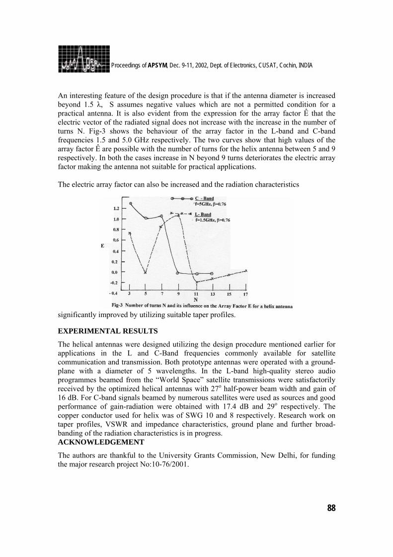
88
Proceedings of APSYM, Dec. 9-11, 2002, Dept. of Electronics, CUSAT, Cochin, INDIA
An interesting feature of the design procedure is that if the antenna diameter is increased beyond 1.5 λ, S assumes negative values which are not a permitted condition for a practical antenna. It is also evident from the expression for the array factor Ê that the electric vector of the radiated signal does not increase with the increase in the number of turns N. Fig-3 shows the behaviour of the array factor in the L-band and C-band frequencies 1.5 and 5.0 GHz respectively. The two curves show that high values of the array factor Ê are possible with the number of turns for the helix antenna between 5 and 9 respectively. In both the cases increase in N beyond 9 turns deteriorates the electric array factor making the antenna not suitable for practical applications. The electric array factor can also be increased and the radiation characteristics
significantly improved by utilizing suitable taper profiles. EXPERIMENTAL RESULTS
The helical antennas were designed utilizing the design procedure mentioned earlier for applications in the L and C-Band frequencies commonly available for satellite communication and transmission. Both prototype antennas were operated with a ground-plane with a diameter of 5 wavelengths. In the L-band high-quality stereo audio programmes beamed from the “World Space” satellite transmissions were satisfactorily received by the optimized helical antennas with 27o half-power beam width and gain of 16 dB. For C-band signals beamed by numerous satellites were used as sources and good performance of gain-radiation were obtained with 17.4 dB and 29o respectively. The copper conductor used for helix was of SWG 10 and 8 respectively. Research work on taper profiles, VSWR and impedance characteristics, ground plane and further broad-banding of the radiation characteristics is in progress. ACKNOWLEDGEMENT
The authors are thankful to the University Grants Commission, New Delhi, for funding the major research project No:10-76/2001.
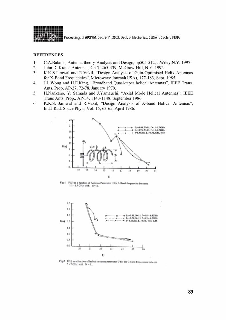
89
Proceedings of APSYM, Dec. 9-11, 2002, Dept. of Electronics, CUSAT, Cochin, INDIA
REFERENCES
1. C.A.Balanis, Antenna theory-Analysis and Design, pp505-512, J.Wiley,N.Y. 1997 2. John D. Kraus: Antennas, Ch-7, 265-339, McGraw-Hill, N.Y. 1992 3. K.K.S.Jamwal and R.Vakil, “Design Analysis of Gain-Optimised Helix Antennas
for X-Band Frequencies”, Microwave Journal(USA), 177-183, Sept. 1985 4. J.L.Wong and H.E.King, “Broadband Quasi-taper helical Antennas”, IEEE Trans.
Ants. Prop, AP-27, 72-78, January 1979. 5. H.Nankano, Y. Samada and J.Yamauchi, “Axial Mode Helical Antennas”, IEEE
Trans Ants. Prop., AP-34, 1143-1148, September 1986. 6. K.K.S. Jamwal and R.Vakil, “Design Analysis of X-band Helical Antennas”,
Ind.J.Rad. Space Phys., Vol. 15, 63-65, April 1986.
90
Proceedings of APSYM, Dec. 9-11, 2002, Dept. of Electronics, CUSAT, Cochin, INDIA
NEURAL NETWORK APPROACH FOR ONE-DIMENSIONAL ELECTROMAGNETIC TRANSIENT
PROPAGATION
Sridhar Patnaik and Rabindra K. Mishra Electronic Science Department, Berhampur University, Orissa
Novel field computation scheme is proposed for one-dimensional transient propagation problems. This new scheme discretizes first in time-domain. Then Finite Impulse Response Artificial Neural Network (FIR-ANN) is used. Numerical results show that this NFDTD method is faster than the popular FDTD method.
INTRODUCTION
Transient computation has drawn much attention during recent years. The most popular method for electromagnetic transient analysis is the finite-difference time-domain (FDTD) method [1]. It is admitted that the FDTD is very useful in obtaining time-varying field distributions. However, the FDTD requires huge computational time and storage due to spatial-temporal discretization. This paper will present a technique that discretizes in time-domain and then uses FIR-NN. Since it uses neural network, the new technique is called NFDTD technique. Though only one-dimensional transient propagation is dealt with here, its extension to more complicate problems is possible.
FORMULATION
Consider a one-dimensional electromagnetic field problem, where the electromagnetic field is ),(ˆ tzExE = , ),(ˆ txHyH = . The Maxwell equations for this problem can be reduced to
tH
zE
∂∂−=
∂∂ µ (1)
tE
zH
∂∂−=
∂∂ ε (2)
Equations (1) and (2) lead to the wave equation for the electric field
2
2
2
2
tE
zE
∂∂=
∂∂ µε (3)
Assume that ),()( tnzEzEn ∆= is the electric field sampled at tn∆ , where n is an
91
Proceedings of APSYM, Dec. 9-11, 2002, Dept. of Electronics, CUSAT, Cochin, INDIA
integer. Approximate the second derivative with respect to time by central difference
211
2
2 )()(2)(),(t
zEzEzEt
tzE nnn
tnt ∆+−
≈∂
∂ −+
∆=
(4)
The original wave equation now becomes a difference-differential equation
211
22
2 )()(2)(1)(t
zEzEzEcdz
zEd nnnn
∆+−= −+ (5)
Here µε/1=c . Suppose that in the space region to be considered, 0)( =zEn for 0<n and Nn ≥ .
As a means of capturing time-dependent signals in a nonlinear framework, multiplayer perceptrons (MLPs) with synapses described by filters have recently been proposed [2, 3, 4]. These approaches replace the traditional scalar synaptic weights with finite impulse response (FIR) filters commonly used in digital filter theory. The architecture can be considered an extension of earlier work in which time delays were incorporated as a means of capturing time-dependent input information. FIR networks provide a more general model for distributed time representations.
An FIR MLP of size (L, nw) with N0, N1, …., NL nodes per layer, is defined by
( ))(ˆ)( txftz lk
lk = (6)
∑=
=lN
i
lik
lk tytx
1)(ˆ)(ˆ (7)
)()(ˆ tycty lik
lik
lik = (8)
)()()( 11 tzqWty li
lik
lik
−−= (9)
Here, each neuron in the layer l has an output at time t of )(tz li ; a layer consists of Nl
neurons (l=0 denotes the input layer, and l=L denotes the output layer, 0.1=lNl
z may be
used for a bias); )(ˆ ty lik is the output of a synapse connecting from neuron I in the previous
layer to neuron k in layer l; likc is a synaptic gain; and f(.) is a sigmoid function typically
evaluated as tanh(.). An FIR synapse is represented by ∑ =−− = wn
jjl
ikjl
ik qwqW0
1 )()( where
likjw correspond to the variable coefficients, and q-1 is a delay operator ( ))1()(( 1 −=
∆− tztzq ,
and nw is the number of delays.
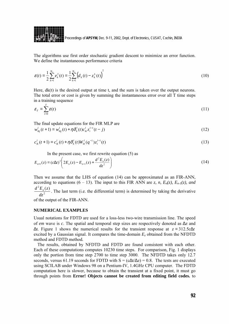
92
Proceedings of APSYM, Dec. 9-11, 2002, Dept. of Electronics, CUSAT, Cochin, INDIA
The algorithms use first order stochastic gradient descent to minimize an error function. We define the instantaneous performance criteria
( )2
11
2 )()(21)(
21)( ∑∑
==
−==LL N
k
Lkk
N
kk tztdtetε (10)
Here, dk(t) is the desired output at time t, and the sum is taken over the output neurons. The total error or cost is given by summing the instantaneous error over all T time steps in a training sequence
∑=
=T
tT t
0)(εε (11)
The final update equations for the FIR MLP are
)()()()1( 1 jtzcttwtw li
lik
lk
likj
likj −+=+ −ηδ (12)
)()()()()1( 11 tzqWttctc l
il
iklk
lik
lik
−−+=+ ηδ (13) In the present case, we first rewrite equation (5) as
+−∆= −+ 2
2
12
1)(
)()(2)()(dz
zEdzEzEtczE nnnn (14)
Then we assume that the LHS of equation (14) can be approximated as an FIR-ANN, according to equations (6 – 13). The input to this FIR ANN are z, n, En(z), En-1(z), and
2
2 )(dz
zEd n . The last term (i.e. the differential term) is determined by taking the derivative
of the output of the FIR-ANN. NUMERICAL EXAMPLES
Usual notations for FDTD are used for a loss-less two-wire transmission line. The speed of em wave is c. The spatial and temporal step sizes are respectively denoted as ∆z and ∆t. Figure 1 shows the numerical results for the transient response at tcz ∆= 5.312 excited by a Gaussian signal. It compares the time-domain Ez obtained from the NFDTD method and FDTD method.
The results, obtained by NFDTD and FDTD are found consistent with each other. Each of these computations computes 10230 time steps. For comparison, Fig. 1 displays only the portion from time step 2700 to time step 3000. The NFDTD takes only 12.7 seconds, versus 61.19 seconds for FDTD with S = (c∆t/∆z) = 0.8. The tests are executed using SCILAB under Windows 98 on a Pentium-IV, 1.4GHz CPU computer. The FDTD computation here is slower, because to obtain the transient at a fixed point, it must go through points from Error! Objects cannot be created from editing field codes. to
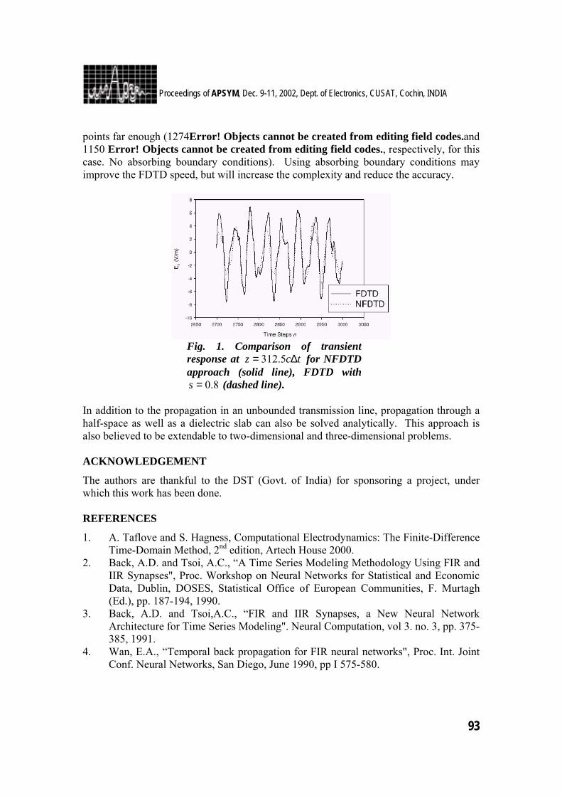
93
Proceedings of APSYM, Dec. 9-11, 2002, Dept. of Electronics, CUSAT, Cochin, INDIA
points far enough (1274Error! Objects cannot be created from editing field codes.and 1150 Error! Objects cannot be created from editing field codes., respectively, for this case. No absorbing boundary conditions). Using absorbing boundary conditions may improve the FDTD speed, but will increase the complexity and reduce the accuracy.
Fig. 1. Comparison of transient response at tcz ∆= 5.312 for NFDTD approach (solid line), FDTD with
8.0=s (dashed line). In addition to the propagation in an unbounded transmission line, propagation through a half-space as well as a dielectric slab can also be solved analytically. This approach is also believed to be extendable to two-dimensional and three-dimensional problems. ACKNOWLEDGEMENT
The authors are thankful to the DST (Govt. of India) for sponsoring a project, under which this work has been done. REFERENCES
1. A. Taflove and S. Hagness, Computational Electrodynamics: The Finite-Difference Time-Domain Method, 2nd edition, Artech House 2000.
2. Back, A.D. and Tsoi, A.C., “A Time Series Modeling Methodology Using FIR and IIR Synapses", Proc. Workshop on Neural Networks for Statistical and Economic Data, Dublin, DOSES, Statistical Office of European Communities, F. Murtagh (Ed.), pp. 187-194, 1990.
3. Back, A.D. and Tsoi,A.C., “FIR and IIR Synapses, a New Neural Network Architecture for Time Series Modeling". Neural Computation, vol 3. no. 3, pp. 375-385, 1991.
4. Wan, E.A., “Temporal back propagation for FIR neural networks", Proc. Int. Joint Conf. Neural Networks, San Diego, June 1990, pp I 575-580.
94
Proceedings of APSYM, Dec. 9-11, 2002, Dept. of Electronics, CUSAT, Cochin, INDIA
CAVITY BACKED SLOTTED RECTANGULAR ANTENNA WITH CIRCULAR POLARIZATION
Bharoti Sinha, Ranjan Barik
(Department of Electronics and Computer Engineering, Indian Institute of Technology Roorkee)
E-mail: [email protected], [email protected]
Low profile, lightweight, circularly polarized antennas are the most perfect and eligible choice for the applications in mobile communications such as antennas on vehicles, aircrafts, satellite communication. Slot antenna is one of the widely used antenna for such applications. This paper presents design and performance of a four-bent rectangular slot antenna with a short, backed by rectangular cavity. It can be used to emulate an array of two dipoles by virtue of a short position properly, giving a circularly polarized wave. The design frequency is 2.4 GHz. Various parameters of interest such as impedance, bandwidth, and radiation pattern in E/H plane have been investigated with and without cavity. Resonance frequency greatly depends on the slot shorting position, the slot width, and the cavity width and radiation pattern in E/H plane are circular, confirming the accuracy of the design.
INTRODUCTION
The slot antenna is one of the most widely used antennas because it is relatively simple to build and analyze besides meeting the requirements of weight and size. The advantage over other types of radiating elements is that it can be flush mounted to the surface of an aircraft or similar objects for space application. This antenna is inexpensive and electrically efficient, but imposes bandwidth constraint as a dynamic penalty. [1] Round annular slot antennas are often used to provide similar radiation pattern coverage where flush mounting is required. Structural and other requirements of high performance aircraft can place further constraints on allowable antenna configurations. The antenna proposed here is designed to fit within a limited rectangular volume. It is a four-bent slot rectangular antenna shorted by a pin at a suitable position giving circular polarization and wide beam width. Further it is backed by a cavity to enhance more radiation power but decreased bandwidth slightly. The main feature of the antenna is that the slot aperture is shorted at such a point, which enables to obtain a wide bandwidth and or variation in radiation pattern. It is well known that by integrating an impedance element with an antenna and varying its value, the antenna characteristics such as input impedance and radiation pattern can be controlled. Here zero impedance, i.e. a short is employed instead of a reactive element, and the antenna characteristics such as input impedance, bandwidth, radiation pattern and
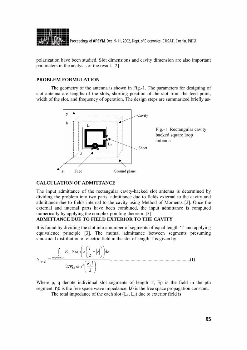
95
Proceedings of APSYM, Dec. 9-11, 2002, Dept. of Electronics, CUSAT, Cochin, INDIA
polarization have been studied. Slot dimensions and cavity dimension are also important parameters in the analysis of the result. [2]
PROBLEM FORMULATION
The geometry of the antenna is shown in Fig.-1. The parameters for designing of slot antenna are lengths of the slots, shorting position of the slot from the feed point, width of the slot, and frequency of operation. The design steps are summarized briefly as- d Cavity Short z Feed Ground plane CALCULATION OF ADMITTANCE
The input admittance of the rectangular cavity-backed slot antenna is determined by dividing the problem into two parts: admittance due to fields external to the cavity and admittance due to fields internal to the cavity using Method of Moments [2]. Once the external and internal parts have been combined, the input admittance is computed numerically by applying the complex pointing theorem. [3] ADMITTANCE DUE TO FIELD EXTERIOR TO THE CAVITY
It is found by dividing the slot into a number of segments of equal length ‘l’ and applying equivalence principle [3]. The mutual admittance between segments presuming sinusoidal distribution of electric field in the slot of length 'l' is given by
Where p, q denote individual slot segments of length 'l', Ep is the field in the pth segment. η0 is the free space wave impedance; k0 is the free space propagation constant.
The total impedance of the each slot (L1, L2) due to exterior field is
)1......(............................................................
2sin2
2sin
020
),(
−×
=∫
lk
dzzlkEY segmentsp
p
qp
πη
y b x a
L
L1
L2 d
Fig.-1: Rectangular cavity backed square loop antenna
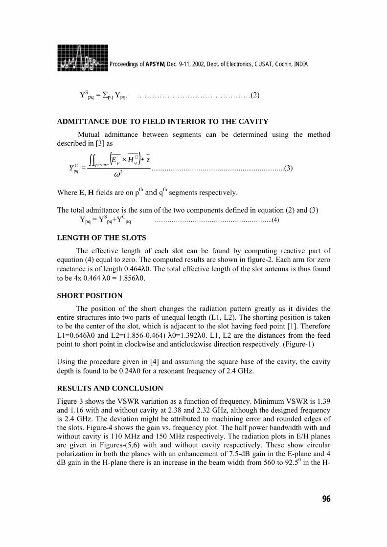
96
Proceedings of APSYM, Dec. 9-11, 2002, Dept. of Electronics, CUSAT, Cochin, INDIA
YSpq = ∑pq Ypq. ………………………………………(2)
ADMITTANCE DUE TO FIELD INTERIOR TO THE CAVITY
Mutual admittance between segments can be determined using the method described in [3] as
Where E, H fields are on pth and qth segments respectively. The total admittance is the sum of the two components defined in equation (2) and (3)
Ypq = YSpq+YC
pq ………………………………………………..(4)
LENGTH OF THE SLOTS
The effective length of each slot can be found by computing reactive part of equation (4) equal to zero. The computed results are shown in figure-2. Each arm for zero reactance is of length 0.464λ0. The total effective length of the slot antenna is thus found to be 4x 0.464 λ0 = 1.856λ0.
SHORT POSITION
The position of the short changes the radiation pattern greatly as it divides the entire structures into two parts of unequal length (L1, L2). The shorting position is taken to be the center of the slot, which is adjacent to the slot having feed point [1]. Therefore L1=0.646λ0 and L2=(1.856-0.464) λ0=1.392λ0. L1, L2 are the distances from the feed point to short point in clockwise and anticlockwise direction respectively. (Figure-1) Using the procedure given in [4] and assuming the square base of the cavity, the cavity depth is found to be 0.24λ0 for a resonant frequency of 2.4 GHz.
RESULTS AND CONCLUSION
Figure-3 shows the VSWR variation as a function of frequency. Minimum VSWR is 1.39 and 1.16 with and without cavity at 2.38 and 2.32 GHz, although the designed frequency is 2.4 GHz. The deviation might be attributed to machining error and rounded edges of the slots. Figure-4 shows the gain vs. frequency plot. The half power bandwidth with and without cavity is 110 MHz and 150 MHz respectively. The radiation plots in E/H planes are given in Figures-(5,6) with and without cavity respectively. These show circular polarization in both the planes with an enhancement of 7.5-dB gain in the E-plane and 4 dB gain in the H-plane there is an increase in the beam width from 560 to 92.50 in the H-
( ))3(......................................................................2ω
∫∫ •×=
∗
aperture qpCpq
zHEY
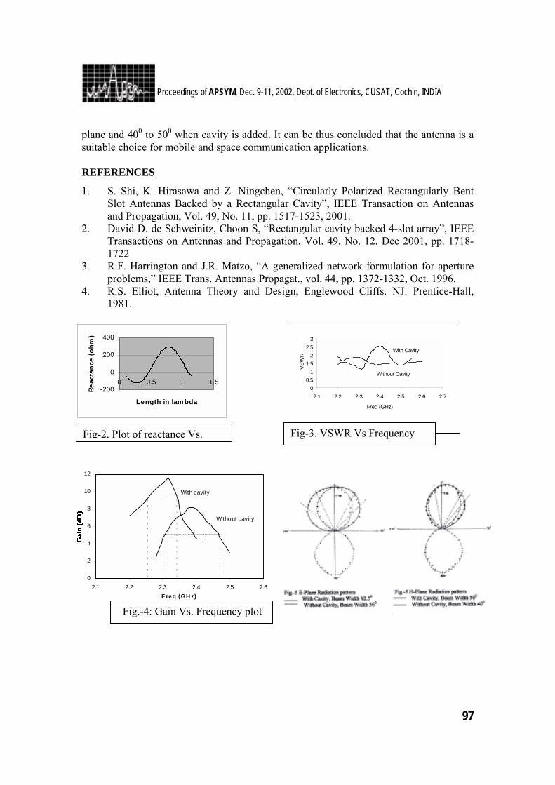
97
Proceedings of APSYM, Dec. 9-11, 2002, Dept. of Electronics, CUSAT, Cochin, INDIA
plane and 400 to 500 when cavity is added. It can be thus concluded that the antenna is a suitable choice for mobile and space communication applications.
REFERENCES
1. S. Shi, K. Hirasawa and Z. Ningchen, “Circularly Polarized Rectangularly Bent Slot Antennas Backed by a Rectangular Cavity”, IEEE Transaction on Antennas and Propagation, Vol. 49, No. 11, pp. 1517-1523, 2001.
2. David D. de Schweinitz, Choon S, “Rectangular cavity backed 4-slot array”, IEEE Transactions on Antennas and Propagation, Vol. 49, No. 12, Dec 2001, pp. 1718-1722
3. R.F. Harrington and J.R. Matzo, “A generalized network formulation for aperture problems,” IEEE Trans. Antennas Propagat., vol. 44, pp. 1372-1332, Oct. 1996.
4. R.S. Elliot, Antenna Theory and Design, Englewood Cliffs. NJ: Prentice-Hall, 1981.
00.5
11.5
22.5
3
2.1 2.2 2.3 2.4 2.5 2.6 2.7
Freq (GHz)
VSW
R
With Cavity
Without Cavity
0
2
4
6
8
10
12
2.1 2.2 2.3 2.4 2.5 2.6F req (GH z)
-----------------------
--------------------------------------------:
;
:
:
:
:
:
:
:
:
:
:
:
:
:
:
;
:
:
:
:
:
:
:
:
:
:
:
:
:
:
:
:
:
:
:
:
:
:
:
:
:
:
:
With cavity
Without cavity
-200
0
200
400
0 0.5 1 1.5
Length in lam bda
Reac
tanc
e (o
hm)
Fig-3. VSWR Vs Frequency l
Fig-2. Plot of reactance Vs.
Fig.-4: Gain Vs. Frequency plot

98
Proceedings of APSYM, Dec. 9-11, 2002, Dept. of Electronics, CUSAT, Cochin, INDIA
99
Proceedings of APSYM, Dec. 9-11, 2002, Dept. of Electronics, CUSAT, Cochin, INDIA
RESEARCH SESSION III December 9, Monday 2002 (3.30 p.m. to 5.30 p.m)
MICROWAVE PROPAGATION Hall : 1
CHAIRS: PROF. S.K. SRIVASTAVA DR. D. SRINIVASAN
3.1
Electromagnetic Characterisation Of Indian Coal G. Sahoo, A. Chakrabarty, S. Sanyal, S. Ghosh, Y.K. Singh Dept. of Electronics & Electrical Commn, IIT, Kharagpur – 721 302. [email protected]
101
3.2 Electrical Properties Of Coal In Very High Frequency Band G. Sahoo, A .Chakraborty, S. Sanyal, S. Ghosh, Y.K. Singh Dept. of Electronics & Electrical Commn. IIT, Kaharagpur – 721 302. [email protected]
105
3.3 Microwave Absorption Studies In (Mn-Ti) Substituted Barium Hexagonal Ferrite Based Absorbing Paint. M.R. Meshram, Bharati Sinha, Nawal.K. Agrawal,& P.S.Misra* Department of Electronics & Computer Engg. IIT, Roorkee-247 667. *Dept. of Material Eng., IIT, Rorrkee - 247 667. [email protected]
109
3.4 Microwave Permittivity Studies On A Novel Composite Material - Polystyrene/Alumina For Application As Substrate In MIC/MMIC Juti R. Deka and Nidhi.S. Bhattacharya Dept.of Physics, Tezpur University, Napaam, Tezpur, Assam. [email protected]
113
3.5 Analysis of an In homogeneously loaded Helical slow wave structure with attenuator coating Satya Prakash, S. Ghosh, V. Kiran, P.K. Jain and B.N. Basu Development & Engg. Section, Microwave Tube Division, BEL, Jalahalli, Bangalore 560 013. Electronics Engg. Dept., Institute of Technology, Banaras Hindu University, Varanasi 221 005
117
3.6 Retrieval Of Water Cloud Parameters With Ground Based Radar And Lidar Observations A Maitra, J W F Goddard* Institute Of Radio Physics And Electronics, University of Calcutta, Calcutta-700 009. [email protected] *Radio Communications Research Unit, Rutherford Appleton Laboratory, Chilton, Didcot, Oxon OX11 0QX, UK
120
3.7 Broad Band Propagation At Millimeter Wavelengths Through The Dispersive Atmosphere A Maitra , Mausumi Kundu*, Institute Of Radio Physics And Electronics, University of Calcutta, Calcutta-700 009. [email protected] *Gobardanga Hindu College, Gobardanga, North 24 Parganas, West Bengal, INDIA
124

100
Proceedings of APSYM, Dec. 9-11, 2002, Dept. of Electronics, CUSAT, Cochin, INDIA
3.8 Estimation Of IGP Availability For A Given INWAAS Configuration G. Sasibhushana Rao, A.D. Sarma, K. Ramalingam, Niranjan Prasad R&T Unit for Navigational Electronics, Osmania University, Hyderabad 500 007. [email protected]
128
3.9 Mitigation of Multipath Using Shaped Beam Spiral Antenna B. Ramakrishna Rao, A.D. Sarma and Y. Ravi Kumar R&T Unit for Navigational Electronics, Osmania University, Hyderabad 500 007 [email protected]
132
3.10 Effect Of Beam Width On Adaptive Path Loss Models For Mobile Communications K.Raveendra & A.D Sarma. R&T Unit for Navigational Electronics,Osmania University Hyderabad
136
3.11 Resolution Improvement in Non-coherent Imaging Radars Joita Mukherjee, J.V. Prasad, N.S. Prasad, V.G. Borkar Research Centre Imarat, P.O. Vigyanakancha,Hyderabad-500 069
140
3.12 Photo Response Of An INP MESFET Considering Field Depended Mobility In The Channel M. Madheswaran Dept of ECE, PSNA College of Engg Technology,Dindigal 624 622
144
3.13 Scattering Behaviour Of A Metallo-Dielectric Structure Based On Fractal Geometry Anupam R Chandran, Thomaskutty Mathew, C.K.Aanandan. P. Mohanan & K. Vasudevan CREMA, Dept. of Electronics, CUSAT, Cochin 682 022. [email protected]
148
101
Proceedings of APSYM, Dec. 9-11, 2002, Dept. of Electronics, CUSAT, Cochin, INDIA
ELECTROMAGNETIC CHARACTERISATION OF INDIAN COAL
G.Sahoo, A.Chakrabarty, S.Sanyal, S.Ghosh, Y.K.Singh Department of Electronics & Electrical Communication, Indian Institute of Technology,
Kharagpur - 721 302, India E-mail - [email protected], [email protected]
Radio wave propagation through Coal medium has been investigated for Indian Coal. A simple Propagation model has been developed. Electro-Magnetic properties of Coal have been experimentally determined “in situ” over a frequency range of 80 to 200 MHz. Theoretical and experimental results of attenuation constant show close agreement.
INTRODUCTION
Investigation on radio wave propagation through coal medium has been reported in literature [1,2]. Radio wave technique has been successfully used by a few researchers in detecting boreholes and geological fissures in a coalmine [3,4]. Electromagnetic characterization of a coal medium has also been reported [5,6] which may help better design of the electromagnetic probing system. Experimental techniques are being continually improved [7] to detect the week return signal. The above investigations have been mostly carried out in the U.S.A. and Europe. A conclusive evidence of investigations is that electromagnetic properties of coal vary from mines to mines. Not much is known about the electromagnetic properties of Indian coal. The investigation reported here is on coal deposits of Model Coal Mine, Kedla under Eastern Coal Field. It may help development of suitable radio equipment for detection of geological discontinuities and weak zones like trapped water bodies and gas pockets which have time and again proved hazardous for coal mining industry. THEORY: MODEL FOR RADIO WAVE PROPAGATION
A visual inspection of any large coal pillar in a coalmine will establish the fact that coal is a layered medium. The layers are almost parallel to each other and run with a gradient to earth’s crust. The physical constitutants like volatile material, moisture, ash and carbon content vary marginally form layer to layer. The average inter layer spacing is assumed to be "' ∈−∈=∈ j . Consider a uniform plane electromagnetic wave polarized along x-direction incident on the layered medium. The problem can be considered as two-dimensional, allowing on variation with y-coordinate. The wave is assumed to travel along z-direction. The mode under consideration will be TM to x. The characteristics equation resulting form a solution of the boundary value problem is given by [8]
mm
mmmmu
vhu1
12
tan−∈
−∈= …(1)
2222mmozm kwku =∈=+ µ
211
2221 −−− =∈=+− mmozm kwkv µ …. (2)
where mu and 1−mjv are the wave numbers in the mth and (m-1)th layer respectively along the x-direction. The (m-1)th and (m+1)th layers are assumed to be identical for the same of simplification. zk is the propagation wave number along the z-direction. mh is the thickness of

102
Proceedings of APSYM, Dec. 9-11, 2002, Dept. of Electronics, CUSAT, Cochin, INDIA mth layer. In order that propagation of radio wave is possible through the mth layer zk must satisfy the following relation mzm kkk <<−1 ….(3)
Since 1−mk and mk are not very much different from each other zk may be nearly equal to mk . Therefore
222zmm kku −= may be assumed small. Hence
tan 22
mmmm huhu ≈ . Therefore equation (1) reduces to
m
m
m
mmmu
vhu 1
12−
−∈∈
= ….(4)
Equation (4) can be solved for zk . Since zzz jk αβ −= for attenuated propagation, the phase shift constant zβ and attenuation constant zα can be determined. Equation (1) can also be solved directly for zk , but since the parameters involved are complex in nature evaluation is time consuming. When the electric field is y-polarized, the mode of propagation to be considered is TE to x. The resulting characteristic equation for odd mode is
22
tan2
1
1
mm
m
mmmmm hvhuhu −
−=µµ
….(5)
Since the media are non-magnetic, equation (5) reduces to
m
mmmu
uhu 12
tan −= …..(6)
Equation (6) can be solved for zk as before, EXPERIMENTAL INVESTIGATION
Electrical parameters of coal ‘in situ’ have been measured using a coal pillar measuring 15m×28m inside the Model Coal Mines, Kedla. The experimental arrangement is shown in Fig. 1. The key equipment with the set up is the vector voltmeter. The relative phase and amplitude of the received signal have been recorded over the frequency range of 80 to 200 MHZ.
Fig. 1 ‘in situ’ measurement set up for Coal’s electrical properties.
If ‘d’ is the depth of a coal block, then the relative dielectric constant is given by
2
21'
+=
dK
r πλε ….(9)
where
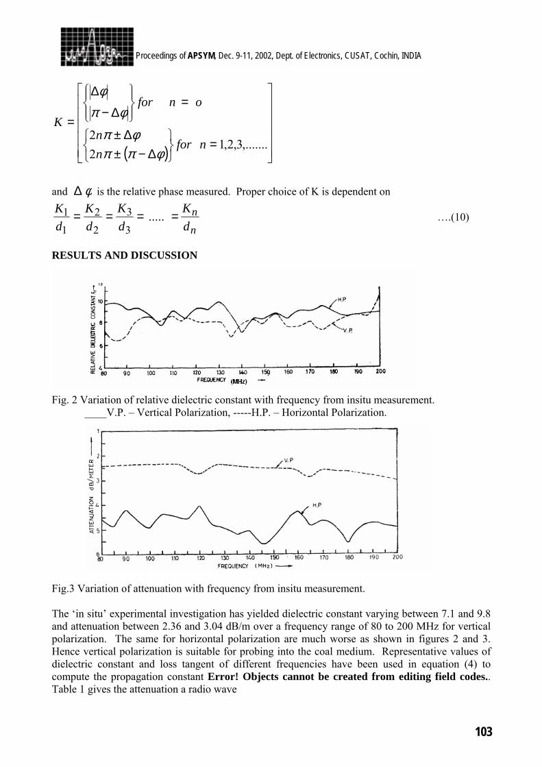
103
Proceedings of APSYM, Dec. 9-11, 2002, Dept. of Electronics, CUSAT, Cochin, INDIA
( )
=
∆−±∆±
=
∆−
∆
=
,.......3,2,122
nfornn
onforK
φππφπ
φπφ
and φ∆ is the relative phase measured. Proper choice of K is dependent on
nn
dK
dK
dK
dK ==== .....
3
3
2
2
1
1 ….(10)
RESULTS AND DISCUSSION
Fig. 2 Variation of relative dielectric constant with frequency from insitu measurement. ____V.P. – Vertical Polarization, -----H.P. – Horizontal Polarization. Fig.3 Variation of attenuation with frequency from insitu measurement. The ‘in situ’ experimental investigation has yielded dielectric constant varying between 7.1 and 9.8 and attenuation between 2.36 and 3.04 dB/m over a frequency range of 80 to 200 MHz for vertical polarization. The same for horizontal polarization are much worse as shown in figures 2 and 3. Hence vertical polarization is suitable for probing into the coal medium. Representative values of dielectric constant and loss tangent of different frequencies have been used in equation (4) to compute the propagation constant Error! Objects cannot be created from editing field codes.. Table 1 gives the attenuation a radio wave
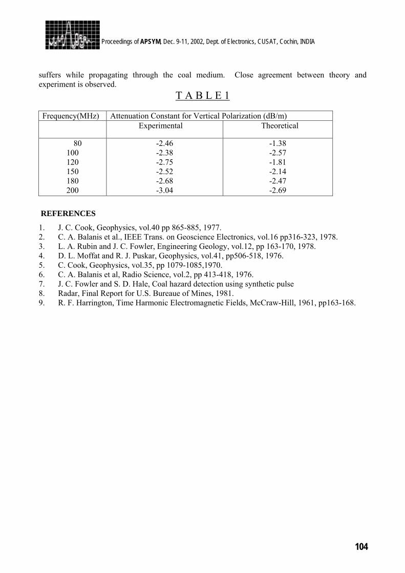
104
Proceedings of APSYM, Dec. 9-11, 2002, Dept. of Electronics, CUSAT, Cochin, INDIA suffers while propagating through the coal medium. Close agreement between theory and experiment is observed.
T A B L E 1 Frequency(MHz) Attenuation Constant for Vertical Polarization (dB/m)
Experimental Theoretical
80 100 120 150 180 200
-2.46 -2.38 -2.75 -2.52 -2.68 -3.04
-1.38 -2.57 -1.81 -2.14 -2.47 -2.69
REFERENCES
1. J. C. Cook, Geophysics, vol.40 pp 865-885, 1977. 2. C. A. Balanis et al., IEEE Trans. on Geoscience Electronics, vol.16 pp316-323, 1978. 3. L. A. Rubin and J. C. Fowler, Engineering Geology, vol.12, pp 163-170, 1978. 4. D. L. Moffat and R. J. Puskar, Geophysics, vol.41, pp506-518, 1976. 5. C. Cook, Geophysics, vol.35, pp 1079-1085,1970. 6. C. A. Balanis et al, Radio Science, vol.2, pp 413-418, 1976. 7. J. C. Fowler and S. D. Hale, Coal hazard detection using synthetic pulse 8. Radar, Final Report for U.S. Bureaue of Mines, 1981. 9. R. F. Harrington, Time Harmonic Electromagnetic Fields, McCraw-Hill, 1961, pp163-168.

105
Proceedings of APSYM, Dec. 9-11, 2002, Dept. of Electronics, CUSAT, Cochin, INDIA
ELECTRICAL PROPERTIES OF COAL IN VERY HIGH FREQUENCY BAND
G.Sahoo, A.Chakrabarty, S.Sanyal, S.Ghosh, Y.K.Singh
Department of Electronics & Electrical Communication, Indian Institute of Technology, Kharagpur - 721 302, India
E-mail - [email protected], [email protected]
Laboratory measurements of RF complex permittivity have been made on a number of coals encountered in coalmines. RF impedance bride and parallel-plate capacitance test cells were employed at frequencies starting from 50 to 100 MHz with step frequency of 10MHz. The result predicts that low-loss propagation will be possible in certain coals. Existing VHF mining radar should be capable of exploring into such coals to distance of up to hundreds of feet. Useful but shorter probing distances are predicted for other coals. Uncombined moisture content is evidently the governing factor. Efforts were made throughout the experiments to preserve or simulate the original moisture content of the coal in place.
INTRODUCTION
The development of electromagnetic systems to detect, monitor and communicate through an underground coal environment necessitates knowledge of the electrical properties of coal. Coal as a medium is quite complex in nature. Coal is a layered medium and in general the homogeneity of each layer is different from the other. The moisture content also varies from layer to layer. But the variation in homogeneity and moisture content is so negligible that it can be safely assumed to be a homogeneous anisotropy non-magnetic medium. Recent investigation have shown that the electrical properties of coal (dielectric constant and loss tangent) are function of electromagnetic wave polarization and propagation direction, frequency of the wave and moisture content of the coal [1,2,3]. Since attenuation in the coal medium generally increases with frequency of the electromagnetic wave, lower end of the frequency spectrum is more suitable for greater depth of penetration. Since the aim of determination of electrical properties of coal is to design and develop instrument for detection of geological discontinuities and weak zones in coalmines using Radar technique, the frequency range for the investigation naturally lies between RF to microwave.
THEORY
The RF electrical properties of coal sample are measured by the GR type 1601-A V.H.F. Bridge. It is a null instrument for use in measuring the impedance of coaxial line and lumped – constant circuits at frequencies between 10 and 165 MHz. Measurements can also be made with decreased accuracy at frequencies somewhat below and above these nominal frequency limits. The bridge is used with a series substitution method for measuring unknown impedance, XZ , in terms of its series resistance component, XR , and series reactance component XX , the resistance is read form a variable capacitor dial directly calibrated in resistance in ohms. The reactance dial is read from a variable capacitor dial directly calibrated in reactance in ohms at frequency of 100 MHz. The resistance dial reading is independent of frequency and the reactance dial reading increases linearly with frequency. For frequencies other than 100 MHz the reactance dial reading is therefore divided by the operating frequency in hundreds of megahertz. The resistance dial reads from 0 to 200 ohms; the reactance dial from 0 to 230 ohms at 100 MHz.
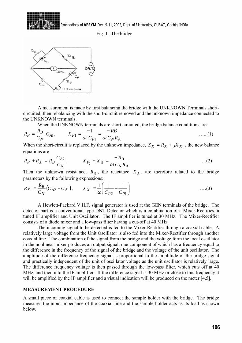
106
Proceedings of APSYM, Dec. 9-11, 2002, Dept. of Electronics, CUSAT, Cochin, INDIA
Fig. 1. The bridge
A measurement is made by first balancing the bridge with the UNKNOWN Terminals short-circuited; then rebalancing with the short-circuit removed and the unknown impedance connected to the UNKNOWN terminals. When the UNKNOWN terminals are short circuited, the bridge balance conditions are:
1AN
BP C
CRR = ,
ANPP RC
RBC
Xωω−=−=
11
1 ….. (1)
When the short-circuit is replaced by the unknown impedance, XXX jXRZ += , the new balance equations are
N
ABXP C
CRRR 2=+ , AN
BXP RC
RXXω−
=+2
….(2)
Then the unknown resistance, XR , the reactance XX , are therefore related to the bridge parameters by the following expressions:
( )12 AAN
BX CC
CRR −= ,
−=
12
111
PPX CC
Xω
.…(3)
A Hewlett-Packard V.H.F. signal generator is used at the GEN terminals of the bridge. The detector part is a conventional type DNT Detector which is a combination of a Mixer-Rectifies, a tuned IF amplifier and Unit Oscillator. The IF amplifier is tuned at 30 MHz. The Mixer-Rectifier consists of a diode mixer and a low-pass filter having a cut-off at 40 MHz. The incoming signal to be detected is fed to the Mixer-Rectifier through a coaxial cable. A relatively large voltage from the Unit Oscillator is also fed into the Mixer-Rectifier through another coaxial line. The combination of the signal from the bridge and the voltage form the local oscillator in the nonlinear mixer produces an output signal, one component of which has a frequency equal to the difference in the frequency of the signal of the bridge and the voltage of the unit oscillator. The amplitude of the difference frequency signal is proportional to the amplitude of the bridge-signal and practically independent of the unit of oscillator voltage as the unit oscillator is relatively large. The difference frequency voltage is then passed through the low-pass filter, which cuts off at 40 MHz, and then into the IF amplifier. If the difference signal is 30 MHz or close to this frequency it will be amplified by the IF amplifier and a visual indication will be produced on the meter [4,5]. MEASUREMENT PROCEDURE
A small piece of coaxial cable is used to connect the sample holder with the bridge. The bridge measures the input impedance of the coaxial line and the sample holder acts as its load as shown below.
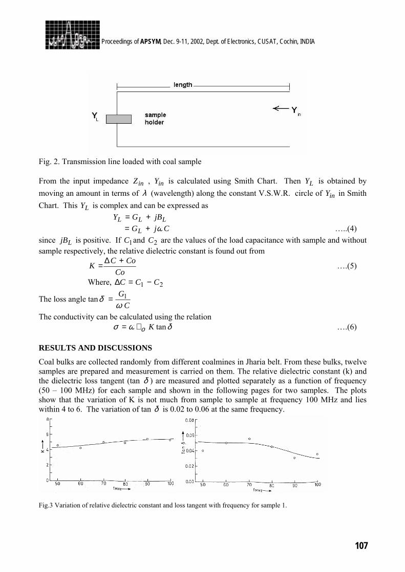
107
Proceedings of APSYM, Dec. 9-11, 2002, Dept. of Electronics, CUSAT, Cochin, INDIA
Fig. 2. Transmission line loaded with coal sample
From the input impedance inZ , inY is calculated using Smith Chart. Then LY is obtained by moving an amount in terms of λ (wavelength) along the constant V.S.W.R. circle of inY in Smith Chart. This LY is complex and can be expressed as
LLL jBGY += CjGL ω+= …..(4)
since LjB is positive. If 1C and 2C are the values of the load capacitance with sample and without sample respectively, the relative dielectric constant is found out from
Co
CoCK +∆= ….(5)
Where, 21 CCC −=∆
The loss angle tanC
Gω
δ 1=
The conductivity can be calculated using the relation δωσ ο tanK∈= ….(6)
RESULTS AND DISCUSSIONS
Coal bulks are collected randomly from different coalmines in Jharia belt. From these bulks, twelve samples are prepared and measurement is carried on them. The relative dielectric constant (k) and the dielectric loss tangent (tan δ ) are measured and plotted separately as a function of frequency (50 – 100 MHz) for each sample and shown in the following pages for two samples. The plots show that the variation of K is not much from sample to sample at frequency 100 MHz and lies within 4 to 6. The variation of tan δ is 0.02 to 0.06 at the same frequency.
Fig.3 Variation of relative dielectric constant and loss tangent with frequency for sample 1.
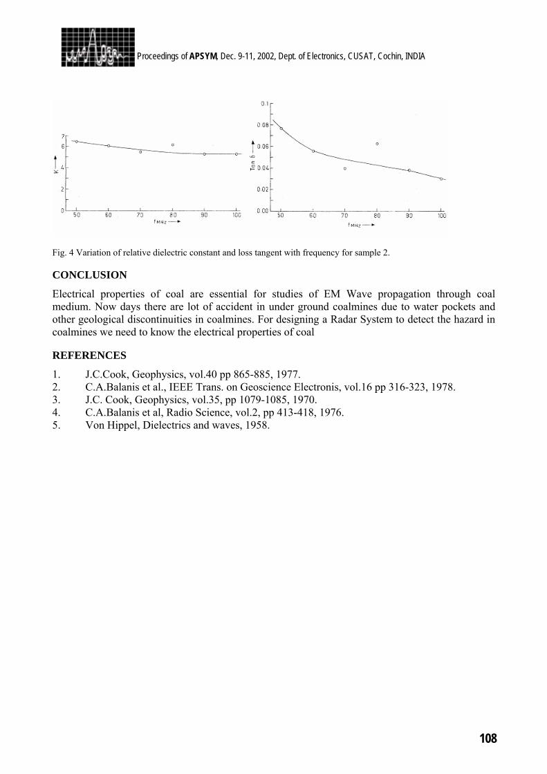
108
Proceedings of APSYM, Dec. 9-11, 2002, Dept. of Electronics, CUSAT, Cochin, INDIA
Fig. 4 Variation of relative dielectric constant and loss tangent with frequency for sample 2.
CONCLUSION
Electrical properties of coal are essential for studies of EM Wave propagation through coal medium. Now days there are lot of accident in under ground coalmines due to water pockets and other geological discontinuities in coalmines. For designing a Radar System to detect the hazard in coalmines we need to know the electrical properties of coal REFERENCES
1. J.C.Cook, Geophysics, vol.40 pp 865-885, 1977. 2. C.A.Balanis et al., IEEE Trans. on Geoscience Electronis, vol.16 pp 316-323, 1978. 3. J.C. Cook, Geophysics, vol.35, pp 1079-1085, 1970. 4. C.A.Balanis et al, Radio Science, vol.2, pp 413-418, 1976. 5. Von Hippel, Dielectrics and waves, 1958.
109
Proceedings of APSYM, Dec. 9-11, 2002, Dept. of Electronics, CUSAT, Cochin, INDIA
MICROWAVE ABSORPTION STUDIES IN (Mn-Ti) SUBSTITUTED BARIUM HEXAGONAL FERRITE BASED
ABSORBING PAINT
M. R MESHRAM, BHAROTI SINHA & NAWAL K. AGRAWAL Department of Electronics & Computer Engineering Indian Institute of Technology Roorkee 247 667 India E
mail: [email protected] P.S. MISRA
Department of Metallurgical and materials Engineering Indian Institute of Technology Roorkee 247 667 India.
This paper deals with the development of ferrite material Ba(MnTi)δFe(12-
2δ)O19 at δ=2.7 in the form of powders by dry attrition and sintering process. This ferrite powder has been mixed 60% by weight in 40% part of an epoxy resin to synthesize a microwave absorbing paint at Ku band of microwave .The performance characteristics of single layer coating of ferrite paint have been presented in this communication. It has been found that single layer absorbing paint exhibit peak absorption of 12.5 dB at 16.6 GHz for a coating thickness of 0.68 mm.
INTRODUCTION
There has been a growing and widespread interest in radar absorbing material technology. As the name implies, radar absorbing materials or RAM are coating whose electrical and magnetic properties have been altered to allow absorption of microwave energy at discrete or broadband frequency. Radar absorbing material is a substance, which absorb EM energy at microwave frequency. so fundamental to the development process is a comprehensive study of the intrinsic electronic properties of such material over the frequency range of interest. These properties are described by complex permeability( µr=µr’-jµr’’) and complex permittivity (εr=εr’-jεr’’). [1 ] The material which exhibit both dielectric and magnetic parameter is known as four parameter materials which play an important role because it can give more absorption performance over wide range of frequency. Radar absorbing material selected on the basis of above requirement is (Mn-Ti) substituted Barium hexagonal ferrite. In case of ferrite material microwave absorption takes place due to the lossy interaction between magnetization in ferrite material and magnetic field of incident microwave on absorber.[ 2 ] [3] EXPERIMENTAL
i) preparation of ferrite powder & paint
The ferrite powder of composition Ba(MnTi)δFe(12−2δ)O19 for δ=2.7 has been prepared by dry attrition and sintering process. The starting materials were Barium Carbonate, Manganese Carbonate, Titanium Dioxide and Ferric Oxide in form of extremely pure. The sintering was carried out at 11500C. The particle size of these ferrite powder has been measured by fisher sub sieve sizer instrument [ 4 ].The developed ferrite powder has been mixed 60 % by weight in epoxy resin to form a paint. This paint was coated on aluminum sheet of size(85mm ×54.5 mm) and kept in oven at 100oC for curing. An absorber sheet of thickness t=0.38 mm,0.51 mm and .68 mm have been fabricated for microwave absorption studies at Ku band. The dielectric constant of ferrite material has been measured by short circuit and open circuit method [ 2 ]
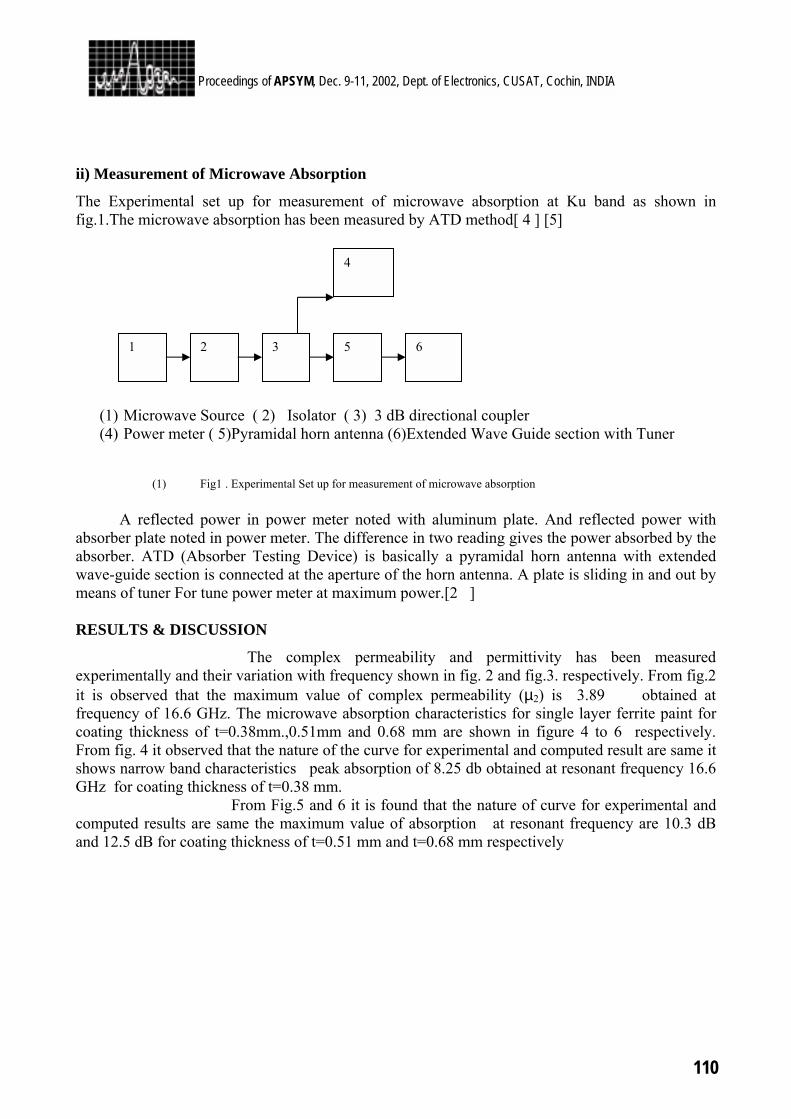
110
Proceedings of APSYM, Dec. 9-11, 2002, Dept. of Electronics, CUSAT, Cochin, INDIA
ii) Measurement of Microwave Absorption
The Experimental set up for measurement of microwave absorption at Ku band as shown in fig.1.The microwave absorption has been measured by ATD method[ 4 ] [5]
(1) Microwave Source ( 2) Isolator ( 3) 3 dB directional coupler (4) Power meter ( 5)Pyramidal horn antenna (6)Extended Wave Guide section with Tuner
(1) Fig1 . Experimental Set up for measurement of microwave absorption A reflected power in power meter noted with aluminum plate. And reflected power with absorber plate noted in power meter. The difference in two reading gives the power absorbed by the absorber. ATD (Absorber Testing Device) is basically a pyramidal horn antenna with extended wave-guide section is connected at the aperture of the horn antenna. A plate is sliding in and out by means of tuner For tune power meter at maximum power.[2 ] RESULTS & DISCUSSION
The complex permeability and permittivity has been measured experimentally and their variation with frequency shown in fig. 2 and fig.3. respectively. From fig.2 it is observed that the maximum value of complex permeability (µ2) is 3.89 obtained at frequency of 16.6 GHz. The microwave absorption characteristics for single layer ferrite paint for coating thickness of t=0.38mm.,0.51mm and 0.68 mm are shown in figure 4 to 6 respectively. From fig. 4 it observed that the nature of the curve for experimental and computed result are same it shows narrow band characteristics peak absorption of 8.25 db obtained at resonant frequency 16.6 GHz for coating thickness of t=0.38 mm. From Fig.5 and 6 it is found that the nature of curve for experimental and computed results are same the maximum value of absorption at resonant frequency are 10.3 dB and 12.5 dB for coating thickness of t=0.51 mm and t=0.68 mm respectively
1 2 3 5 6
4
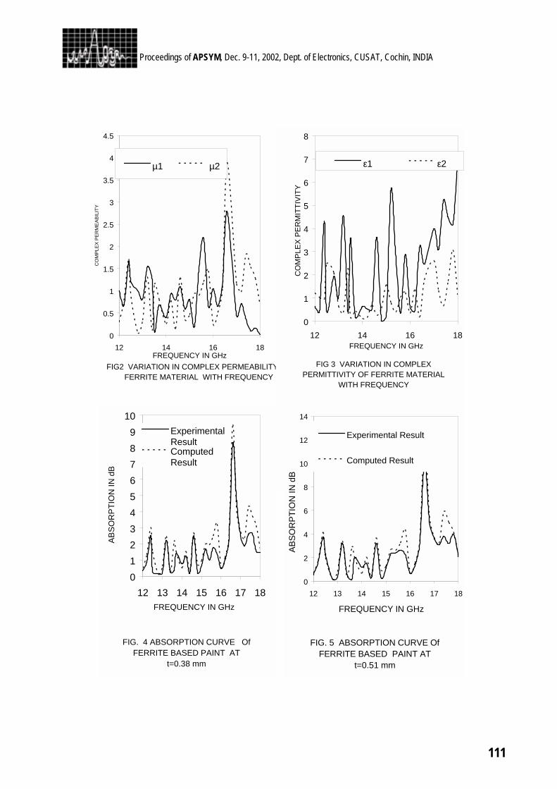
111
Proceedings of APSYM, Dec. 9-11, 2002, Dept. of Electronics, CUSAT, Cochin, INDIA
FIG2 VARIATION IN COMPLEX PERMEABILITY OF FERRITE MATERIAL WITH FREQUENCY
0
0.5
1
1.5
2
2.5
3
3.5
4
4.5
12 14 16 18FREQUENCY IN GHz
CO
MPL
EX P
ERM
EAB
ILIT
Y
µ1 µ2
FIG 3 VARIATION IN COMPLEX PERMITTIVITY OF FERRITE MATERIAL
WITH FREQUENCY
0
1
2
3
4
5
6
7
8
12 14 16 18FREQUENCY IN GHz
CO
MP
LEX
PE
RM
ITTI
VIT
Y
ε1 ε2
FIG. 4 ABSORPTION CURVE Of FERRITE BASED PAINT AT
t=0.38 mm
0123456789
10
12 13 14 15 16 17 18FREQUENCY IN GHz
AB
SO
RP
TIO
N IN
dB
ExperimentalResult ComputedResult
FIG. 5 ABSORPTION CURVE Of FERRITE BASED PAINT AT
t=0.51 mm
0
2
4
6
8
10
12
14
12 13 14 15 16 17 18
FREQUENCY IN GHz
ABSO
RPT
ION
IN d
B
Experimental Result
Computed Result
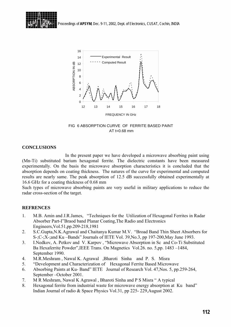
112
Proceedings of APSYM, Dec. 9-11, 2002, Dept. of Electronics, CUSAT, Cochin, INDIA
CONCLUSIONS
In the present paper we have developed a microwave absorbing paint using (Mn-Ti) substituted barium hexagonal ferrite. The dielectric constants have been measured experimentally. On the basis the microwave absorption characteristics it is concluded that the absorption depends on coating thickness. The natures of the curve for experimental and computed results are nearly same. The peak absorption of 12.5 dB successfully obtained experimentally at 16.6 GHz for a coating thickness of 0.68 mm Such types of microwave absorbing paints are very useful in military applications to reduce the radar cross-section of the target.
REFRENCES
1. M.B. Amin and J.R.James, “Techniques for the Utilization of Hexagonal Ferrites in Radar Absorber Part-I”Braod band Planar Coating,The Radio and Electronics Engineers,Vol.51,pp.209-218,1981
2. S.C.Gupta,N.K.Agrawal and Chaitanya Kumar M.V. “Broad Band Thin Sheet Absorbers for S-;C-;X-;and Ku –Bands” Journals of IETE Vol. 39,No.3, pp 197-200,May June 1993.
3. I.Nedkov, A. Petkov and V. Karpov , “Microwave Absorption in Sc and Co-Ti Substituted Ba Hexaferrite Powder”,IEEE Trans. On Magnetics Vol.26. no. 5,pp. 1483 –1484, September 1990.
4. M.R.Meshram , Nawal K. Agrawal ,Bharoti Sinha and P. S. Misra 5. “Development and Characterization of Hexagonal Ferrite Based Microwave 6. Absorbing Paints at Ku- Band” IETE Journal of Research Vol. 47,Nos. 5, pp.259-264,
September –October 2001. 7. M R Meshram, Nawal K Agrawal , Bharoti Sinha and P S Misra “ A typical 8. Hexagonal ferrite from industrial waste for microwave energy absorption at Ku band”
Indian Journal of radio & Space Physics Vol.31, pp 225- 229,August 2002.
FIG 6 ABSORPTION CURVE OF FERRITE BASED PAINT AT t=0.68 mm
0
2
4
6
8
10
12
14
16
12 13 14 15 16 17 18
FREQUENCY IN GHz
AB
SO
RP
TIO
N IN
dB
Experimental Result
Computed Result
113
Proceedings of APSYM, Dec. 9-11, 2002, Dept. of Electronics, CUSAT, Cochin, INDIA
MICROWAVE PERMITTIVITY STUDIES ON A NOVEL COMPOSITE MATERIAL- POLYSTYRENE/ALUMINA FOR
APPLICATION AS SUBSTRATE IN MIC/MMIC.
Juti R. Deka and Nidhi.S. Bhattacharya Dept. of Physics, Tezpur University, Napaam, Tezpur, Assam. [email protected]
In the present investigation a new polymer substrate- polystyrene with alumina as filler is made and its permittivity and loss tangent at X-band is determined. The studies show that with increase in the filler there is increase in dielectric constant value and decrease in the dielectric loss. Low frequency permittivity and loss factor, conductivity and density measurements are also carried out for characterizing the material. The new material shows promising characteristic for its applicability as substrates at higher microwave frequencies.
INTRODUCTION
In microstrip applications, generally, a focus is on high dielectric constant and good physical properties of the substrate material. Broadly, the substrates are characterized as ceramics, ferrites and plastics. Plastics (polymers) have advantages of flexibility, light weight, good surface adhesion for metallization and low cost but has serious disadvantage of poor dielectric properties. Some work on high molecular weight polymers like polyethylene terephthalate, polystyrene, polyethylene, polypropylene and Polytetraflouroethylene and their application, as substrates in microwave and millimeter have been reported [1,2,3]. In this paper we have tried to develop a new composite material with improved microwave dielectric properties. To the polystyrene sample, measured quantity of alumina is added as filler. Dielectric permittivity and loss factor at microwave X-band frequency of this composite is measured using the cavity perturbation technique. Measurements of low frequency permittivity and loss factor, density, and specific conductivity are also carried out. An enhancement in the dielectric properties is found with increase in alumina content. METHODOLOGY
Polystyrene sample (S1) is made by stirring few drops of MEK methyl ethyl ketone peroxide as a catalyst in the polyester resin, at room temperature. To the above solution 2-3 drops of cobalt napthanoate is mixed as drying agent. The resulting homogenous solution is then transferred into a mould of thickness 1.5mm. The mould is then kept in the oven at 700C for 4 hours. To get alumina filler polystyrene sample, 10% (S2) and 30% (S3) by weight of Al2O3 is added to polyester resin and is stirred for half an hour to make a homogenous mixture. The above procedure is followed on the mixture to get the final samples. While pouring the sample in the mould, care is taken of the fact that no air bubble is formed in the matrix. The low frequency up to 5MHZ permittivity measurement is carried out using HIOKI 3132-50 LCR Hitester. Specific conductivity and density of all the three samples are also measured. High frequency permittivity is measured using cavity perturbation technique [4,5]. For this purpose TE103 cavity with Q = 4840 at 9.68 GHz was designed and the sample placed at the point of maximum electric field. The change in Q values of cavity without and with the samples is noted. The shift in resonant frequency with the sample is also noted. Real part of permittivity (ε′) is calculated by
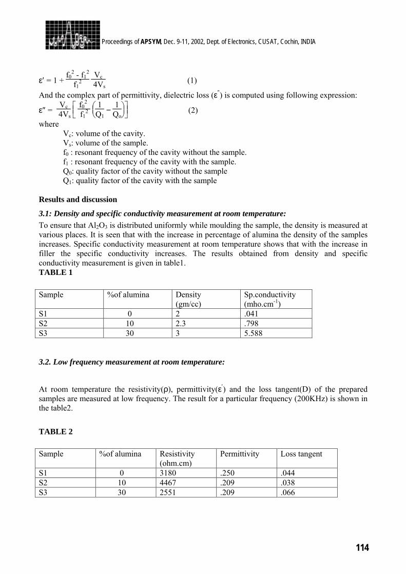
114
Proceedings of APSYM, Dec. 9-11, 2002, Dept. of Electronics, CUSAT, Cochin, INDIA
ε′ = 1 + f0
2 - f12
f12
Vc 4Vs
(1)
And the complex part of permittivity, dielectric loss (ε″) is computed using following expression:
ε″ = Vc
4Vs
f02
f12
1
Q1 −
1Qo
(2)
where Vc: volume of the cavity. Vs: volume of the sample. f0 : resonant frequency of the cavity without the sample. f1 : resonant frequency of the cavity with the sample. Q0: quality factor of the cavity without the sample Q1: quality factor of the cavity with the sample Results and discussion
3.1: Density and specific conductivity measurement at room temperature:
To ensure that Al2O3 is distributed uniformly while moulding the sample, the density is measured at various places. It is seen that with the increase in percentage of alumina the density of the samples increases. Specific conductivity measurement at room temperature shows that with the increase in filler the specific conductivity increases. The results obtained from density and specific conductivity measurement is given in table1. TABLE 1
Sample %of alumina Density (gm/cc)
Sp.conductivity (mho.cm-1)
S1 0 2 .041 S2 10 2.3 .798 S3 30 3 5.588
3.2. Low frequency measurement at room temperature:
At room temperature the resistivity(ρ), permittivity(ε′) and the loss tangent(D) of the prepared samples are measured at low frequency. The result for a particular frequency (200KHz) is shown in the table2.
TABLE 2
Sample %of alumina Resistivity (ohm.cm)
Permittivity Loss tangent
S1 0 3180 .250 .044 S2 10 4467 .209 .038 S3 30 2551 .209 .066
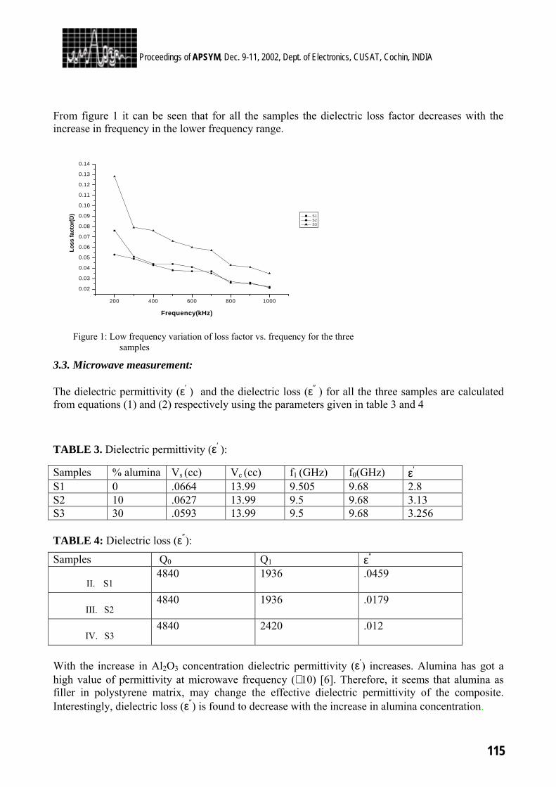
115
Proceedings of APSYM, Dec. 9-11, 2002, Dept. of Electronics, CUSAT, Cochin, INDIA
From figure 1 it can be seen that for all the samples the dielectric loss factor decreases with the increase in frequency in the lower frequency range.
Figure 1: Low frequency variation of loss factor vs. frequency for the three samples
3.3. Microwave measurement: The dielectric permittivity (ε′ ) and the dielectric loss (ε″ ) for all the three samples are calculated from equations (1) and (2) respectively using the parameters given in table 3 and 4
TABLE 3. Dielectric permittivity (ε′ ):
Samples % alumina Vs (cc) Vc (cc) f1 (GHz) f0(GHz) ε′
S1 0 .0664 13.99 9.505 9.68 2.8 S2 10 .0627 13.99 9.5 9.68 3.13 S3 30 .0593 13.99 9.5 9.68 3.256 TABLE 4: Dielectric loss (ε″):
Samples Q0 Q1 ε″
II. S1 4840 1936 .0459
III. S2 4840 1936 .0179
IV. S3 4840 2420 .012
With the increase in Al2O3 concentration dielectric permittivity (ε′) increases. Alumina has got a high value of permittivity at microwave frequency (≅ 10) [6]. Therefore, it seems that alumina as filler in polystyrene matrix, may change the effective dielectric permittivity of the composite. Interestingly, dielectric loss (ε″) is found to decrease with the increase in alumina concentration.
200 400 600 800 1000
0.02
0.03
0.04
0.05
0.06
0.07
0.08
0.09
0.10
0.11
0.12
0.13
0.14
Loss
fact
or(D
)
Frequency(kHz)
S1 S2 S3
116
Proceedings of APSYM, Dec. 9-11, 2002, Dept. of Electronics, CUSAT, Cochin, INDIA When alumina particles are present as filler their impact resistance increases. As the impact resistance increases therefore the matrix dissipates much energy [7] which may result in reduction of the dielectric loss of the composite. CONCLUSIONS
The increase in permittivity and decrease in loss tangent shows that polystyrene filled with alumina can be a new set of polymer material which can be used as substrate for MIC’s. Although losses are quite high as compared to alumina (about 100 times), on optimizing the addition of alumina the losses may further be reduced. Moreover, at higher frequencies the new composite can replace quartz (dielectric constant 3.8), which is costly, as circuits on high dielectric material, gets congested and hence reduce the power handling capability. REFERENCES
1. Mohd. Nurul Afser, “Precession Dielectric Measurements of Nonpolar Polymers in
the Millimeter Wavelength Range”, IEEE Trans Microwave Theory Tech., vol.-33, No-12,pp-1410-1414,1985.
2. Hallford Ben R., “ Low Noise Microstrip Mixer o a Plastic Substrate”, IEEE Trans Microwave Theory Tech., vol-18, pp-1178-1181, Dec 1970,.
3. Schnieder Frank , Heinrich Wolfgang, “ Model of Thin –Film Microstrip Line for Circuit Design”, IEEE Trans Microwave Theory Tech., vol-49, No-1,pp-104-110, 2001.
4. Murthy, V.R.K , Sundaram S, Viswanathan B,“ Microwave Materials”, Naros Publishing House.
5. J.S. Artman and T.E. Tammelwald, Journal of Applied Physics., 26,1124,1955. 6. Sobol,Harold, “ Application of Integrated Circuit Technology to Microwave
Frequencies” , Proc. IEEE, 59, No. 8, 1200-1211,August 1971. 7. Nicholson John W., “ The Chemistry of Polymers”, The Royal Society of Chemistry,
Second Edition.
117
Proceedings of APSYM, Dec. 9-11, 2002, Dept. of Electronics, CUSAT, Cochin, INDIA
ANALYSIS OF AN INHOMOGENEOUSLY LOADED HELICAL SLOW-WAVE STRUCTURE WITH ATTENUATOR COATING
Satya Prakash, S. Ghosh, V. Kiran, P. K. Jain¶and B. N. Basu
Development & Engineering Section, Microwave Tubes Division, Bharat Electronics Limited, Jalahalli, Bangalore – 560 013
¶Electronics Engineering Department, Institute of Technology, Banaras Hindu University, Varanasi – 221 005
Effect of attenuator coating on helical slow-wave structure (SWS), used in a traveling wave tube (TWT), has been presented here. The analysis for attenuator coated helix, reported earlier, was carried out for a single dielectric tube region considering same radial propagation constant. Here, the authors have presented the analysis for n dielectric tube regions considering different radial propagation constant over the different structure region taking attenuator coating on the outer surface of the helix. The transcendental dispersion relation is solved for the complex propagation constant to predict the structure characteristics of the structure in presence of lossy attenuator on the helix surface. The effect of loss due to attenuator coating on the propagation constant and interaction impedance have been studied and presented here.
INTRODUCTION
Helix traveling tube (TWTs) continues to be interest for their applications in space communication to electronic warfare systems due to unique combination of bandwidth, power, gain and efficiency [1]. The dielectric supports, when deviates from simple wedge geometry structure to any tapered geometry structure, gives an in homogeneously loading to the helical slow-wave structure (SWS) [2]. The inhomogeneity factor controls the dispersion characteristics of the structure. However, it is expected that due to the presence of losses due to attenuator coating on the helical SWS significantly affects not only the attenuation constant but also the propagation constant and the interaction impedance of the structure [3], though the effect of the conductivity losses are of second order importance and ignored here. The attenuator coated helix may be considered as a helix with its turns shorted circuited by a resistive attenuator coating. Attempts have been made in [4],[5] to analyse the attenuator coated helical SWS to some limited extension, moreover, these analyses have been modified and extended in [3], for a simple situation in which the dielectric supports are smoothed out into a single tube region of an effective permittivity value and also considered same radial propagation constant. In this paper, authors have presented the analysis for a practical situation where the discrete supports are smoothed out into n number of equivalent dielectric tube regions and considering different radial propagation constant over different regions of the structure [1], [2]. Moreover, authors have presented here the effect of inhomogeneity factor and surface resistivity of the attenuator coating on helical SWS to study the cold behaviors of the structure. ANALYSIS
Dispersion
The structure under study consists of a helical SWS supported by three arbitrary shaped dielectric supports and the whole is enclosed in a isotropic metal envelope [3]. The analysis treated in sheath helix model and the helix/envelope has been assumed to be perfectly conducting, since the effect of the finite conductivity losses of the helix/envelope on the propagation constant is negligible
118
Proceedings of APSYM, Dec. 9-11, 2002, Dept. of Electronics, CUSAT, Cochin, INDIA compared to attenuator coating losses. Using the field expression or boundary conditions the dispersion relation can be written as [1]-[3]
( )( )aSIaKaI
aRIaKaIcotk
111
0002
22
γ−γγγ+γγ=
γψ
(1)
where
( )
( ) bIjbKbI
bIPbKbIPbK
bKjbKbK
bIPbKbIPbK
R
203,r3
2
0
20s21
31331
30330
203,r3
2
0
20s21
31331
30330
γε′γγ
+
ωεγγσ+γ
γ−γγ+γ
γε′γγ
−
ωεγγσ−γ
γ−γγ+γ
= (2)
γγσωµ+γ
γγ
−γ
γ−γγ+γ
γγσωµ−γ
γγ
+γ
γ−γγ+γ
=
2
21s020
3
221
31313
30303
2
21s020
3
221
31313
30303
bIjbIbIbKbIQbKbIQ
bKjbKbKbKbIQbKbIQ
S (3)
with '2
'1
1n
1n1n
PP
BAP ==
+
++ and '
2
'1
1n
1n1n Q
QDCQ ==
+
++ (4)
1P′ , 2P′ , 1Q′ and 2Q′ are complicated function of structure parameters. The dispersion relation above is essentially a complex transcendental equation due to presence of attenuator coating, the radial propagation constant is complex (γ = (-Γ2-k2 )0.5, Γ = α+jβ, α is the attenuation constant and β is the phase propagation constant, k is the free space propagation constant). σs is the conductivity of the resistive material. a, b, d, are the mean helix radius, outer helix radius or metal envelope radius respectively. The solution of the dispersion relation (1) is obtained by using MATLAB program. Interaction Impedance
Interaction impedance of the structure can be written as [3]:
( )
t
2
222z P2
)2(/exp
0EK
β+αβαπ−α−β
= (5)
where Pt is the power propagating down the structure. The expression for Pt can be obtained by taking the real part of the integration of the Poynting vector over the structure. Ez(0) is the axial electric field at the axis of the helix [1] – [3]. RESULTS AND DISCUSSION
The theoretical results presented to study the effect of surface resistivity (Rs) on normalized phase velocity (vp/c) (Fig. 1a), interaction impedance (K) (Fig. 1b) and attenuation constant (α) (Fig. 1c) for a given set of structure parameters for both single and n dielectric tube regions. It is found from the figure 1, that with the increase in Rs, vp/c decreases and gives negative to flatter response (Fig. 1a) but the interaction impedance of the structure increases (Fig. 1b) with surface resistivity. Also it is found that the results obtained from n dielectric tube regions are less than the single dielectric tube region, which is reasonably accurate and gives closer to the experimental results [2]. However,
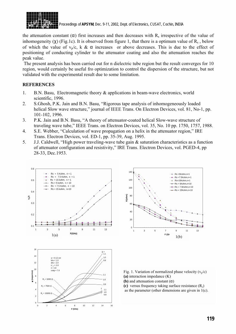
119
Proceedings of APSYM, Dec. 9-11, 2002, Dept. of Electronics, CUSAT, Cochin, INDIA
the attenuation constant (α) first increases and then decreases with Rs irrespective of the value of inhomogeneity (χ) (Fig.1c). It is observed from figure 1, that there is a optimum value of Rs , below of which the value of vp/c, k & α increases or above decreases. This is due to the effect of positioning of conducting cylinder to the attenuator coating and also the attenuation reaches the peak value. The present analysis has been carried out for n dielectric tube region but the result converges for 10 region, would certainly be useful fro optimization to control the dispersion of the structure, but not validated with the experimental result due to some limitation. REFERENCES
1. B.N. Basu, Electromagnetic theory & applications in beam-wave electronics, world scientific, 1996.
2. S.Ghosh, P.K. Jain and B.N. Basu, “Rigorous tape analysis of inhomogeneously loaded helical Slow wave structure,” journal of IEEE Trans. On Electron Devices, vol. 81, No-1, pp. 101-102, 1996.
3. P.K. Jain and B.N. Basu, “A theory of attenuator-coated helical Slow-wave structure of traveling wave tube,” IEEE Trans. on Electron Devices, vol. 35, No. 10 pp. 1750, 1757, 1988.
4. S.E. Webber, “Calculation of wave propagation on a helix in the attenuator region,” IRE Trans. Electron Devices, vol. ED-1, pp. 35-39, Aug. 1995.
5. J.J. Caldwell, “High power traveling-wave tube gain & saturation characteristics as a function of attenuator configuration and resistivity,” IRE Trans. Electron Devices, vol. PGED-4, pp 28-33, Dec.1953.
0.1
0.2
0.3
0.4
0.5
0.6
1 3 5 7 9 11 13
F(GHz)
v p/c
Rs = 5 Kohm, n = 1 Rs = 7.5 Kohm, n = 1 Rs = 15 kohm, n = 1 Rs = 5 kohm, n = 10 Rs = 7.5 Kohm, n = 10 Rs = 15 kohm, n=10
0
20
40
60
80
100
120
140
1 3 5 7 9 11 13
F (GHz)
K(o
hm)
Rs =5Kohm,n=1Rs =7.5Kohm,n=1Rs=15Kohm,n=1Rs = 5Kohm,n=10Rs = 7.5Kohm,n=10Rs = 15Kohm,n=10
1(a) 1(b)
0
2
4
6
8
10
12
14
16
0 2 4 6 8 10 12 14 16
F (GHz)
αα αα (n
eper
/cm
)
a = 0.12 cmb/a = 1.0d/a = 2.0ε'r,3 = 2.0n = 10cotψ = 7.0
χ =1.1
1.00.9
1.1
1.0
0.9
1.11.00.9
Rs = 5000 Ω
Rs = 7500 Ω
Rs = 15000 Ω
Fig. 1. Variation of normalized phase velocity (vp/c) (a) interaction impedance (K) (b) and attenuation constant (α) (c) versus frequency taking surface resistance (Rs) as the parameter (other dimensions are given in 1(c).
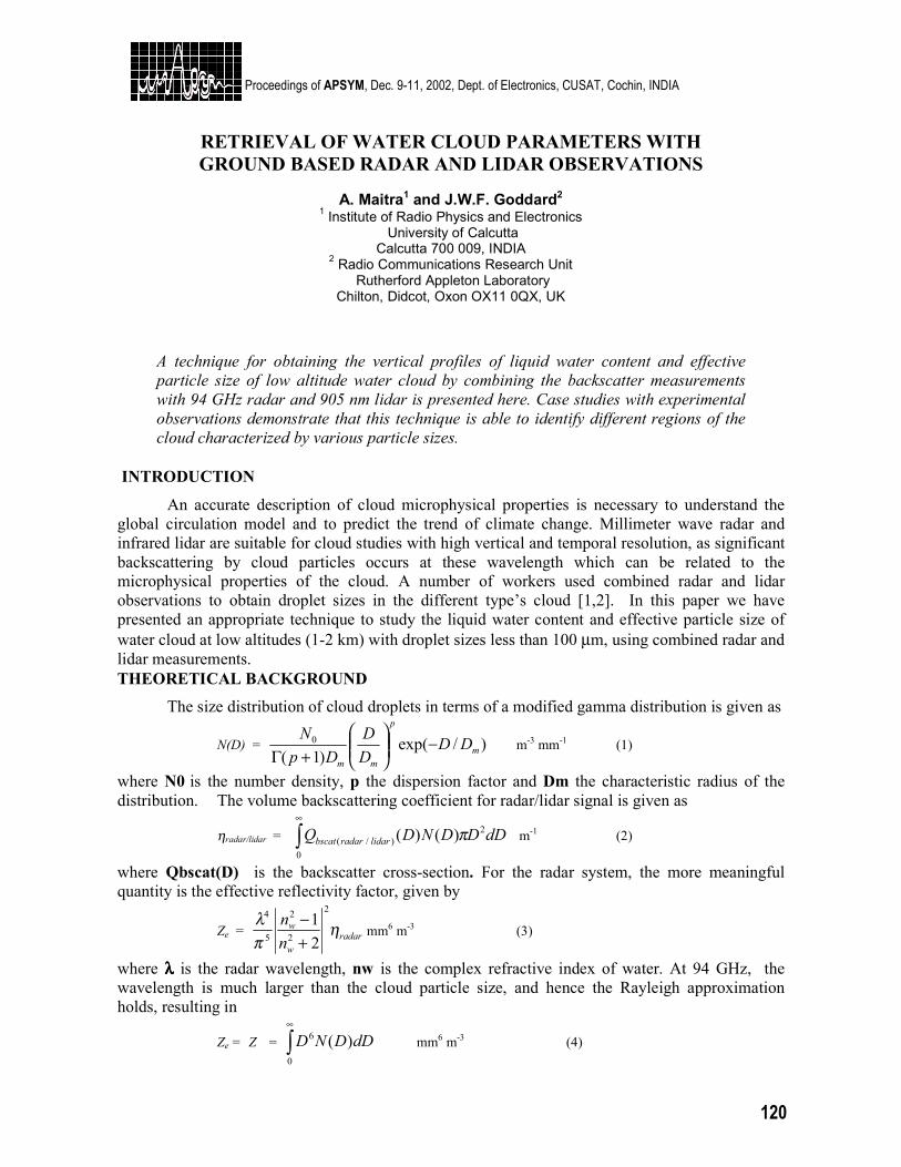
120
Proceedings of APSYM, Dec. 9-11, 2002, Dept. of Electronics, CUSAT, Cochin, INDIA
RETRIEVAL OF WATER CLOUD PARAMETERS WITH GROUND BASED RADAR AND LIDAR OBSERVATIONS
A. Maitra1 and J.W.F. Goddard2
1 Institute of Radio Physics and Electronics University of Calcutta
Calcutta 700 009, INDIA 2 Radio Communications Research Unit
Rutherford Appleton Laboratory Chilton, Didcot, Oxon OX11 0QX, UK
A technique for obtaining the vertical profiles of liquid water content and effective particle size of low altitude water cloud by combining the backscatter measurements with 94 GHz radar and 905 nm lidar is presented here. Case studies with experimental observations demonstrate that this technique is able to identify different regions of the cloud characterized by various particle sizes.
INTRODUCTION
An accurate description of cloud microphysical properties is necessary to understand the global circulation model and to predict the trend of climate change. Millimeter wave radar and infrared lidar are suitable for cloud studies with high vertical and temporal resolution, as significant backscattering by cloud particles occurs at these wavelength which can be related to the microphysical properties of the cloud. A number of workers used combined radar and lidar observations to obtain droplet sizes in the different type’s cloud [1,2]. In this paper we have presented an appropriate technique to study the liquid water content and effective particle size of water cloud at low altitudes (1-2 km) with droplet sizes less than 100 µm, using combined radar and lidar measurements. THEORETICAL BACKGROUND
The size distribution of cloud droplets in terms of a modified gamma distribution is given as
N(D) = )/exp()1(
0m
p
mm
DDDD
DpN −
+Γ
m-3 mm-1 (1)
where N0 is the number density, p the dispersion factor and Dm the characteristic radius of the distribution. The volume backscattering coefficient for radar/lidar signal is given as
ηradar/lidar = ∫∞
0
2)/( )()( dDDDNDQ lidarradarbscat π m-1 (2)
where Qbscat(D) is the backscatter cross-section. For the radar system, the more meaningful quantity is the effective reflectivity factor, given by
Ze = radarw
w
nn η
πλ
2
2
2
5
4
21
+−
mm6 m-3 (3)
where λλλλ is the radar wavelength, nw is the complex refractive index of water. At 94 GHz, the wavelength is much larger than the cloud particle size, and hence the Rayleigh approximation holds, resulting in
Ze = Z = ∫∞
0
6 )( dDDND mm6 m-3 (4)
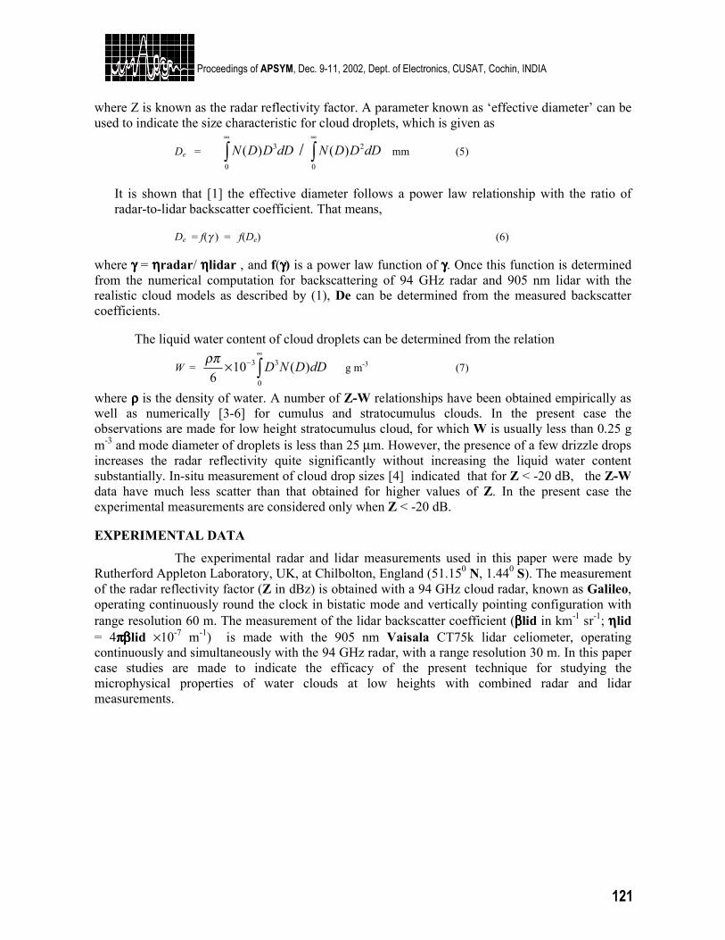
121
Proceedings of APSYM, Dec. 9-11, 2002, Dept. of Electronics, CUSAT, Cochin, INDIA where Z is known as the radar reflectivity factor. A parameter known as ‘effective diameter’ can be used to indicate the size characteristic for cloud droplets, which is given as
De = dDDDN∫∞
0
3)( / dDDDN∫∞
0
2)( mm (5)
It is shown that [1] the effective diameter follows a power law relationship with the ratio of radar-to-lidar backscatter coefficient. That means, De = f(γ ) = f(De) (6)
where γγγγ = ηηηηradar/ ηηηηlidar , and f(γγγγ) is a power law function of γγγγ. Once this function is determined from the numerical computation for backscattering of 94 GHz radar and 905 nm lidar with the realistic cloud models as described by (1), De can be determined from the measured backscatter coefficients.
The liquid water content of cloud droplets can be determined from the relation
W = ∫∞
−×0
33 )(106
dDDNDρπ g m-3 (7)
where ρρρρ is the density of water. A number of Z-W relationships have been obtained empirically as well as numerically [3-6] for cumulus and stratocumulus clouds. In the present case the observations are made for low height stratocumulus cloud, for which W is usually less than 0.25 g m-3 and mode diameter of droplets is less than 25 µm. However, the presence of a few drizzle drops increases the radar reflectivity quite significantly without increasing the liquid water content substantially. In-situ measurement of cloud drop sizes [4] indicated that for Z < -20 dB, the Z-W data have much less scatter than that obtained for higher values of Z. In the present case the experimental measurements are considered only when Z < -20 dB. EXPERIMENTAL DATA
The experimental radar and lidar measurements used in this paper were made by Rutherford Appleton Laboratory, UK, at Chilbolton, England (51.150 N, 1.440 S). The measurement of the radar reflectivity factor (Z in dBz) is obtained with a 94 GHz cloud radar, known as Galileo, operating continuously round the clock in bistatic mode and vertically pointing configuration with range resolution 60 m. The measurement of the lidar backscatter coefficient (ββββlid in km-1 sr-1; ηηηηlid = 4ππππββββlid ×10-7 m-1) is made with the 905 nm Vaisala CT75k lidar celiometer, operating continuously and simultaneously with the 94 GHz radar, with a range resolution 30 m. In this paper case studies are made to indicate the efficacy of the present technique for studying the microphysical properties of water clouds at low heights with combined radar and lidar measurements.
122
Proceedings of APSYM, Dec. 9-11, 2002, Dept. of Electronics, CUSAT, Cochin, INDIA
RESULTS AND DISCUSSION
Fig. 1. Size distributions of cloud droplets.
De = 0.28 γ0.21 mm (9) For case studies, the radar and lidar data simultaneously obtained on 11 January 2000 are analyzed. The observations during the whole day from 00 to 24 hrs at a time interval of 15 min were considered. Fig. 2 gives the height profiles of radar signal (Z) and lidar
Fig. 2. Radar and lidar signal profiles
Fig.1 shows the size distributions of cloud droplets considered according to the distribution function given in (1). The range of values of the parameters of size distributions, appropriate to the stratocumulus clouds, considered are: N0 = 106, 107, 108 m-3 ; Dm = 2, 3, 4 µm ; p = 1-6. The Z-W relationship obtained with the above size distributions is W = 3.8 Z0.71 g m-3 (8) and the power-law relation between the effective diameter is and the backscattering ratio is found to be
signal (βrad) simultaneously obtained. For the radar signal, the dotted lines are for the entire height range up to 2 km, whereas the continuous portions of the profiles correspond to Z < -20 dB used in the present estimations. Fig. 3 gives the profiles of retrieved liquid water content and effective diameter as obtained form relations (8) and (9) respectively. It may be noted that the De-profiles indicate a peak value of De around 60 µm at an altitude of about 1 km, and a dip value of De around 25 µm a height of about 1.3 km. The W-profiles, however, do not exhibit any significant layering with the
123
Proceedings of APSYM, Dec. 9-11, 2002, Dept. of Electronics, CUSAT, Cochin, INDIA
Fig. 3. Profiles of liquid water contents and effective diameters retrieved from radar and lidar backscatter measurements
ACKNOWLEDGEMENTS
One of the authors (AM) thankfully acknowledges the financial and administrative support from the Royal Society, London, and the Indian National Science Academy, New Delhi, for his visit under an international exchange programme at the Rutherford Appleton Laboratory, UK, where a part of the work was carried out. The service of the British Atmospheric Data Centre, UK, in providing the experimental data is also thankfully acknowledged.
REFERENCES
1. J.M. Intrieri, G.L. Stephens, W.L. Eberhard, and T. Uttal, “A method for cirrus cloud particle
sizes using lidar and radar backscatter technique”, J. Appl. Meterol., vol. 32, pp. 1074-1082, 1993.
2. D.P. Donovan and A.C.A.P. van Lammeren, “Cloud effective particle size and water content profile retrieval using combined lidar and radar observations: 1. theory and examples”, J. Geophys. Res., vol. 106, No. D21, pp. 27425-27448, 2001.
3. D. Atlas, “The estimation of cloud parameters by radar”, J. Meteorol., vol. 11, pp. 309-317, 1954.
4. H. Sauvageot and J. Omar, “Radar reflectivity of cumulus clouds”, J. Atmos. Oceanic. Technol., vol. 4, pp. 264-272, 1987.
5. A.S. Frisch, C.W. Fairall, and J.B. Snider, “Measurements of stratus cloud and drizzle parameters in ASTEX with a Ka-band Doppler radar and a microwave radiometer”, J. Atmos. Sci., vol. 52, pp. 2788-2799, 1995
6. N.I. Fox and A.J. Illingworth, “The retrieval of stratocumulus cloud properties by ground-based cloud radar”, J. Appl. Meterol., vol. 36, pp. 485-492, 1997.
cloud height. These observations indicate that that the base region of clouds is dominated by large drops and there is a distinct region of small droplets at higher altitudes. In this paper, a technique to study the microphysical properties of water clouds at low altitudes, using combined radar and lidar observations, is demonstrated. This technique can be used to identify different regions of the cloud and to investigate the evolution of cloud characteristics.
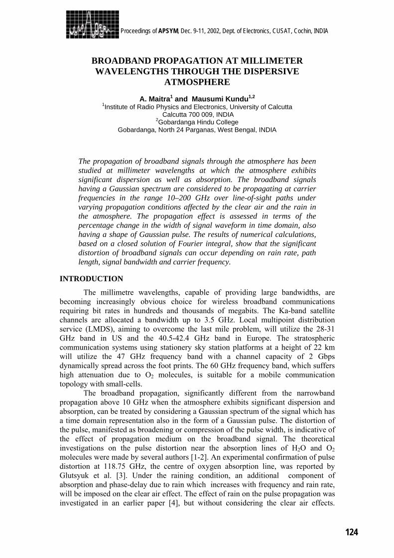
124
Proceedings of APSYM, Dec. 9-11, 2002, Dept. of Electronics, CUSAT, Cochin, INDIA
BROADBAND PROPAGATION AT MILLIMETER WAVELENGTHS THROUGH THE DISPERSIVE
ATMOSPHERE
A. Maitra1 and Mausumi Kundu1,2 1Institute of Radio Physics and Electronics, University of Calcutta
Calcutta 700 009, INDIA 2Gobardanga Hindu College
Gobardanga, North 24 Parganas, West Bengal, INDIA
The propagation of broadband signals through the atmosphere has been studied at millimeter wavelengths at which the atmosphere exhibits significant dispersion as well as absorption. The broadband signals having a Gaussian spectrum are considered to be propagating at carrier frequencies in the range 10–200 GHz over line-of-sight paths under varying propagation conditions affected by the clear air and the rain in the atmosphere. The propagation effect is assessed in terms of the percentage change in the width of signal waveform in time domain, also having a shape of Gaussian pulse. The results of numerical calculations, based on a closed solution of Fourier integral, show that the significant distortion of broadband signals can occur depending on rain rate, path length, signal bandwidth and carrier frequency.
INTRODUCTION
The millimetre wavelengths, capable of providing large bandwidths, are becoming increasingly obvious choice for wireless broadband communications requiring bit rates in hundreds and thousands of megabits. The Ka-band satellite channels are allocated a bandwidth up to 3.5 GHz. Local multipoint distribution service (LMDS), aiming to overcome the last mile problem, will utilize the 28-31 GHz band in US and the 40.5-42.4 GHz band in Europe. The stratospheric communication systems using stationery sky station platforms at a height of 22 km will utilize the 47 GHz frequency band with a channel capacity of 2 Gbps dynamically spread across the foot prints. The 60 GHz frequency band, which suffers high attenuation due to O2 molecules, is suitable for a mobile communication topology with small-cells. The broadband propagation, significantly different from the narrowband propagation above 10 GHz when the atmosphere exhibits significant dispersion and absorption, can be treated by considering a Gaussian spectrum of the signal which has a time domain representation also in the form of a Gaussian pulse. The distortion of the pulse, manifested as broadening or compression of the pulse width, is indicative of the effect of propagation medium on the broadband signal. The theoretical investigations on the pulse distortion near the absorption lines of H2O and O2 molecules were made by several authors [1-2]. An experimental confirmation of pulse distortion at 118.75 GHz, the centre of oxygen absorption line, was reported by Glutsyuk et al. [3]. Under the raining condition, an additional component of absorption and phase-delay due to rain which increases with frequency and rain rate, will be imposed on the clear air effect. The effect of rain on the pulse propagation was investigated in an earlier paper [4], but without considering the clear air effects.

125
Proceedings of APSYM, Dec. 9-11, 2002, Dept. of Electronics, CUSAT, Cochin, INDIA
However, the presently proposed broadband communications are not always strictly in the window region, and both the clear air and the rain can affect the propagation. In the present paper, the broadband propagation in the frequency range 10 – 200 GHz has been investigated under varying propagation conditions over line-of-sight paths for Gaussian bandwidths in the range 1.6 – 16 GHz using numerical computations based on the technique of Forrer [5]. THEORETICAL BACKGROUND A Gaussian spectrum of the broadband signal is given as F (ω) = √(π/b) ( exp (-ω2/4b) (1) which has a time domain representation , f(t) = exp (-bt2) (2) where, b = 4 ln (10) / T02, and T0 is the pulse width at 10% level. The signal is considered propagating at a carrier frequency ωωωω0 over a distance L through a medium with complex propagation constant, γγγγ (ωωωω) = αααα(ωωωω) + jββββ(ωωωω), αααα(ωωωω) and ββββ(ωωωω) being extinction and phase delay coefficient and can be expressed in time domain as
r(t, L) = (1/2π) ∫∞
∞−
F(ω) exp [j (ω0 + ω) t] exp(-γL) dω (3)
If αααα(ωωωω) and ββββ(ωωωω) are expressed with the truncated Taylor series taking the terms up to second derivative, then a closed solution is obtained under the convergence condition, namely, (1+2 bα” L) > 0, as [ 5] r(t*, L) = A(L) exp [-kb(t* + ξ)2]. exp [-j(ω*t* + δ)] (4) There are several changes occurred to the propagated signal given by (4) with respect to the original signal. The signal arrives with a retarded timescale t* and the carrier frequency, which is actually the mode frequency where maximum energy is received, is shifted from ωωωω0 to ωωωω*. Also the carrier phase is changed by δδδδ. Although the envelope of the propagated signal, exp [-kb(t* + ξξξξ)2], is still Gaussian, it suffers a group delay ξξξξ and the pulse width is changed by a factor √k, where k is given by
k = 22 )"2()"21("21
LbLbLbβα
α++
+ (5)
and the modified pulse width will be, T = T0 /√k (6) To obtain the propagation constants αααα(ωωωω) and ββββ(ωωωω) of the atmosphere, contributions of two components are to be considered. One component is due to the clear effect caused by the molecular absorption due to H2O and O2 in the atmosphere. The second component, which occurs under the raining condition, is due to the absorption and scattering by raindrops. In the present numerical calculations the Liebe’s propagation model [6] is considered to obtain the propagation constants. RESULTS OF NUMERICAL CALCULATIONS AND DISCUSSION
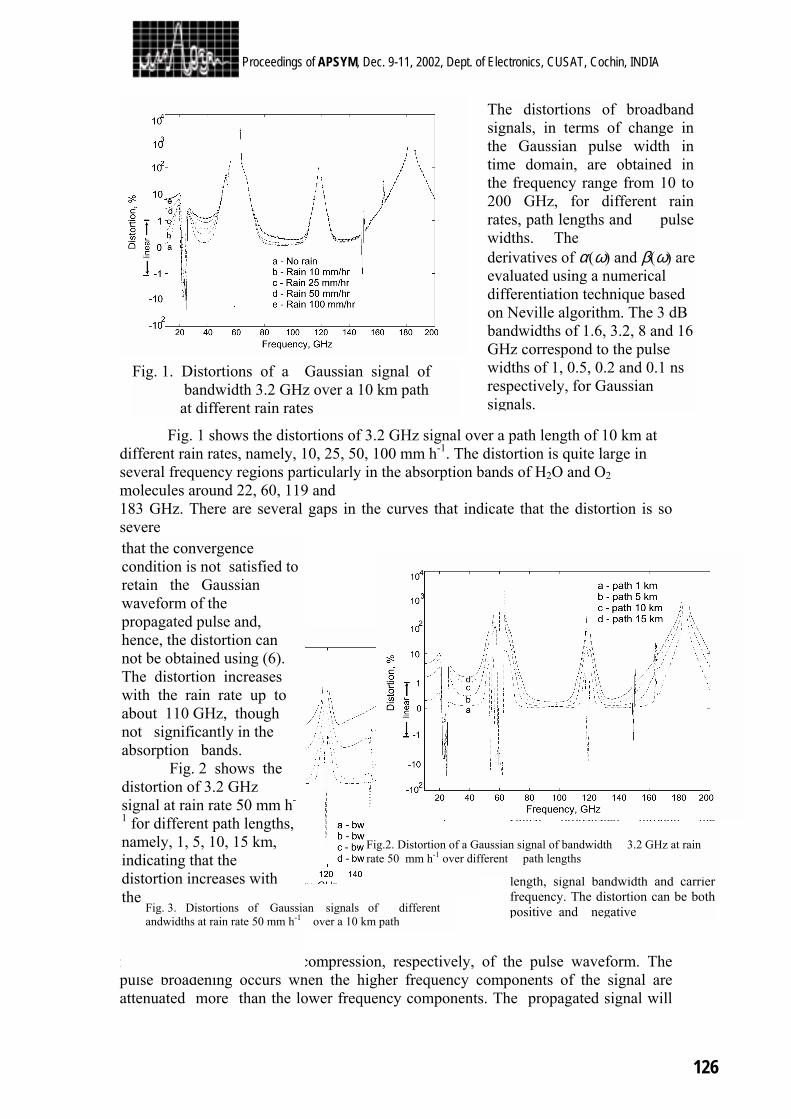
126
Proceedings of APSYM, Dec. 9-11, 2002, Dept. of Electronics, CUSAT, Cochin, INDIA
Fig. 1 shows the distortions of 3.2 GHz signal over a path length of 10 km at
different rain rates, namely, 10, 25, 50, 100 mm h-1. The distortion is quite large in several frequency regions particularly in the absorption bands of H2O and O2 molecules around 22, 60, 119 and 183 GHz. There are several gaps in the curves that indicate that the distortion is so severe
indicating broadening and compression, respectively, of the pulse waveform. The pulse broadening occurs when the higher frequency components of the signal are attenuated more than the lower frequency components. The propagated signal will
Fig. 1. Distortions of a Gaussian signal of bandwidth 3.2 GHz over a 10 km path at different rain rates
The distortions of broadband signals, in terms of change in the Gaussian pulse width in time domain, are obtained in the frequency range from 10 to 200 GHz, for different rain rates, path lengths and pulse widths. The derivatives of α(ω) and β(ω) are evaluated using a numerical differentiation technique based on Neville algorithm. The 3 dB bandwidths of 1.6, 3.2, 8 and 16 GHz correspond to the pulse widths of 1, 0.5, 0.2 and 0.1 ns respectively, for Gaussian signals.
that the convergence condition is not satisfied to retain the Gaussian waveform of the propagated pulse and, hence, the distortion can not be obtained using (6). The distortion increases with the rain rate up to about 110 GHz, though not significantly in the absorption bands.
Fig. 2 shows the distortion of 3.2 GHz signal at rain rate 50 mm h-
1 for different path lengths, namely, 1, 5, 10, 15 km, indicating that the distortion increases with the path length.
Fig. 3 depicts how the distortion increases with increasing bandwidth from 1.6 GHz to 16 GHz, a path length 5 km and a rain rate 50 mm h-1 being considered. For a large bandwidth, the distortion can be so severe that the Gaussian shape of the pulse is often not retained. The distortion of broadband signal propagated through the atmosphere can be very large depending on the propagation conditions typified by rain rate, path length, signal bandwidth and carrier frequency. The distortion can be both positive and negative Fig. 3. Distortions of Gaussian signals of different
andwidths at rain rate 50 mm h-1 over a 10 km path
Fig.2. Distortion of a Gaussian signal of bandwidth 3.2 GHz at rain rate 50 mm h-1 over different path lengths

127
Proceedings of APSYM, Dec. 9-11, 2002, Dept. of Electronics, CUSAT, Cochin, INDIA
have an imposed frequency modulation on the carrier, due to the frequency dependence of both phase-delay and absorption [5]. Under the condition when the frequencies at the leading edge of the pulse suffer more delay than the frequencies at the trailing edge, the pulse compression occurs. The effect of broadband propagation on the performance of the high-rate data communication system can be significant. The broadening of pulse waveform can increase the intersymbol interference. The pulse compression, resulting in an increase of signal bandwidth, will cause a loss of signal strength for a receiving system with finite bandwidth. REFERENCES 1. D. B. Trizna, and T. A. Weber, "Brillouin revisited: signal velocity definition for pulse
propagation in a medium with resonant anomalous dispersion", Radio Sci., vol. 17, pp. 1169-1180¸1982.
2. C. J. Gibbins, "Propagation of very short pulses though the absorptive and dispersive atmosphere", IEE Proc. H, vol. 137, pp. 304-310, 1990.
3. A.M. Glutsyuk, L.I. Sharapov, and I.K. Vakser, “Distortion of short electromagnetic pulses propagating at the frequencies of atmospheric oxygen absorption lines”, Proc. URSI Comm. F. Open Symp. La Baule France, pp. 637-642, 1977.
4. A. Maitra, M. Dan, A. K. Sen, K. Bhattacharyya, and C. K. Sarkar, "Propagation of very short pulses at millimeter wavelengths through rain filled medium", Int. J. Infrared Millimeter Waves, vol. 14, pp. 703-713, 1993.
5. M.P. Forrer, “Analysis of millimicrosecond RF pulse transmission”, Proc. IRE, vol. 40, pp. 1830-1853, 1958.
6. H. J. Liebe, "MPM - an atmospheric millimeter-wave propagation model", Int. J. Infrared Millimeter Waves, vol. 10, pp. 631-650, 1989.
128
Proceedings of APSYM, Dec. 9-11, 2002, Dept. of Electronics, CUSAT, Cochin, INDIA
ESTIMATION OF IGP AVAILABILITY FOR A GIVEN
INWAAS CONFIGURATION
G. SASIBHUSHANA RAO*, A. D. SARMA, K. RAMALINGAM* and NIRANJAN PRASAD'
R & T Unit for Navigational Electronics, Osmania University, Hyderabad - 500 007, India.
* Airports Authority of India, Hyderabad Airport, Hyderabad – 500 016
A new IPP/IGP model has been developed for the purpose of INWAAS implementation in India. The model can be used for optimizing the separation between ionospheric reference stations. Considering 20 wide area reference stations for INWAAS, IPP availability analysis for ionospheric error correction is presented in this paper. The results are validated with experimental data obtained from dual frequency GPS receivers located at Hyderabad and Bangalore stations.
INTRODUCTION
The Federal Aviation Administration (FAA) is developing a Wide Area Augmentation System (WAAS) to augment Global Positioning System (GPS) for use during enroute through Category I (CAT I) precision approach flight operations (FAA-E2872B, 1997). The ionospheric delay corrections are broadcast as vertical delay estimates at 1808 predefined global IGP imaginary grid. In calculating the vertical delays at ionospheric grid points (IGPs) and their error bounds, IPPs availability around the IGP due to the reference stations placement is necessary. The availability of ionospheric error correction is a function of the ionospheric pierce point (IPP) density over the service volume of interest. Closer spacing of stations gives closer spacing of IPPs and better estimation of ionospheric delay error. However, closer spacing may cause data redundant and cost effective. In this paper, IPP density around all grid points even if they are falling outside the mainland are also investigated. For Precision Approach (PA) service the IPP availability of 0.95 over INWAAS coverage area is required. IONOSPHERIC GRID POINT VALIDITY
The CAT I PA service availability is highly dependent on the calibration of ionospheric vertical delays at IGPs. These IGPs are located in the imaginary ionospheric thin shell above the surface of the earth at a constant altitude of 350 Km. To cover geographical region of India with approximate latitude of 6o-38oN and longitude of 68o-98oE, vertical delays at 60 IGPs in the predefined global IGP imaginary grid are required. These delays will be used to provide the ionospheric correction for the INWAAS user. To define vertical delay at an IGP, at least 1 IPP in each of at least 3 grid squares surrounding an IGP are required. The proposed INWAAS consists of 20 ionospheric reference stations to provide sufficient IPP density data to define the 60 IGPs that serve the Indian subcontinent (Sarma, et. al., 2000). SALIENT FEATURES OF THE MODEL
129
Proceedings of APSYM, Dec. 9-11, 2002, Dept. of Electronics, CUSAT, Cochin, INDIA
The inputs to the model are latitude, longitude, altitude of the reference station, mask angle, time duration over which the information is needed and the latest almanac or ephemeris in RINEX format. The outputs of the model are IPP density estimation for a given IGP and their GIVE values. Linear interpolation method is incorporated in this model for estimation of grid point vertical error (GIVE) values (Conker, et. al., 1995). The percentage availability of IPPs for a particular day for specific grid nodes was determined assuming the occurrence of the condition of at least 1 IPP in each of at least 3 grid squares surrounding an IGP. In the ionospheric WAAS function availability analysis the following conditional probability relationship is used. Pr [Ionospheric WAAS function available] = Pr [overall GIVE ≤4m | IPP density requirement satisfied] x Pr [IPP density requirement satisfied]= 0.95 (Kaplan, 1996). Using this model IPP density has been calculated for different locations and different spacings between stations. Data from all reference stations are combined using an IGP estimation algorithm to determine the IPPs around IGPs. From the total number of IPPs, IPP density is calculated for each IGP of 5O x 5O latitude and longitude grid square over the Indian subcontinent. Similar analysis is carried out for 3O x 3O grid squares also for obtaining better estimation of errors. DATA PROCESSING, RESULTS AND DISCUSSION
In order to minimize multipath effects a mask angle of 10 degrees was used. The simulated data, necessary for estimation of IPP density, were due to INWAAS ionospheric reference stations which were suggested earlier (Sarma, et. al., 2000). Fig. 1 shows the IPP density around the IGP 10 /75o on 3rd Dec 2000. The data corresponds to 300 sec. from 0000Hrs-0005 Hrs. While estimating the IPP density, the number of IPPs is determined once in every 10 seconds of total time duration. It is obvious from the figure, that this IGP is available to the users as the four surrounding square grids consist of sufficient IPP density. Similar procedure can be followed for assessing the availability of other IGPs of interest. Table 1 gives the IPP density availability surrounding various IGPs over the region of interest in the Indian subcontinent (0000Hrs to 0005Hrs on 3rd Dec, 2000). From the table it is observed that IPP density around the IGP (15/65o) is not sufficient for calculating the vertical delay. But this grid node is not in the service region of interest. However other grid nodes, which are in the service region, are satisfying the minimum IPP square grid requirement. Table 2 gives the IPP density availability for the IGPs with 5 x 5 degree and 3 x 3 degree spacing. With 3 x 3 degree spacing the IPP density availability is zero for some of the IGPs (10/70, 10/80, 10/90, 10/95,15/60, 15/95, 20/95, 20/80, 20/85). Where as with 5 x 5 degree spacing, only 10/95, 15/60, 15/95 and 20/95 IGPs are not covered with required IPP density. But these IGPs are not falling in the service area of our interest. In the 3O x 3O grid squares analysis it is concluded that required IPP density around several IGPs is not there. So 3O x 3O grid squares spacing can’t be used for IGP vertical delay estimation, with the suggested reference station configuration. Also it is concluded that in the 5O x 5O grid squares analysis, all IGPs of interest are covered with required IPP density. Table 3 gives the GIVE values calculated for some of the IGPs observed on 6th Jan 2002. From this table it is observed that almost all the IGPs within the region of interest are satisfying the required criteria of GIVE (less than 5 meters). The GIVE values could not be calculated for some of the IGPs (example 15o/90o) shown in table 3 due to non availability of sufficient number of IPPs. In the WAAS function
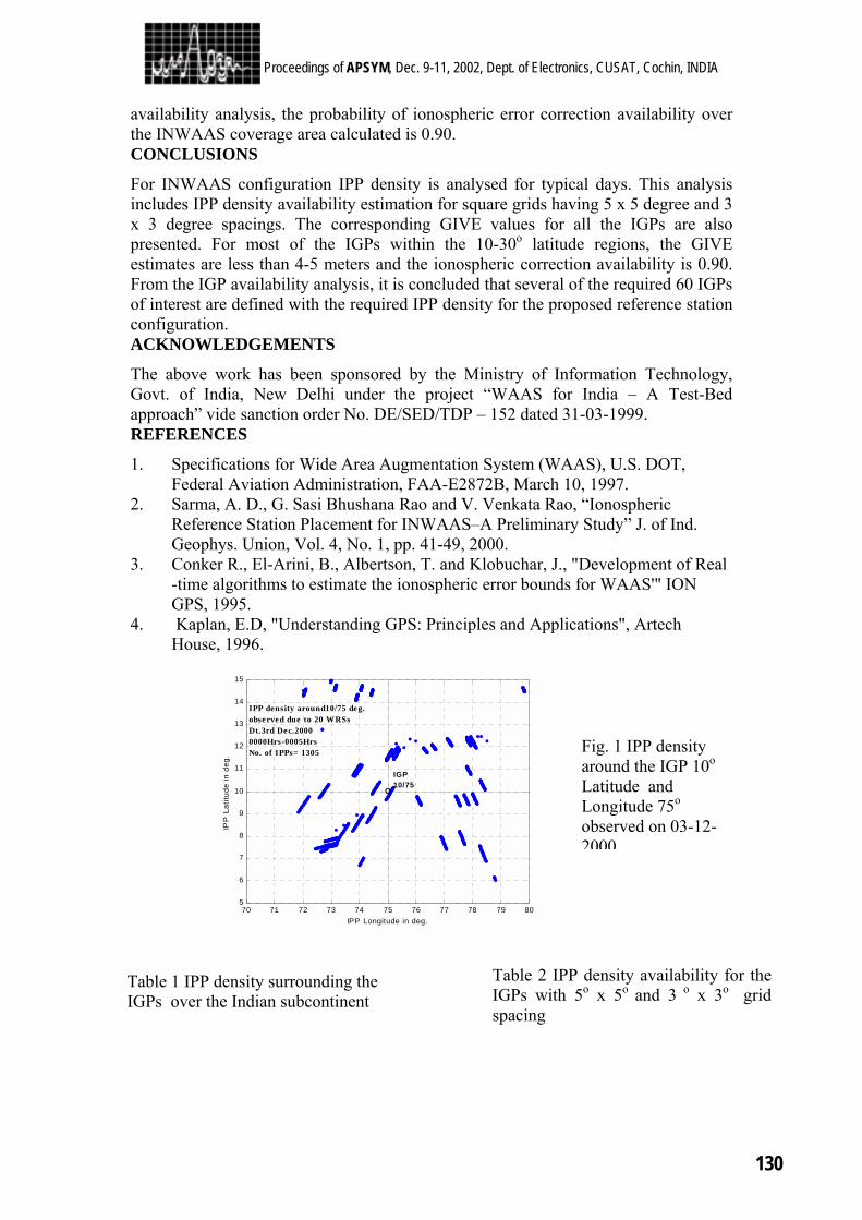
130
Proceedings of APSYM, Dec. 9-11, 2002, Dept. of Electronics, CUSAT, Cochin, INDIA
availability analysis, the probability of ionospheric error correction availability over the INWAAS coverage area calculated is 0.90. CONCLUSIONS
For INWAAS configuration IPP density is analysed for typical days. This analysis includes IPP density availability estimation for square grids having 5 x 5 degree and 3 x 3 degree spacings. The corresponding GIVE values for all the IGPs are also presented. For most of the IGPs within the 10-30o latitude regions, the GIVE estimates are less than 4-5 meters and the ionospheric correction availability is 0.90. From the IGP availability analysis, it is concluded that several of the required 60 IGPs of interest are defined with the required IPP density for the proposed reference station configuration. ACKNOWLEDGEMENTS
The above work has been sponsored by the Ministry of Information Technology, Govt. of India, New Delhi under the project “WAAS for India – A Test-Bed approach” vide sanction order No. DE/SED/TDP – 152 dated 31-03-1999. REFERENCES
1. Specifications for Wide Area Augmentation System (WAAS), U.S. DOT, Federal Aviation Administration, FAA-E2872B, March 10, 1997.
2. Sarma, A. D., G. Sasi Bhushana Rao and V. Venkata Rao, “Ionospheric Reference Station Placement for INWAAS–A Preliminary Study” J. of Ind. Geophys. Union, Vol. 4, No. 1, pp. 41-49, 2000.
3. Conker R., El-Arini, B., Albertson, T. and Klobuchar, J., "Development of Real -time algorithms to estimate the ionospheric error bounds for WAAS'" ION GPS, 1995.
4. Kaplan, E.D, "Understanding GPS: Principles and Applications", Artech House, 1996.
Table 2 IPP density availability for the IGPs with 5o x 5o and 3 o x 3o grid spacing
Table 1 IPP density surrounding the IGPs over the Indian subcontinent
70 71 72 73 74 75 76 77 78 79 805
6
7
8
9
10
11
12
13
14
15
IPP Longitude in deg.
IPP
Lat
itude
in d
eg.
O
IGP10/75
IPP density around10/75 deg.observed due to 20 WRSsDt.3rd Dec.20000000Hrs-0005HrsNo. of IPPs= 1305 Fig. 1 IPP density
around the IGP 10o
Latitude and Longitude 75o observed on 03-12-2000
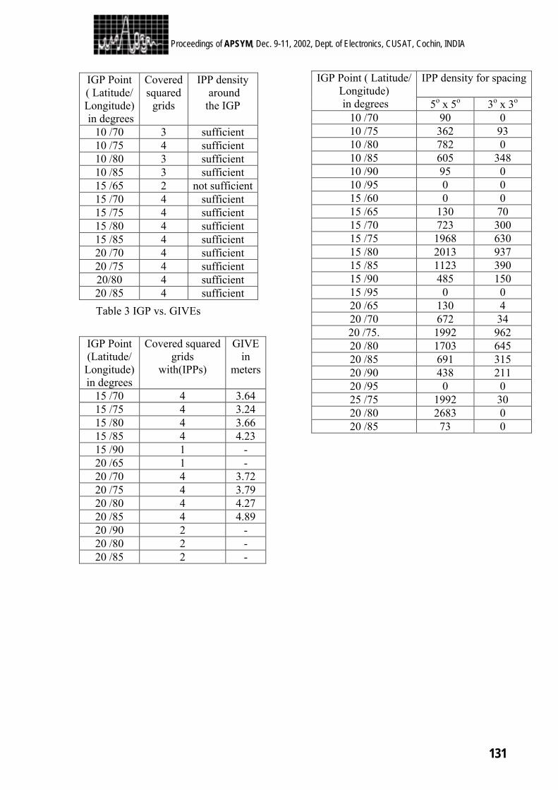
131
Proceedings of APSYM, Dec. 9-11, 2002, Dept. of Electronics, CUSAT, Cochin, INDIA
IGP Point ( Latitude/ Longitude) in degrees
Covered squared
grids
IPP density around the IGP
10 /70 3 sufficient 10 /75 4 sufficient 10 /80 3 sufficient 10 /85 3 sufficient 15 /65 2 not sufficient15 /70 4 sufficient 15 /75 4 sufficient 15 /80 4 sufficient 15 /85 4 sufficient 20 /70 4 sufficient 20 /75 4 sufficient 20/80 4 sufficient 20 /85 4 sufficient
IPP density for spacing
IGP Point ( Latitude/ Longitude) in degrees 5o x 5o 3o x 3o
10 /70 90 0 10 /75 362 93 10 /80 782 0 10 /85 605 348 10 /90 95 0 10 /95 0 0 15 /60 0 0 15 /65 130 70 15 /70 723 300 15 /75 1968 630 15 /80 2013 937 15 /85 1123 390 15 /90 485 150 15 /95 0 0 20 /65 130 4 20 /70 672 34 20 /75. 1992 962 20 /80 1703 645 20 /85 691 315 20 /90 438 211 20 /95 0 0 25 /75 1992 30 20 /80 2683 0 20 /85 73 0
IGP Point (Latitude/ Longitude) in degrees
Covered squared grids
with(IPPs)
GIVE in
meters
15 /70 4 3.64 15 /75 4 3.24 15 /80 4 3.66 15 /85 4 4.23 15 /90 1 - 20 /65 1 - 20 /70 4 3.72 20 /75 4 3.79 20 /80 4 4.27 20 /85 4 4.89 20 /90 2 - 20 /80 2 - 20 /85 2 -
Table 3 IGP vs. GIVEs
132
Proceedings of APSYM, Dec. 9-11, 2002, Dept. of Electronics, CUSAT, Cochin, INDIA
MITIGATION OF MULTIPATH USING SHAPED BEAM SPIRAL ANTENNA
B.Rama Krishna Rao* , A.D.Sarma and Y.Ravi Kumar*
R & T Unit for Navigational Electronics, Osmania University, Hyderabad-500 007, (A.P), India Email: [email protected]
* Defence Electronics Research Laboratory(DLRL), Hyderabad – 500 005, (A.P), India
Multipath is one of the important sources of error in direction finding systems for Electronic Warfare applications. One of the solutions to reduce the multipath is by shaping lower part of the receiving antenna beam. This paper deals with the modeling of ground plane to reduce the lower angle coverage of the cavity backed spiral antenna. This modeling reduces the reflections coming from onboard structure of ship platform or sea surface. Experimental results compare well with theoretical results. Also, this technique can be extended to global positioning system (GPS) antennas.
INTRODUCTION
Multipath is due to interference between direct, reflected and scattered components of incoming signal. The signal from radar will interfere with multipath signals in direction finding (DF) systems for Electronic Warfare applications. In addition to signal received via line-of-sight from the radar, a signal of substantial strength are almost always reflected form the ground, sea surface, vehicle body and/or onboard structures below the receiver antenna affecting the accuracy of the angle of arrival (AOA) of the incoming signal. Similarly the signal received at the GPS antenna via multipath from a satellite cause errors in relative positioning. To mitigate the multipath interference, the antennas are to be designed to reject radio waves arriving from below 250-elevation angle while accepting signals from above. The situation is complex in case of ship borne DF antenna system, wherein the antenna has to operate in a dense environment consisting of many onboard antenna masts. Amplitude comparison in one of the techniques for finding out AOA of the incoming signal. In amplitude comparison DF systems, the signal amplitudes of adjacent antenna elements will be compared. These antenna elements are separated by an angular displacement of α , given by
αααα = 3600/N (1)
Where, N is the number of antenna elements to cover 3600 in azimuth plane. Most of the amplitude comparison DF systems employ spiral antennas as elements. Cavity backed spiral antennas exhibit symmetrical beam widths in both elevation and azimuth planes. One of the solutions to avoid multipath effect on antenna system is by reducing field-of-view in lower part of the radiation pattern. By using a properly designed ground plane below the antenna can effectively reduce the multipath effect.
MULTIPATH SCENARIO
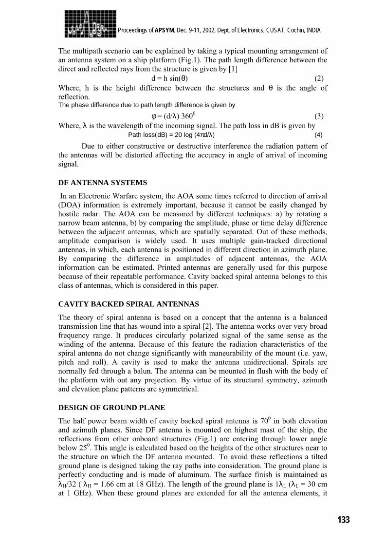
133
Proceedings of APSYM, Dec. 9-11, 2002, Dept. of Electronics, CUSAT, Cochin, INDIA
The multipath scenario can be explained by taking a typical mounting arrangement of an antenna system on a ship platform (Fig.1). The path length difference between the direct and reflected rays from the structure is given by [1] d = h sin(θ) (2) Where, h is the height difference between the structures and θ is the angle of reflection. The phase difference due to path length difference is given by
φ = (d/λ) 3600 (3) Where, λ is the wavelength of the incoming signal. The path loss in dB is given by
Path loss(dB) = 20 log (4πd/λ) (4)
Due to either constructive or destructive interference the radiation pattern of the antennas will be distorted affecting the accuracy in angle of arrival of incoming signal.
DF ANTENNA SYSTEMS
In an Electronic Warfare system, the AOA some times referred to direction of arrival (DOA) information is extremely important, because it cannot be easily changed by hostile radar. The AOA can be measured by different techniques: a) by rotating a narrow beam antenna, b) by comparing the amplitude, phase or time delay difference between the adjacent antennas, which are spatially separated. Out of these methods, amplitude comparison is widely used. It uses multiple gain-tracked directional antennas, in which, each antenna is positioned in different direction in azimuth plane. By comparing the difference in amplitudes of adjacent antennas, the AOA information can be estimated. Printed antennas are generally used for this purpose because of their repeatable performance. Cavity backed spiral antenna belongs to this class of antennas, which is considered in this paper.
CAVITY BACKED SPIRAL ANTENNAS
The theory of spiral antenna is based on a concept that the antenna is a balanced transmission line that has wound into a spiral [2]. The antenna works over very broad frequency range. It produces circularly polarized signal of the same sense as the winding of the antenna. Because of this feature the radiation characteristics of the spiral antenna do not change significantly with maneurability of the mount (i.e. yaw, pitch and roll). A cavity is used to make the antenna unidirectional. Spirals are normally fed through a balun. The antenna can be mounted in flush with the body of the platform with out any projection. By virtue of its structural symmetry, azimuth and elevation plane patterns are symmetrical.
DESIGN OF GROUND PLANE
The half power beam width of cavity backed spiral antenna is 700 in both elevation and azimuth planes. Since DF antenna is mounted on highest mast of the ship, the reflections from other onboard structures (Fig.1) are entering through lower angle below 250. This angle is calculated based on the heights of the other structures near to the structure on which the DF antenna mounted. To avoid these reflections a tilted ground plane is designed taking the ray paths into consideration. The ground plane is perfectly conducting and is made of aluminum. The surface finish is maintained as λH/32 ( λH = 1.66 cm at 18 GHz). The length of the ground plane is 1λL (λL = 30 cm at 1 GHz). When these ground planes are extended for all the antenna elements, it
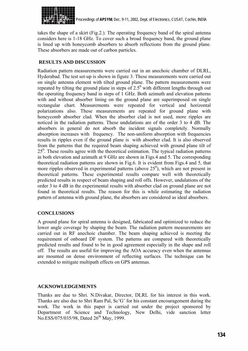
134
Proceedings of APSYM, Dec. 9-11, 2002, Dept. of Electronics, CUSAT, Cochin, INDIA
takes the shape of a skirt (Fig.2.). The operating frequency band of the spiral antenna considers here is 1-18 GHz. To cover such a broad frequency band, the ground plane is lined up with honeycomb absorbers to absorb reflections from the ground plane. These absorbers are made out of carbon particles.
RESULTS AND DISCUSSION
Radiation pattern measurements were carried out in an anechoic chamber of DLRL, Hyderabad. The test set-up is shown in figure 3. These measurements were carried out on single antenna element with tilted ground plane. The pattern measurements were repeated by tilting the ground plane in steps of 2.50 with different lengths through out the operating frequency band in steps of 1 GHz. Both azimuth and elevation patterns with and without absorber lining on the ground plane are superimposed on single rectangular chart. Measurements were repeated for vertical and horizontal polarizations also. These measurements are repeated for ground plane with honeycomb absorber clad. When the absorber clad is not used, more ripples are noticed in the radiation patterns. These undulations are of the order 3 to 4 dB. The absorbers in general do not absorb the incident signals completely. Normally absorption increases with frequency. The non-uniform absorption with frequencies results in ripples even if the ground plane is with absorber clad. It is also observed from the patterns that the required beam shaping achieved with ground plane tilt of 250. These results agree with the theoretical estimation. The typical radiation patterns in both elevation and azimuth at 9 GHz are shown in Figs.4 and 5. The corresponding theoretical radiation patterns are shown in Fig.6. It is evident from Figs.4 and 5, that more ripples observed in experimental patterns (above 250), which are not present in theoretical patterns. These experimental results compare well with theoretically predicted results in respect of beam shaping and roll offs. However, undulations of the order 3 to 4 dB in the experimental results with absorber clad on ground plane are not found in theoretical results. The reason for this is while estimating the radiation pattern of antenna with ground plane, the absorbers are considered as ideal absorbers.
CONCLUSIONS
A ground plane for spiral antenna is designed, fabricated and optimized to reduce the lower angle coverage by shaping the beam. The radiation pattern measurements are carried out in RF anechoic chamber. The beam shaping achieved is meeting the requirement of onboard DF system. The patterns are compared with theoretically predicted results and found to be in good agreement especially in the shape and roll off. The results are useful for improving the AOA accuracy even when the antennas are mounted on dense environment of reflecting surfaces. The technique can be extended to mitigate multipath effects on GPS antennas.
ACKNOWLEDGEMENTS
Thanks are due to Shri. N.Divakar, Director, DLRL for his interest in this work. Thanks are also due to Shri Ram Pal, Sc’G’ for his constant encouragement during the work. The work in this paper is carried out under the project sponsored by Department of Science and Technology, New Delhi, vide sanction letter No.ESS/075/035/98, Dated 26th May, 1999.
135
Proceedings of APSYM, Dec. 9-11, 2002, Dept. of Electronics, CUSAT, Cochin, INDIA
REFERENCES
1. Charles C. Counselman, “ Multipath-rejecting GPS Antennas.” Proceedings of the IEEE, Vol.87, No.1 January,1999.
2. Bawer R and Wolfe J J “The Spiral Antenna.” Aero Geo Astro Corporation, Alexandira, Virginia.
136
Proceedings of APSYM, Dec. 9-11, 2002, Dept. of Electronics, CUSAT, Cochin, INDIA
EFFECT OF BEAMWIDTH ON ADAPTIVE PATH LOSS MODELS FOR MOBILE COMMUNICATIONS
K. Ravindra and A.D. Sarma R&T Unit for Navigational Electronics, Osmania University, Hyderabad-500 007, India
e-mail:[email protected]
Path loss modeling is an essential pre-requisite for optimizing the performance of mobile communication systems. In this paper, three models are proposed to investigate the effect of variation in the beam width of receiving antenna. They are adaptive four coefficient model for antenna beam width variation (AFOCM), adaptive five coefficient model for the combined effect of frequency and antenna beam width (AFICMFB) and adaptive five coefficient model for the combined effect of distance and antenna beam width (AFICMDB). Practical data at three coherent frequencies at microwave and millimeter wave frequencies available in the open literature are used for validating the proposed models. The results are well agreeing with the measurements and the standard deviations are within 4.9 dB at all three frequencies. These models are useful for predicting the path loss at new frequencies and are adaptable to variations in the antenna beam width. INTRODUCTION
In today’s rapid evolution of cellular and telecommunications technology, simulation-based system design and analysis has become the standard. The demand for mobile radio communication services has increased dramatically in recent years and new mobile cellular systems are needed to accommodate more users with limited frequency bandwidth. The successful implementation of these systems requires the exact understanding of electromagnetic wave propagation mechanisms such as path loss. For this purpose, it is important to make path loss models, which can predict propagation characteristics for various environments at different operating frequencies. A wide variety of mobile radio propagation prediction models for different wireless services that specifically address varying propagation environments and operating frequency bands are generally known (Okumura et. al. 1968, Stern et. al. 1997). These models can be generalized, if they are made adaptable to the variations in the operating parameters such as frequency, propagation distance, antenna beam width. In this paper, three adaptive path loss models are proposed, which are adaptable to variations in these parameters. MODEL DESCRIPTION
The present work is related to the development of newer path loss prediction models for mobile communication environments. Keeping in view the ever-changing cellular standards (Stuber, 2001), three adaptive models, which are suitable for microwave and millimeter wave frequencies are proposed. They are adaptive four coefficient model for antenna beam width variation (AFOCM), adaptive five coefficient model for the combined effect of frequency and antenna beam width (AFICMFB) and adaptive five coefficient model for the combined effect of distance and antenna beam width (AFICMDB). The proposed models are based on the deterministic free-space path loss model, adaptive path loss model reported by Stern
137
Proceedings of APSYM, Dec. 9-11, 2002, Dept. of Electronics, CUSAT, Cochin, INDIA
et. al., (1997) and adaptive three coefficient model (ATCM) reported by Ravindra and Sarma (1999). According to ATCM, the path loss P3 in dB is given by,
where, r is the distance between the base station and mobile receiver in meters, f is the carrier frequency in MHz and a0, a1 and a2 are the adaptive coefficient. These are unique to the particular geographical area and represent the characteristics of the environment. ATCM is adaptable to variations in distance and carrier frequency only. Even though, ATCM predicts reasonably well, to generalize the model so that it is adaptable to variation in the antenna beam width, the following models are developed. AFOCM for antenna beam width variation
According to this model, path loss P4bw in dB is given by
where, ‘bw’ represents the half power beam width of the receiving antenna and a0 bw4 , a1 bw4 , a2 bw4 , a3 bw4 are adaptive coefficients. The four coefficients are calculated using the following simultaneous equations which are derived from the partial derivatives of Eq.(2) with respect to the four adaptive coefficients.
)3()(log)(log)(log 410341024101404 ∑ ∑∑∑ =+++ bwbwbwbwbw Pbwafarana
)4()(log)(log)(log
)(log)(log)(log)(log
104101034
1010242
10141004
∑ ∑
∑∑∑=+
++
rPbwra
frarara
bwbw
bwbwbw
)5()(log)(log)(log
)(log)(log)(log)(log
104101034
210241010141004
∑∑
∑∑∑=+
++
fPbwfa
farfafa
bwbw
bwbwbw
)6()(log)(log
)(log)(log)(log)(log)(log
1042
1034
1010241010141004
∑∑
∑∑∑
=+
++
bwPbwa
bwfabwrabwa
bwbw
bwbwbw
n in Eq.(3) represents the number of data points.
AFICM for combined effect of frequency and beam width
The preliminary steps in developing the model are similar to those explained for ATCM. An additional product term is introduced to find out the combined effect of frequency and beam width variation. According to this model, the path loss P5fbw
in dB is given by The five adaptive coefficients a05fbw, a15fbw, a25fbw, a35fbw and a45fbw can be calculated using the five simultaneous equations obtained using the procedure followed in the previous section.
( )1)(log)(log 10210103 faraap ++=
( ) ( ) )2()(logloglog 103410241014044 bwafaraaP bwbwbwbwbw +++=
( ) ( ))7()(log)(log)(log
loglog
1010451035
10251015055
fbwabwafaraaP
fbwfbw
fbwfbwfbwfbw
++
++=
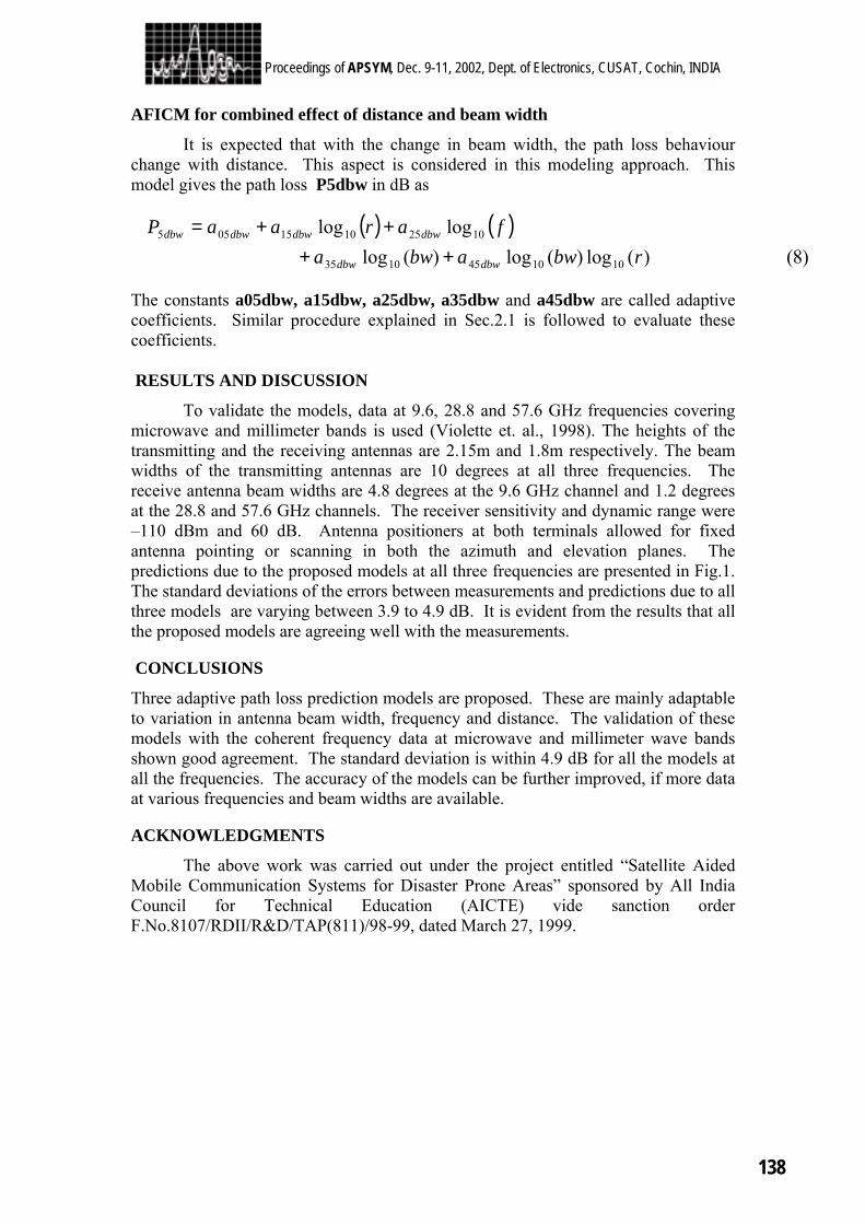
138
Proceedings of APSYM, Dec. 9-11, 2002, Dept. of Electronics, CUSAT, Cochin, INDIA
AFICM for combined effect of distance and beam width
It is expected that with the change in beam width, the path loss behaviour change with distance. This aspect is considered in this modeling approach. This model gives the path loss P5dbw in dB as
The constants a05dbw, a15dbw, a25dbw, a35dbw and a45dbw are called adaptive coefficients. Similar procedure explained in Sec.2.1 is followed to evaluate these coefficients. RESULTS AND DISCUSSION
To validate the models, data at 9.6, 28.8 and 57.6 GHz frequencies covering microwave and millimeter bands is used (Violette et. al., 1998). The heights of the transmitting and the receiving antennas are 2.15m and 1.8m respectively. The beam widths of the transmitting antennas are 10 degrees at all three frequencies. The receive antenna beam widths are 4.8 degrees at the 9.6 GHz channel and 1.2 degrees at the 28.8 and 57.6 GHz channels. The receiver sensitivity and dynamic range were –110 dBm and 60 dB. Antenna positioners at both terminals allowed for fixed antenna pointing or scanning in both the azimuth and elevation planes. The predictions due to the proposed models at all three frequencies are presented in Fig.1. The standard deviations of the errors between measurements and predictions due to all three models are varying between 3.9 to 4.9 dB. It is evident from the results that all the proposed models are agreeing well with the measurements.
CONCLUSIONS
Three adaptive path loss prediction models are proposed. These are mainly adaptable to variation in antenna beam width, frequency and distance. The validation of these models with the coherent frequency data at microwave and millimeter wave bands shown good agreement. The standard deviation is within 4.9 dB for all the models at all the frequencies. The accuracy of the models can be further improved, if more data at various frequencies and beam widths are available. ACKNOWLEDGMENTS
The above work was carried out under the project entitled “Satellite Aided Mobile Communication Systems for Disaster Prone Areas” sponsored by All India Council for Technical Education (AICTE) vide sanction order F.No.8107/RDII/R&D/TAP(811)/98-99, dated March 27, 1999.
( ) ( ))8()(log)(log)(log
loglog
1010451035
10251015055
rbwabwafaraaP
dbwdbw
dbwdbwdbwdbw
++++=
139
Proceedings of APSYM, Dec. 9-11, 2002, Dept. of Electronics, CUSAT, Cochin, INDIA
REFERENCES
1. Okumura Y., E. Ohnori, T. Kawano, and K. Fukuda, “Field Strength and its Variability in VHF and UHF Land Mobile Radio Service”, Rev. Elec. Commun. Lab, Vol. 16, pp. 825 – 873, Sept – Oct. 1968.
2. Stern H.P., Hermes J.G., and Subrahmanyam D., "An Adaptive Propagation Prediction Program for Land Mobile Radio Systems", IEEE Trans. on Broadcasting, BC-43, pp.56-63, March 1997.
3. Stuber G.L., “Principles of Mobile Communication”, 2nd edn., Kluwer Academic Pub., 2001.
4. Ravindra K., A.D. Sarma, “Modeling Path loss in the Near Field Region for cm and mm wave Mobile Communication”, Proc. International conference on Electromagnetic Interference and Compatibility ’99, pp. 79 – 82, Dec. 1999.
5. Violette J.E., Richard H. Espeland, Robert O. DeBolt and Felix Schwering, “Millimeter – Wave Propagation at Street Level in an Urban Environment”, IEEE Trans. On Geoscience and Remote Sensing, Vol. 26, No. 3, pp. 368 – 380, May, 1998.
0 15
-15 -30
10 0
-10 -20 -30
0 0.2 0.4 0.6 0.8 1.0 1.2 1.4 1.6
0 -15 -30 -45
Practical AFOCM AFICMFB
AFICMDB
Distance, km
Path
loss
, dB
f = 9.6 GHz
f = 28.8 GHz
f = 57.6 GHz
Fig.1:Path loss prediction due to proposed models at three coherent frequencies
140
Proceedings of APSYM, Dec. 9-11, 2002, Dept. of Electronics, CUSAT, Cochin, INDIA
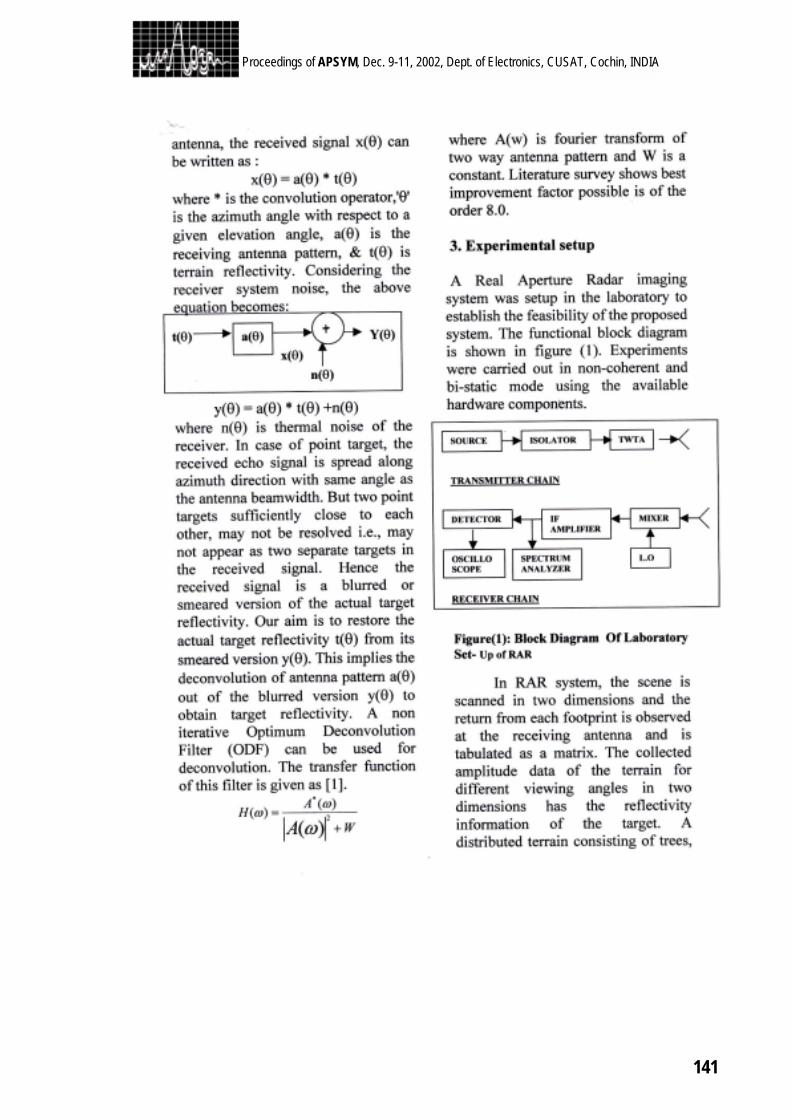
141
Proceedings of APSYM, Dec. 9-11, 2002, Dept. of Electronics, CUSAT, Cochin, INDIA
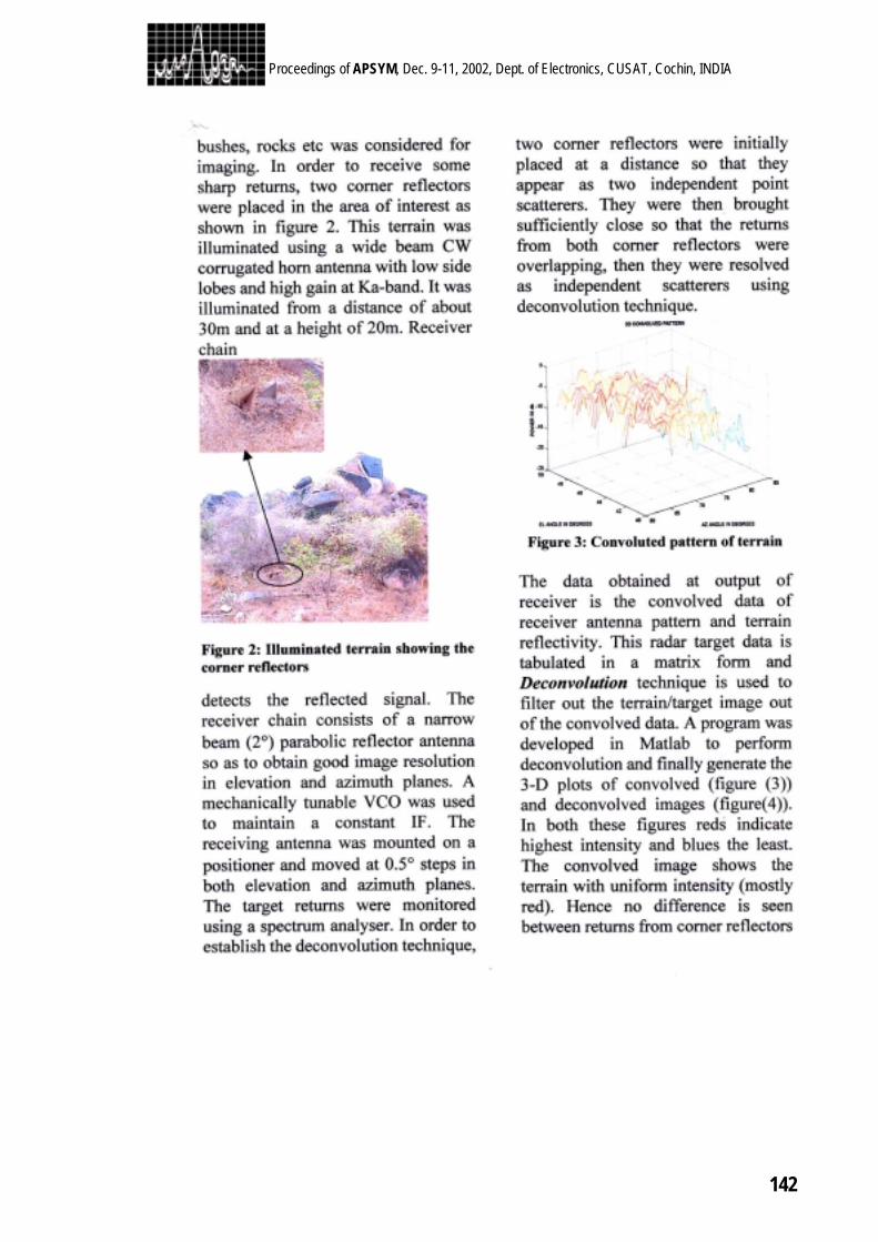
142
Proceedings of APSYM, Dec. 9-11, 2002, Dept. of Electronics, CUSAT, Cochin, INDIA
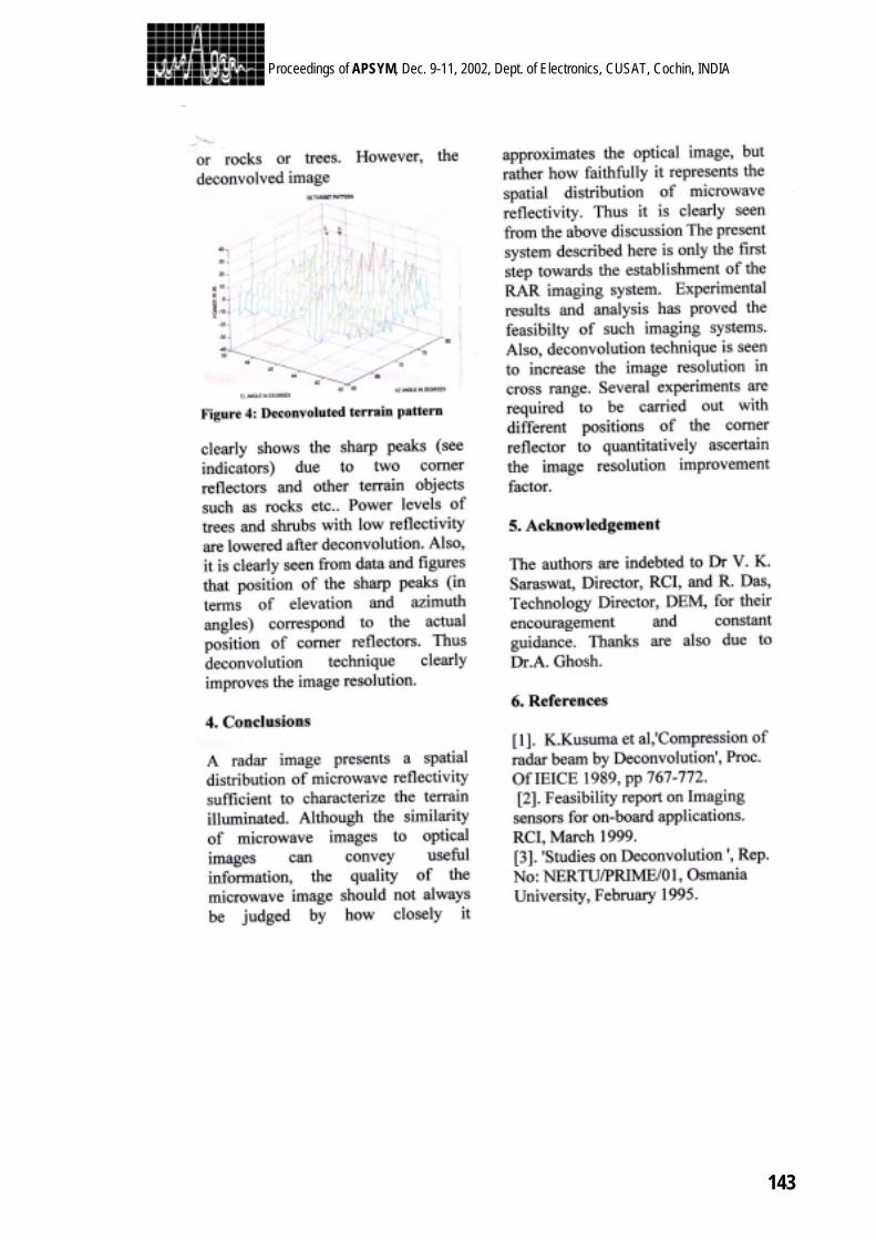
143
Proceedings of APSYM, Dec. 9-11, 2002, Dept. of Electronics, CUSAT, Cochin, INDIA
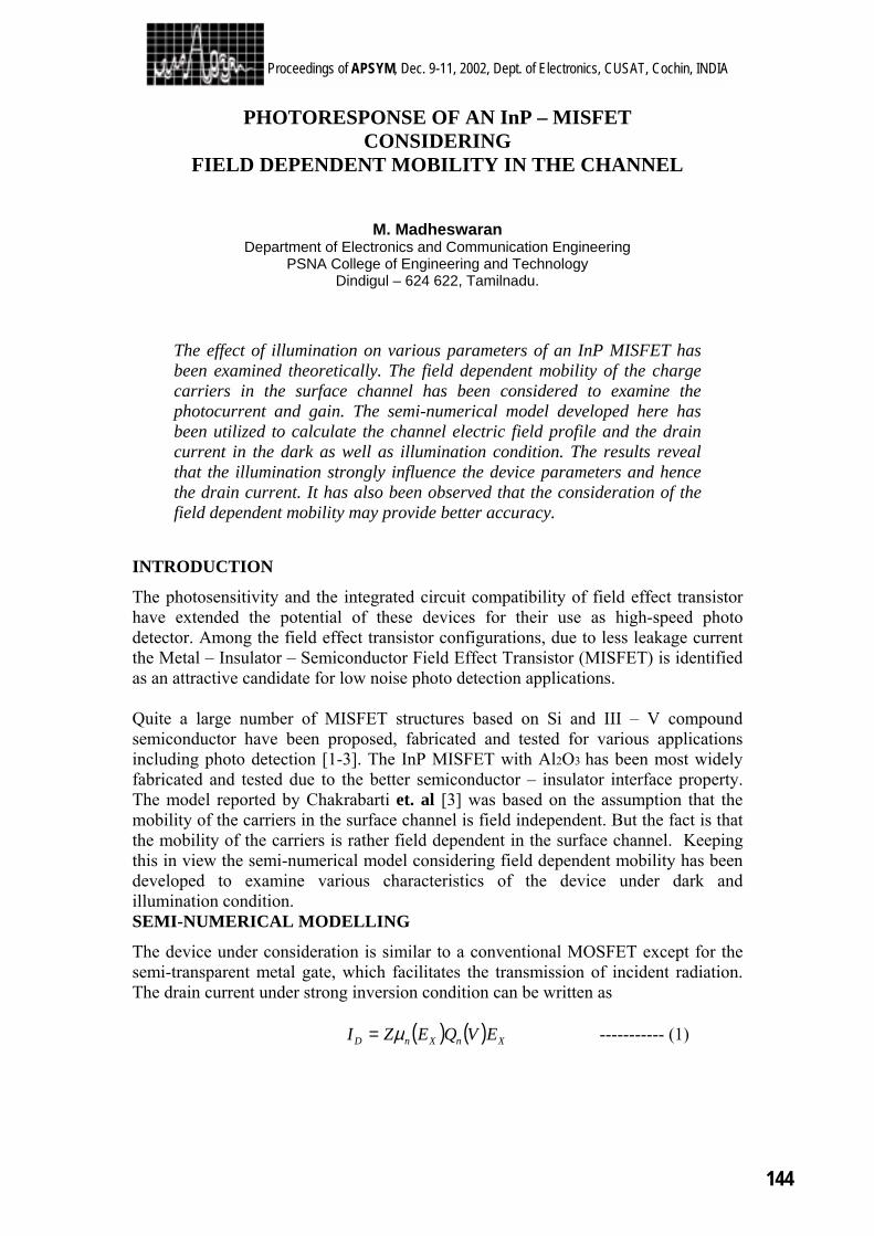
144
Proceedings of APSYM, Dec. 9-11, 2002, Dept. of Electronics, CUSAT, Cochin, INDIA
PHOTORESPONSE OF AN InP – MISFET CONSIDERING
FIELD DEPENDENT MOBILITY IN THE CHANNEL
M. Madheswaran Department of Electronics and Communication Engineering
PSNA College of Engineering and Technology Dindigul – 624 622, Tamilnadu.
The effect of illumination on various parameters of an InP MISFET has been examined theoretically. The field dependent mobility of the charge carriers in the surface channel has been considered to examine the photocurrent and gain. The semi-numerical model developed here has been utilized to calculate the channel electric field profile and the drain current in the dark as well as illumination condition. The results reveal that the illumination strongly influence the device parameters and hence the drain current. It has also been observed that the consideration of the field dependent mobility may provide better accuracy.
INTRODUCTION
The photosensitivity and the integrated circuit compatibility of field effect transistor have extended the potential of these devices for their use as high-speed photo detector. Among the field effect transistor configurations, due to less leakage current the Metal – Insulator – Semiconductor Field Effect Transistor (MISFET) is identified as an attractive candidate for low noise photo detection applications. Quite a large number of MISFET structures based on Si and III – V compound semiconductor have been proposed, fabricated and tested for various applications including photo detection [1-3]. The InP MISFET with Al2O3 has been most widely fabricated and tested due to the better semiconductor – insulator interface property. The model reported by Chakrabarti et. al [3] was based on the assumption that the mobility of the carriers in the surface channel is field independent. But the fact is that the mobility of the carriers is rather field dependent in the surface channel. Keeping this in view the semi-numerical model considering field dependent mobility has been developed to examine various characteristics of the device under dark and illumination condition. SEMI-NUMERICAL MODELLING
The device under consideration is similar to a conventional MOSFET except for the semi-transparent metal gate, which facilitates the transmission of incident radiation. The drain current under strong inversion condition can be written as
( ) ( ) XnXnD EVQEZI µ= ----------- (1)
145
Proceedings of APSYM, Dec. 9-11, 2002, Dept. of Electronics, CUSAT, Cochin, INDIA
Where Z is the channel width, ( )Xn Eµ is the electron mobility in the surface channel
at any point X,
≡dXdVEX being the electric field in the horizontal X- direction,
( )VQn , the electron density per unit area in the surface channel. The field dependent mobility in the channel has been approximated using the velocity electric field profile as
( ) ( ) ( ) 23
12
1 23322X
C
SatCoX
C
SatCooXn E
EVEE
EVEE −++−+= µµµµ ----------- (2)
where oµ is the low field mobility, CE is the critical electric field and 1SatV is the peak velocity [4]. Substituting eqn. (2) in eqn. (1) and integrating from the source to the drain, the drain current is obtained as
( ) ( ) ( )[ ]2
21
02
12
0
322
+−∗+= ∫∫ dVVQE
VELZdVVQ
LZI
DD V
nC
SatCoV
no
Dµµ
( ) ( )( )3
0
31
31
3
23
−∗+ ∫DV
nC
SatCo dVVQE
VELZ µ ----------- (3)
The effect of illumination can be obtained by focusing light on the semi-transparent metal gate. The excess carriers generated due to illumination changes the conductivity of the channel. These changes are accounted for the calculation of the drain current under illumination. The drain current is expected to increase in the illuminated condition. This is due to the fact that the generation of electron-hole pairs increases the conductivity of the channel as well as electron density in the channel. The photo response current is given by
)()min( darkIationilluII DDph −= ----------(4)
)min( ationilluI D is estimated using eqn.(3), considering the necessary equation
taken from [3]. The photocurrent gain M is given by
L
ph
II
M = ----------- (5)
where LI is the primary current and given by
AhvP
qI optL = ----------- (6)
RESULT AND CONCLUSION
Computations have been carried out for InP MISFET photo detector. The standard parameters used for the calculations are taken from [5]. The various device parameters used in the present calculations are listed in the table-1.
Table-1. The device parameters
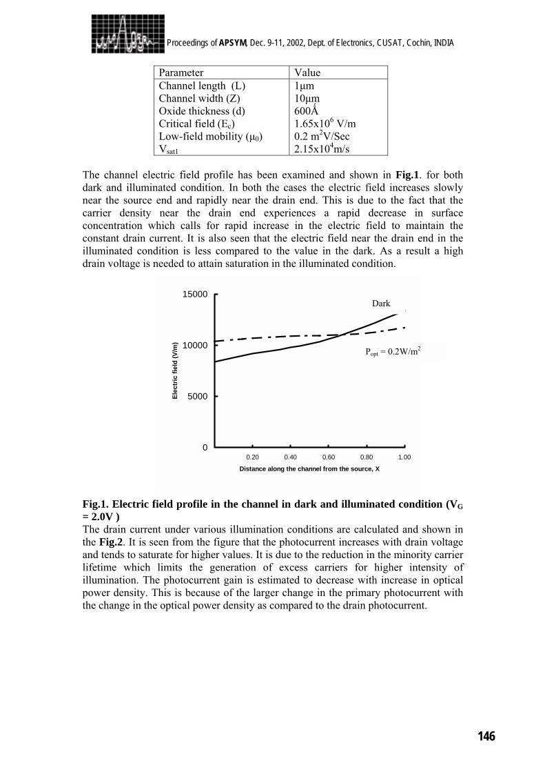
146
Proceedings of APSYM, Dec. 9-11, 2002, Dept. of Electronics, CUSAT, Cochin, INDIA
Parameter Value Channel length (L) Channel width (Z) Oxide thickness (d) Critical field (Ec) Low-field mobility (µ0) Vsat1
1µm 10µm 600Ǻ 1.65x10⁶ V/m 0.2 m2V/Sec 2.15x10⁴m/s
The channel electric field profile has been examined and shown in Fig.1. for both dark and illuminated condition. In both the cases the electric field increases slowly near the source end and rapidly near the drain end. This is due to the fact that the carrier density near the drain end experiences a rapid decrease in surface concentration which calls for rapid increase in the electric field to maintain the constant drain current. It is also seen that the electric field near the drain end in the illuminated condition is less compared to the value in the dark. As a result a high drain voltage is needed to attain saturation in the illuminated condition. Fig.1. Electric field profile in the channel in dark and illuminated condition (VG = 2.0V ) The drain current under various illumination conditions are calculated and shown in the Fig.2. It is seen from the figure that the photocurrent increases with drain voltage and tends to saturate for higher values. It is due to the reduction in the minority carrier lifetime which limits the generation of excess carriers for higher intensity of illumination. The photocurrent gain is estimated to decrease with increase in optical power density. This is because of the larger change in the primary photocurrent with the change in the optical power density as compared to the drain photocurrent.
0
5000
10000
15000
0.20 0.40 0.60 0.80 1.00
Distance along the channel from the source, X
Elec
tric
fiel
d (V
/m)
Dark
Popt = 0.2W/m2
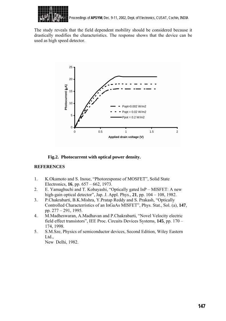
147
Proceedings of APSYM, Dec. 9-11, 2002, Dept. of Electronics, CUSAT, Cochin, INDIA
The study reveals that the field dependent mobility should be considered because it drastically modifies the characteristics. The response shows that the device can be used as high speed detector.
Fig.2. Photocurrent with optical power density.
REFERENCES 1. K.Okamoto and S. Inoue, “Photoresponse of MOSFET”, Solid State
Electronics, 16, pp. 657 – 662, 1973. 2. E. Yamaghuchi and T. Kobayashi, “Optically gated InP – MISFET: A new
high-gain optical detector”, Jap. J. Appl. Phys., 21, pp. 104 – 108, 1982. 3. P.Chakrabarti, B.K.Mishra, Y.Pratap Reddy and S. Prakash, “Optically
Controlled Characterristics of an InGaAs MISFET”, Phys. Stat., Sol. (a), 147, pp. 277 – 291, 1995.
4. M.Madheswaran, A.Madhavan and P.Chakrabarti, “Novel Velocity electric field effect transistors”, IEE Proc. Circuits Devices Systems, 145, pp. 170 – 174, 1998.
5. S.M.Sze, Physics of semiconductor devices, Second Edition, Wiley Eastern Ltd., New Delhi, 1982.
0
5
10
15
20
25
0 0.5 1 1.5 2
Applied drain voltage (V)
Phot
ocur
rent
( µµ µµA
)
Popt=0.002 W/m2
Popt = 0.02 W/m2
Ppot = 0.2 W/m2
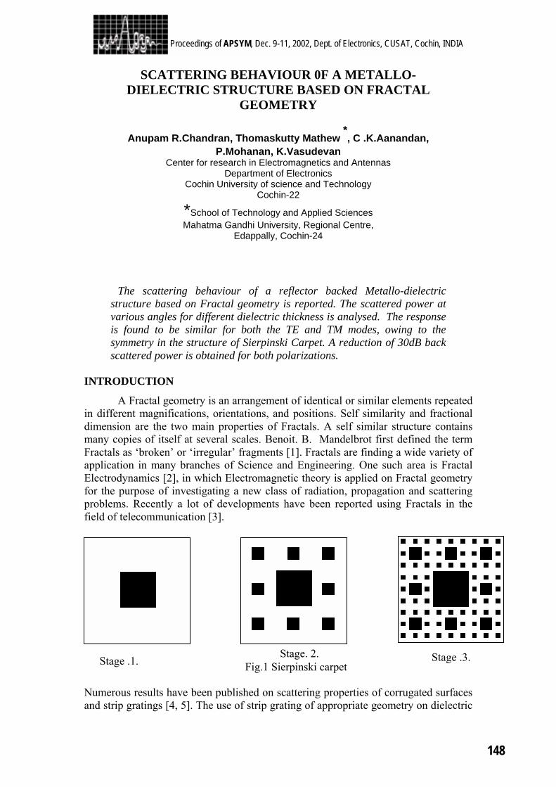
148
Proceedings of APSYM, Dec. 9-11, 2002, Dept. of Electronics, CUSAT, Cochin, INDIA
SCATTERING BEHAVIOUR 0F A METALLO-DIELECTRIC STRUCTURE BASED ON FRACTAL
GEOMETRY
Anupam R.Chandran, Thomaskutty Mathew *, C .K.Aanandan,
P.Mohanan, K.Vasudevan Center for research in Electromagnetics and Antennas
Department of Electronics Cochin University of science and Technology
Cochin-22
*School of Technology and Applied Sciences Mahatma Gandhi University, Regional Centre,
Edappally, Cochin-24
The scattering behaviour of a reflector backed Metallo-dielectric structure based on Fractal geometry is reported. The scattered power at various angles for different dielectric thickness is analysed. The response is found to be similar for both the TE and TM modes, owing to the symmetry in the structure of Sierpinski Carpet. A reduction of 30dB back scattered power is obtained for both polarizations.
INTRODUCTION
A Fractal geometry is an arrangement of identical or similar elements repeated in different magnifications, orientations, and positions. Self similarity and fractional dimension are the two main properties of Fractals. A self similar structure contains many copies of itself at several scales. Benoit. B. Mandelbrot first defined the term Fractals as ‘broken’ or ‘irregular’ fragments [1]. Fractals are finding a wide variety of application in many branches of Science and Engineering. One such area is Fractal Electrodynamics [2], in which Electromagnetic theory is applied on Fractal geometry for the purpose of investigating a new class of radiation, propagation and scattering problems. Recently a lot of developments have been reported using Fractals in the field of telecommunication [3].
Numerous results have been published on scattering properties of corrugated surfaces and strip gratings [4, 5]. The use of strip grating of appropriate geometry on dielectric
Fig.1 Sierpinski carpet Stage .1. Stage. 2. Stage .3.
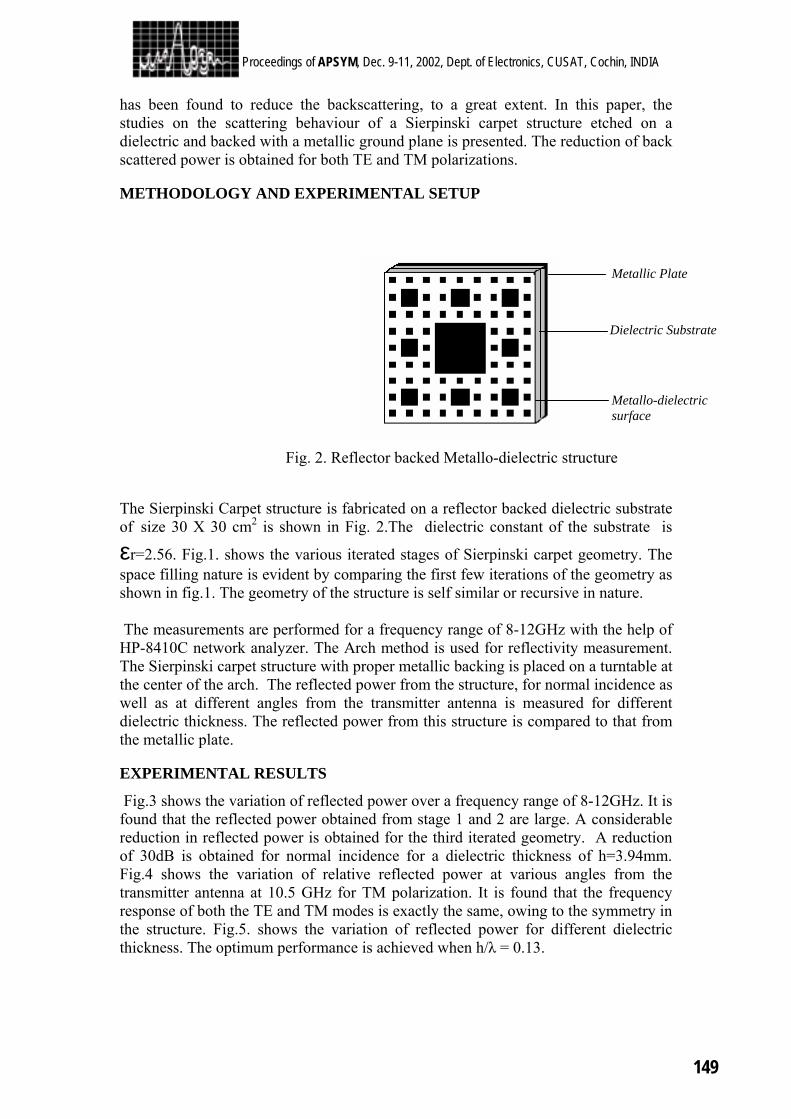
149
Proceedings of APSYM, Dec. 9-11, 2002, Dept. of Electronics, CUSAT, Cochin, INDIA
has been found to reduce the backscattering, to a great extent. In this paper, the studies on the scattering behaviour of a Sierpinski carpet structure etched on a dielectric and backed with a metallic ground plane is presented. The reduction of back scattered power is obtained for both TE and TM polarizations. METHODOLOGY AND EXPERIMENTAL SETUP
The Sierpinski Carpet structure is fabricated on a reflector backed dielectric substrate of size 30 X 30 cm2 is shown in Fig. 2.The dielectric constant of the substrate is
εr=2.56. Fig.1. shows the various iterated stages of Sierpinski carpet geometry. The space filling nature is evident by comparing the first few iterations of the geometry as shown in fig.1. The geometry of the structure is self similar or recursive in nature. The measurements are performed for a frequency range of 8-12GHz with the help of HP-8410C network analyzer. The Arch method is used for reflectivity measurement. The Sierpinski carpet structure with proper metallic backing is placed on a turntable at the center of the arch. The reflected power from the structure, for normal incidence as well as at different angles from the transmitter antenna is measured for different dielectric thickness. The reflected power from this structure is compared to that from the metallic plate. EXPERIMENTAL RESULTS
Fig.3 shows the variation of reflected power over a frequency range of 8-12GHz. It is found that the reflected power obtained from stage 1 and 2 are large. A considerable reduction in reflected power is obtained for the third iterated geometry. A reduction of 30dB is obtained for normal incidence for a dielectric thickness of h=3.94mm. Fig.4 shows the variation of relative reflected power at various angles from the transmitter antenna at 10.5 GHz for TM polarization. It is found that the frequency response of both the TE and TM modes is exactly the same, owing to the symmetry in the structure. Fig.5. shows the variation of reflected power for different dielectric thickness. The optimum performance is achieved when h/λ = 0.13.
Dielectric Substrate
Metallic Plate
Metallo-dielectric surface
Fig. 2. Reflector backed Metallo-dielectric structure
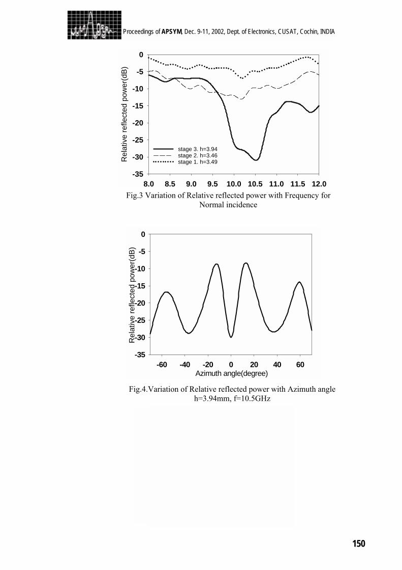
150
Proceedings of APSYM, Dec. 9-11, 2002, Dept. of Electronics, CUSAT, Cochin, INDIA
8.0 8.5 9.0 9.5 10.0 10.5 11.0 11.5 12.0
Rel
ativ
e re
flect
ed p
ower
(dB
)
-35
-30
-25
-20
-15
-10
-5
0
stage 3. h=3.94stage 2. h=3.46stage 1. h=3.49
Fig.3 Variation of Relative reflected power with Frequency for Normal incidence
Azimuth angle(degree)-60 -40 -20 0 20 40 60
Rel
ativ
e re
flect
ed p
ower
(dB
)
-35
-30
-25
-20
-15
-10
-5
0
Fig.4.Variation of Relative reflected power with Azimuth angle h=3.94mm, f=10.5GHz
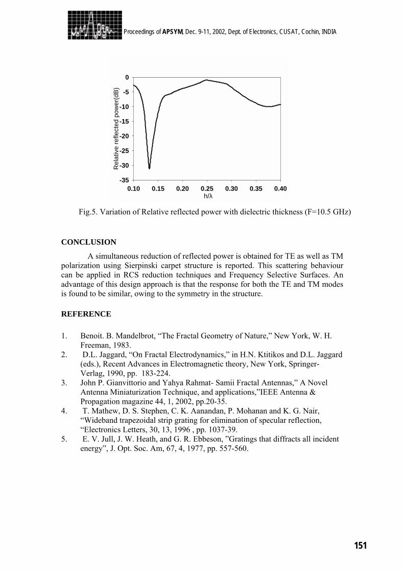
151
Proceedings of APSYM, Dec. 9-11, 2002, Dept. of Electronics, CUSAT, Cochin, INDIA
CONCLUSION
A simultaneous reduction of reflected power is obtained for TE as well as TM polarization using Sierpinski carpet structure is reported. This scattering behaviour can be applied in RCS reduction techniques and Frequency Selective Surfaces. An advantage of this design approach is that the response for both the TE and TM modes is found to be similar, owing to the symmetry in the structure. REFERENCE 1. Benoit. B. Mandelbrot, “The Fractal Geometry of Nature,” New York, W. H.
Freeman, 1983. 2. D.L. Jaggard, “On Fractal Electrodynamics,” in H.N. Ktitikos and D.L. Jaggard
(eds.), Recent Advances in Electromagnetic theory, New York, Springer-Verlag, 1990, pp. 183-224.
3. John P. Gianvittorio and Yahya Rahmat- Samii Fractal Antennas,” A Novel Antenna Miniaturization Technique, and applications,”IEEE Antenna & Propagation magazine 44, 1, 2002, pp.20-35.
4. T. Mathew, D. S. Stephen, C. K. Aanandan, P. Mohanan and K. G. Nair, “Wideband trapezoidal strip grating for elimination of specular reflection, “Electronics Letters, 30, 13, 1996 , pp. 1037-39.
5. E. V. Jull, J. W. Heath, and G. R. Ebbeson, ”Gratings that diffracts all incident energy”, J. Opt. Soc. Am, 67, 4, 1977, pp. 557-560.
h/λ0.10 0.15 0.20 0.25 0.30 0.35 0.40
Rel
ativ
e re
flect
ed p
ower
(dB
)
-35
-30
-25
-20
-15
-10
-5
0
Fig.5. Variation of Relative reflected power with dielectric thickness (F=10.5 GHz)
152
Proceedings of APSYM, Dec. 9-11, 2002, Dept. of Electronics, CUSAT, Cochin, INDIA

153
Proceedings of APSYM, Dec. 9-11, 2002, Dept. of Electronics, CUSAT, Cochin, INDIA
RESEARCH SESSION IV December 9, Monday 2002.(3.30 p.m. to5.30 p.m)
MICROWAVE DEVICES Hall : 1
CHAIRS: DR. G.M. CLEETUS PROF. S.N. JOSHI
4.1
Waffle-Iron Filter For Ground Station Application - Design And Fabrication Aspects A.V.G. Subramanyam, U. Prabhakaran, V. Mahadevan V.K. Lakshmeesha & S. Pal Communication Systems Group, ISRO Satellite Centre, Bangalore-560 017. [email protected]
155
4.2 Design Of 2-Way Equal Power Dividers Using Lumped Elements Subhabindhu Ray & Girish Kumar Department of Electrical Engineering, IIT Bombay, Mumbai-400 076 [email protected]
159
4.3 A 2.0-8.0GHz MMIC Linear Amplifier P.S. Vasu, P. Mohan, P.A. Govindacharyulu Semiconductor Complex Ltd. GAETEC Project, P.O. Vignyana Kancha, Hyderabad-500 069 [email protected]
163
4.4 A DC-12GHz 6-Bit Digital Attenuator Utilizing Monolithic GaAs MESFET Technology Ch. Krishna Veni, P. Mohan Semiconductor Complex Ltd. GAETEC Project, P.O. Vignyana Kancha, Hyderabad-500 069 [email protected]
167
4.5 MMIC Approach to A 6-Bit Digital Phase Shifter for L-Band Transmit/Receive Module Pummy Ratna, P. Mohan, P.A. Govindacharyulu Semiconductor Complex Ltd. GAETEC Project, P.O. Vignyana Kancha, Hyderabad-500 069 [email protected]
171
4.6 Microwave signal and Sensor Design-In Perspective G.R Panda & AK Mallick Ministry of Defence, Govt. of India , DRDO, Interim Test Range, Chandipur P.O, Balasore-756 025
175
4.7 Double Avalanche/Single Drift Silicon Diode – A Prospective Mm-Wave Source For E- Communication S.P. Pati, S.K. Dash and P. Purohit Department of Physics, Sambalpur University, Jyoti Vihar, Burla, Sambalpur–768 019
180
4.8 Velocity Overshoot 2D-effect in Si-MOSFET to use at High-frequency S.K. Achari, S.K. Panigrahi & A.K. Panda NIST, Palur Hills, Berhampur, Orissa-761 008 [email protected]
185
154
Proceedings of APSYM, Dec. 9-11, 2002, Dept. of Electronics, CUSAT, Cochin, INDIA
4.9 Study of Si/Si-Ge Heterojunction DAR IMPATT diode S.R. Pattanaik, J.K. Mishra, I.P .Mishra & G.N. Dash Sambalpur University, Jyotivihar, Burla, Sambalpur – 768 019, Orissa [email protected]
189
4.10 GaN based Gunn diode for THz Signal Generation S.K. Panigrahi & A.K. Panda NIST, Palur Hills, Berhampur, Orissa-761 [email protected]
193
4.11 Genetic Algorithm Based Performance Study Of GaAs And Ino.53 Gao.47 As Quantum Wells In The Microwave & Millimeter Wave Regime A. Karamhar, A. Moi, M.K. Naskar & S.K. Sarkar Dept. of Electronic & Telecommunication Engg. Jadavpur University, Kolkata-32. [email protected]
197
4.12 Design And Development Of 10W C-Band Pulsed Solid State Power Amplifier For High Resolution Synthetic Aperture Radar J. Dhar, S.K. Garg, R.K. Arora, V.H. Bora, S.S. Rana MSTD/MSG, Space Applications Centre, ISRO, DOS, Ahmedabad-380 015. [email protected]
201
4.13 Ku-Band 140 W space TWT for Satellite Communication R.K. Sharma, A. Bera, V. Srivastava Microwave Tubes Area, Central Electronics Engg. Research Institute(CEERI)Pilani-333 031 [email protected]
206
4.14 Ka-Band Whispering Gallery Mode DRO S.L. Badnikar G-FAST, DRDO, New Delhi – 110 011
210
4.15 Design of Rectangular Cavity Resonator for Microwave Heating Applications S.B. Kumar ,P.A. Barnes, G.M.B. Parkes, N. Sibley and G. Bond, Dept of Chemical and Biological Sciences, University of Hudderfield UK
215
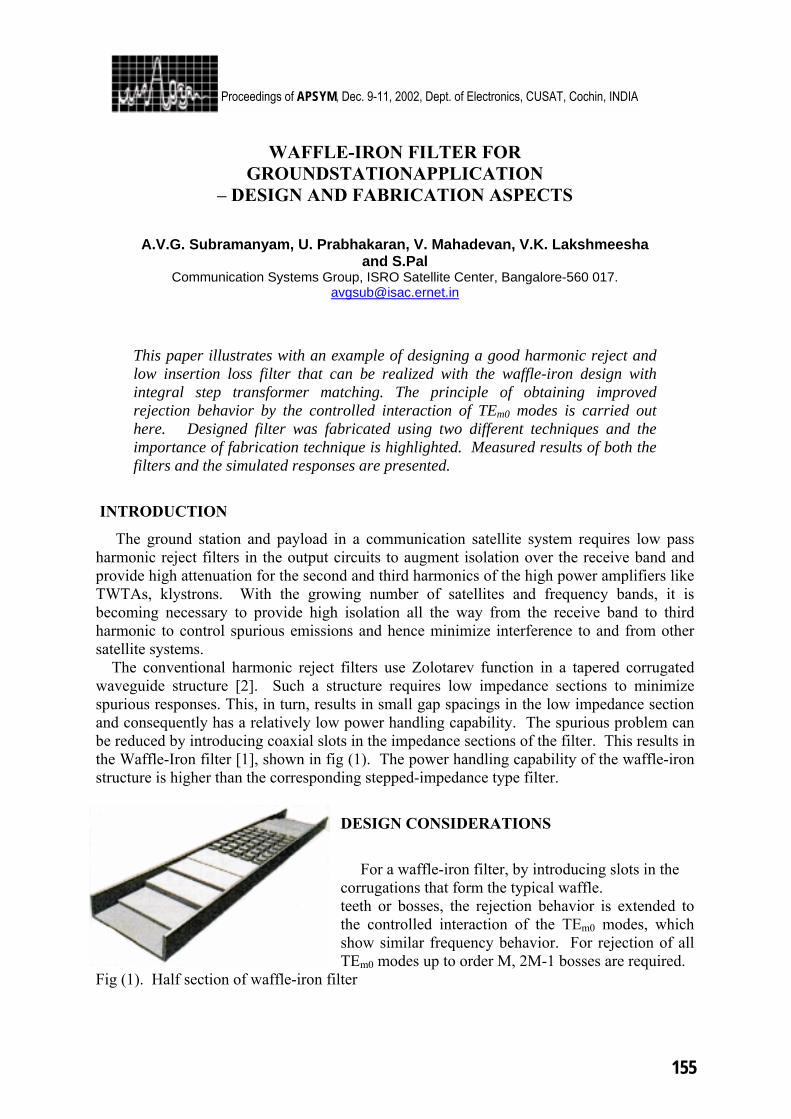
155
Proceedings of APSYM, Dec. 9-11, 2002, Dept. of Electronics, CUSAT, Cochin, INDIA
WAFFLE-IRON FILTER FOR GROUNDSTATIONAPPLICATION
– DESIGN AND FABRICATION ASPECTS
A.V.G. Subramanyam, U. Prabhakaran, V. Mahadevan, V.K. Lakshmeesha and S.Pal
Communication Systems Group, ISRO Satellite Center, Bangalore-560 017. [email protected]
This paper illustrates with an example of designing a good harmonic reject and low insertion loss filter that can be realized with the waffle-iron design with integral step transformer matching. The principle of obtaining improved rejection behavior by the controlled interaction of TEm0 modes is carried out here. Designed filter was fabricated using two different techniques and the importance of fabrication technique is highlighted. Measured results of both the filters and the simulated responses are presented.
INTRODUCTION
The ground station and payload in a communication satellite system requires low pass harmonic reject filters in the output circuits to augment isolation over the receive band and provide high attenuation for the second and third harmonics of the high power amplifiers like TWTAs, klystrons. With the growing number of satellites and frequency bands, it is becoming necessary to provide high isolation all the way from the receive band to third harmonic to control spurious emissions and hence minimize interference to and from other satellite systems. The conventional harmonic reject filters use Zolotarev function in a tapered corrugated waveguide structure [2]. Such a structure requires low impedance sections to minimize spurious responses. This, in turn, results in small gap spacings in the low impedance section and consequently has a relatively low power handling capability. The spurious problem can be reduced by introducing coaxial slots in the impedance sections of the filter. This results in the Waffle-Iron filter [1], shown in fig (1). The power handling capability of the waffle-iron structure is higher than the corresponding stepped-impedance type filter.
DESIGN CONSIDERATIONS
For a waffle-iron filter, by introducing slots in the corrugations that form the typical waffle. teeth or bosses, the rejection behavior is extended to the controlled interaction of the TEm0 modes, which show similar frequency behavior. For rejection of all TEm0 modes up to order M, 2M-1 bosses are required.
Fig (1). Half section of waffle-iron filter
156
Proceedings of APSYM, Dec. 9-11, 2002, Dept. of Electronics, CUSAT, Cochin, INDIA Usually 5 bosses are used which leads to a rejection up to the third harmonic. The critical mode for waffle-iron filters that distorts the rejection quality is the TE01 mode. For symmetrical filters where TE01 is not excited, the upper rejection band is determined mainly by the TE12 and TM12 cutoff frequency of the waffle-section region. Since complete symmetry is difficult to be fabricated, when having high tolerances, the filter should be dimensioned such that the TE01 mode is below cutoff in the waffle-region. If low tolerances can be maintained and extremely good fabrication quality concerning symmetry can be guaranteed, the excitation of the TE01 mode can be neglected, and higher rejection bandwidth is possible. In these filters it is essential that the centre-to-centre spacing of the bosses be no longer than a half of a free-space wavelength at the highest required stop-band frequency. Under these conditions the waffle-iron structure is essentially isotropic and has the same characteristics, at a given frequency, for TEM waves propagating through it in any direction. Thus, since any TEm0 mode can be resolved into TEM waves traveling in different directions through the filter it is seen that the properties of the waffle-iron filter for TEm0 modes are functions of frequency only. This is in contrast to the unslotted corrugated waveguide filters, whose response properties involve guide dimensions and mode numbers also, and are functions of guide wavelength. Incident modes having horizontal components of electric field can excite slot modes that will propagate through the longitudinal slots in the filter at frequencies where the slot height ‘b’ is greater than one half a free-space wavelength. Usually these modes are troublesome only at the highest stop-band frequencies. However, when unslotted step transformers are used to match the waffle-iron filters to the standard height, the reduced height of the stepped transformers effectively suppresses the incident modes with horizontal components of electric field that could otherwise excite slot modes in the filters. For an antenna feed system requirement of a satellite earth station, where we have to pass 3.6-4.2GHz and reject 6.42GHz frequency to an extent of 70dB and above, a waffle-iron filter was designed as shown in fig (1). This was simulated using WASP-NET and its
response is shown in fig (2). This was fabricated, twice, in an aluminum block by precision milling process with 20µm accuracy, as below Case-I :- three pieces – one empty waveguide section and two symmetric blocks each with transformer steps and waffle section which are pushed into the empty guide and fastened with screws to the broader walls. Fig (2). Simulated response on WASP-NET
Case-II :- two pieces - each containing one half waveguide section incorporating the transformer steps and waffle section as an integral piece, along the axis of the filter. A C-band standard waveguide dimension of WR-229 was used to fabricate this filter. The overall length of the filter is 280 mm.
157
Proceedings of APSYM, Dec. 9-11, 2002, Dept. of Electronics, CUSAT, Cochin, INDIA
RESULTS
The filter responses in case-I and case-II above are as shown in fig (3) and fig (4) respectively. Fig (3) shows that the rejection is poor (around 42dB) which is mainly due to the RF mismatch encountered at the junction of first step of the transformer to the propagating guide, which is fastened by screws to the empty guide. Whereas the Fig (4), of case-II filter, shows a good agreement with the simulated response with respect to insertion loss (<0.25dB) in the pass band and rejection (>80dB) upto 12GHz. Fig (3). Measured response of case-I filter The overall improvement in the electrical behavior of the filter obviously
Fig (4). Measured response of case-II filter shows the importance of good fabrication. The above filter is subjected to 500watts of power and found that the filter is working normal.
158
Proceedings of APSYM, Dec. 9-11, 2002, Dept. of Electronics, CUSAT, Cochin, INDIA
CONCLUSIONS
After the case-I filter is fabricated and tested, we simulated the structure again in ANSOFT’s HFSS software, and found the design to be perfect. This made us to suspect the way in which we fabricated the piece. By proper fabrication of the filter as in case-II, we have achieved the required rejection characteristics. Though we tested the filter upto 500 watts, it is expected to withstand for more power. Further by making the waffle-iron filter with circular teeth instead of square teeth the power handling capability can be increased to 1.39 times [1] and by connecting ‘n’ similar filters in parallel, power handling capability can be increased by ‘n‘ times to that of a single filter. ACKNOWLEDGMENT
The authors would like to thank Mr.Radhakrishnan, Mr.Prasad, Mr. Ramakrishna Reddy, Mr.Swaminathan of ISTRAC, and Mr. T.Mallikarjunaiah, ISRO Satellite Centre, Bangalore for their effort in fabrication and testing this Waffle-Iron filter. REFERENCES
1. G.Matthaei, L.Young, E.M.T.Jones, Microwave Filters, Impedance-Matching
Networks, and Coupling Structures. Norwood, MA: Artech House, 1980. 2. Dr.A.M.K.Saad., ”Novel Low pass Harmonic Filters for Satellite Application”, IEEE
MTT-Sym. Dig, 1984.
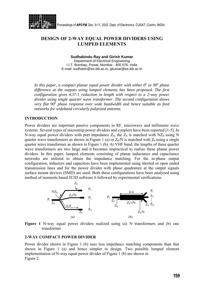
159
Proceedings of APSYM, Dec. 9-11, 2002, Dept. of Electronics, CUSAT, Cochin, INDIA
DESIGN OF 2-WAY EQUAL POWER DIVIDERS USING LUMPED ELEMENTS
Sudhabindu Ray and Girish Kumar
Department of Electrical Engineering I.I.T. Bombay, Powai, Mumbai - 400 076, India
E-mail: [email protected], [email protected]
In this paper, a compact planar equal power divider with either 0o or 90o phase difference at the outputs using lumped elements has been proposed. The first configuration gives 4.37:1 reduction in length with respect to a 2-way power divider using single quarter wave transformer. The second configuration shows very flat 90o phase response over wide bandwidth and hence suitable as feed networks for wideband circularly polarized antenna.
INTRODUCTION
Power dividers are important passive components in RF, microwave and millimeter wave systems. Several types of microstrip power dividers and couplers have been reported [1-5]. In N-way equal power dividers with port impedance Z0, the Z0 is matched with NZ0 using N quarter wave transformers as shown in Figure 1 (a) or Z0/N is matched with Z0 using a single quarter wave transformer as shown in Figure 1 (b). At VHF band, the lengths of these quarter wave transformers are two large and it becomes impractical to realize these planar power dividers. In this paper, lumped elements consisting of planar inductance and capacitance networks are utilized to obtain the impedance matching. For the in-phase output configuration, inductors and capacitors have been implemented using shorted or open ended transmission lines and for the power divider with phase quadrature at the output signals surface mount devices (SMD) are used. Both these configurations have been analyzed using method of moments based IE3D software 6 followed by experimental verifications.
Figure 1 N-way equal power dividers realized using (a) N transformers and (b) one
transformer 2-WAY COMPACT POWER DIVIDER
Power divider shown in Figure 1 (b) uses less impedance matching components than that shown in Figure 1 (a) and hence simpler to design. Two possible lumped element implementation of N-way equal power divider of Figure 1 (b) are shown in Figure 2.
Z0
NZ0
Z0
P1
P2
PN
Z0
Pi
P1
P2
PN Z0
Z0
Z0
Z0/N
Pi
(b) (a)
λ/4
λ/4 Z0√N
Z0/√N

160
Proceedings of APSYM, Dec. 9-11, 2002, Dept. of Electronics, CUSAT, Cochin, INDIA
Figure 2 N-way equal power dividers using lumped element (a) series inductor and parallel
capacitor and (b) series capacitor and parallel inductor
For a N-way equal power divider shown in
Figure 2 (a) with N = 2, the values of ZL and ZC (impedances due to the inductor and capacitor respectively) are given by ZL/Z0 = + 0.5 j (1) ZC/Z0 = – j (2) Which gives, L = 0.5Z0/ω = 0.0796 Z0/fc and C = (ωZ0)–1 = 0.159 (fcZ0)–1 where, L is the inductance in Henry, C is the capacitance in Farad and fc is the center frequency in Hz.Similarly, for a N-way equal power divider shown in Figure 2 (b) with N = 2, ZL/Z0 = + j (3) ZC/Z0 = – 0.5 j (4) Though both these power dividers are realizable using chip inductors and capacitors, planar microstrip realization is convenient for the first type where the inductor and capacitor is connected in series and parallel, respectively. Planar realization of a lumped element power divider is designed for low cost glass epoxy substrate (∈ r = 4.3, h = 1.59 mm and tanδ = 0.02). At the center frequency of fc = 170 MHz the entire circuit fits within 100 × 50 mm2 as shown in Figure 3. A 10 Ω line of length l1 is cascaded with a 125 Ω line of length l2 to obtain the impedance matching. The thick 10 Ω line behaves like a shunt capacitance and the thin 125 Ω line acts as a series inductance. The lengths of the transmission line sections are approximately calculated using the formulae given below: l1 = (λ/2π) sin–1(2πfcCZ0C) (5) l2 = (λ/2π) sin–1(2πfcL/Z0L) (6) where, Z0C and Z0L are the characteristic impedances of the thick and thin lines, respectively. The photograph of the fabricated configuration and its dimensions are shown in Figure 3. Theoretical and experimental S-parameters vs. frequency curves for the above lumped 2-way power divider are shown in
L
C Pi
P1
P2
PN (a)
LPi
P1
P2
PN
(b)
C
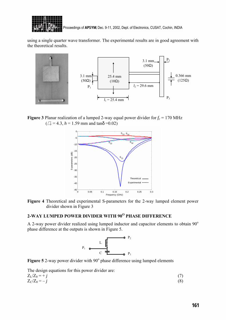
161
Proceedings of APSYM, Dec. 9-11, 2002, Dept. of Electronics, CUSAT, Cochin, INDIA
0 0.05 0.1 0.15 0.2 0.25 0.3-45
-40
-35
-30
-25
-20
-15
-10
-5
0
Frequency (GHz)
S-p
aram
eter
s (d
B)
Theoretical
Experimental
S21
S22 S32
S11
, S31
using a single quarter wave transformer. The experimental results are in good agreement with the theoretical results.
Figure 3 Planar realization of a lumped 2-way equal power divider for fc = 170 MHz (∈ r = 4.3, h = 1.59 mm and tanδ =0.02)
Figure 4 Theoretical and experimental S-parameters for the 2-way lumped element power
divider shown in Figure 3 2-WAY LUMPED POWER DIVIDER WITH 90O PHASE DIFFERENCE
A 2-way power divider realized using lumped inductor and capacitor elements to obtain 90o phase difference at the outputs is shown in Figure 5.
Figure 5 2-way power divider with 90o phase difference using lumped elements
The design equations for this power divider are: ZL/Z0 = + j (7) ZC/Z0 = – j (8)
L
C P1
P2
P3
P1
P2
P3
25.4 mm(10Ω)
l1 = 25.4 mm
l2 = 29.6 mm
0.366 mm (125Ω)
3.1 mm (50Ω)
3.1 mm (50Ω)
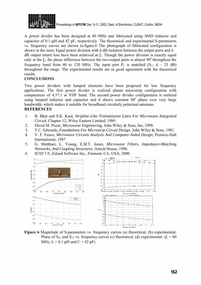
162
Proceedings of APSYM, Dec. 9-11, 2002, Dept. of Electronics, CUSAT, Cochin, INDIA A power divider has been designed at 80 MHz and fabricated using SMD inductor and capacitor of 0.1 µH and 42 pF, respectively. The theoretical and experimental S-parameters vs. frequency curves are shown in.figure.6 The photograph of fabricated configuration is shown in the inset. Equal power division with 6 dB isolation between the output ports and 6 dB output return loss have been achieved at fc. Though the power division is exactly equal only at the fc, the phase difference between the two-output ports is almost 90o
throughout the frequency band from 40 to 120 MHz. The input port P1 is matched (S11 ≤ – 25 dB) throughout the range. The experimental results are in good agreement with the theoretical results. CONCLUSIONS
Two power dividers with lumped elements have been proposed for low frequency applications. The first power divider is realized planar microstrip configuration with compactness of 4.37:1 at VHF band. The second power divider configuration is realized using lumped inductor and capacitor and it shows constant 90o phase over very large bandwidth, which makes it suitable for broadband circularly polarized antennas. REFERENCES
1. B. Bhat and S.K. Kaul, Stripline-Like Transmission Lines For Microwave Integrated Circuit, Chapter 12, Wiley Eastern Limited, 1989.
2. David M. Pozar, Microwave Engineering, John Wiley & Sons, Inc, 1998. 3. T.C. Edwards, Foundations For Microstrip Circuit Design, John Wiley & Sons, 1981. 4. V. F. Fusco, Microwave Circuits Analysis And Computer-Aided Design, Prentice-Hall
International, 1987 5. G. Matthaei, L. Young, E.M.T. Jones, Microwave Filters, Impedance-Matching
Networks, And Coupling Structures, Artech House, 1980. 6. IE3D 7.0, Zeland Software Inc., Fremont, CA, USA, 2000.
Figure 6 Magnitude of S-parameters vs. frequency curves (a) theoretical, (b) experimental.
Phase of S21 and S31 vs. frequency curves (c) theoretical, (d) experimental. (fc = 80 MHz, L = 0.1 µH and C = 42 pF)
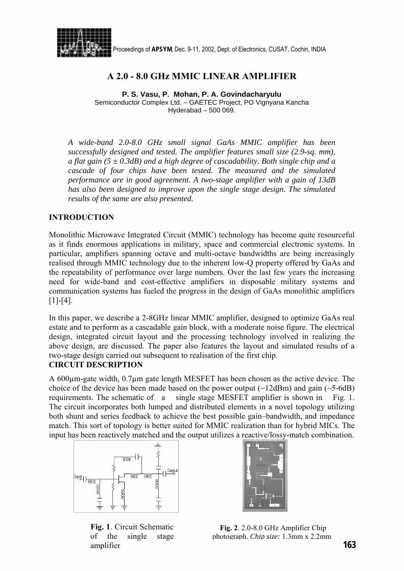
163
Proceedings of APSYM, Dec. 9-11, 2002, Dept. of Electronics, CUSAT, Cochin, INDIA
Fig. 1. Circuit Schematic of the single stage amplifier
Fig. 2. 2.0-8.0 GHz Amplifier Chip photograph. Chip size: 1.3mm x 2.2mm
A 2.0 - 8.0 GHz MMIC LINEAR AMPLIFIER
P. S. Vasu, P. Mohan, P. A. Govindacharyulu Semiconductor Complex Ltd. – GAETEC Project, PO Vignyana Kancha
Hyderabad – 500 069.
A wide-band 2.0-8.0 GHz small signal GaAs MMIC amplifier has been successfully designed and tested. The amplifier features small size (2.9-sq. mm), a flat gain (5 ± 0.3dB) and a high degree of cascadability. Both single chip and a cascade of four chips have been tested. The measured and the simulated performance are in good agreement. A two-stage amplifier with a gain of 13dB has also been designed to improve upon the single stage design. The simulated results of the same are also presented.
INTRODUCTION
Monolithic Microwave Integrated Circuit (MMIC) technology has become quite resourceful as it finds enormous applications in military, space and commercial electronic systems. In particular, amplifiers spanning octave and multi-octave bandwidths are being increasingly realised through MMIC technology due to the inherent low-Q property offered by GaAs and the repeatability of performance over large numbers. Over the last few years the increasing need for wide-band and cost-effective amplifiers in disposable military systems and communication systems has fueled the progress in the design of GaAs monolithic amplifiers [1]-[4].
In this paper, we describe a 2-8GHz linear MMIC amplifier, designed to optimize GaAs real estate and to perform as a cascadable gain block, with a moderate noise figure. The electrical design, integrated circuit layout and the processing technology involved in realizing the above design, are discussed. The paper also features the layout and simulated results of a two-stage design carried out subsequent to realisation of the first chip. CIRCUIT DESCRIPTION
A 600µm-gate width, 0.7µm gate length MESFET has been chosen as the active device. The choice of the device has been made based on the power output (~12dBm) and gain (~5-6dB) requirements. The schematic of a single stage MESFET amplifier is shown in Fig. 1. The circuit incorporates both lumped and distributed elements in a novel topology utilizing both shunt and series feedback to achieve the best possible gain–bandwidth, and impedance match. This sort of topology is better suited for MMIC realization than for hybrid MICs. The input has been reactively matched and the output utilizes a reactive/lossy-match combination.
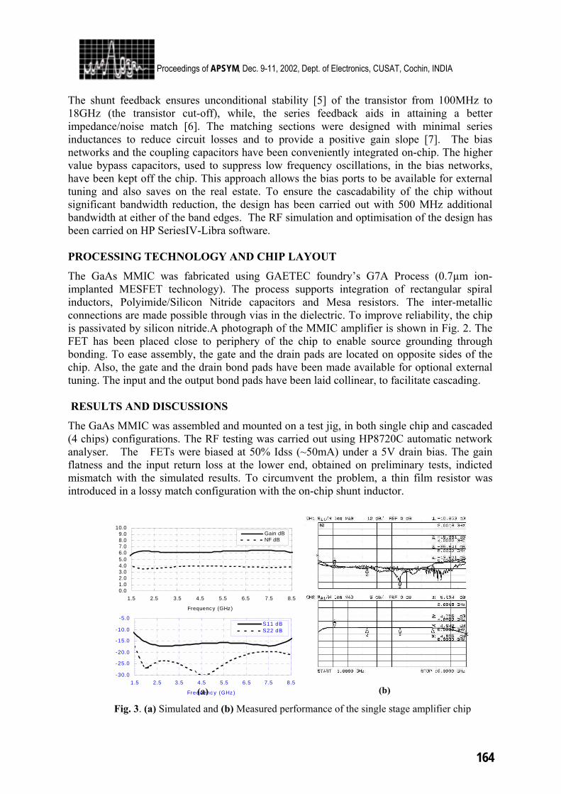
164
Proceedings of APSYM, Dec. 9-11, 2002, Dept. of Electronics, CUSAT, Cochin, INDIA
0.01.02.03.04.05.06.07.08.09.0
10.0
1.5 2.5 3.5 4.5 5.5 6.5 7.5 8.5
Frequency (GHz)
Gain dBNF dB
-30.0
-25.0
-20.0
-15.0
-10.0
-5.0
1.5 2.5 3.5 4.5 5.5 6.5 7.5 8.5
Frequenc y (GHz )
S11 dBS22 dB
The shunt feedback ensures unconditional stability [5] of the transistor from 100MHz to 18GHz (the transistor cut-off), while, the series feedback aids in attaining a better impedance/noise match [6]. The matching sections were designed with minimal series inductances to reduce circuit losses and to provide a positive gain slope [7]. The bias networks and the coupling capacitors have been conveniently integrated on-chip. The higher value bypass capacitors, used to suppress low frequency oscillations, in the bias networks, have been kept off the chip. This approach allows the bias ports to be available for external tuning and also saves on the real estate. To ensure the cascadability of the chip without significant bandwidth reduction, the design has been carried out with 500 MHz additional bandwidth at either of the band edges. The RF simulation and optimisation of the design has been carried on HP SeriesIV-Libra software. PROCESSING TECHNOLOGY AND CHIP LAYOUT
The GaAs MMIC was fabricated using GAETEC foundry’s G7A Process (0.7µm ion-implanted MESFET technology). The process supports integration of rectangular spiral inductors, Polyimide/Silicon Nitride capacitors and Mesa resistors. The inter-metallic connections are made possible through vias in the dielectric. To improve reliability, the chip is passivated by silicon nitride.A photograph of the MMIC amplifier is shown in Fig. 2. The FET has been placed close to periphery of the chip to enable source grounding through bonding. To ease assembly, the gate and the drain pads are located on opposite sides of the chip. Also, the gate and the drain bond pads have been made available for optional external tuning. The input and the output bond pads have been laid collinear, to facilitate cascading. RESULTS AND DISCUSSIONS
The GaAs MMIC was assembled and mounted on a test jig, in both single chip and cascaded (4 chips) configurations. The RF testing was carried out using HP8720C automatic network analyser. The FETs were biased at 50% Idss (~50mA) under a 5V drain bias. The gain flatness and the input return loss at the lower end, obtained on preliminary tests, indicted mismatch with the simulated results. To circumvent the problem, a thin film resistor was introduced in a lossy match configuration with the on-chip shunt inductor. Fig. 3. (a) Simulated and (b) Measured performance of the single stage amplifier chip
(a) (b)
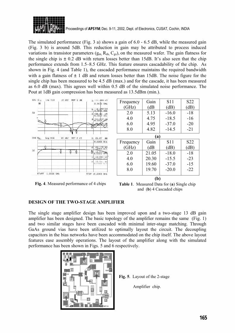
165
Proceedings of APSYM, Dec. 9-11, 2002, Dept. of Electronics, CUSAT, Cochin, INDIA The simulated performance (Fig. 3 a) shows a gain of 6.0 - 6.5 dB, while the measured gain (Fig. 3 b) is around 5dB. This reduction in gain may be attributed to process induced variations in transistor parameters (gm, Rds, Cgs), on the measured wafer. The gain flatness for the single chip is ± 0.2 dB with return losses better than 15dB. It’s also seen that the chip performance extends from 1.5–8.5 GHz. This feature ensures cascadability of the chip. As shown in Fig. 4 (and Table 1), the cascaded performance maintains the required bandwidth with a gain flatness of ± 1 dB and return losses better than 15dB. The noise figure for the single chip has been measured to be 4.5 dB (max.) and for the cascade, it has been measured as 6.0 dB (max). This agrees well within 0.5 dB of the simulated noise performance. The Pout at 1dB gain compression has been measured as 13.5dBm (min.).
DESIGN OF THE TWO-STAGE AMPLIFIER The single stage amplifier design has been improved upon and a two-stage 13 dB gain amplifier has been designed. The basic topology of the amplifier remains the same (Fig. 1) and two similar stages have been cascaded with minimal inter-stage matching. Through GaAs ground vias have been utilized to optimally layout the circuit. The decoupling capacitors in the bias networks have been accommodated on the chip itself. The above layout features ease assembly operations. The layout of the amplifier along with the simulated performance has been shown in Figs. 5 and 6 respectively.
Fig. 4. Measured performance of 4 chips Table 1. Measured Data for (a) Single chip and (b) 4 Cascaded chips
Frequency (GHz)
Gain (dB
S11 (dB)
S22 (dB)
2.0 4.0 6.0 8.0
5.13 4.75 4.95 4.82
-16.0 -18.5 -37.0 -14.5
-18 -16 -20 -21
(a) Frequency
(GHz) Gain (dB
S11 (dB)
S22 (dB)
2.0 4.0 6.0 8.0
21.05 20.30 19.60 19.70
-18.0 -15.5 -37.0 -20.0
-18 -23 -15 -22
(b)
Fig. 5. Layout of the 2-stage
Amplifier chip.
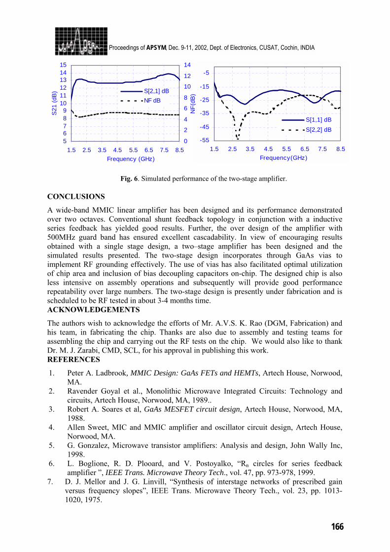
166
Proceedings of APSYM, Dec. 9-11, 2002, Dept. of Electronics, CUSAT, Cochin, INDIA
CONCLUSIONS
A wide-band MMIC linear amplifier has been designed and its performance demonstrated over two octaves. Conventional shunt feedback topology in conjunction with a inductive series feedback has yielded good results. Further, the over design of the amplifier with 500MHz guard band has ensured excellent cascadability. In view of encouraging results obtained with a single stage design, a two–stage amplifier has been designed and the simulated results presented. The two-stage design incorporates through GaAs vias to implement RF grounding effectively. The use of vias has also facilitated optimal utilization of chip area and inclusion of bias decoupling capacitors on-chip. The designed chip is also less intensive on assembly operations and subsequently will provide good performance repeatability over large numbers. The two-stage design is presently under fabrication and is scheduled to be RF tested in about 3-4 months time. ACKNOWLEDGEMENTS
The authors wish to acknowledge the efforts of Mr. A.V.S. K. Rao (DGM, Fabrication) and his team, in fabricating the chip. Thanks are also due to assembly and testing teams for assembling the chip and carrying out the RF tests on the chip. We would also like to thank Dr. M. J. Zarabi, CMD, SCL, for his approval in publishing this work. REFERENCES
1. Peter A. Ladbrook, MMIC Design: GaAs FETs and HEMTs, Artech House, Norwood, MA.
2. Ravender Goyal et al., Monolithic Microwave Integrated Circuits: Technology and circuits, Artech House, Norwood, MA, 1989..
3. Robert A. Soares et al, GaAs MESFET circuit design, Artech House, Norwood, MA, 1988.
4. Allen Sweet, MIC and MMIC amplifier and oscillator circuit design, Artech House, Norwood, MA.
5. G. Gonzalez, Microwave transistor amplifiers: Analysis and design, John Wally Inc, 1998.
6. L. Boglione, R. D. Plooard, and V. Postoyalko, “Rn circles for series feedback amplifier ”, IEEE Trans. Microwave Theory Tech., vol. 47, pp. 973-978, 1999.
7. D. J. Mellor and J. G. Linvill, “Synthesis of interstage networks of prescribed gain versus frequency slopes”, IEEE Trans. Microwave Theory Tech., vol. 23, pp. 1013-1020, 1975.
-55
-45
-35
-25
-15
-5
1.5 2.5 3.5 4.5 5.5 6.5 7.5 8.5Frequency(GHz)
S[1,1] dBS[2,2] dB
56789
101112131415
1.5 2.5 3.5 4.5 5.5 6.5 7.5 8.5Frequency (GHz)
S21
(dB
)
0
2
4
6
8
10
12
14
NF(
dB)S[2,1] dB
NF dB
Fig. 6. Simulated performance of the two-stage amplifier.
167
Proceedings of APSYM, Dec. 9-11, 2002, Dept. of Electronics, CUSAT, Cochin, INDIA
A DC– 12 GHz 6-Bit Digital Attenuator Utilizing Monolithic GaAs Mesfet Technology
Ch. Krishna Veni and P. Mohan
Semiconductor Complex Ltd –GAETEC Project, PO Vignayana Kancha Post,
Hyderabad-500069. Email : [email protected]
An ultra BroadBand 6-Bit Attenuator has been designed using Monolithic approach.G7S process of 0.7 micron gate length ion implanted Mesfet technology has been used in realizing the chip at GAETEC foundry.The schematic and layout are presented. The topology employs suitable combination of Mesfets and resistors to get the required attenuation for each bit. The Attenuator provides minimum reference state insertion Loss of less than 5 dB at 12GHz.The chip provides attenuation in the range of 0.5-31.5 dB in steps of 0.5dB.The I/P and O/P VSWR of the attenuator is better than 1.8:1 over all attenuation states in the entire band. The simulated results have been presented in the paper.
INTRODUCTION
The development of Digital Attenuators using monolithic GaAs approach rather than the hybrid pin diode approach has several advantages like reduced size, better tracking, minimum insertion loss, fast switching speeds and least power consumption. The bits are realized using T, Π and bridged T networks with impedance matching conditions employing proper Mesfet and resistor combination. The choice of Mesfets and resistors is dependent on the trade off between insertion loss and phase variation. The design strategy and the characteristics of the Digital Attenuator are described in subsequent sections. DESIGN OF 6-BIT DIGITAL ATTENUATOR
DC-12 GHz 6 bit Digital Attenuator has been designed for the following specifications.
Specifications:
Freq Range : Dc–12GHz No. of bits : 6 Attenuation Range : 0.5–31.5dB Attenuation Step : 0.5 dB Attenuation Accuracy :+ 0.5dB + 3% of setting Insertion Loss :5dB max Loss Tracking : + 0.5dB VSWR : 1.8 : 1 Switching Speed : 50nsec max The design philosophy and methodology employed for the DC –12 GHz Digital Attenuator is discussed below.
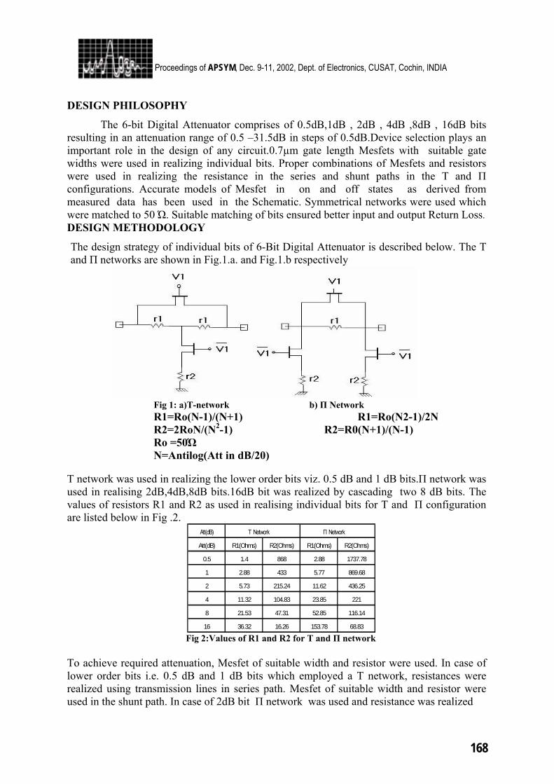
168
Proceedings of APSYM, Dec. 9-11, 2002, Dept. of Electronics, CUSAT, Cochin, INDIA
DESIGN PHILOSOPHY
The 6-bit Digital Attenuator comprises of 0.5dB,1dB , 2dB , 4dB ,8dB , 16dB bits resulting in an attenuation range of 0.5 –31.5dB in steps of 0.5dB.Device selection plays an important role in the design of any circuit.0.7µm gate length Mesfets with suitable gate widths were used in realizing individual bits. Proper combinations of Mesfets and resistors were used in realizing the resistance in the series and shunt paths in the T and Π configurations. Accurate models of Mesfet in on and off states as derived from measured data has been used in the Schematic. Symmetrical networks were used which were matched to 50 Ώ. Suitable matching of bits ensured better input and output Return Loss. DESIGN METHODOLOGY
The design strategy of individual bits of 6-Bit Digital Attenuator is described below. The T and Π networks are shown in Fig.1.a. and Fig.1.b respectively
Fig 1: a)T-network b) Π Network R1=Ro(N-1)/(N+1) R1=Ro(N2-1)/2N R2=2RoN/(N2-1) R2=R0(N+1)/(N-1) Ro =50Ώ N=Antilog(Att in dB/20)
T network was used in realizing the lower order bits viz. 0.5 dB and 1 dB bits.Π network was used in realising 2dB,4dB,8dB bits.16dB bit was realized by cascading two 8 dB bits. The values of resistors R1 and R2 as used in realising individual bits for T and Π configuration are listed below in Fig .2.
Att(dB) T Network Π Network
Att(dB) R1(Ohms) R2(Ohms) R1(Ohms) R2(Ohms)
0.5 1.4 868 2.88 1737.78
1 2.88 433 5.77 869.68
2 5.73 215.24 11.62 436.25
4 11.32 104.83 23.85 221
8 21.53 47.31 52.85 116.14
16 36.32 16.26 153.78 68.83 Fig 2:Values of R1 and R2 for T and Π network To achieve required attenuation, Mesfet of suitable width and resistor were used. In case of lower order bits i.e. 0.5 dB and 1 dB bits which employed a T network, resistances were realized using transmission lines in series path. Mesfet of suitable width and resistor were used in the shunt path. In case of 2dB bit Π network was used and resistance was realized
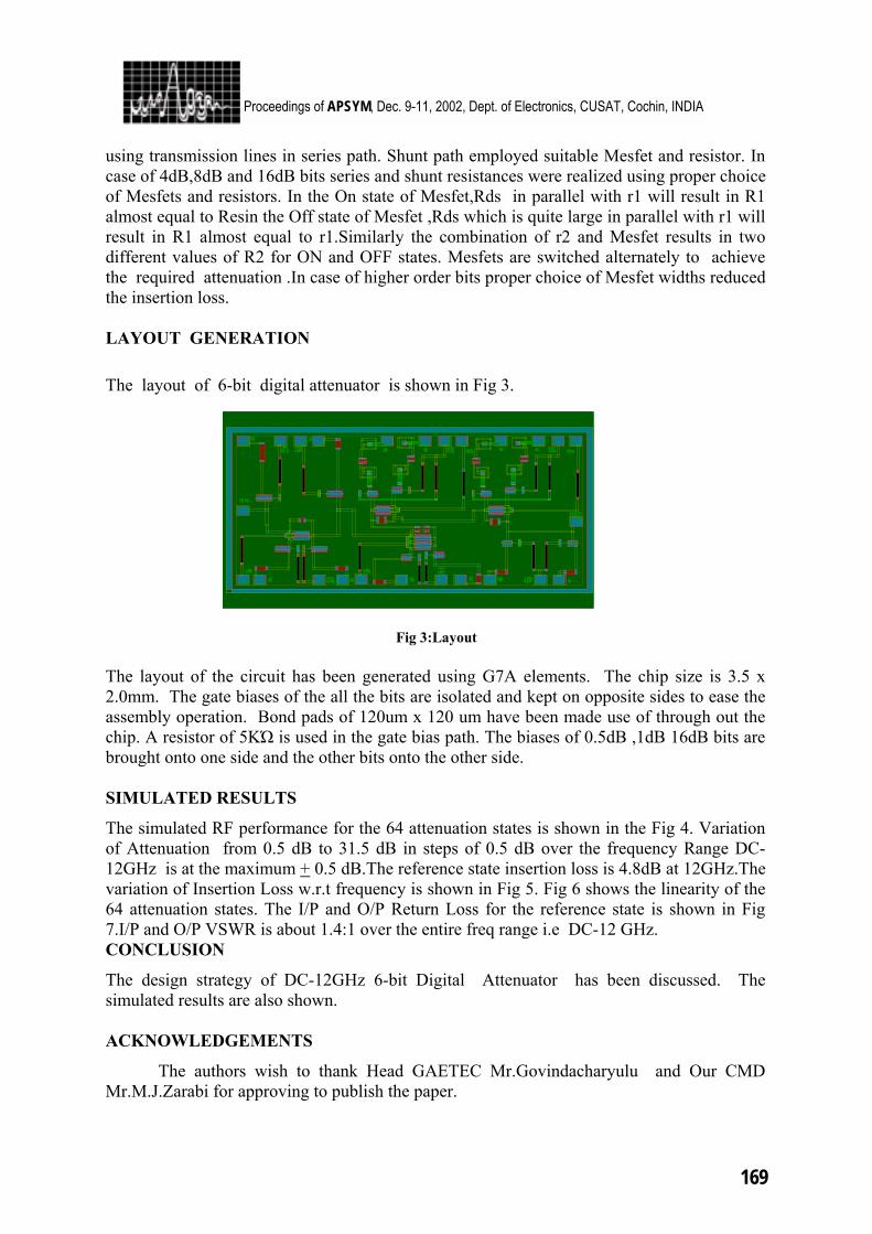
169
Proceedings of APSYM, Dec. 9-11, 2002, Dept. of Electronics, CUSAT, Cochin, INDIA using transmission lines in series path. Shunt path employed suitable Mesfet and resistor. In case of 4dB,8dB and 16dB bits series and shunt resistances were realized using proper choice of Mesfets and resistors. In the On state of Mesfet,Rds in parallel with r1 will result in R1 almost equal to Resin the Off state of Mesfet ,Rds which is quite large in parallel with r1 will result in R1 almost equal to r1.Similarly the combination of r2 and Mesfet results in two different values of R2 for ON and OFF states. Mesfets are switched alternately to achieve the required attenuation .In case of higher order bits proper choice of Mesfet widths reduced the insertion loss. LAYOUT GENERATION The layout of 6-bit digital attenuator is shown in Fig 3.
Fig 3:Layout The layout of the circuit has been generated using G7A elements. The chip size is 3.5 x 2.0mm. The gate biases of the all the bits are isolated and kept on opposite sides to ease the assembly operation. Bond pads of 120um x 120 um have been made use of through out the chip. A resistor of 5KΏ is used in the gate bias path. The biases of 0.5dB ,1dB 16dB bits are brought onto one side and the other bits onto the other side. SIMULATED RESULTS
The simulated RF performance for the 64 attenuation states is shown in the Fig 4. Variation of Attenuation from 0.5 dB to 31.5 dB in steps of 0.5 dB over the frequency Range DC-12GHz is at the maximum + 0.5 dB.The reference state insertion loss is 4.8dB at 12GHz.The variation of Insertion Loss w.r.t frequency is shown in Fig 5. Fig 6 shows the linearity of the 64 attenuation states. The I/P and O/P Return Loss for the reference state is shown in Fig 7.I/P and O/P VSWR is about 1.4:1 over the entire freq range i.e DC-12 GHz. CONCLUSION
The design strategy of DC-12GHz 6-bit Digital Attenuator has been discussed. The simulated results are also shown. ACKNOWLEDGEMENTS
The authors wish to thank Head GAETEC Mr.Govindacharyulu and Our CMD Mr.M.J.Zarabi for approving to publish the paper.
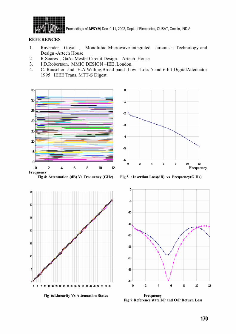
170
Proceedings of APSYM, Dec. 9-11, 2002, Dept. of Electronics, CUSAT, Cochin, INDIA
REFERENCES
1. Ravender Goyal , Monolithic Microwave integrated circuits : Technology and Design -Artech House
2. R.Soares , GaAs Mesfet Circuit Design- Artech House. 3. I.D.Robertson, MMIC DESIGN –IEE ,London. 4. C. Rauscher and H.A.Willing,Broad band ,Low –Loss 5 and 6-bit DigitalAttenuator
1995 IEEE Trans. MTT-S Digest.
Frequency Frequency Fig 4: Attenuation (dB) Vs Frequency (GHz) Fig 5 : Insertion Loss(dB) vs Frequency(G Hz)
Fig 6:Linearity Vs Attenuation States Frequency Fig 7:Reference state I/P and O/P Return Loss
-40
-35
-30
-25
-20
-15
-10
-5
0
0 2 4 6 8 10 12
-6
-5
-4
-3
-2
-1
0
0 2 4 6 8 10 120
5
10
15
20
25
30
35
0 2 4 6 8 10 12
0
5
10
15
20
25
30
35
1 4 7 10 13 16 19 22 25 28 31 34 37 40 43 46 49 52 55 58 61
171
Proceedings of APSYM, Dec. 9-11, 2002, Dept. of Electronics, CUSAT, Cochin, INDIA
MMIC APPROACH TO A 6-BIT DIGITAL PHASE SHIFTER FOR L-BAND TRANSMIT / RECEIVE MODULE
PUMMY RATNA, P. MOHAN & P.A.GOVINDACHARYULU
Semiconductor Complex Ltd. (GAETEC Project) Vignyana Kancha Post, Hyderabad-500069, INDIA.
E-mail: [email protected]
Phase shifters are one of the most critical components in a T/R module. Extensive work has been done to arrive at the suitable topologies to achieve minimum phase error with maximum figure of merit. A 6-bit L-band phase shifter was designed and fabricated at GAETEC, Hyderabad, using GaAs based technology through MMIC approach. The design was carried out in 1.0–1.6 GHz frequency band using the passive mode operation of the MESFETs. The differential phase shifts from 0° to 360° were achieved in 64 steps with a step size of 5.625° by cascading 6-bits. It exhibited excellent measured performance in terms of peak phase shift error. Figure of merit achieved in this design was also very high due to extremely low insertion loss. GaAs MESFETs with 0.7m Gate length of GAETEC foundry were used in switching mode. Switch process was implemented for the fabrication of this MMIC.
INTRODUCTION
Gallium Arsenide based MMICs have attained tremendous attention in the recent years in the field of satellite communication, military and commercial applications. MMICs offer large reduction in size and weight, coupled with improved reliability and repeatability at microwave frequencies. The Transmit and Receive (T/R) Module consists of various circuits such as low noise amplifier, attenuator, high power amplifier, 6-bit digital phase shifter and switches. These components are required in large numbers for the active phase array radar (APAR). The excellent gain and phase tracking along with small size, light weight, low cost and repeatability, achievable through MMIC approach has made the realization of the components in monolithic ways, essential for the success of these APARs. The 6-bit phase shifter is one of the most important and critical component of a T/R module. It needs extremely careful design and very stable process. DESIGN OF THE PHASE SHIFTER
The desired specifications of the phase shifter to be used in the T/R module are as given below :
Frequency : 1.2 – 1.4 GHz No. of Bits : 6 Insertion loss : -8.5 dB (max.) VSWR : 2 : 1 Phase error : + 5° (max.)
The 6-bits constituting the phase shifter are, 5.625°, 11.25°, 22.5°, 45°, 90° and 180°. Since the frequency of operation is very low, the distributed approach was not preferable in order to achieve an effective reduction in chip area.
172
Proceedings of APSYM, Dec. 9-11, 2002, Dept. of Electronics, CUSAT, Cochin, INDIA The concept of switching between a low pass and a high pass structure using lumped elements were found to be most suitable to achieve the differential phase shift for higher bits. The high pass network provides a phase advance, whereas the low pass network offers a phase lag. The lower bits 5.625° and 11.25° have been realized with simple delay line configuration using transmission line inductance and lumped capacitance connected in series. Either of these is bypassed by a MESFET in the two states. The off-state capacitance of 180° bit was balanced out with the inductors connected in parallel to them. This resulted in effective reduction in insertion of 180° bit. Wide transmission lines were used in order to minimize the losses and coupling effects. The circuit was designed using series IV Libra simulation. The coupling effects were thoroughly analyzed by coupled line analysis. The foundry model of switch MESFET and all the other passive elements, except for inductor model were used in the design. In order to improve the insertion loss, the non-standard 16/16 inductors (16µm track width, 16µm Gap) were used in the design. The de-embedded measured data of these inductors were used in the simulation. The 6-bits were separated in 2 chips to improve the yield. The first chip contained 180°, 90° and 11.25° bits, whereas, 5.625°, 45° and 22.5° bits constituted the second chip. These two chips were cascaded while tiling using bottom layer metallization to facilitate the dicing of all the 6-bits together as a single chip. The schematic of the phase shifter is shown in fig.1 and the layout of the circuit is shown in fig.2. FABRICATION
The circuit was fabricated using 0.7µm technology, switch process of GAETEC foundry, India. It implements ion implantation process, allows two levels of metallization, MIM capacitors of two types, namely Polyimide and nitride, along with via hole technology for providing grounds to the various elements. TESTING
The fabricated phase shifter was diced with all the 6-bits cascaded together through bottom layer of metallization. This eliminates the need of any external bonding for cascading the chips. The chip was assembled on a test jig for testing purpose. An external driver was used for giving the control voltages.
The measured performance is shown in figs. 3, 4, 5 & 6. The 180° bit shown a 4° increase in the angle and 100 MHz frequency shift towards lower frequency as compared to the simulation. The reason for this discrepancy was analyzed thoroughly. It was concluded that the de-embedding of bond wire length for the measured data of 16 / 16 inductor was not exact as the measured bond wire lengths were approximate.
Since 7 of these inductors were used in this bit, the overall effect of this inaccuracy in the data gave additional differential phase shift. The same inaccuracy was not dominating in other bits since lesser number of inductors was used in them. The lowest bits, 5.625° and 11.25° did not include any inductor at all. The inductances in them were realized through transmission lines. CORRECTIVE MEASURES
The 180° bit and other bits as well shown exact repeatability over 3 different wafers. The design for 180° bit was modified by reducing the designed angle by 4°. For this, only the capacitors were tuned, leaving the inductors untouched. It was expected that the inaccuracy
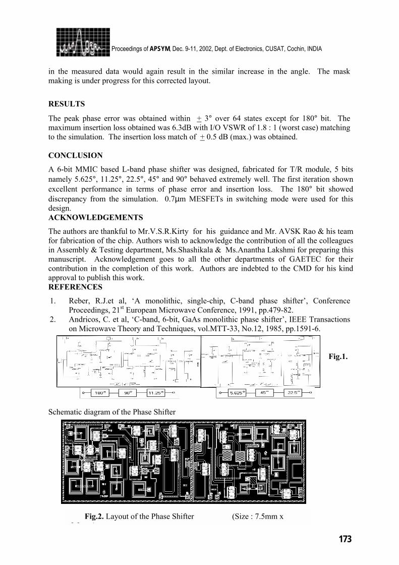
173
Proceedings of APSYM, Dec. 9-11, 2002, Dept. of Electronics, CUSAT, Cochin, INDIA
Fig.2. Layout of the Phase Shifter (Size : 7.5mm x 2 2 )
in the measured data would again result in the similar increase in the angle. The mask making is under progress for this corrected layout.
RESULTS
The peak phase error was obtained within + 3° over 64 states except for 180° bit. The maximum insertion loss obtained was 6.3dB with I/O VSWR of 1.8 : 1 (worst case) matching to the simulation. The insertion loss match of + 0.5 dB (max.) was obtained. CONCLUSION
A 6-bit MMIC based L-band phase shifter was designed, fabricated for T/R module, 5 bits namely 5.625°, 11.25°, 22.5°, 45° and 90° behaved extremely well. The first iteration shown excellent performance in terms of phase error and insertion loss. The 180° bit showed discrepancy from the simulation. 0.7µm MESFETs in switching mode were used for this design. ACKNOWLEDGEMENTS
The authors are thankful to Mr.V.S.R.Kirty for his guidance and Mr. AVSK Rao & his team for fabrication of the chip. Authors wish to acknowledge the contribution of all the colleagues in Assembly & Testing department, Ms.Shashikala & Ms.Anantha Lakshmi for preparing this manuscript. Acknowledgement goes to all the other departments of GAETEC for their contribution in the completion of this work. Authors are indebted to the CMD for his kind approval to publish this work. REFERENCES
1. Reber, R.J.et al, ‘A monolithic, single-chip, C-band phase shifter’, Conference Proceedings, 21st European Microwave Conference, 1991, pp.479-82.
2. Andricos, C. et al, ‘C-band, 6-bit, GaAs monolithic phase shifter’, IEEE Transactions on Microwave Theory and Techniques, vol.MTT-33, No.12, 1985, pp.1591-6.
Fig.1.
Schematic diagram of the Phase Shifter
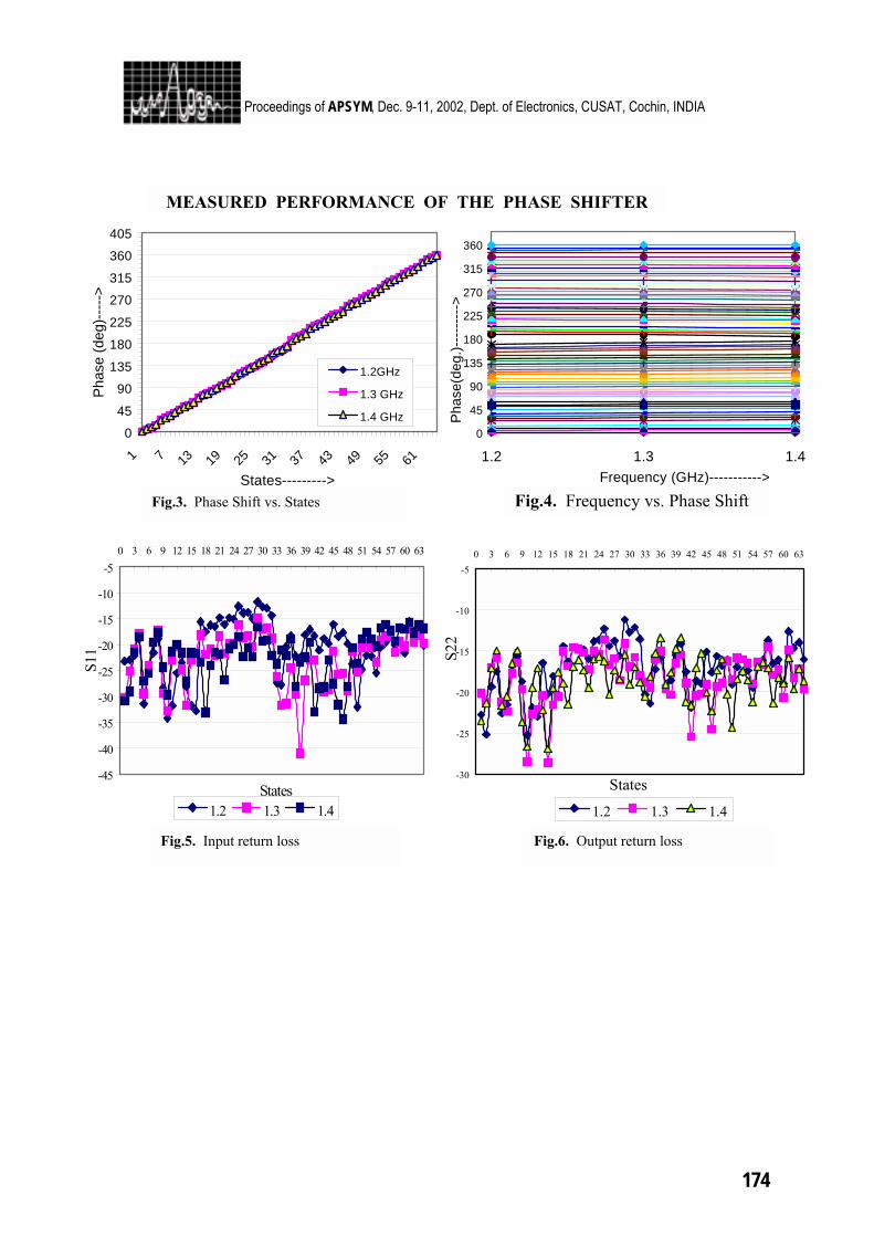
174
Proceedings of APSYM, Dec. 9-11, 2002, Dept. of Electronics, CUSAT, Cochin, INDIA
0
45
90
135
180
225
270
315
360
405
1 7 13 19 25 31 37 43 49 55 61
States--------->
Pha
se (d
eg)--
--->
1.2GHz
1.3 GHz
1.4 GHz
-45
-40
-35
-30
-25
-20
-15
-10
-50 3 6 9 12 15 18 21 24 27 30 33 36 39 42 45 48 51 54 57 60 63
States
S11
1.2 1.3 1.4
Fig.3. Phase Shift vs. States Fig.4. Frequency vs. Phase Shift
Fig.5. Input return loss
0
45
90
135
180
225
270
315
360
1.2 1.3 1.4Frequency (GHz)----------->
Pha
se(d
eg.)-
----
----
>
-30
-25
-20
-15
-10
-50 3 6 9 12 15 18 21 24 27 30 33 36 39 42 45 48 51 54 57 60 63
States
S22
1.2 1.3 1.4
Fig.6. Output return loss
MEASURED PERFORMANCE OF THE PHASE SHIFTER
175
Proceedings of APSYM, Dec. 9-11, 2002, Dept. of Electronics, CUSAT, Cochin, INDIA
MICROWAVE SIGNAL AND SENSOR DESIGN – IN PERSPECTIVE
G R Panda
Interim Test Range, DRDO, Chandipur &
A K Mallick Indian Institute of Technology, Kharagpur
Electronic signals ranging from audio waves to microwaves have a wideband spectral allocation. Behaviour of these can be studied, controlled and utilised for different applications. The reflected signals exhibit their pre-defined characteristics for which nature of obstruction of signal is a factor. Signal transmitted and measured in microwave domain, can have manifold applications. The devices, thus used for transmission, can be considered as very useful tools, which when calibrated can be utilised to locate desirable and undesirable objects. The present paper highlights on how characteristics of microwave transmission can be exploited and put to use for sensor design. Relevant theoretical treatment along with practical considerations, have also been discussed.
INTRODUCTION
Sensor in any form finds its in-roads to various engineering applications in modern technological scenario. Sensoring can make its existence felt everywhere, starting from a kid’s toy to a sophisticated robot, including even in the transducers while transforming energy from one form to another. This paper deliberates on different aspects of microwave signal sensing by utilising the properties of wave propagation. Subsequent calibration can further improve accuracy of the sensing device. An insulating plate such as that of good dielectric will be transparent to high frequency, whereas high conductive material, even of small thickness will reflect the incident high frequency microwave signal. A piston made up of a good quality metal can behave like a shorting plunger to microwave signal incident upon it, thus causing reflection of wave. This property can be utilised to know the rate of movement of piston. The initial part of paper is a preview on theoretical relations, which is followed by results obtained through practical studies and experiments. Subsequently, practical results obtained have been linked up with theoretical counterpart. The paper ends with concluding remarks and analysis. THEORETICAL ANALYSIS
In a transmission line, input impedance to the transmission line can be mathematically represented by Zin=Z0 ZL CosL+jZ0 SinL___________ ( i) Z0 CosL +jZL SinL Where Zin, Z0, ZL are input, characteristic and load impedances respectively.
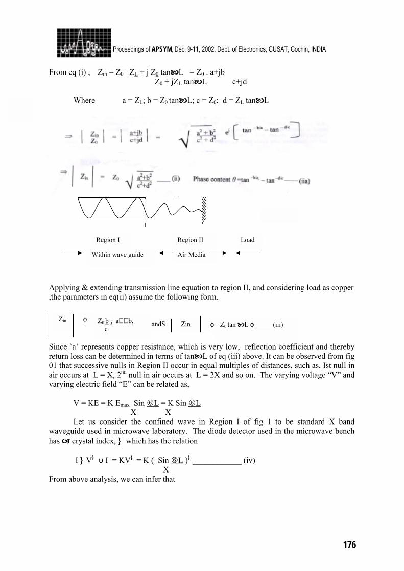
176
Proceedings of APSYM, Dec. 9-11, 2002, Dept. of Electronics, CUSAT, Cochin, INDIA From eq (i) ; Zin = Z0 ZL + j Z0 tanL = Z0 . a+jb Z0 + jZL tanL c+jd
Where a = ZL; b = Z0 tanL; c = Z0; d = ZL tanL
Applying & extending transmission line equation to region II, and considering load as copper ,the parameters in eq(ii) assume the following form.
Since `a’ represents copper resistance, which is very low, reflection coefficient and thereby return loss can be determined in terms of tanL of eq (iii) above. It can be observed from fig 01 that successive nulls in Region II occur in equal multiples of distances, such as, Ist null in air occurs at L = X, 2nd null in air occurs at L = 2X and so on. The varying voltage “V” and varying electric field “E” can be related as,
V = KE = K Emax Sin 6L = K Sin 6L X X Let us consider the confined wave in Region I of fig 1 to be standard X band waveguide used in microwave laboratory. The diode detector used in the microwave bench has crystal index, which has the relation
I V υ I = KV = K ( Sin 6L ) ____________ (iv) X
From above analysis, we can infer that
Zin ϕ Z0 b ; a⊃⊃ b, c
andS Zin ϕ Z0 tan L ϕ ____ (iii)
Load Region I Region II
Within wave guide Air Media
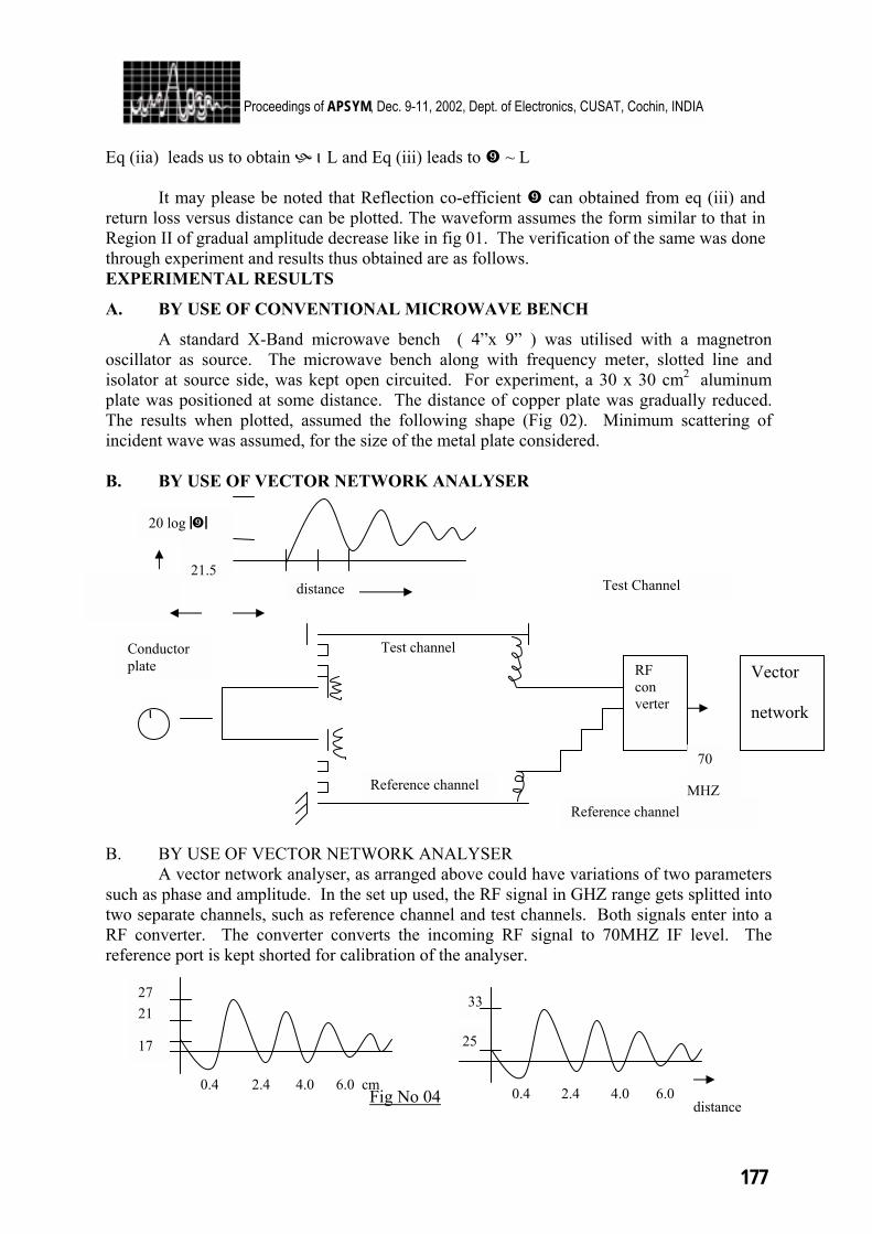
177
Proceedings of APSYM, Dec. 9-11, 2002, Dept. of Electronics, CUSAT, Cochin, INDIA Eq (iia) leads us to obtain ι L and Eq (iii) leads to ~ L It may please be noted that Reflection co-efficient can obtained from eq (iii) and return loss versus distance can be plotted. The waveform assumes the form similar to that in Region II of gradual amplitude decrease like in fig 01. The verification of the same was done through experiment and results thus obtained are as follows. EXPERIMENTAL RESULTS
A. BY USE OF CONVENTIONAL MICROWAVE BENCH
A standard X-Band microwave bench ( 4”x 9” ) was utilised with a magnetron oscillator as source. The microwave bench along with frequency meter, slotted line and isolator at source side, was kept open circuited. For experiment, a 30 x 30 cm2 aluminum plate was positioned at some distance. The distance of copper plate was gradually reduced. The results when plotted, assumed the following shape (Fig 02). Minimum scattering of incident wave was assumed, for the size of the metal plate considered. B. BY USE OF VECTOR NETWORK ANALYSER
B. BY USE OF VECTOR NETWORK ANALYSER A vector network analyser, as arranged above could have variations of two parameters such as phase and amplitude. In the set up used, the RF signal in GHZ range gets splitted into two separate channels, such as reference channel and test channels. Both signals enter into a RF converter. The converter converts the incoming RF signal to 70MHZ IF level. The reference port is kept shorted for calibration of the analyser. Fig No 04
20 log
21.5
RF con verter
Vector
network
IF 70
MHZ Reference channel
ι
distance
Conductor plate
Test Channel
Reference channel
Test channel
33
25
0.4 2.4 4.0 6.0 distance
27 21
17
0.4 2.4 4.0 6.0 cm
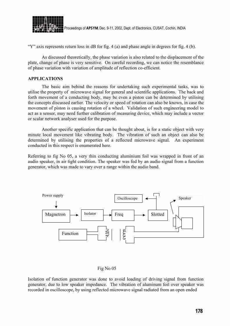
178
Proceedings of APSYM, Dec. 9-11, 2002, Dept. of Electronics, CUSAT, Cochin, INDIA “Y” axis represents return loss in dB for fig. 4 (a) and phase angle in degrees for fig. 4 (b). As discussed theoretically, the phase variation is also related to the displacement of the plate, change of phase is very sensitive. On careful recording, we can notice the resemblance of phase variation with variation of amplitude of reflection co-efficient. APPLICATIONS
The basic aim behind the reasons for undertaking such experimental tasks, was to utilise the property of microwave signal for general and scientific applications. The back and forth movement of a conducting body, may be even a piston can be determined by utilising the concepts discussed earlier. The velocity or speed of rotation can also be known, in case the movement of piston is causing rotation of a wheel. Validation of such engineering model to act as a sensor, may need further calibration of measuring device, which may include a vector or scalar network analyser used for the purpose. Another specific application that can be thought about, is for a static object with very minute local movement like vibrating body. The vibration of such an object can also be determined by utilising the properties of a reflected microwave signal. An experiment conducted in this respect is enumerated here. Referring to fig No 05, a very thin conducting aluminium foil was wrapped in front of an audio speaker, in air tight condition. The speaker was fed by an audio signal from a function generator, which was made to vary over a range within the audio band.
Fig No 05
Isolation of function generator was done to avoid loading of driving signal from function generator, due to low speaker impedance. The vibration of aluminum foil over speaker was recorded in oscilloscope, by using reflected microwave signal radiated from an open ended
Magnetron Isolator Freq Slotted
Function
Speaker Power supply
Oscilloscope
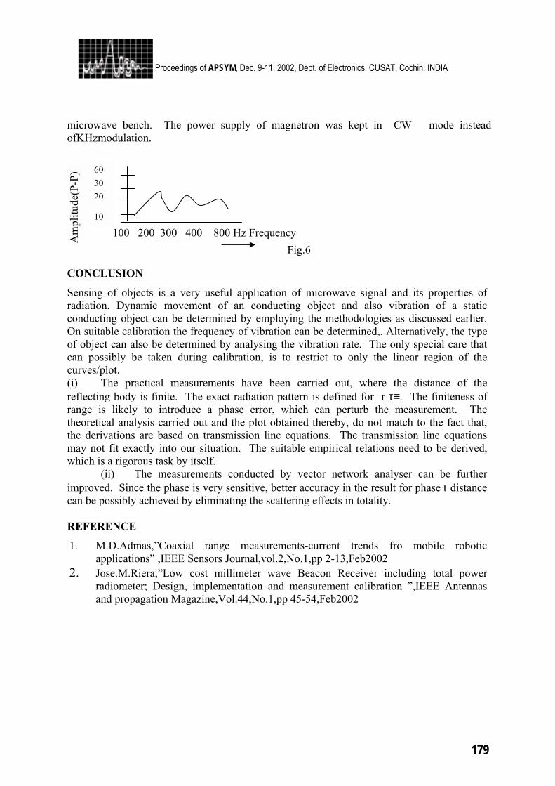
179
Proceedings of APSYM, Dec. 9-11, 2002, Dept. of Electronics, CUSAT, Cochin, INDIA microwave bench. The power supply of magnetron was kept in CW mode instead ofKHzmodulation.
CONCLUSION
Sensing of objects is a very useful application of microwave signal and its properties of radiation. Dynamic movement of an conducting object and also vibration of a static conducting object can be determined by employing the methodologies as discussed earlier. On suitable calibration the frequency of vibration can be determined,. Alternatively, the type of object can also be determined by analysing the vibration rate. The only special care that can possibly be taken during calibration, is to restrict to only the linear region of the curves/plot. (i) The practical measurements have been carried out, where the distance of the reflecting body is finite. The exact radiation pattern is defined for r τ≡. The finiteness of range is likely to introduce a phase error, which can perturb the measurement. The theoretical analysis carried out and the plot obtained thereby, do not match to the fact that, the derivations are based on transmission line equations. The transmission line equations may not fit exactly into our situation. The suitable empirical relations need to be derived, which is a rigorous task by itself. (ii) The measurements conducted by vector network analyser can be further improved. Since the phase is very sensitive, better accuracy in the result for phase ι distance can be possibly achieved by eliminating the scattering effects in totality. REFERENCE
1. M.D.Admas,”Coaxial range measurements-current trends fro mobile robotic applications” ,IEEE Sensors Journal,vol.2,No.1,pp 2-13,Feb2002
2. Jose.M.Riera,”Low cost millimeter wave Beacon Receiver including total power radiometer; Design, implementation and measurement calibration ”,IEEE Antennas and propagation Magazine,Vol.44,No.1,pp 45-54,Feb2002
Fig.6
60 30 20
10
Am
plitu
de(P
-P)
100 200 300 400 800 Hz Frequency
180
Proceedings of APSYM, Dec. 9-11, 2002, Dept. of Electronics, CUSAT, Cochin, INDIA
DOUBLE AVALANCHE/SINGLE DRIFT SILICON DIODE – A PROSPECTIVE MM-WAVE SOURCE FOR E-COMMUNICATION
S. P. Pati, S. K. Dash and P. Purohit Department of Physics, Sambalpur University, Jyoti Vihar- 768 019
Burla, Sambalpur ( Orissa )
Several favorable rf characteristics, like negligible avalanche expansion at very high values of operating current densities, existence of multiple rf bands, availability of high efficiency, generation of low avalanche expansion and insensitiveness of device performance to drift zone width could be noticed through of a full computer simulation algorithm in case of double avalanche/common drift diode which can make it a promising hf source of the coming decades.
INTRODUCTION
Several solid state devices, which include MESFET, GUNN, IMPATT, HEMT etc., have been used these days in advanced communication systems. The IMPATT diode can generate frequency upto 300 GHz and this remained as a favorable parameter of this device over other semiconductor devices. The diode width becomes nearly 100 nm ( for 300 GHz )and makes it difficult for fabrication. A diode structure of the form n+pnp+ or p+npn+ has two junctions and two avalanche zones separated by one drift region. Minority charge carriers entering left side junction gets multiplied in first avalanche zone, drifts in the common / zone and then further multiplied in second junction. Thus the avalanche phase delay produced in both the junctions become nearly and transit time delay does not become critical in this device to cause rf oscillation in ATT mode. Further the drifting of charge carriers in a common drift zone causes some more favorable characteristics. The suitability of this diode as a mm-wave source is discussed in this paper based on numerical analyses of this device under dc/rf/noise conditions. COMPUTER METHOD
A very fast, stable, double iterative and converging computer method [1] has been framed and by the authors to analyse both the complementary DJ/DA structures between 10 and 300 GHz which covers the entire micro/mm-wave region. The method has been made accurate by incorporating necessary physical parameters that become important for mm-wave frequencies. The existence of high impurity gradient along the diode active zone causes tunneling/diffusion currents, which have been accounted for along-with the drift current while framing/solving device equations by the computer method. The transition zones of doping profile have been replaced by ion-implantation/gaussian/exponential functions as could be generated by diffusion/ion-implantation fabrication processes [2,3]. The diode has been assumed to have silicon as the base material and material parameters as reported in recent literature have been considered [4,5]. The computer algorithm/logic has been framed to ensure automatic flow along converging track. To present a comparative account of the results obtained from this device with the performance of other conventional single junction device, the authors have used results reported in their other publications. The favorable features of the DJ/DA diodes are discussed in the following section. The results indicate
181
Proceedings of APSYM, Dec. 9-11, 2002, Dept. of Electronics, CUSAT, Cochin, INDIA several favorable features like negligible avalanche expansion at heavy bias current densities, possible operation at various frequency bands covering the entire microwave/mm-wave frequencies, realisation of high efficiency and low avalanche noise. RESULTS DISCUSSIONS
The DARD structures show the structural forms of n+pνnp+ and p+nπpp+. Both the complementary DARD structures show nearly similar properties and are presented in the following sections. Table 1: Multiple bands of Negative Resistance of DAR Diode
Band Number
Band Width (GHz) J= 108 A/m2
Negative Resistance ( 10-10 m2 )
Band Width (GHz) J= 5x10 A/m2
Negative Resistance ( 10-10 m2 )
I 17.5-30 198.0 17.5-30 56.80 II 45-60 17.90 47.5-60 6.56 III 75-90 4.88 77.5-90 2.26 IV 115-120 2.13 110-120 0.967 V 142.5-150 1.050 142.5-155 0.520 VI 175-180 0.663 173.5-185 0.307 VII 210-215 0.378 207.5-215 0.188 VIII 240-245 0.215 237.5-250 0.0939 IX 275-285 0.158 270-285 0.0805 X 305-320 0.146 305-320 0.0722
WIDE BAND CHARACTERISTICS
A conventional SDD/DDD exhibit narrow BW for rf generation. Separate diode has to be designed/fabricated for different frequency ranges. However, the DARD has been observed to show the existence negative rf conductance from 10 to 300 GHz. The results have been shown in Table I. The entire range of frequency band has been observed to be split into a large number of discrete bands with one optimum frequency for each band. The table shows the same number of bands for two values of bias current densities. The number of bands for each of the DARD is 14-15 bands. Thus a single diode can oscillate at different frequency bands covering the entire range of microwave/mm-wave region with multiple band tuning facility [6]. The avalanche phase delay produced in two junctions becomes nearly equal to , thus the extension of drift zone does not become a critical parameter for the diode design and the diode BW remains independent of / regions. The authors have analysed the DAR diode with different extensions of drift zones from 2micrometers to 0.2 micrometers. The magnitude of rf negative resistance/conductance become small by nearly an order of magnitude which can be compensated through incorporation of asymmetry in the doping/width of n/p regions of the device. The authors have tried various values of different dopings/widths for the n/p regions and observed sufficient enhancement of rf negative resistance values( not shown in table ). The quality factor, which indicates the stability of oscillation, remains high even compared to the best structure amongst the conventional diodes. The negative resistance generation along the depletion zone of the DJ/DAD has also been obtained which clearly indicates the contribution of negative resistance by each space
182
Proceedings of APSYM, Dec. 9-11, 2002, Dept. of Electronics, CUSAT, Cochin, INDIA
step. The distribution profile shows the existence of a peak in the central region of the drift zone. Thus the major portion of the contribution towards negative resistance is from the drift region. The avalanche zone being narrow, the efficiency of the diode remains high even with drastic changes of diode structural parameters. But for non-conventional microwave sources slight change in the design parameters produces considerable changes in the device properties. HIGH EFFICIENCY
The high field zone/avalanche region remains localized for this diode as the field maximum as well as the field gradient along n/p regions become high (Table II). The device efficiency for the entire range of frequency of operation becomes high i.e. becomes nearly 17-20%. The high efficiency specialized ( LHL/HL) SD/DD structure shows the efficiency to be 19% for 60 GHz operation, which falls to 10% at 220 GHz frequency. But for DARD the efficiency remains at same level for higher bands. The efficiency could be further enhanced for the DARD by introduction of asymmetry to the n/p regions. Thus the DARD can provide efficiency on par with the special high efficiency conventional flat impurity profile. Table-II : DC Characteristics Of DARD At Different Current Densities Current Density J(108A/m2)
Emax 107(V/m) n-side p-side
Avalanche zone width n-side p-side
Avalanche Voltage Drop n-side p-side
Efficiency (η)
0.5 1.0 2.0 5.0 10.0 40.0 100.0 200.0
8.35 8.49 8.42 8.59 8.07 8.79 10.1 11.9
7.85 7.94 7.96 7.96 8.81 9.79 11.3 13.3
95 98 102 88 88 74 64 57
96 100 83.97 105.92 128.79 125.21 112.30 101.40
6.04 6.00 5.96 5.6 5.4 5.0 4.7 4.5
4.85 4.88 4.9 5.513 5.882 5.655 5.27 4.953
15.970 16.210 16.190 15.723 15.478 16.188 16.419 17.090
Table-III : Small Signal Characteristics Of DARD At High Current Densities Current Densities J = (x108(A/m2)
Band Number Band Width (GHz)
Fp (GHz) -Gp(106 S/m2)
5.0
I II III IV V VI VII VIII IX
23-31 41-49 65-83 91-105 123-135 145-160 200-215 260-270 315-330
23 41 65 91 129 150 210 265 325
0.0527 0.869 0.430 0.594 0.123 0.317 0.241 0.192 0.131
NEGLIGIBLE AVALANCHE EXPANSION
The rf output power delivery from a device source can be enhanced by increasing the input/operating current. This has been reported [7] that when the bias current is increased in case of conventional flat profile diode, the avalanche zone expands due to increase in mobile
183
Proceedings of APSYM, Dec. 9-11, 2002, Dept. of Electronics, CUSAT, Cochin, INDIA
space charge concentration within the depletion zone. When the current density is increased by ten times the avalanche zone expands from 40% to 95% of the depletion zone. This causes the efficiency to fall to negligible values ( less than 1% ). The electric field profile assumes abnormal shape when mobile space charge overpowered the impurity is quite different as both the charge carriers after first phase multiplication drift through the common drift zone in opposite direction resulting in cancellation of space charge effect. The DARD has been analyzed for a bias current as high as 200 times the normal current [8]. The results have been presented in Tables II & III. It is very surprising to see that the avalanche zone thereby the efficiency remain at the normal level corresponding to normal current value even at high values of bias current. This is one of the most suitable features for this diode operation which makes it possible to operate this diode output power delivery. The microwave characteristics also show only marginal changes with increase of bias current densities. The deteriorating effect of mobile space charge on rf performance is also minimized.
LOW NOISE CHARACTERISTICS
The avalanche noise generation due to random ionization process is the only unfavorable parameter for the ATT diodes. The authors have analyzed the operation of the DARD with locating the noise source at various space steps and solving the modified device equation [9] with the help of another double iterative program. The noise source has been considered at one space point at one time and from the final solution the noise generation distribution has been computed along the active region. This process has been repeated by shifting the noise source location. The method gives the integrated noise generation as well as space distribution of the noise generation. The noise assessment also has been made for other conventional diodes. The results of such calculations have been given in Table IV. It is very interesting to see that the v2/df i.e. the mean square noise voltage for the DARD becomes of the order of 10-20 as against 10-17 V2.s for flat DDD. Table-4 : Comparative Account of RF Properties Of Flat and DAR Diodes
fp
Flat DDR Width (nm) <v2>/df (10-
17 V2.s)
DAR Width 1300 nm <v2>/df (10-20 V2.s)
50 GHz 1000 1.15 6.2 95GHz 600 0.474 0.614 150 GHz 450 0.171 0.072 200 GHz 215 0.046 0.028
The table shows similar trends for diodes designed for several frequencies. The high efficiency low-high-low diode, which gives efficiency on par with DARD, generates noise high by further order of magnitude than the flat DD. Thus the avalanche/random noise generation in the DJ/DAD is less nearly by four orders of magnitude and can be considered negligible [9]. This fact can be explained from the fact that the noise generation is wide spread in DDD as against its localized generation in the case of the DAR diode. The noise generation profile in the case of DDD becomes of double peak nature with little difference of magnitude between the maxima and minimum. Thus the noise is almost generated with equal intensity along a major portion of the DD active zone. In the case of the noise profile for the DARD, it exhibits a single peak nature with the magnitude decreasing by five orders of magnitude when the location of the noise source is shifted from the point of field maximum to the drift region.
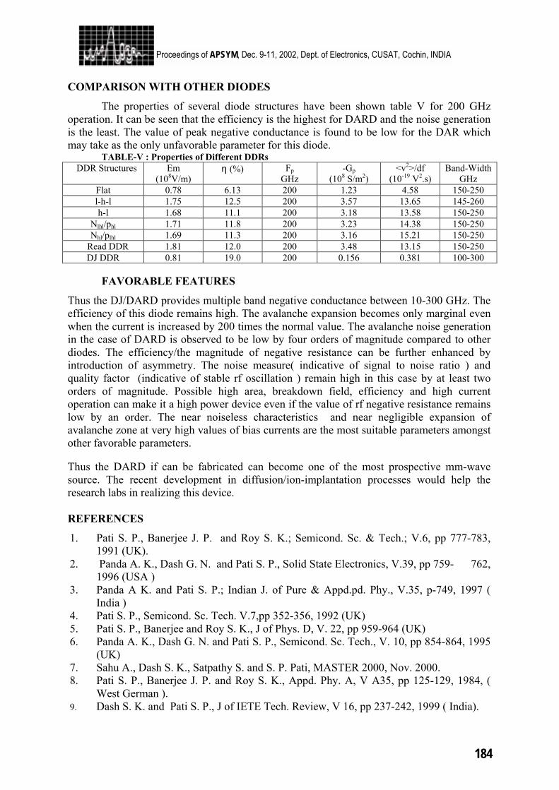
184
Proceedings of APSYM, Dec. 9-11, 2002, Dept. of Electronics, CUSAT, Cochin, INDIA
COMPARISON WITH OTHER DIODES
The properties of several diode structures have been shown table V for 200 GHz operation. It can be seen that the efficiency is the highest for DARD and the noise generation is the least. The value of peak negative conductance is found to be low for the DAR which may take as the only unfavorable parameter for this diode.
TABLE-V : Properties of Different DDRs DDR Structures Em
(108V/m) η (%) Fp
GHz -Gp
(108 S/m2) <v2>/df
(10-19 V2.s) Band-Width
GHz Flat 0.78 6.13 200 1.23 4.58 150-250 l-h-l 1.75 12.5 200 3.57 13.65 145-260 h-l 1.68 11.1 200 3.18 13.58 150-250
Nlhl/phl 1.71 11.8 200 3.23 14.38 150-250 Nhl/plhl 1.69 11.3 200 3.16 15.21 150-250
Read DDR 1.81 12.0 200 3.48 13.15 150-250 DJ DDR 0.81 19.0 200 0.156 0.381 100-300
FAVORABLE FEATURES
Thus the DJ/DARD provides multiple band negative conductance between 10-300 GHz. The efficiency of this diode remains high. The avalanche expansion becomes only marginal even when the current is increased by 200 times the normal value. The avalanche noise generation in the case of DARD is observed to be low by four orders of magnitude compared to other diodes. The efficiency/the magnitude of negative resistance can be further enhanced by introduction of asymmetry. The noise measure( indicative of signal to noise ratio ) and quality factor (indicative of stable rf oscillation ) remain high in this case by at least two orders of magnitude. Possible high area, breakdown field, efficiency and high current operation can make it a high power device even if the value of rf negative resistance remains low by an order. The near noiseless characteristics and near negligible expansion of avalanche zone at very high values of bias currents are the most suitable parameters amongst other favorable parameters. Thus the DARD if can be fabricated can become one of the most prospective mm-wave source. The recent development in diffusion/ion-implantation processes would help the research labs in realizing this device.
REFERENCES
1. Pati S. P., Banerjee J. P. and Roy S. K.; Semicond. Sc. & Tech.; V.6, pp 777-783, 1991 (UK).
2. Panda A. K., Dash G. N. and Pati S. P., Solid State Electronics, V.39, pp 759- 762, 1996 (USA )
3. Panda A K. and Pati S. P.; Indian J. of Pure & Appd.pd. Phy., V.35, p-749, 1997 ( India )
4. Pati S. P., Semicond. Sc. Tech. V.7,pp 352-356, 1992 (UK) 5. Pati S. P., Banerjee and Roy S. K., J of Phys. D, V. 22, pp 959-964 (UK) 6. Panda A. K., Dash G. N. and Pati S. P., Semicond. Sc. Tech., V. 10, pp 854-864, 1995
(UK) 7. Sahu A., Dash S. K., Satpathy S. and S. P. Pati, MASTER 2000, Nov. 2000. 8. Pati S. P., Banerjee J. P. and Roy S. K., Appd. Phy. A, V A35, pp 125-129, 1984, (
West German ). 9. Dash S. K. and Pati S. P., J of IETE Tech. Review, V 16, pp 237-242, 1999 ( India).
185
Proceedings of APSYM, Dec. 9-11, 2002, Dept. of Electronics, CUSAT, Cochin, INDIA
VELOCITY OVERSHOOT 2D-EFFECT IN Si-MOSFET TO
USE AT HIGH-FREQUENCY
S. K. Achary1, S. K. Panigrahi, and A. K. Panda*, Member, IETE
National Institute of Science and Technology Palur Hills, Berhampur, Orissa, India – 761 008
E-mail: [email protected], [email protected] 1. B.E. Final year student
* Regular Associate of ICTP, Trieste, Italy mailto:[email protected]
A simulator that can calculate the power consumption, can show velocity overshoot and define the relationship between various parameters of a Silicon MOSFET is designed. The simulator so developed is based on the solution of two-dimensional Poisson equation. The ensemble Monte Carlo method is used for calculating transport properties of carriers. The Monte Carlo method used in this simulation is the most instructive way in seeing the effect of scattering process on device performance. In this simulation important scattering rates that appear in the Monte Carlo method is included. This simulator shows the relationship between perpendicular electric field, parallel electric field and temperature on velocity and energy of the device. Close proximity with published results confirms the validity of our approach.
INTRODUCTION
The Si MOSFET has revolutionized the electronic industry and as a result impacts our daily lives in every conceivable way [1,2]. One of the most important features of FETs is that the minority-carrier storage effect can be completely eliminated and hence the switching speed can be increased. Although good quality heterojunctions can be achieved by the advanced growth techniques, the restrictions of growing lattice-matched layers to avoid interfacial dislocation still limits the combination of different lattice constant semiconductor and Si MOSFET is still dominated in the market because for its mature technology and well understood physics [3]. It is well known that there is a considerable interest in the electron transport in submicron devices for possible high frequency and high-speed application [1,2]. As the transit time of electron in a device becomes comparable, or less than, the relaxation time of electrons, cold electrons injected into the device does not reach their steady state velocity during their transit through the device. It is therefore important to realize that the velocity-field curves calculated for bulk semiconductors may not be applicable to the transport of the electrons in the submicron-sized devices. The transit nature after injection allows the mean velocity to overshoot the usual saturation velocity and thus increase the cut-off frequency moving towards microwave/mm-wave frequency. Such type of a study is presented in this paper to show the two dimensional effect in submicron Si-based MOSFET. An ensemble Monte Carlo technique used for this study which is reported in the next section. The results obtained from such study for Si submicron MOSFET are presented in section III and finally conclusion has been given in section IV. ANALYSIS
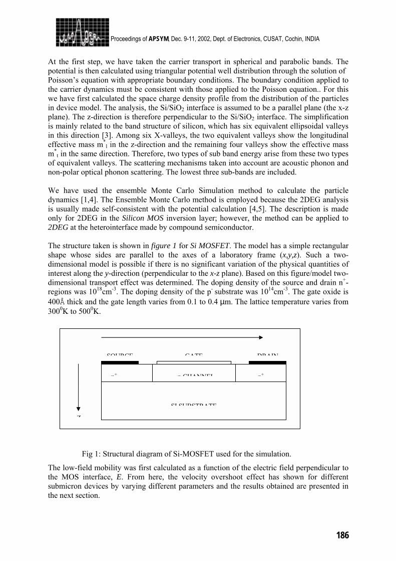
186
Proceedings of APSYM, Dec. 9-11, 2002, Dept. of Electronics, CUSAT, Cochin, INDIA
At the first step, we have taken the carrier transport in spherical and parabolic bands. The potential is then calculated using triangular potential well distribution through the solution of Poisson’s equation with appropriate boundary conditions. The boundary condition applied to the carrier dynamics must be consistent with those applied to the Poisson equation.. For this we have first calculated the space charge density profile from the distribution of the particles in device model. The analysis, the Si/SiO2 interface is assumed to be a parallel plane (the x-z plane). The z-direction is therefore perpendicular to the Si/SiO2 interface. The simplification is mainly related to the band structure of silicon, which has six equivalent ellipsoidal valleys in this direction [3]. Among six X-valleys, the two equivalent valleys show the longitudinal effective mass m*
l in the z-direction and the remaining four valleys show the effective mass m*
t in the same direction. Therefore, two types of sub band energy arise from these two types of equivalent valleys. The scattering mechanisms taken into account are acoustic phonon and non-polar optical phonon scattering. The lowest three sub-bands are included. We have used the ensemble Monte Carlo Simulation method to calculate the particle dynamics [1,4]. The Ensemble Monte Carlo method is employed because the 2DEG analysis is usually made self-consistent with the potential calculation [4,5]. The description is made only for 2DEG in the Silicon MOS inversion layer; however, the method can be applied to 2DEG at the heterointerface made by compound semiconductor. The structure taken is shown in figure 1 for Si MOSFET. The model has a simple rectangular shape whose sides are parallel to the axes of a laboratory frame (x,y,z). Such a two-dimensional model is possible if there is no significant variation of the physical quantities of interest along the y-direction (perpendicular to the x-z plane). Based on this figure/model two-dimensional transport effect was determined. The doping density of the source and drain n+-regions was 1018cm-3. The doping density of the p- substrate was 1014cm-3. The gate oxide is 400Å thick and the gate length varies from 0.1 to 0.4 µm. The lattice temperature varies from 3000K to 5000K.
Fig 1: Structural diagram of Si-MOSFET used for the simulation.
The low-field mobility was first calculated as a function of the electric field perpendicular to the MOS interface, E. From here, the velocity overshoot effect has shown for different submicron devices by varying different parameters and the results obtained are presented in the next section.
SOURCE GATE DRAIN
SI SUBSTRATE
n+ n CHANNEL n+
Z
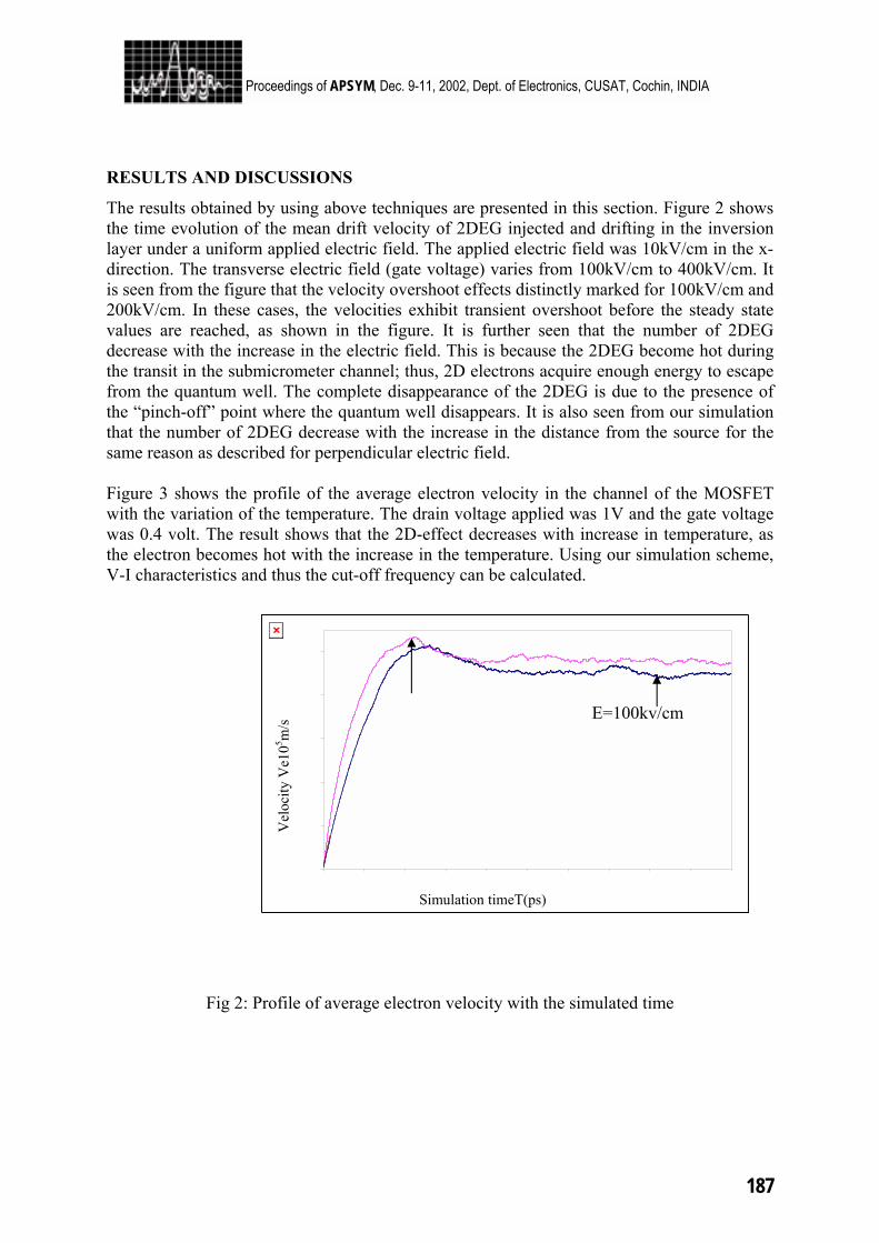
187
Proceedings of APSYM, Dec. 9-11, 2002, Dept. of Electronics, CUSAT, Cochin, INDIA
RESULTS AND DISCUSSIONS
The results obtained by using above techniques are presented in this section. Figure 2 shows the time evolution of the mean drift velocity of 2DEG injected and drifting in the inversion layer under a uniform applied electric field. The applied electric field was 10kV/cm in the x-direction. The transverse electric field (gate voltage) varies from 100kV/cm to 400kV/cm. It is seen from the figure that the velocity overshoot effects distinctly marked for 100kV/cm and 200kV/cm. In these cases, the velocities exhibit transient overshoot before the steady state values are reached, as shown in the figure. It is further seen that the number of 2DEG decrease with the increase in the electric field. This is because the 2DEG become hot during the transit in the submicrometer channel; thus, 2D electrons acquire enough energy to escape from the quantum well. The complete disappearance of the 2DEG is due to the presence of the “pinch-off” point where the quantum well disappears. It is also seen from our simulation that the number of 2DEG decrease with the increase in the distance from the source for the same reason as described for perpendicular electric field. Figure 3 shows the profile of the average electron velocity in the channel of the MOSFET with the variation of the temperature. The drain voltage applied was 1V and the gate voltage was 0.4 volt. The result shows that the 2D-effect decreases with increase in temperature, as the electron becomes hot with the increase in the temperature. Using our simulation scheme, V-I characteristics and thus the cut-off frequency can be calculated.
Fig 2: Profile of average electron velocity with the simulated time
Simulation timeT(ps)
Vel
ocity
Ve1
05 m/s
E=200kv/cm E=100kv/cm
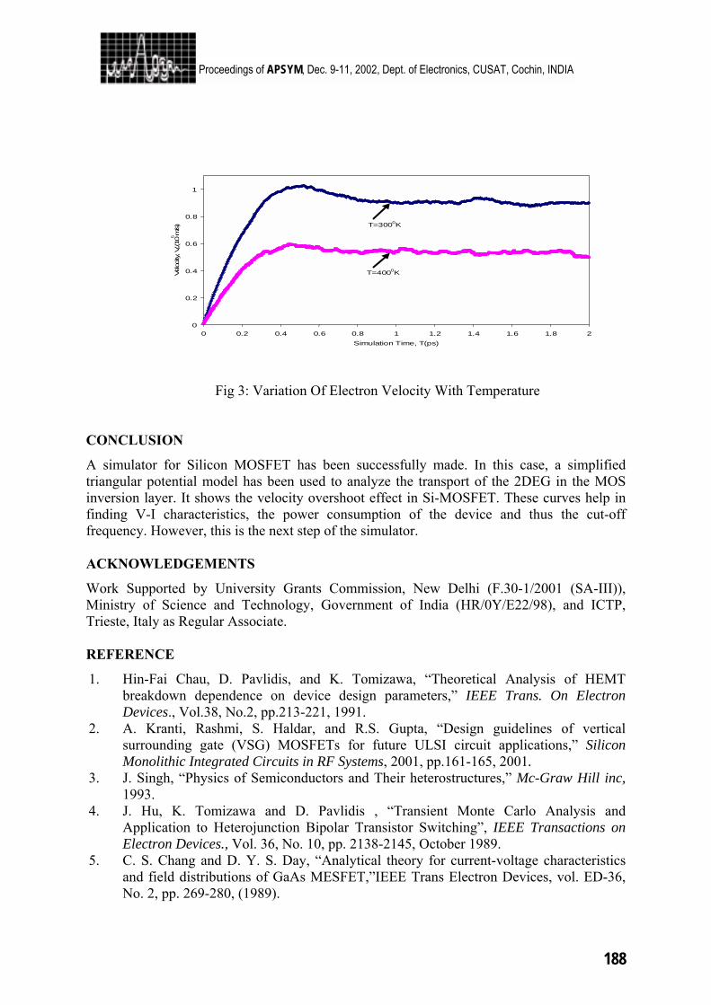
188
Proceedings of APSYM, Dec. 9-11, 2002, Dept. of Electronics, CUSAT, Cochin, INDIA
Fig 3: Variation Of Electron Velocity With Temperature
CONCLUSION
A simulator for Silicon MOSFET has been successfully made. In this case, a simplified triangular potential model has been used to analyze the transport of the 2DEG in the MOS inversion layer. It shows the velocity overshoot effect in Si-MOSFET. These curves help in finding V-I characteristics, the power consumption of the device and thus the cut-off frequency. However, this is the next step of the simulator. ACKNOWLEDGEMENTS
Work Supported by University Grants Commission, New Delhi (F.30-1/2001 (SA-III)), Ministry of Science and Technology, Government of India (HR/0Y/E22/98), and ICTP, Trieste, Italy as Regular Associate. REFERENCE
1. Hin-Fai Chau, D. Pavlidis, and K. Tomizawa, “Theoretical Analysis of HEMT breakdown dependence on device design parameters,” IEEE Trans. On Electron Devices., Vol.38, No.2, pp.213-221, 1991.
2. A. Kranti, Rashmi, S. Haldar, and R.S. Gupta, “Design guidelines of vertical surrounding gate (VSG) MOSFETs for future ULSI circuit applications,” Silicon Monolithic Integrated Circuits in RF Systems, 2001, pp.161-165, 2001.
3. J. Singh, “Physics of Semiconductors and Their heterostructures,” Mc-Graw Hill inc, 1993.
4. J. Hu, K. Tomizawa and D. Pavlidis , “Transient Monte Carlo Analysis and Application to Heterojunction Bipolar Transistor Switching”, IEEE Transactions on Electron Devices., Vol. 36, No. 10, pp. 2138-2145, October 1989.
5. C. S. Chang and D. Y. S. Day, “Analytical theory for current-voltage characteristics and field distributions of GaAs MESFET,”IEEE Trans Electron Devices, vol. ED-36, No. 2, pp. 269-280, (1989).
0
0.2
0.4
0.6
0.8
1
0 0.2 0.4 0.6 0.8 1 1.2 1.4 1.6 1.8 2Simulation Time, T(ps)
Veloc
ity, V
e(1
05 m/s) T=3000K
T=4000K
189
Proceedings of APSYM, Dec. 9-11, 2002, Dept. of Electronics, CUSAT, Cochin, INDIA
STUDY OF Si/SiGe HETEROJUNCTION DAR IMPATT
DIODE
S.R. Pattanaik, *J.K. Mishra, I.P. Mishra and G.N. Dash P.G. Department of Physics, Sambalpur University, JyotiVihar, Burla-768019
* P.G. Department of Physics, G.M. College (Autonomous), Sambalpur-768004
A realistic and accurate computer simulation study of Si/Si0.5Ge0.5 heterojunction Double Avalanche Region (DAR) IMPATT diode, for operation at 42 GHz, has been carried out. Our results show that the Si/SiGe heterojunction DAR diode exhibits some superior microwave and noise characteristic as compared to the Si homojunction DAR IMPATT diode.
INTRODUCTION
Since the evolution of IMPATT diode, different types of IMPATT diode structures like single drift region (SDR), double drift region (DDR), double avalanche region (DAR) etc based on different materials have been proposed for the improvement in its noise and power performance. The IMPATT diode with DAR structure has drawn attention of the researchers all over the world as it provides high efficiency and multiple negative conductance bands at microwave frequency, since its first report [1]. Several authors [2,3] have studied the potentiality of the DAR IMPATT diode. Heterojunction IMPATT diode structure has also shown significant improvements on the diode performance over the homojunction IMPATT diode structure [4,5]. Our group [6] is first to explore these advantages to investigate the behaviour of DAR heterojunction IMPATT diode. In this present study, we have considered a Si/Si0.5Ge0.5 heterojunction DAR IMPATT diode structure. The results of Si/SiGe heterojunction DAR IMPATT diode, obtained through computer simulation, have been compared with the results for Si homojunction DAR IMPATT diode. The comparative study reveals that the Si/SiGe heterojunction DAR IMPATT diode exhibits superior noise as well as microwave properties at a frequency of interest (42 GHz) over the corresponding Si homojunction DAR IMPATT diode.
METHOD
A simple DAR structure of the form n+pnp+ [7] has been proposed for this study. The one-dimensional model of this structure is shown in figure 1.
n+
Si
p
SiGe
p
Si
n
Si
n
SiGe
p+
Si
0 x1 x2 x3 W
Figure 1: 1-D model of the proposed DAR IMPATT diode. We have developed a set of realistic and accurate computer simulation programs,
which comprises of DC analysis, small-signal analysis and noise analysis to simulate the proposed diode structures. The DC analysis starts with solving simultaneously the Poisson’s equation, Combined Carrier continuity equation and Space Charge equation with appropriate
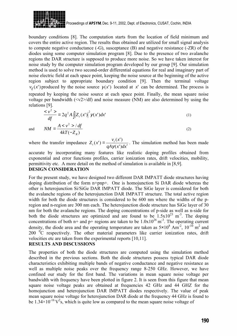
190
Proceedings of APSYM, Dec. 9-11, 2002, Dept. of Electronics, CUSAT, Cochin, INDIA
boundary conditions [8]. The computation starts from the location of field minimum and covers the entire active region. The results thus obtained are utilized for small signal analysis to compute negative conductance (-G), susceptance (B) and negative resistance (-ZR) of the diodes using some computer simulation program [8]. Due to the presence of two avalanche regions the DAR structure is supposed to produce more noise. So we have taken interest for noise study by the computer simulation program developed by our group [9]. Our simulation method is used to solve two second-order differential equations for real and imaginary part of noise electric field at each space point, keeping the noise source at the beginning of the active region subject to appropriate boundary condition [9]. Then the terminal voltage
)'(xtv produced by the noise source )'(xγ located at 'x can be determined. The process is repeated by keeping the noise source at each space point. Finally, the mean square noise voltage per bandwidth (<v2>/df) and noise measure (NM) are also determined by using the relations [9].
')'()'(222
2
dxxxZAqdfv
t γ∫=>< (1)
and )(4
/2
RZkTdfvANM
−><= (2)
where the transfer impedance xdxqA
xvxZ tt ′
=)'()'(
)'(γ
. The simulation method has been made
accurate by incorporating many features like realistic doping profiles obtained from exponential and error functions profiles, carrier ionization rates, drift velocities, mobility, permittivity etc. A more detail on the method of simulation is available in [8,9]. DESIGN CONSIDERATION
For the present study, we have designed two different DAR IMPATT diode structures having doping distribution of the form n+pnp+. One is homojunction Si DAR diode whereas the other is heterojunction Si/SiGe DAR IMPATT diode. The SiGe layer is considered for both the avalanche regions of the heterojunction DAR IMPATT structure. The total active region width for both the diode structures is considered to be 600 nm where the widths of the p-region and n-region are 300 nm each. The heterojunction diode structure has SiGe layer of 30 nm for both the avalanche regions. The doping concentrations of p-side as well as n-side for both the diode structures are optimized and are found to be 1.5x10²³ m-3. The doping concentrations of both n+ and p+ regions are taken to be 1.0x1026 m-3. The operating current density, the diode area and the operating temperature are taken as 5×10⁸ Am-2, 10-10 m2 and 200 0C respectively. The other material parameters like carrier ionization rates, drift velocities etc are taken from the experimental reports [10,11]. RESULTS AND DISCUSSIONS
The properties of both the diode structures are computed using the simulation method described in the previous sections. Both the diode structures possess typical DAR diode characteristics exhibiting multiple bands of negative conductance and negative resistance as well as multiple noise peaks over the frequency range 8-250 GHz. However, we have confined our study for the first band. The variations in mean square noise voltage per bandwidth with frequency have been plotted in figure 2. It is seen from this figure that mean square noise voltage peaks are obtained at frequencies 42 GHz and 44 GHZ for the homojunction and heterojunction DAR IMPATT diodes respectively. The value of peak mean square noise voltage for heterojunction DAR diode at the frequency 44 GHz is found to be 1.34×10⁻¹⁶
V2s, which is quite low as compared to the mean square noise voltage of
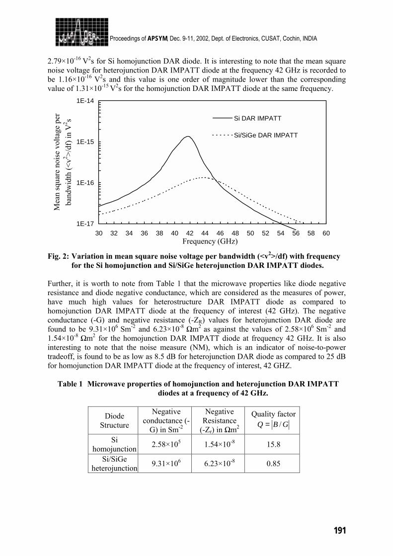
191
Proceedings of APSYM, Dec. 9-11, 2002, Dept. of Electronics, CUSAT, Cochin, INDIA
2.79×10⁻¹⁶
V2s for Si homojunction DAR diode. It is interesting to note that the mean square noise voltage for heterojunction DAR IMPATT diode at the frequency 42 GHz is recorded to be 1.16×10⁻¹⁶
V2s and this value is one order of magnitude lower than the corresponding value of 1.31×10⁻¹⁵
V2s for the homojunction DAR IMPATT diode at the same frequency.
1E-17
1E-16
1E-15
1E-14
30 32 34 36 38 40 42 44 46 48 50 52 54 56 58 60Frequency (GHz)
Mea
n sq
uare
noi
se v
olta
ge p
er
band
wid
th (<
v2 >/df
) in
V2 s Si DAR IMPATT
Si/SiGe DAR IMPATT
Fig. 2: Variation in mean square noise voltage per bandwidth (<v2>/df) with frequency
for the Si homojunction and Si/SiGe heterojunction DAR IMPATT diodes. Further, it is worth to note from Table 1 that the microwave properties like diode negative resistance and diode negative conductance, which are considered as the measures of power, have much high values for heterostructure DAR IMPATT diode as compared to homojunction DAR IMPATT diode at the frequency of interest (42 GHz). The negative conductance (-G) and negative resistance (-ZR) values for heterojunction DAR diode are found to be 9.31×10⁶
Sm-2 and 6.23×10⁻⁸ Ωm2 as against the values of 2.58×10⁶ Sm-2 and
1.54×10⁻⁸ Ωm2 for the homojunction DAR IMPATT diode at frequency 42 GHz. It is also interesting to note that the noise measure (NM), which is an indicator of noise-to-power tradeoff, is found to be as low as 8.5 dB for heterojunction DAR diode as compared to 25 dB for homojunction DAR IMPATT diode at the frequency of interest, 42 GHZ.
Table 1 Microwave properties of homojunction and heterojunction DAR IMPATT diodes at a frequency of 42 GHz.
Diode Structure
Negative conductance (-
G) in Sm-2
Negative Resistance
(-Zr) in Ωm2
Quality factor GBQ /=
Si homojunction 2.58×10⁵ 1.54×10⁻⁸ 15.8
Si/SiGe heterojunction 9.31×10⁶ 6.23×10⁻⁸ 0.85
192
Proceedings of APSYM, Dec. 9-11, 2002, Dept. of Electronics, CUSAT, Cochin, INDIA
CONCLUSION
The potentials of Si/SiGe heterostructure DAR IMPATT diode have been explored by the computer simulation programs developed by our group. It is observed from the results that the heterojunction DAR IMPATT diode has remarkable low noise and high power performance at 42 GHz as compared to its homojunction counterpart. A noise measure (NM) as low as 8.5 dB has been reported for the heterostructure DAR IMPATT diode as compared to 25 dB for the homojunction DAR IMPATT diode at a frequency of 42 GHz. The performance of the Si/SiGe heterostructure DAR IMPATT diode may be further improved by optimizing the diode structure. ACKNOWLEDGEMENT
The authors wish to acknowledge the Department of Science and Technology, Govt. of India for financial support of this work through a major research project (SP/S2/M-12/98). REFERENCES
1. B. Som, B.B. Pal and S.K. Roy, “A small-signal analysis of an Impatt device having two avalanche layers interspaced by a drift layer”, Solid State Electronics, Vol. 17, pp 1029, 1974
2. S.P. Pati, J.P. Banerjee and S.K. Roy, “High frequency numerical analysis of double avalanche region Impatt diode”, Semicond. Sci. and Technol. Vol. 6, pp 777, 1991
3. J.K. Mishra, G.N. Dash and I.P. Mishra, “Simulation studies on the noise behaviour of double avalanche region diodes”, Semicond. Sci. and Technol. Vol. 16, pp 895, 2001
4. J.F. Luy, H. Jorke, H. Kibbel, A. Casel and E. Kasper, “Si/SiGe heterostructure MITTAT diode”, Electronics Lett., Vol. 24, pp 386, 1988
5. M.J. Bailey,” Heterojunction IMPATT Diodes”, IEEE Trans. Electron. Devices, Vol. 39, pp 1829, 1992
6. S.R. Pattanaik, I.P. Mishra, J.K. Mishra and G.N. Dash, “ The potential of InP/GaInAs Double Avalanche Region IMPATT Diode”, IWPSD-2001, Physics of Semiconductor Devices, Allied Publishers Ltd. New Delhi, Vol. 2, pp 902, 2001
7. I.P. Mishra, J.K. Mishra and G.N. Dash,” Single fundamental band output from DAR IMPATT diode”, IWPSD-1999, Physics of Semiconductor Devices, Allied Publishers Ltd. New Delhi, pp 562, 1999
8. G.N. Dash and S.P. Pati, “A generalized simulation method for MITATT mode operation and studies on the influence of tunnel current on IMPATT properties”, Semicond. Sci. and Technol., Vol. 7, pp 222, 1992.
9. G.N. Dash, J.K. Mishra and A.K. Panda, “ Noise in Mixed Tunneling Avalanche Transit Time (MITATT) Diodes”, Solid State Electronics, Vol. 39, pp 1473, 1996
10. M. Ershov and V. Ryzhii, “ High field electron transport in SiGe Alloy”, Jpn. Appl. Phys., Vol. 33, pp 1365, 1994
11. T. Yamada and D.K. Ferry, “Monte carlo simulation of hole transport in strained Si1-xGex”, Solid State Electronics, Vol. 38, pp 881, 1995
193
Proceedings of APSYM, Dec. 9-11, 2002, Dept. of Electronics, CUSAT, Cochin, INDIA
GaN-BASED GUNN DIODE FOR THz SIGNAL GENERATION
S. K. Panigrahi and A. K. Panda*, Member, IETE
National Institute of Science and Technology
Palur Hills, Berhampur, Orissa, India – 761 008 E-mail: [email protected], [email protected]
* Regular Associate of ICTP, Trieste, Italy mailto:[email protected]
The GaN material had been explored to see the potentiality of the material to use as Gunn diode. A new simulation technique was developed to study the device characteristics of the Gunn diode. The results obtained for GaN diode is compared with GaAs-based Gunn diode and found that GaN-based Gunn diode can generate two orders of magnitude of more power than GaAs-based Gunn diode at similar operating conditions. The reported improvement in the mm-wave/Thz-wave performance are supported by the high value of GaN Pf2Z figure of merit, which is 50-100 times higher than the GaAs, indicating a strong potential of the GaN for the mm-wave signal generation.
INTRODUCTION
Many applications in the millimeter and submillimeter wave regions of the electromagnetic spectrum require compact solid-state local oscillators that provide low noise and adequate power levels. Oscillators based on GaAs and InP Gunn devices have been widely used to serve this purpose at frequency upto 140GHz. These devices have proved to be reliably with excellent amplitude and phase noise characteristics. For high frequency operation, the principal limiting factor is the semiconductor material itself as the Gunn effect is directly related to the band structure and the material properties of the semiconductor. Gunn devices based on GaAs are limited to W-band (70-110GHz) whereas InP devices have been shown to generate considerable power level upto 140GHz. However, wide band gap semiconductors like GaN and compounds based on it have recently been established as technologically important materials for both electronic and optoelectronic devices to obtain high power [1-2] at high frequency. High power GaN-based transistors have been reported recently with excellent electrical characteristics [1-2]. Even high-frequency devices such as GaN-based IMPATTs with excellent electrical characteristics have been reported recently [3-4]. As a first order, the oscillation frequency of a Gunn device is proportional to the space charge layer transit velocity, which can be approximated by the saturated velocity. It is clear that GaN with a saturated velocity a factor of two higher than the corresponding velocity in InP, has the potential of operating at a much higher frequency than InP or GaAs Gunn devices. Other properties that make GaN attractive compared to InP/GaAs include a higher thermal conductivity and a much higher breakdown electric field [3]. To the best of our knowledge, the feasibility of using GaN in Gunn diode has not yet been explored properly so far. However, some group at University of Michigan, Purdue University is engaged to fabricate the device experimentally [5]. Hence a detailed and systematic theoretical study is necessary at the present stage to see the potentiality of GaN and its compounds to use as Gunn diode at mm-wave and THz frequency range. A theoretical study including all these aspects will be very much helpful to research community before the material is dedicated to grow and fabricate the device.
194
Proceedings of APSYM, Dec. 9-11, 2002, Dept. of Electronics, CUSAT, Cochin, INDIA
With this in mind, the authors have reported here a detailed theoretical study on GaN-based Gunn devices and compare the results obtained with GaAs and its compounds based Gunn diode operating under similar conditions. Device operation is studied over a wide range of frequencies. Computer software was developed to study the dynamic properties of such devices. The developed program is a generalized one and can be used at any operating conditions and for any type of Gunn device structures (such as flat profile, notch profile and heterostructure). The dependence of the oscillation frequency and output power on GaN NDR diode design and operating conditions are reported. The outline of the simulation scheme and material parameters used in this study are presented in the next section. The results obtained from this study are presented in section III. Section IV finally presents the conclusion of the study. SIMULATION METHOD AND MATERIAL PARAMETERS
A computer model based on the drift-diffusion technique for the simulation of carrier transport in semiconductor devices has been employed to obtain the results presented in this paper. This tool is capable of analyzing Gunn structures with any doping profile in the active region with various injectors at the cathode terminal. The input to the program consists of device doping profile, material composition of the various regions, DC bias conditions, and device size. For a given frequency, the program starts with a small RF voltage and performs the simulation for a number of periods. The current response is then computed as a function of time and the output RF power, conversion efficiency, and DC current are then obtained from Fourier analysis of the current response. Simulation results obtained from this complete model have been shown to yield very good agreement with experimental results in the mm-wave region [6] for GaAs-based Gunn diode and hence can be used for GaN case also. We report results based on this model for GaN-based Gunn devices with emphasis on operation at high-frequency in the next section. Since material parameters play a major role in the outcome of the simulation, appropriate parameter values for Zincblende GaN [7] were selected based on an extensive search of data reported in [3]. The v-E characteristics of GaN used for this study were based on Monte Carlo simulation of Albrecht et al [7]. The threshold field for the intervalley transfer Eth is much larger in GaN (150 KV/cm) than in GaAs (3.5KV/cm). The separation between the high and low mobility valleys (∆E) in GaN, the effective mass (m0) etc are taken from different experimental reports. The energy-relaxation time (τER) was calculated as (τER=(2m*δE/qEth)0.5) and the intervalley transfer relaxation time τET was evaluated from the results of Monte Carlo studies of ballistic transport [5,7]. Based on this, the NDR relaxation frequency of GaN was found to be 740GHz compared to 110 GHZ of GaAs. All the material parameters used for GaAs and AlGaAs are taken from experimental reports and summarized in MEDICI manual [8]. The Gunn device for the present study was designed using same standard criterion given elsewhere. The schematic diagram with designed data is shown in figure 1 with its usual meaning. The results obtained from such simulation method are presented in the next section.
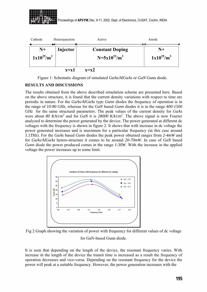
195
Proceedings of APSYM, Dec. 9-11, 2002, Dept. of Electronics, CUSAT, Cochin, INDIA
N+
1x1025/m3
Injector Constant Doping
N=5x10²³/m3
N+
1x1025/m3
x=x1 x=x2 Figure 1: Schematic diagram of simulated GaAs/AlGaAs or GaN Gunn diode.
RESULTS AND DISCUSSIONS
The results obtained from the above described simulation scheme are presented here. Based on the above structure, it is found that the current density variations with respect to time are periodic in nature. For the GaAs/AlGaAs type Gunn diodes the frequency of operation is in the range of 10-80 GHz, whereas for the GaN based Gunn diodes it is in the range 400-1500 GHz for the same structural parameters. The peak values of the current density for GaAs were about 80 KA/cm2 and for GaN it is 28000 KA/cm2. The above signal is now Fourier analyzed to determine the power generated by the device. The power generated at different dc voltages with the frequency is shown in figure 2. It shows that with increase in dc voltage the power generated increases and is maximum for a particular frequency (in this case around 1.1THz). For the GaAs based Gunn diodes the peak power obtained ranges from 2-4mW and for GaAs/AlGaAs hetero-structure it comes to be around 20-70mW. In case of GaN based Gunn diode the power produced comes in the range 1-30W. With the increase in the applied voltage the power increases up to some limit.
Fig 2 Graph showing the variation of power with frequency for different values of dc voltage
for GaN-based Gunn diode.
It is seen that depending on the length of the device, the resonant frequency varies. With increase in the length of the device the transit time is increased as a result the frequency of operation decreases and vice-versa. Depending on the resonant frequency for the device the power will peak at a suitable frequency. However, the power generation increases with the
Cathode Heterojunction Active Anode
Variation of Power with frequency for different dc voltage
0
5
10
15
20
25
30
35
0.5 0.7 0.9 1.1 1.3 1.5 1.7 1.9Frequency (THz)
Pow
er (W
)
Vdc = 17V
Vdc = 21V
Vdc = 19V
Variation of Power with frequency for different dc voltage
0
5
10
15
20
25
30
35
0.5 0.7 0.9 1.1 1.3 1.5 1.7 1.9Frequency (THz)
Pow
er (W
)
Vdc = 17V
Vdc = 21V
Vdc = 19V
196
Proceedings of APSYM, Dec. 9-11, 2002, Dept. of Electronics, CUSAT, Cochin, INDIA
increase in the active region length. The results have been computed for different values of active region concentration also and the power was computed with the frequency (the graphs are not shown here). As the charge bunch moves across the active region it grows in size. The rate at which it grows depends on the available electrons and hence the active region concentration. So with the increase in the active region concentration the power obtained will increase. CONCLUSION
In this report we have studied the feasibility of using GaN as a material of choice for different Gunn devices. It was found that due to the fundamental properties of the material, GaN NDR diodes offered twice the frequency capability of the GaAs Gunn diode, while their output power density was 2x10⁵W/cm2 compared with 1x10³W/cm2 fort the GaAs devices. The devices made of GaN can operate at much high temperature. The GaAs/AlGaAs heterostructure Gunn diode oscillators were also simulated for comparison and verification purposes. Yet, GaN is found to be better alternative material for fabrication of Gunn devices as compared to GaAs/AlGaAs devices or GaAs and InP-based Gunn devices. ACKNOWLEDGEMENTS
Work Supported by University Grants Commission, New Delhi (F.30-1/2001 (SA-III)), Ministry of Science and Technology, Government of India (HR/0Y/E22/98), and ICTP, Trieste, Italy as Regular Associate. REFERENCE
1. U. K. Mishra, Yi-Feng Wu, B. P. keller, S. Keller, and S. P. Denbaars, “GaN
Microwave Electronics,” IEEE Trans. On Micro. Th. And Tech., Vol. 46, No.6, pp.756-761, 1998.
2. M. S. Shur, “GaN based Transistors for high power applications,” Solid-State Electronics, Vol.42, No.12, pp.2131-2138, 1998.
3. A. K. Panda, D. Pavlidis and Egor Alekseev, “DC and High-Frequency characteristics of GaN-based IMPATTs”, IEEE Trans. On Electron. Devices, Vol.48, No.4, pp.820-823,2001.
4. A. K. Panda, D. Pavlidis and Egor Alekseev, “Noise characteristics of GaN-based IMPATTs”, IEEE Trans. On Electron. Devices, Vol. 48,No.7,pp.1473-1475,2001.
5. E. Alekseev, A. Eisenbech, D. Pavlidis, S. M. Hubbard, and W. Sutton, “Development of GaN-based Gunn effect MM-wave sources,” Proceedings of WOSCDICE-2000.
6. Ridha Kamuria, “Potential Of GaAs and In P Gunn Devices at High Frequencies,” Ph.D. Thesis, University Of Michigan, 1992.
7. J. D. Albrecht, R. P. Wang, P. P. Ruden, M. Farahmand, and K. F. Brennan, “Electronic transport characteristics of GaN for high temperature device modeling,” J. of Appl. Phys., vol. 83(9), pp. 4777-4781, 1998.
8. MEDICI, “Two Dimensional Device Simulation Program,” Technol. Model. Assoc., 1997.
197
Proceedings of APSYM, Dec. 9-11, 2002, Dept. of Electronics, CUSAT, Cochin, INDIA
GENETIC ALGORITHM BASED PERFORMANCE STUDY
OF GaAs AND In0.53Ga0.47As QUANTUM WELLS IN THE MICROWAVE AND MILLIMETER WAVE REGIME
A. Karmakar, A. Moi1, M. K. Naskar1and S. K. Sarkar1
Dept. of Electronics & Communication Engg., Kalyani Govt. Engg. College, Kalyani, West Bengal, India.
1Dept. of Electronics & Telecommunication Engg., Jadavpur University, Kolkata - 32, India.
A soft computing tool, like Genetic Algorithm, is employed here to study the performance of GaAs and In0.53Ga0.47As quantum wells incorporating acoustic deformation potential, ionized impurity scattering and no equilibrium longitudinal optic phonons in the framework of heated Fermi-Dirac distribution function. Alloy disorder scattering is additionally considered for (In,Ga)As quantum wells. For a desired high frequency response characterized by a 3dB cutoff frequency, where ac mobility drops to 0.707 of its low frequency value, genetic algorithm is applied and system parameters for the desired response are optimized for both GaAs and (In,Ga)As quantum wells under hot electron condition. Studies are also made in absence of no equilibrium longitudinal optic phonons to get an idea about the influence of no equilibrium longitudinal optic phonons on the high frequency response of the quantum wells.
INTRODUCTION
Intensive research during the last two decades have been made on the study of the transport properties of current carriers, confined quantum mechanically in 1, 2 and 3 dimensions in semiconductor heterostructures [1-4]. In modern quasi low dimensional high speed devices operating under high electric fields and in devices operating under optical excitations no equilibrium longitudinal optic (LO) phonons or hot phonons are generated which slowdown the carrier cooling rate. Since the carrier energy and momentum loss rates are influenced by the hot phonons [5], understanding of the relationship of the device performance with the carrier kinetics in presence of the no equilibrium LO phonons. We study here theoretically the influence of the no equilibrium LO phonons on the small-signal ac transport of two-dimensional (2D) hot electrons in GaAs and In0.53Ga0.47As quantum wells (QWs) in the microwave and millimeter wave regime as an aid to the device related work. Genetic Algorithms (GAs) have been successfully used in many optimization problems. It is a biological evolutionary process in intelligent search, machine learning and optimization problems [6]. These are basically search algorithms based on the mechanics of natural selection and natural genetics. The main theme of these algorithms is robustness. GAs are theoretically and empirically proven to provide robust search in complex spaces. So, GAs are now finding more wide spread applications in business, scientific and engineering circles [7]. GAs are computationally simple but powerful in its search for an improvement. GAs are different from traditional optimization [8] and search procedures in the following four ways: GAs work with a coding of the parameter set, not the parameters themselves. GAs search from a population of points not a single point. GAs use payoff (objective function) not derivatives or other auxiliary knowledge.
198
Proceedings of APSYM, Dec. 9-11, 2002, Dept. of Electronics, CUSAT, Cochin, INDIA
GAs use probabilistic transition rules, not deterministic rules. To perform an effective search for better and better structures, GAs require only payoff values (objective function values) associated with individual strings. This characteristic makes GAs most canonical method than any other search schemes. Unlike other methods, GAs use probabilistic transition rules to guide their search. GAs use random choice as a tool to guide a search towards region of the search space with likely improvement. In this present work, we employ GAs to determine the optimized system parameters for the desired response of GaAs and In0.53Ga0.47As QWs for better high frequency performance under hot electron condition. ANALYTICAL MODEL
Square QWs of GaAs and (In, Ga)As of infinite barrier height having channel width Lz is considered. We choose the system parameters here, namely, the 2D carrier concentration (n2D), the channel width (Lz) and the lattice temperature (TL) such that the separation between the lowest and the next higher subband is sufficiently higher than the maximum average electron energy. The carrier distribution is, therefore, degenerate as the electrons are assumed to populate only the lowest subband of the square QWs in the infinite barrier height approximation. In the present work, we include the carrier scatterings via deformation potential acoustic phonons, polar optic phonons and ionized impurities. Alloy disorder scattering in momentum loss is additionally considered for (In, Ga)As QWs. The effect of screening on the scattering rate for polar optic phonons is not significant over the temperature range of interest [9] and hence not included in the present calculations. Screening is, however, incorporated for the other scattering processes. Improved carrier confinement and reduced ionized impurity scattering in the well establish a strong electron-electron interaction in the QW structure. This strong interaction in energy and momentum exchanges favors a heated drifted Fermi-Dirac distribution function for the carriers characterized by an electron temperature Te and a drift crystal momentum pd. The establishment of an electron temperature in 2D systems has been demonstrated by the photo luminescent experiments [10]. Analytical details adopted here are available in Ref.11, where net rate of increase of phonon occupation equation is solved with the help of energy and momentum balance equations together with the expressions of applied electric field, electron temperature, phonon occupation number and drift momentum [11]. GENETIC ALGORITHM
Genetic algorithms work on a population or collection of several alternative solutions to the given problem. Each individual in the population is called a string or chromosome. The population of strings is coded into binary string. In each iteration of the GA, a new generation is evolved from the existing population to obtain better solutions. The amount of information stored by the GA is determined by the population size. The GA population is evolved over a number of generations. An evaluation function (or fitness function) is used to determine the fitness of each individual solution. The fitness values associated with each individual are calculated from the binary strings. A highly fit population is evolved through several generations by selecting chromosome depending on the fitness values. The selected individuals form pairs, called parents. Crossover is the main operator used for reproduction. It combines portions of two parents to create two new individuals, known as offspring. In the present work, natural selection procedure, called “Roulette Wheel” is used for reproduction. A simple spin of the weighted Roulette wheel yields the reproduction candidate whenever another offspring is required. The string is then entered into a mating pool for reproduction and further genetic operations. The crossover proceeds in two steps. Firstly, the newly reproduced strings are
199
Proceedings of APSYM, Dec. 9-11, 2002, Dept. of Electronics, CUSAT, Cochin, INDIA
mated at random and secondly, each pair of strings undergoes crossing over. Mutation, which is an incremental change made to each member of the population, enables new features to be introduced into a population. The frequency of mutation to obtain good results in empirical GA is in the order of one mutation per thousand-bit transfer. Mutation rates are small in natural population. Thus mutation is considered as a secondary mechanism of GA adaptation. OPTIMIZATION TECHNIQUE
The following strings and fitness values (shown below) are considered here for the simulation of GA.
String Fitness value 1010 0011 0100 0101
100 9
16 25
We find certain similarities among the strings and certain string patterns have the tendency of good performance. For example, in the sample population, the string starting with a ‘1’ seems to be the best. Then, the fitness values are set from the system parameters of GaAs and (In,Ga)As QWs under hot electron condition. Then the reproduction process is initiated by taking all the fitness values to form a population of strings. These strings are then entered into a mating pool for further genetic operations. Then crossover is done in two steps. Firstly, members of the newly reproduced strings in the mating pool are mated at random. Secondly, each pair of strings undergoes crossing over as stated earlier in section. Then the mutation is done to get good results in empirical GA. Here in this process the mutation rates are very small. After the first generation the average of the newly generated strings and the original strings are taken. Those strings that are higher than the new average value are suited for the next generation. Then from the population of the next generation, according to the fitness values, we take the first best, second best and so on for the optimum values in our work. Therefore, we get the optimum values of the system parameters of GaAs and (In,Ga)As QWs for better high frequency performance under hot electron condition. RESULTS AND DISCUSSIONS
Genetic Algorithm based computations are performed with the parameter values of GaAs and (In,Ga)As given in Table-1 for a biasing field for 0.5X10⁵V/m. In the present mode of optimization, detailed studies are made for getting optimized system parameters together with lattice and electron temperature for a desired high frequency performance characterized by a well defined cutoff frequency. Thus, the proposed model can predict the optimum system parameters if the cutoff frequency and biasing field are provided. Table-2 depicts the optimized system parameters for GaAs and (In,Ga)As QWs. The cutoff frequencies vary from 100 to 250GHz. The values of the system parameters obtained under this optimization technique clearly indicate that they are not in regular order but represent the optimized value for getting the desired cutoff frequency at a particular dc biasing field. It is also revealed from the Table-2 that for a desired cutoff frequency (In,Ga)As QW provides better ac mobility reflecting that (In,Ga)As QW has better high frequency response [11]. Further, for a particular dc biasing field it is possible to predict the optimum values of the system parameters like, carrier concentration, channel width and electron temperature for realizing a particular high frequency response characterized by a cutoff frequency. The present model is capable of predicting the optimized parameters that will surely give an idea about the search time for the technologist involved in the fabrication of the high frequency
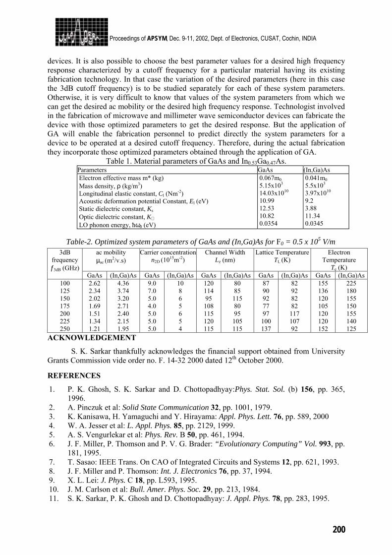
200
Proceedings of APSYM, Dec. 9-11, 2002, Dept. of Electronics, CUSAT, Cochin, INDIA
devices. It is also possible to choose the best parameter values for a desired high frequency response characterized by a cutoff frequency for a particular material having its existing fabrication technology. In that case the variation of the desired parameters (here in this case the 3dB cutoff frequency) is to be studied separately for each of these system parameters. Otherwise, it is very difficult to know that values of the system parameters from which we can get the desired ac mobility or the desired high frequency response. Technologist involved in the fabrication of microwave and millimeter wave semiconductor devices can fabricate the device with those optimized parameters to get the desired response. But the application of GA will enable the fabrication personnel to predict directly the system parameters for a device to be operated at a desired cutoff frequency. Therefore, during the actual fabrication they incorporate those optimized parameters obtained through the application of GA.
Table 1. Material parameters of GaAs and In0.53Ga0.47As. Parameters GaAs (In,Ga)As Electron effective mass m* (kg) Mass density, ρ (kg/m3) Longitudinal elastic constant, Cl (Nm-2) Acoustic deformation potential Constant, El (eV) Static dielectric constant, Ks Optic dielectric constant, K∝ LO phonon energy, ħω0 (eV)
0.067m0 5.15x10³ 14.03x10¹⁰ 10.99 12.53 10.82 0.0354
0.041m0 5.5x10³ 3.97x10¹⁰ 9.2 3.88 11.34 0.0345
Table-2. Optimized system parameters of GaAs and (In,Ga)As for F0 = 0.5 x 10⁵ V/m ac mobility µac (m2/v.s)
Carrier concentrationn2D (1015m-2)
Channel Width Lz (nm)
Lattice Temperature TL (K)
Electron Temperature
Te (K)
3dB frequency ƒ3dB (GHz)
GaAs (In,Ga)As GaAs (In,Ga)As GaAs (In,Ga)As GaAs (In,Ga)As GaAs (In,Ga)As100 125 150 175 200 225 250
2.62 2.34 2.02 1.69 1.51 1.34 1.21
4.36 3.74 3.20 2.71 2.40 2.15 1.95
9.0 7.0 5.0 4.0 5.0 5.0 5.0
10 8 6 5 6 5 4
120 114 95 108 115 120 115
80 85 115 80 95 105 115
87 90 92 77 97 100 137
82 92 82 82
117 107 92
155 136 120 105 120 120 152
225 180 155 150 155 140 125
ACKNOWLEDGEMENT
S. K. Sarkar thankfully acknowledges the financial support obtained from University Grants Commission vide order no. F. 14-32 2000 dated 12th October 2000. REFERENCES
1. P. K. Ghosh, S. K. Sarkar and D. Chottopadhyay:Phys. Stat. Sol. (b) 156, pp. 365, 1996.
2. A. Pinczuk et al: Solid State Communication 32, pp. 1001, 1979. 3. K. Kanisawa, H. Yamaguchi and Y. Hirayama: Appl. Phys. Lett. 76, pp. 589, 2000 4. W. A. Jesser et al: L. Appl. Phys. 85, pp. 2129, 1999. 5. A. S. Vengurlekar et al: Phys. Rev. B 50, pp. 461, 1994. 6. J. F. Miller, P. Thomson and P. V. G. Brader: “Evolutionary Computing” Vol. 993, pp.
181, 1995. 7. T. Sasao: IEEE Trans. On CAO of Integrated Circuits and Systems 12, pp. 621, 1993. 8. J. F. Miller and P. Thomson: Int. J. Electronics 76, pp. 37, 1994. 9. X. L. Lei: J. Phys. C 18, pp. L593, 1995. 10. J. M. Carlson et al: Bull. Amer. Phys. Soc. 29, pp. 213, 1984. 11. S. K. Sarkar, P. K. Ghosh and D. Chottopadhyay: J. Appl. Phys. 78, pp. 283, 1995.
201
Proceedings of APSYM, Dec. 9-11, 2002, Dept. of Electronics, CUSAT, Cochin, INDIA
DESIGN AND DEVELOPMENT OF 10W C BAND PULSED
SOLID STATE POWER AMPLIFIER FOR HIGH RESOLUTION SYNTHETIC APERTURE RADAR
J. Dhar, S.K.Garg, R.K.Arora, V.H.Bora, S.S.Rana
MSTD/MSG, Space Applications Centre, ISRO, DOS, Ahmedabad-380 015, India E-mail: [email protected]
This article describes the design and development of Bread Board Model of 10W C-band Pulsed SSPA for High Resolution Synthetic Aperture Radar (HRSAR) Sensor. This sensor will be kept onboard in Radar Imaging Satellite (RISAT) for microwave remote sensing applications. It also describes RF design , Amplifier Design using CAD simulator, EPC & Pulse Driver Circuit Design. The test results are discussed at the end of this paper, which validate the design specifications.
INTRODUCTION
The 10W C-band Pulsed Solid State Power Amplifier (SSPA) will be used as feeder SSPA for High Resolution Synthetic Aperture Radar sensor in transmit chain of the RF subsystem required for Radar Imaging Satellite. The feeder Pulsed SSPA provides input signal to 288 Transreceive modules placed on 6mx2m active phased array antenna through distribution network. C-BAND PULSED SSPA
The detailed block diagram of the 10.0 W C-band (5.35 GHz± 125 MHz) Pulsed SSPA with 35.2 dB gain is given in fig 1. It amplifies the 4.8 dBm input signal to 40 dBm output power, which is fed to 288 TR modules through distribution network. The Pulse biasing is adapted to minimise the raw input power consumption and to reduce thermal stresses, which in turn reduces the size and weight of the SSPA. The SSPA is classified into two sections viz. RF section AND Electronic Power Conditioner (EPC) & Pulse Driver Circuit section. The SSPA RF section consists of Driver Amplifier and Power Amplifier. Both Driver Amplifier and Power Amplifier are two stage amplifiers. The first stage of the Driver Amplifier is designed to give high-gain, whereas the second stage is linear, high gain and medium power amplifier used to drive the power stages. The power stages are designed using high-power internally matched GaAs MESFET devices that boost the power to the required level. The DC voltages required for biasing the amplifier are derived from the Electronic Power Conditioner (EPC). RF DESIGN
The RF design of the Amplifier is based on the design of the impedance matching networks at the input and output of the devices so as to transfer the maximum power from input to the output. Single-stage matching with 50Ω input and output impedances and an isolator between each stage is considered. Since bandwidth is 250 MHz, which is only about 4.7 % of the center frequency 5350 MHz, narrow band design concept is considered. The S-parameters provided by the manufacturers are used for matching and stability analysis. The conditions for unconditional stability are:
121122211 <−=∆ SSSS , 12
1
1221
222
211
2
>−−∆+
=SS
SSK
202
Proceedings of APSYM, Dec. 9-11, 2002, Dept. of Electronics, CUSAT, Cochin, INDIA
K is called the Rollet's stability factor, [Sij] are Scattering Parameters of the device. The maximum power transfer theorem states that the maximum power will be transferred from source to load if their impedances are conjugate to each other, i.e., ZL = Zs
*. Conjugate matching realizes those loads at input and output, which satisfy the theorem by simultaneous conjugate matching at both input and output. If ΓMS is the reflection coefficient of the generator impedance required to match the input of the transistor conjugately and ΓML is the reflection coefficient of the load impedance required to match the output of the transistor conjugately, then
−±=Γ 2
22*
112
1411
C
CBBCMS
,
−±=Γ 2
22*2
22
2422
C
CBBCML
In the above expressions, + sign is considered when B’s are negative and vice-versa, where
*22111 SSC ∆−= , *
11222 SSC ∆−= , 2222
21111 ∆−−+= SSB , 22
112
2212 ∆−−+= SSB
and *iC is complex conjugate of iC .
The maximum power gain possible with conjugate matching is calculated using the following equation
12
12
21 −±= KKSS
GMAX
AMPLIFIER DESIGN USING CAD SIMULATOR
Microwave CAD tools LIBRA and Advanced Design Software (ADS) of Agilent Technologies has been used for analysis, simulation and optimisation of the circuit for the required performance. The driver stage of SSPA consists of one NE800196 device and one FLC103 device. The Driver Amplifier is designed considering maximum gain since the devices are unconditionally stable. Driver Amplifier can deliver a power of 22.8 dBm with a gain of 18 dB and gain flatness of better than ±0.2 dB over the entire frequency. Yield analysis and yield optimisation has been carried out to improve unit performance and the production yield. The selection of the Power stage devices are based on maximum output power, maximum efficiency and internally matched configuration. The power stage design has been done using internally matched FET devices of Fujitsu FLC253MH-6 and Mitshubishi device MGFC40V5258, together of which can deliver 17.2 dB gain and 10 Watt output power. The stability consideration has been kept in mind for entire frequency range of the devices since any oscillation outside the desired band of frequency can damage the device. Matching circuit networks of the Amplifier are completed using microstrip transmission lines on the Alumina substrate. EPC & PULSE DRIVER CIRCUIT DESIGN
EPC design is based on single ended current mode PWM flyback topology operating in discontinuous mode. It is multi output Switch Mode Power Supply having Pulsed as well as continuous outputs. Electronic Power Conditioner (EPC) converts the raw dc voltage (70±1V) coming from the satellite bus to appropriate dc (CW) and pulsed voltages. Positive voltages are required for drain biasing while negative voltages for gate biasing. EPC has the provision of proper sequencing for the application and removal of gate and drain biasing voltages. While applying the bias, gate must be energized prior to drain and while removing the bias, drain biasing must be removed first. The typical values of various voltages and currents required for biasing gates and drains of the FETs are: 8 V: 150 mA (for First Stage), 9 V: 3350 mA (for last three stages) and -5 V: negligible current (for gate biasing).
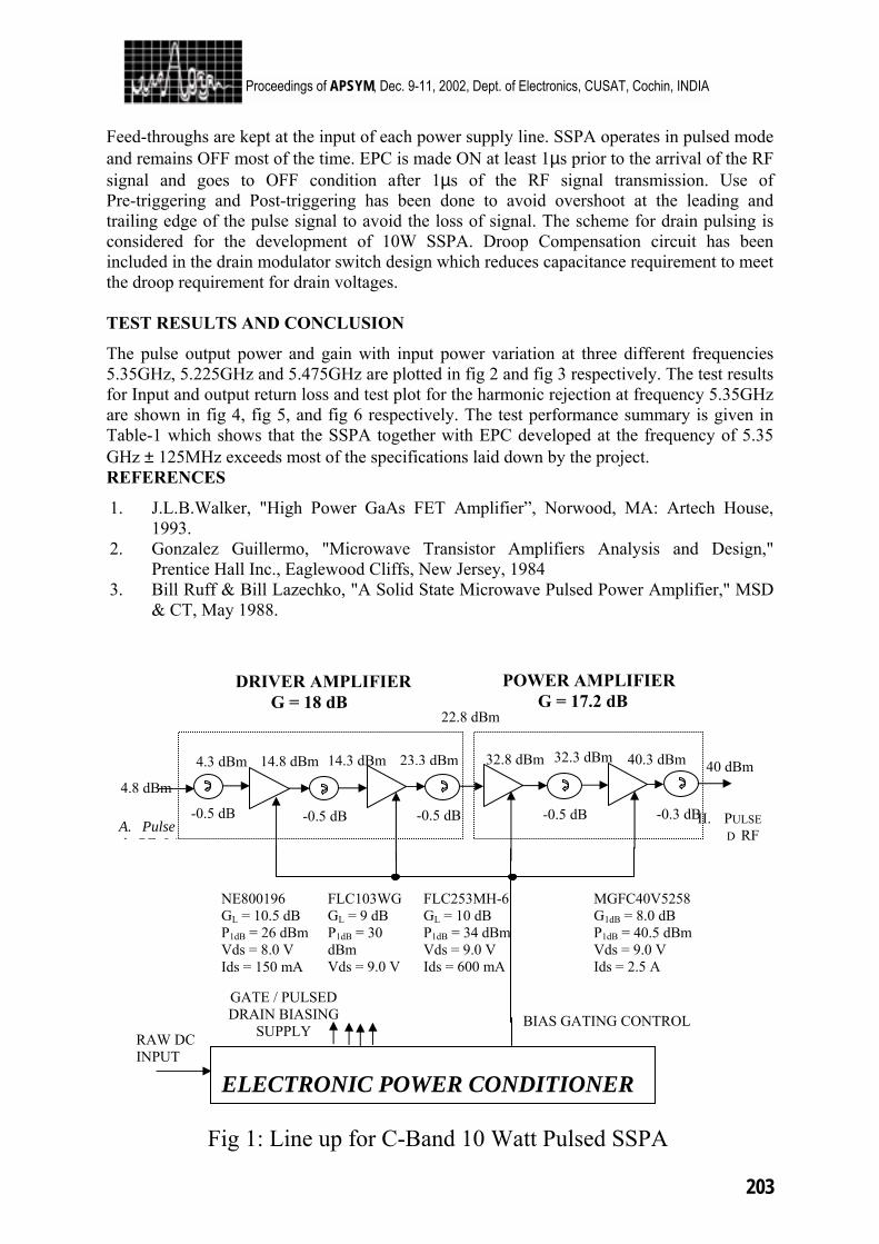
203
Proceedings of APSYM, Dec. 9-11, 2002, Dept. of Electronics, CUSAT, Cochin, INDIA
Feed-throughs are kept at the input of each power supply line. SSPA operates in pulsed mode and remains OFF most of the time. EPC is made ON at least 1µs prior to the arrival of the RF signal and goes to OFF condition after 1µs of the RF signal transmission. Use of Pre-triggering and Post-triggering has been done to avoid overshoot at the leading and trailing edge of the pulse signal to avoid the loss of signal. The scheme for drain pulsing is considered for the development of 10W SSPA. Droop Compensation circuit has been included in the drain modulator switch design which reduces capacitance requirement to meet the droop requirement for drain voltages. TEST RESULTS AND CONCLUSION
The pulse output power and gain with input power variation at three different frequencies 5.35GHz, 5.225GHz and 5.475GHz are plotted in fig 2 and fig 3 respectively. The test results for Input and output return loss and test plot for the harmonic rejection at frequency 5.35GHz are shown in fig 4, fig 5, and fig 6 respectively. The test performance summary is given in Table-1 which shows that the SSPA together with EPC developed at the frequency of 5.35 GHz ± 125MHz exceeds most of the specifications laid down by the project. REFERENCES
1. J.L.B.Walker, "High Power GaAs FET Amplifier”, Norwood, MA: Artech House, 1993.
2. Gonzalez Guillermo, "Microwave Transistor Amplifiers Analysis and Design," Prentice Hall Inc., Eaglewood Cliffs, New Jersey, 1984
3. Bill Ruff & Bill Lazechko, "A Solid State Microwave Pulsed Power Amplifier," MSD & CT, May 1988.
Fig 1: Line up for C-Band 10 Watt Pulsed SSPA
FLC253MH-6 GL = 10 dB P1dB = 34 dBm Vds = 9.0 V Ids = 600 mA
-0.3 dB
RAW DC INPUT
14.3 dBm 40.3 dBm
FLC103WG GL = 9 dB P1dB = 30 dBm Vds = 9.0 V
NE800196 GL = 10.5 dB P1dB = 26 dBm Vds = 8.0 V Ids = 150 mA
-0.5 dB-0.5 dB
32.3 dBm
-0.5 dB
32.8 dBm 23.3 dBm
22.8 dBm
II. PULSED RF
ELECTRONIC POWER CONDITIONER
BIAS GATING CONTROL GATE / PULSED DRAIN BIASING
SUPPLY
MGFC40V5258 G1dB = 8.0 dB P1dB = 40.5 dBm Vds = 9.0 V Ids = 2.5 A
-0.5 dB
4.3 dBm 14.8 dBm 40 dBm
POWER AMPLIFIER G = 17.2 dB
DRIVER AMPLIFIER G = 18 dB
4.8 dBm
A. Pulsed RF I /
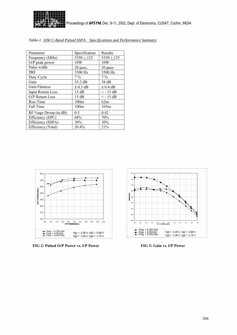
204
Proceedings of APSYM, Dec. 9-11, 2002, Dept. of Electronics, CUSAT, Cochin, INDIA
Table-1 10W C-Band Pulsed SSPA Specifications and Performance Summary
Parameter Specification Results Frequency (MHz) 5350 + 125 5350 + 125 O/P peak power 10W 10W Pulse width 20 µsec. 20 µsec PRF 3500 Hz 3500 Hz Duty Cycle 7 % 7 % Gain 35.2 dB 38 dB Gain Flatness ± 0.3 dB ± 0.4 dB Input Return Loss 15 dB < - 15 dB O/P Return Loss 15 dB < - 15 dB Rise Time 100ns 62ns Fall Time 100ns 103ns RF %age Droop (in dB) 0.5 0.42 Efficiency (EPC) 68% 70% Efficiency (SSPA) 30% 30% Efficiency (Total) 20.4% 21%
37.0
37.5
38.0
38.5
39.0
39.5
40.0
40.5
0.5 1.0 1.5 2.0 2.5 3.0 3.5 4.0 4.5 5.0 5.5I/P POWER(dBm)
O/P
PO
WER
(dB
m)
Freq. = 5.225 GHzFreq. = 5.35 GHzFreq. = 5.475 GHz
Vg1 = -1.09 V, Vg2 = -0.68 VVg3 = -1.09 V, Vg4 = -1.75 V
34.0
35.0
36.0
37.0
38.0
39.0
40.0
41.0
42.0
-6.0 -5.0 -4.0 -3.0 -2.0 -1.0 0.0 1.0 2.0 3.0 4.0 5.0I / P POWER( dBm)
Freq. = 5.225 GHzFreq. = 5.35 GHzFreq. = 5.475 GHz
Vg1 = -1.09 V, Vg2 = -0.68 VVg3 = -1.09 V, Vg4 = -1.75 V
FIG 2: Pulsed O/P Power vs. I/P Power FIG 3: Gain vs. I/P Power
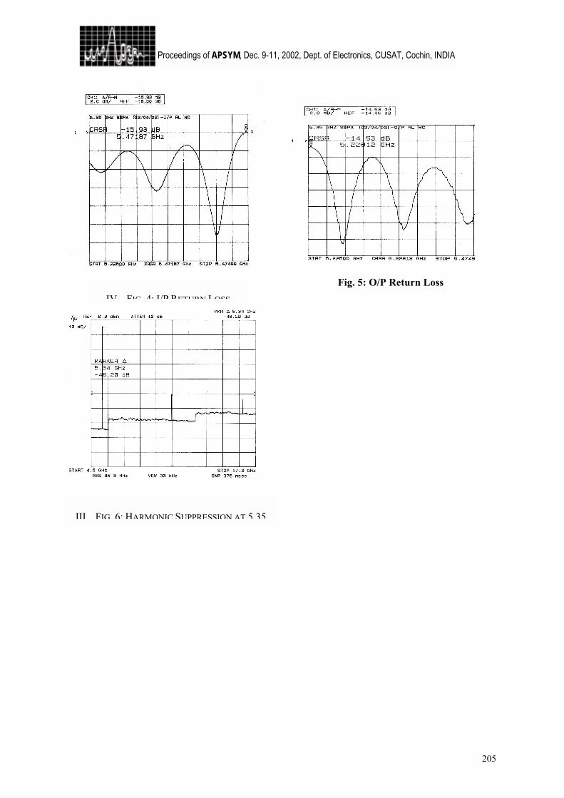
205
Proceedings of APSYM, Dec. 9-11, 2002, Dept. of Electronics, CUSAT, Cochin, INDIA
III FIG 6: HARMONIC SUPPRESSION AT 5 35
IV FIG 4: I/P RETURN LOSS
Fig. 5: O/P Return Loss
206
Proceedings of APSYM, Dec. 9-11, 2002, Dept. of Electronics, CUSAT, Cochin, INDIA
KU-BAND 140 W SPACE TWT FOR SATTELITE
COMMUNICATION
RK Sharma, A. Bera, V. Srivastava Microwave Tubes Area
Central Electronics Engineering Research Institute (CEERI), Pilani-333 031
In modern satellite system, TWTs in general and helix TWTs in particular play an important role in enhancing its communication capacity and quality, overall life time in the orbit etc. CEERI has successfully designed a C-band 60W(CW) helix space TWT and BEL, Bangalore has successfully developed the same for ISRO. ISRO recently sponsored another project to CEERI for the design of Ku-band 140W(CW) helix space TWT and development of its related critical technology to achieve the overall goals in terms of power, gain and overall efficiency in addition to the reliability over the expected long life more than 15 years. This paper discusses the design philosophy being adopted by the CEERI to meet the overall requirements.
INTRODUCTION
The Travelling Wave Tubes (TWTs) play vital role in the development of modern satellite communication system. The satellite system which requires microwave amplifier with broad frequency band with medium CW power at high gain (50dB) and efficiency (>50%), the helix TWTs are the unique choice till date. TWT amplifiers (TWTA) are used on direct broadcasting, telecommunications or earth observation transponders. The prime stringent requirements for the space qualified TWTs includes the high reliability, long life (typically more than 15 years), high overall efficiency at rated output power and gain, high linearity, low noise factor along with the low mass, weight and minimum possible size. The broad specifications of Ku-band space TWT under discussion are as follows: (i) frequency band: 10.9 to 11.7 GHz, (ii) output power: 140W(CW), (iii) gain at rated output power: 50 dB, (iv) overall efficiency at rated out put power: 50 %, (v) AM/PM factor: 5.0 deg. / dB max, (iv) inter modulation levels: 10 dBc etc. In order to meet the above specifications and other stringent requirements of space qualified devices, special considerations need to be given right from the designing of its various components like electron gun, RF section comprising of helix delay line, APBN support rods with optimum loss coating on the same and integral pole piece (IPP) barrel, periodic permanent magnet (PPM), input and output coupler, multistage depressed collector. The selection of material and adoption of the proper techniques for the fabrication of the above components and the tubes as a whole are equally important to meet the overall requirements of the space TWTs. This paper mainly discusses the salient features of the design approach for the design electron gun and slow wave structure of Ku-band 140 W (CW) helix space TWT.
ELECTRON GUN DESIGN
An M-type dispenser cathode with the following important features like (i) low emission current density (< 1.0 A / cm2), low cathode operating temperature (< 9500 C) and (iii) highly efficient potted heater with heater power (< 3.5 watt) for the desired cathode temperature has been selected. The cathode’s quality parameters mentioned above are chosen for the long life and high reliability of the TWT. Design of low convergent and low perveance electron gun
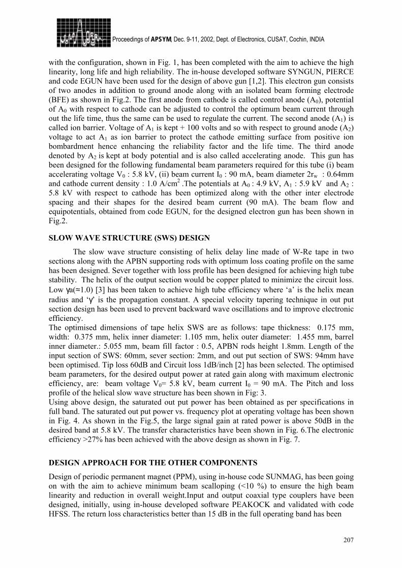
207
Proceedings of APSYM, Dec. 9-11, 2002, Dept. of Electronics, CUSAT, Cochin, INDIA
with the configuration, shown in Fig. 1, has been completed with the aim to achieve the high linearity, long life and high reliability. The in-house developed software SYNGUN, PIERCE and code EGUN have been used for the design of above gun [1,2]. This electron gun consists of two anodes in addition to ground anode along with an isolated beam forming electrode (BFE) as shown in Fig.2. The first anode from cathode is called control anode (A0), potential of A0 with respect to cathode can be adjusted to control the optimum beam current through out the life time, thus the same can be used to regulate the current. The second anode (A1) is called ion barrier. Voltage of A1 is kept + 100 volts and so with respect to ground anode (A2) voltage to act A1 as ion barrier to protect the cathode emitting surface from positive ion bombardment hence enhancing the reliability factor and the life time. The third anode denoted by A2 is kept at body potential and is also called accelerating anode. This gun has been designed for the following fundamental beam parameters required for this tube (i) beam accelerating voltage V0 : 5.8 kV, (ii) beam current I0 : 90 mA, beam diameter 2rw : 0.64mm and cathode current density : 1.0 A/cm2 .The potentials at A0 : 4.9 kV, A1 : 5.9 kV and A2 : 5.8 kV with respect to cathode has been optimized along with the other inter electrode spacing and their shapes for the desired beam current (90 mA). The beam flow and equipotentials, obtained from code EGUN, for the designed electron gun has been shown in Fig.2. SLOW WAVE STRUCTURE (SWS) DESIGN
The slow wave structure consisting of helix delay line made of W-Re tape in two sections along with the APBN supporting rods with optimum loss coating profile on the same has been designed. Sever together with loss profile has been designed for achieving high tube stability. The helix of the output section would be copper plated to minimize the circuit loss. Low γa(≈1.0) [3] has been taken to achieve high tube efficiency where ‘a’ is the helix mean radius and ‘γ’ is the propagation constant. A special velocity tapering technique in out put section design has been used to prevent backward wave oscillations and to improve electronic efficiency. The optimised dimensions of tape helix SWS are as follows: tape thickness: 0.175 mm, width: 0.375 mm, helix inner diameter: 1.105 mm, helix outer diameter: 1.455 mm, barrel inner diameter.: 5.055 mm, beam fill factor : 0.5, APBN rods height 1.8mm. Length of the input section of SWS: 60mm, sever section: 2mm, and out put section of SWS: 94mm have been optimised. Tip loss 60dB and Circuit loss 1dB/inch [2] has been selected. The optimised beam parameters, for the desired output power at rated gain along with maximum electronic efficiency, are: beam voltage V0= 5.8 kV, beam current I0 = 90 mA. The Pitch and loss profile of the helical slow wave structure has been shown in Fig: 3. Using above design, the saturated out put power has been obtained as per specifications in full band. The saturated out put power vs. frequency plot at operating voltage has been shown in Fig. 4. As shown in the Fig.5, the large signal gain at rated power is above 50dB in the desired band at 5.8 kV. The transfer characteristics have been shown in Fig. 6.The electronic efficiency >27% has been achieved with the above design as shown in Fig. 7.
DESIGN APPROACH FOR THE OTHER COMPONENTS
Design of periodic permanent magnet (PPM), using in-house code SUNMAG, has been going on with the aim to achieve minimum beam scalloping (<10 %) to ensure the high beam linearity and reduction in overall weight.Input and output coaxial type couplers have been designed, initially, using in-house developed software PEAKOCK and validated with code HFSS. The return loss characteristics better than 15 dB in the full operating band has been
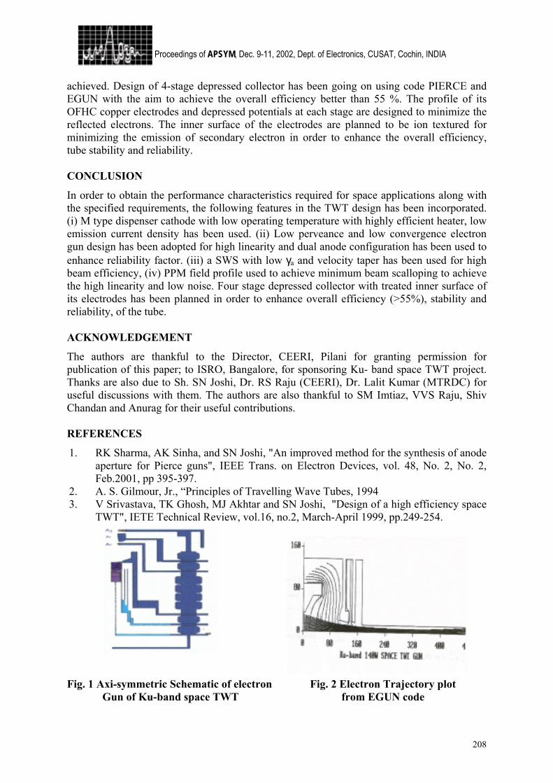
208
Proceedings of APSYM, Dec. 9-11, 2002, Dept. of Electronics, CUSAT, Cochin, INDIA
achieved. Design of 4-stage depressed collector has been going on using code PIERCE and EGUN with the aim to achieve the overall efficiency better than 55 %. The profile of its OFHC copper electrodes and depressed potentials at each stage are designed to minimize the reflected electrons. The inner surface of the electrodes are planned to be ion textured for minimizing the emission of secondary electron in order to enhance the overall efficiency, tube stability and reliability. CONCLUSION
In order to obtain the performance characteristics required for space applications along with the specified requirements, the following features in the TWT design has been incorporated. (i) M type dispenser cathode with low operating temperature with highly efficient heater, low emission current density has been used. (ii) Low perveance and low convergence electron gun design has been adopted for high linearity and dual anode configuration has been used to enhance reliability factor. (iii) a SWS with low γa and velocity taper has been used for high beam efficiency, (iv) PPM field profile used to achieve minimum beam scalloping to achieve the high linearity and low noise. Four stage depressed collector with treated inner surface of its electrodes has been planned in order to enhance overall efficiency (>55%), stability and reliability, of the tube. ACKNOWLEDGEMENT
The authors are thankful to the Director, CEERI, Pilani for granting permission for publication of this paper; to ISRO, Bangalore, for sponsoring Ku- band space TWT project. Thanks are also due to Sh. SN Joshi, Dr. RS Raju (CEERI), Dr. Lalit Kumar (MTRDC) for useful discussions with them. The authors are also thankful to SM Imtiaz, VVS Raju, Shiv Chandan and Anurag for their useful contributions. REFERENCES
1. RK Sharma, AK Sinha, and SN Joshi, "An improved method for the synthesis of anode aperture for Pierce guns", IEEE Trans. on Electron Devices, vol. 48, No. 2, No. 2, Feb.2001, pp 395-397.
2. A. S. Gilmour, Jr., “Principles of Travelling Wave Tubes, 1994 3. V Srivastava, TK Ghosh, MJ Akhtar and SN Joshi, "Design of a high efficiency space
TWT", IETE Technical Review, vol.16, no.2, March-April 1999, pp.249-254.
Fig. 1 Axi-symmetric Schematic of electron Gun of Ku-band space TWT
Fig. 2 Electron Trajectory plot from EGUN code
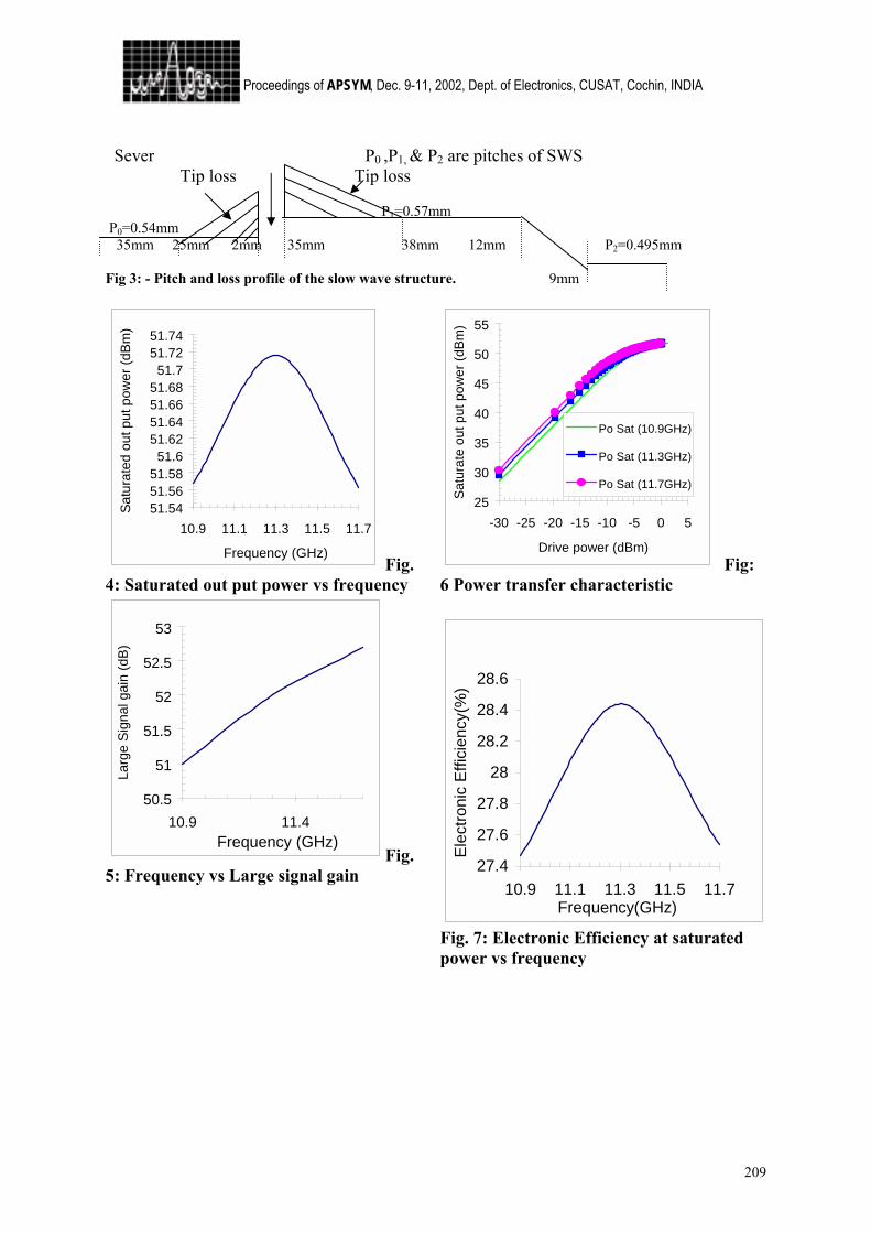
209
Proceedings of APSYM, Dec. 9-11, 2002, Dept. of Electronics, CUSAT, Cochin, INDIA
Sever P0 ,P1, & P2 are pitches of SWS Tip loss Tip loss P1=0.57mm P0=0.54mm 35mm 25mm 2mm 35mm 38mm 12mm P2=0.495mm Fig 3: - Pitch and loss profile of the slow wave structure. 9mm
51.5451.5651.5851.6
51.6251.6451.6651.6851.7
51.7251.74
10.9 11.1 11.3 11.5 11.7
Frequency (GHz)
Satu
rate
d ou
t put
pow
er (d
Bm)
Fig. 4: Saturated out put power vs frequency
50.5
51
51.5
52
52.5
53
10.9 11.4Frequency (GHz)
Larg
e Si
gnal
gai
n (d
B)
Fig. 5: Frequency vs Large signal gain
25
30
35
40
45
50
55
-30 -25 -20 -15 -10 -5 0 5
Drive power (dBm)
Sat
urat
e ou
t put
pow
er (d
Bm
)
Po Sat (10.9GHz)
Po Sat (11.3GHz)
Po Sat (11.7GHz)
Fig: 6 Power transfer characteristic
27.4
27.6
27.8
28
28.2
28.4
28.6
10.9 11.1 11.3 11.5 11.7Frequency(GHz)
Ele
ctro
nic
Effi
cien
cy(%
)
Fig. 7: Electronic Efficiency at saturated power vs frequency
210
Proceedings of APSYM, Dec. 9-11, 2002, Dept. of Electronics, CUSAT, Cochin, INDIA
Ka BAND WHISPERING GALLERY MODE DRO
S.L.Badnikar
G-FAST, Defence Research and Development Organisation, New Delhi- 110 011.
Recently high permittivity whispering gallery mode dielectric resonators have been used in preference to fundamental mode dielectric resonators because of their high quality factors and reasonable dimensions at millimeter wavelengths. This paper presents the design and realisation of a whispering gallery mode dielectric resonator oscillator for microwave integrated circuit(MIC) applications. A series feedback method has been employed with commercial HEMT chip as an active device. A large signal Curtice-Ettenberg model has been used for the CAD simulation. As an illustrative example, the design of WG mode DRO at Ka band is discussed. Good oscillator power output, low phase noise and reasonable frequency stability have been achieved.
INTRODUCTION
Oscillators represent the basic microwave energy source for all microwave systems such as radars, communications, navigation or electronic warfare. A dielectric resonator oscillator(DRO) clearly fills the gap between a free running oscillator and a synthesised source and presents a good compromise on cost, size and performance. Also, due to a high quality factor of the resonator, this class of oscillators offers excellent FM noise performance, high temperature stability, reasonably high power output apart from the small size. Central to the design of the DRO is a selection of the dielectric resonator(DR), a high εr, low loss, temperature stable compound ceramic material in a regular geometric shape. DROs are classified into four types: reaction, transmission, parallel feedback and reflection types. Each configuration has its specific utility [1]. TE01δ mode is the commonly used mode for DROs. However, its usefulness is significantly reduced at millimeter wave frequencies because the DR dimensions become impractically small to handle and manufacture. Apart from this, quality factor and temperature stability also need to be preserved in this range of frequency operation. The whispering gallery(WG) mode DR is preferred as it is an oversized cylindrical DR configuration with a higher quality factor vis–a-vis the conventional mode DRs. In this paper a WGDR is used as a frequency determining element in the oscillator where negative resistance is induced in the HEMT active device by introducing external feedback thereby making the device potentially unstable. The WGDR is coupled to the input port of the active device using WGE mode. Good output power, low phase noise and reasonable frequency stability over a temperature range of operation have been achieved. THEORY
A) ANALYSIS FOR WGE RESONANT FREQUENCY IN MIC ENVIRONMENT
The WG modes move essentially in the plane of a circular cross-section and most of the modal energy is confined between the resonator boundary and the inner modal caustic as well
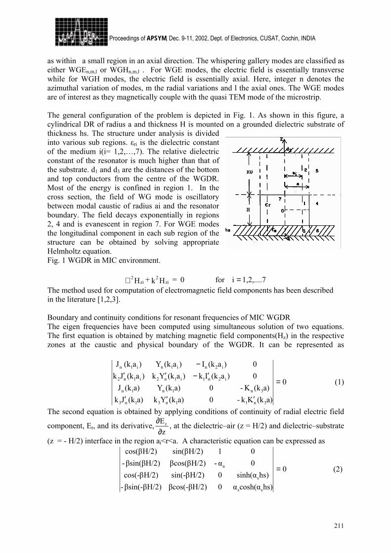
211
Proceedings of APSYM, Dec. 9-11, 2002, Dept. of Electronics, CUSAT, Cochin, INDIA
as within a small region in an axial direction. The whispering gallery modes are classified as either WGEn,m,l or WGHn,m,l . For WGE modes, the electric field is essentially transverse while for WGH modes, the electric field is essentially axial. Here, integer n denotes the azimuthal variation of modes, m the radial variations and l the axial ones. The WGE modes are of interest as they magnetically couple with the quasi TEM mode of the microstrip. The general configuration of the problem is depicted in Fig. 1. As shown in this figure, a cylindrical DR of radius a and thickness H is mounted on a grounded dielectric substrate of thickness hs. The structure under analysis is divided into various sub regions. εri is the dielectric constant of the medium i(i= 1,2,…,7). The relative dielectric constant of the resonator is much higher than that of the substrate. d1 and d3 are the distances of the bottom and top conductors from the centre of the WGDR. Most of the energy is confined in region 1. In the cross section, the field of WG mode is oscillatory between modal caustic of radius ai and the resonator boundary. The field decays exponentially in regions 2, 4 and is evanescent in region 7. For WGE modes the longitudinal component in each sub region of the structure can be obtained by solving appropriate Helmholtz equation. Fig. 1 WGDR in MIC environment.
1,2,....7ifor0 = Hk+H zi
2zi
2 =∇ The method used for computation of electromagnetic field components has been described in the literature [1,2,3]. Boundary and continuity conditions for resonant frequencies of MIC WGDR The eigen frequencies have been computed using simultaneous solution of two equations. The first equation is obtained by matching magnetic field components(Hz) in the respective zones at the caustic and physical boundary of the WGDR. It can be represented as
0
a)(kKk-0a)(kYka)(kJka)(kK-0a)(kYa)(kJ
0)a(kIk)a(kYk)a(kJk0)a(kI)a(kY)a(kJ
3n11n31n3
3n1n1n
i2n1i1n2i1n2
i2ni1ni1n
=
′′′
′−′′−
(1)
The second equation is obtained by applying conditions of continuity of radial electric field
component, Er, and its derivative,z
Er
∂∂ , at the dielectric–air (z = H/2) and dielectric–substrate
(z = - H/2) interface in the region ai<r<a. A characteristic equation can be expressed as
0
hs)cosh(αα0H/2)βcos(-βH/2)βsin(-β-hs)sinh(α0H/2)sin(-βH/2)cos(-β
0α-H/2)cos(βββsin(βH/2)-01H/2)sin(βH/2)cos(β
ss
s
a = (2)
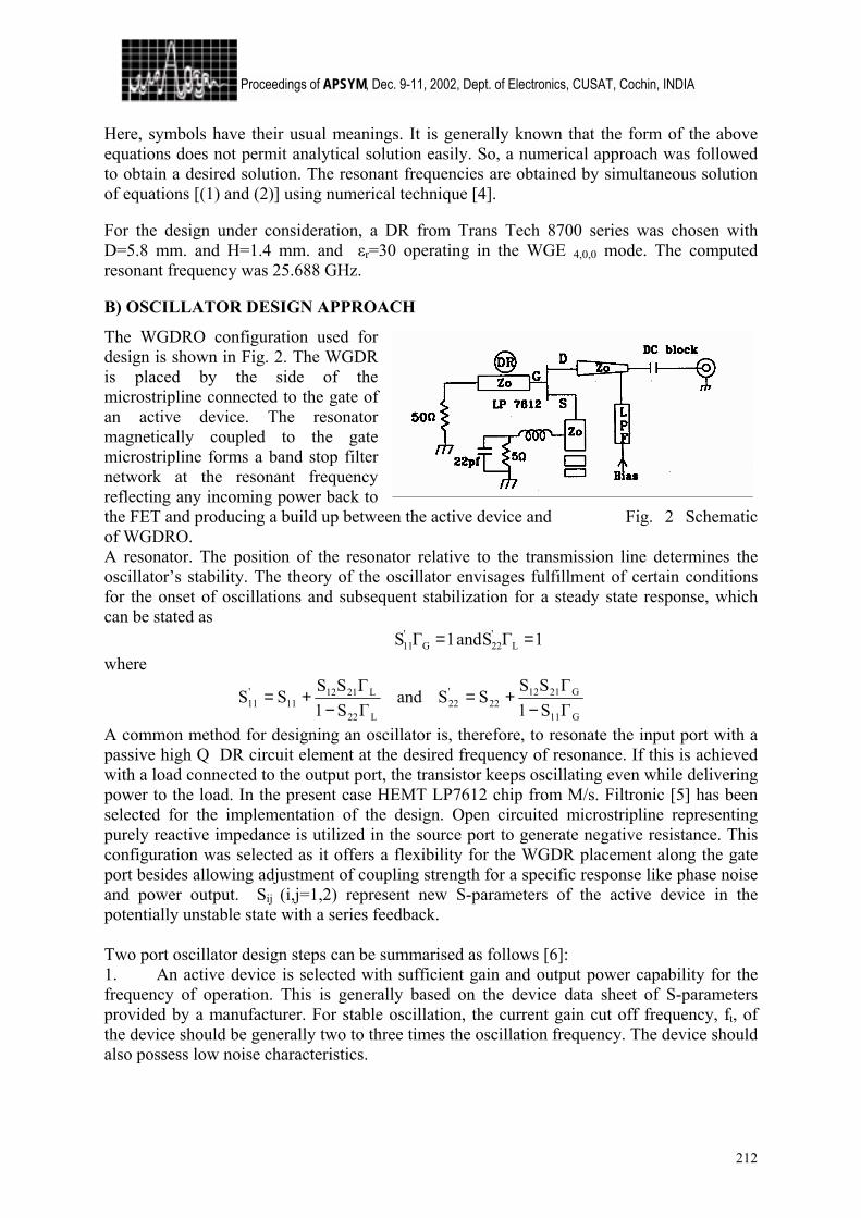
212
Proceedings of APSYM, Dec. 9-11, 2002, Dept. of Electronics, CUSAT, Cochin, INDIA
Here, symbols have their usual meanings. It is generally known that the form of the above equations does not permit analytical solution easily. So, a numerical approach was followed to obtain a desired solution. The resonant frequencies are obtained by simultaneous solution of equations [(1) and (2)] using numerical technique [4].
For the design under consideration, a DR from Trans Tech 8700 series was chosen with D=5.8 mm. and H=1.4 mm. and εr=30 operating in the WGE 4,0,0 mode. The computed resonant frequency was 25.688 GHz.
B) OSCILLATOR DESIGN APPROACH
The WGDRO configuration used for design is shown in Fig. 2. The WGDR is placed by the side of the microstripline connected to the gate of an active device. The resonator magnetically coupled to the gate microstripline forms a band stop filter network at the resonant frequency reflecting any incoming power back to the FET and producing a build up between the active device and Fig. 2 Schematic of WGDRO. A resonator. The position of the resonator relative to the transmission line determines the oscillator’s stability. The theory of the oscillator envisages fulfillment of certain conditions for the onset of oscillations and subsequent stabilization for a steady state response, which can be stated as
1ΓSand1ΓS L'22G
'11 ==
where
G11
G211222
'22
L22
L211211
'11 ΓS1
ΓSSSSand
ΓS1ΓSSSS
−+=
−+=
A common method for designing an oscillator is, therefore, to resonate the input port with a passive high Q DR circuit element at the desired frequency of resonance. If this is achieved with a load connected to the output port, the transistor keeps oscillating even while delivering power to the load. In the present case HEMT LP7612 chip from M/s. Filtronic [5] has been selected for the implementation of the design. Open circuited microstripline representing purely reactive impedance is utilized in the source port to generate negative resistance. This configuration was selected as it offers a flexibility for the WGDR placement along the gate port besides allowing adjustment of coupling strength for a specific response like phase noise and power output. Sij (i,j=1,2) represent new S-parameters of the active device in the potentially unstable state with a series feedback.
Two port oscillator design steps can be summarised as follows [6]: 1. An active device is selected with sufficient gain and output power capability for the frequency of operation. This is generally based on the device data sheet of S-parameters provided by a manufacturer. For stable oscillation, the current gain cut off frequency, ft, of the device should be generally two to three times the oscillation frequency. The device should also possess low noise characteristics.
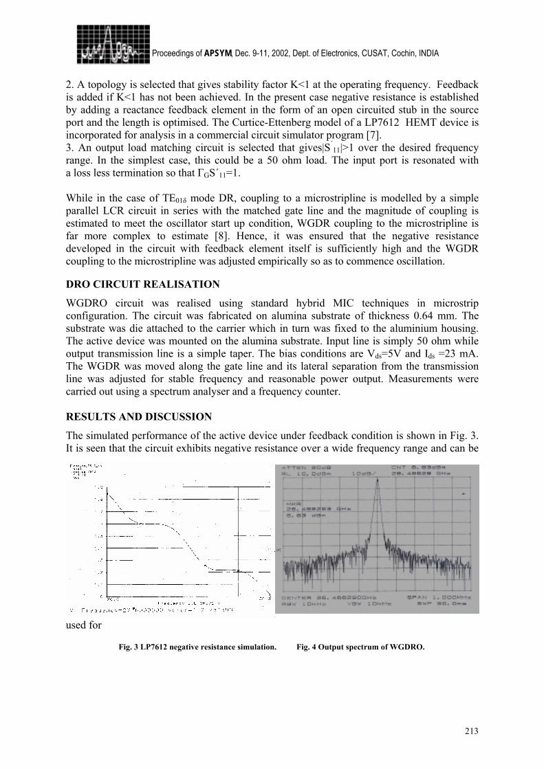
213
Proceedings of APSYM, Dec. 9-11, 2002, Dept. of Electronics, CUSAT, Cochin, INDIA
2. A topology is selected that gives stability factor K<1 at the operating frequency. Feedback is added if K<1 has not been achieved. In the present case negative resistance is established by adding a reactance feedback element in the form of an open circuited stub in the source port and the length is optimised. The Curtice-Ettenberg model of a LP7612 HEMT device is incorporated for analysis in a commercial circuit simulator program [7]. 3. An output load matching circuit is selected that gives|S´
11|>1 over the desired frequency range. In the simplest case, this could be a 50 ohm load. The input port is resonated with a loss less termination so that ΓGS´11=1.
While in the case of TE01δ mode DR, coupling to a microstripline is modelled by a simple parallel LCR circuit in series with the matched gate line and the magnitude of coupling is estimated to meet the oscillator start up condition, WGDR coupling to the microstripline is far more complex to estimate [8]. Hence, it was ensured that the negative resistance developed in the circuit with feedback element itself is sufficiently high and the WGDR coupling to the microstripline was adjusted empirically so as to commence oscillation.
DRO CIRCUIT REALISATION
WGDRO circuit was realised using standard hybrid MIC techniques in microstrip configuration. The circuit was fabricated on alumina substrate of thickness 0.64 mm. The substrate was die attached to the carrier which in turn was fixed to the aluminium housing. The active device was mounted on the alumina substrate. Input line is simply 50 ohm while output transmission line is a simple taper. The bias conditions are Vds=5V and Ids =23 mA. The WGDR was moved along the gate line and its lateral separation from the transmission line was adjusted for stable frequency and reasonable power output. Measurements were carried out using a spectrum analyser and a frequency counter. RESULTS AND DISCUSSION
The simulated performance of the active device under feedback condition is shown in Fig. 3. It is seen that the circuit exhibits negative resistance over a wide frequency range and can be
used for
Fig. 3 LP7612 negative resistance simulation. Fig. 4 Output spectrum of WGDRO.
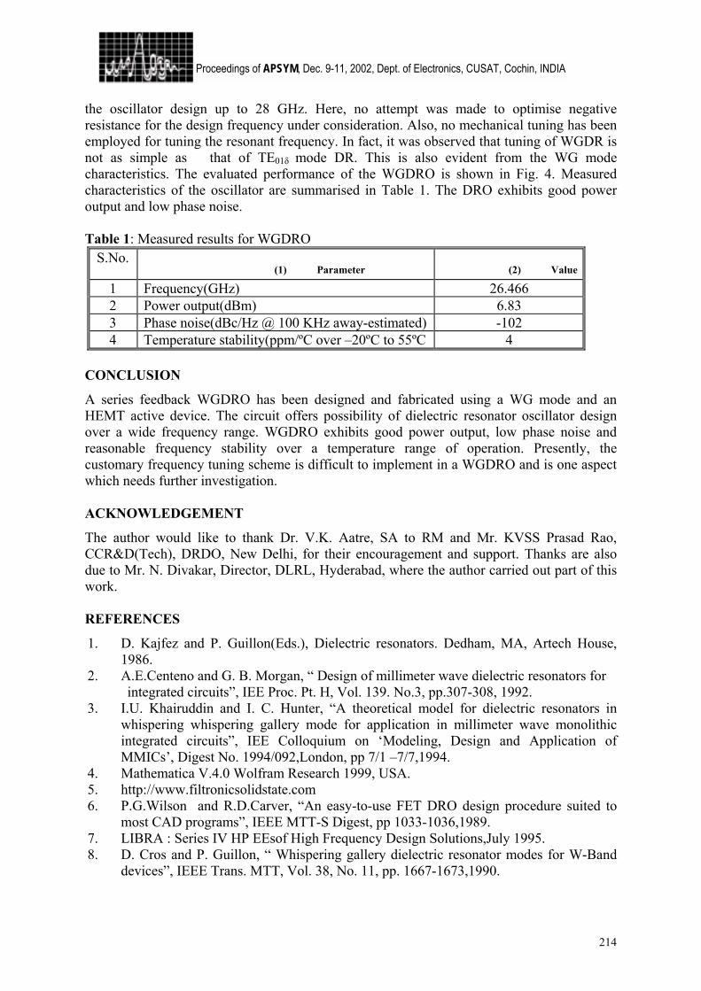
214
Proceedings of APSYM, Dec. 9-11, 2002, Dept. of Electronics, CUSAT, Cochin, INDIA
the oscillator design up to 28 GHz. Here, no attempt was made to optimise negative resistance for the design frequency under consideration. Also, no mechanical tuning has been employed for tuning the resonant frequency. In fact, it was observed that tuning of WGDR is not as simple as that of TE01δ mode DR. This is also evident from the WG mode characteristics. The evaluated performance of the WGDRO is shown in Fig. 4. Measured characteristics of the oscillator are summarised in Table 1. The DRO exhibits good power output and low phase noise. Table 1: Measured results for WGDRO
S.No. (1) Parameter (2) Value
1 Frequency(GHz) 26.466 2 Power output(dBm) 6.83 3 Phase noise(dBc/Hz @ 100 KHz away-estimated) -102 4 Temperature stability(ppm/ºC over –20ºC to 55ºC 4
CONCLUSION
A series feedback WGDRO has been designed and fabricated using a WG mode and an HEMT active device. The circuit offers possibility of dielectric resonator oscillator design over a wide frequency range. WGDRO exhibits good power output, low phase noise and reasonable frequency stability over a temperature range of operation. Presently, the customary frequency tuning scheme is difficult to implement in a WGDRO and is one aspect which needs further investigation. ACKNOWLEDGEMENT
The author would like to thank Dr. V.K. Aatre, SA to RM and Mr. KVSS Prasad Rao, CCR&D(Tech), DRDO, New Delhi, for their encouragement and support. Thanks are also due to Mr. N. Divakar, Director, DLRL, Hyderabad, where the author carried out part of this work. REFERENCES
1. D. Kajfez and P. Guillon(Eds.), Dielectric resonators. Dedham, MA, Artech House, 1986.
2. A.E.Centeno and G. B. Morgan, “ Design of millimeter wave dielectric resonators for integrated circuits”, IEE Proc. Pt. H, Vol. 139. No.3, pp.307-308, 1992. 3. I.U. Khairuddin and I. C. Hunter, “A theoretical model for dielectric resonators in
whispering whispering gallery mode for application in millimeter wave monolithic integrated circuits”, IEE Colloquium on ‘Modeling, Design and Application of MMICs’, Digest No. 1994/092,London, pp 7/1 –7/7,1994.
4. Mathematica V.4.0 Wolfram Research 1999, USA. 5. http://www.filtronicsolidstate.com 6. P.G.Wilson and R.D.Carver, “An easy-to-use FET DRO design procedure suited to
most CAD programs”, IEEE MTT-S Digest, pp 1033-1036,1989. 7. LIBRA : Series IV HP EEsof High Frequency Design Solutions,July 1995. 8. D. Cros and P. Guillon, “ Whispering gallery dielectric resonator modes for W-Band
devices”, IEEE Trans. MTT, Vol. 38, No. 11, pp. 1667-1673,1990.
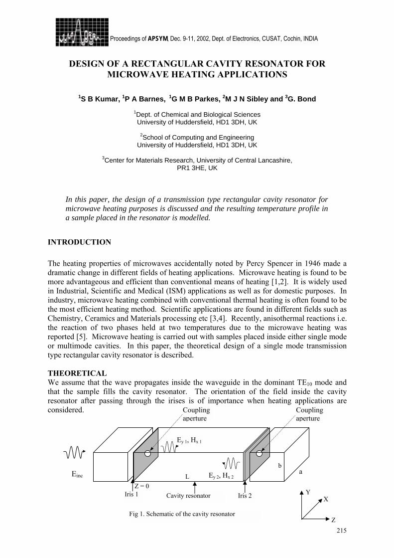
215
Proceedings of APSYM, Dec. 9-11, 2002, Dept. of Electronics, CUSAT, Cochin, INDIA
DESIGN OF A RECTANGULAR CAVITY RESONATOR FOR
MICROWAVE HEATING APPLICATIONS
1S B Kumar, 1P A Barnes, 1G M B Parkes, 2M J N Sibley and 3G. Bond
1Dept. of Chemical and Biological Sciences University of Huddersfield, HD1 3DH, UK
2School of Computing and Engineering
University of Huddersfield, HD1 3DH, UK
3Center for Materials Research, University of Central Lancashire, PR1 3HE, UK
In this paper, the design of a transmission type rectangular cavity resonator for microwave heating purposes is discussed and the resulting temperature profile in a sample placed in the resonator is modelled.
INTRODUCTION The heating properties of microwaves accidentally noted by Percy Spencer in 1946 made a dramatic change in different fields of heating applications. Microwave heating is found to be more advantageous and efficient than conventional means of heating [1,2]. It is widely used in Industrial, Scientific and Medical (ISM) applications as well as for domestic purposes. In industry, microwave heating combined with conventional thermal heating is often found to be the most efficient heating method. Scientific applications are found in different fields such as Chemistry, Ceramics and Materials processing etc [3,4]. Recently, anisothermal reactions i.e. the reaction of two phases held at two temperatures due to the microwave heating was reported [5]. Microwave heating is carried out with samples placed inside either single mode or multimode cavities. In this paper, the theoretical design of a single mode transmission type rectangular cavity resonator is described. THEORETICAL We assume that the wave propagates inside the waveguide in the dominant TE10 mode and that the sample fills the cavity resonator. The orientation of the field inside the cavity resonator after passing through the irises is of importance when heating applications are considered. Einc
Z
Y X
Iris 1 Iris 2 Cavity resonator
Coupling aperture
Coupling aperture
Z = 0
b L
a
Ey 1, Hx 1
Ey 2, Hx 2
Fig 1. Schematic of the cavity resonator

216
Proceedings of APSYM, Dec. 9-11, 2002, Dept. of Electronics, CUSAT, Cochin, INDIA
When the incident field reaches the first iris, part of the power penetrates into the resonator depending on the dimension of the coupling aperture, and this is determined by the polarisation currents Pe and Pm [6]. Since there is no electric component along the direction of propagation, Pe = 0
and the polarisation current density, )()2
()2
(10
zbyaxZ
AxP mm δδδα −−=
Λ,
the magnetic current density, mPjM 0µω= , and the coefficient of the transmitted wave is given by
∫−+ =
v nn
n dvMHP
A .1 (for Z>0)
Solving this equation, we get ab
jAA mβα410 =+ , where the magnetic polarizibility for a
circular aperture of radius r0, mα is given by3
4 30r .
Similarly, the coefficient of reflected amplitude is given by, ab
jAA mβα410 =− (for Z<0)
The field reflected from iris 1 is given byaxeeAA tjzj πωβ sin)( 10 −
−
Thus, the field penetrating iris1 and entering the cavity is
axsineeAE tjzj
101yπ= ωβ−+ (1a)
axsinee
ZA
H tjzj
10
101x
π−= ωβ−+
(1b)
When the fields Ey
1 and Hx1 reach iris 2, partial transmission and reflection again occurs. The
corresponding parameters of the transmission and reflection coefficients will be A20+ and
A20+-A10
+ The reflected field strengths from iris 2 will be
axsineeAAE tjzj
10202yπ−= ωβ+− (2a)
axsineeAA
Z1H tjzj
102010
2xπ−−= ωβ+− (2b)
The total field inside the cavity is
Ey cav = Ey 1 + Ey 2 (3a)
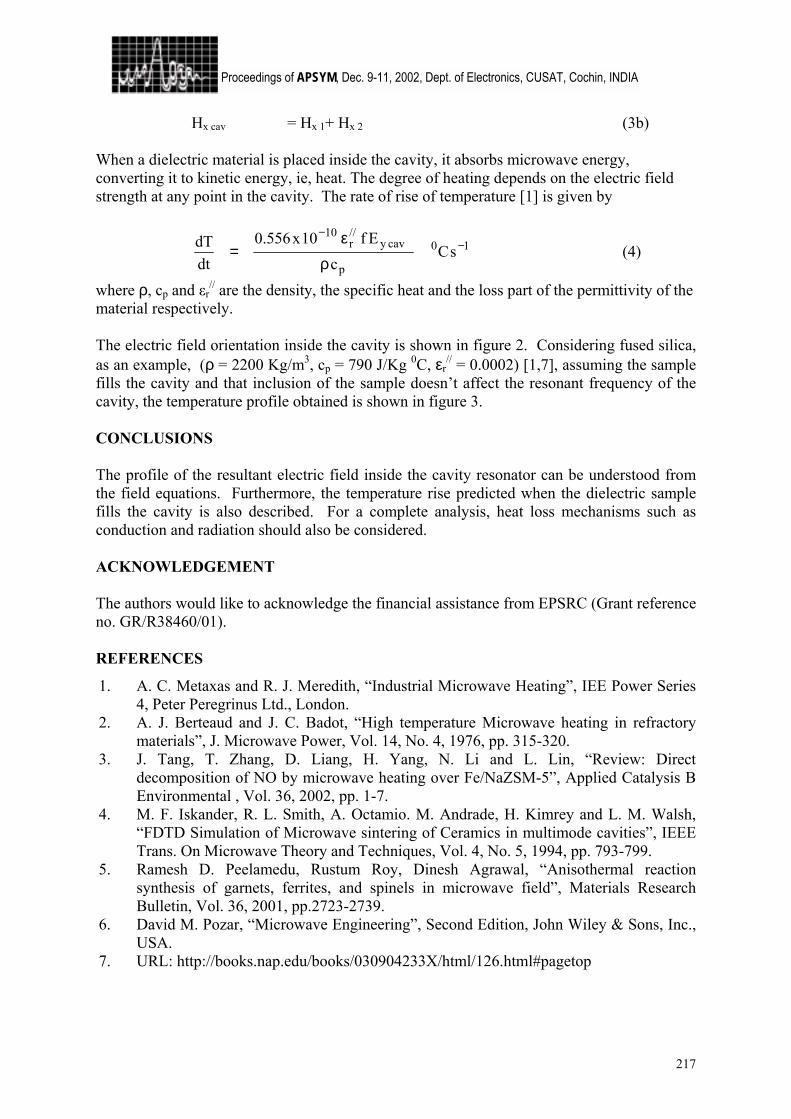
217
Proceedings of APSYM, Dec. 9-11, 2002, Dept. of Electronics, CUSAT, Cochin, INDIA
Hx cav = Hx 1+ Hx 2 (3b)
When a dielectric material is placed inside the cavity, it absorbs microwave energy, converting it to kinetic energy, ie, heat. The degree of heating depends on the electric field strength at any point in the cavity. The rate of rise of temperature [1] is given by
10
p
cavy//r
10
sCc
Ef10x556.0dtdT −
−
ρε
= (4)
where ρ, cp and εr// are the density, the specific heat and the loss part of the permittivity of the
material respectively. The electric field orientation inside the cavity is shown in figure 2. Considering fused silica, as an example, (ρ = 2200 Kg/m3, cp = 790 J/Kg 0C, εr
// = 0.0002) [1,7], assuming the sample fills the cavity and that inclusion of the sample doesn’t affect the resonant frequency of the cavity, the temperature profile obtained is shown in figure 3. CONCLUSIONS The profile of the resultant electric field inside the cavity resonator can be understood from the field equations. Furthermore, the temperature rise predicted when the dielectric sample fills the cavity is also described. For a complete analysis, heat loss mechanisms such as conduction and radiation should also be considered. ACKNOWLEDGEMENT The authors would like to acknowledge the financial assistance from EPSRC (Grant reference no. GR/R38460/01). REFERENCES
1. A. C. Metaxas and R. J. Meredith, “Industrial Microwave Heating”, IEE Power Series 4, Peter Peregrinus Ltd., London.
2. A. J. Berteaud and J. C. Badot, “High temperature Microwave heating in refractory materials”, J. Microwave Power, Vol. 14, No. 4, 1976, pp. 315-320.
3. J. Tang, T. Zhang, D. Liang, H. Yang, N. Li and L. Lin, “Review: Direct decomposition of NO by microwave heating over Fe/NaZSM-5”, Applied Catalysis B Environmental , Vol. 36, 2002, pp. 1-7.
4. M. F. Iskander, R. L. Smith, A. Octamio. M. Andrade, H. Kimrey and L. M. Walsh, “FDTD Simulation of Microwave sintering of Ceramics in multimode cavities”, IEEE Trans. On Microwave Theory and Techniques, Vol. 4, No. 5, 1994, pp. 793-799.
5. Ramesh D. Peelamedu, Rustum Roy, Dinesh Agrawal, “Anisothermal reaction synthesis of garnets, ferrites, and spinels in microwave field”, Materials Research Bulletin, Vol. 36, 2001, pp.2723-2739.
6. David M. Pozar, “Microwave Engineering”, Second Edition, John Wiley & Sons, Inc., USA.
7. URL: http://books.nap.edu/books/030904233X/html/126.html#pagetop
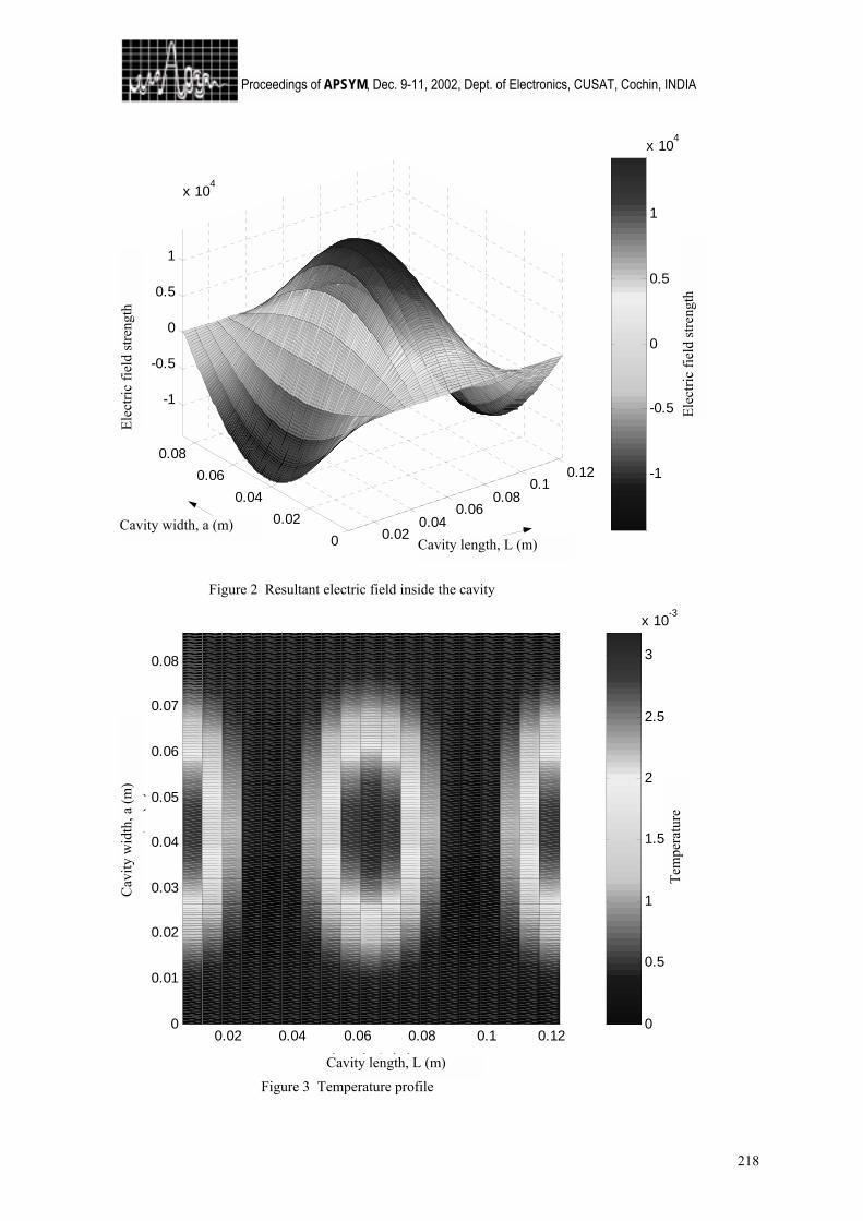
218
Proceedings of APSYM, Dec. 9-11, 2002, Dept. of Electronics, CUSAT, Cochin, INDIA
-1
-0.5
0
0.5
1
x 104
0.020.04
0.060.08
0.10.12
00.02
0.040.06
0.08
-1
-0.5
0
0.5
1
x 104
width, a (m)length, L (m)
Figure 2 Resultant electric field inside the cavity
0
0.5
1
1.5
2
2.5
3
x 10-3
0.02 0.04 0.06 0.08 0.1 0.120
0.01
0.02
0.03
0.04
0.05
0.06
0.07
0.08
wid
th, a
(m)
length, L (m)
Figure 3 Temperature profile
Cav
ity w
idth
, a (m
)
Cavity width, a (m)
Cavity length, L (m)
Cavity length, L (m)
Elec
tric
field
stre
ngth
Elec
tric
field
stre
ngth
Te
mpe
ratu
re

1.
219
Proceedings of APSYM, Dec. 9-11, 2002, Dept. of Electronics, CUSAT, Cochin, INDIA
RESEARCH SESSION V December 10, Tuesday 2002.(11.00 a.m. to 12.45 p.m)
MICROSTRIP ANTENNAS 2 Hall : 1
CHAIRS: PROF. FRED GARDIOL PROF. PARVEEN WAHID
5.1 Planar Microstrip Array Antenna for METSAT Debojyoti Choudhuri, Praveen Kumar, V.V. Srinivasan V .Mahadevan, V.K. Lakshmeesha,& S. Pal Communication System Group, ISRO Satellite Centre, Bangalore-560 017 [email protected]
221
5.2 Suspended Multi-layer Multi-Resonator Rectangular Microstrip Antennas Girish Kumar & K.P. Ray Department of Electrical Engineering, IIT Bombay, Powai Mumbai-400 076. [email protected]
225
5.3 Compact Broadband S-Shaped Stacked Microstrip Antennas Amit A. Deshmukh & Girish Kumar Department of Electrical Engineering, IIT Bombay, Powai Mumbai-400 076. [email protected]
229
5.4 Slot Loaded Rectangular Microstrip Antenna For Tunable Dual band Operation Asha E. Daniel & Girish Kumar Department of Electrical Engineering, IIT Bombay, Powai Mumbai-400 076 [email protected]
233
5.5 Simple Approximation For Characteristic Impedance Of Asymmetrically Coupled Microstrip Line Rabindra K. Mishra and Gopal K. Patra Electronic Science Dept. Berhampur Uty., Orrissa-760 007
237
5.6 A Printed Series-fed Microstrip Array D.R. Jahagirdar and V.G. Borkar Microwave Antennas & Components Division, Directorate of Electromagnetics, RCI, Hyderabad.
241
5.7 Dual Band Octagonal Patch Antenna Binu Paul,S. Mridula,C.K Aanandan and P. Mohanan Dept of Electronics ,CUSAT,Cochin-682 [email protected]
244
1.
220
Proceedings of APSYM, Dec. 9-11, 2002, Dept. of Electronics, CUSAT, Cochin, INDIA
1.
221
Proceedings of APSYM, Dec. 9-11, 2002, Dept. of Electronics, CUSAT, Cochin, INDIA PLANAR MICROSTRIP ARRAY ANTENNA FOR METSAT
Debojyoti Choudhuri, Praveen Kumar, V.V Srinivasan, V Mahadevan, V.K Lakshmeesha & S Pal
Communication Systems Group, ISRO Satellite Centre, Bangalore-560 017. [email protected], [email protected]
Microstrip array antennas are very good candidates for space application, where the weight and the volume of the antenna are of prime importance. A 16 x16 microstrip antenna array is developed for the Metsat (Meteorological Satellite). The C-band array achieved a bandwidth of 80 MHz, 26-dBi gain and a total weight of 1 Kg including supporting structure. In this paper design and configuration of the antenna is presented.
INTRODUCTION
There was a requirement of low weight, high gain antenna for forthcoming Meteorological satellite. The candidates for these requirements were reflector antenna and microstrip antenna array. The problem with the reflector antenna is that the weight of this antenna will be 3.5 Kg (0.8 mtrs diameter) for 26 dBi gain at 4.5 GHz whereas the weight of the microstrip antenna array is only 1 Kg for this gain which is of great advantage for space application. This paper outlines the electrical design and the simulated & practical results of the antenna. The specifications of the antenna are:
Frequency 4.5 GHz EOC Gain (± 2°) 25dBi Polarization Linear Bandwidth 20 MHz 3dB Beam width ± 6.4° Power handling 15 W
Return loss 15 dB and better Cross-polarization 28 dB and better Weight 1Kg
RADIATING ELEMENT
The printed radiating element is an important electromagnetic structure, which should function with good impedance match and pattern behavior over the band of interest. The different types of radiating elements that are widely used are the probe fed, microstrip fed and electromagnetically coupled microstrip patch antennas. As the bandwidth requirement is not critical single layer configuration is chosen where the basic radiating element is microstrip fed. The single element is simulated in IE3D electromagnetic simulation software that is based on MOM (Method of Moment). The material used is TFG of dielectric constant 2.55 and thickness 0.8 mm (1/32”). Fig. 1 shows the single radiating element.
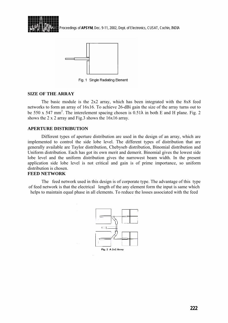
1.
222
Proceedings of APSYM, Dec. 9-11, 2002, Dept. of Electronics, CUSAT, Cochin, INDIA
SIZE OF THE ARRAY
The basic module is the 2x2 array, which has been integrated with the 8x8 feed networks to form an array of 16x16. To achieve 26-dBi gain the size of the array turns out to be 550 x 547 mm2. The interelement spacing chosen is 0.51λ in both E and H plane. Fig. 2 shows the 2 x 2 array and Fig.3 shows the 16x16 array.
APERTURE DISTRIBUTION
Different types of aperture distribution are used in the design of an array, which are implemented to control the side lobe level. The different types of distribution that are generally available are Taylor distribution, Chebyseb distribution, Binomial distribution and Uniform distribution. Each has got its own merit and demerit. Binomial gives the lowest side lobe level and the uniform distribution gives the narrowest beam width. In the present application side lobe level is not critical and gain is of prime importance, so uniform distribution is chosen. FEED NETWORK
The feed network used in this design is of corporate type. The advantage of this type of feed network is that the electrical length of the any element form the input is same which helps to maintain equal phase in all elements. To reduce the losses associated with the feed
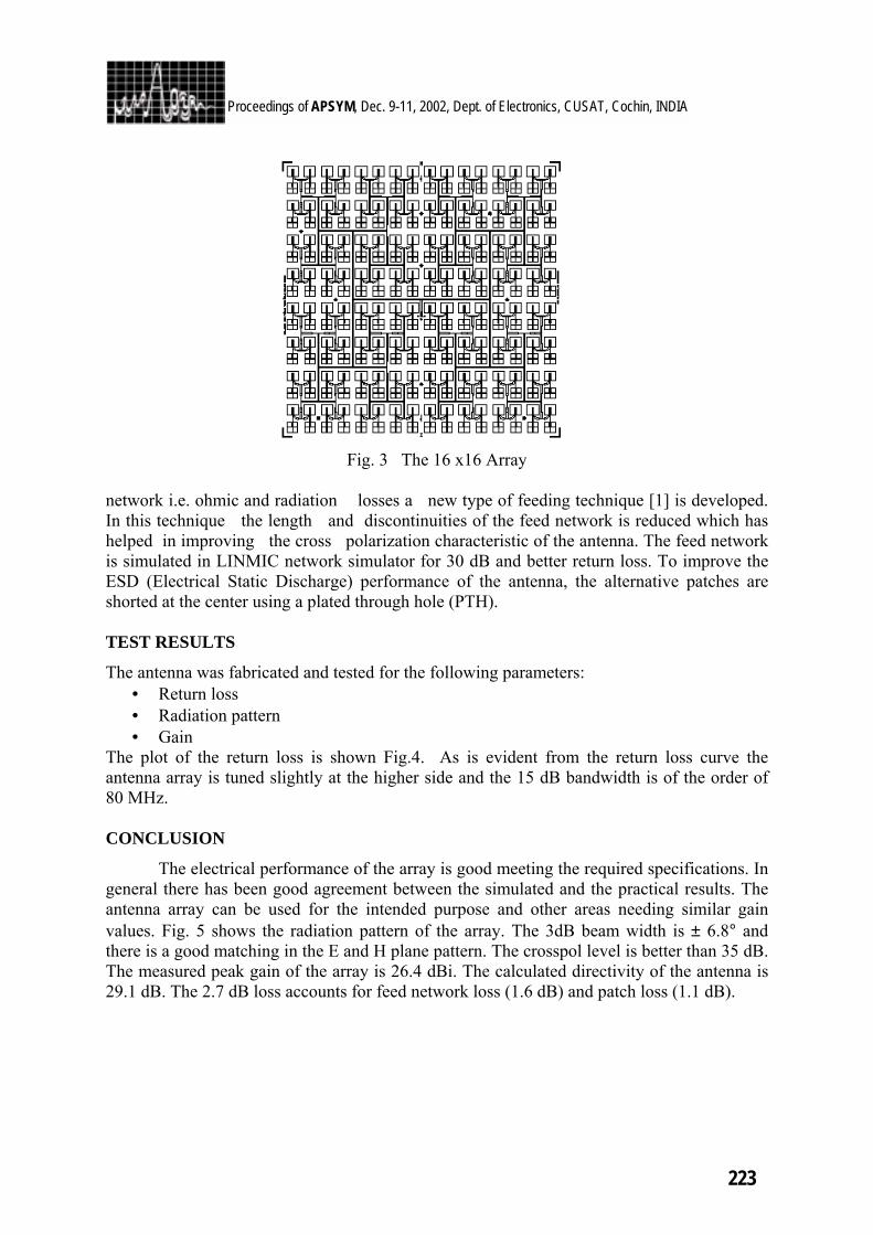
1.
223
Proceedings of APSYM, Dec. 9-11, 2002, Dept. of Electronics, CUSAT, Cochin, INDIA
Fig. 3 The 16 x16 Array
network i.e. ohmic and radiation losses a new type of feeding technique [1] is developed. In this technique the length and discontinuities of the feed network is reduced which has helped in improving the cross polarization characteristic of the antenna. The feed network is simulated in LINMIC network simulator for 30 dB and better return loss. To improve the ESD (Electrical Static Discharge) performance of the antenna, the alternative patches are shorted at the center using a plated through hole (PTH).
TEST RESULTS
The antenna was fabricated and tested for the following parameters: • Return loss • Radiation pattern • Gain
The plot of the return loss is shown Fig.4. As is evident from the return loss curve the antenna array is tuned slightly at the higher side and the 15 dB bandwidth is of the order of 80 MHz. CONCLUSION
The electrical performance of the array is good meeting the required specifications. In general there has been good agreement between the simulated and the practical results. The antenna array can be used for the intended purpose and other areas needing similar gain values. Fig. 5 shows the radiation pattern of the array. The 3dB beam width is ± 6.8° and there is a good matching in the E and H plane pattern. The crosspol level is better than 35 dB. The measured peak gain of the array is 26.4 dBi. The calculated directivity of the antenna is 29.1 dB. The 2.7 dB loss accounts for feed network loss (1.6 dB) and patch loss (1.1 dB).
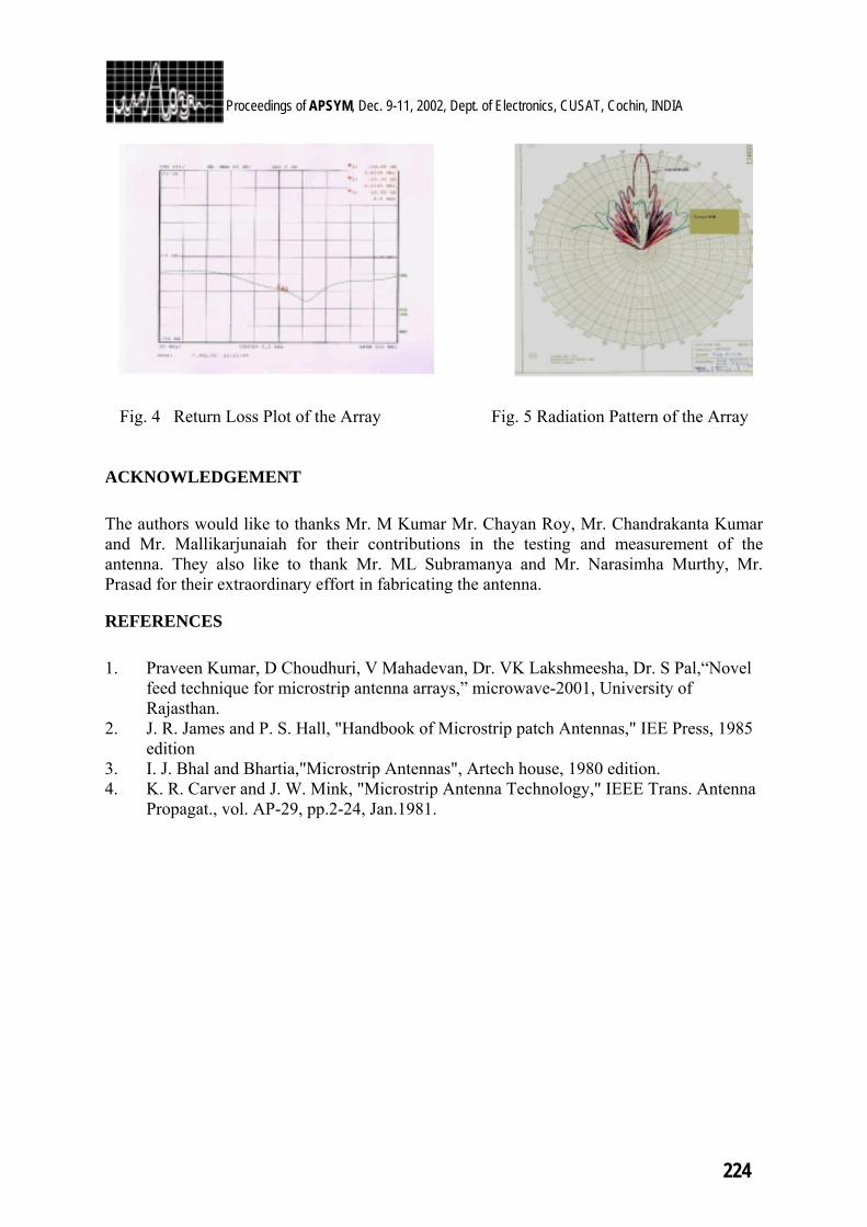
1.
224
Proceedings of APSYM, Dec. 9-11, 2002, Dept. of Electronics, CUSAT, Cochin, INDIA
Fig. 4 Return Loss Plot of the Array Fig. 5 Radiation Pattern of the Array
ACKNOWLEDGEMENT The authors would like to thanks Mr. M Kumar Mr. Chayan Roy, Mr. Chandrakanta Kumar and Mr. Mallikarjunaiah for their contributions in the testing and measurement of the antenna. They also like to thank Mr. ML Subramanya and Mr. Narasimha Murthy, Mr. Prasad for their extraordinary effort in fabricating the antenna.
REFERENCES 1. Praveen Kumar, D Choudhuri, V Mahadevan, Dr. VK Lakshmeesha, Dr. S Pal,“Novel
feed technique for microstrip antenna arrays,” microwave-2001, University of Rajasthan.
2. J. R. James and P. S. Hall, "Handbook of Microstrip patch Antennas," IEE Press, 1985 edition
3. I. J. Bhal and Bhartia,"Microstrip Antennas", Artech house, 1980 edition. 4. K. R. Carver and J. W. Mink, "Microstrip Antenna Technology," IEEE Trans. Antenna
Propagat., vol. AP-29, pp.2-24, Jan.1981.
1.
225
Proceedings of APSYM, Dec. 9-11, 2002, Dept. of Electronics, CUSAT, Cochin, INDIA
SUSPENDED MULTI-LAYER MULTI-RESONATOR RECTANGULAR MICROSTRIP ANTENNAS
Girish Kumar1 and K. P. Ray2
1Electrical Engineering Dept., I.I.T. Bombay, Powai, Mumbai – 400 076 2SAMEER, I.I.T. Campus, Powai, Mumbai – 400 076
E-mail: [email protected], [email protected]
The bandwidth of a microstrip antenna (MSA) increases by using thick substrate with low dielectric constant or planar or stacked multi-resonators. These methods are combined to achieve broad bandwidth with higher gain. A stacked configuration of two identical rectangular MSAs (RMSAs) on the top layer with one co-axial fed RMSA on the bottom layer yielded bandwidth of 35 % with gain of 10.8 dB at 3 GHz. When four identical patches are placed on the top layer, it yielded bandwidth of 1070 MHz with a gain of 11.5 dB.
INTRODUCTION
The bandwidth of a MSA increases with increase in substrate thickness and decrease in dielectric constant. The bandwidth can also be increased by using coupled multi-resonators in planar or stacked configurations. Some of these techniques are combined to obtain broad bandwidth with higher gain [1-3]. In this paper, a new configuration is described which consists of one co-axial fed RMSA on the bottom layer with two identical RMSAs on the top layer (1B2T). The optimized results are also presented for a single rectangular patch on the bottom layer and four patches on the top layer (1B4T).
ONE RECTANGULAR PATCH AT BOTTOM AND TWO PATCHES ON TOP
A single fed RMSA on the bottom layer with two rectangular patches symmetrically placed on the top layer is shown in Figure 1. The two patches on the top layer are taken identical for symmetrical radiation pattern. For the given bottom patch dimensions, the broad bandwidth of the antenna is obtained for different height h1 of the top layer by optimizing the length L1 of the parasitic patch and center to center spacing (2 ox) between them. For L = 5.0 cm, W = 3.0 cm, h = 0.5 cm, x = 2.4 cm and various values of h1, the optimized dimensions of L1, ox and overall length L1 + 2ox along with bandwidth and gain at 3.0 GHz are given in Table 1. With increase in h1 from 0.4 cm to 1.1 cm, the effective length of the top patch increases due to increase in the fringing fields, hence the length L1 of the top patch is reduced from 3.8 cm to 3.2 cm, so that the loop in the impedance plot is within VSWR = 2 circle. Also, with increase in h1 the coupling between the bottom and the top patch decreases. The coupling is increased by decreasing the value of ox from 4.7 cm to 2.5 cm. The maximum coupling is obtained when ox is approximately equal to L/2, because the edges of the fed patches act as magnetic currents, which will give maximum coupling to the top patches when its edges coincide with the maximum magnetic field region (i.e. the center) of the top patches.
With increase in h1 from 0.4 cm to 0.9 cm, the bandwidth of the antenna increases from 650 MHz to 1043 MHz, because the total height of the antenna increases. The center frequency of the antenna remains at around 3.0 GHz. When h1 is increased further, the bandwidth decreases slightly because the loop size decreases due to the decrease in the
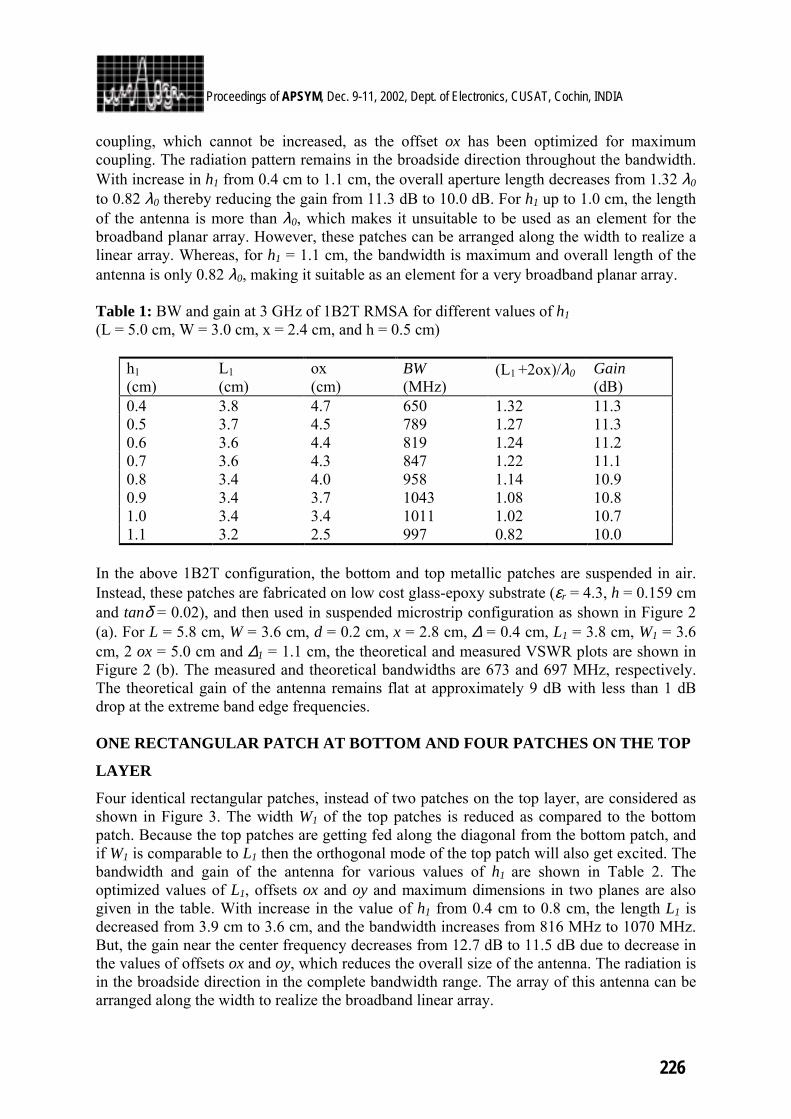
1.
226
Proceedings of APSYM, Dec. 9-11, 2002, Dept. of Electronics, CUSAT, Cochin, INDIA coupling, which cannot be increased, as the offset ox has been optimized for maximum coupling. The radiation pattern remains in the broadside direction throughout the bandwidth. With increase in h1 from 0.4 cm to 1.1 cm, the overall aperture length decreases from 1.32 λ0 to 0.82 λ0 thereby reducing the gain from 11.3 dB to 10.0 dB. For h1 up to 1.0 cm, the length of the antenna is more than λ0, which makes it unsuitable to be used as an element for the broadband planar array. However, these patches can be arranged along the width to realize a linear array. Whereas, for h1 = 1.1 cm, the bandwidth is maximum and overall length of the antenna is only 0.82 λ0, making it suitable as an element for a very broadband planar array. Table 1: BW and gain at 3 GHz of 1B2T RMSA for different values of h1 (L = 5.0 cm, W = 3.0 cm, x = 2.4 cm, and h = 0.5 cm)
h1 (cm)
L1 (cm)
ox (cm)
BW (MHz)
(L1 +2ox)/λ0 Gain (dB)
0.4 3.8 4.7 650 1.32 11.3 0.5 3.7 4.5 789 1.27 11.3 0.6 3.6 4.4 819 1.24 11.2 0.7 3.6 4.3 847 1.22 11.1 0.8 3.4 4.0 958 1.14 10.9 0.9 3.4 3.7 1043 1.08 10.8 1.0 3.4 3.4 1011 1.02 10.7 1.1 3.2 2.5 997 0.82 10.0
In the above 1B2T configuration, the bottom and top metallic patches are suspended in air. Instead, these patches are fabricated on low cost glass-epoxy substrate (εr = 4.3, h = 0.159 cm and tanδ = 0.02), and then used in suspended microstrip configuration as shown in Figure 2 (a). For L = 5.8 cm, W = 3.6 cm, d = 0.2 cm, x = 2.8 cm, ∆ = 0.4 cm, L1 = 3.8 cm, W1 = 3.6 cm, 2 ox = 5.0 cm and ∆1 = 1.1 cm, the theoretical and measured VSWR plots are shown in Figure 2 (b). The measured and theoretical bandwidths are 673 and 697 MHz, respectively. The theoretical gain of the antenna remains flat at approximately 9 dB with less than 1 dB drop at the extreme band edge frequencies.
ONE RECTANGULAR PATCH AT BOTTOM AND FOUR PATCHES ON THE TOP
LAYER
Four identical rectangular patches, instead of two patches on the top layer, are considered as shown in Figure 3. The width W1 of the top patches is reduced as compared to the bottom patch. Because the top patches are getting fed along the diagonal from the bottom patch, and if W1 is comparable to L1 then the orthogonal mode of the top patch will also get excited. The bandwidth and gain of the antenna for various values of h1 are shown in Table 2. The optimized values of L1, offsets ox and oy and maximum dimensions in two planes are also given in the table. With increase in the value of h1 from 0.4 cm to 0.8 cm, the length L1 is decreased from 3.9 cm to 3.6 cm, and the bandwidth increases from 816 MHz to 1070 MHz. But, the gain near the center frequency decreases from 12.7 dB to 11.5 dB due to decrease in the values of offsets ox and oy, which reduces the overall size of the antenna. The radiation is in the broadside direction in the complete bandwidth range. The array of this antenna can be arranged along the width to realize the broadband linear array.
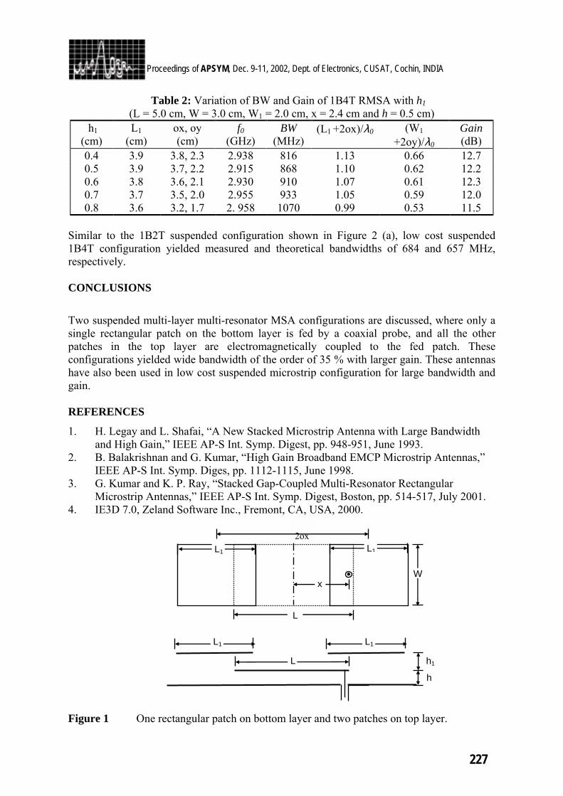
1.
227
Proceedings of APSYM, Dec. 9-11, 2002, Dept. of Electronics, CUSAT, Cochin, INDIA
Table 2: Variation of BW and Gain of 1B4T RMSA with h1 (L = 5.0 cm, W = 3.0 cm, W1 = 2.0 cm, x = 2.4 cm and h = 0.5 cm)
h1 (cm)
L1 (cm)
ox, oy (cm)
f0 (GHz)
BW (MHz)
(L1 +2ox)/λ0 (W1
+2oy)/λ0 Gain (dB)
0.4 3.9 3.8, 2.3 2.938 816 1.13 0.66 12.7 0.5 3.9 3.7, 2.2 2.915 868 1.10 0.62 12.2 0.6 3.8 3.6, 2.1 2.930 910 1.07 0.61 12.3 0.7 3.7 3.5, 2.0 2.955 933 1.05 0.59 12.0 0.8 3.6 3.2, 1.7 2. 958 1070 0.99 0.53 11.5
Similar to the 1B2T suspended configuration shown in Figure 2 (a), low cost suspended 1B4T configuration yielded measured and theoretical bandwidths of 684 and 657 MHz, respectively. CONCLUSIONS
Two suspended multi-layer multi-resonator MSA configurations are discussed, where only a single rectangular patch on the bottom layer is fed by a coaxial probe, and all the other patches in the top layer are electromagnetically coupled to the fed patch. These configurations yielded wide bandwidth of the order of 35 % with larger gain. These antennas have also been used in low cost suspended microstrip configuration for large bandwidth and gain. REFERENCES
1. H. Legay and L. Shafai, “A New Stacked Microstrip Antenna with Large Bandwidth and High Gain,” IEEE AP-S Int. Symp. Digest, pp. 948-951, June 1993.
2. B. Balakrishnan and G. Kumar, “High Gain Broadband EMCP Microstrip Antennas,” IEEE AP-S Int. Symp. Diges, pp. 1112-1115, June 1998.
3. G. Kumar and K. P. Ray, “Stacked Gap-Coupled Multi-Resonator Rectangular Microstrip Antennas,” IEEE AP-S Int. Symp. Digest, Boston, pp. 514-517, July 2001.
4. IE3D 7.0, Zeland Software Inc., Fremont, CA, USA, 2000.
Figure 1 One rectangular patch on bottom layer and two patches on top layer.
2ox
L1
L
h
h1
L1
L
W x
L1 L1
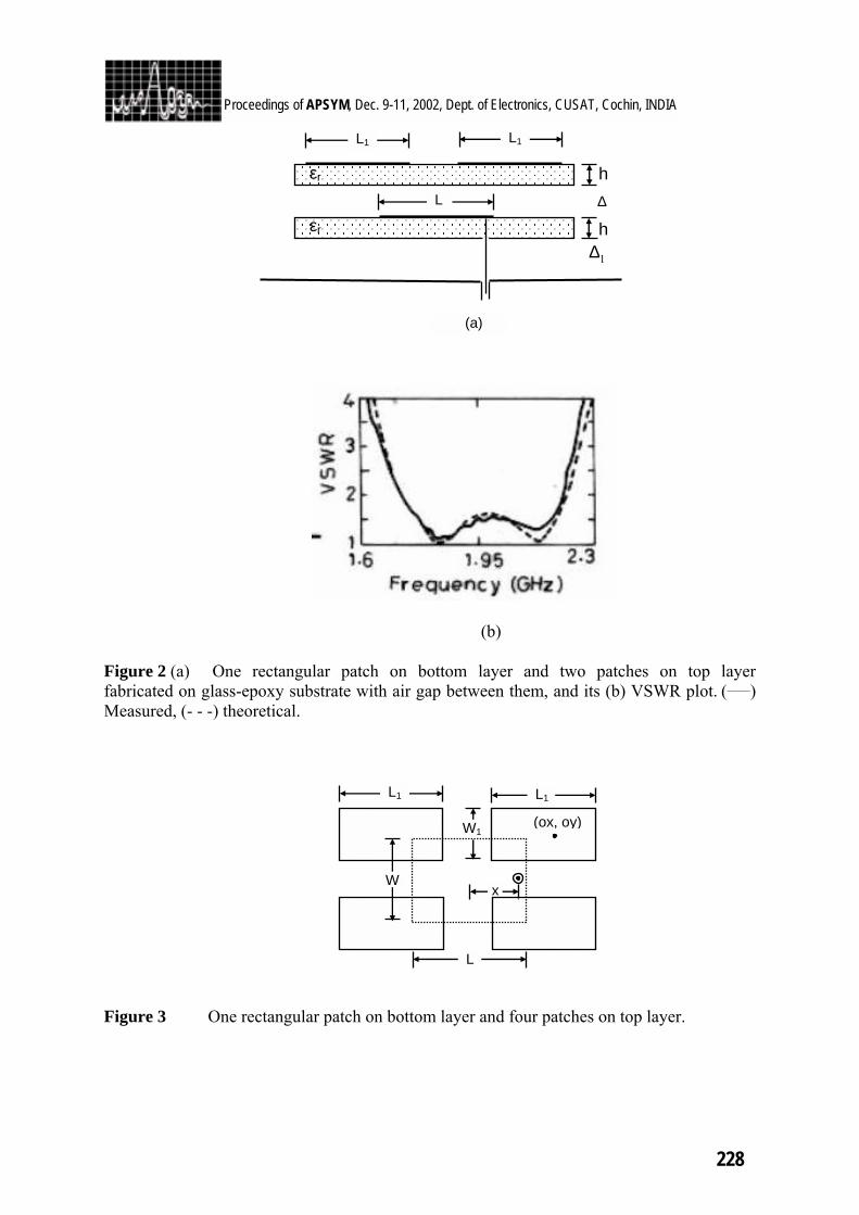
1.
228
Proceedings of APSYM, Dec. 9-11, 2002, Dept. of Electronics, CUSAT, Cochin, INDIA ∆1
(b) Figure 2 (a) One rectangular patch on bottom layer and two patches on top layer fabricated on glass-epoxy substrate with air gap between them, and its (b) VSWR plot. (____) Measured, (- - -) theoretical. Figure 3 One rectangular patch on bottom layer and four patches on top layer.
L
L1 L1
xW
(ox, oy)W1
∆
εr
εr
L1 L1
h
h
L
(a)
1.
229
Proceedings of APSYM, Dec. 9-11, 2002, Dept. of Electronics, CUSAT, Cochin, INDIA
COMPACT BROADBAND S-SHAPED STACKED MICROSTRIP ANTENNAS
Amit A. Deshmukh and Girish Kumar
Department of Electrical Engineering, I.I.T. Bombay, Powai, Mumbai – 400 076
Email: - [email protected], [email protected]
A new compact S-shaped microstrip antenna (MSA) configuration is proposed. This compact MSA is used in stacked configuration with either another S-shaped MSA or compact shorted MSAs like corner shorted square MSA and shorted L-shaped MSA to realize broad bandwidth with an increased gain.
INTRODUCTION
Microstrip antennas (MSAs) have several advantages like low cost, low profile planar configuration, but they suffer from the disadvantage of lower operating bandwidth and larger size in the UHF range (300 – 3000 MHz). Several techniques like slot and shorting post loaded MSAs have been reported for reducing the size of the antenna [1,2]. A bandwidth enhancement has been achieved using multi-resonator gap-coupled MSAs, stacked MSAs or U-slot loaded MSAs [3-5]. In this paper, stacked configurations of compact S-shaped MSA with either another S-shaped MSA or with shorted MSAs like corner shorted square MSA (SMSA) and shorted L-shaped MSA (L-MSA) are proposed to yield broadband response with an increased gain. All the MSAs were first analyzed using IE3D software [6] followed by experimental verification.
S-SHAPED MSA
A S-shaped MSA is a variation of a compact C-shaped MSA as shown in Fig. 1(a, b). For the C-shaped MSA on the glass epoxy substrate (εr = 4.3, h = 0.159 cm, tan δ = 0.02), the theoretical resonance frequency and bandwidth are 848 and 14 MHz, whereas for the S-shaped MSA these are 845 and 14 MHz, respectively. Thus the S-shaped MSA has nearly the same resonance frequency and bandwidth as compared to that of the C-shaped MSA. However due to the orientation of the S-shaped MSA, the E and H-planes are aligned along Φ = 450 and 1350, respectively whereas they are along Φ = 900 and 00 in the C-shaped MSA. The S-shaped MSA has better gain as compared to C-shaped MSA, but has higher cross polarization levels. Since these MSAs were made on lossy glass epoxy substrate, they have poor gain. In order to improve bandwidth and gain, a suspended configuration as shown in Fig. 1(c) is used in which two layers of glass epoxy substrate are separated by an air gap of 1.0 cm. A stacked configuration is used to improve the bandwidth. STACKED S-SHAPED MSA
A stacked configuration of two S-shaped MSAs, in which both the fed and stacked parasitic patches were used in the suspended mode is shown in Fig. 2(a-c). A probe diameter of 0.12 cm is used. By optimizing the dimensions of both the patches, feed point location and an air gap between them, a broadband response as shown in Fig. 3 is obtained. An experimental
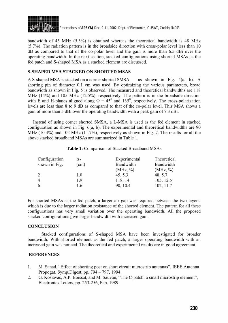
1.
230
Proceedings of APSYM, Dec. 9-11, 2002, Dept. of Electronics, CUSAT, Cochin, INDIA bandwidth of 45 MHz (5.3%) is obtained whereas the theoretical bandwidth is 48 MHz (5.7%). The radiation pattern is in the broadside direction with cross-polar level less than 10 dB as compared to that of the co-polar level and the gain is more than 6.5 dBi over the operating bandwidth. In the next section, stacked configurations using shorted MSAs as the fed patch and S-shaped MSA as a stacked element are discussed.
S-SHAPED MSA STACKED ON SHORTED MSAS
A S-shaped MSA is stacked on a corner shorted SMSA as shown in Fig. 4(a, b). A shorting pin of diameter 0.1 cm was used. By optimizing the various parameters, broad bandwidth as shown in Fig. 5 is observed. The measured and theoretical bandwidths are 118 MHz (14%) and 105 MHz (12.5%), respectively. The pattern is in the broadside direction with E and H-planes aligned along Φ = 450 and 1350, respectively. The cross-polarization levels are less than 8 to 9 dB as compared to that of the co-polar level. This MSA shows a gain of more than 5 dBi over the operating bandwidth with a peak gain of 7.3 dBi.
Instead of using corner shorted SMSA, a L-MSA is used as the fed element in stacked configuration as shown in Fig. 6(a, b). The experimental and theoretical bandwidths are 90 MHz (10.4%) and 102 MHz (11.7%), respectively as shown in Fig. 7. The results for all the above stacked broadband MSAs are summarized in Table 1.
Table 1: Comparison of Stacked Broadband MSAs
Configuration shown in Fig.
∆2 (cm)
Experimental Bandwidth (MHz, %)
Theoretical Bandwidth (MHz, %)
2 1.0 45, 5.3 48, 5.7 4 1.9 118, 14 105, 12.5 6 1.6 90, 10.4 102, 11.7
For shorted MSAs as the fed patch, a larger air gap was required between the two layers, which is due to the larger radiation resistance of the shorted element. The pattern for all these configurations has very small variation over the operating bandwidth. All the proposed stacked configurations give larger bandwidth with increased gain. CONCLUSION
Stacked configurations of S-shaped MSA have been investigated for broader bandwidth. With shorted element as the fed patch, a larger operating bandwidth with an increased gain was noticed. The theoretical and experimental results are in good agreement. REFERENCES 1. M. Sanad, “Effect of shorting post on short circuit microstrip antennas”, IEEE Antenna
Propogat. Symp.Digest, pp. 794 – 797, 1994. 2. G. Kosiavas, A.P. Boissat, and M. Sauvan, “The C-patch: a small microstrip element”,
Electronics Letters, pp. 253-256, Feb. 1989.
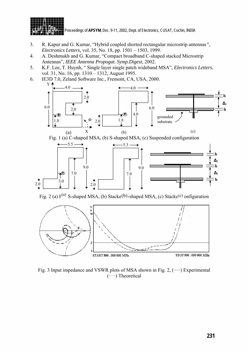
1.
231
Proceedings of APSYM, Dec. 9-11, 2002, Dept. of Electronics, CUSAT, Cochin, INDIA 3. R. Kapur and G. Kumar, “Hybrid coupled shorted rectangular microstrip antennas”,
Electronics Letters, vol. 35, No. 18, pp. 1501 – 1503, 1999. 4. A. Deshmukh and G. Kumar, “Compact broadband C-shaped stacked Microstrip
Antennas”, IEEE Antenna Propogat. Symp.Digest, 2002. 5. K.F. Lee, T. Huynh, “ Single layer single patch wideband MSA”, Electronics Letters,
vol. 31, No. 16, pp. 1310 – 1312, August 1995. 6. IE3D 7.0, Zeland Software Inc., Fremont, CA, USA, 2000.
Fig. 1 (a) C-shaped MSA, (b) S-shaped MSA, (c) Suspended configuration
Fig. 2 (a) Fed S-shaped MSA, (b) Stacked S-shaped MSA, (c) Stacked configuration
Fig. 3 Input impedance and VSWR plots of MSA shown in Fig. 2, (____) Experimental (_ _ _) Theoretical
h
∆∆∆∆1 h
∆∆∆∆2
h
5.5
9.0
2.0
7.0
3.0
9.0
2.0
7.0
5.3
(b) (c) (a)
1
2
V S W
4.0
6.0
2.0
2.0
1.8
∆∆∆∆1 h
h
grounded substrate
4.0
6.0
2.0
4.01.8
(a) (c) (b)
Y
X
Ф
1.
232
Proceedings of APSYM, Dec. 9-11, 2002, Dept. of Electronics, CUSAT, Cochin, INDIA
Fig. 4 (a) Fed corner shorted SMSA, (b) Stacked S-shaped MSA
Fig. 5 Input impedance and VSWR plots of MSA shown in Fig. 4, (____) Experimental (_ _ _) Theoretical
Fig. 6 (a) Fed L-MSA, (b) Stacked S-shaped MSA
Fig. 7 Input impedance and VSWR plots of MSA shown in Fig. 6, (____) Experimental (_ _ _) Theoretical
5.1
9
2
2
3.2 0.3
(a) (b)
0.3
3.5
2
2
3.5
5.15
8.6
2
2
(a) (b)
1.
233
Proceedings of APSYM, Dec. 9-11, 2002, Dept. of Electronics, CUSAT, Cochin, INDIA
SLOT LOADED RECTANGULAR MICROSTRIP ANTENNA FOR TUNABLE DUAL BAND OPERATION
Asha E. Daniel and Girish Kumar
Department of Electrical Engineering I.I.T. Bombay, Powai, Mumbai – 400 076, INDIA
email: [email protected]
A rectangular microstrip antenna (RMSA) embedded with a λ/4 slot along its non-radiating edge exhibits dual band operation. The antenna radiates in the broadside direction at both the resonance frequencies. The effects of slot dimensions and its location on the two resonance frequencies and the tunability range of the antenna have been investigated.
INTRODUCTION
Various applications require a single radiating element, which is tunable to operate at two frequency bands. When a microstrip antenna (MSA) is loaded with monolithic stubs, shorting pins or slots, the electrical resonant length of the patch gets modified and hence tunable or multiple frequency antennas can be realized [1-2]. A RMSA with a λ/2 short circuited or λ/4 open circuited stub placed along the radiating or non-radiating edge of the patch, exhibits dual frequency operation [3-4]. Since the stub is protruding out from the periphery of the patch, the configuration occupies more space and hence limits its application where compact dual frequency antennas are required. This paper describes a compact dual frequency RMSA in which, the effect of reactive loading is realized by cutting a slot of nearly λ/4 length along one of its non-radiating edges. The configuration has broadside radiation pattern at both the resonance frequencies. The antenna has been analyzed using multiport network model (MNM) with segmentation method [1] and the simulated results have been verified using method of moment based IE3D software [5]. SLOT LOADED RMSA
A RMSA with a λ/4 slot etched along one of its non-radiating edges and its multiport network model are shown in Fig. 1(a) and (b) respectively. The antenna has been divided into three rectangular segments. The physical periphery of the patch is extended outwards to account for the fringing fields. The extended periphery is divided into three rectangular segments. Each segment is divided into number of ports. In this case, six and thirty ports are considered for the end segments and two and twenty ports are considered for the middle segment along its length and width respectively. The impedance matrices of these segments are evaluated separately using Green’s functions. The radiation from the periphery is taken into account by loading these ports with the corresponding radiation resistance. The input impedance of the patch is calculated by combining these impedance matrices using segmentation method. A RMSA of length L = 4 cm and W = 6 cm loaded with a rectangular slot of length l = 2 cm (corresponding to λ /4), width w = 0.5 cm, and the slot at the center of non-radiating edge, having εr = 4.3, thickness h = 0.159 cm and the loss tangent tanδ = 0.02 fed at x= 0.1 cm has been simulated using both MNM and IE3D. The antenna resonates at two frequencies and the simulated input impedance and VSWR plots are shown in Fig. 2 (a) and (b). The voltage distribution along the periphery at f1 and f2 for unit current
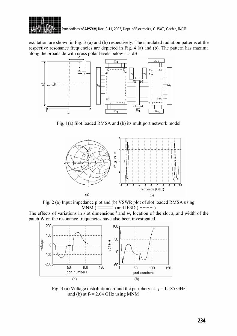
1.
234
Proceedings of APSYM, Dec. 9-11, 2002, Dept. of Electronics, CUSAT, Cochin, INDIA excitation are shown in Fig. 3 (a) and (b) respectively. The simulated radiation patterns at the respective resonance frequencies are depicted in Fig. 4 (a) and (b). The pattern has maxima along the broadside with cross polar levels below -15 dB.
Fig. 1(a) Slot loaded RMSA and (b) its multiport network model
Fig. 2 (a) Input impedance plot and (b) VSWR plot of slot loaded RMSA using MNM ( ) and IE3D ( )
The effects of variations in slot dimensions l and w, location of the slot s, and width of the patch W on the resonance frequencies have also been investigated.
(a) (b)
Fig. 3 (a) Voltage distribution around the periphery at f1 = 1.185 GHz and (b) at f2 = 2.04 GHz using MNM
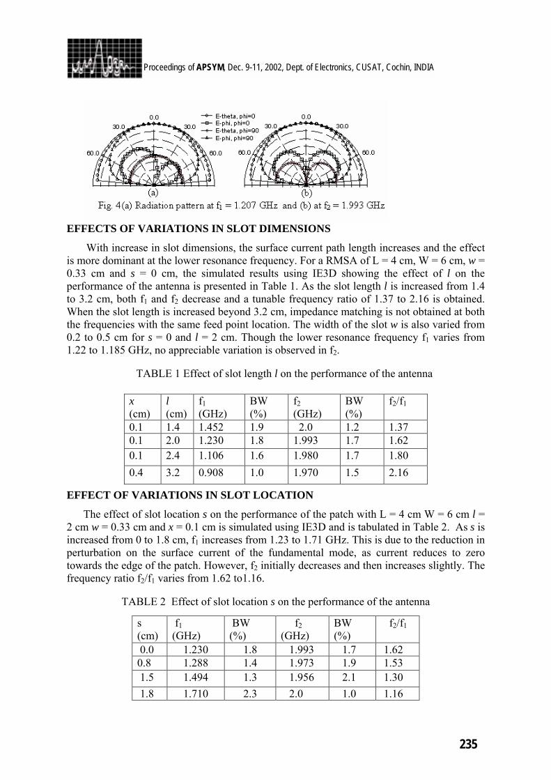
1.
235
Proceedings of APSYM, Dec. 9-11, 2002, Dept. of Electronics, CUSAT, Cochin, INDIA
EFFECTS OF VARIATIONS IN SLOT DIMENSIONS
With increase in slot dimensions, the surface current path length increases and the effect is more dominant at the lower resonance frequency. For a RMSA of L = 4 cm, W = 6 cm, w = 0.33 cm and s = 0 cm, the simulated results using IE3D showing the effect of l on the performance of the antenna is presented in Table 1. As the slot length l is increased from 1.4 to 3.2 cm, both f1 and f2 decrease and a tunable frequency ratio of 1.37 to 2.16 is obtained. When the slot length is increased beyond 3.2 cm, impedance matching is not obtained at both the frequencies with the same feed point location. The width of the slot w is also varied from 0.2 to 0.5 cm for s = 0 and l = 2 cm. Though the lower resonance frequency f1 varies from 1.22 to 1.185 GHz, no appreciable variation is observed in f2. TABLE 1 Effect of slot length l on the performance of the antenna EFFECT OF VARIATIONS IN SLOT LOCATION
The effect of slot location s on the performance of the patch with L = 4 cm W = 6 cm l = 2 cm w = 0.33 cm and x = 0.1 cm is simulated using IE3D and is tabulated in Table 2. As s is increased from 0 to 1.8 cm, f1 increases from 1.23 to 1.71 GHz. This is due to the reduction in perturbation on the surface current of the fundamental mode, as current reduces to zero towards the edge of the patch. However, f2 initially decreases and then increases slightly. The frequency ratio f2/f1 varies from 1.62 to1.16.
TABLE 2 Effect of slot location s on the performance of the antenna
x (cm)
l (cm)
f1 (GHz)
BW (%)
f2 (GHz)
BW (%)
f2/f1
0.1 1.4 1.452 1.9 2.0 1.2 1.37 0.1 2.0 1.230 1.8 1.993 1.7 1.62 0.1 2.4 1.106 1.6 1.980 1.7 1.80 0.4 3.2 0.908 1.0 1.970 1.5 2.16
s (cm)
f1 (GHz)
BW (%)
f2 (GHz)
BW (%)
f2/f1
0.0 1.230 1.8 1.993 1.7 1.62 0.8 1.288 1.4 1.973 1.9 1.53 1.5 1.494 1.3 1.956 2.1 1.30 1.8 1.710 2.3 2.0 1.0 1.16
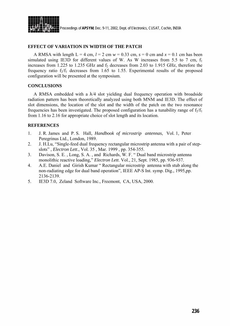
1.
236
Proceedings of APSYM, Dec. 9-11, 2002, Dept. of Electronics, CUSAT, Cochin, INDIA
EFFECT OF VARIATION IN WIDTH OF THE PATCH
A RMSA with length L = 4 cm, l = 2 cm w = 0.33 cm, s = 0 cm and x = 0.1 cm has been simulated using IE3D for different values of W. As W increases from 5.5 to 7 cm, f1 increases from 1.225 to 1.235 GHz and f2 decreases from 2.03 to 1.915 GHz, therefore the frequency ratio f2/f1 decreases from 1.65 to 1.55. Experimental results of the proposed configuration will be presented at the symposium. CONCLUSIONS
A RMSA embedded with a λ/4 slot yielding dual frequency operation with broadside radiation pattern has been theoretically analyzed using both MNM and IE3D. The effect of slot dimensions, the location of the slot and the width of the patch on the two resonance frequencies has been investigated. The proposed configuration has a tunability range of f2/f1 from 1.16 to 2.16 for appropriate choice of slot length and its location. REFERENCES
1. J. R. James and P. S. Hall, Handbook of microstrip antennas, Vol. 1, Peter Peregrinus Ltd., London, 1989.
2. J. H.Lu, “Single-feed dual frequency rectangular microstrip antenna with a pair of step-slots” , Electron Lett., Vol. 35 , Mar. 1999 , pp. 354-355.
3. Davison, S. E. , Long, S. A. , and Richards, W. F. “ Dual band microstrip antenna monolithic reactive loading,” Electron Lett. Vol., 21, Sept. 1985, pp. 936-937.
4. A.E. Daniel and Girish Kumar “ Rectangular microstrip antenna with stub along the non-radiating edge for dual band operation”, IEEE AP-S Int. symp. Dig., 1995,pp. 2136-2139.
5. IE3D 7.0, Zeland Software Inc., Freemont, CA, USA, 2000.
1.
237
Proceedings of APSYM, Dec. 9-11, 2002, Dept. of Electronics, CUSAT, Cochin, INDIA
SIMPLE APPROXIMATION FOR CHARACTERISTIC IMPEDANCE OF ASYMMETRICALLY COUPLED MICROSTRIP
LINE
Rabindra K. Mishra1 and Gopal K. Patra2 1Electronic Science Department, Berhampur University, Orissa – 760 007
2C-MMACS, Bangalore – 560 037. E-mail:[email protected]
The results of quasi-static analysis to determine mutual coupling between symmetric microstrip lines are used to approximate the characteristic impedance of an asymmetric coupled line.
INTRODUCTION
Simple coupled mode approach [1-2] is used for finding the characteristics of a symmetric coupled line. Generally, variational Fourier Transfer Domain (VFTD) method [3] is used for analysis of asymmetric coupled lines. This is comparatively more complex and time consuming. This article suitably modifies the results of coupled mode approach, to find characteristic impedance of asymmetric lines. The results compare well with VFDTD method. COUPLED MODE APPROACH
A “coupled line” configuration consists of two microstrip lines placed parallel to each other and in close proximity, causing coupling between the electromagnetic fields. This coupling supports two different modes of propagation called c and π modes, with different characteristic impedances. The phase constants and the characteristic impedances of the two modes are related to the line constants in the following manner [2].
[ ]LCmmcc XCLCLCLjj ±−+== 22 2211,,
ωβγ ππ (1)
( ) ( )( )mmmmLC CLCLCLCLCLCLX 12212
1122 4 −−+−= (2)
−=
πβω
RLLZ m
cc 11 (3)
−=
c
m
RLLZ 11
ππ β
ω (4)
( )mm
LCc CLCL
XCLCLR12
1122, 2 −
±−=π (5)
The next section proposes a modified quasi-static analysis for determining self-capacitances C1 and C2, self-inductances L1 and L2 as well as mutual capacitance and inductance Cm and Lm respectively.
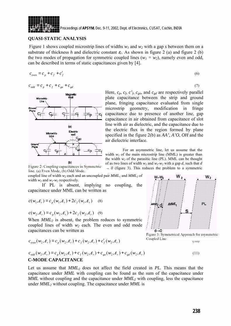
1.
238
Proceedings of APSYM, Dec. 9-11, 2002, Dept. of Electronics, CUSAT, Cochin, INDIA
QUASI-STATIC ANALYSIS
Figure 1 shows coupled microstrip lines of widths w1 and w2 with a gap s between them on a substrate of thickness h and dielectric constant εr. As shown in figure 2 (a) and figure 2 (b) the two modes of propagation for symmetric coupled lines (w1 = w2), namely even and odd, can be described in terms of static capacitances given by [4].
ffpeven cccc ′++= (6)
gdgafpodd ccccc +++= (7)
Here, cp, cf, c’f, cga, and cgd are respectively parallel plate capacitance between the strip and ground plane, fringing capacitance evaluated from single microstrip geometry, modification in fringe capacitance due to presence of another line, gap capacitance in air obtained from capacitance of slot line with air as dielectric, and the capacitance due to the electric flux in the region formed by plane specified in the figure 2(b) as AA’, A’O, OH and the air dielectric interface.
For an asymmetric line, let us assume that the width w1 of the main microstrip line (MML) is greater than the width w2 of the parasitic line (PL). MML can be thought of as two lines of width w2 and w1-w2 with a gap d, such that d → 0 (figure 3). This reduces the problem to a symmetric
coupled line of width w2 each and an uncoupled pair MML1 and MML2 of width w2 and w1-w2 respectively. If PL is absent, implying no coupling, the capacitance under MML can be written as
),(2),(),( 111 rfrpr wcwcwc εεε += (8)
),(2),(),( 222 rfrpr wcwcwc εεε += (9)
When MML2 is absent, the problem reduces to symmetric coupled lines of width w2 each. The even and odd mode capacitances can be written as
),(),(),(),( 2222 rfrfrpreven wcwcwcwc εεεε ′++= (10)
),(),(),(),(),( 22222 rgdrgarfrprodd wcwcwcwcwc εεεεε +++= (11)
C-MODE CAPACITANCE
Let us assume that MML2 does not affect the field created in PL. This means that the capacitance under MML with coupling can be found as the sum of the capacitance under MML without coupling and the capacitance under MML2 with coupling, less the capacitance under MML2 without coupling. The capacitance under MML is

1.
239
Proceedings of APSYM, Dec. 9-11, 2002, Dept. of Electronics, CUSAT, Cochin, INDIA
),(),(),(),( 22121 rrevenrrcw wcwcwcwc εεεε −+= (12)
),()( 22 revenrcw wcc εε = (13)
ππππ-MODE CAPACITANCE
A. Similarly, π mode capacitance under MML and PL are given respectively by
),(),(),(),( 22121 rroddrrcw wcwcwcwc εεεε −+= (14)
),()( 22 roddrcw wcc εε = (15)
COUPLED MODE PARAMETERS
For TEM modes the lines are characterised by inductance per unit length L1, L2 and capacitance per unit length C1, C2 for MML and PL respectively. The mutual inductance and capacitance are Lm and Cm. In terms of C and π mode capacitances, these parameters are [4]
=+
==
)1(1
)1(1
2 rcwrw
oon
nncc
Lεε
εµπ
(16)
2
)()( rwrcwn
nncc
Cεε π+
= (17)
21 mwmwm LLL = (18)
21 mwmwm CCC = (19)
=−
==
)1(1
)1(1
2 rcwrw
oon
nncc
Lεε
εµ
π (20)
2
)()( rwrcwn
nncc
Cεε π−
= (21)
In these equations, n=1 for MML and 2 for PL. Using these parameters in equations (1) – (5), we can calculate the c and π mode characteristic impedances. RESULTS AND DISCUSSION
The results of this method are compared with those from the VFTD method [1], in figure 4, both for c and π modes. The coupled line considered here has MML width 1.2 mm, PL of length 0.6 mm, substrate thickness 0.635 cm, and dielectric constant 9.7. It is observed from the plot that for very small values of gap spacing, the difference in the results between the two methods are more, but as the gap spacing is gradually increased the results of both the methods follow each other closely. The discrepancy for small spacing can be due to the following reasons. It is assumed that MML2 is not affected much by the electromagnetic field
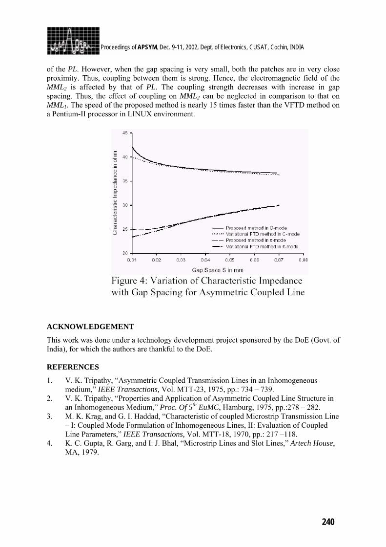
1.
240
Proceedings of APSYM, Dec. 9-11, 2002, Dept. of Electronics, CUSAT, Cochin, INDIA of the PL. However, when the gap spacing is very small, both the patches are in very close proximity. Thus, coupling between them is strong. Hence, the electromagnetic field of the MML2 is affected by that of PL. The coupling strength decreases with increase in gap spacing. Thus, the effect of coupling on MML2 can be neglected in comparison to that on MML1. The speed of the proposed method is nearly 15 times faster than the VFTD method on a Pentium-II processor in LINUX environment.
ACKNOWLEDGEMENT
This work was done under a technology development project sponsored by the DoE (Govt. of India), for which the authors are thankful to the DoE. REFERENCES
1. V. K. Tripathy, “Asymmetric Coupled Transmission Lines in an Inhomogeneous medium,” IEEE Transactions, Vol. MTT-23, 1975, pp.: 734 – 739.
2. V. K. Tripathy, “Properties and Application of Asymmetric Coupled Line Structure in an Inhomogeneous Medium,” Proc. Of 5th EuMC, Hamburg, 1975, pp.:278 – 282.
3. M. K. Krag, and G. I. Haddad, “Characteristic of coupled Microstrip Transmission Line – I: Coupled Mode Formulation of Inhomogeneous Lines, II: Evaluation of Coupled Line Parameters,” IEEE Transactions, Vol. MTT-18, 1970, pp.: 217 –118.
4. K. C. Gupta, R. Garg, and I. J. Bhal, “Microstrip Lines and Slot Lines,” Artech House, MA, 1979.
1.
241
Proceedings of APSYM, Dec. 9-11, 2002, Dept. of Electronics, CUSAT, Cochin, INDIA 5.
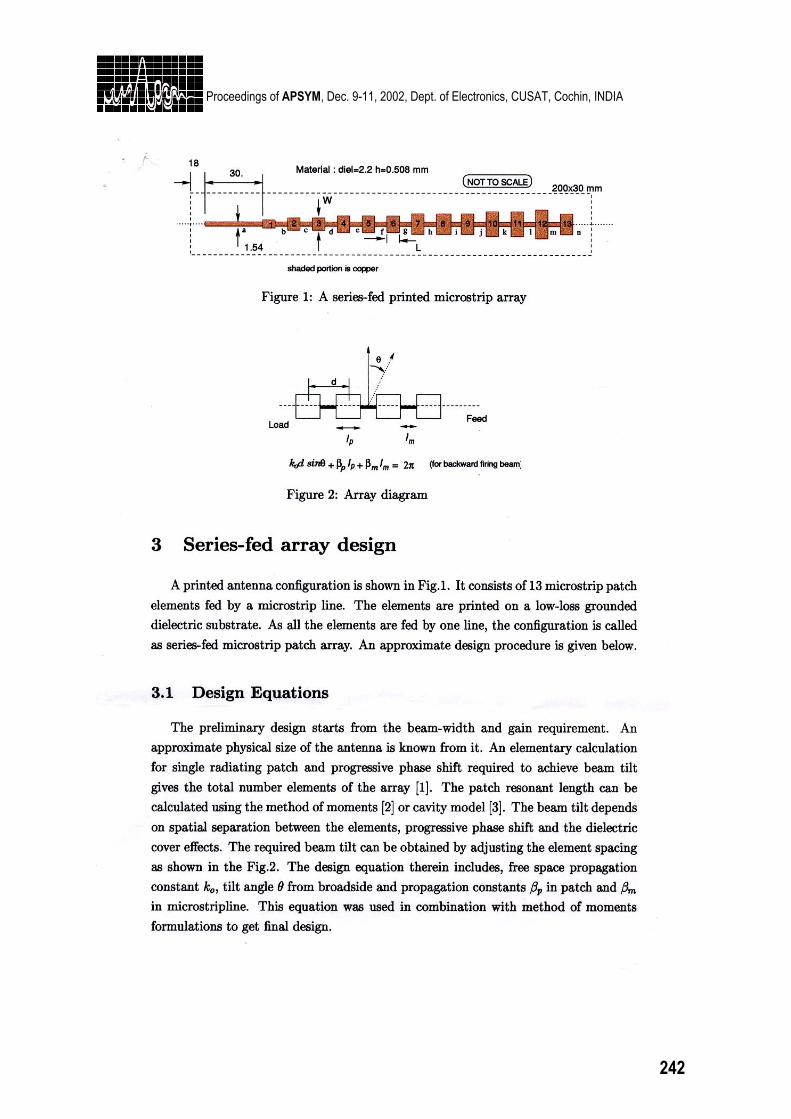
1.
242
Proceedings of APSYM, Dec. 9-11, 2002, Dept. of Electronics, CUSAT, Cochin, INDIA
1.
243
Proceedings of APSYM, Dec. 9-11, 2002, Dept. of Electronics, CUSAT, Cochin, INDIA
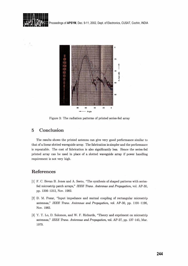
1.
244
Proceedings of APSYM, Dec. 9-11, 2002, Dept. of Electronics, CUSAT, Cochin, INDIA
1.
244
Proceedings of APSYM, Dec. 9-11, 2002, Dept. of Electronics, CUSAT, Cochin, INDIA
DUAL BAND OCTAGONAL PATCH ANTENNA
Binu Paul, S.Mridula, C.K.Aanandan and P.Mohanan
Centre for Research in Electromagnetics and Antennas Department of Electronics, Cochin University of Science and Technology Kochi - 682 022, email :[email protected] , [email protected]
An octagonal Microstrip Patch Antenna suitable for dual band applications is presented. The antenna offers good matching characteristics, rather high isolation between the two operating bands and an area reduction of ~ 29% in comparison to a conventional circular patch antenna operating in the same band. A simple formula to calculate the resonant frequency is also reported.
INTRODUCTION
The technique of wireless connection between PC and peripherals is an issue of growing interest in recent times. The Bluetooth technology developed for this purpose, operates in the 2.4GHz ISM (Industrial Scientific Medical) frequency band [1]. The availability of a simple low cost antenna is a very important feature of a Bluetooth interface. Planar antennas offer attractive solutions that can be easily integrated into a Bluetooth system. This paper focuses on the development of a Microstrip antenna to be installed in Bluetooth enabled mobile communication terminals. The frequency presently allotted for Mobile communication applications in the DCS band is 1.8GHz. Basically, Microstrip patches require two elements of different dimensions, resonating in the required frequency bands to achieve dual band characteristics. The potential of an irregular shaped planar antenna has been proposed for multi – band operation [2]. Perturbation of the shape of a conventional microstrip patch antenna in a prescribed manner also results in multi - band operation [3] . But, most of these techniques achieve dual frequency operation by either increasing the patch size or using complicated manufacturing methods. Good VSWR characteristics, reasonably good isolation between ports and reduced area are the striking features of the antenna proposed in this paper. DESIGN AND METHODOLOGY Table1 shows the dimensions and Figure.1. shows the geometry of the octagonal patch antenna .The two ports are energized electromagnetically using two 50 Ω orthogonal Microstrip feed lines fabricated on a similar substrate. The measurements have been carried out by means of an HP 8510C network analyzer.
Patch Substrate Feed Points L1 24mm εr 4.28 F1 12mm L2 15.5mm h 1.6mm F2 3.5mm L3 10mm
Table.1. Dimensions of the octagonal patch antenna.
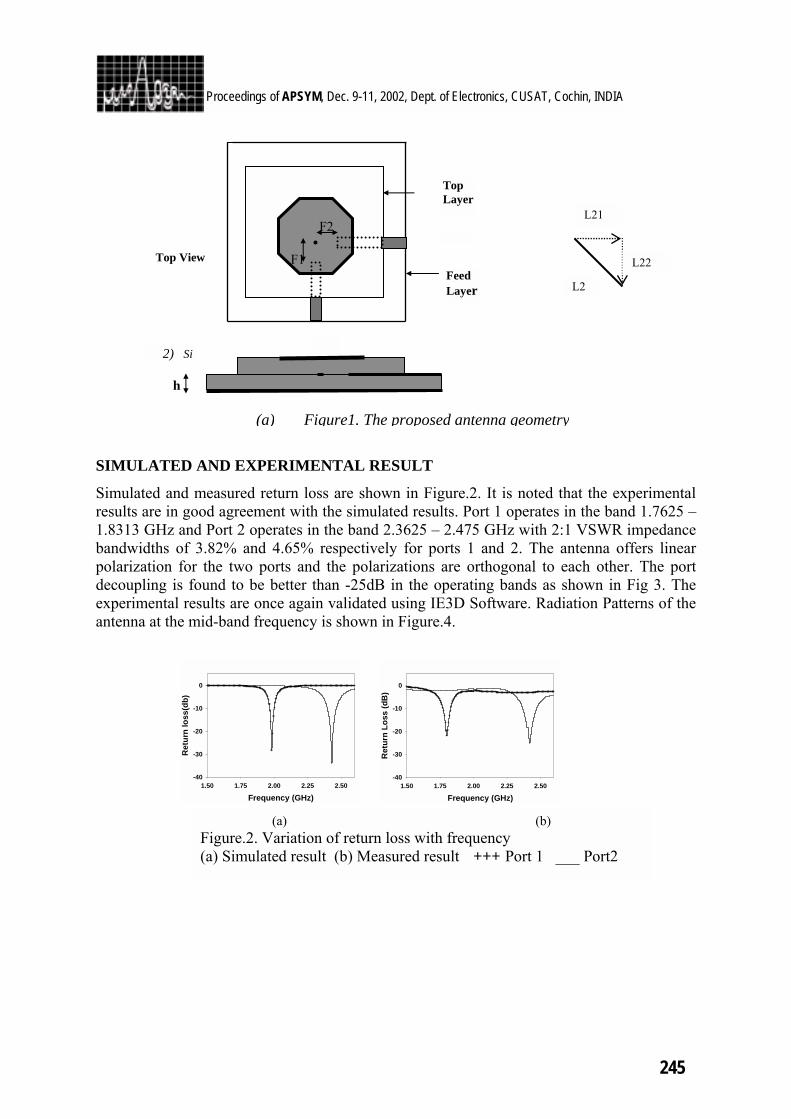
1.
245
Proceedings of APSYM, Dec. 9-11, 2002, Dept. of Electronics, CUSAT, Cochin, INDIA
SIMULATED AND EXPERIMENTAL RESULT
Simulated and measured return loss are shown in Figure.2. It is noted that the experimental results are in good agreement with the simulated results. Port 1 operates in the band 1.7625 – 1.8313 GHz and Port 2 operates in the band 2.3625 – 2.475 GHz with 2:1 VSWR impedance bandwidths of 3.82% and 4.65% respectively for ports 1 and 2. The antenna offers linear polarization for the two ports and the polarizations are orthogonal to each other. The port decoupling is found to be better than -25dB in the operating bands as shown in Fig 3. The experimental results are once again validated using IE3D Software. Radiation Patterns of the antenna at the mid-band frequency is shown in Figure.4.
Frequency (GHz)1.50 1.75 2.00 2.25 2.50
Ret
urn
loss
(db)
-40
-30
-20
-10
0
Frequency (GHz)1.50 1.75 2.00 2.25 2.50
Ret
urn
Loss
(dB
)
-40
-30
-20
-10
0
(a) (b) Figure.2. Variation of return loss with frequency (a) Simulated result (b) Measured result +++ Port 1 ___ Port2
(a) Figure1. The proposed antenna geometry
Top Layer
Feed Layer
F2
F1
h
Top View
2) Si
L2
L21
L22
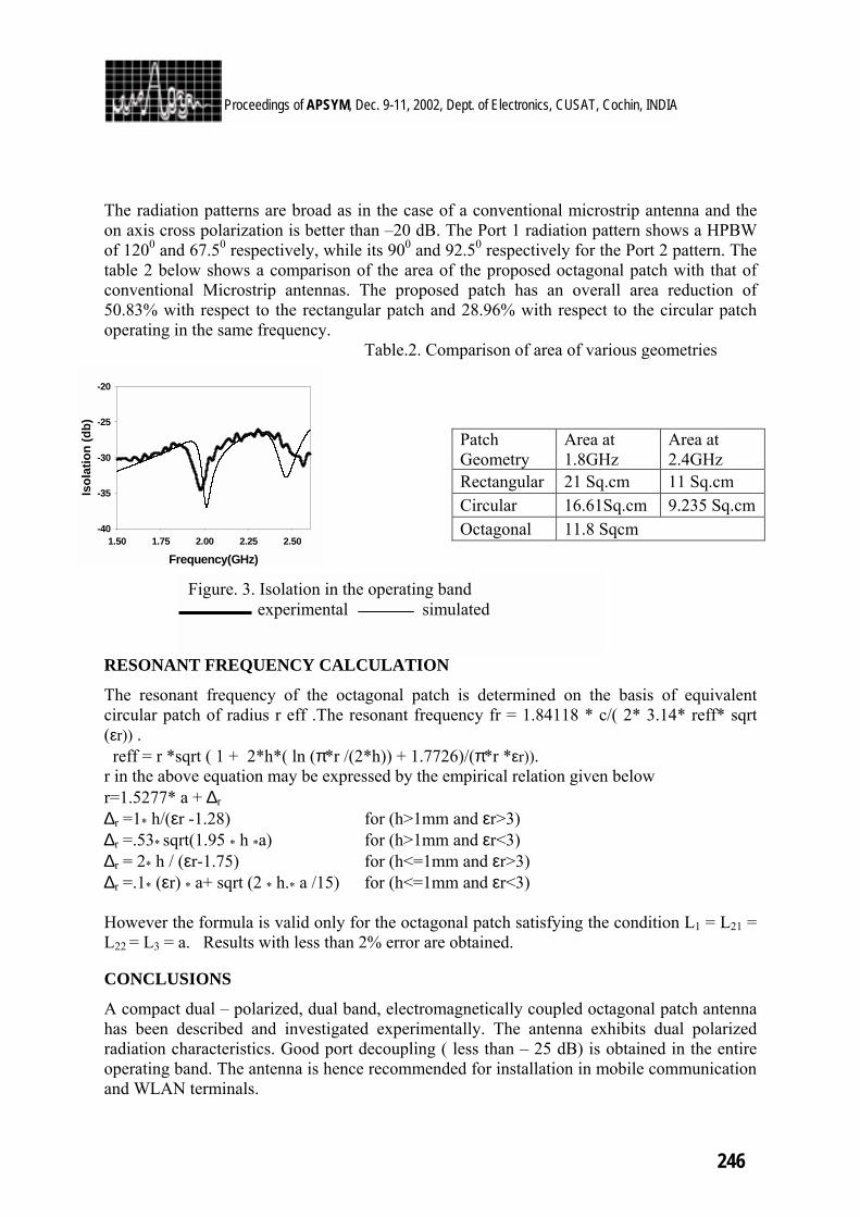
1.
246
Proceedings of APSYM, Dec. 9-11, 2002, Dept. of Electronics, CUSAT, Cochin, INDIA
Figure. 3. Isolation in the operating band experimental simulated
Frequency(GHz)1.50 1.75 2.00 2.25 2.50
Isol
atio
n (d
b)
-40
-35
-30
-25
-20
The radiation patterns are broad as in the case of a conventional microstrip antenna and the on axis cross polarization is better than –20 dB. The Port 1 radiation pattern shows a HPBW of 1200 and 67.50 respectively, while its 900 and 92.50 respectively for the Port 2 pattern. The table 2 below shows a comparison of the area of the proposed octagonal patch with that of conventional Microstrip antennas. The proposed patch has an overall area reduction of 50.83% with respect to the rectangular patch and 28.96% with respect to the circular patch operating in the same frequency.
Table.2. Comparison of area of various geometries
RESONANT FREQUENCY CALCULATION
The resonant frequency of the octagonal patch is determined on the basis of equivalent circular patch of radius r eff .The resonant frequency fr = 1.84118 * c/( 2* 3.14* reff* sqrt (εr)) . reff = r *sqrt ( 1 + 2*h*( ln (π*r /(2*h)) + 1.7726)/(π*r *εr)). r in the above equation may be expressed by the empirical relation given below r=1.5277* a + ∆r
∆r =1* h/(εr -1.28) for (h>1mm and εr>3) ∆r =.53* sqrt(1.95 * h *a) for (h>1mm and εr<3) ∆r = 2* h / (εr-1.75) for (h<=1mm and εr>3) ∆r =.1* (εr) * a+ sqrt (2 * h.* a /15) for (h<=1mm and εr<3) However the formula is valid only for the octagonal patch satisfying the condition L1 = L21 = L22 = L3 = a. Results with less than 2% error are obtained. CONCLUSIONS
A compact dual – polarized, dual band, electromagnetically coupled octagonal patch antenna has been described and investigated experimentally. The antenna exhibits dual polarized radiation characteristics. Good port decoupling ( less than – 25 dB) is obtained in the entire operating band. The antenna is hence recommended for installation in mobile communication and WLAN terminals.
Patch Geometry
Area at 1.8GHz
Area at 2.4GHz
Rectangular 21 Sq.cm 11 Sq.cm Circular 16.61Sq.cm 9.235 Sq.cm Octagonal 11.8 Sqcm
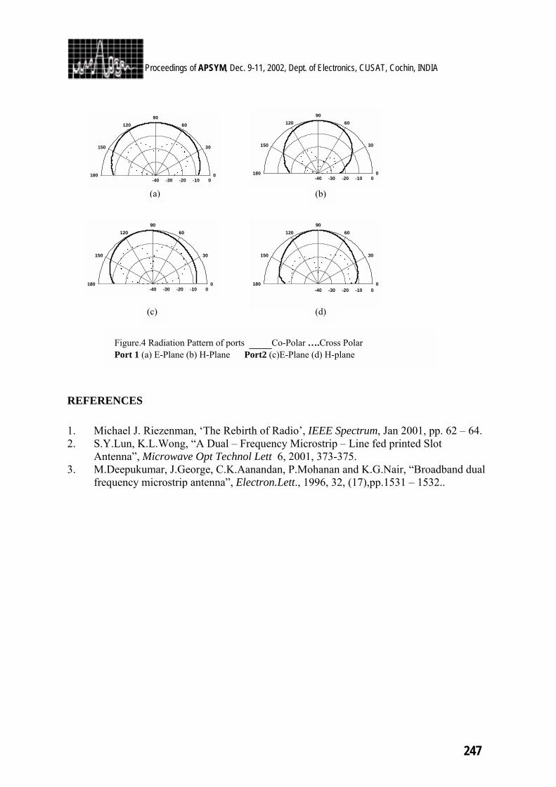
1.
247
Proceedings of APSYM, Dec. 9-11, 2002, Dept. of Electronics, CUSAT, Cochin, INDIA
REFERENCES 1. Michael J. Riezenman, ‘The Rebirth of Radio’, IEEE Spectrum, Jan 2001, pp. 62 – 64. 2. S.Y.Lun, K.L.Wong, “A Dual – Frequency Microstrip – Line fed printed Slot
Antenna”, Microwave Opt Technol Lett 6, 2001, 373-375. 3. M.Deepukumar, J.George, C.K.Aanandan, P.Mohanan and K.G.Nair, “Broadband dual
frequency microstrip antenna”, Electron.Lett., 1996, 32, (17),pp.1531 – 1532..
(a) (b) -40 -30 -20 -10 0
0
30
6090
120
150
180 -40 -30 -20 -10 00
30
6090
120
150
180
-40 -30 -20 -10 00
30
6090
120
150
180-40 -30 -20 -10 0
0
30
6090
120
150
180
Figure.4 Radiation Pattern of ports ___Co-Polar ….Cross Polar Port 1 (a) E-Plane (b) H-Plane Port2 (c)E-Plane (d) H-plane
(c) (d)

248
Proceedings of APSYM, Dec. 9-11, 2002, Dept. of Electronics, CUSAT, Cochin, INDIA
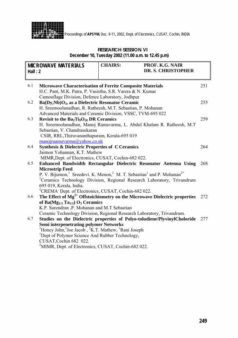
6.1 Microwave Characterisation of Ferrite Composite Materials H.C. Pant, M.K. Patra, P. Vasistha, S.R. Varera & N. Kumar
251
249
Proceedings of APSYM, Dec. 9-11, 2002, Dept. of Electronics, CUSAT, Cochin, INDIA
RESEARCH SESSION VI December 10, Tuesday 2002 (11.00 a.m. to 12.45 p.m)
MICROWAVE MATERIALS Hall : 2
CHAIRS: PROF. K.G. NAIR DR. S. CHRISTOPHER
Camouflage Division, Defence Laboratory, Jodhpur 6.2 Ba(Dy,Nb)O3, as a Dielectric Resonator Ceramic
H. Sreemoolanadhan, R. Ratheesh, M.T. Sebastian, P. Mohanan Advanced Materials and Ceramic Division, VSSC, TVM-695 022
255
6.3 Revisit to the Ba2Ti9O20 DR Ceramics H. Sreemoolanadhan, Manoj Ramavarma, L. Abdul Khalam R. Ratheesh, M.T Sebastian, V. Chandrasekaran CSIR, RRL,Thiruvananthapuram, Kerala-695 019 [email protected]
259
6.4 Synthesis & Dielectric Properties of C Ceramics Jaimon Yohannan, K.T. Mathew MIMR,Dept. of Electronics, CUSAT, Cochin-682 022.
264
6.5 Enhanced Bandwidth Rectangular Dielectric Resonator Antenna Using Microstrip Feed P. V. Bijumon,1 Sreedevi. K. Menon,2 M. T. Sebastian1 and P. Mohanan2* 1Ceramics Technology Division, Regional Research Laboratory, Trivandrum 695 019, Kerala, India. 2CREMA, Dept. of Electronics, CUSAT, Cochin-682 022.
268
6.6 The Effect of Mg2+ Offstoichiometry on the Microwave Dielectric properties of Ba(Mg1/3 Ta1/3) O3 Ceramics K.P. Surendran ,P. Mohanan and M.T Sebastian Ceramic Technology Division, Regional Research Laboratory, Trivandrum.
272
6.7 Studies on the Dielectric properties of Polyo-toludiene/PlyvinylCholoride Semi interpenetrating polymer Networks 1Honey John,2Joe Jacob , 2K.T. Mathew, 1Rani Joseph 1Dept of Polymer Science And Rubber Technology, CUSAT,Cochin 682 022. 2MIMR, Dept. of Electronics, CUSAT, Cochin-682 022.
277
250
Proceedings of APSYM, Dec. 9-11, 2002, Dept. of Electronics, CUSAT, Cochin, INDIA
251
Proceedings of APSYM, Dec. 9-11, 2002, Dept. of Electronics, CUSAT, Cochin, INDIA
MICROWAVE CHARACTERIZATION OF FERRITE COMPOSITE MATERIALS
H C Pant, M K Patra, P Vasistha, S R Vadera & N Kumar
Camouflage Division, Defence Laboratory, Jodhpur
Two ferrite materials, W-phase Cobalt doped Barium Hexaferrite and Nickel Spinel Ferrite, and their composites, were characterized for their magnetic losses over a broad band of microwave frequencies from 3.95 to 18.0 GHz. The frequency response of the permeability of individual ferrites is different. The hexaferrite losses are observed to peak in the high band (Ku), while the spinel ferrite has maximum losses in the C band. The composites of these ferrites are observed to have uniform losses over the entire band. This behaviour is also predicted by the theoretical models for host-inclusion composite systems viz. Maxwell-Garnet(MG), Symmetrical(SBG) and Asymmetric Bruggeman(ABG) model.
INTRODUCTION
Electromagnetic Interference (EMI) has always been an area of interest due to the explosive growth in the utilization of electric and electronic devices in industrial, commercial and military applications. This has led to the search for more effective Electromagnetic Wave absorbing materials in the microwave range. Ferrites are a class of magnetic material that can absorb microwave energy by lossy interaction of the magnetic field of EM wave with their individual magnetization. The hexagonal ferrite/hexaferrites are very good subject of study in the microwave range and find potential microwave applications due to significant value of permeability(>1) in GHz range, planner anisotropic behaviour and high magnetization1. There are several types of hexaferrites, denoted as M, W, Y-Phase and having complex crystal and magnetic structure. The magnetic ions can be removed by substituting divalent ion and the magnetization was reported to be increased with increasing amount of nonmagnetic substitution2. The presence of large Barium ions and the slightly modified crystal structure causes the Barium hexaferrites to have high magnetic properties unlike spinels and garnets. The magnetization and the anisotropy of Barium hexaferrite can be further improved by the external doping of divalent ions (Zn,Co,Ni etc.)2 The other frequently used microwave ferrites are spinels having isomorphous crystal structure. One very attractive property of ferrites is the possibility of mixing different compositions to tailor the magnetic frequency response. Thus mixed ferrites or the ferrite composites are most widely used materials in microwave technology. The influence of magnetic component on the microwave properties of composite materials has been insufficiently studied. Usually combinations of ferrites and other fillers are used in specific weight fractions and studies have been performed in the limited microwave frequency ranges3,4. The aim of the present study is to characterize and develop a magnetic lossy ferrite material using the magnetic loss limitations of both the constituent hexaferrites for broadband microwave applications. For better understanding the behaviour of these composites the
252
Proceedings of APSYM, Dec. 9-11, 2002, Dept. of Electronics, CUSAT, Cochin, INDIA
measured data trend was studied with an entire range of relative volume fractions of inclusion i.e. W-phase Co doped Barium hexaferrite in the host Spinel Nickel ferrite, and the measured data was compared to predictions from three composite theoretical models; viz, Maxwell-Garnet(MG), Symmetric(SBG) and Asymmetric Bruggeman(ABG) models. EXPERIMENTAL SETUP
An HP8510C Network Analyzer was used to perform transmission and reflection measurements on waveguide sized ferrite and ferrite-composite samples over 4 individual microwave frequency bands (i) 3.95 – 5.85 GHz, (ii) 5.85 - 8.2 GHz, (iii) 8.2 - 12.4 GHz, and (iv) 12 - 18.0 GHz. The complex permittivity and permeability of the composite materials have been calculated from measured values of S-parameters using transmission line algorithm5. The theoretical modelling has been performed using the above EMTs. The measured data trend is compared with the theoretically plots corresponding to three different models viz. MG, ABG and SBG. SAMPLE PREPARATION
The twelve samples of ferrite composites each of particular size for different bands of MW frequency were prepared by homogeneous mixing of W-phase Co doped Barium hexaferrite with Spinel Nickel ferrite both synthesized at Defence Laboratory, Jodhpur by taking weight % of W-phase Co doped Barium hexaferrite in 40, 50 & 60% with Spinel Nickel ferrite. Precise filling factor or volume fraction is calculated by using formula5
f = vol. Inclusion powder / (vol. Inclusion powder + vol. Host powder) = (Mi / ρi) / [(Mi / ρi) + (Mh / ρh)] where Mi, ρi are the mass and density of the inclusion and Mh, ρh are of host material, respectively. RESULTS AND DISCUSSIONS
The plots of the values of complex dielectric constants and loss tangents with respect to frequency for W-Phase Co-doped barium hexaferrite & Spinel Nickel Ferrite are given in the Fig.1a & b. From these figures it was observed that W-Phase Co-doped barium hexaferrite shows magnetic lossy behaviour & loss tangent varies between -0.4 to –1 and gives magnetic absorption peak around 15 GHz, while the Spinel Nickel Ferrite shows magnetic loss tangent varying between –1 to –0.1 and gives absorption peak around 6 GHz, with maximum loss tangent of –1.5. Fig 2 is the corresponding plot for a Composite formed from 50% W-Phase Co-doped barium hexaferrite & 50% Spinel Nickel Ferrite. From this figure we observe that the real value of permittivity (er) for this composite varies in between 7.3 – 8.8 with the frequency ranging from 3.95 – 18.0 GHz, while it’s imaginary part is negligibly small thus showing no dielectric loss. The real part of permeability (ur) starts at slightly >1.5 at 3.95 GHz and around 1.10 at 5.85 GHz. It remains almost constant around 1 in between 5.85 – 12 GHz and decreases up to 0.80 in between 12-18 GHz. The imaginary value of permeability (ui) starts around -1 at 3.95 GHz and increases with frequency up to -0.25 at 18 GHz. The magnetic loss tangent varies in between -0.5 to –0.8 at 3.95 - 5.85 GHz and showing reverse trend in between 5.85 – 8.2 GHz, then remains more or less constant around -0.5 in between 8.2-18 GHz.
253
Proceedings of APSYM, Dec. 9-11, 2002, Dept. of Electronics, CUSAT, Cochin, INDIA
.
5 10 150
5
10
15
20
GHz
er-r
eal
5 10 15-20
-15
-10
-5
0
GHz
er-im
ag
5 10 15-2
-1.5
-1
-0.5
0
GHz
tan-
er
5 10 150
1
2
3
4
GHz
ur-r
eal
5 10 15-4
-3
-2
-1
0
GHz
ur-im
ag
5 10 15-2
-1.5
-1
-0.5
0
GHz
tan-
ur
Fig. 1a (W-Phase Co-doped Barium hexaferrite)
5 10 150
5
10
15
20
GHz
er-r
eal
5 10 15-20
-15
-10
-5
0
GHz
er-im
ag
5 10 15-2
-1.5
-1
-0.5
0
GHz
tan-
er
5 10 150
1
2
3
4
GHz
ur-r
eal
5 10 15-4
-3
-2
-1
0
GHz
ur-im
ag
5 10 15-2
-1.5
-1
-0.5
0
GHz
tan-
ur
Fig. 1b (Spinel Ferrite)
5 10 150
5
10
15
20
GHz
er-r
eal
5 10 15-20
-15
-10
-5
0
GHz
er-im
ag
5 10 15-2
-1.5
-1
-0.5
0
GHz
tan-
er
5 10 150
1
2
3
4
GHz
ur-r
eal
5 10 15-4
-3
-2
-1
0
GHz
ur-im
ag
5 10 15-2
-1.5
-1
-0.5
0
GHz
tan-
ur
Fig. 2 (Ferrite Composite 50%+50% wt fraction)
254
Proceedings of APSYM, Dec. 9-11, 2002, Dept. of Electronics, CUSAT, Cochin, INDIA
0 0.1 0.2 0.3 0.4 0.5 0.6 0.7 0.8 0.9 1-1
-0.5
0
0.5
1
vol frac
vol frac
imag(u)
MG
ABG
SBG
0 0.1 0.2 0.3 0.4 0.5 0.6 0.7 0.8 0.9 10
0.5
1
1.5
2
real(u)MG
ABG
SBG
Fig.3
Fig 3 plots the measured real and imaginary values of permeability over a sample of volume fractions at a frequency of 10.3 GHz. The predictions of the 3 EMTs are superposed. From this figure it is observed that the real values of permeability of all the three composites follows an almost linearly increasing trend, and imaginary values of permeability follows a linearly decreasing trend with the increase of volume fraction of inclusion into host matrix from 0.4 to 0.6, and agrees reasonably well with the three theoretical models for composites based on Maxwell-Garnet, Symmetric and Asymmetric Bruggman formulations, thus conforming to the expected behaviour of host – inclusion composites at microwave frequency ranges. CONCLUSION It has been observed that the W-Phase Co doped Barium hexaferrite which normally gives an absorption peak at higher frequency range i.e. 8.2 –18 GHz, when mixed with Spinel Nickel Ferrite having low frequency absorption behaviour i.e. in between 3.95 - 8.2 GHz; we could obtain almost constant magnetic loss in the entire frequency range i.e. 3.95 - 18 GHz. The spinel-hexaferrite combination improves the microwave absorbing properties within specific concentration limits of the hexaferrite. Thus we can conclude that composites provide an effective technique of improving the properties of magnetic composites for broadband applications. REFERENCES
1. M P Horvath, J. Magn. & Magn. Mater.,215-216, 171 (2000). 2. M R Meshram et al, Bull. Mater. Sci., 25, 169, April 2002. 3. H S Cho et al , IEEE Trans Magn. 35(5), 3151, 1999. 4. S S Kim et al, IEEE Trans Magn. 27(6), 5462, Nov. 1991. 5. K.M. Bober et al, Submillimeter Wave Technology Center, University of
Massachusetts/Lowell, Lowell, MA 018
255
Proceedings of APSYM, Dec. 9-11, 2002, Dept. of Electronics, CUSAT, Cochin, INDIA
Ba(Dy,Nb)O3 AS A DIELECTRIC RESONATOR CERAMIC H. Sreemoolanadhan*, R. Ratheesh**, M. T. Sebastian#, P. Mohanan+
*Advanced Materials & Ceramics Divn., Vikram Sarabhai Space Centre, Tvm−695022
**Centre For Materials For Electronics Technology, M. G. Kavu, Thrissur−680771 #Regional Research Laboratory, CSIR, Industrial Estate P O, Tvm−695019
+Dept. Of Electronics, Cochin University Of Science & Technology, Kochi−682022
Complex perovskite ceramic Ba(Dy,Nb)O3 has been prepared through mixed oxide route and characterised as a microwave dielectric resonator. Ceramic with a bulk density 6.15g/cc showed dielectric constant of 35 and unloaded quality factor >2,000 at C−band. Non-linear variation of frequency with temperature having a minimum near 50°C make this ceramic an attractive one for application in practical circuits. The turning point of the temperature−frequency curve is suggested as evidence of a displacive phase transition.
INTRODUCTION
Ceramics with general formula Ba(B'1/2Nb1/2)O3 (B'=ions like La3+)[1−3] have been found to possess interesting dielectric properties at Microwave frequency. Many of the above can be used as dielectric resonators and substrates[4]. This class of ceramics, known as Complex Perovskite, has a skeletal array of cation octahedra, which is supposed to play a significant role in deciding the dielectric and other properties. It is established that in the unit cell, the Ba2+ ions are located at 12 −coordinated sites of a nearly cubic crystal. The trivalent B' ions are 6−coordinated and placed near the centre of the oxygen octahedra. The vast reviews and monographs on Perovskites confirm the fact that the dielectric properties can be adjusted to a great extent by suitable substitutions in the sites of Ba2+ or B'3+ or Nb5+ or all sites. In an earlier work, it was reported that the temperature coefficients of these ceramics depended strongly on the tolerance factor(t)[2,5]. Tolerance factor is a characteristic number of a complex perovskite material. It is calculated using the radii of ions, assuming the crystal as a perfect cube. (Kindly refer to ref.[1] for the details). Accordingly, ceramics with t<1 possess a non−cubic symmetry at room temperature due to the tilting of octahedra. Also, such a material undergoes a 'displacive−type' phase transformation at higher temperature that is a function of the tolerance factor. It is important to note that such transformation cannot be detected or verified through routine techniques such as DSC, DTA etc. for the enthalpy change is very much low. This paper discusses about the observations in one of our recent studies of the microwave dielectric properties of Ba(Dy,Nb)O3 ceramic, which could be a confirmation of such a phase transformation. For convenience, the ceramic's name will be used as BDN. The t of BDN is 0.982 [1] assuming the ionic radius[6] of Dy3+ as 0.908 Å.
256
Proceedings of APSYM, Dec. 9-11, 2002, Dept. of Electronics, CUSAT, Cochin, INDIA
CERAMIC PREPARATION
The ceramics were prepared by mixed oxide route using 99.9% pure BaCO3, Dy2O3 and Nb2O5 as starting materials. These were mixed in 4:1:1 stoichiometry, dried and calcined at 1300−1400°C for 4h. About 1 wt.% of CeO2 was added to the calcined powder as a sintering aid. The calcined powder was ground and compacted under a pressure of 250MPa to make discs of diameter(D) 13mm and thickness (L) 4mm. These discs were sintered at 1450−1500°C for 4 h. TESTING OF MICROWAVE DIELECTRIC PROPERTIES
Dielectric properties at microwave frequency such as dielectric constant (k), quality factor (Qu) and temperature coefficient of frequency (tcf) were measured using resonance method with the help of HP 8510B Network Analyser and accessories. The k and tcf were determined from the TE011 mode of resonance of the ceramics. The ceramic was end shorted using two gold plated brass plates and two E−field probes were used as coupling antennas. The k was calculated using the relation given by Hakki and Colemann[7]
( )21
21
2
1 βαπ
+
+=Dfc
k
12
2
1 −
=fLc
cDfπβ
where c is the velocity of electromagnetic wave in free space, f is the resonant frequency, D is the diameter and L is the length of the specimen. The tcf was calculated from the curve obtained by plotting frequencies corresponding to different temperatures. This was done by slowly heating the resonator on a low voltage hot plate. The Q−factors were evaluated following the method of Khanna and Garault[8]. Accordingly, the ceramics were coupled to a 50Ω stripline on RT Duroid substrate inside a Cu−cavity of size 5×5×3 cm3. The unloaded quality factor was determined using the transmission coefficient(S21) in the TE01δ mode. RESULTS & DISCUSSION
The ceramic DRs were discs of D=13.5 mm and L=5.2mm. They had a bulk density of 6.15 g/cm3. Since BDN is a derivative of perovskite structure (fcc), an ideal cubic symmetry was assumed and the k value was calculated using the Clausius−Mossotti equation
2.374383 =
−+=
Dm
Dm
PVPV
kππ
Table 1. Two different TE modes, ββββ, αααα and k of BDN ceramics Mode f (GHz) ββββ1 αααα k TE011 6.1898 3.97 α1=3.17 34.5 TE021 8.4578 3.89 α2=6.00 36.5
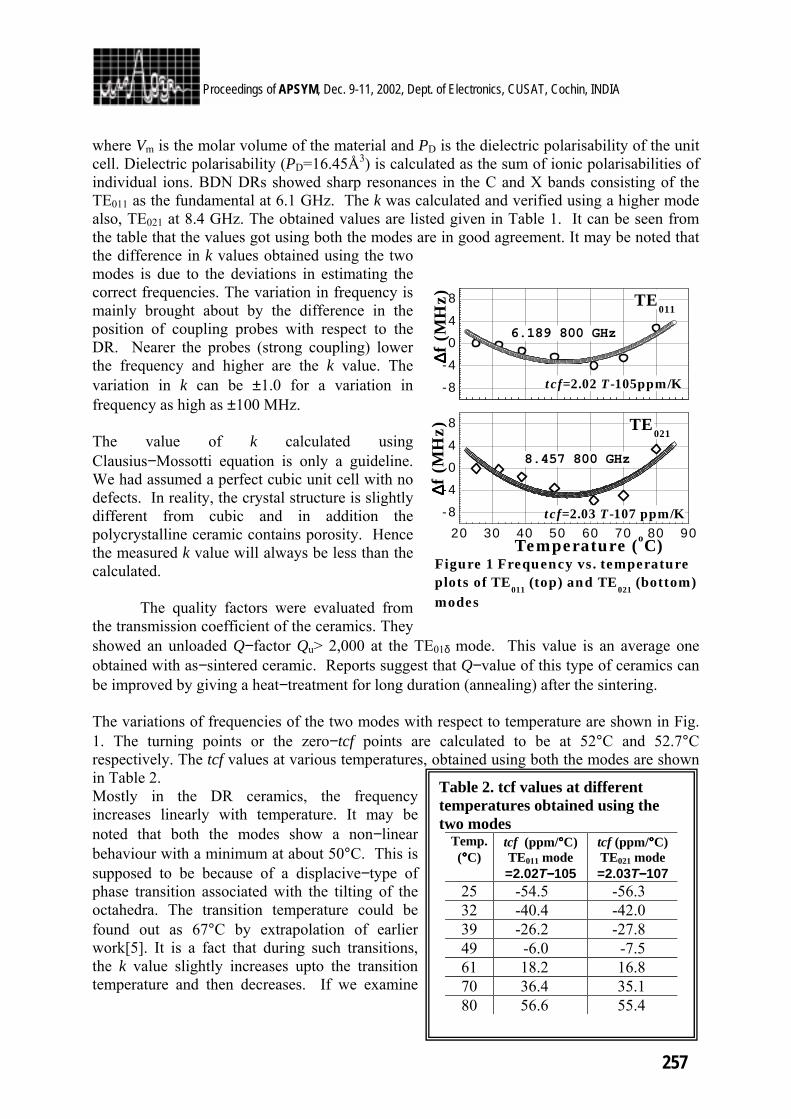
257
Proceedings of APSYM, Dec. 9-11, 2002, Dept. of Electronics, CUSAT, Cochin, INDIA
20 30 40 50 60 70 80 90
-8
-4
0
4
8
-8
-4
0
4
8
Figure 1 Frequency vs. temperature plots of TE
011 (top) and TE
021 (bottom)
modes
TE021
tcf=2.03 T-107 ppm/K
8.457 800 GHz
∆∆ ∆∆ f (
MH
z)
Temperature (oC)
TE011
tcf=2.02 T-105ppm/K
6.189 800 GHz
∆∆ ∆∆ f (
MH
z)
where Vm is the molar volume of the material and PD is the dielectric polarisability of the unit cell. Dielectric polarisability (PD=16.45Å3) is calculated as the sum of ionic polarisabilities of individual ions. BDN DRs showed sharp resonances in the C and X bands consisting of the TE011 as the fundamental at 6.1 GHz. The k was calculated and verified using a higher mode also, TE021 at 8.4 GHz. The obtained values are listed given in Table 1. It can be seen from the table that the values got using both the modes are in good agreement. It may be noted that the difference in k values obtained using the two modes is due to the deviations in estimating the correct frequencies. The variation in frequency is mainly brought about by the difference in the position of coupling probes with respect to the DR. Nearer the probes (strong coupling) lower the frequency and higher are the k value. The variation in k can be ±1.0 for a variation in frequency as high as ±100 MHz. The value of k calculated using Clausius−Mossotti equation is only a guideline. We had assumed a perfect cubic unit cell with no defects. In reality, the crystal structure is slightly different from cubic and in addition the polycrystalline ceramic contains porosity. Hence the measured k value will always be less than the calculated. The quality factors were evaluated from the transmission coefficient of the ceramics. They showed an unloaded Q−factor Qu> 2,000 at the TE01δ mode. This value is an average one obtained with as−sintered ceramic. Reports suggest that Q−value of this type of ceramics can be improved by giving a heat−treatment for long duration (annealing) after the sintering. The variations of frequencies of the two modes with respect to temperature are shown in Fig. 1. The turning points or the zero−tcf points are calculated to be at 52°C and 52.7°C respectively. The tcf values at various temperatures, obtained using both the modes are shown in Table 2. Mostly in the DR ceramics, the frequency increases linearly with temperature. It may be noted that both the modes show a non−linear behaviour with a minimum at about 50°C. This is supposed to be because of a displacive−type of phase transition associated with the tilting of the octahedra. The transition temperature could be found out as 67°C by extrapolation of earlier work[5]. It is a fact that during such transitions, the k value slightly increases upto the transition temperature and then decreases. If we examine
Table 2. tcf values at different temperatures obtained using the two modes
Temp. (°°°°C)
tcf (ppm/°°°°C) TE011 mode =2.02T−−−−105
tcf (ppm/°°°°C) TE021 mode =2.03T−−−−107
25 -54.5 -56.3 32 -40.4 -42.0 39 -26.2 -27.8 49 -6.0 -7.5 61 18.2 16.8 70 36.4 35.1 80 56.6 55.4

258
Proceedings of APSYM, Dec. 9-11, 2002, Dept. of Electronics, CUSAT, Cochin, INDIA
the equation T
tcktcf α−−=
2the quadratic variation in tck will give rise to an inverse
variation in tcf as in figures. During the measurement of tcf, the temperature-sensor was located about 5cm away from the DR to avoid any perturbation of the evanescent field. Hence the actual transition temperature of DR can be more than that shown in the curve. Hence these temperatures are in good agreement with the value reported earlier indicating the transition. SUMMARY
BDN ceramics can be prepared through solid-state mixed oxide route. Microwave dielectric properties of this ceramic k~35, Qu>2,000 and a small tcf are attractive for application in practical circuits. The turning point of the temperature−frequency curve indicates the existence of a minor phase transition. REFERENCES
1. M. Takata and K. Kageyama, J. Am. Ceram. Soc., 72, 1955, (1989). 2. E. L. Colla, I. M. Reaney and N. Setter, J. Appl. Phys., 74, 3414, (1993). 3. H. Sreemoolanadhan, Ph. D. Thesis, University of Kerala, (1996). 4. H. Sreemoolanadhan, R. Ratheesh, M. T. Sebastian and P. Mohanan, Mater. Lett., 33,
161, (1997). 5. R. Zurmuhlen, J. Petzelt, S. Kamba, V. V. Voitsckhovkvskii, E. L. Colla and N. Setter,
J. Appl. Phys., 77 (10), 5341, (1995). 6. Shannon, J. Appl. Phys. 73(1), 348, (1993) 7. B. W. Hakki and P. D. Coleman, IRE Trans. on Microwave Theory and Tech., MTT−−−−8,
402, (1960). 8. A. P. S. Khanna and Y. Garault, IEEE Trans. on Microwave Theory and Tech.,
MTT−−−−31(3), 261, (1983).
259
Proceedings of APSYM, Dec. 9-11, 2002, Dept. of Electronics, CUSAT, Cochin, INDIA
REVISIT TO Ba2Ti9O20 DR CERAMICS H. Sreemoolanadhan*, Manoj Rama Varma#, L. Abdul Khalam#,
R. Ratheesh**, M. T. Sebastian#, V. Chandrasekaran*
*Advanced Materials & Ceramics Division, Vikram Sarabhai Space Centre, Tvm−695022 #Regional Research Laboratory, CSIR, Industrial Estate P O, Tvm−695019
**Centre for Materials for Electronics Technology, M. G. Kavu, Thrissur−680771
Dibarium nona titanate (Ba2Ti9O20) has been prepared through mixed oxide route using different brands of raw materials and the microwave dielectric resonator properties are tested. Additives and substituents could not improve the properties to the required values. Impurities in the raw materials pose many problems in attaining the best dielectric properties.
INTRODUCTION
Dibarium nona titanate Ba2Ti9O20 (hereafter B2T9) is the maximum Ti−rich compound in the BaO−TiO2 system reported so far. It contains 81.8mol% TiO2. Among the many polytitanates of the system, BaTiO3 is the most widely studied compound and the earliest known ferroelectric. Another important compound is BaTi4O9 (hereafter BT4) with 80mol% TiO2. It has been established that both BT4 and B2T9 possess high dielectric constant (k), low dielectric loss at microwave frequency. So, these two materials are being used as dielectric resonators (DR) in S, C and lower X bands. Among the two, B2T9 has an edge over the other in practical applications due to slightly higher k and lower temperature coefficient of frequency (tcf). Because of these facts, right from the 80s B2T9 found place in industries that produce DRs for wireless, cellular and other microwave devices. B2T9 ceramic was invented as a DR in 1974 in Bell Laboratories, USA[1]. O'Bryan and co−workers conducted detailed studies and successfully established the materials technology. Further researches conducted at other parts of the world added many findings to the science of preparation of these ceramics. It is worth-mentioning that even now this ceramic invites a considerable attention from both industries and researchers because of the attractive dielectric properties and complex structure−property relationship. There have been a few reports on the B2T9 based ceramics from our country also[2−4]. From all these studies, it was clear that in order to get good dielectric properties, the B2T9 phase formation should be complete without the presence of TiO2. In this article, we bring out the results of our efforts in preparing B2T9 ceramics using raw materials of various manufacturers. Our aim is to present a guideline for realising useful B2T9 ceramics. CERAMIC PREPARATION
The ceramics were prepared by mixed oxide route using high pure BaCO3 and TiO2 as starting materials. Raw materials of different manufacturers were used and the purity ranged from 99−99.99%. These were mixed in 2:9 stoichiometry, dried and calcined at 1150−1300°C. Dopants like MnO2, SnO2 and SrCO3 were added wherever necessary to get dense ceramics and to get reasonably good dielectric properties. The calcined powders were ground and compacted under pressure of 100−250MPa to make discs of diameter(D) 10−13mm and thickness (L) 4−10 mm. These discs were sintered at 1260−1400°C. Since the phase diagram

260
Proceedings of APSYM, Dec. 9-11, 2002, Dept. of Electronics, CUSAT, Cochin, INDIA
of B2T9 has a curvature above 1275°C, compacts sintered above this temperature were slow−cooled @1°C/min upto 1250°C. TESTING OF MICROWAVE DIELECTRIC PROPERTIES
Microwave DR properties− dielectric constant (k), quality factor (Qu) and temperature coefficient of frequency(tcf)− were measured using resonance methods with the help of HP8510B Network Analyser system. TE011 mode frequencies were used to find out the k and tcf of the ceramics. The k was calculated using the equation of Hakki and Colemann[5]. The tcf was obtained from the frequency versus temperature graph, obtained by heating the resonator in 25−80°C range. The Q−factors of the DRs were determined using the transmission coefficients(S21) in the TE01δ mode when coupled to a 50Ω stripline inside a Cu−cavity following the method of Khanna and Garault[6]. Table1 shows the dielectric properties we got on various batches of 2.BaCO3−9.TiO2 ceramics.
RESULTS & DISCUSSION
A ceramic can function as a DR only if it has a reasonably high k(>20) and low dielectric loss (tanδ<10−3). When a single-phase compound is considered, the properties of single crystal are the best and reproducible. Single crystal B2T9 has a triclinic unit cell with a theoretical density of 4.61g/cm3 (JCPDS 40−405)[7]. However, so far no reports are available on the single−crystal dielectric properties. Best dielectric properties reported on ceramics are k~39.8, Q>8,000 and tcf~2ppm/K at 4.5GHz [1].
Table 1 Microwave dielectric properties of various 2.BaCO3-9.TiO2 ceramics.
Batch Process temp.
k Q.f tcf Remarks
B1 1360 34.0 5,150 12-0.12T Fluka 99.9% (minor SiO2 content)
B2 1335 34.8 12,980 20 Otto kemi99% (0.6% SiO2, 0.3% Fe2O3), 2.5at.%Sr for Ba
B3 1285 37.0 12,000 39 BaCO3 Aldrich 99.9% & TiO2 SD Fine, 12.5% Sr for Ba
B4 1335 35.5 17,500 2 BEL 99.9% B5 1260 39.7 17,900 37 Otto kemi99% (0.6% SiO2)
B5S 1340 -- -- 24 Same as above, 6 at.% Sn for Ti
B6 1360 37.3 15,400 3 BaCO3 Aldrich 99.9 & TiO2 Otto kemi 99%
B6M 1360 37.2 16,800 6.5 Same as above, 0.4 mol% MnO2
B7 1385 37.0 21,150 0.035T−3.48 Aldrich 99.99%
B7M 1375 37.7 22,000 5 Same as above, 2.5 mol% MnO2
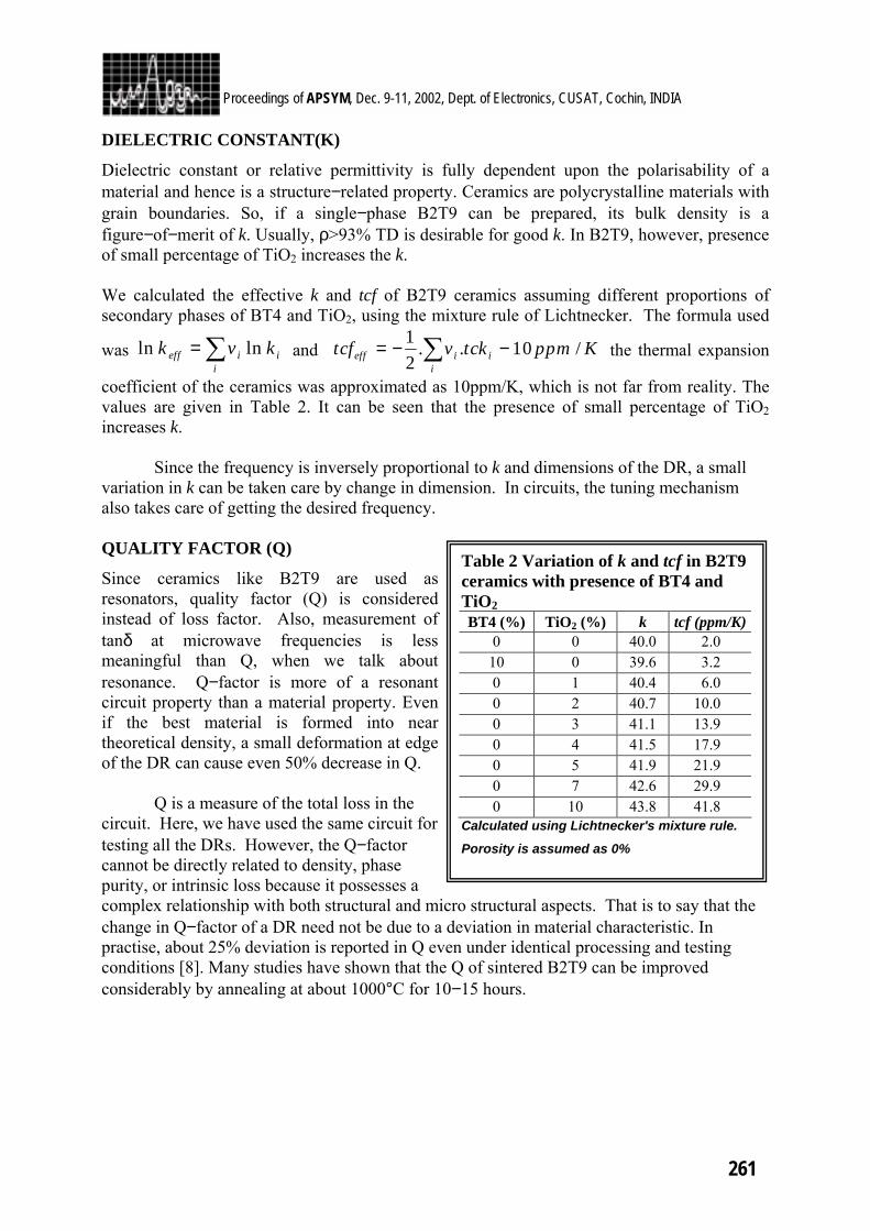
261
Proceedings of APSYM, Dec. 9-11, 2002, Dept. of Electronics, CUSAT, Cochin, INDIA
DIELECTRIC CONSTANT(K)
Dielectric constant or relative permittivity is fully dependent upon the polarisability of a material and hence is a structure−related property. Ceramics are polycrystalline materials with grain boundaries. So, if a single−phase B2T9 can be prepared, its bulk density is a figure−of−merit of k. Usually, ρ>93% TD is desirable for good k. In B2T9, however, presence of small percentage of TiO2 increases the k. We calculated the effective k and tcf of B2T9 ceramics assuming different proportions of secondary phases of BT4 and TiO2, using the mixture rule of Lichtnecker. The formula used
was ∑=i
iieff kvk lnln and Kppmtckvtcfi
iieff /10..21 −−= ∑ the thermal expansion
coefficient of the ceramics was approximated as 10ppm/K, which is not far from reality. The values are given in Table 2. It can be seen that the presence of small percentage of TiO2 increases k.
Since the frequency is inversely proportional to k and dimensions of the DR, a small variation in k can be taken care by change in dimension. In circuits, the tuning mechanism also takes care of getting the desired frequency.
QUALITY FACTOR (Q)
Since ceramics like B2T9 are used as resonators, quality factor (Q) is considered instead of loss factor. Also, measurement of tanδ at microwave frequencies is less meaningful than Q, when we talk about resonance. Q−factor is more of a resonant circuit property than a material property. Even if the best material is formed into near theoretical density, a small deformation at edge of the DR can cause even 50% decrease in Q.
Q is a measure of the total loss in the circuit. Here, we have used the same circuit for testing all the DRs. However, the Q−factor cannot be directly related to density, phase purity, or intrinsic loss because it possesses a complex relationship with both structural and micro structural aspects. That is to say that the change in Q−factor of a DR need not be due to a deviation in material characteristic. In practise, about 25% deviation is reported in Q even under identical processing and testing conditions [8]. Many studies have shown that the Q of sintered B2T9 can be improved considerably by annealing at about 1000°C for 10−15 hours.
Table 2 Variation of k and tcf in B2T9 ceramics with presence of BT4 and TiO2 BT4 (%) TiO2 (%) k tcf (ppm/K)
0 0 40.0 2.0 10 0 39.6 3.2 0 1 40.4 6.0 0 2 40.7 10.0 0 3 41.1 13.9 0 4 41.5 17.9 0 5 41.9 21.9 0 7 42.6 29.9 0 10 43.8 41.8
Calculated using Lichtnecker's mixture rule.
Porosity is assumed as 0%
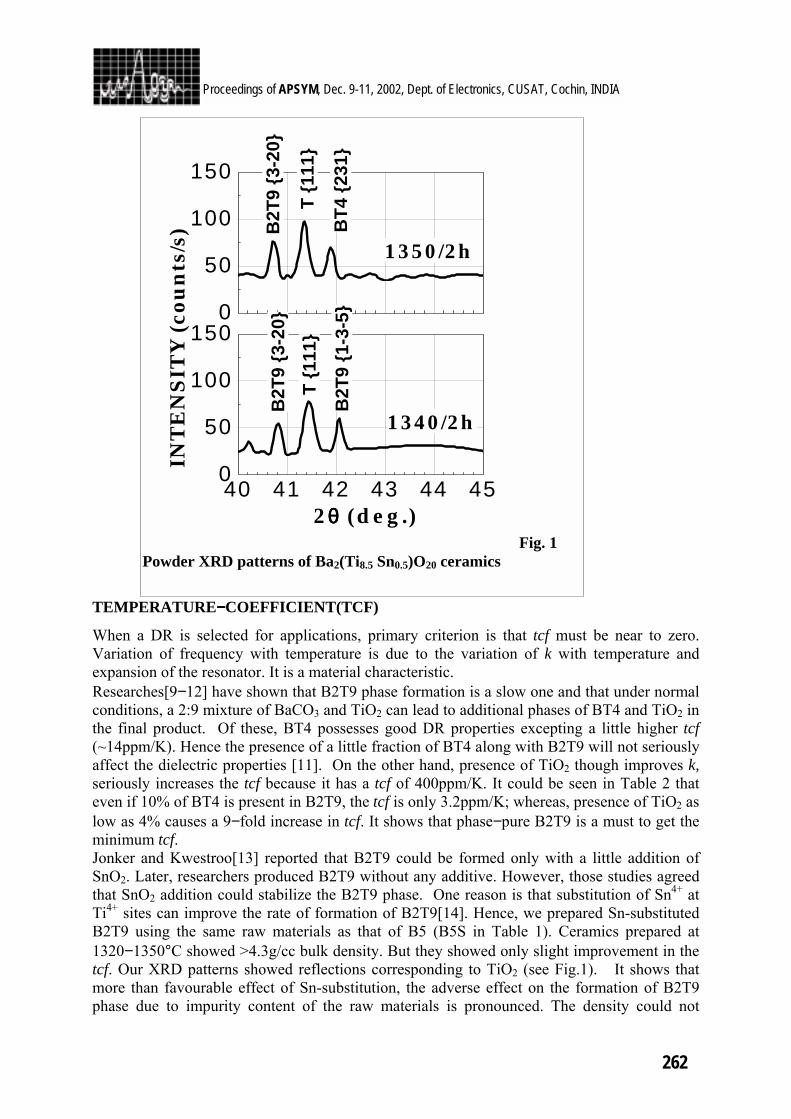
262
Proceedings of APSYM, Dec. 9-11, 2002, Dept. of Electronics, CUSAT, Cochin, INDIA
TEMPERATURE−−−−COEFFICIENT(TCF)
When a DR is selected for applications, primary criterion is that tcf must be near to zero. Variation of frequency with temperature is due to the variation of k with temperature and expansion of the resonator. It is a material characteristic. Researches[9−12] have shown that B2T9 phase formation is a slow one and that under normal conditions, a 2:9 mixture of BaCO3 and TiO2 can lead to additional phases of BT4 and TiO2 in the final product. Of these, BT4 possesses good DR properties excepting a little higher tcf (~14ppm/K). Hence the presence of a little fraction of BT4 along with B2T9 will not seriously affect the dielectric properties [11]. On the other hand, presence of TiO2 though improves k, seriously increases the tcf because it has a tcf of 400ppm/K. It could be seen in Table 2 that even if 10% of BT4 is present in B2T9, the tcf is only 3.2ppm/K; whereas, presence of TiO2 as low as 4% causes a 9−fold increase in tcf. It shows that phase−pure B2T9 is a must to get the minimum tcf. Jonker and Kwestroo[13] reported that B2T9 could be formed only with a little addition of SnO2. Later, researchers produced B2T9 without any additive. However, those studies agreed that SnO2 addition could stabilize the B2T9 phase. One reason is that substitution of Sn4+ at Ti4+ sites can improve the rate of formation of B2T9[14]. Hence, we prepared Sn-substituted B2T9 using the same raw materials as that of B5 (B5S in Table 1). Ceramics prepared at 1320−1350°C showed >4.3g/cc bulk density. But they showed only slight improvement in the tcf. Our XRD patterns showed reflections corresponding to TiO2 (see Fig.1). It shows that more than favourable effect of Sn-substitution, the adverse effect on the formation of B2T9 phase due to impurity content of the raw materials is pronounced. The density could not
40 41 42 43 44 450
50
100
1500
50
100
150
T 1
11
B2T
9 1
-3-5
B2T
9 3
-20
INT
EN
SIT
Y (
cou
nts
/s)
2θθθθ (deg.)
1340/2h
T 1
11
BT4
231
B2T
9 3
-20
1350/2h
Fig. 1 Powder XRD patterns of Ba2(Ti8.5 Sn0.5)O20 ceramics
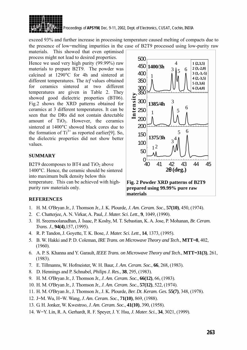
263
Proceedings of APSYM, Dec. 9-11, 2002, Dept. of Electronics, CUSAT, Cochin, INDIA
exceed 93% and further increase in processing temperature caused melting of compacts due to the presence of low−melting impurities in the case of B2T9 processed using low-purity raw materials. This showed that even optimised process might not lead to desired properties. Hence we used very high purity (99.99%) raw materials to prepare B2T9. The powder was calcined at 1290°C for 4h and sintered at different temperatures. The tcf values obtained for ceramics sintered at two different temperatures are given in Table 2. They showed good dielectric properties (BT06). Fig.2 shows the XRD patterns obtained for ceramics at 3 different temperatures. It can be seen that the DRs did not contain detectable amount of TiO2. However, the ceramics sintered at 1400°C showed black cores due to the formation of Ti3+ as reported earlier[9]. So, the dielectric properties did not show better values. SUMMARY
B2T9 decomposes to BT4 and TiO2 above 1400°C. Hence, the ceramic should be sintered into maximum bulk density below this temperature. This can be achieved with high-purity raw materials only. REFERENCES
1. H. M. O'Bryan Jr., J. Thomson Jr., J. K. Plourde, J. Am. Ceram. Soc., 57(10), 450, (1974). 2. C. Chatterjee, A. N. Virkar, A. Paul, J. Mater. Sci. Lett., 9, 1049, (1990). 3. H. Sreemoolanadhan, J. Isaac, P. Koshy, M. T. Sebastian, K. A. Jose, P. Mohanan, Br. Ceram.
Trans. J., 94(4),157, (1995). 4. R. P. Tandon, J. Goyette, T. K. Bose, J. Mater. Sci. Lett., 14, 1373, (1995). 5. B. W. Hakki and P. D. Coleman, IRE Trans. on Microwave Theory and Tech., MTT−−−−8, 402,
(1960). 6. A. P. S. Khanna and Y. Garault, IEEE Trans. on Microwave Theory and Tech., MTT−−−−31(3), 261,
(1983). 7. E. Tillmanns, W. Hofmeister, W. H. Baur, J. Am. Ceram. Soc., 66, 268, (1983). 8. D. Hennings and P. Schnabel, Philips J. Res., 38, 295, (1983). 9. H. M. O'Bryan Jr., J. Thomson Jr., J. Am. Ceram. Soc., 66(12), 66, (1983). 10. H. M. O'Bryan Jr., J. Thomson Jr., J. Am. Ceram. Soc., 57(12), 522, (1974). 11. H. M. O'Bryan Jr., J. Thomson Jr., J. K. Plourde, Ber. Dt. Keram. Ges. 55(7), 348, (1978). 12. J−M. Wu, H−W. Wang, J. Am. Ceram. Soc., 71(10), 869, (1988). 13. G. H. Jonker, W. Kwestroo, J. Am. Ceram. Soc., 41(10), 390, (1958). 14. W−Y. Lin, R. A. Gerhardt, R. F. Speyer, J. Y. Hsu, J. Mater. Sci., 34, 3021, (1999).
300350400450500
200250300350
40 41 42 43 44 450
50100150200
15
43 61400/3h
1 5
36
1385/4h
Inte
nsi
ty65
4321
1 2,3,52 3,-2,03 1,-3,-54 2,-3,55 1,3,66 3,4,0
2θθθθ (deg.)
1375/3h
Fig. 2 Powder XRD patterns of B2T9 prepared using 99.99% pure raw materials
264
Proceedings of APSYM, Dec. 9-11, 2002, Dept. of Electronics, CUSAT, Cochin, INDIA
SYNTHESIS AND MICROWAVE DIELECTRIC PROPERTIES OF Sr(1-X/2)NaXNb2O6 FERROELECTRIC CERAMICS.
Jaimon Yohannan, K. T. Mathew
Microwave Imaging and Materials Research Laboratory. Department of Electronics, Cochin University of Science and Technology, Kochi-682 022, Kerala,
India-682022, Ph: 91 484 576418, Fax: 91 484 575800, E-mail: [email protected].
Strontium sodium niobate ceramic are prepared by solid state reaction method. The real and imaginary part of complex permittivity of the samples is determined by cavity perturbation technique. The temperature coefficient of resonant frequency was measured by Courtney method. It is observed that the real part of complex permittivity varies with frequency. The variation of the resonant frequency with temperature is described in terms of physical parameters, one part of the frequency variation is caused by the physical expansion of material parts, and the other by the change in the relative dielectric constant.
INTRODUCTION
Recently following the rapid development of microwave integrated circuit technology, the ceramic materials with high dielectric constant εr, high Q, and small temperature coefficient of resonant frequency τf are particularly required for being applied to the dielectric resonator[1] Resonators are used in a number of applications in frequency bands covering audio, RF, microwave and optical frequencies. They are basic elements in filters, oscillators; antennas etc., The individual communication channels in wireless transmission networks operating from 400 MHz to 2 GHz can be as close as 150 kHz. Therefore, the resonant cavities must exhibit very high stability of resonant frequency with power and temperature variations. To analyse the temperature stability one must know the properties of all the materials used in the construction of the cavity device. The experimental characterization of dielectric materials suitable for resonant cavities has been subject of [2]-[3]. Dielectric resonators exhibiting high Q factor and very low temperature coefficient of resonant frequency have been recently developed [4]-[5], they promise to shrink the size and cost of waveguide cavities. Developing a zero τf material is probably the most difficult aspect of research into microwave dielectrics. There are a host of high-Q, high ε materials with τf’s far too large to be usable, notably TiO2, for which εr = 104, Qf = 43800, τf = + 427 ppm / k. The challenge is to find ways of tuning τf without reducing εr and maintaining Q [6]. When a particularly high Q is required, tantalates are used. The two main compounds on the market are Ba(Mg1/3Ta2/3)O3 (BMT) and Ba(Zn1/3Ta2/3)O3 (BZT). Although tantalates satisfy the high Q end of the market in terms of performance, Ta2O3 is expensive. Ideally, cheaper materials with equivalent Q/ε, values based on either niobates or titanates must be found. EXPERIMENTAL PROCEDURE
Raw materials of high purity SrCO3, Na2CO3, Nb2O5 are weighed in accordance with chemical composition of (Sr0.80Na0.40Nb2O6). The starting raw materials were mixed in a mortar with a pestle for 1 hour, dried and calcined at 1000 0C for 4 hours. After the powder was milled again with organic binder (Polyvinyl alcohol). It was pressed in to disc type and ring type specimens
265
Proceedings of APSYM, Dec. 9-11, 2002, Dept. of Electronics, CUSAT, Cochin, INDIA
in suitable die under pressure. It is then sintered at 1200 0C for 4 hours in air. The sintered samples were ground and polished before microwave measurements. The real and imaginary part of complex permittivity was measured in the S-band by cavity perturbation method. For the measurement of temperature coefficient of resonant frequency Courtney[7] method is used. The temperature coefficient of resonant frequency fo was measured in the range of 27 to 100 0C. The frequency coefficient due to copper cavity was estimated to be of the order of 1ppm/0C. A dielectric resonator of (DR) with the diameter d = 16 mm and length l = 6 mm was used for experiments. According to this method many modes generated were classified and then εr was accurately calculated from TEonl or quasi TE mode. The quality factor Q is determined from the 3 dB bandwidth of TE011 mode. RESULTS AND DISCUSSIONS
The relationship between the resonant frequency and the relative dielectric constant can be expressed in terms of Bessel functions. Courtney method is adopted for the solid cylindrical type sample. Figure 1 shows the real part of permittivity of SNN sample measured using cavity perturbation method in the S-band frequency region. The real part of Permittivity is found to vary with frequency. Figure 2 shows the variation of imaginary part of permittivity with frequency. It is interesting to note that the imaginary part of Permittivity shows a minimum value around 2.45 GHz, whereas real part shows a maxima for this frequency.
Figure 1. Frequency versus real part of complex Permittivity of SNN sample.
For the measurement of temperature coefficient of resonant frequency, the cavity was placed in a hot plate in which the temperature was stabilized. The resonant frequency and line width of the TE011 resonance measured when the mode become stationary at each value of temperature. τf was calculated using the equation
o
o
o TTTf
ffT=∆
∆= 1
-------------------- (1)
o
r
r TTTT=∆
∆= εεε1
-------------------- (2)
Where fo is the resonant frequency at a given temperature and df = f0(T) - f0 (27 0C).
8.5
8.75
9
9.25
9.5
2100 2300 2500 2700 2900 3100Frequency (MHz)
Rea
l par
t of p
erm
ittiv
ity
266
Proceedings of APSYM, Dec. 9-11, 2002, Dept. of Electronics, CUSAT, Cochin, INDIA
0.020.030.040.050.060.070.080.090.1
0.11
2100 2300 2500 2700 2900 3100
Frequency (MHz)
Imag
inar
y pa
rt of
per
mitt
ivity
Figure 2. Frequency versus imaginary part of complex Permittivity of SNN sample.
10.44
10.445
10.45
10.455
10.46
25 45 65 85 105
Temperature (C)
Die
lect
ric c
onst
ant
Figure 3. Temperature variation of real part of complex Permittivity of SNN sample.
The temperature coefficient of resonant frequency was found to be very small, equal to 1.46137 ppm /0C at 9.37GHz. The temperature coefficient of resonant frequency, τf is the parameter which indicates the thermal stability of the resonator. Figure 3 shows the temperature variation of real part of Permittivity measured using Courtney method. The dielectric constant is found to decrease as temperature increases from 270C to 1000C. The dielectric constant comes out to be a linear function of temperature as shown is figure 3. For the reference temperature 600C, the temperature coefficient of the dielectric constant is computed in accordance with equation (2)
τε = (10.447-10.449) ⁄ [30.448 × (100 -27)] = -2.622 ppm/0C
Due to the linear behaviour, the same coefficient is valid over the entire range of temperature.
The quality factor, Q = 1/ Tanδ, is a measure of the efficiency or power loss of a microwave system. It is determined from the shape of the resonant peak. A peak occurs in the transmitted signal amplitude at the resonant frequency with a finite width. The band width is defined at half its maximum amplitude (∆f). The peak frequency divided by this width ( fo / ∆f ) is equal to Q. A high Q means a narrow peak, which in turn gives high selectivity to a given frequency band. Losses normally increase with increasing frequency; therefore, Q also depends on frequency.
267
Proceedings of APSYM, Dec. 9-11, 2002, Dept. of Electronics, CUSAT, Cochin, INDIA
The variation of the resonant frequency with temperature is described in terms of physical parameters, one part of the frequency variation is caused by the physical expansion of material parts, and the other by the change in the relative dielectric constant. The dielectric constant and temperature coefficient of resonant frequency depend mainly on the composition of the material. But loss quality varies from sample to sample of the same composition, indicating that the loss quality is sensitive to slight differences in crystallographic structure and microstructure of the material. CONCLUSIONS
Sr(1-X/2)NaXNb2O6 ceramics were prepared by solid state reaction method. The complex permittivity of this material and its variation with frequency and temperature are studied at the microwave frequencies. The dielectric constant and temperature variation of resonant frequency are in the range suitable for use as microwave dielectric resonators. REFERENCES
1. Y. C. Heiao, L. Wu, and C.C. Wei, “ Microwave dielectric properties of (Zr Zn)TiO4 ceramics”, Mat.Res. Bull. Vol. 23, pp 1687-1692, 1998.
2. Darko Kajfez, Siva Chebolu, Ahmed A. Kishk, Mohammed R. Abdul-Gaffoor, “ Temperature dependence of composite microwave cavities.” IEEE Trans. MicrowaveTheory and Tech., Vol. MTT 49, No.1, January 2001.
3. A. P. Mourachkine and A. R. F. Barel, “ Temperature dependence of the principal properties of dielectric resonators,” Microwave J., Vol. 38, pp 220-233, Apr. 1995.
4. J. K. Plurde et al., “ BaTi9O20 as a microwave dielectric resonator”, J. Amer. Ceram.Soc., Vol. 58, pp 418-420, Nov. 1975.
5. Toru Higashi and Toshihiko Makino, “Resonant frequency stability of the dielectric resonator on a dielectric substrate, IEEE Trans. Microwave Theory and Tech., Vol. MTT 29, No.10, October 1981.
6. I. M. Reaney and R. Ubic, “ Talking microwaves: A review of ceramics at the heart of the telecommunications network.” International ceramics, Issue 1, pp 48-52, 2000.
7. W. E. Courtney, “Analysis and evaluation method of measuring the complex Permittivity and permeability of microwave insulators,” IEEE Trans. MicrowaveTheory and Tech., Vol. MTT-18, 476-485, August (1970).
268
Proceedings of APSYM, Dec. 9-11, 2002, Dept. of Electronics, CUSAT, Cochin, INDIA
ENHANCED BANDWIDTH RECTANGULAR DIELECTRIC RESONATOR ANTENNA USING MICROSTRIP FEED
P. V. Bijumon,1 Sreedevi. K. Menon,2 M. T. Sebastian1 and P. Mohanan2*
1Ceramics Technology Division, Regional Research Laboratory
Trivandrum 695 019, Kerala, India. 2Centre for Research in Electromagnetics and Antennas
Department of Electronics Cochin University of Science &Technology
Cochin 682 022, Kerala, India.
The present paper reports a rectangular low density, high permittivity dielectric resonator antenna excited by microstrip feed offering a 2:1 VSWR bandwidth of ~16% at 3 GHz with excellent gain and radiation performances. The radiation characteristics of the proposed antenna are compared with a circular microstrip patch antenna resonating at the same frequency.
INTRODUCTION
Dielectric resonator antennas (DRAs) offer several advantages like smaller size, higher radiation efficiency, wider bandwidth and no excitation of surface waves. The operating bandwidth of a DRA can be varied by suitably choosing the permittivity of the dielectric resonator (DR) material and its dimensions. Compared with cylindrical and hemispherical ones, rectangular DRAs are easier to fabricate and have more dimensional parameters, which provide additional degrees of freedom for antenna designers. A considerable amount of theoretical and experimental research work has been carried out on rectangular DRAs [1– 4]. In this letter the design methodology, radiation performance and the gain levels of a rectangular DRA operating at 3 GHz are described. The results are compared with those of a conventional circular microstrip patch antenna operating at the same frequency.
ANTENNA DESIGN
The geometry of the rectangular DRA is shown in Fig. 1. High dielectric constant (εdr = 48), low loss ceramic material Ca5Nb2TiO12 [5] is prepared as single phase by solid-state ceramic route. This material has been reported earlier to be best suited for bandwidth enhancement by loading over the microstrip patch antennas [6]. A rectangular DR of Ca5Nb2TiO12 material with length l = 2.25cm, breadth b = 1.190cm and height h = 0.555cm resonating at 3 GHz is loaded on 50Ω microstrip feed fabricated on a substrate of thickness h1 = 0.16cm and permittivity εr1 = 4.28. The position of DR on the feed line was optimised to provide coupling with microstrip line at the desired frequency. It is observed that optimum coupling is achieved when the microstrip feed line is exactly at the center of the DR (Fp (x0, y0)) as shown in Fig. 1.
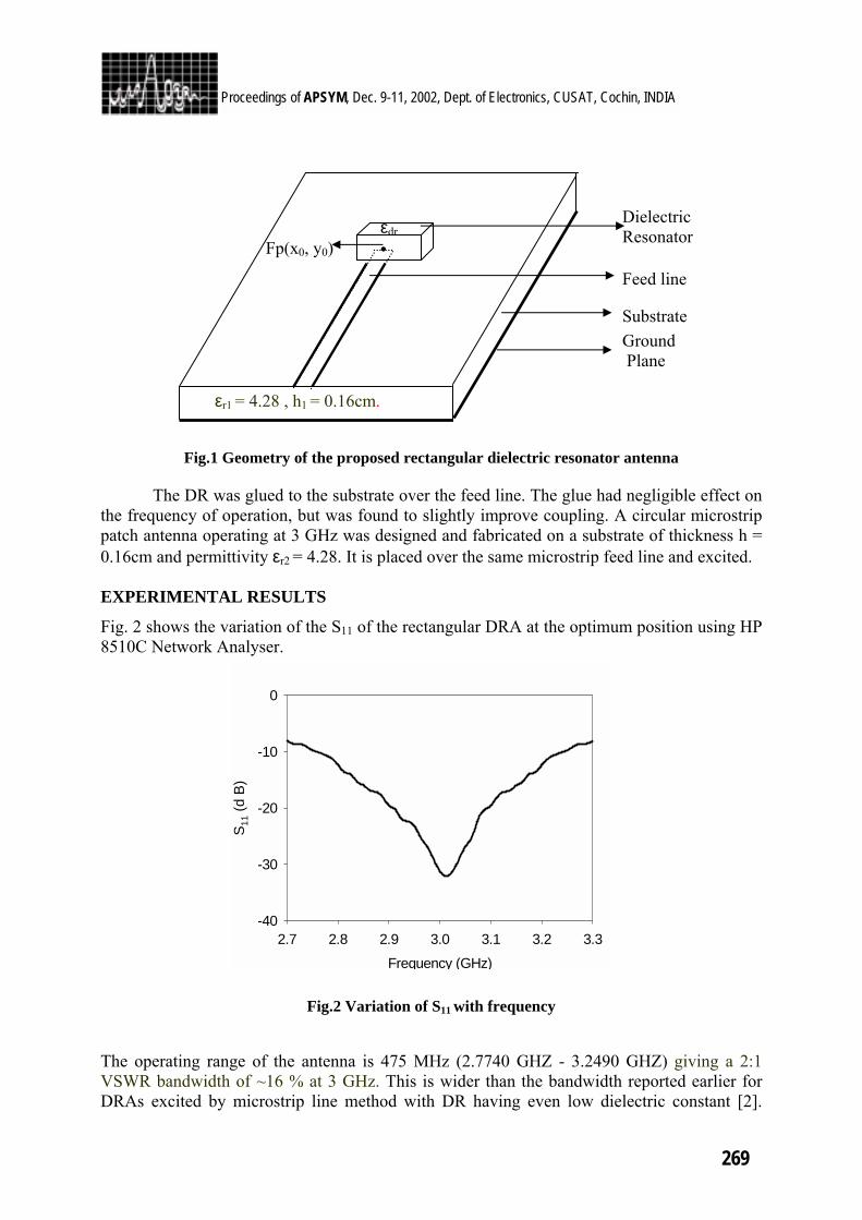
269
Proceedings of APSYM, Dec. 9-11, 2002, Dept. of Electronics, CUSAT, Cochin, INDIA
Fig.1 Geometry of the proposed rectangular dielectric resonator antenna
The DR was glued to the substrate over the feed line. The glue had negligible effect on the frequency of operation, but was found to slightly improve coupling. A circular microstrip patch antenna operating at 3 GHz was designed and fabricated on a substrate of thickness h = 0.16cm and permittivity εr2 = 4.28. It is placed over the same microstrip feed line and excited. EXPERIMENTAL RESULTS
Fig. 2 shows the variation of the S11 of the rectangular DRA at the optimum position using HP 8510C Network Analyser.
Fig.2 Variation of S11 with frequency
The operating range of the antenna is 475 MHz (2.7740 GHZ - 3.2490 GHZ) giving a 2:1 VSWR bandwidth of ~16 % at 3 GHz. This is wider than the bandwidth reported earlier for DRAs excited by microstrip line method with DR having even low dielectric constant [2].
εdr
Feed line
Substrate Ground Plane
Dielectric Resonator
εr1 = 4.28 , h1 = 0.16cm.
Fp(x0, y0) •
Frequency (GHz)
2.7 2.8 2.9 3.0 3.1 3.2 3.3
S 11 (
d B)
-40
-30
-20
-10
0
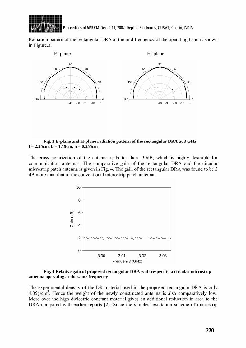
270
Proceedings of APSYM, Dec. 9-11, 2002, Dept. of Electronics, CUSAT, Cochin, INDIA
Radiation pattern of the rectangular DRA at the mid frequency of the operating band is shown in Figure.3.
Fig. 3 E-plane and H-plane radiation pattern of the rectangular DRA at 3 GHz l = 2.25cm, b = 1.19cm, h = 0.555cm
The cross polarization of the antenna is better than -30dB, which is highly desirable for communication antennas. The comparative gain of the rectangular DRA and the circular microstrip patch antenna is given in Fig. 4. The gain of the rectangular DRA was found to be 2 dB more than that of the conventional microstrip patch antenna.
Fig. 4 Relative gain of proposed rectangular DRA with respect to a circular microstrip
antenna operating at the same frequency
The experimental density of the DR material used in the proposed rectangular DRA is only 4.05g/cm3. Hence the weight of the newly constructed antenna is also comparatively low. More over the high dielectric constant material gives an additional reduction in area to the DRA compared with earlier reports [2]. Since the simplest excitation scheme of microstrip
H- planeE- plane
-40 -30 -20 -10 00
30
6090
120
150
180-40 -30 -20 -10 0
0
30
6090
120
150
180
Frequency (GHz)3.00 3.01 3.02 3.03
Gai
n (d
B)
0
2
4
6
8
10
271
Proceedings of APSYM, Dec. 9-11, 2002, Dept. of Electronics, CUSAT, Cochin, INDIA
transmission line method is adopted, the antenna system is looking very simple and easy to operate.
CONCLUSIONS
A rectangular DRA excited by microstrip transmission feed line has been studied. The antenna has a bandwidth of 475 MHz at 3 GHz and exhibits excellent radiation performances with a cross polar isolation of more than –30dB. Its gain was found to be 2dB more than that of a circular microstrip patch resonating at the same frequency. The measured properties of the rectangular DRA indicate that this antenna is more advantageous than other currently using antennas in many aspects and is desirable for applications in millimetre and microwave frequencies in the communication fields.
ACKNOWLEDGEMENT
The authors are grateful to the Department of Science and Technology, New Delhi for the financial assistance. REFERENCES
1. M. W. McAllister, S. A Long, and G. L. Conway, “Rectangular dielectric resonator antenna”, Electron. Lett., Vol. 19, pp. 218-219, 983.
2. R. A Kranenburg and S. A Long, “Microstrip Transmission line Excitation of Dielectric Resonator Antennas”, Electron. Lett., Vol. 24, pp. 1156-1157, 1998.
3. R. K. Mongia, A. Ittipiboon, M. Cuhachi and D. Roscoe, “Radiation Q-factor of rectangular dielectric resonator antennas; theory and experiment”, IEEE Antennas and Propagation society international symposium digest, pp. 764-767, 1994.
4. S. M. Shum and K. M. Luk, “Analysis of aperture coupled rectangular dielectric resonator antenna”, Electron. Lett., Vol. 30, pp. 1726-1727, 1994.
5. P. V. Bijumon, P. Mohanan and M. T. Sebastian, “Synthesis, Characterization and Properties of Ca5A2TiO12 (A=Nb, Ta) Ceramic Dielectric Materials for Applications in Microwave Telecommunication Systems”, Jpn. J. Appl. Phys., Part I, Vol. 41(6A), pp. 3384 – 3385, 2002.
6. P. V. Bijumon, Sreedevi. K. Menon, M. T. Sebastian and P. Mohanan, “Enhanced bandwidth microstrip patch antennas loaded with high permittivity dielectric resonators”, Microwave Opt. Technol. Lett., Vol.35,pp. 327-330,2002
272
Proceedings of APSYM, Dec. 9-11, 2002, Dept. of Electronics, CUSAT, Cochin, INDIA
THE EFFECT OF Mg2+ OFFSTOICHIOMETRY ON THE MICROWAVE DIELECTRIC PROPERTIES OF
Ba(Mg1/3Ta2/3)O3 CERAMICS
K. P. Surendran, P. Mohanan # and M. T. Sebastian ∗ Ceramic Technology Division, Regional Research Laboratory,
Trivandrum 695 019, India Email : [email protected]
# Department of Electronics, Cochin University of Science and Technology, Cochin 682 022, India
The effect of a slight magnesium ion offstoichiometry on the structure, densification and microwave dielectric properties of Ba(Mg1/3Ta2/3)O3 is investigated. Magnesium offstoichiometric compositions based on Ba(Mg0.33-
xTa0.67)O3 [x = -0.015, -0.010, -0.005. 0.0. 0.005, 0.010, 0.015, 0.020, 0.025 and 0.030] were prepared using the mixed oxide route. The lattice distortion and cation ordering are determined using XRD technique. The sintered samples are characterized in the microwave frequency range using the resonance method. It is found that a slight magnesium deficiency can improve the density, microwave dielectric properties and cation ordering but the addition of excess Mg2+ ions deteriorated them. Best densification, quality factor and τf are observed for x=0.015 in Ba(Mg0.33-xTa0.67)O3.
INTRODUCTION Complex perovskite oxides based on Ba(B’1/3B”2/3)O3 [B’=Mg, Zn ; B”=Ta, Nb] were reported be ideal for dielectric resonator (DR) applications due to their high unloaded quality factor and low variation of the resonant frequency with temperature1. In particular Ba(Mg1/3Ta2/3)O3 (BMT) is reported 1,2 to possess the highest quality factor among DR materials. Galasso et al.3 found that these ceramics crystallize in a disordered cubic structure or in an ordered hexagonal structure. The ordered structure results from the 1:2 ordering of the B’ and B” cations along the [111] direction of the cubic perovskite cell. It is well established that B-site ordering in complex perovskites has a significant influence on the dielectric loss quality at microwave frequencies. Rapid firing4 and doping5 are some of the techniques adopted to improve sinterability and better dielectric properties in BMT. One way to improve the sinterability is to enhance the material transport processes in the dielectric through altering the material’s stoichiometry. An improvement in the degree of 1: 2 ordering and sinterability was proposed by Lu et al.6 in Ba deficient Ba(Mg1/3Ta2/3)O3 ceramics but they didn’t throw light into the effect of Mg deficiency on the microwave dielectric properties of BMT. In 1998, Paik et al. 7 investigated the effect of Mg deficiency on the microwave dielectric properties of complex perovskite Ba(Mg1/3Nb2/3)O3. It was also reported 8 that presence of the extra phase BaTa2O6 in BMT would cause degradation of the Q factor. The volatilization of MgO at high temperature leads to secondary phase. Tochi 9 observed that the sinterability of BMT could be improved with the addition of the extra phase
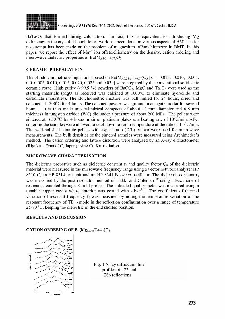
273
Proceedings of APSYM, Dec. 9-11, 2002, Dept. of Electronics, CUSAT, Cochin, INDIA
BaTa2O6 that formed during calcination. In fact, this is equivalent to introducing Mg deficiency in the crystal. Though lot of work has been done on various aspects of BMT, so far no attempt has been made on the problem of magnesium offstoichiometry in BMT. In this paper, we report the effect of Mg2+ ion offstoichiometry on the density, cation ordering and microwave dielectric properties of Ba(Mg1/3Ta2/3)O3. CERAMIC PREPARATION
The off stoichiometric compositions based on Ba(Mg0.33-xTa0.67)O3 [x = -0.015, -0.010, -0.005. 0.0. 0.005, 0.010, 0.015, 0.020, 0.025 and 0.030] were prepared by the conventional solid-state ceramic route. High purity (>99.9 %) powders of BaCO3, MgO and Ta2O5 were used as the starting materials (MgO as received was calcined at 1000oC to eliminate hydroxide and carbonate impurities). The stoichiometric mixture was ball milled for 24 hours, dried and calcined at 1300oC for 4 hours. The calcined powder was ground in an agate mortar for several hours. It is then made into cylindrical compacts of about 14 mm diameter and 6-8 mm thickness in tungsten carbide (WC) die under a pressure of about 200 MPa. The pellets were sintered at 1650 oC for 4 hours in air on platinum plates at a heating rate of 10oC/min. After sintering the samples were allowed to cool down to room temperature at the rate of 1.5oC/min. The well-polished ceramic pellets with aspect ratio (D/L) of two were used for microwave measurements. The bulk densities of the sintered samples were measured using Archimedes’s method. The cation ordering and lattice distortion were analyzed by an X-ray diffractometer (Rigaku – Dmax 1C, Japan) using Cu Kα radiation. MICROWAVE CHARACTERISATION
The dielectric properties such as dielectric constant εr and quality factor Qu of the dielectric material were measured in the microwave frequency range using a vector network analyzer HP 8510 C, an HP 8514 test unit and an HP 8341 B sweep oscillator. The dielectric constant εr
was measured by the post resonator method of Hakki and Coleman 10 using TE01δ mode of resonance coupled through E-field probes. The unloaded quality factor was measured using a tunable copper cavity whose interior was coated with silver11. The coefficient of thermal variation of resonant frequency τf was measured by noting the temperature variation of the resonant frequency of TE01δ mode in the reflection configuration over a range of temperature 25-80 oC, keeping the dielectric in the end shorted position. RESULTS AND DISCUSSION CATION ORDERING OF Ba(Mg0.33-x Ta0.67)O3
Fig. 1 X-ray diffraction line profiles of 422 and 266 reflections
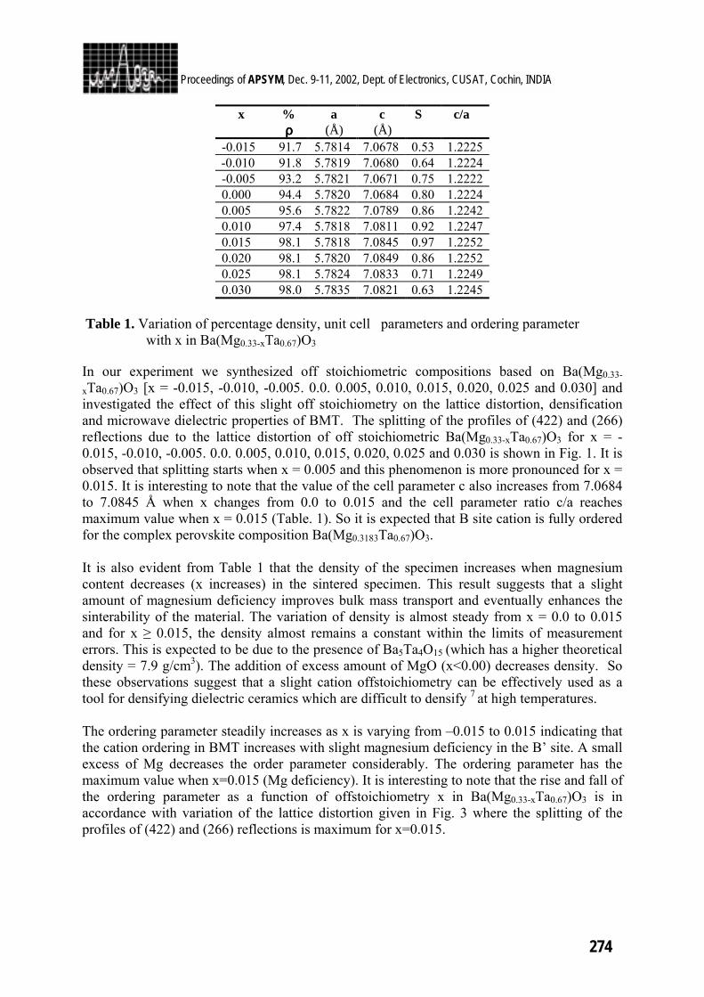
274
Proceedings of APSYM, Dec. 9-11, 2002, Dept. of Electronics, CUSAT, Cochin, INDIA
x % ρρρρ
a (Å)
c (Å)
S c/a
-0.015 91.7 5.7814 7.0678 0.53 1.2225 -0.010 91.8 5.7819 7.0680 0.64 1.2224-0.005 93.2 5.7821 7.0671 0.75 1.22220.000 94.4 5.7820 7.0684 0.80 1.22240.005 95.6 5.7822 7.0789 0.86 1.22420.010 97.4 5.7818 7.0811 0.92 1.22470.015 98.1 5.7818 7.0845 0.97 1.22520.020 98.1 5.7820 7.0849 0.86 1.22520.025 98.1 5.7824 7.0833 0.71 1.22490.030 98.0 5.7835 7.0821 0.63 1.2245
Table 1. Variation of percentage density, unit cell parameters and ordering parameter with x in Ba(Mg0.33-xTa0.67)O3
In our experiment we synthesized off stoichiometric compositions based on Ba(Mg0.33-
xTa0.67)O3 [x = -0.015, -0.010, -0.005. 0.0. 0.005, 0.010, 0.015, 0.020, 0.025 and 0.030] and investigated the effect of this slight off stoichiometry on the lattice distortion, densification and microwave dielectric properties of BMT. The splitting of the profiles of (422) and (266) reflections due to the lattice distortion of off stoichiometric Ba(Mg0.33-xTa0.67)O3 for x = -0.015, -0.010, -0.005. 0.0. 0.005, 0.010, 0.015, 0.020, 0.025 and 0.030 is shown in Fig. 1. It is observed that splitting starts when x = 0.005 and this phenomenon is more pronounced for x = 0.015. It is interesting to note that the value of the cell parameter c also increases from 7.0684 to 7.0845 Å when x changes from 0.0 to 0.015 and the cell parameter ratio c/a reaches maximum value when x = 0.015 (Table. 1). So it is expected that B site cation is fully ordered for the complex perovskite composition Ba(Mg0.3183Ta0.67)O3. It is also evident from Table 1 that the density of the specimen increases when magnesium content decreases (x increases) in the sintered specimen. This result suggests that a slight amount of magnesium deficiency improves bulk mass transport and eventually enhances the sinterability of the material. The variation of density is almost steady from x = 0.0 to 0.015 and for x ≥ 0.015, the density almost remains a constant within the limits of measurement errors. This is expected to be due to the presence of Ba5Ta4O15 (which has a higher theoretical density = 7.9 g/cm3). The addition of excess amount of MgO (x<0.00) decreases density. So these observations suggest that a slight cation offstoichiometry can be effectively used as a tool for densifying dielectric ceramics which are difficult to densify 7 at high temperatures. The ordering parameter steadily increases as x is varying from –0.015 to 0.015 indicating that the cation ordering in BMT increases with slight magnesium deficiency in the B’ site. A small excess of Mg decreases the order parameter considerably. The ordering parameter has the maximum value when x=0.015 (Mg deficiency). It is interesting to note that the rise and fall of the ordering parameter as a function of offstoichiometry x in Ba(Mg0.33-xTa0.67)O3 is in accordance with variation of the lattice distortion given in Fig. 3 where the splitting of the profiles of (422) and (266) reflections is maximum for x=0.015.
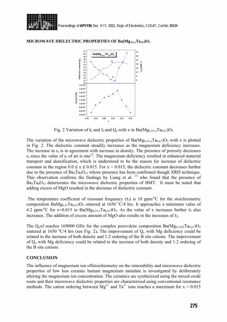
275
Proceedings of APSYM, Dec. 9-11, 2002, Dept. of Electronics, CUSAT, Cochin, INDIA
MICROWAVE DIELECTRIC PROPERTIES OF Ba(Mg.33-xTa.67)O3
Fig. 2 Variation of εr and τf and Qu with x in Ba(Mg0.33-xTa0.67)O3
The variation of the microwave dielectric properties of Ba(Mg0.33-xTa0.67)O3 with x is plotted in Fig. 2. The dielectric constant steadily increases as the magnesium deficiency increases. The increase in εr is in agreement with increase in density. The presence of porosity decreases εr since the value of εr of air is one12. The magnesium deficiency resulted in enhanced material transport and densification, which is understood to be the reason for increase of dielectric constant in the region 0.0 ≤ x ≤ 0.015. For x > 0.015, the dielectric constant decreases further due to the presence of Ba5Ta4O15 whose presence has been confirmed though XRD technique. This observation confirms the findings by Liang et al. 13 who found that the presence of Ba5Ta4O15 deteriorates the microwave dielectric properties of BMT. It must be noted that adding excess of MgO resulted in the decrease of dielectric constant. The temperature coefficient of resonant frequency (τf) is 10 ppm/oC for the stoichiometric composition BaMg0.33Ta0.67)O3 sintered at 1650 oC/4 hrs. It approaches a minimum value of 4.2 ppm/oC for x=0.015 in Ba(Mg0.33-xTa0.67)O3. As the value of x increases further τf also increases. The addition of excess amount of MgO also results in the increases of τf. The Quxf reaches 169000 GHz for the complex perovskite composition Ba(Mg0.3183Ta0.67)O3 sintered at 1650 oC/4 hrs (see Fig. 2). The improvement of Qu with Mg deficiency could be related to the increase of both density and 1:2 ordering of the B site cations. The improvement of Qu with Mg deficiency could be related to the increase of both density and 1:2 ordering of the B site cations. CONCLUSION The influence of magnesium ion offstoichiometry on the sinterability and microwave dielectric properties of low loss ceramic barium magnesium tantalate is investigated by deliberately altering the magnesium ion concentration. The ceramics are synthesized using the mixed oxide route and their microwave dielectric properties are characterized using conventional resonance methods. The cation ordering between Mg2+ and Ta5+ ions reaches a maximum for x = 0.015
22222323242424252526262627
ττττ f
εεεεr
Die
lect
ric
Con
stan
t (εε εε r)
Ba(Mg.33-xTa.67)O3
4
8
12
16
20
24
28
32
ττ ττf (ppm/ oC
)
-0.02 -0.01 0.00 0.01 0.02 0.03
4.0x10⁴
6.0x10⁴
8.0x10⁴
1.0x10⁵
1.2x10⁵
1.4x10⁵
1.6x10⁵
1.8x10⁵
2.0x10⁵
(Quxf
) (G
Hz)
x
276
Proceedings of APSYM, Dec. 9-11, 2002, Dept. of Electronics, CUSAT, Cochin, INDIA
in Ba(Mg0.33Ta0.67)O3. It is found that density increases with slight offstoichiometry (x=0.015) of Mg2+ concentration. The dielectric constant and unloaded quality factor reach maximum values and the τf is minimum for this composition. The microwave dielectric properties deteriorate for larger magnesium ion offstoichiometry. REFERENCES 1. W. Wersing, Electronic ceramics, Edited by B.C. H. Steele, Elsevier Pub. Co. Inc., 67
(1991). 2. S. Nomura, K. Toyama and K. Kaneta, Jpn. J. Appl. Phys., 21, L624 (1982). 3. F. Galasso and R. Pyle, J. Phys. Chem., 67, 1961 (1963). 4. K. Matsumoto and T. Hiuga, Seramikkusu, 22, 878 (1987) (Japanese). 5. L. Chai, M. A. Akbas and P. K. Davies, Proc. of the Inter. Conf. on Solid state
Chemistry of Inorganic Materials, 2-3 December, Boston, p. 443 (1996) 6. C.-H. Lu and C.-C. Tsai, J. Mater. Res., 5, 1219 (1996). 7. J.H. Paik, S. Nahm, J. D, Bylin, M. H. Kim and H. J. Lee, J. Mat. Sci. Lett., 17, 1779
(1998). 8. S.-Y. Kim, H.-Y.Lee, C.-K. Yang and J.-J. Kim, Proc. Inter. Symp. Application of
Ferroelectrics, August 7-10 (1994). 9. Tochi. K., J. Ceram. Soc. Japan, 100 , 1545 (1992). 10. B. W. Hakki and P. D. Coleman, IRE Trans. Microwave Theor. Tech., MTT-8, 402
(1960). 11. J. Krupka, K. Derzakowski, B. Riddle, and J. B. Jarvis, Meas. Sci. Technol., 9, 1751
(1998). 12. S. J. Penn, N. McN Alford, A. Templeton, X. Wang, M. Xu, M. Reece and K. Schrapel,
J. Am. Ceram. Soc., 80, 1885 (1997). 13. M.-H. Liang, C.-T. Hu, C.-G. Chiou, Y.-N. Tsai and I.-N. Lin, Jpn. J. Appl. Phys. 38,
5621 (1999).
277
Proceedings of APSYM, Dec. 9-11, 2002, Dept. of Electronics, CUSAT, Cochin, INDIA
STUDIES ON THE DIELECTRIC PROPERTIES OF POLY O-TOLUIDINE/POLYVINYL CHLORIDE SEMI INTER
PENETRATING POLYMER NETWORKS
Honey John1, Joe Jacob2 ,K.T.Mathew2, Rani Joseph1 1-Department of Polymer Science and Rubber Technology
2-Department of Electronics Cohin University of Science and Technology
Cochin 682 022, Kerala, India
Polyo-touidine / Poly Vinyl chloride Semi Inter Penetrating Polymer Network (POT/PVC SIPN)was prepared by the chemical oxidative polymerization of aniline. The dielectric properties of SIPN were measured using cavity perturbation technique. A rectangular Cavity operating at S band of the microwave frequency was employed for the study. These materials may find applications in anti static coatings, as sensors, polymer batteries etc
INTRODUDCTION
The recent widespread use of conducting polymers especially Polyaniline for various technological applications such as energy storage devices, sensors and above all as a strong EMI 1,2 material has attracted significant attention from all polymer branches with a growing interdisciplinary trend. Among the large variety of conducting polymers, polyaniline (PAN) has received much attention because of its properties of reversible proton doping, high electrical conductivity and ease of bulk preparation3. However, to make polyaniline technologically viable, processability and thermal stability of polymer have to be improved. To improve the solubility and hence the solution processing for various applications poly o-toluidine is envisaged since the introduction of a substituent group (-CH3 group in o-toluidine) would increases the torsional angle between the two adjacent phenylene rings and facilitate better solvation at the -NH group on the polymer back bone4. PREPARATION
Materials Used 1. o-toluidine (reagent grade) was distilled prior to use. 2. Ammonium per sulfate, emulsion grade Polyvinyl chloride were analar grade Preparation of Polyo-toluidine / Poly vinyl chloride SIPN Chemical oxidative polymerization of o-toluidine was carried out using ammonium per sulfate as initiator in the presence of emulsion grade polyvinyl chloride and 1M HCl. The polymerization was carried out for about 4 hrs. at room temperature. It was then filtered, washed and dried under vacuum and was then pelletized. The dielectric properties of these SIPN’s were measured using cavity perturbation technique. Different compositions of POT/PVC SIPN’s, say, 1:.5, 1:1, 1:2,1:3 were prepared using the above procedure and the dielectric properties were measured. EXPERIMENTAL SET UP AND THEORY
278
Proceedings of APSYM, Dec. 9-11, 2002, Dept. of Electronics, CUSAT, Cochin, INDIA
The experimental set up5 consists of a HP8510 vector network analyzer; sweep oscillator, S- parameter test set and rectangular cavity resonator. The measurements were done at 250 C in S band (2 GHz - 4 GHz) of the microwave spectrum When a dielectric material is introduced in a cavity resonator at the position of maximum electric field, the contribution of magnetic field for the perturbation is minimum. The real and imaginary parts of the relative complex permittivity are given by6
−+=
s
c
s
sor V
Vf
ff2
1/ε (4)
−=
so
so
s
cr QQ
QQV
V4
//ε (5)
where fo and fs are the resonant frequencies of the empty and sample loaded cavity and Vc and Vs are the volumes of the cavity and sample and respectively. Qs and Qo denotes quality factors of cavity with and without sample. Quality factor Q is given by Q = f / ∆f where f is the resonant frequency and ∆f is the corresponding 3dB bandwidth. The real part of the complex permittivity, ε′r is generally known as dielectric constant and the imaginary part ε′′ r is related to the dielectric loss of the material. The loss tangent is given by tanδ = σ + ωε′′r / ωε′r (6) Here σ + ωε′′r is the effective conductivity of the medium. When the conductivity σ due to free charge is negligibly small (good dielectric) the effective conductivity is due to electric polarization and is reduced to σe = ωε′′r = 2*π* f * ε0 * ε′′ r (7) The efficiency of heating is usually compared by means of a comparison coefficient J, which is defined as J = 1/εr tan δ. RESULTS AND DISCUSSION
Dielectric Conductivity Fig. I shows the variation of the dielectric loss of different SIPN’s at S band (2 GHz-3GHz). It consists of a conductivity region at lower frequencies and a dielectric relaxation region at higher frequencies7. The dielectric loss is found to be high at lower frequency in all cases. The dielectric loss is a direct function of relaxation process and the origin of this relaxation is due to the local motion of polar groups. The dielectric loss is very high at very low frequencies due to the free charge motion within the material8,9. For very low frequencies there is time for charges to build up at the inter faces before the field changes the direction and this contributes to the high dielectric loss. Figure II shows the loss tangent tanδ, which is defined as ε′′ r / ε′r ( for a good dielectric)plotted for different proportions against frequencies. Fig.III shows the conductivity of different SIPN’s with frequency,& it depends upon the dielectric loss factor and so it shows the same behavior as the dielectric loss factor shows. Protonation in POT leads to the formation of radical cations by an internal redox reaction which causes reorganization of electronic structure to give semiquinone radical cations. The degree of protonation and the electronic conductivity thus become a function of dopant concentration. The behaviour is found to be same for all cases. It is assumed from the figures III that at higher loadings a part of PVC is acting as a dopant molecule
. Dielectric constant (εεεε′′′′r)
Error! Objects cannot be created from editing field codes.
279
Proceedings of APSYM, Dec. 9-11, 2002, Dept. of Electronics, CUSAT, Cochin, INDIA
Fig IV shows that the dielectric constant decreases with increase in frequency The polarization is caused by the alternating accumulation of charges at inter faces between different phases of material. At higher frequencies, due to the orientation polarization caused by the rotational displacement of molecular dipoles under the influence of alternating field may leads to dielectric relaxation and this may leads to a decrease in dielectric constant10. Dielectric heating coefficient (J) Fig.V shows the variation of dielectric heating coefficient of different SIPN’s with frequency. It is a direct function of the loss tangent tanδ. Higher the J value poorer will be the polymer for dielectric heating purposes. Fig VI shows that the variation of dielectric loss, conductivity, & dielectric heating coefficient with different proportions. It is clear from the figure that the conductivity is less for polyo-touidine alone and is increased with increasing PVC content and is reaches a maximum at (POT:PVC) 1:2 proportion. 1:2 proportions are an optimum composition which will give high dielectric loss due to the easy interchange of polar groups which in turn increases the conductivity. The dielectric heating is found to be less for 1:2 proportions and this proportion is an ideal one for dielectric heating purpose. CONCLUSION
The microwave conductivity of POT& POT – PVC SIPN is found to be related to the dielectric loss factor and frequency. Also the conductivity is found to be higher for POT: PVC SIPN compared to POT alone. and is found to be maximum for 1:2 (POT:PVC) proportion. The dielectric heating is found to be less for 1:2 proportions and this proportion can be selected for dielectric heating applications.
REFERENCES
1. N. Li. Lee and L. H. Ong. J.Appl.Electrochem. Vol 22,512, 1992 2. F.Trinidal, M.C. Montemayer and E. Falas. J. Electro chem. Society Vol 138,3186, 1991 3. A.J.Epstein and A.G.MacDiarmid, Faraday Discuss. Chem. Soc.Vol. 88,-317(1989). 4. Meenakshi Maruthamuthu, G.Harichandran and D.Jeyakumar, Macromolecules New
Frontiers, Vol.1, 359, 1998 5. K.T.Mathew and U.Raveendranath, "Waveguide cavity Perturbation method for
measuring complex permittivity of water", Microwave and Optical Technology Letters, (USA). Vol.6, No.2, pp. 104-106,1993
6. H.Baltes, W. Goopel and J. Hesse, Sensors Update, Wiley-VCH Germany,Vol. 7 pp185-213,2000
7. N.G.McCrum,B.Ee. Read, G.Williams,Anelastic Dielectric Effects in Polymer solids, John Wiley & Sons Ltd., London, 1967
8. R.J.Maccallum,C.A. Vincent, Polymer Electrolyte ReviewsII, Elsevier Applied Science Publuishers Ltd, London and New York, 1987,Ch.2
9. A.Kyritsis, P.Pissis, J.Grammatikakis, J.Polym.Sci. Part B: Polym.Phys. Vol.33, pp-1737-1750, 1995
10. T.A Ezquerra, F.Kremmer, G.Wegner, AC, Ddielectric properties of heterogeneous Materials: Progress in Eelectromagnetic research, Vol. 6, Elsvier, new York,1992
280
Proceedings of APSYM, Dec. 9-11, 2002, Dept. of Electronics, CUSAT, Cochin, INDIA
Frequency Vs dielectric loss
00.20.40.60.8
11.21.4
2 2.5 3Frequency(GHz)
Die
lect
ric lo
ss(S
/m)
POT alone 1:.5(POT:PVC)1:1(POT:PVC) 1:2(POT:PVC)1:3(POT:PVC)
Frequency Vs loss tangent
0
0.2
0.4
2 2.5 3Frequency(GHz)
loss
tang
ent
POT alone 1:.5(POT:PVC)1:1(POT:PVC) 1:2(POT:PVC)1:3(POT:PVC)
Frequency Vs Conduct ivity
0
0.1
0.2
0.3
2 2.5 3
Frequency(GHz)
Con
duct
ivity
(S/m
)
POT alone 1:.5(POT :PVC)1:1(POT :PVC) 1:2(POT :PVC)1:3(POT :PVC)
Frequency Vs Dielectric heat ing
024
2 2.5 3
Frequency(GHz)
lnJ
POT alone 1:.5(POT :PVC)1:1(POT :PVC) 1:2(POT :PVC)1:3(POT :PVC)
Proport ions Vs dielect ric propert ies
0
1
2
3
POTalone
1:05 1:01 1:02 1:03
Proportions(PPY:PVC)
Die
lect
riclo
ss
cond
uctiv
ity,ln
J
Dielect ric loss conduct ivity lnJ
Frequency Vs Dielectric constant
0
4
8
12
2 2.5 3Frequency(GHz)
Die
lect
ric c
onst
ant
POT alone 1:.5(POT:PVC)1:1(POT:PVC) 1:2(POT:PVC)1:3(POT:PVC)
Fig I Fig II
Fig III Fig IV
Fig V Fig VI
7.1 Theoretical And Experimental Investigation Of The Circular Microstrip
Antenna In The Free Space And In The Simulated Plasma Medium R.P. Yadav, S. Sancheti, R.K. Gupta
283
281
Proceedings of APSYM, Dec. 9-11, 2002, Dept. of Electronics, CUSAT, Cochin, INDIA
RESEARCH SESSION VII December 10, Tuesday 2002 (3.15 pm to 4.30 pm)
Dept. of Electronics & Commn. Engg., Malviya National Institute of Technology, Jaipur [email protected]
7.2 Magnetically Biased Ferrite Microstrip Antennas J.S. Roy and N. Chattoraj ECE Dept., Birla Institute of Technology, Mesra, Ranchi – 835 215
288
7.3 A Proximity Fed Loudspeaker-Shaped Broad Band Microstrip Antenna P.K. Singhal and Laxmi Shrivastava Dept. of electronics and CSE, Madhav Institute of Technology and Science, Gwalior – 474 005. [email protected]
292
7.4 Progress In Circularly Polarized Microstrip Antenna Ram. L. Yadav & K. Shambavi Ramalingam Dept. of Electronics & Commn.Engg., Vellore Institute of Technology, Vellore - 632 014. [email protected]
296
7.5 Superstrate Loaded Elliptical Microstrip Patch Antenna Ram L. Yadav Dept. of Electronics & Commn.Engg., Vellore Institute of Technology, DU, Vellore- 632 014, Tamil Nadu. [email protected]
300
7.6 Bandwidth Enhancement of Microstrip Antenna Using Photonic Band Gap Structure Sreedevi K Menon, B Lethakumary, C K Aanandan, K Vasudevan, P Mohanan CREMA, Dept. of Electronics, CUSAT, Cochin-682 022.
305
MICROSTRIP ANTENNAS III Hall : 1
CHAIRS: PROF. T.K.SARKAR PROF. S.K. CHOWDHARY

282
Proceedings of APSYM, Dec. 9-11, 2002, Dept. of Electronics, CUSAT, Cochin, INDIA
283
Proceedings of APSYM, Dec. 9-11, 2002, Dept. of Electronics, CUSAT, Cochin, INDIA
284
Proceedings of APSYM, Dec. 9-11, 2002, Dept. of Electronics, CUSAT, Cochin, INDIA
285
Proceedings of APSYM, Dec. 9-11, 2002, Dept. of Electronics, CUSAT, Cochin, INDIA

286
Proceedings of APSYM, Dec. 9-11, 2002, Dept. of Electronics, CUSAT, Cochin, INDIA
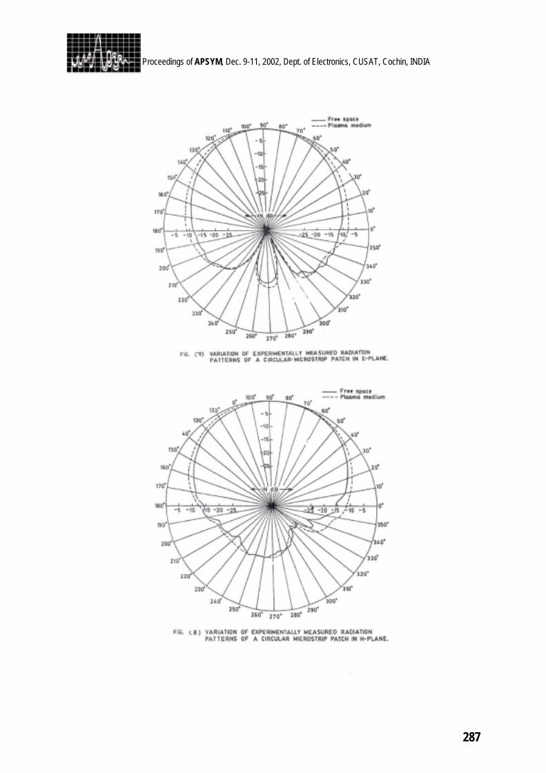
287
Proceedings of APSYM, Dec. 9-11, 2002, Dept. of Electronics, CUSAT, Cochin, INDIA
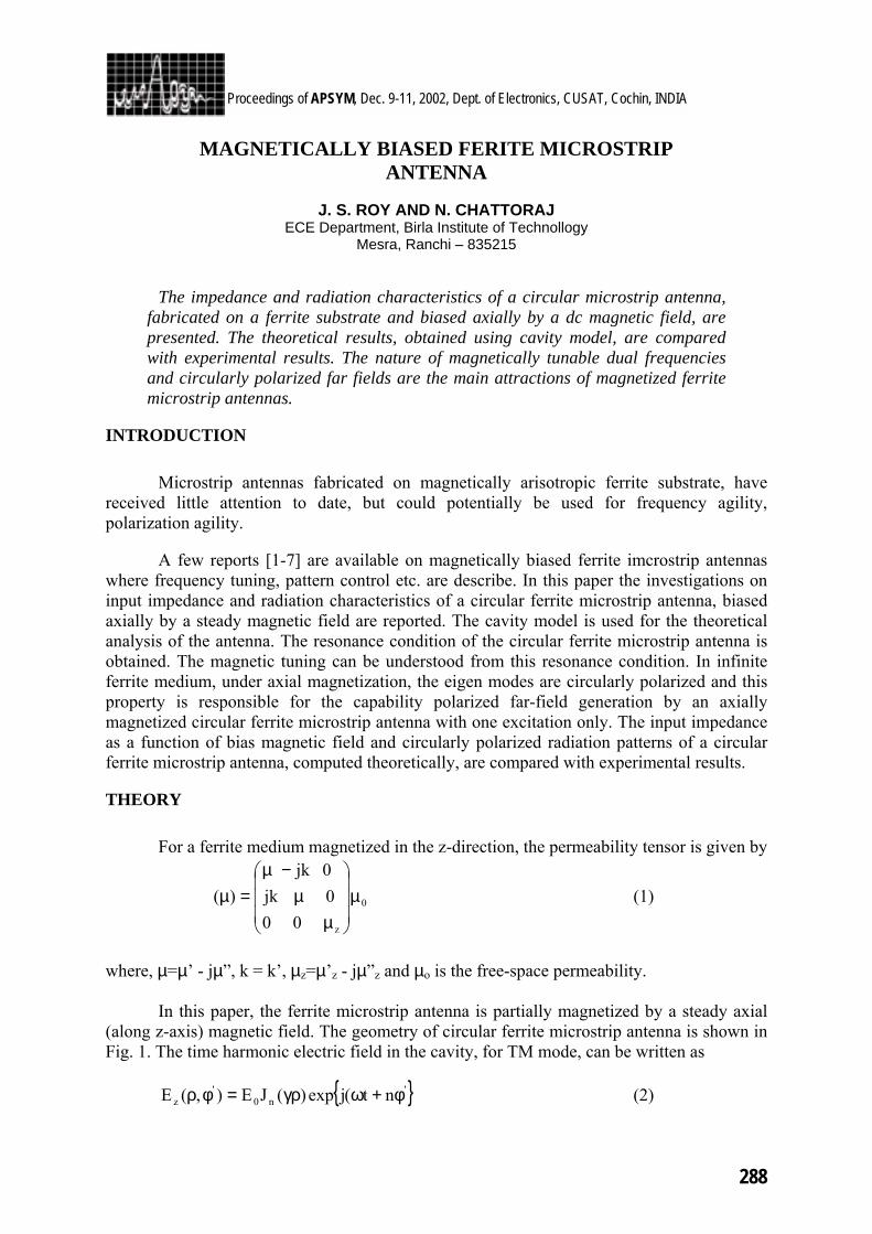
288
Proceedings of APSYM, Dec. 9-11, 2002, Dept. of Electronics, CUSAT, Cochin, INDIA
MAGNETICALLY BIASED FERITE MICROSTRIP ANTENNA
J. S. ROY AND N. CHATTORAJ
ECE Department, Birla Institute of Technollogy Mesra, Ranchi – 835215
The impedance and radiation characteristics of a circular microstrip antenna, fabricated on a ferrite substrate and biased axially by a dc magnetic field, are presented. The theoretical results, obtained using cavity model, are compared with experimental results. The nature of magnetically tunable dual frequencies and circularly polarized far fields are the main attractions of magnetized ferrite microstrip antennas.
INTRODUCTION Microstrip antennas fabricated on magnetically arisotropic ferrite substrate, have received little attention to date, but could potentially be used for frequency agility, polarization agility. A few reports [1-7] are available on magnetically biased ferrite imcrostrip antennas where frequency tuning, pattern control etc. are describe. In this paper the investigations on input impedance and radiation characteristics of a circular ferrite microstrip antenna, biased axially by a steady magnetic field are reported. The cavity model is used for the theoretical analysis of the antenna. The resonance condition of the circular ferrite microstrip antenna is obtained. The magnetic tuning can be understood from this resonance condition. In infinite ferrite medium, under axial magnetization, the eigen modes are circularly polarized and this property is responsible for the capability polarized far-field generation by an axially magnetized circular ferrite microstrip antenna with one excitation only. The input impedance as a function of bias magnetic field and circularly polarized radiation patterns of a circular ferrite microstrip antenna, computed theoretically, are compared with experimental results. THEORY For a ferrite medium magnetized in the z-direction, the permeability tensor is given by
0
z000jk0jk
)( µ
µµ
−µ=µ (1)
where, µ=µ’ - jµ”, k = k’, µz=µ’z - jµ”z and µo is the free-space permeability. In this paper, the ferrite microstrip antenna is partially magnetized by a steady axial (along z-axis) magnetic field. The geometry of circular ferrite microstrip antenna is shown in Fig. 1. The time harmonic electric field in the cavity, for TM mode, can be written as 'n0
'z nt(jexp)(JE),(E φ+ωγρ=φρ (2)
289
Proceedings of APSYM, Dec. 9-11, 2002, Dept. of Electronics, CUSAT, Cochin, INDIA
Here, rfffoo22 µεµεω=γ and 02
⟩γ where fε is the relative permittivity of ferrite and
µ−µ=µ
22
effk is the effective permeability of ferrite substrate. The resonance condition for
circular ferrite microstrip antenna can be written as ( ) 0)(J)k()(Jk 1n1n =γα−µ−γα+µ ++ (3) and from this equation it is clear that the resonant frequencies are different for positive and magnetive values of n and the difference between two frequencies depends on the bias strength (µ, k and γ are the functions of bias magnetic field). So by changing the bias strength, different resonance frequencies can be obtained by the same microstrip patch. The range of this frequency-tuning depends on the bias magnetic field strength and on the material properties of the ferrite. The far field components of magnetically biased circular ferrite patch are obtained, which are
[ ])aSink(J)aSink(J.eer
e2akV
jE o1no1ntj)2/n(j
rjkoon
o
θ−θ= −+ωπ−φ
−
θ (4)
[ ])aSink(J)aSink(Jcos.eer
e2akV
jE o1no1ntj)2/n(j
rjkoon
o
θ+θθ= −+ωπ−φ
−
φ (5)
where, Vo = hEoJn(γα) The far field components are circularly polarized in broadside direction and elliptically polarized in other directions. Positive and negative values of ‘n’ give left-hand and right-hand circular polarizations respectively. The far field components and hence the radiated power depend on the bias magnetic-field. The input impedance of the antenna is given by the expression,
ωω
−ωω+
=r
rT
ln
jQ1
RZ (6)
Total stored energy WT=WE+WM PT=Pd+Pc+Pm+Pr RESULTS The circular microstrip antennas, fabricated on two types of ferrites, were studied. Sample 1 : Ferrite type Y209
290
Proceedings of APSYM, Dec. 9-11, 2002, Dept. of Electronics, CUSAT, Cochin, INDIA
0002.0tan,cm3.0h,cm3.1a,e20H,3.14,G900M4 efffs =δ===∆=∈=π Sample 2 : Ferrite type Y27
0002.0tan,cm3.0h,cm65.1a,e20H,3.14,G704M4 efffs =δ===∆=∈=π The variations of resonance frequencies with bias magnetic field, obtained theoretically by solving eqn. (3) for resonance frequencies, is plotted in Fig. 2. Resonance frequencies for n = -1 mode increase with bias magnetic field. Resonance frequencies for n = +1 modes decrease with bias magnetic field when biasing is below saturation magnetization and increase when biasing is above saturation magnetization. So some antenna parameters (efficiency, Gain, bandwidth etc.) may have different nature of variation below and above saturation magnetization for n = +1 mode, when using the antenna as a tunable element. The circular polarized radiation pattern, obtained theoretically is compared with the experimental results in Fig. 3 for the Sample 1. The magnetic field below saturation was applied along the +ve z-direction adjusting the magnet below the placing some pieces of honeycomb between the magnet and the ground plane. The theoretical input impedance for sample 1 computed using eqn. (6), is compared with the experimental result in Fig. 4. Some experimental results for the real part of input impedance of sample 1, for different magnetic fields, are presented in Fig. 5 and Fig. 6. CONCLUSION
Theoretical and experimental studies on circular ferrite microstrip antenna biased axially by a steady magnetic field, are reported in this communication. Very good circular polarization with single feed is achieved. The property of magnetic tuning of ferrite microstrip antennas cannot be achieved using normal dielectric microstrip antennas. The impedance mismatching, when using as a tunable element, is a problem in practical work and this is a limitation in the range of frequency tuning. REFERENCES
1. A Henderson, J R James & D Fray, Magnetic Microstrip Antenna with Pattern
Control, Electron Lett, 24, 1998, pp 45-47. 2. D M Pozar & V Sanchez, Magnetic Tuning of a Microstrip Antenna on a Ferrite
Substrate, Electron Lett, 24, 1988, pp 729-731. 3. D M Pozar, Radiation and Scattering Characteristics of Microstrip Antennas on
Normally Biased Ferrites Substrates, IEEE Trans Antennas & Propagat, 40(9), 1990, pp 1038-1092.
4. Y-H Yang, J A Casteneda & N G Alexopoulos, The RCs of a Microstrip Patch on an Arbitrarily Biased Frrite Substrate, IEEE Trans Antennas & Propagat, 41(12), 1993, pp 1610-1614.
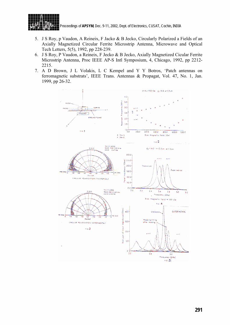
291
Proceedings of APSYM, Dec. 9-11, 2002, Dept. of Electronics, CUSAT, Cochin, INDIA
5. J S Roy, p Vaudon, A Reineix, F Jacko & B Jecko, Circularly Polarized a Fields of an Axially Magnetized Circular Ferrite Microstrip Antenna, Microwave and Optical Tech Letters, 5(5), 1992, pp 228-239.
6. J S Roy, P Vaudon, a Reineix, F Jecko & B Jecko, Axially Magnetized Cicular Ferrite Microstrip Antenna, Proc IEEE AP-S Intl Symposium, 4, Chicago, 1992, pp 2212-2215.
7. A D Brown, J L Volakis, L C Kempel and Y Y Botros, ‘Patch antennas on ferromagnetic substrats’, IEEE Trans. Antennas & Propagat, Vol. 47, No. 1, Jan. 1999, pp 26-32.
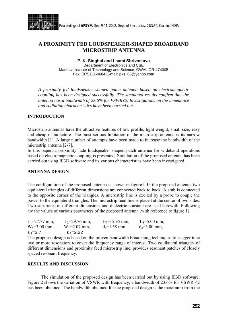
292
Proceedings of APSYM, Dec. 9-11, 2002, Dept. of Electronics, CUSAT, Cochin, INDIA
A PROXIMITY FED LOUDSPEAKER-SHAPED BROADBAND
MICROSTRIP ANTENNA
P. K. Singhal and Laxmi Shrivastava Department of Electronics and CSE
Madhav Institute of Technology and Science, GWALIOR-474005 Fax: (0751)364684 E-mail: [email protected]
A proximity fed loudspeaker shaped patch antenna based on electromagnetic coupling has been designed successfully. The simulated results confirm that the antenna has a bandwidth of 23.6% for VSWR≤2. Investigations on the impedance and radiation characteristics have been carried out.
INTRODUCTION
Microstrip antennas have the attractive features of low profile, light weight, small size, easy and cheap manufacture. The most serious limitation of the microstrip antenna is its narrow bandwidth [1]. A large number of attempts have been made to increase the bandwidth of the microstrip antenna [2-7]. In this paper, a proximity fade loudspeaker shaped patch antenna for wideband operations based on electromagnetic coupling is presented. Simulation of the proposed antenna has been carried out using IE3D software and its various characteristics have been investigated. ANTENNA DESIGN
The configuration of the proposed antenna is shown in figure1. In the proposed antenna two equilateral triangles of different dimensions are connected back to back. A stub is connected to the opposite corner of the triangles. A microstrip line is excited by a probe to couple the power to the equilateral triangles. The microstrip feed line is placed at the center of two sides. Two substrates of different dimensions and dielectric constant are used herewith. Following are the values of various parameters of the proposed antenna (with reference to figure 1). L1=27.77 mm, L2=29.76 mm, LT=15.95 mm, LS=5.00 mm, WS=3.00 mm, WT=2.07 mm, d1=1.58 mm, d2=3.00 mm, εr1=3.7, εr2=2.32 The proposed design is based on the proven bandwidth broadening techniques to stagger tune two or more resonators to cover the frequency range of interest. Two equilateral triangles of different dimensions and proximity feed microstrip line, provides resonant patches of closely spaced resonant frequency. RESULTS AND DISCUSSION
The simulation of the proposed design has been carried out by using IE3D software. Figure 2 shows the variation of VSWR with frequency, a bandwidth of 23.6% for VSWR <2 has been obtained. The bandwidth obtained for the proposed design is the maximum from the
293
Proceedings of APSYM, Dec. 9-11, 2002, Dept. of Electronics, CUSAT, Cochin, INDIA
so far reported such type of design. The simulated input impedance loci of the antenna are shown in figure 3. Radiation characteristics of the antenna in the operating bands are studied. Figure 4 shows radiation pattern at center frequency. It is found that the antenna gives similar radiation patterns at all the frequencies along the band. CONCLUDING REMARK
A proximity fed Loud-speaker shaped antenna with stub loading for wide band operation has been proposed. The proposed design has similar radiation characteristics throughout the operating band. ACKNOWLEDGEMENT
Authors thankfully acknowledge the financial support provided by University Grant Commission, New Delhi and the authorities of Madhav Institute of Technology & Science, Gwalior. REFERENCES
1. D.M. Pozar, “Microstrip antenna”, IEEE proceedings, Vol.80,pp79-81, Jan. 1992. 2. Griffin J.M. and Forrest J.R., “Broadband circular disc microstrip antenna”,
Electronics Letter, 18, pp266-269, 1982. 3. Naftali Herscovici,”A wide band single layer patch antenna”, IEEE Trans. On
Antenna and Propagations, Vo.46, No.4, April 1998, pp471-474. 4. Zhi Ning Chen and Y.W.M. Chia, “Broadband probe fed L-shaped plate antenna”,
Microwave and Optical Technology Letters, Vol. 26, No.3, Aug. 2002, pp204-206. 5. Jia Ye Sze and Kin Lu Wong, “Broadband rectangular microstrip antenna with of
toothbrush shaped slots”, Electronics Lett., 1998, 34, 9230,pp2186-2187. 6. Y.X. Guo, K.M. Luk, K.F. Lee and Y.L. Chow, “Double U-slot rectangular patch
antenna”, Electronics Lett. 1998, 34,(19),pp1805-1806 7. Z.N. Chen, “Broadband probe–fed L-shaped plate antenna, Microwave and Optical
Letters, Aug. 2000.
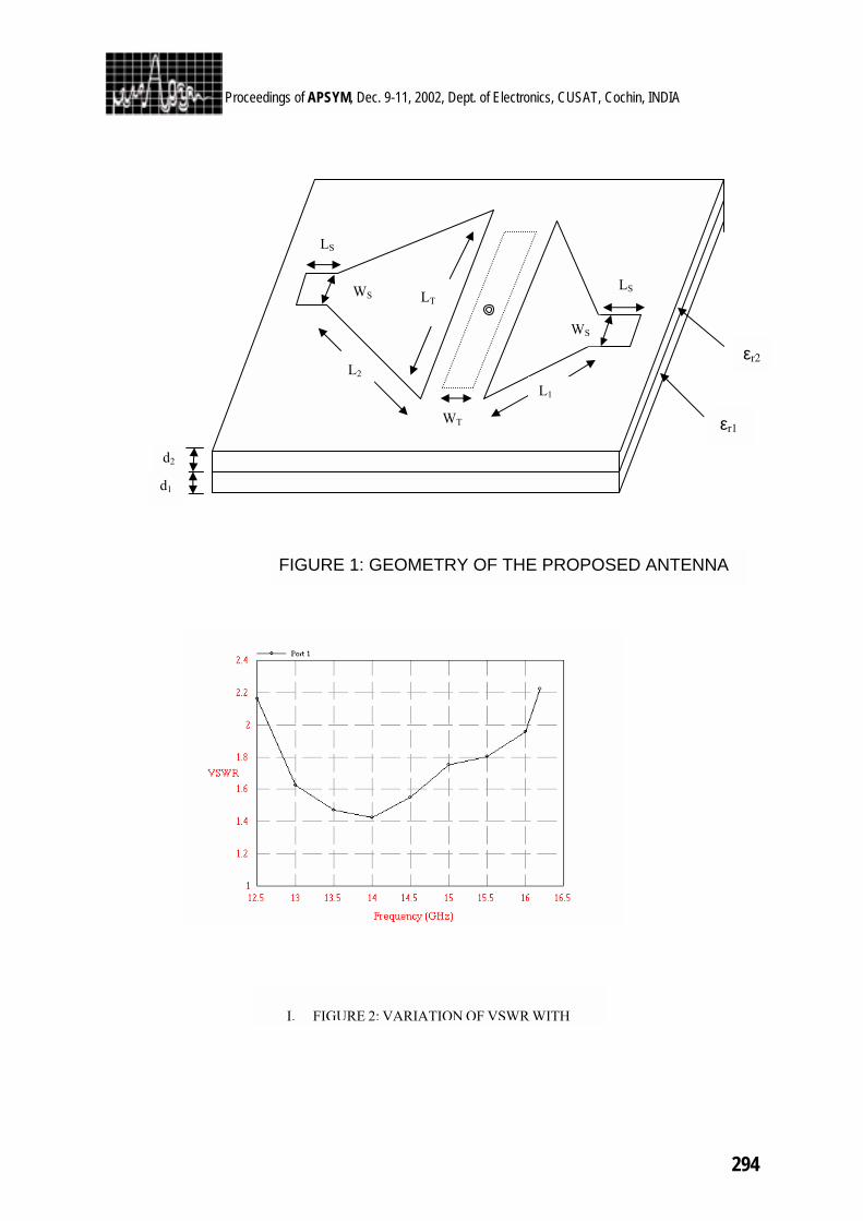
294
Proceedings of APSYM, Dec. 9-11, 2002, Dept. of Electronics, CUSAT, Cochin, INDIA
L2
L1
LS
WS
LS
WS
WT
LT
εr1
εr2
d1
d2
FIGURE 1: GEOMETRY OF THE PROPOSED ANTENNA
I. FIGURE 2: VARIATION OF VSWR WITH
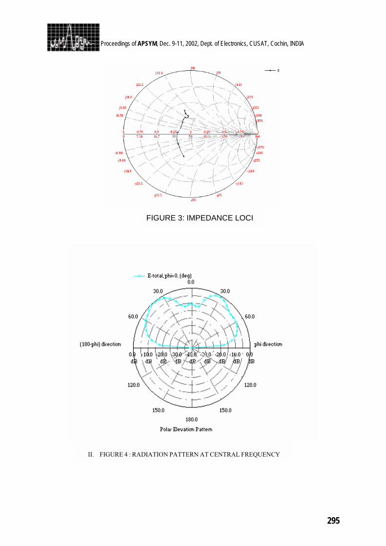
295
Proceedings of APSYM, Dec. 9-11, 2002, Dept. of Electronics, CUSAT, Cochin, INDIA
FIGURE 3: IMPEDANCE LOCI
II. FIGURE 4 : RADIATION PATTERN AT CENTRAL FREQUENCY
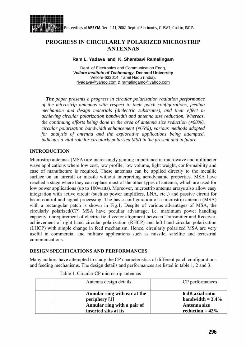
296
Proceedings of APSYM, Dec. 9-11, 2002, Dept. of Electronics, CUSAT, Cochin, INDIA
PROGRESS IN CIRCULARLY POLARIZED MICROSTRIP ANTENNAS
Ram L. Yadava and K. Shambavi Ramalingam
Dept. of Electronics and Communication Engg,
Vellore Institute of Technology, Deemed University Vellore-632014, Tamil Nadu (India).
[email protected] & [email protected]
The paper presents a progress in circular polarization radiation performance of the microstrip antennas with respect to their patch configurations, feeding mechanism and design materials (dielectric substrates), and their effect in achieving circular polarization bandwidth and antenna size reduction. Whereas, the continuing efforts being done in the area of antenna size reduction (≈68%), circular polarization bandwidth enhancement (≈65%), various methods adopted for analysis of antenna and the explorative applications being attempted, indicates a vital role for circularly polarized MSA in the present and in future.
INTRODUCTION
Microstrip antennas (MSA) are increasingly gaining importance in microwave and millimeter wave applications where low cost, low profile, low volume, light weight, conformability and ease of manufacture is required. These antennas can be applied directly to the metallic surface on an aircraft or missile without interpreting aerodynamic properties. MSA have reached a stage where they can replace most of the other types of antenna, which are used for low power applications (up to 100watts). Moreover, microstrip antenna arrays also allow easy integration with active circuit (such as power amplifiers, LNA, etc.,) and passive circuit for beam control and signal processing. The basic configuration of a microstrip antenna (MSA) with a rectangular patch is shown in Fig.1. Despite of various advantages of MSA, the circularly polarized(CP) MSA have peculiar advantage, i.e. maximum power handling capacity, unrequirement of electric field vector alignment between Transmitter and Receiver, achievement of right hand circular polarization (RHCP) and left hand circular polarization (LHCP) with simple change in feed mechanism. Hence, circularly polarized MSA are very useful in commercial and military applications such as missile, satellite and terrestrial communications. DESIGN SPECIFICATIONS AND PERFORMANCES
Many authors have attempted to study the CP characteristics of different patch configurations and feeding mechanisms. The design details and performances are listed in table 1, 2 and 3.
Table 1. Circular CP microstrip antennas
Antenna design details CP performances
Annular ring with ear at the periphery [1]
6 dB axial ratio bandwidth = 3.4%
Annular ring with a pair of inserted slits at its
Antenna size reduction = 42%
297
Proceedings of APSYM, Dec. 9-11, 2002, Dept. of Electronics, CUSAT, Cochin, INDIA
fundamental TM11 mode [2]. (Fig. 2) Proximity couple with a cross slot [4]. (Fig. 3)
Antenna size reduction = 36%
Proximity L-strip line feed[5] Axial ratio bandwidth = 16.15% & Impedance bandwidth = 78%
Proximity coupled ring antenna with two inner stubs[6]
3 dB bandwidth = 1% & VSWR bandwidth = 6.1%
Table: 2a Square CP Microstrip antenna
Feeding Mechanism CP performances
Printed stepped-T feed[7] CP bandwidth = 30% Antenna size reduction = 68%
Rectangular MSA excited by diagonal slots integrated with PIN diode switches[8]
CP bandwidth = 4%
Microstrip line feed through a dual aperture [9]. (Fig. 4)
CP bandwidth = 3.5%
Two perpendiculars cross-slots feed [10]. (Fig. 5)
3 dB gain bandwidth = 13.15% 3 dB axial ratio bandwidth = 48% -15dBr return loss bandwidth = 60%
Single coaxial feed[11] Optimum axial ratio = 1.39 6 dB CP bandwidth = 1.63%
Coplanar wave guide[12] CP bandwidth = 1.6%
Inset microstrip line feed[13]
CP bandwidth = 8%Antenna size reduction = 55%
298
Proceedings of APSYM, Dec. 9-11, 2002, Dept. of Electronics, CUSAT, Cochin, INDIA
Table: 2b Square CP Microstrip antenna
Patch configurations Size reduction
Slits cut in patch[14] ~36% Diagonal cross strips[15] 40% Dielectric loading [16] Reduced antenna size
with good CP performance
T – shaped slits inserted at the patch edges.[17]
36%
Corner truncated with four slits at the patch edges [18]. (Fig. 6)
36%
Table: 3 Equilateral Triangular CP microstrip antenna
Antenna design details CP performances
Aspect ratio of the patch slightly less than 1.0 [19]
Good CP radiation
Single feed with a narrow slit at one of the patch edges [20]. (Fig. 7)
CP bandwidth = 1.3%
Single probe feed embedded with a narrow slot or cross slots of unequal slot lengths in the patch [21]
Good CP radiation with antenna size reduction
Single feed with a truncated tip [22]. (Fig. 8)
CP bandwidth ~ 1.0 –1.4%
CONCLUSION
The circularly polarized MSA are promising candidates for the antenna of low power applications. Among the other patch configurations, square patches MSA surpass in delivering the design objectives. A size reduction of 68% [6] in circularly polarized MSA and bandwidth enhancement of 65% [3] in MSA has been attained. Considering, the compatibility of MSA with micro circuits, the new analytical tools being developed for analysis, the applications being explored, the innumerable options available in patch configuration, feeding and dielectric loading mechanism, the circularly polarized MSA have affluent future.
ACKNOWLEDGEMENT
Authors are thankful to Dr T.S. Vedavathy, I.I.Sc, Bangalore, and Dr. B.R.Vishvakarma, I.I.T, BHU, Varanasi for their enthusiasm given to us for performing this work.
299
Proceedings of APSYM, Dec. 9-11, 2002, Dept. of Electronics, CUSAT, Cochin, INDIA
REFERENCES
1. A.K.Bhattacharyya and L.Shafai, “ A wide band microstrip antenna for circular polarization,” IEEE Trans. Antennas Propagat., vol. 6, no.2, Feb 1988. Pp. 157-163.
2. H. M.Chen and K.L.Wong, “ On the circular polarization operation of annular ring microstrip antennas,” IEEE Trans. Antennas Propagat., vol. 47, no. 8, Aug. 1999, pp. 1289-1292.
3. S. Gupta, et al , “Integrated active antennas, “ IETE Technical Review, vol.18, no. 2 &3, Mar-Jun. 2001, pp. 139-146.
4. H. Iwasaki, “ A circularly polarized small size microstrip antennas with cross slots,” IEEE Trans. Antennas Propagat., vol. 44, no. 10, Oct 1996, pp. 1399-1401.
5. W. K. Lo, et al.,”Circularly polarised patch antenna array using proximity-coupled L- strip line feed,” Electron. Lett., vol.36, no.14, 6th July 2000, pp.1174-1175.
6. R. R. Ramirez, et al., ”Single feed circularly polarized microstrip ring antenna and arrays,” IEEE Trans. Antennas Propogat.,vol.48, no.7, July 2000, pp. 1040-1046
7. P. H. Rao, “ A wideband linear and circularly polarized patch antenna using a printed stepped T-feed,” IEEE Trans. Antennas Propagat., vol. 50, 3, Mar. 2002, pp. 356-361.
8. M. Boti, et al ,”Circularly polarized antenna with suitable polarization sense,” Electron. Lett., vol.36, no.18, 31st Aug 2000, pp. 1518-1519.
9. A. Adrain, ”Dual aperture coupled microstrip antenna for dual or circular polarization,” Electron. Lett., vol.23, no.23, 5th Nov. 1987, pp.1226-1227.
10. E. Aloni and R. Kastner,” Analysis of a dual circularly polarized microstrip antenna fed by cross slots,” IEEE Trans. Antennas Propagat., vol.42, no.8, Aug. 1994.
11. C. S. Lee, et al, “Circularly polarized microstrip antenna with a single feed,” IEEE Trans. Antennas Propogat., vol. 44, no.10, Oct. 1996, pp.1426-1427.
12. C. Y. Huang, et al, “Coplanar waveguide-fed circularly polarised microstrip antenna,” IEEE Trans. Antennas Propogat., vol.48, no.2, Feb 2000, pp. 328-329.
13. W. S. Chen, et al, “Inset microstripline-fed circularly polarised microstrip antennas,” IEEE Trans. Antennas Propagat., vol.48, no.8, Aug. 2000, pp. 1253-1254.
14. K. L. Wong, et al, “Single feed circularly polarized square microstrip antenna,” Electron. Lett., vol.33, no.22, 23rd Oct 1997, pp.1883-1834.
15. W.S. Chen, et al, “Square ring microstrip antenna with a cross strip for compact circular polarization operation,” IEEE Trans. Antennas Propogat., vol.47, no.10, Oct 1999, pp. 1566-1568.
16. C. J. Currie, et al, “Compact dielectric loaded circularly polarized microstrip antenna, “ Electron. Lett., vol. 37, no.18, 30th Aug 2001, pp. 1104-1105.
17. K. P. Yang, et al, “Dual band circularly polarised square microstrip antenna,” IEEE Trans. Antennas Propogat., vol. 49, no.3, Mar. 2000, pp. 377-381.
18. W.S. Chen, et al, “Novel compact circularly polarised square microstrip antenna,” IEEE Trans. Antennas Propogat., vol. 49, no.3, Mar. 2001, pp. 340-342.
19. Y. Suzuki, et al, “Circularly polarized radiation from singly fed equilateral- triangular microstrip antenna,” IEE Proc. Microwave, Antennas and Propagat., H.,134, 1987, pp. 194-194.
20. J.H. Lu, et al, “Circular polarization design of a single feed equilateral- triangular microstrip antenna,” Electron. Lett, vol. 34, no. 4, 19th Feb. 1998, pp.319-321.
21. J.H. Lu, et al, “Single feed slotted equilateral-triangular microstrip antenna for circular polarization,” IEEE Trans. Antennas Propogat., vol.47, no.7, July 1999, pp. 1174-1178.
22. C. L. Tang, et al, “Circularly polarized equilateral- triangular microstrip antenna with truncated tip,” Electron. Lett., vol.34, no.13, 25th June 1998, pp. 1277-1278.
300
Proceedings of APSYM, Dec. 9-11, 2002, Dept. of Electronics, CUSAT, Cochin, INDIA
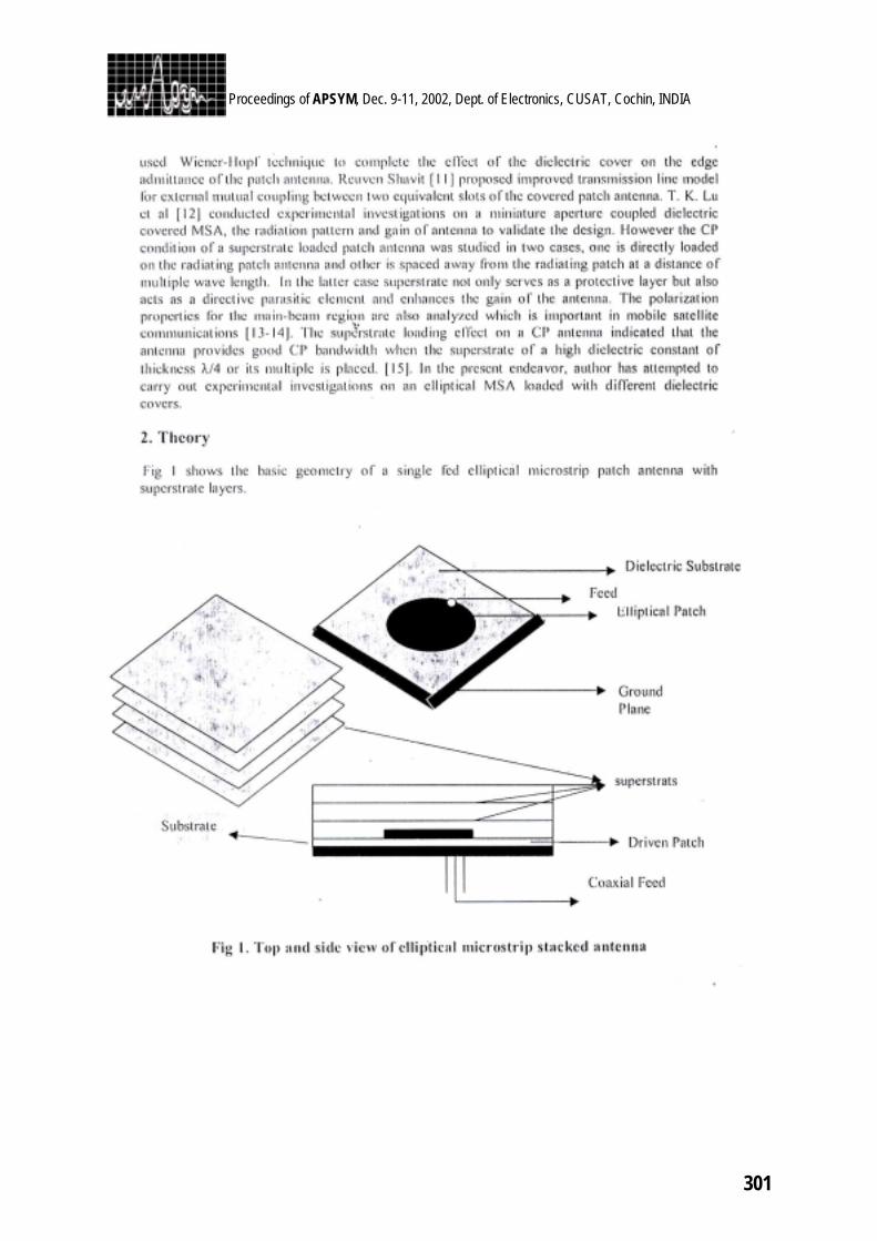
301
Proceedings of APSYM, Dec. 9-11, 2002, Dept. of Electronics, CUSAT, Cochin, INDIA
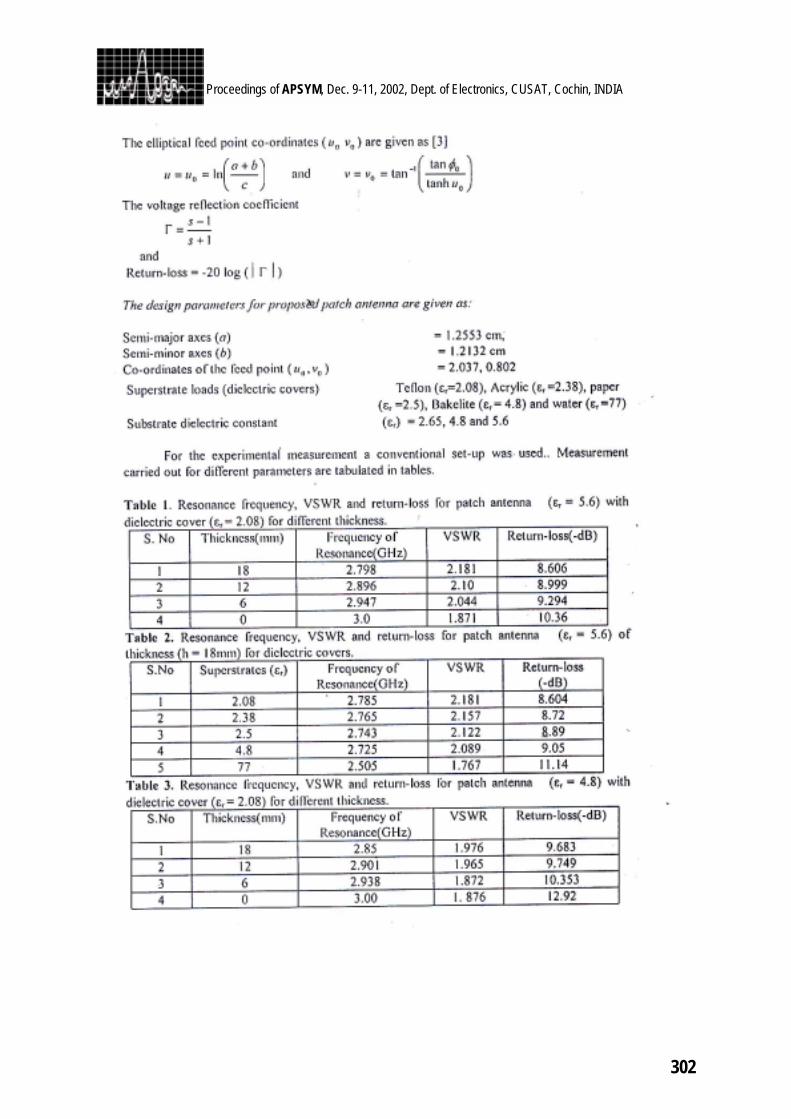
302
Proceedings of APSYM, Dec. 9-11, 2002, Dept. of Electronics, CUSAT, Cochin, INDIA
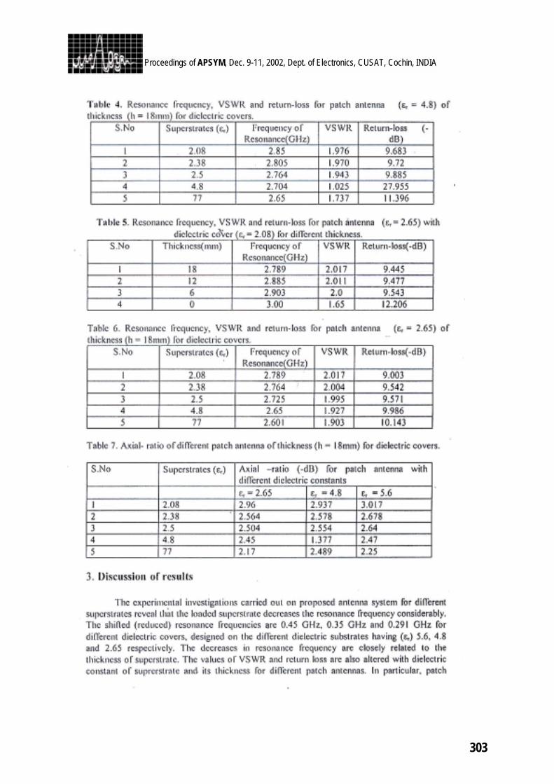
303
Proceedings of APSYM, Dec. 9-11, 2002, Dept. of Electronics, CUSAT, Cochin, INDIA
304
Proceedings of APSYM, Dec. 9-11, 2002, Dept. of Electronics, CUSAT, Cochin, INDIA
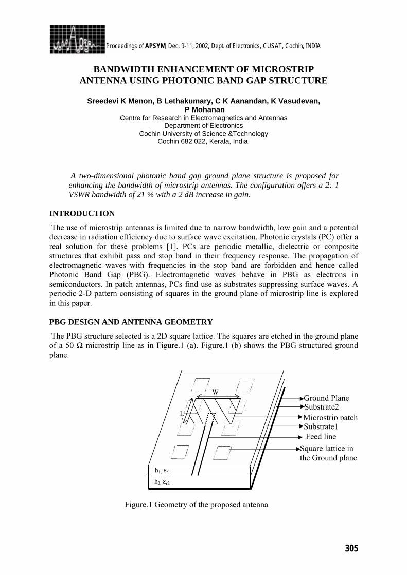
305
Proceedings of APSYM, Dec. 9-11, 2002, Dept. of Electronics, CUSAT, Cochin, INDIA
BANDWIDTH ENHANCEMENT OF MICROSTRIP ANTENNA USING PHOTONIC BAND GAP STRUCTURE
Sreedevi K Menon, B Lethakumary, C K Aanandan, K Vasudevan,
P Mohanan Centre for Research in Electromagnetics and Antennas
Department of Electronics Cochin University of Science &Technology
Cochin 682 022, Kerala, India.
A two-dimensional photonic band gap ground plane structure is proposed for enhancing the bandwidth of microstrip antennas. The configuration offers a 2: 1 VSWR bandwidth of 21 % with a 2 dB increase in gain.
INTRODUCTION
The use of microstrip antennas is limited due to narrow bandwidth, low gain and a potential decrease in radiation efficiency due to surface wave excitation. Photonic crystals (PC) offer a real solution for these problems [1]. PCs are periodic metallic, dielectric or composite structures that exhibit pass and stop band in their frequency response. The propagation of electromagnetic waves with frequencies in the stop band are forbidden and hence called Photonic Band Gap (PBG). Electromagnetic waves behave in PBG as electrons in semiconductors. In patch antennas, PCs find use as substrates suppressing surface waves. A periodic 2-D pattern consisting of squares in the ground plane of microstrip line is explored in this paper.
PBG DESIGN AND ANTENNA GEOMETRY
The PBG structure selected is a 2D square lattice. The squares are etched in the ground plane of a 50 Ω microstrip line as in Figure.1 (a). Figure.1 (b) shows the PBG structured ground plane.
Feed line Square lattice in the Ground plane
Ground PlaneSubstrate2
L
W
h1, εr1
h2, εr2
Microstrip patchSubstrate1
Figure.1 Geometry of the proposed antenna
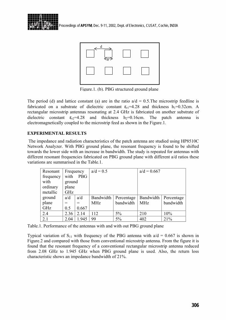
306
Proceedings of APSYM, Dec. 9-11, 2002, Dept. of Electronics, CUSAT, Cochin, INDIA
The period (d) and lattice constant (a) are in the ratio a/d = 0.5.The microstrip feedline is fabricated on a substrate of dielectric constant εr1=4.28 and thickness h1=0.32cm. A rectangular microstrip antennas resonating at 2.4 GHz is fabricated on another substrate of dielectric constant εr2=4.28 and thickness h2=0.16cm. The patch antenna is electromagnetically coupled to the microstrip feed as shown in the Figure.1. EXPERIMENTAL RESULTS
The impedance and radiation characteristics of the patch antenna are studied using HP8510C Network Analyzer. With PBG ground plane, the resonant frequency is found to be shifted towards the lower side with an increase in bandwidth. The study is repeated for antennas with different resonant frequencies fabricated on PBG ground plane with different a/d ratios these variations are summarised in the Table.1.
Table.1. Performance of the antennas with and with out PBG ground plane
Typical variation of S11 with frequency of the PBG antenna with a/d = 0.667 is shown in Figure.2 and compared with those from conventional microstrip antenna. From the figure it is found that the resonant frequency of a conventional rectangular microstrip antenna reduced from 2.08 GHz to 1.945 GHz when PBG ground plane is used. Also, the return loss characteristic shows an impedance bandwidth of 21%.
Frequency with PBG ground plane GHz
a/d = 0.5
a/d = 0.667
Resonant frequency with ordinary metallic ground plane GHz
a/d = 0.5
a/d = 0.667
Bandwidth MHz
Percentage bandwidth
Bandwidth MHz
Percentage bandwidth
2.4 2.36 2.14 112 5% 210 10% 2.1 2.04 1.945 99 5% 402 21%
a
d
Figure.1. (b). PBG structured ground plane
307
Proceedings of APSYM, Dec. 9-11, 2002, Dept. of Electronics, CUSAT, Cochin, INDIA
The large bandwidth is achieved with an increase in gain of 2 dB than a standard circular microstrip antenna resonating at the same frequency [2]. The comparative gain is shown in Figure.3.
The overall aperture area of a circular microstrip antenna resonating at 1.945 GHz is 17 sq.cm. whereas the aperture area of the present antenna is only 9 sq.cm. This means the effective radiating area of the present antenna is reduced by 47%. This confirms that the present antenna is more compact than the conventional circular or rectangular shapes. The E-plane and H-plane radiation pattern of the antenna in the pass band is given in Fig.4. At the center frequency the half power beam width is 80o for E-plane and 96o for H-plane. The cross polarization studies show that the cross-polar isolation is better than -40 dB in the entire azimuth and elevation plane, which is a desirable characteristic for communication antennas.
Figure.3. Variation of gain improvement of the present antenna with frequency
a/d = 0.667, LxW=2.6x3.6cm2
Frequency(GHz)
1.9 2.0 2.1 2.2
Gai
n Im
prov
emen
t (d
B)
0.0
0.5
1.0
1.5
2.0
2.5
Frequency(GHz)
1.6 1.8 2.0 2.2 2.4
S11
(d B
)
-35
-30
-25
-20
-15
-10
-5
0
a/d = 0.667a/d = 0.55without PBG
Figure.2. Variation of S11 with frequency εr1=4.28, h1=0.32cm and εr2=4.28, h2=0.16cm
LxW = 2.6x3.6cm2
308
Proceedings of APSYM, Dec. 9-11, 2002, Dept. of Electronics, CUSAT, Cochin, INDIA
Co
CONCLUSIONS
The performance of patch antennas using PBG structure is studied. The antenna offers the following desirable radiation characteristics:
• Large 2:1 VSWR bandwidth of 21%. • Low cross-polarisation discrimination in the entire azimuth and elevation angle (better
than -40 d B) • Reduced aperture area. • Broad HPBW. • Enhanced gain (better than 1.8 d B in the entire operating band). All the above
characteristics show that the present antenna is an ideal substitute for conventional antennas for large bandwidth, low cross-polarisation applications.
REFERENCE
1. Ramon Ganzalo, Peter de Maagt, Mario Sorolla. “Enhanced Patch-Antenna Performance by Suppressing Surface Waves Using Photonic-Bandgap Substrates”, IEEE Trans., Microwave Theory & Tech., Vol.47,No.4,pp-2131-2138, Nov.’99
2. I.J.Bahl and P.Bhartia, “Microstrip antennas,”Artech House, Dedham, MA 1980.
-50 -40 -30 -20 -10 00
30
6090
120
150
180-50 -40 -30 -20 -10 0
0
30
6090
120
150
180
-50 -40 -30 -20 -10 00
30
6090
120
150
180-50 -40 -30 -20 -10 00
30
6090
120
150
180
(a)
(b)
Figure.4. Radiation pattern of the proposed antenna (a) 1.94 GHz (b) 2.1 GHz a/d = 0.667, LxW = 2.6x3.6cm2
E- plane H- plane
8.1 A MULTIOCTAVE PRINTED CIRCUIT SQUARE SPIRAL ANTENNA,(2-12 GHz) M. Chakravarthy, V.M. Pandharipande, B. Ramakrishna Rao, R. Sreehari Rao
311
309
Proceedings of APSYM, Dec. 9-11, 2002, Dept. of Electronics, CUSAT, Cochin, INDIA
RESEARCH SESSION VIII December 10, Tuesday 2002. (3.15 p.m. to 4.30 p.m)
ANTENNAS II Hall : 2
CHAIRS: PROF. G.P. SRIVASTAVA DR. J.C. GOSWAMI
Defence Electronics Research Laboratory (DERL), Hyderabad 500005, Chandrayanagutta
8.2 SOME RESULTS ON DIELECTRIC WAVEGUIDE ANTENNA R. Bhattacharjee1, B. Gupta2, D.R. Poddar2, & S.K. Chowdhury2 1Dept. of ECE, IIT Guwahati, North Guwahati, Guwahati-781039 2Dept. of ETCE, Jadavpur University, Calcutta-700032
315
8.3 MULTIPLE BEAM ANTENNA USING OFFSET REFLECTOR CONFIGURATION Chayan Roy, V.V. Srinivasan, V. Mahadevan, V.K. Lakshmeesha, S. Pal Communication System Group, ISRO Satellite Centre, Bangalore-560017. [email protected]
319
8.4 A MULTIPLE SPOT BEAM SPACECRAFT ANTENNA WITH APERTURE REUSE CAPABILITY Khagindra Sood and Arun Kumar SCAD-ASG, Space Applications centre (ISRO), Ahmedabad-380015. [email protected]
323
8.5 DESIGN AND DEVELOPMENT OF MONOPULSE ANTENNA SYSTEM G.V. Ramakotesware Rao, J.V. Prasad, A. Ghosh, V.G. Borkar Research Centre IMARAT, Hyderabad 500 069
327
310
Proceedings of APSYM, Dec. 9-11, 2002, Dept. of Electronics, CUSAT, Cochin, INDIA
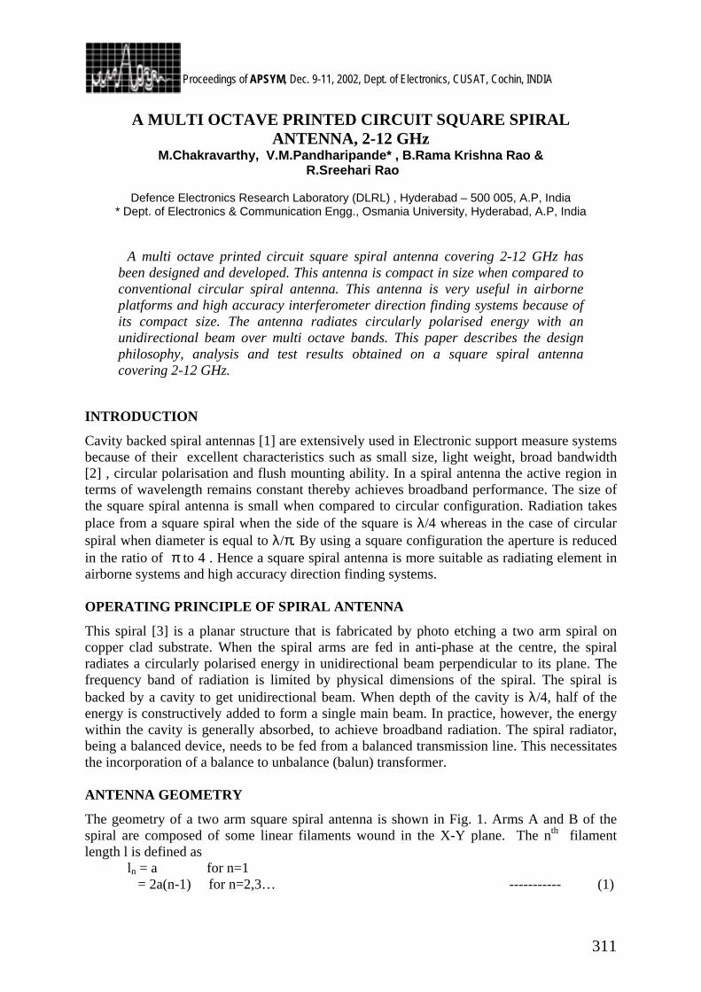
311
Proceedings of APSYM, Dec. 9-11, 2002, Dept. of Electronics, CUSAT, Cochin, INDIA
A MULTI OCTAVE PRINTED CIRCUIT SQUARE SPIRAL ANTENNA, 2-12 GHz
M.Chakravarthy, V.M.Pandharipande* , B.Rama Krishna Rao & R.Sreehari Rao
Defence Electronics Research Laboratory (DLRL) , Hyderabad – 500 005, A.P, India
* Dept. of Electronics & Communication Engg., Osmania University, Hyderabad, A.P, India
A multi octave printed circuit square spiral antenna covering 2-12 GHz has been designed and developed. This antenna is compact in size when compared to conventional circular spiral antenna. This antenna is very useful in airborne platforms and high accuracy interferometer direction finding systems because of its compact size. The antenna radiates circularly polarised energy with an unidirectional beam over multi octave bands. This paper describes the design philosophy, analysis and test results obtained on a square spiral antenna covering 2-12 GHz.
INTRODUCTION
Cavity backed spiral antennas [1] are extensively used in Electronic support measure systems because of their excellent characteristics such as small size, light weight, broad bandwidth [2] , circular polarisation and flush mounting ability. In a spiral antenna the active region in terms of wavelength remains constant thereby achieves broadband performance. The size of the square spiral antenna is small when compared to circular configuration. Radiation takes place from a square spiral when the side of the square is λ/4 whereas in the case of circular spiral when diameter is equal to λ/π. By using a square configuration the aperture is reduced in the ratio of π to 4 . Hence a square spiral antenna is more suitable as radiating element in airborne systems and high accuracy direction finding systems. OPERATING PRINCIPLE OF SPIRAL ANTENNA
This spiral [3] is a planar structure that is fabricated by photo etching a two arm spiral on copper clad substrate. When the spiral arms are fed in anti-phase at the centre, the spiral radiates a circularly polarised energy in unidirectional beam perpendicular to its plane. The frequency band of radiation is limited by physical dimensions of the spiral. The spiral is backed by a cavity to get unidirectional beam. When depth of the cavity is λ/4, half of the energy is constructively added to form a single main beam. In practice, however, the energy within the cavity is generally absorbed, to achieve broadband radiation. The spiral radiator, being a balanced device, needs to be fed from a balanced transmission line. This necessitates the incorporation of a balance to unbalance (balun) transformer.
ANTENNA GEOMETRY
The geometry of a two arm square spiral antenna is shown in Fig. 1. Arms A and B of the spiral are composed of some linear filaments wound in the X-Y plane. The nth filament length l is defined as ln = a for n=1 = 2a(n-1) for n=2,3… ----------- (1)
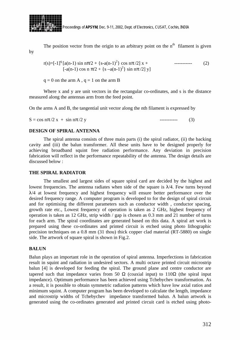
312
Proceedings of APSYM, Dec. 9-11, 2002, Dept. of Electronics, CUSAT, Cochin, INDIA
The position vector from the origin to an arbitrary point on the nth filament is given by r(s)=[-1]q [a(n-1) sin nπ/2 + s-a(n-1)2 cos nπ /2] x + ----------- (2) [-a(n-1) cos n π/2 + s –a(n-1)2 sin nπ /2] y] q = 0 on the arm A , q = 1 on the arm B Where x and y are unit vectors in the rectangular co-ordinates, and s is the distance measured along the antennas arm from the feed point. On the arms A and B, the tangential unit vector along the nth filament is expressed by S = cos nπ /2 x + sin nπ /2 y ----------- (3) DESIGN OF SPIRAL ANTENNA
The spiral antenna consists of three main parts (i) the spiral radiator, (ii) the backing cavity and (iii) the balun transformer. All these units have to be designed properly for achieving broadband squint free radiation performance. Any deviation in precision fabrication will reflect in the performance repeatability of the antenna. The design details are discussed below : THE SPIRAL RADIATOR
The smallest and largest sides of square spiral card are decided by the highest and lowest frequencies. The antenna radiates when side of the square is λ/4. Few turns beyond λ/4 at lowest frequency and highest frequency will ensure better performance over the desired frequency range. A computer program is developed to for the design of spiral circuit and for optimising the different parameters such as conductor width , conductor spacing, growth rate etc., Lowest frequency of operation is taken as 2 GHz, highest frequency of operation is taken as 12 GHz, strip width / gap is chosen as 0.3 mm and 21 number of turns for each arm. The spiral coordinates are generated based on this data. A spiral art work is prepared using these co-ordinates and printed circuit is etched using photo lithographic precision techniques on a 0.8 mm (31 thou) thick copper clad material (RT-5880) on single side. The artwork of square spiral is shown in Fig.2.
BALUN
Balun plays an important role in the operation of spiral antenna. Imperfections in fabrication result in squint and radiation in undesired sectors. A multi octave printed circuit microstrip balun [4] is developed for feeding the spiral. The ground plane and centre conductor are tapered such that impedance varies from 50 Ω (coaxial input) to 110Ω (the spiral input impedance). Optimum performance has been achieved using Tchebychev transformation. As a result, it is possible to obtain symmetric radiation patterns which have low axial ratios and minimum squint. A computer program has been developed to calculate the length, impedance and microstrip widths of Tchebychev impedance transformed balun. A balun artwork is generated using the co-ordinates generated and printed circuit card is etched using photo-
313
Proceedings of APSYM, Dec. 9-11, 2002, Dept. of Electronics, CUSAT, Cochin, INDIA
lithographic techniques on a 20 thou thick copper clad material (RT-5880, εr = 2.2) on double side. The balun art works are shown in Fig.3.
CAVITY
Depth of the cavity is chosen as λ/4 for getting optimum performance. But this results in performance variation over the designed frequency range. Hence back radiation is absorbed by filling the cavity with microwave absorber for achieving uniform performance over wider bandwidths. Honeycomb absorber is chosen because of its light weight, high structural integrity and broad bandwidth.
PERFORMANCE EVALUATION
The reduced size spiral antenna has been fabricated and evaluated for various characteristics. Return loss measurements have been carried out on a Network Analyser. Radiation pattern measurements have been carried out in Anechoic Chamber. Axial ratio patterns were taken using rotating linear source. Gain was measured using gain comparison technique. The achieved results are shown in Fig.4.
RESULTS
The VSWR of the antenna is less than 2.5 over entire band. The antenna exhibited symmetric radiation patterns with maximum axial ratio of 3 dB over 2 to 12 GHz. The nominal gain of this antenna is 0 dB with the pattern squint restricted to a maximum of ± 5° over the entire frequency range.
CONCLUSIONS
A multi octave printed circuit square spiral antenna has been developed covering the frequency range of 2-12 GHz. The antenna exhibited symmetric patterns over the entire frequency range. This antenna is used extensively in airborne systems and high accuracy direction finding systems because of its compact size .
ACKNOWLEDGEMENTS The authors are grateful to Sri N.Divakar, Director, DLRL for his constant support and encouragement. We are thankful to Sri Ram Pal, Director, Technology for his encouragement during the development of this antenna.
REFERENCES
1. Richard C.Johnson, "Antenna Engineering Handbook", Mc-Graw Hill, Inc.1993. 2. V.H.Rumsey, "Frequency independent antennas", IRE Nat. Conv. Rec., Part-I, 1957. 3. R.Bawer and J.J.Wolfe, "The Spiral antenna", IRE Int.Conv.Rec., April 1960. 4. M.chakravarthy et al., "A Wide band printed circuit balun " , National Conference on
Electronic materials, Devices & systems (NCEMDS–99) , Jan 1999.
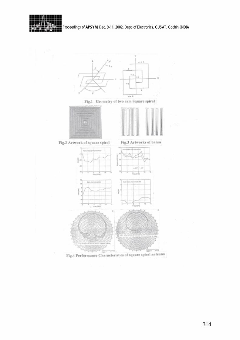
314
Proceedings of APSYM, Dec. 9-11, 2002, Dept. of Electronics, CUSAT, Cochin, INDIA
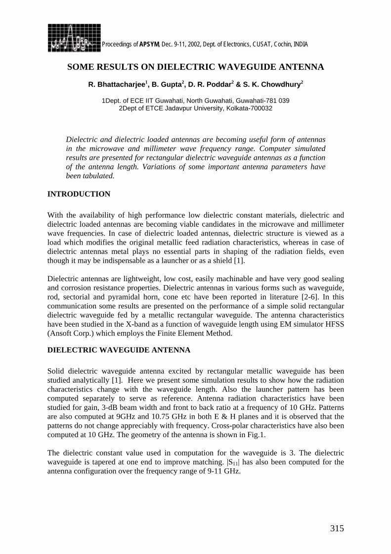
315
Proceedings of APSYM, Dec. 9-11, 2002, Dept. of Electronics, CUSAT, Cochin, INDIA
SOME RESULTS ON DIELECTRIC WAVEGUIDE ANTENNA
R. Bhattacharjee1, B. Gupta2, D. R. Poddar2 & S. K. Chowdhury2
1Dept. of ECE IIT Guwahati, North Guwahati, Guwahati-781 039 2Dept of ETCE Jadavpur University, Kolkata-700032
Dielectric and dielectric loaded antennas are becoming useful form of antennas in the microwave and millimeter wave frequency range. Computer simulated results are presented for rectangular dielectric waveguide antennas as a function of the antenna length. Variations of some important antenna parameters have been tabulated.
INTRODUCTION
With the availability of high performance low dielectric constant materials, dielectric and dielectric loaded antennas are becoming viable candidates in the microwave and millimeter wave frequencies. In case of dielectric loaded antennas, dielectric structure is viewed as a load which modifies the original metallic feed radiation characteristics, whereas in case of dielectric antennas metal plays no essential parts in shaping of the radiation fields, even though it may be indispensable as a launcher or as a shield [1]. Dielectric antennas are lightweight, low cost, easily machinable and have very good sealing and corrosion resistance properties. Dielectric antennas in various forms such as waveguide, rod, sectorial and pyramidal horn, cone etc have been reported in literature [2-6]. In this communication some results are presented on the performance of a simple solid rectangular dielectric waveguide fed by a metallic rectangular waveguide. The antenna characteristics have been studied in the X-band as a function of waveguide length using EM simulator HFSS (Ansoft Corp.) which employs the Finite Element Method.
DIELECTRIC WAVEGUIDE ANTENNA
Solid dielectric waveguide antenna excited by rectangular metallic waveguide has been studied analytically [1]. Here we present some simulation results to show how the radiation characteristics change with the waveguide length. Also the launcher pattern has been computed separately to serve as reference. Antenna radiation characteristics have been studied for gain, 3-dB beam width and front to back ratio at a frequency of 10 GHz. Patterns are also computed at 9GHz and 10.75 GHz in both E & H planes and it is observed that the patterns do not change appreciably with frequency. Cross-polar characteristics have also been computed at 10 GHz. The geometry of the antenna is shown in Fig.1. The dielectric constant value used in computation for the waveguide is 3. The dielectric waveguide is tapered at one end to improve matching. |S11| has also been computed for the antenna configuration over the frequency range of 9-11 GHz.
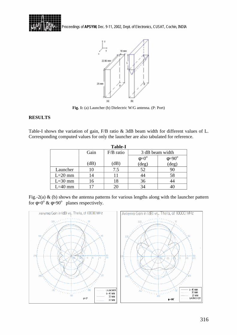
316
Proceedings of APSYM, Dec. 9-11, 2002, Dept. of Electronics, CUSAT, Cochin, INDIA
Fig. 1: (a) Launcher (b) Dielectric W/G antenna. (P: Port)
RESULTS
Table-I shows the variation of gain, F/B ratio & 3dB beam width for different values of L. Corresponding computed values for only the launcher are also tabulated for reference.
Table-I 3 dB beam width Gain
(dB)
F/B ratio
(dB) φ=0o (deg)
φ=90o (deg)
Launcher 10 7.5 52 90 L=20 mm 14 11 44 58 L=30 mm 16 18 36 44 L=40 mm 17 20 34 40
Fig.-2(a) & (b) shows the antenna patterns for various lengths along with the launcher pattern for φ=0o & φ=90o planes respectively.
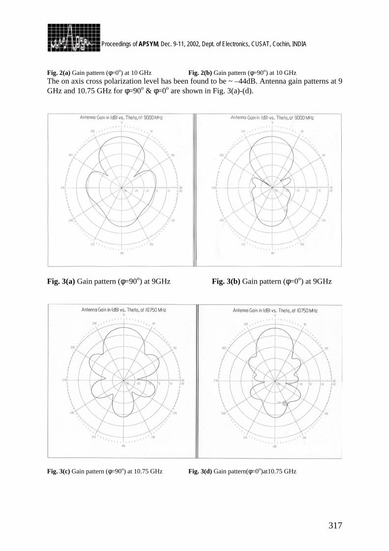
317
Proceedings of APSYM, Dec. 9-11, 2002, Dept. of Electronics, CUSAT, Cochin, INDIA
Fig. 2(a) Gain pattern (φ=0o) at 10 GHz Fig. 2(b) Gain pattern (φ=90o) at 10 GHz The on axis cross polarization level has been found to be ~ –44dB. Antenna gain patterns at 9 GHz and 10.75 GHz for φ=90o & φ=0o are shown in Fig. 3(a)-(d).
Fig. 3(a) Gain pattern (φ=90o) at 9GHz Fig. 3(b) Gain pattern (φ=0o) at 9GHz
Fig. 3(c) Gain pattern (φ=90o) at 10.75 GHz Fig. 3(d) Gain pattern(φ=0o)at10.75 GHz
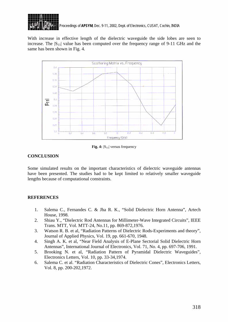
318
Proceedings of APSYM, Dec. 9-11, 2002, Dept. of Electronics, CUSAT, Cochin, INDIA
With increase in effective length of the dielectric waveguide the side lobes are seen to increase. The |S11| value has been computed over the frequency range of 9-11 GHz and the same has been shown in Fig. 4.
Fig. 4: |S11| versus frequency
CONCLUSION
Some simulated results on the important characteristics of dielectric waveguide antennas have been presented. The studies had to be kept limited to relatively smaller waveguide lengths because of computational constraints. REFERENCES
1. Salema C., Fernandes C. & Jha R. K., “Solid Dielectric Horn Antenna”, Artech House, 1998.
2. Shiau Y., “Dielectric Rod Antennas for Millimeter-Wave Integrated Circuits”, IEEE Trans. MTT, Vol. MTT-24, No.11, pp. 869-872,1976.
3. Watson R. B. et al, “Radiation Patterns of Dielectric Rods-Experiments and theory”, Journal of Applied Physics, Vol. 19, pp. 661-670, 1948.
4. Singh A. K. et al, “Near Field Analysis of E-Plane Sectorial Solid Dielectric Horn Antennas”, International Journal of Electronics, Vol. 71, No. 4, pp. 697-706, 1991.
5. Brooking N. et al, “Radiation Pattern of Pyramidal Dielectric Waveguides”, Electronics Letters, Vol. 10, pp. 33-34,1974.
6. Salema C. et al. “Radiation Characteristics of Dielectric Cones”, Electronics Letters, Vol. 8, pp. 200-202,1972.
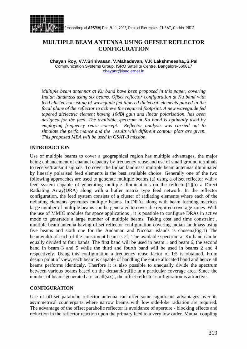
319
Proceedings of APSYM, Dec. 9-11, 2002, Dept. of Electronics, CUSAT, Cochin, INDIA
MULTIPLE BEAM ANTENNA USING OFFSET REFLECTOR CONFIGURATION
Chayan Roy, V.V.Srinivasan, V.Mahadevan, V.K.Lakshmeesha,.S.Pal
Communication Systems Group, ISRO Satellite Centre, Bangalore-560017 [email protected]
Multiple beam antennas at Ku band have been proposed in this paper, covering Indian landmass using six beams. Offset reflector configuration at Ku band with feed cluster consisting of waveguide fed tapered dielectric elements placed in the focal plane of the reflector to achieve the required footprint. A new waveguide fed tapered dielectric element having 16dBi gain and linear polarisation. has been designed for the feed. The available spectrum at Ku band is optimally used by employing frequency reuse concept. Reflector analysis was carried out to simulate the performance and the results with different contour plots are given. This proposed MBA will be used in GSAT-3 mission.
INTRODUCTION
Use of multiple beams to cover a geographical region has multiple advantages, the major being enhancement of channel capacity by frequency reuse and use of small ground terminals to receive/transmit signals. To cover the Indian landmass multiple beam antennas illuminated by linearly polarised feed elements is the best available choice. Generally one of the two following approaches are used to generate multiple beams (a) using a offset reflector with a feed system capable of generating multiple illuminations on the reflector[1](b) a Direct Radiating Array(DRA) along with a butler matrix type feed network. In the reflector configuration, the feed system consists of a cluster of radiating elements where each of the radiating elements generates multiple beams. In DRAs along with beam forming matrices large number of multiple beams can be generated to cover the required coverage zones. With the use of MMIC modules for space applications , it is possible to configure DRAs in active mode to generatde a large number of multiple beams. Taking cost and time constraint , multiple beam antenna having offset reflector configuration covering indian landmass using five beams and sixth one for the Andaman and Nicobar islands is chosen.(Fig.1) The beamwidth of each of the constituent beam is 2°. The available spectrum at Ku band can be equally divided to four bands. The first band will be used in beam 1 and beam 6, the second band in beam 3 and 5 while the third and fourth band will be used in beams 2 and 4 respectively. Using this configuration a frequency reuse factor of 1:5 is obtained. From design point of view, each beam is capable of handling the entire allocated band and hence all beams performs identicaly. Therfore it is also possible to unequally divide the spectrum between various beams based on the demand/traffic in a particular coverage area. Since the number of beams generated are small(six) , the offset reflector configuration is attractive. CONFIGURATION
Use of off-set parabolic reflector antenna can offer some significant advantages over its asymmetrical counterparts where narrow beams with low side-lobe radiation are required. The advantage of the offset parabolic reflector is avoidance of aperture - blocking effects and reduction in the reflector reaction upon the primary feed to a very low order. Mutual coupling

320
Proceedings of APSYM, Dec. 9-11, 2002, Dept. of Electronics, CUSAT, Cochin, INDIA
between feed elements via the reflector is also greatly reduced. The offset structure leads to the use of higher gain primary feed elements while maintaining mechanical rigidity as well as to be made compact and rugged. In an offset refletor configuration, the main beam can be made to point to a direction different from the axis of the reflector by offsetting the location of the feed away from the focal point in the feed plane. A shift of the feed in the x and y axis in the feed plane scans the beam to a different direction and this is the concept used in multiple beams reflector antennas.The beam along the reflector axis is defined as the first beam and this direction is defined as the reference direction(θ = 0 and φ = 0). From the footprint coverage(Fig1.), the beam offset angle for the remaining beams are computed and given in Table1. An offset reflector with a f/D of 1.0 and an offset angle of 6° is considered at Ku Band. Offset reflector analysis was carried out to find the location of the feeds in the feed plane to generate the beams along the direction given in Table1. The analysis was carried out for a 0.95mtr offset configuration at Ku band . Thus the multibeam generation at Ku band can be achieved using the reflector of the dimension mentioned above. DESIGN EQUATIONS
The geometry of the offset parabolic antenna condidered in this paper is shown in Fig2 . The length F is the focal length of the parent paraoloid , θ0 is the off-set angle and θ* is the semi-angle subtended by the reflector periphery at the geometrical focus. The physical contour of the reflector is elliptical but the projection of the reflector into the (x'-y) plane produces a circle. In terms of the reflector parameters, the diameter(D) of the circle is given by D = 4Fsinθ*/(cosθ0 + cosθ*) ------(1) where F is the focal length and θ0 is the offset angle. Secondary parameters can be found out using formulas dc = 2Ftan[(θ0 - θ*)/2] ------(2) where dc is the clearance distance between z-axis and the lower edge of the aperture. for feed clearance θ0 > θ* and dc ≥ 3λ Xc = 2Fsinθ0/(cosθ0 + cosθ*) -------(3) Xc is the distance between the centre of the projected aperture and the geometric focus. Using eq.(1) and (2) parameters F,θ*,θ0 are optimised.
Beam ID θ ( in Deg) φ(in Deg) 1 0 0 2 1.7 -29.94 3 1.7 74.93 4 1.7 -150.06 5 1.7 -90 6 3.3 125
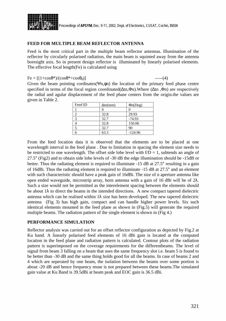
321
Proceedings of APSYM, Dec. 9-11, 2002, Dept. of Electronics, CUSAT, Cochin, INDIA
FEED FOR MULTIPLE BEAM REFLECTOR ANTENNA
Feed is the most critical part in the multiple beam reflector antennas. Illumination of the reflector by circularly polarised radiation, the main beam is squinted away from the antenna boresight axis. So in present design reflector is illuminated by linearly polarised elements. The effective focal length(Fe) is calculated using Fe = [(1+cosθ*)/(cosθ*+cosθ0)] -----(4) Given the beam pointing cordinates(Ψn,φn) the location of the primary feed phase centre specified in terms of the focal region coordinated(∆tn,Φn).Where (∆tn ,Φn) are respectively the radial and agular displacement of the feed phase centers from the origin.the values are given in Table 2.
Feed ID ∆tn(mm) Φn(Deg) 1 0 0 2 32.8 29.93 3 32.7 -74.93 4 32.8 150.06 5 32.7 90 6 63.3 -124.96
From the feed location data it is observed that the elements are to be placed at one wavelength interval in the feed plane . Due to limitation in spacing the element size needs to be restricted to one wavelength. The offset side lobe level with f/D = 1, subtends an angle of 27.5° (Fig2) and to obtain side lobe levels of -30 dB the edge illumination should be -15dB or better. Thus the radiating element is required to illuminate -15 dB at 27.5° resulting in a gain of 16dBi. Thus the radiating element is required to illuminate -15 dB at 27.5° and an element with such characteristic should have a peak gain of 16dBi. The size of n aperture antenna like open ended waveguide, microstrip array, horn antenna with a gain of 16 dBi will be of 2λ. Such a size would not be permitted as the interelement spacing between the elements should be about 1λ to direct the beams in the intended directions. A new compact tapered dielectric antenna which can be realised within 1λ size has been developed. The new tapered dielectric antenna (Fig 3) has high gain, compact and can handle higher power levels. Six such identical elements mounted in the feed plane as shown in (Fig.5) will generate the required multiple beams. The radiation pattern of the single element is shown in (Fig 4.) PERFORMANCE SIMULATION
Reflector analysis was carried out for an offset reflector configuration as depicted by Fig.2 at Ku band. A linearly polarised feed elements of 16 dBi gain is located at the computed location in the feed plane and radiation pattern is calculated. Contour plots of the radiation pattern is superimposed on the coverage requirements for the differentbeams. The level of signal from beam 3 falling on a beam that uses the same frequency slot i.e. beam 5 is found to be better than -30 dB and the same thing holds good for all the beams. In case of beams 2 and 4 which are seperated by one beam, the isolation between the beams over some portion is about -20 dB and hence frequency reuse is not prepared between these beams.The simulated gain value at Ku Band is 39.5dBi at beam peak and EOC gain is 36.5 dBi.
322
Proceedings of APSYM, Dec. 9-11, 2002, Dept. of Electronics, CUSAT, Cochin, INDIA
CONCLUSION
A multiple beam antenna with six beams is configured to cover the Indian landmass for a communication payload application. The beam width of each of the constituent beam is 2° and offset reflector configuration at Ku band with a cluster is proposed to generate multiple beams. A reflector antennas of 0.95 mtrs diameter will be used at Ku band. The radiating elements of the feed cluster would illuminate the reflector with a 15 dB taper at the rim resulting in a side lobe level of -30 dB and better. Design of a radiating element to meet the above illumination requirement has been achieved using waveguide tapered dielectric antenna. Simulated contour plots are shown. (Fig 6.)
323
Proceedings of APSYM, Dec. 9-11, 2002, Dept. of Electronics, CUSAT, Cochin, INDIA
A MULTIPLE SPOT-BEAM SPACECRAFT ANTENNA WITH APERTURE REUSE CAPABILITY
Khagindra Sood and Arun Kumar
SCAD-ASG, Space Applications Centre, Ahmedabad. 380015. INDIA. Email: [email protected]
A multiple spot-beam antenna at Ku-band is described for zonal coverage over India. This antenna achieves multi-fold aperture reuse, conserving the on-board real estate. The concepts of spatial-, polarization- and frequency-diversity are explained. The design and measured results of a six-beam technology demonstrator are presented and discussed. Good spatial and cross-polar isolation of about 25 dB is achieved. A four-fold frequency reuse was obtained from this antenna. This demonstrator validates the various concepts of this technology and will serve as a forerunner to future ISRO satellites.
INTRODUCTION
The size and weight of spacecraft subsystems is constrained by high launch expense and limited payload envelopes on launch vehicles. This constraint is particularly severe for antennas, as unlike other electronic instrumentation, they cannot derive advantage from miniaturization techniques. The situation is compounded for the antenna designer as the spacecraft EIRP’s have steadily increased over the years. This forces the use of larger antennas in an attempt to simplify the user terminals. These requirements have led to the development of several interesting techniques to enhance the antenna capabilities without requiring proportional space on the spacecraft. This paper presents an important technique that achieves multi-fold aperture reuse. A single aperture is used to derive an antenna function equivalent to that of several independent antennas. The technique also offers high gain performance and allows frequency reuse through a variety of methods. A multiple spot-beam antenna that achieves these objectives has been proven under a technology demonstration programme at the Space Applications Centre (ISRO.) The basic concept of the multiple beam antenna technology is described in the following section. Various terms and methods of achieving beam isolation are explained. The design of a zonal-beam antenna at Ku-band is described followed by measured results and discussion. BASIC CONCEPT
A conventional reflector with a single feed produces a spot-beam on boresight. Placement of additional feeds adjacent to the central feed in the reflector focal-plane results in the generation of additional spot-beams. These beams are scanned off-axis depending on the lateral offset given to the feed and also the offset-angle and edge clearance. The major design challenge lies in isolating these beams from one another by a proper selection of reflector geometry, feed element and the beam locations. By separating the beams in the angular domain, good mutual isolation can be achieved. The minimum allowable separation depends on the pattern roll-off, governed by the reflector size. This technique is referred to as spatial diversity. To operate adjacent beams with identical frequencies, use of orthogonal polarizations is essential. This is referred to as polarization diversity and requires an antenna
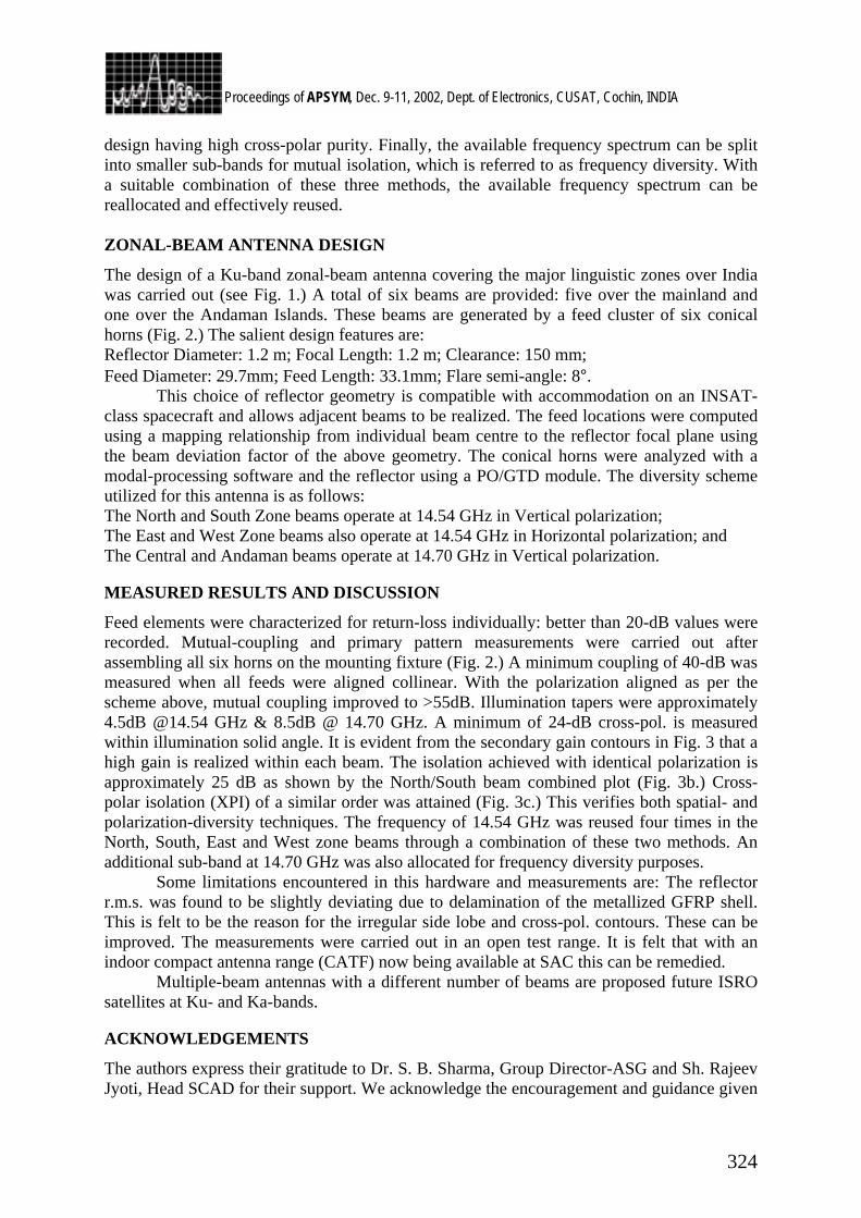
324
Proceedings of APSYM, Dec. 9-11, 2002, Dept. of Electronics, CUSAT, Cochin, INDIA
design having high cross-polar purity. Finally, the available frequency spectrum can be split into smaller sub-bands for mutual isolation, which is referred to as frequency diversity. With a suitable combination of these three methods, the available frequency spectrum can be reallocated and effectively reused. ZONAL-BEAM ANTENNA DESIGN
The design of a Ku-band zonal-beam antenna covering the major linguistic zones over India was carried out (see Fig. 1.) A total of six beams are provided: five over the mainland and one over the Andaman Islands. These beams are generated by a feed cluster of six conical horns (Fig. 2.) The salient design features are: Reflector Diameter: 1.2 m; Focal Length: 1.2 m; Clearance: 150 mm; Feed Diameter: 29.7mm; Feed Length: 33.1mm; Flare semi-angle: 8°. This choice of reflector geometry is compatible with accommodation on an INSAT-class spacecraft and allows adjacent beams to be realized. The feed locations were computed using a mapping relationship from individual beam centre to the reflector focal plane using the beam deviation factor of the above geometry. The conical horns were analyzed with a modal-processing software and the reflector using a PO/GTD module. The diversity scheme utilized for this antenna is as follows: The North and South Zone beams operate at 14.54 GHz in Vertical polarization; The East and West Zone beams also operate at 14.54 GHz in Horizontal polarization; and The Central and Andaman beams operate at 14.70 GHz in Vertical polarization. MEASURED RESULTS AND DISCUSSION
Feed elements were characterized for return-loss individually: better than 20-dB values were recorded. Mutual-coupling and primary pattern measurements were carried out after assembling all six horns on the mounting fixture (Fig. 2.) A minimum coupling of 40-dB was measured when all feeds were aligned collinear. With the polarization aligned as per the scheme above, mutual coupling improved to >55dB. Illumination tapers were approximately 4.5dB @14.54 GHz & 8.5dB @ 14.70 GHz. A minimum of 24-dB cross-pol. is measured within illumination solid angle. It is evident from the secondary gain contours in Fig. 3 that a high gain is realized within each beam. The isolation achieved with identical polarization is approximately 25 dB as shown by the North/South beam combined plot (Fig. 3b.) Cross-polar isolation (XPI) of a similar order was attained (Fig. 3c.) This verifies both spatial- and polarization-diversity techniques. The frequency of 14.54 GHz was reused four times in the North, South, East and West zone beams through a combination of these two methods. An additional sub-band at 14.70 GHz was also allocated for frequency diversity purposes. Some limitations encountered in this hardware and measurements are: The reflector r.m.s. was found to be slightly deviating due to delamination of the metallized GFRP shell. This is felt to be the reason for the irregular side lobe and cross-pol. contours. These can be improved. The measurements were carried out in an open test range. It is felt that with an indoor compact antenna range (CATF) now being available at SAC this can be remedied. Multiple-beam antennas with a different number of beams are proposed future ISRO satellites at Ku- and Ka-bands. ACKNOWLEDGEMENTS
The authors express their gratitude to Dr. S. B. Sharma, Group Director-ASG and Sh. Rajeev Jyoti, Head SCAD for their support. We acknowledge the encouragement and guidance given
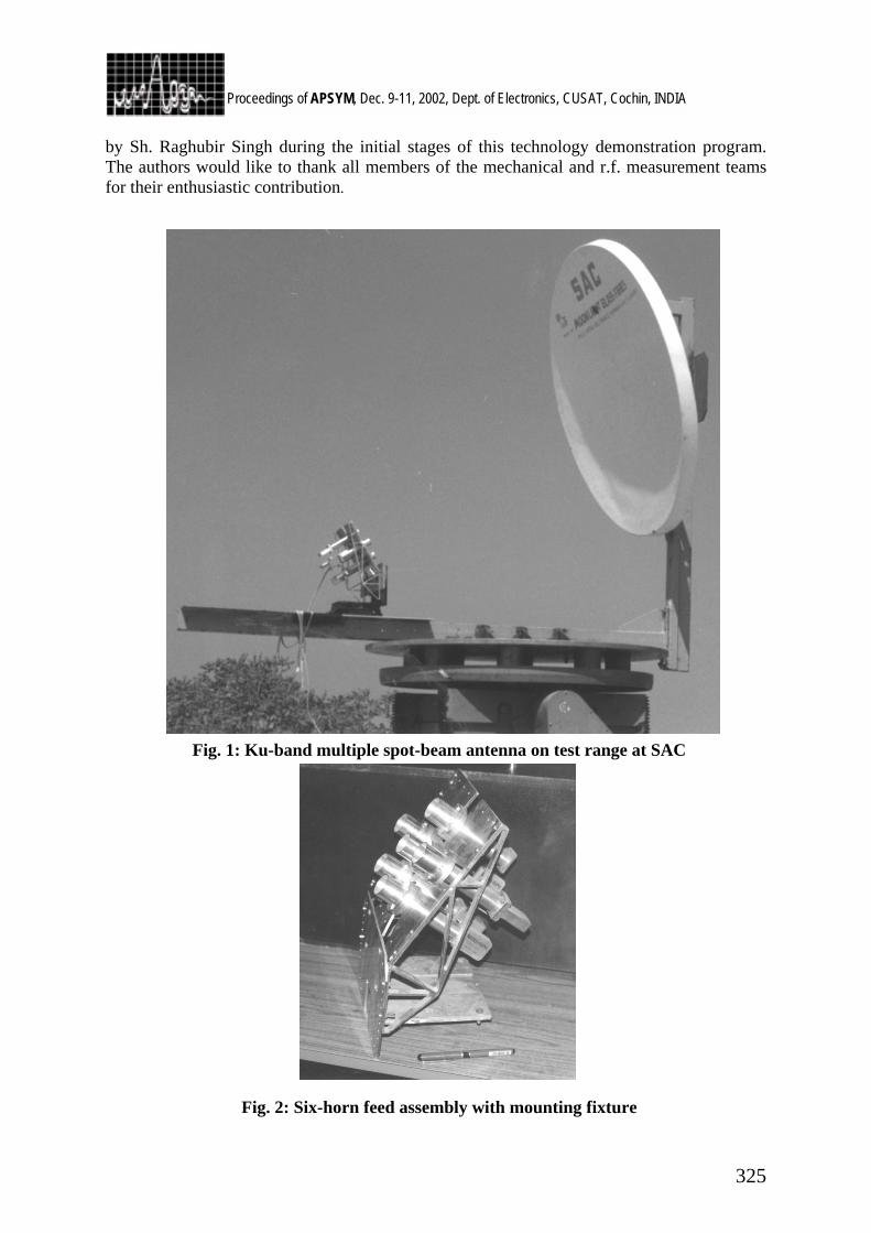
325
Proceedings of APSYM, Dec. 9-11, 2002, Dept. of Electronics, CUSAT, Cochin, INDIA
by Sh. Raghubir Singh during the initial stages of this technology demonstration program. The authors would like to thank all members of the mechanical and r.f. measurement teams for their enthusiastic contribution.
Fig. 1: Ku-band multiple spot-beam antenna on test range at SAC
Fig. 2: Six-horn feed assembly with mounting fixture
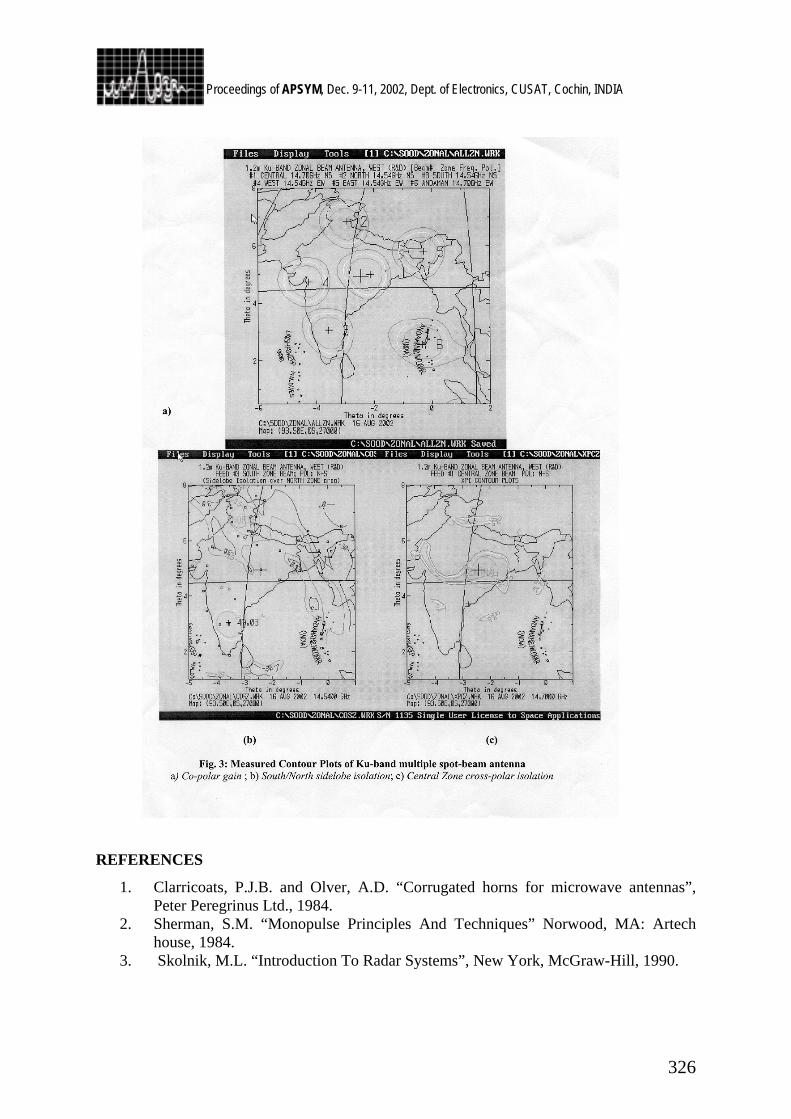
326
Proceedings of APSYM, Dec. 9-11, 2002, Dept. of Electronics, CUSAT, Cochin, INDIA
REFERENCES
1. Clarricoats, P.J.B. and Olver, A.D. “Corrugated horns for microwave antennas”, Peter Peregrinus Ltd., 1984.
2. Sherman, S.M. “Monopulse Principles And Techniques” Norwood, MA: Artech house, 1984.
3. Skolnik, M.L. “Introduction To Radar Systems”, New York, McGraw-Hill, 1990.
327
Proceedings of APSYM, Dec. 9-11, 2002, Dept. of Electronics, CUSAT, Cochin, INDIA
DESIGN AND DEVELOPMENT OF MONOPULSE ANTENNA SYSTEM
G.V.Ramakoteswara rao, J.V.Prasad, A.Ghosh, V.G.Borkar
Scientists, Research Center Imarat, Hyderabad
This paper aims for providing design details and subsequent development of monopulse antenna system. The critical design issues such as multi mode feed design for monopulse application; minimum blockage criteria, design and development of planar monopulse comparator are addressed in brief. The antenna measurement was carried out at Compact antenna test range and the derived results for guidance predicts an excellent performance of the system.
INTRODUCTION
Monopulse antennas find extensive applications in tracking and gathering of an air borne vehicle. The monopulse method was originally developed to achieve accurate automatic target tracking. Amplitude-comparison method has been used for the development of the antenna described here. The antenna has been realised using Cassegrain geometry. The details of the Cassegrain geometry are described in the next section. CASSEGRAIN GEOMETRY AND ITS PRINCIPLE
Fig 1 depicts the Cassegrain geometry of an antenna system, which primarily consists of a feed, parabolic and hyperbolic reflectors. The two basic properties of the parabolic antenna are (i) Diverging beams radiated by a source at the focus become parallel upon reflection at the surface, (ii) the distance traveled by any beam from the focus to a plane perpendicular to the axis upon reflection from the surface is independent of the angle at which the beam left the focus. As a result such antenna tends to produce a wave front with uniform phase. The principle of Cassegrain antenna is an adoption of folded optics technique. The classical Cassegrain geometry employs a parabolic contour for the main dish and a hyperbolic contour for sub dish. One of the two foci of the hyperbola is the real focal point of the system, and is located at the center of the feed. The other is a virtual focal point, which is located at the focus of the parabola. As a result, all parts of a wave originating at the real focal point, and then reflected from both the surfaces travel equal distance to a plane in front of the antenna. ANTENNA AND RELATED COMPONENTS
The monopulse antenna of Cassegrain configuration consists of the following: ( a) main Reflector(b)sub reflector(c) Monopulse feed (d) compact four square Horns (e)Compact four transitions, (f) Planar transition( g)Planar Comparator( h) Assembly components. Fig 2 shows some of the antenna components. Main Reflector The basic parabolic contour has been used in a variety of configurations. Rotating the parabolic curve about its axis produces a parabola of revolution called a circular parabola or a paraboloid. When properly illuminated by a source at focus, the paraboloid generates a near symmetrical pencil-beam antenna pattern. The beam width of the antenna system is decided by the aperture diameter of the paraboloid. Focal length to diameter ratio (f/D) has been appropriately chosen to make the total system compact. For a monopulse
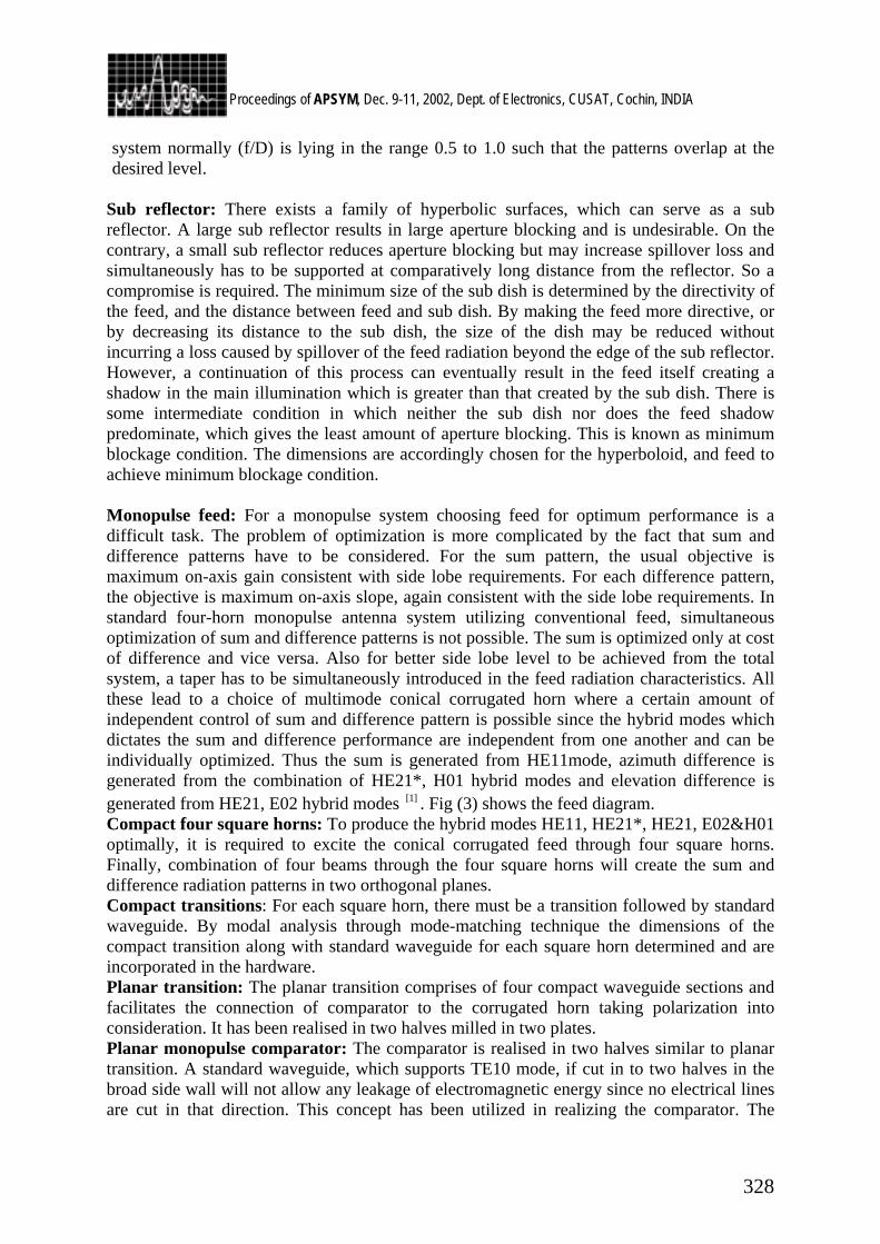
328
Proceedings of APSYM, Dec. 9-11, 2002, Dept. of Electronics, CUSAT, Cochin, INDIA
system normally (f/D) is lying in the range 0.5 to 1.0 such that the patterns overlap at the desired level.
Sub reflector: There exists a family of hyperbolic surfaces, which can serve as a sub reflector. A large sub reflector results in large aperture blocking and is undesirable. On the contrary, a small sub reflector reduces aperture blocking but may increase spillover loss and simultaneously has to be supported at comparatively long distance from the reflector. So a compromise is required. The minimum size of the sub dish is determined by the directivity of the feed, and the distance between feed and sub dish. By making the feed more directive, or by decreasing its distance to the sub dish, the size of the dish may be reduced without incurring a loss caused by spillover of the feed radiation beyond the edge of the sub reflector. However, a continuation of this process can eventually result in the feed itself creating a shadow in the main illumination which is greater than that created by the sub dish. There is some intermediate condition in which neither the sub dish nor does the feed shadow predominate, which gives the least amount of aperture blocking. This is known as minimum blockage condition. The dimensions are accordingly chosen for the hyperboloid, and feed to achieve minimum blockage condition. Monopulse feed: For a monopulse system choosing feed for optimum performance is a difficult task. The problem of optimization is more complicated by the fact that sum and difference patterns have to be considered. For the sum pattern, the usual objective is maximum on-axis gain consistent with side lobe requirements. For each difference pattern, the objective is maximum on-axis slope, again consistent with the side lobe requirements. In standard four-horn monopulse antenna system utilizing conventional feed, simultaneous optimization of sum and difference patterns is not possible. The sum is optimized only at cost of difference and vice versa. Also for better side lobe level to be achieved from the total system, a taper has to be simultaneously introduced in the feed radiation characteristics. All these lead to a choice of multimode conical corrugated horn where a certain amount of independent control of sum and difference pattern is possible since the hybrid modes which dictates the sum and difference performance are independent from one another and can be individually optimized. Thus the sum is generated from HE11mode, azimuth difference is generated from the combination of HE21*, H01 hybrid modes and elevation difference is generated from HE21, E02 hybrid modes ]1[ . Fig (3) shows the feed diagram. Compact four square horns: To produce the hybrid modes HE11, HE21*, HE21, E02&H01 optimally, it is required to excite the conical corrugated feed through four square horns. Finally, combination of four beams through the four square horns will create the sum and difference radiation patterns in two orthogonal planes. Compact transitions: For each square horn, there must be a transition followed by standard waveguide. By modal analysis through mode-matching technique the dimensions of the compact transition along with standard waveguide for each square horn determined and are incorporated in the hardware. Planar transition: The planar transition comprises of four compact waveguide sections and facilitates the connection of comparator to the corrugated horn taking polarization into consideration. It has been realised in two halves milled in two plates. Planar monopulse comparator: The comparator is realised in two halves similar to planar transition. A standard waveguide, which supports TE10 mode, if cut in to two halves in the broad side wall will not allow any leakage of electromagnetic energy since no electrical lines are cut in that direction. This concept has been utilized in realizing the comparator. The
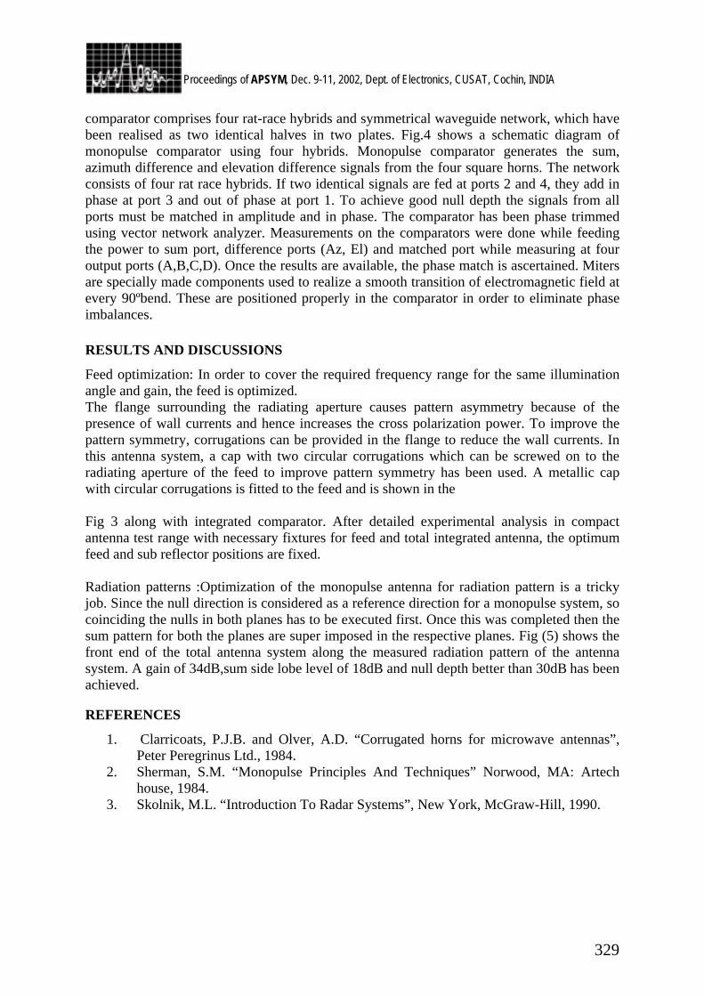
329
Proceedings of APSYM, Dec. 9-11, 2002, Dept. of Electronics, CUSAT, Cochin, INDIA
comparator comprises four rat-race hybrids and symmetrical waveguide network, which have been realised as two identical halves in two plates. Fig.4 shows a schematic diagram of monopulse comparator using four hybrids. Monopulse comparator generates the sum, azimuth difference and elevation difference signals from the four square horns. The network consists of four rat race hybrids. If two identical signals are fed at ports 2 and 4, they add in phase at port 3 and out of phase at port 1. To achieve good null depth the signals from all ports must be matched in amplitude and in phase. The comparator has been phase trimmed using vector network analyzer. Measurements on the comparators were done while feeding the power to sum port, difference ports (Az, El) and matched port while measuring at four output ports (A,B,C,D). Once the results are available, the phase match is ascertained. Miters are specially made components used to realize a smooth transition of electromagnetic field at every 90ºbend. These are positioned properly in the comparator in order to eliminate phase imbalances. RESULTS AND DISCUSSIONS
Feed optimization: In order to cover the required frequency range for the same illumination angle and gain, the feed is optimized. The flange surrounding the radiating aperture causes pattern asymmetry because of the presence of wall currents and hence increases the cross polarization power. To improve the pattern symmetry, corrugations can be provided in the flange to reduce the wall currents. In this antenna system, a cap with two circular corrugations which can be screwed on to the radiating aperture of the feed to improve pattern symmetry has been used. A metallic cap with circular corrugations is fitted to the feed and is shown in the Fig 3 along with integrated comparator. After detailed experimental analysis in compact antenna test range with necessary fixtures for feed and total integrated antenna, the optimum feed and sub reflector positions are fixed. Radiation patterns :Optimization of the monopulse antenna for radiation pattern is a tricky job. Since the null direction is considered as a reference direction for a monopulse system, so coinciding the nulls in both planes has to be executed first. Once this was completed then the sum pattern for both the planes are super imposed in the respective planes. Fig (5) shows the front end of the total antenna system along the measured radiation pattern of the antenna system. A gain of 34dB,sum side lobe level of 18dB and null depth better than 30dB has been achieved. REFERENCES
1. Clarricoats, P.J.B. and Olver, A.D. “Corrugated horns for microwave antennas”, Peter Peregrinus Ltd., 1984.
2. Sherman, S.M. “Monopulse Principles And Techniques” Norwood, MA: Artech house, 1984.
3. Skolnik, M.L. “Introduction To Radar Systems”, New York, McGraw-Hill, 1990.
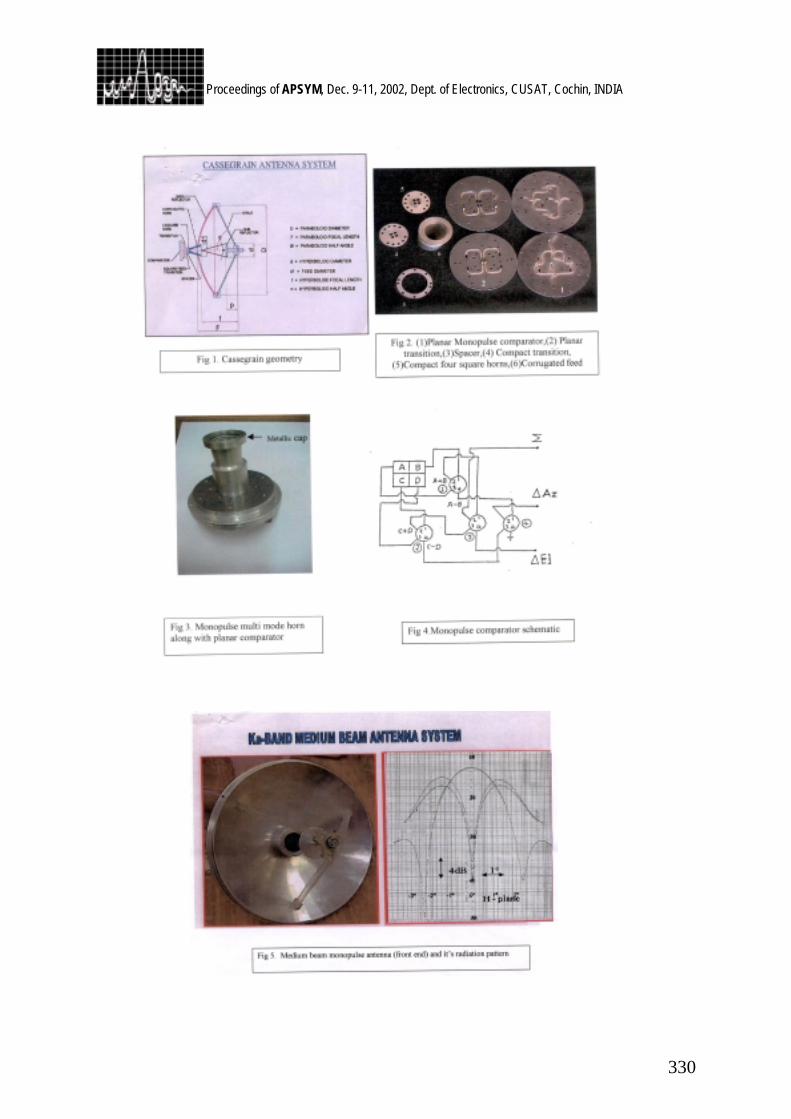
330
Proceedings of APSYM, Dec. 9-11, 2002, Dept. of Electronics, CUSAT, Cochin, INDIA
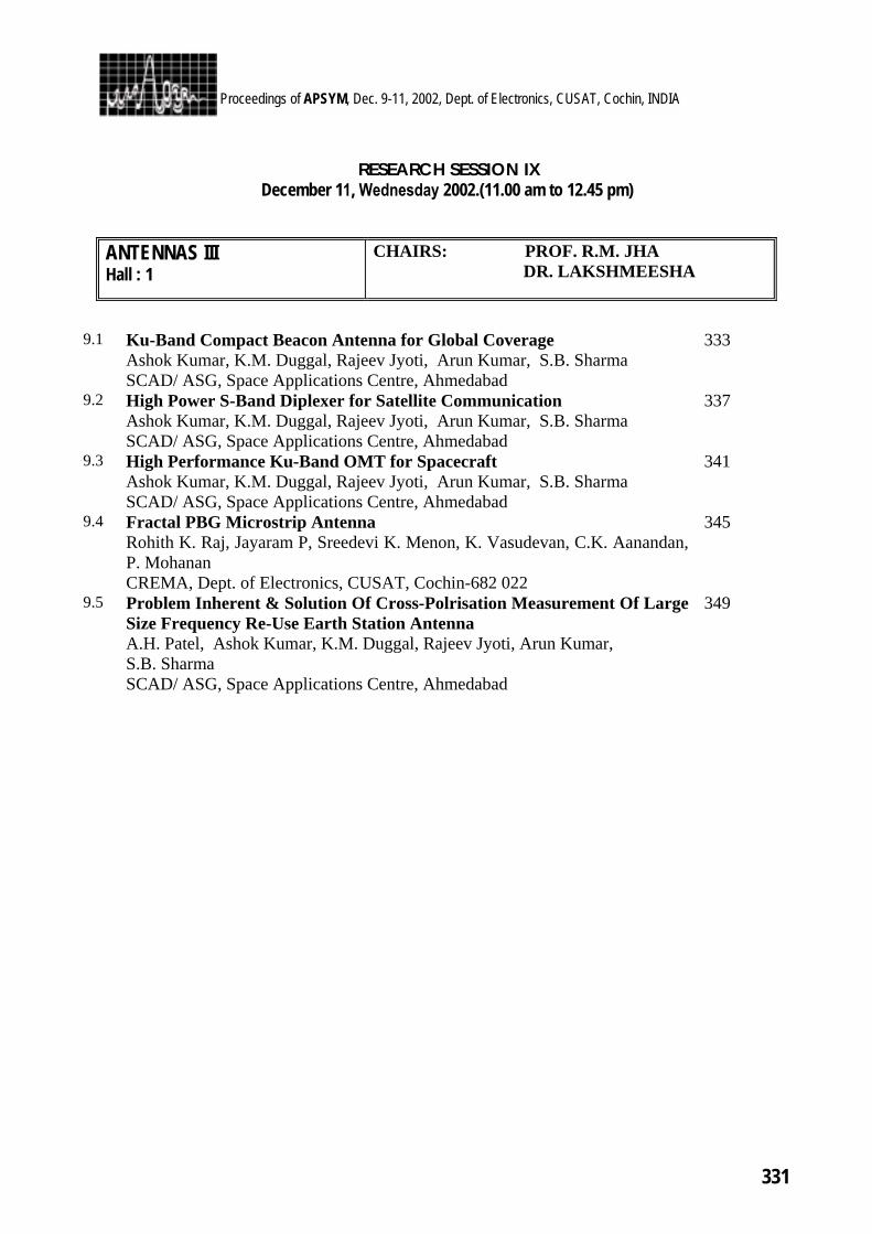
331
Proceedings of APSYM, Dec. 9-11, 2002, Dept. of Electronics, CUSAT, Cochin, INDIA
RESEARCH SESSION IX
December 11, Wednesday 2002.(11.00 am to 12.45 pm)
ANTENNAS III Hall : 1
CHAIRS: PROF. R.M. JHA DR. LAKSHMEESHA
9.1 Ku-Band Compact Beacon Antenna for Global Coverage Ashok Kumar, K.M. Duggal, Rajeev Jyoti, Arun Kumar, S.B. Sharma SCAD/ ASG, Space Applications Centre, Ahmedabad
333
9.2 High Power S-Band Diplexer for Satellite Communication Ashok Kumar, K.M. Duggal, Rajeev Jyoti, Arun Kumar, S.B. Sharma SCAD/ ASG, Space Applications Centre, Ahmedabad
337
9.3 High Performance Ku-Band OMT for Spacecraft Ashok Kumar, K.M. Duggal, Rajeev Jyoti, Arun Kumar, S.B. Sharma SCAD/ ASG, Space Applications Centre, Ahmedabad
341
9.4 Fractal PBG Microstrip Antenna Rohith K. Raj, Jayaram P, Sreedevi K. Menon, K. Vasudevan, C.K. Aanandan, P. Mohanan CREMA, Dept. of Electronics, CUSAT, Cochin-682 022
345
9.5 Problem Inherent & Solution Of Cross-Polrisation Measurement Of Large Size Frequency Re-Use Earth Station Antenna A.H. Patel, Ashok Kumar, K.M. Duggal, Rajeev Jyoti, Arun Kumar, S.B. Sharma SCAD/ ASG, Space Applications Centre, Ahmedabad
349
332
Proceedings of APSYM, Dec. 9-11, 2002, Dept. of Electronics, CUSAT, Cochin, INDIA

333
Proceedings of APSYM, Dec. 9-11, 2002, Dept. of Electronics, CUSAT, Cochin, INDIA
334
Proceedings of APSYM, Dec. 9-11, 2002, Dept. of Electronics, CUSAT, Cochin, INDIA
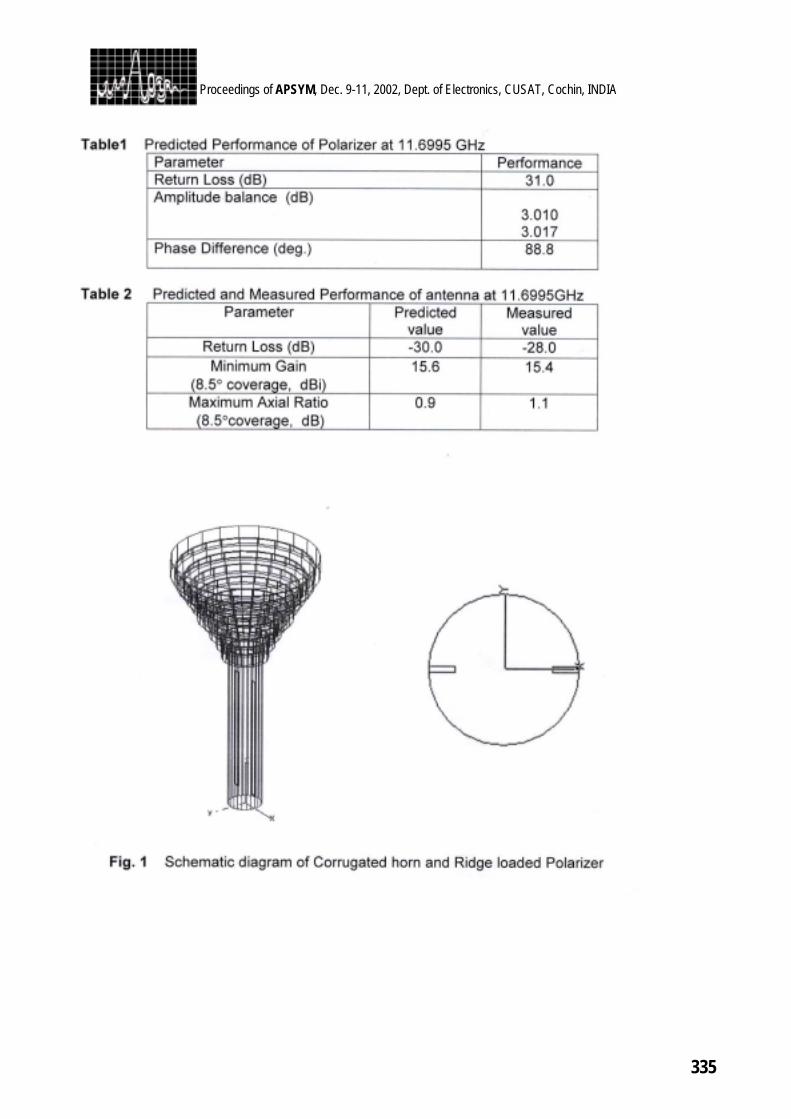
335
Proceedings of APSYM, Dec. 9-11, 2002, Dept. of Electronics, CUSAT, Cochin, INDIA
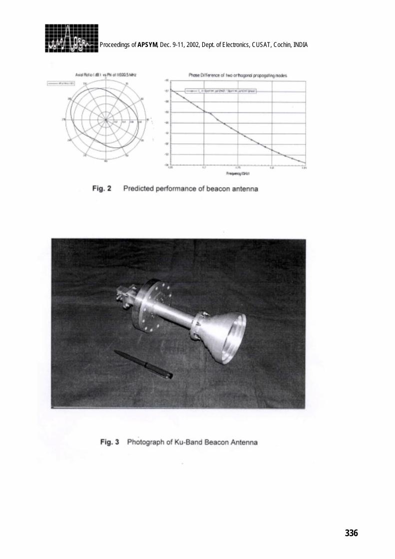
336
Proceedings of APSYM, Dec. 9-11, 2002, Dept. of Electronics, CUSAT, Cochin, INDIA
337
Proceedings of APSYM, Dec. 9-11, 2002, Dept. of Electronics, CUSAT, Cochin, INDIA
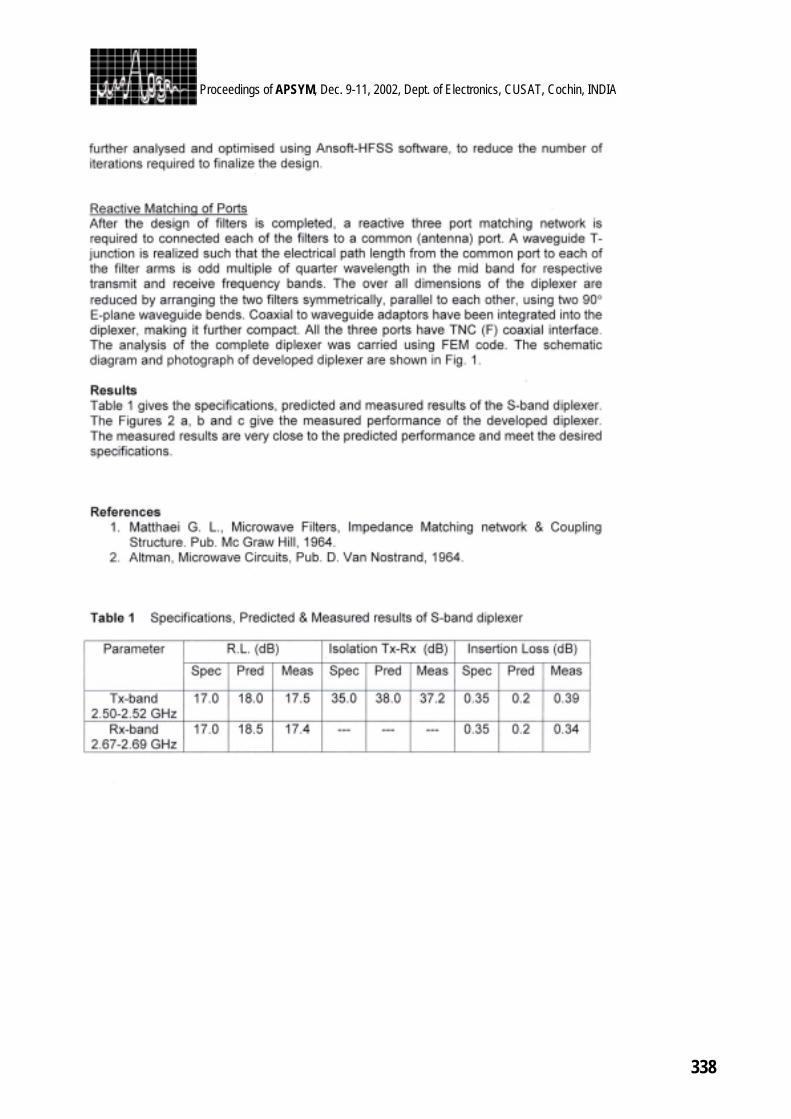
338
Proceedings of APSYM, Dec. 9-11, 2002, Dept. of Electronics, CUSAT, Cochin, INDIA
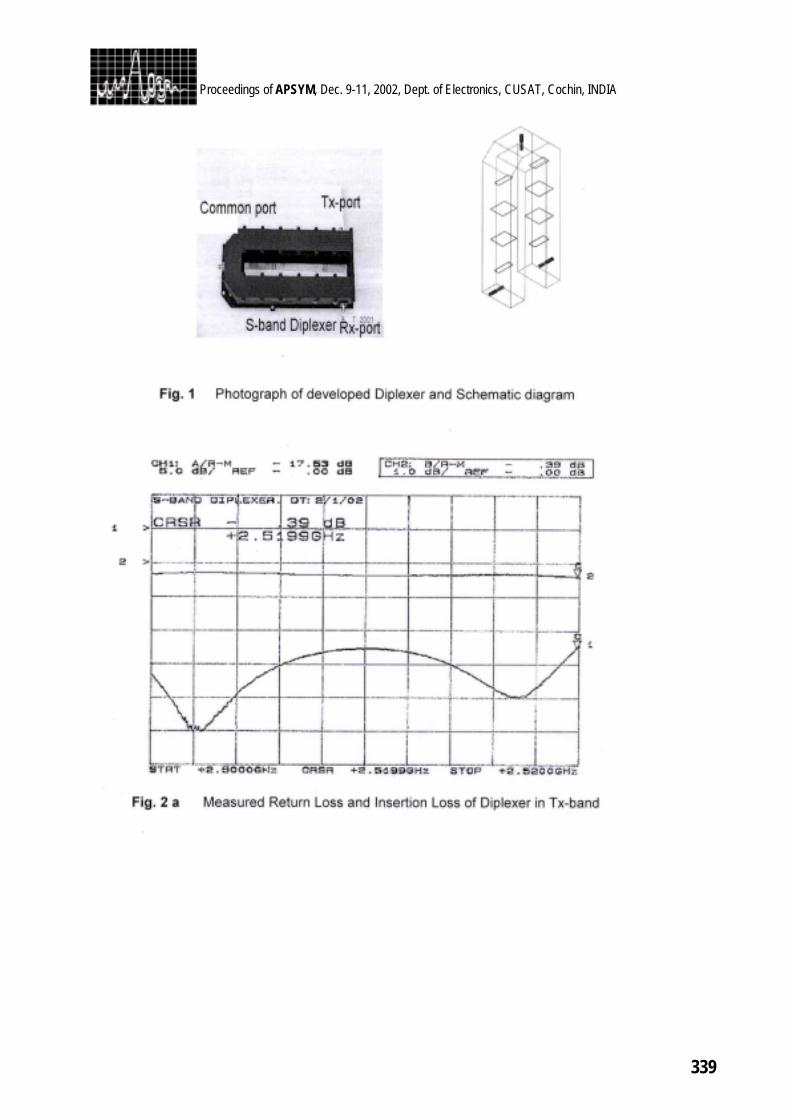
339
Proceedings of APSYM, Dec. 9-11, 2002, Dept. of Electronics, CUSAT, Cochin, INDIA
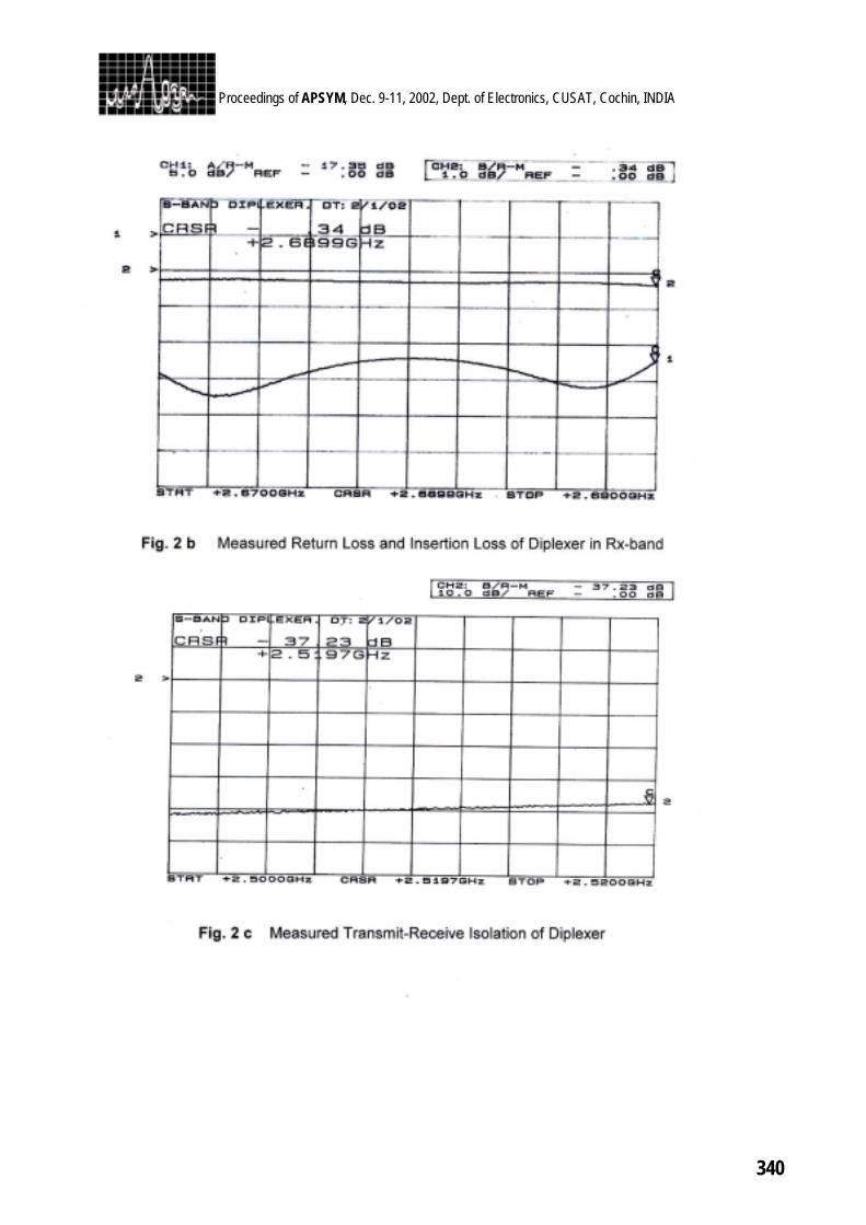
340
Proceedings of APSYM, Dec. 9-11, 2002, Dept. of Electronics, CUSAT, Cochin, INDIA
341
Proceedings of APSYM, Dec. 9-11, 2002, Dept. of Electronics, CUSAT, Cochin, INDIA

342
Proceedings of APSYM, Dec. 9-11, 2002, Dept. of Electronics, CUSAT, Cochin, INDIA
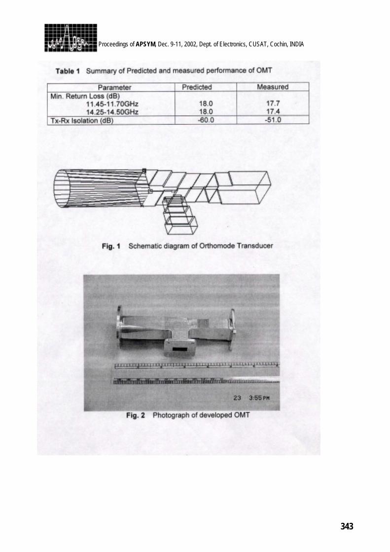
343
Proceedings of APSYM, Dec. 9-11, 2002, Dept. of Electronics, CUSAT, Cochin, INDIA
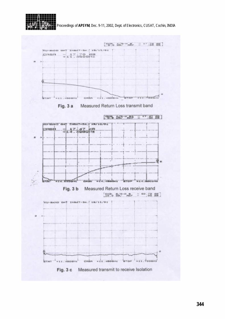
344
Proceedings of APSYM, Dec. 9-11, 2002, Dept. of Electronics, CUSAT, Cochin, INDIA
345
Proceedings of APSYM, Dec. 9-11, 2002, Dept. of Electronics, CUSAT, Cochin, INDIA
FRACTAL PBG MICROSTRIP ANTENNA
Rohith.K.Raj, Jayaram P, Sreedevi K. Menon, K. Vasudevan, C.K. Anandan and P. Mohanan
Centre for Research in Electromagnetics and Antennas, Department of Electronics Cochin University of
Science and Technology, Cochin-22
Experimental investigation of a Photonic Band Gap (PBG) microstrip antenna using fractal geometry in the ground plane is presented. It makes use of a Sierpinski fractal structure with two iterations etched in the ground plane instead of conventional circle or rectangular PBG structure. It is found that this structure has increased the bandwidth of the microstrip antenna up to 17% without degrading the gain.
INTRODUCTION Microstrip antennas are widely used in a broad range of military and commercial applications mainly because of its excellent features like light weight, low profile, low cost, and ease of fabrication. The inherent property of a microstrip antenna is its poor bandwidth, which is only in the range of 2 to 4%. It is observed that as the substrate thickness and dielectric constant increases, the bandwidth of the antenna is increased. But an increase in substrate permittivity may excite surface waves, causing power loss in microstrip antenna, which in turn reduces overall efficiency of the antenna.
Two technologies have been mainly pursued so far to achieve microstrip antennas on high dielectric substrate with optimum performance. One is based on micromachining technology [1, 2] while the other makes use of the concept of photonic band gap substrates [3]. In micromachining technique a part of the substrate underneath the radiating element is removed to realize a low effective dielectric constant environment for the antenna. Thus the surface waves are attenuated and the radiated power to space is enhanced.
The Photonic Band Gap (PBG) structures are periodic structure in which propagation of certain bands of frequency is prohibited [4]. The studies were originally done in optical region and then extended to microwave region. The PBG structure can be introduced by drilling or etching periodic patterns on the ground plane [5] and thus reducing the surface waves.
A simple Sierpinski triangle with 2 iterations is etched on the ground plane of the rectangular microstrip antenna is employed instead of conventional geometries like rectangle and circle. A comparison is done between the microstrip rectangular patch antenna with Sierpinski Fractal structure PBG and Complementary Sierpinski Fractal PBG.
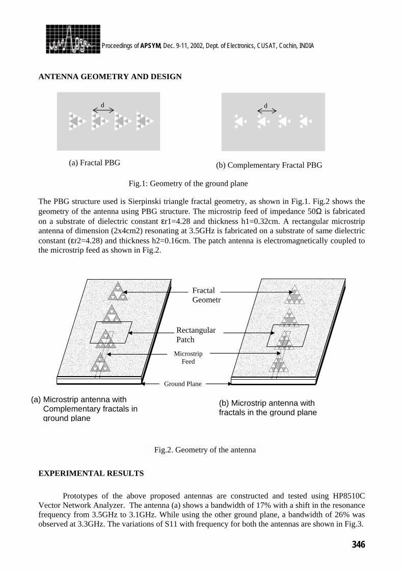
346
Proceedings of APSYM, Dec. 9-11, 2002, Dept. of Electronics, CUSAT, Cochin, INDIA
ANTENNA GEOMETRY AND DESIGN The PBG structure used is Sierpinski triangle fractal geometry, as shown in Fig.1. Fig.2 shows the geometry of the antenna using PBG structure. The microstrip feed of impedance 50Ω is fabricated on a substrate of dielectric constant εr1=4.28 and thickness h1=0.32cm. A rectangular microstrip antenna of dimension (2x4cm2) resonating at 3.5GHz is fabricated on a substrate of same dielectric constant (εr2=4.28) and thickness h2=0.16cm. The patch antenna is electromagnetically coupled to the microstrip feed as shown in Fig.2.
EXPERIMENTAL RESULTS Prototypes of the above proposed antennas are constructed and tested using HP8510C Vector Network Analyzer. The antenna (a) shows a bandwidth of 17% with a shift in the resonance frequency from 3.5GHz to 3.1GHz. While using the other ground plane, a bandwidth of 26% was observed at 3.3GHz. The variations of S11 with frequency for both the antennas are shown in Fig.3.
Fig.1: Geometry of the ground plane
d
(b) Complementary Fractal PBG (a) Fractal PBG
d
Fig.2. Geometry of the antenna
(a) Microstrip antenna with Complementary fractals in ground plane
(b) Microstrip antenna with fractals in the ground plane
Ground Plane
Fractal Geometr
Rectangular Patch
Microstrip Feed
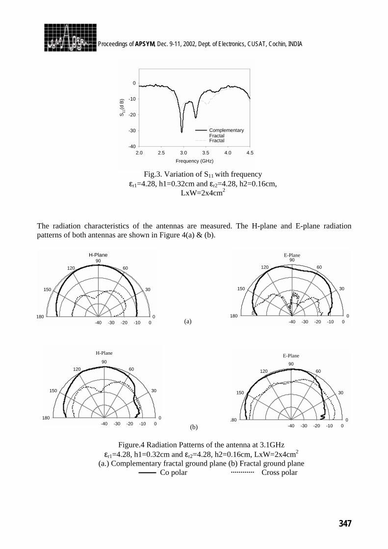
347
Proceedings of APSYM, Dec. 9-11, 2002, Dept. of Electronics, CUSAT, Cochin, INDIA
The radiation characteristics of the antennas are measured. The H-plane and E-plane radiation patterns of both antennas are shown in Figure 4(a) & (b).
H-Plane
-40 -30 -20 -10 00
30
6090
120
150
180
E-Plane
-40 -30 -20 -10 00
30
6090
120
150
180
H-Plane
-40 -30 -20 -10 00
30
6090
120
150
180
E-Plane
-40 -30 -20 -10 00
30
6090
120
150
180
(a)
(b)
Frequency (GHz)
2.0 2.5 3.0 3.5 4.0 4.5
S11
(d B
)
-40
-30
-20
-10
0
Complementary FractalFractal
Fig.3. Variation of S11 with frequency εr1=4.28, h1=0.32cm and εr2=4.28, h2=0.16cm,
LxW=2x4cm2
Figure.4 Radiation Patterns of the antenna at 3.1GHz εr1=4.28, h1=0.32cm and εr2=4.28, h2=0.16cm, LxW=2x4cm2
(a.) Complementary fractal ground plane (b) Fractal ground plane Co polar Cross polar
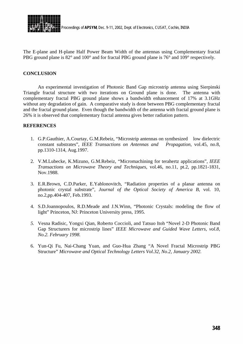
348
Proceedings of APSYM, Dec. 9-11, 2002, Dept. of Electronics, CUSAT, Cochin, INDIA
The E-plane and H-plane Half Power Beam Width of the antennas using Complementary fractal PBG ground plane is 82° and 100° and for fractal PBG ground plane is 76° and 109° respectively. CONCLUSION An experimental investigation of Photonic Band Gap microstrip antenna using Sierpinski Triangle fractal structure with two iterations on Ground plane is done. The antenna with complementary fractal PBG ground plane shows a bandwidth enhancement of 17% at 3.1GHz without any degradation of gain. A comparative study is done between PBG complementary fractal and the fractal ground plane. Even though the bandwidth of the antenna with fractal ground plane is 26% it is observed that complementary fractal antenna gives better radiation pattern. REFERENCES
1. G.P.Gauthier, A.Courtay, G.M.Rebeiz, “Microstrip antennas on synthesized low dielectric constant substrates”, IEEE Transactions on Antennas and Propagation, vol.45, no.8, pp.1310-1314, Aug.1997.
2. V.M.Lubecke, K.Mizuno, G.M.Rebeiz, “Micromachining for terahertz applications”, IEEE
Transactions on Microwave Theory and Techniques, vol.46, no.11, pt.2, pp.1821-1831, Nov.1988.
3. E.R.Brown, C.D.Parker, E.Yablonovitch, “Radiation properties of a planar antenna on
photonic crystal substrate”, Journal of the Optical Society of America B, vol. 10, no.2,pp.404-407, Feb.1993.
4. S.D.Joannopoulos, R.D.Meade and J.N.Winn, “Photonic Crystals: modeling the flow of
light” Princeton, NJ: Princeton University press, 1995.
5. Vesna Radisic, Yongxi Qian, Roberto Coccioli, and Tatsuo Itoh “Novel 2-D Photonic Band Gap Structurers for microstrip lines” IEEE Microwave and Guided Wave Letters, vol.8, No.2. February 1998.
6. Yun-Qi Fu, Nai-Chang Yuan, and Guo-Hua Zhang “A Novel Fractal Microstrip PBG
Structure” Microwave and Optical Technology Letters Vol.32, No.2, January 2002.
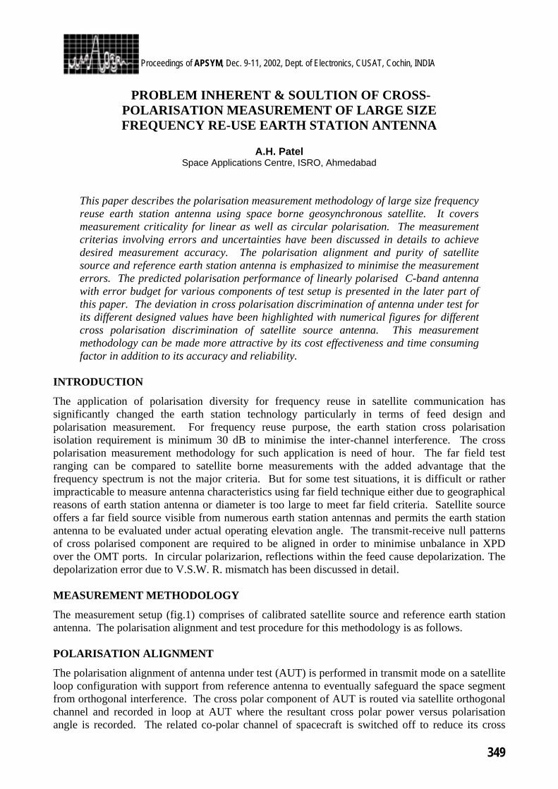
349
Proceedings of APSYM, Dec. 9-11, 2002, Dept. of Electronics, CUSAT, Cochin, INDIA
PROBLEM INHERENT & SOULTION OF CROSS-POLARISATION MEASUREMENT OF LARGE SIZE FREQUENCY RE-USE EARTH STATION ANTENNA
A.H. Patel
Space Applications Centre, ISRO, Ahmedabad
This paper describes the polarisation measurement methodology of large size frequency reuse earth station antenna using space borne geosynchronous satellite. It covers measurement criticality for linear as well as circular polarisation. The measurement criterias involving errors and uncertainties have been discussed in details to achieve desired measurement accuracy. The polarisation alignment and purity of satellite source and reference earth station antenna is emphasized to minimise the measurement errors. The predicted polarisation performance of linearly polarised C-band antenna with error budget for various components of test setup is presented in the later part of this paper. The deviation in cross polarisation discrimination of antenna under test for its different designed values have been highlighted with numerical figures for different cross polarisation discrimination of satellite source antenna. This measurement methodology can be made more attractive by its cost effectiveness and time consuming factor in addition to its accuracy and reliability.
INTRODUCTION
The application of polarisation diversity for frequency reuse in satellite communication has significantly changed the earth station technology particularly in terms of feed design and polarisation measurement. For frequency reuse purpose, the earth station cross polarisation isolation requirement is minimum 30 dB to minimise the inter-channel interference. The cross polarisation measurement methodology for such application is need of hour. The far field test ranging can be compared to satellite borne measurements with the added advantage that the frequency spectrum is not the major criteria. But for some test situations, it is difficult or rather impracticable to measure antenna characteristics using far field technique either due to geographical reasons of earth station antenna or diameter is too large to meet far field criteria. Satellite source offers a far field source visible from numerous earth station antennas and permits the earth station antenna to be evaluated under actual operating elevation angle. The transmit-receive null patterns of cross polarised component are required to be aligned in order to minimise unbalance in XPD over the OMT ports. In circular polarizarion, reflections within the feed cause depolarization. The depolarization error due to V.S.W. R. mismatch has been discussed in detail. MEASUREMENT METHODOLOGY
The measurement setup (fig.1) comprises of calibrated satellite source and reference earth station antenna. The polarisation alignment and test procedure for this methodology is as follows. POLARISATION ALIGNMENT
The polarisation alignment of antenna under test (AUT) is performed in transmit mode on a satellite loop configuration with support from reference antenna to eventually safeguard the space segment from orthogonal interference. The cross polar component of AUT is routed via satellite orthogonal channel and recorded in loop at AUT where the resultant cross polar power versus polarisation angle is recorded. The related co-polar channel of spacecraft is switched off to reduce its cross
350
Proceedings of APSYM, Dec. 9-11, 2002, Dept. of Electronics, CUSAT, Cochin, INDIA
polar component. This measurement is repeated for other transmits port of AUT. The intersection of nulls of the two cross polar transmit curves are aligned to reduce the cross polar isolation ambiguity. PROCEDURE
The measurement of transmit cross polarisation can be made by switching the transmit signal between two transmit ports of OMT of AUT and measuring the down link looped back signal at reference antenna on spectrum analyser without changing the polarisation status. The co-polar channel in spacecraft is switched off to eliminate XPD contributions from spacecraft transmit antenna. The receive polarisation test is similarly carried out by unlinking reference antenna and measuring signal at AUT for two receive ports of OMT. In case of AUT of circular polarisation, the polarisation discrimination measurement needs circularly polarised sources and reference antenna both with their axial ratio performances better than Of AUT. In this case, relative coupling to two OMT ports (RHCP and LHCP) of AUT is measured by slowly rotating reference antenna. The cross polar isolation between the two circularly polarised waves can be computed as :
24.8 - 10 log (0.5 (1+sin2θ1 . sin2θ2 + cos2θ1 . cos2θ2 . cos2β)) dB 2
where β = angle between their major axes (Port 1 & 2) θ1 = ½(cos-1M - sin-1m) θ2 = ½(cos-1M + sin-1m) Where M and m are maximum and minimum coupling values respectively. MEASUREMENT ACCURACY
The accuracy of XPD measurement of earth station antenna is limited by polarisation purity of reference and space borne satellite antenna. The measured XPD with this method will be resultant of polarisation purity of these antennas. The polarisation purity of reference and satellite borne antenna is required to be 10 dB higher than that of AUT. Fig.2 is a vector diagram for satellite isolation and earth station isolation in terms of XPD. The measured XPD is the resultant XPD of satellite XPD and AUT XPD. The AUT XPD is then calculated for known XPD value of satellite. As an example 27 dB XPD of satellite and 30 dB XPD of AUT the resultant XPD value will be 22.5 dB for 0 degree tilt angle β. The measured values for β = 90 will be 38.8 dB which is higher by 8.8 dB than the actual value of AUT.When the polarisation purity of both antennas is comparable, tremendous errors are introduced due to phase ambiguity. Fig.3 shows the prediction of measurement error due to inphase and phase opposition for 45 dB XPD source of antenna. This figure also indicates that for lower value of polarisation purity of AUT, the error is not serious for inphase and phase opposition but for 30 dB XPD of AUT, this error is significant and has to be accounted for calculating net XPD. Reflections in a circularly polarised feed system, depolarise a radiating signal unless they are absorbed by match terminated ports. The depolarisation is equal to the sum of pre and post feed return losses. For example a feed with 1.2 VSWR at input/output port will further depolarise the axial ratio by 0.15 dB. The depolarisation error due to this mismatch is given by
Depolarisation error = 17.37 X ( 10- sum of R.L./20 )
The finite return loss of connector interface of test cable can cause similar error and has to be accounted for calculating actual value.
351
Proceedings of APSYM, Dec. 9-11, 2002, Dept. of Electronics, CUSAT, Cochin, INDIA
ERROR BUDGET
The error budget in XPD measurement of AUT can be put together in the following manner to calculate the total error. The polarisation purity of source (satellite receive antenna) and reference antenna is assumed -45 dB. And the design parameter of XPD of AUT is -35 dB.
AUT EIRP stability + 0.1 dB
Reference antenna EIRP stability + 0.1 dB
Satellite gain stability + 0.1 dB
Propagation stability at AUT + 0.2 dB
Propagation stability at Ref. Antenna + 0.2 dB
Instrument calibration error + 0.2 dB
Polarisation axis alignment + 0.2 dB
Total error + 1.1 dB In addition to this, the error due to inphase and phase opposition in signals from satellite and AUT can be incorporated if phase characteristics of signals are measured separately. These errors are large for higher value of XPD and could reach + 3 dB for highly depolarized level of source and test antenna. CONCLUSION
The polarisation purity of the frequency reuse earth station antenna can be evaluated in actual operational condition of earth station by spacecraft loop configuration with reference antenna. This method does not require large estate to generate far-field criteria as required in out door test range since satellite is very far and also highly isolated from multiple reflections as the earth station antenna is looking upwards in elevation during measurement. The measurement error for inphase and phase opposition are predominant for higher XPD value of AUT and has least significance for lower XPD of AUT. The measurements are cost effective and less time consuming compared to far-field test range and therefore this methodology is more attractive for such applications. ACKNOWLEDGEMENT
The author is indebted to Dr. Arun Kumar, Group Head, ASG and Dr. S.B. Sharma, Group Director, ASG for giving many useful suggestions on antenna measurements. REFERECES
1. "Problems inherent in the design and measurement of an 11/14 GHz 3M antenna" by Mr. Brain and P.J. Wood, Marconi Electronics Ltd.
2. "Earth station antenna measurement technique using satellites" by B.J. Kasstan EUTELSAT. 3. "INTELSAT V EARTH STATION TECHNOLOGY 77CLR47" by R.W. Gruner. 4. "IEEE standards test procedure for antennas 1980", by William R. Kruesi and Irvin N. Howell.
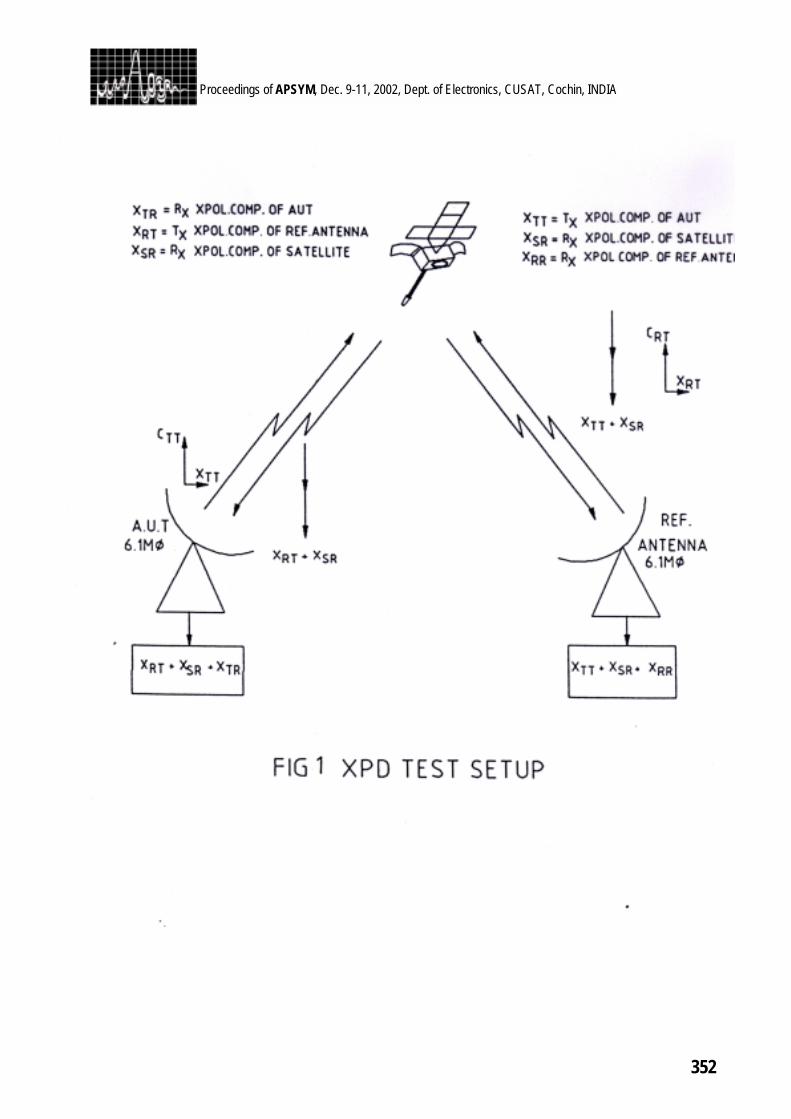
352
Proceedings of APSYM, Dec. 9-11, 2002, Dept. of Electronics, CUSAT, Cochin, INDIA
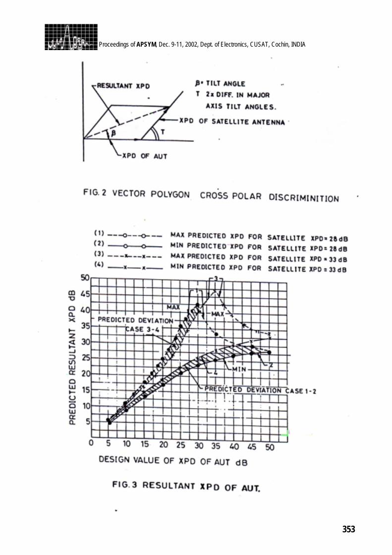
353
Proceedings of APSYM, Dec. 9-11, 2002, Dept. of Electronics, CUSAT, Cochin, INDIA
354
Proceedings of APSYM, Dec. 9-11, 2002, Dept. of Electronics, CUSAT, Cochin, INDIA
355
Proceedings of APSYM, Dec. 9-11, 2002, Dept. of Electronics, CUSAT, Cochin, INDIA
RESEARCH SESSION X December 11, Wednesday 2002. (11.00 a.m. to 12.45 p.m)
Microwave and optical Tech. Hall : 2
CHAIRS: PROF.V.P. KULKARNI PROF.M.C.CHANDRA MOULY
10.1 Design and Development of an Efficient Power Control Module for DS-CDMA multimedia wireless networks in an AWGN, Path-loss, Rayleigh-fading Channel Manikandan. K., D. Rajaveerappa Department of Electronics, CUSAT,Cochin-682 022 ABHA, N.S.S. Engg. College (P.O.), Palakkad-678 008 [email protected]
357
10.2 The pulsed Wire Method for Wiggler Field Mapping Ravi A.V. Kumar, K.K. Mohandas and K.K. Jain Institute of Plasma Research, Bhat, Gandhinagar 382 428, Gujarat [email protected]
361
10.3 Plasma Antenna D. Bora, Rajneesh Kumar, R.G. Trivedi, S.K.P. Tripathi Institute of Plasma Research, Bhat, Gandhinagar - 382 428 [email protected]
365
10.4 Peak Identification in optical spectrum in ANN model Saritha N & V.P.N. Nampoori International School of Photonics, CUSAT, Cochin-682 022 [email protected]
369
10.5 Design And Development Of Cell phone Based CATV Spectrum Analysis System Ameen A, Nowshad S, Ganesh. S, Sreeja. S, P.Anguswamy, K.R. Suresh Nair, Franklin. G, Prakash R, Satish P NeST, Technopark, Trivandrum . NeST, CSEZ, Cochin.
372
10.6 Millimeter Wave Attenuation in Sand & Dust Storms S.K. Srivastava, B.R. Vishwakarma Dept. Physics, Govt. P.G. College, Ambikapur, Chhattisgarh-497001
375
10.7 Study Of The Emissivity Properties Of Soils For Remote Sensing Using Microwave Techniques S.K. Srivastava, Ambika Jain Dept. Physics, Govt. P.G. College, Ambikapur, Chhattisgarh-497001
378

356
Proceedings of APSYM, Dec. 9-11, 2002, Dept. of Electronics, CUSAT, Cochin, INDIA
357
Proceedings of APSYM, Dec. 9-11, 2002, Dept. of Electronics, CUSAT, Cochin, INDIA
DESIGN AND DEVELOPMENT OF AN EFFICIENT POWER CONTROL MODULE
FOR DS-CDMA MULTIMEDIA WIRELESS NETWORKS IN AN AWGN, PATH-LOSS, RAYLEIGH-FADING CHANNEL
K. Manikandan & D. Rajaveerappa
Dept. of Electronics, Cochin University of Science & Technology, Cochin 682 022.
INTRODUCTION
In recent years, CDMA based on SS techniques is considered to be very much suitable for wireless multimedia applications. CDMA is interference limited: that is, the number of users that can use the same spectrum and still have acceptable performance is determined by the total interference power that all of the users, taken as a whole, generate in the receiver. Unless one takes great care in power control, those CDMA transmitters, which are close to the receiver, will cause the overwhelming interference. This effect is known as the "near-far" problem. In a mobile environment the near-far problem could be the dominant effect. Therefore, we have to control the power of each individual mobile user so that the received power each mobile user is the same. This technique is called “adaptive power control." In this paper, a wireless multimedia DS-CDMA system based on reverse link closed-loop power control is considered.
IMPLEMENTATION OF POWER CONTROL IN CDMA
While, both the forward and reverse links require power control, the main need for power control arises in the reverse link. Co-channel interference is the biggest problem on the forward link and for a single-cell-scenario this will be absent. The reverse link requires power control primarily to solve the “near-far” problem. All handsets transmit on the same frequency channel at the same time but with different codes. Therefore, one handset’s signal may interfere with the others. A mobile’s received signal quality at the base station is inversely proportional to the power of the interference from other mobiles. The near-far problem arises when two mobiles transmit at the same power but at different distances from the base station. The mobile near the base station, which has a high received signal-power, greatly interferes with the distant mobile, which may not be detected. To solve problems encountered in urban mobile environments, the power control algorithm ensures that the received power levels of all handsets are the same at the base station. The algorithm does this by controlling the mobile’s transmit power. Handsets are commanded to transmit at a higher power level when their received power is low and at a lower power level when their received power is high. To control power in this manner, the algorithm continuously monitors the received power of each mobile and continuously adjusts its transmit power to achieve predefined performance levels, such as bit error rate (BER).
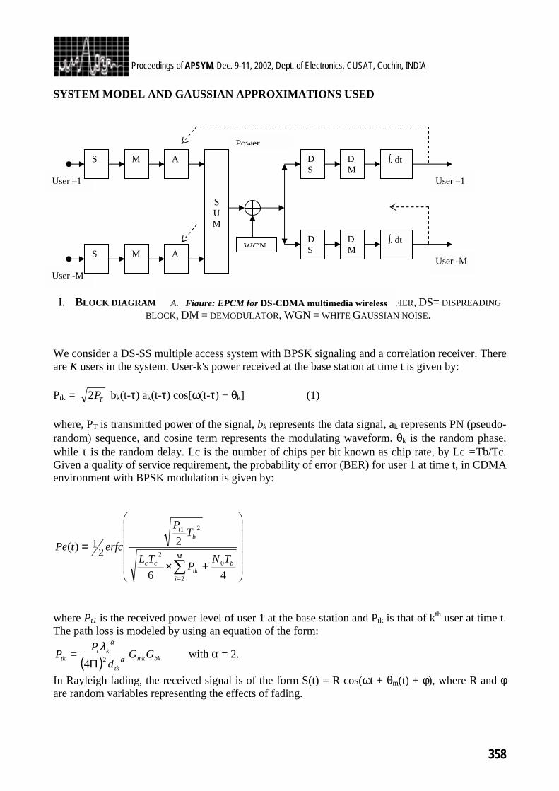
358
Proceedings of APSYM, Dec. 9-11, 2002, Dept. of Electronics, CUSAT, Cochin, INDIA
SYSTEM MODEL AND GAUSSIAN APPROXIMATIONS USED
I. BLOCK DIAGRAM: S = SPREADING BLOCK, M = MODULATOR, A= AMPLIFIER, DS= DISPREADING BLOCK, DM = DEMODULATOR, WGN = WHITE GAUSSIAN NOISE.
We consider a DS-SS multiple access system with BPSK signaling and a correlation receiver. There are K users in the system. User-k's power received at the base station at time t is given by: Ptk = TP2 bk(t-τ) ak(t-τ) cos[ω(t-τ) + θk] (1) where, PT is transmitted power of the signal, bk represents the data signal, ak represents PN (pseudo-random) sequence, and cosine term represents the modulating waveform. θk is the random phase, while τ is the random delay. Lc is the number of chips per bit known as chip rate, by Lc =Tb/Tc. Given a quality of service requirement, the probability of error (BER) for user 1 at time t, in CDMA environment with BPSK modulation is given by:
+×
=
∑= 46
22
1)(0
2
2
21
bM
itk
cc
bt
TNP
TL
TP
erfctPe
where Pt1 is the received power level of user 1 at the base station and Ptk is that of kth user at time t. The path loss is modeled by using an equation of the form:
( ) bkmktk
kttk GG
dP
P α
αλ24Π
= with α = 2.
In Rayleigh fading, the received signal is of the form S(t) = R cos(ωt + θm(t) + φ), where R and φ are random variables representing the effects of fading.
User –1
S M
SUM
D S
D M
∫. dt
User -M
M WGN
S D S
D M
∫. dt
User –1
User -M
A. Figure: EPCM for DS-CDMA multimedia wireless
A
A
Power
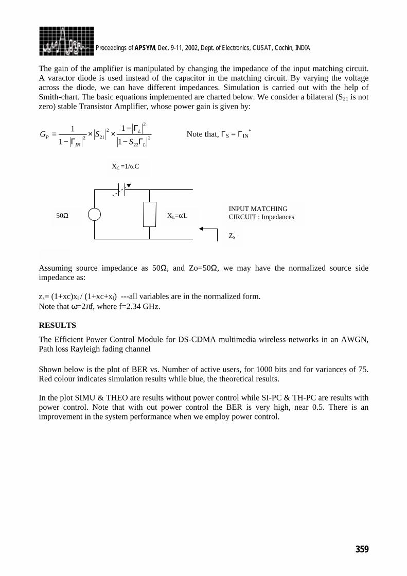
359
Proceedings of APSYM, Dec. 9-11, 2002, Dept. of Electronics, CUSAT, Cochin, INDIA
The gain of the amplifier is manipulated by changing the impedance of the input matching circuit. A varactor diode is used instead of the capacitor in the matching circuit. By varying the voltage across the diode, we can have different impedances. Simulation is carried out with the help of Smith-chart. The basic equations implemented are charted below. We consider a bilateral (S21 is not zero) stable Transistor Amplifier, whose power gain is given by:
222
22
212 1
1
11
L
L
INP
SSG
Γ−
Γ−××
Γ−= Note that, ΓS = ΓIN
*
Assuming source impedance as 50Ω, and Zo=50Ω, we may have the normalized source side impedance as: zs= (1+xc)xl / (1+xc+xl) ---all variables are in the normalized form. Note that ω=2πf, where f=2.34 GHz.
RESULTS
The Efficient Power Control Module for DS-CDMA multimedia wireless networks in an AWGN, Path loss Rayleigh fading channel Shown below is the plot of BER vs. Number of active users, for 1000 bits and for variances of 75. Red colour indicates simulation results while blue, the theoretical results. In the plot SIMU & THEO are results without power control while SI-PC & TH-PC are results with power control. Note that with out power control the BER is very high, near 0.5. There is an improvement in the system performance when we employ power control.
XC =1/ωC
XL=ωL INPUT MATCHING CIRCUIT : Impedances
ZS
50Ω
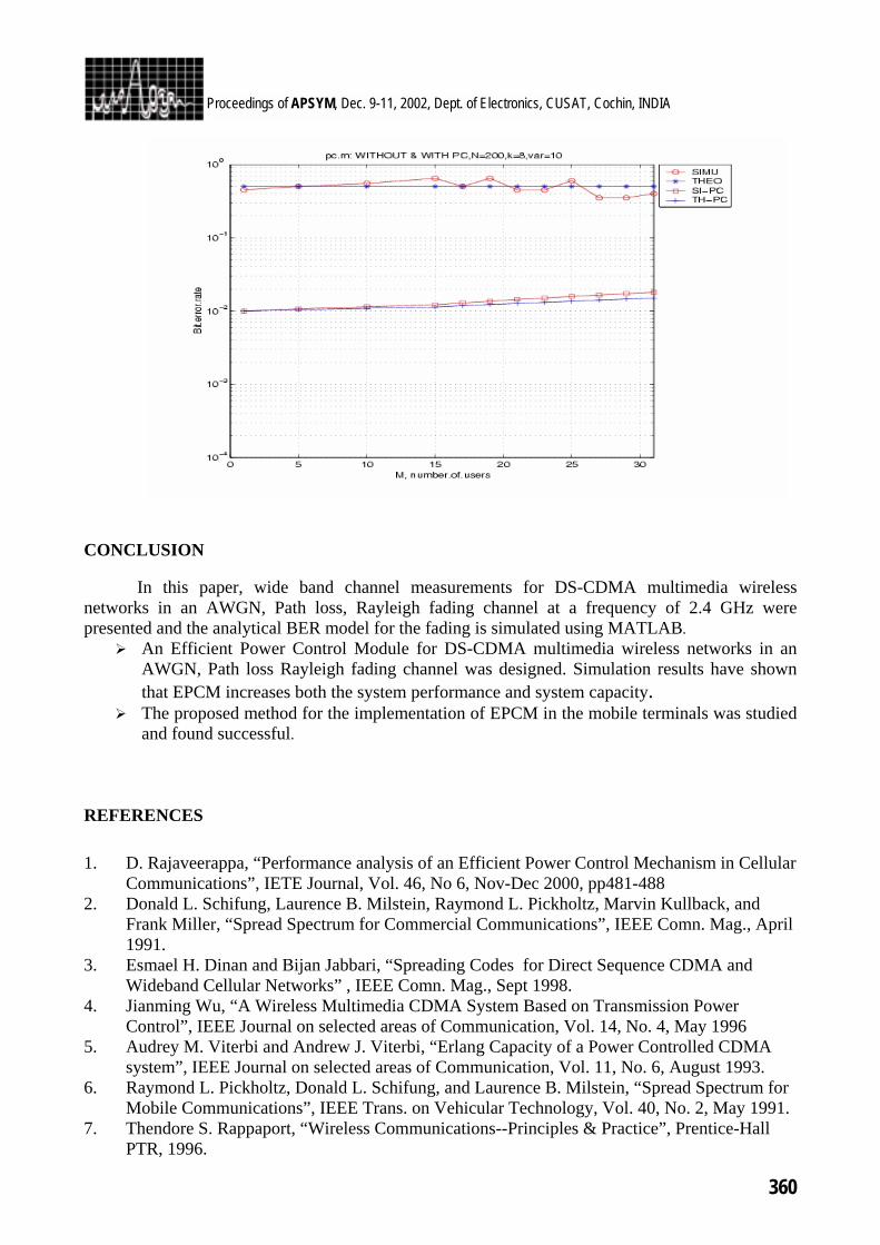
360
Proceedings of APSYM, Dec. 9-11, 2002, Dept. of Electronics, CUSAT, Cochin, INDIA
CONCLUSION
In this paper, wide band channel measurements for DS-CDMA multimedia wireless networks in an AWGN, Path loss, Rayleigh fading channel at a frequency of 2.4 GHz were presented and the analytical BER model for the fading is simulated using MATLAB.
An Efficient Power Control Module for DS-CDMA multimedia wireless networks in an AWGN, Path loss Rayleigh fading channel was designed. Simulation results have shown that EPCM increases both the system performance and system capacity.
The proposed method for the implementation of EPCM in the mobile terminals was studied and found successful.
REFERENCES 1. D. Rajaveerappa, “Performance analysis of an Efficient Power Control Mechanism in Cellular
Communications”, IETE Journal, Vol. 46, No 6, Nov-Dec 2000, pp481-488 2. Donald L. Schifung, Laurence B. Milstein, Raymond L. Pickholtz, Marvin Kullback, and
Frank Miller, “Spread Spectrum for Commercial Communications”, IEEE Comn. Mag., April 1991.
3. Esmael H. Dinan and Bijan Jabbari, “Spreading Codes for Direct Sequence CDMA and Wideband Cellular Networks” , IEEE Comn. Mag., Sept 1998.
4. Jianming Wu, “A Wireless Multimedia CDMA System Based on Transmission Power Control”, IEEE Journal on selected areas of Communication, Vol. 14, No. 4, May 1996
5. Audrey M. Viterbi and Andrew J. Viterbi, “Erlang Capacity of a Power Controlled CDMA system”, IEEE Journal on selected areas of Communication, Vol. 11, No. 6, August 1993.
6. Raymond L. Pickholtz, Donald L. Schifung, and Laurence B. Milstein, “Spread Spectrum for Mobile Communications”, IEEE Trans. on Vehicular Technology, Vol. 40, No. 2, May 1991.
7. Thendore S. Rappaport, “Wireless Communications--Principles & Practice”, Prentice-Hall PTR, 1996.
361
Proceedings of APSYM, Dec. 9-11, 2002, Dept. of Electronics, CUSAT, Cochin, INDIA
THE PULSED WIRE METHOD FOR WIGGLER FIELD MAPPING
Ravi A.V. Kumar, K. K. Mohandas and K. K. Jain
Institute For Plasma Research, Bhat, Gandhinagar 382 428, Gujarat
The Pulsed wire technique is used as an alternative method for magnetic field measurements. It has an added advantage over conventional Hall-probe method, specially for measurements of magnetic field profiles of long wigglers used in current single-pass Free-Electron Lasers. It is based on the simple principle that when a current pulse of appropriate pulse-width is passed through a stretched wire, placed in close proximity of a magnetic field, the wire experiences a kick. The amplitude of the displacement of the wire being proportional to the magnetic field. This experiment attempts to optimize the parameters of the pulsed-wire technique using a single magnet prior to measurements on longer wigglers used in the FEL experiment that are currently underway at Institute For Plasma Research. The results show that the pulsed wire system has a linear dependency on magnetic field with a calibration factor of 215.47 mV/kGauss within the range of magnetic field investigated (0.5 to 1.8 kGauss).
INTRODUCTION
Pulsed wire technique was first used by Warren in 1988 [1] and then by many other groups for measurement of the magnetic field profiles in wigglers used in Free-Electron Lasers [2-4]. Use of Hall probe for such measurement is very time consuming because in order to scan a Hall probe over the entire length of the wiggler not only consumes a lot of time, but the inherent alignment problems of the hall probe induces errors in field measurement. Also to determine the field integrals and the electron beam drifts, it is necessary to measure the vertical field and horizontal field and integrated twice. But a single measurement using the pulsed wire methods which requires a few milliseconds is sufficient to establish the first and second integral of the field. The pulse wire technique is quite different from competing magnetic field measuring techniques and it has particular advantages that can be important in specific cases like in free electron laser. A thin wire is stretched between two supports in the region where the field is to be measured and a current pulse is passed through the wire. A force proportional to the product of the current in the wire in the field perpendicular to the wire is exerted on the wire. The force generates a deflection of the wire that progresses to both ends of the wire in the form of the wave. An appropriately designed sensor, usually a laser-photodiode combination, at one end detects the amplitude and time dependence of the deflection in the wire. In our experiment, we employed the simplest arrangement in which we use only one magnet in an attempt to optimize the experimental setup and establish a relationship between the deflection of the wire and the magnetic field. The traveling wave packets associated with the wire deflection travel to both ends with acoustic wave velocity. A detector which is placed at a point away from the magnet detects these transverse
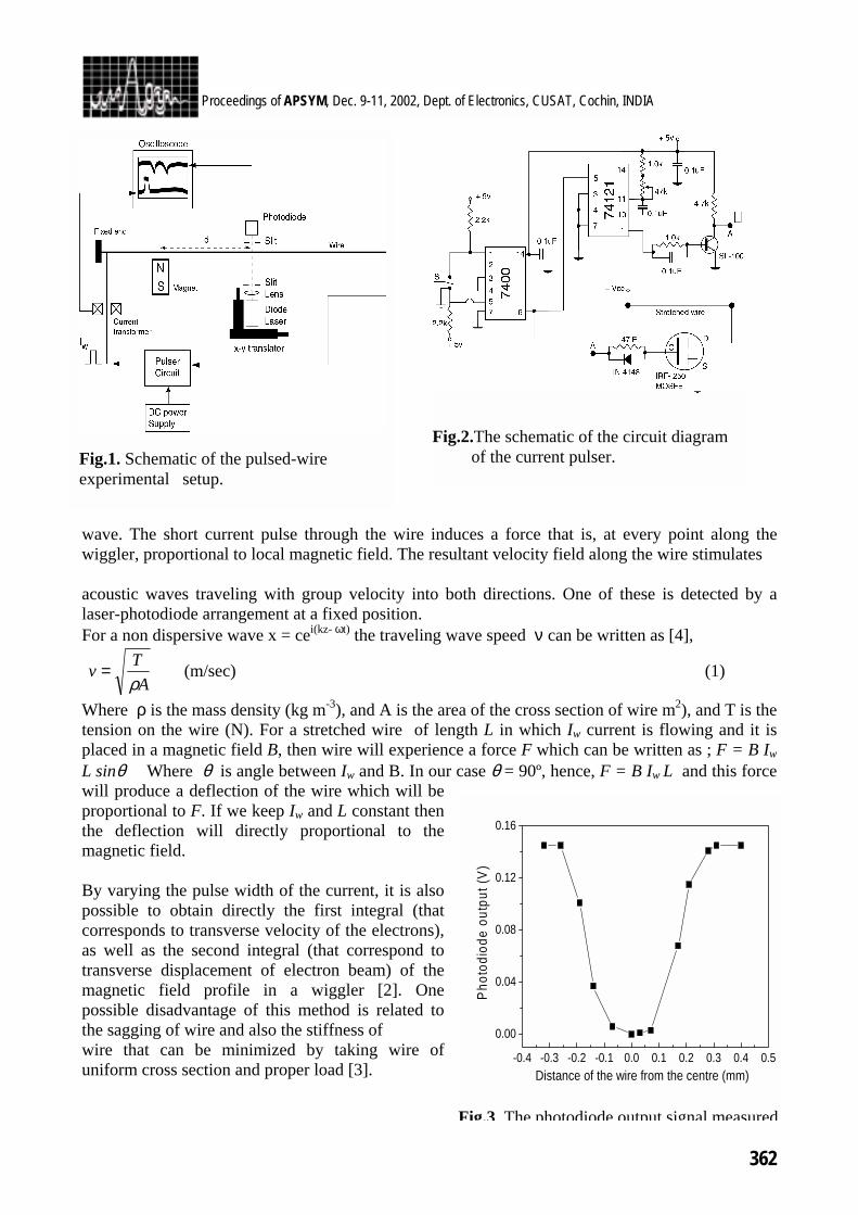
362
Proceedings of APSYM, Dec. 9-11, 2002, Dept. of Electronics, CUSAT, Cochin, INDIA
Fig.1. Schematic of the pulsed-wire experimental setup.
Fig.2.The schematic of the circuit diagram of the current pulser.
-0.4 -0.3 -0.2 -0.1 0.0 0.1 0.2 0.3 0.4 0.5
0.00
0.04
0.08
0.12
0.16
Pho
todi
ode
outp
ut (V
)
Distance of the wire from the centre (mm)
Fig.3 The photodiode output signal measured
wave. The short current pulse through the wire induces a force that is, at every point along the wiggler, proportional to local magnetic field. The resultant velocity field along the wire stimulates acoustic waves traveling with group velocity into both directions. One of these is detected by a laser-photodiode arrangement at a fixed position. For a non dispersive wave x = cei(kz- ωt) the traveling wave speed ν can be written as [4],
A
Tvρ
= (m/sec) (1)
Where ρ is the mass density (kg m-3), and A is the area of the cross section of wire m2), and T is the tension on the wire (N). For a stretched wire of length L in which Iw current is flowing and it is placed in a magnetic field B, then wire will experience a force F which can be written as ; F = B Iw L sinθ Where
θ is angle between Iw and B. In our case θ = 90º, hence, F = B Iw L and this force will produce a deflection of the wire which will be proportional to F. If we keep Iw and L constant then the deflection will directly proportional to the magnetic field. By varying the pulse width of the current, it is also possible to obtain directly the first integral (that corresponds to transverse velocity of the electrons), as well as the second integral (that correspond to transverse displacement of electron beam) of the magnetic field profile in a wiggler [2]. One possible disadvantage of this method is related to the sagging of wire and also the stiffness of wire that can be minimized by taking wire of uniform cross section and proper load [3].
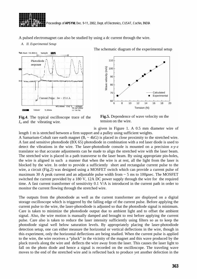
363
Proceedings of APSYM, Dec. 9-11, 2002, Dept. of Electronics, CUSAT, Cochin, INDIA
Fig.4. The typical oscilloscope trace of theIw and the vibrating wire.
A pulsed electromagnet can also be studied by using a dc current through the wire.
A. II. Experimental Setup The schematic diagram of the experimental setup
is given in Figure 1. A 0.5 mm diameter wire of
length 1 m is stretched between a firm support and a pulley using sufficient weights. A Samarium-Cobalt rare earth magnet (Br ~ 4kG) is placed in close proximity to the stretched wire. A fast and sensitive photodiode (BX 65) photodiode in combination with a red laser diode is used to detect the vibrations in the wire. The laser-photodiode console is mounted on a precision x-y-z translator so that accurate adjustments can be made to align the stretched wire with the laser beam. The stretched wire is placed in a path transverse to the laser beam. By using appropriate pin-holes, the wire is aligned in such a manner that when the wire is at rest, all the light from the laser is blocked by the wire. In order to provide a sufficiently short and rectangular current pulse to the wire, a circuit (Fig.2) was designed using a MOSFET switch which can provide a current pulse of maximum 30 A peak current and an adjustable pulse width from ~ 5 ms to 100µsec. The MOSFET switched the current provided by a 180 V, 12A DC power supply through the wire for the required time. A fast current transformer of sensitivity 0.1 V/A is introduced in the current path in order to monitor the current flowing through the stretched wire. The outputs from the photodiode as well as the current transformer are displayed on a digital storage oscilloscope which is triggered by the falling edge of the current pulse. Before applying the current pulse to the wire, the laser-photodiode is adjusted so that the photodiode signal is minimum. Care is taken to minimize the photodiode output due to ambient light and to offset the ambient signal. Also, the wire motion is manually damped and brought to rest before applying the current pulse. Care also is taken to reduce the laser intensity sufficiently using filters so as to keep the photodiode signal well below saturation levels. By appropriately placing the laser-photodiode detection setup, one can either measure the horizontal or vertical deflections in the wire, though in this experiment, only the horizontal deflections are being studied. When the current pulse is applied to the wire, the wire receives a “pluck” in the vicinity of the magnet and this wave produced by the pluck travels along the wire and deflects the wire away from the laser. This causes the laser light to fall on the photo diode and hence a signal is recorded on the oscilloscope. The traveling wave moves to the end of the stretched wire and is reflected back to produce yet another defection in the
6 8 10 12 14 16 18 2060
70
80
90
100
110
Calculated Experimental
Wav
e ve
loci
ty (m
/s)
Tension (N)
Fig.5. Dependence of wave velocity on the tension on the wire.
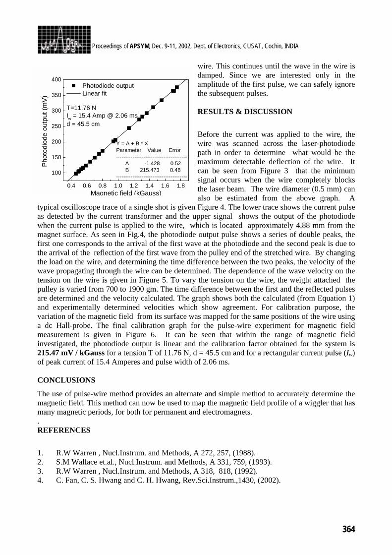
364
Proceedings of APSYM, Dec. 9-11, 2002, Dept. of Electronics, CUSAT, Cochin, INDIA
0.4 0.6 0.8 1.0 1.2 1.4 1.6 1.8
100
150
200
250
300
350
400
T=11.76 NIw = 15.4 Amp @ 2.06 ms d = 45.5 cm
Y = A + B * XParameter Value Error--------------------------------------- A -1.428 0.52 B 215.473 0.48---------------------------------------
Photodiode output Linear fit
Pho
todi
ode
outp
ut (m
V)
Magnetic field (kGauss)
wire. This continues until the wave in the wire is damped. Since we are interested only in the amplitude of the first pulse, we can safely ignore the subsequent pulses. RESULTS & DISCUSSION
Before the current was applied to the wire, the wire was scanned across the laser-photodiode path in order to determine what would be the maximum detectable deflection of the wire. It can be seen from Figure 3 that the minimum signal occurs when the wire completely blocks the laser beam. The wire diameter (0.5 mm) can also be estimated from the above graph. A
typical oscilloscope trace of a single shot is given Figure 4. The lower trace shows the current pulse as detected by the current transformer and the upper signal shows the output of the photodiode when the current pulse is applied to the wire, which is located approximately 4.88 mm from the magnet surface. As seen in Fig.4, the photodiode output pulse shows a series of double peaks, the first one corresponds to the arrival of the first wave at the photodiode and the second peak is due to the arrival of the reflection of the first wave from the pulley end of the stretched wire. By changing the load on the wire, and determining the time difference between the two peaks, the velocity of the wave propagating through the wire can be determined. The dependence of the wave velocity on the tension on the wire is given in Figure 5. To vary the tension on the wire, the weight attached the pulley is varied from 700 to 1900 gm. The time difference between the first and the reflected pulses are determined and the velocity calculated. The graph shows both the calculated (from Equation 1) and experimentally determined velocities which show agreement. For calibration purpose, the variation of the magnetic field from its surface was mapped for the same positions of the wire using a dc Hall-probe. The final calibration graph for the pulse-wire experiment for magnetic field measurement is given in Figure 6. It can be seen that within the range of magnetic field investigated, the photodiode output is linear and the calibration factor obtained for the system is 215.47 mV / kGauss for a tension T of 11.76 N, d = 45.5 cm and for a rectangular current pulse (Iw) of peak current of 15.4 Amperes and pulse width of 2.06 ms. CONCLUSIONS
The use of pulse-wire method provides an alternate and simple method to accurately determine the magnetic field. This method can now be used to map the magnetic field profile of a wiggler that has many magnetic periods, for both for permanent and electromagnets. . REFERENCES
1. R.W Warren , Nucl.Instrum. and Methods, A 272, 257, (1988). 2. S.M Wallace et.al., Nucl.Instrum. and Methods, A 331, 759, (1993). 3. R.W Warren , Nucl.Instrum. and Methods, A 318, 818, (1992). 4. C. Fan, C. S. Hwang and C. H. Hwang, Rev.Sci.Instrum.,1430, (2002).
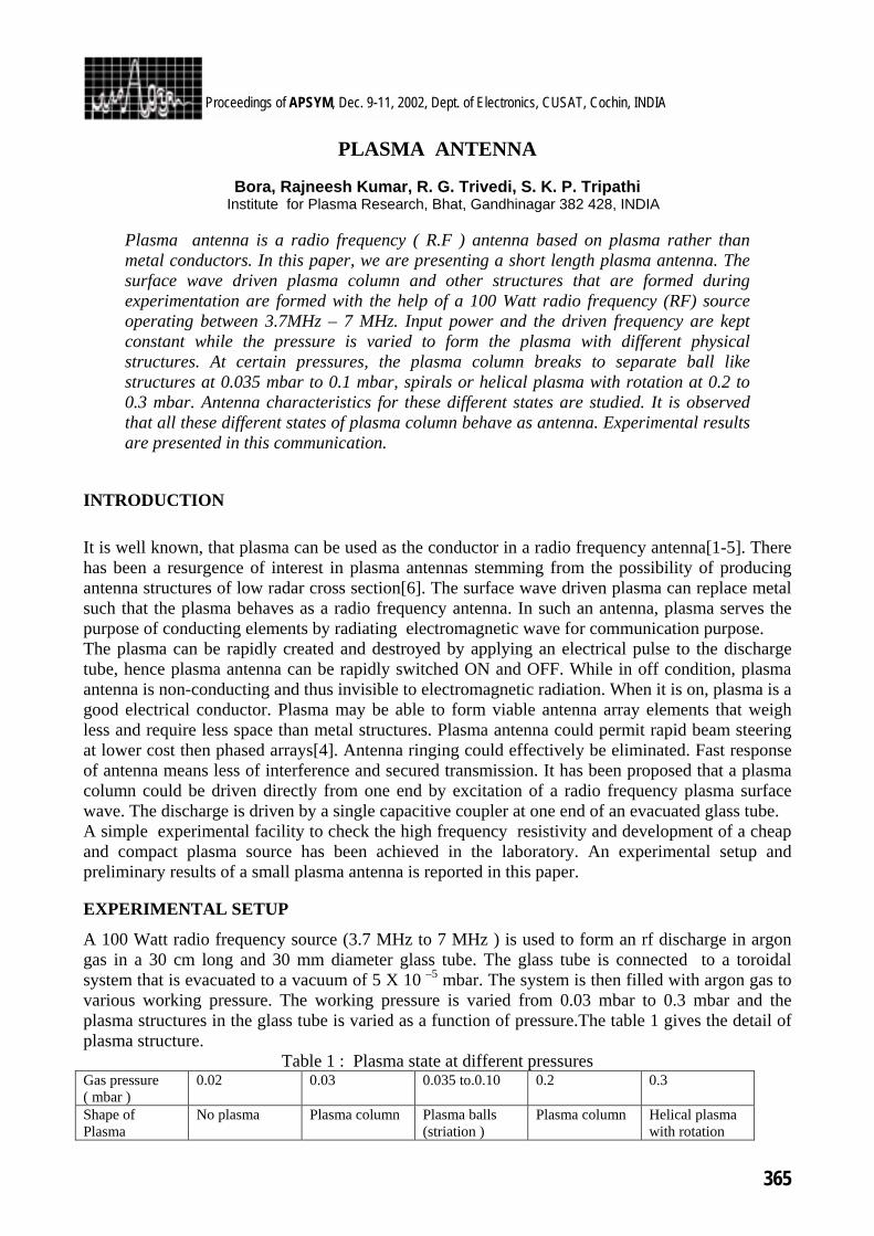
365
Proceedings of APSYM, Dec. 9-11, 2002, Dept. of Electronics, CUSAT, Cochin, INDIA
PLASMA ANTENNA
Bora, Rajneesh Kumar, R. G. Trivedi, S. K. P. Tripathi Institute for Plasma Research, Bhat, Gandhinagar 382 428, INDIA
Plasma antenna is a radio frequency ( R.F ) antenna based on plasma rather than metal conductors. In this paper, we are presenting a short length plasma antenna. The surface wave driven plasma column and other structures that are formed during experimentation are formed with the help of a 100 Watt radio frequency (RF) source operating between 3.7MHz – 7 MHz. Input power and the driven frequency are kept constant while the pressure is varied to form the plasma with different physical structures. At certain pressures, the plasma column breaks to separate ball like structures at 0.035 mbar to 0.1 mbar, spirals or helical plasma with rotation at 0.2 to 0.3 mbar. Antenna characteristics for these different states are studied. It is observed that all these different states of plasma column behave as antenna. Experimental results are presented in this communication.
INTRODUCTION It is well known, that plasma can be used as the conductor in a radio frequency antenna[1-5]. There has been a resurgence of interest in plasma antennas stemming from the possibility of producing antenna structures of low radar cross section[6]. The surface wave driven plasma can replace metal such that the plasma behaves as a radio frequency antenna. In such an antenna, plasma serves the purpose of conducting elements by radiating electromagnetic wave for communication purpose. The plasma can be rapidly created and destroyed by applying an electrical pulse to the discharge tube, hence plasma antenna can be rapidly switched ON and OFF. While in off condition, plasma antenna is non-conducting and thus invisible to electromagnetic radiation. When it is on, plasma is a good electrical conductor. Plasma may be able to form viable antenna array elements that weigh less and require less space than metal structures. Plasma antenna could permit rapid beam steering at lower cost then phased arrays[4]. Antenna ringing could effectively be eliminated. Fast response of antenna means less of interference and secured transmission. It has been proposed that a plasma column could be driven directly from one end by excitation of a radio frequency plasma surface wave. The discharge is driven by a single capacitive coupler at one end of an evacuated glass tube. A simple experimental facility to check the high frequency resistivity and development of a cheap and compact plasma source has been achieved in the laboratory. An experimental setup and preliminary results of a small plasma antenna is reported in this paper. EXPERIMENTAL SETUP
A 100 Watt radio frequency source (3.7 MHz to 7 MHz ) is used to form an rf discharge in argon gas in a 30 cm long and 30 mm diameter glass tube. The glass tube is connected to a toroidal system that is evacuated to a vacuum of 5 X 10 –5 mbar. The system is then filled with argon gas to various working pressure. The working pressure is varied from 0.03 mbar to 0.3 mbar and the plasma structures in the glass tube is varied as a function of pressure.The table 1 gives the detail of plasma structure.
Table 1 : Plasma state at different pressures Gas pressure ( mbar )
0.02 0.03 0.035 to.0.10
0.2 0.3
Shape of Plasma
No plasma Plasma column Plasma balls (striation )
Plasma column Helical plasma with rotation
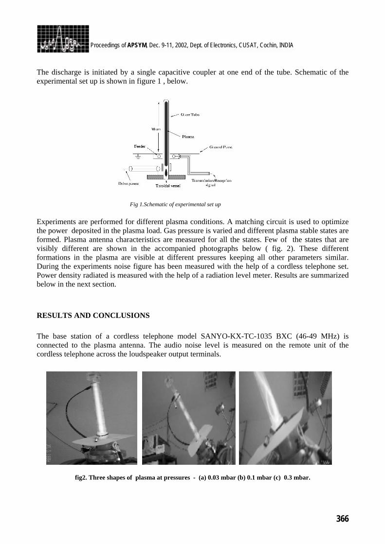
366
Proceedings of APSYM, Dec. 9-11, 2002, Dept. of Electronics, CUSAT, Cochin, INDIA
The discharge is initiated by a single capacitive coupler at one end of the tube. Schematic of the experimental set up is shown in figure 1 , below.
Fig 1.Schematic of experimental set up Experiments are performed for different plasma conditions. A matching circuit is used to optimize the power deposited in the plasma load. Gas pressure is varied and different plasma stable states are formed. Plasma antenna characteristics are measured for all the states. Few of the states that are visibly different are shown in the accompanied photographs below ( fig. 2). These different formations in the plasma are visible at different pressures keeping all other parameters similar. During the experiments noise figure has been measured with the help of a cordless telephone set. Power density radiated is measured with the help of a radiation level meter. Results are summarized below in the next section.
RESULTS AND CONCLUSIONS The base station of a cordless telephone model SANYO-KX-TC-1035 BXC (46-49 MHz) is connected to the plasma antenna. The audio noise level is measured on the remote unit of the cordless telephone across the loudspeaker output terminals.
fig2. Three shapes of plasma at pressures - (a) 0.03 mbar (b) 0.1 mbar (c) 0.3 mbar.
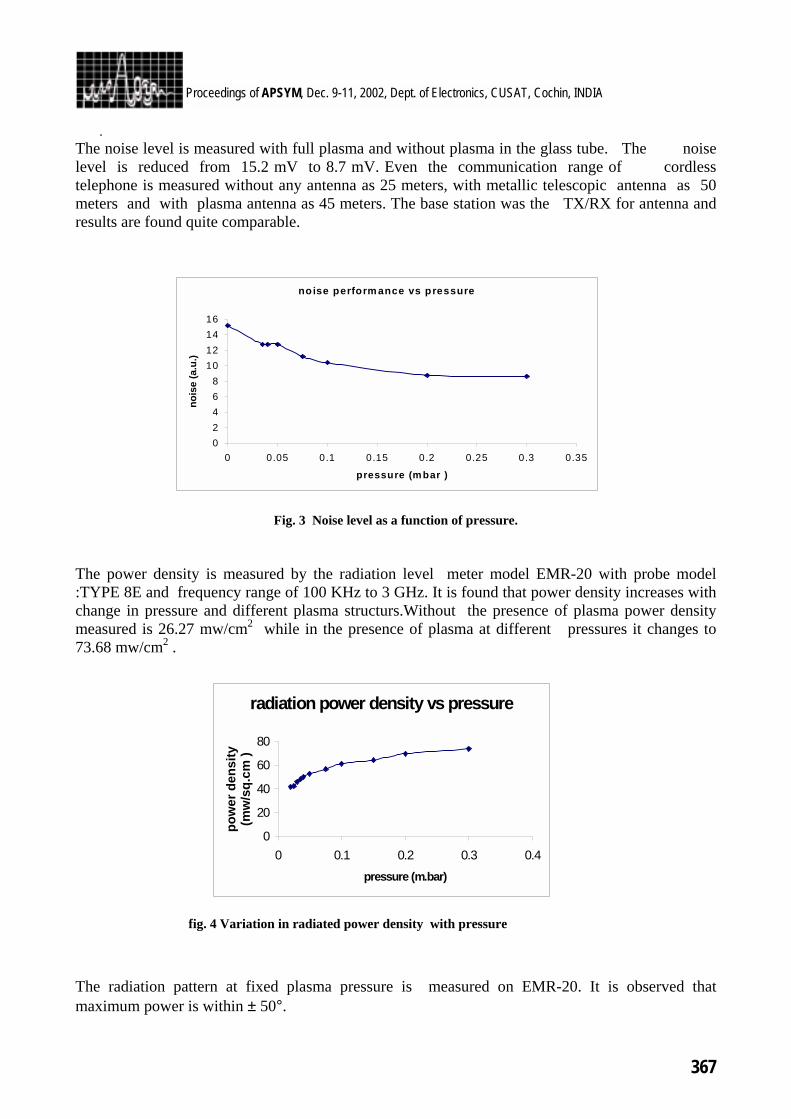
367
Proceedings of APSYM, Dec. 9-11, 2002, Dept. of Electronics, CUSAT, Cochin, INDIA
. The noise level is measured with full plasma and without plasma in the glass tube. The noise level is reduced from 15.2 mV to 8.7 mV. Even the communication range of cordless telephone is measured without any antenna as 25 meters, with metallic telescopic antenna as 50 meters and with plasma antenna as 45 meters. The base station was the TX/RX for antenna and results are found quite comparable.
Fig. 3 Noise level as a function of pressure.
The power density is measured by the radiation level meter model EMR-20 with probe model :TYPE 8E and frequency range of 100 KHz to 3 GHz. It is found that power density increases with change in pressure and different plasma structurs.Without the presence of plasma power density measured is 26.27 mw/cm2 while in the presence of plasma at different pressures it changes to 73.68 mw/cm2 .
fig. 4 Variation in radiated power density with pressure
The radiation pattern at fixed plasma pressure is measured on EMR-20. It is observed that maximum power is within ± 50°.
radiation power density vs pressure
0
20
40
60
80
0 0.1 0.2 0.3 0.4
pressure (m.bar)
pow
er d
ensi
ty
(mw
/sq.
cm )
no ise perform ance vs pressure
02468
10121416
0 0.05 0.1 0.15 0.2 0.25 0.3 0.35
pressure (m bar )
nois
e (a
.u.)
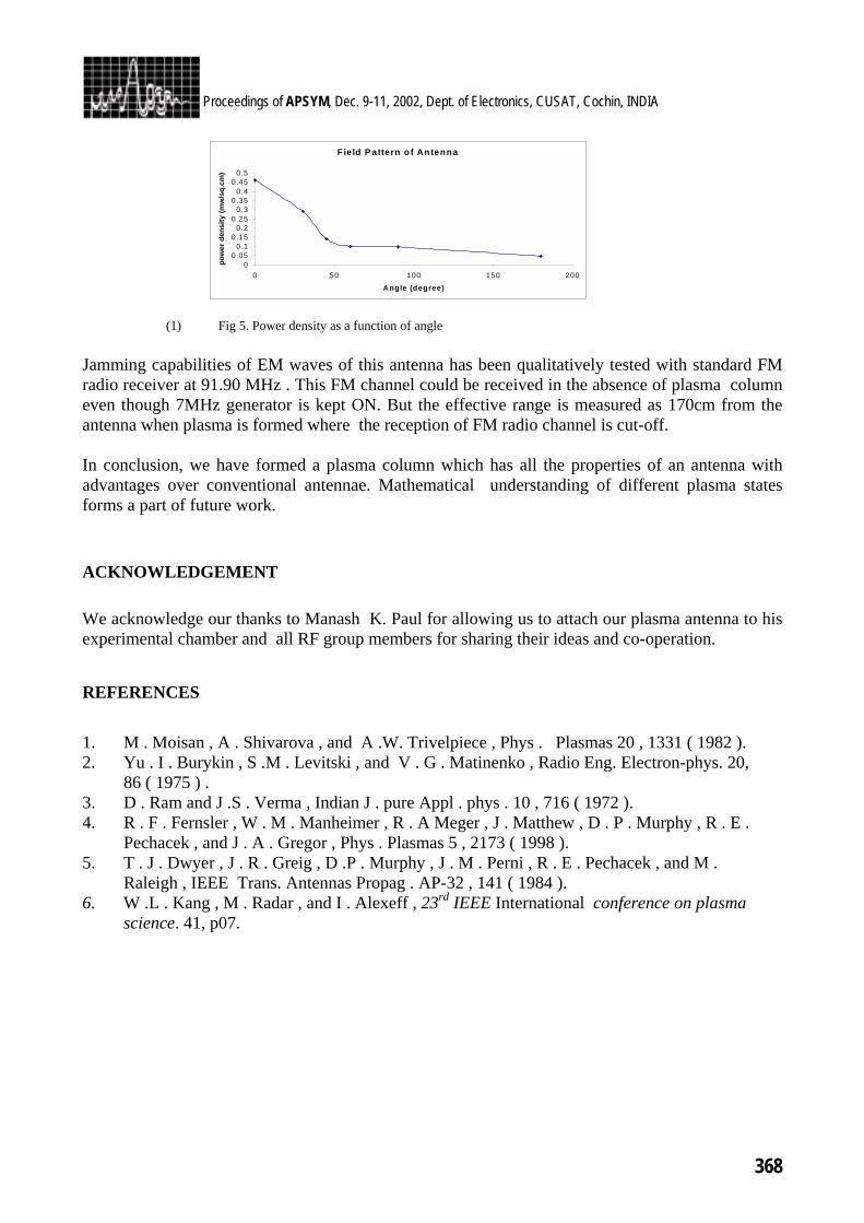
368
Proceedings of APSYM, Dec. 9-11, 2002, Dept. of Electronics, CUSAT, Cochin, INDIA
(1) Fig 5. Power density as a function of angle
Jamming capabilities of EM waves of this antenna has been qualitatively tested with standard FM radio receiver at 91.90 MHz . This FM channel could be received in the absence of plasma column even though 7MHz generator is kept ON. But the effective range is measured as 170cm from the antenna when plasma is formed where the reception of FM radio channel is cut-off. In conclusion, we have formed a plasma column which has all the properties of an antenna with advantages over conventional antennae. Mathematical understanding of different plasma states forms a part of future work.
ACKNOWLEDGEMENT We acknowledge our thanks to Manash K. Paul for allowing us to attach our plasma antenna to his experimental chamber and all RF group members for sharing their ideas and co-operation. REFERENCES
1. M . Moisan , A . Shivarova , and A .W. Trivelpiece , Phys . Plasmas 20 , 1331 ( 1982 ). 2. Yu . I . Burykin , S .M . Levitski , and V . G . Matinenko , Radio Eng. Electron-phys. 20,
86 ( 1975 ) . 3. D . Ram and J .S . Verma , Indian J . pure Appl . phys . 10 , 716 ( 1972 ). 4. R . F . Fernsler , W . M . Manheimer , R . A Meger , J . Matthew , D . P . Murphy , R . E .
Pechacek , and J . A . Gregor , Phys . Plasmas 5 , 2173 ( 1998 ). 5. T . J . Dwyer , J . R . Greig , D .P . Murphy , J . M . Perni , R . E . Pechacek , and M .
Raleigh , IEEE Trans. Antennas Propag . AP-32 , 141 ( 1984 ). 6. W .L . Kang , M . Radar , and I . Alexeff , 23rd IEEE International conference on plasma
science. 41, p07.
Field P attern of Antenna
00.05
0.10.15
0.20.25
0.30.35
0.40.45
0.5
0 50 100 150 200
Angle (degree)
pow
er d
ensi
ty (m
w/s
q.cm
)
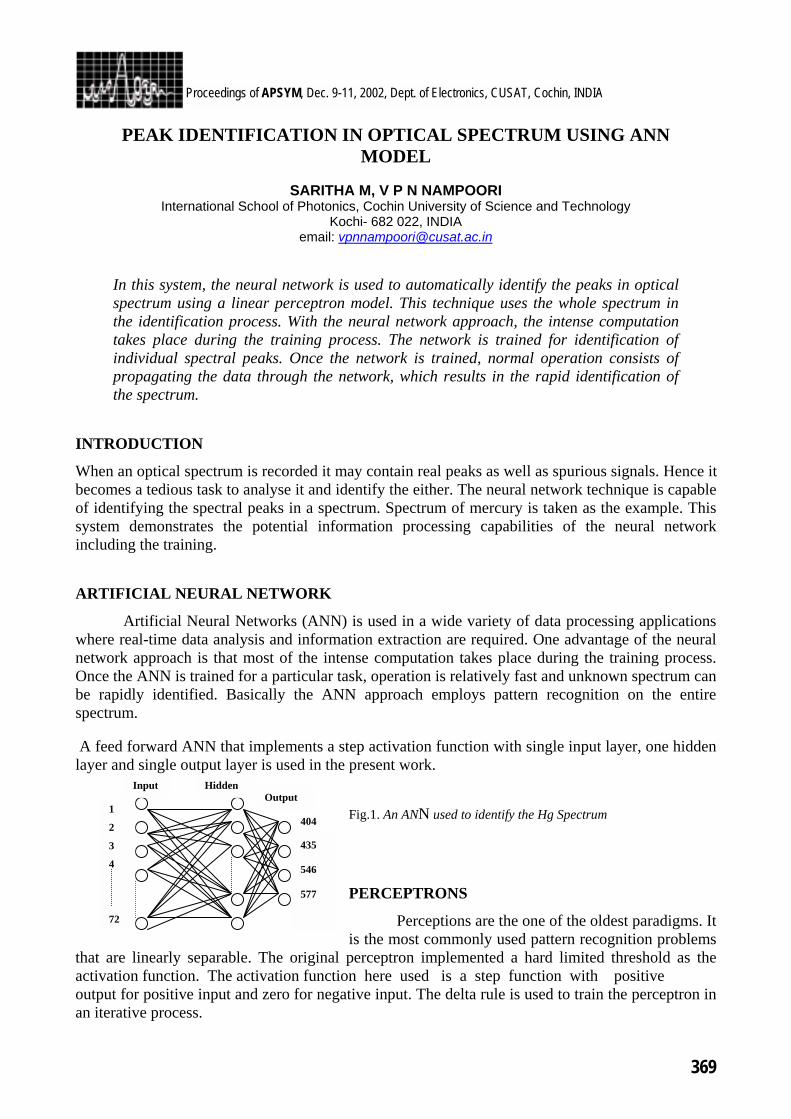
369
Proceedings of APSYM, Dec. 9-11, 2002, Dept. of Electronics, CUSAT, Cochin, INDIA
PEAK IDENTIFICATION IN OPTICAL SPECTRUM USING ANN MODEL
SARITHA M, V P N NAMPOORI
International School of Photonics, Cochin University of Science and Technology Kochi- 682 022, INDIA
email: [email protected]
In this system, the neural network is used to automatically identify the peaks in optical spectrum using a linear perceptron model. This technique uses the whole spectrum in the identification process. With the neural network approach, the intense computation takes place during the training process. The network is trained for identification of individual spectral peaks. Once the network is trained, normal operation consists of propagating the data through the network, which results in the rapid identification of the spectrum.
INTRODUCTION
When an optical spectrum is recorded it may contain real peaks as well as spurious signals. Hence it becomes a tedious task to analyse it and identify the either. The neural network technique is capable of identifying the spectral peaks in a spectrum. Spectrum of mercury is taken as the example. This system demonstrates the potential information processing capabilities of the neural network including the training. ARTIFICIAL NEURAL NETWORK
Artificial Neural Networks (ANN) is used in a wide variety of data processing applications where real-time data analysis and information extraction are required. One advantage of the neural network approach is that most of the intense computation takes place during the training process. Once the ANN is trained for a particular task, operation is relatively fast and unknown spectrum can be rapidly identified. Basically the ANN approach employs pattern recognition on the entire spectrum. A feed forward ANN that implements a step activation function with single input layer, one hidden layer and single output layer is used in the present work.
Fig.1. An ANN used to identify the Hg Spectrum PERCEPTRONS
Perceptions are the one of the oldest paradigms. It is the most commonly used pattern recognition problems
that are linearly separable. The original perceptron implemented a hard limited threshold as the activation function. The activation function here used is a step function with positive output for positive input and zero for negative input. The delta rule is used to train the perceptron in an iterative process.
404
435 546 577
1
2
3
4
72
Input HiddenOutput
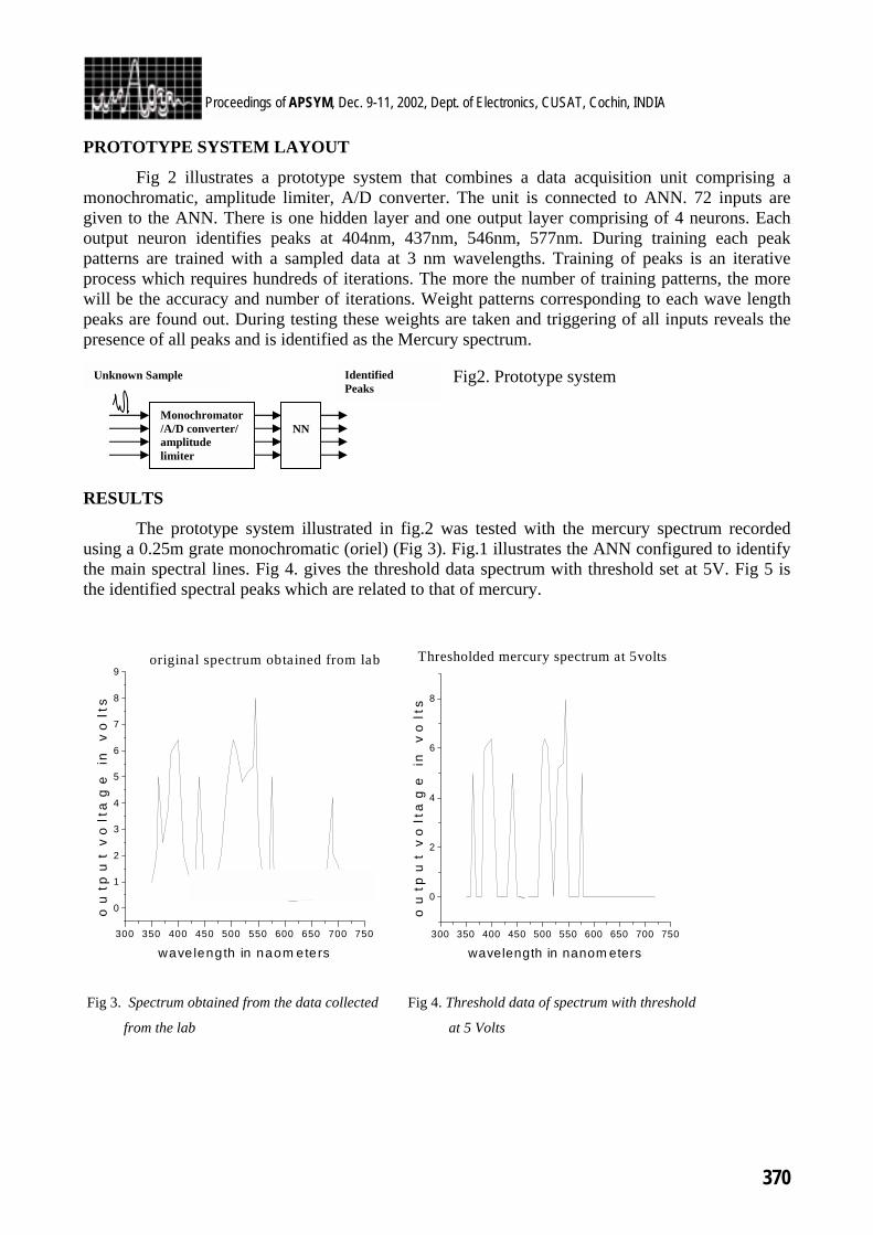
370
Proceedings of APSYM, Dec. 9-11, 2002, Dept. of Electronics, CUSAT, Cochin, INDIA
PROTOTYPE SYSTEM LAYOUT
Fig 2 illustrates a prototype system that combines a data acquisition unit comprising a monochromatic, amplitude limiter, A/D converter. The unit is connected to ANN. 72 inputs are given to the ANN. There is one hidden layer and one output layer comprising of 4 neurons. Each output neuron identifies peaks at 404nm, 437nm, 546nm, 577nm. During training each peak patterns are trained with a sampled data at 3 nm wavelengths. Training of peaks is an iterative process which requires hundreds of iterations. The more the number of training patterns, the more will be the accuracy and number of iterations. Weight patterns corresponding to each wave length peaks are found out. During testing these weights are taken and triggering of all inputs reveals the presence of all peaks and is identified as the Mercury spectrum.
Fig2. Prototype system
RESULTS
The prototype system illustrated in fig.2 was tested with the mercury spectrum recorded using a 0.25m grate monochromatic (oriel) (Fig 3). Fig.1 illustrates the ANN configured to identify the main spectral lines. Fig 4. gives the threshold data spectrum with threshold set at 5V. Fig 5 is the identified spectral peaks which are related to that of mercury.
300 350 400 450 500 550 600 650 700 750
0
1
2
3
4
5
6
7
8
9original spectrum obtained from lab
ou
tpu
t v
olt
ag
e i
n v
olt
s
wave length in naom eters300 350 400 450 500 550 600 650 700 750
0
2
4
6
8
Thresholded mercury spectrum at 5volts
ou
tpu
t v
olt
ag
e i
n v
olt
s
wavelength in nanom eters
Fig 3. Spectrum obtained from the data collected Fig 4. Threshold data of spectrum with threshold
from the lab at 5 Volts
Monochromator/A/D converter/ amplitude limiter
NN
Identified Peaks
Unknown Sample
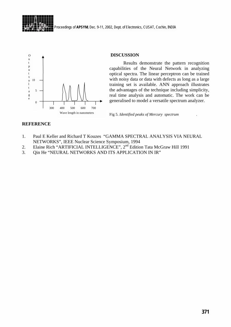
371
Proceedings of APSYM, Dec. 9-11, 2002, Dept. of Electronics, CUSAT, Cochin, INDIA
DISCUSSION
Results demonstrate the pattern recognition capabilities of the Neural Network in analyzing optical spectra. The linear perceptron can be trained with noisy data or data with defects as long as a large training set is available. ANN approach illustrates the advantages of the technique including simplicity, real time analysis and automatic. The work can be generalised to model a versatile spectrum analyzer. Fig 5. Identified peaks of Mercury spectrum .
REFERENCE 1. Paul E Keller and Richard T Kouzes “GAMMA SPECTRAL ANALYSIS VIA NEURAL
NETWORKS”, IEEE Nuclear Science Symposium, 1994 2. Elaine Rich “ARTIFICIAL INTELLIGENCE”, 2nd Edition Tata McGraw Hill 1991 3. Qin He “NEURAL NETWORKS AND ITS APPLICATION IN IR”
300 500 600 400 700
0
5
10
Wave length in nanometers
Output voltage
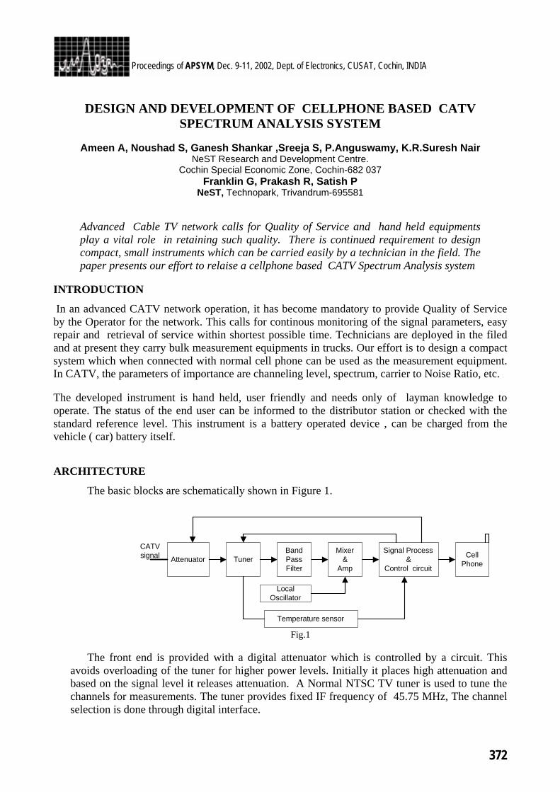
372
Proceedings of APSYM, Dec. 9-11, 2002, Dept. of Electronics, CUSAT, Cochin, INDIA
DESIGN AND DEVELOPMENT OF CELLPHONE BASED CATV
SPECTRUM ANALYSIS SYSTEM
Ameen A, Noushad S, Ganesh Shankar ,Sreeja S, P.Anguswamy, K.R.Suresh Nair NeST Research and Development Centre.
Cochin Special Economic Zone, Cochin-682 037 Franklin G, Prakash R, Satish P
NeST, Technopark, Trivandrum-695581
Advanced Cable TV network calls for Quality of Service and hand held equipments play a vital role in retaining such quality. There is continued requirement to design compact, small instruments which can be carried easily by a technician in the field. The paper presents our effort to relaise a cellphone based CATV Spectrum Analysis system
INTRODUCTION
In an advanced CATV network operation, it has become mandatory to provide Quality of Service by the Operator for the network. This calls for continous monitoring of the signal parameters, easy repair and retrieval of service within shortest possible time. Technicians are deployed in the filed and at present they carry bulk measurement equipments in trucks. Our effort is to design a compact system which when connected with normal cell phone can be used as the measurement equipment. In CATV, the parameters of importance are channeling level, spectrum, carrier to Noise Ratio, etc.
The developed instrument is hand held, user friendly and needs only of layman knowledge to operate. The status of the end user can be informed to the distributor station or checked with the standard reference level. This instrument is a battery operated device , can be charged from the vehicle ( car) battery itself.
ARCHITECTURE
The basic blocks are schematically shown in Figure 1.
Fig.1
The front end is provided with a digital attenuator which is controlled by a circuit. This avoids overloading of the tuner for higher power levels. Initially it places high attenuation and based on the signal level it releases attenuation. A Normal NTSC TV tuner is used to tune the channels for measurements. The tuner provides fixed IF frequency of 45.75 MHz, The channel selection is done through digital interface.
Attenuator TunerSignal Process
&Control circuit
CellPhone
Temperature sensor
CATVsignal
BandPassFilter
Mixer&
Amp
LocalOscillator
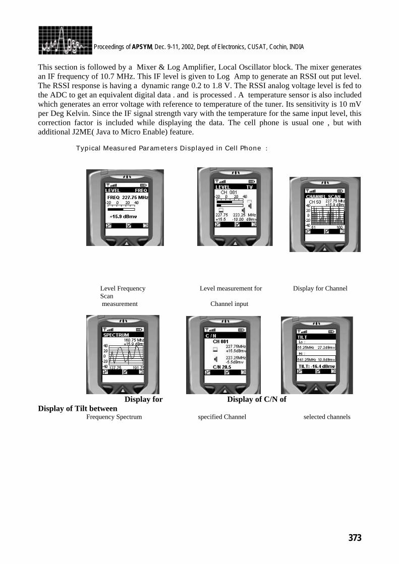
373
Proceedings of APSYM, Dec. 9-11, 2002, Dept. of Electronics, CUSAT, Cochin, INDIA
This section is followed by a Mixer & Log Amplifier, Local Oscillator block. The mixer generates an IF frequency of 10.7 MHz. This IF level is given to Log Amp to generate an RSSI out put level. The RSSI response is having a dynamic range 0.2 to 1.8 V. The RSSI analog voltage level is fed to the ADC to get an equivalent digital data . and is processed . A temperature sensor is also included which generates an error voltage with reference to temperature of the tuner. Its sensitivity is 10 mV per Deg Kelvin. Since the IF signal strength vary with the temperature for the same input level, this correction factor is included while displaying the data. The cell phone is usual one , but with additional J2ME( Java to Micro Enable) feature.
Typical Measured Parameters Displayed in Cell Phone :
Level Frequency Level measurement for Display for Channel Scan measurement Channel input
Display for Display of C/N of Display of Tilt between Frequency Spectrum specified Channel selected channels
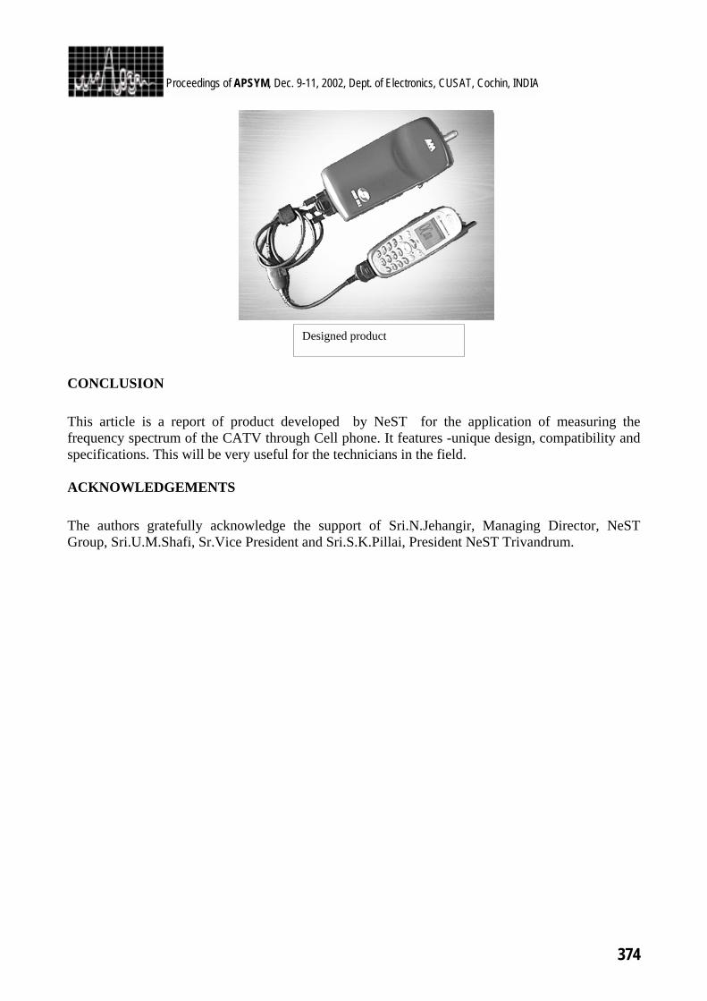
374
Proceedings of APSYM, Dec. 9-11, 2002, Dept. of Electronics, CUSAT, Cochin, INDIA
CONCLUSION
This article is a report of product developed by NeST for the application of measuring the frequency spectrum of the CATV through Cell phone. It features -unique design, compatibility and specifications. This will be very useful for the technicians in the field.
ACKNOWLEDGEMENTS
The authors gratefully acknowledge the support of Sri.N.Jehangir, Managing Director, NeST Group, Sri.U.M.Shafi, Sr.Vice President and Sri.S.K.Pillai, President NeST Trivandrum.
Designed product
375
Proceedings of APSYM, Dec. 9-11, 2002, Dept. of Electronics, CUSAT, Cochin, INDIA
376
Proceedings of APSYM, Dec. 9-11, 2002, Dept. of Electronics, CUSAT, Cochin, INDIA
377
Proceedings of APSYM, Dec. 9-11, 2002, Dept. of Electronics, CUSAT, Cochin, INDIA
378
Proceedings of APSYM, Dec. 9-11, 2002, Dept. of Electronics, CUSAT, Cochin, INDIA
378
Proceedings of APSYM, Dec. 9-11, 2002, Dept. of Electronics, CUSAT, Cochin, INDIA
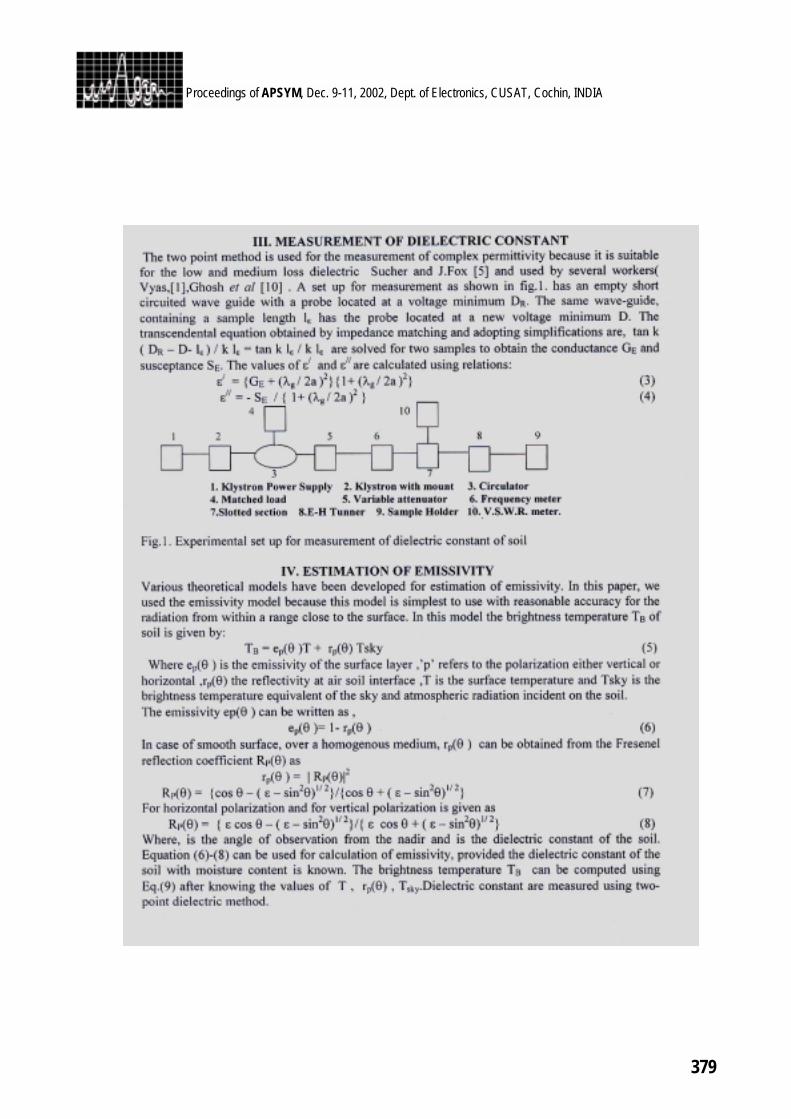
379
Proceedings of APSYM, Dec. 9-11, 2002, Dept. of Electronics, CUSAT, Cochin, INDIA
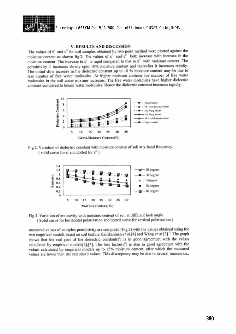
380
Proceedings of APSYM, Dec. 9-11, 2002, Dept. of Electronics, CUSAT, Cochin, INDIA

381
Proceedings of APSYM, Dec. 9-11, 2002, Dept. of Electronics, CUSAT, Cochin, INDIA

382
Proceedings of APSYM, Dec. 9-11, 2002, Dept. of Electronics, CUSAT, Cochin, INDIA

384
Proceedings of APSYM, Dec. 9-11, 2002, Dept. of Electronics, CUSAT, Cochin, INDIA
385
Proceedings of APSYM, Dec. 9-11, 2002, Dept. of Electronics, CUSAT, Cochin, INDIA
Invited Talk 1 TIME-DOMAIN CFIE FOR THE ANALYSIS OF TRANSIENT
SCATTERING FROM ARBITRARILY SHAPED 3-D CONDUCTING OBJECTS
Tapan Kumar Sarkar1 and Baek Ho Jung2
1 Department of Electrical Engineering and Computer Science
Syracuse University, Syracuse, NY 13244 e-mail: [email protected]
2 Department of Information and Communication Engineering Hoseo University, Asan 336-795, South Korea
e-mail: [email protected]
A time-domain combined field integral equation (CFIE) is presented to obtain the transient scattering response from arbitrarily shaped three-dimensional (3-D) conducting bodies. This formulation is based on a linear combination of the time-domain electric field integral equation (EFIE) with the magnetic field integral equation (MFIE). The time derivative of the magnetic vector potential in EFIE is approximated using a central finite difference approximation for the derivative and the scalar potential is averaged over time. The time-domain CFIE approach produces results that are accurate and stable when solving for transient scattering responses from conducting objects. The incident spectrum of the field may contain frequency components, which may correspond to the internal resonance of the structure. For the numerical solution, we consider both the explicit and implicit scheme and use two different kinds of Gaussian pulses, which may or may not contain frequencies corresponding to the internal resonance. Numerical results for the EFIE, MFIE, and CFIE are presented and compared with those obtained from the inverse discrete Fourier transform (IDFT) of the frequency-domain CFIE solution.
INTRODUCTION
The solution technique developed in this work is capable of handling either an explicit or implicit scheme of the electric field integral equation(EFIE), magnetic field integral equation (MFIE), and combined field integral equation (CFIE). TIME DOMAIN COMBINED FIELD INTEGRAL EQUATION
Let S denote the surface of a perfectly conducting body, which may be closed or open, illuminated by a transient electromagnetic wave. This incident wave induces a surface current J on S . We have
φ∇−∂∂−=
tAJE s )( (1)
where A and φ are the magnetic vector potential and the electric scalar potential given by

386
Proceedings of APSYM, Dec. 9-11, 2002, Dept. of Electronics, CUSAT, Cochin, INDIA
( )∫ ′=
SSd
RrJtrA τ
πµ ,'
4),( (2)
∫ ∫ ′′⋅∇ ′−=S
SdtdR
trJtrτ
πεφ
0
)','(4
1),( (3)
Where cRt /−=τ is a retarded time, 'rrR −= represents the distance between the observation point r and the source point 'r , c is the velocity of wave propagation in the surrounding medium, and µ and ε are permeability and permittivity of that space, respectively. Since the total tangential electric field is zero on the conducting surface, we have
0)]([ tan =+ JEE si , Sr ∈ . (4) Combining (1) and (4) gives
[ ] tantan
iEtA =
∇+∂∂ φ , Sr ∈ (5)
where iE is the incident electric field on the scatter and the subscript ‘tan’ denotes the tangential component. Eq. (5) with (2) and (3) constitutes a time-domain EFIE from which the unknown current ( )trJ , may be determined. For the numerical solution of the time-domain integral equation we divide the time axis into equal intervals of segment t∆ and define titi ∆= . The time derivative in (5) can be approximated by the forward or backward finite difference for the explicit and implicit solutions of a EFIE. We now present a formulation to improve the accuracy and stability of the implicit solution. We write (5) at time 2/1−= itt
[ ] tan2/1tan
11 ),(2
),(),(),(),(−
−− =
∇+∇+∆−
iiiiii trEtrtr
ttrAtrA φφ (6)
where we use the central finite difference for the time derivative associated with the vector potential term and the time averaging for the scalar potential term. For the MFIE, we obtain
JJHHn si =+× )]([ˆ (7) where n represents an outward-directed unit vector normal to the surface S at a field point,
iH is the incident field, and sH is the scattered magnetic field due to the induced currents J . The scattered field can be written in terms of the potential functions, and is given by
AJH s ×∇=µ1)( (8)
Where the magnetic vector potential A is given in (2). We note that (7) along with (8) represents the magnetic field integral equation.
Combining (7) and (8) with (2), we obtain
∫ ′×∇×+×=S
i SdRrJntrHntrJ ),'(
41ˆ),(ˆ),( τπ
. (9)
Extracting the Cauchy principal value from the curl term, we may write the second term of the right-hand side in (9) as

387
Proceedings of APSYM, Dec. 9-11, 2002, Dept. of Electronics, CUSAT, Cochin, INDIA
∫∫ ′×∇×+=′×∇×0
),'(41ˆ
2),(),'(
41ˆ
SSSd
RrJntrJSd
RrJn τ
πτ
π (10)
Where 0S denotes the surface with the contribution due to the singularity at 'rr = or 0=R , removed from the surface S . Now, by substituting (10) into (9), we obtain
),(ˆ),'(41ˆ
2),(
0
trHnSdRrJntrJ i
S×=′×∇×− ∫
τπ
. (11)
In (11), the curl operator is taken inside the integral, which is allowed as long as 0≠R . The combined field integral equation is obtained by combining the EFIE and MFIE,
respectively. Both these equations, the EFIE and MFIE, fail to give a unique solution when the frequency spectrum of the incident wave includes internal resonant frequencies of the object. To overcome this problem, CFIE can be used. The time-domain CFIE is obtained by means of a linear combination of the EFIE with the MFIE through
]ˆ[])[1()](ˆ[)]()[1( tantaniiss HnEJHnJJE ×+−=×−+−− κηκκηκ (12)
Where κ is the parameter of linear combination, which is between 0 (EFIE) and 1 (MFIE), and η is the wave impedance of the space. Using planar triangular patches to approximate the structure. The triangular patches have the ability to conform to any geometrical surface of the boundary. We can obtain a matrix equation for the time-domain CFIE
[ ] ( )[ ] ( )[ ]iminmn ttI βα = (13) where
Mmn
Emnmn κηαακα +−= )1( (14)
( ) ( ) ( )iMmi
Emim ttt κηββκβ +−= )1( . (15)
Also the matrix [ ]mnα is not function of time, and hence the inverse of the matrix need to be computed only once at the beginning of the computation step NUMERICAL RESULTS
In this section, we present the numerical results for a sphere. The field is incident from 0=φ and 0=θ with zk ˆˆ −= and xE ˆ0 = . Figure 1 show the explicit and the implicit
solutions when a Gaussian plane wave with =T 2 lm is incident on the sphere. This incident pulse contains several internal resonant frequencies of the sphere.
CONCLUSION
In this paper, we have presented a time-domain combined field integral equation to obtain the solution of transient scattering from three-dimensional closed conducting structures. The numerical results have been compared with those from EFIE, MFIE, and the inverse Fourier transform solution of the frequency-domain result. The agreement with the result from the IDFT solution calculated using CFIE in frequency domain was very good. Transient responses computed by the CFIE have been found to be very accurate and quite stable. However, the explicit CFIE blows up. The implicit scheme of time-domain CFIE presented here does not break down when the incident wave includes several resonant frequencies. In addition, the IDFT of the frequency-domain CFIE solutions shows better agreement with the
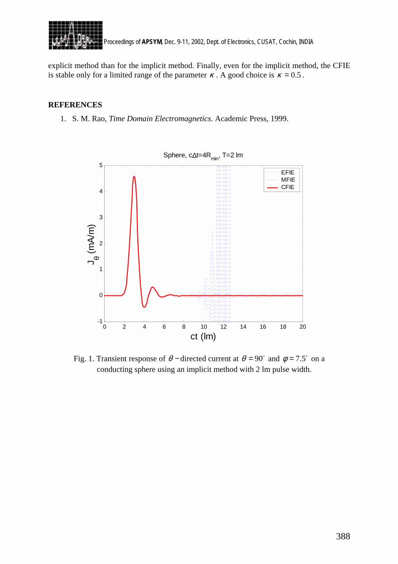
388
Proceedings of APSYM, Dec. 9-11, 2002, Dept. of Electronics, CUSAT, Cochin, INDIA
explicit method than for the implicit method. Finally, even for the implicit method, the CFIE is stable only for a limited range of the parameter κ . A good choice is 5.0=κ . REFERENCES
1. S. M. Rao, Time Domain Electromagnetics. Academic Press, 1999.
0 2 4 6 8 10 12 14 16 18 20-1
0
1
2
3
4
5Sphere, c∆t=4Rmin, T=2 lm
ct (lm)
J θ (m
A/m
)
EFIEMFIECFIE
Fig. 1. Transient response of −θ directed current at 90=θ and 5.7=φ on a conducting sphere using an implicit method with 2 lm pulse width.
389
Proceedings of APSYM, Dec. 9-11, 2002, Dept. of Electronics, CUSAT, Cochin, INDIA
Invited Talk 2
390
Proceedings of APSYM, Dec. 9-11, 2002, Dept. of Electronics, CUSAT, Cochin, INDIA
391
Proceedings of APSYM, Dec. 9-11, 2002, Dept. of Electronics, CUSAT, Cochin, INDIA
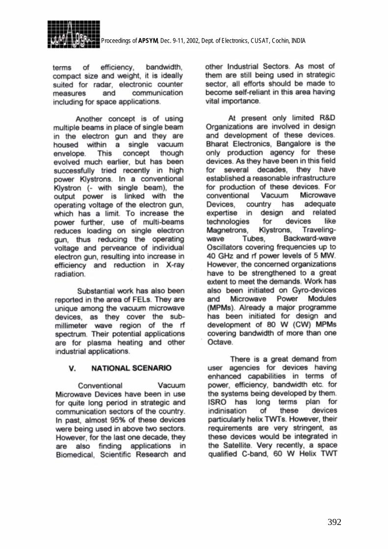
392
Proceedings of APSYM, Dec. 9-11, 2002, Dept. of Electronics, CUSAT, Cochin, INDIA
393
Proceedings of APSYM, Dec. 9-11, 2002, Dept. of Electronics, CUSAT, Cochin, INDIA
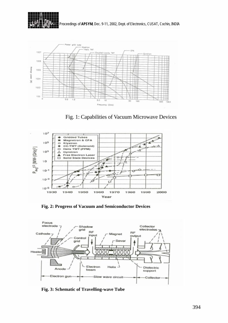
394
Proceedings of APSYM, Dec. 9-11, 2002, Dept. of Electronics, CUSAT, Cochin, INDIA
Fig. 1: Capabilities of Vacuum Microwave Devices
Fig. 2: Progress of Vacuum and Semiconductor Devices
Fig. 3: Schematic of Travelling-wave Tube
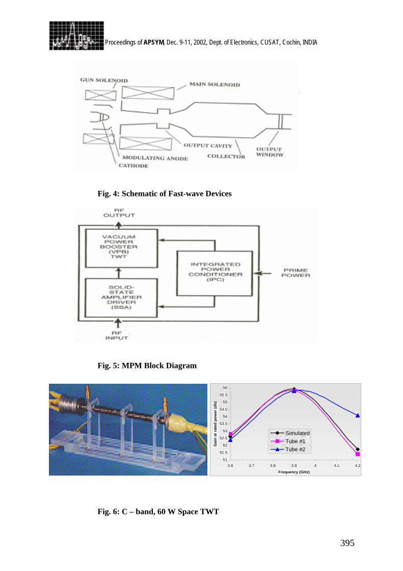
395
Proceedings of APSYM, Dec. 9-11, 2002, Dept. of Electronics, CUSAT, Cochin, INDIA
Fig. 4: Schematic of Fast-wave Devices
Fig. 5: MPM Block Diagram
Fig. 6: C – band, 60 W Space TWT
51
51.5
52
52.5
53
53.5
54
54.5
55
55.5
56
3.6 3.7 3.8 3.9 4 4.1 4.2Frequency (GHz)
Gai
n at
rate
d po
wer
(db)
SimulatedTube #1Tube #2
396
Proceedings of APSYM, Dec. 9-11, 2002, Dept. of Electronics, CUSAT, Cochin, INDIA
Invited Talk 3
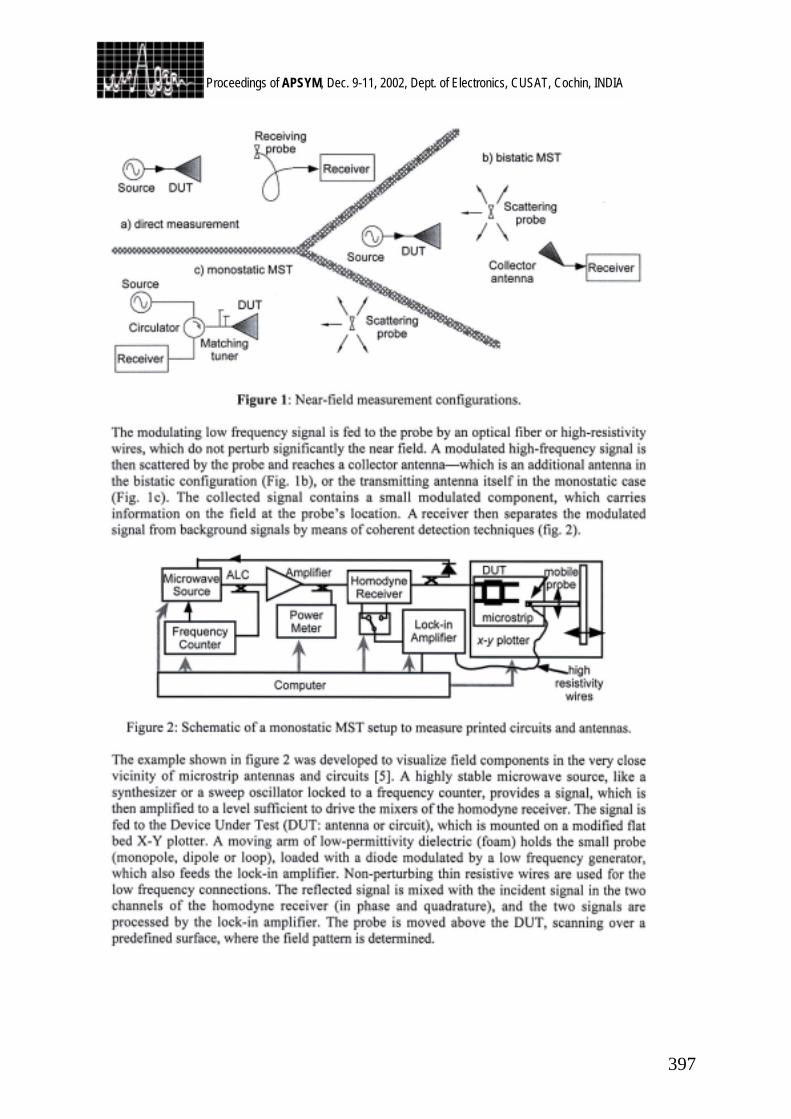
397
Proceedings of APSYM, Dec. 9-11, 2002, Dept. of Electronics, CUSAT, Cochin, INDIA
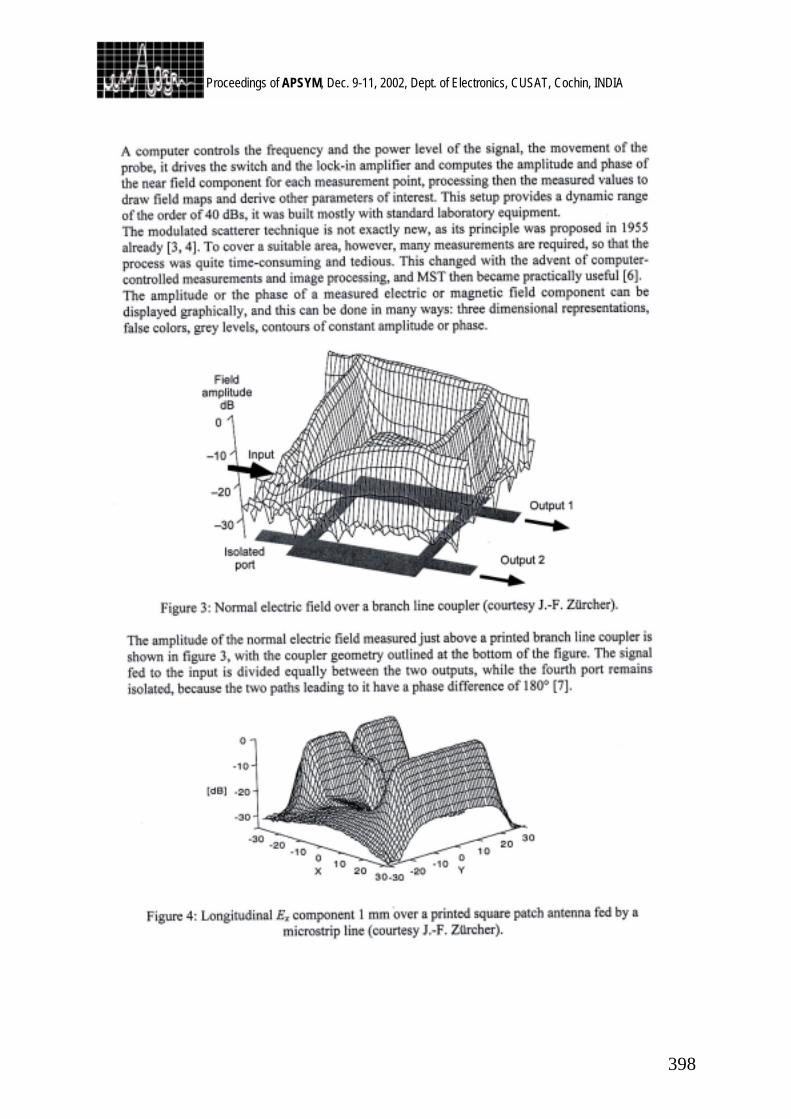
398
Proceedings of APSYM, Dec. 9-11, 2002, Dept. of Electronics, CUSAT, Cochin, INDIA
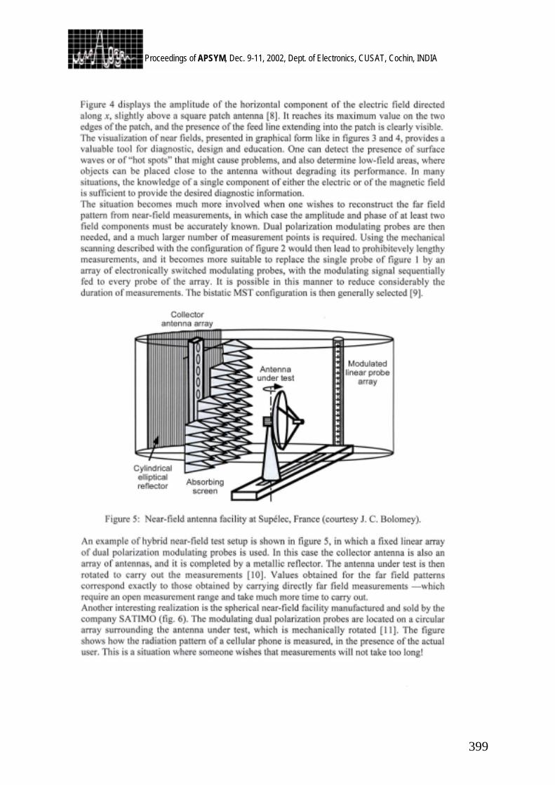
399
Proceedings of APSYM, Dec. 9-11, 2002, Dept. of Electronics, CUSAT, Cochin, INDIA
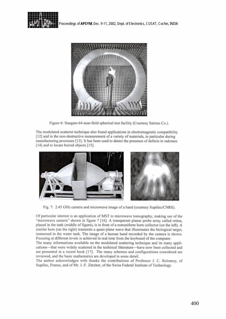
400
Proceedings of APSYM, Dec. 9-11, 2002, Dept. of Electronics, CUSAT, Cochin, INDIA
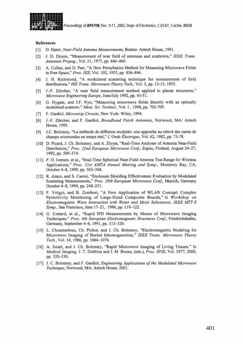
401
Proceedings of APSYM, Dec. 9-11, 2002, Dept. of Electronics, CUSAT, Cochin, INDIA
402
Proceedings of APSYM, Dec. 9-11, 2002, Dept. of Electronics, CUSAT, Cochin, INDIA
Invited Talk 4
GROWTH OF MICROWAVES
G.P .Srivastava
Department of Electronic Science, University of Delhi South Campus, New Delhi -110 021
Jagdish Chandra Bose began activities in field of microwaves in 1893. Oliver Lodge's Paper on Henrich Hertz had inspired him so much he conducted research on radio-waves. Although he did not get any facility or money from the college, he made the equipment needed within three months and embarked upon his research. He degenerated millimeter waves through electric discharge. He used a Galena crystal as the receiver which was used as detector. He succeeded in demonstrating reflection, refraction, total internal reflection, double refraction and polarization by crystals of Tourmaline and Nemalite. Microwave generators were fabricated in thirties. In 1933 Cleeton and Williams
conducted research on inversion spectrum of ammonia. They claimed they have observed absorption due to inversion of ammonia. The success of this experiment could have provided experimental verification of Quantum Mechanics. Though Cleeton and Williams felt they have observed the absorption, no one else believed their experiment as the equipment was very crude.
However microwave technology developed during Second World War due to its application in detecting aeroplanes. Concentrated effort was made by Lincoln Laboratory of Massachusetts Institute of Technology.
The research activity in Microwaves was extended by Townes and Gordy in U.S.A. The research resulted in the development of Masers which resulted in development of LASERS. Interesting work was done on hydrogen bonded molecules using microwave spectrometer.
Almost at the same time applications of microwaves for communication was initiated. Communication technology was developed and improved. Analog modulation was replaced by digital modulation. Lot of improvements have been made in communication technology. Various types of multiplexing techniques were developed. Spread spectrum technology was also useful.

403
Proceedings of APSYM, Dec. 9-11, 2002, Dept. of Electronics, CUSAT, Cochin, INDIA
Millimetre-Wave Technology also has been developed which has many advantages. Cellular Communication Technology have also developed which is facing competition from Wireless Local Loop.
Many other applications of microwaves have also been made. Application in
Electronic-Warfare, Radiometry, Radar, Collision-Avoidance technology, microwave oven etc., are being widely used.
404
Proceedings of APSYM, Dec. 9-11, 2002, Dept. of Electronics, CUSAT, Cochin, INDIA
Invited Talk 5
ON EM WELL-LOGGING SENSORS AND DATA
INTERPRETATION
Jaideva C. Goswami Schlumberger Technology Corporation
110 Schlumberger Drive, Sugar Land, Texas 77478, U.S.A. [email protected] or [email protected]
This paper begins with an overview of oilfield exploration methods. Efficient design of resistivity and magnetic resonance sensors using a combination of finite element method and an optimal control technique is discussed, followed by a brief review of data inversion using differential evolutionary algorithm.
The primary goal of oilfield exploration is to identify and quantify hydrocarbon reservoirs and to estimate their producibility. Characterization of earth formation is a complex problem and no single measurement can effectively do so. Formation properties, such as porosity, permeability, oil-saturation, anisotropy, and rock matrix, are estimated by combining measurements from various sensors. These measurements, among others, include voltage (resistivity-type sensor), T2-distribution (nuclear magnetic resonance sensor), velocity (acoustic sensor), time/energy spectra (nuclear sensor), and pressure (mechanical sensor). In a typical exploration environment, a hole, about 15 to 30 cms in diameter is drilled in the earth formation to a depth that may extend to a few kilometers. The measuring instrument may be attached to the drill-bit or may be lowered in the borehole using a long current carrying cable. Designing these instruments poses many challenges since they must withstand high temperatures (175oc), high pressures (20,000 psi), corrosive fluids, and high mechanical shocks. In addition, the instrument must operate with limited electrical power and must fit inside a small hole. There are thus many challenges in designing a sensor for well-logging applications. In this paper we will focus only on resistivity and nuclear magnetic resonance (NMR) sensors and present an efficient design technique. A typical resistivity sensor consists of several transmitters and receivers, operating at frequencies ranging from a few Hz to a few MHz. By measuring voltage across receiver coils, one can deduce properties of the formation. The nuclear magnetic resonance sensors, on the other hand, involve solving nonlinear static magnetic field as well as the RF field. The measurement of T2-distribution then provides the formation properties.
Once a sensor is designed, it is yet another challenge to interpret the measured data. Inverse problems associated with many geophysical measurements are often nonunique and multimodal. In this paper we briefly discuss a robust method for data inversion using evolutionary algorithm.
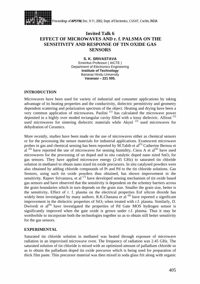
405
Proceedings of APSYM, Dec. 9-11, 2002, Dept. of Electronics, CUSAT, Cochin, INDIA
Invited Talk 6 EFFECT OF MICROWAVES AND r. f. PALSMA ON THE
SENSITIVITY AND RESPONSE OF TIN OXIDE GAS SENSORS
S. K. SRIVASTAVA
Emeritus Professor ( AICTE ) Department of Electronics Engineering
Institute of Technology Banaras Hindu University
Varanasi – 221 005. INTRODUCTION
Microwaves have been used for variety of industrial and consumer applications by taking advantage of its heating properties and the conductivity, dielectric permittivity and geometry dependent scattering and polarization spectrum of the object. Heating and drying have been a very common application of microwaves. Paolini (1) has calculated the microwave power deposited in a highly over moded rectangular cavity filled with a lossy dielectric. Alliout (2) used microwaves for sintering dielectric materials while Akyel (3) used microwaves for dehydration of Ceramics. More recently, studies have been made on the use of microwaves either as chemical sensors or for the processing the sensor materials for industrial applications. Evanescent microwave probes in gas and chemical sensing has been reported by M.Tabib et al(5) Catherine Bernou et al (6) have reported the use of microwaves for sensing humidity. Ciera A et al(4) have used microwaves for the processing of un doped and in situ catalytic doped nano sized SnO2 for gas sensors. They have applied microwave energy (2-45 GHz) to saturated tin chloride solution in methanol to obtain nano sized tin oxide precursors. In situ catalysed powders were also obtained by adding chloride compounds of Pt and Pd to the tin chloride solutions. Gas Sensors, using such tin oxide powders thus obtained, has shown improvement in the sensitivity. Rajeev Srivastava, et al (7) have developed sensing mechanism of tin oxide based gas sensors and have observed that the sensitivity is dependent on the schottey barriers across the grain boundaries which in turn depends on the grain size. Smaller the grain size, better is the sensitivity. Effect of r. f. plasma on the electrical properties Eof silicon dioxide has widely been investigated by many authors. R.K.Chanana et al (8) have reported a significant improvement in the dielectric properties of SiO2 when treated with r.f. plasma. Similarly, D. Dwivedi et al(9) have investigated the properties of Pd Gate MOS hydrogen sensor is significantly improved when the gate oxide is grown under r.f. plasma. Thus it may be worthwhile to incorporate both the technologies together so as to obtain still better sensitivity for the gas sensors. EXPERIMENTAL
Saturated tin chloride solution in methanol was heated through exposure of microwave radiation in an improvised microwave oven. The frequency of radiation was 2.45 GHz. The saturated solution of tin chloride is mixed with an optimized amount of palladium chloride so as to obtain the palladium doped tin oxide precursor which is being used for preparation of thick film paste. Thin precursor material was then mixed in soda glass frit along with organic
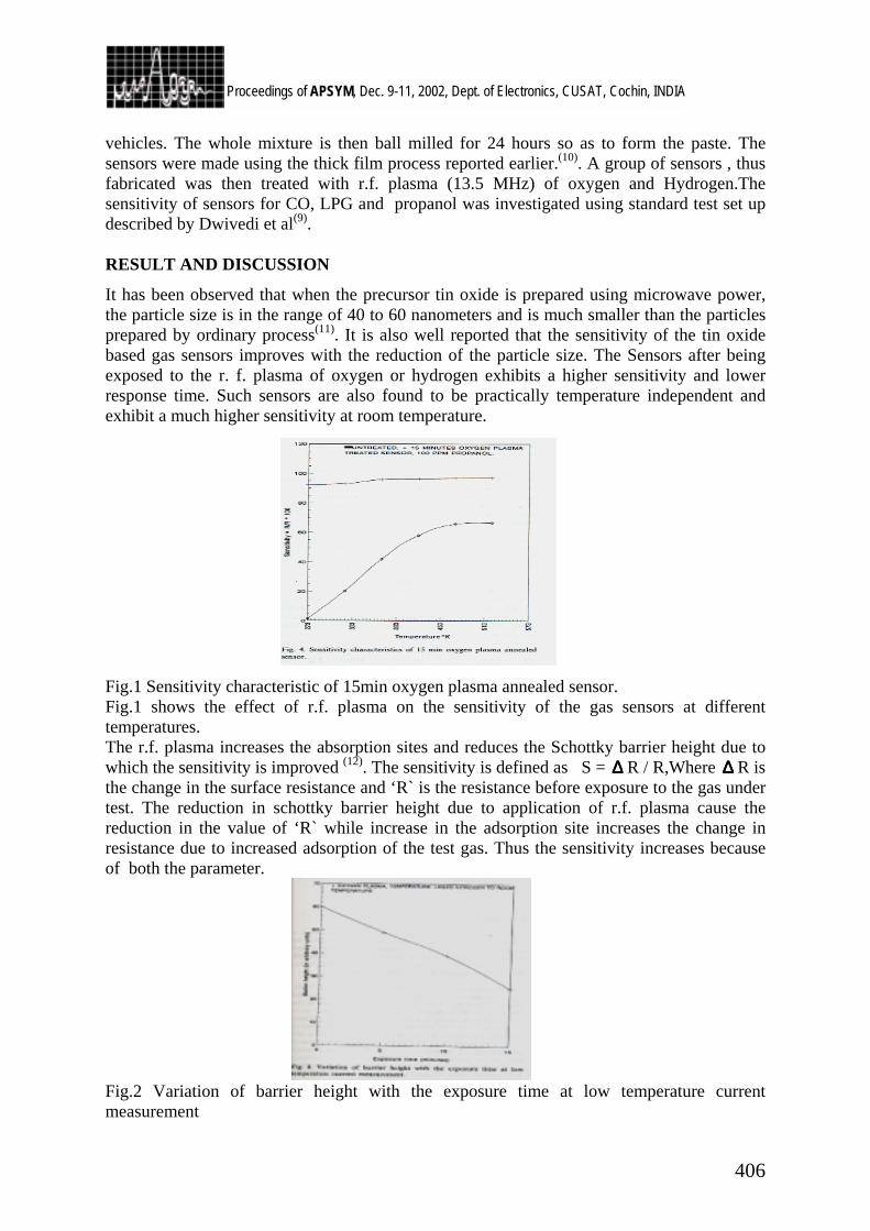
406
Proceedings of APSYM, Dec. 9-11, 2002, Dept. of Electronics, CUSAT, Cochin, INDIA
vehicles. The whole mixture is then ball milled for 24 hours so as to form the paste. The sensors were made using the thick film process reported earlier.(10). A group of sensors , thus fabricated was then treated with r.f. plasma (13.5 MHz) of oxygen and Hydrogen.The sensitivity of sensors for CO, LPG and propanol was investigated using standard test set up described by Dwivedi et al(9). RESULT AND DISCUSSION
It has been observed that when the precursor tin oxide is prepared using microwave power, the particle size is in the range of 40 to 60 nanometers and is much smaller than the particles prepared by ordinary process(11). It is also well reported that the sensitivity of the tin oxide based gas sensors improves with the reduction of the particle size. The Sensors after being exposed to the r. f. plasma of oxygen or hydrogen exhibits a higher sensitivity and lower response time. Such sensors are also found to be practically temperature independent and exhibit a much higher sensitivity at room temperature.
Fig.1 Sensitivity characteristic of 15min oxygen plasma annealed sensor. Fig.1 shows the effect of r.f. plasma on the sensitivity of the gas sensors at different temperatures. The r.f. plasma increases the absorption sites and reduces the Schottky barrier height due to which the sensitivity is improved (12). The sensitivity is defined as S = ∆∆∆∆ R / R,Where ∆∆∆∆ R is the change in the surface resistance and ‘R` is the resistance before exposure to the gas under test. The reduction in schottky barrier height due to application of r.f. plasma cause the reduction in the value of ‘R` while increase in the adsorption site increases the change in resistance due to increased adsorption of the test gas. Thus the sensitivity increases because of both the parameter.
Fig.2 Variation of barrier height with the exposure time at low temperature current measurement
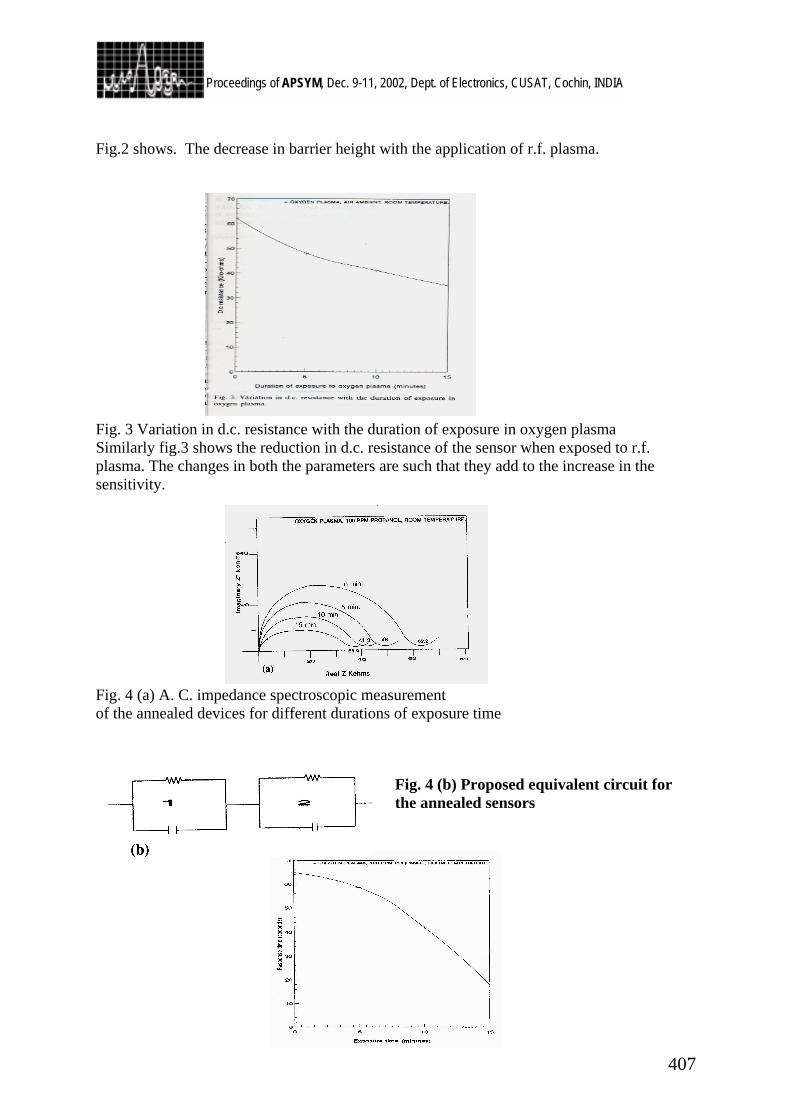
407
Proceedings of APSYM, Dec. 9-11, 2002, Dept. of Electronics, CUSAT, Cochin, INDIA
Fig.2 shows. The decrease in barrier height with the application of r.f. plasma.
Fig. 3 Variation in d.c. resistance with the duration of exposure in oxygen plasma Similarly fig.3 shows the reduction in d.c. resistance of the sensor when exposed to r.f. plasma. The changes in both the parameters are such that they add to the increase in the sensitivity.
Fig. 4 (a) A. C. impedance spectroscopic measurement of the annealed devices for different durations of exposure time
Fig. 4 (b) Proposed equivalent circuit for the annealed sensors
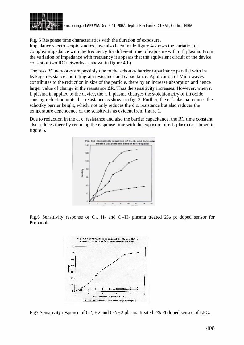
408
Proceedings of APSYM, Dec. 9-11, 2002, Dept. of Electronics, CUSAT, Cochin, INDIA
Fig. 5 Response time characteristics with the duration of exposure. Impedance spectroscopic studies have also been made figure 4-shows the variation of complex impedance with the frequency for different time of exposure with r. f. plasma. From the variation of impedance with frequency it appears that the equivalent circuit of the device consist of two RC networks as shown in figure 4(b).
The two RC networks are possibly due to the schottky barrier capacitance parallel with its leakage resistance and intragrain resistance and capacitance. Application of Microwaves contributes to the reduction in size of the particle, there by an increase absorption and hence larger value of change in the resistance ∆R. Thus the sensitivity increases. However, when r. f. plasma in applied to the device, the r. f. plasma changes the stoichiometry of tin oxide causing reduction in its d.c. resistance as shown in fig. 3. Further, the r. f. plasma reduces the schottky barrier height, which, not only reduces the d.c. resistance but also reduces the temperature dependence of the sensitivity as evident from figure 1.
Due to reduction in the d. c. resistance and also the barrier capacitance, the RC time constant also reduces there by reducing the response time with the exposure of r. f. plasma as shown in figure 5.
Fig.6 Sensitivity response of O2, H2 and O2/H2 plasma treated 2% pt doped sensor for Propanol.
Fig7 Sensitivity response of O2, H2 and O2/H2 plasma treated 2% Pt doped sensor of LPG.
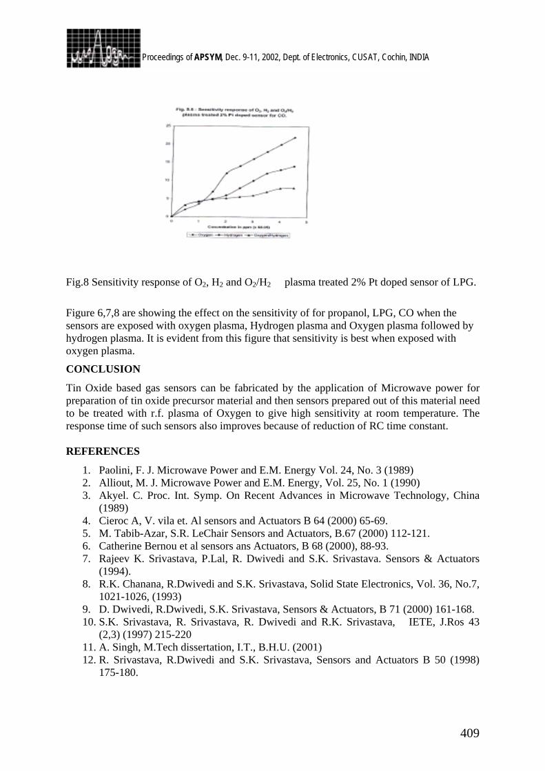
409
Proceedings of APSYM, Dec. 9-11, 2002, Dept. of Electronics, CUSAT, Cochin, INDIA
Fig.8 Sensitivity response of O2, H2 and O2/H2 plasma treated 2% Pt doped sensor of LPG.
Figure 6,7,8 are showing the effect on the sensitivity of for propanol, LPG, CO when the sensors are exposed with oxygen plasma, Hydrogen plasma and Oxygen plasma followed by hydrogen plasma. It is evident from this figure that sensitivity is best when exposed with oxygen plasma.
CONCLUSION
Tin Oxide based gas sensors can be fabricated by the application of Microwave power for preparation of tin oxide precursor material and then sensors prepared out of this material need to be treated with r.f. plasma of Oxygen to give high sensitivity at room temperature. The response time of such sensors also improves because of reduction of RC time constant. REFERENCES
1. Paolini, F. J. Microwave Power and E.M. Energy Vol. 24, No. 3 (1989) 2. Alliout, M. J. Microwave Power and E.M. Energy, Vol. 25, No. 1 (1990) 3. Akyel. C. Proc. Int. Symp. On Recent Advances in Microwave Technology, China
(1989) 4. Cieroc A, V. vila et. Al sensors and Actuators B 64 (2000) 65-69. 5. M. Tabib-Azar, S.R. LeChair Sensors and Actuators, B.67 (2000) 112-121. 6. Catherine Bernou et al sensors ans Actuators, B 68 (2000), 88-93. 7. Rajeev K. Srivastava, P.Lal, R. Dwivedi and S.K. Srivastava. Sensors & Actuators
(1994). 8. R.K. Chanana, R.Dwivedi and S.K. Srivastava, Solid State Electronics, Vol. 36, No.7,
1021-1026, (1993) 9. D. Dwivedi, R.Dwivedi, S.K. Srivastava, Sensors & Actuators, B 71 (2000) 161-168. 10. S.K. Srivastava, R. Srivastava, R. Dwivedi and R.K. Srivastava, IETE, J.Ros 43
(2,3) (1997) 215-220 11. A. Singh, M.Tech dissertation, I.T., B.H.U. (2001) 12. R. Srivastava, R.Dwivedi and S.K. Srivastava, Sensors and Actuators B 50 (1998)
175-180.
410
Proceedings of APSYM, Dec. 9-11, 2002, Dept. of Electronics, CUSAT, Cochin, INDIA
Invited Talk 7 AN OVERVIEW OF DIELECTRIC HORN ANTENNAS AND
AN ATTEMPT TO INVESTIGATE BROAD BAND DIELECTRIC STRUCTURES
R. K. Jha, S. P. Singh and Rajeev Gupta*
Department of Electronics Engineering Institute of Technology, Banaras Hindu University
Varanasi – 221 005.
In this paper various approaches for characterizing dielectric horn antennas are reviewed and their limitations highlighted. Further, at very high microwave frequencies including millimeter waves, the metal antennas suffer from inherent conductor losses. In addition manufacturing cost of metal antennas at these frequencies is also high. Therefore, an attempt is being made to review various approaches to the analysis of radiation pattern of a few dielectric structures, which would be suitable at these frequencies, especially because space qualified almost loss less dielectrics are available for construction of antennas. Also self complementary (log periodic) dielectric structure is being proposed for investigation in the microwave frequency range, which can act as a frequency independent antenna or at least a broadband antenna.
INTRODUCTION
Metallic horn antennas suffer from conductor losses at very high frequencies, that are why efforts have been made by some investigators [1],[2],[3],[4],[5],[6] to study the characteristics of alternative dielectric antenna structures. Different approaches for the analysis of radiation pattern of dielectric rod and horn have been made in the literature. They are
1. Scalar Huygens Principle 2. Equivalence Theorem 3. Vector Kirchoff-Huygens Formula 4. Scattering Theory
These approaches are applied to characterize the hollow as well as solid dielectric horns of various kinds under several simplifing assumptions. As a consequence, the theoretical results when compared with the experimental ones sometimes show large deviations. Further, an attempt is made to investigate the characteristics of self complementary (log periodic) dielectric structure and compare with those of identical metal structure for broadband applications . THEORY
Different approaches to the analysis of radiation pattern of dielectric antenna structures are reviewed here

411
Proceedings of APSYM, Dec. 9-11, 2002, Dept. of Electronics, CUSAT, Cochin, INDIA
SCALAR HUYGENS PRINCIPLE
According to this principle each point of a wave front can be considered as a secondary spherical wave. These secondary waves combine to form a new wave front, which is the envelope of the secondary wavelets. The wave at a field point is obtained by the superposition of these elementary secondary wavelets taking their phase differences into account when they reach the point in question. The theory has been applied to
1. Cylindrical dielectric rod antenna 2. H-plane sectoral dielectric Horn
The expression for field intensity at a point P is given by
)1..(..........)sin()tan2(Cos
x )()(
)()(
2
2
+Ψ+
−Ψ−
−Ψ−=
ααλπ
αελαπ
αελαπ
La
CosLSec
CosLSecSinE
Yr
Yr
P
Where ψ is the angle of a radius vector from the
line along the side surface, α is the semi flare angle, L is the axial length, 2a is the broad dimension of the throat and εr is the real part of relative paramilitary of horn dielectric.
EQUIVALENCE PRINCIPLE
Mathematically, the Equivalence principle may be expressed as
J n x H= , ExnM
−= ………(2)
or alternately the theorem states that the electromagnetic field inside a surface S due to sources out side the surface can be produced by sheet electric & magnetic currents over the surface S. Where
H is the magnetic field vector
E is the electric field vector n is the unit outward normal vector from the surface
MJ
& are sheet electric and sheet magnetic currents respectively over the surface. The electric field at point P (r,θ,φ ) is given by
EACurlHAdivgradojwHAojwE
−∈
+−= 1
µ …………………(3)
where EA and HA are the electric and magnetic vector potentials respectively. (3) Vector Kirchhoff - Huygens Formula : Referring to Fig.1, assume a Cartesian systems of Coordinates, a radiating aperture A limited by a contour line ΓA , a general point Q, also called the integration point or source point on A and an observation point P, ( R, θ, Ø ) also referred to as field point [ 3 ].

412
Proceedings of APSYM, Dec. 9-11, 2002, Dept. of Electronics, CUSAT, Cochin, INDIA
Fig. 1 Geometry for the application of the Kirchoff-Huygens formula
The radiation field at P is given by
xRR
jKRjkE
KrP 14
)exp(lim
π−−=
∞→
dsRjkHxnXA
RZExn )1.exp()](1[
ρ∫ − ………………….(4)
and 1RXZPE
HlimKr
P
−=∞→
…..(5)
where εµ=Z and
R 1 is a unit vector and all other symbols have their usual meanings.
SCATTERING THEORY
The radiation field at a distant point from an antenna (say H-plane sectoral dielectric horn) is estimated by determining separately, the field from the waveguide in the absence of scatterers (scatterers are the dielectric flares of the horn) and the scattered field and then adding the two fields at the point in order to simplify the problem. Total field at far point is E (r) = Ei (r) + Es (r) where subscript ‘i’ refers to the incident wave and ‘s’ refers to the scattering wave. Using magnetic vector potential concept, which is a function of polarisation current density.
,)1(0 Ε−= req jj εωε ……….(6)
Es can be written as
−∇∇=
∇∇=Ε
∫−−
v
rrjkeq
s
dvrr
ejXX
j
XAXj
r
''
.411
1)(
)'(
0
0
πωε
ωε ……………….(7)

413
Proceedings of APSYM, Dec. 9-11, 2002, Dept. of Electronics, CUSAT, Cochin, INDIA
The dielectric rectangular wave guides whose taper is gradually increasing to the free end, converting it to solid dielectric horn will be analyzed to determine its radiation pattern. The hollow H-Plane dielectric horn will also be analyzed using plane wave & scattering theory approach.
FREQUENCY INDEPENDENT ANTENNA
Antennas which theoretically have no limitation on the bandwidth are called frequency independent antennas. Rumsey’s principle is that the impedance and the pattern properties of an antenna will be frequency independent if the antenna shape is specified only in terms of angles. Thus, an infinite logarithmic spiral meets this requirement. The scaling characteristics (i.e. impedance, pattern, and polarisation) of antenna model also indicate that if the shape of the antenna were completely specified by angles, its performance would have to be independent of frequency. To make infinite structures more practical, the design usually requires that the current on the structure decreases with distance away from the input terminals. After a certain point the current is negligible, and the structure beyond that point to infinity can be truncated and removed. Practically then the truncated antenna has a lower cutoff frequency above which its radiation characteristics are the same as those of the infinite structure. A successful self scaling or frequency independent antenna structure satisfies the following requirements 1. The antenna radiates most of the power in a finite active region so that it can be
terminated with the minimal effect. 2. The dimension of active region must scale with the wavelength. 3. The antenna is fed from the high frequency end and it must be a transmission line to
carry power to the low frequency end. LOG PERIODIC ANTENNAS
The metal log periodic structure was introduced by Du Hamel and Isbell. In a logarithmically periodic antenna, the electrical properties vary periodically with the logarithm of the operating frequency. If the variations of the antenna characteristics are small within a period, they are small within each of the periods, and the antenna is a broadband device.
Fig.2 log periodic Antenna

414
Proceedings of APSYM, Dec. 9-11, 2002, Dept. of Electronics, CUSAT, Cochin, INDIA
The geometric ratio of the logarithmically periodic antenna of the Fig.2 is
n
n
RR 1+=τ ………………..(8)
where Rn+1 is the length of the first cell & Rn= is the length of the next cell. The width of the slot of the antenna is given by
n
n
Rr
=σ ………………(9)
where rn is the length of first cell of the side. τ defines the period of operation. That is, if the frequencies f1 and f2 are exactly one period apart, then
122
1 , ffff
⟩=τ ……………(10)
The magnitude of the log-frequency periods is determined by the design ratio, τ, and is in general of magnitude log (1/τ). That is, if two successive maxima of the impedance or pattern variation occur at frequencies f1 and f2, it will be found that they are related by the formula
τ1loglogloglog
1
212 ==−
ffff ……. (11)
From which it follows that f2/f1=1/τ or f1=f2τ. Therefore, if the log periodic antenna has certain measured properties (e.g. impedances, gain) at any particular frequency f, it follows that it will have exactly the same properties at frequencies τf, τ2f, τ3f and so on, and also at f/τ, f/τ2, f/τ3,……….provided that these frequencies are all within the cutoff limits. Log periodic structures which are also self complementary have a radiation pattern which remain more or less constant with frequency. A self complementary structure is a planar structure in which the metal, area is congruent to the open area and has a constant input impedance. This follows from Babinet’s principle which shows that the product of the impedance of two complementary planar structures is equal to η0
2 / 4, where η0 is the free space intrinsic impedance (377ohms). Therefore, a self-complementary structure has an impedance of η0 / 2 = 189 ohms, which is independent of frequency. DESIGN PROCEDURE
Design of a self complementary log periodic frequency independent antenna depends upon various parameters such as geometric ratio (τ), tooth width (σ) and the angles α and β as given in fig.2. We have another relation between σ and τ. τσ ≅ Let us take
060=α , 020=β , 85.0=τ So, τσ = and 922.0=σ Frequency range: 7.5 GHz to 10.5 GHz. The wavelength corresponding to higher frequency 10.5 GHz is given by
cmx
x 857.2105.10
1039
8
==λ
415
Proceedings of APSYM, Dec. 9-11, 2002, Dept. of Electronics, CUSAT, Cochin, INDIA
Antenna will radiate for frequencies 10.5 GHz, 8.925 GHz, 7.586 GHz in the specified range (7.5 – 10.5 GHz). Finally we have different dimensions of cells. Design for three cells of antenna: If we take the length of first cell is equal to λ/2, using the design parameters given above and utilizing equations 8, 9, and 10. We have R3 = λ/2= 1.42 cm R2 = 1.68 cm r2 = 1.54 cm R1 = 1.97 cm r1 = 1.83 cm Both dielectric )56.2( ' =rε and metal log periodic structures of above dimensions are fabricated. Experiment on the structures is in progress the results of which will be reported in the conference (AP SYM 2002).
REFERENCE
1. R. Chatterjee, “Dielectric and Dielectric Loaded Antenna”, Research Studies Press Ltd., Letch, Hertfordshire, England (1985).
2. J. R. James, “Theretical Investigation of Cylindrical Dielectric Rod Antennas”, Proceedings of the IEE, vol. 144, pp. 309-319 (1967).
3. W. Love, “Reflector Antennas”, IEEE Press, New York (1976). 4. D. F. Halliday and D. G. Kiely, “Dielectric Rod Aerials”, Journals of the IEE, vol. 94,
pt. IIIA, pp. 610-618 (1947). 5. B. Jha, and R. K. Jha, “Surface fields of H-Plane Sectoral Dielectric Horn Anteena”,
Proceedings of the 15th European Microwave Conference (1984). 6. K. Singh, B. Jha and R. K. Jha, “Near Field Analysis of H-Plane Hollow Sectoral
Dielectric Horn Antennas”, International Journal of Electronics, vol. 68, No. 6, pp. 1055-1061 (1990).
7. A. D. Olver, P. J. B. Clarricoats, A. A. Kishk and L. Shafai, “ Microwave Horns and Feeds”, IEEE Press, New York (1994).
8. Constantine A. Balanis, Antenna Theory Analysis & Design. New York: John Willey & Sons, 1982.
9. L. V. Blake, Antenna. Washington: Artech House, 1984. 10. Edward A. Wolff. Antenna Analysis. Washington: Artech House, 1988. 11. Carlos Salema, Carlos Fernandes and R. K. Jha, Solid Dielectric Horn Antenna.
Artech House: Boston (1998)
418
Proceedings of APSYM, Dec. 9-11, 2002, Dept. of Electronics, CUSAT, Cochin, INDIA
Invited Talk 8
Diversity Schemes for Mobile Communications
Parveen F. Wahid, Senior Member, IEEE School of Electrical Engineering and Computer Science
University of Central Florida Orlando, FL 32816-2450
Email: [email protected]
An overview of various diversity schemes, such as space, angle, pattern and polarization diversity schemes, used in wireless communications are discussed. A comparison between space and polarization diversity schemes is made and the performance of combined space and polarization schemes is presented. The use of the combined scheme in a mutlipath-rich environment is discussed.
INTRODUCTION
Diversity is the technique employed to reduce the effects of wideband fading and co-channel interference encountered in wireless communications. This is generally implemented at the receiver and provides the receiver with more than one independent path of the transmitted signal that it can select. The diversity performance depends on the number of channels or diversity branches and on the correlation between the branches. The signals received have to be combined appropriately using a diversity combiner for improved performance.
The two main criteria necessary for good performance in a diversity system are that (i) the fading in the individual branches have low cross-correlation and (ii) the mean power available from each branch be equal. Diversity schemes employed in wireless communications include the space diversity, polarization diversity and angle diversity schemes. The definitions of parameters used in describing the performance of diversity schemes are given below [1,-3]. CORRELATION COEFFICIENT
The correlation coefficient ρ12 between two branches is defined as
( )( )[ ]21
221112 σσ
µµρ∗−−
= aaE … (1)
where µ is the log-normal mean in dB, σ is the standard deviation and 1a and 2a are the narrowband channel amplitudes. For Rayleigh fading the channels have zero mean, so the above equation reduces to
[ ]21
2112 σσ
ρ∗
=aaE
… (2)
The mean power in the channel is given by

419
Proceedings of APSYM, Dec. 9-11, 2002, Dept. of Electronics, CUSAT, Cochin, INDIA
[ ]2
2i
i
aEP = … (3)
Diversity schemes should provide channels with low values of ρ12 and high mean powers Pi.
CROSS-POLARIZATION DISCRIMINATION (XPD)
This is a measure of the ratio of the mean incident power of the vertically to the horizontally polarized signal received by the antenna and is given by
H
V
PPXPD = … (4)
where PV and PH are the mean incident powers of the V-polarized and H-polarized signals. MEAN EFFECTIVE GAIN (MEG)
This is defined as the ratio of the mean received power of the antenna over a random route (Prec) to the total mean incident power (PV + PH), and is expressed as
)( HV
rece PP
PG+
= … (5)
SPACE DIVERSITY
Space diversity involves the use of two or more identical antennas separated by a distance. Here the branches can receive almost the same signal levels but to achieve a low correlation a large spacing between the branches is necessary. The correlation coefficient ρ12 in equation (2) expressed in terms of the components of radiation pattern (Eθ and Eφ) of the antennas and the XPD of the environment, is given by [2]
( )∫ ∫ ⋅⋅⋅⋅⋅⋅+⋅⋅⋅= ⋅−∗∗π π
φφφθθθ φθθσσ
ρ2
0 02121
2112 sin1 ddePEEPEEXPD dkj
ρρ
… (6)
and ( )∫ ∫ ⋅⋅⋅⋅⋅+⋅⋅⋅= ∗∗π π
φφφθθθ φθθσ2
0 0
2 sin ddPEEPEEXPD iiiii i = 1,2 … (7)
where Pθ and Pφ are the distributions of vertical and horizontal polarized incident waves, kρ
is the wave vector and d
ρis the separation between two antennas. The correlation coefficient for
the observed envelope ρe is approximately equal to ρ122.. In a space diversity scheme the radiation patterns of the two antennas are exactly the same i.e. 21 θθ EE = and 21 φφ EE = . Assuming two vertically polarized dipoles ( 0,sin == φθ θ EE ) with a vertical separation of ‘d’ shown in Figure 3a, and for uniform distributions of the vertical and horizontal polarized incoming waves (i.e. Pθ = Pφ = π21 ), we have
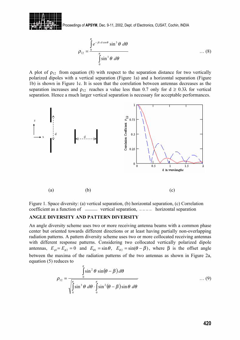
420
Proceedings of APSYM, Dec. 9-11, 2002, Dept. of Electronics, CUSAT, Cochin, INDIA
∫
∫ ⋅−
= π
πθ
θθ
θθρ
0
3
0
3cos
12
sin
sin
d
de djk
… (8)
A plot of ρ12 from equation (8) with respect to the separation distance for two vertically polarized dipoles with a vertical separation (Figure 1a) and a horizontal separation (Figure 1b) is shown in Figure 1c. It is seen that the correlation between antennas decreases as the separation increases and ρ12 reaches a value less than 0.7 only for d ≥ 0.3λ for vertical separation. Hence a much larger vertical separation is necessary for acceptable performances.
z
x d d
(a) (b) (c)
Figure 1. Space diversity: (a) vertical separation, (b) horizontal separation, (c) Correlation coefficient as a function of vertical separation, horizontal separation
ANGLE DIVERSITY AND PATTERN DIVERSITY
An angle diversity scheme uses two or more receiving antenna beams with a common phase center but oriented towards different directions or at least having partially non-overlapping radiation patterns. A pattern diversity scheme uses two or more collocated receiving antennas with different response patterns. Considering two collocated vertically polarized dipole antennas, 021 == φφ EE and ,sin1 θθ =E )sin(2 βθθ −=E , where β is the offset angle between the maxima of the radiation patterns of the two antennas as shown in Figure 2a, equation (5) reduces to
( )
( )∫ ∫
∫
−⋅
−=
π π
π
θθβθθθ
θβθθρ
0 0
23
0
2
12
sinsinsin
sinsin
dd
d … (9)
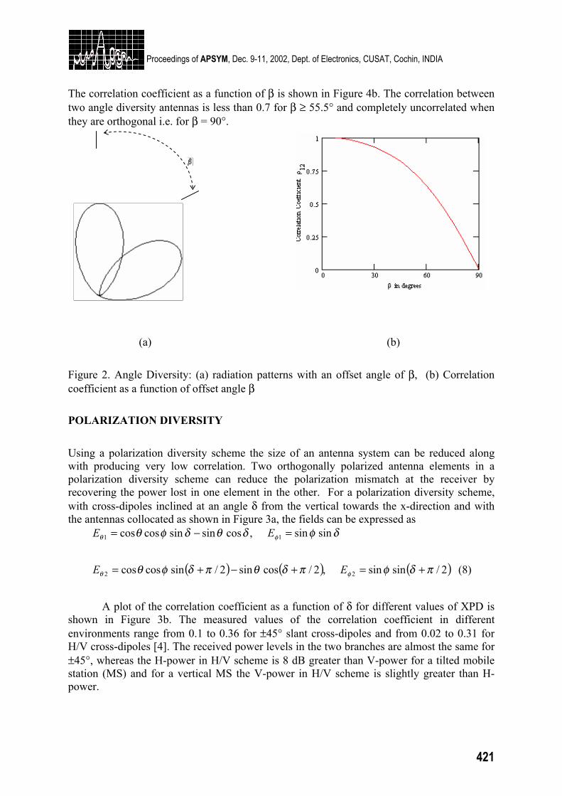
421
Proceedings of APSYM, Dec. 9-11, 2002, Dept. of Electronics, CUSAT, Cochin, INDIA
The correlation coefficient as a function of β is shown in Figure 4b. The correlation between two angle diversity antennas is less than 0.7 for β ≥ 55.5° and completely uncorrelated when they are orthogonal i.e. for β = 90°.
(a) (b)
Figure 2. Angle Diversity: (a) radiation patterns with an offset angle of β, (b) Correlation coefficient as a function of offset angle β
POLARIZATION DIVERSITY
Using a polarization diversity scheme the size of an antenna system can be reduced along with producing very low correlation. Two orthogonally polarized antenna elements in a polarization diversity scheme can reduce the polarization mismatch at the receiver by recovering the power lost in one element in the other. For a polarization diversity scheme, with cross-dipoles inclined at an angle δ from the vertical towards the x-direction and with the antennas collocated as shown in Figure 3a, the fields can be expressed as ,cossinsincoscos1 δθδφθθ −=E δφφ sinsin1 =E
( ) ( ),2/cossin2/sincoscos2 πδθπδφθθ +−+=E ( )2/sinsin2 πδφφ +=E (8)
A plot of the correlation coefficient as a function of δ for different values of XPD is shown in Figure 3b. The measured values of the correlation coefficient in different environments range from 0.1 to 0.36 for ±45° slant cross-dipoles and from 0.02 to 0.31 for H/V cross-dipoles [4]. The received power levels in the two branches are almost the same for ±45°, whereas the H-power in H/V scheme is 8 dB greater than V-power for a tilted mobile station (MS) and for a vertical MS the V-power in H/V scheme is slightly greater than H-power.
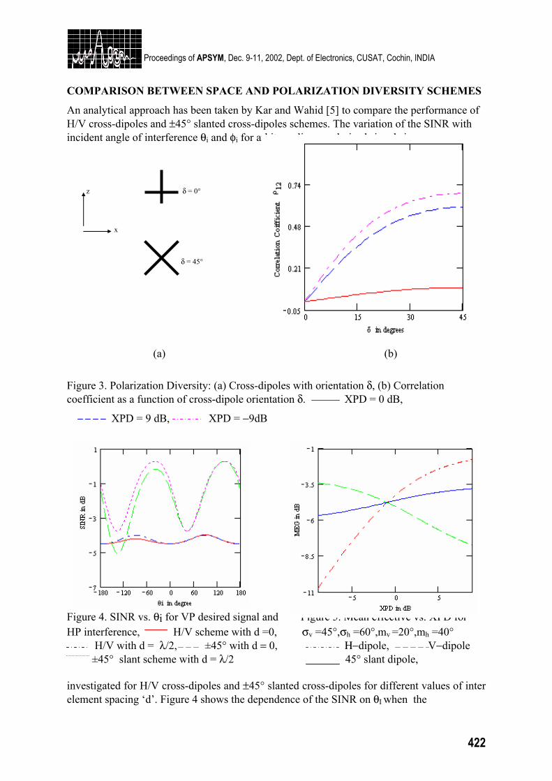
422
Proceedings of APSYM, Dec. 9-11, 2002, Dept. of Electronics, CUSAT, Cochin, INDIA
COMPARISON BETWEEN SPACE AND POLARIZATION DIVERSITY SCHEMES
An analytical approach has been taken by Kar and Wahid [5] to compare the performance of H/V cross-dipoles and ±45° slanted cross-dipoles schemes. The variation of the SINR with incident angle of interference θi and φi for arbitrary linear polarized signals is
z δ = 0°
x
δ = 45°
(a) (b)
Figure 3. Polarization Diversity: (a) Cross-dipoles with orientation δ, (b) Correlation coefficient as a function of cross-dipole orientation δ. XPD = 0 dB,
XPD = 9 dB, XPD = −9dB
Figure 4. SINR vs. θi for VP desired signal and Figure 5. Mean effective vs. XPD for HP interference, H/V scheme with d =0, σv =45°,σh =60°,mv =20°,mh =40° H/V with d = λ/2, ±45° with d = 0, Η−dipole, V−dipole ±45° slant scheme with d = λ/2 45° slant dipole, investigated for H/V cross-dipoles and ±45° slanted cross-dipoles for different values of inter element spacing ‘d’. Figure 4 shows the dependence of the SINR on θI when the
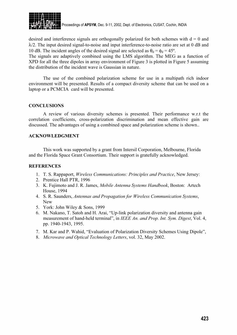
423
Proceedings of APSYM, Dec. 9-11, 2002, Dept. of Electronics, CUSAT, Cochin, INDIA
desired and interference signals are orthogonally polarized for both schemes with d = 0 and λ/2. The input desired signal-to-noise and input interference-to-noise ratio are set at 0 dB and 10 dB. The incident angles of the desired signal are selected as θd = φd = 45º. The signals are adaptively combined using the LMS algorithm. The MEG as a function of XPD for all the three dipoles in array environment of Figure 3 is plotted in Figure 5 assuming the distribution of the incident wave is Gaussian in nature. The use of the combined polarization scheme for use in a multipath rich indoor environment will be presented. Results of a compact diversity scheme that can be used on a laptop or a PCMCIA card will be presented. CONCLUSIONS
A review of various diversity schemes is presented. Their performance w.r.t the correlation coefficients, cross-polarization discrimination and mean effective gain are discussed. The advantages of using a combined space and polarization scheme is shown..
ACKNOWLEDGMENT
This work was supported by a grant from Intersil Corporation, Melbourne, Florida
and the Florida Space Grant Consortium. Their support is gratefully acknowledged.
REFERENCES
1. T. S. Rappaport, Wireless Communications: Principles and Practice, New Jersey: 2. Prentice Hall PTR, 1996 3. K. Fujimoto and J. R. James, Mobile Antenna Systems Handbook, Boston: Artech House, 1994 4. S. R. Saunders, Antennas and Propagation for Wireless Communication Systems,
New 5. York: John Wiley & Sons, 1999 6. M. Nakano, T. Satoh and H. Arai, “Up-link polarization diversity and antenna gain
measurement of hand-held terminal”, in IEEE An. and Prop. Int. Sym. Digest, Vol. 4, pp. 1940-1943, 1995.
7. M. Kar and P. Wahid, “Evaluation of Polarization Diversity Schemes Using Dipole”, 8. Microwave and Optical Technology Letters, vol. 32, May 2002.
A CHRONOLOGY OF DEVELOPMENTS OF WIRELESS COMMUNICATION AND ELECTRONICS TILL 1920
Magdalena Salazar-Palma*, Tapan K. Sarkar**, Dipak Sengupta***
*Departamento de Señales, Sistemas y Radiocomunicaciones, Escuela Técnica Superior de
Ingenieros de Telecomunicación, Universidad Politécnica de Madrid, Ciudad Universitaria s/n, 28040 Madrid, Spain,
Phone: +34-91-336-7366, ext: 391, Fax: +34-91-336-7362, E-mail: [email protected] **Department of Electrical Engineering and Computer Science, Syracuse University, 121 Link Hall, Syracuse, New York 13244-1240, USA, Phone: +1-315-443-3775, Fax: +1-315-443-4441,
E-mail: [email protected], Homepage: http://web.syr.edu/~tksarkar ***Department of Electrical Engineering, University of Michigan, Ann Arbor, Michigan 48109-
2122, USA, Phone: +1-734-764-3370, Email: [email protected]
ABSTRACT: The goal of this paper is to present a chronology of the developments of wireless communication and supporting electronics. Often, the invention of radio is delegated to one or two persons, the names of whom vary from country to country, depending on the country of origin of the authors. The aim of this paper is to illustrate that simultaneous development was going on all over the world and that each invention provided a solution to the portion of the puzzle. We will only highlight some of the crucial events from 1831 up to 1920 without further details. A longer version of the manuscript along with the references may be obtained from the authors. BACKGROUND: The history of Wireless Communication starts with the understanding of electric and magnetic phenomena (already observed during the very early days of the Chinese and Greek cultures) and related experiments and inventions carried out during the last half of the eighteen century and the first decades of the nineteen century, by scientists like Ampère, Arago, Becquerel, Berzelius, Coulomb, Davy, Faraday, Franklin, Galvani, Gauss, Green, Hisinger, Oersted, Ohm, Schweigger, Volta, and many others from different countries. From 1831, important events are: 1831: Henry invented Telegraph. 1834: Morse invented the code that bears his name. 1835: Roschenschold discovered semiconductor rectifying action over alternating current. 1843: Bain authored the first recorded proposal and patent for the electrical transmission of
pictures. The first apparatus for transmission of pictures was made in 1848. 1844: With the transmission of the words “What hath God wrought”, through Morse’s electric
telegraph between Washington, D. C., USA, and Baltimore, Maryland, USA, a completely revolutionary mean of real-time, long-distance communication was triggered.
1847: Helmholtz suggested electrical oscillation six years before this process was theoretically calculated by Lord Kelvin (1853) and ten years before it was experimentally verified by Fedderson (1857).
1853: Gintl invented Duplex Telegraphy. 1855: Gaugain studied the rectifying action between two metal balls in an evacuated chamber,
producing the first Electric Valve. 1864: Maxwell formulated the electromagnetic theory of light and predicted the existence of radio
waves. Loomis wrote the earliest description of a radio transmission system. He
demonstrated and patented it in 1866. 1870: Maxwell deduced: (a) the relations between the mean diameter and axial length of a square
section coil for maximal inductance, and (b) the increase of resistance and decrease of inductance of a coil due to skin effect. He also deduced the shape of electrostatic field lines about a wire grid placed between two electrodes.
1875: Baudot developed a fixed-length binary code for telegraphy. Heaviside and Edison invented Quadruplex Telegraphy.
1876: Bell fabricated the electromagnetic telephone transmitter. The term microphone was first used in 1878. 1877: Discovery of Electro-Optical Effect by Kerr. A carbon transmitter (mouth piece) for
telephone was invented by Edison, as well as the Phonography (gramophone). 1878: Huxley communicated Hughes’s investigation about the effect of contact pressure between
elements of an electric circuit on the value of the current flowing through it. He gave the name microphone to the instrument he was using. Bell successfully demonstrated voice modulation of a light beam by a microphone. He detected it at a distance of 500 yards using a selenium (photo) cell and a paraboloid reflector.
1882: Dolbear granted a patent for a wireless transmission and reception system using induction coil, microphone, telephone receiver and battery.
1883: Edison observed that the bulb of a carbon filament lamp became coated with black deposit. He also discovered that when a metal plate is suspended inside a bulb and connected through a galvanometer to the positive end of the filament a steady current flowed into the plate as long as the filament was heated.
1884: First patent on a complete system of Television was done by Nipkow. 1885: Edison patented a system of wireless communication by electrostatic induction. He placed
two high masts at a distance apart and fixed a metal plate on top of each. One metal plate was charged to a high voltage producing an electric field which could be detected on the plate of the receiving mast. The two plates on the high masts were the first electrical aerials. The patent for the aerials was sold to Marconi in 1903
1887: Sympathetic Resonance (i.e., standing waves) in wires was discovered by Lodge. The existence of radio waves was established experimentally by Hertz. He also discovered the Photo Emissive Effect. He observed that the length of the spark between two electrodes increases when ultraviolet light falls on the negative electrode of the spark gap.
1888: Hertz produced, transmitted and detected electromagnetic waves of wavelength 5 m and 50 cm. He used reflectors at the transmitting and receiving positions to concentrate the waves into a beam. Smith published an article suggesting the magnetic recording of sound.
1890: Tesla patents his Tesla Coil (USP 433702) which was used later in every spark gap generator for generation of high frequencies. Auburn prison in New York State electrocutes a prisoner to demonstrate the ugly side of AC as opposed to Edison’s DC.
1891: Jackson sent Morse codes by wireless over a few hundred yards. Branly discovered that an electric spark occurring near an ebonite tube of metal fillings increased their conductivity appreciably. In 1894 Lodge publicly demonstrated that the conductivity of loosely packed iron fillings, contained in a glass tube closed by a metal plug at each end (device named coherer) was increased when electric radiation fell upon it.
1892: Heaviside showed that a circuit had four fundamental constants, the resistance, inductance, capacity and leakance. Crookes published the possibilities of wireless communications such as: “wave lengths can be used from few thousand miles to a few feet”, "telegraphy without wires", “directional transmission¨, “receiver could be adjusted to receive a particular
wavelength by turning a screw, this would give sufficient secrecy and this could be increased by using a code”.
1893: Pupin suggested the use of tuned circuits for harmonic analysis. Thomson published the first theoretical analysis of electric oscillations within a conducting cylindrical cavity of finite length suggesting the possibility of wave propagation in hollow pipes (waveguides).
1894: Lodge demonstrated the possibility of Morse signaling by wireless, i.e., wireless communication. As suggested by the telegraphist Muirhead, he sent dot and dash signals over a relatively short distance through two stone walls. He used a Kelvin dead-beat mirror galvanometer to make long and short sweeps of a beam of light.
1895: Popov demonstrated his Thunderstorm Recorder using aerial, coherer and electromagnetic relay. Marconi transmitted and received a coded message at a distance of 1.75 miles. Bose generated and detected wireless signals of 6 mm wavelength. He produced a variety of devices and techniques (e.g., wave-guides, horn antenna, cut-off gratings, dielectric lens, microwave reflectors, double-prism directional coupler, polarimeter, interferometer, dielectrometer). He studied the effects of treating the contacts of the coherer with chemicals (impurity) and its response to a flash of radiation (pulse) using a home made recorder.
1896: Tesla obtains 8 patents for producing Electric Currents of Very High Frequency. Marconi applied for the first patent in wireless, covering use of transmitter with coherer connected to a high aerial and earth.
1897: The first wireless company, Wireless Telegraph and Signal Company Ltd. was founded; the company bought most of Marconi's patents. Its name was changed to Marconi’s Wireless Telegraph Co. Ltd. in 1900. Lodge patented the fundamental method of tuning transmitters and receivers of electric wave: Improvement in Synchronized Telegraphy without Wires, Syntonic Wireless. Rayleigh devised the first waveguide. A radio-wave controlled boat was operated in the Thames river by Wilson and Evans. Rayleigh published an analysis of propagation through dielectrically filled waveguide. When telephone service was only a few years old, the interest developed in automating it. Strowger devised an automatic step-by-step switch.
1898: First magnetic recording of sound on wire by Poulsen. Paper condenser by Boucherot. Tesla demonstrates a radio controlled boat at Madison square gardens and obtains a US patent (613809) for it.
1899: Braun used a loop aerial for transmission and reception of wireless signal. For directional transmission of wireless signals the use of vertical aerials spaced half a wavelength apart was proposed by Brown. He patented parabolic reflectors with the transmitting aerial at the focus. Wireless telegraph was installed on the ship “St. Paul” by Marconi.
1900: First speech transmission (25 miles) by Fessenden using a spark transmitter; the carrier frequency was 10 kHz. Duddel discovered that when an inductance and a condenser are connected in series across an ordinary direct current (dc) arc a steady oscillation sets up on the circuit for a certain ratio of inductance and capacitance. Maximum frequency obtained by Duddel was 10,000 Hz. He patented it as a Singing Arc, a method of producing alternating currents from direct current. The word Television was coined by Perskye. Tesla patented a security system (ECCM) for remote control, using coincidental transmission (wireless) on two channels, a forerunner of AND circuit. Tesla obtains USP 645576 and 649621 on System of Transmission of Electrical Energy, submitted in 1897, which the US Supreme Court recognizes to be first patents on Radio. Marconi submitted his first US patent (November 10, 1900). He continued to submit patent applications on Radio. They were all turned down. In 1903 the US Patent Office made remarks: “Many of the claims are
not patentable over Tesla patents # 645576 and 649621, of record, the amendment to overcome said references as well as Marconi’s pretended ignorance of the nature of a Tesla Oscillator being little short of absurd … the term Tesla Oscillator has become a household word on both continents (Europe and North America)”.
1901: On December 12, the first long distance wireless message was transmitted from Poldhu, Cornwall, England, UK and received by Marconi in Signal Hill, New Foundland. The distance covered was 1,700 miles across the Atlantic Ocean. For the experiment Fleming designed a 20 HP engine to drive an alternator of 2000 V stepped-up by a transformer to 20 kV, and a spark gap of 2 inches (immersed in oil). The transmitting aerial height was 219 feet, and the receiving aerial was suspended from a kite flying at 400 feet at a site called Signal Bay. Wave length of transmission was 800 m and the cost of the experiment was £40,000. Bose filed a patent for his Point Contact Diode Using Galena (Galena detector). It was given to him in 1904. Fessenden patented the idea of using a saturable reactor in a Wireless Signaling system as a magnetic modulator.
1902: Heaviside and Kennely suggested that the upper layers of the earth’s atmosphere could have conducting layers. Heterodyne method of reception was patented by Fessenden. Stone patented a method of directional transmission and reception using aerials spaced half a wavelength apart, aligned in the direction of transmission but this was not practical with long waves. Ignition interference from a two-cylinder automobile was reported by Taylor. Ehret filed two patents covering the transmission and reception of code signals or speech (frequency modulation: FM). So far as it is known these were the first disclosures to describe any system of modulation by name. The method of modulation consisted of varying resistance or reactance of an oscillator.
1903: Pickard filed a patent application for a crystal detector (thin wire in contact with silicon). To produce high frequency for wireless telegraphy and keep the arc stable Poulsen did the following modifications: (a) use of copper positive electrode, water cooled and slowly rotating carbon negative electrode, (b) to maintain the arc in an atmosphere of hydrogen, (c) a transverse magnetic field across the arc. Blondel showed that, provided the aerials were fed in correct phase they need not be half-a-wave length apart. Bellini had also suggested that twenty Blondel pairs would radiate a beam in one direction, but the suggestion proved premature because such phasing of radio frequency (RF) currents was not possible at that time and the distance between the aerial rendered it impractical for long waves (concept of End-fire-array). Obstacle detector and ship navigational device by Hertzian-wave projecting and receiving devices patented by Hullsmeyer.
1904: First telegraphic transmission of pictures from Munich to Nuremberg was made by Korn. Idea of printed circuit developed by Sprague. Fleming suggested the rectifying action of vacuum-tube diode for detecting high frequency oscillation (Oscillation Valve). He used a carbon filament as the incandescent electrode and metal plate as a cold electrode (anode). The vacuum-tube diode paved the way for the invention of the vacuum-tube triode. Wireless telegraphy act was passed to grant license to amateurs in UK. Wehnelt invented the oxide coated emitters (Wehnelt cathode) for vacuum diode. They were used in valves in 1914. US Patent office reverses itself and gives radio patent to Marconi (Marconi Company stock increased, Carnegie invested in American Marconi, Edison was consulting engineer). In 1943, two months after Tesla’s death, US Supreme Court upheld Tesla’s patent 645576 for invention of Radio. The court had selfish reasons for doing so. Marconi Company was suing US Government for using its patents in World War I. The court simply avoided the action by resorting priority to Tesla’s patent over Marconi.
1905: Photoelectric emission under the action of radiation was explained by Einstein, who proposed that Planck’s quantum theory of radiation be applied to photoelectric studies (second law of Photoelectric emission). Radio controlled torpedoes designed by Shoemaker, built in USA, were sold to Japan. Fessenden demonstrated wireless telephony by transmitting speech and music over a radio channel.
1906: Lee de Forest invented the three electrode valve or vacuum-tube triode (Audion Valve) and discovered how to use it as an amplifier. The discovery of the triode was instrumental in the development of transcontinental telephony in 1913 and signaled the dawn of wireless voice communications. Dieckmann and Glage proposed and performed an experimental use of cathode ray tube for facsimile reproduction. First advertised Radio Broadcast in USA by Fessenden.
1907: Radio telephony apparatus were installed in 24 battle ships for reception at a distance of 25 miles. Aerial for directional transmission and reception was developed by Bellini and Tosi. Direction finding using vertical aerial was developed by Pickard. Scheller patented his Course-Setter (for navigation) using interlocked A/N (Morse code) signal. Poulsen transmitted music by wireless using an arc transmitter with 1 kW input power and 200 feet high aerial. The music was heard at a distance of 300 miles. Fessenden used the term modulation in an article for the first time. The term was used later on by Pierce and Fleming in books published in 1910.
1908: Alexanderson constructed 100 kHz, 2 kW and 22 kHz, 200 kW alternators. L. de Forest installed a transmitter at the top of the Eiffel Tower for broadcasting music from a gramophone; the transmission was heard up to 500 miles. Fleming found that, for valves, tungsten filament was better than carbon filament and patented it.
1909 Austin and Cohen developed an empirical formula to measure the range of wireless stations and checked it up to a range of 1,100 miles over the Atlantic.
1910: Wireless telegraphy (transmitting) from airplane done by Ferris. The dielectric rod was studied by Hondros and Debye (origin of optical waveguides).
1911: The Lieben valve (using mercury) was used to construct the Lieben Transmitting Triode. Guidance of aircraft by radio telegraphy done by Blondell.
1912: Loop aerial modified from Bellini-Tosi aerial was developed by Prince. Two wireless operators went down with the Titanic sending wireless signals. This saved 712 passengers. The History of Earth Aerials (first history related with wireless) was published by Keitz. A four electrode valve with two grids, used as a fullwave detector was patented by Majorana.
1913: Radio frequency amplifier in cascade was patented by Alexanderson. Transmission of time signal by wireless for ships was started from Eiffel Tower. Neutralizing circuit for RF amplifier was patented by Round.
1914: FM of carrier was proposed to accommodate more number of channels within the available wavebands (only medium and long waves) using very small frequency deviation. Atmospheric refraction and its bearing in the transmission of electromagnetic (EM) wave round the earth's surface was studied by Fleming.
1915: Arlington to Paris and Honolulu radiophone service was opened. Using single valve tuned-anode tuned-grid receiver, signal was received in USA from UK by Armstrong. Direction finding equipment was used to locate sources of atmospherics. Push-Pull audio frequency power amplifier was made by Western Electric Co. Use of vacuum tube (diode) to measure voltage was patented by Heising.
1916: Sub-surface communication using EM wave was done by Roger. RC coupled amplifier was patented by Brillouin and Beauvais. A magnetic amplifier for radio telephony, used as

modulator, with Alexanderson high frequency alternator, was proposed by Alexanderson and Nixdroff. Cutting designed a radio telegraphic transformer.
1917: Elwell designed and constructed 714 feet high wooden lattice mast for supporting aerial; the mast was erected at Rome and was the highest wooden structure in the world. The highest frequency (750 MHz) continuous wave (CW) triode oscillator (up to 1932) was obtained by Kruse. Franklin designed and constructed mirrors made of wires for reflecting waves of 3 to 15 m; radio communication was carried out with short wave transmitters of 200 W between London and Birmingham. An automatic transmitter for distress signal was developed. The first use of direction finding equipment in aircraft was designed by NPL of UK. Armstrong invented the Superheterodyne Radio Receiver. He used eight valves. Even to this day, almost all radio receivers are of this type.
1918: Direction-finding was one of the key weapons in England during the First World War. 30 feet high Bellini-Tosi aerials were installed around the coast. Millener set up radio communication with moving trains. Wattson established the diffraction of electric waves by earth.
1919: The relation between the amplification factor and the electrode dimensions of a triode was developed by Schottky and Abraham. A formula for radiation resistance of a vertical loop aerial in terms of area, number of turns and wave length was proposed by Abraham. Barkhansen and Kurz designed an oscillator of 300 MHz. Variations of induction and radiation fields of aerials and coil (loop) antenna with distance were published by Dellinger. The variations were measured by Ramsey in 1928 at distances from 0.05 wavelength
1920: Valve transmitters were installed in airplanes for wireless telephony by Prince. Blow by blow account (broadcasting from ringside) of a boxing match was first made in UK. 15 kW valve transmitter was constructed by Marconi Co. Valluri measured the field strength of a signal produced at Leghorn from Annapolis and found that energy of 10 pW could be detected by using an eight valve amplifier. Plate modulation (AM) known as constant current modulation was developed by Heising for aircraft transmitters. The square-law detection of AM signal was done by Breit.

417
Proceedings of APSYM, Dec. 9-11, 2002, Dept. of Electronics, CUSAT, Cochin, INDIA
425
Proceedings of APSYM, Dec. 9-11, 2002, Dept. of Electronics, CUSAT, Cochin, INDIA
Aanandan C K 58,148,245,305 345 Abdul Khalam L. 259 Achari S.K. 185 Agrawal 109 Ajay Chakraborthy 65 Amalendu Patnaik 54 Ambika Jain 379 Ameen A 372 Amit A. Deshmukh 229 Anguswamy P. 372 Annapurna Das 72,76 AnupamR Chandran 148 Arora R.K. 201 Arun Kumar 323,333,337,341 Asha E. Daniel 233 Ashok Kumar 333,337,341 Badnikar S.L. 210 Baek Ho Jung 385 Barnes P.A 215 Basu B.N. 117 Bera A 206 Bharoti Sinha 94,109 Bhattacharjee R. 315 Bijumon P. V 268 Binod K. Kanaujia 32 Binu Paul 245 Bond G 215 Bonomali Khuntia 27
Bora D. 365 Bora V.H. 201 Borkar V.G. 140,241,327 Chakraborty. A 101,105 Chakravarthy M 311 Chandrasekaran V 259 Chattoraj N. 288 Chayan Roy 319 Chowdhury S.K 70,315 Das S 70
Dash G.N. 189 Dash S.K.` 180 Debatosh Guha 45 Debojyoti Choudhuri 221 Dhar J. 201 Dhruba C .Panda 27 Dipak K.Neog 27 Duggal K.M. 333,337,341 Durgaprasad V. 80 Fouzia Yousuf 86 Franklin. G 372 Ganesh. S 372 Gardiol Fred 396 Garg S.K. 201 Ghosh A 327 Ghosh S. 101,105,117 Girish Kumar 159,233,225,229 Goddard J W F 120 Gopal K. Patra 237 Goswami J. 404 Govindacharyulu P.A. 163, 171 Gupta B. 315 Gupta R.K. 283 Honey John 277 Iti Saha Misra 80 Jahagirdar D.R. 241 Jaimon Yohannan,. 264 Jain K.K. 361 Jain P.K. 117 Jamwal K.K.S 86 Jawad Y.Siddique 45 Jayaram P 345 Jha R.K. 412 Joe Jacob 277 Joita Mukherjee 140 Joshi S.N. 389 Juti R. Deka 113 Karmakar A 197
426
Proceedings of APSYM, Dec. 9-11, 2002, Dept. of Electronics, CUSAT, Cochin, INDIA
Khagindra Sood 323 Khan R.U 37 Kiran V. 117 Krishna Veni Ch. 167 Kumar N 251 Kumar S.B. 215 Lakshmeesha V.K. 155,221,319 Laxmi Shrivastava 292 Lethakumary B 58,305 Madheswaran M 144 Mahadevan V 155,221, 319 Maitra A 120,124 Malathi K 72,76 Mallick AK 175 Mangraj B 80 Manikandan. K 357 Manoj Ramavarma 259 Mathew K.T 264,277 Mausumi Kund 124 Meshram M.R. 109 Mishra I.P 189 Mishra J.K 189 Misra P.S 109 Mohan P 163,167,171 Mohanan P 58,148,245,255
268,272,305,345 Mohandas K.K 361 Moi A 197 Mridula S 245 Nampoori V.P.N 369 Naskar M.K 197 Nawal.K 109 Nidhi.S. Bhattachary 113 Niranjan Prasad 128 Nowshad S 372 Pal S 155,221,319 Panda G.R 175 Panda A.K 185,193
Pandharipande V.M 41,311 Panigrahi S.K 193, 185 Pant H.C. 251 Parkes G.M.B 215 Patel A.H 349 Pati, S.P 180 Patra M.K 251 Pattanaik S.R 189 Poddar D.R 315 Prabhakaran, U 155 Pradyot Kala 37 Prakash R 372 Prasad J.V 140,327 Prasad N.S 140 Praveen Kumar 221 Pummy Ratna 171 Purohit P 180 Rabindra K. Mishra 54,90,237 Rajaveerappa D 357 Rajeev Gupta 412 Rajeev Jyoti 333,337,341 Rajesh K. Vishwakarma 50 Rajneesh Kumar 365 Ramakotesware Rao G.V. 327 Ramakrishna Rao B 132,311 Ramalingam K 128 Rana S.S 201 Rani Joseph 277 Ranjan Barik 94 Ratheesh R 255,259 Raveendra K 136 Ravi A.V. Kumar 361 Ravi Kumar Y 132 Ray K.P. 225 Reena Pant 37 Rohith K. Raj 345 Roy J.S 288
427
Proceedings of APSYM, Dec. 9-11, 2002, Dept. of Electronics, CUSAT, Cochin, INDIA
Sreeja. S 372 Sreemoolanadhan H 255,259 Sridhar Patnaik 90 Srinivasan V.V 221,319 Srivastava G.P. 402 Srivastava S.K. 375,379,405 Srivastava V 206 Sudhabindhu Ray 159 Subramanyam A.V.G 155 Surendran K.P 272 Suresh Nair K.R 372 Swapna Devi 27 Syam.S. Pattnaik 27 Thomaskutty Mathew 148 Tripathi S.K.P 365 Trivedi R.G 365 Vadera S.R 251 Vasistha P 251 Vasu P.S 163 Vasudevan K 58,148,305,345 Vishvakarma B.R 32,37,50,375 Wahid P. 418 Yadav R.P 283 Yadava Ram L 296,300
Roy M.N 80 Sahoo G 101,105 Salazar M 424 Sanyal S 65,101,105 Sarala V 41 Saritha M 369 Sarkar D 70 Sarkar P.P 70 Sarkar S.K 197 Sarkar T.K. 385 Sarma A.D 128,132,136 Sasibhushana Rao G 128 Saswati Ghosh, , 65 Satish P 372 Satya Prakash 117 Sebastian M.T 255,259,268,272 Shambavi Ramalingam K 296 Sharma R.K. 206 Sharma S.B. 333,337,341 Sibley N. 215 Singh S.P. 412 Singh Y.K. 101,105 Singhal P.K 292 Sreedevi K Menon 58, 268,305,345 Sreehari Rao R. 311