
Application Specificities of Array Antennas - ESAT, KULeuven
327
KATHOLIEKE UNIVERSITEIT LEUVEN FACULTEIT INGENIEURSWETENSCHAPPEN DEPARTEMENT ELEKTROTECHNIEK (ESAT) AFDELING ESAT-TELEMIC Kasteelpark Arenberg 10, B-3001 Leuven (Heverlee), Belgi¨ e Application Specificities of Array Antennas: Satellite Communication and Electromagnetic Side Channel Analysis Promotor : Prof. Dr. Ir. G. Vandenbosch Prof. Dr. Ir. I. Verbauwhede Prof. Dr. Ir. P. Coppin Proefschrift voorgedragen tot het behalen van het doctoraat in de ingenieurswetenschappen door Wim AERTS June 2009
-
Upload
khangminh22 -
Category
Documents
-
view
0 -
download
0
Transcript of Application Specificities of Array Antennas - ESAT, KULeuven

KATHOLIEKE UNIVERSITEIT LEUVEN
FACULTEIT INGENIEURSWETENSCHAPPEN
DEPARTEMENT ELEKTROTECHNIEK (ESAT)
AFDELING ESAT-TELEMIC
Kasteelpark Arenberg 10, B-3001 Leuven (Heverlee), Belgie
Application Specificities of Array Antennas:
Satellite Communication and
Electromagnetic Side Channel Analysis
Promotor :
Prof. Dr. Ir. G. Vandenbosch
Prof. Dr. Ir. I. Verbauwhede
Prof. Dr. Ir. P. Coppin
Proefschrift voorgedragen tot
het behalen van het doctoraat
in de ingenieurswetenschappen
door
Wim AERTS
June 2009


“ There’s never time to do it right,but always time to do it over.”
– Meskimen’s law
“ Der Horizont vieler Menschenist ein Kreis mit dem Radius Null- und das nennen sie ihren Standpunkt.”
– Albert Einstein
“ Research is what I’m doingwhen I don’t know what I’m doing.”
– Wernher von Braun
“ When elephants fight,it is the grass that suffers.”
– While the source of this quoteis lost in the distant past,
the wisdom is as true today
“ Verstandig kiezen is de boodschap.”– Koen Van Vlaanderen
“ ... where questions make dancers ofpeople who’s stories aren’t straight.”
– Living in detente / NoMeansNo
“ The years we had togethernever we’ll forget.You’re in my heart as long asdaylight gets me straight.”
– Takes you back / Jazzanova


KATHOLIEKE UNIVERSITEIT LEUVEN
FACULTEIT INGENIEURSWETENSCHAPPEN
DEPARTEMENT ELEKTROTECHNIEK (ESAT)
AFDELING ESAT-TELEMIC
Kasteelpark Arenberg 10, B-3001 Leuven (Heverlee), Belgie
Application Specificities of Array Antennas:
Satellite Communication and
Electromagnetic Side Channel Analysis
Jury :
Prof. Dr. Ir. Y. Willems, voorzitter
Prof. Dr. Ir. G. Vandenbosch, promotor
Prof. Dr. Ir. I. Verbauwhede, promotor
Prof. Dr. Ir. P. Coppin, promotor
Prof. Dr. Ir. E. Van Lil
Prof. Dr. Ir. L. Ligthart
bla (Technische Universiteit Delft, Nederland)
Prof. Dr. Ir. D. Stroobandt
bla (Universiteit Gent)
Prof. Dr. Ir. C. Craeye
bla (Universite catholique de Louvain)
Proefschrift voorgedragen tot
het behalen van het doctoraat
in de ingenieurswetenschappen
door
Wim AERTS
U.D.C. 621.39
Wet. Depot: D/2009/7515/70
ISBN 978-94-6018-087-3
June 2009

c©Katholieke Universiteit Leuven - Faculteit IngenieurswetenschappenArenbergkasteel, B-3001 Leuven (Heverlee), Belgie
Alle rechten voorbehouden. Niets uit deze uitgave mag worden vermenigvuldigd en/ofopenbaar gemaakt worden door middel van druk, fotocopie, microfilm, elektronischof op welke andere wijze ook zonder voorafgaande schriftelijke toestemming van deuitgever.
All rights reserved. No part of the publication may be reproduced in any form byprint, photoprint, microfilm or any other means without written permission from thepublisher.
Wet. Depot: D/2009/7515/70ISBN 978-94-6018-087-3
Voorwoord
Het is bij momenten op het randje geweest, of moet ik zeggen tot aan het randje:“Zie dat je nog thuis geraakt he Steven”. Het is er bij momenten ook over geweest,zoals die ene keer dat ik mijn laptop niet mee had genomen naar het toilet. Als ikhad geweten hoe het hier ineen zat, dan was ik hier nooit begonnen. Maar als hethier niet zo leuk was, dan had ik hier nooit al die jaren gebleven! Ik heb hier altijdgeprobeerd veel bij te leren, leuke dingen te doen en aangenaam met mensen om tegaan. Op een luttel klein detail is me dat toch redelijk goed gelukt, denk ik.
Op al die jaren, ben ik met zeer veel dingen bezig geweest. Deels omdat ik alles demoeite vind, deels omdat ik niet nee kan zeggen als iemand me iets vraagt. Bijgevolgbevat dit boekje stukken afkomstig uit heel veel domeinen. Hopelijk zit er ook eenstukje bij dat U kan boeien. Het merendeel van de kennis die ik vergaard heb, heb ikerin proberen condenseren, zodat het een aanzet of startpunt kan zijn voor toekom-stige onderzoekers of collegae die willen bijlezen over een verwant onderwerp. Ik hoopdat op die manier, met mijn vertrek, toch niet al mijn kennis mee verdwijnt.
Dat streven, en het feit dat ik graag dingen uitleg en netjes opschrijf, hebben hetaantal bladzijden behoorlijk laten oplopen. Op zich vind ik dat geen slechte zaak.Het aanbod is er, de keuze is aan de lezer.
Veel plezier ermee!
Wim AertsLeuven, juni 2009.
i

invisible filling

Dankwoord
Op die bijna acht jaren dat ik op ESAT werkte, heb ik het geluk gehad met velefijne mensen te mogen omgaan. Ik heb van vele mensen steun, hulp of gewoon leukgezelschap gekregen.
Toen ik mijn tekst begon te schrijven, zag ik daar echt tegen op. Vooral door dewilde verhalen die de ronde deden. Een babbeltje tussen pot en pint met ClaudiaDiaz heeft me eraan gezet. En eigenlijk viel het allemaal mee, want ik schrijf graag.Maar na bladzijde 160 begon het wel wat te veel van het goede te worden.
In mijn eerste jaren heb ik ongetwijfeld Servaas Vandenberghe en Peter Delmottedanig verveeld met al mijn vragen. Het leuke aan de antwoorden van Servaas was,dat ze me hebben geleerd de handleiding te lezen. Later heb ik genoeg vragen vanjongere collega’s mogen beantwoorden om volgens het pay forward principe uit deschuld te geraken. Ik vrees alleen dat ik iets te weinig mijn best heb gedaan om hente leren lezen.
Tijdens mijn tijd op ESAT, heb ik voor verscheidene projecten met vele mensensamengewerkt. Vooral Eugene Jansen (Verhaert N.V.), Stefaan Burger (O.M.P.),Arnold Schoonwinkel (Stellenbosch Universiteit), Keith Palmer (Stellenbosch Univer-siteit), Dirk Stroobandt (UGent) en Michiel De Wilde (UGent) zijn me bijgeblevenvoor de vlotte samenwerking.
Binnen ESAT kon ik altijd terecht bij Jozef Lodeweyckx, Ilja Ocket, Christophe DeCanniere, Danny De Cock, Nele Mentens en Frederique Gobert voor consulting enleuke babbels. Met Roel Peeters viel ook leuk te babbelen, zolang het maar over debesjestheorie ging.
Als meetverantwoordelijke heb ik leuk mogen samenwerken en uitwisselen met Frede-rik Daenen (MICAS), Luc Pauwels (IMEC) en Robert Roovers (De Nayer), en mogenafdingen bij o.a. Johan Buschgens (Anritsu) en Veerle Kerkhofs (Agilent/Telogy).
Dat de studenten van vandaag de collega’s van morgen zijn, heb ik aan den lijve mogenondervinden. Iedereen die op langere termijn kan denken, weet dus hoe belangrijkhet is om oefenzittingen goed te geven en thesissen goed te begeleiden.
iii
iv Dankwoord
Ik heb mijn studenten altijd met heel veel enthousiasme, overgave en hartstocht be-geleid. Maar ik heb daar ook veel voor teruggekregen. Het was mijn plezier omPieter Vandromme, Joris Vankeerbergen, Dieter De Moitie en Sebastiaan Indesteegete kunnen helpen.
Sebastiaan is daarna ook een fijne collega geworden. Gelukkig waren er wel meer.Steven Mestdagh en Yves Schols zijn buiten categorie. Onze onvergetelijke wande-lingetjes in het prachtige park hebben vele problemen opgelost of voorkomen en warennoodzakelijk in het uitstippelen van het traject op lange termijn of het ontwikkelenvan de visie. Ook Peter Delmotte en Elke De Mulder waren buitengewone collega’s.
Luc Mombaerts, Rudi Casteels en Bruno Vanham zijn buitengewone technici. Hunvakmanschap en precisie bewonder ik enorm en is minstens evenwaardig aan de intel-lectuele prestaties die aan de K.U.Leuven worden geleverd.
Mijn promotoren Guy Vandenbosch, Ingrid Verbauwhede en Pol Coppin wil ik bedan-ken voor de mogelijkheid om mijn doctoraat (af) te maken en de enorme academischevrijheid die ik van hen kreeg. Dankzij die vrijheid heb ik kunnen onderzoeken watik interessant vond, me kunnen bijscholen en me helemaal kunnen ontplooien. Zon-der die vrijheid had ik nooit zoveel bij kunnen leren en de ingenieur en onderzoekerworden die ik nu ben. Hun bijdrage van vakkennis, kritische opmerkingen en zinvollesuggesties hebben de kwaliteit van mijn werk en publicaties, en – niet in het minst –van dit proefschrift sterk verbeterd. Dit laatste geldt zeker ook voor de feedback vanmijn assessors Emmanuel Van Lil en Leo Ligthart, en van de leden van de leesjury,Dirk Stroobandt en Christophe Craeye.
In de acht jaar, en zeker ook in het laatste jaar, heb ik eigenlijk enorm veel gewerkten bijgevolg de zorg voor Sander en Elin voor ruim meer dan de helft overgelatenaan Barbara. Zoals eigenlijk altijd het geval is, hangt het slagen van een project nietalleen af van de persoon die het project uitvoert, maar zeker ook van die mensen dieongevraagd en in stilte het werk overnemen en zorgen dat alles blijft draaien.
Hoewel dankjewel zeggen nogal goedkoop is, heb ik spijtig genoeg ook moeten vast-stellen dat het voor sommigen veel moeite is. Een mens kan het niet te veel zeggen. . .
Bedankt!Wim Aerts

Abstract
Array antennas have numerous applications in every day life. In this work the clas-sical array theory is profoundly reviewed and applied to satellite communication andelectromagnetic side channel analysis.
Satellite communication is a typical communication application. Bandwidths aregenerally spoken small and all standard telecommunication engineering methods arevalid. Designing for space, however, requires special attention due to the hostile envi-ronment. Consequently, in the design of a system for up link of in-situ collected datato an earth observation satellite, much effort was spent on material and componentselection. Another interesting peculiarity of the design, was the application of ananalog base band implementation of a technique often used for digital beam forming.
Electromagnetic side channel analysis requires an approach sometimes very differ-ent from standard telecommunication engineering methods. When observing directradiation of small currents performing cryptographic operations in silicon hardware,the antennas are designed to be small and sensitive to magnetic fields. Matching isnot performed in order to assure power transfer, but to obtain a high signal-to-noiseratio. The signal should be digitized with as less quantization error as possible toallow calculation of correlation with a hypothesis in post-processing. Array antennasshould perform beam forming on very wide band signals and preferably off-line toallow simultaneous monitoring of different active regions in the chip.
v
vi Abstract
Roosterantennes vinden hun toepassing in vele aspecten van het dagelijkse leven. Indit werk wordt de klassieke theorie van roosterantennes grondig herhaald en toegepastop satellietcommunicatie en electromagnetische nevenkanaalsanalyse.
Satellietcommunicatie is een typische communicatietoepassing. Bandbreedtes zijndoorgaans klein en alle standaardmethodieken uit het telecommunicatieontwerp mo-gen toegepast worden. Het ontwerpen voor toepassing in de ruimte vereist echterspeciale aandacht, omwille van het vijandige klimaat. Bijgevolg werd veel aandachtbesteed aan de keuze van materialen en componenten tijdens het ontwerp van een sys-teem, dat in-situ verzamelde gegevens opzendt naar een satelliet voor aardobservatie.Een ander interessant aspekt van het ontwerp, was de toepassing van een analoge ba-sisbandimplementatie van een techniek die veelvuldig voor digitale fasesturing wordtgebruikt.
Electromagnetische nevenkanaalsanalyse vereist een aanpak die soms erg verschilt vande standaard ontwerptechnieken in de telecommunicatie. Wanneer men de stralingprobeert waar te nemen afkomstig van kleine stromen die de cryptografische bewer-kingen uitvoeren in een apparaat, moeten de antennes klein zijn en gevoelig voor hetmagnetische veld. Aanpassen is hier niet zozeer nodig om maximale vermogensover-dracht te realiseren, maar wel om een zo goed mogelijke signaal-tot-ruisverhoudingte bekomen. Het signaal moet gedigitaliseerd worden met een zo klein mogelijkequantisatiefout, om achteraf de correlatie met een hypothese te kunnen berekenen.Roosterantennes moeten hun bundelsturing toepassen op signalen met grote band-breedte en liefst off-line om toe te laten gelijktijdig verschillende actieve delen van dechip te kunnen monitoren.

Contents
Voorwoord i
Dankwoord iii
Abstract v
Contents vii
List of Figures xv
List of Tables xxii
List of publications xxv
Nomenclature xxix
List of Acronyms xxxv
Nederlandse samenvatting xxxix
1 Introduction 1
1.1 Array Antennas . . . . . . . . . . . . . . . . . . . . . . . . . . . . . . . 1
1.2 Outline of this Thesis . . . . . . . . . . . . . . . . . . . . . . . . . . . 3
1.3 The Thesis at a Glance . . . . . . . . . . . . . . . . . . . . . . . . . . 4
vii

viii Contents
I Array Theory 7
2 Beam Forming 13
2.1 Beam Forming in the Receiving Chain . . . . . . . . . . . . . . . . . . 14
2.2 Some Beam Forming Implementations . . . . . . . . . . . . . . . . . . 18
2.2.1 Time Delaying . . . . . . . . . . . . . . . . . . . . . . . . . . . 18
2.2.2 Phase Shifting . . . . . . . . . . . . . . . . . . . . . . . . . . . 19
2.2.3 Frequency Scanning . . . . . . . . . . . . . . . . . . . . . . . . 23
2.3 Beam Forming Approximation Effects . . . . . . . . . . . . . . . . . . 24
3 Phased Array Design 25
3.1 Definitions . . . . . . . . . . . . . . . . . . . . . . . . . . . . . . . . . . 25
3.1.1 Array Factor . . . . . . . . . . . . . . . . . . . . . . . . . . . . 25
3.1.2 Array Radiation Properties . . . . . . . . . . . . . . . . . . . . 27
3.1.3 Example: Subarray of the ATCRBS in Bertem . . . . . . . . . 28
3.2 The Array Factor via a Fourier Transform . . . . . . . . . . . . . . . . 30
3.3 Array Design with Array Factor . . . . . . . . . . . . . . . . . . . . . . 32
3.3.1 Influence of the Array Geometry . . . . . . . . . . . . . . . . . 32
3.3.2 Influence of Excitations . . . . . . . . . . . . . . . . . . . . . . 40
3.3.3 Common Design Techniques . . . . . . . . . . . . . . . . . . . . 47
3.4 What if the Assumptions no longer Hold . . . . . . . . . . . . . . . . . 48
3.4.1 Errors that can be solved by Calibrating . . . . . . . . . . . . . 48
3.4.2 Quantization Errors . . . . . . . . . . . . . . . . . . . . . . . . 48
3.4.3 Errors that Void the Theory . . . . . . . . . . . . . . . . . . . 49
3.5 Conclusions . . . . . . . . . . . . . . . . . . . . . . . . . . . . . . . . . 49

Contents ix
II Application: Satellite Communication 51
4 Introduction to the Application 55
4.1 System Overview . . . . . . . . . . . . . . . . . . . . . . . . . . . . . . 56
4.1.1 In-Situ Data Collection . . . . . . . . . . . . . . . . . . . . . . 56
4.1.2 Space-Ground Communication Protocol . . . . . . . . . . . . . 57
4.1.3 Space Segment . . . . . . . . . . . . . . . . . . . . . . . . . . . 59
4.1.4 System Design Choices . . . . . . . . . . . . . . . . . . . . . . . 60
4.2 Orbit . . . . . . . . . . . . . . . . . . . . . . . . . . . . . . . . . . . . . 60
4.3 Link Budget . . . . . . . . . . . . . . . . . . . . . . . . . . . . . . . . . 62
4.3.1 Theory . . . . . . . . . . . . . . . . . . . . . . . . . . . . . . . 62
4.3.2 Space Ground Trade Off . . . . . . . . . . . . . . . . . . . . . . 64
4.3.3 Example: Link Budget for an Orbit at 600 km . . . . . . . . . 65
4.4 Motivation of Electronic Beam Steering . . . . . . . . . . . . . . . . . 66
4.4.1 Note on Vibration . . . . . . . . . . . . . . . . . . . . . . . . . 67
4.4.2 Examples of Phased Arrays on Satellites . . . . . . . . . . . . . 68
4.5 Designing Space Instruments . . . . . . . . . . . . . . . . . . . . . . . 70
4.5.1 Space Conditions . . . . . . . . . . . . . . . . . . . . . . . . . . 70
4.5.2 Product Assurance . . . . . . . . . . . . . . . . . . . . . . . . . 76
4.6 Conclusions . . . . . . . . . . . . . . . . . . . . . . . . . . . . . . . . . 77
5 Array Elements 79
5.1 Element Specifications . . . . . . . . . . . . . . . . . . . . . . . . . . . 79
5.2 Antenna Substrates for Space Application . . . . . . . . . . . . . . . . 80
5.2.1 Tolerances . . . . . . . . . . . . . . . . . . . . . . . . . . . . . . 80
5.2.2 Properties . . . . . . . . . . . . . . . . . . . . . . . . . . . . . . 80
5.2.3 Substrate Materials . . . . . . . . . . . . . . . . . . . . . . . . 82
5.2.4 Metalization . . . . . . . . . . . . . . . . . . . . . . . . . . . . 83

x Contents
5.2.5 Space Environment . . . . . . . . . . . . . . . . . . . . . . . . . 85
5.2.6 Material Selection . . . . . . . . . . . . . . . . . . . . . . . . . 88
5.3 Element Design . . . . . . . . . . . . . . . . . . . . . . . . . . . . . . . 89
5.4 Selecting Array Geometry . . . . . . . . . . . . . . . . . . . . . . . . . 89
5.4.1 Linear Array . . . . . . . . . . . . . . . . . . . . . . . . . . . . 90
5.4.2 Planar Array . . . . . . . . . . . . . . . . . . . . . . . . . . . . 97
5.5 Conclusions . . . . . . . . . . . . . . . . . . . . . . . . . . . . . . . . . 101
6 Signal Modification and Combination 103
6.1 Analog Quadrature BB Phase Shifter . . . . . . . . . . . . . . . . . . . 104
6.1.1 Analog Implementation of Digital Technique . . . . . . . . . . 104
6.1.2 Architecture of the Demonstrator Array Antenna . . . . . . . . 105
6.1.3 Measurement Results . . . . . . . . . . . . . . . . . . . . . . . 109
6.2 Space Qualified Phase Shifter . . . . . . . . . . . . . . . . . . . . . . . 116
6.2.1 Space Segment System Overview . . . . . . . . . . . . . . . . . 117
6.2.2 Signal Path . . . . . . . . . . . . . . . . . . . . . . . . . . . . . 118
6.2.3 Control Hardware . . . . . . . . . . . . . . . . . . . . . . . . . 119
6.2.4 Software Overview . . . . . . . . . . . . . . . . . . . . . . . . . 119
6.3 Conclusions . . . . . . . . . . . . . . . . . . . . . . . . . . . . . . . . . 121
III Application: EM Side Channel Analysis 123
7 Introduction to the Application 127
7.1 Example of A Block Cipher . . . . . . . . . . . . . . . . . . . . . . . . 128
7.2 Cryptographic Hardware . . . . . . . . . . . . . . . . . . . . . . . . . . 129
7.2.1 Field Programmable Gate Array (FPGA) . . . . . . . . . . . . 130
7.2.2 Microcontroller (µC) . . . . . . . . . . . . . . . . . . . . . . . . 131

Contents xi
7.3 Side Channels . . . . . . . . . . . . . . . . . . . . . . . . . . . . . . . . 132
7.3.1 Timing . . . . . . . . . . . . . . . . . . . . . . . . . . . . . . . 133
7.3.2 Power Consumption . . . . . . . . . . . . . . . . . . . . . . . . 133
7.3.3 Electromagnetic Radiation . . . . . . . . . . . . . . . . . . . . 134
7.4 Frequency Spectrum . . . . . . . . . . . . . . . . . . . . . . . . . . . . 135
7.5 Conclusions . . . . . . . . . . . . . . . . . . . . . . . . . . . . . . . . . 136
8 Array Elements 137
8.1 Element Specifications . . . . . . . . . . . . . . . . . . . . . . . . . . . 137
8.1.1 Capacitive and Inductive Sensors . . . . . . . . . . . . . . . . . 138
8.1.2 Resolution . . . . . . . . . . . . . . . . . . . . . . . . . . . . . . 140
8.1.3 Sensitivity . . . . . . . . . . . . . . . . . . . . . . . . . . . . . . 141
8.1.4 Bandwidth . . . . . . . . . . . . . . . . . . . . . . . . . . . . . 141
8.1.5 Rigidity . . . . . . . . . . . . . . . . . . . . . . . . . . . . . . . 142
8.1.6 Matching . . . . . . . . . . . . . . . . . . . . . . . . . . . . . . 142
8.1.7 Baluns . . . . . . . . . . . . . . . . . . . . . . . . . . . . . . . . 143
8.2 Shielded Loop . . . . . . . . . . . . . . . . . . . . . . . . . . . . . . . . 146
8.2.1 Loop Types . . . . . . . . . . . . . . . . . . . . . . . . . . . . . 146
8.2.2 Matching . . . . . . . . . . . . . . . . . . . . . . . . . . . . . . 150
8.2.3 Sensitivity . . . . . . . . . . . . . . . . . . . . . . . . . . . . . . 154
8.3 RFID Loop . . . . . . . . . . . . . . . . . . . . . . . . . . . . . . . . . 155
8.3.1 Loop Design . . . . . . . . . . . . . . . . . . . . . . . . . . . . 155
8.3.2 Power source and current enhancement . . . . . . . . . . . . . 163
8.3.3 Validation . . . . . . . . . . . . . . . . . . . . . . . . . . . . . . 166
8.4 Maximal Resolution Sensor . . . . . . . . . . . . . . . . . . . . . . . . 168
8.4.1 Geometrical Design . . . . . . . . . . . . . . . . . . . . . . . . 169
8.4.2 Enhancement Design . . . . . . . . . . . . . . . . . . . . . . . . 180
xii Contents
8.4.3 Practically Implementing a Large Nt . . . . . . . . . . . . . . . 180
8.4.4 Twins . . . . . . . . . . . . . . . . . . . . . . . . . . . . . . . . 182
8.5 Array Design . . . . . . . . . . . . . . . . . . . . . . . . . . . . . . . . 184
8.6 Conclusions . . . . . . . . . . . . . . . . . . . . . . . . . . . . . . . . . 185
9 Signal Modification and Combination 187
9.1 Digitization . . . . . . . . . . . . . . . . . . . . . . . . . . . . . . . . . 188
9.2 Measurement Setup . . . . . . . . . . . . . . . . . . . . . . . . . . . . 189
9.2.1 Noise Contributions . . . . . . . . . . . . . . . . . . . . . . . . 189
9.3 Improving Signal-to-Noise Ratio . . . . . . . . . . . . . . . . . . . . . 191
9.3.1 Filtering . . . . . . . . . . . . . . . . . . . . . . . . . . . . . . . 191
9.3.2 Avoiding Standing Waves . . . . . . . . . . . . . . . . . . . . . 192
9.3.3 Amplification . . . . . . . . . . . . . . . . . . . . . . . . . . . . 192
9.3.4 Comparison of some Setups . . . . . . . . . . . . . . . . . . . . 204
9.4 Digital time shifting . . . . . . . . . . . . . . . . . . . . . . . . . . . . 207
9.5 Conclusions . . . . . . . . . . . . . . . . . . . . . . . . . . . . . . . . . 208
IV Conclusions 209
Appendices 217
A Doppler Shift Compensation by Frequency Scanning 217
A.1 Introduction . . . . . . . . . . . . . . . . . . . . . . . . . . . . . . . . . 217
A.2 Mathematical Description . . . . . . . . . . . . . . . . . . . . . . . . . 218
A.2.1 Doppler Shift . . . . . . . . . . . . . . . . . . . . . . . . . . . . 218
A.2.2 Frequency Scanning . . . . . . . . . . . . . . . . . . . . . . . . 218
A.2.3 Doppler Shift Compensation . . . . . . . . . . . . . . . . . . . 220

Contents xiii
A.3 Applicability . . . . . . . . . . . . . . . . . . . . . . . . . . . . . . . . 220
A.3.1 LEO satellite . . . . . . . . . . . . . . . . . . . . . . . . . . . . 220
A.3.2 Future spacecraft and base station . . . . . . . . . . . . . . . . 221
A.4 Conclusion . . . . . . . . . . . . . . . . . . . . . . . . . . . . . . . . . 221
B The Orbit Simulator 223
B.1 The Orbit . . . . . . . . . . . . . . . . . . . . . . . . . . . . . . . . . . 223
B.2 The Simulation . . . . . . . . . . . . . . . . . . . . . . . . . . . . . . . 224
C Pseudo Code of the Array Control Routines 227
D Eavesdropping on Computer Displays 231
D.1 Source of Radiation . . . . . . . . . . . . . . . . . . . . . . . . . . . . 231
D.2 Screen Reconstruction . . . . . . . . . . . . . . . . . . . . . . . . . . . 233
E A KeeLoq Transceiver 237
F A Low Cost VNA 243
G RFID Basics 245
G.1 Different Transmission Systems . . . . . . . . . . . . . . . . . . . . . . 245
G.1.1 Inductive Coupling . . . . . . . . . . . . . . . . . . . . . . . . . 246
G.1.2 Capacitive Coupling . . . . . . . . . . . . . . . . . . . . . . . . 247
G.1.3 Back Scattering . . . . . . . . . . . . . . . . . . . . . . . . . . . 247
G.1.4 Radio Transmission . . . . . . . . . . . . . . . . . . . . . . . . 248
G.2 Link Budget . . . . . . . . . . . . . . . . . . . . . . . . . . . . . . . . . 248
G.2.1 Electric Far Fields . . . . . . . . . . . . . . . . . . . . . . . . . 249
G.2.2 Electric Near Fields . . . . . . . . . . . . . . . . . . . . . . . . 249
G.2.3 Magnetic Near Fields . . . . . . . . . . . . . . . . . . . . . . . 250
G.3 ISO-14443A RFID Standard . . . . . . . . . . . . . . . . . . . . . . . . 250
xiv Contents
H Determining the Inductance of a Coil 253
H.1 Calculation . . . . . . . . . . . . . . . . . . . . . . . . . . . . . . . . . 253
H.2 Measurement . . . . . . . . . . . . . . . . . . . . . . . . . . . . . . . . 255
I Standing Waves in Measurement Setup 257
I.1 Oscillations in a parallel RLC circuit . . . . . . . . . . . . . . . . . . . 257
I.2 Reflections . . . . . . . . . . . . . . . . . . . . . . . . . . . . . . . . . . 257
I.3 Validation . . . . . . . . . . . . . . . . . . . . . . . . . . . . . . . . . . 261
References 263

List of Figures
1.1 The principle of beam steering. . . . . . . . . . . . . . . . . . . . . . . 9
1.2 Spheres to determine main lobe for time delay beam forming. . . . . . 10
1.3 The three parts of a phased array antenna. . . . . . . . . . . . . . . . 11
2.1 Phase steering at different stages in the receiver. . . . . . . . . . . . . 16
2.2 The phase shift can also be applied to the local oscillator signal. . . . 17
2.3 Working principle of the I-Q phase shifter. . . . . . . . . . . . . . . . . 21
2.4 Spectra for BB and IF mixing. . . . . . . . . . . . . . . . . . . . . . . 22
2.5 The I-Q phase shifter for IF. . . . . . . . . . . . . . . . . . . . . . . . 22
2.6 The shifter of Fig. 2.3(b) for transmission and reception. . . . . . . . . 23
3.1 The geometry of an array antenna. . . . . . . . . . . . . . . . . . . . . 26
3.2 The array factor and the directivity of an array. . . . . . . . . . . . . . 29
3.3 The array of dipoles as inserted in MAGMAS . . . . . . . . . . . . . . 30
3.4 Array factors of a 1D, 2D and 3D array. . . . . . . . . . . . . . . . . . 33
3.5 Array factors (LESA, N = 10, varying d). . . . . . . . . . . . . . . . . 34
3.6 Darray of a uniform LESA varies with d. . . . . . . . . . . . . . . . . . 35
3.7 Array factors (LESA, length 20λ, varying N). . . . . . . . . . . . . . . 36
3.8 Several sparse arrays are combined into one antenna. . . . . . . . . . . 37
3.9 The radiation pattern of a sparse array is symmetrical. . . . . . . . . . 38
xv

xvi List of Figures
3.10 Array factors of geometric arrays (a > 1, N = 10). . . . . . . . . . . . 39
3.11 Array factors of geometric arrays (a < 1, N = 10). . . . . . . . . . . . 40
3.12 Comparison of some linear non-equally spaced arrays. . . . . . . . . . 41
3.13 Array factor of regular planar array. . . . . . . . . . . . . . . . . . . . 41
3.14 Random arrays have no grating lobes but should be sparse. . . . . . . 42
3.15 Beam steering makes use of a Fourier property. . . . . . . . . . . . . . 43
3.16 Chebychev polynomial mapped to one interval of array factor function. 45
3.17 Any type of tapering results in a lower value for Dmax (N = 7). . . . . 46
3.18 Directivity of the ATCRBS subarray. . . . . . . . . . . . . . . . . . . . 47
4.1 Subsystems of the ground segment. . . . . . . . . . . . . . . . . . . . . 58
4.2 Steps of the space-ground communication protocol . . . . . . . . . . . 59
4.3 Subsystems of the space segment. . . . . . . . . . . . . . . . . . . . . . 59
4.4 User and satellite geometry. . . . . . . . . . . . . . . . . . . . . . . . . 62
4.5 Link budget. . . . . . . . . . . . . . . . . . . . . . . . . . . . . . . . . 63
4.6 Signal and noise in the link. . . . . . . . . . . . . . . . . . . . . . . . . 64
4.7 Channel capacity as a function of SNR. . . . . . . . . . . . . . . . . . 65
4.8 Model of the satellite. . . . . . . . . . . . . . . . . . . . . . . . . . . . 67
4.9 The 80 beams of the IRIDIUM antenna. . . . . . . . . . . . . . . . . . 68
4.10 The Alcatel X-band antenna for LEO satellites. . . . . . . . . . . . . . 69
4.11 Overview of the problems due to low pressure. . . . . . . . . . . . . . 71
4.12 Overview of the problems related to temperature. . . . . . . . . . . . . 73
4.13 Aurora Borealis and Van Allen Belts. . . . . . . . . . . . . . . . . . . . 74
4.14 Overview of the problems related to radiation. . . . . . . . . . . . . . 75
5.1 Gain as a function of εr for a probe fed patch antenna. . . . . . . . . . 88
5.2 Gain as a function of dt for a probe fed patch antenna. . . . . . . . . . 89

List of Figures xvii
5.3 Scaled layout of the dual feed patch antenna. . . . . . . . . . . . . . . 90
5.4 Scattering parameter of the dual feed patch antenna. . . . . . . . . . . 90
5.5 The array topology, with dipoles as array elements. . . . . . . . . . . . 91
5.6 Supergaining on an array factor function graph. . . . . . . . . . . . . . 91
5.7 dopt for LESA with uniform tapering, scanned to φ = 10. . . . . . . . 92
5.8 Gain of the optimal LESA scanned to φ = 10 as a function of N . . . 93
5.9 Directivity of several arrays as a function of scan angle (N = 8). . . . 93
5.10 Free space path loss and array gain. . . . . . . . . . . . . . . . . . . . 94
5.11 Directivity as a function of d for N = 8 array. . . . . . . . . . . . . . . 96
5.12 Directivity of current imposed and voltage fed dipole array. . . . . . . 97
5.13 Satellite passing over a ground station. . . . . . . . . . . . . . . . . . . 97
5.14 Two types of planar arrays obtained from linear arrays. . . . . . . . . 99
5.15 Gain as a function of d for concentric circles array. . . . . . . . . . . . 99
5.16 Gain variation as a function of φ for planar arrays. . . . . . . . . . . . 102
6.1 Analog implementation of Eq. (6.1). . . . . . . . . . . . . . . . . . . . 104
6.2 Photograph of the array antenna inside the anechoic chamber. . . . . . 105
6.3 Photograph of the antenna element. . . . . . . . . . . . . . . . . . . . 106
6.4 Influence of ground plane and superstrate on element radiation pattern 107
6.5 Schematic of four phase shifters on one controller PCB. . . . . . . . . 108
6.6 Photograph of PCB with four phase shifters. . . . . . . . . . . . . . . 109
6.7 Implementation of the array control. . . . . . . . . . . . . . . . . . . . 110
6.8 Constellation plot of the phase shifter. . . . . . . . . . . . . . . . . . . 113
6.9 Radiation patterns of uniform eight-by-eight array. . . . . . . . . . . . 114
6.10 Radiation patterns of Chebychev eight-by-eight array . . . . . . . . . . 115
6.11 7 elements concentric circles array. . . . . . . . . . . . . . . . . . . . . 117
6.12 Subsystems of the space segment. . . . . . . . . . . . . . . . . . . . . . 118

xviii List of Figures
6.13 Implementation of the signal path of the array hardware. . . . . . . . 119
6.14 Implementation of the control of the array hardware. . . . . . . . . . . 120
6.15 Overview of the Routines that are needed on the Satellite. . . . . . . . 121
7.1 Schematic of the KeeLoq block cipher. . . . . . . . . . . . . . . . . . . 129
7.2 Schematic of a typical FPGA. . . . . . . . . . . . . . . . . . . . . . . . 131
7.3 Block diagram of a typical 8051 family µC. . . . . . . . . . . . . . . . 132
8.1 |E|/|H| of a dipole as a function of distance. . . . . . . . . . . . . . . 139
8.2 This system is not balanced nor unbalanced if Z1 6= Z2. . . . . . . . . 144
8.3 A sleeve balun . . . . . . . . . . . . . . . . . . . . . . . . . . . . . . . 145
8.4 A practical implementation of a sleeve balun . . . . . . . . . . . . . . 145
8.5 Working principle of a transformer balun. . . . . . . . . . . . . . . . . 145
8.6 Photograph of the shielded loops. . . . . . . . . . . . . . . . . . . . . . 146
8.7 Schematic drawings of the four loop types. . . . . . . . . . . . . . . . . 147
8.8 A shielded loop implementation using biax. . . . . . . . . . . . . . . . 147
8.9 S11 of the loops for 22 MHz − 1 GHz . . . . . . . . . . . . . . . . . . . 150
8.10 S11 of the loops for 1 kHz − 50 MHz . . . . . . . . . . . . . . . . . . . 151
8.11 S11 of the mœbius with short on a Smith Chart. . . . . . . . . . . . . 152
8.12 S11 of a mœbius without short with different capacitances. . . . . . . . 153
8.13 Layout of a loop that combines the balanced and mœbius loop. . . . . 153
8.14 Working principle of a shielded loop. . . . . . . . . . . . . . . . . . . . 155
8.15 Reader loop geometry. . . . . . . . . . . . . . . . . . . . . . . . . . . . 157
8.16 rl/rd as a function of rd/λ. . . . . . . . . . . . . . . . . . . . . . . . . 159
8.17 Magnetic field as a function of reading distance for several Nt. . . . . 160
8.18 Equivalent circuit of an inductor. . . . . . . . . . . . . . . . . . . . . . 162
8.19 Schematic of the four RLC resonance circuits . . . . . . . . . . . . . . 164

List of Figures xix
8.20 The RFID reader loops. . . . . . . . . . . . . . . . . . . . . . . . . . . 167
8.21 Resonance circuit used to determine the reading range. . . . . . . . . . 167
8.22 Frequency dependent value of L for the copper tube. . . . . . . . . . . 168
8.23 Contour lines of Eq. (8.39) as a function of rl and Nt. . . . . . . . . . 170
8.24 Nt as function of fL = fH for Z = ∞ and Z = 1 MΩ. . . . . . . . . . 173
8.25 Minimum rl as a function of fL = fH for Z = ∞ and Z = 1 MΩ. . . . 174
8.26 Minimum rl for two loop sensors with varying working frequency band. 175
8.27 Variation of Nswitch as function of rl/rw and d/2rw. . . . . . . . . . . 175
8.28 rl as function of fL = fH for unloaded loops with different d/2rw. . . 176
8.29 Minimum rl as function of fL = fH for Z = 1 MΩ ‖ 13 pF and Z = 50. 176
8.30 rl for Z = 1 MΩ ‖ 13 pF and Z = 50 as function of frequency band. . 177
8.31 Effect of restricted Nt on rl. . . . . . . . . . . . . . . . . . . . . . . . . 177
8.32 rl as function of fL = fH for Z = 1 MΩ ‖ 13 pF and several rw/rl. . . 178
8.33 Graphical representation of the minimum rl search. . . . . . . . . . . . 179
8.34 The difference between Eq. (8.39) and (8.55). . . . . . . . . . . . . . . 181
8.35 Equivalent circuit of the loop sensor connected to a load. . . . . . . . 182
8.36 V of loop as function of position relative to dipole. . . . . . . . . . . . 183
8.37 A twin loop configuration solves location ambiguity of a dipole source. 183
8.38 V of loop as function of position relative to magnetic dipole. . . . . . 184
8.39 Twin loops can be used to suppress noise. . . . . . . . . . . . . . . . . 184
9.1 Typical measurement setup for a EM side channel analysis. . . . . . . 189
9.2 Circuit of diode detector. . . . . . . . . . . . . . . . . . . . . . . . . . 192
9.3 The importance of matching . . . . . . . . . . . . . . . . . . . . . . . . 193
9.4 Possible circuit for a matched amplifier with a MAR-6+. . . . . . . . . 194
9.5 Schematics of an ideal class E amplifier . . . . . . . . . . . . . . . . . 195
9.6 The topology of a push-pull class E amplifier. . . . . . . . . . . . . . . 196

xx List of Figures
9.7 Circuit schematic of the modulation circuit. . . . . . . . . . . . . . . . 197
9.8 Equivalent low frequency scheme of the class E. . . . . . . . . . . . . . 198
9.9 Choke current and drain voltages of transistors of class E. . . . . . . . 198
9.10 Drain voltage of the IRF9530 with and without diode. . . . . . . . . . 199
9.11 Simulation of loop current with and without Rext. . . . . . . . . . . . 200
9.12 Waveforms of a class E amplifier with the complete SPICE model. . . 201
9.13 Picture of the class E amplifier. . . . . . . . . . . . . . . . . . . . . . . 202
9.14 PCB layout of the class E amplifier. . . . . . . . . . . . . . . . . . . . 202
9.15 Gate and drain voltage of the class E transistors. . . . . . . . . . . . . 203
9.16 Field transmitted by the loop antenna driven by the class E amplifier. 204
9.17 Zoom of the signal as received with a magnetic probe at 30 cm. . . . . 204
9.18 Circuit schematic of the modulation circuit with current mirror. . . . . 205
9.19 General schematic of the measurement chain. . . . . . . . . . . . . . . 205
9.20 SNRos for four different setups. . . . . . . . . . . . . . . . . . . . . . . 207
A.1 The principle of frequency scanning. . . . . . . . . . . . . . . . . . . . 219
A.2 The geometry of a LEO satellite that passes over a ground station. . . 221
A.3 Doppler shift as a function of αε for some LEO satellites. . . . . . . . 222
B.1 Satellite orbit and ground station in two coordinate systems. . . . . . 224
B.2 Doppler shift with and without earth rotation. . . . . . . . . . . . . . 226
D.1 Schematic representation of a PSD of a video signal. . . . . . . . . . . 232
D.2 Effect of using a repetition instead of BB version of the video signal. . 233
D.3 Effect of averaging multiple frames on the image quality. . . . . . . . . 234
D.4 Measurement setup for eavesdropping on computer displays. . . . . . . 235
E.1 Photograph of the KeeLoq transceiver. . . . . . . . . . . . . . . . . . . 238
List of Figures xxi
E.2 Envelope of voltage over transmitting loop sending opcode. . . . . . . 238
E.3 Circuit of the Tx part in the KeeLoq transceiver. . . . . . . . . . . . . 239
E.4 Envelope of voltage over transmitting loop receiving response. . . . . . 239
E.5 Circuit of the Rx part in the KeeLoq transceiver. . . . . . . . . . . . . 240
E.6 Circuit to interface Rx with FPGA in KeeLoq transceiver. . . . . . . . 241
F.1 Setup for the S11 measurements below 45MHz. . . . . . . . . . . . . . 244
G.1 Schematic representation of inductive coupling. . . . . . . . . . . . . . 246
G.2 Schematic representation of capacitive coupling. . . . . . . . . . . . . . 247
G.3 Schematic representation of back scattering. . . . . . . . . . . . . . . . 248
G.4 Schematic representation of radio transmission. . . . . . . . . . . . . . 248
G.5 Specifications of the pause in the PCD signal as defined in ISO14443 . 251
G.6 Schematic of the building blocks of the altered RFID system . . . . . 251
H.1 The integration over the area of the loop. . . . . . . . . . . . . . . . . 254
H.2 Inductance calculated with integral and with Grover’s formula. . . . . 254
I.1 Lowest resonance frequency as function of cable length. . . . . . . . . 259
I.2 Resonance frequency as function of cable length for different k. . . . . 260
I.3 Experimental validation of theory on standing waves. . . . . . . . . . . 262

invisible filling

List of Tables
2.1 Comparison of phase steering at RF, IF and BB. . . . . . . . . . . . . 17
3.1 Shading windows and their properties. . . . . . . . . . . . . . . . . . . 44
3.2 Numeric values of the DFT pair for Chebychev tapering synthesis. . . 45
3.3 Excitation coefficients of the ATCRBS subarray. . . . . . . . . . . . . 47
4.1 Orbit characteristics for Low Earth Orbits. . . . . . . . . . . . . . . . 61
4.2 Numeric example for link budget. Input left, output right. . . . . . . . 66
4.3 Temperature cycles for LEO satellites (αT /εT = 1). . . . . . . . . . . . 72
5.1 Some examples of the available εr for RF substrates. . . . . . . . . . . 81
5.2 Overview of the different PTFE based substrates. . . . . . . . . . . . . 82
5.3 Overview of some commonly used metals. . . . . . . . . . . . . . . . . 84
5.4 Weights and corresponding heights for copper. . . . . . . . . . . . . . 84
5.5 Some substrates that meet the specs concerning outgassing. . . . . . . 86
5.6 TCεr from data sheets compared with measurements. . . . . . . . . . 87
5.7 ∆ue for linear arrays with uniform tapering. . . . . . . . . . . . . . . . 92
5.8 dopt compared to results of an optimization search. . . . . . . . . . . . 94
5.9 Optimal d in dipole arrays from near and far field iterative search. . . 95
5.10 Orbit heights h and corresponding scan angles θmax. . . . . . . . . . . 98
xxiii

xxiv List of Tables
5.11 Optimal d for arrays of concentric circles scanned to broadside. . . . . 100
5.12 Optimal d for regular grid arrays scanned to broadside. . . . . . . . . 100
6.1 Geometrical and electrical parameters of the patch. . . . . . . . . . . . 106
6.2 Components in signal path and controller. . . . . . . . . . . . . . . . . 120
8.1 Overview of the relevant probe specs. . . . . . . . . . . . . . . . . . . . 138
8.2 Measured DC resistance values for the four loop types. . . . . . . . . . 148
8.3 Advantages and disadvantages of the four loop types. . . . . . . . . . . 149
8.4 Self-resonance frequency of loops with and without insulation. . . . . . 162
8.5 Characteristics overview of the RFID reader loops. . . . . . . . . . . . 168
9.1 Measured noise contributions for an oscilloscope. . . . . . . . . . . . . 190
9.2 Components selected for the class E amplifier . . . . . . . . . . . . . . 201
D.1 Comparison of screen reconstruction methods. . . . . . . . . . . . . . . 234
I.1 The properties of the different cables. . . . . . . . . . . . . . . . . . . 261

List of publications
International Journals
• W. Aerts and G.A.E. Vandenbosch, “Gain Enhancement by Optimizing In-terelement Spacing in Linear Array Antennas,” Microwave and Optical Tech-nology Letters, vol. 43, no. 4, 20 November 2004JCR 2004 Impact Factor 0.456.
• M. Vrancken, Y. Schols, W. Aerts and G.A.E. Vandenbosch, “Benchmark of fullMaxwell 3-dimensional electromagnetic field solvers on prototype cavity-backedaperture antenna,” AEU - International Journal of Electronics and Communi-cations, doi:10.1016/j.aeue.2006.07.001, July 2006SCIE 2004 Impact Factor 0.483.
• M. Vrancken, W. Aerts, Y. Schols and G.A.E. Vandenbosch, “Benchmark ofFull Maxwell 3D Electromagnetic Field Solvers on an SOIC8 Packaged andInterconnected Circuit,” International Journal of RF and Microwave Computer-Aided Engineering, vol. 64, issue 6, 1 June 2007JCR 2007 Impact Factor 0.291.
• W. Aerts, E. De Mulder, B. Preneel, G. Vandenbosch, and I. Verbauwhede,“Dependence of RFID Reader Antenna Design on Read Out Distance,” IEEETransactions on Antennas and Propagation, vol. 56, issue 12, 1 December 2008ISI 2007 Impact Factor 1.636.
• W. Aerts, P. Delmotte and G. Vandenbosch, “Conceptual Study of Analog Base-band Beam Forming: Design and Measurement of an Eight-by-eight PhasedArray,” IEEE Transactions on Antennas and Propagation, vol. 57, issue 6, 1June 2009ISI 2007 Impact Factor 1.636.
xxv

xxvi List of publications
National Journals
• W. Aerts and G.A.E. Vandenbosch, “Optimal Element Spacing in Linear Arraysfor Satellite Communication,” HF Revue, Belgian Journal of Electronics andCommunications, no. 2, p. 30, 2004.
International Conferences
• W. Aerts and G.A.E. Vandenbosch, “Optimal Inter-Element Spacing in LinearArray Antennas and its Application in Satellite Communications,” Proc. of34th European Micorwave Conference (EuMC), Amsterdam, Nederland, 12-14October 2004
• P. Delmotte, W. Aerts, V. Volski, S. Mestdagh and G.A.E. Vandenbosch, “Mea-surement Results of a Phased Array with a New Type of Phase Shifter”, Proc.28th ESA Antenna Workshop on Space Antenna Systems and Technologies, No-ordwijk, Nederland, 31 May-3 June 2005
• V. Volski, W. Aerts, A. Vasylchenko and G.A.E. Vandenbosch, “CompositeTextiles Filled with Arbitrarily Oriented Conducting Fibres using a PeriodicModel for Crossed Strips”, Proc. International Conference on MathematicalMethods in Electromagnetic Theory 2006, Kharkiv , Ukraine, 26 June-1 July2006
• W. Aerts, E. De Mulder, B. Preneel, G.A.E. Vandebosch and I. Verbauwhede,“Matching Shielded Loops for Cryptographic Analysis,” Proc. of 1st EuropeanConference on Antennas and Propagation (EuCAP) 2006, Nice, France, 6-10November 2006
• W. Aerts and G.A.E. Vandenbosch, “Reflections on Doppler Shift Compensa-tion by Frequency Scanning”, 30th ESA Antenna Workshop on Antennas forEarth Observation, Science, Telecommunication and Navigation Space Missions,Noordwijk, Nederland, 27-30 May 2008
• W. Aerts, E. De Mulder, B. Preneel, G.A.E. Vandebosch and I. Verbauwhede,“Designing Maximal Resolution Loop Sensors for Electromagnetic CryptographicAnalysis,” Proc. of 3rd European Conference on Antennas and Propagation (Eu-CAP) 2009, Berlin, Germany, 23-27 March 2009
• E. De Mulder, W. Aerts, B. Preneel, G.A.E. Vandebosch and I. Verbauwhede,“A Class E Power Amplifier for ISO-14443A,” Proc. of IEEE Symposium onDesign and Diagnostics of Electronic Circuits and Systems (DDECS) 2009,Liberec, Czech Republic, 15-17 April 2009

List of publications xxvii
National Conferences
• W. Aerts and G.A.E. Vandenbosch, “The Influence of Array Geometry,” Proc.K.U.Leuven Faculty of Engineering PhD Symposium, Leuven, Belgium, p. 44,11 December 2002.
• W. Aerts and G.A.E. Vandenbosch, “Study of Array Factor with Fourier Trans-form,” Proc. 10th URSI Forum, Brussels, Belgium, 13 December 2002.
• W. Aerts and G.A.E. Vandenbosch, “Optimal Element Spacing in Linear Arraysfor Satellite Communication,” Proc. 11th URSI Forum, Brussels, Belgium, p.41, 18 December 2003.
• W. Aerts and G.A.E. Vandenbosch, “Choosing Substrates for Space Applica-tions,” Proc. 12th URSI Forum, Brussels, Belgium, p. 50, 10 December 2004.

invisible filling

Nomenclature
αi Inclination Angle of the Satellite Orbit, page 223
αl Latitude Coordinate of the Ground Station, page 223
αT Thermal Absorption Coefficient, page 72
αε Elevation Angle of Satellite above Horizon, page 62
β Wave Number (β = 2π/λ), page 26
⊗Convolution, page 36
∆ue Half of Width of Main Lobe in u for d = λ, page 91
δ3 3D Dirac Delta Function, page 30
δADC Step Size of ADC [V], page 189
ε Dielectric Permittivity (ε = ε0εr), page 18
ε0 Dielectric Permittivity of vacuum (8.85419 × 10⁻¹² F/m), page 18
εT Thermal Emissivity Coefficient, page 71
η Antenna Efficiency, page 28
ηA Array Tapering Efficiency, page 46
λ Wavelength [m], page 63
µ Magnetic Permeability (µ = µ0µr), page 18
µ0 Magnetic Permeability of vacuum (4π × 10−7 N/A2), page 18
ωc Carrier pulsation (ωc = 2πfc), page 14
ωe Sidereal Rotation of the Earth (7.2925 × 10⁻⁵ rad/s), page 61
⊕ Exclusive Or, page 129
xxix

xxx Nomenclature
φ Angle of the Azimuth Beam Direction, page 27
Π(x) Rectangular Function, page 36
ψ Arc, page 61
< Real Part of a Complex Number, page 31
tan δ Loss Tangent of a Substrate, page 81
θ Angle of the Elevation Beam Direction, page 27
θDOA Angle between a propagation vector and an array indicating the DOA, page 9
δ Phase Difference between Two consecutive Elements, page 19
~A Vector Potential, page 26
~bn Translation Vector for the nth Element, page 26
~E Electric Field, page 27
~H Magnetic Field, page 27
~ir Unit Vector along r-axis (Spherical Coordinates), page 27
~J Current Density, page 26
~r′ Vector Source Coordinate, page 27
~r Vector Observation Coordinate, page 27
∗ Complex Conjugate, page 34
A Area [m2], page 63
a Geometry Factor of the Geometric Array, page 38
an Complex Excitation Coefficient for the nth element, page 26
Aeff Effective Area [m2], page 63
B Bandwidth [Hz], page 64
C Capacitance [F], page 81
c Speed of light in a medium, equal to c = 1/√µε = c0/
√µrεr, page 9
c0 Speed of light in vacuum (c0 = 1/√ε0µ0 = 2.997925 × 10⁸ m/s), page 18
Cc Channel Capacity [bit/s], page 64
Ctt Inter Turn Capacitance [F], page 161

Nomenclature xxxi
d Inter element spacing, page 9
dt Thickness of the Substrate Dielectric [m], page 81
Dant Antenna Directivity, page 27
ddip Optical Inter Element Spacing in Arrays of Dipoles, page 95
dff Optical Inter Element Spacing from Far Field Calculation, page 95
dnear Optical Inter Element Spacing from Near Field Calculation, page 95
dopt Optical Inter Element Spacing, page 91
Eb Energy per Bit [J], page 66
F Array Factor, page 27
fc Carrier frequency, page 14
fH Upper Working Frequency of the Sensor [Hz], page 141
fL Lower Working Frequency of the Sensor [Hz], page 142
fres Resonance Frequency [Hz], page 161
Fg Gravitational Force [N], page 60
G Constant of Gravitation (6.67 × 10⁻¹¹ Nm2/kg2), page 60
g Acceleration of Gravity (9,81 m/s2), page 70
Gr Gain of the Receiving Antenna, page 63
Gs Gain of the Transmitting Antenna, page 63
Gant Antenna Gain, page 28
Gatm Attenuation Factor of the Atmosphere, page 63
Gfs Free Space Path Loss, page 63
h Height [m], page 61
hp Planck’s Constant (6.61 × 10⁻³⁴ Js), page 74
Il Loop Current [A], page 157
k Boltzmann’s Constant (1.38 × 10⁻²³ J/K), page 65
L Loop Inductance [H], page 156
l Length [m], page 67

xxxii Nomenclature
L Moment of Inertia of a Cube, page 67
LM Moment of Inertia of a Prism, page 67
Lchoke Choke Inductance [H], page 194
m Mass [kg], page 60
Me Mass of the Earth, page 60
N Number of Elements in the Array, page 26
N0 Power Spectral Density of Noise [W/Hz], page 65
nb Number of Bits, page 48
Nt Number of Turns of a Loop, page 157
NF Amplifier Noise Figure, page 190
P Power [W], page 63
Pn Noise Power [W], page 64
Ps Transmitted Power [W], page 63
Pin Incoming Power [W], page 71
Pout Outgoing Power [W], page 71
QRLC Quality Factor of an RLC Chain, page 164
R Resistance [Ω], page 164
Rd Distance Radius [m], page 63
rd Read Out Distance [m], page 157
rl Loop Radius [m], page 139
rw Radius of a Wire [m], page 152
RDS(ON) Transistor Drain-to-Source Resistance in Saturation [Ω], page 195
Re Radius of the Earth [m], page 61
Ro Radius of the Orbit [m], page 61
Rsl Chebychev Side Lobe Level, page 44
Sxy Scattering parameter from port x to port y., page 143
T Temperature [K], page 71

Nomenclature xxxiii
Tm(u) Chebychev Polynomial of order m, page 45
Tn Noise Temperature [K], page 65
v Speed [m/s], page 71
Vl Voltage over a Loop [V], page 161
vcab Signal Speed in Cable [m/s], page 189
Vcc Power Supply Voltage [V], page 195
Vsat Saturation Voltage of Transistor [V], page 195
w(~r) Windowing (Shading or Tapering) Function of the Array, page 40
Z0 Free Space Wave Impedance (Z0 ≈ 120π), page 139
Zc Characteristic Impedance of a Transmission Line [Ω], page 81
Zs Oscilloscope Input Impedance [Ω], page 257
Zin Input Impedance of a Port [Ω], page 151
F Fourier Transformation, page 30

invisible filling

List of Acronyms
ACR Anomalous Component of Galactic Cosmic Radiation
ADC Analog to Digital Converter
ASIC Application Specific Integrated Circuit
ATCRBS Air Traffic Control Radar Beacon System
BAP Battery Assisted Passive RFID Tag
BB BaseBand
BBM Bread Board Model
BER Bit Error Rate
BNC Bayonet Neill-Concelman
CME Coronal Mass Ejection
CMOS Complementary Metal Oxide Semiconductor
COTS Commercial Off-The-Shelf
CPU Central Processing Unit
CRAND Cosmic Ray Albedo Neutron Decay
CSP Chip Scale Package
CTE Coefficient of Thermal Expansion
DAC Digital to Analog Converter
DFT Discrete Fourier Transformation
DOA Direction Of Arrival
DOD Direction of Departure
xxxv

xxxvi List of Acronyms
EMA ElectroMagnetic Analysis
EMC Electromagnetic Compatibility
EM ElectroMagnetic
EMP Electro Magnetic Pulse
ESA European Space Agency
ESD ElectroStatic Discharge
FEC Forward Error Correction
FM Flight Model
FPGA Field Programmable Gate Array
GCR Galactic Cosmic Radiation
GEO Geostationary Earth Orbit
GSM Global System for Mobile Communications
IDFT Inverse Discrete Fourier Transform
IFF Identify Friend or Foe
IF Intermediate Frequencies
I/O Input Output
IP International Protection Rating
ISI Inter Symbol Interference
JERS Japanese Earth Resources Satellite
LEO Low Earth Orbit
LESA Linear Equally Spaced Array
LNA Low Noise Amplifier
LO Local Oscillator
LOS Line of Sight
LUT LookUp Table
MAGMAS Model for the Analysis of General Multilayered Antenna Structures
MEMS Micro Electro Mechanical System

List of Acronyms xxxvii
MIMO Multiple Input Multiple Output
MSG Meteosat Second Generation
NASA National Aeronautics and Space Administration
NLF Non Linear Function
NSA National Security Agency
PA Product Assurance
PCB Printed Circuit Board
PE PolyEthylene
PhD Doctor of Philosophy
PIM Passive Inter Modulation
PLL Phase Locked Loop
PoE Power over Ethernet
PPL Preferred Parts List
PSD Power Spectral Density
PTFE PolyTetraFluoroEthyleen (or Teflon)
QAM Quadrature Amplitude Modulation
QEM Quality Engineering Model
QPL Qualified Parts List
QPSK Quadrature Phase Shift Keying
RAM Random Access Memory
RFID Radio-frequency identification
RF Radio Frequencies
ROM Read Only Memory
RTFM Read The Manual
RTF Reader Talks First
Rx Receive
SAA South Atlantic Anomaly

xxxviii List of Acronyms
SCADA Supervisory Control And Data Acquisition
SDR Software Defined Radio
SKA Square Kilometer Array
SNR Signal to Noise Ratio
SOIC8 Small Outline Integrated Circuit with 8 pins
SSB Single Side Band
SVGA Super Video Graphics Array
TDMA Time Division Multiple Access
TTC Telemetry, Tracking and Command
TV TeleVision
Tx Transmit
UART Universal Asynchronous Receiver/Transmitter
UV UltraViolet
UWB Ultra Wide Band
VGA Variable Gain Amplifier
VHDL VHSIC Hardware Description Language
VHSIC Very High Speed Integrated Circuit
VNA Vector Network Analyzer
WISE Wide Band Sparse Elements
XOR eXclusive OR

Nederlandse samenvatting
Toepassingsspecificiteiten bij Roosterantennes:
Satellietcommunicatie en
Electromagnetische Nevenkanaalsanalyse
Inleiding
In dit werk zullen twee totaal verschillende toepassingen van roosterantennes bestu-deerd worden. De bestudeerde roosterantennes zijn klassieke roosterantennes, waaralle elementen van de roosterantenne translaties zijn van een basiselement en alleelementen hetzelfde signaal delen. Dit sluit multiple input multiple output (MIMO)systemen en gekromde roosterantennes uit. De twee toepassingen die hier wordenuitgewerkt, zijn: een roosterantenne voor het oppikken met een satelliet van in-situverzamelde meetgegevens, en een roosterantenne voor gebruik bij nevenkanaalsana-lyse van cryptografische toestellen. Maar eerst wordt een overzicht gegeven van deklassieke theorie over roosterantennes.
Theorie van Roosterantennes
De essentiele werking van roosterantennes is uit te leggen doordat alle elementen in deroosterantenne hetzelfde signaal oppikken, maar lichtjes verschoven in de tijd. Inder-daad zal een signaal op licht verschillende tijdstippen aankomen bij de verschillendeelementen in de roosterantenne. Dit tijdverschil zal afhangen van de richting vanwaaruit het signaal komt. Bijgevolg zal het optellen van de verschillende signalenvan de verschillende elementen, na een inverse verschuiving in de tijd, terug het oor-spronkelijke signaal opleveren. Bovendien zullen op die manier de signalen afkomstiguit andere richtingen niet constructief worden opgeteld, maar zullen ze zich eerder(gedeeltelijk) uitdoven.
xxxix

xl Nederlandse samenvatting
Dit verschuiven in de tijd is equivalent met een faseverschuiving in het geval hetsignaal een sinusfunctie is. Daarom wordt dikwijls gesproken over fasegestuurde roos-terantennes en wordt als benadering het gedrag van de roosterantenne bestudeerdaan de hand van de karakteristieken van de roosterantenne op de draaggolffrequentie.Deze benadering is alsmaar juister naarmate de bandbreedte van het signaal meernaar nul gaat.
Zowel het verschuiven in de tijd als het draaien van de fase (van de draaggolf) wordenin de praktijk gebruikt om de signalen klaar te maken alvorens ze op te tellen of samente voegen. Hoewel enkel het tijdsverschuiven op de radiofrequenties exact is, wordt,omwille van kostprijs of ontwerpgemak, ook vaak tijdsverschuiven op intermediairefrequenties of faseverschuiven op radio-, intermediaire- of basisbandfrequenties ge-bruikt. Zowel analoge als digitale implementaties zijn in gebruik. De digitale hebbenhet voordeel dat ze zeer flexibel zijn en bovendien met off-line verwerking de moge-lijkheid bieden om de ganse ruimte te onderzoeken. Het kan dan ook niet verbazendat vele militaire radars dit systeem gebruiken.
Naast tijds- en faseverschuivingen, kan ook het varieren van frequentie gebruikt wor-den om de richting van constructieve interferentie te veranderen. Vermits dit echterhet wijzigen van de draaggolffrequentie inhoudt, moet er een apart kanaal zijn waar-over zender en ontvanger hun frequenties op elkaar kunnen afstellen. Het is duidelijkdat deze beperking het gebruik in de praktijk in de weg staat. We zien dan ookde techniek vooral opduiken in toepassingen waarbij de zender en ontvanger fysischdezelfde locatie delen, zoals bij radar of andere types sensorroosters.
Om een roosterantenne te bestuderen, zoals reeds gezegd, kan in eerste instantie bestde bandbreedte nul worden verondersteld, zodat tijdsverschuiving en faseverschui-ving identiek zijn. Uit de wetten van Maxwell blijkt dan dat de eigenschappen vande roosterantenne in zijn geheel, kunnen worden opgesplitst in een bijdrage afkomstigvan het roosterelement, en een bijdrage afkomstig van de opbouw en aansturing vanhet rooster. De invloed van de positie van de roosterelementen en van de amplitudeen fase van het signaal waarmee elk element wordt aangestuurd, kan eenvoudig be-studeerd worden via een Fouriertransformatie. Daaruit blijkt dan dat hoe groter hetgebied is dat ingenomen wordt door de roosterantenne, hoe kleiner de ruimtehoek iswaarbinnen de straling (voor zenden) of gevoeligheid (voor ontvangen) maximaal is.Verder blijkt dat een kleinere singaalamplitude naar de randen van de roosterantennetoe resulteert in lagere zijlobniveaus, maar een bredere ruimtehoek voor het maxi-mum. De interpretatie met de kenmerken van de Fouriertransformatie bevestigt ookde intuitieve uitleg over het wijzigen van de richting van constructieve interferrentievia het lineair laten oplopen van de fase over de roosterantenne.

Nederlandse samenvatting xli
Satellietcommunicatie
Bij satellietcommunicatie, waar de afstand tussen zender en ontvanger algauw honder-den tot duizenden kilometers bedraagt, is het gebruik van directieve antennes zondermeer aan te raden. Het heeft immers geen zin om vermogen in alle richtingen uit testralen, daar in de meeste richtingen toch alleen maar een lege ruimte gaapt.
Natuurlijk hoeft die directieve antenne niet perse een roosterantenne te zijn. Eenparaboolantenne heeft bijvoorbeeld een hogere winst voor dezelfde ingenomen opper-vlakte. Maar het nadeel van dit soort directieve antennes is dat ze mechanisch naarde zender of ontvanger gericht moeten worden. Dit is in sommige gevallen te traag,zodat bijvoorbeeld de IRIDIUM satellieten toch voorzien zijn van een roosterantenne.Bovendien veroorzaakt het slijtage en trillingen, iets wat aan boord van een satellietvoor (optische) aardobservatie absoluut uit den boze is, omdat het de ruimtelijkeresolutie van de (beeld)sensor aanzienlijk vermindert.
Gezien de hoge kost, van materialen en ontwerp, van elektronica voor toepassing inde ruimte, omwille van de vijandige atmosfeer en de onmogelijkheid tot reparatie, kanbest getracht worden om zoveel mogelijk complexiteit van het systeem te implemen-teren in het grondsegment en zo weinig mogelijk in het ruimtesegment. Een duidelijkvoorbeeld is het overhevelen van antennewinst naar de antenne van het grondstati-on, immers in de radiovergelijking is enkel het product van de winst van zend- enontvangstantenne van belang. Echter, in een systeem met zeer veel grondstations (ofaardse gebruikers) kan het economischer zijn om de antenne van het grondstation zogoedkoop mogelijk te houden, gezien het grote aantal.
Hoewel het voor aardobservatiesatellieten een voordeel is als ze veel gebied overvlie-gen, is dit voor communicatie niet erg handig. Gezien de grote snelheid zal hettijdsvenster waarin communicatie mogelijk is, zeer beperkt zijn. Bijgevolg dient dehoeveelheid informatie die overgebracht moet worden best klein gehouden te worden,of moet getracht worden de signaal-tot-ruisverhouding zeer groot te maken, met veelzendvermogen of zeer grote antennewinsten. In het kader van de eerste oplossing,kan het systeem gezien worden dat in de tekst wordt uitgewerkt: een systeem omin-situ verzamelde data naar een aardobservatiesatelliet te sturen zodat die meteenkan gebruikt worden om de gegevens van de beeldsensor te verwerken en te reducerenvoor transmissie naar het grondstation.
Dit systeem is een typisch communicatiesysteem met een klassieke toepassing vanroosterantennes, op het vereisen van functioneren in de ruimte na, en biedt een mooiegelegenheid om bijvoorbeeld het berekenen van een linkbudget of ontwerpen van eensturing voor een roosterantenne te illustreren. De toepassing in de ruimte vereistspeciale aandacht wat betreft het kiezen van het antennesubstraat. Dit substraat moetimmers in vacuum en bij sterk varierende temperaturen nog steeds zijn eigenschappenhouden en er mag geen breuk optreden, noch van (de metalen vlakken of baantjes op)het substraat, noch van probes, pootjes van componenten of vias.
xlii Nederlandse samenvatting
De roosterantenne moet ontworpen worden voor maximale winst onder lage elevatievan de satelliet ten opzichte van de horizon van het grondstation. Dit behelst ei-genlijk het zoeken van de tussenafstand in een roosterantenne waarvoor het totaleuitgestraalde vermogen zo klein mogelijk is voor een zelfde maximum in een bepaalderichting. Voor lineaire roosterantennes van isotrope stralers kan dit berekend worden.In essentie wordt de tussenafstand van de elementen in het rooster zo gekozen dat dehoofdlob zo smal mogelijk is en er juist geen tweede hoofdlob in het zichtbare intervalopduikt. Voor lineaire roosterantennes van dipolen werkt de uitgewerkte techniek ooknog aanvaardbaar. De techniek is echter niet eenvoudig uit te breiden naar planaireroosterantennes.
Voor de fasedraaiers werd eerst aan een analoge implementatie van een veelgebruiktedigitale techniek gedacht. Met de steeds sneller en nauwkeuriger wordende digitalelogica, ligt het echter meer voor de hand om rechtstreeks die digitale implementatiete gaan gebruiken. Enkel als de roosterantenne zeer veel elementen heeft of als debandbreedte van het systeem zeer groot is, biedt de analoge uitvoering voordelen.
Electromagnetische Nevenkanaalsanalyse
De hele wetenschap van nevenkanaalsanalyse onstond toen men midden de jaren ne-gentig van vorige eeuw plots besefte dat, hoewel een algoritme perfect wiskundig veiligkan zijn, het misschien kan gekraakt worden door te kijken naar nevenkanalen, zoalstijdsduur van de berekeningen, vermogenverbruik of electromagnetische straling vande implementatie van het algoritme. Cryptografische algoritmes kunnen bijvoorbeeldgeımplementeerd worden op een CPU van een computer, een FPGA, een microcon-troller of een ASIC.
Inderdaad zullen stromen die lopen in een logische schakeling om registers te schrij-ven of logische bewerkingen te doen, ook electromagnetische velden uitstralen. Dezevelden zullen gemiddeld genomen zeer klein zijn in vergelijking met het veld afkom-stig van bijvoorbeeld klokken in het systeem. Maar soms kan door een fout tegen deontwerpregels om overspraak te beperken, door die kleine stroompjes een veel sterkersignaal worden gemoduleerd. Observatie van dit gemoduleerde signaal kan dan veelgevoelige informatie opleveren.
Maar zelfs als het ontwerp perfect gebeurt en er dus geen observeerbare modulatie vaninformatie op sterkere dragers plaatsvindt, kan nog steeds de directe straling van dekleine stroompjes die de logische bewerkingen uitvoeren, worden geobserveerd. Voordergelijke meting zal de sensor zeer dicht tegen de bron van straling geplaatst moetenworden. De weinig wetenschappelijke manier waarop deze metingen meestal wordenuitgevoerd, is dat men met de sensor een beetje in het rond beweegt en op enkeleplaatsen een aanval probeert uit te voeren. Het toepassen van een roosterantennezou deze tijdrovende voorzoekstap uitsparen en bovendien metingen van verschillendeplaatsen verschaffen die, gecombineerd, waarschijnlijk meer informatie opleveren.
Nederlandse samenvatting xliii
Maar alvorens tot een rooster te komen, moet eerst het roosterelement ontworpenworden. Dit moet een antenne zijn die (vooral) gevoelig is aan magnetische velden,vermits deze het sterkst zullen zijn rondom een cryptografische chip gezien het gro-te aantal kleine stroomlussen. Het moet, met andere woorden, een lusantenne zijn.Enkele voorbeelden van lusantennes zijn antennes voor (inductieve) RFID of afge-schermde lusantennes, typisch gebruikt in EMC remediering en certifiering. Maar deantenne in het sensorrooster zal een spiraalantenne zijn. Het aantal wikkelingen wordtvolledig bepaald door de veldsterkte, de gewenste signaalamplitude en bandbreedte.
Het rooster zelf is een honingraat van spiraalsensoren, om ieder stukje van de onderlig-gende chip te kunnen observeren. De grootste uitdaging zal echter het uitbrengen vande sensorsignalen voor verdere verwerking zijn. Inderdaad is er fysisch plaats nodigom signalen over een degelijke golfgeleider naar buiten te brengen. Er zou dus kun-nen gedacht worden aan geıntegreerde signaalverwerking om de hoeveelheid kanalente reduceren, bijvoorbeeld door tijds-multiplexing of een digitale voorbewerking. In-derdaad moet het signaal immers toch gedigitaliseerd worden om een cryptografischeanalyse met behulp van stochastische technieken uit te voeren. Daarbij moet echteropgelet worden dat niet net die informatie die cruciaal is voor de nevekanaalsanalysewordt weggegooid. Bepalen wat dan die cruciale informatie is, is een zeer moeilijkeopgave.
In die context is het ook onduidelijk waaraan een goede meetopstelling voor nevenka-naalsanalyse moet voldoen. Het streven naar een optimale signaal-tot-ruisverhoudinglijkt logisch van het uitgangspunt van informatietheorie. Maar omdat voor vele aan-vallen slechts correlatie wordt gezocht op een welbepaald tijdstip, dient eigenlijk enkelde signaal-tot-ruisverhouding op dat welbepaalde tijdstip geoptimaliseerd te worden.Dit desnoods door reflecties te introduceren, wat resulteert in een lagere signaal-tot-ruisverhouding over de tijd uitgemiddeld.
Enkele middelen om de signaal-tot-ruisverhouding te verbeteren, zijn filteren, voor-al handig als een gemoduleerd signaal wordt bestudeerd, of versterken, wat nodig isom ervoor te zorgen dat het signaal het totale ingangsbereik van de analoog-naar-digitaalomzetter bestrijkt. Versterkers kunnen niet alleen gebruikt worden om hetsignaal van een sensor te versterken. Ze kunnen ook ingezet worden om met eenlusantenne een fout te injecteren in systemen. Deze techniek wordt gebruikt bij fout-aanvallen, die verwant zijn met nevenkanaalsaanvallen omdat ook hier de implemen-tatie wordt aangevallen en niet het wiskundige algoritme. Over de noodzaak van hetvoorkomen van reflecties voor een goede signaal-tot-ruisverhouding doorheen de tijdbestaat geen twijfel, maar het is niet eenduidig te zeggen of dit ook noodzakelijk isvoor nevenkanaalsanalyse. In de meeste gevallen wel, maar sommige omstandighedenkunnen leiden tot een beter resultaat in geval van reflecties.
xliv Nederlandse samenvatting
Besluit
Roosterantennes hebben vele toepassingen. Hier werden er twee besproken, die bui-ten het feit dat de elementen translaties zijn van een basiselement, en dat steedsde driedeling elementen, signaalconditionering en -combinatie terugkomt, weinig ge-meenschappelijk hebben. De verschillen springen meer in het oog. Bij een typischetelecommunicatietoepassing zijn de signalen smalbandig, bij nevenkanaalsanalyse al-gemeen gesproken niet. Ook zal een signaalbron zich typisch in het verre veld bevin-den voor een telecommunicatietoepassing. De afstand tussen bron en sensorroosterdaarentegen is doorgaans klein. Bijgevolg kan in dit laatste geval de roosterbenade-ring niet gebruikt worden en kan de invloed van element en roostergeometrie op deroostereigenschappen niet zondermeer gesplitst worden. Ook is de afstand tussen deelementen in het sensorrooster veel kleiner, dit wederom omwille van het feit dat designaalbron zich niet in het verre veld bevindt. Tot slot wordt bij een telecommuni-catietoepassing doorgaans naar een optimale signaal-tot-ruisverhouding doorheen detijd gestreefd, terwijl voor nevenkanaalsanalyse enkel de signaal-tot-ruisverhoudingop een welbepaald tijdstip van belang is.

Chapter 1
Introduction
1.1 Array Antennas
With the ever increasing importance of wireless communication, antennas have oc-cupied a prominent position in everyday’s live. Though antennas are no more thana transition between a guided wave on a transmission line system and a radiatedwave, many different ways of implementing this transition are in use. Indeed everyapplication has its specific demands regarding bandwidth, antenna size and radiationdirectivity, resulting in a different antenna.
As a Fourier transform relates the currents on an antenna with the radiation pat-tern, Sect. 3.2, it can be understood that in order to obtain a radiation pattern thatconcentrates nearly all power in one spatial direction, the current carrying antennaarea should be large. One example of such antennas, are parabola dish antennas.Another way of enlarging the antenna area, is (periodically) placing distinct antennasinto some array configuration, filling a much larger space. This however does notallow current flowing over the entire area, as the current can only flow in the antennaconductors, not in the space between the separate antennas. The disadvantage isthat in this way less spatial resolution can be obtained. The array of antennas, orarray antenna, has a wider main beam in its radiation pattern than an antenna ofthe same size that allows current to flow over its entire area. Array antennas howeverallow varying the direction of the main beam in an electronic way, without mechanicalmovements and its associated problems such as wear and slow reconfiguration.
From an antenna point of view, it is natural to explain increased spatial resolutionof a structure of separate antennas based on the larger antenna area. From a signalprocessing point of view, array antennas use multiple elements to sample a signal witha spatial diversity in order to increase signal quality. Both approaches are equivalent.
1

2 Chapter 1. Introduction
This work will only discuss the classical array antennas where each radiating elementis a translation of a base element, which is not the case for e.g. conformal arrays, andwhere all array elements share the same signal, as opposed to the situation in trueMultiple Input Multiple Output (MIMO) systems.
Indeed, conformal arrays are generally spoken planar arrays that are bent and at-tached to a surface with a certain curvature such as the body of an airplane, or thehull of a ship. Consequently, the array elements are no longer translations of thebase element, but rotations are necessary to obtain all elements from the base ele-ment. These rotations void the assumptions made in order to be able to split elementand location effects on the radiation properties of the array antenna, resulting in thedefinition of the array factor. Hence classical array theory does not apply to confor-mal array antennas, but fortunately literature, e.g. [1], is available on analysis andsynthesis of this specific array type.
Though literally spoken, any system using multiple antennas on both receiver andtransmitter can be regarded as a MIMO system, true MIMO supposes the use ofmultiple channels. More specific, the information that is to be transmitted is dividedinto several streams that are then divided in some way over (a subgroup of the)multiple antennas [2, 3]. MIMO counts on the orthogonality of the channels, dueto the scattering and fading in the environment, and to the design of the sets ofreceiving and transmitting antennas, to improve link capacity. Hence the antennasin receiver and transmitter array do not share the same signal and moreover shouldpreferably not be translations of a base element, but have different radiation patternsor polarizations and should preferably be spaced far apart [4].
Still of the classical phased arrays, an abundance of examples can be found in everyday life. Without having the intention of being exhaustive, a small enumeration ofsystems that were studied, to a lesser degree or greater extent, during this work, isgiven below:
• Communication: Global System for Mobile communication (GSM) base stationantennas (Gamma Nu EDBDP-900F/1800-17-65), satellite antennas for mobilecommunication (IRIDIUM Sect. 4.4.2)
• RAdio Detection And Ranging (RADAR): missile detection radars (ThalesSMART-L), earth observation radars (RADARSAT Sect. 4.4.2), air traffic con-trol radars (Secondary RADAR in Bertem Sect. 3.3.2.3),
• Radio Astronomy: deep space probing (Square Kilometer Array (SKA) [5])
1.2. Outline of this Thesis 3
1.2 Outline of this Thesis
This thesis tackles array antennas used for yet two other selected, very different ap-plications. The first application, satellite communication, explained in detail inChapter 4, is a typical communication application. Bandwidths are generally spokensmall and all standard telecommunication engineering methods are valid. Designingfor space, however, requires special attention due to the hostile environment. Con-sequently, in the design of a system for up link of in-situ collected data to an earthobservation satellite, much effort was spent on material and component selection.Another interesting peculiarity of the design, was the application of an analog baseband implementation of a technique often used for digital beam forming.
Electromagnetic side channel analysis of cryptographic hardware, which is the sec-ond application and is discussed in depth in Chapter 7, requires an approach some-times very different from standard telecommunication engineering methods. Whenobserving direct radiation of small currents performing cryptographic operations insilicon hardware, the antennas are designed to be small and sensitive to magneticfields. Matching is not performed in order to assure power transfer, but to obtain ahigh signal-to-noise ratio. The signal should be digitized with as less quantization er-ror as possible to allow calculation of correlation with a hypothesis in post-processing.Array antennas should perform beam forming on very wide band signals and prefer-ably off-line to allow simultaneous monitoring of different active regions in the chip.
Covering two very distinct applications, allows to point out what aspects of arraytheory and practice are application independent, and how applications will alter thearray design. Hence, besides the very technical treatments in this work, this leavessome room for meta-discussions on the topic of array antennas in a more philosophicalway, which is an inevitable prerequisite for obtaining a Doctor of Philosophy (PhD)degree.
In general, as explained at the beginning of Part I, the array antenna consists of:
• antenna elements,
• a signal shaping device for each antenna, to ensure constructive summing withsignals from other array elements,
• and the summing or combining network.
Obviously those three items will be discussed for both applications covered in thiswork.
But firstly the general theory of array antennas is reviewed. At a sufficiently highlevel of abstraction, some common possible ways of implementing beam forming willbe summed up. Then the mathematics of the array factor will demonstrate theworking principle of arrays and provide a basis for array topology design.
4 Chapter 1. Introduction
In a second part of this work, the application of array antennas for space commu-nication is discussed. After a chapter of introduction to this application, with somedefinitions, its relevance, an overview of the current state of the art and reference tothe general design approach for space and its pitfalls, following chapters will zoom inon the three parts of an array antenna, mentioned above: the antenna element, thesignal shaping device and the combining network.
The second application, also chronologically, is treated in a third part of this work.Again, a first chapter introduces the reader to the world behind this application: sidechannel analysis of cryptographic hardware. Here, again, the three parts, namelyantenna element, signal conditioning for constructive interference and signal combi-nation will make up the extensive treatment of the array for this application.
1.3 The Thesis at a Glance
Essentially, this work reviews much of the existing array theory and aims at indicatingwhat aspects of array theory and practice are application (in)dependent. This study isperformed by working out two applications in detail, namely satellite communicationand side channel analysis. Consequently, many problems and solutions at a smallerscale, encountered in these two applications, are discussed throughout the work.
These smaller scale problems and solutions, in turn, are sometimes covered by existingtheory or common knowledge. When appropriate this existing material is reviewed.Some new contributions, developed during the work reported here, are listed below,to allow readers experienced in the field, to quickly browse to that parts that mightbe of most interest to them.
• Sect. 4.1 describes a system design for in-situ data up link to an earth observa-tion satellite. This system would allow, for the first time in earth observationhistory, to retrieve data from locations other than those that are under obser-vation with the imaging tool on board the satellite.
• Sect. 6.1 reports for the first time on an array that was designed and build by ir.P. Delmotte to demonstrate an analog implementation of a technique commonlyused in digital beam forming.
• Sect. 6.2 adapts the design of Sect. 6.1 for usage on a satellite.
• Sect. 8.2 covers matching of several types of shielded loops.
• Sect. 8.3 generalizes the design of an RFID reader antenna, commonly describedin the literature for antennas that are small compared to the wavelength, to atechnique that is valid regardless of antenna size.

1.3. The Thesis at a Glance 5
• Sect. 8.4 calculates the maximal resolution of an inductive sensor based onbandwidth and signal amplitude requirements.
• Appendix A elaborates on the possibility of compensating Doppler shift byfrequency scanning.
• Appendix D gives an improved signal processing technique to reconstruct animage on a computer display after an interception of the radiation of the displaywith an antenna.
The array content in Part III is very limited. While working on the side channelanalysis application, the lack of a good sensor element emerged. As the need for anelement, at the time of writing, was much stronger than the need for an array ofsensors, much effort was spent in studying and designing such element. As time ishowever limited, this had its consequences on how much time could be invested instudying arrays for this application.

invisible filling

Part I
Array Theory
7

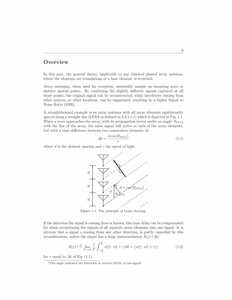
9
Overview
In this part, the general theory, applicable to any classical phased array antenna,where the elements are translations of a base element, is reviewed.
Array antennas, when used for reception, essentially sample an incoming wave atdistinct spatial points. By combining the slightly different signals captured at allthose points, the original signal can be reconstructed, while interferers coming fromother sources, at other locations, can be suppressed, resulting in a higher Signal toNoise Ratio (SNR).
A straightforward example is an array antenna with all array elements equidistantlyspaced along a straight line (LESA as defined in 3.3.1.1.1) which is depicted in Fig. 1.1.When a wave approaches the array, with its propagation vector under an angle1 θDOA
with the line of the array, the same signal will arrive at each of the array elements,but with a time difference between two consecutive elements of:
∆t =d cos (θDOA)
c(1.1)
where d is the element spacing and c the speed of light.
d
d
d
θDOAd
d× cos (θDOA)
Figure 1.1: The principle of beam steering.
If the direction the signal is coming from is known, this time delay can be compensatedfor when recombining the signals of all separate array elements into one signal. It isobvious that a signal s coming from any other direction, is partly cancelled by thisrecombination, unless the signal has a large autocorrelation Rs(τ) [6]:
Rs(τ)4= lim
T→∞
1
T
∫ T2
−T2
s(t) · s(t+ τ)dt = 〈s(t) · s(t+ τ)〉 (1.2)
for τ equal to ∆t of Eq. (1.1).
1This angle indicates the Direction of Arrival (DOA) of the signal.
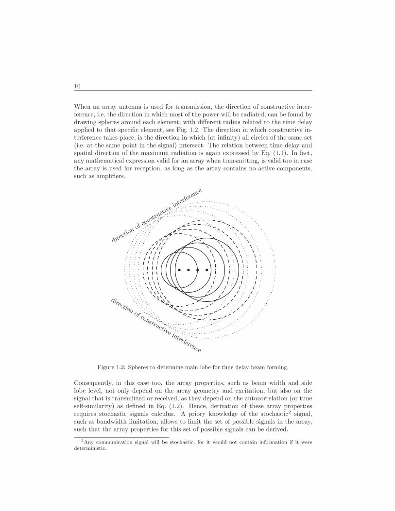
10
When an array antenna is used for transmission, the direction of constructive inter-ference, i.e. the direction in which most of the power will be radiated, can be found bydrawing spheres around each element, with different radius related to the time delayapplied to that specific element, see Fig. 1.2. The direction in which constructive in-terference takes place, is the direction in which (at infinity) all circles of the same set(i.e. at the same point in the signal) intersect. The relation between time delay andspatial direction of the maximum radiation is again expressed by Eq. (1.1). In fact,any mathematical expression valid for an array when transmitting, is valid too in casethe array is used for reception, as long as the array contains no active components,such as amplifiers.
direct
ionof
constr
uctiv
e interf
erenc
e
direction of constructive interference
Figure 1.2: Spheres to determine main lobe for time delay beam forming.
Consequently, in this case too, the array properties, such as beam width and sidelobe level, not only depend on the array geometry and excitation, but also on thesignal that is transmitted or received, as they depend on the autocorrelation (or timeself-similarity) as defined in Eq. (1.2). Hence, derivation of these array propertiesrequires stochastic signals calculus. A priory knowledge of the stochastic2 signal,such as bandwidth limitation, allows to limit the set of possible signals in the array,such that the array properties for this set of possible signals can be derived.
2Any communication signal will be stochastic, for it would not contain information if it weredeterministic.
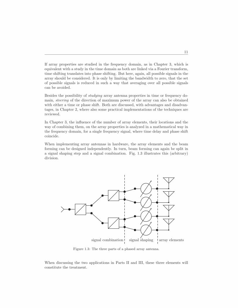
11
If array properties are studied in the frequency domain, as in Chapter 3, which isequivalent with a study in the time domain as both are linked via a Fourier transform,time shifting translates into phase shifting. But here, again, all possible signals in thearray should be considered. It is only by limiting the bandwidth to zero, that the setof possible signals is reduced in such a way that averaging over all possible signalscan be avoided.
Besides the possibility of studying array antenna properties in time or frequency do-main, steering of the direction of maximum power of the array can also be obtainedwith either a time or phase shift. Both are discussed, with advantages and disadvan-tages, in Chapter 2, where also some practical implementations of the techniques arereviewed.
In Chapter 3, the influence of the number of array elements, their locations and theway of combining them, on the array properties is analyzed in a mathematical way inthe frequency domain, for a single frequency signal, where time delay and phase shiftcoincide.
When implementing array antennas in hardware, the array elements and the beamforming can be designed independently. In turn, beam forming can again be split ina signal shaping step and a signal combination. Fig. 1.3 illustrates this (arbitrary)division.
array elementssignal shapingsignal combination
Figure 1.3: The three parts of a phased array antenna.
When discussing the two applications in Parts II and III, these three elements willconstitute the treatment.

invisible filling
Chapter 2
Beam Forming
Several techniques in order to shape the signals from the distinct array elements sothat they sum up constructively are in use. They can be categorized into three classes:time delay (Sect. 2.2.1), phase shift (Sect. 2.2.2) and frequency change (Sect. 2.2.3).
Both analog and digital implementations are in use. Due to the advantage of highflexibility and reconfigurability, the digital systems are gaining popularity. For someapplications, however, analog-to-digital conversion, that is indispensable prior to per-forming digital arithmetic in a processing unit, is not yet feasible due to the highbandwidth or number of elements in the array. In such case, the analog systems, thatalready have proven their capabilities for several decades, are to be used.
But before elaborating on these beam forming techniques, the choice of applyingthe beam forming at the different stages in the receiving (or transmitting) chain,namely Radio Frequencies (RF), Intermediate Frequencies (IF) or baseband (BB),is discussed. Beam forming by frequency change is excluded from this discussion,because of its limited relevance for practical systems. Beam forming by frequencychange is difficult to implement. Since it requires change of the mixing frequencyin both transmitter and receiver, the occupied bandwidth is large, the transmittersand receivers are complex devices, and a separate channel is required to make suretransmitter and receiver use the same1 carrier frequency [7]. Consequently, it ismerely applied in RADAR and sensing systems, where transmitter and receiver can becombined into one device. Nevertheless is the study of the phenomenon of frequencyscanning important, as it unintentionally occurs in arrays using delay lines for signalsthat have a non-zero bandwidth.
1A bandpass communication signal can indeed only be received around the carrier frequency, hencevarying frequency for scanning destroys signal reception if synchronization between transmitter andreceiver is not assured in one way or another.
13

14 Chapter 2. Beam Forming
It will become clear that from the beam forming techniques covered in Sect. 2.1, theonly one that does not suffer from InterSymbol Interference (ISI), even for wide bandsignals, is a time delay at RF. A phase shift of the carrier is always an approximationfor signals with small bandwidth, which is often the case in communication systems.
Besides those errors due to the non-zero bandwidth of signals, digital implementationsof beam forming introduce errors due to their discrete nature. The impact of thoseapproximation errors is evaluated in Sect. 2.3.
2.1 Beam Forming in the Receiving Chain
Essentially the signals that are received at the several elements of a phased array, aretime shifted versions of each other. Let us define ∆t as the time shift between thesignals of two adjacent elements, already calculated in Eq. (1.1), then the bandpasssignal at the two elements, can be written as:
R(t) cos (ωct+ θ(t))R(t+ ∆t) cos
(ωc(t+ ∆t) + θ(t+ ∆t)
) (2.1)
where ωc = 2πfc is the carrier pulsation containing the carrier frequency fc. R andθ contain the information in the form of an amplitude and phase deviation from thecarrier, similar to the split implicitly made when using complex envelope notation [6].
At Radio Frequencies (RF) it is obvious that by delaying the first signal with ∆t,both signals get synchronized again such that they can be combined again. If thebandwidth of the signal is small, this time delay can be approximated by a phaseshift δ = ωc∆t in the first signal of Eqs. (2.1):
R(t) cos (ωct+ ωc∆t+ θ(t))R(t+ ∆t) cos
(ωc(t+ ∆t) + θ(t+ ∆t)
) (2.2)
This approximation is only valid when the information signal varies slowly:
R(t) ≈ R(t+ ∆t) and θ(t) ≈ θ(t+ ∆t) (2.3)
as indeed only the carrier is rotated, not the information signal. If Eq. (2.3) does nothold, inter symbol interference (ISI) will occur.
At intermediate frequencies (IF), the signals are already multiplied with a LocalOscillator (LO) signal cos (ωLOt), so that after a low pass filter (to stop the (ωc+ωLO)component), one gets2:
R(t) cos
((ωc − ωLO)t+ θ(t)
)
R(t+ ∆t) cos((ωc − ωLO)t+ ωc∆t+ θ(t+ ∆t)
) (2.4)
2The multiplication of two cosines is: 2 cos (x) cos (y) = cos (x + y) + cos (x − y), the LPF stopsthe high frequency component cos (x + y). Filters behind mixers are not obligatory as the frequencyresponse of amplifiers acts as a filter for the ωc + ωLO component.

2.1. Beam Forming in the Receiving Chain 15
The phase shift in order to synchronize the signals is again ωc∆t. If a time delay isapplied, this delay should be ωc∆t/(ωc − ωLO).
One thus sees that the phase shift stays the same (the angles of the cosines are simplysummed when expanding the product of two cosines), but the time delay is longer inthe IF than in the RF case. Therefore at IF, the recombination after a time delay isnot exact anymore; the approximation that is made here, is:
R
(t+
ωc
ωc − ωLO∆t
)≈ R(t+ ∆t) (2.5)
Generally, ωc/(ωc−ωLO) > 1. If ωLO ≈ ωc, then ωc/(ωc−ωLO) 1. If the bandwidthof the signal R(t) is not small compared to (ωc−ωLO)/(ωLO∆t), this will, again, resultin ISI.
For baseband (BB) the mixing signal cos (ωct) has the same frequency as the RFcarrier, resulting in:
R(t) cos (θ(t))R(t+ ∆t) cos
(ωc∆t+ θ(t+ ∆t)
) (2.6)
so that the phase shift that should be applied to the first signal, is again ωc∆t, as inthe RF case. Summing both signals again implies that Eq. (2.3) is valid. At BB acarrier phase shift is not feasible with a time delay.
Besides the “correctness”, also the practical implementation issues of RF, IF and BBphase shifting are to be considered. Time delay in IF results in longer lines and thusmore losses (though the substrates for IF are less lossy than for RF). Pure phase shiftat lower frequencies (IF and BB) requires more relative bandwidth of the componentsbut in general components at lower frequencies are much cheaper.
The topology of the signal chain with beam forming in IF, RF and BB can be foundin Fig. 2.1. In the RF and BB case, the IF stage is left out: instead of using theheterodyne topology, a direct conversion scheme is depicted. This has the advantagethat no image rejection filters3 are needed, unless the signal is Single Side Band (SSB)signal. If this is the case, beam forming at RF, still only needs one image rejectionfilter for the entire array, namely after beam forming, before mixing down. For IFbeam forming, an image rejection filter is needed for every element prior to mixingto IF, where beam forming takes place.
In case of signals with non-symmetrical side bands, such as e.g. SSB signals, the directconversion to BB has to be a quadrature mixing. Otherwise the upper and lower sideband will interfere after mixing, as Fig. 2.4 clearly shows.
3Whenever mixing with an LO of pulsation ωLO, not only the frequencies above the LO frequency,but also those below are mixed to baseband. In case of IF mixing, where ωLO = ωc−ωIF, this causessignals at the mirror frequencies (ωLO − (ωc − ωLO)) to interfere with the useful IF signal. Henceprior to mixing, an image rejection filter should suppress those frequencies [8].
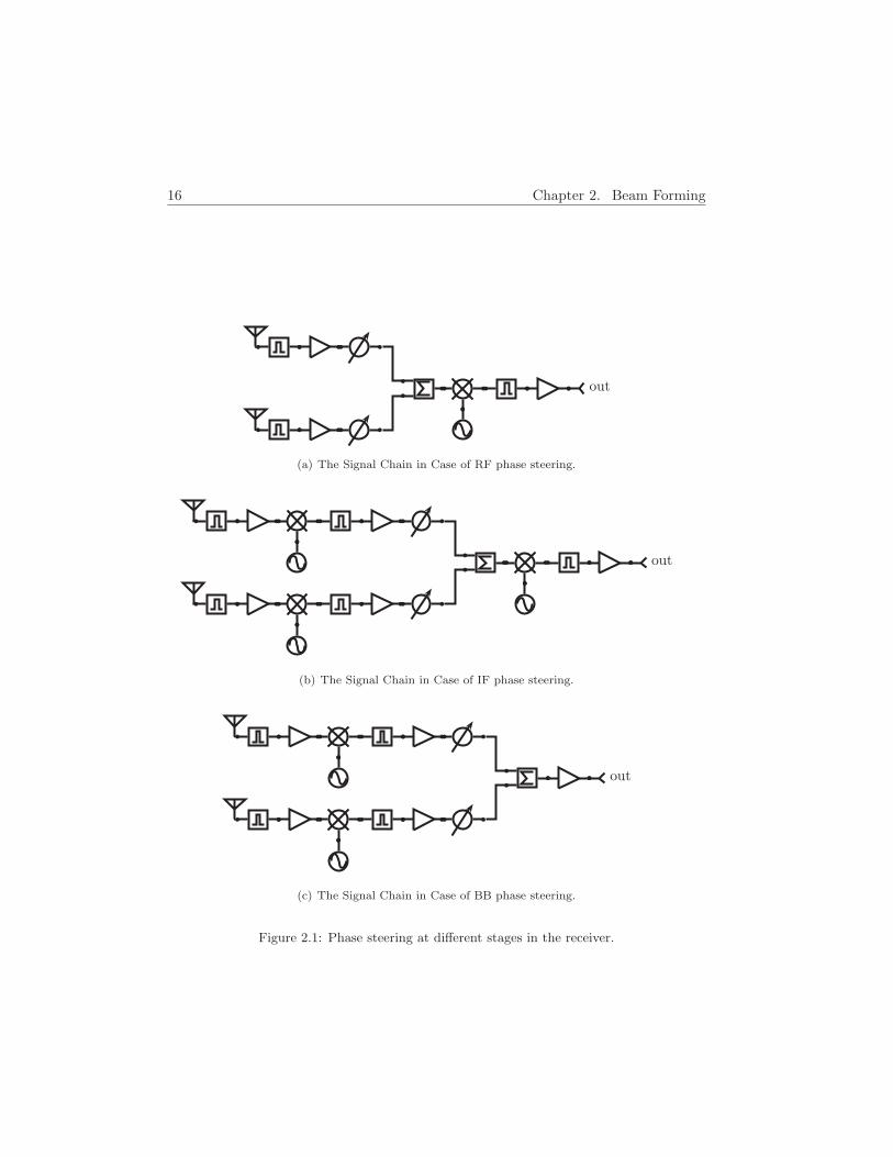
16 Chapter 2. Beam Forming
out
(a) The Signal Chain in Case of RF phase steering.
out
(b) The Signal Chain in Case of IF phase steering.
out
(c) The Signal Chain in Case of BB phase steering.
Figure 2.1: Phase steering at different stages in the receiver.
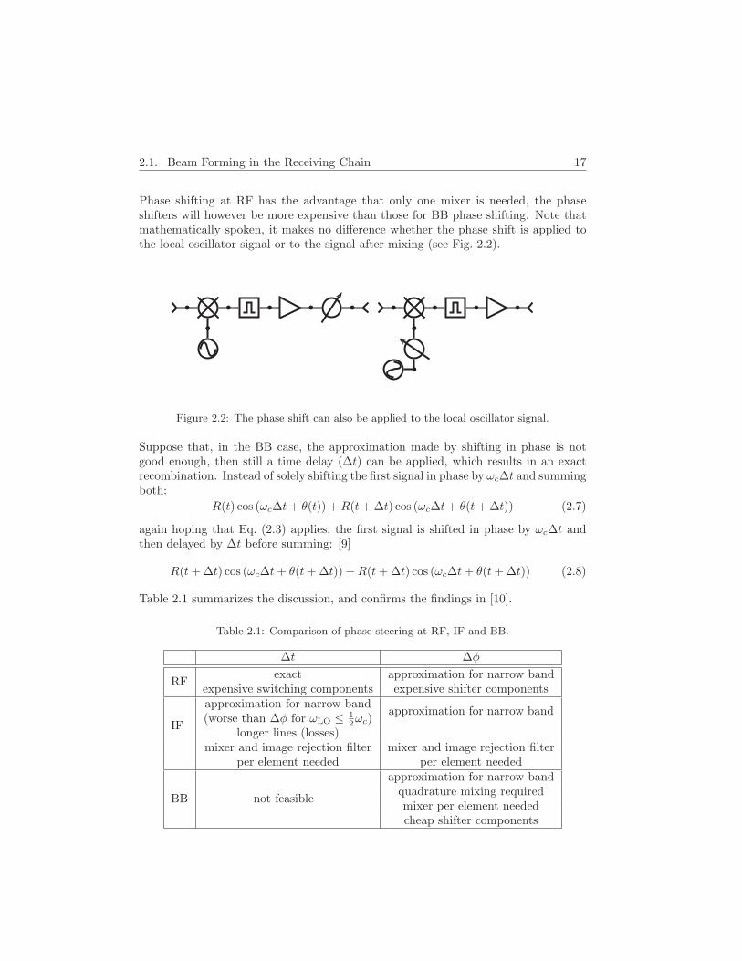
2.1. Beam Forming in the Receiving Chain 17
Phase shifting at RF has the advantage that only one mixer is needed, the phaseshifters will however be more expensive than those for BB phase shifting. Note thatmathematically spoken, it makes no difference whether the phase shift is applied tothe local oscillator signal or to the signal after mixing (see Fig. 2.2).
Figure 2.2: The phase shift can also be applied to the local oscillator signal.
Suppose that, in the BB case, the approximation made by shifting in phase is notgood enough, then still a time delay (∆t) can be applied, which results in an exactrecombination. Instead of solely shifting the first signal in phase by ωc∆t and summingboth:
R(t) cos (ωc∆t+ θ(t)) +R(t+ ∆t) cos (ωc∆t+ θ(t+ ∆t)) (2.7)
again hoping that Eq. (2.3) applies, the first signal is shifted in phase by ωc∆t andthen delayed by ∆t before summing: [9]
R(t+ ∆t) cos (ωc∆t+ θ(t+ ∆t)) +R(t+ ∆t) cos (ωc∆t+ θ(t+ ∆t)) (2.8)
Table 2.1 summarizes the discussion, and confirms the findings in [10].
Table 2.1: Comparison of phase steering at RF, IF and BB.
∆t ∆φ
RFexact approximation for narrow band
expensive switching components expensive shifter components
IF
approximation for narrow bandapproximation for narrow band
(worse than ∆φ for ωLO ≤ 12ωc)
longer lines (losses)mixer and image rejection filter mixer and image rejection filter
per element needed per element needed
BB not feasible
approximation for narrow bandquadrature mixing requiredmixer per element neededcheap shifter components
18 Chapter 2. Beam Forming
2.2 Some Beam Forming Implementations
Neither with the intention of being exhaustive, nor of going into much technicaldetails, the basic principle of the three classes of beam forming, as introduced at thebeginning of the chapter, will be reviewed. References will point the reader to sourceswhere all technical details can be found.
Both analog and digital implementations are in use. A disadvantage of digital tech-niques is that the signal has to be sampled (or digitized) first, putting high demandson the Analog to Digital Converter (ADC). If the signal has to be digitized at RFfrequencies, due to the Nyquist-Shannon sampling theorem [11, 12], the sample ratehas to be at least twice the carrier frequency.
Sampling at a rate equal to twice the bandwidth of the signal, is sufficient for recon-struction of the modulating signal at BB [13]. This however requires perfect filteringprior to sampling (and inherently mixing down) to avoid aliasing from signals at anyother frequency. Recall, no time shifting at BB is possible, as already mentioned inSect. 2.1.
The huge advantage of digital beam forming techniques, is that heavy array processingcan be done (even off-line). This way, significant better performance can be obtained[14]. And the entire half space as seen by the array can afterwards be analyzed andreceived, simply by performing the digital calculations over and over again but withother constants for other “directions of interest”. It is no surprise that many militaryRADAR systems make use of this possibility [15].
2.2.1 Time Delaying
By making the feed line to a certain antenna element longer or shorter, a variabletime delay is introduced. This is mostly obtained by switching line sections in andout of the feed line, similar to playing a trumpet by pushing the valves, using diodes[16] or Micro Electro Mechanical System (MEMS) switches [17].
Digitally, this is even more straightforward to implement, using shift registers withreconfigurable taps.
A more advanced approach is to delay the signal by modulating the propagationvelocity in the medium. This is mostly achieved by changing the permittivity ε = ε0εr(in ferroelectric materials) [18] or the permeability µ = µ0µr (in ferrites) [19] of themedium. This changes the propagation velocity:
c =1√εµ
=c0√εrµr
(2.9)
and thus the travelling time to the end of the line. The physical processes that causethis change are way beyond the scope of this work.

2.2. Some Beam Forming Implementations 19
An advantage of the latter technique is that the signal path is not switched whilereconfiguring the array. For both analog and digital straightforward implementationsindeed a part of the signal is simply dropped, or repeated, when changing the timedelay, voiding that part of the received signal.
2.2.2 Phase Shifting
Eq. (1.1) explained the working principle of a phased array with time delay. Fornarrow band applications, another way of explaining, is saying that the array inreceiving mode is sensitive to signals that arrive at each antenna element with aphase which is the inverse of the phase shift imposed by the beam forming network.In transmitting mode, the array will concentrate its power in locations (or Directionsof Departure (DOD) θDOD for far field approximation) where the signals departingfrom each antenna element arrive in phase, which results in constructive interference.This phase shift can easily be derived from the time delay of Eq. (1.1):
δ = ωc∆t = ωc ×d cos (θDOD)
λfc= 2π
d× cos θ
λ(2.10)
Note that the beam can indeed be steered by applying the appropriate phase shift,but that the antenna elements should be sensitive (for receiving mode) or be able toradiate (for transmitting mode) in that direction as well to obtain a beam. A detailedelaboration of this is delayed to Chapter 3.
The digital way to implement this, is by performing the matrix and vector multipli-cations of Sect. 2.2.2.1. The technique explained in that Sect. 2.2.2.1, referred to asquadrature phase shifting, is also implementable in an analog way, by using analogsumming and multiplication devices. The block diagram is given in 2.6, a more de-tailed discussion is delayed to Sect. 6.1.1. Apart from this technique, many others arein use. Some count on the phase change due to a reflection on a line end, terminatedwith a complex impedance. Diodes are then used to switch capacitances in and outin order to change the complex impedance [20]. Similar to this technique, a voltagedivider over a complex impedance can be used. If for this complex impedance a semi-conductor is used, its capacitance can simply be changed by changing the bias andhence the thickness of the depletion layer [21].
2.2.2.1 Quadrature Phase Shifting
A bandpass signal, as indeed in Eq. (2.1) too, can be written as the real part of acomplex envelope multiplied with a carrier phaser, see Fig. 2.3(a):
v(t) = <R(t)ejθ(t)ejωct = R(t) cos (ωct+ θ(t)) (2.11)

20 Chapter 2. Beam Forming
In a quadrature demodulator this signal is mixed with the sine and cosine of the LOfrequency:
I = v(t) × cos (ωLOt)Q = v(t) × sin (ωLOt)
(2.12)
so that it can easily be combined into the original RF signal with the same device:
v(t) = I × cos (ωLOt) +Q× sin (ωLOt) = v(t) ×(cos2(ωLOt) + sin2(ωLOt)
)(2.13)
If now the LO frequency is taken equal to the RF frequency and the 2ωct componentis stopped by a filter, the I and Q components are indeed the in-phase (with the RFcarrier) and the orthogonal (to the RF carrier) component of the BB signal:
I = R(t) cos (ωct+ θ(t)) × cos (ωLOt)
LPF= R(t) cos (θ(t))
Q = R(t) cos (ωct+ θ(t)) × sin (ωLOt)LPF= −R(t) sin (θ(t))
(2.14)
and the complex notation of the BB signal is:
R(t) cos θ(t) = <R(t)ejθt = <I − jQ (2.15)
Suppose, in the most general case of Eqs. (2.14), that a linear combination of I andQ leads to I ′ and Q′ [22]:
I ′ = a cos (∆θ) × I + a sin (∆θ) ×QQ′ = −a sin (∆θ) × I + a cos (∆θ) ×Q
(2.16)
then these I ′ and Q′ are the in-phase and quadrature components of the originalsignal, shifted in phase by ∆θ and amplified by a (this can also be interpreted as theLO delayed by ∆θ):
av(t) × cos (ωLOt− ∆θ)
LPF= I ′
av(t) × sin (ωLOt− ∆θ)LPF= Q′
(2.17)
so that after recombination (with cos (ωLOt) and sin (ωLOt)) the shifted version isobtained. The block diagram is given in Fig. 2.3(b). If the I and Q signals aresampled by an ADC, resulting in two vectors, I and Q, the phase shift can also beobtained by a simple matrix multiplication in digital logic. The vectors I ′ and Q′ arethe in phase and quadrature vectors if the carrier in the original signal was rotatedover a phase ∆θ [22]:
[I ′
Q′
]=
[cos (∆θ) sin (∆θ)− sin (∆θ) cos (∆θ)
]·[I
Q
](2.18)
This is similar to a coordinate rotation.

2.2. Some Beam Forming Implementations 21
=
<v(t)
IQ
R(t)ejθ(t)ejωct
ejωctθ(t)
(a) Complex Envelope Notation
0/90 0/90
(b) I-Q Phase Shifter (BB)
Figure 2.3: Working principle of the I-Q phase shifter.
If the LO shifts the signal to an IF instead of to BB, the implementation of the phaseshifter is even cheaper because only two instead of four variable gain amplifiers areneeded [23]. This is because the I and Q signal are not independent in the IF case(but phase π/2 shifted version of each other), whereas in case of BB I and Q are bothneeded to construct the original signal as they have only half the bandwidth of theoriginal signal, see Fig. 2.4, [13].
In some more detail for IF, the Q signal is thus the time delayed version of I (for BBthis is definitely not the case as I and Q are independent) so that:
I
LPF= vbase(t) × cos (ωIFt)
QLPF= vbase(t) × cos (ωIFt+ π
2 ) = vbase(t) × sin (ωIFt)(2.19)
which gives us the possibility of obtaining a shifted version of I by simply adding thetwo amplified signals.
vbase(t) × cos (ωIFt− ∆θ) = I ′ +Q′ = cos (∆θ) × I + sin (∆θ) ×Q (2.20)
A huge disadvantage of this technique is however that in order to obtain Q a timedelay is applied with possible ISI as a result.

22 Chapter 2. Beam Forming
ω
<
ωLO−ωLO
(a) I signal for BB mixing.
ω
=
−ωLO
ωLO
(b) Q signal for BB mixing.
ω
<
ωLO−ωLO
(c) I signal for IF mixing.
ω
=
−ωLO
ωLO
(d) Q signal for IF mixing.
Figure 2.4: Spectra for BB and IF. For IF Q is I after a π/2 phase shift.
II ′
Q
Q′ I ′ +Q′
∆θ
(a) I-Q shifting in IF
I0/90
I ′ +Q′
(b) I-Q Phase Shifter (IF)
Figure 2.5: The I-Q phase shifter for IF.
The shifter of Fig. 2.3(b) takes an RF signal in and outputs an RF signal, rotated inphase. The shifting itself is done in BB. When sending or receiving, one of the mixingstages can be left out. We thus get the schemes of Fig. 2.6(a) and 2.6(b).
Any type of modulation can be sent or received by this scheme, but the appropriateI and Q should be provided at the input for transmission. For a QPSK signal, theseare the two orthogonal bit streams, but for other schemes such as FM the generationof I and Q is less straightforward.
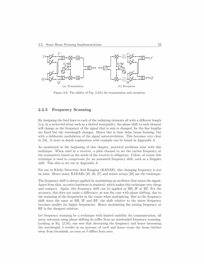
2.2. Some Beam Forming Implementations 23
I
Q
I ′
Q′
0/90
(a) Transmission
0/90
Q
I
Q′
I ′
(b) Reception
Figure 2.6: The shifter of Fig. 2.3(b) for transmission and reception.
2.2.3 Frequency Scanning
By designing the feed lines to each of the radiating elements all with a different length(e.g. in a series-fed array such as a slotted waveguide), the phase shift to each elementwill change as the frequency of the signal that is sent is changed, for the line lengthsare fixed but the wavelength changes. Hence this is time delay beam forming, butwith a deliberate modulation of the signal autocorrelation. This becomes very clearin [24]. A more in depth explanation with example can be found in Appendix A.
As mentioned at the beginning of this chapter, practical problems arise with thistechnique. When used in a receiver, a pilot channel to set the carrier frequency atthe transmitter based on the needs of the receiver is obligatory. Unless, of course thistechnique is used to compensate for an unwanted frequency shift, such as a Dopplershift. This idea is set out in Appendix A.
For use in RAdio Detection And Ranging (RADAR), this changing frequency is notan issue. Hence many RADARs [25, 26, 27] and sensor arrays [28] use the technique.
The frequency shift is always applied by modulating an oscillator that mixes the signal.Apart from that, no extra hardware is required, which makes this technique very cheapand compact. Again, this frequency shift can be applied at BB, IF or RF. For theaccuracy, this does not make a difference, as was the case with phase shifting, due tothe summing of the frequencies in the cosine when multiplying. But as the frequencyshift stays the same at BB, IF and RF, the shift relative to the mixer frequencybecomes smaller for higher frequencies. Hence modulating the mixing frequency atRF is the cheapest solution.
Let frequency scanning be a technique with limited usability for communication, allarray antennas using phase shifting do suffer from an unintended frequency scanning.Looking at Eq. (2.10), one sees that decreasing the frequency and hence increasingthe wavelength λ results in an increase of cos θ and hence scans the beam furtheraway from broadside, as soon as δ differs from zero.

24 Chapter 2. Beam Forming
This is a second order effect, but shows up as soon as the signal has a bandwidth in% that is comparable to the beam width in , due to the aperture fill effect [29]. Theamplitude of this effect depends on the bandwidth of the signal and the scan angleof the array. The more the array is scanned off broadside, the more pronounced thiseffect becomes. The inter-element distance d is of no influence as δ linearly dependson d. This follows immediately from Eq. (2.10):
∆ cos θ =∆λ× δ
2πd=
∆λ× 2πd×cos θλ
2πd=
∆λ
λ× cos θ (2.21)
2.3 Beam Forming Approximation Effects
For any digital beam forming implementation, not every possible time, phase orfrequency shift can be selected. This introduces errors. Moreover, all analog im-plementations are controlled in a digital way, hence the system deals with the sameproblem4.
How this affects the array factor in case of phase shift beam forming, is explained inSect. 3.4.2. For time delay beam forming, the reader is referred to Sect. 9.4.
4There is one way of circumventing the problem, namely in case the beam always has to performthe same scanning movement, the controlling signals can be Low Pass Filtered (LPF), resulting in asmooth transition with the beam maximum always pointing towards the receiver.
Chapter 3
Phased Array Design
In Sect. 2.2.2 was explained that for signals with sufficiently small bandwidth, thebeam of an array antenna can be steered by applying the appropriate phase shifts.In this chapter a mathematical treatment of such phased arrays is given. For startersis demonstrated in Sect. 3.1.1, that from Maxwell’s laws, the radiation properties, asintroduced in Sect. 3.1.2, of an array antenna, can be split into a part only dependingon the array element and another part only depending on the array geometry andexcitation.
The influence of array geometry and excitation can be studied via the properties ofthe Fourier transform, as explained in Sect. 3.2. This is worked out in detail forgeometry in Sect. 3.3.1 and for phase and amplitude of the excitation in Sect. 3.3.2.1and 3.3.2.2 respectively. The recommendations and techniques for designing arraysresulting from the discussion, are summarized in Sect. 3.3.3.
All theory in this chapter can be found elsewhere. If appropriate, references are given.No overview was available at the moment of writing, however, where all array theorywas linked with Fourier transform properties. Unless stated differently, all graphswere obtained with numerical calculations in MATLABTM.
3.1 Definitions
3.1.1 Array Factor
An array antenna consists of N identical elements, translated from the origin by thevectors ~bn (with n : 1 → N) as on Fig. 3.1(a). The radiated field of the array inlinear, homogeneous media is found by summing the contributions of all elements.
25

26 Chapter 3. Phased Array Design
z
y
x
reference element
element 1
~b1element 2
~b2
~ir
θ
φ
(a) Array in Spherical Coordinate System.
reference element
element n
~bn
~ir
~ir
~ir
~r
|R|
|Rn|
~r′
~r′n
(b) Far Field Approximation.
Figure 3.1: The geometry of an array antenna.
Writing out the vector potential ~A for the array results in [30]:
~A(~r) =
N∑
n=1
~An(~r) =
N∑
n=1
µ(~r′n)
4π
∫
v′
n
~Jn(~r′n)e−jβRn
Rndv′n (3.1)
where Rn = |~r − ~r′n| is the distance between the observation point where ~A(~r) is
calculated and a varying point ~r′n in the current carrying volume of the nth elementv′n that is integrated. ~Jn(~r′n) is the current density in this varying point.
Neglecting the possible distortion on the current profile that mutual coupling betweenarray elements can cause, the current distribution on each element is supposed identi-cal to the current distribution ~Jref on the reference element, except for a complex ex-citation coefficient an, expressing the difference in amplitude and phase of the appliedsignal with respect to the signal on the reference element. Thus ~Jn(~r′n) = an
~Jref(~r′)
where ~r′n = ~r′ +~bn (see Fig. 3.1(b)).
For large distances Rn → ∞ (i.e. far field approximation)~ir, the vector of unit lengththat points in the direction of ~r, see also Fig. 3.1(a):
~ir = (sin θ · cosφ, sin θ · sinφ, cos θ) (3.2)
is the same for each point ~r′n. This results in an approximation for Rn:
Rn ≈ |~r − ~r′ ·~ir −~ir ·~bn| (3.3)
For the value of Rn in the denominator of Eq. (3.1), this can even further be approx-imated by |~r|, as no phase information has to be preserved.
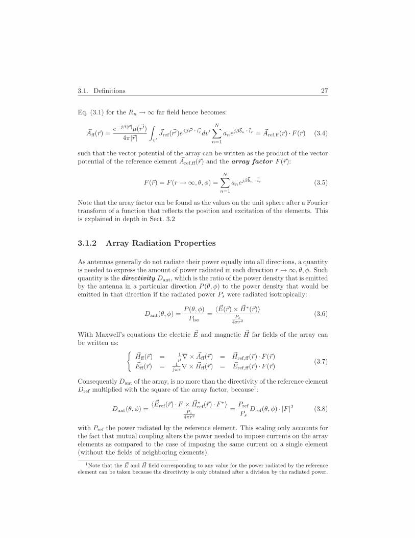
3.1. Definitions 27
Eq. (3.1) for the Rn → ∞ far field hence becomes:
~Aff(~r) =e−jβ|~r|µ(~r′)
4π|~r|
∫
v′
~Jref(~r′)ejβ~r′ · ~irdv′
N∑
n=1
anejβ~bn ·~ir = ~Aref,ff(~r) ·F (~r) (3.4)
such that the vector potential of the array can be written as the product of the vectorpotential of the reference element ~Aref,ff(~r) and the array factor F (~r):
F (~r) = F (r → ∞, θ, φ) =
N∑
n=1
anejβ~bn ·~ir (3.5)
Note that the array factor can be found as the values on the unit sphere after a Fouriertransform of a function that reflects the position and excitation of the elements. Thisis explained in depth in Sect. 3.2
3.1.2 Array Radiation Properties
As antennas generally do not radiate their power equally into all directions, a quantityis needed to express the amount of power radiated in each direction r → ∞, θ, φ. Suchquantity is the directivity Dant, which is the ratio of the power density that is emittedby the antenna in a particular direction P (θ, φ) to the power density that would beemitted in that direction if the radiated power Ps were radiated isotropically:
Dant(θ, φ) =P (θ, φ)
Piso=
〈 ~E(~r) × ~H∗(~r)〉Ps
4πr2
(3.6)
With Maxwell’s equations the electric ~E and magnetic ~H far fields of the array canbe written as:
~Hff(~r) = 1
µ∇× ~Aff(~r) = ~Href,ff(~r) ·F (~r)~Eff(~r) = 1
jωε∇× ~Hff(~r) = ~Eref,ff(~r) ·F (~r)(3.7)
ConsequentlyDant of the array, is no more than the directivity of the reference elementDref multiplied with the square of the array factor, because1:
Dant(θ, φ) =〈 ~Eref(~r) ·F × ~H∗
ref(~r) ·F ∗〉Ps
4πr2
=Pref
PsDref(θ, φ) · |F |2 (3.8)
with Pref the power radiated by the reference element. This scaling only accounts forthe fact that mutual coupling alters the power needed to impose currents on the arrayelements as compared to the case of imposing the same current on a single element(without the fields of neighboring elements).
1Note that the ~E and ~H field corresponding to any value for the power radiated by the referenceelement can be taken because the directivity is only obtained after a division by the radiated power.
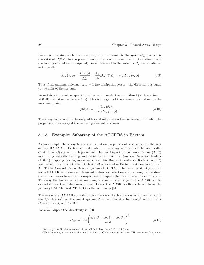
28 Chapter 3. Phased Array Design
Very much related with the directivity of an antenna, is the gain Gant, which isthe ratio of P (θ, φ) to the power density that would be emitted in that direction ifthe total (radiated and dissipated) power delivered to the antenna Pin, were radiatedisotropically:
Gant(θ, φ) =P (θ, φ)
Pin
4πr2
=Ps
PinDant(θ, φ) = ηradDant(θ, φ) (3.9)
Thus if the antenna efficiency ηrad = 1 (no dissipation losses), the directivity is equalto the gain of the antenna.
From this gain, another quantity is derived, namely the normalized (with maximumat 0 dB) radiation pattern p(θ, φ). This is the gain of the antenna normalized to themaximum gain:
p(θ, φ) =Gant(θ, φ)
max Gant(θ, φ) (3.10)
The array factor is thus the only additional information that is needed to predict theproperties of an array if the radiating element is known.
3.1.3 Example: Subarray of the ATCRBS in Bertem
As an example the array factor and radiation properties of a subarray of the sec-ondary RADAR in Bertem are calculated. This array is a part of the Air TrafficControl (ATC) system of Belgocontrol. Besides Airport Surveillance Radars (ASR)monitoring aircrafts landing and taking off and Airport Surface Detection Radars(ASDR) mapping taxiing movements, also Air Route Surveillance Radars (ARSR)are needed for enroute traffic. Such ARSR is located in Bertem, with on top of it anAir Traffic Control Radar Beacon System (ATCRBS). The latter is strictly spokennot a RADAR as it does not transmit pulses for detection and ranging, but insteadtransmits queries to aircraft transponders to request their altitude and identification.This way the two dimensional mapping of azimuth and range of the ARSR can beextended to a three dimensional one. Hence the ARSR is often referred to as theprimary RADAR, and ATCRBS as the secondary [31].
The secondary RADAR consists of 35 subarrays. Each subarray is a linear array often λ/2 dipoles2, with element spacing d = 14.6 cm at a frequency3 of 1.06 GHz(λ = 28, 3 cm), see Fig. 3.3.
For a λ/2 dipole the directivity is: [30]
Dant = 1.64
(cos (β λ
4 · cos θ) − cosβ λ4
sin θ
)2
(3.11)
2Actually the dipoles measure 12 cm, slightly less than λ/2 = 14.6 cm.3This frequency is chosen as the mean of the 1.03 GHz transmit and 1.09 GHz receiving frequency.
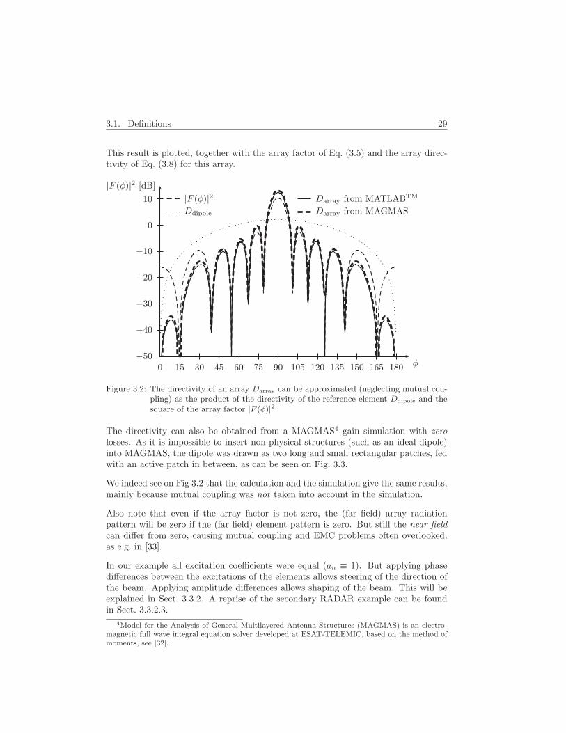
3.1. Definitions 29
This result is plotted, together with the array factor of Eq. (3.5) and the array direc-tivity of Eq. (3.8) for this array.
0 15 30 45 60 75 90 105 120 135 150 165 180−50
−40
−30
−20
−10
0
10
|F (φ)|2 [dB]
φ
|F (φ)|2Ddipole
Darray from MATLABTM
Darray from MAGMAS
Figure 3.2: The directivity of an array Darray can be approximated (neglecting mutual cou-pling) as the product of the directivity of the reference element Ddipole and thesquare of the array factor |F (φ)|2.
The directivity can also be obtained from a MAGMAS4 gain simulation with zerolosses. As it is impossible to insert non-physical structures (such as an ideal dipole)into MAGMAS, the dipole was drawn as two long and small rectangular patches, fedwith an active patch in between, as can be seen on Fig. 3.3.
We indeed see on Fig 3.2 that the calculation and the simulation give the same results,mainly because mutual coupling was not taken into account in the simulation.
Also note that even if the array factor is not zero, the (far field) array radiationpattern will be zero if the (far field) element pattern is zero. But still the near fieldcan differ from zero, causing mutual coupling and EMC problems often overlooked,as e.g. in [33].
In our example all excitation coefficients were equal (an ≡ 1). But applying phasedifferences between the excitations of the elements allows steering of the direction ofthe beam. Applying amplitude differences allows shaping of the beam. This will beexplained in Sect. 3.3.2. A reprise of the secondary RADAR example can be foundin Sect. 3.3.2.3.
4Model for the Analysis of General Multilayered Antenna Structures (MAGMAS) is an electro-magnetic full wave integral equation solver developed at ESAT-TELEMIC, based on the method ofmoments, see [32].

30 Chapter 3. Phased Array Design
element
passive patch
active patch
passive patch
12 cm
0.05 cm
array
Figure 3.3: The array of dipoles as inserted in MAGMAS
3.2 The Array Factor via a Fourier Transform
Eq. (3.5) reflects that the array factor can be found via the inverse Fourier transform ofa function that reflects the position and excitation of the elements. Define a functionf(x, y, z) that consists of Dirac impulses multiplied with the excitation coefficient onthe locations of the array elements and is zero elsewhere:
f(~r) =∑
N
anδ3(~r −~bn) (3.12)
The inverse Fourier transform of this function is:
F (~u) = F (u, v, w) = F−1f(~r)=
y ∑
N
anδ3(~r − ~bn)ej2π~r · ~ud~r =
∑
N
anej2π~bn · ~u (3.13)
This is a function over three variables (u, v, w), but only the values on the spherewith a radius of one in this transformed domain have a physical meaning5 as these
are the only points where |~u| = 1 such that ~bn · ~u = |~bn| cos(ubn). The interpretationof u = sin θ · cosφ, v = sin θ · sinφ and w = cos θ results in the array factor ofEq. (3.5). This is of course only true if the position of the elements as expressed in~bn is measured in wavelengths.
5The points that lie on the sphere with radius two have a physical meaning too as they representthe array factor of the array when ~bn gives the element locations measured in 2λ and so on.

3.2. The Array Factor via a Fourier Transform 31
The properties of the Fourier transform hence apply. But be aware of the fact that thetransformed domain is not only the unit sphere on which the values with a physicalmeaning lie. Consequently, care should be taken when studying the array using theFourier properties. E.g. when applying the theorem of Parceval [6]:
y|f(~r)|2d~r =
y|F (~u)|2d~u 6=
π∫
0
2π∫
0
|F (θ, φ)|2 sin θdθdφ. (3.14)
The integration of the rightmost expression is over the unit sphere and gives thepower radiated by the array with isotropic array elements. The other two expressionsintegrate over the entire (u, v, w) and (x, y, z) domain, which, because the integrationof a squared Dirac impulse is infinite, equals ∞.
Consequently, even two arrays of isotropic radiators, that share the same set of ex-citation coefficients an, but have different geometries, are not guaranteed to radiatethe same amount of power. This is a result of the fact that the elements are in thepresence of their mutual fields6 between array elements. Physically this is due to thefact that the power is found as:
P = <
∫
v′
~E ~J∗
2dv′
(3.15)
If the geometry of the array is changed, the same currents are to be imposed in apossibly different electric field, resulting in an other value for the consumed (radiated)power. The shortcoming in treating an element as if it were not embedded in thearray is thus that it violates the conservation of energy. But still the approximationto suppose all current distributions as identical to the distribution on the referenceelement does not conflict with the conservation of energy.
A possible way to compare two arrays is calculating the power by integrating theproduct of the square of the array factor and the element pattern of both arrays andthen scaling the set of excitation coefficient of one array until the power is equalto the power of the other array. By doing this the supposition about the currentdistribution is maintained but the fact that the elements are in their mutual electricfields is reckoned by scaling the Zin of all elements resulting in the same power forboth arrays. This is not physically correct, as only in single mode infinite arraysthe elements experience the same environment and hence all have identical inputimpedances.
6The effect of this is actually twofold. Firstly, fields caused by neighboring elements can alter thecurrent profile of an element. This effect is bypassed by imposing currents (identical to the current onthe reference element except for an excitation coefficient an). Note that in practice arrays are voltagedriven. Hence imposing current, limits the practical applicability of the results tremendously. Thesecond effect, is the changing input impedance of an element when in the presence of fields comingfrom neighboring elements. This effect is discussed here.

32 Chapter 3. Phased Array Design
For finite arrays, the outer array elements have input impedances different from thoseof the center array elements. Consequently, because most arrays are not currentdriven, the (complex) current amplitudes will differ over the elements, resulting inarray properties different from those predicted when simply scaling the excitationcoefficients. Array factor calculations are a good starting point. Full wave simulationof the array at a further design stage is ever sensible.
For a 1D array along the x-axis, the y and z values of ~bn are all zero such that thevalue of F in Eq. (3.13) only depends on u. Thus for all (θ, φ) that give the sameresult for u = sin θ · cosφ the array factor is the same. This results in a radiationpattern that is rotation symmetric around the u axis, as on Fig. 3.4, because thelocus of the points where u is a constant and r = 1 is a circle around the u-axis(u = r · sin θ · cosφ). For a 2D array in the x, y-plane the same derivation results in apattern that is mirrored by the u, v-plane (same array factor if u and v are the sameand r = 1). For a 3D array each point on the unit sphere can result in a differentvalue for the array factor.
Note that for the translation vectors ~bn any set of vectors can be chosen. Also arrayswith non-equally spaced radiators or even arrays with element locations on irregulargeometric figures have applications.
3.3 Array Design with Array Factor
3.3.1 Influence of the Array Geometry
To study the influence of the element locations of an array on the array factor, wewill first evaluate the equally spaced uniform linear array. This is an array whereall elements are fed uniformly (ai ≡ aj) and are spaced equally along a line (asfor example on Fig. 3.3). Then linear arrays with non-equally spaced elements arediscussed. After that we look at non-linear arrays.
Throughout the discussion it will be clear that all results stem with the propertiesof the Fourier transform. The emphasis in the text is on the physical interpretation,related to array antennas.
3.3.1.1 Linear Equally Spaced Arrays (LESA)
The array factor of Eq. (3.5) for the case of a uniform linear array along the x-axis,is a complex periodic (in u = sin θ cosφ) function [30]:
F (θ, φ) =
N∑
n=1
cos
(2πn
d
λsin θ cosφ
)+ j
N∑
n=1
sin
(2πn
d
λsin θ cosφ
)(3.16)

3.3. Array Design with Array Factor 33
(a) 1D array(b) 2D array
(c) 3D array
(d) Array layouts: Nx = Ny = Nz = 4, d = 0.9λ
Figure 3.4: Array factors of a 1D, 2D and 3D array.
3.3.1.1.1 Element Spacing d In Fig 3.5 the array factor of a uniform LESAwith N = 10 elements is plotted as a function of u. This is sufficient because thearray factor of a linear array only depends on u (see Sect. 3.2). As the array factoris the inverse Fourier transform of a discrete function, it is a periodical function in u(not in φ). The value for d determines the periodicity and thus the number of periodsmapped to the u = [−1, 1] visible interval.
As soon as d ≥ λ, we see that a second maximum appears on the edges of the plot,because a direction exists in which the waves of each element have a difference inpath length of exactly one wavelength λ (in phase). Mathematically, more than oneperiod of the array factor function lies in the u = [−1, 1] or φ = [0, π] interval. Theseadditional maxima are called grating lobes and must be avoided, even if the far fieldpattern of the reference element is zero, because they causes in-phase mutual couplingbetween the elements in the near field.
The advantage of taking d as close to λ as possible is that the beam width is as smallas possible: with the same number of elements, a bigger d results in a longer antenna.But one has to avoid that the array pattern raises too much at the edges of the [0, π]interval, thus avoid that the grating lobe comes up higher than the side lobes.
If d is changed and hence another number of periods lies in the visible interval, alsothe total power radiated by the array changes. The explanation7 for this was givenin Sect. 3.2.
7Curves similar to those in Fig. 3.6 were assigned to surface waves in [34]. This is only partiallytrue.
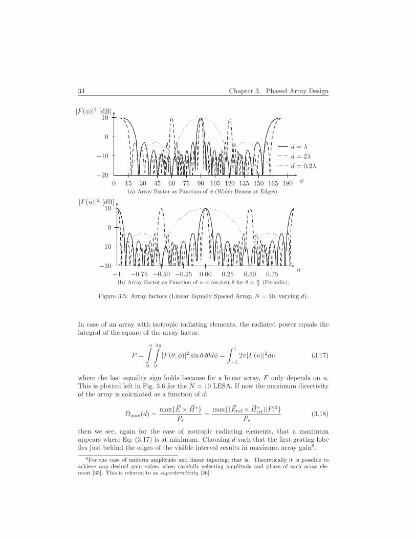
34 Chapter 3. Phased Array Design
0 15 30 45 60 75 90 105 120 135 150 165 180−20
−10
0
10|F (φ)|2 [dB]
φ
d = λ
d = 2λ
d = 0.2λ
(a) Array Factor as Function of φ (Wider Beams at Edges).
−1 −0.75 −0.50 −0.25 0.00 0.25 0.50 0.75−20
−10
0
10|F (u)|2 [dB]
u
(b) Array Factor as Function of u = cos φ sin θ for θ = π2
(Periodic).
Figure 3.5: Array factors (Linear Equally Spaced Array, N = 10, varying d).
In case of an array with isotropic radiating elements, the radiated power equals theintegral of the square of the array factor:
P =
π∫
0
2π∫
0
|F (θ, φ)|2 sin θdθdφ =
∫ 1
−1
2π|F (u)|2du (3.17)
where the last equality sign holds because for a linear array, F only depends on u.This is plotted left in Fig. 3.6 for the N = 10 LESA. If now the maximum directivityof the array is calculated as a function of d:
Dmax(d) =max ~E × ~H∗
Ps=
max( ~Eref × ~H∗ref)|F |2
Ps(3.18)
then we see, again for the case of isotropic radiating elements, that a maximumappears where Eq. (3.17) is at minimum. Choosing d such that the first grating lobelies just behind the edges of the visible interval results in maximum array gain8.
8For the case of uniform amplitude and linear tapering, that is. Theoretically it is possible toachieve any desired gain value, when carefully selecting amplitude and phase of each array ele-ment [35]. This is referred to as superdirectivity [36].
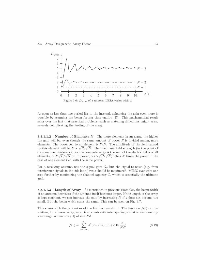
3.3. Array Design with Array Factor 35
0 1 2 3 4 5 6 7 8 9 100
1
2
3
4
5
6
7
N = 1
N = 2
N = 5
d [λ]
Darray
Figure 3.6: Darray of a uniform LESA varies with d.
As soon as less than one period lies in the interval, enhancing the gain even more ispossible by scanning the beam further than endfire [37]. This mathematical resultskips over the fact that practical problems, such as matching difficulties, might arise,severely complicating the feeding of the array.
3.3.1.1.2 Number of Elements N The more elements in an array, the higherthe gain will be, even though the same amount of power P is divided among moreelements. The power fed to an element is P/N . The amplitude of the field causedby this element will be E ∝
√P/
√N . The maximum field strength (in the point of
constructive interference) for the complete array is the sum of the electric fields of allelements, ∝ N
√P/
√N or, in power, ∝ (N
√P/
√N)2 thus N times the power in the
case of one element (fed with the same power).
For a receiving antenna not the signal gain Gr but the signal-to-noise (e.g. frominterference signals in the side lobes) ratio should be maximized. MIMO even goes onestep further by maximizing the channel capacity C, which is essentially the ultimategoal.
3.3.1.1.3 Length of Array As mentioned in previous examples, the beam widthof an antenna decreases if the antenna itself becomes larger. If the length of the arrayis kept constant, we can increase the gain by increasing N if d does not become toosmall. But the beam width stays the same. This can be seen on Fig. 3.7.
This stems with the properties of the Fourier transform. The function f(~r) can bewritten, for a linear array, as a Dirac comb with inter spacing d that is windowed bya rectangular function (Π) of size Nd:
f(~r) =
∞∑
n=−∞δ3(~r − (nd, 0, 0)) × Π(
x
Nd) (3.19)

36 Chapter 3. Phased Array Design
−1 −0.75 −0.50 −0.25 0.00 0.25 0.50 0.75−20
−10
0
10
20
30
40
|F (u)|2 [dB]
u
d = 0.2λ,N = 101
d = 2λ,N = 11
d = 4λ,N = 6
Figure 3.7: Array factors (LESA, length 20λ, varying N).
The array factor is the convolution9 of a Dirac impulse train with the inverse Fouriertransform of the rectangular window (a sinc(x) = sin(πx)/(πx) function):
F (u) = F−1 f(~r) = Ndsin(Ndπu)
Ndπu
⊗ 1
d
∞∑
n=−∞δ3(u− n
d) (3.20)
Form this equation we indeed get the conclusions:
• as the element spacing d increases, the spacings between the Dirac impulses inthe u domain is smaller (causing grating lobes);
• as more elements in the array make the window larger, the beam width willbecome smaller for the frequency of the sine function is higher;
• as the length Nd of the array is kept the same, the Fourier transform of thewindow will remain the same; if then more elements are added, the spacing ddecreases such that the separation between the Dirac impulses in the u domain,and hence the grating lobes, will be larger.
Obtaining a higher gain by adding elements (increasing N) however has its limits. AsN becomes so high that d is smaller than d at the maximum directivity on Fig. 3.6,adding more elements will on the contrary result in less gain.
9x(t)N
y(t) =R +∞
−∞x(t)y(u − t)du

3.3. Array Design with Array Factor 37
3.3.1.2 Linear Non-equally Spaced Arrays
Arrays with unequally spaced elements can be divided into three groups10:
• Sparse Array: a LESA where elements are left out,
• Perturbed Array: a LESA (or sparse array) where elements are displaced(randomly) from their original grid position,
• Fixed Array: an array where the placing of the elements is according to aformula (e.g. geometric series).
Sparse arrays have less mutual coupling and need fewer radiating elements. Thishowever results in a lower gain, which depends on the number of elements. An exampleis the multi-band RADAR of the Wide Band Sparse Elements (WISE) research projectat T.U.Delft, where several sparse arrays are put on the same substrate, resulting inone antenna, containing arrays for multiple applications (as on Fig. 3.8). [38]
!!!!!!!!!!!!!!!!!!!!
!!!!!!!!!!!!!!!
!!!!!!!!!!!!!!!
!!!!!!!!!!!!!!!!!!!!!!!!!!!!!!!!!!!!!!!!!!!!!!!!!!!!!!!!!!!!!!!!!!!!!!!!!!!!!!!!!!!!!!!!!!!!!!!!!!!
!!!!!!!!!!!!!!!!!!!!!!!!!!!!!!!!!!!!!!!!!!!!!!!!!!!!!!!!!!!!!!!!!!!!!!!!!!!!!!!!!!!!!!!!
!!!!!!
!!!
!!!
!!!
!!!!!!
!!!
!!!
!!!
!!!
!!!
Figure 3.8: Several sparse arrays are combined into one antenna.
Another example of a sparse array, used e.g. in ultrasound medical imaging, is theperfect array . This is an array that has one and just one pair of elements that areseparated by distance nd for every integer of the set n = 1 → N(N − 1)/2. Sucharrays have the smallest possible beam width (for a certain antenna length) and thusthe best possible resolution. But, as shown on Fig. 3.12, this results in very high sidelobes, which is not a disadvantage in a quiet measurement environment. No perfectarray with more than four elements exists [39].
The amplitude of the array factor function of any11 array with excitation coefficientsall real (i.e. when not scanned), is symmetrical (in u). If f(x) is real12, then F ∗(u) =F (−u) where F (u) = F−1f(x) such that:
|F (u)| =√F (u)F ∗(u) =
√F ∗(−u)F (−u) = |F (−u)| (3.21)
10Every (finite) fixed or perturbed array is also a sparse array for it can be obtained from a LESAwith d equal to the greatest common factor of the element spacings in the fixed or perturbed array.
11Including sparse arrays, even though the array geometry itself is not symmetric.12If f(x) is real and even f(x) = f(−x), then:
Ff(x) =
Z
∞
−∞
f(x)e−j2πxydx =
Z
∞
−∞
f(x)ej2πxydx = F−1f(x).

38 Chapter 3. Phased Array Design
But this can also intuitively be seen. Because only the far field radiation pattern is ofinterest, the only path lengths that have an influence on the interference and thus theradiation pattern are the path lengths from the radiating elements to the phase frontof the direction that we are looking at. These differences are equal in both cases,except for a minus sign, resulting in the same amplitude after summing.
phase front phase front
−10 +10
phase to front: 6,5 and 2
or -1,-4 and -6
phase to front: 1,4 and 6
or -6,-5 and -2
Figure 3.9: The radiation pattern of a sparse array is symmetrical.
Perturbed arrays, such as for example random arrays (where the elements aredisplaced randomly) are mainly used to avoid grating lobes without having to lowerd. Moreover random arrays are very robust: even when a radiating element fails, theperformance of the array is hardly influenced [40]. The disadvantage of random arraysis that even though the grating lobes can be lowered, the side lobes are higher than inthe equidistant case. A means to combine the advantages of equidistant arrays andrandom arrays is the so called fractal array. Here the boundaries of the area that isfilled with elements are generated as fractals [41].
An example of a fixed array is the geometric array . Here the placement ofthe elements is based on a geometric series. The distance between two consecutiveelements becomes smaller or bigger at the edges of the array, depending on whether0 < a < 1 or a > 1: (xn = −x−n)
d|n|+1 = a× d|n| = a|n| × d1 (3.22)
The array factor of some geometric arrays with 10 elements and an array length of 6λwith a > 1 is given in Fig. 3.10. We see that there is no use in taking the a > 1 forthis results in a wider beam and a higher side lobe level. On Fig. 3.11 some examplesof geometric arrays with a < 1 are given. In that case beam width can be traded offagainst side lobe level.
As an overview, on Fig. 3.12 some linear arrays with N = 4 are given as well as theirarray factor. We see indeed that the perfect array has the smallest beam width. Theperturbed array suppresses the raising grating lobe at the edges of the plot betterthan the equidistant array. The geometric array trades off the beam width for ahigher (overall) side lobe level.

3.3. Array Design with Array Factor 39
a = 1
a = 1.2
a = 1.5
a = 2
(a) Array layouts.
−1 −0.75 −0.50 −0.25 0.00 0.25 0.50 0.75−20
−10
0
10
|F (u)|2 [dB]
u
(b) Array factors.
Figure 3.10: Array factors of geometric arrays (a > 1, N = 10).
3.3.1.3 Non-linear Arrays
An example is an Nx ×Ny grid with spacing dx and dy along the x- and y-directionrespectively.
This array can be seen as a linear array of perpendicularly oriented linear subarraysHence, the array factor can be calculated as the product of two array factors of lineararrays (see Fig. 3.13).
Regular 2D arrays can, as well as the 1D arrays, be thinned or perturbed, resultingin a sparse or random planar array. The latter, as mentioned before, is often used totackle grating lobes (that appear when d ≥ λ). This is shown on Fig. 3.14(d). But onFig. 3.14(h) we see that using a random array for the case where d < λ gives a largerbeam width and higher side lobe level than the equidistant array. Moreover, it isnearly impossible to make a random array for small values of d when the dimensionsof the radiating elements are not infinitely small.
Another example that is used in practice is the circular array. This is an easy way toobtain a two dimensional array (and thus an array pattern with a beam instead of arotational symmetric pattern) with very few elements. It has been applied on ESAsMSG-I satellite [42]. But in [43] it is used to generate a rotation symmetric patternfor the reception of GEOs in cars.
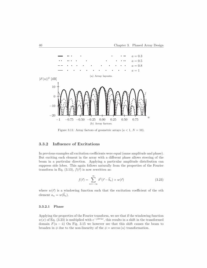
40 Chapter 3. Phased Array Design
a = 1
a = 0.8
a = 0.5
a = 0.3
(a) Array layouts.
−1 −0.75 −0.50 −0.25 0.00 0.25 0.50 0.75−20
−10
0
10
|F (u)|2 [dB]
u
(b) Array factors.
Figure 3.11: Array factors of geometric arrays (a < 1, N = 10).
3.3.2 Influence of Excitations
In previous examples all excitation coefficients were equal (same amplitude and phase).But exciting each element in the array with a different phase allows steering of thebeam in a particular direction. Applying a particular amplitude distribution cansuppress side lobes. This again follows naturally from the properties of the Fouriertransform in Eq. (3.13), f(~r) is now rewritten as:
f(~r) =
∞∑
n=−∞δ3(~r −~bn) × w(~r) (3.23)
where w(~r) is a windowing function such that the excitation coefficient of the nth
element an = w(~bn).
3.3.2.1 Phase
Applying the properties of the Fourier transform, we see that if the windowing functionw(x) of Eq. (3.23) is multiplied with e−j2πux, this results in a shift in the transformeddomain F (u − u) On Fig. 3.15 we however see that this shift causes the beam tobroaden in φ due to the non-linearity of the φ = arccos (u) transformation.

3.3. Array Design with Array Factor 41
perfect array N = 4
LESA N = 4, d = 2λ
perturbed array N = 4
geometric array a = 1.5
(a) Array layouts.
−1 −0.75 −0.50 −0.25 0.00 0.25 0.50 0.75−20
−10
0
10
|F (u)|2 [dB]
u
(b) Array factors.
Figure 3.12: Comparison of some linear non-equally spaced arrays.
(a) LESA Nx = 4, dx = 0.5λ. (b) LESA Ny = 4, dy = 0.5λ. (c) Four-by-four array.
Figure 3.13: Array factor of regular planar array.
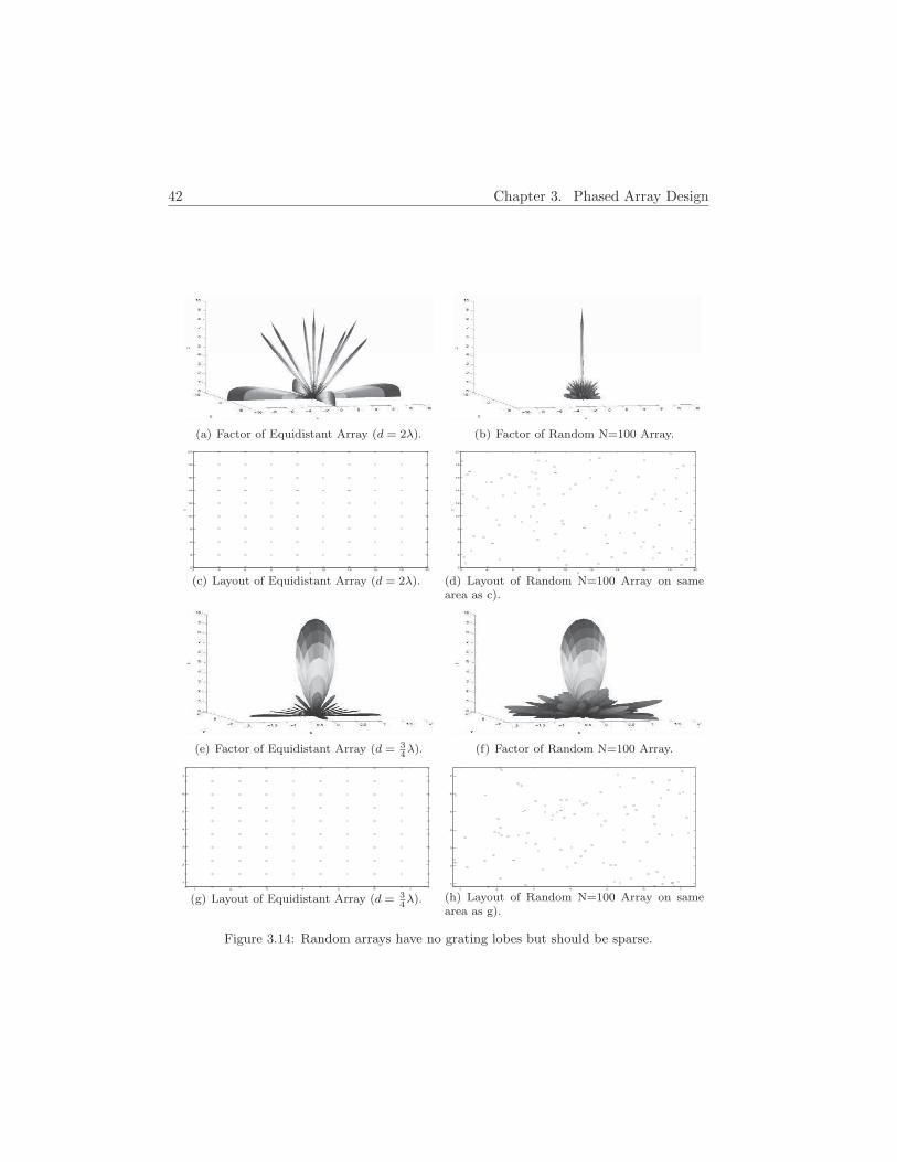
42 Chapter 3. Phased Array Design
(a) Factor of Equidistant Array (d = 2λ). (b) Factor of Random N=100 Array.
2 4 6 8 10 12 14 16 18 202
4
6
8
10
12
14
16
18
20
x
y
(c) Layout of Equidistant Array (d = 2λ).2 4 6 8 10 12 14 16 18 20
2
4
6
8
10
12
14
16
18
20
x
y
(d) Layout of Random N=100 Array on samearea as c).
(e) Factor of Equidistant Array (d = 34λ). (f) Factor of Random N=100 Array.
1 2 3 4 5 6 7
1
2
3
4
5
6
7
(g) Layout of Equidistant Array (d = 34λ).
1 2 3 4 5 6 7
1
2
3
4
5
6
7
(h) Layout of Random N=100 Array on samearea as g).
Figure 3.14: Random arrays have no grating lobes but should be sparse.

3.3. Array Design with Array Factor 43
−2 −1.5 −1.0 −0.5 0.0 0.5 1.0 1.5−20
−10
0
10
visible interval
visible interval
∆u = 0.3
|F (u)|2 [dB]
u
(a) Beam Steering in u for LESA N = 10, d = λ/2.
0 15 30 45 60 75 90 105 120 135 150 165 180−20
−10
0
10
17.46|F (φ)|2 [dB]
φ
δ = 0
δ = 54
(b) Beam Steering in φ for LESA N = 10, d = λ/2.
Figure 3.15: Beam steering makes use of a Fourier property.
The excitation coefficients to steer the beam to (u, v, w) can be found as:
an = ejδn = e−j2π(u,v,w) ·~bn (3.24)
or expressed as a phase:
δn = −2π
λ(sin θ cosφ ·xn + sin θ sinφ · yn + cos θ · zn) (3.25)
This indeed results in constructive interference:
∀n : anejβ(~ir ·~bn) = Ane
jδnejβ(~ir ·~bn) ≡ 1 (3.26)
If d > λ/2, it is possible that by shifting the visible interval, more than one maximumappears. We conclude that as soon as beam steering is required over the full range ofφ : 0 → π, the element spacing must be d ≤ λ/2.
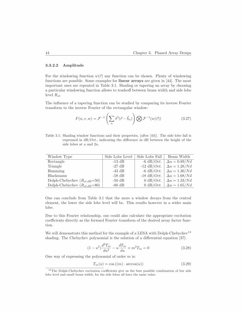
44 Chapter 3. Phased Array Design
3.3.2.2 Amplitude
For the windowing function w(~r) any function can be chosen. Plenty of windowingfunctions are possible. Some examples for linear arrays are given in [44]. The mostimportant ones are repeated in Table 3.1. Shading or tapering an array by choosinga particular windowing function allows to tradeoff between beam width and side lobelevel Rsl.
The influence of a tapering function can be studied by comparing its inverse Fouriertransform to the inverse Fourier of the rectangular window:
F (u, v, w) = F−1
(∑
n
δ3(~r −~bn)
)⊗F−1(w(~r)) (3.27)
Table 3.1: Shading window functions and their properties, (after [44]). The side lobe fall isexpressed in dB/Oct., indicating the difference in dB between the height of theside lobes at u and 2u.
Window Type Side Lobe Level Side Lobe Fall Beam WidthRectangle -13 dB -6 dB/Oct. ∆u = 0.89/NdTriangle -27 dB -12 dB/Oct. ∆u = 1.28/NdHamming -43 dB -6 dB/Oct. ∆u = 1.30/NdBlackmann -58 dB -18 dB/Oct. ∆u = 1.68/NdDolph-Chebychev (Rsl,dB=50) -50 dB 0 dB/Oct. ∆u = 1.33/NdDolph-Chebychev (Rsl,dB=80) -80 dB 0 dB/Oct. ∆u = 1.65/Nd
One can conclude from Table 3.1 that the more a window decays from the centralelement, the lower the side lobe level will be. This results however in a wider mainlobe.
Due to this Fourier relationship, one could also calculate the appropriate excitationcoefficients directly as the forward Fourier transform of the desired array factor func-tion.
We will demonstrate this method for the example of a LESA with Dolph-Chebychev13
shading. The Chebychev polynomial is the solution of a differential equation [37]:
(1 − u2)d2Tm
du2− u
dTm
du+m2Tm = 0 (3.28)
One way of expressing the polynomial of order m is:
Tm(u) = cos ((m) · arccos(u)) (3.29)
13The Dolph-Chebychev excitation coefficients give us the best possible combination of low sidelobe level and small beam width, for the side lobes all have the same value.
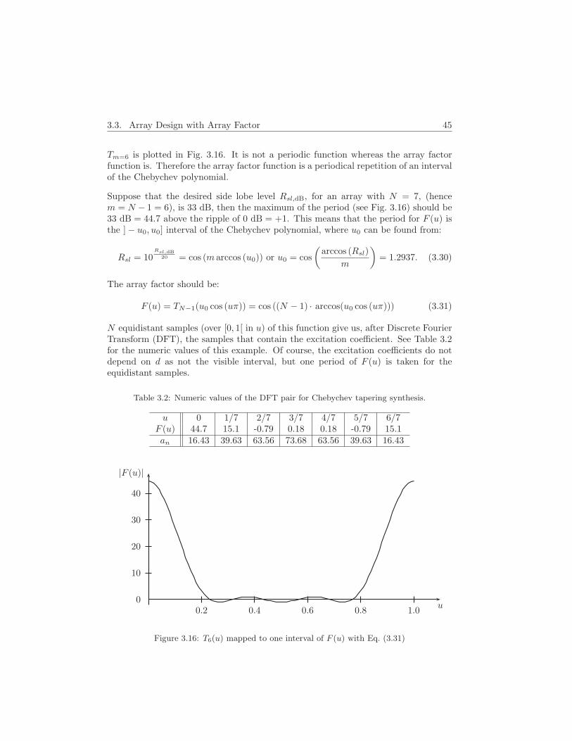
3.3. Array Design with Array Factor 45
Tm=6 is plotted in Fig. 3.16. It is not a periodic function whereas the array factorfunction is. Therefore the array factor function is a periodical repetition of an intervalof the Chebychev polynomial.
Suppose that the desired side lobe level Rsl,dB, for an array with N = 7, (hencem = N − 1 = 6), is 33 dB, then the maximum of the period (see Fig. 3.16) should be33 dB = 44.7 above the ripple of 0 dB = +1. This means that the period for F (u) isthe ] − u0, u0] interval of the Chebychev polynomial, where u0 can be found from:
Rsl = 10Rsl,dB
20 = cos (m arccos (u0)) or u0 = cos
(arccos (Rsl)
m
)= 1.2937. (3.30)
The array factor should be:
F (u) = TN−1(u0 cos (uπ)) = cos ((N − 1) · arccos(u0 cos (uπ))) (3.31)
N equidistant samples (over [0, 1[ in u) of this function give us, after Discrete FourierTransform (DFT), the samples that contain the excitation coefficient. See Table 3.2for the numeric values of this example. Of course, the excitation coefficients do notdepend on d as not the visible interval, but one period of F (u) is taken for theequidistant samples.
Table 3.2: Numeric values of the DFT pair for Chebychev tapering synthesis.
u 0 1/7 2/7 3/7 4/7 5/7 6/7F (u) 44.7 15.1 -0.79 0.18 0.18 -0.79 15.1an 16.43 39.63 63.56 73.68 63.56 39.63 16.43
0.2 0.4 0.6 0.8 1.00
10
20
30
40
|F (u)|
u
Figure 3.16: T6(u) mapped to one interval of F (u) with Eq. (3.31)

46 Chapter 3. Phased Array Design
Note that using a DFT for array synthesis introduces errors intrinsic to DFT, suchas leakage. This is due to the fact that DFT supposes that the function is periodicand discrete in both domains. This is certainly not the case.
A disadvantage of any shading is gain degradation. The uniform tapering providesthe highest possible gain due to the smallest main lobe, as can be seen on Fig. 3.17.This figure also shows that the maximum D for the different taperings lies at othervalues for d. This is because the beam width differs for different taperings, such thatthe point where the grating lobe lies just behind the edges of the interval, differs. dequal to any multiple of λ/2 always results in the same value for Dmax. Indeed, ifonly one period or several periods of the periodic function are averaged out, makesno difference. This value, moreover, is the limit for an infinite number of periods, orstated differently, for d→ ∞. In [45] is proven that this value Dmax = ηA ×N with
ηA =(∑an)2
N ×∑a2
n
(3.32)
the tapering efficiency of the array.
0 0.5 1.0 1.5 2.0 2.5 3.00123456789
101112
d [λ]
Darray
uniform gabledbinomial
Chebychev Rsl = 50 dBChebychev Rsl = 80 dB
Figure 3.17: Any type of tapering results in a lower value for Dmax (N = 7).
3.3.2.3 Example: Subarray of the ATCRBS in Bertem
The reader will already have noticed that the radiation pattern of Fig. 3.2 in Sect. 3.1.3is not practical for a secondary RADAR as half of the power in the main beam goesinto the ground. An airplane can only be expected under an elevation angle, between0 and 90. Eq. (3.25) can be used to elevate the beam above the horizon. But asexplained in Sect. 3.3.2.1, this will only shift the pattern. It is however recommendedto broaden the main beam to cover all elevation angles from 0 to 90.
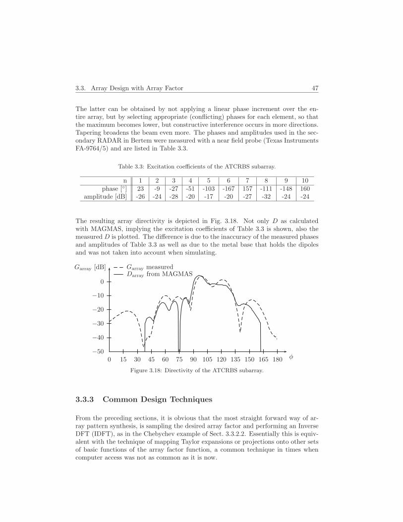
3.3. Array Design with Array Factor 47
The latter can be obtained by not applying a linear phase increment over the en-tire array, but by selecting appropriate (conflicting) phases for each element, so thatthe maximum becomes lower, but constructive interference occurs in more directions.Tapering broadens the beam even more. The phases and amplitudes used in the sec-ondary RADAR in Bertem were measured with a near field probe (Texas InstrumentsFA-9764/5) and are listed in Table 3.3.
Table 3.3: Excitation coefficients of the ATCRBS subarray.
n 1 2 3 4 5 6 7 8 9 10phase [] 23 -9 -27 -51 -103 -167 157 -111 -148 160
amplitude [dB] -26 -24 -28 -20 -17 -20 -27 -32 -24 -24
The resulting array directivity is depicted in Fig. 3.18. Not only D as calculatedwith MAGMAS, implying the excitation coefficients of Table 3.3 is shown, also themeasured D is plotted. The difference is due to the inaccuracy of the measured phasesand amplitudes of Table 3.3 as well as due to the metal base that holds the dipolesand was not taken into account when simulating.
0 15 30 45 60 75 90 105 120 135 150 165 180−50
−40
−30
−20
−10
0
Garray [dB]
φ
Garray measuredDarray from MAGMAS
Figure 3.18: Directivity of the ATCRBS subarray.
3.3.3 Common Design Techniques
From the preceding sections, it is obvious that the most straight forward way of ar-ray pattern synthesis, is sampling the desired array factor and performing an InverseDFT (IDFT), as in the Chebychev example of Sect. 3.3.2.2. Essentially this is equiv-alent with the technique of mapping Taylor expansions or projections onto other setsof basic functions of the array factor function, a common technique in times whencomputer access was not as common as it is now.
48 Chapter 3. Phased Array Design
With the increase in computer power, the approach of random search and optimizationroutines become popular in all kinds of fields. Even so in array synthesis. Manyexamples of genetic algorithms can be found, all differing in the trade-off betweengenerality and calculation times, using more or less information about the topologyresulting in faster or slower convergence.
3.4 What if the Assumptions no longer Hold
3.4.1 Errors that can be solved by Calibrating
When implementing beam steering in a phased array in practice, sometimes the ex-citation coefficients in reality are not those intended by the designers. One causefor this difference are the mutual electric fields (that even depend on the directionin which the beam points) of the elements in the array. This will change the com-plex input impedance of the elements, resulting in a varying phase and amplitudeof the current. A second cause are hardware imperfections. Some examples will begiven in Sect. 6.1.3.1. There also a basic calibration technique will be explained thatcompensates for systematic phase and amplitude errors.
3.4.2 Quantization Errors
Quantization of the phase by digital phase shifters, or digital control of analog phaseshifters, causes errors. This was already touched in Sect. 2.3, and now will be workedout to some extent.
Suppose that a phase shifter can only be controlled by n bits, then the number ofpossible states is limited, introducing a phase quantization error of at most:
∆δ =1
2
2π
2n. (3.33)
If the array consists of only two elements, this phase error can easily be related to thebeam direction error starting from Eq. (3.25):
∆δ = −2π
λ∆u⇔ ∆u =
λ
2n+1d. (3.34)
If the array has more elements, the phase approximations not only obstruct the beamfrom being steered under certain angles, but also causes broadening of the main beamand increasing of the side lobe levels. This effect is caused by the fact that whenlooking at pairs of array elements, these pairs do not all share the same direction ofconstructive interference.

3.5. Conclusions 49
Hence the conflicting phases of the array elements, that were deliberately introducedin Sect. 3.3.2.3 to obtain a good ATCRBS radiation pattern, are to be avoided in caseof directive antennas, as it is obvious that main beam broadening and side lobe levelrise, result in gain degradation.
Studying the beam width, side lobe level and gain degradation is a topic on its ownas it strongly depends on the array topology. Values from a case study on the arrayantenna of Sect. 6.1.2 can be found in [46]. The conclusion there was that a 3 bitphase shifter is sufficient, taking into account the effects of the other imperfections inthe system, such as the fact that grating lobes appear when the beam is scanned 48
off broadside.
3.4.3 Errors that Void the Theory
If the array elements are not all translated versions of a reference element, or thecurrent profile on all elements is not identical in shape, Eq. (3.1) can not be split intoan array and an element part, voiding all statements and formulas derived from it.Fortunately theory on this matter is available, e.g. in [1].
3.5 Conclusions
In this chapter, the array factor was introduced, to describe the influence of geometryand excitation in an array with phase shift beam forming. This chapter did not containany new contribution to science, but reviewed a lot of array theory and linked everystatement with Fourier properties. The introduced theory only holds for arrays whereevery element is a translation of the base or reference element, hence not for conformalor MIMO arrays. Moreover, the radiation properties (directivity) are only studied in afar field approximation. This assumption holds for most communication applications,as there indeed the intention is to transmit information over a considerable distance.If the far field assumption does not hold, e.g. in case of the sensor application ofPart III, the approximations applied in the chapter are invalid.
Using Fourier transform properties, it can be understood that the larger the aperturethat is spanned by the array elements, the smaller the beam will be and the higherthe gain. The most basic illustration, is comparing a linear array with a conical beamto a planar (2D) array with a pencil beam. Still following the same principle, the useof tapering is disrecommended if the gain of the array has to be high.
50 Chapter 3. Phased Array Design
Tapering can however be very useful for side lobe level reduction to avoid interferencefrom communications in other directions. The trade off between beam width and sidelobe level can also be used at another extreme, as in sparse arrays: by allowing veryhigh side lobes but having a very narrow main beam, hence a very high resolution, inapplications with sensor arrays in a quiet measurement environment.
Adding more elements generally increases the gain, but only up to a certain level, ifthis diminishes the element spacing d too much.
Scanning of an array is essentially using the shifting property of the Fourier transform.Note that as the beam scans towards the edges of a planar or linear array, the beamwidens.

Part II
Application: SatelliteCommunication
51


53
Overview
Array antennas are a logical choice for LEO satellite communication antennas. Aspower on the satellite is scarce, and the distance between satellite and receiver onearth is considerable, preferably high gain antennas should be used for the satellite-to-ground link. These high gain antennas should moreover be scanned when thesatellite flies by a ground based receiver at a speed of about 7 km/s, the typical LEOsatellite orbit speed.
Mechanical scanning of the antenna has its associated disadvantages such as wear andvibrations. As in space reparation is out of the question, wear should be avoided. Ifthe LEO satellite is used for earth observation and thus carries an imaging sensor,vibrations would dramatically limit the image resolution.
Consequently, for the system of in-situ data up link to a LEO earth observationsatellite, an array antenna was selected. Chapter 4 explains the full system layout,justifies the choice for an array antenna, shows with a link budget calculation thatthe link is feasible with the proposed antenna and explains that the hostile spaceenvironment requires special attention when designing electronics for satellites.
Chapter 5 is dedicated to the design of a space qualified antenna element and thedetermination of the array geometry, i.e. of the array antenna elements locations. Ashigh gain is especially needed when the satellite elevation is low, the array shouldhave its gain maximized under large scan angles. A technique to achieve this forlinear equidistant arrays is proposed, but unfortunately the technique is not easilygeneralized for planar arrays.
The signal shaping and combination parts of the array are discussed in Chapter 6.There the analog baseband implementation of a technique commonly used for digitalbeam forming, designed by ir. P. Delmotte, is reported and evaluated. Afterwardsthis implementation is adapted to the space environment for use in the system forin-situ data up link, deployed in Chapter 4.

invisible filling
Chapter 4
Introduction to theApplication
As is often the case, earth observation was first used for military purposes. Soon gov-ernments started using it to obtain better maps. Later on, better imaging techniqueswere developed and earth observation became a tool in monitoring and assessingnatural resources such as water and forest. With the unfortunate evolutions in cli-mate, it is nowadays applied to monitor the health status of our planet (CryoSAT,EarthCARE) [47].
Earth observation sensors not only “look” at the earth in many parts of the Elec-troMagnetic (EM) spectrum (such as visible light, infrared and microwaves). Alsoactive systems, e.g. RADARSAT Sect. 4.4.2, that emit power and analyze the delay,intensity and polarization of the reflections, are operational for already quite someyears.
If now this “image” (in a broad meaning) data could be combined with in-situ col-lected data, much more correlations could be investigated, increasing the knowledgeon the impact of factors such as rain, temperature and carbon dioxide concentrationson crops, climate and so on. Moreover, if this in-situ data is available1 in the imagingsatellite, on board processing could reduce the amount of data that has to be downlinked to the ground station. That this down link is indeed a bottleneck, can eas-ily be understood looking at the vast amount of data that imaging sensors produce.RADARSAT-I fills up to 76 GB with only 15 minutes of imaging [49].
1If the satellite does not use the in-situ data, there can still be reasons for up link. Simpletransport can be done way cheaper and easier over terrestrial networks, even for sensors at the polesof the earth, using sensor networks that transport the data to one connection node of the sensornetwork, e.g. ASTRonomisch Onderzoek in Nederland (ASTRON) LOw Frequency ARray (LOFAR)AGRO project [48]. But sometimes performance (in terms of uptime or delay) of existing terrestrialnetworks is insufficient and beyond control.
55
56 Chapter 4. Introduction to the Application
In this chapter, first a concept of a system for in-situ data up link will be investigated.The link budget and a calculation of the loss of image resolution due to vibration,motivate the use of electronic beam steering on earth observation satellites. Someintroduction into space design at the end of the chapter makes the reader awareof the fact that designing electronics for use in space is very much different fromdesigning consumer electronics. The details on the implementation are postponed toChapters 5 and 6.
4.1 System Overview
In-situ data of about 2002 sensors is collected and stored by data loggers. When thesatellite flies by, it activates the ground station that sends the recorded data to thesatellite. There the data is ideally processed with the imaging data, but for the timebeing, only stored and down linked together with the image data.
Except for the unconventional routing of the data packets, this system looks very sim-ilar to a standard Supervisory Control And Data Acquisition (SCADA) system [50].Similar services are available from SpaceChecker [51]. That system uses a Geosta-tionary Earth Orbit (GEO) satellite. But obviously up link of the data to an earthobservation satellite offers a huge advantage if the up linked data can be processedand combined with the imaging data on board of the satellite.
All numbers given here, follow either from the link budget in Sect. 4.3.3 or from thesystem design choices in Sect. 4.1.4.
4.1.1 In-Situ Data Collection
In the field, data of about 200 sensors, measuring e.g. temperature, humidity and pH,is linked up per terminal. The sensors can be interfaced with RS-232, (Power over)Ethernet (PoE), ISM 868 MHz, 802.11 (WLAN) or in most cases a simple electricalwire. They should all be connected to a data logger that stores their value hourly forabout four days, the maximum revisit period of a Low Earth Orbit (LEO) satellite.Hence the data logger should have at least 100 kB of data storage, which is certainlythe case in contemporary devices3. The ELTEK SQ-1000 data logger, for example,can store 250 k measurements. It can however only interface with 124 sensors, thusfor 200 sensors two data loggers are needed.
2The number of 200 sensors was agreed upon by the future users of the system.3It is obvious that in the future smart data loggers will be designed to combine and extract
relevant information from far more than 200 sensors. As long as the amount of information from thedata logger corresponds to the equivalent of 200 sensors, it can still be linked up with the systemproposed.
4.1. System Overview 57
The data loggers should be connected with the ground station modem via an RS-232 or Ethernet link, possibly wireless (up to about 7 km with the DECAGON RM1Radio Receiver). The data rate is not an issue, as only few data is to be exchanged.Even the standard RS-232 baud rate will do. The ELTEK SQ-1000 uses RS-232(38400 baud).
The ELTEK SQ-1000 needs 9 − 14 V. A battery pack should deliver power to thesensors, data loggers, and a terminal. The data loggers are only active once an hour.The terminal needs, as a rule of thumb, about 5 W in receive mode and, from thelink budget in Sect. 4.3.3, about 15 W in transmit, for about 16 s/day. Indeed, tosend 100 kB of total data, at a data rate of 6400 bit/s, see Sect. 4.3.3, about 16 sis needed. With the assumption that 6 W is sufficient for the entire ground segmentand that the night lasts for 14 h, a battery is needed that delivers 12 V and has acapacity of at least 17 Ah. The PANASONIC LC-RD1217P lead acid battery canserve these requirements, but batteries up to 33 Ah are available and if that is stillinsufficient more than one can be used in parallel. To charge the batteries, solarcells, with a charger to avoid damage, can be used. They are sold in large variety.For demonstration purpose, the SOLARKING PT15-300 Powerfilm can be used.
To communicate with the satellite, a separate Transmit (Tx) and Receive (Rx) patchantenna on spacers in air (εr = 1), with two feeds for circular polarization is recom-mended, as this gives the highest attainable gain and least cross polar leakage. Theterminal (including antennas) should be able to withstand rain and ice (class4 IP67).An overview of the ground segment, can be found in Fig. 4.1.
4.1.2 Space-Ground Communication Protocol
Software at the Telemetry, Tracking and Command (TT&C) ground station shouldmake up a time schedule for the satellite on when to query which ground terminals.One record in this to-do list could be:
time stamp ground terminal serial number ground station GPS coordinates
This list will be forwarded to the satellite and be stored there. Once the time is equalto the time stamp of querying a certain ground station, the activation message forthis ground station has to be broadcasted.
Another approach could be that the satellite sends out a request for serial numbers.Any terminal hearing this request starts a random timer. When the timer counts downto zero, it transmits its serial number. The satellite, that listens for serial numbers,selects the first one, that comes in without collision, for up link and broadcasts anactivation message containing this serial number.
4The International Protection Rating (IP) code, defined in norm IEC-60529 [52], specifies thedegree of protection against intrusion of objects and dust (first digit 0-6) and water (second digit0-8) in electrical enclosures.
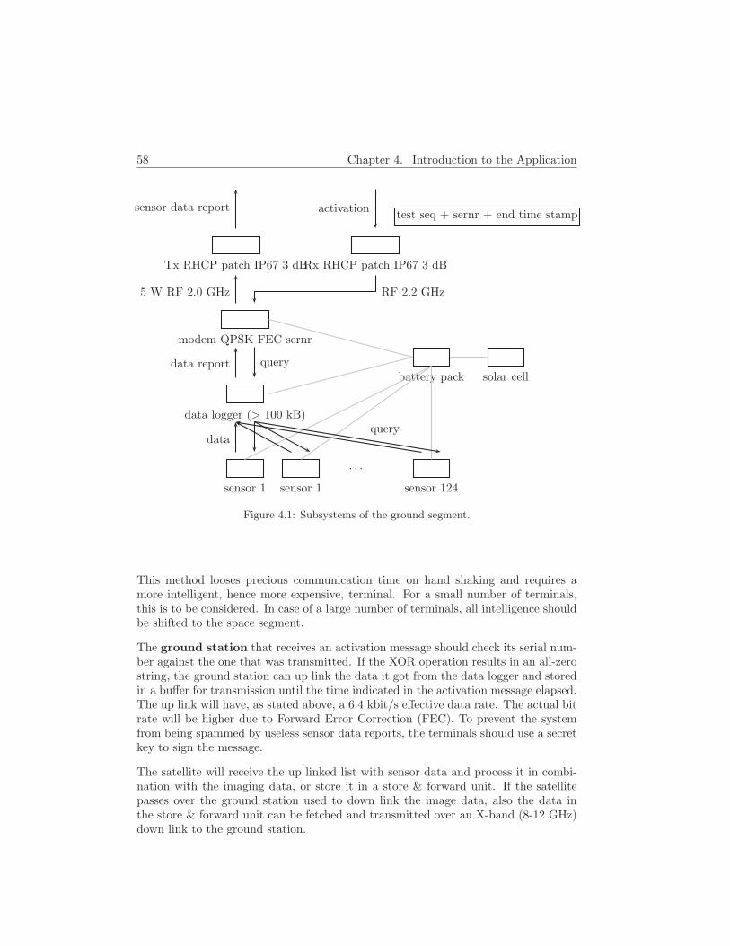
58 Chapter 4. Introduction to the Application
sensor 1 sensor 1
. . .
sensor 124
data logger (> 100 kB)
battery pack solar cell
modem QPSK FEC sernr
Tx RHCP patch IP67 3 dBRx RHCP patch IP67 3 dB
test seq + sernr + end time stampactivation
RF 2.2 GHz
sensor data report
5 W RF 2.0 GHz
data report query
dataquery
Figure 4.1: Subsystems of the ground segment.
This method looses precious communication time on hand shaking and requires amore intelligent, hence more expensive, terminal. For a small number of terminals,this is to be considered. In case of a large number of terminals, all intelligence shouldbe shifted to the space segment.
The ground station that receives an activation message should check its serial num-ber against the one that was transmitted. If the XOR operation results in an all-zerostring, the ground station can up link the data it got from the data logger and storedin a buffer for transmission until the time indicated in the activation message elapsed.The up link will have, as stated above, a 6.4 kbit/s effective data rate. The actual bitrate will be higher due to Forward Error Correction (FEC). To prevent the systemfrom being spammed by useless sensor data reports, the terminals should use a secretkey to sign the message.
The satellite will receive the up linked list with sensor data and process it in combi-nation with the imaging data, or store it in a store & forward unit. If the satellitepasses over the ground station used to down link the image data, also the data inthe store & forward unit can be fetched and transmitted over an X-band (8-12 GHz)down link to the ground station.
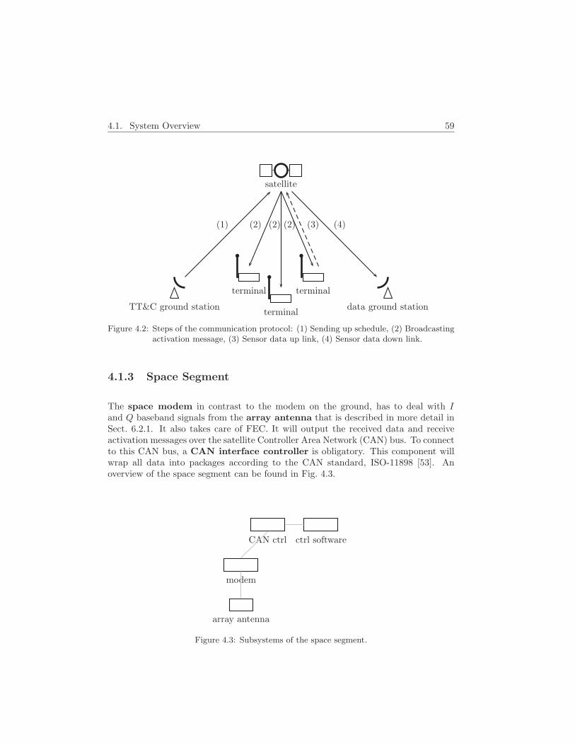
4.1. System Overview 59
satellite
terminal
terminal terminal
TT&C ground station data ground station
(1) (2) (2) (2) (3) (4)
Figure 4.2: Steps of the communication protocol: (1) Sending up schedule, (2) Broadcastingactivation message, (3) Sensor data up link, (4) Sensor data down link.
4.1.3 Space Segment
The space modem in contrast to the modem on the ground, has to deal with Iand Q baseband signals from the array antenna that is described in more detail inSect. 6.2.1. It also takes care of FEC. It will output the received data and receiveactivation messages over the satellite Controller Area Network (CAN) bus. To connectto this CAN bus, a CAN interface controller is obligatory. This component willwrap all data into packages according to the CAN standard, ISO-11898 [53]. Anoverview of the space segment can be found in Fig. 4.3.
array antenna
modem
CAN ctrl ctrl software
Figure 4.3: Subsystems of the space segment.
60 Chapter 4. Introduction to the Application
4.1.4 System Design Choices
One of the most important choices, is the selection of the frequency. From a tech-nological point of view, higher frequencies result in smaller antennas, which is ad-vantageous as satellite surface is scarce. A higher frequency however, results in moreexpensive components. But the main driving force in selecting a frequency, is the li-censing. Up link at 1980−2010 MHz and down link at 2170−2200 MHz was selected,keeping ease of licensing in mind, [54].
Although for frequencies around 2 GHz and higher, Faraday rotation in the iono-sphere, which is a polarization rotation, is negligible, this effect is noticeable up to5 GHz, [55]. It is hence better to use circular instead of linear polarization. Moreoverbecause in that case no attention should be payed to the relative position (rotation)of the satellite and receiving antenna.
The bandwidth that is available, combined with the available transmit power and thelosses, determine the data rate. The link budget in Sect. 4.3.3 results in 6.4 kbit/s.This is sufficient for the application. If the modem is implemented as a SoftwareDefined Radio (SDR), the data rate can still be changed afterwards.
4.2 Orbit
With the aid of Newton’s laws of motion, the speed of a satellite in its orbit can becalculated. The force that keeps the satellite in its orbit is the gravitational force Fg
between the earth and the satellite:
Fg = −GMem
R2d
(4.1)
with Me = 6.0 × 1024 kg the mass of the earth, m the mass of the satellite, G =6.67×10⁻¹¹ Nm2/kg2 the universal constant of gravity, and Rd is the distance betweenthe center of the earth and the satellite. From Fg the speed of the satellite in itscircular motion can be found combining Eq. (4.1) with Newton’s First Law:
Fg = ma = mv2
Rd⇔ v =
√GMe
Rd(4.2)
v is independent of the mass of the satellite.
LEO satellites circle (according to all definitions) around the earth in a circular (orelliptical) orbit less than 2000 km above the surface of the earth. In Table 4.1 thevelocity for some orbits is calculated5. They were checked with the NASA OrbitalVelocity Calculator [57] and agree with the values in [58]. Orbits lower than 185 kmare unstable, because of too much air drag, and therefore never used.
5In our calculation it is assumed that the earth is a perfect sphere and the influence of the moonand the sun and air drag is neglected. In [56] it is explained how to take these effects into account.
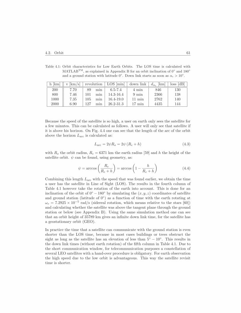
4.2. Orbit 61
Table 4.1: Orbit characteristics for Low Earth Orbits. The LOS time is calculated with
MATLABTM, as explained in Appendix B for an orbit inclination of 0 and 180
and a ground station with latitude 0. Down link starts as soon as αε > 10.
h [km] v [km/s] revolution LOS [min] down link dαε[km] loss [dB]
200 7.70 89 min 6.5-7.4 4 min 846 130800 7.46 101 min 14.3-16.4 9 min 2366 1381000 7.35 105 min 16.4-19.0 11 min 2762 1402000 6.90 127 min 26.2-31.3 17 min 4435 144
Because the speed of the satellite is so high, a user on earth only sees the satellite fora few minutes. This can be calculated as follows. A user will only see that satellite ifit is above his horizon. On Fig. 4.4 one can see that the length of the arc of the orbitabove the horizon Larc is calculated as:
Larc = 2ψRo = 2ψ (Re + h) (4.3)
with Ro the orbit radius, Re = 6371 km the earth radius [59] and h the height of thesatellite orbit. ψ can be found, using geometry, as:
ψ = arccos
(Re
Re + h
)= arccos
(1 − h
Re + h
)(4.4)
Combining this length Larc with the speed that was found earlier, we obtain the timea user has the satellite in Line of Sight (LOS). The results in the fourth column ofTable 4.1 however take the rotation of the earth into account. This is done for aninclination of the orbit of 0 − 180 by simulating the (x, y, z) coordinates of satelliteand ground station (latitude of 0) as a function of time with the earth rotating atωe = 7.2925 × 10⁻⁵ rad/s (sidereal rotation, which means relative to the stars [60])and calculating whether the satellite was above the tangent plane through the groundstation or below (see Appendix B). Using the same simulation method one can seethat an orbit height of 35789 km gives an infinite down link time, for the satellite hasa geostationary orbit (GEO).
In practice the time that a satellite can communicate with the ground station is evenshorter than the LOS time, because in most cases buildings or trees obstruct thesight as long as the satellite has an elevation of less than 5 − 10. This results inthe down link times (without earth rotation) of the fifth column in Table 4.1. Due tothe short communication window, for telecommunication purposes a constellation ofseveral LEO satellites with a hand-over procedure is obligatory. For earth observationthe high speed due to the low orbit is advantageous. This way the satellite revisittime is shorter.
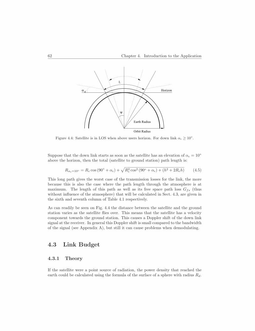
62 Chapter 4. Introduction to the Application
Horizon
L
ψ
Earth Radius
Orbit Radius
α ε
Figure 4.4: Satellite is in LOS when above users horizon. For down link αε ≥ 10.
Suppose that the down link starts as soon as the satellite has an elevation of αε = 10
above the horizon, then the total (satellite to ground station) path length is:
Rαε=10 = Re cos (90 + αε) +√R2
e cos2 (90 + αε) + (h2 + 2Reh) (4.5)
This long path gives the worst case of the transmission losses for the link, the morebecause this is also the case where the path length through the atmosphere is atmaximum. The length of this path as well as its free space path loss Gfs (thuswithout influence of the atmosphere) that will be calculated in Sect. 4.3, are given inthe sixth and seventh column of Table 4.1 respectively.
As can readily be seen on Fig. 4.4 the distance between the satellite and the groundstation varies as the satellite flies over. This means that the satellite has a velocitycomponent towards the ground station. This causes a Doppler shift of the down linksignal at the receiver. In general this Doppler shift is small compared to the bandwidthof the signal (see Appendix A), but still it can cause problems when demodulating.
4.3 Link Budget
4.3.1 Theory
If the satellite were a point source of radiation, the power density that reached theearth could be calculated using the formula of the surface of a sphere with radius Rd.
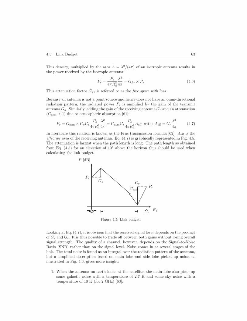
4.3. Link Budget 63
This density, multiplied by the area A = λ2/(4π) of an isotropic antenna results inthe power received by the isotropic antenna:
Pr =Ps
4πR2d
λ2
4π= Gfs × Ps (4.6)
This attenuation factor Gfs is referred to as the free space path loss.
Because an antenna is not a point source and hence does not have an omni-directionalradiation pattern, the radiated power Ps is amplified by the gain of the transmitantenna Gs. Similarly, adding the gain of the receiving antennaGr and an attenuation(Gatm < 1) due to atmospheric absorption [61]:
Pr = Gatm ×GrGsPs
4πR2d
λ2
4π= GatmGs
Ps
4πR2d
Aeff with: Aeff = Grλ2
4π(4.7)
In literature this relation is known as the Friis transmission formula [62]. Aeff is theeffective area of the receiving antenna. Eq. (4.7) is graphically represented in Fig. 4.5.The attenuation is largest when the path length is long. The path length as obtainedfrom Eq. (4.5) for an elevation of 10 above the horizon thus should be used whencalculating the link budget.
Rd
P [dB]
PsGs Gr
PrGatm
Figure 4.5: Link budget.
Looking at Eq. (4.7), it is obvious that the received signal level depends on the productof Gs and Gr. It is thus possible to trade off between both gains without losing overallsignal strength. The quality of a channel, however, depends on the Signal-to-NoiseRatio (SNR) rather than on the signal level. Noise comes in at several stages of thelink. The total noise is found as an integral over the radiation pattern of the antenna,but a simplified description based on main lobe and side lobe picked up noise, asillustrated in Fig. 4.6, gives more insight:
1. When the antenna on earth looks at the satellite, the main lobe also picks upsome galactic noise with a temperature of 2.7 K and some sky noise with atemperature of 10 K (for 2 GHz) [63].
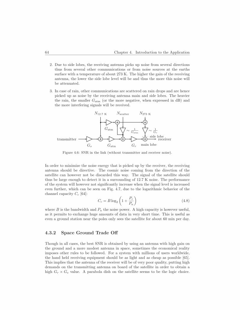
64 Chapter 4. Introduction to the Application
2. Due to side lobes, the receiving antenna picks up noise from several directionsthus from several other communications or from noise sources at the earthssurface with a temperature of about 273 K. The higher the gain of the receivingantenna, the lower the side lobe level will be and thus the more this noise willbe attenuated.
3. In case of rain, other communications are scattered on rain drops and are hencepicked up as noise by the receiving antenna main and side lobes. The heavierthe rain, the smaller Gatm (or the more negative, when expressed in dB) andthe more interfering signals will be received.
transmitter
Gs Gatm Gr
receiver
N12.7 K
∼ 1Gatm
Nscatter
∼ 1Gr
N273 K
main lobe
side lobe
Gatm
Figure 4.6: SNR in the link (without transmitter and receiver noise).
In order to minimize the noise energy that is picked up by the receiver, the receivingantenna should be directive. The cosmic noise coming from the direction of thesatellite can however not be discarded this way. The signal of the satellite shouldthus be large enough to detect it in a surrounding of 12.7 K noise. The performanceof the system will however not significantly increase when the signal level is increasedeven further, which can be seen on Fig. 4.7, due to the logarithmic behavior of thechannel capacity Cc [64]:
Cc = B log2
(1 +
Pr
Pn
)(4.8)
where B is the bandwidth and Pn the noise power. A high capacity is however useful,as it permits to exchange huge amounts of data in very short time. This is useful aseven a ground station near the poles only sees the satellite for about 60 min per day.
4.3.2 Space Ground Trade Off
Though in all cases, the best SNR is obtained by using an antenna with high gain onthe ground and a more modest antenna in space, sometimes the economical realityimposes other rules to be followed. For a system with millions of users worldwide,the hand held receiving equipment should be as light and as cheap as possible [65].This implies that the antenna of the receiver will be of very poor quality, putting highdemands on the transmitting antenna on board of the satellite in order to obtain ahigh Gr × Gs value. A parabola dish on the satellite seems to be the logic choice.
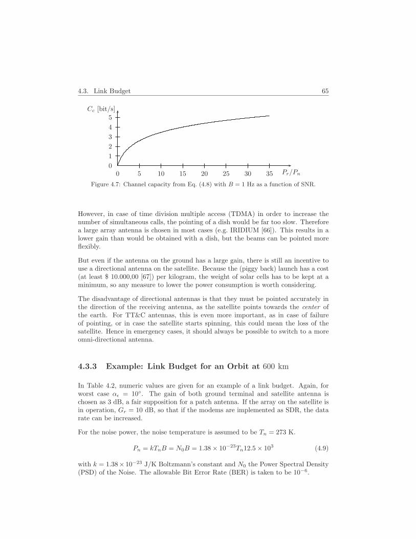
4.3. Link Budget 65
0 5 10 15 20 25 30 350
1
2
3
4
5
Pr/Pn
Cc [bit/s]
Figure 4.7: Channel capacity from Eq. (4.8) with B = 1 Hz as a function of SNR.
However, in case of time division multiple access (TDMA) in order to increase thenumber of simultaneous calls, the pointing of a dish would be far too slow. Thereforea large array antenna is chosen in most cases (e.g. IRIDIUM [66]). This results in alower gain than would be obtained with a dish, but the beams can be pointed moreflexibly.
But even if the antenna on the ground has a large gain, there is still an incentive touse a directional antenna on the satellite. Because the (piggy back) launch has a cost(at least $ 10.000,00 [67]) per kilogram, the weight of solar cells has to be kept at aminimum, so any measure to lower the power consumption is worth considering.
The disadvantage of directional antennas is that they must be pointed accurately inthe direction of the receiving antenna, as the satellite points towards the center ofthe earth. For TT&C antennas, this is even more important, as in case of failureof pointing, or in case the satellite starts spinning, this could mean the loss of thesatellite. Hence in emergency cases, it should always be possible to switch to a moreomni-directional antenna.
4.3.3 Example: Link Budget for an Orbit at 600 km
In Table 4.2, numeric values are given for an example of a link budget. Again, forworst case αε = 10. The gain of both ground terminal and satellite antenna ischosen as 3 dB, a fair supposition for a patch antenna. If the array on the satellite isin operation, Gr = 10 dB, so that if the modems are implemented as SDR, the datarate can be increased.
For the noise power, the noise temperature is assumed to be Tn = 273 K.
Pn = kTnB = N0B = 1.38 × 10⁻²³Tn12.5 × 103 (4.9)
with k = 1.38× 10⁻²³ J/K Boltzmann’s constant and N0 the Power Spectral Density(PSD) of the Noise. The allowable Bit Error Rate (BER) is taken to be 10−6.
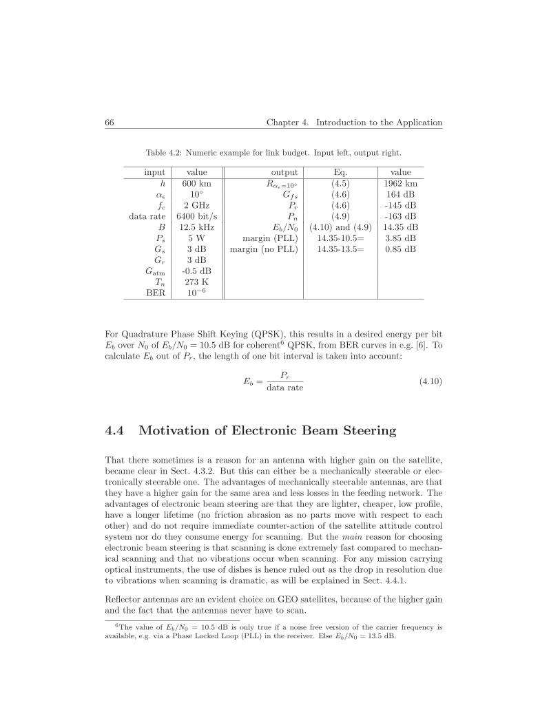
66 Chapter 4. Introduction to the Application
Table 4.2: Numeric example for link budget. Input left, output right.
input value output Eq. valueh 600 km Rαε=10 (4.5) 1962 kmαε 10 Gfs (4.6) 164 dBfc 2 GHz Pr (4.6) -145 dB
data rate 6400 bit/s Pn (4.9) -163 dBB 12.5 kHz Eb/N0 (4.10) and (4.9) 14.35 dBPs 5 W margin (PLL) 14.35-10.5= 3.85 dBGs 3 dB margin (no PLL) 14.35-13.5= 0.85 dBGr 3 dB
Gatm -0.5 dBTn 273 K
BER 10−6
For Quadrature Phase Shift Keying (QPSK), this results in a desired energy per bitEb over N0 of Eb/N0 = 10.5 dB for coherent6 QPSK, from BER curves in e.g. [6]. Tocalculate Eb out of Pr, the length of one bit interval is taken into account:
Eb =Pr
data rate(4.10)
4.4 Motivation of Electronic Beam Steering
That there sometimes is a reason for an antenna with higher gain on the satellite,became clear in Sect. 4.3.2. But this can either be a mechanically steerable or elec-tronically steerable one. The advantages of mechanically steerable antennas, are thatthey have a higher gain for the same area and less losses in the feeding network. Theadvantages of electronic beam steering are that they are lighter, cheaper, low profile,have a longer lifetime (no friction abrasion as no parts move with respect to eachother) and do not require immediate counter-action of the satellite attitude controlsystem nor do they consume energy for scanning. But the main reason for choosingelectronic beam steering is that scanning is done extremely fast compared to mechan-ical scanning and that no vibrations occur when scanning. For any mission carryingoptical instruments, the use of dishes is hence ruled out as the drop in resolution dueto vibrations when scanning is dramatic, as will be explained in Sect. 4.4.1.
Reflector antennas are an evident choice on GEO satellites, because of the higher gainand the fact that the antennas never have to scan.
6The value of Eb/N0 = 10.5 dB is only true if a noise free version of the carrier frequency isavailable, e.g. via a Phase Locked Loop (PLL) in the receiver. Else Eb/N0 = 13.5 dB.
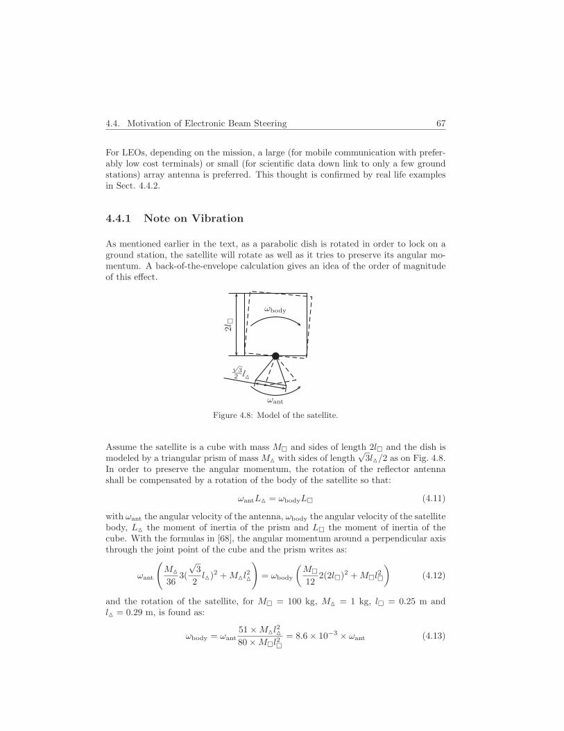
4.4. Motivation of Electronic Beam Steering 67
For LEOs, depending on the mission, a large (for mobile communication with prefer-ably low cost terminals) or small (for scientific data down link to only a few groundstations) array antenna is preferred. This thought is confirmed by real life examplesin Sect. 4.4.2.
4.4.1 Note on Vibration
As mentioned earlier in the text, as a parabolic dish is rotated in order to lock on aground station, the satellite will rotate as well as it tries to preserve its angular mo-mentum. A back-of-the-envelope calculation gives an idea of the order of magnitudeof this effect.
2l
√3
2 lM
ωbody
ωant
Figure 4.8: Model of the satellite.
Assume the satellite is a cube with mass M and sides of length 2l and the dish ismodeled by a triangular prism of mass MM with sides of length
√3lM/2 as on Fig. 4.8.
In order to preserve the angular momentum, the rotation of the reflector antennashall be compensated by a rotation of the body of the satellite so that:
ωantLM = ωbodyL (4.11)
with ωant the angular velocity of the antenna, ωbody the angular velocity of the satellitebody, LM the moment of inertia of the prism and L the moment of inertia of thecube. With the formulas in [68], the angular momentum around a perpendicular axisthrough the joint point of the cube and the prism writes as:
ωant
(MM
363(
√3
2lM)2 +MMl
2M
)= ωbody
(M
122(2l)2 +Ml
2
)(4.12)
and the rotation of the satellite, for M = 100 kg, MM = 1 kg, l = 0.25 m andlM = 0.29 m, is found as:
ωbody = ωant51 ×MMl
2M
80 ×Ml2
= 8.6 × 10⁻³ × ωant (4.13)

68 Chapter 4. Introduction to the Application
For an orbit height of 600 km, ωant = 0.72/s when in zenith above the groundstation. If the rotation of the bus would not be compensated by the attitude controlsystem, for 1/30 s which is a standard shutter time, this would give an angularrotation of the bus of 2 × 10⁻⁴ or 3.4 × 10⁻⁶ rad, corresponding to a movement of600 × 103 × 3.4 × 10−6 = 2.2 m on the ground.
Knowing that the resolution of the Japanese Earth Resources Satellite (JERS-1) is18 m× 18 m and of the French SPOT-4 is 10 m× 10 m, we see that these vibrationsindeed lower the spatial resolution considerably. Even for RADAR sensing, vibrationslower the resolution, because of displacement of the array elements, causing the mainlobe of the antenna to become wider. The same problem arises for RADARS mountedon the wings of airplanes.
4.4.2 Examples of Phased Arrays on Satellites
A first example are the IRIDIUM R© satellites [66]. Each of the 66 satellites carriesthree phased array panels. These allow each satellite to produce 48 fixed down linkbeams. The disadvantage is that when the receiver is at the edge of a certain fixedbeam, the signal level will be lower. The beams are formed by use of Butler matrices:16 RF signals (for one panel) are fed into a power divider, which sends each inputsignal to the appropriate ones of 80 outputs. Each one of these 80 outputs is aninput to the Butler Matrices, which have 80 output beams that fill the scan volumeof the array, depicted in Fig. 4.9. Besides, each patch antenna has a 5-bit phaseshifter for temperature compensation, even though the panels are kept at a constanttemperature by heat pipes.
Figure 4.9: The 80 beams of the IRIDIUM antenna (from [66]).

4.4. Motivation of Electronic Beam Steering 69
IRIDIUM has a large array, as it is a satellite for personal communication. Scientificsatellites need a smaller array for data down link, e.g. the commercially availableAlcatel high-rate X-band antenna [69], especially designed for down link of earthobservation images to a ground station. Again, to obtain a high data rate at a lowBER, the received signal must be high. This can be achieved using an antenna withhigh gain.
As can be seen on Fig. 4.10, the antenna consists of a truncated cone with 24 arraysof stacked patch antennas mounted on it. Note that for this antenna the radiatingelements are not translations of a basic element. This means that the antenna is notan array antenna, but a conformal array antenna. The advantage is that the beamdoes not loose gain when it is pointed under an angle larger than 60, which is aproblem with planar arrays of patch radiators.
The phase shifting is done by 5-bit phase shifters. Butler matrices are used in theantenna as well, not for the scanning, but to allow (by means of destructive interfer-ence) to not excite the subarrays that are at the back of the antenna with respectto the scanned beam. This could also be obtained by simply switching off certainsubarrays, but then the amplifiers after the phase shifters are not always loaded inthe same way. The structure weighs about 8 kg.
Figure 4.10: The Alcatel X-band antenna for LEO satellites [69].
Phased arrays not only serve as communication antennas. On RADARSAT [70] a 15by 1.5 m slotted waveguide phased array is used as a steerable active remote sensingRADAR. The azimuth beam pattern is fixed but the elevation angle of the mainbeam can be varied (to obtain different incidence angles) by the use of 32 variablephase shifters. Because these ferrite phase shifters are not reciprocal, they have toswitch back and forth each time the antenna is switched between transmit and receivemode.

70 Chapter 4. Introduction to the Application
4.5 Designing Space Instruments
Due to the cost of a launch per kg, the power consumption and mass of any designshould be minimal. As reparation or upgrading in space is impossible, it has to resistthe severe space conditions. This makes going into space expensive.
4.5.1 Space Conditions
One could say that the conditions in space are hostile. But the advantage over thecircumstances on earth is that it is a more predictable situation. No fingers will pokeand no users will do unexpected things. [71]
Apart from space conditions, the structure has to endure severe shocks (with accel-erations up to several times g = 9, 81 m/s2) and mechanical (with accelerations ofabout 0.5g) as well as acoustical (up to 140 dB) vibrations during launch.
4.5.1.1 Pressure
Due to the absence of gas particles, the pressure in space is very low. A slight pressureincrease is caused by sun particles, resulting in (10−2 − 10−7 Pa) [72]. But this stilllow pressure causes some problems:
• no convection: Because of the absence of gases, there is no convection. Theonly way of heat dissipation is radiation. When the satellite is in sunlight, itmight become a problem to cool the electronics.
• outgassing: Some materials become volatile once the spacecraft is in orbit.This of course alters the properties of the devices and can disturb the function-ing. Moreover, the gases that are set free can condense elsewhere, causing a lotof problems.
The advantages of low pressure are:
• less corrosion: Because the pressure is lower, there is less oxygen to oxidatethe metals. Note however that the oxygen that is present, is atomic oxygenwhich is a lot more corrosive.
• perfect insulation: The breakdown voltage in vacuum is the highest possible.However, due to outgassing, corona discharge and eventually an arc can occur.
A complete overview is given in Fig. 4.11.
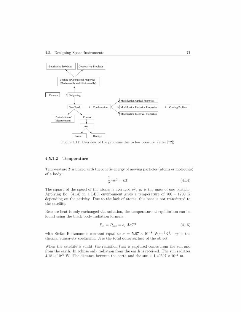
4.5. Designing Space Instruments 71
Change in Operational Properties
(Mechanically and Electronically)
Lubrication Problems Conductivity Problems
Condensation Modification Radiation Properties
Modification Electrical Properties
Modification Optical Properties
Cooling Problem
Damage
Vacuum Outgassing
Perturbation of
Measurements
Corona
Arc
Gas Cloud
Noise
Figure 4.11: Overview of the problems due to low pressure. (after [72])
4.5.1.2 Temperature
Temperature T is linked with the kinetic energy of moving particles (atoms or molecules)of a body:
1
2mv2 = kT (4.14)
The square of the speed of the atoms is averaged v2. m is the mass of one particle.Applying Eq. (4.14) in a LEO environment gives a temperature of 700 − 1700 Kdepending on the activity. Due to the lack of atoms, this heat is not transferred tothe satellite.
Because heat is only exchanged via radiation, the temperature at equilibrium can befound using the black body radiation formula:
Pin = Pout = εTAσT4 (4.15)
with Stefan-Boltzmann’s constant equal to σ = 5.67 × 10⁻⁸ W/m2K4. εT is thethermal emissivity coefficient. A is the total outer surface of the object.
When the satellite is sunlit, the radiation that is captured comes from the sun andfrom the earth. In eclipse only radiation from the earth is received. The sun radiates4.18 × 1026 W. The distance between the earth and the sun is 1.49597 × 10¹¹ m.

72 Chapter 4. Introduction to the Application
So the earth captures:
Pin,e = αT × 4.18 × 1026
4π(1.49597 × 10¹¹)2× πR2
e = 1.14 × 10¹⁷ W (4.16)
where αT = 0.6 is the thermal absorption coefficient of the earth. With Eq. (4.15)the temperature of the earth is: (εT = 0.9) [73]
Te = 4
√Pin,e
εTAeσ= 4
√1.14 × 10¹⁷
εTσ4πR2e
= 257 K (4.17)
Applying the same formulas (with αT /εT = 1) to the case of the satellite in sunlightas well as in eclipse, leads to the results in Table 4.3. The higher the orbit abovethe earth’s surface, the colder the satellite. Note that the choice of material caninfluence αT and εT allowing to control the temperature. Two types of satellites werecalculated, based on the ratio:
fA =Asat
Asat,proj=
area that emits thermal radiation
area that captures thermal radiation(4.18)
with Asat,proj the projected surface, namely satellites with fA = 2 such as satelliteswith large solar panels or spheric objects, and with fA = 6 such as cubical satellites.The formula used to obtain the values for eclipse in Table 4.3 is:
Tsat,eclipse = 4
√αTPin,sat,m2
εT fAσ= 4
√αTPout,e
εT fAσ4π(Re + h)2(4.19)
where the power density at the satellite Pin,sat,m2 is calculated from the power emitted(or captured, as both are equal according to Eq. (4.15)) by the earth Pout,e that wascalculated in Eq. (4.16). When sunlit, the first equality of Eq. (4.19) can still be used,with:
Pin,sat,m2 =4.18 × 1026
4π(1.49597 × 10¹¹)2(4.20)
The results in Table 4.3 show that the satellite undergoes a cyclic variation of tem-perature with amplitude of about 55 K.
Table 4.3: Temperature cycles for LEO satellites (αT /εT = 1).
position 200 km 500 km 800 km 1000 km 2000 km
(fA = 2) sunlight 350 K 349 K 348 K 347 K 345 K(fA = 2) eclipse 207 K 203 K 198 K 195 K 183 K(fA = 6) sunlight 266 K 265 K 264 K 264 K 262 K(fA = 6) eclipse 158 K 154 K 151 K 148 K 140 K
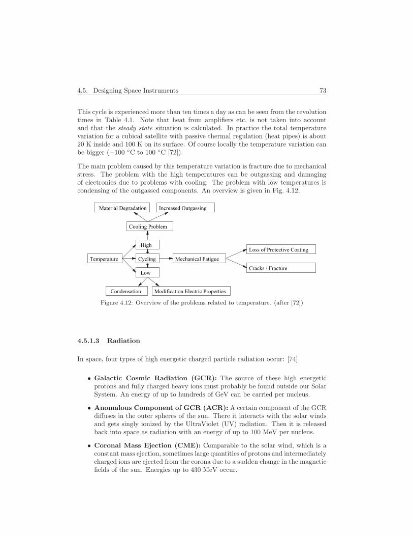
4.5. Designing Space Instruments 73
This cycle is experienced more than ten times a day as can be seen from the revolutiontimes in Table 4.1. Note that heat from amplifiers etc. is not taken into accountand that the steady state situation is calculated. In practice the total temperaturevariation for a cubical satellite with passive thermal regulation (heat pipes) is about20 K inside and 100 K on its surface. Of course locally the temperature variation canbe bigger (−100 C to 100 C [72]).
The main problem caused by this temperature variation is fracture due to mechanicalstress. The problem with the high temperatures can be outgassing and damagingof electronics due to problems with cooling. The problem with low temperatures iscondensing of the outgassed components. An overview is given in Fig. 4.12.
Modification Electric PropertiesCondensation
Cooling Problem
Material Degradation Increased Outgassing
Cracks / Fracture
Temperature Cycling
High
Low
Mechanical Fatigue
Loss of Protective Coating
Figure 4.12: Overview of the problems related to temperature. (after [72])
4.5.1.3 Radiation
In space, four types of high energetic charged particle radiation occur: [74]
• Galactic Cosmic Radiation (GCR): The source of these high energeticprotons and fully charged heavy ions must probably be found outside our SolarSystem. An energy of up to hundreds of GeV can be carried per nucleus.
• Anomalous Component of GCR (ACR): A certain component of the GCRdiffuses in the outer spheres of the sun. There it interacts with the solar windsand gets singly ionized by the UltraViolet (UV) radiation. Then it is releasedback into space as radiation with an energy of up to 100 MeV per nucleus.
• Coronal Mass Ejection (CME): Comparable to the solar wind, which is aconstant mass ejection, sometimes large quantities of protons and intermediatelycharged ions are ejected from the corona due to a sudden change in the magneticfields of the sun. Energies up to 430 MeV occur.
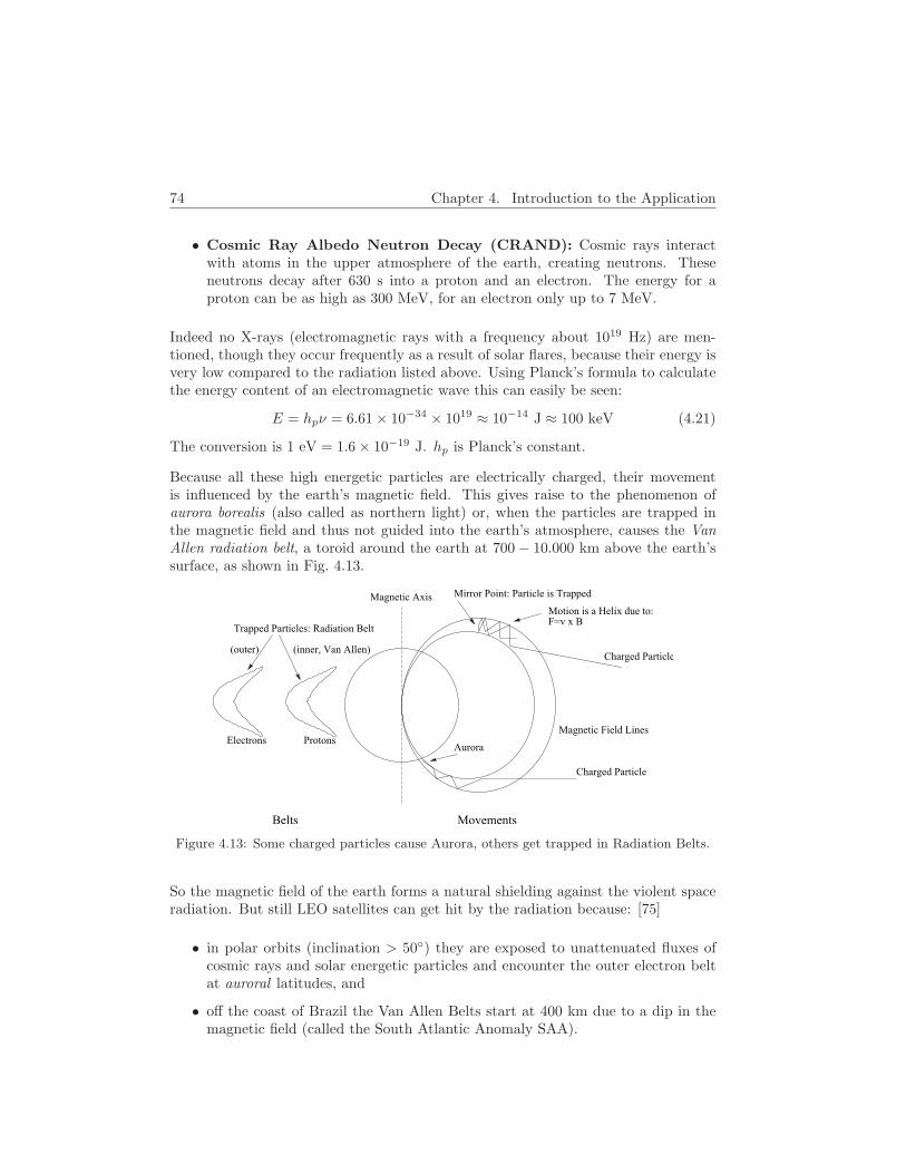
74 Chapter 4. Introduction to the Application
• Cosmic Ray Albedo Neutron Decay (CRAND): Cosmic rays interactwith atoms in the upper atmosphere of the earth, creating neutrons. Theseneutrons decay after 630 s into a proton and an electron. The energy for aproton can be as high as 300 MeV, for an electron only up to 7 MeV.
Indeed no X-rays (electromagnetic rays with a frequency about 1019 Hz) are men-tioned, though they occur frequently as a result of solar flares, because their energy isvery low compared to the radiation listed above. Using Planck’s formula to calculatethe energy content of an electromagnetic wave this can easily be seen:
E = hpν = 6.61 × 10−34 × 1019 ≈ 10−14 J ≈ 100 keV (4.21)
The conversion is 1 eV = 1.6 × 10⁻¹⁹ J. hp is Planck’s constant.
Because all these high energetic particles are electrically charged, their movementis influenced by the earth’s magnetic field. This gives raise to the phenomenon ofaurora borealis (also called as northern light) or, when the particles are trapped inthe magnetic field and thus not guided into the earth’s atmosphere, causes the VanAllen radiation belt, a toroid around the earth at 700 − 10.000 km above the earth’ssurface, as shown in Fig. 4.13.
Belts Movements
Electrons Protons
(outer) (inner, Van Allen)
Trapped Particles: Radiation Belt
Magnetic Axis Mirror Point: Particle is Trapped
Motion is a Helix due to:F=v x B
Charged Particle
Magnetic Field Lines
Charged Particle
Aurora
Figure 4.13: Some charged particles cause Aurora, others get trapped in Radiation Belts.
So the magnetic field of the earth forms a natural shielding against the violent spaceradiation. But still LEO satellites can get hit by the radiation because: [75]
• in polar orbits (inclination > 50) they are exposed to unattenuated fluxes ofcosmic rays and solar energetic particles and encounter the outer electron beltat auroral latitudes, and
• off the coast of Brazil the Van Allen Belts start at 400 km due to a dip in themagnetic field (called the South Atlantic Anomaly SAA).

4.5. Designing Space Instruments 75
The harmful effects of the radiation, summarized in Fig. 4.14 are:
• displacement damage: (or material degradation or bulk damage) The radi-ation damages the lattice structure of the material, producing recombinationcenters, which degrades the performance of semi-conductors.
• ionization damage: The charged particles that are trapped in the material,introduce an electric charge. This can offset the bias of a transistor.
• Single Event Effects (SEE): (mainly caused by protons) Due to radiation abit flips (e.g. 0 → 1). This can result in wrong data, but can also cause fatalerrors if the bit in a system command was flipped.
The first two effects are cumulative, this means that during time more and moreradiation degrades the component until it stops functioning. Mathematically thiscomes down to integrating the flux of radiation (that is stopped and absorbed) overthe life time of the component. This total dose is expressed in gray or rad where1 Gy = 1 J/kg = 8.6207 × 10¹⁸ eV/kg = 100 rad.
Also UV radiation occurs. This causes embrittlement (the structure of e.g. polymerschanges) and gives raise to the photo-electric effect (electrons are excited out of thematerial). The latter results in electrostatic charges (which can also be caused bythe electrons in the plasma surrounding the spacecraft) and eventually ElectroStaticDischarge (ESD) problems.
Radiation
Surface Charging
Lattice Damage
Single Event Upsets
Arc DischargeBias Offset
Aging
Latch UpBit Flip
Figure 4.14: Overview of the problems related to radiation.

76 Chapter 4. Introduction to the Application
4.5.1.4 Space Debris
It is not unlikely that debris hits the satellite. On the one hand this can be naturaldebris such as (dust of) a comet (with ice) or an asteroid (without), for many of themhave orbits that cross the earth’s orbit [76]. On the other hand also lots of wrecksfrom former spacecrafts still orbit around the earth. A collision can cause severedamage and can even leave a crater on the surface that was hit (triggering ESD).
4.5.2 Product Assurance
The science on designing instruments for the space environment is called productassurance (PA). The design should be such that the chance that an error occurs isas small as possible and if an error occurs the damage should be as small as possible[56].
PA works on all levels of designing a satellite: materials, components, subsystems andthe entire satellite. Some materials are prohibited in space as they outgass (e.g. fluidglue) or form whiskers (e.g. Zinc). All tested and space qualified components appearon the Space Qualified Parts List (QPL) or the Preferred Parts List (PPL), availablefrom [77]. If Commercial Off-The-Shelf (COTS) or newly developed componentsare considered for usage, they should be tested first, in order to asses the risk ofbreakdown, and to find out what the failure modes are.
Based on the failure modes of the components, the subsystems are tested on theirbehavior in case of failure. Some ways to enhance performance are shielding, redun-dancy and derating. Derating means that several components function in parallel sothat they are only partially loaded, which longens the lifetime. In case of redundancy,the components also function in parallel but are fully loaded, so that if one fails,another can be made active (standby redundancy) or a decision is taken by majorityvote over all parallel components (active redundancy).
In the end the satellite has to be tested. In former a prototype, called the Qualifi-cation Engineering Model (QEM) was built and tested to destruction. Nowadays aprotoflight model is used, which means that the QEM will become the Flight Model(FM) which will fly if all tests succeeded. The tests are based on expected failuresthat are related to system level failures, which are induced. In the end a figure forthe probability that the satellite will accomplish the mission is obtained.
Often the concept of the satellite is tested on a Bread Board Model (BBM). This isdone in an early phase of the design, even before the optimization phase.

4.6. Conclusions 77
4.6 Conclusions
In this chapter, a system for in-situ collected data up link to an earth observationsatellite was deployed. This system would bring the advantageous possibility of com-bining the data from the imaging sensor on board the earth observation satellite within-situ data. This way, preprocessing on the image data could be carried out on boardthe satellite, drastically reducing the demands on the imaging data down link, whichis obviously a bottleneck for earth observation satellites. Due to the high orbit speed,calculated to be typically 7 km/s in this chapter, the communication window withthe ground station is indeed limited.
Although the data that must be exchanged for the in-situ data up link system is verymodest, compared to the huge amount of image data, still the use of array antennasfor that system is advisable. Array antennas make sure that the power, that is scarceon the satellite, is not wasted by radiating it into unwanted directions, and do notsuffer from wear or give raise to vibrations, which is the problem when mechanicallyscanning high gain antennas such as parabola dishes. Moreover, the link budgetcalculation and the examples of existing LEO satellite array antennas, given in thischapter, indicate that the communication link for the in-situ data up link system isfeasible with the proposed antenna.
The orbit calculations in this chapter point out that the array antenna should haveits highest gain under large scan angles, used when the satellite elevation above theground station horizon is low. This will be the starting point for the array optimizationin Chapter 5. The same orbit calculation also shows that Doppler shift will be aproblem for the communication link. This issue will be dealt with in Chapter 6.
Another issue is the hostile space environment. In this chapter, the possible failuresassociated with the LEO space environment were discussed, as well as the generaldesign rules to avoid or minimize damage. These guidelines at a high level of abstrac-tion, will be translated into practical engineering rules, when designing antenna andcontrol circuitry in Chapters 5 and 6.

invisible filling

Chapter 5
Array Elements
In this chapter, first the element specifications that follow from the design choicesmade in Sect. 4.1.4 and from the general rules for space design in Sect. 4.5, will besummarized. Then, in Sect. 5.2, an appropriate substrate will be chosen and a patchelement will be designed in Sect. 5.3. With this element an array geometry can beevaluated. A first step is taken in Sect. 5.4.
5.1 Element Specifications
In Sect. 4.1.4 the working frequency was fixed to 1980 − 2010 MHz and 2170 −2200 MHz. This is a huge bandwidth for patch antennas, hence stacked patchesare preferred to obtain a dual band operation. In the same Sect. 4.1.4, circular po-larization was selected. This can be obtained by a single feed and a modified patch(e.g. a corner cut away). But a dual feed topology results in better RF performance.
The feeds should be implemented mechanically as robust as possible. Probe feedingis preferred as it has no backward radiation, as opposed to aperture feeding, and iscompact, in contrast to line feeding. As long as a substrate is used, no force acts onthe probe which means that there is no danger of breaking the probes during launch.Aperture feeding is not recommended as multi layer substrate needs gluing. Moreover,as the power is low, Passive Inter Modulation (PIM), the prime reason why probes,that need soldering, are avoided on satellites, will not be a problem.
To prevent the antenna substrate from being charged by radiation, a passivationcoating should be applied. This is closed space specific know how, that lies waybeyond the scope of this text. Related to passivation coating, a plastic cover shouldbe placed over the antenna to prevent debris impacts causing craters and ESD.
79

80 Chapter 5. Array Elements
The antenna should not degrade the performance of other systems on the satellite.Conducting shielding walls are appropriate to avoid ElectroMagnetic Compatibility(EMC) problems with other components, but can cause secondary radiation, and addweight to the structure.
5.2 Antenna Substrates for Space Application
Choosing a substrate for an antenna or circuit design deserves special attention. Inthis section we will first explain what the characteristics of substrates are, whichsubstrates are in use and what would be the best choice to use in space.
5.2.1 Tolerances
Substrates are only available for a limited number of values for ε. Indeed is it lessimportant to have a certain value for ε, than to have tight bounds on the variationof ε over the entire substrate. A circuit or antenna after redesign with the correct(measured) value for ε on a substrate with ε different from the ε originally intended,overperform an implementation on a substrate with the right (mean) ε but witha strong deviation depending on the place on the substrate. In other words, thetolerances are much more important than the value. The ideal substrate has: [78]
• a well defined and constant dielectric constant
• a well defined thickness and a smooth surface
• a high purity with high uniformity and low losses and anisotropy
• a high resistivity
• a high thermal conductivity
5.2.2 Properties
5.2.2.1 Dielectric Constant ε
The relative magnetic permeability for most substrates is µr = 1, but the electricpermeability differs considerably from substrate to substrate. All common substrateshave εr between 2.10 and 10.2. Some examples can be found in Table 5.1.

5.2. Antenna Substrates for Space Application 81
Table 5.1: Some examples of the available εr for RF substrates.
type εr materialArlon CuClad 217 2.17 ± 0.02 Crossplied Woven glass PTFEArlon DiClad 880 2.17 ± 0.02 Unidirected Woven glass PTFE
Rogers UltraLam 1217 2.17 ± 0.02 Woven glass PTFERogers RT/Duroid 5880 2.20 ± 0.02 Random glass PTFE
Rogers RO4003 3.38 ± 0.05 Woven glass Polymer CeramicRogers RO6006 10.2 ± 0.25 PTFE Ceramic
The value of εr, at a certain frequency, of a substrate can be determined by measuringthe capacitance of a double cladded substrate panel:
C =Q
V=εrA
dt(5.1)
where A is the area and dt the thickness of the substrate.
The higher the value for εr, the lower the speed of light in the material due to:
c =c0√εr
(5.2)
and thus the shorter the wavelength. For this reason, a high εr is a good choice forcircuit substrates or for antenna miniaturization. For high gain antennas, εr shouldbe small, to have a large antenna resulting in a higher gain. This also results in ahigher bandwidth.
The value of the characteristic impedance Zc for a micro strip line (of width b) alsodepends on εr: [79]
Zc =1√εr
60 ln4b
d∼ 1√
εr(5.3)
5.2.2.2 Dissipation Factor tan δ
A double cladded substrate is a capacitor. Hence, to quantify the resistive losses in asubstrate, the dissipation factor or loss tangent [79]
tan δ =dissipated energy
stored energy(5.4)
can be measured, which is the ratio of the resistive part to the capacitive part of theimpedance of the lossy capacitor.

82 Chapter 5. Array Elements
5.2.2.3 Dielectric Thickness dt
The thickness or height of the substrate dt is the thickness of the bare substrate, thuswithout metal. This is often expressed in mil1 e.g. 50 mil is 0.050” or 1.27 mm.
A higher dt gives more bandwidth for micro strip antennas as it longens the resonatorat the sides. But due to a longer path length in the material, the losses increase, sothat the efficiency and gain decrease [80].
A constant thickness and very few pits are important. This is expressed in tolerancegrades from grade A (best) to C for pits and class 1 (best) to 4 for thickness variation.
5.2.3 Substrate Materials
5.2.3.1 Teflon (εr : 2.10 → 10.2)
Teflon or PolyTetraFluoroEthyleen (PTFE) has a dielectric constant of 2.10. Byadding impurities a higher εr can be obtained:
• ceramics result in high dielectric constants (εr : 6 → 10).
• glass generally results in lower dielectric constants (εr : 2.17 → 4).
The glass in the PTFE can either be a woven matrix or randomly distributed fibers.The first results in a more rigid structure that is however more lossy and anisotrope.Due to capillarity the substrate will also absorb more water than the random glasscounterpart. Both are though better on this issue than the Teflon with ceramic type.PTFE with ceramic also has a lower peel strength and deforms easier than PTFE withglass. Therefore often a metal backing is used. An overview is given in Table 5.2.
The more impurity added, the higher the εr will be. But with more glass or ceramicadded, also the losses and anisotropy will increase. The peel strength fortunately alsoincreases with more impurities as this improves the adhesion.
Table 5.2: Overview of the different PTFE based substrates.
type εr strength H2O abs. peelwoven glass 2.17 → 4 best ±0.02% ++
random glass 2.17 → 4 chips sink in substrate ±0.01% +ceramics 6 → 10 use a metal backing ±0.05% -
1One mil is 1/1000 of an inch.

5.2. Antenna Substrates for Space Application 83
5.2.3.2 Alumina (εr : 8 → 10)
Alumina or Al2O3 is a brittle material that thus has some difficulties with drilling, butthat is more rigid than Teflon. It has lower losses than its Teflon high εr counterpart.
5.2.3.3 Thermoset Polymer (εr : 3 → 10)
The most used thermoset substrate is FR4. This low cost material consists of glasswith εr = 3 and a polymer resin with εr = 6. The overall εr ≈ 4.5, but the toler-ances are not tight. Many polymer substrates were invented to combine the goodperformance of the PTFE substrates and the low cost of FR4.
5.2.3.4 Sapphire (εr ≈ 11) and Beryllia (εr ≈ 6)
These materials are only used in applications where the substrate should have ahigh thermal conductivity. Both materials are brittle and thus difficult to process.Moreover, beryllia is toxic. Avoid these materials if possible.
5.2.3.5 PolyPhenyleenOxide PPO (εr = 2.55)
This material disappeared from the laminate scene as it became sticky after etchingand cracked after drilling.
5.2.4 Metalization
Most substrates have metal on one or both sides. This can be etched to form thestrips of the circuit. There are two ways to put metal on substrates:
• sputtering gas ions collide with a negatively biased target, setting metal atomsfree that will settle on the positively charged substrate.
• cladding with the aid of heath and pressure the metal and the substrate arestuck together.
The metal layer for the latter process can be either Electro Deposited (ED) or rolledmetal. ED is the standard method where the metal atoms are electrically joined toform a sheet of the desired thickness. For a rolled metal, the thickness is obtainedby pushing a thick metal sheet through a pair of rollers. The rolled metal thus hasa better conductivity and a higher uniformity. This makes it suited for more criticalapplications.
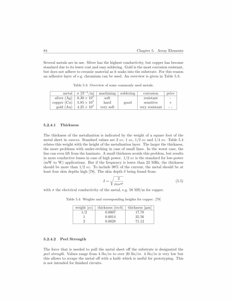
84 Chapter 5. Array Elements
Several metals are in use. Silver has the highest conductivity, but copper has becomestandard due to its lower cost and easy soldering. Gold is the most corrosion resistant,but does not adhere to ceramic material as it soaks into the substrate. For this reasonan adhesive layer of e.g. chromium can be used. An overview is given in Table 5.3.
Table 5.3: Overview of some commonly used metals.
metal σ [Ω−1/m] machining soldering corrosion pricesilver (Ag) 6.30 × 10⁷ soft resistant -
copper (Cu) 5.85 × 10⁷ hard good sensitive +gold (Au) 4.25 × 10⁷ very soft very resistant - -
5.2.4.1 Thickness
The thickness of the metalization is indicated by the weight of a square foot of themetal sheet in ounces. Standard values are 2 oz, 1 oz, 1/2 oz and 1/4 oz. Table 5.4relates this weight with the height of the metalization layer. The larger the thickness,the more problems with under-etching in case of small lines. In the worst case, theline can even lift from the laminate. A small thickness avoids this problem, but resultsin more conductive losses in case of high power. 1/2 oz is the standard for low-power(mW to W) applications. But if the frequency is lower than 22 MHz, the thicknessshould be more than 1/2 oz. To include 98% of the current, the metal should be atleast four skin depths high [78]. The skin depth δ being found from:
δ =
√2
µ0ωσ(5.5)
with σ the electrical conductivity of the metal, e.g. 58 MS/m for copper.
Table 5.4: Weights and corresponding heights for copper. [79]
weight [oz] thickness [inch] thickness [µm]1/2 0.0007 17.781 0.0014 35.562 0.0028 71.12
5.2.4.2 Peel Strength
The force that is needed to pull the metal sheet off the substrate is designated thepeel strength. Values range from 4 lbs/in to over 20 lbs/in. 4 lbs/in is very low butthis allows to scrape the metal off with a knife which is useful for prototyping. Thisis not intended for finished circuits.

5.2. Antenna Substrates for Space Application 85
5.2.5 Space Environment
In this section selection criteria for substrates intended for space use will be given.
5.2.5.1 Pressure
Outgassing is measured with three quantities, all as percentage of the initial samplemass:
• Total Mass Loss (TML) which is the difference in weight before and after anoutgassing test
• Collected Volatile Condensible Material (CVCM) or the mass of the condensedmaterial during an outgassing test
• Water Vapor Regain (WVR) or the mass of water that is re-absorbed after theoutgassing test during 24 hours at 25C with a relative humidity of 50%
National Aeronautics and Space Administration (NASA) specifies [81] that materialswith TML > 1.0% and/or CV CM > 0.1% should be avoided in space applications.European Space Agency (ESA) [82] allows more TML as long as the mass loss ismainly due to water, so that the Recovered Mass Loss (RML=TML-WVR) should beless than 1.0%. Some substrates that meet the specs are listed in Table 5.5.
5.2.5.2 Temperature
The mean working temperature of the substrate in space will be lower than on earth,but the issue of importance is the temperature cycling, rather than the extremetemperatures. Depending on the orbit height, 12 to 16 cycles a day with an amplitudeof more than 50 K are experienced. The use of a thermal control paint could have apositive effect on the amplitude of the temperature cycles. For this purpose a FlexibleOptical Solar Reflector (FOSR) was used on IRIDIUM [66].
During these cycles the properties of the substrate change constantly. The change ofε is expressed with the Thermal Coefficient of εr (TCεr):
εr,T = εr,T0× (1 + TCεr(T − T0)). (5.6)
with T0 an arbitrary chosen reference temperature. The change in dimensions in xyzdirection is expressed with the Coefficient of Thermal Expansion (CTE):
lxyz,T = lxyz,T0× (1 + CTExyz(T − T0)). (5.7)
Some values can be found in Table 5.5.
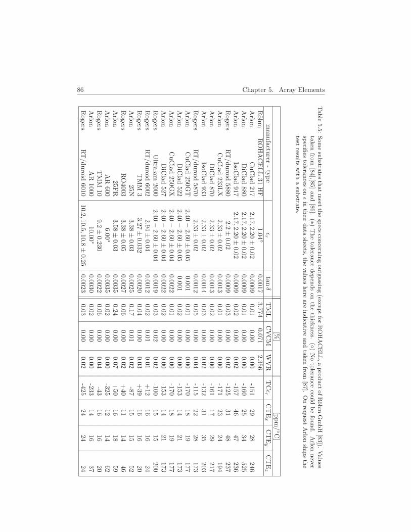
86 Chapter 5. Array ElementsTable
5.5
:Som
esu
bstra
testh
atm
eetth
esp
ecsco
ncern
ing
outg
assin
g(ex
ceptfo
rR
OH
AC
ELL,a
pro
duct
ofR
ohm
Gm
bH
[83]).
Valu
esta
ken
from
[84],[8
5]and
[86].
(∗)
The
tolera
nce
dep
ends
on
the
thick
ness.
()
No
tolera
nce
could
be
found.
Arlo
nnev
ersp
ecifies
tolera
nces
on
εin
their
data
sheets,
the
valu
eshere
are
indica
tive
and
taken
from
[87].
On
request
Arlo
nsh
ips
the
testresu
ltsw
itha
substra
te.
[%]
[ppm/ C
]m
anufactu
rer-
type
εr
tanδ
TM
LC
VC
MW
VR
TCεr
CT
Ex
CT
Ey
CT
Ez
Roh
mR
OH
AC
ELL
31H
F1.04
0.00173.774
0.0712.356
Arlon
CuC
lad217
2.17,2.20±0.02
0.00090.01
0.000.00
-15129
28246
Arlon
DiC
lad880
2.17,2.20±0.02
0.00090.01
0.000.00
-16025
34525
Arlon
IsoClad
9172.17,2.20±
0.020.0009
0.020.00
0.02-157
4647
236R
ogersRT
/duroid
58802.2±
0.020.0009
0.030.00
0.02-125
3148
237A
rlonC
uC
lad233L
X2.33±
0.020.0013
0.010.00
0.00-171
2324
194A
rlonD
iClad
8702.33±
0.020.0013
0.020.00
0.00-161
1729
217A
rlonIsoC
lad933
2.33±0.02
0.00140.03
0.000.02
-13231
35203
Rogers
RT
/duroid
58702.33±
0.020.0012
0.050.00
0.04-115
2228
173A
rlonC
uC
lad250G
T2.40−
2.60±0.05
0.0010.01
0.000.00
-17018
19177
Arlon
DiC
lad522
2.40−2.60±
0.050.001
0.020.00
0.00-153
1421
173A
rlonC
uC
lad250G
X2.40−
2.60±0.04
0.00220.01
0.000.00
-17018
19177
Arlon
DiC
lad527
2.40−2.60±
0.040.0022
0.020.00
0.00-153
1421
173R
ogersU
ltralam2000
2.40−2.60±
0.040.0019
0.030.02
0.02-100
1515
200R
ogersRT
/duroid
60022.94±
0.040.0012
0.020.01
0.01+
1216
1624
Rogers
TM
M3
3.27±0.032
0.00200.04
0.000.03
+39
1616
20A
rlon25N
3.38±0.03
0.00250.17
0.010.02
-8715
1552
Rogers
RO
40033.38±
0.050.0027
0.060.00
0.02+
4011
1446
Arlon
25FR
3.58±0.03
0.00350.24
0.000.07
+50
1618
59A
rlonA
R600
6.00 ∗0.0035
0.020.00
0.00-325
1214
62R
ogersT
MM
109.2±
0.2300.0022
0.060.00
0.04-43
1616
20A
rlonA
R1000
10.00 ∗0.0030
0.020.00
0.00-233
1416
37R
ogersRT
/duroid
601010.2,10.5,10.8±
0.250.0023
0.030.00
0.02-425
2424
24
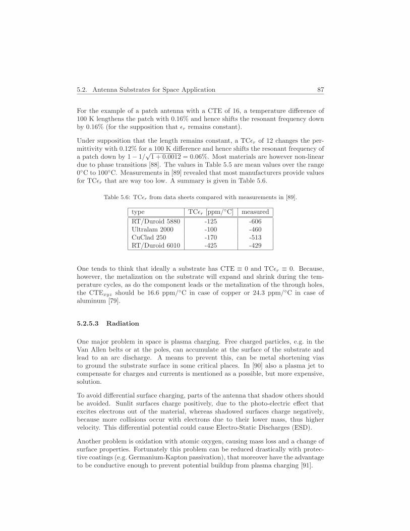
5.2. Antenna Substrates for Space Application 87
For the example of a patch antenna with a CTE of 16, a temperature difference of100 K lengthens the patch with 0.16% and hence shifts the resonant frequency downby 0.16% (for the supposition that εr remains constant).
Under supposition that the length remains constant, a TCεr of 12 changes the per-mittivity with 0.12% for a 100 K difference and hence shifts the resonant frequency ofa patch down by 1− 1/
√1 + 0.0012 = 0.06%. Most materials are however non-linear
due to phase transitions [88]. The values in Table 5.5 are mean values over the range0C to 100C. Measurements in [89] revealed that most manufacturers provide valuesfor TCεr that are way too low. A summary is given in Table 5.6.
Table 5.6: TCεr from data sheets compared with measurements in [89].
type TCεr [ppm/C] measured
RT/Duroid 5880 -125 -606Ultralam 2000 -100 -460CuClad 250 -170 -513RT/Duroid 6010 -425 -429
One tends to think that ideally a substrate has CTE ≡ 0 and TCεr ≡ 0. Because,however, the metalization on the substrate will expand and shrink during the tem-perature cycles, as do the component leads or the metalization of the through holes,the CTExyz should be 16.6 ppm/C in case of copper or 24.3 ppm/C in case ofaluminum [79].
5.2.5.3 Radiation
One major problem in space is plasma charging. Free charged particles, e.g. in theVan Allen belts or at the poles, can accumulate at the surface of the substrate andlead to an arc discharge. A means to prevent this, can be metal shortening viasto ground the substrate surface in some critical places. In [90] also a plasma jet tocompensate for charges and currents is mentioned as a possible, but more expensive,solution.
To avoid differential surface charging, parts of the antenna that shadow others shouldbe avoided. Sunlit surfaces charge positively, due to the photo-electric effect thatexcites electrons out of the material, whereas shadowed surfaces charge negatively,because more collisions occur with electrons due to their lower mass, thus highervelocity. This differential potential could cause Electro-Static Discharges (ESD).
Another problem is oxidation with atomic oxygen, causing mass loss and a change ofsurface properties. Fortunately this problem can be reduced drastically with protec-tive coatings (e.g. Germanium-Kapton passivation), that moreover have the advantageto be conductive enough to prevent potential buildup from plasma charging [91].
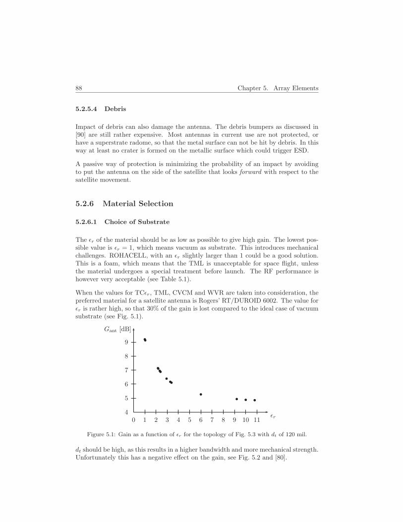
88 Chapter 5. Array Elements
5.2.5.4 Debris
Impact of debris can also damage the antenna. The debris bumpers as discussed in[90] are still rather expensive. Most antennas in current use are not protected, orhave a superstrate radome, so that the metal surface can not be hit by debris. In thisway at least no crater is formed on the metallic surface which could trigger ESD.
A passive way of protection is minimizing the probability of an impact by avoidingto put the antenna on the side of the satellite that looks forward with respect to thesatellite movement.
5.2.6 Material Selection
5.2.6.1 Choice of Substrate
The εr of the material should be as low as possible to give high gain. The lowest pos-sible value is εr = 1, which means vacuum as substrate. This introduces mechanicalchallenges. ROHACELL, with an εr slightly larger than 1 could be a good solution.This is a foam, which means that the TML is unacceptable for space flight, unlessthe material undergoes a special treatment before launch. The RF performance ishowever very acceptable (see Table 5.1).
When the values for TCεr, TML, CVCM and WVR are taken into consideration, thepreferred material for a satellite antenna is Rogers’ RT/DUROID 6002. The value forεr is rather high, so that 30% of the gain is lost compared to the ideal case of vacuumsubstrate (see Fig. 5.1).
0 1 2 3 4 5 6 7 8 9 10 114
5
6
7
8
9
Gant [dB]
εr
Figure 5.1: Gain as a function of εr for the topology of Fig. 5.3 with dt of 120 mil.
dt should be high, as this results in a higher bandwidth and more mechanical strength.Unfortunately this has a negative effect on the gain, see Fig. 5.2 and [80].

5.3. Element Design 89
0 50 100 1505
6
7
8
Gant [dB]
dt [mil]
Figure 5.2: Gain as a function of dt for the topology of Fig. 5.3 on RT/DUROID 6002.
5.2.6.2 Choice of Metalization
As the chosen substrate is Rogers’ RT/DUROID 6002, the cladding material shouldbe copper as it matches CTExy, and probes or component pins should be madeof aluminum to match CTEz. As mentioned in Sect. 5.2.4.1, the cladding thicknessshould be at least four skin depths δ. For a 2 GHz signal, Eq. (5.5) gives δ = 2.608 µm.The standard 1/2 oz cladding with thickness 17.78 µm suffices.
5.3 Element Design
For the array element, a patch antenna can be used. Fig. 5.3 depicts a design for adual feed circularly polarized patch antenna, for the lower band, 1980 − 2010 MHz.The patch is put on Rogers’ RT/DUROID 6002 with a thickness of 3.048 mm or 120mil. By feeding the two probes with a phase difference of 90, circular polarization isobtained. Shifting probes more to the center, results in a smaller input impedance.The limiting case of a probe in the center results in zero input impedance, a probeat the side result in a high input impedance. This as the result of standing waveson the patch. The probe position is optimized for a 50 Ω input impedance over the1980 − 2010 MHz band. The scattering parameter depicted in Fig. 5.4 indeed staysbelow −10 dB. The gain is 6.34 dB, which is in accordance with Fig. 5.1 and 5.2. Thedesign was simulated with MAGMAS, on an infinite ground plane and substrate. Iftransmit and receive antenna should be integrated, e.g. to save space which is scarceat the satellite, see Sect. 6.2.1, a stacked patch topology can be used with the upperpatch slightly smaller to add a second resonance at the 2170 − 2200 MHz band.
5.4 Selecting Array Geometry
In Sect. 4.2 was stated that a link budget should be calculated for αε = 10 asthis case gives the worst signal attenuation. Here, a design method is introduced toenhance the gain of the array under that angle, based on selecting the appropriate d,see Fig. 3.6.

90 Chapter 5. Array Elements
4.235 cm
4.235 cm
0.73 cm
0.73 cm
TOP VIEW SIDE VIEW
Figure 5.3: Scaled layout of the dual feed patch antenna.
1.95 1.96 1.97 1.98 1.99 2.00 2.01 2.02 2.03 2.040
−10
−20
−30
f [MHz]
|S11|Figure 5.4: Scattering parameter of the dual feed patch antenna.
This will result in the optimal array in the sense that it is the array with the highestpossible gain in the direction appropriate for this low elevation constellation, withouthaving grating lobes that could interfere with neighboring communications.
First the technique is explained on a one dimensional array, then generalized to a twodimensional one.
5.4.1 Linear Array
5.4.1.1 Theoretical Background
Let the linear array be an N -element LESA along the x-axis with inter elementspacing d, as in Fig. 5.5. As explained in Sect. 3.3.1.1.1, the radiated power of theLESA depends on d. One should choose d so that the first grating lobe lies just behindthe edges of the visible interval. In this case, the main beam is the smallest possiblewithout the appearance of grating lobes, so that the total power is low and thus thegain high, without risk of interfering with neighboring communications.
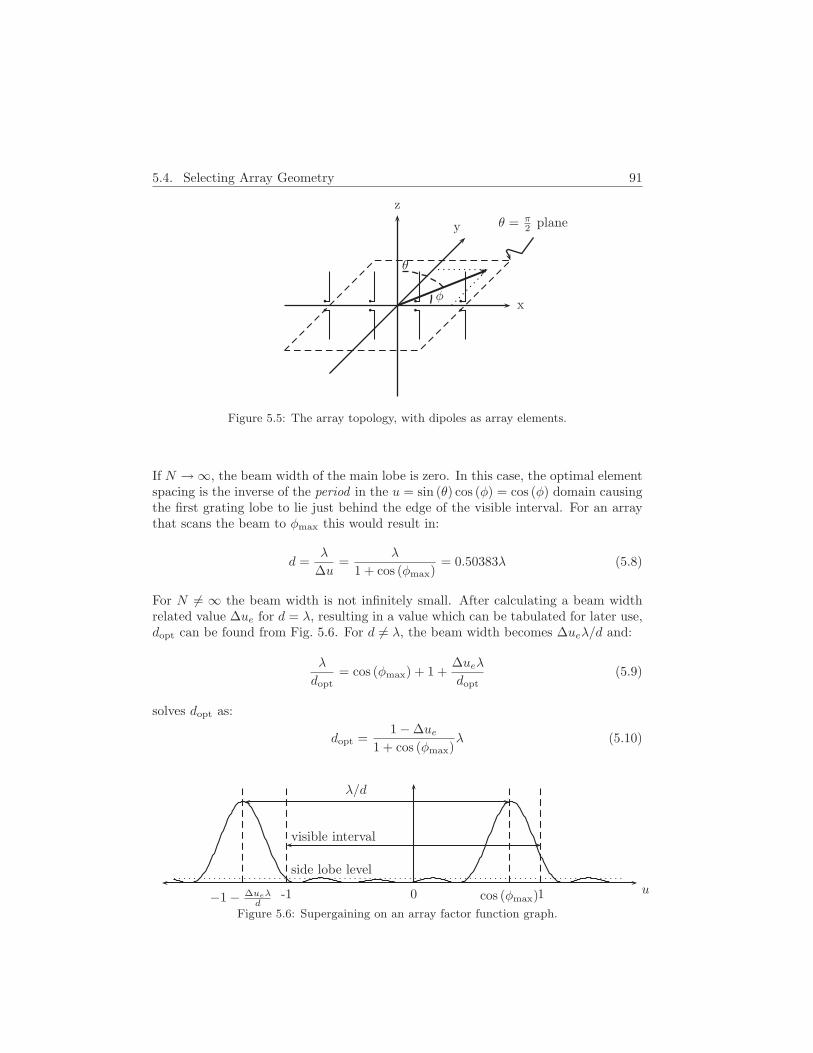
5.4. Selecting Array Geometry 91
x
z
y θ = π2 plane
φ
θ
Figure 5.5: The array topology, with dipoles as array elements.
If N → ∞, the beam width of the main lobe is zero. In this case, the optimal elementspacing is the inverse of the period in the u = sin (θ) cos (φ) = cos (φ) domain causingthe first grating lobe to lie just behind the edge of the visible interval. For an arraythat scans the beam to φmax this would result in:
d =λ
∆u=
λ
1 + cos (φmax)= 0.50383λ (5.8)
For N 6= ∞ the beam width is not infinitely small. After calculating a beam widthrelated value ∆ue for d = λ, resulting in a value which can be tabulated for later use,dopt can be found from Fig. 5.6. For d 6= λ, the beam width becomes ∆ueλ/d and:
λ
dopt= cos (φmax) + 1 +
∆ueλ
dopt(5.9)
solves dopt as:
dopt =1 − ∆ue
1 + cos (φmax)λ (5.10)
u0 1-1
visible interval
λ/d
side lobe level
−1 − ∆ueλd
cos (φmax)
Figure 5.6: Supergaining on an array factor function graph.
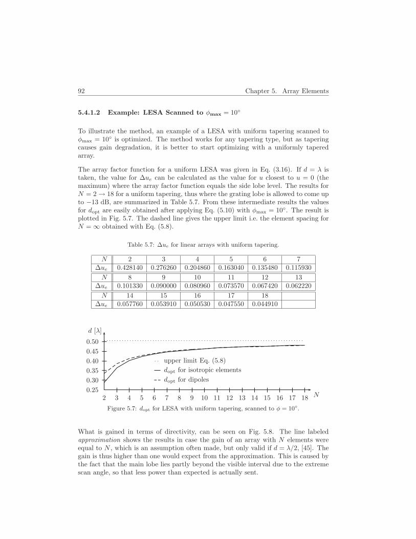
92 Chapter 5. Array Elements
5.4.1.2 Example: LESA Scanned to φmax = 10
To illustrate the method, an example of a LESA with uniform tapering scanned toφmax = 10 is optimized. The method works for any tapering type, but as taperingcauses gain degradation, it is better to start optimizing with a uniformly taperedarray.
The array factor function for a uniform LESA was given in Eq. (3.16). If d = λ istaken, the value for ∆ue can be calculated as the value for u closest to u = 0 (themaximum) where the array factor function equals the side lobe level. The results forN = 2 → 18 for a uniform tapering, thus where the grating lobe is allowed to come upto −13 dB, are summarized in Table 5.7. From these intermediate results the valuesfor dopt are easily obtained after applying Eq. (5.10) with φmax = 10. The result isplotted in Fig. 5.7. The dashed line gives the upper limit i.e. the element spacing forN = ∞ obtained with Eq. (5.8).
Table 5.7: ∆ue for linear arrays with uniform tapering.
N 2 3 4 5 6 7∆ue 0.428140 0.276260 0.204860 0.163040 0.135480 0.115930
N 8 9 10 11 12 13∆ue 0.101330 0.090000 0.080960 0.073570 0.067420 0.062220
N 14 15 16 17 18∆ue 0.057760 0.053910 0.050530 0.047550 0.044910
2 3 4 5 6 7 8 9 10 11 12 13 14 15 16 17 180.25
0.30
0.35
0.40
0.45
0.50
upper limit Eq. (5.8)
dopt for isotropic elements
dopt for dipoles
d [λ]
N
Figure 5.7: dopt for LESA with uniform tapering, scanned to φ = 10.
What is gained in terms of directivity, can be seen on Fig. 5.8. The line labeledapproximation shows the results in case the gain of an array with N elements wereequal to N , which is an assumption often made, but only valid if d = λ/2, [45]. Thegain is thus higher than one would expect from the approximation. This is caused bythe fact that the main lobe lies partly beyond the visible interval due to the extremescan angle, so that less power than expected is actually sent.

5.4. Selecting Array Geometry 93
1 2 3 4 5 6 7 8 9 10 11 12 13 14 15 16 17 1802468
101214
approximation Nisotropic elementsdipoles
D [dB]
N
Figure 5.8: Gain of the optimal LESA scanned to φ = 10 as a function of N .
5.4.1.3 Evaluation of the Method
To verify that the method indeed found the optimal array, the gain of several arrayswith N elements scanned to φ = 10, is compared in Fig. 5.9. From φ = 90 downto φ = 40, the gain is independent of the scan angle. When the beam is scannedfurther, the main lobe is partly scanned behind the edge of the visible interval. Arrayswith a higher gain at φ = 10, have a lower gain at broadside. This is however not aproblem as it is still the φ < 40 region that is important when designing. This canbe understood when looking at the uncompensated part of the free space path lossGfs in Fig. 5.10.
0 10 20 30 40 50 60 70 80 906
7
8
9
10
11
12
13
φ
D [dB]
d = 0.41
d = 0.43
d = 0.45
d = 0.47
d = 0.49
Figure 5.9: Directivity of several arrays as a function of scan angle (N = 8).
To avoid interference coming in, the grating lobe is only allowed to come up as highas the maximum side lobe level. This keeps the algorithm from finding the arraywith the highest possible gain. Indeed, the directivity of several LESAs scanned toφmax = 26 is given in Table 5.8. Comparing dopt found by Eq. (5.10) with dite
found by an iterative optimization search for maximum gain, reveals that all dopt aresmaller, to keep the grating lobe low. Table 5.8 moreover shows that for arrays withN ≥ 11, allowing grating lobes, maximizes the gain even more.

94 Chapter 5. Array Elements
0 10 20 30 40 50 60 70 80 90−145
−140
−135
−130
−125
−120
φ
G [dB]
array gain
uncompensated part
d = 0.4528, N = 8
1/(4πR2d)
Figure 5.10: Free space path loss and array gain as a function of elevation angle.
Table 5.8: dopt of Eq. (5.10) compared to dite and ddip of an iterative optimization search,for isotropic elements and dipoles, respectively. dite1 and ddip1 are the first localmaxima. dite is the global maximum in [0, 2]. φmax = 26. The gain in case of anarray of dipoles is higher due to the gain of the dipoles.
N dopt[λ] Gopt dite1[λ] Gite1 dite[λ] Gite ddip1[λ] Gdip1
2 0.3012 2.1379 0.3764 2.3611 0.3764 2.3611 0.3493 3.61153 0.3812 3.5382 0.4143 3.6366 0.4143 3.6366 0.4027 5.10334 0.4188 4.7450 0.4368 4.7867 0.4368 0.4368 0.4305 6.36955 0.4408 5.8199 0.4517 5.8299 0.4517 5.8299 0.4480 7.49066 0.4553 6.8036 0.4625 6.7936 0.4625 6.7936 0.4601 8.51867 0.4656 7.7276 0.4706 7.7034 0.4706 7.7034 0.4689 9.49118 0.4733 8.6163 0.4769 8.5813 0.4769 8.5813 0.4757 10.43659 0.4793 9.4893 0.4820 9.4451 0.4820 9.4451 0.4812 11.3763
10 0.4840 10.3613 0.4862 10.3090 0.4862 10.3090 0.4855 12.326811 0.4879 11.2438 0.4897 11.1837 0.4897 11.1837 0.4892 13.300012 0.4911 12.1448 0.4926 12.0772 1.5466 12.2132 0.4922 14.304213 0.4939 13.0696 0.4951 12.9946 1.5488 13.2533 0.4947 15.344414 0.4962 14.0206 0.4972 13.9383 1.5507 14.2915 0.4969 16.422715 0.4983 14.9981 0.4991 14.9085 1.5524 15.3222 0.4988 17.538116 0.5000 16.0002 0.5007 15.9032 1.5539 16.3472 0.5004 18.687117 0.5016 17.0228 0.5021 16.9187 1.5553 17.3734 0.5019 19.864318 0.5030 18.0608 0.5033 17.9499 1.5565 18.4057 0.5032 21.0621
5.4.1.4 Applicability to Non Isotropic Radiators
For non isotropic element types, the approach of only allowing the grating lobe ashigh as the highest side lobe level, to maximize the gain, will definitely not work. Thisis because although the array factor is scaled with varying d, the element radiationpattern is not scaled.

5.4. Selecting Array Geometry 95
Moreover, the main lobe can be made even smaller by allowing grating lobes in thevisible interval that are suppressed by zeros in the radiation pattern of the elements(as in [33]). It is unsure whether this is a wise approach, for this might cause hugelosses or be extremely narrow band. In such case the use of an iterative optimizationin combination with an electromagnetic solver is advisable.
For elements with a rotation symmetric radiation pattern, such as dipoles, a plane canbe found where the array radiation pattern contains only the array factor. Moreover,this is the plane of interest as here lies the maximum of the element pattern. Tovalidate the applicability of the proposed algorithm to non isotropic radiators with arotation symmetric radiation pattern, dopt are now compared to the optimal elementspacings ddip in arrays of dipoles, as found with an iterative optimization search. SeeTable 5.8 for the numerical results. The routine maximizes the directivity function ofEq. (3.18) yielding ddip,ff from:
D(d) =Ddipole(θ = 90, φ = 10)|F (90, 10, d)|2
π∫0
2π∫0
Ddipole(θ, φ)|F (θ, φ, d)|2 sin θdθdφ
(5.11)
where Ddipole was defined in Eq. (3.11). No conditions on the grating lobes wereimposed. The integral used 1 × 1 discretizations. An analytical expression forEq. (5.11) can be found in [92].
The optimum search with near field calculation of Ps as in Eq. (3.15) gave, as expectedbecause both are theoretically identical, very similar values dnear, see Table 5.9. Thedifference is due to numerical approximations. The current on the dipoles was dis-cretized using 100 segments with a constant, uniform current profile. For the segmentto segment coupling the formulas for hertzian dipoles were used.
Table 5.9: Optimal d in dipole arrays from near and far field iterative search.
N diso dnear dff N diso dnear dff
3 0.3646 0.3882 0.3861 11 0.4668 0.4669 0.46674 0.4006 0.4137 0.4124 12 0.4699 0.4697 0.46965 0.4217 0.4295 0.4287 13 0.4725 0.4721 0.47206 0.4356 0.4405 0.4399 14 0.4747 0.4742 0.47407 0.4454 0.4485 0.4481 15 0.4767 0.4759 0.47598 0.4528 0.4547 0.4544 16 0.4784 0.4776 0.47759 0.4585 0.4596 0.4593 17 0.4799 0.4790 0.4789
10 0.4630 0.4636 0.4634 18 0.4812 0.4803 0.4802
In Fig. 5.11 can be seen that for a N = 8 dipole array, scanned to φ = 10, the globalmaximum of the directivity appears for an inter-element distance that gives rise toa grating lobe. The local maximum around d = λ/2 corresponds quite well with thedistance found by the algorithm explained.
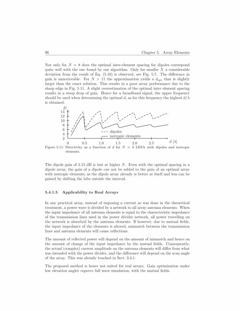
96 Chapter 5. Array Elements
Not only for N = 8 does the optimal inter-element spacing for dipoles correspondquite well with the one found by our algorithm. Only for smaller N a considerabledeviation from the result of Eq. (5.10) is observed, see Fig. 5.7. The difference ingain is unnoticeable. For N > 11 the approximation yields a dopt that is slightlylarger than the exact solution. This results in a poor array performance due to thesharp edge in Fig. 5.11. A slight overestimation of the optimal inter element spacingresults in a steep drop of gain. Hence for a broadband signal, the upper frequencyshould be used when determining the optimal d, as for this frequency the highest d/λis obtained.
0 0.5 1.0 1.5 2.0 2.52468
101214
dipolesisotropic elements
d [λ]
D
Figure 5.11: Directivity as a function of d for N = 8 LESA with dipoles and isotropicelements.
The dipole gain of 2.15 dB is lost at higher N . Even with the optimal spacing in adipole array, the gain of a dipole can not be added to the gain of an optimal arraywith isotropic elements, as the dipole array already is better at itself and less can begained by shifting the lobe outside the interval.
5.4.1.5 Applicability to Real Arrays
In any practical array, instead of imposing a current as was done in the theoreticaltreatment, a power wave is divided by a network to all array antenna elements. Whenthe input impedance of all antenna elements is equal to the characteristic impedanceof the transmission lines used in the power divider network, all power travelling onthe network is absorbed by the antenna elements. If however, due to mutual fields,the input impedance of the elements is altered, mismatch between the transmissionlines and antenna elements will cause reflections.
The amount of reflected power will depend on the amount of mismatch and hence onthe amount of change of the input impedance by the mutual fields. Consequently,the actual (complex) current amplitude on the antenna elements will differ from whatwas intended with the power divider, and the difference will depend on the scan angleof the array. This was already touched in Sect. 3.4.1.
The proposed method is hence not suited for real arrays. Gain optimization underlow elevation angles requires full wave simulation, with the mutual fields.

5.4. Selecting Array Geometry 97
As an illustration, the curve of gain variation of a dipole array as obtained from asimulation with imposed current from Fig. 5.11, is compared in Fig. 5.12 with a fullwave simulation with NEC of the same array fed with a power divider network. Itis clear that for small values of d the results are worse, mainly due to the changein reactive input impedance that destroys the phase relations between the elementsneeded for beam forming.
The curve has relatively high values for closely spaced dipoles. This is misleading asthe plot only shows the directivity. But as the input impedance of the dipoles forthat case is nearly entirely imaginary, it is practically impossible to feed power to thedipoles.
0 0.5 1.0 1.5 2.0 2.54
6
8
10
12
14imposed current power divider
d [λ]
D
Figure 5.12: Directivity as a function of d for N = 8 dipole LESA with current imposed andfed with a power divider network.
5.4.2 Planar Array
h
Earth Radius 6378 km
Rαmax
10
Figure 5.13: Satellite passing over a ground station.
For planar ground station antennas, maximizing the gain at a scan angle of θ = 80
is the design goal. For satellite antennas, θ depends on the orbit height. Some valuesare given in Table 5.10. The situation of a zenith pass is depicted in Fig. 5.13. Thevalues of Table 5.10 apply to any over pass, not only when the satellite passes overthe zenith of the ground station.

98 Chapter 5. Array Elements
Table 5.10: Orbit heights h and their corresponding maximal deviation from broadside θmax.
h [km] θmax [] h [km] θmax []200 73 600 64300 70 700 63400 68 800 61500 66 900 60
The study of the linear array was only a first step in designing a 2D array that canbe used on satellites or ground stations. Generalizing the one dimensional to a twodimensional array can be done in several ways, amongst others:
• a N elements LESA can be used as an element in an M elements LESA, ob-taining an N ×M regular grid array,
• or a N elements LESA can be repeated M times after a rotation by mπ/M form : 0 →M − 1 obtaining an array of N concentric circles.
Both possibilities, depicted in Fig. 5.14, are now compared, first in case of a broadsidebeam, then for the scan angle θmax = 64. In the end the best one for our purpose ischosen.
5.4.2.1 Broadside
5.4.2.1.1 Concentric Circles For odd N , the center element is placed only once.All elements, even the center element, should be excited with the same amplitude, astapering causes gain degradation.
For M > 1, the radiation pattern can not be derived from the radiation pattern ofthe linear array. Especially not for odd N , where even the array factor does not equalthe sum of the array factors of the rotated arrays, as the center element is only placedonce. This means that mathematically, the conclusion on the optimal inter-elementspacing in a linear array will no longer hold for M > 1. We will now investigate howgood the approximation with Eq.(5.10) is for arrays of concentric circles.
The higher M , the less side lobes suffer from beam broadening [37] at the edges ofthe scan interval. Then, when side lobes appear or disappear at the ends of the scaninterval, they cause a sudden change in gain, as opposed to in the case of a lineararray where the beam broadening compensates partly for a lobe shifting out of or into the visible interval, with a smoother curve in Fig. 5.15 as a result. The curves foran array of concentric circles have a shape similar to the curve for a linear array. Alsothe sharp edges behind the maxima are present, which means that in this case as welloverestimation of d, lowers the gain drastically.
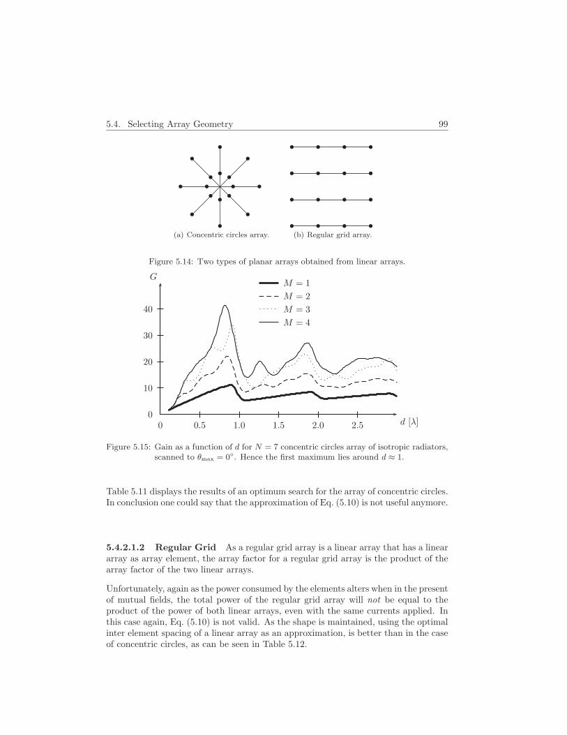
5.4. Selecting Array Geometry 99
(a) Concentric circles array. (b) Regular grid array.
Figure 5.14: Two types of planar arrays obtained from linear arrays.
0 0.5 1.0 1.5 2.0 2.50
10
20
30
40
M = 1
M = 2
M = 3
M = 4
G
d [λ]
Figure 5.15: Gain as a function of d for N = 7 concentric circles array of isotropic radiators,scanned to θmax = 0. Hence the first maximum lies around d ≈ 1.
Table 5.11 displays the results of an optimum search for the array of concentric circles.In conclusion one could say that the approximation of Eq. (5.10) is not useful anymore.
5.4.2.1.2 Regular Grid As a regular grid array is a linear array that has a lineararray as array element, the array factor for a regular grid array is the product of thearray factor of the two linear arrays.
Unfortunately, again as the power consumed by the elements alters when in the presentof mutual fields, the total power of the regular grid array will not be equal to theproduct of the power of both linear arrays, even with the same currents applied. Inthis case again, Eq. (5.10) is not valid. As the shape is maintained, using the optimalinter element spacing of a linear array as an approximation, is better than in the caseof concentric circles, as can be seen in Table 5.12.
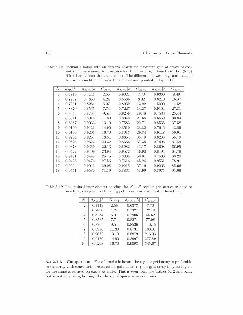
100 Chapter 5. Array Elements
Table 5.11: Optimal d found with an iterative search for maximum gain of arrays of con-centric circles scanned to broadside for M : 1 → 3. dopt found with Eq. (5.10)differs largely from the actual values. The difference between dopt and dM=1 isdue to the condition of low side lobe level incorporated in Eq. (5.10).
N dopt[λ] dM=1[λ] GM=1 dM=2[λ] GM=2 dM=3[λ] GM=3
2 0.5719 0.7143 2.55 0.9021 7.70 0.9360 8.493 0.7237 0.7860 4.24 0.5686 8.32 0.8210 16.374 0.7951 0.8284 5.97 0.8939 13.22 1.5000 14.585 0.8370 0.8565 7.74 0.7227 14.27 0.9104 27.816 0.8645 0.8765 9.51 0.9256 19.78 0.7533 25.447 0.8841 0.8916 11.30 0.8340 21.66 0.6669 30.848 0.8987 0.9033 13.10 0.7583 22.71 0.8535 37.589 0.9100 0.9126 14.90 0.8510 28.82 0.7646 43.59
10 0.9190 0.9203 16.70 0.8013 29.84 0.9118 50.0111 0.9264 0.9267 18.51 0.8864 35.79 0.8233 55.7912 0.9326 0.9322 20.32 0.8366 37.35 0.7696 51.8913 0.9378 0.9369 22.13 0.8982 43.17 0.8608 66.9514 0.9422 0.9409 23.94 0.9572 46.90 0.8194 64.7915 0.9461 0.9445 25.75 0.9085 50.01 0.7538 68.2816 0.9495 0.9476 27.56 0.7616 45.26 0.9551 78.9117 0.9524 0.9043 29.08 0.9215 57.16 0.9063 85.6618 0.9551 0.9530 31.19 0.8861 58.99 0.8975 91.06
Table 5.12: The optimal inter element spacings for N × N regular grid arrays scanned tobroadside, compared with the dopt of linear arrays scanned to broadside.
N dN×1[λ] GN×1 dN×N [λ] GN×N
2 0.7143 2.55 0.6373 7.703 0.7860 4.24 0.7327 22.404 0.8284 5.97 0.7906 45.625 0.8565 7.74 0.8274 77.086 0.8765 9.51 0.8536 116.157 0.8916 11.30 0.8731 163.018 0.9033 13.10 0.8879 216.939 0.9126 14.90 0.8997 277.89
10 0.9203 16.70 0.9093 345.67
5.4.2.1.3 Comparison For a broadside beam, the regular grid array is preferableto the array with concentric circles, as the gain of the regular grid array is by far higherfor the same area used on e.g. a satellite. This is seen from the Tables 5.12 and 5.11,but is not surprising keeping the theory of sparse arrays in mind.

5.5. Conclusions 101
Sparse arrays can be used to obtain a small beam and thus a high resolving capability,but have in general a lower gain due to higher side lobes [39], especially when thearray elements are concentrated in the middle of the array and the array becomes moresparse on the outer side. This is indeed the case for an array of concentric circles orits one dimensional analogy of a geometric linear array with geometric factor largerthan 1.
5.4.2.2 Scanned to θmax = 64
5.4.2.2.1 Concentric Circles Apart from the fact that Eq. (5.10) is no longerapplicable, now also the optimal distance changes with changing scan angle φ. If Mis however high enough, the symmetry of the structure is so high, that the geometryis nearly the same, no matter under which φ angle the array is scanned. In this case,the gain (and the optimal inter element spacing) is nearly independent of the scanangle φ, as can be seen in Fig. 5.16(a).
5.4.2.2.2 Regular Grid For the regular grid, the relative difference in gain alsodecreases with more elements used, as in Fig. 5.16(b).
5.4.2.2.3 Comparison For the purpose of an array antenna on board an earthobservation satellite, where the attitude of the satellite is dictated by the part of theearth’s surface under observation, the array of concentric circles is the best choice, asfor this array, when M is chosen high enough, the gain does not depend on the scanangle φ.
5.5 Conclusions
In this chapter, the array element was designed, taking into account the system spec-ifications such as bandwidth and gain, as well as the general guidelines for spacedesign. Consequently, much effort was spent on the antenna substrate selection.
Once the element is designed, the array geometry can be optimized. For the applica-tion of the in-situ data up link to an earth observation satellite, the antenna shouldhave high gain for large scan angles, to partially compensate for the larger satelliteto ground station distance, and hence free space path loss, when the satellite has alow elevation above the ground station’s horizon. A new technique for linear arrayswas introduced. Unfortunately, this technique is not easily generalized to planar ar-rays. Moreover, as the technique supposes current imposed on the array elements, thepractical relevance of the results is questionable, for most practical array antennasare voltage driven.

102 Chapter 5. Array Elements
0 15 30 45 60 75−0.8
−0.7
−0.6
−0.5
−0.4
−0.3
−0.2
−0.1
0.0
φ
∆G [dB]
M = 1M = 2M = 3M = 4M = 5M = 6
(a) Gain variation over φ for N = 7, d = 0.4656 concentric circles array scanned to θ = 64.
0 15 30 45 60 75−0.6
−0.5
−0.4
−0.3
−0.2
−0.1
0.0
φ
∆G [dB]
M = N = 4M = N = 5M = N = 6M = N = 7
(b) Gain variation over φ for dx = dy = 0.4656 regular grid array scanned to θ = 64.
Figure 5.16: Gain variation over φ for concentric circle and regular grid array.
Chapter 6
Signal Modification andCombination
After having designed the array element and the array geometry in Chapter 5, for thesystem for in-situ data up link to an earth observation satellite that was describedin Chapter 4, this chapter will deal with the signal shaping and combination. Signalcombination is obtained by a BB summing opamp. For the signal shaping, an analogBB implementation of a technique commonly used for digital BB beam forming,touched in Sect. 2.2.2.1, will be used. The implementation was developed alreadyback in 2003 by ir. P. Delmotte [93]. Sect. 6.1.1 describes the implementation.
In recent years, the capabilities of Analog-to-Digital Converters (ADCs) have tremen-dously increased, both regarding speed and resolution. This evolution offers lots ofpossibilities for digital beam forming and makes the implementation of Sect. 6.1.1 lessattractive. In some cases however, implementing the digital beam forming techniquein an analog way is useful. Indeed, when a large bandwidth is needed, the demandson sampling speed might be beyond ADC specs. If the array has a large numberof antenna elements, the demands on processing power to combine the output of allADCs (used in parallel) might be unrealistic.
Ir. P. Delmotte built an array to demonstrate his analog BB phase shifter at 2.4 GHz,in order to allow testing and demonstrational use of the array in the unrestrictedIndustrial, Scientific and Medical (ISM) band. The demonstrated technique, however,can be implemented at any frequency and with minor changes for a transmittingarray as well. This antenna architecture as well as its control and calibration will bediscussed in Sect. 6.1.2 as, unfortunately, no references on this work were available atthe time of writing. Afterwards, new work, namely the adaptation of the techniquefor space operation is discussed.
103
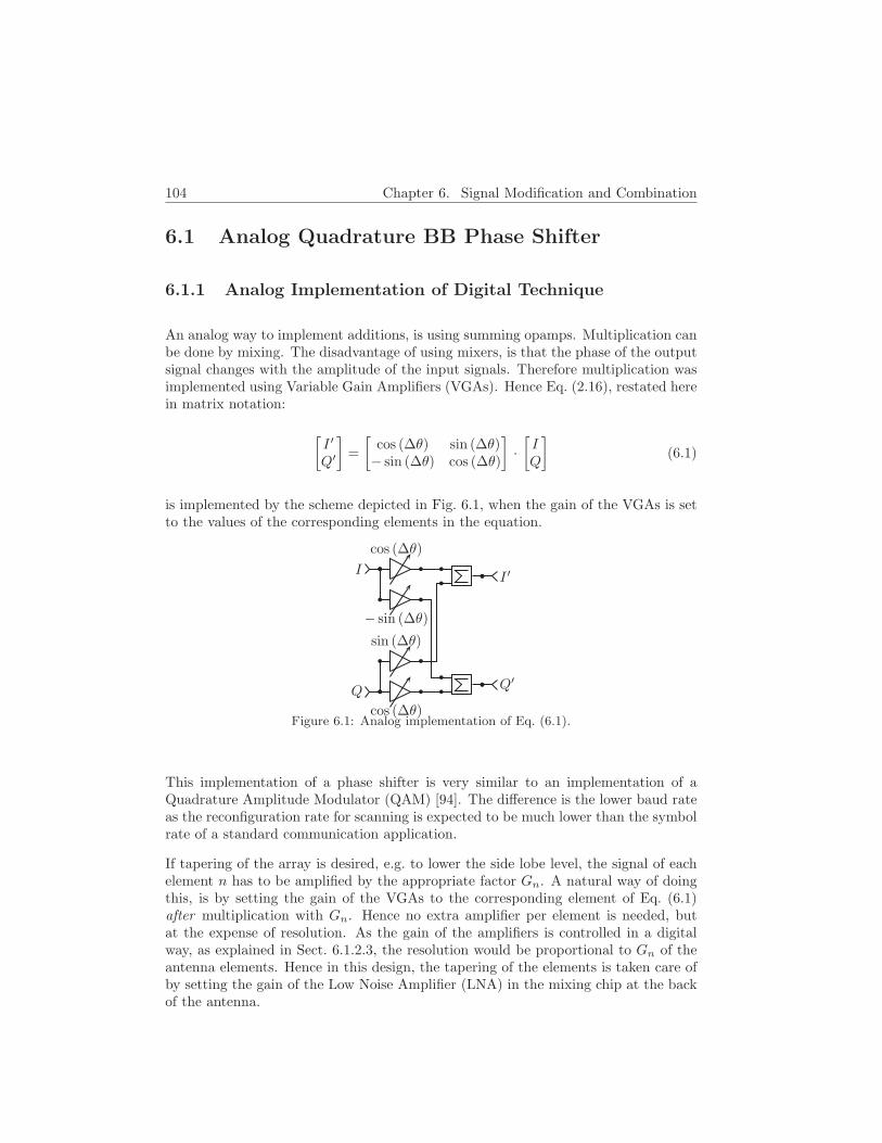
104 Chapter 6. Signal Modification and Combination
6.1 Analog Quadrature BB Phase Shifter
6.1.1 Analog Implementation of Digital Technique
An analog way to implement additions, is using summing opamps. Multiplication canbe done by mixing. The disadvantage of using mixers, is that the phase of the outputsignal changes with the amplitude of the input signals. Therefore multiplication wasimplemented using Variable Gain Amplifiers (VGAs). Hence Eq. (2.16), restated herein matrix notation:
[I ′
Q′
]=
[cos (∆θ) sin (∆θ)− sin (∆θ) cos (∆θ)
]·[IQ
](6.1)
is implemented by the scheme depicted in Fig. 6.1, when the gain of the VGAs is setto the values of the corresponding elements in the equation.
I
Q
cos (∆θ)
− sin (∆θ)
sin (∆θ)
cos (∆θ)
I ′
Q′
Figure 6.1: Analog implementation of Eq. (6.1).
This implementation of a phase shifter is very similar to an implementation of aQuadrature Amplitude Modulator (QAM) [94]. The difference is the lower baud rateas the reconfiguration rate for scanning is expected to be much lower than the symbolrate of a standard communication application.
If tapering of the array is desired, e.g. to lower the side lobe level, the signal of eachelement n has to be amplified by the appropriate factor Gn. A natural way of doingthis, is by setting the gain of the VGAs to the corresponding element of Eq. (6.1)after multiplication with Gn. Hence no extra amplifier per element is needed, butat the expense of resolution. As the gain of the amplifiers is controlled in a digitalway, as explained in Sect. 6.1.2.3, the resolution would be proportional to Gn of theantenna elements. Hence in this design, the tapering of the elements is taken care ofby setting the gain of the Low Noise Amplifier (LNA) in the mixing chip at the backof the antenna.

6.1. Analog Quadrature BB Phase Shifter 105
6.1.2 Architecture of the Demonstrator Array Antenna
As any scanning phased array, this antenna too consists of radiating elements, de-scribed in Sect. 6.1.2.1, phase shifters and a power combination network, describedin Sect. 6.1.2.2, and hardware to control the phase shifters and apply the tapering,detailed in Sect. 6.1.2.3. A photo of the array, taken inside the anechoic chamber, canbe found in Fig. 6.2.
Figure 6.2: Photograph of the array antenna inside the anechoic chamber.
6.1.2.1 Patch Antenna Element
The antenna element is a probe fed patch with a superstrate. The ground plane of thepatch also serves as the ground plane of the mixing circuitry, discussed in Sect. 6.1.2.2,that sits behind the antenna element. FR4 was used for both patch superstrate andcircuitry board. For the probe, solid 1.5 mm2 copper wire was used. The geometricalparameters are summarized in Table 6.1 and a photograph is shown in Fig. 6.3
The finiteness of the ground plane, and especially of the superstrate have strongrepercussions on the gain of the antenna element, This choice was made to obtain amodular system. In order to illustrate the effect, the antenna element was simulatedin IE3D in [95]. The radiation pattern of the three different situations, i.e. infinitesuperstrate and ground plane, finite ground plane and infinite superstrate and finiteground plane and finite superstrate, are given in Fig. 6.4(a),6.4(b) and 6.4(c).

106 Chapter 6. Signal Modification and Combination
Table 6.1: Geometrical and electrical parameters of the patch.
feature dimension [mm]
probe height 5probe offset 10
patch width, length 40, 47ground plane width, length 50, 50
superstrate thickness 1.575superstrate dielectric constant ±4.5
superstrate loss tangent ±0.0012horizontal inter element spacing 75
vertical inter element spacing 75
Figure 6.3: Photograph of the antenna element.
6.1.2.2 Signal Path
As soon as the signal is picked up by the antenna, it is amplified with an LNAwith controllable gain, so that tapering can be applied, as touched in Sect. 6.1.1.Then it is mixed down by a quadrature mixer, and fed into the baseband phaseshifter that was introduced in Sect. 6.1.1. The mixer (MAX2701) is fed with an LOthat is distributed through a dedicated Printed Circuit Board (PCB) to all elementsover cables of (intentionally) identical length and amplified by a transistor per fourantennas. As a consequence the phase of the LO arriving at all mixers, can notbe expected to have exactly the same phase. This error will be corrected whencalibrating. To avoid problems with LO cross talk as mentioned in [8], the LO wasdistributed at half the carrier frequency. This frequency is then doubled prior tomixing, inside the mixer IC, at the back of each antenna element.
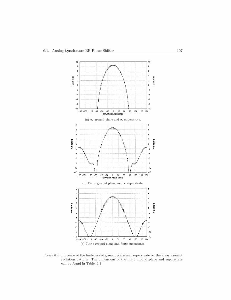
6.1. Analog Quadrature BB Phase Shifter 107
(a) ∞ ground plane and ∞ superstrate.
(b) Finite ground plane and ∞ superstrate.
(c) Finite ground plane and finite superstrate.
Figure 6.4: Influence of the finiteness of ground plane and superstrate on the array elementradiation pattern. The dimensions of the finite ground plane and superstratecan be found in Table. 6.1
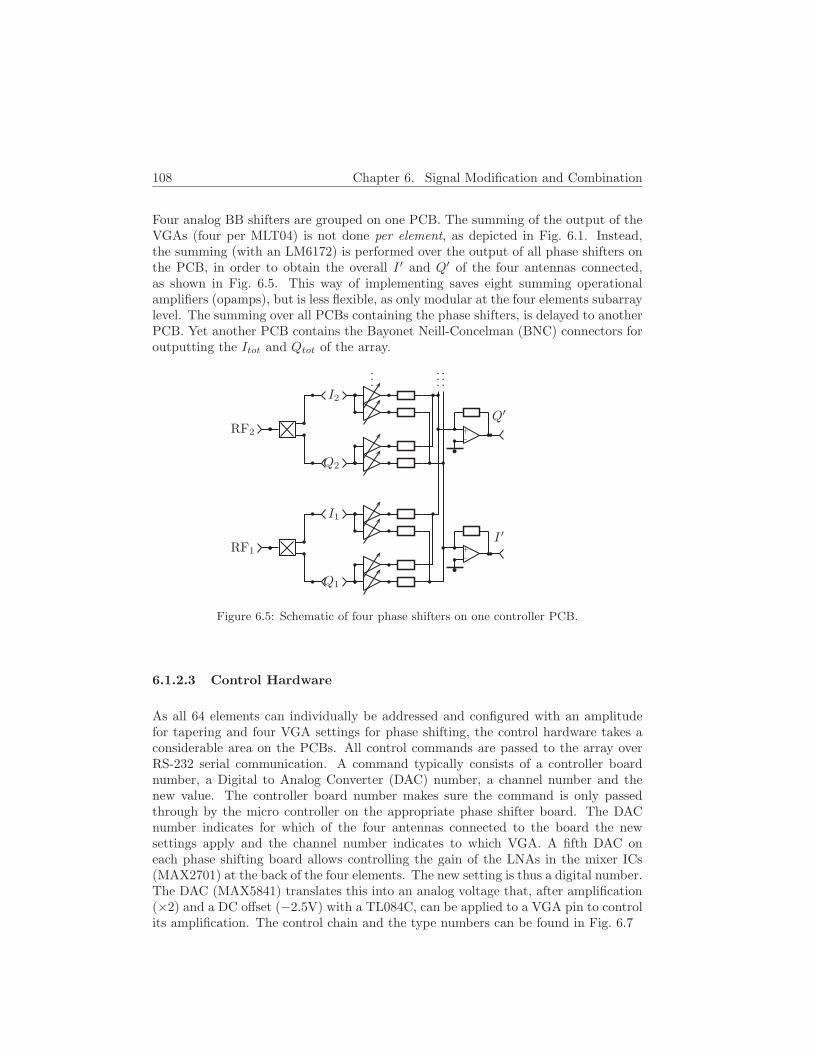
108 Chapter 6. Signal Modification and Combination
Four analog BB shifters are grouped on one PCB. The summing of the output of theVGAs (four per MLT04) is not done per element, as depicted in Fig. 6.1. Instead,the summing (with an LM6172) is performed over the output of all phase shifters onthe PCB, in order to obtain the overall I ′ and Q′ of the four antennas connected,as shown in Fig. 6.5. This way of implementing saves eight summing operationalamplifiers (opamps), but is less flexible, as only modular at the four elements subarraylevel. The summing over all PCBs containing the phase shifters, is delayed to anotherPCB. Yet another PCB contains the Bayonet Neill-Concelman (BNC) connectors foroutputting the Itot and Qtot of the array.
RF1
I1
Q1
-+
RF2
I2
Q2
-+
I ′
Q′
...
...
...
Figure 6.5: Schematic of four phase shifters on one controller PCB.
6.1.2.3 Control Hardware
As all 64 elements can individually be addressed and configured with an amplitudefor tapering and four VGA settings for phase shifting, the control hardware takes aconsiderable area on the PCBs. All control commands are passed to the array overRS-232 serial communication. A command typically consists of a controller boardnumber, a Digital to Analog Converter (DAC) number, a channel number and thenew value. The controller board number makes sure the command is only passedthrough by the micro controller on the appropriate phase shifter board. The DACnumber indicates for which of the four antennas connected to the board the newsettings apply and the channel number indicates to which VGA. A fifth DAC oneach phase shifting board allows controlling the gain of the LNAs in the mixer ICs(MAX2701) at the back of the four elements. The new setting is thus a digital number.The DAC (MAX5841) translates this into an analog voltage that, after amplification(×2) and a DC offset (−2.5V) with a TL084C, can be applied to a VGA pin to controlits amplification. The control chain and the type numbers can be found in Fig. 6.7

6.1. Analog Quadrature BB Phase Shifter 109
Figure 6.6: Photograph of PCB with four phase shifters.
6.1.3 Measurement Results
Before using the array and hence before measuring, too, a calibration should be per-formed. Why this is necessary and how this is done is explained in Sect. 6.1.3.1. Af-terwards the measurement setup and the results are given in Sect. 6.1.3.2 and 6.1.3.3.
As the antenna puts out a separate I and Q signal, all measurements are carried outfor both the I and Q output of the antenna. Hence calibration and measurement areperformed twice.
6.1.3.1 Calibration
Several causes make a calibration inevitable:
• the phase of the LO at all mixers will not be exactly identical
• the amplification characteristics of the VGAs differ mutually
• the I and Q signals of the mixers are not perfectly orthogonal

110 Chapter 6. Signal Modification and Combination
UTP
I
Q
MLT04
I’1
Q’1
I’2 I’3 I’4
Q’2 Q’3 Q’4
LM6172
UTP
Itot
Qtot
TL08
4
MAX5841
AT89C4051
RS-232
Figure 6.7: Implementation of the array control.
If calibration is needed on the fly, e.g. in adaptive “smart” antennas, additional ADCsand a DSP processor will be needed, but these can operate at a lower data rate andperiodically instead of continuously, eliminating the need for fast or unobtainabledigital components [96]. The demonstration model discussed here uses a feed-forwardsystem, calibrated and controlled off-line using a network analyzer and a PC runningMATLABTM. The calibration discussed here is very limited as it only serves to obtainreliable measurements. Much more advanced techniques are available in literature [97,98].
For calibration, the array antenna is placed in an incident field of constant ampli-tude and frequency coming from the broadside direction of the array. Then all butone antenna elements of the antenna are shut down, sequentially both VGAs thatcontribute to the I ′ signal of the active element are set to an arbitrary value e.g.half of the maximum, and the amplitude and phase of the down converted I ′ signal,are measured. This measurement is repeated for all array elements, resulting in thecomplex amplitudes I ′∗n,1 and I ′∗n,2 for n = 1 → 64. All measured amplitudes shouldbe equal and the phase ∠I ′∗n,1 = 0 and ∠I ′∗n,2 = π
2 . But apparently this is not the case.
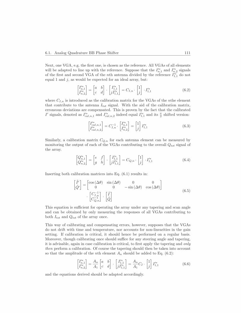
6.1. Analog Quadrature BB Phase Shifter 111
Next, one VGA, e.g. the first one, is chosen as the reference. All VGAs of all elementswill be adapted to line up with the reference. Suppose that the I ′∗n,1 and I ′∗n,2 signalsof the first and second VGA of the nth antenna divided by the reference I ′∗1,1 do notequal 1 and j, as would be expected for an ideal array, but:
[I ′∗n,1
I ′∗n,2
]=
[a bc d
]·[I ′∗1,1
jI ′∗1,1
]= CI,n ·
[1j
]· I ′∗1,1 (6.2)
where CI,n is introduced as the calibration matrix for the VGAs of the nthe elementthat contribute to the antenna Itot signal. With the aid of the calibration matrix,erroneous deviations are compensated. This is proven by the fact that the calibratedI ′ signals, denoted as I ′∗cal,n,1 and I ′∗cal,n,2 indeed equal I ′∗1,1 and its π
2 shifted version:
[I ′∗cal,n,1
I ′∗cal,n,2
]= C−1
I,n ·[I ′∗n,1
I ′∗n,2
]=
[1j
]I ′∗1,1 (6.3)
Similarly, a calibration matrix CQ,n for each antenna element can be measured bymonitoring the output of each of the VGAs contributing to the overall Qtot signal ofthe array.
[Q′∗
n,1
Q′∗n,2
]=
[e fg h
]·[I ′∗1,1
jI ′∗1,1
]= CQ,n ·
[1j
]· I ′∗1,1 (6.4)
Inserting both calibration matrices into Eq. (6.1) results in:
[I ′
Q′
]=
[cos (∆θ) sin (∆θ) 0 0
0 0 − sin (∆θ) cos (∆θ)
]
·[C−1
I,n
C−1Q,n
]·[I
Q
] (6.5)
This equation is sufficient for operating the array under any tapering and scan angleand can be obtained by only measuring the responses of all VGAs contributing toboth Itot and Qtot of the array once.
This way of calibrating and compensating errors, however, supposes that the VGAsdo not drift with time and temperature, nor accounts for non-linearities in the gainsetting. If calibration is critical, it should hence be performed on a regular basis.Moreover, though calibrating once should suffice for any steering angle and tapering,it is advisable, again in case calibration is critical, to first apply the tapering and onlythen perform a calibration. Of course the tapering should then be taken into accountso that the amplitude of the nth element An should be added to Eq. (6.2):
[I ′∗n,1
I ′∗n,2
]=An
A1
[a bc d
]·[I ′∗1,1
jI ′∗1,1
]=An
A1CI ·
[1j
]I ′∗1,1 (6.6)
and the equations derived should be adapted accordingly.
112 Chapter 6. Signal Modification and Combination
For the antenna described here, the calibration did not seem to be critical. Withthe very basic calibration as explained above, the performance of the array is still“acceptable”.
6.1.3.2 Measurement Setup
The array antenna was measured in the anechoic room. An RF source at 2.4001 GHzwas connected to an EMCO Type 3115 broadband horn that was used as transmitantenna. Care was taken that the entire array was uniformly illuminated. The arrayantenna was supplied with the 1.2 GHz LO signal. The I output signal of 100 kHzwas connected to the test input port of the receiver of an HP8510C Vector NetworkAnalyzer (VNA). The signal obtained by mixing the 2.4001 GHz RF and 1.2 GHzLO signal, which also contains a component at 100 kHz, is connected to the referenceport of the receiver.
Usually, RF signals are sampled inside a test set of the VNA, down converted to20 MHz and transmitted through an IF cable to the microwave receiver. Inside thereceiver, the 20 MHz signals are further filtered, amplified and down converted to100 kHz [99, 100]. When feeding 100 kHz signals with a sufficient amplitude at the20 MHz IF ports, enough signal gets through the filters, amplifiers and mixers toproduce repeatable measurement results.
Then the antenna is calibrated with the procedure explained in Sect. 6.1.3.1. Nextthe antenna is configured for a certain tapering and scan angle, with the aid of acomputer running MATLABTM as explained in Sect. 6.1.2.3. Now the antenna canbe rotated, measuring the result of the complex division of test and reference signalfor all rotation angles. These measurements allow to plot the radiation patterns givenand discussed in Sect. 6.1.3.3.
6.1.3.3 Measurement Results
Firstly, the response of a phase shifter with calibration is measured. Secondly, thefunctioning of the system is demonstrated with the measurement of radiation patternsfor some taperings and scanning angles after calibration.
6.1.3.3.1 Phase Shifter Constellation Plot First the phase shifter of one an-tenna element was measured. All other elements of the array were shut down and thenthe phase shifter was configured for some selected angles and amplifications. Fig. 6.8shows the constellation plot, i.e. the points in the complex plane that indicate theratio of I ′ over I for the configured shifter settings. The plot clearly shows that cal-ibration is inevitable. The amplifier in the Q channel amplifies too much comparedto the one in the I channel. After calibration this is compensated.

6.1. Analog Quadrature BB Phase Shifter 113
Calibration was performed for the inner circle and gets less effective for the largercircles, due to the fact that the errors are not linear. From the plot it is also obviousthat applying a tapering by lowering the gain of the VGAs deteriorates the accuracyof the shifter, as already mentioned in Sect. 6.1.1. Indeed, the same absolute error, asthe digital control of the gain is linear, results in a higher relative phase and amplitudedeviation.
−2.5 −2 −1.5 −1 −0.5 0 0.5 1 1.5 2 2.5
−2
−1.5
−1
−0.5
0
0.5
1
1.5
2
Figure 6.8: Constellation plot of the phase shifter for some selected angles, with (o) andwithout (+) calibration.
6.1.3.3.2 Radiation Patterns Fig. 6.9 and 6.10 show some array radiation pat-terns after calibration, to demonstrate the functioning of the array. The measure-ments indicate that if the array is scanned beyond 48, grating lobes occur, becausedx = dy = 0.6λ. For the Chebychev taperings, the beam widening for lower side lobelevels is clearly noticeable. The side lobes still come up higher than expected, dueto the approximation made by the digital control of the tapering. Only 4 effectivebits were used because if the gain was varied more, the amplifiers in some shifterssaturated. See Sect. 3.4.2 for a discussion on the effect of phase approximation on theradiation pattern of a phased array.
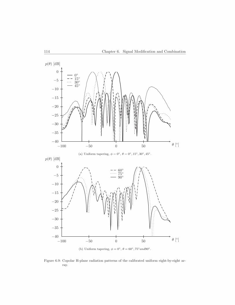
114 Chapter 6. Signal Modification and Combination
−100 −50 0 50−40
−35
−30
−25
−20
−15
−10
−5
0
θ []
p(θ) [dB]
0153045
(a) Uniform tapering, φ = 0, θ = 0, 15, 30, 45.
−100 −50 0 50−40
−35
−30
−25
−20
−15
−10
−5
0
θ []
p(θ) [dB]
607590
(b) Uniform tapering, φ = 0, θ = 60, 75and90.
Figure 6.9: Copolar H-plane radiation patterns of the calibrated uniform eight-by-eight ar-ray.
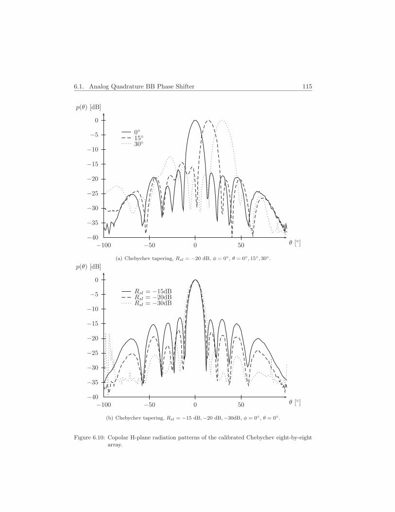
6.1. Analog Quadrature BB Phase Shifter 115
−100 −50 0 50−40
−35
−30
−25
−20
−15
−10
−5
0
θ []
p(θ) [dB]
01530
(a) Chebychev tapering, Rsl = −20 dB, φ = 0, θ = 0, 15, 30.
−100 −50 0 50−40
−35
−30
−25
−20
−15
−10
−5
0
θ []
p(θ) [dB]
Rsl = −15dBRsl = −20dBRsl = −30dB
(b) Chebychev tapering, Rsl = −15 dB,−20 dB,−30dB, φ = 0, θ = 0.
Figure 6.10: Copolar H-plane radiation patterns of the calibrated Chebychev eight-by-eightarray.

116 Chapter 6. Signal Modification and Combination
6.2 Space Qualified Phase Shifter
This section contains the results of a feasibility study on how to modify the archi-tecture of the shifter in Sect. 6.1.1 to obtain an implementation suitable for spaceapplication.
One approach could have been to simply copy the implementation, in COTS andtest for space environment. However, the tests are costly and this involves a risk ofincreasing the number of design cycles. Using space graded versions of every compo-nent is expensive but excludes risk at component level. For this implementation, acompromise is suggested. For components sitting at the back of the antenna, spacegraded components should be used. For others, COTS components can be chosen,as long as their working temperature ranges was from -55 C to +125 C and theyare not implemented in CMOS technology. If a space graded version of a componentis available from one of the main vendors (Analog Devices, Maxim Dallas, Radial,National Semiconductor), this is preferred.
As no suitable quadrature VGAs could be found, the option of using mixers wasreconsidered again. Now in the form of multipliers, which are essentially mixersimplemented in an IC that compensates for the non-linearity.
For the driving of the DAC, one microcontroller with direct addressing was chosen.All DACs are connected to the same data output of the microcontroller. Which DACis updated depends on which output pin of the microcontroller is high. Hence as manyoutput pins of the microcontroller are needed as there are DACs. As no more thanseven elements are used in the array, this is a defendable choice. For more elements, amicrocontroller with binary addressing has to be used, reducing the number of outputlines to a number smaller than the number of elements. One microcontroller per DACis another solution. This is undoubtedly the option with the lowest reconfigurationtime. But the most expensive one, too.
As malfunctioning of the array must not lead to the loss of the mission, a switch inorder to disable all but the backup element, can be inserted in the signal path. Thisway, in case of error, the system falls back on using a single element.
In order to compensate for the Doppler shift at the receiving ground station, thetransmit frequency can be varied. This can be obtained by using a Voltage Con-trolled Oscillator (VCO) for the Tx LO, with an analog input voltage controlling thefrequency. Experiments performed by ir. Aliakbarian showed that to make sure thatthe quadrature mixing to baseband is perfectly in phase (needed for easy QPSK de-tection) the use of a PLL is indispensable. This PLL should be narrow band, not tofollow the phase jumps in the QPSK signal. Consequently its pull-in region1 will notbe large enough to track the Doppler shift. Yet another control signal is needed, toset the frequency of the voltage controlled LO for Rx to the appropriate value.
1The pull-in region is the frequency range in which the PLL is able to lock onto a carrier, [6].

6.2. Space Qualified Phase Shifter 117
Again, as was stated earlier in this chapter, a digital implementation of beam forming,and even of the PLL, might bring tremendous advantages. That would, e.g. makeit possible to lock the PLL digitally on a varying carrier frequency, by calculatingthe fourth power of the QPSK signal, which is a sine wave because 4 × π/2 = 2π, asexplained in [101].
6.2.1 Space Segment System Overview
The array with space qualified phase shifter is actually intended to serve as a part ofthe system described in Sect. 4.1.3. Hence, Fig. 6.12 that gives an overview of thesystem described below, is a more detailed reprise of Fig. 4.3.
The array antenna as proposed, consists of seven identical elements. The number ofseven allows to optimally use all outputs of the micro controller. Moreover, this allowsan array topology of concentric circles (with one center element), as in Sect. 5.4.2 withN = 3 and M = 3, depicted in Fig. 6.11. This way a planar array antenna is obtained,hence with a beam instead of a rotation symmetric radiation pattern, with a limitednumber of elements and hence a manageable complexity.
Figure 6.11: 7 elements concentric circles array (M = N = 3).
One of the seven elements will also be used for Tx. It will broadcast the activationmessage. And it will be used in the array for Rx, as the one element without phaseshifting and tapering. This way, this element can be seen as a backup element in casethe beam steering fails. Instead of this Tx/backup element, a separate Tx elementcould be used. This would simplify the element design tremendously, as in that caseno elements should be dual band. As area on the satellite is however scarce and henceexpensive, space saving solutions must be applied whenever possible.
The beam forming network as proposed is slightly different from the one inSect. 6.1.2.2. The I and Q signals from the six Rx elements are phase shifted andcombined to one overall I and Q signal. Adding the I and Q from the backup elementis delayed to a next summing opamp to allow an emergency switch to disconnectthe array signal in case of a failure.
The signals to control the emergency switch, to drive the VCO of the LO with thecorrect voltage, and to set the gain of the VGAs in the BFN to the correct value,come from a microcontroller that receives the necessary input from software on themain CPU over the CAN bus. The software routines are summarized in Sect. 6.2.4and given in pseudo code in Appendix C. The signal path and controller are nowworked out into some more detail. The components numbers are listed in Table 6.2.
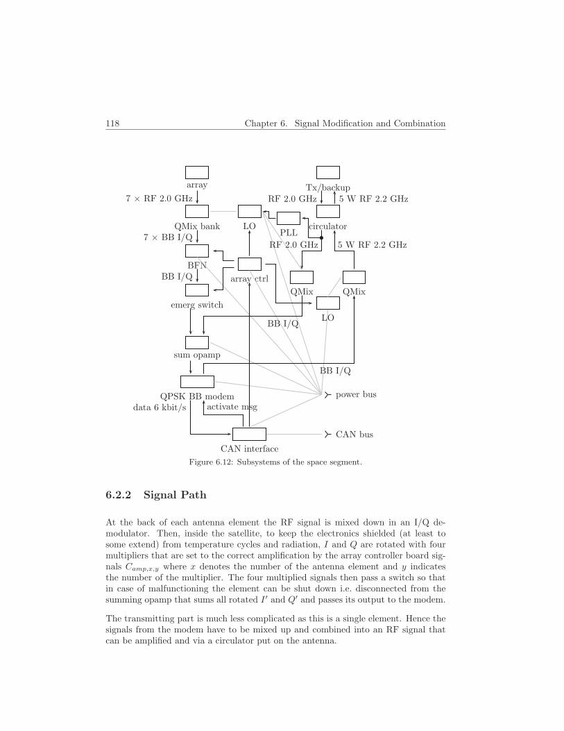
118 Chapter 6. Signal Modification and Combination
CAN bus
power bus
CAN interface
QPSK BB modem
sum opamp
array ctrl
emerg switch
BFN
QMix bank LOPLL
LO
QMix QMix
array Tx/backup
circulator
data 6 kbit/s activate msg
BB I/Q
7 × BB I/Q
7 × RF 2.0 GHz
BB I/Q
BB I/Q
5 W RF 2.2 GHzRF 2.0 GHz
RF 2.0 GHz 5 W RF 2.2 GHz
Figure 6.12: Subsystems of the space segment.
6.2.2 Signal Path
At the back of each antenna element the RF signal is mixed down in an I/Q de-modulator. Then, inside the satellite, to keep the electronics shielded (at least tosome extend) from temperature cycles and radiation, I and Q are rotated with fourmultipliers that are set to the correct amplification by the array controller board sig-nals Camp,x,y where x denotes the number of the antenna element and y indicatesthe number of the multiplier. The four multiplied signals then pass a switch so thatin case of malfunctioning the element can be shut down i.e. disconnected from thesumming opamp that sums all rotated I ′ and Q′ and passes its output to the modem.
The transmitting part is much less complicated as this is a single element. Hence thesignals from the modem have to be mixed up and combined into an RF signal thatcan be amplified and via a circulator put on the antenna.
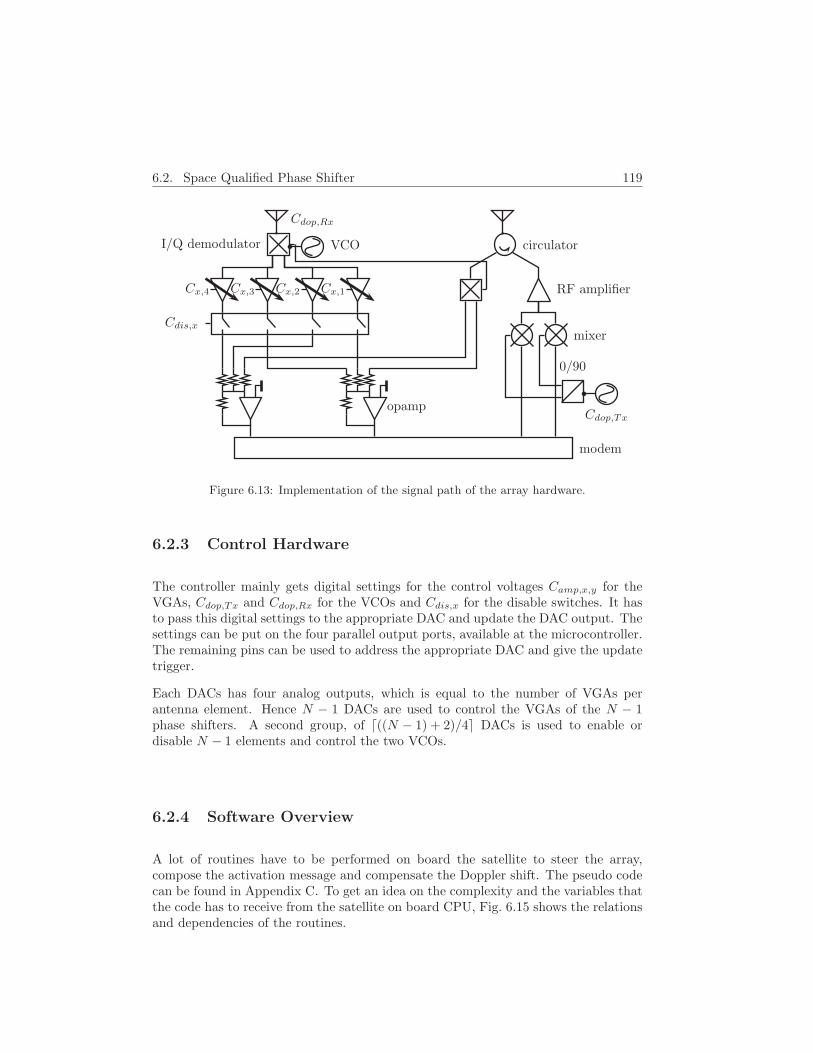
6.2. Space Qualified Phase Shifter 119
I/Q demodulator VCO
Cdop,Rx
circulator
RF amplifierCx,1Cx,2Cx,3Cx,4
Cdis,xmixer
Cdop,Tx
0/90
opamp
modem
Figure 6.13: Implementation of the signal path of the array hardware.
6.2.3 Control Hardware
The controller mainly gets digital settings for the control voltages Camp,x,y for theVGAs, Cdop,Tx and Cdop,Rx for the VCOs and Cdis,x for the disable switches. It hasto pass this digital settings to the appropriate DAC and update the DAC output. Thesettings can be put on the four parallel output ports, available at the microcontroller.The remaining pins can be used to address the appropriate DAC and give the updatetrigger.
Each DACs has four analog outputs, which is equal to the number of VGAs perantenna element. Hence N − 1 DACs are used to control the VGAs of the N − 1phase shifters. A second group, of d((N − 1) + 2)/4e DACs is used to enable ordisable N − 1 elements and control the two VCOs.
6.2.4 Software Overview
A lot of routines have to be performed on board the satellite to steer the array,compose the activation message and compensate the Doppler shift. The pseudo codecan be found in Appendix C. To get an idea on the complexity and the variables thatthe code has to receive from the satellite on board CPU, Fig. 6.15 shows the relationsand dependencies of the routines.
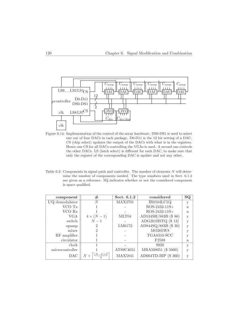
120 Chapter 6. Signal Modification and Combination
clk
clk
µcontroller
DAC
Camp
DAC
Cdis
DAC
Camp
DAC
Cdis/dop
DAC
Camp
DAC
Camp
DAC
Camp
DAC
Camp
D0-D1112
DS0-DS12
CS
CS
LS1LS2. . .LS6
LS7LS8
Figure 6.14: Implementation of the control of the array hardware. DS0-DS1 is used to selectone out of four DACs in each package. D0-D11 is the 12 bit setting of a DAC.CS (chip select) updates the output of the DACs with what is in the registers.Hence one CS for all DACs controlling the VGAs is used. A second one controlsthe other DACs. LS (latch select) is different for each DAC, to make sure thatonly the register of the corresponding DAC is update and not any other.
Table 6.2: Components in signal path and controller. The number of elements N will deter-mine the number of components needed. The type numbers used in Sect. 6.1.2are given as a reference. SQ indicates whether or not the considered componentis space qualified.
component # Sect. 6.1.2 considered SQI/Q demodulator N MAX2701 IR0104LC1Q y
VCO Tx 1 - ROS-2432-119+ nVCO Rx 1 - ROS-2432-119+ n
VGA 4 × (N − 1) MLT04 AD534SH/883B ($ 86) yswitch N − 1 - ADG201HSTQ ($ 13) yopamp 2 LM6172 AD844SQ/883B ($ 30) ymixer 2 - MO205W8 y
RF amplifier 1 - TGA8310-SCC ycirculator 1 - F2588 n
clock 1 - 9920 ymicrocontroller 1 AT89C4051 MRAM8051 ($ 5000) y
DAC N +⌈
(N−1)+24
⌉MAX5841 AD664TD-BIP ($ 360) y
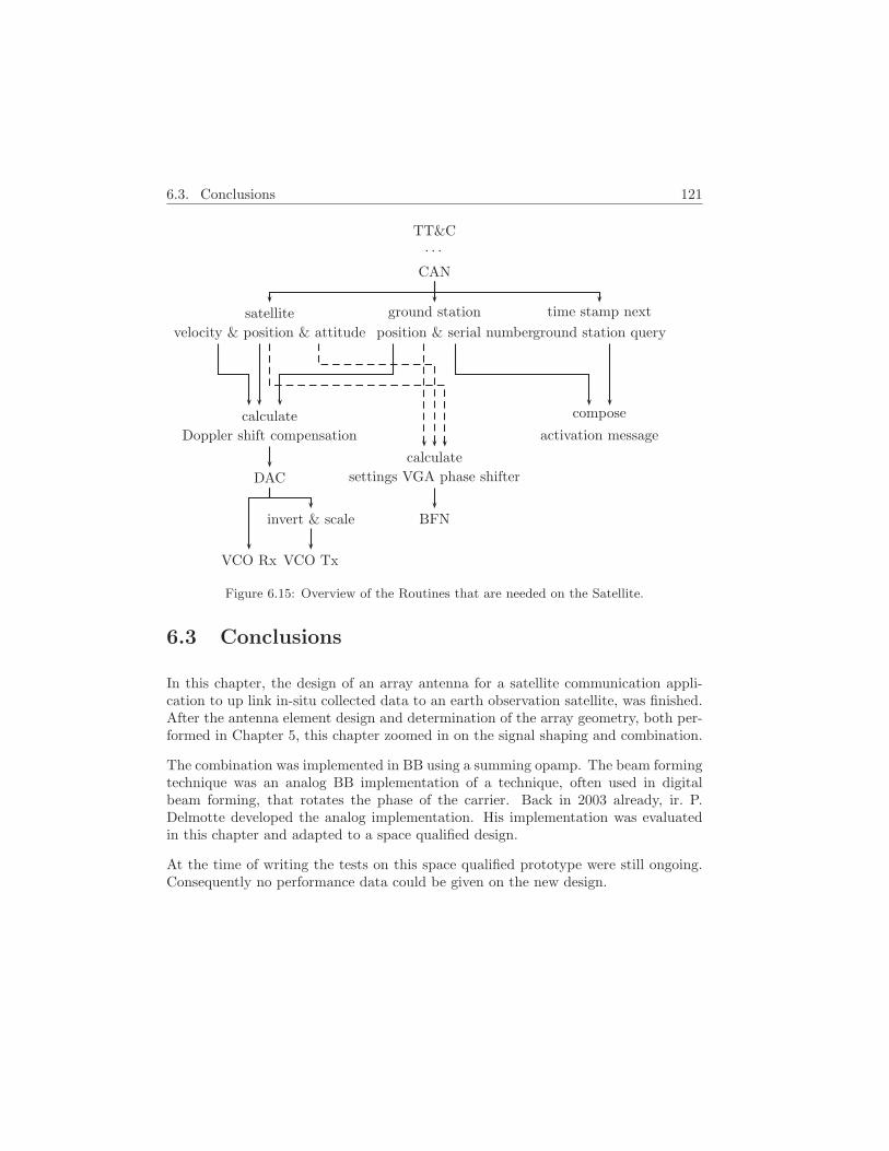
6.3. Conclusions 121
TT&C. . .
CAN
satellite
velocity & position & attitude
ground station
position & serial number
time stamp next
ground station query
calculate
Doppler shift compensation
DAC
invert & scale
VCO TxVCO Rx
calculate
settings VGA phase shifter
BFN
compose
activation message
Figure 6.15: Overview of the Routines that are needed on the Satellite.
6.3 Conclusions
In this chapter, the design of an array antenna for a satellite communication appli-cation to up link in-situ collected data to an earth observation satellite, was finished.After the antenna element design and determination of the array geometry, both per-formed in Chapter 5, this chapter zoomed in on the signal shaping and combination.
The combination was implemented in BB using a summing opamp. The beam formingtechnique was an analog BB implementation of a technique, often used in digitalbeam forming, that rotates the phase of the carrier. Back in 2003 already, ir. P.Delmotte developed the analog implementation. His implementation was evaluatedin this chapter and adapted to a space qualified design.
At the time of writing the tests on this space qualified prototype were still ongoing.Consequently no performance data could be given on the new design.

invisible filling
Part III
Application: EM SideChannel Analysis
123

125
Overview
The second application for which array antennas are applied in this work, is elec-tromagnetic side channel analysis. This is a field of study related to cryptography.Similar to cryptology, that seeks for weaknesses in mathematical algorithms and cryp-tographic protocols, side channel analysis looks for weaknesses in implementation.Such weaknesses might lead to observable variations in current consumption, execu-tion time or electromagnetic radiation, that correlate with a secret parameter, insidethe cryptographic device, which should not be revealed.
Chapter 7 explains the underlying physical principles that cause information on thelogic operations that are performed in a cryptographic device to leak via e.g. electro-magnetic radiation. This chapter also indicates that no practical system can ever be100% secure. No matter what countermeasures are applied, the only system that doesnot radiate any secret information, is a system that does not do anything. With anunlimited amount of time and equipment, any system can be broken. Designers canonly make sure that the effort needed to break a system is unfavorably high comparedto the benefit of breaking the system. Where hackers try to break systems for theirown benefit, the side channel community tries to evaluate the effort needed to break asystem and seeks to improve security by detecting weaknesses and suggesting countermeasures.
The application of electromagnetic side channel analysis would benefit a lot fromarray antennas as this would increase the signal-to-noise ratio and would allow (si-multaneous if off-line beam forming is applied) monitoring of different regions in thecryptographic device. For an FPGA it is obvious that this would reveal a lot of ex-tra information, as there is a direct link between active regions in the FPGA andoperations performed. For a microcontroller it would allow to monitor activity incontroller, memory, input/output blocks and so on. Apart from some minor remarkson how these arrays should best be implemented and used, the array content in thispart is limited. While working on the side channel analysis application, the lack of agood sensor element emerged. As the need for an element, at the time of writing, wasmuch stronger than the need for an array of sensors, much effort was spent in studyingand designing such element. As time is however limited, this had its repercussions onthe time that could be invested in studying arrays for this application.
Chapter 8 provides a profound theory for designing inductive sensors for electro-magnetic side channel analysis. Much of the contemporary work is carried out in ahaphazard way, with little or no understanding of radio frequency engineering. Thischapter studies the sensors in a systematic way. First the specifications for a goodsensor are defined. Next some well known inductive antenna types are studied and themaximum practical resolution limit for small coils is calculated as a function of thebandwidth and signal amplitude required and the input impedance of the measure-ment device. This calculation also provides a design method for maximal resolutionloop sensors.

126
As a side step of the study of existing loop antennas, the design of an RFID readerantenna, commonly described in the literature for antennas that are small comparedto the wavelength, was generalized to a technique that is valid regardless of antennasize, in Sect. 8.3.
At the end of Chapter 8, in Sect. 8.5, some hints and suggestions are given on how toimplement an array of sensors for the application. At the same time, it is indicatedthat still many problems need to be solved in order to come to an implementation ofan array of sensors.
Just as there was little or no theory nor good practice available on sensors for cryp-tographic analysis, no guidelines on the measurement setup were at hand. Chapter 9,again, tries to study this in a systematic way, and compares some possible setups re-garding signal-to-noise ratio. As the theory developed here, is useful for a setup witha single sensor, also arrays of sensors benefit from application of the insights presentedhere. Apart from a note suggesting off-line digital time shifting as the preferred beamforming technique, in Sect. 9.4, again no specific array aspects are discussed.

Chapter 7
Introduction to theApplication
With the shift towards electronic implementation of almost all everyday actions, theapplicability area of cryptography has broadened from purely strategic (military,diplomacy and intelligence) to practically any aspect of modern life [102]. Con-sequently anyone uses cryptography on a daily basis, some probably even withoutknowing. Obvious examples are online banking and electronic signatures with aneID. But even entertainment, with e.g. water marking and copy protection, has be-come a field of application.
Essentially, cryptography tries to hide a secret by transforming a plaintext into aciphertext. The intended reader can transform in the opposite direction, by using thekey that was agreed with the transmitter (symmetric key cryptography) or by usingthe personal secret key (public key cryptography). An unintended reader can not getto the secret information as he or she lacks the key. Hence the problem of keeping asecret is shifted to protecting a key.
Shannon [103] showed that in the trivial case were the secret and the key are of thesame length (Vernam scheme) the encryption is perfectly safe1, as he shows that akey with a data rate equal to or greater than the data rate of the message leads toa system with perfect secrecy. In any other practical situation where the key lengthis smaller than the message length, the system can be broken with an appropriatenumber of trials. In short: any cryptographic system is breakable, designers haveto make sure that the effort to break a system is unfavorably high compared to thebenefit of breaking the system.
1Under the assumption that the key is never reused: one-time pad.
127
128 Chapter 7. Introduction to the Application
Moreover, even if a system were perfectly safe, the implementation of the transforma-tion mentioned adds another link to the chain that can be used to attack the system.Only limiting the discussion to electronic semiconductor hardware, the electrons thatmove when performing logic operations will cause a radiation that carries away somesecret information on the transformation, the secret information or even on the secretkey. Such alternative information channels that can be used in attempts to break thesystem are referred to as side channels [104].
The work of this part is merely developing sensor systems and measurement setupsfor evaluating vulnerability to side channel analysis. Hence no extensive treatment oncryptography as such can be expected. As an example, one cryptographic primitive2
is reviewed. This should give the reader an idea of the logic functions that are carriedout by the cryptographic hardware that is under test when evaluating side channelleakage.
7.1 Example of A Block Cipher
To illustrate how a cryptographic operation can be implemented in Silicon hardware,an example of a block cipher is given. The example, the KeeLoq block cipher [105],should preferably not be used in practice. Both the mathematics behind the cipherand the only commercially available implementation have been proven to be insecure,by a sliding attack in [106] and a power analysis in [107].
A block cipher, as opposed to a stream cipher, divides the message or plaintext inputstream into blocks of a certain size, e.g. 32 bits. Those 32 bit blocks are encrypted withthe aid of a secret key that is only known by the two parties communicating. Afterencryption, a 32 bit block of ciphertext is obtained, that can ideally only be decryptedby the intended addressee. After decryption of all blocks by the addressee, the originalmessage, apart from some padding if the message length was not a multiple of 32 bit,is obtained by concatenation of all blocks.
Hence, first the message block is shifted into the 32 bit shift register of Fig. 7.1.Encryption of a block is done by executing 528 rounds. In one round the Non LinearFunction (NLF) is applied to five bits that are tapped from the shift register atpositions 1,9,20,26 and 31 as indicated on Fig. 7.1. This result is combined with twomore bits tapped from the shift register at positions 0 and 16, and the bit at position0 of the 64 bit shift register used to cycle the key. The resulting value is shifted intothe 32 bit shift register and the 64 bit shift register is cycled, ready for the next round.
2A cryptographic primitive is a low level cryptographic algorithm such as a stream cipher or ahash function.

7.2. Cryptographic Hardware 129
NLF
+
01916202631
63 0
Figure 7.1: Schematic of the KeeLoq block cipher.
The NLF can be implemented as a LookUp Table (LUT), where the five input bitsof the NLF indicate the address or bit position in the 32 bit 0x3A5C742E string:
31 30 29 28 . . . 3 2 1 00 0 1 1 101001011100011101000010 1 1 1 0
An eXclusive OR (XOR, ⊕) implementation of the NLF is possible too:
NLF (x4, x3, x2, x1, x0) = x4x3x2 ⊕ x4x3x1 ⊕ x4x2x0 ⊕ x4x1x0 ⊕x4x2 ⊕ x4x0 ⊕ x3x2 ⊕ x3x0 ⊕ x2x1 ⊕ x1x0 ⊕x1 ⊕ x0 (7.1)
In Appendix E, the transceiver is described that was used to implement and test theattack on KeeLoq as described in [106].
7.2 Cryptographic Hardware
Cryptographic primitives can be implemented on any electronic digital device. Theycan be run on general purpose microprocessors, such as a computer Central ProcessingUnit (CPU), or on dedicated hardware such as an Application Specific IntegratedCircuit (ASIC).
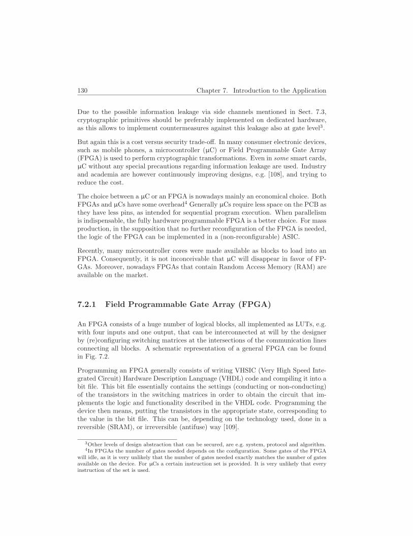
130 Chapter 7. Introduction to the Application
Due to the possible information leakage via side channels mentioned in Sect. 7.3,cryptographic primitives should be preferably implemented on dedicated hardware,as this allows to implement countermeasures against this leakage also at gate level3.
But again this is a cost versus security trade-off. In many consumer electronic devices,such as mobile phones, a microcontroller (µC) or Field Programmable Gate Array(FPGA) is used to perform cryptographic transformations. Even in some smart cards,µC without any special precautions regarding information leakage are used. Industryand academia are however continuously improving designs, e.g. [108], and trying toreduce the cost.
The choice between a µC or an FPGA is nowadays mainly an economical choice. BothFPGAs and µCs have some overhead4 Generally µCs require less space on the PCB asthey have less pins, as intended for sequential program execution. When parallelismis indispensable, the fully hardware programmable FPGA is a better choice. For massproduction, in the supposition that no further reconfiguration of the FPGA is needed,the logic of the FPGA can be implemented in a (non-reconfigurable) ASIC.
Recently, many microcontroller cores were made available as blocks to load into anFPGA. Consequently, it is not inconceivable that µC will disappear in favor of FP-GAs. Moreover, nowadays FPGAs that contain Random Access Memory (RAM) areavailable on the market.
7.2.1 Field Programmable Gate Array (FPGA)
An FPGA consists of a huge number of logical blocks, all implemented as LUTs, e.g.with four inputs and one output, that can be interconnected at will by the designerby (re)configuring switching matrices at the intersections of the communication linesconnecting all blocks. A schematic representation of a general FPGA can be foundin Fig. 7.2.
Programming an FPGA generally consists of writing VHSIC (Very High Speed Inte-grated Circuit) Hardware Description Language (VHDL) code and compiling it into abit file. This bit file essentially contains the settings (conducting or non-conducting)of the transistors in the switching matrices in order to obtain the circuit that im-plements the logic and functionality described in the VHDL code. Programming thedevice then means, putting the transistors in the appropriate state, corresponding tothe value in the bit file. This can be, depending on the technology used, done in areversible (SRAM), or irreversible (antifuse) way [109].
3Other levels of design abstraction that can be secured, are e.g. system, protocol and algorithm.4In FPGAs the number of gates needed depends on the configuration. Some gates of the FPGA
will idle, as it is very unlikely that the number of gates needed exactly matches the number of gatesavailable on the device. For µCs a certain instruction set is provided. It is very unlikely that everyinstruction of the set is used.
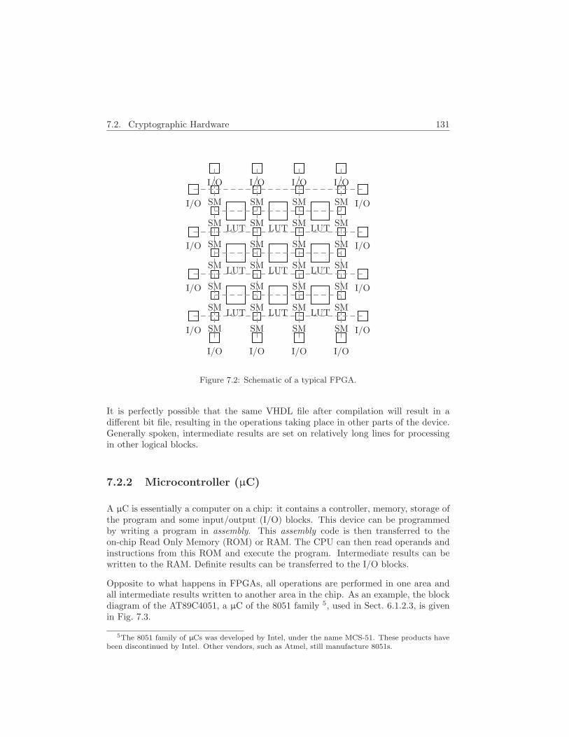
7.2. Cryptographic Hardware 131
I/O I/O I/O I/O
I/O
I/O
I/O
I/O
I/O I/O I/O I/O
I/O
I/O
I/O
I/O
LUT LUT LUT
LUT LUT LUT
LUT LUT LUT
SM
SM
SM
SM
SM
SM
SM
SM
SM
SM
SM
SM
SM
SM
SM
SM
SM
SM
SM
SM
SM
SM
SM
SM
SM
SM
SM
SM
Figure 7.2: Schematic of a typical FPGA.
It is perfectly possible that the same VHDL file after compilation will result in adifferent bit file, resulting in the operations taking place in other parts of the device.Generally spoken, intermediate results are set on relatively long lines for processingin other logical blocks.
7.2.2 Microcontroller (µC)
A µC is essentially a computer on a chip: it contains a controller, memory, storage ofthe program and some input/output (I/O) blocks. This device can be programmedby writing a program in assembly. This assembly code is then transferred to theon-chip Read Only Memory (ROM) or RAM. The CPU can then read operands andinstructions from this ROM and execute the program. Intermediate results can bewritten to the RAM. Definite results can be transferred to the I/O blocks.
Opposite to what happens in FPGAs, all operations are performed in one area andall intermediate results written to another area in the chip. As an example, the blockdiagram of the AT89C4051, a µC of the 8051 family 5, used in Sect. 6.1.2.3, is givenin Fig. 7.3.
5The 8051 family of µCs was developed by Intel, under the name MCS-51. These products havebeen discontinued by Intel. Other vendors, such as Atmel, still manufacture 8051s.
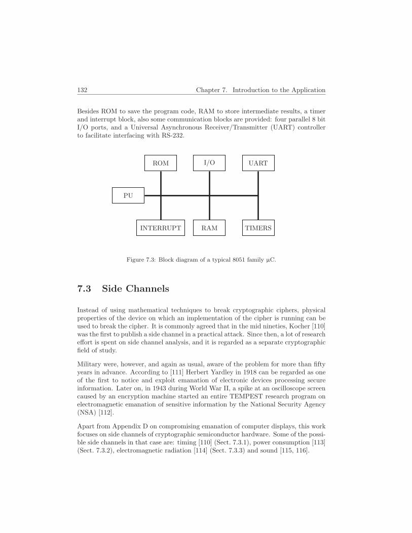
132 Chapter 7. Introduction to the Application
Besides ROM to save the program code, RAM to store intermediate results, a timerand interrupt block, also some communication blocks are provided: four parallel 8 bitI/O ports, and a Universal Asynchronous Receiver/Transmitter (UART) controllerto facilitate interfacing with RS-232.
PU
INTERRUPT RAM TIMERS
ROM I/O UART
Figure 7.3: Block diagram of a typical 8051 family µC.
7.3 Side Channels
Instead of using mathematical techniques to break cryptographic ciphers, physicalproperties of the device on which an implementation of the cipher is running can beused to break the cipher. It is commonly agreed that in the mid nineties, Kocher [110]was the first to publish a side channel in a practical attack. Since then, a lot of researcheffort is spent on side channel analysis, and it is regarded as a separate cryptographicfield of study.
Military were, however, and again as usual, aware of the problem for more than fiftyyears in advance. According to [111] Herbert Yardley in 1918 can be regarded as oneof the first to notice and exploit emanation of electronic devices processing secureinformation. Later on, in 1943 during World War II, a spike at an oscilloscope screencaused by an encryption machine started an entire TEMPEST research program onelectromagnetic emanation of sensitive information by the National Security Agency(NSA) [112].
Apart from Appendix D on compromising emanation of computer displays, this workfocuses on side channels of cryptographic semiconductor hardware. Some of the possi-ble side channels in that case are: timing [110] (Sect. 7.3.1), power consumption [113](Sect. 7.3.2), electromagnetic radiation [114] (Sect. 7.3.3) and sound [115, 116].
7.3. Side Channels 133
Somehow related to side channel analysis, knowledge of the physical implementationof a cryptographic primitive can be (ab)used to deliberately induce errors duringexecution, e.g. by pulsing laser light or RF power into the device. Observing theoutput of the device after an induced error, and possibly comparing this with thenormal error free behavior of the device might again reveal some information that isintended to be kept secret. This way of studying vulnerability of systems is generallyreferred to as fault attacks [117, 118].
Yet another way of inducing errors in semiconductor devices, also mentioned in [117],is bombing a device with an ion beam. The consequences this can have, were alreadydiscussed in a completely different context of designing for space in Sect. 4.5.1. Theprotective measures (shielding and redundancy) suggested there remain valid. Suchmeasures have a cost however, so that only for critical devices this protection against(possibly) hypothetical threads such as Electro Magnetic Pulse (EMP) [119] can bejustified.
7.3.1 Timing
In many cases the time it takes for some cryptographic hardware to process some (par-tial) message and (partial) key inputs into a (partial) ciphertext output will slightlydiffer. Reason for the deviation can be: condition branches, cache hits and misses,difference in execution time of multiplications and divisions, and so one. Careful ob-servation of the time duration of processes might hence disclose sensitive information.
A way to avoid information leakage via this mechanism is to make sure all operationshave the same time duration. This often requires bypassing of the cross compileroptimizations and is even harder, if not impossible, if caching is involved. Anotherapproach could be blinding or masking of the inputs prior to processing. This howevermerely adds another step and hence an additional effort for an observer, but doesnot solve the problem profoundly as the masking step can not be supposed to beperfectly secret [120]. A better approach might be to always calculate the resultsfor all branches in a conditional tree and afterwards select the appropriate value tooutput. This at the expense of computational power.
7.3.2 Power Consumption
With each clock rise, transistors in (parts of) the cryptographic device have to switchto charge or discharge registers (or capacitors). Depending on the value of the ca-pacitance, either the capacitor (dis)charge current or the short current when the twocomplementary transistors conduct together when switching, dominates. In the firstcase, observation of the current consumption reveals the difference in hamming weightbetween the old and new state of a register. In the second case, the transition count(number of registers that update, not necessary to a new value) is disclosed.
134 Chapter 7. Introduction to the Application
This current I (or power P = V × I as V is the constant voltage of the power supply)can be measured [121] by a current probe or by measuring the voltage drop over asmall resistor (e.g. 1 Ω) inserted in the power line6 of the voltage source.
The best approach to suppress this information leakage, is to use secure logic, suchas dual rail logic, where always one register holds the logic results and another oneits complement to balance the power consumption to a value independent of thelogic result. This technique can be implemented on FPGAs [122] or by using dualrail logic cells in the design. In the latter case, non-standard routing algorithmsmust be used as well, as now the number of signal lines doubles. Regardless of theimplementation, care should be taken that the capacitance of both the signal andcomplementary register are exactly the same. This can never be perfectly achieved,hence the problem of information leakage is not solved in a fundamental way, at best,again, additional effort is required from an observer.
7.3.3 Electromagnetic Radiation
As the current mentioned in Sect. 7.3.2 not only draws power from the source, butalso causes EM radiation, observing the fields around the chip, might also be a wayto get to certain sensitive information. The radiation caused directly by the currentsthat perform the actual logic operation, is, generally spoken, rather small and difficultto observe in the presence of radiation of clock lines and the like. Due to typical EMCissues, such as common ground impedance or cross-talk, the nearly unobservable signalin the logic often modulates a much stronger signal, e.g. the clock signal. Hence theinformation can be captured as the modulation7 of a strong carrier, improving itsobservability drastically [123].
It is commonly agreed in literature that the EM side channel contains more informa-tion than just the power side channel. An intuitive way of explaining this, is that inthe case of power analysis only one signal is at the disposal of an adversary, whereasthe number of signals that can be obtained from the EM channel is virtually unlim-ited. By positioning the EM sensor slightly differently, a signal with another weightingfrom all radiating source in the chip is obtained. Indeed if the chip is modeled as aset of elementary dipoles that all radiate a different signal, the relative weight (andphase) of the different signals in the sum signal at a certain location depends on thedistance between source and observation point.
6This resistor can be put between the positive output of the power supply and the power railof the circuit, but then the voltage must be measured differentially in order not to short the powersupply by the ground of the oscilloscope probe. A resistor between the ground of the power sourceand the ground of the circuit makes the latter floating. Especially when the circuit is fed withmultiple power supplies (at different voltages) this is not recommended.
7It can be expected that (some of) these modulations are present too in the power consumptionsignal.
7.4. Frequency Spectrum 135
Hence many publications e.g. [124, 125] report on measurements obtained after ran-domly shifting around the sensor until a position was reached were statistical attackssimilar to those used for power traces succeeded (even for hardware that was resistantagainst power analysis). Inspection of the signal picked up by the sensor on an oscillo-scope or spectrum analyzer while varying the position of the sensor is then often usedas an ad hoc method to avoid running the attack for every possible spatial positionof the sensor. That the scientific nature of this method is questionable, will be clear.The method is not that surprisingly, either: an attacker, in general, does not have thedesign plans of the device under test; nor are standard methods at hand to positionthe sensor.
By collecting signals at different spatial points simultaneously, with EM sensors ar-ranged in some array structure, it should theoretically be possible to reconstruct theseparate original signals to some extent. The question remains whether this is usefulas statistical methods might even be able to distract the information from this setright away, i.e. without reconstructing the original signals. Nevertheless it is obviousthat array antennas are very promising in this application, as several of these dif-ferently weighted sum signals will, after appropriate combination, allow to improvethe SNR of the system. This could hence be a way to overcome the tedious shiftingaround of the sensor to find the optimum location or, at least, facilitate the process.
It is expected that moving the sensor away for a considerable distance from theradiating device, the weighting of all sources will be equal, resulting in a signal equalto the power consumption signal.
Countermeasures to prevent leakage via the EM channel include all common EMCtechniques, such as: shielding, bypass capacitors and cross coupling aware design.Besides that, again in this case dual rail logic or additional noise sources could beconsidered.
7.4 Frequency Spectrum
The clock frequency of a device is selected such that the (chain of) executions thatshould be performed during a clock cycle are finished well in time before the followingrising clock edge. Consequently, the spectrum of a power or EM signal from theseexecutions will go up to several tens of the clock frequency, depending on the timeconstants of the (gate) capacitances in the logic device.
Thus, a wide band is needed to reconstruct the original signal. As it is, however, onlythe information in the signal that is of interest, it might already be sufficient to onlyuse a fraction of the bandwidth and still be able to extract sensitive information. Thiswill depend on the hardware used (µC or FPGA) and on the code that is executed.Unfortunately, at the time of writing, no founded theory was available on this matter.
136 Chapter 7. Introduction to the Application
Contemporary analysis hence always involves scanning of the frequency spectrum. Itis obvious that interesting and challenging research on this subject can and should beperformed.
Instead of working on the time signals, and looking for correlation between measure-ments and key bits, it is possible to do all calculations in the frequency domain. Asthe Fourier transform is a one-to-one transformation, this is not surprising. Whatis however surprising, is that when leaving out the phase information, and workingwith the Power Spectral Density (PSD) instead of with the Fourier transform, sidechannel analysis still seems to work [126]. Here, the PSD was calculated from thetime signal. But a spectrum analyzer, or even better, real time spectrum analyzer,can directly measure (instantaneous) PSD. The latter even without missing events,which is a problem with the first one, due to the non-zero sweep time.
Even if a PSD should not be sufficient for a side channel analysis, it will already givean indication of the amount of information leakage. If a PSD as calculated on thetime signal recorded with e.g. an oscilloscope is compared with an instantaneous PSDof a spectrum analyzer, deviation of both will signal a deviation from the generalbehavior in a short time interval. This reveals data or instruction dependency of thesignal.
7.5 Conclusions
In this chapter the underlying physical principles were explained that cause informa-tion on the logic operations that are performed in a cryptographic device to leak viae.g. electromagnetic radiation. This chapter also indicated that no practical systemcan ever be 100% secure. With an unlimited amount of time and equipment, anysystem can be broken. Designers can only make sure that the effort needed to breaka system is unfavorably high compared to the benefit of breaking the system.
After a short review of two hardware platforms often used for cryptographic oper-ations, namely the FPGA and µC, some side channels such as power consumption,execution time and electromagnetic radiation were discussed. A note on the lack ofknowledge about the optimal frequencies for EM side channel analysis concluded thechapter.

Chapter 8
Array Elements
In this chapter, first the specifications for the sensor are summarized in Sect. 8.1.Next the sensor can be designed. Three designs are reviewed: a shielded loop inSect. 8.2, a loop suitable for RFID in Sect. 8.3 and a tiny loop in Sect. 8.4. Withthis small element, again an array can be implemented. Some details on this can befound in Sect. 8.5.
8.1 Element Specifications
As already mentioned in Sect. 7.3.3, several approaches to retrieving informationvia EM radiation, or ElectroMagnetic Analysis (EMA) can be followed: either theinformation radiated directly by the (small) current performing the operations canbe captured, or the information can be extracted from a much stronger field thatis modulated by the same current via capacitive, inductive or resistive coupling. Aclear example is when the small current performing the logical operation couples to aclock line running nearby, slightly altering the amplitude of the clock pulses. In suchcase information might be extracted more easily by looking at the variations of thefield radiated by the clock lines, than when looking for the radiation of the currentperforming the logical operation itself.
In the case of direct radiation by the current performing the logical operation, thefields will be very small and nearly unnoticeable in the presence of the radiation of allother parts in the chip. In such case the sensor should be small and put very close tothe radiating part of the device. Possibly the chip must be (partially) unpackaged1
to further reduce the distance and obtain distinguishable signals.
1Note that the removal of the plastic around the silicon device puts the semiconductor in acorrosive environment, reducing the lifetime of the chip dramatically.
137

138 Chapter 8. Array Elements
In the case of logical currents modulating a stronger signal, positioning of the sensoris of less importance. Some other specifications, such as resonance frequency, becomemore important, though.
Also mentioned in Sect. 7.3.3, was the fact that it is possible with EM probes to per-form a power analysis without the need for physically contacting the device, allowinga certain distance between the adversary and the device under test. This will againresult in different specifications.
All three approaches are compared in Table 8.1, regarding specifications. Followingsubsections clarify the specifications. Only when eavesdropping on direct radiatingcurrent, the sensor must be sensitive to magnetic fields. When a modulated carrieror the integrated flux (proportional to the power consumption) is to be captured,the sensor could also be an electric field probe. If the classical techniques of poweranalysis are to be used on the signal recorded via the EM side channel, the sensorshould preferably have a flat frequency response, to preserve the signal in the timedomain as much as possible. If an integration is performed first, this issue is solvedand the sensor should preferably follow Eq. (8.7). Whether matching and a balun isneeded, depends on the rest of the signal chain, described in Chapter 9. Hence thoseproperties are not mentioned in the table.
Table 8.1: Overview of the relevant probe specs, depending on the approach to EMA. Alltypes need a rigid implementation, see Sect. 8.1.5.
type field resolution sensitivity bandwidth distanceSect. 8.1.1 8.1.2 8.1.3 8.1.4
power E or H low low large, flat response largedirect H high high large small
modulated E or H medium medium around carrier medium
8.1.1 Capacitive and Inductive Sensors
In EMC problems, the sensors used, either pick up magnetic or electric fields. Inside channel analysis, it is not relevant to know the value of electric nor magneticfield at a certain point. The only thing needed, is a signal that can be analyzed withthe aid of statistics and might reveal information on a secret key. This means thata sensor for side channel attacks not necessarily has to discriminate between electricand magnetic fields. Nevertheless in many cases the magnetic and electric fields willdiffer in magnitude.

8.1. Element Specifications 139
10
100
1000
10000
0.01 0.1 1 10
r [λ]
|E|/|H
|Electric dipole
Magnetic dipole
Figure 8.1: |E|/|H| of a dipole as a function of distance.
If a source can be seen as a magnetic dipole, e.g. when current I flows in a loopwith radius rl that is small compared to the sensor and the wavelength, the magneticcomponent will dominate the near field, as the field of a magnetic dipole [30]:
~Hr =jβIπr2
l
2πr2 e−jβr(1 + 1
jβr
)cos θ × ~ir (8.1)
~Hθ = −β2Iπr2l
4πr e−jβr(1 + 1
jβr − 1β2r2
)sin θ × ~iθ (8.2)
~Eφ = −ωµ jβIπr2l
4πr e−jβr(1 + 1
jβr
)sin θ × ~iφ (8.3)
β = 2π/λ is the wave number. The spherical coordinate system was illustrated onFig. 3.1(a). If the distance between source and observation rβ 1, indeed Hθ termsdominate. In the far field, the ratio Z0 = |E|/|H| ≈ 120π is the free space waveimpedance. The relative amplitude of both components is depicted on Fig. 8.1.
If on the contrary the current I flows in a loop that is large compared to the sensor,the source can be approximated as a set of electric dipoles with momentum Il, witha mainly electric component in near field [127]:
~Er =√
µε
Il2πr2 e
−jβr(1 + 1
jβr
)cos θ × ~ir (8.4)
~Eθ =√
µε
jβIl4πr e
−jβr(1 + 1
jβr − 1β2r2
)sin θ × ~iθ (8.5)
~Hφ = jβIl4πr e
−jβr(1 + 1
jβr
)sin θ × ~iφ (8.6)
Due to the similarity, except for some constants, between both sets, the results inFig. 8.1 are each others dual, apart from a constant Z0.
140 Chapter 8. Array Elements
A capacitive sensor can be useful when attacking power lines running to the crypto-graphic device, or package pins. This capacitive sensor, e.g. a monopole, can be heldeither along the wire or perpendicular to the wire. The latter measures ~Er, whereasthe first position measures ~Eθ, but in practice the measured signal strength is thesame.
8.1.2 Resolution
The resolution to aim for, is in the order of magnitude of 100 µm or less. The area tocover (or scan) is about 3 cm by 3 cm. The ITRS roadmap [128] indicates for 2009 amaximum die size of 723 mm2, which is about 2.6 cm by 2.6 cm. The ratio of packagesize over die size can be less than 1.2, for so called Chip Scale Packages (CSP), but isusually higher. In that case, bonding wires, which typically have a diameter of 20 µmand a pitch of 35 µm, will be longer. A typical FPGA, the Xilinx Virtex II XC2V1000that came out in 2002, has a die of approximately 1 cm2 [129]. The array of LUTs is40 by 32 elements [130]. Hence one block in 2002 was 250 µm. The 8051 core in theSCARD [131] test chip has a die size of about 1 mm2 for about ten thousand gates.
The resolution that can be obtained, depends on the design and on the implementa-tion. Shielded loops will, due to their topology always require more physical spacethan just coiled conductors. But shielded loops from PCB traces manage to achieveconsiderably smaller implementations than can be obtained with coaxial cables. Ma-suda [132] reports an aperture of 20 µm × 1 mm, compared to a diameter of at leasta centimeter with RG-58 coax.
Using a loop sensor to detect varying magnetic fields is based on the Faraday-Lenzlaw, that indicates that a varying magnetic flux through a surface will cause the lineintegral of the electric field along the line enclosing the surface to be non-zero2:
V =
∮
s
~Ed~l = −dφB
dt= −
d(∮
A~Bd ~A
)
dt(8.7)
φB is the magnetic flux. The integral is taken over the line s or surface A closed bythe loop. It is clear that location sensitivity necessitates a small loop. Otherwise, fluxfrom several sources is combined into one signal. Unfortunately, again from Eq. (8.7)smaller loops result in a smaller induced voltage. This problem can be solved byusing more than one turn. This however limits the bandwidth of the sensor, as willbe explained in Sect. 8.1.4.
If the loop is intended for a contact less power analysis, a large loop can be used, asnow the entire flux of the device should be integrated.
2This voids Kirchhoff’s second law which states that the sum of all directed voltages in a closedcircuit is zero. Introducing an extra voltage source with voltage equal to Eq. (8.7) is a workaroundthat allows to keep using Kirchhoff’s laws, and apply circuit theory, though invalid in this case.
8.1. Element Specifications 141
Note that if the device that is eavesdropped is placed right in the middle of a largeshielded loop, a net flux of zero will be measured no matter what the power consump-tion is. The best location for the device under investigation is at the side of the loop,as will become clear in Fig. 8.38.
8.1.3 Sensitivity
What sensitivity is desired, heavily depends on the rest of the signal capturing chain.Hence a more in-depth discussion with order of magnitudes is delayed to Sect. 9.3.4.There it will also be pointed out that not only the amplitude of the signal is important,but that it is ultimately the SNR that determines the system quality.
Sensitivity will always be traded-off either versus spatial resolution, as explained inSect. 8.1.2, or versus bandwidth, see Sect. 8.4.1 and 8.4.2.
8.1.4 Bandwidth
From the discussion in Sect. 7.4, it will be clear that the sensor should have an upperworking frequency fH of at least several times the clock frequency of the device undertest. Preferably fH should be as high as possible to allow detection of transitioncurrents3 and other typical short time semiconductor phenomena. As the bandwidthof a signal chain is limited by the lowest and highest working frequency of the separatelinks in the chain, there is not much use in imposing a fH for the sensor that is muchhigher than the upper frequency of e.g. the oscilloscope bandwidth.
Common clock frequencies for digital logic range from a few kHz to a few MHz. Themaximum working frequency, determined by the delays in the critical path of the logic,results in the least calculation or operation time, at the expense of power consumption.Indeed, the average dynamic power consumption of an inverter is linearly proportionalto the clock frequency fclk:
Pdyn,avg = CLV2ddfclkP0→1 (8.8)
CL is the load capacitance, Vdd the power supply voltage, and P0→1 the averagenumber of transitions from 0 to 1 [133]. With the scaling of the transistors followingMoore’s law in combination with the aggressive scaling of clock frequencies, an everincreasing amount of power must be dissipated in an ever decreasing volume. By nowthe limits are more or less met (or the thermal wall is hit) and it is expected thatclock frequencies, nowadays commonly about 3 GHz for CPUs, will not increase agreat deal any more [134].
3In Complementary Metal Oxide Semiconductor (CMOS), which is the most commonly used logicstyle nowadays, short circuit current flows for a short period of time during the switching of a gatewhen both complementary transistors are conducting.
142 Chapter 8. Array Elements
The lowest operating frequency for a loop fL will never be 0 Hz. From Eq. (8.7) itis understood that a DC flux will never induce a voltage over the loop. Moreover,the induced voltage is linearly proportional to the frequency. Hence the frequencyresponse of a loop will never be flat, or translated to the time domain: the shapeof the signal will not be preserved. Some techniques can, however, result in a flatfrequency response for a limited frequency band, but again, at the cost of sensitivity.Examples will be given in Sect. 8.4.2.
As soon as the perimeter of the loop is considerable compared to the wavelength,wave phenomena come into play and the insertion of a voltage source with value ofEq. (8.7), in order to keep using simple circuit theory, becomes inaccurate.
8.1.5 Rigidity
It will be clear from Eq. (8.7) that the loop should not deform as this alters the fluxthrough the surface and hence the measured signal. Deformation during a measure-ment would obstruct interpretation of the results. Deformation when applying orremoving would inhibit comparison between different measurements. Therefore allloops should be implemented rigidly.
8.1.6 Matching
As soon as the sensor becomes a part of a signal chain, the sensor will be interfaced:either with cables or with measurement devices or amplifiers. This introduces extraboundary conditions for the sensor design. It might be necessary to match the sensorto the cable, commonly4 50 Ω, to avoid reflections. This will again become muchclearer when worked out in detail in Sect. 9.3.2. Some generalities can however alreadybe discussed here.
In general antenna design, whenever transmission lines, such as coaxial cables, areused, telecommunication applications require that the loads at both ends of the lineare matched to the characteristic impedance of the line, in order to assure a maximumpower transfer. Moreover a minimization of the reflections back into the transmitterlenghtens the lifetime of the transmitter. However, when measuring magnetic fields,a transfer of power is not the issue, as not necessarily analog circuitry is driven, butthe voltage signal might be sampled and digitally stored. In that case, the amplitudeof the measured signal, or even more correct, the signal-to-noise ratio, is what is to bemaximized. Therefore, matching as performed in the measurement setup of Chapter 9differs from the standard approach in RF engineering.
4The value of 50 Ω was the compromise between 30 Ω, for maximum power carrying capability,60 Ω, for highest breakdown voltage, and 77 Ω for minimum attenuation, according to tests by LloydEspenschied and Herman Affel at Bell Labs in 1929.
8.1. Element Specifications 143
Matching of a single port device (or one port5), such as an antenna, is characterizedby measuring the scattering parameter at the port of the device under test:
S11 =V −
1
V +1
(8.9)
which is the ratio of the complex amplitude of the reflected voltage wave V −1 from port
1 over the complex amplitude of the incoming voltage wave V +1 in port 1. Squaring
gives the ratio in reflected power to incoming power, as the characteristic impedanceis the same for both voltage waves.
Matching can be measured with a VNA, such as an HP 8510C or HP 8753C, dependingon the frequency range of interest, or with a scope and function generator as explainedin Appendix F.
8.1.7 Baluns
Transmission lines, and more generally systems, can be grouped into balanced andunbalanced ones. Many ways to define these terms can be found. Ultimately, regard-less of the definition chosen, the grouping is identical. However, not all definitions areas rigorous as one would want them to be.
Defining a balanced transmission line as a system of two conductors that are elec-trically identical and can hence be interchanged, is about the only way of seeing itwithout introducing an arbitrary ground or reference point, complicating things morethan necessary.
The IEEE6 dictionary [136] defines a balanced line as: A transmission line consistingof two . . . conductors capable of being operated in such a way that when the voltage ofthe two . . . conductors at any transverse plane are equal in magnitude and oppositein polarity with respect to ground, the total currents along the two . . . conductors areequal in magnitude and opposite in direction.
According to [137], transmission lines with two conductors are said to be: balanced ifthe impedance between each conductor and ground is equal or unbalanced if one of theconductors is connected to the ground. Although the terminology suggests that eachsystem should either be balanced or unbalanced, this way of defining, hence allowsa third more general case, where both impedances are non-zero and not equal. Thissituation is depicted in Fig. 8.2
5A device with two terminals has exactly one port to connect signals as for signal transfer at leasttwo conductors are required in order to close the current loop.
6The IEEE name was originally an acronym for the Institute of Electrical and Electronics Engi-neers, Inc. Today, the organization’s scope of interest has expanded into so many related fields, thatit is simply referred to by the letters IEEE, [135].

144 Chapter 8. Array Elements
Z1−2
Z1 Z 2
conductor 1 conductor 2
ground
Figure 8.2: This system is not balanced nor unbalanced if Z1 6= Z2.
Both, balanced and unbalanced transmission lines, can (and should) be excited insuch a way, that the current in both conductors is balanced, canceling out any fieldsat larger distance7. Otherwise the transmission line would radiate and hence loosepower instead of simply transferring a signal from one place to another with as fewlosses as possible. If however balanced and unbalanced systems are interconnected,modes of transmission are generated, due to different boundary conditions, that causecurrents to flow in an unbalanced way, resulting in emitted radiation propagating andcarrying away signal power.
Dipole and loop antennas are examples of a balanced system. Coaxial cables areunbalanced. Again, when excited in a proper way, no radiation from the transmissionline will occur, as the current will only run in the center conductor and at the innerside of the coaxial conductor. This gives the coaxial cable its good shielding property.If now a balanced antenna is connected to this unbalanced cable, current will run atthe outer side of the outer conductor of the unbalanced coaxial cable near the pointof connection to the balanced antenna, just as a result of boundary conditions. Dueto the alternative path to the ground, via outer side of the cable sleeve, possibly withless impedance, now the current is not forced to go into the antenna anymore. In casethe loop should be very location sensitive, this should be avoided as it deterioratesthe sensor resolution.
A balun, or balanced-unbalanced transition, can be used to avoid that current canflow on the outer side of the conductor, by adding a λ/4 transmission line aroundthe outer conductor that is shortened at the end. The transmission line transformsthis short into an open so that no signal can enter the transmission line. An outlineof the balun is drawn in Fig. 8.3. A common implementation of the same principleis depicted in Fig. 8.4. At λ/4 from the end of the coaxial cable, an open stub isconnected to the outer conductor. Usually a short is placed between O and B andthe antenna is connected to B and C, as opposed to the scheme from Fig. 8.3 wherethe antenna is simply connected to C and O. This implementation shows severalcorrespondences with shielded loops, see Sect. 8.2.
7At closer distance there will always be field observable, allowing for e.g. current consumptionmonitoring, as a field around the conductors is indispensable for propagation
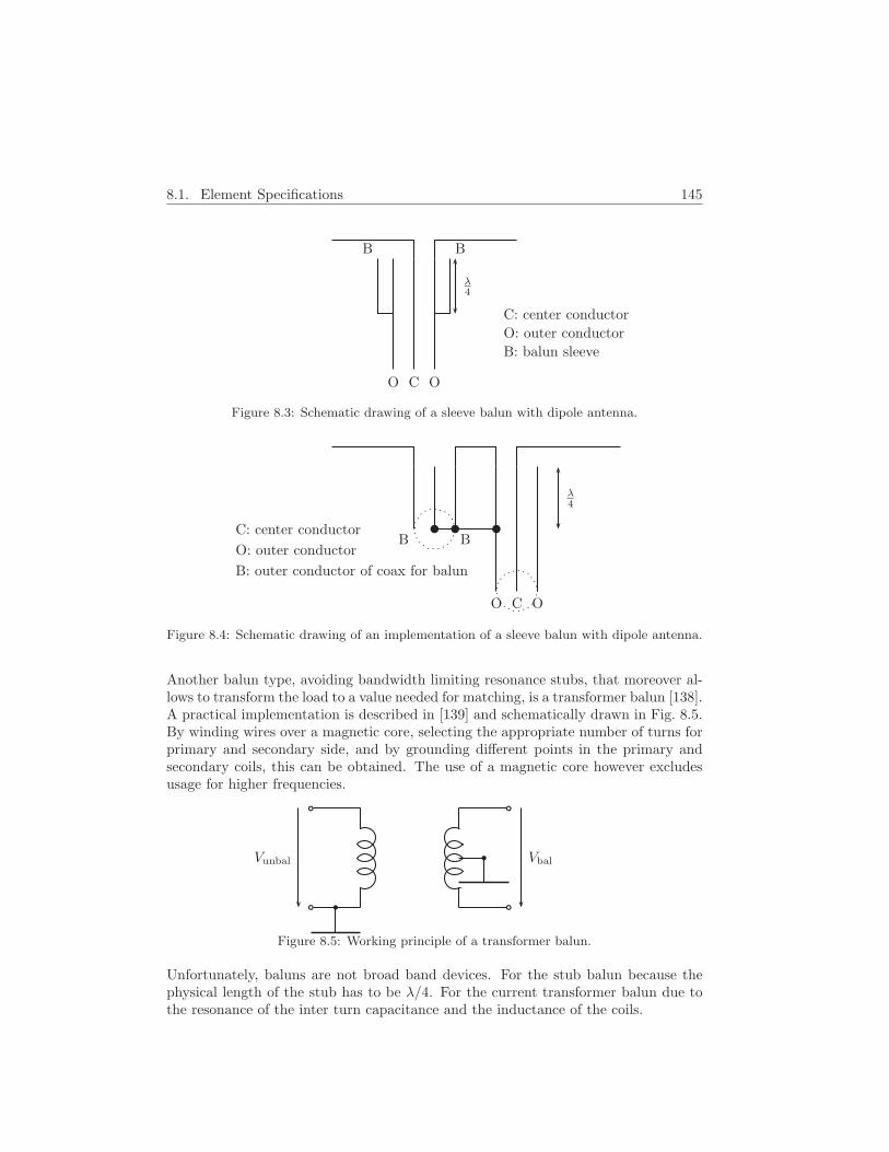
8.1. Element Specifications 145
CO O
B B
λ4
C: center conductor
O: outer conductor
B: balun sleeve
Figure 8.3: Schematic drawing of a sleeve balun with dipole antenna.
CO O
BB
λ4
C: center conductor
O: outer conductor
B: outer conductor of coax for balun
Figure 8.4: Schematic drawing of an implementation of a sleeve balun with dipole antenna.
Another balun type, avoiding bandwidth limiting resonance stubs, that moreover al-lows to transform the load to a value needed for matching, is a transformer balun [138].A practical implementation is described in [139] and schematically drawn in Fig. 8.5.By winding wires over a magnetic core, selecting the appropriate number of turns forprimary and secondary side, and by grounding different points in the primary andsecondary coils, this can be obtained. The use of a magnetic core however excludesusage for higher frequencies.
VbalVunbal
Figure 8.5: Working principle of a transformer balun.
Unfortunately, baluns are not broad band devices. For the stub balun because thephysical length of the stub has to be λ/4. For the current transformer balun due tothe resonance of the inter turn capacitance and the inductance of the coils.

146 Chapter 8. Array Elements
Another way of dealing with the problem, is adding lossy material, such as ferritebeads, which is a very common technique in measurement of small antennas, such asUltra Wide Band (UWB) and handset antennas [140].
Balun problems with symmetric antennas can be avoided by using two coaxial cables,both connected to the scoop or one terminated with a 50 Ω load, or by connecting thesymmetric antenna directly to the measurement device, without cables. This relatesto the measurement setup, which is discussed in Chapter 9.
8.2 Shielded Loop
8.2.1 Loop Types
Although a vast amount of shielded loop magnetic field sensors are in use, only fourimplementations, depicted in Fig. 8.6, namely an unshielded loop, a symmetrical loop,a balanced loop and a mœbius loop will be discussed and compared. First, the typeswill however be introduced briefly, with remarks when necessary. A schematic foreach type can be found in Fig. 8.7.
Figure 8.6: Photograph of the shielded loops. The upper one is the EMCO loop. Belowfrom left to right are the unshielded, symmetrical, balanced and mœbius withand without short.
The naming of the loops is in accordance with the naming in [141], but might beconfusing as interfering with the naming in [142]. The latter interpretation of ashielded loop is depicted in Fig. 8.8, but will not be discussed in this work, as itrequires biax8 cable, which can not be interfaced as is with a standard oscilloscope.Moreover, its characteristics are similar to those of the balanced shielded loop.
8A biaxial cable is a signal cable with a sleeve and two inner conductors.
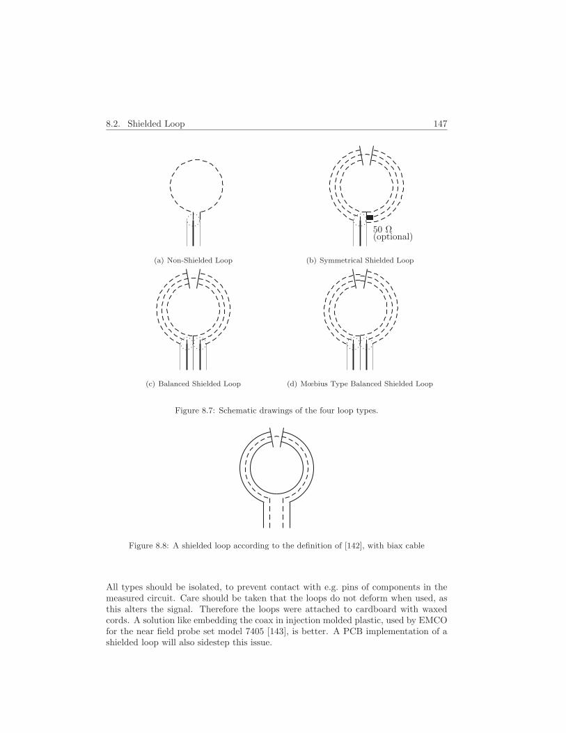
8.2. Shielded Loop 147
(a) Non-Shielded Loop
50 Ω(optional)
(b) Symmetrical Shielded Loop
(c) Balanced Shielded Loop (d) Mœbius Type Balanced Shielded Loop
Figure 8.7: Schematic drawings of the four loop types.
Figure 8.8: A shielded loop according to the definition of [142], with biax cable
All types should be isolated, to prevent contact with e.g. pins of components in themeasured circuit. Care should be taken that the loops do not deform when used, asthis alters the signal. Therefore the loops were attached to cardboard with waxedcords. A solution like embedding the coax in injection molded plastic, used by EMCOfor the near field probe set model 7405 [143], is better. A PCB implementation of ashielded loop will also sidestep this issue.

148 Chapter 8. Array Elements
Table 8.2 lists the DC resistance between inner and outer conductor of the sensors.This allows quick verification of the contacts before using the sensor and reveals thematching at low frequencies: the non shielded, symmetrical and mœbius shortedloop will have an S11 = 1 (0 dB), whereas the balanced and mœbius without shortare matched to 50 Ω so that S11 = 0 (−∞ dB). In Table 8.3 the advantages anddisadvantages of each type, now explained in detail, are summarized.
8.2.1.1 Non-Shielded Loop
A straightforward way to implement a loop sensor, is to simply bend a wire and solderone end to the center conductor and the other end to the outer conductor of a coaxialcable.
This system needs a balun and will, without balun, suffer from the antenna effect,i.e. current will run at the outer side of the outer conductor of the coax and willhence pick up signals and influence the output signal of the sensor, as was explainedin Sect. 8.1.7.
8.2.1.2 Symmetrical Shielded Loop
A loop is formed by the connection of center and outer conductor at the end of thecoaxial cable to the outer conductor of the coaxial cable at the beginning of the loop.In this way, a line integral for Eq. (8.7) similar to the one of the non-shielded loop isobtained. A piece of outer conductor is cut away, however, obstructing current fromflowing on the outer side of the outer conductor of the coax. Without this gap thecurrent flowing would cancel the magnetic field so that the measured signal would bezero.
Table 8.2: Measured DC resistance values (rounded) between connectors of the four looptypes. i: inner conductor, o: outer, sa: same end, op: opposite end. 50 Ω willonly be measured if one port of the sensor is loaded with 50 Ω. If left open, ∞will be measured.
type o-i sa o-i op o-o op i-i op
non-shielded 0 Ω - - -symmetrical 0 Ω - - -
EMCO φ = 6 cm 0 Ω - - -balanced 50 Ω 50 Ω 0 Ω 0 Ωmœbius 50 Ω 0 Ω 50 Ω 50 Ω
mœbius with short 0 Ω 0 Ω 0 Ω 0 Ω

8.2. Shielded Loop 149
Table 8.3: Advantages and disadvantages of the four loop types.
type local pickup antenna effect imped match amplitude
non-shielded - - - - 1symmetrical + - - 1
balanced + + +(LF)/-(HF) 1/2mœbius + + -(LF)/+(HF) 1
The short at the end of the coaxial cable will cause large reflections. Inserting a50 Ω resistor, as in Fig. 8.7(b) can solve this problem, at the cost of loosing signalstrength and generating extra noise. Indeed, following the expression of Johnson-Nyquist noise [144], the root mean square (rms) value of the noise generated in aresistance R is proportional to R:
√〈v2〉 =
√4kTBR. (8.10)
The loop antennas of the EMCO near field probe set model 7405 are of this type. Infact, this type is widely used in EMC diagnostics as it allows to measure values forthe magnetic field strength without errors due to the presence of electric fields. Thisantenna is indeed less sensitive to the electric field, compared to the non-shieldedloop, due to the shielding of the outer conductor.
8.2.1.3 Balanced Shielded Loop
If a coaxial cable is taken and the two ends are connected to a scope (or one to ascope and one to a 50 Ω load), then the reflection problem is avoided. Moreover, alsothe issue with current flowing on the outer side of the sleeve is avoided, as now theinterconnection of an unbalanced cable and a balanced loop is avoided by using two(unbalanced) cables, balancing each other.
A loop is obtained by bending the coaxial cable. Where the coaxial cable does not haveto form a loop, some insulation is removed and the outer conductor of the adjacentcoaxial cables is soldered together. Again a piece of outer conductor in the loop iscut away as otherwise the measured signal would be zero.
The signal that is picked up will have the same magnitude if the loop is about thesame size compared to the previous types. The signal however now has to be measuredbetween the two ports of the scope, so that an oscilloscope with math function comesin handy.
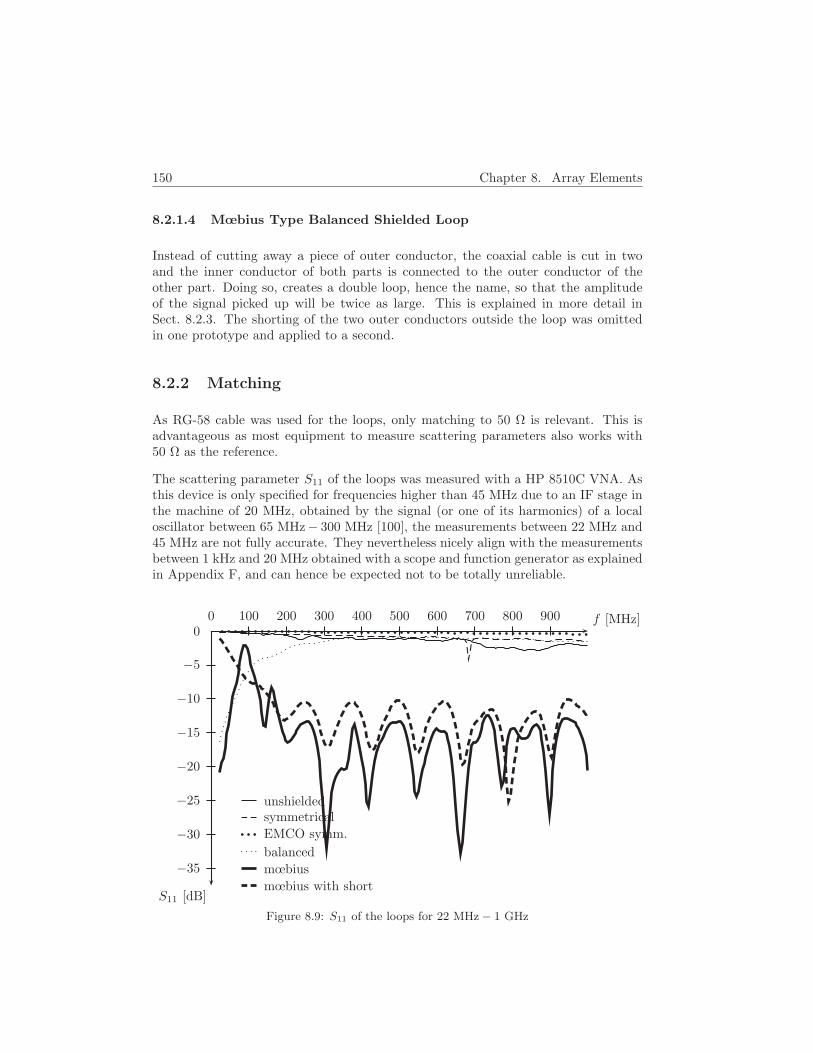
150 Chapter 8. Array Elements
8.2.1.4 Mœbius Type Balanced Shielded Loop
Instead of cutting away a piece of outer conductor, the coaxial cable is cut in twoand the inner conductor of both parts is connected to the outer conductor of theother part. Doing so, creates a double loop, hence the name, so that the amplitudeof the signal picked up will be twice as large. This is explained in more detail inSect. 8.2.3. The shorting of the two outer conductors outside the loop was omittedin one prototype and applied to a second.
8.2.2 Matching
As RG-58 cable was used for the loops, only matching to 50 Ω is relevant. This isadvantageous as most equipment to measure scattering parameters also works with50 Ω as the reference.
The scattering parameter S11 of the loops was measured with a HP 8510C VNA. Asthis device is only specified for frequencies higher than 45 MHz due to an IF stage inthe machine of 20 MHz, obtained by the signal (or one of its harmonics) of a localoscillator between 65 MHz− 300 MHz [100], the measurements between 22 MHz and45 MHz are not fully accurate. They nevertheless nicely align with the measurementsbetween 1 kHz and 20 MHz obtained with a scope and function generator as explainedin Appendix F, and can hence be expected not to be totally unreliable.
0 100 200 300 400 500 600 700 800 9000
−5
−10
−15
−20
−25
−30
−35
f [MHz]
S11 [dB]
unshieldedsymmetrical
balanced
EMCO symm.
mœbius
mœbius with short
Figure 8.9: S11 of the loops for 22 MHz − 1 GHz

8.2. Shielded Loop 151
0 5 10 15 20 25 30 35 40 450
−5
−10
−15
−20
f [MHz]
S11 [dB]
unshieldedsymmetrical
balanced
mœbius
mœbius with short
Figure 8.10: S11 of the loops for 1 kHz − 50 MHz
The measured values for S11 are displayed in Figs. 8.9 and 8.10. For lower frequencies,all probe types with shorting of inner and outer conductor have a scattering parameterS11 = 1. The mœbius without short and balanced type are matched to 50 Ω at lowerfrequencies. For higher frequencies however, it is less evident for a current to takethe short between the inner and outer conductor if this path would have a largeinductance. Hence the mœbius with and without short behave the same for higherfrequencies.
The periodic peaks for both mœbius types are due to the non-perfect characteristicimpedance Zc of the coaxial cable. The cable used was of the RG-58 type, definedin [145], but canceled in [146] and hence invalid as a standard. The manufacturerspecified Zc as 50 ± 2 Ω [147]. At 200 MHz, a value of 52 Ω was measured. Thisvalue was obtained as the geometric mean of an impedance measurement with a short(Zin,0) and an open (Zin,∞). The validity of this technique is easily checked, by writingout Zin in terms of scattering parameters and then filling in 0 and ∞ for ZL:
√Zin,0 × Zin,∞ = Zc
√√√√1 + ej2kl ZL−Zc
ZL+Zc
1 − ej2kl ZL−Zc
ZL+Zc
×1 + ej2kl ZL−Zc
ZL+Zc
1 − ej2kl ZL−Zc
ZL+Zc
= Zc
√1 − ej2kl
1 + ej2kl× 1 + ej2kl
1 − ej2kl= Zc (8.11)
At higher frequencies Zc becomes complex, due to losses. Being e.g. 52 + 8i Ω at500 MHz, the cables transform the load on circles around the center of a smith chartreferenced to 52 + 8i Ω. On a smith chart referenced to 50 Ω, those circles becomeegg shaped curves around the point corresponding to 52 + 8i Ω, i.e. a little up to theright from the center point.

152 Chapter 8. Array Elements
Figure 8.11: S11 of the mœbius with short on a Smith Chart.
The curve for the mœbius without short comes up as high as −2 dB around 100 MHz.This peak is due to a short when the capacitance between the two adjacent outerconductors before and behind the loop starts to conduct signals. The capacitancebetween two cables of radius rw with distance d between the wire centers, is [148]:
C = l × c = l × επ
log
(d2r +
√( d2r )2 − 1
) (8.12)
This expression is not exact in the case of hollow coax outer conductors due to theskin effect, but still, it can be concluded that the capacitance between the cablesis influenced by both the length l of the cables, and the distance d between them.Hence this peak can be avoided by moving the 50 Ω termination at the end of thesecond cable to just behind the loop, so that the second cable has zero length. Ameasurement, shown in Fig. 8.12, indeed reveals that this action solves the matchingissue. This sensor is indeed matched sufficiently over the entire frequency range.
Such sensor would however only partially pick up signals as the voltage induced by themagnetic flux stands partly between the two outer conductors and does not contributeto the signal that arrives at the scope.
This actually means that none of the four probe types is matched over the entirefrequency range of interest. If, for some application, only frequencies below e.g.50 MHz are to be used, the balanced loop can be used without matching problems.If, for another application a band will be used around a frequency of some hundreds ofMHz, that will be mixed down in a receiver, the mœbius loop with short can be used.

8.2. Shielded Loop 153
0 100 200 300 400 500 600 700 800 9000
−5
−10
−15
−20
−25
−30
−35
f [MHz]
S11 [dB]
mœbius large C
mœbius small C
Figure 8.12: S11 of a mœbius without short with different capacitances between the twoadjacent cables.
Only if for some reason the entire band from (nearly) DC to 1 GHz is important, acombination of the balanced and mœbius with short can be the solution. A schematiclayout of this solution is given in Fig. 8.13. Capacitances and an inductor are usedto obtain the connections for a balanced loop at low frequencies and the connectionsfor a mœbius loop at high frequencies.
Figure 8.13: Layout of a loop that combines the balanced and mœbius loop.
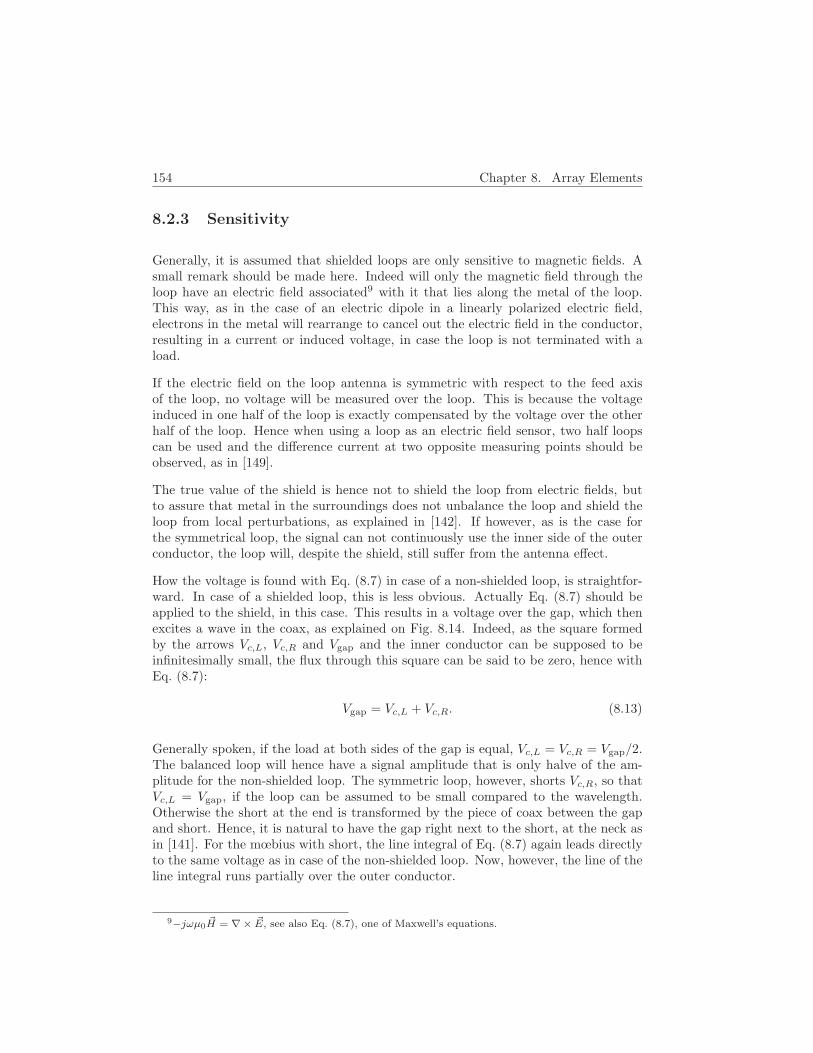
154 Chapter 8. Array Elements
8.2.3 Sensitivity
Generally, it is assumed that shielded loops are only sensitive to magnetic fields. Asmall remark should be made here. Indeed will only the magnetic field through theloop have an electric field associated9 with it that lies along the metal of the loop.This way, as in the case of an electric dipole in a linearly polarized electric field,electrons in the metal will rearrange to cancel out the electric field in the conductor,resulting in a current or induced voltage, in case the loop is not terminated with aload.
If the electric field on the loop antenna is symmetric with respect to the feed axisof the loop, no voltage will be measured over the loop. This is because the voltageinduced in one half of the loop is exactly compensated by the voltage over the otherhalf of the loop. Hence when using a loop as an electric field sensor, two half loopscan be used and the difference current at two opposite measuring points should beobserved, as in [149].
The true value of the shield is hence not to shield the loop from electric fields, butto assure that metal in the surroundings does not unbalance the loop and shield theloop from local perturbations, as explained in [142]. If however, as is the case forthe symmetrical loop, the signal can not continuously use the inner side of the outerconductor, the loop will, despite the shield, still suffer from the antenna effect.
How the voltage is found with Eq. (8.7) in case of a non-shielded loop, is straightfor-ward. In case of a shielded loop, this is less obvious. Actually Eq. (8.7) should beapplied to the shield, in this case. This results in a voltage over the gap, which thenexcites a wave in the coax, as explained on Fig. 8.14. Indeed, as the square formedby the arrows Vc,L, Vc,R and Vgap and the inner conductor can be supposed to beinfinitesimally small, the flux through this square can be said to be zero, hence withEq. (8.7):
Vgap = Vc,L + Vc,R. (8.13)
Generally spoken, if the load at both sides of the gap is equal, Vc,L = Vc,R = Vgap/2.The balanced loop will hence have a signal amplitude that is only halve of the am-plitude for the non-shielded loop. The symmetric loop, however, shorts Vc,R, so thatVc,L = Vgap, if the loop can be assumed to be small compared to the wavelength.Otherwise the short at the end is transformed by the piece of coax between the gapand short. Hence, it is natural to have the gap right next to the short, at the neck asin [141]. For the mœbius with short, the line integral of Eq. (8.7) again leads directlyto the same voltage as in case of the non-shielded loop. Now, however, the line of theline integral runs partially over the outer conductor.
9−jωµ0~H = ∇× ~E, see also Eq. (8.7), one of Maxwell’s equations.
8.3. RFID Loop 155
Vgap
Vc,L Vc,R
Figure 8.14: Working principle of a shielded loop.
8.3 RFID Loop
Following part was reported in [150]. The designed loop is not exactly a sensor forEMA, but a loop for a reader that extends the reading range of an ISO-14443A RFIDsystem. Although Radio-frequency identification (RFID) is beyond the scope of thistext, the design of the loop is relevant, as it fits in analyzing existing loop design.Indeed many aspect studied here will turn out to be very relevant when designing asmall sensor in Sect. 8.4.
RFID was developed during the second world war by the British, to identify friendlyfrom other airplanes, Identify Friend or Foe (IFF). It took however several years untilthe technique was used in industry. With the ever decreasing cost of silicon logic, itis not unlogical that sooner or later, RFID will replace bar codes. RFID offers someadvantages over bar codes. Besides the obvious application of tracking goods, it canbe used for counterfeit control and is writable. More reasons to use RFID can befound in [151]. A drawback of RFID is that it requires special attention concerningprivacy. Access to sensitive information should be denied to unauthorized parties.
RFID can be implemented in several ways: active or passive, inductive or capacitiveand so on. Appendix G gives an overview and explains one inductive standard, ISO-14443A for 13.56 MHz in more detail. This is the standard that is also used inthe Belgian passports. Often remarks on privacy and security issues are counteredby the small read out distance of the system, often assumed to be about 10 cm.Kirschenbaum and Wool [152] however designed a low-cost, extended range RFIDskimmer. With the RFID loop designed here and the amplifier of Sect. 9.3.3.1, aneven larger reading distance can be bridged.
8.3.1 Loop Design
The reader antenna has to provide the tag with a field that is sufficient to power upthe hardware in the tag. Hence the antenna will be designed in such a way that themagnetic field at a certain read out distance rd is large enough. In second order, theantenna should also be suited to receive the answer from the tag. This condition is notconsidered here, as an adversary is presumed to have access to a separate receivingantenna if needed.
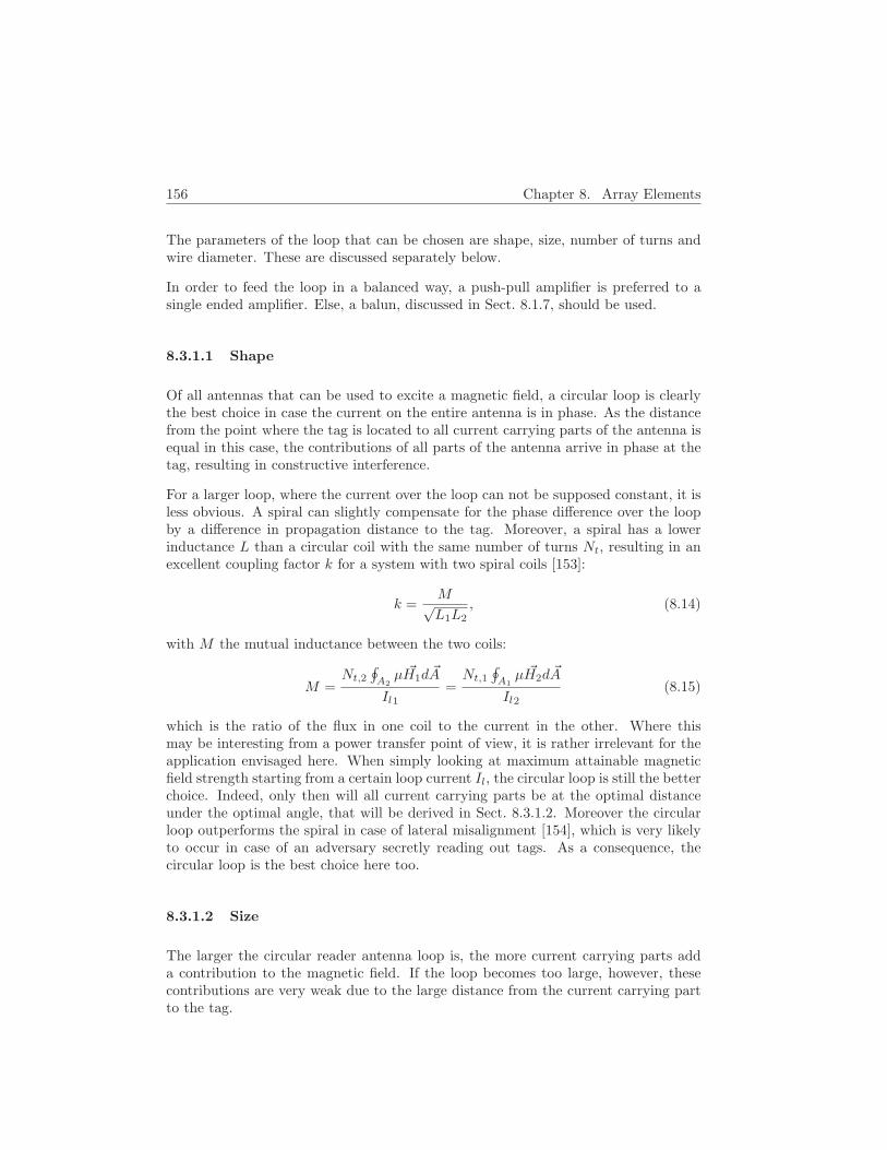
156 Chapter 8. Array Elements
The parameters of the loop that can be chosen are shape, size, number of turns andwire diameter. These are discussed separately below.
In order to feed the loop in a balanced way, a push-pull amplifier is preferred to asingle ended amplifier. Else, a balun, discussed in Sect. 8.1.7, should be used.
8.3.1.1 Shape
Of all antennas that can be used to excite a magnetic field, a circular loop is clearlythe best choice in case the current on the entire antenna is in phase. As the distancefrom the point where the tag is located to all current carrying parts of the antenna isequal in this case, the contributions of all parts of the antenna arrive in phase at thetag, resulting in constructive interference.
For a larger loop, where the current over the loop can not be supposed constant, it isless obvious. A spiral can slightly compensate for the phase difference over the loopby a difference in propagation distance to the tag. Moreover, a spiral has a lowerinductance L than a circular coil with the same number of turns Nt, resulting in anexcellent coupling factor k for a system with two spiral coils [153]:
k =M√L1L2
, (8.14)
with M the mutual inductance between the two coils:
M =Nt,2
∮A2µ ~H1d ~A
Il1=Nt,1
∮A1µ ~H2d ~A
Il2(8.15)
which is the ratio of the flux in one coil to the current in the other. Where thismay be interesting from a power transfer point of view, it is rather irrelevant for theapplication envisaged here. When simply looking at maximum attainable magneticfield strength starting from a certain loop current Il, the circular loop is still the betterchoice. Indeed, only then will all current carrying parts be at the optimal distanceunder the optimal angle, that will be derived in Sect. 8.3.1.2. Moreover the circularloop outperforms the spiral in case of lateral misalignment [154], which is very likelyto occur in case of an adversary secretly reading out tags. As a consequence, thecircular loop is the best choice here too.
8.3.1.2 Size
The larger the circular reader antenna loop is, the more current carrying parts adda contribution to the magnetic field. If the loop becomes too large, however, thesecontributions are very weak due to the large distance from the current carrying partto the tag.
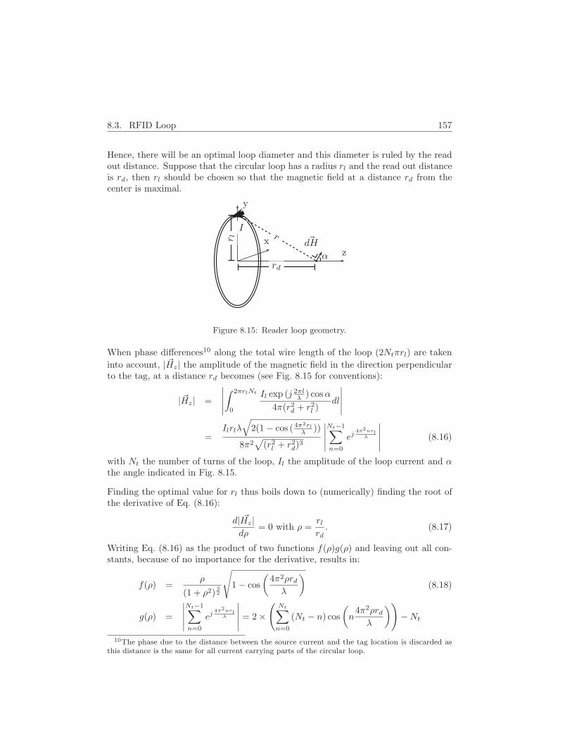
8.3. RFID Loop 157
Hence, there will be an optimal loop diameter and this diameter is ruled by the readout distance. Suppose that the circular loop has a radius rl and the read out distanceis rd, then rl should be chosen so that the magnetic field at a distance rd from thecenter is maximal.
y
x
z
Ir
rd
r l ~dH
α
Figure 8.15: Reader loop geometry.
When phase differences10 along the total wire length of the loop (2Ntπrl) are taken
into account, | ~Hz| the amplitude of the magnetic field in the direction perpendicularto the tag, at a distance rd becomes (see Fig. 8.15 for conventions):
| ~Hz| =
∣∣∣∣∣
∫ 2πrlNt
0
Il exp (j 2πlλ ) cosα
4π(r2d + r2l )dl
∣∣∣∣∣
=Ilrlλ
√2(1 − cos ( 4π2rl
λ ))
8π2√
(r2l + r2d)3
∣∣∣∣∣Nt−1∑
n=0
ej4π2nrl
λ
∣∣∣∣∣ (8.16)
with Nt the number of turns of the loop, Il the amplitude of the loop current and αthe angle indicated in Fig. 8.15.
Finding the optimal value for rl thus boils down to (numerically) finding the root ofthe derivative of Eq. (8.16):
d| ~Hz|dρ
= 0 with ρ =rlrd. (8.17)
Writing Eq. (8.16) as the product of two functions f(ρ)g(ρ) and leaving out all con-stants, because of no importance for the derivative, results in:
f(ρ) =ρ
(1 + ρ2)32
√1 − cos
(4π2ρrdλ
)(8.18)
g(ρ) =
∣∣∣∣∣Nt−1∑
n=0
ej4π2nrl
λ
∣∣∣∣∣ = 2 ×(
Nt∑
n=0
(Nt − n) cos
(n
4π2ρrdλ
))−Nt
10The phase due to the distance between the source current and the tag location is discarded asthis distance is the same for all current carrying parts of the circular loop.

158 Chapter 8. Array Elements
The derivative of those functions is:
f ′(ρ) =
√1 − cos
(4π2ρrd
λ
)
(1 + ρ2)52
(1 − 2ρ2) +2π2ρrd sin
(4π2ρrd
λ
)
λ(1 + ρ2)32
√1 − cos
(4π2ρrd
λ
) (8.19)
g′(ρ) = −2 ×Nt∑
n=0
n(Nt − n)4π2rdλ
sin
(n
4π2ρrdλ
)(8.20)
Knowing that:(fg)′ = f ′g + fg′ (8.21)
the equation to be solved in order to find the optimal ρ, is:((
1 − cos(
4π2ρrd
λ
))λ(1 − 2ρ2) + 2π2ρrd(1 + ρ2) sin
(4π2ρrd
λ
))
×(2(∑Nt
n=0(Nt − n) cos(n 4π2ρrd
λ
))−Nt
)− 2ρ(1 + ρ2)
(1 − cos
(4π2ρrd
λ
))
(∑Nt
n=0 n(Nt − n)4π2rd sin(n 4π2ρrd
λ
))= 0 (8.22)
After a division by λ, an equation is obtained that leads to the solutions for rd/λ.Hence solving this equation once leads to design curves valid for any frequency. Forthe case of a single turn (Nt = 1), the optimal value for ρ and hence rl is found asthe solution of:
(2ρ2 − 1)
ρ− sin (4π2ρrd
λ )
1 − cos ( 4π2ρrd
λ )2π2 rd
λ(1 + ρ2) = 0. (8.23)
The result, as well as the solutions for Nt = 2, 3, 5, 10, plotted in Fig. 8.16, showthat as rd increases, rl also increases, even up to rd/λ = 1/2π ≈ 0.16. But the ratiobetween rl and rd decreases as rd increases. For any number of turns, the limit forrd/λ→ 0:
limrdλ
→0ρ = lim
rdλ
→0
rlrd
=√
2. (8.24)
This can be expected as in this limiting case, also rl/λ → 0. The assumption of aconstant current over the entire wire length of the loop, leading to the ratio rl/rd =
√2
as published in a.o. [155] and [156] in such case surely holds.
8.3.1.2.1 Total wire length of loop small compared to wavelength Underthis precondition, the current can be assumed to be constant over the loop. Eq. (8.16)then simplifies to,
| ~Hz| =
∣∣∣∣∫ 2πrl
0
NtIl cosα
4πr2dl
∣∣∣∣ =
∣∣∣∣∣NtIlr
2l
2√
(r2l + r2d)3
∣∣∣∣∣ , (8.25)
which can e.g. also be found in [157].

8.3. RFID Loop 159
0 0.05 0.10 0.150
0.5
1.0
Nt = 1
Nt = 2
Nt = 3
Nt = 5
Nt = 10
rd/λ
rl/rd
Figure 8.16: rl/rd as a function of rd/λ.
The optimal value for rl can be found with Eq. (8.24), as assuming that 2πrl/λ→ 0is equivalent with assuming that rd/λ → 0, because both rl and rd are of the sameorder of magnitude.
The ISO-14443 standard [158] specifies the minimum (rms) magnetic field strengthfor the cards to operate11 as Hmin = 1.5 A/m. Combining Eq. (8.25) with (8.24)yields:
| ~Hz| =
∣∣∣∣∣NtIlr
2l
2√
(r2l + r2d)3
∣∣∣∣∣ =
∣∣∣∣∣NtIlr
2d√
(3r2d)3
∣∣∣∣∣ =
∣∣∣∣NtIl√27rd
∣∣∣∣ . (8.26)
The minimum current (rms) Imin needed in the reader antenna (with rd in m) is:
Imin ×Nt =√
27 ×Hmin × rd = 7.8 × rd. (8.27)
Assume, e.g. Nt = 1, rd = 0.1 m and L = 1 µH. The current with Eq. (8.27) will be0.78 A and the voltage:
|V | = |ωL√
27Hminrd| ≈ 66 V. (8.28)
It is obvious that applying this voltage directly to the loop is not practical. Hencecurrent enhancement techniques, covered in Sect. 8.3.2, should be used.
8.3.1.2.2 Total wire length of loop comparable to wavelength As soon asthe total wire length of the loop is considerable, say λ/10 as a rule of thumb, themagnetic field of the loop will be smaller than what would be expected when usingEq. (8.25), which is indeed invalid in this case. Due to the phase differences overthe loop, the contributions of all parts of the loop at the location of the tag will notbe in phase and partial cancellation will occur. In that sense it might even be moreadvantageous to use a slightly smaller loop with more current, as Fig. 8.16 indeedindicates.
11That is to build up a voltage high enough to power up the hardware in the tag.

160 Chapter 8. Array Elements
8.3.1.2.3 Total wire length of loop multiple of half wavelength If the loopperimeter equals half a wavelength or a multiple, standing waves will occur. Theloop itself will then resonate and the reactance on the Smith chart crosses the realaxis, going from inductive to capacitive impedance. This dependence of the reactanceon the frequency has its effect on the usage of the coil in an RLC circuit to enhancecurrent. If e.g. Eq. (8.35), the resonance condition for a combined series-parallel RLC,has, due to frequency dependence, multiple solutions for different ω, the RLC systemwill resonate at multiple frequencies and the energy will be divided amongst them.Fig. 8.22 shows multiple crossings of the curves for the resonance condition and theimaginary part of the input impedance.
8.3.1.3 Number of Turns Nt
Looking at Eq. (8.25), which is only valid for small loops and in the case the coilis fed with a current source, it is tempting to think that a high Nt will result in ahigh magnetic field H at the tag location. The considerations below, however, argueagainst a value of Nt > 1.
8.3.1.3.1 Phase degradation The more turns are used, the longer the total wirelength of the loop and hence the more pronounced the effect described in Sect. 8.3.1.2.2becomes. For a small loop, fed by a current source, the magnetic field can be boostedby taking more turns. But as soon as the total wire length of the loop can not beregarded small compared to the wavelength, it is advantageous to take Nt smaller.Fig. 8.17 depicts the magnetic field as a function of rd in the case of Nt = 1, 2, 3, 5, 10when the optimal rl as calculated in Sect. 8.3.1.2 is used. The conclusion that usingmore turns is only advantageous for smaller rd, is clear.
0 1 2 3 4−30
−20
−10
0
10
Nt = 1Nt = 2Nt = 3Nt = 5Nt = 10
rd [m]
| ~Hz| [dB]
Figure 8.17: | ~Hz| at rd when optimal rl for that value of rd is used. Il = 1 A and fc =13.56 MHz.

8.3. RFID Loop 161
8.3.1.3.2 Loop impedance For a loop, fed by a voltage source, discardingthe small ohmic and radiation resistance with respect to ωL, following Schrank andMahony [159]:
|NtIl| = Nt|Vl|ωL
= Nt|Vl|
ωN2t L1,Nt=1
∝ |Vl|NtL1,Nt=1
, (8.29)
with L1,Nt=1 the inductance of a loop of the same size with only one turn. Thus
maximizing NtIl, in order to maximize | ~Hz| in Eq. (8.25), means Nt = 1 and L1,Nt=1
small.
8.3.1.3.3 Bandwidth When the loop antenna is placed in an RLC chain andused for a communication link, raising Nt is not without a price. As L is proportionalto the quality factor, defined later on in Eq. (8.34), it can only be increased up to acertain level as otherwise the bandwidth of the system would become too small. Thisis not in contradiction with the results of Yates et al. [160], namely that the powertransfer ratio is proportional to N2
t , but they do not consider bandwidth issues.
8.3.1.3.4 Self-resonance frequency When the loop perimeter is about half awavelength, the loop will resonate. But if the loop has multiple turns, resonance atlower frequency occurs due to the parallel resonance of the inductance of the loop andthe capacitance between its turns. Above its resonance frequency, the loop starts tobehave as a capacitance. Therefore it is important to know the resonance frequencyfres of the loop.
The capacitance between two turns Ctt of bare wire can be calculated with Eq. (8.12).If the wire has an insulation with a relative permittivity εr different from 1, inGrandi [161] the formula becomes:
Ctt = 2πrl ×εrε0π
log ( d2rw
), (8.30)
where the insulation of both wires is supposed to touch, resulting in d = 2rw + 2twith t the insulation thickness. This formula only holds for a radial electric field inthe insulation, which is surely not the case for εr → 1. Hence substituting εr = 1 intoEq. (8.30) does not result in Eq. (8.12) due to approximations used in the model thatled to Eq. (8.30).
If an inductor with multiple turns is used, the equivalent capacitance is found as theseries circuit of all turn-to-turn capacitances. This is a simplification and it assumesthat the capacitance between non-adjacent turns can be neglected. In Fig. 8.18 theequivalent circuit of an inductor with all capacitances is drawn. The capacitancesthat are neglected are drawn with dashed lines.

162 Chapter 8. Array Elements
L1
L2
L3
LN
C1
C2
C3
CN
. . .
. . .. . .
Figure 8.18: Equivalent circuit of an inductor.
Note that discarding the capacitance between non-adjacent turns implies that theself-resonance frequency only shifts downwards by a factor
√Nt when adding more
turns. Indeed, the resonance frequency is found as:
fres =1
2π√L1Ctt
=1
2π√NtL1,Nt=1Ctt
=
√2
Ntfres,Nt=2, (8.31)
where L1,Ntand Ctt indicate the inductance (in the presence of the other turns), resp.
capacitance of a single turn. L1,Nt= Nt × L1,Nt=1 still depends on the number of
turns, L1,Nt=1 is the inductance of a single turn in the absence of all other turns.Table 8.4 shows the result obtained from Eq. (8.31).
Table 8.4: Self-resonance frequency of loops with rw = 1 mm with and without insulation of0.2 mm with εr = 4 for varying loop radius. The last column gives the resonancefrequency in case of a single turn.
rl [m] Ctt [pF] Lt [µH] fres,Nt=2 (ε0) fres,Nt=2 (εr = 4) fres,Nt=1 (ε0)0.01 2.016 0.07729 403.2 MHz 125.6 MHz 4775 MHz0.1 20.16 1.352 30.49 MHz 9.498 MHz 477.5 MHz1 201.6 19.3 2.551 MHz 0.7947 MHz 47.75 MHz
8.3. RFID Loop 163
Taking the inter-turn capacitance into account, the impedance of the coil equals:
Zcoil =jωN2
t L1,Nt=1
1 − ω2NtL1,Nt=1Ctt. (8.32)
which is again frequency dependent, possibly causing resonances at multiple frequen-cies, similar to those mentioned for Nt = 1 in Sect. 8.3.1.2.3.
8.3.1.3.5 Resistance of Parallel Wires Another disadvantage of multiturnloops, is their increased ohmic resistance. Due to the capacitive inter-turn coupling,the current in the loop wire is even more confined than should be expected due to theskin effect alone. Smith [162] provides formulas to calculate this effect in the case ofa loop that is small compared to the wavelength.
The argumentation above leads to the conclusion that Nt should be taken small unlessonly power transfer is considered or the loop antenna is fed by a current source andrd is rather small.
8.3.1.4 Wire Diameter
Sect. 8.3.1.3 revealed that when a voltage source is used, or the loop is placed in anRLC chain and used for data communication, its inductance L should be small. Usinga wire with large diameter reduces L.
8.3.2 Power source and current enhancement
As is mentioned before and expressed in Eq. (8.27), a minimum amount of current isneeded to activate the RFID tag. This current can be directly drawn from an externalpower source, but sometimes it can be more convenient to enhance the current if forexample a powerful power source is not available. This can be done either passivelyby means of an RLC circuit or actively with the aid of an amplifier. The choice ofpower source and enhancement technique affects the design of the loop so these needto be taken into consideration. Some passive enhancement techniques are treatedbelow. For active enhancement, with the aid of amplifiers, the reader is referred toSect. 9.3.3.
When adding a capacitor and a resistor to the loop, in order to obtain an RLC circuit,many combinations with a capacitor, inductor and resistor can be made. Only theones with L, the inductance of the loop antenna, and R in series are considered forthis application, because the loop resistance is inherently in series with the inductanceof the antenna [163]. If an external resistor has to be added, it is preferably added inseries with the loop, for the same reason. The internal resistance of the capacitors issmaller and will be neglected. An overview of the possible circuits is given in Fig. 8.19.
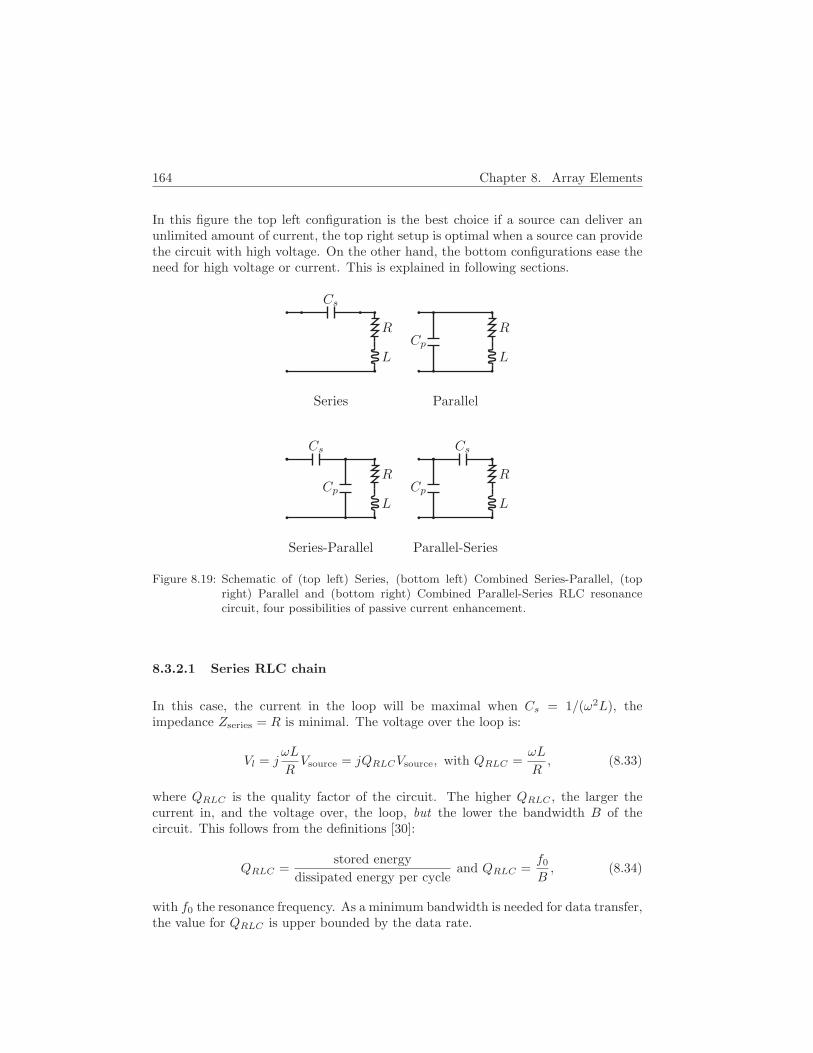
164 Chapter 8. Array Elements
In this figure the top left configuration is the best choice if a source can deliver anunlimited amount of current, the top right setup is optimal when a source can providethe circuit with high voltage. On the other hand, the bottom configurations ease theneed for high voltage or current. This is explained in following sections.
Cs
R
L
Series
Cp
R
L
Parallel
Cs
Cp
R
L
Series-Parallel
Cp
Cs
R
L
Parallel-Series
Figure 8.19: Schematic of (top left) Series, (bottom left) Combined Series-Parallel, (topright) Parallel and (bottom right) Combined Parallel-Series RLC resonancecircuit, four possibilities of passive current enhancement.
8.3.2.1 Series RLC chain
In this case, the current in the loop will be maximal when Cs = 1/(ω2L), theimpedance Zseries = R is minimal. The voltage over the loop is:
Vl = jωL
RVsource = jQRLCVsource, with QRLC =
ωL
R, (8.33)
where QRLC is the quality factor of the circuit. The higher QRLC , the larger thecurrent in, and the voltage over, the loop, but the lower the bandwidth B of thecircuit. This follows from the definitions [30]:
QRLC =stored energy
dissipated energy per cycleand QRLC =
f0B, (8.34)
with f0 the resonance frequency. As a minimum bandwidth is needed for data transfer,the value for QRLC is upper bounded by the data rate.
8.3. RFID Loop 165
8.3.2.2 Parallel RLC chain
Here, the current in the loop only depends on the voltage applied to the RLCchain, but the current drawn from the source will be minimum if the conditionCp = L/(ω2L2 +R2) or Zparallel = R+ω2L2/R is met. In this case the impedance ofthe chain is maximal as is the current amplification.
8.3.2.3 Combined series/parallel RLC chain
The loop current is maximized when
ω2Cs =1 − 2ω2LCp + ω2C2
p(ω2L2 +R2)
L− Cp(ω2L2 +R2). (8.35)
Due to the second degree of freedom, Cp, any value for the impedance can be obtained:
ZcombinedSP =R
1 − 2ω2LCp + ω2C2p(ω2L2 +R2)
. (8.36)
Hence this is the best choice for the resonance circuit, as it allows to match theinternal resistance of any source, to ensure maximum power transfer to the load. Ifthe loop antenna is located at a distance from the reader, a transmission line has tobe used to connect both and the use of the combined chain is obligatory: of the fourcircuits, only this one can match the characteristic impedance of any line.
8.3.2.4 Combined parallel/series RLC chain
The loop current is maximized when Cs = 1/(ω2L). This is identical to the resonancecondition of the series resonance chain. The second degree of freedom, Cp, can againbe used to choose the input impedance of the chain:
ZcombinedPS =R− jωR2Cp
1 + ω2R2C2p
, (8.37)
but to a lesser extent than was the case in the series/parallel chain as ZcombinedPS willalways be smaller than R.
In order to use the RLC equations mentioned above, the inductance L of the antennashould be known. Appendix H learns that this is not straightforward. Even more,the value for L also depends on the surroundings, especially for larger loops. Thepresence of metal is one of the reasons for this alteration. Consequently, the value forthe capacitance C needed after installation can differ slightly from the value calculatedwith the design equations given above.
166 Chapter 8. Array Elements
This problem is easily solved by tuning12 the resonance circuit, using trimming ca-pacitors. Automatic tuning compensates on the fly, but, at the cost of increasedcomplexity. One example [164] uses a control circuit to set the DC bias in a ferritecore to change the inductance of a coil.
8.3.2.5 Impact of R on Cs and Cp
The last parameter to determine is the resistance R. The total resistance R of thechain will be the internal resistance of the loop Rl and an external resistor that is de-liberately added. The equations above show that the value of R can also influence theresonance frequency of the chain. This deviation can also be corrected by tuning thecapacitors, so that the value for R can be determined only based on the requirementsfor the bandwidth, mathematically condensed in QRLC .
8.3.3 Validation
Three antennas were made to validate the formulas and statements: two solid copperwire loops, one with Nt = 1, another one with Nt = 2 and one copper tube loop, seeFig. 8.20. Their geometrical parameters are summarized in Table 8.5.
The MIFARE Pegoda MF RD 700 is used as a reader. Its RF output is a voltage sourcewith internal resistance. For such a source, as explained in Sect. 8.3.2, the best choiceis the series-parallel circuit. Tuning of this circuit is necessary because the frequencyresponse of the circuit is very sensitive to L, Cp and Cs. The capacitors bought hada tolerance of 10 %. Moreover, neither the measured Lmeas nor the calculated Lcalc
are exact due to the problems mentioned in Appendix H. The calculated inductancesLcalc were verified against values derived from measurements. The values obtainedcan be found in Table 8.5. Due to balun problems the measurements were totallyunreliable for the copper tube loop. Instead, the inductance of the loop was measuredin an indirect way: the loop was taken out of the circuit and replaced by a lumpedelement inductance with a certain value L. This was repeated for lumped elementswith different values of L, until the resonance frequency matched the original one.
The resonance circuit is a variation on the series-parallel circuit: it consists of anupright and a mirrored version of it, see Fig. 8.21, to feed the antenna in a balancedway. If this is not done, problems as those shown in Fig. 8.22 can arise because ofa transition from a balanced loop to an unbalanced vectorial network analyzer. Thesimulated curve is obtained from a NEC simulation with 400 divisions along the circleperimeter.
12Try to find the values for the capacitors that result in the largest current in the loop. Monitoringof the current in the loop can be done by 1) using a current probe, but this adds another inductance,2) measuring the voltage over the loop, but voltage probes always form a small loop and pick upfields or 3) using a field probe. The last method is preferred.

8.3. RFID Loop 167
rl d
A B
(a) Layout. A = top view, B = sideview. Nt = 1. The same schematic holdsfor Nt > 1, only more turns are stacked.
(b) Photograph. Largest = coppertube loop, Smallest = two turn solidcopper wire loop
Figure 8.20: Layout drawing and pictures of the RFID reader loops designed and made tovalidate the formulas and statements. The values for rl and d of the differentantennas can be found in Table 8.5.
Cs,1
Cp,1
R
L
Cs,2
Cp,2
Figure 8.21: Resonance circuit used to determine the reading range.
Furthermore, Table 8.5 also lists some electrical parameters: the magnetic field H atthe origin of the loop and the maximum reading distance with a MIFARE card. Forthe latter measurement no other alterations were done to the setup but tuning theresonance circuit. For the first measurement an EMCO − 902, 3 cm magnetic fieldprobe is utilized [143]. Although Table 8.5 indicates that the loop with two turnsgenerates a higher magnetic field compared to the loop with one turn, this does notresult in a larger reading distance because of a QRLC which is too high, so that evenat a very small distance no communication can take place in this setup. Adding anexternal resistor can solve this, but this is beyond the scope of validating the formulasand statements. When holding a card very close to the copper tube, this card couldbe read by the reader, but the reader could not supply enough current to obtain afunctioning system with a card at the origin or further along the z-axis.

168 Chapter 8. Array Elements
Another difference between the two solid wire loops is the remarkably lower fres ofthe two turn loop. This confirms the effect of Ctt, calculated with Eq. (8.30) forεr = 4 [165], on fres.
10 20 30 40 50 60 70 80 90 1000
5
10
−5
L[µ
H]
f [MHz]
measurementEq. (8.35)
simulation
Figure 8.22: Frequency dependent value of L for the copper tube loop as obtained from sim-ulation and measurement. A balanced to unbalanced system transition causesthis value to fluctuate heavily around 13 MHz so that the loop is useless unlessfed in a balanced way.
Table 8.5: Characteristics overview of the RFID reader loops: A-B) Solid copper wire loops,C) Copper tube loop, (*) reading distance not measurable because of QRLC toohigh, (**) reading distance not measurable because the reader could not supplyenough current, this requires an amplifier.
coil RLC circuitNt rl d Rl Lcalc Lmeas fres,calc fres,meas H(000) rd
[cm] [cm] [Ω] [µH] [µH] [MHz] [MHz] [A/m] [cm]A 1 8.25 0.1 0.5 0.537 0.569 579 583 4.16 10B 2 8.25 0.1 2.09 2.15 2.27 48 41 5.35 (*)C 1 56.5 1.5 200 3.1 3.45 85 27 0.12 (**)
8.4 Maximal Resolution Sensor
As the sensor should have the largest possible area, resulting in a higher amplitude,for the shortest possible perimeter, resulting in a larger working frequency band, theloop shape should be circular. Nt and rl are determined by trade-off as explainedin Sect. 8.4.1. There it will also become clear that the wire diameter, which shouldbe as large as possible for low resistance, is determined by material selection andfabrication technique as soon as rl is determined. Sect. 8.4.1 makes abstraction ofthe fact that a considerable amount of turns can not be wound circularly withoutstacking turns, distancing from the source. Sect. 8.4.3 points out that in such case itis more appropriate to fabricate spirals.
8.4. Maximal Resolution Sensor 169
8.4.1 Geometrical Design
Sect. 8.2 zoomed in on shielded loops. Those loops were quite large in comparisonwith a micro-controller, ASIC or even FPGA and were consequently not suited forlocalized measurements. Smaller implementations of the same concept do manage toachieve smaller resolutions. Masuda et al. [132] reports an aperture of 20 µm×1 mm.One of the commercially available high resolution sensors is the NEC CP-2S with aresolution of ≈ 250µm. This is a shielded loop printed on glass ceramic multilayer withthin film technology, after [166]. Even shielded loops on chips have been fabricated,as in [167].
Non-shielded loop sensors can inherently be made smaller than the shielded loops.The commercially available types, such as the ICR near field microprobes, sold byLanger EMV-Technik, are sold under specification of 80 µm resolution.
Sect. 8.4.1.1 discusses the maximal spatial resolution of non-shielded loop sensors.Examples in Sect. 8.4.1.2 give numerical results. A straightforward design method-ology can not be derived due to the complexity of the equations. Numerical searchmethods are to be applied. The practical limits on the resolution are however athand. For additional calculations, Sect. 8.4.1.3, which was left out in [168] due to thepage limit, contains details on the numerical implementation of the displayed theory.
8.4.1.1 Theory
In this section the minimum achievable dimension of a circular inductive sensor forusage in a frequency interval [fL, fH ] is evaluated and values for the number of turnsNt and the loop radius rl are derived starting from the value of the magnetic fieldstrength B and a minimum amplitude Vmin that should be generated over a load Z,the input impedance of the measurement device, in parallel with the loop. This valueVmin is determined by the measurement equipment and relates to the minimum voltagethat can be measured by an oscilloscope or the minimum signal amplitude that hasto be fed to an amplifier connected to the loop to obtain a reasonable signal-to-noiseratio or the like.
8.4.1.1.1 General Case: Arbitrary Z Rewriting Eq. (8.7) for a single fre-quency:
|V | =
∣∣∣∣dφB
dt
∣∣∣∣ = ωNtAB. (8.38)
The rightmost equality sign implies that the loop is positioned orthogonally to themagnetic field.
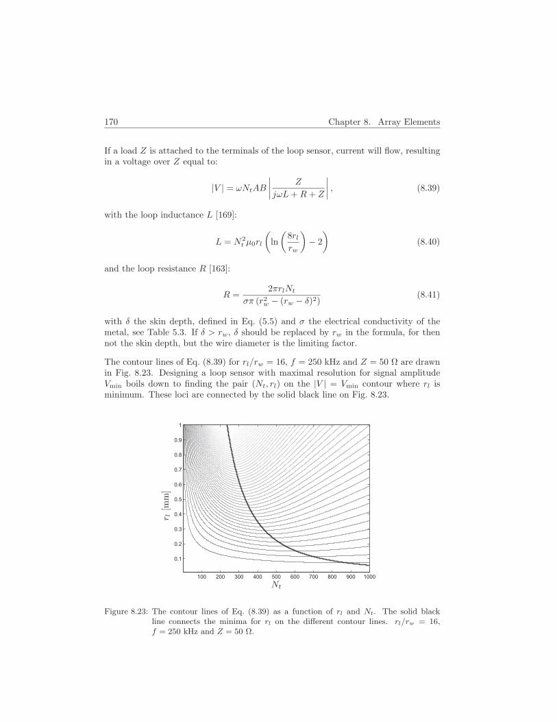
170 Chapter 8. Array Elements
If a load Z is attached to the terminals of the loop sensor, current will flow, resultingin a voltage over Z equal to:
|V | = ωNtAB
∣∣∣∣Z
jωL+R+ Z
∣∣∣∣ , (8.39)
with the loop inductance L [169]:
L = N2t µ0rl
(ln
(8rlrw
)− 2
)(8.40)
and the loop resistance R [163]:
R =2πrlNt
σπ (r2w − (rw − δ)2)(8.41)
with δ the skin depth, defined in Eq. (5.5) and σ the electrical conductivity of themetal, see Table 5.3. If δ > rw, δ should be replaced by rw in the formula, for thennot the skin depth, but the wire diameter is the limiting factor.
The contour lines of Eq. (8.39) for rl/rw = 16, f = 250 kHz and Z = 50 Ω are drawnin Fig. 8.23. Designing a loop sensor with maximal resolution for signal amplitudeVmin boils down to finding the pair (Nt, rl) on the |V | = Vmin contour where rl isminimum. These loci are connected by the solid black line on Fig. 8.23.
100 200 300 400 500 600 700 800 900 1000
0.1
0.2
0.3
0.4
0.5
0.6
0.7
0.8
0.9
1
Nt
r l[m
m]
Figure 8.23: The contour lines of Eq. (8.39) as a function of rl and Nt. The solid blackline connects the minima for rl on the different contour lines. rl/rw = 16,f = 250 kHz and Z = 50 Ω.

8.4. Maximal Resolution Sensor 171
The optimum value for Nt is a trade off between increasing Nt to increase the inducedvoltage of Eq. (8.38), and decreasing Nt to lower L ∝ N2
t and R ∝ Nt, avoiding that|jωL+R| |Z| in the denominator of Eq. (8.39).
Still, not all (Nt, rl) pairs found as the minimum on the appropriate contour arevalid. Eq. (8.39) implies that the total wire length of the loop is small to avoid signalcancellation due to phase differences over the loop:
Nt2πrl <λH
10or Ntrl <
λH
20π=
c
10ωH(8.42)
with c the speed of light. Due to the inverse proportionality with ω, this inequalitycondition only has to be validated for fH , the upper bound of the intended frequencyband.
Moreover, for similar reasons, explained in more detail in Sect. 8.4.2, the resonancefrequency of the system fres, consisting of loop sensor and measuring device, shouldbe higher than ten times the highest frequency in the working frequency band:
fres =1
2π√LtotCtot
=1
2π
√N2
t L1,Nt=1
(Ctt
Nt+ CZ
) > 10fH (8.43)
with CZ the capacitive part of Z. The capacitance between two turns Ctt can becalculated with Eq. (8.12). The inductance of one turn (in the absence of the otherturns) is given in Eq. (H.2). Filling in Eq. (8.12) and (H.2) into Eq. (8.43) results in:
λ
10> 2π
√Ntrl
√√√√(ln
(8rl
rw
)− 2
)(2π2rl + NtCZ
ε0ln (α)
)
ln (α)(8.44)
with α =d
2rw+
√(d
2rw
)2
− 1
In conclusion, in the general case, for arbitrary values of Z, the minima for rl onthe contour lines of Eq. (8.39) must be sought for: e.g. by a minimum search, in the(Nt, rl) domain bound by the conditions Eq. (8.42) and (8.44), for all frequencies inthe [fL, fH ] interval. Sect. 8.4.1.3 provides additional details.
8.4.1.1.2 Ideal Case: Z = ∞ In the ideal13 case that no load is attached to theloop sensor, the voltage between its terminals simply equals the voltage induced bythe varying magnetic field, see Eq. (8.38).
13This case is ideal in the sense that the voltage measured over the loop terminals is maximal.Any load between the terminals would cause a current through the loop, resulting in a smaller loopvoltage.
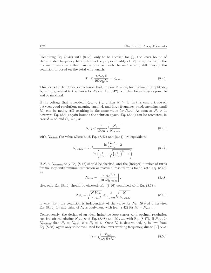
172 Chapter 8. Array Elements
Combining Eq. (8.42) with (8.38), only to be checked for fL, the lower bound ofthe intended frequency band, due to the proportionality of |V | ∝ ω, results in themaximum amplitude that can be obtained with the best sensor, still obeying thecondition imposed on the total wire length:
|V | ≤ πc2ωLB
100ω2HNt
= Vmax. (8.45)
This leads to the obvious conclusion that, in case Z = ∞, for maximum amplitude,Nt = 1. rl, related to the choice for Nt via Eq. (8.42), will then be as large as possibleand A maximal.
If the voltage that is needed, Vmin < Vmax, then Nt ≥ 1. In this case a trade-offbetween good resolution, meaning small A, and large frequency band, meaning smallNt, can be made, still resulting in the same value for NtA. As soon as Nt > 1,however, Eq. (8.44) again bounds the solution space. Eq. (8.44) can be rewritten, incase Z = ∞ and CZ = 0, as:
Ntrl <c
10ωH
√Nt
Nswitch(8.46)
with Nswitch the value where both Eq. (8.42) and (8.44) are equivalent:
Nswitch = 2π2ln
(8rl
rw
)− 2
ln
(d
2rw+
√(d
2rw
)2
− 1
) . (8.47)
If Nt > Nswitch, only Eq. (8.42) should be checked, and the (integer) number of turnsfor the loop with minimal dimension or maximal resolution is found with Eq. (8.45)as:
Nmax =
⌊πωLc
2B
100ω2HVmin
⌋, (8.48)
else, only Eq. (8.46) should be checked. Eq. (8.46) combined with Eq. (8.38):
Ntrl =
√NtVmin
πωLB<
c
10ωH
√Nt
Nswitch(8.49)
reveals that this condition is independent of the value for Nt. Stated otherwise,Eq. (8.46) for any value of Nt is equivalent with Eq. (8.42) for Nt = Nswitch.
Consequently, the design of an ideal inductive loop sensor with optimal resolutionconsists of: calculating Nmax with Eq. (8.48) and Nswitch with Eq. (8.47). If Nmax ≥Nswitch, then Nt = Nmax, else Nt = 1. Once Nt is determined, rl follows fromEq. (8.38), again only to be evaluated for the lower working frequency, due to |V | ∝ ω:
rl =
√Vmin
ωLBπNt. (8.50)
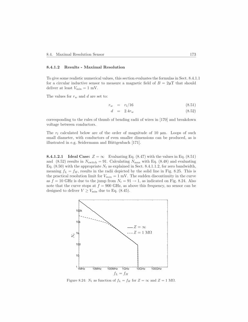
8.4. Maximal Resolution Sensor 173
8.4.1.2 Results - Maximal Resolution
To give some realistic numerical values, this section evaluates the formulas in Sect. 8.4.1.1for a circular inductive sensor to measure a magnetic field of B = 2µT that shoulddeliver at least Vmin = 1 mV.
The values for rw and d are set to:
rw = rl/16 (8.51)
d = 2.4rw (8.52)
corresponding to the rules of thumb of bending radii of wires in [170] and breakdownvoltage between conductors.
The rl calculated below are of the order of magnitude of 10 µm. Loops of suchsmall diameter, with conductors of even smaller dimensions can be produced, as isillustrated in e.g. Seidermann and Buttgenbach [171].
8.4.1.2.1 Ideal Case: Z = ∞ Evaluating Eq. (8.47) with the values in Eq. (8.51)and (8.52) results in Nswitch = 91. Calculating Nmax with Eq. (8.48) and evaluatingEq. (8.50) with the appropriate Nt as explained in Sect. 8.4.1.1.2, for zero bandwidth,meaning fL = fH , results in the radii depicted by the solid line in Fig. 8.25. This isthe practical resolution limit for Vmin = 1 mV. The sudden discontinuity in the curveas f = 10 GHz is due to the jump from Nt = 91 → 1, as indicated on Fig. 8.24. Alsonote that the curve stops at f = 900 GHz, as above this frequency, no sensor can bedesigned to deliver V ≥ Vmin due to Eq. (8.45).
1MHz 10MHz 100MHz 1GHz 10GHz 100GHz1
10
100
1k
10k
100k
fL = fH
Nt
Z = ∞Z = 1 MΩ
Figure 8.24: Nt as function of fL = fH for Z = ∞ and Z = 1 MΩ.
174 Chapter 8. Array Elements
1MHz 10MHz 100MHz 1GHz 10GHz 100GHz0
1
2
3
4
5
6x 10
fL = fH
r l[µ
m]
Z = ∞Z = 1 MΩ
Figure 8.25: Minimum rl as a function of fL = fH for Z = ∞ and Z = 1 MΩ.
Fig. 8.26 depicts the loop radius in case fL is fixed and fH is varied from 1MHz →10 GHz. This figure nicely illustrates the trade-off between resolution and workingfrequency band. At a certain value for fH , no sensor can be designed to deliverV ≥ Vmin due to Eq. (8.45) and the curve goes to zero. The curve has no meaning forvalues of fH < fL and is hence set to zero. The flat part in the curves correspondswithNt = 1. For zero bandwidth, Fig. 8.25, the radius decreased again with increasingfrequency after the steep rise, due to the proportionality of V with ω in Eq. (8.38).For a non-zero bandwidth, fL limits the resolution, resulting in the flat part of thecurve.
Effects of the parameters on the optimal resolution Eq. (8.47) reveals thatNswitch depends slightly on rw/rl and heavily on d/2rw (especially for d/2rw ≈ 1,which is often the case when winding a conductor). Indeed, for d ≈ rw the capacitanceCtt is much larger, hence Eq. (8.42) will only overrule Eq. (8.44) for a higher Nt.Fig. 8.27 plots this dependency in the interval of interest for rw/rl and d/2rw IfNswitch
drops, a higher frequency upper bound can be achieved with the sensor, although thisimplies that if the same resolution has to be kept, the lower frequency bound has togo up. Fig. 8.28 shows the effect of varying ratio d/2rw on the resolution.
8.4.1.2.2 General Case: Arbitrary Z As soon as a load is attached to thesensor, the resolution is equal to or worse than in the ideal case of no load over theloop. This is due to the division in Eq. (8.39).

8.4. Maximal Resolution Sensor 175
100MHz 1GHz 10GHz0
1
2
3
4
5
6x 10⁻⁴
fH
r l[m
]fL = 100 MHz fL = 1 GHz
Figure 8.26: Minimum rl for two loop sensors with varying working frequency band.
020
4060
80100
11.2
1.41.6
1.82
0
50
100
150
200
250
300
350
400
rl/rwd/2rw
Nsw
itch
Figure 8.27: Variation of Nswitch as function of rl/rw and d/2rw.
For Z = 1 MΩ, the difference in resolution is negligibly small, except for smallerfrequencies. The dashed line in Fig. 8.25 indeed deviates from the solid line below300 MHz. This is due to the difference in Nt. In case of no load Z = ∞, Nt shouldbe taken as high as possible with Eq. (8.48). In case of a finite load, however, anexcessive14 value for Nt results in a smaller loop voltage as |jωL + R| |Z| inEq. (8.39).
14From a practical point of view, Nt = 104 can be regarded as excessive too. This treatment ishowever purely mathematical as a starting point.
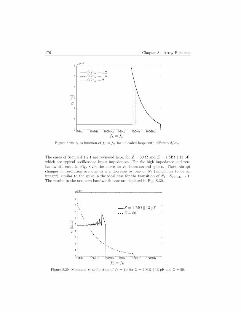
176 Chapter 8. Array Elements
1MHz 10MHz 100MHz 1GHz 10GHz 100GHz0
1
2
3
4
5
6x 10⁻⁵
fL = fH
r l[m
]d/2rw = 1.2d/2rw = 1.5d/2rw = 2
Figure 8.28: rl as function of fL = fH for unloaded loops with different d/2rw.
The cases of Sect. 8.4.1.2.1 are reviewed here, for Z = 50 Ω and Z = 1 MΩ ‖ 13 pF,which are typical oscilloscope input impedances. For the high impedance and zerobandwidth case, in Fig. 8.29, the curve for rl shows several spikes. Those abruptchanges in resolution are due to a a decrease by one of Nt (which has to be aninteger), similar to the spike in the ideal case for the transition of Nt : Nswitch → 1.The results in the non-zero bandwidth case are depicted in Fig. 8.30.
1MHz 10MHz 100MHz 1GHz 10GHz 100GHz0
1
2
3
4
5
6
7
8
9
10x 0.1
fL = fH
r l[m
m]
Z = 1 MΩ ‖ 13 pF
Z = 50
Figure 8.29: Minimum rl as function of fL = fH for Z = 1 MΩ ‖ 13 pF and Z = 50.

8.4. Maximal Resolution Sensor 177
1MHz 10MHz 100MHz 1GHz 10GHz 100GHz0
2
4
6
8
10
12
14
16
fH
r l[m
m]
fL = 0.1 MHz, Z = 1 MΩ ‖ 13 pF
fL = 0.1 MHz, Z = 50 ΩfL = 1 MHz, Z = 1 MΩ ‖ 13 pF
fL = 1 MHz, Z = 50 Ω
Figure 8.30: Minimum rl for Z = 1 MΩ ‖ 13 pF with varying working frequency band.
As the number of turns in e.g. Fig. 8.24 is impractically high for some values offL = fH , the effect of limiting Nt ≤ 30 is illustrated for the case of Z = 50 Ω inFig. 8.31. This deteriorates the resolution for lower values of fL.
1MHz 10MHz 100MHz 1GHz 10GHz 100GHz0
1
2
3
4
5
6
7
8
9
10x 0.1
fL = fH
r l[m
m]
Nt ≤ 30Nt is unbound
Figure 8.31: Minimum rl as function of fL = fH for Z = 50 Ω with and without restrictionon Nt.

178 Chapter 8. Array Elements
Effects of the parameters on the optimal resolution d/2rw now no longer hasany effect. The curves for d/rw = 1.5 and 2 coincide with the curve for d/rw = 1.2(and Z = 1 MΩ ‖ 13 pF) on Fig. 8.29. Fig. 8.32 shows the effect of varying ratiorw/rl on the resolution in case of Z = 1 MΩ ‖ 13 pF.
1MHz 10MHz 100MHz 1GHz0
1
2
3
4
5
6
7
8x 10⁻⁴
fL = fH
r l[m
]
rl/rw = 16rl/rw = 20
Figure 8.32: rl as function of fL = fH for Z = 1 MΩ ‖ 13 pF and several rw/rl.
8.4.1.3 Numerical Implementation of the Optimum Search Routine
The value of minimum rl was found by first determining the corresponding minimumvalue of rl for all values of Nt in the way described below. Afterwards the minimumrl out of this set for all values of Nt was selected.
To find the minimum value of rl for a fixed Nt, first the region in the (rl, ω) domainis determined were all conditions are satisfied. Fig. 8.33 depicts an imaginary case toillustrate the procedure. The minimum and maximum frequency, resp. ωL and ωH
bound the possible solution area with two horizontal lines, the resonance conditionEq. (8.42) bounds the r-dimension between 0 and rres.
If Nt > 1 the resonance frequency changes and also Eq. (8.44) should be satisfied.This condition, which is most restrictive for ω = ωH , bounds the r-dimension fur-ther with two vertical lines r = ri1 and r = ri2. If rres > min (ri1, ri2), the solu-tion area is bounded by the rectangle formed by the lines ω = ωL, ω = ωH , r =max (min (ri1, ri2), 0) and r = min (max (ri1, ri2), rres), in case rres < min (ri1, ri2)there is no solution.
In this solution area, the minimum rl needs to be found such that ∀ω ∈ [ωL, ωH ] thevoltage from Eq. (8.39) is at least Vmin.

8.4. Maximal Resolution Sensor 179
r
ω
ωH
ωL
rresri2ri3
W1
W2
K
∆
Figure 8.33: Graphical representation of the conditions in the ω,rl plane for the minimumrl search for a fixed Nt
As the remark on δ > rw below Eq. (8.41) indicates, the formula to calculate thisvoltage differs left and right of the curve δ = rw. With Eq. (8.51) this curve ∆can be determined. In Fig. 8.33, the contour lines for V = Vmin are drawn for thecase where δ ≥ rw and δ < rw. Left from the line ∆ the area between W1 andW2 is the valid area. Right from the ∆-line the grey colored area bounded by Kis part of the possible solution area. The shape of the contour lines is constructedto explain the next steps in the search algorithm. In most cases the contour lineshowever have a much less complex shape. Consequently not all cases implemented inthe algorithm will occur in practice, but being complete in coding avoids undefinedstates and premature program termination.
Inside this area the minimum rl can only be either 1) an intersection of the W or Kcurve with the lines w = wL and w = wH or 2) points of inflection of the W or Kcurve. For each of this points it should be checked whether the vertical line throughthe point lies completely in the feasible interval. Of all the points to which this finalcondition applies, the minimum one should chosen. This is the minimum rl for thisspecific Nt.
To allow manipulation of the contour lines in MAGMA [172]. First, the function:
|V |2 − V 2min =
∣∣∣∣ωNtπr2l B
(Z
jωL+R+ Z
)∣∣∣∣2
− V 2min = 0 (8.53)
was rewritten in polynomial form,
v4(Ntr
2l ZRδ(2rlv − aδ)
)2 (X2 + v4Y 2
)−
(Vmin
πB
)2 (X2 − v4Y 2
)2= 0 (8.54)
with:
X = ZRδ(2rlv − aδ) + 2v2arlNt/σ − v4ZRCZN2t µrlαδ(2rlv − aδ)
Y = N2t µrlαδ(2rlv − aδ) + v2ZRCZ2arlNt/σ
α = log
(8
a
)− 2 ; a =
rlrw
; v =√ω and δ =
√2
σµ
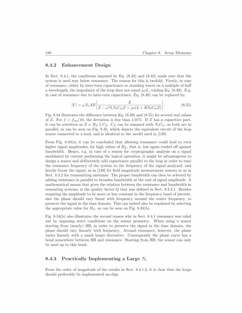
180 Chapter 8. Array Elements
8.4.2 Enhancement Design
In Sect. 8.4.1, the conditions imposed by Eq. (8.42) and (8.43) made sure that thesystem is used way below resonance. The reason for this is twofold. Firstly, in caseof resonance, either by inter-turn capacitance or standing waves on a multiple of halfa wavelength, the impedance of the loop does not equal jωL, voiding Eq. (8.39). E.g.in case of resonance due to inter-turn capacitance, Eq. (8.39) can be replaced by:
|V | = ωNtAB
∣∣∣∣Z
Z − ω2LNtCttZ + jω(L+RNtCttZ)
∣∣∣∣ . (8.55)
Fig. 8.34 illustrates the difference between Eq. (8.39) and (8.55) for several real valuesof Z. For f < fres/10, the deviation is less than 1.01%. If Z has a capacitive part,it can be rewritten as Z = RZ ‖ CZ . CZ can be summed with NtCtt, as both are inparallel, as can be seen on Fig. 8.35, which depicts the equivalent circuit of the loopsensor connected to a load, and is identical to the model used in [149].
From Fig. 8.34(a) it can be concluded that allowing resonance could lead to evenhigher signal amplitudes, for high values of RZ , that is, but again traded off againstbandwidth. Hence, e.g. in case of a sensor for cryptographic analysis on a signalmodulated by current performing the logical operation, it might be advantageous todesign a sensor and deliberately add capacitance parallel to the loop in order to tunethe resonance frequency of the system to the frequency of the signal analyzed, andhereby boost the signal, as in [149] for field magnitude measurement sensors or as inSect. 8.3.2 for transmitting antennas. The proper bandwidth can then be selected byadding resistance in parallel to broaden bandwidth at the cost of signal amplitude. Amathematical means that gives the relation between the resistance and bandwidth inresonating systems, is the quality factor Q that was defined in Sect. 8.3.2.1. Besidesrequiring the amplitude to be more or less constant in the frequency band of interest,also the phase should vary linear with frequency around the center frequency, topreserve the signal in the time domain. This can indeed also be regulated by selectingthe appropriate value for RZ , as can be seen on Fig. 8.34(b).
Fig. 8.34(b) also illustrates the second reason why in Sect. 8.4.1 resonance was ruledout by imposing strict conditions on the sensor geometry. When using a sensorstarting from (nearly) BB, in order to preserve the signal in the time domain, thephase should vary linearly with frequency. Around resonance, however, the phasevaries linearly with a much larger derivative. Consequently the phase curve has abend somewhere between BB and resonance. Starting from BB, the sensor can onlybe used up to this bend.
8.4.3 Practically Implementing a Large Nt
From the order of magnitude of the results in Sect. 8.4.1.2, it is clear that the loopsshould preferably be implemented on-chip.
8.4. Maximal Resolution Sensor 181
0.001
0.01
0.1
1
10
100
0.01 0.1 1 10 100
ω/ωres
|V|
Eq. (8.39) RZ = 0.1Eq. (8.55) RZ = 0.1Eq. (8.39) RZ = 1Eq. (8.55) RZ = 1Eq. (8.39) RZ = 100Eq. (8.55) RZ = 100
(a) Amplitude
-3
-2.5
-2
-1.5
-1
-0.5
0
0.01 0.1 1 10 100
ω/ωres
∠V
Eq. (8.39) RZ = 0.1
Eq. (8.55) RZ = 0.1
Eq. (8.39) RZ = 1
Eq. (8.55) RZ = 1
Eq. (8.39) RZ = 100
Eq. (8.55) RZ = 100
(b) Phase
Figure 8.34: The difference between Eq. (8.39) and (8.55) for several real values of Z.
Designing loops on a lossy and heterogeneous material as silicon is a topic on its own,way beyond the scope of this work. Moreover, as the number of layers is not infinite,it can be expected that the number of turns will be very limited, when implementinga loop on-chip. The best solution to this problem, is to use a spiral instead of solenoidloop.

182 Chapter 8. Array Elements
L
R
NtCtt + CZ RZ
V
Figure 8.35: Equivalent circuit of the loop sensor connected to a load.
This way, L of the loop is smaller, resulting in a smaller denominator in Eq. (8.39).Moreover, stacking turns enlarges the distance from the source, resulting in a decreaseof the magnetic field proportional to r3, from Eq. (8.1). In a spiral the area enclosedby the turns only decreases proportional to r2 with each turn added.
8.4.4 Twins
In order to improve resolution, one immediately thinks of tiny loops. In large loops,however, it is possible too to extract information on the location, but only if thesignal amplitude is known (or two measurements are recorded with different sensorlocations), and only one signal source is present. Hence this is not useful in case ofside channel analysis on chips. It is however relevant to choose the sensor location ofa large (e.g. shielded) loop with respect to the hardware, and it points out that thereis an ambiguity or crosstalk between two dipole sources at opposite sides of a loop.
Indeed, consider an electric dipole at the origin along the y axis. Moving a loopsensor along the x axis, results in a voltage amplitude depending on the loop locationas depicted in Fig. 8.36. Moving the sensor around until the zero is found, is theonly way to localize the current dipole. Indeed, due to the symmetry, except for thedifference in sign, no distinction can be made between a dipole at the left or at thesame distance at the right of the loop. Moreover, the minus sign still does not solvethe ambiguity between an electric dipole at the left of the loop and the case of adipole with opposite phase at the right of the loop. Fig. 8.37 makes this clear andalso suggest two loops in a twin configuration to solve the problem.
In case of a magnetic dipole, which is a better building block for modeling a cryp-tographic device, the curve for V is entirely symmetrical, without a reverse of sign,as can be seen on Fig 8.38. Here, again, two sensor loops are advisable as they givemore location information than a single loop.

8.4. Maximal Resolution Sensor 183
0.01 0.02−0.01−0.02
0.5
1.0
−0.5
−1.0
x [m]
V
Figure 8.36: Analytically calculated V of a loop sensor as function of x position with respectto dipole along y axis at origin. Maximum scaled to one. Loop at 1 mm abovex, y plane.
≡
(a) Flux caused by current at left or opposite current at right is equal
(b) A twin configuration of loops can solve this duality
Figure 8.37: A twin loop configuration solves location ambiguity of a dipole source.
From the same graph it is observed that the loop size should be of the order ofmagnitude of the source loop. A smaller loop will give a very low signal amplitude,again due to the small area in Eq. (8.7). A loop that is too large, will however encloseflux in both positive and negative directions, canceling out. As a consequence, fora loop with certain diameter, it is advantageous to position the loop such that thesource lies at the loop perimeter.
A last advantage of twin loops is that they can suppress noise as an unwanted flux willmost probably be caused by a source at a larger distance from the loops. The signalpicked up from this unwanted source will hence be identical for both loops. Hencedistracting the signal of both loops will suppress the noise and enhance the measuredsignal. This is of course not necessary if the measurements are performed in a shieldedenvironment. Be aware, however, that shielding is costly. All power or signal lines thatinterface between the shielded environment and the data recording devices, should beproperly filtered and will even then import unwanted signals into the measurementsetup. The only way to avoid this problem, is including the data recording devicesinto the shielded environment, and powering everything with batteries.

184 Chapter 8. Array Elements
0.01 0.02−0.01−0.02
0.5
1.0
−0.5
sensor = 0.1source
sensor = 1source
sensor = 2source
sensor = 5source
sensor = 10source
x [m]
V
Figure 8.38: Analytically calculated V of differently sized loops as function of x positionwith respect to magnetic dipole at origin. Maximum scaled to one. Sensorloop, with diameter sensor at 1 mm above x, y plane. Source magnetic dipolehas a diameter of source = 1 mm
clock line
(a) A clock line runs between both loops
clock line
(b) A clock line runs above both loops
(c) Combining both loops enhances the signal (d) Combining both loops suppresses the noise
Figure 8.39: Twin loops can be used to suppress noise.
8.5 Array Design
The essential difference with classical application of arrays, is the fact that in thisapplication the array elements are put as close as possible to the source, as otherwisethe signal is too weak. Hence the far field approximation that allowed to approximateRn as in Eq. (3.3) and ultimately led to the introduction of the array factor, is invalidin this case. Indeed, now one source is seen under different angles by the differentarray elements. Hence not only the distance, that in this case causes a huge amplitudedifference in the field strength, proportional to r3, is different. Also the orientationof the sensor, that determines the signal strength proportional to the cosine of theangle under which the source is seen, differs.
8.6. Conclusions 185
Consequently, definitely not all elements of the array will pick up a signal from onelocation in the chip with a sufficient amplitude to allow beam forming and enhancethe location sensitivity. Only the sensors in the vicinity of the source will be usefulin shaping the signal. In other words, the sensor right above the source location andall its twins (in the meaning of Sect. 8.4.4) will form the active region of the array fora certain signal source. Fortunately, digital off-line beam forming allows to monitorthe entire chip that is observed, as the recorded date of all sensors in the array canafterwards be processed active region per active region.
As opposed to in the case of classical arrays, the array topology design is straightfor-ward. The array should be a planar honeycomb. A close packing of the sensors hasto make sure that every part of the chip is covered by a sensor. This implies thatthe inter element spacing is generally much smaller than in case of an array antennafor telecommunication purposes. Indeed, now the entire half space should be covered.Implementation limitations and certainly the connection that leads away the signalpicked up by the sensors for further processing, will however complicate things, turn-ing the implementation of the straightforward topology into a research topic on itsown.
Indeed, with Eq. (5.3) the width of a micro strip line for Zc = 50 Ω on FR4 ofdt = 1 mm is 1.5 mm, which is even more than the pitch for a Small Outline Inte-grated Circuit with 8 pins (SOIC8), which is ±1.27 mm. Consequently it might beadvantageous to integrate at least some signal processing with the sensor array inorder to reduce the number of channels. Care should be taken that no informationcrucial for the side channel analysis is dropped this way. It is however not clear atthe moment of writing how to determine what information is crucial and what is not.
One advantage of the array of sensors will be that different parts of the chip can bemonitored simultaneously. Currently, most work on EM side channel analysis is donewith a single probe. A first step then consists of choosing the sensor location. Forthis, often a two dimensional map of the radiation from the chip is made by movingaround the probe above the chip, and looking at the signal amplitude or spectrumat that location. This is commonly referred to as EM cartography. One of the firstworks showing such map is [124]. The method is still popular, [173]. An array wouldbypass this time consuming step, that moreover is not guaranteed to lead to the bestlocation, as it is uncertain what signal properties correlate with the degree of successof an attack.
8.6 Conclusions
In this chapter first the specifications for a good sensor for side channel analysis weredefined. If direct radiation of the current performing the cryptographic operation isto be observed, the sensor should be a small, rigid loop sensor, with a large bandwidthand large signal amplitude.

186 Chapter 8. Array Elements
Before however coming to the design of such maximum resolution loop sensor, someexisting loop antenna types, the shielded loops and loops used for RFID, were stud-ied. The design of the maximum resolution sensor is essentially a trade-off betweenbandwidth, signal amplitude and sensor size. Indeed, to obtain a reasonable signalamplitude in case of a small sensor, multiple turns should be used. Due to inter-turncapacitance this however limits the bandwidth. For an infinite input impedance ofthe measurement device, the design of the maximum resolution sensor can be doneanalytically. For any practical value, an iterative search as proposed in this chaptershould be used.
Instead of using a single sensor, it is advised to use a twin configuration. This solvesthe location ambiguity inherently connected to magnetic dipole sources, and allowscommon mode noise suppression. This is also a first step in the direction of arrays.Indeed, with a regular grid of sensors, each loop sensor could be used in conjunctionwith all its neighboring twins. Off-line beam forming would then allow to use theseactive subregions of the array to monitor distinct parts of a cryptographic devicesimultaneously and with an improved signal-to-noise ratio.
Chapter 9
Signal Modification andCombination
With all elements in the antenna or sensor array of Chapter 8 intercepting magneticfields, the voltages from all elements should be combined into one signal for furtherprocessing.
For the application in Part II, essentially, apart from the trend of digitizing as much aspossible for cost and flexibility reasons, and the recent advances in the field of digitalbeam forming, the signal could be analog up to the demodulator, where the bit valuesare decided based on the received signal. For the application that is discussed in thispart, the information extraction does not simply follow from the digitization of theanalog signal. Sect. 9.1 will explain how recorded signals are correlated with certainvalues of a secret, let it be (a part of) the key or plaintext, in order to extractinformation from a measurement.
Consequently, the digitization should ideally be performed using an infinite amountof quantization levels, to limit the quantization noise. Moreover, it should generallybe implemented at an early stage in the signal chain, in order to obtain a high SNR.Sect. 9.2 elaborates on the sources of noise in the measurement setup. Techniquesto improve SNR, such as filtering and amplification, should be applied with care, asthey inevitably add noise to the signal as well. Sect. 9.3 will go more into detail onthis topic.
Improving SNR is ever a wise thing to do, for a single sensor as well as for an array.Sect. 9.4 narrows the discussion again to sensor arrays. In that section it is arguedthat combining the signals from the distinct elements in the array should be performedin a digital way. The limitations on sample frequency and processing power will betranslated into the spectral and spatial resolution of the system.
187
188 Chapter 9. Signal Modification and Combination
9.1 Digitization
In this section, one approach for side channel analysis is given. Many other imple-mentations or variations on the same idea are used. The only intention of this sectionis to indicate that digitization of the measured side channel signal is compulsory.
Suppose an attacker wants to obtain a secret key inside a device. One possible ap-proach to retrieve the key, is obtaining another identical device where the key can beprogrammed. By programming any possible key and measuring the EM emanation ofthe device for every key, an attacker can make up a list of template signals, hence itsname template attack, [174]. If now the EM emanation of the device with unknownkey is measured and compared to all templates of the list, the key can be found asthe key corresponding to the template signal that matches the signal of the devicewith unknown key.
In the presence of noise, it is obvious that the template signal for a certain key shouldbe an average of several measured signals for that key. The more noise, the moremeasurements should be averaged. Eventually, besides the average signal, also thestandard deviation can be stored, in order to use probability intervals instead of simplythe Euclidean distance when matching a signal to a template. In that case, maximumlikelihood decoding is performed. The probability that the measured signal occurs,under the assumption that they has a certain value, is calculated for all possible keyvalues. The key that results in the highest probability is supposed to be the keyresiding in the device.
The technique as explained above is essentially a brute force attack as all possibilitiesfor the key are to be checked. Fortunately, or unfortunately, the amount of workneeded, can be reduced by not working on the entire key, but parts (or single bits)of the key. Then, not only different templates for different key bits are needed, butfor the same key bit, different templates correspond with different values for registerswith intermediate results. Fortunately, from the plaintext, the starting state of theregisters is known. Moreover, during execution, the next register state can be derivedfrom the previous one for the possible values of the key bit. This limits the numberof possibilities and moreover provides a means of error correction. An example canbe found in [175].
In case an attacker does not have a programmable identical device at its disposal, stillother ways are possible to retrieve the secret key inside the device.
For template attacks as explained above, as well as for any other technique, distancemeasures between signals, and correlations between a secret and signals are calculated.Consequently, the measured signals must be available in a digital way to allow furthermathematical or statistical processing. An ADC is hence inevitable in a side channelanalysis measurement setup. This will in most cases be an oscilloscope due to itseasy interfacing with computers, where the computations to extract information canbe performed in mathematical software such as MATLABTM.
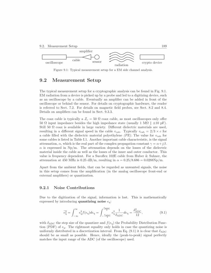
9.2. Measurement Setup 189
oscilloscopecable
amplifier
sensorradiation
crypto device
Figure 9.1: Typical measurement setup for a EM side channel analysis.
9.2 Measurement Setup
The typical measurement setup for a cryptographic analysis can be found in Fig. 9.1.EM radiation from a device is picked up by a probe and led to a digitizing device, suchas an oscilloscope by a cable. Eventually an amplifier can be added in front of theoscilloscope or behind the sensor. For details on cryptographic hardware, the readeris referred to Sect. 7.2. For details on magnetic field probes, see Sect. 8.2 and 8.4.Details on amplifiers can be found in Sect. 9.3.3.
The coax cable is typically a Zc = 50 Ω coax cable, as most oscilloscopes only offer50 Ω input impedance besides the high impedance state (usually 1 MΩ ‖ ±10 pF).Still 50 Ω coax is available in large variety. Different dielectric materials are used,resulting in a different signal speed in the cable vcab. Typically vcab = 2/3 × c fora cable filled with the dielectric material polyethylene (PE). The value for vcab forsome cables is listed in Table I.1. Another important cable characteristic, is the signalattenuation, α, which is the real part of the complex propagation constant γ = α+jβ.α is expressed in Np/m. The attenuation depends on the losses of the dielectricmaterial inside the cable as well as the losses of the inner and outer conductor. Thisvalue is frequency dependent. For a Sucoflex 102E cable from Huber & Suhner, theattenuation at 450 MHz is 0.25 dB/m, resulting in α = 0.25/8.686 = 0.0288Np/m.
Apart from the ambient fields, that can be regarded as unwanted signals, the noisein this setup comes from the amplification (in the analog oscilloscope front-end orexternal amplifiers) or quantization.
9.2.1 Noise Contributions
Due to the digitization of the signal, information is lost. This is mathematicallyexpressed by introducing quantizing noise eq:
e2q =
∫ ∞
−∞e2qf(eq)deq =
∫ δADC2
− δADC2
e2q1
δADCdeq =
δ2ADC
12, (9.1)
with δADC the step size of the quantizer and f(eq) the Probability Distribution Func-tion (PDF) of eq. The rightmost equality only holds in case the quantizing noise isuniformly distributed in a discretization interval. From Eq. (9.1) it is clear that δADC
should be as small as possible. Hence, ideally the (peak-to-peak) signal perfectlymatches the input range of the ADC (of the oscilloscope) used.
190 Chapter 9. Signal Modification and Combination
The second source of noise is the oscilloscope noise which exists out of two com-ponents. The first component is fixed Nf and caused by the oscilloscope’s front-endattenuator and amplifier. Its rms value is generally around nf,rms = 200 − 300 µV.The relative importance of this component depends on the amplitude setting. It issignificant for the most sensitive setting (lower V/div) and almost negligible for thehigher V/div settings. The second component is variable Nv and finds its origin inthe ADC. The rms value of this part nv,rms equals a few percent of the oscilloscope’sV/div setting. As such it is important for higher V/div settings but overruled bynf,rms for the most sensitive settings. Table 9.1 displays the values that were mea-sured on a Tektronix DPO7254 with full bandwidth. Indeed, limiting the bandwidthlimits the noise power, as will be explained in Sect. 9.3.1.
Table 9.1: Measured rms values of fixed and variable noise for a Tektronix DPO7254.
mV/div Zs nf [mV rms ] nv [% of mV/div]< 100 50 Ω 0.13 1.1> 100 50 Ω 0.9 1.0< 100 1 MΩ 0.27 1.5> 100 1 MΩ 0.3 1.5
The rms values can be converted into power by:
Px =x2
rms
Zs=
(√〈x2(t)〉
)2
Zs(9.2)
where Zs is the oscilloscope impedance.
Obviously, an amplifier amplifies the noise at its input by a factor Gamp = Vout/Vin,the amplification. Besides, it adds noise Nextra. The noise figure NF relates the noiseat the output of the amplifier to the noise at the input:
NFdB = 10 logNextra +NinG
NinG(9.3)
Amplifier noise consists of a fixed part and a part that is relative to the input noisepower, too. For normal use, the fixed part will be negligible, compared to the noisethat is proportional to the input noise power. Hence NF in most data sheets onlyreports on the variable part of the amplifier noise. The EMCO 7405 amplifier, forexample, is specified with G = 30 dB and NF = 3.5 dB. Moreover, NF specified onmost datasheets is only valid in matched systems. Hence, a Northon/Thevenin equiv-alent for current and voltage noise is the only correct way of modeling the noise, [176].In general NF is proportional to the gain and bandwidth of the amplifier.

9.3. Improving Signal-to-Noise Ratio 191
Each amplifier has its minimum noise source impedance, [176]. A Low Noise Amplifier(LNA) specified for 50 Ω systems can be hoped to have this minimum NF in case ofa source impedance of 50 Ω. When in doubt, the minimum noise figure impedanceshould be measured. A trade-off can be made between matching the sensor for min-imum noise and for maximum signal amplitude. Some more considerations on thiscan be found in Sect. 9.3.4.3.
9.3 Improving Signal-to-Noise Ratio
9.3.1 Filtering
As noise is present at every frequency, it is advantageous to suppress frequencies wherethe PSD of the signal is too low compared to the PSD of the noise, as in such case theoverall SNR can be improved by not including that frequency interval. An examplecould be a signal with the PSD of Fig. D.1 in the presence of white noise, which hasa PSD that is constant over all frequencies.
This is especially important in case not the direct radiation, but a modulation ontoa carrier is observed, see Sect. 7.3.3. In that case, either a heterodyne receiver or adirect down conversion scheme can be applied, see Fig. 2.1. Here, again, as explainedin Sect. 2.1 an IF stage requires appropriate filters to suppress the mirror frequencies.
A mixer-less approach, if the modulation is plain AM modulation, which is often thecase, could be to use a simple diode detector. This circuit, depicted on Fig. 9.2, usesthe non-linearity of a diode to implicitly mix down all frequencies to BB. In thatsense it is of uttermost importance to have a band pass filter in front of the diodedetector. Without it, noise of all frequencies is superimposed at BB. A LPF behindthe diode detector becomes obsolete, as the RC system acts as a LPF with 3 dB upperfrequency:
f3 dB,up =1
2πRC(9.4)
Filtering the input prior to down mixing is less important in case of mixing, againexcept for the image rejection filters. A LPF at BB prior to digitization will besufficient. Therefore, the cost that is saved by using a diode detector might be lostagain when designing the custom band pass filter needed in front of the diode detector.
Besides improving the SNR by suppressing noise, in many cases also quantizationnoise is decreased. This is because the peak-to-peak amplitude of the signal willgenerally be smaller if the bandwidth of the signal is limited.

192 Chapter 9. Signal Modification and Combination
D
R CVin Vout
Figure 9.2: Circuit of diode detector.
9.3.2 Avoiding Standing Waves
Although it might be possible, mathematically, to reconstruct1 the original signalfrom a measurement with reflections, these reflections will enlarge the peak-to-peakamplitude and hence should be avoided as they increase the quantization noise.
A detailed discussion on standing waves, reflections and oscillations in cables canbe found in Appendix I. In short, in order to avoid reflections or standing waves,at least one side of the cable between sensor and oscilloscope should be terminatedwith a load that is matched to Zc of the cable. Fig. 9.3 indeed shows that onlyin case of mismatch at both sides, standing waves are observed. It however makessome difference, whether both sides (smallest amplitude), the sensor side (largestamplitude) or the oscilloscope side is matched. This can be understood by looking atthe voltage division in Fig. 8.35 and filling in the values for R of the sensor and Z ofthe oscilloscope (after transformation over a cable with Zc and length l).
9.3.3 Amplification
Essentially two types of amplifier are available on the market: those that are matchedto 50 Ω impedances and those that have generally higher input impedance, typicallyabout a few MΩ. The first ones require no further action and can simply be connectedto an oscilloscope and to cables. The latter ones generally require adding resistors todetermine the amplification.
An example of a 50 Ω matched amplifier is the EMCO 7405 amplifier. A way to builda similar amplifier is to start from a matched amplifier IC, such as the minicircuitsMAR-6+. They can be cascaded to increase the gain. But as the output port ofthe MAR-6+ is also used as the DC bias port, DC blocking capacitors are neededbetween consecutive stages. This results in a circuit as in Fig. 9.4. Eventually theMAR-6+ can be replaced by a MAR-3+ in the last stage(s) of the amplifier. Thiscomponent can give more output power, at the cost of loosing gain. An example ofthe other category is the class E amplifier, discussed in Sect. 9.3.3.1.
1It is expected that with common signal processing techniques it is possible to extract informationand hence signal power from the reflections. A deconvolution with the system response might be agood starting point. Further details are irrelevant for this work.
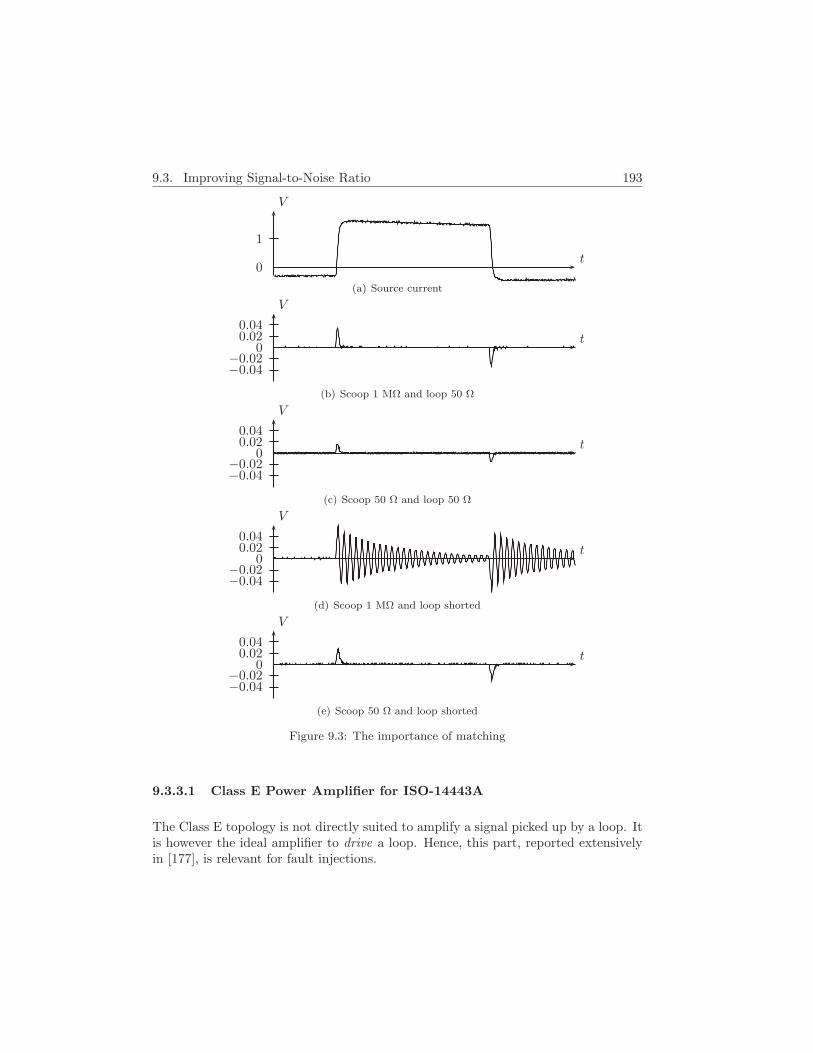
9.3. Improving Signal-to-Noise Ratio 193
0
1
t
V
(a) Source current
00.020.04
−0.02−0.04
t
V
(b) Scoop 1 MΩ and loop 50 Ω
00.020.04
−0.02−0.04
t
V
(c) Scoop 50 Ω and loop 50 Ω
00.020.04
−0.02−0.04
t
V
(d) Scoop 1 MΩ and loop shorted
00.020.04
−0.02−0.04
t
V
(e) Scoop 50 Ω and loop shorted
Figure 9.3: The importance of matching
9.3.3.1 Class E Power Amplifier for ISO-14443A
The Class E topology is not directly suited to amplify a signal picked up by a loop. Itis however the ideal amplifier to drive a loop. Hence, this part, reported extensivelyin [177], is relevant for fault injections.

194 Chapter 9. Signal Modification and Combination
in
Cblock
A06
Lbias
Rbias
Cblock
A06
Lbias
Rbias
Cblock
A06
Lbias
Rbias
Vcc
out
Figure 9.4: Possible circuit for a matched amplifier with a MAR-6+.
The application envisaged here, was amplifying the signal between an ISO-14443Areader and the antenna, see Fig. G.6 in Appendix G. To power up an RFID card withinductive coupling over great distances, very large primary coil currents are needed,which build up high coil voltages. A class E amplifier has a parallel-series tuned loadnetwork, see also Fig. 8.19, that following the discussion in Sect. 8.3.2.4 is essentiallya series RLC resonance chain with a parallel capacitor to tune the impedance. Theseries capacitor then acts as a DC decoupling capacitor which relieves the voltagestress on the transistor. The parallel capacitor adjusts the (phase of the) impedanceof the load and bypasses the transistor to guide most of the current.
9.3.3.1.1 Class E Amplifier Design Formulas As stated in [178], the class Eamplifier obtains a high power efficiency by minimizing the time in which current andvoltage exist simultaneously in the transistor. In a class D amplifier, this is obtainedby driving a parallel RLC chain with a square voltage wave. The dual of this, namelydriving a series RLC with a square current wave, is exactly what happens in a class Eamplifier.
Obviously, this requires a current source, which is in this case obtained by using achoke inductor Lchoke. Fig. 9.5 shows the basic class E topology. As opposed to e.g. incase of the class A amplifier, where the transistor is used as a variable resistor, here thetransistor is used as a switch S. Consequently the transistor is driven by a square waveswitching the transistor between off state and saturation. The series resonance chainof a capacitor Cser, inductor L, and resistor R is connected in parallel with capacitorCpar to compensate for the phase so that the current is zero, with derivative of zero,when switching the transistor into saturation.
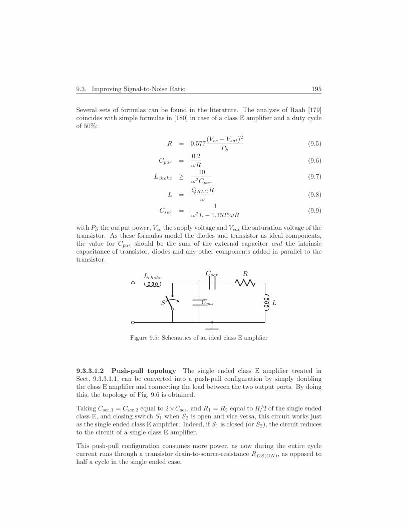
9.3. Improving Signal-to-Noise Ratio 195
Several sets of formulas can be found in the literature. The analysis of Raab [179]coincides with simple formulas in [180] in case of a class E amplifier and a duty cycleof 50%:
R = 0.577(Vcc − Vsat)
2
PS(9.5)
Cpar =0.2
ωR(9.6)
Lchoke ≥ 10
ω2Cpar(9.7)
L =QRLCR
ω(9.8)
Cser =1
ω2L− 1.1525ωR(9.9)
with PS the output power, Vcc the supply voltage and Vsat the saturation voltage of thetransistor. As these formulas model the diodes and transistor as ideal components,the value for Cpar should be the sum of the external capacitor and the intrinsiccapacitance of transistor, diodes and any other components added in parallel to thetransistor.
S
Lchoke
Cpar
Cser R
L
Figure 9.5: Schematics of an ideal class E amplifier
9.3.3.1.2 Push-pull topology The single ended class E amplifier treated inSect. 9.3.3.1.1, can be converted into a push-pull configuration by simply doublingthe class E amplifier and connecting the load between the two output ports. By doingthis, the topology of Fig. 9.6 is obtained.
Taking Cser,1 = Cser,2 equal to 2×Cser, and R1 = R2 equal to R/2 of the single endedclass E, and closing switch S1 when S2 is open and vice versa, this circuit works justas the single ended class E amplifier. Indeed, if S1 is closed (or S2), the circuit reducesto the circuit of a single class E amplifier.
This push-pull configuration consumes more power, as now during the entire cyclecurrent runs through a transistor drain-to-source-resistance RDS(ON), as opposed tohalf a cycle in the single ended case.

196 Chapter 9. Signal Modification and Combination
Vcc
S1 S2
Lchoke,1 Lchoke,2
Cpar,1 Cpar,2Cdist
R1 R2Cser,1 Cser,2L
Figure 9.6: The topology of a push-pull class E amplifier.
The current drawn from the source also increases, requiring the switch transistorsto conduct more current. The transistor currents can be partially reduced by redis-tributing Cpar by adding a Cdist drawn in dashed on Fig. 9.6 as explained in [181].Fortunately the current through the loop increases too, as now during the entire cycle,one end node of the series chain is excited.
9.3.3.1.3 Modulation The class E amplifier of Sect. 9.3.3.1.1 was able to am-plify a continuous sine wave. For the ISO-14443A communication, data has to bemodulated onto this sine carrier with ASK, see Appendix G. This can be done bymodulating the voltage on the power supply [182]. Changing the amplitude of thesquare wave on the transistor gate is not an option, because shutting down the class Etransistor causes the continuous current delivered by the choke inductor to charge Cpar
to a value that breaks the transistor.
The power can be modulated by adding a switch transistor Smod between the powersource and the power line of the class E amplifier. The gate of this transistor is drivenby a gate driver controlled by the modulation signal (envelope). In case the envelopeis high, the switch must close, otherwise the switch must be open.
If the use of a gate driver is inappropriate, e.g. because no additional power supplyvoltage is available, the driver can be implemented by the circuit in Fig. 9.7, wherethe envelope signal is applied to a transistor Senv that switches the voltage at thegate of Smod between Vcc and VccRb/(Ra +Rb).
As the current in the choke inductor of the class E amplifier only varies slowly, thecurrent will not immediately drop when the modulation circuit opens the transistor inthe power line. This delay adds up to the influence of the quality factor QRLC of theload of the class E amplifier and should be kept low in order to be able to silence thecarrier when needed. Therefore it is advised to keep the value of the choke inductorLchoke low.
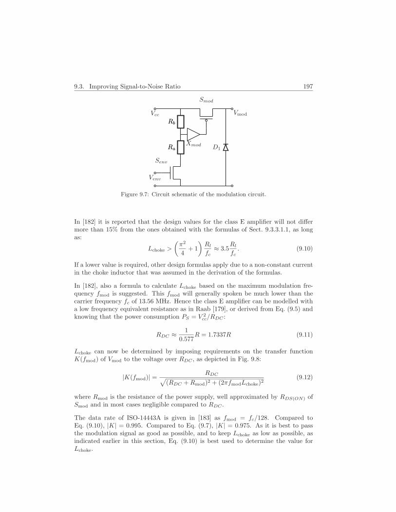
9.3. Improving Signal-to-Noise Ratio 197
Senv
Ra
Rb
Ra
Rb
Smod
Xmod D1
Venv
Vcc Vmod
Figure 9.7: Circuit schematic of the modulation circuit.
In [182] it is reported that the design values for the class E amplifier will not differmore than 15% from the ones obtained with the formulas of Sect. 9.3.3.1.1, as longas:
Lchoke >
(π2
4+ 1
)Rl
fc≈ 3.5
Rl
fc. (9.10)
If a lower value is required, other design formulas apply due to a non-constant currentin the choke inductor that was assumed in the derivation of the formulas.
In [182], also a formula to calculate Lchoke based on the maximum modulation fre-quency fmod is suggested. This fmod will generally spoken be much lower than thecarrier frequency fc of 13.56 MHz. Hence the class E amplifier can be modelled witha low frequency equivalent resistance as in Raab [179], or derived from Eq. (9.5) andknowing that the power consumption PS = V 2
cc/RDC :
RDC ≈ 1
0.577R = 1.7337R (9.11)
Lchoke can now be determined by imposing requirements on the transfer functionK(fmod) of Vmod to the voltage over RDC , as depicted in Fig. 9.8:
|K(fmod)| =RDC√
(RDC +Rmod)2 + (2πfmodLchoke)2(9.12)
where Rmod is the resistance of the power supply, well approximated by RDS(ON) ofSmod and in most cases negligible compared to RDC .
The data rate of ISO-14443A is given in [183] as fmod = fc/128. Compared toEq. (9.10), |K| = 0.995. Compared to Eq. (9.7), |K| = 0.975. As it is best to passthe modulation signal as good as possible, and to keep Lchoke as low as possible, asindicated earlier in this section, Eq. (9.10) is best used to determine the value forLchoke.

198 Chapter 9. Signal Modification and Combination
∼Vmod
Rmod Lchoke
RDC
Figure 9.8: Equivalent low frequency scheme of the class E amplifier to determine Lchoke
When opening the switch in the power line of the class E amplifier, the current throughthe choke inductor can not change immediately, causing the voltage over the inductorto change abruptly. To prevent break down of Smod due to an excessive VDS , a diodecan be added. This component keeps Vmod equal to zero, at least until the chokecurrent is zero. After the choke current becomes zero, the voltage at both sides of thechoke is equal and Vmod will follow the voltage of the drain of the class E transistor,as can be seen on Fig. 9.9. If Smod, an IRF9530 in our design, is not modelled asa switch but with its spice model as supplied by the vendor, its capacitances causea resonance in series with the choke inductor in the absence of a diode. With theES1D diode, Vmod again stays zero until the choke current becomes zero and thenagain Vmod starts oscillating due to the series resonance of the choke inductor and thecapacitances of the IRF9530 and the diode.
1.896 1.898 1.9 1.902 1.904 1.906 1.908 1.91 1.912
x 10−4
−20
0
20
40
60
80
100
120
−0.5
0
0.5
1
1.5
2
2.5
Time [s]
VD
S,V
mod
[V]
I choke
[A]
VDS IRF510Vmod
Ichoke
Figure 9.9: Ichoke and drain voltages of the IRF510 and Smod.

9.3. Improving Signal-to-Noise Ratio 199
1.896 1.898 1.9 1.902 1.904 1.906 1.908 1.91 1.912
x 10−4
−80
−60
−40
−20
0
20
40
60
80
100
Time [s]
VD
S,V
mod
[V]
With DiodeWithout DiodeVDS of IRF510
Figure 9.10: The drain voltage of the IRF9530 with and without the diode.
Adding another transistor switch between Vmod and the ground that closes when theIRF9530 opens and vice versa, instead of using a diode, is a better solution as thisachieves the same without the risk of oscillation of Vmod.
9.3.3.1.4 Determining Cser and Cpar The two turn antenna of [150] or Ta-ble 8.5 was used to load the amplifier. Hence L = 2.2 µH and Rl = 2 Ω. Theformulas in Sect. 9.3.3.1.1 combined with the remarks in Sect. 9.3.3.1.2 then lead toCser = 130 pF and Cpar = 439 pF. The actual values differ from these values asindicated in Sect. 9.3.3.1.1: the intrinsic output capacitance of the transistor addsto the effective Cpar of the circuit. This output capacitance Coss can be retrievedfrom the data sheet [184], but will vary with the voltage VDS , as does the junctioncapacitance Cj of the diodes with varying bias Vbias [185]:
Cj =Cj0(
1 − Vbias
Vj
)m (9.13)
with Cj0 the junction capacitance when no voltage is applied, Vj the intrinsic junctionvoltage depending on the doping and m a constant indicating the type of junction.Hence the effective output capacitance for a voltage swing can be obtained e.g. via thetechnique explained in [186] where essentially the transistor is biased and connectedin series with a resistor, allowing the derivation of drain-to-source capacitance CDS
by measuring the RC time constant.
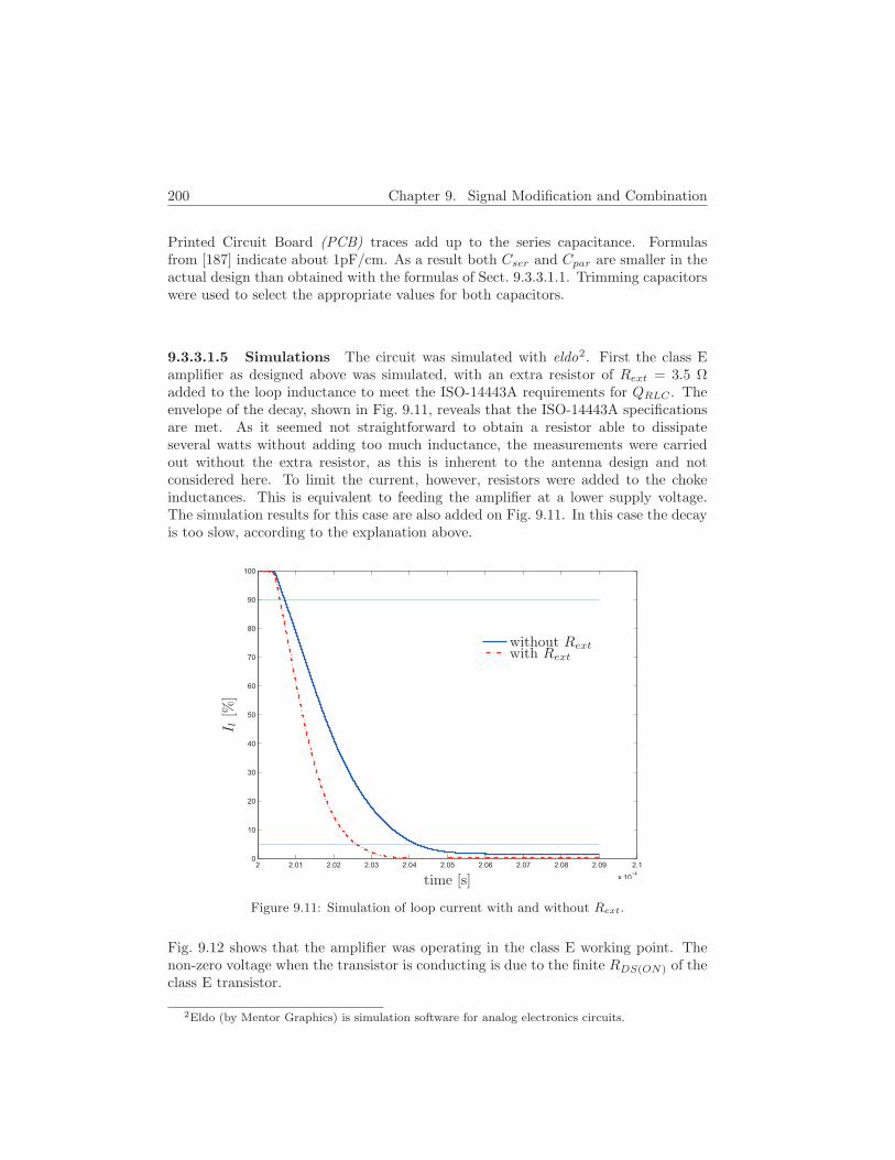
200 Chapter 9. Signal Modification and Combination
Printed Circuit Board (PCB) traces add up to the series capacitance. Formulasfrom [187] indicate about 1pF/cm. As a result both Cser and Cpar are smaller in theactual design than obtained with the formulas of Sect. 9.3.3.1.1. Trimming capacitorswere used to select the appropriate values for both capacitors.
9.3.3.1.5 Simulations The circuit was simulated with eldo2. First the class Eamplifier as designed above was simulated, with an extra resistor of Rext = 3.5 Ωadded to the loop inductance to meet the ISO-14443A requirements for QRLC . Theenvelope of the decay, shown in Fig. 9.11, reveals that the ISO-14443A specificationsare met. As it seemed not straightforward to obtain a resistor able to dissipateseveral watts without adding too much inductance, the measurements were carriedout without the extra resistor, as this is inherent to the antenna design and notconsidered here. To limit the current, however, resistors were added to the chokeinductances. This is equivalent to feeding the amplifier at a lower supply voltage.The simulation results for this case are also added on Fig. 9.11. In this case the decayis too slow, according to the explanation above.
2 2.01 2.02 2.03 2.04 2.05 2.06 2.07 2.08 2.09 2.1
x 10−4
0
10
20
30
40
50
60
70
80
90
100
time [s]
I l[%
]
without Rextwith Rext
Figure 9.11: Simulation of loop current with and without Rext.
Fig. 9.12 shows that the amplifier was operating in the class E working point. Thenon-zero voltage when the transistor is conducting is due to the finite RDS(ON) of theclass E transistor.
2Eldo (by Mentor Graphics) is simulation software for analog electronics circuits.
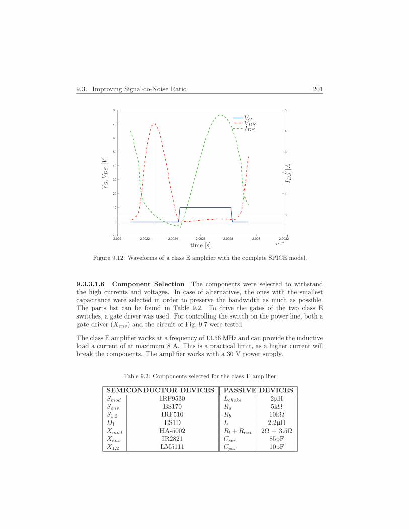
9.3. Improving Signal-to-Noise Ratio 201
2.002 2.0022 2.0024 2.0026 2.0028 2.003 2.0032
x 10−4
−10
0
10
20
30
40
50
60
70
80
−1
0
1
2
3
4
5
time [s]
VG,V
DS
[V]
I DS
[A]
VGVDSIDS
Figure 9.12: Waveforms of a class E amplifier with the complete SPICE model.
9.3.3.1.6 Component Selection The components were selected to withstandthe high currents and voltages. In case of alternatives, the ones with the smallestcapacitance were selected in order to preserve the bandwidth as much as possible.The parts list can be found in Table 9.2. To drive the gates of the two class Eswitches, a gate driver was used. For controlling the switch on the power line, both agate driver (Xenv) and the circuit of Fig. 9.7 were tested.
The class E amplifier works at a frequency of 13.56 MHz and can provide the inductiveload a current of at maximum 8 A. This is a practical limit, as a higher current willbreak the components. The amplifier works with a 30 V power supply.
Table 9.2: Components selected for the class E amplifier
SEMICONDUCTOR DEVICES PASSIVE DEVICESSmod IRF9530 Lchoke 2µHSenv BS170 Ra 5kΩS1,2 IRF510 Rb 10kΩD1 ES1D L 2.2µHXmod HA-5002 Rl +Rext 2Ω + 3.5ΩXenv IR2821 Cser 85pFX1,2 LM5111 Cpar 10pF
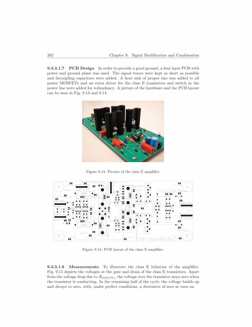
202 Chapter 9. Signal Modification and Combination
9.3.3.1.7 PCB Design In order to provide a good ground, a four layer PCB withpower and ground plane was used. The signal traces were kept as short as possibleand decoupling capacitors were added. A heat sink of proper size was added to allpower MOSFETs and an extra driver for the class E transistors and switch in thepower line were added for redundancy. A picture of the hardware and the PCB layoutcan be seen in Fig. 9.13 and 9.14.
Figure 9.13: Picture of the class E amplifier.
Figure 9.14: PCB layout of the class E amplifier.
9.3.3.1.8 Measurements To illustrate the class E behavior of the amplifier,Fig. 9.15 depicts the voltages at the gate and drain of the class E transistors. Apartfrom the voltage drop due to RDS(ON), the voltage over the transistor stays zero whenthe transistor is conducting. In the remaining half of the cycle, the voltage builds upand decays to zero, with, under perfect conditions, a derivative of zero at turn on.

9.3. Improving Signal-to-Noise Ratio 203
4 5 6 7 8 9 10 11 12 13
x 10−8
−5
0
5
10
15
20
25
30
35
time [s]
VG,V
DS
[V]
VG
VDS
Figure 9.15: Gate and drain voltage of the class E transistors.
The signal picked up with a commercial magnetic field probe [143] kept parallel ata distance of 30 cm above the center point of the transmitting loop, is representedin Fig. 9.17. The measured peak-to-peak voltage of approximately 100 mV corre-sponds to a magnetic field strength of 0.63 A/m. To build up this field, the loopcarries 2.8 A. A maximum read out distance of 21.79 cm can be inferred from this.Fig. 9.16 illustrates that the decay does not completely comply with the ISO-14443recommendations. This is due to the lack of an external resistor, a choice that wasmade in Sect. 9.3.3.1.5. To obtain a modulated signal, given in Fig. 9.16, an envelopewas applied to the gate driver Xenv of the Smod transistor.
Performing these measurements was a very tedious experience as things tended tobreak continuously. Indeed, when one component fails, this causes an over currentin all connected components, breaking nearly the entire circuit. Eventually, someprotection was included by adding current limiting resistors between the gate driversand the class E transistors. Addition of thermal circuit breakers, or control systemsbased on Current Sensing Resistors (CSR) is unavoidable if any further action withthe circuit is intended. The use of a current mirror can be considered as well, thishowever consumes twice as much power as in the controlling branch the same currentruns as in the controlled branch. Hence it is not recommendable for a circuit thatconsumes 8 A. With a current mirror, the modulation circuit of Fig. 9.7 is replacedby the one in Fig. 9.18.
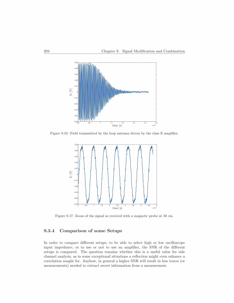
204 Chapter 9. Signal Modification and Combination
0.8 0.9 1 1.1 1.2 1.3 1.4 1.5
x 10−5
−0.05
−0.04
−0.03
−0.02
−0.01
0
0.01
0.02
0.03
0.04
0.05
time [s]
Vl[V
]
Figure 9.16: Field transmitted by the loop antenna driven by the class E amplifier.
0 0.5 1 1.5 2 2.5 3 3.5 4 4.5 5
x 10−7
−0.05
−0.04
−0.03
−0.02
−0.01
0
0.01
0.02
0.03
0.04
0.05
time [s]
Vl[V
]
Figure 9.17: Zoom of the signal as received with a magnetic probe at 30 cm.
9.3.4 Comparison of some Setups
In order to compare different setups, to be able to select high or low oscilloscopeinput impedance, or to use or not to use an amplifier, the SNR of the differentsetups is compared. The question remains whether this is a useful value for sidechannel analysis, as in some exceptional situations a reflection might even enhance acorrelation sought for. Anyhow, in general a higher SNR will result in less traces (ormeasurements) needed to extract secret information from a measurement.
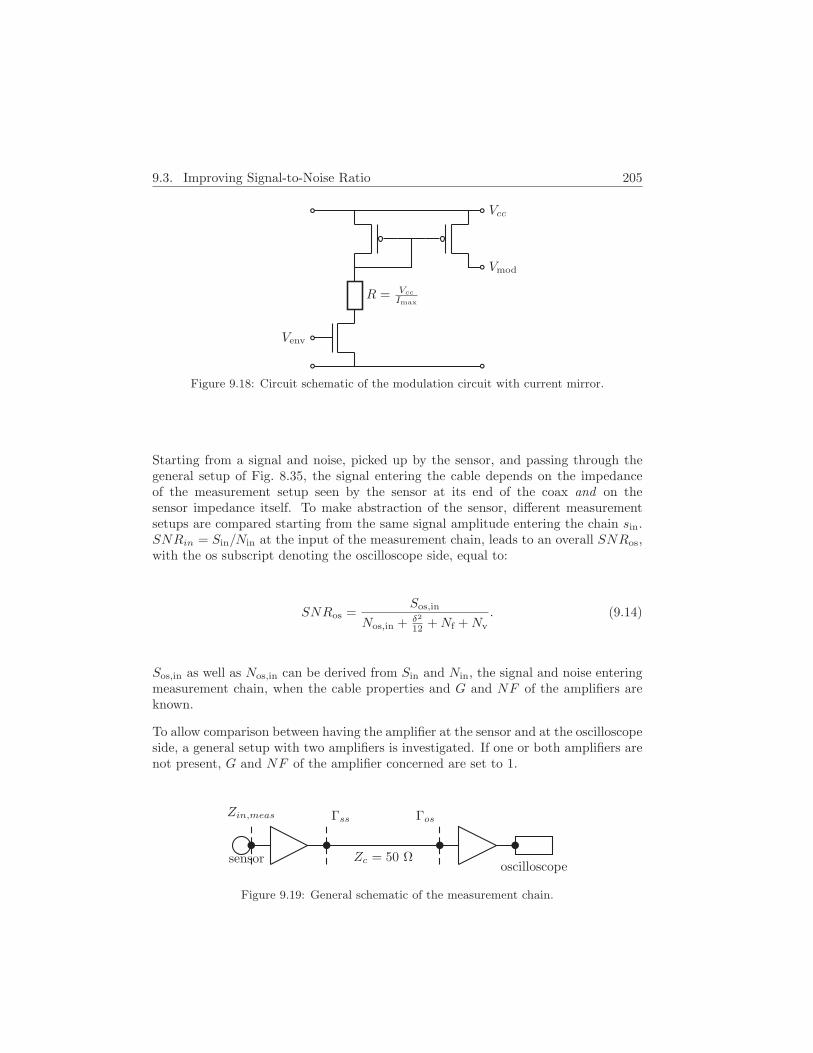
9.3. Improving Signal-to-Noise Ratio 205
Vcc
Venv
R = Vcc
Imax
Vmod
Figure 9.18: Circuit schematic of the modulation circuit with current mirror.
Starting from a signal and noise, picked up by the sensor, and passing through thegeneral setup of Fig. 8.35, the signal entering the cable depends on the impedanceof the measurement setup seen by the sensor at its end of the coax and on thesensor impedance itself. To make abstraction of the sensor, different measurementsetups are compared starting from the same signal amplitude entering the chain sin.SNRin = Sin/Nin at the input of the measurement chain, leads to an overall SNRos,with the os subscript denoting the oscilloscope side, equal to:
SNRos =Sos,in
Nos,in + δ2
12 +Nf +Nv
. (9.14)
Sos,in as well as Nos,in can be derived from Sin and Nin, the signal and noise enteringmeasurement chain, when the cable properties and G and NF of the amplifiers areknown.
To allow comparison between having the amplifier at the sensor and at the oscilloscopeside, a general setup with two amplifiers is investigated. If one or both amplifiers arenot present, G and NF of the amplifier concerned are set to 1.
sensor
Zin,meas Γss
Zc = 50 Ω
Γos
oscilloscope
Figure 9.19: General schematic of the measurement chain.

206 Chapter 9. Signal Modification and Combination
9.3.4.1 Oscilloscope Side at 50 Ω Impedance
The unknowns in Eq. (9.14) become, including both amplifiers of Fig. 9.19:
Sos,in = e−2αlGlin,1Glin,2Sin (9.15)
Nos,in = e−2αl(NFlin,1 +
NFlin,2−1Glin,1
)Glin,1Glin,2Nin (9.16)
with subscript lin denoting linear quantities as opposed to dB.
9.3.4.2 Oscilloscope Side at 1 MΩ input impedance
When the oscilloscope (with amplifier in front) has an input impedance of 1 MΩ, areflection due to mismatch between oscilloscope and characteristic impedance of thecable occurs. If then the sensor side impedance neither matches Zc of the cable, aninfinite number of delayed version of the signal arrive at the oscilloscope. This isexplained in detail in Appendix I. Depending on whether these delayed reflectionsare considered as useful signal or as noise, this leads to a different value for the Sos,in
and Nos,in.
9.3.4.3 Simulation Results and Conclusions
SNRos of Eq. (9.14) was calculated and simulated (with random time signals) inMATLABTM for the setup of Fig. 9.19 for different cases. As an example, the resultsfor a cable of l = 0.3 m are depicted in Fig. 9.20. In all cases the oscilloscope usedwas the Tektronix DPO7254, with noise contributions as in Table 9.1. The amplifierused was the EMCO 7405, discussed in Sect. 9.2.1. The setups are:
• case 1: oscilloscope at 50 Ω input impedance, no amplifier
• case 2: oscilloscope at 50 Ω input impedance, with amplifier
• case 3: oscilloscope at 1 MΩ input impedance, reflections regarded as signal
• case 4: oscilloscope at 1 MΩ input impedance, reflections regarded as noise
For small peak-to-peak signal amplitudes Vpp, an amplifier is advantageous, as am-plification allows to use the entire range of the ADC of the oscilloscope at the mostsensitive setting. For large signals, even without amplifier the signal spans the rangeof the ADC. In such case, an amplifier should not be used as it will inevitably addextra noise. Introducing a mismatch and hence causing reflections is advantageous atlower values for Vpp as then again the range of the ADC can be spanned because ofamplitude increase. From a certain value of Vpp onwards, however, a signal increasewill not result in a better SNR.

9.4. Digital time shifting 207
−5
0
50 1 2 3 4 5
0
0.5
1
1.5
2
SNRin,dB Vpp [mV]
SNR
os,
lin case 2
case 1
case 3
case 4
Figure 9.20: SNRos for four different setups.
In this comparison, the signal as entering the signal chain was supposed to be inde-pendent of the input impedance of the measurement setup. When taking the voltagedivision of sensor and measurement setup input impedance into account, also thedependence of amplifier noise figure on the source impedance should be taken intoaccount. Indeed, not the signal amplitude, but SNR should be maximized.
9.4 Digital time shifting
Where the other topics discussed in this chapter are applicable to single sensor setupstoo, this section narrows the discussion to setups of sensor arrays. As mentioned inSect. 9.1 the signal picked up by the sensor should be digitized. Sect. 8.5 learnedthat the signals of the different sensors should be digitized separately to allow off-linebeam forming. This way multiple beams can be extracted from the measured sensorsignals and hence multiple parts of the cryptographic hardware can be monitoredsimultaneously.
As the signal can be supposed to be wide band when observing the direct radiationof the currents performing the cryptographic operations, the signal shaping methodshould preserve wide band signals. As the signal is digitized per element, digital timeshifting is the most obvious way of (off-line) beam forming.

208 Chapter 9. Signal Modification and Combination
When time delay beam forming is performed in real time, e.g. by switching in andout delay lines of different lengths, the digital nature of the technique introduceserrors and approximations similar to those mentioned in Sect. 3.4.2. If however,signal recombination is done off-line with computers, the sampling frequency of theADC only limits the bandwidth of the system. The spatial resolution is unaffectedby the digitization. Indeed, by simply interpolating the signals, any time delay canbe applied, resulting in a spatial distance between two source points that is onlylimited by computational power. Adding interpolation points obviously increasesboth processing and memory demands. SNR and the spatial sensitivity of the sensorelement will have a much larger impact on the spatial resolution of the sensor array.
9.5 Conclusions
The aim of this chapter was to provide a systematic way of selecting the appropri-ate devices and parameter settings in a measurement setup for side channel analy-sis. Throughout the chapter, the only figure of merit was the SNR that should bemaximized. It is unclear whether a maximum SNR at a certain point in time or amaximum mean SNR over time leads to the side channel analysis with the fewestnumber of measurements needed. Further research is needed to clarify this.
In the chapter, all noise contributions, from digitization device, amplifier and oscillo-scope were analyzed and expressed in numbers. This allowed comparison of differentsetups. This comparison made clear that if the signal is small, an amplifier should beused to make sure that the entire range of the ADC is spanned. Reflections shouldin general be avoided, even in case of small signals, as they will only improve SNRin a haphazard way. Consequently, at least one side of the cable between sensor andoscilloscope must be matched.
If an amplifier is used that is matched to 50 Ω at input and output port, the am-plifier can be placed at the sensor side, at the oscilloscope side or even halfway thecable without any difference in performance. If the amplifier has a high input andoutput impedance, it should be inserted at the oscilloscope side and the sensor shouldbe matched to 50 Ω. The ideal setup however has an amplifier with a high in-put impedance connected to the sensor, as this results in the highest resolution, seeSect. 8.4, and an output impedance of 50 Ω driving the signal on the cable to theoscilloscope that is set to an input impedance of 50 Ω as this was measured in thischapter to give the smallest variable oscilloscope noise.
Although the comparison of measurement setups was useful for systems with a singlesensor too, it is a necessary step to take in array design as well. Sensor arrays forside channel analysis will use off-line digital time shifting as beam forming techniqueso that in that case too the signals from the individual sensor elements are to betransported, in a way that preserves SNR as much as possible, to the digitizing device.

Part IV
Conclusions
209


211
In this work, the classical array antenna theory was reviewed and applied to twodifferent applications. The general array theory was derived from the properties ofFourier transform of the source function that consisted of three dimensional Diracimpulses with a complex amplitude that reflects the amplitude and phase of theexcitation. This way effect of topology, amplitude tapering and phase excitation werecoherently restated in terms of Fourier transform properties. The different ways ofbeam forming, time delay, phase shift and frequency change, as well as the differentways of implementing in the receiving chain, namely at radio frequencies, intermediatefrequencies and baseband, were compared regarding performance and cost.
The first application, satellite communication, was introduced and the benefit of elec-tronic beam steering over mechanical pointing was clarified. Next some peculiaritiesof designing for space were reviewed. Then the three parts of an array antenna, beingantenna elements, phase shifters and combining network were discussed. From thiswork can be concluded that the challenges when applying array antennas to satel-lite communication are not scientific questions but rather design, development andengineering issues. What requires special attention, is designing antenna and beamsteering hardware to withstand the hostile space environment. Another difficulty ofthis application is that gain should be maximized for low elevation angle as in thiscase, the satellite-to-ground station distance is largest and hence the free space pathloss at maximum.
For the second application, electromagnetic side channel analysis, the link betweencurrents performing cryptographic calculations and the leakage of information over theside channel of electromagnetic radiation from the chip was established. Specificationsfor the ideal sensor were made up, for monitoring direct radiation from the currents aswell as for analysis via a modulated signal. Much work was done on designing sensors.Some existing types, such as shielded loops and radio frequency identification coilswere investigated. The design of small loops, for obtaining a high spatial resolution,was investigated as well. Besides the sensor, the other components of the measurementchain, being cable, amplifier and digitizing device, were analyzed as well, in order tocharacterize all noise sources in the measurement setup.
The second application, electromagnetic side channel analysis, differs much from thefirst one, satellite communication, regarding the application of array antennas. Firstlybecause the distance between signal source and array is not large enough to justify theapproximations made when deriving classical array antenna theory. This also resultsin a much smaller inter element spacing in the case of side channel analysis. Secondly,this application would benefit from off-line beam forming, which allows multi beamconfigurations, or, stated differently, simultaneously monitoring of the different activeparts in the cryptographic hardware. In order to achieve this, a way has to be foundto bring out and process multiple signals. Eventually, signals could be combined insignal processing hardware integrated with the sensor array. Care should however betaken that this way no information crucial to the process of side channel analysis isdropped.

212
Yet a third difference with classical array antennas, is that in the sensor array it isnot useful to combine the signals of all array elements into one signal. Ideally, for theoff-line processing, the signal of all elements should be digitized separately. And evenin the off-line recombinations will only signals from parts of the array be combinedinto one signal. This is somehow related to MIMO systems.
As spatial resolution is of main importance, it can be expected that the array ofsensors is best implemented in a silicon device. This will not be straightforwardas silicon is definitely not the best antenna substrate, neither regarding losses norregarding predictability of electrical parameters.
As it is obvious that still some years of research are needed to make this sensor arrayon chip available, meanwhile, side channel analysis on modulated signals should notbe discarded. Contemporary work is much like looking for a needle in a haystack.Currently it is unclear whether the amount of information in a signal can be eval-uated without actually performing a side channel analysis. It is unlikely that thesensor should be positioned relative to the cryptographic device where the amplitudeis largest. It might sound more logical to look for sensor positions where spectralcomponents appear that do not appear elsewhere. A study of the spectra emitted bycryptographic hardware might lead to a more scientific standard methodology.
In this text, the measurement setup was studied thoroughly which led to formulas andcurves to compare the signal-to-noise ratio in different setups. From this comparisonit can be concluded that for small signals, it is advantageous to use an amplifier andreflections should be avoided. However, from assessment of orders of magnitude ofradiation, it would be possible to derive specifications for amplifiers and digitizingdevices, ideally in relation with the number of measurements needed for a successfulside channel analysis.
Much of the material in this work is a review of work that can be found elsewhere,but from a different point of view or applied in a case study. A few topics, however,can be regarded as new contributions to science. For the satellite communicationapplication, the idea of Doppler shift compensation by frequency scanning, and themethod to design a linear equally spaced array to maximize gain under low elevationangle, both resulted in a publication. For the side channel analysis, not much work onarray antennas was carried out, due to the lack of theoretical background and a goodsensor element. Hence these gaps were filled first. A review of shielded loops andtheir matching, and a mathematical study on the spatial resolution limit of magneticsensors were published.
In this work, whenever appropriate, the developed theory was materialized in de-signs. A radio frequency identification reader loop antenna, a class E amplifier anda KeeLoq transceiver where built and tested. Measurements on a modular arrayantenna illustrated the array theory.

213
Future Work
When given time, many more interesting things, both enjoyable and useful, couldhave been investigated. A more in depth mathematical study of the effect of phaseapproximations on array radiation patterns, would be very useful to decide on how wellperforming digital phase shifters, and their control chain, have to be, in order not to bethe limiting factor. The further development of the combined balanced-mœbius sensorseems to be very promising. A study of spectra emitted by cryptographic devicesresulting in a standard methodology for side channel analysis on modulated signals,will be inevitable to make up standard tests for fast screening of vulnerability levelof cryptographic devices to electromagnetic side channel analysis. The translation ofsignal-to-noise ratio in measurement setups to the number of measurements neededfor side channel analysis, will make clear whether or not signal-to-noise ratio is auseful measure to compare measurement setups.
It can be hoped, that it is only a matter of years until side channel analysis onmodulated signals will not reveal any secret information. With the advances in securelogic styles and the awareness of the need for applying best practice design methodsfrom electromagnetic compatibility theory, this can indeed be expected. Hence for thelong term, the development of an on chip sensor array is imperative. The road aheadwill be bumpy. Implementing loop sensors on silicon will not be straightforward.Neither will interfacing the sensor array with the digitization devices over decenttransmission lines. Eventually integrated signal processing can be considered
Once this sensor array will be available, it will still be a challenge to apply theappropriate weight functions to combine the signals of parts of the array into signalsuseful for side channel analysis. Modeling of the cryptographic hardware is a first stepin understanding and predicting radiation spectra and magnitudes that are necessarilyknow when deciding on the details of the sensor array.

invisible filling

Appendices
215

Appendix A
Doppler Shift Compensationby Frequency Scanning
This appendix is [188] and evaluates Doppler shift compensation by varying the fre-quency in such way that it could also be used for frequency scanning.
A.1 Introduction
As a spacecraft might travel at high speeds, the Doppler shift of a down link signalis considerable compared to the carrier frequency. As such this Doppler shift shouldbe taken into account when down converting for demodulation. A common techniqueis to use a PLL to lock onto the signal and slowly follow the frequency shift, asin [189]. For Spread Spectrum techniques, this is not feasible and hence many signalprocessing algorithms are used to determine the actual frequency after an FFT e.g.[190], [191]. Compensating the shift at the transmitter instead of at the receiving sideis also considered, a.o. in [192].
In this paper it is mathematically shown that the Doppler shift frequency caused bythe movement of a vehicle coincides with the frequency shift needed for frequencyscanning, if the ratio of the element spacing, expressed in wavelengths in free space,over the additional line length, in wavelengths in the substrate medium, equals theratio of the vehicle speed over the speed of light. By choosing a high value for thepermittivity of the substrate, this additional line length can still be reduced by e.g.a factor of ten, but this is insufficient for practical contemporary applications. ForLEO satellites for example, this technique is inappropriate as it would require severalhundreds of meters of additional line lengths per array element, but for future spacevehicles traveling at nearly the speed of light, this technique has obvious advantages.
217

218 Appendix A. Doppler Shift Compensation by Frequency Scanning
The drawback of the method is that with only one degree of freedom, namely thevarying frequency, the beam can indeed only be steered with one degree of freedom.This is sufficient for a linear array, but a planar or any other array with dimensionmore than one needs an additional steering mechanism.
A.2 Mathematical Description
In this section the mathematical proof will be given that frequency shift needed forDoppler shift compensation can be used to perform frequency scanning of a lineararray. A discussion on the practical implications is delayed to Sect. A.3.
A.2.1 Doppler Shift
Suppose that a spacecraft, traveling at a constant speed of v0 on a trajectory thatcould have any curvature, tries to communicate with a ground station it passes by.The Doppler shift ∆fc of the carrier fc, as received by the ground station then dependson the velocity of the spacecraft towards this ground station:
vt = vo × cos (φ) (A.1)
with φ the angle between the tangent of the trajectory and a line connecting thespacecraft and ground station. Once the velocity of the source in the direction of thereceiver is established, the Doppler shift is calculated as (e.g. in [193]):
∆fc = fcvt
c− vt= fc
vo
c− vo × cos (φ)cos (φ) (A.2)
where c stands for the speed of light (≈ 3 × 10⁸ m/s).
A.2.2 Frequency Scanning
To point the beam of a directional equidistant linear array in a certain direction (angleφ), each radiating element of the antenna array should be driven with the appropriatephase shifted version of the signal. The phase difference δ between two consecutiveelements was already calculated earlier in Eq. (2.10), and restated here: (see Fig. A.1)
δ =2πd
λ0cos (φ) (A.3)
where d is the inter-element spacing and λ0 is the wavelength of the signal in freespace.
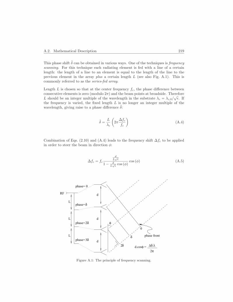
A.2. Mathematical Description 219
This phase shift δ can be obtained in various ways. One of the techniques is frequencyscanning. For this technique each radiating element is fed with a line of a certainlength: the length of a line to an element is equal to the length of the line to theprevious element in the array plus a certain length L (see also Fig. A.1). This iscommonly referred to as the series-fed array.
Length L is chosen so that at the center frequency fc, the phase difference betweenconsecutive elements is zero (modulo 2π) and the beam points at broadside. ThereforeL should be an integer multiple of the wavelength in the substrate λc = λc,0/
√ε. If
the frequency is varied, the fixed length L is no longer an integer multiple of thewavelength, giving raise to a phase difference δ:
δ =L
λc
(2π
∆fc
fc
)(A.4)
Combination of Eqs. (2.10) and (A.4) leads to the frequency shift ∆fc to be appliedin order to steer the beam in direction φ:
∆fc = fc
dL√
ε
1 − dL√
εcos (φ)
cos (φ) (A.5)
d
d
d
phase=
phase=
phase=
2δ
phase front
2π
phase= 0
∆δ.λφd.cos =
δ
δ
3δ
2δ
L
L
L
RF
φ
0
Figure A.1: The principle of frequency scanning.
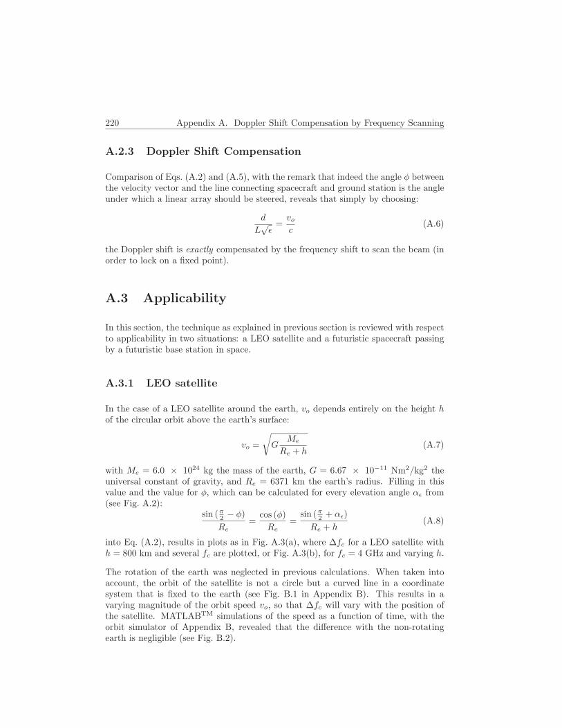
220 Appendix A. Doppler Shift Compensation by Frequency Scanning
A.2.3 Doppler Shift Compensation
Comparison of Eqs. (A.2) and (A.5), with the remark that indeed the angle φ betweenthe velocity vector and the line connecting spacecraft and ground station is the angleunder which a linear array should be steered, reveals that simply by choosing:
d
L√ε
=vo
c(A.6)
the Doppler shift is exactly compensated by the frequency shift to scan the beam (inorder to lock on a fixed point).
A.3 Applicability
In this section, the technique as explained in previous section is reviewed with respectto applicability in two situations: a LEO satellite and a futuristic spacecraft passingby a futuristic base station in space.
A.3.1 LEO satellite
In the case of a LEO satellite around the earth, vo depends entirely on the height hof the circular orbit above the earth’s surface:
vo =
√G
Me
Re + h(A.7)
with Me = 6.0 × 1024 kg the mass of the earth, G = 6.67 × 10⁻¹¹ Nm2/kg2 theuniversal constant of gravity, and Re = 6371 km the earth’s radius. Filling in thisvalue and the value for φ, which can be calculated for every elevation angle αε from(see Fig. A.2):
sin (π2 − φ)
Re=
cos (φ)
Re=
sin (π2 + αε)
Re + h(A.8)
into Eq. (A.2), results in plots as in Fig. A.3(a), where ∆fc for a LEO satellite withh = 800 km and several fc are plotted, or Fig. A.3(b), for fc = 4 GHz and varying h.
The rotation of the earth was neglected in previous calculations. When taken intoaccount, the orbit of the satellite is not a circle but a curved line in a coordinatesystem that is fixed to the earth (see Fig. B.1 in Appendix B). This results in avarying magnitude of the orbit speed vo, so that ∆fc will vary with the position ofthe satellite. MATLABTM simulations of the speed as a function of time, with theorbit simulator of Appendix B, revealed that the difference with the non-rotatingearth is negligible (see Fig. B.2).

A.4. Conclusion 221
eR
α ε
vt
ov
horizon (plane)
earth (sphere)
h
φ
orbit (circle)
Figure A.2: The geometry of a LEO satellite that passes over a ground station.
The value of the Doppler shift in the case of a LEO satellite, is hence ±0.002 % offc. Referring to Eq. (A.6), for practical arrays, where d varies between λ
2 and λ, Lshould be about 105 × λc, thus for fc in the GHz region, at least a kilometer, whichis infeasible in practice.
A.3.2 Future spacecraft and base station
Imagine a spacecraft cruising at a constant speed of about 0.1×c along a straight line,passing a base station. The same exercise over again, results in exact compensationof the Doppler shift by frequency scanning if L ≈ 5× λ. For fc = 10 GHz this wouldbe 30 cm, which is feasible.
A.4 Conclusion
Although Doppler shift and frequency scanning shift mathematically collide, in casethe linear array antenna is always aligned with the instantaneous velocity vector andthe magnitude of the velocity is constant, it is impractical to compensate for Dopplershift by frequency scanning. The practical problems when implementing the suggestedcompensation, can be solved if a component that magnifies phase shifts is found, orvanish for vehicles cruising with approximately the speed of light.
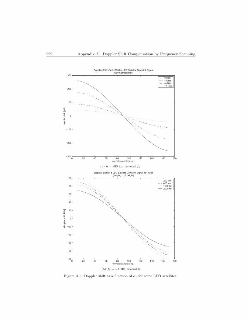
222 Appendix A. Doppler Shift Compensation by Frequency Scanning
0 20 40 60 80 100 120 140 160 180−300
−200
−100
0
100
200
300
elevation angle [deg.]
do
pp
ler
sh
ift
[kH
z]
Doppler Shift of a h=800 km LEO Satellite Downlink Signal(varying frequency)
2 GHz4 GHz8 GHz12 GHz
(a) h = 800 km, several fc
0 20 40 60 80 100 120 140 160 180−100
−80
−60
−40
−20
0
20
40
60
80
100
elevation angle [deg.]
do
pp
ler
sh
ift
[kH
z]
Doppler Shift of a LEO Satellite Downlink Signal at 4 GHz(varying orbit height)
200 km600 km1000 km2000 km
(b) fc = 4 GHz, several h
Figure A.3: Doppler shift as a function of αε for some LEO satellites.
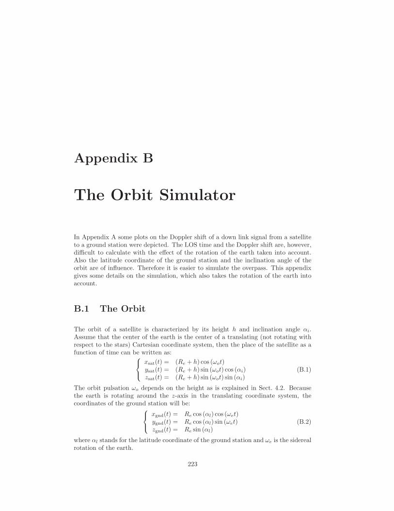
Appendix B
The Orbit Simulator
In Appendix A some plots on the Doppler shift of a down link signal from a satelliteto a ground station were depicted. The LOS time and the Doppler shift are, however,difficult to calculate with the effect of the rotation of the earth taken into account.Also the latitude coordinate of the ground station and the inclination angle of theorbit are of influence. Therefore it is easier to simulate the overpass. This appendixgives some details on the simulation, which also takes the rotation of the earth intoaccount.
B.1 The Orbit
The orbit of a satellite is characterized by its height h and inclination angle αi.Assume that the center of the earth is the center of a translating (not rotating withrespect to the stars) Cartesian coordinate system, then the place of the satellite as afunction of time can be written as:
xsat(t) = (Re + h) cos (ωot)ysat(t) = (Re + h) sin (ωot) cos (αi)zsat(t) = (Re + h) sin (ωot) sin (αi)
(B.1)
The orbit pulsation ωo depends on the height as is explained in Sect. 4.2. Becausethe earth is rotating around the z-axis in the translating coordinate system, thecoordinates of the ground station will be:
xgnd(t) = Re cos (αl) cos (ωet)ygnd(t) = Re cos (αl) sin (ωet)zgnd(t) = Re sin (αl)
(B.2)
where αl stands for the latitude coordinate of the ground station and ωe is the siderealrotation of the earth.
223
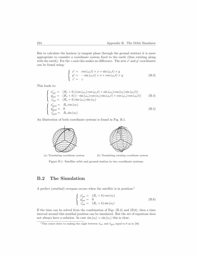
224 Appendix B. The Orbit Simulator
But to calculate the horizon (a tangent plane through the ground station) it is moreappropriate to consider a coordinate system fixed to the earth (thus rotating alongwith the earth). For the z-axis this makes no difference. The new x′ and y′ coordinatescan be found using:
x′ = cos (ωet) × x+ sin (ωet) × yy′ = − sin (ωet) × x+ cos (ωet) × yz′ = z
(B.3)
This leads to:
x′sat = (Re + h) (cos (ωo) cos (ωet) + sin (ωo) cos (αi) sin (ωet))y′sat = (Re + h) (− sin (ωo) cos (αi) sin (ωet) + cos (ωo) cos (ωet))z′sat = (Re + h) sin (ωo) sin (αi)
(B.4)
x′gnd = Re cos (αl)
y′gnd = 0
z′gnd = Re sin (αl)(B.5)
An illustration of both coordinate systems is found in Fig. B.1.
(a) Translating coordinate system (b) Translating rotating coordinate system
Figure B.1: Satellite orbit and ground station in two coordinate systems.
B.2 The Simulation
A perfect (zenithal) overpass occurs when the satellite is in position:1
x′sat = (Re + h) cos (αl)y′sat = 0z′sat = (Re + h) sin (αl)
(B.6)
If the time can be solved from the combination of Eqs. (B.4) and (B.6), then a timeinterval around this zenithal position can be simulated. But the set of equations doesnot always have a solution. In case sin (αl) > sin (αi) this is clear.
1This comes down to making the angle between ~rsat and ~rgnd equal to 0 as in [58].

B.2. The Simulation 225
Furthermore each equation of the set gives an infinite number of solutions (if any) sothat an infinite number of values must be checked in the other equations. Thereforeit is easier not to look for the solution of the perfect pass, but to look for a tsat whenthe satellite is above a place with αl:
zsat = (Re + h) sin (ωotsat) sin (αi) = (Re + h) sin (αl) (B.7)
and a tgnd 6= tsat when the ground station is exactly beneath the satellite:
xgnd = Re cos (αl) cos (ωetgnd) =Re
Re + hxsat (B.8)
This gives:
tsat =1
ωoarcsin
(sin (αl)
sin (αi)
)(B.9)
tgnd =1
ωearccos
(cos (ωotsat)
cos (αl)
)(B.10)
If the numerical calculation of tgnd is not accurate enough (not resulting in a passthat is good enough) an optimization can be done by exhaustively searching a time∆tgnd where the distance between the satellite and the ground station is nearly equalto the orbit height:
√(xsat − xgnd)2 + (ysat − ygnd)2 + (zsat − zgnd)2 = h
(1 +
∆h
h
)(B.11)
The more times that are checked, the smaller ∆h will become and thus the better theoverpass. A near overpass occurs every 30 days (∆h/h < 0.001).
When good values for tsat and tgnd are found, both times can be varied in an intervalaround the calculated values, in order to simulate the position of satellite and groundstation over this time interval. This makes it possible to calculate the Doppler shiftas the speed of the satellite towards the ground station is the derivative to time of thedistance between both. Note that the values do not differ much from those obtainedneglecting the rotation of the earth, as can be seen on Fig. B.2. Here the worst caseis taken (ground station at 0 latitude and orbit inclination equal to 180).
But also the down link time can be calculated. Knowing that the expression for thetangent plane through the ground station is:
x′gnd(x′ − x′gnd) + y′gnd(y′ − y′gnd) + z′gnd(z′ − z′gnd) = 0 (B.12)
the moment the satellite appears above the horizon will be found as the time wherethe left hand side of Eq. (B.12), with the coordinates of the satellite filled in, reversessign.
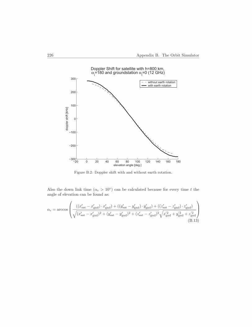
226 Appendix B. The Orbit Simulator
−20 0 20 40 60 80 100 120 140 160 180−300
−200
−100
0
100
200
300
elevation angle [deg.]
do
pp
ler
sh
ift
[kH
z]
Doppler Shift for satellite with h=800 km,α
i=180 and groundstation α
l=0 (12 GHz)
without earth rotationwith earth rotation
Figure B.2: Doppler shift with and without earth rotation.
Also the down link time (αε > 10) can be calculated because for every time t theangle of elevation can be found as:
αε = arccos
((x′sat − x′gnd) ·x′gnd) + ((y′sat − y′gnd) · y′gnd) + ((z′sat − z′gnd) · z′gnd)√
(x′sat − x′gnd)2 + (y′sat − y′gnd)2 + (z′sat − z′gnd)2√x
′2gnd + y
′2gnd + z
′2gnd
(B.13)
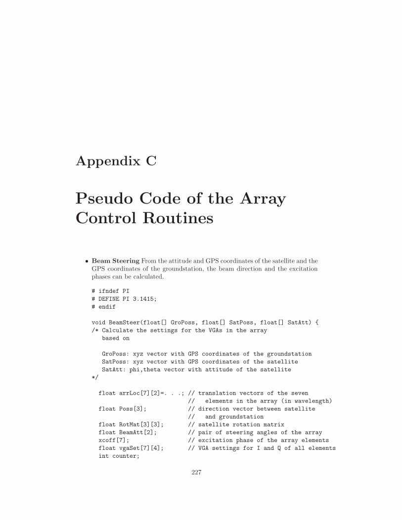
Appendix C
Pseudo Code of the ArrayControl Routines
• Beam Steering From the attitude and GPS coordinates of the satellite and theGPS coordinates of the groundstation, the beam direction and the excitationphases can be calculated.
# ifndef PI
# DEFINE PI 3.1415;
# endif
void BeamSteer(float[] GroPoss, float[] SatPoss, float[] SatAtt)
/* Calculate the settings for the VGAs in the array
based on
GroPoss: xyz vector with GPS coordinates of the groundstation
SatPoss: xyz vector with GPS coordinates of the satellite
SatAtt: phi,theta vector with attitude of the satellite
*/
float arrLoc[7][2]=. . .; // translation vectors of the seven
// elements in the array (in wavelength)
float Poss[3]; // direction vector between satellite
// and groundstation
float RotMat[3][3]; // satellite rotation matrix
float BeamAtt[2]; // pair of steering angles of the array
xcoff[7]; // excitation phase of the array elements
float vgaSet[7][4]; // VGA settings for I and Q of all elements
int counter;
227

228 Appendix C. Pseudo Code of the Array Control Routines
// Make up satellite rotation matrix
// Euler rotation with alpha=phi, beta=theta, phy=0
RotMat[1][1]=cos(SatAtt[1]);
RotMat[1][2]=-sin(SatAtt[1])*cos(SatAtt[2]);
RotMat[1][3]=sin(SatAtt[1])*sin(SatAtt[2]);
RotMat[2][1]=sin(SatAtt[1]);
RotMat[2][2]=cos(SatAtt[1])*cos(SatAtt[2]);
RotMat[2][3]=-cos(SatAtt[1])*sin(SatAtt[2]);
RotMat[3][1]=0;
RotMat[3][2]=sin(SatAtt[2]);
RotMat[3][3]=cos(SatAtt[2]);
// Find angles for the beam
for (counter=1;counter<4;counter++)
Poss[counter]=SatPoss[counter]-GroPoss[counter];
for (counter=1;counter<4;counter++)
Poss[counter]=Poss[1]*RotMat[counter][1]+
Poss[2]*RotMat[counter][2]+
Poss[3]*RotMat[counter][3];
for (counter=1;counter<4;counter++)
Poss[counter]=Poss[counter]
/sqrt((Poss[1])^2+(Poss[2])^2+(Poss[3])^2);
// Calculation of phase excitations
for (counter=1;counter<8;counter++)
xcoff[counter]=Poss[1]*arrLoc[counter][1]
+Poss[2]*arrLoc[counter][2];
vgaSet[counter][1]=cos(2*PI*xcoff[counter])
vgaSet[counter][2]=sin(2*PI*xcoff[counter]);
vgaSet[counter][3]=-sin(2*PI*xcoff[counter]);
vgaSet[counter][4]=cos(2*PI*xcoff[counter]);
// Convert to integers for VGA settings
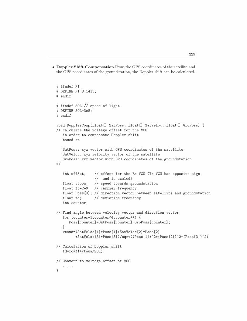
229
• Doppler Shift Compensation From the GPS coordinates of the satellite andthe GPS coordinates of the groundstation, the Doppler shift can be calculated.
# ifndef PI
# DEFINE PI 3.1415;
# endif
# ifndef SOL // speed of light
# DEFINE SOL=3e8;
# endif
void DopplerComp(float[] SatPoss, float[] SatVeloc, float[] GroPoss)
/* calculate the voltage offset for the VCO
in order to compensate Doppler shift
based on
SatPoss: xyz vector with GPS coordinates of the satellite
SatVeloc: xyz velocity vector of the satellite
GroPoss: xyz vector with GPS coordinates of the groundstation
*/
int offSet; // offset for the Rx VCO (Tx VCO has opposite sign
// and is scaled)
float vtowa; // speed towards groundstation
float fc=2e9; // carrier frequency
float Poss[3]; // direction vector between satellite and groundstation
float fd; // deviation frequency
int counter;
// Find angle between velocity vector and direction vector
for (counter=1;counter<4;counter++)
Poss[counter]=SatPoss[counter]-GroPoss[counter];
vtowa=(SatVeloc[1]*Poss[1]+SatVeloc[2]*Poss[2]
+SatVeloc[3]*Poss[3])/sqrt((Poss[1])^2+(Poss[2])^2+(Poss[3])^2)
// Calculation of Doppler shift
fd=fc*(1+vtowa/SOL);
// Convert to voltage offset of VCO
. . .
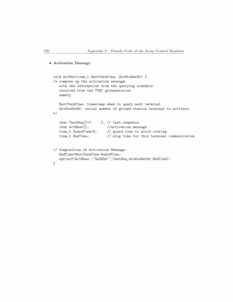
230 Appendix C. Pseudo Code of the Array Control Routines
• Activation Message
void ActMes(time_t NextTermTime, GroStaSerNr)
/* compose up the activation message
with the information from the querying schedule
received from the TT&C groundstation
namely
NextTermTime: timestamp when to query next terminal
GroStaSerNr: serial number of ground station terminal to activate
*/
char TestSeq[]=. . .; // test sequence
char ActMess[]; //activation message
time_t GuardTime=5; // guard time to avoid overlap
time_t EndTime; // stop time for this terminal communication
// Composition of Activation Message:
EndTime=NextTermTime-GuardTime;
sprintf(ActMess,‘‘%s%d%d’’,TestSeq,GroStaSerNr,EndTime);

Appendix D
Eavesdropping on ComputerDisplays
This appendix elaborates on one example of information leakage through EM radia-tion, namely on what is referred to as Van Eck phreaking.
Back in 1985 [194] was the first to deal with the subject in the open literature. Again,military and security agencies are supposed to apply the techniques much longer.But [194] suggested that with a very modest investment, the technique was availablefor anyone. This can be questioned, referring to the expensive receiving equipmentused in [195]. But tests reported in [196] clearly indicate that reconstruction ofinformation displayed on screens from a signal captured with an antenna is possible.The equipment used in [196] is considerably cheaper than the military receiver usedin [195]. But if an FPGA could be used instead of an oscilloscope, cost would decreaseeven more.
This appendix focusses on implementing the reconstruction of a screen image onFPGAs, which is an ongoing master thesis project at the moment of writing. Muchgeneral background information is omitted, as can be extensively found in [196].
D.1 Source of Radiation
Images are written on computer displays in a way similar to the way an image iswritten on a TeleVision (TV). An electron beam is scanned over the entire screen,line after line, hitting the phosphor dots that glow green, red or blue when hit by anelectron. By modulating the intensity of the electron beam, the intensity of a pixelcan be varied.
231
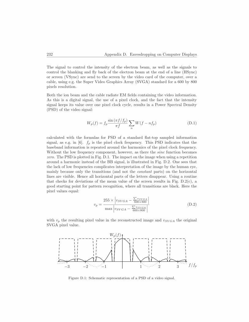
232 Appendix D. Eavesdropping on Computer Displays
The signal to control the intensity of the electron beam, as well as the signals tocontrol the blanking and fly back of the electron beam at the end of a line (HSync)or screen (VSync) are send to the screen by the video card of the computer, over acable, using e.g. the Super Video Graphics Array (SVGA) standard for a 600 by 800pixels resolution.
Both the ion beam and the cable radiate EM fields containing the video information.As this is a digital signal, the use of a pixel clock, and the fact that the intensitysignal keeps its value over one pixel clock cycle, results in a Power Spectral Density(PSD) of the video signal:
Wp(f) = fpsin (πf/fp)
πf
∑
n
W (f − nfp) (D.1)
calculated with the formulas for PSD of a standard flat-top sampled informationsignal, as e.g. in [6]. fp is the pixel clock frequency. This PSD indicates that thebaseband information is repeated around the harmonics of the pixel clock frequency.Without the low frequency component, however, as there the sinc function becomeszero. The PSD is plotted in Fig. D.1. The impact on the image when using a repetitionaround a harmonic instead of the BB signal, is illustrated in Fig. D.2. One sees thatthe lack of low frequencies complicates interpretation of the image by the human eye,mainly because only the transitions (and not the constant parts) on the horizontallines are visible. Hence all horizontal parts of the letters disappear. Using a routinethat checks for deviations of the mean value of the screen results in Fig. D.2(c), agood starting point for pattern recognition, where all transitions are black. Here thepixel values equal:
vp =255 ×
∣∣∣vSV GA −P
vSV GA
600×800
∣∣∣
max∣∣∣vSV GA −
P
vSV GA
600×800
∣∣∣(D.2)
with vp the resulting pixel value in the reconstructed image and vSV GA the originalSVGA pixel value.
1 2 3−1−2−3
Wp(f)
f/fp
Figure D.1: Schematic representation of a PSD of a video signal.
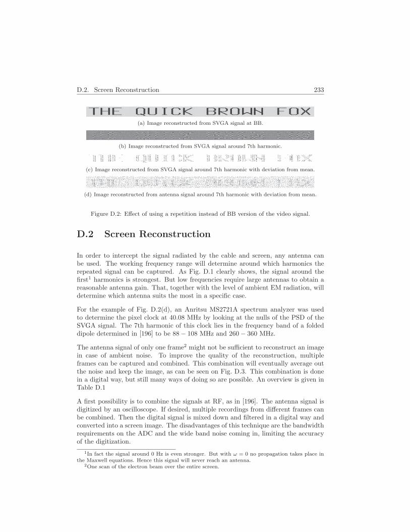
D.2. Screen Reconstruction 233
(a) Image reconstructed from SVGA signal at BB.
(b) Image reconstructed from SVGA signal around 7th harmonic.
(c) Image reconstructed from SVGA signal around 7th harmonic with deviation from mean.
(d) Image reconstructed from antenna signal around 7th harmonic with deviation from mean.
Figure D.2: Effect of using a repetition instead of BB version of the video signal.
D.2 Screen Reconstruction
In order to intercept the signal radiated by the cable and screen, any antenna canbe used. The working frequency range will determine around which harmonics therepeated signal can be captured. As Fig. D.1 clearly shows, the signal around thefirst1 harmonics is strongest. But low frequencies require large antennas to obtain areasonable antenna gain. That, together with the level of ambient EM radiation, willdetermine which antenna suits the most in a specific case.
For the example of Fig. D.2(d), an Anritsu MS2721A spectrum analyzer was usedto determine the pixel clock at 40.08 MHz by looking at the nulls of the PSD of theSVGA signal. The 7th harmonic of this clock lies in the frequency band of a foldeddipole determined in [196] to be 88 − 108 MHz and 260 − 360 MHz.
The antenna signal of only one frame2 might not be sufficient to reconstruct an imagein case of ambient noise. To improve the quality of the reconstruction, multipleframes can be captured and combined. This combination will eventually average outthe noise and keep the image, as can be seen on Fig. D.3. This combination is donein a digital way, but still many ways of doing so are possible. An overview is given inTable D.1
A first possibility is to combine the signals at RF, as in [196]. The antenna signal isdigitized by an oscilloscope. If desired, multiple recordings from different frames canbe combined. Then the digital signal is mixed down and filtered in a digital way andconverted into a screen image. The disadvantages of this technique are the bandwidthrequirements on the ADC and the wide band noise coming in, limiting the accuracyof the digitization.
1In fact the signal around 0 Hz is even stronger. But with ω = 0 no propagation takes place inthe Maxwell equations. Hence this signal will never reach an antenna.
2One scan of the electron beam over the entire screen.
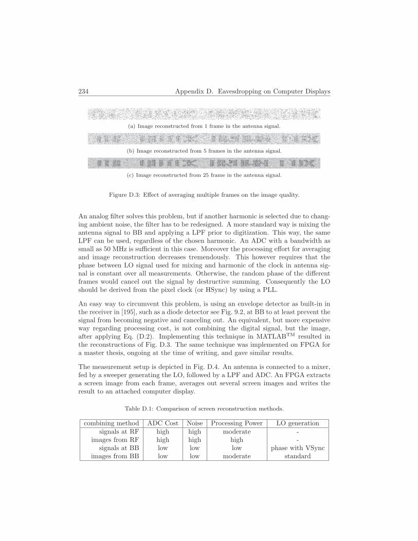
234 Appendix D. Eavesdropping on Computer Displays
(a) Image reconstructed from 1 frame in the antenna signal.
(b) Image reconstructed from 5 frames in the antenna signal.
(c) Image reconstructed from 25 frame in the antenna signal.
Figure D.3: Effect of averaging multiple frames on the image quality.
An analog filter solves this problem, but if another harmonic is selected due to chang-ing ambient noise, the filter has to be redesigned. A more standard way is mixing theantenna signal to BB and applying a LPF prior to digitization. This way, the sameLPF can be used, regardless of the chosen harmonic. An ADC with a bandwidth assmall as 50 MHz is sufficient in this case. Moreover the processing effort for averagingand image reconstruction decreases tremendously. This however requires that thephase between LO signal used for mixing and harmonic of the clock in antenna sig-nal is constant over all measurements. Otherwise, the random phase of the differentframes would cancel out the signal by destructive summing. Consequently the LOshould be derived from the pixel clock (or HSync) by using a PLL.
An easy way to circumvent this problem, is using an envelope detector as built-in inthe receiver in [195], such as a diode detector see Fig. 9.2, at BB to at least prevent thesignal from becoming negative and canceling out. An equivalent, but more expensiveway regarding processing cost, is not combining the digital signal, but the image,after applying Eq. (D.2). Implementing this technique in MATLABTM resulted inthe reconstructions of Fig. D.3. The same technique was implemented on FPGA fora master thesis, ongoing at the time of writing, and gave similar results.
The measurement setup is depicted in Fig. D.4. An antenna is connected to a mixer,fed by a sweeper generating the LO, followed by a LPF and ADC. An FPGA extractsa screen image from each frame, averages out several screen images and writes theresult to an attached computer display.
Table D.1: Comparison of screen reconstruction methods.
combining method ADC Cost Noise Processing Power LO generationsignals at RF high high moderate -
images from RF high high high -signals at BB low low low phase with VSync
images from BB low low moderate standard
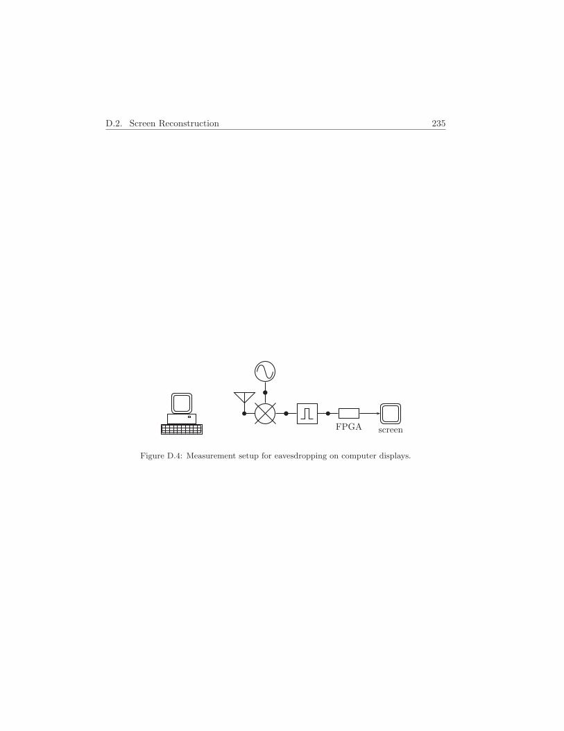
D.2. Screen Reconstruction 235
screenFPGA
Figure D.4: Measurement setup for eavesdropping on computer displays.

invisible filling
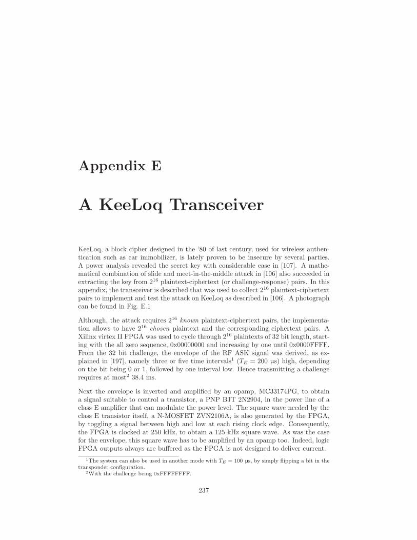
Appendix E
A KeeLoq Transceiver
KeeLoq, a block cipher designed in the ’80 of last century, used for wireless authen-tication such as car immobilizer, is lately proven to be insecure by several parties.A power analysis revealed the secret key with considerable ease in [107]. A mathe-matical combination of slide and meet-in-the-middle attack in [106] also succeeded inextracting the key from 216 plaintext-ciphertext (or challenge-response) pairs. In thisappendix, the transceiver is described that was used to collect 216 plaintext-ciphertextpairs to implement and test the attack on KeeLoq as described in [106]. A photographcan be found in Fig. E.1
Although, the attack requires 216 known plaintext-ciphertext pairs, the implementa-tion allows to have 216 chosen plaintext and the corresponding ciphertext pairs. AXilinx virtex II FPGA was used to cycle through 216 plaintexts of 32 bit length, start-ing with the all zero sequence, 0x00000000 and increasing by one until 0x0000FFFF.From the 32 bit challenge, the envelope of the RF ASK signal was derived, as ex-plained in [197], namely three or five time intervals1 (TE = 200 µs) high, dependingon the bit being 0 or 1, followed by one interval low. Hence transmitting a challengerequires at most2 38.4 ms.
Next the envelope is inverted and amplified by an opamp, MC33174PG, to obtaina signal suitable to control a transistor, a PNP BJT 2N2904, in the power line of aclass E amplifier that can modulate the power level. The square wave needed by theclass E transistor itself, a N-MOSFET ZVN2106A, is also generated by the FPGA,by toggling a signal between high and low at each rising clock edge. Consequently,the FPGA is clocked at 250 kHz, to obtain a 125 kHz square wave. As was the casefor the envelope, this square wave has to be amplified by an opamp too. Indeed, logicFPGA outputs always are buffered as the FPGA is not designed to deliver current.
1The system can also be used in another mode with TE = 100 µs, by simply flipping a bit in thetransponder configuration.
2With the challenge being 0xFFFFFFFF.
237
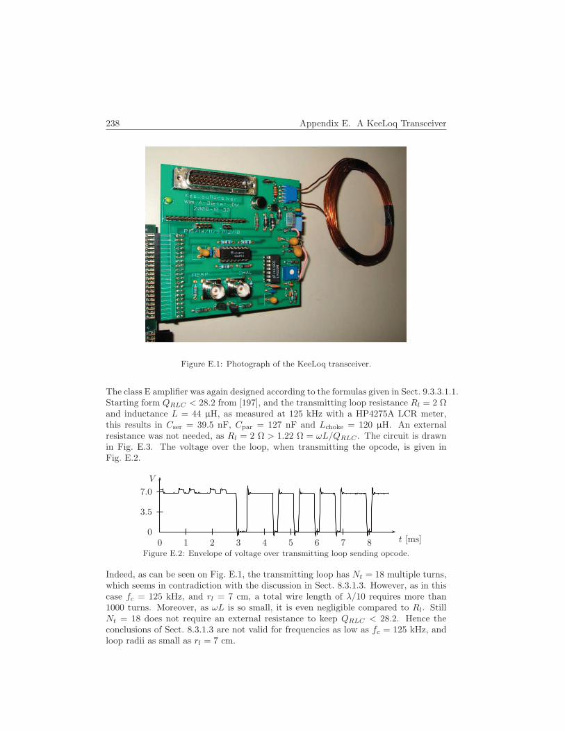
238 Appendix E. A KeeLoq Transceiver
Figure E.1: Photograph of the KeeLoq transceiver.
The class E amplifier was again designed according to the formulas given in Sect. 9.3.3.1.1.Starting form QRLC < 28.2 from [197], and the transmitting loop resistance Rl = 2 Ωand inductance L = 44 µH, as measured at 125 kHz with a HP4275A LCR meter,this results in Cser = 39.5 nF, Cpar = 127 nF and Lchoke = 120 µH. An externalresistance was not needed, as Rl = 2 Ω > 1.22 Ω = ωL/QRLC . The circuit is drawnin Fig. E.3. The voltage over the loop, when transmitting the opcode, is given inFig. E.2.
0 1 2 3 4 5 6 7 80
3.5
7.0
t [ms]
V
Figure E.2: Envelope of voltage over transmitting loop sending opcode.
Indeed, as can be seen on Fig. E.1, the transmitting loop has Nt = 18 multiple turns,which seems in contradiction with the discussion in Sect. 8.3.1.3. However, as in thiscase fc = 125 kHz, and rl = 7 cm, a total wire length of λ/10 requires more than1000 turns. Moreover, as ωL is so small, it is even negligible compared to Rl. StillNt = 18 does not require an external resistance to keep QRLC < 28.2. Hence theconclusions of Sect. 8.3.1.3 are not valid for frequencies as low as fc = 125 kHz, andloop radii as small as rl = 7 cm.
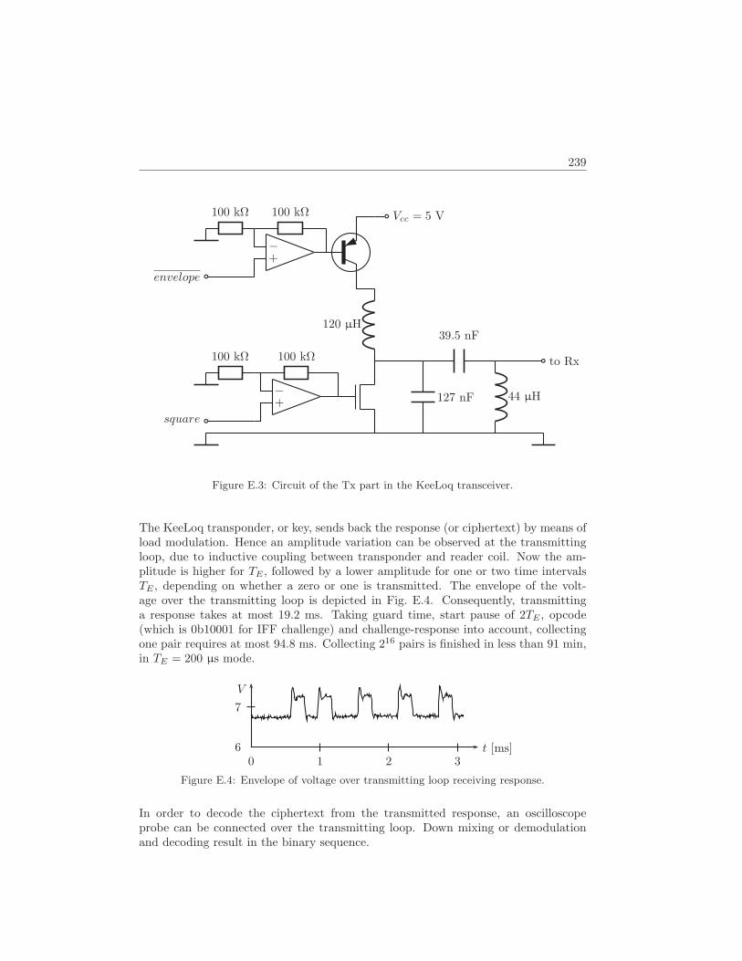
239
127 nF
39.5 nF
44 µH
120 µH
Vcc = 5 V
to Rx
square
−+
100 kΩ100 kΩ
envelope
−+
100 kΩ100 kΩ
Figure E.3: Circuit of the Tx part in the KeeLoq transceiver.
The KeeLoq transponder, or key, sends back the response (or ciphertext) by means ofload modulation. Hence an amplitude variation can be observed at the transmittingloop, due to inductive coupling between transponder and reader coil. Now the am-plitude is higher for TE , followed by a lower amplitude for one or two time intervalsTE , depending on whether a zero or one is transmitted. The envelope of the volt-age over the transmitting loop is depicted in Fig. E.4. Consequently, transmittinga response takes at most 19.2 ms. Taking guard time, start pause of 2TE , opcode(which is 0b10001 for IFF challenge) and challenge-response into account, collectingone pair requires at most 94.8 ms. Collecting 216 pairs is finished in less than 91 min,in TE = 200 µs mode.
0 1 2 36
7
t [ms]
V
Figure E.4: Envelope of voltage over transmitting loop receiving response.
In order to decode the ciphertext from the transmitted response, an oscilloscopeprobe can be connected over the transmitting loop. Down mixing or demodulationand decoding result in the binary sequence.
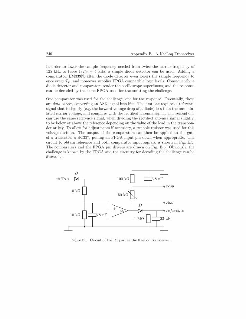
240 Appendix E. A KeeLoq Transceiver
In order to lower the sample frequency needed from twice the carrier frequency of125 kHz to twice 1/TE = 5 kHz, a simple diode detector can be used. Adding acomparator, LM339N, after the diode detector even lowers the sample frequency toonce every TE , and moreover supplies FPGA compatible logic levels. Consequently, adiode detector and comparators render the oscilloscope superfluous, and the responsecan be decoded by the same FPGA used for transmitting the challenge.
One comparator was used for the challenge, one for the response. Essentially, theseare data slicers, converting an ASK signal into bits. The first one requires a referencesignal that is slightly (e.g. the forward voltage drop of a diode) less than the unmodu-lated carrier voltage, and compares with the rectified antenna signal. The second onecan use the same reference signal, when dividing the rectified antenna signal slightly,to be below or above the reference depending on the value of the load in the transpon-der or key. To allow for adjustments if necessary, a tunable resistor was used for thisvoltage division. The output of the comparators can then be applied to the gateof a transistor, a BC337, pulling an FPGA input pin down when appropriate. Thecircuit to obtain reference and both comparator input signals, is shown in Fig. E.5.The comparators and the FPGA pin drivers are drawn on Fig. E.6. Obviously, thechallenge is known by the FPGA and the circuitry for decoding the challenge can bediscarded.
to Tx
D
10 kΩ
10 kΩ 6.8 nF
+− ∞
D
1 MΩ 22 µF
reference
chal
50 kΩ
100 kΩ 6.8 nF
resp
Figure E.5: Circuit of the Rx part in the KeeLoq transceiver.

241
+−
1 kΩ
Vcc = 5 V100 Ω
to FPGA in
+−
1 kΩ
Vcc = 5 V100 Ω
to FPGA in
reference
chal
resp
Figure E.6: Circuit to interface the Rx part with the FPGA in the KeeLoq transceiver.

invisible filling

Appendix F
A Low Cost VNA
This Appendix, part of [198], explains how to obtain a low cost VNA from an oscillo-scope and a function generator. The technique turned out to be relatively accurate.The idea for this implementation is from ir. P. Delmotte.
To measure S11, a sine wave of a certain frequency generated by an Agilent 33220Afunction generator, was applied to a RG-58 50 Ω coax cable. At the end of the cable,the loop and a scope were connected with a BNC-T connector to the end of the cable.If the input impedance of the Tektronix TDS2024 scope, namely 1 MΩ, is regardedas infinite, the signal measured with the scope is the actual voltage at the end of thecoaxial cable:
Vscope = V +1 + V −
1 = V +2 + V −
2 (F.1)
The setup and symbol conventions can be found on figure F.1.
Now S11 is found as:
S11 =V −
1
V +1
=Vscope − V +
1
V +1
(F.2)
where Vscope can be read from the scope and V +1 from the function generator. All
voltages are complex values, as the phase is also of importance. Suppose that V +
and V − have the same magnitude, but are 120 out of phase, so that |Vscope| = |V +1 |,
then S11 = 1 whereas a scalar sum would give S11 = 0.
In order to obtain a complex measurement of the voltage Vscope, the signal V +1 should
also be connected to the scope. The best way is to use another signal source, syn-chronised with the first one, that generates exactly the same sine.
243
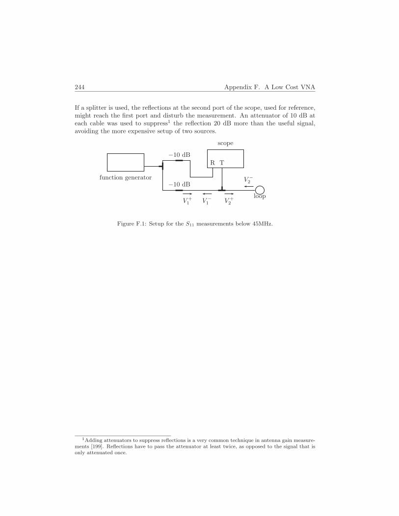
244 Appendix F. A Low Cost VNA
If a splitter is used, the reflections at the second port of the scope, used for reference,might reach the first port and disturb the measurement. An attenuator of 10 dB ateach cable was used to suppress1 the reflection 20 dB more than the useful signal,avoiding the more expensive setup of two sources.
function generator
TR−10 dB
−10 dB
loop
scope
V +1 V −
1 V +2
V −2
Figure F.1: Setup for the S11 measurements below 45MHz.
1Adding attenuators to suppress reflections is a very common technique in antenna gain measure-ments [199]. Reflections have to pass the attenuator at least twice, as opposed to the signal that isonly attenuated once.
Appendix G
RFID Basics
Radio-frequency identification (RFID) is a wireless technique to identify and trackitems. The items that should be identified or tracked are all tagged with a chipthat responds to the fields of an RFID reader by sending the requested information.Depending on the environment and the specific application, other technological im-plementations are choosen. Hence the variety of active and passive tags, inductiveand capacitive tags and LF, HF, UHF or microwave tags.
The distinction as defined in [200], specifying an active tag as a tag that is able toproduce a radio signal as opposed to a passive tag which reflects and modulates acarrier signal received from an interrogator, as by far the most convenient one. Havinga battery is not sufficient for a tag to be active. Besides sending a radio signal, abattery in an RFID tag can have many other purposes: power up sensors, loggingdata or maintaining volatile memory. A tag with battery that is not used to send aradio signal is sometimes called a Battery Assisted Passive tag (BAP).
G.1 Different Transmission Systems
Depending on the frequency, several different transmission methods are used to pro-vide a communication channel between reader and tag. The frequency and the factwether the tag is active or passive, rules in many case out some techniques anddefinitely discourages others. Nevertheless there is no one-to-one relation betweenfrequency, active or passive and the system used for the link.
245

246 Appendix G. RFID Basics
The first two techniques, inductive and capacitive coupling, suppose that tag andreader are in each others vicinity, as otherwise the modeling of the mutual inductanceor capacitance between tag and reader as lumped element, does not make sense. Thethird method, back scattering, supposes the tag to be in the far field of the readerantenna. Last method is supposed to work for small and large distance between tagand reader.
G.1.1 Inductive Coupling
Just as coils in a voltage transformer can couple magnetically and pass power fromthe primary to secondary windings, a reader with a coil or loop antenna will be ableto couple power and data to a tag with a coil or loop. Then the alternating current inthe transmitter coil will generate a magnetic field that is picked up by the receiver coiland will induce a voltage in the receiving chain. Let ZTx and ZRx be the impedanceof the transmitter and receiver and LTx, LRx, RTx and RRx the inductances andresistances of the reader and tag loop. The setup and its equivalent circuit is thendepicted in Fig. G.1. By changing the impedance of the receiver (e.g. by switching inand out some extra resistor or capacitance), the voltage over the reader coil can bealtered and information can be sent back to the reader. This technique is commonlyreferred to as load modulation.
Energy
Data
PICC
PCD(a) setup
Vreader
ZTx RTx
LTx Vinduced,tag
ZRxRRx
LRx
tag
(b) equivalent circuit
Figure G.1: Schematic representation of inductive coupling.
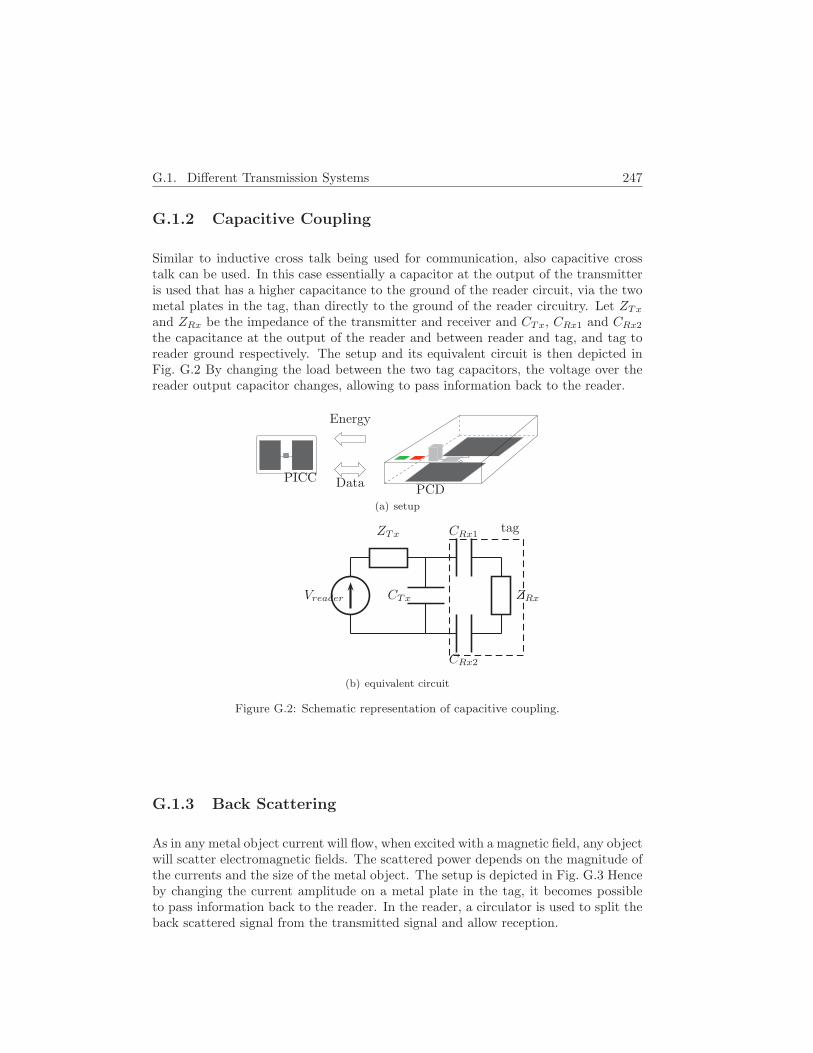
G.1. Different Transmission Systems 247
G.1.2 Capacitive Coupling
Similar to inductive cross talk being used for communication, also capacitive crosstalk can be used. In this case essentially a capacitor at the output of the transmitteris used that has a higher capacitance to the ground of the reader circuit, via the twometal plates in the tag, than directly to the ground of the reader circuitry. Let ZTx
and ZRx be the impedance of the transmitter and receiver and CTx, CRx1 and CRx2
the capacitance at the output of the reader and between reader and tag, and tag toreader ground respectively. The setup and its equivalent circuit is then depicted inFig. G.2 By changing the load between the two tag capacitors, the voltage over thereader output capacitor changes, allowing to pass information back to the reader.
Energy
DataPICCPCD
(a) setup
Vreader
ZTx
CTx
CRx1
ZRx
CRx2
tag
(b) equivalent circuit
Figure G.2: Schematic representation of capacitive coupling.
G.1.3 Back Scattering
As in any metal object current will flow, when excited with a magnetic field, any objectwill scatter electromagnetic fields. The scattered power depends on the magnitude ofthe currents and the size of the metal object. The setup is depicted in Fig. G.3 Henceby changing the current amplitude on a metal plate in the tag, it becomes possibleto pass information back to the reader. In the reader, a circulator is used to split theback scattered signal from the transmitted signal and allow reception.
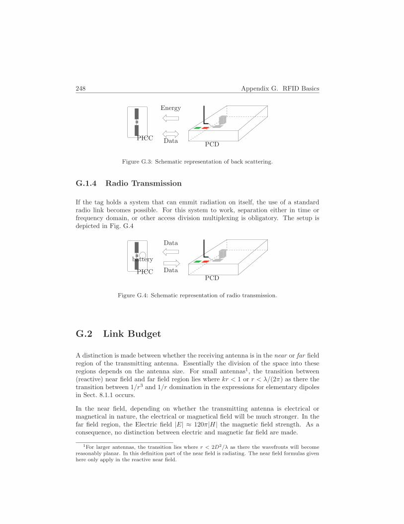
248 Appendix G. RFID Basics
Energy
DataPICCPCD
Figure G.3: Schematic representation of back scattering.
G.1.4 Radio Transmission
If the tag holds a system that can emmit radiation on itself, the use of a standardradio link becomes possible. For this system to work, separation either in time orfrequency domain, or other access division multiplexing is obligatory. The setup isdepicted in Fig. G.4
Data
DataPICCPCD
battery
Figure G.4: Schematic representation of radio transmission.
G.2 Link Budget
A distinction is made between whether the receiving antenna is in the near or far fieldregion of the transmitting antenna. Essentially the division of the space into theseregions depends on the antenna size. For small antennas1, the transition between(reactive) near field and far field region lies where kr < 1 or r < λ/(2π) as there thetransition between 1/r3 and 1/r domination in the expressions for elementary dipolesin Sect. 8.1.1 occurs.
In the near field, depending on whether the transmitting antenna is electrical ormagnetical in nature, the electrical or magnetical field will be much stronger. In thefar field region, the Electric field |E| ≈ 120π|H| the magnetic field strength. As aconsequence, no distinction between electric and magnetic far field are made.
1For larger antennas, the transition lies where r < 2D2/λ as there the wavefronts will becomereasonably planar. In this definition part of the near field is radiating. The near field formulas givenhere only apply in the reactive near field.

G.2. Link Budget 249
G.2.1 Electric Far Fields
Starting from the power transmitted by the reader PTX , the reader and tag antennagain GTX and GRX respectively, the received power can be calculated based on Friisformula:
PRX = PTX × GTXGRX
4πR2× λ2
4π(G.1)
One tends to conclude from this equation that the received power will be larger if lowerfrequencies and thus longer wavelengths are used. This is however a misperceptionas it becomes easier to build antennas with a higher gain at higher frequencies. If aparabola dish is taken as an example, this can be illustrated by looking at the formulaof the gain G of the parabola dish:
G =π2D2
λ2(G.2)
with D the diameter of the dish. At low frequencies, it becomes impractical to builda dish that is reasonable large compared to the wavelength. If a fixed physical size isused, λ falls out of the equation.
If attenuation due to trees and other obstacles, or even raindrops and gasses whenthe frequency is above 10 GHz, are taken into account, in general, the received poweris inverse proportional to the wavelength.
In the case of an active tag, equation (G.1) is valid for the tag to reader communicationas well, but in that case the tag becomes the transmitter (Tx) and the reader thereceiver (Rx). In the case of a passive tag, the power that is received by the reader,can be calculated from the power transmitted by the reader, again starting fromequation (G.1), but with addition of the scattering term [201]:
PRX = PTX × GTXGRXλ2
(4πR)24Rrad
|Za + Zc|2(G.3)
where Rrad is the radiation resistance of the tag antenna, Za and Zc the impedanceof the antenna, respectively the IC in the tag.
G.2.2 Electric Near Fields
With the reasonable assumptions that the tag is kept parallel to the reader and thatboth plates of the tag and reader have the same shape and size, CRX1 ≡ CRX2 =2 × CRX . Hence solving the circuit of Fig. G.2(b):
PRX = PTXRRXω
2C2RX
RTXω2 ((CRX + CTX)2 + ω2C2TXC
2RXZ
2RX) +RRXω2C2
RX
(G.4)

250 Appendix G. RFID Basics
Matching would require ZTX to be the complex conjugate of the load, but as CRX
changes with reading range, the load changes depending on the read out distance.Moreover the mismatch in the load is used to transfer data back.
Indeed, the voltage over CTX contains the information that modulates ZRX :
VCT X= VTX
1 + jωCRXZRX
1 − ω2CTXCRXZRXZTX + jω (CRXZRX + ZTX(CRX + CTX))(G.5)
G.2.3 Magnetic Near Fields
Looking at the circuit in Fig. G.1(b), the power transfer formula becomes:
PRX = PTXω2M2RRX
2RRX(RRX + jωLRX + ZRX)2(G.6)
In this case, again, matching is impossible due to the change of M with the read outdistance. Assuming matching in the unloaded case, i.e. ZTX = RTX − jωLTX andZRX = RRX − jωLRX , (G.6) becomes:
PRX = PTXω2M2
8RRXRTX(G.7)
which is in accordance with [160].
Again the mismatch in the tag is modulated to pass data back to the reader. Thisdata can be read out from the voltage over LTX :
VLT X= VTX
jωLTX (jωLRX +RRX + ZRX) + ω2M2
(ZTX +RTX + jωLTX)(ZRX +RRX + jωLRX) − ω2M2(G.8)
G.3 ISO-14443A RFID Standard
ISO-14443A 13.56 MHz RFID systems, defined in [183, 158, 202, 203] use inductivemagnetic coupling and a battery-less tag, as explained in Sect. G.1.1. The readeror proximity coupling device (PCD) transmits a query to the tag or proximity ICcard (PICC) by a 100 % amplitude modulated (AM) magnetic field. A pauze at thebeginning of a bit interval indicates a zero. For a one the silence starts at half theinterval. The specifications for the pauze are delineated in Fig. G.5. With 2 µs <t1 < 3 µs, t2 > 0.7 µs, t3 < 1.5 µs and t4 < 0.4 µs. The tag modulates the load withManchester encoding. A higher voltage at the reader coil during the first half bitinterval indicates a one, otherwise a zero was sent.

G.3. ISO-14443A RFID Standard 251
110%90%
60%
5%5%
60%
90%110%
t1 t3t2
t4
t
Figure G.5: Specifications of the pause in the PCD signal as defined in ISO14443
To provide enough energy to the PICC to power up, the magnetic field strength atthe tag should be at least 1.5A/m. The bit rate is 106 kbit/s.
The read out distance can not be infinite, because inductive coupling from the tagto the reader implies that the tag must be in the near field of the reader. Indeed,if the tag receives a traveling wave instead of a quasi-static field, the modificationsto the field due to the tag will never travel back to the reader. This means that thetag must be located in the reactive near field [160] around the antenna, in this caserd λ/(2π) ≈ 4 m.
Most COTS readers are designed for a reading range of 10 cm. Kfir and Wool [204]and Kirschenbaum and Wool [152] have designed a system for relay attacks and alow-cost, extended range RFID skimmer respectively. In these papers, little focus isput on the actual design of the antenna and the relevant theory to achieve larger readout distances with it. [150] filled the gap. [177] focusses on a powerful amplifier toboost the signal in between the two building blocks, reader and antenna, as shown inFig. G.6. With an extended reading range and the fact that most implementationsare Reader Talks First (RTF), it is possible that tags can be read without the ownerbeing aware of it.
AntennaClass E
RFID logic
Figure G.6: Schematic of the building blocks of the altered RFID system

invisible filling

Appendix H
Determining the Inductanceof a Coil
When modeling a coil or loop (antenna), the major parameter is the inductance of theloop L. To find this value is not straightforward, especially not if a reasonable accuracyis desired.If only an order of magnitude for L is sufficient, simply approximate L by1 µH per meter of wire used.
Many formulas can be found. They give a good approximation, but are only validfor specific types of coils, and moreover only for low frequencies i.e. only in case theperimeter of the loop is small compared to the wavelength. It is possible to calculatethe value exactly with an integral, but this becomes rapidely time consuming forlarger loops as the area in the loop must be discretized. Moreover these formulasassume a certain geometry e.g. circle or square, whereas the manufactured loop hasimperfections.
For these reasons, it is even better to measure the value for L. Several techniques canbe used, but measuring S11 and deducing Zin is the most accurate one.
H.1 Calculation
The way to calculate L, is to apply a current Il to a coil and calculate the magniticflux φB that is enclosed by the coil. For a circular loop with radius rl made of roundwire with radius rw, this leads to a numerical integration:
L =φB
Il=µ0rl2
∫ rl−rw
0
x
∫ 2π
0
rl − x cosα
(x2 + r2l − 2xrl cosα)32
dαdx (H.1)
253

254 Appendix H. Determining the Inductance of a Coil
In figure H.1 is explained how the area of the loop is integrated.
x
x
dx
rl
αdα
dI
Figure H.1: The integration over the area of the loop.
In literature an approximation for equation (H.1) is [169]:
L = µ0rl
(ln
(8rlrw
)− 2
)(H.2)
To illustrate the validity of the approximation, the result of formulas (H.1) and (H.2)are plotted on figure H.2. The numerical integral of (H.1) gives a slightly higher resultdue to the discretization. In this case 10000 division along the loop radius and 8×360angular divisions were used. With each increase the result still converged more to theresult of (H.2).
0 0.1 0.2 0.3 0.40
1
2
3
4formula (H.1)formula (H.2)
rl [m]
L [µH]
Figure H.2: L as a function of rl (rw = 0.5 mm) calculted with formulas (H.1) and (H.2).
For a solenoide, the formula:
L =r2l N
2
9rl + 10l(H.3)
with l the length of the solenoide, stays valid as long as l > 0.8rl [205].
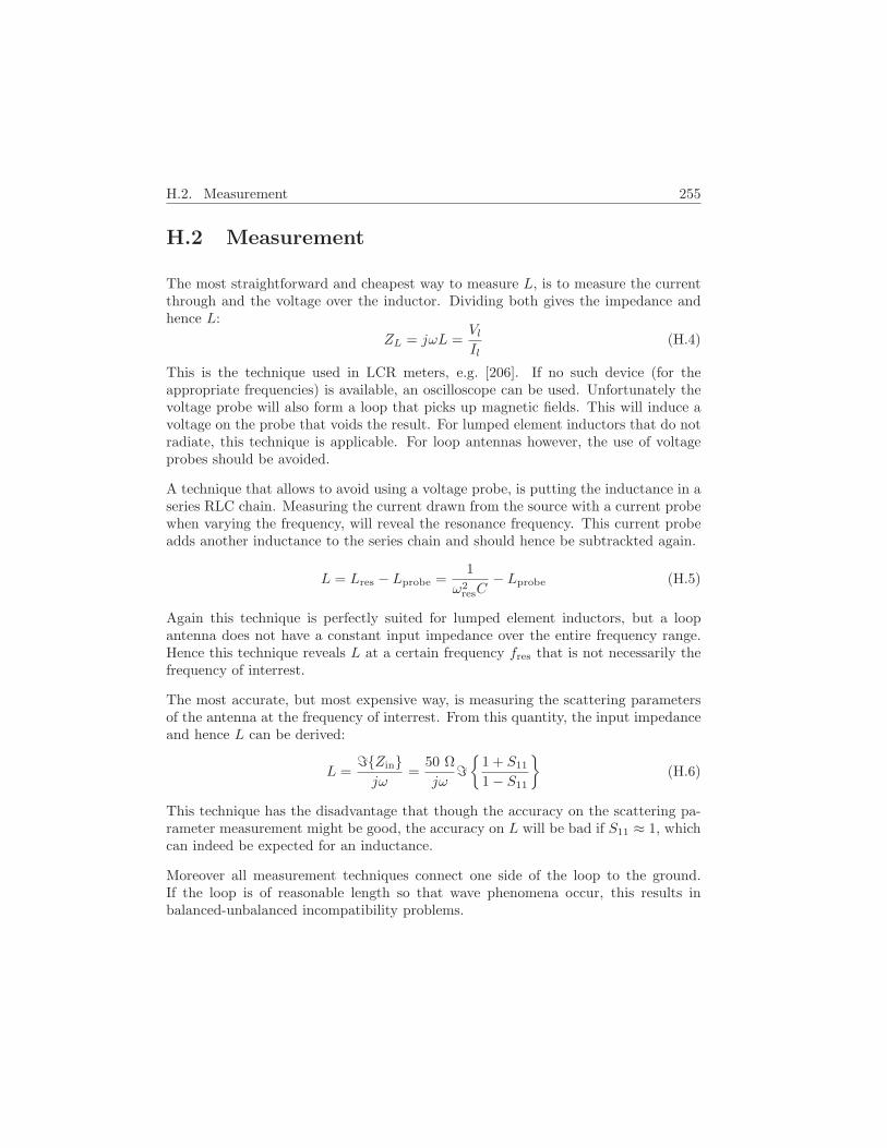
H.2. Measurement 255
H.2 Measurement
The most straightforward and cheapest way to measure L, is to measure the currentthrough and the voltage over the inductor. Dividing both gives the impedance andhence L:
ZL = jωL =Vl
Il(H.4)
This is the technique used in LCR meters, e.g. [206]. If no such device (for theappropriate frequencies) is available, an oscilloscope can be used. Unfortunately thevoltage probe will also form a loop that picks up magnetic fields. This will induce avoltage on the probe that voids the result. For lumped element inductors that do notradiate, this technique is applicable. For loop antennas however, the use of voltageprobes should be avoided.
A technique that allows to avoid using a voltage probe, is putting the inductance in aseries RLC chain. Measuring the current drawn from the source with a current probewhen varying the frequency, will reveal the resonance frequency. This current probeadds another inductance to the series chain and should hence be subtrackted again.
L = Lres − Lprobe =1
ω2resC
− Lprobe (H.5)
Again this technique is perfectly suited for lumped element inductors, but a loopantenna does not have a constant input impedance over the entire frequency range.Hence this technique reveals L at a certain frequency fres that is not necessarily thefrequency of interrest.
The most accurate, but most expensive way, is measuring the scattering parametersof the antenna at the frequency of interrest. From this quantity, the input impedanceand hence L can be derived:
L ==Zinjω
=50 Ω
jω=
1 + S11
1 − S11
(H.6)
This technique has the disadvantage that though the accuracy on the scattering pa-rameter measurement might be good, the accuracy on L will be bad if S11 ≈ 1, whichcan indeed be expected for an inductance.
Moreover all measurement techniques connect one side of the loop to the ground.If the loop is of reasonable length so that wave phenomena occur, this results inbalanced-unbalanced incompatibility problems.

invisible filling

Appendix I
Standing Waves inMeasurement Setup
When the oscilloscope is put to an input impedance of 1 MΩ, oscillations and reflec-tions occur. They are caused by the inductance of the sensor and the capacitive partof the oscilloscope input impedance, or by mismatch of both sensor and oscilloscopeto the characteristic impedance of the cable. This appendix calculates the frequencyof the standing waves in a setup of a sensor, cable and oscilloscope as a function ofsensor inductance, cable parameters and oscilloscope input impedance.
I.1 Oscillations in a parallel RLC circuit
In the case an oscilloscope is used at high input impedance, Zs = RZ + jωCZ ≈1 MΩ ‖ ±10 pF. Directly connecting an inductive sensor to the oscilloscope willadd an inductance Lss to this parallel RC network, possibly causing a parallel RLCresonance that spoils the signal to be measured. The resonance frequency is calculatedwith Eq. (8.31).
I.2 Reflections
If an inductive sensor is connected to an oscilloscope at an input impedance differentfrom the characteristic impedance Zc of the connection cable, typically 50 Ω, theimpedance mismatch between cable and oscilloscope will cause the signal on the cableto reflect back to the sensor.
257
258 Appendix I. Standing Waves in Measurement Setup
If the input impedance of the sensor neither matches the characteristic impedance ofthe cable, an infinite number of reflections will take place. Let sss(t) be the signalpicked up by the sensor, the signal seen at the oscilloscope can be written as:
sos(t) = (1 + Γos)
∞∑
n=0
e−(2n+1)lαΓnosΓ
nsssss
(t− (2n+ 1)l
vcab
)(I.1)
with α the attenuation of the cable and Γ the reflection coefficient at the oscilloscope(os) and sensor (ss) side.
Remark 1. Eq. (I.1) is only valid in case of real impedances. Complex impedancesgive rise to a different reflection coefficient Γ for each frequency component and re-quires a Fourier transform to calculate the resulting waveform.
The spectrum of this signal at the oscilloscope is:
Sos(f) = e−lαSss(f)(1 + Γos)
∞∑
n=0
(Γtot)ne
−jω(2n+1)l
vcab (I.2)
with Sss(f) = Fsss(t) the Fourier transform of the sensor signal and Γtot the re-sulting scaling factor between two consecutive arrivals of the signal at oscilloscope,e.g. without amplifier:
Γtot = e−2lαΓssΓos = e−2lα
(Zss − Zc
Zss + Zc
)(RZ − Zc − jωZcCZRZ
RZ + Zc + jωZcCZRZ
)(I.3)
This spectrum is dominated by the frequencies fref for which the additions for all nare in phase. In this case standing waves will occur. In the following equation, theleft hand side is the phase of the component at fref of the (n + 1)th-arrival of thesignal at the oscilloscope. The right hand side is the phase of the first arrival at frefwhen no reflection has occurred yet.
∀n ∈ N : n× ∠Γtot(ωref) − ωref(2n+ 1)l
vcab= −ωref
l
vcab+ k2π
∀n ∈ N : n×(
∠Γtot(ωref) − ωref2l
vcab
)= k2π (I.4)
where ∠Γtot is the phase of the scaling factor and k ∈ Z−. From this equation fref
can be solved in an iterative way and this has always a solution.
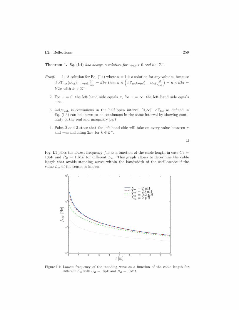
I.2. Reflections 259
Theorem 1. Eq. (I.4) has always a solution for ωres > 0 and k ∈ Z−.
Proof. 1. A solution for Eq. (I.4) where n = 1 is a solution for any value n, because
if ∠Γtot(ωref) − ωref2l
vcab= k2π then n ×
(∠Γtot(ωref) − ωref
2lvcab
)= n × k2π =
k′2π with k′ ∈ Z−
2. For ω = 0, the left hand side equals π, for ω = ∞, the left hand side equals−∞.
3. 2ωl/vcab is continuous in the half open interval [0,∞[, ∠Γtot as defined inEq. (I.3) can be shown to be continuous in the same interval by showing conti-nuity of the real and imaginary part.
4. Point 2 and 3 state that the left hand side will take on every value between πand −∞ including 2kπ for k ∈ Z
−.
Fig. I.1 plots the lowest frequency fref as a function of the cable length in case CZ =13pF and RZ = 1 MΩ for different Lss. This graph allows to determine the cablelength that avoids standing waves within the bandwidth of the oscilloscope if thevalue Lss of the sensor is known.
0 1 2 3 4 5 6 7 8 9 1010
6
107
108
109
l [m]
f ref
[Hz]
Lss = 2 nHLss = 20 nHLss = 0.2 µHLss = 2 µH
Figure I.1: Lowest frequency of the standing wave as a function of the cable length fordifferent Lss with CZ = 13pF and RZ = 1 MΩ.
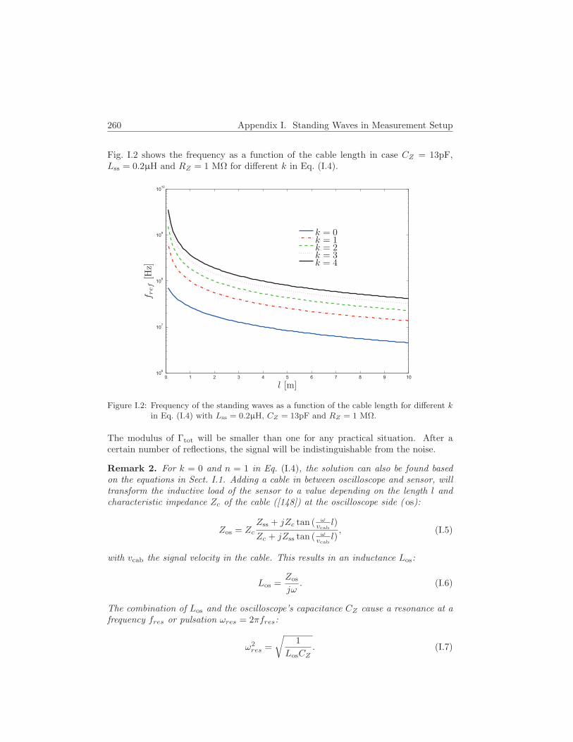
260 Appendix I. Standing Waves in Measurement Setup
Fig. I.2 shows the frequency as a function of the cable length in case CZ = 13pF,Lss = 0.2µH and RZ = 1 MΩ for different k in Eq. (I.4).
0 1 2 3 4 5 6 7 8 9 1010
6
107
108
109
1010
l [m]
f ref
[Hz]
k = 0k = 1k = 2k = 3k = 4
Figure I.2: Frequency of the standing waves as a function of the cable length for different kin Eq. (I.4) with Lss = 0.2µH, CZ = 13pF and RZ = 1 MΩ.
The modulus of Γtot will be smaller than one for any practical situation. After acertain number of reflections, the signal will be indistinguishable from the noise.
Remark 2. For k = 0 and n = 1 in Eq. (I.4), the solution can also be found basedon the equations in Sect. I.1. Adding a cable in between oscilloscope and sensor, willtransform the inductive load of the sensor to a value depending on the length l andcharacteristic impedance Zc of the cable ([148]) at the oscilloscope side ( os):
Zos = Zc
Zss + jZc tan ( ωvcab
l)
Zc + jZss tan ( ωvcab
l), (I.5)
with vcab the signal velocity in the cable. This results in an inductance Los:
Los =Zos
jω. (I.6)
The combination of Los and the oscilloscope’s capacitance CZ cause a resonance at afrequency fres or pulsation ωres = 2πfres:
ω2res =
√1
LosCZ. (I.7)
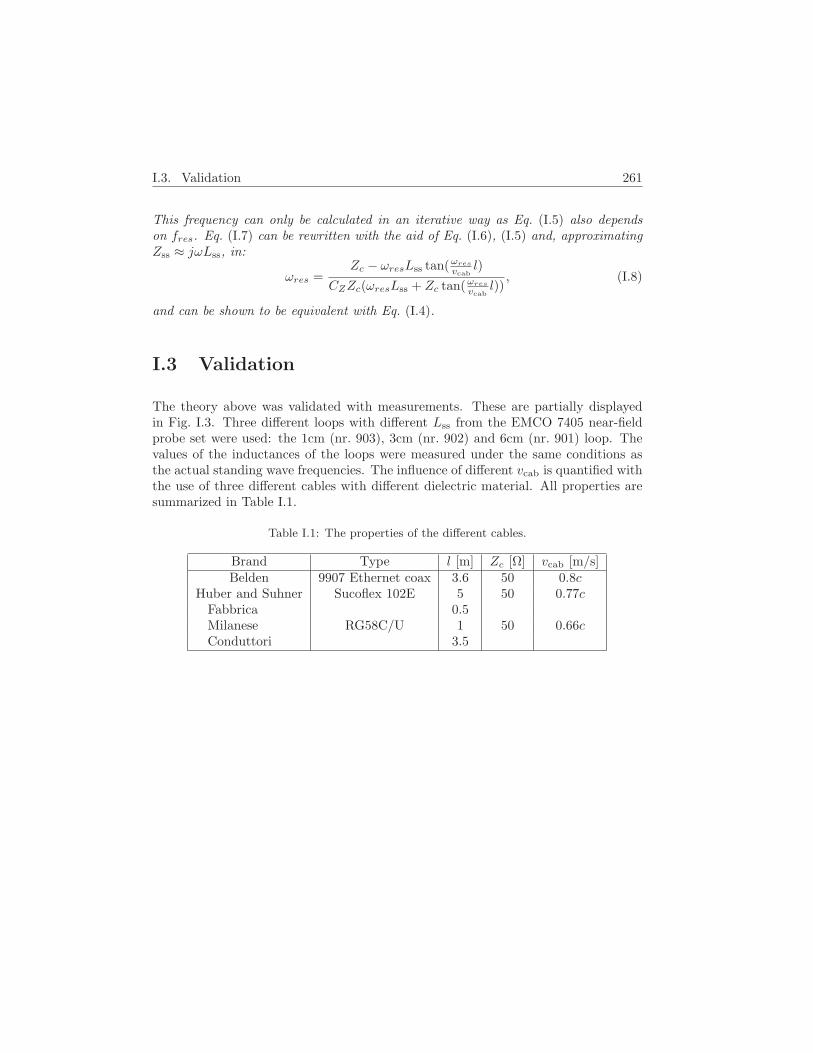
I.3. Validation 261
This frequency can only be calculated in an iterative way as Eq. (I.5) also dependson fres. Eq. (I.7) can be rewritten with the aid of Eq. (I.6), (I.5) and, approximatingZss ≈ jωLss, in:
ωres =Zc − ωresLss tan(ωres
vcabl)
CZZc(ωresLss + Zc tan(ωres
vcabl)), (I.8)
and can be shown to be equivalent with Eq. (I.4).
I.3 Validation
The theory above was validated with measurements. These are partially displayedin Fig. I.3. Three different loops with different Lss from the EMCO 7405 near-fieldprobe set were used: the 1cm (nr. 903), 3cm (nr. 902) and 6cm (nr. 901) loop. Thevalues of the inductances of the loops were measured under the same conditions asthe actual standing wave frequencies. The influence of different vcab is quantified withthe use of three different cables with different dielectric material. All properties aresummarized in Table I.1.
Table I.1: The properties of the different cables.
Brand Type l [m] Zc [Ω] vcab [m/s]Belden 9907 Ethernet coax 3.6 50 0.8c
Huber and Suhner Sucoflex 102E 5 50 0.77cFabbricaMilaneseConduttori
RG58C/U0.5
50 0.66c13.5
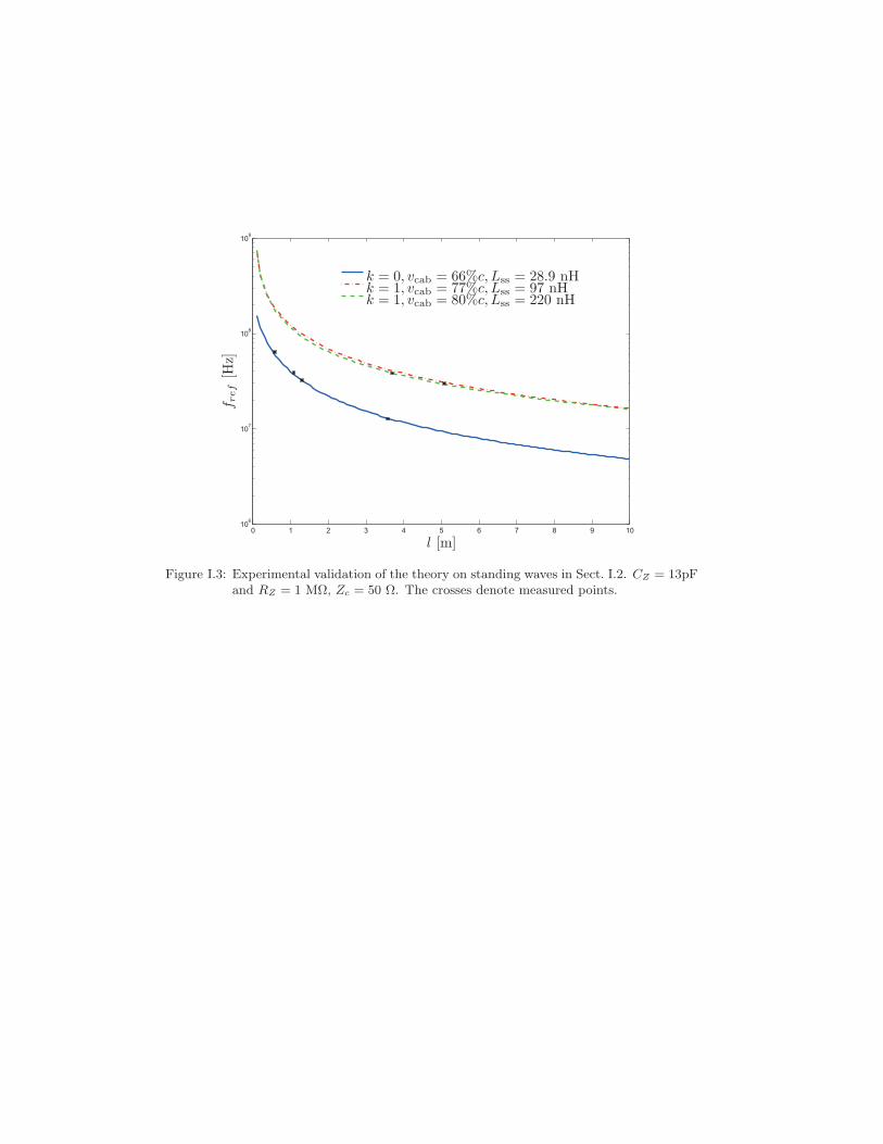
0 1 2 3 4 5 6 7 8 9 1010
6
107
108
109
l [m]
f ref
[Hz]
k = 0, vcab = 66%c, Lss = 28.9 nHk = 1, vcab = 77%c, Lss = 97 nHk = 1, vcab = 80%c, Lss = 220 nH
Figure I.3: Experimental validation of the theory on standing waves in Sect. I.2. CZ = 13pFand RZ = 1 MΩ, Zc = 50 Ω. The crosses denote measured points.
invisible filling

References
[1] L. Josefsson and P. Persson, Conformal Array Antenna Theory and Design.IEEE Press, 2006.
[2] G. J. Foschini, “Layered space-time architecture for wireless communication ina fading environment when using multi-element antennas,” Bell Labs TechnicalJournal, 1996.
[3] V. Tarokh, H. Jafarkhani, and A. R. Calderbank, “Space-time block codes fromorthogonal designs,” IEEE Transactions on Information Theory, vol. 45, no. 5,July 1999.
[4] A. M. Sayeed and V. Raghavan, “The ideal mimo channel: Maximizing ca-pacity in sparse multipath with reconfigurable arrays,” in IEEE InternationalSymposium on Information Theory, July 2006.
[5] J. Lazio and Y. Terzian, “The square kilometre array.” [Online]. Available:http://www.skatelescope.org/PDF/publications/Bhat-Cordes.pdf
[6] Leon W. Couch II, Digital and Analog Communication Systems. Prentice Hall,1997.
[7] K. Markus, A. Roederer, M. Shelley, and D. Brain, “A frequency scanning con-cept for aeronautical satellite communications,” in European Microwave Con-ference, vol. 1, 1992.
[8] B. Razavi, “Design considerations for direct-conversion receivers,” IEEE Trans-actions on Circuits and Systems II: Analog and Digital Signal Processing,vol. 44, no. 6, pp. 428–435, June 1997.
[9] R. Tang, “Survey of time-delay beam steering techniques,” in Phased ArrayAntenna Symposium, 1970.
[10] P. Delmotte and W. Aerts, “Kulsat STWW project (IWT),” ESAT-TELEMIC-Katholieke Universiteit Leuven, Tech. Rep., 2005.
263

264 References
[11] H. Nyquist, “Certain topics in telegraph transmission theory,” TransactionsAmerican Institute of Electrical Engineers (AIEE now IEEE), vol. 47, April1928.
[12] C. E. Shannon, “Communication in the presence of noise,” Proceedings Instituteof Radio Engineers (IRE), vol. 37, no. 1, January 1949.
[13] P. Wambacq and H. Mannaert, Handboek Signaalverwerking. Acco, 1998.
[14] D. P. Scholnik and J. O. Coleman, “Superdirectivity and SNR constraints inwideband array-pattern design,” in 2001 IEEE Radar Conference, Atlanta, May2001.
[15] “Radar in the twentieth century,” IEEE Aerospace and Electronic Systems Mag-azine, vol. 15, no. 10, October 2000.
[16] D. Temme, “Diode and ferrite phaser technology,” in Phased Array AntennaSymposium, 1970.
[17] G. Rebeiz, T. Guan-Leng, and J. Hayden, “Rf mems phase shifters: design andapplications,” IEEE Microwave Magazine, vol. 3, no. 2, June 2002.
[18] J. Rao, D. Patel, L. Sengupta, and J. Synowezynski, “Ferroelectric materials forphased array applications,” in Antennas and Propagation Society InternationalSymposium Digest, vol. 4, July 1997.
[19] L. R. Whicker, “Review of ferrite phase shifter technology,” in G-MTT Inter-national Microwave Symposium Digest, vol. 73, no. 1, 1973.
[20] R. G. Garver, “Broad-band diode phase shifters,” IEEE Transactions on Mi-crowave Theory and Techniques, vol. 20, no. 5, May 1972.
[21] F. Ellinger, R. Vogt, and W. Bachtold, “Ultra compact, low loss, varactor tunedphase shifter mmic at c-band,” IEEE Microwave and Wireless ComponentsLetters, vol. 11, no. 3, March 2001.
[22] T. Haynes, “A primer on digital beamforming,”http://www.spectrumsignal.com/Products/ Product PDFs/beamform primer.pdf.
[23] S. Obayashi, O. Shibata, H. Kasami, H. Shoki, and Y. Suzuki, “An adaptivearray antenna steered by IF local signal phase shifters for K-band broadbandwireless access base station,” in Proceedings of ISAP2000, Fukuoka, Japan.
[24] G. J. Vogel, B. Lyons, K. Parsons, and L. Beachler, “Time scanned array radar,”in Phased Array Antenna Symposium, 1970.
[25] K.-L. Chan and S. R. Judah, “A beam scanning frequency modulated continuouswave radar,” IEEE Transactions on Instrumentation and Measurement, vol. 47,October 1998.

References 265
[26] J. D. Adams, M. J. Mannion, and B. S. Newton, “Dual band frequency scanned,height finder antenna,” in 21st European Microwave Conference, 1991.
[27] W. Mayer, M. Wetzel, and W. Menzel, “A novel direct-imaging radar sensorwith frequency scanned antenna,” in IEEE MTT-S Microwave Symposium Di-gest, vol. 3, June 2003.
[28] C. Dixiang, P. Mengchun, and L. Feilu, “Research of crack depth detectionmethod based on frequency scanning technique,” in 8th International Confer-ence on Electronic Measurement and Instruments (ICEMI), 2007.
[29] J. Frank, “Bandwidth criteria for phased array antennas,” in Phased ArrayAntenna Symposium, 1970.
[30] D. Staelin, A. Morgenthaler, and J. Kong, Electromagnetic Waves. Prentice-Hall International, 1994.
[31] M. I. Skolnik, Ed., Radar Applications. IEEE Press, 1988.
[32] “MAGMAS – the TELEMIC antenna modeling software,”http://www.esat.kuleuven.be/telemic/antennas/magmas/, visited on 2009-01-31.
[33] J. Anguera, G. Montesinos, C. Puente, C. Borja, and J. Soler, “High-directivitymicrostrip array using high-directivity fractal-based elements,” in 4th ESA An-tenna Workshop on Satellite Antenna Technology, september 2002, pp. 59–62.
[34] S. Mestdagh, “Small and integrated microstrip patch and planar monopole an-tennas,” Ph.D. dissertation, Katholieke Universiteit Leuven, 2007.
[35] C. Oseen, “Die einsteinsche nadelstichstrahlung und die maxwellschen gleichun-gen,” Annalen der Physik, vol. 69, 1922.
[36] “IEEE standard definitions of terms for antennas.” IEEE Std 145-1993, pp. i–,Jun 1993.
[37] R. C. Hansen, Ed., Microwave Scanning Antennas. Academic Press, 1966,vol. 2.
[38] IRCTR (T.U.Delft), “Research project proposal: Wide band sparse elements,”slides, December 2001.
[39] J. O. Erstad, “Design of sparse and non-equally spaced arrays for medical ultra-sound,” Master’s thesis, Institutt for Informatikk (Universitetet i Oslo), Novem-ber 1994.
[40] B. Smolders, “Random sparse arrays,”http://www.nfra.nl/skai/archive/technical/smo01.pdf, SKAI memo 034.
[41] H. E. Dimas, “Fractal antenna arrays,” University of Pennsylvania, Tech. Rep.,2000, summer Undergraduate Research.
266 References
[42] Cees G.M. Van ’t Klooster, “Some antenna configuraions for remote sensingand scientific satellites applications,” 1999.
[43] M. Lozano, G. Franceschetti, F. Ares, J. M. S. Vaccaro, and J. Vassal’lo, “Landmobile antenna for geo satellite communications,” in 4th ESA Antenna Work-shop on Satellite Antenna Technology, september 2002, pp. 59–62.
[44] F. J. Harris, “On the use of windows for harmonic analysis with the discretefourier transform,” in IEEE, vol. 66, no. 1, January 1978.
[45] R. Elliott, Antenna Theory and Design. Prentice-Hall, 1981.
[46] Q. Feng, “Phase approximation effect in array antennas,” Master’s thesis,Katholieke Universiteit Leuven, 2005.
[47] J.-L. Bz, P. Bensi, C. Lin, Y. Durand, F. Hlie, A. Regan, P. Ingmann, J. Lan-gen, M. Berger, and M. D. Rebhan, “Esa future earth observation explorer mis-sions,” in International Geoscience and Remote Sensing Symposium IGARSS,July 2007.
[48] [Online]. Available: http://www.lofar.org/p/Agriculture.htm
[49] K.-D. Reiniger, “Digital storage devices for photogrammetry and remote sens-ing,” in Photogrammetric Week, 1997.
[50] S. A. Boyer, SCADA: Supervisory Control and Data Acquisition, 3rd ed. ISA,2004.
[51] http://www.spacechecker.com/, visited on 2009-01-31.
[52] IEC, “Degrees of protection provided by enclosures (ip code),” InternationalElectrotechnical Commission, International Standard IEC 60529, February2001.
[53] “Road vehicles – controller area network (CAN) – part 1: Data link layer andphysical signalling,” ISO, International standard ISO 11898, 2003.
[54] “The european table of frequency allocations and utilisa-tions covering the frequency range 9 khz to 275 ghz,”http://www.itu.int/ITU-D/study groups/SGP 2002-2006/JGRES09/CEPT2.pdf,2003.
[55] K. Davies, Ionospheric Radio. Peter Peregrinus, 1989.
[56] P. W. Fortescue and J. P. W. Stark, Eds., Spacecraft systems engineering. WileyChichester, 1990.
[57] “Orbital velocity calculator,”http://liftoff.msfc.nasa.gov/academy/rocket sci/orbmech/vel calc.html, June1995.
References 267
[58] J. de Lafontaine, J. Buijs, P. Vuilleumier, and P. V. den Braembussche, “De-velopment of the proba attitude control and navigation software,” in 4th EsaInternational Conference on Spacecraft Guidance, Navigation and Control Sys-tems, 1999, pp. 427–441.
[59] C. F. Yoder, “Earth: Geodetic and geophysical data,”http://ssd.jpl.nasa.gov/phys props earth.html, 1995, from Global EarthPhysics, A Handbook of Physical Constants, AGU Reference Shelf 1, Amer-ican Geophysical Union.
[60] “Period of rotation,”http://liftoff.msfc.nasa.gov/academy/rocket sci/orbmech/period.html, July1995.
[61] J. Martin, Communications Satellite Systems. Prentice-Hall, 1978.
[62] H. T. Friis, “A note on a simple transmission formula.” in Proceedings of IRE,vol. 41, May 1946, pp. 254–256.
[63] G. Maral and M. Bousquet, Satellite Communications Systems. John Wiley &Sons, 1975.
[64] C. E. Shannon, “A mathematical theory of communication,” The Bell SystemTechnical Journal, vol. 27, July, October 1948.
[65] J. Evans, “Satellite systems for personal communications,” Proceedings of theIEEE, vol. 86, no. 7, July 1998, special Issue: Mobile Radio Centennial.
[66] J.J.Schuss, J. Upton, B. Myers, T. Sikina, A. Rohwer, P. Makridakas, R. Fran-cois, L. Wardle, and R. Smith, “The iridium main mission antenna concept,”IEEE Transactions on Antennas and Propagation, vol. 47, no. 3, pp. 416–424,March 1999.
[67] “Technical, managerial and financial aspects of a possible future swedish satelliteprogram,” Swedish Space Corporation, Tech. Rep. SSB490-4, october 2000.
[68] G. Woan, The Cambridge Handbook of Physics Formulas. Cambridge Univer-sity Press, 2000.
[69] C. Mangenot, P. Lepeltier, F. Croq, and J. Maurel, “Recent antennas develop-ments at alcatel space industries,” in Proceedings of ISAP2000, Fukuoka, Japan,2000.
[70] V. Gupta, Y. Lanthier, G. Bush, and D. Zimcik, “Performance of theRADARSAT SAR antenna,” Canadian Aeronautics and Space Journal, vol. 39,no. 3, pp. 142–149, September 1993.
[71] A.M.Cruise, J.A.Bowles, T.J.Patrick, and C.V.Goodall, Principles of Space In-strument Design. Cambridge University Press, 1998.

268 References
[72] A. Roederer, “Specificity of space related developements,”http://www.estec.esa.nl/conferences/isd2001/8.pdf, May 2001.
[73] D. J. Newman, Interactive Aerospace Engineering and Design. MacGraw-Hill,2002, ch. The Space Environment: An Engineering Perspective.
[74] K. A. Skaret, “Space weather and the most microsatellite,” Master’s thesis,University of British Columbia, 2001.
[75] ESA-ESTEC, “Ecss-e-10-04a, space engineering, space environment,”http://www.ecss.nl/, 21 January 2000.
[76] L. D. Bell, W. Bender, and M. Carey, “Planetary asteroid defence study, chapter2: Natural space debris,” Air Command and Staff College, Tech. Rep., april1995.
[77] ESA-ESTEC, “European space components information exchange system,”https://escies.org, visited on 2009-02-01.
[78] F. Z. Keister, “An evaluation of materials and processes for integrated mi-crowave circuits,” IEEE Transactions on Microwave Theory and Techniques,vol. MTT-16, no. 7, pp. 469–475, 1968.
[79] T. S. Laverghetta, Microwave Materials and Fabrication Techniques. ArtechHouse, 1984.
[80] X.-H. Shen, “Microstrip antennas in general multi-layered structures,” Ph.D.dissertation, Katholiek Universiteit Leuven, 2000.
[81] “General specification vacuum stability requirements of polymeric materials forspacecraft application,” Lyndon B. Johnson Space Center, Tech. Rep., 1974.
[82] “Space product assurance: Thermal vacuum outgassing test for the screeningof space materials,” European Cooperation for Space Standardization (ECSS),Tech. Rep., 2000.
[83] “Rohm gmbh,” http://www.roehm.com/.
[84] “Rogers corporation,” http://www.rogers-corp.com/.
[85] “Arlon materials for electronics division,” http://www.arlon-med.com/.
[86] “Outgassing data for selecting spacecraft materials online,”http://outgassing.nasa.gov/.
[87] “Microwave laminates comparison chart,”http://www.cirexx.com/info/pdf/metcladcompchart.pdf.
[88] P. Kabacik and M. E. Bialkowski, “The temperature dependence of substrateparameters and their effect on microstrip antenna performance,” IEEE Trans-actions on Antennas and Propagation, vol. 47, no. 6, June 1999.
References 269
[89] P. Kabacik, “Electrical characteristics of microwave laminates.”
[90] R. C. Olsen, Introduction to the Space Environment, 2003, ch. 8. EnvironmentalEffects on Space Systems, pp. 173–198.
[91] D. Zimcik, M. Wertheimer, K. Balmain, and R. Tennyson, “Plasma-depositedprotective coatings for spacecraft applications,” Journal of Spacecraft and Rock-ets, vol. 28, no. 6, pp. 652–657, November-December 1991.
[92] I. De Coster, “Deterministic propagation prediction for wireless communicationsystems,” Ph.D. dissertation, Katholieke Universiteit Leuven, October 2000.
[93] P. Delmotte and G. Vandenbosch, “An analog implementation of a basebandbeamformer,” in European Conference on Wireless Technology, Munich, 8-10October 2003.
[94] F. M. Kashif, W. Qadeer, and S. I. Shah, “Efficient implementation of quadra-ture amplitude modulation transmitters,” in IEEE INMIC Technology for the21st Century, 2001.
[95] P. Delmotte, W. Aerts, V. Volski, S. Mestdagh, and G. Vandenbosch, “Mea-surement results of a phased array with a new type of phase shifter,” in 28thESA Antenna Workshop on Space Antenna Systems and Technologies, ESTEC,Nederland, 2005, pp. 303–308.
[96] S.-S. Jeon, Y. Wang, Y. Qian, and T. Itoh, “Integrated adaptive beamformingantennas for wireless communications,” in IEEE Antennas and PropagationSociety International Symposium, vol. 2, 2002.
[97] M. G. Kyeong, H. G. Park, H. S. Oh, and J. H. Jung, “Array calibration forCDMA smart antenna systems,” Electronics and Telecommunications ResearchInstitute (ETRI) Journal, vol. 26, no. 6, December 2004.
[98] T. Cooper, J. McCormack, R. Farrell, and G. Baldwin, “Toward scalable, au-tomated tower-top phased array calibration,” in IEEE Vehicular TechnologyConference (VTC), April 2007.
[99] M. Hiebel, Fundamentals of Vector Network Analysis, 3rd ed. Rohde &Schwarz, 2008.
[100] Agilent Technologies 8510C Network Analyzer System Operating and Program-ming Manual, May 2001.
[101] J. Rustako, A., L. Greenstein, R. Roman, and A. Saleh, “Using times-fourcarrier recovery in m-qam digital radio receivers,” Selected Areas in Communi-cations, IEEE Journal on, vol. 5, no. 3, pp. 524–533, Apr 1987.
[102] A. G. Konheim, Ed., Computer Security And Cryptography. Wiley-Interscience,2007.
270 References
[103] C. E. Shannon, “Communication theory of secrecy systems,” Bell System Tech-nical Journa, vol. 28, no. 4, October 1949.
[104] H. Bar-El, “Introduction to side channel attacks,” Discretix Technologies Ltd.,Tech. Rep., 2003.
[105] “Keeloq R© authentication products,” http://www.microchip.com/keeloq, vis-ited on 2009-01-27.
[106] S. Indesteege, N. Keller, O. Dunkelman, E. Biham, and B. Preneel, “A practicalattack on keeloq.” in EUROCRYPT, ser. Lecture Notes in Computer Sci-ence, N. P. Smart, Ed., vol. 4965. Springer, 2008, pp. 1–18. [Online]. Available:http://dblp.uni-trier.de/db/conf/eurocrypt/eurocrypt2008.html#IndesteegeKDBP08
[107] T. Eisenbarth, T. Kasper, A. Moradi, C. Paar, M. Salmasizadeh, and M. T. M.Shalmani, “Physical cryptanalysis of keeloq code hopping applications,” Cryp-tology ePrint Archive, Report 2008/058, 2008, http://eprint.iacr.org/.
[108] A. Shamir, “Protecting smart cards from passive power analysis with detachedpower supplies,” in 2nd International Workshop Cryptographic Hardware andEmbedded Systems (CHES), 2000.
[109] S. Brown and J. Rose, “Architecture of fpgas and cplds: A tutorial,” IEEEDesign and Test of Computers, vol. 13, no. 2, 1996.
[110] P. Kocher, “Timing attacks on implementations of Diffie-Hellman, RSA, DSSand other systems,” in Advances in Cryptology: Proceedings of CRYPTO’96,1996.
[111] J. M. Atkinson, http://www.tscm.com/TSCM101tempest.html, visited on2008-11-04.
[112] NSA, “Tempest: A signal problem,” Cryptologic Spectrum, vol. 2, no. 3, 1972.
[113] P. Kocher, J. Jaffe, and B. Jun, “Differential power analysis,” in Advances inCryptology: Proceedings of CRYPTO’99, 1999.
[114] D. Agrawal, B. Archambeault, J. R. Rao, and P. Rohatgi, “The em side-channel(s),” in CHES ’02: Revised Papers from the 4th International Workshopon Cryptographic Hardware and Embedded Systems. Springer-Verlag, 2003.
[115] D. Asonov and R. Agrawal, “Keyboard acoustic emanations,” in IEEE Sympo-sium on Security and Privacy, 2004.
[116] A. Shamir and E. Tromer, “Acoustic cryptanalysis: on nosy people andnoisy machines,” in Eurocrypt rump session, 2004. [Online]. Available:http://people.csail.mit.edu/tromer/acoustic/
[117] H. Bar-El, H. Choukri, D. Naccache, M. Tunstall, and C. Whelan, “The sor-cerers apprentice guide to fault attacks,” in Proceedings of the IEEE, vol. 94,no. 2, Februari 2006.
References 271
[118] M. Otto, “Fault attacks and countermeasures,” Ph.D. dissertation, UniversitatPaderborn, December 2004.
[119] Engineering and Design - Electromagnetic Pulse (EMP) and Tempest Protectionfor Facilities. US Army Corps of Engineers, 1990.
[120] S. Mangard, T. Popp, and M. E. Oswald, Power Analysis Attacks – Revealingthe Secrets of Smart Cards, 2007.
[121] P. A. Bode, “Current measurement applications handbook,” ZETEX Semicon-ductors, Tech. Rep., November 2007.
[122] K. Tiri and I. Verbauwhede, “Secure logic synthesis,” Field-Programmable Logicand Applications, 2004.
[123] D. Agrawal, B. Archambeault, S. Chari, J. R. Rao, and P. Rohatgi, “Advancesin side-channel cryptanalysis, electromagnetic analysis and template attacks,”CryptoBytes, vol. 6, no. 1, 2003.
[124] J.-J. Quisquater and D. Samyde, “Electromagnetic analysis (ema): Measuresand countermeasures for smard cards,” in Proceedings of Smart Card Program-ming and Security (E-smart 2001), I. Attali and T. Jensen, Eds. Springer-Verlag, 2001.
[125] K. Gandolfi, C. Mourtel, and F. Olivier, “Electromagnetic analysis: Concreteresults,” in Proceedings of 3rd International Workshop on Cryptographic Hard-ware and Embedded Systems (CHES), C. K. Koc, D. Naccache, and C. Paar,Eds. Springer-Verlag, 2001.
[126] C. C. Tiu, “A new frequency-based side channel attack for embedded systems,”Master’s thesis, University of Waterloo, Canada, 2005.
[127] K. F. Lee, Principles of antenna theory. John Wiley & Sons, 1984.
[128] “ITRS international technology roadmap for semiconductors,”http://www.itrs.net, 2007, visited on 2009-01-26.
[129] C. Yui, G. Swift, and C. Carmichael, “Single event upset susceptibility testingof the xilinx virtex II FPGA,” in Military and Aerospace Programmable LogicDevices (MAPLD) Conference, 2002.
[130] Virtex II Platform FPGAs: Complete Datasheet,http://www.xilinx.com/support/documentation/virtex-ii data sheets.htm,November 2005.
[131] “Side channel analysis resistant design (SCARD),”http://www.scard-project.eu/, visited on 2009-01-26.

272 References
[132] N. Masuda, N. Tamaki, T. Kuriyama, J. C. Bu, M. Yamaguchi, and K.-I. Arai,“High frequency magnetic near field measurement on lsi chip using planar multi-layer shielded loop coil,” in IEEE International Symposium on ElectromagneticCompatibility, 2003.
[133] J. M. Rabaey, A. Chandrakasan, and B. Nikolic, Digital Integrated Circuits,2nd ed. Prentice Hall, 2003.
[134] D. Sima, “The end of an era in processor evolution,” manuscript,http://nik.bmf.hu/sima/letoltes/cikkek/theendofanera.pdf.
[135] http://www.ieee.org/web/aboutus/home/index.html, visited on 2009-01-15.
[136] J. Radatz, The IEEE Standard Dictionary of Electrical and Electronics Terms.New York, NY, USA: IEEE Standards Office, 1997.
[137] A. O. A.W. Rudge, K. Milne and P. Knight, Eds., The Handbook of AntennaDesign. IEE Electromagnetic Waves Series, 1983.
[138] R. W. Lewallen W7EL, “Baluns: What they do and how they do it,” ARRLAntenna Compendium, pp. 157–164, 1985.
[139] “HF antenna cookbook – technical application report – radio frequency identi-fication systems,” Texas Instruments, Tech. Rep., 2004.
[140] S. Saario, D. V. Thiel, J. W. Lu, and S. G. O’Keefe, “An assessment of cable ra-diation effects on mobile communicationsantenna measurements,” in Antennasand Propagation Society International Symposium. IEEE, 1997.
[141] R. Ediss, “Probing the magnetic field probe,” EMC & Compliance Journal, July2003.
[142] H. R. Mimno, R. W. P. King, and A. H. Wing, Transmission Lines, Antennasand Wave Guides. McGraw-Hill, 1945.
[143] Users’s Manual Near-Field Probe Set Model 7405.
[144] H. Nyquist, “Thermal agitation of electric charge in conductors,” Phys. Rev.,vol. 32, no. 1, pp. 110–113, Jul 1928.
[145] MIL-HDBK-216, Military Standardization Handbook - RF Transmission Linesand Fittings. Defense Supply Agency, 4 January 1962.
[146] M.-H.-. notice 11, Cancellation Notice. Defense Supply Center Columbus, 6September 2001.
[147] “http://www.hubersuhner.com.”
[148] P. C. Magnusson, G. C. Alexander, V. K. Tripathi, and A. Weisshaar, Trans-mission Lines and Wave Propagation. CRC Press, 2001.
References 273
[149] M. Kanda, “Standard probes for electromagnetic field measurements,” IEEETransactions on Antennas and Propagation, vol. 41, no. 10, 1993.
[150] W. Aerts, E. De Mulder, B. Preneel, G. Vandenbosch, and I. Verbauwhede, “De-pendence of RFID reader antenna design on read out distance,” IEEE Trans-actions on Antennas and Propagation, vol. 56, no. 12, December 2008.
[151] “Radio frequency identification device technology - factfile,”http://www.rfidc.com/docs/papers downloads.htm, 2005, visited on 2009-01-18.
[152] I. Kirschenbaum and A. Wool, “How to build a low-cost, extended-range RFIDskimmer,” in Proceedings of the 15th USENIX Security Symposium. USENIX,31th of July - 4th of August 2006, pp. 43–57.
[153] C. M. Zierhofer and E. S. Hochmair, “Geometric approach for coupling en-hancement of magnetically coupled coils,” IEEE Transactions on BiomedicalEngineering, vol. 43, no. 7, pp. 708–714, July 1996.
[154] K. Fotopoulou and B. W. Flynn, “Optimum antenna coil structure for inductivepowering of passive RFID tags,” in IEEE International Conference on RFID,2007, pp. 71–77.
[155] K. Finkenzeller, RFID Handbook, 2nd ed. John Wiley and Sons, 2003.
[156] Y. Lee, “RFID coil design,” Microchip Technology Inc. Application Note, 1998.
[157] M. H. Choudhury, Electromagnetism, J. W. Mason, Ed. Ellis Horwood Limited,1989.
[158] ISO/IEC/JTC1 Information technology, “Identification cards - contactless inte-grated circuit(s) cards - proximity cards - part 2:radio frequency power and sig-nal interface,” ISO/IEC/JTC1, International standard ISO/IEC 14443-2, 1999.
[159] H. Schrank and J. D. Mahony, “Approximations to the radiation resistanceand directivity of circular-loop antennas,” IEEE Antennnas and PropagationMagazine, vol. 36, no. 4, pp. 52–55, August 1994.
[160] D. C. Yates, A. S. Holmes, and A. J. Burdett, “Optimal transmission frequencyfor ultralow-power short-range radio links,” IEEE Transactions on Circuits andSystems, vol. 51, no. 7, pp. 1405–1413, July 2004.
[161] A. M. Gabriele Grandi, Marian K. Kazimierczuk and U. Reggiani, “Stray ca-pacitances of single-layer solenoid air-core inductors,” IEEE Transactions onIndustry Applications, vol. 35, no. 5, pp. 1162–1168, September/October 1999.
[162] G. S. Smith, “Radiation efficiency of electrically small multiturn loop antennas,”IEEE Transactions on Antennas and Propagation, september 1972.
274 References
[163] D. J. Goedbloed, Elektromagnetische compatibiliteit. Ten Hagen en Stam, DenHaag/Deventer, 2000.
[164] G. Steiner, H. Zangl, P. Fulmek, and G. Brasseur, “A tuning transformer forautomatic adjustment of resonant loop antennas in RFID systems,” in IEEEConference on Industrial Technology (ICIT), 2004.
[165] I. Diaconu and D. Dorohoi, “Properties of polyurethane thin films,” Optoelec-tronics and Advanced Materials, vol. 7, no. 2, pp. 921–924, April 2005.
[166] N. Ando, N. Masuda, N. Tarnaki, T. Kuriyama, S. Saito, K. Kato, K. Ohashi,M. Saito, and M. Yarnaguchi, “Miniaturized thin-film magnetic field probe withhigh spatial resolution for lsi chip measurement,” 2004.
[167] M. Yamaguchi, S. Koya, H. Torizuka, S. Aoyama, and S. Kawahito, “Shielded-loop-type onchip magnetic-field probe to evaluate radiated emission from thin-film noise suppressor,” IEEE Transactions on Magnetics, vol. 43, no. 6, June2007.
[168] W. Aerts, E. De Mulder, B. Preneel, G. Vandenbosch, and I. Verbauwhede,“Designing maximal resolution loop sensors for cryptographic analysis,” in Pro-ceedings of EuCAP, Berlin, Germany, 2009.
[169] F. W. Gover, Inductance Calculations: Working Formulas and Tables. DoverPublications, 1946.
[170] T. O. Company, “Minimum bending radii,” The OkoniteCompany, Tech. Rep., September 2008. [Online]. Available:http://www.okonite.com/engineering/bending-ratios.html
[171] V. Seidermann and S. Buttgenbach, “Closely coupled micro coils with inte-grated flux guidance: Fabrication technology and application to proximity andmagnetoelastic force sensors,” IEEE Sensors Journal, 2003.
[172] W. Bosma, J. Cannon, and C. Playoust, “The magma algebra system. i. theuser language,” Journal of Symbolic Calculation, vol. 24, no. 3-4, 1997.
[173] L. Sauvage, S. Guilley, J.-L. Danger, Y. Mathieu, and M. Nas-sar, “Successful attack on an fpga-based automatically placedand routed wddl+ crypto processor.” 2008. [Online]. Available:http://hal.archives-ouvertes.fr/hal-00339858/en/
[174] S. Chari, J. R. Rao, and P. Rohatgi, “Template attacks,” in CHES, 2002, pp.13–28.
[175] S. Indesteege, “Cryptografische aspecten van nevenkanaalaanvallen op cryp-tografische chips,” Master’s thesis, Katholieke Universiteit Leuven, 2006.

References 275
[176] H. Haus, W. Atkinson, G. Branch, W. Davenport, W. Fonger, W. Harris, S. Har-rison, W. McLeod, E. Stodola, and T. Talpey, “Representation of noise in lineartwoports,” Proceedings of the IRE, vol. 48, no. 1, pp. 69–74, January 1960.
[177] E. De Mulder, W. Aerts, B. Preneel, G. Vandenbosch, and I. Verbauwhede, “Aclass e power amplifier for iso-14443a,” in Proceedings of the 12th IEEE Work-shop on Design and Diagnostics of Electronic Circuits and Systems (DDECS),2009.
[178] N. O. Sokal and A. D. Sokal, “Class E - a new class of high-efficiency tunedsingle-ended switching power amplifiers,” IEEE Journal of Solid-State Circuits,vol. SC-10, no. 3, pp. 168–176, June 1975.
[179] F. H. Raab, “Idealized operation of the class E tuned power amplifier,” IEEETransactions on Circuits and Systems, vol. CAS-24, no. 12, pp. 725–735, De-cember 1977.
[180] STMicroelectronics, “How to extend the operating range of the crx14 contactlesscoupler chip,” STMicroelectronics Application Note, 2006.
[181] Y. L. Haixing Hu and Z. Wang, “An improved push-pull class-E RF tunedpower amplifier with low maximum transistor current,” in 4th InternationalConference on ASIC, 2001.
[182] M. Kazimierczuk, “Collector amplitude modulation of the class E tuned poweramplifier,” IEEE Transactions on Circuits and Systems, vol. CAS-31, no. 6,June 1984.
[183] ISO/IEC/JTC1 Information technology, “Identification cards - contactless in-tegrated circuit(s) cards - proximity cards - part 1:physical characteristics,”ISO/IEC/JTC1, International standard ISO/IEC 14443-1, 1997.
[184] “Irf510,” International Rectifier, Datasheet PD-9-325Q.
[185] P. Antognetti and G. Massobio, Semiconductor Device Modeling with Spice. McGraw-Hill, 1988.
[186] “A more realistic characterisation of power mosfet output capacitance coss,”International Rectifier, Tech. Rep. AN-1001.
[187] I. Bahl and R. Garg, “Simple and accurate formulas for a microstrip with finitestrip thickness,” IEEE Transactions on Microwave Theory and Techniques, vol.MTT-29, no. 10, October 1981.
[188] W. Aerts and G. A. Vandenbosch, “Reflections on doppler shift compensationby frequency scanning,” in 30th ESA Antenna Workshop on Antennas for EarthObservation, Science, Telecommunication and Navigation Space Missions, May2008.

276 References
[189] M. Katayama, A. Ogawa, and N. Morinaga, “Carrier synchronization underdoppler shift of the nongeostationary satellite communication systems,” in Sin-gapore ICCS/ISITA ’Communications on the Move’, vol. 2, 1992, pp. 466–470.
[190] G. J. R. Povey and J. Talvitie, “Doppler compensation and code acquisitiontechniques for LEO satellite mobile radio communications,” in Satellite Systemsfor Mobile Communications and Navigation, May 1996.
[191] H. Lim, S. I. Lee, and S. P. Lee, “A simple carrier frequency detection algorithmfor fine compensation of doppler shift in direct-sequence code division multipleaccess mobile satellite communications,” in IEEE International Conference onCommunications, 2000.
[192] L. L.-f. Zhang Zhao-yang, “A practical slotted quasi-synchronous CDMA accesssystem for LEO micro-satellite short message transmission,” in IEEE Interna-tional Conference on Communications, vol. 3, 2003, pp. 2114–2118.
[193] D. Roddy, Satellite Communication, S. S. Chapman, Ed. Mc Graw Hill, 1989.
[194] W. V. Eck and N. Laborato, “Electromagnetic radiation from video displayunits: An eavesdropping risk,” Computers & Security, vol. 4, pp. 269–286,1985.
[195] M. Kuhn, “Compromising emanations: Eavesdropping risks of computer dis-plays,” Ph.D. dissertation, University of Cambridge, 2003.
[196] P. Vandromme and J. Vankeerbergen, “Afluisteren van beeldschermen,” Mas-ter’s thesis, Katholieke Universiteit Leuven, 2007.
[197] HCS410 – KeeLoq R© Code Hopping Encoder and Transponder,http://ww1.microchip.com/downloads/en/DeviceDoc/40158e.pdf, 2001.
[198] W. Aerts, E. De Mulder, B. Preneel, G. Vandenbosch, and I. Verbauwhede,“Matching shielded loops for cryptographic analysis,” in EuCAP, 2006.
[199] R. R. FitzGerrell, “Swept-frequency antenna gain measurements,” IEEE Trans-actions on Antennas and Propagation, vol. 14, no. 2, 1966.
[200] ISO/IEC, “Information technology AIDC techniques - harmonized vocabulary,part 3 - radio-frequency identification (RFID),” ISO/IEC, International Stan-dard - Under development ISO 19762-3, 2007, not sure this is the correct version.
[201] P. V. Nikitin and K. V. S. Rao, “Theory and measurement of backscatteringfrom RFID tags,” IEEE Antennas and Propagation Magazine, vol. 48, no. 6,pp. 212–218, December 2006.
[202] ISO/IEC/JTC1 Information technology, “Identification cards - contactless inte-grated circuit(s) cards - proximity cards - part 3:initialization and anticollision,”ISO/IEC/JTC1, International standard ISO/IEC 14443-3, 1999.

References 277
[203] ——, “Identification cards - contactless integrated circuit(s) cards - proximitycards - part 4:transmission protocol,” ISO/IEC/JTC1, International standardISO/IEC 14443-1, 2000.
[204] Z. Kfir and A. Wool, “Picking virtual pockets using relay at-tacks on contactless smartcard systems,” 2005. [Online]. Available:citeseer.ist.psu.edu/kfir05picking.html
[205] H. A. Wheeler, “Simple inductance formulas for radio coils,” Proceedings of theI.R.E, 1942.
[206] Model SR715/720 LCR Meters User Manual,http://www.thinksrs.com/downloads/PDFs/Manuals/SR715720m.pdf, Febru-ari 2006.