Analytical Design Procedures for the Odd Mode of Ridge Gap ...
163
Analytical Design Procedures for the Odd Mode of Ridge Gap Waveguide Devices and Antennas Abduladeem Altayib Amer Beltayib A Thesis In the Department of Electrical and Computer Engineering Presented in Partial Fulfillment of the Requirements For the Degree of Doctor of Philosophy (Electrical and Computer Engineering) at Concordia University Montréal, Québec, Canada March, 2020 c ⃝ Abduladeem Altayib Amer Beltayib, 2020
-
Upload
khangminh22 -
Category
Documents
-
view
3 -
download
0
Transcript of Analytical Design Procedures for the Odd Mode of Ridge Gap ...

Analytical Design Procedures for the Odd Mode of RidgeGap Waveguide Devices and Antennas
Abduladeem Altayib Amer Beltayib
A Thesis
In the Department
of
Electrical and Computer Engineering
Presented in Partial Fulfillment of the Requirements
For the Degree of
Doctor of Philosophy (Electrical and Computer Engineering) at
Concordia University
Montréal, Québec, Canada
March, 2020
c⃝ Abduladeem Altayib Amer Beltayib, 2020
CONCORDIA UNIVERSITY
School of Graduate Studies
This is to certify that the thesis prepared
By: Abduladeem Altayib Amer Beltayib
Entitled: Analytical Design Procedures for the Odd Mode of Ridge Gap Waveguide
ttttttttttttttttt Devices and Antennas
and submitted in partial fulfillment of the requirements for the degree of
Doctor of Philosophy (Electrical and Computer Engineering)complies with the regulations of the University and meets the accepted standards with
respect to originality and quality.
Signed by the final examining committee:
ChairDr. Ming Yuan Chen
External ExaminerDr. Serioja Ovidiu Tatu
External to ProgramDr. Abdessamad Ben Hamza
ExaminerDr. Ahmed A. Kishk
ExaminerDr. Robert Paknys
Thesis SupervisorDr. Abdel R. Sebak
Approved by:Dr. Rastko Selmic, Graduate Program Director
February 10, 2020Dr. Amir Asif, DeanGina Cody School of Engineering & Computer Science

Abstract
Analytical Design Procedures for the Odd Mode of Ridge Gap Waveguide Devices and
Antennas
Abduladeem Altayib Amer Beltayib, Ph.D.
Concordia University, 2020
The millimeter-wave (mm-wave) band has attracted attention due to its wideband
characteristics that make it able to support multi-gigabit per second data rate. Never-
theless, the performance of mm-wave wireless communication systems is restricted due
to attenuation loss. Design of mm-wave components and antennas is rapidly growing
with the current evolution in the wireless communication systems. However, the tra-
ditional waveguide structures such as microstrip, coplanar, substrate integrated waveg-
uide, and rectangular waveguide either suffer from high losses or difficulty in manufac-
turing at mm-wave band. The ridge gap waveguide (RGW) technology is considered as
a promising waveguide technology for the mm-wave band. RGW technology overcomes
the conventional guiding structure problems as the wave propagates in an air gap region
which eliminates the dielectric loss. Moreover, RGW does not need any electrical con-
tacts, unlike traditional rectangular waveguides. Also, the RGW can be implemented in
the printed form (PRGW) for easy integration with other planer system components.
In this thesis, the use of the odd mode (TERGW10 ) RGW to design mm-wave compo-
nents and antennas is presented. First, a systematic design methodology for the RGW
using hybrid PEC/PMC waveguide approximation is presented. This reduces the design
time using full wave simulators. The concept has been verified by simulation and exper-
imental measurements. Second, two different methods to excite the odd mode in RGW
are studied and investigated. In the first method, a planar L-shape RGW is used where
less than -10 dB reflection coefficient is achieved, from 28 to 36 GHz, and more than 93%
of the input power has been converted into the odd mode at the output port. The second
iii

method uses a magic tee with a shorted sum port and provides a wideband pure odd
mode at the output port with reflection coefficient less than -10 dB from 28 GHz to 39
GHz. Other mm-wave components based on odd mode TERGW10 RGW are designed and
presented including a Y-junction power divider and 3 dB forward coupler are designed
for the first time in RGW technology. The Y-junction has a wideband matching from 28
to 34 GHz with a reflection coefficient less than -15 dB and the transmission output levels
are about -3.3 dB.
The usefulness of the odd mode RGW lies in the ability to increase the channel band-
width that has been achieved by designing a dual-mode RGW. A magic tee is used to
simultaneously excite the fundamental mode Q-TEM and the odd mode TERGW10 on the
ridgeline. The proposed dual-mode RGW performance is verified through simulation
and measurement of a back-to-back configuration. The proposed design achieves a match-
ing level less than -10 dB for the two modes over the frequency range from 29 GHz to 34.5
GHz with isolation better than 23 dB. The dual-mode RGW is then used to feed a recon-
figurable Vivaldi horn antenna where two different radiation patterns can be obtained
depending on the excited mode. The Q-TEM generates a single beam pattern, while the
odd mode TERGW10 generates a dual-beam pattern. The maximum gain for the single beam
radiation is 12.1 dBi, while it is 10.43 dBi for the dual-beam pattern. The bandwidth of
the dual-mode antenna is 25% at 32 GHz with impedance matching less than -10 dB and
isolation better than 20 dB.
Finally, several antennas are presented in this thesis based on the odd mode RGW. A
novel differential feeding cavity antenna using the odd mode of RGW is presented. The
measured results show good performance in terms of gain, bandwidth, sidelobe level,
and cross-polarization. The maximum gain is 16.5 dBi, and the sidelobe level is -17 dB
and -13.8 dB, for the E-plane and H-plane, respectively. Moreover, the proposed antenna
has low cross-polarization levels of -35 dB in the E-plane and -27 dB in the H-plane. In ad-
dition, two 2x1 linear frequency scanning array antennas are designed and implemented
using the proposed Y-junction to generate single beam and dual-beam patterns. The beam
scan is from -11o to 40o at 28 GHz and 32 GHz, respectively.
iv

Acknowledgments
First of all, I sincerely wish to thank my supervisor Prof. Abdel Razik Sebak, who
gave me the opportunity to join his group, and support me. It was a real pleasure for
me to have such an exceptional scholar and it was my honor to be his PhD student. Fur-
thermore, I would like to thank my committee members, Prof.Paknys, Prof.Kishk,Dr. S
Tatu,and Prof.Ben Hamza for their review of my dissertation and their constructive com-
mentsand feedback.
My thanks extend to my colleagues in my office, who provided me with some use-
ful discussions. Also, I would like to thank Moufthah Asadi, Magid Alzidani, Zouhair
Briquish, Walid Dyab, and Ahmad Sakar.
In particular, I would like to acknowledge my colleague Islam Afifi who collaborated
with me and helped me during measurements.
I finally would like to thank my beloved parents, brother, sisters, and wife for their
love and warm support.
v

Contents
List of Figures x
List of Abbreviations xvii
1 Introduction and Historical Overview 1
1.1 Introduction . . . . . . . . . . . . . . . . . . . . . . . . . . . . . . . . . . . . . 1
1.2 Millimeter Wave Overview . . . . . . . . . . . . . . . . . . . . . . . . . . . . 3
1.3 Motivations and Problem Statement . . . . . . . . . . . . . . . . . . . . . . . 4
1.4 Objectives . . . . . . . . . . . . . . . . . . . . . . . . . . . . . . . . . . . . . . 6
1.5 Contributions . . . . . . . . . . . . . . . . . . . . . . . . . . . . . . . . . . . . 7
1.6 Thesis Organization . . . . . . . . . . . . . . . . . . . . . . . . . . . . . . . . . 8
2 Background and Literature Review 9
2.1 Historical Overview of Guiding Structures . . . . . . . . . . . . . . . . . . . 9
2.1.1 Microstrip and Striplines, Coplanar and Grounded Coplanar Waveg-
uides, Metal and Substrate-integrated Waveguides . . . . . . . . . . 10
2.1.2 Gap Waveguide Technology . . . . . . . . . . . . . . . . . . . . . . . 15
2.2 Ridge Gap Waveguide (RGW) Concept . . . . . . . . . . . . . . . . . . . . . 16
2.2.1 Ridge Gap Waveguide Structure . . . . . . . . . . . . . . . . . . . . . 18
2.2.2 Bed of Nails Operation . . . . . . . . . . . . . . . . . . . . . . . . . . 19
2.2.3 Bed of Nails Region Downed by a PEC Ground Plane . . . . . . . . 20
2.2.4 Bed of Nails Covered From Both Sides by PEC-Plates . . . . . . . . . 21
2.3 Analytical Design Procedure for Forward Wave Couplers in RGW Technol-
ogy . . . . . . . . . . . . . . . . . . . . . . . . . . . . . . . . . . . . . . . . . . 24
vi

2.4 RGW High Order Mode Excitation . . . . . . . . . . . . . . . . . . . . . . . . 25
2.5 RGW Power Divider Based on First High Order Mode . . . . . . . . . . . . . 26
2.6 RGW Forward Hybrid Coupler Based on First High Order Mode . . . . . . 27
2.7 Dual Mode Waveguide . . . . . . . . . . . . . . . . . . . . . . . . . . . . . . 27
2.8 Sum and Difference Beam Switching Antenna . . . . . . . . . . . . . . . . . 28
2.9 Frequency Scanning and leaky Wave Antenna Based on First Higher Order
Mode Ridge Gap Waveguide . . . . . . . . . . . . . . . . . . . . . . . . . . . 29
2.10 Design Methodology . . . . . . . . . . . . . . . . . . . . . . . . . . . . . . . . 30
3 Analytical Design Procedure for RGW Forward Coupler Based on PEC/PMC
Waveguide Model 31
3.1 Introduction . . . . . . . . . . . . . . . . . . . . . . . . . . . . . . . . . . . . 31
3.1.1 Hybrid PEC/PMC Waveguide Operation . . . . . . . . . . . . . . . 33
3.2 Hybrids PEC/PMC Coupler . . . . . . . . . . . . . . . . . . . . . . . . . . . 37
3.3 Analytical Design of RGW Coupler . . . . . . . . . . . . . . . . . . . . . . . 41
3.3.1 Design of Unit Cell and Dispersion Diagram . . . . . . . . . . . . . . 42
3.3.2 Dispersion Diagram of the Complete RGW . . . . . . . . . . . . . . . 44
3.3.3 Excitation Based on PEC/PMC Circular Bend . . . . . . . . . . . . . 47
3.3.4 The Full RGW Coupler . . . . . . . . . . . . . . . . . . . . . . . . . . 52
3.3.5 Frequency-Tunable RGW Coupler . . . . . . . . . . . . . . . . . . . 52
3.4 A Possible Setup for Prototyping the Proposed RGW Coupler . . . . . . . . 55
3.4.1 Microstrip to RGW Transition . . . . . . . . . . . . . . . . . . . . . . 55
3.4.2 Whole Setup Model of 0dB Coupler Include the Microstrip Transition 57
3.4.3 Fabrication and Experimental Results . . . . . . . . . . . . . . . . . . 59
4 Odd Mode RGW-based Devices: Design Procedure 61
4.1 Introduction . . . . . . . . . . . . . . . . . . . . . . . . . . . . . . . . . . . . . 61
4.2 First High Order Mode Ridge Gap Waveguide . . . . . . . . . . . . . . . . . 62
4.2.1 Ridge Gap Waveguide Analysis and Unit Cell . . . . . . . . . . . . . 63
4.2.2 Ridge Gap Waveguide Section . . . . . . . . . . . . . . . . . . . . . . 63
vii

4.3 Excitation of First High Order Mode by Magic Tee . . . . . . . . . . . . . . . 68
4.3.1 Magic Tee Implementation . . . . . . . . . . . . . . . . . . . . . . . . 68
4.3.2 RGW Excitation by Magic Tee . . . . . . . . . . . . . . . . . . . . . . 70
4.4 Excitation of First High Order Mode by L-Shape transition . . . . . . . . . . 71
4.4.1 Odd Mode RGW Transition Design . . . . . . . . . . . . . . . . . . . 71
4.5 RGW Y-Junction Based on First High Order Mode . . . . . . . . . . . . . . . 74
4.5.1 First High Order Mode RGW Y-Junction Design Procedure . . . . . 75
4.6 Hybrid Forward Coupler Based on First Higher Order Mode RGW . . . . . 79
4.6.1 3dB Hybrid Coupler . . . . . . . . . . . . . . . . . . . . . . . . . . . . 79
4.7 Design of Dual Mode Ridge Gap Waveguide . . . . . . . . . . . . . . . . . . 84
4.8 High order modes concept of RGW . . . . . . . . . . . . . . . . . . . . . . . . 86
4.8.1 Bandgap of unit Cell . . . . . . . . . . . . . . . . . . . . . . . . . . . . 86
4.8.2 RGW Section . . . . . . . . . . . . . . . . . . . . . . . . . . . . . . . . 86
4.9 Higher order Mode Excitation . . . . . . . . . . . . . . . . . . . . . . . . . . . 88
4.10 Design of Dual Mode RGW . . . . . . . . . . . . . . . . . . . . . . . . . . . . 91
4.11 Fabrication and Measurement . . . . . . . . . . . . . . . . . . . . . . . . . . 94
5 Antennas Design Based on Odd Mode of Ridge Gap Waveguide 98
5.1 4x4-element Cavity Slot Antenna Differentially-fed by Odd Mode Ridge
Gap Waveguide . . . . . . . . . . . . . . . . . . . . . . . . . . . . . . . . . . . 98
5.1.1 Antenna Design . . . . . . . . . . . . . . . . . . . . . . . . . . . . . . . 99
5.1.2 4 x 4 Cavity Slot Antenna with Differential RGW Feeding . . . . . . 100
5.1.3 Parametric Study . . . . . . . . . . . . . . . . . . . . . . . . . . . . . . 102
5.1.4 3D Printing Implementation and Measurements . . . . . . . . . . . . 104
5.2 Frequency Beam-Scanning Antenna Array Using Frist Higher Order Mode
Ridge Gap Waveguide . . . . . . . . . . . . . . . . . . . . . . . . . . . . . . . 109
5.2.1 Single-Element Frequency Beam Scanning Antenna . . . . . . . . . . 109
5.2.2 Two-Element Frequency Beam Scanning Antenna. . . . . . . . . . . . 112
5.2.3 Dual-Beam RGW Frequency Beam-Scanning Antenna. . . . . . . . . 115
viii

5.2.4 Leaky Wave Antenna based on a First Higher-order Mode Ridge
Gap Waveguide . . . . . . . . . . . . . . . . . . . . . . . . . . . . . . . 117
Antenna Design and Theory . . . . . . . . . . . . . . . . . . . . . . . 117
5.3 Sum and Difference Beam Switching Antenna . . . . . . . . . . . . . . . . . 123
5.3.1 Antenna Design . . . . . . . . . . . . . . . . . . . . . . . . . . . . . . 124
5.3.2 Results and Discussion . . . . . . . . . . . . . . . . . . . . . . . . . . 124
6 Conclusion and future work 127
6.1 Conclusion . . . . . . . . . . . . . . . . . . . . . . . . . . . . . . . . . . . . . 127
6.2 The future work . . . . . . . . . . . . . . . . . . . . . . . . . . . . . . . . . . 129
Bibliography 131
List of Publications 144
ix

List of Figures
1.1 Atmospheric absorption at millimeter-wave frequencies [1] c⃝ 2009 IEEE. . 4
2.1 Some conventional transmission lines; (a) Microstrip Line,(b) Stripline. . . . 11
2.2 (a) Coplanar Waveguide,(b) Grounded Coplanar Waveguide. . . . . . . . . . 12
2.3 (a) Suspended Microstrip Line (b) Inverted Microstrip Line . . . . . . . . . . 12
2.4 Typical Metal Waveguide. . . . . . . . . . . . . . . . . . . . . . . . . . . . . . 14
2.5 Substrate Integrated Waveguide (SIW). . . . . . . . . . . . . . . . . . . . . . 14
2.6 Configurations of: (a) a Ridge gap waveguide, (b) a Groove gap waveg-
uide, (c) an Inverted microstrip gap waveguide, and(d) a Microstrip ridge
gap waveguide. . . . . . . . . . . . . . . . . . . . . . . . . . . . . . . . . . . . 16
2.7 Basic concept of hard and soft surface . . . . . . . . . . . . . . . . . . . . . . 17
2.8 Basic concepts of operation of Ideal RGW . . . . . . . . . . . . . . . . . . . . 19
2.9 Different Views of Ridge gap Waveguide Configuration . . . . . . . . . . . . 19
2.10 Thin wire media . . . . . . . . . . . . . . . . . . . . . . . . . . . . . . . . . . . 20
2.11 Geometry of the “Fakir’s bed of nails” . . . . . . . . . . . . . . . . . . . . . . 21
2.12 Bed of Nails Covered by PEC-Plates . . . . . . . . . . . . . . . . . . . . . . . 22
2.13 TM and TE dispersion equation of the bed of nails covered by PEC-Plates
and light line . . . . . . . . . . . . . . . . . . . . . . . . . . . . . . . . . . . . . 23
2.14 The unit cell’s geometry, simulated and theoretical dispersion curves of the
TE and TM modes . . . . . . . . . . . . . . . . . . . . . . . . . . . . . . . . . . 24
2.15 Flow chart of the design methodology for designing several components
and antennas based on the first high order mode RGW. . . . . . . . . . . . . 30
3.1 Equivalent hybrid PEC/PMC waveguide. . . . . . . . . . . . . . . . . . . . . 33
x

3.2 Hybrid PEC/PMC waveguide: (a) dispersion curves, (b) cross-sectional
electric field distribution for the TEM, TE10 and TE20 modes, respectively
at wr = 13mm . . . . . . . . . . . . . . . . . . . . . . . . . . . . . . . . . . . . 35
3.3 Field Distribution of the ideal PMC waveguide (a) at width of w = 5mm
for m=0 and m=1 and (b) at w = 13mm for m=0 and m=1. . . . . . . . . . . 36
3.4 Hybrid PEC/PMC Coupler, (a) geometry, (b) electric field distribution at
13GHz . . . . . . . . . . . . . . . . . . . . . . . . . . . . . . . . . . . . . . . . 37
3.5 dispersion diagram of the common section of the hybrid PEC/PMC Cou-
pler. . . . . . . . . . . . . . . . . . . . . . . . . . . . . . . . . . . . . . . . . . 38
3.6 S-parameters of 0dB hybrid PEC/PMC waveguide coupler. . . . . . . . . . 40
3.7 Complete Ridge Gap Waveguide configuration. . . . . . . . . . . . . . . . . 41
3.8 Periodic bed of nails, (a) geometry and (b) simulated and theoretical dis-
persion curves of the TE and TM modes. . . . . . . . . . . . . . . . . . . . . 43
3.9 Comparison between dispersion curves of RGW obtained from HFSS and
theoretically, at w = 13mm . . . . . . . . . . . . . . . . . . . . . . . . . . . . . 46
3.10 Dispersion curves for the common waveguide of RGW coupler obtained
from, hybrid PEC/PMC theoretical model (solid lines), theoretical analysis
of RGW coupler (circles and diamonds) and simulation results of RGW
coupler (dashed lines) where w = 13mm. . . . . . . . . . . . . . . . . . . . . 46
3.11 Dispersion curves of the RGW coupler and the hybrid PEC/PMC waveg-
uide with width equal to the effective width. . . . . . . . . . . . . . . . . . . 48
3.12 Coupling length versus frequency for both of a 0dB and a 3dB couplers. . . 48
3.13 Circulating hybrid PEC/PMC and Realistic waveguide bends with the cor-
responding field distributions” . . . . . . . . . . . . . . . . . . . . . . . . . . 49
3.14 Comparison among the theoretical, Realistic and hybrid PEC/PMC phase
and magnitude response of circular bend waveguide: (a) Magnitude re-
sponse, (b) phase response. . . . . . . . . . . . . . . . . . . . . . . . . . . . . 51
3.15 The physical structure of the RGW 0dB coupler. . . . . . . . . . . . . . . . . 53
xi

3.16 Full wave simulation for the 0dB RGW coupler at 13 GHz, (a) electric field
distribution and (b) magnitude of S-parameters. . . . . . . . . . . . . . . . . 53
3.17 The behavior of odd mode versus the air gap height. . . . . . . . . . . . . . 54
3.18 The coupling length versus the air gap height. . . . . . . . . . . . . . . . . . 55
3.19 Full wave simulation for the 0dB RGW coupler at 13 GHz: magnitude S-
parameters (S31 and S21) versus the air gap height. . . . . . . . . . . . . . . 55
3.20 The fundamental mode in Microstrip and metallic ridge gap waveguide. . 56
3.21 Microstrip to metallic Ridge gap waveguide transition. . . . . . . . . . . . . 57
3.22 Simulated results microstrip to metallic ridge gap waveguide transition. . . 57
3.23 The whole setup model of 0dB coupler include the microstrip transition. . . 58
3.24 Simulated scattering parameters and Electric field distribution of the whole
setup model of 0dB coupler include the microstrip transition. (a) Scattering
parameters, (b) Electric field distribution. . . . . . . . . . . . . . . . . . . . . 58
3.25 Pictures of the fabricated individual parts and assembled structure. (a)
Individual parts of designed 0dB coupler, (b) Assembled 0dB coupler. . . . 59
3.26 Measured and simulated scattering parameters of the whole setup model
of 0dB coupler include the microstrip transition. . . . . . . . . . . . . . . . . 60
4.1 The configuration of unit cell and its dispersion diagram. (a) The configu-
ration of the unit cell. (b) Dispersion diagram. . . . . . . . . . . . . . . . . . 63
4.2 The configuration of wide RGW and dispersion curves of RGW obtained
from HFSS. (a) The configuration of wide RGW. (b) Dispersion diagram. . . 64
4.3 Electric field distribution of the first three modes proposed wide RGW. . . . 65
4.4 Cross sectional fields distribution of the first three modes. . . . . . . . . . . 65
4.5 The configuration of RGW with PEC boundary at the middle and its dis-
persion curves. (a) The configuration of RGW. (b) Dispersion diagram. (c)
Electric field distribution of the RGW. . . . . . . . . . . . . . . . . . . . . . . 67
4.6 Electric and magnetic field distribution of the RGW first odd mode TERGW10
(proposed wide RGW). . . . . . . . . . . . . . . . . . . . . . . . . . . . . . . 67
xii

4.7 The configuration of the magic tee transition. (a) 3D view with the electric
field distribution. (b) Top view right, middle cut left. . . . . . . . . . . . . . 69
4.8 The magic tee S-parameters. (a) Magnitude. (b) Phase. . . . . . . . . . . . . 69
4.9 RGW with the magic tee transition. (a) Electric field distribution of the
TERGW10 mode in the proposed RGW. . . . . . . . . . . . . . . . . . . . . . . . 70
4.10 S-parameters of back to back transition. . . . . . . . . . . . . . . . . . . . . . 71
4.11 (a) Odd mode RGW configuration (b) Top view . . . . . . . . . . . . . . . . 72
4.12 The magnitude of the proposed RGW odd mode S-parameters . . . . . . . . 73
4.13 The field distribution for the proposed odd mode RGW transition at 32
GHz . . . . . . . . . . . . . . . . . . . . . . . . . . . . . . . . . . . . . . . . . . 73
4.14 Y-Junction RGW based on first higher mode with ideal PMC boundary con-
ditions. (a) Structure top view. (b) Simulated electric field distribution . . . 76
4.15 The Y-junction S-parameters. (a) Magnitude. (b) Phase . . . . . . . . . . . . 77
4.16 The Y-junction RGW based on first higher mode with bed of nails. (a) Struc-
ture side view. (b) Electric field distribution. . . . . . . . . . . . . . . . . . . 78
4.17 The Y-junction RGW based on first higher mode with bed of nails. (a) Struc-
ture top view. (b) Electric field distribution. . . . . . . . . . . . . . . . . . . . 78
4.18 3dB Hybrid PEC/PMC Coupler, (a) geometry, (b) electric field distribution
at 32GHz. . . . . . . . . . . . . . . . . . . . . . . . . . . . . . . . . . . . . . . . 80
4.19 S-parameters of the proposed 3dB hybrid PEC/PMC waveguide coupler . . 81
4.20 Phase response of the proposed 3dB hybrid PEC/PMC waveguide coupler 81
4.21 3dB Hybrid Coupler, (a) geometry, (b) electric field distribution at 32 GHz. . 82
4.22 Scattering parameters of the 3dB coupler. . . . . . . . . . . . . . . . . . . . . 83
4.23 Phase difference between Port2 and port3(∠S21 −∠S31). . . . . . . . . . . . 83
4.24 The configuration of unit cell and its dispersion diagram. . . . . . . . . . . . 86
4.25 The RGW section and its dispersion diagram. . . . . . . . . . . . . . . . . . . 87
4.26 Electric field distribution of (a) Q-TEM mode (b)TERGW10 mode. (c) TERGW
20
mode. . . . . . . . . . . . . . . . . . . . . . . . . . . . . . . . . . . . . . . . . 88
xiii

4.27 The configuration of the magic tee transition. (a) 3D view without the top
plate. (b) 3D side view of the magic tee transition. . . . . . . . . . . . . . . . 89
4.28 2D view with the electric field distribution in port2 and port3 (a) the electric
field distribution in port2 and port3 when the input from port1, (b) the
electric field distribution in port2 and port3 when the input from port4. . . 90
4.29 The magnitude of magic tee S-parameters. . . . . . . . . . . . . . . . . . . . 90
4.30 The phase of magic tee S-parameters. . . . . . . . . . . . . . . . . . . . . . . 90
4.31 The geometry of the proposed dual-mode RGW structure. (a) Top and side
views. (b) 3D view of the RGW. . . . . . . . . . . . . . . . . . . . . . . . . . . 92
4.32 The field distribution for the proposed RGW dual mode structure. (a) Q-
TEM mode. (b) TERGW10 mode. . . . . . . . . . . . . . . . . . . . . . . . . . . 93
4.33 S-parameters of the proposed RGW dual mode. . . . . . . . . . . . . . . . . 94
4.34 The fabricated dual-mode RGW structure (a) individually parts. (b) As-
sembled parts. . . . . . . . . . . . . . . . . . . . . . . . . . . . . . . . . . . . 95
4.35 Dual-mode RGW measurements setup. . . . . . . . . . . . . . . . . . . . . . 95
4.36 Dual-Mode RGW results using back-to-back setup. (a) Measurements and
simulations obtained from port1 and port2. (b) Measurements and simula-
tions obtained from port3 and port4. . . . . . . . . . . . . . . . . . . . . . . . 96
4.37 Measurements and simulations the Isolation of proposed dual-Mode RGW.
. . . . . . . . . . . . . . . . . . . . . . . . . . . . . . . . . . . . . . . . . . . . . 96
5.1 Magnetic and electric fields distribution of TE440 mode in square waveg-
uide cavity. (a) The electric field in square waveguide cavity. (b) The mag-
netic field in the cavity and Electric field across the slots. . . . . . . . . . . . 100
5.2 The geometry of the proposed cavity antenna structure. (a) 3D view of the
SIW cavity. (b) Cavity excitation structure. (c) Whole cavity slot antenna
structure. . . . . . . . . . . . . . . . . . . . . . . . . . . . . . . . . . . . . . . . 101
5.3 Comparison of the HFSS and CST simulated reflection coefficients and
gains of the proposed cavity antenna. . . . . . . . . . . . . . . . . . . . . . . 103
xiv

5.4 Simulated reflection coefficients and gain of the proposed antenna consid-
ering the impact of varying different geometric parameters of cavity feed-
ing: (a) lmatch; (b) lslot. . . . . . . . . . . . . . . . . . . . . . . . . . . . . . . . . 104
5.5 Simulated reflection coefficients and gain of the proposed antenna consid-
ering the impact of varying different geometric parameters of the cavity:
(a) hc; (b) Sc; (c) Ls. . . . . . . . . . . . . . . . . . . . . . . . . . . . . . . . . . 105
5.6 The fabricated 4 x 4 cavity antenna (a) individually parts. (b) Assembled
parts. . . . . . . . . . . . . . . . . . . . . . . . . . . . . . . . . . . . . . . . . . 106
5.7 Photos of the measurement set up. . . . . . . . . . . . . . . . . . . . . . . . . 106
5.8 Comparison of simulated and measured reflection coefficients and gains of
the proposed cavity antenna. . . . . . . . . . . . . . . . . . . . . . . . . . . . 108
5.9 Measured and Simulated radiation patterns of the proposed cavity an-
tenna. (a) 32.75 GHz. (b) 33.5 GHz. (c) 34.5 GHza. . . . . . . . . . . . . . . . 108
5.10 The configuration of an element of the FSA. . . . . . . . . . . . . . . . . . . . 110
5.11 Simulated reflection and transmission coefficients of the single-element FSA.111
5.12 Simulated realized gain of the E-plane radiation pattern for 28,29,30,31 and
32 GHz. . . . . . . . . . . . . . . . . . . . . . . . . . . . . . . . . . . . . . . . 111
5.13 (a) Separated view of the top, bottom and a magic tee transition; and (b)
Complete configuration of the FSA array. . . . . . . . . . . . . . . . . . . . . 112
5.14 Simulated reflection and realized gain of the FSA array. . . . . . . . . . . . . 113
5.15 Simulated realized gain of the E-plane radiation pattern for 28,29,30,31 and
32 GHz. . . . . . . . . . . . . . . . . . . . . . . . . . . . . . . . . . . . . . . . . 113
5.16 Simulated E-field distribution in slots for 28, 30, 31,32,33 and 34 GHz. . . . . 114
5.17 Simulated realized gain of 3D radiation pattern for 29, 30, 31 and 32 GHz. . 114
5.18 Configuration of the dual-beam FSA array line with identical slots on both
Y-junction arms. . . . . . . . . . . . . . . . . . . . . . . . . . . . . . . . . . . . 116
5.19 Simulated realized gain of 3D radiation pattern of dual-beam FSA array for
29, 30, 31 and 32 GHz. . . . . . . . . . . . . . . . . . . . . . . . . . . . . . . . 116
5.20 Sketch of center dismantlement leaky wave antenna. . . . . . . . . . . . . . 118
xv

5.21 (a) Sketch of a leaky wave antenna; (b) Dispersion diagram; and (c) Com-
parison of the simulated and calculated angles of maximum radiation of
the RGW leaky-wave antenna for the TERGW10 . . . . . . . . . . . . . . . . . . . 119
5.22 (a) Complete configuration of the RGW-LWA; and (b) Separated view of
the stacked layers with a zoom view close to the slots and a magic tee . . . . 121
5.23 Simulated S parameters and gain of the proposed LWA . . . . . . . . . . . . 122
5.24 Simulated realized gain of the radiation pattern for 28,30,32,34 and 35 GHz
for feeding from port1 and port2. . . . . . . . . . . . . . . . . . . . . . . . . . 122
5.25 Switchable sum and difference radiation pattern. . . . . . . . . . . . . . . . 123
5.26 RGW Dual mode horn antenna views. . . . . . . . . . . . . . . . . . . . . . . 124
5.27 Simulated reflection coefficients and gain for both the sum- and difference-
beam radiation modes. . . . . . . . . . . . . . . . . . . . . . . . . . . . . . . 125
5.28 Simulated radiation patterns for the sum- and difference-beam radiation
modes at center and at the two edge frequencies. (a) 28 GHz, (b) 32 GHz,
and (c) 36 GHz. . . . . . . . . . . . . . . . . . . . . . . . . . . . . . . . . . . . 126
xvi

List of Abbreviations
2D Two-Dimensional
CST Computer Simulation Technology
HFSS High Frequency Structure Simulator
PBG Photonic Bandgap
EBG Electromagnetic Bandgap
RGW Ridge gap waveguide
PRGW printed Ridge gap waveguide
mm-wave Millimeter wave
PEC Perfect Electric Conductor
PMC Perfect Magnetic Conductor
AMC Artificial Magnetic Conductor
SIW Substrate Integrated Waveguide
PCB Printed Circuit Board
MMICs Monolithic Microwave Integrated Circuit
5G Fifth generation communication
TEM Transverse electromagnetic wave
QTEM Quasi Transverse electromagnetic wave
TE Transverse Electro wave
TM Transverse Magnatic wave
NRD Nonradiative Dielectric
MS Microstrip
CPW Coplanar Waveguides
G-CPW Grounded Coplanar Waveguides
xvii

DSW Dielectric Slab Waveguide
EHF Extremely High-frequency
FSA Frequency Scanning Antenna
LWA Leaky Wave Antenna
DC Direct Current
xviii

Chapter 1
Introduction and Historical Overview
1.1 Introduction
The ongoing demand for high data for wireless communication systems has been grow-
ing exponentially in the past few years. One of the highly anticipated solutions to satisfy
such demand is to operate at the millimeter-wave (mm-wave) band (30 GHz-300 GHz) [1].
Migrating the operating frequencies to mm-wave frequencies will require new front-end
designs for the antenna stage, feeding structures, up/down converting stages and the
baseband circuits. The current focus of microwave engineers is to implement efficient
microwave components and feeding structures with high-performance metrics.
At the mm-wave band, the traditional technologies (microstrip, coplanar microstrip,
stripline, substrate integrated waveguide, and metal waveguide) have many shortcom-
ings related to performance or manufacturing challenges. The printed technologies, such
as the microstrip, coplanar, and substrate integrated waveguides (SIW), are appropriate
for integrating with other printed circuits and are easy to fabricate. However, they suf-
fer from dielectric losses as the signal propagates in the dielectric substrate, especially
at high frequencies. Also, these technologies are hindered by the existence of the cav-
ity resonances when using a closed structure, which has negatively influenced waveg-
uide performance. In addition of the dielectric loss, microstrip and coplanar structures
may suffer from radiation loss if they are not perfectly packaged. Surface waves are an-
other critical issue that causes high losses when designing a microstrip network for an
array antenna. These unwanted waves have an impact on the radiation pattern of the
1

antenna [2, 3]. The metal waveguides (rectangular and circular waveguide) are preferred
for applications that require low-loss and high power handling [4]. However, they are
difficult to integrate with planar circuits, especially at high frequencies.
Ridge-gap waveguide (RGW) technology is a suitable candidate with which to over-
come the limitations of the other technologies. RGWs do not suffer from dielectric losses,
as the wave propagates in an air-gap between the ridge and the upper plate, and they
can be designed in a printed form which allows them to be easily integrated with other
circuits [5–8].
However, the utilization of traditional waveguides’ higher-order modes may also be
considered as a means to improve the performance, simplify the structure, increase chan-
nel capacity (multimode transmission), and reduce fabrication cost. Many studies have
invested significant efforts into designing the excitation structure for higher-order modes
based on different technologies; developing and evaluating several types of transitions
and antennas for higher-order modes. Several higher-order modes of rectangular di-
electric resonator antennas that use multi-mode operations to improve the impedance
bandwidth and gain are presented in [9–11]. In [12], the first higher-order mode (TE20
mode) is excited by using an SIW hybrid coupler and an SIW 90o phase shifter, which
then use this transition for feeding an SIW slot array to reduce the number of metal vias.
A multimode signal transmission based on generating a TE20 mode in SIW by using a
multilayer balun is presented in [13], and two wideband balun transitions are presented
to excite TE20 mode in SIW in [14]. Both transitions have a simple structure and broad
bandwidth. A millimeter-wave patch antenna fed differentially by a TE20 mode SIW is
introduced in [15]]; the same study shows that the higher-order-mode in SIW technology
provides high radiation gain, a wide impedance bandwidth and a compact size.
Combining the above-mentioned advantages of the mm-wave band and gap waveg-
uide technology, it is clear that using the higher-order mode opens the door for the devel-
opment of wireless communication, which requires a multi-gigabit per second (Gbit/s)
data rate transmission. In this chapter, we first present a brief overview of the properties
2

of millimeter waves, followed by a brief discussion about the potential problems and dif-
ficulties that may appear when using conventional technologies at high frequencies. We
finish with a short overview of the characteristics and advantages of RGW technology.
1.2 Millimeter Wave Overview
The millimeter wave spectrum opens the door for the development of wireless commu-
nication systems, especially for 5G cellular networks. The huge range of the microwave
band, which starts at 3 GHz and ends at 300 GHz (only 5.8 GHz is used presently) re-
mains underutilized. This band is divided into two sub bands: a super high-frequency
(SHF) band from 3 GHz to 30 GHz, and a second band from 30 GHz to 300 GHz, called
the extremely high-frequency (EHF) band [16, 17].
The several attractive factors that distinguish the millimeter-wave frequency band are
its:
1. Wide bandwidth;
2. Multi Gbit wireless communications;
3. License-free bands;
4. Resistance to interference;
5. High security;
6. Frequency re-use; and
7. High gain/narrow beam antennas with small physical dimensions.
These advantages indicate that mm-wave systems could be utilized in several appli-
cations such as satellite communications and applications that need high-quality video
transmission (gigabit data rates). However, the propagating signal at the mm-wave band
is susceptible to high attenuation due to atmospheric absorption. Fig 1.1 shows atmo-
spheric the absorption losses from direct current (Dc) to 400 GHz, revealing where these
3

losses are especially high at certain frequencies. Atmospheric absorption loss has dis-
couraged the development of high data rate wireless systems capable of covering a wide
area, but they have proven to be very suitable for short-distance applications that need
high-speed data.
FIGURE 1.1: Atmospheric absorption at millimeter-wave frequencies [1] c⃝2009 IEEE.
1.3 Motivations and Problem Statement
The demand for high data rates for wireless communication systems is growing more and
more, motivating researchers to investigate mm-wave bands (30 GHz-300 GHz) where
more spectrum range is available that can provide a multi-gigabit per second (Gbit/s)
data rate transmission. However, there are serious challenges related to the propaga-
tion loss, dielectric losses, interference effect, multipath, and link blockage by obstruc-
tions. Also, designing components to work at mm-wave frequencies with practical, small-
sized, easily integrated, low loss, and low cost is a must. Indeed, there is a disparity
4

between printed guiding structures (microstrip, coplanar, stripline, and substrate inte-
grated waveguides) and non-printed guiding structures (metal rectangular and circular
waveguides) in terms of the amount of loss, their size, ease (or not) of manufacture, and
cost.
The main mm-wave research challenge is to design a guide structure that is as inex-
pensive as the microstrip, and that is as low-loss as the conventional metal waveguide.
Recent research points to the ridge gap waveguide (RGW) as a very good candidate that
combines the advantages of microstrip and metal waveguides at high-frequency bands.
The RGW does not suffer from dielectric and radiation losses, as it is a closed structure
and the wave propagates in an air-gap region. Also, it can be designed in a printed form
using printed circuit board technology (PCB), which is low cost and allows it to be in-
tegrated with other circuits. Designing RGW structures using the full-wave simulators
takes a long simulation time. Kildal et al. have offered an analytical solution to such a
waveguide, but it is complex and has some limitations regarding the dimensions to have
a homogenous medium. In our work, we proposed a PEC/PMC hybrid waveguide to
model the RGW and give initial dimensions to design components with a simplified ana-
lytical equation, a 0-dB coupler is designed based on the proposed equations and accurate
dimensions are obtained.
The dominant mode of RGW structure is Q-TEM mode and it has been studied in
many reported works. However, higher-order modes of RGW have not taken the same
attention as the Q-TEM mode. It is well known that each mode has characteristics differ-
ent from other modes, and so each kind of mode might suit different applications. Based
on this insight, we decided to study the effect of having the first -higher-order mode (the
odd mode TERGW10 ) propagating through an RGW structure rather than the more usu-
allystudied even mode Q-TEM. The first odd mode can be used as a differential feed
structure instead of a conventional magic-tee and rat-race coupler. It has the advantage
of low profile compared to the magic-tee and the advantage of a wideband 180o constant
phase difference compared to rat-race coupler. Another usage of the odd mode is to de-
sign a high data rate transmission line by exciting the Q-TEM mode and odd mode on the
5
same structure simultaneously.
Generally, designing antennas using RGW technology is desired to have high radia-
tion efficiency. Also, the antenna must have a high gain to compensate the path losses. On
the other hand, in order to avoid the effect of interference, multipath, and signal block-
age, beamforming, beam switching, multi-beam antenna, and reconfigurable beam an-
tenna are required. Though, most of the beamforming networks use complex feeding
networks that include phase shifters and/or crossovers that lead to a relatively narrow
bandwidth. In this thesis, the odd mode has been used to design a frequency scanning
antenna. Also, a sum and difference beam switching antenna based on Q-TEM and odd
mode is presented.
1.4 Objectives
The main purpose of the thesis is to develop the concept of a fictitious type of ridge gap
waveguide, called the hybrid PEC/PMC waveguide and then design components and
antennas based on first higher-order TERGW10 mode RGW which has the functionality to
be used to feed a cavity antenna differentially, design a dual-mode RGW, and design a
frequency scanning antenna. The objectives are classified into four specific parts:
• Develop a simple theoretical design procedure for the RGW-based components, in
which this procedure mainly based on a hybrid PEC/PMC waveguide. This will fa-
cilitate and simplify the theoretical analysis of RGWs, which would be rather com-
plicated if an RGW is analyzed directly in its complete form [18]. Furthermore, due
to its simplicity and accuracy, this analysis is also used to analyze the transitional
bends and hybrid junctions that are the main building blocks of many mm-wave
components, such as the six-port junction and the Butler matrix.
• Introduce different methods to excite a first high-order mode RGW, and to then
design several components based on the first high-order mode RGW, such as a Y-
junction power divider and a forward 3dB coupler, where the fundamental mode in
6

those components is TERGW10 rather than Q-TEM.
• Design a dual-mode ridge gap waveguide at mm-wave band. Due to the orthog-
onality of the fundamental mode Q-TEM and the first higher-order mode TERGW10 ,
these modes can be used for carrying several signals with low interference through
the same waveguide. Using the fundamental mode Q-TEM and the first high order
mode TERGW10 on the same waveguide offers many advantages. First, the channel
capacity is increased, which helps to improve system performance. Second, a dual
pattern antenna can be designed, with each pattern corresponding to one mode.
Third, the number of pins utilized to build the dual-mode RGW can be reduced
compared to the number required for two parallel lines, reducing the fabrication
cost.
• The last objective of this work is to use the first higher-order mode in RGW TERGW10
in the design of a frequency scanning antenna array and a cavity slot antenna, both
differentially fed by an odd-mode RGW.
1.5 Contributions
This thesis offers the main contributions summarized below:
• A systematic design methodology of a 0dB forward couplers based on the ridge
gap waveguide (RGW) technology is presented, which reduces the computational
time of full-wave simulators. Based on the designed model, a simple analyzing of
transitional bends and phase shifters with accurate calculations is presented. More-
over, the possibility of tuning the coupler center frequency is introduced without
the need to use any nonlinear elements [J1];
• Two different methods to excite the first higher-order mode TERGW10 with wide band-
width is introduced [C1].These excitation methods enable various components to be
designed based on the first higher-order mode RGW;
7

• Novel Y-junction power divider and 3-dB hybrid coupler based on the first high-
erorder mode are introduced.Then, a frequency scanning antenna array (FSA) and
a leaky-wave antenna (LWA) based on the first higher-order mode TERGW10 are pre-
sented;
• New differential excitation mechanism for a 4x4-element cavity slot array antenna
is introduced and implemented using the TERGW10 mode of a wide RGW [J2];and
• Novel dual-mode ridge gap waveguide is introduced and implemented to double
the channel capacity of the mm-wave guiding structure.Then, based on the pro-
posed dual-mode RGW, a dual-functional sum and difference beam switching an-
tenna is presented [J3].
1.6 Thesis Organization
The thesis is divided into six chapters and an abstract. The first chapter covers the in-
troduction, the motivation, the objectives and contributions, and a brief overview of
mm-wave and conventional waveguides. A historical overview of guiding structures
is presented in chapter two, along with the background and basic concepts of the ridge
gap waveguide (RGW). The third chapter describes a new systematic design methodol-
ogy for the RGW using a vertical PMC wall, which models a periodic bed of nails. The
same chapter shows an analysis of the phase response of a circular RGW based on the
proposed model and the possibility of tuning the coupler center frequency. The fourth
chapter presents two different methods to excite the first higher-order mode(TERGW10 ), the
Y-junction power divider,the 3dB coupler based on the first high order mode of RGW,
and a dual mode RGW. Chapter five displays a differential feeding structure using the
first higher-order mode (TERGW10 ) of an RGW. A frequency scanning antenna array, a leaky
wave antenna, and a multi-beam radiation antenna as an application of the dual-mode
RGW are also presented in chapter five. Finally, the last chapter summarizes and dis-
cusses results obtained in this dissertation and outlines further work.
8

Chapter 2
Background and Literature Review
This chapter presents a brief literature review of Ridge gap waveguides (RGWs) and some
background of the study of RGWs, including their propagation properties, propagation
constant, and characteristic impedance. Some works on the high-order excitation mode
are also included, along with an overview of several components and antennas based
on high order modes and using different technologies. A brief literature review of the
dual-mode waveguide and its advantages is presented at the end of this chapter.
2.1 Historical Overview of Guiding Structures
One of the more challenging topics in Radio-Frequency’ mm-wave research is the de-
velopment of guiding structures for millimeter signals, where the basic concepts of the
propagation of electromagnetic waves inside the guiding structures are analyzed by solv-
ing Maxwell’s equations. The major principles of the electromagnetic (EM ) waves inside
guided structures were established in [19, 20]. Based on Maxwell’s equations, Helmholtz
derived wave equations at the end of the 18th century. The electric and magnetic fields
inside guided structures are obtained as solutions of wave equations, which are second-
order partial differential equations. Solving these equations in accordance with the struc-
ture boundary conditions shows the propagating modes inside the waveguide, in which
each mode is a solution for a wave equation, and is in the form of an Eigen function.
Propagation modes inside the guided structure depend on the operating frequency, the
9
fields’ polarization, and the guide’s shape and dimension. Accordingly, these modes can
be classified into the following types:
1. TE modes (Transverse Electric);
2. TM modes (Transverse Magnetic); and
3. TEM modes (Transverse Electromagnetic).
Each of these mode types has a cutoff frequency below with they cannot exist in the guide.
In low-frequency bands, the performance of conventional waveguides, such as rectangu-
lar, circular, microstrip, parallel plate, coplanar and substrate integrated waveguides is
acceptable, but it degrades as the frequency increases. In addition, it is difficult to man-
ufacture rectangular and circular waveguides for use at high-frequency bands. These are
just a few of the some limitations in using conventional guide structures in especially in
the SHF or EHF (mm-wave) bands.
2.1.1 Microstrip and Striplines, Coplanar and Grounded Coplanar Waveg-
uides, Metal and Substrate-integrated Waveguides
As shown in Fig 2.1 (a), the microstrip is a strip conductor and a ground plane separated
by a dielectric material. The quasi-TEM mode propagates between the strip conductor
and the ground plane through the dielectric substrate [21]. Since the wave propagates
in the dielectric material and the strip conductor is uncovered, the microstrip line suffers
from three types of losses, dielectric, ohmic, and radiation loss. These losses become
more significant at high frequency bands. Unlike the microstrip waveguide, the stripline
confines wave propagation within a substrate between two grounds, as shown in Fig
2.1 (b). The TEM mode propagates between the strip and the top ground, similar to
the coaxial transmission line, which is non-dispersive at all frequencies. Moreover, since
the strapline confines wave propagation between two ground planes, there is no wave
leakage, which provides high isolation between adjacent circuits (unlike the microstrip
waveguide).
10

The coplanar waveguide (CPW) is another form of transmission line realized by in-
cluding the conductor strip between two ground conductors with a certain width, as
shown in Fig 2.2 (a). In this technology, the fields propagate inside the dielectric sub-
strate as a quasi-TEM mode at low frequencies and as a TE mode at high frequencies.
As the fields are not totally confined within metallic boundaries, there is some leakage
in the fields. The loss due to this energy leakage is partially controlled by tuning the
ratio between the width of the central strip and the substrate’s thickness, in which 1:2
is the optimum ratio. The CPW has low dispersion losses in large part because it sup-
ports quasi-TEM mode. Moreover, it is easy to fabricate. However, the CPW suffers from
dielectric losses and surface waves.
The grounded coplanar waveguide (GCPW) is similar to the CPW, but with a ground
plane at the bottom of the substrate and side strips grounded through a metallic substrate
via holes. As shown in Fig 2.2(b), the ground is used at the bottom of the substrate to
protect the structure from any active components in lower layers when integrated within
a system. The GCPW has even lower losses than the CPW, although it still suffers from
dielectric losses. When the GCPW is integrated and packaged inside an enclosed system,
some cavity modes may propagate and affect the performance [22].
Ground
Substrate
(a) Microstrip Line
Substrate
Ground
(b) Stripline
FIGURE 2.1: Some conventional transmission lines; (a) Microstrip Line,(b)Stripline.
11

(a)
Ground
Ground
Strip
Substrate
Coplanar Waveguide (b) Grounded Coplanar Waveguide
Ground
Substrate
Ground Via
Ground
FIGURE 2.2: (a) Coplanar Waveguide,(b) Grounded Coplanar Waveguide.
Microstrip line
Microstrip line
Substrate
Substrate
o
o
𝜀𝑟
𝜀𝑟
Ground plane
Ground plane
Air
Air
(a)
(b)
FIGURE 2.3: (a) Suspended Microstrip Line (b) Inverted Microstrip Line
12

Various technologies have been developed to reduce dielectric loss, such as a sus-
pended microstrip line, which includes an air gap between the ground plane and the
dielectric substrate, as shown in Fig 2.3 (a). The suspended microstrip line is especially
effective at mm-wave frequencies, as it offers low losses compared to conventional mi-
crostrip lines [23,24]. Fig 2.3 (b) shows the configuration of an inverted microstrip, which
incurs low losses compared to conventional microstrip lines because the field confines
the air between the ground plane and the bottom of the substrate. However, the radi-
ation losses will increase due to the larger air gap between the ground plane and the
bottom plane of the substrate. Thus, a new guiding technology is still needed, one that
can solve all the above-mentioned problems simultaneously. The dielectric loss is not
the only problem for these technologies; the conductive losses become more significant
whenever the narrower metal stripline is used to match 50Ω line impedance.
Figs 2.4 (a) and (b) show the traditional rectangular and circular metal waveguides,
respectively, which guide waves of both TE and TM modes. Even though TE and TM
modes are subjected to dispersion loss, they have much lower losses than transmission
lines that support the TEM mode. In general, these waveguides are passive components,
and they have a very low loss level. Despite these features, traditional metallic waveg-
uides are costly, especially at the mm-wave spectrum, due to their complexity [25, 26].
Another drawback of these waveguides is their bulky structure, which makes it diffi-
cult to integrate them with the other components to form a single model. Moreover,
when joined with other hardware components, like PCB components and planar mono-
lithic microwave integrated circuit devices (MMICs), the performance degrades at the
millimeter-wave band due to leakage loss at the joints. Hence, these hollow waveguides
are not the right solution for millimeter-wave applications.
The substrate integrated waveguide technology (SIW), shown in Fig 2.5 , is presented
in [27,28]. Basically, the configuration of an SIW is similar to that of a rectangular waveg-
uide filled with a dielectric in which the SIW is a dielectric substrate with a metal plate on
top and bottom, and metalized holes act as a metallic sidewall. This technology is now
considered to be the most promising technology for the realization of millimeter-wave
13

ab
x
y
z
(b)(a)
Metal
b
Metal
FIGURE 2.4: Typical Metal Waveguide.
system’s components as it offers a compact waveguide that is flexible enough to integrate
with PCB technology. The fields inside the SIW structure can be guided in the form of
TE modes, which is the dominant mode. However, this technology is subject to dielectric
losses, as in microstrip transmission lines, especially at the mm-wave range, which is a
significant drawback [28, 29].
Dielectric substrate
PortMetal Vias
Top plate (PEC)
Bottom plate (PEC)
Port
FIGURE 2.5: Substrate Integrated Waveguide (SIW).
14

2.1.2 Gap Waveguide Technology
Ridge gap waveguide (RGW) technology was introduced over the past decade [30, 31] as
a new version of guiding structure that offers a high potential to overcome the problems
of traditional technologies. Moreover, it can be used to design millimeter components
and antennas. The RGW guides the wave in the form of a quasi-TEM mode, in which
the artificial perfect magnetic conductors’ (PMC) boundary around the ridgeline stops
the leakage and confines the wave, so that the wave propagates inside an air gap be-
tween the ridgeline the top plate. Because the wave is confined and propagated in air,
gap waveguides are not subjected to dielectric losses as in the microstrip and SIW tech-
nologies. Also, unlike metal waveguides, a gap waveguide does not need any electrical
contacts. Moreover, the RGW can be implemented in a printed form (PRGW) for easy
integration with other planer system components. The gap waveguide can be classified
into the following types:
1. Ridge gap waveguide;
2. Groove gap ;
3. Inverted microstrip gap ; and
4. Microstrip ridge gap waveguide.
In ridge gap waveguides, the field propagates in the form of a Q-TEM mode along the
metal ridge, as shown in Fig 2.6(a), while in groove gap waveguides, the field propagates
as a TE mode along the groove as shown in Fig 2.6(b). The third and fourth forms of gap
waveguide are called microstrip and inverted microstrip gap waveguide, respectively,
where the field propagates in the air gap between the upper plate and the stripline in the
form of a Q-TEM mode as shown in Fig 2.6(c,d).
As can be concluded from the characteristics of traditional waveguides, there is still a
need for suitable guiding technology for mm-wave frequency bands. Although the metal
waveguides have the most excellent performance concerning the loss and power han-
dling, the insufficiency to achieve the electrical contact between the separate portions,
15

Ridge Gap Waveguide Groove Gap Waveguide
Microstrip Ridge Gap Waveguide
Q-TEM mode
Air gap𝒅 < 𝝀/𝟒
Q-TEM mode
𝒅 = 𝝀/𝟒
Air gap 𝒅 < 𝝀/𝟒
TE10 mode
𝒅 = 𝝀/𝟒
Air gap 𝒅 < 𝝀/𝟒
Q-TEM mode
Air gap
𝒅 = 𝝀/𝟒
𝒅 < 𝝀/𝟒
DielectricPEC
(a) (b)
(d)(c)
Inverted-microstrip Gap Waveguide
FIGURE 2.6: Configurations of: (a) a Ridge gap waveguide, (b) a Groove gapwaveguide, (c) an Inverted microstrip gap waveguide, and(d) a Microstrip
ridge gap waveguide.
the electric contact can be realized by deep-brazing, screwing, or diffusion bonding, tech-
niques. However, as working at mm-wave frequencies, the physical dimensions decrease,
in which high precision technology is needed for industrialization, which increases the
cost. On the other hand, most all the planar waveguide technologies that based on propa-
gating the wave inside the dielectric, which have high losses that led to the low-efficiency
device, especially at the mm-wave band. Also, microstrip technology suffers from radi-
ation loss. Consequently, there is an extreme need for appropriate guiding technology
that can combine the characteristics of metal waveguides and the characteristics of planar
waveguide technologies.
2.2 Ridge Gap Waveguide (RGW) Concept
Many applications based on hard and soft surfaces have proven useful for improving the
performance of antenna feeding structures. Periodic hard and soft surfaces can be used to
control the field distribution of microwave components and antenna apertures by means
16
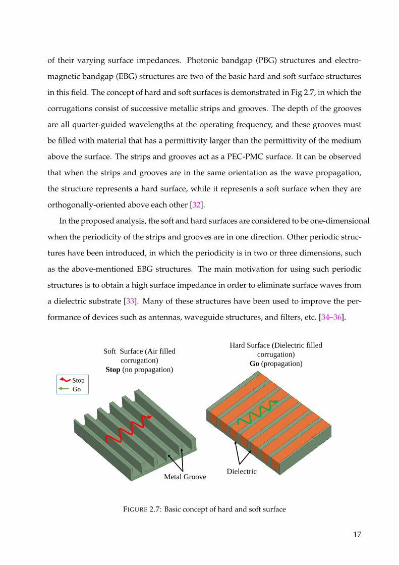
of their varying surface impedances. Photonic bandgap (PBG) structures and electro-
magnetic bandgap (EBG) structures are two of the basic hard and soft surface structures
in this field. The concept of hard and soft surfaces is demonstrated in Fig 2.7, in which the
corrugations consist of successive metallic strips and grooves. The depth of the grooves
are all quarter-guided wavelengths at the operating frequency, and these grooves must
be filled with material that has a permittivity larger than the permittivity of the medium
above the surface. The strips and grooves act as a PEC-PMC surface. It can be observed
that when the strips and grooves are in the same orientation as the wave propagation,
the structure represents a hard surface, while it represents a soft surface when they are
orthogonally-oriented above each other [32].
In the proposed analysis, the soft and hard surfaces are considered to be one-dimensional
when the periodicity of the strips and grooves are in one direction. Other periodic struc-
tures have been introduced, in which the periodicity is in two or three dimensions, such
as the above-mentioned EBG structures. The main motivation for using such periodic
structures is to obtain a high surface impedance in order to eliminate surface waves from
a dielectric substrate [33]. Many of these structures have been used to improve the per-
formance of devices such as antennas, waveguide structures, and filters, etc. [34–36].
Hard Surface (Dielectric filled
corrugation)
Go (propagation)
Soft Surface (Air filled
corrugation)
Stop (no propagation)
Stop
Go
Metal Groove Dielectric
FIGURE 2.7: Basic concept of hard and soft surface
17

In [18], the quasi-TEM modes can propagate on the ridge of the corrugations as long
as the corrugations are covered by a metallic plate, where the distances between them are
less than a quarter wavelength. This concept is similar to that of the PEC and PMC strips
with metal covers at less than quarter-wavelength distances. The wave in this kind of
structure propagates along the longitudinal direction and is prevented from propagating
along the other directions by means of the periodic grooves. The development of the
RGW was inspired based on this concept [30].
2.2.1 Ridge Gap Waveguide Structure
Ridge Gap waveguide (RGW) technology is an extension of the above-mentioned soft
and hard surfaces. Kildal [30] ] was the first to show how these surfaces can guarantee
the guidance needed for the operation of a waveguide. Fig 2.8 illustrates the basic con-
ceptual geometry of the RGW. In the ideal case, a RGW consists of two horizontal PEC
plates surrounded by PMC plates on the left and right sides, as shown in Fig 2.8. In this
design, the distance between the top and bottom plates should be less than a quarter of
the guided wavelengths at the operation frequency in order to stop the propagation of
any mode supported by the RGW. In this case, all the modes between the PEC and the
PMC plates are prevented from leaking inside of the periodic bed of nails. Meanwhile, the
TEM mode propagates on the ridge, guided by the two horizontal PEC plates [31].How-
ever, the PMC boundary does not exist naturally, and so a horizontal Artificial Magnetic
Conductor (AMC) may be used as an equivalent model for the periodic bed of nails.
Therefore, the design of an AMC is necessary to stop the modes of operation from prop-
agating through the bed of nails. Fig 2.9 shows different views of a three-dimensional
RGW image. The main concept is based on using a quarter wavelength bed of nails on
both sides of the ridge to form a PMC surface and to cover them with a metal plate. In
this case, the propagation path is between the ridge and the top plate. All the modes
between the bed of nails and the top plate are blocked while the Quasi-TEM mode prop-
agates along the ridge in the gap between the two PEC plates. The bed of nails is the
18
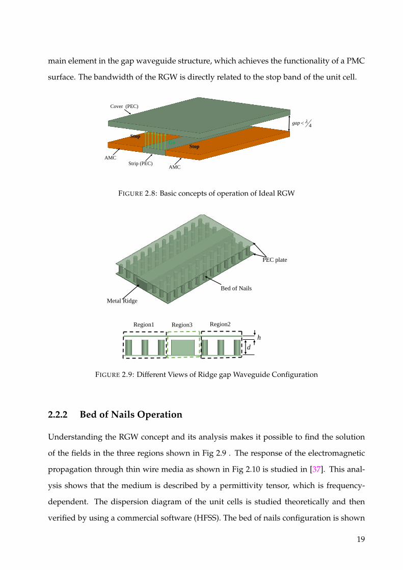
main element in the gap waveguide structure, which achieves the functionality of a PMC
surface. The bandwidth of the RGW is directly related to the stop band of the unit cell.
Strip (PEC)AMC
AMC
Cover (PEC)
4gap
Go
Stop
Stop
FIGURE 2.8: Basic concepts of operation of Ideal RGW
PEC plate
Metal Ridge
Bed of Nails
d
h
Region1 Region2Region3
FIGURE 2.9: Different Views of Ridge gap Waveguide Configuration
2.2.2 Bed of Nails Operation
Understanding the RGW concept and its analysis makes it possible to find the solution
of the fields in the three regions shown in Fig 2.9 . The response of the electromagnetic
propagation through thin wire media as shown in Fig 2.10 is studied in [37]. This anal-
ysis shows that the medium is described by a permittivity tensor, which is frequency-
dependent. The dispersion diagram of the unit cells is studied theoretically and then
verified by using a commercial software (HFSS). The bed of nails configuration is shown
19

in Fig 2.10, where the cells are formed by metallic cylinders with radius b, height d , and
with period a .The permittivity of such medium is a frequency dependent quantity as
given in [37].
x
y
z
d
a
2b
FIGURE 2.10: Thin wire media
εyy(ω, ky) =1 − k2
p
k2h + k2
y(2.1)
where kh =√
εhk , εh is the permittivity of the host medium, selected to equal unity
for simplicity, k is the wavenumber and kp is the plasma wavenumber [37] where
kp =1a
√2π
ln( a2πb ) + 0.5275
(2.2)
This model is valid only when a/d, a/λ << 1 as presented in [18].
2.2.3 Bed of Nails Region Downed by a PEC Ground Plane
In Fig 2.11, metallic pins are connected to a PEC ground plane.This structure is called
Fakir’s bed of nails. Fakir’s bed of nails was studied in [38] in order to examine the
20

reflection properties of TE and TM modes.That work reported that this kind of medium
can support three modes: a transverse electromagnetic TEM mode, a transverse magnetic
TM-y mode, and a transverse electric TE-y mode [38]. Considering the matching points
at the air-medium interface, the reflection coefficients of the TE and TM modes can be
calculated by exciting the surface of a Fakir bed of nails with a plane wave, as shown in
Fig 2.11.
FIGURE 2.11: Geometry of the “Fakir’s bed of nails”
2.2.4 Bed of Nails Covered From Both Sides by PEC-Plates
By covering the upper and lower sides of the bed of nails with bottom and top metallic
plates, as shown in Fig 2.12, a parallel plate waveguide (PPWG) is formed. The top plate
is a PEC plate and the bed of nails, together with the bottom plate, act as a homogenized
surface as explained in the previous section. The wave in such structures bounces in
the gap between the two surfaces as illustrated in Fig 2.12. By applying the boundary
conditions, the propagation constant can be derived in the y-direction for both cases of
the TE and TM modes. The TE and TM dispersion equations of this periodic structure
can be formulated as follows [18]:
21

For the TE mode,
ky =π
h + d(2.3)
where ky is the propagation constant in y-direction and, For the TM mode,
ky
ktan(khh) +
[1 −
k2 − k2y
k2y + k2 − k2
y
]tan(kd) +
k2 − k2y
k2p + k2 − k2
y
√k2
p − k2y
ktan
(√k2
p − k2yd)= 0
(2.4)
The value of ky is the solution of a transcendental equation which is obtained from
bouncing the wave in the gap between the two surfaces, as shown in Fig 2.12. The pe-
riodic bed of nails’ dimensions are chosen to be the same as the dimensions presented
in [18], where the height of the unit cell is d = 7.5mm , radius b = 0.5mm, air gap is
h = 1mm and the unit cells’ period a = 2mm.
FIGURE 2.12: Bed of Nails Covered by PEC-Plates
A Matlab code is then used to solve this equation. The dispersion curves (kTEy , kTM
y )
and the dimensions of the periodic bed of nails are presented in Fig 2.13. As illustrated
in the Fig 2.13, the TE solution does not change with the frequency. The TM solution is
shown in the same figure, where the graph is divided into three regions. The first and
third regions start from zero to f (d = λ/4) and f > (d = λ/4) , respectively, where ky
is purely imaginary.This means that there is a TM wave that propagates on the surface of
the pins. The second region consists of two sub-regions, both of which are purely real.
22

In the region between f (d = λ/4) and f (d + h = λ/2), ky is greater than the value of
light line, which means that the attenuation will be in all the directions along the surface.
Therefore, this region represents the stopband of this structure. The dispersion diagram
in Fig 2.13 clearly shows the stop band of the periodic medium, where the dispersion
relation is the relationship between the frequency and the propagation constant in the
z-direction, which can be written as
kz =√
k2 − k2y (2.5)
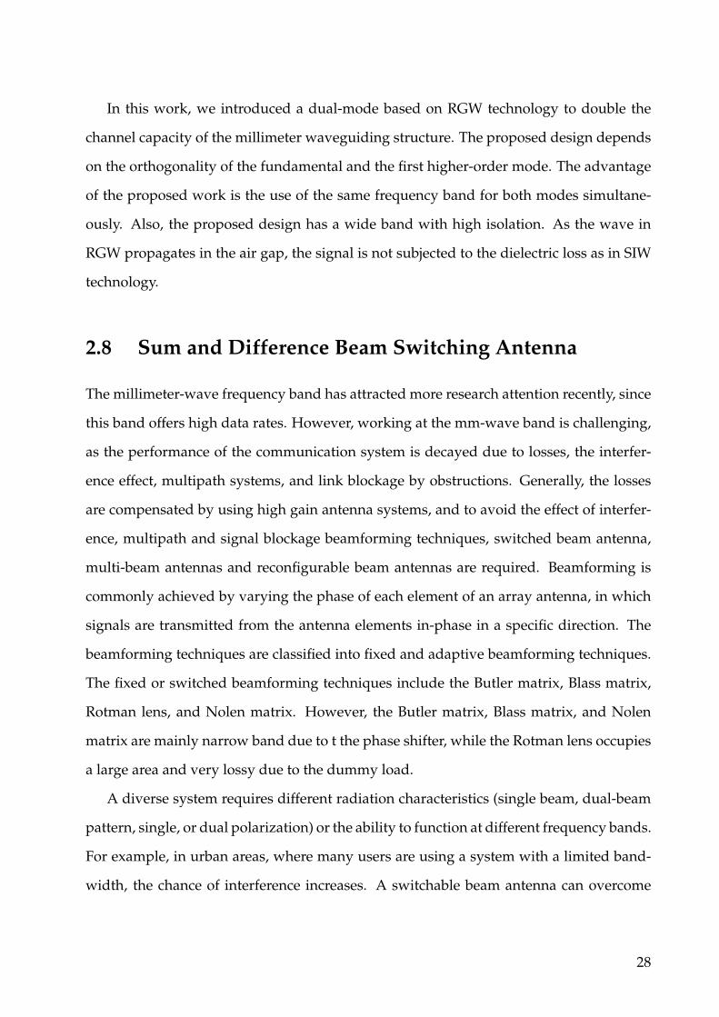
The dispersion curves of the periodic bed of nails are presented in Fig 2.14 based on
(2.3)-(2.5). The accuracy of the resulting dispersion equations is confirmed when they are
compared with simulation results obtained from the HFSS eigen mode solver.
Fig 2.14 shows that in the frequency range between 10 and 17GHz, there is no solu-
tion for (2.3) and (2.5) that gives real solution for (2.5). This means there are no waves
propagating on the bed of nails within this band of frequencies.
FIGURE 2.13: TM and TE dispersion equation of the bed of nails covered byPEC-Plates and light line
23
FIGURE 2.14: The unit cell’s geometry, simulated and theoretical dispersioncurves of the TE and TM modes
2.3 Analytical Design Procedure for Forward Wave Cou-
plers in RGW Technology
Due to the advantages as mentioned earlier of the ridge gap waveguide, it is being con-
sidered as a promising candidate for high-frequency applications, especially for the fifth-
generation (5G) applications of wireless technology [39, 40]. RGW technology is also a
remarkable candidate for the implementation of slot array antennas [41–43]. Therefore, it
is extremely important to have a clear theoretical design procedure for RGW-based struc-
tures.
Most of the published works about microwave components based on RGW technol-
ogy mainly rely on approximate or empirical equations. For example, a design procedure
for the hybrid couplers was presented in [44], in which the coupling length of the cou-
pling section is calculated by empirical expression. However, the long processing time for
optimization is needed, which led to complicate the design procedure for such microwave
components. In order to reduce the processing time, an ideal PEC-over-PMC ridge gap
24

waveguide is presented in [45] for the design of a model of a stripline. This model rep-
resents a good approximation, thereby reducing the time need for time-consuming full-
wave simulators.
A theoretical analysis of the fundamental and the first higher-order mode in gap
waveguide has been investigated in [18, 30, 46]. In [18, 46], the dispersion diagrams of
both modes are obtained in an analytical form. This facilitates analyzing hybrid couplers
with precise calculations, which will bring the dispersion characteristics under control to
design components in the required frequency band. However, those models introduced
in [18, 46] are complicated and valid whenever the period of the pins much smaller than
the height of the pin and the period of the pins much smaller than the wavelength.
In this work, we develop the concept of a fictitious type of ridge gap waveguide,
called the hybrid PEC/PMC waveguide. This will simplify and facilitate the theoretical
analysis of RGW, which would be rather complicated if an RGW is analyzed directly in
its complete form. Furthermore, due to its simplicity and accuracy, this analysis is also
used to analyze the transitional bends, hybrid junctions, and leaky-wave antenna.
2.4 RGW High Order Mode Excitation
The employment of higher-order modes for wireless communication system design is
promising at mm-wave bands. Many higher-order mode antennas and components based
on substrate integrated waveguide (SIW) have been implemented recently, and several
transitions have been utilized to excite higher-order mode in SIWs [47–49]. A simple
structure of an SIW slot array antenna based on high order mode (TE20) was presented
in [12]. Another technique was used in [13], where a multilayer balun was used to excite
the high order mode (TE20) of the SIW in order to design the multimode signal transmis-
sion.
All the above-mentioned transitions are designed for the high order mode of the SIW.
Relatively little research has been done on the high order mode of the RGW. With the
increasing number of applications for using the RGW in wireless communication systems,
25

RGW higher-order mode components and antennas have become more attractive to the
researchers. One such effort is [50], in which a magic tee was designed to feed a leaky
wave slot array antenna based on RGW. In this thesis, two different methods to excite
the first higher-order mode TERGW10 with wide bandwidth is introduced, which opens the
door to design components and antennas based on high order mode RGW technology.
2.5 RGW Power Divider Based on First High Order Mode
Aa low loss feed network is desirable for building an array antenna, and the RGW can be
used to build low loss feed network. A number of T-junction power dividers have been
designed and investigated using the ridge gap waveguide technology [51, 52]. In [53],
a Y-shaped power divider based on a printed RGW is designed to feed two leaky-wave
antennae (LWA) subarrays, which provide backward scanning and a high gain antenna.
The studies in [54, 55] present a 1:4 power divider designed to feed a one-by-four linear
slot array antenna. And, single T-junction was designed in order to build a two-by-two
slot antenna array based on RGW technology in [56].
All the above-mentioned power dividers are designed based on the dominant mode
of the RGW, namely, the Q-TEM mode. However, there is not enough information about
designing power dividers or slot array antennas based on higher-order mode RGWs. Due
to the increasing number of publications that use the RGW, especially in high-frequency
bands, higher-order mode RGW components and antennas are attracting more research
attention. To date, except for the leaky-wave antenna covered in [50], there have not
been any publications on RGW components and antennas. Therefore, one of the primary
purposes of the thesis is to introduce the first high order mode power divider based on
RGW technology. We introduce a high order mode single Y-junction power divider for
the first time in this thesis. This power divider is applied to the design of RGW frequency
scanning RGW antenna.
26

2.6 RGW Forward Hybrid Coupler Based on First High Or-
der Mode
Our literature review shows that, there has been no work reported on designing forward
couplers based on a high order mode RGW. All the available couplers based on RGW
technology have been designed and analyzed for the dominant mode, namely, the quasi-
TEM mode. A forward 3dB coupler based on RGW technology is designed and analyzed
here for the first high order mode, namely, the TERGW10 mode.
2.7 Dual Mode Waveguide
With the enormous development in using the ridge gap waveguide to design microwave
and millimeter wave components and with the limitation of channel bandwidth, it be-
comes imperative to concentrate on the increase of channel capacity of RGW. The most
effective way to achieve that is by generating two orthogonal modes on the same guiding
structure.
The multimode transmission concept is applied in [13] by using the TE10 and TE20
modes to provide a high data rate to an SIW interconnect. Meanwhile, the bandwidth
of the TE10 channel is limited by the cutoff frequency of the TE20 channel. That method
uses two separate bands for each mode, contrary to the orthomode transducer (OMT),
which uses the same band with different polarizations. Moreover, the SIW technology is
subjected to the dielectric loss as the wave propagates in the dielectric substrate.
OMT has been employed in antenna feeding networks to transmit and receive orthog-
onal modes through the same waveguide [57, 58].But, the OMT is large and bulky. One
approach to design a planar orthomode transducer (OMT) on microstrip technology is re-
ported in [59], which employed a rat-race coupler to create one polarization and a single
feed to generate another polarization, with good isolation between them. However, this
design has a narrow band.
27
In this work, we introduced a dual-mode based on RGW technology to double the
channel capacity of the millimeter waveguiding structure. The proposed design depends
on the orthogonality of the fundamental and the first higher-order mode. The advantage
of the proposed work is the use of the same frequency band for both modes simultane-
ously. Also, the proposed design has a wide band with high isolation. As the wave in
RGW propagates in the air gap, the signal is not subjected to the dielectric loss as in SIW
technology.
2.8 Sum and Difference Beam Switching Antenna
The millimeter-wave frequency band has attracted more research attention recently, since
this band offers high data rates. However, working at the mm-wave band is challenging,
as the performance of the communication system is decayed due to losses, the interfer-
ence effect, multipath systems, and link blockage by obstructions. Generally, the losses
are compensated by using high gain antenna systems, and to avoid the effect of interfer-
ence, multipath and signal blockage beamforming techniques, switched beam antenna,
multi-beam antennas and reconfigurable beam antennas are required. Beamforming is
commonly achieved by varying the phase of each element of an array antenna, in which
signals are transmitted from the antenna elements in-phase in a specific direction. The
beamforming techniques are classified into fixed and adaptive beamforming techniques.
The fixed or switched beamforming techniques include the Butler matrix, Blass matrix,
Rotman lens, and Nolen matrix. However, the Butler matrix, Blass matrix, and Nolen
matrix are mainly narrow band due to t the phase shifter, while the Rotman lens occupies
a large area and very lossy due to the dummy load.
A diverse system requires different radiation characteristics (single beam, dual-beam
pattern, single, or dual polarization) or the ability to function at different frequency bands.
For example, in urban areas, where many users are using a system with a limited band-
width, the chance of interference increases. A switchable beam antenna can overcome
28

this issue by covering multiple non-adjacent areas, and hence making a space multiplex-
ing. Using switched beam antennas has many other advantages such as saving energy,
avoiding noise, and improving the system security [60, 61].Moreover, the switched beam
antenna is able to switch the main beam to a particular direction. Therefore, it is able to
cover a large area by pointing the main beam.
Switched beam antennas are essential for designing smart antennas and adaptive sys-
tems, and have attracted much attention in the past decade. Several switched beam anten-
nas were designed and presented rather recently [62–64]; most of these designed antenna
achieved beam steering or switching by using diodes or switches. A switched beam an-
tenna is mainly dependent on using active elements and switches, but the diodes and
switches introduce additional loss and complexity to the system.
This thesis presents a sum and difference beam switching antenna based on dual-
mode RGW. The proposed antenna has a wide bandwidth and can generate two radiated
beams with reasonable high gain for the single and dual beam patterns. All these features
help to improve wireless communications links [65, 66].
2.9 Frequency Scanning and leaky Wave Antenna Based
on First Higher Order Mode Ridge Gap Waveguide
In general, the frequency scanning antenna (FSA) and leaky-wave antenna(LWA) are ones
of the traveling wave antenna family, in which they can be designed to achieve high gain
and directional beam. They have been received a significant consideration of the antenna
designers due to their abilities to produce a steering beam [67,68]. In addition to the abil-
ities to produce a steering beam, the impedance bandwidth of FSA and LWA are wider
than the phased array and slot antenna array. Moreover, those kind of antennas do not
need any complex or lossy feed network. To design of frequency-scanning antennas, the
frequency bandwidth, the beam scanning angle, and the loss in the traveling-wave an-
tenna must be considered. Frequency-scanning antenna is based on the phase-shifting
29

induced, between successive slots, by the traveling wave in the waveguide [69]. The
conventional metal waveguide offers a low loss as the wave propagates in the air. How-
ever, it is bulky, which makes it hard to be integrated with the other planar components.
On the other hand, FSA and LWA based on microstrip or SIW technology are presented
in [70–73]. Yet, the gain is relatively low due to the radiation and dielectric losses in the
microstrip line and dielectric loss in the SIW structure.
In this thesis, frequency scanning and leaky-wave antenna based on RGW technology
are designed using the first high order mode.The proposed antennas have good perfor-
mance in terms of band width,gain,wide scanning angle,and losses.
2.10 Design Methodology
In this section, the design methodology for the proposed factitious type of waveguides
referred to as the hybrid PEC/PMC waveguide and several antennas, components based
on first higher-order mode RGW are shown in Fig 2.15.
Fabrication/ Measurement
Literature Review
Mm-wave
Technology
Mm-wave propagationLoss/ Attenuation / Blockage /
Multipath
Antenna/ Components
requirementsBandwidth/Gain/ Efficiency
RGW high Order Mode ExcitationL-shape/Magic Tee
Beamforming techniqueHigh gain antenna
Based on higher order mode RGW Low-loss mm-wave components
Based on higher order mode RGW
Design/ Simulation/ Optimization
Beamforming technique1 - Frequency Scanning Antenna
2-singal and dual switched-beam
Antenna(Cavity slot/FSA/LWA/singal and
dual beam switching antenna)
Components ( Y-Junction power
divider/3dB coupler)
FIGURE 2.15: Flow chart of the design methodology for designing severalcomponents and antennas based on the first high order mode RGW.
30

Chapter 3
Analytical Design Procedure for RGW Forward
Coupler Based on PEC/PMC Waveguide Model
3.1 Introduction
Several technologies have been utilized to implement the forward wave couplers, as ear-
lier mentioned in the Chapter 1. Unfortunately, all the mentioned technologies have some
issues that could adversely affect the hybrid junction operation. For instance, the conven-
tional rectangular waveguide (WG) is bulky and hard to be integrated with the printed
waveguides. This issue becomes more and more critical at high frequencies in particu-
lar at millimeter-wave (mm-wave) band. Furthermore, either the SIW of the microstrip
technologies is subjected to high dielectric losses at high frequencies. The previously-
mentioned problems make the study of the RGW technology for designing microwave
components with better performance is preferred.
In this chapter, a design methodology of a 0dB forward coupler based on the ridge gap
waveguide (RGW) technology is presented. The proposed design methodology is based
on exact theoretical formulations rather than any approximate or empirical equations.
The procedure of this methodology is to build a virtual equivalent waveguide model. The
proposed waveguide has two vertical left and right walls are made of perfect magnetic
conductors (PMC), while the horizontal upper and lower perfect electric conductor (PEC)
walls. A detailed analysis of the proposed hybrid PEC/PMC waveguide is introduced as
the starting stage to design the RGW couplers. The equivalent RGW coupler that assures
31

the same operation of the hybrid PEC/PMC waveguide at a specific frequency range is
deduced based on detailed theoretical aspects. Furthermore, a simple analyzing of tran-
sitional bends with precise calculations is presented in this chapter, which is an essential
building block of several mm-wave components such as the six-port junction and the but-
ler matrix.The possibility of tuning the coupler center frequency is presented without the
need for utilizing any nonlinear elements. The resulting RGW couplers are implemented
by the well-known full-wave simulator (Ansoft HFSS), with verification through proto-
type measurements to confirm the validity of the proposed design methodology. A good
agreement is achieved between measurement and simulation results.
The design procedure of the proposed RGW-based hybrid junction begins by deriving
the field solutions and dispersion equations of the hybrid PEC/PMC waveguide. The
obtained dispersion is applied for determining the required coupling length at the oper-
ating frequency range. The coupling mechanism, in this design, is based on Riblet (short
slot) coupler [74]. The following step is to implement the RGW coupler based on the di-
mensions obtained from the hybrid PEC/PMC waveguide. A comparison between the
results of the hybrid PEC /PMC waveguide coupler and the RGW-based coupler leads to
an important observation. This comparison proves that the width of the RGW is not con-
stant with the frequency, which may be considered as an effective width that varies with
frequency. In other words, the equivalence between the hybrid PEC/PMC waveguide
width and the RGW effective width is a frequency-dependent property. This is described
in detail through the chapter.
Recent researches about microwave components based on RGW technology typically
depend on approximate, empirical equations, and numerical solutions. For instance, and
to the best of our knowledge, there is no reported work in the literature that applies even
and odd mode to obtain the coupling length of the forward coupler. Consequently, the
long processing time for optimization is required, which led to complicates the design
procedure for such microwave components. Hence, it is important to have a clear and
simple theoretical design procedure for the RGW-based components. A simple model
represents a good approximation of the RGW based on theoretical analysis is presented
32

in this chapter, which decreases the computational time of full-wave simulators.
3.1.1 Hybrid PEC/PMC Waveguide Operation
The main goal of this part is to develop the concept of an artificial type of waveguides
referred to as the hybrid PEC/PMC waveguide. This is to facilitate and simplify the
theoretical analysis which would be rather complicated if the RGW is analyzed directly in
its complete form. In Fig. 3.1, an equivalent hybrid PEC/PMC waveguide is presented.
The operation of the hybrid PEC/PMC waveguide is introduced firstly in this section.
Then later, the relation between this hybrid PEC/PMC waveguide and the realistic ridge
gap waveguide is explained.
PMC boundary
PEC boundary
w
h
x
y
z
FIGURE 3.1: Equivalent hybrid PEC/PMC waveguide.
The proposed waveguide in Fig.3.1 consists of two vertical PMC walls and two hori-
zontal PEC walls. For simplicity and without loss of principle, the waveguide is assumed
to be filled with free space. The width of the waveguide is w, and its height is h. It is
assumed that h is always smaller than w in order to avoid the variation of fields in y-
direction. Consequently, only the modes that are uniform in the vertical y-direction are
the modes of interest in this work.
33

In order to find full expressions for the field of those modes, one can follow a tradi-
tional solution methodology to solve the Heaviside wave equation in rectangular coordi-
nates [4]. Particular boundaries conditions have to be satisfied to solve the wave equation.
That is tangential magnetic field has to vanish on the left and right PMC walls, while the
tangential electric field has to vanish on the top and bottom PEC walls. The first condition
is different from the traditional boundary condition known in conventional rectangular
PEC waveguides.
To satisfy this boundary condition at PMC walls, one can write the expression for the
tangential electric field component as follows,
Ey =∞
∑m=0,2,4
Emcos(βxmx)e−jβzmz +∞
∑m=1,3,5
Emsin(βxmx)e−jβzmz (3.1)
where x = 0 is taken at the center of the waveguide, βzm is the propagation constant
in z-direction and βxm is the propagation constant in x-direction which can be written as,
βxm =mπ
w, m = 0, 1, 2, 3..... (3.2)
The relation between βzm and βxm is given by
β2zm + β2
xm = k20 = ω2µ0ε0 (3.3)
where k0 is the wavenumber, ω = 2π f is the radial frequency, µ0 , ε0 are the perme-
ability and permittivity of free space, respectively.
The mode that corresponds to m = 0 is the well-known TEM parallel plate mode with
propagation only in the z-direction and uniform distribution in the y- and x-directions.
This mode has real propagation constant in the z-direction βzm for all frequencies down
to direct current DC, regardless of the width w, as illustrated by the solid black curve in
Fig.3.2 (a). Moreover, this propagation constant is equal to the wavenumber in free space,
k0 . The electric field Ey of this mode as a function of x is shown by the solid black curve
in Fig.3.2 (b).
34

By assuming that the vertical PMC walls are not artificial and can be truly realized by
certain artificial material, we consider the behavior of the first higher-order mode corre-
sponding to m = 1 as a plane wave propagating forth and back between the two PMC
walls. The reflection coefficient of PMC walls must be in the way that cancels out the
tangential magnetic field components and not the electric field components as in the con-
ventional PEC waveguide, i.e., the reflection coefficient magnitude has to be equal to
unity.
As a result, the wave will be propagated in the region between those two artificial
PMC walls with the tangential electric field taking a maximum value at PMC walls. The
propagation constant of this mode in z-direction is purely imaginary below a particular
frequency, which is calculated by the distance between the two PMC walls, w. That is,
βz1 =
√k2
0 − (π
w)2 (3.4)
From (3.4), one can conclude that βz1 is pure imaginary for all frequencies less than
fc_PMC/PEC = c/2w. The behavior of the real part of βz1 is displayed versus frequency by
the dashed red curve of Fig.3.2 (a), and the electric field of this mode as a function of x is
demonstrated by the dashed red curve in Fig.3.2 (b).
(a)(b)
w/2 w/2
FIGURE 3.2: Hybrid PEC/PMC waveguide: (a) dispersion curves, (b) cross-sectional electric field distribution for the TEM, TE10 and TE20 modes, re-
spectively at wr = 13mm
35

Although this mode is the first higher order mode and not the fundamental mode, it
resembles in behavior the fundamental mode of a traditional PEC waveguide except that
the electric field is maximum at the PMC walls and zero at the center, i.e., this mode has
an odd symmetry about the longitudinal axis of the guide. The following higher-order
mode will be of even symmetry and has a cutoff frequency which is double that of the
first higher-order mode, as indicated in Fig.3.2 (b). As a further clarification, suppose w =
5mm and h = 1mm. The fundamental propagating mode is the TEM mode with m = 0
for all frequencies. The cutoff of the first higher-order mode is fc_PMC/PEC = c/2w = 30
GHz. Therefore, at 13 GHz, for instance, the field distribution will be as shown in Fig. 3.3
(a), where the only propagating mode is the uniform parallel-plate mode, while the first
higher-order mode still cannot propagate. For the first higher-order mode to propagate,
either the frequency of operation should be increased to be higher than 30 GHz or the
width w should be increased such that fc_PMC/PEC = c/2w = 30 is below 13 GHz. For
instance, if w = 13mm , the field distribution for the possible two modes at 13 GHz is
indicated in Fig. 3.3 (b). These deduced information can be used as the starting phase for
designing a factitious forward wave coupler as illustrated in the next section.
5 mmw
13 mmw 13 mmw
5 mmw
13 GHzf 0m 1m
x
y
z
x
y
z
x
y
z
x
y
z
FIGURE 3.3: Field Distribution of the ideal PMC waveguide (a) at width ofw = 5mm for m=0 and m=1 and (b) at w = 13mm for m=0 and m=1.
36

3.2 Hybrids PEC/PMC Coupler
Generally, the hybrid coupler is a kind of four ports directional coupler, which can be
designed to achieve theoretical coupling levels as high as 0dB. The coupling phenomenon
discussed in this part is mainly based on the concept of the Riblet coupler [74]. The
Riblet coupler consists of two rectangular waveguides placed parallel to each other. The
common wall is the short wall, and this wall is completely opened between the guides for
a certain length, hence the name “short-slot” coupler. The main objective of this section is
to develop the concept of the factitious type of hybrid coupler based on the Riblet coupler
concept. We called this new type “Hybrid PEC/PMC” coupler. The configuration of the
hybrid PEC/PMC coupler is illustrated in Fig.3.4 (a), where all the horizontal walls are
PECs and vertical “short” walls are PMCs.
(a) (b)
Port1
Port2
Port4
Port3
FIGURE 3.4: Hybrid PEC/PMC Coupler, (a) geometry, (b) electric field dis-tribution at 13GHz
The proposed structure consists of two PEC/PMC waveguides parallel to each other.
The common wall is the short PMC wall and this wall is opened between the guides for
a certain coupling length. The required coupling level is achieved based on this specific
37
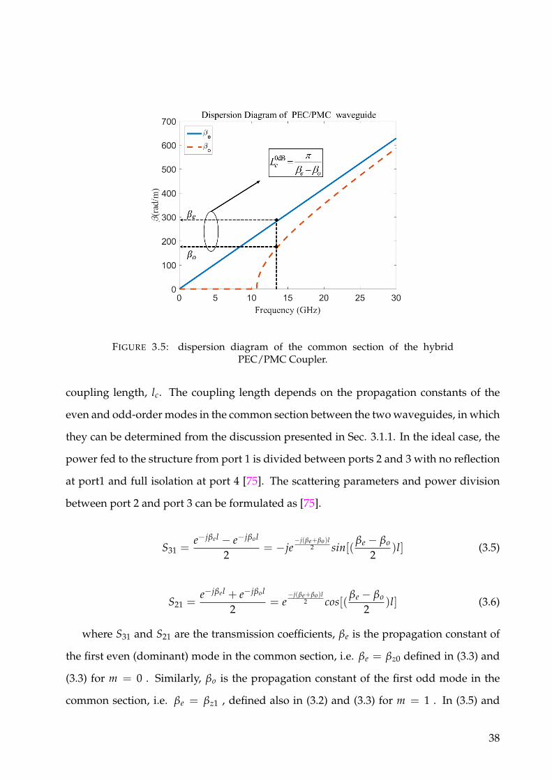
FIGURE 3.5: dispersion diagram of the common section of the hybridPEC/PMC Coupler.
coupling length, lc. The coupling length depends on the propagation constants of the
even and odd-order modes in the common section between the two waveguides, in which
they can be determined from the discussion presented in Sec. 3.1.1. In the ideal case, the
power fed to the structure from port 1 is divided between ports 2 and 3 with no reflection
at port1 and full isolation at port 4 [75]. The scattering parameters and power division
between port 2 and port 3 can be formulated as [75].
S31 =e−jβel − e−jβo l
2= −je
−j(βe+βo)l2 sin[(
βe − βo
2)l] (3.5)
S21 =e−jβel + e−jβo l
2= e
−j(βe+βo)l2 cos[(
βe − βo
2)l] (3.6)
where S31 and S21 are the transmission coefficients, βe is the propagation constant of
the first even (dominant) mode in the common section, i.e. βe = βz0 defined in (3.3) and
(3.3) for m = 0 . Similarly, βo is the propagation constant of the first odd mode in the
common section, i.e. βe = βz1 , defined also in (3.2) and (3.3) for m = 1 . In (3.5) and
38

(3.6), l denotes the length of the coupling section. Equations (3.5) and (3.6) show that by
obtaining the numerical value of the βe and βo , the required coupling length can be easily
deduced without the need of empirical equations and optimizations. For example, if the
input power should be completely transferred from port 1 to port 3, i.e. a coupling level
of 0dB is required, then from (3.5), one can obtain the required coupling length according
to,
S31 = 1 → l = lc =π
βe − βo(3.7)
The design procedure for the discussed factitious Hybrid PEC/PMC coupler is illus-
trated in the following example. Suppose the operating frequency is chosen to be 13
GHz. For suitable operation of the coupler, the dimensions of the common section must
be selected such that in this common area both the dominant and the first higher order
modes are excited. At the same time, the dimensions of the input ports must be selected
to guarantee that only the dominant mode is excited and no other mode can propagate.
As discussed in Sec. 3.1.1, the fundamental mode has no cutoff while the cutoff fre-
quency of the first odd mode is fc_PMC/PEC = c/2w , and the cutoff of the second higher
order even mode is 2 fc_PMC/PEC . Thus, for only the first two modes to exist at the oper-
ating frequency, the width of the common section must satisfy
c2 fc_PMC/PEC
< w <c
fc_PMC/PEC(3.8)
At 13 GHz, the width can be chosen to be .
Physically, the width of the input must be less than half of the width of the common
part. This should also guarantee that only the dominant mode of each input waveguide
can be excited. In this example, we select the width of the input ports to be wr = 5mm. It
is very clear from the field distribution in Fig.3.4 (b) that the required design conditions
are satisfied at the operating frequency of 13 GHz. The last step is to determine the length
of the common section which is the coupling length. To determine the coupling length,
one can substitute in (3.2) and (3.3) by wr = 13mm, m = 0 to get βe and by m = 1 to
39

get β0 at 13 GHz. After that substituting βe and βo in (3.7) gives the required coupling
length, which is found to be 21 mm. The resultant dispersion curves are shown in Fig.3.5.
With the obtained dimensions, full wave simulation gives the field distribution shown
in Fig.3.4 (b). The field distribution illustrated confirms the occurrence of full coupling,
where all the input power at port 1 is transferred to port 3 at the operating frequency.
FIGURE 3.6: S-parameters of 0dB hybrid PEC/PMC waveguide coupler.
The simulated magnitude of the S-parameters of the proposed hybrid PEC/PMC waveg-
uide coupler is shown in Fig.3.6 where the coupling level to port 3 is about 0dB from 13 to
15 GHz, the isolation level at port 4 and the through level at port 2 are below -15 dB. Con-
sequently, it could be confirmed that the power is totally transferred from port 1 to port
3 at the center frequency with a bandwidth behaviour governed by the dispersion curves
shown in Fig.3.5. Even though the proposed coupler in this section is factitious, this de-
sign procedure is found to be very useful to facilitate and simplify the design of realistic
forward wave couplers based on modern technologies such as the ridge gap waveguide
(RGW) technology. This is illustrated in the rest of this chapter.
40

3.3 Analytical Design of RGW Coupler
Artificial magnetic conductor (AMC) has been an emerging topic of research over the
last few years. AMC is made of periodic metallic structures. The configuration and the
periodicity of those structures are designed in such a way that gives a certain required
behavior. The behavior of interest in this section is to design vertical guiding walls.The
RGW technology is a relatively new type of waveguides realized by the concept of the
AMC. In this chapter, RGW is modeled and developed by the factitious hybrid-type of
waveguides discussed in Sec. 3.1.1. The main goal in the present section is to show the
last step in the design procedure presented in Sec. 3.2. That is the design of realistic
forward wave couplers using the RGW technology. The obtained parameters from the
hybrid PEC/PMC waveguide model can be utilized directly in the implementation of the
region where the wave propagates (values of h and w) in the realistic RGW.
PEC
Bed of nails
d
h
w
Stop
Go
x
y
z
FIGURE 3.7: Complete Ridge Gap Waveguide configuration.
41

Moreover, the AMC boundaries in the proposed design are realized by periodic per-
fect conducting cells. As shown in Fig.3.7, the vertical PMC boundaries model the whole
dotted region enclosed by the top and bottom PEC plates containing the periodic cells.
This is the novelty in this work whereas the dotted region was previously modeled as
horizontal PMC boundary. This periodic section is applied to stop the electromagnetic
waves from leaking outside the region on top of the ridge within certain stopband. This
structure with such boundaries supports a quasi-TEM mode as the fundamental mode.
In [18] the analytical solution of the fundamental mode propagating through the RGW
has been introduced. In [18], the dispersion diagram was obtained theoretically and ver-
ified by using a full-wave eigenmode solver. This part concentrates on summarizing the
analytical solution discussed in [18] to obtain the appropriate dimensions of the periodic
part in order to act as perfect as the PMC boundary at the required frequency band. In
addition to the analytical solution provided in [18], we consider the first two modes not
only the fundamental mode. The study of the higher order modes gives the potential of
designing the RGW coupler analytically as explained in the following subsections.
3.3.1 Design of Unit Cell and Dispersion Diagram
The dispersion curves of the unit cells is obtained theoretically and then verified by a
commercial software (HFSS). The configuration of unit cells is shown in Fig.3.8 (a), where
the cells are shaped by metallic cylinders with heigh d,radius b, and with period a. The
height of the nails d should be λ/4 [18] and the total height between the two horizontal
metal plates which is h + d equals λ/2, where h is the air gap between the bed of nails
and the top metal plate, and λ is the free space wavelength. The characteristic impedance
of AMC periodic structure depends on the dimensions of the unit cell.
The unit cell dimensions is selected to be the same as the dimensions presented in [18],
where the radius of the unit cell b = 0.5mm, height of the unit cell d = 7.5mm, air gap
is h = 1mm and the unit cells period a = 2mm. The dispersion diagram with those di-
mensions of the periodic bed of nails are presented in Fig.3.8 (b) based on (2.3)-(2.5). The
42
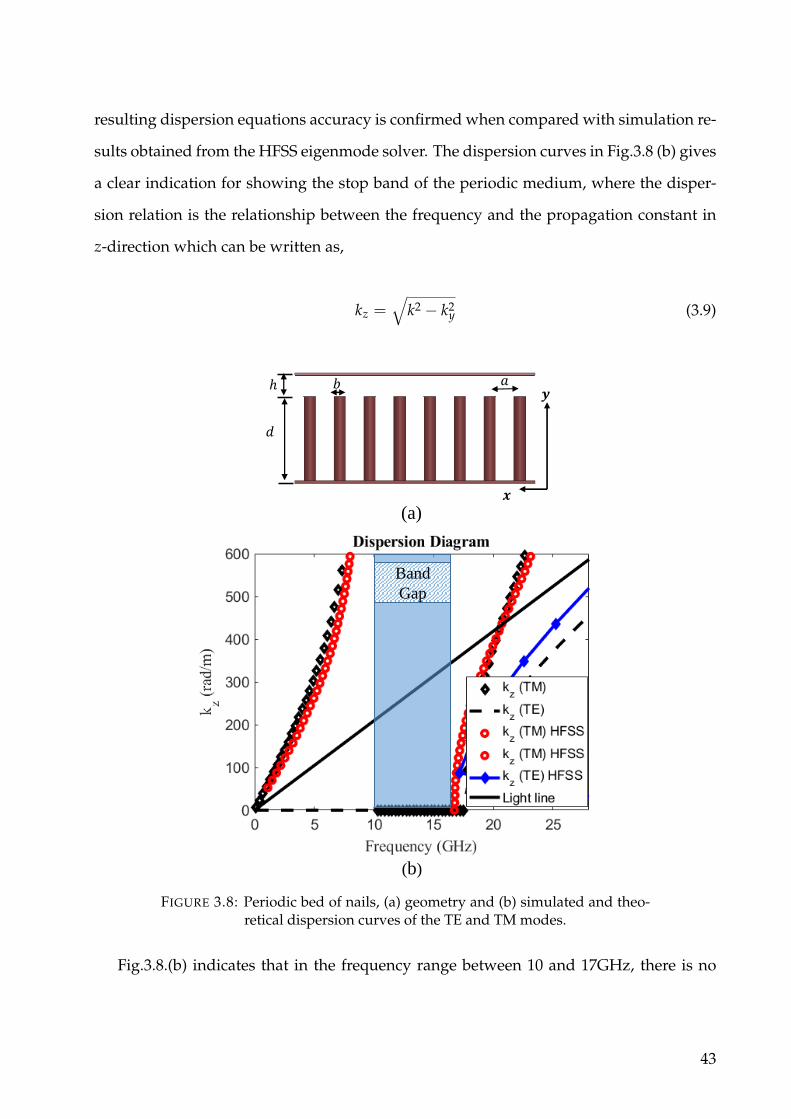
resulting dispersion equations accuracy is confirmed when compared with simulation re-
sults obtained from the HFSS eigenmode solver. The dispersion curves in Fig.3.8 (b) gives
a clear indication for showing the stop band of the periodic medium, where the disper-
sion relation is the relationship between the frequency and the propagation constant in
z-direction which can be written as,
kz =√
k2 − k2y (3.9)
(a)
(b)
Band
Gap
𝑎𝑏
𝑑
ℎ𝒚
𝒙
FIGURE 3.8: Periodic bed of nails, (a) geometry and (b) simulated and theo-retical dispersion curves of the TE and TM modes.
Fig.3.8.(b) indicates that in the frequency range between 10 and 17GHz, there is no
43

solution for (2.3) and (2.4) which gives real solution for (2.5). This means there is no prop-
agating waves on the bed of nails within this band of frequencies. In this band, a wave
incident from the middle region in Fig.3.7 does not have the possibility of propagating
on top of the bed of nails. The phase matching at this boundary ensures that the wave
has to be totally reflected. Therefore, by using this bed of nails it is possible to replace
the vertical PMC walls by the structure shown in Fig.3.7. Hence, the dispersion equations
(2.3)-(2.5) of the bed of nails can be used for designing the operating band of a complete
RGW coupler.
3.3.2 Dispersion Diagram of the Complete RGW
In order to form the complete ridge gap waveguide, a metal ridge with width w is placed
into the bed of nails as shown in Fig.3.9 (a). Considering the above in Sec. 3.2, the width of
the common section can be chosen as w = 13mm in order to guarantee both the dominant
(Q-TEM mode) and the first higher-order modes are excited over the bandwidth. Within
such structure, Q-TEM mode and the first higher-order mode are propagating along z-
direction with phase e−jkzmz.
To satisfy the boundary conditions of this design, where the cells act as PMC boundary
at both ridge sides, one can write the expression for the electric field component on the
ridge as follows,
Ey =∞
∑m=0,2,4
Emcos(kxmx)e−jkzmz +∞
∑m=1,3,5
Emsin(kxmx)e−jkzmz (3.10)
where x = 0 is taken at the center of the ridgeline. By deriving the remaining field
equations and applying the continuity of the fields along the edge of the walls (x =
±w/2), the dispersion curves of the Q-TEM mode and the first higher order mode can be
44

stated, respectively, as follows [18, 46]:
√k2 − k2
ztan(√
k2 − k2z
w2
)(k2 − k2
y) +k2
z k2y − k2
√k2
z − k2 + k2y
√k2
z − k2 + ˜k2y√
k2z − k2 + ˜k2
y
= 0 (3.11)
√k2 − k2
zcot(√
k2 − k2z
w2
)(k2 − k2
y)−k2
z k2y − k2
√k2
z − k2 + k2y
√k2
z − k2 + ˜k2y√
k2z − k2 + ˜k2
y
= 0 (3.12)
where ˜ky = ky for TE solution in (2.3), ky = ky for TM solution in (2.4),
A Matlab code is employed to solve the above transcendental equations, from which
the dispersion diagram of the Q-TEM mode and the first higher-order mode are obtained
and shown in Fig.3.9 (b). From this figure, it is clear that there are only two modes prop-
agating within the 10 to 17 GHz band. Those modes are the Q-TEM mode and the first
higher order mode.The other modes that appear on both sides of the band gap are due
to the truncated of the periodicity in the direction normal to the propagation direction.
Fig.3.9 (b) shows there is a good agreement between the analytical solution and the full-
wave solution.
To validate the relationship between the Hybrid PEC/PMC waveguide and the real
waveguide realized by the bed of nails, the result of Fig.3.5 is compared to those of Fig.3.9
(b) and shown in Fig.3.10. From the comparison in Fig.3.10, it can be depicted that the
cut-off frequency of the higher-order mode relies on the width of the ridge. Also, it can be
observed that there is an agreement in the behavior among the simulated, theoretical re-
sults and the hybrid PEC/PMC waveguide model. However, there is a slight variance in
the cut off frequency of the odd mode of the RGW and the hybrid PEC/PMC waveguide
model.
This observation reveals important information about how to utilize the design rules
shown in Sec. 3.2 for RGW coupler without causing any shift in the coupler bandwidth.
The interpretation of this deviation is that the electrical width of any RGW is slightly
45

𝑑
ℎ
𝑤𝑟
(a)
(b)
Bandwidth
FIGURE 3.9: Comparison between dispersion curves of RGW obtained fromHFSS and theoretically, at w = 13mm
𝑓𝑐 =𝑐
2 × 𝑤𝑒𝑓𝑓
𝑓𝑐_𝑃𝑀𝐶/𝑃𝐸𝐶 =𝑐
2 × 𝑤
FIGURE 3.10: Dispersion curves for the common waveguide of RGW couplerobtained from, hybrid PEC/PMC theoretical model (solid lines), theoreticalanalysis of RGW coupler (circles and diamonds) and simulation results of
RGW coupler (dashed lines) where w = 13mm.
46

different from PEC/PMC waveguide. Therefore, it is extremely important to find the
relation between the effective width of the RGW and the hybrid PEC/PMC waveguide
width. The effective width of this structure can be determined from the cutoff frequency
obtained from the dispersion diagram where,
we f f =c
2 fc≈ 1.1 × w (3.13)
The cut-off frequency of the odd mode is 10.57 GHz as shown in Fig.3.10, therefore
its effective width we f f is 14.2 mm which is about 10% wider than the actual width of
the ridgeline. By using the effective width as the width of the hybrid PEC/PMC waveg-
uide, the obtained dispersion diagram will be exactly the dispersion diagram required for
designing the RGW coupler.
As a validation for the previously-mentioned concept, the dispersion diagram of the
hybrid PEC/PMC waveguide coupler and the RGW coupler that has a width equal to the
calculated effective width of the RGW are shown in Fig.3.11. From this figure, it is very
clear that there is an agreement between simulation and theoretical results. This means
that the width of any RGW is not the physical width, but it is an effective width that must
be obtained from its dispersion. Thus, the required coupling length based on the ob-
tained effective width is demonstrated in Fig.3.12 (b) based on the PEC/PMC waveguide
dispersion of Fig.3.2 (a) or Fig.3.5.
As a conclusion, the design of any RGW-based microwave component is related to
the effective width of the RGW not the actual width dimension. The relation in (3.13) is,
of course, specific to this example. However, it is not expected to deviate much in other
examples. Therefore, it is the task of the designer to recheck the performance of the final
product if the dimensions are initially selected based on (3.13).
3.3.3 Excitation Based on PEC/PMC Circular Bend
Physically, it is impracticable to design two ports beside each other as in the hybrid
PEC/PMC waveguide. Sufficient space must be kept for at least one or two rows of
47

FIGURE 3.11: Dispersion curves of the RGW coupler and the hybridPEC/PMC waveguide with width equal to the effective width.
3dB / 2c
e o
L
0dBc
e o
L
Possible BW
FIGURE 3.12: Coupling length versus frequency for both of a 0dB and a 3dBcouplers.
48

pins to operate as a PMC. For that reason, it is chosen to deliver the signal through cir-
cular bends. The phase and amplitude responses of a circulating RGW is determined
analytically in this section. The presented phase shift by circulating RGW has not been
previously studied in details. In several applications, the phase shifter is considered as a
critical element especially in beamforming networks. As usual, a phase shift is designed
in bent shapes rather than in straight lines. Therefore, it is important to study the phase
response in such a curve-shaped RGW. The hybrid PEC/PMC waveguide is applied to
determine the phase response of circulating bends at the output and input ports of the
RGW coupler. This is to simplify and facilitate the theoretical analysis which would be
rather difficult if the RGW is analyzed directly in its complete form.
(a)
(b)
𝜌𝑜𝑢𝑡
𝜌𝑖𝑛 𝑤
inPMC boundary
𝜑 =𝜋
2
PEC
Ridge
Plate
Bed of nailsw
FIGURE 3.13: Circulating hybrid PEC/PMC and Realistic waveguide bendswith the corresponding field distributions”
A circulating bend hybrid PEC/PMC waveguide equivalent to the curved RGW is
shown in Fig.3.13. A simple theoretical design procedure for designing the circulating
49

bend hybrid PEC/PMC waveguide is introduced in this section. Also, the relation be-
tween this hybrid PEC/PMC waveguide and the realistic ridge gap circulating bend
waveguide is explained. The suggested geometry of the output and the input ports is
a circulating waveguide bend with cross section w + h , inner radius ρin and outer radius
ρout = ρin + w . The same problem was introduced earlier for the traditional metallic
rectangular waveguide [76]. Consequently, by using the same concept and changing the
boundaries condition according to the proposed design, the resultant operation can be
deduced. The wave function in circular bend waveguide can be written as [76]:
ψ = [AJn(kρ) + BNn(kρ)]exp(−jnϕ) (3.14)
where Jn(kρ) is the Bessel function of the first kind of order n, Nn(kρ) is the Bessel
function of the second kind of order n, and ρ, ϕ are the cylindrical coordinates and A is
an arbitrary constant. The constant n represents the propagation constant in ϕ - direc-
tion. This is the unknown which needs to be calculated. The wave function ψ, in (3.14)
is utilized to obtain the complete expressions for the electric and magnetic fields. How-
ever, this can be done for two types of possible solutions, namely the TEz and TMz. The
boundary conditions in this problem at hand dictate that the solution of interest is the
TMz. The general solution for TMz modes must satisfy [76]:
J′n(kρρin)N′n(kρρout)− J′n(kρρout)N′
n(kρρin) = 0 (3.15)
where kρ = k . Equation 3.15 is solved numerically for the unknown,n. For instance,
suppose the circulating waveguide designed in Section 3.2 to be of inner radius ρin =
17mm, outer radius ρout = 22mm, and ϕ = π/2 as displayed in Fig.3.13. This radius is
selected to minimize the reflections and maximize the transmission through the bend.
A Comparison among the hybrid simulated PEC/PMC waveguide bend, theoretical
analysis, and the simulated realistic waveguide bend is shown in Fig.3.14. The phase
and magnitude responses are displayed in Fig.3.14 (a) and (b), respectively. The phase
response of such waveguide is more significant than the magnitude response, which is
50

(a)
(b)
FIGURE 3.14: Comparison among the theoretical, Realistic and hybridPEC/PMC phase and magnitude response of circular bend waveguide: (a)
Magnitude response, (b) phase response.
51

critical if the coupler is to be included in beamforming networks such as Butler matrix.
From Fig.3.14 (a) and (b), it is clear that there is an agreement in the behavior of magnitude
and phase responses among the theoretical, realistic simulated results and the hybrid
PEC/PMC waveguide model from 12.5-13.5 GHz. However, there is a slight variance in
the phase at frequencies far from the center frequency. The explanation of this deviation
is that the bed of nails loses its perfect periodicity in the bent waveguide. The bed of nails
surrounding the ridge act as PMC just around the 13GHz.
3.3.4 The Full RGW Coupler
In this subsection, the vertical PMC boundaries are replaced by the periodic unit cells.
The dimensions of the unit cell are the same as presented in Sec. 3.3.1 to work over an
approximate bandwidth of (10-17) GHz. The configration of a 0dB RGW coupler with the
designed input and output ports is shown in Fig.3.15. The coupling length is obtained
from the graph shown in Fig.3.12 and (3.6) based on what is obtained from the hybrid
PEC/PMC waveguide coupler. By using the obtained effective width, the required cou-
pling length becomes 29 mm. For a physical connection to the input and output ports,
they are designed based on circulating bends as explained in Sec. 3.3.3.
The field distribution and the scattering parameters of the designed RGW coupler are
displayed in Fig.3.16 (a) and 3.16 (b), respectively. From the figures, it can be noted that
the proposed design procedure resulted in an excellent operation of the RGW coupler
exactly at the selected design frequency where full coupling occurs.
3.3.5 Frequency-Tunable RGW Coupler
One of the most valuable features that may exist in a microwave component is the tun-
ing capability. The tunability of the RGW is not widely reported in the literature. For
instance, in [77], an electrically-tunable planar groove gap waveguide resonant cavity is
presented. A combline low-loss tunable resonator based on a SIW cavity loaded with
52
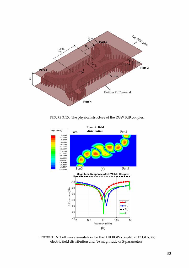
0dBcL
w
s
d
Port 1Port 3
Port 4
Port 2
Rin
Bottom PEC ground
Pin
Air gap
FIGURE 3.15: The physical structure of the RGW 0dB coupler.
Port1Port2
Electric field
distribution
Port4Port3 (a)
(b)
FIGURE 3.16: Full wave simulation for the 0dB RGW coupler at 13 GHz, (a)electric field distribution and (b) magnitude of S-parameters.
53

varactor tuning diodes is presented in [78]. In the referred examples, the tunability is
achieved by applying a nonlinear varactor element.
In this section, it is noted that the frequency tuning could be obtained easily without
the need for employing nonlinear elements. This could be achieved by just slightly mov-
ing the top conducting plate of the RGW which controls the height h of the RGW. The
result of changing the height h is presented in Fig.3.17. It could be noticed from this fig-
ure that the propagation constant of the first higher-order mode (odd mode) has different
values for different heights at every single frequency. The difference in the propagation
constant reaches to 45.7rad/m with only 2.5 mm change in the height.
FIGURE 3.17: The behavior of odd mode versus the air gap height.
On the other hand, the propagation constant of the Q-TEM mode (even mode) is al-
most independent on the height. Therefore, the coupling length obtained from equation
(3.6) may have different values for different heights as shown in Fig.3.18. This means
that controlling the height of the upper conducting plate may tune the coupler center fre-
quency as shown in Fig.3.19. The tunability mechanism is feasible, especially the upper
conducting plate of the RGW is not attached to the lower plate.
54

FIGURE 3.18: The coupling length versus the air gap height.
FIGURE 3.19: Full wave simulation for the 0dB RGW coupler at 13 GHz:magnitude S-parameters (S31 and S21) versus the air gap height.
3.4 A Possible Setup for Prototyping the Proposed RGW
Coupler
3.4.1 Microstrip to RGW Transition
To physically excite and measure the performance of the proposed structure by a Vector
Network Analyzer (VNA), a microstrip transition to RGW is needed at all input and out-
put ports. This transition should cover the entire bandwidth of our design with better
55

than 15 dB in back to back configuration. Different models of transition are presented
in [79–81].as shown in Fig.3.20 the dominant mode in microstrip and RGW is Q-TEM
mode, which is easy to design transition from microstrip to RGW. Based on previous ref-
erences, a transition from microstrip waveguide to metallic RGW is designed and tested
with the whole 0dB coupler structure. The microstrip transition is displayed in Fig.3.21.
The proposed design is very simple, which the transition of microstrip is printed over Ro-
3006 dielectric substrate with εr = 6.15 . In this transition, the microstrip line is located
on the ridgeline of the RGW. Consequently, the microstrip mode will transform gradually
to the air-filled ridge gap waveguide mode. Due to the standers of the substrate height of
the microstrip line, the size of the air gap should be adjusted gradually to be identical to
the substrate height. The changing of air gap size is realized by tapering the height of the
matching section. Two microstrip transitions to RGW are used in a back-to-back design
is illustrated in Fig.3.21. The result of the back-to-back transition is shown in Fig.3.22. It
can be observed that the S11 is below -20 dB from 12.5 to 14.5 GHz, and S21 is about 0.2
dB.
Ground
Metal ridgeline
Q-TEM mode
Metallic pin
Metallic top plate
Air gap
Dielectric SubstrateQ-TEM mode Microstrip line
Ground
(a)
(b)
FIGURE 3.20: The fundamental mode in Microstrip and metallic ridge gapwaveguide.
56

Matching section
Ground plane
Guiding ridge
Metal pin
Ro 3006(Epsr=6.15)
Metallic upper plate
Microstrip line
Ro 3006(Epsr=6.15)
FIGURE 3.21: Microstrip to metallic Ridge gap waveguide transition.
FIGURE 3.22: Simulated results microstrip to metallic ridge gap waveguidetransition.
3.4.2 Whole Setup Model of 0dB Coupler Include the Microstrip Tran-
sition
The complete structure of the 0dB coupler with the designed transitions is solved nu-
merically before the fabrication stage. Fig.3.23 shows the whole model setup of the 0dB
coupler, where the top metal plate is displaced to up to show the internal details of the
structure.The scattering parameters and field distribution of the designed RGW coupler
are shown in Fig.3.24 (a) and (b), respectively. From this figure, it can be concluded that
the proposed design procedure resulted in an excellent operation of the RGW coupler.
Where a full coupling occurs specifically at the chosen design frequency.
57

Matching section
Ridgeline
Ground plane
Metallic pin
Connector’s holes
Top plate
Connector model
Ro 3006
(Epsr=6.15)
FIGURE 3.23: The whole setup model of 0dB coupler include the microstriptransition.
(a)
(b)port1
port4
port2
port3
FIGURE 3.24: Simulated scattering parameters and Electric field distributionof the whole setup model of 0dB coupler include the microstrip transition.
(a) Scattering parameters, (b) Electric field distribution.
58

3.4.3 Fabrication and Experimental Results
In order to verify the proposed structure, a prototype of the 0dB coupler is fabricated and
measured, as shown in Fig.3.25. The main body of the 0dB coupler and the microstrip
transition are built separately. After that, all parts are assembled by bolts. We use plastic
3D printing technology to build the main body of the structure of the 0dB coupler. The
3D printer uses an opaque white SLA plastic that acts similarly to polycarbonate and has
elevated heat resistant. Then, the printed structure is electroplated with 0.02 mm thick
copper material. Also, the PCB technology is used to fabricate the microstrip transition
and the top plate. Fig.3.25 (a) and (b) show the individual parts and the assembled 0dB
coupler with the connectors respectively.
(a)
(b)
FIGURE 3.25: Pictures of the fabricated individual parts and assembled struc-ture. (a) Individual parts of designed 0dB coupler, (b) Assembled 0dB cou-
pler.
The simulated and measured S parameters of the proposed design are shown in Fig.3.26.
From this figure, it can be observed that the measured and simulated results in good
agreement. The designed coupler works perfectly at the chosen design frequency where
59
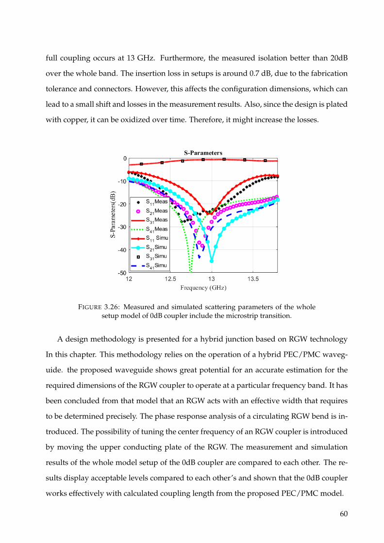
full coupling occurs at 13 GHz. Furthermore, the measured isolation better than 20dB
over the whole band. The insertion loss in setups is around 0.7 dB, due to the fabrication
tolerance and connectors. However, this affects the configuration dimensions, which can
lead to a small shift and losses in the measurement results. Also, since the design is plated
with copper, it can be oxidized over time. Therefore, it might increase the losses.
FIGURE 3.26: Measured and simulated scattering parameters of the wholesetup model of 0dB coupler include the microstrip transition.
A design methodology is presented for a hybrid junction based on RGW technology
In this chapter. This methodology relies on the operation of a hybrid PEC/PMC waveg-
uide. the proposed waveguide shows great potential for an accurate estimation for the
required dimensions of the RGW coupler to operate at a particular frequency band. It has
been concluded from that model that an RGW acts with an effective width that requires
to be determined precisely. The phase response analysis of a circulating RGW bend is in-
troduced. The possibility of tuning the center frequency of an RGW coupler is introduced
by moving the upper conducting plate of the RGW. The measurement and simulation
results of the whole model setup of the 0dB coupler are compared to each other. The re-
sults display acceptable levels compared to each other’s and shown that the 0dB coupler
works effectively with calculated coupling length from the proposed PEC/PMC model.
60

Chapter 4
Odd Mode RGW-based Devices: Design
Procedure
4.1 Introduction
The main requirements in the components and antennas design are a low loss, a high
gain antenna, and compact size, which are highly recommended to compensate various
loses that conventional waveguides are suffered [82–84]. The antenna array is commonly
used to achieve high gain, in which a complex feeding network is needed to excite each
radiator element. However, the feeding network causes extra losses in addition to the
conventional waveguide losses. Therefore, the mentioned issues must be considered to
implement any wireless system.
Recently, substrate integrated waveguide (SIW) high order mode becomes more at-
tractive to design antenna and network antenna. Based on the properties of high order
mode, the antenna feeding can be implemented with a more compact size and low losses.
Several higher-order-mode (SIW) designed were implemented for high performance,
cost reduction ,and simple manufacture at mm-wave band [85–87]. In [88], A single-
fed slotted cavity SIW antenna using high-order modes is introduced, which offers a
wideband and high gain with low-cost. For mm-wave polarization changeable appli-
cations, a microstrip patch antenna based on SIW technology using high-order-mode is
presented in [89]. Using high order mode SIW cavity, high-gain dual-polarization and
dual-frequency high-gain cavity slot antennas are presented in [90,91]. Generally, most of
61

the works that based on high order mode are designed using substrate integrated waveg-
uide (SIW) technology, which are suffering from the dielectric loss.
The ridge gap waveguide (RGW) has many advantages rather than conventional waveg-
uides, which is low loss and integrated with planar circuits. Therefore, by using high or-
der mode RGW, it is possible to gather between the aforementioned advantages of using
high order mode and overcoming the dielectric loss.
The employment of ridge gap waveguide (RGW) higher-order modes can consider-
ably to design several effective components and antennas at the millimeter-wave band
, which led to reduce the number of metal pins and therefore simplify the component
configuration. As the hybrid couplers, Y-junction power divider and antennas are a nec-
essary for any wireless system, various components and antennas are designed based on
high order mode RGW in this thesis.
4.2 First High Order Mode Ridge Gap Waveguide
In this chapter, two methods to excite the first higher order mode of the ridge gap wave-
guide (RGW) is presented. The fundamental mode of the RGW is well studied in a lot
of papers while the higher order modes are ignored. However, they have some good
properties that make them suitable for specific applications. First high order mode of
ridge gap waveguide can be used in many applications, but this fact enormously depends
on the performance of the transition that use to excite the first high order mode and the
components that are suitable to use with RGW. The chosen frequency band, in this thesis,
objective to design components and antennas works in Ka-band. The ka band is exploited
for a diversity of applications such; police radar, satellite, and many different millimeter-
wave applications [92, 93]. Because of that, it is needed a transition works at the specific
frequency with a small size, acceptable bandwidth, low losses, and simple configuration.
In this chapter, a two method to excite the first higher order mode of the ridge gap wave-
guide (RGW) is introduced.
62

4.2.1 Ridge Gap Waveguide Analysis and Unit Cell
The dimensions of the unit cell chosen to work between 25GHz and 40GHz. The unit cell
structure is shown in Fig 4.1 (a), where the cell is formed by metallic cylinder with height
d = 2.3mm, radius b = 0.5mm, period a = 2.5mm, and air gap height h = 1mm. The
dispersion diagram of the unit cells is obtained by using commercial software (HFSS).
The dispersion curves of the unit cell, shown in Fig 4.1 (b), is obtained based on assuming
that the propagation is in the z-direction. It is very clear from the dispersion diagram in
Fig 4.1 (b) that there is a bandgap from 22 GHz to 50 GHz.
a
h
d
b
y
x
(a)
(b)
FIGURE 4.1: The configuration of unit cell and its dispersion diagram. (a)The configuration of the unit cell. (b) Dispersion diagram.
4.2.2 Ridge Gap Waveguide Section
To design the complete RGW, a metal ridgeline with width w is inserted into the bed of
nails as shown in Fig 4.2 (a). The ridgeline width is selected to be w = 7.5mm in order
to ensure the excitation of the dominant (Q-TEM) and the higher-order modes (TEm0)
63
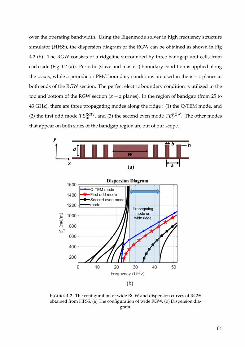
over the operating bandwidth. Using the Eigenmode solver in high frequency structure
simulator (HFSS), the dispersion diagram of the RGW can be obtained as shown in Fig
4.2 (b). The RGW consists of a ridgeline surrounded by three bandgap unit cells from
each side (Fig 4.2 (a)). Periodic (slave and master ) boundary condition is applied along
the z-axis, while a periodic or PMC boundary conditions are used in the y − z planes at
both ends of the RGW section. The perfect electric boundary condition is utilized to the
top and bottom of the RGW section (x − z planes). In the region of bandgap (from 25 to
43 GHz), there are three propagating modes along the ridge : (1) the Q-TEM mode, and
(2) the first odd mode TERGW10 , and (3) the second even mode TERGW
20 . The other modes
that appear on both sides of the bandgap region are out of our scope.
hd
w
b
x
y
a
Propagating
mode on
wide ridge
(a)
(b)
FIGURE 4.2: The configuration of wide RGW and dispersion curves of RGWobtained from HFSS. (a) The configuration of wide RGW. (b) Dispersion dia-
gram.
64

Using HFSS, electric fields distribution of the first three modes propagate on the ridge
between 25 GHz to 43 GHz can be obtained, as shown in Fig 4.3. From this figure, it is
clear that both of the fundamental mode and second higher order mode have even sym-
metry while the first higher mode has odd symmetry. All the modes excited within this
RGW are propagating along the z-direction. The periodic bed of nails acts as a perfect
magnetic conductor (PMC) which satisfies the boundary conditions of this RGW struc-
ture.
Q_TEM
𝑻𝑬𝟏𝟎𝑹𝑮𝑾
𝑻𝑬𝟐𝟎𝑹𝑮𝑾
First odd mode
Second even mode
FIGURE 4.3: Electric field distribution of the first three modes proposed wideRGW.
w/2 w/2
E/Em
𝑥
FIGURE 4.4: Cross sectional fields distribution of the first three modes.
65

By using the hybrid PEC/PMC waveguide, the electric field distribution for the TEM,
TERGW10 and TERGW
20 modes in the middle of the air gap along the x-axis can be obtained as
shown in Fig.4.4 based on equation (3.10). From this figure, it can be shown that the field
distribution of the TEM and TERGW20 modes in RGW is maximum in the center and at the
PMC walls (w/2) while the TERGW10 mode is maximum at the PMC walls and vanishes at
the center. Accordingly, both the Q-TEM and the TERGW20 modes shown in the dispersion
diagram must be suppressed to guarantee a single-mode operation. Given Fig.4.4, if a
vertical PEC wall located on the origin point (0,0) of the graph, the only fist odd mode
TERGW10 will satisfy the boundary condition at the PEC wall, while the other even modes
(Q-TEM and TERGW20 ) do not satisfy the new boundary condition, where those modes
have a maximum E-field at the center. Therefore, in such a structure with such boundary
conditions, only the odd mode will be propagated on the ridge. So by imposing a PEC
wall in the middle of the ridgeline, the even modes are eliminated and only the odd mode
exists. To prove that, the following ridge gap waveguide with a PEC wall at the middle
is investigated and the corresponding dispersion diagram is shown in Fig.4.5 (a). From
the dispersion diagram shown in Fig.4.5 (b), there is only one propagating mode TERGW10 ,
from 25 GHz to 43 GHz.
To verify this analysis, a simulated results of electric fields distribution of the prop-
agated modes of RGW with PEC wall is obtained and shown in Fig.4.5 (c). From this
figure, it is very clear that only the odd mode TERGW10 satisfies the new boundary condi-
tion. The simulated E-field distribution of the TERGW10 mode in such an RGW structure is
shown in Fig.4.6. From this figure, one can notice the odd symmetry of the electric field
with respect to the x-axis can be used to create two horizontal slots to differently feed the
cavity.
66

x
y
PEC Wall
BC Et =0
(a)
(b)
(c)
𝑻𝑬𝟏𝟎𝑹𝑮𝑾
FIGURE 4.5: The configuration of RGW with PEC boundary at the middleand its dispersion curves. (a) The configuration of RGW. (b) Dispersion dia-
gram. (c) Electric field distribution of the RGW.
x
y
z
E-Field
H-Field
FIGURE 4.6: Electric and magnetic field distribution of the RGW first oddmode TERGW
10 (proposed wide RGW).
67

4.3 Excitation of First High Order Mode by Magic Tee
4.3.1 Magic Tee Implementation
In order to suppress the undesired even modes, to guarantee the propagation of only
TERGW10 mode over the bandwidth for single-mode operation, a vertical PEC wall over the
ridge is necessary. However, vertical PEC in the form displayed in Fig.4.5 (a) is hard to
physically construct. As an alternative solution, the magic tee structure shown in Fig.4.7
can be employed to obtain the same behavior, but with a realizable geometry. The magic
tee provides a differential excitation to the ridgeline which imposes a virtual PEC wall in
the middle of the ridge. Consequently, only the odd mode TERGW10 is excited on the ridge
and the even modes (Q-TEM and TERGW20 ) are suppressed. A magic tee is commonly used
to feed microwave systems, which consists of four ports and can be utilized as an E-plane
or H-plane power dividers. For instance, if the power is applied to the difference port of
the magic tee, the power will be equally divided between two ports with a 180o phase shift
and the remaining port is isolated. In this work, a short circuit is placed in the isolation
port of the magic tee as it does not affect the magic tee performance. Fig.4.7 (a) shows
a 3D view of the three-port magic tee configuration with all associated dimensions are
listed in Table 4.1. In the shown structure, port 1 is the input port while port 2 and port 3
are the output ports. When exciting this structure at port 1, the power is equally divided
between port 2 and port 3 with a 180o phase shift between them as clearly appears in the
field distribution of Fig.4.7 (a). A hemisphere is applied as shown in Fig.4.7 (b) in order
to improve the matching [50].
TABLE 4.1: Parameters of The Magic Tee
Parameter Win Lin Wp Hp Ws Ls Lis LpValue(mm) 7.212 3.556 5.5 0.9 4.4 3.7 5.5 3.4
The simulated magnitude and phase responses of the S-parameters of the designed
magic tee are shown in Fig.4.8 (a) and (b), respectively where the transmission levels to
68

Lin
Win
Ls
Lis
Wp
Ws
hemisphere
Port1
Port3
Port2
Hp
Lp
(a)
(b)
FIGURE 4.7: The configuration of the magic tee transition. (a) 3D view withthe electric field distribution. (b) Top view right, middle cut left.
port 2 and port 3 are about -3 dB from 26 to 40 GHz, the reflection level at port 1 is below
-20 dB and the phase difference between port 2 and port 3 is 180o degrees.
FIGURE 4.8: The magic tee S-parameters. (a) Magnitude. (b) Phase.
69

4.3.2 RGW Excitation by Magic Tee
To excite the proposed wide RGW, the magic tee shown in Fig.4.7 is used where its output
ports 2 and 3 are the inputs to the wide RGW as shown in Fig.4.9, the top metal plate is
hidden to show the inside structure. By applying the power to port1 of the magic tee, the
power is equally divided between port 2 and port 3 with 180o phase shift. Then those
outputs are used as inputs of the proposed wide RGW. Fig.4.9 shows the electric field dis-
tribution of the mode that can propagate in this ridge . From the E-filed distribution, it is
clear that there is only one propagating mode TERGW10 within the ridge with the tangential
electric field is zero in the middle of the ridge and maximum on its sides.
Magic Tee
Transition
x
y
z
Magic Tee
Transition
FIGURE 4.9: RGW with the magic tee transition. (a) Electric field distributionof the TERGW
10 mode in the proposed RGW.
By applying the superposition method of these two inputs, the even modes are elim-
inated while only the odd mode propagates inside the wide RGW. The simulated E-field
distribution in RGW with the magic tee transition is shown also in Fig.4.9 (a). A very good
matching is achieved over the whole bandwidth between 28 GHz and 39 GHz which is
shown in Fig.4.10.
70
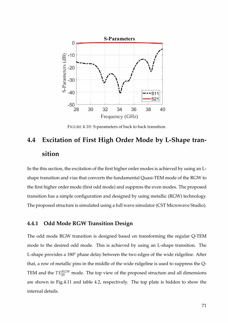
FIGURE 4.10: S-parameters of back to back transition.
4.4 Excitation of First High Order Mode by L-Shape tran-
sition
In the this section, the excitation of the first higher order modes is achieved by using an L-
shape transition and vias that converts the fundamental Quasi-TEM mode of the RGW to
the first higher order mode (first odd mode) and suppress the even modes. The proposed
transition has a simple configuration and designed by using metallic (RGW) technology.
The proposed structure is simulated using a full wave simulator (CST Microwave Studio).
4.4.1 Odd Mode RGW Transition Design
The odd mode RGW transition is designed based on transforming the regular Q-TEM
mode to the desired odd mode. This is achieved by using an L-shape transition. The
L-shape provides a 180o phase delay between the two edges of the wide ridgeline. After
that, a row of metallic pins in the middle of the wide ridgeline is used to suppress the Q-
TEM and the TERGW20 mode. The top view of the proposed structure and all dimensions
are shown in Fig.4.11 and table 4.2, respectively. The top plate is hidden to show the
internal details.
71

Pc
Ld
wd
Lc
win
wmatch
wrD port2
port1
Top plate Metallic pins
Ridgeline
Input
Output
Groundpin
(a) (b)
FIGURE 4.11: (a) Odd mode RGW configuration (b) Top view .
TABLE 4.2: Parameters of the transition
Parameter Value(mm) Parameter Value(mm)Pc 6.5 Wr 10
Wmatch 1.5 Wd 30Win 1.4 Ld 25Lc 14.3 D 0.3
The matching is achieved by using a quarter wave transformer between the input port
which supports only the Q-TEM mode and the output port that supports the odd mode.
The equation of the strip line can be used to have the starting dimension of the ridge
line [94].
ZRGW =η0
2
[Wr
2h+ 0.0441
]−1
(4.1)
where η0 is the intrinsic impedance of the air.
An optimization process is carried out to have a wide bandwidth matching. The S-
parameters of the proposed odd mode transition is shown in Fig.4.12. The reflection
coeffi-cient of this structure is less than -10 dB over 8GHz from 28 to 36 GHz. Where
more than 93% of the input power has been transformed into the odd mode at the output
port. Fig.4.13 illustrates the electric field distribution on the proposed transition at 32
72
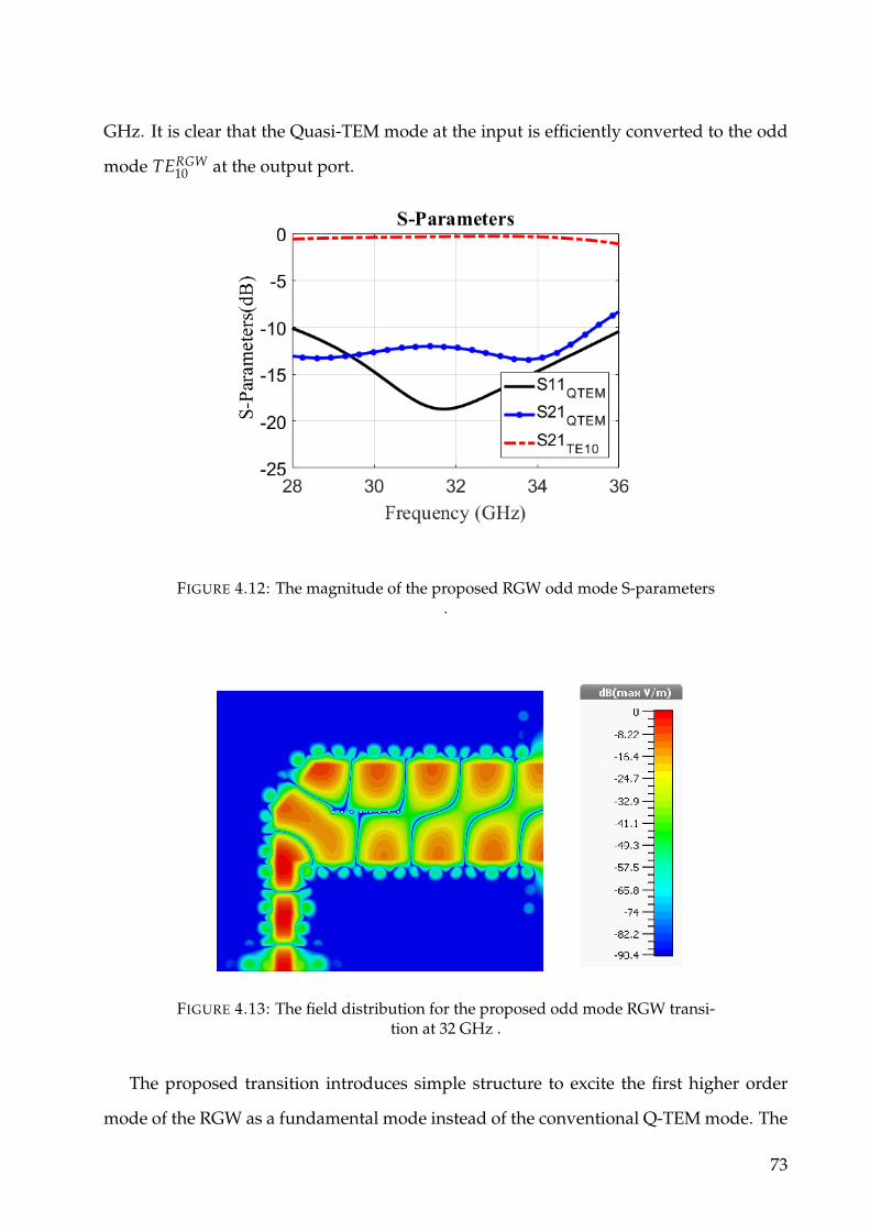
GHz. It is clear that the Quasi-TEM mode at the input is efficiently converted to the odd
mode TERGW10 at the output port.
FIGURE 4.12: The magnitude of the proposed RGW odd mode S-parameters.
FIGURE 4.13: The field distribution for the proposed odd mode RGW transi-tion at 32 GHz .
The proposed transition introduces simple structure to excite the first higher order
mode of the RGW as a fundamental mode instead of the conventional Q-TEM mode. The
73

structure is fed by a Q-TEM mode at the input port then it is transformed into the odd
mode at the wide ridgeline. The whole structure has achieved a matching level of less
than -10 dB from 28 to 36 GHz. With the proposed waveguide, the odd mode can be used
which has a great potential for millimeter-wave devices that needs the use of higher order
modes.
4.5 RGW Y-Junction Based on First High Order Mode
Ridge gap waveguide and slot array antennas have been a remarkable topic among mi-
crowave components and the antennas designers. Typical RGW components and anten-
nas can be lightweight and compact. Also, it can offer low losses as the field propagates
in the air rather than propagates in a dielectric substrate which suffers from dielectric
losses, especially at high frequencies. Moreover, when design an array antenna based
on conventional waveguide for high gain or multiple beam application, the efficiency of
antenna decreases as losses increased. Furthermore, any discontinuities in the feeding
network cause a radiation loss [95].
Recently developed the RGW technology verified in [96, 97] which can be used to ad-
dress most mentioned issues. Thus, the RGW power divider to feed slot array antenna
can be used in many applications. As we discussed necessity exploit high order mode
in RGW to improve the performance of antenna feeding network, till now, there has not
been any work on high order mode RGW antennas. Therefore A novel Y-junction power
divider structure based on the first higher order mode (TERGW10 ) mode of RGW is intro-
duced.
The proposed odd mode power divider has a simple configuration based on metallic
(RGW) technology. The fundamental mode through this structure is the odd mode of
RGW (First high order mode ) rather than the usually-studied quasi -TEM mode. The first
higher order mode of the RGW (TERGW10 ) is used to excite the Y-junction by expanding
the ridge width, and suppressing both of the Q-TEM and (TERGWm0 ) modes,where (m =
2, 4, 6..). Due to the nature of the field distribution of an odd mode through RGW, two
74

of half wavelength can be generated successively. This kind of field distribution allows
etching two horizontal slots successive in phase during half wavelength, in which this
completely removes grating lobes in E-plane and reduces the beamwidth in H-plane. The
resulting proposed structure is implemented through well-known full wave simulator,
Ansoft HFSS.
4.5.1 First High Order Mode RGW Y-Junction Design Procedure
Y-junction is a basic component of an array antenna as a feed network, where commonly
consists of transformer sections. It is well-known that the even and odd modes have
different impedance, so each kind of mode could suit various applications. From this
point, we decided to study the design of the odd mode RGW Y-junction power divider.
Where the propagating mode in the structure is odd mode rather than the usually-studied
even mode. Here we describe how the proposed Y-junction based on higher order mode
RGW is designed, and how it works in two cases:
1. Ideal Case
The ridge line of proposed Y-junction is designed with a width supports first high
order mode as shown in Fig.4.14. A suitable transformer section is used to match
different parts of ridge line. As an ideal case, we use vertical PMC boundary con-
ditions surround the ridge instead of using bed of nails as shown in Fig.4.14 (a). In
this figure, the upper ground is hidden to show the internal details of the structure.
Two rows of matching vias and matching steps, which are symmetrical with respect
to the x-axis, and are used to improve the matching level. The structure is designed
and optimized using HFSS. Considering the boundary conditions, two vertical PMC
boundaries on the YZ-plane on the both sides of the ridge line are set in software.
This helps in saving the processing time and improves the accuracy of the results.
Then, dimensions have been optimized in order to reach the best values as they are
listed in table 4.3. The three arms of Y-junction are divided such away in order to
75

set the bed of nails that required to create PMC boundary. The simulated magni-
tude and phase responses of the S-parameters of designed Y-junction are shown in
Fig.4.15 (a) and (b), respectively where the transmission levels to port 2 and port 3
are about -3 dB from 28 to 34 GHz, the reflection level at port 1 is below -15 dB and
in phase.
(b)
vias
ww2
w1
d1
viasPMC boundary
w
w2
w1
d1
port1
(a)
port3
port2
FIGURE 4.14: Y-Junction RGW based on first higher mode with ideal PMCboundary conditions. (a) Structure top view. (b) Simulated electric field dis-
tribution
TABLE 4.3: Parameters of the Y-Junction
Parameter W W1 W2 d1Value(mm) 8.1 7.28 9.2 0.5
76

(a) (b)
FIGURE 4.15: The Y-junction S-parameters. (a) Magnitude. (b) Phase
2. Realized Case
The realized case of Y-junction is to replace the vertical PMC boundary with periodic
nails. The configuration of the unit cell and its dispersion diagram is shown in Fig.
4.1 (a,b). It can be illustrated from the dispersion diagram of the unit cell that the
stopband of the unit cell covers from 25 to 40 GHz. The structure of the unit cell and
dispersion relation are designed and obtained using the eigenmode solver.
The realized structure of RGW Y -junction is shown in Fig.4.16 (a). Fig.4.16 (b) shows
the electric field distribution of the mode that can propagate in this structure. From
the E-filed distribution, it is clear that there is only one propagating mode within
the ridge with the tangential electric field is zero in the middle of the ridge and
maximum on its sides. The simulated magnitude and phase responses of the S-
parameters of the designed Y-junction are shown in Fig.4.17 (a) and (b), respectively
where the transmission levels to port 2 and port 3 are about -3 dB from 28 to 34 GHz,
the reflection level at port 1 is below -15 dB. From the results, it clear that there is
an agreement between the ideal case results and realized case, in which this will be
helped to save the processing time and improve the accuracy of results. By using
the Magic tee designed in Sec 4.3.1, we can implement effective Y-Junction based on
the first order mode RGW.
77
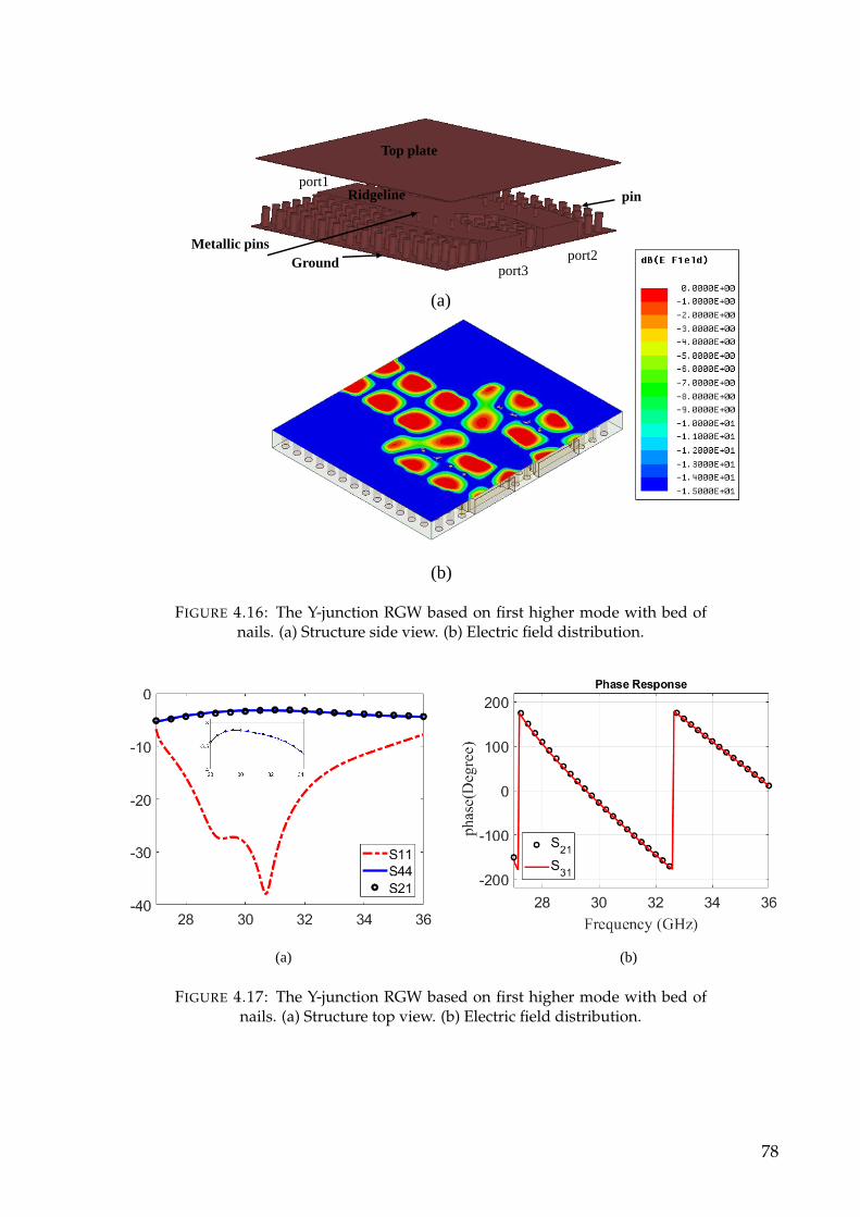
(b)
(a)
port1
port2
Top plate
Metallic pins
Ridgeline
Ground
pin
port3
FIGURE 4.16: The Y-junction RGW based on first higher mode with bed ofnails. (a) Structure side view. (b) Electric field distribution.
(a) (b)
FIGURE 4.17: The Y-junction RGW based on first higher mode with bed ofnails. (a) Structure top view. (b) Electric field distribution.
78

4.6 Hybrid Forward Coupler Based on First Higher Order
Mode RGW
In general, the hybrid coupler can be designed to achieve theoretical coupling levels as
high as 3 dB or 0 dB. The coupling phenomenon discussed in this section is mainly based
on the concept of the Riblet coupler [41]. The Riblet coupler consists of two rectangular
waveguides placed parallel to each other. The common wall is the short wall and this
wall is totally opened between the guides for a certain coupling length, hence the name
“short-slot” coupler. The main goal in this section is to develop the hybrid coupler based
on the odd mode RGW. We call this new type “RGW Odd Mode” coupler. Where the
fundamental propagating mode in the input ports of this coupler is first high order mode
rather than the usually-studied quasi-TEM mode.
4.6.1 3dB Hybrid Coupler
Starting with the same analysis of Riblet coupler. Since, the fundamental mode through
the input ports of this structure is first high order mode of RGW TERGW10 rather than
the usually-studied quasi -TEM mode, the coupling length depends on the propagation
constants of the first higher order mode and second higher order mode in the common
section between the two waveguides. Hybrid PEC/PMC coupler which is presented in
Chapter 3 is deployed in order to calculate the coupling length. The required coupling
level is achieved based on this specific coupling length lc. The width of coupling section in
this design should be more than two times of the waveguide width to allow the third high
order mode to propagate in the waveguide. The configuration of the hybrid PEC/PMC
coupler is shown in Fig. 4.18 (a), where all the vertical “short” walls are PMCs and the
horizontal walls are PECs. Ideally, the power fed to the structure from port1 is divided
equally between ports 2 and 3 with phase shift π/2 between the outputs 1 and 2, and
with full isolation at port 4.
79

Since the input of the coupler is odd mode and designed frequency is 32 GHz, the
ridge width is selected to be 6 mm to support TERGW10 mode. As shown in Fig 4.18 (a). in
order to improve the matching and isolation level, a raw of vias is centered in the air gap
between the top and bottom plate in all ports.
TABLE 4.4: Parameters of the 3dB Coupler
Parameter Value(mm) Parameter Value(mm) Parameter Value(mm)ltotal 29.5 wc 16 Lc 9.1Lsin 10 wB 4 dmatching 0.4
dcenter 0.5 hgap 0.5 dperiod 2
(a)
(b)
port1
port4
port2
port3
hgap
win
Lc
dmatching
dcenter
wc
Ltotal
wB
Lsin
dperiod
FIGURE 4.18: 3dB Hybrid PEC/PMC Coupler, (a) geometry, (b) electric fielddistribution at 32GHz.
The simulation results expose the ability to design a forward coupler, where the cou-
pling occurs in the coupling section. The simulated S-parameters of the proposed hybrid
PEC/PMC waveguide coupler is shown in Fig. 4.19, where the coupling level at port 2
and port 3 is about about 3 dB from 28 GHz to 35 GHz, the isolation level at port 4 is be-
low -15 dB. Accordingly, it could be confirmed that the power is divided equally between
80

FIGURE 4.19: S-parameters of the proposed 3dB hybrid PEC/PMC waveg-uide coupler
FIGURE 4.20: Phase response of the proposed 3dB hybrid PEC/PMC waveg-uide coupler
81

port 2 and port 3 at the design frequency. Fig.4.20 illustrates the phase difference between
| S21 | and | S31 | which equal a 90o with a phase imbalance of ±5o.
Win_eff
Lc-eff
Wc_eff
Top plate
(a)
(b)
Port 1
Port 4
Port 3
Port 2
FIGURE 4.21: 3dB Hybrid Coupler, (a) geometry, (b) electric field distributionat 32 GHz.
The final phase in the design of 3 dB coupler is to replace the PMC boundary walls
with bed of nails. The unit cell design is presented in Sec4.2.1. Using the HFSS, the pro-
posed 3dB coupler can be simulated to obtain of the S parameters, where all the dimen-
sions are the same what is listed in Table 4.4 except the width of the input and coupling
section. The width of any RGW is not the physical width, but it is an effective width that
should be obtained from its dispersion. Two unit cell rows should be located between
the ports of 3 dB coupler RGW to guarantee the period cell and bottom plate act as PMC
boundary. The final configuration is displayed in Fig.4.21 (a), while the electric field dis-
tribution illustrated in Fig.4.21 (b). From the figure of the electric field distribution, it is
clear that the power is divided between Port 2 and Port 3 with π/2 phase difference.
simulated scattering parameters of the 3 dB coupler with using bed of nails instate
using PMC/PEC boundary are shown in Fig.4.22. From s-parameters results its clearer
82

FIGURE 4.22: Scattering parameters of the 3dB coupler.
FIGURE 4.23: Phase difference between Port2 and port3(∠S21 −∠S31).
83

that the reflection coefficient and isolation between ports 1 and 4 are better than 15 dB
from 29 to 35 GHz . Accordingly, it could be confirmed that the power is completely
divided equally between port 2 and port 3 at the design frequency. Fig.4.23 illustrates the
phase difference between | S21 | and | S31 | which equal a 90o with a phase imbalance of
±5o.
4.7 Design of Dual Mode Ridge Gap Waveguide
Currently, a wide bandwidth (high channel capacity) is required to meet the requirements
of new applications such as augmented reality, virtual reality, and the internet of things
(IoT), as limitations of the channel bandwidth restricts the system performance. There-
fore, high data rate and wide bandwidth transmission channels are in demand. Usually,
a parallel structure design with some transmission lines is utilized to provide high data
rates [98]. However, the parallel systems’ performance is restricted by the number of lines
and by the bandwidth of each line, which is relatively narrow. Using a high number of
line leads to fabrication challenges, as they need to have high isolation and occupy a large
area. Various solutions, such as multilevel coding, differential signaling, and equalization
are used to provide high data rates [99–102]. However, these solutions result in increasing
the system complexity and the power consumption.
Due to the advantages of using the substrate integrated waveguide (SIW) in commu-
nication systems, multimode SIW devices have been investigated and utilized to increase
the channel capacity. SIW technology offers low losses compared to the traditional mi-
crostrip technology [103,104],as the radiation losses are eliminated, but it still suffers from
dielectric loss.
Over the last two decades, SIW interconnections have been introduced to achieve high
data rates for signal transmission [105, 106]. However, the main restriction in using a
SIW is the need for a large transmission line width compared to the microstrip or the
strip line technologies. This problem was addressed in [85, 107]by reusing the volume of
the waveguide to transmit another signal with the SIW fundamental signal. This reuse
84
was accomplished by inserting a stripline into the waveguide which allowed multimode
transmission in the same waveguide; this method is called a hybrid SIW.
Furthermore, since the SIW interconnections have an enclosed structure, the wave is
totally confined in this structure, which result in elimination of the crosstalk between the
channels and the electronic circuits [28, 108, 109]. The multimode transmission concept
is applied in [13] by using the TE10 and TE20 modes to provide a high data rate to an
SIW interconnect. Meanwhile, the bandwidth of the TE10 channel is limited by the cutoff
frequency of the TE20 channel. That method uses two separate bands for each mode,
contrary to the orthomode transducer (OMT), which uses the same band with different
polarizations.
In [57,58], an orthomode transducer is used for receiving and transmitting two signals
with orthogonal polarizations through the same waveguide. The OMT is bulky, which is
not directly compatible with printed circuit feeds, and it requires expensive machining to
be implemented at the high-frequency band.
A dual-mode concept is exploited in this work to double the channel capacity of mil-
limeter wave guiding structure. A ridge gap waveguide transmission line is implemented
to feed a sum and difference beam switching antenna. The fundamental mode (Q-TEM)
and the first higher-order mode (TERGW10 ) are excited to the guiding structure using a
magic tee junction. The dual mode transmission line design achieves a matching level
less than -10 dB for the two modes over the operating band 28.77 GHz to 34.61 GHz with
high isolation between the input ports. The proposed structure is fabricated using CNC
technology. The simulated and measured results are in a good agreement. It is demon-
strated that the proposed dual mode waveguide can be used to generate two different
radiation patterns depending on the excited mode.
In this section, a four-port magic tee is used to excite the quasi-TEM and the first
higher-order (TERGW10 ) of RGW simultaneously. Both of these modes have the same polar-
ization. After that, a dual mode transmission line is designed, fabricated, and measured.
The advantage of the proposed work is the use of the same frequency band for both
modes simultaneously.
85
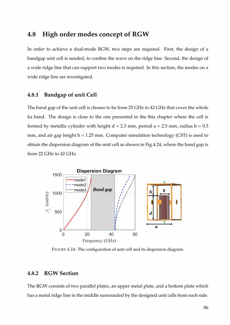
4.8 High order modes concept of RGW
In order to achieve a dual-mode RGW, two steps are required. First, the design of a
bandgap unit cell is needed, to confine the wave on the ridge line. Second, the design of
a wide ridge line that can support two modes is required. In this section, the modes on a
wide ridge line are investigated.
4.8.1 Bandgap of unit Cell
The band gap of the unit cell is chosen to be from 25 GHz to 42 GHz that cover the whole
ka band. The design is close to the one presented in the this chapter where the cell is
formed by metallic cylinder with height d = 2.3 mm, period a = 2.5 mm, radius b = 0.5
mm, and air gap height h = 1.25 mm. Computer simulation technology (CST) is used to
obtain the dispersion diagram of the unit cell as shown in Fig.4.24, where the band gap is
from 22 GHz to 42 GHz.
a
bh
d
Band gap
FIGURE 4.24: The configuration of unit cell and its dispersion diagram.
4.8.2 RGW Section
The RGW consists of two parallel plates, an upper metal plate, and a bottom plate which
has a metal ridge line in the middle surrounded by the designed unit cells from each side.
86

In order to design a dual-mode RGW, the ridge width is chosen to guarantee the presence
of both fundamental and first higherorder modes over the operating bandwidth. When
the wide ridge is excited properly, the two modes can simultaneously propagate along
the ridge line.
wr
h
dp
D
(a)
(b)
FIGURE 4.25: The RGW section and its dispersion diagram.
In Sec 4.3, the first higher order mode is excited using an E-plane T- junction. In this
section, a magic Tee is used to excite both the fundamental mode Q-TEM and first higher
mode TERGW10 simultaneously on the same ridge line. The width (w) of the ridge is chosen
to be 7.288 mm that guarantee the propagation of both modes. The propagating modes
on the ridge line are: (1) the quasi-TEM mode, (2) the first high order mode TERGW10 , and
(3) the second high order mode TERGW20 as depicted in Fig.4.25 (b). The bandpass region
of the dual-mode is from 25 to 34.5 GHz, that avoids the presence of the TERGW20 mode.
The other modes that appear on both sides of the bandpass region are out of the scope of
this work. The simulated E-field distributions of the first three modes of RGW structure
(Q-TEM, TERGW10 and TERGW
20 ) are shown in Fig.4.26. It is clear that the fundamental mode
Q-TEM and the second higher order mode TERGW20 have even symmetry while the TERGW
10
87

mode has odd symmetry. The electric field distribution of the first three modes of RGW
as shown in Fig.4.26 are generated by defining the port and setting these modes.
Q_TEM 10
RGWTE 20
RGWTE
(a) (b) (c)
FIGURE 4.26: Electric field distribution of (a) Q-TEM mode (b)TERGW10 mode.
(c) TERGW20 mode.
The quasi-TEM and TERGWm0 modes are orthogonal modes in the RGW structure. Con-
sequently, these modes can be used for carrying several signals with low interference
through the same waveguide. Therefore, by using proper excitation for RGW, Q-TEM
and TERGW10 modes can be sent simultaneously on the same waveguide. This is achieved,
in this work, by using a four-port magic tee to feed the wide RGW.
4.9 Higher order Mode Excitation
Generally, several transitions are used to excite high order mode in the conventional
waveguides. For example, many different techniques use to excite the SIW high order
mode [12, 14, 86]. However, there is no enough reported information about transitions to
excite high order mode in RGW. In this thesis, the magic tee is used to excite the Q-TEM
and the TERGW10 on the ridgeline. The magic tee is commonly used to feed microwave
systems, where it consists of four ports and can be used as an E-plane or H-plane power
dividers. Fig.4.27 shows a 3D view of the four-port magic tee structure and the associated
dimensions are in Table 5.1. A hemisphere is used, as shown in Fig.4.27 (b), to improve
88
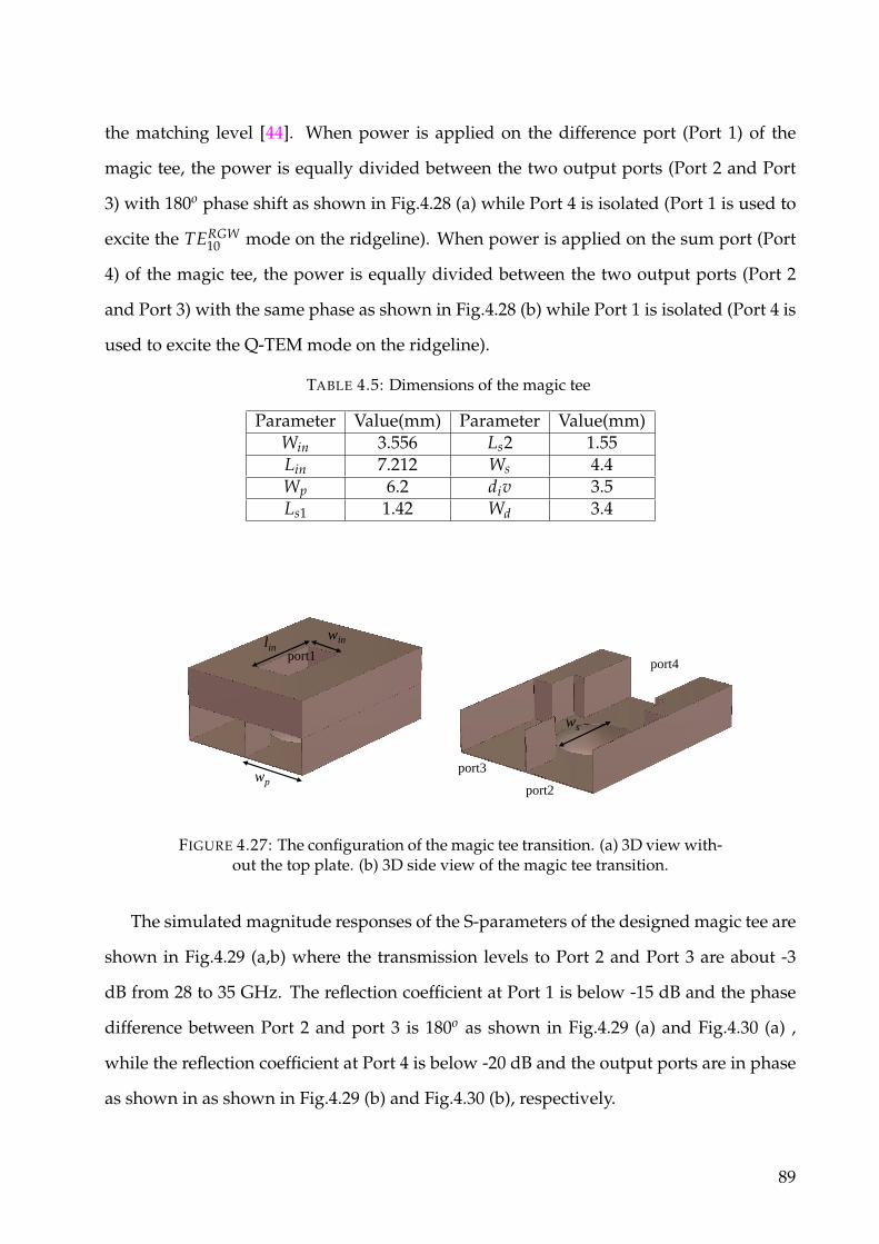
the matching level [44]. When power is applied on the difference port (Port 1) of the
magic tee, the power is equally divided between the two output ports (Port 2 and Port
3) with 180o phase shift as shown in Fig.4.28 (a) while Port 4 is isolated (Port 1 is used to
excite the TERGW10 mode on the ridgeline). When power is applied on the sum port (Port
4) of the magic tee, the power is equally divided between the two output ports (Port 2
and Port 3) with the same phase as shown in Fig.4.28 (b) while Port 1 is isolated (Port 4 is
used to excite the Q-TEM mode on the ridgeline).
TABLE 4.5: Dimensions of the magic tee
Parameter Value(mm) Parameter Value(mm)Win 3.556 Ls2 1.55Lin 7.212 Ws 4.4Wp 6.2 div 3.5Ls1 1.42 Wd 3.4
port3
port2
port4
ws
port1
wp
winlin
FIGURE 4.27: The configuration of the magic tee transition. (a) 3D view with-out the top plate. (b) 3D side view of the magic tee transition.
The simulated magnitude responses of the S-parameters of the designed magic tee are
shown in Fig.4.29 (a,b) where the transmission levels to Port 2 and Port 3 are about -3
dB from 28 to 35 GHz. The reflection coefficient at Port 1 is below -15 dB and the phase
difference between Port 2 and port 3 is 180o as shown in Fig.4.29 (a) and Fig.4.30 (a) ,
while the reflection coefficient at Port 4 is below -20 dB and the output ports are in phase
as shown in as shown in Fig.4.29 (b) and Fig.4.30 (b), respectively.
89

(a) (b)
FIGURE 4.28: 2D view with the electric field distribution in port2 and port3(a) the electric field distribution in port2 and port3 when the input fromport1, (b) the electric field distribution in port2 and port3 when the input
from port4.
FIGURE 4.29: The magnitude of magic tee S-parameters.
FIGURE 4.30: The phase of magic tee S-parameters.
90

4.10 Design of Dual Mode RGW
The Q-TEM mode and other modes of RGW are orthogonal. Therefore, there is no cou-
pling between the modes, theoretically. Therefore, the dominant and first higher-order
mode can be used for guiding two different signals without interference through the
RGW. Using the fundamental mode and the first high order mode on the same waveg-
uide provide many advantages. First, the channel capacity is increased, which helps to
improve system performance. Second, a dual pattern antenna is designed with each pat-
tern corresponding to one mode. Third, the number of pins utilized to build RGW can be
reduced compared to two parallel lines, which reduces the fabrication cost.
Fig.4.31 shows a dual mode RGW with the magic tee (used for the excitation of the two
modes). The outputs ports of the magic tee are designed with total width greater than the
wavelength at center frequency. If the magic tee use to feed the RGW directly with same
width, the second high order mode TERGW20 can propagate from the beginning of the band.
Therefore, a tapered section is used, from the magic tee outputs to the designed ridge line,
to have a ridge line width that supports the first two modes only. Moreover, using the
tapered section is very important to improve the matching for both modes. By applying
the power on Port 4 of the magic tee, the power is equally divided between Port 2 and
Port 3 with the same phase as shown in Fig.4.30 (b). Then, those outputs are used to excite
the proposed wide RGW. In this case, the magic tee provides excitation to the ridgeline,
which imposes a high even symmetry along ridge line. Therefore, only the Q-TEM mode
is excited on the ridge and the odd modes are suppressed. Fig.4.32 (a) shows the electric
field distribution of the Q-TEM mode that can propagate in this ridge. On the other hand,
by applying the power to Port 1 of the magic tee, the power is equally divided between
Port 2 and Port 3 with 180o phase shift as illustrated in Fig.4.30 (a). Then, those outputs
are used to feed the proposed wide RGW. In this case, the magic tee provides a differential
excitation to the ridge line, which imposes a virtual PEC wall in the middle of the ridge.
Therefore, only the odd mode is excited on the ridge and the even modes are suppressed.
Fig.4.32 (b) shows the electric field distribution of the TERGW10 that can propagate in this
91

ridge. From the E-filed distribution, it is clear that there is only one propagating mode on
the ridge with zero tangential electric field in the middle of the ridge and maximum on
its sides.
Matching section
Ridge line
port4 port3
port1 port2Top
Bottom
Side view
Air gap
pins
(b)
(a)
FIGURE 4.31: The geometry of the proposed dual-mode RGW structure. (a)Top and side views. (b) 3D view of the RGW.
The simulation of the proposed design shows good performance in a back-to-back
configuration. The simulated S-parameters of the designed dual-mode RGW are depicted
in Fig.4.33 (a) where the transmission levels (S21 and S34) are ≥-0.7 dB from 28.7 to 35
GHz whereas the reflection coefficients at Port 1 (S11) and Port 4 (S44) are below -10 dB
from 28.77 to 34.61 GHz. Furthermore, the isolation between the two modes is very high
92

(> 30 dB) at center frequency, as illustrated in Fig.4.33 (b). In the proposed structure, the
matching for both modes starts from the same frequency. Therefore, an actual and useful
dual-mode RGW is achieved, in which the two modes operate in the same frequency
band. The proposed design has attractive performance where the bandwidth is more
than 18.5% at 31.5 GHz.
(a) (b)
FIGURE 4.32: The field distribution for the proposed RGW dual mode struc-ture. (a) Q-TEM mode. (b) TERGW
10 mode.
93
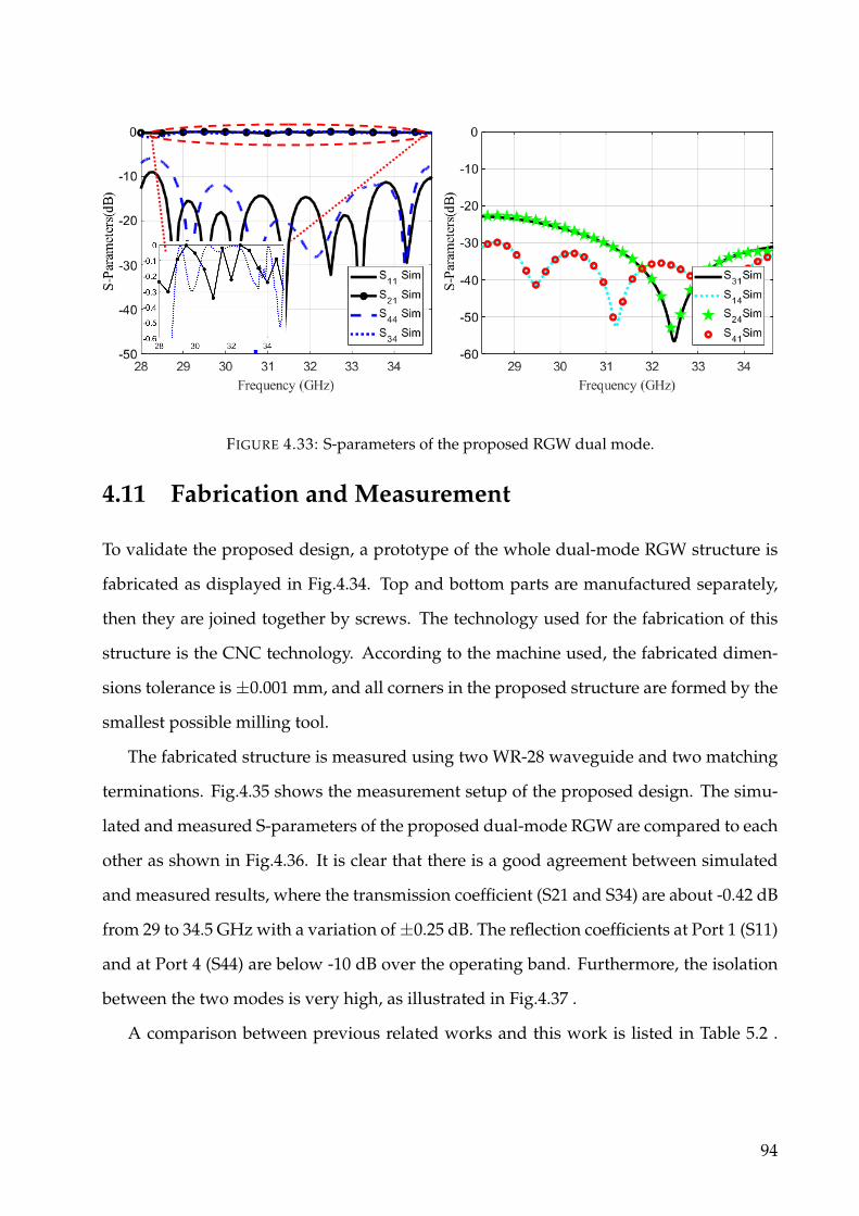
FIGURE 4.33: S-parameters of the proposed RGW dual mode.
4.11 Fabrication and Measurement
To validate the proposed design, a prototype of the whole dual-mode RGW structure is
fabricated as displayed in Fig.4.34. Top and bottom parts are manufactured separately,
then they are joined together by screws. The technology used for the fabrication of this
structure is the CNC technology. According to the machine used, the fabricated dimen-
sions tolerance is ±0.001 mm, and all corners in the proposed structure are formed by the
smallest possible milling tool.
The fabricated structure is measured using two WR-28 waveguide and two matching
terminations. Fig.4.35 shows the measurement setup of the proposed design. The simu-
lated and measured S-parameters of the proposed dual-mode RGW are compared to each
other as shown in Fig.4.36. It is clear that there is a good agreement between simulated
and measured results, where the transmission coefficient (S21 and S34) are about -0.42 dB
from 29 to 34.5 GHz with a variation of ±0.25 dB. The reflection coefficients at Port 1 (S11)
and at Port 4 (S44) are below -10 dB over the operating band. Furthermore, the isolation
between the two modes is very high, as illustrated in Fig.4.37 .
A comparison between previous related works and this work is listed in Table 5.2 .
94

(a)
(b)
FIGURE 4.34: The fabricated dual-mode RGW structure (a) individuallyparts. (b) Assembled parts.
FIGURE 4.35: Dual-mode RGW measurements setup.
95

FIGURE 4.36: Dual-Mode RGW results using back-to-back setup. (a) Mea-surements and simulations obtained from port1 and port2. (b) Measurements
and simulations obtained from port3 and port4.
FIGURE 4.37: Measurements and simulations the Isolation of proposed dual-Mode RGW. .
As indicated, this work has benefits compared to other listed works. The proposed dual-
mode RGW takes the advantages of wide impedance bandwidth, high isolation level be-
tween the propagating modes, and low insertion loss for both modes compared with the
listed works. In [57], an OMT is designed to carry two orthogonal modes (TE10 and TE01
modes) using a square waveguide. Yet, the device is bulky and difficult to fabricate at
96

TABLE 4.6: Comparison with previously related works
Ref Technology Freq(GHz) Modes / pol Bandwidth
(dB) Insertion loss Isolation(dB)
[13] SIW 9.813.24
TE10,TE20Single pola
17.3%(TE10)7.9%(TE20) - >30
[57] RWG 19 TE10,TE01Dual pol 15.7% -1 >30
[59] Microstrip andWG 30 TE10,TE01
Dual pol 6.7% TE10( -2.2 to -3)TE20( -1.2 to -2) >30
This work RGW 31 Q-TEM,TE10Single pol 18.7% TERGW
10 ( -0.14 to -0.7)Q-TEM( -0.2 to -0.6)
>30
high-frequency bands as the dimensions become very small, contrary to the proposed
RGW dual-mode, which can be implemented in the printed RGW form. On the other
hand, an SIW technology is used to have compact dual-mode waveguide (TE10 and TE20
modes) [13]. However, the two modes operate at different frequencies that does not effi-
ciently use the bandwidth. Moreover, in SIW technology, the wave suffers from dielectric
losses as it propagates in a dielectric material. Conversely, the proposed design has supe-
rior performance as the RGW has low loss compare with SIW technology since the wave
propagates on an air gap.
97

Chapter 5
Antennas Design Based on Odd Mode of Ridge
Gap Waveguide
5.1 4x4-element Cavity Slot Antenna Differentially-fed by
Odd Mode Ridge Gap Waveguide
In this section, a differential feeding, based on the first higher-order mode (TERGW10 ) of
the ridge gap waveguide (RGW), for a cavity slot antenna is presented. This feeding is
based on a simple mechanism rather than the conventional complex networks that suf-
fer from high losses. It is based on exciting the first higher-order mode TERGW10 of the
ridge gap waveguide (RGW) by expanding the ridge width. This expansion would excite
some undesired even modes that are suppressed by embedding a vertical perfectly elec-
tric conducting (PEC) wall in the middle of the waveguide based on the concept of magic
tee operation. The proposed 4x4 cavity slot antenna is realized using substrate integrated
waveguide (SIW) technology. Two horizontal slots on the top of proposed wide RGW,
representing the differential feeding approach, are etched to feed the cavity slot antenna.
The slots couple the fields with the same amplitudes and 180o phase difference to the
cavity. The electric fields of the two coupling slots have odd symmetry in the x-axis and
subsequently, uniform electric field distribution of the TE440 mode of a cavity can be ex-
cited. The 4/4 radiating slots are etched on the top of the cavity in a specific distribution
98

to ensure having in-phase fields for broadside radiation with low cross-polarization lev-
els. The simulation and measurement results of the cavity slot antenna are in good agree-
ment. The results confirm that the proposed cavity antenna achieves a relative bandwidth
of 7.1% for -10 dB return loss, a gain of about 16.5 dBi and side lobe level about -17 dB in
E-plane and -13.8 dB in H-plane. Furthermore, the proposed antenna provides low cross-
polarization levels (-35 dB in E-plane and -27 dB in H-plane) within the operating fre-
quency band of 32.5 GHz to 34.9 GHz. With this achieved a high gain and high efficiency
of the proposed antenna, it may have a great potential for millimeter-wave (mm-wave)
applications.Up to the authors’ knowledge, this proposed TERGW10 -mode RGW and its use
as a differential feeding is presented for the first time in literature.
5.1.1 Antenna Design
Generally, microwave resonator builds from a closed waveguide, where called waveg-
uide resonators. They are commonly short-circuited at ends to form a closed cavity. The
energy stores in the cavity where a part of the power is wasted in the metallic walls and
in the dielectric that might use to fill the cavity [4]. A cavity resonator usually feeds by
coaxial probe or slot. The location of the feeding probe or slot plays an essential role to
define the resonant modes of the cavity, based on the field changes along the three dimen-
sions of the cavity. Starting the design with the same analysis of a rectangular cavity, The
resonant frequency of TEmnl mode can be stated as follows [4]:
fmnl =c
2π√
µrεr
√(mπ
a
)2+
(nπ
b
)2+
(lπd
)2
(5.1)
where m,n,l is are integer number indicate the variation of wave in x,y,z direction,
respectively.
In our design, since we interest to design 4x4 SIW cavity antenna, 4x4 standing waves
uniformly distributed in the cavity should be generated which demonstrates that the res-
onant mode is TE440 mode. By using resonant frequency equation we can calculate all
the cavity dimensions.
99
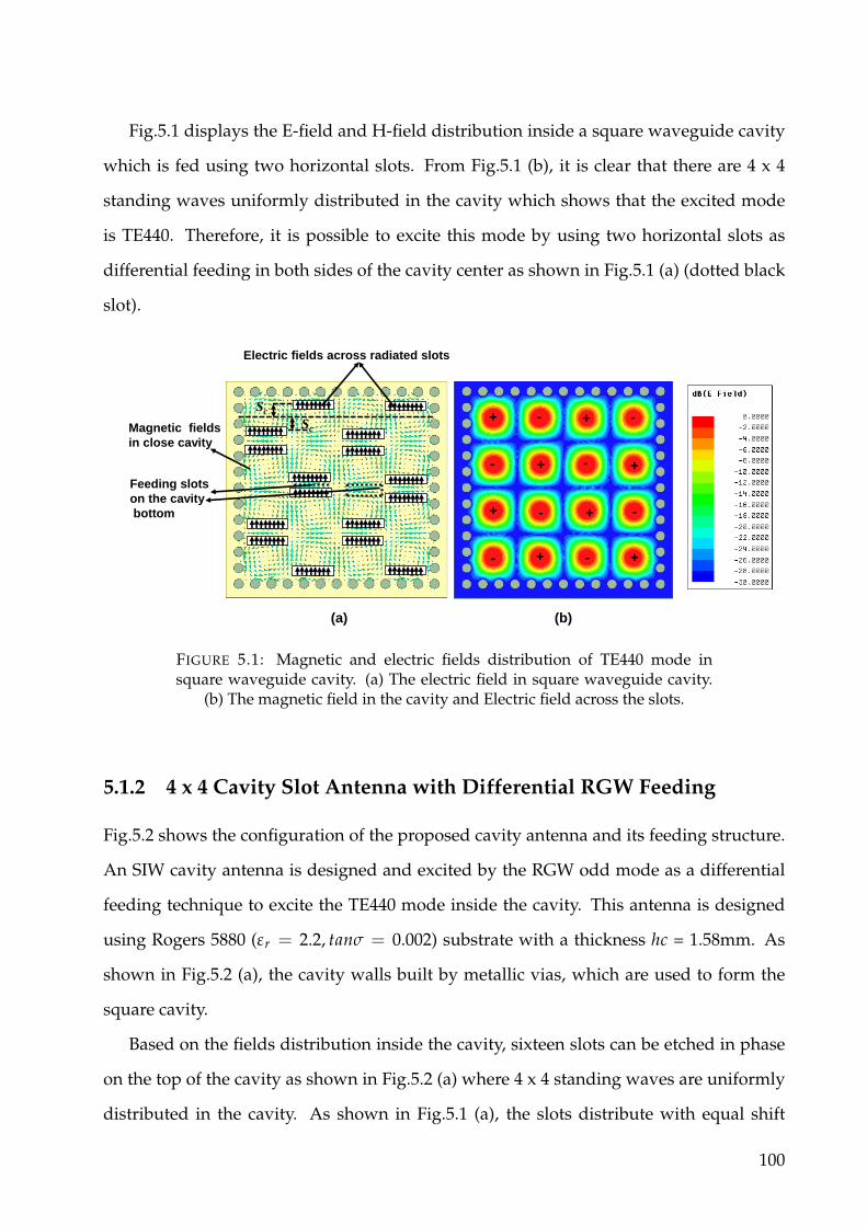
Fig.5.1 displays the E-field and H-field distribution inside a square waveguide cavity
which is fed using two horizontal slots. From Fig.5.1 (b), it is clear that there are 4 x 4
standing waves uniformly distributed in the cavity which shows that the excited mode
is TE440. Therefore, it is possible to excite this mode by using two horizontal slots as
differential feeding in both sides of the cavity center as shown in Fig.5.1 (a) (dotted black
slot).
ScSc
Feeding slots
on the cavity
bottom
Electric fields across radiated slots
Magnetic fields
in close cavity
Sc
Sc
(a) (b)
+ +
+
+
+
+
+
+
-
-
-
-
-
-
- -
FIGURE 5.1: Magnetic and electric fields distribution of TE440 mode insquare waveguide cavity. (a) The electric field in square waveguide cavity.
(b) The magnetic field in the cavity and Electric field across the slots.
5.1.2 4 x 4 Cavity Slot Antenna with Differential RGW Feeding
Fig.5.2 shows the configuration of the proposed cavity antenna and its feeding structure.
An SIW cavity antenna is designed and excited by the RGW odd mode as a differential
feeding technique to excite the TE440 mode inside the cavity. This antenna is designed
using Rogers 5880 (εr = 2.2, tanσ = 0.002) substrate with a thickness hc = 1.58mm. As
shown in Fig.5.2 (a), the cavity walls built by metallic vias, which are used to form the
square cavity.
Based on the fields distribution inside the cavity, sixteen slots can be etched in phase
on the top of the cavity as shown in Fig.5.2 (a) where 4 x 4 standing waves are uniformly
distributed in the cavity. As shown in Fig.5.1 (a), the slots distribute with equal shift
100

Dvia
Pvia
Wc
LsWs
RT5880(𝑨 = 𝜺𝒓 = 𝟐. 𝟐)
hc
Lc
(a)
Wridge
LSlot
WSlot
Top Metal Plate
Ground
DM
Hshort
l-match
(b)
4×4 SIW cavity
port2
port3
port2port3
port1
(c)
FIGURE 5.2: The geometry of the proposed cavity antenna structure. (a) 3Dview of the SIW cavity. (b) Cavity excitation structure. (c) Whole cavity slot
antenna structure.
101

TABLE 5.1: Dimensions of the proposed antenna
Parameter Wridge Lslot Wslot Dvia hc PviaValue(mm) 7.5 3.3 1.1 1 1.58 1.7Parameter Wc = Lc lmatch Ws Ls DM HshortValue(mm) 19.8 2.5 0.6 4.4 0.27 1
distance (Sc=1.4mm) from the dotted line. The electric field across the slots is shown in
Fig.5.1 (a), where the black arrows describe the orientation of the electric field. Since all
the slots are etched in phase, all the sixteen slots of the antenna radiate in phase. The
cavity antenna is excited by the structure shown in Fig.5.2 (b). All the dimensions of the
proposed structure are listed in Table 5.1.
The whole structure of the 4 x 4 cavity slot antenna is shown in Fig.5.2 (c). The field
propagates from the magic tee ports along with the wide RGW structure and couples to
the cavity through the two horizontal slots that are etched on top of the RGW. In order to
improve the impedance matching, two vias with a radius of DM and a height of Hshort are
placed at the centers of the two coupling slots of the RGW.
The simulated results of the reflection coefficient and gain of the proposed cavity an-
tenna are obtained using two full-wave solvers, namely the HFSS and CST. The purpose
of this comparison is to provide a solid verification of the results before the fabrication
stage.
As shown in Fig.5.3, a very good agreement between the results is obtained. The
fractional bandwidth is about 7.1% with a center frequency of 33.5 GHz. The simulated
gain is about 16.5 dBi over the bandwidth.
5.1.3 Parametric Study
A parametric study has been carried out to show the effect of the most critical dimensions
on the proposed antenna performance, in terms of the gain and the reflection coefficient.
The length of slot that etched on the top plate of RGW to feed the cavity (Lslot), matching
pin position (lmatch), substrate thickness (hc), and cavity slot length and slot center offset
102

FIGURE 5.3: Comparison of the HFSS and CST simulated reflection coeffi-cients and gains of the proposed cavity antenna.
(Ls and Sc) are selected for this parametric study. The parametric study can be concluded
in followed points:
• The length of the feeding slot (lslot) and matching pin position (l-match) have the
same effect on the antenna’s gain and matching performances, where increasing
any one of them improves the gain and the matching until it reaches the optimum
value. Then, the performance degrades again when moving away from the opti-
mum value. This is illustrated in Fig.5.4 where the gain and reflection coefficient
with different values of the l-match and lslot are presented. The optimum value of
lmatcht and lslot are 2.5 mm and 3.3 mm respectively. The gain drops more than 1.5
dBi when moving away from the optimum values.
• The parametric study carry outed on cavity parameters hc, and ls, shows a shift on
the resonance frequency toward lower frequencies when increasing any of them.
This is depicted in Fig.5.5 (a), (c) where the gain and reflection coefficient for differ-
ent values of hc and ls is presented. The optimum values of hc and ls are 1.58 mm
and 4.4 mm respectively. Also, there is a gain drop and degradation on the matching
away from the optimum values.
103

• Varying Sc has a slight impact on the peak gain and the reflection coefficient as
displayed in Fig.5.5 (b). There is a drop in the gain at high frequencies for high
values of Sc where the slots reach the edge of the cavity. The optimum value of Sc
is 1.4 mm.
(a) (b)
FIGURE 5.4: Simulated reflection coefficients and gain of the proposed an-tenna considering the impact of varying different geometric parameters of
cavity feeding: (a) lmatch; (b) lslot.
5.1.4 3D Printing Implementation and Measurements
To test the proposed design, a prototype of the cavity slot antenna with differential feed-
ing is fabricated and measured. Fig.5.6 (a,b) show the individual part and assembled
parts. The feeding part, the SIW cavity antenna, and the transition are fabricated indi-
vidually, then they are combined by screws. The standard WR-28 waveguide is used to
excite the antenna at the Ka-band. The technology utilized for the implementation of
this structure is the three-dimensional printing of plastic material, then the structure is
plated with copper. In the measurement setup, the antenna is mounted on the fixture
as shown in Fig.5.7. The reflection coefficient of the antenna is measured by the Agilent
104
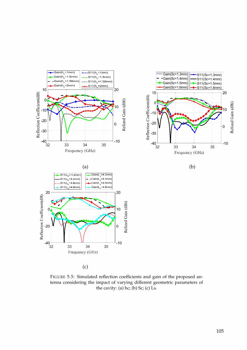
(a) (b)
(c)
FIGURE 5.5: Simulated reflection coefficients and gain of the proposed an-tenna considering the impact of varying different geometric parameters of
the cavity: (a) hc; (b) Sc; (c) Ls.
105

N52271A network analyzer while the antenna radiation pattern and gain are measured
in the antenna anechoic chamber by NSI far-field measurement system.
(a) (b)
FIGURE 5.6: The fabricated 4 x 4 cavity antenna (a) individually parts. (b)Assembled parts.
FIGURE 5.7: Photos of the measurement set up.
• Gain and Reflection Coefficient
The measured and simulated results of the reflection coefficient and gain of the pro-
posed antenna are compared to each other as shown in Fig.5.8. There is a good
106

agreement between simulation and measurement results. The measured fractional
bandwidth of the structure is 8.3% (from 32.5 GHz to 35.3 GHz). The measured
and simulated gains of the proposed antenna are also shown in Fig.5.8 where both
of them are around 16.5 dBi in the operating bandwidth. The slight difference be-
tween the simulated and measured results is due to the effect of the manufacturing
accuracy.
• Radiation Pattern
The measured and simulated H-plane and E-plane radiation patterns of the pro-
posed cavity antenna are depicted in Fig.5.9. The results are in good agreement in
both H- and E-planes. The sidelobe levels of E-plane and H-plane patterns at 33.5
GHz are -17 dB and -13.8 dB, respectively. Since the cavity has symmetric shape and
excited by differential feeding, the radiation patterns of the cavity are mainly sym-
metric, especially in H-plane. The results show that the cross-polarization level is
below -35 dB and -27 dB in the E-plane and H-plane, respectively, across the whole
the operating bandwidth.
A comparison among related reported works and this work is listed in Table 5.2. Us-
ing the second-order mode as a differential feeding for the cavity slot antenna presented
in this work has some advantages compared to other antennas listed in the table. The
proposed cavity has a superior radiation performance which has low cross-polarization
level, relatively higher gain, low sidelobe level, symmetrical radiation pattern, and good
aperture efficiency. Moreover, the matching bandwidth has been enhanced compared to
the reported works.
107

FIGURE 5.8: Comparison of simulated and measured reflection coefficientsand gains of the proposed cavity antenna.
E-plane
H-plane
E-plane
H-plane H-plane
E-plane
(a) (b) (c)
33.5GHz
33.5GHz
32.75GHz
32.75GHz
34.5GHz
34.5GHz
FIGURE 5.9: Measured and Simulated radiation patterns of the proposed cav-ity antenna. (a) 32.75 GHz. (b) 33.5 GHz. (c) 34.5 GHza.
108
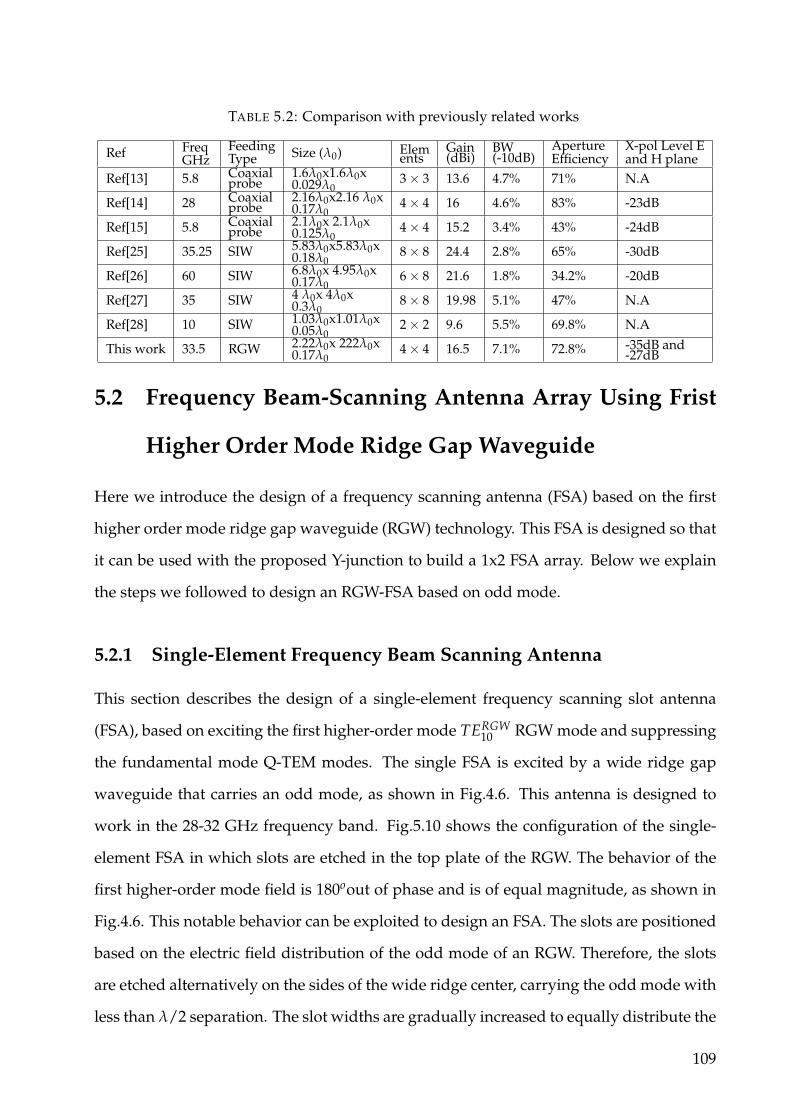
TABLE 5.2: Comparison with previously related works
Ref FreqGHz
FeedingType Size (λ0) Elem
entsGain(dBi)
BW(-10dB)
ApertureEfficiency
X-pol Level Eand H plane
Ref[13] 5.8 Coaxialprobe
1.6λ0x1.6λ0x0.029λ0
3 × 3 13.6 4.7% 71% N.A
Ref[14] 28 Coaxialprobe
2.16λ0x2.16 λ0x0.17λ0
4 × 4 16 4.6% 83% -23dB
Ref[15] 5.8 Coaxialprobe
2.1λ0x 2.1λ0x0.125λ0
4 × 4 15.2 3.4% 43% -24dB
Ref[25] 35.25 SIW 5.83λ0x5.83λ0x0.18λ0
8 × 8 24.4 2.8% 65% -30dB
Ref[26] 60 SIW 6.8λ0x 4.95λ0x0.17λ0
6 × 8 21.6 1.8% 34.2% -20dB
Ref[27] 35 SIW 4 λ0x 4λ0x0.3λ0
8 × 8 19.98 5.1% 47% N.A
Ref[28] 10 SIW 1.03λ0x1.01λ0x0.05λ0
2 × 2 9.6 5.5% 69.8% N.A
This work 33.5 RGW 2.22λ0x 222λ0x0.17λ0
4 × 4 16.5 7.1% 72.8% -35dB and-27dB
5.2 Frequency Beam-Scanning Antenna Array Using Frist
Higher Order Mode Ridge Gap Waveguide
Here we introduce the design of a frequency scanning antenna (FSA) based on the first
higher order mode ridge gap waveguide (RGW) technology. This FSA is designed so that
it can be used with the proposed Y-junction to build a 1x2 FSA array. Below we explain
the steps we followed to design an RGW-FSA based on odd mode.
5.2.1 Single-Element Frequency Beam Scanning Antenna
This section describes the design of a single-element frequency scanning slot antenna
(FSA), based on exciting the first higher-order mode TERGW10 RGW mode and suppressing
the fundamental mode Q-TEM modes. The single FSA is excited by a wide ridge gap
waveguide that carries an odd mode, as shown in Fig.4.6. This antenna is designed to
work in the 28-32 GHz frequency band. Fig.5.10 shows the configuration of the single-
element FSA in which slots are etched in the top plate of the RGW. The behavior of the
first higher-order mode field is 180oout of phase and is of equal magnitude, as shown in
Fig.4.6. This notable behavior can be exploited to design an FSA. The slots are positioned
based on the electric field distribution of the odd mode of an RGW. Therefore, the slots
are etched alternatively on the sides of the wide ridge center, carrying the odd mode with
less than λ/2 separation. The slot widths are gradually increased to equally distribute the
109
power among all radiation slots. Thirteen rectangular slots were etched in the top plate
of the metal ridge gap waveguide to achieve the desired radiation pattern. The proposed
FSA structure is designed by using commercial software (HFSS) in which the wave ports
are used to excite both sides of the proposed antenna. The phase constant varies as the
frequency varies, which allows the main beam to be scanned. The slot length design is
determined to be 4mm, which is almost equal to half of the wavelength in the RGW.
Wridge
Port1
Port2
p
GroundMetal pin
Top plate
slot
L_slot
FIGURE 5.10: The configuration of an element of the FSA.
The simulated results of the S-parameters (S11 and S21) of the designed FSA are
shown in Fig.5.11, where the antenna works appropriately over the 28-32 GHz range.
Fig.5.12 shows the realized gain of the E-plane radiation pattern of all frequencies of the
operating bandwidth. The simulated peak gain of the single element antenna is 15.5 dBi
with about 1.5 dBi variation, and the beam scanning range is from −32o to −11o. A vari-
ation of antenna gain of about 4dBi can be exchanged in order to achieve a wider beam
scanning range of from −40o to −11o over the operating bandwidth, while keeping an
acceptable side lobe level.
110

FIGURE 5.11: Simulated reflection and transmission coefficients of the single-element FSA.
FIGURE 5.12: Simulated realized gain of the E-plane radiation pattern for28,29,30,31 and 32 GHz.
111

5.2.2 Two-Element Frequency Beam Scanning Antenna.
In this section, the proposed Y-junction introduced in Chapter 4 is used to build a linear
array of the FSA based on odd mode RGW technology. Both arms of the Y-junction power
divider are extended to join FSA subarrays (the single element was introduced in the
previous subsection), as depicted in Fig.5.13 (a). The distance between the two sub-arrays
is set to be two rows of unit cells to act as the PMC . Commercial software (HFSS) is used
to design and simulate the proposed structure.The whole structure of an FSA array with
a Y-junction power divider is shown in Fig.5.13.
Wridge
p
Ground
Metal pin
Top plate
slot
L_slot
Magic Tee
Transition
(a)
(b)
FIGURE 5.13: (a) Separated view of the top, bottom and a magic tee transi-tion; and (b) Complete configuration of the FSA array.
112

The simulated matching performance of the FSA array is illustrated in Fig.5.14, and
remains below -15 dB over the operating bandwidth. Fig.5.15 and Fig 5.17 show polar
and 3D radiation patterns, respectively, at frequencies 28, 29.30,31, and 32 GHz. From the
radiation pattern results, it is clear that beam scanning continues through the broadside.
The electric field distribution inside slots at different frequencies of the proposed design
are shown in Fig.5.16. The simulated peak gain of the proposed antenna is 19.15 dBi, and
beam scanning range is from −11o to −40o the operating bandwidth, with an acceptable
side lobe level.
FIGURE 5.14: Simulated reflection and realized gain of the FSA array.
FIGURE 5.15: Simulated realized gain of the E-plane radiation pattern for28,29,30,31 and 32 GHz.
113

28GHz 30GHz
32GHz
33GHz
31GHz
34GHz
FIGURE 5.16: Simulated E-field distribution in slots for 28, 30, 31,32,33 and34 GHz.
28 GHz29GHz
30GHz 31GHz
32GHz
FIGURE 5.17: Simulated realized gain of 3D radiation pattern for 29, 30, 31and 32 GHz.
114
5.2.3 Dual-Beam RGW Frequency Beam-Scanning Antenna.
Designing components and antennas using RGW to work at millimeter-wave frequency
band has attracted much attention recently, as this band offers high data rates. However,
working at the mm-wave band is challenging, as the performance of the communication
system decays due to multipath, dielectric losses and link blockage because of obstruc-
tions. These losses can be compensated by using high gain directional antennas rather
than omnidirectional antennas [110]. Directional antennas confine the beam in a particu-
lar direction to reduce the multipath and interference effects. The dual-beam antenna is
part of the directional antenna family, and has two directional beams. Since a dual-beam
antenna has two symmetrical beams, it is capable of covering two nonadjacent areas, es-
pecially for indoor wireless systems [111]. The characteristics of the dual-beam antenna
also offer valuable advantages for mobile communications [112].
In this section, the proposed FSA array in the previous section is exploited to design
a dual-beam antenna for mm-wave applications over 28–32 GHz. The proposed antenna
is designed based on exciting the odd mode TERGW10 rather than the fundamental mode.
The behavior of the field distribution of the first higher mode TERGW10 , which is 180o out
of phase and is of equal magnitude, as shown in Fig.5.10 (b), can be exploited to design
an FSA antenna that has a dual-beam radiation pattern. Etching the slots alternating on
one arm of the Y-junction and then making a mirror to the slots means that all the slots in
the first arm will radiate in phase while being be out of phase with those of the other Y-
junction arm. Fig.5.18 shows the configuration of the proposed dual-beam FSA array line
with identical slots on both Y-junction arms. The 3D radiation pattern of this proposed
LWA array is shown in Fig.5.19.
115

FIGURE 5.18: Configuration of the dual-beam FSA array line with identicalslots on both Y-junction arms.
FIGURE 5.19: Simulated realized gain of 3D radiation pattern of dual-beamFSA array for 29, 30, 31 and 32 GHz.
116
5.2.4 Leaky Wave Antenna based on a First Higher-order Mode Ridge
Gap Waveguide
Beam scanning antennas have received significant attention recently for short-range ap-
plications such as image and radar system detection. The leaky wave antenna (LWA) has
the ability to produce beam scanning, and is part the traveling wave antenna family [113].
The LWA is used extensively due to its unique advantages compared to other antennas
such as phased array and slot array antennas. For example, the LWA can produce a beam
scanning without using phase shifters or requiring a complicated feeding network for its
radiating elements.
Generally, the spacing between the radiated elements should be maintained suffi-
ciently small to avoid having grating lobes at the highest frequency. To avoid the ap-
pearance of grating lobes in slot array and traveling-wave antennas, a phase shifter of
180o is used at the feed end of the antenna [113]. This will allow for the engraving and
separating of the slots by a half wavelength. In [50], another technique is used to achieve
a similar slot arrangement without needing a phase shifter.
Antenna Design and Theory
Based on the first higher-order mode of RGW discussed in Chapter 4, a leaky-wave an-
tenna is designed and presented here for mm-wave applications. For the LWA to radiate
to the broadside free space, it must operate in the fast-wave region space [113], in which
the primary condition for designing an LWA is
−k0 ≤ β ≤ k0 (5.2)
where k0 is free space wavenumber and β is the phase constant of the wave along the
guiding structure. The angle of the main lobe radiation pattern (θn) can be determined by
sin(θn) =βn
k0(5.3)
117

where βn is the phase constant of nth space harmonic, in which the space harmonic
based on the Floquet’s theory. Based on the hybrid PEC/PMC waveguide that introduced
in Chapter 3 and Floquet’s theorem, the dispersion diagram can be obtained by
βn = β0 +2πn
p(5.4)
β10 =
√k2
0εr − (π
w)2 (5.5)
Where p, n, and εr are the period, the number of the space harmonic and the permit-
tivity in the RGW gap, respectively. Because the fundamental mode in this RGW is the
first higher-order mode TERGW10 rather than the usual Q-TEM mode, the β0 is β10. In this
structure, the excitation of the nth slots, including 180o phase, is different due to the dis-
placement of all the slots on the sides of the center line, as shown in Fig.5.20. Therefore
for all slots to radiate in phase in the broadside with beam scanning angle θ, it is essential
that [114]
βn = β0 − π +2πn
p(5.6)
𝜃
𝑃
Input
Matched load
FIGURE 5.20: Sketch of center dismantlement leaky wave antenna.
Based on (5.6), we select the appropriate values for εr and p so that the radiation occurs
only due to the n = -1 space harmonic, which leads to beam scanning of the radiation
pattern in the backward quadrant. Fig.5.21 (a) shows the designed antenna based on
RGW technology, in which an RT/Duroid 5880 substrate with a 1.58mm thickness is used.
118

The proposed leaky-wave antenna without the feed parts is designed and simulated by
using the CST simulator. Wave ports are used at the ends of the RGW. The dispersion
diagram of the harmonics created by the periodic slots can be determined from (5.6),
in which the distance between two successive slots is 2.5 mm. The mode curves of the
proposed leaky wave antenna are shown in Fig.5.21 (b). The propagation constant β0
of the fundamental mode is larger than the propagation constant in free space k0, which
is labeled by the red curve in Fig.5.21 (b). The leaky wave mode (β−1) enters the leaky
mode region at f = 27.6 GHz. According to the dispersion diagram, the proposed antenna
can work as a leaky-wave antenna with a single beam only when −k0 < β−1 < k0 so
that the radiation of the designed antenna occurs due to n=-1 space harmonic. Fig.5.21
(c) presents both the beam angle created with the CST simulator and the beam angle
calculated by using (5.6) and (5.3).
Metallic top plate
RT5880(𝜀𝑟 = 2.2)
Ground
pins
Periodic slots
pLs
(a)
(b)
FIGURE 5.21: (a) Sketch of a leaky wave antenna; (b) Dispersion diagram;and (c) Comparison of the simulated and calculated angles of maximum ra-
diation of the RGW leaky-wave antenna for the TERGW10 .
119

TABLE 5.3: DIMENSIONS OF THE LWA
Parameter Ls Wsub Wtap Ltap w1 w2 w3Value(mm) 2.3 22 7.28 10 0.2 0.24 0.32Parameter w4 w5 w6 w7 w8 w9 w10Value(mm) 0.4 0.48 0.56 0.64 0.72 0.8 0.88Parameter w11 w12 w13 w14 w15 w16 w17Value(mm) 0.96 1.04 1.12 1.2 1.28 1.36 1.44Parameter w18 w19 Lsub PValue(mm) 1.52 1.6 124 2.5
The proposed geometry of the LWA is shown in Fig.5.22, in which horizontal slots are
etched in the top plate, alternating on the two sides of the RGW. In order to have uniform
amplitude distribution from each slot, the width of the slots is gradually increased, as
shown in Fig.5.22. Two magic tees are used to feed the antenna, one at the input of the
ridgeline and one at the end. Two tapered substrate sections are used at the outputs of
the magic tees; these are very important for improving the matching. The associated
dimensions are given in Table 5.3.
The simulated reflection coefficients of the RGW-LWA are shown in Fig.5.23, and are
below −10 dB. The simulated peak realized gain of the antenna is 18.4 dBi, with less than
3dB variation throughout the whole operating bandwidth (28 to 35 GHz). The simulated
radiation patterns of the designed LWA are presented in Fig 5.24, and show that the de-
sired beam scanning has been achieved, in which the range of beam scanning is from
−62o at 28 GHz to −12o at 35GHz.
120

Metallic top plate
RT5880(𝜀𝑟 = 2.2)
Guiding ridgeline
Ground pins
port2
slots
Lsub port1
w1
w3
w6
w5
w9
w2
w4
w7
w8
w10 w15
w14
w13
w12
w11
w19
w18
w17
w16
P
(b)
Magic Tee
port1
port2
(a)
FIGURE 5.22: (a) Complete configuration of the RGW-LWA; and (b) Sepa-rated view of the stacked layers with a zoom view close to the slots and a
magic tee .
121

FIGURE 5.23: Simulated S parameters and gain of the proposed LWA .
FIGURE 5.24: Simulated realized gain of the radiation pattern for 28,30,32,34and 35 GHz for feeding from port1 and port2.
122

5.3 Sum and Difference Beam Switching Antenna
Switched beam antennas have attracted a huge amount of attention in wireless commu-
nication systems. This kind of antenna has several beneficial features, such as their cov-
erage of multiple nonadjacent areas, ability to overcome interference and to enhance the
channel capacity of wireless communication, as well as to point to multipoint systems. In
addition, these antennas can guide power in particular directions instead of spreading it
everywhere.
A Sum and difference beam switching antenna is presented here. The proposed an-
tenna produces a single radiation pattern when fed by the Q-TEM mode, and a dual-beam
pattern when fed by the TERGW10 mode. The typical application for type of antenna’s char-
acteristics is to cover nonadjacent areas by using difference-beam radiation and to cover
the center area by using sum-beam radiation, as shown in Fig.5.25.
M-UE
M-UE
M-UE
M-UE
M-UE
M-UE
M-UE
M-UE
M-UE
Fade zoneFade zone
Difference Radiation Pattern Sum Radiation Pattern
FIGURE 5.25: Switchable sum and difference radiation pattern.
123

5.3.1 Antenna Design
The proposed antenna is designed by using the dual-mode RGW introduced in the pre-
vious section to feed a horn antenna. The end of the ridge line section and the corre-
sponding section of the top plate are extended to form the horn. The horn shape follows
the Vivaldi antenna shape in the E-plane, and has the same width as the ridge line in the
H-plane. Different views of the proposed antenna are shown in Fig.5.26.
Hhorn
Horn
Port2
Port1
Top
Bottom
Side view
FIGURE 5.26: RGW Dual mode horn antenna views.
5.3.2 Results and Discussion
The simulated results of the sum and difference beam switching antenna fed by both
Q-TEM and TERGW10 mode (Fig.5.27) reveal an overlap bandwidth of 25% from 28 to 36
124
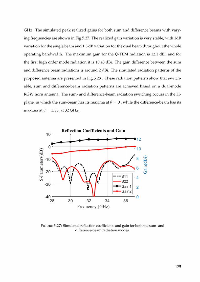
GHz. The simulated peak realized gains for both sum and difference beams with vary-
ing frequencies are shown in Fig.5.27. The realized gain variation is very stable, with 1dB
variation for the single beam and 1.5 dB variation for the dual beam throughout the whole
operating bandwidth. The maximum gain for the Q-TEM radiation is 12.1 dBi, and for
the first high order mode radiation it is 10.43 dBi. The gain difference between the sum
and difference beam radiations is around 2 dBi. The simulated radiation patterns of the
proposed antenna are presented in Fig.5.28 . These radiation patterns show that switch-
able, sum and difference-beam radiation patterns are achieved based on a dual-mode
RGW horn antenna. The sum- and difference-beam radiation switching occurs in the H-
plane, in which the sum-beam has its maxima at θ = 0 , while the difference-beam has its
maxima at θ = ±35, at 32 GHz.
FIGURE 5.27: Simulated reflection coefficients and gain for both the sum- anddifference-beam radiation modes.
125
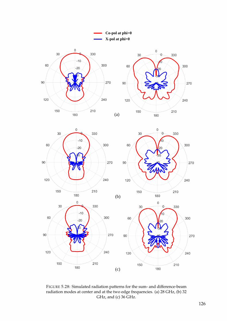
(a)
Co-pol at phi=0
X-pol at phi=0
(b)
(c)
FIGURE 5.28: Simulated radiation patterns for the sum- and difference-beamradiation modes at center and at the two edge frequencies. (a) 28 GHz, (b) 32
GHz, and (c) 36 GHz.
126

Chapter 6
Conclusion and future work
6.1 Conclusion
To exploit the huge available bandwidth at the mm-wave band, microwave researchers
and designers have started developing components, antennas and circuits that work at
high-frequency bands. However, there are massive challenges to designing high fre-
quency systems, such as propagation and system loss. A low-loss guiding structure and
a high-gain antenna are required to compensate the losses in high-frequency systems.
Consequently, in this work, the ridge gap waveguide (RGW) technology is used for de-
signing components and antennas at the mm-wave band. The main scope of this work
concentrates on designing the first higher-order gap waveguide passive components and
antennas at the mm-wave band. This dissertation concentrates mainly on the metallic
ridge gap waveguide. Chapter 2 provided a literature review and background of the
ridge gap waveguide and its dispersion diagram.
A systematic design methodology for a hybrid junction based on RGW technology in-
troduced in Chapter 3. The proposed method relies on the operation of a hybrid PEC/PMC
waveguide. This waveguide offers the possibility to accurately estimate all the dimen-
sions of the RGW coupler that are required in order to operate at a particular frequency
band. The phase response analysis of a circular RGW bend is also introduced in chapter
3. The potential of tuning the center frequency of an RGW coupler by moving the upper
plate of the RGW is proposed. To validate the proposed design, a prototype of the whole
127

0dB coupler structure was fabricated and tested. The measurement and simulation re-
sults show reasonable agreement and prove that the 0dB coupler works effectively with
a coupling lengths calculated from the proposed PEC/PMC model.
Chapter 4 proposes two methods for the first higher-order mode TERGW10 excitation:
excitation of the first high order mode by magic tee and by L-shape transition. A Y-
junction power divider and 3dB forward coupler based on the first higher-order mode
of an RGW are then designed. The Y-junction has a wideband frequency matching from
28 to 34 GHz, with return loss better than 15dB, and the transmission output levels are
about -3.3 dB. A new 3dB odd-mode RGW coupler is also introduced, in which the sim-
ulated return loss and isolation are better than 15dB for the frequency band from 28GHz
to 35GHz, and the output transmission coefficients are about -3dB with 1 dB variation.
Moreover, a dual-mode ridge gap waveguide is simulated, fabricated, and measured.
The measured results are in good agreement with the simulated results. The dual-mode
ridge gap waveguide achieved a matching level less than -10 dB for the two modes over
the operating band 28.77GHz to 34.61GHz with high isolation between the input ports.
A differential excitation mechanism for a 4x4-element cavity slot array antenna is pre-
sented in Chapter 5. This mechanism is implemented using the TERGW10 mode of a wide
RGW. The designed antenna structure is fabricated and measured, and the results show a
good agreement .The designed antenna offers good performance with a 16.5 dBi realized
gain, a good symmetrical radiation pattern, and low cross-polarization level (-35 dB in
the Eplane and -27 dB in the H-plane) within the 32.5-35.3 GHz frequency range.
In the same Chapter, 2x1 linear frequency scanning array antennas is designed. Ini-
tially, a single element of frequency scanning antenna was designed, followed by the
design of a 2x1 element linear array. The bandwidth is from 28 GHz to 32.5 GHz and
the matching is -15 dB with 19.15 dBi peak realized gain. The beam scan is from −11o to
40o at 28 GHz and 32 GHz, respectively. And then a dual-beam FSA array line antenna
is presented, which provides reasonable results in terms of the gain and bandwidth, and
in terms of the beam angle scanning. Also, a leaky wave antenna (LWA) based on the
first higher-order mode RGW at the mm-wave band is introduced. The proposed design
128

provides wide bandwidth, wide scanning range,and high gain with high radiation effi-
ciency. This designed LWA offers 22% of bandwidth at 31.5 GHz and a peak realized gain
of 18.5 dBi with beam scanning range from −62o at 28 GHz to −12o at 35GHz. The ra-
diation efficiency of this design is more than 94% over the operating band of 28-35 GHz.
Finally, A dual-functional sum- and difference-beam antenna is then presented, based on
the proposed dual-mode RGW. The proposed antenna features a wide bandwidth and
switchable radiation pattern from 28 to 36 GHz. Moreover, the gain and the radiation
pattern are stable over the entire operating frequency.
6.2 The future work
The future proposed research has three main goals, namely the following:
• The work proposed in the dissertation presents as a proof of concept for a first
higher-order mode of gap waveguide technology and it’s potential, however its
usage at the mm-wave frequency for wireless systems need more system-level esti-
mation. Many components such as magic tees, couplers, phase shifters, and feeding
networks are needed to design a full system based on first higher-order mode RGW.
Also, in order to exploit the full advantages of high order mode RGW, the active
components need to be combined with RGW.
• A critical technical issue needs to be resolved in order to improve the results. This
issue is the fabrication tolerances of CNC milling technique, which need much more
investigations in order to implement various gap waveguide antennas and compo-
nents at the mm-wave band. On the other hand, several manufacturing techniques
such as metallic 3D printing and laser milling can be proper for realizing high fre-
quency RGW structures, in which they need more investigation.
129

• The present work mainly focuses on metallic ridge gap waveguide technology, in
which the potential of printed gap waveguide technology still remains to be investi-
gated. Efforts to design suitable transitions for exciting the first higher-order mode
would greatly help to advance this field.
130

Bibliography
[1] J. Wells, “Faster than fiber: The future of multi G/S wireless,” IEEE Microwave Mag-
azine, vol. 10, no. 3, pp. 104–112, 2009.
[2] E. Levine, G. Malamud, S. Shtrikman, and D. Treves, “A study of microstrip array
antennas with the feed network,” IEEE Transactions on Antennas and Propagation,
vol. 37, no. 4, pp. 426–434, 1989.
[3] F. Mesa, A. A. Oliner, D. R. Jackson, and M. J. Freire, “The influence of a top cover
on the leakage from microstrip line,” IEEE Transactions on Microwave Theory and
Techniques, vol. 48, no. 12, pp. 2240–2248, Dec 2000.
[4] D. Pozar, Microwave Engineering. Wiley, 1997.
[5] S. Gupta, Z. Briqech, and A. R. Sebak, “Analysis of 60 GHz ridge gap waveguide
based junctions, bends and losses,” IEEE International Conference on Antenna Inno-
vations Modern Technologies for Ground, Aircraft and Satellite Applications (iAIM), pp.
1–4, Nov 2017.
[6] A. Vosoogh, P.-S. Kildal, and V. Vassilev, “Wideband and high-gain corporate-fed
gap waveguide slot array antenna with ETSI class II radiation pattern in V -band,”
IEEE Transactions on Antennas and Propagation, vol. 65, no. 4, pp. 1823–1831, 2016.
[7] A. Vosoogh and P. S. Kildal, “Corporate-fed planar 60 GHz slot array made of three
unconnected metal layers using AMC pin surface for the gap waveguide,” IEEE
Antennas and Wireless Propagation Letters, vol. 15, pp. 1935–1938, 2015.
[8] D. Zarifi, A. Farahbakhsh, A. U. Zaman, and P. S. Kildal, “Design and fabrication
of a high gain 60 GHz corrugated slot antenna array with ridge gap waveguide
131

distribution layer,” IEEE Transactions on Antennas and Propagation, vol. 64, no. 7, pp.
2905–2913, 2016.
[9] G. Bit-Babik, C. Di Nallo, and A. Faraone, “Multimode dielectric resonator antenna
of very high permittivity,” IEEE Antennas and Propagation Society Symposium, vol. 2,
pp. 1383–13 868, June 2004.
[10] B. Li and K. W. Leung, “A wideband strip-fed rectangular dielectric resonator an-
tenna,” IEEE Antennas and Propagation Society International Symposium, vol. 2A, pp.
172–175, July 2005.
[11] A. Petosa, S. Thirakoune, and A. Ittipiboon, “Higher-order modes in rectangular
dras for gain enhancement,” 2009 13th International Symposium on Antenna Technol-
ogy and Applied Electromagnetics and the Canadian Radio Science Meeting, pp. 1–4, Feb
2009.
[12] J. Xu, Z. N. Chen, X. Qing, and W. Hong, “A single-layer SIW slot array antenna
with TE20 mode,” Asia-Pacific Microwave Conference 2011, pp. 1330–1333, Dec 2011.
[13] A. Suntives and R. Abhari, “Design and application of multimode substrate inte-
grated waveguides in parallel multichannel signaling systems,” IEEE Transactions
on Microwave Theory and Techniques, vol. 57, no. 6, pp. 1563–1571, 2009.
[14] P. Wu, J. Liu, and Q. Xue, “Wideband Excitation Technology of TE20 Mode Sub-
strate Integrated Waveguide (SIW) and Its Applications,” IEEE Transactions on Mi-
crowave Theory and Techniques, vol. 63, no. 6, pp. 1863–1874, 2015.
[15] X. Li, J. Xiao, Z. Qi, and H. Zhu, “Broadband and High-Gain SIW-Fed Antenna
Array for 5G Applications,” IEEE Access, vol. 6, pp. 56 282–56 289, 2018.
[16] Z. Pi and F. Khan, “An introduction to millimeter-wave mobile broadband sys-
tems,” IEEE Communications Magazine, vol. 49, no. 6, pp. 101–107, June 2011.
132

[17] T. S. Rappaport, S. Sun, R. Mayzus, H. Zhao, Y. Azar, K. Wang, G. N. Wong, J. K.
Schulz, M. Samimi, and F. Gutierrez, “Millimeter Wave Mobile Communications
for 5G Cellular,” IEEE Access, vol. 1, pp. 335–349, 2013.
[18] A. Polemi, S. Maci, and P. S. Kildal, “Dispersion characteristics of a metamaterial-
based parallel plate ridge gap waveguide realized by bed of nails,” IEEE Transac-
tions on Antennas and Propagation, vol. 59, no. 3, pp. 904–913, 2010.
[19] T. K. Sarkar, M. C. Wicks, M. Salazar Palma, R. J. Bonneau et al., Smart antennas.
Wiley Online Library, 2003.
[20] T. K. Sarkar, R. Mailloux, A. A. Oliner, M. Salazar Palma, and D. L. Sengupta, His-
tory of wireless. John Wiley & Sons, 2006, vol. 177.
[21] H. Jia-Sheng and M. Lancaster, Microstrip filters for RF/microwave applications. New
York:Wiley, 2001.
[22] R. Simons, Coplanar Waveguide Circuits, Components, and Systems, ser. Wiley Series
in Microwave and Optical Engineering. Wiley, 2004.
[23] L. G. Maloratsky, “Reviewing the basics of suspended striplines.(tutorial),” Mi-
crowave journal, vol. 45, no. 10, pp. 82–91, 2002.
[24] M.-H. Ho and P.-F. Chen, “Suspended substrate stripline bandpass filters with
source load coupling structure using lumped and ful -wave mixed approach,”
Progress In Electromagnetics Research, vol. 122, pp. 519–535, 2012.
[25] C. A. Balanis, Antenna theory: analysis and design. John wiley & sons, 2016.
[26] C. A. Palmer and E. G. Loewen, Diffraction grating handbook. Thermo RGL New
York, 2002, vol. 5.
[27] D. Deslandes and K. Wu, “Single substrate integration technique of planar circuits
and waveguide filters,” IEEE Transactions on microwave theory and Techniques, vol. 51,
no. 2, pp. 593–596, 2003.
133

[28] F. Xu and K. Wu, “Guided wave and leakage characteristics of substrate integrated
waveguide,” IEEE Transactions on microwave theory and techniques, vol. 53, no. 1, pp.
66–73, 2005.
[29] M. Bozzi, M. Pasian, L. Perregrini, and K. Wu, “On the losses in substrate integrated
waveguides,” 2007 European Microwave Conference, pp. 384–387, 2007.
[30] P. S. Kildal, E. Alfonso, A. Valero Nogueira, and E. Rajo Iglesias, “Local metama-
terial based waveguides in gaps between parallel metal plates,” IEEE Antennas and
Wireless Propagation Letters, vol. 8, no. 2009, pp. 84–87, 2009.
[31] P.-S. Kildal, “Three metamaterial-based gap waveguides between parallel metal
plates for mm/submm waves,” 2009 3rd European Conference on Antennas and Prop-
agation, pp. 28–32, 2009.
[32] P.-S. Kildal and A. Kishk, “EM Modeling of surfaces with STOP or GO
characteristics-artificial magnetic conductors and soft and hard surfaces,” Applied
Computational Electromagnetics Society Journal, vol. 18, no. 1, pp. 32–40, 2003.
[33] D. Sievenpiper, L. Zhang, R. F. Broas, N. G. Alexopolous, E. Yablonovitch et al.,
“High impedance electromagnetic surfaces with a forbidden frequency band,” IEEE
Transactions on Microwave Theory and techniques, vol. 47, no. 11, pp. 2059–2074, 1999.
[34] Y. J. Lee, J. Yeo, R. Mittra, and W. S. Park, “Application of electromagnetic bandgap
(EBG) superstrates with controllable defects for a class of patch antennas as spatial
angular filters,” IEEE Transactions on Antennas and Propagation, vol. 53, no. 1, pp.
224–235, 2005.
[35] S.-G. Mao and M.-Y. Chen, “Propagation characteristics of finite width conductor-
backed coplanar waveguides with periodic electromagnetic bandgap cells,” IEEE
transactions on Microwave Theory and Techniques, vol. 50, no. 11, pp. 2624–2628, 2002.
134

[36] F. Yang and Y. Rahmat-Samii, “Reflection phase characterizations of the EBG
ground plane for low profile wire antenna applications,” IEEE Transactions on an-
tennas and propagation, vol. 51, no. 10, pp. 2691–2703, 2003.
[37] P. A. Belov, R. Marqués, S. I. Maslovski, I. S. Nefedov, M. Silveirinha, C. R. Simovski,
and S. A. Tretyakov, “Strong spatial dispersion in wire media in the very large
wavelength limit,” Phys. Rev. B, vol. 67, p. 113103, Mar 2003.
[38] M. G. Silveirinha, C. A. Fernandes, and J. R. Costa, “Electromagnetic characteriza-
tion of textured surfaces formed by metallic pins,” IEEE Transactions on Antennas
and Propagation, vol. 56, no. 2, pp. 405–415, 2008.
[39] E. Rajo-Iglesias, M. Ferrando-Rocher, and A. U. Zaman, “Gap waveguide technol-
ogy for millimeter wave antenna systems,” IEEE Communications Magazine, vol. 56,
no. 7, pp. 14–20, 2018.
[40] N. Ashraf, A. A. Kishk, and A. Sebak, “Ridge Gap Waveguide Quasi-TEM Horn
Antenna for Ka-band Applications,” 2018 IEEE International Symposium on Antennas
and Propagation USNC/URSI National Radio Science Meeting, pp. 421–422, July 2018.
[41] J. Liu, A. Vosoogh, A. U. Zaman, and J. Yang, “A slot array antenna with single-
layered corporate-feed based on ridge gap waveguide in the 60 GHz band,” IEEE
Transactions on Antennas and Propagation, vol. 67, no. 3, pp. 1650–1658, 2018.
[42] Q. Gao, “Ridged waveguide slot antenna using high impedance ground plane,”
IEEE Antennas and Wireless Propagation Letters, vol. 6, pp. 454–456, 2007.
[43] D. Zarifi, A. Farahbakhsh, A. U. Zaman, and P.-S. Kildal, “Design and fabrication
of a high gain 60 GHz corrugated slot antenna array with ridge gap waveguide
distribution layer,” IEEE Transactions on Antennas and Propagation, vol. 64, no. 7, pp.
2905–2913, 2016.
135

[44] S. I. Shams and A. A. Kishk, “Design of 3-dB hybrid coupler based on RGW tech-
nology,” IEEE Transactions on Microwave Theory and Techniques, vol. 65, no. 10, pp.
3849–3855, 2017.
[45] M. M. M. Ali, S. I. Shams, and A. R. Sebak, “Printed ridge gap waveguide 3 dB
coupler Analysis and design procedure,” IEEE Access, vol. 6, pp. 8501–8509, 2017.
[46] A. Polemi and S. Maci, “Closed form expressions for the modal dispersion equa-
tions and for the characteristic impedance of a metamaterial based gap waveguide,”
IET microwaves, antennas propagation, vol. 4, no. 8, pp. 1073–1080, 2010.
[47] Y. J. Cheng, W. Hong, and K. Wu, “Design of a monopulse antenna using a dual
V-type linearly tapered slot antenna (DVLTSA),” IEEE Transactions on Antennas and
Propagation, vol. 56, no. 9, pp. 2903–2909, 2008.
[48] X. Cheng and Y.-K. Yoon, “Hybrid mode radiation in patch antenna loaded with
corrugated electric via arrays,” 2011 IEEE International Symposium on Antennas and
Propagation (APSURSI), pp. 2080–2082, 2011.
[49] W. Peng, W. Cao, and Z. Qian, “High-gain electrically large air-cavity-backed patch
antenna element and array,” IEEE Access, vol. 6, pp. 74 072–74 080, 2018.
[50] S. I. Shams, M. A. Abdelaal, and A. A. Kishk, “Broadside uniform leaky-wave slot
array fed by ridge gap splitted line,” in 2015 IEEE International Symposium on An-
tennas and Propagation USNC/URSI National Radio Science Meeting. IEEE, 2015, pp.
2467–2468.
[51] S. I. Shams and A. A. Kishk, “Wide band power divider based on ridge gap waveg-
uide,” in 2016 17th International Symposium on Antenna Technology and Applied Elec-
tromagnetics (ANTEM), 2016, pp. 1–2.
[52] E. Alfonso, M. Baquero, A. Valero-Nogueira, J. Herranz, and P.-S. Kildal, “Power
divider in ridge gap waveguide technology,” in Proceedings of the Fourth European
Conference on Antennas and Propagation, 2010, pp. 1–4.
136

[53] M. R. Rahimi, N. Bayat-Makou, and A. A. Kishk, “Millimeter-Wave Substrate Inte-
grated Gap Waveguide Leaky-Wave Antenna for WiGig Applications,” IEEE Trans-
actions on Antennas and Propagation, 2019.
[54] J. Xi, B. Cao, H. Wang, and Y. Huang, “A novel 77 GHz circular polarization slot an-
tenna using ridge gap waveguide technology,” in 2015 Asia-Pacific Microwave Con-
ference (APMC), vol. 3, 2015, pp. 1–3.
[55] A. U. Zaman and P.-S. Kildal, “Ku band linear slot-array in ridge gapwaveguide
technology,” in 2013 7th European Conference on Antennas and Propagation (EuCAP),
2013, pp. 3078–3081.
[56] M. Ferrando-Rocher, A. Valero-Nogueira, J. I. Herranz-Herruzo, and A. Berenguer,
“V-band single-layer slot array fed by ridge gap waveguide,” in 2016 IEEE Interna-
tional Symposium on Antennas and Propagation (APSURSI), 2016, pp. 389–390.
[57] M. A. Abdelaal, S. I. Shams, M. A. Moharram, M. Elsaadany, and A. A. Kishk,
“Compact full band omt based on dual-mode double-ridge waveguide,” IEEE
Transactions on Microwave Theory and Techniques, vol. 66, no. 6, pp. 2767–2774, 2018.
[58] J. Rebollar, J. Esteban, and J. De Frutos, “A dual frequency OMT in the Ku band for
TT&C applications,” in IEEE Antennas and Propagation Society International Sympo-
sium, vol. 4, 1998, pp. 2258–2261.
[59] R. W. Jackson, “A planar orthomode transducer,” IEEE microwave and wireless com-
ponents letters, vol. 11, no. 12, pp. 483–485, 2001.
[60] L. Petit, L. Dussopt, and J.-M. Laheurte, “MEMS-switched parasitic-antenna ar-
ray for radiation pattern diversity,” IEEE Transactions on Antennas and Propagation,
vol. 54, no. 9, pp. 2624–2631, 2006.
[61] A. I. Sotiriou, P. K. Varlamos, P. Trakadas, and C. N. Capsalis, “Performance of a
six-beam switched parasitic planar array under one path rayleigh fading environ-
ment,” Progress In Electromagnetics Research, vol. 62, pp. 89–106, 2006.
137

[62] M. Kamran Saleem, M. A. Alkanhal, and A. F. Sheta, “Switched beam dielectric
resonator antenna array with six reconfigurable radiation patterns,” International
Journal of RF and Microwave Computer-Aided Engineering, vol. 26, no. 6, pp. 519–530,
2016.
[63] S. Yonezawa, R. Bakar, H. Arai, A. Miura, and H. Tsuji, “Beam switched antenna
using inverted F antenna for mobile terminal,” in 2016 International Symposium on
Antennas and Propagation (ISAP), 2016, pp. 1064–1065.
[64] V. Semkin, F. Ferrero, A. Bisognin, J. Ala-Laurinaho, C. Luxey, F. Devillers, and
A. Räisänen, “Beam switching conformal antenna array for mm-wave communica-
tions,” IEEE Antennas and Wireless Propagation Letters, vol. 15, pp. 28–31, 2015.
[65] K. Hosoya, N. Prasad, K. Ramachandran, N. Orihashi, S. Kishimoto, S. Rangara-
jan, and K. Maruhashi, “Multiple sector ID capture (MIDC): A novel beamforming
technique for 60-GHz band multi-Gbps WLAN/PAN systems,” IEEE Transactions
on Antennas and Propagation, vol. 63, no. 1, pp. 81–96, 2014.
[66] Z. L. Ma, C. H. Chan, K. B. Ng, and L. J. Jiang, “A supercell based dual beam dielec-
tric grating antenna for 60 GHz application,” in 2015 IEEE International Symposium
on Antennas and Propagation and USNC/URSI National Radio Science Meeting, 2015,
pp. 643–644.
[67] M. Danielsen and R. Jorgensen, “Frequency scanning microstrip antennas,” IEEE
Transactions on Antennas and Propagation, vol. 27, no. 2, pp. 146–150, 1979.
[68] W. Cao, Z. N. Chen, W. Hong, B. Zhang, and A. Liu, “A beam scanning leaky-
wave slot antenna with enhanced scanning angle range and flat gain characteristic
using composite phase-shifting transmission line,” IEEE Transactions on Antennas
and Propagation, vol. 62, no. 11, pp. 5871–5875, Nov 2014.
[69] R. S. Elliot, antenna theory and design. Prentice-Hall, 1981.
138

[70] L. Cui, W. Wu, and D.-G. Fang, “Printed frequency beam-scanning antenna with
flat gain and low sidelobe levels,” IEEE Antennas and Wireless Propagation Letters,
vol. 12, pp. 292–295, 2013.
[71] F. Molaee-Ghaleh and K. Mohammadpour-Aghdam, “Design of a Millimeter-Wave
Frequency-Scanning Slot Array Antenna in SIW Technology,” in 2018 Fifth Interna-
tional Conference on Millimeter-Wave and Terahertz Technologies (MMWaTT), 2018, pp.
74–77.
[72] M. Singh and B. Ghosh, “Substrate Integrated Waveguide (SIW) Leaky-Wave An-
tenna With Sinusoidally Modulated Transverse Slots,” in 2018 IEEE Indian Confer-
ence on Antennas and Propogation (InCAP), Dec 2018, pp. 1–4.
[73] J. L. Gomez-Tornero, D. Canete-Rebenaque, and A. Alvarez-Melcon, “Microstrip
leaky-wave antenna with control of leakage rate and only one main beam in the
azimuthal plane,” IEEE Transactions on Antennas and Propagation, vol. 56, no. 2, pp.
335–344, Feb 2008.
[74] H. J. Riblet, “The short-slot hybrid junction,” Proceedings of the IRE, vol. 40, no. 2,
pp. 180–184, 1952.
[75] I. Bahl and P. B. R. Mongia, “RF and microwave coupled line circuits,” Microwave
Journal, vol. 44, no. 5, pp. 390–390, 2001.
[76] R. F. Harrington, “Time-harmonic,” Electromagnetic Fields, pp. 168–171, 2001.
[77] T. Oyedokun, R. Geschke, and T. Stander, “A tunable ka-band planar groove gap
waveguide resonant cavity,” in 2017 IEEE Radio and Antenna Days of the Indian Ocean
(RADIO), 2017, pp. 1–2.
[78] S. Sirci, J. Martinez, M. Taroncher, and V. Boria, “Varactor-loaded continuously tun-
able SIW resonator for reconfigurable filter design,” in 2011 41st European Microwave
Conference, 2011, pp. 436–439.
139

[79] A. A. Brazález, A. U. Zaman, and P.-S. Kildal, “Investigation of a microstrip-to-
ridge gap waveguide transition by electromagnetic coupling,” in Proceedings of the
2012 IEEE International Symposium on Antennas and Propagation, 2012, pp. 1–2.
[80] A. U. Zaman, T. Vukusic, M. Alexanderson, and P.-S. Kildal, “Design of a simple
transition from microstrip to ridge gap waveguide suited for MMIC and antenna
integration,” IEEE Antennas and wireless propagation letters, vol. 12, pp. 1558–1561,
2013.
[81] A. A. Brazález, J. Flygare, J. Yang, V. Vassilev, M. Baquero-Escudero, and P.-S. Kildal,
“Design of F-Band Transition From Microstrip to Ridge Gap Waveguide Including
Monte Carlo Assembly Tolerance Analysis,” IEEE Transactions on Microwave Theory
and Techniques, vol. 64, no. 4, pp. 1245–1254, 2016.
[82] A. Chauloux, F. Colombel, M. Himdi, J. Lasserre, P. Bruguiere, P. Pouliguen, and
P. Potier, “High gain and low losses antenna array for high power microwave appli-
cations,” in The 8th European Conference on Antennas and Propagation (EuCAP 2014),
2014, pp. 1705–1709.
[83] S. B. Yeap, Z. N. Chen, and X. Qing, “Gain enhanced 60 GHz LTCC antenna array
with open air cavities,” IEEE Transactions on Antennas and Propagation, vol. 59, no. 9,
pp. 3470–3473, 2011.
[84] W. Yang, H. Wang, W. Che, Y. Huang, and J. Wang, “High gain and low loss mil-
limeter wave ltcc antenna array using artificial magnetic conductor structure,” IEEE
Transactions on Antennas and Propagation, vol. 63, no. 1, pp. 390–395, 2014.
[85] A. Suntives and R. Abhari, “Ultra high speed multichannel data transmission using
hybrid substrate integrated waveguides,” IEEE Transactions on Microwave Theory
and Techniques, vol. 56, no. 8, pp. 1973–1984, 2008.
140

[86] H. Jin, W. Che, W. Yang, and K.-S. Chin, “A millimeter-wave TE 20-mode SIW-
fed patch antenna array with differential feeding network,” in 2017 47th European
Microwave Conference (EuMC), 2017, pp. 400–403.
[87] J. Xu, Z. N. Chen, X. Qing, and W. Hong, “A single-layer SIW slot array antenna
with TE 20 mode,” in Asia-Pacific Microwave Conference, 2011, pp. 1330–1333.
[88] W. Han, F. Yang, J. Ouyang, and P. Yang, “Low cost wideband and high gain slot-
ted cavity antenna using high order modes for millimeter wave application,” IEEE
Transactions on Antennas and Propagation, vol. 63, no. 11, pp. 4624–4631, 2015.
[89] F. Ren, W. Hong, K. Wu, D. Yu, and Y. Wan, “Polarization adjustable planar ar-
ray antenna with SIW fed high order mode microstrip patch,” IEEE Transactions on
Antennas and Propagation, vol. 65, no. 11, pp. 6167–6172, 2017.
[90] K.-D. Xu, W. Li, and Y. Liu, “Dual-Frequency SIW cavity-backed slot antenna us-
ing two high-order modes,” in 2017 Sixth Asia-Pacific Conference on Antennas and
Propagation (APCAP), 2017, pp. 1–3.
[91] C. Wu, H. Wang, X. Jiang, S. Quan, and X. Liu, “High-gain dual-polarization higher
order mode substrate integrated cavity antenna array,” in 2016 11th International
Symposium on Antennas, Propagation and EM Theory (ISAPE), 2016, pp. 129–131.
[92] A. Kaur, R. Khanna, and M. Kartikeyan, “A novel miniature antenna for Ka band
applications at 33 GHz,” in 2011 International Conference on Multimedia Technology,
2011, pp. 2880–2883.
[93] J. Huang, “A ka band circularly polarized high-gain microstrip array antenna,”
IEEE Transactions on antennas and propagation, vol. 43, no. 1, pp. 113–116, 1995.
[94] P.-S. Kildal, A. U. Zaman, E. Rajo-Iglesias, E. Alfonso, and A. Valero-Nogueira,
“Design and experimental verification of ridge gap waveguide in bed of nails for
parallel-plate mode suppression,” IET Microwaves, Antennas and Propagation, vol. 5,
no. 3, pp. 262–270, 2011.
141

[95] A. U. Zaman and P.-S. Kildal, “Slot antenna in ridge gap waveguide technology,” in
2012 6th European Conference on Antennas and Propagation (EUCAP), 2012, pp. 3243–
3244.
[96] P. S. Kildal, A. U. Zaman, E. Rajo Iglesias, E. Alfonso, and A. Valero Nogueira,
“Design and experimental verification of ridge gap waveguide in bed of nails for
parallel-plate mode suppression,” IET Microwaves, Antennas & Propagation, vol. 5,
no. 3, pp. 262–270, 2011.
[97] M. Bosiljevac, Z. Sipus, and P.-S. Kildal, “Construction of green’s functions of par-
allel plates with periodic texture with application to gap waveguides–a plane-wave
spectral-domain approach,” IET microwaves, antennas and propagation, vol. 4, no. 11,
pp. 1799–1810, 2010.
[98] T. Granberg, Handbook of digital techniques for high-speed design: design examples, sig-
naling and memory technologies, fiber optics, modeling and simulation to ensure signal
integrity. Prentice-Hall, 2004.
[99] F. Zarkeshvari, P. Noel, S. Uhanov, and T. Kwasniewski, “An overview of high-
speed serial I/O trends, techniques and standards,” in Canadian Conference on Elec-
trical and Computer Engineering 2004 (IEEE Cat. No. 04CH37513), vol. 2, 2004, pp.
1215–1220.
[100] R. Farjad-Rad, C.-K. Yang, and M. A. Horowitz, “A 0.3-/spl mu/m CMOS 8-Gb/s
4-PAM serial link transceiver,” IEEE Journal of Solid-State Circuits, vol. 35, no. 5, pp.
757–764, 2000.
[101] J. T. Stonick, G.-Y. Wei, J. L. Sonntag, and D. K. Weinlader, “An adaptive PAM-4 5-
Gb/s backplane transceiver in 0.25-/spl mu/m CMOS,” IEEE Journal of Solid-State
Circuits, vol. 38, no. 3, pp. 436–443, 2003.
142

[102] X. Ma, L. Li, M. Zhu, W. Chen, and Z. Han, “Multilevel polar-coded modulation
based on cooperative relaying,” in 2017 9th International Conference on Wireless Com-
munications and Signal Processing (WCSP), 2017, pp. 1–4.
[103] K. Wu, D. Deslandes, and Y. Cassivi, “The substrate integrated circuits-a new con-
cept for high-frequency electronics and optoelectronics,” in 6th International Confer-
ence on Telecommunications in Modern Satellite, Cable and Broadcasting Service, vol. 1,
2003, pp. P–III.
[104] C.-H. Tseng and T.-H. Chu, “Measurement of frequency-dependent equivalent
width of substrate integrated waveguide,” IEEE transactions on microwave theory and
techniques, vol. 54, no. 4, pp. 1431–1437, 2006.
[105] X.-W. Yuan, X.-C. Li, N. Wang, X.-J. Ma, Y. Shao, and J.-F. Mao, “High-speed data
transmission system using half mode substrate integrated waveguide,” in 2014
IEEE Electrical Design of Advanced Packaging Systems Symposium (EDAPS), 2014, pp.
105–108.
[106] W. Ma, K. Wu, W. Hong, and Y.-J. Cheng, “Investigations on half-mode substrate
integrated waveguide for high-speed interconnect application,” in 2008 IEEE MTT-
S International Microwave Workshop Series on Art of Miniaturizing RF and Microwave
Passive Components, 2008, pp. 120–123.
[107] A. Suntives and R. Abhari, “Dual-mode high-speed data transmission using sub-
strate integrated waveguide interconnects,” in 2007 IEEE Electrical Performance of
Electronic Packaging, 2007, pp. 215–218.
[108] H. Li, W. Hong, T. J. Cui, K. Wu, Y. L. Zhang, and L. Yan, “Propagation characteris-
tics of substrate integrated waveguide based on LTCC,” in IEEE MTT-S International
Microwave Symposium Digest, 2003, vol. 3, 2003, pp. 2045–2048.
143
[109] D. Stephens, P. R. Young, and I. D. Robertson, “Millimeter-wave substrate in-
tegrated waveguides and filters in photoimageable thick-film technology,” IEEE
Transactions on Microwave Theory and Techniques, vol. 53, no. 12, pp. 3832–3838, 2005.
[110] P. F. Driessen, “Gigabit/s indoor wireless systems with directional antennas,” IEEE
Transactions on Communications, vol. 44, no. 8, pp. 1034–1043, 1996.
[111] Y. Tao and G. Delisle, “Lens-fed multiple beam array for millimeter wave indoor
communications,” in IEEE Antennas and Propagation Society International Symposium
1997. Digest, vol. 4, 1997, pp. 2206–2209.
[112] C.-C. Hu, C. Jsu, and J.-J. Wu, “An aperture-coupled linear microstrip leaky-wave
antenna array with two-dimensional dual-beam scanning capability,” IEEE Trans-
actions on Antennas and Propagation, vol. 48, no. 6, pp. 909–913, 2000.
[113] A. A. Oliner, D. R. Jackson, and J. Volakis, “Leaky-wave antennas,” Antenna engi-
neering handbook, vol. 4, p. 12, 2007.
[114] R. E. Collin and F. Zucker, Antenna theory. McGraw-Hill, 1969.
144

List of Publications
Journals
[J1] A. Beltayib and A. Sebak, "Analytical Design Procedure for Forward Wave Couplers
in RGW Technology Based on Hybrid PEC/PMC Waveguide Model," in IEEE Access, vol.
7, pp. 119319-119331, 2019.
[J2] A. Beltayib, I. Afifi and A. Sebak, "4 × 4 -Element Cavity Slot Antenna Differentially-
Fed by Odd Mode Ridge Gap Waveguide," in IEEE Access, vol. 7, pp. 48185-48195, 2019.
[J3] A. Beltayib, I. Afifi and A. Sebak„ " Design of Dual Mode Ridge Gap Waveguide
for Switchable Dual and Single Beam Antenna," submitted to IEEE Transactions on Mi-
crowave Theory and Techniques, November 2019.
[J4] Z. Briqech, S. Gupta, A. Beltayib, A. Elboushi, , A. Sebak, and T. Denidni, “57- 64
GHz Imaging/Detection Sensor—Part I: System Setup and Experimental Evaluations,”
IEEE Sensors Journal, has been accepted for publication on Feb. 05, 2020
Conferences
[C1] A.Beltayib , I. Afifi and A. Sebak, “Excitation of the first High order mode in Ridge
Gap Waveguide,” RAEMP2019 conference on Engineering Math and Physics , Cairo uni-
versity, "accepted".
[C2] I. Afifi , A.Beltayib and A. Sebak, “Ultra-wideband compact T-junction with opti-
mized V cut for millimeter wave applications,” RAEMP2019 conference on Engineering
Math and Physics, Cairo university, "accepted" .
[C3] A. Beltayib, M. Asaadi, Z. Briqech and A. Sebak, "A beam deflector based on gradi-
ent refractive index metamaterial," 2017 International Conference on Electromagnetics in
Advanced Applications (ICEAA), Verona, 2017, pp. 1134-1136.
[C4] M. Asaadi, A. Beltayib and A. Sebak, "High Gain High Dense Dielectric Patch An-
tenna Using FSS Superstrate for Millimeter-Wave Applications," 2018 18th International
Symposium on Antenna Technology and Applied Electromagnetics (ANTEM), Waterloo,
ON, 2018, pp. 1-2.
145