Analysis of nanobridge tests
14
Published by AMSS Press, Wuhan, China Acta Mechanica Solida Sinica, Vol. 23, No. 4, August, 2010 ISSN 0894-9166 ANALYSIS OF NANOBRIDGE TESTS Wing Kin Chan Jianrong Li Yong Wang Shengyao Zhang Tongyi Zhang (Department of Mechanical Engineering, Hong Kong University of Science and Technology, Clear Water Bay, Kowloon, Hong Kong, China) Received 20 January 2010, revision received 30 June 2010 ABSTRACT This paper analyzes nanobridge tests with consideration of adhesive contact defor- mation, which occurs between a probe tip and a tested nanobeam, and deformation of a substrate or template that supports the tested nanobeam. Analytical displacement-load relation, including adhesive contact deformation and substrate deformation, is presented here for small deformation of bending. The analytic results are confirmed by finite element analysis. If adhesive contact de- formation and substrate deformation are not considered in the analysis of nanobridge test data, they might lead to lower values of Young’s modulus of tested nanobeams. KEY WORDS nanobridge tests, size-dependency, adhesion, contact compliance, surface effect, substrate effect, finite element I. INTRODUCTION Nanowires are one-dimensional materials with lateral dimension less than 100 nm. Different from their bulk counterparts, nanowires have unique material properties and important applications in nanotechnologies [1] . Reliably characterizing mechanical properties of nanowires and understanding their behaviors are of academic merits and applicational importance to nanoscience and nanotechnologies. Nanobridge tests are widely used to evaluate the Young’s modulus of nanowires [2–12] , in which nanowires are cross trenches or holes and clamped on substrates or templates. An atomic force microscope (AFM) is usually used as a testing machine to bend the double-clamped nanowire vertically. Figure 1(a) is a schematic depiction of the nanobridge test. During the nanobridge test, load and displacement of the probe tip are recorded. In current practice, displacement of the probe tip is regarded as the deflection of bending and classical Euler’s beam theory under small deformation is used to analyze experimental data. Euler’s beam theory under small deformation gives a linear relation between deflection and load. The bending compliance is defined as the slope of deflection versus load. When a load is applied on the center of a nanobridge and deflection is measured at the loading point, the compliance based on Euler’s beam theory with clamped ends is given by C Euler = L 3 192E NW I (1) where E NW is the Young’s modulus of the nanobeam in the axial direction, I is the second moment of the cross-sectional area, and L is the length of the nanobridge. Rewriting Eq.(1), one calculates the Young’s modulus by E NW = κ Euler /C Euler with κ Euler = L 3 /(192I ). In the nanobridge test, however, Corresponding author. Tel: (852) 2358-7192, Fax: (852) 2358-1543, Email: [email protected] Project supported by an Earmarked Research Grant (No. 622506) from the Research Grants Council of the Hong Kong Special Administrative Region, China. The authors would like to thank Mr. Zhijia Wang for his helpful discussion.
-
Upload
independent -
Category
Documents
-
view
0 -
download
0
Transcript of Analysis of nanobridge tests

Published by AMSS Press, Wuhan, ChinaActa Mechanica Solida Sinica, Vol. 23, No. 4, August, 2010 ISSN 0894-9166
ANALYSIS OF NANOBRIDGE TESTS��
Wing Kin Chan Jianrong Li Yong Wang Shengyao Zhang Tongyi Zhang�
(Department of Mechanical Engineering, Hong Kong University of Science and Technology,
Clear Water Bay, Kowloon, Hong Kong, China)
Received 20 January 2010, revision received 30 June 2010
ABSTRACT This paper analyzes nanobridge tests with consideration of adhesive contact defor-mation, which occurs between a probe tip and a tested nanobeam, and deformation of a substrateor template that supports the tested nanobeam. Analytical displacement-load relation, includingadhesive contact deformation and substrate deformation, is presented here for small deformationof bending. The analytic results are confirmed by finite element analysis. If adhesive contact de-formation and substrate deformation are not considered in the analysis of nanobridge test data,they might lead to lower values of Young’s modulus of tested nanobeams.
KEY WORDS nanobridge tests, size-dependency, adhesion, contact compliance, surface effect,substrate effect, finite element
I. INTRODUCTIONNanowires are one-dimensional materials with lateral dimension less than 100 nm. Different from
their bulk counterparts, nanowires have unique material properties and important applications innanotechnologies[1]. Reliably characterizing mechanical properties of nanowires and understanding theirbehaviors are of academic merits and applicational importance to nanoscience and nanotechnologies.Nanobridge tests are widely used to evaluate the Young’s modulus of nanowires[2–12], in which nanowiresare cross trenches or holes and clamped on substrates or templates. An atomic force microscope (AFM)is usually used as a testing machine to bend the double-clamped nanowire vertically. Figure 1(a) is aschematic depiction of the nanobridge test.
During the nanobridge test, load and displacement of the probe tip are recorded. In current practice,displacement of the probe tip is regarded as the deflection of bending and classical Euler’s beamtheory under small deformation is used to analyze experimental data. Euler’s beam theory under smalldeformation gives a linear relation between deflection and load. The bending compliance is defined asthe slope of deflection versus load. When a load is applied on the center of a nanobridge and deflectionis measured at the loading point, the compliance based on Euler’s beam theory with clamped ends isgiven by
CEuler =L3
192ENWI(1)
where ENW is the Young’s modulus of the nanobeam in the axial direction, I is the second momentof the cross-sectional area, and L is the length of the nanobridge. Rewriting Eq.(1), one calculates theYoung’s modulus by ENW = κEuler/CEuler with κEuler = L3/(192I). In the nanobridge test, however,
� Corresponding author. Tel: (852) 2358-7192, Fax: (852) 2358-1543, Email: [email protected]�� Project supported by an Earmarked Research Grant (No. 622506) from the Research Grants Council of the HongKong Special Administrative Region, China. The authors would like to thank Mr. Zhijia Wang for his helpful discussion.

· 284 · ACTA MECHANICA SOLIDA SINICA 2010
Fig. 1. (a) Schematic depiction of nanobridge tests where an AFM tip loads a nanowire vertically; (b) Modeling adhesivecontact deformation and substrate deformation with springs.
adhesion contact deformation inevitably occurs between a probe tip and a tested nanobeamand substratedeformation also happens unavoidably. Adhesion contact deformation and substrate deformation arecalled extrinsic deformations in the present work, which are not considered in the current practice ofnanobridge tests. Young’s modulus of a nanowire determined from the nanobridge test is lower due toextrinsic deformations, if one does not consider adhesion contact deformation and substrate deformationin the analysis of test data. There are many reports showing that the Young’s modulus of a nanowiremeasured by the nanobridge test is smaller than that of its bulk counterpart. For example, the measuredYoung’s modulus of ZnS nanobelts exhibits a 10%-40% reduction compared with the bulk value[6]. Themeasured Young’s modulus of ZnO nanobelts ranges from 32 to 57 GPa[10], which is much smaller thanthe bulk value of 140 GPa[13]. The reported Young’s modulus of GaN nanowires has an average valueof 43.9 GPa, much smaller than the bulk value of 293 GPa[8]. There might be different mechanismsfor the reported lower values of Young’s modulus determined from the nanobridge test. The presentanalysis will demonstrate that if adhesion deformation and substrate deformation are not considered inthe data analysis, they will decrease the measured Young’s modulus of a nanowire from the nanobridgetest. The effects of adhesion deformation and substrate deformation on determined Young’s modulus,which are called extrinsic factors in the present work, depend on the size of a tested nanowire, therebyleading to size-dependent apparent Young’s modulus.
Nanowires may exhibit size-dependent Young’s modulus due to intrinsic mechanism such as thesurface-related intrinsic effect. In the nanobridge test on a nanowire, the intrinsic and extrinsic factorsfunction jointly. If extrinsic factors are not considered in the data analysis, nanowires of the same materialmay show the smaller-the stiffer behavior, but the Young’s modulus is still lower than that of the bulkcounterpart, as reported in the literature[7,11,12]. Clearly, the extrinsic factors must be considered inthe analysis of nanobridge test data in order to have intrinsic mechanical properties. The present studyaims at clarifying the extrinsic factors by analyzing nanobridge tests with the consideration of adhesioncontact deformation and substrate deformation. The following reported analysis results allow one toanalyze nanobridge test data with the consideration of extrinsic deformations so that Young’s modulusof a tested nanowire can be accurately determined from the nanobridge test.
In macroscopic scales, adhesive force between two solid bodies in contact is generally small due tothe presence of surface roughness. Therefore, the adhesion-induced pullout phenomenon is not observedin microbridge tests[14–16]. In nanometer scales, however, adhesion occurs always between two solidbodies in contact[17,18]. There are several approaches to include adhesion into the analysis of contactproblems[19–21], among which the JKR theory is easy to be analytically manipulated. In the presentstudy, we use the JKR theory to analyze adhesive contact deformation between a probe tip and ananobeam. The effects of substrate deformation have been studied in micro/nanobending tests[9,22–25].In practice, an extra length can be added to the real beam length to include the influence of substratedeformation, as Baker and Nix[22] did in microcantilever tests and Wong et al.[23] in nanocantilevertests. In a review article, Zhang[16] systematically described how to model substrate deformation inmicrobridge tests by using two coupled springs for small deformation and three coupled springs for largedeformation. Following the approach[16], we use two coupled springs to model substrate deformation in

Vol. 23, No. 4 Wing Kin Chan et al.: Analysis of Nanobridge Tests · 285 ·
nanobridge tests for small deformation. With these approaches, we are able to study nanobridge testsanalytically and clarify quantitatively adhesion deformation and substrate deformation.
II. ADHESION IN NANOBRIDGE TESTS2.1. Analytical Contact Model in Nanobridge Tests
An AFM tip is assumed to have a half spherical shape with a radius, Rtip, and a tested nanowireis assumed to be a circular cylinder with a radius of RNW. When the tip contacts with the nanowire,the contact area is elliptical. The principal relative radii of curvature of surfaces, R′ and R′′, take theforms
R′ =
(1
Rtip+
1
∞
)−1
= Rtip, R′′ =
(1
Rtip+
1
RNW
)−1
(2)
To use the JKR model[19,26], we assume that the radii of the elliptical contact area is much smallerthan Rtip and RNW. We set a local Cartesian coordinate system with its origin at the ellipse centerand the coordinate axes, x and y, parallel with semi-axes a and b of the ellipse, respectively. Accordingto the JKR theory, the pressure exerted by the AFM tip on the nanowire is given by
p(x, y) = p0
[1−
(xa
)2
−(yb
)2]−1/2
+ p1
[1−
(xa
)2
−(yb
)2]1/2
(3)
where the first term with p0 in the right side of Eq.(3) corresponds to the pressure that gives a uniformdisplacement in the z-direction. The second term with p1 corresponds to the Hertz pressure distribution,which is exerted between two frictionless solids in contact. Based on the elasticity theory, the pressurefield of Eq.(3) produces the following displacement[26]:
uz =2p0bK(e)
E∗+p1b
E∗
[K(e)−
K(e)− E(e)
e2a2x2 −
E(e)/(1− e2)−K(e)
e2a2y2
](4)
where E∗ is the reduced modulus defined by
1
E∗=
1− ν2tip
Etip+
1− ν2NW
ENW(5)
νtip and νNW, Etip and ENW are Poisson’s ratios and Young’s moduli of the probe tip and the tested
nanobeam, respectively; e =√
1− b2/a2 is the eccentricity; and K(e) and E(e) are respectively theelliptic integrals of the first and second kinds,
K(e) =
∫ π/2
0
(1− e sin2 θ)−1/2dθ, E(e) =
∫ π/2
0
(1− e sin2 θ)1/2dθ (6)
The geometric relation with the two kinds of elliptic integrals is given by Johnson[26]
K(e)− E(e)
a2E(e)/b2 −K(e)=R′′
R′(7)
with the definition of eccentricity e =√
1− b2/a2, Eq.(7) gives the relationship between a and b.The elastic displacement can also be expressed by the principal relative radii of curvature as
uz = δ −x2
2R′−
y2
2R′′(8)
where δ is the displacement of the probe tip. Comparing Eq.(4) with Eq.(8) yields
p0 =E∗{e2a2K(e) + 2δR′[E(e)−K(e)]}
4bR′K(e)[E(e)−K(e)](9a)
p1 =E∗e2a2
2bR′[K(e)− E(e)](9b)

· 286 · ACTA MECHANICA SOLIDA SINICA 2010
Substituting Eqs.(9a) and (9b) into Eq.(3) gives the pressure distribution. Integrating the pressure overthe contact area yields the applied force:
P =
∫p(x, y)dxdy =
E∗πa{6δR′[E(e)−K(e)]− a2e2K(e)}
6R′[K(e)− E(e)]K(e)(10)
In the nanobridge test, a probe tip penetrates into a tested beam for some distance, which is identicalto the above discussed adhesion contact displacement δ at the tip. In addition, the tested nanobeamdeflects and has bending deflection ub at the loading point. Therefore, the total displacement of theprobe tip is given by
u = ub + δ (11a)
The bending deflection ub can be calculated using the beam bending theory[14–16]. Under linear smalldeflection, the bending deflection is linearly proportional to the load, i.e., ub = C ·P , where C representsthe bending compliance with or without the consideration of substrate deformation,which will be clarifiedwhen needed. Thus, the total displacement of the probe tip given by Eq.(11a) is rewritten as
u = C · P + δ (11b)
Equation (11b) provides a relationship among the three variables, u, P and δ. As indicated in Eq.(10),the applied load is related to semi-major axis a of the contact area. To have the relationship betweendisplacement u and load P , which are measurable in the nanobridge test, we must determine a as afunction of u. Thus, we expressP and δ in terms of u and a, and then determine a by energy minimizationbased on the JKR theory. With Eqs.(11b), (10) and (4), we have
δ(u, a) =K(e){CE∗πa3e2 + 6uR′[K(e)− E(e)]}
6R′[K(e)− E(e)][CE∗πa+K(e)](12a)
P (u, a) =E∗πa{6uR′[K(e)− E(e)]− a2e2K(e)}
6R′[K(e)− E(e)][CE∗πa+K(e)](12b)
The elastic strain energy only due to adhesion contact is calculated to be
Uel1 =1
2
∫p(x, y)uzdxdy = πaE∗
·
{a4e2[R′′ +R′(1− e2)]
40(R′)2 [K(e)− E(e)]R′′+
δ2
2K(e)−
δa2e2
12R′ [K(e)− E(e)]−δa2[R′′ +R′(1 − e2)]
12R′R′′K(e)
}(13)
The elastic strain energy due to bending is given by
Uel2 =1
2CP 2 (14)
The surface energy Us is the product of the contact surface area and the adhesive surface energy perunit area γ, i.e.,
Us = γπab = γπa2√
1− e2 (15)
Combining Eqs.(13), (14) and (15) yields the total free energy:
Utotal = Uel1 + Uel2 − Us (16)
which is a function of a and u. For a given u, minimization of Utotal with respect to a determines thevalue of a, meaning that
∂Utotal
∂a
∣∣∣∣u
= 0 (17a)
∂2Utotal
∂a2
∣∣∣∣u
> 0 (17b)

Vol. 23, No. 4 Wing Kin Chan et al.: Analysis of Nanobridge Tests · 287 ·
Equations (17a) and (17b) determine the value of a as a function of u, with which Eqs.(12a) and (12b)give the probe tip displacement due to adhesion contact and the load as functions of u.
When no adhesion exists between a probe tip and a tested nanobeam, the derivation is reduced to thatfor Hertz contact. Appendix A describes in detail the analysis of nanobridge tests with Hertz contact.Furthermore, the AFM probe may be pressed on a flat lattice plane of a nanowire or a nanobelt, whennanobridge tests are conducted on nanobelts or nanowires with rectangular or hexagonal cross-sections.In such a case, the contact area will be circular. The above described analysis of nanobridge tests withelliptical adhesion contact can be reduced to that for circular adhesion contact, which is described inAppendix B for detail.
2.2. Results from Analytical Contact Model
Since substrate deformation can be separately considered from adhesion contact, we first analyzethe role of adhesion contact in the nanobridge test without considering substrate deformation. Withdifferent values of γ and the input data: ENW = 200 GPa, Rtip = 20 nm, RNW = 50 nm, and L = 1000nm, we plot the load P vs. tip displacement u in Fig.2(a) for 0.1 nm ≤ u ≤ 1 nm and in Fig.2(b)for 1 nm ≤ u ≤ 10 nm to illustrate clearly the effect of adhesion contact. Due to adhesion, there arenegative forces in the P -u plots, indicating that the probe tip and the tested nanobeam attract eachother and this attraction becomes stronger when the adhesion energy γ is higher, as shown in Fig.2(a).As expected, the P -u curve with adhesion approaches to that of the Hertz solution when the valueof γ is reduced to zero. Nevertheless, the relation between P and u is nonlinear if adhesion contactor Hertz contact is considered, especially, in the small tip displacement region, as shown in Fig.2(a).The nonlinearity raises a question that is how to take the slope of load vs. tip displacement curve andhow much error will be induced if the slope is taken from different regions of the P -u curves. With theinput data, the compliance of an Euler nanobridge is 5.30 m/N, which is called the Euler complianceand serves here as a reference. From the Hertz solution, the compliances by linear fitting of P vs. ufor the regions of 0.1 nm ≤ u ≤ 1 nm, 1 nm ≤ u ≤ 10 nm and 10 nm ≤ u ≤ 30 nm are 7.32 m/N,6.43 m/N and 6.16 m/N, respectively, implying that the effect of contact compliance decreases slowlyduring the loading. When the tip displacement is sufficiently large, the compliance with Hertz contactwill approach the Euler compliance. The inset of Fig.2(b) shows that the P -u curve of an Euler beam,where u is linearly proportional to P and the slope of u vs. P gives the Euler compliance, is nearlyparallel to that of a nanobeam with Hertz contact deformation.
Fig. 2. Tip displacement-load curves for adhesive contact with different values of γ and for Hertz contact, (a) 0.1 nm ≤ u ≤ 1nm and (b) 1 nm ≤ u ≤ 10 nm and the inset for 30 nm ≤ u ≤ 50 nm, where Rtip = 20 nm, RNW = 50 nm and L = 1000nm.
The total compliance with the consideration of adhesion contact is called the JKR compliance CJKR,which is related to γ, ENW, Rtip, RNW and L. As discussed above for Hertz contact, the average slope ofu-P varies with the linear fitting region of u-P curves. Therefore, we take the JKR compliance from tworegions, 0.1 nm ≤ u ≤ 1 nm and 1 nm ≤ u ≤ 10 nm, and normalize it by the Euler compliance. Firstly,we study the effects of γ and ENW, which represent, respectively, the intrinsic strength of adhesion and

· 288 · ACTA MECHANICA SOLIDA SINICA 2010
the elastic property of a tested nanobeam. We use geometric dimensions of Rtip = 20 nm, RNW = 50nm, and L = 1000 nm to plot curves of CJKR/CEuler vs. γ for different values of ENW in Fig.3. The ratioCJKR/CEuler decreases with increasing γ monotonically for each given value of ENW, while for a givenvalue of γ, CJKR/CEuler increases with increasing ENW. This behavior occurs in both tip displacementregions, as shown in Fig.3(a) for 0.1 nm ≤ u ≤ 1 nm and in Fig.3(b) for 1 nm ≤ u ≤ 10 nm. Theeffect of geometric parameters Rtip, RNW and L on the JKR compliance may be studied with twodimensionless variables of RNW/L and Rtip/RNW. For example, we use Rtip/RNW = 2.5, ENW = 600GPa and γ = 0.4 N/m to calculate CJKR/CEuler as a function of L, ranging from 1000 nm to 1500nm, for RNW = 25, 27.5, 50, 62.5 and 75 nm, which are plotted in Fig.4(a) for 0.1 nm ≤ u ≤ 1 nmand in Fig.4(b) for 1 nm ≤ u ≤ 10 nm. As expected, a longer beam with a smaller radius makes theclassical Euler beam theory more appropriate. On the other hand, a larger RNW and/or a shorter Lincrease the contact deformation, as shown in Fig.4. Although this trend is the same in both fittingregions, the value of CJKR fitted in the large tip displacement region of 1 nm ≤ u ≤ 10 nm is muchcloser to CEuler than that fitted from the short tip displacement region of 0.1 nm ≤ u ≤ 1 nm, as shownby Figs. 4(a) and 4(b). For a given radius of nanobeams, as mentioned above, a longer beam is moreappropriate when using the classical Euler beam theory. Figure 5(a) clearly illustrates this behavior byplotting CJKR/CEuler vs. L/RNW for RNW = 50 nm, and Rtip = 10, 20 and 30 nm. Figure 5(a) showsalso that a large tip radius reduces the effect of adhesive contact deformation. This is because for agiven load, a probe tip with a lager radius will penetrate less into the tested nanobeam. Figure 5(b)shows CJKR/CEuler vs. L/Rtip for Rtip = 20 nm, and RNW = 30, 40 and 50 nm, indicating again thata longer and thinner beam is more appropriate when using the classical Euler beam theory.
Fig. 3. CJKR/CEuler as a function of γ with different ENW values, CJKR is linearly fitted in regions, where Rtip = 20 nm,RNW = 50 nm and L = 1000 nm.
Fig. 4. CJKR/CEuler vs. L with different RNW values. CJKR is linearly fitted in regions, where RNW/Rtip = 2.5, ENW = 600GPa and γ = 0.4 N/m.
2.3. Finite Element Analysis with Adhesion Contact
In this section, we implement finite element (FE) analysis of nanobridge tests with adhesion contact to
Vol. 23, No. 4 Wing Kin Chan et al.: Analysis of Nanobridge Tests · 289 ·
Fig. 5. CJKR/CEuler against L/RNW for different Rtip values, where CJKR is linearly fitted in regions 0.1 nm ≤ u ≤1nm and 1 nm ≤ u ≤10 nm and plotted by solid and dashed lines, respectively, where ENW = 200 GPa and γ = 0.4 N/mare input data in both (a) and (b), and RNW = 50 nm and Rtip = 10, 20 and 30 nm in (a), whereas Rtip = 20 nm,RNW = 30, 40 and 50 nm in (b).
confirm the analytic results. The commercial code, ABAQUS, is adopted here. We use the Lennard-Jones(LJ) potential to describe adhesion, in which the contact pressure is given by p(α) = ψ[(d0/α)10 −(d0/α)4]/6, where d0 is the equilibrium distance, ψ is the adhesion stiffness per unit area, α is theseparation between two interaction points. The adhesive energy γ is defined as the work done per unitarea to separate two unit faces from the equilibrium position and is calculated by γ =
∫∞
d0
p(α)dα, which
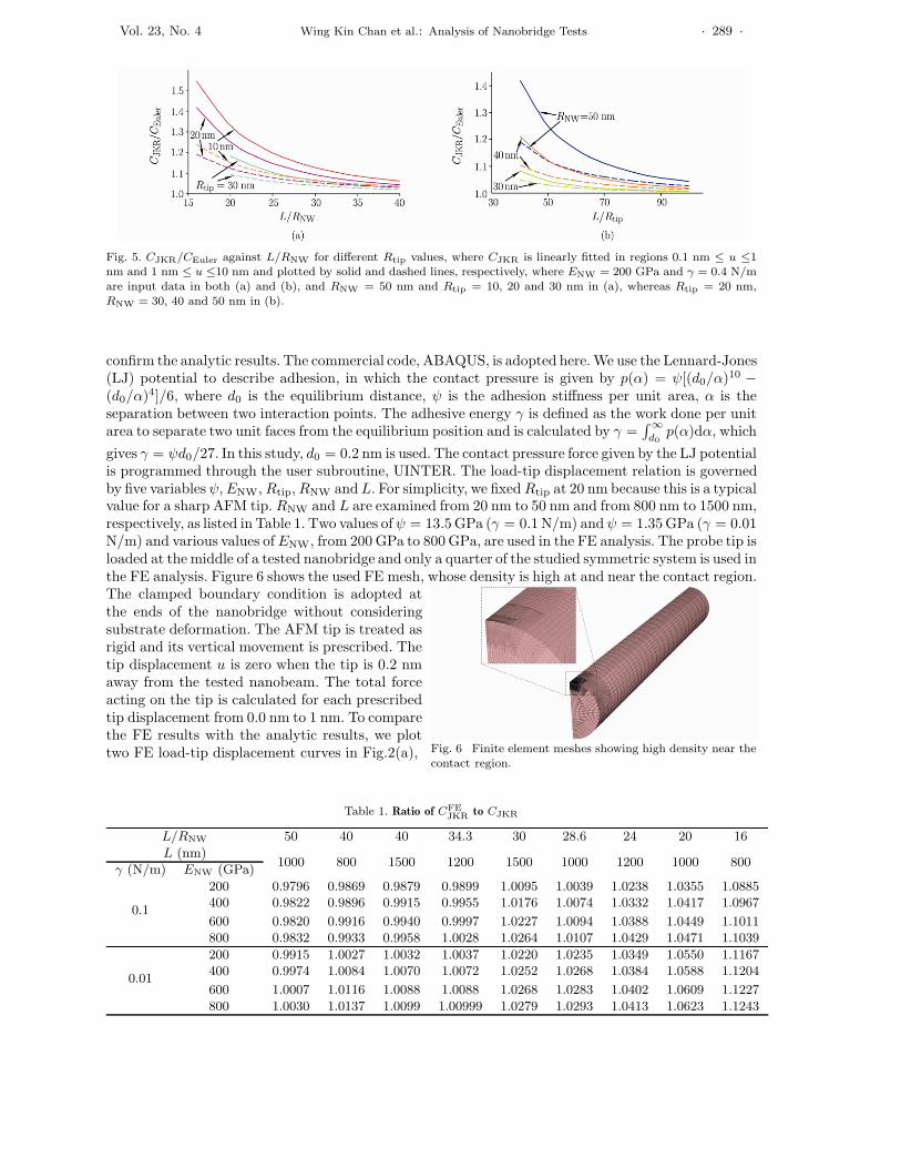
gives γ = ψd0/27. In this study, d0 = 0.2 nm is used. The contact pressure force given by the LJ potentialis programmed through the user subroutine, UINTER. The load-tip displacement relation is governedby five variablesψ,ENW,Rtip,RNW andL. For simplicity, we fixedRtip at 20 nm because this is a typicalvalue for a sharp AFM tip. RNW and L are examined from 20 nm to 50 nm and from 800 nm to 1500 nm,respectively, as listed in Table 1. Two values ofψ = 13.5 GPa (γ = 0.1 N/m) andψ = 1.35 GPa (γ = 0.01N/m) and various values ofENW, from 200 GPa to 800 GPa, are used in the FE analysis. The probe tip isloaded at the middle of a tested nanobridge and only a quarter of the studied symmetric system is used inthe FE analysis. Figure 6 shows the used FE mesh, whose density is high at and near the contact region.The clamped boundary condition is adopted atthe ends of the nanobridge without consideringsubstrate deformation. The AFM tip is treated asrigid and its vertical movement is prescribed. Thetip displacement u is zero when the tip is 0.2 nmaway from the tested nanobeam. The total forceacting on the tip is calculated for each prescribedtip displacement from 0.0 nm to 1 nm. To comparethe FE results with the analytic results, we plottwo FE load-tip displacement curves in Fig.2(a), Fig. 6 Finite element meshes showing high density near the
contact region.
Table 1. Ratio of CFEJKR
to CJKR
L/RNW 50 40 40 34.3 30 28.6 24 20 16
L (nm)γ (N/m) ENW (GPa)
1000 800 1500 1200 1500 1000 1200 1000 800
200 0.9796 0.9869 0.9879 0.9899 1.0095 1.0039 1.0238 1.0355 1.0885
0.1400 0.9822 0.9896 0.9915 0.9955 1.0176 1.0074 1.0332 1.0417 1.0967
600 0.9820 0.9916 0.9940 0.9997 1.0227 1.0094 1.0388 1.0449 1.1011800 0.9832 0.9933 0.9958 1.0028 1.0264 1.0107 1.0429 1.0471 1.1039
200 0.9915 1.0027 1.0032 1.0037 1.0220 1.0235 1.0349 1.0550 1.1167
0.01400 0.9974 1.0084 1.0070 1.0072 1.0252 1.0268 1.0384 1.0588 1.1204
600 1.0007 1.0116 1.0088 1.0088 1.0268 1.0283 1.0402 1.0609 1.1227800 1.0030 1.0137 1.0099 1.00999 1.0279 1.0293 1.0413 1.0623 1.1243

· 290 · ACTA MECHANICA SOLIDA SINICA 2010
showing that the FE results are close to the analytical results. Again, the average total compliance iscalculated from linear fitting of u vs. P curve in the region 0.1 nm ≤ u ≤ 1 nm. The FE results showthat the dependence of the FE compliance CFE
JKR, on parameters ψ (γ), ENW, Rtip, RNW and L are allcorrespondingly the same as the dependence of the analytic compliance CJKR. Table 1 lists the ratio ofCFE
JKR to CJKR, indicating that the difference between them is below 6.3% except for the L/RNW = 16case, in which the shear deformation is noticeable and has an effect on CFE
JKR. The good agreementbetween the FE results and the analytic results verifies the analytic study.
2.4. Contact Spring Compliance
Since adhesion contact deformation makes the probe tip displacement larger in the nanobridge test,we may model it as an additional spring attached between the probe tip and the tested nanobeam, asillustrated in Fig.1(b), and the spring compliance for adhesion contact Cac is calculated from
Cac = CJKR − CEuler (18)
Based on the dimension analysis, we deduce an expression for adhesive contact compliance as
Cac =A
ENWRNW
(ENWRNW
γ
)m
·
(RNW
Rtip
)n
·
(L
RNW
)p
·
(RNW
umax
)q
(19a)
or
Cac =κac(ENW)
ENW(19b)
where A, m, n, p, and q are fitting parameters and umax is the upper limit of the tip displacement inthe fitting region. Note that κac might still be a weak function of ENW. To determine the values ofA, m, n, p and q, we compute as many values of Cac as possible with various values of ENW, RNW,Rtip, L and γ, and for different values of umax. The analytical approach is adopted here because of itsanalytic nature. Thus, Rtip = 10, 20, 30 and 40 nm; RNW = 20, 30, 40 and 50 nm; L = 800, 1000, 1200,1400, 1600, 1800 and 2000 nm; ENW = 200, 400, 600, 800 and 1000 GPa; γ = 0.1, 0.4 and 1 N/m;d0 = 0.2 nm; and the tip displacement regions from u = 1 nm to umax = 5, 10 and 20 nm are used inthe computation, which leads to 5040 combinations. Fitting the 5040 cases gives
κac =
(0.1538
RNW
)(ENWRNW
γ
)0.0818 (RNW
Rtip
)0.3489(L
RNW
)0.7422(RNW
umax
)0.2549
(19c)
with correlation coefficient 0.90.Similarly, we calculate the total compliance of the nanobeam including Hertz contact CHertz. The
spring compliance for the Hertz contact Chc is calculated from
Chc = CHertz − CEuler (20)
The adhesive surface energy per unit area γ is not involved in Hertz contact so that the dimensionanalysis result is reduced to
Chc =A
ENWRNW·
(RNW
Rtip
)n
·
(L
RNW
)p
·
(RNW
umax
)q
(21a)
Chc =κhc
ENW(21b)
Then, fitting the numerical results calculated from the analytic approach with the same parameters asmentioned above for the JKR contact, we have
κhc =
(0.1814
RNW
)(RNW
Rtip
)0.2781(L
RNW
)0.9566(RNW
umax
)0.3230
(21c)
Equations (19) and (21) allow us to estimate the additional compliances induced by adhesive contactand Hertz contact, respectively.
Vol. 23, No. 4 Wing Kin Chan et al.: Analysis of Nanobridge Tests · 291 ·
III. SUBSTRATE DEFORMATION IN NANOBRIDGE TESTSZhang et al. developed a theoretical approach to include substrate deformation into the bending
analysis for microbridge tests under large deformation[15,16,27] and for microcantilever tests[16,27]. Undersmall deformation, longitudinal stretching can be ignored and thus the number of coupled springsis reduced to two, which correspond to the rotational and vertical displacement, respectively. Theconstitutive equation of the two coupled springs is thus given by[14,16,28]:{
δθ
}=
[SQQ SQM
SMQ SMM
]{QM
}(22)
where Sij (i, j = Q, M) represent the substrate compliances reflecting the substrate deformation undera unit load and/or a moment; Q and M are the vertical load and moment, respectively, and δ and θare the vertical displacement and rotation angle of the substrate, respectively, at the joint location ofsubstrate with a tested nanowire. Based on the Betti-Rayleigh reciprocal theorem, SQM is equal toSMQ. Incorporating substrate deformation into the boundary conditions at nanobridge ends, we derivethe total compliance for an Euler beam with substrate deformation as
CSD =L3
48ENWI−
[SMQ − l2/(8EtI)]
2
2[SMM + l/(2EtI)]+SQQ
2(23)
The substrate compliances Sij are calculated out from FE analysis. In general, the substrate compliancesSij are the function of Young’s modulus ENW and Poisson’s ratio νNW of a tested nanobeam, Young’smodulusES and Poisson’s ratio νS of substrate and nanowire radiusRNW. In the present work, νNW andνS are assumed to be constants, independent of RNW. Based on dimensional analysis, we can expressSij as
SMM =aMM
ES (RNW)3
(ENW
ES
)bMM
, SQQ =aQQ
ESRNW
(ENW
ES
)bQQ
, SMQ =aMQ
ES (RNW)2
(ENW
ES
)bMQ
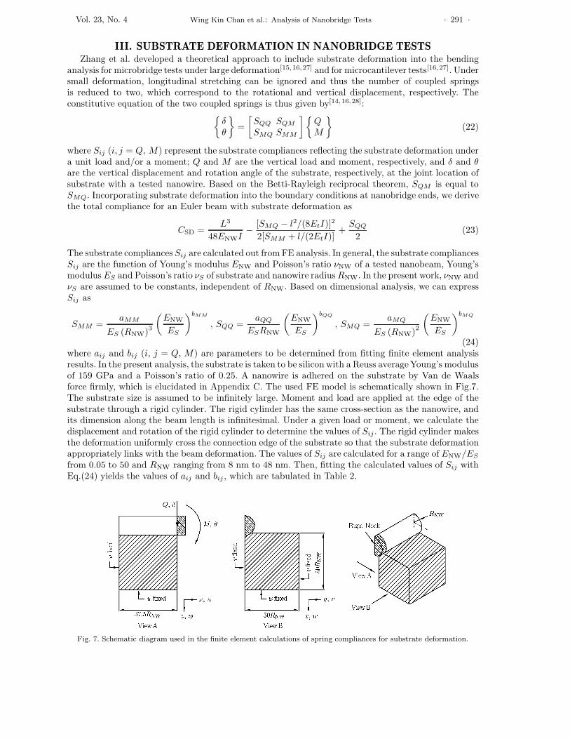
(24)where aij and bij (i, j = Q, M) are parameters to be determined from fitting finite element analysisresults. In the present analysis, the substrate is taken to be silicon with a Reuss average Young’s modulusof 159 GPa and a Poisson’s ratio of 0.25. A nanowire is adhered on the substrate by Van de Waalsforce firmly, which is elucidated in Appendix C. The used FE model is schematically shown in Fig.7.The substrate size is assumed to be infinitely large. Moment and load are applied at the edge of thesubstrate through a rigid cylinder. The rigid cylinder has the same cross-section as the nanowire, andits dimension along the beam length is infinitesimal. Under a given load or moment, we calculate thedisplacement and rotation of the rigid cylinder to determine the values of Sij . The rigid cylinder makesthe deformation uniformly cross the connection edge of the substrate so that the substrate deformationappropriately links with the beam deformation. The values of Sij are calculated for a range of ENW/ES
from 0.05 to 50 and RNW ranging from 8 nm to 48 nm. Then, fitting the calculated values of Sij withEq.(24) yields the values of aij and bij , which are tabulated in Table 2.
Fig. 7. Schematic diagram used in the finite element calculations of spring compliances for substrate deformation.

· 292 · ACTA MECHANICA SOLIDA SINICA 2010
Table 2. Empirical parameters for the spring compliances, Sij
SMM SQQ SMQ
aij 1.25 3.36 0.74bij −0.729 −0.300 −0.294
After examining the value of CSD for a range of L, RNW and ENW, we found that SMM plays themost important role in substrate deformation. Thus, simplifying Eq.(23) by taking SQQ = SMQ = 0,we have
C∗SD =L3
48ENWI−
L4
64ENWI(2SMMENWI + L)(25a)
or
C∗SD =κSD(ENW)
ENW(25b)
Note that κSD is still a function of ENW.
IV. SIZE-DEPENDENT APPARENT YOUNG’S MODULUSDuring the nanobridge test, adhesive contact deformation and substrate deformation occur simul-
taneously. Thus, the total compliance should be
C∗SD + Cac =κSD + κac
ENW(26)
Equation (26) paves the way for us to calculate a correct value of ENW in the nanobridge test. LettingE′NW denote the apparentYoung’s modulus evaluated from total compliance by using Eq.(1), we calculatethe ratio of E′NW to ENW
E′NW
ENW=
κEuler
κSD + κac(27)
As described above, the effects of adhesive con-tact deformation and substrate deformation onthe apparent Young’s modulus relate to the di-ameter of tested nanowires. For a given length,the larger the diameter is, the greater the effectswill be. Therefore, adhesive contact deformationand substrate deformation lead to size-dependentapparent Young’s modulus. To illustrate the size-dependent apparent Young’s modulus, we plot theratio E′NW/ENW vs. nanowire diameter RNW inFig.8, where the used data are Eb = 473 GPa,Rtip = 20 nm, γ = 0.4 N/m and L = 1000 nm.
Fig. 8 Intrinsic effect and extrinsic effect as a function of thenanowire radius, where Eb = 473 GPa, Rtip = 20 nm, andL = 1000 nm.
We take the Young’s modulus of SiC in the 〈111〉 directions, Eb = 473 GPa, which is independent ofthe nanowire diameter, as an example to illustrate the size-dependent Young’s modulus. As shown bythe solid curve in Fig.8, adhesive contact deformation and substrate deformation make the apparentYoung’s modulus smaller and the ratio E′NW/ENW decrease almost linearly with the increase of thediameter RNW. The results might explain the experimental results that the Young’s modulus of ananowire measured by the nanobridge test is smaller than that of its bulk counterpart, as is describedin the Introduction.
Many researchers[29–32] suggest that surface elastic constants are intrinsic properties of nanowiresthat make the apparent Young’s modulus of nanowires size-dependent. Zhang et al.[30] proposed afundamental energy-based mechanics approach for the study of surface-related intrinsic effects on size-dependent Young’s modulus. In the energy-based mechanics approach, a nanowire is treated as acomposite of a bulk core and surfaces (including edges). Let Eb and cs be Young’s moduli of the coreand surfaces, respectively, the bending stiffness D of a nanowire is given by
D = EbI + csIs (28)

Vol. 23, No. 4 Wing Kin Chan et al.: Analysis of Nanobridge Tests · 293 ·
where Is is the second moment of lines and Is = π (RNW)3 for circular section nanowires[31]. Theapparent Young’s modulus E is calculated byD/I. Without considering the extrinsic effect, E increases(or decreases) for a positive (or negative) cs, as the diameter decreases. For either a positive or negativecs, E approaches Eb when the diameter becomes sufficiently large. In nanobridge tests, intrinsic andextrinsic effects co-exist. Considering the surface-related intrinsic effect, we may replace ENW in theabove analysis with E because E is the bending equivalent Young’s modulus. Let Eex denote themeasured Young’s modulus by using Eq.(1). The normalized Eex/Eb is plotted in Fig.8 for differentvalues of cs. As expected, the curve with cs = 0, meaning there is no surface-related intrinsic effect,separates the curves for cs > 0 from those for cs < 0. For a negative cs, the value of Eex/Eb increasesfrom a lower value to a maximum, which is still smaller than unity, and then decreases as the nanowireradius increases. For a positive cs, however, the nanowire exhibits the-smaller-the-harder behavior,but approaches a value lower than the bulk one due to the extrinsic effects, which might explain theexperimental results[7,11,12].
V. CONCLUDING REMARKSIn nanomechanics, a crucial and challenging issue is the size-dependent apparent Young’s modulus.
In the present work, we separate factors that cause size-dependent apparent Young’s modulus into twocategories, intrinsic and extrinsic factors. The extrinsic factors are also called extrinsic deformations here,which include adhesion contact deformation and substrate deformation. Extrinsic deformations occurduring nanobridge tests, which are, however, often ignored in the literature when Young’s modulusof a nanowire is characterized by the nanobridge test. The present work studies systematically therole of extrinsic deformations in the nanobridge test and the results show that the apparent Young’smodulus measured without consideration of the extrinsic deformations is lower than the real value.The apparent Young’s modulus might also exhibit the-smaller-the-harder behavior, but the values ofapparent Young’s modulus of nanowires with larger diameters are smaller than the Young’s modulus ofthe bulk counterpart. Excluding extrinsic factors is the essential step to explore intrinsic size-dependentYoung’s modulus in nanomaterials.
In the present work, adhesive contact deformation is analyzed based on the JKR model and adhesivecontact-induced compliance is modeled by a spring connecting a probe tip and a tested nanobeam.Under small deflection, the bending deformation of the tested nanobeam is linear, but adhesive contactdeformation is nonlinear. Analytical solution is presented here and verified by the FE analysis. Thedeveloped analytic approach is powerful in solving adhesion-bending coupling problems. However, theanalytic solution is complex due to the nonlinear deformation of adhesion contact. To be user-friendly,the present work provides two empirical equations based on the analytic solution. The two empiricalequations give general expression of adhesion contact compliance and Hertz contact compliance, whichare both valid for the maximum tip displacement up to around 20 nm. Following the previous work[14,16],the substrate deformation is modeled by two coupled springs connecting to each of the nanobeam ends tothe substrate. The spring compliances are calculated for silicon substrate and presented in a generalizedexpression for a large range of nanobeam diameters. In this way, the explicit results presented here allowone to exclude the extrinsic factors and determine Young’s modulus of a nanowire from the nanobridgetest more accurately. The approach developed here can be directly applied to the adhesion-bendingproblem in nanocantilever tests.
References[1] Xia,Y.N., Yang,P.D., Sun,Y.G., Wu,Y.Y., Mayers,B., Gates,B., Yin,Y.D., Kim,F. and Yan,Y.Q., One-
dimensional nanostructures: Synthesis, characterization and applications. Advanced Materials, 2003, 15(5):353-389.
[2] Salvetat,J.P., Briggs,G.A.D., Bonard,J.M., Bacsa,R.R., Kulik,A.J., Stockli,T., Burnham,N.A. and Forro,L.,Elastic and shear moduli of single-walled carbon nanotube ropes. Physical Review Letters, 1999, 82(5): 944-947.
[3] Cuenot,S., Demoustier-Champagne,S. and Nysten,B., Elastic modulus of polypyrrole nanotubes. Physical
Review Letters, 2000, 85(8): 1690-1693.[4] Kis,A., Kasas,S., Babic,B., Kulik,A.J., Benoit,W., Briggs,G.A.D., Schonenberger,C., Catsicas,S. and
Forro,L., Nanomechanics of microtubules. Physical Review Letters, 2002, 89(24): 248101.

· 294 · ACTA MECHANICA SOLIDA SINICA 2010
[5] Wu,B., Heidelberg,A. and Boland,J.J., Mechanical properties of ultrahigh-strength gold nanowires. Nature
Materials, 2005, 4: 525-529.
[6] Xiong,Q.H., Duarte,N., Tadigadapa,S. and Eklund,P.C., Force-deflection spectroscopy: A new method todetermine the Young’s modulus of nanofilaments. Nano Letters, 2006, 6(9): 1904-1909.
[7] Jing,G.Y., Duan,H.L., Sun,X.M., Zhang,Z.S., Xu,J., Li,Y.D., Wang,J.X. and Yu,D.P., Surface effects onelastic properties of silver nanowires: Contact atomic-force microscopy. Physical Review B, 2006, 73(23):235409.
[8] Ni,H., Li,X.D., Cheng,G.S. and Klie,R., Elastic modulus of single-crystal GaN nanowires. Journal of Ma-
terials Research, 2006, 21(11): 2882-2887.
[9] Chen,Y.X., Dorgan,B.L., McIlroy,D.N. and Aston,D.E., On the importance of boundary conditions onnanomechanical bending behavior and elastic modulus determination of silver nanowires. Journal of Applied
Physics, 2006, 100(10): 104301.
[10] Ni,H. and Li,X.D., Young’s modulus of ZnO nanobelts measured using atomic force microscopy and nanoin-dentation techniques. Nanotechnology, 2006, 17(14): 3591-3597.
[11] Chen, Y.X., Stevenson, I., Pouy, R., Wang, L.D., McIlroy, D.N., Pounds, T., Norton, M.G. and Aston, D.E.,Mechanical elasticity of vapour-liquid-solid grown GaN nanowires. Nanotechnology, 2007, 18(13): 135708.
[12] Varghese,B., Zhang,Y.S., Dai,L., Tan,V.B.C., Lim,C.T. and Sow,C.H., Structure-Mechanical property ofindividual cobalt oxide nanowires. Nano Letters, 2008, 8(10): 3226-3232.
[13] Manoharan,M.P., Desai,A.V., Neely,G. and Haque,M.A., Synthesis and elastic characterization of zinc oxidenanowires. Journal of Nanomaterials, 2008: 849745.
[14] Huang,H.Y., Li,Z.Y., Lu,J.Y., Wang,Z.J., Wang,C.S., Lau,K.M., Chen,K.J. and Zhang,T.Y., Microbridgetests on gallium nitride thin films. Journal of Micromechanics and Microengineering, 2009, 19(9): 095019.
[15] Zhang,T.Y., Su,Y.J., Qian,C.F., Zhao,M.H. and Chen,L.Q., Microbridge testing of silicon nitride thin filmsdeposited on silicon wafers. Acta Materialia, 2000, 48(11): 2843-2857.
[16] Zhang,T.Y., Microbridge tests. In: Micro and Nano Mechanical Testing of Materials and Devices, Yang,F.Q.and Li,J.C.M. Editors. Springer Science+Business Media, LLC. 2008: 215-285.
[17] Gao,H.J. and Yao,H.M., Shape insensitive optimal adhesion of nanoscale fibrillar structures. Proceedings
of the National Academy of Sciences of the United States of America, 2004, 101(21): 7851-7856.[18] Sirghi,L. and Rossi,F., Adhesion and elasticity in nanoscale indentation. Applied Physics Letters, 2006,
89(24): 243118.
[19] Johnson,K.L., Kendall,K. and Roberts,A.D., Surface energy and the contact of elastic solids. Proceedings
of the Royal Society of London. Series A, Mathematical and Physical Sciences, 1971, 324(1558): 301-313.
[20] Derjaguin,B.V., Muller,V.M. and Toporov,Y.P., Effect of contact deformations on adhesion of particles.Journal of Colloid and Interface Science, 1975, 53(2): 314-326.
[21] Maugis, D., Adhesion of spheres — The JKR-DMT transition using a Dugdale model. Journal of Colloid
and Interface Science, 1992, 150(1): 243-269.
[22] Baker,S.P. and Nix,W.D., Mechanical properties of compositionally modulated Au-Ni Thin-films - Nanoin-dentation and Microcantilever deflection experiments. Journal of Materials Research, 1994, 9(12): 3131-3145.
[23] Wong,E.W., Sheehan,P.E. and Lieber,C.M., Nanobeam mechanics: Elasticity, strength and toughness ofnanorods and nanotubes. Science, 1997, 277(5334): 1971-1975.
[24] Zeng,D.J. and Zheng,Q.S., Resonant frequency-based method for measuring the Young’s moduli ofnanowires. Physical Review B, 2007, 76(7): 075417.
[25] Zhou,P., Wu,C.W. and Li,X.D., Three-point bending Young’s modulus of nanowires. Measurement Science
& Technology, 2008, 19(11): 115703-115707.[26] Johnson,K.L., Contact Mechanics. Cambridge: Cambridge University Press, 1985.
[27] Zhang,T.Y., Zhao,M.H. and Qian,C.F., Effect of substrate deformation on the microcantilever beam-bending test. Journal of Materials Research, 2000, 15(9): 1868-1871.
[28] Xu,W.H. and Zhang,T.Y., Mechanical characterization of trilayer thin films by the microbridge testingmethod. Applied Physics Letters, 2003, 83(9): 1731-1733.
[29] Cuenot,S., Fretigny,C., Demoustier-Champagne,S. and Nysten,B., Surface tension effect on the mechanicalproperties of nanomaterials measured by atomic force microscopy. Physical Review B, 2004, 69(16): 165410.
[30] Zhang,T.Y., Luo,M. and Chan,W.K., Size-dependent surface stress, surface stiffness and Young’s modulusof hexagonal prism [111] beta-SiC nanowires. Journal of Applied Physics, 2008, 103(10): 104308.
[31] Chan,W.K., Luo,M. and Zhang,T.Y., Molecular dynamics simulations of four-point bending tests on SiCnanowires. Scripta Materialia, 2008, 59(7): 692-695.
[32] Zhang,T.Y., Wang,Z.J. and Chan,W.K., Eigenstress model for surface stress of solids. Physical Review B,2010, 81(19): 195427.

Vol. 23, No. 4 Wing Kin Chan et al.: Analysis of Nanobridge Tests · 295 ·
APPENDIX A: ANALYTICAL SOLUTION OF
HERTZ CONTACT WITH ELLIPTICAL CONTACT AREAIn Hertz contact, two surfaces in contact are frictionless and only normal force is interacted between
two bodies. In this case, Eq.(2) is reduced to
p(x, y) = p1
[1−
(xa
)2
−(yb
)2]1/2
(29)
This pressure field produces a displacement field:
uz =p1b
E∗
[K(e)−
K(e)− E(e)
e2a2x2 −
E(e)/(1− e2)−K(e)
e2a2y2
](30)
Substituting Eq.(9b) into Eq.(30) and letting x = y = 0, we have the tip displacement
δ =e2a2K(e)
2R′[K(e)− E(e)](31)
Then, the total force is calculated to be
P =e2a3E∗π2
3R′[K(e)− E(e)](32)
Substituting Eqs.(31) and (32) into the tip displacement u = C · P + δ yields
u =2CE∗π2e2a3 + 3K(e)e2a2
6R′ [K(e)− E(e)](33)
Equations (33) and (32) give the relations among u, a and P .When the tip is loaded on a nanowire with a rectangular or polygonal cross-section, the contact area
will be circular. For circular Hertz contact, the eccentricity is zero and both elliptical integrals have avalue of π/2. Then, Eqs.(32) and (33) are respectively reduced to
P =4πa3E∗
3Rtip(34)
u =a2(4CE∗πa+ 3)
3Rtip(35)
APPENDIX B: ANALYTICAL SOLUTION OF
ADHESION CONTACT WITH CIRCULAR CONTACT AREAFor circular adhesion contact, the deformation is axisymmetric and local cylindrical coordinates, r
and θ, are used here. The vertical displacement for circular adhesion contact is given by
uz = δ
(1−
r2
2hRtip
)(36)
The adhesion contact pressure field is expressed as
p = p0
(1−
r2
a2
)−1/2
+ p1
(1−
r2
a2
)1/2
(37)
where a is the circular radius of contact. The contact pressure reproduces a local displacement field
uz =πa
E∗
[p0 +
p1
2
(1−
r2
2a2
)](38)

· 296 · ACTA MECHANICA SOLIDA SINICA 2010
Comparing Eq.(36) and Eq.(38), we have
p0 =E∗
π
(δ
a−
a
Rtip
)(39)
p1 =E∗
π·
2a
Rtip(40)
By integrating the contact pressure over the contact area, we obtain the total force
P =
∫ a
0
σ · 2πrdr =2a(3δRtip − a
2)E∗
3Rtip(41)
with Eq.(41) and u = C · P + δ, we express P and δ in terms of u and a, respectively, as
P =2E∗a(3Rtipu− a
2)
3Rtip(1 + 2aE∗C)(42)
δ =3Rtipu+ 2a3E∗C
3Rtip(1 + 2aE∗C)(43)
The elastic strain energy only due to adhesion contact is calculated by
Uel =
∫p(r)uzdxdy = E∗
(δ2a−
2
3
δa3
Rtip+
1
5
a5
R2tip
)(44)
Equations (41)-(44) can be deduced from Eqs.(10)-(13), respectively, as the eccentricity e approacheszero. The total energy is then given by
Utotal = E∗
(δ2a−
2
3
δa3
Rtip+
1
5
a5
R2tip
)+CP 2
2− γπa2 (45)
Using Eq.(17a), we have
9E∗R2tipu
2 − a(18γπR2tip)− a
2(72γπR2tipE
∗C + 18E∗Rtipu)
−a3(72γπR2tipE
∗2C2 + 24E∗2CRtipu) + 9a4E∗ + 24E∗2a5C + 16E∗3C2a6 = 0 (46)
which yields
u =a2
Rtip+
4E∗Ca3
3Rtip±
√8γπa2C(1 + aE∗C) +
2γπa
E∗(47a)
If there is no bending deformation, the bending compliance is null, i.e., C = 0. In this case, thedisplacement is induced completely by adhesion contact and Eq.(47a) is reduced to
u =a2
Rtip±
√2γπa
E∗(47b)
which is that given by the JKR theory[19,26].
APPENDIX C: ADHESION BETWEEN A NANOWIRE AND ITS SUBSTRATEThe lateral contact length l of a nanowire on its substrate may be described by an adhesion angle
φ as shown in Fig.9. The vertical distance of thecylindrical surface of the nanowire to the substratesurface is given by h(φ) = h0 + RNW(1 − cosφ).The total force acting on the cylinder is calculatedby using the Lennard-Jones (LJ) potential and h0
is determined by force equilibrium. The contact isassumed to be lost when the adhesive pressure issmaller than one tenth of its maximum. ForRNW =16, 32, 48 and 96 nm, we calculated the contactangles to be 16◦, 11◦, 9◦ and 6◦, respectively. Finiteelement analysis verifies the analysis results.
Fig. 9 The lateral contact length l and adhesion angle φ be-tween a nanowire and the supported substrate.